High-speed, multi-channel detector readout electronics … · Final Report for DOE Grant DE ... In...
36
High-speed, multi-channel detector readout electronics for fast radiation detectors Final Report for DOE Grant DE-FG02-08ER84981 Grant Recipient XIA LLC Principal Investigator Wolfgang Hennig Date of Report 1/31/2012 Period Covered 8/14/2009 through 8/14/2011 For Distribution This document contains no proprietary technical information and can be made available to individuals involved the administering and reviewing of DOE grant DE-FG02-08ER84981 as well as the general public. DE-FG02-08ER84981
Transcript of High-speed, multi-channel detector readout electronics … · Final Report for DOE Grant DE ... In...

High-speed, multi-channel detector readout electronics for fast radiation detectors
Final Report for DOE Grant DE-FG02-08ER84981
Grant Recipient XIA LLC Principal Investigator Wolfgang Hennig Date of Report 1/31/2012 Period Covered 8/14/2009 through 8/14/2011
For Distribution This document contains no proprietary technical information and can be made available to individuals involved the administering and reviewing of DOE grant DE-FG02-08ER84981 as well as the general public.
DE-FG02-08ER84981

Final Executive Summary (June 2012)
This final report is a combination of progress reports submitted previously. It was originally submitted 01/31/2012, and is now resubmitted with the SBIR/STTR rights notice.
In this project, we had the following 5 Objectives:
Objective 1: Improvements and further evaluation of P500:
Objective 2: Develop Pixie-500 Express hardware:
Objective 3: Develop firmware for Pixie-500 Express:
Objective 4: Adapt existing host software and user interface for Pixie-500 Express and Pixie-500:
Objective 5: Performance testing of Pixie-500 and Pixie-500 Express:
Overall, due to the unanticipated complexity of the PCI Express interface, some aspects of the project could not be completed with the time and funds available in Phase II. These aspects include the high throughput “zero dead time” firmware in Objective 3 (only the basic firmware has been implemented), final integration of the user interface in Objective 4, and final testing of the Pixie-500 Express in Objective 5.These aspects will be completed in self-funded Phase III; in fact, at time of writing the user interface (task 6 and 7) is essentially complete. Production and release of commercial spectrometer modules are planned for the end of 2012.
On the other hand, as the project was set up to first develop a simple demonstration prototype (P500) and then work on advanced features, we were able to turn the P500 into a commercial module (Pixie-500) and use the key developments to upgrade the another product (Pixie-16/250). These commercial developments, entirely funded by XIA, resulted in sales of several hundred thousand dollars (by the end of 2011) from products related to this project. Already therefore the project can be considered a success commercially.

High-speed, multi-channel detector readout electronics for fast radiation detectors
3rd Progress Report for DOE Grant DE-FG02-08ER84981
Grant Recipient XIA LLC Principal Investigator Wolfgang Hennig Date of Report 11/30/2011 Period Covered 12/14/2010 through 8/14/2011
For Distribution This document contains no proprietary technical information and can be made available to individuals involved the administering and reviewing of DOE grant DE-FG02-08ER84981 as well as the general public.

Final report: High-speed, multi-channel detector readout electronics for fast radiation detectors
© XIA LLC 4 6/22/2012
Table of Contents 1. Introduction ..................................................................................................................................................5 2. Status of Technical Objectives And Tasks ...................................................................................................6 2.1. Task 1 (Objective 1): Implement Online Processing And Investigate Noise And Non-linearity In P500....7 2.2. Task 2 (Objective 1): Implement Clock/trigger Distribution For P500 And Characterize Timing
Between Channels And Modules..................................................................................................................7 2.3. Task 3 (Objective 2): Develop Hardware Design Concept For Pixie-500....................................................7 2.4. Task 4 (Objective 2): Hardware Design Entry And Production ...................................................................8 2.5. Task 5 (Objective 3): Firmware Development .............................................................................................9 2.6. Task 6 (Objective 4): Host Software Development ......................................................................................9 2.7. Task 7 (Objective 5): Test And Debug Hardware, Firmware, And Software For Pixie-500......................10 2.8. Task 8 (Objective 5): Performance Testing ................................................................................................10 2.9. Other Developments ...................................................................................................................................11 3. Cost Status ..................................................................................................................................................11 4. Summary of Performance Schedule............................................................................................................12 5. Personnel Changes......................................................................................................................................12 6. Attachments ................................................................................................................................................13

1. Introduction This report summarizes the progress made on DOE grant DE-FG02-08ER84981, “High-speed, multi-channel
detector readout electronics for fast radiation detectors” in the period from 12/14/2010 through 8/14/2011, i.e. from the second progress report (4 months year 2 funding notice) the end of the project. In this project, we are developing a high speed digital spectrometer that
a) captures detector waveforms at rates up to 500 MSPS
b) has upgraded event data acquisition with additional data buffers for “zero dead time” operation
c) moves energy calculations to the FPGA to increase spectrometer throughput in fast scintillator applications
d) uses a streamlined architecture and high speed data interface for even faster readout to the host PC
These features are in addition to the standard functions in our existing spectrometers such as digitization, programmable trigger and energy filters, pileup inspection, data acquisition with energy and time stamps, MCA histograms, and run statistics. In Phase I, we upgraded one of our existing spectrometer designs to demonstrate the key principle of fast waveform capture using a 500 MSPS, 12 bit ADC and a Xilinx Virtex-4 FPGA. This upgraded spectrometer, named P500, performed well in initial tests of energy resolution, pulse shape analysis, and timing measurements, thus achieving item (a) above.
In Phase II, we are revising the P500 to build a commercial prototype with the improvements listed in items (b)-(d). As described in the previous report, two devices were built to pursue this goal, named the “Pixie-500” and the “Pixie-500 Express”. The Pixie-500 has only minor improvements from the Phase I prototype and is intended as an early commercial product (its production and part of its development were funded outside the SBIR). It also allows testing of the ADC performance in real applications. The Pixie-500 Express (or Pixie-500e) includes all of the improvements (b)-(d). The Phase II work comprises 5 Objectives:
Objective 1: Improvements and further evaluation of P500: Implement online processing and clock/trigger distribution between channels and modules. Investigate noise characteristics in analog sections and eliminate excess noise sources. Explore compensation for non-linearities. Characterize improvements in energy resolution, timing resolution, and linearity.
Objective 2: Develop Pixie-500 Express hardware: Combine features tested on the P500 with a SHARC DSP, a PCIe host interface, and upgrades in data flow and processing architecture. Allow board variant with 14 bit, 400 MSPS ADC and monitor manufactures’ release of improved fast ADCs. Draw design schematic and layout printed circuit boards, produce small batch of boards.
Objective 3: Develop firmware for Pixie-500 Express: Adapt P500 firmware to hardware upgrades; later improve for higher throughput and reduced dead time.
Objective 4: Adapt existing host software and user interface for Pixie-500 Express and Pixie-500: Adapt the Pixie-4 C library to the PCIe interface and the 32bit variables used in the SHARC DSP. Update existing Pixie-4 user interface accordingly and develop sample open source interface using ROOT as a starting point for user’s system integration.
Objective 5: Performance testing of Pixie-500 and Pixie-500 Express: test and debug hardware, firmware and software, then characterize performance in house and in labs of potential users.
Progress for each objective is described in section 3, divided into tasks as defined in the Phase II proposal.

2. Status of Technical Objectives And Tasks
Executive Summary
Fig. 1: Overview of the Pixie hardware, software and firmware developments. Fields in green are
completed new developments in this project, Fields in red are new developments that are not yet fully completed (about 80% done).
In months 17-24 of the project, we tested and debugged the hardware, firmware and software of the Pixie-500 Express prototype boards delivered 12/3/2010. This proved substantially more complex than anticipated. At the time
Igor GUI
LabView ROOT Sample.exe
C lib
glue glue glue glue
Common C library (specific functions for file download, time constants)
PCI interface (PLX) PCIe interface (gennum)
Pixie-4 and Pixie-500 System FPGA
Pixie-500e “system functions” (import from Pixie-4, add SDRAM, PCIe I/O)
System
Pixie-4 and Pixie-500 DSP code with compiler switches
Pixie-500e DSP code (import from Pixie-4/-16) DSP
Pixie-4 Fippi Schematic
Fippi Pixie-500 Fippi and Pixie-500e “Fippi functions” Verilog
Pixie-4 Module Pixie-500 Pixie-500e
of writing, all hardware bugs have been fixed, the PCI Express interface is working, the SDRAM has been successfully tested and the SHARC DSP has been booted with preliminary code. All new ICs and circuitry on the prototype are working properly, however some of the planned firmware and software functions have not yet been completely implemented and debugged. This effort will continue in self-funded Phase III.
We continued to test the performance of the Pixie-500 with new detectors and sources. (Since the front end digitization and pulse processing is the same on Pixie-500 and Pixie-500 Express, the test results also apply to the Pixie-500 Express.) These tests include additional measurements involving timing of ultra short neutron bursts in cooperation with AASC, published at the 11th International Conference on Applications of Nuclear Techniques (Crete 11), and loans of Pixie-500 systems to ORNL, the University of Michigan and Rensselaer Polytechnic Institute. Results of the Michigan tests have been presented at the 2011 IEEE Nuclear Science Symposium.
Following the evaluation at ORNL, it became clear that a lower cost high speed spectrometer is desirable for applications with large numbers of channels. Outside the scope of this project, but based on the experience of developing the Pixie-500, we therefore developed a high speed version of our Pixie-16 spectrometer
Overall, due to the unanticipated complexity of the PCI Express interface, some aspects of the project could not be completed with the time and funds available in Phase II. These aspects will be completed in self-funded Phase III. On the other hand, by dividing development efforts into one branch focused on immediate sales and a second branch focused on more advanced improvements, we were able to already make sales of several hundred thousand dollars (by the end of 2011) from products related to this project.
2.1. Task 1 (Objective 1): Implement Online Processing And Investigate Noise And Non-linearity In P500
Original Schedule: Months 1 – 3
Goals: Implement online processing, investigate/eliminate noise and nonlinearity, consider implementation of nonlinearity compensation scheme, optionally test 14-bit 400 MSPS footprint compatible ADC
Percent Completed @ month 24: 100%
Status: No changes since month 9. See previous report
2.2. Task 2 (Objective 1): Implement Clock/trigger Distribution For P500 And Characterize Timing Between Channels And Modules
Original Schedule: Months 4 – 6
Goals: Implement clock and trigger distribution in firmware, characterize timing resolutions between channels and modules, explore doubling digitization rate by combining phase shifted channels.
Percent Completed @ month 24: 100%
Status: No changes since month 9. See previous report
2.3. Task 3 (Objective 2): Develop Hardware Design Concept For Pixie-500
Original Schedule: Months 1 – 6
Goals: Develop hardware architecture; choose parts.
Percent Completed @ month 24: 100%
Status: No changes since month 9. The concept is to build an immediately available version called the “Pixie-500” and a fully featured version called the “Pixie-500 Express”. The Pixie-500 is derived from the Phase I prototype with minor changes as a first commercial product. The Pixie-500 Express has the same front end (ADCs etc) as the Pixie-500, but uses a PXI Express interface for host I/O, faster DSP, and increased memory to support items (b)-(d) from the introduction.
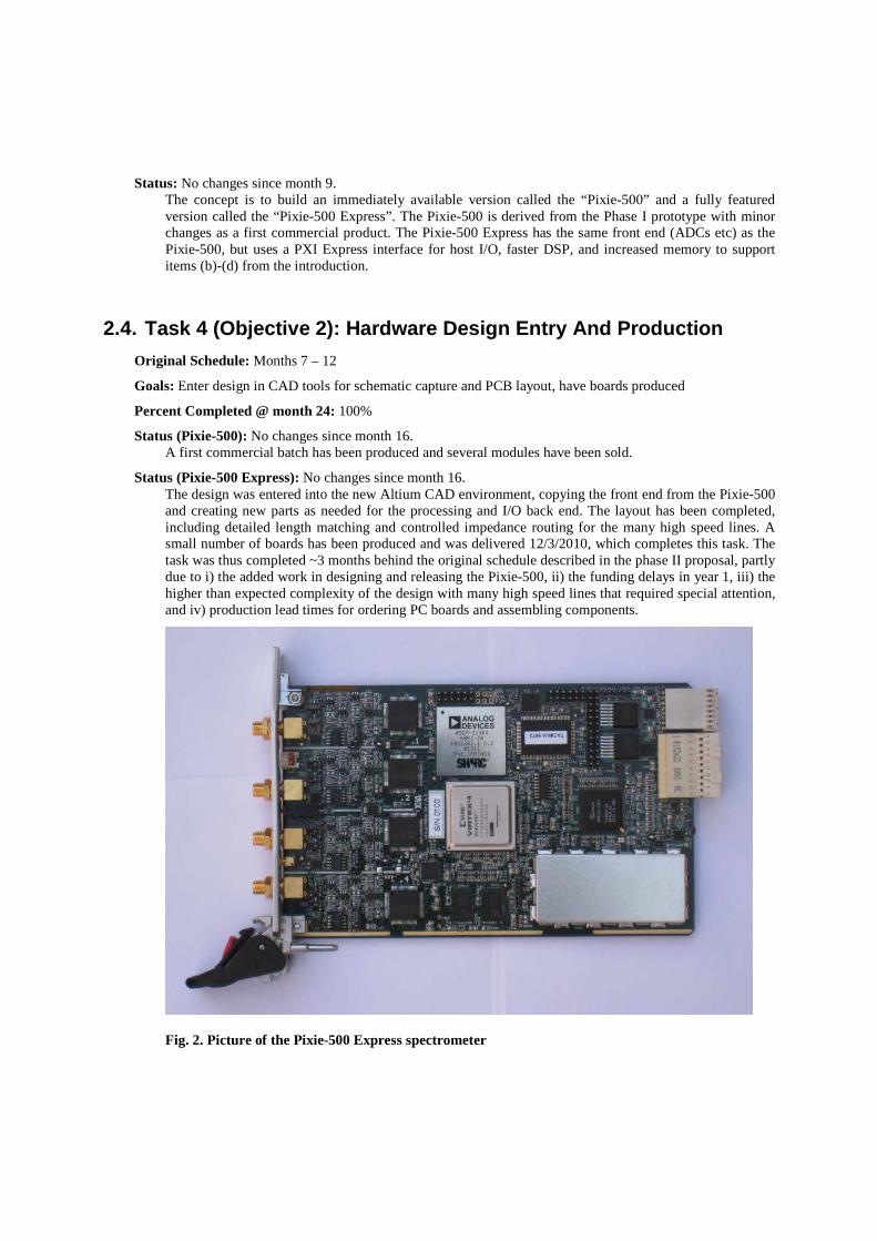
2.4. Task 4 (Objective 2): Hardware Design Entry And Production
Original Schedule: Months 7 – 12
Goals: Enter design in CAD tools for schematic capture and PCB layout, have boards produced
Percent Completed @ month 24: 100%
Status (Pixie-500): No changes since month 16. A first commercial batch has been produced and several modules have been sold.
Status (Pixie-500 Express): No changes since month 16. The design was entered into the new Altium CAD environment, copying the front end from the Pixie-500 and creating new parts as needed for the processing and I/O back end. The layout has been completed, including detailed length matching and controlled impedance routing for the many high speed lines. A small number of boards has been produced and was delivered 12/3/2010, which completes this task. The task was thus completed ~3 months behind the original schedule described in the phase II proposal, partly due to i) the added work in designing and releasing the Pixie-500, ii) the funding delays in year 1, iii) the higher than expected complexity of the design with many high speed lines that required special attention, and iv) production lead times for ordering PC boards and assembling components.
Fig. 2. Picture of the Pixie-500 Express spectrometer

2.5. Task 5 (Objective 3): Firmware Development
Original Schedule: Stage 1: Months 7 – 12 Stage 2: Months 13 – 21
Goals: Stage 1: Merge logic from P500 trigger/filter FPGA with interface logic, add PCIe host interface to FPGA, update FPGA’s DSP interface for Sharc DSP; update/merge Pixie-16 and P500 DSP code for Sharc DSP Stage 2: Move pulse processing from DSP to FPGA for higher throughput, implement “zero dead time” processing; streamline DSP code.
Percent Completed @ month 24: Stage 1: 100% Stage 2: 0%
Status (Stage 1): No changes since month 16. We have integrated a) the PCIe supplier provided firmware design, b) the logic from the Pixie-500 trigger/filter FPGA, c) timer and trigger distribution logic from the Pixie-500, and d) new logic for the Sharc DSP booting and data I/O in a single FPGA design. This included translation of (c) into verilog coding, rewriting of the top level interface with new port and pin definitions, and “weeding out” of unnecessary logic from (a). The design has been extensively modeled to ensure proper operation. It has been debugged and tested on the Pixie-500 Express hardware. The DSP code has been upgraded from the Pixie-16 (which also uses a Sharc DSP) to match the specific chip used in the Pixie-500 Express. To maintain compatibility with the Pixie-500, the input parameters are identical in both modules (16 bit integers), and are formatted in the Pixie-500 Express DSP code to match the style used in the Sharc code (32 bit floating point). In addition the Sharc code has been updated to use the same FPGA register map as the Pixie-500, so that the trigger/filter logic can remain identical for the two boards.
Status (Stage 2): Stage 2 requires that the Stage 1 firmware is fully debugged (Task 7) and has not started yet.
2.6. Task 6 (Objective 4): Host Software Development
Original Schedule: Stage 1: Months 7 – 12 Stage 2: Months 13 – 21
Goals: Stage 1: Upgrade I/O driver for PCI Express, adapt parameter I/O to new DSP Stage 2: Develop ROOT interface
Percent Completed @ month 24: Stage 1: 95% Stage 2: 100%
Status (Stage 1): The vendor provided C++ sample code has been adapted to a simpler C utility program that can be used for C debugging of the key functions: PCIe bridge register I/O, FPGA download, FPGA register I/O, DMA transfer, and read/write of the on-board PROM. An unexpected expense in this step was the requirement to purchase a PCIe driver library to compile the lower level routines of the sample code. These functions have been tested successfully with the PCIe evaluation module (and its firmware has been modified and recompiled by XIA). Communication with the Pixie-500 Express prototype boards

used the same utility program for debugging; the debugged functions are now being integrated in the standard Pixie C library so that the module can be operated through the standard Pixie-500 graphical user interface. Completion of this integration constitutes the remaining 5% of work in Stage 1 and is expected to be finished by the end of the year.
Status (Stage 2): Initially a simple Linux utility for the existing Pixie-16 product has been adapted for use with the Pixie-500 C library and the Pixie-500 acquisition parameters. This included updating of the C library for Linux compatibility issues; it has been tested on 2 major Linux variants. A graphical user interface based on ROOT has then been developed for tasks like booting the module, adjusting parameters, acquiring data, and viewing the outputs. As the C library ultimately handles any differences between Pixie-500 and Pixie-500 Express, and the ROOT interface only communicates with the C library, this interface serves both the Pixie-500 and the Pixie-500 Express (and the existing Pixie-4), as indicated in Fig. 1. Screenshots of the Linux interface are shown in Fig. 3.
Fig. 3. Screenshots of the Pixie Linux interface
2.7. Task 7 (Objective 5): Test And Debug Hardware, Firmware, And Software For Pixie-500
Original Schedule: Months 11 – 24
Goals: Debug Hardware, firmware and software
Percent Completed @ month 24: 80%
Status: Having spent a small amount of time in year 1 to debug the Pixie-500, the debugging started in earnest after the delivery of Pixie-500 Express prototypes on 12/3/2010. At the time of writing, all hardware bugs have been fixed, all new ICs and circuitry on the prototype are working properly, the FPGA firmware is stable, the PCI Express interface is working, the SDRAM has been successfully tested and the SHARC DSP has been booted (with preliminary code). Still to be debugged are the details of the DSP firmware and some elements of the FPGA firmware that rely on the DSP.
2.8. Task 8 (Objective 5): Performance Testing
Original Schedule: Months 1 – 24

Goals: Test performance in cooperation with interested users, report and publish
Percent Completed @ month 16: 100%
Status: During the 2010 SBIR exchange meeting, contacts were established with Alameda Advanced Science Corporation (AASC) and we agreed to collaborate in timing measurements with their ultra short neutron bursts. Several sets of data have been acquired, analyzed, and results have been presented at the 11th International Conference on Applications of Nuclear Techniques (Crete 11). A preprint is attached.
Further performance tests of the Pixie-500 have been performed at ORNL to evaluate the requirements for the electronics in the VANDLE experiment (timing resolutions), at the University of Michigan, and at Rensselaer Polytechnic Institute. Results from the Michigan test have been presented at the IEEE Nuclear Science Symposium (see abstract below).
2.9. Other Developments
Pixie-500 and Pixie-16/250 sales: At the time of writing, approximately 18 months after the introduction of the product, at total of 5 Pixie-500 systems have been sold, 2 of them in the 400 MHz, 14-bit version, and 2 more sales are pending. The sale of a large Pixie-16 system, upgraded for digitization at 250 MHz based on experience in this project, is pending with modules scheduled to be shipped before the end of the year. Sales literature has been added to the company website, and demo modules have been loaned to several labs. A demonstration has also been performed in early January at PTB Braunschweig in Germany.
3. Cost Status The approved total budget for phase II (August 15, 2009 – August 14, 2011) is $690,672. All funds have been
spent by the end of the project. Additional XIA funds spend in Phase III up to the time of writing are in the order of $100,000. On the other hand, Pixie-500 and Pixie-16/250 sales (projected to end of 2011) amount to several hundred thousand dollar.

4. Summary of Performance Schedule Quarter Task
1 2 3 4 5 6 7 8
1. Online processing 9 2. Clock distribution 7 3. Hardware concept 3 3
3 6
4. Schematic design PCB layout Board manufacture 1
3 5 3 3 2 4 4
5. Initial FPGA firmware Initial DSP code High throughput firmware High throughput DSP code 1 2 1
3 2 2 1
6. PCIe software Host software adaptation ROOT interface 2 3 3
7. Test/debug HW/FW/SW 4 8 2 2 6 1 3 1 8. P500 performance
Pixie-500 performance 3 1 2 6 Total man-weeks 13 13 21 16 16 12 12 12
Milestones
Fully working P500, HW concept finalized
Pixie-500 HW produced, initial FW/SW implemented
Initial FW/SW fully debugged
High throughput FW/SW implemented
High throughput FW/SW fully debugged, performance testing of Pixie-500 completed
completed In progress, on/ahead of schedule
In progress, behind schedule
Work not started, postponed to Phase III
Table 3: Performance Schedule
5. Personnel Changes none
6. Attachments
6.1. Univ. Michigan paper at IEEE Nuclear Science Symposium:
Requirements and Qualitative Comparison of Fast Waveform Digitizers for Data-Acquisition Systems Designed for Nuclear Nonproliferation Applications
M. Flaska, G. Chaud, R. T. Schiffer, S. A. Pozzi, D. D. Wentzloff
University of Michigan, Ann Arbor, USA
Conference record N50-4 Accurate pulse shape discrimination (PSD) is essential for organic scintillators such as EJ-301s (309s) because these detectors are sensitive to both neutrons and gamma rays. Because of the background gamma-ray presence the accurate neutron detection requires accurate discrimination of neutrons from gamma rays. This is especially important for applications where fast and robust systems are paramount, such as nuclear nonproliferation and safeguards. Recently, characteristics of digital PSD systems were described and discussed [1] and the results clearly indicate that there is an advantage of using digital over analog PSD systems. It has been shown in the past that the digital PSD provides accurate results for various organic scintillation detectors and the results are superior to analog PSD. For nuclear nonproliferation and safeguards applications, accurate discrimination of neutrons from gamma rays significantly influences the outcome of material identification/characterization. Specifically, particle misclassification can lead to longer measurement times needed or even to false identification/misclassification of measured material. With recent developments in the area of fast waveform digitizers it is clear that the digital PSD will eventually replace older analog PSD systems in most applications due to simplicity, applicability, and accuracy of the new systems. A major question needs to be answered before completely replacing the analog technology: What sampling properties are needed for the replacement waveform digitizers? This works objective is to answer the question.
6.2. AASC paper at Crete 11
See attached

High-speed, multi-channel detector readout electronics for fast radiation detectors
2nd Progress Report for DOE Grant DE-FG02-08ER84981
Grant Recipient XIA LLC Principal Investigator Wolfgang Hennig Date of Report 12/14/2010 Period Covered 04/15/2009 through 012/14/2010
For Distribution This document contains no proprietary technical information and can be made available to individuals involved the administering and reviewing of DOE grant DE-FG02-08ER84981 as well as the general public.
Progress report: High-speed, multi-channel detector readout electronics for fast radiation detectors
© XIA LLC 15 6/22/2012
Table of Contents1. Introduction..................................................................................................................................3 2. Status of Technical Objectives And Tasks ..................................................................................3 2.1. Task 1 (Objective 1): Implement Online Processing And Investigate Noise And Non-linearity In P500 ..............................................................................................................................4 2.2. Task 2 (Objective 1): Implement Clock/trigger Distribution For P500 And Characterize Timing Between Channels And Modules ........................................................................................5 2.3. Task 3 (Objective 2): Develop Hardware Design Concept For Pixie-500 ...............................7 2.4. Task 4 (Objective 2): Hardware Design Entry And Production ...............................................9 2.5. Task 5 (Objective 3): Firmware Development .......................................................................10 2.6. Task 6 (Objective 4): Host Software Development................................................................11 2.7. Task 7 (Objective 5): Test And Debug Hardware, Firmware, And Software For Pixie-500 .11 2.8. Task 8 (Objective 5): Performance Testing............................................................................11 3. Cost Status .................................................................................................................................12 4. Summary of Performance Schedule..........................................................................................12 5. Personnel Changes .....................................................................................................................12 6. Attachments ...............................................................................................................................13

7. Introduction This report summarizes the progress made on DOE grant DE-FG02-08ER84981, “High-speed, multi-channel
detector readout electronics for fast radiation detectors” in the period from 05/14/2009 through 12/14/2010, i.e. from the first progress report (9 months after phase II started) to 4 months after the year 2 funding notice. In this project, we are developing a high speed digital spectrometer that
e) captures detector waveforms at rates up to 500 MSPS
f) has upgraded event data acquisition with additional data buffers for “zero dead time” operation
g) moves energy calculations to the FPGA to increase spectrometer throughput in fast scintillator applications
h) uses a streamlined architecture and high speed data interface for even faster readout to the host PC
These features are in addition to the standard functions in our existing spectrometers such as digitization, programmable trigger and energy filters, pileup inspection, data acquisition with energy and time stamps, MCA histograms, and run statistics. In Phase I, we upgraded one of our existing spectrometer designs to demonstrate the key principle of fast waveform capture using a 500 MSPS, 12 bit ADC and a Xilinx Virtex-4 FPGA. This upgraded spectrometer, named P500, performed well in initial tests of energy resolution, pulse shape analysis, and timing measurements, thus achieving item (a) above.
In Phase II, we are revising the P500 to build a commercial prototype with the improvements listed in items (b)-(d). As described in the previous report, this spectrometer will be built in 2 variants named the “Pixie-500” and the “Pixie-500 Express”. The Phase II work comprises 5 Objectives:
Objective 1: Improvements and further evaluation of P500: Implement online processing and clock/trigger distribution between channels and modules. Investigate noise characteristics in analog sections and eliminate excess noise sources. Explore compensation for non-linearities. Characterize improvements in energy resolution, timing resolution, and linearity.
Objective 2: Develop Pixie-500 hardware: Combine features tested on the P500 with a SHARC DSP, a PCIe host interface, and upgrades in data flow and processing architecture. Allow board variant with 14 bit, 400 MSPS ADC and monitor manufactures’ release of improved fast ADCs. Draw design schematic and layout printed circuit boards, produce small batch of boards.
Objective 3: Develop firmware for Pixie-500: Adapt P500 firmware to hardware upgrades; later improve for higher throughput and reduced dead time.
Objective 4: Adapt existing host software and user interface for Pixie-500: Adapt the Pixie-4 C library to the PCIe interface and the 32bit variables used in the SHARC DSP. Update existing Pixie-4 user interface accordingly and develop sample open source interface using ROOT as a starting point for user’s system integration.
Objective 5: Performance testing of Pixie-500: test and debug hardware, firmware and software, then characterize performance in house and in labs of potential users.
Progress for each objective is described in the following section, divided into tasks as defined in the Phase II proposal.

8. Status of Technical Objectives And Tasks
Executive Summary
Fig. 1: Overview of the Pixie hardware, software and firmware. Fields in red are new developments
In months 10-16, we finalized the schematic design and layout of the Pixie-500 Express and manufactured 5 modules -- the first prototype boards were delivered 12/3/2010. The initial phase of firmware and software development for the Pixie-500 Express has been completed, resulting in basic code to test and debug the Pixie-500 Express. Debugging of firmware, hardware and software has begun with the delivery of the prototype boards.
Igor GUI
LabView ROOT Sample.exe
C lib
glue glue glue glue
Common C library (specific functions for file download, time constants)
PCI interface (PLX) PCIe interface (gennum)
Pixie-4 and Pixie-500 System FPGA
Pixie-500e “system functions” (import from Pixie-4, add SDRAM, gennum)
System
Pixie-4 and Pixie-500 DSP code with compiler switches
Pixie-500e DSP code (import from Pixie-4/-16) DSP
Pixie-4 Fippi Schematic
Fippi Pixie-500 Fippi and Pixie-500e “Fippi functions” Verilog
Pixie-4 Module Pixie-500 Pixie-500e

We further tested the performance of the Pixie-500 with new detectors and sources. (Since the front end digitization and pulse processing is the same on Pixie-500 and Pixie-500 Express, the test result also apply to the Pixie-500 Express.) These tests include gamma neutron discrimination measurements with CLYC and Stilbene, performed at LBL, and subsequent analysis of the data to quantify the effectiveness of the discrimination. Results of the test measurements have been reported at the 2010 IEEE Nuclear Science Symposium and a conference record has been submitted. Further measurements involving timing of ultra short neutron bursts have been performed in cooperation with AASC and are now being analyzed. The article on the results of the P500 performance tests previously submitted to the IEEE Transactions of Nuclear Science has now been published: IEEE Transactions on Nuclear Science, Vol. 57, No. 4, August 2010, p. 2365-2370.
Due to delays in the year 1 funding agreement, some of the later tasks were approached slower than originally described in the proposal. Additional delays have been caused by the added work in designing and releasing the Pixie-500, the unforeseen high complexity of the PCIe interface as well as production lead times for the prototype boards. Overall we are now approximately 3 months behind schedule. Future developments strongly depend on the outcome of testing and debugging, so it is unclear if we can catch up on the delay in the coming months.
8.1. Task 1 (Objective 1): Implement Online Processing And Investigate Noise And Non-linearity In P500
Original Schedule: Months 1 – 3
Goals: Implement online processing, investigate/eliminate noise and nonlinearity, consider implementation of nonlinearity compensation scheme, optionally test 14-bit 400 MSPS footprint compatible ADC
Percent Completed @ month 16: 100%
Status: No changes since month 9.
8.2. Task 2 (Objective 1): Implement Clock/trigger Distribution For P500 And Characterize Timing Between Channels And Modules
Original Schedule: Months 4 – 6
Goals: Implement clock and trigger distribution in firmware, characterize timing resolutions between channels and modules, explore doubling digitization rate by combining phase shifted channels.
Percent Completed @ month 16: 100%
Status: No changes since month 9.
8.3. Task 3 (Objective 2): Develop Hardware Design Concept For Pixie-500
Original Schedule: Months 1 – 6
Goals: Develop hardware architecture; choose parts.
Percent Completed @ month 16: 100%
Status: No changes since month 9. The concept is to build an immediately available version called the “Pixie-500” and a fully featured version called the “Pixie-500 Express”. The Pixie-500 is derived from the Phase I prototype with minor changes as a first commercial product. The Pixie-500 Express has the same front end (ADCs etc) as the

Pixie-500, but uses a PXI Express interface for host I/O, faster DSP, and increased memory to support items (b)-(d) from the introduction.
8.4. Task 4 (Objective 2): Hardware Design Entry And Production
Original Schedule: Months 7 – 12
Goals: Enter design in CAD tools for schematic capture and PCB layout, have boards produced
Percent Completed @ month 16: 100%
Status (Pixie-500): A first commercial batch has been produced and several modules have been sold.
Status (Pixie-500 Express): The design was entered into the new Altium CAD environment, copying the front end from the Pixie-500 and creating new parts as needed for the processing and I/O back end. The layout has been completed, including detailed length matching and controlled impedance routing for the many high speed lines. A small number of boards has been produced and was delivered 12/3/2010, which completes this task. The task was thus completed ~ 3 months behind the original schedule described in the phase II proposal, partly due to i) the added work in designing and releasing the Pixie-500, ii) the funding delays in year 1, iii) the higher than expected complexity of the design with many high speed lines that required special attention, and iv) production lead times for ordering PC boards and assembling components.
Fig. 2. Picture of the Pixie-500 Express spectrometer
8.5. Task 5 (Objective 3): Firmware Development
Original Schedule:

Stage 1: Months 7 – 12 Stage 2: Months 13 – 21
Goals: Stage 1: Merge logic from P500 trigger/filter FPGA with interface logic, add PCIe host interface to FPGA, update FPGA’s DSP interface for Sharc DSP; update/merge Pixie-16 and P500 DSP code for Sharc DSP Stage 2: Move pulse processing from DSP to FPGA for higher throughput, implement “zero dead time” processing; streamline DSP code.
Percent Completed @ month 16: Stage 1: 100% Stage 2: 0%
Status (Stage 1): We have integrated a) the PCIe supplier provided firmware design, b) the logic from the Pixie-500 trigger/filter FPGA, c) timer and trigger distribution logic from the Pixie-500, and d) new logic for the Sharc DSP booting and data I/O in a single FPGA design. This included translation of (c) into verilog coding, rewriting of the top level interface with new port and pin definitions, and “weeding out” of unnecessary logic from (a). The design has been extensively modeled to ensure proper operation. It is now ready to be debugged and tested on the recently delivered Pixie-500 Express hardware. The DSP code has been upgraded from the Pixie-16 (which also uses a Sharc DSP) to match the specific chip used in the Pixie-500 Express. To maintain compatibility with the Pixie-500, the input parameters are identical in both modules (16 bit integers), and are formatted in the Pixie-500 Express DSP code to match the style used in the Sharc code (32 bit floating point). In addition the Sharc code has been updated to use the same FPGA register map as the Pixie-500, so that the trigger/filter logic can remain identical for the two boards.
Status (Stage 2): Stage 2 requires that the Stage 1 firmware is fully debugged (Task 7) and has not started yet.
Note: The start of this work was delayed somewhat by lengthy DOE contract negotiations and Stage 1 was timed to complete with the delivery of the Pixie-500 Express prototypes.
8.6. Task 6 (Objective 4): Host Software Development
Original Schedule: Stage 1: Months 7 – 12 Stage 2: Months 13 – 21
Goals: Stage 1: Upgrade I/O driver for PCI Express, adapt parameter I/O to new DSP Stage 2: Develop ROOT interface
Percent Completed @ month 16: Stage 1: 90% Stage 2: 10%
Status (Stage 1): The vendor provided C++ sample code has been adapted to a simpler C utility program that can be used for C debugging of the key functions: PCIe bridge register I/O, FPGA download, FPGA register I/O, DMA transfer, and read/write of the on-board PROM. An unexpected expense in this step was the need to purchase a PCIe driver library to compile the lower level routines of the sample code. These functions have been tested successfully with the PCIe evaluation module (and firmware modified and recompiled by XIA). Communication with the prototype boards will initially use the same utility program for debugging, then the debugged functions will be integrated in the standard Pixie C library and the module can be operated through the standard Pxiie-500 interface. This integration constitutes the remaining 10% of work in Stage 1 and is expected to be completed by the end of the year.

Status (Stage 2): Stage 2 was scheduled to begin after stage one is completed, but since the work can initially be performed in parallel (using the Pixie-500 instead of the prototype), work has already begun. At this point, a very basic Linux interface for the existing Pixie-16 product is adapted for use with the Pixie-4 parameters. The next step will be to develop an outline of the controls and panels in the user interface, which will then be implemented in ROOT.
8.7. Task 7 (Objective 5): Test And Debug Hardware, Firmware, And Software For Pixie-500
Original Schedule: Months 11 – 24
Goals: Debug Hardware, firmware and software
Percent Completed @ month 16: 20%
Status: Having spend a small amount of time in year 1 to debug the Pixie-500, the debugging started in earnest after the delivery of modules on 12/3/2010. Since that was very recent, this task is still at its beginning. At this point, it has been verified that the power supplies work ok (with minor rework). Current debugging focuses on the PCIe interface with the host PC, which yet has to recognize our module. Future debugging steps will include I/O with the PCIe bridge registers, FPGA download, DSP download, communication between DSP and FPGA, test of the DSP code conversion, FPGA I/O with the memory chips, and the DMA transfers
8.8. Task 8 (Objective 5): Performance Testing
Original Schedule: Months 1 – 24
Goals: Test performance in cooperation with interested users, report and publish
Percent Completed @ month 16: 65%
Status: The article describing performance testing with the P500 Phase I prototype was accepted for publication (IEEE transactions of Nuclear Science Vol. 57, No. 4, August 2010, p. 2365-2370).
The P500 was also tested in gamma/neutron discrimination experiments with Stilbene and Cs2LiYCl 6: Ce scintillator (called CLYC) at XIA and LBL, which has been reported at the 2010 IEEE Nuclear Science Symposium. This work focused on characterizing the ability of CLYC to distinguish gamma interactions from neutron interactions, and the high digitization rate of the P500 was a valuable tool in acquiring the “fast gamma” type of waveforms ascribed to the phenomenon of Core-to-Valence-Luminescence. Pdf files of the poster and the conference record are attached.
During the 2010 SBIR exchange meeting, contacts were established with Alameda Advanced Science Corporation (AASC) and we agreed to collaborate in measurements with their ultra short neutron bursts. A first set of data has been acquired and is currently being analyzed.
Further performance tests of the Pixie-500 are in progress at LBL by Bill Moses, and at ORNL to evaluate the requirements for the electronics in the VANDLE experiment (timing resolutions)
8.9. Other Developments
Pixie-500 sales: At the time of writing, approximately 6 months after the introduction of the product, at total of four Pixie-500 systems have been sold, 2 of them in the 400 MHz, 14-bit version. Sales literature has been added to the company website, and demo modules have been loaned to several labs. A future demonstration is planned in early January at PTB Braunschweig in Germany.

Possible new hardware: In recent months, there has been interest at ORNL to instrument the VANDLE experiment with high speed electronics. This research group has long been using Pixie-16 modules and found that their 12-bit, 100 MHz digitization rate is marginally suitable for the experiment’s needs, but higher rates and/or more bits are desirable. A Pixie-500 module is currently used to better determine the requirements. In the desire to stay compatible with their existing Pixie-16 system and keep costs low, we are in discussions to develop a new module, essentially a Pixie-16 upgraded with a 250 MHz ADC. This low cost module would be the 3rd member of the “high speed Pixie” series of modules. Any such development will be conducted outside the scope of this grant, but will largely be based on the experience in the Pixie-500 development.
9. Cost Status The approved total budget for phase II (August 15, 2009 – August 14, 2011) is $690,672. The actual cost
incurred in Phase II up to November 11, 2010 is approximately $450k (not all of which have been billed yet). The remaining balance for the current budget period is about $240k, roughly on schedule in time, but somewhat ahead in respect of the work completed. We believe we can still completed the essential tasks in the original time frame and within the budget of the grant, and if necessary will fund some of the less critical tasks (e.g. the ROOT interface) with internal funds. Details of the project costs can be found in the financial reports submitted to the DOE by XIA LLC.
10. Summary of Performance Schedule Quarter Task
1 2 3 4 5 6 7 8
1. Online processing 9 2. Clock distribution 7 3. Hardware concept 3 3
3 6
4. Schematic design PCB layout Board manufacture 1
3 5 3 3 2 4 4
5. Initial FPGA firmware Initial DSP code High throughput firmware High throughput DSP code 1 2 1
3 2 2 1
6. PCIe software Host software adaptation ROOT interface 2 3 3
7. Test/debug HW/FW/SW 4 8 2 2 6 1 3 1 8. P500 performance
Pixie-500 performance 3 1 2 6 Total man-weeks 13 13 21 16 16 12 12 12
Milestones
Fully working P500, HW concept finalized
Pixie-500 HW produced, initial FW/SW implemented
Initial FW/SW fully debugged

High throughput FW/SW implemented
High throughput FW/SW fully debugged, performance testing of Pixie-500 completed
completed In progress, on/ahead of schedule
In progress, behind schedule
Work not yet started
Table 3: Performance Schedule
11. Personnel Changes none
12. Attachments 1) “CLYC versus Stilbene: Optimization and comparison of two neutron-gamma discriminating
scintillators”, a poster presented at the 2010 IEEE Nuclear Science Symposium (CLYC_IEEE10poster.pdf);
2) “CLYC versus Stilbene: Optimization and comparison of two neutron-gamma discriminating scintillators”, a paper in the Proceedings for the 2010 IEEE Nuclear Science Symposium (CLYC_IEEE10cr.pdf);

High-speed, multi-channel detector readout electronics for fast radiation detectors
1st Progress Report for DOE Grant DE-FG02-08ER84981
Grant Recipient XIA LLC Principal Investigator Wolfgang Hennig Date of Report 5/14/2010 Period Covered 08/14/2009 through 05/14/2010
For Distribution This document contains no proprietary technical information and can be made available to individuals involved the administering and reviewing of DOE grant DE-FG02-08ER84981 as well as the general public.
Progress report: High-speed, multi-channel detector readout electronics for fast radiation detectors
© XIA LLC 25 6/22/2012
Table of Contents1. Introduction..................................................................................................................................3 2. Status of Technical Objectives And Tasks ..................................................................................3 2.1. Task 1 (Objective 1): Implement Online Processing And Investigate Noise And Non-linearity In P500 ..............................................................................................................................4 2.2. Task 2 (Objective 1): Implement Clock/trigger Distribution For P500 And Characterize Timing Between Channels And Modules ........................................................................................5 2.3. Task 3 (Objective 2): Develop Hardware Design Concept For Pixie-500 ...............................7 2.4. Task 4 (Objective 2): Hardware Design Entry And Production ...............................................9 2.5. Task 5 (Objective 3): Firmware Development .......................................................................10 2.6. Task 6 (Objective 4): Host Software Development................................................................11 2.7. Task 7 (Objective 5): Test And Debug Hardware, Firmware, And Software For Pixie-500 .11 2.8. Task 8 (Objective 5): Performance Testing............................................................................11 3. Cost Status .................................................................................................................................12 4. Summary of Performance Schedule..........................................................................................12 5. Personnel Changes .....................................................................................................................12 6. Attachments ...............................................................................................................................13
Progress report: High-speed, multi-channel detector readout electronics for fast radiation detectors
© XIA LLC 26 6/22/2012
13. Introduction This report summarizes the progress made on DOE grant DE-FG02-08ER84981, “High-speed, multi-channel
detector readout electronics for fast radiation detectors” in the period from 08/14/2009 through 05/14/2010, i.e. the first nine months of Phase II of the grant. In this project, we are developing a high speed digital spectrometer that
i) captures detector waveforms at rates up to 500 MSPS
j) has upgraded event data acquisition with additional data buffers for “zero dead time” operation
k) moves energy calculations to the FPGA to increase spectrometer throughput in fast scintillator applications
l) uses a streamlined architecture and high speed data interface for even faster readout to the host PC
These features are in addition to the standard functions in our existing spectrometers such as digitization, programmable trigger and energy filters, pileup inspection, data acquisition with energy and time stamps, MCA histograms, and run statistics. In Phase I, we upgraded one of our existing spectrometer designs to demonstrate the key principle of fast waveform capture using a 500 MSPS, 12 bit ADC and a Xilinx Virtex-4 FPGA. This upgraded spectrometer, named P500, performed well in initial tests of energy resolution, pulse shape analysis, and timing measurements, thus achieving item (a) above.
In Phase II, we are revising the P500 to build a commercial prototype with the improvements listed in items (b)-(d). As described in more detail below, this spectrometer will be built in 2 variants named the “Pixie-500” and the “Pixie-500 Express”. This work includes investigation, and where necessary and possible elimination or compensation, of the noise and non-linearity issues found in the testing of the Phase I prototype. The Phase II work comprises 5 Objectives:
Objective 1: Improvements and further evaluation of P500: Implement online processing and clock/trigger distribution between channels and modules. Investigate noise characteristics in analog sections and eliminate excess noise sources. Explore compensation for non-linearities. Characterize improvements in energy resolution, timing resolution, and linearity.
Objective 2: Develop Pixie-500 hardware: Combine features tested on the P500 with a SHARC DSP, a PCIe host interface, and upgrades in data flow and processing architecture. Allow board variant with 14 bit, 400 MSPS ADC and monitor manufactures’ release of improved fast ADCs. Draw design schematic and layout printed circuit boards, produce small batch of boards.
Objective 3: Develop firmware for Pixie-500: Adapt P500 firmware to hardware upgrades; later improve for higher throughput and reduced dead time.
Objective 4: Adapt existing host software and user interface for Pixie-500: Adapt the Pixie-4 C library to the PCIe interface and the 32bit variables used in the SHARC DSP. Update existing Pixie-4 user interface accordingly and develop sample open source interface using ROOT as a starting point for user’s system integration.
Objective 5: Performance testing of Pixie-500: test and debug hardware, firmware and software, then characterize performance in house and in labs of potential users.
Progress for each objective is described in the following section, divided into tasks as defined in the Phase II proposal. Since up to the time of writing a final funding agreement was not in place, we had to operate only with the amounts approved in the initial funding agreement ($125k from 8/14/2009) and self-finance any further expenses. This lack of funding caused some of the later tasks to be approached slower than originally planned and described in the proposal.
Progress report: High-speed, multi-channel detector readout electronics for fast radiation detectors
© XIA LLC 27 6/22/2012
14. Status of Technical Objectives And Tasks
Executive Summary
In the first 9 months, we upgraded the processing and clock distribution firmware of the P500 prototype to include all the essential functions of a final commercial spectrometer module. In a variety of performance tests at XIA and collaborating research labs, we found that the design of the prototype has no significant flaws with the only exception that a more precise DAC is required to be able to implement an on-board nonlinearity compensation. We designed the hardware architecture for the commercial prototype of the fully featured “Pixie-500 Express”, and implemented most of the schematics in the CAD software. In addition, we upgraded the Phase I prototype to a commercial spectrometer module “Pixie-500” to capture some early sales; the first set of boards have been produced and we expect to offer them commercially by June 2010. Firmware and software development for the Pixie-500 Express have begun, somewhat delayed by lengthy DOE contract negotiations. Results of the performance tests were presented at the 2009 IEEE Nuclear Science Symposium and a paper was submitted to the IEEE Transactions of Nuclear Science. We expect to have manufactured the first prototypes of the Pixie-500 Express boards by August or September 2010.
14.1. Task 1 (Objective 1): Implement Online Processing And Investigate Noise And Non-linearity In P500
Original Schedule: Months 1 – 3
Goals: Implement online processing, investigate/eliminate noise and nonlinearity, consider implementation of nonlinearity compensation scheme, optionally test 14-bit 400 MSPS footprint compatible ADC
Percent Completed @ month 9: 100%
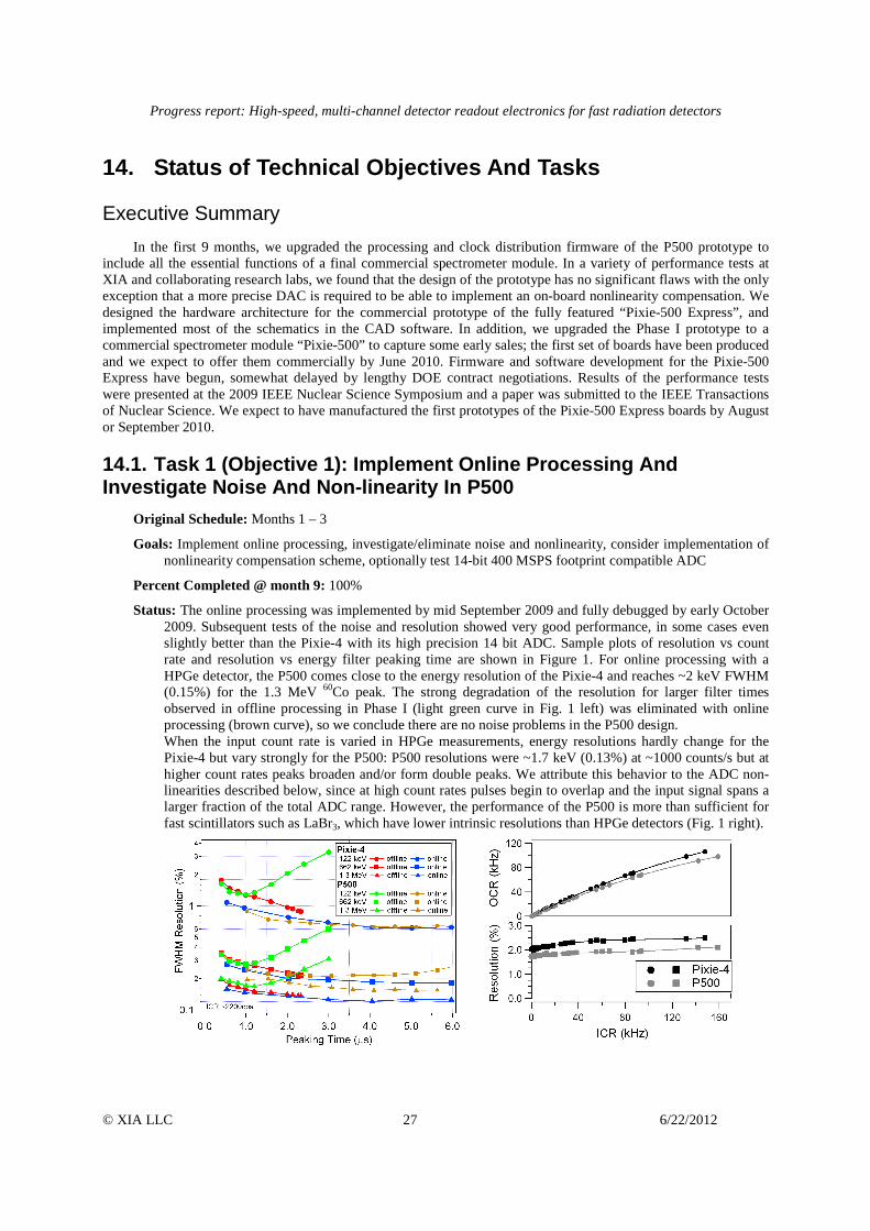
Status: The online processing was implemented by mid September 2009 and fully debugged by early October 2009. Subsequent tests of the noise and resolution showed very good performance, in some cases even slightly better than the Pixie-4 with its high precision 14 bit ADC. Sample plots of resolution vs count rate and resolution vs energy filter peaking time are shown in Figure 1. For online processing with a HPGe detector, the P500 comes close to the energy resolution of the Pixie-4 and reaches ~2 keV FWHM (0.15%) for the 1.3 MeV 60Co peak. The strong degradation of the resolution for larger filter times observed in offline processing in Phase I (light green curve in Fig. 1 left) was eliminated with online processing (brown curve), so we conclude there are no noise problems in the P500 design. When the input count rate is varied in HPGe measurements, energy resolutions hardly change for the Pixie-4 but vary strongly for the P500: P500 resolutions were ~1.7 keV (0.13%) at ~1000 counts/s but at higher count rates peaks broaden and/or form double peaks. We attribute this behavior to the ADC non-linearities described below, since at high count rates pulses begin to overlap and the input signal spans a larger fraction of the total ADC range. However, the performance of the P500 is more than sufficient for fast scintillators such as LaBr3, which have lower intrinsic resolutions than HPGe detectors (Fig. 1 right).

Progress report: High-speed, multi-channel detector readout electronics for fast radiation detectors
© XIA LLC 28 6/22/2012
Fig. 1: (right) Energy resolution with HPGe as a function of peaking time at 3 energy values. (The right plot combines offline data from Phase I [green] with the new online data from Task 1 [brown]) (left) Energy resolution and output count rate with LaBr 3 at 1.3 MeV as a function of input count rate.
Fig. 2. Measurement of integral nonlinearity (INL): Residual from a linear fit to measured ADC output as a function of input voltage set by an on-board DAC
Measuring the integral nonlinearity (INL) of the ADCs on the 500 MSPS channels for all existing P500 boards resulted in similar curves as observed in Phase I, i.e. the measured output from the ADC shows a series of jumps as the input voltage is ramped from minimum to maximum (red curves in Fig. 2). A P500 board where the ADC was replaced with a footprint compatible 14-bit, 400 MHz ADC, which is nominally more precise, shows the same behavior (blue curves). A Pixie-4, having a very similar analog front end except for the ADC, showed no jumps (black curve). However, the overall envelope of variations are about 10-15 LSB12 peak to peak for both Pixie-4 and P500. We concluded that the on-board digital to analog converter (DAC) used to ramp the input voltage, which was originally chosen only for offset compensation with a specified precision of 1%, dominates INL and thus the lower specified INL values for the ADC can not be confirmed in these measurements. However, since DAC and other circuit elements are essentially the same for the P500 and the Pixie-4, we conclude that the jumps are specific to the high speed ADCs, likely due to their design as “folding ADCs”. Thus we confirmed that the Phase I measurement was not an isolated bad ADC, but that the design of the ADC itself causes the jumps and this behavior should be compensated for best performance. Any practical compensation scheme should use only on-board functions to avoid external calibration procedures that can not be performed in the field, but the DAC limits the precision of such on-board non-linearity measurements. Therefore there is no benefit in implementing a compensation scheme at this point for the P500 Phase I prototype. Instead, the new Phase II hardware will be equipped with a more precise DAC, and a compensation scheme can be developed as part of year 2 work if there is demand from potential users. It is unclear that there will be such demand since the effects of the nonlinearity only are visible with very high resolution detectors (i.e. HPGe, but not LaBr3), which are not the main application for this module.
14.2. Task 2 (Objective 1): Implement Clock/trigger Distribution For P500 And Characterize Timing Between Channels And Modules
Original Schedule: Months 4 – 6
Goals: Implement clock and trigger distribution in firmware, characterize timing resolutions between channels and modules, explore doubling digitization rate by combining phase shifted channels.

Progress report: High-speed, multi-channel detector readout electronics for fast radiation detectors
© XIA LLC 29 6/22/2012
Percent Completed @ month 9: 100%
Status: The firmware updates to program the clock generation chip on the P500 were implemented by mid October 2009 and the clock and trigger distribution was implemented and fully debugged by December 2009. Performance tests to measure timing resolutions were completed by early February 2010, and separate tests to explore 180 degree phase shifts between channels for a double digitization rate were completed January 2010. The timing resolution tests were performed in 4 different modes shown to the right: A) a single signal source split into two branches, one of them delayed, and then merged and fed into a single ADC channel; as in Phase I. B) a single signal source split into 2 branches, one of them delayed and each branch fed into a separate ADC channel in the same module; C) as in B), but using two separate ADC channels in two modules; and D) 2 coincident signals, one of them delayed, each fed into a separate ADC channel in the same module. The signal source was either a programmable pulse generator or a photomultiplier tube (PMT) attached to a LaBr3 crystal. In each case, we measured the time difference ∆T between the two rising edges by applying a constant fraction algorithm offline to captured waveforms. Histogramming several hundred measurements, we obtain a distribution of ∆T with a timing resolution dT (FWHM of Gauss fit). In mode A), we measured dT ~ 20 ps FWHM with the pulser and ~53 ps with LaBr3. In modes B) and C), pulser measurements with the P500 resulted in timing resolutions of ~20 ps and ~40 ps, respectively (Fig. 4). Equivalent measurements with a Pixie-4 resulted in timing resolutions of 100-300 ps in mode B, but histograms of ∆T often showed double peaks or shoulders. Applying a rise time cut to limit the analysis to pulses with a certain rise time reduced these effects and improved the timing resolution to about 100 ps, but removed about 70% of collected events. Mode B) and C) measurements with the P500 and LaBr3 resulted in timing resolutions of on average ~75 ps in both modes B, though dT was in some cases as good as 23 ps.

Progress report: High-speed, multi-channel detector readout electronics for fast radiation detectors
© XIA LLC 30 6/22/2012
Fig. 4. FWHM timing resolution for P500 and Pixie-4 in modes B and C using an Agilent pulser. A rise time cut improves results for the Pixie-4, which otherwise has a non-Gaussian distribution.
In mode D), using a pair of LaBr3 crystals and PMTs, we measured ~900 ps with a Pixie-4 and ~630 ps with the P500 when including all events. Limiting events to those with energies >1 MeV and applying a rise time cut to Pixie-4 data that removes approximately 50% of the >1MeV events, we achieve ~400 ps and ~250 ps for the Pixie-4 and P500, respectively. The timing resolution attributed to each channel is then 1/sqrt(2) of these values, i.e. ~282 ps and 177 ps for the Pixie-4 and P500, respectively. In comparison, for a traditional timing measurement [NIM A, 567 (2006), p31] similar to mode D) with an analog constant fraction discriminator to measure the delay between coincident pulses from two scintillators/PMTs (BaF2 and LaBr3), the timing resolution attributed to the LaBr3 channel is reported to be ~140ps FWHM with 60Co. These measurements used a PMT model XP20D0, an improved model of the model XP2020 used in our tests.
Fig. 5. Histograms of measured relative gain, offset and phase shift for several thousand waveforms from 2 ADCs clocked at 250 MHz with 1.95 ns phase shift at the source.
To test the feasibility of doubling the digitization rate, the clock generation chip on the P500 was programmed to output a 250 MHz clock signal, for one channel delayed by 1.95 ns. (The chip is limited to delays in steps of 150 ps, and we chose a base frequency of 250 MHz to be able to compare the interleaved data with single-channel full rate data). Fig. 5 shows histograms of relative gain, offset and phase from several thousand pulses acquired synchronously in channels 2 and 3. Gain mismatch is ~0.2% with a jitter of 0.11% FWHM; offset mismatch is ~11.7 ADC steps with a jitter of 0.45 ADC steps, and phase mismatch from the ideal 2 ns is ~130ps with a jitter of 36 ps. The offset mismatch could be further reduced by finely adjusting the offset DAC for each channel, and the phase mismatch (most likely due to PCB clock line delays) could be further reduced by delaying the clock in the PLL by one additional 150 ps step. The P500 thus fulfills a necessary condition for interleaved operation, i.e. small and stable mismatch, and is potentially able to generate 12 bit data streams at double or even four times the ADC clock rate, though the quality of such data remains to be investigated. This feature can be implemented in year 2 if there is demand from potential users.
14.3. Task 3 (Objective 2): Develop Hardware Design Concept For Pixie-500
Original Schedule: Months 1 – 6
Goals: Develop hardware architecture; choose parts.
Percent Completed @ month 9: 100%

Progress report: High-speed, multi-channel detector readout electronics for fast radiation detectors
© XIA LLC 31 6/22/2012
Status: The goal of this task was to define the hardware architecture for the commercial prototype Pixie-500, based on a) experience with the Phase I prototype P500 and b) desired features for a next generation of spectrometer modules. In addition, since it became clear in discussions with potential users that there is immediate demand for a high speed spectrometer module, we decided to manufacture the P500 prototype (with minor changes) as a first commercial product. This module will be called “Pixie-500” (Fig. 6), and the fully featured module will be called the “Pixie-500 Express” (Fig. 7). As a consequence of this decision, some of the time planned for tasks 1 and 2 – which were completed faster than expected as no significant problems were encountered – was moved to a new subtask of task 4, i.e. the hardware update of the P500 prototype to the commercial Pixie-500. Firmware and software for the Pixie-500 require only very minor updates from the P500. Pixie-500: The only significant changes from the P500 to the Pixie-500 are the replacement of the 125 MSPS reference channel with a full speed 500 MSPS channel, addition of a gain relay, and the use of a more precise DAC. The ADC–FPGA connections were also upgraded to accommodate bits 13 and 14 of the footprint compatible 14 bit ADC. The Pixie-500 will be limited in pulse processing throughput to roughly the same 100,000-200,000 events/s as the Pixie-4, but will be useful as a lower cost alternative for applications that do not have highest count rates and it is expected to capture a number of early sales. It will also serve as a test bed of the DAC and the gain option planned for the Pixie-500 Express. The Pixie-500 architecture is shown in Fig. 6.
MCA, LM memory
DSP
Analog, gain and offset
500 MSPS ADC
500 MSPS ADC
Analog, gain and offset
Analog, gain and offset
500 MSPS ADC
Analog, gain and offset
14bit ADC
32 bit, 33MHz
PCI
clock, trigger (J2)
Veto
500 MSPS ADC
OSC 37.5
PLL, VCO, phase
FPGA Virtex 4
System FPGA
PCI I/O (J1)
Fig. 6. Architecture of the commercial version of the P500 prototype “Pixie-500”. Changes to P500 Phase I prototype are shown in red
Pixie-500 Express: Work on the Pixie-500 Express includes selection of - Spectrum memory - List mode memory - PCI Express interface - Digital Signal Processor (DSP) - Field Programmable Gate Array (FPGA) - Clock distribution - Power requirements and supplies - Modifications in analog front end. The resulting architecture is summarized in Fig. 7. New parts are shown in red. Following the outline in the proposal, we selected a 32-bit, floating point DSP, a Gennum x4 PCI Express bridge, a larger version of the processing FPGA used on the P500 to merge pulse processing and data I/O in the same chip, a SDRAM for list mode memory, a separate SRAM for MCA memory to avoid contention for list mode and spectrum access, and a separate low cost I/O FPGA to protect the expensive processing FPGA from user connection errors on the front panel. Analog front end, clock distribution and ADC are the same as on the Pixie-500.

Progress report: High-speed, multi-channel detector readout electronics for fast radiation detectors
© XIA LLC 32 6/22/2012
MCA mem CY7C1370D
DSP ADSP-21369
Comm FPGA Virtex 4 LX40
Veto, I/O link
4x channels
Analog - CRF relays - DAC - usual opamp chain and filter
LM mem. MT47H32M16
IO FPGA Spartan II 15
PLL clock LMK30300
ADC - ADS5463 - ADS5474
PCIe bridge Gennum GN4124
clock, trigger
XJ4
PCIe I/O XJ3
Fig. 7. Architecture of the commercial prototype “Pixie-500 Express”. New parts are shown in red.
14.4. Task 4 (Objective 2): Hardware Design Entry And Production
Original Schedule: Months 7 – 12
Goals: Enter design in CAD tools for schematic capture and PCB layout, have boards produced
Percent Completed @ month 9: 30%
Status (Pixie-500): The updates in schematic and layout for the Pixie-500 were implemented and submitted for production by late February 2010. The first assembled boards were received May 4 2010. A picture of this module is shown in Fig. 8. Testing of these boards is now in progress and showed no errors up to this point. We expect an official product release by early June 2010.
Fig. 8. Photograph of the Pixie-500 spectrometer
Status (Pixie-500 Express): The design was entered into the new Altium CAD environment, copying the front end from the Pixie-500 and creating new parts as needed for the processing and I/O back end. The major

Progress report: High-speed, multi-channel detector readout electronics for fast radiation detectors
© XIA LLC 33 6/22/2012
parts have been placed in a preliminary PCB layout, as shown in Fig. 9. Final placement and routing will begin when pin assignments for the FPGA have been finalized in Task 5. Since production of the commercial Pixie-500 was added to this task, we are about 4-6 weeks behind schedule in the PCB layout, but still expect to take delivery of the first Pixie-500 Express boards by August or September 2010.
Fig. 9. Screenshot from Altium CAD software of the Pixie-500 Express spectrometer showing preliminary parts placement of major parts and one analog channel.
14.5. Task 5 (Objective 3): Firmware Development
Original Schedule: Stage 1: Months 7 – 12 Stage 2: Months 13 – 21
Goals: Stage 1: Merge logic from P500 trigger/filter FPGA with interface logic, add PCIe host interface to FPGA, update FPGA’s DSP interface for Sharc DSP; update/merge Pixie-16 and P500 DSP code for Sharc DSP Stage 2: Move pulse processing from DSP to FPGA for higher throughput, implement “zero dead time” processing; streamline DSP code.
Percent Completed @ month 9: Stage 1: 20% Stage 2: 0%
Status (Stage 1): We have implemented and compiled the PCIe supplier provided firmware design and performed simulations of the PCIe and memory interfaces to verify the selected FPGA chip can contain the planned logic. Integration of the trigger/filter logic is now in progress. This will also produce a pin assignment map for the PCB layout (Task 4). The work on the DSP code upgrade has begun in May 2010.
Status (Stage 2): Stage 2 is scheduled for year 2 and has not started yet.
Note: The start of this work was delayed somewhat by lengthy DOE contract negotiations

Progress report: High-speed, multi-channel detector readout electronics for fast radiation detectors
© XIA LLC 34 6/22/2012
14.6. Task 6 (Objective 4): Host Software Development
Original Schedule: Stage 1: Months 7 – 12 Stage 2: Months 13 – 21
Goals: Stage 1: Upgrade I/O driver for PCI Express, adapt parameter I/O to new DSP Stage 2: Develop ROOT interface
Percent Completed @ month 9: Stage 1: 5% Stage 2: 0%
Status (Stage 1): An initial work outline for stage 1 of the software development has been established. The PCIe evaluation module has been procured. Actual development began in May.
Status (Stage 2): Stage 2 is scheduled for year 2 and has not started yet, but some of the work (i.e. the ROOT interface will be shifted to year 1 because the interface is also a valuable feature for the Pixie-500. This work will thus begin shortly
Note: The start of this work was delayed somewhat by lengthy DOE contract negotiations
14.7. Task 7 (Objective 5): Test And Debug Hardware, Firmware, And Software For Pixie-500
Original Schedule: Months 11 – 24
Goals: Debug Hardware, firmware and software
Percent Completed @ month 9: 10%
Status: Originally, this task would not yet have started, but due to the decision to make a commercial version of the P500 prototype, some of its newer firmware functions (e.g. waveform capture) were tested more thoroughly and required some bug fixes. This logic will be fully reused on the Pixie-500 Express and thus this debug work is essentially shifted from year 2 to year 1.
14.8. Task 8 (Objective 5): Performance Testing
Original Schedule: Months 1 – 24
Percent Completed @ month 9: 25%
Status: Performance testing was done with the P500 Phase I prototype at XIA (see tasks 1 and 2) and by interested parties at ORNL and LANL. ORNL reported ~140 ps FWHM timing resolution with BaF2 detectors, similar to the results found at XIA. Additional performance testing is planned at LBL but has been postponed multiple times due to scheduling problems. The P500 will also be tested in gamma/neutron discrimination experiments with Cs2LiYCl 6: Ce scintillator (called CLYC) at XIA and LBL or LLNL once a test date with access to a neutron source is secured. The results of these performance tests, together with some of the results from Phase I, were presented at the 2009 IEEE Nuclear Science Symposium and also submitted to the IEEE Transactions of Nuclear Science. These publications are attached separately.

Progress report: High-speed, multi-channel detector readout electronics for fast radiation detectors
© XIA LLC 35 6/22/2012
15. Cost Status The approved budget for the current budget period (August 15, 2009 – August 14, 2010) is $375k. However,
until now, we are operating only under the initial funding agreement for $125k. The actual cost incurred up to April 23, 2010 is approximately $175k, of which $125k were billed. Since we had to temporary self-finance expenses over $125k, we had to limit and delay the work in tasks 5 and 6; these are less time critical than task 4 and we expect to make up for the delay in the coming months. The remaining balance for the current budget period is about $200k, obviously higher than planned for this time in the project because of the delay. However, since 10-15 man-weeks of work for quarter 3 will have to be moved into quarter 4 due to the delay in contracting, the amount of money remaining for this budged period is roughly proportional to the amount of work remaining. Details of the project costs can be found in the financial reports submitted to the DOE by XIA LLC.
16. Summary of Performance Schedule Quarter Task
1 2 3 4 5 6 7 8
1. Online processing 9 2. Clock distribution 7 3. Hardware concept 3 3
3 6
4. Schematic design PCB layout Board manufacture 1
3 5 3 3 2 4 4
5. Initial FPGA firmware Initial DSP code High throughput firmware High throughput DSP code 1 2 1
3 2 2 1
6. PCIe software Host software adaptation ROOT interface 2 3 3
7. Test/debug HW/FW/SW 4 8 2 2 6 1 3 1 8. P500 performance
Pixie-500 performance 3 1 2 6 Total man-weeks 13 13 21 16 16 12 12 12
Milestones
Fully working P500, HW concept finalized
Pixie-500 HW produced, initial FW/SW implemented
Initial FW/SW fully debugged
High throughput FW/SW implemented
High throughput FW/SW fully debugged, performance testing of Pixie-500 completed
completed In progress, on/ahead of schedule
In progress, behind schedule
Work not yet started
Table 3: Performance Schedule
17. Personnel Changes none

Progress report: High-speed, multi-channel detector readout electronics for fast radiation detectors
© XIA LLC 36 6/22/2012
18. Attachments 3) “Development of 500 MHz multi-channel readout electronics for fast radiation detectors”, a poster
presented at the 2009 IEEE Nuclear Science Symposium (IEEE09 poster01.pdf);
4) “Development of 500 MHz Multi-Channel Readout Electronics for Fast Radiation Detectors”, a paper in the Proceedings for the 2009 IEEE Nuclear Science Symposium (P500_IEEE09cr06.pdf);
5) “Development of 500 MHz Multi-Channel Readout Electronics for Fast Radiation Detectors”, a paper submitted to IEEE Transactions of Nuclear Science (P500_TNS.pdf);
6) Product flyer for Pixie-500 (P500_flyer.pdf)