High-performance digital predistortion test platform ...
14
research paper High-performance digital predistortion test platform development for wideband RF power amplifiers lei guan, ray kearney, chao yu, and anding zhu In this paper, a complete design procedure, together with robust system validation approaches, is presented for implementing a high-performance re-configurable digital predistortion (DPD) test platform for compensating for nonlinear distortion and memory effects induced by radio frequency (RF) power amplifiers (PAs) in the transmitters of modern wireless communi- cation systems. This hardware and software co-operated test system not only enables effective validation for DPD algorithm development, but also provides a high-performance and reliable hardware-based linearization test platform. The experimen- tal test was applied on a medium power Doherty amplifier, which was designed for 3 G/4 G wireless communication base stations. By applying our DPD algorithms on the proposed platform, more than 30 dB improvements in adjacent channel power ratio can be achieved for Universal Mobile Telecommunications System and long-term evolution signal excitations. Keywords: Power amplifiers and linearizers, Wireless systems and signal processing (SDR, MIMO, UWB, etc.) Received 30 September 2012; Revised 30 January 2013 I. INTRODUCTION With continuously increasing demands for higher data rates and larger user capacities, the development of future wireless communication systems, e.g., the fourth generation (4G) Long-Term Evolution Advanced (LTE-A) system, faces sig- nificant challenges. It requires not only wideband system architectures to be employed, but also high-order modulation schemes to be utilized. In the meantime, power consumption of the system must be kept as low as possible. In practice, these requirements often conflict with each other. For instance, in order to provide highly efficient power conversion, the radio frequency (RF) power amplifiers (PAs), are normally required to be driven into the saturation region. The saturated PAs introduce nonlinear distortion into the system, which con- taminates the signal to be transmitted. Owing to the nonlinea- rities of the PAs, the spectrum of the transmit signal will also grow much wider than it is supposed to be. It causes out-of-band distortion that interferes with the systems at the adjacent frequency bands, consequently decreases the spectra utilization efficiency, especially in a wideband system. To tackle the nonlinear distortion introduced by the PAs, besides the traditional back-off approach, several solutions have been proposed, such as feedback compensation tech- niques [1–3], which use a close-loop regulator to reduce the nonlinear distortion, and predistortion techniques [4–6], which use a pre-distorted cascaded system to linearize non- linear PAs. Owing to its flexibility and excellent linearization performance, digital predistortion (DPD) has become one of the most preferred choices, and it also tends to be one of the essential units in wireless transmitters for the next gener- ation wireless communication systems. The basic idea of DPD is simple. As shown in Fig. 1, a pre- distortion block, providing an inverse behavior of the PA, is inserted into the transmitter chain before the nonlinear PA. The cascade system will produce a reasonably linear output with respect to the original input, as long as the inverse behav- ior of the PA has been properly characterized and well described. Although the concept is straightforward, designing a DPD system with high-linearization performance and the required flexibility is not an easy task. This is because, firstly, the bandwidth of the signal in 3 G and 4 G systems has increased significantly, e.g., 60 MHz in multi-carrier Universal Mobile Telecommunications System (UMTS) and 100 MHz in the LTE-A system. To perform DPD in these systems, not only a wideband observation feedback loop, nor- mally over several hundred megahertz bandwidth, is required to capture the spectra-regrowthed signal from the PA output, but also a wideband transmitter chain is required to produce a predistorted signal for the PA input. The wide bandwidth requirement significantly increases implementation difficul- ties in the transmitter. For instance, high-speed and high- performance data converters must be employed to achieve accurate data conversion between analog and digital domains. A high-speed baseband digital signal processor is also required, which often challenges the existing commer- cially available hardware computational processing capability. Secondly, various types of PAs generate diverse nonlinear Corresponding author: Anding Zhu Email: [email protected] School of Electrical, Electronic and Communications Engineering, University College Dublin, Belfield, Dublin 4, Ireland 149 International Journal of Microwave and Wireless Technologies, 2013, 5(2), 149–162. # Cambridge University Press and the European Microwave Association, 2013 doi:10.1017/S1759078713000184
Transcript of High-performance digital predistortion test platform ...
research paper
High-performance digital predistortion testplatform development for wideband RFpower amplifiers
lei guan, ray kearney, chao yu, and anding zhu
In this paper, a complete design procedure, together with robust system validation approaches, is presented for implementing ahigh-performance re-configurable digital predistortion (DPD) test platform for compensating for nonlinear distortion andmemory effects induced by radio frequency (RF) power amplifiers (PAs) in the transmitters of modern wireless communi-cation systems. This hardware and software co-operated test system not only enables effective validation for DPD algorithmdevelopment, but also provides a high-performance and reliable hardware-based linearization test platform. The experimen-tal test was applied on a medium power Doherty amplifier, which was designed for 3 G/4 G wireless communication basestations. By applying our DPD algorithms on the proposed platform, more than 30 dB improvements in adjacent channelpower ratio can be achieved for Universal Mobile Telecommunications System and long-term evolution signal excitations.
Keywords: Power amplifiers and linearizers, Wireless systems and signal processing (SDR, MIMO, UWB, etc.)
Received 30 September 2012; Revised 30 January 2013
I . I N T R O D U C T I O N
With continuously increasing demands for higher data ratesand larger user capacities, the development of future wirelesscommunication systems, e.g., the fourth generation (4G)Long-Term Evolution Advanced (LTE-A) system, faces sig-nificant challenges. It requires not only wideband systemarchitectures to be employed, but also high-order modulationschemes to be utilized. In the meantime, power consumptionof the system must be kept as low as possible. In practice, theserequirements often conflict with each other. For instance, inorder to provide highly efficient power conversion, the radiofrequency (RF) power amplifiers (PAs), are normally requiredto be driven into the saturation region. The saturated PAsintroduce nonlinear distortion into the system, which con-taminates the signal to be transmitted. Owing to the nonlinea-rities of the PAs, the spectrum of the transmit signal will alsogrow much wider than it is supposed to be. It causesout-of-band distortion that interferes with the systems at theadjacent frequency bands, consequently decreases thespectra utilization efficiency, especially in a wideband system.
To tackle the nonlinear distortion introduced by the PAs,besides the traditional back-off approach, several solutionshave been proposed, such as feedback compensation tech-niques [1–3], which use a close-loop regulator to reduce thenonlinear distortion, and predistortion techniques [4–6],
which use a pre-distorted cascaded system to linearize non-linear PAs. Owing to its flexibility and excellent linearizationperformance, digital predistortion (DPD) has become one ofthe most preferred choices, and it also tends to be one ofthe essential units in wireless transmitters for the next gener-ation wireless communication systems.
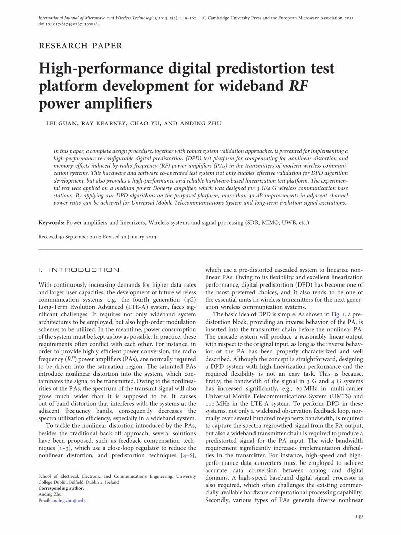
The basic idea of DPD is simple. As shown in Fig. 1, a pre-distortion block, providing an inverse behavior of the PA, isinserted into the transmitter chain before the nonlinear PA.The cascade system will produce a reasonably linear outputwith respect to the original input, as long as the inverse behav-ior of the PA has been properly characterized and welldescribed. Although the concept is straightforward, designinga DPD system with high-linearization performance and therequired flexibility is not an easy task. This is because,firstly, the bandwidth of the signal in 3 G and 4 G systemshas increased significantly, e.g., 60 MHz in multi-carrierUniversal Mobile Telecommunications System (UMTS) and100 MHz in the LTE-A system. To perform DPD in thesesystems, not only a wideband observation feedback loop, nor-mally over several hundred megahertz bandwidth, is requiredto capture the spectra-regrowthed signal from the PA output,but also a wideband transmitter chain is required to produce apredistorted signal for the PA input. The wide bandwidthrequirement significantly increases implementation difficul-ties in the transmitter. For instance, high-speed and high-performance data converters must be employed to achieveaccurate data conversion between analog and digitaldomains. A high-speed baseband digital signal processor isalso required, which often challenges the existing commer-cially available hardware computational processing capability.Secondly, various types of PAs generate diverse nonlinear
Corresponding author:Anding ZhuEmail: [email protected]
School of Electrical, Electronic and Communications Engineering, UniversityCollege Dublin, Belfield, Dublin 4, Ireland
149
International Journal of Microwave and Wireless Technologies, 2013, 5(2), 149–162. # Cambridge University Press and the European Microwave Association, 2013doi:10.1017/S1759078713000184
behaviors. The DPD unit must be able to describe variousnonlinear behaviors in order to keep its high-linearizationperformance. Furthermore, in order to rapidly evaluatevarious DPD algorithms, flexible software algorithm emula-tion and robust re-configurable hardware algorithm validationare also required. Finally, DPD development is a systemengineering project, which involves various parts of thesystem, from the analog RF front-end to the digital baseband,and it requires a wide range of knowledge and experience,from algorithm development to software programming andhardware design.
Currently, most of the predistortion systems/platforms areinstrument based, such as Signal Generator – Vector SignalAnalyzer-based test benches [4–7], or similarly ArbitraryWaveform Generator – Digital Oscilloscope-based testsystems [8]. These instrument-based platforms suffer fromseveral drawbacks, such as high-financial cost and relativelynarrow bandwidth. Although some new instruments havebeen upgraded to support 160 MHz analysis bandwidth, thedominant commercially used test benches typically onlysupport 80 MHz, which means that they are only suitablefor signals with bandwidths up to 40 MHz+. The otherDPD platforms/systems that have appeared in the literaturemainly focused on field programmable gate array (FPGA)implementations of the DPD algorithms [9–13]. There hasnot been a single paper discussing a complete systemimplementation including digital baseband signal processingand analog RF front-end.
In this paper, we present a complete design procedure forimplementing a flexible FPGA-based DPD platform, whichincludes an analog RF front-end, a digital baseband unitand a system control panel. This platform provides two oper-ational modes: software algorithm validation mode and hard-ware linearization evaluation mode. The two modes arecomplimentary to each other and provide a good balancebetween algorithm validation complexity and physical linear-ization performance. Moreover, by applying the dual-loopDPD technique [14] and newly developed band-limitedDPD models [15, 16], an excellent linearization performancecan be achieved with limited hardware and softwareresources.
The paper is organized as follows. After analyzing the func-tional requirements of the platform at the system level inSection II, the design procedures will be discussed in threeseparated parts: analog RF front-end, digital baseband, andhosting PC in Sections III, IV, and V, respectively. Therobust validation methodology and experimental resultswill be given in Section VI, followed by a conclusion inSection VII.
I I . D P D S Y S T E M O V E R V I E W A N DF U N C T I O N A L R E Q U I R E M E N T S A TT H E S Y S T E M L E V E L
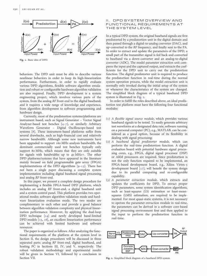
In a typical DPD system, the original baseband signals are firstpredistorted by a predistortion unit in the digital domain andthen passed through a digital-to-analog converter (DAC), andup-converted to the RF frequency, and finally sent to the PA.In order to extract and update the parameters of the DPD, asmall part of the transmitter signal is fed back and convertedto baseband via a down-converter and an analog-to-digitalconverter (ADC). The model parameter extraction unit com-pares the input and the captured output, and extracts the coef-ficients for the DPD unit to carry out the predistortionfunction. The digital predistorter unit is required to producethe predistortion function in real-time during the normalsystem operation process, while the model extraction unit isnormally only invoked during the initial setup of the systemor whenever the characteristics of the system are changed.The simplified block diagram of a typical baseband DPDsystem is illustrated in Fig. 2.
In order to fulfill the roles described above, an ideal predis-tortion test platform must have the following four functionalmodules:
(1) A flexible signal source module, which provides variousbaseband signals to be tested. To easily generate arbitrarytest waveforms at a designated data rate, software runningon a personal computer (PC), e.g., MATLAB, can be con-sidered as a good option, because of its flexibility indealing with signal processing;
(2) A baseband digital predistorter module, which canperform the real-time predistortion function. A digitalevaluation board with potential hardware signal proces-sing cores, e.g., FPGA, digital signal processor (DSP)or ARM processors are required. Since predistortion isnot the only function required to be implemented, anFPGA-based development board, e.g., Xilinx Virtex-5development board [17], will benefit the system designdue to its parallel computing and re-configurablecapability.
(3) A parameter extraction module, which extracts andupdates the coefficients for DPD. To extract properDPD parameters, some system identification algorithms,such as least-squares (LS) estimation or least-mean-squares (LMS) estimation, are required to be imple-mented. For most quasi-static systems, it is not necessaryto operate the parameter extraction module in real-time,the parameters can be derived in a software core-basedsignal processing environment first and then applied tothe input to perform the predistortion function inreal-time.
Fig. 2. Simplified block diagram of a baseband DPD system.
Fig. 1. Basic idea of DPD.
150 lei guan et al.
(4) An RF transceiver module, which can carry out data con-version between digital and analog domains, as well as up/down conversion between baseband and RF. To accu-rately convert the data between digital baseband andanalog RF, a high-performance and linear transceiver isrequired, including high-speed DAC/ADC stages, andlow-noise modulation/demodulation.
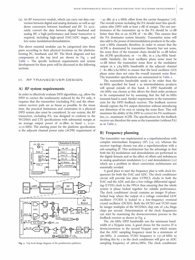
The above essential modules can be categorized into threeparts according to their physical locations on the platform:hosting PC, baseband, and RF. The block diagram and keycomponents at the top level are shown in Fig. 3 andTable 1. The specific technical requirements and systemdevelopment for these parts will be discussed in the followingsections.
I I I . R F T R A N S C E I V E R D E S I G N
A) RF system requirementsIn order to effectively evaluate DPD algorithms, e.g., allow theDPD to correct the nonlinearity induced by the PA only, itrequires that the transmitter (excluding PA) and the obser-vation receiver path are as linear as possible. In the meantime, the practical limitations and constraints in a physicalDPD system also must be considered. In our system, the RFtransceiver, excluding PA, was designed to conform to theWCDMA and LTE specifications with substantial margin atan average output power of 20 dBm in band 1, 2110–2170 MHz. The starting point for the platform specificationis the adjacent channel power ratio (ACPR) requirement of
245 dBc at a 5-MHz offset from the carrier frequency [18].The overall system including the PA should meet this specifi-cation after DPD with at least 5 dB of margin. The raw per-formance of the transmitter up to the PA should be 10 dBbetter than this or an ACPR of 260 dBc. This ensures thatthe PA dominates system linearity. Transmitter noise willalso add to the power of intermodulation products in the adja-cent 5 MHz channels; therefore, in order to ensure that theACPR is dominated by transmitter linearity but not noise,the noise floor of the transmit chain should be 10 dB belowthe ACPR specification, or 270 dBc, in a 3.84-MHz band-width. Similarly, the local oscillator phase noise must be10 dB below the transmitter noise floor at the modulatoroutput in a 3.84 MHz bandwidth at the adjacent channel(280 dBc/3.84 MHz) to ensure that the local oscillator (LO)phase noise does not raise the overall transmit noise floor.The transmitter specifications are summarized in Table 2.
The transmitter bandwidth needs to be wider than the60 MHz specified for band 1 as intermodulation productswill spread outside of this band. A DPD bandwidth of180 MHz was chosen as this allows the third-order productsto be compensated for by assuming that the full 60 MHztransmit band is used. Similar requirements to the transmitterexist for the DPD feedback receiver. The feedback receivershould capture the PA output distortion without introducingany distortion of its own or raising the noise floor. This willmaximize the ability of the DPD to correct for PA nonlineari-ties, i.e., maximum ACPR. The specifications for the feedbackreceiver are therefore the same as the transmitter (without PA)as in Table 2.
B) Frequency planningThe transmitter was implemented as a superheterodyne withcomplex intermediate frequency (IF) [19, 20], whereas thereceiver topology chosen was also a superheterodyne with asub-sampling IF. This architecture has the advantage in thatboth the IQ modulation and demodulation are performed inthe digital domain and so the effect of offsets and imbalancesin analog quadrature modulators [21] and demodulators [22]which are a problem in direct conversion architectures areessentially avoided.
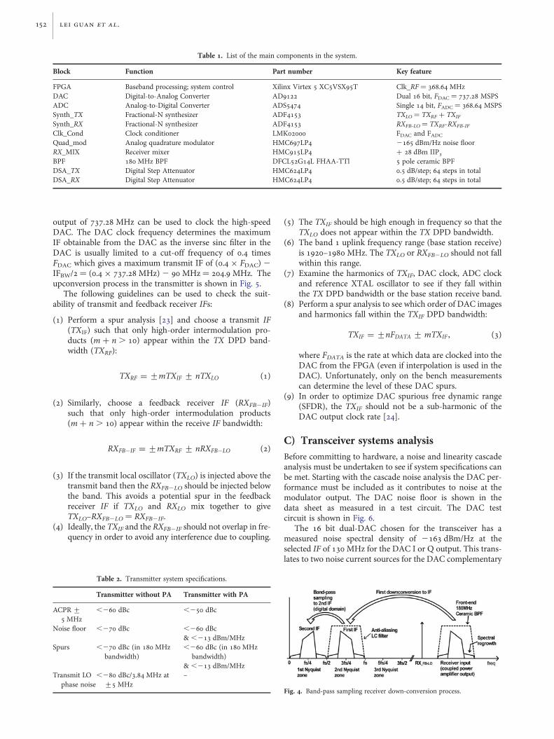
A good place to start the frequency plan is with clock fre-quencies for both the DAC and ADC. The clock conditionercircuit will provide low jitter LVPECL clocks to both theDAC and the ADC and also a low-voltage differential signal-ing (LVDS) clock to the FPGA thus ensuring that the wholesystem is phase locked together for reliable performance.The clock conditioner circuit contains an integer N-phase-locked loop where the output of a voltage controlled SAWoscillator (VCSO) is locked to a low-frequency ovenizedcrystal oscillator (OCXO). Both the OCXO and VCSO mustbe integer multiples of the WCDMA chip rate of 3.84 Megachips per second. Determination of the clock frequenciescan start by examining the downconversion process in thefeedback receiver as shown in Fig. 4.
The 180 MHz DPD bandwidth sets the minimum band-width of a Nyquist zone. A good choice for the receive IF isdownconversion to the second Nyquist zone which meansthat the ADC sampling frequency must be a minimum of360 MHz. A common VCSO frequency is 737.28 MHz sodividing this by 2 in the clock conditioner will give an ADCsampling frequency of 368.64 MHz. The clock conditionerFig. 3. Top level design diagram of the predistortion platform.
high-performance digital predistortion test platform development 151
output of 737.28 MHz can be used to clock the high-speedDAC. The DAC clock frequency determines the maximumIF obtainable from the DAC as the inverse sinc filter in theDAC is usually limited to a cut-off frequency of 0.4 timesFDAC which gives a maximum transmit IF of (0.4 × FDAC) 2
IFBW/2 ¼ (0.4 × 737.28 MHz) 2 90 MHz ¼ 204.9 MHz. Theupconversion process in the transmitter is shown in Fig. 5.
The following guidelines can be used to check the suit-ability of transmit and feedback receiver IFs:
(1) Perform a spur analysis [23] and choose a transmit IF(TXIF) such that only high-order intermodulation pro-ducts (m + n . 10) appear within the TX DPD band-width (TXRF):
TXRF = +mTXIF + nTXLO (1)
(2) Similarly, choose a feedback receiver IF (RXFB2IF)such that only high-order intermodulation products(m + n . 10) appear within the receive IF bandwidth:
RXFB−IF = +mTXRF + nRXFB−LO (2)
(3) If the transmit local oscillator (TXLO) is injected above thetransmit band then the RXFB2LO should be injected belowthe band. This avoids a potential spur in the feedbackreceiver IF if TXLO and RXLO mix together to giveTXLO–RXFB2LO ¼ RXFB2IF.
(4) Ideally, the TXIF and the RXFB2IF should not overlap in fre-quency in order to avoid any interference due to coupling.
(5) The TXIF should be high enough in frequency so that theTXLO does not appear within the TX DPD bandwidth.
(6) The band 1 uplink frequency range (base station receive)is 1920–1980 MHz. The TXLO or RXFB2LO should not fallwithin this range.
(7) Examine the harmonics of TXIF, DAC clock, ADC clockand reference XTAL oscillator to see if they fall withinthe TX DPD bandwidth or the base station receive band.
(8) Perform a spur analysis to see which order of DAC imagesand harmonics fall within the TXIF DPD bandwidth:
TXIF = +nFDATA + mTXIF , (3)
where FDATA is the rate at which data are clocked into theDAC from the FPGA (even if interpolation is used in theDAC). Unfortunately, only on the bench measurementscan determine the level of these DAC spurs.
(9) In order to optimize DAC spurious free dynamic range(SFDR), the TXIF should not be a sub-harmonic of theDAC output clock rate [24].
C) Transceiver systems analysisBefore committing to hardware, a noise and linearity cascadeanalysis must be undertaken to see if system specifications canbe met. Starting with the cascade noise analysis the DAC per-formance must be included as it contributes to noise at themodulator output. The DAC noise floor is shown in thedata sheet as measured in a test circuit. The DAC testcircuit is shown in Fig. 6.
The 16 bit dual-DAC chosen for the transceiver has ameasured noise spectral density of 2163 dBm/Hz at theselected IF of 130 MHz for the DAC I or Q output. This trans-lates to two noise current sources for the DAC complementary
Table 1. List of the main components in the system.
Block Function Part number Key feature
FPGA Baseband processing; system control Xilinx Virtex 5 XC5VSX95T Clk_RF ¼ 368.64 MHzDAC Digital-to-Analog Converter AD9122 Dual 16 bit, FDAC ¼ 737.28 MSPSADC Analog-to-Digital Converter ADS5474 Single 14 bit, FADC ¼ 368.64 MSPSSynth_TX Fractional-N synthesizer ADF4153 TXLO ¼ TXRF + TXIF
Synth_RX Fractional-N synthesizer ADF4153 RXFB-LO ¼ TXRF-RXFB-IF
Clk_Cond Clock conditioner LMK02000 FDAC and FADC
Quad_mod Analog quadrature modulator HMC697LP4 2165 dBm/Hz noise floorRX_MIX Receiver mixer HMC915LP4 + 28 dBm IIP3
BPF 180 MHz BPF DFCL52G14L FHAA-TTl 5 pole ceramic BPFDSA_TX Digital Step Attenuator HMC624LP4 0.5 dB/step; 64 steps in totalDSA_RX Digital Step Attenuator HMC624LP4 0.5 dB/step; 64 steps in total
Fig. 4. Band-pass sampling receiver down-conversion process.
Table 2. Transmitter system specifications.
Transmitter without PA Transmitter with PA
ACPR +5 MHz
,260 dBc ,250 dBc
Noise floor ,270 dBc ,260 dBc& ,213 dBm/MHz
Spurs ,270 dBc (in 180 MHzbandwidth)
,260 dBc (in 180 MHzbandwidth)
& ,213 dBm/MHzTransmit LO
phase noise,280 dBc/3.84 MHz at
+5 MHz–
152 lei guan et al.

outputs with noise current spectral densities of 60 pA/[(Hz)1/2]each. The noise voltage at the quadrature modulator basebandinputs was simulated as 1.65 nV/[(Hz)1/2] as shown in Fig. 7.
The modulator itself has an extremely low output noisefloor (Nmod_added) of 2165 dBm/Hz. Added to this is thenoise from the DAC appearing at the modulator output(2164.2 dBm/Hz). The calculation is shown in Eq. (4)where the resulting total broadband noise power at the modu-lator output, Nmod, is 2161.6 dBm/Hz.
Nmod dBm( ) = 10 log(gv × Vn bb I)2 + (gv × Vn bb �I)2
50
([
+10
[Nmod added
10− 3
])× 103
](4)
Consideration must also be given to the phase noise of thelocal oscillator as it may raise the noise floor in the adjacentchannel at the quadrature modulator output as shown in Fig. 8.
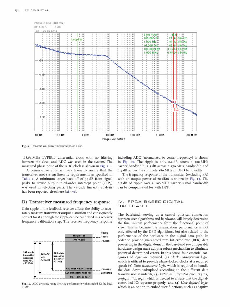
The transmitter local oscillator phase noise is shown reci-procally mixed onto each LTE subcarrier and this noisespills into the adjacent channel [25]. The transmit synthesizerphase noise was measured with a Rohde & Schwarz FSUP asshown in Fig. 9.
Using a 5 MHz LTE signal as an example the phase noisefor each subcarrier must be integrated over the 4.5 MHzadjacent channel bandwidth. For optimum system ACPRperformance, the baseband drive levels into the analog quad-rature modulator have been set so that the quadrature modu-lator output power level is 216 dBm. The power level of eachof the 5 MHz LTE signal’s 300 subcarriers is therefore given as216 dBm 2 10 log(300) ¼ 240.7 dBm (assuming equalpower levels for each subcarrier). The resulting integrationyields a phase noise power of 2113.6 dBm/4.5 MHz in theadjacent channel at a 5 MHz offset. The broadband noise
from the modulator was previously given as 2161.6 dBm/Hzor 295 dBm/4.5 MHz. As the LO phase noise in the adjacentchannel is 18.6 dB below the quadrature modulator outputnoise floor it does not raise the noise floor for our system.
The noise floor at the modulator output sets the systemsignal-to-noise ratio (excluding distortion) as further linearstages do not degrade this value. The single carrier 5 MHzLTE alternate channel (10 MHz offset) at the modulatoroutput is dominated by system noise and therefore has a limit-ing value of 295 dBm/4.5 MHz 2 (216 dBm/4.5 MHz) ¼279 dBc. This value is well within target specifications of270 dBc and has been verified by measurement. Furthermore,the broadband transmitter noise must meet the more demand-ing spurious emissions specification of 230 dBm/MHz at a10 MHz offset below or above the band edge (where theduplex filter will have little attenuation) for a category B basestation [26, 27]. For example, if the base station has an outputpower of 100 W or 50 dBm the gain required from themodulator output to the antenna connector will be 50 dBm–(216 dBm) ¼ 66 dB. The noise floor will get a similar boostof 66 dB to 295 dBm/4.5 MHz + 66 dB ¼229 dBm/4.5 MHzor 235.5 dBm/MHz, which leaves 5.5 dB of margin.
On the feedback receiver side a 14 bit ADC is needed togive the minimum 270 dBc/3.84 MHz of noise floor as perthe specification in Table 2. The ADC dynamic range isshown in Fig. 10.
The measured noise floor at the ADC input in a 3.84 MHzbandwidth for a single carrier WCDMA signal is 275.15 dBc.This is the SNR of the transmitter and receiver path up to theADC input. After sampling the SNR is reduced to 71.4 dB (seethe sampling performance results in the Section VI) due toADC noise. From these two measurements the ADC SNR iscalculated as 73.77 dB/3.84 MHz. This figure includes a6.5 dB PAR for the single-carrier WCDMA signal plus 1 dBof back-off from ADC full scale. The stand alone ADC SNRis therefore 81.27 dBFS. The jitter performance of the ADCclock has a significant impact on the ADC SNR. A
Fig. 7. DAC noise contribution to modulator output noise.
Fig. 8. Reciprocal mixing of transmit LO phase noise onto LTE subcarriers.Fig. 6. DAC test circuit.
Fig. 5. Superheterodyne transmitter upconversion process.
high-performance digital predistortion test platform development 153
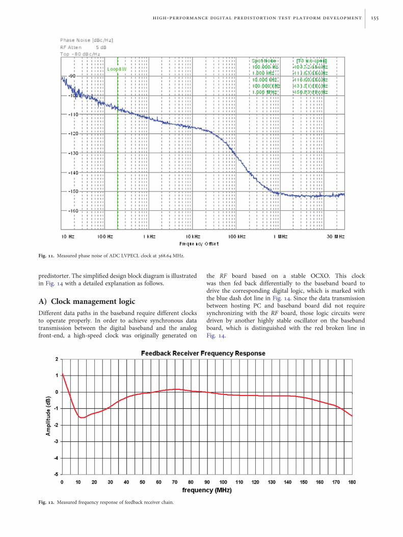
368.64 MHz LVPECL differential clock with no filteringbetween the clock and ADC was used in the system. Themeasured phase noise of the ADC clock is shown in Fig. 11.
A conservative approach was taken to ensure that thetransceiver met system linearity requirements as specified inTable 2. A minimum target back-off of 35 dB from signalpeaks to device output third-order intercept point (OIP3)was used in selecting parts. The cascade linearity analysishas been reported elsewhere [28–30].
D) Transceiver measured frequency responseGain ripple in the feedback receiver affects the ability to accu-rately measure transmitter output distortion and consequentlycorrect for it although the ripple can be calibrated in a receiverfrequency calibration step. The receiver frequency response
including ADC (normalized to center frequency) is shownin Fig. 12. The ripple is only 0.2 dB across a 100 MHzcarrier bandwidth, 1.5 dB across a 170 MHz bandwidth and2.5 dB across the complete 180 MHz of DPD bandwidth.
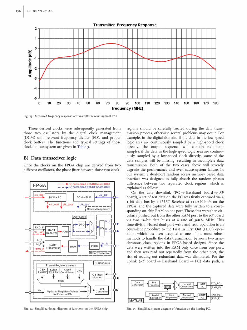
The frequency response of the transmitter (excluding PA)with an output power of 20 dBm is shown in Fig. 13. The1.7 dB of ripple over a 100 MHz carrier signal bandwidthcan be compensated for with DPD.
I V . F P G A - B A S E D D I G I T A LB A S E B A N D
The baseband, serving as a central physical connectionbetween user algorithms and hardware, will largely determinethe final system performance from the functional point ofview. This is because the linearization performance is notonly affected by the DPD algorithms, but also related to theperformance of the hardware in the digital data path. Inorder to provide guaranteed zero bit error rate (BER) dataprocessing in the digital domain, the baseband re-configurablehardware design must adopt a robust mechanism to eliminatepotential determined errors. In this sense, four essential cat-egories of logic are required: (1) Clock management logic,which is utilized to provide phase-locked clocks at a requiredspeed; (2) Data transceiver logic, which is required to handlethe data download/upload according to the different datatransmission standards; (3) External integrated circuits (ICs)configuration logic, which is needed to ensure that the digital-controlled ICs operate properly; and (4) User defined logic,which is an option to embed user functions, such as adaptive
Fig. 9. Transmit synthesizer measured phase noise.
Fig. 10. ADC dynamic range showing performance with sampled TX fed backto RX.
154 lei guan et al.
predistorter. The simplified design block diagram is illustratedin Fig. 14 with a detailed explanation as follows.
A) Clock management logicDifferent data paths in the baseband require different clocksto operate properly. In order to achieve synchronous datatransmission between the digital baseband and the analogfront-end, a high-speed clock was originally generated on
the RF board based on a stable OCXO. This clockwas then fed back differentially to the baseband board todrive the corresponding digital logic, which is marked withthe blue dash dot line in Fig. 14. Since the data transmissionbetween hosting PC and baseband board did not requiresynchronizing with the RF board, those logic circuits weredriven by another highly stable oscillator on the basebandboard, which is distinguished with the red broken line inFig. 14.
Fig. 11. Measured phase noise of ADC LVPECL clock at 368.64 MHz.
Fig. 12. Measured frequency response of feedback receiver chain.
high-performance digital predistortion test platform development 155
Three derived clocks were subsequently generated fromthose two oscillators by the digital clock management(DCM) unit, relevant frequency divider (FD), and properclock buffers. The functions and typical settings of thoseclocks in our system are given in Table 3.
B) Data transceiver logicSince the clocks on the FPGA chip are derived from twodifferent oscillators, the phase jitter between those two clock-
regions should be carefully treated during the data trans-mission process, otherwise several problems may occur. Forexample, in the digital domain, if the data in the low-speedlogic area are continuously sampled by a high-speed clockdirectly, the output sequence will contain redundantsamples; if the data in the high-speed logic area are continu-ously sampled by a low-speed clock directly, some of thedata samples will be missing, resulting in incomplete datatransmission. Both of the two cases above will severelydegrade the performance and even cause system failure. Inour system, a dual-port random access memory based datainterface was designed to fully absorb the random phasesdifference between two separated clock regions, which isexplained as follows.
On the data downlink (PC � Baseband board � RFboard), a set of test data on the PC was firstly captured via a1-bit data bus by a UART Receiver at 115.2 K bit/s on theFPGA, and the captured data were fully written to a corre-sponding on-chip RAM on one port. These data were then cir-cularly pushed out from the other RAM port to the RF boardvia two 16-bit data buses at a rate of 368.64 MHz. Thistime-division-based dual-port write and read operation is anequivalent procedure to the First In First Out (FIFO) oper-ation, which has been accepted as one of the most robustmethods to handle the data transmission between two asyn-chronous clock regions in FPGA-based designs. Since thedata were written into the RAM only once from one port,and then was read out repeatedly from the other port, therisk of reading out redundant data was eliminated. For theuplink (RF board � Baseband Board � PC) data path, a
Fig. 13. Measured frequency response of transmitter (excluding final PA).
Fig. 14. Simplified design diagram of functions on the FPGA chip. Fig. 15. Simplified system diagram of function on the hosting PC.
156 lei guan et al.
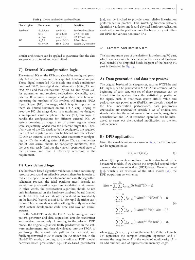
similar architecture can be applied to guarantee that the dataare properly captured and transmitted.
C) External ICs configuration logicThe external ICs on the RF board should be configured prop-erly before they produce the expected functional output.Those digital-controlled ICs include one clock conditioner,one dual DAC, two digital step attenuators (DSA_TX andDSA_RX) and two synthesizers (Synth_TX and Synth_RX)for transmitter and receiver, respectively. Generally, eachexternal IC requires a unique configuration path; however,increasing the numbers of ICs involved will increase FPGAInput/Output (I/O) pin usage, which is quite important asthere are limited resources on the FPGA chip. Trying tokeep the I/O pin usage down to a minimum, we designeda multiplexed serial peripheral interface (SPI) bus logic tohandle the configurations for different external ICs. Atsystem powering up stage, a set of pre-set register valueswere sequentially loaded into the different target ICs. Then,if any one of the ICs needs to be re-configured, the requireduser defined register values can be latched into the selectedIC with an external 8-bit switch. After successfully configur-ing the ICs, the working states of those ICs, e.g., synthesizerout of lock alarm, should be constantly monitored, thusthe user can easily find out the current operational state ofthe platform, and tune it efficiently according to therequirement.
D) User defined logicThe hardware-based algorithm validation is time consuming,resource costly, and an inflexible process, therefore in order toreduce the cycle time of development and ease the algorithmvalidation process, the ideal platform must provide aneasy-to-use predistortion algorithm validation environment.In other words, the predistortion algorithm should be notonly implemented on the hardware baseband board (namedas Hard-DPD), but also should be realized intermediatelyon the host PC (named as Soft-DPD) for rapid algorithm vali-dation. This two-mode operation will significantly reduce theDPD system development cycle time and save on overallexpense.
In the Soft-DPD mode, the FPGA can be configured as apattern generator and data acquisition unit for transmitterand receiver, respectively. According to the selected DPDmodel, the original signal was firstly predistorted in the soft-ware environment, and then downloaded into the FPGA togo through the normal data path in the baseband, andfinally upconverted to RF to excite the PA under test. In theHard-DPD mode, according to the validated DPD model,hardware-based predistorter, e.g., FPGA-based predistorter
[12], can be invoked to provide more reliable linearizationperformance in practice. This switching function betweenalgorithm validation mode and physical hardware realizationmode will make the platform more flexible to carry out differ-ent DPDs for various nonlinear PAs.
V . H O S T I N G P C P A R T
The last important part of the platform is the hosting PC part,which serves as an interface between the user and hardwarePCB boards. The simplified block diagram of the hosing PCpart is illustrated in Fig. 15.
A) Data generation and data pre-processThe original baseband data sequences, such as WCDMA andLTE signals, can be generated in MATLAB in advance. At thebeginning of each test, one set of those sequences can beloaded into the system. Since the statistical properties ofthe signal, such as root-mean-square (RMS) value andpeak-to-average power ratio (PAPR), are directly related tothe final linearization performance, data pre-processapproaches are required to provide a set of original testsignals satisfying the requirements. For example, magnitudenormalization and PAPR reduction operation can be intro-duced to carry out the required modification on the testdata sequence.
B) DPD applicationGiven the signal definition as shown in Fig. 1, the DPD outputcan be represented as
u(n) = H x(n)[ ], (5)
where H[.] represents a nonlinear function structured by thebehavioral models. If we choose the simplified second-orderdynamic deviation reduction (DDR)-based Volterra model[31], which is an extension of the DDR model [32], theDPD output can be written as
u(n) =∑P−1
2
k=0
∑M
i=0
g2k+1,1(i) x(n)| |2kx(n − i)
+∑P−1
2
k=1
∑M
i=1
g2k+1,2(i) x(n)| |2(k−1)x2(n)x∗(n − i)
+∑P−1
2
k=1
∑M
i=1
g2k+1,3(i) x(n)| |2(k−1)x(n) x(n − i)| |2
+∑P−1
2
k=1
∑M
i=1
g2k+1,4(i) x(n)| |2(k−1)x∗(n)x2(n − i),
(6)
where g2k+1,j(j = 1, 2, 3, 4) are the complex Volterra kernels,(.)∗ represents the complex conjugate operation and |.|returns the magnitude. P is the order of nonlinearity (P isan odd number) and M represents the memory length.
Table 3. Clocks involved on baseband board.
Clock region Clock name Speed Function
Baseband clk_BB_osc 100 MHz Baseband oscillatorclk_u 115.2 KHz UART bit rateclk_byte 14.4 KHz UART byte rate
RF clk_RF 368.64 MHz RF oscillatorclk_system 368.64 MHz System I/Q data rate
high-performance digital predistortion test platform development 157
In a compact form, (6) can be rewritten in a matrix format,
U = XC, (7)
where the matrix X contains all of the linear and productterms x(n), x(n − 1), . . ., x(n)| |2x(n), . . ., appearing in theinput of the model, for n ¼ 1, 2, . . ., N, and C represents theparameter vector containing all of the unknown coefficientsg2p+1,j(·). The vector U represents the DPD output vector.
C) Time alignment and parameters extractionTo extract the coefficients for DPD, the first step is to obtain apair of data including the input and its corresponding output.Since the physical data path introduces time delays into thesystem, proper time alignment is needed to get a “timematched” data pair. And then the pth-order post-inverse [4]or the in-direct learning technique [33] can be employed,where the feedback signal, e.g., the output of the PA, y(n), isused as the input of the model, while the predistortedoutput signal, u(n), is used as the expected output. Since theVolterra series models are linear-in-parameter, the simplelinear system identification approaches, e.g., LS estimationcan be utilized. For example, by employing the standard LSalgorithm, the coefficients vector C can be estimated from
C = (YH)Y[ ]−1
YHU, (8)
where Y is the PA output matrix in a similar form to thematrix X, and (.)H represents the Hermitian transpose.
D) Data format conversion and datatransceiverThe MATLAB environment uses the floating-point decimaldata format to process signals; however, the digital basebandcan only recognize the signal in binary format. Thereforeproper format conversion should be performed to satisfy thesystem requirements. For example, due to using a 16-bitDAC, the complex data in MALTAB should be convertedinto 16-bit binary format representation.
Moreover, depending on different interfaces between PCand baseband, the binary data will be packed according todifferent interface standards. For example, to transfer databetween PC and baseband through a UART interface, the16-bit binary data should be converted to an 8-bit (byte)binary data package for transmitting and vice versa for
receiving. Then the packaged data can be downloaded toFPGA or uploaded from FPGA for further signal processing.
V I . E X P E R I M E N T A L T E S TP R O C E D U R E S A N D E X A M P L EL I N E A R I Z A T I O N R E S U L T S
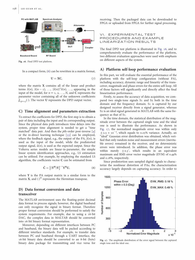
The final DPD test platform is illustrated in Fig. 16, and tocomprehensively evaluate the performance of the platform,two different evaluation approaches were used with emphasison different aspects of the system.
A) Platform self-loop performance evaluationIn this part, we will evaluate the essential performance of theplatform with the self-loop configuration (without PA),including accuracy, dynamic range and linearity of the trans-ceiver, magnitude and phase errors for the entire self-loop. Allof those factors will significantly and directly affect the finallinearization performance.
Firstly, to assess the accuracy of data acquisition, we com-pared two single-tone signals S1 and S2 both in the timedomain and the frequency domain. S1 is captured by ourdesigned receiver directly from a signal generator, whereasS2 is an ideal signal generated in MATLAB with the same fre-quency as that of S1.
In the time domain, the statistical distribution of the mag-nitude error between the captured single tone and the idealone is used to illustrate the performance. As shown inFig. 17, the normalized magnitude error was within only+2.5 × 10²³, which equals to 0.25% variance. Actually, an“ideal” Gaussian error distribution was obtained, which veri-fied that only random noise and measurement errors (inevita-ble errors) remained in the receiver, and no deterministicerrors were introduced. In addition, the phase error waswithin merely +0.38, which results in an equivalentmaximum and RMS error vector magnitude (EVM) of 0.49%and 0.18%, respectively.
Since predistortion uses sampled digital signals to charac-terize the nonlinear distortion of PAs, the characterizationaccuracy largely depends on capturing accuracy. In order to
Fig. 16. Final DPD test platform.
Fig. 17. The amplitude distribution of the error signal between the capturedsingle tone and the ideal one.
158 lei guan et al.
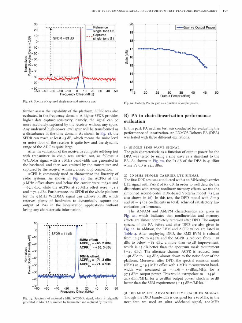
further assess the capability of the platform, SFDR was alsoevaluated in the frequency domain. A higher SFDR provideshigher data capture sensitivity, namely, the signal can bemore accurately captured by the receiver without any spurs.Any undesired high-power level spur will be transformed asa disturbance in the time domain. As shown in Fig. 18, theSFDR can reach at least 83 dB, which means the noise levelor noise floor of the receiver is quite low and the dynamicrange of the ADC is quite large.
After the validation of the receiver, a complete self-loop testwith transmitter in chain was carried out, as follows: aWCDMA signal with a 5 MHz bandwidth was generated inthe baseband, and then was emitted by the transmitter andcaptured by the receiver within a closed loop connection.
ACPR is commonly used to characterize the linearity ofradio systems. As shown in Fig. 19, the ACPRs at the5 MHz offset above and below the carrier were 265.2 and265.3 dBc, while the ACPRs at 10 MHz offset were 271.3and 271.4 dBc. Furthermore, the SFDR of the whole platformfor the 5 MHz WCDMA signal can achieve 71 dB, whichreserves plenty of headroom to dynamically capture theoutput of PAs in the linearization applications withoutlosing any characteristic information.
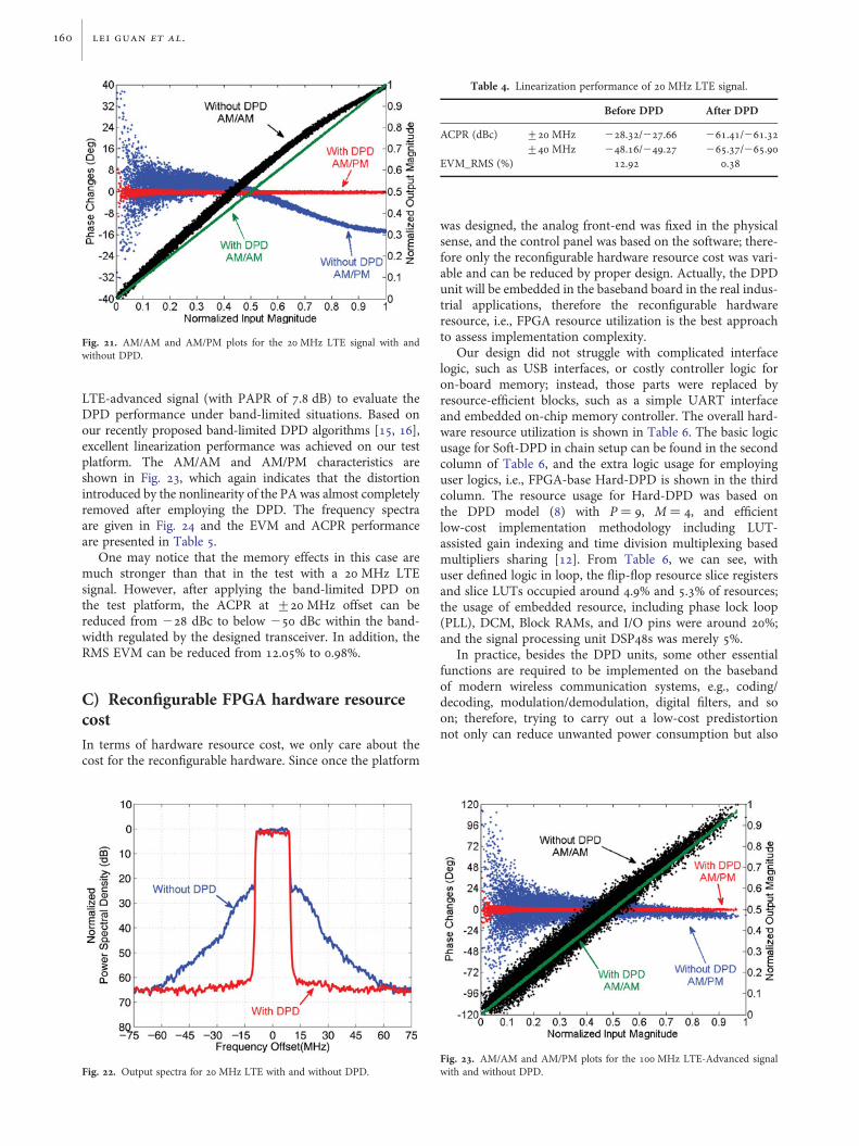
B) PA in-chain linearization performanceevaluationIn this part, PA in chain test was conducted for evaluating theperformance of linearization. An LDMOS Doherty PA (DPA)was tested with three different excitations.
1) single sine wave signal
The gain characteristic as a function of output power for theDPA was tested by using a sine wave as a stimulant to thePA. As shown in Fig. 20, the P1 dB of the DPA is 41 dBmwhile P2 dB is 44.3 dBm.
2) 20 mhz single carrier lte signal
The first DPD test was conducted with a 20 MHz single carrierLTE signal with PAPR of 6.5 dB. In order to well describe thedistortions with strong nonlinear memory effects, we use thesimplified second-order DDR-based Volterra model [31], asalso shown in (6). In this test, the DPD model with P ¼ 9and M ¼ 4 (73 coefficients in total) achieved satisfactory lin-earization performance.
The AM/AM and AM/PM characteristics are given inFig. 21, which indicates that nonlinearities and memoryeffects are almost completely removed after DPD. The outputspectra of the PA before and after DPD are also given inFig. 22. In addition, the EVM and ACPR values are listed inTable 4. After employing DPD, the RMS EVM is reducedfrom 12.92% to 0.38% and the ACPR is reduced from 228dBc to below 261 dBc, a more than 30 dB improvement,which is 15 dB better than the spectrum mask requirement(245 dBc). The alternate channel ACPR is reduced from248 dBc to 265 dBc, almost down to the noise floor of theplatform. Moreover, after DPD, the spectral emission mask(SEM) at +19.5 MHz offset with 1 MHz measurement band-width was measured as 237.6/ 2 37 dBm/MHz for a37.3 dBm output power. This would extrapolate to 224.9/ 2
24.3 dBm/MHz, for a 50 dBm output power which is 10 dBbetter than the SEM requirement (213 dBm/MHz).
3) 100 mhz lte-advanced five-carrier signal
Though the DPD bandwidth is designed for 180 MHz, in thenext test, we used an ultra wideband signal, 100 MHz
Fig. 18. Spectra of captured single-tone and reference one. Fig. 20. Doherty PA cw gain as a function of output power.
Fig. 19. Spectrum of captured 5 MHz WCDMA signal, which is originallygenerated in MATLAB, emitted by transmitter and captured by receiver.
high-performance digital predistortion test platform development 159
LTE-advanced signal (with PAPR of 7.8 dB) to evaluate theDPD performance under band-limited situations. Based onour recently proposed band-limited DPD algorithms [15, 16],excellent linearization performance was achieved on our testplatform. The AM/AM and AM/PM characteristics areshown in Fig. 23, which again indicates that the distortionintroduced by the nonlinearity of the PA was almost completelyremoved after employing the DPD. The frequency spectraare given in Fig. 24 and the EVM and ACPR performanceare presented in Table 5.
One may notice that the memory effects in this case aremuch stronger than that in the test with a 20 MHz LTEsignal. However, after applying the band-limited DPD onthe test platform, the ACPR at +20 MHz offset can bereduced from 228 dBc to below 250 dBc within the band-width regulated by the designed transceiver. In addition, theRMS EVM can be reduced from 12.05% to 0.98%.
C) Reconfigurable FPGA hardware resourcecostIn terms of hardware resource cost, we only care about thecost for the reconfigurable hardware. Since once the platform
was designed, the analog front-end was fixed in the physicalsense, and the control panel was based on the software; there-fore only the reconfigurable hardware resource cost was vari-able and can be reduced by proper design. Actually, the DPDunit will be embedded in the baseband board in the real indus-trial applications, therefore the reconfigurable hardwareresource, i.e., FPGA resource utilization is the best approachto assess implementation complexity.
Our design did not struggle with complicated interfacelogic, such as USB interfaces, or costly controller logic foron-board memory; instead, those parts were replaced byresource-efficient blocks, such as a simple UART interfaceand embedded on-chip memory controller. The overall hard-ware resource utilization is shown in Table 6. The basic logicusage for Soft-DPD in chain setup can be found in the secondcolumn of Table 6, and the extra logic usage for employinguser logics, i.e., FPGA-base Hard-DPD is shown in the thirdcolumn. The resource usage for Hard-DPD was based onthe DPD model (8) with P ¼ 9, M ¼ 4, and efficientlow-cost implementation methodology including LUT-assisted gain indexing and time division multiplexing basedmultipliers sharing [12]. From Table 6, we can see, withuser defined logic in loop, the flip-flop resource slice registersand slice LUTs occupied around 4.9% and 5.3% of resources;the usage of embedded resource, including phase lock loop(PLL), DCM, Block RAMs, and I/O pins were around 20%;and the signal processing unit DSP48s was merely 5%.
In practice, besides the DPD units, some other essentialfunctions are required to be implemented on the basebandof modern wireless communication systems, e.g., coding/decoding, modulation/demodulation, digital filters, and soon; therefore, trying to carry out a low-cost predistortionnot only can reduce unwanted power consumption but also
Fig. 21. AM/AM and AM/PM plots for the 20 MHz LTE signal with andwithout DPD.
Fig. 22. Output spectra for 20 MHz LTE with and without DPD.
Table 4. Linearization performance of 20 MHz LTE signal.
Before DPD After DPD
ACPR (dBc) +20 MHz 228.32/227.66 261.41/261.32+40 MHz 248.16/249.27 265.37/265.90
EVM_RMS (%) 12.92 0.38
Fig. 23. AM/AM and AM/PM plots for the 100 MHz LTE-Advanced signalwith and without DPD.
160 lei guan et al.

is prudent to reserve limited resource for baseband integrationwith any other essential algorithms.
V I I . C O N C L U S I O N
In this paper, we presented a complete design and test processfor implementing a high performance re-configurable soft-ware/hardware co-operated DPD platform. Although weonly demonstrated experimental results for Volterra series-based DPD models for a medium power DPA in this paper,this platform can be used to evaluate various DPD algorithmsfor various types of RF PAs operated at a wide range of con-ditions. The FPGA implementation of the DPD block can alsobe easily extended to other types of digital circuits, suchas general DSP chips, or application-specific integratedcircuits.
R E F E R E N C E S
[1] Faulkner, M.: Amplifier linearization using RF feedback and feedfor-ward techniques. IEEE Trans. Veh. Technol., 47 (1) (1998), 209–215.
[2] Botti, M.E.; Dallago, E.; Venchi, G.: PWM power audio amplifierwith voltage/current mixed feedback for high-efficiency speakers.IEEE Trans. Ind. Electron., 54 (2) (2007), 1141–1149.
[3] Woo, Y.Y. et al.: Adaptive digital feedback predistortion techniquefor linearizing power amplifiers. IEEE Trans. Microw. TheoryTech., 55 (5) (2007), 932–940.
[4] Zhu, A.; Draxler, P.J.; Yan, J.J.; Brazil, T.J.; Kinball, D.F.; Asbeck,P.M.: Open-loop digital predistorter for RF power amplifiers usingdynamic deviation reduction-based Volterra series. IEEE Trans.Microw. Theory Tech., 56 (7) (2008), 1524–1534.
[5] Braithwaite, R.N.: An improved Doherty amplifier using cascadeddigital predistortion and digital gate voltage enhancement. IEEETrans. Microw. Theory Tech., 57 (12) (2009), 3118–3126.
[6] Kim, J.; Park, C.; Moon, J.; Kim, B.: Analysis of adaptive digital feed-back linearization techniques. IEEE Trans. Circuits. Syst. II, ExpressBriefs, 57 (2) (2010), 345–353.
[7] Younes, M.; Hammi, O.; Kwan, A.; Ghannouchi, F.M.: An accuratecomplexity-reduced “PLUME” model for behavioral modeling anddigital predistortion of RF power amplifiers. IEEE Trans. Ind.Electron., 58 (4) (2011), 1397–1405.
[8] Cao, H.; Nemati, H.M.; Tehrani, A.S.; Eriksson, T.; Grahn, J.; Fager,C.: Linearization of efficiency-optimized dynamic load modulationtransmitter architectures. IEEE Trans. Microw. Theory Tech., 58(4) (2010), 873–881.
[9] Mato, J.L.; Pereira, M.; Rodrıguez-Andina, J.J.; Farina, J.; Soto, E.;Perez, R.: Distortion mitigation in RF power amplifiers throughFPGA based amplitude and phase predistortion. IEEE Trans. Ind.Electron., 55 (11) (2008), 4085–4093.
[10] Gilabert, P.L.; Cesari, A.; Montoro, G.; Bertran, E.; Dilhac, J.-M.:Multi-lookup table FPGA implementation of an adaptive digital pre-distorter for linearizing RF power amplifiers with memory effects.IEEE Trans. Microw. Theory Tech., 56 (2) (2008), 372–384.
[11] Rawat, K.; Rawat, M.; Ghannouchi, F.M.: Compensating I–Q imper-fections in hybrid RF/digital predistortion with an adapted look-uptable implemented in an FPGA. IEEE Trans. Circuits. Syst. II,Express Briefs, 57 (5) (2010), 389–393.
[12] Guan, L.; Zhu, A.: Low-cost FPGA implementation of Volterraseries-based digital predistorter for RF power amplifiers. IEEETrans. Microw. Theory Tech., 58 (4) (2010), 866–872.
[13] Kwan, A.; Ghannouchi, F.M.; Hammi, O.; Helaoui, M.; Smith, M.R.:Look-up table-based digital predistorter implementation for FPGAusing long-term evolution signals with 60 MHz bandwidth. IETSci. Meas. Technol., 6 (3) (2012), 181–188.
[14] Guan, L.; Zhu, A.: Dual-loop model extraction for digital predistor-tion of wideband RF power amplifiers. IEEE Microw. Wirel.Compon. Lett., 21 (9) (2011), 501–503.
[15] Yu, C.; Guan, L.; Zhu, E.; Zhu, A.: Band-limited Volterra series-baseddigital predistortion for wideband RF power amplifiers. IEEE Trans.Microw. Theory Tech., 60 (12) (2012), 4198–4208.
[16] Guan, L.; Yu, C.; Zhu, A.: Bandwidth-constrained least squares-based model extraction for band-limited digital predistortion of RFpower amplifiers, in IEEE Int. Workshop on Integrated NonlinearMicrowave and Millimeterwave Circuits, INMMIC, Dublin,Ireland, September, 2012, 1–3.
[17] Http://www.xilinx.com
Fig. 24. Output spectra for 100 MHz LTE-Advanced with and without DPD.
Table 5. Linearization performance of 100 MHz LTE-A signal.
Before DPD After DPD
ACPR (dBc) +20 MHz 230.69/227.82 251.02/252.22EVM_RMS (%) 12.05 0.98
Table 6. FPGA resource utilization.
Usage(systemlogic∗)
Usage(userlogic†)
Total‡ Percentage
Soft-DPD Hard-DPD
I/O 110 2 640 17.2% 17.2%Slice Registers 1589 1282 58 880 2.7% 4.9%Slice LUTs 1690 1418 58 880 2.7% 5.3%PLL 1 2 6 16.7% 16.7%DCM 3 2 12 25% 25%BlockRAM
(32 kb)40 18 244 16.4% 23.8%
DSP48 0 32 640 0% 5%
∗Refers to basic logic for platform with soft-DPD.†Refers to extra logic for employing FPGA-based hard-DPD.‡Based on Xilinx Virtex 5 XC5VSX95T chip.
high-performance digital predistortion test platform development 161
[18] Technical Specification TS 125 104. Universal MobileTelecommunications System (UMTS); Base Station (BS) radio trans-mission and reception (FDD).
[19] Boutin, N.: Complex Signals: Part III. RF Design, March 1990,109–115.
[20] Reine, S.: Gain, LO, and Phase Compensation in a Single SidebandTransmitter Using the AD9788 TxDAC and ADL5372 QuadratureModulator. Analog Devices, Application Note An-920.
[21] RF Micro Devices. Optimization of Quadrature ModulatorPerformance. AN0001.
[22] Wong, J.; Zou, M.; Stuetzle, D.; Hsiao, S.: A direct conversion I/Qdemodulator drives favorable basestation cost-performancemetrics. Microw. Eng. Eur., March 2008, 11–14.
[23] VanDyke, R.: Software shaves spurs in frequency planning, inMicrowaves & RF, 44 (6) (2005), 102, 104, 106, 108.
[24] Kester, W.: The Data Conversion Handbook. Analog Devices,Newnes, UK, 2005.
[25] Smaıni, L.: RF Analog Impairments Modeling for CommunicationSystems Simulation. Wiley, UK, 2012.
[26] 3GPP TS 36.141. Base Station Conformance Testing. V11.2,September, 2012.
[27] Brannon, B.; Schofield, B.: Multicarrier WCDMA Feasibility. AnalogDevices, Application Note, AN-807.
[28] Yin, P.: A simplified approximation method for cascaded systemadjacent and alternative channel power ratio. Appl. Microw.Wirel., 14 (4) (2002), 70–76.
[29] Small-Signal Intermodulation Distortion in OFDM TransmissionSystems. RF Micro Devices, Application Note, AN120214, 2012.
[30] Adjacent Channel Leakage Ratio (ACLR) Derivation for General RFDevices. Maxim Integrated Products, Application Note 3902.
[31] Guan, L.; Zhu, A.: Simplified dynamic deviation reduction-basedVolterra model for doherty power amplifiers, in IEEE Int.Workshop on Integrated Nonlinear Microwave and MillimeterwaveCircuits, INMMIC, Vienna, Austria, April, 2011, 1–4.
[32] Zhu, A.; Pedro, J.C.; Brazil, T.J.: Dynamic deviation reduction-basedVolterra behavioral modeling of RF power amplifiers. IEEE Trans.Microw. Theory Tech., 54 (12) (2006), 4323–4332.
[33] Eun, C.; Powers, E.J.: A new Volterra predistorter based on the indir-ect learning architecture. IEEE Trans. Signal Process., 45 (1) (1997),223–227.
Lei Guan received the B.E. degree andthe M.E. degree, both in ElectronicEngineering from Harbin Institute ofTechnology (HIT), Harbin, China in2006 and 2008, respectively. He wasawarded the Ph.D. degree in ElectronicEngineering in 2012 by University Col-lege Dublin (UCD), Dublin, Ireland.Then he served as a Senior Research
Engineer in UCD School of Electrical, Electronic and Com-munications Engineering. Currently, he is a Research Fellowin CTVR the Telecommunications Research Centre, TrinityCollege Dublin (TCD), Ireland. His research interests includedigital predistortion (DPD)-based linearization and system-level modeling of radio frequency (RF)/Microwave power
amplifiers (PAs); peak-to-average power ratio (PAPR)reduction for OFDM systems. He also has interests in non-linear system identification algorithms and FPGA-based par-allel computing, digital signal processing, wirelesscommunication system design and network protocol design.
Ray Kearney received a BSc. (Eng)degree in Electronic and Communi-cations Engineering from Dublin Insti-tute of Technology, Ireland in 1993and an MSc. degree in RF and Micro-wave Engineering from the Universityof Bradford, UK in 1994. From 1994 to1997 he worked for Nokia MobilePhones (UK) on analog handset
design. In 1998, he joined Lucent Technologies in Dublin towork on GSM base stations until their closure in 2001. He sub-sequently worked for TDK Electronics Ireland on GSM mod-ules and LTCC filters until 2006 when he joined Benetel Ltd todesign a femto-cell transceiver. In 2008, he joined the Instituteof Microelectronics and Wireless Systems at the National Uni-versity of Ireland, Maynooth where he worked on Class S RFPA’s. From 2009 to present he has been with University Col-lege Dublin where he designed RF hardware for the DPD testplatform described in this paper. He has also worked on low-power radar for biomotion sensors while at UCD.
Chao Yu received the B.E. and M.E.degrees from Southeast University,Nanjing, China, in 2007 and 2010,respectively. He is currently workingtoward the Ph.D. degree at UniversityCollege Dublin, Dublin, Ireland. His re-search interests include antenna design,behavioral modeling, and DPD for RFPAs.
Anding Zhu received the B.E. degree intelecommunication engineering fromNorth China Electric Power University,Baoding, China, in 1997, and the M.E.degree in computer applications fromBeijing University of Posts and Tele-communications, Beijing, China, in2000, and the Ph.D. degree in ElectronicEngineering from University College
Dublin (UCD), Dublin, Ireland, in 2004. He is currently a Lec-turer with the School of Electrical, Electronic and Communi-cations Engineering, UCD. His research interests includehigh-frequency nonlinear system modeling and devicecharacterization techniques with a particular emphasis onVolterra-series-based behavioral modeling and linearizationfor RF PAs. He is also interested in wireless and RF systemdesign, digital signal processing, and nonlinear systemidentification algorithms.
162 lei guan et al.