High Aspect Ratio Copper Filling of Through-Silicon-Vias ... · High Aspect Ratio Copper Filling of...
1
High Aspect Ratio Copper Filling of Through-Silicon-Vias by Bottom-Up Electroplating for Fabrication of 3D Air-core MEMS Inductors Io Mizushima*, Peter Torben Tang*, Hoà Lê Thanh** & Anpan Han** Concept Electroplating set-up and holders Bottom-up electroplating using different plating rates Plating through the wafer Pulse plating of copper Conclusion Acknowledgement TT 160914 *) IPU, Kgs. Lyngby, Denmark [[email protected]] **) DTU Danchip, Technical University of Denmark, Kgs. Lyngby, Denmark Silicon Copper Aluminum oxide The whole process has 12 steps, including coating of aluminium oxide on a silicon substrate, etching the coating with a mask, create through- silicon-vias (TSV), copper plating to close the TSVs, bottom-up electroplating to fill the TSVs, plating of the top layer, etching of the copper with a mask and finally etching of core silicon. In this work the copper filling of the through-silicon-vias with aspect ratio of 10:1 (width 30 µm and depth 300 µm) by bottom-up electroplating is in focus. Influence of current applied to the electroplating was investigated. Anode Cathode + - Air bobling The pulse waveform is consisting of current densities alternating 250 times between 1.56 A/dm² for 20 ms and 0.78 A/dm² for 20 ms of cathodic (normal) current, followed by 2.33 A/dm² for 500 ms of anodic (reverse) current. Repeat 250 times Current density (A/dm²) Time (ms) Wetting using ultrasonic stimulation helps closing the bottom conductor, since air in structure can disturb elecroplating and create a porous or interrupted metal via. Filling without vacuum treatment Generally it is difficult to fill high aspect ratio TSVs. Degassing in water, by using a vacuum chamber, improved copper filling significantly. Copper electroplating was applied succesfully for creating a toroidal inductor. Pulse plating was utilised for the top and bottom layers, while low current density DC plating was applied for bottom-up plating. Bottom-up electroplating of the TSVs could be achieved by introducing a wetting treatment subsequently using both ultra sound and vacuum. Lower current density improved the uniformity of the copper filling during bottom-up filling of the TSVs, but also leads to increased process time. Pulse plating can improve uniformity and reduce time consumption. Direct current at 0.3 A/dm² for 33 hours Direct current at 0.6 A/dm² for 11 hours Cross-section Surface pictures We are working for the development of a process for MEMS fabrication of micro-scale air-core toroidal inductors, especially designed for very high frequency (30-300 MHZ) switch mode power supplies (SMPS). Without wetting With wetting Sputtering of seed layer ① Electroplating bottom conductor ② Bottom-up electroplating ③ Sputtering of seed layer ④ Electroplating top conductor ⑤ Stainless steel plate Silicon wafer with TSVs and copper coating closing the TSVs Wire with pin contact This work is part of a project called “TinyPower: Ultra compact integrated power supplies” financed by Innovationsfonden in Denmark under file number 67-2014-1
Transcript of High Aspect Ratio Copper Filling of Through-Silicon-Vias ... · High Aspect Ratio Copper Filling of...
High Aspect Ratio Copper Filling of Through-Silicon-Vias by Bottom-UpElectroplating for Fabrication of 3D Air-core MEMS Inductors
Io Mizushima*, Peter Torben Tang*, Hoà Lê Thanh** & Anpan Han**
Concept
Electroplating set-up and holders Bottom-up electroplating using different plating rates
Plating through the wafer
Pulse plating of copper
Conclusion
Acknowledgement
TT 160914
*) IPU, Kgs. Lyngby, Denmark [[email protected]]
**) DTU Danchip, Technical University of Denmark, Kgs. Lyngby, Denmark
Silicon
Copper
Aluminum oxide
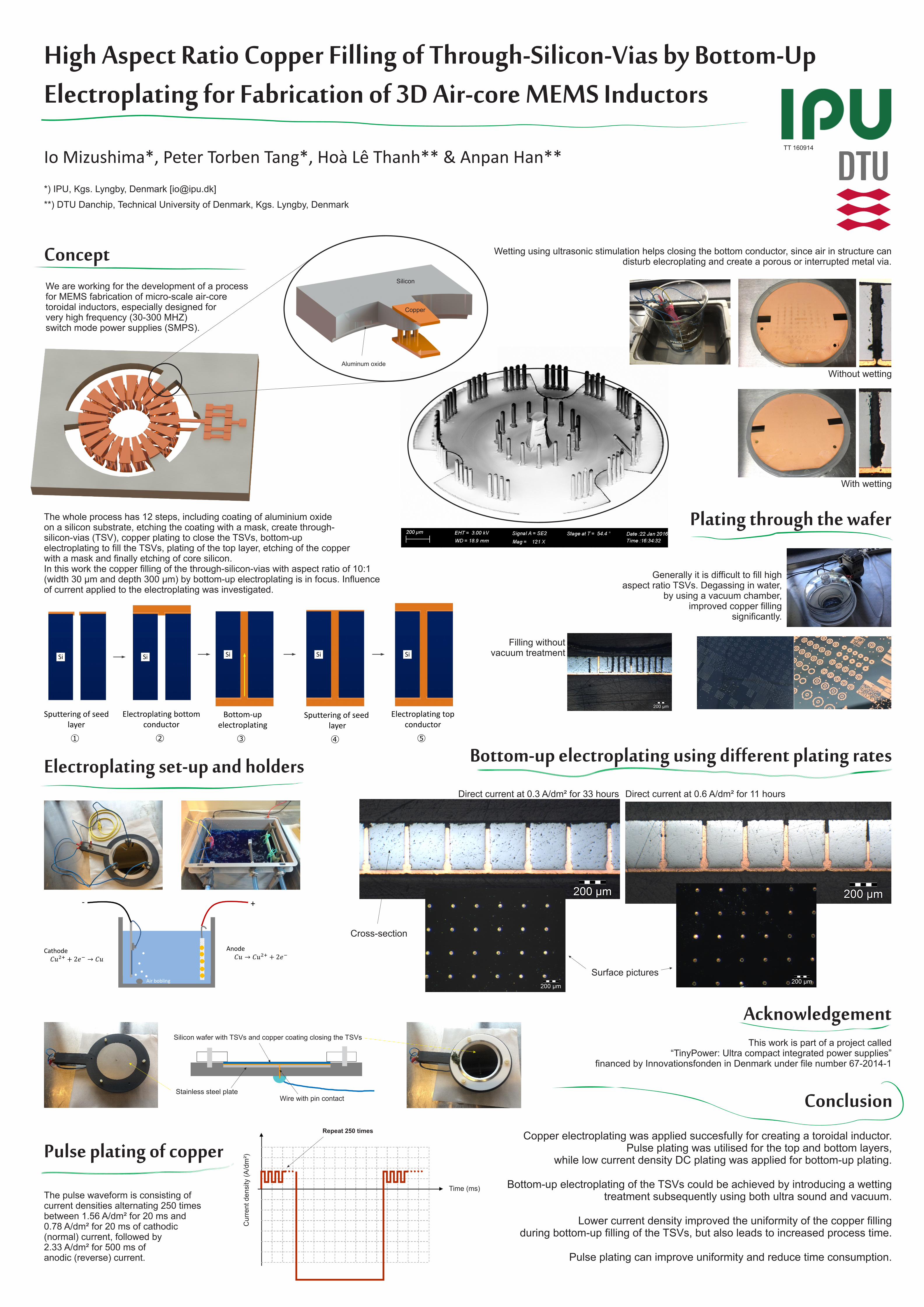
The whole process has 12 steps, including coating of aluminium oxideon a silicon substrate, etching the coating with a mask, create through-silicon-vias (TSV), copper plating to close the TSVs, bottom-upelectroplating to fill the TSVs, plating of the top layer, etching of the copperwith a mask and finally etching of core silicon. In this work the copper filling of the through-silicon-vias with aspect ratio of 10:1(width 30 µm and depth 300 µm) by bottom-up electroplating is in focus. Influenceof current applied to the electroplating was investigated.
AnodeCathode
+-
Air bobling
The pulse waveform is consisting ofcurrent densities alternating 250 timesbetween 1.56 A/dm² for 20 ms and0.78 A/dm² for 20 ms of cathodic(normal) current, followed by 2.33 A/dm² for 500 ms ofanodic (reverse) current.
Repeat 250 times
Curr
ent densi
ty (
A/d
m²)
Time (ms)
Wetting using ultrasonic stimulation helps closing the bottom conductor, since air in structure can disturb elecroplating and create a porous or interrupted metal via.
Filling without vacuum treatment
Generally it is difficult to fill highaspect ratio TSVs. Degassing in water,
by using a vacuum chamber,improved copper filling
significantly.
Copper electroplating was applied succesfully for creating a toroidal inductor.Pulse plating was utilised for the top and bottom layers,
while low current density DC plating was applied for bottom-up plating.
Bottom-up electroplating of the TSVs could be achieved by introducing a wetting treatment subsequently using both ultra sound and vacuum.
Lower current density improved the uniformity of the copper filling during bottom-up filling of the TSVs, but also leads to increased process time.
Pulse plating can improve uniformity and reduce time consumption.
Direct current at 0.3 A/dm² for 33 hours Direct current at 0.6 A/dm² for 11 hours
Cross-section
Surface pictures
We are working for the development of a processfor MEMS fabrication of micro-scale air-coretoroidal inductors, especially designed forvery high frequency (30-300 MHZ)switch mode power supplies (SMPS).
Without wetting
With wetting
Sputtering of seedlayer
①
Electroplating bottom conductor
②
Bottom-up electroplating
③
Sputtering of seedlayer
④
Electroplating top conductor
⑤
Stainless steel plate
Silicon wafer with TSVs and copper coating closing the TSVs
Wire with pin contact
This work is part of a project called“TinyPower: Ultra compact integrated power supplies”
financed by Innovationsfonden in Denmark under file number 67-2014-1