Hardware Functional Specification - Pacific Display … notes/epson/S1D13A04 Spec Rev 7.0.pdfEpson...
163
S1D13A04 LCD/USB Companion Chip Hardware Functional Specification Document Number: X37A-A-001-07 Status: Revision 7.0 Issue Date: 2006/07/07 © SEIKO EPSON CORPORATION 2001 - 2006. All Rights Reserved. Information in this document is subject to change without notice. You may download and use this document, but only for your own use in evaluating Seiko Epson/EPSON products. You may not modify the document. Epson Research and Development, Inc. disclaims any representation that the contents of this document are accurate or current. The Programs/Technologies described in this document may contain material protected under U.S. and/or International Patent laws. EPSON is a registered trademark of Seiko Epson Corporation. All other Trademarks are the property of their respective owners.
Transcript of Hardware Functional Specification - Pacific Display … notes/epson/S1D13A04 Spec Rev 7.0.pdfEpson...
S1D13A04 LCD/USB Companion Chip
Hardware Functional Specification
Document Number: X37A-A-001-07
Status: Revision 7.0
Issue Date: 2006/07/07
© SEIKO EPSON CORPORATION 2001 - 2006. All Rights Reserved.
Information in this document is subject to change without notice. You may download and use this document, but only for your own use inevaluating Seiko Epson/EPSON products. You may not modify the document. Epson Research and Development, Inc. disclaims anyrepresentation that the contents of this document are accurate or current. The Programs/Technologies described in this document may contain material protected under U.S. and/or International Patent laws.
EPSON is a registered trademark of Seiko Epson Corporation. All other Trademarks are the property of their respective owners.

Page 2 Epson Research and DevelopmentVancouver Design Center
THIS PAGE LEFT BLANK
S1D13A04 Hardware Functional SpecificationX37A-A-001-07 Issue Date: 2006/07/07
Revision 7.0

Epson Research and Development Page 3Vancouver Design Center
Table of Contents
1 Introduction . . . . . . . . . . . . . . . . . . . . . . . . . . . . . . . . . . . . . . . . 71.1 Scope . . . . . . . . . . . . . . . . . . . . . . . . . . . . . . . . . . . 7
1.2 Overview Description . . . . . . . . . . . . . . . . . . . . . . . . . . . . 7
2 Features . . . . . . . . . . . . . . . . . . . . . . . . . . . . . . . . . . . . . . . . . . 82.1 Integrated Frame Buffer . . . . . . . . . . . . . . . . . . . . . . . . . . . 8
2.2 CPU Interface . . . . . . . . . . . . . . . . . . . . . . . . . . . . . . . 8
2.3 Display Support . . . . . . . . . . . . . . . . . . . . . . . . . . . . . . . 8
2.4 Display Modes . . . . . . . . . . . . . . . . . . . . . . . . . . . . . . . 9
2.5 Display Features . . . . . . . . . . . . . . . . . . . . . . . . . . . . . . 9
2.6 Clock Source . . . . . . . . . . . . . . . . . . . . . . . . . . . . . . . . 9
2.7 USB Device . . . . . . . . . . . . . . . . . . . . . . . . . . . . . . . . 9
2.8 2D Acceleration . . . . . . . . . . . . . . . . . . . . . . . . . . . . . 10
2.9 Miscellaneous . . . . . . . . . . . . . . . . . . . . . . . . . . . . . . 10
3 Typical System Implementation Diagrams . . . . . . . . . . . . . . . . . . . . . . 113.1 Typical System Diagrams. . . . . . . . . . . . . . . . . . . . . . . . . . 11
3.2 USB Interface . . . . . . . . . . . . . . . . . . . . . . . . . . . . . . 15
4 Pins . . . . . . . . . . . . . . . . . . . . . . . . . . . . . . . . . . . . . . . . . . . 164.1 Pinout Diagram - PFBGA - 121-pin . . . . . . . . . . . . . . . . . . . . . . 16
4.2 Pinout Diagram - TQFP15 - 128-pin . . . . . . . . . . . . . . . . . . . . . 17
4.3 Pin Descriptions . . . . . . . . . . . . . . . . . . . . . . . . . . . . . 18
4.3.1 Host Interface . . . . . . . . . . . . . . . . . . . . . . . . . . . . . . . . . . . . . 18
4.3.2 LCD Interface . . . . . . . . . . . . . . . . . . . . . . . . . . . . . . . . . . . . . 22
4.3.3 Clock Input . . . . . . . . . . . . . . . . . . . . . . . . . . . . . . . . . . . . . . 25
4.3.4 Miscellaneous . . . . . . . . . . . . . . . . . . . . . . . . . . . . . . . . . . . . . 25
4.3.5 Power And Ground . . . . . . . . . . . . . . . . . . . . . . . . . . . . . . . . . . 25
4.4 Summary of Configuration Options . . . . . . . . . . . . . . . . . . . . . . 26
4.5 Host Bus Interface Pin Mapping . . . . . . . . . . . . . . . . . . . . . . . 27
4.6 LCD Interface Pin Mapping . . . . . . . . . . . . . . . . . . . . . . . . . 28
5 D.C. Characteristics . . . . . . . . . . . . . . . . . . . . . . . . . . . . . . . . . . 29
6 A.C. Characteristics . . . . . . . . . . . . . . . . . . . . . . . . . . . . . . . . . . 306.1 Clock Timing . . . . . . . . . . . . . . . . . . . . . . . . . . . . . . 30
6.1.1 Input Clocks . . . . . . . . . . . . . . . . . . . . . . . . . . . . . . . . . . . . . . 30
6.1.2 Internal Clocks . . . . . . . . . . . . . . . . . . . . . . . . . . . . . . . . . . . . 31
6.2 RESET# Timing . . . . . . . . . . . . . . . . . . . . . . . . . . . . . 32
6.3 CPU Interface Timing . . . . . . . . . . . . . . . . . . . . . . . . . . . 33
6.3.1 Generic #1 Interface Timing (e.g. Epson EOC33) . . . . . . . . . . . . . . . . . . 33
Hardware Functional Specification S1D13A04Issue Date: 2006/07/07 X37A-A-001-07
Revision 7.0

Page 4 Epson Research and DevelopmentVancouver Design Center
6.3.2 Generic #2 Interface Timing (e.g. ISA) . . . . . . . . . . . . . . . . . . . . . . . . 36
6.3.3 Hitachi SH-3 Interface Timing . . . . . . . . . . . . . . . . . . . . . . . . . . . . 38
6.3.4 Hitachi SH-4 Interface Timing . . . . . . . . . . . . . . . . . . . . . . . . . . . . 40
6.3.5 Motorola MC68K #1 Interface Timing (e.g. MC68000) . . . . . . . . . . . . . . . 42
6.3.6 Motorola MC68K #2 Interface Timing (e.g. MC68030) . . . . . . . . . . . . . . . 44
6.3.7 Motorola REDCAP2 Interface Timing . . . . . . . . . . . . . . . . . . . . . . . . 46
6.3.8 Motorola Dragonball Interface Timing with DTACK (e.g. MC68EZ328/MC68VZ328) 48
6.3.9 Motorola Dragonball Interface Timing w/o DTACK (e.g. MC68EZ328/MC68VZ328) 50
6.4 LCD Power Sequencing . . . . . . . . . . . . . . . . . . . . . . . . . . .52
6.4.1 Passive/TFT Power-On Sequence . . . . . . . . . . . . . . . . . . . . . . . . . . . 52
6.4.2 Passive/TFT Power-Off Sequence . . . . . . . . . . . . . . . . . . . . . . . . . . . 53
6.4.3 ‘Direct’ HR-TFT Interface Power-On/Off Sequence . . . . . . . . . . . . . . . . . 53
6.5 Display Interface . . . . . . . . . . . . . . . . . . . . . . . . . . . . . .54
6.5.1 Generic STN Panel Timing . . . . . . . . . . . . . . . . . . . . . . . . . . . . . . 56
6.5.2 Single Monochrome 4-Bit Panel Timing . . . . . . . . . . . . . . . . . . . . . . . 58
6.5.3 Single Monochrome 8-Bit Panel Timing . . . . . . . . . . . . . . . . . . . . . . . 60
6.5.4 Single Color 4-Bit Panel Timing . . . . . . . . . . . . . . . . . . . . . . . . . . . 62
6.5.5 Single Color 8-Bit Panel Timing (Format 1) . . . . . . . . . . . . . . . . . . . . . 64
6.5.6 Single Color 8-Bit Panel Timing (Format 2) . . . . . . . . . . . . . . . . . . . . . 66
6.5.7 Single Color 16-Bit Panel Timing . . . . . . . . . . . . . . . . . . . . . . . . . . . 68
6.5.8 Generic TFT Panel Timing . . . . . . . . . . . . . . . . . . . . . . . . . . . . . . 70
6.5.9 9/12/18-Bit TFT Panel Timing . . . . . . . . . . . . . . . . . . . . . . . . . . . . 71
6.5.10 160x160 Sharp ‘Direct’ HR-TFT Panel Timing (e.g. LQ031B1DDxx) . . . . . . . 74
6.5.11 320x240 Sharp ‘Direct’ HR-TFT Panel Timing (e.g. LQ039Q2DS01) . . . . . . . . 78
6.6 USB Timing . . . . . . . . . . . . . . . . . . . . . . . . . . . . . . . .80
7 Clocks . . . . . . . . . . . . . . . . . . . . . . . . . . . . . . . . . . . . . . . . . . .837.1 Clock Descriptions . . . . . . . . . . . . . . . . . . . . . . . . . . . . .83
7.1.1 BCLK . . . . . . . . . . . . . . . . . . . . . . . . . . . . . . . . . . . . . . . . . 83
7.1.2 MCLK . . . . . . . . . . . . . . . . . . . . . . . . . . . . . . . . . . . . . . . . . 83
7.1.3 PCLK . . . . . . . . . . . . . . . . . . . . . . . . . . . . . . . . . . . . . . . . . 84
7.1.4 PWMCLK . . . . . . . . . . . . . . . . . . . . . . . . . . . . . . . . . . . . . . . 85
7.1.5 USBCLK . . . . . . . . . . . . . . . . . . . . . . . . . . . . . . . . . . . . . . . 85
7.2 Clock Selection . . . . . . . . . . . . . . . . . . . . . . . . . . . . . .86
7.3 Clocks versus Functions . . . . . . . . . . . . . . . . . . . . . . . . . . .87
8 Registers . . . . . . . . . . . . . . . . . . . . . . . . . . . . . . . . . . . . . . . . .888.1 Register Mapping . . . . . . . . . . . . . . . . . . . . . . . . . . . . .88
8.2 Register Set . . . . . . . . . . . . . . . . . . . . . . . . . . . . . . . .88
8.3 LCD Register Descriptions (Offset = 0h) . . . . . . . . . . . . . . . . . . . .90
8.3.1 Read-Only Configuration Registers . . . . . . . . . . . . . . . . . . . . . . . . . . 90
S1D13A04 Hardware Functional SpecificationX37A-A-001-07 Issue Date: 2006/07/07
Revision 7.0

Epson Research and Development Page 5Vancouver Design Center
8.3.2 Clock Configuration Registers . . . . . . . . . . . . . . . . . . . . . . . . . . . . 91
8.3.3 Panel Configuration Registers . . . . . . . . . . . . . . . . . . . . . . . . . . . . . 92
8.3.4 Look-Up Table Registers . . . . . . . . . . . . . . . . . . . . . . . . . . . . . . . 97
8.3.5 Display Mode Registers . . . . . . . . . . . . . . . . . . . . . . . . . . . . . . . . 99
8.3.6 Picture-in-Picture Plus (PIP+) Registers . . . . . . . . . . . . . . . . . . . . . . . 104
8.3.7 Miscellaneous Registers . . . . . . . . . . . . . . . . . . . . . . . . . . . . . . . . 109
8.4 USB Registers (Offset = 4000h) . . . . . . . . . . . . . . . . . . . . . . . 116
8.5 2D Acceleration (BitBLT) Registers (Offset = 8000h) . . . . . . . . . . . . . . 134
8.6 2D Accelerator (BitBLT) Data Register Descriptions . . . . . . . . . . . . . . . 140
9 2D Accelerator (BitBLT) Engine . . . . . . . . . . . . . . . . . . . . . . . . . . . . 1419.1 Overview . . . . . . . . . . . . . . . . . . . . . . . . . . . . . . . . 141
9.2 BitBLT Operations . . . . . . . . . . . . . . . . . . . . . . . . . . . . 141
10 Frame Rate Calculation . . . . . . . . . . . . . . . . . . . . . . . . . . . . . . . . 142
11 Display Data Formats . . . . . . . . . . . . . . . . . . . . . . . . . . . . . . . . . 143
12 Look-Up Table Architecture . . . . . . . . . . . . . . . . . . . . . . . . . . . . . . 14412.1 Monochrome Modes . . . . . . . . . . . . . . . . . . . . . . . . . . . . 144
12.2 Color Modes . . . . . . . . . . . . . . . . . . . . . . . . . . . . . . . 146
13 SwivelView™ . . . . . . . . . . . . . . . . . . . . . . . . . . . . . . . . . . . . . . 15013.1 Concept . . . . . . . . . . . . . . . . . . . . . . . . . . . . . . . . . 150
13.2 90° SwivelView™ . . . . . . . . . . . . . . . . . . . . . . . . . . . . 150
13.2.1 Register Programming . . . . . . . . . . . . . . . . . . . . . . . . . . . . . . . . 151
13.3 180° SwivelView™ . . . . . . . . . . . . . . . . . . . . . . . . . . . . 152
13.3.1 Register Programming . . . . . . . . . . . . . . . . . . . . . . . . . . . . . . . . 152
13.4 270° SwivelView™ . . . . . . . . . . . . . . . . . . . . . . . . . . . . 153
13.4.1 Register Programming . . . . . . . . . . . . . . . . . . . . . . . . . . . . . . . . 154
14 Picture-in-Picture Plus (PIP+) . . . . . . . . . . . . . . . . . . . . . . . . . . . . . 15514.1 Concept . . . . . . . . . . . . . . . . . . . . . . . . . . . . . . . . . 155
14.2 With SwivelView Enabled . . . . . . . . . . . . . . . . . . . . . . . . . 156
14.2.1 SwivelView 90° . . . . . . . . . . . . . . . . . . . . . . . . . . . . . . . . . . . . 156
14.2.2 SwivelView 180° . . . . . . . . . . . . . . . . . . . . . . . . . . . . . . . . . . . 156
14.2.3 SwivelView 270° . . . . . . . . . . . . . . . . . . . . . . . . . . . . . . . . . . . 157
15 Power Save Mode . . . . . . . . . . . . . . . . . . . . . . . . . . . . . . . . . . . . 158
16 Mechanical Data . . . . . . . . . . . . . . . . . . . . . . . . . . . . . . . . . . . . 159
17 References . . . . . . . . . . . . . . . . . . . . . . . . . . . . . . . . . . . . . . . 161
18 Sales and Technical Support . . . . . . . . . . . . . . . . . . . . . . . . . . . . . 162
Hardware Functional Specification S1D13A04Issue Date: 2006/07/07 X37A-A-001-07
Revision 7.0

Page 6 Epson Research and DevelopmentVancouver Design Center
THIS PAGE LEFT BLANK
S1D13A04 Hardware Functional SpecificationX37A-A-001-07 Issue Date: 2006/07/07
Revision 7.0

Epson Research and Development Page 7Vancouver Design Center
1 Introduction
1.1 Scope
This is the Hardware Functional Specification for the S1D13A04 LCD/USB Companion Chip. Included in this document are timing diagrams, AC and DC characteristics, register descriptions, and power management descriptions. This document is intended for two audiences: Video Subsystem Designers and Software Developers.
This document is updated as appropriate. Please check for the latest revision of this document before beginning any development. The latest revision can be downloaded at www.erd.epson.com
We appreciate your comments on our documentation. Please contact us via email at [email protected].
1.2 Overview Description
The S1D13A04 is an LCD/USB solution designed for seamless connection to a wide variety of microprocessors. The S1D13A04 integrates a USB slave controller and an LCD graphics controller with an embedded 160K byte SRAM display buffer. The LCD controller, based on the popular S1D13706, supports all standard panel types including the Sharp HR-TFT family of products. In addition to the S1D13706 feature set, the S1D13A04 includes a Hardware Acceleration Engine to greatly improve screen drawing functions. The USB controller provides revision 1.1 compliance for applications requiring a USB client.This high level of integration provides a low cost, low power, single chip solution to meet the demands of embedded markets requiring USB client support, such as Mobile Communications devices and Palm-size PCs.
The S1D13A04 utilizes a guaranteed low-latency CPU architecture that provides support for microprocessors without READY/WAIT# handshaking signals. The 32-bit internal data path, write buffer and the Hardware Acceleration Engine provide high performance bandwidth into display memory allowing for fast display updates. ‘Direct’ support for the Sharp HR-TFT removes the requirement of an external Timing Control IC.
Additionally, products requiring a rotated display can take advantage of the SwivelViewTM feature which provides hardware rotation of the display memory transparent to the software application. The S1D13A04 also provides support for “Picture-in-Picture Plus” (a variable size Overlay window).
The S1D13A04, with its integrated USB client, provides impressive support for Palm OS® handhelds. However, its impartiality to CPU type or operating system makes it an ideal display solution for a wide variety of applications.
Hardware Functional Specification S1D13A04Issue Date: 2006/07/07 X37A-A-001-07
Revision 7.0

Page 8 Epson Research and DevelopmentVancouver Design Center
2 Features
2.1 Integrated Frame Buffer
• Embedded 160k byte SRAM display buffer.
2.2 CPU Interface
• Direct support of the following interfaces:Generic MPU bus interface with programmable ready (WAIT#).Hitachi SH-4 / SH-3.Motorola M68K.Motorola MC68EZ328/MC68VZ328 DragonBall.Motorola “REDCAP2” - no WAIT# signal.
• “Fixed” low-latency CPU access times.
• Registers are memory-mapped - M/R# input selects between memory and register address space.
• The complete 160k byte display buffer is directly and contiguously available through the 18-bit address bus.
2.3 Display Support
• Single-panel, single drive passive displays.
• 4/8-bit monochrome LCD interface.
• 4/8/16-bit color LCD interface.
• Active Matrix TFT interface.
• 9/12/18-bit interface.
• ‘Direct’ support for 18-bit Sharp HR-TFT LCD or compatible interface.
S1D13A04 Hardware Functional SpecificationX37A-A-001-07 Issue Date: 2006/07/07
Revision 7.0

Epson Research and Development Page 9Vancouver Design Center
2.4 Display Modes
• 1/2/4/8/16 bit-per-pixel (bpp) color depths.
• Up to 64 gray shades on monochrome passive LCD panels.
• Up to 64K colors on passive panels.
• Up to 64K colors on active matrix LCD panels.
• Example resolutions:320x240 at a color depth of 16 bpp320x320 at a color depth of 8 bpp160x160 at a color depth of 16 bpp (2 pages)160x240 at a color depth of 16 bpp
2.5 Display Features
• SwivelView™: 90°, 180°, 270° counter-clockwise hardware rotation of display image.
• Virtual display support: displays images larger than the panel size through the use of panning and scrolling.
• Picture-in-Picture Plus (PIP+): displays a variable size window overlaid over back-ground image.
• Pixel Doubling: independent control of both horizontal and vertical pixel doubling.
• example usage: 160x160 8 bpp can be expanded to 320x320 8 bpp without any addi-tional memory.
• Double Buffering/Multi-pages: provides smooth animation and instantaneous screen updates.
2.6 Clock Source
• Three independent clock inputs: CLKI, CLKI2 and USBCLK.
• Flexible clock source selection:
• internal Bus Clock (BCLK) selected from CLKI or CLKI/2 (CNF6)
• internal Memory Clock (MCLK) selected from BCLK or BCLK divide ratio (REG[04h)
• internal Pixel Clock (PCLK) selected from CLKI, CLKI2, MCLK, or BCLK. PCLK can also be divided down from source (REG[08h])
• Single clock input possible if USB support not required.
2.7 USB Device
• USB Client, revision 1.1 compliant.
• Dedicated clock input: USBCLK.
Hardware Functional Specification S1D13A04Issue Date: 2006/07/07 X37A-A-001-07
Revision 7.0

Page 10 Epson Research and DevelopmentVancouver Design Center
2.8 2D Acceleration
• 2D BitBLT engine including:
Write BitBLT Transparent Write BitBLTMove BitBLT Transparent Move BitBLTSolid Fill BitBLT Read BitBLTPattern Fill BitBLT Color Expansion BitBLTMove BitBLT with Color Expansion
2.9 Miscellaneous
• Software Video Invert.
• Software initiated Power Save mode.
• General Purpose Input/Output pins are available.
• IO Operates at 3.3 volts ± 10%.
• Core operates at 2.0 volts ± 10% or 2.5 volts ± 10%.
• 121-pin PFBGA package.
• 128-pin TQFP15 package.
S1D13A04 Hardware Functional SpecificationX37A-A-001-07 Issue Date: 2006/07/07
Revision 7.0

Epson Research and Development Page 11Vancouver Design Center
3 Typical System Implementation Diagrams
3.1 Typical System Diagrams.
Figure 3-1: Typical System Diagram (Generic #1 Bus).
Figure 3-2: Typical System Diagram (Generic #2 Bus)
S1D13A04
FPLINE
FPFRAME
FPSHIFT
DRDY
FPDAT[15:0]
CLK
I2
Oscillator
FPLINE
FPFRAME
FPSHIFT
MOD
D[15:0]
16-bit
Generic #1BUS
RESET#
D[15:0]
RD0#
WAIT#
A[17:1]
BUSCLK
RD/WR#
AB[17:1]
DB[15:0]
WE1#
RD#
M/R#
CS#
CLKI
WAIT#
RESET#
A[27:18]
CSn#
WE1# GPIO0
Decoder
WE0#WE0#
SingleLCD
Display
Bia
s P
ower
BS#
RD1#
IOVDD
VSS
AB0
S1D13A04
FPLINE
FPFRAME
FPSHIFT
DRDY
FPDAT[8:0]
CLK
I2
Oscillator
FPLINE
FPFRAME
FPSHIFT
DRDY
D[8:0]9-bit
Generic #2BUS
RESET#
D[15:0]
RD#
WAIT#
A[17:0]
BUSCLK
RD/WR#
AB[17:0]
DB[15:0]
WE1#
RD#
M/R#
CS#
CLKI
WAIT#
RESET#
A[27:18]
CSn#
BHE# GPIO0
Decoder
WE0#WE#
TFT
Bia
s P
ower
BS#
IOVDD
Display
Hardware Functional Specification S1D13A04Issue Date: 2006/07/07 X37A-A-001-07
Revision 7.0

Page 12 Epson Research and DevelopmentVancouver Design Center
.
Figure 3-3: Typical System Diagram (Hitachi SH-4 Bus).
Figure 3-4: Typical System Diagram (Hitachi SH-3 Bus)
S1D13A04
FPLINE
FPFRAME
FPSHIFT
DRDY
FPDAT[9:0]
FPLINE
FPFRAME
FPSHIFT
DRDY
D[9:0]
12-bit
SH-4BUS
RESET#
WE0#
D[15:0]
BS#
RD/WR#
RD#
RDY#
A[17:1]
CKIO
WE0#
RD/WR#
AB[17:1]
DB[15:0]
WE1#
BS#
RD#
M/R#
CS#
CLKI
WAIT#
RESET#
A[25:18]
CSn#
WE1#
GPIO0
CLK
I2
Oscillator
TFTDisplay
Bia
s P
ower
FPDAT12
FPDAT15
D10D11
DecoderVSS
AB0
S1D13A04
FPLINE
FPFRAME
FPSHIFT
DRDY
FPDAT[17:0]
FPLINE
FPFRAME
FPSHIFT
DRDY
D[17:0]
18-bit
SH-3BUS
RESET#
WE0#
D[15:0]
BS#
RD/WR#
RD#
WAIT#
A[17:1]
CKIO
WE0#
RD/WR#
AB[17:1]
DB[15:0]
WE1#
BS#
RD#
M/R#
CS#
CLKI
WAIT#
RESET#
A[25:18]
CSn#
WE1#
GPIO0
CLK
I2
Oscillator
TFTDisplay
Bia
s P
ower
DecoderVSS
AB0
S1D13A04 Hardware Functional SpecificationX37A-A-001-07 Issue Date: 2006/07/07
Revision 7.0

Epson Research and Development Page 13Vancouver Design Center
.
Figure 3-5: Typical System Diagram (MC68K # 1, Motorola 16-Bit 68000).
Figure 3-6: Typical System Diagram (MC68K #2, Motorola 32-Bit 68030)
S1D13A04
FPLINE
FPFRAME
FPSHIFT
FPDAT[17:0]
LP
SPS
CLK
D[17:0] 18-bit
MC68K #1BUS
RESET#
LDS#
D[15:0]
AS#
R/W#
DTACK#
A[17:1]
CLK
AB0
RD/WR#
AB[17:1]
DB[15:0]
WE1#
BS#
M/R#
CS#
CLKI
WAIT#
RESET#
A[23:18]FC0, FC1 Decoder
Decoder
UDS#
CLK
I2
Oscillator
HR-TFTDisplay
RD#
WE0#
IOVDD
GPIO0
GPIO1
GPIO2
GPIO3
PS
CLS
REV
SPL
S1D13A04
MC68K #2BUS
RESET#
SIZ0
D[31:16]
AS#
R/W#
SIZ1
DSACK1#
A[17:0]
CLK
WE0#
RD/WR#
AB[17:0]
DB[15:0]
WE1#
BS#
RD#
M/R#
CS#
CLKI
WAIT#
RESET#
A[31:18]FC0, FC1 Decoder
Decoder
DS#
CLK
I2
Oscillator
FPLINE
FPFRAME
FPSHIFT
FPDAT[17:0]
LP
SPS
CLK
D[17:0] 18-bitHR-TFTDisplay
GPIO0
GPIO1
GPIO2
GPIO3
PS
CLS
REV
SPL
Hardware Functional Specification S1D13A04Issue Date: 2006/07/07 X37A-A-001-07
Revision 7.0

Page 14 Epson Research and DevelopmentVancouver Design Center
.
Figure 3-7: Typical System Diagram (Motorola REDCAP2 Bus).
Figure 3-8: Typical System Diagram (Motorola MC68EZ328/MC68VZ328 “DragonBall” Bus)
S1D13A04
FPFRAME
FPSHIFT
FPLINE
DRDY
FPDAT[7:4]
FPFRAME
FPSHIFT
FPLINE
MOD
D[3:0]
4-bit
REDCAP2BUS
RESET_OUT
EB1
D[15:0]
R/W
OE
A[17:1]
CLK
WE0#
RD/WR#
AB[17:1]
DB[15:0]
WE1#
RD#
M/R#
CS#
CLKI
RESET#
A[21:18] Decoder
EB0
GPIO0
CLK
I2
Oscillator
SingleLCD
Bia
s P
ower
CSn
*Note: CSn# can be any of CS0-CS4
Display
BS#
VSS
AB0
IOVDD
S1D13A04
FPFRAME
FPSHIFT
FPLINE
DRDY
FPDAT[7:0]
FPFRAME
FPSHIFT
FPLINE
MOD
D[7:0]
8-bit
MC68EZ328/
RESET
D[15:0]
OE
DTACK
A[17:1]
CLKO
RD/WR#
AB[17:1]
DB[15:0]
WE1#
RD#
M/R#
CS#
CLKI
WAIT#
RESET#
A[25:18]
CSX
UWE
GPIO0
Decoder
WE0#LWE
IOVDD
CLK
I2
Oscillator
Single
Bia
s P
ower
BS#DragonBallBUS
LCDDisplay
MC68VZ328
VSSAB0
S1D13A04 Hardware Functional SpecificationX37A-A-001-07 Issue Date: 2006/07/07
Revision 7.0

Epson Research and Development Page 15Vancouver Design Center
3.2 USB Interface
Figure 3-9: USB Typical Implementation
USBDP
USBDM
S1D13A04 USB Socket
USBDETECT
USBPUP
DM
DP
VBus
GNDVSS
LVDD
NNCD5.6LG
150kΩ
300kΩ
1.5kΩ
20Ω
20Ω
300kΩ
Full Speed Device
OvervoltageProtection ESD
Protection
Hardware Functional Specification S1D13A04Issue Date: 2006/07/07 X37A-A-001-07
Revision 7.0

Page 16 Epson Research and DevelopmentVancouver Design Center
4 Pins
4.1 Pinout Diagram - PFBGA - 121-pin
Figure 4-1: Pinout Diagram - PFBGA 121-pin
Table 4-1: PFBGA 121-pin Mapping
L NC IOVDD DB7 DB3 DB0 GPIO7 GPIO3 GPIO0 IOVDD COREVDD NC
K NC VSS DB8 DB4 DB1 GPIO6 GPIO2 IRQ DRDY VSS NC
J NC DB9 DB6 DB5 DB2 NC GPIO1 USBCLK FPFRAME COREVDD NC
H DB12 DB11 DB10 DB13 NC IOVDD GPIO4 NC FPLINE FPSHIFT FPDAT0
G WAIT# DB15 DB14 IOVDD VSS GPIO5 FPDAT5 FPDAT1 FPDAT2 FPDAT3 FPDAT4
F RESET# VSS RD/WR# WE1# CLKI NC FPDAT8 FPDAT6 VSS FPDAT7 IOVDD
E RD# BS# M/R# CS# WE0# AB13 TESTEN FPDAT9 FPDAT12 FPDAT11 FPDAT10
D AB0 AB1 AB2 AB8 AB12 AB17 CNF3 FPDAT13 FPDAT16 FPDAT15 FPDAT14
C NC COREVDD AB3 AB6 AB9 AB16 CNF2 CNF5 CNF6 FPDAT17 NC
B NC VSS AB5 NC AB10 AB14 CNF1 CNF4 CLKI2 VSS NC
A NC COREVDD AB4 AB7 AB11 AB15 CNF0 NC PWMOUT IOVDD NC
1 2 3 4 5 6 7 8 9 10 11
L
K
J
H
G
F
E
D
C
B
A
1 2 3 4 5 6 7 8 9 10 11
BOTTOM VIEW
S1D13A04 Hardware Functional SpecificationX37A-A-001-07 Issue Date: 2006/07/07
Revision 7.0

Epson Research and Development Page 17Vancouver Design Center
4.2 Pinout Diagram - TQFP15 - 128-pin
Figure 4-2: Pinout Diagram - TQFP15 128-pin
1 2 3 4 5 6 7 8 9 10 11 12 13 14 15 16 17 18 19 20 21 22 23 24 25 26 27 28 29 30 31 32
96 95 94 93 92 91 90 89 88 87 86 85 84 83 7475 73 72 71 70 69 68 67 66 6582 81 80 79 78 77 76
128
127
126
125
124
123
122
121
120
119
118
117
116
115
114
113
112
111
110
109
108
107
106
105
104
103
102
101
100
99
98
97
33
34
35
36
37
38
39
40
41
42
43
44
45
46
47
48
49
50
58
59
60
61
62
63
51
52
53
54
55
56
57
64
S1D13A04M
/R#
RD
/WR
#
RD
#
WE
1#
RE
SE
T#
NC
CLK
I
DB
15
DB
12
DB
10
DB
9
NC
NC
VS
S
DB
11
CO
RE
VD
D
BS
#
IOVDD
VSS
IRQ
DB
14
FP
DAT
7
NC
NC
CO
RE
VD
D
COREVDD
NC
GPIO0
IOVDD
DRDY
USBCLK
GPIO1
GPIO2
CNF3
FP
DAT
12
CNF6
CNF5
NC
FP
DAT
15
GPIO3
NC
NC
GPIO5
GPIO6
GPIO7
VSS
NC
DB0
DB1
DB2
DB3
DB4
DB5
DB6
COREVDD
AB
1
CS
#
NC
AB
0
AB
2
AB
3
NC
NC
AB9
AB10
AB12
AB13
AB14
AB15
AB16
AB17
TESTEN
NC
CNF2
NC
CNF4
IOVDD
NC
FP
DAT
8
NC
FP
DAT
6
FP
DAT
5
FP
DAT
4
FP
DAT
3
FP
DAT
2
FP
FR
AM
E
NC
NC
NC
VS
S
CLKI2
DB7
NC
WA
IT#
VS
S
IOV
DD
DB
13NC
GPIO4
IOVDD
FP
DAT
9
FP
DAT
11
FP
DAT
1
FP
SH
IFT
FP
DAT
13
DB8
FP
DAT
14
FP
DAT
17
VS
S
IOV
DD
CNF0
FP
DAT
16
CNF1
NC
AB11
AB5
VSS
NC
AB6
AB7
AB8
AB4
PWMOUT
FP
DAT
10
FP
LINE
WE
0#
FP
DAT
0NC
Hardware Functional Specification S1D13A04Issue Date: 2006/07/07 X37A-A-001-07
Revision 7.0

Page 18 Epson Research and DevelopmentVancouver Design Center
4.3 Pin DescriptionsKey:
a LVTTL is Low Voltage TTL (see Section 5, “D.C. Characteristics” on page 29).
4.3.1 Host Interface
I = InputO = Output
IO = Bi-Directional (Input/Output)P = Power pinCI = CMOS input
LI = LVTTL inputLB2A = LVTTL IO buffer (6mA/[email protected])LB3P = Low noise LVTTL IO buffer (6mA/[email protected])
LO3 = Low noise LVTTL Output buffer (3mA/[email protected])LB3M = Low noise LVTTL IO buffer with input mask (3mA/[email protected])T1 = Test mode control input with pull-down resistor (typical value of 50KΩ at 3.3V)
Hi-Z = High ImpedanceCUS = Custom Cell Type
Table 4-2: Host Interface Pin Descriptions
Pin Name TypePFBGAPin #
TQFP15 Pin#
CellRESET#
StateDescription
AB0 I D1 7 LI —
This input pin has multiple functions.
• For Generic #1, this pin is not used and should be connected to VSS.
• For Generic #2, this pin inputs system address bit 0 (A0).• For SH-3/SH-4, this pin is not used and should be
connected to VSS.
• For MC68K #1, this pin inputs the lower data strobe (LDS#).
• For MC68K #2, this pin inputs system address bit 0 (A0).
• For REDCAP2, this pin is not used and should be connected to VSS.
• For DragonBall, this pin is not used and should be connected to VSS.
See Table 4-8: “Host Bus Interface Pin Mapping,” on page 27 for summary.
AB[17:1] I
C6,A6,B6,E6,D5,A5,B5,C5,D4,A4,C4,B3,A3,C3,D3,D2,D6
4-6,111-116, 118-125
CI — System address bus bits 17-1.
S1D13A04 Hardware Functional SpecificationX37A-A-001-07 Issue Date: 2006/07/07
Revision 7.0

Epson Research and Development Page 19Vancouver Design Center
DB[15:0] IO
L5,K5,J5,L4,K4,J4,J3,L3,K3,J2,H3,H2,H1,H4,G3
,G2
23-29,35-43
LB2A Hi-Z
Input data from the system data bus.
• For Generic #1, these pins are connected to D[15:0].• For Generic #2, these pins are connected to D[15:0].
• For SH-3/SH-4, these pins are connected to D[15:0].• For MC68K #1, these pins are connected to D[15:0].• For MC68K #2, these pins are connected to D[31:16] for
a 32-bit device (e.g. MC68030) or D[15:0] for a 16-bit device (e.g. MC68340).
• For REDCAP2, these pins are connected to D[15:0].
• For DragonBall, these pins are connected to D[15:0].
See Table 4-8: “Host Bus Interface Pin Mapping,” on page 27 for summary.
WE0# I E5 13 LI —
This input pin has multiple functions.
• For Generic #1, this pin inputs the write enable signal for the lower data byte (WE0#).
• For Generic #2, this pin inputs the write enable signal (WE#)
• For SH-3/SH-4, this pin inputs the write enable signal for data byte 0 (WE0#).
• For MC68K #1, this pin must be tied to IO VDD
• For MC68K #2, this pin inputs the bus size bit 0 (SIZ0).
• For REDCAP2, this pin inputs the byte enable signal for the D[7:0] data byte (EB1).
• For DragonBall, this pin inputs the byte enable signal for the D[7:0] data byte (LWE).
See Table 4-8: “Host Bus Interface Pin Mapping,” on page 27 for summary.
WE1# I F4 14 LI —
This input pin has multiple functions.
• For Generic #1, this pin inputs the write enable signal for the upper data byte (WE1#).
• For Generic #2, this pin inputs the byte enable signal for the high data byte (BHE#).
• For SH-3/SH-4, this pin inputs the write enable signal for data byte 1 (WE1#).
• For MC68K #1, this pin inputs the upper data strobe (UDS#).
• For MC68K #2, this pin inputs the data strobe (DS#).• For REDCAP2, this pin inputs the byte enable signal for
the D[15:8] data byte (EB0).
• For DragonBall, this pin inputs the byte enable signal for the D[15:8] data byte (UWE).
See Table 4-8: “Host Bus Interface Pin Mapping,” on page 27 for summary.
CS# I E4 9 CI —Chip select input. See Table 4-8: “Host Bus Interface Pin Mapping,” on page 27 for summary.
Table 4-2: Host Interface Pin Descriptions
Pin Name TypePFBGA
Pin #TQFP15
Pin#Cell
RESET# State
Description
Hardware Functional Specification S1D13A04Issue Date: 2006/07/07 X37A-A-001-07
Revision 7.0

Page 20 Epson Research and DevelopmentVancouver Design Center
M/R# I E3 10 LI —
This input pin is used to select between the display buffer and register address spaces of the S1D13A04. M/R# is set high to access the display buffer and low to access the registers. See Table 4-8: “Host Bus Interface Pin Mapping,” on page 27 for summary.
BS# I E2 11 LI —
This input pin has multiple functions.
• For Generic #1, this pin must be tied to IO VDD.• For Generic #2, this pin must be tied to IO VDD.• For SH-3/SH-4, this pin inputs the bus start signal (BS#).
• For MC68K #1, this pin inputs the address strobe (AS#).• For MC68K #2, this pin inputs the address strobe (AS#).• For REDCAP2, this pin must be tied to IO VDD.
• For DragonBall, this pin must be tied to IO VDD.
See Table 4-8: “Host Bus Interface Pin Mapping,” on page 27 for summary.
RD/WR# I F3 15 LI —
This input pin has multiple functions.
• For Generic #1, this pin inputs the read command for the upper data byte (RD1#).
• For Generic #2, this pin must be tied to IO VDD.• For SH-3/SH-4, this pin inputs the RD/WR# signal. The
S1D13A04 needs this signal for early decode of the bus cycle.
• For MC68K #1, this pin inputs the R/W# signal.• For MC68K #2, this pin inputs the R/W# signal.
• For REDCAP2, this pin inputs the R/W signal.• For DragonBall, this pin must be tied to IO VDD.
See Table 4-8: “Host Bus Interface Pin Mapping,” on page 27 for summary.
RD# I E1 12 LI —
This input pin has multiple functions.
• For Generic #1, this pin inputs the read command for the lower data byte (RD0#).
• For Generic #2, this pin inputs the read command (RD#).• For SH-3/SH-4, this pin inputs the read signal (RD#).
• For MC68K #1, this pin must be tied to IO VDD.• For MC68K #2, this pin inputs the bus size bit 1 (SIZ1).• For REDCAP2, this pin inputs the output enable (OE).
• For DragonBall, this pin inputs the output enable (OE).
See Table 4-8: “Host Bus Interface Pin Mapping,” on page 27 for summary.
Table 4-2: Host Interface Pin Descriptions
Pin Name TypePFBGAPin #
TQFP15 Pin#
CellRESET#
StateDescription
S1D13A04 Hardware Functional SpecificationX37A-A-001-07 Issue Date: 2006/07/07
Revision 7.0
Epson Research and Development Page 21Vancouver Design Center
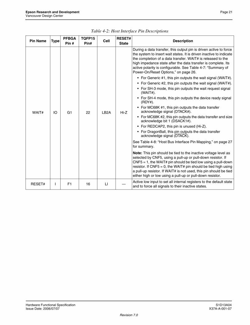
WAIT# IO G1 22 LB2A Hi-Z
During a data transfer, this output pin is driven active to force the system to insert wait states. It is driven inactive to indicate the completion of a data transfer. WAIT# is released to the high impedance state after the data transfer is complete. Its active polarity is configurable. See Table 4-7: “Summary of Power-On/Reset Options,” on page 26.
• For Generic #1, this pin outputs the wait signal (WAIT#).
• For Generic #2, this pin outputs the wait signal (WAIT#).• For SH-3 mode, this pin outputs the wait request signal
(WAIT#).
• For SH-4 mode, this pin outputs the device ready signal (RDY#).
• For MC68K #1, this pin outputs the data transfer acknowledge signal (DTACK#).
• For MC68K #2, this pin outputs the data transfer and size acknowledge bit 1 (DSACK1#).
• For REDCAP2, this pin is unused (Hi-Z).• For DragonBall, this pin outputs the data transfer
acknowledge signal (DTACK).
See Table 4-8: “Host Bus Interface Pin Mapping,” on page 27 for summary.
Note: This pin should be tied to the inactive voltage level as selected by CNF5, using a pull-up or pull-down resistor. If CNF5 = 1, the WAIT# pin should be tied low using a pull-down resistor. If CNF5 = 0, the WAIT# pin should be tied high using a pull-up resistor. If WAIT# is not used, this pin should be tied either high or low using a pull-up or pull-down resistor.
RESET# I F1 16 LI —Active low input to set all internal registers to the default state and to force all signals to their inactive states.
Table 4-2: Host Interface Pin Descriptions
Pin Name TypePFBGA
Pin #TQFP15
Pin#Cell
RESET# State
Description
Hardware Functional Specification S1D13A04Issue Date: 2006/07/07 X37A-A-001-07
Revision 7.0

Page 22 Epson Research and DevelopmentVancouver Design Center
4.3.2 LCD Interface
Table 4-3: LCD Interface Pin Descriptions
Pin Name TypePFBGA
Pin#TQFP15
Pin#Cell
RESET# State
Description
FPDAT[17:0] O
C10,D9,D10,D,11,D8,E9,E10,E11,E8,F7,F10,F8,G7,G11,G10,G9,G8
,H11
71-77,82-92
LB3P 0 Panel Data bits 17-0.
FPFRAME O J9 68 LB3P 0
This output pin has multiple functions.
• Frame Pulse• SPS for ‘Direct’ HR-TFT
See Table 4.6 “LCD Interface Pin Mapping,” on page 28 for summary.
FPLINE O H9 69 LB3P 0
This output pin has multiple functions.
• Line Pulse
• LP for ‘Direct’ HR-TFT
See Table 4.6 “LCD Interface Pin Mapping,” on page 28 for summary.
FPSHIFT O H10 70 LB3P 0
This output pin has multiple functions.
• Shift Clock• CLK for ‘Direct’ HR-TFT
See Table 4.6 “LCD Interface Pin Mapping,” on page 28 for summary.
DRDY O K9 60 LO3 0
This output pin has multiple functions.
• Display enable (DRDY) for TFT panels• 2nd shift clock (FPSHIFT2) for passive LCD with Format
1 interface
• LCD backplane bias signal (MOD) for all other LCD panels
• General Purpose Output
See Table 4.6 “LCD Interface Pin Mapping,” on page 28 for summary.
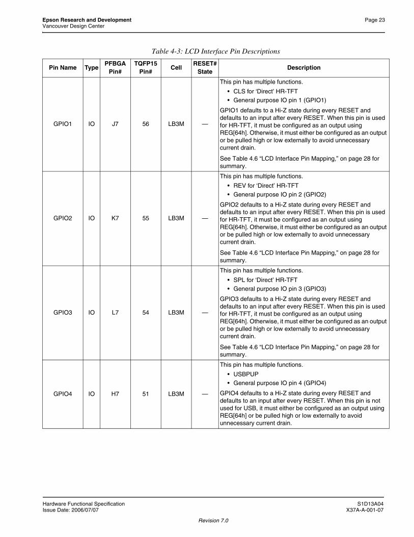
GPIO0 IO L8 57 LB3M —
This pin has multiple functions.
• PS for ‘Direct’ HR-TFT• General purpose IO pin 0 (GPIO0)
GPIO0 defaults to a Hi-Z state during every RESET and defaults to an input after every RESET. When this pin is used for HR-TFT, it must be configured as an output using REG[64h]. Otherwise, it must either be configured as an output or be pulled high or low externally to avoid unnecessary current drain.
See Table 4.6 “LCD Interface Pin Mapping,” on page 28 for summary.
S1D13A04 Hardware Functional SpecificationX37A-A-001-07 Issue Date: 2006/07/07
Revision 7.0
Epson Research and Development Page 23Vancouver Design Center
GPIO1 IO J7 56 LB3M —
This pin has multiple functions.
• CLS for ‘Direct’ HR-TFT• General purpose IO pin 1 (GPIO1)
GPIO1 defaults to a Hi-Z state during every RESET and defaults to an input after every RESET. When this pin is used for HR-TFT, it must be configured as an output using REG[64h]. Otherwise, it must either be configured as an output or be pulled high or low externally to avoid unnecessary current drain.
See Table 4.6 “LCD Interface Pin Mapping,” on page 28 for summary.
GPIO2 IO K7 55 LB3M —
This pin has multiple functions.
• REV for ‘Direct’ HR-TFT
• General purpose IO pin 2 (GPIO2)
GPIO2 defaults to a Hi-Z state during every RESET and defaults to an input after every RESET. When this pin is used for HR-TFT, it must be configured as an output using REG[64h]. Otherwise, it must either be configured as an output or be pulled high or low externally to avoid unnecessary current drain.
See Table 4.6 “LCD Interface Pin Mapping,” on page 28 for summary.
GPIO3 IO L7 54 LB3M —
This pin has multiple functions.
• SPL for ‘Direct’ HR-TFT• General purpose IO pin 3 (GPIO3)
GPIO3 defaults to a Hi-Z state during every RESET and defaults to an input after every RESET. When this pin is used for HR-TFT, it must be configured as an output using REG[64h]. Otherwise, it must either be configured as an output or be pulled high or low externally to avoid unnecessary current drain.
See Table 4.6 “LCD Interface Pin Mapping,” on page 28 for summary.
GPIO4 IO H7 51 LB3M —
This pin has multiple functions.
• USBPUP• General purpose IO pin 4 (GPIO4)
GPIO4 defaults to a Hi-Z state during every RESET and defaults to an input after every RESET. When this pin is not used for USB, it must either be configured as an output using REG[64h] or be pulled high or low externally to avoid unnecessary current drain.
Table 4-3: LCD Interface Pin Descriptions
Pin Name TypePFBGA
Pin#TQFP15
Pin#Cell
RESET# State
Description
Hardware Functional Specification S1D13A04Issue Date: 2006/07/07 X37A-A-001-07
Revision 7.0

Page 24 Epson Research and DevelopmentVancouver Design Center
GPIO5 IO G6 50 LB3M —
This pin has multiple functions.
• USBDETECT• General purpose IO pin 5 (GPIO5)
GPIO5 defaults to a Hi-Z state during every RESET and defaults to an input after every RESET. When this pin is not used for USB, it must either be configured as an output using REG[64h] or be pulled high or low externally to avoid unnecessary current drain.
GPIO6 IO K6 49 CUS —
This pin has multiple functions.
• USBDM• General purpose IO pin 6 (GPIO6)
GPIO6 defaults to a Hi-Z state during every RESET and defaults to an input after every RESET. When this pin is not used for USB, it must either be configured as an output using REG[64h] or be pulled high or low externally to avoid unnecessary current drain.
GPIO7 IO L6 48 CUS —
This pin has multiple functions.
• USBDP
• General purpose IO pin 7
GPIO7 defaults to a Hi-Z state during every RESET and defaults to an input after every RESET. When this pin is not used for USB, it must either be configured as an output using REG[64h] or be pulled high or low externally to avoid unnecessary current drain.
IRQ O K8 58 LO3 0This output pin is the IRQ pin for USB. When IRQ is activated, an active high pulse is generated and stays high until the IRQ is serviced by software at REG[404Ah] or REG[404Ch].
PWMOUT O A9 100 LO3 0
This pin has multiple functions.
• PWM Clock output
• General purpose output
Table 4-3: LCD Interface Pin Descriptions
Pin Name TypePFBGA
Pin#TQFP15
Pin#Cell
RESET# State
Description
S1D13A04 Hardware Functional SpecificationX37A-A-001-07 Issue Date: 2006/07/07
Revision 7.0

Epson Research and Development Page 25Vancouver Design Center
4.3.3 Clock Input
4.3.4 Miscellaneous
4.3.5 Power And Ground
Table 4-4: Clock Input Pin Descriptions
Pin Name TypePFBGA
Pin#TQFP15
Pin#Cell
RESET# State
Description
CLKI I F5 19 CI —Typically used as input clock source for bus clock and memory clock
CLKI2 I B9 99 CI — Typically used as input clock source for pixel clock
USBCLK I J8 59 LI — Typically used as input clock source for USB
Table 4-5: Miscellaneous Pin Descriptions
Pin Name TypePFBGA
Pin#TQFP15
Pin#Cell
RESET# State
Description
CNF[6:0] IC9,C8,B8,D7,C7,B
7,A7102-108 CI —
These inputs are used to configure the S1D13A04 - see Table 4-7: “Summary of Power-On/Reset Options,” on page 26.
Note: These pins are used for configuration of the S1D13A04 and must be connected directly to IO VDD or VSS.
TESTEN I E7 109 T1 —
Test Enable input used for production test only (has type 1 pull-down resistor with a typical value of 50KΩ at 3.3V).
Note: This pin must not be connected.
Table 4-6: Power And Ground Pin Descriptions
Pin Name TypePFBGA
Pin#TQFP15
Pin#Cell
RESET# State
Description
IOVDD PL2,G4, H6,L9,
A10,F11
20, 33, 46, 61, 80, 97
P — 6 IO VDD pins.
COREVDD PA2,C2,L10,J10
1, 64-65, 128
P —2 double-bonded Core VDD. pins on TQFP package.4 Core VDD. pins on PFBGA package.
VSS P
B2,F2,K2,G5,
F9,B10,K10
18, 32, 45, 62, 79, 96,
127
P — 7 VSS pins.
Hardware Functional Specification S1D13A04Issue Date: 2006/07/07 X37A-A-001-07
Revision 7.0
Page 26 Epson Research and DevelopmentVancouver Design Center
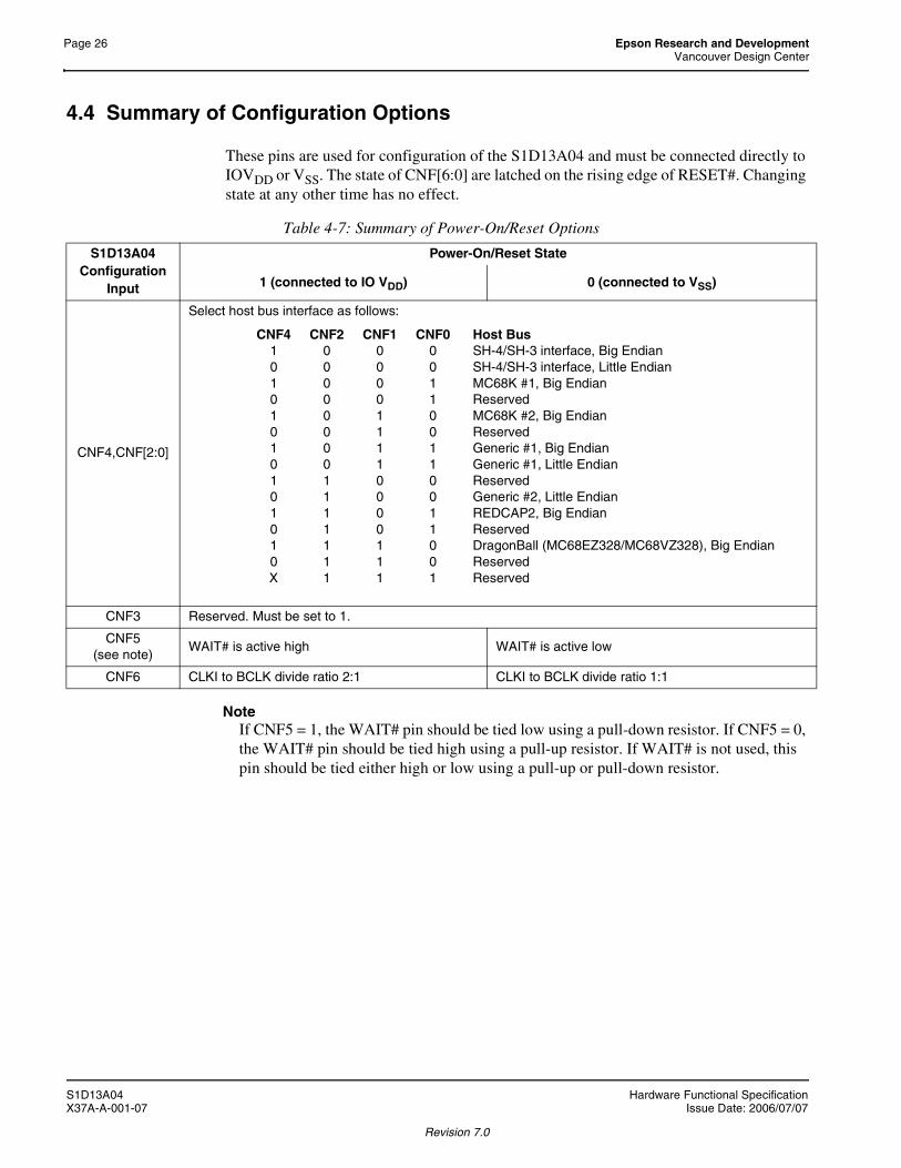
4.4 Summary of Configuration Options
These pins are used for configuration of the S1D13A04 and must be connected directly to IOVDD or VSS. The state of CNF[6:0] are latched on the rising edge of RESET#. Changing state at any other time has no effect.
NoteIf CNF5 = 1, the WAIT# pin should be tied low using a pull-down resistor. If CNF5 = 0, the WAIT# pin should be tied high using a pull-up resistor. If WAIT# is not used, this pin should be tied either high or low using a pull-up or pull-down resistor.
Table 4-7: Summary of Power-On/Reset Options
S1D13A04 Configuration
Input
Power-On/Reset State
1 (connected to IO VDD) 0 (connected to VSS)
CNF4,CNF[2:0]
Select host bus interface as follows:
CNF4 CNF2 CNF1 CNF0 Host Bus1 0 0 0 SH-4/SH-3 interface, Big Endian0 0 0 0 SH-4/SH-3 interface, Little Endian1 0 0 1 MC68K #1, Big Endian0 0 0 1 Reserved1 0 1 0 MC68K #2, Big Endian0 0 1 0 Reserved1 0 1 1 Generic #1, Big Endian0 0 1 1 Generic #1, Little Endian1 1 0 0 Reserved0 1 0 0 Generic #2, Little Endian1 1 0 1 REDCAP2, Big Endian0 1 0 1 Reserved1 1 1 0 DragonBall (MC68EZ328/MC68VZ328), Big Endian0 1 1 0 ReservedX 1 1 1 Reserved
CNF3 Reserved. Must be set to 1.
CNF5(see note)
WAIT# is active high WAIT# is active low
CNF6 CLKI to BCLK divide ratio 2:1 CLKI to BCLK divide ratio 1:1
S1D13A04 Hardware Functional SpecificationX37A-A-001-07 Issue Date: 2006/07/07
Revision 7.0
Epson Research and Development Page 27Vancouver Design Center
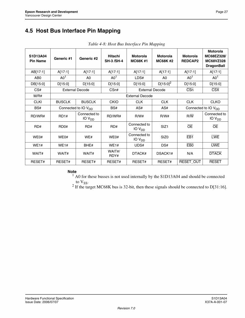
4.5 Host Bus Interface Pin Mapping
Note1 A0 for these busses is not used internally by the S1D13A04 and should be connected
to VSS.2 If the target MC68K bus is 32-bit, then these signals should be connected to D[31:16].
Table 4-8: Host Bus Interface Pin Mapping
S1D13A04 Pin Name
Generic #1 Generic #2Hitachi
SH-3 /SH-4Motorola
MC68K #1Motorola
MC68K #2Motorola
REDCAP2
Motorola MC68EZ328/MC68VZ328 DragonBall
AB[17:1] A[17:1] A[17:1] A[17:1] A[17:1] A[17:1] A[17:1] A[17:1]
AB0 A01 A0 A01 LDS# A0 A01 A01
DB[15:0] D[15:0] D[15:0] D[15:0] D[15:0] D[15:0]2 D[15:0] D[15:0]
CS# External Decode CSn# External Decode CSn CSX
M/R# External Decode
CLKI BUSCLK BUSCLK CKIO CLK CLK CLK CLKO
BS# Connected to IO VDD BS# AS# AS# Connected to IO VDD
RD/WR# RD1#Connected to
IO VDDRD/WR# R/W# R/W# R/W
Connected to IO VDD
RD# RD0# RD# RD#Connected to
IO VDDSIZ1 OE OE
WE0# WE0# WE# WE0#Connected to
IO VDDSIZ0 EB1 LWE
WE1# WE1# BHE# WE1# UDS# DS# EB0 UWE
WAIT# WAIT# WAIT#WAIT#/RDY#
DTACK# DSACK1# N/A DTACK
RESET# RESET# RESET# RESET# RESET# RESET# RESET_OUT RESET
Hardware Functional Specification S1D13A04Issue Date: 2006/07/07 X37A-A-001-07
Revision 7.0
Page 28 Epson Research and DevelopmentVancouver Design Center
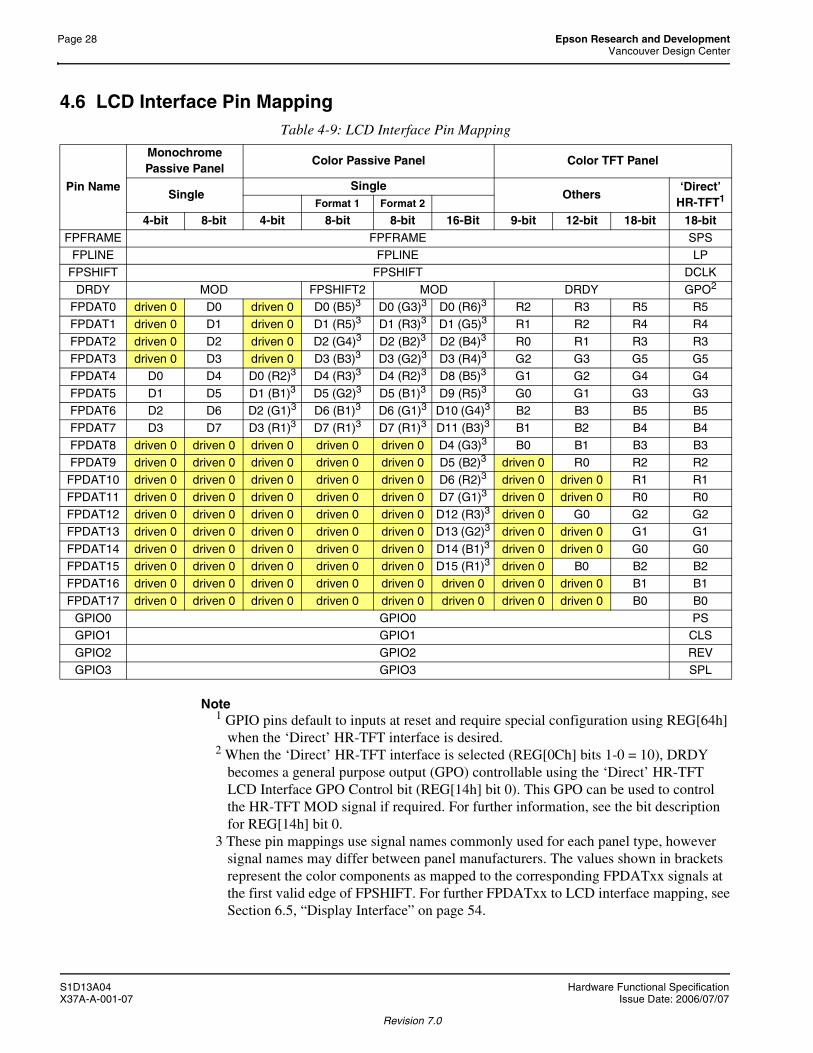
4.6 LCD Interface Pin Mapping
Note1 GPIO pins default to inputs at reset and require special configuration using REG[64h]
when the ‘Direct’ HR-TFT interface is desired.2 When the ‘Direct’ HR-TFT interface is selected (REG[0Ch] bits 1-0 = 10), DRDY
becomes a general purpose output (GPO) controllable using the ‘Direct’ HR-TFTLCD Interface GPO Control bit (REG[14h] bit 0). This GPO can be used to controlthe HR-TFT MOD signal if required. For further information, see the bit descriptionfor REG[14h] bit 0.
3 These pin mappings use signal names commonly used for each panel type, howeversignal names may differ between panel manufacturers. The values shown in bracketsrepresent the color components as mapped to the corresponding FPDATxx signals atthe first valid edge of FPSHIFT. For further FPDATxx to LCD interface mapping, seeSection 6.5, “Display Interface” on page 54.
Table 4-9: LCD Interface Pin Mapping
Pin Name
Monochrome Passive Panel
Color Passive Panel Color TFT Panel
SingleSingle
Others‘Direct’
HR-TFT1Format 1 Format 2
4-bit 8-bit 4-bit 8-bit 8-bit 16-Bit 9-bit 12-bit 18-bit 18-bitFPFRAME FPFRAME SPS
FPLINE FPLINE LPFPSHIFT FPSHIFT DCLK
DRDY MOD FPSHIFT2 MOD DRDY GPO2
FPDAT0 driven 0 D0 driven 0 D0 (B5)3 D0 (G3)3 D0 (R6)3 R2 R3 R5 R5FPDAT1 driven 0 D1 driven 0 D1 (R5)3 D1 (R3)3 D1 (G5)3 R1 R2 R4 R4
FPDAT2 driven 0 D2 driven 0 D2 (G4)3 D2 (B2)3 D2 (B4)3 R0 R1 R3 R3FPDAT3 driven 0 D3 driven 0 D3 (B3)3 D3 (G2)3 D3 (R4)3 G2 G3 G5 G5FPDAT4 D0 D4 D0 (R2)3 D4 (R3)3 D4 (R2)3 D8 (B5)3 G1 G2 G4 G4
FPDAT5 D1 D5 D1 (B1)3 D5 (G2)3 D5 (B1)3 D9 (R5)3 G0 G1 G3 G3FPDAT6 D2 D6 D2 (G1)3 D6 (B1)3 D6 (G1)3 D10 (G4)3 B2 B3 B5 B5FPDAT7 D3 D7 D3 (R1)3 D7 (R1)3 D7 (R1)3 D11 (B3)3 B1 B2 B4 B4
FPDAT8 driven 0 driven 0 driven 0 driven 0 driven 0 D4 (G3)3 B0 B1 B3 B3FPDAT9 driven 0 driven 0 driven 0 driven 0 driven 0 D5 (B2)3 driven 0 R0 R2 R2
FPDAT10 driven 0 driven 0 driven 0 driven 0 driven 0 D6 (R2)3 driven 0 driven 0 R1 R1
FPDAT11 driven 0 driven 0 driven 0 driven 0 driven 0 D7 (G1)3 driven 0 driven 0 R0 R0FPDAT12 driven 0 driven 0 driven 0 driven 0 driven 0 D12 (R3)3 driven 0 G0 G2 G2FPDAT13 driven 0 driven 0 driven 0 driven 0 driven 0 D13 (G2)3 driven 0 driven 0 G1 G1
FPDAT14 driven 0 driven 0 driven 0 driven 0 driven 0 D14 (B1)3 driven 0 driven 0 G0 G0FPDAT15 driven 0 driven 0 driven 0 driven 0 driven 0 D15 (R1)3 driven 0 B0 B2 B2FPDAT16 driven 0 driven 0 driven 0 driven 0 driven 0 driven 0 driven 0 driven 0 B1 B1
FPDAT17 driven 0 driven 0 driven 0 driven 0 driven 0 driven 0 driven 0 driven 0 B0 B0GPIO0 GPIO0 PSGPIO1 GPIO1 CLS
GPIO2 GPIO2 REVGPIO3 GPIO3 SPL
S1D13A04 Hardware Functional SpecificationX37A-A-001-07 Issue Date: 2006/07/07
Revision 7.0

Epson Research and Development Page 29Vancouver Design Center
5 D.C. Characteristics
NoteWhen applying Supply Voltages to the S1D13A04, Core VDD must be applied to the chip before, or simultaneously with IO VDD, or damage to the chip may result.
1. When Core VDD is 2.0V ± 10%, the MCLK must be less than or equal to 30MHz (MCLK ≤ 30MHz)
Table 5-1: Absolute Maximum Ratings
Symbol Parameter Rating Units
Core VDD Supply Voltage VSS - 0.3 to 3.0 V
IO VDD Supply Voltage VSS - 0.3 to 4.0 V
VIN Input Voltage VSS - 0.3 to IO VDD + 0.5 V
VOUT Output Voltage VSS - 0.3 to IO VDD + 0.5 V
TSTG Storage Temperature -65 to 150 ° C
TSOL Solder Temperature/Time 260 for 10 sec. max at lead ° C
Table 5-2: Recommended Operating Conditions
Symbol Parameter Condition Min Typ Max Units
Core VDD Supply VoltageVSS = 0 V 1.8 (note 1) 2.0 (note 1) 2.2 (note 1) V
VSS = 0 V 2.25 2.5 2.75 V
IO VDD Supply Voltage VSS = 0 V 3.0 3.3 3.6 V
VIN Input VoltageVSS IO VDD V
VSS CORE VDD
TOPR Operating Temperature -40 25 85 ° C
Table 5-3: Electrical Characteristics for VDD = 3.3V typical
Symbol Parameter Condition Min Typ Max UnitsIDDS Quiescent Current Quiescent Conditions 170 μAIIZ Input Leakage Current -1 1 μA
IOZ Output Leakage Current -1 1 μA
VOH High Level Output VoltageVDD = min.IOH = -3mA (Type 1)
-6mA (Type 2)VDD - 0.4 V
VOL Low Level Output VoltageVDD = min.IOL = 3mA (Type 1)
6mA (Type 2)0.4 V
VIH High Level Input Voltage LVTTL Level, VDD = max 2.0 V
VIL Low Level Input Voltage LVTTL Level, VDD = min 0.8 VRPD Pull Down Resistance VIN = VDD 20 50 120 kΩCI Input Pin Capacitance 10 pF
CO Output Pin Capacitance 10 pFCIO Bi-Directional Pin Capacitance 10 pF
Hardware Functional Specification S1D13A04Issue Date: 2006/07/07 X37A-A-001-07
Revision 7.0
Page 30 Epson Research and DevelopmentVancouver Design Center
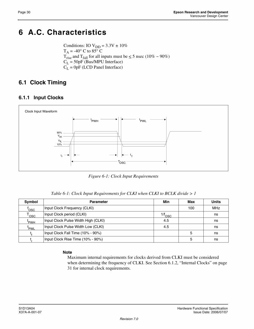
6 A.C. Characteristics
Conditions: IO VDD = 3.3V ± 10%TA = -40° C to 85° CTrise and Tfall for all inputs must be < 5 nsec (10% ~ 90%)CL = 50pF (Bus/MPU Interface)CL = 0pF (LCD Panel Interface)
6.1 Clock Timing
6.1.1 Input Clocks
Figure 6-1: Clock Input Requirements
NoteMaximum internal requirements for clocks derived from CLKI must be considered when determining the frequency of CLKI. See Section 6.1.2, “Internal Clocks” on page 31 for internal clock requirements.
Table 6-1: Clock Input Requirements for CLKI when CLKI to BCLK divide > 1
Symbol Parameter Min Max Units
fOSC
Input Clock Frequency (CLKI) 100 MHz
TOSC
Input Clock period (CLKI) 1/fOSC
ns
tPWH
Input Clock Pulse Width High (CLKI) 4.5 ns
tPWL
Input Clock Pulse Width Low (CLKI) 4.5 ns
tf
Input Clock Fall Time (10% - 90%) 5 ns
tr
Input Clock Rise Time (10% - 90%) 5 ns
tPWLtPWH
t f
Clock Input Waveform
tr
TOSC
VIH
VIL10%
90%
S1D13A04 Hardware Functional SpecificationX37A-A-001-07 Issue Date: 2006/07/07
Revision 7.0

Epson Research and Development Page 31Vancouver Design Center
NoteMaximum internal requirements for clocks derived from CLKI must be considered when determining the frequency of CLKI. See Section 6.1.2, “Internal Clocks” on page 31 for internal clock requirements.
NoteMaximum internal requirements for clocks derived from CLKI2 must be considered when determining the frequency of CLKI2. See Section 6.1.2, “Internal Clocks” on page 31 for internal clock requirements.
6.1.2 Internal Clocks
1. When COREVDD = 2.0V ±10% fMCLK max = 30MHz.2. MCLK is derived from BCLK, therefore when BCLK is greater than 50MHz, MCLK must be divided using
REG[04h] bits 5-4.
NoteFor further information on internal clocks, refer to Section 7, “Clocks” on page 83.
Table 6-2: Clock Input Requirements for CLKI when CLKI to BCLK divide = 1
Symbol Parameter Min Max Units
fOSC
Input Clock Frequency (CLKI) 66 MHz
TOSC
Input Clock period (CLKI) 1/fOSC
ns
tPWH
Input Clock Pulse Width High (CLKI) 3 ns
tPWL
Input Clock Pulse Width Low (CLKI) 3 ns
tf
Input Clock Fall Time (10% - 90%) 5 ns
tr
Input Clock Rise Time (10% - 90%) 5 ns
Table 6-3: Clock Input Requirements for CLKI2
Symbol Parameter Min Max Units
fOSC
Input Clock Frequency (CLKI2) 66 MHz
TOSC
Input Clock period (CLKI2) 1/fOSC
ns
tPWH
Input Clock Pulse Width High (CLKI2) 3 ns
tPWL
Input Clock Pulse Width Low (CLKI2) 3 ns
tf
Input Clock Fall Time (10% - 90%) 5 ns
tr
Input Clock Rise Time (10% - 90%) 5 ns
Table 6-4: Internal Clock Requirements
Symbol Parameter Min Max Units
fBCLK
Bus Clock frequency 66 MHz
fMCLK
Memory Clock frequency50
(note 1,note 2)MHz
fPCLK
Pixel Clock frequency 50 MHz
fPWMCLK
PWM Clock frequency 66 MHz
Hardware Functional Specification S1D13A04Issue Date: 2006/07/07 X37A-A-001-07
Revision 7.0

Page 32 Epson Research and DevelopmentVancouver Design Center
6.2 RESET# Timing
Figure 6-2 S1D13A04 RESET# Timing
Table 6-5 S1D13A04 RESET# Timing
Symbol Parameter Min Max Units
t1 Active Reset Pulse Width 1 — CLKI
t1
RESET#
S1D13A04 Hardware Functional SpecificationX37A-A-001-07 Issue Date: 2006/07/07
Revision 7.0

Epson Research and Development Page 33Vancouver Design Center
6.3 CPU Interface Timing
6.3.1 Generic #1 Interface Timing (e.g. Epson EOC33)
Figure 6-3: Generic #1 Interface Timing
CLK
A[16:1], M/R#
CS#
WE0#, WE1#, RD0#, RD1#
WAIT#
D[15:0] (write)
D[15:0] (read)
TCLK
t1
t2
t3
t4
t5
t14
t6
t7
t8
t9t10
t11
t12
t13
valid
valid
Hardware Functional Specification S1D13A04Issue Date: 2006/07/07 X37A-A-001-07
Revision 7.0
Page 34 Epson Research and DevelopmentVancouver Design Center
Table 6-6: Generic #1 Interface Timing
Symbol Parameter Min Max Unit
fCLK Bus clock frequency 50 MHz
TCLK Bus clock period 1/fCLK ns
t1A[16:1], M/R# setup to first CLK rising edge where CS# = 0 and either RD0#, RD1# = 0 or WE0#, WE1# = 0
9 ns
t2 CS# setup to CLK rising edge 9 ns
t3 RD0#, RD1#, WE0#, WE1# setup to CLK rising edge 1 ns
t4 RD0#, RD1# or WE0#, WE1# state change to WAIT# driven low 1 10 ns
t5 RD0#, RD1# falling edge to D[15:0] driven (read cycle) 2 10 ns
t6D[15:0] setup to 4th rising CLK edge after CS#=0 and WE0#, WE1#=0
1 TCLK
t7A[16:1], M/R# and CS# hold from RD0#, RD1#, WE0#, WE1# rising edge
0 ns
t8 CS# deasserted to reasserted 0 ns
t9 WAIT# rising edge to RD0#, RD1#, WE0#, WE1# rising edge 0 ns
t10 WE0#, WE1#, RD0#, RD1# deasserted to reasserted 1 TCLK
t11Rising edge of either RD0#, RD1# or WE0#, WE1# to WAIT# high impedance
0.5 TCLK
t12 D[15:0] hold from WE0#, WE1# rising edge (write cycle) 2 ns
t13 D[15:0] hold from RD0#, RD1# rising edge (read cycle) 1 ns
t14 Cycle Length 5 TCLK
Table 6-7: Generic #1 Interface Truth Table for Little Endian
WE0# WE1# RD0# RD1# D[15:8] D[7:0] Comments
0 0 1 1 valid valid 16-bit write
0 1 1 1 - valid 8-bit write; data on low byte (even byte address1)
1 0 1 1 valid - 8-bit write; data on high byte (odd byte address1)
1 1 0 0 valid valid 16-bit read
1 1 0 1 - valid 8-bit read; data on low byte (even byte address1)
1 1 1 0 valid - 8-bit read; data on high byte (odd byte address1)
S1D13A04 Hardware Functional SpecificationX37A-A-001-07 Issue Date: 2006/07/07
Revision 7.0

Epson Research and Development Page 35Vancouver Design Center
1. Because A0 is not used internally, all addresses are seen by the S1D13A04 as even addresses (16-bit wordaddress aligned on even byte addresses).
Table 6-8: Generic #1 Interface Truth Table for Big Endian
WE0# WE1# RD0# RD1# D[15:8] D[7:0] Comments
0 0 1 1 valid valid 16-bit write
0 1 1 1 - valid 8-bit write; data on low byte (odd byte address1)
1 0 1 1 valid - 8-bit write; data on high byte (even byte address1)
1 1 0 0 valid valid 16-bit read
1 1 0 1 - valid 8-bit read; data on low byte (odd byte address1)
1 1 1 0 valid - 8-bit read; data on high byte (even byte address1)
Hardware Functional Specification S1D13A04Issue Date: 2006/07/07 X37A-A-001-07
Revision 7.0

Page 36 Epson Research and DevelopmentVancouver Design Center
6.3.2 Generic #2 Interface Timing (e.g. ISA)
Figure 6-4: Generic #2 Interface Timing
BUSCLK
A[16:0], M/R#, BHE#
CS#
WE#, RD#
WAIT#
D[15:0] (write)
D[15:0] (read)
TBUSCLK
t1
t2
t3
t4
t5
t14
t6
t7
t8
t9t10
t11
t12
t13
valid
valid
S1D13A04 Hardware Functional SpecificationX37A-A-001-07 Issue Date: 2006/07/07
Revision 7.0

Epson Research and Development Page 37Vancouver Design Center
NoteGeneric #2 interface only supports Little Endian mode.
Table 6-9: Generic #2 Interface Timing
Symbol Parameter Min Max Unit
fBUSCLK Bus clock frequency 50 MHz
TBUSCLK Bus clock period 1/fBUSCLK ns
t1A[16:0], M/R#, BHE# setup to first BUSCLK rising edge where CS# = 0 and either RD# = 0 or WE# = 0
9 ns
t2 CS# setup to BUSCLK rising edge 9 ns
t3 RD#, WE# setup to BUSCLK rising edge 1 ns
t4 RD# or WE# state change to WAIT# driven low 1 10 ns
t5 RD# falling edge to D[15:0] driven (read cycle) 2 10 ns
t6 D[15:0] setup to 4th rising BUSCLK edge after CS#=0 and WE#=0 1 TBUSCLK
t7 A[16:0], M/R#, BHE# and CS# hold from RD#, WE# rising edge 0 ns
t8 CS# deasserted to reasserted 0 ns
t9 WAIT# rising edge to RD#, WE# rising edge 0 ns
t10 WE#, RD# deasserted to reasserted 1 TBUSCLK
t11 Rising edge of either RD# or WE# to WAIT# high impedance 0.5 TBUSCLK
t12 D[15:0] hold from WE# rising edge (write cycle) 2 ns
t13 D[15:0] hold from RD# rising edge (read cycle) 1 ns
t14 Cycle Length 6 TBUSCLK
Table 6-10: Generic #2 Interface Truth Table for Little Endian
WE# RD# BHE# A0 D[15:8] D[7:0] Comments
0 1 0 0 valid valid 16-bit write
0 1 1 0 - valid 8-bit write at even address
0 1 0 1 valid - 8-bit write at odd address
1 0 0 0 valid valid 16-bit read
1 0 1 0 - valid 8-bit read at even address
1 0 0 1 valid - 8-bit read at odd address
Hardware Functional Specification S1D13A04Issue Date: 2006/07/07 X37A-A-001-07
Revision 7.0

Page 38 Epson Research and DevelopmentVancouver Design Center
6.3.3 Hitachi SH-3 Interface Timing
Figure 6-5: Hitachi SH-3 Interface Timing
NoteFor this interface, the following formula must apply:
MCLK = BCLK ≤ 33MHz
If a BCLK greater than 33MHz is desired, MCLK must be divided such that MCLK is not greater than 33MHz (see REG[04h] bits 5-4).
CKIO
A[16:1], M/R#, RD/WR#
BS#
CSn#
WEn#, RD#
WAIT#
D[15:0] (write)
D[15:0] (read)
TCKIO
t1
t2 t3
t4
t6
t8
t7
t5 t13
t15
t16t17
t14
t12
t11
t9
t18t10
valid
valid
S1D13A04 Hardware Functional SpecificationX37A-A-001-07 Issue Date: 2006/07/07
Revision 7.0

Epson Research and Development Page 39Vancouver Design Center
1. The S1D13A04 requires 2ns of write data hold time.
Table 6-11: Hitachi SH-3 Interface Timing
Symbol Parameter Min Max Unit
fCKIO Bus clock frequency 66 MHz
TCKIO Bus clock period 1/fCKIO ns
t1 A[16:1], RD/WR# setup to CKIO 1 ns
t2 BS# setup 1 ns
t3 BS# hold 5 ns
t4 CSn# setup 1 ns
t5 WEn#, RD# setup to next CKIO after BS# low 0 ns
t6 Falling edge CSn# to WAIT# driven low 3 10 ns
t7D[15:0] setup to 3rd CKIO rising edge after BS# deasserted(write cycle)
1 TCKIO
t8 Falling edge of RD# to D[15:0] driven (read cycle) 2 12 ns
t9 WE#, RD# deasserted to A[16:1], M/R#, RD/WR# deasserted 0 ns
t10 Rising edge of WAIT# to BS# falling TCKIO + 16 ns
t11 WE#, RD# deasserted to CS# high 0 ns
t12CKIO rising edge before WAIT# deasserted to WEn#, RD# asserted for next cycle
2 TCKIO
t13 Rising edge of WAIT# to WE#, RD# deasserted 0 ns
t14 Rising edge of CSn# to WAIT# high impedance 0.5 TCKIO
t15 D[15:0] hold from WEn# deasserted (write cycle) 2 (note 1) ns
t16 D[15:0] setup to CKIO falling edge (read cycle) 12 ns
t17 Rising edge of RD# to D[15:0] high impedance (read cycle) 1 5 ns
t18 Cycle Length 4 TCKIO
Hardware Functional Specification S1D13A04Issue Date: 2006/07/07 X37A-A-001-07
Revision 7.0

Page 40 Epson Research and DevelopmentVancouver Design Center
6.3.4 Hitachi SH-4 Interface Timing
Figure 6-6: Hitachi SH-4 Interface Timing
CKIO
A[16:1], M/R#, RD/WR#
BS#
CSn#
WEn#, RD#
RDY#
D[15:0] (write)
D[15:0] (read)
TCKIO
t1
t2 t3
t4
t6
t8
t7
t5 t13
t16
t17
t18
t14
t12
t11
t9
t19t10
t15
valid
valid
S1D13A04 Hardware Functional SpecificationX37A-A-001-07 Issue Date: 2006/07/07
Revision 7.0

Epson Research and Development Page 41Vancouver Design Center
Table 6-12: Hitachi SH-4 Interface Timing
Symbol Parameter Min Max Unit
fCKIO Bus clock frequency 66 MHz
TCKIO Bus clock period 1/fCKIO ns
t1 A[16:1], M/R#, RD/WR# setup to CKIO 1 ns
t2 BS# setup 1 ns
t3 BS# hold 5 ns
t4 CSn# setup 1 ns
t5 WEn#, RD# setup to 2nd CKIO rising edge after BS# low 0 ns
t6 Falling edge CSn# to RDY driven high 3 10 ns
t7D[15:0] setup to 3rd CKIO rising edge after BS# deasserted(write cycle)
1 TCKIO
t8 Falling edge RD# to D[15:0] driven (read cycle) 2 12 ns
t9 WE#,RD# deasserted to A[16:1],M/R#,RD/WR# deasserted 0 ns
t10 RDY falling edge to BS# falling TCKIO + 11 ns
t11 WE#,RD# deasserted to CS# high 0 ns
t12CKIO rising edge before RDY deasserted to WEn#, RD# asserted for next cycle
2 TCKIO
t13 RDY falling edge to WE#,RD# deasserted 0 ns
t14 Rising edge CSn# to RDY rising edge 3 10 ns
t15 CKIO falling edge to RDY tristate 3 9 ns
t16 D[15:0] hold from WEn# deasserted (write cycle) 3 ns
t17 D[15:0] setup to CKIO falling edge (read cycle) 12 ns
t18 Rising edge of RD# to D[15:0] high impedance (read cycle) 1 4 ns
t19 Cycle Length 4 TCKIO
Hardware Functional Specification S1D13A04Issue Date: 2006/07/07 X37A-A-001-07
Revision 7.0

Page 42 Epson Research and DevelopmentVancouver Design Center
6.3.5 Motorola MC68K #1 Interface Timing (e.g. MC68000)
Figure 6-7: Motorola MC68K #1 Interface Timing
CLK
A[16:1], R/W#, M/R#
CS#
AS#
UDS#, LDS#, (A0)
DTACK#
D[15:0] (write)
D[15:0] (read)
TCLK
t1
t1
t1
t1
t2
t3
t9
t5 t6
t7
t8
t10
t11
t4
t4t13
t12
valid
valid
S1D13A04 Hardware Functional SpecificationX37A-A-001-07 Issue Date: 2006/07/07
Revision 7.0

Epson Research and Development Page 43Vancouver Design Center
Table 6-13: Motorola MC68K#1 Interface Timing
Symbol Parameter Min Max Unit
fCLK Bus clock frequency 66 MHz
TCLK Bus clock period 1/fCLK ns
t1A[16:1], M/R#, R/W# and CS# and AS# and UDS#, LDS# setup to first CLK rising edge
1 ns
t2 CS# and AS# asserted to DTACK# driven 3 10 ns
t3 UDS# = 0 or LDS# = 0 to D[15:0] driven (read cycle) 10 ns
t4 A[16:1], M/R#, R/W# and CS# hold from AS# rising edge 0 ns
t5 DTACK# falling edge to UDS#, LDS# rising edge 0 ns
t6 UDS#, LDS# deasserted high to reasserted low 1 TCLK
t7 CLK rising edge to DTACK# high impedance TCLK - 2 ns
t8 AS# rising edge to DTACK# rising edge 3 11 ns
t9D[15:0] valid to 4th CLK rising edge where CS# = 0, AS# = 0 and either UDS# = 0 or LDS# = 0 (write cycle)
1 TCLK
t10 D[15:0] hold from UDS#, LDS# falling edge (write cycle) 4 ns
t11 UDS#, LDS# rising edge to D[15:0] high impedance (read cycle) 2 ns
t12D[15:0] valid setup time to 2nd CLK falling edge after DTACK# goes low (read cycle)
10 ns
t13 Cycle Length 7 TCLK
Hardware Functional Specification S1D13A04Issue Date: 2006/07/07 X37A-A-001-07
Revision 7.0
Page 44 Epson Research and DevelopmentVancouver Design Center
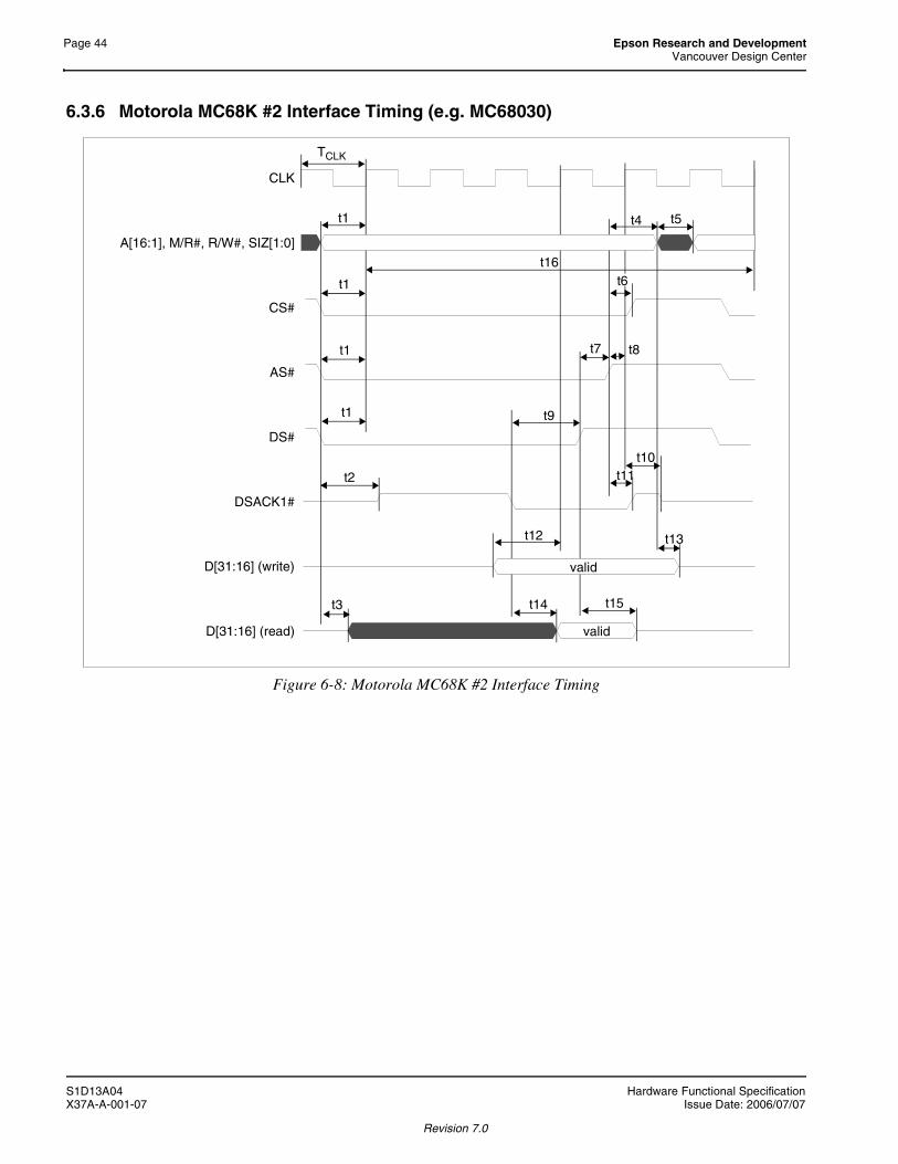
6.3.6 Motorola MC68K #2 Interface Timing (e.g. MC68030)
Figure 6-8: Motorola MC68K #2 Interface Timing
t6
CLK
A[16:1], M/R#, R/W#, SIZ[1:0]
CS#
AS#
DS#
DSACK1#
D[31:16] (write)
D[31:16] (read)
TCLK
t1
t1
t1
t1
t2
t3 t14 t15
t12 t13
t11t10
t9
t16
t7
t4 t5
t8
valid
valid
S1D13A04 Hardware Functional SpecificationX37A-A-001-07 Issue Date: 2006/07/07
Revision 7.0

Epson Research and Development Page 45Vancouver Design Center
Table 6-14: Motorola MC68K#2 Interface Timing
Symbol Parameter Min Max Unit
fCLK Bus clock frequency 50 MHz
TCLK Bus clock period 1/fCLK ns
t1A[16:0], M/R#, R/W#, SIZ[1:0] and CS# and AS# and DS# setup to first CLK rising edge
1 ns
t2 CS# and AS# asserted low to DSACK1# driven 3 10 ns
t3 A[1:0], R/W#, SIZ[1:0], DS# asserted to D[15:0] driven 8 ns
t4 A[16:1], M/R#, R/W#, SIZ[1:0] hold from AS# rising edge 0 ns
t5R/W#, A[1:0], SIZ[1:0] deasserted to R/W#, A[1:0], SIZ[1:0] asserted for next cycle
1 TCLK
t6 CS# hold from AS# rising edge 0 ns
t7 DS# rising edge to AS# rising edge 0 ns
t8 AS# setup to CLK rising edge 1 ns
t9 DSACK1# falling edge to DS# rising edge 0 ns
t10 CLK rising edge to DSACK1# high impedance TCLK - 2 ns
t11 AS# rising edge to DSACK1# rising edge 3 9 ns
t12D[15:0] setup to 4th CLK rising edge after CS#=0, AS#=0, and UDS#=0 or LDS#=0
1 TCLK
t13 D[15:0] hold from A[1:0], R/W#, SIZ[1:0] (write cycle) 1 ns
t14 DSACK1# falling edge to D[15:0] valid (read cycle) 3 ns
t15 DS# rising edge to D[15:0] high impedance (read cycle) 2 7 ns
t16 Cycle Length 6 TCLK
Hardware Functional Specification S1D13A04Issue Date: 2006/07/07 X37A-A-001-07
Revision 7.0

Page 46 Epson Research and DevelopmentVancouver Design Center
6.3.7 Motorola REDCAP2 Interface Timing
Figure 6-9: Motorola Redcap2 Interface Timing
CKO
A[16:1], R/W#, CS#
EBO#, EB1# (write)
D[15:0] (write)
EB0#, EB1#, OE# (read)
D[15:0] (read)
TCKO
t1
t2
t5
t7t6
t3 t4
t11
t10
t9t12
t8
valid
valid
S1D13A04 Hardware Functional SpecificationX37A-A-001-07 Issue Date: 2006/07/07
Revision 7.0

Epson Research and Development Page 47Vancouver Design Center
1. The cycle length for the REDCAP interface is fixed.2. The Read and Write 2D BitBLT functions are not available when using the REDCAP interface.
Table 6-15: Motorola Redcap2 Interface Timing
Symbol Parameter Min Max Unit
fCKO Bus clock frequency 17 MHz
TCKO Bus clock period 1/fCKO ns
t1 A[16:1], R/W, CSn# setup to CKO rising edge 1 ns
t2 EB0,EB1 setup to CKO rising edge (write) 1 ns
t3D[15:0] input setup to 4th CKO rising edge after CSn# and EB0 or EB1 asserted low (write cycle)
1 TCKO
t4D[15:0] input hold from 4th CKO rising edge after CSn# and EB0 or EB1 asserted low (write cycle)
11 ns
t5 EB0,EB1,OE setup to CKO rising edge (read cycle) 1 ns
t6a1st CKO rising edge after CSn#, EB0 or EB1,OE asserted low to D[15:0] valid for MCLK = BCLK (read cycle)
5 TCKO
t6b1st CKO rising edge after CSn#, EB0 or EB1,OE asserted low to D[15:0] valid for MCLK = BCLK ÷ 2 (read cycle)
8 TCKO
t6c1st CKO rising edge after CSn#, EB0 or EB1,OE asserted low to D[15:0] valid for MCLK = BCLK ÷ 3 (read cycle)
10 TCKO
t6d1st CKO rising edge after CSn#, EB0 or EB1,OE asserted low to D[15:0] valid for MCLK = BCLK ÷ 4 (read cycle)
13 TCKO
t7 EB0,EB1,OE falling edge to D[15:0] driven (read cycle) 4 11 ns
t8 A[16:1], R/W, CSn hold from CKO rising edge 0 ns
t9 EB0, EB1 setup to CKO rising edge (write cycle) 1 ns
t10 CKO falling edge to EB0, EB1, OE deasserted (read) 0 ns
t11 OE, EB0, EB1 deasserted to D[15:0] output high impedance (read) 1 7 ns
t12 Cycle Length (note 1) 10 10 TCKO
Hardware Functional Specification S1D13A04Issue Date: 2006/07/07 X37A-A-001-07
Revision 7.0

Page 48 Epson Research and DevelopmentVancouver Design Center
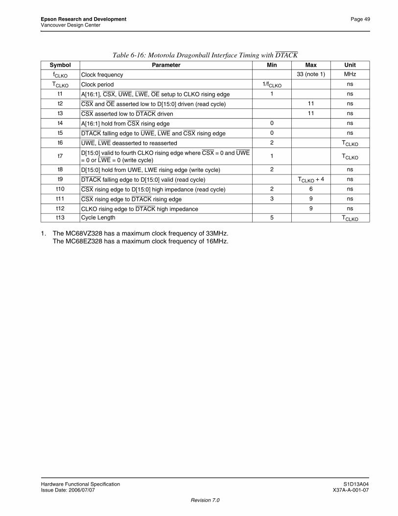
6.3.8 Motorola Dragonball Interface Timing with DTACK (e.g. MC68EZ328/MC68VZ328)
Figure 6-10: Motorola Dragonball Interface Timing with DTACK
CLKO
A[16:1]
CSX
UWE, LWE (write)
OE (read)
D[15:0] (write)
D[15:0] (read)
DTACK
TCLKO
t1
t1
t1
t1
t4
t5t13
t5t6
t8
t10
t12t11
t9
t7
t2
t3
Valid
Valid
S1D13A04 Hardware Functional SpecificationX37A-A-001-07 Issue Date: 2006/07/07
Revision 7.0
Epson Research and Development Page 49Vancouver Design Center
1. The MC68VZ328 has a maximum clock frequency of 33MHz.The MC68EZ328 has a maximum clock frequency of 16MHz.
Table 6-16: Motorola Dragonball Interface Timing with DTACKSymbol Parameter Min Max Unit
fCLKO Clock frequency 33 (note 1) MHz
TCLKO Clock period 1/fCLKO ns
t1 A[16:1], CSX, UWE, LWE, OE setup to CLKO rising edge 1 ns
t2 CSX and OE asserted low to D[15:0] driven (read cycle) 11 ns
t3 CSX asserted low to DTACK driven 11 ns
t4 A[16:1] hold from CSX rising edge 0 ns
t5 DTACK falling edge to UWE, LWE and CSX rising edge 0 ns
t6 UWE, LWE deasserted to reasserted 2 TCLKO
t7 D[15:0] valid to fourth CLKO rising edge where CSX = 0 and UWE = 0 or LWE = 0 (write cycle)
1 TCLKO
t8 D[15:0] hold from UWE, LWE rising edge (write cycle) 2 ns
t9 DTACK falling edge to D[15:0] valid (read cycle) TCLKO + 4 ns
t10 CSX rising edge to D[15:0] high impedance (read cycle) 2 6 ns
t11 CSX rising edge to DTACK rising edge 3 9 ns
t12 CLKO rising edge to DTACK high impedance 9 ns
t13 Cycle Length 5 TCLKO
Hardware Functional Specification S1D13A04Issue Date: 2006/07/07 X37A-A-001-07
Revision 7.0

Page 50 Epson Research and DevelopmentVancouver Design Center
6.3.9 Motorola Dragonball Interface Timing w/o DTACK (e.g. MC68EZ328/MC68VZ328)
Figure 6-11: Motorola Dragonball Interface Timing w/o DTACK
CLKO
A[16:1]
CSX#
UWE#, LWE# (write)
OE# (read)
D[15:0] (write)
D[15:0] (read)
TCLKO
t1
t1
t1
t1
t2
t3t4
t7
t5
t6
t5
t5
t5
valid
valid
S1D13A04 Hardware Functional SpecificationX37A-A-001-07 Issue Date: 2006/07/07
Revision 7.0

Epson Research and Development Page 51Vancouver Design Center
1. The MC68VZ328 has a maximum clock frequency of 33MHz.The MC68EZ328 has a maximum clock frequency of 16MHz.
2. The MC68EZ328 does not support the MCLK = BCLK ÷ 3 and MCLK = BCLK ÷ 4 options.3. The cycle length for the Dragonball w/o DTACK interface is fixed.4. The Read and Write 2D BitBLT functions are not available when using the Dragonball w/o DTACK interface.
Table 6-17: Motorola Dragonball Interface Timing w/o DTACK
Symbol Parameter Min Max Unit
fCLKO Bus clock frequency 33 (note 1) MHz
TCLKO Bus clock period 1/fCLKO ns
t1A[16:1] and CSX# and UWE#, LWE# and OE# setup to CLKO rising edge
1 ns
t2D[15:0] valid to 4th CLK rising edge where CSX# = 0 and UWE# = 0 or LWE# = 0 (write cycle)
1 TCLKO
t3 CSX# and OE# asserted low to D[15:0] driven (read cycle) 11 ns
t4a1st CLKO rising edge after CSX# and OE# asserted to D[15:0] valid for MCLK=BCLK (read cycle)
5 TCLKO
t4b1st CLKO rising edge after CSX# and OE# asserted to D[15:0] valid for MCLK=BCLK ÷ 2 (read cycle)
8 TCLKO
t4c1st CLKO rising edge after CSX# and OE# asserted to D[15:0] valid for MCLK=BCLK ÷ 3 (read cycle) (see note 2)
10 TCLKO
t4d1st CLKO rising edge after CSX# and OE# asserted to D[15:0] valid for MCLK=BCLK ÷ 4 (read cycle) (see note 2)
13 TCLKO
t5A[16:1] and UWE#, LWE# and OE# and D[15:0] (write) hold from CSX# rising edge
0 ns
t6 CSX# rising edge to D[15:0] high impedance 2 6 ns
t7 Cycle Length 9 9 TCLKO
Hardware Functional Specification S1D13A04Issue Date: 2006/07/07 X37A-A-001-07
Revision 7.0

Page 52 Epson Research and DevelopmentVancouver Design Center
6.4 LCD Power Sequencing
6.4.1 Passive/TFT Power-On Sequence
Figure 6-12: Passive/TFT Power-On Sequence Timing
1. t1 is controlled by software and must be determined from the bias power supply delay requirements of the panel connected.
Table 6-18: Passive/TFT Power-On Sequence Timing Symbol Parameter Min Max Units
t1 LCD signals active to LCD bias active Note 1 Note 1
t2 Power Save Mode disabled to LCD signals active 0 1 BCLK
LCD Signals***
GPIO0*
Power Save t1
*It is recommended to use the general purpose IO pin GPIO0 to control the LCD bias power.
t2
**The LCD power-on sequence is activated by programming the Power Save Mode Enable bit (REG[14h] bit 4) to 0.***LCD Signals include: FPDAT[17:0], FPSHIFT, FPLINE, FPFRAME, and DRDY.
(REG[A0h] bit 0)Mode Enable**
S1D13A04 Hardware Functional SpecificationX37A-A-001-07 Issue Date: 2006/07/07
Revision 7.0

Epson Research and Development Page 53Vancouver Design Center
6.4.2 Passive/TFT Power-Off Sequence
Figure 6-13: Passive/TFT Power-Off Sequence Timing
1. t1 is controlled by software and must be determined from the bias power supply delay requirements of the panel connected.
6.4.3 ‘Direct’ HR-TFT Interface Power-On/Off Sequence
For ‘Direct’ HR-TFT Interface Power-On/Off sequence information, see Connecting to the Sharp HR-TFT Panels, document number X37A-G-011-xx.
Table 6-19: Passive/TFT Power-Off Sequence Timing Symbol Parameter Min Max Units
t1 LCD bias deactivated to LCD signals inactive Note 1 Note 1
t2 Power Save Mode enabled to LCD signals low 0 1 BCLK
LCD Signals***
GPIO0*
t1
*It is recommended to use the general purpose IO pin GPIO0 to control the LCD bias power. **The LCD power-off sequence is activated by programming the Power Save Mode Enable bit (REG[14h] bit 4) to 1.***LCD Signals include: FPDAT[17:0], FPSHIFT, FPLINE, FPFRAME, and DRDY.
t2
Power Save
(REG[A0h] bit 0)Mode Enable**
Hardware Functional Specification S1D13A04Issue Date: 2006/07/07 X37A-A-001-07
Revision 7.0

Page 54 Epson Research and DevelopmentVancouver Design Center
6.5 Display Interface
The timing parameters required to drive a flat panel display are shown below. Timing details for each supported panel type are provided in the remainder of this section.
Figure 6-14: Panel Timing Parameters
HT
VDPVT
VDPSVPW
VPS
HDP
HPWHPS
HDPS
S1D13A04 Hardware Functional SpecificationX37A-A-001-07 Issue Date: 2006/07/07
Revision 7.0

Epson Research and Development Page 55Vancouver Design Center
H
H
H
HHV
VVV
V
1. For passive panels, the HDP must be a minimum of 32 pixels and must be increased by multiples of 16.For TFT panels, the HDP must be a minimum of 8 pixels and must be increased by multiples of 8.
2. The following formulas must be valid for all panel timings:HDPS + HDP < HTVDPS + VDP < VT
Table 6-20: Panel Timing Parameter Definition and Register Summary
Symbol Description Derived From UnitsT Horizontal Total ((REG[20h] bits 6-0) + 1) x 8
Ts
DP1 Horizontal Display Period1 ((REG[24h] bits 6-0) + 1) x 8
DPS Horizontal Display Period Start PositionFor STN panels: ((REG[28h] bits 9-0) + 22)For TFT panels: ((REG[28h] bits 9-0) + 5)
PS FPLINE Pulse Start Position (REG[2Ch] bits 9-0) + 1PW FPLINE Pulse Width (REG[2Ch] bits 22-16) + 1T Vertical Total (REG[30h] bits 9-0) + 1
Lines (HT)DP Vertical Display Period (REG[34h] bits 9-0) + 1DPS Vertical Display Period Start Position REG[38h] bits 9-0PS FPFRAME Pulse Start Position REG[2Ch] bits 9-0
PW FPFRAME Pulse Width (REG[3Ch] bits 18-16) + 1
Hardware Functional Specification S1D13A04Issue Date: 2006/07/07 X37A-A-001-07
Revision 7.0

Page 56 Epson Research and DevelopmentVancouver Design Center
6.5.1 Generic STN Panel Timing
Figure 6-15: Generic STN Panel Timing
FPFRAME
VT (= 1 Frame)
MOD1(DRDY)
FPLINE
MOD2(DRDY)
FPLINE
VDP
VPW
HT (= 1 Line)
HDPS HDP
FPDAT[17:0]
FPDAT[17:0]
1PCLK
FPSHIFT
HPWHPS
S1D13A04 Hardware Functional SpecificationX37A-A-001-07 Issue Date: 2006/07/07
Revision 7.0
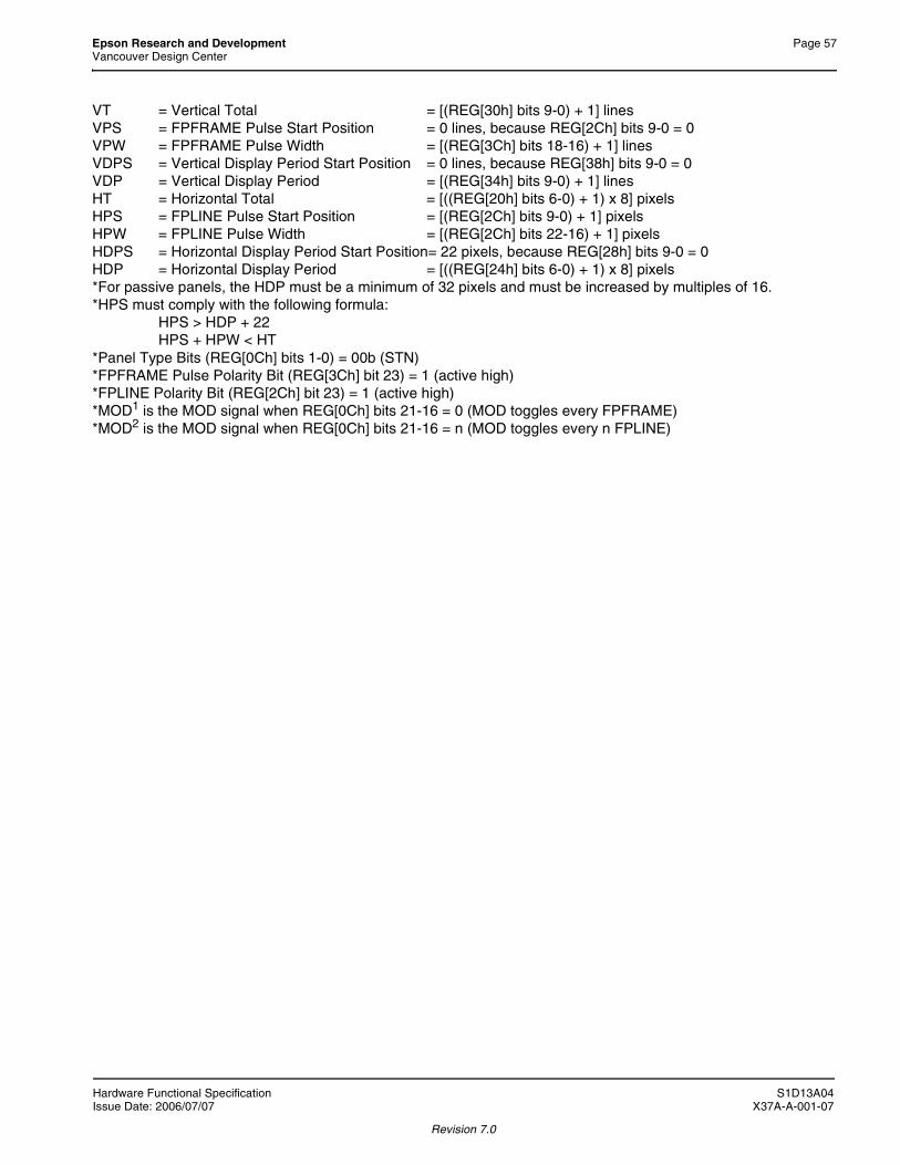
Epson Research and Development Page 57Vancouver Design Center
VT = Vertical Total = [(REG[30h] bits 9-0) + 1] linesVPS = FPFRAME Pulse Start Position = 0 lines, because REG[2Ch] bits 9-0 = 0VPW = FPFRAME Pulse Width = [(REG[3Ch] bits 18-16) + 1] linesVDPS = Vertical Display Period Start Position = 0 lines, because REG[38h] bits 9-0 = 0VDP = Vertical Display Period = [(REG[34h] bits 9-0) + 1] linesHT = Horizontal Total = [((REG[20h] bits 6-0) + 1) x 8] pixelsHPS = FPLINE Pulse Start Position = [(REG[2Ch] bits 9-0) + 1] pixelsHPW = FPLINE Pulse Width = [(REG[2Ch] bits 22-16) + 1] pixelsHDPS = Horizontal Display Period Start Position= 22 pixels, because REG[28h] bits 9-0 = 0HDP = Horizontal Display Period = [((REG[24h] bits 6-0) + 1) x 8] pixels*For passive panels, the HDP must be a minimum of 32 pixels and must be increased by multiples of 16.*HPS must comply with the following formula:
HPS > HDP + 22HPS + HPW < HT
*Panel Type Bits (REG[0Ch] bits 1-0) = 00b (STN)*FPFRAME Pulse Polarity Bit (REG[3Ch] bit 23) = 1 (active high)*FPLINE Polarity Bit (REG[2Ch] bit 23) = 1 (active high)*MOD1 is the MOD signal when REG[0Ch] bits 21-16 = 0 (MOD toggles every FPFRAME)*MOD2 is the MOD signal when REG[0Ch] bits 21-16 = n (MOD toggles every n FPLINE)
Hardware Functional Specification S1D13A04Issue Date: 2006/07/07 X37A-A-001-07
Revision 7.0

Page 58 Epson Research and DevelopmentVancouver Design Center
6.5.2 Single Monochrome 4-Bit Panel Timing
Figure 6-16: Single Monochrome 4-Bit Panel Timing
VDP = Vertical Display Period = (REG[34h] bits 9:0) + 1 Lines
VNDP = Vertical Non-Display Period= VT - VDP= (REG[30h] bits 9:0) - (REG[34h] bits 9:0) Lines
HDP = Horizontal Display Period= ((REG[24h] bits 6:0) + 1) x 8Ts
HNDP = Horizontal Non-Display Period= HT - HDP= (((REG[20h] bits 6:0) + 1) x 8Ts) - (((REG[24h] bits 6:0) + 1) x 8Ts)
FPLINE
FPSHIFT
FPFRAME
FPLINE
DRDY (MOD)
DRDY (MOD)
* Diagram drawn with 2 FPLINE vertical blank periodExample timing for a 320x240 panel
FPDAT[7:4]
FPDAT6FPDAT5
FPDAT4
FPDAT7
VDP
LINE1 LINE2 LINE3 LINE4 LINE239 LINE240 LINE1 LINE2
1-2 1-6 1-318
1-3 1-7 1-319
1-4 1-8 1-320
1-1 1-5 1-317
VNDP
HDP HNDP
Invalid
Invalid
Invalid
Invalid Invalid
Invalid
Invalid
Invalid
Invalid Invalid
S1D13A04 Hardware Functional SpecificationX37A-A-001-07 Issue Date: 2006/07/07
Revision 7.0

Epson Research and Development Page 59Vancouver Design Center
Figure 6-17: Single Monochrome 4-Bit Panel A.C. Timing
1. Ts = pixel clock period2. t1min = HPS + t4min3. t2min = t3min - (HPS + t4min)4. t3min = HT5. t4min = HPW6. t5min = HPS - 17. t6min = HPS - (HDP + HDPS) + 2, if negative add t3min8. t14min = HDPS - (HPS + t4min), if negative add t3min
Table 6-21: Single Monochrome 4-Bit Panel A.C. Timing
Symbol Parameter Min Typ Max Unitst1 FPFRAME setup to FPLINE falling edge note 2 Ts (note 1)t2 FPFRAME hold from FPLINE falling edge note 3 Tst3 FPLINE period note 4 Tst4 FPLINE pulse width note 5 Tst5 MOD transition to FPLINE rising edge note 6 Tst6 FPSHIFT falling edge to FPLINE rising edge note 7 Tst7 FPSHIFT falling edge to FPLINE falling edge t6 + t4 Tst8 FPLINE falling edge to FPSHIFT falling edge t14 + 2 Tst9 FPSHIFT period 4 Ts
t10 FPSHIFT pulse width low 2 Tst11 FPSHIFT pulse width high 2 Tst12 FPDAT[7:4] setup to FPSHIFT falling edge 1 Tst13 FPDAT[7:4] hold to FPSHIFT falling edge 2 Tst14 FPLINE falling edge to FPSHIFT rising edge note 8 Ts
FPFRAME
FPLINE
DRDY (MOD)
Sync Timing
FPLINE
FPSHIFT
FPDAT[7:4]
Data Timing
t12 t13
t14 t10t11
t5
t1 t2
t3t4
t8 t9
1 2
t7
t6
Hardware Functional Specification S1D13A04Issue Date: 2006/07/07 X37A-A-001-07
Revision 7.0
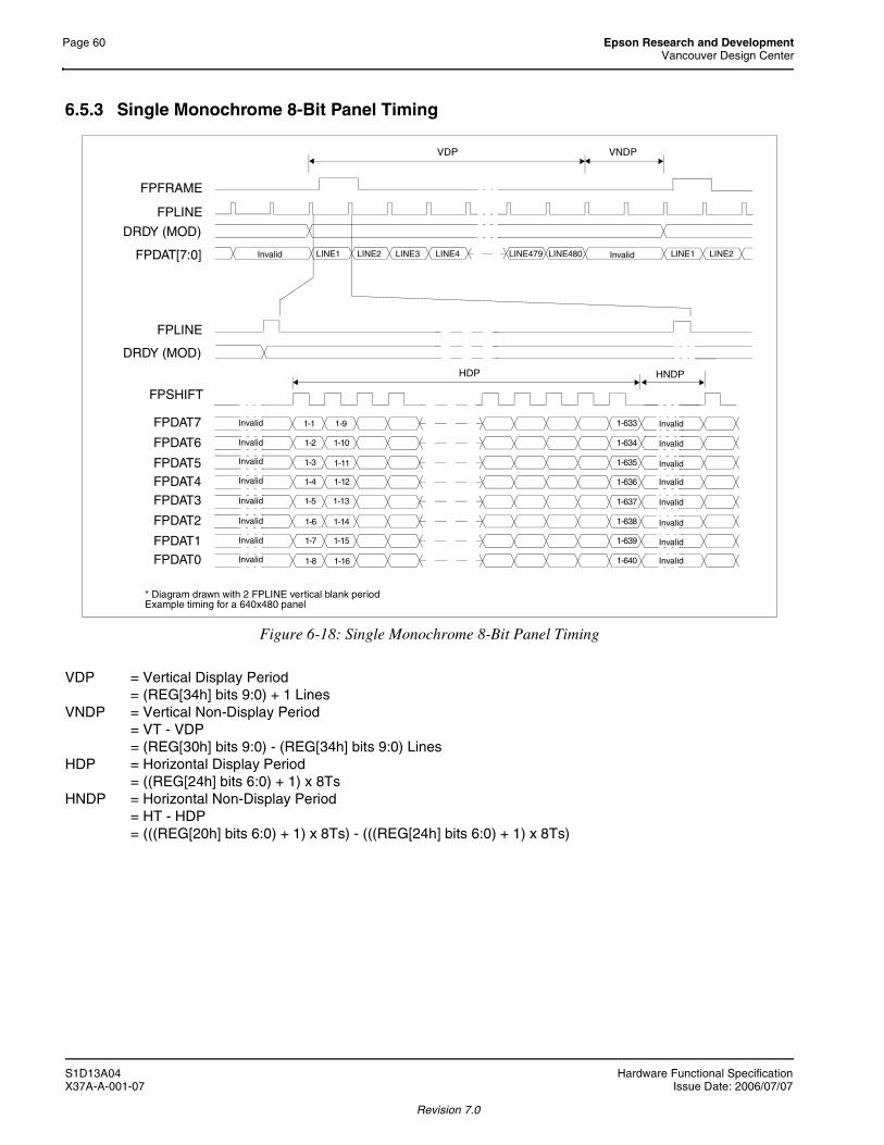
Page 60 Epson Research and DevelopmentVancouver Design Center
6.5.3 Single Monochrome 8-Bit Panel Timing
Figure 6-18: Single Monochrome 8-Bit Panel Timing
VDP = Vertical Display Period = (REG[34h] bits 9:0) + 1 Lines
VNDP = Vertical Non-Display Period= VT - VDP= (REG[30h] bits 9:0) - (REG[34h] bits 9:0) Lines
HDP = Horizontal Display Period= ((REG[24h] bits 6:0) + 1) x 8Ts
HNDP = Horizontal Non-Display Period= HT - HDP= (((REG[20h] bits 6:0) + 1) x 8Ts) - (((REG[24h] bits 6:0) + 1) x 8Ts)
FPLINE
FPSHIFT
FPFRAME
FPLINE
DRDY (MOD)
DRDY (MOD)
* Diagram drawn with 2 FPLINE vertical blank periodExample timing for a 640x480 panel
FPDAT[7:0]
FPDAT6
FPDAT5FPDAT4
FPDAT7
FPDAT2
FPDAT1FPDAT0
FPDAT3
HNDP
VDP
LINE1 LINE2 LINE3 LINE4 LINE479 LINE480 LINE1 LINE2
1-2 1-10 1-634
1-3 1-11 1-635
1-4 1-12 1-636
1-5 1-13 1-637
1-6 1-14 1-638
1-7 1-15 1-639
1-8 1-16 1-640
1-1 1-9 1-633
VNDP
HDP
Invalid
Invalid
Invalid
Invalid
Invalid
Invalid
Invalid
Invalid
Invalid
Invalid
Invalid
Invalid
Invalid
Invalid
Invalid
Invalid
Invalid Invalid
S1D13A04 Hardware Functional SpecificationX37A-A-001-07 Issue Date: 2006/07/07
Revision 7.0
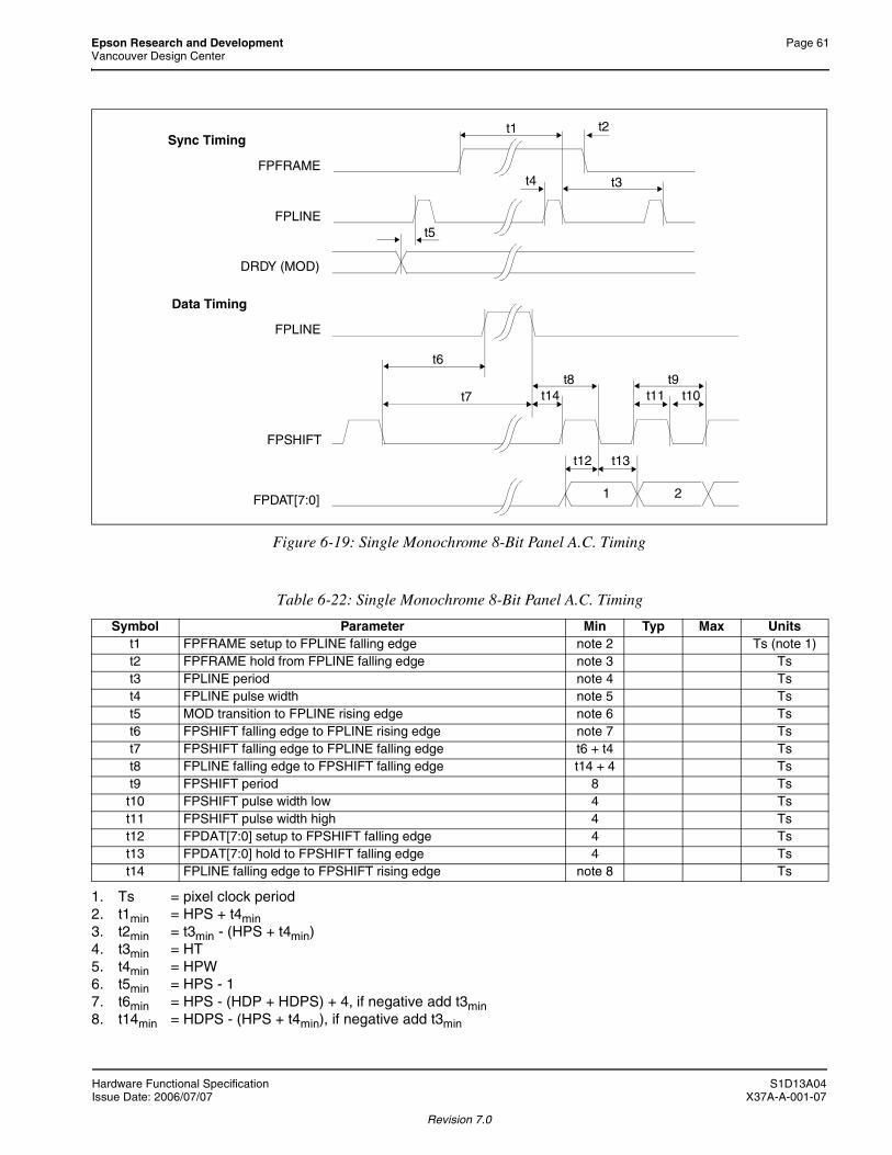
Epson Research and Development Page 61Vancouver Design Center
Figure 6-19: Single Monochrome 8-Bit Panel A.C. Timing
1. Ts = pixel clock period2. t1min = HPS + t4min3. t2min = t3min - (HPS + t4min)4. t3min = HT5. t4min = HPW6. t5min = HPS - 17. t6min = HPS - (HDP + HDPS) + 4, if negative add t3min8. t14min = HDPS - (HPS + t4min), if negative add t3min
Table 6-22: Single Monochrome 8-Bit Panel A.C. Timing
Symbol Parameter Min Typ Max Unitst1 FPFRAME setup to FPLINE falling edge note 2 Ts (note 1)t2 FPFRAME hold from FPLINE falling edge note 3 Tst3 FPLINE period note 4 Tst4 FPLINE pulse width note 5 Tst5 MOD transition to FPLINE rising edge note 6 Tst6 FPSHIFT falling edge to FPLINE rising edge note 7 Tst7 FPSHIFT falling edge to FPLINE falling edge t6 + t4 Tst8 FPLINE falling edge to FPSHIFT falling edge t14 + 4 Tst9 FPSHIFT period 8 Ts
t10 FPSHIFT pulse width low 4 Tst11 FPSHIFT pulse width high 4 Tst12 FPDAT[7:0] setup to FPSHIFT falling edge 4 Tst13 FPDAT[7:0] hold to FPSHIFT falling edge 4 Tst14 FPLINE falling edge to FPSHIFT rising edge note 8 Ts
t12 t13
FPFRAME
FPLINE
DRDY (MOD)
Sync Timing
FPLINE
FPSHIFT
FPDAT[7:0]
Data Timing
t5
t1 t2
t3t4
t14t8 t9
t10t11
1 2
t7
t6
Hardware Functional Specification S1D13A04Issue Date: 2006/07/07 X37A-A-001-07
Revision 7.0

Page 62 Epson Research and DevelopmentVancouver Design Center
6.5.4 Single Color 4-Bit Panel Timing
Figure 6-20: Single Color 4-Bit Panel Timing
VDP = Vertical Display Period = (REG[34h] bits 9:0) + 1 Lines
VNDP = Vertical Non-Display Period= VT - VDP= (REG[30h] bits 9:0) - (REG[34h] bits 9:0) Lines
HDP = Horizontal Display Period= ((REG[24h] bits 6:0) + 1) x 8Ts
HNDP = Horizontal Non-Display Period= HT - HDP= (((REG[20h] bits 6:0) + 1) x 8Ts) - (((REG[24h] bits 6:0) + 1) x 8Ts)
FPLINE
FPFRAME
FPLINE
DRDY (MOD)
DRDY (MOD)
FPSHIFT
VDP
LINE1 LINE2 LINE3 LINE4 LINE239 LINE240 LINE1 LINE2
VNDP
1-R1
1-G1
1-B1
1-R2
1-G2
1-B2
1-R3
1-G3
1-B3
1-R4
1-G4
1-B4
1-B319
1-R320
1-G320
1-B320
HDP HNDP
FPDAT[7:4]
FPDAT4
FPDAT5
FPDAT6
FPDAT7Invalid
Invalid
Invalid
Invalid
Invalid
Invalid
Invalid
Invalid
InvalidInvalid
- Diagram drawn with 2 FPLINE vertical blank period- Example timing for a 320x240 panel
Notes:
- Ts = Pixel clock period (PCLK)- FPSHIFT uses extended low states in order to process 8 pixels in 6 FPSHIFT clocks
.5Ts .5Ts.5Ts .5Ts .5Ts .5Ts .5Ts .5Ts .5Ts
.5Ts .5Ts .5Ts .5Ts .5Ts .5Ts2.5Ts
.5Ts .5Ts
.5Ts
S1D13A04 Hardware Functional SpecificationX37A-A-001-07 Issue Date: 2006/07/07
Revision 7.0

Epson Research and Development Page 63Vancouver Design Center
Figure 6-21: Single Color 4-Bit Panel A.C. Timing
1. Ts = pixel clock period2. t1min = HPS + t4min3. t2min = t3min - (HPS + t4min)4. t3min = HT5. t4min = HPW6. t5min = HPS - 17. t6min = HPS - (HDP + HDPS) + 1.5), if negative add t3min8. t14min = HDPS - (HPS + t4min) + 1, if negative add t3min
Table 6-23: Single Color 4-Bit Panel A.C. Timing
Symbol Parameter Min Typ Max Unitst1 FPFRAME setup to FPLINE falling edge note 2 Ts (note 1)t2 FPFRAME hold from FPLINE falling edge note 3 Tst3 FPLINE period note 4 Tst4 FPLINE pulse width note 5 Tst5 MOD transition to FPLINE rising edge note 6 Tst6 FPSHIFT falling edge to FPLINE rising edge note 7 Tst7 FPSHIFT falling edge to FPLINE falling edge t6 + t4 Tst8 FPLINE falling edge to FPSHIFT falling edge t14 + 0.5 Tst9 FPSHIFT period 1 Ts
t10 FPSHIFT pulse width low 0.5 Tst11 FPSHIFT pulse width high 0.5 Tst12 FPDAT[7:4] setup to FPSHIFT falling edge 0.5 Tst13 FPDAT[7:4] hold to FPSHIFT falling edge 0.5 Tst14 FPLINE falling edge to FPSHIFT rising edge note 8 Ts
FPFRAME
FPLINE
DRDY (MOD)
Sync Timing
FPLINE
FPSHIFT
FPDAT[7:4]
Data Timing
t14
t1 t2
t3t4
t8 t9t10t11
t12 t13
1 2
t7
t6
t5
Hardware Functional Specification S1D13A04Issue Date: 2006/07/07 X37A-A-001-07
Revision 7.0
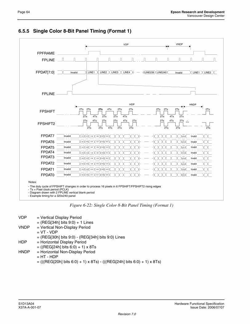
Page 64 Epson Research and DevelopmentVancouver Design Center
6.5.5 Single Color 8-Bit Panel Timing (Format 1)
Figure 6-22: Single Color 8-Bit Panel Timing (Format 1)
VDP = Vertical Display Period = (REG[34h] bits 9:0) + 1 Lines
VNDP = Vertical Non-Display Period= VT - VDP= (REG[30h] bits 9:0) - (REG[34h] bits 9:0) Lines
HDP = Horizontal Display Period= ((REG[24h] bits 6:0) + 1) x 8Ts
HNDP = Horizontal Non-Display Period= HT - HDP= (((REG[20h] bits 6:0) + 1) x 8Ts) - (((REG[24h] bits 6:0) + 1) x 8Ts)
FPLINE
FPSHIFT2
FPFRAME
FPLINE
FPSHIFT
FPDAT[7:0]
VDP
LINE1 LINE2 LINE3 LINE4 LINE239 LINE240 LINE1 LINE2
HDP
VNDP
HNDP
FPDAT5
FPDAT6
FPDAT4FPDAT3
FPDAT2
FPDAT1
FPDAT0
FPDAT7 Invalid
Invalid
Invalid
Invalid
Invalid
Invalid
Invalid
Invalid
Invalid
Invalid
Invalid
Invalid
Invalid
Invalid
Invalid
Invalid
Invalid Invalid
- Diagram drawn with 2 FPLINE vertical blank period- Example timing for a 320x240 panel
Notes:
- Ts = Pixel clock period (PCLK)- The duty cycle of FPSHIFT changes in order to process 16 pixels in 6 FPSHIFT/FPSHIFT2 rising edges
2Ts 2Ts 2Ts 2Ts 2Ts 2Ts 2Ts 2Ts 2Ts
2Ts 2Ts 2Ts 2Ts 2Ts
2Ts 2Ts 2Ts 2Ts 2Ts 2Ts
2Ts
4Ts
4Ts
4Ts 4Ts
4Ts4Ts
4Ts
4Ts
2Ts 2Ts 2Ts 2Ts 2Ts 2Ts
2Ts
1-R1
1-B1
1-G2
1-R3
1-B3
1-G4
1-R5
1-B5 1-R6
1-G5
1-B4
1-R4 1-R9 1-G9 1-G14 1-B14
1-R14
1-G13
1-B12
1-R121-B61-G6
1-R7
1-B7
1-G8
1-B9
1-G10
1-R11 1-G11 1-B16
1-B10
1-R10
1-B8
1-R8
1-G7
1-B11
1-B2
1-R2
1-G1
1-G3
1-R15
1-B15
1-G16
1-B13
1-G15
1-R13
1-G12
1-R16
1-R316
1-R316
1-B316
1-G317
1-R318
1-B318
1-G319
1-R320
1-B320
S1D13A04 Hardware Functional SpecificationX37A-A-001-07 Issue Date: 2006/07/07
Revision 7.0

Epson Research and Development Page 65Vancouver Design Center
Figure 6-23: Single Color 8-Bit Panel A.C. Timing (Format 1)
1. Ts = pixel clock period2. t1min = HPS + t4min3. t2min = t3min - (HPS + t4min)4. t3min = HT5. t4min = HPW6. t6amin = HPS - (HDP + HDPS), if negative add t3min7. t6bmin = HPS - (HDP + HDPS) + 2, if negative add t3min8. t14min = HDPS - (HPS + t4min), if negative add t3min
Table 6-24: Single Color 8-Bit Panel A.C. Timing (Format 1)
Symbol Parameter Min Typ Max Unitst1 FPFRAME setup to FPLINE falling edge note 2 Ts (note 1)t2 FPFRAME hold from FPLINE falling edge note 3 Tst3 FPLINE period note 4 Tst4 FPLINE pulse width note 5 Ts
t6a FPSHIFT falling edge to FPLINE rising edge note 6 Tst6b FPSHIFT2 falling edge to FPLINE rising edge note 7 Tst7a FPSHIFT falling edge to FPLINE falling edge t6a + t4 Tst7b FPSHIFT2 falling edge to FPLINE falling edge t6b + t4 Tst8 FPLINE falling edge to FPSHIFT rising, FPSHIFT2 falling edge t14 + 2 Tst9 FPSHIFT2, FPSHIFT period 4 6 Ts
t10 FPSHIFT2, FPSHIFT pulse width low 2 Tst11 FPSHIFT2, FPSHIFT pulse width high 2 Tst12 FPDAT[7:0] setup to FPSHIFT2, FPSHIFT falling edge 1 Tst13 FPDAT[7:0] hold from FPSHIFT2, FPSHIFT falling edge 1 Tst14 FPLINE falling edge to FPSHIFT rising edge note 8 Ts
FPFRAME
FPLINE
Sync Timing
FPLINE
FPSHIFT
FPDAT[7:0]
Data Timing
t14
t1 t2
t3t4
t8 t9t10t11
t12 t13
21
t7a
t6b
FPSHIFT2
t6a
t7b
t12 t13
Hardware Functional Specification S1D13A04Issue Date: 2006/07/07 X37A-A-001-07
Revision 7.0
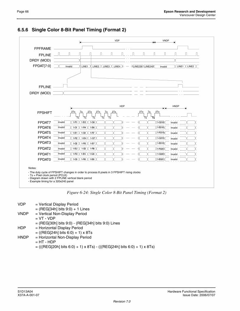
Page 66 Epson Research and DevelopmentVancouver Design Center
6.5.6 Single Color 8-Bit Panel Timing (Format 2)
Figure 6-24: Single Color 8-Bit Panel Timing (Format 2)
VDP = Vertical Display Period = (REG[34h] bits 9:0) + 1 Lines
VNDP = Vertical Non-Display Period= VT - VDP= (REG[30h] bits 9:0) - (REG[34h] bits 9:0) Lines
HDP = Horizontal Display Period= ((REG[24h] bits 6:0) + 1) x 8Ts
HNDP = Horizontal Non-Display Period= HT - HDP= (((REG[20h] bits 6:0) + 1) x 8Ts) - (((REG[24h] bits 6:0) + 1) x 8Ts)
FPLINE
FPFRAME
FPLINE
DRDY (MOD)
DRDY (MOD)
FPSHIFT
VDP
LINE1 LINE2 LINE3 LINE4 LINE239 LINE240 LINE1 LINE2
VNDP
1-R1
1-G1
1-B1
1-R2
1-G2
1-B2
1-R3
1-G3
1-B3
1-R4
1-G4
1-B4
1-R5
1-G5
1-B5
1-R6
1-G6
1-B6
1-R7
1-G7
1-B7
1-R8
1-G8
1-B8
1-G318
1-B318
1-R319
1-G319
1-B319
1-R320
1-G320
1-B320
HDP HNDP
FPDAT[7:0]
FPDAT7FPDAT6FPDAT5FPDAT4FPDAT3
FPDAT2
FPDAT1
FPDAT0
Invalid
Invalid
Invalid
Invalid
Invalid
Invalid
Invalid
Invalid
Invalid
Invalid
Invalid
Invalid
Invalid
Invalid
Invalid
Invalid
InvalidInvalid
2Ts 2Ts 2Ts 2Ts 2Ts 2Ts
Ts
Ts
Ts Ts Ts Ts
Ts
Ts
Ts
TsTs
- Diagram drawn with 2 FPLINE vertical blank period- Example timing for a 320x240 panel
Notes:
- Ts = Pixel clock period (PCLK)- The duty cycle of FPSHIFT changes in order to process 8 pixels in 3 FPSHIFT rising clocks
S1D13A04 Hardware Functional SpecificationX37A-A-001-07 Issue Date: 2006/07/07
Revision 7.0
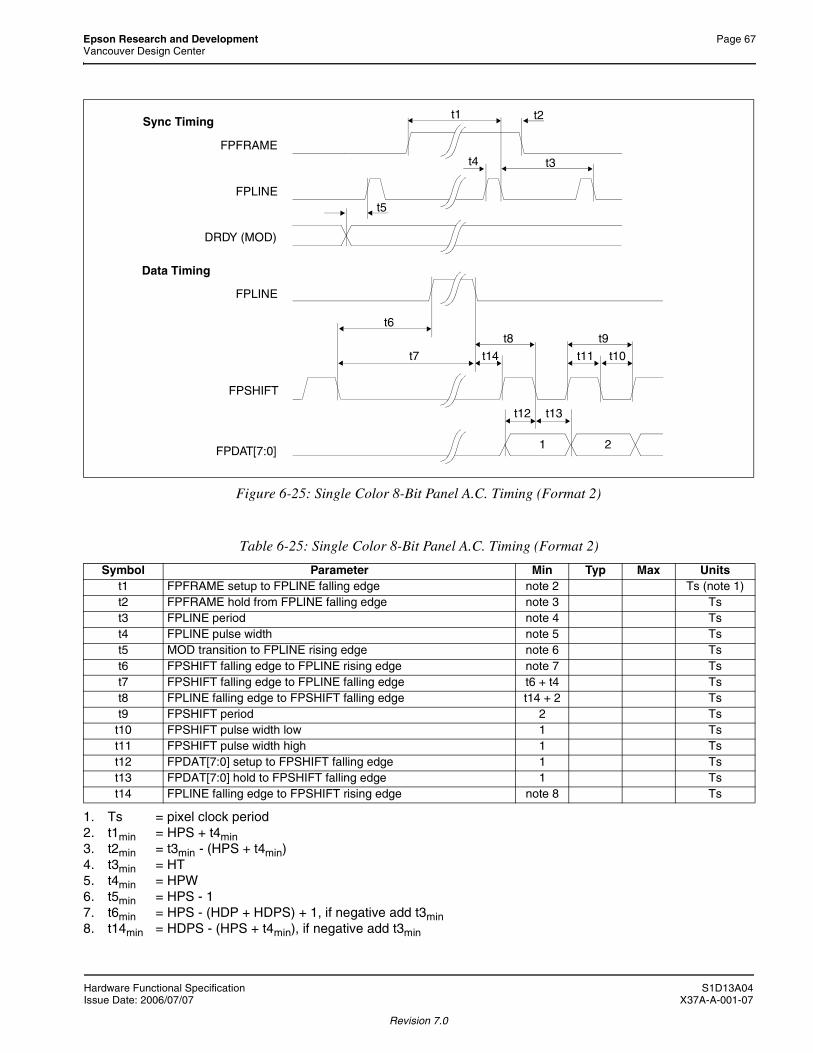
Epson Research and Development Page 67Vancouver Design Center
Figure 6-25: Single Color 8-Bit Panel A.C. Timing (Format 2)
1. Ts = pixel clock period2. t1min = HPS + t4min3. t2min = t3min - (HPS + t4min)4. t3min = HT5. t4min = HPW6. t5min = HPS - 17. t6min = HPS - (HDP + HDPS) + 1, if negative add t3min8. t14min = HDPS - (HPS + t4min), if negative add t3min
Table 6-25: Single Color 8-Bit Panel A.C. Timing (Format 2)
Symbol Parameter Min Typ Max Unitst1 FPFRAME setup to FPLINE falling edge note 2 Ts (note 1)t2 FPFRAME hold from FPLINE falling edge note 3 Tst3 FPLINE period note 4 Tst4 FPLINE pulse width note 5 Tst5 MOD transition to FPLINE rising edge note 6 Tst6 FPSHIFT falling edge to FPLINE rising edge note 7 Tst7 FPSHIFT falling edge to FPLINE falling edge t6 + t4 Tst8 FPLINE falling edge to FPSHIFT falling edge t14 + 2 Tst9 FPSHIFT period 2 Ts
t10 FPSHIFT pulse width low 1 Tst11 FPSHIFT pulse width high 1 Tst12 FPDAT[7:0] setup to FPSHIFT falling edge 1 Tst13 FPDAT[7:0] hold to FPSHIFT falling edge 1 Tst14 FPLINE falling edge to FPSHIFT rising edge note 8 Ts
t14 t10t11
t12 t13
Data Timing
FPFRAME
t1 t2
t3
t5
t4
FPLINE
DRDY (MOD)
Sync Timing
FPLINE
FPSHIFT
t8 t9
1 2
t7
t6
FPDAT[7:0]
Hardware Functional Specification S1D13A04Issue Date: 2006/07/07 X37A-A-001-07
Revision 7.0

Page 68 Epson Research and DevelopmentVancouver Design Center
6.5.7 Single Color 16-Bit Panel Timing
Figure 6-26: Single Color 16-Bit Panel Timing
VDP = Vertical Display Period = (REG[34h] bits 9:0) + 1 Lines
VNDP = Vertical Non-Display Period= VT - VDP= (REG[30h] bits 9:0) - (REG[34h] bits 9:0) Lines
HDP = Horizontal Display Period= ((REG[24h] bits 6:0) + 1) x 8Ts
HNDP = Horizontal Non-Display Period= HT - HDP= (((REG[20h] bits 6:0) + 1) x 8Ts) - (((REG[24h] bits 6:0) + 1) x 8Ts)
VDP
FPLINE
FPSHIFT
LINE1 LINE2 LINE3 LINE4 LINE479 LINE480
FPFRAME
LINE1 LINE2
FPLINE
DRDY (MOD)
DRDY (MOD)
VNDP
HDP
1-R1 1-G6 1-G635
1-B1 1-R7 1-G636
1-G2 1-B7 1-R637
1-R3 1-G8 1-B637
1-B3 1-R9 1-G638
1-G4 1-B9 1-R639
1-R5 1-G10 1-B639
1-G1 1-B6 1-R636
1-R2 1-G7 1-B636
1-B2 1-R8 1-G637
1-G3 1-B8 1-R638
1-R4 1-G9 1-B638
1-B4 1-R10 1-G639
1-G5 1-B10 1-R640
1-R6 1-G11 1-B640
1-B11
1-G12
1-R13
1-B13
1-G14
1-R15
1-B15
1-R12
1-B12
1-G13
1-R14
1-B14
1-G15
1-R16
1-B16
1-B5 1-R11 1-G6401-G16
HNDP
- Diagram drawn with 2 FPLINE vertical blank period- Example timing for a 640x480 panel
FPDAT[15:0]
FPDAT15
FPDAT9FPDAT8
FPDAT3
FPDAT2
FPDAT1
FPDAT0
FPDAT5FPDAT4
FPDAT11FPDAT10
FPDAT12FPDAT7FPDAT6
FPDAT13
FPDAT14
Invalid
Invalid
Invalid
Invalid
Invalid
Invalid
Invalid
Invalid
Invalid
Invalid
Invalid
Invalid
Invalid
Invalid
Invalid
Invalid
Invalid
Invalid
Invalid
Invalid
Invalid
Invalid
Invalid
Invalid
Invalid
Invalid
Invalid
Invalid
Invalid
Invalid
Invalid
Invalid
Invalid Invalid
-
3Ts
3Ts 3Ts
3Ts 3Ts
3Ts 3Ts
3Ts 3Ts2Ts
2Ts
2Ts
2Ts
3Ts 3Ts 3Ts2Ts
3Ts 3Ts2Ts
Notes:
- Ts = Pixel clock period (PCLK)- The duty cycle of FPSHIFT changes in order to process 16 pixels in 3 FPSHIFT rising clocks
S1D13A04 Hardware Functional SpecificationX37A-A-001-07 Issue Date: 2006/07/07
Revision 7.0

Epson Research and Development Page 69Vancouver Design Center
Figure 6-27: Single Color 16-Bit Panel A.C. Timing
1. Ts = pixel clock period2. t1min = HPS + t4min3. t2min = t3min - (HPS + t4min)4. t3min = HT5. t4min = HPW6. t5min = HPS - 17. t6min = HPS - (HDP + HDPS) + 2, if negative add t3min8. t14min = HDPS - (HPS + t4min), if negative add t3min
Table 6-26: Single Color 16-Bit Panel A.C. Timing
Symbol Parameter Min Typ Max Unitst1 FPFRAME setup to FPLINE falling edge note 2 Ts (note 1)t2 FPFRAME hold from FPLINE falling edge note 3 Tst3 FPLINE period note 4 Tst4 FPLINE pulse width note 5 Tst5 MOD transition to FPLINE rising edge note 6 Tst6 FPSHIFT falling edge to FPLINE rising edge note 7 Tst7 FPSHIFT falling edge to FPLINE falling edge t6 + t4 Tst8 FPLINE falling edge to FPSHIFT falling edge t14 + 3 Tst9 FPSHIFT period 5 Ts
t10 FPSHIFT pulse width low 2 Tst11 FPSHIFT pulse width high 2 Tst12 FPDAT[15:0] setup to FPSHIFT rising edge 2 Tst13 FPDAT[15:0] hold to FPSHIFT rising edge 2 Tst14 FPLINE falling edge to FPSHIFT rising edge note 8 Ts
t14 t10t11
Data Timing
FPFRAME
t1 t2
t3
t5
t4
FPLINE
DRDY (MOD)
Sync Timing
FPLINE
FPSHIFT
t8 t9
t7
t6
t12 t13
1 2FPDAT[15:0]
Hardware Functional Specification S1D13A04Issue Date: 2006/07/07 X37A-A-001-07
Revision 7.0

Page 70 Epson Research and DevelopmentVancouver Design Center
6.5.8 Generic TFT Panel Timing
Figure 6-28: Generic TFT Panel Timing
VT = Vertical Total = [(REG[30h] bits 9-0) + 1] linesVPS = FPFRAME Pulse Start Position = (REG[3Ch] bits 9-0) linesVPW = FPFRAME Pulse Width = [(REG[3Ch] bits 18-16) + 1] linesVDPS = Vertical Display Period Start Position= (REG[38h] bits 9-0) linesVDP = Vertical Display Period = [(REG[34h] bits 9-0) + 1] linesHT = Horizontal Total = [((REG[20h] bits 6-0) + 1) x 8] pixelsHPS = FPLINE Pulse Start Position = [(REG[2Ch] bits 9-0) + 1] pixelsHPW = FPLINE Pulse Width = [(REG[2Ch] bits 22-16) + 1] pixelsHDPS = Horizontal Display Period Start Position= [(REG[28h] bits 9-0) + 5] pixelsHDP = Horizontal Display Period = [((REG[24h] bits 6-0) + 1) x 8] pixels
*For TFT panels, the HDP must be a minimum of 8 pixels and must be increased by multiples of 8.*Panel Type Bits (REG[0Ch] bits 1-0) = 01 (TFT)*FPLINE Pulse Polarity Bit (REG[2Ch] bit 23) = 0 (active low)*FPFRAME Polarity Bit (REG[3Ch] bit 23) = 0 (active low)
FPFRAME
VT (= 1 Frame)
DRDY
FPLINE
DRDY
FPLINEVDPS
VPS VPW
VDP
HT (= 1 Line)
HPS
HDPS HDP
FPDAT[17:0]
FPDAT[17:0] invalid invalid
FPSHIFT
HPW
S1D13A04 Hardware Functional SpecificationX37A-A-001-07 Issue Date: 2006/07/07
Revision 7.0

Epson Research and Development Page 71Vancouver Design Center
6.5.9 9/12/18-Bit TFT Panel Timing
Figure 6-29: 18-Bit TFT Panel Timing
VDP = Vertical Display Period= VDP Lines
VNDP = Vertical Non-Display Period= VNDP1 + VNDP2= VT - VDP Lines
VNDP1 = Vertical Non-Display Period 1= VNDP - VNDP2 Lines
VNDP2 = Vertical Non-Display Period 2= VDPS - VPS Lines if negative add VT
HDP = Horizontal Display Period= HDP Ts
HNDP = Horizontal Non-Display Period= HNDP1 + HNDP2 = HT - HDP Ts
HNDP1 = Horizontal Non-Display Period 1= HDPS - HPS Ts if negative add HT
HNDP2 = Horizontal Non-Display Period 2= HPS - (HDP + HDPS) Ts if negative add HT
FPFRAME
FPLINE
LINE1 LINE480
1-1 1-2 1-320
FPLINE
FPSHIFT
DRDY
FPDAT[17:0]
VDP
DRDY
Note: DRDY is used to indicate the first pixelExample Timing for 18-bit 320x240 panel
VNDP2
HDPHNDP1 HNDP2
LINE240
VNDP1
FPDAT[17:0] invalid invalid
Hardware Functional Specification S1D13A04Issue Date: 2006/07/07 X37A-A-001-07
Revision 7.0

Page 72 Epson Research and DevelopmentVancouver Design Center
Figure 6-30: TFT A.C. Timing
t3
t5
FPLINE
t1
t4
FPFRAME
DRDY
FPSHIFT
320
t2
FPLINE
21 319
t13t10 t11 t14
t15 t16
t7t8
t9 t12
FPDAT[17:0]
Note: DRDY is used to indicate the first pixel
t6
invalidinvalid
S1D13A04 Hardware Functional SpecificationX37A-A-001-07 Issue Date: 2006/07/07
Revision 7.0

Epson Research and Development Page 73Vancouver Design Center
1. Ts = pixel clock period2. t6min = HDPS - HPS if negative add HT3. t8min = HPS - (HDP + HDPS) if negative add HT
Table 6-27: TFT A.C. Timing
Symbol Parameter Min Typ Max Units
t1 FPFRAME cycle time VT Lines
t2 FPFRAME pulse width low VPW Lines
t3 FPFRAME falling edge to FPLINE falling edge phase difference HPS Ts (note 1)
t4 FPLINE cycle time HT Ts
t5 FPLINE pulse width low HPW Ts
t6 FPLINE Falling edge to DRDY active note 2 250 Ts
t7 DRDY pulse width HDP Tst8 DRDY falling edge to FPLINE falling edge note 3 Tst9 FPSHIFT period 1 Ts
t10 FPSHIFT pulse width high 0.5 Tst11 FPSHIFT pulse width low 0.5 Tst12 FPLINE setup to FPSHIFT falling edge 0.5 Tst13 DRDY to FPSHIFT falling edge setup time 0.5 Tst14 DRDY hold from FPSHIFT falling edge 0.5 Tst15 Data setup to FPSHIFT falling edge 0.5 Tst16 Data hold from FPSHIFT falling edge 0.5 Ts
Hardware Functional Specification S1D13A04Issue Date: 2006/07/07 X37A-A-001-07
Revision 7.0

Page 74 Epson Research and DevelopmentVancouver Design Center
6.5.10 160x160 Sharp ‘Direct’ HR-TFT Panel Timing (e.g. LQ031B1DDxx)
Figure 6-31: 160x160 Sharp ‘Direct’ HR-TFT Panel Horizontal Timing
FPLINE
t2
FPDAT[17:0]
t3
t4
t12
t11
GPIO3
GPIO2
t10t9
FPSHIFT
GPIO1
GPIO0
D1
t13
t8
D2 D3 D160
FPLINE
t1FPFRAME
t7
(SPS)
(LP)
(LP)
(CLK)
(SPL)
(CLS)
(PS)
(REV)
t5 t6
S1D13A04 Hardware Functional SpecificationX37A-A-001-07 Issue Date: 2006/07/07
Revision 7.0

Epson Research and Development Page 75Vancouver Design Center
1. Ts = pixel clock period2. t1typ = (REG[2Ch] bits 9-0) + 13. t2typ = ((REG[20h] bits 6-0) + 1) x 84. t3typ = (REG[2Ch] bits 22-16) + 15. t7typ = ((REG[28h] bits 9-0) + 5) - ((REG[2Ch] bits 9-0) + 1)6. t8typ = ((REG[24h] bits 6-0) + 1) x 8
Table 6-28: 160x160 Sharp ‘Direct’ HR-TFT Horizontal Timing
Symbol Parameter Min Typ Max Units
t1 FPLINE start position 13 Ts (note 1)
t2 Horizontal total period 180 220 Ts
t3 FPLINE width 2 Ts
t4 FPSHIFT period 1 Tst5 Data setup to FPSHIFT rising edge 0.5 Tst6 Data hold from FPSHIFT rising edge 0.5 Ts
t7 Horizontal display start position 5 Ts
t8 Horizontal display period 160 Ts
t9 FPLINE rising edge to GPIO3 rising edge 4 Tst10 GPIO3 pulse width 1 Tst11 GPIO1(GPIO0) pulse width 136 Tst12 GPIO1 rising edge (GPIO0 falling edge) to FPLINE rise edge 4 Tst13 GPIO2 toggle edge to FPLINE rise edge 10 Ts
Hardware Functional Specification S1D13A04Issue Date: 2006/07/07 X37A-A-001-07
Revision 7.0

Page 76 Epson Research and DevelopmentVancouver Design Center
Figure 6-32: 160x160 Sharp ‘Direct’ HR-TFT Panel Vertical Timing
t1
FPDAT[17:0]
GPIO1
t4
FPFRAME
GPIO0
t2 t3
LINE1 LINE2 LINE160
t5 t6
t7 t8
t10 t11 t12
GPIO1
GPIO0
t9
t13
t14
FPLINE
FPSHIFT
(SPS)
(CLS)
(PS)
(LP)
(CLK)
(CLS)
(PS)
S1D13A04 Hardware Functional SpecificationX37A-A-001-07 Issue Date: 2006/07/07
Revision 7.0
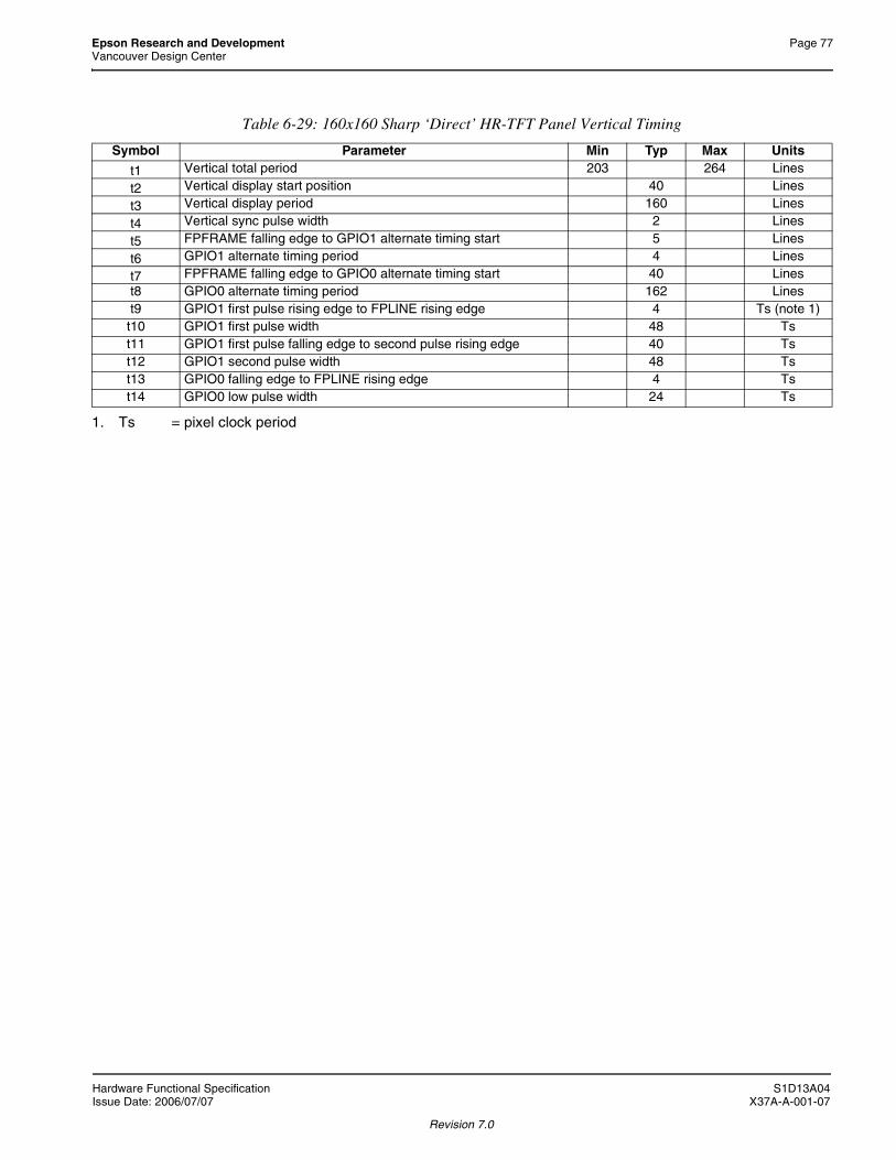
Epson Research and Development Page 77Vancouver Design Center
1. Ts = pixel clock period
Table 6-29: 160x160 Sharp ‘Direct’ HR-TFT Panel Vertical Timing
Symbol Parameter Min Typ Max Units
t1 Vertical total period 203 264 Lines
t2 Vertical display start position 40 Lines
t3 Vertical display period 160 Lines
t4 Vertical sync pulse width 2 Lines
t5 FPFRAME falling edge to GPIO1 alternate timing start 5 Lines
t6 GPIO1 alternate timing period 4 Lines
t7 FPFRAME falling edge to GPIO0 alternate timing start 40 Linest8 GPIO0 alternate timing period 162 Linest9 GPIO1 first pulse rising edge to FPLINE rising edge 4 Ts (note 1)
t10 GPIO1 first pulse width 48 Tst11 GPIO1 first pulse falling edge to second pulse rising edge 40 Tst12 GPIO1 second pulse width 48 Tst13 GPIO0 falling edge to FPLINE rising edge 4 Tst14 GPIO0 low pulse width 24 Ts
Hardware Functional Specification S1D13A04Issue Date: 2006/07/07 X37A-A-001-07
Revision 7.0

Page 78 Epson Research and DevelopmentVancouver Design Center
6.5.11 320x240 Sharp ‘Direct’ HR-TFT Panel Timing (e.g. LQ039Q2DS01)
Figure 6-33: 320x240 Sharp ‘Direct’ HR-TFT Panel Horizontal Timing
FPLINE
t2
FPDAT[17:0]
t3
t4
t12
t11
GPIO3
GPIO2
t10t9
FPSHIFT
GPIO1
GPIO0
D1
t13
t6
D2 D3 D320
FPLINE
t1FPFRAME
(SPS)
(LP)
(LP)
(CLK)
(SPL)
(CLS)
(PS)
(REV)
t5
t7 t8
S1D13A04 Hardware Functional SpecificationX37A-A-001-07 Issue Date: 2006/07/07
Revision 7.0

Epson Research and Development Page 79Vancouver Design Center
1. Ts = pixel clock period2. t1typ = (REG[2Ch] bits 9-0) + 13. t2typ = ((REG[20h] bits 6-0) + 1) x 84. t3typ = (REG[2Ch] bits 22-16) + 15. t7typ = ((REG[28h] bits 9-0) + 5) - ((REG[2Ch] bits 9-0) + 1)6. t8typ = ((REG[24h] bits 6-0) + 1) x 8
Figure 6-34: 320x240 Sharp ‘Direct’ HR-TFT Panel Vertical Timing
Table 6-30: 320x240 Sharp ‘Direct’ HR-TFT Panel Horizontal Timing
Symbol Parameter Min Typ Max Units
t1 FPLINE start position 14 Ts (note 1)
t2 Horizontal total period 400 440 Ts
t3 FPLINE width 1 Ts
t4 FPSHIFT period 1 Tst5 Data setup to FPSHIFT rising edge 0.5 Tst6 Data hold from FPSHIFT rising edge 0.5 Ts
t7 Horizontal display start position 60 Ts
t8 Horizontal display period 320 Ts
t9 FPLINE rising edge to GPIO3 rising edge 59 Tst10 GPIO3 pulse width 1 Tst11 GPIO1(GPIO0) pulse width 353 Tst12 GPIO1 rising edge (GPIO0 falling edge) to FPLINE rise edge 5 Tst13 GPIO2 toggle edge to FPLINE rise edge 11 Ts
Table 6-31: 320x240 Sharp ‘Direct’ HR-TFT Panel Vertical Timing
Symbol Parameter Min Typ Max Units
t1 Vertical total period 245 330 Lines
t2 Vertical display start position 4 Lines
t3 Vertical display period 240 Lines
t4 Vertical sync pulse width 2 Lines
t1
t4
FPFRAME
t2 t3
LINE1 LINE2 LINE240FPDAT[17:0]
(SPS)
Hardware Functional Specification S1D13A04Issue Date: 2006/07/07 X37A-A-001-07
Revision 7.0

Page 80 Epson Research and DevelopmentVancouver Design Center
6.6 USB Timing
Figure 6-35 Data Signal Rise and Fall Time
Figure 6-36 Differential Data Jitter
Data Signal Rise and Fall Time
S1D13A04 Hardware Functional SpecificationX37A-A-001-07 Issue Date: 2006/07/07
Revision 7.0
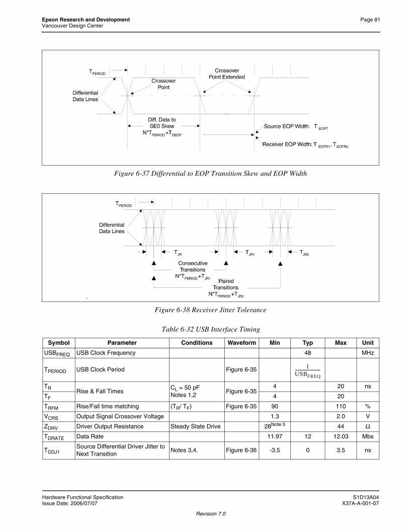
Epson Research and Development Page 81Vancouver Design Center
Figure 6-37 Differential to EOP Transition Skew and EOP Width
Figure 6-38 Receiver Jitter Tolerance
Table 6-32 USB Interface Timing
Symbol Parameter Conditions Waveform Min Typ Max Unit
USBFREQ USB Clock Frequency 48 MHz
TPERIOD USB Clock Period Figure 6-35
TR Rise & Fall Times
CL = 50 pFNotes 1,2
Figure 6-354 20 ns
TF 4 20
TRFM Rise/Fall time matching (TR/ TF) Figure 6-35 90 110 %
VCRS Output Signal Crossover Voltage 1.3 2.0 V
ZDRV Driver Output Resistance Steady State Drive 28Note 5 44 Ω
TDRATE Data Rate 11.97 12 12.03 Mbs
TDDJ1 Source Differential Driver Jitter to Next Transition
Notes 3,4. Figure 6-36 -3.5 0 3.5 ns
1USBFREQ-------------------------
Hardware Functional Specification S1D13A04Issue Date: 2006/07/07 X37A-A-001-07
Revision 7.0

Page 82 Epson Research and DevelopmentVancouver Design Center
1 Measured from 10% to 90% of the data signal.2 The rising and falling edges should be smoothly transitioning (monotonic).3 Timing difference between the differential data signals.4 Measured at crossover point of differential data signals.5 20 Ω is placed in series to meet this USB specification. The actual driver output impedance is 15 Ω.
TDDJ2 Source Differential Driver Jitter for Paired Transitions
Notes 3,4 Figure 6-36 -4.0 0 4.0 ns
TDEOP Differential to EOP Transition Skew
Note 4 Figure 6-37 -2 0 5 ns
TEOPT Source EOP Width Note 4 Figure 6-37 160 167 175 ns
TJR1Receiver Data Jitter Tolerance to Next Transition
Note 4 Figure 6-38 -18.5 0 18.5 ns
TJR2Receiver Data Jitter Tolerance for Paired Transitions
Note 4 Figure 6-38 -9 0 9 ns
TEOPR1EOP Width at Receiver; Must reject as EOP
Note 4 Figure 6-37 40 ns
TEOPR2EOP Width at Receiver; Must accept as EOP
Note 4 Figure 6-37 80 ns
Table 6-32 USB Interface Timing
Symbol Parameter Conditions Waveform Min Typ Max Unit
S1D13A04 Hardware Functional SpecificationX37A-A-001-07 Issue Date: 2006/07/07
Revision 7.0

Epson Research and Development Page 83Vancouver Design Center
7 Clocks
7.1 Clock Descriptions
7.1.1 BCLK
BCLK is an internal clock derived from CLKI. BCLK can be a divided version (÷1, ÷2) of CLKI. CLKI is typically derived from the host CPU bus clock.
The source clock options for BCLK may be selected as in the following table.
NoteFor synchronous bus interfaces, it is recommended that BCLK be set the same as the CPU bus clock (not a divided version of CLKI) e.g. SH-3, SH-4.
7.1.2 MCLK
MCLK provides the internal clock required to access the embedded SRAM. The S1D13A04 is designed with efficient power saving control for clocks (clocks are turned off when not used); reducing the frequency of MCLK does not necessarily save more power. Furthermore, reducing the MCLK frequency relative to the BCLK frequency increases the CPU cycle latency and so reduces screen update performance. For a balance of power saving and performance, the MCLK should be configured to have a high enough frequency setting to provide sufficient screen refresh as well as acceptable CPU cycle latency.
NoteThe maximum frequency of MCLK is 50MHz (30MHz if running CORE VDD at 2.0V ± 10%). As MCLK is derived from BCLK, when BCLK is greater than 50MHz, MCLK must be divided using REG[04h] bits 5-4.
The Memory Controller Power Save Status bit (REG[14h] bit 6) must return a 1 before disabling the MCLK source.
The source clock options for MCLK may be selected as in the following table.
Table 7-1: BCLK Clock Selection
Source Clock Options BCLK Selection
CLKI CNF6 = 0
CLKI ÷ 2 CNF6 = 1
Table 7-2: MCLK Clock Selection
Source Clock Options MCLK Selection
BCLK REG[04h] bits 5-4 = 00
BCLK ÷ 2 REG[04h] bits 5-4 = 01
BCLK ÷ 3 REG[04h] bits 5-4 = 10
BCLK ÷ 4 REG[04h] bits 5-4 = 11
Hardware Functional Specification S1D13A04Issue Date: 2006/07/07 X37A-A-001-07
Revision 7.0

Page 84 Epson Research and DevelopmentVancouver Design Center
7.1.3 PCLK
PCLK is the internal clock used to control the panel. It should be chosen to match the optimum frame rate of the panel. See Section 10, “Frame Rate Calculation” on page 142 for details on the relationship between PCLK and frame rate.
Some flexibility is possible in the selection of PCLK. Firstly, panels typically have a range of permissible frame rates. Secondly, it may be possible to choose a higher PCLK frequency and tailor the horizontal non-display period to bring down the frame-rate to its optimal value.
The source clock options for PCLK may be selected as in the following table.
Table 7-3: PCLK Clock Selection
Source Clock Options PCLK Selection
MCLK REG[08h] bits 7-0 = 00h
MCLK ÷2 REG[08h] bits 7-0 = 10h
MCLK ÷3 REG[08h] bits 7-0 = 20h
MCLK ÷4 REG[08h] bits 7-0 = 30h
MCLK ÷8 REG[08h] bits 7-0 = 40h
BCLK REG[08h] bits 7-0 = 01h
BCLK ÷2 REG[08h] bits 7-0 = 11h
BCLK ÷3 REG[08h] bits 7-0 = 21h
BCLK ÷4 REG[08h] bits 7-0 = 31h
BCLK ÷8 REG[08h] bits 7-0 = 41h
CLKI REG[08h] bits 7-0 = 02h
CLKI ÷2 REG[08h] bits 7-0 = 12h
CLKI ÷3 REG[08h] bits 7-0 = 22h
CLKI ÷4 REG[08h] bits 7-0 = 32h
CLKI ÷8 REG[08h] bits 7-0 = 42h
CLKI2 REG[08h] bits 7-0 = 03h
CLKI2 ÷2 REG[08h] bits 7-0 = 13h
CLKI2 ÷3 REG[08h] bits 7-0 = 23h
CLKI2 ÷4 RREG[08h] bits 7-0 = 33h
CLKI2 ÷8 REG[08h] bits 7-0 = 43h
S1D13A04 Hardware Functional SpecificationX37A-A-001-07 Issue Date: 2006/07/07
Revision 7.0

Epson Research and Development Page 85Vancouver Design Center
There is a relationship between the frequency of MCLK and PCLK that must be maintained.
7.1.4 PWMCLK
PWMCLK is the internal clock used by the Pulse Width Modulator for output to the panel.
The source clock options for PWMCLK may be selected as in the following table.
For further information on controlling PWMCLK, see “PWM Clock Configuration Register” on page 113..
7.1.5 USBCLK
CLKUSB is an internal clock derived from USBCLK and should be fixed at 48MHz. USBCLK must be active to access the USB Registers.
Table 7-4: Relationship between MCLK and PCLK
SwivelView Orientation Color Depth (bpp) MCLK to PCLK Relationship
SwivelView 0° and 180°
16 fMCLK ≥ fPCLK
8 fMCLK ≥ fPCLK ÷ 24 fMCLK ≥ fPCLK ÷ 42 fMCLK ≥ fPCLK ÷ 81 fMCLK ≥ fPCLK ÷16
SwivelView 90° and 270° 16/8/4/2/1 fMCLK ≥ 1.25fPCLK
Table 7-5: PWMCLK Clock Selection
Source Clock Options PWMCLK Selection
CLKI REG[70h] bits 2-1 = 00
CLKI2 REG[70h] bits 2-1 = 01
MCLK REG[70h] bits 2-1 = 10
PCLK REG[70h] bits 2-1 = 11
Hardware Functional Specification S1D13A04Issue Date: 2006/07/07 X37A-A-001-07
Revision 7.0
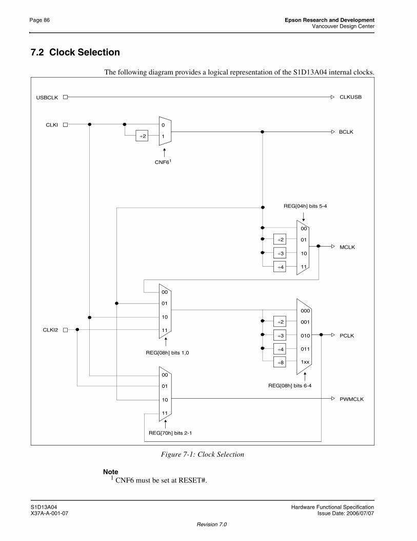
Page 86 Epson Research and DevelopmentVancouver Design Center
7.2 Clock Selection
The following diagram provides a logical representation of the S1D13A04 internal clocks.
Figure 7-1: Clock Selection
Note1 CNF6 must be set at RESET#.
CLKI
CLKI2
÷2
0
1BCLK
÷2
÷3
÷4
00
01
10
11
MCLK
00
01
10
11
÷2
÷3
÷4
000
001
010
011
÷8 1xx
PCLK
PWMCLK
REG[08h] bits 1,0
REG[70h] bits 2-1
REG[08h] bits 6-4
REG[04h] bits 5-4
CNF61
CLKUSBUSBCLK
00
01
10
11
S1D13A04 Hardware Functional SpecificationX37A-A-001-07 Issue Date: 2006/07/07
Revision 7.0
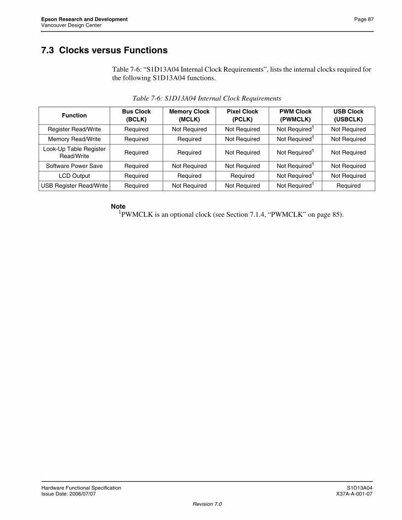
Epson Research and Development Page 87Vancouver Design Center
7.3 Clocks versus Functions
Table 7-6: “S1D13A04 Internal Clock Requirements”, lists the internal clocks required for the following S1D13A04 functions.
Note1PWMCLK is an optional clock (see Section 7.1.4, “PWMCLK” on page 85).
Table 7-6: S1D13A04 Internal Clock Requirements
FunctionBus Clock
(BCLK)Memory Clock
(MCLK)Pixel Clock
(PCLK)PWM Clock (PWMCLK)
USB Clock(USBCLK)
Register Read/Write Required Not Required Not Required Not Required1 Not Required
Memory Read/Write Required Required Not Required Not Required1 Not Required
Look-Up Table Register Read/Write
Required Required Not Required Not Required1 Not Required
Software Power Save Required Not Required Not Required Not Required1 Not Required
LCD Output Required Required Required Not Required1 Not Required
USB Register Read/Write Required Not Required Not Required Not Required1 Required
Hardware Functional Specification S1D13A04Issue Date: 2006/07/07 X37A-A-001-07
Revision 7.0

Page 88 Epson Research and DevelopmentVancouver Design Center
8 Registers
This section discusses how and where to access the S1D13A04 registers. It also provides detailed information about the layout and usage of each register.
8.1 Register Mapping
The S1D13A04 registers are memory-mapped. When the system decodes the input pins as CS# = 0 and M/R# = 0, the registers may be accessed. The register space is decoded by AB[16:0] and is mapped as follows.
8.2 Register Set
The S1D13A04 register set is as follows.
Table 8-1: S1D13A04 Register Mapping
M/R# Address Size Function
1 00000h to 28000h 160K bytes SRAM memory
0 0000h to 0088h 136 bytes Configuration registers
0 4000h to 4054h 84 bytes USB registers
0 8000h to 8019h 25 bytes 2D Acceleration Registers
0 10000h to 1FFFEh 65536 bytes (64K bytes) 2D Accelerator Data Port
Table 8-2: S1D13A04 Register Set
Register Pg Register Pg
LCD Register Descriptions (Offset = 0h)
Read-Only Configuration Registers
REG[00h] Product Information Register 90
Clock Configuration Registers
REG[04h] Memory Clock Configuration Register 91 REG[08h] Pixel Clock Configuration Register 91
Panel Configuration Registers
REG[0Ch] Panel Type & MOD Rate Register 92 REG[10h] Display Settings Register 93
REG[14h] Power Save Configuration Register 95
Look-Up Table Registers
REG[18h] Look-Up Table Write Register 97 REG[1Ch] Look-Up Table Read Register 98
Display Mode Registers
REG[20h] Horizontal Total Register 99 REG[24h] Horizontal Display Period Register 99
REG[28h] Horizontal Display Period Start Position Register 100 REG[2Ch] FPLINE Register 100
REG[30h] Vertical Total Register 101 REG[34h] Vertical Display Period Register 101
REG[38h] Vertical Display Period Start Position Register 102 REG[3Ch] FPFRAME Register 102
REG[40h] Main Window Display Start Address Register 103 REG[44h] Main Window Line Address Offset Register 103
Picture-in-Picture Plus (PIP+) Registers
REG[50h] PIP+ Window Display Start Address Register 104 REG[54h] PIP+ Window Line Address Offset Register 104
S1D13A04 Hardware Functional SpecificationX37A-A-001-07 Issue Date: 2006/07/07
Revision 7.0

Epson Research and Development Page 89Vancouver Design Center
REG[58h] PIP+ Window X Positions Register 105 REG[5Ch] PIP+ Window Y Positions Register 107
Miscellaneous Registers
REG[60h] Special Purpose Register 109 REG[64h] GPIO Status and Control Register 111
REG[70h] PWM Clock Configuration Register 113 REG[74h] PWMOUT Duty Cycle Register 114
REG[80h] Scratch Pad A Register 115 REG[84h] Scratch Pad B Register 115
REG[88h] Scratch Pad C Register 115
USB Register Descriptions (Offset = 4000h)
REG[4000h] Control Register 116 REG[4002h] Interrupt Enable Register 0 117
REG[4004h] Interrupt Status Register 0 118 REG[4006h] Interrupt Enable Register 1 119
REG[4008h] Interrupt Status Register 1 119 REG[4010h] Endpoint 1 Index Register 120
REG[4012h] Endpoint 1 Receive Mailbox Data Register 120 REG[4018h] Endpoint 2 Index Register 120
REG[401Ah] Endpoint 2 Transmit Mailbox Data Register 121 REG[401Ch] Endpoint 2 Interrupt Polling Interval Register 121
REG[4020h] Endpoint 3 Receive FIFO Data Register 121 REG[4022h] Endpoint 3 Receive FIFO Count Register 121
REG[4024h] Endpoint 3 Receive FIFO Status Register 122 REG[4026h] Endpoint 3 Maximum Packet Size Register 122
REG[4028h] Endpoint 4 Transmit FIFO Data Register 122 REG[402Ah] Endpoint 4 Transmit FIFO Count Register 123
REG[402Ch] Endpoint 4 Transmit FIFO Status Register 123 REG[402Eh] Endpoint 4 Maximum Packet Size Register 123
REG[4030h] Endpoint 4 Maximum Packet Size Register 123 REG[4032h] USB Status Register 124
REG[4034h] Frame Counter MSB Register 125 REG[4036h] Frame Counter LSB Register 125
REG[4038h] Extended Register Index 125 REG[403Ah] Extended Register Data 125
REG[403Ah], Index[00h] Vendor ID MSB 125 REG[403Ah], Index[01h] Vendor ID LSB 125
REG[403Ah], Index[02h] Product ID MSB 126 REG[403Ah], Index[03h] Product ID LSB 126
REG[403Ah], Index[04h] Release Number MSB 126 REG[403Ah], Index[05h] Release Number LSB 126
REG[403Ah], Index[06h] Receive FIFO Almost Full Threshold 126 REG[403Ah], Index[07h] Transmit FIFO Almost Empty Threshold 127
REG[403Ah], Index[08h] USB Control 127 REG[403Ah], Index[09h] Maximum Power Consumption 127
REG[403Ah], Index[0Ah] Packet Control 127 REG[403Ah], Index[0Bh] Reserved 128
REG[403Ah], Index[0Ch] FIFO Control 129 REG[4040h] USBFC Input Control Register 129
REG[4042h] Reserved 130 REG[4044h] Pin Input Status / Pin Output Data Register 130
REG[4046h] Interrupt Control Enable Register 0 130 REG[4048h] Interrupt Control Enable Register 1 131
REG[404Ah] Interrupt Control Status/Clear Register 0 131 REG[404Ch] Interrupt Control Status/Clear Register 1 132
REG[404Eh] Interrupt Control Masked Status Register 0 133 REG[4050h] Interrupt Control Masked Status Register 1 133
REG[4052h] USB Software Reset Register 133 REG[4054h] USB Wait State Register 133
2D Acceleration (BitBLT) Register Descriptions (Offset = 8000h)
REG[8000h] BitBLT Control Register 134 REG[8004h] BitBLT Status Register 135
REG[8008h] BitBLT Command Register 136 REG[800Ch] BitBLT Source Start Address Register 138
REG[8010h] BitBLT Destination Start Address Register 138 REG[8014h] BitBLT Memory Address Offset Register 139
REG[8018h] BitBLT Width Register 139 REG[801Ch] BitBLT Height Register 139
REG[8020h] BitBLT Background Color Register 140 REG[8024h] BitBLT Foreground Color Register 140
2D Acceleration (BitBLT) Data Register Descriptions (Offset = 10000h)
AB16-AB0 = 10000h-1FFFEh, 2D Accelerator (BitBLT) Data Memory Mapped Region Register 140
Table 8-2: S1D13A04 Register Set
Register Pg Register Pg
Hardware Functional Specification S1D13A04Issue Date: 2006/07/07 X37A-A-001-07
Revision 7.0
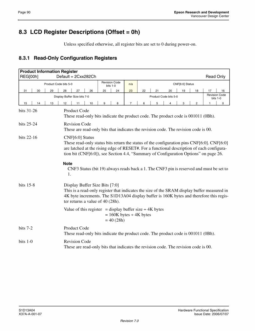
Page 90 Epson Research and DevelopmentVancouver Design Center
8.3 LCD Register Descriptions (Offset = 0h)
Unless specified otherwise, all register bits are set to 0 during power-on.
8.3.1 Read-Only Configuration Registers
bits 31-26 Product CodeThese read-only bits indicate the product code. The product code is 001011 (0Bh).
bits 25-24 Revision CodeThese are read-only bits that indicates the revision code. The revision code is 00.
bits 22-16 CNF[6:0] StatusThese read-only status bits return the status of the configuration pins CNF[6:0]. CNF[6:0] are latched at the rising edge of RESET#. For a functional description of each configura-tion bit (CNF[6:0]), see Section 4.4, “Summary of Configuration Options” on page 26.
NoteCNF3 Status (bit 19) always reads back a 1. The CNF3 pin is reserved and must be set to 1.
bits 15-8 Display Buffer Size Bits [7:0]This is a read-only register that indicates the size of the SRAM display buffer measured in 4K byte increments. The S1D13A04 display buffer is 160K bytes and therefore this regis-ter returns a value of 40 (28h).
Value of this register = display buffer size ÷ 4K bytes= 160K bytes ÷ 4K bytes= 40 (28h)
bits 7-2 Product CodeThese read-only bits indicate the product code. The product code is 001011 (0Bh).
bits 1-0 Revision CodeThese are read-only bits that indicates the revision code. The revision code is 00.
Product Information RegisterREG[00h] Default = 2Cxx282Ch Read Only
Product Code bits 5-0 Revision Code bits 1-0 n/a CNF[6:0] Status
31 30 29 28 27 26 25 24 23 22 21 20 19 18 17 16
Display Buffer Size bits 7-0 Product Code bits 5-0 Revision Code bits 1-0
15 14 13 12 11 10 9 8 7 6 5 4 3 2 1 0
S1D13A04 Hardware Functional SpecificationX37A-A-001-07 Issue Date: 2006/07/07
Revision 7.0

Epson Research and Development Page 91Vancouver Design Center
8.3.2 Clock Configuration Registers
bits 5-4 MCLK Divide Select Bits [1:0]These bits determine the divide used to generate the Memory Clock (MCLK) from the Bus Clock (BCLK).
bit 0 Reserved.This bit must be set to 0.
bits 6-4 PCLK Divide Select Bits [1:0]These bits determine the divide used to generate the Pixel Clock (PCLK) from the Pixel Clock Source.
Memory Clock Configuration RegisterREG[04h] Default = 00000000h Read/Write
n/a
31 30 29 28 27 26 25 24 23 22 21 20 19 18 17 16
n/a MCLK Divide Select bits 1-0 Reserved
15 14 13 12 11 10 9 8 7 6 5 4 3 2 1 0
Table 8-3: MCLK Divide Selection
MCLK Divide Select Bits BCLK to MCLK Frequency Ratio
00 1:1
01 2:1
10 3:1
11 4:1
Pixel Clock Configuration RegisterREG[08h] Default = 00000000h Read/Write
n/a
31 30 29 28 27 26 25 24 23 22 21 20 19 18 17 16
n/a PCLK Divide Select bits 2-0 n/aPCLK Source Select bits 1-0
15 14 13 12 11 10 9 8 7 6 5 4 3 2 1 0
Table 8-4: PCLK Divide Selection
PCLK Divide Select Bits PCLK Source to PCLK Frequency Ratio
000 1:1
001 2:1
010 3:1
011 4:1
100 8:1
101 - 111 Reserved
Hardware Functional Specification S1D13A04Issue Date: 2006/07/07 X37A-A-001-07
Revision 7.0

Page 92 Epson Research and DevelopmentVancouver Design Center
bits 1-0 PCLK Source Select Bits [1:0]These bits determine the source of the Pixel Clock (PCLK).
8.3.3 Panel Configuration Registers
bits 21-16 MOD Rate Bits [5:0]These bits are for passive LCD panels only.When these bits are all 0, the MOD output signal (DRDY) toggles every FPFRAME. For a non-zero value n, the MOD output signal (DRDY) toggles every n FPLINE.
bit 7 Panel Data Format SelectWhen this bit = 0, 8-bit single color passive LCD panel data format 1 is selected. For AC timing see Section 6.5.5, “Single Color 8-Bit Panel Timing (Format 1)” on page 64.When this bit = 1, 8-bit single color passive LCD panel data format 2 is selected. For AC timing see Section 6.5.6, “Single Color 8-Bit Panel Timing (Format 2)” on page 66.
bit 6 Color/Mono Panel SelectWhen this bit = 0, a monochrome LCD panel is selected.When this bit = 1, a color LCD panel is selected.
bits 5-4 Panel Data Width Bits [1:0]These bits select the data width size of the LCD panel.
Table 8-5: PCLK Source Selection
PCLK Source Select Bits PCLK Source
00 MCLK
01 BCLK
10 CLKI
11 CLKI2
Panel Type & MOD Rate RegisterREG[0Ch] Default = 00000000h Read/Write
n/a MOD Rate bits 5-0
31 30 29 28 27 26 25 24 23 22 21 20 19 18 17 16
n/a
Panel Data
Format Select
Color/Mono Panel Select
Panel Data Width bits 1-0
‘Direct’ HR-TFT
Res Select
n/a Panel Typebits 1-0
15 14 13 12 11 10 9 8 7 6 5 4 3 2 1 0
Table 8-6: Panel Data Width Selection
Panel Data Width Bits [1:0]Passive Panel Data Width
SizeActive Panel Data Width Size
00 4-bit 9-bit
01 8-bit 12-bit
10 16-bit 18-bit
11 Reserved Reserved
S1D13A04 Hardware Functional SpecificationX37A-A-001-07 Issue Date: 2006/07/07
Revision 7.0

Epson Research and Development Page 93Vancouver Design Center
bit 3 ‘Direct’ HR-TFT Resolution SelectThis bit selects one of two panel resolutions when the ‘Direct’ HR-TFT interface is selected. This bit has no effect for other panel types.
bits 1-0 Panel Type Bits[1:0]These bits select the panel type.
bit 25 Pixel Doubling Vertical EnableThis bit controls the pixel doubling feature for the vertical dimension or height of the panel (i.e. 160 pixel high data doubled to 320 pixel high panel).When this bit = 1, pixel doubling in the vertical dimension (height) is enabled.When this bit = 0, there is no hardware effect.
NotePixel Doubling is not designed to support color depths of 1 bit-per-pixel or SwivelView 90° / 270° modes.
Table 8-7: Active Panel Resolution Selection
‘Direct’ HR-TFT Resolution Select Bit HR-TFT Resolution
0 160x160
1 320x240
Table 8-8: LCD Panel Type Selection
Panel Type Bits [1:0] Panel Type
00 STN
01 TFT
10 ‘Direct’ HR-TFT
11 Reserved
Display Settings RegisterREG[10h] Default = 00000000h Read/Write
n/a
Pixel
Doubling
Vertical
Pixel
Doubling
Horiz.
Display Blank
Dithering Disable
n/aSW
Video Invert
PIP+ Window Enable
n/a SwivelView Mode Select
31 30 29 28 27 26 25 24 23 22 21 20 19 18 17 16
n/a Bits-per-pixel Select(actual value: 1, 2, 4, 8 or 16 bpp)
15 14 13 12 11 10 9 8 7 6 5 4 3 2 1 0
Hardware Functional Specification S1D13A04Issue Date: 2006/07/07 X37A-A-001-07
Revision 7.0

Page 94 Epson Research and DevelopmentVancouver Design Center
bit 24 Pixel Doubling Horizontal EnableThis bit controls the pixel doubling feature for the horizontal dimension or width of the panel (i.e. 160 pixel wide data doubled to 320 pixel wide panel)When this bit = 1, pixel doubling in the horizontal dimension (width) is enabled.When this bit = 0, there is no hardware effect.
NotePixel Doubling is not designed to support color depths of 1 bit-per-pixel or SwivelView 90° / 270° modes.
bit 23 Display BlankWhen this bit = 0, the LCD display pipeline is enabled.When this bit = 1, the LCD display pipeline is disabled and all LCD data outputs are forced to zero (i.e., the screen is blanked).
bit 22 Dithering DisableWhen this bit = 0, dithering on the passive LCD panel is enabled, allowing a maximum of 64K colors (218) or 64 gray shades in 1/2/4/8 bpp mode. In 16bpp mode, only 64K colors (216) can also be achieved.When this bit = 1, dithering on the passive LCD panel is disabled, allowing a maximum of 4096 colors (212) or 16 gray shades.The dithering algorithm provides more shades of each primary color.
NoteFor a summary of the results of dithering for each color depth, see Table 8-10: “LCD Bit-per-pixel Selection,” on page 95.
bit 20 Software Video InvertWhen this bit = 0, video data is normal.When this bit = 1, video data is inverted.
NoteVideo data is inverted after the Look-Up Table
bit 19 PIP+ Window EnableThis bit enables a PIP+ window within the main window. The location of the PIP+ win-dow within the landscape window is determined by the PIP+ X Position register (REG[58h]) and PIP+ Y Position register (REG[5Ch]). The PIP+ window has its own Dis-play Start Address register (REG[50h]) and Memory Address Offset register (REG[54h]). The PIP+ window shares the same color depth and SwivelViewTM orientation as the main window.When this bit = 1, the PIP+ window is enabled.When this bit = 0, the PIP+ window is disabled.
S1D13A04 Hardware Functional SpecificationX37A-A-001-07 Issue Date: 2006/07/07
Revision 7.0

Epson Research and Development Page 95Vancouver Design Center
bit 17-16 SwivelView Mode Select Bits [1:0]These bits select different SwivelViewTM orientations:
bits 4-0 Bit-per-pixel Select Bits [4:0]These bits select the color depth (bit-per-pixel) for the displayed data for both the main window and the PIP+ window (if active).
1, 2, 4 and 8 bpp modes use the 18-bit LUT, allowing maximum 64K colors. 16 bpp mode bypasses the LUT, allowing only 64K colors.
bit 7 Vertical Non-Display Period Status (Read-only)This is a read-only status bit.When this bit = 0, the LCD panel output is in a Vertical Display Period. When this bit = 1, the LCD panel output is in a Vertical Non-Display Period.
Table 8-9: SwivelViewTM Mode Select Options
SwivelView Mode Select Bits SwivelView Orientation
00 0° (Normal)
01 90°
10 180°
11 270°
Table 8-10: LCD Bit-per-pixel Selection
Bit-per-pixel Select Bits [4:0]
Color Depth (bpp)
Maximum Number of Colors/Shades Max. No. Of Simultaneously
Displayed Colors/Shades
Passive Panel (Dithering On)
TFT Panel
00000 Reserved
00001 1 bpp 64K/64 64K/64 2/2
00010 2 bpp 64K/64 64K/64 4/4
00011 Reserved
00100 4 bpp 64K/64 64K/64 16/16
00101 - 00111 Reserved
01000 8 bpp 64K/64 64K/64 256/64
10000 16 bpp 64K/64 64K/64 64K/64
10001 - 11111 Reserved
Power Save Configuration RegisterREG[14h] Default = 00000010h Read/Write
n/a
31 30 29 28 27 26 25 24 23 22 21 20 19 18 17 16
n/aVNDP Status (RO)
Memory Power Save Status (RO)
n/aPower Save
Enablen/a
‘Direct’ HR-TFT
GPO Control
15 14 13 12 11 10 9 8 7 6 5 4 3 2 1 0
Hardware Functional Specification S1D13A04Issue Date: 2006/07/07 X37A-A-001-07
Revision 7.0

Page 96 Epson Research and DevelopmentVancouver Design Center
bit 6 Memory Controller Power Save Status (Read-only)This read-only status bit indicates the power save state of the memory controller and must be checked before turning off the MCLK source clock.When this bit = 0, the memory controller is powered up.When this bit = 1, the memory controller is powered down and the MCLK source can be turned off.
NoteMemory writes are possible during power save mode because the S1D13A04 dynami-cally enables the memory controller for display buffer writes.
bit 4 Power Save Mode EnableWhen this bit = 1, the software initiated power save mode is enabled.When this bit = 0, the software initiated power save mode is disabled.At reset, this bit is set to 1. For a summary of Power Save Mode, see Section 15, “Power Save Mode” on page 158.
NoteMemory writes are possible during power save mode because the S1D13A04 dynami-cally enables the memory controller for display buffer writes.
Power Considerations:The S1D13A04 may experience higher than normal Quiescent Current immediately after applying power. To prevent this condition, the following start up sequence must be followed:
1. Power-up/Reset the S1D13A04.
2. Initialize all registers.
3. Disable power save mode (set REG[14h] bit 4 to 0)
NoteBy default, Power Save Mode is enabled (equal to 1) after power-up/Reset. If it is desir-able/necessary to remain in power save mode for any length of time after power-up/Re-set, the above described condition can be prevented by performing a R/W access to the embedded memory.
bit 0 ‘Direct’ HR-TFT LCD Interface GPO ControlThis bit is for HR-TFT panels only. For all other panel types, this bit has no effect. When the ‘direct’ HR-TFT LCD interface is selected (REG[0Ch] bits 1-0 = 10), the DRDY pin becomes a general purpose output (GPO). This GPO can be used to control the HR-TFT MOD signal.When this bit = 0, DRDY (GPO) is forced low.When this bit = 1, DRDY (GPO) is forced high.
S1D13A04 Hardware Functional SpecificationX37A-A-001-07 Issue Date: 2006/07/07
Revision 7.0

Epson Research and Development Page 97Vancouver Design Center
8.3.4 Look-Up Table Registers
NoteThe S1D13A04 has three 256-position, 6-bit wide LUTs, one for each of red, green, and blue (see Section 12, “Look-Up Table Architecture” on page 144).
NoteThis is a write-only register and returns 00h if read.
bits 31-24 LUT Write Address Bits [7:0]These bits form a pointer into the Look-Up Table (LUT) which is used to write the LUT Red, Green, and Blue data. When the S1D13A04 is set to a host bus interface using lit-tle endian (CNF4 = 0), the RGB data is updated to the LUT with the completion of a write to these bits.
NoteWhen a value is written to the LUT Write Address Bits, the same value is automatically placed in the LUT Read Address Bits (REG[1Ch] bits 31-24).
bits 23-18 LUT Red Write Data Bits [5:0]These bits contains the data to be written to the red component of the Look-Up Table. The LUT position is controlled by the LUT Write Address bits (bits 31-24).
bits 15-10 LUT Green Write Data Bits [5:0]These bits contains the data to be written to the green component of the Look-Up Table. The LUT position is controlled by the LUT Write Address bits (bits 31-24).
bits 7-2 LUT Blue Write Data Bits [5:0]These bits contains the data to be written to the blue component of the Look-Up Table. The LUT position is controlled by the LUT Write Address bits (bits 31-24). When the S1D13A04 is set to a host bus interface using big endian (CNF4 = 1), the RGB data is updated to the LUT with the completion of a write to these bits.
Look-Up Table Write RegisterREG[18h] Default = 00000000h Write Only
LUT Write Address LUT Red Write Data n/a
31 30 29 28 27 26 25 24 23 22 21 20 19 18 17 16LUT Green Write Data n/a LUT Blue Write Data n/a
15 14 13 12 11 10 9 8 7 6 5 4 3 2 1 0
Hardware Functional Specification S1D13A04Issue Date: 2006/07/07 X37A-A-001-07
Revision 7.0

Page 98 Epson Research and DevelopmentVancouver Design Center
NoteThe S1D13A04 has three 256-position, 6-bit wide LUTs, one for each of red, green, and blue (see Section 12, “Look-Up Table Architecture” on page 144).
bits 31-24 LUT Read Address Bits [7:0] (Write Only)This register forms a pointer into the Look-Up Table (LUT) which is used to read LUT data. Red data is read from bits 23-18, green data from bits 15-10, and blue data from bits 7-2.
NoteIf a write to the LUT Write Address Bits (REG[18h] bits 31-24) is made, the LUT Read Address bits are automatically updated with the same value.
bits 23-18 LUT Red Read Data Bits [5:0] (Read Only)These bits point to the data from the red component of the Look-Up Table. The LUT posi-tion is controlled by the LUT Read Address bits (bits 31-24). This is a read-only register.
bits 15-10 LUT Green Read Data Bits [5:0] (Read Only)These bits point to the data from the green component of the Look-Up Table. The LUT position is controlled by the LUT Read Address bits (bits 31-24). This is a read-only regis-ter.
bits 7-2 LUT Blue Read Data Bits [5:0] (Read Only)These bits point to the data from the blue component of the Look-Up Table. The LUT position is controlled by the LUT Read Address bits (bits 31-24). This is a read-only regis-ter.
Look-Up Table Read RegisterREG[1Ch] Default = 00000000h Write Only (bits 31-24)/Read Only
LUT Read Address (write only) LUT Red Read Data n/a
31 30 29 28 27 26 25 24 23 22 21 20 19 18 17 16
LUT Green Read Data n/a LUT Blue Read Data n/a
15 14 13 12 11 10 9 8 7 6 5 4 3 2 1 0
S1D13A04 Hardware Functional SpecificationX37A-A-001-07 Issue Date: 2006/07/07
Revision 7.0

Epson Research and Development Page 99Vancouver Design Center
8.3.5 Display Mode Registers
bits 6-0 Horizontal Total Bits [6:0]These bits specify the LCD panel Horizontal Total period, in 8 pixel resolution. The Hori-zontal Total is the sum of the Horizontal Display period and the Horizontal Non-Display period. Since the maximum Horizontal Total is 1024 pixels, the maximum panel resolu-tion supported is 800x600.
REG[20h] bits 6:0 = (Horizontal Total in number of pixels ÷ 8) - 1
Note1 For all panels this register must be programmed such that:
HDPS + HDP < HTHT - HDP ≥ 8MCLK
2 For passive panels, this register must be programmed such that:HPS + HPW < HT
3 See Section 6.5, “Display Interface” on page 54.
bits 6-0 Horizontal Display Period Bits [6:0]These bits specify the LCD panel Horizontal Display period, in 8 pixel resolution. The Horizontal Display period should be less than the Horizontal Total to allow for a sufficient Horizontal Non-Display period.
REG[24h] bits 6:0 = (Horizontal Display Period in number of pixels ÷ 8) - 1
NoteFor passive panels, HDP must be a minimum of 32 pixels and must be increased by mul-tiples of 16.
For TFT panels, HDP must be a minimum of 8 pixels and must be increased by multi-ples of 8.
NoteSee Section 6.5, “Display Interface” on page 54.
Horizontal Total RegisterREG[20h] Default = 00000000h Read/Write
n/a
31 30 29 28 27 26 25 24 23 22 21 20 19 18 17 16n/a Horizontal Total bits 6-0
15 14 13 12 11 10 9 8 7 6 5 4 3 2 1 0
Horizontal Display Period RegisterREG[24h] Default = 00000000h Read/Write
n/a
31 30 29 28 27 26 25 24 23 22 21 20 19 18 17 16n/a Horizontal Display Period bits 6-0
15 14 13 12 11 10 9 8 7 6 5 4 3 2 1 0
Hardware Functional Specification S1D13A04Issue Date: 2006/07/07 X37A-A-001-07
Revision 7.0

Page 100 Epson Research and DevelopmentVancouver Design Center
bits 9-0 Horizontal Display Period Start Position Bits [9:0]These bits specify a value used in the calculation of the Horizontal Display Period Start Position (in 1 pixel resolution) for TFT and ‘direct’ HR-TFT panels.
For passive LCD panels these bits must be set to 00h which will result in HDPS = 22.HDPS = (REG[28h] bits 9-0) + 22
For TFT panels, HDPS is calculated using the following formula.HDPS = (REG[28h] bits 9-0) + 5
NoteThis register must be programmed such that the following formula is valid.
HDPS + HDP < HT
bit 23 FPLINE Pulse PolarityThis bit selects the polarity of the horizontal sync signal. For passive panels, this bit must be set to 1. For TFT panels, this bit is set according to the horizontal sync signal of the panel (typically FPLINE or LP).When this bit = 0, the horizontal sync signal is active low.When this bit = 1, the horizontal sync signal is active high.
bits 22-16 FPLINE Pulse Width Bits [6:0]These bits specify the width of the panel horizontal sync signal, in 1 pixel resolution. The horizontal sync signal is typically FPLINE or LP, depending on the panel type.
REG[2Ch] bits 22-16 = FPLINE Pulse Width in number of pixels - 1
NoteFor passive panels, these bits must be programmed such that the following formula is valid.
HPW + HPS < HT
NoteSee Section 6.5, “Display Interface” on page 54.
Horizontal Display Period Start Position RegisterREG[28h] Default = 00000000h Read/Write
n/a
31 30 29 28 27 26 25 24 23 22 21 20 19 18 17 16
n/a Horizontal Display Period Start Position bits 9-0
15 14 13 12 11 10 9 8 7 6 5 4 3 2 1 0
FPLINE RegisterREG[2Ch] Default = 00000000h Read/Write
n/a FPLINE Polarity FPLINE Pulse Width bits 6-0
31 30 29 28 27 26 25 24 23 22 21 20 19 18 17 16
n/a FPLINE Pulse Start Position bits 9-0
15 14 13 12 11 10 9 8 7 6 5 4 3 2 1 0
S1D13A04 Hardware Functional SpecificationX37A-A-001-07 Issue Date: 2006/07/07
Revision 7.0

Epson Research and Development Page 101Vancouver Design Center
bits 9-0 FPLINE Pulse Start Position Bits [9:0]These bits specify the start position of the horizontal sync signal, in 1 pixel resolution.
FPLINE Pulse Start Position in pixels = (REG[2Ch] bits 9-0) + 1
NoteFor passive panels, these bits must be programmed such that the following formula is valid.
HPW + HPS < HT
NoteSee Section 6.5, “Display Interface” on page 54.
bits 9-0 Vertical Total Bits [9:0]These bits specify the LCD panel Vertical Total period, in 1 line resolution. The VerticalTotal is the sum of the Vertical Display Period and the Vertical Non-Display Period. Themaximum Vertical Total is 1024 lines.
REG[30h] bits 9:0 = Vertical Total in number of lines - 1
Note1 This register must be programmed such that the following formula is valid.
VDPS + VDP < VT2 See Section 6.5, “Display Interface” on page 54.
bits 9-0 Vertical Display Period Bits [9:0]These bits specify the LCD panel Vertical Display period, in 1 line resolution. The Vertical Display period should be less than the Vertical Total to allow for a sufficient Vertical Non-Display period.
REG[34h] bits 9:0 = Vertical Display Period in number of lines - 1
Note1This register must be programmed such that the following formula is valid.
VDPS + VDP < VT2See Section 6.5, “Display Interface” on page 54.
Vertical Total RegisterREG[30h] Default = 00000000h Read/Write
n/a
31 30 29 28 27 26 25 24 23 22 21 20 19 18 17 16n/a Vertical Total bits 9-0
15 14 13 12 11 10 9 8 7 6 5 4 3 2 1 0
Vertical Display Period RegisterREG[34h] Default = 00000000h Read/Write
n/a
31 30 29 28 27 26 25 24 23 22 21 20 19 18 17 16n/a Vertical Display Period bits 9-0
15 14 13 12 11 10 9 8 7 6 5 4 3 2 1 0
Hardware Functional Specification S1D13A04Issue Date: 2006/07/07 X37A-A-001-07
Revision 7.0
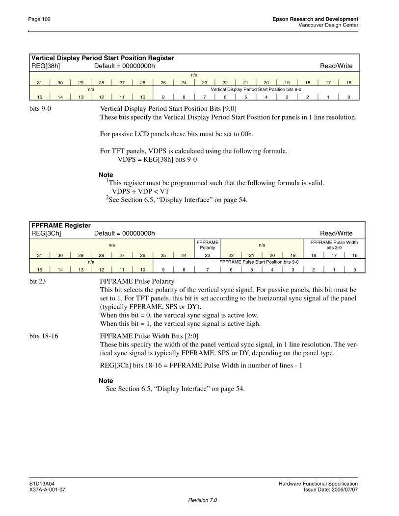
Page 102 Epson Research and DevelopmentVancouver Design Center
bits 9-0 Vertical Display Period Start Position Bits [9:0]These bits specify the Vertical Display Period Start Position for panels in 1 line resolution.
For passive LCD panels these bits must be set to 00h.
For TFT panels, VDPS is calculated using the following formula.VDPS = REG[38h] bits 9-0
Note1This register must be programmed such that the following formula is valid.
VDPS + VDP < VT2See Section 6.5, “Display Interface” on page 54.
bit 23 FPFRAME Pulse PolarityThis bit selects the polarity of the vertical sync signal. For passive panels, this bit must be set to 1. For TFT panels, this bit is set according to the horizontal sync signal of the panel (typically FPFRAME, SPS or DY).When this bit = 0, the vertical sync signal is active low.When this bit = 1, the vertical sync signal is active high.
bits 18-16 FPFRAME Pulse Width Bits [2:0]These bits specify the width of the panel vertical sync signal, in 1 line resolution. The ver-tical sync signal is typically FPFRAME, SPS or DY, depending on the panel type.
REG[3Ch] bits 18-16 = FPFRAME Pulse Width in number of lines - 1
NoteSee Section 6.5, “Display Interface” on page 54.
Vertical Display Period Start Position RegisterREG[38h] Default = 00000000h Read/Write
n/a
31 30 29 28 27 26 25 24 23 22 21 20 19 18 17 16
n/a Vertical Display Period Start Position bits 9-0
15 14 13 12 11 10 9 8 7 6 5 4 3 2 1 0
FPFRAME RegisterREG[3Ch] Default = 00000000h Read/Write
n/aFPFRAME
Polarity n/aFPFRAME Pulse Width
bits 2-0
31 30 29 28 27 26 25 24 23 22 21 20 19 18 17 16n/a FPFRAME Pulse Start Position bits 9-0
15 14 13 12 11 10 9 8 7 6 5 4 3 2 1 0
S1D13A04 Hardware Functional SpecificationX37A-A-001-07 Issue Date: 2006/07/07
Revision 7.0

Epson Research and Development Page 103Vancouver Design Center
bits 9-0 FPFRAME Pulse Start Position Bits [9:0]These bits specify the start position of the vertical sync signal, in 1 line resolution.
For passive panels, these bits must be set to 00h.
For TFT panels, VDPS is calculated using the following formula.VPS = REG[3Ch] bits 9-0
NoteSee Section 6.5, “Display Interface” on page 54.
bits 16-0 Main Window Display Start Address Bits [16:0]This register specifies the starting address, in DWORDS, for the LCD image in the display buffer for the main window.
Note that this is a double-word (32-bit) address. An entry of 00000h into these registers represents the first double-word of display memory, an entry of 00001h represents the sec-ond double-word of the display memory, and so on. Calculate the Display Start Address as follows:
REG[40h] bits 16:0 = image address ÷ 4 (valid only for SwivelView 0°)
NoteFor information on setting this register for other SwivelView orientations, see Section 13, “SwivelView™” on page 150.
bits 9-0 Main Window Line Address Offset Bits [9:0]This register specifies the offset, in DWORDS, from the beginning of one display line to the beginning of the next display line in the main window. Note that this is a 32-bit address increment. Calculate the Line Address Offset as follows:
REG[44h] bits 9:0 = display width in pixels ÷ (32 ÷ bpp)
NoteA virtual display can be created by programming this register with a value greater than the formula requires. When a virtual display is created the image width is larger than the display width and the displayed image becomes a window into the larger virtual image.
Main Window Display Start Address RegisterREG[40h] Default = 00000000h Read/Write
n/a bit 16
31 30 29 28 27 26 25 24 23 22 21 20 19 18 17 16
Main Window Display Start Address bits 15-0
15 14 13 12 11 10 9 8 7 6 5 4 3 2 1 0
Main Window Line Address Offset RegisterREG[44h] Default = 00000000h Read/Write
n/a
31 30 29 28 27 26 25 24 23 22 21 20 19 18 17 16
n/a Main Window Line Address Offset bits 9-0
15 14 13 12 11 10 9 8 7 6 5 4 3 2 1 0
Hardware Functional Specification S1D13A04Issue Date: 2006/07/07 X37A-A-001-07
Revision 7.0

Page 104 Epson Research and DevelopmentVancouver Design Center
8.3.6 Picture-in-Picture Plus (PIP+) Registers
bits 16-0 PIP+ Display Start Address Bits [16:0]These bits form the 17-bit address for the starting double-word of thePIP+ window.
Note that this is a double-word (32-bit) address. An entry of 00000h into these registers represents the first double-word of display memory, an entry of 00001h represents the sec-ond double-word of the display memory, and so on.
NoteThese bits have no effect unless the PIP+ Window Enable bit is set to 1 (REG[10h] bit 19).
bits 9-0 PIP+ Window Line Address Offset Bits [9:0]These bits are the LCD display’s 10-bit address offset from the starting double-word ofline “n” to the starting double-word of line “n + 1” for the PIP+window. Note that this is a32-bit address increment.
NoteThese bits have no effect unless the PIP+ Window Enable bit is set to 1 (REG[10h] bit 19).
PIP+ Display Start Address RegisterREG[50h] Default = 00000000h Read/Write
n/a bit 16
31 30 29 28 27 26 25 24 23 22 21 20 19 18 17 16PIP+ Display Start Address bits 15-0
15 14 13 12 11 10 9 8 7 6 5 4 3 2 1 0
PIP+ Line Address Offset RegisterREG[54h] Default = 00000000h Read/Write
n/a
31 30 29 28 27 26 25 24 23 22 21 20 19 18 17 16n/a PIP+ Line Address Offset bits 9-0
15 14 13 12 11 10 9 8 7 6 5 4 3 2 1 0
S1D13A04 Hardware Functional SpecificationX37A-A-001-07 Issue Date: 2006/07/07
Revision 7.0
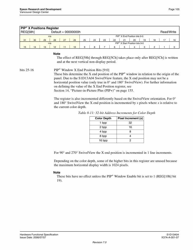
Epson Research and Development Page 105Vancouver Design Center
NoteThe effect of REG[58h] through REG[5Ch] takes place only after REG[5Ch] is written and at the next vertical non-display period.
bits 25-16 PIP+ Window X End Position Bits [9:0]These bits determine the X end position of the PIP+ window in relation to the origin of thepanel. Due to the S1D13A04 SwivelView feature, the X end position may not be ahorizontal position value (only true in 0° and 180° SwivelView). For further informationon defining the value of the X End Position register, seeSection 14, “Picture-in-Picture Plus (PIP+)” on page 155.
The register is also incremented differently based on the SwivelView orientation. For 0°and 180° SwivelView the X end position is incremented by x pixels where x is relative tothe current color depth.
For 90° and 270° SwivelView the X end position is incremented in 1 line increments.
Depending on the color depth, some of the higher bits in this register are unused becausethe maximum horizontal display width is 1024 pixels.
NoteThese bits have no effect unless the PIP+ Window Enable bit is set to 1 (REG[10h] bit 19).
PIP+ X Positions RegisterREG[58h] Default = 00000000h Read/Write
n/a PIP+ X End Position bits 9-0
31 30 29 28 27 26 25 24 23 22 21 20 19 18 17 16
n/a PIP+ X Start Position bits 9-0
15 14 13 12 11 10 9 8 7 6 5 4 3 2 1 0
Table 8-11: 32-bit Address Increments for Color Depth
Color Depth Pixel Increment (x)
1 bpp 32
2 bpp 16
4 bpp 8
8 bpp 4
16 bpp 2
Hardware Functional Specification S1D13A04Issue Date: 2006/07/07 X37A-A-001-07
Revision 7.0

Page 106 Epson Research and DevelopmentVancouver Design Center
bits 9-0 PIP+ Window X Start Position Bits [9:0]These bits determine the X start position of the PIP+ window in relation to the origin of the panel. Due to the S1D13A04 SwivelView feature, the X start position may not be ahorizontal position value (only true in 0° and 180° SwivelView). For further informationon defining the value of the X Start Position register, seeSection 14, “Picture-in-Picture Plus (PIP+)” on page 155.
The register is also incremented differently based on the SwivelView orientation. For 0°and 180° SwivelView the X start position is incremented by x pixels where x is relative tothe current color depth.
For 90° and 270° SwivelView the X start position is incremented in 1 line increments.
Depending on the color depth, some of the higher bits in this register are unused becausethe maximum horizontal display width is 1024 pixels.
NoteThese bits have no effect unless the PIP+ Window Enable bit is set to 1 (REG[10h] bit 19).
Table 8-12: 32-bit Address Increments for Color Depth
Color Depth Pixel Increment (x)
1 bpp 32
2 bpp 16
4 bpp 8
8 bpp 4
16 bpp 2
S1D13A04 Hardware Functional SpecificationX37A-A-001-07 Issue Date: 2006/07/07
Revision 7.0
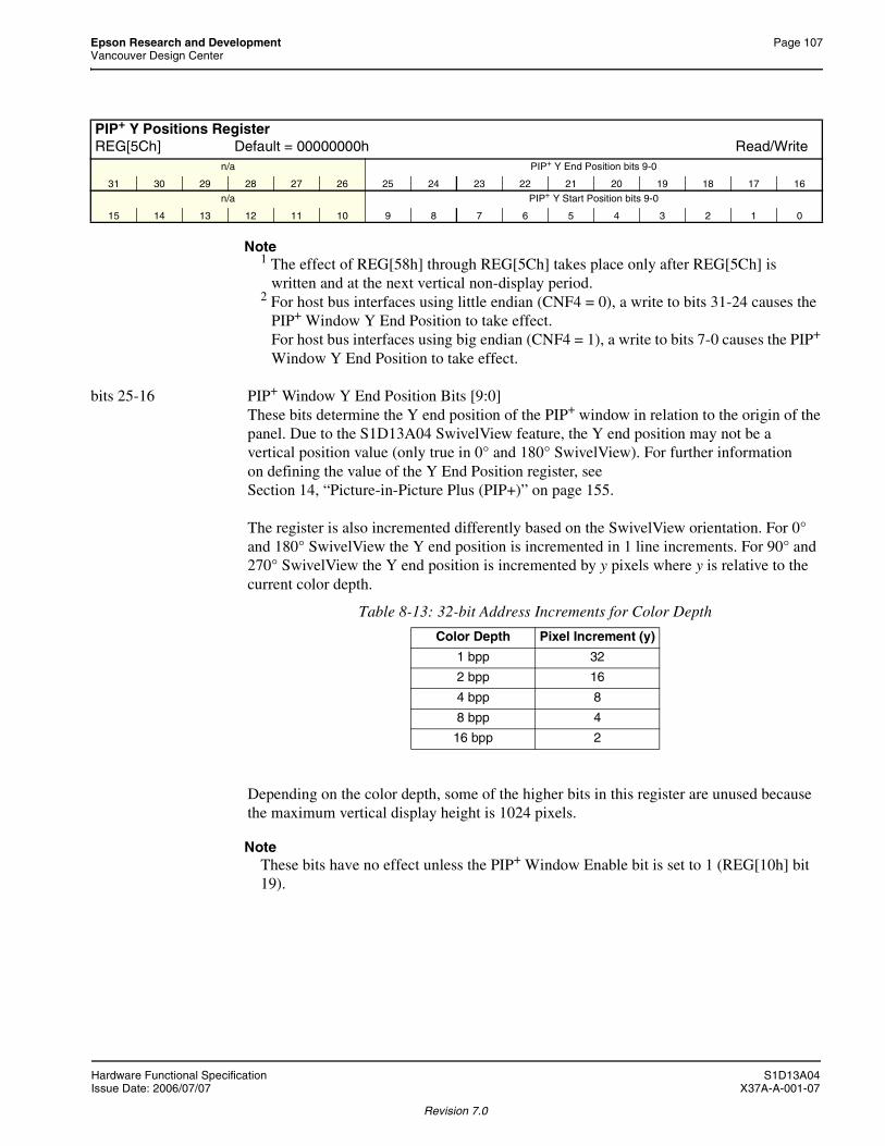
Epson Research and Development Page 107Vancouver Design Center
Note1 The effect of REG[58h] through REG[5Ch] takes place only after REG[5Ch] is
written and at the next vertical non-display period.2 For host bus interfaces using little endian (CNF4 = 0), a write to bits 31-24 causes the
PIP+ Window Y End Position to take effect.For host bus interfaces using big endian (CNF4 = 1), a write to bits 7-0 causes the PIP+
Window Y End Position to take effect.
bits 25-16 PIP+ Window Y End Position Bits [9:0]These bits determine the Y end position of the PIP+ window in relation to the origin of thepanel. Due to the S1D13A04 SwivelView feature, the Y end position may not be avertical position value (only true in 0° and 180° SwivelView). For further informationon defining the value of the Y End Position register, seeSection 14, “Picture-in-Picture Plus (PIP+)” on page 155.
The register is also incremented differently based on the SwivelView orientation. For 0°and 180° SwivelView the Y end position is incremented in 1 line increments. For 90° and270° SwivelView the Y end position is incremented by y pixels where y is relative to thecurrent color depth.
Depending on the color depth, some of the higher bits in this register are unused becausethe maximum vertical display height is 1024 pixels.
NoteThese bits have no effect unless the PIP+ Window Enable bit is set to 1 (REG[10h] bit 19).
PIP+ Y Positions RegisterREG[5Ch] Default = 00000000h Read/Write
n/a PIP+ Y End Position bits 9-0
31 30 29 28 27 26 25 24 23 22 21 20 19 18 17 16
n/a PIP+ Y Start Position bits 9-0
15 14 13 12 11 10 9 8 7 6 5 4 3 2 1 0
Table 8-13: 32-bit Address Increments for Color Depth
Color Depth Pixel Increment (y)
1 bpp 32
2 bpp 16
4 bpp 8
8 bpp 4
16 bpp 2
Hardware Functional Specification S1D13A04Issue Date: 2006/07/07 X37A-A-001-07
Revision 7.0

Page 108 Epson Research and DevelopmentVancouver Design Center
bits 9-0 PIP+ Window Y Start Position Bits [9:0]These bits determine the Y start position of the PIP+ window in relation to the origin of the panel. Due to the S1D13A04 SwivelView feature, the Y start position may not be avertical position value (only true in 0° and 180° SwivelView). For further informationon defining the value of the Y Start Position register, seeSection 14, “Picture-in-Picture Plus (PIP+)” on page 155.
The register is also incremented differently based on the SwivelView orientation. For 0°and 180° SwivelView the Y start position is incremented in 1 line increments. For 90° and270° SwivelView the Y start position is incremented by y pixels where y is relative to thecurrent color depth.
Depending on the color depth, some of the higher bits in this register are unused becausethe maximum vertical display height is 1024 pixels.
NoteThese bits have no effect unless the PIP+ Window Enable bit is set to 1 (REG[10h] bit 19).
Table 8-14: 32-bit Address Increments for Color Depth
Color Depth Pixel Increment (y)
1 bpp 32
2 bpp 16
4 bpp 8
8 bpp 4
16 bpp 2
S1D13A04 Hardware Functional SpecificationX37A-A-001-07 Issue Date: 2006/07/07
Revision 7.0

Epson Research and Development Page 109Vancouver Design Center
8.3.7 Miscellaneous Registers
bits 23-16 Reserved.These bits must be set to 0.
bit 7 2D Byte SwapThis bit enables the word data sent to/read from the 2D BitBLT port to be swapped (byte 0 and byte 1 are swapped).
NoteThis bit is only used when the S1D13A04 is configured for Big Endian (CNF4 = 1 at RESET#). If configured for Little Endian (CNF4 = 0), this bit has no effect.
bit 6 Display Data Word SwapThe display pipe fetches 32-bits of data from the display buffer. This bit enables the lower 16-bit word and the upper 16-bit word to be swapped before sending them to the LCD dis-play. If the Display Data Byte Swap bit is also enabled, then the byte order of the fetched 32-bit data is reversed.
NoteThis bit is only used when the S1D13A04 is configured for Big Endian (CNF4 = 1 at RESET#). If configured for Little Endian (CNF4 = 0), this bit has no effect.
Special Purpose RegisterREG[60h] Default = 00000000h Read/Write
n/a Reserved
31 30 29 28 27 26 25 24 23 22 21 20 19 18 17 16
n/a2D
Byte Swap
Display Data Word Swap
Display Data Byte Swap
n/aLatch Byte
Selectn/a
15 14 13 12 11 10 9 8 7 6 5 4 3 2 1 0
Hardware Functional Specification S1D13A04Issue Date: 2006/07/07 X37A-A-001-07
Revision 7.0

Page 110 Epson Research and DevelopmentVancouver Design Center
bit 5 Display Data Byte SwapThe display pipe fetches 32-bit of data from the display buffer. This bit enables byte 0 and byte 1 to be swapped, and byte 2 and byte 3 to be swapped, before sending them to the LCD display. If the Display Data Word Swap bit is also enabled, then the byte order of the fetched 32-bit data is reversed.
NoteThis bit is only used when the S1D13A04 is configured for Big Endian (CNF4 = 1 at RESET#). If configured for Little Endian (CNF4 = 0), this bit has no effect.
Figure 8-1: Display Data Byte/Word Swap
bit 2 Latch Byte SelectWhen this bit = 1, REG[5Ch] is latched in reverse order.When this bit = 0, there is no hardware effect.
byte 0
byte 1
byte 2
byte 3
32-bit display datafrom display buffer
Byte Swap Word Swap
Data
Serialization
To LUT
S1D13A04 Hardware Functional SpecificationX37A-A-001-07 Issue Date: 2006/07/07
Revision 7.0

Epson Research and Development Page 111Vancouver Design Center
NoteThe GPIO pins default as inputs after power-up and must be configured using the bits in this register.
NoteFor information on GPIO pin mapping when the ‘direct’ HR-TFT LCD interface is se-lected, see Table 4-9: “LCD Interface Pin Mapping,” on page 28.
bits 31-24 GPIO[7:0] Pin Input Enable bitsThese bits are used to enable the input function of each GPIO pin. They must be changed to a 1 after power-on reset to enable the input function of the corresponding GPIO pin (default is 0).
NoteThe default for GPIO5 Pin Input Enable is 1.
bits 23-16 GPIO[7:0] Pin IO ConfigurationWhen this bit = 0 (default), the corresponding GPIO pin is configured as an input pin.When this bit = 1, the corresponding GPIO pin is configured as an output pin.
NoteThe input function of each GPIO pin must be enabled using the GPIO[7:0] Pin Input En-able bits (bits 31-24) before the input configuration takes effect.
bit 7 GPIO7 Pin IO StatusWhen GPIO7 is configured as an output, writing a 1 to this bit drives GPIO7 high and writing a 0 to this bit drives GPIO7 low.When GPIO7 is configured as an input, a read from this bit returns the status of GPIO7.
bit 6 GPIO6 Pin IO StatusWhen GPIO6 is configured as an output, writing a 1 to this bit drives GPIO6 high and writing a 0 to this bit drives GPIO6 low.When GPIO6 is configured as an input, a read from this bit returns the status of GPIO6.
bit 5 GPIO5 Pin IO StatusWhen GPIO5 is configured as an output, writing a 1 to this bit drives GPIO5 high and writing a 0 to this bit drives GPIO5 low.When GPIO5 is configured as an input, a read from this bit returns the status of GPIO5.
GPIO Status and Control RegisterREG[64h] Default = 20000000h Read/WriteGPIO7 Input
Enable
GPIO6 Input
Enable
GPIO5 Input
Enable
GPIO4 Input
Enable
GPIO3 Input
Enable
GPIO2 Input
Enable
GPIO1 Input
Enable
GPIO0 Input
Enable
GPIO7 Config
GPIO6 Config
GPIO5 Config
GPIO4 Config
GPIO3 Config
GPIO2 Config
GPIO1 Config
GPIO0 Config
31 30 29 28 27 26 25 24 23 22 21 20 19 18 17 16
n/a GPIO7 Status
GPIO6 Status
GPIO5 Status
GPIO4 Status
GPIO3 Status
GPIO2 Status
GPIO1 Status
GPIO0 Status
15 14 13 12 11 10 9 8 7 6 5 4 3 2 1 0
Hardware Functional Specification S1D13A04Issue Date: 2006/07/07 X37A-A-001-07
Revision 7.0

Page 112 Epson Research and DevelopmentVancouver Design Center
bit 4 GPIO4 Pin IO StatusWhen GPIO4 is configured as an output, writing a 1 to this bit drives GPIO4 high and writing a 0 to this bit drives GPIO4 low.When GPIO4 is configured as an input, a read from this bit returns the status of GPIO4.
bit 3 GPIO3 Pin IO StatusWhen the ‘Direct’ HR-TFT LCD interface is not selected (REG[0Ch] bits 1:0) and GPIO3 is configured as an output, writing a 1 to this bit drives GPIO3 high and writing a 0 to this bit drives GPIO3 low.When the ‘Direct’ HR-TFT LCD interface is not selected (REG[0Ch] bits 1:0) and GPIO3 is configured as an input, a read from this bit returns the status of GPIO3.
When the ‘Direct’ HR-TFT LCD interface is enabled (REG[0Ch] bits 1:0 = 10), GPIO0 outputs the SPL signal automatically and writing to this bit has no effect.
bit 2 GPIO2 Pin IO StatusWhen the ‘Direct’ HR-TFT LCD interface is not selected (REG[0Ch] bits 1:0) and GPIO2 is configured as an output, writing a 1 to this bit drives GPIO2 high and writing a 0 to this bit drives GPIO2 low.When the ‘Direct’ HR-TFT LCD interface is not selected (REG[0Ch] bits 1:0) and GPIO2 is configured as an input, a read from this bit returns the status of GPIO2.
When the ‘Direct’ HR-TFT LCD interface is enabled (REG[0Ch] bits 1:0 = 10), GPIO0 outputs the REV signal automatically and writing to this bit has no effect.
bit 1 GPIO1 Pin IO StatusWhen the ‘Direct’ HR-TFT LCD interface is not selected (REG[0Ch] bits 1:0) and GPIO1 is configured as an output, writing a 1 to this bit drives GPIO1 high and writing a 0 to this bit drives GPIO1 low.When the ‘Direct’ HR-TFT LCD interface is not selected (REG[0Ch] bits 1:0) and GPIO1 is configured as an input, a read from this bit returns the status of GPIO1.
When the ‘Direct’ HR-TFT LCD interface is enabled (REG[0Ch] bits 1:0 = 10), GPIO0 outputs the CLS signal automatically and writing to this bit has no effect.
bit 0 GPIO0 Pin IO StatusWhen the ‘Direct’ HR-TFT LCD interface is not selected (REG[0Ch] bits 1:0) and GPIO0 is configured as an output, writing a 1 to this bit drives GPIO0 high and writing a 0 to this bit drives GPIO0 low.When the ‘Direct’ HR-TFT LCD interface is not selected (REG[0Ch] bits 1:0) and GPIO0 is configured as an input, a read from this bit returns the status of GPIO0.
When the ‘Direct’ HR-TFT LCD interface is enabled (REG[0Ch] bits 1:0 = 10), GPIO0 outputs the PS signal automatically and writing to this bit has no effect.
S1D13A04 Hardware Functional SpecificationX37A-A-001-07 Issue Date: 2006/07/07
Revision 7.0

Epson Research and Development Page 113Vancouver Design Center
Figure 8-2: PWM Clock Block DiagramNote
For further information on PWMCLK, see Section 7.1.4, “PWMCLK” on page 85.
bits 7-4 PWM Clock Divide Select Bits [3:0]The value of these bits represents the power of 2 by which the selected PWM clock source is divided.
NoteThis divided clock is further divided by 256 before it is output at PWMOUT.
PWM Clock Configuration RegisterREG[70h] Default = 00000000h Read/Write
n/a
31 30 29 28 27 26 25 24 23 22 21 20 19 18 17 16
n/aPWM Clock Divide Select
bits 3-0
PWM Clock Force High
PWMCLK Source Select bits 1-0
PWM Clock
Enable
15 14 13 12 11 10 9 8 7 6 5 4 3 2 1 0
Table 8-15: PWM Clock Divide Select Options
PWM Clock Divide Select Bits [3:0] PWM Clock Divide Amount
0h 1
1h 2
2h 4
3h 8
4h 16
5h 32
6h 64
7h 128
8h 256
9h 512
Ah 1024
Bh 2048
Ch 4096
Dh 8192
Eh 16384
Fh 32768
PWM ClockDivider
PWM Duty CycleModulation to PWMOUTPWMCLK
DividedClock
Clock Source / 2 m
m = PWM Clock Divide Select value
Duty = n / 256
n = PWM Clock Duty Cycle
frequency = Clock Source / (2m X 256)
PWM Clock Force High
PWM Clock Enable
Hardware Functional Specification S1D13A04Issue Date: 2006/07/07 X37A-A-001-07
Revision 7.0

Page 114 Epson Research and DevelopmentVancouver Design Center
bit 3 PWM Clock Force HighWhen this bit = 0, the PWMOUT pin function is controlled by the PWM Clock enable bit.When this bit = 1, the PWMOUT pin is forced to high.
bit 1 PWMCLK Source Select Bits [1:0]These bits determine the source of PWMCLK.
NoteFor further information on the PWMCLK source select, see Section 7.2, “Clock Selec-tion” on page 86.
bit 0 PWM Clock EnableWhen this bit = 0, PWMOUT output acts as a general purpose output pin controllable by bit 3 of REG[70h].When this bit = 1, the PWM Clock circuitry is enabled.
NoteThe PWM Clock circuitry is disabled when Power Save Mode is enabled.
bits 7-0 PWMOUT Duty Cycle Bits [7:0]This register determines the duty cycle of the PWMOUT output.
Table 8-16: PWMCLK Source Selection
PWMCLK Source Select Bits PWMCLK Source
00 CLKI
01 CLKI2
10 BCLK
11 PCLK
PWMOUT Duty Cycle RegisterREG[74h] Default = 00000000h Read/Write
n/a
31 30 29 28 27 26 25 24 23 22 21 20 19 18 17 16
n/a PWMOUT Duty Cycle bits 7-0
15 14 13 12 11 10 9 8 7 6 5 4 3 2 1 0
Table 8-17: PWMOUT Duty Cycle Select Options
PWMOUT Duty Cycle [7:0] PWMOUT Duty Cycle
00h Always Low
01h High for 1 out of 256 clock periods
02h High for 2 out of 256 clock periods
... ...
FFh High for 255 out of 256 clock periods
S1D13A04 Hardware Functional SpecificationX37A-A-001-07 Issue Date: 2006/07/07
Revision 7.0

Epson Research and Development Page 115Vancouver Design Center
bits 31-0 Scratch Pad A Bits [31:0]This register contains general purpose read/write bits. These bits have no effect on hard-ware.
NoteThe contents of the Scratch Pad A register defaults to an un-defined state after initial power-up. Any data written to this register remains intact when the S1D13A04 is reset, as long as the chip is not powered off.
bits 31-0 Scratch Pad B Bits [31:0]This register contains general purpose read/write bits. These bits have no effect on hard-ware.
NoteThe contents of the Scratch Pad B register defaults to an un-defined state after initial power-up. Any data written to this register remains intact when the S1D13A04 is reset, as long as the chip is not powered off.
bits 31-0 Scratch Pad C Bits [31:0]This register contains general purpose read/write bits. These bits have no effect on hard-ware.
NoteThe contents of the Scratch Pad C register defaults to an un-defined state after initial power-up. Any data written to this register remains intact when the S1D13A04 is reset, as long as the chip is not powered off.
Scratch Pad A RegisterREG[80h] Default = not applicable Read/Write
Scratch Pad A bits 31-24
31 30 29 28 27 26 25 24 23 22 21 20 19 18 17 16
Scratch Pad A bits 15-0
15 14 13 12 11 10 9 8 7 6 5 4 3 2 1 0
Scratch Pad B RegisterREG[84h] Default = not applicable Read/Write
Scratch Pad B bits 31-24
31 30 29 28 27 26 25 24 23 22 21 20 19 18 17 16Scratch Pad B bits 15-0
15 14 13 12 11 10 9 8 7 6 5 4 3 2 1 0
Scratch Pad C RegisterREG[88h] Default = not applicable Read/Write
Scratch Pad C bits 31-24
31 30 29 28 27 26 25 24 23 22 21 20 19 18 17 16Scratch Pad C bits 15-0
15 14 13 12 11 10 9 8 7 6 5 4 3 2 1 0
Hardware Functional Specification S1D13A04Issue Date: 2006/07/07 X37A-A-001-07
Revision 7.0

Page 116 Epson Research and DevelopmentVancouver Design Center
8.4 USB Registers (Offset = 4000h)
The S1D13A04 USB device occupies a 48 byte local register space which can be accessed by the CPU on the local host interface.
To access the USB registers:
1. A valid USBCLK must be provided.
2. The USBClk Enable bit (REG[4000h] bit 7) must be set to 1 and the USB Setup bit (REG[4000h] bit 2) must be set to 1. Both bits should be set together.
If any of the above conditions are not true, the USB registers must not be accessed.
bit 7 USBClk Enable.This bit allows the USBClk to be enabled/disabled allowing the S1D13A04 to save power when the USBClk is not required. This bit should be initially set with the USB Setup bit. However, it can be disabled/re-enabled individually.When this bit = 1, the USBClk is enabled.When this bit = 0, the USBClk is disabled.
NoteThe USB Registers must not be accessed when this bit is 0.
bit 6 Software EOTThis bit determines the response to an IN request to Endpoint 4 when the transmit FIFO is empty. If this bit is asserted, the S1D13A04 responds to an IN request to Endpoint 4 with an ACK and a zero length packet if the FIFO is empty. If this bit is not asserted, the S1D13A04 responds to an IN request from Endpoint 4 with an NAK if the FIFO is empty, indicating that it expects to transmit more data. This bit is automatically cleared when the S1D13A04 responds to the host with a zero length packet when the FIFO is empty.
bit 5 USB EnableAny device or configuration descriptor reads from the host will be acknowledged with a NAK until this bit is set. This allows time for the local CPU to set up the interrupt polling register, maximum packet size registers, and other configuration registers (e.g. Product ID and Vendor ID) before the host reads the descriptors.
NoteAs the device and configuration descriptors cannot be read by the host until the USB Enable bit is set, the device enumeration process will not complete and the device will not be recognized on the USB.
Control RegisterREG[4000h] Default = 00h Read/Write
n/a
15 14 13 12 11 10 9 8USBClk Enable Software EOT USB Enable Endpoint 4 Stall Endpoint 3 Stall USB Setup Reserved Reserved
7 6 5 4 3 2 1 0
S1D13A04 Hardware Functional SpecificationX37A-A-001-07 Issue Date: 2006/07/07
Revision 7.0

Epson Research and Development Page 117Vancouver Design Center
bit 4 Endpoint 4 Stall. If this bit is set, host bulk reads from the transmit FIFO will result in a STALL acknowl-edge by the S1D13A04. No data will be returned to the USB host.
bit 3 Endpoint 3 Stall. If this bit is set, host bulk writes to the receive FIFO will result in a STALL acknowledge by the S1D13A04. Receive data will be discarded.
bit 2 USB SetupThis bit is used by software to select between GPIO and USB functions for multifunction GPIO pins (GPIO[7:4]). This bit should be set at the same time as the USBClk Enable bit.When this bit = 1, the USB function is selected.When this bit = 0, the GPIO function is selected.
NoteThe USB Registers must not be accessed when this bit is 0.
bit 1 Reserved.This bit must be set to 0.
bit 0 Reserved.This bit must be set to 0.
bit 7 Suspend Request Interrupt Enable. When set, this bit enables an interrupt to occur when the USB host is requesting the S1D13A04 USB device to enter suspend mode.
bit 6 SOF Interrupt Enable. When set, this bit enables an interrupt to occur when a start-of-frame packet is received by the S1D13A04.
bit 5 Reserved.This bit must be set to 0.
bit 4 Endpoint 4 Interrupt Enable. When set, this bit enables an interrupt to occur when a USB Endpoint 4 Data Packet has been sent by the S1D13A04.
bit 3 Endpoint 3 Interrupt Enable. When set, this bit enables an interrupt to occur when a USB Endpoint 3 Data Packet has been received by the S1D13A04.
bit 2 Endpoint 2 Interrupt Enable. When set, this bit enables an interrupt to occur when the USB Endpoint 2 Transmit Mail-box registers have been read by the USB host.
Interrupt Enable Register 0REG[4002h] Default = 00h Read/Write
n/a
15 14 13 12 11 10 9 8Suspend Request Interrupt Enable
SOF Interrupt Enable reserved
Endpoint 4 Interrupt Enable
Endpoint 3 Interrupt Enable
Endpoint 2 Interrupt Enable
Endpoint 1 Interrupt Enable n/a
7 6 5 4 3 2 1 0
Hardware Functional Specification S1D13A04Issue Date: 2006/07/07 X37A-A-001-07
Revision 7.0
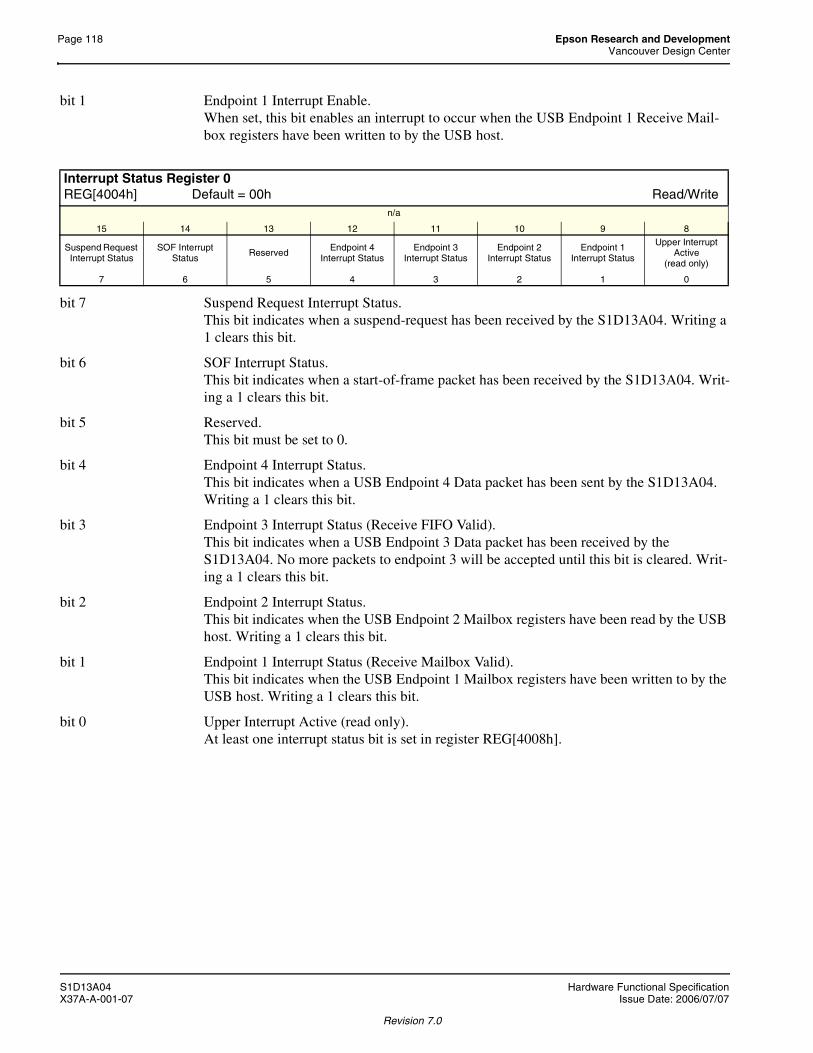
Page 118 Epson Research and DevelopmentVancouver Design Center
bit 1 Endpoint 1 Interrupt Enable. When set, this bit enables an interrupt to occur when the USB Endpoint 1 Receive Mail-box registers have been written to by the USB host.
bit 7 Suspend Request Interrupt Status. This bit indicates when a suspend-request has been received by the S1D13A04. Writing a 1 clears this bit.
bit 6 SOF Interrupt Status. This bit indicates when a start-of-frame packet has been received by the S1D13A04. Writ-ing a 1 clears this bit.
bit 5 Reserved.This bit must be set to 0.
bit 4 Endpoint 4 Interrupt Status. This bit indicates when a USB Endpoint 4 Data packet has been sent by the S1D13A04. Writing a 1 clears this bit.
bit 3 Endpoint 3 Interrupt Status (Receive FIFO Valid). This bit indicates when a USB Endpoint 3 Data packet has been received by the S1D13A04. No more packets to endpoint 3 will be accepted until this bit is cleared. Writ-ing a 1 clears this bit.
bit 2 Endpoint 2 Interrupt Status. This bit indicates when the USB Endpoint 2 Mailbox registers have been read by the USB host. Writing a 1 clears this bit.
bit 1 Endpoint 1 Interrupt Status (Receive Mailbox Valid). This bit indicates when the USB Endpoint 1 Mailbox registers have been written to by the USB host. Writing a 1 clears this bit.
bit 0 Upper Interrupt Active (read only). At least one interrupt status bit is set in register REG[4008h].
Interrupt Status Register 0REG[4004h] Default = 00h Read/Write
n/a
15 14 13 12 11 10 9 8
Suspend Request Interrupt Status
SOF Interrupt Status
Reserved Endpoint 4 Interrupt Status
Endpoint 3 Interrupt Status
Endpoint 2 Interrupt Status
Endpoint 1 Interrupt Status
Upper Interrupt Active
(read only)
7 6 5 4 3 2 1 0
S1D13A04 Hardware Functional SpecificationX37A-A-001-07 Issue Date: 2006/07/07
Revision 7.0

Epson Research and Development Page 119Vancouver Design Center
bit 1 Transmit FIFO Almost Empty Interrupt Enable. When set, this bit enables an interrupt to be generated when the Transmit FIFO Almost Empty status bit is set.
NoteThe Transmit FIFO Almost Empty threshold must be set greater than zero, as the FIFO count must drop below the threshold to cause an interrupt.
bit 0 Receive FIFO Almost Full Interrupt Enable.When set, this bit enables an interrupt to be generated when the Receive FIFO Almost Full status bit is set.
NoteThe Receive FIFO Almost Full threshold must be set less than 64, as the FIFO count must rise above the threshold to cause an interrupt.
bit 1 Transmit FIFO Almost Empty Status. This bit is set when the number of bytes in the Transmit FIFO is equal to the Transmit FIFO Almost Empty Threshold, and another byte is sent to the USB bus from the FIFO. Writing a 1 clears this bit.
bit 0 Receive FIFO Almost Full Status. This bit is set when the number of bytes in the Receive FIFO is equal to the Receive FIFO Almost Full Threshold, and another byte is received from the USB bus into the FIFO. Writing a 1 clears this bit.
Interrupt Enable Register 1REG[4006h] Default = 00h Read/Write
n/a
15 14 13 12 11 10 9 8
n/aTransmit FIFO Almost Empty
Interrupt Enable
Receive FIFO Almost Full
Interrupt Enable
7 6 5 4 3 2 1 0
Interrupt Status Register 1REG[4008h] Default = 00h Read/Write
n/a
15 14 13 12 11 10 9 8
n/aTransmit FIFO Almost Empty
Status
Receive FIFO Almost Full Status
7 6 5 4 3 2 1 0
Hardware Functional Specification S1D13A04Issue Date: 2006/07/07 X37A-A-001-07
Revision 7.0

Page 120 Epson Research and DevelopmentVancouver Design Center
bits 2-0 Endpoint 1 Index Register Bits [2:0]. This register determines which Endpoint 1 Receive Mailbox is accessed when the End-point 1 Receive Mailbox Data register is read. This register is automatically incremented after the Endpoint 1 Receive Mailbox Data register is read. This index register wraps around to zero when it reaches the maximum count (7).
bits 7-0 Endpoint 1 Receive Mailbox Data Bits [7:0]. This register is used to read data from one of the receive mailbox registers. Data is returned from the register selected by the Endpoint 1 Index Register. The eight receive mailbox registers are written by a USB bulk transfer to endpoint 1, and can be used to pass messages from the USB host to the local CPU. The format and content of the messages are user defined. If enabled, USB writes to this register can generate an interrupt.
bits 2-0 Endpoint 2 Index Register Bits [2:0]. This register determines which Endpoint 2 Transmit Mailbox is accessed when the End-point 2 Transmit Mailbox Data register is read or written. This register is automatically incremented after the Endpoint 2 Transmit Mailbox Data port is read or written. This index register wraps around to zero when it reaches the maximum count (7).
Endpoint 1 Index RegisterREG[4010h] Default = 00h Read/Write
n/a
15 14 13 12 11 10 9 8
n/a Endpoint 1 Index bits 2-0 (RO)
7 6 5 4 3 2 1 0
Endpoint 1 Receive Mailbox Data RegisterREG[4012h] Default = 00h Read Only
n/a
15 14 13 12 11 10 9 8Endpoint 1 Receive Mailbox Data bits 7-0
7 6 5 4 3 2 1 0
Endpoint 2 Index RegisterREG[4018h] Default = 00h Read/Write
n/a
15 14 13 12 11 10 9 8n/a Endpoint 2 Index bits 2-0
7 6 5 4 3 2 1 0
S1D13A04 Hardware Functional SpecificationX37A-A-001-07 Issue Date: 2006/07/07
Revision 7.0

Epson Research and Development Page 121Vancouver Design Center
bits 7-0 Endpoint 2 Transmit Mailbox Data Bits [7:0]. This register is used to read or write one of the transmit mailbox registers. The register being accessed is selected by the Endpoint 2 Index register. The eight Transmit Mailbox registers are written by the local CPU and are read by a USB transfer from endpoint 2. The format and content of the messages are user defined. If enabled, USB reads from this reg-ister can generate an interrupt.
bits 7-0 Interrupt Polling Interval Bits [7:0]. This register specifies the Endpoint 2 interrupt polling interval in milliseconds. It can be read by the host through the endpoint 2 descriptor.
bits7-0 Endpoint 3 Receive FIFO Data Bits [7:0]. This register is used by the local CPU to read USB receive FIFO data. The FIFO data is written by the USB host using bulk or isochronous transfers to endpoint 3.
bits 7-0 Receive FIFO Count Bits [7:0]. This register returns the number of receive FIFO entries containing valid entries. Values range from 0 (empty) to 64 (full).
Endpoint 2 Transmit Mailbox Data RegisterREG[401Ah] Default = 00h Read/Write
n/a
15 14 13 12 11 10 9 8
Endpoint 2 Transmit Mailbox Data bits 7-0
7 6 5 4 3 2 1 0
Endpoint 2 Interrupt Polling Interval RegisterREG[401Ch] Default = FFh Read/Write
n/a
15 14 13 12 11 10 9 8Interrupt Polling Interval bits 7-0
7 6 5 4 3 2 1 0
Endpoint 3 Receive FIFO Data RegisterREG[4020h] Default = 00h Read Only
n/a
15 14 13 12 11 10 9 8
Endpoint 3 Receive FIFO Data bits 7-0
7 6 5 4 3 2 1 0
Endpoint 3 Receive FIFO Count RegisterREG[4022h] Default = 00h Read Only
n/a
15 14 13 12 11 10 9 8Receive FIFO Count bits 7-0
7 6 5 4 3 2 1 0
Hardware Functional Specification S1D13A04Issue Date: 2006/07/07 X37A-A-001-07
Revision 7.0

Page 122 Epson Research and DevelopmentVancouver Design Center
bit 4 Receive FIFO FlushWriting to this bit causes the receive FIFO to be flushed. Reading this bit always returns a 0.
bit 3 Receive FIFO OverflowIf set, this bit indicates that an attempt was made by the USB host to write to the receive FIFO when the receive FIFO was full. Writing a 1 clears this bit.
bit 2 Receive FIFO UnderflowIf set, this bit indicates that an attempt was made to read the receive FIFO when the receive FIFO was empty. Writing a 1 clears this bit.
bit 1 Receive FIFO FullIf set, this bit indicates that the receive FIFO is full.
bit 0 Receive FIFO EmptyIf set, this bit indicates that the receive FIFO is empty.
bits 7-0 Endpoint 3 Max Packet Size Bits [7:0]. This register specifies the maximum packet size for endpoint 3 in units of 8 bytes (default = 64 bytes). It can be read by the host through the endpoint 3 descriptor.
bits 7-0 Transmit FIFO Data Bits [7:0]. This register is used by the local CPU to write data to the transmit FIFO. The FIFO data is read by the USB host using bulk or isochronous transfers from endpoint 4.
Endpoint 3 Receive FIFO Status RegisterREG[4024h] Default = 01h Read/Write
n/a
15 14 13 12 11 10 9 8
n/a Receive FIFO Flush
Receive FIFO Overflow
Receive FIFO Underflow
Receive FIFO Full(read only)
Receive FIFO Empty
(read only)
7 6 5 4 3 2 1 0
Endpoint 3 Maximum Packet Size RegisterREG[4026h] Default = 08h Read/Write
n/a
15 14 13 12 11 10 9 8Endpoint 3 Max Packet Size bits 7-0
7 6 5 4 3 2 1 0
Endpoint 4 Transmit FIFO Data RegisterREG[4028h] Default = 00h Write Only
n/a
15 14 13 12 11 10 9 8Transmit FIFO Data bits 7-0
7 6 5 4 3 2 1 0
S1D13A04 Hardware Functional SpecificationX37A-A-001-07 Issue Date: 2006/07/07
Revision 7.0
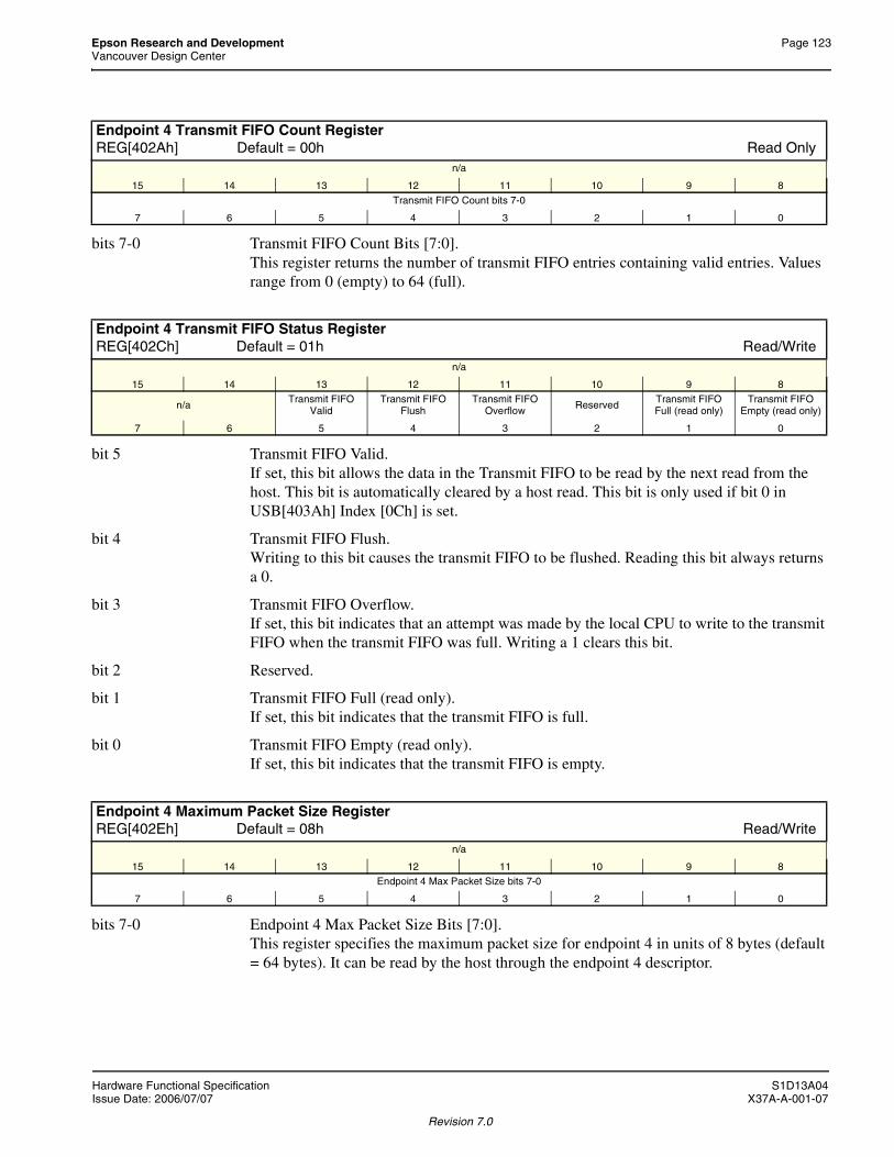
Epson Research and Development Page 123Vancouver Design Center
bits 7-0 Transmit FIFO Count Bits [7:0]. This register returns the number of transmit FIFO entries containing valid entries. Values range from 0 (empty) to 64 (full).
bit 5 Transmit FIFO Valid. If set, this bit allows the data in the Transmit FIFO to be read by the next read from the host. This bit is automatically cleared by a host read. This bit is only used if bit 0 in USB[403Ah] Index [0Ch] is set.
bit 4 Transmit FIFO Flush. Writing to this bit causes the transmit FIFO to be flushed. Reading this bit always returns a 0.
bit 3 Transmit FIFO Overflow. If set, this bit indicates that an attempt was made by the local CPU to write to the transmit FIFO when the transmit FIFO was full. Writing a 1 clears this bit.
bit 2 Reserved.
bit 1 Transmit FIFO Full (read only). If set, this bit indicates that the transmit FIFO is full.
bit 0 Transmit FIFO Empty (read only). If set, this bit indicates that the transmit FIFO is empty.
bits 7-0 Endpoint 4 Max Packet Size Bits [7:0]. This register specifies the maximum packet size for endpoint 4 in units of 8 bytes (default = 64 bytes). It can be read by the host through the endpoint 4 descriptor.
Endpoint 4 Transmit FIFO Count RegisterREG[402Ah] Default = 00h Read Only
n/a
15 14 13 12 11 10 9 8
Transmit FIFO Count bits 7-0
7 6 5 4 3 2 1 0
Endpoint 4 Transmit FIFO Status RegisterREG[402Ch] Default = 01h Read/Write
n/a
15 14 13 12 11 10 9 8
n/aTransmit FIFO
ValidTransmit FIFO
FlushTransmit FIFO
Overflow ReservedTransmit FIFO Full (read only)
Transmit FIFO Empty (read only)
7 6 5 4 3 2 1 0
Endpoint 4 Maximum Packet Size RegisterREG[402Eh] Default = 08h Read/Write
n/a
15 14 13 12 11 10 9 8Endpoint 4 Max Packet Size bits 7-0
7 6 5 4 3 2 1 0
Hardware Functional Specification S1D13A04Issue Date: 2006/07/07 X37A-A-001-07
Revision 7.0
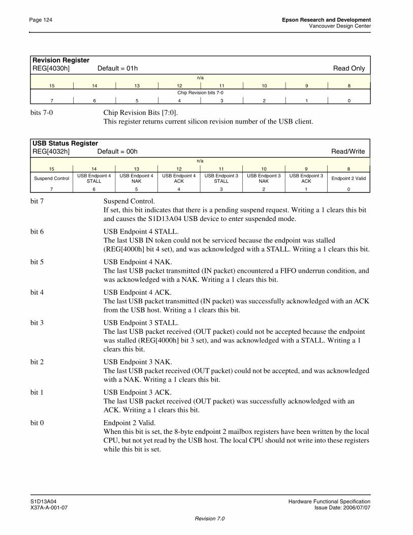
Page 124 Epson Research and DevelopmentVancouver Design Center
bits 7-0 Chip Revision Bits [7:0]. This register returns current silicon revision number of the USB client.
bit 7 Suspend Control. If set, this bit indicates that there is a pending suspend request. Writing a 1 clears this bit and causes the S1D13A04 USB device to enter suspended mode.
bit 6 USB Endpoint 4 STALL. The last USB IN token could not be serviced because the endpoint was stalled (REG[4000h] bit 4 set), and was acknowledged with a STALL. Writing a 1 clears this bit.
bit 5 USB Endpoint 4 NAK. The last USB packet transmitted (IN packet) encountered a FIFO underrun condition, and was acknowledged with a NAK. Writing a 1 clears this bit.
bit 4 USB Endpoint 4 ACK. The last USB packet transmitted (IN packet) was successfully acknowledged with an ACK from the USB host. Writing a 1 clears this bit.
bit 3 USB Endpoint 3 STALL. The last USB packet received (OUT packet) could not be accepted because the endpoint was stalled (REG[4000h] bit 3 set), and was acknowledged with a STALL. Writing a 1 clears this bit.
bit 2 USB Endpoint 3 NAK.The last USB packet received (OUT packet) could not be accepted, and was acknowledged with a NAK. Writing a 1 clears this bit.
bit 1 USB Endpoint 3 ACK. The last USB packet received (OUT packet) was successfully acknowledged with an ACK. Writing a 1 clears this bit.
bit 0 Endpoint 2 Valid. When this bit is set, the 8-byte endpoint 2 mailbox registers have been written by the local CPU, but not yet read by the USB host. The local CPU should not write into these registers while this bit is set.
Revision RegisterREG[4030h] Default = 01h Read Only
n/a
15 14 13 12 11 10 9 8
Chip Revision bits 7-0
7 6 5 4 3 2 1 0
USB Status RegisterREG[4032h] Default = 00h Read/Write
n/a
15 14 13 12 11 10 9 8
Suspend Control USB Endpoint 4 STALL
USB Endpoint 4 NAK
USB Endpoint 4 ACK
USB Endpoint 3 STALL
USB Endpoint 3 NAK
USB Endpoint 3 ACK
Endpoint 2 Valid
7 6 5 4 3 2 1 0
S1D13A04 Hardware Functional SpecificationX37A-A-001-07 Issue Date: 2006/07/07
Revision 7.0

Epson Research and Development Page 125Vancouver Design Center
bits 10-0 Frame Counter Bits [10:0] This register contains the frame counter from the most recent start-of-frame packet.
bits 7-0 Extended Register Index Bits [7:0] This register selects which extended data register is accessed when the REG[403Ah] is read or written.
bits 7-0 Extended Data Bits [7:0] This port provides access to one of the extended data registers. The index of the current register is held in REG[4038h].
bits 15-0 Vendor ID Bits [15:0] These registers determine the Vendor ID returned in a “Get Device Descriptor” request.
Frame Counter MSB RegisterREG[4034h] Default = 00h Read Only
n/a
15 14 13 12 11 10 9 8
n/a Frame Counter bits 10-8
7 6 5 4 3 2 1 0
Frame Counter LSB RegisterREG[4036h] Default = 00h Read Only
n/a
15 14 13 12 11 10 9 8Frame Counter bits 7-0
7 6 5 4 3 2 1 0
Extended Register IndexREG[4038h] Default = 00h Read/Write
n/a
15 14 13 12 11 10 9 8Extended Register Index bits 7-0
7 6 5 4 3 2 1 0
Extended Register DataREG[403Ah] Default = 04h Read/Write
n/a
15 14 13 12 11 10 9 8
Extended Data bits 7-0
7 6 5 4 3 2 1 0
Vendor ID MSBREG[403Ah], Index[00h] Default = 04h Read/Write
Vendor ID bits 15-8
7 6 5 4 3 2 1 0
Vendor ID LSBREG[403Ah], Index[01h] Default = B8h Read/Write
Vendor ID bits 7-0
7 6 5 4 3 2 1 0
Hardware Functional Specification S1D13A04Issue Date: 2006/07/07 X37A-A-001-07
Revision 7.0

Page 126 Epson Research and DevelopmentVancouver Design Center
bits 15-0 Product ID Bits [15:0] These registers determine the Product ID returned in a “Get Device Descriptor” request.
bits 15-0 Release Number Bits [15:0] These registers determine the device release number returned in a “Get Device Descriptor” request.
bits 5-0 Receive FIFO Almost Full Threshold Bits [5:0] This register determines the threshold at which the receive FIFO almost full status bit is set.
NoteThe Receive FIFO Almost Full threshold must be set less than 64, as the FIFO count must rise above the threshold to cause an interrupt.
Product ID MSBREG[403Ah], Index[02h] Default = 88h Read/Write
Product ID bits 15-8
7 6 5 4 3 2 1 0
Product ID LSBREG[403Ah], Index[03h] Default = 21h Read/Write
Product ID bits 7-0
7 6 5 4 3 2 1 0
Release Number MSBREG[403Ah], Index[04h] Default = 01h Read/Write
Release Number bits 15-8
7 6 5 4 3 2 1 0
Release Number LSBREG[403Ah], Index[05h] Default = 00h Read/Write
Release Number bits 7-0
7 6 5 4 3 2 1 0
Receive FIFO Almost Full ThresholdREG[403Ah], Index[06h] Default = 3Ch Read/Write
n/a Receive FIFO Almost Full Threshold bits 5-0
7 6 5 4 3 2 1 0
S1D13A04 Hardware Functional SpecificationX37A-A-001-07 Issue Date: 2006/07/07
Revision 7.0

Epson Research and Development Page 127Vancouver Design Center
bits 5-0 Transmit FIFO Almost Empty Threshold Bits [5:0]. This register determines the threshold at which the transmit FIFO almost empty status bit is set.
NoteThe Transmit FIFO Almost Empty threshold must be set greater than zero, as the FIFO count must drop below the threshold to cause an interrupt.
bit 0 USB String Enable. When set, this bit allows the default Vendor and Product ID String Descriptors to be returned to the host. When this bit is cleared, the string index values in the Device Descriptor are set to zero.
bits 7-0 Maximum Current Bits [7:0]. The amount of current drawn by the peripheral from the USB port in increments of 2 mA. The S1D13A04 reports this value to the host controller in the configuration descriptor. The default and maximum value is 500 mA (FAh * 2 mA).
In order to comply with the USB specification the following formula must apply:REG[403Ah] index[09h] ≤ FAh.
bit 7 EP4 Data Toggle Bit. Contains the value of the Data Toggle bit to be sent in response to the next IN token to endpoint 4 from the USB host.
NoteWhen a write is made to this bit, the value cannot be read back before a minimum of 12 USBCLK.
Transmit FIFO Almost Empty ThresholdREG[403Ah], Index[07h] Default = 04h Read/Write
n/a Transmit FIFO Almost Empty Threshold bits 5-0
7 6 5 4 3 2 1 0
USB ControlREG[403Ah], Index[08h] Default = 01h Read/Write
n/aUSB String
Enable
7 6 5 4 3 2 1 0
Maximum Power ConsumptionREG[403Ah], Index[09h] Default = FAh Read/Write
Maximum Current bits 7-0
7 6 5 4 3 2 1 0
Packet ControlREG[403Ah], Index[0Ah] Default = 00h Read/WriteEP4 Data Toggle EP3 Data Toggle EP2 Data Toggle EP1 Data Toggle Reserved Reserved n/a Reserved
7 6 5 4 3 2 1 0
Hardware Functional Specification S1D13A04Issue Date: 2006/07/07 X37A-A-001-07
Revision 7.0

Page 128 Epson Research and DevelopmentVancouver Design Center
bit 6 EP3 Data Toggle Bit. Contains the value of the Data Toggle bit expected in the next DATA packet to endpoint 3 from the USB host.
NoteWhen a write is made to this bit, the value cannot be read back before a minimum of 12 USBCLK.
bit 5 EP2 Data Toggle Bit. Contains the value of the Data Toggle bit to be sent in response to the next IN token to endpoint 2 from the USB host.
NoteWhen a write is made to this bit, the value cannot be read back before a minimum of 12 USBCLK.
bit 4 EP1 Data Toggle Bit. Contains the value of the Data Toggle bit expected in the next DATA packet to endpoint 1 from the USB host.
NoteWhen a write is made to this bit, the value cannot be read back before a minimum of 12 USBCLK.
bit 3 Reserved.This bit must be set to 0.
bit 2 Reserved.This bit must be set to 0.
bit 0 Reserved.This bit must be set to 0.
bit 0 Reserved.This bit must be set to 0.
ReservedREG[403Ah], Index[0Bh] Default = 00h Read/Write
n/a Reserved
7 6 5 4 3 2 1 0
S1D13A04 Hardware Functional SpecificationX37A-A-001-07 Issue Date: 2006/07/07
Revision 7.0

Epson Research and Development Page 129Vancouver Design Center
bit 0 Transmit FIFO Valid Mode. When set, this bit causes a NAK response to a host read request from the transmit FIFO (EP4) unless the FIFO Valid bit (in register EP4STAT) is set. When this bit is cleared, any data waiting in the transmit FIFO will be sent in response to a host read request, and the FIFO Valid bit is ignored.
These bits control inputs to the USB module.
bit 6 USCMPENThis bit controls the USB differential input receiver.
0 = differential input receiver disabled1 = differential input receiver enabled
bits 5 Reserved.This bit must be set to 0.
bits 4 Reserved.This bit must be set to 0.
bit 3 ISO This bits selects between isochronous and bulk transfer modes for the FIFOs (Endpoint 3 and Endpoint 4).0 = Isochronous transfer mode1 = Bulk transfer mode
bit 2 WAKEUP This active low bit initiates a USB remote wake-up.0 = initiate USB remote wake-up1 = no action
bit 1 Reserved.This bit must be set to 0.
bit 0 Reserved.This bit must be set to 0.
FIFO ControlREG[403Ah], Index[0Ch] Default = 00h Read/Write
n/aTransmit FIFO
Valid Mode
7 6 5 4 3 2 1 0
USBFC Input Control RegisterREG[4040h] Default = 0Dh Read/Write
n/a
15 14 13 12 11 10 9 8n/a USCMPEN Reserved Reserved ISO WAKEUP Reserved Reserved
7 6 5 4 3 2 1 0
Hardware Functional Specification S1D13A04Issue Date: 2006/07/07 X37A-A-001-07
Revision 7.0
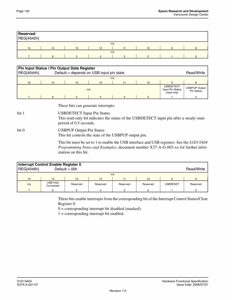
Page 130 Epson Research and DevelopmentVancouver Design Center
These bits can generate interrupts.
bit 1 USBDETECT Input Pin StatusThis read-only bit indicates the status of the USBDETECT input pin after a steady-state period of 0.5 seconds.
bit 0 USBPUP Output Pin StatusThis bit controls the state of the USBPUP output pin.
This bit must be set to 1 to enable the USB interface and USB registers. See the S1D13A04 Programming Notes and Examples, document number X37-A-G-003-xx for further infor-mation on this bit.
These bits enable interrupts from the corresponding bit of the Interrupt Control Status/Clear Register 0.0 = corresponding interrupt bit disabled (masked).1 = corresponding interrupt bit enabled.
ReservedREG[4042h]
n/a
15 14 13 12 11 10 9 8
n/a
7 6 5 4 3 2 1 0
Pin Input Status / Pin Output Data RegisterREG[4044h] Default = depends on USB input pin state Read/Write
n/a
15 14 13 12 11 10 9 8
n/aUSBDETECT
Input Pin Status(read only)
USBPUP Output Pin Status
7 6 5 4 3 2 1 0
Interrupt Control Enable Register 0REG[4046h] Default = 00h Read/Write
n/a
15 14 13 12 11 10 9 8
n/a USB Host Connected
Reserved Reserved Reserved Reserved USBRESET Reserved
7 6 5 4 3 2 1 0
S1D13A04 Hardware Functional SpecificationX37A-A-001-07 Issue Date: 2006/07/07
Revision 7.0

Epson Research and Development Page 131Vancouver Design Center
These bits enable interrupts from the corresponding bit of the Interrupt Control Status/Clear Register 1.0 = corresponding interrupt bit disabled (masked).1 = corresponding interrupt bit enabled.
On reads, these bits represent the interrupt status for interrupts caused by low-to-high transitions on the corresponding signals.0 (read) = no low-to-high event detected on the corresponding signal.1 (read) = low-to-high event detected on the corresponding signal.
On writes, these bits clear the corresponding interrupt status bit.0 (write) = corresponding interrupt status bit unchanged.1 (write) = corresponding interrupt status bit cleared to zero.
These bits must always be cleared via a write to this register before first use. This will ensure that any changes on input pins during system initialization do not generate erroneous interrupts. The interrupt bits are used as follows.
bit 6 USB Host ConnectedIndicates the USB device is connected to a USB host.
bit 5 Reserved.Must be set to 0.
bit 4 Reserved.Must be set to 0.
bit 3 Reserved.Must be set to 0.
bit 2 Reserved.Must be set to 0.
bit 1 USBRESETIndicates the USB device is reset using the RESET# pin or using the USB port reset.
Interrupt Control Enable Register 1REG[4048h] Default = 00h Read/Write
n/a
15 14 13 12 11 10 9 8
n/a USB Host Disconnect Reserved Device
Configured Reserved Reserved Reserved INT
7 6 5 4 3 2 1 0
Interrupt Control Status/Clear Register 0REG[404Ah] Default = 00h Read/Write
n/a
15 14 13 12 11 10 9 8
n/aUSB Host Connected Reserved Reserved Reserved Reserved USBRESET Reserved
7 6 5 4 3 2 1 0
Hardware Functional Specification S1D13A04Issue Date: 2006/07/07 X37A-A-001-07
Revision 7.0

Page 132 Epson Research and DevelopmentVancouver Design Center
bit 0 Reserved.Must be set to 0.
On reads, these bits represent the interrupt status for interrupts caused by high-to-low transitions on the corresponding signals.0 (read) = no high-to-low event detected on the corresponding signal.1 (read) = high-to-low event detected on the corresponding signal.
On writes, these bits clear the corresponding interrupt status bit.0 (write) = corresponding interrupt status bit unchanged.1 (write) = corresponding interrupt status bit cleared to zero.
These bits must always be cleared via a write to this register before first use. This will ensure that any changes on input pins during system initialization do not generate erroneous interrupts. The interrupt bits are used as follows.
bit 6 USB Host DisconnectedIndicates the USB device is disconnected from a USB host.
bit 5 Reserved.Must be set to 0.
bit 4 Device Configured.Indicates the USB device has been configured by the USB host.
bit 3 Reserved.Must be set to 0.
bit 2 Reserved.Must be set to 0.
bit 1 Reserved.Must be set to 0.
bit 0 INTIndicates an interrupt request originating from within the USB registers (REG[4000h] to REG[403Ah]).
Interrupt Control Status/Clear Register 1REG[404Ch] Default = 00h Read/Write
n/a
15 14 13 12 11 10 9 8
n/aUSB Host
Disconnected ReservedDevice
Configured Reserved Reserved Reserved INT
7 6 5 4 3 2 1 0
S1D13A04 Hardware Functional SpecificationX37A-A-001-07 Issue Date: 2006/07/07
Revision 7.0

Epson Research and Development Page 133Vancouver Design Center
These read-only bits represent the logical AND of the corresponding Interrupt Control Status/Clear Register 0 (REG[404Ah])and the Interrupt Control Enable Register 0 (REG[4046h]).
These read-only bits represent the logical AND of the corresponding Interrupt Control Status/Clear Register 1 (REG[404Ch]) and the Interrupt Control Enable Register 1 (REG[4048h]).
bits 7-0 USB Software Reset Bits [7:0] (Write Only)When the specific code of 10100100b is written to these bits the USB module of the S1D13A04 is reset. Use of the above code avoids the possibility of accidently resetting the USB.
bits 1-0 USB Wait State Bits [1:0]This register controls the number of wait states the S1D13A04 uses for its internal USB support. For all bus interfaces supported by the S1D13A04 these bits must be set to 01.
Interrupt Control Masked Status Register 0REG[404Eh] Default = 00h Read Only
n/a
15 14 13 12 11 10 9 8
n/a USB Host Connected Reserved Reserved Reserved Reserved USBRESET Reserved
7 6 5 4 3 2 1 0
Interrupt Control Masked Status Register 1REG[4050h] Default = 00h Read Only
n/a
15 14 13 12 11 10 9 8
n/a USB Host Disconnected
Reserved Device Configured
Reserved Reserved Reserved INT
7 6 5 4 3 2 1 0
USB Software Reset RegisterREG[4052h] Default = 00h Write Only
n/a
15 14 13 12 11 10 9 8USB Software Reset (Code = 10100100) bits 7-0
7 6 5 4 3 2 1 0
USB Wait State RegisterREG[4054h] Default = 00h Read/Write
n/a
15 14 13 12 11 10 9 8
n/a USB Wait State bits 1-0
7 6 5 4 3 2 1 0
Hardware Functional Specification S1D13A04Issue Date: 2006/07/07 X37A-A-001-07
Revision 7.0

Page 134 Epson Research and DevelopmentVancouver Design Center
8.5 2D Acceleration (BitBLT) Registers (Offset = 8000h)
These registers control the S1D13A04 2D Acceleration engine. For detailed BitBLT programming instructions, see the S1D13A04 Programming Notes and Examples, document number X37A-G-003-xx.
bit 18 BitBLT Color Format SelectThis bit selects the color format that the 2D operation is applied to.When this bit = 0, 8 bpp (256 color) format is selected.When this bit = 1, 16 bpp (64K color) format is selected.
bit 17 BitBLT Destination Linear SelectWhen this bit = 1, the Destination BitBLT is stored as a contiguous linear block ofmemory.When this bit = 0, the Destination BitBLT is stored as a rectangular region of memory.The BitBLT Memory Address Offset register (REG[8014h]) determines the address offset from the start of one line to the next line.
bit 16 BitBLT Source Linear SelectWhen this bit = 1, the Source BitBLT is stored as a contiguous linear block of memory. When this bit = 0, the Source BitBLT is stored as a rectangular region of memory.The BitBLT Memory Address Offset register (REG[8014h]) determines the address offset from the start of one line to the next line.
bit 0 BitBLT EnableThis bit is write only.Setting this bit to 1 begins the 2D BitBLT operation. This bit must not be set to 0 while a BitBLT operation is in progress.
NoteTo determine the status of a BitBLT operation use the BitBLT Busy Status bit (REG[8004h] bit 0).
BitBLT Control RegisterREG[8000h] Default = 00000000h Read/Write
n/aColor
Format Select
Dest Linear Select
Source Linear Select
31 30 29 28 27 26 25 24 23 22 21 20 19 18 17 16
n/aBitBLT Enable(WO)
15 14 13 12 11 10 9 8 7 6 5 4 3 2 1 0
S1D13A04 Hardware Functional SpecificationX37A-A-001-07 Issue Date: 2006/07/07
Revision 7.0
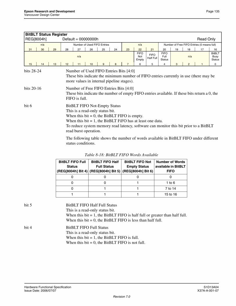
Epson Research and Development Page 135Vancouver Design Center
bits 28-24 Number of Used FIFO Entries Bits [4:0]These bits indicate the minimum number of FIFO entries currently in use (there may be more values in internal pipeline stages).
bits 20-16 Number of Free FIFO Entries Bits [4:0]These bits indicate the number of empty FIFO entries available. If these bits return a 0, the FIFO is full.
bit 6 BitBLT FIFO Not-Empty StatusThis is a read-only status bit.When this bit = 0, the BitBLT FIFO is empty.When this bit = 1, the BitBLT FiFO has at least one data.To reduce system memory read latency, software can monitor this bit prior to a BitBLT read burst operation.
The following table shows the number of words available in BitBLT FIFO under differentstatus conditions.
bit 5 BitBLT FIFO Half Full StatusThis is a read-only status bit.When this bit = 1, the BitBLT FIFO is half full or greater than half full.When this bit = 0, the BitBLT FIFO is less than half full.
bit 4 BitBLT FIFO Full StatusThis is a read-only status bit.When this bit = 1, the BitBLT FIFO is full.When this bit = 0, the BitBLT FIFO is not full.
BitBLT Status RegisterREG[8004h] Default = 00000000h Read Only
n/a Number of Used FIFO Entries n/a Number of Free FIFO Entries (0 means full)
31 30 29 28 27 26 25 24 23 22 21 20 19 18 17 16
n/aFIFO Not
Empty
FIFO Half Full
FIFO Full
Statusn/a
BitBLT Busy
Status
15 14 13 12 11 10 9 8 7 6 5 4 3 2 1 0
Table 8-18: BitBLT FIFO Words Available
BitBLT FIFO Full Status
(REG[8004h] Bit 4)
BitBLT FIFO Half Full Status
(REG[8004h] Bit 5)
BitBLT FIFO Not Empty Status
(REG[8004h] Bit 6)
Number of Words available in BitBLT
FIFO
0 0 0 0
0 0 1 1 to 6
0 1 1 7 to 14
1 1 1 15 to 16
Hardware Functional Specification S1D13A04Issue Date: 2006/07/07 X37A-A-001-07
Revision 7.0

Page 136 Epson Research and DevelopmentVancouver Design Center
bit 0 BitBLT Busy StatusThis bit is a read-only status bit.When this bit = 1, the BitBLT operation is in progress.When this bit = 0, the BitBLT operation is complete.
NoteDuring a BitBLT Read operation, the BitBLT engine does not attempt to keep the FIFO full. If the FIFO becomes full, the BitBLT operation stops temporarily as data is read out of the FIFO. The BitBLT will restart only when less than 14 values remain in the FIFO.
bits 19-16 BitBLT Raster Operation Code/Color Expansion Bits [3:0]ROP Code for Write BitBLT and Move BitBLT. Bits 2-0 also specify the start bit position for Color Expansion.
NoteS = Source, D = Destination, P = Pattern.~ = NOT, . = Logical AND, + = Logical OR, ^ = Logical XOR
BitBLT Command RegisterREG[8008h] Default = 00000000h Read/Write
n/a BitBLT ROP Code bits 3-0
31 30 29 28 27 26 25 24 23 22 21 20 19 18 17 16
n/a BitBLT Operation bits 3-0
15 14 13 12 11 10 9 8 7 6 5 4 3 2 1 0
Table 8-19 : BitBLT ROP Code/Color Expansion Function Selection
BitBLT ROP Code Bits [3:0]
Boolean Function for Write BitBLT and Move BitBLT
Boolean Function forPattern Fill
Start Bit Position for Color Expansion
0000 0 (Blackness) 0 (Blackness) bit 0
0001 ~S . ~D or ~(S + D) ~P . ~D or ~(P + D) bit 1
0010 ~S . D ~P . D bit 2
0011 ~S ~P bit 3
0100 S . ~D P . ~D bit 4
0101 ~D ~D bit 5
0110 S ^ D P ^ D bit 6
0111 ~S + ~D or ~(S . D) ~P + ~D or ~(P . D) bit 7
1000 S . D P . D bit 0
1001 ~(S ^ D) ~(P ^ D) bit 1
1010 D D bit 2
1011 ~S + D ~P + D bit 3
1100 S P bit 4
1101 S + ~D P + ~D bit 5
1110 S + D P + D bit 6
1111 1 (Whiteness) 1 (Whiteness) bit 7
S1D13A04 Hardware Functional SpecificationX37A-A-001-07 Issue Date: 2006/07/07
Revision 7.0

Epson Research and Development Page 137Vancouver Design Center
bits 3-0 BitBLT Operation Bits [3:0]Specifies the 2D Operation to be carried out based on the following table.
Table 8-20 : BitBLT Operation Selection
BitBLT Operation Bits [3:0] BitBLT Operation
0000 Write BitBLT with ROP.
0001 Read BitBLT.
0010 Move BitBLT in positive direction with ROP.
0011 Move BitBLT in negative direction with ROP.
0100 Transparent Write BitBLT.
0101 Transparent Move BitBLT in positive direction.
0110 Pattern Fill with ROP.
0111 Pattern Fill with transparency.
1000 Color Expansion.
1001 Color Expansion with transparency.
1010 Move BitBLT with Color Expansion.
1011 Move BitBLT with Color Expansion and transparency.
1100 Solid Fill.
Other combinations Reserved
Hardware Functional Specification S1D13A04Issue Date: 2006/07/07 X37A-A-001-07
Revision 7.0

Page 138 Epson Research and DevelopmentVancouver Design Center
bits 20-0 BitBLT Source Start Address Bits [20:0]A 21-bit register that specifies the source start address for the BitBLT operation.If data is sourced from the CPU, then bit 0 is used for byte alignment within a 16-bit wordand the other address bits are ignored. In pattern fill operation, the BitBLT Source StartAddress is defined by the following equation.
Value programmed to the Source Start Address Register =Pattern Base Address + Pattern Line Offset + Pixel Offset.
The following table shows how Source Start Address Register is defined for 8 and 16 bpp color depths.
NoteFor further information on the BitBLT Source Start Address register, see the S1D13A04 Programming Notes and Examples, document number X37A-G-003-xx.
bits 20-0 BitBLT Destination Start Address Bits [20:0]A 21-bit register that specifies the destination start address for the BitBLT operation.
BitBLT Source Start Address RegisterREG[800Ch] Default = 00000000h Read/Write
n/a BitBLT Source Start Address bits 20-16
31 30 29 28 27 26 25 24 23 22 21 20 19 18 17 16BitBLT Source Start Address bits 15-0
15 14 13 12 11 10 9 8 7 6 5 4 3 2 1 0
Table 8-21 : BitBLT Source Start Address Selection
Color Format Pattern Base Address[20:0] Pattern Line Offset[2:0] Pixel Offset[3:0]
8 bpp BitBLT Source Start Address[20:6]BitBLT Source Start
Address[5:3]BitBLT Source Start
Address[2:0]
16 bpp BitBLT Source Start Address[20:7]BitBLT Source Start
Address[6:4]BitBLT Source Start
Address[3:0]
BitBLT Destination Start Address RegisterREG[8010h] Default = 00000000h Read/Write
n/a BitBLT Destination Start Address bits 20-16
31 30 29 28 27 26 25 24 23 22 21 20 19 18 17 16
BitBLT Destination Start Address bits 15-0
15 14 13 12 11 10 9 8 7 6 5 4 3 2 1 0
S1D13A04 Hardware Functional SpecificationX37A-A-001-07 Issue Date: 2006/07/07
Revision 7.0

Epson Research and Development Page 139Vancouver Design Center
bits 10-0 BitBLT Memory Address Offset Bits [10:0]These bits are the display’s 11-bit address offset from the starting word of line n to the starting word of line n + 1. They are used only for address calculation when the BitBLT isconfigured as a rectangular region of memory. They are not used for the displays.
bits 9-0 BitBLT Width Bits [9:0]A 10-bit register that specifies the BitBLT width in pixels - 1.
BitBLT width in pixels = (ContentsOfThisRegister) + 1
bits 9-0 BitBLT Height Bits [9:0]A 10-bit register that specifies the BitBLT height in lines - 1.
BitBLT height in lines = (ContentsOfThisRegister) + 1
BitBLT Memory Address Offset RegisterREG[8014h] Default = 00000000h Read/Write
n/a
31 30 29 28 27 26 25 24 23 22 21 20 19 18 17 16
n/a BitBLT Memory Address Offset bits 10-0
15 14 13 12 11 10 9 8 7 6 5 4 3 2 1 0
BitBLT Width RegisterREG[8018h] Default = 00000000h Read/Write
n/a
31 30 29 28 27 26 25 24 23 22 21 20 19 18 17 16
n/a BitBLT Width bits 9-0
15 14 13 12 11 10 9 8 7 6 5 4 3 2 1 0
BitBLT Height RegisterREG[801Ch] Default = 00000000h Read/Write
n/a
31 30 29 28 27 26 25 24 23 22 21 20 19 18 17 16
n/a BitBLT Height bits 9-0
15 14 13 12 11 10 9 8 7 6 5 4 3 2 1 0
Hardware Functional Specification S1D13A04Issue Date: 2006/07/07 X37A-A-001-07
Revision 7.0
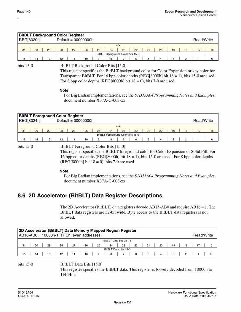
Page 140 Epson Research and DevelopmentVancouver Design Center
bits 15-0 BitBLT Background Color Bits [15:0]This register specifies the BitBLT background color for Color Expansion or key color for Transparent BitBLT. For 16 bpp color depths (REG[8000h] bit 18 = 1), bits 15-0 are used. For 8 bpp color depths (REG[8000h] bit 18 = 0), bits 7-0 are used.
NoteFor Big Endian implementations, see the S1D13A04 Programming Notes and Examples, document number X37A-G-003-xx.
bits 15-0 BitBLT Foreground Color Bits [15:0]This register specifies the BitBLT foreground color for Color Expansion or Solid Fill. For 16 bpp color depths (REG[8000h] bit 18 = 1), bits 15-0 are used. For 8 bpp color depths (REG[8000h] bit 18 = 0), bits 7-0 are used.
NoteFor Big Endian implementations, see the S1D13A04 Programming Notes and Examples, document number X37A-G-003-xx.
8.6 2D Accelerator (BitBLT) Data Register Descriptions
The 2D Accelerator (BitBLT) data registers decode AB15-AB0 and require AB16 = 1. The BitBLT data registers are 32-bit wide. Byte access to the BitBLT data registers is not allowed.
bits 15-0 BitBLT Data Bits [15:0]This register specifies the BitBLT data. This register is loosely decoded from 10000h to 1FFFEh.
BitBLT Background Color RegisterREG[8020h] Default = 00000000h Read/Write
n/a
31 30 29 28 27 26 25 24 23 22 21 20 19 18 17 16
BitBLT Background Color bits 15-0
15 14 13 12 11 10 9 8 7 6 5 4 3 2 1 0
BitBLT Foreground Color RegisterREG[8024h] Default = 00000000h Read/Write
n/a
31 30 29 28 27 26 25 24 23 22 21 20 19 18 17 16BitBLT Foreground Color bits 15-0
15 14 13 12 11 10 9 8 7 6 5 4 3 2 1 0
2D Accelerator (BitBLT) Data Memory Mapped Region RegisterAB16-AB0 = 10000h-1FFFEh, even addresses Read/Write
BitBLT Data bits 31-16
31 30 29 28 27 26 25 24 23 22 21 20 19 18 17 16
BitBLT Data bits 15-0
15 14 13 12 11 10 9 8 7 6 5 4 3 2 1 0
S1D13A04 Hardware Functional SpecificationX37A-A-001-07 Issue Date: 2006/07/07
Revision 7.0

Epson Research and Development Page 141Vancouver Design Center
9 2D Accelerator (BitBLT) Engine
9.1 Overview
The S1D13A04 is designed with a built-in 2D BitBLT engine which increases the perfor-mance of Bit Block Transfers (BitBLT). It supports 8 and 16 bit-per-pixel color depths.
The BitBLT engine supports rectangular and linear addressing modes for source and desti-nation in a positive direction for all BitBLT operations except the move BitBLT which also supports in a negative direction.
The BitBLT operations support byte alignment of all types. The BitBLT engine has a dedicated BitBLT IO access space. This allows the BitBLT engine to support simultaneous BitBLT and host side operations.
9.2 BitBLT Operations
The S1D13A04 2D BitBLT engine supports the following BitBLTs. For detailed infor-mation on using the individual BitBLT operations, refer to the S1D13A04 Programming Notes and Examples, document number X37A-G-003-xx.
• Write BitBLT.
• Move BitBLT.
• Solid Fill BitBLT.
• Pattern Fill BitBLT.
• Transparent Write BitBLT.
• Transparent Move BitBLT.
• Read BitBLT.
• Color Expansion BitBLT.
• Move BitBLT with Color Expansion.
NoteFor details on the BitBLT registers, see Section 8.5, “2D Acceleration (BitBLT) Regis-ters (Offset = 8000h)” on page 134.
Hardware Functional Specification S1D13A04Issue Date: 2006/07/07 X37A-A-001-07
Revision 7.0
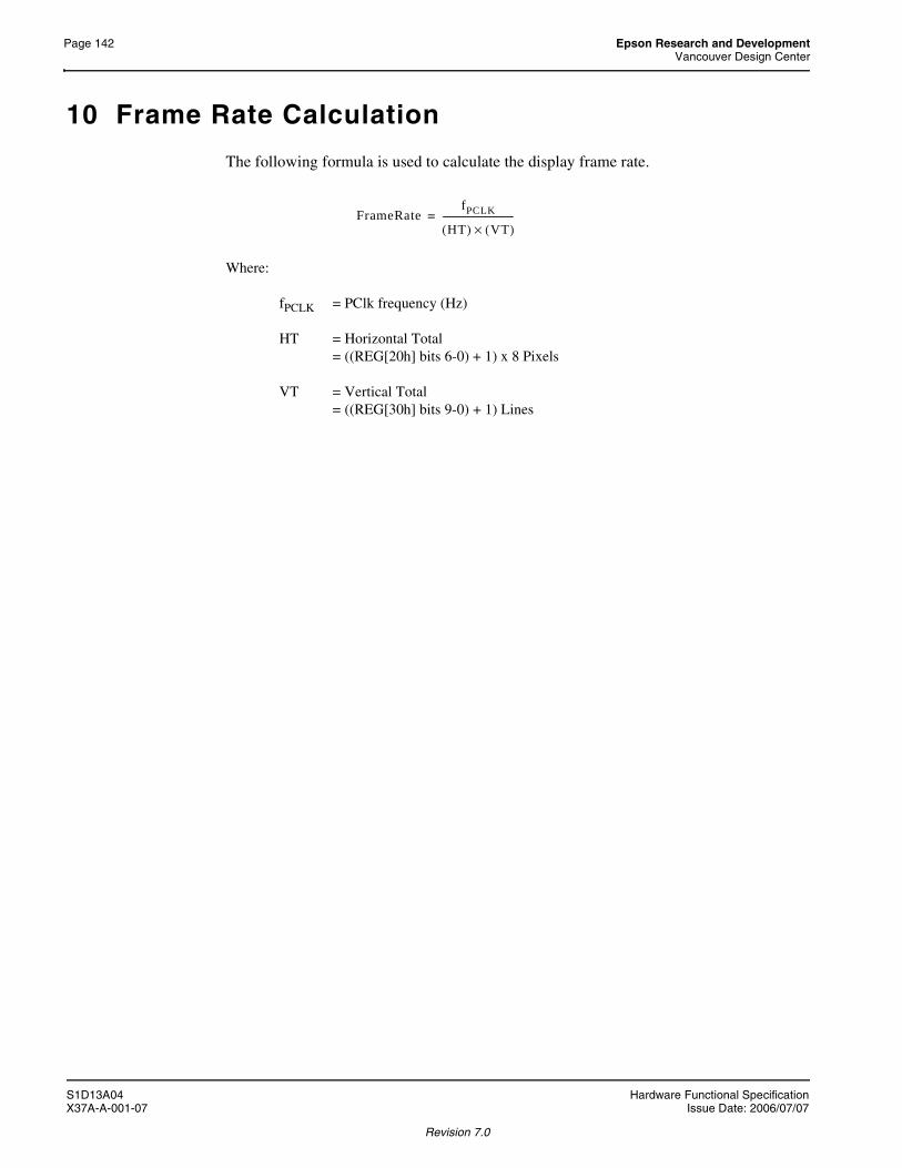
Page 142 Epson Research and DevelopmentVancouver Design Center
10 Frame Rate Calculation
The following formula is used to calculate the display frame rate.
Where:
fPCLK = PClk frequency (Hz)
HT = Horizontal Total= ((REG[20h] bits 6-0) + 1) x 8 Pixels
VT = Vertical Total= ((REG[30h] bits 9-0) + 1) Lines
FrameRatefPCLK
HT( ) VT( )×--------------------------------=
S1D13A04 Hardware Functional SpecificationX37A-A-001-07 Issue Date: 2006/07/07
Revision 7.0
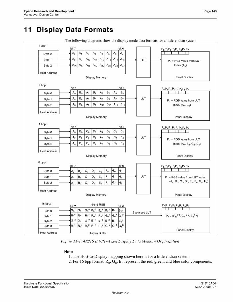
Epson Research and Development Page 143Vancouver Design Center
11 Display Data FormatsThe following diagrams show the display mode data formats for a little-endian system.
Figure 11-1: 4/8/16 Bit-Per-Pixel Display Data Memory Organization
Note1. The Host-to-Display mapping shown here is for a little endian system.2. For 16 bpp format, Rn, Gn, Bn represent the red, green, and blue color components.
4 bpp:
A0 B0 C0 D0 A1 B1 C1 D1
Host Address
Display Memory
A2 B2 C2 D2 A3 B3 C3 D3
bit 7 bit 0
A4 B4 C4 D4 A5 B5 C5 D5
Host AddressDisplay Memory
bit 7 bit 08 bpp:
A0 B0 C0 D0 E0 F0 G0 H0
A1 B1 C1 D1 E1 F1 G1 H1
A2 B2 C2 D2 E2 F2 G2 H2
Byte 0
Byte 1
Byte 2
Byte 0
Byte 1
Byte 2
Panel Display
P0P1P2 P3P4P5P6 P7
Panel Display
P0P1P2 P3P4P5P6 P7
(An, Bn, Cn, Dn, En, Fn, Gn, Hn)
16 bpp:
R04
Host Address Display Buffer
bit 7 bit 0
R03 R0
2 R01 R0
0 G05 G0
4 G03
G02 G0
1 G00 B0
4 B03 B0
2 B01 B0
0
R14 R1
3 R12 R1
1 R10 G1
5 G14 G1
3
G12 G1
1 G10 B1
4 B13 B1
2 B11 B1
0
5-6-5 RGB
Byte 0
Byte 1
Byte 2
Byte 3Panel Display
P0P1P2 P3P4P5P6 P7
Pn = (Rn4-0, Gn 5-0, Bn
4-0)
2 bpp:
A0 B0 A1 B1 A2 B2 A3 B3
Host Address
Display Memory
A4 B4 A5 B5 A6 B6 A7 B7
bit 7 bit 0
A8 B8 A9 B9 A10 B10 A11 B11
Byte 0
Byte 1
Byte 2
Panel Display
P0P1P2 P3P4P5P6 P7
1 bpp:
A0 A1 A2 A3 A4 A5 A6 A7
Host Address
Display Memory
A8 A9 A10 A11 A12 A13 A14 A15
bit 7 bit 0
A16 A17 A18 A19 A20 A21 A22 A23
Byte 0
Byte 1
Byte 2
Panel Display
P0P1P2 P3P4P5P6 P7
LUT
LUT
LUT
LUT
Bypasses LUT
Pn = RGB value from LUT
Index (An, Bn, Cn, Dn)
Pn = RGB value from LUT
Index (An, Bn)
Pn = RGB value from LUT
Index (An)
Pn = RGB value from LUT Index
Hardware Functional Specification S1D13A04Issue Date: 2006/07/07 X37A-A-001-07
Revision 7.0

Page 144 Epson Research and DevelopmentVancouver Design Center
12 Look-Up Table Architecture
The following figures are intended to show the display data output path only.
NoteWhen Video Data Invert is enabled the video data is inverted after the Look-Up Table.
12.1 Monochrome Modes
The green Look-Up Table (LUT) is used for all monochrome modes.
1 Bit-per-pixel Monochrome Mode
Figure 12-1: 1 Bit-per-pixel Monochrome Mode Data Output Path
2 Bit-per-pixel Monochrome Mode
Figure 12-2: 2 Bit-per-pixel Monochrome Mode Data Output Path
Green Look-Up Table 256x6
0001
1 bit-per-pixel data
6-bit Gray Data
from Display Buffer= unused Look-Up Table entries
0001
FCFDFEFF
Green Look-Up Table 256x6
0001
2 bit-per-pixel data
6-bit Gray Data
from Display Buffer
1011
= unused Look-Up Table entries
00010203
FCFDFEFF
S1D13A04 Hardware Functional SpecificationX37A-A-001-07 Issue Date: 2006/07/07
Revision 7.0

Epson Research and Development Page 145Vancouver Design Center
4 Bit-per-pixel Monochrome Mode
Figure 12-3: 4 Bit-per-pixel Monochrome Mode Data Output Path
8 Bit-per-pixel Monochrome Mode
Figure 12-4: 8 Bit-per-pixel Monochrome Mode Data Output Path
Green Look-Up Table 256x6
00000001
4 bit-per-pixel data
6-bit Gray Data
from Display Buffer
00100011010001010110011110001001101010111100110111101111
= unused Look-Up Table entries
00010203
FCFDFEFF
0405060708090A0B0C0D0E0F
0000 00000000 0001
6-bit Gray Data
0000 00100000 00110000 01000000 01010000 01100000 0111
1111 10001111 10011111 10101111 10111111 11001111 11011111 11101111 1111
Green Look-Up Table 256x6
0001020304050607
F8F9FAFBFCFDFEFF
8 bit-per-pixel datafrom Display Buffer
Hardware Functional Specification S1D13A04Issue Date: 2006/07/07 X37A-A-001-07
Revision 7.0

Page 146 Epson Research and DevelopmentVancouver Design Center
16 Bit-Per-Pixel Monochrome Mode
The LUT is bypassed and the green data is directly mapped for this color depth– “Display Data Formats” on page 143..
12.2 Color Modes
1 Bit-Per-Pixel Color
Figure 12-5: 1 Bit-Per-Pixel Color Mode Data Output Path
1 bit-per-pixel datafrom Image Buffer
6-bit Blue Data01
Blue Look-Up Table 256x60001
FCFDFEFF
6-bit Red Data01
Red Look-Up Table 256x60001
FCFDFEFF
6-bit Green Data01
Green Look-Up Table 256x60001
FCFDFEFF
= unused Look-Up Table entries
S1D13A04 Hardware Functional SpecificationX37A-A-001-07 Issue Date: 2006/07/07
Revision 7.0

Epson Research and Development Page 147Vancouver Design Center
2 Bit-Per-Pixel Color
Figure 12-6: 2 Bit-Per-Pixel Color Mode Data Output Path
2 bit-per-pixel datafrom Image Buffer
6-bit Blue Data00011011
Blue Look-Up Table 256x600010203
FCFDFEFF
6-bit Red Data00011011
Red Look-Up Table 256x600010203
FCFDFEFF
6-bit Green Data00011011
Green Look-Up Table 256x600010203
FCFDFEFF
= unused Look-Up Table entries
Hardware Functional Specification S1D13A04Issue Date: 2006/07/07 X37A-A-001-07
Revision 7.0
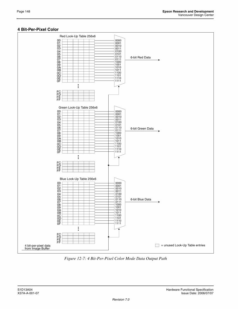
Page 148 Epson Research and DevelopmentVancouver Design Center
4 Bit-Per-Pixel Color
Figure 12-7: 4 Bit-Per-Pixel Color Mode Data Output Path
00000001
4 bit-per-pixel data
6-bit Red Data
from Image Buffer
00100011010001010110011110001001101010111100110111101111
6-bit Green Data
6-bit Blue Data
Red Look-Up Table 256x600010203
FCFDFEFF
0405060708090A0B0C0D0E0F
0000000100100011010001010110011110001001101010111100110111101111
Green Look-Up Table 256x600010203
FCFDFEFF
0405060708090A0B0C0D0E0F
0000000100100011010001010110011110001001101010111100110111101111
Blue Look-Up Table 256x600010203
FCFDFEFF
0405060708090A0B0C0D0E0F
= unused Look-Up Table entries
S1D13A04 Hardware Functional SpecificationX37A-A-001-07 Issue Date: 2006/07/07
Revision 7.0
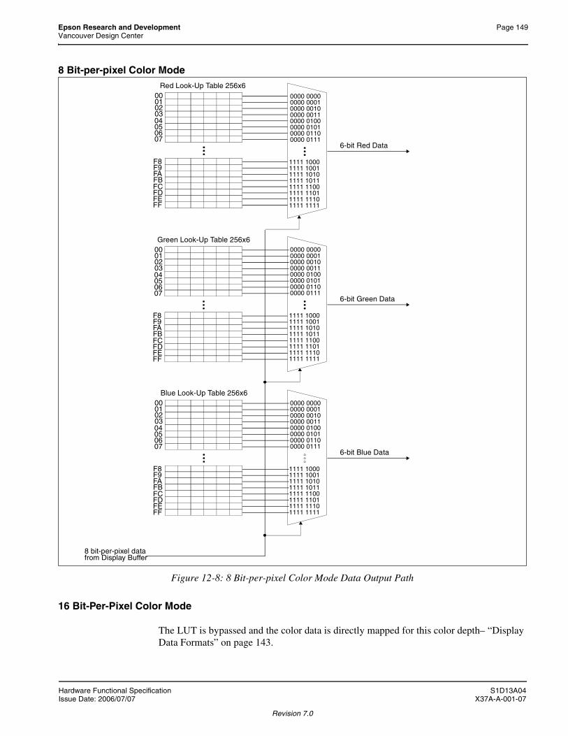
Epson Research and Development Page 149Vancouver Design Center
8 Bit-per-pixel Color Mode
Figure 12-8: 8 Bit-per-pixel Color Mode Data Output Path
16 Bit-Per-Pixel Color Mode
The LUT is bypassed and the color data is directly mapped for this color depth– “Display Data Formats” on page 143.
Red Look-Up Table 256x600010203
0000 00000000 0001
8 bit-per-pixel data
6-bit Red Data
from Display Buffer
0000 00100000 0011
04050607
0000 01000000 01010000 01100000 0111
F8F9FAFBFCFDFEFF
1111 10001111 10011111 10101111 10111111 11001111 11011111 11101111 1111
0000 00000000 0001
6-bit Green Data
0000 00100000 00110000 01000000 01010000 01100000 0111
1111 10001111 10011111 10101111 10111111 11001111 11011111 11101111 1111
0000 00000000 0001
6-bit Blue Data
0000 00100000 00110000 01000000 01010000 01100000 0111
1111 10001111 10011111 10101111 10111111 11001111 11011111 11101111 1111
Green Look-Up Table 256x60001020304050607
F8F9FAFBFCFDFEFF
Blue Look-Up Table 256x60001020304050607
F8F9FAFBFCFDFEFF
Hardware Functional Specification S1D13A04Issue Date: 2006/07/07 X37A-A-001-07
Revision 7.0
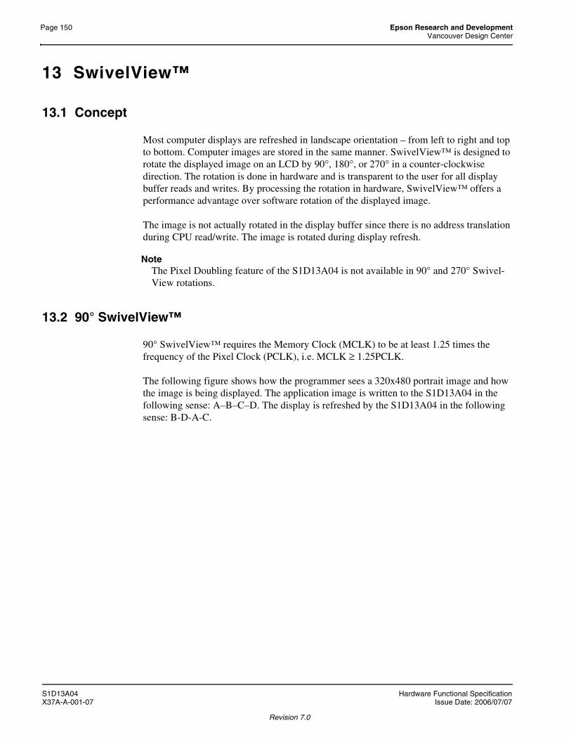
Page 150 Epson Research and DevelopmentVancouver Design Center
13 SwivelView™
13.1 Concept
Most computer displays are refreshed in landscape orientation – from left to right and top to bottom. Computer images are stored in the same manner. SwivelView™ is designed to rotate the displayed image on an LCD by 90°, 180°, or 270° in a counter-clockwise direction. The rotation is done in hardware and is transparent to the user for all display buffer reads and writes. By processing the rotation in hardware, SwivelView™ offers a performance advantage over software rotation of the displayed image.
The image is not actually rotated in the display buffer since there is no address translation during CPU read/write. The image is rotated during display refresh.
NoteThe Pixel Doubling feature of the S1D13A04 is not available in 90° and 270° Swivel-View rotations.
13.2 90° SwivelView™
90° SwivelView™ requires the Memory Clock (MCLK) to be at least 1.25 times the frequency of the Pixel Clock (PCLK), i.e. MCLK ≥ 1.25PCLK.
The following figure shows how the programmer sees a 320x480 portrait image and how the image is being displayed. The application image is written to the S1D13A04 in the following sense: A–B–C–D. The display is refreshed by the S1D13A04 in the following sense: B-D-A-C.
S1D13A04 Hardware Functional SpecificationX37A-A-001-07 Issue Date: 2006/07/07
Revision 7.0

Epson Research and Development Page 151Vancouver Design Center
Figure 13-1: Relationship Between The Screen Image and the Image Refreshed in 90° SwivelView.
13.2.1 Register Programming
Enable 90° SwivelView™ Mode
Set SwivelView™ Mode Select bits (REG[10h] bits 17:16) to 01.
Display Start Address
The display refresh circuitry starts at pixel “B”, therefore the Main Window Display Start Address register (REG[40h]) must be programmed with the address of pixel “B”. To calculate the value of the address of pixel “B” use the following formula (assumes 8 bpp color depth).
REG[40h] bits 16:0 = ((image address + (panel height x bpp ÷ 8)) ÷ 4) - 1= ((0 + (320 pixels x 8 bpp ÷ 8)) ÷ 4) -1= 79 (4Fh)
Line Address Offset
The Main Window Line Address Offset register (REG[44h]) is based on the display width and programmed using the following formula.
REG[44h] bits 9:0 = display width in pixels ÷ (32 ÷ bpp)= 320 pixels ÷ (32 ÷ 8 bpp)= 80 (50h)
image seen by programmer= image in display buffer
480
SwivelViewwindow48
0
320
A B
C D
DC
BA
320
Sw
ivel
Vie
w
win
dowdisplay start address
image refreshed by S1D13A04
(panel origin)
physical memorystart address
Hardware Functional Specification S1D13A04Issue Date: 2006/07/07 X37A-A-001-07
Revision 7.0

Page 152 Epson Research and DevelopmentVancouver Design Center
13.3 180° SwivelView™
The following figure shows how the programmer sees a 480x320 landscape image and how the image is being displayed. The application image is written to the S1D13A04 in the following sense: A–B–C–D. The display is refreshed by the S1D13A04 in the following sense: D-C-B-A.
Figure 13-2: Relationship Between The Screen Image and the Image Refreshed in 180° SwivelView.
13.3.1 Register Programming
Enable 180° SwivelView™ Mode
Set SwivelView™ Mode Select bits (REG[10h] bits 17:16) to 10.
Display Start Address
The display refresh circuitry starts at pixel “D”, therefore the Main Window Display Start Address register (REG[40h]) must be programmed with the address of pixel “D”. To calculate the value of the address of pixel “D” use the following formula (assumes 8 bpp color depth).
REG[40h] bits 16:0 = ((image address + (offset x (panel height - 1) + panel width) x bpp ÷ 8) ÷ 4) - 1= ((0 + (480 pixels x 319 pixels + 480 pixels) x 8 bpp ÷ 8) ÷ 4) - 1= 38399 (95FFh)
image seen by programmer= image in display buffer
480
SwivelViewwindow
480
320
A B
C D
320
image refreshed by S1D13A04
SwivelViewwindow
AB
CD
display start address(panel origin)
physical memorystart address
S1D13A04 Hardware Functional SpecificationX37A-A-001-07 Issue Date: 2006/07/07
Revision 7.0

Epson Research and Development Page 153Vancouver Design Center
Line Address Offset
The Main Window Line Address Offset register (REG[44h]) is based on the display width and programmed using the following formula.
REG[44h] bits 9:0 = display width in pixels ÷ (32 ÷ bpp)= 480 pixels ÷ (32 ÷ 8 bpp)= 120 (78h)
13.4 270° SwivelView™
270° SwivelView™ requires the Memory Clock (MCLK) to be at least 1.25 times the frequency of the Pixel Clock (PCLK), i.e. MCLK ≥ 1.25PCLK.
The following figure shows how the programmer sees a 320x480 portrait image and how the image is being displayed. The application image is written to the S1D13A04 in the following sense: A–B–C–D. The display is refreshed by the S1D13A04 in the following sense: C-A-D-B.
Figure 13-3: Relationship Between The Screen Image and the Image Refreshed in 270° SwivelView.
image seen by programmer= image in display buffer
480
SwivelViewwindow48
0
320
A B
C D
DC
BA
320
SwivelV
iew
window
image refreshed by S1D13A04
physical memory
display start address(panel origin)
start address
Hardware Functional Specification S1D13A04Issue Date: 2006/07/07 X37A-A-001-07
Revision 7.0

Page 154 Epson Research and DevelopmentVancouver Design Center
13.4.1 Register Programming
Enable 270° SwivelView™ Mode
Set SwivelView™ Mode Select bits (REG[10h] bits 17:16) to 11.
Display Start Address
The display refresh circuitry starts at pixel “C”, therefore the Main Window Display Start Address register (REG[40h]) must be programmed with the address of pixel “C”. To calculate the value of the address of pixel “C” use the following formula (assumes 8 bpp color depth).
REG[40h] bits 16:0 = (image address + ((panel width - 1) x offset x bpp ÷ 8) ÷ 4)= (0 + ((480 pixels - 1) x 320 pixels x 8 bpp ÷ 8) ÷ 4)= 38320 (95B0h)
Line Address Offset
The Main Window Line Address Offset register (REG[44h]) is based on the display width and programmed using the following formula.
REG[44h] bits 9:0 = display width in pixels ÷ (32 ÷ bpp)= 320 pixels ÷ (32 ÷ 8 bpp)= 80 (50h)
S1D13A04 Hardware Functional SpecificationX37A-A-001-07 Issue Date: 2006/07/07
Revision 7.0
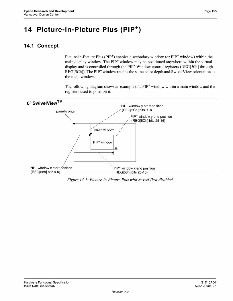
Epson Research and Development Page 155Vancouver Design Center
14 Picture-in-Picture Plus (PIP+)
14.1 Concept
Picture-in-Picture Plus (PIP+) enables a secondary window (or PIP+ window) within the main display window. The PIP+ window may be positioned anywhere within the virtual display and is controlled through the PIP+ Window control registers (REG[50h] through REG[5Ch]). The PIP+ window retains the same color depth and SwivelView orientation as the main window.
The following diagram shows an example of a PIP+ window within a main window and the registers used to position it.
Figure 14-1: Picture-in-Picture Plus with SwivelView disabled
PIP+ window
main-window
PIP+ window y start position
panel’s origin
PIP+ window y end position
PIP+ window x start position PIP+ window x end position
0° SwivelViewTM
(REG[58h] bits 9-0) (REG[58h] bits 25-16)
(REG[5Ch] bits 25-16)
(REG[5Ch] bits 9-0)
Hardware Functional Specification S1D13A04Issue Date: 2006/07/07 X37A-A-001-07
Revision 7.0

Page 156 Epson Research and DevelopmentVancouver Design Center
14.2 With SwivelView Enabled
14.2.1 SwivelView 90°
Figure 14-2: Picture-in-Picture Plus with SwivelView 90° enabled
14.2.2 SwivelView 180°
Figure 14-3: Picture-in-Picture Plus with SwivelView 180° enabled
PIP+ window
main-window
PIP+ window y start position
panel’s origin
PIP+ window y end position
PIP+ window x start positionPIP+ window x end position
90° SwivelViewTM
(REG[58h] bits 25-16) (REG[58h] bits 9-0)
(REG[5Ch] bits 9-0)
(REG[5Ch] bits 25-16)
PIP+ window
main-window
PIP+ window y start position panel’s originPIP+ window y end position
PIP+ window x start positionPIP+ window x end position
180° SwivelViewTM
(REG[58h] bits 25-16) (REG[58h] bits 9-0)
(REG[5Ch] bits 25-16) (REG[5Ch] bits 9-0)
S1D13A04 Hardware Functional SpecificationX37A-A-001-07 Issue Date: 2006/07/07
Revision 7.0

Epson Research and Development Page 157Vancouver Design Center
14.2.3 SwivelView 270°
Figure 14-4: Picture-in-Picture Plus with SwivelView 270° enabled
PIP+ window
main-window
PIP+ window y start position
panel’s origin
PIP+ window y end position
PIP+ window x start positionPIP+ window x end position
270° SwivelViewTM
(REG[58h] bits 25-16)
(REG[5Ch] bits 25-16)
(REG[5Ch] bits 9-0)
(REG[58h] bits 9-0)
Hardware Functional Specification S1D13A04Issue Date: 2006/07/07 X37A-A-001-07
Revision 7.0

Page 158 Epson Research and DevelopmentVancouver Design Center
15 Power Save Mode
A software initiated Power Save Mode is incorporated into the S1D13A04 to accommodate the need for power reduction in the hand-held devices market. This mode is enable via the Power Save Mode Enable bit (REG[14h] bit 4).
Software Power Save Mode saves power by powering down the control signals and stopping display refresh accesses to the display buffer. For programming information on disabling the clocks, see the S1D13A04 Programming Notes and Examples, document number X37A-G-003-xx.
Note1 When power save mode is enabled, the memory controller is powered down and the status of the memory controller is indicated by the Memory Controller Power Save Sta-tus bit (REG[14h] bit 6). However, memory writes are possible during power save mode because the S1D13A04 dynamically enables the memory controller for display buffer writes. This ability does not increase power consumption. 2GPIOs can be accessed, and if configured as outputs can be changed.
After reset, the S1D13A04 is always in Power Save Mode. Software must initialize the chip (i.e. programs all registers) and then clear the Power Save Mode Enable bit. For further details, see the register description for REG[14h] bit 4.
Table 15-1: Power Save Mode Function Summary
Software Power Save
Normal
IO Access Possible? Yes Yes
Memory Writes Possible? Yes1 Yes
Memory Reads Possible? No1 Yes
Look-Up Table Registers Access Possible? Yes Yes
USB Registers Access Possible? No Yes
Display Active? No Yes
LCD I/F Outputs Forced Low Active
PWMCLK Stopped Active
Access Possible for GPIO pins configured for HR-TFT? Forced Low Active
Access Possible for GPIO Pins configured as GPIOs? Yes2 Yes
USB Running? No Yes
S1D13A04 Hardware Functional SpecificationX37A-A-001-07 Issue Date: 2006/07/07
Revision 7.0

Epson Research and Development Page 159Vancouver Design Center
16 Mechanical Data
Figure 16-1: Mechanical Data PFBGA 121-pin Package
All dimensions in mm
10
1.2max
0.
05m
axTOP VIEW
L
K
J
H
G
F
E
D
C
B
A
1 2 3 4 5 6 7 8 9 10 11
0.8
1.0
0.45
BOTTOM VIEW
0.08 M
SIDE VIEW
1.0
-0.15+0.30
10-0
.15
+0.
30
0.35 -0.05+0.10
0.1max
-0.05+0.10
Hardware Functional Specification S1D13A04Issue Date: 2006/07/07 X37A-A-001-07
Revision 7.0

Page 160 Epson Research and DevelopmentVancouver Design Center
Figure 16-2: Mechanical Data TQFP15 128-pin Package
1 32
96 65
64
33
97
128
Index
0~10°
14.0 ± 0.1
14.0
± 0
.1
16.0 ± 0.4
16.0
± 0
.40.4 0.16
1.0
± 0
.1
0.125
1.0
0.5 ± 0.2
All dimensions in mm
-0.03+0.05
1.2
max
0.1
-0.025+0.05
S1D13A04 Hardware Functional SpecificationX37A-A-001-07 Issue Date: 2006/07/07
Revision 7.0

Epson Research and Development Page 161Vancouver Design Center
17 References
The following documents contain additional information related to the S1D13A04. Document numbers are listed in parenthesis after the document name. All documents can be found at the Epson Research and Development Website at www.erd.epson.com.
• 13A04CFG Configuration Utility Users Manual (X37A-B-001-xx)
• 13A04PLAY Diagnostic Utility Users Manual (X37A-B-002-xx)
• 13A04BMP Demonstration Program User Manual (X37A-B-003-xx)
• S1D13A04 Product Brief (X37A-C-001-xx)
• S1D13A04 Wind River WindML v2.0 Display Drivers (X37A-E-002-xx)
• S1D13A04 Linux Console Driver (X37A-E-004-xx)
• S1D13A04 QNX Photon v2.0 Display Drivers (X37A-E-005-xx)
• S1D13A04 Windows CE v3.x Display Drivers (X37A-E-006-xx)
• Interfacing to the Toshiba TMPR3905/3912 Microprocessor (X37A-G-002-xx)
• S1D13A04 Programming Notes And Examples (X37A-G-003-xx)
• S5U13A04B00C Rev. 1.0 Evaluation Board User Manual (X37A-G-004-xx)
• Interfacing to the PC Card Bus (X37A-G-005-xx)
• S1D13A04 Power Consumption (X37A-G-006-xx)
• Interfacing to the NEC VR4102/VR4111 Microprocessors (X37A-G-007-xx)
• Interfacing to the NEC VR4181 Microprocessor (X37A-G-008-xx)
• Interfacing to the Motorola MPC821 Microprocessor (X37A-G-009-xx)
• Interfacing to the Motorola MCF5307 "Coldfire" Microprocessors (X37A-G-010-xx)
• Connecting to the Sharp HR-TFT Panels (X37A-G-011-xx)
• Interfacing to the Motorola MC68VZ328 Dragonball Microprocessor (X37A-G-012-xx)
• Interfacing to the Intel StrongARM SA-1110 Microprocessor (X37A-G-013-xx)
• S1D13A04 Register Summary (X37A-R-001-xx)
Hardware Functional Specification S1D13A04Issue Date: 2006/07/07 X37A-A-001-07
Revision 7.0

Page 162 Epson Research and DevelopmentVancouver Design Center
18 Sales and Technical Support
JapanSeiko Epson CorporationElectronic Devices Marketing Division421-8, Hino, Hino-shiTokyo 191-8501, JapanTel: 042-587-5812Fax: 042-587-5564http://www.epson.co.jp/
Hong KongEpson Hong Kong Ltd.20/F., Harbour Centre25 Harbour RoadWanchai, Hong KongTel: 2585-4600Fax: 2827-4346http://www.epson.com.hk/
TaiwanEpson Taiwan Technology & Trading Ltd.10F, No. 287Nanking East RoadSec. 3, Taipei, TaiwanTel: 02-2717-7360Fax: 02-2712-9164http://www.epson.com.tw/
SingaporeEpson Singapore Pte., Ltd.No. 1Temasek Avenue #36-00Millenia TowerSingapore, 039192Tel: 337-7911Fax: 334-2716http://www.epson.com.sg/
EuropeEpson Europe Electronics GmbHRiesstrasse 1580992 Munich, GermanyTel: 089-14005-0Fax: 089-14005-110http://www.epson-electronics.de/
North AmericaEpson Electronics America, Inc.150 River Oaks ParkwaySan Jose, CA 95134, USATel: (408) 922-0200Fax: (408) 922-0238http://www.eea.epson.com/
S1D13A04 Hardware Functional SpecificationX37A-A-001-07 Issue Date: 2006/07/07
Revision 7.0

Epson Research and Development Page 163Vancouver Design Center
Change Record
X37A-A-001-07 Revision 7, Released: July 7, 2006
• all changes from the previous revision are in Red
• add section 6.2 RESET# Timing
Hardware Functional Specification S1D13A04Issue Date: 2006/07/07 X37A-A-001-07
Revision 7.0