HAR24xy High-Precision Programmable Linear Hall-Effect ...
44
Hardware Documentation HAR ® 24xy High-Precision Dual-Die Programmable Linear Hall-Effect Sensor Family Edition Nov. 4, 2020 DSH000170_002EN Data Sheet
Transcript of HAR24xy High-Precision Programmable Linear Hall-Effect ...

HardwareDocumentation
HAR® 24xy
High-Precision Dual-Die ProgrammableLinear Hall-Effect Sensor Family
Edition Nov. 4, 2020DSH000170_002EN
Data Sheet

DATA SHEET HAR 24xy
TDK-Micronas GmbH Nov. 4, 2020; DSH000170_002EN 2
Copyright, Warranty, and Limitation of Liability
The information and data contained in this document are believed to be accurate and reli-able. The software and proprietary information contained therein may be protected bycopyright, patent, trademark and/or other intellectual property rights of TDK-Micronas. Allrights not expressly granted remain reserved by TDK-Micronas.
TDK-Micronas assumes no liability for errors and gives no warranty representation orguarantee regarding the suitability of its products for any particular purpose due tothese specifications.
By this publication, TDK-Micronas does not assume responsibility for patent infringementsor other rights of third parties which may result from its use. Commercial conditions, prod-uct availability and delivery are exclusively subject to the respective order confirmation.
Any information and data which may be provided in the document can and do vary indifferent applications, and actual performance may vary over time.
All operating parameters must be validated for each customer application by customers’technical experts. Any mention of target applications for our products is made without aclaim for fit for purpose as this has to be checked at system level.
Any new issue of this document invalidates previous issues. TDK-Micronas reservesthe right to review this document and to make changes to the document’s content at anytime without obligation to notify any person or entity of such revision or changes. Forfurther advice please contact us directly.
Do not use our products in life-supporting systems, military, aviation, or aerospaceapplications! Unless explicitly agreed to otherwise in writing between the parties,TDK-Micronas’ products are not designed, intended or authorized for use as compo-nents in systems intended for surgical implants into the body, or other applicationsintended to support or sustain life, or for any other application in which the failure of theproduct could create a situation where personal injury or death could occur.
No part of this publication may be reproduced, photocopied, stored on a retrieval sys-tem or transmitted without the express written consent of TDK-Micronas.
TDK-Micronas Trademarks
– HAL
– HAR
Third-Party Trademarks
All other brand and product names or company names may be trademarks of theirrespective companies.

Contents
Page Section Title
DATA SHEET HAR 24xy
TDK-Micronas GmbH Nov. 4, 2020; DSH000170_002EN 3
4 1.Introduction5 1.1.Major Applications6 1.2.Features
7 2.Ordering Information7 2.1.Device-Specific Ordering Codes
8 3.Functional Description8 3.1.General Function10 3.2.Signal Path and Register Definition10 3.2.1.Signal Path11 3.2.2.Definition of Registers11 3.2.2.1.RAM registers16 3.2.2.2.EEPROM Registers19 3.2.2.3.NVRAM Registers21 3.2.2.4.Setpoint Linearization Accuracy23 3.3.On-Board Diagnostic Features26 3.4.Calibration of the Sensor
27 4.Specifications27 4.1.Outline Dimensions28 4.2.Soldering, Welding and Assembly28 4.3.Pin Connections and Short Descriptions29 4.4.Dimensions of Sensitive Area30 4.5.Absolute Maximum Ratings31 4.6.Storage and Shelf Life31 4.7.Recommended Operating Conditions32 4.8.Characteristics34 4.9.Open-Circuit Detection34 4.10.Overvoltage and Undervoltage Detection35 4.11.Output Short Detection Parameter35 4.12.Output Voltage in Case of Error Detection36 4.13.Magnetic Characteristics37 4.13.1.Definition of Sensitivity Error ES
38 5.Application Notes38 5.1.Application Circuit39 5.2.Measurement of a PWM Output Signal of HAR 245539 5.3.Ambient Temperature40 5.4.Pad Size Layout
41 6.Programming of the Sensor41 6.1.Programming Interface43 6.2.Programming Environment and Tools43 6.3.Programming Information
44 7.Document History
DATA SHEET HAR 24xy
High-Precision Dual-Die Programmable Linear Hall-Effect Sensor Family
Release Note: Revision bars indicate significant changes to the previous edition.
1. Introduction
HAR 24xy is a dual-die programmable linear Hall-effect sensor family. It providesredundancy as it consists of two independent dies stacked in a single package, eachbonded to a separate side of the leadframe. The stacked-die integration ensures thatboth dies occupy the same magnetic field position, thus generating synchronous mea-surement outputs.
The integrated dies are two HAR 24xy, universal magnetic-field sensors with linear ana-log or PWM outputs based on the Hall effect. For both dies major characteristics likemagnetic field range, sensitivity, output quiescent voltage (output voltage at B=0 mT),and output voltage range are programmable in non-volatile memories. The output char-acteristics are ratiometric, which means that the output voltages are proportional to themagnetic flux and the supply voltage. Additionally, both dies offer wire-break detection.
Each die of the HAR 24xy offers 16 setpoints to change the output characteristics fromlinear to arbitrary or vice versa. They feature temperature-compensated Hall plates withspinning current offset compensation, A/D converters, digital signal processing,D/A converters with output driver (HAR 2425), programmable PWM output modules(HAR 2455), EEPROMs with redundancy and lock function for calibration data, serialinterfaces for programming the EEPROMs, and protection devices at all pins. The inter-nal digital signal processing prevents the signal being influenced by analog offsets, tem-perature shifts, and mechanical stress.
The easy programmability allows individual adjustment of each HAR 24xy during thefinal manufacturing process by means of a 2-point calibration, by adjusting the outputsignals directly to the input signal (like mechanical angle, distance, or current). With thiscalibration procedure, the tolerances of the sensor, the magnet-, and the mechanicalpositioning can be compensated in the final assembly.
In addition, the temperature compensation of the Hall ICs can be fit to all common mag-netic materials by programming first- and second-order temperature coefficients of theHall sensor sensitivity.
TDK-Micronas GmbH Nov. 4, 2020; DSH000170_002EN 4

DATA SHEET HAR 24xy
It is also possible to compensate offset drift over temperature generated by the cus-tomer application with a first-order temperature coefficient for the sensors offset. Thisenables operation over the full temperature range with a high accuracy.
The calculation of the individual sensors characteristics and the programming of thecorresponding EEPROMs can easily be done with a PC and the application kit fromMicronas.
The sensors are designed for stringent industrial and automotive applications andare AECQ100 qualified. They operate with typically 5 V supply voltage in the junc-tion temperature range from 40 °C up to 170 °C. The HAR 24xy is available in theultra-thin shrink small outline 14 leads package TSSOP14-1.
1.1. Major Applications
Thanks to its redundancy capability, HAR 24xy can address safety-critical applications.The sensors’ versatile programming characteristics and low temperature drifts make theHAR 24xy the optimal system solution for:
– Angular measurements: throttle position, pedal position, steering torque and EGR applications;
– Distance and linear movement measurements in safety-critical applications
– Magnetic-field and current measurement with specific resolution over different ranges, by appropriate sensitivity programming for each die.
TDK-Micronas GmbH Nov. 4, 2020; DSH000170_002EN 5

DATA SHEET HAR 24xy
1.2. Features
High-precision, redundant, linear Hall-effect sensor with two independent 12-bit analogoutputs (HAR 2425) or with two independent PWM outputs up to 2 kHz (HAR 2455).
Each die provides:
– 16 setpoints for various output signal shapes
– 16 bit digital signal processing
– Multiple customer-programmable magnetic characteristics in a non-volatile memory with redundancy and lock function
– Programmable temperature compensation for sensitivity and offset
– Magnetic-field measurements in the range up to 200 mT
– Low output voltage drifts over temperature
– Active open-circuit (ground and supply line break detection) with 5 k pull-up and pull-down resistor, overvoltage and undervoltage detection
– Programmable clamping function
– Digital readout of temperature and magnetic field information in calibration mode
– Programming and operation of multiple sensors at the same supply line
– Active detection of output short between two sensors
– High immunity against mechanical stress, ESD, and EMC
– Operation from TJ = 40 °C up to 170 °C
– Operation from 4.5 V up to 5.5 V supply voltage in specification and functions up to 8.5 V
– Operation with static magnetic fields and dynamic magnetic fields up to 2 kHz
– Overvoltage and reverse-voltage protection at all pins
– Short-circuit protected push-pull output
TDK-Micronas GmbH Nov. 4, 2020; DSH000170_002EN 6

DATA SHEET HAR 24xy
2. Ordering Information
A Micronas device is available in a variety of delivery forms. They are distinguished by aspecific ordering code:
Fig. 2–1: Ordering Code Principle
For a detailed information, please refer to the brochure: “Micronas Sensors and Control-lers: Ordering Codes, Packaging, Handling”.
2.1. Device-Specific Ordering Codes
The HAR 24xy is available in the following package and temperature variants.
The relationship between ambient temperature (TA) and junction temperature (TJ) isexplained in Section 5.3. on page 39.
For available variants for Configuration (C), Packaging (P), Quantity (Q), and SpecialProcedure (SP) please contact Micronas.
Table 2–1: Available packages
Package Code (PA) Package Type
GP TSSOP14-1
Table 2–2: Available temperature ranges
Temperature Code (T) Temperature Range
A TJ = 40 °C to +170 °C
Table 2–3: Available ordering codes and corresponding package marking
Ordering Code Package Marking
HAR2425GP-A-[C-P-Q-SP] HAR2425A
HAR2455GP-A-[C-P-Q-SP] HAR2455A
XXX NNNN PA-T-C-P-Q-SP
Further Code Elements
Temperature Range
Package
Product Type
Product Group
TDK-Micronas GmbH Nov. 4, 2020; DSH000170_002EN 7

DATA SHEET HAR 24xy
3. Functional Description
3.1. General Function
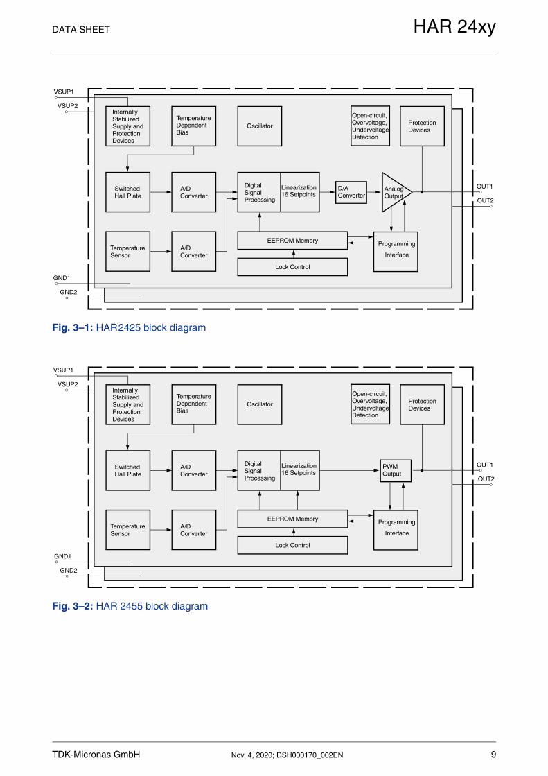
HAR 24xy is a dual-die integrated circuit. The two dies have independent pins for powersupply, ground, and output to guaranty full redundancy. Due to the stacked assemblythey are in the same magnetic field position, and thereby generating synchronous mea-surement outputs. The HAR 2425 provides redundant output voltages proportional tothe magnetic flux through the Hall plates and proportional to the supply voltage (ratio-metric behavior). The HAR 2455 offers PWM outputs.
The external magnetic field component perpendicular to the branded side of the pack-age generates a Hall voltage. The Hall IC is sensitive to magnetic north and south polar-ity. For each die this voltage is converted to a digital value, processed in the Digital Sig-nal Processing unit (DSP) according to the settings of the EEPROM registers,converted back to an analog voltage with ratiometric behavior and buffered by a push-pull output transistor stage (HAR 2425) or output as PWM signal (HAR 2455).
The setting of a LOCK bit disables the programming of the EEPROM memory for alltime. This bit cannot be reset by the customer.
As long as the LOCK bit is not set, the output characteristic can be adjusted by pro-gramming the EEPROM registers. The IC is addressed by modulating the output volt-age.
In the supply voltage range from 4.5 V up to 5.5 V, the sensor generates an analog out-put voltage (HAR 2425) or a PWM signal (HAR 2455). After detecting a command, thesensor reads or writes the memory and answers with a digital signal on the output pin.The analog output is switched off during the communication.
Several sensors in parallel to the same supply and ground line can be programmedindividually. The selection of each sensor is done via its output pin. For further informa-tion, please refer to the document “HAL 24xy, HAR 24xy Programming Guide”.
The open-circuit detection provides a defined output voltage if the VSUP or GND line isbroken.
Internal temperature compensation circuitry and the spinning-current offset compensa-tion enable operation over the full temperature range with minimal changes in accuracyand high offset stability. The circuitry also reduces offset shifts due to mechanical stressfrom the package. In addition, the sensor IC is equipped with overvoltage and reverse-voltage protection at all pins.
TDK-Micronas GmbH Nov. 4, 2020; DSH000170_002EN 8
DATA SHEET HAR 24xy
Fig. 3–1: HAR2425 block diagram
Fig. 3–2: HAR 2455 block diagram
OUT2
VSUP2
GND2
InternallyTemperature
Oscillator
Switched A/D Digital OUT1
VSUP1
GND1
EEPROM Memory
Lock Control
StabilizedSupply andProtectionDevices
DependentBias
ProtectionDevices
Hall Plate Converter SignalProcessing
Temperature A/DSensor Converter
Programming
Interface
Linearization
Open-circuit, Overvoltage,UndervoltageDetection
AnalogOutput
D/AConverter16 Setpoints
OUT2
VSUP2
GND2
InternallyTemperature
Oscillator
Switched A/D Digital OUT1
VSUP1
GND1
EEPROM Memory
Lock Control
StabilizedSupply andProtectionDevices
DependentBias
ProtectionDevices
Hall Plate Converter SignalProcessing
Temperature A/DSensor Converter
Programming
Interface
Linearization
Open-circuit, Overvoltage,UndervoltageDetection
16 SetpointsPWMOutput
TDK-Micronas GmbH Nov. 4, 2020; DSH000170_002EN 9
DATA SHEET HAR 24xy
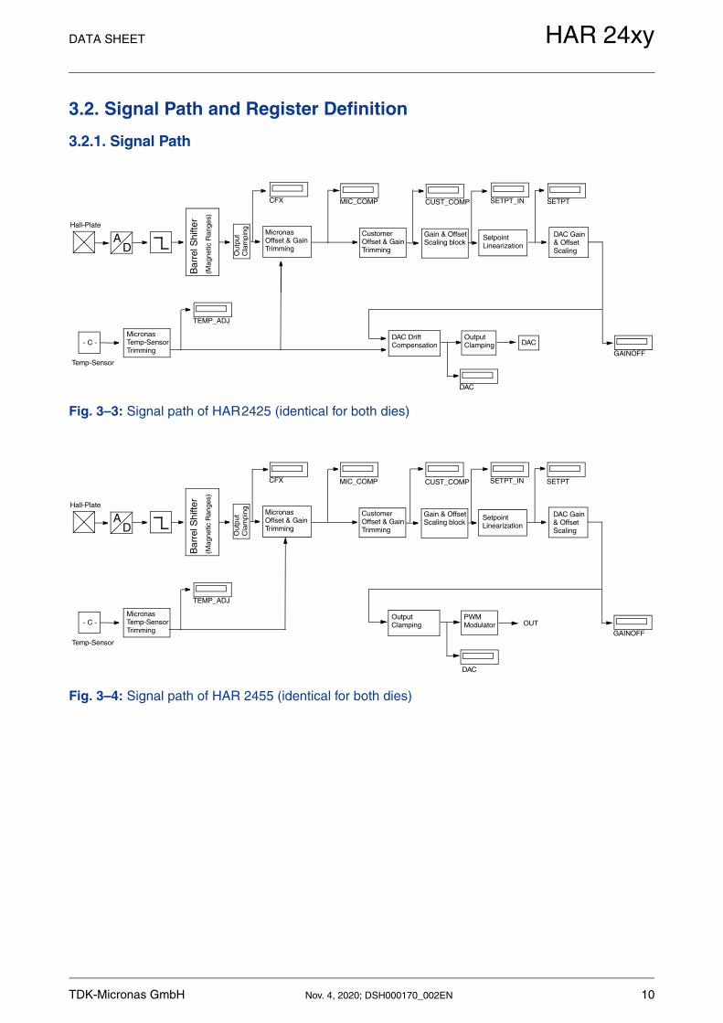
3.2. Signal Path and Register Definition
3.2.1. Signal Path
Fig. 3–3: Signal path of HAR2425 (identical for both dies)
Fig. 3–4: Signal path of HAR 2455 (identical for both dies)
AD
Hall-PlateMicronasOffset & GainTrimming
CustomerOffset & GainTrimming
SetpointLinearization
DAC Gain& OffsetScaling
DAC DriftCompensation
OutputClamping DAC- C -
MicronasTemp-SensorTrimming
Temp-Sensor
CFX MIC_COMP CUST_COMP SETPT
GAINOFF
DAC
TEMP_ADJ
Bar
rel S
hifte
r
(Mag
netic
Ran
ges)
Out
put
Cla
mpi
ng
SETPT_IN
Gain & OffsetScaling block
AD
Hall-PlateMicronasOffset & GainTrimming
CustomerOffset & GainTrimming
SetpointLinearization
DAC Gain& OffsetScaling
Output PWM- C -
MicronasTemp-SensorTrimming
Temp-Sensor
CFX MIC_COMP CUST_COMP SETPT
GAINOFF
TEMP_ADJ
Bar
rel S
hifte
r
(Mag
netic
Ran
ges)
Out
put
Cla
mpi
ng
SETPT_IN
Gain & OffsetScaling block
Clamping Modulator OUT
DAC
TDK-Micronas GmbH Nov. 4, 2020; DSH000170_002EN 10

DATA SHEET HAR 24xy
3.2.2. Definition of Registers
The DSP is the major part of each die and performs the signal conditioning. The param-eters for the DSP are stored in the EEPROM registers. The details are shown in Fig. 3–5 and Fig. 3–7.
Terminology:
GAIN: Name of the register or register value
Gain: Name of the parameter
The sensors signal path contains two kinds of registers. Registers that are readout only(RAM) and programmable registers (EEPROM & NVRAM). The RAM registers containmeasurement data at certain positions of the signal path and the EEPROM registershave influence on the sensors signal processing.
3.2.2.1. RAM registers
TEMP_ADJ
The TEMP_ADJ register contains the calibrated temperature sensor information.TEMP_ADJ can be used for the sensor calibration over temperature. This register has alength of 16 bit and it is two’s-complement coded. Therefore the register value can varybetween 32768...32767.
CFX
The CFX register is representing the magnetic field information directly after A/D con-version, decimation filter and magnetic range (barrel shifter) selection. The register con-tent is not temperature compensated. The temperature variation of this register is spec-ified in Section 4.13. on page 36 by the parameter RANGEABS.
Note During application design, it must be taken into consideration that CFX should never overflow in the operational range of the specific application and especially over the full temperature range. In case of a potential over-flow the barrel shifter should be switched to the next higher range.
This register has a length of 16 bit and it is two’s-complement coded. Therefore the reg-ister value can vary between 32768...32767. CFX register values will increase for pos-itive magnetic fields (south pole) on the branded side of the package (positive CFX val-ues) and it will decrease with negative magnetic field polarity.
TDK-Micronas GmbH Nov. 4, 2020; DSH000170_002EN 11

DATA SHEET HAR 24xy
MIC_COMP
The MIC_COMP register is representing the magnetic field information directly after theMicronas temperature trimming. The register content is temperature compensated andhas a typical gain drift over temperature of 0 ppm/k. Also the offset and its drift overtemperature is typically zero. The register has a length of 16 bit and it is two’s-comple-ment coded. Therefore the register value can vary between 32768...32767.
CUST_COMP
The CUST_COMP register is representing the magnetic field information after the cus-tomer temperature trimming. For HAR 2425 it is possible to set a customer specific gainof second order over temperature as well as a customer specific offset of first order overtemperature. The customer gain and offset can be set with the EEPROM registersTCCO0, TCCO1 for offset and TCCG0...TCCG2 for gain. Details of these registers aredescribed on the following pages.
The register has a length of 16 bit and it is two’s-complement coded. Therefore the reg-ister value can vary between 32768...32767.
SETPT_IN
The SETPT_IN register offers the possibility to read the magnetic field information afterthe scaling of the input signal to the input range of the linearization block. For furtherdetails see the description of the EEPROM registers SCALE_GAIN andSCALE_OFFSET that are described in the next chapter.
The register has a length of 16 bit and it is two’s-complement coded. Therefor the regis-ter value can vary between 32768...32767.
SETPT
The SETPT register offers the possibility to read the magnetic field information after thelinearization of the magnetic field information with 16 setpoints. This information is alsorequired for the correct setting of the sensors DAC GAIN and OFFSET in the followingblock.
The register has a length of 16 bit and it is two’s-complement coded. Therefore the reg-ister value can vary between 32768...32767.
TDK-Micronas GmbH Nov. 4, 2020; DSH000170_002EN 12

DATA SHEET HAR 24xy
GAINOFF
The GAINOFF register offers the possibility to read the magnetic field information afterthe DAC GAIN and OFFSET scaling.
This register has a length of 16 bit and it is two’s-complement coded. Therefore the reg-ister value can vary between 32768...32767.
DAC
The DAC register offers the possibility to read the magnetic field information at the endof the complete signal path. The value of this register is then converted into an analogoutput voltage.
The register has a length of 16 bit and it is two’s-complement coded. Therefore the reg-ister value can vary between 32768...32767.
MIC_ID1 and MIC_ID2
The two registers MIC_ID1 and MIC_ID2 are used by Micronas to store productioninformation like, wafer number, die position on wafer, production lot, etc. Both registershave a length of 16 bit each and are readout only.
PWM Frequency
The PWM frequency is selectable by 2 bits, which are part of the CUSTOMER SETUP register (bits 11:10). The CUSTOMER SETUP register is described on the following pages. The following four dif-ferent frequencies can be used:
Table 3–1: Selectable PWM frequencies
PWM_FREQ Frequency Resolution
Bit 11 Bit 10
1 1 2 kHz 11 bit
0 0 1 kHz 12 bit
0 1 500 Hz 12 bit
1 0 250 Hz 12 bit
TDK-Micronas GmbH Nov. 4, 2020; DSH000170_002EN 13

DATA SHEET HAR 24xy
DIAGNOSIS
The DIAGNOSIS register enables the customer to identify certain failures detected bythe sensor. HAR 2425 performs certain self tests during power-up of the sensor andalso during normal operation. The result of these self tests is stored in the DIAGNOSISregister. DIAGNOSIS register is a 16 bit register.
Details on the sensor self tests can be found in Section 3.3. on page 23.
Bit no. Function Description
15:6 None Reserved
5 State Machine (DSP) Self test
This bit is set to 1 in case that the statemachine self test fails.(continuously running)
4 EEPROM Self test This bit is set to 1 in case that the EEPROM self test fails.(Performed during power-up only)
3 ROM Check This bit is set to 1 in case that ROM parity check fails.(continuously running)
2 AD converter over-flow
This bit is set to 1 in case the input sig-nal is too high, indicating a problem with the magnetic range.
1:0 None Reserved
TDK-Micronas GmbH Nov. 4, 2020; DSH000170_002EN 14

DATA SHEET HAR 24xy
PROG_DIAGNOSIS
The PROG_DIAGNOSIS register enables the customer to identify errors occurring dur-ing programming and writing of the EEPROM or NVRAM memory. The customer musteither check the status of this register after each write or program command or alterna-tively the second acknowledge. Please check the Programming Guide for HAR 24xy.
The PROG_DIAGNOSIS register is a 16 bit register. The following table shows the dif-ferent bits indicating certain errors possibilities.
Bit No. Function Description
15:11 None Reserved
10 Charge Pump Error This bit is set to 1 in case that the internal programming voltage was to low
9 Voltage Error during Program/Erase
This bit is set to 1 in case that the internal supply voltage was to low during program or erase
8 NVRAM Error This bit is set to 1 in case that the programming of the NVRAM failed
7:0 Memory Programming For further information please refer to the Programming Guide for HAL 242x
TDK-Micronas GmbH Nov. 4, 2020; DSH000170_002EN 15

DATA SHEET HAR 24xy
3.2.2.2. EEPROM Registers
Fig. 3–5: Details of EEPROM and Digital Signal Processing for HAR 2425 (equal for both dies).
Fig. 3–6: Details of EEPROM and Digital Signal Processing for HAR 2455 (equal for both dies).
AD
Hall-Plate
Bar
rel S
hifte
r
(Mag
netic
Ran
ges)
MicronasOffset & GainTrimming
CustomerOffset & GainTrimming
SetpointLinearization
DAC Gain& OffsetScaling
DAC DriftCompensation
OutputClamping DAC- C -
MicronasTemp-SensorTrimming
Temp-Sensor
CUSTOMER SETUP
Digital Signal Processing
TCCGxTCCOx
SETPOINTxSCALE_OFFSETSCALE_GAIN
DAC_OFFSETDAC_GAIN
DAC_CMPLODAC_CMPHI
EEPROM
Offset & GainScaling
AD
Hall-Plate
Bar
rel S
hifte
r
(Mag
netic
Ran
ges)
MicronasOffset & GainTrimming
CustomerOffset & GainTrimming
SetpointLinearization
DAC Gain& OffsetScaling
OutputClamping
PWM- C -MicronasTemp-SensorTrimming
Temp-Sensor
CUSTOMER SETUP
Digital Signal Processing
TCCGxTCCOx
SETPOINTxSCALE_OFFSETSCALE_GAIN
DAC_OFFSETDAC_GAIN
DAC_CMPLODAC_CMPHI
EEPROM
Offset & GainScaling
Out
TDK-Micronas GmbH Nov. 4, 2020; DSH000170_002EN 16

DATA SHEET HAR 24xy
CUST_ID1 and CUST_ID2
The two registers CUST_ID1 and CUST_ID2 can be used to store customer informa-tion. Both registers have a length of 16 bit each.
Barrel Shifter (Magnetic Ranges)
The signal path of HAR 24xy contains a Barrel Shifter to emulate magnetic ranges. Thecustomer can select between different magnetic ranges by changing the Barrel Shiftersetting. After decimation filter the signal path has a word length of 22 bit. The BarrelShifter selects 16 bit out of the available 22 bit.
The Barrel Shifter bits are part of the CUSTOMER SETUP register (bits 14...12). TheCUSTOMER SETUP register is described on the following pages.
Note In case that the external field exceeds the magnetic field range the CFX register will be clamped either to 32768 or 32767 depending on the sign of the magnetic field.
Magnetic Sensitivity TCCG
The TCCG (Sensitivity) registers (TCCG0...TCCG2) contain the customer setting tem-perature dependant gain factor. The multiplication factor is a second order polynomialof the temperature.
All three polynomial coefficients have a bit length of 16 bit and they are two’s-comple-ment coded. Therefore the register values can vary between 32768...32767. In casethat the target polynomial is based on normalized values, then each coefficient canvary between 4 ... +4. To store each coefficient into the EEPROM it is necessary tomultiply the normalized coefficients with 32768.
Table 3–2: Relation between Barrel Shifter setting and emulated magnetic range
BARREL SHIFTER
Used bits Typ. magnetic range
0 22...7 not used
1 21...6 200 mT
2 20...5 100 mT
3 19...4 50 mT
4 18...3 25 mT
5 17...2 12 mT
6 16...1 6 mT
TDK-Micronas GmbH Nov. 4, 2020; DSH000170_002EN 17

DATA SHEET HAR 24xy
Example:
– Tccg0 = 0.5102 => TCCG0 = 16719
– Tccg1 = 0.0163 => TCCG1 = 536
– Tccg2 = 0.0144 => TCCG2 = 471
In case that the polynomial was calculated based on not normalized values ofTEMP_ADJ and MIC_COMP, then it is not necessary to multiply the polynomial coeffi-cients with a factor of 32768.
Magnetic Offset TCCO
The TCCO (Offset) registers (TCCO0 and TCCO1) contain the parameters for tempera-ture dependant offset correction. The offset value is a first order polynomial of the tem-perature.
Both polynomial coefficients have a bit length of 16 bit and they are two’s-complementcoded. Therefore the register values can vary between 32768...32767. In case that the target polynomial is based on normalized values, then each coefficientcan vary between 4 ... +4. To store each coefficient into the EEPROM it is necessaryto multiply the normalized coefficients with 32768.
In case that the polynomial was calculated based on not normalized values ofTEMP_ADJ and MIC_COMP, then it is not necessary to multiply the polynomial coeffi-cients.
In addition HAR 24xy features a linearization function based on 16 setpoints. The set-point linearization in general allows to linearize a given output characteristic by applyingthe inverse compensation curve.
Each of the 16 setpoints (SETPT) registers have a length of 16 bit. The setpoints haveto be computed and stored in a differential way. This means that if all setpoints are setto 0, then the linearization is set to neutral and a linear curve is used.
Sensitivity and Offset Scaling before Setpoint Linearization SCALE_GAIN/SCALE_OFFSET
The setpoint linearization uses the full 16 bit number range 0...32767 (only positive val-ues possible). So the signal path should be properly scaled for optimal usage of all 16setpoints.
For optimum usage of the number range an additional scaling stage is added in front ofthe set point algorithm. The setpoint algorithm allows positive input numbers only.
The input scaling for the linearization stage is done with the EEPROM registersSCALE_GAIN and SCALE_OFFSET. The register content is calculated based on thecalibration angles. Both registers have a bit length of 16 bit and are two’s-comple-mented coded.
TDK-Micronas GmbH Nov. 4, 2020; DSH000170_002EN 18

DATA SHEET HAR 24xy
Analog Output Signal Scaling with DAC_GAIN/DAC_OFFSET (HAR 2425)
The required output voltage range of the analog output is defined by the registersDAC_GAIN (Gain of the output) and DAC_OFFSET (Offset of the output signal). Bothregister values can be calculated based on the angular range and the required outputvoltage range. They have a bit length of 16 bit and are two’s-complemented coded.
Output Signal Scaling with DAC_GAIN/DAC_OFFSET (HAR 2455)
The required output duty cycle of the output is defined by the registers DAC_GAIN(Gain of the output) and DAC_OFFSET (Offset of the output signal). Both register val-ues can be calculated based on the angular range and the required output PWM dutycycle range.They have a bit length of 16 bit and are two’s-complemented coded.
Clamping Levels
The clamping levels DAC_CMPHI and DAC_CMPLO define the maximum and mini-mum output voltage of the analog output. The clamping levels can be used to define thediagnosis band for the sensor output. Both registers have a bit length of 16 bit and aretwo’s-complemented coded. Both clamping levels can have values between 0% and100% of VSUP.
3.2.2.3. NVRAM Registers
Customer Setup
The CUST_SETUP register is a 16 bit register that enables the customer to activatevarious functions of the sensor like, customer burn-in mode, diagnosis modes, function-ality mode, customer lock, etc.
Table 3–3: Functions in CUST_SETUP register
Bit No. Function Description
15 None Reserved
14:12 Barrel Shifter Magnetic Range(see Section Table 3–2: on page 17)
11:10 None (HAR 2425) Reserved
PWM frequency setting (HAR 2455)
PWM frequency selection(see Table 3–1 on page 13)
TDK-Micronas GmbH Nov. 4, 2020; DSH000170_002EN 19

DATA SHEET HAR 24xy
9:8 Output Short Detection 0: Disabled1: High & low side over current detection -> OUT = VSUP in error case2: High & low side over current detection -> OUT = GND in error case3: Low side over current detection -> OUT = Tristate in error case
7 Error Band (HAR 2425) Error band selection for locked devices (Customer Lock bit set).0: High error band (VSUP)1: Low error band (GND)The sensor will always go to high error band as long as it is not locked (Customer Lock bit not set).(see Section 4.12. on page 35)
PWM Output Polarity (OP) (HAR 2455)
0: PWM period starts with a highpulse1: PWM period starts with a lowpulse (effective after LC=1)
6 None Reserved
5 FunctionalityMode
Supply voltage supervision0: extended: undervoltage (POR) 3.8 V, overvolt-age 9 V1: normal: undervoltage (POR) 4.2 V, overvoltage 6 V
4 Communication Mode (POUT)
Communication via output pin0: Disabled1: Enabled
3 Overvoltage Detection 0: Overvoltage detection active1: Overvoltage detection disabled
2 Diagnosis Latch Latching of diagnosis bits0: No latching1: Latched till next POR (power-on reset)
1 Diagnosis (HAR 2425) 0: Diagnosis errors force output to the selected error band1: Diagnosis errors do not force output to the selected error band
Diagnosis (HAR 2455) 0: Diagnosis errors force the PWM output into error mode (see Table 3–5 on page 25)1: Diagnosis errors do not force the PWM output into error mode
0 Customer Lock Bit must be set to 1 to lock the sensor memory
Table 3–3: Functions in CUST_SETUP register, continued
Bit No. Function Description
TDK-Micronas GmbH Nov. 4, 2020; DSH000170_002EN 20

DATA SHEET HAR 24xy
The Output Short Detection feature is implemented to detect a short circuit between twosensor outputs. The customer can define how the sensor should signalize a detectedshort circuit (see table above). The time interval in which the sensor is checking for anoutput short and the detectable short circuit current are defined in Section 4.11. onpage 35.
This feature should only be used in case that two sensors are used in one module. Incase that the Output Short Detection is not active both sensors will try to drive their out-put voltage and the resulting voltage will be within the valid signal band.
Note The Output Short Detection feature is only active after setting the Cus-tomer Lock bit and a power-on reset.
3.2.2.4. Setpoint Linearization Accuracy
The set point linearization in general allows to linearize a given output characteristic byapplying the inverse compensation curve.
For this purpose the compensation curve will be divided into 16 segments with equaldistance. Each segment is defined by two setpoints, which are stored in EEPROM.Within the interval, the output is calculated by linear interpolation according to the posi-tion within the interval.
Fig. 3–7: Linearization - Principle
-4 -3 -2 -1 0 1 2 3 4
x 104
-4
-3
-2
-1
0
1
2
3
4x 10
4
Linearized
Distorted
Compensation
TDK-Micronas GmbH Nov. 4, 2020; DSH000170_002EN 21

DATA SHEET HAR 24xy
Fig. 3–8: Linearization - Detail
xnl: non linear distorted input valueyl: linearized value remaining error
The constraint of the linearization is that the input characteristic has to be a monotonicfunction. In addition to that it is recommended that the input does not have a saddlepoint or inflection point, i.e. regions where the input is nearly constant. This wouldrequire a high density of set points
ysn
ysn+1
xnl
yl
input
outp
ut
xsn+1xsn
TDK-Micronas GmbH Nov. 4, 2020; DSH000170_002EN 22

DATA SHEET HAR 24xy
3.3. On-Board Diagnostic Features
The HAR 24xy is made of two completely separated dies, each featuring two groups ofdiagnostic functions. The first group contains basic functions that are always active. Thesecond group can be activated by the customer and contains supervision and self-testsrelated to the signal path and sensor memory.
Table 3–4 describes the HAR 24xy overall behavior in case of wiring faults.
Diagnostic Features that are Always Active:
– Wire-break detection for supply and ground line
– Undervoltage detection
– Thermal supervision of output stage: overcurrent, short circuit, etc. (HAR 2455)
Diagnostic Features that can be Activated by Customer:
– Overvoltage detection
– EEPROM self-test at power-on
– Continuous ROM parity check
– Continuous state machine self-test
– Adder overflow
Failure Indication for HAR 24xy
Each die indicates a fault immediately by switching the output signal to the selectederror band in case that the diagnostic mode is activated by the customer. The customercan select if the output goes to the upper or lower error band by setting bit number 7 inthe CUST_SETUP register (Table 3–3 on page 19). Further details can be found inSection 4.12. on page 35.
The sensor switches the output to tristate if an over temperature is detected by the ther-mal supervision. The sensor switches the output to ground in case of a VSUP wirebreak.
TDK-Micronas GmbH Nov. 4, 2020; DSH000170_002EN 23

DATA SHEET HAR 24xy
Table 3–4: HAR 24xy behavior in case of faults
Short Circuitto 5 V Supply
Short Circuitto GND
Short Circuitto Signal/s
Short Circuitto Battery (12 V)
Open Circuit
Component Power Supply
Normal Component is not supplied: Wire break is active out-put is tied to ground.
Voltage drop across extern pull up resistor is too big to supply compo-nent.
Output is not predictable because device operates below recommended operating con-dition.
Supply above recommended operating con-dition.
See “Absolute Maximum Rat-ings” for stress rating.
Output is in overvoltage condition.
Component is not supplied: Wire break is active out-put is tied to ground.
Component Out Signal/s
External pull-up resistor is bypassed by short which is below allowed minimal pull-up resistance.
See “Recom-mended Oper-ating Conditions” for stress rating.
Out = 5 V sup-ply
Output stage of component is short circuit to ground.
See “Recom-mended Oper-ating Conditions” for stress rating.
Out = GND
Normal Excess of Out-put Voltage over Supply Voltage.
See “Absolute Maximum Rat-ings” for stress rating.
Component output is dis-connected from signal line. Sig-nal line is pulled up to 5 V by external pull-up resistor.
Component Ground
Component is not supplied: Wire break is active out-put is tied to 5 V supply.
Normal Component is not supplied: Wire break is active out-put is tied to 5 V supply.
Component is reversed biased.
See “Absolute Maximum Rat-ings” for stress rating.
Wire break is active Out ? 8.5 V
Component is not supplied: Wire break is active out-put is tied to 5 V supply.
TDK-Micronas GmbH Nov. 4, 2020; DSH000170_002EN 24

DATA SHEET HAR 24xy
Failure Indication for HAR 2455
The HAR 2455 indicates a failure by changing the PWM frequency. The different errorsare then coded in different duty-cycles.
Note In case of an error the sensor changes the selected PWM frequency. Example: During normal operation, the PWM frequency is 1 kHz, in case of an error it is 500 Hz.
Table 3–5: Failure indication for HAR 2455
Failure Mode Frequency Duty-Cycle
EEPROM and state machine self-test
50% 95%
Adder overflow 50% 85%
Overvoltage 50% 75%
Undervoltage 50% 100%
TDK-Micronas GmbH Nov. 4, 2020; DSH000170_002EN 25

DATA SHEET HAR 24xy
3.4. Calibration of the Sensor
For calibration in the system environment, the application kit from Micronas is recom-mended. It contains the hardware for the generation of the serial telegram for program-ming and the corresponding LabView based programming environment for the input ofthe register values (see Section 6.2. on page 43).
For the individual calibration of each sensor in the customer application, a two point cal-ibration is recommended.
A detailed description of the calibration software example provided by Micronas, cali-bration algorithm, programming sequences and register value calculation can be foundin the Application Note “HAR 24xy Programming Guide”.
TDK-Micronas GmbH Nov. 4, 2020; DSH000170_002EN 26

DATA SHEET HAR 24xy
4. Specifications4.1. Outline Dimensions
Fig. 4–1:TSSOP14-1: Plastic Thin Shrink Small Outline Package; 14 pins; 0.9 mm thickness
B ( 20 : 1 )
B
SPECIFICATIONDRAWING-NO.ISSUE DATE(YY-MM-DD)
ISSUEITEM NO.
JEDEC STANDARD
c Copyright 2018 TDK-Micronas GmbH, all rights reserved
20-07-09 CTSSOP143012.1
PACKAGE
TSSOP14-12117_Ver.01
ANSI REVISION DATE(YY-MM-DD)
20-07-09
REV.NO.
1
TYPE NO.
ZGMO-153 F
Product
weight 0.054 g
00
0.210.21
HAR24xy
0.550.33
0.3
0 2.5 5 mm scale
All dimensions are in mm.Physical dimensions do not include moldflash.Sn-thickness might be reduced by mechanical handling.
TOP VIEW
BOTTOM VIEW
Y1
D
X1
A2
X2
Y2
A1
5 �0.1
6.4�
0.2
4.4�
0.1
0.65 0.25 �0.05
Sn plated� 0,2� A B C
1234567
8 9 10 11 12 13 14
PIN 1 INDEX
X2X1
Y1
Y2
3�
0.1
3.6 �0.1
0.39
�0.
11
14° �2°
14°�2°
0.9
�0.
050.
1�
0.05
� 0,1 C
seating plane
0.15�0.05
Sn plated
4°�
4 °
A2
Y2
Y1
A1
� center ofsensitive area
D
seating plane
0.25
gauge plane
0.6�0.1
C
B
A
TDK-Micronas GmbH Nov. 4, 2020; DSH000170_002EN 27

DATA SHEET HAR 24xy
4.2. Soldering, Welding and Assembly
Information related to solderability, welding, assembly, and second-level packaging isincluded in the document “Guidelines for the Assembly of Micronas Packages”. It is available on the Micronas website (http://www.micronas.com/en/service-center/downloads) or on the service portal (http://service.micronas.com).
4.3. Pin Connections and Short Descriptions
All not connected (NC) pins must be connected to GND. In case of redundancy require-ments Micronas recommends the following grounding:
• GND plane1: Pin 1, 3, 5, 7• GND plane2: Pin 8, 10, 12, 14• GND plane3: Pin 4, 11
To avoid a separate GND plane3, please connect either pin 4 or pin 11 to the nearestGND and leave the other pin not connected.
Note To minimize mechanical stress to the dies, the exposed pad should not be soldered!
Pin No
Pin Name Type Short Description
Die 1
2 VSUP1 SUPPLY Supply Voltage die 1
3 GND1 GND Ground die 1
4 GNDePad GNDePad Ground ePad
6 OUT1 I/O Push-Pull Output (HAR 2425)
or
PWM Output (HAR 2455)
and Programming Pin Die 1
Die 2
9 VSUP2 SUPPLY Supply Voltage die 2
11 GNDePad GNDePad Ground ePad
12 GND2 GND Ground die 2
13 OUT2 I/O Push-Pull Output (HAR 2425)
or
PWM Output (HAR 2455)
and Programming Pin Die 2
TDK-Micronas GmbH Nov. 4, 2020; DSH000170_002EN 28

DATA SHEET HAR 24xy
Fig. 4–2: Pin configuration
Fig. 4–3: Top/side view of the package.
4.4. Dimensions of Sensitive Area
250 x 250 µm2
2
12
Pin 13
VSUP1
OUT2
GND23
Pin 6OUT1
GND1
VSUP294 GNDePad
11GNDePad
2
11
VSUP1
GND2
4
6OUT1
GND1
VSUP29
OUT213
5
12
GNDePadGNDePad
1
3
7
10
8
14NC
NC
NC
NC
NC
NC
TDK-Micronas GmbH Nov. 4, 2020; DSH000170_002EN 29

DATA SHEET HAR 24xy
4.5. Absolute Maximum Ratings
Stresses beyond those listed in the “Absolute Maximum Ratings” may cause permanentdamage to the device. This is a stress rating only. Functional operation of the device atthese conditions is not implied. Exposure to absolute maximum rating conditions forextended periods will affect device reliability.
This device contains circuitry to protect the inputs and outputs against damage due tohigh static voltages or electric fields; however, it is advised that normal precautionsmust be taken to avoid application of any voltage higher than absolute maximum-ratedvoltages to this circuit.
All voltages listed are referenced to ground (GND1=GND2=GNDePad).
Symbol Parameter Pin Min. Max. Unit Condition
VSUP Supply Voltage VSUPx 8.518
1018
VV
t < 96 h4) t < 1 h4)
VOUT Output Voltage OUTx 61) 18 V t < 1 h4)
VOUT VSUP Excess of Output Voltage over Supply Voltage
OUTx
VSUPx
7 V t < 1 h4)
TJ Junction Temperature under Bias
50 1902) °C 4)
Tstorage Transportation/Short-Term Storage Temperature
50 150 °C Device only without packing material
Vdie-to-die isolation Dielectric Strength between Both Dies
500 500 V 5)6)
VESD ESD Protection for Single Die
VSUP1
OUT1
GND1
8 +8 kV 3)
VSUP2
OUT2
GND2
1) Internal protection resistor = 50 2) For 96h, please contact Micronas for other temperature requirements.3) HBM AEC-Q-100-002 (100 pF and 1.5 k)4) No cumulated stress5) GNDs galvanic isolation not tested6) Characterized on small sample size
TDK-Micronas GmbH Nov. 4, 2020; DSH000170_002EN 30

DATA SHEET HAR 24xy
4.6. Storage and Shelf Life
Information related to storage conditions of Micronas sensors is included in the docu-ment “Guidelines for the Assembly of Micronas Packages”. It gives recommendationslinked to moisture sensitivity level and long-term storage. It is available on the Micronas website (http://www.micronas.com/en/service-center/downloads) or on the service portal (http://service.micronas.com).
4.7. Recommended Operating Conditions
Functional operation of the device beyond those indicated in the “Recommended Oper-ating Conditions/Characteristics” is not implied and may result in unpredictable behav-ior, reduce reliability and lifetime of the device.
All voltages listed are referenced to ground (GND1=GND2=GNDePad).
Symbol Parameter Pin Min. Typ. Max. Unit Remarks
VSUP Supply Voltage VSUPx 4.55.7
56
5.56.5
V Normal operationDuring programming
IOUT Continuous Output Current
OUTx 1.2 1.2 mA for HAR 2425
1.2 5.5 for HAR 2455
RL Load Resistor OUTx 5.0 10 k pull-up and pull-down resistor for HAR 2425
1 pull-up resistor for HAR 2455
CL Load Capacitance OUTx 0.33 47 600 nF for HAR 2425
0.18 10 for HAR 2455
NPRG Number of Memory Programming Cycles1)
100 cycles 0°C < Tamb < 55°C
TJ Junction Temperature2)
404040
125150170
°C 8000 h 3)
2000 h 3)
1000 h 3)
1) In the EEPROM, it is not allowed to program only one single address within a 'bank' in the memory. In case of programming one single address the complete bank has to be programmed.
2) Depends on the temperature profile of the application. Please contact Micronas for life timecalculations. Time values are not additive.
3) Time values are not cumulative.
TDK-Micronas GmbH Nov. 4, 2020; DSH000170_002EN 31

DATA SHEET HAR 24xy
4.8. Characteristics
at TJ = 40 °C to +170 °C, VSUP1=VSUP2 = 4.5 V to 5.5 V, GND1=GND2=GNDePad =0 V after programming and locking, at Recommended Operating Conditions if not other-wise specified in the column “Conditions”.Typical Characteristics for TJ = 25 °C and VSUP = 5 V.
Symbol Parameter Pin Min. Typ. Max. Unit Conditions
ISUP Supply Current over Temperature Range
VSUPx 7 11 mA
Resolution5) OUTx 12 bit HAR 2425: ratiometric to VSUP 1)
HAR 2455: depends on PWM Period
tr(O) HAR 2425: Step Response Time of Output6)
OUTx 0.5 0.6 ms CL = 10 nF, time from 10% to 90% of final output voltage for a step like signal Bstep from 0 mT to Bmax
HAR 2455: Response Time of Output2)6)
OUTx
1.52.54.58.5
1.835.410.2
ms fPWM = 2 kHzfPWM = 1 kHzfPWM = 500 HzfPWM = 250 Hz
DNL Differential Non-Linearity of D/A Converter4)
OUTx 0.9 0 0.9 LSB Test limit at 25 °C ambient tem-perature
INL Non-Linearity of Output Volt-age over Temperature6)
OUTx 0.3 0.3 %VSUP2)For Vout = 0.35 V ... 4.65 V; VSUP = 5 V ; Linear Setpoint Characteristics
ER Ratiometric Error of Output over Temperature (Error in VOUT / VSUP)
OUTx 0.25 0.25 % Max of [VOUT5 VOUT4.5 and VOUT5.5 VOUT5] at VOUT = 10% and 90% VSUP
Voffset Offset Drift over Temperature Range6)
VOUT(B = 0 mT)25°C VOUT(B = 0 mT)max
OUTx 0 0.1 0.2 %VSUP VSUP = 5 V ; BARREL SHIFTER = 3 (±50 mT)
VOUTCL Accuracy of Output Voltage at Clamping Low Voltage over Temperature Range5)
OUTx 11 11 mV RL = 5 k, VSUP = 5 VSpec values are derived from resolution of the registers DAC_CMPHI/LO and Voffset.
VOUTCH Accuracy of Output Voltage at Clamping High Voltage over Temperature Range5)
OUTx 11 11 mV
VOUTH Upper Limit of Signal Band3) OUTx 93 %VSUP VSUP = 5 V, 1 mA IOUT 1 mA
VOUTL Lower Limit of Signal Band3) OUTx 7 %VSUP VSUP = 5 V, 1 mA IOUT 1 mA
1) Output DAC full scale = 5 V ratiometric, Output DAC offset = 0 V, Output DAC LSB = VSUP/40962) If more than 50% of the selected magnetic field range is used and the temperature compensation is suitable.
INL = VOUT - VOUTLSF with VOUTLSF = Least Square Fit through measured output voltage3) Signal Band Area with full accuracy is located between VOUTL and VOUTH. The sensor accuracy is reduced below
VOUTL and above VOUTH4) External package stress or overmolding might change this parameter5) Guaranteed by Design6) Characterized on small sample size, not tested
TDK-Micronas GmbH Nov. 4, 2020; DSH000170_002EN 32

DATA SHEET HAR 24xy
tPOD Power-Up Time (Time to Reach Certain Output Accuracy)6)
OUTx
1.78.0
msms
Additional error of 1% Full-ScaleFull accuracy
BW Small Signal Bandwidth(3 dB)6)
OUTx 2 kHz
VOUTrms Output Noise Voltage RMS6) OUT 1.5 mV BARREL SHIFTER=3Overall gain in signal path =1External circuitry according to Fig. 5–1 on page 38 with low-noise supply
fPWM PWM Frequency (HAR 2455 only)2)6)
OUT 1.70.850.4250.213
210.50.25
2.31.150.5750.288
kHz Customer programmable
JPWM RMS PWM Jitter(HAR 2455 only)2)6)
OUT 1 2 LSB12 fPWM = 1 kHz
ROUT Output Resistance over Rec-ommended Operating Range
OUTx 1 10 VOUTLmax VOUT VOUTHmin
TSSOP14-1 Package
RthjaRthjaRthjcRthjc
Thermal resistance
Junction to AmbientJunction to AmbientJunction to CaseJunction to Case
1461874749
K/WK/WK/WK/W
determined on 2s2p boarddetermined on 1s0p boarddetermined on 2s2p boarddetermined on 1s0p board
1) Output DAC full scale = 5 V ratiometric, Output DAC offset = 0 V, Output DAC LSB = VSUP/40962) If more than 50% of the selected magnetic field range is used and the temperature compensation is suitable.
INL = VOUT - VOUTLSF with VOUTLSF = Least Square Fit through measured output voltage3) Signal Band Area with full accuracy is located between VOUTL and VOUTH. The sensor accuracy is reduced below VOUTL and above VOUTH4) External package stress or overmolding might change this parameter5) Guaranteed by Design6) Characterized on small sample size, not tested
Symbol Parameter Pin Min. Typ. Max. Unit Conditions
TDK-Micronas GmbH Nov. 4, 2020; DSH000170_002EN 33

DATA SHEET HAR 24xy
4.9. Open-Circuit Detection
at TJ = 40 °C to +170 °C, Typical Characteristics for TJ = 25 °C
4.10. Overvoltage and Undervoltage Detection
at TJ = 40 °C to +170 °C, GND1=GND2=GNDepad=0V, Typical Characteristics for TJ = 25 °C, after programming and locking
Symbol Parameter Pin Min. Typ. Max. Unit Comment
VOUT Output Voltage at Open VSUP Line
OUTx 0 0 0.15 V VSUP = 5 VRL = 10 kto 200 k
0 0 0.2 V VSUP = 5 VRL = 5 kto 10 k
VOUT Output Voltage at Open GND Line
OUTx 4.85 4.9 5.0 V VSUP = 5 VRL = 10 kto 200 k
4.8 4.9 5.0 V VSUP = 5 VRL = 5 kto 10 k
RL: Can be pull-up or pull-down resistor
Symbol Parameter Pin Min. Typ. Max. Unit Test Conditions
VSUP,UV Undervoltage Detection Level
VSUPx 3.3 3.9 4.3 V
VSUP,UVhyst Undervoltage Detection Level Hysteresis1)
VSUPx 200 mV
VSUP,OV Overvoltage Detection Level
VSUPx 5.6 6.2 6.9 V
VSUP,OVhyst Overvoltage Detection LevelHysteresis1)
VSUPx 225 mV
1) Characterized on small sample size, not tested
TDK-Micronas GmbH Nov. 4, 2020; DSH000170_002EN 34

DATA SHEET HAR 24xy
4.11. Output Short Detection Parameter
at TJ = 40 °C to +170 °C, Typical Characteristics for TJ = 25 °C, after programmingand locking
4.12. Output Voltage in Case of Error Detection
at TJ = 40 °C to +170 °C, Typical Characteristics for TJ = 25 °C, after programmingand locking
Fig. 4–4: Behavior of HAR 2425 for different VSUP
Symbol Parameter Pin Min. Typ. Max. Unit Test Conditions
tOCD Over Current Detection Time1)
OUTx 128 µs
tTimeout Time Period without Over Current Detection1)
OUTx 256 ms
IOVC Detectable Output Short Current1)
OUTx 10 mA
1) Characterized on small sample size, not tested
Symbol Parameter Pin Min. Typ. Max. Unit Test Conditions
VSUP,DIAG Supply Voltage required to get defined Output Voltage Level1)
VSUPx 2.1 V
VError,Low Output Voltage Range of Lower Error Band1)
OUTx 0 4 %VSUP VSUP > VSUP,DIAG5 k >= RL <= 200 k
VError,High Output Voltage Range of Upper Error Band1)
OUTx 96 100 %VSUP VSUP > VSUP,DIAG5 k >= RL <= 200 k
1) Characterized on small sample size, not tested
VSUP,DIAG VSUP,UV 5 VSUP,OV VSUP [V]
Vout [V]
: Output Voltage will be between VSUP and GND: CUST_SETUP Register Bit no. 7 set to 1 VOUT 4% VSUP: CUST_SETUP Register Bit no. 7 set to 0 VOUT 96% VSUP
TDK-Micronas GmbH Nov. 4, 2020; DSH000170_002EN 35

DATA SHEET HAR 24xy
4.13. Magnetic Characteristics
at TJ = 40 °C to +170 °C, VSUP1=VSUP2 = 4.5 V to 5.5 V, GND1=GND2=GNDePad =0 V after programming and locking, at Recommended Operation Conditions if not other-wise specified in the column “Conditions”.Typical Characteristics for TJ = 25 °C and VSUPx = 5 V.
Symbol Parameter Pin Min. Typ. Max. Unit Test Conditions
SENS Magnetic Sensitivity VOUT/(2xRANGEABS) mV/mT
Example for HAR 2425:For Barrel_shifter=5 and VOUT = 4 V
RANGEABS = 12 mT
Sensitivity=4 V/(2x12mT= 166 mV/mT typ.
DC/(2xRANGEABS) %DC/mT3)
Example for HAR 2455:For Barrel_shifter=5 and DC = 100%
RANGEABS = 12 mT
Sensitivity=100%/(2x12 mT=
4.2%DC/mT max.
RANGEABS Absolute Range of CFX Register (Magnetic Range)1)
6 200 mT Programmable:See Table 3–2 for relation between barrel shifter and Magnetic Range.
BOffset Magnetic Offset1) OUTx 0.4 0 0.4 mT B = 0 mT, IOUT = 0 mA, TJ = 25 °C,unadjusted sensor
BOffset/T Magnetic Offset Change due to TJ
1)OUTx 5 0 5 T/K B = 0 mT, IOUT = 0 mA
BARREL SHIFTER = 3 (±50 mT)
ES Error in Magnetic Sensitivity2)
OUTx 1% 2.5 % VSUP = 5 V
BARREL SHIFTER = 3 (±50 mT)
1) Characterized on small sample size, not tested.2) ES over the complete temperature range is tested on sample basis.3) DC = duty cycle
TDK-Micronas GmbH Nov. 4, 2020; DSH000170_002EN 36
DATA SHEET HAR 24xy
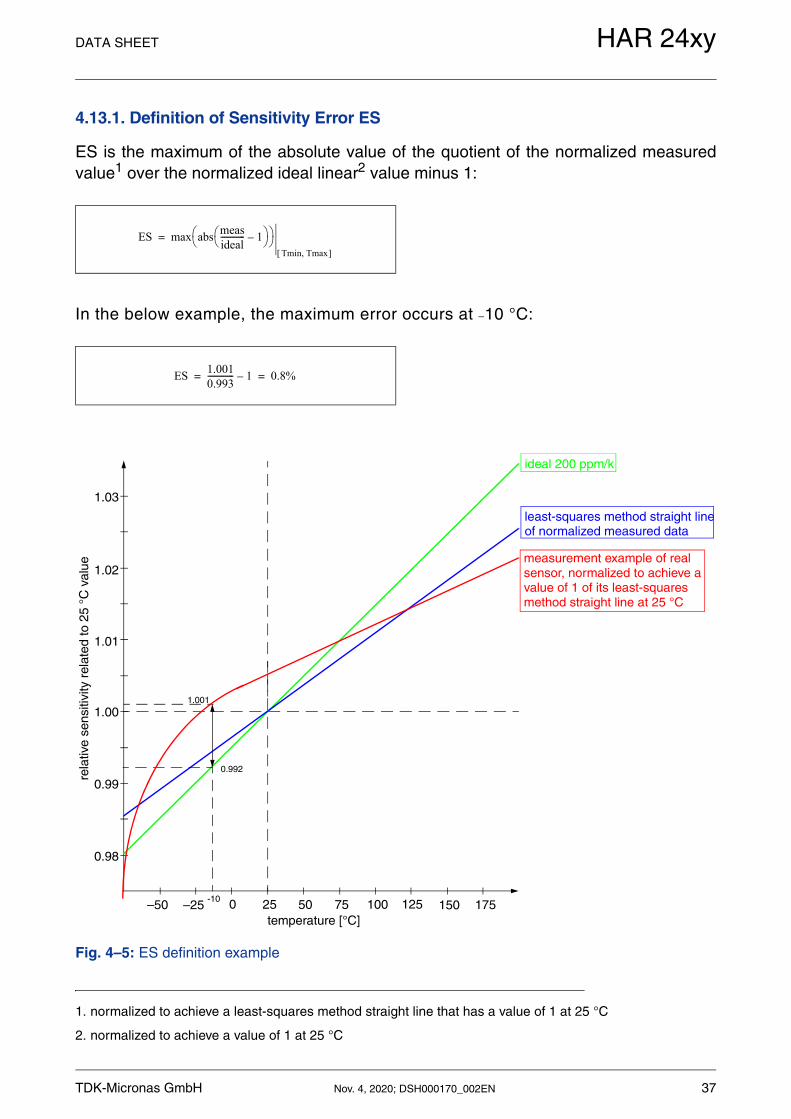
4.13.1. Definition of Sensitivity Error ES
ES is the maximum of the absolute value of the quotient of the normalized measuredvalue1 over the normalized ideal linear2 value minus 1:
In the below example, the maximum error occurs at 10 °C:
Fig. 4–5: ES definition example
1. normalized to achieve a least-squares method straight line that has a value of 1 at 25 °C
2. normalized to achieve a value of 1 at 25 °C
ES max absmeasideal------------ 1–
Tmin, Tmax
=
ES1.0010.993------------- 1– 0.8%= =
50 75 100 125 150 175250–25–50
0.98
0.99
1.00
1.01
1.02
1.03
-10
0.992
1.001
temperature [°C]
rela
tive
sens
itivi
ty r
elat
ed to
25
°C v
alue
ideal 200 ppm/k
least-squares method straight line
measurement example of realsensor, normalized to achieve avalue of 1 of its least-squares
of normalized measured data
method straight line at 25 °C
TDK-Micronas GmbH Nov. 4, 2020; DSH000170_002EN 37
DATA SHEET HAR 24xy
5. Application Notes
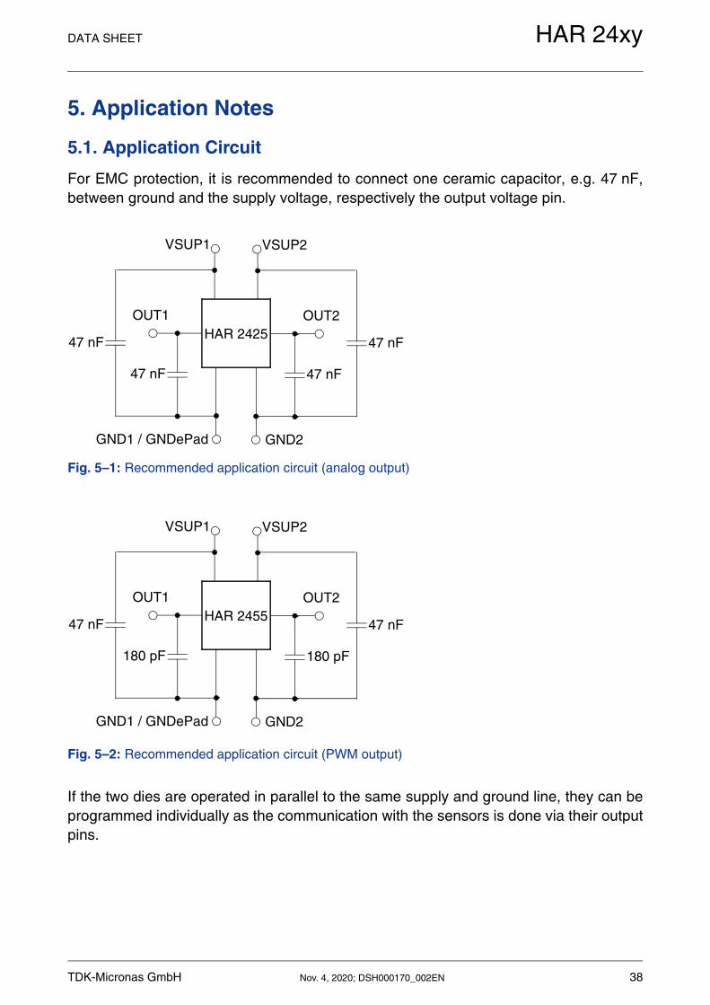
5.1. Application Circuit
For EMC protection, it is recommended to connect one ceramic capacitor, e.g. 47 nF,between ground and the supply voltage, respectively the output voltage pin.
Fig. 5–1: Recommended application circuit (analog output)
Fig. 5–2: Recommended application circuit (PWM output)
If the two dies are operated in parallel to the same supply and ground line, they can beprogrammed individually as the communication with the sensors is done via their outputpins.
OUT1
GND1 / GNDePad
47 nF
VSUP1
47 nFHAR 2425
OUT2
GND2
47 nF
VSUP2
47 nF
OUT1
GND1 / GNDePad
180 pF
VSUP1
47 nFHAR 2455
OUT2
GND2
180 pF
VSUP2
47 nF
TDK-Micronas GmbH Nov. 4, 2020; DSH000170_002EN 38
DATA SHEET HAR 24xy
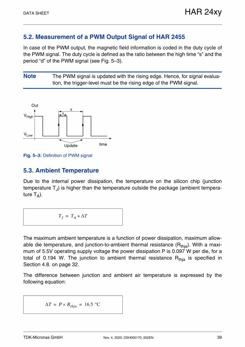
5.2. Measurement of a PWM Output Signal of HAR 2455
In case of the PWM output, the magnetic field information is coded in the duty cycle ofthe PWM signal. The duty cycle is defined as the ratio between the high time “s” and theperiod “d” of the PWM signal (see Fig. 5–3).
Note The PWM signal is updated with the rising edge. Hence, for signal evalua-tion, the trigger-level must be the rising edge of the PWM signal.
Fig. 5–3: Definition of PWM signal
5.3. Ambient Temperature
Due to the internal power dissipation, the temperature on the silicon chip (junctiontemperature TJ) is higher than the temperature outside the package (ambient tempera-ture TA).
The maximum ambient temperature is a function of power dissipation, maximum allow-able die temperature, and junction-to-ambient thermal resistance (Rthja). With a maxi-mum of 5.5V operating supply voltage the power dissipation P is 0.097 W per die, for atotal of 0.194 W. The junction to ambient thermal resistance Rthja is specified inSection 4.8. on page 32.
The difference between junction and ambient air temperature is expressed by thefollowing equation:
Update
Out
time
VHigh
VLow
ds
TJ TA T+=
T P Rthja 16.5 °C= =
TDK-Micronas GmbH Nov. 4, 2020; DSH000170_002EN 39

DATA SHEET HAR 24xy
Note Note: The calculated self-heating of the device is only valid for the Rth test boards. Depending on the application setup, the final results in an applica-tion environment might deviate from these values.
5.4. Pad Size Layout
Fig. 5–4: Recommended pad size dimensions in mm
0.4 mm
4.5 mm
1.35 mm
7.2 mm
0.65 mm
4.3 mm
TDK-Micronas GmbH Nov. 4, 2020; DSH000170_002EN 40

DATA SHEET HAR 24xy
6. Programming of the Sensor
HAR 24xy features two different customer modes. In Application Mode the sensor pro-vides an output signal. In Programming Mode it is possible to change the register set-tings of the sensor.
After power-up the sensor is always operating in the Application Mode. It is switchedto the Programming Mode by a pulse on the sensor output pin.
6.1. Programming Interface
In Programming Mode the sensor is addressed by modulating a serial telegram on thesensors output pin. The sensor answers with a modulation of the output voltage.
A logical “0” is coded as no level change within the bit time. A logical “1” is coded as alevel change of typically 50% of the bit time. After each bit, a level change occurs (seeFig. 6–1).
The serial telegram is used to transmit the EEPROM content, error codes and digitalvalues of the angle information from and to the sensor.
Fig. 6–1: Definition of logical 0 and 1 bit
A description of the communication protocol and the programming of the sensor is avail-able in a separate document (Application: HAR 2425 Programming Guide).
logical 0
or
tbittime tbittime
logical 1
or
tbittime tbittime
50% 50% 50% 50%
TDK-Micronas GmbH Nov. 4, 2020; DSH000170_002EN 41

DATA SHEET HAR 24xy
Table 6–1: Telegram parameters (All voltages are referenced to GND1=GND2=GNDePad = 0 V)
Symbol Parameter Pin Limit Values Unit Test Conditions
Min. Typ. Max.
VOUTL Voltage for Output Low Level during Program-ming through Sensor Output Pin
OUTx 0
0
0.2*VSUP
1
V
V for VSUP = 5 V
VOUTH Voltage for Output High Level during Program-ming through Sensor Output Pin
OUTx 0.8*VSUP
4
VSUP
5.0
V
V for VSUP = 5 V
VSUPProgram VSUP Voltage for EEPROM program-ming (after PROG and ERASE)
VSUPx 5.7 6.0 6.5 V Supply voltage for bidirectional com-munication via out-put pin.
tbittime Biphase Bit Time OUTx 900 1000 1100 µs
Slew rate OUTx 2 V/µs
TDK-Micronas GmbH Nov. 4, 2020; DSH000170_002EN 42
DATA SHEET HAR 24xy
6.2. Programming Environment and Tools
For the programming of HAR 24xy it is possible to use the Micronas tool kit (HAL-APBV1.x & LabView Programming Environment) or the USB kit in order to ease the productdevelopment. The details of programming sequences are also available on request.
6.3. Programming Information
For reliability in service, it is mandatory to set the LOCK bit to one and the POUT bit tozero after final adjustment and programming of HAR 2425.
The success of the LOCK process must be checked by reading the status of the LOCKbit after locking and by a negative communication test after a power on reset.
It is also mandatory to check the acknowledge (first and second) of the sensor or toread/check the status of the PROG_DIAGNOSIS register after each write and storesequence to verify if the programming of the sensor was successful. Please check HAR24xy Programming Guide for further details.
Electrostatic Discharges (ESD) may disturb the programming pulses. Please take pre-cautions against ESD.
Note Please check also the “HAL 24xy Programming Guide”. It contains addi-tional information and instructions about the programming of the devices.
TDK-Micronas GmbH Nov. 4, 2020; DSH000170_002EN 43

DATA SHEET HAR 24xy
TDK-Micronas GmbH Nov. 4, 2020; DSH000170_002EN 44
TDK-Micronas GmbHHans-Bunte-Strasse 19 D-79108 Freiburg P.O. Box 840 D-79008 Freiburg, Germany
Tel. +49-761-517-0 Fax +49-761-517-2174 www.micronas.tdk.com
7. Document History
1. Advance Information: “HAR 24xy High-Precision Dual-Die Programmable Linear Hall-Effect Sensor Family”, May 23, 2015, AI000179_001EN. First release of the advance information.
2. Data Sheet: “HAR 24xy High-Precision Dual-Die Programmable Linear Hall-Effect Sensor Family”, July 14, 2015, DSH000170_001EN. First release of the data sheet.
Major changes:
– Absolute Maximum Ratings on page 30: Value Vdie-to-die isolation
– Recommended Operating Conditions on page 31:junction temperature conditions specified
– Application Circuit on page 38
– Recommended pad size dimensions in mm on page 40
– TSSOP14 tape and reel finishing added
3. Data Sheet: “HAR 24xy High-Precision Dual-Die Programmable Linear Hall-Effect Sensor Family”, Nov. 4, 2020, DSH000170_002EN. Second release of the data sheet.
Major changes:
– Outline Dimensions on page 27:TSSOP14 package drawing updated
– Absolute Maximum Ratings on page 30:Tstorage added
– Recommended Operating Conditions on page 31:new values for parameters IOUT and RL
– Characteristics on page 32: new values for parameters VOUTrms and ISUP
– Magnetic Characteristics on page 36:new values for parameters SENS and RANGEABS