Functionalized Graphene and Graphene Oxide: Materials Synthesis

Graphene-Based Adaptive Thermal CamouflageOmer Salihoglu,† Hasan Burkay Uzlu,† Ozan Yakar,† Shahnaz Aas,† Osman Balci,† Nurbek Kakenov,†
Sinan Balci,‡ Selim Olcum,§ Sefik Suzer,∥ and Coskun Kocabas*,†,⊥
†Department of Physics, Bilkent University, 06800, Ankara Turkey‡Department of Photonics, Izmir Institute of Technology, 35430 Izmir, Turkey§Department of Biological Engineering, Massachusetts Institute of Technology Cambridge Massachusetts 02139-4307, UnitedStates,∥Department of Chemistry, Bilkent University, 06800, Ankara Turkey⊥School of Materials and National Graphene Institute, University of Manchester, Oxford Road, Manchester, M13 9PL, UnitedKingdom
*S Supporting Information
ABSTRACT: In nature, adaptive coloration has beeneffectively utilized for concealment and signaling. Variousbiological mechanisms have evolved to tune the reflectivity forvisible and ultraviolet light. These examples inspire manyartificial systems for mimicking adaptive coloration to matchthe visual appearance to their surroundings. Thermalcamouflage, however, has been an outstanding challengewhich requires an ability to control the emitted thermalradiation from the surface. Here we report a new class ofactive thermal surfaces capable of efficient real-time electrical-control of thermal emission over the full infrared (IR) spectrum without changing the temperature of the surface. Our approachrelies on electro-modulation of IR absorptivity and emissivity of multilayer graphene via reversible intercalation of nonvolatileionic liquids. The demonstrated devices are light (30 g/m2), thin (<50 μm), and ultraflexible, which can conformably coat theirenvironment. In addition, by combining active thermal surfaces with a feedback mechanism, we demonstrate realization of anadaptive thermal camouflage system which can reconfigure its thermal appearance and blend itself with the varying thermalbackground in a few seconds. Furthermore, we show that these devices can disguise hot objects as cold and cold ones as hot in athermal imaging system. We anticipate that, the electrical control of thermal radiation would impact on a variety of newtechnologies ranging from adaptive IR optics to heat management for outer space applications.
KEYWORDS: Graphene optoelectronics, variable emissivity, electrolyte gating, thermal camouflage, thermal emission,multilayer graphene, reconfigurable surface, heat management, IR optics
The ability to control thermal radiation from a hot objecthas both scientific1−5 and technological importance.2,6−8
The radiated thermal energy per unit area from a hot surface ischaracterized by the Stefan−Boltzmann law, P = εσT4 where εis the emissivity of the surface, σ is the Stefan−Boltzmannconstant, and T is the temperature of the surface. Theemissivity is the only material-dependent parameter that varieswith the wavelength and temperature. At thermodynamicequilibrium, Kirchhoff’s radiation law connects the wavelength-specific thermal emissivity with the optical absorption of thesurface as ε(T,λ) = α(T,λ). One can engineer the thermalradiation by coating the surface with photonic crystals5,9−11 orplasmonic structures.12 The dynamic control of thermalradiation, however, requires the ability to alter opticalabsorption via electrical means. Phase change materials,13−16
quantum wells,17 electrochromic dyes,18 ferroelectric materi-als,19 or plasmonic resonators12,20,21 have all been investigatedfor tunable infrared emission. These research efforts ondynamic control of thermal radiation have encountered various
problems such as, low tunability,19,20,22 narrow spectralwindow,17 slow response speed,18 and rigid substrates.17
Electrochromic materials have been the most promisingone,23−25 however, the requirement of a top metallic contactlayer and volatile electrolytes limit their performance (see thebenchmarking in Table S1). These challenges have beenhindering the realization of adaptive thermal camouflagesystems.Graphene provides new perspectives to control electro-
magnetic radiation in a very broad spectral range from visibleto microwave frequencies.26−33 Optical absorption of graphenecan be tuned by electrostatic gating owing to the Pauliblocking.34,35 Although optical response of graphene has beenstudied extensively, the use of graphene for dynamic control of
Received: April 29, 2018Revised: June 5, 2018Published: June 27, 2018
Letter
pubs.acs.org/NanoLettCite This: Nano Lett. 2018, 18, 4541−4548
© 2018 American Chemical Society 4541 DOI: 10.1021/acs.nanolett.8b01746Nano Lett. 2018, 18, 4541−4548
Dow
nloa
ded
via
BIL
KE
NT
UN
IV o
n Ju
ly 1
2, 2
018
at 0
6:06
:11
(UT
C).
Se
e ht
tps:
//pub
s.ac
s.or
g/sh
arin
ggui
delin
es f
or o
ptio
ns o
n ho
w to
legi
timat
ely
shar
e pu
blis
hed
artic
les.

thermal radiation has remained unexplored because of thesmall optical absorption (<2%) in mid-IR region.36 In thiswork, we developed a new class of active thermal surfaces usingmultilayer graphene, which yields significant tunable opticalabsorption in IR region. Because thermal radiation originatesfrom the very top surface, top-gating or electrolyte gatingschemes are not suitable for the control of thermal radiation.These gating methods generate either buried graphene surfacesor low electrostatic doping,34,37 which yields negligible IRmodulation. None of the previously reported graphene devicesby our group and others are suitable for dynamic control ofthermal radiation. Therefore, we introduce a new gatingscheme using an inverse device structure, which leadsintercalation of a nonvolatile ionic liquid into graphene layersfrom the porous substrate. The inverse device configurationyields an uncovered graphene surface with tunable chargedensity and Fermi energy. Figure 1a shows the schematic ofthe active thermal surface consisting of a multilayer-grapheneelectrode on a porous polyethylene (PE) membrane and aback gold-electrode. We synthesized multilayer-graphene onnickel foils using a chemical vapor deposition method and thentransferred them on PE membrane, which is IR transparentand can hold the electrolyte (room-temperature ionic liquid,RTIL).The thermal radiation emitted by the device mainly
originates from the top graphene electrode because theemissivity of gold-coated substrate is very low (<0.01) dueto its highly reflective nature and IR transparency of the PEmembrane. The gold electrode also prevents transmission ofthe background thermal radiation. Figure 1b illustrates theworking principle of the active thermal surface. Under a voltagebias, the ionic liquid intercalates into the graphene layers anddopes them. As a result of doping, the charge density ongraphene increases and Fermi-level shifts to higher energies,which suppress the IR absorption and thus the emissivity of thegraphene electrode.35 Figure 1c,d shows the thermal camera
images of the fabricated device at 0 and 3 V, respectively. At 0V, the temperature profile of the background (author’s hand)can be seen through the device. However, at 3 V the emissivityof the device is significantly suppressed, which screens thebackground temperature profile (Movie S1). The emissivity ofthe device can be switched between high and low states manytimes with a response time of <1 s. These devices are thin,light, and flexible and could easily wrap around everydayobjects (Figures S1 and S2).To quantify the performance of the fabricated active thermal
surfaces, we first placed them on a hot plate at 55 °C andrecorded the thermal images (Figure 2a,b and Figure S1 andMovie 2) at different bias voltages between 0 and 4 V. Notethat the voltage range is limited by the electrochemical windowof the room temperature ionic liquid.38 We obtained the bestperformance with the IL [DEME][TFSI], which yieldsrelatively large electrochemical window up to 4 V. Thethermograms show substantial variation in the thermalappearance, which is quite homogeneous over a large areadevice (10 × 9 cm2). The IR camera renders the thermogramsassuming a constant emissivity of 1. Although the temperatureof the device is the same, the gold electrode appears cold athigh voltages due to its low emissivity.First, we measured the IR spectrum of the emitted radiation
at different bias voltages (Figure 2c) using a Fourier transforminfrared spectrometer (FTIR). The modulation of spectralradiance of the device covers the full mid-infrared range. Theintensity of the spectrum decreases by a factor of 2.5 at 3.5 Vover a broad range. To measure the variation of the totalemitted thermal power from the device, we used a thermopilesensor, which performs a differential measurement with respectto the room temperature (inset in Figure 2d). We recorded theoutput voltage of the sensor as we scanned the bias voltagebetween 0 and 4 V with a scan rate of 0.01 V/s(Supplementary Movie 2). To block the background radiation,we used a 3 in. silicon wafer coated with 100 nm thick gold
Figure 1. Active thermal surfaces. (a) Schematic drawing of the active thermal surface consisting of a multilayer-graphene electrode, a porouspolyethylene membrane soaked with a RTIL, and a back gold-electrode coated on heat resistive nylon. (b) Schematic representation of the workingprinciple of the active thermal surface. The emissivity of the surface is suppressed by intercalation of anions into the graphene layers. (c,d) Thermalcamera images of the device placed on the author’s hand under the voltage bias of 0 and 3 V, respectively.
Nano Letters Letter
DOI: 10.1021/acs.nanolett.8b01746Nano Lett. 2018, 18, 4541−4548
4542

film having very low emissivity (<0.1). The voltage depend-ence of emitted power from the device is shown in Figure 2d.We observed a clear steplike behavior with a threshold voltageof 2 V. The emitted thermal power is reduced by a factor of 2.5at a bias voltage of 3.5 V. These numbers agree very well withthe spectral measurements.To calculate the emissivity of the device, we used a carbon
nanotube forest as a reference black surface having emissivityclose to 1 (Figure S3).39 The extracted emissivity of themultilayer graphene at 10 μm is reduced from 0.76 down to0.33 as we scanned the voltage from 0 to 3.5 V (scattered plotin Figure 2d). Variation of the total radiated power and theextracted emissivity values show similar voltage dependenceindicating that the variation of emissivity with the bias voltageis nearly constant over the mid-IR range. The intercalationprocess is reversible and the device can be switched betweenhigh and low emissivity values with a time constant of 0.5 s.We observed a small shift in the threshold voltage due tohysteresis in the intercalation process.Our results suggest that the observed suppression of the
emissivity is due to the suppression of IR absorption ofmultilayer graphene via intercalation of ionic liquid. To furtherquantify the intercalation process, we measured variation of thesheet resistance of ML−graphene using four-point resistivitymethod (inset in Figure 2e). Similarly, the sheet resistance ofthe graphene electrode shows a step like variation from 33 Ωdown to 0.6 Ω (Figure 2e). The sheet resistance and theemissivity of ML−graphene are correlated. As the layernumber increases, both sheet resistance and emissivitydecrease (Figure S4). To gain more insight into themechanism behind the electrical control of thermal radiation,we performed in situ optical characterization of the ML−graphene electrodes (Figures S5 and S6). We observed that thetransmittance of ML−graphene decreases substantially where-as the reflectivity increases due to the high level of doping. Wealso tested similar devices with single-layer graphene and
observed slight modulation (<2% increase) of thermalradiation due to enhanced interband absorption (Figure S7).These results and our electromagnetic simulations reveal thatboth interband and intraband transitions of the ML−graphenecontribute to the observed emissivity modulation in the IRspectrum35,40,41 (Figure S8). The tunable high mobility freecarriers on graphene layers are responsible for the control ofthe emissivity.42,43
Using the nonvolatile RTIL electrolyte allows us to operatethese devices also in ultrahigh vacuum conditions. This abilityis critical for some special applications such as active thermalshields for outer space applications,23 as well as utilization ofsurface characterization tools such as X-ray photoelectronspectroscopy (XPS), which can elucidate the operation of thedevices in a chemically specific fashion. Although, intercalationof graphitic materials with metallic ions has been extensivelystudied,40 intercalation of ionic liquids remains relativelyunexplored.38 Our device layout (Figure 3a) provides a uniqueadvantage to characterize the intercalation process. The ionicliquid contains two nitrogen atoms (Figure 3b), one with apositive charge (quaternized nitrogen) and the other with anegative charge (imide nitrogen), which yield two well-resolved N 1s peaks. Figure 3c shows the recorded C 1s, N1s, and F 1s region of XPS spectra at different bias voltages.These spectral evolutions provide a wealth of informationabout the operation of the device. The appearance of N 1s andF 1s peaks after 1.5 V indicates the onset of the intercalationprocess and the threshold voltage. Because XPS probes thevery top surface (∼10 nm), the appearance of F 1s and N 1speaks shows that the ions can efficiently intercalate the thickactive surface (>100 graphene layers). The intensity of C 1sdecreases with increasing voltage owing to the partial coverageof the top surface with the IL. The C 1s peak of the CF3 groupassociated with IL also appears after the threshold voltage.Although, the graphene surface is grounded, the bindingenergy of C 1s also experiences a small shift with the applied
Figure 2. Voltage-controlled thermal emission. (a,b) Thermal camera images of the fabricated device biased at 0 to 3 V, respectively. The device isplaced on a hot plate and kept at a temperature of 55 °C. (c) Spectra of the thermal radiation from the device at different bias voltages. (d) Voltagedependence of the emitted thermal power (blue line) and extracted emissivity (red scattered data) at the wavelength of 10 μm. The thermopileradiation sensor is placed 1 cm away from the device sitting on a hot plate. The emissivity is calculated using the carbon nanotube forest as areference. The inset shows the experimental setup used for measuring the voltage dependence of thermal radiation. (e) The sheet resistance of themultilayer graphene electrode plotted against the bias voltage. The inset shows the four-point measurement setup.
Nano Letters Letter
DOI: 10.1021/acs.nanolett.8b01746Nano Lett. 2018, 18, 4541−4548
4543
bias from 284.37 to 283.67 eV (Figure 3e) most likely due tothe shift in the Fermi energy of graphene.44 Interestingly, weobserved cointercalation of anions and cations of the ionicliquid with a significant charge imbalance >20% (the ratio ofN− to N+). This charge imbalance (due to mobile and quasi-independent ions) is responsible for electrostatic doping ongraphene layers. When we apply negative bias voltage, thecharge imbalance is reversed (Figure 3d). Our results showthat intercalation of ionic liquid into multilayer graphene yieldseffectively a charge imbalance with a charge excess of about 1ion for ∼200 C atoms of the intercalated active layer (FigureS9). This direct observation of the chemical contents ofintercalate with related electronic properties of the graphenelayers will further guide us to optimize the device operation.To show one promising application of the developed
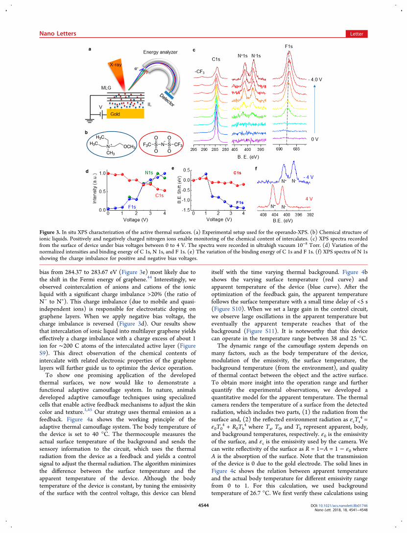
thermal surfaces, we now would like to demonstrate afunctional adaptive camouflage system. In nature, animalsdeveloped adaptive camouflage techniques using specializedcells that enable active feedback mechanisms to adjust the skincolor and texture.1,45 Our strategy uses thermal emission as afeedback. Figure 4a shows the working principle of theadaptive thermal camouflage system. The body temperature ofthe device is set to 40 °C. The thermocouple measures theactual surface temperature of the background and sends thesensory information to the circuit, which uses the thermalradiation from the device as a feedback and yields a controlsignal to adjust the thermal radiation. The algorithm minimizesthe difference between the surface temperature and theapparent temperature of the device. Although the bodytemperature of the device is constant, by tuning the emissivityof the surface with the control voltage, this device can blend
itself with the time varying thermal background. Figure 4bshows the varying surface temperature (red curve) andapparent temperature of the device (blue curve). After theoptimization of the feedback gain, the apparent temperaturefollows the surface temperature with a small time delay of <5 s(Figure S10). When we set a large gain in the control circuit,we observe large oscillations in the apparent temperature buteventually the apparent temperate reaches that of thebackground (Figure S11). It is noteworthy that this devicecan operate in the temperature range between 38 and 25 °C.The dynamic range of the camouflage system depends on
many factors, such as the body temperature of the device,modulation of the emissivity, the surface temperature, thebackground temperature (from the environment), and qualityof thermal contact between the object and the active surface.To obtain more insight into the operation range and furtherquantify the experimental observations, we developed aquantitative model for the apparent temperature. The thermalcamera renders the temperature of a surface from the detectedradiation, which includes two parts, (1) the radiation from thesurface and, (2) the reflected environment radiation as εcTa
4 =ε0T0
4 + R0Tb4 where Ta, T0, and Tb represent apparent, body,
and background temperatures, respectively. ε0 is the emissivityof the surface, and εc is the emissivity used by the camera. Wecan write reflectivity of the surface as R = 1−A = 1 − ε0 whereA is the absorption of the surface. Note that the transmissionof the device is 0 due to the gold electrode. The solid lines inFigure 4c shows the relation between apparent temperatureand the actual body temperature for different emissivity rangefrom 0 to 1. For this calculation, we used backgroundtemperature of 26.7 °C. We first verify these calculations using
Figure 3. In situ XPS characterization of the active thermal surfaces. (a) Experimental setup used for the operando-XPS. (b) Chemical structure ofionic liquids. Positively and negatively charged nitrogen ions enable monitoring of the chemical content of intercalates. (c) XPS spectra recordedfrom the surface of device under bias voltages between 0 to 4 V. The spectra were recorded in ultrahigh vacuum 10−8 Torr. (d) Variation of thenormalized intensities and binding energy of C 1s, N 1s, and F 1s. (e) The variation of the binding energy of C 1s and F 1s. (f) XPS spectra of N 1sshowing the charge imbalance for positive and negative bias voltages.
Nano Letters Letter
DOI: 10.1021/acs.nanolett.8b01746Nano Lett. 2018, 18, 4541−4548
4544
a gold-coated surface (εAu ∼ 0) and carbon-nanotube sample(εCNT ∼ 1). Gold-coated surface always shows the backgroundtemperature due to the perfect IR reflectivity, however, CNTsample shows the actual body temperature due to perfectemissivity (no reflectivity, see Figure S12). Apparent temper-ature of our device varies between these values depending onthe emissivity (ε ∼ 0.3−0.8) and body temperature. Figure 4creveals three intriguing results due to the interplay between theradiation and reflection. First, the dynamic range of the activesurface increases with the temperature difference between thebody and the background. Second, when the body temperatureis the same with background, the apparent temperature of thedevice does not change with the applied voltage. Thesuppression of the emissivity is compensated by the increasingreflectivity. Third, when the body temperature is lower thanthe background, the apparent temperature increases withdecrease in emissivity (increasing voltage). When the voltage isapplied, the cold surface looks hotter. Therefore, the voltage-controlled emissivity and reflectivity of ML−graphene enablesus to design new camouflage systems that can disguise not onlyhot surfaces as cold and but also cold ones as hot in a thermalimaging system. When the surface is hotter than thebackground temperature, the thermal emission is dominant.Suppression of the emissivity of the surface yields colderappearance. However, when the object is colder than thebackground temperature, the reflection of the backgroundradiation is dominant. Increasing concentration of highmobility carrier on the graphene surface under a bias voltageyields hotter appearance in thermal imaging systems.
The thickness of the multilayer graphene is anotherimportant parameter that defines the modulation range ofthe emissivity. We fabricated and characterized a series ofdevices with varying the thickness of the active graphene layer.Figure 4d shows the variation of the measured and calculatedemissivity with the layer number. The maximum emissivity of0.8 can be obtained with 100 layers of graphene. Thicker orthinner films yield less emissivity due to larger reflectivity orsmaller absorption, respectively. In Figure 4d, we also show themeasured emissivity for the doped graphene (at 3.5 V, bluedots). We observed that minimum emissivity also varies withthe layer number, which is likely due to inefficient intercalationfor thick films and residual infrared absorption of dopedgraphene in Pauli blocking regime, which is not fullyunderstood yet. The maximum emissivity modulation can beobtained with around 150 layers of graphene.Finally, we would like to demonstrate an integration scheme
which yields more complex reconfigurable thermal images.Figure 5a shows the multipixel device consisting of large areacontinuous graphene film on PE substrate and 5 × 5 arrays ofindividually addressable gold electrodes deposited on a printedcircuit board. In this layout, the graphene film is wired to theground electrode. The top IR transparent PE layer preventsscratches to the multilayer graphene as well. By controlling thevoltage of a pixel with an external circuit, we were able toconfine the intercalation within the pixel and thus results inmodulation of local emissivity. Figure 5b shows three thermalimages of the device with different voltage configurations. Forlow and high emissivity, we applied −3.5 and 0 V to the pixels,respectively. A temperature contrast of 10 °C can be obtained
Figure 4. Adaptive thermal camouflage systems. (a) Schematic drawing of the device capable of blending its thermal appearance into a variabletemperature background. (b) Time trace of the surface temperature and the apparent temperature of the device. (c) Apparent temperature of asurface plotted against the actual body temperature with different emissivity. The lines show the calculations and the scattered dots represent themeasured data. (d) Layer dependence of the averaged emissivity of multilayer graphene (between 7 and 14 μm wavelengths for the deviceconfiguration given in Figure 1a. The maximum emissivity of 0.8 is obtained around 100 layers. The scattered plot shows the measured values at 0and 3.5 V bias voltages.
Nano Letters Letter
DOI: 10.1021/acs.nanolett.8b01746Nano Lett. 2018, 18, 4541−4548
4545

at each pixel individually (Figure 5c) and can be switched in0.1 s (Figure 5d). The crosstalk between the pixels isnegligible. With this area-selective intercalation, we generatedcomplex thermal images such as a text “HELLO” (see Movie4). The size of the pixels can be scaled down to millimeterwithout a significant crosstalk. These devices can also befabricated by patterning the graphene layer and using differentaddressing mechanisms (see Figures S13 and S14). Theseresults show that our approach can be used to disguise theshape and temperature of objects in thermal imaging systems.Furthermore, these devices can also operate as adaptive IR-mirrors. These devices can operate up to 500 full operationcycles in ambient conditions. However, we observeddegradation in the device performance likely due to hydrationof the ionic liquid in ambient conditions and corrosion of thegold electrode. We believe that reliability of the device can beimproved significantly by a passivation of the device.In conclusion, we have developed a new class of active
thermal surfaces capable of efficient real-time electrical-controlof their thermal emission over the full infrared spectrum. Weshowed that emissivity of multilayer graphene electrodes canbe controlled electrically between 0.8 down to 0.3 with a biasvoltage less than 4 V. Using these active surfaces, we havedemonstrated adaptive camouflage systems that can disguisehot surfaces as cold and cold ones as hot in a thermal imagingsystem. Simplicity of the layered device structure together withthe efficient modulation over broad IR spectrum (from 2 to 25μm) provides an unprecedented ability for adaptive thermalcamouflage. These active surfaces are flexible which enabletheir integration with nonplanar surfaces, such as soft roboticsystems.2 Fabricating these devices on strained elastomers
could provide possibilities for stretchable camouflage devices.Furthermore, these devices can operate at high temperaturesand under high vacuum conditions due to low vapor pressureof the ionic liquids enabling us to monitor the intercalationprocess using X-ray photoelectron spectroscopy. Our resultsprovide a significant step for realization of adaptive thermalmanagement, which could enable new technologies, not onlyfor thermal camouflage but also for adaptive IR optics andadaptive heat shields for satellites.23
Methods. Synthesis and Transfer Printing of MultilayerGraphene. We synthesized multilayer graphene on 50 μmthick Ni foil substrates (Alfa Aesar Item #12722) using achemical vapor deposition system. By adjusting the growthtemperature between 900 to 1050 °C, we controlled thenumber of graphene layers from 60 to 100 layers. During thegrowth, we used 30 sccm of CH4 and 100 sccm Ar and 100sccm H2 gases at ambient pressure. The growth duration was 5min. After cooling the samples to room temperature, we etchedthe Ni foil in a FeCl3 solution (1 M). We transferred the ML−graphene on a clean water surface. The surface of graphene ishydrophobic allowing free-standing ML−graphene film on thewater surface. By immersing the polyethylene membrane intothe water, graphene conformably coats the surface.
Fabrication of Active Thermal Surfaces. After the transferprocess, we injected room-temperature ionic liquid electrolyte[DEME][TFSI] (98.5%, diethylmethyl(2-methoxyethyl)-ammoniumbis(trifluoromethylsulfonyl)imide, Sigma-Aldrich,727679) into the membrane and attached copper wires onthe ML−graphene with a conductive tape. To fabricate thegold electrode, we evaporated 5 nm Ti adhesive layer and 100nm Au layer on 25 μm thick heat resistive nylon using thermal
Figure 5.Multipixel active thermal surface. (a) Photograph of the device consisting of 5 × 5 arrays of individually addressable pixels with an area of2 × 2 cm2. The pixels are defined by the patterned gold electrodes on a printed circuit board and the top graphene layer is wired to the groundelectrode. (b) Thermal camera images of the device (heated to 55 °C) for three different voltage configurations; all pixels are grounded (bottom),all pixels are biased to −3.5 V (middle), and pixels are biased alternatively between 0 and −3.5 V. (c) Line profile of the apparent temperature ofthe device shown in (b). (d) Time-trace of the apparent temperature of the device switched between different voltage configurations. (e) Complexthermal images of text “HELLO” generated by the device.
Nano Letters Letter
DOI: 10.1021/acs.nanolett.8b01746Nano Lett. 2018, 18, 4541−4548
4546
evaporation. We placed the PE membrane on the gold coatednylon.Thermal Imaging. The thermographs of the samples were
recorded using FLIR A40 thermal camera. The camera rendersthe thermographs using constant emissivity of 1.Electrical Measurements. To apply the bias voltage to the
devices, we used Keithley 2400 source measure unit. Werecorded both voltage and charging current during theintercalation and deintercalation processes. To measure sheetresistance, we used 4-point resistance measurement system(Nano Magnetics Inc.), which includes two separate sourcemeters (Keithley 2400 and 2600). The first power supplyapplies the bias voltage between the ML−graphene and thegold electrodes to initiate intercalation and the second onemeasures the sheet resistance.Spectroscopic Characterization. Thermal emission meas-
urements were performed using Bruker Vertex 70v Fouriertransform infrared spectrometer (FTIR). The devices wereplaced on a hot plate at constant temperature of 55 °C. Thehot plate is aligned to the emission port of the spectrometer.We used wide range DLATGS detector (D201/BD) and wide-range beam splitter (T240) in the spectrometer. A ThermoFisher K-Alpha spectrometer was used for XPS character-izations.
■ ASSOCIATED CONTENT*S Supporting InformationThe Supporting Information is available free of charge on theACS Publications website at DOI: 10.1021/acs.nano-lett.8b01746.
Additional details on the experimental setup, character-ization, and analysis of multilayer graphene films,characterization of control devices, detailed theoreticalanalysis, additional experimental results, and comparisonof electrochromic materials used for IR emissivitycontrol (PDF)Real time thermal movie of an operating device placedon the author’s hand (AVI)Real time thermal movie of a large area device placed ona hot plate (AVI)Real time thermal movie of an operating device placedon a hot plate under linear voltage sweep (AVI)Real time thermal movie of the multipixel active thermalsurface (AVI)
■ AUTHOR INFORMATIONCorresponding Author*E-mail: [email protected] Kakenov: 0000-0003-2321-6157Sinan Balci: 0000-0002-9809-8688Sefik Suzer: 0000-0002-5866-2600Coskun Kocabas: 0000-0003-0831-5552Author ContributionsC.K. and O.S. proposed the idea and planned the experiments.B.U synthesized the samples. B.U and O.S. fabricated thedevices. B.U., O.Y., O.S., and C.K. performed the experiments.S.S. performed the XPS measurements and analyzed the data.S.B., S.A., N.K., O.B., and O.S. helped for the measurementsand electromagnetic modeling of the devices. S.O. designed themultipixel device. C.K. analyzed the data and wrote the
manuscript. All authors discussed the results and contributedto the scientific interpretation as well as to the writing of themanuscript.
NotesThe authors declare no competing financial interest.
■ ACKNOWLEDGMENTS
C.K. acknowledges the financial support from EuropeanResearch Counsel for ERC- Consolidator Grant SmartGra-phene 682723. C.K. acknowledges BAGEP Award of theScience Academy.
■ REFERENCES(1) Ramachandran, V. S.; Tyler, C. W.; Gregory, R. L.;RogersRamachandran, D.; Duensing, S.; Pil lsbury, C.;Ramachandran, C. Nature 1996, 379 (6568), 815−818.(2) Morin, S. A.; Shepherd, R. F.; Kwok, S. W.; Stokes, A. A.;Nemiroski, A.; Whitesides, G. M. Science 2012, 337 (6096), 828−832.(3) Schittny, R.; Kadic, M.; Guenneau, S.; Wegener, M. Phys. Rev.Lett. 2013, 110 (19), 195901.(4) Han, T. C.; Bai, X.; Gao, D. L.; Thong, J. T. L.; Li, B. W.; Qiu, C.W. Phys. Rev. Lett. 2014, 112 (5), 054302.(5) Han, T. C.; Bai, X.; Thong, J. T. L.; Li, B. W.; Qiu, C. W. Adv.Mater. 2014, 26 (11), 1731−1734.(6) Yu, C. J.; Li, Y. H.; Zhang, X.; Huang, X.; Malyarchuk, V.; Wang,S. D.; Shi, Y.; Gao, L.; Su, Y. W.; Zhang, Y. H.; Xu, H. X.; Hanlon, R.T.; Huang, Y. G.; Rogers, J. A. Proc. Natl. Acad. Sci. U. S. A. 2014, 111(36), 12998−13003.(7) Raman, A. P.; Anoma, M. A.; Zhu, L.; Rephaeli, E.; Fan, S.Nature 2014, 515 (7528), 540−4.(8) Lampert, C. M. Sol. Energy Mater. 1984, 11 (1−2), 1−27.(9) Luo, C. Y.; Narayanaswamy, A.; Chen, G.; Joannopoulos, J. D.Phys. Rev. Lett. 2004, 93 (21), 213905.(10) Laroche, M.; Carminati, R.; Greffet, J. J. Phys. Rev. Lett. 2006,96 (12), 123903.(11) Han, S. E.; Norris, D. J. Phys. Rev. Lett. 2010, 104 (4), 043901.(12) Tsai, M. W.; Chuang, T. H.; Meng, C. Y.; Chang, Y. T.; Lee, S.C. Appl. Phys. Lett. 2006, 89 (17), 251102.(13) Kats, M. A.; Blanchard, R.; Zhang, S. Y.; Genevet, P.; Ko, C. H.;Ramanathan, S.; Capasso, F. Phys. Rev. X 2013, 3 (4), 041004.(14) Bessiere, A.; Marcel, C.; Morcrette, M.; Tarascon, J. M.; Lucas,V.; Viana, B.; Baffier, N. J. Appl. Phys. 2002, 91 (3), 1589−1594.(15) Sauvet, K.; Sauques, L.; Rougier, A. Sol. Energy Mater. Sol. Cells2009, 93 (12), 2045−2049.(16) Xiao, L.; Ma, H.; Liu, J. K.; Zhao, W.; Jia, Y.; Zhao, Q.; Liu, K.;Wu, Y.; Wei, Y.; Fan, S. S.; Jiang, K. L. Nano Lett. 2015, 15 (12),8365−8370.(17) Inoue, T.; De Zoysa, M.; Asano, T.; Noda, S. Nat. Mater. 2014,13 (10), 928−31.(18) Hutchins, M. G.; Butt, N. S.; Topping, A. J.; Gallego, J.; Milne,P.; Jeffrey, D.; Brotherston, I. Electrochim. Acta 2001, 46 (13−14),1983−1988.(19) Huang, Y.; Boriskina, S. V.; Chen, G. Appl. Phys. Lett. 2014, 105(24), 244102.(20) Vassant, S.; Doyen, I. M.; Marquier, F.; Pardo, F.; Gennser, U.;Cavanna, A.; Pelouard, J. L.; Greffet, J. J. Appl. Phys. Lett. 2013, 102(8), 051127.(21) Schuller, J. A.; Taubner, T.; Brongersma, M. L. Nat. Photonics2009, 3 (11), 658−661.(22) Jun, Y. C.; Luk, T. S.; Ellis, A. R.; Klem, J. F.; Brener, I. Appl.Phys. Lett. 2014, 105 (13), 131109.(23) Demiryont, H.; Moorehead, D. Sol. Energy Mater. Sol. Cells2009, 93 (12), 2075−2078.(24) Li, H.; Xie, K.; Pan, Y.; Yao, M.; Xin, C. Synth. Met. 2009, 159(13), 1386−1388.(25) Mortimer, R. J. Annu. Rev. Mater. Res. 2011, 41, 241−268.
Nano Letters Letter
DOI: 10.1021/acs.nanolett.8b01746Nano Lett. 2018, 18, 4541−4548
4547

(26) Sensale-Rodriguez, B.; Yan, R.; Kelly, M. M.; Fang, T.; Tahy,K.; Hwang, W. S.; Jena, D.; Liu, L.; Xing, H. G. Nat. Commun. 2012,3, 780−786.(27) Liu, M.; Yin, X. B.; Ulin-Avila, E.; Geng, B. S.; Zentgraf, T.; Ju,L.; Wang, F.; et al. Nature 2011, 474 (7349), 64−67.(28) Balci, O.; Polat, E. O.; Kakenov, N.; Kocabas, C. Nat. Commun.2015, 6, 6628.(29) Shi, C.; Mahlmeister, N. H.; Luxmoore, I. J.; Nash, G. R. NanoRes. 2017, 10, 1−7.(30) Barnard, H. R.; Zossimova, E.; Mahlmeister, N. H.; Lawton, L.M.; Luxmoore, I. J.; Nash, G. R. Appl. Phys. Lett. 2016, 108 (13),131110.(31) Mahlmeister, N. H.; Lawton, L. M.; Luxmoore, I. J.; Nash, G. R.Appl. Phys. Express 2016, 9 (1), 012105.(32) Balci, O.; Kakenov, N.; Kocabas, C. Appl. Phys. Lett. 2017, 110(16), 161102.(33) Balci, O.; Kakenov, N.; Karademir, E.; Balci, S.; Cakmakyapan,S.; Polat, E. O.; Caglayan, H.; Ozbay, E.; Kocabas, C. Science Advances2018, 4 (1), eaao1749.(34) Polat, E. O.; Kocabas, C. Nano Lett. 2013, 13 (12), 5851−5857.(35) Bao, W. Z.; Wan, J. Y.; Han, X. G.; Cai, X. H.; Zhu, H. L.; Kim,D. H.; Ma, D. K.; Xu, Y. L.; Munday, J. N.; Drew, H. D.; Fuhrer, M.S.; Hu, L. B. Nat. Commun. 2014, 5, 4224.(36) Brar, V. W.; Sherrott, M. C.; Jang, M. S.; Kim, S.; Kim, L.; Choi,M.; Sweatlock, L. A.; Atwater, H. A. Nat. Commun. 2015, 6, 7032.(37) Polat, E. O.; Balci, O.; Kocabas, C. Sci. Rep. 2015, 4, 6484.(38) Armand, M.; Endres, F.; MacFarlane, D. R.; Ohno, H.; Scrosati,B. Nat. Mater. 2009, 8 (8), 621−629.(39) Mizuno, K.; Ishii, J.; Kishida, H.; Hayamizu, Y.; Yasuda, S.;Futaba, D. N.; Yumura, M.; Hata, K. Proc. Natl. Acad. Sci. U. S. A.2009, 106 (15), 6044−6047.(40) Dresselhaus, M.; Dresselhaus, G. Adv. Phys. 1981, 30 (2), 139−326.(41) Hennig, G. J. Chem. Phys. 1965, 43 (4), 1201−1206.(42) Solanki, A. K.; Kashyap, A.; Nautiyal, T.; Auluck, S.; Khan, M.A. Solid State Commun. 1996, 100 (9), 645−649.(43) Taft, E. A.; Philipp, H. R. Phys. Rev. 1965, 138 (1A), A197.(44) Copuroglu, M.; Aydogan, P.; Polat, E. O.; Kocabas, C.; Suzer,S. Nano Lett. 2014, 14 (5), 2837−2842.(45) Kreit, E.; Mathger, L. M.; Hanlon, R. T.; Dennis, P. B.; Naik, R.R.; Forsythe, E.; Heikenfeld, J. J. R. Soc., Interface 2013, 10 (78),20120601.
Nano Letters Letter
DOI: 10.1021/acs.nanolett.8b01746Nano Lett. 2018, 18, 4541−4548
4548