NANO EXPRESS Open Access Silicon nanowires prepared by electron
JOURNAL OF APPLIED PHYSICS VOLUME 94, NUMBER 9 1 NOVEMBER 2003
Gold catalyzed growth of silicon nanowires by plasma enhanced chemicalvapor deposition
S. Hofmann,a) C. Ducati, R. J. Neill, S. Piscanec, and A. C. FerrariDepartment of Engineering, University of Cambridge, Cambridge CB2 1PZ, United Kingdom
J. GengDepartment of Chemistry, University of Cambridge, Cambridge CB2 1EW, United Kingdom
R. E. Dunin-BorkowskiDepartment of Materials Science and Metallurgy, University of Cambridge, Cambridge CB2 3QZ, UnitedKingdom
J. RobertsonDepartment of Engineering, University of Cambridge, Cambridge CB2 1PZ, United Kingdom
~Received 7 April 2003; accepted 7 August 2003!
Silicon nanowires were selectively grown at temperatures below 400 °C by plasma enhancedchemical vapor deposition using silane as the Si source and gold as the catalyst. A detailed growthstudy is presented using electron microscopy, focused ion beam preparation, and Ramanspectroscopy. A radio-frequency plasma significantly increased the growth rate. The Si nanowiresshow an uncontaminated, crystalline silicon core surrounded by a 2-nm-thick oxide sheath. Theas-grown diameters are small enough for the observation of quantum confinement effects. Plasmaactivation could allow a further decrease in deposition temperature. A growth model for plasmaenhanced nanowire growth is discussed. ©2003 American Institute of Physics.@DOI: 10.1063/1.1614432#
anna
icalshon
asianir
lylte
e
n-ldchod
orrin
tue
Ws:
odel
wth
vehis
aturestem
less
idewce,ast
ofby
epo-n
ore-te,n
I. INTRODUCTION
Crystalline nanostructures such as nanotubes and nwires offer unique access to low-dimensional physics, athey can be used as nanotechnology building blocks to rehigher device integration densities than conventional fabrtion methods.1,2 A great advantage of synthetic nanocrystis that they inherently grow in nanometer size, without tneed of complicated lithography processes. One-dimensinanomaterials could play a key role in nanotechnology,well as provide model systems to demonstrate quantumeffects. However, their small size makes the assemblyintegration difficult, so nanostructures will not realize thefull potential until their growth can be controlled accurate
Nanowires have recently attracted attention as an anative system to carbon nanotubes~CNTs!.3 The extensivestudy of CNTs in the past decade has hit problems, somwhich might be overcome by using nanowires.3 Siliconnanowires~SiNWs! are particularly attractive due to the cetral role of the silicon semiconductor industry, which wouallow Si nanowires to be implemented using existing tenologies. The bulk properties of silicon are well understoTherefore, SiNWs offer an ideal basis to study the effectsquantum confinement and possible applications. The catype and concentration in crystalline SiNWs could be cotrolled by doping, as in bulk Si.4 Silicon turns into a directband-gap semiconductor at nanometer size due to quanconfinement,5,6 so it could be used in optoelectronics, unlikbulk Si.
a!Electronic mail: [email protected]
6000021-8979/2003/94(9)/6005/8/$20.00
Downloaded 28 Nov 2006 to 129.169.177.41. Redistribution subject to AI
o-dcha-
ealszed
.r-
of
-.fer-
m
Different methods have been used to synthesize SiNchemical vapor deposition ~CVD!,7 laser-ablation,8
evaporation,9 and solution-based methods.10 Various direc-tional features of these techniques were reported and a mproposed for preferred SiNW growth directions.11 High-temperature laser ablation enables metal-catalyst-free grobased on SiO2 assisted synthesis.12 CVD does require the useof a metal catalyst, but this allows controlled, selectigrowth by prepatterning the metal on the substrate. Tmethod is often based on the vapor–liquid–solid~VLS!idea13 in which various metals, such as Au,7,13 Fe,8,14 Ti,15
and Ga,16 catalytically enhance the growth of SiNWs. Gappears to be the most favorable catalyst for low-temperasynthesis from its phase diagram, because the Ga–Si syhas a very low eutectic temperature.16 However, the diffusiv-ity and possible contamination by the catalyst makes Gafavored, and Ti a more promising catalyst.15
We used Au as a catalyst, as it does not form a silicand the bulk Au/Si eutectic temperature is relatively lo(363 °C) compared to other catalysts, like Fe and Ti. HenAu gives low-temperature growth but it does not leave a fdiffusing impurity.
In this article, we demonstrate the selective growthSiNWs at temperatures below 400 °C. This is achievedusing a commercial plasma enhanced chemical vapor dsition ~PECVD! system typically used to grow silicon thifilms.
The ability to grow at low temperatures is important fdevice integration. We show that a low-power radio frquency ~rf! plasma significantly increases the growth rawithout decreasing the high crystallinity of the as-grow
5 © 2003 American Institute of Physics
P license or copyright, see http://jap.aip.org/jap/copyright.jsp
mteve
en
nsWe
havbln
-
sttat
ar
tAure
at
ptgflo
9zth
nap
rhfo
os
theslle
d to
-
oldno-
asuresin.thateei.teallyrlso
ing
zedeoteata-er
ata-rf
ered-
ughrustr tos is
b-
°C,
6006 J. Appl. Phys., Vol. 94, No. 9, 1 November 2003 Hofmann et al.
structures. As in carbon nanotubes, plasma enhancementallow the growth of SiNWs at lower substratemperatures.17,18 For example, a microwave plasma gaSiNWs without needing a separate heater.16
Focusing on the influence of the Au catalyst, we presa detailed electron microscopy study comparing the usedifferent Au film thicknesses and Au colloidal suspensioQuantum confinement was recently demonstrated in SiNby scanning tunneling microscopy on single, oxide-removSiNWs.19 Here, we show that Raman spectroscopy issimple way to demonstrate phonon confinement effects. Talso allows us to probe quickly and nondestructively theerage diameter of SiNWs. Finally, we discuss possigrowth mechanisms for PECVD and thermally growSiNWs.
II. EXPERIMENTAL DETAILS
A 20-nm-thick SiO2 layer was grown by thermal oxidation or low-temperature electron cyclotron resonance~ECR!onto polishedn-type Si~100! substrates to act as a catalydiffusion barrier. Au was deposited by evaporating Au me~99.99%! from a tungsten boat in a standard evaporator abase pressure below 1026 mbar. The thickness of the Aulayer was determined by profilometry and conductivity mesurements. Au colloidal suspensions were made by theduction of aqueous HAuCl4 solution by sodium citrate a110 °C.20 The resulting Au suspension has clusters ofwith diameter 16 nm610% and contains 5.8 mg of Au pe100 ml H2O. The colloids can be applied directly or with thhelp of a surfactant on the substrates.
The samples were then loaded into the rf parallel plPECVD system~Plasmalab DP 80!. Typically, between 10and 20 samples were loaded at the same time. The samwere heated to 380 °C under vacuum, and allowed to oufor 3 h. The process gases were then admitted at variousrates. The gas flow was maintained for between 15 andmin and pressures between 0.4 and 2.4 mbar. 13.6 MHpower was supplied to create a plasma, except when amal reaction was desired.
The structure and composition of the SiNWs were alyzed by a combination of scanning electron microsco~SEM! ~Jeol 6340 FEGSEM!, high-resolution transmissionelectron microscopy~HRTEM! ~Jeol JEM 4000EX, 400 kV!,energy-dispersive x-ray spectroscopy~EDX!, electron energyloss spectroscopy~EELS! @Philips CM300ST with Gatan im-aging filter~GIF! 2000# and Raman spectroscopy~RenishawMicroRaman 1000, 514.5 nm Ar-ion laser!. For HRTEM,EDX, and EELS analyses, the as-grown samples weremoved from the substrates and dispersed onto 1000 mesgrids, Cu finder grids, or lacey carbon grids. Pt contactspinning individual SiNWs and trench markers were depited or milled on the samples by a focused ion beam~FIB!~FEI 200FX!.
III. RESULTS AND DISCUSSION
In order to observe quantum confinement effects,nanowire core diameter must be reduced to 10 nm or lUsing silane as the Si source gas allows growth of sma
Downloaded 28 Nov 2006 to 129.169.177.41. Redistribution subject to AI
ay
tof.sdais-e
la
-e-
e
lesasw0rf
er-
-y
e-Aur-
es.r
diameter SiNWs and lower growth temperatures compareSiCl4 .7 It is also known that a higher SiH4 partial pressuregives smaller diameter SiNWs.7 Therefore, we used undiluted silane as the precursor gas.
The SiNW growth rate was about 0.2 nm s21 at a silanepressure of 0.4 mbar at 380 °C without a plasma. A gcatalyst layer of more than 3 nm thickness showed no nawire growth at these conditions.
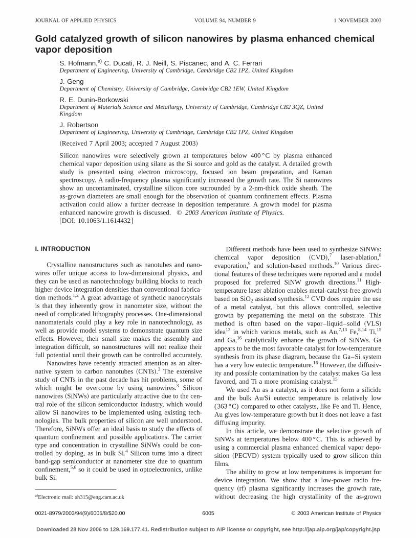
To increase the growth rate, a 13.6 MHz rf plasma wthen used. Figure 1 shows a SEM image of Si nanostructgrown at 0.4 mbar, 380 °C, and 10 W rf power for 15 mThe initial 3-nm-thick Au catalyst layer formed droplets wian average diameter below 30 nm. The nanowires originfrom those droplets, adopting the size of the initial Au nuclHowever, a large fraction of the Au catalyst did not nucleaany structure and is aggregated. The nanowires are typicless than 2mm long and slightly tapered, with a smallediameter at the tip than at the bottom. The taper was areported for Ti-catalyzed SiNWs,21 and it can be attributed tothe uncatalyzed deposition of Si on the sides of wires durgrowth.
The unwanted uncatalyzed Si deposition and catalySiNW growth always coexist. A key role of Au is to makthe catalytic process dominant under given conditions. Nthat low growth temperature enhances the controlled clytic nanowire growth by thermal CVD, as it has a lowactivation energy than uncatalyzed Si deposition.22
Rather than selectively increasing the nanowire~NW!growth rate, an applied rf plasma also enhances the unclytical decomposition of the Si precursor gas. A largepower, therefore, causes the Au catalyst to become covwith a-Si and deactivated. A 3 nm Au film did hardly nucleate any nanowire in a 100 W plasma, and gave only a rosurface, indicating coverage bya-Si. In order to use a higheplasma power for higher plasma activation, the silane mbe diluted by an etchant such as hydrogen. This is similathe PECVD of carbon nanotubes, where an etchant gaused to minimize uncatalyzed surface deposition.23 We arepresently investigating the effect of rf power on SiNWgrowth to reduce the substrate temperature.17,18 This couldallow direct growth of SiNWs onto low-temperature su
FIG. 1. SEM photograph of Si nanostructures grown at 0.4 mbar, 380and 10 W rf power for 15 min.
P license or copyright, see http://jap.aip.org/jap/copyright.jsp

f
6007J. Appl. Phys., Vol. 94, No. 9, 1 November 2003 Hofmann et al.
FIG. 2. SEM photographs of SiNWsgrown at 2 mbar, 380 °C, and 10 W rpower for 90 min from evaporated Authin films of decreasing thickness@~a!:5 nm,~b!: 1 nm,~c!: 0.5 nm# and a Aucolloidal suspension~d!.
n
atneow
mtin
soram
b-
nom-
m.ate,ter
ig.s
-
ve.hlyous
strates and allow their integration in sensitive nanoelectrodevices.
Figure 2 shows SEM images of samples processedmbar, 380 °C, and 10 W rf power for 90 min. A higher silapressure gives a higher catalytical growth rate. The nanires are not tapered. Figures 2~a!–2~c! show the effect of theAu film thickness on growth. In Fig. 2~a!, a 5-nm-thick Aufilm creates worm-like structures of up to 300 nm in diaeter. A Au droplet of similar diameter can be seen on theof the structures indicating catalytical growth. In additiovery straight, small diameter (,15 nm) wires are found. InFig. 2~b!, a 1-nm-thick Au film gives both long straight wireand worm-like structures. The straight wires are now mabundant, and the worm-like structures have a smaller dieter (,100 nm) than in Fig. 2~a!. In Fig. 2~c!, for an Authickness of;0.5 nm, the total yield is lower and the su
Downloaded 28 Nov 2006 to 129.169.177.41. Redistribution subject to AI
ic
2
-
-p,
e-
strate is seen in the background. The SEM image allowsstructural distinction, as all the structures have small diaeters (,20 nm) and are mainly straight.
Figure 2~d! shows SiNWs grown from a colloidal Aususpension. As in previous reports,24 the SiNWs have diam-eters slightly larger than the colloidal diameter of 16 nDespite an initial homogenous dispersion on the substrthe Au colloids do agglomerate, leading to a larger diamedistribution and to some worm-like features similar to F2~b!. The synthesis method for the colloidal gold sol allowsmaller initial diameters.20 Here the similarity to the evaporated Au film is emphasized.
HRTEM supports the structural distinction made aboFor all deposition conditions, straight nanowires are higcrystalline, whereas worm-like structures are amorph@Figs. 3~a!–3~c!, and 3~d!, respectively#. The growth direc-
-
FIG. 3. HRTEM images of as-grownnanowires. A structural distinction between straight, crystalline SiNWs@~a!–~c!# and amorphous, worm-likestructures~d! can be made.P license or copyright, see http://jap.aip.org/jap/copyright.jsp
nsig
s
oe
Å
yths
ithte
on
1p
tommthh
an
00
iths
rys-nd
ingly-at
ted
con-sism-m
asas-be
hees
is.elf-
ns
ch-
heEM
ye
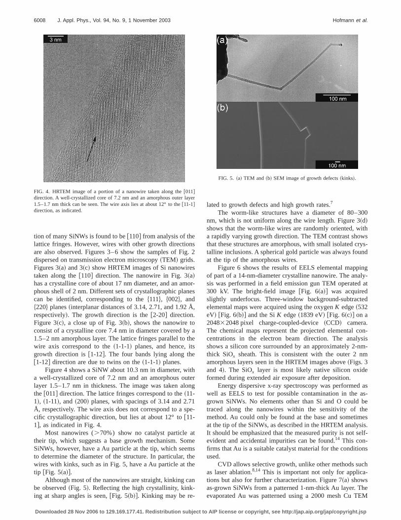
6008 J. Appl. Phys., Vol. 94, No. 9, 1 November 2003 Hofmann et al.
tion of many SiNWs is found to be@110# from analysis of thelattice fringes. However, wires with other growth directioare also observed. Figures 3–6 show the samples of Fdispersed on transmission electron microscopy~TEM! grids.Figures 3~a! and 3~c! show HRTEM images of Si nanowiretaken along the@110# direction. The nanowire in Fig. 3~a!has a crystalline core of about 17 nm diameter, and an amphous shell of 2 nm. Different sets of crystallographic plancan be identified, corresponding to the$111%, $002%, and$220% planes~interplanar distances of 3.14, 2.71, and 1.92respectively!. The growth direction is the@2-20# direction.Figure 3~c!, a close up of Fig. 3~b!, shows the nanowire toconsist of a crystalline core 7.4 nm in diameter covered b1.5–2 nm amorphous layer. The lattice fringes parallel towire axis correspond to the~1-1-1! planes, and hence, itgrowth direction is@1-12#. The four bands lying along the@1-12# direction are due to twins on the~1-1-1! planes.
Figure 4 shows a SiNW about 10.3 nm in diameter, wa well-crystallized core of 7.2 nm and an amorphous oulayer 1.5–1.7 nm in thickness. The image was taken althe @011# direction. The lattice fringes correspond to the~11-1!, ~1-11!, and~200! planes, with spacings of 3.14 and 2.7Å, respectively. The wire axis does not correspond to a scific crystallographic direction, but lies at about 12° to@11-1#, as indicated in Fig. 4.
Most nanowires (.70%) show no catalyst particle atheir tip, which suggests a base growth mechanism. SSiNWs, however, have a Au particle at the tip, which seeto determine the diameter of the structure. In particular,wires with kinks, such as in Fig. 5, have a Au particle at ttip @Fig. 5~a!#.
Although most of the nanowires are straight, kinking cbe observed~Fig. 5!. Reflecting the high crystallinity, kink-ing at sharp angles is seen,@Fig. 5~b!#. Kinking may be re-
FIG. 4. HRTEM image of a portion of a nanowire taken along the@011#direction. A well-crystallized core of 7.2 nm and an amorphous outer la1.5–1.7 nm thick can be seen. The wire axis lies at about 12° to the@11-1#direction, as indicated.
Downloaded 28 Nov 2006 to 129.169.177.41. Redistribution subject to AI
. 2
r-s
,
ae
rg
e-
esee
lated to growth defects and high growth rates.7
The worm-like structures have a diameter of 80–3nm, which is not uniform along the wire length. Figure 3~d!shows that the worm-like wires are randomly oriented, wa rapidly varying growth direction. The TEM contrast showthat these structures are amorphous, with small isolated ctalline inclusions. A spherical gold particle was always fouat the tip of the amorphous wires.
Figure 6 shows the results of EELS elemental mappof part of a 14-nm-diameter crystalline nanowire. The anasis was performed in a field emission gun TEM operated300 kV. The bright-field image@Fig. 6~a!# was acquiredslightly underfocus. Three-window background-subtracelemental maps were acquired using the oxygenK edge~532eV! @Fig. 6~b!# and the SiK edge~1839 eV! @Fig. 6~c!# on a204832048 pixel charge-coupled-device~CCD! camera.The chemical maps represent the projected elementalcentrations in the electron beam direction. The analyshows a silicon core surrounded by an approximately 2-nthick SiOx sheath. This is consistent with the outer 2 namorphous layers seen in the HRTEM images above~Figs. 3and 4!. The SiOx layer is most likely native silicon oxideformed during extended air exposure after deposition.
Energy dispersive x-ray spectroscopy was performedwell as EELS to test for possible contamination in thegrown SiNWs. No elements other than Si and O couldtraced along the nanowires within the sensitivity of tmethod. Au could only be found at the base and sometimat the tip of the SiNWs, as described in the HRTEM analysIt should be emphasized that the measured purity is not sevident and accidental impurities can be found.14 This con-firms that Au is a suitable catalyst material for the conditioused.
CVD allows selective growth, unlike other methods suas laser ablation.8,14 This is important not only for applications but also for further characterization. Figure 7~a! showsas-grown SiNWs from a patterned 1-nm-thick Au layer. Tevaporated Au was patterned using a 2000 mesh Cu T
r
FIG. 5. ~a! TEM and ~b! SEM image of growth defects~kinks!.
P license or copyright, see http://jap.aip.org/jap/copyright.jsp

-e
s
6009J. Appl. Phys., Vol. 94, No. 9, 1 November 2003 Hofmann et al.
FIG. 6. EELS elemental maps of aportion of a 14-nm-diam SiNW. Thebright-field image was acquiredslightly under focus ~a!. Three-window background-subtracted elemental maps were acquired using thoxygenK edge~532 eV! ~b! and the SiK edge ~1839 eV! ~c! on a 204832048 pixel CCD camera. The;2-nm-thick SiOx sheath correspondswell with the outer amorphous layerseen in the HRTEM analysis~Fig. 4!.
tio
c
usctllinheor
obia
niecgngoes
led
in,ar-he
e-ent
ad-ap-
ens
e
ly
e
ctra.
grid as a disposable shadow mask. The process condiwere the same as for the samples in Fig. 2. Figure 7~b! showsa nanowire on the same sample pinned by two Pt contaThe Pt was written by a Ga1 focused ion beam from ametal–organic precursor. Deposited metal contacts areto fix and mark a nanowire. Alternatively, to avoid direbeam exposure, trench markers were set by ion beam minear individual nanowires. The patterned growth togetwith pinning and marking of individual SiNWs was used fsubsequent Raman spectroscopy analysis.
Raman spectroscopy is one of the main tools to prcarbon nanotubes, being able to assess their chirality, deter, and their metallic or semiconducting nature.25 As forCNTs, Raman spectroscopy can become a standard techfor nondestructive characterization of SiNWs and a dirprobe for quantum confinement effects. Raman scatterinan inelastic process in which incoming photons exchaenergy with the crystal vibrational modes. As the photmomentum is very small on the scale of the Brillouin zonin an infinite crystal light can only interact with phononhaving zero momentum, which gives the fundamental setion rule q;0, whereq is the wave vector of the scattere
FIG. 7. SEM photograph of selectively grown SiNWs on a Au patternsubstrate~a!. The pattern allows the pinning of individual nanowires~b!. Ptmetal contacts were written by a Ga1 focused ion beam from a metal–organic precursor.
Downloaded 28 Nov 2006 to 129.169.177.41. Redistribution subject to AI
ns
ts.
ed
gr
em-
quetise
n,
c-
phonon. The selection rule is relaxed for a finite size domadue to the Heisenberg uncertainty principle, allowing the pticipation of phonons near the Brillouin zone center. Tphonon uncertainty goes roughly asDq;1/d, whered is thegrain dimension or NW diameter. As the optic phonon frquency falls away from the zone center in Si, confinemcauses lower-frequency phonons to participate.26,27 Thisgives a downshift of the Si peak and an asymmetric broening. These features can be predicted and calculated byplying the confinement model of Richteret al.27 and Camp-bell and Fauchet26 to a SiNW.
In this article, we only consider the evolution of thmain ;520 cm21 Si first-order Raman peak. Peak positioof ;500– 505 cm21 are reported for wires of;10– 15 nmdiameter,28–30 and it was claimed that this downshift is duto phonon confinement.28–30However, we calculate that 10–15-nm-diam wires should have a downshift of on;1 cm21.31,32 The Raman intensity is given by26,27
I ~v!5E uC~0,q!u2
@v2v~q!#21~G0/2!2 d3q. ~1!
d
FIG. 8. Raman spectra of SiNW for increasing laser power. The spewere acquired with a 1003 objective and a laser power of 0.02–2.6 mW
P license or copyright, see http://jap.aip.org/jap/copyright.jsp

tiuri
t tW
tuiff
tioAre
Wuio
igintacarv
no
-o
aif
ak
of
we
ys-gSi
of
6010 J. Appl. Phys., Vol. 94, No. 9, 1 November 2003 Hofmann et al.
The integration is over the Brillouin zone.C(0,q) is aFourier coefficient of the confinement function, and quanfies theqÞ0 phonons participating in the scattering. In ocaseuC(0,q)u25exp(2q2d2/16p2). We approximate the STO dispersion asv(q)5@A1B cos(qp/2)#0.51D, with A51.7143105 cm22 andB5105 cm22, derived by fittingAand B to the Si TO branch and adjustingD to the bulkreference Si measured with our Raman spectrometer asame experimental conditions used to measure the SiNG0 is the full width at half maximum~FWHM! of the refer-ence Si. In the case of a quantum dotd3q}q2dq, while for acylindrical nanowire with length@diameterd3q}qdq. In-deed, wires are not confined along the axis unlike quandots. Thus, the expected Raman frequency and width dsignificantly in each case.
Several spectra were acquired at 514.5 nm excitawith a 1003 objective and a laser power of 0.02–2.6 mW.power of a few mW is common in micro-Raman measuments and is comparable to that used in previous papers.28–30
Figure 8 shows how, for increasing laser power, the SiNspectra broaden and downshift significantly. The spectrtaken at;2.6 mW closely resembles in shape and positpreviously reported data for wires of similar size.28–30How-ever, this is inconsistent with just phonon confinement. Fure 9 shows that the Anti-Stokes/Stokes intensity ratiocreases with laser power for a SiNW, whereas it is consfor a bare Si substrate. This ratio increases with lotemperature.33 Figure 9 clearly shows that very low powemust be used to avoid local heating of SiNWs. We haimproved the standard confinement function~1! by includinglocal heating effects and the resulting anharmonic phoprocesses by replacingv(q) with v(q, T)5v0(q)1D(T)and G0 with G01G(T). An analytical expression forD(T)andG(T) in bulk Si was given by Balkanskiet al. as a func-tion of four anharmonic constants.34 We calibrated these constants to reproduce the experimental trends on bulk Si onRaman spectrometer in the 83–700 K range.31,32 Figure10~a! shows a measured low-power spectrum of a SiNW,compared to crystalline and amorphous Si. The downsh
FIG. 9. Anti-Stokes/Stokes intensity ratio as a function of the laser pofor a SiNW and bare Si substrate. 100% corresponds to;2.6 mW on thesample.
Downloaded 28 Nov 2006 to 129.169.177.41. Redistribution subject to AI
-
hes.
mer
n
-
mn
--ntl
e
n
ur
st
(;1 cm21! and asymmetric broadening of the SiNW peis evident with respect to the crystalline bulk Si peak@Fig10~b!#. Fitting the SiNW spectrum gives a diameter;9 nm and a local temperature of;300 K @Fig. 10~c!#. This
r
FIG. 10. ~a! Low-power Raman spectrum of a SiNW as compared to crtalline and amorphous Si.~b! Downshift and asymmetric broadenin(FWHMa.FWHMb) of the SiNW Raman peak with respect to the bulkpeak.~c! Fit to the measured SiNW spectrum. The fit gives a diameter;9 nm and a local temperature of;300 K.
P license or copyright, see http://jap.aip.org/jap/copyright.jsp

opt
ribto-gE
lear
-s.m
a
,radn-
mthacsw
i-ich
ws
thingartriwelpega
oAucysth
alreheth
or
e Si
m.c-asto
rate
un-hisoret-
m-ost-re
byturestedlec-andrs
ne-mam-b-s.
IB
pl.
Sci.
.tt.
v. B
d P.
g,
6011J. Appl. Phys., Vol. 94, No. 9, 1 November 2003 Hofmann et al.
diameter is in good agreement with the electron microscresults presented above. This demonstrates confinemenfects in as-grown PECVD SiNWs.
IV. GROWTH MODEL ISSUES
The vapor–liquid–solid process is often used to descthermal growth of metal-catalyzed semiconducnanowires.8,13 Although the individual stages of the VLS reaction can be separated, the detailed processes leadinhigh-aspect-ratio nanostructures are not well understood.sentially, the VLS model consists of~1! catalytic decompo-sition of the source gas on the surface of the metal partic~2! diffusion of Si from the surface through the catalyst pticle or along its surface, and~3! nucleation of the NW andprecipitation of Si into the growing structure. The liquid intermediate, namely, the metal–Si eutectic, is not a necesas solid catalyst particles can also lead to SiNW growth22
Therefore, Au could possibly be used below the equilibriuAu/Si eutectic temperature~corrected by particle-sizeeffects35 and pressure influences! especially under plasmconditions.
The effect of the plasma is to preionize the source gaswell as to provide some local surface heating at low substtemperatures, which enables an efficient adsorption andfusion of silicon atoms. Both effects could explain the icreased growth rate.
A plasma is a nonisothermal condition, so equilibriuthermodynamic arguments need not always apply. InVLS mechanism, the supersaturation on the growth interfdepends on the diameter. Therefore, the Gibbs–Thomequation places a lower limit on the diameter of as-grostructures for thermal growth.36 Accordingly, measuredgrowth rates of silicon whiskers were lower for smaller dameter and a critical diameter was found below whgrowth stops completely.36 In this study, smaller SiNWsshow a higher growth rate than thicker structures andfound a continuous diameter distribution rather than a threold behavior. Following the Gibbs–Thomson equationlower limit for the wire diameter decreases for increassilane pressure.7 Here, for a pressure range of 0.4–2.4 mbwe found no significant change in the SiNW diameter disbution. However, increasing pressure increased the nanogrowth rate. An increased silane pressure appears to stively enhance the catalytical growth process since no taing due to uncatalytical decomposition of the precursorwas seen anymore.
The variation of catalyst thickness had no influencethe diameter of crystalline SiNWs. Instead, a thickerlayer led to the formation of amorphous, worm-like strutures of increasing diameter coexisting with the fewer crtalline SiNWs. This is surprising, as in carbon nanotubescatalyst thickness directly controls the CNT diameter.37 Theworm-like features are catalytically grown since Au wasways found in the tip matching the diameter of the structuThis indicates that diffusive transport of Si through or on tcatalyst particle is fast, supplying Si at a higher rate thancrystallization rate for a given diameter.
Downloaded 28 Nov 2006 to 129.169.177.41. Redistribution subject to AI
yef-
er
tos-
s,-
ity,
asteif-
ee
onn
eh-e
,-ireec-r-s
n
--e
-.
e
Growth directional features of SiNWs are reported fvarious synthesis methods.11 For low growth rates CVDgrown nanowires were seen to adopt the orientation of thsubstrate and grow aligned perpendicular to the surface.7 Forhigher growth rates the growth direction appeared rando7
In this study, despite the crystallinity of the as-grown strutures, no preferential crystallographic growth direction wfound. This may be due to the high growth rate and duethe use of an oxide diffusion barrier screening the substorientation.
Compared to carbon nanotubes, SiNWs have a verystable surface. An oxide layer surrounds all the wires in tstudy. A hydrogen termination was reported to give a mresistant surface.19 On the other hand, a wide range of posgrowth modifications is possible with SiNWs, such as diaeter variation by etching and doping processes. This pgrowth tailoring of properties is attractive for many futuapplications.
V. CONCLUSIONS
Crystalline silicon nanowires have been grownplasma enhanced chemical vapor deposition at temperabelow 400 °C. The Si nanowires show an uncontaminasilicon core surrounded by a 2-nm-thick oxide sheath. Setive growth on prepatterned substrates enabled pinningmarking of individual nanowires. The as-grown diameteare small enough for the observation of quantum confiment effects by low-power Raman spectroscopy. Plasactivation could allow a further decrease in deposition teperature facilitating direct growth on low-temperature sustrates and integration in sensitive nanoelectronic device
ACKNOWLEDGMENTS
The authors wish to thank Dae-Joon Kang for the Fpreparation. Two of the authors~A.C.F. and R.E.D.B.! ac-knowledge the Royal Society for financial support.
1S. J. Wind, J. Appenzeller, R. Martel, V. Derycke, and P. Avouris, ApPhys. Lett.80, 3817~2002!.
2Y. Cui and C. M. Lieber, Science291, 851 ~2001!.3D. Appell, Nature~London! 419, 553 ~2002!.4Y. Cui, X. Duan, J. Hu, and C. M. Lieber, J. Phys. Chem. B104, 5213~2000!.
5L. T. Canham, Appl. Phys. Lett.57, 1046~1990!.6G. D. Sanders and C. Yia-Chung, Phys. Rev. B45, 9202~1992!.7J. Westwater, D. P. Gosain, S. Tomiya, S. Usui, and H. Ruda, J. Vac.Technol. B15, 554 ~1997!.
8A. M. Morales and C. M. Lieber, Science279, 208 ~1998!.9D. P. Yu, Z. G. Bai, Y. Ding, Q. L. Hang, H. Z. Zhang, J. J. Wang, Y. HZou, W. Qian, G. C. Xiong, H. T. Zhou, and S. Q. Feng, Appl. Phys. Le72, 3458~1998!.
10J. D. Holmes, K. P. Johnston, R. C. Doty, and B. A. Korgel, Science287,71 ~2000!.
11T. Y. Tan, S. T. Lee, and U. Gosele, Appl. Phys. A: Mater. Sci. Process.74,423 ~2002!.
12N. Wang, Y. H. Tang, Y. F. Zhang, C. S. Lee, and S. T. Lee, Phys. Re58, R16024~1998!.
13R. S. Wagner and W. C. Ellis, Appl. Phys. Lett.4, 89 ~1964!.14R. J. Barsotti, J. E. Fischer, C. H. Lee, J. Mahmood, C. K. W. Adu, an
C. Eklund, Appl. Phys. Lett.81, 2866~2002!.15T. I. Kamins, R. S. Williams, Y. Chen, Y. L. Chang, and Y. A. Chan
Appl. Phys. Lett.76, 562 ~2000!.
P license or copyright, see http://jap.aip.org/jap/copyright.jsp

pl
va
et
ce
d
, J
.ys
pl
sG
.
n
J.
S.
J.pl.
6012 J. Appl. Phys., Vol. 94, No. 9, 1 November 2003 Hofmann et al.
16M. K. Sunkara, S. Sharma, R. Miranda, G. Lian, and E. C. Dickey, ApPhys. Lett.79, 1546~2001!.
17B. O. Boskovic, V. Stolojan, R. U. A. Khan, S. Haq, and S. R. P. SilNat. Mater.1, 165 ~2002!.
18S. Hofmann, C. Ducati, J. Robertson, and B. Kleinsorge, Appl. Phys. L83, 135 ~2003!.
19D. D. D. Ma, C. S. Lee, F. C. K. Au, S. Y. Tong, and S. T. Lee, Scien299, 1874~2003!.
20J. F. Geng, B. F. G. Johnson, M. D. R. Thomas, D. S. Shephard, anJiang, Inorg. Chim. Acta330, 33 ~2002!.
21T. I. Kamins, X. Li, and R. S. Williams, Appl. Phys. Lett.82, 263 ~2003!.22T. I. Kamins, R. S. Williams, D. P. Basile, T. Hesjedal, and J. S. Harris
Appl. Phys.89, 1008~2001!.23K. B. K. Teo, M. Chhowalla, G. A. J. Amaratunga, W. I. Milne, D. G
Hasko, G. Pirio, P. Legagneux, F. Wyczisk, and D. Pribat, Appl. PhLett. 79, 1534~2001!.
24C. Yi, L. J. Lauhon, M. S. Gudiksen, W. Jianfang, and C. M. Lieber, ApPhys. Lett.78, 2214~2001!.
25A. M. Rao, E. Richter, S. Bandow, B. Chase, P. C. Eklund, K. A. WilliamS. Fang, K. R. Subbaswamy, M. Menon, A. Thess, R. E. Smalley,
Downloaded 28 Nov 2006 to 129.169.177.41. Redistribution subject to AI
.
,
t.
L.
.
.
.
,.
Dresselhaus, and M. S. Dresselhaus, Science275, 187 ~1997!.26I. H. Campbell and P. M. Fauchet, Solid State Commun.58, 739 ~1986!.27H. Richter, Z. P. Wang, and L. Ley, Solid State Commun.39, 625 ~1981!.28S. L. Zhang, W. Ding, Y. Yan, J. Qu, B. Li, L. Y. Li, K. T. Yue, and D. P
Yu, Appl. Phys. Lett.81, 4446~2002!.29B. Li, D. Yu, and S. L. Zhang, Phys. Rev. B59, 1645~1999!.30P. C. Eklund, inProceedings of the XVIIIth International Conference o
Raman Spectroscopy~Wiley, New York, 2002!.31A. C. Ferrari, S. Piscanec, S. Hofmann, M. Cantoro, C. Ducati, and
Robertson, inProceedings of IWEPNM 2003~AIP, Melville, NY, 2003!.32S. Piscanec, M. Cantoro, A. C. Ferrari, A. Zapien, Y. Lifshitz, S. T. Lee,
Hofmann, and J. Robertson, Phys. Rev. B~to be published!.33P. Y. Yu and M. Cardona,Fundamentals of Semiconductors~Springer,
New York, 1999!.34M. Balkanski, R. F. Wallis, and E. Haro, Phys. Rev. B28, 1928~1983!.35P. Buffat and J. P. Borel, Phys. Rev. A13, 2287~1976!.36E. I. Givargizov, J. Cryst. Growth31, 20 ~1975!.37M. Chhowalla, K. B. K. Teo, C. Ducati, N. L. Rupesinghe, G. A.
Amaratunga, A. C. Ferrari, D. Roy, J. Robertson, and W. I. Milne, J. ApPhys.90, 5308~2001!.
P license or copyright, see http://jap.aip.org/jap/copyright.jsp