
Giant Electroresistance in Ferroionic Tunnel Junctions
38
Article Giant Electroresistance in Ferroionic Tunnel Junctions Jiankun Li, Ning Li, Chen Ge, ..., Can Wang, Guozhen Yang, Kuijuan Jin [email protected] (C.G.) [email protected] (P.G.) [email protected] (K.J.) HIGHLIGHTS Ferroionic tunnel junctions with ON/OFF ratio of 5.1310 7 at 300 K were demonstrated Both ferroelectric and ionic degrees of freedom were exploited in the device Field-induced oxygen vacancy migration switches it between FTJ and Schottky junction Li et al., iScience 16, 368–377 June 28, 2019 ª 2019 The Author(s). https://doi.org/10.1016/ j.isci.2019.05.043
Transcript of Giant Electroresistance in Ferroionic Tunnel Junctions

Article
Giant Electroresistance in Ferroionic TunnelJunctions
Jiankun Li, Ning Li,
Chen Ge, ..., Can
Wang, Guozhen
Yang, Kuijuan Jin
[email protected] (C.G.)
[email protected] (P.G.)
[email protected] (K.J.)
HIGHLIGHTSFerroionic tunnel
junctions with ON/OFF
ratio of 5.13107 at 300 K
were demonstrated
Both ferroelectric and
ionic degrees of freedom
were exploited in the
device
Field-induced oxygen
vacancy migration
switches it between FTJ
and Schottky junction
Li et al., iScience 16, 368–377June 28, 2019 ª 2019 TheAuthor(s).
https://doi.org/10.1016/
j.isci.2019.05.043

Article
Giant Electroresistancein Ferroionic Tunnel JunctionsJiankun Li,1,6 Ning Li,2,6 Chen Ge,1,3,7,* Heyi Huang,1 Yuanwei Sun,2 Peng Gao,2,4,* Meng He,1 Can Wang,1,5
Guozhen Yang,1 and Kuijuan Jin1,5,*
SUMMARY
Oxide-based resistive switching devices, including ferroelectric tunnel junctions and resistance
random access memory, are promising candidates for the next-generation non-volatile memory tech-
nology. In this work, we propose a ferroionic tunnel junction to realize a giant electroresistance. It
functions as a ferroelectric tunnel junction at low resistance state and as a Schottky junction at high
resistance state, due to interface engineering through the field-induced migration of oxygen va-
cancies. An extremely large electroresistance with ON/OFF ratios of 5.13107 at room temperature
and 2.13109 at 10 K is achieved, using an ultrathin BaTiO3-d layer as the ferroelectric barrier and a
semiconducting Nb-doped SrTiO3 substrate as the bottom electrode. The results point toward an
appealingway for the design of high-performance resistive switching devices based on ultrathin oxide
heterostructures by ionic controlled interface engineering.
INTRODUCTION
Nanoscale ferroelectric systems are a realm of fascination in condensed-matter physics and material com-
munity (Yang et al., 2017; Duan et al., 2006). Ferroelectric tunnel junction (FTJ), an ultrathin ferroelectric
layer sandwiched by two metallic electrodes (Qin et al., 2016; Li et al., 2015; Pantel et al., 2012), attracts
extensive interests as one of the promising ways to achieve semiconductor memories for its advantages
of non-destructive readout (Garcia and Bibes, 2014; Scott, 2007; Li et al., 2017a; Garcia et al., 2009), high
switching speed (Garcia and Bibes, 2014; Chanthbouala et al., 2012; Yoon et al., 2017), high endurance
(Boyn et al., 2017), and simple structure (Guo et al., 2017; Yau et al., 2017). The basic concept of FTJs (called
a polar switch at that time) was first proposed by Esaki et al. (1971). The idea is to control the tunnel trans-
mission by ferroelectric polarization modulated barriers, which leads to tunnel electroresistance (Tsymbal
and Kohlstedt, 2006; Zhuravlev et al., 2005). The ON/OFF ratio, which is defined as the ratio of the high
resistance to the low resistance, is one of the most important parameters to characterize these devices
because a higher ON/OFF ratio can help to act as a promising candidate for low-power and high-perfor-
mance electronic devices (Linn et al., 2010). In 2003, Contreras et al. found two well-defined stable and
reproducible resistance states in Pt/Pb(Zr0.52Ti0.48)O3/SrRuO3 junctions with an ON/OFF ratio close to
four and confirmed that the polarization reversal in the ferroelectric barrier is the origin of the resistance
switching (Rodrıguez Contreras et al., 2003). Since then, endeavors of improving the ON/OFF ratio have
been made from 10 to 103 in devices consisting of two metal electrodes separated by a nanometer-thick
ferroelectric barrier (Zenkevich et al., 2013; Yin et al., 2013; Soni et al., 2014; Li et al., 2014). Furthermore,
Wen et al. enhanced the ON/OFF ratios to 104–106 in metal/ferroelectric/semiconductor (MFS) structures
by utilizing an extra space charge layer at the ferroelectric/semiconductor interface in recent years, which
greatly promoted the development of FTJs (Wen et al., 2013; Xi et al., 2017). In addition, Guo et al. achieved
a giant ON/OFF ratio in MFS structures through interface engineering, indicating the potential of MFS
structures (Guo et al., 2018).
In FTJs, as the thickness of ferroelectric layer reduces to a few nanometers, quantum-mechanical tunneling
commonly dominates the electronic conduction: direct tunneling (DT) is conspicuous at a low voltage,
whereas Fowler-Nordheim tunneling (FNT) plays a key role at a high voltage (Garcia and Bibes, 2014; Pantel
and Alexe, 2010). The imperfect screening of ferroelectric polarization charges at the interface leads to
different average barrier heights depending on the polarization direction, which gives rise to the high resis-
tance state (HRS) and low resistance state (LRS) (Zhuravlev et al., 2005). Comparing with tunneling current,
the current induced by thermionic emission (TE) mechanism is usually negligible because of its low value.
As the barrier width increases, the tunneling current decreases exponentially and the TE current dominates.
Moreover, the TE current can also be suppressed by raising the barrier height. Therefore, an extremely high
1Beijing National Laboratoryfor Condensed MatterPhysics, Institute of Physics,Chinese Academy ofSciences, Beijing 100190,China
2International Center forQuantum Materials andElectron MicroscopyLaboratory, School of Physics,Peking University, Beijing100871, China
3Key Laboratory of PolarMaterials and Devices,Ministry of Education,Shanghai 200241, China
4Collaborative InnovationCentre of Quantum Matter,Beijing 100871, China
5Songshan Lake MaterialsLaboratory, Dongguan,Guangdong 523808, China
6These authors contributedequally
7Lead Contact
*Correspondence:[email protected] (C.G.),[email protected] (P.G.),[email protected] (K.J.)
https://doi.org/10.1016/j.isci.2019.05.043
368 iScience 16, 368–377, June 28, 2019 ª 2019 The Author(s).This is an open access article under the CC BY-NC-ND license (http://creativecommons.org/licenses/by-nc-nd/4.0/).

ON/OFF ratio can be anticipated by harnessing the DT-induced LRS and TE-induced HRS in FTJ devices.
The main challenge is to effectively manipulate the conduction mechanism accompanying the polarization
reversal.
The voltage-driven ion migration offers a promising way toward the achievement of this goal. Oxygen va-
cancies (V$$O) are commonly regarded as important functional defects in oxides (Li et al., 2017b; Jang et al.,
2017; Adepalli et al., 2017; Lu et al., 2017; Christensen et al., 2017; Yao et al., 2014) and generally function as
mobile electron donors (Ge et al., 2015). It is well known that the voltage-driven migration of positively
charged V$$O is responsible for resistive switching phenomena in complex oxide films (Waser et al., 2009;
Cooper et al., 2017; Yao et al., 2017; Hu et al., 2016). For FTJs, the electric field could be extremely strong
owing to its operation on the nanoscale ferroelectric film, even though only a few volts are applied on the
barriers. This strong electric field further facilitates the movement of V$$O across the nanoscale ferroelectric
films (Yang et al., 2017). Recently, several pioneering works have been performed to investigate the role of
oxygen vacancies in FTJ devices (Qin et al., 2016; Lu et al., 2017). Hu et al. realized a large ON/OFF ratio
of 105 in a 3-nm-thick Sm0.1Bi0.9FeO3-based FTJ device, where large tunneling electroresistance originates
from the transition between DT and Schottky TE induced by oxygen vacancy migration (Hu et al., 2016).
Furthermore, oxide materials usually possess a wide range of band structures depending on the band
filling controlled by the V$$O concentration. A high concentration of V$$
O can change the material property
and even promote emergent functional phenomena (Das et al., 2017). Thus, the possibility to dynamically
manipulate V$$O in FTJs provides an opportunity to discover novel physical phenomena. In this work, we aim
to obtain a large DT current at LRS and achieve a low TE current at HRS by modifying the oxide barrier via
ionic degree of freedom.
Herein, we achieve a giant electroresistance effect with an extremely highON/OFF ratio in ferroionic tunnel
junction (FITJ). It works between FTJ and Schottky junction by switching mobile functional ions. A giant
electroresistance, with ON/OFF ratios as high as 5.1 3 107 at room temperature and 2.1 3 109 at 10 K,
has been achieved through controlling the concentration of V$$O and the kind of metallic electrodes. The
result raises the prospect of concurrently exploiting the ferroelectric and ionic degrees of freedom for
new generations of nanoscale perovskite-based devices.
RESULTS
Properties of Ultrathin BTO Films with Different Oxygen Vacancy Concentrations
We choose an MFS structure to investigate FITJs due to its advantages from the space charge layer in
semiconductors (Xi et al., 2017; Asa and Bertacco, 2018). Epitaxial BTO ultrathin films are grown on
single-crystalline 0.7 wt% Nb-doped SrTiO3 (SNTO) substrates through pulsed laser deposition technique.
The details about the film growth procedure can be found in Transparent Methods. The SNTO substrate
acts as the semiconductor layer, and Pt is chosen as the metal layer because it has a large work function
(5.65 eV) to induce a high barrier. Non-ferroelectric SrTiO3 (STO) films, fabricated under the same
conditions with BTO films, are also studied for comparison because non-ferroelectric STO has a band
structure very similar to that of ferroelectric BTO and provide an excellent control sample to study the ionic
modulation phenomena (Christensen et al., 2017; Zhang et al., 2011; Peacock and Robertson, 2002).
A variety of deposition oxygen pressures are used to optimize the effect of V$$O. Figure 1 shows the basic
properties of BTO/SNTO heterostructure with 7 u.c. thick BTO film deposited under an oxygen pressure
of 0.01 Pa. From the high-angle annular dark field (HAADF) image of scanning transmission electron micro-
scopy (STEM), we can see a sharp interface between BTO and SNTO, indicating a good epitaxy quality (Fig-
ure 1A). Atomic force microscopy (AFM) measurement with a scanned area of 6 3 6 mm2 shows that the
epitaxial film was atomically flat with terrace structure (Figures 1B and 1C). The high quality of epitaxial
films, which prevents short circuits between top and bottom electrodes, is crucial for the sequent fabrica-
tion of junction devices.
Before measuring the electrical properties of the devices, we first characterize the ferroelectricity of the
bare BTO films with thickness of 7 u.c. through piezoresponse forcemicroscopy (PFM) technique. Figure 1D
shows the out-of-plane PFM phase image of antiparallel domains written withG9.5 V on BTO(0.01) surface.
Here, we use BTO(Op) (STO(Op)) notation to denote the BTO (STO) ultrathin films fabricated under Op Pa
oxygen pressure for the convenience of expression. A clear phase contrast of �180� was observed in the
BTO(0.01) (Figure 1D), BTO(1) and BTO(20) (Figure S1). Interestingly, we can obtain a clear PFM phase
iScience 16, 368–377, June 28, 2019 369

and amplitude contrast in the STO(0.01) film (Figure S1), which is mainly ascribed to the surface electro-
chemical behavior from ionic movements (Yang et al., 2017). The phase contrast becomes weaker with
increasing deposition oxygen pressure in STO films (Figure S1). The VAC-dependent PFM measurements
further imply coupled ferroelectric-electrochemical (ferroionic) states in the BTO ultrathin films deposited
under low oxygen pressures (Figure S2) (Balke et al., 2015).
We also performed the local current mapping measurement using conductive AFM (C-AFM). A clear cur-
rent contrast between two written domains implies that the ferroionic statemodifies the local conduction of
BTO(0.01) through the applied bias (Figure 1E). There is a larger current for the downward domain than for
the upward domain, consistent with the previous studies (Wen et al., 2013; Xi et al., 2017; Hu et al., 2016).
The local current-voltage (I-V) curves at LRS and HRS measured by the C-AFM tip shows a typical resistive
switching phenomenon (Figure 1F).
Room-Temperature Electroresistance in BTO- and STO-Based Devices
Now we turn to investigate the electrical properties of tunnel junctions with the BTO and STO ultrathin
films. The microscale Pt electrodes were patterned on the film surfaces via the standard photolithography
method. Here, a thickness of 7 u.c. was chosen according to our investigation on the thickness dependence
of device performance (Figure S3). The pristine ferroelectric polarization state of the BTO layers is pointing
to the top electrode. All Pt/BTO/SNTO and Pt/STO/SNTOdevices exhibit non-volatile resistance switching
behavior, as shown in resistance-voltage (R-V) hysteresis loops (Figure S4). Figure 2A shows the largest R-V
hysteresis loops measured in the Pt/BTO(0.01)/SNTO device at room temperature. Positive bias sets the
device to LRS, whereas negative bias switches the device to HRS, in agreement with the C-AFM measure-
ments. The resistances at HRS and LRS of BTO- and STO-based tunnel junctions and corresponding
ON/OFF ratios are summarized in Figures 2B and S5, respectively. It can be seen that the HRS of
A B
D E
C
F
Figure 1. Geometry and Ferroelectric Properties of 7 u.c.-Thick BaTiO3 (BTO) Film Deposited on Nb-doped
SrTiO3 (SNTO) Substrate
The BTO/SNTO heterostructure is fabricated under 0.01 Pa oxygen pressure.
(A) A cross-sectional high-angle annular dark field (HAADF) image. The red, orange, and green circles display the Ba,
Ti/O, and Sr sites, respectively. The interface is marked by the red line. The intensity profile, with respect to the white
maker, determines the position of interface.
(B) Atomic force microscopy (AFM) surface morphology of the heterostructure. The film displays atomically flat surface
and uniform terraces.
(C) Height profile of the region marked by the red line in (B).
(D) Out-of-plane piezoresponse force microscopy (PFM) phase contrast image. The pattern was written by scanning the
conductive-tip bias with G9.5 V.
(E) Tunneling current mapping acquired by conductive AFM (C-AFM) after the domain patterning and performed by
scanning a 0.5-V biased conductive-tip over the two domains.
(F) Current-voltage (I-V) curves at low resistance state (LRS) and high resistance state (HRS) measured by the C-AFM tip.
370 iScience 16, 368–377, June 28, 2019

STO-based devices is slightly higher than that of BTO-based devices (Figure 2B). This result confirms the
dominant role of the oxygen vacancy accumulation for the HRS in our devices. The resistance of HRS be-
comes larger with the decrease of the oxygen pressure, except for the device fabricated under the lowest
oxygen pressure. From the atom contrast in the HAADF image of Pt/BTO(0.001)/SNTO device (Figure S6),
there exists a large structural distortion in the samples grown under 0.001 Pa due to a large amount of ox-
ygen vacancies. We believe that this large structural distortion could be responsible for this reduced HRS.
The oxygen vacancy concentration decreases as the deposited oxygen pressure increases. At HRS driven
by negative biases, less V$$O accumulates to decrease the height and width of the Schottky barrier at the
Pt/BTO interface with increasing the oxygen pressure. Therefore, the maximum resistance emerges in
BTO(0.01). In contrast, LRS resistances show no dependence on the oxygen pressure. LRS resistances in
BTO- and STO-based devices remain 102 and 104 ohms with the variation of deposited oxygen pressure,
respectively (Figure 2B). Owing to a lower LRS resistance, ON/OFF ratios in BTO-based devices are always
higher than those in STO-based devices, demonstrating the role of ferroelectricity. The atomic displace-
ments of Ti atoms were carefully analyzed in the HAADF image of BTO(0.01), confirming the existence
of ferroelectricity (Figure S7). A giant ON/OFF ratio of 5.13107 is obtained in the BTO(0.01) device at
room temperature. To further confirm the role of V$$O in increasing the ON/OFF ratio, BTO(0.01) film was
annealed in oxygen atmosphere at 573 K for 30 min and then Au top electrodes were prepared and
patterned. The ON/OFF ratio of the Au/annealed BTO(0.01)/SNTO device reduced four orders of magni-
tude compared with the unannealed device (Figure S8).
Figure 2C shows the HRS and LRS resistances reading at +0.1 V for various Pt/BTO(0.01)/SNTO devices,
suggesting good uniformity and reproducibility. The other BTO-based devices also exhibit good unifor-
mity (Figure S9). Moreover, we performed the retention tests of BTO-based devices (Figures 2D and
S10). HRS and LRS keep almost constant during 104 s, suggesting an excellent nonvolatility. Figure 2E
A B
C
D E
Figure 2. Device Performance of the Pt/BTO/SNTO Heterostructures
(A) A typical resistance memory loop as a function of write voltage at room temperature. The arrows indicate the
direction of the applied pulse sequence, and the read voltage is 0.1 V. The inset indicates the schematic description of the
devices.
(B) HRS and LRS resistances of BTO- and STO-based devices as a function of deposited oxygen pressure at room
temperature. The resistances of LRS for both BTO and STO devices prepared under different oxygen pressures were
obtained under the same write voltage of +2.2 V. At HRS, the resistances were obtained using the write voltage slightly
lower than the breakdown voltage. The HRS and LRS resistances are represented by solid symbols and open symbols,
respectively. The vertical error bars correspond to deviations of resistance from 10 devices.
(C) ‘‘ON’’ (dark blue) and ‘‘OFF’’ (red) resistance states of 20 different memory cells (upper panel) and the corresponding
ON/OFF ratios (lower panel).
(D) Retention property up to more than 104 s. The pulse width is about 200 ms.
(E) Fatigue property for more than 12,000 cycles. In each cycle, the writing voltages are �7 V for HRS and +2.2 V for LRS.
iScience 16, 368–377, June 28, 2019 371

shows fatigue tests of the resistance switching effect under bipolar pulse cycling of the Pt/BTO(0.01)/SNTO
device. The write pulses of +2.2 and �7 V were applied alternately on the Pt top electrode. The repetitive
bistable resistance state with ON/OFF ratio of �107 could be maintained during up to 104 cycles, showing
good switching property.
Furthermore, BTO devices with various top electrodes (Au, Cr, and Ti) were fabricated to enable us to
get more insights into the effects of the top electrodes on the ferroionic electroresistance. The R-V char-
acteristics of BTO films deposited under various oxygen pressures with different top electrode materials
are shown in Figure 3. Similar to the devices with Pt top electrodes, the resistance of LRS is in the same
range of about a few hundred ohms and the HRS resistance increases with the decreasing oxygen pressure,
reaching a maximum at 0.01 Pa (Figure S11). Higher resistance of HRS can be achieved with a higher work
function of the top metals (Ti 4.33 eV, Cr 4.5 eV, Au 5.1 eV, Pt 5.6 eV). Correspondingly, the ON/OFF ratio
increases with the increase of work function and reaches a maximum in the Pt/BTO(0.01)/SNTO device (Fig-
ure S12). This result implies the important role of the metal/barrier interface.
Temperature-Dependent Electroresistance in Pt/BTO/SNTO Devices
Figure 4A represents the temperature-dependent LRS and HRS resistances of the BTO-based devices
deposited under various oxygen pressures. We can see that the LRS resistances are almost independent
with the varying of the temperature, implying a tunneling process. On the other hand, the HRS resistances
increase with decreasing the temperature. For the Pt/BTO(20)/SNTO device, the HRS resistance increases
about 10 times as the temperature decreases from 290 to 10 K, whereas for the Pt/BTO(0.01)/SNTO device,
the HRS resistance increases about 1,000 times from 290 to 10 K. This temperature-dependent phenome-
non shows a typical thermionic process at HRS. Correspondingly, as shown in Figure 4B, the ON/OFF ratios
of BTO-based devices increase with decreasing temperature. We measured the evolution of the
Pt/BTO(0.01)/SNTO device at various temperatures (Figure 4C). With the decrease of temperature, the
negative voltage that can achieve maximum HRS resistance is almost changeless, because the pulse width
is long enough for the migration of oxygen vacancies. The I-V hysteresis loops at 10 K are shown in
Figure S13, exhibiting a giant ON/OFF ratio of 2.13109.
Transport Mechanisms at Different Resistance States
To get more insight into the underlying mechanism, we further investigate the effect of the operation
speed on the resistance modulation in our devices. Figure S14 shows the resistance evolution of BTO(1)
using square pulses with amplitudes of �4.8 and +2.2 V. Write pulses with widths ranging from 20 ns
to 0.1 s were applied to modulate the resistance states, and the resistances were read using a voltage
of +0.1 V. The devices were pre-poled by applying a voltage of �4.8 V (from HRS to LRS) and +2.2 V
(from LRS to HRS) with a duration of 200 ms, to ensure the same initial states. In the process from HRS
to LRS, the resistance starts to change when the pulse width exceeds 10�7 s, corresponding to the charac-
teristic time of the ferroelectric polarization switching (Boyn et al., 2017). The device resistance decreases
rapidly as the pulse width increases, showing a sharp drop and reaching saturation around 10�4 s. In the
process from LRS to HRS, the device resistance responses to pulses with any widths. As the pulse width
rises, the device resistance increases gradually, eventually reaching saturation around 10�3 s. Considering
that the mobility of oxygen vacancy in BTO is about 10�11–10�12 cm2/Vs (El Kamel and Gonon, 2006), the
migration time for oxygen vacancies to move the distance of several nanometers is about 1 ms. Therefore,
different switching times imply that HRS to LRS and LRS to HRS processes are dominated by ferroelectric
polarization switching and oxygen vacancy migration, respectively.
Then, we analyzed I-V curves of BTO-based devices for both LRS and HRS. The tunneling feature at LRS was
further confirmed by fitting the LRS I-V curve in the Pt/BTO(0.01)/SNTO device. Good agreement between
the experimental data and fitting curves shows that the DT mechanism dominates the LRS in the low-bias
regime and the FNTmechanism dominates the LRS in the high-bias regime (Figure S15). We estimated that
the DT barrier height at Pt/BTO and BTO/SNTO interfaces are, respectively, 0.78 and 0.53 eV, and the FNT
barrier height is 0.35 eV (Note S1). To exclude the possibility of the filamentary conduction, we investigated
the area dependence of LRS resistances. For filamentary-type conduction, the resistance is not linearly
associated with the top electrode area. In case of the interfacial-type conduction, the resistance should
linearly decrease with the area (Guo et al., 2017). For the Pt/BTO(0.01)/SNTO device (Figure S16), the
LRS resistance reduces exponentially as the electrode area increases exponentially, which confirms the
dominant role of the interfacial-type conduction mechanism.
372 iScience 16, 368–377, June 28, 2019

For HRS, we found that the TE model is responsible for transport by fitting the rectifying I-V curves of HRS
via the TE model (Figure S17). The calculation details are shown in Figure S18 and Note S2. The extracted
Schottky barrier height FB and the corresponding ideality factor n, as a function of the deposited oxygen
pressures, are plotted in Figure 4D. The FB increases from 0.175 to 0.814 eV with decreasing oxygen
pressure from 20 to 0.01 Pa. However, as the deposited oxygen pressure further decreases from 0.01 to
0.001 Pa, FB decreases abruptly to 0.215 eV. The ideality factor n indicates the deviation of experimental
results from an ideal TE (n = 1) over a Schottky barrier (Mikheev et al., 2014). Here, n decreases from 3.82 to
A G M
N
O
H
I
B
C
D
E
F
J
L
K
P
Q
R
Figure 3. Resistance Switching Behavior Depending on the Top Electrode Material
Typical R-V loop of top electrode/BTO/SNTO tunnel junctions deposited at different oxygen pressure, where top
electrode is Au (A–F), Cr/Au (G–L), and Ti/Au (M–R).
iScience 16, 368–377, June 28, 2019 373

1.79 with increasing the deposited oxygen pressure from 0.001 to 20 Pa, which is usually linked to the
presence of a voltage-sharing insulating interface layer (Card and Rhoderick, 1971).
Distributions of the Valence of Ti at Different Resistance States
The distributions of the Ti valence in Pt/BTO(0.01)/SNTO at both HRS and LRS were determined by the
spatially resolved electron energy loss spectroscopy (EELS) (Figure S19). By fitting the EELS data with
the multiple linear least-squares fitting method, we obtained the spatially resolved Ti valence data.
More details on 2-D mapping of Ti valence and interface determination could be found in Figure S20.
At LRS, the Ti valence is +3.5 at the Pt/BTO interface, and it gradually increases to +3.8 at the BTO/
SNTO interface. At HRS, the valence of Ti is +3.1 at the Pt/BTO interface due to the V$$O accumulation,
and it subsequently increases to +3.7 at the BTO/SNTO interface. The average Ti valence at HRS is
about +3.4, which is 0.3 lower than that at LRS (+3.7). The Ti valence is +4 in ideal BTO and decreases
with increasing the concentration of V$$O. Therefore, the obvious change of V$$
O between LRS and HRS was
confirmed by EELS measurements.
DISCUSSION
The schematic energy profiles at LRS and HRS in our FITJs can be deduced following the above-mentioned
measurements (Figure 5). At LRS, the device functions as an FTJ by repelling the V$$O from the BTO barrier
into the SNTO semiconducting layer under the positive bias (Figure 5A). In this case, the DT conduction
dominates the transport process of the devices. Therefore, the transport properties of BTO-based devices
are nearly temperature independent. The resistance values are almost the same for all the BTO-based de-
vices owing to the similar width and height of the tunnel barriers after repelling the V$$O. The ferroelectric
polarization of the BTO barrier further reduces the barrier height and thus enhances the conduction of
LRS. By comparing the BTO- and STO-based devices and confirming the ferroelectricity in the BTO(0.01)
film, we can conclude that the ferroelectric polarization contributes to about one magnitude enhancement
of ON/OFF ratios by decreasing the LRS resistances in BTO-based devices (Figures S4 and S5).
A B
DC
Figure 4. Temperature-Dependent Electrical Properties of BTO-Based Devices
(A) Temperature-dependent HRS and LRS resistances of the BTO-based devices.
(B) ON/OFF ratios of the BTO-based devices as a function of temperature, calculated from (A).
(C) Semi-log resistance-voltage (R-V) loops of Pt/BTO(0.01)/SNTO device with various temperatures for the same point.
The write pulse is 200 ms. The arrows show the DC voltage scanning sequence. The read voltage is 0.1 V.
(D) Schottky barrier height (FB) and ideality factor (n) of BTO-based devices as a function of the deposited oxygen
pressure.
374 iScience 16, 368–377, June 28, 2019

At HRS, a large amount of V$$O accumulate near the barrier region driven by the negative bias (Figure 5B). In
this case, the devices can be regarded as Schottky junctions, which is confirmed by our fitting results (Fig-
ure S17). The work function of Pt is 5.65 eV and the electron affinity of BTO is 3.9 eV, generating Schottky
barrier with a height of 1.75 eV. However, the Schottky barrier height between Pt and BTO(0.01) was calcu-
lated to be 0.81 eV by analyzing the low-temperature transport data (Figure 4D), about 0.94 eV less than the
theoretical barrier height. It was reported that a defect energy level within the band gap could be intro-
duced by V$$O depending on the defect concentration (Shanthi and Sarma, 1998). According to Lin et al.
(Lin and Demkov, 2013), this in-gap level is approximately 0.4–1 eV lower than the bottom of the conduction
band. The angle-resolved photoelectron spectroscopy results also showed a V$$O -induced in-gap energy
level, which is about 0.9 eV below the bottom of the conduction band (Aiura et al., 1994). Since our calcu-
lated barrier height was 0.94 eV lower than the ideal barrier height, close to the energy difference between
the conduction band bottom and the V$$O-introduced in-gap level, we speculate that the V$$
O-induced defect
energy levels were responsible for the Schottky barrier height. V$$O acts as an electron donor in BTO; there-
fore, a higher concentration of V$$O could dopemore electrons in the oxides, making the in-gap level upward
and increasing the Schottky barrier height FB. Thus, a larger FB can be obtained in junctions fabricated un-
der a lower oxygen pressure (Lee et al., 2014). Moreover, a larger barrier height also leads to a wider barrier
width. Therefore, the accumulated V$$O near the barrier region works to increase the height and width of
Schottky barrier, leading to a sharp drop in the conductance at HRS.
The ON/OFF ratio of FITJ can reach giant values of 5.1 3 107 at room temperature and 2.1 3 109 at 10 K.
To the best of our knowledge, this is the largest value to date in the literature (Figure S21). This great
enhancement of ON/OFF ratio can be attributed to the coexistence of oxygen vacancy migration and
ferroelectricity in the devices. We note that a recent pioneering work reported the combination of
both ferroelectricity and interface oxygen vacancy migration in FTJs fabricated under high oxygen
pressure (�10 Pa) containing a small amount of V$$O (Lu et al., 2017). We investigated the effect of the
deposition oxygen pressure (10�3–20 Pa) on the device performance and focused on the device fabri-
cated under low oxygen pressure (0.01 Pa) containing a large amount of V$$O. This difference makes us suc-
cessfully realize a much larger ON/OFF ratio than that of about 103 at 10 K in their work by fully harnessing
the ionic degree of freedom.
Conclusions
The results presented here demonstrate a giant electroresistance by exploiting the coupled ferroelectric-
ionic states in ultrathin oxygen-deficient BTO-based FITJs. The migration of oxygen vacancies accompa-
nying polarization reversal induced by the applied bias could effectively modify the width and height of
A B
Figure 5. Energy Profiles of Pt/BTO/SNTO Ferroionic Tunnel Junctions (FITJs) in LRS and HRS Configurations
(A) Band diagram of FITJ at LRS, which is achieved by applying positive bias on the Pt electrode (represented by the green
circle with plus sign). The polarization direction points to SNTO, and the oxygen vacancies (red circles) drift away from the
BTO layer.
(B) Band diagram of FITJ at HRS, which is achieved by applying negative bias on the Pt electrode (represented by the
green circle with minus sign). Positively charged oxygen vacancies accumulate at the barrier region, forming a Schottky
barrier and increasing the width of depletion layer.
iScience 16, 368–377, June 28, 2019 375

the interface barriers. As shown here, such interface engineering can switch the conduction mechanisms
between direct tunneling and TE and thus readily provide giant resistive switching effects. The electrical
manipulation of the coupled ferroelectric and ionic states in nanoscale ferroelectric oxide films offers a
new direction for designing novel high-density memories.
Limitation of the Study
In this work, we deposited BaTiO3 epitaxial ultrathin films on single-crystalline 0.7 wt% Nb-doped SrTiO3
substrates through pulsed laser deposition technique. However, these epitaxial films are hard to be
applied in existing silicon-based circuits. It would be more interesting to deposit high-quality BaTiO3
epitaxial films on Si substrates and fabricate devices with high performance.
METHODS
All methods can be found in the accompanying Transparent Methods supplemental file.
SUPPLEMENTAL INFORMATION
Supplemental Information can be found online at https://doi.org/10.1016/j.isci.2019.05.043.
ACKNOWLEDGMENTS
This work was supported by National Key R&D Program of China (No. 2017YFA0303604), the National
Natural Science Foundation of China (Nos. 11674385, 11404380, 11721404, and 51672007), the Youth
Innovation Promotion Association of CAS (No. 2018008), the Key Research Program of Frontier Sciences
CAS (No. QYZDJSSW-SLH020), and the Open Research Fund of Key Laboratory of Polar Materials and
Devices Ministry of Education.
AUTHOR CONTRIBUTIONS
C.G. conceived and designed the experiments. K.J. directed the project. J.L. and H.H. fabricated samples
under the supervision of C.G. J.L. carried out the device measurements under the supervision of C.G. N.L.
and Y.S. performed and analyzed STEM experiments under the supervision of P.G. C.G. and J.L. wrote the
manuscript with input from P.G. and N.L. All authors commented on the manuscript.
DECLARATION OF INTERESTS
The authors declare no competing interests.
Received: March 20, 2019
Revised: May 7, 2019
Accepted: May 29, 2019
Published: June 28, 2019
REFERENCESAdepalli, K.K., Yang, J., Maier, J., Tuller, H.L., andYildiz, B. (2017). Tunable oxygen diffusion andelectronic conduction in SrTiO3 by dislocation-induced space charge fields. Adv. Funct. Mater.27, 1700243.
Aiura, Y., Nishihara, Y., Haruyama, Y., Komeda, T.,Kodaira, S., Sakisaka, Y., Maruyama, T., and Kato,H. (1994). Effect of surface oxygen vacancies onelectronic states of TiO2(110), TiO2(001) andSrTiO3(001) surfaces. Phys. B 194-196, 1215–1216.
Asa, M., and Bertacco, R. (2018). Impact ofsemiconducting electrodes on theelectroresistance of ferroelectric tunnel junctions.Appl. Phys. Lett. 112, 082903.
Balke, N., Maksymovych, P., Jesse, S., Herklotz,A., Tselev, A., Eom, C.B., Kravchenko, I.I., Yu, P.,and Kalinin, S.V. (2015). Differentiatingferroelectric and nonferroelectric
electromechanical effects with scanning probemicroscopy. ACS Nano 9, 6484–6492.
Boyn, S., Grollier, J., Lecerf, G., Xu, B., Locatelli,N., Fusil, S., Girod, S., Carretero, C., Garcia, K.,Xavier, S., et al. (2017). Learning throughferroelectric domain dynamics in solid-statesynapses. Nat. Commun. 8, 14736.
Card, H.C., and Rhoderick, E.H. (1971). Studies oftunnel MOS diodes I. Interface effects in siliconSchottky diodes. J. Phys. D Appl. Phys. 4, 1589–1601.
Chanthbouala, A., Garcia, V., Cherifi, R.O.,Bouzehouane, K., Fusil, S., Moya, X., Xavier, S.,Yamada, H., Deranlot, C., Mathur, N.D., et al.(2012). A ferroelectric memristor. Nat. Mater. 11,860–864.
Christensen, D.V., von Soosten, M., Trier, F.,Jespersen, T.S., Smith, A., Chen, Y., and Pryds, N.(2017). Controlling the carrier density of SrTiO3-based heterostructures with annealing. Adv.Electron. Mater. 3, 1700026.
Cooper, D., Baeumer, C., Bernier, N., Marchewka,A., La Torre, C., Dunin Borkowski, R.E., Menzel, S.,Waser, R., and Dittmann, R. (2017). Anomalousresistance hysteresis in oxide ReRAM: oxygenevolution and reincorporation revealed by in situTEM. Adv. Mater. 29, 1700212.
Das, S., Wang, B., Cao, Y., Cho, M.R., Shin, Y.J.,Yang, S.M., Wang, L., Kim, M., Kalinin, S.V., Chen,L.Q., and Noh, T.W. (2017). Controlledmanipulation of oxygen vacancies usingnanoscale flexoelectricity. Nat. Commun. 8, 615.
Duan, C.G., Sabiryanov, R.F., Mei, W., Jaswal,S.S., and Tsymbal, E.Y. (2006). Interface effect on
376 iScience 16, 368–377, June 28, 2019

ferroelectricity at the nanoscale. Nano Lett. 6,483–487.
Esaki, L., Laibowitz, R.B., and Stiles, P.J. (1971).Polar switch. IBM Tech. Discl. Bull. 13, 2161.
Garcia, V., and Bibes, M. (2014). Ferroelectrictunnel junctions for information storage andprocessing. Nat. Commun. 5, 4289.
Garcia, V., Fusil, S., Bouzehouane, K., Enouz-Vedrenne, S., Mathur, N.D., Barthelemy, A., andBibes, M. (2009). Giant tunnel electroresistancefor non-destructive readout of ferroelectricstates. Nature 460, 81–84.
Ge, C., Jin, K., Gu, L., Peng, L., Hu, Y., Guo, H., Shi,H., Li, J., Wang, J., Guo, X., et al. (2015). Metal-insulator transition induced by oxygen vacanciesfrom electrochemical reaction in ionic liquid-gated manganite films. Adv. Mater. Interfaces 2,1500407.
Guo, R., Wang, Y., Yoong, H.Y., Chai, J., Wang,H., Lin, W., Chen, S., Yan, X., Venkatesan, T.,Ariando, et al.. (2017). Effect of extrinsicallyintroduced passive interface layer on theperformance of ferroelectric tunnel junctions.ACS Appl. Mater. Interfaces 9, 5050–5055.
Guo, R., Zhou, Y., Wu, L., Wang, Z., Lim, Z., Yan,X., Lin, W., Wang, H., Yoong, H.Y., Chen, S., et al.(2018). Control of synaptic plasticity learning offerroelectric tunnel memristor by nanoscaleinterface engineering. ACS Appl. Mater.Interfaces 10, 12862–12869.
Hu, W.J., Wang, Z.H., Yu, W., and Wu, T. (2016).Optically controlled electroresistance andelectrically controlled photovoltage inferroelectric tunnel junctions. Nat. Commun. 7,10808.
Jang, J.H., Kim, Y.M., He, Q., Mishra, R., Qiao, L.,Biegalski, M.D., Lupini, A.R., Pantelides, S.T.,Pennycook, S.J., Kalinin, S.V., and Borisevich, A.Y.(2017). In situ observation of oxygen vacancydynamics and ordering in the epitaxial LaCoO3
system. ACS Nano 11, 6942–6949.
El Kamel, F., and Gonon, P. (2006). Space chargelimited transient currents and oxygen vacancymobility in amorphous BaTiO3 thin films. J. Appl.Phys. 99, 094107.
Lee, S., Lee, J.S., Park, J.B., Kyong, Y.K., Lee, M.J.,and Noh, T.W. (2014). Anomalous effect due tooxygen vacancy accumulation below theelectrode in bipolar resistance switchingPt/Nb:SrTiO3 cells. APL Mater. 2, 066103.
Li, C., Huang, L., Li, T., Lu, W., Qiu, X., Huang, Z.,Liu, Z., Zeng, S., Guo, R., Zhao, Y., et al. (2015).Ultrathin BaTiO3-based ferroelectric tunneljunctions through interface engineering. NanoLett. 15, 2568–2573.
Li, H.B., Lu, N., Zhang, Q., Wang, Y., Feng, D.,Chen, T., Yang, S., Duan, Z., Li, Z., Shi, Y., et al.(2017b). Electric-field control of ferromagnetismthrough oxygen ion gating. Nat. Commun. 8,2156.
Li, T., Sharma, P., Lipatov, A., Lee, H., Lee, J.W.,Zhuravlev, M.Y., Paudel, T.R., Genenko, Y.A.,Eom, C.B., Tsymbal, E.Y., et al. (2017a).Polarization-mediated modulation of electronicand transport properties of hybrid MoS2-BaTiO3-SrRuO3 tunnel junctions. Nano Lett. 17, 922–927.
Li, Z., Guo, X., Lu, H., Zhang, Z., Song, D., Cheng,S., Bosman, M., Zhu, J., Dong, Z., and Zhu, W.(2014). An epitaxial ferroelectric tunnel junctionon silicon. Adv. Mater. 26, 7185–7189.
Lin, C., and Demkov, A.A. (2013). Electroncorrelation in oxygen vacancy in SrTiO3. Phys.Rev. Lett. 111, 217601.
Linn, E., Rosezin, R., Kugeler, C., and Waser, R.(2010). Complementary resistive switches forpassive nanocrossbar memories. Nat. Mater. 9,403–406.
Lu, W., Li, C., Zheng, L., Xiao, J., Lin, W., Li, Q.,Wang, X.R., Huang, Z., Zeng, S., Han, K., et al.(2017). Multi-nonvolatile state resistive switchingarising from ferroelectricity and oxygen vacancymigration. Adv. Mater. 29, 1606165.
Mikheev, E., Hoskins, B.D., Strukov, D.B., andStemmer, S. (2014). Resistive switching and itssuppression in Pt/Nb:SrTiO3 junctions. Nat.Commun. 5, 3990.
Pantel, D., and Alexe, M. (2010). Electroresistanceeffects in ferroelectric tunnel barriers. Phys. Rev. B82, 134105.
Pantel, D., Goetze, S., Hesse, D., and Alexe, M.(2012). Reversible electrical switching of spinpolarization in multiferroic tunnel junctions. Nat.Mater. 11, 289–293.
Peacock, P.W., and Robertson, J. (2002). Bandoffsets and Schottky barrier heights of highdielectric constant oxides. J. Appl. Phys. 92,4712–4721.
Qin, Q.H., Akaslompolo, L., Tuomisto, N., Yao, L.,Majumdar, S., Vijayakumar, J., Casiraghi, A.,Inkinen, S., Chen, B., Zugarramurdi, A., andPuska, M. (2016). Resistive switching in all-oxideferroelectric tunnel junctions with ionic interfaces.Adv. Mater. 28, 6852–6859.
Rodrıguez Contreras, J., Kohlstedt, H., Poppe, U.,andWaser, R. (2003). Resistive switching inmetal–ferroelectric–metal junctions. Appl. Phys. Lett. 83,4595–4597.
Scott, J.F. (2007). Applications of modernferroelectrics. Science 315, 954–959.
Shanthi, N., and Sarma, D.D. (1998). Electronicstructure of electron doped SrTiO3: SrTiO3-d andSr1-xLaxTiO3. Phys. Rev. B 57, 2153.
Soni, R., Petraru, A., Meuffels, P., Vavra, O.,Ziegler, M., Kim, S.K., Jeong, D.S., Pertsev, N.A.,and Kohlstedt, H. (2014). Giant electrode effecton tunneling electroresistance in ferroelectrictunnel junctions. Nat. Commun. 5, 5414.
Tsymbal, E.Y., and Kohlstedt, H. (2006). Tunnelingacross a ferroelectric. Science 313, 181–183.
Waser, R., Dittmann, R., Staikov, G., and Szot, K.(2009). Redox-based resistive switchingmemories - nanoionic mechanisms, prospects,and challenges. Adv. Mater. 21, 2632–2663.
Wen, Z., Li, C., Wu, D., Li, A., and Ming, N. (2013).Ferroelectric-field-effect-enhancedelectroresistance in metal/ferroelectric/semiconductor tunnel junctions. Nat. Mater. 12,617–621.
Xi, Z., Ruan, J., Li, C., Zheng, C.,Wen, Z., Dai, J., Li,A., and Wu, D. (2017). Giant tunnellingelectroresistance in metal/ferroelectric/semiconductor tunnel junctions by engineeringthe Schottky barrier. Nat. Commun. 8, 15217.
Yang, S.M., Morozovska, A.N., Kumar, R., Eliseev,E.A., Cao, Y., Mazet, L., Balke, N., Jesse, S.,Vasudevan, R.K., Dubourdieu, C., and Kalinin, S.V.(2017). Mixed electrochemical-ferroelectric statesin nanoscale ferroelectrics. Nat. Phys. 13,812–818.
Yao, L., Inkinen, S., and van Dijken, S. (2017).Direct observation of oxygen vacancy-drivenstructural and resistive phase transitions inLa2/3Sr1/3MnO3. Nat. Commun. 8, 14544.
Yao, L., Majumdar, S., Akaslompolo, L., Inkinen,S., Qin, Q.H., and Dijken, van S. (2014). Electron-beam-induced Perovskite-Brownmillerite-Perovskite structural phase transitions in epitaxialLa2/3Sr1/3MnO3 films. Adv. Mater. 26, 2789–2793.
Yau, H.M., Xi, Z., Wen, Z., Wu, G., and Dai, J.Y.(2017). Dynamic strain-induced giantelectroresistance and erasing effect in ultrathinferroelectric tunnel-junctionmemory. Phys. Rev. B95, 214304.
Yin, Y.W., Burton, J.D., Kim, Y.-M., Borisevich,A.Y., Pennycook, S.J., Yang, S.M., Noh, T.W.,Gruverman, A., Li, X.G., Tsymbal, E.Y., and Li, Q.(2013). Enhanced tunnelling electroresistanceeffect due to a ferroelectrically induced phasetransition at a magnetic complex oxide interface.Nat. Mater. 12, 397–402.
Yoon, C., Lee, J.H., Lee, S., Jeon, J.H., Jang, J.T.,Kim, D.H., Kim, Y.H., and Park, B.H. (2017).Synaptic plasticity selectively activated bypolarization-dependent energy-efficient ionmigration in an ultrathin ferroelectric tunneljunction. Nano Lett. 17, 1949–1955.
Zhang, T.J., Pan, R.K., Ma, Z.J., Duan, M.G.,Wang, D.F., and He, M. (2011). Large rectifyingleakage current in Pt/BaTiO3/Nb:SrTiO3/Ptstructure. Appl. Phys. Lett. 99, 182106.
Zenkevich, A., Minnekaev, M., Matveyev, Y.,Levedinskii, Y., Bulakh, K., Chouprik, A., Baturin,A., Maksimova, K., Thiess, S., and Drube, W.(2013). Electronic band alignment and electrontransport in Cr/BaTiO3/Pt ferroelectric tunneljunctions. Appl. Phys. Lett. 102, 062907.
Zhuravlev, M.Y., Sabirianov, R.F., Jaswal, S.S., andTsymbal, E.Y. (2005). Giant electroresistance inferroelectric tunnel junctions. Phys. Rev. Lett. 94,246802.
iScience 16, 368–377, June 28, 2019 377

ISCI, Volume 16
Supplemental Information
Giant Electroresistance
in Ferroionic Tunnel Junctions
Jiankun Li, Ning Li, Chen Ge, Heyi Huang, Yuanwei Sun, Peng Gao, Meng He, CanWang, Guozhen Yang, and Kuijuan Jin

Supplemental Figures
Figure S1, related to Figure 1. PFM out-of-plane phase images and the corresponding amplitude
images of BTO and STO based devices. BTO(Op) (STO(Op)) notation denote the BTO (STO)
ultrathin films fabricated under Op Pa oxygen pressure. PFM out-of-plane phase images and
corresponding amplitude images are obtained on BTO/SNTO (A-F) and STO/SNTO (G-L)
heterostructures after applying an external voltage of +6.5 V (+9.5 V) to a square of 6×6 μm2 and
-6.5 V (-9.5 V) to a square of 3 × 3 μm2 inside it. Large writing voltages (±9.5 V) for PFM
measurements are utilized to ensure the migration and accumulation of oxygen vacancies during
the tip scanning.

Figure S2, related to Figure 1. Off-field out-of-plane PFM response hysteresis loops with various
AC voltages of BTO(20) (A), BTO(0.01) (B) and STO(0.01) (C), respectively. The PFM hysteresis
loops starts to reduce and eventually collapse with the increasing of AC voltage, confirming a
robust ferroelectricity of BTO(20) (Balke et al., 2015). The PFM response of BTO(0.01) is reduced
compared with that of BTO(20), which is attributed to the weakening of ferroelectricity by oxygen
vacancies. Significant attenuation and collapse of the PFM amplitude can also occur in BTO(0.01).
An electrochemical process induced piezoresponse was observed in STO(0.01).
A B C

Figure S3, related to Figure 2. Resistances at high resistance (HRS) and low resistance state
(LRS) (A) and corresponding ON/OFF ratios (B) for Pt/BTO/SNTO tunnel junctions as a function
of BTO layer thickness, which ranged from 4 to 14 u.c.. The deposited oxygen pressure was 0.01
Pa.

Figure S4, related to Figure 2. Typical resistance-voltage (R-V) hysteresis loops of BTO (A-F)
and STO (G-L) based devices. The corresponding ON/OFF ratios are indicated in each panel. The
arrows exhibit the direction of the pulse sequence.
-4 -3 -2 -1 0 1 2 3
103
105
107
109
R (
)
Voltage (V)
2.4103
-8 -6 -4 -2 0 2
103
105
107
109
R (
)
Voltage (V)
5.1107
BTO(0.001)
BTO(0.01)
-6 -4 -2 0 2
103
105
107
109
R (
)
Voltage (V)
1.1106
-5 -4 -3 -2 -1 0 1 2 3
103
105
107
109
R (
)
Voltage (V)
2.4105
BTO(0.1)
BTO(1)
-4 -3 -2 -1 0 1 2 3
103
105
107
109
R (
)
Voltage (V)
1.8104
-3 -2 -1 0 1 2
103
105
107
109
R (
)
Voltage (V)
1.3103
BTO(10)
BTO(20)
-4 -3 -2 -1 0 1 2 3
103
105
107
109
R (
)
Voltage (V)
1.4102
STO(0.001)
-4 -3 -2 -1 0 1 2 3
103
105
107
109
R (
)
Voltage (V)
9.5105
-5 -4 -3 -2 -1 0 1 2 3
103
105
107
109
R (
)Voltage (V)
6.2104
STO(0.01)
-5 -4 -3 -2 -1 0 1 2 3
103
105
107
109
R (
)
Voltage (V)
8.7103
STO(0.1)
STO(1)
-4 -3 -2 -1 0 1 2 3
103
105
107
109
R (
)
Voltage (V)
2.9102
STO(10)
-3 -2 -1 0 1 2 3
103
105
107
109
R (
)
Voltage (V)
84
STO(20)
A G
B H
C I
D J
E K
F L

Figure S5, related to Figure 2. ON/OFF ratios of BTO and STO based devices calculated from
Figure 2B. The error bars correspond to deviations of 10 devices.

Figure S6, related to Figure 2. A cross-sectional high angle annular dark field (HAADF) image
of Pt/BTO(0.001)/SNTO device. The blurring of the atomic points indicates a large structural
distortion induced by a large amount of oxygen vacancies.

Figure S7, related to Figure 2. Quantitative measurements of atomic displacement in BTO(0.01).
(A) Schematic shows the calculated center-displacement of Ti atoms. (B) A HAADF image of the
pristine BTO(0.01) film shows the distribution of center-displacements. The TiO2 plane between
the BaO and SrO planes is labelled as the interface. The direction of arrows denotes the
polarization direction and the length of arrows denotes the relative values. (C) Quantitative values
of atomic displacements. The error bars are defined by the standard deviation (s.d.). (D-E) Lattice
spacing at out-of-plane direction (D) and in-plane direction (E), respectively.
380
390
400
410
420
430
pm
ΔxΔy
Ba Ti
BTO SNTOA
C
B
380
390
400
410
420
430pmD
E
-8 -4 0 4 8
-10
0
10
20
30 In-plane
Dis
pla
ce
men
t (p
m)
Distance (Unit Cell)
Out-of-plane Total

Figure S8, related to Figure 2. R-V loops of Au/BTO (0.01)/SNTO (A) and Au/annealed
BTO(0.01)/SNTO (B).

Figure S9, related to Figure 2. LRS (dark blue) and HRS (red) resistances (upper panel) and the
corresponding ON/OFF ratios (bottom panel) of 20 different memory cells for BTO based devices.
The read voltage is 0.1 V. The results demonstrate that our devices are uniform and reproducible.

Figure S10, related to Figure 2. Retention properties of the 7 u.c.-thick Pt/BTO/SNTO films with
various deposited oxygen pressures from 0.001 Pa to 20 Pa, respectively. The HRS and LRS are
measured as a function of time at a read voltage of 0.1 V.
1 10 100 1000 10000
103
105
107
109
R (
)
Time (s)
BTO(0.1) BTO(1)
BTO(10) BTO(20)
1 10 100 1000 10000
103
105
107
109
R (
)
Time (s)
1 10 100 1000 10000
103
105
107
109
R (
)Time (s)
1 10 100 1000 10000
103
105
107
109
R (
)
Time (s)1 10 100 1000 10000
103
105
107
109
R (
)
Time (s)
BTO(0.001)
A B
ED
C

Figure S11, related to Figure 3. HRS and LRS resistances of top electrode/BTO/SNTO thin films
with different top electrodes as a function of different deposited oxygen pressure at room
temperature. Solid symbols represent the HRS resistances while open symbols represent LRS
resistances. The vertical error bars correspond to deviations of resistance from 10 devices.

Figure S12, related to Figure 3. ON/OFF ratios of top electrodes/BTO/SNTO thin films as a
function of different deposited oxygen pressures. The vertical error bars correspond to deviations
of 10 devices.

Figure S13, related to Figure 4. A typical current-voltage (I-V) loop of Pt/BTO(0.01)/SNTO
devices at 10 K.

Figure S14, related to Figure 5. The resistance evolution of BTO(1) with writing pulse widths
ranging from 20 ns to 0.1 s. Write voltages +2.2 V and -4.8 V were applied for HRS to LRS and
LRS to HRS process, respectively. All measurement data have the same initial resistance states
and are excited by a single pulse. Different switching times for HRS to LRS and LRS to HRS
imply that they are driven by different mechanisms.

Figure S15, related to Figure 5. Measured and fitted I-V curve of LRS for BTO based junctions.
Red open circles, blue lines and grey lines denote measured data, direct tunneling fitting and FN
fitting, respectively. Inset: Schematic of the device configuration, oxygen vacancy content and
bias direction at LRS.
Note S1, related to Figure 5.
The nonlinear LRS I-V curves at low voltage can be well fitted by the direct tunneling (DT)
theory (Gruverman et al., 2009). The direct tunneling current IDC through a trapezoidal barrier can
be described by
}2
])2
Φ()2
Φ)[((2
3sinh{
])2
Φ()2
Φ[(
]})2
Φ()2
Φ)[((exp{
9
*4I 2
1
12
1
2
22
1
12
1
2
2
2
3
12
3
2
32DC
eVeVeVV
eVeV
eVeVV
emS
(1)
where )(3
*)2(4
21
2
1
eV
md
, Φ1 and Φ2 are the barrier height at Pt/BTO and BTO/SNTO
interface, respectively. S is the junction area, m* is the effective electron mass, ħ is the reduced
Planck constant and d is the BTO barrier width of about 2.8 nm. Here, Φ1 and Φ2 are used as fit
parameters to describe the direct tunnelling through a trapezoidal potential barrier. The calculated
Φ1 and Φ2 are 0.78 eV and 0.53 eV.

The Fowler-Nordheim (FN) tunneling corresponds to electrodes tunneling across a triangular-
shaped potential barrier, when an electrical field E is applied to a rectangular or trapezoidal barrier
(Pantel et al., 2010). The current is given by:
]3
*28exp[)(
8
2
3
23
heV
dm
d
V
h
eSI i
i
FN
(2)
where Φi is the height of trapezoidal barrier.
Equation (2) can be rewritten as:
)1
(lnln)ln(2 V
kASV
IFN (3)
where ihd
eA
2
3
8 , he
dmk i
3
*28 2
3
.
It can be deduced from Equation (3) that, in FN model, ln(IFN/V2) versus (1/V) curve shows a
linear dependence at high voltage. In our experiment, we estimate that the voltage shreshold for
transition from DT to FNT start at a voltage higher than ±0.1 V. According to the fitting results of
the FN model, Φi was found to be 0.35 eV for BTO based devices.

Figure S16, related to Figure 5. LRS resistances of Pt/BTO(0.01)/SNTO devices as a function
of circular electrode sizes. The error bars correspond to deviations of resistance from 10 devices.
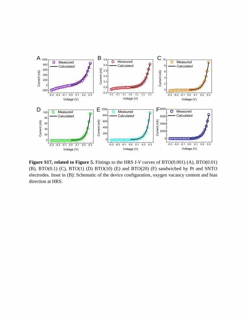
Figure S17, related to Figure 5. Fittings to the HRS I-V curves of BTO(0.001) (A), BTO(0.01)
(B), BTO(0.1) (C), BTO(1) (D) BTO(10) (E) and BTO(20) (F) sandwiched by Pt and SNTO
electrodes. Inset in (B): Schematic of the device configuration, oxygen vacancy content and bias
direction at HRS.
A B C
D E F
-0.3 -0.2 -0.1 0.0 0.1 0.2 0.3
0
2
4
6
8
10 Measured
Calculated
Cu
rre
nt
(nA
)
Voltage (V)
-0.3 -0.2 -0.1 0.0 0.1 0.2 0.3
-200
0
200
400
600
800
1000 Measured
Calculated
Cu
rre
nt
(nA
)
Voltage (V)
-0.3 -0.2 -0.1 0.0 0.1 0.2 0.3-0.1
0.0
0.1
0.2
0.3
0.4
0.5 Measured
Calculated
Curr
ent (n
A)
Voltage (V)
-0.3 -0.2 -0.1 0.0 0.1 0.2 0.3
0
20
40
60
80
100 Measured
Calculated
Cu
rre
nt
(nA
)
Voltage (V)
-0.3 -0.2 -0.1 0.0 0.1 0.2 0.3
0
2000
4000
6000
8000 Measured
Calculated
Cu
rre
nt
(nA
)
Voltage (V)
-0.3 -0.2 -0.1 0.0 0.1 0.2 0.3
0
200
400
600
800
1000 Measured
Calculated
Cu
rre
nt
(nA
)
Voltage (V)

Figure S18, related to Figure 5. I-V curves (A-C, G-I) and F(T)-1/T plots (D-F, J-L) of the
corresponding I-V data measured for Pt/BTO(0.001)/SNTO to Pt/BTO(20)/SNTO junctions at
HRS at different temperatures, where the lines fit the F(T)-1/T curves in (D-F, J-L).
A B C
D E F
G H I
J K L
-0.2 -0.1 0.0 0.1 0.2
10-15
10-13
10-11
10-9
10-7
C
urr
ent
(A)
Voltage (V)
290 K
260 K
230 K
200 K
170 K
140 K
110 K
80 K
50 K
20 K
10 K
0.003 0.004 0.005 0.006 0.007
-30.8
-30.4
-30.0
-29.6
F(T
)
1/T
-0.2 -0.1 0.0 0.1 0.2
10-15
10-13
10-11
10-9
10-7
Curr
ent
(A)
Voltage (V)
290 K
260 K
230 K
200 K
170 K
140 K
110 K
80 K
50 K
20 K
10 K
0.003 0.004 0.005 0.006 0.007
-41
-40
-39
-38
F(T
)
1/T
-0.2 -0.1 0.0 0.1 0.2
10-15
10-13
10-11
10-9
10-7
Curr
ent
(A)
Voltage (V)
290 K
260 K
230 K
200 K
170 K
140 K
110 K
80 K
50 K
20 K
10 K
0.003 0.004 0.005 0.006 0.007
-39
-38
-37
-36
F(T
)
1/T
-0.2 -0.1 0.0 0.1 0.2
10-15
10-13
10-11
10-9
10-7
Cu
rre
nt (A
)
Voltage (V)
290 K
260 K
230 K
200 K
170 K
140 K
110 K
80 K
50 K
20 K
10 K
0.003 0.004 0.005 0.006 0.007
-35.5
-35.0
-34.5
-34.0
-33.5
-33.0
F(T
)
1/T
0.003 0.004 0.005 0.006 0.007-31.2
-31.0
-30.8
-30.6
-30.4
-30.2
-30.0
F(T
)
1/T
-0.2 -0.1 0.0 0.1 0.2
10-15
10-13
10-11
10-9
10-7
Curr
net
(A)
Voltage (V)
290 K
260 K
230 K
200 K
170 K
140 K
110 K
80 K
50 K
20 K
10 K
-0.2 -0.1 0.0 0.1 0.2
10-15
10-13
10-11
10-9
10-7
Curr
ent
(A)
Voltage (V)
290 K
260 K
230 K
200 K
170 K
140 K
110 K
80 K
50 K
20 K
10 K
BTO(0.001) BTO(0.01) BTO(0.1)
0.003 0.004 0.005 0.006 0.007
-30.0
-29.6
-29.2
-28.8
F
(T)
1/T
BTO(1) BTO(10) BTO(20)

Note S2, related to Figure 5.
For the thermionic emission (TE) currents, under forward bias (V > 3kBT/q), the current across
the Schottky barrier is given by
)exp()exp(* 2
Tnk
qV
TkTSAI
BB
Bn
(4)
where A* is the standard Richardson constant, ΦB is the Schottky barrier height, T is the
temperature, kB is the Boltzmann's constant and n is the ideality factor.
Equation (4) can be rewritten as:
Tnk
qV
TkSA
T
I
BB
Bn
)*ln()ln(
2
(5)
For a given T, the ln(I/T2) scales in approximate linearity with V, consistent with equation (5).
If the overall current originates purely from the thermionic emission, the ln(J/T2)-V slope would
be reciprocal to T according to equation (5). The fact that the ln (J/T2)-V curves at different T
remain largely parallel suggests non-negligible contribution from the tunneling current. In this case,
the ideality factor n should be modified to account for the tunneling contribution, so that the
thermionic emission theory is still applicable. To extract parameter ΦB, one may turn to the
intercept of the ln (J/T2)-V curve on the vertical axis (V=0):
TkSATF
B
Bn
))*ln()(
(6)
Then, F(T) vs. (1/V) is linear with a slope equal to B
B
k
.
For the BTO based devices, we showed the temperature dependent I-V characteristics of HRS
and the corresponding F(T) vs. (1/T) fitting curves of BTO based devices from 290 K to 10 K
(Figure S18). In the calculations, A*=156 A cm-2 K-2 and m*=0.12 m0. The linear fitting gives the
value of ΦB of different devices. In addition, n can be calculated by Equation (5).

Figure S19, related to Figure 5. Distribution of the Ti valence at HRS and LRS in the
Pt/BTO(0.01)/SNTO device. Orange dots and blue squares represent the Ti valence distribution at
LRS and HRS, respectively. Two dashed lines denote the interfaces which are distinguished by M
edge intensity of Ba-M edge. The error bars are defined by the s.d.

Figure S20, related to Figure 5. 2-D mapping of Ti valence and Ba-M edge intensity at LRS and
HRS in the Pt/BTO(0.01)/SNTO device. (A) 2-D mapping of the Ti valence distribution at LRS.
The Ba-M edge intensity mapping (B) and line profile (C) of the LRS sample, which are used to
locate the interfaces. (D) 2-D mapping of the Ti valence distribution at HRS. The Ba-M edge
intensity mapping (E) and line profile (F) of HRS sample, which are used to locate the interfaces.
The error bars in (C) and (F) are defined by the s.d.
-2 -1 0 1 2 3 4 5
PtBTO
Ba M edge of LRS
Distance (nm)
SNTO0
1
2
3
4
5
Inte
nsity (
co
un
ts ×
10
5)
-2 -1 0 1 2 3 4 5 6
SNTO BTO
Ba M edge of HRS
Distance (nm)
Pt 0.0
0.4
0.8
1.2
Inte
nsity (
co
unts
×10
5)
A
B
C
D
-104
1054x105
0
2.8
4.2
2.8
4.2
SNTO BTO PtSNTO BTO Pt
E
F

Figure S21, related to Figure 5. ON/OFF ratio timeline for ferroelectric tunnel junctions. Our
experimental data for Pt/BTO(0.01)/SNTO device measured at room temperature (red circle) and
10 K (red pentagram) show the highest ON/OFF ratio.

Transparent Methods
Film Growth
Epitaxial single-crystalline BaTiO3 (BTO) and SrTiO3 (STO) films were grown by pulsed laser
deposition (PLD) on (001)-oriented 0.7 wt% Nb-doped SrTiO3 substrates using a XeCl (λ=308
nm) excimer laser with an energy density of 2.5 J cm-2 and a repetition rate of 2 Hz. BTO and STO
films were deposited at 750 °C in a flowing oxygen atmosphere of various oxygen pressures (0.001
Pa, 0.01 Pa, 0.1 Pa, 1 Pa, 10 Pa and 20 Pa) and cooled down to room temperature at 20 °C min-1.
The deposition rates of oxide films deposited at different oxygen pressures were calibrated by X-
ray Reflection (XRR). Thickness of BTO films was further confirmed by STEM measurements.
Device Fabrication
Top electrodes with radii of 5 μm, 10μm and 20μm on BTO/SNTO heterostructures were
fabricated using ultraviolet lithography, thermal evaporation (Au, Cr and Ti) or e–beam
evaporation (Pt). Capping layers of Au were adopted on Cr and Ti to prevent oxidation and
followed by lift-off process. When not specifically indicated, the electrical properties of the BTO
and STO based devices were measured with a top electrode radius of 5 μm.
Characterization
The BTO films crystal structures were characterized using STEM images. Cross-sectional
HAADF images were recorded at 300 kV on the Titan Cubed Themis G2 300 aberration-corrected
transmission electron microscope with the Gatan EnfiniumTMER (Model 977) spectrometer. Using
a home-made MatLab code, atom positions are determined by simultaneously fitting with 2D
Gaussian peaks. The displacements of Ti columns respectively to the neighboring Ba
isΔtotal=(Δx2+Δy
2)1/2, whereΔx and Δy are horizontal and vertical distance between Ti atom and the
center of neighboring Ba atoms. Small systematic-error-displacements can exist in the bulk due to
the tiny specimen mis-tilt between optical axis and specimen, which is unavoidable during
experiments. The surface morphology, polarization imaging, local ferroelectric properties and
current mapping were performed using a commercial scanning probe microscope (Asylum
Research MFP3D). Pt/Ti-coated silicon cantilevers were adopted in the PFM images and
conductive-diamond-coated silicon cantilevers were used in the C-AFM measurements. Local
hysteretic behaviors of the PFM phase and amplitude signals were collected in DART (dual a.c.
resonance tracking) mode and the signals were recorded while the voltage was off.
Electrical Measurement
Electrical measurements were performed by a Keithley 4200 semiconductor characterization
system in a LakeShore TTPX cryogenic vacuum probe station with 3-μm tungsten probes. The test

pulses were applied to the metal electrodes and the SNTO substrates were grounded, where
positive bias means currents flow from the metal electrodes to the SNTO substrates.

Supplemental References
Fan, Z., Fan, H., Yang, L., Li, P., Lu, Z., Tian, G., Huang, Z., Li, Z., Yao, J., Luo, Q. et al. (2017).
Resistive switching induced by charge trapping/detrapping: a unified mechanism for colossal
electroresistance in certain Nb:SrTiO3-based heterojunctions. J. Mater. Chem. C 5, 7317-7327.
Gruverman, A., Wu, D., Lu, H. Wang, Y. Jang, H. W., Folkman, C. M., Zhuravlev, M. Ye., Felker,
D., Rzchowski, M., Eom, C.-B., and Tsymbal, E. Y. (2009). Tunneling Electroresistance Effect in
ferroelectric Tunnel Junctions at the Nanoscale. Nano Lett. 9, 3539-3543.
Jiang, L., Choi, W. S., Jeen, H., Dong, S., Kim, Y., Han, M. G., Zhu, Y., Kalinin, S. V., Dagotto,
E., Egami, T., and Lee, H. N. (2013). Tunneling electroresistance induced by interfacial phase
transitions in ultrathin oxide heterostructures. Nano Lett. 13, 5837-5843.
Kim, D. J., Lu, H., Ryu, S., Bark, C.-W., Eom, C.-B., Tsymbal, E. Y., and Gruverman, A. (2012).
Ferroelectric tunnel memristor. Nano Lett. 12, 5697-5702.
Lu, H., Lipatov, A., Ryu, S., Kim, D. J., Lee, H., Zhuravlev, M. Y., Eom, C. B., Tsymbal, E. Y.,
Sinitskii, A., and Gruverman, A. (2014). Ferroelectric tunnel junctions with graphene electrodes.
Nat. Commun. 5, 5518.
Pantel, D., and Alexe, M. (2010). Electroresistance effects in ferroelectric tunnel barriers. Phys.
Rev. B 82, 134105.
Wang, L., Cho, M. R., Shin, Y. J., Kim, J. R., Das, S., Yoon, J.-G., Chung, J.-S., and Noh, T. W.
(2016). Overcoming the Fundamental Barrier Thickness Limits of Ferroelectric Tunnel Junctions
through BaTiO3/SrTiO3 Composite Barriers. Nano Lett. 16, 3911-3918.