Germanium: from material to FET devices · 1 1. Background 2. Advantages and some issues about...
19
Germanium: from material to FET devices Guang-Li Luo Research Fellow National Nano Device Laboratories
Transcript of Germanium: from material to FET devices · 1 1. Background 2. Advantages and some issues about...

Germanium: from material to FET devices
Guang-Li Luo
Research Fellow
National Nano Device Laboratories
1
1. Background
2. Advantages and some issues about germanium material and process
3. Germanium FET devices in NDL
Outline

Requirements for logic• High on‐off ratio Ion/Ioff
105…107.• High Ion (high speed).• Low Ioff (low static power).• Steep slope in
sub‐threshold, i.e., small SS.
Ion=W/LCox(Vg-Vt)Vd
n+ n+p
W
L
VG
Ioff
FET Basics
2

22/20-10
7,5,3…ok?
For Lg<5nm
3

Intel 32nm SoC platform technology,iedm09, p.647
Intel 22nm SoC platform technology,iedm12, p.44
4
Node name vs. gate length
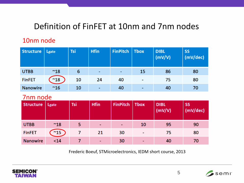
Definition of FinFET at 10nm and 7nm nodes
10nm node
7nm node
Frederic Boeuf, STMicroelectronics, IEDM short course, 2013
5

Source to drain tunneling will set an ultimate limit on scaling down.
Tsi=4nm
Direct tunneling between source and drain @ Lg < 5nm (not the node name)
7
When will non-Si be possibly used?(a frequently asked question)
8
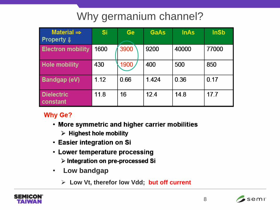
Why germanium channel?
• Low bandgap
Low Vt, therefor low Vdd; but off current

9
Situations for Ge MOSFETs
Gate-Stack:Successful high-k/GeO2/Ge gate stack process.
Ultrathin Si cap passivation of Ge before high-k deposition.
N+/P Ge junction:n-type dopants diffuse fast in Germanium; low activation rate.
Short-channel nFETdevice hard to fabricate.
Metal contact with N+-Ge:Strong Fermi Level Pinning of metals close to valence band edge
of Ge. Contact resistance to n+ Ge can be a serious problem.
Metal contact with P+-Ge is good.
Ge pMOSFETs are successful, but Ge nMOSFETS still have
many problems!
This is also why “Ge pFETs + III-V nFETs” finds a chance ?
Germanium Material:Ge blanket epitaxy on Si with PDA for TDs reduction; Selective Epitaxy
of Ge in small areas.
P

10
Ge layer
Si-sub
Ge critical thickness: 1-2nmLattice mismatch
2um Ge on Si with 850C, 10min
in-situ annealing Ref: JECS, 156(9), H703-H706 2009
Ge SEG in 50 nm SiO2 trenches
Ge epaitxy on Si substrates: dislocation reduction
High density of
dislocations in Ge/Si
11
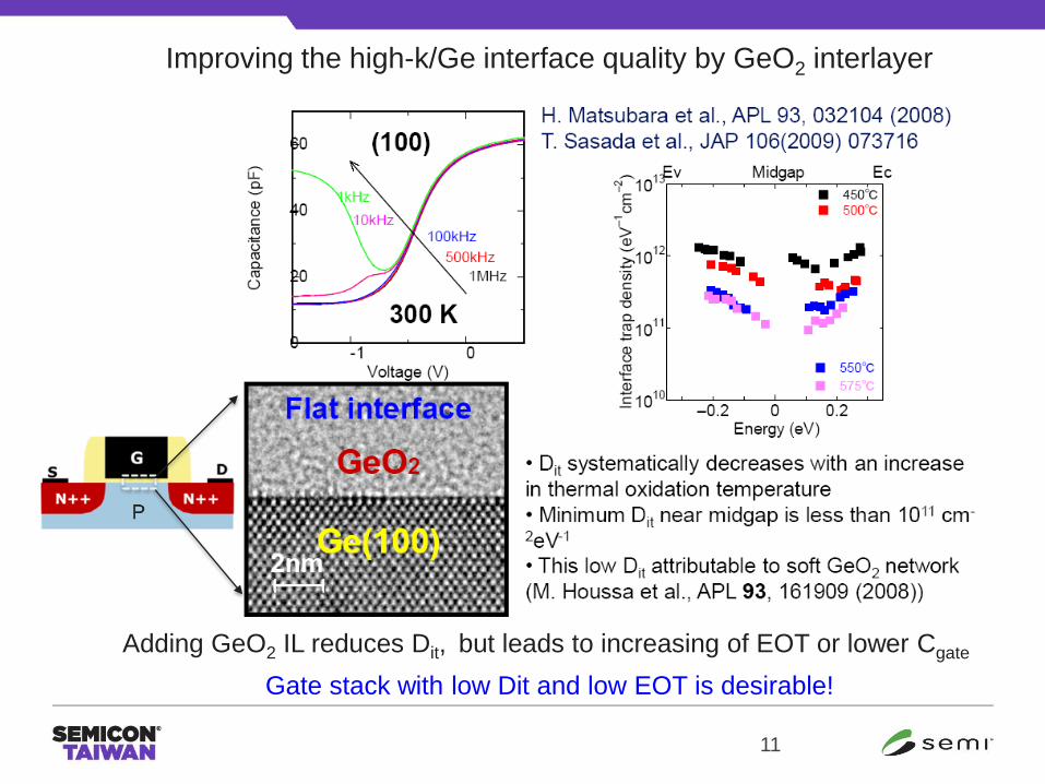
Improving the high-k/Ge interface quality by GeO2 interlayer
Adding GeO2 IL reduces Dit, but leads to increasing of EOT or lower Cgate
Gate stack with low Dit and low EOT is desirable!

12
P Type Doping in Ge (easy !!)

13
N Type Doping in Ge (difficult !!)
The in-situ doping in epitaxy is possibly
a feasible way for achieving n-type
dopant in Ge.
No diffusion of phos in Ge is observed.
in-situ doping is promising

14
Experimentally obtained SBHs BN on n-Si and
n-Ge and reported metal work functions M.
Appl. Phys. Lett. 91,
123123 2007
metal-induced-gap-state MIGS
Easy ohmic contact for metal/p-Ge
But difficult for metal/n-Ge
Good metal/n-Ge contact can be achieved by high
concentration doping of n-type dopant in Ge through reducing
the electron tunneling barrier width. However there is still a
long way to go in term of contact resistivity.

15
Ge p-channel FinFETs Directly on SOI Substrate
IEDM2012, p.383

16
Ge Gate-All-Around FETs on SOI Substrates
IEDM2011, p.826
17
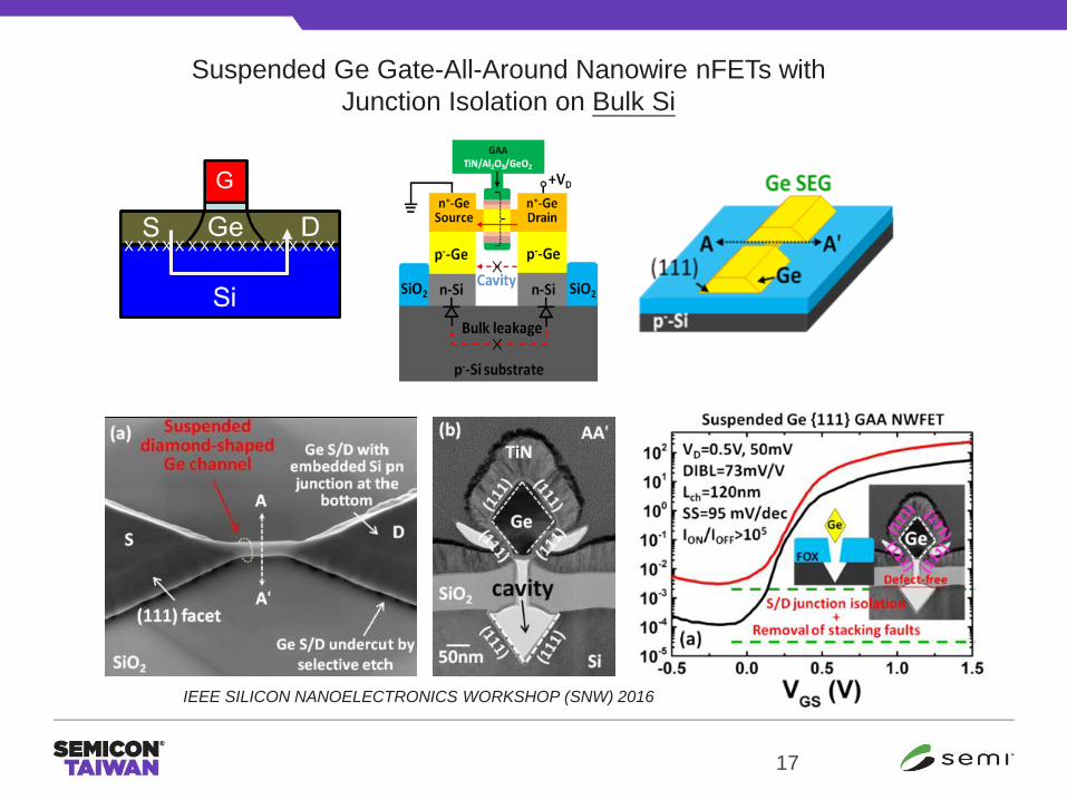
Suspended Ge Gate-All-Around Nanowire nFETs with
Junction Isolation on Bulk Si
IEEE SILICON NANOELECTRONICS WORKSHOP (SNW) 2016
18
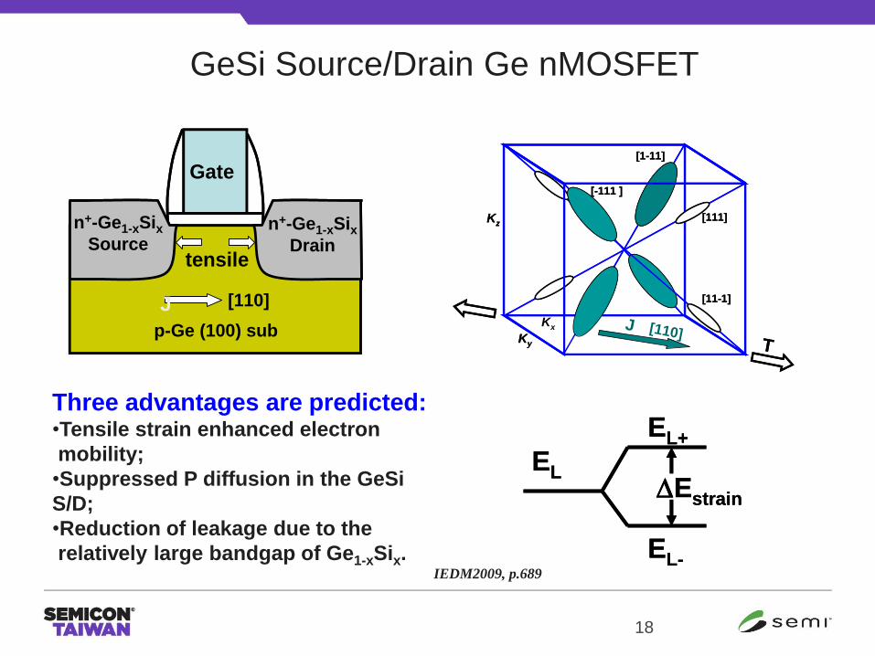
GeSi Source/Drain Ge nMOSFET
Three advantages are predicted:•Tensile strain enhanced electron
mobility;
•Suppressed P diffusion in the GeSi
S/D;
•Reduction of leakage due to the
relatively large bandgap of Ge1-xSix.
p-Ge (100) sub
Gate
n+-Ge1-xSixDrain
[110]
tensile
n+-Ge1-xSixSource
p-Ge (100) sub
Gate
n+-Ge1-xSixDrain
[110]
tensile
n+-Ge1-xSixSource
J
IEDM2009, p.689
Kx
Ky
Kz
[-111 ]
[111]
[11-1]
[1-11]
J
T[110]
Kx
Ky
Kz
[-111 ]
[111]
[11-1]
[1-11]
J
T[110]
EL
EL+
EL-
Estrain
EL
EL+
EL-
Estrain

20
Si FinFETs
When Si comes to end, germanium may be the most
promising among all non-Si materials in high power
application because of its high mobility. But for low power
application, its chance is small because of its natural high
leakage due to low band-gap.
Conclusion