Germanium Doped Czochralski Silicon - InTech -...
27
18 Germanium Doped Czochralski Silicon Jiahe Chen and Deren Yang State Key Lab of Silicon Materials, Zhejiang University People’s Republic of China 1. Introduction Due to the development of higher integrity electronic devices, it is required to improve the quality of Czochralski (CZ) silicon. On one hand, voids at the near-surface of wafers degrade gate oxide integration (GOI) of MOS devices and therefore reduce the yield of devices. On the other hand, it is a trend for the oxygen concentration of CZ silicon used for ultra large scale integrated circuits (ULSI) to become lower, so it will be difficult to form oxygen precipitates and create gettering sites in the bulk for undesirable metallic contaminants on silicon wafers. In addition, with increasing the diameter of wafers, the dislocations due to higher thermal stress and gravitational stress will generate easily, therefore it is desirable to enhance the mechanical property of wafers. As an important consist for the novel “impurity engineering” for CZ silicon materials (Chen et al., 2010; Chen & Yang, 2009; Yang et al., 2009), the behaviors of germanium in CZ silicon have attracted considerable attention in recent years, which was invented by our group. Compared to normal dopant elements, germanium doping will not induce electrical centers such as shallow thermal donors due to its equivalent electrons with silicon. Furthermore, the solubility of germanium in silicon is so large that germanium doping will not have influence on the growth of CZ silicon, if germanium concentration is lower than 10 19 cm -3 . And, it is believed that germanium doping in CZ silicon could be much easier to control, so that the influences of germanium doping to the properties of CZ silicon wafers could be adjusted”. Recently, we have investigated the effect of germanium with concentration of 10 15 -10 19 cm -3 on the mechanical stress, the formation of oxygen-related donors, oxygen precipitation and void defects in CZ silicon materials. It has been established that the mechanical strength of silicon wafers could be improved by germanium doping, which benefits the improved production yield of wafers (Chen et al., 2008). It is also found that germanium suppresses thermal donors (TDs) and new donors (NDs), which benefits the stable electrical property of wafers (Cui et al., 2006; Li et al., 2004b). More importantly, germanium has been found to suppress the formation of crystal originated particles (COPs) related to void defects, which can be annihilated easily during high temperature treatments (Chen et al., 2007a; Yang et al., 2002). Meanwhile, the enhancement of oxygen precipitation can be obtained by germanium doping ( Chen et al., 2009; Chen et al., 2006a; Chen et al., 2006b; Li et al., 2004a), and therefore internal gettering (IG) capability could be improved (Chen et al., 2007b; Chen et al., 2007c). Up to now, ascribing to the novel properties induced from germanium atoms, it Source: Advances in Solid State Circuits Technologies, Book edited by: Paul K. Chu, ISBN 978-953-307-086-5, pp. 446, April 2010, INTECH, Croatia, downloaded from SCIYO.COM www.intechopen.com
Transcript of Germanium Doped Czochralski Silicon - InTech -...

18
Germanium Doped Czochralski Silicon
Jiahe Chen and Deren Yang State Key Lab of Silicon Materials, Zhejiang University
People’s Republic of China
1. Introduction
Due to the development of higher integrity electronic devices, it is required to improve the
quality of Czochralski (CZ) silicon. On one hand, voids at the near-surface of wafers
degrade gate oxide integration (GOI) of MOS devices and therefore reduce the yield of
devices. On the other hand, it is a trend for the oxygen concentration of CZ silicon used for
ultra large scale integrated circuits (ULSI) to become lower, so it will be difficult to form
oxygen precipitates and create gettering sites in the bulk for undesirable metallic
contaminants on silicon wafers. In addition, with increasing the diameter of wafers, the
dislocations due to higher thermal stress and gravitational stress will generate easily,
therefore it is desirable to enhance the mechanical property of wafers.
As an important consist for the novel “impurity engineering” for CZ silicon materials (Chen
et al., 2010; Chen & Yang, 2009; Yang et al., 2009), the behaviors of germanium in CZ silicon
have attracted considerable attention in recent years, which was invented by our group.
Compared to normal dopant elements, germanium doping will not induce electrical centers
such as shallow thermal donors due to its equivalent electrons with silicon. Furthermore, the
solubility of germanium in silicon is so large that germanium doping will not have influence
on the growth of CZ silicon, if germanium concentration is lower than 1019 cm-3. And, it is
believed that germanium doping in CZ silicon could be much easier to control, so that the
influences of germanium doping to the properties of CZ silicon wafers could be adjusted”.
Recently, we have investigated the effect of germanium with concentration of 1015-1019 cm-3
on the mechanical stress, the formation of oxygen-related donors, oxygen precipitation and
void defects in CZ silicon materials. It has been established that the mechanical strength of
silicon wafers could be improved by germanium doping, which benefits the improved
production yield of wafers (Chen et al., 2008). It is also found that germanium suppresses
thermal donors (TDs) and new donors (NDs), which benefits the stable electrical property of
wafers (Cui et al., 2006; Li et al., 2004b). More importantly, germanium has been found to
suppress the formation of crystal originated particles (COPs) related to void defects, which
can be annihilated easily during high temperature treatments (Chen et al., 2007a; Yang et al.,
2002). Meanwhile, the enhancement of oxygen precipitation can be obtained by germanium
doping ( Chen et al., 2009; Chen et al., 2006a; Chen et al., 2006b; Li et al., 2004a), and
therefore internal gettering (IG) capability could be improved (Chen et al., 2007b; Chen et
al., 2007c). Up to now, ascribing to the novel properties induced from germanium atoms, it
Source: Advances in Solid State Circuits Technologies, Book edited by: Paul K. Chu, ISBN 978-953-307-086-5, pp. 446, April 2010, INTECH, Croatia, downloaded from SCIYO.COM
www.intechopen.com

Advances in Solid State Circuits Technologies
368
is considered that germanium doped CZ (GCZ) silicon could probably become one of the
new type silicon materials met requirements of higher performance ULSI. In this chapter, the behaviors of germanium doping CZ silicon will be reviewed mainly based on our recent work, and two preliminary applications of GCZ silicon wafers will be shown as examples.
2. Mechanical strength
By alloying with oxygen and some dopants, such as nitrogen, the mechanical strength of silicon single crystals could be increased. The strengthening is believed to be associated with impurity concentrations and dislocation densities. Like that for nitrogen-doped float zone (FZ) silicon, it shows a much higher yield strength than usual FZ silicon because nitrogen atoms bring about the hardening of silicon crystals through locking of dislocations upon congregating on the latter one (Kishino et al., 1982; Yonenaga, 2005). As a similar story, the mechanical strength improvement of silicon crystals doped with germanium is considered to be effective at immobilizing and retarding the velocity of dislocations while germanium doping level excessed 6×1019 cm-3 (Fukuda & Ohsawa, 1992). Furthermore, dislocation-free CZ silicon crystal could be obtained using a heavily germanium doped seed without Dash necking(Huang et al., 2003). Recently, we emphasize that the lightly germanium doping benefits the mechanical stress improvements for CZ silicon wafers. Table 1 lists the statistical Total Thickness Variation (TTV), Warp and Bow data from 100
pieces of the as-processed wafer during a mass production for both the CZ and GCZ silicon
(with the germanium level of 1018 cm-3) (Chen et al., 2008). Normally, Warp represents the
total amount of maximum variations between the medium and reference surfaces of wafers,
while Bow is defined as a half dispersion of concave and convexo maximum between the
medium and reference wafer surfaces, both of which are believed to characterize the extent
of warpage for silicon wafers and are controlled in production lines extensively: the smaller
they are, the slighter the warpage would be. As can be seen in Table 1, both the Warp and
Bow merits were relatively smaller in percentage for the GCZ silicon wafers than that for the
CZ silicon wafers, indicating that germanium doping in silicon inclines hardly to cause
warpage during the wafer making from monocrystalline ingots. Moreover, the fact of the
slightly smaller data for the GCZ wafers than the CZ wafers shows that the mechanical
strengths of CZ wafers might be improved slightly by germanium doping, which is
coincident with the fact that a higher yield of polished wafer could be obtained for GCZ
wafer during the assemble wafer making: the yields of polished CZ and GCZ silicon wafers
were 89.9% and 92.8%, respectively. It is therefore concluded that a slight suppression on
the warpage of CZ silicon wafer could be presented by light germanium doping. It is
considered that, compared with normal CZ silicon, grown-in oxygen precipitation could be
enhanced in GCZ silicon, which will be discussed below. Then, the enhanced grown-in
oxygen precipitates could pin up dislocations and retard their movements, so that the
macroscopical mechanical strength of GCZ silicon wafers could be increased.
Herein, it is believed that the novel concept of “mechanical strength improvement by germanium doping” is of great merit, not limiting to the application field of IC used silicon wafers. Especially, it is worthwhile to point out that this novel concept could be adopted in improving the wafer production yield and producing super thin wafer support for solar cells.
www.intechopen.com

Germanium Doped Czochralski Silicon
369
TTV (μm) Warp (μm) Bow (μm) Statistical Index
CZ GCZ CZ GCZ CZ GCZ
Mean 2.7 2.9 15.9 11.6 -0.31 0.26 Range 4.7 4.9 20.1 16.8 25.6 16.9
Quartile 2.0 2.3 4.7 4.5 6.2 3.4 Variance 1.6 1.6 28.5 14.1 16.2 14.4 Standard Deviation
1.3 1.3 5.4 3.3 4.2 3.5
Table 1. Data dispersion degrees of TTV, Warp and Bow for polished CZ and GCZ silicon wafers during the making processing. (from 300 pieces) (Chen et al., 2008)
As a detailed clarification for the mechanical strength of as-processed silicon wafers, the indention tests performed at room temperature followed by a high temperature annealing, which is considered to be one of the popular approaches for investigating the behaviors of dislocations in silicon wafers (Akatsuka et al., 1997; Fukuda & Ohsawa, 1992), were also adopted in our investigation. Fig. 1 shows the classical optical images of the indentation (as indented) and the rosette pattern of punched out dislocations (PODs) introduced by indentations (subjected to 1100oC/2h anneal) in GCZ silicon wafer. Herein, the POD diffusion length stands for the capability of mechanical strength of silicon wafers. From the rosette sizes shown in the GCZ silicon wafers with germanium doping (from the concentrations from 1016 to 1019 cm-3) subjected to 1100oC/2h anneal (Chen et al., 2008), it could be found that the mechanical strength was improved by germanium doping. With the increase of germanium doping level, the POD diffusion length decreases, which should be ascribed to the intensive dislocation pin up effects by the micro-defects (such as small-sized oxygen precipitates).
0
30
60
90
120
150
1019
1018
1017
0 1016
Rosstt
e S
ize
(μm
)
Germanium Concentration (cm-3)
Fig. 1. Optical images of (a) the indentation and (b) the rosette pattern of PODs introduced by indentations in the GCZ silicon wafer subjected to 1100oC/ 2h anneal; (c) Rosette size in the GCZ silicon wafers with different germanium doping subjected to 1100oC/ 2h anneal (Chen et al., 2008).
During ULSI device fabrication, the mechanical strength during thermal processing affects the cracked-wafer breakdown yield and even the lithography accuracy. Considering this, the indentation tests on thermal treated silicon wafers have been studied via varied pre-annealing. Fig. 2 shows the optical images of PODs for the CZ and GCZ silicon, which were annealed at 800oC for 16 h or plus re-annealed at 1000oC for 4 h. Actually, the amorphous silicon and dislocations could be formed around the indentation positions at room temperature and then high stress could occur under a highly localized stress (Minowa &
www.intechopen.com
Advances in Solid State Circuits Technologies
370
Sumino, 1992). The amorphous silicon inclined to transform to the heavy dislocated crystalline silicon and the dislocations began to move so as to release the stresses when high temperature annealing was adopted. Herein, the travel distance of PODs in the GCZ silicon samples after 800oC/16h annealing was calculated to be somewhat shorter than that of the CZ silicon samples. Whereas, for 800oC/16h + 1000oC/4h annealing, the moving distance of PODs in the GCZ silicon sample seemed to be unambiguously shorter than that in the CZ silicon samples. And, these phenomena were consistent with the conclusions drawn from the fracture strength measurement (Chen et al., 2008).
Fig. 2. Typical optical micrographs for the scratch-introduced CZ and GCZ silicon samples annealed at 1000oC/2.5 h. (a) CZ, 800oC/16h, (b) GCZ, 800oC/16h; (c) CZ, 800oC/16h + 1000oC/4h; (d) GCZ, 800oC/16h + 1000oC/4h.
Additionally, the influence of germanium doping levels in CZ silicon on the mechanical strength during device fabrication processing has been clarified by strain-stress checking.
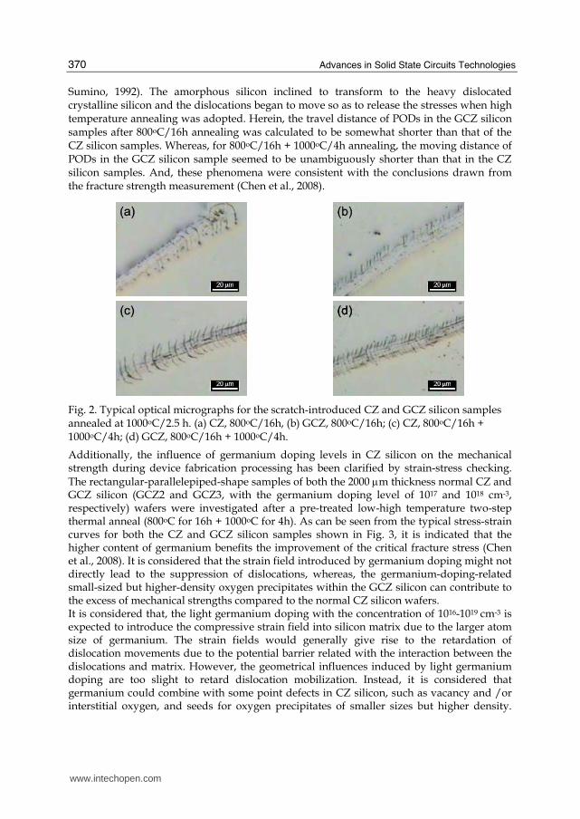
The rectangular-parallelepiped-shape samples of both the 2000 μm thickness normal CZ and GCZ silicon (GCZ2 and GCZ3, with the germanium doping level of 1017 and 1018 cm-3, respectively) wafers were investigated after a pre-treated low-high temperature two-step thermal anneal (800oC for 16h + 1000oC for 4h). As can be seen from the typical stress-strain curves for both the CZ and GCZ silicon samples shown in Fig. 3, it is indicated that the higher content of germanium benefits the improvement of the critical fracture stress (Chen et al., 2008). It is considered that the strain field introduced by germanium doping might not directly lead to the suppression of dislocations, whereas, the germanium-doping-related small-sized but higher-density oxygen precipitates within the GCZ silicon can contribute to the excess of mechanical strengths compared to the normal CZ silicon wafers. It is considered that, the light germanium doping with the concentration of 1016-1019 cm-3 is expected to introduce the compressive strain field into silicon matrix due to the larger atom size of germanium. The strain fields would generally give rise to the retardation of dislocation movements due to the potential barrier related with the interaction between the dislocations and matrix. However, the geometrical influences induced by light germanium doping are too slight to retard dislocation mobilization. Instead, it is considered that germanium could combine with some point defects in CZ silicon, such as vacancy and /or interstitial oxygen, and seeds for oxygen precipitates of smaller sizes but higher density.
www.intechopen.com
Germanium Doped Czochralski Silicon
371
Fig. 3. Typical stress-strain curves for the CZ (CZ) and GCZ silicon samples (GCZ2 and GCZ3, with the germanium concentrations of 1017 and 1018 cm-3, respectively) annealed at 800oC/16h + 1000oC/4h. (Chen et al., 2008)
Therefore, for both the grown-in case and the thermal treatment case, the oxygen precipitate nucleation at the sites of the dislocation cores could be enhanced by light germanium doping and the precipitates could act as the strong pinning complexes for the dislocation mobilization. In this viewpoint, it is reasonable to understand that the higher concentration of germanium atoms in CZ silicon could reduce the dislocation velocity and then decrease their moving distance.
3. Oxygen-related donors
Oxygen-related donors, including thermal donors (TDs) and new donors (NDs), which are believed to generate normally in the temperature ranges of 350-550oC (Fuller & Logan, 1957) and 600-700oC (Capper et al., 1977), respectively, can deteriorate the electrical properties of wafers. Impurities like germanium and nitrogen have been reported to retard TD formation (Hild et al., 1998). Based on the experimental facts, it is considered that germanium doping suppress the formation of TDs, but does not affect the microscopic structure of TDs, which suggested to be the result of the reaction of germanium with point defects (like silicon interstitial, boron, vacancy and interstitial oxygen dimer) in CZ silicon; whereas, the germanium doping could enhance the formation of NDs in CZ silicon, which is proposed as a process associated with the nucleation enhancement of oxygen precipitation by germanium doping. In this section, a conventional CZ silicon and two GCZ silicon (GCZ1 and GCZ2, with the germanium concentrations of 1016 and 1018 cm-3 at the seed-ends, respectively) ingots were grown under almost the same conditions. Samples from different position of CZ and GCZ2 silicon ingots were annealed at 650oC for 30min to annihilate as-grown TDs. The resistivity of the annealed samples was measured by means of four-point probe, and the TD concentration ([TD]s) was converted from resistivity according to ASTM F723-88. Fig. 4 shows the distribution of the as-grown TD concentrations along the axial orientation in CZ and GCZ2 silicon crystals (Yang et al., 2004). Compared with the CZ silicon, the TD concentrations in the middle and the tail part of the GCZ2 silicon are much lower. The segregation coefficient of germanium in crystal is about 0.33, indicating that the germanium concentration would increase from the seed-end to the tang end of the crystal ingot. It is
www.intechopen.com

Advances in Solid State Circuits Technologies
372
therefore believed that germanium suppresses the formation of TDs during crystal growth so that the TD concentration is lower in the tail. Furhtermore, the TD concentration variation in the GCZ1 ingot was similar to that in the GCZ2, which is further inferred that TDs are inhibited in GCZ silicon when germanium concentration is above 1016cm-3. In fact, it was also found that the TD concentrations in the GCZ samples are always lower
than those in the CZ wafers during low temperature annealing. In our experiments, the
samples were annealed at different temperatures from 350oC to 500oC for different time to
investigate the suppression effect of germanium on TD formation. The TD concentrations of
the CZ and GCZ2 samples were plotted as a function of annealing time, as shown in Fig. 5
(Yang et al., 2004). When annealed at 350oC or 500oC, there is nearly no change of the [TD]s
in both the CZ and GCZ2 samples, meaning that almost no donors have been generated at
these temperatures. When annealed at 400oC, [TD]s increased with the annealing time,
however, the increase speed in the thermal donors in the GCZ2 is lower than that of the CZ
samples. When annealed at 450oC, the [TD] variation speed is the most rapid one among all
the anneal temperatures, while the [TD]s of the GCZ2 increases still lower than that of the
CZ silicon. That is, germanium doping could suppress the formation of TDs.
0.00 0.25 0.50 0.75 1.00
0
20
40
60
[TD
] (X
10
13cm
-3)
Relative axial distance (100%)
CZ
GCZ2
Fig. 4. Distribution of the as-grown [TD]s along the axial orientation in the CZ and GCZ2 silicon. (Yang et al., 2004)
(a)
0 4 8 12 16
0
10
20
30
[TD
] (x
10
14cm
-3)
Time(h)
350oC
400oC
450oC
500oC
(b)
0 4 8 12 16
0
10
20
30
Donors
genera
ted (
x10
14cm
-3)
Time(h)
350oC
400oC
450oC
500oC
Fig. 5. TD concentrations of the CZ (a) and GCZ2 (b) samples as a function of annealing time (Yang et al., 2004).
The low temperature Fourie Tansmission Infrared (FTIR) absorption spectra of thermal donors (TDs) in GCZ silicon were found to be similar to the one in CZ silicon, but their density is different. Therefore, it is considered that light germanium doping suppresses the
www.intechopen.com

Germanium Doped Czochralski Silicon
373
formation of TDs but does not affect the microscopic structure of TDs. Fig. 6 shows the low-temperature FTIR spectra of the CZ and GCZ samples in far- (350-650 cm-1) and mid-IR (650-1200 cm-1) range, respectively(Cui et al., 2006). As can be seen in Fig. 6(a), a series of individual FTIR absorption lines related to TDs in silicon are observed in both the CZ and GCZ silicon. These absorption lines were caused by the transitions of neutral TDDs into the conduction band at low temperature of 10K and different absorption lines correspond with different donor energy levels (Wagner & Hage, 1989), and the neutral donors in the GCZ sample have the same energy levels as those in the CZ sample. Meanwhile, from the low-temperature FTIR absorption spectra of the CZ and GCZ silicon in the range 650-1200 cm-1 illustrated in Fig. 5(b), the similar situation could be found. These series of FTIR absorption lines are reported to correspond with the singly ionized TDs (Wagner & Hage, 1989). It is obviously that the FTIR absorption spectrum of the singly ionized donors in the GCZ agrees quite well with that in the CZ silicon, but its density is much stronger. These results further confirm that the TDs in both the silicon samples are the thermal double donors (TDDs) with the same energy levels and microstructures. Therefore, it is considered that germanium doping in silicon suppresses the generation of TDs, but has little influence on their structures, which different from the results in heavily germanium content silicon, GeSi. In GeSi, the TDs were found to be broadbands in the FTIR spectra measured at low-temperature (Hild et al., 1998).
Fig. 6. (a) Low-temperature far-IR spectra of the CZ and GCZ silicon samples subjected to 650oC/30min + 450oC/4h annealing, (b) low temperature mid-IR spectra of the CZ and silicon GCZ samples subjected to 450oC/30 min + 450oC/4h annealing. The TDDn refers to the nth (n=1-5) neutral donor in Fig. 6(a) and singly ionized donor in Fig. 6(b). (Cui et al., 2006)
When iso-electrical germanium atoms are incorporated into silicon lattice, they locate at substitutional sites and usually cause the increase of internal stress. During crystal growth, point defects could interact with germanium atoms. Vacancies incline to combine with germanium atoms to form Ge-Vn complexes, which have been identified by DLTS measurements in GCZ silicon crystals (Budtz-Jorgensen et al., 1998). We have clarified that germanium can enhance the nucleation of oxygen precipitation in the wide temperature range of 650-1200oC, which is based on the assumed Ge-O and Ge-O-V complexes. Normally, the TDs generated around 450oC is due to the aggregation of oxygen atoms (Kaiser et al., 1958). The molar volume of TDs is larger than that of silicon, thus, during the TD formation the lattice strain must be released by attracting free vacancies whose
www.intechopen.com

Advances in Solid State Circuits Technologies
374
concentration is greatly decreased by the formation of Ge-V complexes. Meanwhile, the generation of TDs is a process of oxygen clustering, so that the interactions between the germanium and oxygen atoms together with the complexes of Ge-V with the fast diffusion O2i dimmer will reduce the oxygen flux to form the smaller oxygen clusters during lower temperatures and therefore suppress the TD formation. Considering the effect of germanium doping on NDs, it has ever been reported that
germanium could suppress the formation of NDs (Babitskii et al., 1985) in heavily
germanium doping cases, and it was also suggested that the generate rate of oxygen
precipitates and NDs was lowered down by the lattice deformation caused by germanium
doping in silicon (Babich et al., 1995; Babitskii et al., 1988). However, our investigation
showed an opposite results in light germanium doping silicon materials.
Both the CZ and GCZ2 silicon were annealed at 650oC/128h and the ND concentrations ([ND]s) in the wafers as a function of the annealing time was drawn in Fig. 6 (Li et al., 2004b). The [ND]s for both the silicon increased with the annealing time at 650oC due to the formation of NDs. However, the ND formation rate in the GCZ2 sample is dramatically higher than that in the CZ one, so that the conductivity type reversed from p-type (all the original CZ silicon ingots are boron doped) to n-type after anneal for 128h in the GCZ2 silicon, meaning that large number of NDs have generated due to the enhancement of germanium on the ND formation. Besides, from the oxygen concentration variation of the annealed samples, it is found that more oxygen atoms have precipitated in the GCZ2 samples than in the CZ samples after 650oC/128h annealing. Generally, NDs are considered to be the bigger oxygen clusters compared to TDs, which are generally nuclei of oxygen precipitates during lower temperature anneal (Pensl et al., 1989). It is considered that, the enhanced ND formation by the germanium doping, is believed to be relative to the enhancement of oxygen precipitation. As germanium can enhance the nucleation of oxygen precipitates based on Ge-O complexes, some precipitate nuclei might become NDs. Thus, it is reasonable to suggest that most of these denser small oxygen precipitate nuclei become NDs with electrical activity at 650oC anneal. However, when germanium concentration is much larger than oxygen concentration, most of oxygen will be trapped by germanium to form Ge-O complexes, resulting in the reduction of oxygen flux to form NDs. Therefore, the formation of NDs will be suppressed, which was reported by Babitskii's work (Babitskii et al., 1985).
0 40 80 120
0
5
10
15
20
25
n - type
p - type
[ND
] (x
10
14cm
-3)
Time ( h )
CZ
GCZ2
Fig. 7. ND concentration in the CZ and GCZ2 wafers annealed at 650oC as a function of the annealing time (Li et al., 2004b).
www.intechopen.com

Germanium Doped Czochralski Silicon
375
4. Oxygen precipitation
Oxygen precipitates, the main micro-defects in CZ silicon especially used for the bulk isolated devices in early years, could not only deteriorate the electrical properties itself but also induce the secondary defects such as stacking faults and dislocations which increase the breakdown current of devices. However, oxygen precipitates with suitable density in bulk benefit both for the improvement of mechanical properties and for the enhancement of internal gettering capacitance for wafers. The super-saturated interstitial oxygen atoms in CZ silicon will accumulate to form grown-in oxygen precipitates due to post-anneal in crystal pullers, resulting in so called as-grown oxygen precipitates. It is also widely accepted that the supersaturated oxygen atoms in silicon matrix can precipitate and further induce secondary defects, so-called bulk micro-defects (BMDs), within device fabrication processes. Oxygen precipitates as well as BMDs are believed to be the gettering sites for metallic contamination. Thus, normally, it is required to control the concentration and distribution of oxygen precipitates in silicon bulk so that the optimum comprehensive effects benefit the quality of CZ silicon material. The germanium doping in CZ silicon is found to enhance not only as-grown oxygen precipitation but also oxygen precipitation during successive thermal anneals within a large temperature range; and it could also vary both the distribution situations of BMDs and microscopic morphology of oxygen precipitates, resulting in poor thermal stability of oxygen precipitates at elevated high temperatures. We consider that a certain complexes, the so called germanium-related complexes, could be generated in the GCZ silicon and thus change the behavior of oxygen precipitates in GCZ silicon. A CZ and two GCZ (GCZ1 and GCZ2 with [Ge] ~1016 and 1017 cm-3, respectively) silicon ingots with the comparable initial oxygen concentration have been selected to investigate the formation of grown-in oxygen precipitation: after annealing at 1270oC/2h to annihilate the thermal history, both the CZ and GCZ silicon were cooled down by a controlled rate of 0.5oC/min and were taken out at 1150-850oC separately. The reductions of [Oi] (Δ[Oi]s) in the CZ and GCZ samples as a function of the taking out temperatures is shown in Fig. 8(a) (Chen et al., 2006b). Generally, the thermal history of wafers can well influence the oxygen precipitation of CZ silicon during the successive annealing, while grown-in precipitates can be dissolved when annealed at considerably high temperatures above 1250°C (Kishino et al.,
1982). The Δ[Oi] variation of the CZ and GCZ silicon annealed at 1270°C/2h is shown in Fig. 8(b)(Chen et al., 2006b). It can be seen that the ratio of increased [Oi] and as-received [Oi] in the CZ silicon before and after annealing is a bit smaller than that of the GCZ silicon, which indicates the grown-in precipitates in the GCZ silicon is more than those in the CZ silicon. It is considered that germanium enhances the formation of grown-in oxygen precipitation during crystal growth. From Fig. 8(a), it can be also found that the [Oi]s of the GCZ2 silicon decreased much more dramatically than that of the CZ silicon in the whole temperature range and that the GCZ1 silicon decreased more slightly than that of the CZ silicon below 1050oC, indicating that oxygen can precipitate more easily in the GCZ silicon crystals, even at the temperatures higher than 1150oC. Another ramping-up processing was also performed to investigate the effect of germanium on as-grown oxygen precipitation in GCZ silicon. Samples were annealed at a heating rate of 1oC/min starting at 750oC, 850oC, 950oC or 1050oC, and ending at 1050oC with a isothermal anneal for 16 h,. The Δ[Oi]s as a function of the starting ramping temperature is shown in Fig. 9 (Chen et al., 2006b). It is believed that 1oC/min is a suitable heating rate to grow up oxygen precipitate nuclei, if their radius is larger than the critical nucleation radius
www.intechopen.com

Advances in Solid State Circuits Technologies
376
(a) (b)
Fig. 8. (a) Evolution of the Δ[Oi]s in the CZ and GCZ silicon after 1270°C/2h pre-anneal as a
function of the taking out ramping temperatures during the cooling-down process, (b) Δ[Oi] of the CZ and GCZ silicon before and after annealing at 1270°C/2h. (Chen et al., 2006b)
of oxygen precipitates (rc) at the starting temperatures of the ramping process, while the formation of new oxygen precipitate nuclei during the ramping is suppressed(Kissinger et al., 1998). Accordingly, the precipitated oxygen after 1050oC/16h anneal ramped from different starting temperatures are considered to be roughly related to the grown-in oxygen precipitates whose radius is larger than rc at the starting ramping temperature in the corresponding grown-in crystals. Thus, with the increase of starting temperatures, the amount of grown-in precipitates larger than the rc decreases, which results in the reduction
of oxygen precipitates. As can be seen, the decreased Δ[Oi]s of the GCZ wafers was much more than that of the CZ wafers at every starting temperatures, which indicates that more grown-in oxygen precipitates have been generated in the GCZ wafers than that in the CZ wafers in the investigated temperature range (between 850 and 1050oC). Meanwhile, the [Oi] curve of the GCZ2 wafer moved rightward relative to that of the CZ one as shown in Fig. 9. In this case, there is a sharp decrease of [Oi] when the temperature below 950oC, which means the radius of majority of as-grown oxygen precipitates in the GCZ wafers was smaller than rc at 950oC, while that of most as-grown oxygen precipitates in the CZ wafer was smaller than rc at 850oC. It is therefore believed that the germanium incorporation increases the forming temperatures of as-grown oxygen precipitation during the cooling-down process of crystal growth, and thus larger as-grown oxygen precipitates could be presented in GCZ silicon when the cooling-down processing completed.
Fig. 9. Evolution of Δ[Oi]s in the CZ and GCZ silicon as a function of the starting ramping temperatures in the ramping process with 1oC/min ramping-up rate.(Chen et al., 2006b)
www.intechopen.com

Germanium Doped Czochralski Silicon
377
It is also suggested that germanium doping could enhance the oxygen precipitation in CZ silicon wafer in a large temperature range (from 550 to 1050oC) during successive annealing. The as-received samples of both the CZ and GCZ silicon were put into a diffusion furnace at 550-950oC at every 100oC and then isothermally annealed for 2-64h, following by annealing at 1050oC for 16h. All the thermal treatments were preformed in an argon atmosphere. Fig.
10 shows the Δ[Oi]s in the CZ and GCZ silicon annealed for 64 h as a function of the
annealing temperatures (Chen et al., 2006a). As can be seen, the Δ[Oi]s in both the CZ and
GCZ silicon samples annealed at above 850 °C were larger. Moreover, the amount of Δ[Oi] was always larger in the GCZ silicon than in the CZ silicon. It is therefore suggested that germanium doping could enhance oxygen precipitation in CZ silicon in a wide temperature range.
Fig. 10. Left: Δ[Oi]s in the CZ and GCZ silicon annealed for 64 h as a function of annealing temperatures. Right: Optical micrographs of the BMDs in the CZ (a) and GCZ (b) silicon subjected to 950°C/64 h anneal. (Chen et al., 2006a)
Normally, oxygen precipitate growth is limited by oxygen diffusion especially at low temperatures. (Joly & Robert, 1994) When annealed at low temperatures (such as 750 °C or below), the diffusivity of oxygen is considerably small, thus the growth of oxygen precipitates is not remarkable. However, a part of oxygen atoms can still aggregate into
precipitate nuclei and embryos, so that the Δ[Oi]s in the GCZ silicon subjected to 64h anneal at 750 °C is somewhat larger than that in the CZ silicon. It is thus believed that the formation of precipitate nuclei is enhanced by germanium doping. When the silicon wafers were annealed at higher temperatures (such as 950°C and above), the oxygen diffusion coefficient greatly increased, while the supersaturation of interstitial oxygen in silicon crystal decreased. In this case, oxygen precipitation in silicon was primarily based on the as-grown precipitate nuclei. (Borghesi et al., 1995) The typical optical micrographs of BMDs induced by oxygen precipitates in the CZ and GCZ silicon samples subjected to 950°C/64 h anneal are also shown in Fig. 10. It can be clearly seen that the BMD density was much higher in the GCZ silicon than in the CZ silicon. It is generally believed that the grown-in oxygen precipitates have a size distribution following the Boltzmann’s statistics. Only the oxygen precipitates with radius larger than rc at the annealing temperatures can survive and further grow up. Accordingly, the density of the grown-in oxygen precipitates with rc at 950 °C is much higher in the GCZ silicon than that in the CZ silicon. That is, again, germanium doping can enhance the formation of larger grown-in oxygen precipitates during crystal growth. Furthermore, if as-grown oxygen precipitates were eliminated by high temperature annealing, oxygen precipitation in GCZ silicon wafers during successive thermal cycles
www.intechopen.com

Advances in Solid State Circuits Technologies
378
could still be enhanced by germanium doping. Fig. 11 shows the Δ[Oi]s of the thermal-history-eliminated CZ and GCZ silicon wafers subjected to the 1050-1150oC/2h anneal. As can be seen, a bit larger oxygen precipitates could be generated in the GCZ silicon wafer than in the CZ silicon, which should be ascribed to the presentation as nucleation embryos of the germanium-related complexes formed in the GCZ silicon.
1 2 3 4 5 6 7 8 9-0.4
-0.2
0.0
0.2
0.4
0.6
0.8
1150oC1110
oC
Δ [Oi]
(X1
01
7cm
-3)
Sample Series Number
CZ
GCZ
1050oC
Fig. 11. Δ[Oi]s of the thermal-history-eliminated CZ and GCZ silicon wafers subjected to the 1050-1150oC/2h anneal.
Ascribed to the enhancement of oxygen precipitation nucleation at low temperatures by germanium doping, oxygen precipitation during successive annealing processing will be no doubt enhanced. Fig. 12 shows the comparison of [Oi]s and the optical micrographs of BMDs, which corresponds to oxygen precipitates and induced defects, in the CZ and GCZ silicon subjected to the two-step anneals consisted of different low temperature pre-annealing plus the same high temperature anneal at 1050oC (Chen et al., 2006a). In the experiments, the precipitate nuclei subsisted after the prior annealing would coarsen during the subsequent high temperature annealing since the oxygen precipitate is characteristics of growth at high temperatures. As can be seen in the left of Fig.12, with the pre-anneal at 650 and 750 oC, the [Oi]s in the CZ silicon decreased almost to the oxygen solubility at 1050oC, while the [Oi]s remained at a bit higher levels in the GCZ silicon. Correspondingly, the dense BMDs in larger sizes were formed in the CZ silicon while denser BMDs in smaller sizes were generated in the GCZ silicon, as shown in Figs. 12R(a) and 12R(b). With the 850oC pre-anneal, the [Oi] in the CZ silicon remained at the level much higher than the oxygen solubility at 1050 oC, while the [Oi] in the GCZ silicon was much lower. Moreover, low density BMDs in smaller sizes were formed in the CZ silicon, while high density BMDs in larger sizes were formed in the GCZ silicon, which are illustrated in Figs. 12R(c) and 12R(d). Consequently, it is illuminated that oxygen precipitation is greatly enhanced by germanium-doping during low-high two step annealing. Generally, the nuclei of oxygen precipitates formed at lower temperatures have a size distribution and not all of them can survive in subsequent thermal cycles. That is, the nuclei with smaller size will dissolve while those with larger size will grow up. As shown in Figs. 12R(a) and 12R(b), denser BMDs in smaller sizes were generated in the GCZ silicon in comparison with those in the CZ silicon, which is probably due to the much more nuclei formed at the lower temperatures by germanium-doping. Actually, high density of nuclei in the GCZ silicon was in a competition to attract interstitial oxygen atoms. Therefore, oxygen precipitation was to a certain extent retarded in the 1050oC anneal for the GCZ silicon and
www.intechopen.com

Germanium Doped Czochralski Silicon
379
Fig. 12. Left: [Oi]s in the CZ and GCZ silicon subjected to 1050oC/16h anneal following 64h pre-anneals at different temperatures of 650-850oC. Right: Optical micrographs of BMDs in the CZ and GCZ silicon subjected to two-step anneals: (a) CZ, 650oC/64h+1050oC/16h, (b) GCZ, 650oC/64h+1050oC/16h, (c) CZ, 850oC/64h+1050oC/16h,, and (d) GCZ, 850oC/64h+ 1050oC/16h. (Chen et al., 2006a)
the [Oi] reduced while the BMD density increased in the GCZ silicon when the annealing duration was prolonged. That is, germanium-doping could greatly enhance the nucleation for oxygen precipitate at low temperatures, especially below 750 oC. For 850oC/64h pre-anneal case, only the oxygen precipitates whose sizes are larger than the rc at 850 oC could survive and further grow up in the subsequent 1050oC anneal. Most of the grown-in oxygen precipitates in the CZ silicon is smaller than rc at 850 oC, thus the oxygen precipitation in 1050oC/16h anneal is slight. Whereas, from Figs. 12R(c) and 12R(d), the oxygen precipitate nucleation is enhanced in the GCZ silicon during the 850oC/64h anneal. Consequently, germanium-doping can increase the onset temperature up to 850oC for precipitate nucleation in the GCZ silicon, while, it is usually below 750 oC in CZ silicon. Furthermore, it is considered that the critical radius rc at 850 oC is reduced by germanium-doping, and the oxygen precipitates with smaller radius could generate and survive in the GCZ silicon. The morphology of oxygen precipitates in GCZ silicon is different from the ones in CZ silicon after different thermal treatments. Fig. 13 shows the transmission electron microscopy images of the oxygen precipitates and induced defects in CZ and GCZ samples subjected to 800oC/225h and 1000oC/225h anneal respectively (Yang et al., 2006b). After prolonged anneal at 800oC, platelet precipitates were typical in the CZ silicon, while particle precipitates besides platelet ones were also generated in the GCZ silicon [Figs. 13(a) and 13(b)]; however, after 1000oC/ 225h annealing, the oxygen precipitates generated in the CZ silicon are mainly in polyhedral morphology, while entangled and mixed morphologies consisting of polyhedral and platelet were formed in the GCZ silicon [Figs. 13(c) and 13(d)]. It is reported that the platelet oxygen precipitates could be dissolved easier than the polyhedral ones (Shimura, 1994), thus, the microscopic morphology’s variation of oxygen precipitates in GCZ silicon could decline their thermal stability at high temperatures. Fig. 14(a) shows the [Oi]s for both the CZ and GCZ silicon wafers in the statuses of as-grown, after the 1270oC/1h conventional furnace annealing (CFA) and after the 1280oC/60s rapid thermal annealing (RTA) treatment, respectively. The [Oi]s after CFA or RTA
www.intechopen.com

Advances in Solid State Circuits Technologies
380
treatments for both the CZ and GCZ silicon were higher than that for the as-grown ones, ascribing to the dissolution of grown-in oxygen precipitates. The germanium doping in CZ silicon could decline the thermal stability of grown-in oxygen precipitates by generating the platelet shape precipitates. Furthermore, the concentration of oxygen in both the CZ and GCZ silicon as a function of duration at RTA preformed at 1260oC with pre-annealing at 800-
1000 oC for 225h has been shown in Fig. 14(b). As can be seen, the [Oi]s ia recovered and is slightly higher in the GCZ than in the CZ silicon, indicating the easier dissolution of oxygen precipitates in the GCZ silicon.
Fig. 13. Transmission electron microscopy images of the oxygen precipitates in the annealed CZ and GCZ silicon. (a) CZ, 800oC/225h, (b) GCZ, 800oC/225h, (c) CZ, 1000oC/225h, (d) GCZ, 1000oC/225h. (Yang et al., 2006b)
(a) (b)
Fig. 14. (a) [Oi]s in both the CZ and GCZ silicon wafers with as-grown status, conventional furnace annealing (CFA) at 1270 oC/1h and rapid thermal annealing (RTA) at 1280oC/60s.
(b) Variation of oxygen recoveries (δ[Oi]s) in both the CZ (square points) and GCZ (circle points) silicon as a function of duration at RTA preformed at 1260oC with pre-annealing at 800oC (full points) or 1000 oC (open points) for 225h (Chen et al., 2007d)
Germanium atoms locate at the substitutional sites in CZ silicon, and induce distortion and local stresses in silicon lattice due to their larger atom radius. So, the lattice sites where germanium atoms locate are provided with potential activities and inclined to interact with other structural defects and / or impurities. Ge-Vm or Ge-Vm-On (m, n≥1) complexes, in the great amounts, are supposed to form for relieving the lattice stresses, and they could further act as heterogeneous precipitate nuclei to accumulate interstitial oxygen atoms in GCZ silicon. Due to the limit of oxygen content, the oxygen precipitates in GCZ silicon inclines to present with much smaller size than that in CZ silicon. It is said that vacancies in CZ silicon
www.intechopen.com

Germanium Doped Czochralski Silicon
381
could be gathered by germanium atoms to generate germanium-vacancy-related complexes and thus benefit the generation of polyhedral precipitates, so that the oxygen precipitates could be presented as mixed morphologies in GCZ silicon. Normally, when subjected to the high temperature treatments, the inner Si-O and Si-Si bonding in the oxygen precipitates can be easily cracked and the oxygen atoms situated in the precipitate originally could revert to interstitial oxygen atoms and finally diffuse out the precipitates. Ascribed to the distribution of smaller-sized and higher-density precipitates, the total surface area of oxygen precipitates in GCZ silicon can be dramatically heightened. The net oxygen flux out of precipitates is enhanced and the precipitates can be therefore dissolved easier in GCZ silicon.
5. Void defects
Voids, the main micro-defects in modern large diameter silicon crystal, play more important roles in the reliability and yield of ULSI devices. It is well established that voids, especially those locate in the near-surface region of wafers, can deteriorate gate oxide integration (GOI) and enhance the leakage current of metal-oxide-semiconductor devices (Huth et al., 2000; Park et al., 2000). As a result of the agglomerations of excess vacancies during crystal growth, it is believed that voids are normally of an octahedral structure, about 100-300 nm in size and with a thin oxide film of about 2nm on their {111} surfaces (Itsumi et al., 1995; Yamagishi et al., 1992). It has been reported that during cooling-down process of silicon crystal from the melting point to room temperature, grown-in voids are formed with densities between 105-107cm-3 (Yamagishi et al., 1992). The techniques to control voids have been studied extensively over years, and three different ways to achieve this have been widely accepted: 1) thermally controlled CZ silicon crystal growth (Voronkov, 1982), 2) high-temperature annealing (Wijaranakula, 1994) and 3) nitroge doping (Yu et al., 2002). It is believed that the GOI failure of devices can be improved by germanium doping. The characteristics of the grown-in voids in GCZ wafers, including flow pattern defects (FPDs) and crystal originated particles (COPs) [two main formations of void defects], suggested that germanium can suppress larger voids, resulting in denser and smaller voids. Meanwhile, it has been found that the density of voids can be decreased by germanium doping and then can be eliminated easily in GCZ silicon crystals through high temperature annealing.
Fig. 15. Optical microscopic photographs of FPDs in the head samples of (a) CZ and (b) GCZ silicon crystal. (Yang et al., 2002)
www.intechopen.com

Advances in Solid State Circuits Technologies
382
Three p-type GCZ silicon crystal ingots with different germanium concentrations ([Ge]s) (1015cm-3, 1016cm-3 and 1017cm-3 in the head portions while/and 1016cm-3, 1017cm-3 and 1018cm-
3 in the tail portions and were named as GCZ1, GCZ2, and GCZ3 silicon, respectively) and a conventional CZ Silicon crystal were pulled under almost the same growth conditions. Typical optical microscopic photographs of FPDs in the head portion samples of the CZ and GCZ3 silicon crystals are shown in Fig. 15 (Yang et al., 2002). The FPD density in the GCZ3 silicon wafer was much less than that in the CZ silicon crystal. Similar results were also found in the tail samples. It can accordingly be concluded that germanium doping could significantly suppress the voids in GCZ silicon crystals. The FPD densities in the as-grown silicon wafers sliced from different portions of the four ingots are shown in Fig. 16 (Yang et al., 2002). As can be seen, the FPD densities in the head samples of the CZ, GCZ1 and GCZ2 silicon wafers were almost the same, while that of the head sample of the GCZ3 with a relatively higher [Ge] of 1017cm-3 was much lower. For the CZ silicon crystal, the FPD density of the tail sample was almost the same as that of the head sample. However, for the GCZ1, GCZ2 and GCZ3 silicon crystals, the FPD densities of the tail samples were less than those of the head. Due to the segregation coefficient of germanium in silicon crystal is 0.33, [Ge] in the tail portion of the GCZ silicon is believed to be higher than that in the head portion. It is therefore clear that the FPD densities in the GCZ silicon wafer decreased with the increase of [Ge], and the FPD density in the grown-in GCZ silicon wafer is much less than that in the conventional CZ wafer. Germanium doping in CZ silicon could significantly suppress voids during crystal growth.
Fig. 16. FPD densities in the head and tail portions of the as-grown CZ and GCZ silicon crystals samples with different germanium concentrations. (Yang et al., 2002)
Furthermore, it is suggested that the thermal stability of FPDs in GCZ silicon is much poorer than that in CZ silicon. Fig. 17 indicates the FPD densities in both the CZ and GCZ silicon samples before and after different annealing. As can be seen, after the 1050oC/2h annealing, the FPD density in the GCZ silicon is significantly reduced, while that in the CZ silicon crystals remains almost constant. Although the FPD density in the CZ silicon wafer decreased to a considerable extent after 1150oC/2h annealing, it was still much higher than that in the GCZ1 wafer. However, after 1200oC/2h annealing, the FPD densities in both the CZ and GCZ1 silicon wafers decreased to nearly the same level. The prolonged annealing at high temperatures has no notable effect on the annihilation of FPDs. That is, the FPDs in the GCZ silicon crystals can be annihilated at lower temperatures than those in the CZ crystal, implying the thermal stability of voids in the GCZ silicon crystals is much poorer, i.e., the
www.intechopen.com

Germanium Doped Czochralski Silicon
383
voids in the GCZ silicon crystals can be eliminated by high temperature anneals with a low-cost heat budget.
Fig. 17. FPD densities in both the CZ and GCZ silicon samples before and after different high temperature annealing. (Yang et al., 2002)
Fig. 18 shows the size profiles of grown-in COPs in both the CZ and GCZ silicon wafers
(Yang et al., 2006a). As can be seen, an increase in the percentage of COPs which are smaller
(0.11-0.12 μm), and a decrease in the percentage of COPs which are larger (over 0.12μm) in
the GCZ silicon wafers compared to those in the CZ silicon wafer has been suggested. The
total amount of grown-in COPs on the GCZ silicon wafers was actually more than that on
the CZ wafers, meaning germanium doping could induce a higher density of COPs
generated with smaller sizes. As noted, the evolution of COPs in as-grown GCZ silicon
seems not to coincide with the result given by FPDs detection. It is worthwhile to point out
that the FPDs are believed to be deduced by larger voids, i.e., only those whose radius is
larger than the critical radius rc can bring enough hydrogen bubbles to etch wafer surface
and leave flow patterns. Suggested by the results of COPs detection, the quantity of larger
voids in GCZ silicon crystals is less than that in CZ silicon. Therefore, it is reasonable to
conclude that the fewer FPDs in the GCZ silicon samples is associated with the lack of larger
voids while the higher density COPs on the GCZ silicon wafers is mainly contributed by
smaller size voids.
(a)
0
100
200
300
400
0.11~0.12 0.12~0.13 0.13~0.18 0.18~0.25
CO
P n
um
be
r(/w
afe
r)
Size(um)
CZ
(b)
0
100
200
300
400
0.11~0.12 0.12~0.13 0.13~0.18 0.18~0.25
CO
P n
um
ber(
/wafe
r)
Size(um)
GCZ
Fig. 18. Density and size profiles of the COPs on (a) CZand (b) GCZ S ilicon wafers. (Yang et al., 2006a)
www.intechopen.com

Advances in Solid State Circuits Technologies
384
Similar with the FPDs, poorer thermal stability of COPs could be also detected. Fig. 19 shows the COP maps for both the CZ and GCZ silicon wafers sampled from the tail portions of the crystals before and after annealing in hydrogen at 1200oC (Yang et al., 2006a). COP density on the GCZ silicon was much lower than that on the CZ silicon after the annealing, indicating that the COPs on CZ silicon wafer can be annihilated more easily by germanium
doping. Actually, at the subsurface (such as at the depth of 30μm) in the annealed wafers, it was also found that more grown-in COPs were annihilated on the GCZ silicon wafers than on the CZ ones. Also, from the comparison of COP densities of the CZ and GCZ silicon annealed in Ar or H2 atmosphere shown in Fig. 20 (Chen et al., 2007a), it could be found that germanium doping could reduce the thermal stability of grown-in COPs not only on the surface but also in the bulk of the GCZ silicon wafers. Consequently, it is suggested that germanium doping could effectively deteriorate the thermal stability of grown-in COPs on wafers.
Fig. 19. COP maps of the CZand GCZ silicon wafers before and after annealing in hydrogen at 1200oC. (Yang et al., 2006a)
Fig. 20. Normalized COP densities of the CZand GCZ silicon wafers annealed in (a) Ar or (b) H2 atmosphere as a function of the depth from the wafer surface. Notice that the curves were fitted following exponential growth method. (Chen et al., 2007a)
www.intechopen.com

Germanium Doped Czochralski Silicon
385
Herein, we discuss on the mechanism of germanium doping on void defects by forming germanium-related complexes. It is considered that, germanium atoms can react with the intrinsic point defects in CZ silicon crystals, so that the formation of vacancy-based micro-defects, such as P-band and voids, will be influenced by germanium doping. Meanwhile, the germanium atoms located at substitutional sites of silicon lattice cause lattice distortion and lattice stress. To relieve the lattice stress, germanium inclines to react with vacancy and/or oxygen to form Ge-Vm or Ge-Vn-Om (m, n≥1) complexes when GCZ wafers are annealed at high temperatures, and that the complexes would survive at low temperatures and become the nuclei of oxygen precipitates. Thus, prior to the nucleation of voids, the nuclei of oxygen precipitates can grow by the rapid diffusion of oxygen and absorption of a considerable number of vacancies at high temperatures. Accordingly, the number of surviving vacancies contributing to the formation of voids during the subsequent cooling is reduced. The driving force for void formation is the gain in volume free energy per vacancy associated with vacancy super-saturation, i.e., the vacancy chemical potential f (Voronkov & Falster, 1998):
0logB
e
Cf k T
C
⎛ ⎞= ⎜ ⎟⎝ ⎠ (1)
where kB is Bolztman’s constant, T is the void nucleation temperature, Ce is the equilibrium vacancy concentration, and C0 is the initial vacancy concentration (the actual vacancy concentration in as-grown silicon). From equation (1), it can be found that the void nucleation temperature T will be lower when the initial vacancy concentration C0 is reduced by germanium doping in CZ silicon crystal. Therefore, voids, especially for those with large volume voids which are believed to be the origin of FPDs, are suppressed in as-grown GCZ silicon crystal. This can also explain the fact that the FPD density decreases with the increase of germanium concentration shown in Fig. 16. Additionally, the voids could be formed during lower temperature annealing because of the plentiful vacancy consumption caused by the formation of the germanium-related complexes, which is illustrated in Fig. 18. In fact, when binding temperature of germanium and vacancies Tb is higher than nucleation temperature of voids Tn, the void formation will be strongly or completely suppressed, due to a lack of free vacancies (Voronkov & Falster, 2002). Because Tb is probably higher than Tn, the void formation will be suppressed due to the decrease in free vacancies which results in the decrease of C0. According to Voronkov’s results, the density N and size R (assuming the voids to be spheres in silicon lattice and the radius R standing for their size) of voids in CZ silicon crystals accord with the relational expression as follows:
3 1* 2 2
0* 2
1.72 2
4 B
qE CN
m Dk Tπ ρ−⎛ ⎞ ⎛ ⎞⎛ ⎞= ⎜ ⎟ ⎜ ⎟⎜ ⎟⎝ ⎠ ⎝ ⎠⎝ ⎠ (2)
11 2 2
* 03*
1.35( ) BC Dk TR m
qE
⎛ ⎞= ⎜ ⎟⎝ ⎠ (3)
From which, one could conclude that the N and R of voids is direct proportional to the initial vacancy concentration C0. Therefore, the formation of lower density FPDs and denser
www.intechopen.com

Advances in Solid State Circuits Technologies
386
COPs with smaller size were believed to be enhanced in GCZ silicon crystals, due to the decrease of the initial vacancy concentration C0, as well as the decrease of the formation temperature T of voids. Furthermore, higher germanium concentration in CZ silicon benefits the higher COP density, thus the COP density in the tail portion is higher than that of the head and middle portion of the GCZ silicon crystals, which is shown in Fig. 16. Moreover, voids in CZ silicon usually form in a narrow temperature range about 30oC below 1100oC during crystal growth. They could be annihilated especially in hydrogen gas during elevated temperatures annealing due to dissolving the inner oxide films surrounding voids. The removal of oxide films on the inner walls of grown-in void defects is believed to be the first step in the reduction process, which is an oxygen diffusion-determined process (Adachi et al., 2000). Then the second step is the shrinkage of voids through the diffusion of vacancies, which is a diffusion-determined process. For GCZ silicon crystal, due to the decrease of void formation temperature T and the increase of void density N, the thickness of inner oxide film of voids in GCZ silicon crystals might be thinner than that in CZ silicon; additionally, the volume of voids in GCZ silicon crystals is considered to be smaller than that in CZ silicon. Therefore, the voids in GCZ silicon could be dissolved by thermal cycles easier comparable to those in CZ silicon.
6. Application of germanium doped Czochralski silicon: two examples
6.1 Thick epitaxial layers on germanium doped CZ silicon substrate Misfit dislocations (MDs) would lead significant junction leakage into transistors, while the
generation of MDs is still a serious issue in the volume fabrication of p/p+ epi-wafer to date.
It has been suggested that germanium doping can suppress the epi-layer MDs on high
boron doped CZ silicon substrates (Jiang et al., 2006). A 50μm thick p/p+ epi-wafers were
grown on the conventional heavily boron-doped (B-doped) substrate and germanium boron
co-doping (Ge-B-co-doped) silicon substrates. The germanium content in the CZ silicon is
calculated aiming to balance the stress induced by boron doping. However, in principle, the
co-doping of germanium and boron in CZ silicon substrate can be tailored to achieve misfit
dislocation-free epi-layer with required thickness. It is therefore expected that this solution
to elimination of MDs in p/p+ silicon wafers can be applied in volume production.
Fig. 21 shows the optical images of the etched interface of the p/p+ epi-wafers with 11 μm
thick epi-layer grown on the conventional heavily boron doped and Ge–B-codoped
substrates, respectively. As can be seen, in the p/p+ epi-wafer grown on the conventional
heavily boron-doped substrate, there were three sets of MDs on the etched interface, which
can even be distinguished by naked eye under a spotlight. While, there were no MDs in the
p/p+ epi-wafer using the Ge-B-codoped substrate wafer. It is definite that the MDs in the
p/p+ epi-wafers can be avoided by using the Ge-B-codoped substrates. Furthermore, a
much thicker epi-layer could be fabricated on the Ge-B-copdoped substrate wafer without
misfit dislocations. Fig. 22 shows both the classical cross-view and top-view optical images
of the etched silicon samples. Fig. 22(a) reveals that, in the p/p+ epi-wafer grown on the
conventional heavily B-doped substrate, the MDs penetrated into the epi-layer. Whereas, in
the top-view optical images of the etched interface of the p/p+ epi-wafers, the triangularly
intersected MDs are clearly demonstrated [Fig. 22(c)]. On the contrary, for the p/p+ epi-
wafers using the Ge-B-co-doped silicon substrate, MDs could hardly be observed [Figs. 22(b)
and 22(d)].
www.intechopen.com

Germanium Doped Czochralski Silicon
387
Fig. 21. Plan-view optical images of the etched interface in the 11 μm thick p/p+ epi-wafers using the conventional (a) heavily boron-doped substrate and (b) Ge-B-codoped substrate. (Jiang et al., 2006).
Fig. 22. Cross-sectional-view optical images of the 50μm thick p/p+ epi-wafers grown using conventional heavily boron-doped substrate (a) and Ge-B-co-doped substrate (b). And plan-
view optical images of the 50 μm thick p/p+ epi-wafers grown using conventional heavily boron-doped substrate (c) and Ge-B-co- doped substrate (d) (Jiang et al., 2006).
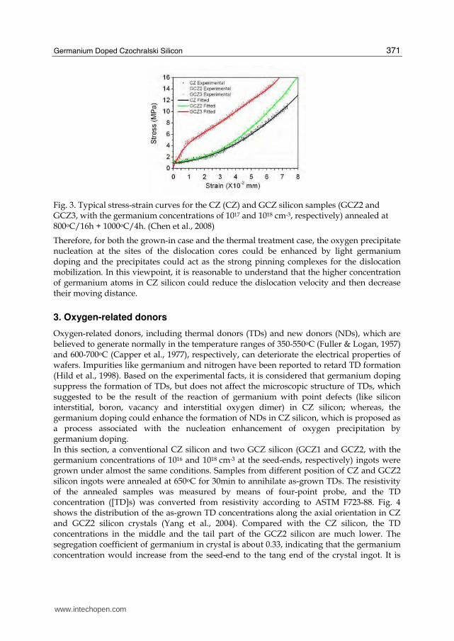
6.2 Improved internal gettering capability Double-side mirror polished wafers will be adopted for industrial manufacturing processes of large diameter CZ silicon, such as 300mm diameter silicon, ascribed to the higher requirements of wafer surface flatness. Therefore, the external gettering processes (such as sand sputtering processes and polycrystalline silicon depositing processes) on backside of CZ silicon wafers will be out of date and replaced by internal gettering (IG) processes based on the formation of high density BMDs in bulk and the thin defect-free denuded zone (DZ) in sub-surface of wafers simultaneously, which can be illustrated in Fig. 23(c) (Chen & Yang, 2009). However, with the ever-decreasing feature size of integrated circuits, the thermal budget for advanced devices is reduced to improve the characteristics; meanwhile, the
www.intechopen.com
Advances in Solid State Circuits Technologies
388
application of magnetic-filed CZ-grown method to large diameter crystal growth leads to the reduction of oxygen concentration in silicon. Both trends led to the density reduction of BMDs which are related to gettering sites for metallic contamination. Fig. 23 illustrates the model of the influence of germanium on generation of IG structure for CZ silicon wafer. Generally, for IG effect, both the high density BMDs and the suitable width of DZ could be generated in the CZ silicon doped with some types of impurities, so as to improve the IG capability of the metal contamination and improve the quality of IC devices. Compared to the CZ silicon, germanium atoms could generally induce germanium-related complexes and then seed for oxygen precipitation in bulk silicon during IG denudation processing based on either CFA or RTA processing. Both the good-quality defect-free DZ in sub-surface region and the BMD region with higher density in bulk silicon could be obtained simultaneously in the GCZ silicon. Generally, the DZ shrinks and is
Fig. 23. Schematic illustrations for internal gettering (IG) structure’ in GCZ silicon wafers. (a)-(d) shows the normal steps generating IG structure for silicon wafer and the gettering capability. As an example, (e)-(f) shows the germanium effects upon IG structure and capability. (Chen & Yang, 2009)
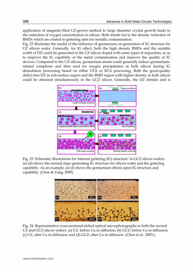
Fig. 24. Representative cross-sectional etched optical microphotographs in both the normal CZ and GCZ silicon wafers. (a) CZ, before Cu in-diffusion; (b) GCZ, before Cu in-diffusion; (c) CZ, after Cu in-diffusion; and (d) GCZ, after Cu in-diffusion. (Chen et al., 2007c)
www.intechopen.com

Germanium Doped Czochralski Silicon
389
slightly smaller than that of the CZ silicon wafer, which might be ascribed to the denser small precipitates located at the boundary of DZ and BMD region. Nevertheless, it has been also indicated that the DZs could present in the GCZ silicon wafers after a certain critical anneals despite the width shrinkage (Chen et al., 2007c). IG capability for metallic contamination could be therefore enhanced by intentional germanium doping in CZ silicon wafers. Taking copper contamination as an example (Chen et al., 2007c). Fig. 24 shows the cross-sectional etching optical photographs of both the normal CZ and GCZ silicon wafers before and after Cu diffusion in 1100oC/1h. As can be seen, denser BMDs of smaller size with denser Cu precipitates were presented in bulk of the GCZ silicon wafers in comparison with the CZ silicon, indicating a stronger IG capability in the GCZ silicon. The explanation could be, the denser gettering sites (even with smaller size) can lower down the total interstitial Cu concentration in wafer bulk, therefore more Cu atoms could be gettered in the GCZ silicon due to the denser but smaller BMDs. It is noted that the fairly clean DZs near surfaces remained in both the silicon wafers, which ensures the integrity of wafer sub-surface for device fabrication.
7. Summary
We have illustrated the effect of germanium doping in CZ silicon on mechanical strength, oxygen-related donors, oxygen precipitation and void defects. It has been established that the mechanical strength of silicon wafers could be improved by intended germanium doping, which benefits the improved production yield of wafers. It is also found that germanium suppresses the generation of TDs, which benefits the stable electrical property of wafers. More importantly, germanium has been found to suppress the formation of void defects, which can be annihilated easily during high temperature treatments. Moreover, oxygen precipitation can be enhanced by germanium doping, and therefore IG capability could be improved. Additionally, compared to nitrogen doped CZ silicon, germanium doping level in CZ silicon could be much easier to control, and no electrical Centers such as shallow thermal donors will be introduced. Ascribing to the novel properties, it is considered that GCZ silicon could satisfy the higher requirements of ULSI.
8. References
Adachi, N., Hisatomi, T., Sano, M., & Tsuya, H. (2000). Reduction of Grown-In Defects by High Temperature Annealing. Journal of The Electrochemical Society, 147, 350.
Akatsuka, M., Sueoka, K., Katahama, H., Morimoto, N., & Adachi, N. (1997). Pinning effect on punched-out dislocations in silicon wafers investigated using indentation method. Japanese Journal of Applied Physics Part 2-Letters & Express Letters, 36, 11A, L1422-L1425.
Babich, V.M., Baran, N.P., Zotov, K.I., Kiritsa, V.L., & Kovalchuk, V.B. (1995). Low-temperature diffusion of oxygen and formation of thermal donors in silicon doped with an isovalent germanium impurity. Fizika i Tekhnika Poluprovodnikov, 29, 0015-3222.
Babitskii, Y.M., Gorbacheva, N.I., Grinshtein, P.M., Il'in, M.A., Kuznetsov, V.P., Mil'vidskii, M.G., & Turovskii, B.M. (1988). Kinetics of generation of low-temperature oxygen donors in silicon containing isovalent impurities. Fizika i Tekhnika Poluprovodnikov, 22, 2, 307-312, 0015-3222
www.intechopen.com

Advances in Solid State Circuits Technologies
390
Babitskii, Y.M., Grinshtein, P.M., Il'in, M.A., Kuznetsov, V.P., & Mil'vidskii, M. (1985). Behavior of oxygen in silicon doped with isovalent impurities. Fizika i Tekhnika Poluprovodnikov, 19, 11, 1982-1985, 0015-3222
Borghesi, A., Pivac, B., Sassella, A., & Stella, A. (1995). Oxygen precipitation in silicon. Journal of Applied Physics, 77, 4169.
Budtz-Jorgensen, C.V., Kringhoj, P., Larsen, A.N., & Abrosimov, N.V. (1998). Deep-level transient spectroscopy of the Ge-vacancy pair in Ge-doped n-type silicon. Physical Review B, 58, 3, 1110-1113, 0163-1829.
Capper, P., Jones, A.W., Wallhouse, E.J., & Wilkes, J.G. (1977). The effects of heat treatment on dislocation-free oxygen-containing silicon crystals. Journal of Applied Physics, 48, 1646.
Chen, J., Ma, X., & Yang, D. (2010). Impurity Engineering of Czochralski Silicon. Solid State Phenomena, 156-158, 261-267.
Chen, J., & Yang, D. (2009). Impurity engineering for germanium-doped Czochralski silicon wafer used for ultra large scale integrated circuit. Physica Status Solidi C - Current Topics in Solid State Physics, Vol 6, No 3, 6, 3, 625-632, 1610-1634.
Chen, J., Yang, D., Li, H., Ma, X., & Que, D. (2006a). Enhancement effect of germanium on oxygen precipitation in Czochralski silicon. Journal of Applied Physics, 99, 7, 0021-8979.
Chen, J., Yang, D., Li, H., Ma, X., & Que, D. (2006b). Germanium effect on as-grown oxygen precipitation in Czochralski silicon. Journal of Crystal Growth, 291, 1, 66-71, 0022-0248.
Chen, J., Yang, D., Li, H., Ma, X., Tian, D., Li, L., & Que, D. (2007a). Crystal-originated particles in germanium-doped czochralski silicon crystal. Journal of Crystal Growth, 306, 2, 262-268, 0022-0248.
Chen, J., Yang, D., Ma, X., Li, H., & Que, D. (2007b). Intrinsic gettering based on rapid thermal annealing in germanium-doped Czochralski silicon. Journal of Applied Physics, 101, 3, 0021-8979.
Chen, J., Yang, D., Ma, X., & Que, D. (2009). Rapid-thermal-anneal-based internal gettering for germanium-doped Czochralski silicon. APPLIED PHYSICS A-MATERIALS SCIENCE & PROCESSING, 94, 4, 905-910, 0947-8396.
Chen, J., Yang, D., Ma, X., Wang, W., Zeng, Y., & Que, D. (2007c). Investigation of intrinsic gettering for germanium doped Czochralski silicon wafer. Journal of Applied Physics, 101, 11, 0021-8979.
Chen, J., Yang, D., Ma, X., Zeng, Z., Tian, D., Li, L., Que, D., & Gong, L. (2008). Influence of germanium doping on the mechanical strength of Czochralski silicon wafers. Journal of Applied Physics, 103, 12, 0021-8979.
Chen, J.H., Yang, D.R., Ma, X.Y., Li, H., Fu, L.M., Li, M., & Que, D.L. (2007d). Dissolution of oxygen precipitates in germanium-doped Czochralski silicon during rapid thermal annealing. Journal of Crystal Growth, 308, 2, 247-251, 0022-0248.
Cui, C., Yang, D., Ma, X., Li, M., & Que, D. (2006). Effect of light germanium doping on thermal donors in Czochralski silicon wafers. Materials Science in Semiconductor Processing, 9, 1-3, 110-113, 1369-8001.
Fukuda, T., & Ohsawa, A. (1992). Mechanical strength of silicon crystals with oxygen and/or germanium impurities. Applied Physics Letters, 60, 1184.
www.intechopen.com

Germanium Doped Czochralski Silicon
391
Fuller, C.S., & Logan, R.A. (1957). Effect of Heat Treatment upon the Electrical Properties of Silicon Crystals. Journal of Applied Physics, 28, 1427.
Hild, E., Gaworzewski, P., Franz, M., & Pressel, K. (1998). Thermal donors in silicon-rich SiGe. Applied Physics Letters, 72, 11, 1362-1364, 0003-6951.
Huang, X., Sato, T., Nakanishi, M., Taishi, T., & Hoshikawa, K. (2003). High strength Si wafers with heavy B and Ge codoping. Japanese Journal of Applied Physics Part 2-Letters, 42, 12B, L1489-L1491, 0021-4922.
Huth, S., Breitenstein, O., Huber, A., & Lambert, U. (2000). Localization of gate oxide integrity defects in silicon metal-oxide-semiconductor structures with lock-in IR thermography. Journal of Applied Physics, 88, 7, 4000-4003, 0021-8979.
Itsumi, M., Akiya, H., Ueki, T., Tomita, M., & Yamawaki, M. (1995). The composition of octahedron structures that act as an origin of defects in thermal SiO on Czochralski silicon. Journal of Applied Physics, 78, 5984.
Jiang, H., Yang, D., Ma, X., Tian, D., Li, L., & Que, D. (2006). Growth of misfit dislocation-free p/p(+) thick epitaxial silicon wafers on Ge-B-codoped substrates. Physica B-Condensed Matter, 376, 841-844, 0921-4526.
Joly, J.P., & Robert, V. (1994). silicon wafers: a detailed analysis. Semicond. Sci. Technol, 9, 105-111.
Kaiser, W., Frisch, H.L., & Reiss, H. (1958). Mechanism of the formation of donor states in heat-treated silicon. Physical Review, 112, 5, 1546-1554, 0031-899X.
Kishino, S., Matsushita, Y., Kanamori, M., & Iizuka, T. (1982). Thermally Induced Microdefects in Czochralski-Grown Silicon - Nucleation and Growth-Behavior. Japanese Journal of Applied Physics Part 1-Regular Papers Short Notes & Review Papers, 21, 1, 1-12, 0021-4922.
Kissinger, G., Vanhellemont, J., Lambert, U., Graf, D., Dornberger, E., & Richter, H. (1998). Influence of Residual Point Defect Supersaturation on the Formation of Grown-In Oxide Precipitate Nuclei in CZ-Si. Journal of The Electrochemical Society, 145, 5, L75-L78.
Li, H., Yang, D., Ma, X., Yu, X., & Que, D. (2004a). Germanium effect on oxygen precipitation in Czochralski silicon. Journal of Applied Physics, 96, 8, 4161-4165, 0021-8979.
Li, H., Yang, D., Yu, X., Ma, X., Tian, D., Li, L., & Que, D. (2004b). The effect of germanium doping on oxygen donors in Czochralski-grown silicon. Journal of Physics-Condensed Matter, 16, 32, 5745-5750, 0953-8984.
Minowa, K., & Sumino, K. (1992). Stress-induced amorphization of silicon crystal by mechanical scratching. Physical Review Letters, 69, 2, 320-322, 0031-9007.
Park, J.G., Lee, G.S., Kwack, K.D., & Park, J.M. (2000). Crystal Originated Particle Induced Isolation Failure in Czochralski Silicon Wafers. Japanese Journal of Applied Physics, 39, 1, 197.
Pensl, G., Schulz, M., Holzlein, K., Bergholz, W., & Hutchison, J.L. (1989). New oxygen donors in silicon Applied Physics a-Materials Science & Processing, 48, 1, 49-57, 0947-8396.
Shimura, F. (1994). Oxygen in silicon. In R.K. Willardson, E.R. Weber, & A.C. Beer, Semiconductors and semimetals. New York: Academic Press, p. 434.
Voronkov, V.V. (1982). The mechanism of swirl defects formation in silicon Journal of Crystal Growth, 59, 3, 625-643, 0022-0248.
www.intechopen.com

Advances in Solid State Circuits Technologies
392
Voronkov, V.V., & Falster, R. (1998). Vacancy-type microdefect formation in Czochralski silicon. Journal of Crystal Growth, 194, 1, 76-88, 0022-0248.
Voronkov, V.V., & Falster, R. (2002). Intrinsic point defects and impurities in silicon crystal growth. Journal of the Electrochemical Society, 149, 3, G167-G174, 0013-4651.
Wagner, P., & Hage, J. (1989). Thermal double donors in silicon. Applied Physics a-Materials Science & Processing, 49, 2, 123-138, 0947-8396.
Wijaranakula, W. (1994). Dissolution kinetics of D defects in Czochralski silicon. Journal of Applied Physics, 75, 7, 3678-3680, 0021-8979.
Yamagishi, H., Fusegawa, I., Fujimaki, N., & Katayama, M. (1992). Recognition of D defects in silicon single crystals by preferential etching and effect on gate oxide integrity. Semicondutor Science and Technology, 7, 1, A135-138.
Yang, D., Chen, J., Ma, X., & Que, D. (2009). Impurity engineering of Czochralski silicon used for ultra large-scaled-integrated circuits. Journal of Crystal Growth, 311, 3, 837-841, 0022-0248.
Yang, D., Li, H., Yu, X., Ma, X., Tian, D., Li, L., & Que, D. (2004). Oxygen-related donors in germanium doped Czochralski silcion. High Purity Silicon VIII: the 206th Fall Meeting of The Electrochemical Society in Honolulu. Hawaii, USA.
Yang, D., Yu, X., Ma, X., Xu, J., Li, L., & Que, D. (2002). Germanium effect on void defects in Czochralski silicon. Journal of Crystal Growth, 243, 3-4, 371-374, 0022-0248.
Yang, D., Chen, J., Li, H., Ma, X., Tian, D., Li, L., & Que, D. (2006a). Micro-defects in Ge doped Czochralski grown Si crystals. Journal of Crystal Growth, 292, 2, 266-271, 0022-0248.
Yang, D., Chen, J., Li, H., Ma, X., Tian, D., Li, L., & Que, D. (2006b). Germanium effect on oxygen-related defects in Czochralski silicon. Physica Status Solidi a-Applications and Materials Science, 203, 4, 685-695, 0031-8965.
Yonenaga, I. (2005). Nitrogen effects on generation and velocity of dislocations in Czochralski-grown silicon. Journal of Applied Physics, 98, 2, 023517, 0021-8979.
Yu, X., Yang, D., Ma, X., Yang, J., Li L., Que D.(2002). Grown-in defects in nitrogen-doped Czochralski Silicon. Journal of Applied Physics,92, 1, 188-194
www.intechopen.com

Advances in Solid State Circuit TechnologiesEdited by Paul K Chu
ISBN 978-953-307-086-5Hard cover, 446 pagesPublisher InTechPublished online 01, April, 2010Published in print edition April, 2010
InTech EuropeUniversity Campus STeP Ri Slavka Krautzeka 83/A 51000 Rijeka, Croatia Phone: +385 (51) 770 447 Fax: +385 (51) 686 166www.intechopen.com
InTech ChinaUnit 405, Office Block, Hotel Equatorial Shanghai No.65, Yan An Road (West), Shanghai, 200040, China
Phone: +86-21-62489820 Fax: +86-21-62489821
This book brings together contributions from experts in the fields to describe the current status of importanttopics in solid-state circuit technologies. It consists of 20 chapters which are grouped under the followingcategories: general information, circuits and devices, materials, and characterization techniques. Thesechapters have been written by renowned experts in the respective fields making this book valuable to theintegrated circuits and materials science communities. It is intended for a diverse readership includingelectrical engineers and material scientists in the industry and academic institutions. Readers will be able tofamiliarize themselves with the latest technologies in the various fields.
How to referenceIn order to correctly reference this scholarly work, feel free to copy and paste the following:
GJiahe Chen and Deren Yangoran (2010). Germanium Doped Czochralski Silicon, Advances in Solid StateCircuit Technologies, Paul K Chu (Ed.), ISBN: 978-953-307-086-5, InTech, Available from:http://www.intechopen.com/books/advances-in-solid-state-circuit-technologies/germanium-doped-czochralski-silicon