Galani Tina G., Riya Saini and R.D.Daruwala Design and ...iret.co.in/Docs/Volume 5/Issue1/4. Design...
7
Galani Tina G., Riya Saini and R.D.Daruwala 18 International Journal of Emerging Trends in Electrical and Electronics (IJETEE – ISSN: 2320-9569) Vol. 5, Issue. 1, July-2013. Design and Implementation of 32 – bit RISC Processor using Xilinx Galani Tina G., Riya Saini and R.D.Daruwala Abstract: These RISC or Reduced Instruction Set Computer is a design philosophy that has become a mainstream in Scientific and engineering applications. The main objective of this paper is to design and implement of 32 – bit RISC (Reduced Instruction Set Computer) processor using XILINX VIRTEX4 Tool for embedded and portable applications. The design will help to improve the speed of processor, and to give the higher performance of the processor. The most important feature of the RISC processor is that this processor is very simple and support load/store architecture. The important components of this processor include the Arithmetic Logic Unit, Shifter, Rotator and Control unit. The module functionality and performance issues like area, power dissipation and propagation delay are analyzed using Virtex4 XC4VLX15 XILINX tool. Keywords: Processor, Reduced Instruction Set Computer (RISC), VHDL, Xilinx 12.1, FPGA. I. INTRODUCTION A digital system was developed by using a set of interconnected digital integrated circuits like counters, buffers, logic gates and memory. It requires lots of analysis, testing and to adapt the design metrics like speed, response time, power consumption etc. which resulted very difficult for development. Also every design change implied a whole analysis and most times expensive. Nowadays, computer and mobile phones is indispensable tool for most of everyday activities. This places an increasing burden on the embedded microprocessor to provide high performance while retaining low power consumption and small die size, which increase the complexity of the device [3]. However, as products grow in complexity more processing power is required while the expectation on battery life also increases. With the rapid development of silicon technology RISC includes extensions to RISC concepts that help achieve given levels of performance at significantly lower cost than other systems. The main features of RISC processor are the instruction set can be hardwired [7] to speed instruction execution. Galani Tina G. and Riya Saini are M.Tech Student, Department of Electrical, VJTI College of Engg., Mumbai and R.D.Daruwala is working as Professor, Department of Electrical, VJTI College of Engg., Mumbai, Email: [email protected] In the present work, the design of a 32-bit data width Reduced Instruction Set Computer (RISC) processor is presented. It has a complete instruction set, program and data memories, general purpose registers and a simple Arithmetical Logical Unit (ALU) for basic operations. In this design, most instructions are of uniform length and similar structure, arithmetic operations are restricted to CPU registers and only separate load and store instructions access memory. The architecture supports 16 instructions to support Arithmetic, Logical, Shifting and Rotational operations. The remainder of this paper is organized as follows. Section II explains System architecture of a 32 – bit RISC processor. Section III presents the implementation of modules of RISC processor and the simulation results implemented in advanced 90nm process technology. Section IV presents RISC Instruction set format. Section V discusses summary with the implementation of the RISC design topology. The final section presents the Conclusion and References. II. SYSTEM ARCHITECTURE OF A 32 – BIT RISC PROCESSOR The system architecture of a 32 - bit RISC processor is shown in Fig. 1. The RISC processor architecture consists of Arithmetic Logic Unit (ALU), Control Unit (CU), Barrel Shifter, Booth’s Multiplier, Register File and Accumulator. RISC processor is designed with load/store (Von Neumann) architecture, meaning that all operations are performed on operands held in the processor registers and the main memory can only be accessed through the load and store instructions. One shared memory for instructions (program) and data with one data bus and one address bus between processor and memory [7]. Instruction and data are fetched in sequential order so that the latency incurred between the machine cycles can be reduced. For increasing the speed of operation RISC processor is designed with five stage pipelining. The pipelining stages are Instruction Fetch (IF), Instruction Decode (ID), Execution (EX), Data Memory (MEM), and Write Back (WB). The function of the instruction fetch unit is to obtain an instruction from the instruction memory using the current value of the PC and increment the PC value for the next instruction. The main function of the instruction decode unit is to use the 32-bit instruction provided from the previous instruction fetch unit to index the register file and obtain the register data values. The instructions opcode field bits [31-26] are sent to a control unit to determine the type of instruction to execute. The type of instruction then determines which
Transcript of Galani Tina G., Riya Saini and R.D.Daruwala Design and ...iret.co.in/Docs/Volume 5/Issue1/4. Design...

Galani Tina G., Riya Saini and R.D.Daruwala 18
International Journal of Emerging Trends in Electrical and Electronics (IJETEE – ISSN: 2320-9569) Vol. 5, Issue. 1, July-2013.
Design and Implementation of 32 – bit RISC Processor using Xilinx
Galani Tina G., Riya Saini and R.D.Daruwala
Abstract: These RISC or Reduced Instruction Set Computer is a design philosophy that has become a mainstream in Scientific and engineering applications. The main objective of this paper is to design and implement of 32 – bit RISC (Reduced Instruction Set Computer) processor using XILINX VIRTEX4 Tool for embedded and portable applications. The design will help to improve the speed of processor, and to give the higher performance of the processor. The most important feature of the RISC processor is that this processor is very simple and support load/store architecture. The important components of this processor include the Arithmetic Logic Unit, Shifter, Rotator and Control unit. The module functionality and performance issues like area, power dissipation and propagation delay are analyzed using Virtex4 XC4VLX15 XILINX tool.
Keywords: Processor, Reduced Instruction Set Computer
(RISC), VHDL, Xilinx 12.1, FPGA.
I. INTRODUCTION A digital system was developed by using a set of
interconnected digital integrated circuits like counters, buffers, logic gates and memory. It requires lots of analysis, testing and to adapt the design metrics like speed, response time, power consumption etc. which resulted very difficult for development. Also every design change implied a whole analysis and most times expensive.
Nowadays, computer and mobile phones is indispensable tool for most of everyday activities. This places an increasing burden on the embedded microprocessor to provide high performance while retaining low power consumption and small die size, which increase the complexity of the device [3]. However, as products grow in complexity more processing power is required while the expectation on battery life also increases.
With the rapid development of silicon technology RISC includes extensions to RISC concepts that help achieve given levels of performance at significantly lower cost than other systems. The main features of RISC processor are the instruction set can be hardwired [7] to speed instruction execution.
Galani Tina G. and Riya Saini are M.Tech Student, Department of Electrical, VJTI College of Engg., Mumbai and R.D.Daruwala is working as Professor, Department of Electrical, VJTI College of Engg., Mumbai, Email: [email protected]
In the present work, the design of a 32-bit data width Reduced Instruction Set Computer (RISC) processor is presented. It has a complete instruction set, program and data memories, general purpose registers and a simple Arithmetical Logical Unit (ALU) for basic operations. In this design, most instructions are of uniform length and similar structure, arithmetic operations are restricted to CPU registers and only separate load and store instructions access memory. The architecture supports 16 instructions to support Arithmetic, Logical, Shifting and Rotational operations.
The remainder of this paper is organized as follows. Section II explains System architecture of a 32 – bit RISC processor. Section III presents the implementation of modules of RISC processor and the simulation results implemented in advanced 90nm process technology. Section IV presents RISC Instruction set format. Section V discusses summary with the implementation of the RISC design topology. The final section presents the Conclusion and References.
II. SYSTEM ARCHITECTURE OF A 32 – BIT RISC PROCESSOR
The system architecture of a 32 - bit RISC processor is shown in Fig. 1. The RISC processor architecture consists of Arithmetic Logic Unit (ALU), Control Unit (CU), Barrel Shifter, Booth’s Multiplier, Register File and Accumulator. RISC processor is designed with load/store (Von Neumann) architecture, meaning that all operations are performed on operands held in the processor registers and the main memory can only be accessed through the load and store instructions. One shared memory for instructions (program) and data with one data bus and one address bus between processor and memory [7]. Instruction and data are fetched in sequential order so that the latency incurred between the machine cycles can be reduced. For increasing the speed of operation RISC processor is designed with five stage pipelining. The pipelining stages are Instruction Fetch (IF), Instruction Decode (ID), Execution (EX), Data Memory (MEM), and Write Back (WB).
The function of the instruction fetch unit is to obtain an instruction from the instruction memory using the current value of the PC and increment the PC value for the next instruction. The main function of the instruction decode unit is to use the 32-bit instruction provided from the previous instruction fetch unit to index the register file and obtain the register data values. The instructions opcode field bits [31-26] are sent to a control unit to determine the type of instruction to execute. The type of instruction then determines which
Galani Tina G., Riya Saini and R.D.Daruwala 19
International Journal of Emerging Trends in Electrical and Electronics (IJETEE – ISSN: 2320-9569) Vol. 5, Issue. 1, July-2013.
control signals are to be asserted and what function the ALU is to perform, thus decoding the instruction. The register file reads in the requested addresses and outputs the data values contained in these registers [1].
Fig. 1 System Architecture of a 32 - bit RISC processor
These data values can then be operated on by the ALU whose operation is determined by the control unit to either compute a memory address (e.g. load or store), compute an arithmetic result (e.g. add, and or slt), or perform a compare (e.g. branch). The control unit has two instruction decoders that decode the instruction bits and the decoded output of the control unit is fed as control signal either into Arithmetic logic unit (ALU) or Barrel shifter or Booth’s Multiplier. If the instruction decoded is arithmetic, the ALU result must be written to a register. If the instruction decoded is a load or a store, the ALU result is then used to address the data memory. The final step writes the ALU result or memory value back to the register file.
III. MODULES DESIGN OF 32 - BIT RISC PROCESSOR This section presents the design of different modules like
Control Unit (CU), ALU, Universal Shift Register, barrel shifter, Booth’s Multiplier and General Purpose Registers.
A. Control Unit The control unit of the RISC processor examines the
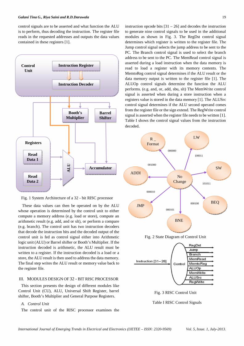
instruction opcode bits [31 – 26] and decodes the instruction to generate nine control signals to be used in the additional modules as shown in Fig. 3. The RegDst control signal determines which register is written to the register file. The Jump control signal selects the jump address to be sent to the PC. The Branch control signal is used to select the branch address to be sent to the PC. The MemRead control signal is asserted during a load instruction when the data memory is read to load a register with its memory contents. The MemtoReg control signal determines if the ALU result or the data memory output is written to the register file [1]. The ALUOp control signals determine the function the ALU performs. (e.g. and, or, add, sbu, slt) The MemWrite control signal is asserted when during a store instruction when a registers value is stored in the data memory [1]. The ALUSrc control signal determines if the ALU second operand comes from the register file or the sign extend. The RegWrite control signal is asserted when the register file needs to be written [1]. Table I shows the control signal values from the instruction decoded.
Fig. 2 State Diagram of Control Unit
Fig. 3 RISC Control Unit
Table I RISC Control Signals
Control Unit
Instruction Register
Instruction Decoder
Booth’s Multiplier
Barrel Shifter
Accumulator
Registers
Read Data 1
Read Data 2
AL
U
R _ Format
No Change
000000
LW
SW
BNE
JMP BEQ
ADDI
100011
000010
001000
000100
101011
000101

Galani Tina G., Riya Saini and R.D.Daruwala 20
International Journal of Emerging Trends in Electrical and Electronics (IJETEE – ISSN: 2320-9569) Vol. 5, Issue. 1, July-2013.
The entire design of the Control Unit is represented in Fig. 4 and the timing waveform for arithmetic unit simulated using Xilinx tool is shown in Fig. 5.
Fig. 4 RTL Schematic of Control Unit (CU)
Fig. 5 Simulated Timing Diagram of Control Unit
B. Arithmetic Logic Unit (ALU) The arithmetic/logic unit (ALU) executes all arithmetic and
logical operations. The arithmetic/logic unit can perform arithmetic operations or mathematical calculations [7] like addition, and subtraction. As its name implies, the arithmetic/logic unit also performs logical operations include Boolean comparisons, such as AND, OR, XOR, NAND, NOR and NOT operations. Table II shows the select lines values from the instruction decoded and operation performed according to select lines.
Table II Operation of Arithmetic Logic Unit (ALU)
Select Lines Op (2:0)
Function Performed
Op(2) Op(1) Op(0) Operation 0 0 0 ADD 0 0 1 SUB 0 1 0 NOT 0 1 1 NAND 1 0 0 NOR 1 0 1 AND 1 1 0 OR 1 1 1 XOR
The entire design of the ALU is represented in Fig.6 and the timing waveform for arithmetic unit simulated using Xilinx tool is shown in Fig. 7.
Fig. 6 RTL Schematic of Airthmatic Logic Unit (ALU)
Fig. 7 Simulated Timing Diagram of Arithmetic Logic Unit
A. Barrel Shifter The design consists of a total of eight 8x1 multiplexers. The
output of one multiplexer is connected as input to the next multiplexer in such a way that the input data gets shifted in each multiplexer thus performing the rotation operation. Depending on the select lines the number of rotation varies. With select lines low there is no output. If select line c0 is high 1-bit rotation takes place, if c1 is high 3-bit rotation. The rotation of the input data for different select lines is shown in Table III. The Fig. 8 shows the top block of the barrel shift rotator. The timing waveform for Barrel Shifter simulated using Xilinx tool is shown in Fig. 9.
Table III Operation of Barrel Shifter
Select Lines Output of Rotator Function
Performed
S2 S1 S0 Q7
Q6
Q5
Q4
Q3
Q2
Q1
Q0
0 0 1 1 0 1 0 0 0 0 1 1- Bit rotate 0 1 1 1 0 0 0 0 1 1 0 3- Bit rotate 1 0 1 0 0 0 1 1 0 1 0 5- Bit rotate 1 1 1 0 1 1 0 1 0 0 0 7- Bit rotate

Galani Tina G., Riya Saini and R.D.Daruwala 21
International Journal of Emerging Trends in Electrical and Electronics (IJETEE – ISSN: 2320-9569) Vol. 5, Issue. 1, July-2013.
Fig. 8 RTL Schematic of Barrel Shifter
Fig. 9 Simulated Timing Diagram of Barrel Shifter
A. Booth’s Multiplier The Multiplier is implemented using the modified Booth
algorithm. The two main advantages of this algorithm are speed and the ability to do signed multiplication (using two’s complement) without any extra conversions. The entire design of the Booth Multiplier is represented in Fig. 10. The flowchart for Booth Algorithm is given in Fig. 11. Booth's algorithm uses an extra bit on the right of the least significant bit in the product register. This bit starts out as 0.
Fig. 10. RTL Schematic of Booth’s Multiplier
Fig. 11 Flowchart of Booth Algorithm The multiplier is implemented using the modified booth
algorithm. The multiplier is scanned sequentially from right to left. In this case, however, three adjacent bits are examined during each step of the procedure. According to the value of the three bits, the multiplicand is added to or subtracted from the accumulated partial product and the later is then shifted. The timing waveform for Booth’s Multiplier simulated using Xilinx tool is shown in Fig. 12.
Start
Test Product (0) and Product (-1)
No Operation
Add Multiplicand to Left half of product. Place Left half of Product Register
No Operation
Subtract Multiplicand to Left half of product. Place Left half of Product Register.
Shift Product Register right 1 bit.
32nd repetition?
End
Yes
No
= 10 = 11
= 00 = 01

Galani Tina G., Riya Saini and R.D.Daruwala 22
International Journal of Emerging Trends in Electrical and Electronics (IJETEE – ISSN: 2320-9569) Vol. 5, Issue. 1, July-2013.
Fig. 12 Simulated Timing Diagram of Booth’s Multiplier
A. General Purpose Register The eight bit input data is stored in this register. This
register acts as a source register. The register file has two read and one write input ports, meaning that during one clock cycle [1], the processor must be able to read two independent data values and write a separate value into the register file. The register file was implemented in VHDL by declaring it as a one-dimensional array of 32 elements or registers each 8-bit wide. It consists of eight D – flip flops and eight AND gates. The gate level view of the register is given by Fig. 13. Taking CLOCK as low or high and RegWr as high the data is stored in the register. The simulated timing waveform in Fig. 14.
Fig. 13 RTL Schematic of Register File
Fig. 14 Simulated Timing Diagram of Register File
IV. RISC INSTRUCTION SET RISC only has three instruction types: I-type is used for the
Load and Stores instructions, R-type is used for Arithmetic instructions, and J-type is used for the Jump instructions [1] as shown in Fig. 15. Table IV provides a description of each of
the fields used in the three different instruction types. Arithmetic instructions or R-type include: ALU Immediate (e.g. addi), three-operand (e.g. add, and, slt), and shift instructions (e.g. sll, srl). The J-type instructions are used for jump instructions (e.g. j). Branch instructions (e.g. beq, bne) are I-type instructions which use the addition of an offset value from the current address in the address/immediate field along with the program counter (PC) to compute the branch target address; this is considered PC-relative addressing.
The most significant feature of instruction set is that all of instruction may be executed conditionally according to the condition flags. A condition field within all instructions is compared with the condition flag in program status register and the result of the comparison determines whether the instruction can be executed or not. This reduces the need for forward branches and allows very dense in-line code (without branches) to be written. In addition, shift operation is performed in serial with ALU in all data path cycles. This enables data processing instructions to execute various arithmetic operations using shift operation in one clock cycle [9].
Table IV RISC Instruction Fields
Fig. 15 RISC Instruction Types
V. SUMMARY This section presents the performance of the processor in
terms of its Total Power and Delay that are obtained using the Virtex4 XC4VLX15 XILINX tool. Table V presents the maximum power dissipation, area occupied and time taken by each module to operate the processor.
Table V Delay, Total Power and Area Calculation

Galani Tina G., Riya Saini and R.D.Daruwala 23
International Journal of Emerging Trends in Electrical and Electronics (IJETEE – ISSN: 2320-9569) Vol. 5, Issue. 1, July-2013.
Topology Delay (ns)
Slices Utilized (Area)
AT Power
Dissipation 10-9W
Total Power
(W) Control
Unit 0.905 15 13.575 0.159 0.165
ALU 4.495 60 269.7 0.159 0.168
Barrel Shifter 2.905 262 761.11 0.159 0.164
Booth’s Multiplier 4.495 60 269.7 0.159 0.166
Register File 5.443 74 402.782 0.159 0.166
Total 18.243 471 8592.453 0.829
It is observed that the overall delay of the circuit is 18.243 ns. The maximum area is occupied by the Barrel Shifter and ALU. The overall power dissipation of this processor is observed to be 6.258 W. The power dissipation can even be reduced if the circuit is designed with any adiabatic logic. Fig. 16 and Fig. 17 show the variation of area, power dissipation and delay of the whole RISC processor and for each sub modules respectively. From the graph it is seen that the maximum power dissipation and chip area is exhibited by the ALU unit.
Fig. 16 Delay Estimation
Fig. 17 Area Estimation
VI. CONCLUSION A 32-bit RISC processor [2] with 16 instruction set has
been designed. Every instruction is executed in one clock cycles with 5-stage pipelining. The design is verified through exhaustive simulations. The processor achieves higher performance, lower area and lower power dissipation. This processor can be used as a systolic core to perform mathematical computations like solving polynomial and differential equations. Apart from this it can be used in portable gaming kits.
VII. REFERENCES [1] David A. Patterson, John L. Hennessy, “Computer
Organization and Design - The Hardware/Software Interface” Second Edition (1998) Morgan Kaufmann Publisher, Inc.
[2] Xiao Li, Longwei Ji, Bo Shen, Wenhong Li, Qianling Zhang, “VLSI implementation of a High-performance 32-bit RISC Microprocessor”, Communications, Circuits and Systems and West Sino Expositions, IEEE 2002 International Conference on ,Volume 2, 2002 ,pp. 1458 – 1461.
[3] Kusumlata Pisda, Deependra Pandey, “Realization & Study of High Performance MIPS RISC Processor Design Using VHDL”, International Journal of Emerging trends in Engineering and Development, Volume 7, Issue 2, November 2012, pp. 134 – 139, ISSN: 2249 – 6149.
[4] Kirat Pal Singh, Shivani Parmar, “VHDL Implementation of a MIPS – 32 bit Pipeline Processor”, International Journal of Applied Engineering Research, Volume 7, Issue 11, ISSN: 0973 – 4562.
[5] Samiappa Sakthikumaran, S.Salivahanan and V.S.Kaanchana Bhaaskaran,“16-Bit RISC Processor Design For Convolution Application”,IEEE
0123456
Delay (ns)

Galani Tina G., Riya Saini and R.D.Daruwala 24
International Journal of Emerging Trends in Electrical and Electronics (IJETEE – ISSN: 2320-9569) Vol. 5, Issue. 1, July-2013.
International Conference on Recent Trends In Information Technology, June 2011, pp.394-397.
[6] Rupali S. Balpande and Rashmi S. Keote, “Design of FPGA based Instruction Fetch & Decode Module of 32-bit RISC (MIPS) Processor, International Conference on Communication Systems and Network Technologies pp. 409 – 413.
[7] R. Uma, “Design and Performance Analysis of 8 – bit RISC Processor using Xilinx Tool”, International Journal of Engineering Research and Applications, Volume 2, Issue 2, March – April 2012, pp. 053 – 058, ISSN: 2248 – 9622.
[8] V.N.Sireesha and D.Hari Hara Santosh, “FPGA Implementation of a MIPS RISC Processor”, International Journal of Computer Technology and Applications, Volume 3, Issue 3, pp. 1251 – 1253, ISSN: 2229 – 6093.
[9] M.Yugandhar and N.Suresh babu, “VLSI Design of Reduced Instruction set Computer Processor Core Using VHDL”, International Journal of Electronics, Communication & Instrumentation Engineering Research and Development (IJECIERD), Volume 2, Issue 3, pp. 42 – 47, ISSN: 2249 – 684X.