
Fully Automated VPD ICP-MS System - Arcsis: Actualités Automated VPD ICP-MS System October 2011...
57
Fully Automated VPD ICP-MS System October 2011 P.Maillot Rousset Technology Center STMicroectronics
Transcript of Fully Automated VPD ICP-MS System - Arcsis: Actualités Automated VPD ICP-MS System October 2011...

Fully Automated VPD ICP-MS System
October 2011
P.Maillot Rousset Technology CenterSTMicroectronics

Outline
�Standard industry monitoring
�Principle of VPD and ICP-MS
�CIMPACA equipment description
Area of interest
?
�CIMPACA equipment description
�Acceptance test
�Applications
�Conclusion

Acknowledgements
• Success of this project was made possible
thanks to the 2009 evaluation team
– E. Lattard LFoundry
– C. Galvez Tera
– D. Goguenheim IM2NP
– H. Wortham LCP– H. Wortham LCP
– F. Michel Vegatec
– C.Grosjean ST/CIMPACA
– A. Planchais ST/CIMPACA
– C. Martin ST
– P. Maillot ST

Acknowledgements
• Installation and qualification was made
possible thanks to
– I. Poulet Tera
– D.Vacher Air Liquide
– S. Giorgi Air Liquide
– A. Planchais ST/CIMPACA– A. Planchais ST/CIMPACA
– C. Martin ST
– P. Maillot ST
– And the local ST EES/facilities/hook-up team!

Basic Metal behavior
SiO2
Segregation
Ex: Ti
Diffusion
Ex: Fe
Precipitation
Ex: Cu Si

Basic Metal behavior
Implant/Recoilor Diffusion
Surface monitoring
Wet Clean, Plasma
Bulk monitoring
SiO2
Si

Standard industry monitoring
• Surface
– Sweeping TXRF
• Bulk :
– Post anneal SPV (or equivalent lifetime
7
– Post anneal SPV (or equivalent lifetime
measurement technique)

Drawbacks
� TXRF
� Limited in terms of detection limits
� 3 beam needed to cover all elements
� Edge exclusion
� No bevel capability
8
� No bevel capability
� SPV
� No specie ID except for Fe
� Indirect techniques / Artifacts / Data interpretation
� Edge exclusion
� No bevel capability

Thus we needed
� Improved detection limits
� Specie identification over the whole atomic
table
9
table
� VPD ICP-MS combines both capabilities

VPD principle
Etching of SiO2 Layer with HF Vapor
Vapor Phase Decomposition

ICP-MS principleInductively Coupled Plasma Mass Spectrometry

Limitation of Conventional VPD
• Loss of scan solution during scan due to poor holding capacity.
• Thicker bulk-Si or poly-Si etching difficult• Recovery of thicker nitride film impossible.• Full wafer collection only giving average value• Full wafer collection only giving average value• Manual wafer handling and manual transferred of
droplet to ICP-MS / cross contamination risk• A separate system is required to perform bevel
scan.

Specie Surface BulkCalcium 1.13 3.34Sodium 2.91 1.29Magnésium 0.57 0.85Aluminum 27.24 34.67Potassium 0.65 0.35Titanium 0.32 12.59
Standard VPD is blind to energetic or
diffused contaminants
• Thus post implant or
diffusion requires bulk VPD
monitoring
Titanium 0.32 12.59Chromium 0.22 0.1Iron 1.43 0.92Cobalt ND NDNickel 0.08 0.14Copper ND 3.18Zinc 0.3 0.11
Molybdenum 0.29 278.9
Tungsten 0.13 1.45VPD ICP-MS data in units of 1010at/cm²
*Maillot/ Roux (STMicroelectronics) .
18th international conference on ion
implantation technology (IIT2010),
Kyoto , Japan, June 2010

Automated VPD ICP-MS
• Risk of loss of scan solution drastically reduced
• No edge exclusion
• Bulk-Si or poly-Si analysis
• Thick nitride analysis
• Bevel analysis• Bevel analysis
• Partial analysis , local analysis
• SMIF enclosure , automation of wafer handling , scan and droplet transfer to ICP-MS minimize risk of cross contamination

CIMPACA equipment overview
VPD : ExpertTM from IASVPD : ExpertTM from IAS
ICP-MS : NexIonTM from Perkin-Elmer

VPD ICP-MS CIMPACA lab

ExpertTM VPD system

NexIonTM ICP-MS

Interface between VPD and ICP-MS

Sas for chemicals

Inside ExpertTM

Inside ExpertTM

Operation sequence (1/3)
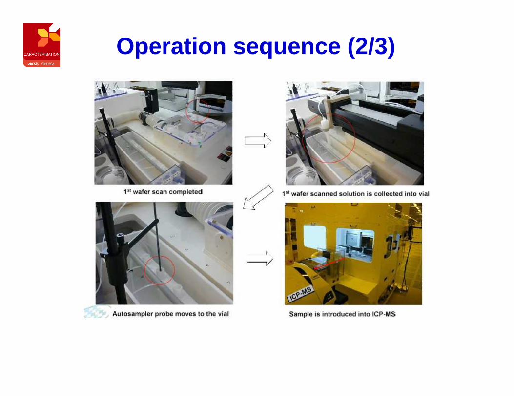
Operation sequence (2/3)

Operation sequence (3/3)

VPD chamber
EPD SensorPort
Wafer LoadSensor
VPDChamber
LocalExhaust
Chamber
HF vapor in HF vapor in
VPD chamber Si wafer with various film layer
Si wafer is placed in a VPD chamber, where HF vapor is introduced and HF vapor etches layers of films on bare-Si wafer. Metallic impurities remain on the bare Si wafer.VPD can etch various types of film on bare-Si wafer.

Qualification test and tool
capabilitiescapabilities

Acceptance specification and results
N o.N o.N o.N o. ParameterParameterParameterParameter SpecificationSpecificationSpecificationSpecification ResultResultResultResult RemarksRemarksRemarksRemarks
1 Collection efficiency>90% all elements listed in Table 7, except Au andAg
Passed Table 1
2 Droplet loss: wafer surface and edge< 0.2%, less than 1 out of 500 wafers. Depending on the wafer
Continued.Continued.Continued.Continued. Table 2 - 4
3 Bevel capability Functional. Passed Demonstration on 31-May
4 Droplet drying for TXRF : positioning Within 1mm from wafer centre Passed
5Detection limit :
VPD (8” wafer)As per supplier specifications Passed (Table 5 - 6)
Au exempted because of no
standard solution.
6 Detection limit : LPD As per supplier specifications Passed (Table 7)Au exempted because of nostandard solution.
7 Partial analysis (ring, sectors..) N/A Passed Demonstration on 31-May
8Process of several wafers with
different recipes in the same runCapability Passed Demonstration on 31-May
9 Auto calibration ICP-MS Choice among 1/wfs Passed Demonstration on 31-May
10 Particle contamination < 2 added per load/unload Continued.Continued.Continued.Continued.
11 Metal contamination from handling
< 10% of added contaminant per specie after VPD
+ load /unload cycles (Need to clarify how toperform the test)
Passed Table 8
12 Overall throughput Bare-Si: > 6 wafers/hr Specification to be changed.Specification to be changed.Specification to be changed.Specification to be changed. Table 9
13VPD , ICP-MS and VPD ICP-MScommunication and handling failures
< 0.2%, less than 1 out of 500 wafrers. Continued.Continued.Continued.Continued.
14 Software VPD and ICP-MS Fully functional as per supplier specifications Passed Demonstration on 31-May
15 Security As per specifications Passed Demonstration on 31-May
16 Wafer counterCapability to log the number of processed wafersand provide pareto per user
Passed Demonstration on 31-May

Automated VPD drasticallly
improve detection limits!
Unit 108/cm²on
8 in wafer TXRF
Manual VPD
ICP-MS
Automated
VPD ICP-MS
Al 5000 18 0.6
Ti 150 10 1.7
Cr 225 9 0.9
Fe 60 9 0.5Fe 60 9 0.5
Co 60 8 0.2
Ni 100 8 0.3
Cu 60 8 0.08
Zn 150 7 0.3
Mo 580 3 0.3
W 1250 3 0.04

Recovery Test Results (Bare Wafer)Elements 1st Scan 2nd Scan 3rd Scan Total Recovery (%)
Li 4.688 0.002 0.001 4.690 99.9
Na 7.737 0.034 0.007 7.778 99.5
Mg 6.700 0.101 0.024 6.824 98.2
Al 32.598 0.900 0.030 33.529 97.2
K 7.179 0.041 0.004 7.223 99.4
Ca 7.105 0.352 0.304 7.761 91.5
Ti 3.403 0.003 0.001 3.406 99.9
Cr 5.188 0.045 0.007 5.240 99.0
Mn 5.105 0.006 0.001 5.112 99.9
Fe 9.465 0.311 0.062 9.838 96.2 Fe 9.465 0.311 0.062 9.838 96.2
Co 3.067 0.002 0.001 3.070 99.9
Ni 5.357 0.019 0.001 5.377 99.6
Cu 2.861 0.429 0.001 3.291 86.9
Zn 4.322 0.012 0.001 4.335 99.7
Ge 3.294 0.003 0.001 3.297 99.9
As 2.865 0.004 0.001 2.869 99.8
Cd 3.293 0.001 0.001 3.295 99.9
In 3.272 0.002 0.001 3.275 99.9
Ba 2.197 0.130 0.019 2.346 93.6
Ta 3.660 0.001 0.001 3.662 99.9
W 3.712 0.036 0.001 3.749 99.0
Pb 2.791 0.053 0.003 2.847 98.0

Matching with manual VPD (AL Crolles)- Deposition on wafer of 1 ml droplet with 1000 ppb by element
- Global incertitude includes
� Wafer contamination (droplet deposition)
� Wafer drying
� Wafer transportation
� Wafer analysis
Element Li:7 Na:23 Mg:24 Al:27 K:39 Ca:40 Ti:48 Cr:52 Fe:56 Ni:58 Co:59 Cu:65 Zn:66 Mo:95 Ta:181 W:184
Auto 1 1138 1137 882 836 998 708 899 846 745 938 922 922 1127 1038 1698 955
Auto 2 1140 1118 832 871 1028 715 894 804 728 911 926 926 1128 1062 1671 945
Auto 3 1158 1159 873 777 1045 689 895 818 711 903 912 959 1123 1073 1721 967
Man 1 NA 1728 1476 1018 1120 1648 1156 684 1296 692 684 908 1180 888 NA 916
Man 2 NA 1352 1284 856 736 1028 868 648 876 684 700 960 760 960 NA 1024
Man 3 NA 1412 1280 924 720 836 952 652 884 696 684 1032 744 948 NA 960
Delta % 21% 49% 13% 16% 32% 11% 20% 21% 25% 25% 3% 21% 12% 1%

Various Scan Patterns
Z
Y
X(1) Full (2) Radial
R
(3) Square
Sector(4) Radial
Sector
• Synchronized operation and workson the same method
(5) Bevel

Partial scan exemple : ONO
contamination , partitioning
• Suspicion of ONO furnace contamination
– Outer sector VPD : OK
– Inner sectors VPD : Metal x identified
– Full wafer NO : nOK– Full wafer NO : nOK
– Full wafer O : OK
– Full wafer N : nOK
– Great added value for root cause analysis , in
this case using only 4 test wafers

Partial scan exemple : Post implant
Al monitoring
Metal y concentration was foundto be 2x higher in outer sector

Qualified recipes
• Bare wafer : native oxide
• Oxyde : up to 500nm
• Nitride : up to 100nm
• Poly : 100 and 250nm
• ONO• ONO
• Radial analysis : 5 sectors
• Bevel
• Bulk Si : full wafer down to 1µµµµm• Local bulk (20mm) : down to 20µµµµm by 3µµµµm steps(still in qualification mode)

Bulk-Si and Poly-Si Etching
• Using ozone introduced into VPD
chamber together with HF
• Air based Ozone : 2.5nm/min
• Oxygen based Ozone : 25nm/min
• Wafer is cooled during VPD
2
• Wafer is cooled during VPD
• Wafer is dried after VPD3 4

Exemple : Poly-Silicon VPD
1 2
Poly 400 Å + Oxide 1,000Å after 5min
3 4
after 10min after 15min

Full Bulk-Si Etching
1 2
3 4

Typical VPD Etching Rate
Film Etch rate (nm/min)
SiO2 (LPCVD) 70
SiO2 (CVD) (HDP) 80
Si N (LPCVD) 3 – 14Si3N4 (LPCVD) 3 – 14
SiON (CVD) 90
Poly-Si (LPCVD) 7 - 14
Bulk-Si 15 - 25
BPSG (CVD) 100
PSG (CVD) 90.

Detection Limit, LPD (Bulk Etching)
Bulk etching typeEtched Area (cm2)Etched Depth (cm) 0.00001 (0.1µm) 0.0001 (1µm) 0.002 (20µm)
Etched volume (cm3)Scan Volume (uL)
Spec Measured Spec Measured Spec MeasuredLi 4.00E+13 2.70E+12 9.00E+14 6.08E+13 4.50E+13 3.04E+12Na 1.00E+13 4.65E+12 2.25E+14 1.05E+14 1.13E+13 5.23E+12Mg 1.20E+13 4.29E+12 2.70E+14 9.66E+13 1.35E+13 4.83E+12Al 1.00E+13 4.82E+12 2.25E+14 1.08E+14 1.13E+13 5.42E+12K 1.20E+13 1.89E+12 2.70E+14 4.26E+13 1.35E+13 2.13E+12
Ca 8.00E+12 3.51E+12 1.80E+14 7.90E+13 9.00E+12 3.95E+12Ti 4.00E+13 5.23E+12 9.00E+14 1.18E+14 4.50E+13 5.89E+12
12" Full surface Local area Local area707 3.14 3.14
0.00707 0.000314 0.00628250 250 250
Unit: Atom/cm3
Ti 4.00E+13 5.23E+12 9.00E+14 1.18E+14 4.50E+13 5.89E+12Cr 8.00E+12 2.87E+12 1.80E+14 6.46E+13 9.00E+12 3.23E+12Mn 2.00E+12 1.84E+12 4.50E+13 4.14E+13 2.25E+12 2.07E+12Fe 6.00E+12 1.62E+12 1.35E+14 3.64E+13 6.75E+12 1.82E+12Co 2.00E+12 6.81E+11 4.50E+13 1.53E+13 2.25E+12 7.66E+11Ni 4.00E+12 8.66E+11 9.00E+13 1.95E+13 4.50E+12 9.75E+11Cu 4.00E+12 2.40E+11 9.00E+13 5.40E+12 4.50E+12 2.70E+11Zn 4.00E+12 8.27E+11 9.00E+13 1.86E+13 4.50E+12 9.31E+11As 1.60E+12 1.40E+12 3.60E+13 3.14E+13 1.80E+12 1.57E+12Mo 1.20E+12 8.55E+11 2.70E+13 1.92E+13 1.35E+12 9.62E+11Ag 1.00E+12 2.61E+11 2.25E+13 5.88E+12 1.13E+12 2.94E+11Ba 6.00E+11 2.10E+11 1.35E+13 4.72E+12 6.75E+11 2.36E+11Ta 6.00E+11 3.02E+11 1.35E+13 6.80E+12 6.75E+11 3.40E+11W 1.00E+12 1.37E+11 2.25E+13 3.08E+12 1.13E+12 1.54E+11Au 8.00E+11 4.67E+11 1.80E+13 1.05E+13 9.00E+11 5.25E+11

Local Bulk Etching
Dual Scan Nozzle holds the scan solution at a spot size of 20 mm and etches around 20 um within 15 minutes.

Local Bulk Etching Depth Profile
40 um depth
20 um depth

Drying + post analysis
• Collected droplet deposition in center of
cleanwafer
• Drying
• Wafer unload
• Then droplet residue can be analysed by ToF-SIMS

Calibration and SPCCalibration and SPC

Calibration
Item Setup
Calibration5 /week 4 concentrations all
elementsRedo if QC is OOC
Detection Limits 2/week
QC 1 concentration , every 15 wfs
– ASAS automatically adds internal standard solution that
compensates matrix effect
– Droplet volume in data report
BlankEvery 2h
or after contaminated wafer
Rince After contaminated Wafer

SPC
• Wafer type 1 : post wet bench class 1 RCA clean
, to validate the whole measurement chain
contamination level . Reusable
• Wafer type 2 : post As implant in oxyde. To
validate VPD cycle ( dissolution and collection)
• Wafer type 3 : Post load /unload added particule• Wafer type 3 : Post load /unload added particule

Software

Expert Software Main Screen

Expert Recipe Set Up Screen

MCM Recipe Set Up Screen
Type wafer informationType wafer information

MCM Main Screen

VIS Main Screen

Results of Radial Scan
VPD
VPD
VPD
VPD
VPD
VPD
Radial results
VPD
VPD
VPD
VPD
VPD
VPD
VPD
VPD
VPD
VPD
VPD
VPD

Results of S-Sector Scan
VPD
VPD
VPD
VPD
VPD
S-Sector results
VPD
VPD
VPD
VPD
VPD
VPD
VPD
VPD
VPD
VPD
VPD
VPD

Typical report Numéro d'analyse et référence de l’échantillon
Unités
Eléments Symbole 10^ 10at/cm2
Lithium Li <0,010 <0,010 <0,010 <0,010 <0,010 <0,010 <0,010 0,010 <0,010 10^ 10at/cm2
Sodium Na <0,023 0,088 0,138 0,075 0,079 0,063 0,075 0.429 0.066 10^ 10at/cm2
Magnésium Mg <0,003 0,050 0,059 0,040 0,048 0,039 0,041 0,135 <0,003 10^ 10at/cm2
Aluminium Al <0,003 0,103 0,094 0,066 0,074 0,062 0,066 0,306 0,017 10^ 10at/cm2
Potassium K <0,021 0,052 0,083 0,037 0,035 0,034 0,034 0,118 <0,021 10^ 10at/cm2
Calcium Ca <0,003 0,017 0,017 0,010 0,013 0,010 0,008 0,044 0,006 10^ 10at/cm2
Titane Ti <0,003 0,015 0,011 0,005 <0,003 <0,003 <0,003 0,202 0,008 10^ 10at/cm2
Chrome Cr <0,006 <0,006 0,018 <0,006 <0,006 <0,006 <0,006 0,097 0.094 10^ 10at/cm2Chrome Cr <0,006 <0,006 0,018 <0,006 <0,006 <0,006 <0,006 0,097 0.094 10^ 10at/cm2
Manganèse Mn <0,002 <0,002 <0,002 <0,002 <0,002 <0,002 <0,002 <0,002 0,005 10^ 10at/cm2
Fer Fe <0,005 0,058 0,097 0,022 0,029 0,016 0,021 0,005 <0,005 10^ 10at/cm2
Nickel Ni <0,005 0,026 0,012 <0,005 <0,005 <0,005 <0,005 0,123 0,016 10^ 10at/cm2
Cobalt Co <0,000 0,003 0,005 0,002 0,002 0,002 0,002 0,012 0,003 10^ 10at/cm2
Cuivre Cu <0,002 0,003 0,008 0,032 0,012 0,006 0,008 0,025 0,009 10^ 10at/cm2
Zinc Zn <0,002 0,008 0,012 0,849 0,008 0,017 0,011 0,030 0,004 10^ 10at/cm2
Arsenic As <0,010 0,017 0,017 0,015 0,016 0,017 0,012 0,191 0.032 10^ 10at/cm2
Molybdène Mo 0,003 <0,001 0,006 <0,001 0,001 <0,001 0,003 0,004 0,001 10^ 10at/cm2
Argent Ag <0,001 <0,001 <0,001 <0,001 <0,001 <0,001 <0,001 0,001 0,003 10^ 10at/cm2
Baryum Ba <0,001 <0,001 0,001 <0,001 0,006 <0,001 <0,001 0,005 <0,001 10^ 10at/cm2
Tantale Ta <0,001 <0,001 <0,001 <0,001 <0,001 0,027 0,002 0,006 0.004 10^ 10at/cm2
Tungstène W 0,002 0,001 0,004 0,001 0,002 0,003 0,003 0,005 <0,001 10^ 10at/cm2
Or Au <0,001 <0,001 0,003 0,003 0,003 0,006 <0,001 0,031 0,003 10^ 10at/cm2

CONCLUSIONS
• CIMPACA VPD ICP-MS is fully qualified
• Capabilities demonstrated as per specifications on
6, 8 and 12in wafers for all common films for full or
local contamination analysislocal contamination analysis
• Tool operated and calibrated by Air Liquide

…. Thank you for your
attention
57
attention