
Full-Wave Characterization of Wave- length-Scaled Phased Arrays
13
148 2011 NRL REVIEW | electronics and electromagnetics Full-Wave Characterization of Wave- length-Scaled Phased Arrays R.W. Kindt Radar Division Introduction: Ultra-wideband antenna arrays achieve operation over bandwidths of 4:1 or more. These arrays are traditionally costly due to high ele- ment counts. Wavelength-scaled arrays (WSAs) have the same aperture size and bandwidth as traditional ultra-wideband arrays, but have significantly fewer ele- ments. Using scaled elements of three different sizes, an 8:1 bandwidth WSA has fewer than 18% of the original element count. Due to the finite array complexity, pow- erful new computational tools based on the domain decomposition–finite element method (DD-FEM) with nonmatching grids have been developed to accurately model the WSA architecture. These simulation tools can model structures 1000 times more complex than previously possible. Prior to building expensive hard- ware, it is now possible to use full-wave characteriza- tion of phased array systems to very accurately predict and correct electromagnetic performance, thereby re- ducing implementation costs and significantly increas- ing the chance that hardware will operate as desired when deployed. Full-Wave Simulation Tools: Phased array design typically begins with full-wave electromagnetic simula- tion tools that can predict exactly how electromagnetic structures perform. The finite element method (FEM) is a popular full-wave analysis technique for modeling electromagnetic structures such as antennas. Because full-wave tools like FEM are exact, they are computa- tionally expensive, such that solving even electrically small objects (such as a single antenna) can require a significant amount of resources. Although modeling complete finite arrays has typically proven too difficult, future Navy platforms require accurate electromagnetic analysis of interference between many multifunction phased array apertures integrated into a common deck house. In order to improve the capacity of FEM for solving large multiscale electromagnetic problems such as this, researchers at NRL (in collaboration with the University of Massachusetts) have been working on domain decomposition techniques for FEM based on new Robin transmission conditions. This divide- and-conquer technique allows previously unsolvable problems (such as large finite phased arrays) to be split into smaller, easily solvable components that are coupled by these new boundary conditions. With this powerful technique, the domain decomposition–finite element method, a simpler, modular analysis approach is followed. With DD-FEM, rather than attempting to model large sections of Navy vessels with embedded phased array apertures as a single system of equations (which may not be computationally possible), modular components of the structure can be analyzed inde- pendently and then accurately coupled to each other, even if the grids at the interface between components do not match. While this research is ongoing, NRL has developed reliable in-house DD-FEM design tools that are currently being used to model electromagnetic in- terference and coupling (EMI/EMC) on ship platform configurations 1000 times more complex than previ- ously possible. 1 Wavelength-Scaled Arrays: The goal of the Office of Naval Research’s Integrated Topside program is to reduce the proliferation of topside antennas and their associated mutual interference by integrating the many current separate antenna systems into a smaller set of wideband phased array apertures. 2 Because of excessive element counts combined with a high cost for electron- ics per array element, large wideband phased arrays can be prohibitively expensive. While the cost factor is somewhat offset by the fact that several antenna systems can be combined into a single aperture, in many cases the antennas being replaced are relatively inexpensive reflector-based systems. Because of the potential benefits in driving down the large number of onboard antennas and improving system flexibility, the Navy has considerable interest in reducing the cost of wideband phased array systems. Efforts to reduce the cost of phased arrays are mainly being directed at less expensive hardware. However, another approach currently being pursued at the Naval Research Labora- tory is aimed at lowering cost by reducing total element count. The WSA architecture is being tested with this goal. 3 Based on the assumption that the multifunction aperture is oversampled at the low end of the frequency spectrum and has more than adequate aperture area to form beams at high frequencies, the wavelength-scaled array architecture uses elements of different scales to significantly alter the aperture layout to better match the required aperture utilization. Using scaled elements of three different sizes, an 8:1 bandwidth WSA has fewer than 18% of the original element count. Further, the subsequent aperture thinning results in additional space on the back side of the aperture, mitigating the need for ultra-miniaturized electronic packaging. Be- cause of the asymmetry in the WSA aperture, the usual infinite-cell design tools cannot be employed to predict the performance of the array, and the large electrical size of the finite arrays means that analysis is beyond the capability of existing full-wave computational tools. To accurately predict the performance of the WSA, the structures must be evaluated using rigorous full-wave DD-FEM tools. Based on successful paper studies of
Transcript of Full-Wave Characterization of Wave- length-Scaled Phased Arrays

148 2011 NRL REVIEW | electronics and electromagnetics
Full-Wave Characterization of Wave-length-Scaled Phased Arrays
R.W. KindtRadar Division
Introduction:Ultra-wideband antenna arrays achieve operation over bandwidths of 4:1 or more. These arrays are traditionally costly due to high ele-ment counts. Wavelength-scaled arrays (WSAs) have the same aperture size and bandwidth as traditional ultra-wideband arrays, but have significantly fewer ele-ments. Using scaled elements of three different sizes, an 8:1 bandwidth WSA has fewer than 18% of the original element count. Due to the finite array complexity, pow-erful new computational tools based on the domain decomposition–finite element method (DD-FEM) with nonmatching grids have been developed to accurately model the WSA architecture. These simulation tools can model structures 1000 times more complex than previously possible. Prior to building expensive hard-ware, it is now possible to use full-wave characteriza-tion of phased array systems to very accurately predict and correct electromagnetic performance, thereby re-ducing implementation costs and significantly increas-ing the chance that hardware will operate as desired when deployed.
Full-WaveSimulationTools: Phased array design typically begins with full-wave electromagnetic simula-tion tools that can predict exactly how electromagnetic structures perform. The finite element method (FEM) is a popular full-wave analysis technique for modeling electromagnetic structures such as antennas. Because full-wave tools like FEM are exact, they are computa-tionally expensive, such that solving even electrically small objects (such as a single antenna) can require a significant amount of resources. Although modeling complete finite arrays has typically proven too difficult, future Navy platforms require accurate electromagnetic analysis of interference between many multifunction phased array apertures integrated into a common deck house. In order to improve the capacity of FEM for solving large multiscale electromagnetic problems such as this, researchers at NRL (in collaboration with the University of Massachusetts) have been working on domain decomposition techniques for FEM based on new Robin transmission conditions. This divide-and-conquer technique allows previously unsolvable problems (such as large finite phased arrays) to be split into smaller, easily solvable components that are coupled by these new boundary conditions. With this powerful technique, the domain decomposition–finite element method, a simpler, modular analysis approach is followed. With DD-FEM, rather than attempting to
model large sections of Navy vessels with embedded phased array apertures as a single system of equations (which may not be computationally possible), modular components of the structure can be analyzed inde-pendently and then accurately coupled to each other, even if the grids at the interface between components do not match. While this research is ongoing, NRL has developed reliable in-house DD-FEM design tools that are currently being used to model electromagnetic in-terference and coupling (EMI/EMC) on ship platform configurations 1000 times more complex than previ-ously possible.1
Wavelength-ScaledArrays:The goal of the Office of Naval Research’s Integrated Topside program is to reduce the proliferation of topside antennas and their associated mutual interference by integrating the many current separate antenna systems into a smaller set of wideband phased array apertures.2 Because of excessive element counts combined with a high cost for electron-ics per array element, large wideband phased arrays can be prohibitively expensive. While the cost factor is somewhat offset by the fact that several antenna systems can be combined into a single aperture, in many cases the antennas being replaced are relatively inexpensive reflector-based systems. Because of the potential benefits in driving down the large number of onboard antennas and improving system flexibility, the Navy has considerable interest in reducing the cost of wideband phased array systems. Efforts to reduce the cost of phased arrays are mainly being directed at less expensive hardware. However, another approach currently being pursued at the Naval Research Labora-tory is aimed at lowering cost by reducing total element count. The WSA architecture is being tested with this goal.3 Based on the assumption that the multifunction aperture is oversampled at the low end of the frequency spectrum and has more than adequate aperture area to form beams at high frequencies, the wavelength-scaled array architecture uses elements of different scales to significantly alter the aperture layout to better match the required aperture utilization. Using scaled elements of three different sizes, an 8:1 bandwidth WSA has fewer than 18% of the original element count. Further, the subsequent aperture thinning results in additional space on the back side of the aperture, mitigating the need for ultra-miniaturized electronic packaging. Be-cause of the asymmetry in the WSA aperture, the usual infinite-cell design tools cannot be employed to predict the performance of the array, and the large electrical size of the finite arrays means that analysis is beyond the capability of existing full-wave computational tools. To accurately predict the performance of the WSA, the structures must be evaluated using rigorous full-wave DD-FEM tools. Based on successful paper studies of

149electronics and electromagnetics | 2011 NRL REVIEW
finite WSA architectures,4 proof-of-concept hardware has been designed (Fig. 1), electromagnetically mod-eled (Fig. 2), built (Fig. 3), and tested, and NRL has applied for patents on this technology. For the initial prototype, flared-notch radiators were selected due to the combination of ultra-wide bandwidths and low VSWR levels. [Sponsored by NRL and ONR]
References1 R.W. Kindt and M.N. Vouvakis, “Analysis of Wavelength-Scaled
Array Architectures via Domain Decomposition Techniques for Finite Arrays,” ICEAA ‘09 International Conference on Electromagnetics in Advanced Applications, Sept. 14–18, 2009, pp. 196–199.
2 “InTop Program: U.S. Navy Develops Open RF Architecture for Future Platforms,” Defense Industry Daily, March 2010, available at http://www.defenseindustrydaily.com/Navy-Awards-18-Contracts-for-RF-Communication-Technologies-for-Future-Platforms-05448/ (accessed May 18, 2010).
3 R.W. Kindt and G. Tavik, “Wavelength-Scaled Ultra-Wide Bandwidth Multi-Function Phased Arrays,” presented at 2010 IEEE International Conference on Wireless Information Tech-nology and Systems, Honolulu, Hawaii, 2010.
4 R.W. Kindt and M.N. Vouvakis, “Analysis of a Wavelength-Scaled Array (WSA) Architecture,” IEEE Trans. Antennas Propag. 58(9), 2866–2874 (2010).
Spectral Nulling of Radar Waveforms
T. Higgins and A. ShackelfordRadar Division
Introduction:The radio frequency (RF) spectrum available for radar operation is becoming increasingly crowded due to high demand for spectrum usage rights by the communications industry coupled with demand for wider bandwidths for radar applications. Conse-quently, techniques enabling radar systems to avoid in-terfering with other nearby narrowband RF systems are desired for future naval radars. Conceptually, a radar could, in real time, sense the RF environment in which it is operating, determine the frequency and bandwidth characteristics of other users, and adapt its transmitted waveform to avoid interference with other users of the spectrum. The Radar Division has developed several tech-niques to achieve spectrally nulled radar waveforms us-ing phase-only weighting techniques. Varying only the phase of the radar waveform (as opposed to amplitude and phase) is critical because it ensures that the adapted waveforms can be transmitted efficiently by standard saturated power amplifiers. In this article, we discuss experimental validation of these techniques for two different types of radar waveforms: stepped-frequency
FIGURE 1Model for a prototype 1–8 GHz wavelength-scaled array of flared notches; the array operates over an 8:1 bandwidth and uses three levels of element scaling to achieve a 6.4:1 reduc-tion in element count.
FIGURE 2Full-wave electromagnetic simulation of the prototype WSA hardware. The complexity of the array structure is such that commercially available simulation tools are not powerful enough to perform the analysis. In-house modeling tools based on DD-FEM were developed to model complex array structures such as the WSA.
FIGURE 3Actual prototype WSA hardware. Measurements of the proto-type hardware compare favorably with full-wave electromagnetic simulations.

150 2011 NRL REVIEW | electronics and electromagnetics
(SF) waveforms and linear frequency modulation wave-forms. In both cases, the spectral null is generated via a small phase perturbation of the radar waveform by a polyphase coded sequence.
SpectralNullingMethods:Stepped-frequency waveforms transmit a burst of multiple narrowband pulses, each at a different center frequency, to synthe-size wider bandwidth. The spectral null is generated by applying a unique phase coding to each pulse within the burst, creating the stepped-frequency polyphase code (SFPC) waveform.1 To further improve perfor-mance, pulses with a center frequency near the desired spectral notch can be omitted. The second method of frequency nulling considered is applicable to linear frequency modulated (LFM) waveforms, which are commonly used in a variety of radar applications. The null is generated by modifying the phase of the LFM waveform via a phase-only weighting that has been optimized to produce a null at the desired location.2
ExperimentalResults:The SFPC and phase coded LFM (PC-LFM) waveforms are generated with a vec-tor signal generator and recorded using a real-time spectrum analyzer for offline analysis. The thinned spectrum waveforms are compared to unperturbed waveforms to assess the performance of each approach. The SFPC waveform is created from a burst of 10 pulses with a frequency step of 1 MHz, yielding a combined bandwidth of 10 MHz spanning from 3.5 to 3.51 GHz. The individual pulse width is 1 µs, resulting in a burst time of 10 µs. Two cases are examined: an in-band spectral null at 3.5015 GHz, and an out-of-band spectral null at 3.5115 GHz. For the first waveform, pulses two and three are removed due to their proxim-ity to the desired spectral null. Figure 4(a) displays the results of the SFPC waveform as well as the original SF burst (with pulses two and three omitted). The spectral
notch is measured to be 48.5 dB below the original waveform. The case for the out-of-band null (3.5115 GHz) is shown in Fig. 4(b), where the depth of the notch relative to the original waveform is 25 dB. The LFM waveform is created using the same pa-rameters as the previous case: 10 MHz bandwidth and 10 μs pulse duration. A phase perturbation is applied to the waveform to produce a spectral notch at 3.5015 GHz. Figure 5 illustrates the performance of the PC-LFM waveform. The in-band null depth relative to the unperturbed LFM is 51 dB. The relative depth for the out-of-band-null is 32 dB, as seen in Fig. 5(b). Interest-ingly, the nulls are much narrower for the PC-LFM waveform than was observed for the SFPC waveform. This is due to the longer temporal extent of the phase coded sequence used to create the notch in the PC-LFM waveform. The phase-coded sequence for the SFPC waveform applied to each of the 10 pulses in the burst was only 1 μs long, whereas the coded sequence for the LFM was applied to the entire waveform (10 μs duration).
RadarPerformance: The experimental results presented in the previous section are promising from the standpoint of interference mitigation. However, degradation in radar performance as a result of modify-ing the transmitted waveform must also be assessed for the techniques to be considered viable. As a metric, we compare the pulse-compressed output of the nulled waveforms relative to their unperturbed counterparts. The pulse compression outputs of the spectrally nulled waveforms (in-band nulls) shown in Figs. 4(a) and 5(a) are depicted in Figs. 6(a) and 6(b), respectively. The spectral nulling has almost no effect on the SFPC wave-form, but the range sidelobes of the PC-LFM waveform are increased (as seen in Fig. 6(b)) relative to the LFM waveform. This slight degradation in performance may be acceptable in many radar applications.
FIGURE 4(a) Stepped-frequency polyphase code (SFPC) for an in-band spectral null at 3.5015 GHz. (b) SFPC with an out-of-band null at 3.5115 GHz.
(b)(a)

151electronics and electromagnetics | 2011 NRL REVIEW
FIGURE 5(a) The in-band spectral null at 3.5015 GHz generated using the phase-coded linear frequency modulation (PC-LFM) approach. (b) PC-LFM result for an out-of-band null at 3.5115 GHz.
(b)(a)
FIGURE 6Radar pulse compression outputs for (a) the stepped-frequency polyphase-coded waveform and (b) phase-coded linear frequency modulation techniques.
(b)(a)
Summary:Initial experimental verification of spectrally nulled radar waveforms has been presented. The next stage of this work is to transmit these wave-forms through saturated power amplifiers, such as those commonly used in radar systems. These experi-ments will allow assessment of the impacts of non-linearities in the power amplifiers on null depth and width. These and other characteristics of saturated power amplifiers may require further distortion of the radar waveform to achieve a sufficiently deep spectral null. Finally, tests will be conducted in the presence of narrowband communications signals to demonstrate radar/communication system spectral sharing. [Sponsored by NRL]
References1 K. Gerlach, “Thinned Spectrum Ultrawideband Waveforms
Using Stepped-Frequency Polyphase Codes,” IEEE Trans. Aero-space and Electron. Sys. 34(4), 1356–1361 (1998).
2 K. Gerlach, M. Frey, M. Steiner, and A. Shackelford, “Spectral Nulling on Transmit via Adaptive Nonlinear FM Radar Wave-
forms,” IEEE Trans. Aerospace and Electron. Sys., accepted for publication.
Demonstration of Highly Efficient 4.5 kV Silicon Carbide Power Rectifiers for Ship Electrification
K. Hobart,1 E. Imhoff,1 F. Kub,1 T. Duong,2 A. Hefner,2
S.-H. Rdu,3 and D. Grider3
1Electronics Science and Technology Division2National Institute of Standards and Technology3Cree, Inc.
Introduction:The dramatic increase in shipboard electrical power due to demands of electric propulsion, weapons, and sensors requires associated innovations in power electronic components in order to address

152 2011 NRL REVIEW | electronics and electromagnetics
size and weight of the associated power delivery sys-tems. The present approach to increasing shipboard power capability is to increase the bus voltage. For ex-ample, on the LHD, LHA, and DDG platforms, the bus voltage has increased from 480 to 4160 V. The increase in bus voltage allows for significantly higher power distribution capability; however, the power electronics required to distribute and control the additional power adds undesirable weight and cabinet space to the ship. The recent interest in modernizing the DDG 51 class of ships will require substantial reductions in size and weight of power electronic systems to maintain a stable ship center of gravity. To address these challenges, NRL has developed new high voltage silicon carbide (SiC)-based power electronic components. SiC is a wide bandgap semiconductor with exceptional high voltage and high temperature capability with approximately 10 times higher critical electric field for breakdown than silicon (Si), the most common semiconductor. As demonstrated here, this high voltage and high tem-perature capability translates into SiC power electronic components that are far more efficient and reliable than their Si counterparts, allowing for more compact power conversion systems.
SiliconCarbideastheAlternative: Presently, the largest payoff for SiC component technology is to replace freewheeling rectifiers in power electronic circuits. The basic power electronic building block is the half-bridge, or phase leg, as each leg would drive a phase of the motor (Fig. 7). The upper and lower power transistors (“switches”) are energized alternately “on” and “off ” to produce a high frequency pulse width modulation (PWM) output to control the torque and rpm of a propulsion motor. The freewheeling recti-
fiers, or diodes, allow current to flow when the upper or lower switches are turned off to produce the correct output phase and magnitude of voltage and current while driving an inductive load. The primary ineffi-ciencies in such a configuration arise from losses that occur during the switching transients, i.e., when the
current and voltage are simultaneously present across the switch. During the “turn-off,” transient losses arise from the natural decay of charge carries in the transis-tor (in this case, an insulated gate bipolar transistor or IGBT), which produces a current “tail.” The primary loss component during “turn-on” comes about from the discharge or reverse “recovery” of the opposing free-wheeling diode. A great deal of charge is stored in the diode during the on-state and this charge, in the form of current, is conducted into the opposing IGBT during the off-state (Fig. 7). The result is a very high current spike that must be managed by switching the transistors more slowly, thereby increasing losses. Neglecting the current spike can result in catastrophic failure of the transis-tors. Replacing conventional Si “PiN” diodes with SiC Schottky barrier diodes is an accepted method of elimi-nating stored charge and the associated current spikes. SiC power rectifiers are available commercially at low voltages (≤1700 V) and have been shown to be highly efficient as Si replacements. However, at high voltages critical to new and future Naval platforms, development is limited. To address this need, NRL led a team to fab-ricate and test the new SiC power rectifiers and perform the first comparisons to state-of-the-art high voltage Si rectifiers.
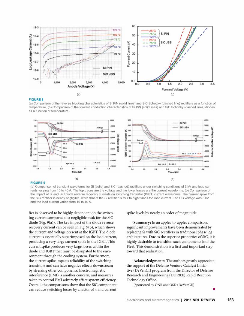
HighVoltageSiliconCarbidePowerRectifierDe-velopment: The new SiC rectifiers are designed to match available high voltage Si components for a clear compari-son. Commercially available Si IGBTs and diodes with ratings of 4.5 kV and 60 A were chosen for the dem-onstration. High voltage SiC junction barrier Schottky (JBS) rectifiers were fabricated at Cree, Inc. (Durham, NC). The rectifiers were characterized for both static and dynamic performance. Dynamic high power testing was performed through collaboration with the National Institute of Standards and Technology (NIST, Gaith-ersburg, MD). Figure 8(a) compares the high voltage standoff properties characterized by the reverse leakage current as a function of reverse voltage with increasing temperature. Due to its wider bandgap, the SiC rectifier can support the same voltage with less than a tenth of the active diode thickness and is less affected by increasing temperature. The forward conduction comparison (Fig. 8(b)) shows the forward current vs the forward voltage drop. Optimally, power rectifiers show an increase in the forward drop with increasing temperature to avoid ther-mal runaway and to allow paralleling of multiple diodes. Overall, the static characteristics demonstrate that SiC can be a direct replacement for equivalent Si parts.
TransientCharacteristics: To quantify the benefit of SiC, the circuit shown by the blue components in Fig. 7 was constructed with an inductive load to simulate a propulsion motor, and the test results are summarized in Fig. 9. The reverse recovery current of the Si recti-
FIGURE 7Schematic drawing of a half-bridge circuit (left) and current-voltage waveforms as seen across the lower (blue) switch (right). During turn-on, the upper diode discharges into the lower switch, producing a large current transient (as illustrated by large arrow).
153electronics and electromagnetics | 2011 NRL REVIEW
fier is observed to be highly dependent on the switch-ing current compared to a negligible peak for the SiC diode (Fig. 9(a)). The key impact of the diode reverse recovery current can be seen in Fig. 9(b), which shows the current and voltage present at the IGBT. The diode current is essentially superimposed on the load current, producing a very large current spike in the IGBT. This current spike produces very large losses within the diode and IGBT that must be dissipated to the envi-ronment through the cooling system. Furthermore, the current spike impacts reliability of the switching transistors and can have negative effects downstream by stressing other components. Electromagnetic interference (EMI) is another concern, and measures taken to control EMI adversely affect system efficiency. Overall, the comparisons show that the SiC component can reduce switching losses by a factor of 4 and current
FIGURE 8(a) Comparison of the reverse blocking characteristics of Si PiN (solid lines) and SiC Schottky (dashed line) rectifiers as a function of temperature. (b) Comparison of the forward conduction characteristics of Si PiN (solid lines) and SiC Schottky (dashed lines) diodes as a function of temperature.
(b)(a)
FIGURE 9(a) Comparison of transient waveforms for Si (solid) and SiC (dashed) rectifiers under switching conditions of 3 kV and load cur-rents varying from 10 to 40 A. The top traces are the voltage and the lower traces are the current waveforms. (b) Comparison of the impact of Si and SiC diode reverse recovery currents on switching transistor (IGBT) current waveforms. The current spike from the SiC rectifier is nearly negligible, while that of the Si rectifier is four to eight times the load current. The DC voltage was 3 kV and the load current varied from 10 to 40 A.
(b)(a)
spike levels by nearly an order of magnitude.
Summary:In an apples-to-apples comparison, significant improvements have been demonstrated by replacing Si with SiC rectifiers in traditional phase leg architectures. Due to the superior properties of SiC, it is highly desirable to transition such components into the Fleet. This demonstration is a first and important step toward that realization.
Acknowledgments: The authors greatly appreciate the support of the Defense Venture Catalyst Initia-tive (DeVenCI) program from the Director of Defense Research and Engineering (DDR&E) Rapid Reaction Technology Office. [Sponsored by ONR and OSD (DeVenCI)]

154 2011 NRL REVIEW | electronics and electromagnetics
Microfabrication of Next-Generation Millimeter-Wave Vacuum Electronic Amplifiers
C.D. Joye,1 J.P. Calame,1 K.T. Nguyen,2 and B. Levush1
1Electronics Science and Technology Division2Beam-Wave Research, Inc.
Introduction:Advanced vacuum electronic (VE) amplifiers capable of high continuous-wave (CW)output power and wide bandwidth are needed for such Naval applications as radar, ultra-high-data-rate communications, long-range imaging, and standoff spectroscopy. Operation at frequencies in the milli-meter wavelength (mmW) and sub-mmW regimes is especially useful for these applications, and is practical because of reasonably low-loss atmospheric windows near 220 GHz, 670 GHz, 850 GHz, and 1 THz. The power levels achievable in VE devices are often orders of magnitude greater than comparable solid-state-based technologies owing to very high voltage operation and the spatially distributed nature of the energy conversion mechanisms, combined with high total current and all-metal construction. In particular, copper construc-tion is preferred because copper exhibits low mmW losses and high thermal conductivity for high power handling, and is vacuum compatible. In order to keep VE devices compact, finely structured subwavelength copper features (“interaction circuits”) are required to slow down the electromagnetic wave such that it can synchronize with a beam of electrons passing through the interaction circuit (Fig. 10). When the beam-wave coupling is significant, the power from the electron
beam is transformed into electromagnetic energy, resulting in amplification. A major challenge at higher frequencies is fabricating the finely structured interac-tion circuits.
MicrofabricationSolutions:Ultraviolet photoli-thography, combined with electroforming and molding (collectively known as UV-LIGA) is a low-cost micro-fabrication technique being developed as a replace-ment for the original and vastly more expensive X-ray LIGA techniques that required a synchrotron X-ray source. Using improved UV-LIGA techniques devel-oped in-house, we recently demonstrated the ability to fabricate complete, all-copper grating circuits for 220 GHz VE amplifiers,1 relying on three main steps (Fig. 11): First, on a copper substrate, we use the highly viscous SU-8 photoresist activated by UV light from a low-cost source to form microscopic features down as small as 10 μm; second, copper is electroformed to fill the volume around the SU-8; and last, the SU-8 is removed, leaving only finely structured copper be-hind. Our photoresist layers are usually in the range of 300 μm to 1 mm thick, far thicker than layers used in IC and transistor manufacturing. The SU-8 acts as a mold while copper is electroformed around it using pulse electroforming techniques in a sulfuric acid–based solution without any problematic grain-refining agents. The electroformed copper is also void-free to ensure vacuum compatibility and has been tested to survive over 900 °C for brazing. After electroforming, the surface is ground and polished, revealing the SU-8 buried in the copper. Since SU-8 is a highly crosslinked epoxy, it is notoriously difficult to remove chemi-cally. We have developed a reliable molten salt method that completely removes SU-8 from high aspect ratio electroformed features, and have demonstrated high vertical aspect ratios in copper of over 15:1. Finally, the 220 GHz amplifier grating circuits were cold tested and characterized using vector network analysis over a very wide frequency range from 75 to 325 GHz. The results agreed with an analytic theory and also revealed that the grating circuits could prove useful as “brick wall” type filters for high-power antijamming applications at G-band and beyond. The next phase of fabrication involves a game-changing ultra-wideband serpentine waveguide ampli-fier at 200 to 270 GHz using multiple electron beams to simultaneously achieve high power and wide band-width while lowering the intermodulation products.2 Initial work on this device looks very promising (Fig. 12), and an electron gun and magnet system are being fabricated to construct a complete amplifier.
Summary:We have demonstrated in-house con-trol over every aspect of the microfabrication process for mmW and sub-mmW amplifier circuits for devices
FIGURE 10(Left) Several kinds of vacuum electron devices illustrating electron guns, beams, and collectors. For clarity, focusing magnets are not shown. (Right) Amplifier interaction circuits are shown in cutaway view.

155electronics and electromagnetics | 2011 NRL REVIEW
FIGURE 11The UV-LIGA process. (a) SU-8 is deposited on a polished copper wafer and exposed with UV, (b) the unexposed SU-8 is removed, and (c) copper is electroformed up between the crosslinked SU-8 patterns. Pulsed copper elec-troforming produces grain sizes far smaller than DC. (d) Finally, the SU-8 is removed.
FIGURE 12A very compact, ultra-wideband multiple-beam serpentine waveguide amplifier designed and fabricated at NRL using UV-LIGA techniques, predicted to generate over 100 W at 220 GHz.
predicted to produce record levels of CW output power. The techniques developed apply not only to VE devic-es, but also to miniaturized filters, couplers, antennas, and other components requiring high power capability and precise fabrication, and we are quickly expanding our fabrication capabilities to 670 GHz devices. These in-house techniques continue to produce high quality interaction circuits for the next generation of vacuum electron devices that will meet a variety of defense needs within the Navy. [Sponsored by ONR]
References1 C.D. Joye, J.P. Calame, M. Garven, and B. Levush, “UV-LIGA
Microfabrication of 220 GHz Sheet Beam Amplifier Gratings with SU-8 Photoresists,” J. Micromech/Microeng, 125016, Dec. 2010.
2 K. Nguyen, J. Pasour, E. Wright, D.K. Abe, L. Ludeking, D. Pershing, and B. Levush, “Linearity Performance of Multi-Stage TWT Amplifiers: Cascade vs. Series,” Proc. 12th IEEE Int’l Vac. Elec. Conf., Bangalore, India, Feb. 21–24, 2011.

156 2011 NRL REVIEW | electronics and electromagnetics
CMOS Integrated MEMS Resonators for RF and Chemical Sensing Applications
M.K. Zalalutdinov, J.W. Baldwin, and B.H. HoustonAcoustics Division
Introduction:In complementary metal oxide semiconductor (CMOS) devices integrated with micro-electromechanical systems (MEMS), the major role for the high spectral purity micromechanical resonators is to provide frequency selectivity — a feature that is crucial for radio frequency (RF) applications and that CMOS alone is lacking almost entirely. Devices like RF filters or frequency generators (clocks) that currently rely on bulky off-chip components (such as quartz crystals, surface acoustic wave (SAW) filters, and thin-film bulk acoustic resonators (FBAR)) will reduce their footprints by orders of magnitude and provide sub-stantial power savings once the frequency determining element is implemented as an on-chip MEMS resona-tor.1 “Radio-on-chip” is widely considered an essential milestone in CMOS-MEMS integration and is crucial for “smart dust” applications.2 Even more important, novel types of RF signal processing that are based on nonlinear dynamics effects in the collective behavior of coupled oscillators are expected to emerge with the ability to fabricate large arrays of high quality factor resonators integrated with electronics.3 The challenges arise from the fact that the integra-tion of the mechanical structures must be done without the risk of affecting the performance of the on-chip electronics. In practical terms, the rigidly defined se-quence of operations in the CMOS fabrication process must go unaltered and the MEMS design frame in terms of structural materials is severely limited by a set combination of layers (with fixed thicknesses) that are included in a particular CMOS process flow. It is not uncommon for CMOS-MEMS designers to feel like they are trying to build a race car using the spare parts of a jet plane. Yet, to be viable, the resulting microme-chanical resonator has to fit the required frequency range, demonstrate high quality factor Q, and pro-vide low insertion loss (often expressed as motional resistance, Rm).4 The last requirement is often the most challenging and most important since in RF MEMS devices, the incoming electrical signal is converted into mechanical motion of the resonator and then back into the electrical domain, and the efficiency of that double transduction is crucial. In our research effort, we have developed a general design approach5 that enables monolithic (on-chip) integration of high-Q RF MEMS resonators into a common type of CMOS process that features
two polycrystalline silicon gate layers and field ox-ide isolation.6 Using a commercially available CMOS process with minimum feature size 1.5 μm offered by ON Semiconductor (formerly AMI Semiconductor, accessible through MOSIS7), we have demonstrated fabrication and operation of polysilicon dome resona-tors with capacitive pick-up and arch bridge resonators with piezoresistive readout. Both domes and bridges are fabricated using the gate polysilicon as a structural material. For the dome resonator, the vibrating structure (the dome itself) is comprised of the top polysilicon (poly2) layer only. In the post-CMOS fabrication process, a narrow gap (~100 nm) is created by dissolving inter-poly oxide (used as a sacrificial layer) that separates the suspended top poly2 layer shell from the anchored bot-tom poly1 layer (Fig. 13), forming a read-out capacitor. Shaping the suspended part as a shell (as opposed to a flat disc) is essential for maintaining the integrity of this ultra-narrow gap. The dome shape of the resona-tor is provided by placing a circular patch of the oxide isolation layer underneath the poly1 layer. The extra
rigidity provided by the out-of-plane curvature of the dome makes the suspended structure robust and capable of withstanding forces that would be fatal for a flat plate. The mechanical-to-electrical transduction is accomplished by applying a DC bias voltage across that poly1–poly2 capacitor and by reading out the AC cur-rent induced by the modulation of the vacuum gap due to the mechanical motion of the top (poly2) shell. A scanning electron microscopy (SEM) image of the common-gate transimpedance amplifier placed next
FIGURE 13SEM image of polysilicon dome resonator. The poly2 shell is released by dissolving interpoly oxide through the irrigation hole (opening at the apex of the dome). The bottom polysilicon layer (poly1, visible through the irrigation hole) is covering a circular patch of field oxide conformally, defining the out-of plane curvature of the dome.
1 µm

157electronics and electromagnetics | 2011 NRL REVIEW
to the dome resonator (Fig. 14) provides direct com-parison for the relative size of the resonator and CMOS components. The fact that the footprint of the resona-tor is significantly smaller than even a single wire-bonding pad demonstrates how effective the monolith-ic CMOS-MEMS integration can be in microminiatur-izing RF devices. In contrast to the single-layer dome, an arch bridge resonator is designed as a laminar structure. The inter-poly oxide is kept intact, providing a bond between a poly1 beam and a slightly wider poly2 cover band (Fig. 15), thus creating a bimorph structure. A rectangular field oxide patch located underneath the bridge is used as a sacrificial layer, which once dissolved sets the bridge free to vibrate. Out-of-plane vibrations of the laminated bridge are accompanied by cycles of com-pression and extension alternated between the top and bottom layers. Piezoresistive properties of polysilicon8 make it possible to read out the resulting stress varia-
tions as a modulation of conductivity (induced by the mechanical motion) in either the bottom or the top polysilicon stripe. The other polysilicon layer, being electrically isolated by interpoly oxide, can be used for electrostatic or thermoelastic actuation. Rigid and robust arch bridges, unburdened by the vulnerabilities associated with ultra-narrow gaps, can find applications beyond RF signal processing. The small mass and high quality factor of the microme-chanical arch bridge resonators provide sensitivity for added mass on the order of 1 femtogram. Featuring fully integrated readout and geared for mass produc-tion, such resonators can be used in chemical sensing, given that proper surface functionalization would pro-vide specificity toward a particular analyte of interest.9 In conclusion, we have demonstrated monolithic integration of MEMS resonators into an unmodified, commercially available CMOS process. High quality factors up to Q ~ 8,000 for the domes and Q ~ 4,000 for arch bridge resonators (to be compared with Q ~ 20 for a conventional on-chip LC tank) in the frequency range 10 to 100 MHz open numerous applications in RF signal processing and chemical sensing. Low mo-tional resistance Rm~ 740 kOhm of the dome resonators represents almost an order of magnitude improvement compared to state-of-the-art CMOS-integrated MEMS resonators.10 We are currently working on extending the frequency range for our RF MEMS resonators and refining the design for integration into cutting-edge, deep submicron CMOS processes.
Acknowledgments: The authors gratefully ac-knowledge the long-standing collaboration with Prof. Jeevak M. Parpia, Dr. Joshua D. Cross, and Dr. Bojan R. Ilic at Cornell University. [Sponsored by ONR]
FIGURE 14Dome resonator integrat-ed with a common-gate CMOS transimpedance amplifier. The dome resonator is depicted as a variable capacitor on the schematic diagram of the transimpedance amplifier (left).
20 µm
FIGURE 15SEM image of an arch bridge resonator. The laminated structure is comprised of a poly1 beam covered by a slightly wider poly2 stripe with a thin layer of interpoly oxide providing mechanical bonding between two poly layers, as well as electrical isolation.
1 µm

158 2011 NRL REVIEW | electronics and electromagnetics
References1 C.T.C. Nguyen, “MEMS Technology for Timing and Frequency
Control,” IEEE Trans. Ultrasonics Ferroelectrics and Frequency Control 54(2), 251–270 (2007).
2 J. Kahn, R. Katz, and K. Pister, “Emerging Challenges: Mobile Networking for “Smart Dust”,” J. Communications and Networks 2(3), 188–196 (2000).
3 F. Hoppensteadt and E. Izhikevich, “Synchronization of MEMS Resonators and Mechanical Neurocomputing,” IEEE Trans. Circuits and Systems I — Fundamental Theory and Applications 48(2), 133–138 (2001); E.M. Izhikevich, Dynamical Systems in Neuroscience (The MIT Press, Cambridge, Mass., 2007).
4 Y. Lin, S. Li, Z. Ren, and C. Nguyen, “Low Phase Noise Array-Composite Micromechanical Wine-Glass Disk Oscillator,” in IEEE International Electron Devices Meeting 2005, Technical Digest, Washington, D.C., Dec. 5–7, 2005, pp. 278–281.
5 M.K. Zalalutdinov, J.D. Cross, J.W. Baldwin, B.R. Ilic, W. Zhou, B.H. Houston, and J.M. Parpia, “CMOS-Integrated MEMS Resonators,” JMEMS 19(4), 807–815 (2010).
6 P.E. Allen and D.R. Holberg, CMOS Analog Circuit Design (Ox-ford University Press, New York, 2002), p. 18.
7 MOSIS (Metal Oxide Semiconductor Implementation Services), Fabrication Processes, available at http://www.mosis.com/prod-ucts/fab/vendors/.
8 N. Matsuzuka and T. Toriyama, “Analysis for Piezoresistive Property of Heavily-Doped Polysilicon with Upper and Lower Bounds,” J. Appl. Phys. 108, 064902 (2010).
9 J. Baldwin, M. Zalalutdinov, B. Pate, M. Martin, and B. Houston, “Optically Defined Chemical Functualization of Silicon Nano-mechanical Resonators for Mass Sensing,” NANO ’08. 8th IEEE Conference on Nanotechnology, Aug. 2008, pp. 139–142.
10 J.L. Lopez, J. Verd, A. Uranga, J. Giner, G. Murillo, F. Torres, G. Abadal, and N. Barniol, “A CMOS-MEMS RF-Tunable Bandpass Filter Based on Two High-Q 22-MHz Polysilicon Clamped-Clamped Beam Resonators,” IEEE Electron Device Lett. 30(7), 718–720 (2009).
Software Reprogrammable Payload (SRP) Development
C.M. HuffineSpace Systems Development Department
Overview:The Software Reprogrammable Payload (SRP) is an open-architecture, government-owned reference design for a flexible, reconfigurable-while-in-operation software radio designed to meet current and future needs for Navy and Marine Corps missions. By using modern software radio technology based on leading-edge components used in the wireless industry, the payload can collect, process, and transmit a wide variety of signals, or utilize its processing elements for other tasks. Optimizing the application development process and location of processing between the field programmable gate array (FPGA) and the general-purpose processor (GPP) allows the system to achieve high reliability and throughput for a variety of applica-tions while providing for application porting at lowered level-of-effort than previous software defined radio
(SDR) designs. Furthermore, suitably flexible hard-ware architecture provides for maximum access to a multitude of varied functions. Integrated with external components such as power amplifiers and antennas that may be indigenous on a particular platform, the SRP forms the core of a radio communications and intelligence-surveillance-reconnaissance (ISR) system. The initial development goal was to provide the USMC with robust, flexible, reconfigurable payload operation with their Shadow UAS (Figs. 16 and 17), starting with four applications: SINCGARS communications relay, bent-pipe UHF communications, UHF IP router for legacy tactical UHF radios, and automated identifica-tion system (AIS) as the “notional” SIGINT application.
History: The genesis of the SRP development was as follow-on to previous efforts by the NRL Space Systems Development Department, including the JCIT and UCIM “system of systems” payloads, and other ISR and communications efforts. Recognizing the long timelimes — often in excess of 10 years — to get new payloads into space, the concept of the reconfigurable, flexible payloads to help “future-proof ” space has been pursued. While support for the space effort was strong, a “rudder redirect” occurred during a briefing to Navy
FIGURE 16Form-factored prototype unit for USMC RQ-7B Shadow UAV.
FIGURE 17USMC RQ-7B Shadow UAV. (Photo credit: marines.mil)

159electronics and electromagnetics | 2011 NRL REVIEW
leadership, who articulated the fact that the more im-mediate need for SRP technology was UAS and aviation platforms. This advice directly supported our Division superintendent’s vision: “Solve the Problem Once” — what can work for aviation can work well for ground, space, and undersea systems, too. Thus, with excellent flag-level support from the USMC Deputy Commandant/Aviation and his techni-cal project officers and the Office of Naval Research (ONR) Code 30, a 30-month development program began. The basic development and applications were finished on August 27, 2010, and now the SRP Team is proceeding with a series of preplanned product im-provements (P3I) that cover a vast array of sensor ap-plications as well as hardware improvement to increase the frequency range and overall utility. Expanding the applications to meet Marine Corps ground require-ments and a vast array of Navy requirements is a logical progression and is currently under active development.
KeyDevelopmentAttributes:The problems that the SRP is designed to solve, in some cases, are not yet defined. The SRP development model has been de-signed to be similar to what occurs in the open source software and hardware environment used today, as well as other government development environments of a similar nature. Thus, the development of hardware/software suites such as those based on the Google An-droid platform serve as a model that can be examined and optimized for our use. The needs of Android, for example, are similar to our needs — flexibility to port hardware to a wide variety of vendor and communica-tions platform provider’s hardware ensuring a common operating environment and the ability to maintain ap-plication compatibility and porting flexibility. Fully recognizing that in an SDR system the key legacy of the development is literally the software is one of the most important factors to consider. Ensuring that expensive software becomes reusable, portable, and generic so that a wide range of hardware platforms can efficiently use it becomes paramount in ensuring the efficiency of the development process. Breaking down traditional barriers that intentionally or unintention-ally develop due to organizational structures, funding streams, or other factors is also key. At NRL, crossing divisional boundaries to utilize the expertise of security engineers in the Information Technology Division or UAS engineers in the Tactical Electronic Warfare Divi-sion expands the SRP team to break down traditional barriers at NRL, just as the program seeks to do within industry. Lowering the cost of entry to develop SRP ap-plications is a key effort — universities and small busi-nesses should be on equal footing with large industry. In recognizing that the software is the long-term investment that is being made, ensuring that the portability of the software is maximized protects the
government’s investment. Maximizing portability by means of government-owned application programming interfaces (APIs) and software development kits (SDKs) lowers the cost of entry into designing and building soft-ware applications. Ensuring that applications developed are not encumbered with proprietary technologies that the government cannot use with government purpose rights needs to be carefully examined — those situations may lower the software value in the long term with only small short-term savings. The SRP development model allows the insertion of proprietary technologies at vari-ous places — if the Service sponsors deem that to be in their best interests. Maintaining a rigorous systems-engineering process (SE) is a key developmental aspect. It can be tempting to bypass the process, particularly within the context of a spiral development, without the due diligence necessary of the SE. However, it is valid and necessary, particularly in cost-constrained programs, to tailor the SE effort in a way that provides the most efficient use of the team’s knowledge and time. Finding the right mix between too little and too much documentation is a challenge. The SRP team’s experience has shown that sufficient documentation, for example, during the design process, forces the engineer to more thoroughly think through the design and the ramifications to other subsystems, and provides other subsystem engineers who are par-ticipating in the peer review process enough insight into the design to add meaningful criticism. Too detailed documentation done too early will require expensive revisions to the as-built state down the line. In any case, detailed documentation is absolutely required for the boundaries — the places where external developers will utilize the SDK/APIs. Finally, following decades of experience in design-ing end-to-end systems, the NRL Naval Center for Space Technology mantra of “test like you fly and fly like you test” is still relevant and necessary and cannot be over-emphasized. Testing complex systems can be extremely expensive, particularly when it is done as an after-thought. Emphasizing testing and testability continu-ously and up front will reduce long-term schedule and costs. In modularized software systems, ensuring that those modules have built in regression testing suites that can be used also reduces the cost of the porting efforts when new hardware platforms become available.
Summary: The SRP provides a hardware and software platform to build upon for current and future requirements. The developmental program emphasized portability and reusability of the software elements and nonproprietary development of applications to ensure that the software, which is the majority of the system cost, has a life beyond a single hardware instantiation. Systems engineering discipline and a robust preplanned product improvement program keep the system and

160 2011 NRL REVIEW | electronics and electromagnetics
software development moving forward for current and future requirements. [Sponsored by ONR]