Free-spectral-range-free filters with ultrawide tunability ...
6
Free-spectral-range-free filters with ultrawide tunability across the S + C + L band CHUNLEI SUN, 1,2 CHUYU ZHONG, 3,4 MAOLIANG WEI, 3,4 HUI MA, 3,4 YE LUO, 1,2 ZEQUN CHEN, 1,2 RENJIE T ANG, 1,2 JIALING JIAN, 1,2 HONGTAO LIN, 3,4 AND LAN LI 1,2, * 1 Key Laboratory of 3D Micro/Nano Fabrication and Characterization of Zhejiang Province, School of Engineering, Westlake University, Hangzhou 310024, China 2 Institute of Advanced Technology, Westlake Institute for Advanced Study, Hangzhou 310024, China 3 Key Laboratory of Micro-Nano Electronics and Smart System of Zhejiang Province, College of Information Science and Electronic Engineering, Zhejiang University, Hangzhou 310027, China 4 School of Microelectronics, Zhejiang University, Hangzhou 310027, China *Corresponding author: [email protected] Received 15 January 2021; revised 21 March 2021; accepted 24 March 2021; posted 25 March 2021 (Doc. ID 420005); published 24 May 2021 Optical filters are essential parts of advanced optical communication and sensing systems. Among them, the ones with an ultrawide free spectral range (FSR) are especially critical. They are promising to provide access to numerous wavelength channels highly desired for large-capacity optical transmission and multipoint multipara- meter sensing. Present schemes for wide-FSR filters either suffer from limited cavity length or poor fabrication tolerance or impose an additional active-tuning control requirement. We theoretically and experimentally dem- onstrate a filter that features FSR-free operation capability, subnanometer optical bandwidth, and acceptable fabrication tolerance. Only one single deep dip within a record-large waveband (S C L band) is observed by appropriately designing a side-coupled Bragg-grating-assisted Fabry–Perot filter, which has been applied as the basic sensing unit for both the refractive index and temperature measurement. Five such basic units are also cascaded in series to demonstrate a multichannel filter. This work provides a new insight to design FSR-free filters and opens up a possibility of flexible large-capacity integration using more wavelength channels, which will greatly advance integrated photonics in optical communication and sensing. © 2021 Chinese Laser Press https://doi.org/10.1364/PRJ.420005 1. INTRODUCTION Integrated optical filters used for spectrum manipulation are among the most significant components in photonic systems on chip, enabling many advanced applications in optical com- munication and computing, spectroscopy, sensing, and high- precision measurement [1–5]. As the fundamental building block for wavelength (de)multiplexing, optical filters are highly desired in wavelength-division-multiplexing (WDM) technol- ogy. WDM technology has been widely adapted for flexible and effective filtering and combining of hundreds of nanometer- wide signals in optical communication applications. Besides, WDM technology is also one of the key technologies to con- struct sensor networks to realize quasi-distributed multisite and multiparameter sensing, which can obtain the spatial distribu- tion and time-varying information of the measured field simul- taneously. A filter with a large free spectral range (FSR) can effectively increase the number of independent sensors on a single sensor link and realize simultaneous sensing of multiple loci and parameters. Therefore, an integrated photonic filter with a large FSR and a small footprint allowing a large number of multiplexed channels is crucial. The filters based on silicon photonics technology with different interferometric structures mainly include echelle diffraction gratings (EDGs) [6,7], arrayed-waveguide gratings (AWGs) [8–10], microring resonators (MRRs) [11–16], Mach–Zehnder interferometers (MZIs) [17–21], Fabry–Perot (F-P) cavities [22–24], Bragg gratings [3,25–28], and nano- beam cavities [29–33], and their FSR usually ranges from sev- eral nanometers to tens of nanometers. Recently, many efforts have been devoted to achieving a large FSR covering multiple wavelength channels by optimizing the filter cavity’ s resonance structures. The FSR of MRRs could be increased to as large as 93 nm by using a submicrometer bending radius [16], while the FSR of the F-P cavity could be larger than 30 nm [24]. For the nanobeam cavity, multiple resonant modes are usually excited in the cavity with a tens-of-nanometers FSR. The lim- ited FSR of the aforementioned integrated filters prevents their use in applications that require numerous channels. Research Article Vol. 9, No. 6 / June 2021 / Photonics Research 1013 2327-9125/21/061013-06 Journal © 2021 Chinese Laser Press
Transcript of Free-spectral-range-free filters with ultrawide tunability ...
Free-spectral-range-free filters with ultrawidetunability across the S +C + L bandCHUNLEI SUN,1,2 CHUYU ZHONG,3,4 MAOLIANG WEI,3,4 HUI MA,3,4 YE LUO,1,2 ZEQUN CHEN,1,2
RENJIE TANG,1,2 JIALING JIAN,1,2 HONGTAO LIN,3,4 AND LAN LI1,2,*1Key Laboratory of 3D Micro/Nano Fabrication and Characterization of Zhejiang Province, School of Engineering, Westlake University,Hangzhou 310024, China2Institute of Advanced Technology, Westlake Institute for Advanced Study, Hangzhou 310024, China3Key Laboratory of Micro-Nano Electronics and Smart System of Zhejiang Province, College of Information Science and Electronic Engineering,Zhejiang University, Hangzhou 310027, China4School of Microelectronics, Zhejiang University, Hangzhou 310027, China*Corresponding author: [email protected]
Received 15 January 2021; revised 21 March 2021; accepted 24 March 2021; posted 25 March 2021 (Doc. ID 420005); published 24 May 2021
Optical filters are essential parts of advanced optical communication and sensing systems. Among them, the oneswith an ultrawide free spectral range (FSR) are especially critical. They are promising to provide access tonumerous wavelength channels highly desired for large-capacity optical transmission and multipoint multipara-meter sensing. Present schemes for wide-FSR filters either suffer from limited cavity length or poor fabricationtolerance or impose an additional active-tuning control requirement. We theoretically and experimentally dem-onstrate a filter that features FSR-free operation capability, subnanometer optical bandwidth, and acceptablefabrication tolerance. Only one single deep dip within a record-large waveband (S� C� L band) is observedby appropriately designing a side-coupled Bragg-grating-assisted Fabry–Perot filter, which has been applied as thebasic sensing unit for both the refractive index and temperature measurement. Five such basic units are alsocascaded in series to demonstrate a multichannel filter. This work provides a new insight to design FSR-freefilters and opens up a possibility of flexible large-capacity integration using more wavelength channels,which will greatly advance integrated photonics in optical communication and sensing. © 2021 Chinese
Laser Press
https://doi.org/10.1364/PRJ.420005
1. INTRODUCTION
Integrated optical filters used for spectrum manipulation areamong the most significant components in photonic systemson chip, enabling many advanced applications in optical com-munication and computing, spectroscopy, sensing, and high-precision measurement [1–5]. As the fundamental buildingblock for wavelength (de)multiplexing, optical filters are highlydesired in wavelength-division-multiplexing (WDM) technol-ogy. WDM technology has been widely adapted for flexible andeffective filtering and combining of hundreds of nanometer-wide signals in optical communication applications. Besides,WDM technology is also one of the key technologies to con-struct sensor networks to realize quasi-distributed multisite andmultiparameter sensing, which can obtain the spatial distribu-tion and time-varying information of the measured field simul-taneously. A filter with a large free spectral range (FSR) caneffectively increase the number of independent sensors on asingle sensor link and realize simultaneous sensing of multipleloci and parameters. Therefore, an integrated photonic filter
with a large FSR and a small footprint allowing a large numberof multiplexed channels is crucial.
The filters based on silicon photonics technology withdifferent interferometric structures mainly include echellediffraction gratings (EDGs) [6,7], arrayed-waveguide gratings(AWGs) [8–10], microring resonators (MRRs) [11–16],Mach–Zehnder interferometers (MZIs) [17–21], Fabry–Perot(F-P) cavities [22–24], Bragg gratings [3,25–28], and nano-beam cavities [29–33], and their FSR usually ranges from sev-eral nanometers to tens of nanometers. Recently, many effortshave been devoted to achieving a large FSR covering multiplewavelength channels by optimizing the filter cavity’s resonancestructures. The FSR of MRRs could be increased to as large as93 nm by using a submicrometer bending radius [16], whilethe FSR of the F-P cavity could be larger than 30 nm [24].For the nanobeam cavity, multiple resonant modes are usuallyexcited in the cavity with a tens-of-nanometers FSR. The lim-ited FSR of the aforementioned integrated filters prevents theiruse in applications that require numerous channels.
Research Article Vol. 9, No. 6 / June 2021 / Photonics Research 1013
2327-9125/21/061013-06 Journal © 2021 Chinese Laser Press
Thus, various design strategies have been adopted to extendthe filter’s FSR or obtain an FSR-free response in the operatingwavelength range. Contradirectional couplers (CDCs) havebeen designed based on the photonic bandgap feature ofBragg grating. Since the bandwidth of Bragg gratings is usuallydisproportionate to the length, a device using shallow gratingmight be quite long [28]. To further reduce the size of filters,CDC is introduced into one or two coupling regions of theMRR to achieve a major resonance [34]. Maximum side-modesuppressions at all other undesired resonant wavelengths will beachieved provided that the stopband of the grating is twice theMRR’s FSR. Another way is to apply the Vernier effect to real-ize quite large FSR by cascading multiple MRRs with differentFSRs [35]. Nevertheless, it is difficult to achieve the resonantwavelength alignment since the stringent requirement for de-sign and fabrication accuracy must be satisfied. Extra activetuning control is usually introduced to compensate for the fab-rication error. Therefore, an ideal integrated filter that com-bines the large FSR and high side-mode suppression ratio toavoid precise wavelength alignment is highly desirable.
In this paper, we address the challenges in integrated opticalfilters by theory, simulation, and experimental analysis for on-chip ultra-wideband optical signal filters, which simultaneouslyachieve FSR-free operation and subnanometer optical band-widths. First, we introduce the structure of the filter consistingof a series of key parts that take up coupling, filtering, modematching, and reflection. Then we introduce the mechanism ofFSR-free spectral response in the grating-assisted F-P cavity byinvestigating and comparing the stopband of Bragg grating and
FSR of the F-P cavity. We show that there is only a single deepdip in a hundreds of nanometers waveband when grating depthand cavity length are adopted appropriately to ensure the stop-band of the Bragg grating is smaller than the FSR of the F-Pcavity. Fabricated devices achieve an FSR-free response in a rec-ord-large waveband (S� C� L band) and a flat-top responseat nonresonant wavelengths.
2. DEVICE DESIGN AND OPERATIONPRINCIPLE
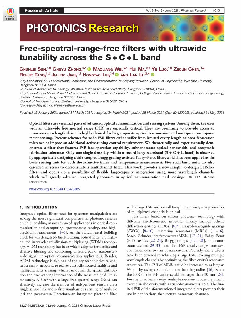
Figure 1(a) shows the schematic of the filter, consisting of aside-coupled waveguide bend and a Bragg grating-assistedF-P cavity. A central single-mode waveguide is embraced bytwo Bragg gratings as side-reflection mirrors, forming the F-P cavity. A tapered/inverse-tapered grating is used to connectthe central waveguide and the Bragg gratings to achieve modematching between the waveguide and Bragg mirror, minimiz-ing the scattering loss at the cavity–mirror interface. The Bragggrating consists of wide and narrow waveguides arranged alter-nately and periodically. For the tapered/inverse-tapered grating,the central transom is linearly tapered from the wide/narrow tothe narrow/wide waveguide. The light from the input wave-guide is coupled into the center of the F-P cavity. The lightat resonant wavelength is trapped and enhanced in the cavity,while the nonresonant wavelength is directionally routed to thethrough waveguide. The parameters to be designed for the filterinclude the width and length of the central waveguide w andLc, the bend radius R, the coupling gap G, the perturbation
Bragg grating
Tapered/Inverse-taperedgrating
Coupler
(a)
(b) (c)
FSRFP
FSR FSRFP
FSRFP
Fig. 1. (a) Schematic of our proposed filter with a grating-assisted F-P cavity selectively trapping a single narrowband beam in the ultrawidewaveband range. (b) Some key parts of the filter as well as the design parameters. (c) Typical spectral response of a Bragg grating (dashed blue curve)and F-P cavity with ideal mirrors (solid red curve). When the stopband of the Bragg grating is smaller than the FSR of the F-P cavity,Δλsb < FSRFP,there remains only one major resonance.
1014 Vol. 9, No. 6 / June 2021 / Photonics Research Research Article
period Λ, and the width of the wide and narrow waveguide ofBragg grating w and d , as illustrated in Fig. 1(b), as well as theperiod number of the Bragg grating and tapered gratingN b andN t. The spectral response of the filter mainly depends on thestopband of the Bragg grating Δλsb and FSR of the F-P cavitywith ideal mirrors FSRFP, as shown in Fig. 1(c). The stopbandis defined here as the width between the null points of the cen-tral lobe.
(i) WhenΔλsb < FSRFP, only one resonant mode of the F-Pcavity in the stopband of Bragg grating is excited and enhanced,and no dip may be observed in cases that all the resonant modesare out of the stopband when the F-P cavity holds a small cavitylength.(ii) When FSRFP < Δλsb < 2FSRFP, one or two resonance
dips can be excited, which depends on the position of the res-onant wavelength. If the resonant wavelength is around thecentral wavelength of the stopband λc, there will be onlyone major resonance. If the resonant wavelength is close tothe nulls of the central lobe, there will be two dips.(iii) When Δλsb > 2FSRFP, two or multiple resonance dipswill be excited.
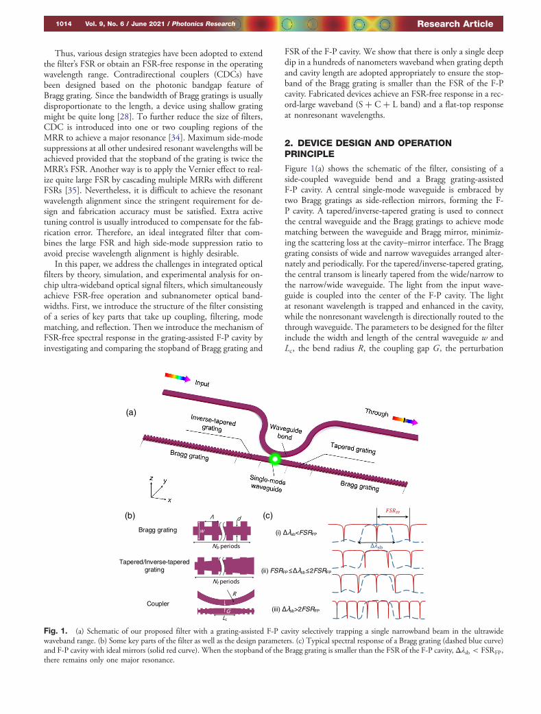
The relation between λc, Δλsb, and d is plotted in Fig. 2(a).The λc is attained by the Bragg equation, and Δλsb is calculatedby using three-dimensional (3D) finite-difference time-domain(FDTD) simulations. The Δλsb decreases as d increases, whileλc increases as d increases. Figure 2(b) shows the calculated FSRas Lc is varied. The FSR is given by
FSRFP �λ2c
2�Lcng1 � 2Lpdng2 � 2Ltng3�,
where Lpd and Lt are the penetration depth of the Bragg mirrorsand the length of the tapered/inverse-tapered grating. ng1, ng2,and ng3 are the group refractive indices of the central wave-guide, the Bragg grating, and the tapered/inverse-tapered gra-ting, respectively. For simplicity, ng3 is approximately equal tothe average of ng1 and ng2, which is suited for the linearly ta-pered grating. Lpd can be given by [36]
Lpd �λ · neff ,n
4�neff ,w − neff ,n�,
where neff ,w and neff ,n are the effective refractive indices of thewide and narrow waveguides in the Bragg grating and λ is theworking wavelength. By the equation, the simulation time forFSRFP can be greatly reduced compared to the fully 3D FDTDsimulation.
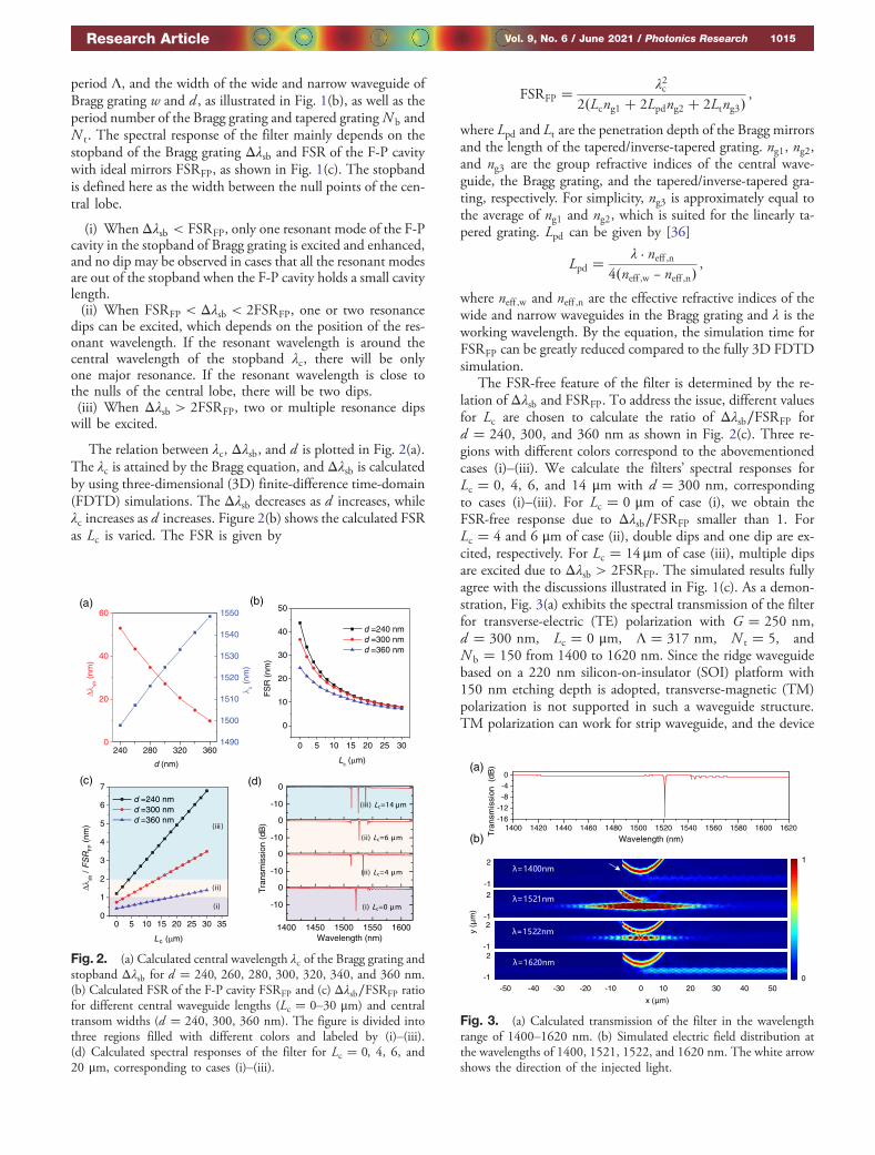
The FSR-free feature of the filter is determined by the re-lation of Δλsb and FSRFP. To address the issue, different valuesfor Lc are chosen to calculate the ratio of Δλsb∕FSRFP ford � 240, 300, and 360 nm as shown in Fig. 2(c). Three re-gions with different colors correspond to the abovementionedcases (i)–(iii). We calculate the filters’ spectral responses forLc � 0, 4, 6, and 14 μm with d � 300 nm, correspondingto cases (i)–(iii). For Lc � 0 μm of case (i), we obtain theFSR-free response due to Δλsb∕FSRFP smaller than 1. ForLc � 4 and 6 μm of case (ii), double dips and one dip are ex-cited, respectively. For Lc � 14 μm of case (iii), multiple dipsare excited due to Δλsb > 2FSRFP. The simulated results fullyagree with the discussions illustrated in Fig. 1(c). As a demon-stration, Fig. 3(a) exhibits the spectral transmission of the filterfor transverse-electric (TE) polarization with G � 250 nm,d � 300 nm, Lc � 0 μm, Λ � 317 nm, N t � 5, andN b � 150 from 1400 to 1620 nm. Since the ridge waveguidebased on a 220 nm silicon-on-insulator (SOI) platform with150 nm etching depth is adopted, transverse-magnetic (TM)polarization is not supported in such a waveguide structure.TM polarization can work for strip waveguide, and the device
Fig. 2. (a) Calculated central wavelength λc of the Bragg grating andstopband Δλsb for d � 240, 260, 280, 300, 320, 340, and 360 nm.(b) Calculated FSR of the F-P cavity FSRFP and (c) Δλsb∕FSRFP ratiofor different central waveguide lengths (Lc � 0–30 μm) and centraltransom widths (d � 240, 300, 360 nm). The figure is divided intothree regions filled with different colors and labeled by (i)–(iii).(d) Calculated spectral responses of the filter for Lc � 0, 4, 6, and20 μm, corresponding to cases (i)–(iii).
2
-1
2
-1
0
1
(a)
(b)1400 1420 1440 1460 1480 1500 1520 1540 1560 1580 1600 1620
-16
-12
-8
-4
0
Tra
nsm
issi
on (
dB)
Wavelength (nm)
0 10 20 30 40 50-50 -40 -30 -20 -10
2
2
-1
-1
y (
m)
x ( m)
Fig. 3. (a) Calculated transmission of the filter in the wavelengthrange of 1400–1620 nm. (b) Simulated electric field distribution atthe wavelengths of 1400, 1521, 1522, and 1620 nm. The white arrowshows the direction of the injected light.
Research Article Vol. 9, No. 6 / June 2021 / Photonics Research 1015
will be FSR free if case (i) (Δλsb < FSRFP) is satisfied. We cansee only a single dramatic dip at 1521 nm in the ultralargewavelength range of 220 nm, whereas there is a flat-top re-sponse at nonresonant wavelengths. Figure 3(b) exhibits theelectric field distribution of the whole structure at the wave-lengths of 1400, 1521, 1522, and 1620 nm. For the lightat the wavelengths of 1400 and 1620 nm out of the stopband,the filter is considered a double-waveguide directional coupler.Hence, the light cannot be enhanced in the F-P cavity but iscoupled into the right Bragg grating. Since the coupling lengthis short, the insertion loss out of the stopband could be ne-glected. For the wavelength of 1522 nm in the stopband,the light is coupled into the cavity, then reflected by theBragg mirror, and finally transferred to the through port.For the resonant wavelength of 1521 nm, the light is coupledinto the cavity, and the power in the cavity is enhanced until adynamic balance between coupled power, outcoupled power,and lossy power is achieved. At the critical coupling condition,the light is like being trapped in the cavity, and almost no poweris coupled out to the through port.
3. DEVICE FABRICATION ANDCHARACTERIZATION
The proposed filter was based on SOI with a 220 nm top layerand was fabricated after the exposure of electron beam lithog-raphy (EBL, Raith Voyager) followed by the dry etching pro-cess in inductively coupled plasma (ICP) equipment (Samco).The fabricated devices have rib waveguides with an etchingdepth of 150 nm and a top oxide cladding. A broadband tun-able laser system (Santec full-band TSL-550) was used to char-acterize the fabricated devices. The measured spectral responseswere normalized with respect to the transmission of a straightwaveguide connected with grating couplers on the same chip.The resolution is 5 pm in the measurements. Instead of utiliz-ing commonly used shallow-etched grating couplers with70 nm depth, here, 150 nm etched grating couplers, whichhave a much slower roll-off despite slightly lower peak couplingefficiency, were applied to enable broadband performance char-acterization. Figure 4 illustrates the scanning electron micro-scope (SEM) image of the filter and the enlarged key parts.
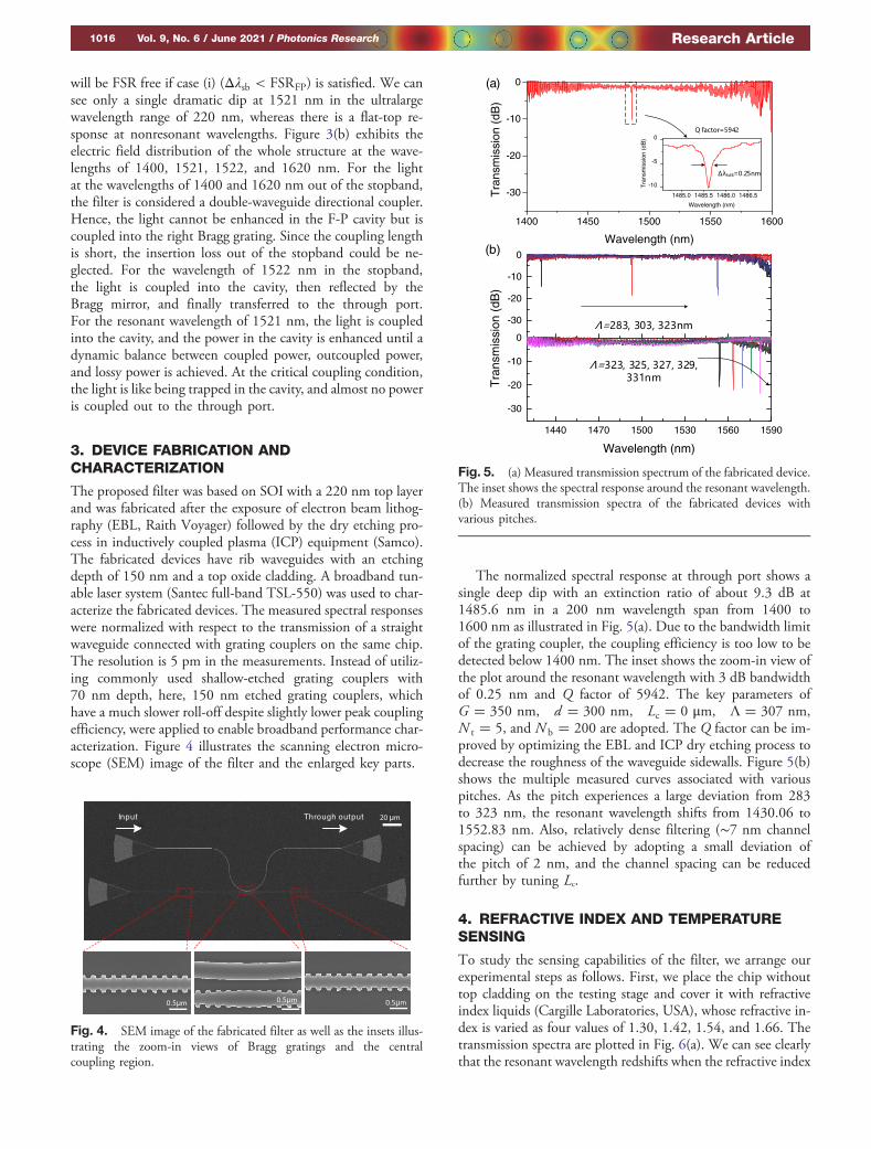
The normalized spectral response at through port shows asingle deep dip with an extinction ratio of about 9.3 dB at1485.6 nm in a 200 nm wavelength span from 1400 to1600 nm as illustrated in Fig. 5(a). Due to the bandwidth limitof the grating coupler, the coupling efficiency is too low to bedetected below 1400 nm. The inset shows the zoom-in view ofthe plot around the resonant wavelength with 3 dB bandwidthof 0.25 nm and Q factor of 5942. The key parameters ofG � 350 nm, d � 300 nm, Lc � 0 μm, Λ � 307 nm,N t � 5, and N b � 200 are adopted. The Q factor can be im-proved by optimizing the EBL and ICP dry etching process todecrease the roughness of the waveguide sidewalls. Figure 5(b)shows the multiple measured curves associated with variouspitches. As the pitch experiences a large deviation from 283to 323 nm, the resonant wavelength shifts from 1430.06 to1552.83 nm. Also, relatively dense filtering (∼7 nm channelspacing) can be achieved by adopting a small deviation ofthe pitch of 2 nm, and the channel spacing can be reducedfurther by tuning Lc.
4. REFRACTIVE INDEX AND TEMPERATURESENSING
To study the sensing capabilities of the filter, we arrange ourexperimental steps as follows. First, we place the chip withouttop cladding on the testing stage and cover it with refractiveindex liquids (Cargille Laboratories, USA), whose refractive in-dex is varied as four values of 1.30, 1.42, 1.54, and 1.66. Thetransmission spectra are plotted in Fig. 6(a). We can see clearlythat the resonant wavelength redshifts when the refractive index
tuptuohguorhTtupnI
Fig. 4. SEM image of the fabricated filter as well as the insets illus-trating the zoom-in views of Bragg gratings and the centralcoupling region.
1440 1470 1500 1530 1560 1590
-30
-20
-10
0
-30
-20
-10
0
Tra
nsm
issi
on (
dB)
Wavelength (nm)
(a)
(b)
1400 1450 1500 1550 1600
-30
-20
-10
0
Tra
nsm
issi
on (
dB)
Wavelength (nm)
1485.0 1485.5 1486.0 1486.5
-10
-5
0
Tra
nsm
issi
on (
dB)
Wavelength (nm)
Fig. 5. (a) Measured transmission spectrum of the fabricated device.The inset shows the spectral response around the resonant wavelength.(b) Measured transmission spectra of the fabricated devices withvarious pitches.
1016 Vol. 9, No. 6 / June 2021 / Photonics Research Research Article
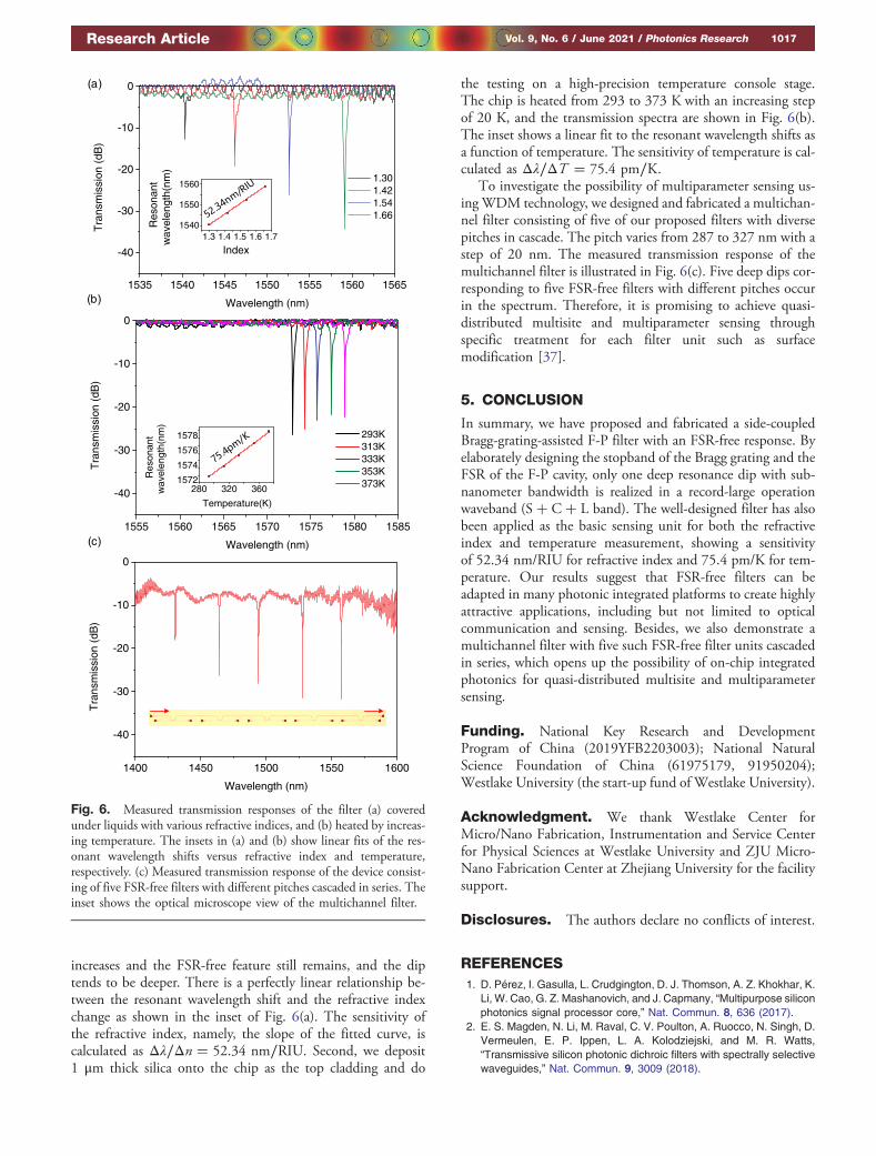
increases and the FSR-free feature still remains, and the diptends to be deeper. There is a perfectly linear relationship be-tween the resonant wavelength shift and the refractive indexchange as shown in the inset of Fig. 6(a). The sensitivity ofthe refractive index, namely, the slope of the fitted curve, iscalculated as Δλ∕Δn � 52.34 nm∕RIU. Second, we deposit1 μm thick silica onto the chip as the top cladding and do
the testing on a high-precision temperature console stage.The chip is heated from 293 to 373 K with an increasing stepof 20 K, and the transmission spectra are shown in Fig. 6(b).The inset shows a linear fit to the resonant wavelength shifts asa function of temperature. The sensitivity of temperature is cal-culated as Δλ∕ΔT � 75.4 pm∕K.
To investigate the possibility of multiparameter sensing us-ingWDM technology, we designed and fabricated a multichan-nel filter consisting of five of our proposed filters with diversepitches in cascade. The pitch varies from 287 to 327 nm with astep of 20 nm. The measured transmission response of themultichannel filter is illustrated in Fig. 6(c). Five deep dips cor-responding to five FSR-free filters with different pitches occurin the spectrum. Therefore, it is promising to achieve quasi-distributed multisite and multiparameter sensing throughspecific treatment for each filter unit such as surfacemodification [37].
5. CONCLUSION
In summary, we have proposed and fabricated a side-coupledBragg-grating-assisted F-P filter with an FSR-free response. Byelaborately designing the stopband of the Bragg grating and theFSR of the F-P cavity, only one deep resonance dip with sub-nanometer bandwidth is realized in a record-large operationwaveband (S� C� L band). The well-designed filter has alsobeen applied as the basic sensing unit for both the refractiveindex and temperature measurement, showing a sensitivityof 52.34 nm/RIU for refractive index and 75.4 pm/K for tem-perature. Our results suggest that FSR-free filters can beadapted in many photonic integrated platforms to create highlyattractive applications, including but not limited to opticalcommunication and sensing. Besides, we also demonstrate amultichannel filter with five such FSR-free filter units cascadedin series, which opens up the possibility of on-chip integratedphotonics for quasi-distributed multisite and multiparametersensing.
Funding. National Key Research and DevelopmentProgram of China (2019YFB2203003); National NaturalScience Foundation of China (61975179, 91950204);Westlake University (the start-up fund of Westlake University).
Acknowledgment. We thank Westlake Center forMicro/Nano Fabrication, Instrumentation and Service Centerfor Physical Sciences at Westlake University and ZJU Micro-Nano Fabrication Center at Zhejiang University for the facilitysupport.
Disclosures. The authors declare no conflicts of interest.
REFERENCES1. D. Pérez, I. Gasulla, L. Crudgington, D. J. Thomson, A. Z. Khokhar, K.
Li, W. Cao, G. Z. Mashanovich, and J. Capmany, “Multipurpose siliconphotonics signal processor core,” Nat. Commun. 8, 636 (2017).
2. E. S. Magden, N. Li, M. Raval, C. V. Poulton, A. Ruocco, N. Singh, D.Vermeulen, E. P. Ippen, L. A. Kolodziejski, and M. R. Watts,“Transmissive silicon photonic dichroic filters with spectrally selectivewaveguides,” Nat. Commun. 9, 3009 (2018).
1535 1540 1545 1550 1555 1560 1565
-40
-30
-20
-10
0
1.30 1.42 1.54 1.66
Tra
nsm
issi
on (
dB)
Wavelength (nm)
1.3 1.4 1.5 1.6 1.71540
1550
1560
Index
Res
onan
t w
avel
engt
h(nm
)
1555 1560 1565 1570 1575 1580 1585
-40
-30
-20
-10
0
Tra
nsm
issi
on (
dB)
Wavelength (nm)
293K 313K 333K 353K 373K280 320 360
1572
1574
1576
1578
Temperature(K)
Res
onan
t w
avel
engt
h(nm
)
(a)
(b)
(c)
1400 1450 1500 1550 1600
-40
-30
-20
-10
0
Tra
nsm
issi
on (
dB)
Wavelength (nm)
Fig. 6. Measured transmission responses of the filter (a) coveredunder liquids with various refractive indices, and (b) heated by increas-ing temperature. The insets in (a) and (b) show linear fits of the res-onant wavelength shifts versus refractive index and temperature,respectively. (c) Measured transmission response of the device consist-ing of five FSR-free filters with different pitches cascaded in series. Theinset shows the optical microscope view of the multichannel filter.
Research Article Vol. 9, No. 6 / June 2021 / Photonics Research 1017

3. W. Zhang and J. Yao, “A fully reconfigurable waveguide Bragg gratingfor programmable photonic signal processing,” Nat. Commun. 9, 1396(2018).
4. W. Zhang and J. Yao, “Photonic integrated field-programmable diskarray signal processor,” Nat. Commun. 11, 406 (2020).
5. D. Pérez-López, A. López, P. DasMahapatra, and J. Capmany,“Multipurpose self-configuration of programmable photonic circuits,”Nat. Commun. 11, 6359 (2020).
6. R. Cheng, C.-L. Zou, X. Guo, S. Wang, X. Han, and H. X. Tang,“Broadband on-chip single-photon spectrometer,” Nat. Commun.10, 4104 (2019).
7. D. Melati, P. G. Verly, A. Delâge, S. Wang, J. Lapointe, P. Cheben,J. H. Schmid, S. Janz, and D.-X. Xu, “Compact and low crosstalkechelle grating demultiplexer on silicon-on-insulator technology,”Electronics 8, 687 (2019).
8. S. Chen, X. Fu, J. Wang, Y. Shi, S. He, and D. Dai, “Compact densewavelength-division (de)multiplexer utilizing a bidirectional arrayed-waveguide grating integrated with a Mach–Zehnder interferometer,”J. Lightwave Technol. 33, 2279–2285 (2015).
9. A. van Wijk, C. R. Doerr, Z. Ali, M. Karabiyik, and B. I. Akca, “Compactultrabroad-bandwidth cascaded arrayed waveguide gratings,” Opt.Express 28, 14618–14626 (2020).
10. E. J. Stanton, N. Volet, and J. E. Bowers, “Silicon arrayed waveguidegratings at 2.0-μm wavelength characterized with an on-chip resona-tor,” Opt. Lett. 43, 1135–1138 (2018).
11. S. N. Zheng, J. Zou, H. Cai, J. F. Song, L. K. Chin, P. Y. Liu, Z. P.Lin, D. L. Kwong, and A. Q. Liu, “Microring resonator-assistedFourier transform spectrometer with enhanced resolution and largebandwidth in single chip solution,” Nat. Commun. 10, 2349(2019).
12. R. A. Cohen, O. Amrani, and S. Ruschin, “Response shaping with asilicon ring resonator via double injection,” Nat. Photonics 12, 706–712 (2018).
13. Y.-H. Lai, M.-G. Suh, Y.-K. Lu, B. Shen, Q.-F. Yang, H. Wang, J. Li,S. H. Lee, K. Y. Yang, and K. Vahala, “Earth rotation measured bya chip-scale ring laser gyroscope,” Nat. Photonics 14, 345–349(2020).
14. D. Hu, C. Zou, H. Ren, J. Lu, Z. Le, Y. Qin, S. Guo, C. Dong, and W.Hu, “Multi-parameter sensing in a multimode self-interferencemicro-ring resonator by machine learning,” Sensors 20, 709(2020).
15. P. Chen, S. Chen, X. Guan, Y. Shi, and D. Dai, “High-order microringresonators with bent couplers for a box-like filter response,” Opt. Lett.39, 6304–6307 (2014).
16. D. Liu, C. Zhang, D. Liang, and D. Dai, “Submicron-resonator-basedadd-drop optical filter with an ultra-large free spectral range,” Opt.Express 27, 416–422 (2019).
17. F. Horst, W. M. J. Green, S. Assefa, S. M. Shank, Y. A. Vlasov, andB. J. Offrein, “Cascaded Mach-Zehnder wavelength filters in siliconphotonics for low loss and flat pass-band WDM (de-)multiplexing,”Opt. Express 21, 11652–11658 (2013).
18. Q. Deng, L. Liu, R. Zhang, X. Li, J. Michel, and Z. Zhou, “Athermal andflat-topped silicon Mach-Zehnder filters,” Opt. Express 24, 29577–29582 (2016).
19. H. Xu, L. Liu, and Y. Shi, “Polarization-insensitive four-channel coarsewavelength-division (de)multiplexer based on Mach-Zehnder interfer-ometers with bent directional couplers and polarization rotators,” Opt.Lett. 43, 1483–1486 (2018).
20. D. M. Kita, B. Miranda, D. Favela, D. Bono, J. Michon, H. Lin, T. Gu,and J. Hu, “High-performance and scalable on-chip digital Fouriertransform spectroscopy,” Nat. Commun. 9, 4405 (2018).
21. M. C. Souza, A. Grieco, N. C. Frateschi, and Y. Fainman, “Fouriertransform spectrometer on silicon with thermo-optic non-linearityand dispersion correction,” Nat. Commun. 9, 665 (2018).
22. W. Zhang, N. Ehteshami, W. Liu, and J. Yao, “Silicon-based on-chipelectrically tunable sidewall Bragg grating Fabry-Perot filter,”Opt. Lett.40, 3153–3156 (2015).
23. Z. Yu, H. Cui, and X. Sun, “Genetically optimized on-chip widebandultracompact reflectors and Fabry-Perot cavities,” Photon. Res. 5,B15–B19 (2017).
24. Y. Wang, S. Gao, K. Wang, H. Li, and E. Skafidas, “Ultra-broadband,compact, and high-reflectivity circular Bragg grating mirror based on220 nm silicon-on-insulator platform,” Opt. Express 25, 6653–6663(2017).
25. D. Oser, F. Mazeas, X. Le Roux, D. Pérez‐Galacho, O. Alibart, S.Tanzilli, L. Labonté, D. Marris‐Morini, L. Vivien, and É. Cassan,“Coherency‐broken Bragg filters: overcoming on‐chip rejection limita-tions,” Laser Photon. Rev. 13, 1800226 (2019).
26. X. Wang, Y. Wang, J. Flueckiger, R. Bojko, A. Liu, A. Reid, J. Pond,N. A. F. Jaeger, and L. Chrostowski, “Precise control of the couplingcoefficient through destructive interference in silicon waveguideBragg gratings,” Opt. Lett. 39, 5519–5522 (2014).
27. H. Yun, M. Hammood, S. Lin, L. Chrostowski, and N. A. F. Jaeger,“Broadband flat-top SOI add-drop filters using apodized sub-wavelength grating contradirectional couplers,” Opt. Lett. 44, 4929–4932 (2019).
28. D. T. H. Tan, K. Ikeda, and Y. Fainman, “Cladding-modulatedBragg gratings in silicon waveguides,” Opt. Lett. 34, 1357–1359(2009).
29. S. I. Halimi, S. Hu, F. O. Afzal, and S. M. Weiss, “Realizing high trans-mission intensity in photonic crystal nanobeams using a side-couplingwaveguide,” Opt. Lett. 43, 4260–4263 (2018).
30. P. Liu and Y. Shi, “Simultaneous measurement of refractive index andtemperature using cascaded side-coupled photonic crystal nanobeamcavities,” Opt. Express 25, 28398–28406 (2017).
31. Y. Chen, W. S. Fegadolli, W. M. Jones, A. Scherer, and M. Li,“Ultrasensitive gas-phase chemical sensing based on functionalizedphotonic crystal nanobeam cavities,” ACS Nano 8, 522–527 (2013).
32. Q. Qiao, J. Xia, C. Lee, and G. Zhou, “Applications of photonic crystalnanobeam cavities for sensing,” Micromachines 9, 541 (2018).
33. Q. Quan, P. B. Deotare, and M. Loncar, “Photonic crystal nanobeamcavity strongly coupled to the feeding waveguide,” Appl. Phys. Lett.96, 203102 (2010).
34. N. Eid, R. Boeck, H. Jayatilleka, L. Chrostowski, W. Shi, and N. A. F.Jaeger, “FSR-free silicon-on-insulator microring resonator based filterwith bent contra-directional couplers,” Opt. Express 24, 29009–29021(2016).
35. R. Boeck, N. A. F. Jaeger, N. Rouger, and L. Chrostowski, “Series-coupled silicon racetrack resonators and the Vernier effect: theoryand measurement,” Opt. Express 18, 25151–25157 (2010).
36. R. P. Stanley, R. Houdré, U. Oesterle, M. Gailhanou, and M. Ilegems,“Ultrahigh finesse microcavity with distributed Bragg reflectors,” Appl.Phys. Lett. 65, 1883–1885 (1994).
37. G. J. Triggs, Y. Wang, C. P. Reardon, M. Fischer, G. J. O. Evans, andT. F. Krauss, “Chirped guided-mode resonance biosensor,” Optica 4,229–234 (2017).
1018 Vol. 9, No. 6 / June 2021 / Photonics Research Research Article