Electrical Tunability of Domain Wall Conductivity in ...
7
1902890 (1 of 7) © 2019 WILEY-VCH Verlag GmbH & Co. KGaA, Weinheim www.advmat.de COMMUNICATION Electrical Tunability of Domain Wall Conductivity in LiNbO 3 Thin Films Haidong Lu, Yueze Tan, James P. V. McConville, Zahra Ahmadi, Bo Wang, Michele Conroy, Kalani Moore, Ursel Bangert, Jeffrey E. Shield, Long-Qing Chen, J. Marty Gregg, and Alexei Gruverman* DOI: 10.1002/adma.201902890 progressively shrinking electronic devices. On the other hand, recent studies have revealed that ferroelectric DWs represent a distinct new phase with diverse func- tional characteristics that are completely different from the host material: they may exhibit metallic, magnetic, or even superconducting behavior, [1–6] while the domains that they separate are insulating and nonmagnetic. Electrical conductivity of the charged DWs has been observed in a number of ferroelectric materials, such as BiFeO 3 , [1,7,8] Pb(Zr,Ti)O 3 , [9,10] BaTiO 3 , [2] ErMnO 3 , [11] (Ca,Sr) 3 Ti 2 O 7 , [12] and boracites, [13] and is usually attributed to accumulation of mobile charges due to polarization discontinuity. A key fea- ture of DWs, that makes them even more appealing for device application, is that they can be created, erased, or control- lably moved from one point to another by external electric fields. [14,15] Recent reports introduced memory devices based on gen- eration and manipulation of the conduc- tive DWs in BiFeO 3 . [16,17] However, to make use of the conductive DWs as active elements in nanoelectronic circuits and devices, efficient control of the charge transport in the walls themselves is essential. [6] Dynamic modulation of DW conductivity through the revers- ible field-induced polarization distortion at the 109° DW was reported for BiFeO 3 thin films. [8] It turns out that this effect is transient and the conducting state is not retained when the bias Domain wall nanoelectronics is a rapidly evolving field, which explores the diverse electronic properties of the ferroelectric domain walls for application in low-dimensional electronic systems. One of the most prominent features of the ferroelectric domain walls is their electrical conductivity. Here, using a combination of scanning probe and scanning transmission electron microscopy, the mechanism of the tunable conducting behavior of the domain walls in the sub-micrometer thick films of the technologically important ferroelectric LiNbO 3 is explored. It is found that the electric bias generates stable domains with strongly inclined domain boundaries with the inclination angle reaching 20° with respect to the polar axis. The head-to-head domain boundaries exhibit high conductance, which can be modulated by application of the sub- coercive voltage. Electron microscopy visualization of the electrically written domains and piezoresponse force microscopy imaging of the very same domains reveals that the gradual and reversible transition between the conducting and insulating states of the domain walls results from the electrically induced wall bending near the sample surface. The observed modulation of the wall conductance is corroborated by the phase-field modeling. The results open a possibility for exploiting the conducting domain walls as the electrically controllable functional elements in the multilevel logic nanoelectronics devices. The ORCID identification number(s) for the author(s) of this article can be found under https://doi.org/10.1002/adma.201902890. Dr. H. Lu, Prof. A. Gruverman Department of Physics and Astronomy University of Nebraska Lincoln, NE 68588-0299, USA E-mail: [email protected] Y. Tan, B. Wang, Prof. L.-Q. Chen Department of Materials Science and Engineering Pennsylvania State University University Park, PA 16802, USA J. P. V. McConville, Prof. J. M. Gregg Centre for Nanostructured Media School of Mathematics and Physics Queen’s University Belfast Belfast BT7 1NN, UK Z. Ahmadi, Prof. J. E. Shield Department of Mechanical & Materials Engineering University of Nebraska Lincoln, NE 68588-0526, USA Dr. M. Conroy, K. Moore, Prof. U. Bangert Department of Physics School of Sciences & Bernal Institute University of Limerick Limerick V94 T9PX, Ireland Research into domain wall (DW) electronics is drawing a lot of attention as a new paradigm in ferroic device concepts based on the use of the properties of domain walls rather than domains. From one perspective, this surge of research activities is driven by recognition of an immense application potential of DWs in Adv. Mater. 2019, 1902890
Transcript of Electrical Tunability of Domain Wall Conductivity in ...

1902890 (1 of 7) © 2019 WILEY-VCH Verlag GmbH & Co. KGaA, Weinheim
www.advmat.de
CommuniCation
Electrical Tunability of Domain Wall Conductivity in LiNbO3 Thin Films
Haidong Lu, Yueze Tan, James P. V. McConville, Zahra Ahmadi, Bo Wang, Michele Conroy, Kalani Moore, Ursel Bangert, Jeffrey E. Shield, Long-Qing Chen, J. Marty Gregg, and Alexei Gruverman*
DOI: 10.1002/adma.201902890
progressively shrinking electronic devices. On the other hand, recent studies have revealed that ferroelectric DWs represent a distinct new phase with diverse func-tional characteristics that are completely different from the host material: they may exhibit metallic, magnetic, or even superconducting behavior,[1–6] while the domains that they separate are insulating and nonmagnetic. Electrical conductivity of the charged DWs has been observed in a number of ferroelectric materials, such as BiFeO3,[1,7,8] Pb(Zr,Ti)O3,[9,10] BaTiO3,[2] ErMnO3,[11] (Ca,Sr)3Ti2O7,[12] and boracites,[13] and is usually attributed to accumulation of mobile charges due to polarization discontinuity. A key fea-ture of DWs, that makes them even more appealing for device application, is that they can be created, erased, or control-lably moved from one point to another by external electric fields.[14,15] Recent reports introduced memory devices based on gen-eration and manipulation of the conduc-tive DWs in BiFeO3.[16,17]
However, to make use of the conductive DWs as active elements in nanoelectronic circuits and devices, efficient control
of the charge transport in the walls themselves is essential.[6] Dynamic modulation of DW conductivity through the revers-ible field-induced polarization distortion at the 109° DW was reported for BiFeO3 thin films.[8] It turns out that this effect is transient and the conducting state is not retained when the bias
Domain wall nanoelectronics is a rapidly evolving field, which explores the diverse electronic properties of the ferroelectric domain walls for application in low-dimensional electronic systems. One of the most prominent features of the ferroelectric domain walls is their electrical conductivity. Here, using a combination of scanning probe and scanning transmission electron microscopy, the mechanism of the tunable conducting behavior of the domain walls in the sub-micrometer thick films of the technologically important ferroelectric LiNbO3 is explored. It is found that the electric bias generates stable domains with strongly inclined domain boundaries with the inclination angle reaching 20° with respect to the polar axis. The head-to-head domain boundaries exhibit high conductance, which can be modulated by application of the sub-coercive voltage. Electron microscopy visualization of the electrically written domains and piezoresponse force microscopy imaging of the very same domains reveals that the gradual and reversible transition between the conducting and insulating states of the domain walls results from the electrically induced wall bending near the sample surface. The observed modulation of the wall conductance is corroborated by the phase-field modeling. The results open a possibility for exploiting the conducting domain walls as the electrically controllable functional elements in the multilevel logic nanoelectronics devices.
The ORCID identification number(s) for the author(s) of this article can be found under https://doi.org/10.1002/adma.201902890.
Dr. H. Lu, Prof. A. GruvermanDepartment of Physics and AstronomyUniversity of NebraskaLincoln, NE 68588-0299, USAE-mail: [email protected]. Tan, B. Wang, Prof. L.-Q. ChenDepartment of Materials Science and EngineeringPennsylvania State UniversityUniversity Park, PA 16802, USA
J. P. V. McConville, Prof. J. M. GreggCentre for Nanostructured MediaSchool of Mathematics and PhysicsQueen’s University BelfastBelfast BT7 1NN, UKZ. Ahmadi, Prof. J. E. ShieldDepartment of Mechanical & Materials EngineeringUniversity of NebraskaLincoln, NE 68588-0526, USADr. M. Conroy, K. Moore, Prof. U. BangertDepartment of PhysicsSchool of Sciences & Bernal InstituteUniversity of LimerickLimerick V94 T9PX, Ireland
Research into domain wall (DW) electronics is drawing a lot of attention as a new paradigm in ferroic device concepts based on the use of the properties of domain walls rather than domains. From one perspective, this surge of research activities is driven by recognition of an immense application potential of DWs in
Adv. Mater. 2019, 1902890
© 2019 WILEY-VCH Verlag GmbH & Co. KGaA, Weinheim1902890 (2 of 7)
www.advmat.dewww.advancedsciencenews.com
is turned off. Reversible switching from resistive to conduc-tive behavior of the charged DWs in ErMnO3 was attributed to the formation and activation of an inversion layer acting as the channel for the charge transport.[18] Potential advantage of this effect is offset by a difficulty in manipulating the domain struc-ture, which limits a write process desirable for programmable devices.
Here, we demonstrate an electrically tunable conducting behavior of the charged DWs, which could be easily cre-ated and erased in the sub-micrometer-thick single-crystal-line LiNbO3 films. Using a combination of piezoresponse and conducting atomic force microscopy (PFM and CAFM, respectively) techniques, we show that the DW conductivity can be modulated by almost 2 orders of magnitude by appli-cation of a subcoercive electrical bias, which reversibly drives the DWs from the resistive to the conducting state. Tunability of DW conductivity, which is a strong function of the pulse polarity, amplitude, and duration, gives rise to multilevel conducting states that also depend on the pulse application prehistory. Electron microscopy of the cross-sectional sam-ples with electrically written domains reveals that the elec-trical control of DW conductivity is related to the bending of the inclined DWs in the vicinity of the film surface, which leads to the local change in the charge carrier density. The experimental data are corroborated by the phase-field mod-eling of the effect of DW orientation and geometry on its conductance. Our findings introduce an effective approach for precise control of DW conductance, which could serve as a basis for development of multilevel logic elements for nanoelectronic devices.
LiNbO3 is a well-known uniaxial ferroelectric with rhombo-hedral (trigonal) symmetry and polarization orientation along the threefold z-axis. Earlier studies[19] have shown that the 180° DWs created by electrical poling in LiNbO3 crystals are slightly inclined (typically by the angle of <1°) with respect to the polar z-axis, indicating that these DWs are not neutral but carry positive or negative charges due to head-to-head (H–H) or tail-to-tail (T–T) domain arrangements, respectively. Several reports gave ample evidence that only H–H DWs are conductive while T–T DWs exhibit an insulating behavior.[20,21] It has been shown that the inclination angle could be increased by an applied voltage leading to DW conductivity enhancement by several orders of magnitude.[22,23]
Here, we use 500 nm thick z-cut LiNbO3 films prepared by the ion-sliced method on the Pt/LiNbO3 substrates.[24] In the as-prepared films, the polarization points away from the bottom electrode in the z+, or upward, direction. Gener-ally, bulk LiNbO3 of a congruent composition has a coer-cive field of about 200 kV cm−1,[25] which means that the samples used in this study should be switchable by rela-tively low voltage affordable by PFM. Local PFM switching spectroscopy testing of the LiNbO3 films yielded the coer-cive voltages of −8 and 32 V (all voltage values are referred to with respect to the probing tip) (Figure S1a, Supporting Information). Figure 1a shows a periodical domain pat-tern produced by scanning the surface with the tip under a 90 V bias. The cross-sectional examination of the produced downward domains by scanning transmission electron micro-scopy (STEM) revealed strongly inclined H–H DWs with the
typical inclination angle of 10°–16° (with maximum inclina-tion of up to ≈20°) (Figure 1b). Obviously, an inhomogeneous electric field generated by the probing tip plays an impor-tant role, as the downward domain nucleation always starts from the top surface where the electric field is the strongest followed by the domain expansion both along the polar direction and sideways. To investigate the effect of the pulse parameters on domain geometry, we used a wide range of pulse amplitudes and durations to generate the domains with downward polarization. The cross-sectional STEM images of the produced domains are shown in Figure S1b,c in the Supporting Information. It can be seen that all domain exhibit highly inclined domain walls and that the pulse dura-tion mainly affects the domain penetration depth and to a less degree the wall inclination angle. The trend due to the pulse amplitude increase is less obvious as the growing domains tend to expand to much larger widths and this process is accompanied by the formation of new spikes at the inclined domain walls when the inclination angle becomes too large to be sustained (Figure S1b, Supporting Information). As is shown below, all these DWs show high conductivity in agree-ment with the earlier reports.
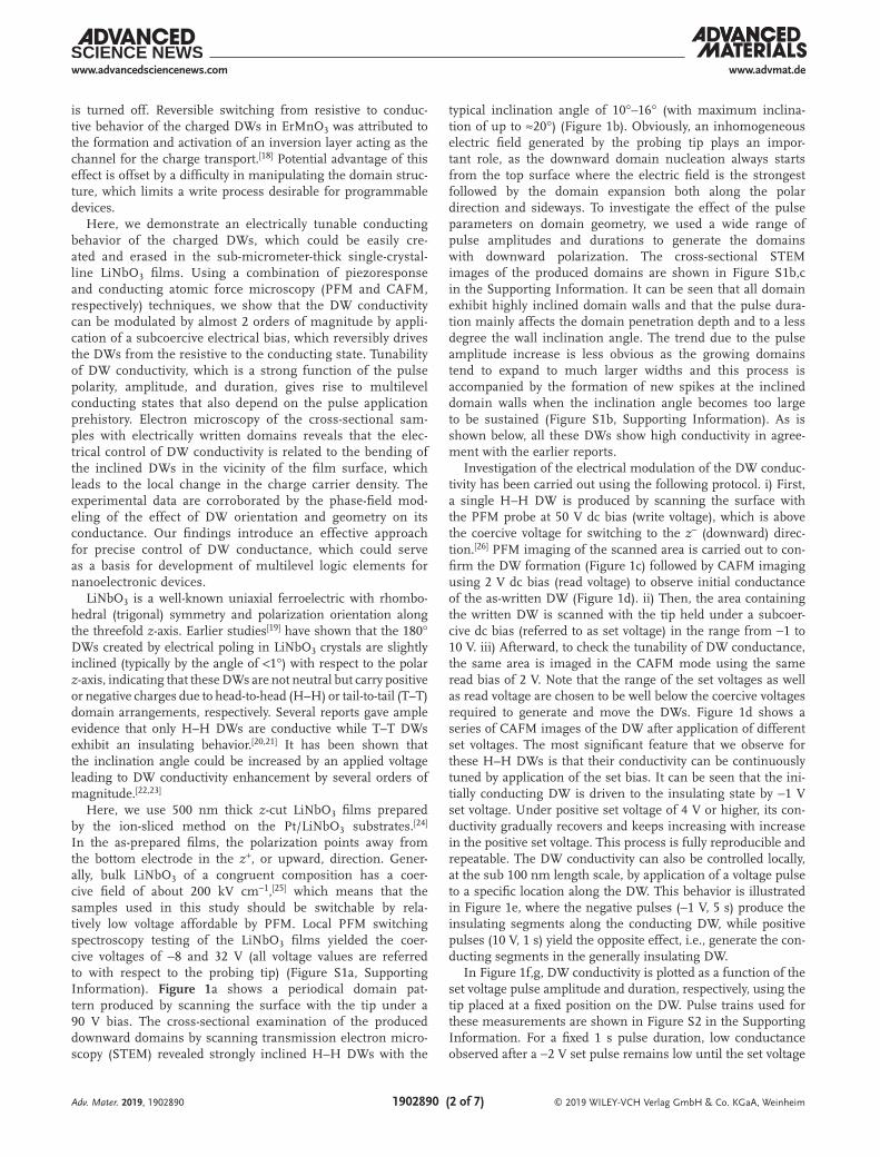
Investigation of the electrical modulation of the DW conduc-tivity has been carried out using the following protocol. i) First, a single H–H DW is produced by scanning the surface with the PFM probe at 50 V dc bias (write voltage), which is above the coercive voltage for switching to the z− (downward) direc-tion.[26] PFM imaging of the scanned area is carried out to con-firm the DW formation (Figure 1c) followed by CAFM imaging using 2 V dc bias (read voltage) to observe initial conductance of the as-written DW (Figure 1d). ii) Then, the area containing the written DW is scanned with the tip held under a subcoer-cive dc bias (referred to as set voltage) in the range from −1 to 10 V. iii) Afterward, to check the tunability of DW conductance, the same area is imaged in the CAFM mode using the same read bias of 2 V. Note that the range of the set voltages as well as read voltage are chosen to be well below the coercive voltages required to generate and move the DWs. Figure 1d shows a series of CAFM images of the DW after application of different set voltages. The most significant feature that we observe for these H–H DWs is that their conductivity can be continuously tuned by application of the set bias. It can be seen that the ini-tially conducting DW is driven to the insulating state by −1 V set voltage. Under positive set voltage of 4 V or higher, its con-ductivity gradually recovers and keeps increasing with increase in the positive set voltage. This process is fully reproducible and repeatable. The DW conductivity can also be controlled locally, at the sub 100 nm length scale, by application of a voltage pulse to a specific location along the DW. This behavior is illustrated in Figure 1e, where the negative pulses (−1 V, 5 s) produce the insulating segments along the conducting DW, while positive pulses (10 V, 1 s) yield the opposite effect, i.e., generate the con-ducting segments in the generally insulating DW.
In Figure 1f,g, DW conductivity is plotted as a function of the set voltage pulse amplitude and duration, respectively, using the tip placed at a fixed position on the DW. Pulse trains used for these measurements are shown in Figure S2 in the Supporting Information. For a fixed 1 s pulse duration, low conductance observed after a −2 V set pulse remains low until the set voltage
Adv. Mater. 2019, 1902890

© 2019 WILEY-VCH Verlag GmbH & Co. KGaA, Weinheim1902890 (3 of 7)
www.advmat.dewww.advancedsciencenews.com
exceeds 4 V, at which point conductance starts to rise continu-ously. Upon decrease of the set voltage from 10 to 0 V, initially almost no decay in DW conductivity is observed and then it
starts decreasing again reaching the low conductance state at −1 V. This data are consistent with the hysteretic behavior deduced from the CAFM imaging studies in Figure 1d (see also
Adv. Mater. 2019, 1902890
(c) (d)4 pA
0 pA(e)
(f) (g)
-1V
Initial
-1V
10V
2V
0V
4V
6V
10V
-1V
10V,1s
10V
-1V,5s
4 pA
0 pA
Pulse amplitude (V)-2 0 2 4 6 8 10
0
2
4
6
8
DW
cond
ucta
nce
(pS
)
Initial 0.01 0.1 1 10
0
2
4
6
8
10
12
DW
cond
ucta
nce
(pS
)
Pulse duration (s)
5 V 6 V 7 V 8 V -1 V
0.001
(b)(a)
Bo�om electrode
LiNbO3
Protec ve layers
500 nm2 µmx
z
x
y
Figure 1. Electrical control of domain wall conductivity. a) PFM phase image of line domains created by scanning the sample surface with the tip under 90 V dc bias. b) TEM cross-sectional view of the line domains showing slanted H–H domain walls. c) PFM amplitude and phase images on a domain wall, where the downward domain was created by +50 V poling. d) A series of CAFM images for different set voltages showing a gradual change in DW conductivity. CAFM read bias is 2 V for all images. The black vertical arrow indicates a sequence of set voltage application. e) Illustration of local control of DW conductivity by set voltage pulses. The black vertical arrow indicates a sequence of set voltage application. The small black arrows indicate locations of the probing tip during set pulse application. f) DW conductance spectroscopy as a function of the set pulse amplitude (pulse duration is 1 s). g) DW conductance spectroscopy as a function of the set pulse duration. A set pulse was applied to induce an initial conductance state: either high (by 8 V pulse) or low (by −2 V pulse).

© 2019 WILEY-VCH Verlag GmbH & Co. KGaA, Weinheim1902890 (4 of 7)
www.advmat.dewww.advancedsciencenews.com
Figure S3 in the Supporting Information). Similarly, local DW conductance depends on the set pulse duration (Figure 1g): an increase in the duration of the positive set pulses leads to higher DW conductivity while longer negative set pulses make the DW less conducting eventually driving it to the insulating state. These results show that the local DW conductivity can be continuously and reversibly tuned by altering the amplitude, duration, and polarity of the set voltage.
The observed voltage dependence of DW conductance pro-vides a possibility of their use in memristive devices with elec-trically tunable resistance.[27,28] Local I–V spectroscopy of the DW in Figure 2 provides additional illustration of their mem-ristive behavior. Figure 2a shows a typical I–V counterclockwise hysteresis in the positive half-cycle and a clockwise hysteresis in the negative half-cycle due to the fact that positive voltage enhances the DW conductivity while negative bias suppresses it. Consecutive I–V cycles in the positive voltage range (Figure 2b) or negative voltage range (Figure 2c) show cycle-to-cycle change of the current level. This prehistory-dependent DW conductivity is again a manifestation of the memristive behavior.
It is worth noting that the application of the set bias that tunes the DW conductivity does not cause any significant modi-fication of the existing domain configuration. As can be seen in Figure S4,b in the Supporting Information, there is no progres-sive change in domain structure upon consecutive scans with 10 V dc set bias. This is not surprising as the set bias used here (in the range from −1 to 10 V) is much lower than the coer-cive voltage of the LiNbO3 film (−8 and 32 V). However, detailed examination of the PFM and CAFM maps before and after application of the set voltage reveals that although the overall domain structure remains intact, there is a small (in the order of 10 nm) shift between the DW positions corresponding to the low and high conductance states. Figure 3a,b shows PFM and CAFM images of the DW after application of −1 V (Figure 3a) and 10 V set voltage (Figure 3b). Comparison of the DW posi-tions shown in Figure 3c reveals that a DW shift coincides with the change in the DW conductance (see also Figure S4b,c in the Supporting Information). In the region, where the DW position is unchanged, the DW conductance does not change either.
A typical range of the DW shift, which is completely revers-ible (see Figure S4 in the Supporting Information), is about 10–20 nm. We emphasize that even though the set voltages are well below the coercive voltages, it is still possible to slightly tilt the domain walls upon perturbation, as the inclined walls are energetically unfavorable.
It has been shown previously that the conducting behavior of the H–H DWs in LiNbO3 is a result of polarization charge discontinuity at the inclined walls, which induces elec-tron charge accumulation and a sharp increase in the DW conductivity.[20] Thus, it can be assumed that application of the set voltage would modulate the accumulated charge density and affect the H–H DW conductivity. However, the range of the conductance change by the set voltage (up to 10 V) is much larger in comparison with the DW conductance observed after polarization reversal by the write voltage of 50 V. Specifically, the average current of the as-written DW is about 3 pA at read bias of 2 V, while after 10 V prescan it increases to about 10 pA. Therefore, it is plausible that an additional mechanism is in play inducing the electrically tunable DW conductance.
Cross-sectional STEM studies reveal the DW bending at the vicinity of the sample surface so that the inclination angle reduces to 0° rendering an upper segment of the DW (up to 50 nm in length) electrically neutral and insulating (Figure 3d). Note that the STEM measurements have been performed about 2 days after domain writing, which means that the bent DW corresponds to the relaxed state. This result is consistent with the fact that DW conductance decays with time as is illustrated by the CAFM maps in Figure S5 in the Supporting Informa-tion. It can be seen that the initial DW conducting state induced by 10 V dc voltage scan (Figure S5a, Supporting Information) transformed into the insulating one 16 h later (Figure S5b, Supporting Information). Comparison of the corresponding PFM maps shows that this transition is accompanied by the DW displacement by a distance of about 20 nm. This behavior is very similar to the transition induced by −1 V dc set voltage (Figure S4b,c, Supporting Information), indicating that the mechanisms behind the conductance changes due to time relaxation and application of the negative set bias were
Adv. Mater. 2019, 1902890
(b) (c)
-2.0 -1.5 -1.0 -0.5 0.0
0
-2
-4
-6
-8
-10
Cur
rent
(pA
)
Bias (V)
1st cycle 2nd cycle 3rd cycle 4th cycle
Bias (V)0 1 2 3 4
0
5
10
15
20
25
30
Cur
rent
(pA)
(a)
-4 -3 -2 -1 0 1 2 3 4 5
-5
0
5
10
15
20
25
Cur
rent
(pA)
Bias (V)
0 2 4 6 8-2
024
Volta
ge (V
)
Time (s)
0 2 4 6 8-202468
Volta
ge (V
)
Time (s)
1st cycle 2nd cycle 3rd cycle 4th cycle
0 1 2 3 4
-2024
Volta
ge (V
)
Time (s)
Figure 2. Local I–V characterization of the H–H domain walls. a) An I–V loop showing a counterclockwise hysteresis for the positive half-cycle and a clockwise hysteresis for the negative half-cycle. Inset shows a pulse train used for I–V testing and applied through the tip. b) Four consecutive I–V cycles in the range from 0 to 4 V showing a gradual increase of the current level measured at the DW from cycle to cycle. A set pulse of −2 V was applied before the measurement to set the initial state to the low conductance level. c) Four consecutive I–V cycles in the range from 0 to −2 V showing a gradual decrease of the current level from cycle to cycle. A set pulse of 8 V was applied before the measurement to set the initial state to the high conductance level. The black arrows illustrate the voltage change directions.

© 2019 WILEY-VCH Verlag GmbH & Co. KGaA, Weinheim1902890 (5 of 7)
www.advmat.dewww.advancedsciencenews.com
one and the same, i.e., DW bending. Schematic illustration of the changes in the DW profile is shown in Figure 3e. The DW displacement by 20 nm associated with the change in its conductivity (Figure S4, Supporting Information) is in good agreement with the DW bending at the depth of 50 nm by ≈20° revealed by STEM. Note that our finding is consistent with the earlier reports on the field-induced modification of the inclina-tion angle in bulk LiNbO3 observed by Cherenkov-type second-harmonic generation.[23]
To get further insight into the observed behavior, we have car-ried out the phase-field simulations following up the earlier approach proposed for LiNbO3 films[29] additionally taking into account the contribution of the free carriers. Details of the math-ematical model can be found in the Experimental Section. The simulation results of the H–H DW conductivity dependence on the inclination angle are shown in Figure 4a. It can be seen that inclination of the wall by 20° leads to an increase in its conductivity by more than 2 orders of magnitude indicating a possibility of fine-tuning of DW transport properties via inclination angle control.
The 2D phase-field simulations of domain evolution begin with consideration of a perfectly triangular shape domain with the depth of around 65 nm and the DW inclination angle of
20° as if written by an external voltage above the coercive bias. The shape of this domain changes after the system is allowed to relax. In Figure 4b, it can be seen that the upper segments of the inclined DWs bend toward the vertical direction in agree-ment with the STEM data (Figure 3d). This behavior can be rationalized by simple energy analysis. The H–H configuration of the inclined DWs induces bound charge density ρb = −∇ · P, generating a significant electric field and increasing the electro-static energy of the system. On the other hand, the DWs aligned parallel to the polar axis are electrically neutral and, as such, are favored from the viewpoint of the system energy minimization.
Results of 2D phase-field modeling of the subcoercive voltage effect on the DW profile and its conductance are shown in Figure 4c–h. According to these results, a positive set voltage tends to make the tilted DW profile more straight giving rise to a higher carrier concentration (Figure 4c). In contrast, a nega-tive set voltage causes the wall bending near the surface, which results in a lower carrier density (Figure 4d). Since electrons are the primary charge carriers for the H–H DW, its conduc-tivity should be nearly proportional to the electron density,[29] as is shown in Figure 4g,h. This means that positive set voltage leads to an increased conductivity, while negative set bias can
Adv. Mater. 2019, 1902890
Figure 3. Correlation between domain wall shift, bending, and conductivity. PFM amplitude, phase, and CAFM images of a domain wall: a) after −1 V set bias scan, which renders a domain wall insulating, and b) after 10 V set bias scan of the wall section marked by two dashed lines, which makes this section conducting. The domain wall position for (a) in blue and (b) in green is overlaid on the CAFM image. c) Direct comparison of the domain wall profiles in (a) and (b) marked by blue and green lines, respectively, with x–y aspect ratio expanded by a factor of 3 for a better view. A domain wall shift is observed only in the region scanned with the 10 V set bias. As seen in (e) below, this shift is due to the increase of the volume of domain with the downward polarization. d) Cross-sectional TEM image showing inclined domain walls with the upper segment aligned almost parallel to the polar direction (marked by the yellow circles). e) Schematic illustration of the changes in the DW profile induced by the set bias. While the −1 V set bias bends the upper DW segment toward the polar direction making the wall electrically neutral and insulating, the 10 V set bias pushes it further away from the polar direction increasing the inclination angle and making the DW charged and conducting.

© 2019 WILEY-VCH Verlag GmbH & Co. KGaA, Weinheim1902890 (6 of 7)
www.advmat.dewww.advancedsciencenews.com
completely “turn off” the DW conductance—in perfect agree-ment with the experimental findings.
In conclusion, using a combination of local probe and elec-tron microscopy, we explore the mechanism of the tunable conducting behavior of the domain walls in archetype techno-logically important ferroelectric LiNbO3 films. STEM visualiza-tion of the electrically written domains in the cross-sectional samples and imaging of the very same domains by scanning probe microscopy on the polar surface allowed us to estab-lish direct correlation between the domain wall orientation, topology, and transport properties. We have observed that the tip-generated domains have strongly inclined domain bounda-ries with the inclination angle of up to 20° with respect to the polar axis. The bound charge density induced at the inclined H–H DWs leads to the electron charge accumulation and a strong increase in the DW conductance. Application of the sub-coercive voltage allows tunability of domain wall conductance by 2 orders of magnitude. It has been directly shown that the reversible transition between the conducting and insulating sates of the DWs is due to the electrically induced wall bending near the sample surface away or toward the polar direction. These experimental findings have been corroborated by the 2D phase-field simulations of the effect of DW orientation and shape on their transport properties. Active control of the charged domain walls and tuning of their electronic properties may facilitate novel developments and applications in the field of domain wall nanoelectronics.
Experimental SectionSample Preparation: 500 nm thick z-cut undoped LiNbO3 films on Pt/
Cr/SiO2/LiNbO3 substrates with z+ oriented polarization were prepared by ion-sliced method cutting from single crystal congruent LiNbO3, and were purchased from NanoLN.
Domain Switching and Imaging: Local probe measurements were carried out using a commercial atomic force microscope (MFP-3D, Asylum Research). Pt-coated Si cantilevers (PPP/EFM from Nanosensors) were used both for domain writing/imaging in the PFM mode and for domain wall CAFM imaging. PFM domain visualization was performed using an ac modulation bias with 0.5 V amplitude and 350 kHz frequency. CAFM imaging was conducted at 2 V dc bias. Electrical bias was applied between the AFM tip and bottom Pt electrode, and all voltage values were mentioned as a potential drop from the tip to the bottom electrode.
Transmission Electron Microscopy: An electron transparent cross-section of patterned LiNbO3 film and substrate was prepared for STEM using a dual-beam focused ion beam (FIB) integrated scanning electron microscope (Thermo-Fisher Scientific FEI Helios 660 and G4 HX models). The specimen was mounted onto an Omniprobe copper-based lift-out grid. The thinning of the sample was done in four steps. The first step reduced the thickness of the sample from 2 µm to 800 nm using Ga ions with a 30 keV energy and 0.23 nA ion beam current and cleaning cross-section mode. Second thinning step at 16 keV energy and 50 pA was used to get from 800 to 500 nm. The third thinning step at 8 keV energy and 50 pA was used to get from 500 to 300 nm. And the final thinning step was done to get to <100 nm using 5 keV energy and 46 Pa. A final polishing step was done at 2 keV and 23 pA. The STEM analysis was performed using a Thermo-Fisher Scientific double tilt TEM holder in the Thermo-Fisher Scientific FEI double aberration-corrected monochromated Titan Themis Z at the University of Limerick. The microscope was operated at 300 kV. The imaging mode used was STEM at a camera length of 280 mm with a 50 µm C2 aperture.
Computational Simulations: The phase-field simulations were carried out following up the earlier approach proposed for LiNbO3 films[19,27] additionally taking into account the contribution of the free carriers. The stable state of the system can be described by the Landau–Ginzburg–Devonshire (LGD) equation along with the Poisson equation of electric potential φ
03 52
2
2
2P P P gPx
Pz zz z z
z zα β γ ϕ+ + − ∂∂
+ ∂∂
+ ∂∂ =
(1)
0 11
2
2 33
2
2x zPz
Qb b zε ε ϕ ε ϕ∂∂
+ ∂∂
= ∂∂ −
(2)
Adv. Mater. 2019, 1902890
0.6
-0.6
3 10× 8
Pz (C/m )2
(V)
Q (C/m )3
4
0
0
θ
0 20 40 60 800
500
1000
1500
2000
2500
3000
0
(deg.)
(a)
(b)0.6
-0.6
Pz (C/m )2
(c) (d)
(e) (f)
(g) (h)
After 10V After -10V
Figure 4. Phase-field modeling of the domain wall profile and conductivity. a) Ratio of domain wall conductivity (σ) to bulk domain conductivity (σ0) as a function of the domain wall inclination angle θ. b) The shape of an electrically written domain after relaxation. Bending of the upper segments of the domain wall toward the vertical direction could be clearly seen. c,d) Domain shapes, e,f) potential distribution, and g,h) mobile charge density for opposite set voltages: c,e,g) +10 V and d,f,h) −10 V. While positive set bias tends to increase the volume of the downward domain by pushing the domain walls further away from the polar direction making them more conducting, the negative set bias shrinks the downward domain by bending the upper segments of the domain walls toward the polar direction making them electrically neutral and insulating. In PFM, this wall bending is perceived as the domain shift. Note that equal amplitudes of the set bias have been used in the modeling since the asymmetry of the film coercivity was not taken into account.

© 2019 WILEY-VCH Verlag GmbH & Co. KGaA, Weinheim1902890 (7 of 7)
www.advmat.dewww.advancedsciencenews.com
Adv. Mater. 2019, 1902890
where α, β, and γ are the expansion coefficients for the Landau potential, g is the gradient energy coefficient, 11
bε and 33bε are relative background
electrical permittivity along x and z directions, respectively, and Q is the total free charge density consisting of contributions from the electrons, holes, as well as ionized donors and acceptors due to impurities or intrinsic point defects. Details of the mathematical model could be found in the method part and from the previous reference. More detailed descriptions of the mathematical model and 1D simplification method can be found in ref. [19]. Both 1D and 2D simulations were carried out using the finite element method (FEM) implemented in the COMSOL Multiphysics computational package. For 1D simulations, the length of system was 200 nm, with a domain wall placed at the center of the system. In 2D simulations, the xz cross-section was 100 nm × 200 nm, while a periodic boundary condition was applied to the y direction. The bottom surface of the 2D system was always grounded, while the voltage on the top surface varied to simulate different tip voltages. To be more specific, two narrow Gaussian functions with an FWHM at around 1.6 nm were applied close to the domain walls, whose magnitudes were recorded under the figures. The initial shape of switched domains was set as triangles with the same size, around 65 nm in depth and domain wall tilting angle θ = 20°, in different simulations. For both kinds of simulations, a static solver was applied to get self-consistent solutions of voltage and polarization fields.
Supporting InformationSupporting Information is available from the Wiley Online Library or from the author.
AcknowledgementsThis research was supported by the National Science Foundation (NSF) grant DMR-1709237 (A.G.) (PFM/CAFM measurements), through the Nebraska Materials Research Science and Engineering Center (MRSEC, grant DMR-1420645) (A.G. and J.E.S.) (electron microscopy studies), by the EPSRC (grant No. EP/P02453X/1) and US-Ireland R&D Partnership Programme (grant No. USI 120) (J.M.G. and U.B.) (electron microscopy measurements). J.P.V.M. was supported by an EPSRC doctoral grant (ref. 1631303). The work at the Penn State University (phase-field modeling) was supported by the NSF MRSEC (grant DMR-1420620 (B.W.) and by the NSF grant DMR-1744213 (Y.T.). The work at the University of Limerick was carried out with financial support from the Science Foundation Ireland (grant No. 16/US/3344).
Conflict of InterestThe authors declare no conflict of interest.
Keywordsconducting domain walls, ferroelectric films, lithium niobate, scanning probe microscopy, transmission electron microscopy
Received: May 6, 2019Revised: September 11, 2019
Published online:
[1] J. Seidel, L. W. Martin, Q. He, Q. Zhan, Y.-H. Chu, A. Rother, M. E. Hawkridge, P. Maksymovych, P. Yu, M. Gajek, N. Balke, S. V. Kalinin, S. Gemming, F. Wang, G. Catalan, J. F. Scott, N. A. Spaldin, J. Orenstein, R. Ramesh, Nat. Mater. 2009, 8, 229.
[2] T. Sluka, A. K. Tagantsev, P. Bednyakov, N. Setter, Nat. Commun. 2013, 4, 1808.
[3] S. Farokhipoor, C. Magén, S. Venkatesan, J. Íñiguez, C. J. M. Daumont, D. Rubi, E. Snoeck, M. Mostovoy, C. de Graaf, A. Müller, M. Döblinger, C. Scheu, B. Noheda, Nature 2014, 515, 379.
[4] A. Aird, E. K. H. Salje, J. Phys.: Condens. Matter 1998, 10, L377.
[5] D. A. Allwood, G. Xiong, C. C. Faulkner, D. Atkinson, D. Petit, R. P. Cowburn, Science 2005, 309, 1688.
[6] G. Catalan, J. Seidel, R. Ramesh, J. F. Scott, Rev. Mod. Phys. 2012, 84, 119.
[7] S. Farokhipoor, B. Noheda, Phys. Rev. Lett. 2011, 107, 127601.
[8] P. Maksymovych, J. Seidel, Y.-H. Chu, P. Wu, A. P. Baddorf, L. Q. Chen, S. V. Kalinin, R. Ramesh, Nano Lett. 2011, 11, 1906.
[9] J. Guyonnet, I. Gaponenko, S. Gariglio, P. Paruch, Adv. Mater. 2011, 23, 5377.
[10] P. Maksymovych, A. N. Morozovska, P. Yu, E. A. Eliseev, Y.-H. Chu, R. Ramesh, A. P. Baddorf, S. V. Kalinin, Nano Lett. 2012, 12, 209.
[11] D. Meier, J. Seidel, A. Cano, K. Delaney, Y. Kumagai, M. Mostovoy, N. A. Spaldin, R. Ramesh, M. Fiebig, Nat. Mater. 2012, 11, 284.
[12] Y. S. Oh, X. Luo, F. T. Huang, Y. Wang, S. W. Cheong, Nat. Mater. 2015, 14, 407.
[13] R. G. P. McQuaid, M. P. Campbell, R. W. Whatmore, A. Kumar, J. M. Gregg, Nat. Commun. 2017, 8, 15105.
[14] J. R. Whyte, R. G. P. McQuaid, P. Sharma, C. Canalias, J. F. Scott, A. Gruverman, J. M. Gregg, Adv. Mater. 2014, 26, 293.
[15] J. R. Whyte, R. G. P. McQuaid, C. M. Ashcroft, J. F. Einsle, C. Canalias, A. Gruverman, J. M. Gregg, J. Appl. Phys. 2014, 116, 066813.
[16] J. Jiang, Z. L. Bai, Z. H. Chen, L. He, D. W. Zhang, Q. H. Zhang, J. A. Shi, M. H. Park, J. F. Scott, C. S. Hwang, A. Q. Jiang, Nat. Mater. 2018, 17, 49.
[17] P. Sharma, Q. Zhang, D. Sando, C. H. Lei, Y. Liu, J. Li, V. Nagarajan, J. Seidel, Sci. Adv. 2017, 3, e1700512.
[18] J. A. Mundy, J. Schaab, Y. Kumagai, A. Cano, M. Stengel, I. P. Krug, D. M. Gottlob, H. Doganay, M. E. Holtz, R. Held, Z. Yan, E. Bourret, C. M. Schneider, D. G. Schlom, D. A. Muller, R. Ramesh, N. A. Spaldin, D. Meier, Nat. Mater. 2017, 16, 622.
[19] V. Ya. Shur, E. L. Rumyantsev, E. V. Nikolaeva, E. I. Shishkin, Appl. Phys. Lett. 2000, 77, 3636.
[20] E. A. Eliseev, A. N. Morozovska, G. S. Svechnikov, V. Gopalan, V. Ya. Shur, Phys. Rev. B 2011, 83, 235313.
[21] M. Schröder, A. Haußmann, A. Thiessen, E. Soergel, T. Woike, L. M. Eng, Adv. Funct. Mater. 2012, 22, 3936.
[22] C. Godau, T. Kämpfe, A. Thiessen, L. M. Eng, A. Haußmann, ACS Nano 2017, 11, 4816.
[23] T. Keampfe, P. Reichenbach, M. Schröder, A. Haußmann, L. M. Eng, T. Woike, E. Soergel, Phys. Rev. B 2014, 89, 035314.
[24] G. Poberaj, H. Hu, W. Sohler, P. Günter, Laser Photonics Rev. 2012, 6, 488.
[25] V. Gopalan, T. E. Mitchell, Y. Furukawa, K. Kitamura, Appl. Phys. Lett. 1998, 72, 1981.
[26] T. R. Volk, R. V. Gainutdinov, H. H. Zhang, Appl. Phys. Lett. 2017, 110, 132905.
[27] L. O. Chua, IEEE Trans. Circuit Theory 1971, 18, 507.[28] D. B. Strukov, G. S. Snider, D. R. Stewart, R. S. Williams, Nature
2008, 453, 80.[29] A. N. Morozovska, E. A. Eliseev, Y. Li, S. V. Svechnikov,
P. Maksymovych, V. Y. Shur, V. Gopalan, L.-Q. Chen, S. V. Kalinin, Phys. Rev. B 2009, 80, 214110.