Ferromagnet/Semiconductor/Ferromagnet Hybrid Trilayers ... · Solid-phase Epitaxy S. Gaucher, B....
4
Ferromagnet/Semiconductor/Ferromagnet Hybrid Trilayers grown using Solid-phase Epitaxy S. Gaucher, B. Jenichen, a) and J. Herfort Paul-Drude-Institut f¨ ur Festk¨ orperelektronik Leibniz-Institut im Forschungsverbund Berlin e.V., Hausvogteiplatz 5-7, 10117 Berlin, Germany (Dated: 8 June 2018) The direct growth of semiconductors over metals by molecular beam epitaxy is a difficult task due to the large differences in crystallization energy between these types of materials. This aspect is problematic in the context of spintronics, where coherent spin-injection must proceed via ballistic transport through sharp interfacial Schottky barriers. We report the realization of single-crystalline ferromagnet/semiconductor/ferromagnet hybrid trilayers using solid-phase epitaxy, with combinations of Fe 3 Si, Co 2 FeSi, and Ge. The slow annealing of amorphous Ge over Fe 3 Si results in a crystalline film identified as FeGe 2 . When the annealing is performed over Co 2 FeSi, reflected high-energy electron diffraction and X-ray diffraction indicate the creation of a different crystalline Ge(Co,Fe,Si) compound, which also preserves growth orientation. It was possible to observe independent magnetization switching of the ferromagnetic layers in a Fe 3 Si/FeGe 2 /Co 2 FeSi sample, thanks to the different coercive fields of the two metals and to the quality of the interfaces. This result is a step towards the implementation of vertical spin-selective transistor-like devices. I. INTRODUCTION The growth by molecular beam epitaxy (MBE) of ferromagnetic (FM) Heusler alloys and semiconductors (SC) heterostructures was found to be a successful ap- proach to realize a number of applications in the field of spintronics. 1,2 The possibility to create lattice-matched and sharp FM/SC interfaces is important to realize high spin injection efficiency, as intermixing and order- ing effects are known to play a detrimental role on spin transport. 3–6 Coherence is better preserved when spin injection proceeds via tunneling through a narrow Schot- tky barrier, 7–9 whose profile is also highly influential. 10 Such studies are more easily performed in bilayer sys- tems, where a single-crystalline FM film is grown over a SC substrate by MBE. Indeed, metals usually require lower crystallization temperatures, which ensures that no undesirable mixing or byproducts occur at the SC/FM interface. Growing a SC over a metallic substrate is how- ever more challenging, and can be a limiting factor for a number of envisaged applications, such as vertical spin- selective devices made in the FM/SC/FM configuration. Ge has been used as a candidate SC to grow on FM surfaces due to its relatively low crystallization temper- ature (∼300 ◦ C), which offers better chances to prevent intermixing at the interface. The growth of Ge over ferro- magnetic Heusler alloys was investigated by MBE, 11–14 surfactant-mediated MBE 15,16 and more recently solid- phase epitaxy (SPE). 17,18 Using the latter approach, it was shown that the slow annealing of a thin amorphous Ge film over Fe 3 Si can yield a compound identified as FeGe 2 , 19 over which it was possible to grow another single-crystalline Fe 3 Si layer. a) Electronic mail: [email protected] In this work, we extend the SPE technique to include Co 2 FeSi within the trilayer stacks. Co 2 FeSi and Fe 3 Si have similar lattice parameters, and thus can both be grown by MBE in a lattice-matched way over GaAs and Ge. The two FM materials are known to have coercive fields differing by only a few Oe, 20,21 which is an advan- tage to control the magnetization of the films indepen- dently. Co 2 FeSi has the highest magnetic moment per unit cell and highest Curie temperature of all ferromag- netic Heusler alloys. It has also for long been expected to exhibit a half-metallic character. Although this property is being disputed, one can minimally expect the com- pound to offer a degree of spin polarization in the 40-60% range. 22 Despite the relatively high reactivity of Co 2 FeSi (com- pared to Fe 3 Si), it was still possible to use the SPE ap- proach to crystallize amorphous Ge films and achieve fully epitaxial trilayers. The realization of such het- erostructures, including FM materials with different co- ercive fields, is a supplementary step towards the creation of new spin-selective devices that could be operated both as tunnel transistors and magnetic tunnel junctions. II. EXPERIMENTAL Figure 1 shows four stacking sequences used in this study, where a Ge buffer layer is inserted between two FM films with thicknesses of 36 and 12 nm. The two FM layers are either Fe 3 Si or Co 2 FeSi, or a combination of both. The samples are grown using low-temperature MBE and SPE, building on methods that were described previously. 17 GaAs(001) substrates are prepared with a 350 nm buffer layer, grown by MBE at 540 ◦ C and As-terminated. The samples then are transferred un- der UHV into an As-free chamber, in which Fe 3 Si and Co 2 FeSi layers are grown by co-deposition from high- arXiv:1806.02733v1 [cond-mat.mtrl-sci] 7 Jun 2018
Transcript of Ferromagnet/Semiconductor/Ferromagnet Hybrid Trilayers ... · Solid-phase Epitaxy S. Gaucher, B....

Ferromagnet/Semiconductor/Ferromagnet Hybrid Trilayers grown usingSolid-phase Epitaxy
S. Gaucher, B. Jenichen,a) and J. HerfortPaul-Drude-Institut fur Festkorperelektronik Leibniz-Institut im Forschungsverbund Berlin e.V., Hausvogteiplatz 5-7,10117 Berlin, Germany
(Dated: 8 June 2018)
The direct growth of semiconductors over metals by molecular beam epitaxy is a difficult task due to the largedifferences in crystallization energy between these types of materials. This aspect is problematic in the contextof spintronics, where coherent spin-injection must proceed via ballistic transport through sharp interfacialSchottky barriers. We report the realization of single-crystalline ferromagnet/semiconductor/ferromagnethybrid trilayers using solid-phase epitaxy, with combinations of Fe3Si, Co2FeSi, and Ge. The slow annealingof amorphous Ge over Fe3Si results in a crystalline film identified as FeGe2. When the annealing is performedover Co2FeSi, reflected high-energy electron diffraction and X-ray diffraction indicate the creation of a differentcrystalline Ge(Co,Fe,Si) compound, which also preserves growth orientation. It was possible to observeindependent magnetization switching of the ferromagnetic layers in a Fe3Si/FeGe2/Co2FeSi sample, thanksto the different coercive fields of the two metals and to the quality of the interfaces. This result is a steptowards the implementation of vertical spin-selective transistor-like devices.
I. INTRODUCTION
The growth by molecular beam epitaxy (MBE) offerromagnetic (FM) Heusler alloys and semiconductors(SC) heterostructures was found to be a successful ap-proach to realize a number of applications in the field ofspintronics.1,2 The possibility to create lattice-matchedand sharp FM/SC interfaces is important to realizehigh spin injection efficiency, as intermixing and order-ing effects are known to play a detrimental role on spintransport.3–6 Coherence is better preserved when spininjection proceeds via tunneling through a narrow Schot-tky barrier,7–9 whose profile is also highly influential.10
Such studies are more easily performed in bilayer sys-tems, where a single-crystalline FM film is grown overa SC substrate by MBE. Indeed, metals usually requirelower crystallization temperatures, which ensures that noundesirable mixing or byproducts occur at the SC/FMinterface. Growing a SC over a metallic substrate is how-ever more challenging, and can be a limiting factor for anumber of envisaged applications, such as vertical spin-selective devices made in the FM/SC/FM configuration.
Ge has been used as a candidate SC to grow on FMsurfaces due to its relatively low crystallization temper-ature (∼300◦C), which offers better chances to preventintermixing at the interface. The growth of Ge over ferro-magnetic Heusler alloys was investigated by MBE,11–14
surfactant-mediated MBE15,16 and more recently solid-phase epitaxy (SPE).17,18 Using the latter approach, itwas shown that the slow annealing of a thin amorphousGe film over Fe3Si can yield a compound identified asFeGe2,19 over which it was possible to grow anothersingle-crystalline Fe3Si layer.
a)Electronic mail: [email protected]
In this work, we extend the SPE technique to includeCo2FeSi within the trilayer stacks. Co2FeSi and Fe3Sihave similar lattice parameters, and thus can both begrown by MBE in a lattice-matched way over GaAs andGe. The two FM materials are known to have coercivefields differing by only a few Oe,20,21 which is an advan-tage to control the magnetization of the films indepen-dently. Co2FeSi has the highest magnetic moment perunit cell and highest Curie temperature of all ferromag-netic Heusler alloys. It has also for long been expected toexhibit a half-metallic character. Although this propertyis being disputed, one can minimally expect the com-pound to offer a degree of spin polarization in the 40-60%range.22
Despite the relatively high reactivity of Co2FeSi (com-pared to Fe3Si), it was still possible to use the SPE ap-proach to crystallize amorphous Ge films and achievefully epitaxial trilayers. The realization of such het-erostructures, including FM materials with different co-ercive fields, is a supplementary step towards the creationof new spin-selective devices that could be operated bothas tunnel transistors and magnetic tunnel junctions.
II. EXPERIMENTAL
Figure 1 shows four stacking sequences used in thisstudy, where a Ge buffer layer is inserted between twoFM films with thicknesses of 36 and 12 nm. The twoFM layers are either Fe3Si or Co2FeSi, or a combinationof both. The samples are grown using low-temperatureMBE and SPE, building on methods that were describedpreviously.17 GaAs(001) substrates are prepared witha 350 nm buffer layer, grown by MBE at 540◦C andAs-terminated. The samples then are transferred un-der UHV into an As-free chamber, in which Fe3Si andCo2FeSi layers are grown by co-deposition from high-
arX
iv:1
806.
0273
3v1
[co
nd-m
at.m
trl-
sci]
7 J
un 2
018

2
temperature effusion cells, both at 200◦C. On top of thesefirst FM layers, the equivalent of 6 nm of crystalline Ge isdeposited at 150◦C, which in fact results in an amorphousfilm. The samples are then annealed in-situ by slowlyincreasing the temperature (5◦/min) up to 245◦C (overCo2FeSi) or 260◦C (over Fe3Si) for 10 minutes. Dur-ing the annealing, the crystallization of the amorphousGe layer is monitored by reflected high-energy electrondiffraction (RHEED). The annealing temperatures weredetermined by observing the appearance of streaks inthe RHEED pattern, which confirmed the obtention ofa crystalline layer. Capping Fe3Si or Co2FeSi layers arethen grown directly over the crystallized compounds, un-der the same conditions as the respective first layers.
FIG. 1. Four trilayer stacking sequences containing a first36 nm FM layer (Co2FeSi or Fe3Si), a 6 nm SC buffer layer(Ge crystallized by annealing), and a capping 12 nm FM layer(Co2FeSi or Fe3Si). An objective is to independently controlthe magnetization of each FM layer as illustrated on the bot-tom left stack.
The structure and quality of the trilayer stacks wereevaluated by X-ray diffraction (XRD) using an X-PertPRO MRDTM system with CuKα1 radiation source hav-ing a wavelength λ = 1.54056 A. The FM layers are madewith thicknesses in a ratio of 3:1 in order for their individ-ual contributions to appear clearly in the XRD patterns(finite thickness oscillations with 1:3 beating pattern).The magnetization of the trilayers was measured in asuperconducting quantum interference device (SQUID),using standard AC techniques. For that purpose, thesamples were cut into pieces of approximately 3×4 nmand cooled down to 10 K.
III. RESULTS
All four hybrid trilayer configurations (illustrated inFigure 1) have single-crystalline individual layers thatpreserve growth orientation. Figure 2 shows a compari-son of the RHEED patterns taken during the growth oftwo samples. In (a), the crystallization the amorphousGe film is performed over a Fe3Si surface. The result-ing compound is a 2D allotrope of FeGe2 with space
group P4mm (with a small amount of diffused Si atomssitting on Ge sites). This material does not exist in abulk form and results from the minimization of the elas-tic energy of the epitaxial film.19 There is a clear dis-tinction between the patterns observed along the [110]and [010] directions. A relationship can thus be estab-lished with the orientation of the overgrown Co2FeSifilm, for which the streaks coincide for the same sam-ple alignments. In (b), the annealing is done over aCo2FeSi surface. Although the exact stoichiometry ofthe Ge(Co,Fe,Si) film was not determined, the RHEEDpattern depicts a lattice-matched compound over whichthe pseudomorphic growth of Fe3Si was possible. Theabsence of Kikuchi lines in the Ge(Co,Fe,Si) images is asign that the surface is not as flat as the one obtainedfor FeGe2, a feature that is also noticeable in the XRDcurves of the trilayers.
[110] [010]
FeGe 2
Fe3Si surface
Co2FeSi
[110] [010]
Fe3Si
Ge(Co
,Fe,Si)
(a)
(b)
Co2FeSi surface
FIG. 2. (a) RHEED images taken during the growth of aFe3Si/FeGe2/Co2FeSi trilayer along the [110] and [010] az-imuths. (b) Corresponding RHEED images taken during thegrowth of a Co2FeSi/Ge(Co,Fe,Si)/Fe3Si trilayer. The SPEof amorphous Ge yields different compounds depending onthe nature of the underlying surface. It does not prevent thestacks from preserving the same crystal orientation, as seenfrom the alignment of the streaks of the capping FM films.
Figure 3 shows the XRD curves of the four samples

3
with different layer combinations. In (a), FeGe2 is vis-ible above Fe3Si and corresponds to the rounded peaksat angles slightly higher than the GaAs(002) and (004)peaks (∼16.5◦ and ∼ 34◦). The layered structure of theFeGe2 is a superstructure with a period of two monolay-ers, which explains the satellite peak around ω ≈ 25◦.19
The Ge(Co,Fe,Si) forming over Co2FeSi has peaks thatcoincide with the FeGe2 ones. However, it does not havea layered structure, as can be asserted from the absenceof a similar satellite peak. Panel (b) shows a close-up ofthe XRD curves near the GaAs(002) reflection peak. Forall four trilayer stacks, it is possible to notice the contri-bution from both FM layers in the finite thickness oscilla-tions. The 36:12 nm thickness ratio effectively generatesa beating pattern between oscillations with periods in a1:3 ratio. The clarity of these oscillations is better whenthe SPE is performed over Fe3Si, which indicates that thestacks have better interface quality. The layered struc-ture of the FeGe2 is likely responsible for the sharpnessof the interfaces. Thus, the SPE approach yields crys-talline films over both Fe3Si and Co2FeSi surfaces, butthe quality of the FM/FeGe2 interfaces is better, which isan advantage in order to achieve clear and abrupt mag-netization switching.
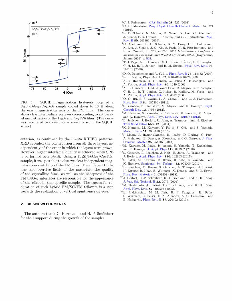
Figure 4 shows the ideal behavior for the magnetiza-tion hysteresis of a trilayer. The sample used for thiscurve is the Fe3Si/FeGe2/Co2FeSi stack, with externalfield applied along the easy magnetization axis of theFM films. At high positive field, both Fe3Si and Co2FeSilayers are magnetized along the same orientation. As thefield is decreased, the magnetization of the thicker Fe3Silayer flips first, resulting in a plateau. The Co2FeSi layerthen flips at slightly higher negative field, due to thehigher coercivity of the material. Thinner films also tendto have higher coercive fields, which in this case accentu-ates the effect. A similar sequential switching is observedalong the other direction of the hysteresis loop. The 6 nmFeGe2 is also ferromagnetic at low temperatures. How-ever, its contribution to the total magnetization is negli-gible and therefore cannot be observed on this curve.
It was not possible to observe clear independent mag-netic switching of the FM layers using the samples hav-ing another stacking order. Single-crystalline Fe3Si filmsare known to have small coercive fields and abrupt mag-netization reversal (within 1 Oe). Despite having idealinterface quality, the different thickness of the FM filmsin the Fe3Si/FeGe2/Fe3Si sample did not translate into acoercivity difference sufficient to produce plateaus of an-tiparallel magnetization. The samples with underlyingCo2FeSi have rougher interfaces, which resulted in ill-defined features around the magnetization reversal whichcould not be clearly attributed to a specific FM layer.The combination of Fe3Si and Co2FeSi with FeGe2 bufferlayer is therefore the best all four stacking configurations.
15 20 25 30 35 15 20 25 30 35
Inte
nsity
(arb
. uni
ts)
! (deg)
(a)Fe3Si/FeGe2/Fe3Si Co2FeSi/Ge(Co,Fe,Si)/Fe3Si
Fe3Si/FeGe2/Co2FeSi Co2FeSi/Ge(Co,Fe,Si)/Co2FeSi
GaAs (002)
GaAs (004)
FeGe2Ge(Co,Fe,Si)
14 15 16 17 18 15 16 17 18 19! (deg)
GaAs (002)
(b)
Ge(Co,Fe,Si)FeGe2
FeGe2Ge(Co,Fe,Si)
Inte
nsity
(arb
. uni
ts)
GaAs (002)
GaAs (002)
GaAs (002)
12 nm filmoscillations
FIG. 3. XRD of four trilayer stacks, consisting of differentcombinations of Fe3Si, Co2FeSi and Ge compounds as indi-cated on each curves (see placement in Figure 1). (a) Widerange diffraction curve showing a characteristic FeGe2 peakabout ω ≈ 25◦ for samples with underlying Fe3Si layer, as wellas the crystalline Ge(Co,Fe,Si) peak over Co2FeSi layers. (b)Close-up of the XRD curves about the GaAs(002) substratepeak, showing a beating pattern in the FM films oscillations.
IV. CONCLUSION
The growth of FM/SC/FM trilayer stacks was inves-tigated by a combination of low temperature MBE andSPE. The crystallization of amorphous Ge was successfulon both Fe3Si and Co2FeSi surfaces. On Fe3Si, a lay-ered allotrope of FeGe2 arises spontaneously, while an-other Ge(Co,Fe,Si) compound forms over Co2FeSi. Inboth cases, capping Fe3Si or Co2FeSi layers could beadded by MBE while preserving the same growth ori-
4
- 75 - 50 - 25 0 25 50 75
- 5
0
5
H (Oe)
M(emu)
! 10- 4
Fe3Si/FeGe2/Co2FeSi10 K
FIG. 4. SQUID magnetization hysteresis loop of aFe3Si/FeGe2/Co2FeSi sample cooled down to 10 K alongthe easy magnetization axis of the FM films. The curveshows clear intermediary plateaus corresponding to antiparal-lel magnetization of the Fe3Si and Co2FeSi films. (The curvewas recentered to correct for a known offset in the SQUIDsetup.)
entation, as confirmed by the in-situ RHEED patterns.XRD revealed the contribution from all three layers, in-dependently of the order in which the layers were grown.However, higher interfacial quality is achieved when SPEis performed over Fe3Si. Using a Fe3Si/FeGe2/Co2FeSisample, it was possible to observe clear independent mag-netization switching of the FM films. The different thick-ness and coercive fields of the materials, the qualityof the crystalline films, as well as the sharpness of theFM/FeGe2 interfaces are responsible for the appearanceof the effect in this specific sample. The successful re-alization of such hybrid FM/SC/FM trilayers is a steptowards the realization of vertical spintronics devices.
V. ACKNOWLEDGMENTS
The authors thank C. Herrmann and H.-P. Schonherrfor their support during the growth of the samples.
1C. J. Palmstrøm, MRS Bulletin 28, 725 (2003).2C. J. Palmstrøm, Prog. Cryst. Growth Charact. Mater. 62, 371(2016).
3B. D. Schultz, N. Marom, D. Naveh, X. Lou, C. Adelmann,J. Strand, P. A. Crowell, L. Kronik, and C. J. Palmstrøm, Phys.Rev. B 80, 201309 (2009).
4C. Adelmann, B. D. Schultz, X. Y. Dong, C. J. Palmstrom,X. Lou, J. Strand, J. Q. Xie, S. Park, M. R. Fitzsimmons, andP. A. Crowell, in 16th IPRM. 2004 International Conferenceon Indium Phosphide and Related Materials, 2004. (Kagoshima,Japan, 2004) p. 505.
5T. J. Zega, A. T. Hanbicki, S. C. Erwin, I. Zutic, G. Kioseoglou,C. H. Li, B. T. Jonker, and R. M. Stroud, Phys. Rev. Lett. 96,196101 (2006).
6D. O. Demchenko and A. Y. Liu, Phys. Rev. B 73, 115332 (2006).7E. I. Rashba, Phys. Rev. B 62, R16267–R16270 (2000).8A. T. Hanbicki, B. T. Jonker, G. Itskos, G. Kioseoglou, andA. Petrou, Appl. Phys. Lett. 80, 1240 (2002).
9A. T. Hanbicki, O. M. J. van’t Erve, R. Magno, G. Kioseoglou,C. H. Li, B. T. Jonker, G. Itskos, R. Mallory, M. Yasar, andA. Petrou, Appl. Phys. Lett. 82, 4092 (2003).
10Q. O. Hu, E. S. Garlid, P. A. Crowell, and C. J. Palmstrøm,Phys. Rev. B 84, 085306 (2011).
11S. Yamada, K. Tanikawa, M. Miyao, and K. Hamaya, Cryst.Growth Des. 12, 4703 (2012).
12M. Kawano, S. Yamada, K. Tanikawa, K. Sawano, M. Miyao,and K. Hamaya, Appl. Phys. Lett. 102, 121908 (2013).
13B. Jenichen, J. Herfort, U. Jahn, A. Trampert, and H. Riechert,Thin Solid Films 556, 120 (2014).
14K. Hamaya, M. Kawano, Y. Fujita, S. Oki, and S. Yamada,Mater. Trans 57, 760–766 (2016).
15I. Maafa, S. Hajjar-Garreau, R. Jaafar, D. Berling, C. Pirri,A. Mehdaoui, E. Denys, A. Florentin, and G. Garreau, J. Phys.Condens. Matter 25, 256007 (2013).
16M. Kawano, M. Ikawa, K. Arima, S. Yamada, T. Kanashima,and K. Hamaya, J. Appl. Phys 119, 045302 (2016).
17S. Gaucher, B. Jenichen, J. Kalt, U. Jahn, A. Trampert, andJ. Herfort, Appl. Phys. Lett. 110, 102103 (2017).
18S. Sakai, M. Kawano, M. Ikawa, H. Sato, S. Yamada, andK. Hamaya, Semicond. Sci. Technol. 32, 094005 (2017).
19B. Jenichen, M. Hanke, S. Gaucher, A. Trampert, J. Herfort,H. Kirmse, B. Haas, E. Willinger, X. Huang, and S. C. Erwin,Phys. Rev. Materials 2, 051402 (2018).
20J. Herfort, H.-P. Schonherr, K.-J. Friedland, and K. H. Ploog,J. Vac. Sci. Technol. B 22, 2073 (2004).
21M. Hashimoto, J. Herfort, H.-P. Schnherr, and K. H. Ploog,Appl. Phys. Lett. 87, 102506 (2005).
22L. Makinistian, M. M. Faiz, R. P. Panguluri, B. Balke,S. Wurmehl, C. Felser, E. A. Albanesi, A. G. Petukhov, andB. Nadgorny, Phys. Rev. B 87, 220402 (2013).