Femto Joule per Conversion 8-Bit Comparator Assisted ... · stantin and Mihaela, as well as Irene...
176
Femto Joule per Conversion 8-Bit Comparator Assisted Binary Search Analog to Digital Converter by Octavian Stelescu, B.Eng. A thesis submitted to the Faculty of Graduate Studies and Research in partial fulfillment of the requirements for the degree of Master of Applied Science in Electrical Engineering Ottawa-Carleton Institute for Electrical and Computer Engineering Department of Electronics Carleton University Ottawa, Ontario April, 2012 ©Copyright Octavian Stelescu, 2012
Transcript of Femto Joule per Conversion 8-Bit Comparator Assisted ... · stantin and Mihaela, as well as Irene...

Femto Joule per Conversion 8-Bit Comparator Assisted Binary Search Analog to Digital Converter
by
Octavian Stelescu, B.Eng.
A thesis submitted to the
Faculty of Graduate Studies and Research
in partial fulfillment of the requirements for the degree of
Master of Applied Science in Electrical Engineering
Ottawa-Carleton Institute for Electrical and Computer Engineering
Department of Electronics
Carleton University
Ottawa, Ontario
April, 2012
©Copyright
Octavian Stelescu, 2012

Library and Archives Canada
Published Heritage Branch
Bibliotheque et Archives Canada
Direction du Patrimoine de I'edition
395 Wellington Street Ottawa ON K1A0N4 Canada
395, rue Wellington Ottawa ON K1A 0N4 Canada
Your file Votre reference
ISBN: 978-0-494-91517-2
Our file Notre reference
ISBN: 978-0-494-91517-2
NOTICE:
The author has granted a nonexclusive license allowing Library and Archives Canada to reproduce, publish, archive, preserve, conserve, communicate to the public by telecommunication or on the Internet, loan, distrbute and sell theses worldwide, for commercial or noncommercial purposes, in microform, paper, electronic and/or any other formats.
AVIS:
L'auteur a accorde une licence non exclusive permettant a la Bibliotheque et Archives Canada de reproduire, publier, archiver, sauvegarder, conserver, transmettre au public par telecommunication ou par I'lnternet, preter, distribuer et vendre des theses partout dans le monde, a des fins commerciales ou autres, sur support microforme, papier, electronique et/ou autres formats.
The author retains copyright ownership and moral rights in this thesis. Neither the thesis nor substantial extracts from it may be printed or otherwise reproduced without the author's permission.
L'auteur conserve la propriete du droit d'auteur et des droits moraux qui protege cette these. Ni la these ni des extraits substantiels de celle-ci ne doivent etre imprimes ou autrement reproduits sans son autorisation.
In compliance with the Canadian Privacy Act some supporting forms may have been removed from this thesis.
While these forms may be included in the document page count, their removal does not represent any loss of content from the thesis.
Conformement a la loi canadienne sur la protection de la vie privee, quelques formulaires secondaires ont ete enleves de cette these.
Bien que ces formulaires aient inclus dans la pagination, il n'y aura aucun contenu manquant.
Canada

Abstract
This work examines the development of an 8-bit analog to digital converter (ADC)
using the comparator assisted binary search (CABS) based architecture. The CABS
ADC is a hybrid structure between the Flash ADC and the successive approximation
register (SAR) ADC, capable of achieving excellent energy per conversion in the order
of femto Joules. The architecture relies on a post fabrication calibration strategy to
correct for process variation tolerances (PVT) and establish comparator threshold
levels.
From simulation results the 8-bit ADC is capable of achieving a resolution of 7.98
bits at DC with a maximum frequency of operation of 20 MHz and an excellent figure
of merit (FOM) of only 15.8 fJ per conversion. The input range is 600 mV differential,
and the integral nonlinearity (INL) and the differential nonlinearity (DNL) are within
1/2 LSB. The effective resolution bandwidth (ERBW) achieved is 25 MHz with a
signal to noise and distortion ratio (SINAD) of 49.1 dB and a spurious free dynamic
range (SFDR) of 66.3 dB. The core power consumption without output latches and
drivers is only 122 pW for a sampling frequency of 20 MHz. The ADC was fabricated
in a 0.13 Jim IBM CMOS eight metal layer process (CMRF8SF). The use of an external
sample-and-hold (SAH) in the measurement phase of the fabricated ADC places an
upper limit on the maximum frequency of operation of the ADC. The measured FOM
at a sampling frequency of 25 MHz is 15 fJ with a core power consumption of 100 pW.
iii

Using a non-optimum calibration code the INL of the fabricated ADC was improved
from 64 LSB to 11LSB. The DNL was improved from -68 LSB to 14 LSB. The ENOB
was improved to 5.1 bits from 3.1 bits. The SINAD was 32.3 dB and the SFDR was
35.7dB for an input frequency of 50 kHz at a sampling frequency of 4 MHz.
iv

Acknowledgments
First and foremost I would like to express my sincere gratitude to my parents Con-
stantin and Mihaela, as well as Irene and Miro for their continuous moral support
during this challenging time. I'm fortunate to be surrounded by such loving peo
ple. As well I am indebted to Igor Miletic, Boris Spokoinyi, Kiril Kidisiuk, Stefan
Shopov, Ivan Smojic, Vahidin Jupic, Nagui Mikhail for their technical support as
well as constant encouragement. I would also like to express my gratitude towards
Dr. Leonard MacEachern, for inspiring me, motivating me, as well as being a close
friend through the entire process. Through this endeavor I have learnt first hand
of the challenges, the struggles and the elated feelings of success when an abstract
concept is transformed into a functioning element in the physical world. The medium
of communication in the information age is created in field of Electronics.
"The limits of my language means the limits of my world."
Ludwig Wittgenstein
v

Contents
Abstract iii
Acknowledgments v
Table of Contents vi
List of Tables x
List of Figures xii
Nomenclature xvii
1 Introduction 1
1.1 Motivation 1
1.2 Thesis Organization 2
2 Background 4
2.1 Contemporary ADC Architectures 4
2.1.1 Flash ADC 4
2.1.2 Pipelined ADC 6
2.1.3 Folding and Interpolating A/D 6
2.1.4 Successive Approximation ADC 8
2.1.5 CABS ADC 10
vi

2.1.6 Comparison of Relevant Architectures 11
2.2 CABS ADC Target Specifications 16
3 CABS Architecture 18
3.1 System Overview 18
3.2 ADC Components 25
3.2.1 Comparator 25
3.2.2 MOSCAP Tuning Arrays 26
3.2.3 Shift Register Memory 26
3.2.4 Clock Tree and Output Buffers 27
3.2.5 CABS Architecture Summary 27
4 Design of CABS ADC 29
4.1 Comparator Architecture 30
4.1.1 Comparator Transient Behavior 30
4.1.2 Analysis of Comparator Delays 32
4.1.3 Offset and Threshold Configuration 42
4.1.4 Offset Tuning 49
4.1.5 Complete Comparator Schematic Devices Sizes 50
4.1.6 Comparator Layout 53
4.2 Bitline Drivers 55
4.3 Switched Capacitance MOSFET Tuning Array (SCMTA) 59
4.3.1 Method of Capacitive Imbalance 59
4.3.2 MOSCAP Varactor Arrays 60
4.3.3 Layout of SCMTAs 67
4.4 Shift Register Based Memory 69
4.4.1 Shift Register Layout 71
vii

4.5 Output Buffer Design 73
4.5.1 Output Buffer Layout 74
4.6 Clock TVee 76
4.6.1 Clock Tree Layout 78
4.7 ASIC Layout Integration 79
4.7.1 Floor Planning 79
4.7.2 4-Bit Hard Coded Core 81
4.7.3 Routing Methodology 82
4.7.4 Power Supply Lines and Decoupling Capacitors 83
4.7.5 Layout Approach Summary 86
4.8 ADC Design Summary 88
5 ADC Metrics and Simulation 90
5.1 Static Linearity Analysis 90
5.1.1 Integral Nonlinearity (INL) 90
5.1.2 Differential Nonlinearity (DNL) 93
5.1.3 Effects of Netlist Complexity on Simulation Time 94
5.2 Dynamic Analysis 96
5.2.1 Jitter Analysis of Dynamic Latched Comparator 99
5.2.2 Dynamic Analysis Metrics 101
5.3 Power Dissipation 103
5.4 The Effects of ADC Design Choices on Static and Dynamic Perfor
mance Metrics 105
5.5 Summary of Simulation Results 108
6 ADC Measured Results 111
6.1 Test Configuration 112
viii

6.1.1 Test Configuration 1 113
6.1.2 Test Configuration 2 114
6.2 PCB Design 116
6.2.1 Power Supply Decoupling 116
6.2.2 Signal Integrity and Propagation 117
6.2.3 Preliminary PCB Design, "PCB1" 118
6.2.4 Secondary PCB Design with External SAH, "PCB2" 123
6.3 Preliminary Testing 130
6.4 Calibration 134
6.5 Static Linearity Analysis 136
6.5.1 Integral Nonlinearity (INL) 136
6.5.2 Differential Nonlinearity (DNL) 138
6.6 Measured Dynamic Analysis 139
6.7 Power Dissipation 140
6.8 Summary of Measurement Results 143
7 Conclusion 146
7.1 Contributions to Research 146
7.2 Future Work 147
List of References 151
Appendix A Bill of Materials for PCBl 157
Appendix B Bill of Materials for PCB2 158
ix

List of Tables
2.1 Comparison of published state-of-the art low power CMOS based ADC
designs 15
2.2 ADC design goal specifications 17
4.1 Device size specifications for the nominal comparator 50
4.2 Device size specifications for the input pairs of the comparators in the
tuned core 51
4.3 Device size specifications for the input pairs of the comparators in the
hard-coded core 51
4.4 Device sizes for the output buffer 74
4.5 Input capacitance of WE-DFF 77
4.6 Maximum current tolerance for power supply nets 84
5.1 Summary of simulation results 108
5.2 Comparison of simulated results to published state-of-the art low power
CMOS based ADC designs 110
6.1 Test bench equipment 113
6.2 Decoupling component device sizes 117
6.3 Summary of measurement results for non-optimum calibration code. . 143
6.4 Comparison of measurement results to published state-of-the art low
power CMOS based ADC designs 145
x

A.l Bill of materials for the preliminary PCBl 157
B.l Bill of materials for PCB2 158
xi

List of Figures
2.1 Conceptual schematic of a 3 bit Flash ADC 5
2.2 Conceptual structure for a Pipelined ADC architecture 7
2.3 Conceptual schematic for a folding and interpolation ADC architecture. 7
2.4 Conceptual diagram of SAR ADC operation 9
2.5 Conceptual schematic of a CABS ADC architecture 10
2.6 Comparison of frequency of operation as a function of the figure of
merit for published ADCs 13
2.7 Comparison of ADC resolution as a function of the figure of merit for
published ADCs 14
3.1 Root and children structure for a segment in the CABS structure . . 19
3.2 CABS hard-coded core 20
3.3 Top level architecture for CABS ADC 22
3.4 Architecture of a row macro cell 24
4.1 Comparator core without tuning arrays 31
4.2 Dynamic latched comparator transient waveforms for a low differential
input voltage 31
4.3 Transient response of the ADC through the positive 1 LSB path ... 33
4.4 Simulation and theoretical total delay for a nominal comparator
V 06 = 0 mV as a function of input voltage 38
xii

4.5 Highest capacitance and lowest input voltage binary search paths . . 41
4.6 Monte carlo simulation for nominal comparator 43
4.7 Standard deviation of the input offset as function of device
width/length variation 46
4.8 Total comparison delay as function of device width/length variation. . 47
4.9 Offset as function of relative width imbalance 48
4.10 Pull comparator schematic including tuning arrays 52
4.11 Initial comparator layout for the nominal comparator 53
4.12 Final comparator layout for the nominal comparator 54
4.13 Positive threshold bitline driver 55
4.14 Comparators with connected bitline drivers and sampling falling edge
D Flip-Flops 55
4.15 Transient simulation including bitline encoder and falling edge flip flop 57
4.16 Propagation delay as a percentage of half the duty cycle of the CLK
signal 58
4.17 Coarse tuning array 61
4.18 Fine tuning array tuning array. 61
4.19 Monte carlo simulation for the offset the nominal comparator 63
4.20 Comparison delay and the minimum tuned threshold as a function of
device length 63
4.21 Contour plot of the capacitance of a MOSCAP (M6) device 65
4.22 Threshold variation as a function of the coarse array tuning code. . . 66
4.23 SCMTA Layout 68
4.24 Shift register used for the control signal of the SCMTA tuning cell. . 69
4.25 Layout of the shift register 71
4.26 Buffer test bench 73
xiii

4.27 Schematic diagram of output buffers 74
4.28 Layout of the output buffer 75
4.29 Clock tree with three levels of corresponding hierarchy. 76
4.30 Clock tree layout 78
4.31 Layout floor plan for the ADC 80
4.32 Layout of the 4 bit HCC 81
4.33 Closeup of the routing channel layout 82
4.34 Layout of power supply lines feeding row macro cells 83
4.35 ICGCUOCT, CABS based ADC full IC layout 86
5.1 Sampled output bits 91
5.2 Magnification of the ADC transfer function 92
5.3 Full transfer function of the ADC with an overlay of the transition
code best fit line 92
5.4 Integral nonlinearity (INL) as a function of input voltage 93
5.5 Differential nonlinearity (DNL) obtained using the difference between
code transition 94
5.6 FFT spectrum of the input signal for fa = 19.9680 MHz,
f, = 0.1365 MHz 99
5.7 Reconstructed analog output using ideal DAC 99
5.8 SINAD and SFDR for a sampling frequency f s = 20 MHz as a function
of the input frequency f i„ 101
5.9 ENOB for a sampling frequency f „ = 20 MHz as a function of the input
frequency fjn 102
5.10 Power dissipation of the digital core 103
5.11 Power dissipation of the full IC 104
5.12 FOM for the core power consumption 105
xiv

5.13 Comparison of ADC resolution as a function of the figure of merit for
published ADCs 109
5.14 Comparison of frequency of operation as a function of the figure of
merit for published ADCs for the design presented in this work. . . . 109
6.1 Photograph of the fabricated IC 112
6.2 Photograph of the packaged IC 113
6.3 Functional diagram for preliminary test plan 114
6.4 Functional diagram for preliminary test plan with back-to-back config
uration 115
6.5 Functional diagram for PCB2 test plan 116
6.6 Selected area of the PCB showing griding between ground planes. . . 119
6.7 Photograph of the top side of PCBl 120
6.8 Photograph of the back side of PCBl 121
6.9 PCB layout, topside pictured left, bottom side pictured right 122
6.10 PCB2 signal path 0 124
6.11 PCB2 signal path 1 125
6.12 PCB2 signal path 2 125
6.13 Functional diagram of PCB2 timing 126
6.14 Layout of PCB2 128
6.15 Photograph of PCB2 129
6.16 Screenshot from the DSO showing the ADC output bits 130
6.17 Reconstructed output for fabricated ADC showing code transition sam
pling 131
6.18 Reconstructed output for simulated ADC showing code transition sam
pling 132
6.19 Shift register programming of the fabricated ADC 133
xv

6.20 Pre-calibration integral nonlinearity (INL) as a function of input voltage 136
6.21 Post-calibration integral nonlinearity (INL) as a function of input voltage 137
6.22 Pre-calibration differential nonlinearity (DNL) obtained using the dif
ference between code transition 138
6.23 Post-calibration differential nonlinearity (DNL) obtained using the dif
ference between code transition 138
6.24 FFT spectrum of the input signal for f 8 = 4 MHz, f j = 50 kHz 139
6.25 Total measured power consumption 140
6.26 Total measured power consumption for Nyquist operation 141
6.27 FOM for measured ADC power consumption 141
6.28 Measured ADC core power dissipation 142
6.29 Comparison of frequency of operation a function of the figure of merit
for published ADCs 144
6.30 Comparison of ADC resolution as a function of the figure of merit for
published ADCs 144
7.1 Functional diagram of SoC calibration of the CABS ADC 149
xvi

Nomenclature
AC Alternating Current
ADC Analog to Digital Converter
AHDL Analog Hardware Description Language
BJT Bipolar Junction Transistor
CMC Candian Microelectronics Corporation
CMOS Complementary Metal Oxide Semiconductor
CS Common-Source
DC Direct Current
DAC Digital to Analog Converter
DFT Discrete Fourier Transform
DSP Digital Signal Processing
DNL Differential Non Linearity
DUT Device Under Test
EM Electromagnetic
ENOB Effective Number of Bits
ESD Electrostatic Discharge
FET Field Effect TVansistor
FFT Fast Fourier Transform
fs Sampling Frequency
xvii

fi Input Frequency
IC Integrated Circuit
IDWI Intentional Device Width Imbalance
INL Integral Non Linearity
LSB Least Significant Bit
MOSFET Metal Oxide Field Effect Transistor
MSB Most Significant Bit
nFET n-Type Field Effect Transistor
NOF Number of Fingers
PCB Printed Circuit Board
pFET p-Type Field Effect Transistor
RF Radio Frequency
SAH Sample and Hold
SCMTA Switched Capacitance MOSFET Tuning Arrays
SINAD Signal to Noise and Distortion Ratio (SNDR)
SFDR Spurious Free Dynamic Range
SMA Subminiature Version A Connector
SNR Signal to Noise Ratio
SPI Serial Peripheral Interface Bus
SRF Self-Resonant Frequency
THD Total Harmonic Distortion
VDD Positive Supply Voltage (Also known as Vs)
VEE Negative Supply Voltage (Also know as VSS)
xviii

Chapter 1
Introduction
1.1 Motivation
A trend in recent years has sought to bring more system components of a mixed signal
environment into the digital domain. In a variety of electronic systems, the analog-
to-digital converter (ADC) is responsible for translating an analog signal (voltage or
current) to a digital representation. As a consequence, there is a growing interest in
ADC architectures which are tunable and treatable as digital building blocks offer
ing maximum integration within highly affordable CMOS digital oriented processes.
Some of these applications are in high-density mixed signal environments including
but not limited to system-on-chip architectures (SoC), radio-frequency identification
(RFID), implanted biomedical devices, sensor networks, low power radio frequency
(RF) communication components, amongst others [1-3]. With a digital calibration
back end it is possible to dynamically improve the performance metrics of the ADC
through calibration at any point in the lifetime of the device allowing for maximum
flexibility in the design of the ADC.
1

CHAPTER 1. INTRODUCTION 2
Following the push towards ever decreasing transistor channel lengths with emerg
ing digital oriented CMOS technology nodes, the performance of analog circuits typ
ically decreases as the channel length shrinks [4,5]. Naturally the choice of circuit
topologies can be used effectively to reduce the effects of device scaling at the expense
of design complexity, but not eliminate those effects altogether. Overall the following
trends are visible with a reduction in the minimum channel of a typical CMOS device;
a higher transit frequency at the expense of decreased linearity, increase in the noise
floor as the headroom shrinks, degradation of intrinsic gain1 as a consequence of the
lower output resistance [5,6]. With all of these factors in mind it becomes evident that
analog circuits and systems, such as the ADC, can benefit directly from calibration
strategies. The objective of the design presented in this work is to extend the maxi
mum resolution of the current state-of-the-art CABS architecture while maintaining
a low FOM for the energy per conversion step.
1.2 Thesis Organization
This work begins with an overview of existing low power topologies in Chap. 2 along
with the merits of the various architectures as well as the desired target specifications
for the ADC designed herein. Chap. 3 contains a formal introduction to the CABS
architecture, which is the architecture of choice for this femto Joule per conversion
8-bit ADC. Chap. 4 covers all aspects of the circuit level design. The design choices
of various components as well as their relationships to system level specifications
are discussed therein. In Chap. 5 static and dynamic ADC performance metrics are
presented for the simulated ADC. In Chap. 6 the reader can find a discussion of the
measured results as well as the test configurations used to extract them. Chap. 7
1Also referred to as the open-circuit gain, which is the product of the transconductance and the output resistance.

CHAPTER 1. INTRODUCTION 3
concludes this work, summarizing the contributions to research as well as possible
techniques to improve the performance of CABS type ADCs.

Chapter 2
Background
2.1 Contemporary ADC Architectures
In the realm of ADC design there exists a plethora of architectures intended for
target applications requiring different specifications; high frequency, low power, small
area, and high resolution. With the vast majority of metrics requiring opposing
design practices, different architectures in ADC design are combined to negotiate
between opposing specifications resulting in over all improved ADC performance. In
the following sub sections, several architectures comparable in performance to the
CABS ADC architecture are briefly discussed.
2.1.1 Flash ADC
Flash ADCs represent the faster branch of high speed ADC architectures [1]. In
a Flash ADC, 2N-1 comparators are connected in parallel for an N bit converter. A
reference ladder2 is constructed to generate input voltages spaced one least significant
bit (LSB) apart from each other. One LSB is defined as VREF/(2N). A conceptual
diagram of the Flash architecture is presented in Fig. 2.1. The parallel comparators
2 Resistive divider ladder.
4

CHAPTER 2. BACKGROUND 5
have the negative input node connected to their respective reference voltage and
another to the common input voltage. When the clock edge rises all the comparators
simultaneously enter the comparison phase.
VRBF 0.5 R R R R R R
I
0.5 R J
-OV/N
-D>CLK
Thermometer Code Decoder and Latches •/C3 CODE
Figure 2.1: Conceptual schematic of a 3 bit Flash ADC. A 3 bit Flash converter requires N = 23 - 1 = 7 comparators. Comparators are simultaneously triggered resulting in a thermometer code which must be decoded into its binary representation.
If a common analog input voltage is higher than the reference voltage at the neg
ative input of the comparator, the output is a logic "1" value. If the comparator falls
within a certain reference bracket, all the comparator outputs below that comparator
will result in logic "1" value and all the comparators above will result in a negative
decision and a "0" logic value output. To extract the digital word, a thermometer code
decoder is necessary to translate the direct output into its respective binary repre
sentation3. The Flash ADC is typically used in applications requiring low to medium
resolution, and high sampling frequencies. Increasing the resolution of a Flash ADC
results in complex layout problems for the reference ladder. Each additional "n" bit
increases the number of devices by 2n resulting in a geometric increase in both the
number of components and the power consumption. Recently more advanced Flash
3For a Flash ADC with a high resolution the decoder can become a significant bottleneck reducing the frequency of operation.

CHAPTER 2. BACKGROUND 6
structures have been introduced which eliminate the need for a reference ladder al
together [7-9] through the use of programmable, MOSFET based, capacitor's banks
which shift the threshold of the comparators4.
2.1.2 Pipelined ADC
The Pipelined A/D converter splits the conversion into several stages. Each stage is
responsible for converting k bits and consists of a k bit ADC converter in a back-to-
back configuration with a k bit ADC in one of the signal paths. The output of the k
bit DAC is then subtracted from the sampled input. This residue is then amplified
by 2k bits in order to reuse the same stage design in the succeeding stage. From
Fig. 2.2 several limitations become evident. It is prohibitive to assign a conversion
higher than 2-3 per stage as the complexity and the limitations of the DAC and ADC
in that stage begin to outweigh the benefits of pipelining. The Pipelined ADC also
suffers from an increased latency5 and when used in a feedback configuration can lead
to a critical decrease in performance [l]6.
Pipelining is more of a concept than a specific architecture. ADCs within the
stage can be constructed from Flash, Interpolating, Folding A/D converters with or
without interpolation, depending on the most critical specification.
2.1.3 Folding and Interpolating A/D
The folding architecture performs its conversion through two parallel paths, fine and
coarse conversion paths. The motivation behind this approach is to reduce the analog-
to-digital conversion latency experienced through a cascaded conversion path 7 or
4By shifting the thresholds of the comparators they act as a reference generator. 5As opposed to Flash, CABS structures. 6A feedback configuration such as Pipelined SAR ADC. 7Such as sub-ranging ADCs.

CHAPTER 2. BACKGROUND 7
Typical Stage Topology 2 bits
ADC 2-Bit DAC 2-Bit
V/at S/H
Stage 1 Stage 2 Stage 4 Stage 3
Digital Logic (Code Alignment and Error Checking)
Figure 2.2: Conceptual structure for a Pipelined ADC architecture. The Pipelined ADC is built from back-to-back ADC/DAC blocks. The input of a sequential stage is the difference between the original and the reconstructed signal of the previous stage.
Pipelined ADC. The folder is typically constructed from cross coupled differential
pairs in a parallel cascaded folding scheme. The input signal is then "folded" around
VREF/2 and generates 2m folding stages with an amplitude of VREF/2m, where M is
the folding factor. This action is illustrated at the bottom of Fig. 2.3. Ideally the
folding circuit requires a linear transfer function which is unattainable by standard
CMOS technologies. For an n-Bit ADC the folder reduces the amount of comparators
by 2m.
n bits
FOLDER Fine Conversion
VIN
2m ADC
VOUT VOUT
m bits
VIN
mmm
Figure 2.3: Conceptual schematic for a folding and interpolation ADC architecture. The folder wraps the input around VREF/2. Digital logic is then responsible for determining the folding region while a lower resolution ADC determines the remaining bits.
CHAPTER 2. BACKGROUND 8
A strategy used to alleviate this problem is to employ parallel folding circuits
with a predetermined delay. The ADC could then be guaranteed to function in the
linear region of operation of the folding circuit. The folder reduces the conversion
range for the following stage but the proceeding stage does not know anything about
the first most significant bits (MSBs) of the code. A "logic" stage is responsible for
determining in which of those folding regions the fine conversion takes place along
with performing error correction and synchronization. Through the fine conversion
path the signal is amplified by 2m, to reduce matching constraints and maintain the
same references [1]. An interpolation stage typically follows the folding stage. The
interpolation is performed by resistive or capacitive voltage dividers and increases
the resolution by some k number of bits. After interpolation an "ADC", typically a
simple flash ADC performs the final m-bit conversion. The resolution of the ADC is
then given by N = k + n + m.
In industry grade applications presented in publications [10,11] some sort of
pipelining is used along with the folding and interpolation strategy to achieve a higher
resolution. As the folding order is increased the size of the necessary coarse converter
increases by the same amount. Thus a folding factor of 4 would require a 4-bit coarse
converter. Taft et al. [10] eliminate the necessity of the parallel coarse channel path
by extracting the coarse information with the addition of "distributed comparators" in
the folding stages. Although this strategy reduces the overall number of comparators
the reduction in parallelism increases the conversion latency.
2.1.4 Successive Approximation ADC
The successive approximation register (SAR) based ADC performs its conversion
through a binary search lasting a minimum of N clock cycles for an N bit ADC. The
SAR ADC employs a single comparator for the conversion process. This in turn,

CHAPTER 2. BACKGROUND 9
decreases both area and power consumption in comparison to other topologies [12].
In modern SAR topologies the DAC is created through a switched capacitor charge
redistribution mechanism. The DAC is implemented by a binary weighted capacitor
array. The required number of capacitors in the array is a minimum of N+l. As a
consequence of the back-to-back configuration, and to guarantee that the DAC does
not degrade the operation of the ADC, the DAC must have a higher number of bits.
A conceptual system diagram of this topology is presented in Fig. 2.4
VIN
C/3
DAC
DIGITAL WORD 1 >Ar
Figure 2.4: Conceptual diagram of SAR ADC operation. The SAR ADC performs a binary search, by adjusting the output value of the DAC through a control logic register. The SAR ADC requires N clock cycles for N bits and a higher resolution DAC.
In the first clock cycle, the DAC output voltage is in the middle of the ADC's
linear input range, VREF/2- If the input voltage is larger, the MSB of the digital code
is determined as a logic "1" with the proceeding bits being set to zero. In the second
conversion, for the MSB -1 bit, the DAC MSB is switched on along with the MSB -1 of
the DAC. The total value of the DAC is then VREF/2 + VREF/4. Writing is enabled
for the corresponding MSB-1 flip-flop in the register. Once the comparison takes
place, the value is stored in the next clock cycle and the ADC proceeds to the next
bit. Thus the SAR architecture performs an operation similar to a bisection search
by halving the range around the approximate value in each successive comparison.

CHAPTER 2. BACKGROUND 10
2.1.5 CABS ADC
The CABS architecture is a recent addition to the world of A/D converters, resembling
a hybrid between the SAR ADC and the Flash ADC [13]. The conversion is realized
through a comparator based assisted binary search (CABS) which is the same search
algorithm performed during the operation of the SAR ADC. Unlike the SAR ADC
the conversion takes place within one clock cycle similar to its Flash counterpart.
The core of the CABS ADC is a binary tree consisting of comparators with built-in
thresholds. The thresholds are established without the use of an external reference
ladder and depending on the stage, combined with tuning circuitry to achieve the
desired thresholds. The root comparator which represents the MSB bit is clocked by
the global clock signal. Once it has reached a decision it asynchronously triggers one
of its children.
Bisection Bracketing for Vjjv = —0.1 V MSB
-Vmin Vmax
CLK "OXX'
MSB-1 0.5 -0.5
• «
2 l01X'
MSB-2 -0.75 -0.25 0.25 0.75
'Oil
Figure 2.5: Conceptual schematic of a CABS ADC architecture. CABS is a SAR and Flash ADC, hybrid structure. The CABS ADC performs an asynchronous binary search in one clock period. Comparators are clocked by the outputs of comparators in a preceeding stage reducing conversion duration to one clock cycle.

CHAPTER 2. BACKGROUND 11
The example in Fig. 2.5 assumes a supply between 1V for VDD and -1V for VSS
and an example input voltage of -0.1 V. If the result of the MSB is "0", as shown in
Fig. 2.5, the comparator with a threshold of - 0.5 V is triggered in the second stage. In
the third stage corresponding to MSB-2, the value of the example input is higher than
the threshold of -1/4 V of the comparator pulling up the positive output node of the
comparator. Through this process the decision is bracketed by each successive stage
from "OXX" for the digital word following the first stage to "OIX" after the second
stage. The final digital word after the comparison in the third stage corresponds to
"Oil".
Each stage has 2n-1 comparators8 with a spacing between the thresholds of
(VMAX — VMIN)/2n_1 (the LSB of the stage) where VMAX and VMIN represent the
maximum, and minimum, of the input linear range. The CABS ADC has 2N — 1 com
parators like the Flash ADC but only N of those comparators are activated during a
conversion cycle leading to impressive power efficiency.
2.1.6 Comparison of Relevant Architectures
A comparison of the current state-of-the art ADC architectures described in this
section is presented in Fig. 2.6. The sampling frequency of the ADC is presented as a
function of the figure of merit (FOM). The figure of merit used as a metric for ADC
performance is given by,
E = 2 • P-l)
where (ENOB) is the effective number of bits, Psw is the average switching power
of the ADC, and f8 is the sampling frequency. The figure of merit in Eq. 2.1 was
8Where the number of comparators in a stage is the same as for a flash ADC, effectively each stage requires a Flash ADC which has only comparator asynchronously triggered. In this discussion the first stage corresponding to MSB conversion is 1, therefore the total number of comparators is 2n"x = 1.

CHAPTER 2. BACKGROUND 12
used in order to allow for a direct comparison to the work presented in [14] which is
the architect viral basis for this design. This figure of merit is also popular in journal
publications describing state-of-the art ADCs, allowing a comparison between ADCs
with different operating parameters such as sampling frequency, ENOB or power
consumption performance.
For journal publications not reporting the ENOB the resolution of the ADC was
used to calculate the FOM. The typical performance regimes of different architectures,
discussed in this chapter, are readily visible in Fig. 2.6. Ideally an ADC should
have an FOM as low as possible and fs as high as possible. SAR ADCs fall in the
bottom left corner with low FOMs but at lower frequencies than other architectures.
As well, some Folding and Pipelined ADCs achieve notable FOMs with the highest
sampling frequencies. The poorest performance in terms of FOM is achieved by the
power hungry Flash ADCs. The CABS architecture achieves better FOMs than any
other architecture, falling in between SAR and Folding/Pipelined ADCs in terms of
sampling frequency. The CABS architecture becomes an interesting option to achieve
ultra low energy per conversion at mid range sampling frequencies.
The comparison between resolution and FOM in Fig. 2.7 brings another insight to
the difference between ADC topologies. The trade off between resolution, sampling
frequency, and FOM becomes more evident. Low power, low frequency SAR ADCs
occupy the upper left corner of the plot. Flash ADCs have low resolution and high
FOM trending towards the bottom right corner. Other topologies such as Folding and
Pipelined are not very well correlated. Folding and Pipelined directly trade resolution
for sampling frequency. A perfect example of this is [19] achieving high resolution and
mid range FOM but at a much lower frequency than its Pipelined counterparts. In
Tb. 2.1 all the relevant performance metrics are presented for the designs presented

CHAPTER 2. BACKGROUND 13
104
s a s? 0 1 &
103
102
101
pipettsed tl7] • Foltfmg ffl
Foltfing'p]" •
fla8h[16]
CABS (14} :
CABS [14] „o1 • Pipelined [18]
::: :: SAR SAll^ [3] • r ••
SAR [20]
Pipelined: fi$l
Flash m:: •
100 200 300 FOM (fj)
400 500
Figure 2.6: Comparison of frequency of operation a function of the figure of merit for published ADCs. For these examples FOM = Psw/(2ENOB fs), where P is average power consumption and fs is the sampling frequency.
in Fig. 2.6 and Fig. 2.7. Any unpublished data is specified by "NS".

CHAPTER 2. BACKGROUND 14
Pipelined [18]
SAR [22]
SAR [21] Pipelined [19]
SAR [20] !
^CABS [14]
CABS [14] SAR [3] Folding [Ut|
Pipelined [17] Flash 16]
Folding [8] Flash [7]
0 100 200 300 400 500
FOM (fj)
Figure 2.7: Comparison of Af)C resolution as a function of the figure of merit for published ADCs. For these examples FOM = Psw/(2EN0B fs), where P is average power consumption and fs is the sampling frequency.

Table 2.1: Compaxison of published state-of-the art low power CMOS based ADC designs.
Architecture VDD Technology Area (mm2) Power (mW) Speed (MS/s) Input Range (mV,diff) Resolution ENOB FOM
CABS [14] IV 90 nm 0.050 0.140 250 384 6 5.3 15.0
CABS [14] IV 90 nm 0.055 0.133 133 768 7 6.4 10.4
Folding [8] IV 90 nm 0.017 2.2 1750 800 5 4.7 50.0
Folding [15] IV 90 nm 0.360 50 2700 800 6 NS 250.0
Flash [7] 1.8 V 0.18 pm NS 4.43 700 NS 4 3.8 460.0
Flash [16] 1.2 V 60 nm 0.130 12 800 NS 6 5.6 234.0
Pipelined [17] 1.1V 40 nm 0.030 2.3 2000 640 6 5.5 17.4
Pipelined [18] 1.3 V 0.13 pm 1.200 91 100 2000 13 NS 110.0
Pipelined [19] 1.2V 0.13 pm 0.980 19.2 60 NS 10 NS 313.0
SAR [3] IV 90 nm 0.055 0.24 50 320 6 5.0 150.0
SAR [20] IV 90 nm 0.132 0.069 10 400 8 7.8 30.0
SAR [21] IV 65 nm 0.060 1.21 40 1000 10 8.9 65.0
SAR [22] 1.3V 90 nm 0.160 3.6 50 2000 12 10.6 52.0

CHAPTER 2. BACKGROUND 16
2.2 CABS ADC Target Specifications
A summary of target specifications for the 8-bit CABS ADC design presented in this
work can be found in Tb. 2.2. The overall design goal was to improve the resolution
of the CABS ADC while maintaining the same low FOM. In that respect the target
specifications do not reflect any particular application or communication standard.
The desired input range was chosen after some preliminary simulations used to
determine highest achievable comparator threshold. A larger tuning range increases
the dynamic range of the ADC and lowers the noise floor. Unlike [14] the design
was implemented in a 0.13 pm technology node as opposed to 90 nm. With a design
implemented in an older technology node the target sample frequency is lowered in
comparison to [14]. The increase in the resolution of the ADC also yields a decrease
in the sampling frequency as will be explained with detail in the following chapters.
Static analysis performance metrics such as the INL and dynamic performance metrics
such as the SINAD are based on the performance of an ideal 8-bit ADC.
The integral nonlinearity (INL) and the differential nonlinearity (DNL) describe
the monotonicity of the ADC transfer function as well as the code integrity9. The
signal to noise and distortion ratio (SINAD)10, spurious free dynamic range (SFDR),
and the effective number of bits (ENOB) are found through AC testing of the ADCU.
The target SINAD is the SINAD of an ideal 8-bit ADC.
9An INL and DNL less than 0.5 LSB guarantees there are no missing codes. 10 Also referred to as SNDR. 11 These metrics describe the performance of ADC for different sampling or input frequencies.

CHAPTER 2. BACKGROUND
Table 2.2: ADC design goal specifications.
Metric Simulation Value
Technology IBM CMRF8SF 130 nm
VDD 1.2 V
Input Range 600 mVpk-pk,diff
Sample Rate 80 MHz
Area 2 mm2
INL < 0.5 LSB
DNL < 0.5 LSB
SINAD @ Nyquist 49.9 dB
SFDR @ Nyquist 65 dB
ENOB @ DC 8
Power 150 pW
FOM 10 fJ

Chapter 3
CABS Architecture
This chapter offers a comprehensive overview of the CABS architecture, while being
independent of any specific CMOS implementation technology e.g. IBM 130 nm. As
such it does not discuss in depth design details which are presented in Chap. 4. A
system overview is presented in Sec. 3.1 detailing the conversion process for the CABS
ADC. A brief discussion of some of the key components can be found in Sec. 3.2.
3.1 System Overview
The CABS ADC can be described as subtle hybrid between the Flash ADC structure
and the SAR ADC [13]. The CABS ADC performs its conversion through the same
strategy as the SAR ADC, a binary search, but within the span of only one clock
cycle. The fundamental mechanism of conversion is carried out by a binary tree of
comparators. The output nodes of a root comparator are connected to the clock inputs
of the branch comparators. As the conversion propagates asynchronously through the
binary tree, the quanta representing the input is bracketed within a shrinking range
which halves at each succeeding stage. This predominant pattern of the CABS binary
tree is illustrated in Fig. 3.1.
18

CHAPTER 3. CABS ARCHITECTURE 19
Kit i
VinQ-
n—1
Figure 3.1: Root and children structure for a segment in the CABS structure, "n" is the stage from 0 to 7, "j" is the comparator in a stage from 1 to 2n.
For each comparator "K" the subscript "n" denotes the stage of the ADC and "j"
denotes the index of a particular comparator in a stage and "N" is the resolution of
the ADC. The generic equation for the offset of a comparator is given by
For an 8-bit CABS ADC the first comparator corresponding to the first stage has an
index K^. The first stage corresponds to the MSB conversion therefore the stage index
is kept the same as the bit conversion index which is in big endian notation. This is
a change in notation from the brief introduction offered in Chap. 2 but necessary to
maintain the same notation as [14].
As an exercise to further investigate the conversion mechanism of the CABS ADC,
the structure of a 4 bit comparator tree is presented in Fig. 3.2. Just like its Flash
counterpart, all comparators in the binary search tree are connected to the same
sampled input voltage. The only comparator connected to the global CLOCK signal
is the root comparator representing the MSB. Through the entire conversion process
only one comparator is asynchronously triggered in each stage leading to efficiencies
V„{K'N) = (?) • (3.1)
where
> € { l ,2K-"},n€{7,0}. (3.2)

CHAPTER 3. CABS ARCHITECTURE 20
of femto Joules per conversion [14].
*f
V0i= 262.5
!! *21
f V„s = 187.5
ATf
l'~ (f/3 lkg3 Vos!=225
"Kb
V„i= -112.5
c|Z3-;
*2 i r *ss ; r -*i\
Cfj3^C|73::iC|Z3 Voj = 150
*31
Voa = 75
Kl
V0, = -37.5
Ki
C|73^|]" C|p:-r Cf/3 = ~37-5
*?j
™ (JtHV4, Q?2 Voa = -22$\ Voa =-112.5
i^2
fi-clfa j j V^,i= -187.5
*2!
V0, = -262.5
Figure 3.2: CABS hard-coded core (HCC). The asynchronous binary search path is illustrated by the directional arrows. This path assumes a differential input of -190 mV and a differential input range of 600 mV. The thresholds are calculated using Eq. 3.1.
Supposing a 4 bit CABS ADC is constructed with the specifications described in
Sec. 2.2 we examine the conversion process in Fig. 3.2. The supply has a fixed value of

CHAPTER 3. CABS ARCHITECTURE 21
1.2 V and the linear input range is 300 mV centered around midrail. The comparators
used in the binary tree have a differential topology so the total linear range of the
ADC is 600 mV differential between 300 mV and -300 mV. This example assumes a
differential input of -190 mV.
On the positive edge of the global CLOCK signal, the root comparator (Kj)
begins the conversion process. Since the built in reference voltage of (K7) is 0 the
comparison results in a logic "0" on the positive output, causing the negative output
node of the comparator to rise to logic "1" value and a converted value of 0XXX.
The negative output node of (K$) is connected to the asynchronous clock input of
(KQ) which has a threshold of -150mV. Notice that the inputs of the comparators
in the bottom half of the tree are inverted to generate the negative threshold. As a
consequence the operation of the comparators is itself inverted and logic "1" output on
the negative node of negative threshold comparator represents a positive "1" bit result
in the binary search. As soon as (K$) is triggered it performs its comparison resulting
logical "1" value on the positive output node and value of 00XX for the binary word,
triggering (K5). The comparator (K$) has a threshold of -225mV resulting in a logic
"1" on the negative output and triggering the (K%) comparator which has an offset of
-187mV resulting in another negative output and the final converted word of 0011.
Through this process the unsigned binary code is generated, starting from the MSB
and proceeding to the LSB.
The first four MSB bits of the digital word are resolved by comparators with built
in reference voltages and no tuning capability. The elimination of a tuning mechanism
reduces the propagation delay through the first four stages, improving the operating
frequency of the ADC, same as the design in [14]. The first four bits are termed the
"hard-coded core" (HCC), in the CABS structure which is identical to the example
described above. This distinction is made in Fig. 3.3 which shows the HCC and the

CHAPTER 3. CABS ARCHITECTURE 22
tuned core (TC). In Fig. 3.3, "CAL" is the calibration clock for the shift register (SR),
"WE" is the write-enable input for the SR, "D" is the data input. Separate clock trees
are used for the aforementioned signals.
Clock Tree
jl_ CLK |CAL,WE,D] /
CLKb3([0..15l)
7^ »CLK
CAL< WE
Tuned Core Hard-coded Core
>Vinp
>Vinn 5280 bit Shift Register
Ideal S/H
/ '[b7..b4] i r
Logic and Output Buffers
Figure 3.3: Top level architecture for CABS ADC. HCC (hard coded core), TC (tuned core), CLKb3 is a 16 bit bus carrying the asynchronous clock signals for stage 5 in the TC, "CAL" is the shift register (SR) calibration clock, "WE" is the SR write-enable signal, "D" is the SR data input
The hard coded core has a total of 24 — 1 or 15 comparators. The complexity of
the architecture grows geometrically with each additional stage (bit). The amount
of comparators in each stage starting with the MSB is (1,2,4,8,16,32,64,128) for a
resolution of 8 bits. This geometric increase in complexity becomes the fundamental
limitation of the CABS structure. For a full Flash architecture, the geometric increase
in complexity leads to a fundamental limitation when the size of the LSB approaches
the PVT variations in the reference voltage ladder. For a full Flash A/D converter a

CHAPTER 3. CABS ARCHITECTURE 23
maximum of 10-11 bits is achievable without trimming [2].
Even with the inherent tuning capability of comparators, the CABS structure
reaches the same limitation as the Flash structure for the maximum number of com
parators in a particular stage. Each extra bit requires an additional, asynchronously
triggered stage. This increases the conversion time and reduces the operating fre
quency. As the stages successively trigger during the high phase of the main clock,
each proceeding stage has a shorter duration output pulse. If the frequency is in
creased, the short duration of a comparator output pulse is not capable of driving the
clock input of the latter stage comparator resulting in a "pulse fading effect". In other
words, one or more of the final stages of the ADC may never be asynchronously trig
gered. For reasons best left for discussion in Sec. 4.1 the comparison time of an LSB
input can take 2X-3X longer than a full scale input further degrading the frequency
of operation.
The CABS tuned core continues the tree structure from the hard-coded core but
employs comparators which have both built in reference voltages and tuning capa
bilities. The motivation for introducing tuning capability in the latter stages of the
ADC comes from process variation tolerance (PVT) during the fabrication of the
chip. Monte Carlo simulations discussed in Sec. 4.1.3 confirm that the 3a variation
of the offset approaches the LSB of the 4th stage representing bit b4. From then on
it becomes absolutely necessary to use tuning and calibration to correct the uninten
tional threshold shift resulting from PVT. Without calibration the INL and DNL of
the ADC would degrade severely rendering the conversion meaningless. In addition
to PVT, operating temperature will affect the INL and DNL. An optimum tuning
code at room temperature is not guaranteed to ensure the same INL and DNL per
formance at a higher temperature e.g. 140° C. The ADC could then be tuned at that

CHAPTER 3. CABS ARCHITECTURE 24
Op
ON r-a Q xP
XN
CAL <
WE Bitline Driver
lap
hk
Figure 3.4: Architecture of a row macro cell, comparator, together the shift register, the tuning circuit (SCMTA), and the bitline driver form a "row macro cell". "Q" is the final element in the SR.
operating temperature or use a look up table to correct for a variation in the oper
ating temperature. As well, over the life time of the ADC the operation of CMOS
devices and interconnect begins to degrade. For this reason the ADC could be re
calibrated at any point in its lifetime. The final bits, bit3 to bitO, require a total of
(2n — 1) — (2m — 1) = 240 comparators where "m" is the total number of bits converted
by the hard coded stage and "N" is resolution of A/D converter. The tuned core is
programmed via a 5280 bit shift register which requires individual clock trees for the
"WE" and "CLK" signals.
Comparators in the tuned core require additional circuitry to shift the threshold
to the desired nominal value. This additional circuitry along with the comparator
comprise a "tuned comparator" macro cell12 presented in Fig. 3.4. Tuning is accom
plished by arrays of switched pFET-based MOSCAP capacitors discussed further in
Sec. 3.2.2. There are four arrays of MOSCAPs connected to the internal nodes of the
12Also referred to as a "row macro cell" when including the SR.

CHAPTER 3. CABS ARCHITECTURE 25
comparator which are indicated as "XN", "Xp", "Op","ON" in Fig. 3.4.
The MOSCAP arrays are programmatically enabled by a serial-in parallel-out shift
register. A bitline driver is responsible for assigning the correct bit for the comparison
in the stage correctly for both positive and negative threshold comparators. The
output of every bitline comparator in a particular stage is connected to the same
node. The bitlines are sampled by a falling edge D flip-flop, on the falling edge of
the global clock. The result of the conversion then becomes available to the output
buffers.
3.2 ADC Components
3.2.1 Comparator
The comparators used for both the hardcoded core, and the tuned core, are based
on the dynamic latched Strongarm comparator used in [14,23]. The structure was
originally introduced by Kobayashi [24] as a sense amplifier based flip-flop for use
in VLSI design of low power, high speed, SRAM memories. A differential voltage is
applied to the input of the comparator. The result of a positive comparison results
in a logic 111" on the positive output node and logic "0" on the negative output node
of the comparator, the opposite being true for a negative comparison.
As previously discussed the comparator suffers from PVT effects which cause the
built in threshold to shift from the nominal values when the IC is fabricated. The
built in thresholds are realized by creating an intentional imbalance in the input
differential pair of the comparator. To allow for both a correction of PVT effects on
the device, and to achieve the desired offset, it is necessary to make use of arrays
of pFET-based MOSCAP capacitors. Utilizing comparator calibration is a common
technique in ADC design. It would be difficult to use auto-zeroing techniques or

CHAPTER 3. CABS ARCHITECTURE 26
offset reduction techniques since the comparator's threshold is not centered around
mid-rail but intentionally unbalanced. Such offset reducing techniques could require a
separate reference ladder, multiple CLK cycles for a single conversion, and increased
power consumption.
3.2.2 MOSCAP Tuning Arrays
Precise tuning of the comparator threshold is accomplished through the use of
switched MOSCAP arrays. The pFET MOSCAP has both the source and drain
terminals tied together and connected to the output of a WE flip-flop (WE-FF). The
gate of a MOSCAP is then tied to the comparator's internal nodes. The tuning ar
rays are responsible for correcting both PVT induced offset shift and bringing the
threshold to within a fraction of an LSB from the desired nominal value. Two types
of arrays are implemented; a coarse array with 7 binary scaled devices creates 7 bits
of tuning or 128 possible capacitance values as well as a 4 element fine tuning array
with linearly scaled devices. When a MOSCAP is activated it creates a capacitance
imbalance on either the negative or the positive output side of the comparator. As a
consequence the opposing output node charges faster and a time delay is transformed
into an output referred input voltage offset shifting the threshold of the comparator.
3.2.3 Shift Register Memory
The tuning array described in Sec. 3.2.2 require 7 bits for a coarse tuning array
and 4 bits for a fine tuning array on each side of the comparator. This leads to
a requirement of 22 bits which are accessed in parallel. Each comparator and its
accompanying circuitry are organized in the "tuned row" macro cell presented in
Fig. 3.4. The shift register is created out of 22 sequential write-enable D flip-flops

CHAPTER 3. CABS ARCHITECTURE 27
(WE-DFFs). The flip flops are in turn constructed from a mux and d-latches built
from transmission gates. The total size of the shift register for the tuned core is 5280
bits which are addressed in parallel at all times during the operation of the ADC,
unless the ADC is in the calibration mode of operation.
3.2.4 Clock Tree and Output Buffers
The large shift register required for the parallel tuning code raises several complica
tions. To guarantee the integrity of the tuning code, the shift register clock signal
must arrive at approximately the same time at each flip-flop. This is also the case
for the WE signal, although the requirement is less stringent since the WE signal is
enabled high for at least 5280 clock periods of the SR clock signal while the tuning
code is loaded. Three levels of hierarchy were used in the design of the clock tree. At
the bottom of the hierarchy, one custom buffer drives 8 rows of macro cells. At the
second level one buffer is capable of driving 5 identically sized buffers. At the top
hierarchy one buffer drives the final three children and associated interconnects. The
buffers used in the clock tree are also used to implement the output buffers of the
ADC. Once fabricated the IC is packaged and placed on a custom designed printed
circuit board (PCB). In order to drive the off chip load impedance it is necessary to
use output buffers. Additionally the output buffers isolate the bitline drivers from
the external environment to the IC.
3.2.5 CABS Architecture Summary
In this chapter an introduction to the CABS ADC architecture was presented with
out reference to any specific CMOS process or technology node. In Sec. 3.1 the
predominant pattern of the CABS ADC was introduced. Only the MSB comparator

CHAPTER 3. CABS ARCHITECTURE 28
is triggered by the global clock signal. Comparators in the MSB-1 stage are triggered
asynchronously by the output of the MSB comparator. This "root and children"
structure, propagates through the entire CABS tree creating the mechanism which
implements the binary search algorithm. The first four MSB bits are resolved by a
hard coded core which features comparators with built-in reference voltages, reducing
the conversion time through those stages.
The last four bits use tuning to compensate for threshold shifts in the comparators
(unintentional offset) as a result of PVT as well as implementing the desired thresholds
for those comparators. The tuning is achieved through switched pFET-based arrays
of MOSCAPS as discussed in Sec. 3.2.2. In the hard coded core, comparators and
bitline drivers are lumped together in a "row macro cell". Similarly for the tuned
core, the pFET-based MOSCAP tuning arrays, shift register memory, comparator,
and bitline driver comprise a "tuned row macro cell". The shift register based memory
used to program the pFET-based MOSCAPS was introduces in Sec. 3.2.2. Compared
to [14] two additional bits are added to the tuned core. As will be discussed in
Chap. 4 the addition of two tuned bits further increases the layout area and design
complexity. Each tuned row macro cell requires 22 bits of parallel memory to program
the switched MOSCAPS. For the entire tuned core it was found that, 5280 bits are
required to program the entire tuning code of the ADC. Finally, the chapter concluded
in Sec. 3.2.4 with a brief introduction to the clock trees used to drive the large shift
register as well as the output buffers necessary to drive off-chip loads.

Chapter 4
Design of CABS ADC
In this chapter the full design process of an 8-bit CABS based ADC is explored. The
chapter starts with an introduction of the fundamental building block of the CABS
ADC, the dynamic latched comparator, in Sec. 4.1. The method used to establish
variable thresholds for the comparators is discussed in depth in Sec. 4.3. The memory
bank used to store the calibration code is examined in Sec. 4.4. Components necessary
to drive a large external off-chip load as well as large capacitive loads on the IC13, such
as output buffers and the clock tree are presented in Sec. 4.5 and Sec. 4.6. Finally
the layout design and integration process is discussed in Sec. 4.7.
All design simulations used the IBM 0.13 ym CMOS BSIM4v4 MOSFET models
and performed using Cadence Spectre vlO.l, part of the IC 6.15 Cadence Tools suite.
All simulations were performed on a server with the following specifications:
• Processor: Dual Intel(R) Xeon(R) CPU W5580
• Memory: 24 Gigabytes TViple Channel DDR2 PC 12000
• Hard Disk: Raid 5 - Intel-SSD 64G 13Such as several rows of tuned comparators
29

CHAPTER 4. DESIGN OF CABS ADC 30
4.1 Comparator Architecture
Throughout Sec. 4.1 the various aspects of comparator behavior and design are pre
sented in a systematic way. Sec. 4.1.1 offers an insight into the dynamic behavior of
the comparator. In section Sec. 4.1.2 two approaches are presented in analyzing the
delays of the dynamic latched comparator. In Sec. 4.1.3, the knowledge gained from
Sec. 4.1.2 is used to an advantage in creating built-in thresholds for the comparators.
Finally Sec. 4.1.4 presents the tuning mechanism used to shift the threshold of the
comparators.
4.1.1 Comparator Transient Behavior
During the reset phase CLK = 0 , transistors M7-M10 in Fig. 4.1 find themselves in
the saturation region of operation behaving as closed switches. In turn they pull the
nodes XN, Xp, Op and On down to the GND. At the same time, the inverter pair Mil
and M12, pulls the common node Vcm down to GND. In this, the low phase of the
CLK signal, the comparator is effectively turned off with no current flow through any
branches. The behavior of the core comparator during a comparison can be broken
down into three separate phases analogous to the presentations in [23,25]. During the
first phase A, the node Vcm is quickly pulled to VDD by the inverter pair Mil and
M12. This begins to push Ml and M2 into the saturation regime of operation. The
nodes Xn and Xp are then linearly charged as shown in Fig. 4.3. During this phase the
cross coupled inverters are not active. In this example a positive differential voltage of
150 mV is applied at the input. The differential signal applied to the input transistors
cause an imbalance in the current flow through the two branches. Transistor Ml is
turned on harder than M2 charging the node XP faster than the node Xn.

CHAPTER 4. DESIGN OF CABS ADC 31
Mil CLK
Ml
*/>
M3 M4 OP j t. j i outp
MIO M9 M5 M6
Figure 4.1: Comparator core without tuning arrays.
Phase A Phase B Phase C
Op
Xn
Xp
On
outp
A— • outn
O CLK
— VCM
0.7 0.8 0.9 1 1.1 1.2 1.3 1.4 1.5
Time (ns)
Figure 4.2: Dynamic latched comparator transient waveforms for a low differential input voltage.
The second phase, "B", is characterized by the activation of the positive feedback
inverters in the dynamic latch. As nodes Xn and Xp are pushed towards VDD
(throughout the 3 phases), the pFET transistors M3, M4 in the positive feedback

CHAPTER 4. DESIGN OF CABS ADC 32
latch begin turning on. This point is approximately given by Vth,M3 which corresponds
to 0.591 mV in this example. When the transistors start conducting the imbalance
between the voltages at the nodes Xn and Xp is further reinforced. During this phase
the nodes On and Op are charged linearly.
In the third phase "C", the input transistors leave the saturation region of opera
tion and enter triode. As M5 and M6 enter the saturation region, the strong positive
feedback action of the cross coupled inverters amplifies the regeneration nodes, bring
ing the comparison closer to the final logic value. During this phase transistors M4
and M5 begin turning off, reducing the current sinked to zero. During this phase
node On is slowly pulled back down to zero. This marks the end of phase C as node
Op reaches the Vt of the buffer driving the final logic output of the comparator to
positive "1".
4.1.2 Analysis of Comparator Delays
The total duration for a comparison is a critical system level consideration which
ultimately determines the maximum operating frequency of the CABS ADC. As can
be seen in Fig. 4.3, the duration of the output pulse shrinks as the comparison prop
agates with a domino effect through the eight stages of the ADC. It is therefore of
great interest to analyze the delays involved in the comparison process along with
their governing factors.
Several analyses of the comparison time14 of the dynamic latched comparator
have appeared in publications over the last few years. Some are based on empiri
cal modeling [25] while others are based on a combination of simulation and large
14Also referred to as the "total delay" or "total comparison delay".

CHAPTER 4. DESIGN OF CABS ADC 33
1 0.5
0
1 0.5
0
1 0.5
0
1 0.5
0 >
i
£ f
Time (ns)
CLK
MSB
b7
"Be
"55 10
10
0.5
10
b2 0.5
10
0.5
LSB
To 0.5
Figure 4.3: Transient response of the ADC through the positive 1 LSB path, f s = 80MHz,differential V in = 0.8 LSB, for an output code of B = 10000000 from top to bottom the signals are CLK,MSB ... LSB
signal analysis [23, 26, 27]. Both approaches are useful in understanding the de
pendence of the total delay on circuit parameters. Although this section does not
describe the threshold configuration mechanism presented in Sec. 4.1.3 it is impor
tant to note that using threshold adjustment increases the load on the regeneration
nodes Op and On- Using threshold adjustment results in an increase in the total
delay of the comparator15. Optimizing comparator device sizes for reduced total de
lay and designing the SCMTA16 threshold tuning circuits or bitline drivers17 must
15Any increase in the total delay reduce the sampling frequency of the ADC. 16MOSFET tuning arrays are used to establish tuned thresholds and are discussed in Sec. 4.3. 17Bitline drivers encode the correct bit decision, presented in Sec. 4.2.

CHAPTER 4. DESIGN OF CABS ADC 34
be performed concurrently as a "comparator macro-cell"18. Throughout the design
discussion, design metrics or delay paths are described in terms of units of LSB given
by Eq. 4.1. Since the ADC presented in this work has an input range of 600mV,diff,
1 LSB = 600/256 =75/32 mV.
LSB = Vinpuyange (4.1)
To capture the behavior of the dynamic latched comparator it is necessary to
solve the differential large signal equations at the boundaries of the "set-up" and
"regeneration" phases. This has been carried out by Nikoozadeh, and Murmann
in [27] as well as Plas et al. [23], amongst others. The following delay for the total
comparison is presented in [23], where CQ is the capacitance at the output nodes, g^
is the drain to source conductance and gm is the transconductance of the specified
transistor,
_ (ffrfal ~t~ 9mz)C0 ^ 2^
9ds\{.9mZ "I" 9mb) 9mZ9m§
During the regeneration phase19, the largest contribution in Eq. 4.2 is from g dsl,
the output conductance, (as the input transistors Ml-2 enter their linear region of
operation)20 and the equation reduces to Eq. 4.3 [27]:
a TR = (4.3) 9ds 1 Sm3 >0m5 (i7m3 9mb)
Although the transconductance of the devices in the latch is lowered by short
18A macro-cell consists of a row which includes the following; comparator, bitline driver, SCMTA, 22 bit shift register memory.
19The regeneration phase refers to Phase B in Sec. 4.1.1. 20The input differential pairs enter the triode region.

CHAPTER 4. DESIGN OF CABS ADC 35
channel effects and dependence on non-linear bias points21, some logical conclusions
can be drawn. Larger devices in the inverter latch will lower the overall latching delay
by some factor of a = \JW/{&W + W), where W is the width, lowering the total
delay.
In turn the parasitic capacitance and the loading capacitance due to the source
of M3 and the drain of M5 slightly increases the contribution to the load capacitance
at the nodes OptN by some factor of 1/a2. As a consequence the delay in the set-up
phase or "slew-phase", Phase A, increases as the time to discharge the regeneration
nodes increases. Evidently there is an optimum size for the devices in the feed-back
latch for any choice of input differential pair device size width. The input differential
size could be scaled up to neutralize the effect of the increase in capacitance and lower
the delay of the slew phase. This is done at the expense of power consumption and
layout real estate.
Threshold tuning is established through switched MOSFET based capacitors con
nected to the regeneration and output nodes. The tuning method is explored with
more detail in Sec. 4.3. In reference to the discussion above, the size of the devices
used to establish the configurable thresholds must be scaled by the same factor as
the differential pair and/or the inverter latch to reduce the total delay22. Each node
utilizes seven binary scaled devices, required to alleviate PVT variations and establish
the desired thresholds. The largest device in the tuning arrays has a size of 128 Wmin
or 20.48 pm. As well, the total delay of the comparator would increase with larger
tuning devices increasing the capacitance on the regeneration nodes.
"Ignored by the approximations in Eq. 4.3. 22This approach is carried to maintain the same threshold tuning range.

CHAPTER 4. DESIGN OF CABS ADC 36
In [25], Wicht presents an empirical analysis of the delays in the dynamic latched
comparator. Fundamentally, the total comparison delay can be divided into two
separate, physically meaningful delays23. The approach is different from [14,27] where
the operation of the comparator is divided into the same respective regions, but
differential equations are used to find approximate expressions for the delay. Please
note that for consistency the notation from [25] has been adjusted to the same notation
used in [14].
The total delay for a comparison is given by
where tQ corresponds to the duration of Phase A which is the "set-up" delay or the
slew-delay. Physically, it reflects the duration necessary to turn on the first nFET in
the inverting latch which is the total time to discharge nodes Xn and Xp. The second
delay tiatCh is the total duration required for the cross coupled inverter pair to latch
the input and is given by
where the output voltage AVout is the threshold of the output buffer connected to
the output node. Assuming that we are operating the comparator within the linear
input range the latching duration is linearly proportional to the capacitance on the
output nodes Op or On through Co24- The latching delay also depends on the voltage
23The final stage Phase C is not significant, by this point the comparator has already reached a decision.
24This example assumes that the differential input pairs are have the same parameters.
td — to + latch (4.4)
9m,eff (4.5)

CHAPTER 4. DESIGN OF CABS ADC 37
difference V0, between the nodes Xp and XN at the beginning of Phase B
Vo = VthpJ-^AVIN, m V Io'
(4.6)
where VthP is the threshold voltage of M5. The current Iq is the average current
through the drain of Mil during the set-up phase. The constant /3 corresponds to
the technology constant for an n-type transistor given by the product fj, „ C ox for M525
where // n is the electron mobility in n-type silicon. The effective transconductance
of the feedback latch gm eff is given by
The terms gm)M3 and gm M5 represent the transconductances of one inverter on one side
of the feedback latch. A higher gm for those devices corresponds to an increased slew
rate, reducing the time spent in the latching phase. The effective transconductance
is lowered by the parallel output impedance of M3 and M5. Substituting Eq. 4.5,
Eq. 4.6 and Eq. 4.7 into the expression for the total delay in Eq. 4.4 we obtain
The total delay td in Eq. 4.8 is affected by the load capacitance which fluctuates
with PVT variations26. Eq. 4.8 does not take this into account instead assuming equal
capacitance on either side of the output nodes. To avoid a transition time based on
unpredictable load capacitances27, the nodes On and Op are buffered to present a
25Cox is the capacitance per area between the gate and the channel. 26During processing device length and width are not matched as well as doping concentrations. "Unpredictable because the output of the comparator represent the asynchronous CLK signals
for comparators in the next stage, the length of interconnect can vary greatly.
9m,eff = 9m,MS + 9m,Mb ~ l/(^DS,M3|kr>S,M5)- (4.7)
(4.8)

CHAPTER 4. DESIGN OF CABS ADC 38
more uniform impedance28.
Simulated Total Delay Theoretical Total Delay [25]
7.5
6.5 a M 6 •§ "a 5.5
4.5
60 LSB 0 10 20 30 40 50
A V I N
Figure 4.4: Simulation and theoretical total delay for a nominal comparator V os = 0 mV as a function of input voltage, theoretical curve is based on Eq. 4.8
from [25], the circuit parameters are extracted from transient simulations at the beginning of Phase B
The previous analysis can be reversed to examine the effects of an asymmetric
variation in the time delay of Phase A or Phase B for the comparator. Examining
Eq. 4.8, the value of AVin will change in order to compensate for the non-symmetric
delay. Therefore a non-symmetric time delay can be transformed into an output
referred input offset voltage. The method of implementing such an asymmetric time
delay is to change to load capacitance on the positive or negative side, of one or both
the nodes XPin or Optn- This effect which is the basis for threshold adjustment is
discussed in Sec. 4.1.3.
From Eq. 4.8 it is ascertainable that only the latching time of the feedback latch
depends on the scale of the input voltage. As Phase B begins, the feedback latch
28Recall, the positive and negative outputs of the comparator serve as the asynchronous clock signal for comparators in the next stage. The distance can then vary from tens of Jim to mm long lengths of interconnect.

CHAPTER 4. DESIGN OF CABS ADC 39
enters a metastable state for low differential inputs. In turn it takes longer for positive
feedback to build and drive the latch to its final state. In Fig. 4.4 simulation results
are presented for the total delay as a function of the differential input voltage A V in
in terms of 1 LSB of the ADC. The circuit parameters in Eq. 4.8 are extracted at
the beginning of Phase B. Please note that the model in [25] was extracted from
transistors with W = 1 pm and L = 300nm and therefore there is no guarantee of their
applicability to the small channel devices used in the design of this comparator.
Although Eq. 4.8 models the trend of the comparator delay, there is an evident
discrepancy between the simulated and theoretical results; it is therefore an unreliable
estimator for extracting device sizes. The real merits of Eq. 4.8 is in providing an
intuitive understanding of the greatest sources contributing to the total delay.
In the CABS ADC the highest frequency of operation is then determined by the
total delay time through the lowest comparison value path29 and the highest compar
ison value path30. These two paths are presented in Fig. 4.5. The highest capacitance
path corresponds to the largest imbalance in differential input pair widths used to
achieve a desired threshold. As a consequence one of the regeneration nodes is loaded
by a larger capacitance resulting in a longer comparison time. This approach to cre
ating built-in references for the comparators is discussed in the next section. Through
the lowest input voltage paths corresponding to codes, "0111111" to "1000000", rep
resenting the MSB transition from 127 to 128, comparators suffer from an increase
in the duration of the metastable region in the comparison phase which in turn in
creases the total delay through the branch. As a quick reference Chap. 3 provides
an overview of the entire CABS architecture, discussing in greater depth the binary
decision paths through the ADC structure.
29 A direct result of the duration of the meta-stable latching period being larger for smaller differential input voltages. Since the input is differential, the smallest comparison paths are those closes to VDD/2 for 1 LSB representing codes 126 and 127.
30 As a consequence of the large capacitance on one side of the output nodes.

CHAPTER 4. DESIGN OF CABS ADC 40
Both the empirical and theoretical approximations for tj yield valuable informa
tion in regards to design choices. Larger devices for the input differential pair can
source more current, have a higher transconductance, resulting in a larger slew rate
and reducing td- Increasing the latch feedback inverters, reduces the meta-stable du
ration of the latch phase at the expense of increasing the load capacitance at the drain
of the input differential pair. There is an optimum point for any input differential
pair for devices in the feedback latch yielding the lowest possible td- Larger devices
lower the tuning range of threshold adjustment circuit unless they are scaled up as
well. Scaling up the tuning devices removes the benefit achieved by larger devices by
adding extra capacitance on output nodes. Therefore the tuning arrays and the com
parator must be designed in unison. Porting the design to lower technology nodes,
such as 90 nm or 65 nm offers a decrease in the total delay as the gate lengths of the
devices shrink. The most critical observation is the effect of the differential input
voltage on the total delay td- The worst case search paths through the ADC must be
used as the benchmark when targeting a certain frequency of operation, as the delay
through the cumulative stages determines the maximum frequency of operation.

K128 K0
«•»* v,"C^3 Hgr
J V0» = 297.656
V„, = 295.313
i Vos = 290.625
.. Hg3 V„, = 281.25
V„, = 262.25
V„. = 225
V„, = 37.5
V„. = 18.75
°°°000o
V„, = 4.687
*Kg3 K|/3
AT«5
VD. = 2.343
Figure 4.5: Highest capacitance and lowest input voltage binary search paths, the offsets Vqs are the differential offsets expressed in mV, away from VDD/2.
I
I s3
I 1 S!
§
2 to CO
tj o

CHAPTER 4. DESIGN OF CABS ADC 42
4.1.3 Offset and Threshold Configuration
The comparator used in this design is a current steered, latch sense-amplifier. At its
core lies a differential pair used to drive the currents through symmetric branches into
the feedback latch. These devices in turn can be mismatched, as a consequence of
random device-to-device variation (device mismatch) from implantation or systematic
shifts from; wafer-to-wafer variation, poor layout techniques and local wafer varia
tions [28]. These variations affect device parameter such as the threshold voltage Vt
and the current factor (3 increasing the variance cr^ of the drain to source current.
This is translated into a different slew rate through the nodes Xn and Xp shifting
the threshold of the comparator and appearing as an offset to the threshold of the
comparator. A large number of analyses exist in publications dealing with mismatch
variation [29-31] but quickly become cumbersome as more short-channel device ef
fects are taken into account. The following relationships can be observed between
the standard deviation of the threshold voltage, and the standard deviation of the
relative current factor and the device sizes:
Although it is tempting to assume that increasing the width of the devices is the
best solution to reduce the mismatch of a parameter, better results can be obtained by
decreasing the aspect ratio31 [32]. Naturally this depends on the circuit application,
current mirrors benefit from a low aspect ratio (big L small W) while the opposite is
31Using non minimum lengths for the devices.
(4.9)
(4.10)

CHAPTER 4. DESIGN OF CABS ADC 43
to be said for differential pair1 which lose accuracy as the slew rate decreases.
Increasing the aspect ratio of input differential pair leads to an decrease in the
comparison time as the transconductance of the devices increases. In the interest
of maintaining a higher frequency of operation, devices lengths were set to mini
mum lengths allowable by processing constraints at the expense of offset variance.
Monte Carlo simulations which are based on empirical statistical models were used
to examine the effect of device mismatch on the input offset. The result of a Monte
Carlo simulation with both process and mismatch variation for the nominal compara
tors32 is presented in Fig. 4.6. As an initial foray into the effects of mismatch on
the comparator offset, a safety of margin of 1 oy01> is used. In the following discus
sion the offsets and the standard deviation are normalized in terms of LSB where
1 LSB = 600 mV / 255 33.
3 2
-8 -6 -4 -2 0 2 4 6 8
Offset Voltage (mV)
Figure 4.6: Monte carlo simulation for nominal comparator with 0 mV threshold; N=600, process and mismatch variation.
Offset as a consequence of mismatch and the accuracy of a comparator are different, although the standard deviation of the offset may decrease, the accuracy of the comparator can degrade as the slew rate decreases and power consumption lowers [12].
32The nominal comparator has an offset Vog = 0 mV. 33From the familiar equation Eq. 4.1.
MEAN=0.004 LSB
STD=2.6 LSB

CHAPTER 4. DESIGN OF CABS ADC 44
For the nominal comparator, the standard deviation of the offset is 2.6 LSB with
a mean of 0.004 LSB . The value of 1 LSB in the 8th stage of the ADC is 2.353 mV.
The maximum accuracy of the simulation itself is 0.085 LSB . Using a benchmark of
only 10" v o, the offset of a single comparator is within the correct range 40% of the
time. For design purposes a tolerance of 1 a v M for the offset is unsatisfactory as it
covers only 67 % of the yield. To improve the success of the IC during fabrication, a
benchmark of 3 a v os was adopted resulting in yield of only 13 %.
Although 3<tvos is enough to guarantee the behavior of the offset of a single
comparator within reasonable limits it does not guarantee the performance of the
overall ADC. The ADC requires a total of 255 comparators, given the interval of
3 ° v os at least one comparator can have an offset outside of the design specification.
The problem is further complicated by the fact that the ADC has cascaded stages and
multiple paths. To guarantee the INL and DNL specifications discussed further on
in Chap. 5, all the comparators through any given delay path must be within 1 LSB.
The probability of having a correct threshold through any one of the 256 possible
binary search paths is given by
where "p", the probability of having < 1 LSB is given by the confidence interval
corresponding to design goal of k a vM. For k = 3 as discussed above the width of
the confidence interval is 99.9730 %. Using the probability of any one path having all
comparators within the desired offset is 90.723%. The probability of all paths in the
ADC simultaneously functioning while being able to tune within a 3 a y ot interval for
the offset, is then given by
8
p(V„<LSB) = n(l-p") , (4.11) 1
p = (1 - 0.90723)256, (4.12)

CHAPTER 4. DESIGN OF CABS ADC 45
which is effectively 0. Using a confidence interval of 5 a y M the probability of one
path working become 99.99 with an overall ADC working probability of 99.473 %.
From this crude analysis one element in the design equation becomes clear, the ADC
must be able to correct random variations of the offset up to 5 ay„ in order to
guarantee the performance of the entire system35.
Consequently, the resolution of the LSB stages must be increased by reducing
the offset variation or canceling the offset. Offset cancelation techniques typically
require the addition of an extra clock phase [33]. The offset is first sampled on a
capacitance and then subtracted from the input during the comparison phase. In the
cascaded CABS structure a cancelation phase would be unrealistic, as a proceeding
comparator would have to generate two phases for the cancelation scheme, paralyzing
the speed advantages gained from the cascade structure. This method increases the
power consumption and halves the frequency of operation. In preference to an offset
cancelation strategy, arrays of programable binary weighted MOSCAP capacitors
are used to generate the desired threshold levels and neutralize the inherent input
offset. Arrays of 7 binary weighted capacitors are connected to the output nodes,
meanwhile an array of linearly scaled units sized capacitors are connected directly
to the regeneration nodes. The details of this technique are discussed in section
Sec. 4.1.4.
In Fig. 4.7 the results of monte carlo simulation for the standard deviation of the
offset are performed on the nominal comparator with varying device sizes. Initially
the width of the devices is scaled by the same amount while maintaining minimum
device lengths. From sensitivity and mismatch analysis it was found, as expected,
that mismatch in the input pair was the largest contributor to offset variation. In
^The actual probability is 0.999979361299. 35A confidence interval of 4 a y M could be considered sufficient as it gives an overall ADC prob
ability of functioning of 91.195 %•

CHAPTER 4. DESIGN OF CABS ADC 46
a second approach the length of the input differential pair was scaled by the same
factor as the width. In other words the aspect ratio was maintained. This yielded
a significant improvement of 22% for the 2 pm comparator but increases the total
delay for sizes larger than 2 pm. The first approach is prohibitive beyond 2 pm as the
width of the required MOSCAP tuning devices scales by the same amount in order to
achieve the same linear tuning range increasing the delay and lowering the operating
frequency. In Fig. 4.8 the total delay is presented as function of the input differential
pair width. Maintaining the same aspect ratio for Ml and M2 while scaling up devices
lowers the offset but increases the delay rapidly past the optimum device size of 2 pm.
Width variation - - - . width and Length variation
5
4
3
2
1
0 2.5 3.5 1.5 1
Width jim
Figure 4.7: Standard deviation of the input offset as function of device width/length variation in LSBs, Monte Carlo; N=400, fs = 80MHz , V in = 1 LSB, where "N" is the number of samples in the Monte Carlo simulation, f s is the sampling frequency with an ADC input voltage of V in-

CHAPTER 4. DESIGN OF CABS ADC 47
- - • Width and length variation Width variation
0.75
0.7
& 0.65
W= 3|im L = 480nm
W= 3itm L = 120nm
0.5 1.5 2 2.5 3 3.5 4
Width iim
Figure 4.8: Total comparison delay as function of device width/length variation, Monte Carlo; N=400, f s = 80 MHz , V in = 1 LSB, where "N" is the number of samples in the Monte Carlo simulation, f s is the sampling frequency with an ADC input voltage of V in-
It is possible to take advantage of the concept of device mismatch by intentionally
unbalancing the input differential pair and creating a predictable offset36 without the
use of reference ladders or feedback mechanisms. An imbalance in the input devices
is created such that the sizes of the input differential pair is given by
To simplify the analysis, it is shown in [26], assuming that the square law model
is valid during the first phase, "slewing" phase, of the comparator, the total input
referred offset as a function of width imbalance is given by
36Note that the offset will still shift from PVT effects but will be centered around the desired, intentionally unbalanced offset. For the largest threshold the nominal offset is 275 mV the offset will then vary by as much as 3CT(Vos) around that value.
(4.13)
(4.14)

CHAPTER 4. DESIGN OF CABS ADC 48
In Eq. 4.14 the gate-to-source voltage Vqs is given by
Vgs = (^gsi + K?S2)/2. (4-15)
0.35
W lpm 0.3
0.25
- - W 2pm 0.2 >
•*»
i 0.15 — W 3pm O
0.1
0.05 -B-W 4pm
1 0 0.2 0.4 0.6 0.8
a w / w
Figure 4.9: Offset as function of relative width imbalance (AW/W) for different differential pair widths; f s = 80 MHz, V in = 300 mV, where f s is the sampling frequency with an ADC input voltage of V in-
Sizing the input differential pair has the largest impact on the linear input range
of the comparator. In Fig. 4.9, Ml and M2 are imbalanced according to Eq. 4.13 for
device widths ranging from 1pm to 4jim. Device lengths are kept to a minimum to
increase the slew rate. Larger devices extend the linear range of the ADC, being able
to produce higher threshold levels, at the expense of the offset scaling non-linearly
in the upper threshold range. This implies that the effect of PVT on the offset will
become more significant for larger (AW/W). In turn the SCMTA tuning arrays must
be designed to accommodate the required increase in tuning range for large imbalances
(50% to 80% of the total width).
Using this method the first four stages of the CABS ADC were hard coded to

CHAPTER 4. DESIGN OF CABS ADC 49
their respective reference threshold value. Unlike [26] where the application is a low
resolution 4-bit flash ADC, it would become difficult to generate the thresholds for
the final four stages solely by employing device mismatch.
In the final four stages, intentional device mismatch is unified with the tuning
mechanism presented in Sec. 4.1.4 to achieve the desired threshold offset and neutral
ize the effect of unintentional offset variation around the desired reference threshold.
The resolution which can be achieved by using device imbalances is limited by mini
mum device size rules in the IBM CMRF8SF design kit. This is a direct consequence
of fabrication constraints which limit the minimum adjustable step for the gate length
to 10 nm increments on top of the minimum gate length of 120 nm37.
4.1.4 Offset Tuning
The final four stages of the CABS ADC use a combination of intentional device
imbalance and offset tuning to establish reference thresholds. Using intentional device
width imbalance (IDWI) eight comparators are generated, from 25 mV to 275 mV with
a step of 25 mV.
Tuning the offset is performed by changing the capacitive loading at the regenera
tion nodes, XN and Xp, and the output node, ON and Op, respectively. The analysis
in [23] is similar to the one performed in [26] for device imbalance. The comparator
was designed in conjunction with the switched capacitance MOSFET tuning arrays.
Although the design of the tuning arrays was performed concurrently with the com
parator, the design approach used in creating the SCMTAs is presented in Sec. 4.3
with considerable depth.
37As a sidenote, with the availability of parasitic extraction tools, it is possible to tweak the capacitances on the nodes further by changing the shape and size of interconnect or vias.

CHAPTER 4. DESIGN OF CABS ADC 50
4.1.5 Complete Comparator Schematic Devices Sizes
The device sizes for the nominal OmV comparator are presented in Tb. 4.1. The
schematic of the full comparator is presented in Fig. 4.10. The comparators in the
tuned core, the last four stages (MSB-4 to LSB), are presented in Tb. 4.2. For the
final tuned stages, any desired threshold is within 10.2 mV or 4.4 LSB from the closest
comparator. The rest of the tuning is completed with the SCMTAs. The threshold
difference between comparators is 2 LSB of the proceeding stage. In the 8th stage the
difference between the reference threshold is 4.7 mV since the ADC LSB is 2.35 mV.
Table 4.1: Device size specifications for the nominal comparator.
TVansistor Width nm Length nm Fingers Transistor Width nm Length nm Fingers
Ml 2000 120 8 M12 2000 120 1
M2 2000 120 8 M13 640 120 8
M3 2000 120 2 M14 640 120 2
M4 2000 120 2 M15 320 120 2
M5 1000 120 1 M16 320 120 1
M6 1000 120 1 M17 640 120 1
M7 1000 120 1 M18 640 120 1
M8 1000 120 1 M19 320 120 1
M9 500 120 1 M20 320 120 1
M10 500 120 1 M21 1000 120 1
Mil 4000 120 6 M22 320 120 1
The choice was made to have gradated pre-defined sizes of comparators to avoid
creating a large IDWI comparator library. It would have been possible to generate
180 different combinations (10 nm variation on the widths), closer to the desired
reference than the current strategy employed. To simplify the relationship between
the tuning codes and the desired threshold the choice was made to perform the most
critical portion of the tuning using the SCMTA arrays.
CHAPTER 4. DESIGN OF CABS ADC 51
Table 4.2: Device size specifications for the input pairs of the comparators in the tuned core.
Offset (mV) Mi Width (nm) Fingers M2 Width (nm) Fingers
25 1720 4 2300 5
50 1500 3 2500 5
75 1290 3 2750 5
100 1020 2 3000 2
125 880 2 3120 6
150 740 2 3360 6
175 620 2 3420 6
200 490 1 3570 7
225 390 1 3640 7
250 320 1 3710 7
275 290 1 3850 7
For the hard-coded core device sizes were custom tailored to the desired threshold
and are presented in Tb. 4.3.38
Table 4.3: Device size specifications for the input pairs of the comparators in the hard-coded core.
Bit Offset MiWidth nm Fingers M2 Width nm Fingers
B7 0 2000 8 2000 8
B6 150 740 2 3360 6
B5 75 1290 3 2750 5
225 390 1 3640 7
B4 262.5 1020 2 3000 2
187.5 880 2 3120 6
112.5 740 2 3360 6
37.5 620 2 3420 6
38Where necessary parasitic layout contributions were used to an advantage in generating the precise threshold. TVaces were made slightly wider to fractions of fF, adjusting the capacitance at the regeneration nodes. This was done because the loading on the regeneration nodes is different in the HCC as opposed to the TC.

CLK
H?
i M21
M22
CRSA
7
outp
M13
VINN o—|l MTL
7 FINA XP
Mil
M12 _|| CJVJNP
M2
XN FINB
CRSB
M17 hkM13 SULJ 4r M3 T|-| |-|rM4 =T |-|rM14 |-|r Op > / \ (i Os
<ZJ- —1 4 j 1—
M18
—I ><mtp
I •~a
1
b P*1
§
§ 2 to Co
b o
Figure 4.10: Full comparator schematic including tuning arrays. Although shown together, in layout the tuned arrays are implemented as a separate analog cell. The bitline driver (not pictured here) is also treated as a separate analog cell.
cn to

CHAPTER 4. DESIGN OF CABS ADC 53
4.1.6 Comparator Layout
The comparator layout went through several iterations. The initial comparator design
presented in Fig. 4.11 made use of analog design techniques such as guard rings and
dummy cells. Due to global device sizing constraints the design was dropped in favor
of the design presented in Fig. 4.12. The initial comparator design is almost twice
as high as the final design. Once the maximum design cell height was established,
guard rings could no longer be used, being too close to the power rails and violating
design rules. In Fig. 4.12 great care was taken to ensure a symmetric layout and
maintain the same loading capacitance on the regeneration nodes and on the output
nodes. The comparator layout illustrated in Fig. 4.12 also includes the bitline drivers
presented in Sec. 4.2.
17.34 pm
VDD
outn
GND
Figure 4.11: Initial comparator layout, 0 mV threshold comparator.

20.7 pm
VDD
GND Dynamic Latch BitHne Driver
Figure 4.12: Final comparator layout, 0 mV threshold comparator.

CHAPTER 4. DESIGN OF CABS ADC 55
4.2 Bitline Drivers
For any given stage the bit is determined by decision of one comparator39 as the
decision propagates through a binary search path. A logical "1" decision corresponds
to a value within the range above the given threshold, while the opposite is true for
logical "0" decision. A bitline encoder/driver is used to set the correct bit value, and
prevent direct loading between comparator output nodes in a stage. An example of
a positive bitline driver is presented in Fig. 4.13.
Figure 4.14: Comparators with connected bitline drivers and sampling falling edge D Flip-Flop, for example; stage j=8 determines the LSB bit, bO, with 128 comparators, the output of all bitline drivers is connected to the same bitline.
390nly one comparator is triggered in any given stage.
Bitline Driver
inn
Figure 4.13: Positive threshold bitline driver.
Bitline
Stage "j
D Q -OPAD DRIVER

CHAPTER 4. DESIGN OF CABS ADC 56
The output of all "n" encoders in a stage must be tied together to one "bitline" as
shown in Fig. 4.14. Since only one comparator is active at a time, only the parasitic
capacitance Cjb and Cdb of the inactive drivers contribute to the bitline capacitance.
In simulation the worst case bitline capacitance of 1 pF40 is used to take into account
the approximate capacitance contributed by the physical layout in addition to the
parasitics from the transistors.
In Fig. 4.15 a transient simulation shows the behaviour of the bitline encoder
along with the comparator and flip flop delays. The tcb delay, necessary to charge
the bitline, becomes an issue in the final stage of the ADC where the comparison
output approaches the falling edge of the clock and the cascaded output can "run
outside" of the falling clock edge for higher clock frequencies. This causes the flip
flop to sample the bitline incorrectly by sampling the logic "0" portion of the bitline
transition resulting in a missing code. The shaded region in Fig. 4.15 corresponds to
an invalid sampling region for the bitline.
When node "outp" is at a logic "1", M24 is in the cut-off region and M23 is in
triode. The output node "Bi" approachedsVdd - IdFds where Id is given by
If the "outn" is at logic "1" M23 enters cut-off and M24 pulls down the bitline to some
value IorDS [34].
Adequately sizing the bitline driver is critical for ensuring the desired frequency of
40This capacitance would correspond to a 7.194 nun long transmission line for a minimum El metal width which is a large over estimation, no bitline on the IC is greater than 1.5 mm.
(Vgs — Vrn) VDS (4.16)
and ros is given by 1
(4.17) r" ^C„(¥)(VOS-VT„Y

CHAPTER 4. DESIGN OF CABS ADC 57
Q • outpr Bi CLK
I -4->
I tp,DFF VBi = VXH.FF
Time (ns)
Figure 4.15: Transient simulation including bitline encoder and falling edge flip flop, tc is the comparison delay, tCb is the delay between VDD/2 of outp and the point where the bitline is charged to input threshold of the falling edge flip flop, tp.DFF IS the propagation delay of the falling edge flip flop; fs = lOOMhz, VIN =
O.lmV.
operation. In Fig. 4.16 (left) the propagation delay as percentage of half a duty cycle
of the clock signal is plotted against the number of drivers in any given stage. The 8th
stage of the ADC, bitO, requires 128 bitline drivers connected in parallel. Although
only 1 bitline driver is active at a time, all inactive encoders contribute some parasitic
capacitance Cdriver.off- The trade off is made between power consumption and delay,
as is typical for any buffer type "circuit". With increasing size, excessive noise can
also be coupled into the substrate or into the power supply lines.

CHAPTER 4. DESIGN OF CABS ADC 58
-W=1.8um W=2.6 (im W=3.4jim • - W=4.2pm • W=5 |im
100 150 200 250
n bitline drivers
300
400
350
300 £ a 250
cn 2{ 200
OU 150
100
50
0 50 100 150 200 250
n bitline drivers
300
Figure 4.16: Propagation delay as a percentage of half the duty cycle of the CLK signal (pictured left), RMS power consumption (pictured right), both plotted as a function of the capacitive loading of n bitline drivers (where Cdriver.off = 7fF for a W=4um device) for varying device widths.

CHAPTER 4. DESIGN OF CABS ADC 59
4.3 Switched Capacitance MOSFET Tuning Array
(SCMTA)
4.3.1 Method of Capacitive Imbalance
As discussed in Sec. 4.1.4 tuning the comparator's threshold is carried out by creating
an intentional capacitive imbalance on one side of the regeneration and output nodes.
For a more complete presentation the reader is encouraged to examine [23], the pre
sentation below is a summary of the work presented therein. Similar to [26], the
linear region of operation is assumed. The output nodes are capacitively unbalanced
resulting in a capacitance on each output node of
The notation from [23] has been maintained in this presentation. The node capaci
tance "Coi" is the capacitance at the output node Op and "C02" is the capacitance
at the output node ON-
It is assumed that the devices are operating in the saturation region of Phase
A and Phase B. The comparator input threshold is first order proportional to the
effective gate to source voltage of transistors Ml and M341. This is the typical square
law model based expression for the transconductance [26] given by
Co 1 = (c0 + and Cm = (c0 - (4.18)
9m = 2 • 1D/\VCS\ — Vrpl- (4.19)
41 Only one side of the dynamic latched comparator is examined.

CHAPTER 4. DESIGN OF CABS ADC 60
The input offset created through an intentional capacitive imbalance is given by
where V Tinv is metastable voltage of the latch during Phase C which can be approx
imated as Vdd /2 for a "non-skewed" cross coupled inverted pair where the PMOS
transistor is scaled up to obtain a threshold voltage of Vdd /2. The gate to source
voltage of Ml or M2, V CSII in Phase A can be approximated as VCM - VDD- V GS3
is the average gate-to-source voltage of latch transistor M3 or M4 in Phase B which
can be estimated by
The equation presented in Eq. 4.20 for the threshold shift is an extension of Fig. 4.14
but takes into account the effects of M3 and M5 on the generated offset. From this
equation it can be asserted, for a fixed desired input offset, a bigger relative loading
capacitance42 can be seen at the nodes for lower over drive voltages corresponding
to smaller device sizes for M1,M3,M5 for the same supply voltage. This behaviour is
verified in Fig. 4.20.
The capacitive imbalance A C in Eq. 4.20 is established through PMOS varactor ar
rays. An array of binary weighted devices is connected to the output nodes, providing
7 bits of coarse tuning on each side. This coarse tuning array is pictured in Fig. 4.17.
The nominal device size is 320 pm by 0.12 pm43. An array of linearly scaled devices
42Note that for smaller devices the capacitance contributed to the output and regeneration nodes decreases but the relative capacitance on the nodes increases.
43The nominal device size refers to bO of the tuning array, or the LSB of the tuning array not the global LSB.
AVinX Ybsiz HL 4
(4.20)
VGS3 ~ VrN5 + VrP3 — VDD- (4.21)
4.3.2 MOSCAP Varactor Arrays

CHAPTER 4. DESIGN OF CABS ADC 61
is connected to regeneration nodes Xp,n to provide 4 additional fine tuning levels
interpolating between the 2 LSB bits of the coarse array. The fine tuning array is
presented in Fig. 4.18.
b6 n B5 n B4 n 83 (~J 82 f) 81 Q 80 n
M6 M5 M4 M3 M2 Ml MO
64 I *T I J& I * t .8 I A I * * _2 J_1 _i I •
Op,i
Figure 4.17: Coarse tuning array with 7 standard, binary scaled PMOS devices implementing 7 bits of tuning, the nominal device MO, is 320/xm by 120 nm
B3 n B2 n B i n BO n
M3 M2 Ml MO 4 r*> 3 a • i r*>
Xp,N
Figure 4.18: Fine tuning axray with 4 standard, linearly scaled PMOS devices, the nominal device MO, is 320/xm by 120 nm
SCMTA devices suffer from device mismatch and variation. Mismatch will result
in a different absolute threshold being generated on either side of the imbalance for the
same tuning code, while variation resulting from processing (gate thickness, doping
concentration, device skew) will randomly affect the capacitive contribution A C of
a particular tuning code for each tuning array. Devices within 150 pm of each other
will track closely [35]. Across the same chip, these variations will become significant
and cause problems for the tuning algorithm as one tuning code will not have the
same AC for comparator's in different regions of the chip (several LSBs).

CHAPTER 4. DESIGN OF CABS ADC 62
For the MOSCAP capacitor, the only physical parameters which the designer
has control over are the length and the width of the device. Some of the types of
variation for those parameters are; site-to-site variation, horizontal-vertical, nested-
to-isolated, total across-chip variation [35]. To reduce the standard deviation of the
tuned threshold, the aspect ratio of the devices could be reduced e.g., 320 pm by
320nm for the 1LSB device (MO). The rest of the devices would have the same
scaling as shown in Fig. 4.17.
The effect of 1 LSB of tuning corresponding to bO being active in Fig. 4.17, shifts
the threshold by 0.18 LSB for a nominal threshold comparator with nominal sized
pFET devices (320 pm by 120 nm). Monte Carlo analyses were performed to deter
mine the statistical parameters of interest and the effect of device and mismatch and
process variation on the tuning arrays 44. In Fig. 4.19 the results of such a Monte
Carlo analysis for the tuned threshold (offset) of the comparator is shown as a function
of the global LSB of the ADC.
Increasing the aspect ratio of the MOSCAPS lowers the variance of A C, however,
the minimum tuning resolution begins to approach 0.5 LSB and greater as the gate
length is increased. The contribution to the capacitance is approximated by Eq. 4.22.
Doubling the length, approximately doubles the additional delay contributed to the
comparator tc delay, lowering the frequency of operation. This effect is intensified for
full scale input paths where the capacitance is larger from intentional device width
imbalance. The results of the discussion above can be seen in Fig. 4.20 where the
comparison delay and the tuned threshold (relative to reference threshold) are plotted
as a function of gate length. The minimum tuned threshold corresponds to the LSB
M0 device being active in the coarse tuning array.
44Contributions to the offset as a consequence of device mismatch and PVT in the comparator were ignored.

CHAPTER 4. DESIGN OF CABS ADC 63
60 MEAN=0.96 LSB
STD=0.069 LSB
i 3 z
0.05 0.1
Offset (LSB)
Figure 4.19: Monte carlo simulation for the offset in terms of ADC LSB for 1 LSB active in the coarse tuning array; bO=1.2V, N=200, f s = 80 MHz , Vin = 1LSB.
Comparison Delay tc Minimum Tuned Offset t
1.9
5 1.7
TJ "o
JM
a Z
100 200 300 400
Device Length pm
500 600
Figure 4.20: Comparison delay and the minimum tuned threshold as a function of device length; the minimum tuned threshold corresponds to CODE = 000001, MO active in the coarse tuning array, f s = 80 MHz , Vin = 1LSB
The MOSCAPS have their source and drain tied together and connected to a
control signal which is ideally "0" when disabled or "1.2" volts when the FET is
operational. For the IBM CMRF8SF 0.13iim technology, gate leakage is higher for

CHAPTER 4. DESIGN OF CABS ADC 64
n-channel devices than p-channel devices [36], [35].
The gate of the device is connected to one of the comparator's output nodes. The
control signal for the MOSCAP comes from a 22-bit parallel memory built from a
shift register which is examined further in Sec. 4.4. During the slewing-phase and
the regeneration phase the common, shorted source and drain voltage is 1.2 V and
the gate voltage swings between 0 V and approximately VDD/2. Since it is desired to
maintain a constant capacitance, regardless of the swing on the regeneration nodes,
the device is operating deep in the accumulation region where there is no inversion
layer formed under the gate. Given the established bias conditions, this region of
operation is guaranteed for p-channel transistor.
When the device is disabled, it still contributes a capacitance to the output nodes
mainly from the drain and source overlap regions. Since the capacitance is propor
tional to the width (length is maintained the same for all devices) the MSB, M6
device will contribute 64X the "off" capacitance of the MO device. The capacitance
as a function of the terminal voltages VSD.B and VG,B is illustrated as a contour plot
in Fig. 4.21.
As the channel is relatively uniform between the source and drain, Cgs and c^
capacitances add to yield
AC » C„WL, (4.22)
along with a contribution, albeit a small contribution, from the external gate capac
itances Cgse and Cgde which can be ignored for estimation purposes.
The extrinsic capacitances c8b,e and Cdb,e are primarily comprised of the source-
to-bulk and drain-to-bulk reverse bias capacitances, overlap and fringe capacitances
[37]. For this process the standard p-channel device sits in an n-well within a p-type
substrate. The pfet then has the advantage of not directly loading the output nodes

CHAPTER 4. DESIGN OF CABS ADC 65
0 0.2 0.4 0.6 0.8 1 1.2
VsG.B
Figure 4.21: Contour plot of the capacitance of a MOSCAP (M6) device for different terminal potentials covering all regions of operation, the device is on when VSD.B
= "1.2" V, VSG.B swings between 0V and 1.2V.
as a result of parasitic coupling through the extrinsic capacitances. Therefore the
ratio of Ion to I0fr [23] is higher for a p-channel device as opposed to an n-channel
device yielding a larger A C for the same layout area.
The comparator threshold is plotted as a function of the tuning code in Fig. 4.22.
For a desired positive threshold shift, corresponding to a positive tuning code, the
enabled coarse array (CRSB) in Fig. 4.10 becomes active, increasing the capacitance
on the negative output node. The 3 a of the offset corresponds to roughly 16 LSB
necessary to correct for process variations. The rest of the 12 LSB is used to tune the
threshold up to a maximum of 6 LSB with a safety of margin. The fine tuning array
contributes an additional 2 LSB to the tuning range.
The accuracy of the comparator must be lower than LSB/4 to the offset [33],
allowing a safety of margin for the contribution from noise. Given the method used
in obtaining the threshold in simulation (long input ramp) there is a finite precision

CHAPTER 4. DESIGN OF CABS ADC 66
36
03 S 22 o
i
%
-36 L— -150 -100 -50 0 50 150 100
Tuning Code
Figure 4.22: Threshold variation as a function of the coarse array tuning codes, positive codes enable array CRSB connected to the negative output node; fs = 80MHz , Vin = 1LSB
for any measured offset, typically corresponding to 200 pV or 8.3% of an LSB.

CHAPTER 4. DESIGN OF CABS ADC 67
4.3.3 Layout of SCMTAs
The layout of the comparator is presented in Fig. 4.12. The annotated layout Fig. 4.12
differentiates between the fine tuning arrays and the coarse tuning arrays. The tuning
lines Xp, Xn run on the third metal layers closer to the power rails. The tuning lines
responsible for the coarse tuning labeled Op,Xn run through the center of the cell.
Ideally the tuning lines should be placed far from the power supply traces, preferably
on a higher metallization layer. Since the tuning cell is connected through 22 lines
to the shift register memory cell, metallization layers are exceedingly dense leaving
little choice in the metallization option for the tuning lines which are connected to
the comparator nodes.
Fortunately, during the typical operating scenario, the shift register is not oper
ating during a comparison. As such there should be considerably less digital noise
being coupled into the power supply rails. Great care was taken when routing the
CLK signals with respect to this design consideration as is presented in Sec. 4.7. The
SCMTA block occupies a total IC real estate area of 224.8inn2.

FINA
VDD
GND
CRSB FINB
Figure 4.23: SCMTA Layout, CRSB refers to the coarse tuning array on the positive input side of the comparator connected to Ops, FINB is the fine tuning array on the positive input side connected to the regeneration node Xn-
Oi 00

CHAPTER 4. DESIGN OF CABS ADC 69
4.4 Shift Register Based Memory
The SCMTA array used to establish the required thresholds in the last four stages
of the ADC necessitates 22 parallel control signals for the coarse and the fine tun
ing arrays. To create these control signals, write-enable D flip-flops (WE-DFF) are
connected sequentially into a shift register.
When the ADC is undergoing calibration, the comparator tuning code is propa
gated into the shift register one bit at a time. Assuming a low clocking frequency
of 3 MHz it takes 7.3 ps to load the data into one 22 bit register or 1.76 ms for the
entire 5280 bit shift register. Calibration and programming are performed off-line and
do not interfere with the conversion process contributing little to the overall small
dynamic power consumption of the ADC.
O Q[0:21] Q22
DQF
WE O
CAL O —B —H WE WE WE
Figure 4.24: Shift register used for the control signal of the SCMTA timing cell, each shift register is 22 bits long, "D", "CAL" and "WE" are the data, calibration clock, and the write enable signals, respectively, QF is the final output and feeds into the "D", data of the following 22 bit register.
An illustration of the 22 bit shift register is presented in Fig. 4.24. The output
"Q[0:21]" is bus connected to the four separate tuning arrays contained within the
SCMTA cell. The design of the digital cells used for the shift register was kept
hierarchical to prevent excessive re-design or the creation of banks of digital cells
with varying drive strength capabilities. Hierarchical design lends itself to ease of
reusability at the expense of increased real estate. The shift register is built out of

CHAPTER 4. DESIGN OF CABS ADC 70
write-enable rising edge D flip-flops. The flip flops themselves are built from d-latches
which in turn are based on transmission gates. The design of the d-latch was adopted
from [38]. For similar designs of digital cells along with an in depth discussion of the
benefits of transmission gates in reducing the device count for digital cells, the reader
is encouraged to examine [39,40].

CHAPTER 4. DESIGN OF CABS ADC 71
4.4.1 Shift Register Layout
The shift register was broken down into standard cells with the same height as the
comparator and bitline driver as well as the SCMTA arrays. Each row formed a
register macro cell with two versions, a feed forward cell, propagating the code from
left to right, and a reverse feed cell propagating the code from right to left. The data
"snakes" around the layout area until reaching the final shift register cell in the 8th
stage.
| GND
VDD
GND
VDD
GND
Figure 4.25: Layout of the shift register.
A close up of the shift register is presented in Fig. 4.28. The layout of the D flip-
flops was done in such a way as to allow for smooth abutting between any number
of cells. The minimum standard cell height was determined by the shift register
macro cell. The 22 bits require 22 nets to be brought to the SCMTA tuning block.
These interconnects were routed on layer MQ and MG, corresponding to the fourth

CHAPTER 4. DESIGN OF CABS ADC 72
and fifth metallization layers. The minimum height was then determined by the
minimum design rule spacing between the interconnects 0.40 imi which is 8 pm for 22
nets, as well as allowing 2 pm for the VDD and GND power rails45. To reduce the
overhead caused by power supply traces each macro cell shared its supply and ground
rail with two adjacent macro cells (excluding the top and bottom macro cells).
The supply and ground rails were doubled, utilizing both Ml and M2 metal layers
to reduce the effects of a voltage drop across the power rail of the macro cell when
data is being loaded into the shift register. The maximum instantaneous current for
a macro cell is 4.21 mA. The voltage drop on the power supply from the first flip flop
to the 22nd flip flop is around 213 mV46. The value is calculated based on the sheet
resistance values in [35].
45Rx>uting the control signal over or near the power supply lines was avoided in the interest of reducing the possibly of coupling from the power lines into the controls signals. Recall Sec. 4.3, any variation in the control signal changes the effective capacitance of the capacitive tuning device.
46Note that this value was based on simulations without extracted layout parasites and capacitances, as a consequence all the D-flip-flops are triggered instantly as data is fed through the register, over estimating the instantaneous maximum power draw.

CHAPTER 4. DESIGN OF CABS ADC 73
4.5 Output Buffer Design
The input/ouput buffers used in the ASIC are also used in the distributed clock tree
presented in Sec. 4.6. The test structure used in Fig. 4.26 was used to remove the
idealized driving power of the signal source. Capacitances are introduced between
the input nodes of the buffers to emulate the capacitive loading of interconnect and
via structures47. A loading capacitance of 150 fF was used at the buffer input nodes.
The full bondpad model with associated ESD protection was included as well as the
inductance and capacitance contributed by the package. An inductor of 2nH was
used for the load impedance along with a capacitance of 15 pF for a rise time of
approximately 1.3 ns or 3.2 % of the sampling period.
Bondpad Zl
Figure 4.26: Test bench schematic for output buffer design.
The schematic of the output buffers is presented Fig. 4.27 along with the device
sizes in Tb. 4.4. The classic work presented in [41] for the design of tapered buffers
points to a 2 stage tapered design for the input capacitance of the smallest inverter
in the buffer chain with a capacitance of 37.5 fF.
47Resistance value of the lines were not critical in this application, a metal interconnect on El with 100 pm and minimum width has a resistance of only 0.4 Ohms.

CHAPTER 4. DESIGN OF CABS ADC 74
IN
It
t
M2
Ml
Ilm4
—Dout
M3
Figure 4.27: Schematic diagram of output buffers.
Table 4.4: Device sizes for the output buffer.
TVansistor Width yra Length nm Fingers
Ml 3 120 4
M2 12 120 4
M3 16 120 16
M4 48 120 20
4.5.1 Output Buffer Layout
The layout of the output buffer is presented in Fig. 4.28, the input and output contacts
are both on the El metallization layer. A tie down is connected to the input of the
buffer to prevent antenna rule violations during processing. As well, a double guard
ring has been included around the buffer to reduce large switching noise from being
injected into the substrate.

VDD
Tie Down
out
i i
tq
§
% 2 to CO
t3 O
Guard Ring
Figure 4.28: Layout of the output buffer, double guard ring (n-well) and (p-well), input/output contacts on the 5th
metallization layer, dual layer power supply rails.
cn

CHAPTER 4. DESIGN OF CABS ADC 76
4.6 Clock Tree
The input capacitance for the calibration clock "CAL", "WE", and "D" input pins was
measured for the WE-DFF and is presented in Tb. 4.5. For a row macro cell containing
22 flip flops the worst case input capacitance for the CAL line is around 325 fF. In
addition the trace contributes an extra 160 fF for a total capacitance of 458 fF. As
a rough approximation, operating without a clock tree, the input capacitance would
be 109 pF for the CLK input to the entire shift register. Such a large capacitance
is impractical on IC, increasing the duration required for loading data into the shift
register as well as requiring unrealistically large and power hungry buffers to obtain
reasonable operating frequencies.
PAD D>
rO7 5 x SR 22 5 x SR 22
SR 22 SR 22 D Q Q D WE WE >C Q Q C<
Stage 1 Stage 2 Stage 3
Left Side
< <\
Eight Side
Figure 4.29: Clock tree with three levels of corresponding hierarchy.
Consequently, a clock tree was designed to distribute the "CLK" signal to the
240 shift register cells. A simple clock tree structure pictured in Fig. 4.29 is used for
both the "WE" and "CAL" signals. Given the large metallization density of the shift

CHAPTER 4. DESIGN OF CABS ADC 77
register48 the root style structure was placed on the sides of the IC as discussed in
Sec. 4.7. The data signal has only one buffer from the PAD to the input of the shift
register as it is loaded only by the trace capacitance and the 1.8 fF input of the first
DFF.
Table 4.5: Input capacitance of WE-DFF.
Pin Capacitance (fF)
CLK 14.5
WE 7.1
D 1.8
Once the input capacitances were measured, a behavioral model was created. The
behavioral model replaced trace impedances by their pi-model equivalents [38,42] and
the input impedance of the flip flops by ideal capacitances49. As shown in Fig. 4.29,
a first stage buffer drives three second stage buffers. In turn each second stage buffer
drives five individual buffers in the third stage. Finally, a buffer in the third stage is
responsible for driving the signal into the eight rows of shift register macro cells. This
structure is symmetrically repeated on both sides of the IC, the first stage buffers
belonging to both clock trees (left and right side of the IC) are driven by a single
buffer from the pad. All the buffers are the same size as Sec. 4.5.
48In a row macro cell, the entirety of the first five metal layers ( Ml, M2, M3, MQ, MG) are used to propagate the data or establish the tuning bits. As such it would be diflBcult to insert contacts to a higher metal layer such as El which requires a minimum 6 Jim by 3 pa contact, there would have be a physical space between rows allowing for a contact.
49Note that there is a reasonable difference between lumped and distributed models. The rise time of "CLK" signal when driving an RLC load can be lower than a pure RC load. The reader is encouraged to examine [42] for an excellent presentation on interconnect design and simulation.

CHAPTER 4. DESIGN OF CABS ADC 78
4.6.1 Clock Tree Layout
A portion of the clock tree is shown in Fig. 4.30. The global signal arrives from a first
stage buffer to the second stage buffer on metal layer "MA" the final metal layer in
the process. The output of the second stage buffer is then connected to a line which
feeds its five subsidiary children. In the "WE" and "CAL" lines are visible as they
extend from the two separate clock trees to eight 22 bit registers. Notice, the clock
trees themselves have their power lines abutted to save layout area. This is acceptable
only because the "WE" signal changes only at the start and the end of a tuning code,
the effect of coupling between the two lines is not significant.
VDD
GND
Figure 4.30: Closeup of a region containing the clock tree.

CHAPTER 4. DESIGN OF CABS ADC
4.7 ASIC Layout Integration
79
4.7.1 Floor Planning
In the design of this ASIC, the full library of analog and digital cells was designed from
the ground up. As such when it came to the floor planning stage in the layout phase
of the design, it was difficult to approximate dimensions of the various physical layout
areas without creating an inial layout for the some of the standard cells. The floor plan
which was followed throughout the design is presented in Fig. 4.31. The comparator
and the WE-DFF were the first cells designed. Initially these cells took advantage of
analog design techniques; guard rings and dummy cells in the case of the comparator
50. Based on a quick estimation including the size of the decoupling capacitors, the
ESD devices, and the chip frame it became evident that the comparator and the DFF
cell were too big ( 14.41pm ) to accommodate 120 rows of macro cells on either size
of the IC. The height of the standard cells were compressed further to 10.97 pm.
All the standard cells designed had a fixed height for the power lines, allowing for
direct abutting of power lines. The DFF was designed to have all signals abut, that
is to say the output of previous flip-flop "Q" is directly connected to the input "D"
of a proceeding flip flop when the cells are abutted. All the cells maintain a standard
left-to-right signal flow.
The floor plan was based on a signal-driven planning methodology [43]. The
motivation behind using such an approach with a low frequency IC, 25 MHz sample
rate, lies with the large amount of asynchronous clock signals used to trigger the
comparators in the 8 stages of the ADC. Over 254 interconnects are used as separate
CLK nets for the eight stages of the ADC. The majority of those, 224 nets are present
50 Common centroid technique was not used for the input differential pair since the devices are intentionally mismatched.
CHAPTER 4. DESIGN OF CABS ADC 80
in the tuned core. 2.016 mm
11 Analog Circuitry £ Shift Register |§| Decoupling Capacitors [7] Power Ring 1
Power Ring 2 ^ Test Structure j||j Clock Tree and Output Buffers
Figure 4.31: Layout floor plan for the ADC.
The most sensitive analog circuitry is located at the center of the IC with 120 row
macro cells symmetrically centered around the routing channel. The routing channel
carries all the asynchronous clock signals along with the differential input signals.
The routing methodology is described with more depth in Sec. 4.7.3. The decoupling
capacitors were placed as close as possible to the power supply pins. The core of
the ADC (shift register, comparators, SCMTA, bitline drivers) is surrounded by a
secondary power ring which is connected to separate supply pins. This was done to
avoid coupling of digital noise through the power supply lines, originating from the
input/output buffers. To avoid running the clock signal through the sensitive routing
channel or the high density shift register, it was determined the best placement of the

CHAPTER 4. DESIGN OF CABS ADC 81
clock tree lies between the first and second power rings. Output buffers with their
corresponding falling edge DFFs used to sample the bitlines are placed in the same
areas as the clock tree, as is indicated in Fig. 4.31.
4.7.2 4-Bit Hard Coded Core
To increase the frequency of operation the first four most significant bits [b0..b3]
are determined by a "hard coded core" (HCC). The HCC is in its own right a four
bit CABS ADC. The layout of the HCC is presented in Fig. 4.32. It uses the same
routing strategy as final tuned stages of the ADC. The output of the HCC is a 16
bit bus carrying the asynchronous clock signals which trigger the CLK inputs of the
comparators in stage 5 ("b3"). The HCC occupies a total area of 10,803 pm2 or 0.265 %
of the total area.
95 pm
MSB MSB - 1 MSB - 2
MSB - 3 (b4)
CLK signal* for stage 5
Figure 4.32: Layout of the 4 bit HCC.

CHAPTER 4. DESIGN OF CABS ADC 82
4.7.3 Routing Methodology
In Fig. 4.33 a close up of the routing channel reveals the high density of asynchronous
clock lines. Metal layers MQ and MG were used to propagate the signals top-down
through the channel. It is tempting to suggest using more metal layers to increase the
distance between neighboring nets. The low metallization layers (Ml, M2) have high
sheet resistance and capacitance for the large routing channel distance of 1.2 mm.
Metal layer M3 is used to connect the CLK outputs/input of comparators in a stage
to the routing channel. Metal layers above MG, specifically El and MA are too large
to accommodate the number of nets required51.
bi3 inn inp biO
Figure 4.33: Closeup of the routing channel layout.
The differential input signal lines, "inp" and "inn" are routed on El. A distance of
8 pm is given between the differential nets and the nearest asynchronous comparator
clock lines to reduce the effects of parasitic coupling. The differential lines themselves
51 The aluminum "LY" metal layer was not used to route interconnect due to its high resistivity of 0.153ft/ym as opposed to 0.004fl/pm for El.

CHAPTER 4. DESIGN OF CABS ADC 83
axe spaced 3.7 pun apart. Lastly the bitlines which hold the bit decisions upon sam
pling are connected close to the bitline drivers with contact arrays to reduce resistive
loading. No global signals of any kind are routed on top of the routing channel.
4.7.4 Power Supply Lines and Decoupling Capacitors
As suggested in [44], power supply nets were one of the first considerations during
the floor planning stage. The first power ring is used for the ESD devices, the clock
tree and the input and output buffers. Row macro cells use a separate power ring.
The individual cells have power supply lines on the first two metal layers. The width
of the power supply lines is ljim for both levels. Contact arrays were placed between
the layers to reduce resistive coupling. Each row macro cell shares both the power
supply and the ground rail with its neighbors above and below. An example of this
is presented in Fig. 4.34. Notice, the power supply root (Power Ring 2) in the left
side of figure is on three metal layers (M1,M2,E1) and feeding half of the ADC core.
VDD
GND
VDD
GND
VDD
GND
VDD
Figure 4.34: Layout of power supply lines feeding row macro cells. The power supply roots for "VDD" and "GND" are in the left side. Feeders extend to the row macro cells on the right.
Main Power Supply Root GND VDD

CHAPTER 4. DESIGN OF CABS ADC 84
To ensure no cells were being current starved during the loading of the tuning code,
the current handling capabilities of the different power supply lines were computed
based on the equations in [35] and are presented in Tb. 4.6. The equations in [35]
are tedious and are based on empirical measurements and fitting analysis. Only the
equations used to calculate the RMS and the DC current handling capabilities of Ml
are presented in this section. When calculating the maximum current tolerance the
corrected line width must be used to correct for process variations based on the width
of the trace. For a trace on the first metallization layer Ml this corresponds to
for a metal trace wider than 1.8 jim and less than 50 jim wide. From this the maximum
RMS current can be calculated with
where the width "W" is in jim and can be either the corrected line width or the drawn
line width. The DC current for Ml is given by
Wc = 1.4 + 0.7-(Wd-1.4) (4.23)
rms (4.24)
IDC = 2.8(W - 0.06) mA. (4.25)
Table 4.6: Maximum current tolerance for power supply nets.
Power Net Metals I max,rms Imax.DC
Row Macro Cell M1,M2 30 mA 5.5 mA
Power Ring 1 (chipframe) M1,M3 78 mA 31mA
Power Ring 2 (core) M1,M2,E1 300 mA 217 mA

CHAPTER 4. DESIGN OF CABS ADC 85
Decoupling capacitors are connected between the power rails to stabilize power
supply voltages and reduce the amount of high frequency noise entering the IC from
the external power supply. The decoupling capacitors used have a maximum capac
itance of 200 pF near DC. The type of decoupling capacitor is "neap" which is an
n-well based capacitor offering the most capacitance per area in this process.

CHAPTER 4. DESIGN OF CABS ADC 86
4.7.5 Layout Approach Summary
The full layout for the ADC is shown in Fig. 4.35. The metal fill is not shown to
improve the clarity of the layout. Eight pads were used for the supply and ground
signals for the second power ring, labeled "VDD" and "GND". The first power ring
has a total of four pads for power and ground, labeled "VDDA" and "GNDA",
Figure 4.35: ICGCUOCT, CABS based ADC full IC layout without metal fill for clarity
The input pins "D", "CAL", and "WE" represent the data, calibration clock, and
write-enable signals for the shift register. The global CLK signal is "CLK". The
output bits are listed as [b7..b0]. A test structure was included which is a nominal

CHAPTER 4. DESIGN OF CABS ADC 87
comparator with the positive and negative output, "outp" and "outn". The bitline
driver for the test device is "Bi". The signal "QF" reprents the final bit from the shift
register and is used for verifying the tuning code integrity while the calibration code
is loaded into the ADC. Only one PAD labeled "N/U" is left unused.

CHAPTER 4. DESIGN OF CABS ADC
4.8 ADC Design Summary
88
The design approach taken to construct an 8-bit exclusively CABS based ADC has
been presented in Chap. 4. The transient behavior of the comparator was analyzed to
find two transient regions of operation52 which determine the total comparison time
of the ADC. The comparison time53 then determines the upper limit on the frequency
of operation since any comparison must be finished within Ts/2 before the bitlines are
sampled on the falling edge of CLK signal. The bitline drivers were examined as well
as their driving capability and their effects on the maximum frequency of operation.
The effect of PVT variation on the comparators was investigated; it was deter
mined that a tuning method capable of handling 5 aQs of variation for the comparator
offset must be used as a design criterion to guarantee the overall performance of the
ADC54. The analysis of device mistmatch was then reversed, using device mismatch
intentionally to shift the trip point of the comparator, shifting the threshold.
To reduce the ammount of custom designed cells and simplify the tuning algo
rithm a set of 12 IDWI devices was created. A method of tuning the threshold of the
comparator around any established threshold was then discussed. The approach used
pFET based MOSCAP capacitors operating deep in the accumulation region, con
nected to the output and regeneration nodes of the comparator. The programmable
devices are then asymmetrically used to change the capacitance on the nodes shifting
the threshold of the comparators. The SCMTA method was to establish threshold
around a IDWI comparator cell as well as correct for PVT fluctuation in the offset
value.
As well as the design of circuit elements, the layout and the approach taken to
52The set-up phase (Phase A) and the regeneration phase (Phase B). 53Here we consider the comparison time as delay from the 50% to 50% delay from the CLK input
to the latched output bit going high for a positive bit transition. 54That is to say, guarantee near INL and DNL specifications.

CHAPTER 4. DESIGN OF CABS ADC 89
generate a systematic ASIC, standard cell library was presented, connecting circuit
level decision with global layout constraints. An overview of the global ADC design
choices as they relate to the discussion presented in this chapter and ADC performance
metrics discussed in the following chapters is given in Sec. 5.4.

Chapter 5
ADC Metrics and Simulation
5.1 Static Linearity Analysis
5.1.1 Integral Nonlinearity (INL)
The integral nonlinearity (INL), is defined as the deviation of a measured or simulated
transfer characteristic of an ADC from an ideal linear fit ignoring quantization, gain,
and offset errors. It is a measure of the "straightness" of the transfer function [1]. Al
though other techniques exist for the measurement of the INL, such as the histogram
method [1] the "slow ramp" method was used measure the transfer characteristic of
the ADC55.
Two slow ramps of 30 p.s were used for a clock frequency of 30 MHz. The differ
ential ramps were swept from 750mV and 450mV on the negative and positive input
node to 450mV to 750mV on the negative and positive node covering the full 600 mV
differential input range. Each code is then sampled approximately 7 times for the
ramp input frequency of 1.66kHz. The sampled output bits of the ADC are presented
in Fig. 5.1.
55The histogram method does not guarantee the monotonicity of the ADC.
90

CHAPTER 5. ADC METRICS AND SIMULATION 91
V,N (mV)
Figure 5.1: Sampled output bits, fs=30MHz, 30/zs differential ramp, T = 90° C.
Although the full transfer curve of the ADC is presented in Fig. 5.3 a portion of
the curve is presented in Fig. 5.2 to underscore the methods used to find the INL and
the DNL for the ADC. To obtain the straight line characteristic curve of the ADC the
code transition points were used instead of code centers for measuring both the INL
and DNL. Code centers are in the center of the "code width" as shown in Fig. 5.2.
Another advantage of using the code transitions is that the DNL for a specific code
is the difference between adjacent code transitions56.
Using code transitions paints a more accurate description of the INL and DNL of
the ADC [1] avoiding unrealistic INL results with alternating high or wide codes. The
transfer function of the ADC is obtained by passing the output of the ADC presented
in Fig. 5.1 through an ideal DAC implemented in software.
58Adjacent code transitions are the transitions of the measured/simulated transfer function and the ideal transfer function transitions.
CHAPTER 5. ADC METRICS AND SIMULATION 92
S" E
>
252
250
248
242
ADC Transfer Function o Coda Transition!
Coda Transition Fit -B-ldaal Transfer Function
-57 -86 -55 -54 -53 -52 -51 -50 -49 -48
V|N(mV)
Figure 5.2: Magnification of the ADC transfer function, code transitions and associated fit, ideal transfer function curve; fs=30MHz, 30/is differential ramp, T = 90° C.
The full transfer curve is presented in Fig. 5.3 for the sake of completeness. The
input has been left in terms of the differential input.
£
300 VN(mV)
Figure 5.3: Full transfer function of the ADC with an overlay of the transition code best fit line; fs=30MHz, 30/xs differential ramp.
The INL is obtained by taking the difference between the transfer function of the

CHAPTER 5. ADC METRICS AND SIMULATION 93
ADC and the code transition fit line, presented in Fig. 5.4. The INL is -0.483 LSB
for the simulation parameters discussed above.
0.6 1 1 !
0.4
0.2
ST 0 CO •J
5s -0 2 M
-0.4
-0.6
-0.8 -300 -200 -100 0 100 200 300
VIN (mV)
Figure 5.4: Integral nonlinearity (INL) as a function of input voltage Vin, worst case INL is -0.483 LSB; fs=30MHz, 30/zs differential ramp.
At these operating conditions the ADC is not experiencing missing codes, the INL
can be further improved by tuning the adjustable thresholds of the comparators.
5.1.2 Differential Nonlinearity (DNL)
The maximum acceptable DNL (excluding specialized applications or extreme regions
of operation) allowed for an ADC is 1 LSB for an ADC without an intentional offset of
LSB/2. A DNL larger than LSB/2 implies that there are input voltages for which the
ADC will produce the same output resulting in a missing code. The DNL is presented
in Fig. 5.5. The worst case DNL is -0.4302 LSB well bellow the requirement of LSB/2
for nominal simulation parameters and an intentionally offset INL/DNL measurement
by LSB/2.

CHAPTER 5. ADC METRICS AND SIMULATION 94
04 j j 1 1 1
-0.3 -
-0.4 -
-300 -200 -100 0 100 200 300
VIN (V)
Figure 5.5: Differential nonlinearity (DNL) obtained using the difference between code transition; fs=30MHz, 30//s differential ramp.
5.1.3 Effects of Netlist Complexity on Simulation Time
With 240 adjustable tunable comparators (including the shift register necessary for
simulation) a 30 ns simulation required for the verification of one tuning threshold
requires approximately 20 minutes, including netlisting and other aspects of simula
tion start up time. Naturally this analysis is performed only for positive threshold
comparators, negative threshold comparators have symmetric tuning codes. A mat-
lab script was written to generate OCEAN scripts57, simulate the offset and adjust
the threshold to the desired level. In order to speed up simulation time the loading
conditions on one comparator were mimicked with only 4 comparators in a simulation
environment instead of using the full ADC. Through this process tuning a comparator
threshold takes about 15 minutes. Given the large number of comparators it takes
about 30 hours to tune all threshold to the desired levels (through simulation). The
INL/DNL static analysis, lasts a duration of 50 hours for a total of 80 hours for
"OCEAN script is the scripting language used in Cadence Tools.

CHAPTER 5. ADC METRICS AND SIMULATION 95
threshold adjust and static analysis simulation. As such it is impractical to perform
Monte Carlo analysis on the INL and DNL and instead is it is necessary to rely on the
component level based Monte Carlo58 analysis for an estimation of the performance
of the ADC under process variation instead of global ADC monte carlo simulation.
58Such as the Monte Carlo analysis for a tuned row macro cell.

CHAPTER 5. ADC METRICS AND SIMULATION
5.2 Dynamic Analysis
96
Through its conversion, the ADC assigns a range of voltage levels to a particular
quantized level. Spectrally, this uncertainty appears as a random noise [45]. Assuming
a uniform distribution of codes59 the noise contributed to the analog signal by the
quantization noise is given by:
To obtain the ADC's dynamic performance metrics, a single sinusoidal tone60 was
used for the input to the ADC. The output of the ADC was then passed through an
ideal DAC and converted back to an analog signal. Using coherent sampling an FFT
was carried out on the reconstructed analog signal to obtain the frequency spectrum.
With the spectral information it was then possible to find the dynamic metrics such
as SINAD, THD, SNR, SFDR and ENOB. The FFT itself has a theoretical noise
floor given by
where "M" is the number of bins of the FFT e.g., 1024, 2048 given by 2k where "k"
is an integer. The number of frequency bins in the FFT is determined by processing
constraints and the capability of available hardware.
The FFT noise floor adds to the SNR of the ADC resulting in a total noise floor
of SNR + FFTN. Therefore it is crucial to use the required number of samples in
the FFT to distinguish the harmonic distortion components from the noise floor and
reduce the effect of processing gain of the FFT [1]. The total noise floor [46] is then
"Assuming each code has the same equal probability of appearing in the conversion. This would be consistent with a linear ramp input.
^Differential signal.
= 0.664 mV. (5.1)
NFFT1B = 10 -log10(M/2), (5.2)

CHAPTER 5. ADC METRICS AND SIMULATION 97
given by
N F I M = -6.02 x N - 10 • log 10(M) + 1.25, (5.3)
where "N" is the number of bits of the ADC.
The dynamic performance metrics were obtained from the power spectrum of
the FFT as presented in [46]. The PSD of the noise floor taking into account both
quantization noise and analog noise is given by
M/2-1
E |ywi2 + i|y(f)|2
|JVFi|2 = M / 2 - K
(5.4)
h=2...h.„
where fj = J-|* and the spectrum ranges from 0 to M/2 ignoring the imaginary
components of the FFT. The noise floor is then the sum of the components in the
spectrum "Y" excluding the DC component and the harmonics61 [46].
The SIN AD is the ratio of the input signal to both noise and the harmonic dis
tortion spectral components [46]. The SIN AD is a strong function of the SNR and
the two metrics typically track together as a function of the amplitude of the input
signal [47]. The SIN AD can be found with
SINADiB = 10 • 1^ t-7)'2 ~ |Aff . (5.5)
£ |y(fc)|2 + 2|ArF(|2 + i|r(f)|2
k=l,k¥=J
The ENOB is a metric which indicates the resolution of the ADC (in bits) for which
it operates as an ideal ADC and can be computed from the SINAD [1] with
ENOB = S I N A f ~ 1 76 (5.6) 6.02 v '
61Typically it is sufficient to remove the first 7 harmonics.

CHAPTER 5. ADC METRICS AND SIMULATION 98
and is typically calculated with the SINAD at full scale input. The SNR is the typical
signal to noise ratio
SNRds = 10 * l°gio | y ( j ) | 2 - \ N F l f
M/2-1
E |Y ( k ) f + ( / i m „ + l ) |JVF<| 2 + i |K(f ) | 2
/i=2...hma*
(5.7)
It excludes harmonic components past the fundamental as well as correcting for the
noise contributed by the noise floor to the harmonic components [46]. The total
harmonic distortion (THD),
E \y(hj ) f
THD i B = 10 • log./-' (5.8)
is the ratio of the sum of all rms harmonic components to the rms value of the
fundamental as shown in Eq. 5.8. The SFDR,
SFDRd B = 10 • log10- ,r(J)l
max\Y (hj)\ ' (5.9)
/l=2.../lmax
is the spurious free dynamic range is the ratio between the amplitude of the funda
mental and the amplitude of the next highest harmonic spur. The equations presented
above were paired with a modified MATLAB template presented in [48] to analyze
the data presented in this chapter.
An example of the FFT spectrum is presented in Fig. 5.6 and its time domain
source in Fig. 5.7. In order to satisfy the requirements for coherent sampling the
frequency of the input sinusoid was 135.5 kHz for a sampling frequency of 19.968 MHz.
For an FFT resolution of 1024 bins, 7 input cycles were observed in 51.282 ps.

CHAPTER 5. ADC METRICS AND SIMULATION 99
FFT PLOT
• 6th < -80
0 7th
^ 8th
1.5 2 2.5
Signal Frequency (MHz)
Figure 5.6: FFT spectrum of the input signal, f g = 19.9680 MHz, f i = 0.1365 MHz, n = 7, m = 1024, ENOB = 7.916, SIN AD = 49.491dB, SFDR = 68.513dB THD = 64.280dB.
o> 0.4
Q. 0.3
II I U i » i / i \ LL
30 Time (b)
40 50 60
Figure 5.7: Reconstructed analog output using ideal DAC, f s = 19.9680 MHz, fi =0.1365 MHz, n = 7, m=1024, ENOB = 7.916, SINAD = 49.491dB,
THD = 64.280dB.
5.2.1 Jitter Analysis of Dynamic Latched Comparator
To measure the noise floor of the ADC it is expedient to start by measuring the
noise contributed by any given stage. Since the output of a comparator is a digital

CHAPTER 5. ADC METRICS AND SIMULATION 100
logic value it is difficult to use traditional noise measurement techniques62. Noise
originating from the comparator's devices is translated into an uncertainty on the
sampling time of the comparator, jitter. All simulations for this ADC were performed
with an ideal SAH. Removing the SAH introduces further uncertainty into sampling
time causing the performance of the ADC to reduce as the input frequency approaches
the sampling frequency of the ADC.
Using PSS and PNOISE analysis with Cadence Tools the jitter of the dynamic
latched comparator was measured for a full scale and low level input, the results of
which were in turn averaged. In [1], the SNR of the ADC in dB for a full scale input,
SNRdBFS = —20 log(27r/a<j) (5.10)
is used to convert the jitter, tj which is in units of "rms s" to a theoretical limit
on the SNR at a clock frequency fs. The jitter was simulated for only one stage, as
PSS and PNOISE jitter analysis does not converge for large numbers of devices. In
the calculation it was assumed that each stage contributes approximately the same
amount of jitter, or noise to the overall conversion noise floor. The jitter measurements
were performed at a Nyquist frequency63 at near Nqyuist rates. The average of the
worst case jitter was measured to be tj = 482 fs. The theoretical noise floor of the
ADC based on the sampling uncertainty of the comparators is then -66.293 dB relative
to the fundamental.
62Using transient analysis with noise requires a large amounts of data points and post processing. 63The actual frequency was f, - A fw where A fw = 100kHz.

CHAPTER 5. ADC METRICS AND SIMULATION 101
5.2.2 Dynamic Analysis Metrics
The SNDR and the SFDR for the ADC is presented in Fig. 5.8. For a constant
sampling frequency of f 8 = 20 MHz. Dynamic testing was performed with a full scale
sinusoidal input of 300 mV single ended peak-to-peak corresponding to a differential
waveform of 600 mV differential peak-to-peak. The input frequency f i was swept
from a low input frequency of 136.5 kHz up to 40 MHz to find the ERBW of the
ADC. All simulations were performed with an ideal sample-and-hold (SAH) VHDL
component at the front end of the ADC. Without the use of a SAH circuit, the
dynamic performance of the ADC would degrade as the input frequency approaches
the sampling rate. Operating without a SAH implies that the input waveform is
changing during the conversion process. This introduces jitter, as the location of the
sampled point can vary significantly. The jitter appears as noise in the frequency
spectrum lowering both the SINAD and the SFDR of the converter.
70
65
60
55
45
40
35
30
25 10-1 10° 101 10*
Input Frequency f jn (Mhz)
Figure 5.8: SINAD and SFDR for a sampling frequency f g = 20 MHz as a function of the input frequency f in
The point at which the SINAD drops by 3dB below its full scale value is the effec
tive resolution bandwidth or ERBW. It corresponds to an uncertainty greater than
SINAD * SFDR

CHAPTER 5. ADC METRICS AND SIMULATION 102
LSB/2 for the digital word. In the CABS architecture this point is determined mainly
by the conversion time through the cascaded chain of comparators. At this point the
comparators in the final stage of the ADC (responsible for the LSB conversion) miss
the conversion altogether for one or more codes64. For clarity the effective number of
bits (ENOB) is presented separately in Fig. 5.9.
8
7
6
ffl 5
§4 w
3
2
1
0 10° 101
Input Frequency fi (MHz)
Figure 5.9: ENOB for a sampling frequency f 8 = 20 MHz as a function of the input frequency fj„.
64 As the rising edge of the clock signal from the bl stage triggers the bO converter it does not rise above Vthp in time as it's asynchronously reset by the falling edge of the global clock signal.

CHAPTER 5. ADC METRICS AND SIMULATION 103
5.3 Power Dissipation
The power consumption was simulated with a full scale input as was performed in
Sec. 5.2.2. For power consumption the input frequency was kept at 987 kHz while
sweeping the sampling rate. A larger input frequency was used to reduce simula
tion time for nine full input cycles. The figure of merit used to characterize the
performance of the ADC is given by
2ENOB FA '
which is the same metric used in [14].
The power consumption of the ADC core is presented in Fig. 5.10. The measured
ADC core power consumption does not include any input or output buffers of the
ADC. The power consumption of the full ADC is presented in Fig. 5.11. The total
power consumption includes all the elements on the IC.
160
1 5 0 *
140
| 130
T 120
1 110
100
90
80 5 10 15 20 25 30 35 40
Sampling Frequency (MHz)
Figure 5.10: Power dissipation of the digital core as a function of the sampling frequency f s for an input frequency of f j = 0.987 MHz.
(5.11)

CHAPTER 5. ADC METRICS AND SIMULATION 104
| I
§" i a
22
21
20
19
18
17
16
15
14
/
10 15 20 25 30 Sampling frequency (MHz)
35 40
Figure 5.11: Power dissipation of the full IC, as a function of the sampling frequency fs for an input frequency of f j =0.987 MHz.
The FOM in terms of the ADC core power consumption is presented in Fig. 5.12.
At a sampling rate of 25 MHz the ADC achieves a similar FOM, 15.8 fJ, as the work
presented in [14] which reports an FOM of 15 fJ. In comparison to [14], approximately
the same FOM is obtained for an ADC with 8 bits as opposed to 6 bits and a larger
input range65. Additionally this work was implemented in a 130 nm technology as
opposed to [14] which is implemented in a superior 90 nm process.
65The input range is twice as large, increasing dynamic range but reducing the operating frequency.

CHAPTER 5. ADC METRICS AND SIMULATION 105
*
§ & 10 g 10 15 20 25 30 35 40
Sampling Frequency (MHz)
Figure 5.12: FOM for the core power consumption, as a function of the sampling frequency f s for an input frequency of f j = 0.987 MHz.
5.4 The Effects of ADC Design Choices on Static
and Dynamic Performance Metrics
In terms of static analysis, the INL and DNL are determined mainly by the capability
of the tuning strategy to bring the thresholds of the comparators within LSB/4.
In the interest of maintaining LSB/4 minimum tuning resolution on the thresholds
generated by the SCMTA devices, the smallest unit sized device must be made as
small as possible. This in turn limits the available tuning range which reduces the
linear input range of the ADC since the SCMTAs can no longer adjust for both desired
thresholds and PVT within the specified accuracy unless more tuning bits are added
to the coarse binary array. This in turn increases the conversion delay and reduces
the operating frequency.
As the resolution of the ADC grows, the voltage range corresponding to 1 LSB
shrinks for the same differential ADC input range. Eventually, even using the mini
mum sized CMOS device for the nominal SCMTA device available in the technology
node, the noise floor becomes bigger than LSB/4 of the ADC. As well, the linear

CHAPTER 5. ADC METRICS AND SIMULATION 106
input range cannot be arbitrarily expanded as was discussed in Sec. 4.1.3 because
IDWI of the devices. The resolution of the CABS ADC can be said to suffer from the
same fundamental limitation as the Flash ADC. Without the use of some pipelining
techniques it is doubtful whether the CABS ADC can be pushed past the typical
maximum resolution of a Flash ADC [1]. This happens to be in the range of 10 to
12 bits. Each additional bit, increases the noise floor and the conversion time. It
would be conceivable using power hungry techniques to correct for offset and improve
the slew rate of the comparators pushing the resolution of the CABS ADC further.
A smaller technology node such as 65 nm could achieve relatively smaller capacitive
gradations. Since the major design goal of the CABS architecture is low energy per
conversion this would be undesirable.
For dynamic analysis there are a large number of metrics, of which only the most
fundamental are discussed. The linear input range of the ADC directly influences the
dynamic range of the ADC. Lowering the input range or increasing the resolution of
the ADC66 causes the noise floor of the ADC to rise relative to the input signal. This
decreases the dynamic metrics of the ADC such as SINAD, SNR, THD. Since the
ENOB is typically calculated from the SINAD, this metric decreases as well.
The frequency of operation of the ADC is determined by the total conversion time
through the highest capacitive imbalance and the lowest voltage input paths. The
delay through the highest capacitive imbalance path can be reduced by decreasing the
ratio of the differential inputs at the expense of the linear input range. The smallest
input voltage path can be improved by switching to a newer technology node67 or
using larger device sizes in the comparator. The second method has immediate trade
offs with the linear input range as well as requiring larger SCMTA devices for the
same input range which in turn add the to the conversion delay resulting in a marginal
66 For the same differential input range. 67This would be the preferred method, devices have a higher ft and gm.

CHAPTER 5. ADC METRICS AND SIMULATION 107
improvement.
The power consumption of CABS ADCs is on the order of a hundred pW resulting
in an excellent FOM, as they can operate at higher frequencies than their SAR coun
terparts. The power consumption can be further improved by switching to a deeper
sub micron technology node. Although the structure of the CABS ADC is elegant
in its simplicity, the optimization on a circuit design level becomes challenging when
trying to achieve the desired system level performance metrics since the majority of
ADC elements must be designed concurrently.

CHAPTER 5. ADC METRICS AND SIMULATION 108
5.5 Summary of Simulation Results
A complete summary of the static and dynamic performance metrics of the ADC
is presented in Tb. 5.1. The ASIC was implemented in a IBM CMRF8SF 130 nm
technology for a power supply of 1.2 V. The input range was 600 mV peak-to-peak
differential. The maximum sampling frequency to guarantee conversion code integrity
was 25 MHz. The ENOB at DC for the ADC was 7.98 with a SINAD of 49.1 dB and
a SFDR of 66.3 dB. The ADC achieved an excellent power consumption for the core
in terms of the FOM of 15.8 fJ per conversion. The work presented in [14] required
48 tuned comparators and half the input range resulting in a smaller layout area.
Table 5.1: Summary of simulation results.
Metric Simulation Value
Technology IBM CMRF8SF 130 nm
VDD 1.2 V
Input Range 600 mVpk-pk,diff
Sample Rate 20 MHz
ERBW 25 MHz
Area 4.064 mm2
INL 0.483 LSB
DNL 0.432 LSB
SINAD @ Nyquist 49.1 dB
SFDR @ Nyquist 66.3 dB
ENOB @ DC 7.98
Power 122pW
FOM 15.8 fJ
A comparison of the relevant low power architectures in recent publications was
presented in Sec. 2.1.6. The same figures and tables are reproduced along with the
simulation results of the CABS ADC presented in this chapter. Since frequency
and resolution are a typical design trade off, the CABS ADC presented in this work

CHAPTER 5. ADC METRICS AND SIMULATION 109
achieves moderate resolution but with excellent FOM, as is pictured in the bottom
left side of Fig. 5.13. To achieve this improvement of two bits over [14] the frequency
of operation drops to the bottom left corner of Fig. 5.14. In Tb. 5.2 all the ADC op
erating parameters of low power architectures with similar performance are compared
to the simulation results presented in this chapter.
14
13
12
11
10
9
8
7
6
5
4
3
Pipelined (18j ? t
SAR |22]
SAR [21{ Pipelined |19)
Tbi« Work ** SAW |20) CABS |14|
CABS [14] SAR |3)
Pipelined! |17| - •
Folding (8|
Folding |1S| •
Flash |16|
Flash |7| •
200 300
FOM (fJ)
Figure 5.13: Comparison of ADC resolution as a function of the figure of merit for published ADCs compared to CABS ADC simulation results.
» 10" s
FR S 9
* <£ ioJ
Pipelined |17|
• Folding [8]
Folding [I5j "• •
. FU*h ^ ; Fl*h f7|
CABS (14) ^
CABS (141 „ , . , L • Pipelined (18j
, • SAR (22) SAR |3) Pipelined [19).
i • SAR {21f TM» Work
SAR [20)
100 200 300 FOM (fJ)
400 500
Figure 5.14: Comparison of the frequency of operation as a function of the figure of merit for published ADCs compared to CABS ADC simulation results.

Table 5.2: Comparison of simulated results to published state-of-the art low power CMOS based ADC designs.
Architecture VDD Technology Area (mm2) Power (mW) Speed (MS/s) Input Range (mV,diff) Resolution ENOB FOM
This Work 1.2 V 0.13pm 4 0.122 25 600 8 7.98 15.8
CABS (14] IV 90 nm 0.050 0.140 250 384 6 5.3 15.0
CABS (14] IV 90 nm 0.055 0.133 133 768 7 6.4 10.4
Folding [8] IV 90 nm 0.017 2.200 1750 800 5 4.7 50.0
Folding [15] IV 90 nm 0.360 50.000 2700 800 6 NS 250.0
Flash [7] 1.8V 0.18 pm NS 4.430 700 NS 4 3.8 460.0
Flash [16] 1.2V 60 nm 0.130 12.000 800 NS 6 5.6 234.0
Pipelined [17] 1.1 V 40 nm 0.030 2.300 2000 640 6 5.5 17.4
Pipelined [18] 1.3V 0.13 pm 1.200 91.000 100 2000 13 NS 110.0
Pipelined [19] 1.2V 0.13 pm 0.980 19.200 60 NS 10 NS 313.0
SAR [3] IV 90 nm 0.055 0.240 50 320 6 5.0 150.0
SAR [20] IV 90 nm 0.132 0.069 10 400 8 7.8 30.0
SAR (21] IV 65 nm 0.060 1.210 40 1000 10 8.9 65.0
SAR (22] 1.3V 90 nm 0.160 3.600 50 2000 12 10.6 52.0
§
I cn
b 0
s
1 Co
§ Co
s
1
o
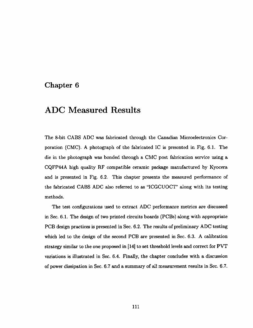
Chapter 6
ADC Measured Results
The 8-bit CABS ADC was fabricated through the Canadian Microelectronics Cor
poration (CMC). A photograph of the fabricated IC is presented in Fig. 6.1. The
die in the photograph was bonded through a CMC post fabrication service using a
CQFP44A high quality RF compatible ceramic package manufactured by Kyocera
and is presented in Fig. 6.2. This chapter presents the measured performance of
the fabricated CABS ADC also referred to as "ICGCUOCT" along with its testing
methods.
The test configurations used to extract ADC performance metrics are discussed
in Sec. 6.1. The design of two printed circuits boards (PCBs) along with appropriate
PCB design practices is presented in Sec. 6.2. The results of preliminary ADC testing
which led to the design of the second PCB are presented in Sec. 6.3. A calibration
strategy similar to the one proposed in [14] to set threshold levels and correct for PVT
variations is illustrated in Sec. 6.4. Finally, the chapter concludes with a discussion
of power dissipation in Sec. 6.7 and a summary of all measurement results in Sec. 6.7.
Ill

CHAPTER 6. ADC MEASURED RESULTS 112
GND D CAL INN INP WE CLK GND
VDD
b7
b6
b3
b2
bl
Bi
VDD
/
GND GNDA VDDA VDDA GNDA GND
Figure 6.1: Photograph of the fabricated IC. The bond wires are labeled instead of the pads to improve visibility. The IC was bonded by CMC and uses a CQFP44A ceramic package.
6.1 Test Configuration
For the test bench, several configurations were used depending on the PCB version
and the kind of ADC test, specifically, the type of ADC test; dynamic AC or static DC
test. Some of the equipment common to all test configurations is discussed in Tb. 6.1.
A computer was used as a test controller with Matlab as the choice of development
environment.
A "Keithley 2600" source meter was used to power the PCB and monitor the
power consumption. The source meter is connected to the computer via an RS-232
serial link. The ADC "CLK", "INP", and "IN" signals are generated using the "Agilent
81150A" arbitrary signal generator. The shift register control signals are generated
VDD
b5
b4
QF
bO
outpr
outnr

CHAPTER 6. ADC MEASURED RESULTS 113
Figure 6.2: Photograph of the packaged IC in the CQFP44A ceramic package.
from two "Agilent U2331A" NI-DAQs. "Agilent U2331A" NI-DAQs are connected via
USB to the computer and are used to generate the shift register signals at a frequency
of 500 kHz. Finally the output of the ADC is connected via an IDE header to the
digital sampling oscilloscope ("Agilent 5855A"). The scope is in turn connected to the
computer via an ethernet link. A summary of the components used is presented in
Tb. 6.1.
Table 6.1: Test bench equipment.
Component Function Signals
Keithley 2600
Agilent U2331A
Agilent 81150A
Agilent 33205A
Source meter and 1.2V power supply for the PCB. VDD
NI-DAQ / Data acquision / Signal generation WE, D, CAL
Arbitrary function generator INP, INN, CLK
Optional CLK or DAC CLK
Agilent 54832DSO Digital spectrum oscilloscope b0-b7
6.1.1 Test Configuration 1
A functional diagram of the preliminary test bench for the ADC can be found in
Fig. 6.3. This test bench was used for the first PCB. The arbitrary signal generator

CHAPTER 6. ADC MEASURED RESULTS 114
is capable of generating differential signals such as a slow ramp, staircase pattern,
DC levels, as well as the standard sinusoidal, square wave and pulse shape. With the
81150A it is then possible to test both AC and DC performance metrics.
Agilent U2331A
Keithley 2600
"D" MWE" "CAL*
VDD
Agilent 61150A
Agilent 54832D
10/100 ADC Output
Figure 6.3: Functional diagram for preliminary test plan.
The test bench was then modified to use a DAC for back-to-back testing of the
ADC. The DAC is the 12-bit "DAC5652" on the evaluation board "DAC5652EVM"
manufactured by Texas Instruments. When using a back-to-back configuration it
is necessary for the DAC to have a minimum of 2 bits higher resolution than the
ADC [1].
6.1.2 Test Configuration 2
The main test configuration used for the second PCB is presented in Fig. 6.5. The
most noticable change is the replacement of the "Agilent U2331A" with a serial par
allel interface bus (SPI) interface to control the shift register inputs. This was done

CHAPTER 6. ADC MEASURED RESULTS 115
10 MHs Reference
Agilent U2331A Agilent 33250A
Keithley 2600
VDD
CAL"
bO-b7 Agilent 61150A CLK
IBM PC
Agilent 54832D DAC5652BVM
iz-4,
ULU.* 411 ill 10/100
DAC Output Single Ended
Figure 6.4: Functional diagram for preliminary test plan with back-to-back configuration.
to improve the certainty with which the calibration code is loaded into the shift reg
ister. In addition three "Keithely 2600" power supply and source meters are used to
generate the 1.2 V,3.3 V,-/+5 V and 0.6 V supply levels necessary to power additional
circuitry needed for the second PCB. The board was also connected in the second
configuration similar to the functional diagram presented in Fig. 6.4. The presence
of level shifting translators on the second PCB allowed for direct coupling of PCB2
to the "DAC5652EVM" which requires TTL logic level inputs. Previously, this had
been achieved by placing the logic translator on a prototyping board and connecting
the ADC and the DAC to the translator via spliced IDE cables.

CHAPTER 6. ADC MEASURED RESULTS 116
SPI Interface
Keithley 2600 X 4
Agilent 81150A
Agilent 54S55A
10/100 ADC Output
Figure 6.5: Functional diagram for PCB2 test plan.
6.2 PCB Design
Two printed circuit boards were designed and manufactured to accommodate the
testing process of the CABS ADC. The first PCB is discussed in Sec. 6.2.3. After
an initial testing phase it became evident that additional components, such as an
external SAH, are necessary to improve the functionality of the ADC as is discussed
in Sec. 6.3. The design of the PCB with external SAH ICs, "PCB2", is discussed in
Sec. 6.2.4.
6.2.1 Power Supply Decoupling
The ADC presented in this work along with any ICs discussed in the proceeding
section are sensitive to ripples on the power supply traces. For the ADC, ripples on
the supply lines are translated into jitter (noise) degrading the overall performance of
the ADC [1]. This phenomenon becomes more prevalent with an increasing frequency
of operation. On both the PCBs designed, power supply decoupling was achieved by

CHAPTER 6. ADC MEASURED RESULTS 117
a combination of decoupling capacitors and ferrite beads. The types of decoupling
capacitors and their magnitudes is presented in Tb. 6.2.
Table 6.2: Decoupling component device sizes.
Device Value Manufacturer Manufacturer ID Description
10 uF Nichicon TCM0J106M8R CAP TANT 10UF 6.3V 20% 0603
0.1 uF Kemet C0603C104K8RACTU CAP CER 0.1UF 10V 10% X7R 0603
27 pF Murata GQM2195C1H270JB01D CAP CER 27PF 50V 5% NP0 0603
1 Kfi Q 100 MHz TDK MMZ1608Y102B FERRITE CHIP 1000 OHM 400MA 0603
Tantalum capacitors on the order of IOjiF68 are used to ground low frequency
transient noise. Their main role is to serve as a charge reservoir [1] so that the power
supplied to the IC does not depend on the length of the supply trace (inductance).
Smaller high quality X7R ceramic capacitors are connected closer to the power pins
of an IC. This is done to ground high frequency noise near the IC. The decoupling
capacitors are then grounded through a large ground plane present on both sides
of the PCB reducing any inductance in the return path. As well, a ferrite bead is
used to block high frequency noise and isolate ICs from the power mains. Ground
connections for all ICs on the PCBs are made via contacts straight to the ground
planes. This reduces the inductances through a possible ground loop.
6.2.2 Signal Integrity and Propagation
Signal traces have a maximum allowable electrical length before impedance matching
becomes necessary to avoid reflections on the lines. The maximum allowable electrical
length [49] is
Ltr^e = (6-1) ZtpD
^High quality electrolytic capacitors could also be used.

CHAPTER 6. ADC MEASURED RESULTS 118
where "RT" is one half of the one way propagation delay and "tpo" is the built in
propagation delay. The built in propagation delay [49] is given by,
For a dielectric constant of 4.7 in FR4 material, the built in propagation delay is
144.4 ps/in. The propagation delay for the output drivers of the ADC assuming a
15 pF load with 1.5 nH of line inductance is around 3 ns. This gives a maximum
length of 41 inches. Instead if we consider the traces as carrying analog signals then
a typical benchmark is for the maximum trace length [49] to be less than
Using the value in [42] for the propagation delay in FR469 type material on an outer
trace, the propagation speed in FR4 is 5.5in/ns. At a typical ADC operating fre
quency of 30 MHz the maximum allowable length is 9.3 in.
Signal integrity is improved through the appropriate grounding of signal return
paths. Since both the top side and the back side of the PCBs have ground planes,
at any given time signal traces have nearby connection to the ground plane for the
returns. To reduce any possible ground loops, vias between the two ground planes
cover the entire PCB, as is presented in the example Fig. 6.6.
6.2.3 Preliminary PCB Design, "PCB1"
The first PCB was designed using CADSOFT Eagle Tools Pro Version 5.1. A photo
graph of the top side of the PCB is presented in Fig. 6.7. The packaged IC is at the
69The PCB is made from a woven fiber glass composite material FR4. The electrical properties can vary slightly between manufacturers.
tpo = 84.75\/0.475er + 0.67 ps/in. (6.2)
< 20- (6.3)

CHAPTER 6. ADC MEASURED RESULTS 119
Ground Plane H| Ground Plane |H Via Q
Figure 6.6: Selected area of the PCB showing griding of ground planes to reduce ground loops and inductance in the signal return path.
center of the PCB. "JP11" is an IDE header which is used to connect the output of the
ADC to the external digital sampling oscilloscope. The shift register inputs "WE",
"CAL", "D" are fed through a SCSI connector at the top of the board. The differential
inputs to the ADC as well as the global CLK signals are connected through the gold
plated SMA connectors. The traces are well below the maximum trace length as
discussed in Sec. 6.2.2.
Both sides of the board are covered with a ground plane as well as scattered vias
connections between the ground planes to reduce return path inductance in a process
called "griding" [50] as discussed in Sec. 6.2.2. Four layer boards offer the potential
to include power planes and ground planes within the internal layers of the PCB.
Ideally signals must be routed directly above a ground plane. Given the significantly
longer and expensive fabrication process only two layer boards were designed for the
ADC. In spite of that, by paying extra care in signal routing and grounding, a similar
performance can be achieved even with a two layer board.
The backside of the PCB is presented in Fig. 6.8. The only components on the
back side of the PCB belong to the power supply decoupling network. Having multiple

CHAPTER 6. ADC MEASURED RESULTS 120
SCSI Connector ("WE,,,"CAL","D")
Figure 6.7: Photograph of the topside of PCB1. The SCSI connector is used for the shift register inputs "D", "CAL", "WE". The ADC CLK and the differential inputs used gold plated SMA connectors. The ADC is in-package and soldered at center of the PCB. The output of the ADC uses a 40 pin IDE connector.
power supply and ground pins on the IC reduces the effects of ground bounce from
large signal digital switching being coupled into the ground. The same power supply
network is used for each power pad; a ferrite bead in series and three capacitors of
varying device size and material as discussed in Sec. 6.2.1.
A layout image for both the top side and the bottom side of the PCB is shown

CHAPTER 6. ADC MEASURED RESULTS 121
in Fig. 6.9. The signal routing and the "griding" between the ground planes is more
evident in Fig. 6.8. The bill of materials for the PCB is presented in Tb. A.l.
Figure 6.8: Photograph of the back side of PCB1. The decoupling capacitors and the ferrite beads are placed on the back side of the PCB.

710*51-003 • • • • • • • • • • • • • • • • • •••••••••••••••it
Figure 6.9: PCB layout, topside pictured left, bottom side pictured right.
to to

CHAPTER 6. ADC MEASURED RESULTS 123
6.2.4 Secondary PCB Design with External SAH, "PCB2"
Without an external SAH, the ADC input is prone to change as the asynchronous
decision propagates through the comparison stages causing erroneous codes to be
sampled, making the use of an external SAH absolutely necessary. With this in
mind the second PCB was designed for maximum flexibility. The PCB features two
separate monolithic IC SAH circuits on the PCB with three signal paths designed
to bring the output of the SAH ICs into the range of the ADC. As well the PCB
has the capability of running from a battery powered supply or directly from source
meter power supplies. The SCSI connector was dropped in favor of a space saving
IDE connection and an optional SPI compatible interface.
6.2.4.1 Signal Paths for Generation of Sampled Differential Inputs
The first path, "Signal Path 0" is presented in Fig. 6.10. The SAH for this signal
path has a short acquisition time of 250ns but a long settling time of 2ps [51]. The
total combination of acquisition and settling time, or the total 'output time' after
the falling edge of SAH clock "S/H", touT, has to be less than half of the clock cycle
of the ADC. Therefore, the maximum frequency of operation of the ADC achievable
using this SAH at its full scale input is approximately 250 kHz. The input and the
output of the DS1843 is between 0V.. 1V and operates on a power supply of 5V.
The output of the DS1843 is then connected to an "ADC driver" developed by Analog
Devices [52].
The ADC driver, "AD8139", serves the function of level shifting the output of the
SAH to the mid-rail value of the ADC determined by the VOCM input. To maintain
the highest resolution achievable from the SAH, the input is driven at the maximum
full scale input. As a consequence the output of the DS1843 must be scaled and level

CHAPTER 6. ADC MEASURED RESULTS 124
5V 1.2 V 5V
ds1Tji VIkds/H
ADC AD8139 _n_ ICLK
-5V
Figure 6.10: PCB2 signal path 0. The "DS1843" is a SAH with an output between 0V.. IV. The "AD8139" ADC driver provides; level tuning, single ended to differential conversion, and fixed signal attenuation.
shifted to bring it into the input range of the ADC. The AD8139 implements the level
shifting function, centering the output of the SAH around VOCM, as well as converting
the input from single ended to differential. In addition the ADC driver provides gain
attenuation through a resistive feedback network. To filter high frequency noise, at
the input of the ADC, a basic one pole low pass filter is implemented using series
resistances and shunt capacitors (R3 and C3). Common mode filtering is accomplished
through the Ccm capacitor.
The remaining signal paths use a common SAH, the "AD783" [53] produced by
Analog Devices. Compared to the first SAH the AD783 has a much higher frequency
of operation of 15 MHz [53]. The AD783 operates on a -/+5V power supply with
a single ended input and output between -2.5V..2.5V. Signal path 1 presented in
Fig. 6.11 shows the output of the AD783 connected through a high frequency low
input/output offset high speed operational amplifier (op-amp), the "ADA4853" [54].
The ADA4853, connected in a non inverting configuration implements an ad
justable signal attenuation using a resistive feedback network in the form of a resistive
potentiometer, Rtrim- The ADA4853 brings the SAH output into the input range of

CHAPTER 6. ADC MEASURED RESULTS 125
5V
5V
AD783
1.2V 5V
ADA4853 vW VoCM ADC cm T" AD8139
-5V
-5V
Figure 6.11: PCB2 signal path 1. The "AD783" is SAH with an output between -2.5V..2.5V. The "ADA4853" provides adjustable gain through Rtrim- The AD8139 handles level shifting and conversion to differential output.
the ADC. The output of the ADA4853 is connected to the same type of ADC driver
used in Signal Path 0 along with its associated low pass filter output.
1.2V 5V 5V 5V
1/1 AD783
ADC AD8475 AD8475
x: -5V -5V
2.5V
-2.5V
Figure 6.12: PCB2 signal path 2. The "AD783" is SAH with an output between -2.5V..2.5V. Two cascaded "AD8475s" provide an attenuation of 0.16 as well as single ended to differential conversion.
The final signal path, "Signal Path 2" uses a bullet proof approach for bringing
the output of the SAH into the input range of the ADC. The AD8475 [55] is a high
quality ADC driver with a maximum output offset of 500 pV, less than LSB/4 of
the ADC. The AD8475 uses built in laser trimmed resistors to achieve a gain of
0.4 V/V with excellent phase matching. The signal path uses two cascaded AD8475s

CHAPTER 6. ADC MEASURED RESULTS 126
implementing a total gain of 0.16V/V out of the required 0.06 V/V. The rest of the
gain attenuation is provided by not driving the SAH at a full scale input. Only one
signal path is necessary at a given time to drive the ADC.
6.2.4.2 Clock Generation
The SAH must acquire the input input and settle before the rising edge of the ADC
clock. As well, the duty cycle of the SAH must encompass the output time and duty
cycle of the ADC clock70. This means that the ADC requires a separate clock from
the ADC clock. The second PCB is designed to allow for the S/H clock signal to be
driven by an additional function generator which has its 10 MHz reference tied to the
ADC clock signal generator.
3.3V
AD9513 RSET <D CLK /1.../32
_n_ CLK
ir CLK U SYNC/
•1 Qr O-
VREF
S/H /1.../32
RGC /1.../32
Configuration Logic CLK
SO..S1Q RGC
Figure 6.13: Functional diagram of PCB2 timing using the "AD9513" and XOR gates. The "AD9513" is frequency divider with adjustable phase, duty, cycle for three output channels. "CLK" is the ADC clock signal, "S/H" is the SAH clock, "RGC" is the 8-bit register clock.
The output of the ADC can be taken from level shifting digital translator, the
"ADG3308" [56] or after an optional, 8-bit clocked register, the "CY74FCT2574T" [57].
70This discussion is in reference to the AD783 SAH.
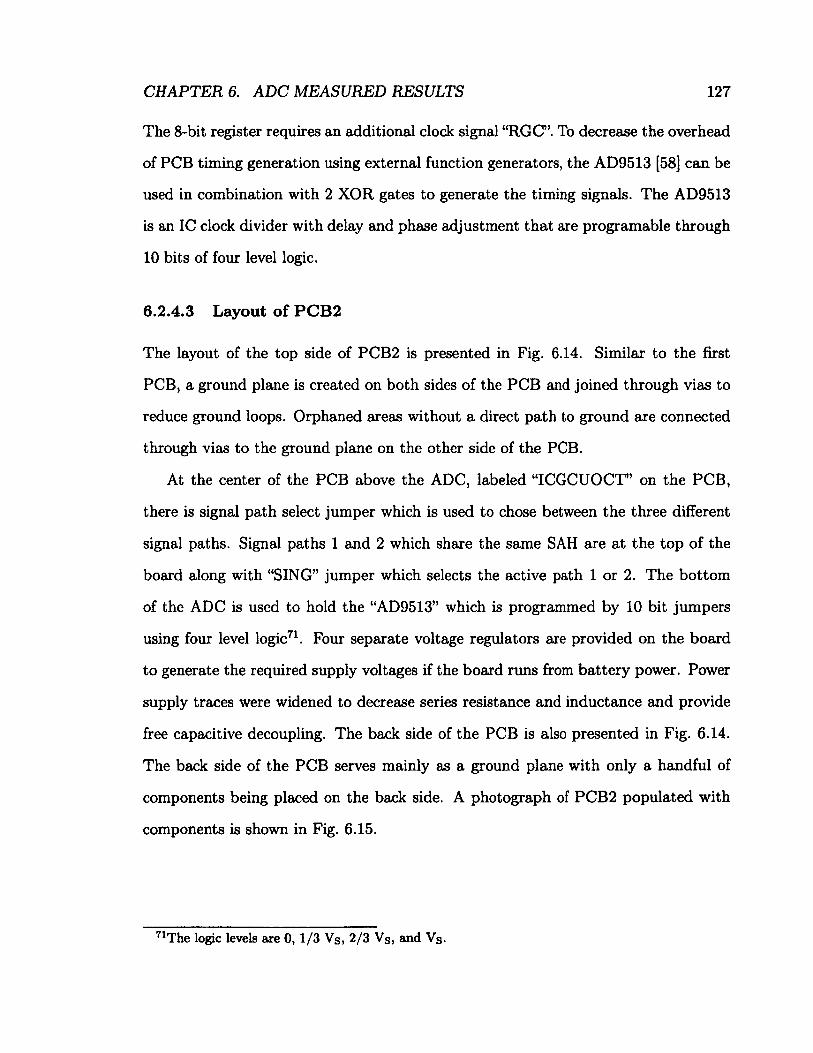
CHAPTER 6. ADC MEASURED RESULTS 127
The 8-bit register requires an additional clock signal "RGC. To decrease the overhead
of PCB timing generation using external function generators, the AD9513 [58] can be
used in combination with 2 XOR gates to generate the timing signals. The AD9513
is an IC clock divider with delay and phase adjustment that are programable through
10 bits of four level logic.
6.2.4.3 Layout of PCB2
The layout of the top side of PCB2 is presented in Fig. 6.14. Similar to the first
PCB, a ground plane is created on both sides of the PCB and joined through vias to
reduce ground loops. Orphaned areas without a direct path to ground are connected
through vias to the ground plane on the other side of the PCB.
At the center of the PCB above the ADC, labeled "ICGCUOCT" on the PCB,
there is signal path select jumper which is used to chose between the three different
signal paths. Signal paths 1 and 2 which share the same SAH are at the top of the
board along with "SING" jumper which selects the active path 1 or 2. The bottom
of the ADC is used to hold the "AD9513" which is programmed by 10 bit jumpers
using four level logic71. Four separate voltage regulators are provided on the board
to generate the required supply voltages if the board rims from battery power. Power
supply traces were widened to decrease series resistance and inductance and provide
free capacitive decoupling. The back side of the PCB is also presented in Fig. 6.14.
The back side of the PCB serves mainly as a ground plane with only a handful of
components being placed on the back side. A photograph of PCB2 populated with
components is shown in Fig. 6.15.
71The logic levels are 0, 1/3 Vs, 2/3 Vs, and Vs.

PCB Top Side Vref +/-5v
PCB Bottom Side
J . , - r - ^ — 15 T i t . i . k T - i " K \ ' 1 K t i - i . x . T:kT -icx:icx : R t : R f x ~X"(X'\X",T••.Tr-(T-lX"'X * \v
b. U 0! >
4.95 in
i 1 Ol
> b 0
1 CO s s CO
1 CO
Clock Generation
Figure 6.14: Layout of PCB2, top side pictured on the left, bottom side pictured on the right.
to oo

PCB Bottom Side
4.95 in
Figure 6.15: Photograph of PCB2, top side pictured on the left, bottom side pictured on the right.
to <0

CHAPTER 6. ADC MEASURED RESULTS 130
6.3 Preliminary Testing
Preliminary testing of the ADC was carried out using PCB1. After the board was
assembled and all connections where checked for shorts, the output of the ADC was
observed using the test configuration depicted in Fig. 6.3. The output of the ADC
showing all the bits switching and active is presented in Fig. 6.16.
L*
b3 WfcRF*
nnrmwu nil u Jfchftffl L-JMIIi jnuojD TuT" .1 njiFir. iTTrniT!
2.00M«/
Figure 6.16: Screenshot from the DSO showing the ADC output bits for an over driven sinusoidal input of 100 kHz and sampling frequency of 20 MHz.
When the ADC output was reconstructed to be evaluated for INL and DNL mea
surements, the presence of large spikes appeared on the reconstructed output as well
as non monotonic code transitions. An example of this can be seen in Fig. 6.17. Non
monotonic code transitions are expected if the ADC does not have the optimum cali
bration code. The spikes which appear on the reconstructed output have the highest
amplitude near the code transitions. The code transitions correspond to an MSB
switch from a logic "0" to a logic "1" or conversely. This corresponds to transition
of the digital word from "0111111" to "1000000" or the reverse. Since the differential

CHAPTER 6. ADC MEASURED RESULTS 131
input to the comparators is only held by the capacitance of the differential trace, this
capacitance is subject to change as the decision propagates through the stages of the
ADC.
250
€ 200
•*>
o. 3 o 0 Q < •8 § 1
150
100
80 90
Time (us)
Figure 6.17: Reconstructed output for fabricated ADC showing code transition sampling.
This behavior was verified through simulation of the ADC and is presented in
Fig. 6.18. In this simulation the ideal SAH circuit was removed and the simulation was
performed with "conservative" simulation settings shrinking the size of the simulation
time step. Another factor which must be taken into account is that no post layout
parasitic extraction could be carried out on the full ADC. Therefore, the input to
all the comparators changes instantaneously making this effect less pronounced in
simulation. The appearance of spikes at code transitions is not a failure of the ADC
to function as required. The appearance of code transition spikes can be removed
through the implementation of a SAH at the front end of the ADC. For the reasons
discussed in this chapter the second SAH was designed and presented in Sec. 6.2.4.
Not only is the dynamic analysis of the ADC impacted by the lack of a SAH but

CHAPTER 6. ADC MEASURED RESULTS 132
0.7
0.6
0.5
O Q 0.4 <
"8 tS 0.3 s i o 0.2
I 0.1
Figure 6.18: Reconstructed output for simulated ADC showing code transition sampling. The SAH was removed and the simulation was performed with conservative simulation settings.
DC testing as well is affected by sampling code transitions or rather, having the input
change during a conversion. The measured noise from the equipment was on the order
of a few LSBs, more than enough to cause pronounced code transitions even for DC
static analysis.
Notice that the spikes in the simulation plot are in the opposite direction compared
to the measured behavior in Fig. 6.17. This is not of fundamental importance but can
be partly attributed to the way in which the ideal VHDL DAC makes its conversion.
As well the simulations were performed without parasitic extraction. If a full IC
simulation with extracted parasitics was performed, it is conceivable that the spikes
would appear in the opposite direction as the bits arrive at slightly different times at
the input to the ideal DAC. What is key of note is that code transition spikes appear
and can be resolved through the use of a SAH.
The next stage involved in the preliminary testing of the ADC involved program
ming the shift register of the ADC. This was achieved using the same test bench.

CHAPTER 6. ADC MEASURED RESULTS 133
The CLK and the INP and INN signals were disabled while the shift register was
programmed. The result of loading the nominal calibration code can be observed in
Fig. 6.19. After the nominal code used to establish the desired comparator thresholds
in simulation was loaded into the ADC, the code depth of the output bits grew72.
This test confirmed the operational functionality of CABS ADC shift register based
memory.
•%*r- wSmTM tsirtsa#" ts "ulnurriiDf.
r r "JMHRi Lfl nifini ~ JUllUl ILTLLBH L_1
Figure 6.19: Shift register programming of the fabricated ADC. After loading the nominal calibration code, the code depth of the outputs bits is evidently increased.
72That is to say, more synchronized code transitions became visible indicating an increase in the number of codes, or the code depth

CHAPTER 6. ADC MEASURED RESULTS
6.4 Calibration
134
The calibration routine described in this section is identical to the calibration routine
used to extract the nominal timing code for the simulated comparator. The Matlab
pseudo-code presented in Listing 6.1 has been modified from [26] as the calibration
code used in the tuning of this ADC is too vast to give a quick insight into the
calibration methodology.
For a desired comparator which requires tuning, nearby comparators in the same
stage have their threshold shifted far from the desired value. For the ADC described in
this work, the neighboring comparators could have their thresholds shifted by as much
as 30LSB. This ensures that the result of any triggering on neighboring comparators
is pushed far from the desired threshold and does not bias the mean of the measured
threshold. The measured threshold is sampled using the digital spectrum oscilloscope
discussed in the Sec. 6.1 and reconstructed to an analog value using an ideal DAC
implemented in software. The stages are progressively tuned, from the fifth stage
to the eight stage of the ADC. Each calibration code is then stored in database of
comparator structures. The ADC can require a different tuning code depending on
the frequency of operation, temperature, maximum input frequency excursion and
PVT.

1 2
1 o
7
, s
9 10 11 12 1 3
M lo l t >
1 7
18 1!)
20
2 1
22
2 3
21 2r>
2ti
CHAPTER 6. ADC MEASURED RESULTS 135
Listing 6.1: Matlab pseudocode binary search calibration routine for a single com-
parator.
f u n c t i o n (code) = ca l ib ra te (K)
% K i s « c o i i i p H r a t o r s t r u c t u r e
maxrange = 127; " ' r s o t s t i n - m a x i m u m r a n g e
s e t T h r e s h o l d ( K ) ; ' X l o a d s t h e c u r r e n t c a l i b r a t i o n c o d e
a = 0 ; se tThreshold (a ) ; % P l i y s i c : a 1 l y s e t s t h e i n p u t t o t h e . M X ' u s i n g t h e A g i l e n t 81 150 A o r K e i t l i l e y t o n o t u n i n g ( c c o d e f r o m — 1 2 7 t o 1 2 7 )
voutA = i n e a n ( recons t ruc tOutput ) ; % r e c o n s t r u c t A D O o u t p u t a n d t a k e t h e m e a n v a l u e
d i f f A = v o u t A — ( K . t h r e s h D e s i r e d — 0 . 5 ) ; / ' t a k e t h e d i f f e r e n c e b e t w e e n t h e d e s i r e
t h r e s h o l d m i d t h e n o m i n a l m e a s u r e d t h r e s h o l d
b = s i g n ( d i f f A ) * ma x s h i f t ; % f i n d t h e m u x t h r e s h o l d o n t h e m a x s i d e o l ' t h e b r a c k e t
se tThreshold (b ) ;
voutB = mean( recons t ruc tOutput ) ;
d i f fB = voutB — (K. th reshDes i red — 0 .5 ) ;
% b i s e c t i o n s e a r c h
w h i l e ( a b s (a—b ) > 1 )
% h a l v e t h e i n t e r v a l i n e v e r y l o o p
c = f l o o r ( (a + b ) / 2) ; se tThreshold (c ) ;
voutC = mean( recons t ruc tOutput ) ;
d i f fC = voutC — (K. th reshDes i red — 0 .5 ) ;
i f (d i f fC » d i f fA) > 0
a = c ; d i f fA = d i f fC ;
e l s e b = c ; d i f fB = d i f fC ;
end i f a b s ( di f fA) > a b s ( di f fC)
code = b ; % t a k e m i n i m u m d i f f e r e n c e s o l u t i o n
else code = a; end
r e tu rn code ;
e n d

CHAPTER 6. ADC MEASURED RESULTS 136
6.5 Static Linearity Analysis
6.5.1 Integral Nonlinearity (INL)
The INL for the fabricated IC was measured using the technique presented in Sec. 5.1.1
using the second PCB, "PCB2". Two differential ramps corresponding to a duration
of 2.5 ms and a full scale input were used to measured the INL. The result of the INL
before calibration is presented in Fig. 6.20 with a worst case INL of 64 LSB.
120
100
80
20
0
-20 5 45 85 125 165 205 245
VIN (LSB)
Figure 6.20: Pre-calibration Integral nonlinearity (INL) as a function of input voltage Vin, worst case INL is 64 LSB; fs=4MHz, 2.5 ms differential ramp.
Using a non-optimum calibration code based on the optimum simulation calibra
tion code, the INL was improved from 64 LSB to 11 LSB. With further optimization
based on the calibrations strategy proposed in [26] or using a novel calibration code
it is conceivable that the static performance of the fabricated ADC could be further
improved.
! !
ik|s k nn
s,m

CHAPTER 6. ADC MEASURED RESULTS 137
I I
i >
3 36 69 102 135 168 201 234 Vin (LSB)
Figure 6.21: Post-calibration Integral nonlinearity (INL) as a function of input voltage Vin, worst case INL is 11 LSB; fs=4MHz, 2.5 ms differential ramp.

CHAPTER 6. ADC MEASURED RESULTS 138
6.5.2 Differential Nonlinearity (DNL)
The DNL was extracted for the fabrication IC using the technique outlined in
Sec. 5.1.2. Similar to the INL the performance of the DNL was improved by using
an improved calibration code albeit a non-optimum calibration code from -68 LSB in
Fig. 6.22 to 14 LSB in Fig. 6.23.
150
100
50
0
-50
-100
-150 5 45 125
Vin (LSB) 165 205 245
Figure 6.22: Pre-calibration differential nonlinearity (DNL); worst case DNL is -68 LSB; fs=4MHz, 2.5 ms differential ramp.
Figure 6.23: Post-calibration differential nonlinearity (DNL); worst case DNL is 14 LSB; fs=4MHz, 2.5 ms differential ramp.

CHAPTER 6. ADC MEASURED RESULTS 139
6.6 Measured Dynamic Analysis
The dynamic performance metrics of the fabricated CABS ADC were measured and
analyzed using the same approach presented in Sec. 5.2.2. Dynamic analysis mea
surements were performed using a sampling frequency of 4 of 4 MHz and an input
frequency fj of 50 kHz. An FFT spectrum for the recontracted output of the ADC
is presented in Fig. 6.24. The ENOB using an improved but non-optimum calibra
tion code was improved to 5.1 bits. Without any calibration the ENOB was 3.1 bits.
The SINAD was 32.3dB with a SFDR of 35.7dB. The maximum sampling frequency
was limited by the operation of the SAH which requires a maximum settling time of
250 ns for a full scale input. With an internal, on-chip SAH amplifier or a faster SAH
it would be possible to test the fabricated ADC at a higher sampling frequency as
was verified by preliminary testing using PCB1 with no SAH.
o 1st
-20 2nd
3rd
n -40 4th
-120
n 6th
" 8th
« 7th
Sth
9th
0 0.5 1 1.5 Signal Frequency (MHz)
2 2.5
Figure 6.24: Post calibration FFT spectrum of the input signal, f„ = 4MHz, f ,= 50 kHz, n = 7, m = 1024, ENOB = 5.1, SINAD = 32.3dB, SFDR = 35.7dB

CHAPTER 6. ADC MEASURED RESULTS 140
6.7 Power Dissipation
The total measured power consumption versus sampling frequency for the IC includ
ing output buffers for a fixed input frequency, fj, of 98.3 KHz is presented in Fig. 6.25.
The power consumption follows a steady, nearly linear increase up until 35 MHz.
Slightly before this point the ADC reaches its maximum frequency of operation, and
the output clock does not trigger the comparator responsible for b7 in the eight stage.
As the frequency is increased, the latter stages of the ADC are not triggered, reduc
ing the switching activity of the output latch and buffer, and reducing the power
consumption.
17.5
^ 17
1 16.5 e t » s 15.5
0 15 b £ | 14.5
0L, 14
1 13.5
13
.v -.v -\ \
- J
10 15 20 25 30 Sampling Frequency (MHz)
35 40 45
Figure 6.25: Total measured power consumption, as a function of the sampling frequency f s for an input frequency of f} = 98.3 KHz
The total measured power consumption for the full IC for Nyquist operation is
presented in Fig. 6.26. The input frequency for the Nqyuist frequency is selected to be
a non integer multiple of the sampling frequency to avoid undesired aliasing effects.
The total Nyquist power consumption is higher than the total power consumption
presented in Fig. 6.25 as the switching activity of the output buffers and core is

CHAPTER 6. ADC MEASURED RESULTS 141
! §
s 0 s 6
CL, •3
I
15 20 25 30 35
Sampling Frequency (MHz)
Figure 6.26: Total measured power consumption, as a function of the sampling frequency f s at Nyquist input frequency.
increased.
Finally, the measured FOM for the power consumption of the ADC core as function
of a fixed input frequency of 98.3 KHz is presented in Fig. 6.28. At the desired
frequency of operation of 25 MHz the total energy per conversion is 15fJ/conversion.
2 30
1 20
20 30 40 Sampling Frequency (MHz)
Figure 6.27: FOM, as a function of the sampling frequency f s for a fixed full scale sinusoidal input at f j = 98.3 KHz.

CHAPTER 6. ADC MEASURED RESULTS 142
As well, for completeness, the measured power consumption of the ADC core is
presented in Fig. 6.28. At the desired frequency of operation of 25 MHz the ADC core
power dissipation is 100 pW. It was possible to measure the core power consumption
since the comparator core is on separate power supply ring from the power hungry
output buffers.
120
110
100
80
/
50
60
40 0 10 20 30 40
Sampling Frequency (MHz) 50 60
Figure 6.28: ADC core power consumption as a function of the sampling frequency f 8 for a fixed full scale sinusoidal input at f j = 98.3 KHz.

CHAPTER 6. ADC MEASURED RESULTS 143
6.8 Summary of Measurement Results
A complete summary of the static and dynamic performance metrics extracted from
measurement results of the ADC is presented in Tb. 6.3. The ASIC was implemented
in a IBM CMRF8SF 130 nm technology for a power supply of 1.2V. The input range
was 600 mV peak-to-peak differential. The ADC achieved an excellent power con
sumption for the core in terms of the FOM of 15 fJ per conversion and core power
consumption of 100 pW. The maximum sampling frequency while driving the external
SAH at is full scale input is 4 MHz which fundamentally limits the operation of the
CABS ADC. Using a non-optimum calibration code the INL was improved to 11 LSB
from 64 LSB and the DNL was improved from -68 LSB to 14 LSB. The ENOB for an
input frequency of 50 kHz was 5.1 bits. In Fig. 6.29 and Fig. 6.30 the frequency and
resolution of the fabricated ADC with a non-optimum calibration code are presented
alongside current published ADCs with similar performance metrics.
Table 6.3: Summary of measurement results for non-optimum calibration code.
Metric Measured Value
Technology
VDD
Input Range
Sample Rate
INL
DNL
SINAD @ 50 kHz
SFDR Q 50 kHz
ENOB @ DC
IBM CMRF8SF 130 nm
1.2 V
600 rn Vpk-pi^d iff
4 MHz
11 LSB
-14 LSB
32.3 dB
35.7 dB
5.1
4.064 mm2
100 pW
15 fJ
Area
Power
FOM

CHAPTER 6. ADC MEASURED RESULTS 144
x S u c 3
I
104
103
102
10'
10°
(Pipelined |1?) Folding |8)
CABS [14);
' CABS [141 | pipelined fl8j
SAR {22} SAR [3] • * . SAR [21] *
SAR [20]
This Work:
Fbtding [13f
Flash [16]
Piptelined [19j
Flash [7| •
100 200 300 FOM (fJ)
400 500
Figure 6.29: Compaxison of frequency of operation a function of the figure of merit for published ADCs and measured CABS ADC performance.
1 Pipelined [18]
1
SAR [22]
SAR [21) Pipelined [19]
* SAR [20 ^CABS [14] !
CABS [14] SAR [3] Folding [15]
Pipelined: [17] • . Folding [8]
Flash |16]
rhis Work Flash [7]
i i
0 100 200 300 400 500
FOM (fJ)
Figure 6.30: Comparison of ADC resolution as a function of the figure of merit for published ADCs and measured CABS ADC performance.

Table 6.4: Comparison of measurement results to published state-of-the art low power CMOS based ADC designs.
Architecture VDD Technology Area (mm2) Power (mW) Speed (MS/s) Input Range (mV.diff) Resolution ENOB FOM
This Work 1.2 V 0.13pm 4 0.1 15 600 8 S.l 18
CABS [14] IV 90 nm 0.050 0.140 250 384 6 5.3 15.0
CABS [14] IV 90 nm 0.055 0.133 133 768 7 6.4 10.4
Folding [8] IV 90 nm 0.017 2.2 1750 800 5 4.7 50.0
Folding [15] IV 90 nm 0.360 50 2700 800 6 NS 250.0
Flash [7] 1.8V 0.18 pm NS 4.43 700 NS 4 3.8 460.0
Flash [16] 1.2V 60 nm 0.130 12 800 NS 6 5.6 234.0
Pipelined [17] 1.1V 40 nm 0.030 2.3 2000 640 6 5.5 17.4
Pipelined [18] 1.3V 0.13 pm 1.200 91 100 2000 13 NS 110.0
Pipelined [19] 1.2V 0.13 pm 0.980 19.2 60 NS 10 NS 313.0
SAR [3] IV 90 nm 0.055 0.240 50 320 6 5.0 150.0
SAR [20] IV 90 nm 0.132 0.069 10 400 8 7.8 30.0
SAR [21] IV 65 nm 0.060 1.21 40 1000 10 8.9 65.0
SAR [22] 1.3V 90 nm 0.160 3.6 50 2000 12 10.6 52.0

Chapter 7
Conclusion
7.1 Contributions to Research
In this work, the design of a hybrid 8-bit CABS based ADC was examined from pre
liminary system level design goals to in depth circuit design of low level components.
To facilitate the design of the CABS ADC, a library of mixed signal analog cells
was designed from the ground up. These cells included flip-flops, transmission gates,
muxes as well as cells more specific to this architecture such as the dynamic latched
comparator, SCMTA timing arrays and bitline drivers. The performance of these
mixed signal cells was analyzed using Monte Carlo simulations to gain insight into
system level performance based on PVT variations of MOS devices. The state of the
art resolution for a pure CABS architecture was extended from 6 bits to 8 bits through
optimization and concurrent design of critical ADC building blocks. Simulation re
sults placed the ADC designed in this work within the moderate to high resolution
and excellent FOM range of ADCs. At the expense of an improvement in resolution
the frequency of the ADC was lower compared to the majority of ADCs with similar
performance metrics. In terms of the FOM, compared to the critical benchmark of
this design, the 8-bit CABS ADC achieved a conversion power of 15 fJ for a resolution
146

CHAPTER 7. CONCLUSION 147
higher by two bits than the current state of the art CABS ADC [14]. The conver
sion power is measured at a desired operating frequency of 25 MHz. The core power
consumption at 25 MHz was 100 pW. Measurement results required the use of an ex
ternal SAH circuit, which reduced the frequency of operation of the ADC. Using a
non-optimum calibration code based on the nominal calibration code extracted from
simulation measurement the INL of the fabricated ADC was improved from 64 LSB
to 11 LSB. Similarly the DNL was improved from -68 LSB to 14 LSB. Using the same
calibration code the dynamic performance metrics of the A/D converter were mea
sured resulting in an ENOB of 5.1 bits improved from 3.1 bits. As well, the SINAD
was 32.3 dB and the SFDR was 35.7dB for a full scale input at an input frequency of
50 kHz and a sampling frequency of 4 MHz.
7.2 Future Work
The fundamental limitation of the ADC presented in this work is the lack of an
internal SAH. The SAH was not placed on the IC due to lack of space on the IC as
well as time constraints. If not designed adequately, a critical front end block such
as a SAH can degrade the performance of ADC by lowering SINAD and THD or not
functioning altogether, removing the opportunity of testing the ADC in any capacity.
A SAH design as described in [59] or [60] could be adapted for a 0.13pm technology
node removing the frequency constraints imposed by external monolithic SAH ICs.
Leaving the SAH consideration behind, an aspect of the ADC which warrants
the greatest amount of consideration is the improvement of the frequency of opera
tion. To maintain the same resolution, the design could be migrated to a deeper sub
micron technology node such as 65 nm or even 45 nm. CMOS devices in progressive
technology nodes have a higher transconductance and larger transit frequency making

CHAPTER 7. CONCLUSION 148
them ideal for high speed calibration based architectures.73 Since the layout area is
proportional to 2N a smaller technology node would allow for a higher resolution in
the same IC real estate area.
The CABS ADC could benefit from more sophisticated further hybridization with
other ADC strategies such as pipelining or pre-amplification. Any existing pipelined
or folding Flash structure could have its Flash converter replaced by a CABS ADC.
Pipelining could conceivably improve the frequency of operation, as less overhead
calibration would be required in each stage but the requirement of a DAC with a cer
tain settling time would decrease from the improvement obtained through pipelining.
Pre-amplification could be used to amplify the input through the smallest delay paths
of the ADC as long the delay through those paths is the upper limit on the maxi
mum operating frequency74. This would lower the duration the comparator spends in
the metastable region of operation. Realistically, any frequency improvement would
come at the expense of addition power consumption which, depending on the target
application, might be undesirable altogether.
With the minimum MOSCAP device size being limited by physical design rules
in the CMOS technology node, there is a fundamental limit for the minimum capac
itance MOSCAP device. This in turn places a limit on the achievable resolution. As
the resolution increases the tuning precision of the MOSCAP decreases eventually
becoming greater than 1 LSB of the device. One potential scenario is to increase
the input range of the ADC, increasing the dynamic range and the size of one LSB
in the ADC. This is not a trivial matter. Because of IDWI of the devices, any in
crease requires larger and larger capacitances on regeneration nodes. This increases
the conversion delay and cripples the frequency of operation. By moving towards a
73The requirement of calibration is even stronger with smaller technology nodes as the effects of PVT increase.
74This only applies as long as the largest capacitance paths with the highest IDWIs have a lower propagation delay than their low voltage input delay paths.

CHAPTER 7. CONCLUSION 149
newer technology node, comparators with the same devices could benefit from the
reduced capacitive footprint of the minimum sized FET which could be fabricated in
the process. A more interesting approach would be to use programable floating gate
references such as those presented in [61,62]. In [62] a 13 bit programable voltage
reference was achievable using floating gate techniques.
SAH
b0-b7 ADC
CLK, D, CAL, WE
Calibration Logic
and Memory
ENC
CLK
Figure 7.1: Functional diagram of SoC calibration of the CABS ADC.
Finally the lack of an on chip calibration strategy is a significant drawback for any
possible implementation in a receiver chain or SoC solution. It would therefore be of
great interest to implement the tuning algorithm for the CABS ADC using register
transfer level (RTL) logic design, preferably on the same IC as is shown in Fig. 7.1.
The calibration strategy75 is based on the binary search strategy presented in [14].
The "ENC" input enables calibration of the ADC. If the input of the CABS ADC
corresponds to the desired threshold for the comparator, the difference between the
desired threshold or measured threshold should approach zero. Each tuning code is
75This refers to the calibration strategy proposed in [14].

CHAPTER 7. CONCLUSION 150
5.28 k Bits. Depending on the calibration strategy adopted, the calibration controller
would have to access a significant memory on the order of megabytes. In addition
this example assumes the differential input could be generated by a DAC in the
same package or on the same PCB. This would be convenient if a DAC of that
resolution is required in an SoC solution. In the case of any device which transmits
and receives data, such as a wireless networking card or sensor node, both ADC and
DAC components are present. The calibration of the ADC would then fall on DSP
block already present in the system.

List of References
[1] W. Kester, The Data Conversion Handbook. New York: Elsevier, 2005.
[2] F. Maloberti, Data converters. Berlin: Springer, 2007.
[3] P. Nuzzo, C. Nani, C. Armiento, A. Sangiovanni-Vincentelli, J. Craninckx, and
G. Van der Plas, "A 6-Bit 50-MS/s Threshold Configuring SAR ADC in 90-nm Digital CMOS," Circuits and Systems I: Regular Papers, IEEE Transactions on,
vol. 59, pp. 80 -92, Jan. 2012.
[4] A. Annema, B. Nauta, R. van Langevelde, and H. Tuinhout, "Analog circuits in ultra-deep-submicron CMOS," Solid-State Circuits, IEEE Journal of, vol. 40,
pp. 132 - 143, Jan. 2005.
[5] Y. Chiu, B. Nikolic, and P. Gray, "Scaling of analog-to-digital converters into
ultra-deep-submicron CMOS," in Custom Integrated Circuits Conference, 2005.
Proceedings of the IEEE 2005, pp. 375 -382, Sept. 2005.
[6] B. Murmann, P. Nikaeen, D. Connelly, and R. Dutton, "Impact of Scaling on
Analog Performance and Associated Modeling Needs," Electron Devices, IEEE
Transactions on, vol. 53, pp. 2160 -2167, Sept. 2006.
[7] G. Torfs, Z. Li, J. Bauwelinck, X. Yin, G. Van der Plas, and J. Vandewege, "Low-power 4-bit flash analogue to digital converter for ranging applications,"
Electronics Letters, vol. 47, pp. 20 -22, June 2011.
[8] B. Verbruggen, J. Craninckx, M. Kuijk, P. Wambacq, and G. Van der Plas, "A 2.2 mW 1.75 GS/s 5 Bit Folding Flash ADC in 90 nm Digital CMOS," Solid-State
Circuits, IEEE Journal of, vol. 44, pp. 874 -882, March 2009.
[9] B. Verbruggen, P. Wambacq, M. Kuijk, and G. Van der Plas, "A 7.6 mW 1.75
GS/s 5 bit flash A/D converter in 90 nm digital CMOS," in VLSI Circuits, 2008
IEEE Symposium on, pp. 14 -15, June 2008.
151

152
[10] R. Taft, R Franeese, M. Tursi, O. Hidri, A. MacKenzie, T. Hohn, P. Schmitz, H. Werker, and A. Glenny, "A 1.8 V 1.0 GS/s 10b Self-Calibrating Unified-Folding-Interpolating ADC With 9.1 ENOB at Nyquist Frequency," Solid-State
Circuits, IEEE Journal of, vol. 44, pp. 3294 -3304, Dec. 2009.
[11] B. Kim, D. Kim, J. Hwang, J. Moon, and M. Song, "12-bit 80MSPS double
folding/interpolation A/D converter," in SoC Design Conference, 2008. ISOCC '08. International, vol. 03, pp. Ill—1 —III—2, Nov. 2008.
[12] T. Louwsma, S. and B. Nauta, Time-interleaved analog-to-digital converters.
Dordrecht: Springer, 2011.
[13] G. Manganaro, Advanced Data Converters. Cambridge: Cambridge University
Presss, 2012.
[14] G. Van der Plas and B. Verbruggen, "A 150 MS/s 133 jiW 7 bit ADC in 90 nm Digital CMOS," Solid-State Circuits, IEEE Journal of vol. 43, pp. 2631 -2640,
Dec. 2008.
[15] Y. Nakajima, A. Sakaguchi, T. Ohkido, N. Kato, T. Matsumoto, and M. Yot-suyanagi, "A Background Self-Calibrated 6b 2.7 GS/s ADC With Cascade-Calibrated Folding-Interpolating Architecture," Solid-State Circuits, IEEE Jour
nal of vol. 45, pp. 707 -718, April 2010.
[16] C.-Y. Chen, M. Le, and K. Y. Kim, "A Low Power 6-bit Flash ADC With
Reference Voltage and Common-Mode Calibration," Solid-State Circuits, IEEE
Journal of, vol. 44, pp. 1041 -1046, April 2009.
[17] B. Verbruggen, J. Craninckx, M. Kuijk, P. Wambacq, and G. Van der Plas, "A 2.6 mW 6 bit 2.2 GS/s Fully Dynamic Pipeline ADC in 40 nm Digital CMOS,"
Solid-State Circuits, IEEE Journal of, vol. 45, pp. 2080 -2090, Oct. 2010.
[18] D.-H. Hwang, J.-E. Song, S.-P. Nam, H.-J. Kim, T.-J. An, K.-S. Kim, and S-
H. Lee, "A range-scaled 13b lOOMS/s 130 nm CMOS SHA-free ADC based on a
single reference," in SoC Design Conference (ISOCC), 2011 International, pp. 62
-65, Nov. 2011.
[19] H.-C. Choi, Y.-J. Kim, S.-W. Yoo, S.-Y. Hwang, and S.-H. Lee, "A Programmable
0.8-V 10-bit 60-MS/s 19.2-mW 0.13pm CMOS ADC Operating Down to 0.5 V,"
Circuits and Systems II: Express Briefs, IEEE Transactions on, vol. 55, pp. 319
-323, April 2008.

153
[20] P. Harpe, C. Zhou, X. Wang, G. Dolmans, and H. de Groot, "A 30fJ/conversion-step 8b O-to-lOMS/s asynchronous SAE ADC in 90nm CMOS," in Solid-State
Circuits Conference Digest of Technical Papers (ISSCC), 2010 IEEE Interna
tional, pp. 388 -389, Feb. 2010.
[21] M. Furuta, M. Nozawa, and T. Itakura, "A 10-bit, 40-MS/s, 1.21 mW Pipelined
SAR ADC Using Single-Ended 1.5-bit/cycle Conversion Technique," Solid-State Circuits, IEEE Journal of, vol. 46, pp. 1360 -1370, June 2011.
[22] C. Lee and M. Flynn, "A SAR-Assisted Two-Stage Pipeline ADC," Solid-State Circuits, IEEE Journal of, vol. 46, pp. 859 -869, April 2011.
[23] P. Nuzzo, C. Nani, C. Armiento, A. Sangiovanni-Vincentelli, J. Craninckx, and
G. Van der Plas, "A 6-Bit 50-MS/s Threshold Configuring SAR ADC in 90-nm Digital CMOS," Circuits and Systems I: Regular Papers, IEEE Transactions on,
vol. PP, no. 99, p. 1, 2011.
[24] T. Kobayashi, K. Nogami, T. Shirotori, and Y. Fujimoto, "A current-controlled latch sense amplifier and a static power-saving input buffer for low-power architecture," Solid-State Circuits, IEEE Journal of vol. 28, pp. 523 -527, April
1993.
[25] B. Wicht, T. Nirschl, and D. Schmitt-Landsiedel, "A yield-optimized latch-type
SRAM sense amplifier," in Solid-State Circuits Conference, 2003. ESSCIRC '03.
Proceedings of the 29th European, pp. 409 - 412, Sept. 2003.
[26] P. Nuzzo, G. Van der Plas, R. De Bernardinis, L. Van der Perre, B. Gyselinckx,
and P. Terreni, "A 10.6mW/0.8pJ power-scalable lGS/s 4b ADC in 0.18pm
CMOS with 5.8GHz ERBW," in Design Automation Conference, 2006 43rd
ACM/IEEE, pp. 873 -878, Jan. 2006.
[27] A. Nikoozadeh and B. Murmann, "An Analysis of Latch Comparator Offset Due
to Load Capacitor Mismatch," Circuits and Systems II: Express Briefs, IEEE
Transactions on, vol. 53, pp. 1398 -1402, Dec. 2006.
[28] P. Kinget, "Device mismatch and tradeoffs in the design of analog circuits,"
Solid-State Circuits, IEEE Journal of, vol. 40, pp. 1212 - 1224, June 2005.
[29] J. Croon, M. Rosmeulen, S. Decoutere, W. Sansen, and H. Maes, "An easy-to-use
mismatch model for the MOS transistor," Solid-State Circuits, IEEE Journal of,
vol. 37, pp. 1056 - 1064, Aug 2002.

154
[30] M. Pelgrom, H. Tuinhout, and M. Vertregt, "Transistor matching in analog CMOS applications," in Electron Devices Meeting, 1998. IEDM '98 Technical Digest., International, pp. 915 -918, Dec 1998.
[31] P. Drennan and C. McAndrew, "A comprehensive MOSFET mismatch model," in Electron Devices Meeting, 1999. IEDM Technical Digest. International, pp. 167 -170, 1999.
[32] P. Drennan and C. McAndrew, "Understanding MOSFET mismatch for analog
design," Solid-State Circuits, IEEE Journal of, vol. 38, pp. 450 - 456, Mar 2003.
[33] P. M. Figueiredo and J. C. Vital, Offset reduction techniques in high-speed analog-
to-digital converters. Dordrecht: Springer, 2009.
[34] J. D and M. K, Analog Integrated Circuit Design. New York: John Wiley and Sons, 2000.
[35] "CMOS8RF (CMRF8SF) Design Manual," tech. rep., IBM Microelectronics Division, 2010.
[36] Y. Shi, T. Ma, S. Prasad, and S. Dhanda, "Polarity dependent gate tunneling
currents in dual-gate CMOSFETs ," Electron Devices, IEEE Transactions on, vol. 45, pp. 2355 -2360, Nov 1998.
[37] A. B. Bhattacharyya, Compact MOSFET models for VLSI design. Singapore: John Wiley and Sons (Asia), 2009.
[38] N. H. E. Weste and D. M. Harris, CMOS VLSI design: a circuits and systems perspective. Boston: Addison-Wesley, 2010.
[39] S.-M. Kang and Y. Leblebici., CMOS Digital Integrated Circuits: Analysis and
Design. Boston: McGraw-Hill, 2003.
[40] B. N. J. M. Rabaey, A. P. Chandrakasan, Digital integrated circuits: a design
perspective. New York: Pearson Education, 2003.
[41] B. Cherkauer and E. Friedman, "Unification of speed, power, area, and reliability
in CMOS tapered buffer design," in Circuits and Systems, 1994• ISCAS '94-,
1994 IEEE International Symposium on, vol. 4, pp. 111-114 vol.4, May 1994.
[42] H. W. Johnson and M. Graham, High-speed signal propagation: Advanced black
magic. Upper Saddle River, NJ: Prentice Hall PTR, 2002.

155
[43] C. Saint and J. Saint, IC mask design: Essential layout techniques; [practical lay
out reference for circuit designers and mask designers; techniques for matching,
noise, high frequency issues and more; step by step case studies detailing CMOS
and bipolar RFICJ. New York: McGraw-Hill, 2002.
[44] D. Clein, CMOS IC layout: concepts, methodologies, and tools. Boston: Newnes,
2000.
[45] S. W. Smith, Digital signal processing: A practical guide for engineers and sci
entists. Amsterdam: Newnes, 2003.
[46] D. Dallet and J. M. Silva, Dynamic characterisation of analogue-to-digital con
verters. Dordrecht: Springer, 2005.
[47] N. Gray, ABCs of ADCs. National Semiconductor, 2006.
[48] "Dynamic Testing of High-Speed ADCs," tech. rep., Maxim Integrated Products,
2001. http://pdfserv.maxim-ic.com/en/an/AN729.pdf; accessed March 30, 2012.
[49] K. Mitzner, Complete PCB design using OrCad capture and layout. Amsterdam: Newnes, 2007.
[50] B. Archambeault, PCB design for real-world EMI control. Boston: Kluwer Academic, 2002.
[51] "ADG3308 Data Sheet," tech. rep., MAXIM, February 2012. http://
datasheets.maxim-ic.com/en/ds/DS1843.pdf; accessed March 30, 2012.
[52] "AD8139 Data Sheet," tech. rep., Analog Devices, Octobre 2007. http:
//www.analog.com/static/imported-files/data_sheets/AD8139.pdf; accessed March 30, 2012.
[53] "AD783 Data Sheet," tech. rep., Analog Devices, Octobre 1992. http://
www.analog.com/static/imported-files/data_sheets/AD783.pdf; accessed March 30, 2012.
[54] "AD4853 Data Sheet," tech. rep., Analog Devices, January 2011.
http: //www. analog. com/static/imported-f iles/data_sheets/ADA4853-1_
4853-2_4853-3.pdf; accessed March 30, 2012.

156
[55] "AD8475 Data Sheet," tech. rep., Analog Devices, April 2011. http: //www.analog.com/static/imported-files/data_sheets/AD8475.pdf; ac
cessed March 30, 2012.
[56] "ADG3308 Data Sheet," tech. rep., Analog Devices, Septembre 2007. http://www.analog.com/static/imported-files/data_sheets/ADG3308_ 3308-l.pdf; accessed March 30, 2012.
[57] "CY74FCT2574T Data Sheet," tech. rep., Texas Instruments, Octobre 2011.
[58] "ADG3308 Data Sheet," tech. rep., Analog Devices, Septembre 2005. http:
//www.analog.com/static/imported-files/data_sheets/AD9513.pdf; ac
cessed March 30, 2012.
[59] H. Wang, H. Hong, L. Sun, and Z. Yu, "A sample-and-hold circuit for 10-bit
lOOMS/s pipelined ADC," in ASIC (ASICON), 2011 IEEE 9th International
Conference on, pp. 480 -483, Oct. 2011.
[60] D. Vecchi, C. Azzolini, A. Boni, F. Chaahoub, and L. Crespi, "100-MS/s 14-b
track-and-hold amplifier in 0.18pm CMOS," in Solid-State Circuits Conference,
2005. ESSCIRC 2005. Proceedings of the 31st European, pp. 259 - 262, Sept.
2005.
[61] P. Brady and P. Hasler, "Offset compensation in flash ADCs using floating-gate circuits," in Circuits and Systems, 2005. ISCAS 2005. IEEE International
Symposium on, pp. 6154 - 6157 Vol. 6, May 2005.
[62] C. Huang, P. Sarkar, and S. Chakrabartty, "Rail-to-Rail, Linear Hot-Electron Injection Programming of Floating-Gate Voltage Bias Generators at 13-Bit Res
olution," Solid-State Circuits, IEEE Journal of, vol. 46, pp. 2685 -2692, Nov.
2011.

Appendix A
Bill of Materials for PCBl
Table A.l: Bill of materials for the preliminary PCBl.
Quantity Manufacturer Manufacturer ID Description
6 Nichicon 6 Kemet
6 Murata
8 TDK 6 Molex Connector Corporation 3 Vishay Thin Film
3 Emerson 6 TB Connectivity
I 3M 4 Littelfuse Inc
TCM0J106M8R
C0603C104K8RACTU GQM2195C1H270JB01D
MMZ1608Y102B 71430-0268
FCO6O3E50R0BTBST1 142-0701-201 A30771-ND
961240-8300-AR-PR SP3010-04UTG
CAP TANT 10UF 6.3V 20% 0603
CAP CER 0.1UF 10V 10% X7R 0603 CAP CER 27PF 50V 5% NP0 0603
FERRITE CHIP 1000 OHM 400MA 060 CONN RECEPT R/A -8MM 68POS PCB
RES 50 OHM 125MW .1% 0603 SMD CONN RECEPT STRAIGHT PCB .155" G
CONN HEADER VERT 3POS .100 30AU CONN HEADER VERT 3POS .100 30AU
TVS ARRAY BSD 4CH .45PF 8KV UDFN
157

Appendix B
Bill of Materials for PCB2
Table B.l: Bill of materials for PCB2.
tantity Manufacturer Manufacturer ID Description
1 Analog Devices ADA4853-1,2,3 IC OPAMP VF R-R 100MHZ SC70-6
2 Analog Devices AD8139ACPZ-REEL7CT-ND IC AMP DIFF R-R LN LDIST 8SOIC 2 Analog Devices AD8475ARMZ IC OP AMP R-R FUNNEL 10 MSOP
1 Intersil ISL21070DIH306Z-TKTR-ND IC VREF SERIES 0.6V SOT-23-3
1 Analog Devices AD8031ANZ IC OPAMP VF R-R LP LDIST 8DIP
1 Fairchild Semiconductor FAN2558S12X IC REG LDO 180MA 1.2V SOT23-5
1 Fairchild Semiconductor FAN2500S33X IC REG LDO CMOS 3.3V SOT-23-5
1 Linear Technology LT3032EDE IC REG LDO +/-5V 15A DL 14DFN
1 Analog Devices AD783JRZ IC AMP SAMPLE HOLD LP 5MA 8SOIC
1 Maxim Integrated Products DS1843D+ IC CIRCUIT SAMPLE-N-HOLD 8-UDFN
1 Analog Devices AD9513BCPZ IC CLOCK DIST 30UT PLL 32LFCSP
1 Analog Devices ADG3301BKSZ-REEL7 TRANSLATOR SGL LL BIDIR SC70-6
1 Analog Devices ADG3308BRUZ IC XLATOR 8CH 1.2-5.5V 20-TSSOP
Fairchild Semiconductor NC7SZ58 IC LOGIC GATE UNIV 2INPUT SC70-6
1 Texas Instruments C Y74FCT2574ATQ CT IC D-TYPE F-F TRI-ST HS 20-QSOP
1 Llttelfuse Inc SP3003-04JTG TVS ARRAY BSD 4CH 0.65PF SC70-6
1 Littelfuse Inc SP3003-08ATG TVS DIODE ARRAY 8CH 0.65PF MSOP-
1 FTDI V2DIP1-32 MOD VINCULUM-II DEV 1 PORT 32DIP
1 FTDI VNC2 DEBUG MODULE MOD VINCULUM-II DEBUGGR/PROGRAMR
1 TE Connectivity FSM4JSMATR SWITCH TACTILE SPST-NO 0.05A 12V
1 Susumu RG1608P-4121-B-T5 RES 4.12K OHM 1/10W .1% 0603 SMD
6 Nichicon TCM0J106M8R CAP TANT 10UF 6.3V 20% 0603
20 Kemet C0603C104K8RACTU CAP CER 0.1UF 10V 10% X7R 0603
6 Murata GQM2195C1H270JB01D CAP CER 27PF 50V 5% NP0 0603
1 Murata PV36W202C0IB00 TRIMMER 2K OHM 0.5W TH
8 Panasonic RGH1608-2C-P-201-B RES 200 OHM 1/6W 0.1% 0603 SMD
1 Yangeo RC0603FR-074K02L RES 4.02K OHM 1/10W 1% 0603 SMD 1 Yangeo RC0603FR-078K06L RES 8.06K OHM 1/10W 1% 0603 SMD
1 Yangeo RC0603JR-0716KL RES 16K OHM 1/10W 5% 0603 SMD
1 Yangeo RC0603FR-071K02L RES 1.02K OHM 1/10W 1% 0603 SMD
6 Yangeo RC0603FR-0715RL RES 1S.0 OHM 1/10W 1% 0603 SMD
6 Murata GRM1885C1H271 JAOtD CAP CER 270PF 50V 5% NP0 0603
6 Murata GRM1885C1H132JA01D CAP CER 1300PF 50V 5% NP0 0603
158