
Fall 2007 Kurt Metzger and Chih-Wei Wang - EECS · EECS 452 TextT Fall 2007 Kurt Metzger and...
458
DRAFT EECS 452 Text Fall 2007 Kurt Metzger and Chih-Wei Wang October 16, 2007 EECS 452 Press, EECS Department, College of Engineering, The University of Michigan, Ann Arbor, Michigan, USA.
Transcript of Fall 2007 Kurt Metzger and Chih-Wei Wang - EECS · EECS 452 TextT Fall 2007 Kurt Metzger and...

DRA
FT
EECS 452 Text
Fall 2007
Kurt Metzger and Chih-Wei Wang
October 16, 2007
EECS 452 Press, EECS Department, College of Engineering,
The University of Michigan, Ann Arbor, Michigan, USA.

DRA
FTCopyright 2007 by Kurt Metzger and Chih-Wei Wang
DRA
FT
Table of Contents
Preface xvii
1 Introduction 1
1.1 Overview of the chapters . . . . . . . . . . . . . . . . . . . . . . . . . . 1
1.1.1 Chapter 1 . . . . . . . . . . . . . . . . . . . . . . . . . . . . . . . 1
1.1.2 Chapter 2 . . . . . . . . . . . . . . . . . . . . . . . . . . . . . . . 2
1.1.3 Chapter 3 . . . . . . . . . . . . . . . . . . . . . . . . . . . . . . . 2
1.1.4 Chapter 7 . . . . . . . . . . . . . . . . . . . . . . . . . . . . . . . 2
1.1.5 Chapter 9 . . . . . . . . . . . . . . . . . . . . . . . . . . . . . . . 2
1.1.6 Chapter 12 . . . . . . . . . . . . . . . . . . . . . . . . . . . . . . 2
1.1.7 Chapter 13 . . . . . . . . . . . . . . . . . . . . . . . . . . . . . . 2
1.1.8 Chapter 15 . . . . . . . . . . . . . . . . . . . . . . . . . . . . . . 3
1.1.9 Chapter 16 . . . . . . . . . . . . . . . . . . . . . . . . . . . . . . 3
1.1.10 Chapter 17 . . . . . . . . . . . . . . . . . . . . . . . . . . . . . . 3
1.1.11 Chapter 18 . . . . . . . . . . . . . . . . . . . . . . . . . . . . . . 3
1.1.12 Chapter 21 . . . . . . . . . . . . . . . . . . . . . . . . . . . . . . 3
1.1.13 Chapter 23 . . . . . . . . . . . . . . . . . . . . . . . . . . . . . . 4
1.1.14 Chapter 25 . . . . . . . . . . . . . . . . . . . . . . . . . . . . . . 4
1.2 Where to find information? . . . . . . . . . . . . . . . . . . . . . . . . 4
1.2.1 DSP resources . . . . . . . . . . . . . . . . . . . . . . . . . . . . 4
1.2.2 VHLD resources . . . . . . . . . . . . . . . . . . . . . . . . . . . 5
1.2.3 Various technical resources . . . . . . . . . . . . . . . . . . . . 6
1.3 Resources used to generate this document . . . . . . . . . . . . . . 6
2 Some DSP basics 7
2.1 Filters . . . . . . . . . . . . . . . . . . . . . . . . . . . . . . . . . . . . . . 7
2.2 Sampling . . . . . . . . . . . . . . . . . . . . . . . . . . . . . . . . . . . . 7
2.3 Reconstruction . . . . . . . . . . . . . . . . . . . . . . . . . . . . . . . . 7
2.4 Amplitude quantization . . . . . . . . . . . . . . . . . . . . . . . . . . 7
2.5 Simple view of statistics . . . . . . . . . . . . . . . . . . . . . . . . . . 7
2.6 Quantization noise level . . . . . . . . . . . . . . . . . . . . . . . . . . 7
2.7 Overview of transforms . . . . . . . . . . . . . . . . . . . . . . . . . . 8
Table of Contents iii October 16, 2007
DRA
FT
EECS 452 Digital Signal Processing Design Laboratory Fall 2007
3 Introduction to TI TMS320C5510 DSP and its DSK 9
3.1 Overview of the chapter . . . . . . . . . . . . . . . . . . . . . . . . . . 9
3.2 The C5510 DSP processor and the DSK . . . . . . . . . . . . . . . . . 10
3.2.1 C5510 architecture . . . . . . . . . . . . . . . . . . . . . . . . . 10
3.2.2 C5510 memory spaces . . . . . . . . . . . . . . . . . . . . . . . 10
3.2.2.1 Program address space . . . . . . . . . . . . . . . . . 12
3.2.2.2 Data address space . . . . . . . . . . . . . . . . . . . 12
3.2.2.3 IO address space . . . . . . . . . . . . . . . . . . . . . 14
3.2.3 C5510 addressing modes . . . . . . . . . . . . . . . . . . . . . 14
3.2.4 C5510 memory mapped registers . . . . . . . . . . . . . . . . 14
3.2.5 C5510 memory page structure . . . . . . . . . . . . . . . . . . 15
3.2.6 Small and large memory models . . . . . . . . . . . . . . . . . 16
3.2.6.1 Small memory model . . . . . . . . . . . . . . . . . . 16
3.2.6.2 Large memory model . . . . . . . . . . . . . . . . . . 16
3.2.6.3 Comparisons . . . . . . . . . . . . . . . . . . . . . . . 16
3.3 Peripherals on the C5510 DSP . . . . . . . . . . . . . . . . . . . . . . . 17
3.3.1 The McBSP serial channels . . . . . . . . . . . . . . . . . . . . 17
3.3.2 Plan the memory usage . . . . . . . . . . . . . . . . . . . . . . 18
3.3.3 C5510 pipeline structure . . . . . . . . . . . . . . . . . . . . . 18
3.3.4 The C5510 Clock . . . . . . . . . . . . . . . . . . . . . . . . . . 18
3.4 The C5510 DSK . . . . . . . . . . . . . . . . . . . . . . . . . . . . . . . . 19
3.5 Code Composer Studio . . . . . . . . . . . . . . . . . . . . . . . . . . . 20
4 Lab Exercise 1 – Code Composer Studio tutorial 25
4.1 Introduction . . . . . . . . . . . . . . . . . . . . . . . . . . . . . . . . . 25
4.1.1 Comments on the lab installation . . . . . . . . . . . . . . . . 26
4.1.2 Objectives of this exercise . . . . . . . . . . . . . . . . . . . . . 27
4.2 Prelab . . . . . . . . . . . . . . . . . . . . . . . . . . . . . . . . . . . . . . 28
4.3 Exercise . . . . . . . . . . . . . . . . . . . . . . . . . . . . . . . . . . . . 29
4.4 Report . . . . . . . . . . . . . . . . . . . . . . . . . . . . . . . . . . . . . 32
5 Using the C5510 33
5.1 Overview of the chapter . . . . . . . . . . . . . . . . . . . . . . . . . . 33
5.2 Using C5510 . . . . . . . . . . . . . . . . . . . . . . . . . . . . . . . . . 33
5.2.1 Access the memory . . . . . . . . . . . . . . . . . . . . . . . . . 33
5.2.1.1 Far peek and poke . . . . . . . . . . . . . . . . . . . . 34
5.2.1.2 How to place arrays into arbitrary 64K memory pages? 36
5.2.1.3 Accessing I/O address space from C . . . . . . . . . 37
5.2.1.4 Accessing the on-chip sine ROM . . . . . . . . . . . 38
5.2.2 Timers in C5510 . . . . . . . . . . . . . . . . . . . . . . . . . . . 39
5.2.2.1 TIMn . . . . . . . . . . . . . . . . . . . . . . . . . . . . 40
5.2.2.2 PRDn . . . . . . . . . . . . . . . . . . . . . . . . . . . . 40
Table of Contents iv October 16, 2007
DRA
FT
EECS 452 Digital Signal Processing Design Laboratory Fall 2007
5.2.2.3 TCRn . . . . . . . . . . . . . . . . . . . . . . . . . . . . 40
5.2.2.4 PRSCn . . . . . . . . . . . . . . . . . . . . . . . . . . . . 40
5.2.3 Setup the clock . . . . . . . . . . . . . . . . . . . . . . . . . . . 41
5.2.4 Multichannel buffered serial port (McBSP) . . . . . . . . . . . 42
5.2.5 DMA controller . . . . . . . . . . . . . . . . . . . . . . . . . . . 42
6 Lab Exercise 2 – basic operations on C5510 DSK 43
6.1 Introduction . . . . . . . . . . . . . . . . . . . . . . . . . . . . . . . . . 43
6.2 Prelab . . . . . . . . . . . . . . . . . . . . . . . . . . . . . . . . . . . . . . 44
6.2.1 C5510 Architecture . . . . . . . . . . . . . . . . . . . . . . . . . 44
6.2.2 Far peeking and poking . . . . . . . . . . . . . . . . . . . . . . 44
6.2.3 About the memory . . . . . . . . . . . . . . . . . . . . . . . . . 44
6.2.4 Addressing modes . . . . . . . . . . . . . . . . . . . . . . . . . 44
6.2.5 Registers . . . . . . . . . . . . . . . . . . . . . . . . . . . . . . . 45
6.2.6 McBSP channels . . . . . . . . . . . . . . . . . . . . . . . . . . . 45
6.2.7 Chip revision number . . . . . . . . . . . . . . . . . . . . . . . 45
6.2.8 DSK peripherals . . . . . . . . . . . . . . . . . . . . . . . . . . . 45
6.2.9 Fixed-point arithmetics . . . . . . . . . . . . . . . . . . . . . . 45
6.3 Exercise . . . . . . . . . . . . . . . . . . . . . . . . . . . . . . . . . . . . 46
6.3.1 Access C5510 memory . . . . . . . . . . . . . . . . . . . . . . . 46
6.3.1.1 Far peeking and poking . . . . . . . . . . . . . . . . . 46
6.3.1.2 The memory map and the data section declaration 47
6.3.1.3 Access the I/O memory space . . . . . . . . . . . . . 48
6.3.1.4 Accessing and using the silicon version number . 48
6.3.2 Timers in C5510 . . . . . . . . . . . . . . . . . . . . . . . . . . . 49
6.3.2.1 Accessing the Timers . . . . . . . . . . . . . . . . . . 49
6.3.2.2 Using the timer . . . . . . . . . . . . . . . . . . . . . . 49
6.3.3 Investigating the DPLL and the CLKMD register . . . . . . . 50
6.3.4 C5510 DSK peripherals . . . . . . . . . . . . . . . . . . . . . . 51
6.3.5 Accessing the DSK DIP switches and LEDs . . . . . . . . . . . 51
6.3.6 Fixed-point arithmetics . . . . . . . . . . . . . . . . . . . . . . 51
6.3.6.1 MANT::NEXP . . . . . . . . . . . . . . . . . . . . . . . . 51
6.4 Report . . . . . . . . . . . . . . . . . . . . . . . . . . . . . . . . . . . . . 53
6.5 Listings . . . . . . . . . . . . . . . . . . . . . . . . . . . . . . . . . . . . . 54
6.5.1 peekpoke.asm . . . . . . . . . . . . . . . . . . . . . . . . . . . . 54
6.5.2 CPLDreadS.c . . . . . . . . . . . . . . . . . . . . . . . . . . . . . 54
6.5.3 CPLDreadL.c . . . . . . . . . . . . . . . . . . . . . . . . . . . . . 54
6.5.4 IOport.c . . . . . . . . . . . . . . . . . . . . . . . . . . . . . . . . 54
6.5.5 freerun.c . . . . . . . . . . . . . . . . . . . . . . . . . . . . . . . 54
6.5.6 CPUclock.c . . . . . . . . . . . . . . . . . . . . . . . . . . . . . . 54
6.5.7 mant_nexp_test.asm . . . . . . . . . . . . . . . . . . . . . . . . 54
6.5.8 mantnexptest_assembly.c . . . . . . . . . . . . . . . . . . . . . 54
Table of Contents v October 16, 2007

DRA
FT
EECS 452 Digital Signal Processing Design Laboratory Fall 2007
6.5.9 mantnexptest.asm . . . . . . . . . . . . . . . . . . . . . . . . . 54
6.5.10 mantnexptest_intrinsic.c . . . . . . . . . . . . . . . . . . . . . 54
7 Introduction to the Spartan-3 starter board and VHDL 57
7.1 Overview of the chapter . . . . . . . . . . . . . . . . . . . . . . . . . . 57
7.2 The Spartan-3 Starter Board . . . . . . . . . . . . . . . . . . . . . . . . 58
7.3 Xilinx ISE WebPACK . . . . . . . . . . . . . . . . . . . . . . . . . . . . . 58
7.3.1 Tutorial . . . . . . . . . . . . . . . . . . . . . . . . . . . . . . . . 58
7.4 VHDL Programming . . . . . . . . . . . . . . . . . . . . . . . . . . . . . 66
7.4.1 Digital system design . . . . . . . . . . . . . . . . . . . . . . . . 66
7.4.1.1 System design flow . . . . . . . . . . . . . . . . . . . 66
7.4.1.2 System description . . . . . . . . . . . . . . . . . . . . 67
7.4.1.3 Levels of abstraction . . . . . . . . . . . . . . . . . . . 67
7.4.1.4 Digital circuits . . . . . . . . . . . . . . . . . . . . . . 68
7.4.2 What is VHDL? . . . . . . . . . . . . . . . . . . . . . . . . . . . . 68
7.4.3 VHDL basics . . . . . . . . . . . . . . . . . . . . . . . . . . . . . 68
7.4.3.1 Library . . . . . . . . . . . . . . . . . . . . . . . . . . . 69
7.4.3.2 Entity . . . . . . . . . . . . . . . . . . . . . . . . . . . . 69
7.4.3.3 Architecture . . . . . . . . . . . . . . . . . . . . . . . . 69
7.4.3.4 Process and Sequential Statements . . . . . . . . . . 69
7.4.3.5 How to include an existing entity? . . . . . . . . . . 69
7.4.3.6 Finite state machine . . . . . . . . . . . . . . . . . . . 69
7.5 Sanp together projects . . . . . . . . . . . . . . . . . . . . . . . . . . . 69
7.6 Exercises . . . . . . . . . . . . . . . . . . . . . . . . . . . . . . . . . . . . 69
7.6.1 ISE WebPACK Implementation Basics . . . . . . . . . . . . . . 69
7.6.1.1 Prelab . . . . . . . . . . . . . . . . . . . . . . . . . . . . 69
7.6.1.2 Exercise . . . . . . . . . . . . . . . . . . . . . . . . . . . 70
7.6.1.3 Report . . . . . . . . . . . . . . . . . . . . . . . . . . . 70
7.6.2 VHDL programming basics . . . . . . . . . . . . . . . . . . . . 70
7.6.2.1 Prelab . . . . . . . . . . . . . . . . . . . . . . . . . . . . 70
7.6.2.2 Exercise . . . . . . . . . . . . . . . . . . . . . . . . . . . 71
7.6.2.3 Report . . . . . . . . . . . . . . . . . . . . . . . . . . . 71
7.6.3 Spartan-3 Starter Board Basics . . . . . . . . . . . . . . . . . . 71
7.6.4 Prelab . . . . . . . . . . . . . . . . . . . . . . . . . . . . . . . . . 71
7.6.5 Exercise . . . . . . . . . . . . . . . . . . . . . . . . . . . . . . . . 71
7.6.6 Report . . . . . . . . . . . . . . . . . . . . . . . . . . . . . . . . . 72
7.6.7 LEDs and slide switches . . . . . . . . . . . . . . . . . . . . . . 72
7.6.7.1 Prelab . . . . . . . . . . . . . . . . . . . . . . . . . . . . 72
7.6.7.2 Exercise . . . . . . . . . . . . . . . . . . . . . . . . . . . 72
7.6.7.3 Report . . . . . . . . . . . . . . . . . . . . . . . . . . . 73
7.6.8 7-segment LED displays . . . . . . . . . . . . . . . . . . . . . . 73
7.6.8.1 Prelab . . . . . . . . . . . . . . . . . . . . . . . . . . . . 74
Table of Contents vi October 16, 2007

DRA
FT
EECS 452 Digital Signal Processing Design Laboratory Fall 2007
7.6.8.2 Exercise . . . . . . . . . . . . . . . . . . . . . . . . . . . 74
7.6.8.3 Seven-Segment Display Module (SSD01.vhd) . . . . 74
7.6.8.4 Use the Seven-Segment Display Module . . . . . . . 74
7.6.8.5 Report . . . . . . . . . . . . . . . . . . . . . . . . . . . 75
7.6.9 Processes and sequential statements . . . . . . . . . . . . . . 75
7.6.9.1 Prelab . . . . . . . . . . . . . . . . . . . . . . . . . . . . 76
7.6.9.2 Exercise . . . . . . . . . . . . . . . . . . . . . . . . . . . 76
7.6.9.3 Report . . . . . . . . . . . . . . . . . . . . . . . . . . . 76
7.6.10 Push buttons and debouncing . . . . . . . . . . . . . . . . . . 76
7.6.10.1 Prelab . . . . . . . . . . . . . . . . . . . . . . . . . . . . 76
7.6.10.2 Exercise . . . . . . . . . . . . . . . . . . . . . . . . . . . 76
7.6.10.3 Report . . . . . . . . . . . . . . . . . . . . . . . . . . . 77
7.6.11 The VGA display . . . . . . . . . . . . . . . . . . . . . . . . . . . 77
7.6.11.1 Prelab . . . . . . . . . . . . . . . . . . . . . . . . . . . . 77
7.6.11.2 Exercise . . . . . . . . . . . . . . . . . . . . . . . . . . . 77
7.6.11.3 Report . . . . . . . . . . . . . . . . . . . . . . . . . . . 77
7.6.12 A push button timer with display . . . . . . . . . . . . . . . . 77
7.6.12.1 Prelab . . . . . . . . . . . . . . . . . . . . . . . . . . . . 78
7.6.12.2 Exercise . . . . . . . . . . . . . . . . . . . . . . . . . . . 78
7.6.12.3 Report . . . . . . . . . . . . . . . . . . . . . . . . . . . 79
7.7 Code . . . . . . . . . . . . . . . . . . . . . . . . . . . . . . . . . . . . . . 79
8 Lab exercise 3 – basic operations on Spartan-3 starter board 81
8.1 Introduction . . . . . . . . . . . . . . . . . . . . . . . . . . . . . . . . . 82
8.2 Prelab . . . . . . . . . . . . . . . . . . . . . . . . . . . . . . . . . . . . . . 82
8.2.1 ISE WebPACK Implementation Basics . . . . . . . . . . . . . . 83
8.2.2 VHDL programming basics . . . . . . . . . . . . . . . . . . . . 83
8.2.3 Spartan-3 Starter Board Basics . . . . . . . . . . . . . . . . . . 83
8.3 Exercise . . . . . . . . . . . . . . . . . . . . . . . . . . . . . . . . . . . . 84
8.3.1 LEDs and slide switches . . . . . . . . . . . . . . . . . . . . . . 84
8.3.2 7-segment LED displays . . . . . . . . . . . . . . . . . . . . . . 84
8.3.2.1 Seven-Segment Display Module (SSD01.vhd) . . . . 86
8.3.2.2 Use the Seven-Segment Display Module . . . . . . . 86
8.3.3 Processes and sequential statements . . . . . . . . . . . . . . 87
8.3.4 Push buttons and debouncing . . . . . . . . . . . . . . . . . . 87
8.3.5 The VGA display . . . . . . . . . . . . . . . . . . . . . . . . . . . 88
8.3.6 A push button timer with display . . . . . . . . . . . . . . . . 89
8.4 Report . . . . . . . . . . . . . . . . . . . . . . . . . . . . . . . . . . . . . 90
8.5 Listings . . . . . . . . . . . . . . . . . . . . . . . . . . . . . . . . . . . . . 91
8.5.1 sw_led.vhd . . . . . . . . . . . . . . . . . . . . . . . . . . . . . . 91
8.5.2 sw_led.ucf . . . . . . . . . . . . . . . . . . . . . . . . . . . . . . . 91
8.5.3 SSD01.vhd . . . . . . . . . . . . . . . . . . . . . . . . . . . . . . 92
Table of Contents vii October 16, 2007

DRA
FT
EECS 452 Digital Signal Processing Design Laboratory Fall 2007
8.5.4 SSD_top.vhd . . . . . . . . . . . . . . . . . . . . . . . . . . . . . 95
8.5.5 spartan3.ucf . . . . . . . . . . . . . . . . . . . . . . . . . . . . . 96
8.5.6 pb_debounce.vhd . . . . . . . . . . . . . . . . . . . . . . . . . . 97
8.5.7 pb_db_top.vhd . . . . . . . . . . . . . . . . . . . . . . . . . . . . 99
8.5.8 VGA_top.vhd . . . . . . . . . . . . . . . . . . . . . . . . . . . . . 100
8.5.9 DCM_config.vhd . . . . . . . . . . . . . . . . . . . . . . . . . . . 103
8.5.10 timer01.vhd . . . . . . . . . . . . . . . . . . . . . . . . . . . . . 105
9 Working with Fixed Point 109
9.1 Examples . . . . . . . . . . . . . . . . . . . . . . . . . . . . . . . . . . . 109
9.1.1 Calculating frequency tuning values . . . . . . . . . . . . . . 109
9.1.2 Moving average filter . . . . . . . . . . . . . . . . . . . . . . . . 109
10 Fixed point homework exercise 115
10.1 C5510 . . . . . . . . . . . . . . . . . . . . . . . . . . . . . . . . . . . . . 115
10.2 S3SB . . . . . . . . . . . . . . . . . . . . . . . . . . . . . . . . . . . . . . 115
11 Bit–serial data movement between whatevers 117
11.1 Overview of bit-serial methods . . . . . . . . . . . . . . . . . . . . . . 119
11.1.1 The Serial Peripheral Interface . . . . . . . . . . . . . . . . . . 120
11.1.2 RS232 . . . . . . . . . . . . . . . . . . . . . . . . . . . . . . . . . 120
11.1.3 Others . . . . . . . . . . . . . . . . . . . . . . . . . . . . . . . . . 121
11.1.4 Crossing clock domain boundaries . . . . . . . . . . . . . . . 121
11.2 The TI McBSP bit-serial interface . . . . . . . . . . . . . . . . . . . . . 122
11.2.1 McBSP overview . . . . . . . . . . . . . . . . . . . . . . . . . . . 123
11.2.2 Accessing the McBSP registers using C . . . . . . . . . . . . . 126
11.2.3 Receiving values . . . . . . . . . . . . . . . . . . . . . . . . . . . 127
11.2.4 Transmitting values . . . . . . . . . . . . . . . . . . . . . . . . 127
11.3 RS232 on the C5510 DSK . . . . . . . . . . . . . . . . . . . . . . . . . . 128
11.4 Accessing the PC from the DSK . . . . . . . . . . . . . . . . . . . . . . 128
11.5 S3B Serial I/O . . . . . . . . . . . . . . . . . . . . . . . . . . . . . . . . . 128
11.6 S3SB RS232 . . . . . . . . . . . . . . . . . . . . . . . . . . . . . . . . . . 129
11.7 Cables and connectors . . . . . . . . . . . . . . . . . . . . . . . . . . . 129
11.7.1 S3SB A1 connector . . . . . . . . . . . . . . . . . . . . . . . . . 129
11.7.2 S3SB A2 connector to C5510 DSK EPI connector . . . . . . . 129
11.7.3 S3SB B1 connector to MIB . . . . . . . . . . . . . . . . . . . . . 129
11.8 Examples: . . . . . . . . . . . . . . . . . . . . . . . . . . . . . . . . . . . 129
11.8.1 DSK (master) to S3SB seven segment display . . . . . . . . . 133
11.8.1.1 Programming the McBSP transmitter . . . . . . . . . 133
11.8.1.2 VHDL to display bit-serial data . . . . . . . . . . . . 139
11.8.2 DSK/S3SB loop back exercise . . . . . . . . . . . . . . . . . . . 139
11.8.3 C5510 to S3SB half-duplex link with handshake . . . . . . . 141
11.8.4 C5510/S3SB full duplex metastability demonstration . . . . 143
Table of Contents viii October 16, 2007
DRA
FT
EECS 452 Digital Signal Processing Design Laboratory Fall 2007
11.8.5 S3SB transfers to/from the PC . . . . . . . . . . . . . . . . . . 145
12 C5510 and S3SB A/D and D/A conversion 147
12.1 The C5510 and the AIC23 A/D–D/A . . . . . . . . . . . . . . . . . . . 148
12.1.1 User connections to the AIC23 . . . . . . . . . . . . . . . . . . 149
12.1.2 AIC23 internals . . . . . . . . . . . . . . . . . . . . . . . . . . . 149
12.1.2.1 AIC23 configuration . . . . . . . . . . . . . . . . . . . 151
12.1.2.2 The data interface . . . . . . . . . . . . . . . . . . . . 151
12.1.3 The DSK interface between the AIC23 and the C5510 . . . . 151
12.1.3.1 McBSP channel 1 setup for use with AIC23 . . . . . 155
12.1.4 Using McBSP port 1 to initialize the AIC23 . . . . . . . . . . . 161
12.1.4.1 McBSP channel 2 setup for use with AIC23 . . . . . 163
12.1.4.2 Changing sample rates on the fly . . . . . . . . . . . 164
12.1.4.3 McBSP programming when using interrupts . . . . 164
12.2 A/D, D/A and bit-serial I/O support on the S3SB . . . . . . . . . . . 165
12.2.1 Connecting to the “real’ world . . . . . . . . . . . . . . . . . . 166
12.2.1.1 MIB . . . . . . . . . . . . . . . . . . . . . . . . . . . . . 166
12.2.1.2 Single supply level shifting . . . . . . . . . . . . . . . 166
12.2.2 The Digilent PMod-AD1 A/D module . . . . . . . . . . . . . . 167
12.2.2.1 PMod-AD1 pin assignments . . . . . . . . . . . . . . 168
12.2.2.2 PMod-AD1 analog input . . . . . . . . . . . . . . . . . 168
12.2.2.3 Sample and SPI interface timings . . . . . . . . . . . 168
12.2.2.4 A bit-serial A/D interface implementation . . . . . 171
12.2.3 The Digilent PMod-DA2 D/A module . . . . . . . . . . . . . . 171
12.2.3.1 PMod-DA2 pin assignments . . . . . . . . . . . . . . 171
12.2.3.2 D/A analog output . . . . . . . . . . . . . . . . . . . . 171
12.2.3.3 Load and SPI interface timings . . . . . . . . . . . . 171
12.2.3.4 A bit-serial D/A interface implementation . . . . . 172
12.2.4 Connecting via a UCF file . . . . . . . . . . . . . . . . . . . . . 172
12.2.5 Changing sample rates . . . . . . . . . . . . . . . . . . . . . . . 172
12.3 Snap together projects . . . . . . . . . . . . . . . . . . . . . . . . . . . 172
12.3.1 Project 1 . . . . . . . . . . . . . . . . . . . . . . . . . . . . . . . . 173
12.3.2 Project 2 . . . . . . . . . . . . . . . . . . . . . . . . . . . . . . . . 173
13 Direct Digital Waveform Synthesis 175
13.1 References . . . . . . . . . . . . . . . . . . . . . . . . . . . . . . . . . . . 176
13.2 Basic DDS operation . . . . . . . . . . . . . . . . . . . . . . . . . . . . . 176
13.3 Modulating a DDS generated waveform . . . . . . . . . . . . . . . . . 182
13.4 Implementing a DDS in the C5510 . . . . . . . . . . . . . . . . . . . . 182
13.5 Implementing a DDS in the Spartan-3 . . . . . . . . . . . . . . . . . . 183
13.6 Measuring DDS artifact performance . . . . . . . . . . . . . . . . . . 183
13.7 Other digital waveform generation techniques . . . . . . . . . . . . 185
Table of Contents ix October 16, 2007
DRA
FT
EECS 452 Digital Signal Processing Design Laboratory Fall 2007
13.8 Exercises . . . . . . . . . . . . . . . . . . . . . . . . . . . . . . . . . . . . 185
14 Exercise 4 187
14.1 Overview . . . . . . . . . . . . . . . . . . . . . . . . . . . . . . . . . . . . 189
14.2 Implementing DDS using the S3SB . . . . . . . . . . . . . . . . . . . . 190
14.2.1 Implementing a sine table in a Spartan-3 block RAM . . . . 190
14.3 Prelab . . . . . . . . . . . . . . . . . . . . . . . . . . . . . . . . . . . . . . 192
14.3.1 Specific to the AIC23 . . . . . . . . . . . . . . . . . . . . . . . . 192
14.3.2 Specific to the DSK & AIC23 . . . . . . . . . . . . . . . . . . . . 193
14.3.3 Specific to the DDS/DTMF . . . . . . . . . . . . . . . . . . . . . 193
14.3.4 Specific to the PMod AD1 module . . . . . . . . . . . . . . . . 195
14.3.5 Specific to the PMod input op-amp circuit . . . . . . . . . . . 196
14.3.5.1 Specific to S3SB DDS . . . . . . . . . . . . . . . . . . . 196
14.3.6 Specific to the PMod DA2 module . . . . . . . . . . . . . . . . 196
14.3.7 Specific to metastability . . . . . . . . . . . . . . . . . . . . . . 196
14.4 Exercise . . . . . . . . . . . . . . . . . . . . . . . . . . . . . . . . . . . . 197
14.4.1 Simple tone test . . . . . . . . . . . . . . . . . . . . . . . . . . . 197
14.4.2 Listening tests . . . . . . . . . . . . . . . . . . . . . . . . . . . . 197
14.4.3 DDS and DTMF waveform generator . . . . . . . . . . . . . . 198
14.4.4 The PMod AD1 level shifting circuit . . . . . . . . . . . . . . . 199
14.4.5 The PMod A/D–D/A loop . . . . . . . . . . . . . . . . . . . . . 200
14.4.6 DTMF on the Spartan-3 Starter Board . . . . . . . . . . . . . . 200
14.4.7 Use of Block RAM as ROM . . . . . . . . . . . . . . . . . . . . . 200
14.4.8 Metastibility of a C5510-S3SB-C5510 loop . . . . . . . . . . . 201
14.5 Listings . . . . . . . . . . . . . . . . . . . . . . . . . . . . . . . . . . . . . 201
14.5.1 McBSP_452.h . . . . . . . . . . . . . . . . . . . . . . . . . . . . . 201
14.5.2 setup_codec.c . . . . . . . . . . . . . . . . . . . . . . . . . . . . 202
14.5.3 C5510 tone generator: tone.c . . . . . . . . . . . . . . . . . . . 203
14.5.4 MATLAB sine table generator . . . . . . . . . . . . . . . . . . . 203
14.5.5 MATLAB Direct Digital Synthesizer . . . . . . . . . . . . . . . . 203
14.5.6 quantization.c . . . . . . . . . . . . . . . . . . . . . . . . . . . . 203
14.5.7 Listing for the C5510 delta/sigma modulator . . . . . . . . . 203
14.5.8 Listing of MATLAB BRAM sine table generator . . . . . . . . 203
14.5.9 Listings for the S3SB AD-DA test . . . . . . . . . . . . . . . . . 204
14.5.9.1 Top level . . . . . . . . . . . . . . . . . . . . . . . . . . 204
14.5.9.2 AD1 PMod support . . . . . . . . . . . . . . . . . . . . 206
14.5.9.3 DA2 PMod support . . . . . . . . . . . . . . . . . . . . 209
14.5.9.4 LED driver . . . . . . . . . . . . . . . . . . . . . . . . . 211
14.5.9.5 Sample timing support . . . . . . . . . . . . . . . . . 213
14.5.9.6 DCM support . . . . . . . . . . . . . . . . . . . . . . . 214
14.5.10Metastability demonstration C and VHDL . . . . . . . . . . . 216
14.5.10.1Metastability demonstration C5510 main . . . . . . 216
Table of Contents x October 16, 2007

DRA
FT
EECS 452 Digital Signal Processing Design Laboratory Fall 2007
14.5.10.2Metastability C5510 codec setup . . . . . . . . . . . 216
14.5.10.3Metastability demonstration top . . . . . . . . . . . 216
14.5.10.4Metastability demonstration main VHDL . . . . . . 218
14.5.10.5Metastability demonstration UCF file . . . . . . . . 221
15 XVGA Display System 227
15.1 Introduction . . . . . . . . . . . . . . . . . . . . . . . . . . . . . . . . . 227
15.2 Commands . . . . . . . . . . . . . . . . . . . . . . . . . . . . . . . . . . 229
15.2.1 Line drawing commands . . . . . . . . . . . . . . . . . . . . . . 229
15.2.1.1 Bits 14-13 equal to 00 . . . . . . . . . . . . . . . . . . 229
15.2.1.2 Bits 14-13 equal to 01 . . . . . . . . . . . . . . . . . . 229
15.2.1.3 Bits 14-13 equal to 10 . . . . . . . . . . . . . . . . . . 230
15.2.1.4 Bits 14-13 equal to 11 . . . . . . . . . . . . . . . . . . 230
15.2.2 Control and character drawing commands . . . . . . . . . . 230
15.2.2.1 Bits 14-8 equal to 0000001 . . . . . . . . . . . . . . . 230
15.2.2.2 Bits 14-8 equal to 0000010 . . . . . . . . . . . . . . . 230
15.2.2.3 Bits 14-8 equal to 0000011 . . . . . . . . . . . . . . . 230
15.2.3 Bits 14-8 equal to 0000100 . . . . . . . . . . . . . . . . . . . . 231
15.3 In the C5510 . . . . . . . . . . . . . . . . . . . . . . . . . . . . . . . . . 231
15.3.1 Setting working and display pages . . . . . . . . . . . . . . . 231
15.3.2 Drawing lines . . . . . . . . . . . . . . . . . . . . . . . . . . . . 231
15.3.3 Drawing characters . . . . . . . . . . . . . . . . . . . . . . . . . 232
15.3.4 Configuring and using the C5510 McBSP channel . . . . . . 232
15.4 Working with the VHDL . . . . . . . . . . . . . . . . . . . . . . . . . . 232
16 Modulation and Demodulation 235
17 Measuring Magnitude and Phase 237
18 Finite Impulse Response Filtering 239
19 Lab exercise 5 – C5510 FIR filter design and implementation 241
19.1 Introduction . . . . . . . . . . . . . . . . . . . . . . . . . . . . . . . . . 242
19.2 Finite impulse response filters . . . . . . . . . . . . . . . . . . . . . . 243
19.3 Transfer function measurement . . . . . . . . . . . . . . . . . . . . . 246
19.4 Group delay . . . . . . . . . . . . . . . . . . . . . . . . . . . . . . . . . . 248
19.4.1 Theory . . . . . . . . . . . . . . . . . . . . . . . . . . . . . . . . . 248
19.4.2 Moving theory into practice . . . . . . . . . . . . . . . . . . . . 250
19.5 C5510 exercise . . . . . . . . . . . . . . . . . . . . . . . . . . . . . . . . 251
19.5.1 Prelab . . . . . . . . . . . . . . . . . . . . . . . . . . . . . . . . . 251
19.5.1.1 FIR filter . . . . . . . . . . . . . . . . . . . . . . . . . . 251
19.5.1.2 The TF test program . . . . . . . . . . . . . . . . . . . 253
19.5.1.3 Group delay . . . . . . . . . . . . . . . . . . . . . . . . 254
Table of Contents xi October 16, 2007
DRA
FT
EECS 452 Digital Signal Processing Design Laboratory Fall 2007
19.5.2 Exercise . . . . . . . . . . . . . . . . . . . . . . . . . . . . . . . . 255
19.5.2.1 FIR function testing . . . . . . . . . . . . . . . . . . . 255
19.5.2.2 Measuring a transfer function . . . . . . . . . . . . . 256
19.5.2.3 Group delay . . . . . . . . . . . . . . . . . . . . . . . . 257
19.5.3 Report . . . . . . . . . . . . . . . . . . . . . . . . . . . . . . . . . 257
19.6 Support documents and listings . . . . . . . . . . . . . . . . . . . . . 257
19.6.1 TI DSPlib manual pages . . . . . . . . . . . . . . . . . . . . . . 257
19.6.2 Intrinsics information . . . . . . . . . . . . . . . . . . . . . . . 262
19.6.3 FIR function test program . . . . . . . . . . . . . . . . . . . . . 274
19.6.4 myFIR.c starter code . . . . . . . . . . . . . . . . . . . . . . . . 274
19.6.5 Source code for the DSPlib FIR function . . . . . . . . . . . . 275
19.6.6 Source code for the TF test program . . . . . . . . . . . . . . 279
20 Lab exercise 5 – S3SB MAC entity implementation 287
20.1 Introduction . . . . . . . . . . . . . . . . . . . . . . . . . . . . . . . . . 288
20.1.1 Bit-serial multiplier . . . . . . . . . . . . . . . . . . . . . . . . . 288
20.1.2 Bit-serial accumulator . . . . . . . . . . . . . . . . . . . . . . . 289
20.2 The MAC test entity and its use . . . . . . . . . . . . . . . . . . . . . . 289
20.2.1 MAC entity port signals . . . . . . . . . . . . . . . . . . . . . . 289
20.2.2 Spartan-3 board device usage . . . . . . . . . . . . . . . . . . . 290
20.3 Discarding bits and rounding . . . . . . . . . . . . . . . . . . . . . . . 290
20.4 The exercise . . . . . . . . . . . . . . . . . . . . . . . . . . . . . . . . . . 292
20.4.1 The MAC entity . . . . . . . . . . . . . . . . . . . . . . . . . . . 293
20.4.2 Adding convergent rounding . . . . . . . . . . . . . . . . . . . 293
20.4.3 Extending the unit . . . . . . . . . . . . . . . . . . . . . . . . . 294
20.5 Listings . . . . . . . . . . . . . . . . . . . . . . . . . . . . . . . . . . . . . 294
20.5.1 MAC test entity source code . . . . . . . . . . . . . . . . . . . 294
20.5.2 The MAC entity VHDL . . . . . . . . . . . . . . . . . . . . . . . 297
20.5.3 The serial-parallel multiplier entity VHDL . . . . . . . . . . . 300
20.5.4 One-bit full adder entity VHDL . . . . . . . . . . . . . . . . . . 302
21 Infinite Impulse Response Filtering 305
22 Lab exercise 6 – IIR filter design and implementation 307
22.1 Introduction . . . . . . . . . . . . . . . . . . . . . . . . . . . . . . . . . 309
22.2 Infinite impulse response filters . . . . . . . . . . . . . . . . . . . . . 310
22.2.1 Theory . . . . . . . . . . . . . . . . . . . . . . . . . . . . . . . . . 310
22.3 Recursive sine/cosine oscillator . . . . . . . . . . . . . . . . . . . . . 311
22.3.1 Theory . . . . . . . . . . . . . . . . . . . . . . . . . . . . . . . . . 311
22.4 Transfer function measurement . . . . . . . . . . . . . . . . . . . . . 314
22.5 C5510 . . . . . . . . . . . . . . . . . . . . . . . . . . . . . . . . . . . . . 316
22.5.1 Prelab . . . . . . . . . . . . . . . . . . . . . . . . . . . . . . . . . 316
22.5.2 The IIR filter . . . . . . . . . . . . . . . . . . . . . . . . . . . . . 316
Table of Contents xii October 16, 2007
DRA
FT
EECS 452 Digital Signal Processing Design Laboratory Fall 2007
22.5.3 The sine/cosine oscillator . . . . . . . . . . . . . . . . . . . . . 318
22.5.4 Measuring transfer functions . . . . . . . . . . . . . . . . . . . 319
22.5.5 Exercise . . . . . . . . . . . . . . . . . . . . . . . . . . . . . . . . 322
22.5.6 The TDF2 biquad IIR cascade . . . . . . . . . . . . . . . . . . . 322
22.5.7 Sine/Cosine oscillator . . . . . . . . . . . . . . . . . . . . . . . 331
22.5.8 Report . . . . . . . . . . . . . . . . . . . . . . . . . . . . . . . . . 332
22.6 S3SB . . . . . . . . . . . . . . . . . . . . . . . . . . . . . . . . . . . . . . 332
22.6.1 Prelab . . . . . . . . . . . . . . . . . . . . . . . . . . . . . . . . . 332
22.6.2 Exercise . . . . . . . . . . . . . . . . . . . . . . . . . . . . . . . . 332
22.6.3 Report . . . . . . . . . . . . . . . . . . . . . . . . . . . . . . . . . 332
22.7 DSPlib IIRCAS5 manual pages . . . . . . . . . . . . . . . . . . . . . . . 332
22.8 List of codes . . . . . . . . . . . . . . . . . . . . . . . . . . . . . . . . . 335
22.9 IIR Transfer function Mark 2 . . . . . . . . . . . . . . . . . . . . . . . 335
22.10 IIR filter function test support . . . . . . . . . . . . . . . . . . . . . . 341
22.11 myDF2IIR source code . . . . . . . . . . . . . . . . . . . . . . . . . . . 346
22.12 IIRCAS5 source code . . . . . . . . . . . . . . . . . . . . . . . . . . . . 348
22.13 myTDF2IIR source starter code . . . . . . . . . . . . . . . . . . . . . . 348
22.14 DisplayTest00 source code . . . . . . . . . . . . . . . . . . . . . . . . 350
22.15 draw_characters source code . . . . . . . . . . . . . . . . . . . . . . . 356
22.16 setup_McBSP_plot source code . . . . . . . . . . . . . . . . . . . . . . 360
22.17 Output to XVGA via McBSP 0 source code . . . . . . . . . . . . . . . 362
22.18 Interrupt support, AIC23int_00.asm . . . . . . . . . . . . . . . . . . . 364
22.19 Interrupt vector . . . . . . . . . . . . . . . . . . . . . . . . . . . . . . . 367
22.20 Interrupt support error, no_isr.asm . . . . . . . . . . . . . . . . . . . 368
22.21 Main function for recursive sine/cosine oscillator . . . . . . . . . . 368
22.22 Starter code for recursive sine/cosine oscillator . . . . . . . . . . . 368
23 Working with FFTs 371
23.0.1 Comments on levels of abstraction . . . . . . . . . . . . . . . 371
23.0.2 Comments on the design process . . . . . . . . . . . . . . . . 371
23.1 The real-time spectrum analyzer and display . . . . . . . . . . . . . 372
23.1.1 Implementing an FFT on the Spartan-3 Starter Board . . . . 373
23.1.2 Memory needs . . . . . . . . . . . . . . . . . . . . . . . . . . . . 373
23.1.3 Whose arithmetic support to use? . . . . . . . . . . . . . . . . 376
23.1.4 Estimated execution time . . . . . . . . . . . . . . . . . . . . . 377
23.2 The OFDM communication system . . . . . . . . . . . . . . . . . . . . 377
23.2.1 Implementing a model OFDM system . . . . . . . . . . . . . . 377
23.2.2 IFFT and FFT needs . . . . . . . . . . . . . . . . . . . . . . . . . 377
23.3 Review of the DFT and the FFT . . . . . . . . . . . . . . . . . . . . . . 378
23.3.1 The DFT . . . . . . . . . . . . . . . . . . . . . . . . . . . . . . . . 378
23.3.2 Dividing and conquering . . . . . . . . . . . . . . . . . . . . . . 379
23.3.3 Consider N = 2R . . . . . . . . . . . . . . . . . . . . . . . . . . . 381
Table of Contents xiii October 16, 2007
DRA
FT
EECS 452 Digital Signal Processing Design Laboratory Fall 2007
23.3.3.1 Radix-2 FFT pseudo-code . . . . . . . . . . . . . . . . 384
23.3.3.2 Implementing the DIT radix-2 butterfly . . . . . . . 385
23.3.3.3 Rounding of intermediate and final values . . . . . 387
23.3.4 Consider N = 4R . . . . . . . . . . . . . . . . . . . . . . . . . . . 387
23.3.5 What about the inverse? . . . . . . . . . . . . . . . . . . . . . . 391
23.4 Radix-2 FFT development first steps . . . . . . . . . . . . . . . . . . . 391
23.4.1 Butterfly entity . . . . . . . . . . . . . . . . . . . . . . . . . . . . 393
23.4.2 Twiddle factor ROM . . . . . . . . . . . . . . . . . . . . . . . . 393
23.4.3 USB/FIFO controller . . . . . . . . . . . . . . . . . . . . . . . . . 393
23.4.4 Testing and the results . . . . . . . . . . . . . . . . . . . . . . . 393
23.5 Radix-4 floating point FFT test C code . . . . . . . . . . . . . . . . . . 394
24 Lab exercise 7 – real-time Fast Fourier Transform 395
24.1 Introduction . . . . . . . . . . . . . . . . . . . . . . . . . . . . . . . . . 396
24.2 C5510 exercise . . . . . . . . . . . . . . . . . . . . . . . . . . . . . . . . 396
24.2.1 Prelab . . . . . . . . . . . . . . . . . . . . . . . . . . . . . . . . . 396
24.2.2 Exercise . . . . . . . . . . . . . . . . . . . . . . . . . . . . . . . . 397
24.2.3 Things to be done . . . . . . . . . . . . . . . . . . . . . . . . . . 398
24.2.4 Some things that might be done . . . . . . . . . . . . . . . . . 398
24.2.5 Report . . . . . . . . . . . . . . . . . . . . . . . . . . . . . . . . . 402
24.3 S3SB exercise . . . . . . . . . . . . . . . . . . . . . . . . . . . . . . . . . 403
24.3.1 Prelab . . . . . . . . . . . . . . . . . . . . . . . . . . . . . . . . . 403
24.3.2 Exercise . . . . . . . . . . . . . . . . . . . . . . . . . . . . . . . . 403
24.3.3 Report . . . . . . . . . . . . . . . . . . . . . . . . . . . . . . . . . 403
24.4 Other versions are available . . . . . . . . . . . . . . . . . . . . . . . . 403
24.4.1 Large memory model 8K data set size . . . . . . . . . . . . . 403
24.4.2 1K version generating display on a PC . . . . . . . . . . . . . 405
24.5 TI DSPlib manual pages . . . . . . . . . . . . . . . . . . . . . . . . . . . 405
24.6 List of codes . . . . . . . . . . . . . . . . . . . . . . . . . . . . . . . . . 405
24.6.1 RTFFT.c . . . . . . . . . . . . . . . . . . . . . . . . . . . . . . . . 405
24.6.2 rsquared64.asm . . . . . . . . . . . . . . . . . . . . . . . . . . . 410
24.6.3 log2_64.asm . . . . . . . . . . . . . . . . . . . . . . . . . . . . . 410
24.6.4 Buffered I/O support for the AIC23 . . . . . . . . . . . . . . . 410
24.6.5 Interrupt vector . . . . . . . . . . . . . . . . . . . . . . . . . . . 415
24.6.6 Interrupt support error, no_isr.asm . . . . . . . . . . . . . . . 415
25 Acoustic OFDM Communication System 417
26 PicoBlaze 419
A Listings of common TI units 421
Table of Contents xiv October 16, 2007
DRA
FT
EECS 452 Digital Signal Processing Design Laboratory Fall 2007
B Listings of common VHDL units 423
B.1 Spartan-3 Starter Board UCF file . . . . . . . . . . . . . . . . . . . . . 423
B.2 Digital clock manager (DCM) entity . . . . . . . . . . . . . . . . . . . 423
B.3 16xN FIFO . . . . . . . . . . . . . . . . . . . . . . . . . . . . . . . . . . . 423
C Listings for Chapter 7 : Spartan-3 Starter Board 425
D Listings for Chapter 9 : Fixed point arithmetic 427
E Chapter 12 appendices : Serial peripherals and data transfers 429
E.1 Single supply level shifting circuit . . . . . . . . . . . . . . . . . . . . 429
E.1.1 Analysis . . . . . . . . . . . . . . . . . . . . . . . . . . . . . . . . 429
E.1.2 A design procedure . . . . . . . . . . . . . . . . . . . . . . . . . 431
E.1.3 Choice of op-amp device . . . . . . . . . . . . . . . . . . . . . . 431
E.1.4 White board construction . . . . . . . . . . . . . . . . . . . . . 432
F Listings for Chapter 13 : Direct Digital Synthesis 433
F.1 BRAM 16-bit word size dual access template . . . . . . . . . . . . . 433
F.2 Block RAM sine table entity . . . . . . . . . . . . . . . . . . . . . . . . 436
Table of Contents xv October 16, 2007

DRA
FTWasted space, consider adding helpful text to this chapter.
DRA
FT
Preface
EECS 452 is the EECS Departments Systems Laboratory’s Major Design Experi-
ence course. The primary focus is on providing students with hands-on experi-
ence of defining, planning and executing a project.
Because the System Laboratory is responsible for EECS 452, the projects are
expected to involve some aspect (but not necessarily all at once) communica-
tions, control, and/or signal processing. In the past there have also been projects
that were oriented to bio-engineering and (electro) mechanical engineering appli-
cations. Projects in these areas remain a possibility.
Underlining all of the above mentioned ares is the use of digital logic to per-
form numerical calculations. An area referred to as Digital Signal Processing
(DSP). Because is fundamental and an enabling technology it is a focus of much
of the material covered in lecture and in the structured lab exercises.
EECS 452 is nominally divided into two parts. The first part consists of a set
of seven structured laboratory exercises intended to introduce the students to
the operation and use of a DSP processor and a FPGA development system. The
DSP processor is the TI TMS320VC5510 a 200 MHz 16-bit processor device. The
FPGA hardware consists of the Digilent Xilinx Spartan-3 Starter Board.
The second part of the course, nominally the latter half of the semester, is
mostly devoted to the creation of a possibly/hopefully commercially viable prod-
uct. At least to the proof of concept or feasibility stage. There are no structured
lab exercises during the second half of the semester. Lectures will continue
pretty much to the end of the semester and are meant to cover material that
hopefully be help to at least some of the projects.
This is the draft of a text for EECS 452. It is a work in progress with the
process having started mid summer 2007. It is intended to augment the lecture
material, provide descriptions of the function and use of various aspects of the
DSP/FPGA equipment in the lab and to serve as a basis for the structured labo-
ratory exercises. It is also intended to serve as a source of DSP C modules and
FPGA VHDL modules for use in the projects.
As a text it is expected to be on the large side. It will include more listings
of C-code functions and VHDL entities than normally included in a text. It ex-
ists only as a PDF document and uses hyperlinks to facilitate navigation using
Adobe’s Acrobat Reader. Electronic reproduction costs are minimal especially
compared to a printed version. The electronic form facilitates adding material
and making corrections and allows ready updating each semester.
Preface xvii October 16, 2007

DRA
FT
EECS 452 Digital Signal Processing Design Laboratory Fall 2007
As noted, this is the first semester that we have tried this approach. It should
be an interesting semester.
There is a companion CD.
Preface xviii October 16, 2007
DRA
FT
1 : Introduction
Digital signal processing is a reasonably mature field. The basic concepts have
been established and are not likely to change significantly in the near future.
In contrast, the devices and equipment used to do digital signal processing
are being driven by Moore’s Law have been changing at a furious pace and con-
tinue to do so with little let-up in sight.
EECS 452 is a mixture of theory and practice, of stability and change, of
structure and amorphism. Hopefully it is a course where the concepts that you
learned in past courses synergetically come together.
High end DSP processor, the C5510 and mid level FPGA the Spartan-3. One is
highly structured and the other moderately amorphous.
Fixed point arithmetic is used almost exclusively. Fixed word sizes are use
in the C5510 and bit-serial arithmetic is used in the FPGA. FPGA arithmetic can
also be implemented using varying word sizes however a choice was made to
use bit-serial methods in order to provide a contrast.
One of Edgar Guest’s most famous poems (Home) starts with the line “It takes
a heap o’ livin’ in a house t’ make it home,” These notes provide intellectual
wood, bricks and mortar. Your efforts in understanding, assimilating and work-
ing with it in the labs will make it into something more.
1.1 Overview of the chapters
The text is hyperlinked. It is easily navigated using Adobe’s Acrobat. Links are
present in the text and Acrobat Reader’s Bookmarks tab and the Pages tab are
supported. This of courtesy of the LaTeX hyperref package.
1.1.1 Chapter 1
This chapter. It gives an overview of what is to come. The intent is to inform
and excite (or is it incite, or inflame, or . . . ?).
Chapter 1 1 October 16, 2007
DRA
FT
EECS 452 Digital Signal Processing Design Laboratory Fall 2007
1.1.2 Chapter 2
A bit of review. Perhaps a unique perspective. One can get a lot of milage out of
a few basic concepts.
1.1.3 Chapter 3
The TI C5510 is introduced in Chapter 3. The laboratory exercise consists of
running the very well designed TI C5510 tutorial.
1.1.4 Chapter 7
VHDL and the Spartan-3 starter board are dealt with in Chapter 7. The basic
structure of VHDL is presented. Xilinx’s WebPACK ISE is used to convert the
VHDL to bit files. Digilent’s Export program is used to load the bit files into
the Spartan-3 FPGA. Xilinx’s Impact can be used for this function as well as to
convert bit files into programming files that can be downloaded into the S3SB
boot ROM.
1.1.5 Chapter 9
The addition and the multiplication of numbers are key to implementing DSP
algorithms. Their inverses, subtraction and division being inverse processes, in-
verses being what they are, are more difficult to implement. Subtraction not too
more complicated and division much more so. Push come to shove, multiplica-
tion uses repeated additions and division uses repeated subtractions.
If one were to do a series of hand calculations using pencil and paper, values
would be written using decimal notation and the arithmetic would be digit serial.
Using a modern computer for the same task one would normally use binary
numbers and “bit-parallel” add/multiplication instructions. Hardware for doing
these bit-parallel operations are optimized configurations of bit-serial units.
1.1.6 Chapter 12
Bit serial communication between a process and devices such as A/D and D/A
converters and between separate devices is treated in Chapter 12.
1.1.7 Chapter 13
Where do waveforms come from? Direct digital waveform synthesis is dealt with
in Chapter 13.
Chapter 1 2 October 16, 2007
DRA
FT
EECS 452 Digital Signal Processing Design Laboratory Fall 2007
1.1.8 Chapter 15
An annoying problem in past semesters was the lack of a stand alone device
that would allow ready display of results generated in the lab exercises. Work
was started on a possible solution the summer of 2006 and was brought to the
current state the summer of 2007. Use of this display system in the lab exercises
started the Fall 2007 semester. The design is also available for use in the student
projects.
This chapter documents the design and implementation the EECS 452 FPGA
based display controller. The displays are 1024 by 768 pixels. The pixels are
two bits. The pixel clock is 75 MHz and the refresh rate is 70 Hz. It is interfaced
to the C5510 DSK via a McBSP channel. In includes a line drawing and character
generation capability. The line drawing uses Bresenham’s algorithm and the
character set glyphs are based on a X11 dot matrix character set. Seven character
sizes are supported. The XVGA FPGA terminal support is not discussed in class.
It is however a useful device and is illustrative of a large project. Sometimes one
needs to build a table before sitting down to write. What? A chair is needed too?
The chapter also serves as a user’s “manual”.
1.1.9 Chapter 16
Many DSP applications involve the movement of information from one portion
of the spectrum to another. The first application of the concepts covered in this
chapter is for implementing a device for making transfer function measurements
(magnitude and phase as a function of frequency).
1.1.10 Chapter 17
Modern signal processing makes extensive use of complex valued waveforms. A
common task is determining the magnitude and phase of a complex number.
1.1.11 Chapter 18
Simplest filter is the moving average. Add up the last N samples. The next step in
complexity is to weight the samples being added. The mathematics are simple,
it’s implementing the data management (movement) where most of the work is.
FIR filters only have zero’s in their transfer functions.
1.1.12 Chapter 21
Often one can use fewer resources than otherwise if one uses past filter out-
puts along with past filter inputs when implementing a filter to meet a given
Chapter 1 3 October 16, 2007
DRA
FT
EECS 452 Digital Signal Processing Design Laboratory Fall 2007
specification requirement.
IIR filters have both zero’s and poles in their transfer functions.
IIR filters are feedback systems. Because the values being fed back are limited
in the number of bits that can be used, they are nonlinear feedback systems.
1.1.13 Chapter 23
The work horse of DSP. The publication in 1965 of an efficient algorithm for com-
puting the DSP pretty much coincided with the start of the running of Moore’s
law. What a ride the DSP field has had! This paper led to thousands more papers
and unknown numbers of implementations. It is late in the journey but we still
get to get on and ride.
1.1.14 Chapter 25
It is not unreasonable to feel that this chapter is what the preceding chapters
have been building toward. OFDM (orthogonal frequency division multiplexing)
is probably the most DSP intensive communication’s technique that exists. It
seems to have everything. Filters, inverse FFTs, FFTs, modulation, demodulation,
etc. In a sense it sits ontop of the DSP food chain.
1.2 Where to find information?
Where ever you can! It must be sought out. It can fall into your lap. It can
be deviously hidden and it can being jumping up and down and waving in your
face. Having some suggestions as to where one might look is often helpful. The
sources listed below are felt to be particularly good. Non inclusion of a particular
book or source is not a negative indication of its quality.
Cruise the magazine racks on the second floor of the Media Center. Lots of
neat journals and magazines are available.
Browse the book stacks located in the Media Center basement. The books
are ordered using the Library of Congress scheme. Most DSP books are located
in the TK area. Numerical and computer books are typically in the QA section.
There is a lot to browse. To reduce the search zone use Myrlin to locate the call
numbers for a book or two of interest and then use these as starting points.
1.2.1 DSP resources
• Digital Signal Processing (4th Edition), Proakis and Manolakis. Contains over
1100 pages! If you are building a personal library this is a must!
Chapter 1 4 October 16, 2007
DRA
FT
EECS 452 Digital Signal Processing Design Laboratory Fall 2007
• Understanding Digital Signal Processing (2nd Edition), Lyons. Noted for its
clear exposition of complex concepts.
• Multirate Signal Processing for Communication Systems, harris. Written that
has consulted on the incorporation of DSP into chip and system designs.
The author has much practical experience to share.
• Multirate Digital Signal Processing, Crochiere and Rabiner. The classic.
Originally published in 1983 still available in facsimile form. Not at a Dover
book price though.
• Multirate Systems And Filter Banks, Vaidyanathan. Another classic.
The IEEE Signal Processing Magazine regularly carries a column titled, DSP
Tips and Tricks.
Consider joining the IEEE Signal Processing Society. You do belong to the
IEEE, don’t you?
The Texas Instruments web site, their DSP manuals, the store, their University
Program.
Buy your own evaluation board. Typically come with full software support.
Don’t forget to USE IT!
1.2.2 VHLD resources
• Circuit Design with VHDL, Pedoroni. An EECS 452 recommended buy. Low
cost, price recently dropped on Amazon to below $30. There must be a
2nd edition coming out. This is the book to use in order to start learning
VHDL.
• The Designer’s Guide to VHDL (2nd Edition), Ashenden. Considered by many
as the standard reference for the working engineer.
• Digital Signal Processing with Field Programmable Gate Arrays, Meyer-Baese.
Uses FPGAs do implement DSP. If we were to teach a FPGA only DSP course
this would be the text.
Buy your own evaluation board. EECS 452 (and EECS 373) use boards man-
ufactured by Digilent (http://www.digilentinc.com/). These use the Xilinx
(http://www.xilinx.com/) Spartan-3 FPGAs. There are other manufacturers of
FPGAs and boards. The Altera (http://www.altera.com/) DE2 board is used in
EECS 270 represent excellent value both as a learning tool and as a useful entity
in its own right. As above, buy one and USE IT!
Chapter 1 5 October 16, 2007

DRA
FT
EECS 452 Digital Signal Processing Design Laboratory Fall 2007
1.2.3 Various technical resources
• Dedicated Digital Processors: Methods in Hardware/Software Co-Design,
Mayer-Lindenberg. Strap yourself in before starting to read this. It is rocket
propelled. The author hits the key points and doesn’t mince words. He uses
his words economically with great precision and accuracy. A must read!
• Digital Integrated Circuits (2nd Edition), Rabaey and Chandrakasan. Want
to know how FPGAs work? This is a place to find out. Goes from below
the gate level to the operating FPGA/ASIC. Used by two courses in the EECS
department.
1.3 Resources used to generate this document
• The MiKTeX distribution for Windows (http://www.miktex.org).
• The WinEDT text editor (http://www.winedt.com).
• SmartDraw (http://www.smartdraw.com).
• The Lucida Bright font set. One copy from TUG and one from PCTeX.
• Adobe Acrobat (http://www.adobe.com)
Used Guide to LaTeX (4th) by Kopka and Daly and The LaTeX Companion
(2nd) by Goossens, et al.
Other miscellaneous conversion routines.
Chapter 1 6 October 16, 2007
DRA
FT
2 : Some DSP basics
Perhaps a review of some concepts learned in EECS 451, or maybe not.
Start with the basic paradigm figure.
2.1 Filters
What a filter is. Transfer functions. MATLAB’s FDAtool.
Finite impulse response. Infinite impulse response.
2.2 Sampling
Aliasing. Caused by sampling. Can we tell where in frequency a spectrum came
from?
2.3 Reconstruction
Imaging. Caused by D/A conversion.
2.4 Amplitude quantization
Quantization error.
2.5 Simple view of statistics
Assume samples are identically independently distributed.
2.6 Quantization noise level
For use in determining performance limits.
Chapter 2 7 October 16, 2007
DRA
FT
EECS 452 Digital Signal Processing Design Laboratory Fall 2007
2.7 Overview of transforms
Moving between the time domain and the frequency domain.
The Fourier shifting theorem.
Parseval’s theorem.
Chapter 2 8 October 16, 2007
DRA
FT
3 : Introduction to TI TMS320C5510
DSP and its DSK
3.1 Overview of the chapter
In this chapter, we introduce the Texas Instrument TMS320VC5510 DSP proces-
sor and the TMS320VC5510 digital signal processing starter kit (DSK) manufac-
tured by Spectrum Digital. In the following sections, we will learn the C5510 DSP
processor including the architecture of the processor, functional blocks, mem-
ory, address space and addressing modes, etc. The C5510 DSP is built into the
DSK with peripherals connected to it. So next we will look into the DSK and
learn the functionalities and usage of these peripherals. The next key concept is
the programming language and compiling tool we use to work with the DSK. We
will use mixed C/assembly programming to work with C5510. The software tool
for building up the project and compiling the programs is TI’s Code Composer
Studio (CCS). There will be an exercise on the CCS tutorial. Once you are familiar
with CCS, we will do more exercises on the basic operations of C5510 DSK.
Suggested reading
The C5510 manuals are good resources for detail information. However, there
are huge amount of pages and it is not recommended to study them. However,
for some sections you might want to read them instead of glancing through for
better concepts about the DSP processor. There are also books listed here as
references. They are available on reserve in the library.
The key C5510 manuals for this chapter are
• CPU Reference Guide,
• TMS320VC5510 Fixed-Point Digital Signal Processor Data Manual,
• DSP Mnemonic Instruction Set Reference Guide,
• Optimizing C/C++ Compiler User’s Guide,
• TMS320C55xx DSP Programmer’s Guide,
• TMS320VC5510 DSK Technical Reference,
• TMS320VC5501/5502/5509/5510 DSP Multichannel Buffered Serial Port
(McBSP) Reference Guide.
Chapter 3 9 October 16, 2007
DRA
FT
EECS 452 Digital Signal Processing Design Laboratory Fall 2007
Reference for C5510 DSP
• Real-Time Digital Signal Processing: Implementations, Applications, and Ex-
periments with the TMS320C55X, S. M. Kuo and B. H. Lee, Wiley 2001.
Reference for programming
• The C Programming Language 2nd Ed., B. W. Kernighan and D. M. Ritchie,
Prentice Hall 1988.
3.2 The C5510 DSP processor and the DSK
In this section we will introduce the C5510 DSK and the essential part of the DSK
– the C5510 DSP processor. We start with the C5510 DSP processor by looking
at its architecture, memory space, addressing modes, registers, memory models,
and how to access the memory. Then we look at the DSK and learn about the
peripherals on the DSK.
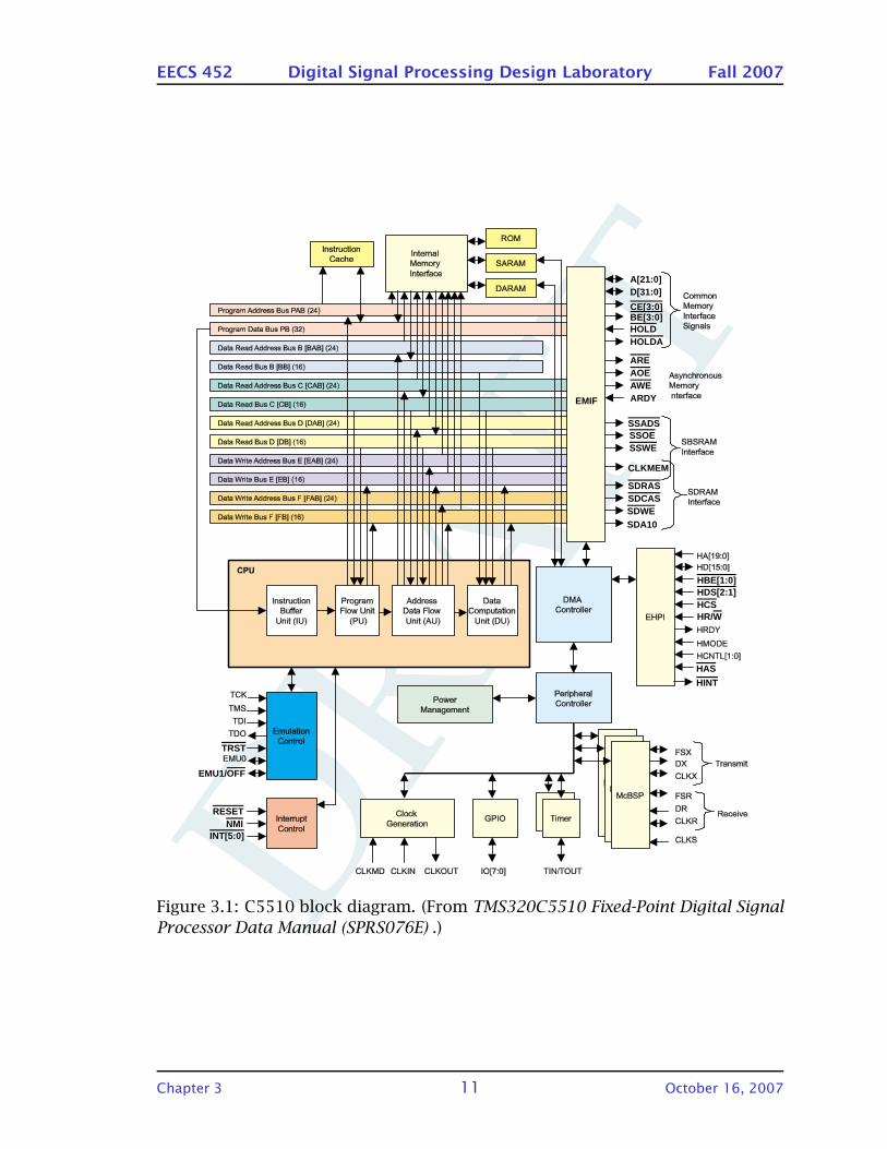
3.2.1 C5510 architecture
The C5510 DSP block diagram is shown in Figure 3.1.
3.2.2 C5510 memory spaces
The C5510 supports three address spaces: program, data and I/O.
Program space is accessed in terms of 8-bit bytes using 24-bit addresses. Data
space is (normally) accessed in terms of 16-bit words using 23-bit addresses. I/O
space is accessed in terms of words using 16-bit addresses.
The C55x uses what TI refers to as a unified memory map. The program and
data spaces share the same physical memory. This physical memory may be off-
chip as well as on. The I/O address space is physically separate and is confined
to being on-chip.
The addressing capability of the C5510 is
• 8M 8-bit bytes of program space,
• 4M 16-bit words of data space,
• 64K 16-bit words of peripheral registers.
A program called the linker is used to collect together individual program
modules and link them together to form an executable program. In order to
Chapter 3 10 October 16, 2007
DRA
FT
EECS 452 Digital Signal Processing Design Laboratory Fall 2007
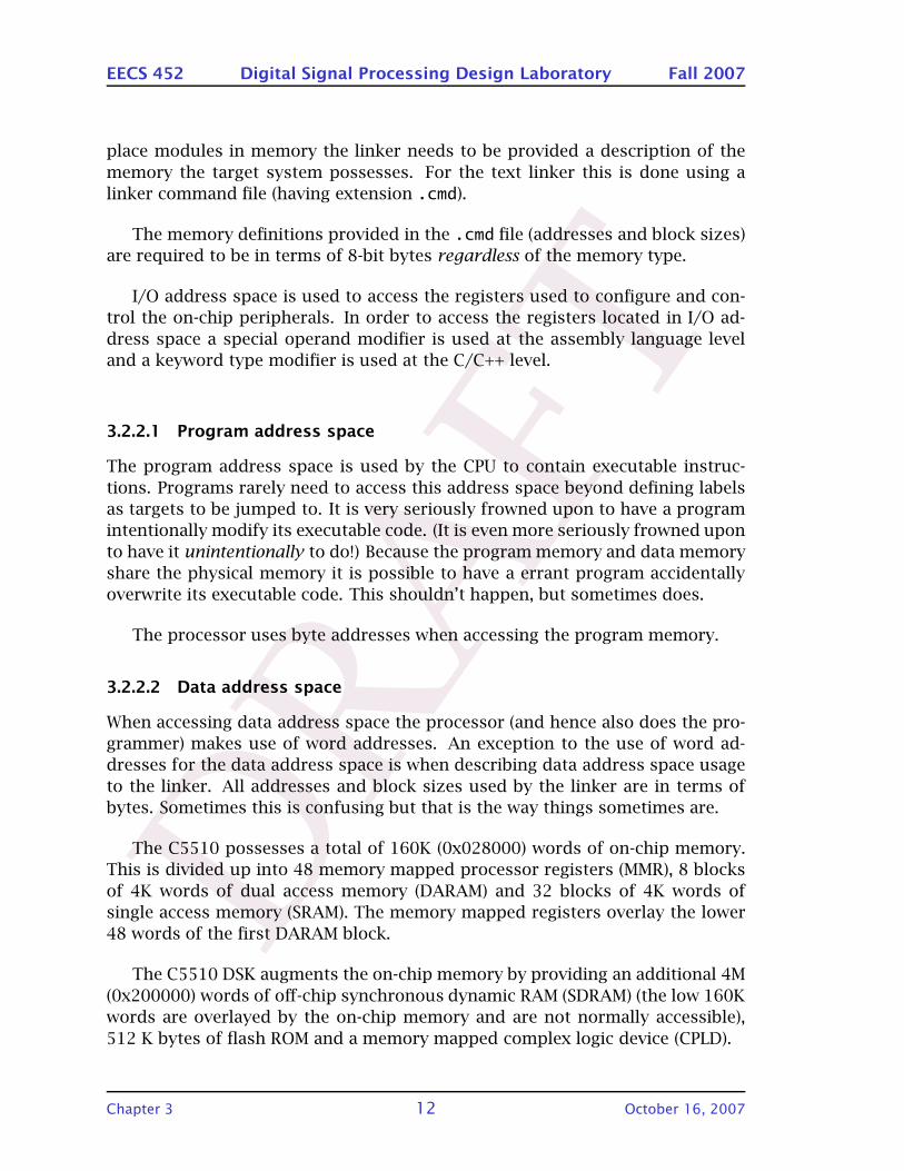
EMIF
CE[3:0]BE[3:0]HOLDHOLDA
A[21:0]D[31:0]
AREAOEAWEARDY
SSADSSSOESSWE
CLKMEM
SDRASSDCASSDWESDA10
HBE[1:0]HDS[2:1]HCS
HAS
HINT
HR/W
RESETNMI
INT[5:0]
EMU1/OFF
TRST
Figure 3.1: C5510 block diagram. (From TMS320C5510 Fixed-Point Digital Signal
Processor Data Manual (SPRS076E) .)
Chapter 3 11 October 16, 2007
DRA
FT
EECS 452 Digital Signal Processing Design Laboratory Fall 2007
place modules in memory the linker needs to be provided a description of the
memory the target system possesses. For the text linker this is done using a
linker command file (having extension .cmd).
The memory definitions provided in the .cmd file (addresses and block sizes)
are required to be in terms of 8-bit bytes regardless of the memory type.
I/O address space is used to access the registers used to configure and con-
trol the on-chip peripherals. In order to access the registers located in I/O ad-
dress space a special operand modifier is used at the assembly language level
and a keyword type modifier is used at the C/C++ level.
3.2.2.1 Program address space
The program address space is used by the CPU to contain executable instruc-
tions. Programs rarely need to access this address space beyond defining labels
as targets to be jumped to. It is very seriously frowned upon to have a program
intentionally modify its executable code. (It is even more seriously frowned upon
to have it unintentionally to do!) Because the program memory and data memory
share the physical memory it is possible to have a errant program accidentally
overwrite its executable code. This shouldn’t happen, but sometimes does.
The processor uses byte addresses when accessing the program memory.
3.2.2.2 Data address space
When accessing data address space the processor (and hence also does the pro-
grammer) makes use of word addresses. An exception to the use of word ad-
dresses for the data address space is when describing data address space usage
to the linker. All addresses and block sizes used by the linker are in terms of
bytes. Sometimes this is confusing but that is the way things sometimes are.
The C5510 possesses a total of 160K (0x028000) words of on-chip memory.
This is divided up into 48 memory mapped processor registers (MMR), 8 blocks
of 4K words of dual access memory (DARAM) and 32 blocks of 4K words of
single access memory (SRAM). The memory mapped registers overlay the lower
48 words of the first DARAM block.
The C5510 DSK augments the on-chip memory by providing an additional 4M
(0x200000) words of off-chip synchronous dynamic RAM (SDRAM) (the low 160K
words are overlayed by the on-chip memory and are not normally accessible),
512 K bytes of flash ROM and a memory mapped complex logic device (CPLD).
Chapter 3 12 October 16, 2007
DRA
FT
EECS 452 Digital Signal Processing Design Laboratory Fall 2007
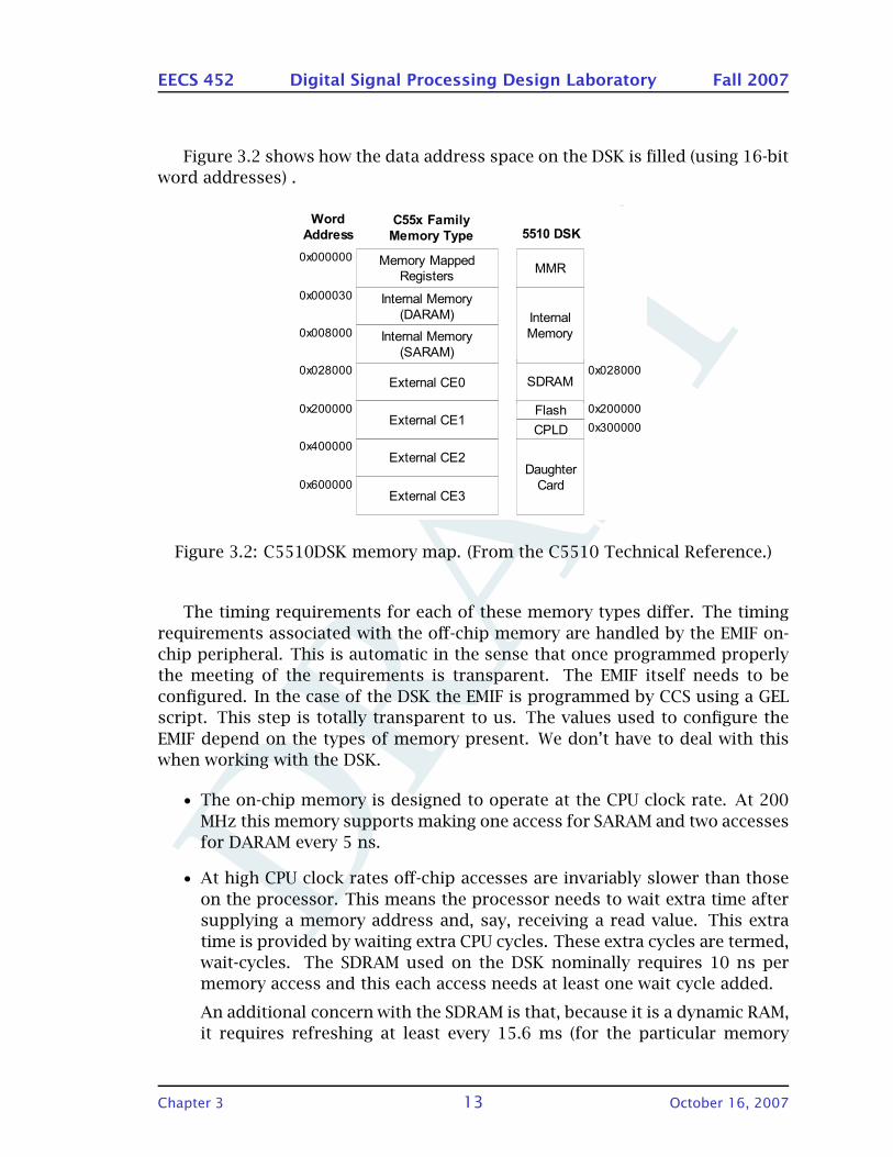
Figure 3.2 shows how the data address space on the DSK is filled (using 16-bit
word addresses) .
Figure 1-2, Memory Map, VC5510 DSK
Memory Mapped
Registers
Internal Memory
(DARAM)
Internal Memory
(SARAM)
External CE0
External CE3
External CE2
External CE1
0x000000
Word
AddressC55x Family
Memory Type
0x000030
0x008000
0x028000
0x200000
0x400000
0x600000
SDRAM
Flash
CPLD
Daughter
Card
5510 DSK
MMR
Internal
Memory
0x028000
0x200000
0x300000
Figure 3.2: C5510DSK memory map. (From the C5510 Technical Reference.)
The timing requirements for each of these memory types differ. The timing
requirements associated with the off-chip memory are handled by the EMIF on-
chip peripheral. This is automatic in the sense that once programmed properly
the meeting of the requirements is transparent. The EMIF itself needs to be
configured. In the case of the DSK the EMIF is programmed by CCS using a GEL
script. This step is totally transparent to us. The values used to configure the
EMIF depend on the types of memory present. We don’t have to deal with this
when working with the DSK.
• The on-chip memory is designed to operate at the CPU clock rate. At 200
MHz this memory supports making one access for SARAM and two accesses
for DARAM every 5 ns.
• At high CPU clock rates off-chip accesses are invariably slower than those
on the processor. This means the processor needs to wait extra time after
supplying a memory address and, say, receiving a read value. This extra
time is provided by waiting extra CPU cycles. These extra cycles are termed,
wait-cycles. The SDRAM used on the DSK nominally requires 10 ns per
memory access and this each access needs at least one wait cycle added.
An additional concern with the SDRAM is that, because it is a dynamic RAM,
it requires refreshing at least every 15.6 ms (for the particular memory
Chapter 3 13 October 16, 2007
DRA
FT
EECS 452 Digital Signal Processing Design Laboratory Fall 2007
chip used on the DSK). The EMIF takes care of this chore as well. It is not
clear whether or not the refreshes are transparent to the CPU in terms of
affecting execution time.
The EMIF peripheral provides four chip enable lines (CE0—CE3) for con-
trolling external memory accesses. The DSK uses the CE0 enable signal
to gain access to the 4M word SDRAM contents. (With the exception of
the lower 160K words of on-chip memory which effectively overlay the
SDRAM’s lower 160K words.)
• The flash CPLD and the EPROM share the portion of the address space
associated with chip enable 1 (CE1). When accessing the flash EPROM the
DSK technical reference manual recommends programming the EMIF for
80 ns accesses. The DSK’s flash EPROM has a 256K×16 capacity.
The timing requirements for the CPLD are not specified in the DSK technical
reference manual beyond that it is faster than the flash EPROM. If the EMIF
is programmed to support the flash EPROM then it is also programmed to
support the CPLD. The CPLD implements four 8-bit registers.
In order to make effective use of the C5510 one needs to understand how the
memory is organized and accessed. Even working at the C/C++ level the details
are not necessarily hidden by the compiler.
3.2.2.3 IO address space
When writing assembly language programs the operand modifier, port( ), can
be used to designate an address as being in I/O space rather than in data space.
With minor exception, any instruction supporting an Smem type memory access
supports use of the port( ) modifier. I/O memory can also be accessed from C
using the ioport keyword that TI added to the language.
3.2.3 C5510 addressing modes
• direct addressing mode
• indirect addressing mode
• absolute addressing mode
• memory mapped register addressing mode
• register bits addressing mode
• circular addressing mode
3.2.4 C5510 memory mapped registers
Introduce all the memory registers in C5510.
Chapter 3 14 October 16, 2007
DRA
FT
EECS 452 Digital Signal Processing Design Laboratory Fall 2007
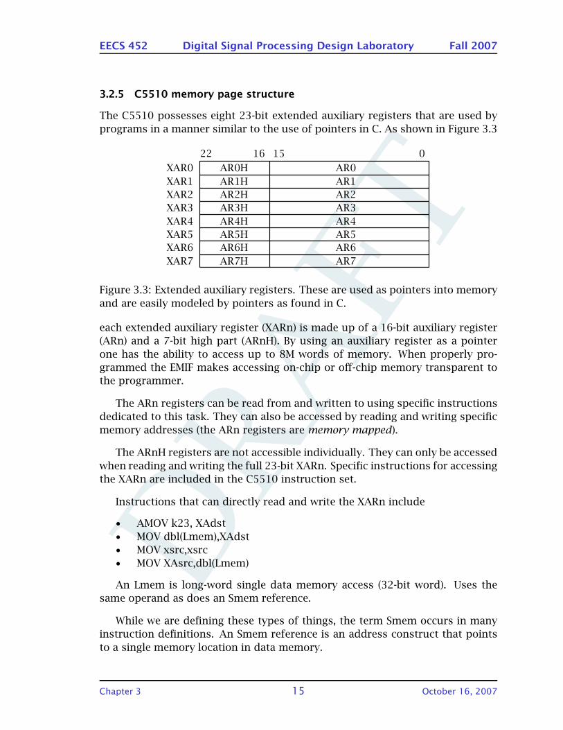
3.2.5 C5510 memory page structure
The C5510 possesses eight 23-bit extended auxiliary registers that are used by
programs in a manner similar to the use of pointers in C. As shown in Figure 3.3
MNRNSOO^oM^oMeu^oM
^oNe ^oN^oOe ^oO^oPe ^oP^oQe ^oQ^oRe ^oR^oSe ^oS^oTe ^oT
u^oOu^oPu^oQu^oRu^oSu^oT
u^oN
Figure 3.3: Extended auxiliary registers. These are used as pointers into memory
and are easily modeled by pointers as found in C.
each extended auxiliary register (XARn) is made up of a 16-bit auxiliary register
(ARn) and a 7-bit high part (ARnH). By using an auxiliary register as a pointer
one has the ability to access up to 8M words of memory. When properly pro-
grammed the EMIF makes accessing on-chip or off-chip memory transparent to
the programmer.
The ARn registers can be read from and written to using specific instructions
dedicated to this task. They can also be accessed by reading and writing specific
memory addresses (the ARn registers are memory mapped).
The ARnH registers are not accessible individually. They can only be accessed
when reading and writing the full 23-bit XARn. Specific instructions for accessing
the XARn are included in the C5510 instruction set.
Instructions that can directly read and write the XARn include
• AMOV k23, XAdst
• MOV dbl(Lmem),XAdst
• MOV xsrc,xsrc
• MOV XAsrc,dbl(Lmem)
An Lmem is long-word single data memory access (32-bit word). Uses the
same operand as does an Smem reference.
While we are defining these types of things, the term Smem occurs in many
instruction definitions. An Smem reference is an address construct that points
to a single memory location in data memory.
Chapter 3 15 October 16, 2007

DRA
FT
EECS 452 Digital Signal Processing Design Laboratory Fall 2007
Carries generated when doing address arithmetic in an auxiliary register do
not propagate into the associated high portion. All address arithmetic involving
an auxiliary register is thus modulo-64K. This characteristic effectively divides
data memory into 64K word pages. The page to be used is determined by the
contents of the ARnH registers. This significantly complicates accessing arrays
greater than 64K words in size. A side effect is that arrays should fit entirely
on a page. There are ways around this restriction but they are, in some sense,
messy.
3.2.6 Small and large memory models
The C5510 C compiler supports two addressing models. These are referred to
as the small memory model and the large memory model.
3.2.6.1 Small memory model
In the small memory model all data and code is assumed to be contained on the
same 64K word page. All of the ARnH registers contain the same value and are
never altered.
3.2.6.2 Large memory model
The large memory model has full access to 8M memory, however still have 64K
pages and associated boundaries to consider.
In the large memory model data and code can be located on various pages.
The ARnH registers are loaded as needed when needed. The page structure is
still present and all data arrays must fit into a single 64K page. However, this
requirement can be circumvented using special code.
3.2.6.3 Comparisons
The small memory model generates more compact code and probably executes
faster than does/will the large memory model. Versions of the run time support
(RTS) library and the DSP library exist for each model. For the small model the
RTS library is named rts.lib and the extended (or large) memory model version
is named rtsx.lib. Generally modules intended for the large memory add an x
to the name of the corresponding small library module.
Chapter 3 16 October 16, 2007

DRA
FT
EECS 452 Digital Signal Processing Design Laboratory Fall 2007
3.3 Peripherals on the C5510 DSP
In this section, we will introduce the peripherals on the C5510 DSK. These in-
clude the multichannel buffered serial port, the timer, the clock, etc.
The details about accessing/configuring the peripherals through specific reg-
isters will be discussed in Chapter 5.
3.3.1 The McBSP serial channels
The use of serial data channels to link together subsystems in a system is a
concept that has been around for some time. This was a key feature of the
ill-fated Transputer introduced many years ago.
Use of serial links to link subsystems is a concept that is presently having a
renaissance. Today’s technology allows the implementation of gigabit per sec-
ond links. This involved not only the drivers and receiver but also the interface
hardware needed to implement the channels in a transmitter and receiver.
The TI C5510 has three such channels. In the C5510 these are referred to
as Multichannel Buffered Serial Ports (McBSP). There are a number of registers
associated with each port. The I/O space locations of the registers can be found
in the C5510 data manual. The registers and the operation of these channels is
described in a separate document included in the list given way up above.
A McBSP channel is a very flexible device. This means that it has options and
configuration bits to worry about. Nothing, at least in today’s technical world
appears to be very simple.
McBSP channel 0 is free for general use and is connected to the peripherals
daughter board connector. We plan to connect this channel to the Spartan-3 via
a 6-pin (4 data, one ground and one power (not to be connected)) PMod type
cable.
McBSP channel 1 is used to implement a SPI bus that is used to program the
AIC23 CODEC chip that provides two channels of A/D and two channels of D/A
conversion to the DSK. The C5510 is the SPI master and the AIC 23 is the slave.
This link can be used for this purpose on startup and then by setting bits in the
CPLD reassigned for use by an external device via the peripheral daughter board
connector. Our C5510/S3 interface board will also allow use of this channel.
McBSP channel 2 is pretty much dedicated to moving sample values between
the C5510 and the AIC23 CODEC chip. For this channel the AIC23 is the bus
Master and the C5510 the slave. The master device generates the timing clock
and the data framing signals.
Chapter 3 17 October 16, 2007

DRA
FT
EECS 452 Digital Signal Processing Design Laboratory Fall 2007
3.3.2 Plan the memory usage
The command file (EECS452.cmd), and the visual linker.
3.3.3 C5510 pipeline structure
The pipeline structure is used in DSP to improve the processor efficiency. In
pipeline execution, operations are broken into smaller segments and then these
smaller pieces are executed in parallel. In this way, the overall time to execute
the instructions can be reduced, and thus improve the efficiency.
The C5510 instruction pipeline has two segments: the fetch pipeline and the
execution pipeline. They are shown in Figure 3.4, 3.5 and 3.6.
Time
Prefetch 1(PF1)
Prefetch 2(PF2)
Fetch(F)
Predecode(PD)
Pipeline
Phase Description
PF1 Present program address to memory.
PF2 Wait for memory to respond.
F Fetch an instruction packet from memory and place it in the IBQ.
PD Pre-decode instructions in the IBQ (identify where instructions
begin and end; identify parallel instructions).
Figure 3.4: The fetch pipeline. From SPRU317F.
The fetch pipeline fetches 32-bit instruction packets from memory, places
them in the instruction buffer queue (IBQ), and then feeds the second pipeline
segment with 48-bit instruction packets. The execution pipeline, decodes in-
structions and performs data accesses and computations.
3.3.4 The C5510 Clock
The C5510 uses a digital phase lock loop (DPLL) to take an externally supplied
clock waveform and create an on-chip clock at a different frequency. The C5510
chip used on the lab DSKs can operate using an internal clock rate as high as
200 MHz. A clock multiplier/divider is built into the C5510 DPLL to simplify
(and reduce the cost of implementation) the generation of a clock at this high
frequency. The maximum external clock rate that can be used with the C5510 is
50 MHz. The C5510 is a fully static design allowing it to work at any lower clock
rate.
Chapter 3 18 October 16, 2007
DRA
FT
EECS 452 Digital Signal Processing Design Laboratory Fall 2007
The clock generator on the C5510 is described in Chapter 3 of TMS320C55x
DSP Peripherals Overview Reference Guide, SPRU317F.
The CC5510 uses an external clock input and has a clock mode input used
to set divide and multiplier factors. A single I/O space register, the clock mode
register (CLKMD), is used to configure and control the clock generation circuitry.
The address of this register can be found in the C5510 data manual.
The frequency of the clock supplied to the C5510 DSK can be determined
by consulting the schematics contained in the DSK technical reference manual.
Doing so is part of the pre-lab.
The state of the clkmd line is determined by the presence/absence of a
jumper on header JP4. A visual check of JP4 on the DSK shows that a jumper
is present. This means that the line is grounded (logic 0) and that the CLKMD
register is initialized to 0x2002 upon reset.
The bit assignments in the CLKMD register are shown in Figure 5.5. The two
bit clock divide field selects an input clock divide factor of from 1 to 4. The 5-bit
PLL MULT field selects a clock multiplication factor of from 2 to 31.
Given a ?? MHz input clock if we divide by ?? and multiply by ?? the C5510
will generate an internal 200 MHz clock frequency. Determining the above values
to be used on the DSK is part of the laboratory exercise.
3.4 The C5510 DSK
The DSP systems used in the EECS 452 lab are TMS320VC5510 digital signal pro-
cessing starter kits (DSKs). The block diagram of the C5510 DSK is shown in
Figure 3.8. The C5510 DSKs were designed and are manufactured by Spectrum
Digital, http://www.spectrumdigital.com. The DSKs are available from Spec-
trum Digital, Texas Instruments as well as from various distributers. The price
is $395. An educational discount is available from TI. This is the first semester
that we have used the C5510 DSK.
The C5510 DSKs are intended to be used as
• a learning tool for the C55x family of DSP processors and the associated
support software.
• a test bed where hardware and software can be developed and tested.
• serve as a reference design. The schematics and other design documenta-
tion are included in the package.
Chapter 3 19 October 16, 2007

DRA
FT
EECS 452 Digital Signal Processing Design Laboratory Fall 2007
The TMS320C5510 processor used on the DSK is a low power, 16-bit, fixed
point processor that can operate using a clock rate of up to 200 MHz and is
capable of executing multiple operations per clock cycle.
Key hardware features of the C5510 DSK include
• operation at clock rates up to 200 MHz,
• a stereo quality codec device, the TI AIC23,
• 4M words of SDRAM,
• 512K bytes of flash EPROM,
• connectors provided for attaching daughter boards,
• four user programmable LEDs,
• four position DIP switch accessible by the user,
• interfaced to a host PC using a version 1.1 USB port.
One of TI’s strengths is the software support that it gives its products. In
particular the Code Composer Studio (CCS) software. CCS is an integrated de-
velopment environment (IDE) designed for use with all of TI’s DSP processors.
The CCS version used in the EECS 452 lab is the one currently supplied with
TMS320C5510 DSK.
CCS executes on a PC and is linked to the C5510 DSK using a USB port. At
the DSK end the USB interfaces to the C5510 JTAG (Joint Test Analysis Group)
hardware built into the C5510 processor. The JTAG interface provides access
to the registers and memory associated with the C5510 and provides control
support. This is done without any associated software support required in the
C5510.
3.5 Code Composer Studio
Code Composer Studio (CCS) Integrated Development Environment (IDE) is a
software development tool from Texas Instruments. It delivers all of the host
tools and runtime software support for your TMS320 DSP and OMAP based re-
alUtime embedded applications. In this course, we will be using this software
for the C5510 programming.
Code Composer Studio includes DSP/BIOS support, real-time analysis capa-
bilities, debugger and optimization tools, C/C++ Compiler, Assembler, Linker,
integrated CodeWright editor, visual project manager, and a variety of simula-
tors and emulation drivers.
Chapter 3 20 October 16, 2007
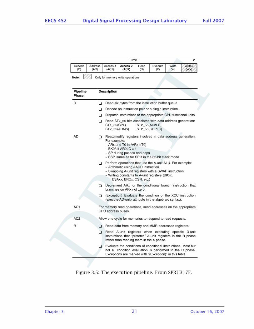
DRA
FT
EECS 452 Digital Signal Processing Design Laboratory Fall 2007
ÍÍÍÍÍÍÍÍÍ
Time
Decode(D)
Write+(W+)
ÍÍÍÍ
Note: Only for memory write operations
Address(AD)
Access 1(AC1)
Access 2(AC2)
Read(R)
Access 2(AC2)
Execute(X)
Write(W)
Pipeline
Phase
Description
D Read six bytes from the instruction buffer queue.
Decode an instruction pair or a single instruction.
Dispatch instructions to the appropriate CPU functional units.
Read STx_55 bits associated with data address generation:
ST1_55(CPL) ST2_55(ARnLC)ST2_55(ARMS) ST2_55(CDPLC)
AD Read/modify registers involved in data address generation.For example:
ARx and T0 in *ARx+(T0) BK03 if AR2LC = 1 SP during pushes and pops
SSP, same as for SP if in the 32-bit stack mode
Perform operations that use the A-unit ALU. For example:
Arithmetic using AADD instruction Swapping A-unit registers with a SWAP instruction Writing constants to A-unit registers (BKxx,
BSAxx, BRCx, CSR, etc.)
Decrement ARx for the conditional branch instruction thatbranches on ARx not zero.
(Exception) Evaluate the condition of the XCC instruction(execute(AD-unit) attribute in the algebraic syntax).
AC1 For memory read operations, send addresses on the appropriateCPU address buses.
AC2 Allow one cycle for memories to respond to read requests.
R Read data from memory and MMR-addressed registers.
Read A-unit registers when executing specific D-unitinstructions that “prefetch” A-unit registers in the R phaserather than reading them in the X phase.
Evaluate the conditions of conditional instructions. Most but
not all condition evaluation is performed in the R phase.Exceptions are marked with “(Exception)” in this table.
Figure 3.5: The execution pipeline. From SPRU317F.
Chapter 3 21 October 16, 2007

DRA
FT
EECS 452 Digital Signal Processing Design Laboratory Fall 2007
Pipeline
Phase
Description
X Read/modify registers that are not MMR-addressed.
Read/modify individual register bits.
Set conditions.
(Exception) Evaluate the condition of the XCCPART
instruction (execute(D-unit) attribute in the algebraic syntax),
unless the instruction is conditioning a write to memory (in this
case, the condition is evaluated in the R phase).
(Exception) Evaluate the condition of the RPTCC instruction.
W Write data to MMR-addressed registers or to I/O space
(peripheral registers).
Write data to memory. From the perspective of the CPU, the
write operation is finished in this pipeline phase.
W+ Write data to memory. From the perspective of the memory, the
write operation is finished in this pipeline phase.
Figure 3.6: The execution pipeline (continued). From SPRU317F.
ÁÁÁÁÁÁÁÁÁÁ
15ÁÁÁÁÁÁÁÁ
14 ÁÁÁÁÁÁÁÁ
13 ÁÁÁÁÁÁÁÁÁÁÁÁ
12 ÁÁÁÁÁÁÁÁÁÁÁÁÁÁÁÁÁÁÁÁÁÁÁÁÁÁÁÁ
11−7 ÁÁÁÁÁÁÁÁ
ÁÁRsvdÎÎÎÎÎÎÎÎ
IAI ÎÎÎÎÎÎÎÎ
IOB TEST (keep 0)ÁÁÁÁÁÁÁÁÁÁÁÁÁÁÁÁÁÁÁÁÁÁÁÁÁÁÁÁ
PLL MULT ÁÁÁÁÁÁÁÁ
ÁÁÁÁÁÁÁÁÁÁÁÁÁÁÁÁ
R/W − 0ÁÁÁÁÁÁÁÁ
R/W − 1ÁÁÁÁÁÁÁÁÁÁÁÁ
ÁÁÁÁÁÁÁÁÁÁÁÁÁÁÁÁÁÁÁÁÁÁÁÁÁÁÁÁ
R/W − 00000 ÁÁÁÁÁÁÁÁ
ÁÁÁÁÁÁÁÁÁÁÁÁÁÁÁÁÁÁÁÁÁÁ
6−5 ÁÁÁÁÁÁÁÁÁÁÁÁ
4 ÁÁÁÁÁÁÁÁÁÁÁÁÁÁÁÁ
3−2 ÁÁÁÁÁÁÁÁÁÁ
1 ÁÁÁÁÁÁÁÁÁÁ
0 ÁÁÁÁ
ÁÁÁÁÁÁ
PLL DIV PLL ENABLEÉÉÉÉÉÉÉÉÉÉÉÉÉÉÉÉ
BYPASS DIV ÁÁÁÁÁÁÁÁÁÁ
BREAKLNÁÁÁÁÁÁÁÁÁÁ
LOCK ÁÁÁÁ
ÁÁÁÁÁÁÁÁÁÁÁÁÁÁÁÁÁÁÁÁÁÁ
R/W − 00 ÁÁÁÁÁÁÁÁÁÁÁÁ
R/W − 0 ÁÁÁÁÁÁÁÁÁÁÁÁÁÁÁÁ
R/W − pin ÁÁÁÁÁÁÁÁÁÁ
R − 1 ÁÁÁÁÁÁÁÁÁÁ
R − 0 ÁÁLegend:
R Read-only accessR/W Read/write access− X X is the value after a DSP reset. X = pin indicates that the reset value depends on the signal
level on the CLKMD pin.
Figure 3.7: Bit usage in the CLKMD register. From SPRU317F.
Chapter 3 22 October 16, 2007
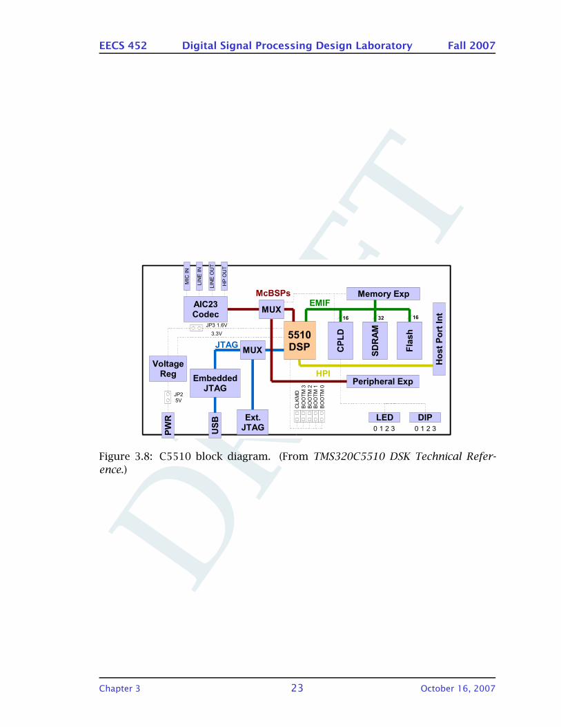
DRA
FT
EECS 452 Digital Signal Processing Design Laboratory Fall 2007
SD
RA
M
Ext.JTAG
AIC23Codec
Ho
st
Po
rt In
t
Fla
sh
MUX
MUX
MIC
IN
LIN
E O
UT
HP
OU
T
LIN
E I
N
Peripheral Exp
LED DIP
EMIF
HPI
McBSPs
JTAG
0 1 2 30 1 2 3
CP
LD
Memory Exp
VoltageReg
PW
R
US
B
EmbeddedJTAG
JP2
5V
JP3 1.6V
3.3V
CL
KM
D
BO
OT
M 3
BO
OT
M 2
BO
OT
M 1
BO
OT
M 0
5510DSP
3216 16
Figure 3.8: C5510 block diagram. (From TMS320C5510 DSK Technical Refer-
ence.)
Chapter 3 23 October 16, 2007

DRA
FTWasted space, consider adding helpful text to this chapter.
DRA
FT
4 : Lab Exercise 1 – Code Composer
Studio tutorial
4.1 Introduction
The DSP systems used in the EECS 452 lab are TMS320VC5510 digital signal
processing starter kits (DSKs). The C5510 DSKs were designed and are manu-
factured by Spectrum Digital, http://www.spectrumdigital.com. The DSKs
are available from Spectrum Digital, Texas Instruments as well as from various
distributers. The price is $395. An educational discount is available from TI.
This is the first semester that we have used the C5510 DSK.
The C5510 DSKs are intended to be used as
• a learning tool for the C55x family of DSP processors and the associated
support software.
• a test bed where hardware and software can be developed and tested.
• serve as a reference design. The schematics and other design documenta-
tion are included in the package.
The TMS320C5510 processor used on the DSK is a low power, 16-bit, fixed
point processor that can operate using a clock rate of up to 200 MHz and is
capable of executing multiple operations per clock cycle.
Key hardware features of the C5510 DSK include
• operation at clock rates up to 200 MHz,
• a stereo quality codec device, the TI AIC23,
• 4M words of SDRAM,
• 512K bytes of flash EPROM,
• connectors provided for attaching daughter boards,
• four user programmable LEDs,
• four position DIP switch accessible by the user,
• interfaced to a host PC using a version 1.1 USB port.
One of TI’s strengths is the software support that it gives its products. In
particular the Code Composer Studio (CCS) software. CCS is an integrated de-
velopment environment (IDE) designed for use with all of TI’s DSP processors.
Chapter 4 25 October 16, 2007
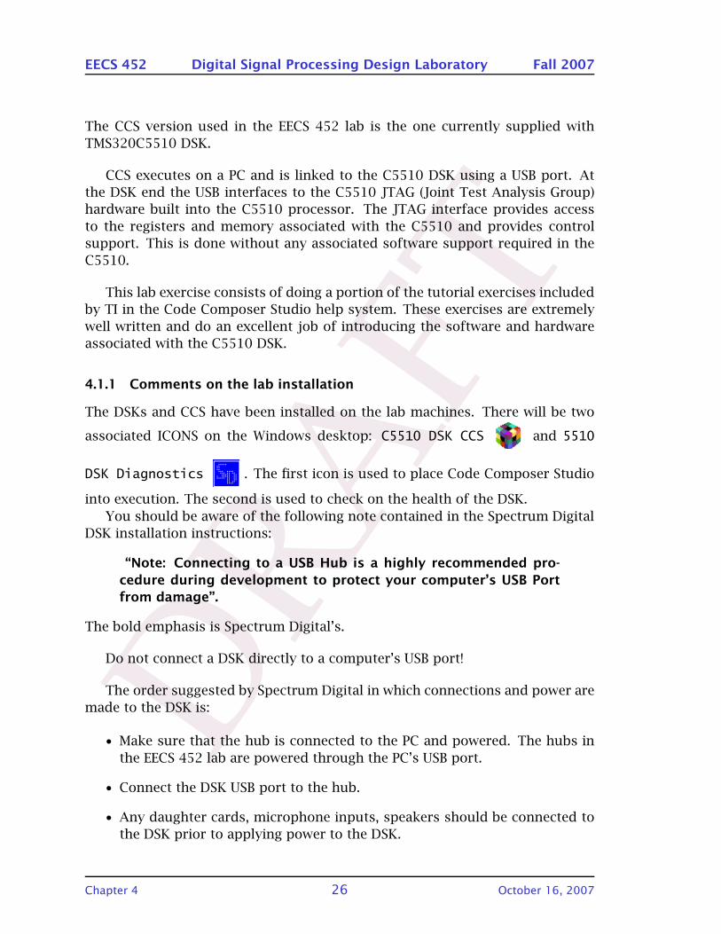
DRA
FT
EECS 452 Digital Signal Processing Design Laboratory Fall 2007
The CCS version used in the EECS 452 lab is the one currently supplied with
TMS320C5510 DSK.
CCS executes on a PC and is linked to the C5510 DSK using a USB port. At
the DSK end the USB interfaces to the C5510 JTAG (Joint Test Analysis Group)
hardware built into the C5510 processor. The JTAG interface provides access
to the registers and memory associated with the C5510 and provides control
support. This is done without any associated software support required in the
C5510.
This lab exercise consists of doing a portion of the tutorial exercises included
by TI in the Code Composer Studio help system. These exercises are extremely
well written and do an excellent job of introducing the software and hardware
associated with the C5510 DSK.
4.1.1 Comments on the lab installation
The DSKs and CCS have been installed on the lab machines. There will be two
associated ICONS on the Windows desktop: C5510 DSK CCS and 5510
DSK Diagnostics . The first icon is used to place Code Composer Studio
into execution. The second is used to check on the health of the DSK.
You should be aware of the following note contained in the Spectrum Digital
DSK installation instructions:
“Note: Connecting to a USB Hub is a highly recommended pro-
cedure during development to protect your computer’s USB Port
from damage”.
The bold emphasis is Spectrum Digital’s.
Do not connect a DSK directly to a computer’s USB port!
The order suggested by Spectrum Digital in which connections and power are
made to the DSK is:
• Make sure that the hub is connected to the PC and powered. The hubs in
the EECS 452 lab are powered through the PC’s USB port.
• Connect the DSK USB port to the hub.
• Any daughter cards, microphone inputs, speakers should be connected to
the DSK prior to applying power to the DSK.
Chapter 4 26 October 16, 2007

DRA
FT
EECS 452 Digital Signal Processing Design Laboratory Fall 2007
• Plug the DSK power supply into the AC prior to connecting the DC power
end to the DSK.
Another quote from the Spectrum Digital installation instructions:
“Warning: Power cable Must be plugged into AC Source Prior to
Plugging the 5 Volt DC output Connector into the DSK.”
Again, the bold emphasis is Spectrum Digital’s.
One would assume that when disconnecting the DSK from the PC that the
order of operations is reversed.
4.1.2 Objectives of this exercise
• Become familiar with Code Composer Studio.
• Learn how to create a project and use it to generate an executable program.
• Learn about using breakpoints and probe points.
• Gain experience with the editor supplied with CCS.
Suggested reading
• Near the end of the Lecture 1 slides there is a reference to a presentation
about CCS that is on the TI web site. This is very informative and very
worthwhile to view.
• TMS320VC5510 DSK Technical Reference.
Don’t attempt to study it. The idea is to look at the document in order to
see what information it contains. Give it a quick read.
The PDF file for this document can be found on the class CD.
Mount the CD. Click on the TIstarthere.html file name. This should
result in a display similar to the listing passed out in class. The top link will
open the manual. You will need Adobe (Acrobat) Reader on your system.
If you wish to open the PDF file directly the path is
X:\TIC55xx\5510_dsk_techref.pdf
where X denotes your CD drive letter.
Chapter 4 27 October 16, 2007

DRA
FT
EECS 452 Digital Signal Processing Design Laboratory Fall 2007
4.2 Prelab
Prelabs are to be done individually and are to be handed in at the
start of the lab period. Handwritten work will not be graded.
This prelab familiarizes you with the DSK and it’s documentation and sets
the stage for the tutorial exercises that you will be doing in the lab itself. The
answers can be determined using the TMS320VC5510 DSK Technical Reference
document (Hint: read it first then do the prelab!).
1. The C5510 DSK has provision for accepting power from a 5 volt supply
using a simple power plug (J5) or power from a alternate external power
source providing 5 volts as well as ±12 volts using a 4-pin Molex connector
(J6). If one were to install and use the Molex connector to power the DSK
the Technical Reference manual contains the warning
Do not plug into J5 and J6 at the same time.
what also needs to be done regarding J5 if the DSK is to be powered using
J6? (Hint: examine the DSK’s Input Power schematic and assume that the
board is designed as shown.)
2. What is the Appendix-A page number of the analog circuitry included on
the C5510 DSK. (Hint: contains the TLV320AIC23 codec chip).
3. Assume that you are facing the side of the DSK that contains the four stereo
jacks used for analog inputs and outputs.
Going from left to right, what are the connector names (e.g., J3) and their
function?
4. The connectors used with the audio inputs and outputs use a 3.5 mm stereo
phone plug. The plug consists of a tip, ring, and body. The signals con-
nected to these are the ground, the left signal and the right signal.
• What signal is connected to the tip?
• What signal is connected to the ring?
• What signal is connected to the body?
5. The DSK uses an Altera complex programmable logic device (CPLD) to im-
plement four functions. These are?
Chapter 4 28 October 16, 2007
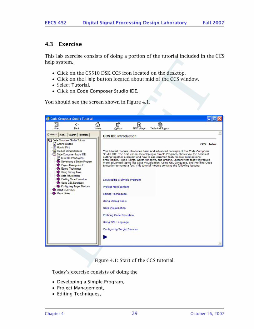
DRA
FT
EECS 452 Digital Signal Processing Design Laboratory Fall 2007
4.3 Exercise
This lab exercise consists of doing a portion of the tutorial included in the CCS
help system.
• Click on the C5510 DSK CCS icon located on the desktop.
• Click on the Help button located about mid of the CCS window.
• Select Tutorial.
• Click on Code Composer Studio IDE.
You should see the screen shown in Figure 4.1.
Figure 4.1: Start of the CCS tutorial.
Today’s exercise consists of doing the
• Developing a Simple Program,
• Project Management,
• Editing Techniques,
Chapter 4 29 October 16, 2007
DRA
FT
EECS 452 Digital Signal Processing Design Laboratory Fall 2007
• Using Debug Tools,
• Data Visualization,
• Profiling Code Execution.
lessons.
The Developing a Simple Program directs you to create a working folder (di-
rectory) under c:\ti\myprojects folder. Because the PCs are being multiple
users we need to keep things a bit more isolated in order to allow users to come
back at a later time and continue using their files.
It is strongly suggested that you make a folder for yourself and/or your part-
nership in the folder c:\users. For example, I generally use c:\users\kurt.
Then, if I am asked to create a folder volume1, I would do so in my directory.
The resulting path would be c:\users\kurt\volume1.
A common problem in past semesters has been to cut rather than to copy.
Cutting is somewhat destructive making it difficult for later users to find files
and folders that they need. Please make sure that you are indeed copying when
you supposed to do so.
When TI refers to the target folder, they in this case mean the dsk5510folder. Apparently the tutorials are somewhat platform independent.
Many of the menu entries that ask for a file have, might be termed, path
memory. The path does not automatically default to the path being used by the
current project. Generally the path defaults to whatever it was from the most
recent use. You need to verify that the path being used is indeed what is desired
and if not click your way there. In past semesters there were several instances of
someone editing someone else’s file of the same name but in another directory,
compiling and wondering why the changes they made had no effect.
Another common past problem when loading an executable into the DSK is
to load someone else’s.
Be paranoid about the paths being used when working with dialog boxes!
We will probably make exclusive of the rts55.lib library through out the
semester. This library was generated assuming that a program and its data fit in
a 64K word page.
There will be a few small inconsistencies between the tutorial and what you
actually encounter. Figuring out what to do about these is part of the learning
process. There also multiple ways to accomplish the same task. For example,
Chapter 4 30 October 16, 2007
DRA
FT
EECS 452 Digital Signal Processing Design Laboratory Fall 2007
saving a file. The tutorial gives two ways. A third is to click on the floppy disk
icon in the top tool bar. Another useful alternative is the Halt button just below
the Run button. Good luck.
A question that I’ve not resolved is whether any customizations you make
become part of the project or if they become global to CCS. If they are global
then changing a setting affects all users. Based on my experience with select-
ing between the text linker and the visual linker the changes remain as part of
the CCS setup. This means you need to recognized when someone has made a
change that is not consistent with your needs and correct the situation (in the
process messing them up). This is a side effect of having the share the software
between lab sections. Make an effort to keep changes to a minimum so as to
maintain harmony between lab sections.
Don’t forget that C is case sensitive. The same is true of the TI assemblers.
Some of the exercises have semi-hidden information. For example, the probe
point one has an apparent link More About Probe Points. They conceal useful
information. Check them out.
When you close a project any windows CCS is displaying remain displayed. It
is good practice to also close these windows. To close any of the sub-windows
(panes?) place the cursor on the pane to be closed, right click, and choose close.
If there is a problem or concern with Set as Active Project check the setting
associated with any other projects that might be present. The difference should
make it apparent what is being done.
We will not being using version control software. The exercise Using Version
Control should be read but not done.
We won’t be generating external makefiles. Read the lesson portion titled
Creating an External Makefile to learn what is involved but don’t do this part of
the lesson.
Before doing the Editing Techniques lesson copy the
c:\ti\tutorial\dsk5510\datedisplay
folder into your user based directory. Use the copy for the editing exercise. This
will result in some small problems that should now be able to easily deal with.
Read but do not do the lesson segment titled Using an External Editor. Editors
are personal things and many programmers have strong feelings about their
Chapter 4 31 October 16, 2007

DRA
FT
EECS 452 Digital Signal Processing Design Laboratory Fall 2007
editor. CCS acknowledges this by allowing use of an editor different than the
one supplied. We will live what we were given. It’s really quite a good editor.
You are all done for today when you get to Profiling Code Execution.
Keep track of the time needed to do each lesson. This will be included in the
lab report. A volunteer a few summers ago recorded times of approximately 90
minutes, 70 minutes and 30 minutes respectively. The total is about 10 minutes
longer than the class period (well since we run on Michigan time, 20 minutes
longer). But the volunteer was of the cautious sort and very thorough. Your
numbers will help give us a better idea of the times typically required.
Ideally this week’s exercise should be done individually. It is very difficult
to learn how to play the piano watching someone else play. The same thing is
going to be true of working with the DSKs. However, the lab is set up expecting
two lab partners per hardware station. Partners might alternate doing portions
of the exercise. Individuals may also choose to return at a later time to do some
individual work. Whatever works.
The goal is to learn what the lessons are teaching, not to just get through the
exercises as fast as possible and then go to dinner.
4.4 Report
There is really not much to report. The report will be quite short. Note that you
did the requested lessons. Below are a couple of questions to be answered to
show having been there and done that. Don’t forget to put your names on the
report.
1. List three ways by which CCS can be made to save the contents of an editing
window into a file.
2. List three uses of probe points.
3. What sort of execution behavior does the animate button cause to happen?
4. In one of the CCS tutorial lessons you used a probe point to access a data
file containing samples of a sine wave. Our course text also discusses the
use of probe points for reading and writing data between the C55x and the
PC’s file system. In particular the text’s author writes about the presence
of magic numbers as part of the file. Did the file used in the lesson about
working with probe points possess such numbers and if so what were they?
Are they the same as given in the text?
5. Include the times in minutes that it took you to do each lesson.
Chapter 4 32 October 16, 2007

DRA
FT
5 : Using the C5510
5.1 Overview of the chapter
In this chapter, we will discuss about the use of C5510. This includes ac-
cess/configure the memory and peripherals in the DSK, and the programming
in C and assembly.
Suggested reading
The key C5510 manuals for this chapter are
• CPU Reference Guide,
• TMS320VC5510 Fixed-Point Digital Signal Processor Data Manual,
• DSP Mnemonic Instruction Set Reference Guide,
• Optimizing C/C++ Compiler User’s Guide,
• TMS320C55xx DSP Programmer’s Guide,
• TMS320VC5510 DSK Technical Reference,
• TMS320VC5501/5502/5509/5510 DSP Multichannel Buffered Serial Port
(McBSP) Reference Guide.
Reference for C5510 DSP
• Real-Time Digital Signal Processing: Implementations, Applications, and Ex-
periments with the TMS320C55X, S. M. Kuo and B. H. Lee, Wiley 2001.
Reference for programming
• The C Programming Language 2nd Ed., B. W. Kernighan and D. M. Ritchie,
Prentice Hall 1988.
5.2 Using C5510
5.2.1 Access the memory
Here we talk about how to access the memory in C5510 from different aspects.
Chapter 5 33 October 16, 2007
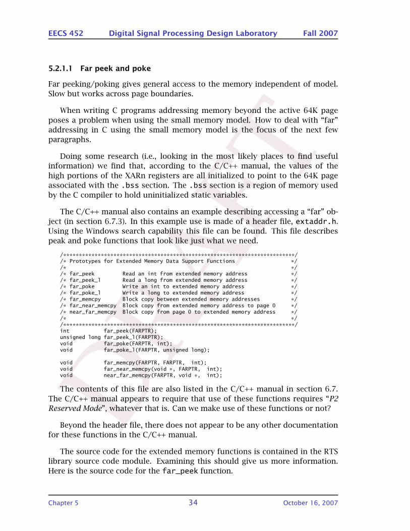
DRA
FT
EECS 452 Digital Signal Processing Design Laboratory Fall 2007
5.2.1.1 Far peek and poke
Far peeking/poking gives general access to the memory independent of model.
Slow but works across page boundaries.
When writing C programs addressing memory beyond the active 64K page
poses a problem when using the small memory model. How to deal with “far”
addressing in C using the small memory model is the focus of the next few
paragraphs.
Doing some research (i.e., looking in the most likely places to find useful
information) we find that, according to the C/C++ manual, the values of the
high portions of the XARn registers are all initialized to point to the 64K page
associated with the .bss section. The .bss section is a region of memory used
by the C compiler to hold uninitialized static variables.
The C/C++ manual also contains an example describing accessing a “far” ob-
ject (in section 6.7.3). In this example use is made of a header file, extaddr.h.
Using the Windows search capability this file can be found. This file describes
peak and poke functions that look like just what we need.
/**************************************************************************//* Prototypes for Extended Memory Data Support Functions *//* *//* far_peek Read an int from extended memory address *//* far_peek_l Read a long from extended memory address *//* far_poke Write an int to extended memory address *//* far_poke_l Write a long to extended memory address *//* far_memcpy Block copy between extended memory addresses *//* far_near_memcpy Block copy from extended memory address to page 0 *//* near_far_memcpy Block copy from page 0 to extended memory address *//* *//**************************************************************************/int far_peek(FARPTR);unsigned long far_peek_l(FARPTR);void far_poke(FARPTR, int);void far_poke_l(FARPTR, unsigned long);
void far_memcpy(FARPTR, FARPTR, int);void far_near_memcpy(void *, FARPTR, int);void near_far_memcpy(FARPTR, void *, int);
The contents of this file are also listed in the C/C++ manual in section 6.7.
The C/C++ manual appears to require that use of these functions requires “P2
Reserved Mode”, whatever that is. Can we make use of these functions or not?
Beyond the header file, there does not appear to be any other documentation
for these functions in the C/C++ manual.
The source code for the extended memory functions is contained in the RTS
library source code module. Examining this should give us more information.
Here is the source code for the far_peek function.
Chapter 5 34 October 16, 2007

DRA
FT
EECS 452 Digital Signal Processing Design Laboratory Fall 2007
;/******************************************************************/;/* far_peek() - read 1 word of data from extended address */;/******************************************************************/_far_peek:
AR4 = AC0 & #0FFFFh ; Move page address to AR registerAC0 = AC0 << #-16 ; Shift page # to bottom 16-bits
MDP05 = @AC0_L || mmap() ; Initialize MDP to correct pageAC0 = uns(*AR4) ; Read 1 word of data (unsigned)MDP05 = #0 ; Reset MDP to the data pagereturn
Note that this is written for the algebraic assembler. We will be making ex-
clusive use of the mnemonic assembler in this class.
The only information that the author can find about the MDP05 register is
contained in the C5510 Data Manual. The data manual flags the register as “re-
served”. This does not seem to be something one should be using. This function
resets the MDP05 contents to zero regardless of what its previous setting had
been. Is this important?
So what to do?
We could use the large model and simply ignore the problem. (The large
memory model inherently supports far pointers.) We could run tests and deter-
mine whether or not the TI functions work in the small model environment. We
could write our own assembly language far peak and poke functions. The latter
is the more interesting (educational) case and the one we will pursue.
Using TI’s code as a guide we will write a peek function supplying it an un-
signed long corresponding to the memory location that we wish to access. The
function saves the contents of an extended auxiliary register (XAR) onto the
stack, loads the XAR with the value in the accumulator, does a move of the value
pointed by the XAR into T0, pops the stack back into the XAR and return. We can
do about the same for a matching poke function. We can also make the code in-
dependent of memory model increasing the portability of future code that might
need to be ported between models.
Simple?
Chapter 5 35 October 16, 2007
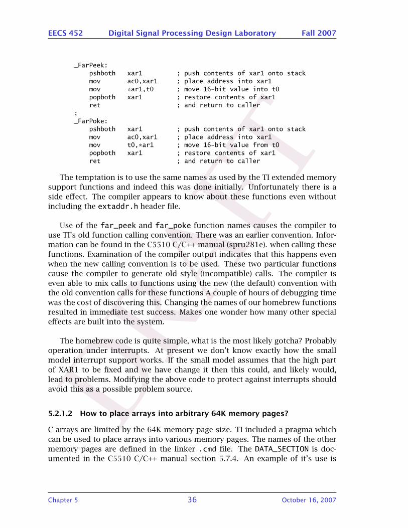
DRA
FT
EECS 452 Digital Signal Processing Design Laboratory Fall 2007
_FarPeek:pshboth xar1 ; push contents of xar1 onto stackmov ac0,xar1 ; place address into xar1mov *ar1,t0 ; move 16-bit value into t0popboth xar1 ; restore contents of xar1ret ; and return to caller
;_FarPoke:
pshboth xar1 ; push contents of xar1 onto stackmov ac0,xar1 ; place address into xar1mov t0,*ar1 ; move 16-bit value from t0popboth xar1 ; restore contents of xar1ret ; and return to caller
The temptation is to use the same names as used by the TI extended memory
support functions and indeed this was done initially. Unfortunately there is a
side effect. The compiler appears to know about these functions even without
including the extaddr.h header file.
Use of the far_peek and far_poke function names causes the compiler to
use TI’s old function calling convention. There was an earlier convention. Infor-
mation can be found in the C5510 C/C++ manual (spru281e). when calling these
functions. Examination of the compiler output indicates that this happens even
when the new calling convention is to be used. These two particular functions
cause the compiler to generate old style (incompatible) calls. The compiler is
even able to mix calls to functions using the new (the default) convention with
the old convention calls for these functions A couple of hours of debugging time
was the cost of discovering this. Changing the names of our homebrew functions
resulted in immediate test success. Makes one wonder how many other special
effects are built into the system.
The homebrew code is quite simple, what is the most likely gotcha? Probably
operation under interrupts. At present we don’t know exactly how the small
model interrupt support works. If the small model assumes that the high part
of XAR1 to be fixed and we have change it then this could, and likely would,
lead to problems. Modifying the above code to protect against interrupts should
avoid this as a possible problem source.
5.2.1.2 How to place arrays into arbitrary 64K memory pages?
C arrays are limited by the 64K memory page size. TI included a pragma which
can be used to place arrays into various memory pages. The names of the other
memory pages are defined in the linker .cmd file. The DATA_SECTION is doc-
umented in the C5510 C/C++ manual section 5.7.4. An example of it’s use is
Chapter 5 36 October 16, 2007
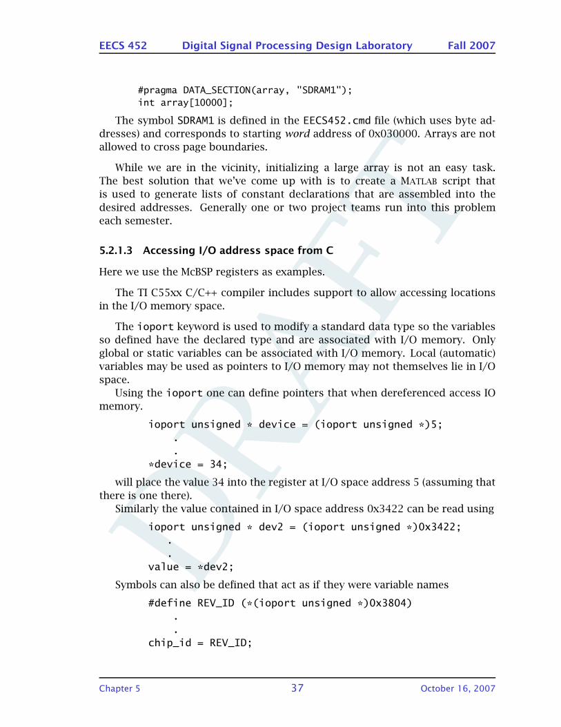
DRA
FT
EECS 452 Digital Signal Processing Design Laboratory Fall 2007
#pragma DATA_SECTION(array, "SDRAM1");int array[10000];
The symbol SDRAM1 is defined in the EECS452.cmd file (which uses byte ad-
dresses) and corresponds to starting word address of 0x030000. Arrays are not
allowed to cross page boundaries.
While we are in the vicinity, initializing a large array is not an easy task.
The best solution that we’ve come up with is to create a MATLAB script that
is used to generate lists of constant declarations that are assembled into the
desired addresses. Generally one or two project teams run into this problem
each semester.
5.2.1.3 Accessing I/O address space from C
Here we use the McBSP registers as examples.
The TI C55xx C/C++ compiler includes support to allow accessing locations
in the I/O memory space.
The ioport keyword is used to modify a standard data type so the variables
so defined have the declared type and are associated with I/O memory. Only
global or static variables can be associated with I/O memory. Local (automatic)
variables may be used as pointers to I/O memory may not themselves lie in I/O
space.
Using the ioport one can define pointers that when dereferenced access IO
memory.
ioport unsigned * device = (ioport unsigned *)5;..
*device = 34;
will place the value 34 into the register at I/O space address 5 (assuming that
there is one there).
Similarly the value contained in I/O space address 0x3422 can be read using
ioport unsigned * dev2 = (ioport unsigned *)0x3422;..
value = *dev2;
Symbols can also be defined that act as if they were variable names
#define REV_ID (*(ioport unsigned *)0x3804)..
chip_id = REV_ID;
Chapter 5 37 October 16, 2007
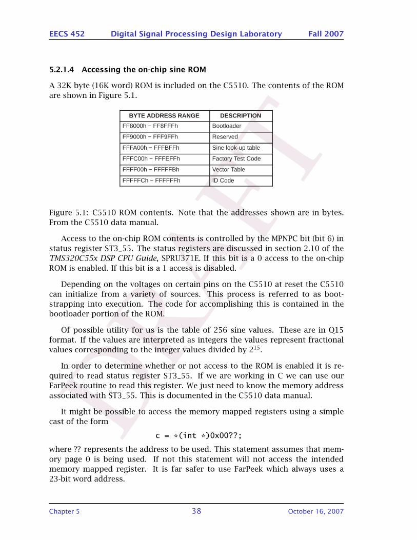
DRA
FT
EECS 452 Digital Signal Processing Design Laboratory Fall 2007
5.2.1.4 Accessing the on-chip sine ROM
A 32K byte (16K word) ROM is included on the C5510. The contents of the ROM
are shown in Figure 5.1.
BYTE ADDRESS RANGE DESCRIPTION
FF8000h − FF8FFFh Bootloader
FF9000h − FFF9FFh Reserved
FFFA00h − FFFBFFh Sine look-up table
FFFC00h − FFFEFFh Factory Test Code
FFFF00h − FFFFFBh Vector Table
FFFFFCh − FFFFFFh ID Code
Figure 5.1: C5510 ROM contents. Note that the addresses shown are in bytes.
From the C5510 data manual.
Access to the on-chip ROM contents is controlled by the MPNPC bit (bit 6) in
status register ST3_55. The status registers are discussed in section 2.10 of the
TMS320C55x DSP CPU Guide, SPRU371E. If this bit is a 0 access to the on-chip
ROM is enabled. If this bit is a 1 access is disabled.
Depending on the voltages on certain pins on the C5510 at reset the C5510
can initialize from a variety of sources. This process is referred to as boot-
strapping into execution. The code for accomplishing this is contained in the
bootloader portion of the ROM.
Of possible utility for us is the table of 256 sine values. These are in Q15
format. If the values are interpreted as integers the values represent fractional
values corresponding to the integer values divided by 215.
In order to determine whether or not access to the ROM is enabled it is re-
quired to read status register ST3_55. If we are working in C we can use our
FarPeek routine to read this register. We just need to know the memory address
associated with ST3_55. This is documented in the C5510 data manual.
It might be possible to access the memory mapped registers using a simple
cast of the form
c = *(int *)0x00??;
where ?? represents the address to be used. This statement assumes that mem-
ory page 0 is being used. If not this statement will not access the intended
memory mapped register. It is far safer to use FarPeek which always uses a
23-bit word address.
Chapter 5 38 October 16, 2007
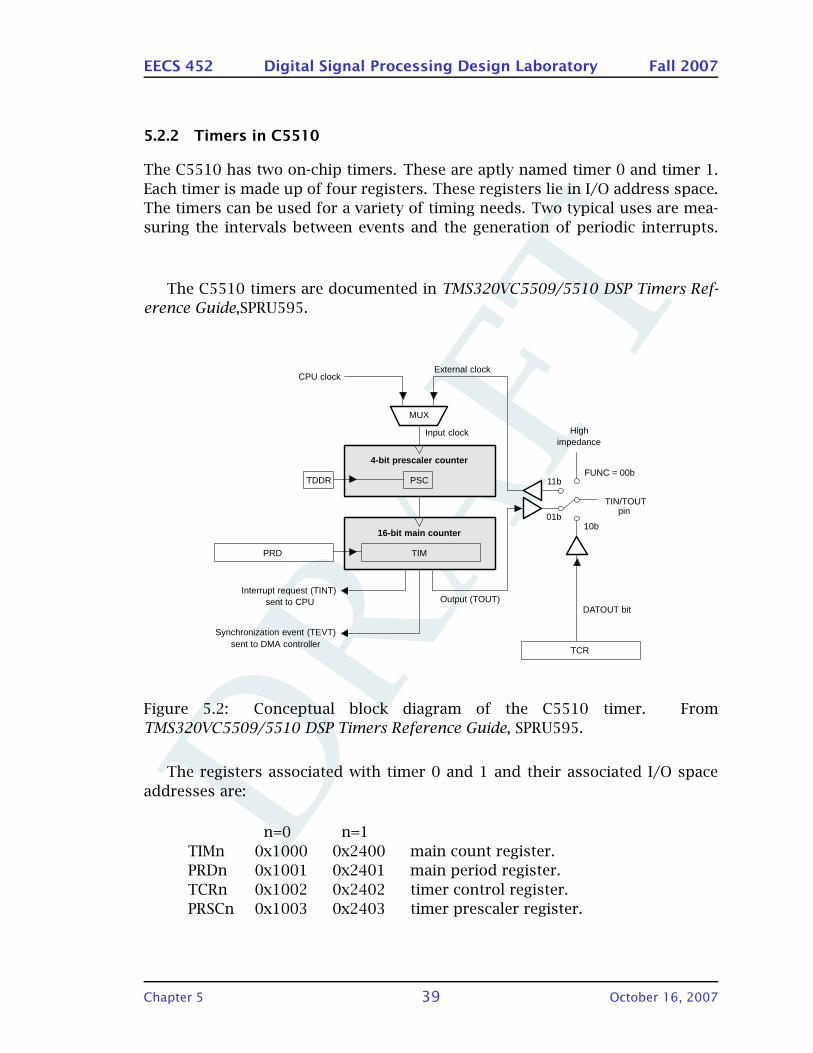
DRA
FT
EECS 452 Digital Signal Processing Design Laboratory Fall 2007
5.2.2 Timers in C5510
The C5510 has two on-chip timers. These are aptly named timer 0 and timer 1.
Each timer is made up of four registers. These registers lie in I/O address space.
The timers can be used for a variety of timing needs. Two typical uses are mea-
suring the intervals between events and the generation of periodic interrupts.
The C5510 timers are documented in TMS320VC5509/5510 DSP Timers Ref-
erence Guide,SPRU595.
16-bit main counter
TIMPRD
4-bit prescaler counter
PSCTDDR
Interrupt request (TINT)sent to CPU
Synchronization event (TEVT)sent to DMA controller
MUX
Input clock
CPU clockExternal clock
TIN/TOUTpin
Output (TOUT)
TCR
DATOUT bit
Highimpedance
11b
01b10b
FUNC = 00b
Figure 5.2: Conceptual block diagram of the C5510 timer. From
TMS320VC5509/5510 DSP Timers Reference Guide, SPRU595.
The registers associated with timer 0 and 1 and their associated I/O space
addresses are:
n=0 n=1
TIMn 0x1000 0x2400 main count register.
PRDn 0x1001 0x2401 main period register.
TCRn 0x1002 0x2402 timer control register.
PRSCn 0x1003 0x2403 timer prescaler register.
Chapter 5 39 October 16, 2007
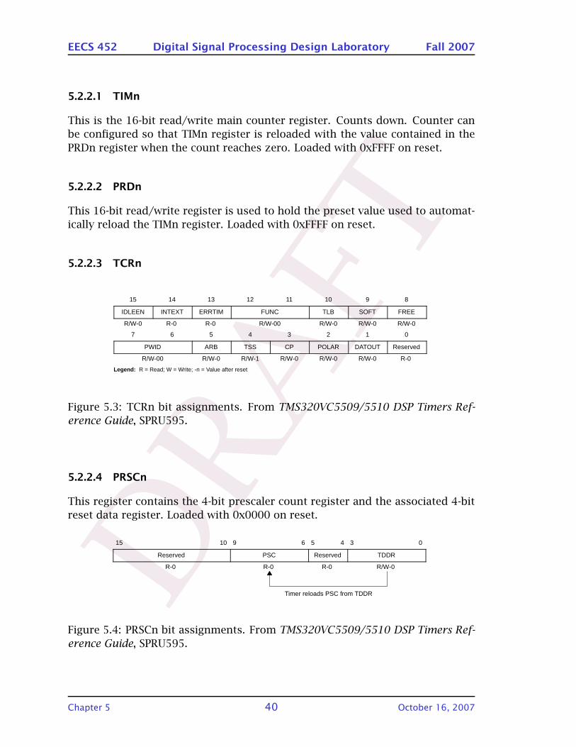
DRA
FT
EECS 452 Digital Signal Processing Design Laboratory Fall 2007
5.2.2.1 TIMn
This is the 16-bit read/write main counter register. Counts down. Counter can
be configured so that TIMn register is reloaded with the value contained in the
PRDn register when the count reaches zero. Loaded with 0xFFFF on reset.
5.2.2.2 PRDn
This 16-bit read/write register is used to hold the preset value used to automat-
ically reload the TIMn register. Loaded with 0xFFFF on reset.
5.2.2.3 TCRn
15 14 13 12 11 10 9 8
IDLEEN INTEXT ERRTIM FUNC TLB SOFT FREE
R/W-0 R-0 R-0 R/W-00 R/W-0 R/W-0 R/W-0
7 6 5 4 3 2 1 0
PWID ARB TSS CP POLAR DATOUT Reserved
R/W-00 R/W-0 R/W-1 R/W-0 R/W-0 R/W-0 R-0
Legend: R = Read; W = Write; -n = Value after reset
Figure 5.3: TCRn bit assignments. From TMS320VC5509/5510 DSP Timers Ref-
erence Guide, SPRU595.
5.2.2.4 PRSCn
This register contains the 4-bit prescaler count register and the associated 4-bit
reset data register. Loaded with 0x0000 on reset.
15 10 9 6 5 4 3 0
Reserved PSC Reserved TDDR
R-0 R-0 R-0 R/W-0
Timer reloads PSC from TDDR
Figure 5.4: PRSCn bit assignments. From TMS320VC5509/5510 DSP Timers Ref-
erence Guide, SPRU595.
Chapter 5 40 October 16, 2007
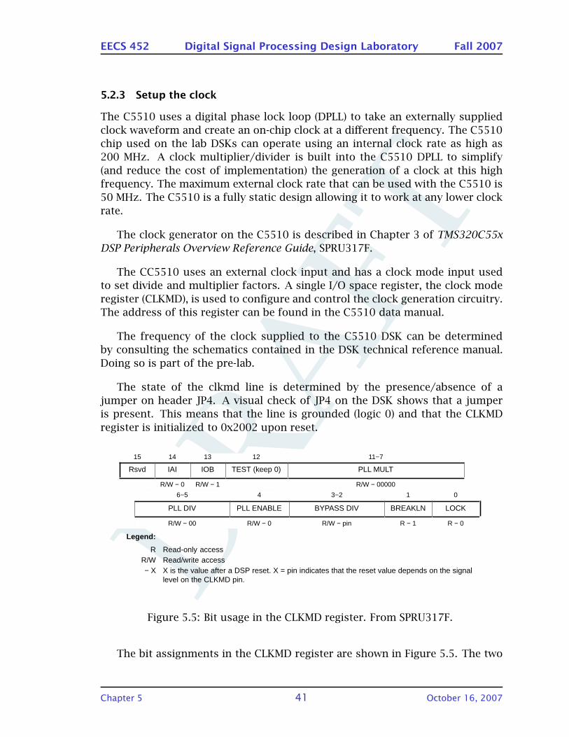
DRA
FT
EECS 452 Digital Signal Processing Design Laboratory Fall 2007
5.2.3 Setup the clock
The C5510 uses a digital phase lock loop (DPLL) to take an externally supplied
clock waveform and create an on-chip clock at a different frequency. The C5510
chip used on the lab DSKs can operate using an internal clock rate as high as
200 MHz. A clock multiplier/divider is built into the C5510 DPLL to simplify
(and reduce the cost of implementation) the generation of a clock at this high
frequency. The maximum external clock rate that can be used with the C5510 is
50 MHz. The C5510 is a fully static design allowing it to work at any lower clock
rate.
The clock generator on the C5510 is described in Chapter 3 of TMS320C55x
DSP Peripherals Overview Reference Guide, SPRU317F.
The CC5510 uses an external clock input and has a clock mode input used
to set divide and multiplier factors. A single I/O space register, the clock mode
register (CLKMD), is used to configure and control the clock generation circuitry.
The address of this register can be found in the C5510 data manual.
The frequency of the clock supplied to the C5510 DSK can be determined
by consulting the schematics contained in the DSK technical reference manual.
Doing so is part of the pre-lab.
The state of the clkmd line is determined by the presence/absence of a
jumper on header JP4. A visual check of JP4 on the DSK shows that a jumper
is present. This means that the line is grounded (logic 0) and that the CLKMD
register is initialized to 0x2002 upon reset.
ÁÁÁÁÁÁÁÁÁÁ
15ÁÁÁÁÁÁÁÁ
14 ÁÁÁÁÁÁÁÁ
13 ÁÁÁÁÁÁÁÁÁÁÁÁ
12 ÁÁÁÁÁÁÁÁÁÁÁÁÁÁÁÁÁÁÁÁÁÁÁÁÁÁÁÁ
11−7 ÁÁÁÁÁÁÁÁ
ÁÁRsvdÎÎÎÎÎÎÎÎ
IAI ÎÎÎÎÎÎÎÎ
IOB TEST (keep 0)ÁÁÁÁÁÁÁÁÁÁÁÁÁÁÁÁÁÁÁÁÁÁÁÁÁÁÁÁ
PLL MULT ÁÁÁÁÁÁÁÁ
ÁÁÁÁÁÁÁÁÁÁÁÁÁÁÁÁ
R/W − 0ÁÁÁÁÁÁÁÁ
R/W − 1ÁÁÁÁÁÁÁÁÁÁÁÁ
ÁÁÁÁÁÁÁÁÁÁÁÁÁÁÁÁÁÁÁÁÁÁÁÁÁÁÁÁ
R/W − 00000 ÁÁÁÁÁÁÁÁ
ÁÁÁÁÁÁÁÁÁÁÁÁÁÁÁÁÁÁÁÁÁÁ
6−5 ÁÁÁÁÁÁÁÁÁÁÁÁ
4 ÁÁÁÁÁÁÁÁÁÁÁÁÁÁÁÁ
3−2 ÁÁÁÁÁÁÁÁÁÁ
1 ÁÁÁÁÁÁÁÁÁÁ
0 ÁÁÁÁ
ÁÁÁÁÁÁ
PLL DIV PLL ENABLEÉÉÉÉÉÉÉÉÉÉÉÉÉÉÉÉ
BYPASS DIV ÁÁÁÁÁÁÁÁÁÁ
BREAKLNÁÁÁÁÁÁÁÁÁÁ
LOCK ÁÁÁÁ
ÁÁÁÁÁÁÁÁÁÁÁÁÁÁÁÁÁÁÁÁÁÁ
R/W − 00 ÁÁÁÁÁÁÁÁÁÁÁÁ
R/W − 0 ÁÁÁÁÁÁÁÁÁÁÁÁÁÁÁÁ
R/W − pin ÁÁÁÁÁÁÁÁÁÁ
R − 1 ÁÁÁÁÁÁÁÁÁÁ
R − 0 ÁÁLegend:
R Read-only accessR/W Read/write access− X X is the value after a DSP reset. X = pin indicates that the reset value depends on the signal
level on the CLKMD pin.
Figure 5.5: Bit usage in the CLKMD register. From SPRU317F.
The bit assignments in the CLKMD register are shown in Figure 5.5. The two
Chapter 5 41 October 16, 2007
DRA
FT
EECS 452 Digital Signal Processing Design Laboratory Fall 2007
bit clock divide field selects an input clock divide factor of from 1 to 4. The 5-bit
PLL MULT field selects a clock multiplication factor of from 2 to 31.
Given a ?? MHz input clock if we divide by ?? and multiply by ?? the C5510
will generate an internal 200 MHz clock frequency. Determining the above values
to be used on the DSK is part of the laboratory exercise.
5.2.4 Multichannel buffered serial port (McBSP)
The details of configuring the McBSP channels will be discussed in Chapter 12.
5.2.5 DMA controller
To be added.
Chapter 5 42 October 16, 2007
DRA
FT
6 : Lab Exercise 2 – basic operations
on C5510 DSK
6.1 Introduction
In lab exercise 1, we learned how to use the software tool Code Composer Studio
to work with C5510. In this lab exercise, we begin to actually use the C5510 DSK.
The C5510 might fit onto a small chip but it is a moderately complex device. With
the DSK interface and its peripherals, C5510 is capable of doing a lot of tasks.
In this exercise, we will begin by learning the basic operations on C5510 and
the peripherals on the DSK. You should make sure you know all the materials
presented here after doing this exercise, since it is the foundation for the more
advanced topics in the course and upcoming lab exercises.
Suggested reading
The key C5510 manuals for this exercise are
• CPU Reference Guide,
• TMS320VC5510 Fixed-Point Digital Signal Processor Data Manual,
• Optimizing C/C++ Compiler User’s Guide,
• TMS320C55xx DSP Programmer’s Guide,
• TMS320VC5510 DSK Technical Reference,
• TMS320VC5501/5502/5509/5510 DSP Multichannel Buffered Serial Port
(McBSP) Reference Guide.
Reference for C5510 DSP
• Real-Time Digital Signal Processing: Implementations, Applications, and Ex-
periments with the TMS320C55X, S. M. Kuo and B. H. Lee, Wiley 2001.
Reference for programming
• The C Programming Language 2nd Ed., B. W. Kernighan and D. M. Ritchie,
Prentice Hall 1988.
Chapter 6 43 October 16, 2007

DRA
FT
EECS 452 Digital Signal Processing Design Laboratory Fall 2007
6.2 Prelab
Prelabs are to be done individually and are to be handed in at the
start of the lab period. Handwritten work will not be graded.
Read the chapter and related materials to answer the following questions.
6.2.1 C5510 Architecture
1. What are the four units in the C5510 CPU? What are their functionalities?
6.2.2 Far peeking and poking
1. What are the differences between small and large memory models? What
are the advantages and disadvantages of each model?
2. What are the purposes of using far peek and poke?
6.2.3 About the memory
1. What three types of address spaces does the C5510 support?
2. What is the basic purpose of each address space?
3. Which address spaces are commonly addressed using byte addresses and
which use word address (in normal use)?
4. What is the size in bytes or words as appropriate of each address space?
5. What is the pragma directive in C programming? (See the C5510 C manual
or google for the answer.)
6. What is the total size of on-chip memory in the C5510?
7. How many pages is the C5510 memory address space divided into? What
is the size of each page?
8. What are the two ways to plan memory usage?
6.2.4 Addressing modes
1. How many types of addressing modes does C5510 support? (Hint: C5510
CPU Reference Guide)
Chapter 6 44 October 16, 2007

DRA
FT
EECS 452 Digital Signal Processing Design Laboratory Fall 2007
6.2.5 Registers
1. What does it mean by “memory mapped registers”?
2. What is the hexadecimal memory mapped address of the status register
ST3_55? (Hint: C5510 data manual.)
3. What is the address in I/O space for the clock mode register CLKMD? (Hint:
C5510 data manual.)
6.2.6 McBSP channels
1. How many McBSP channels does C5510 have?
2. What are the starting addresses of the register sets associated with each
channel?
6.2.7 Chip revision number
1. What address in the I/O space is the chip revision identification code lo-
cated?
6.2.8 DSK peripherals
1. What is the register that contains the information about switches and LEDs
on the C5510 DSK? What is the address of that register? What is the bit
mapping from the register to the switches and LEDs?
6.2.9 Fixed-point arithmetics
1. What does the assembly instruction MANT::NEXP do?
2. What are the mathematical definitions of mantissa and exponent?
3. How many bits are there in the accumulator and temporary register in
C5510?
4. What is 2s-complement representation?
5. What are the results of mantissa and exponent by applying MANT::NEXP to
the following numbers?
• 0x210A0A0A0A
• 0x00E8040000
• 0x0000001234
Chapter 6 45 October 16, 2007

DRA
FT
EECS 452 Digital Signal Processing Design Laboratory Fall 2007
• 0x0000000000
• 0x1111111111
• 0x0078040000
6.3 Exercise
In order to generate an executable program you need to specify a C/C++ run time
support library and linker configuration file. They can be found in the support
folder in the lab files. Here is the list of the files.
• EECS452.cmd: used by the linker to allocate memory.
• peekpoke.asm: used to access extended memory from small memory
model programs.
• rts55.lib: the TI C/C++ run time support library for the small memory
model.
• rts55x.lib: the TI C/C++ run time support library for the large memory
model.
Please make sure that you are working with a copy of the master files when
doing these exercises. In the past there have been instances of the master file
set being modified or having become missing. Make sure that you copy the files
rather than moving them.
6.3.1 Access C5510 memory
In this part of the exercise, we work on accessing different sections of the mem-
ory. We will also work in different memory models and see what is the difference.
6.3.1.1 Far peeking and poking
In this part of the exercise you will create two projects that will be used to access
the contents of the CPLD registers. The first project will named CPLDreadS and
is to use the small memory model. The second project will be named CPLDreadL
is to use the large memory model. Note that the two projects will use the small
and large memory model libraries as appropriate.
The compiler and assembler need to be told whether a small or large memory
program is being generated. This can be done by either checking or unchecking
a box found by accessing
Project – Build Options – Compiler – Advanced
Chapter 6 46 October 16, 2007

DRA
FT
EECS 452 Digital Signal Processing Design Laboratory Fall 2007
This part of the lab uses the main programs given in section 6.5.2 and 6.5.3.
These can be found in the given lab files. The source code for the FarPeek and
FarPoke functions is located in the associated support subdirectory.
Once you locate the lab files, do the following steps:
• Create the executables. You need to create a new project and include all
the relevant codes (C/assembly). Do not forget about the library (.lib) and
linker file (.cmd). You will not be able to compile the project without these
files.
• Examine the assembly listings.
• Examine the memory map files.
The contents of the USER_REG CPLD register will contain the DIP switch set-
tings. Execute each program using the following DIP switch settings:
sw0 = up, sw1 = down, sw2 = down, sw3 = down,
sw0 = down, sw1 = up, sw2 = down, sw3 = down,
sw0 = down, sw1 = down, sw2 = up, sw3 = down,
sw0 = down, sw1 = down, sw2 = down, sw3 = up.
Record the results and include in your report.
6.3.1.2 The memory map and the data section declaration
Sometimes it is desirable to place arrays into any 64K memory pages. Write
a simple C code to use the pragma directive to put an integer array of any
size in the data sections of the memory. You should check the text linker file
(EECS452.cmd) to find out where the data sections are defined.
• Create a project and include your program code and other necessary files
(library and linker files).
• In your code, declare an array and put it in SDRAM3 in the data section of
the memory. Initialize the array with some values.
• Run the executable and check the memory location for the array values you
initialized.
To check the memory location, go to
View – Memory
Chapter 6 47 October 16, 2007
DRA
FT
EECS 452 Digital Signal Processing Design Laboratory Fall 2007
in code composer studio. You will need to specify the address of the memory
content you want to check. This is the address of SDRAM3 in the data section
defined in the linker file. Note that the linker file uses byte address (8-bit) and
to view the memory you need to specify the word address (16-bit).
Try to run the program with several different array sizes. Is there a limitation
of the array size for the code to execute correctly?
Answer questions and include a listing of your C code in your report.
6.3.1.3 Access the I/O memory space
In this part of the exercise, you will access the I/O memory space in C5510. A
lot of times we need to control the I/O of the chip by accessing the registers
associated with the I/O components in the I/O memory space. For example, the
multichannel buffered serial ports (McBSPs) are configures and accessed through
registers in the I/O space. Another example is the clock mode register (CLKMD),
which is used to configure and control the clock generation circuitry using the
external clock source.
As an illustration of accessing the CLKMD register, do the following for the
exercise:
• Create a project and include necessary files.
• Write a C program to access the CLKMD register by defining ioport as a
pointer.
• Print out the content of the CLKMD register in hexadecimal and record it.
• Using the same code, modify your code to define ioport as a variable to
access the CLKM register.
• Again, run the program and print out the register content. Check if it is the
same as the previous result.
6.3.1.4 Accessing and using the silicon version number
The chip revision identification code is located at I/O port address 0x3804. The
C5510 data manual relates this value to the silicon version number. From the
previous exercise we should be able to access the I/O memory space successfully.
Write a program to read the chip ID identifier and determine the silicon version
used by the C5510 on your DSK. You will need to refer to the C5510 data manual
to convert the revision number into a version value.
Chapter 6 48 October 16, 2007
DRA
FT
EECS 452 Digital Signal Processing Design Laboratory Fall 2007
Include the revision ID value that you read and the corresponding version
value in your report.
The CSS support can be made aware of the particular C55xx chip and silicon
version. This is particularly useful in suppressing remarks generated by the
assembler about problems in the silicon that are not relevant. To specify this
number in CSS, go to
Project – Build Options – Compiler – Advanced
Specify the version number in the Processor Version box. The required string for
our DSKs is 5510:version where version represents the silicon version as a text
string, e.g. 1.0.
6.3.2 Timers in C5510
The C5510 has two on-chip timers. These are aptly names timer 0 and timer
1. Each timer is made up of four registers. These registers lie in the I/O ad-
dress space. The timers can be used for a variety of timing needs. Two typical
uses are measuring the intervals between events and the generation of periodic
interrupts. For detail information about the timers can be found in Chapter 5.
6.3.2.1 Accessing the Timers
Create a project named IOport. Create and add a file named IOport.c containing
the text shown in section 6.5.4. Use the small memory model library and the
linker cmd file provided in the support directory. Build a loadable output file.
Execute it. The hexadecimal value 0x1234 is equivalent to the decimal value
4660.
6.3.2.2 Using the timer
This part of the exercise makes use of timer 0 to measure the execution time
required to do various program operations.
The freerun.c source code is provided. Create a project named freerun and
use it to create an executable version of freerun.
Execute the program and note the results. Use the profiler to have CCS time
the same two loops.
When running in a 200 MHz processor it may be necessary to slow up the
counter. This can be done by placing by non zero values into the prescaler. The
code, as given, causes the scaler to divide down by 1. The prescaler can divide
Chapter 6 49 October 16, 2007
DRA
FT
EECS 452 Digital Signal Processing Design Laboratory Fall 2007
by factors of up to 16. The following line of code will set a divide factor into the
prescaler and the prescaler reset register.
PRSC0 = (scale_factor-1)*0x0041;
This line should replace the existing PRSC0 = 0x0000 line. The scale factor
value should be in the range from 1 through 16. Note that the counter count and
prescale registers can only be modified when the counter is configured to permit
this.
Use a scale factor value of 2, and after resetting the CPU measure the mea-
sured execution times. The resulting values should be near half the prior set of
values.
In your report describe what you did and the results. Include a listing of your
program in your lab report.
6.3.3 Investigating the DPLL and the CLKMD register
CCS sets the DPLL register using a GEL script. It is of interest to learn whether or
not the C5510 has been programmed to operate internally at 200 MHz or at some
other clock rate. The C5402 DSK used in previous semesters had the default
clock multiplier set at one. The C5402 DPLL hardware had to be programmed at
execution time to use a larger multiplier in order to run the chip at its maximum
clock rate. This past experience leads us to wonder what the C5510 default clock
rate is.
Write a program to read and print out the values contained in the CLKMD
register that used to determine the clock divide and multiplication factors. What
is the internal C5510 clock rate being set up by CCS? Include the results and a
listing of your program in your report. Your program might simply be a minor
modification of one contained in the appendices.
There are two DPLL operating modes: BYPASS and LOCKED.
The BYPASS mode has a divide factor associated with it The PLL mode has
both a divide factor as well as a multiplier.
The PLL ENABLE bit is used to switch between BYPASS mode and locked PLL
mode. The documentation on the PLL indicates that the transition into lock takes
time. Nothing is said about whether there is any time required to switch out of
lock into BYPASS.
The program CPUclock.c listed in section 6.5.6 does a cursory check to see
if switching the DPLL settings take a detectable amount of time relative to the
Chapter 6 50 October 16, 2007
DRA
FT
EECS 452 Digital Signal Processing Design Laboratory Fall 2007
clock “current” values. The program is almost complete but a few things have
been left to be looked up. These are flagged by ? characters. Determine the
require values, modify the code, compile and run.
Note the counts.
Repeat this four or five times to see if the counts are stable. (They might be
and, then again, they might not be.)
Do the counts change if the code is compiled using optimization level 03.
Switching the clock mode requires time. The designers of the C5510 provided
the means to determine when the change has occurred.
6.3.4 C5510 DSK peripherals
6.3.5 Accessing the DSK DIP switches and LEDs
Write a short test program using C to read the DIP switches and copy the setting
into the LEDs. An up switch should produce a correspondingly positioned LED
to light and a down switch should cause the LED to be unlit. Looping forever
reading the switches and then moving the settings into the LEDs makes an effec-
tive test vehicle. You may use the Upeekpoke.asmU support. Create a project for
your test program and create an executable. Test and demonstrate to the GSI.
Include a listing of your C code in your report.
6.3.6 Fixed-point arithmetics
6.3.6.1 MANT::NEXP
MANT::NEXP is an instruction used to compute the exponent and mantissa of the
source accumulator. The detail description of this instruction is documented in
the TMS320C55x DSP Mnemonic Instruction Set Reference Guide (SPRU374g) and
shown in Figure 6.1 and 6.2.
Chapter 6 51 October 16, 2007

DRA
FT
EECS 452 Digital Signal Processing Design Laboratory Fall 2007
In this part of the exercise, we will observe how this instruction works. We
will check this in the following three cases:
• Assembly programming
• C/assembly mixed programming
• C programming using intrinsics
Assembly programming
Create a project and include mant_nexp_test.asm and other necessary files
in the project. Compile the codes and build up the project. Before you run the
program, go to
View – CPU Registers – CPU Registers
A window with all CPU registers and their values will show up in the CCS.
Right click within this window and select Edit Register. Set register AC0 to
0x210A0A0A0A. Now run the program and observe the values of register AC0
and T0, which are where the results of the mantissa and exponent are stored.
The register values that are changed should be highlighted in red. Right click in
the window and select Refresh Window as necessary. Replace the value of AC0
with the following values:
• 0x00E8040000
• 0x0000001234
• 0x0000000000
• 0x1111111111
• 0x0078040000
Run the program and make observations.
Record the register values and the changes in the report.
C/assembly mixed programming
Create a project and include mantnexptest_assembly.c, mantnexptest.asm
and other necessary files in the project. Assign the variable source with the
following values:
• 0x210A0A0A0A
• 0x00E8040000
• 0x0000001234
• 0x0000000000
• 0x1111111111
Chapter 6 52 October 16, 2007

DRA
FT
EECS 452 Digital Signal Processing Design Laboratory Fall 2007
• 0x0078040000
Compile the codes and build up the project. Run the program the observe the
values of mantissa and exponent.
Record the values and include them in the report.
C programming using intrinsics
Create a project and include mantnexptest_intrinsic.c and other necessary
files in the project. Assign the variable source with the following values:
• 0x210A0A0A0A
• 0x00E8040000
• 0x0000001234
• 0x0000000000
• 0x1111111111
• 0x0078040000
Compile the codes and build up the project. Run the program the observe the
values of mantissa and exponent.
Record the values and include them in the report.
In the report, also compare the results from all three cases. Are they all
consistent? If not, what might be the reasons?
6.4 Report
In the report, record the results of each exercise. State what you did in the
exercise and your findings and comments. Answer the questions asked in each
exercise. Also include the section of codes you created or modified from the
given lab codes in order to make the programs work.
Chapter 6 53 October 16, 2007
DRA
FT
EECS 452 Digital Signal Processing Design Laboratory Fall 2007
6.5 Listings
6.5.1 peekpoke.asm
6.5.2 CPLDreadS.c
6.5.3 CPLDreadL.c
6.5.4 IOport.c
6.5.5 freerun.c
6.5.6 CPUclock.c
6.5.7 mant_nexp_test.asm
6.5.8 mantnexptest_assembly.c
6.5.9 mantnexptest.asm
6.5.10 mantnexptest_intrinsic.c
Chapter 6 54 October 16, 2007
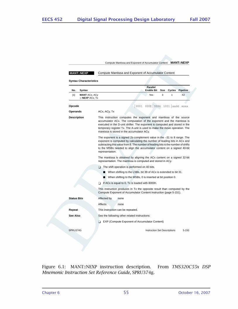
DRA
FT
EECS 452 Digital Signal Processing Design Laboratory Fall 2007
Compute Mantissa and Exponent of Accumulator Content MANT::NEXP
5-193Instruction Set DescriptionsSPRU374G
Compute Mantissa and Exponent of Accumulator ContentMANT::NEXP
Syntax Characteristics
No. SyntaxParallel
Enable Bit Size Cycles Pipeline
[1] MANT ACx, ACy:: NEXP ACx, Tx
Yes 3 1 X2
Opcode 0001 000E DDSS 1001 xxdd xxxx
Operands ACx, ACy, Tx
Description This instruction computes the exponent and mantissa of the sourceaccumulator ACx. The computation of the exponent and the mantissa isexecuted in the D-unit shifter. The exponent is computed and stored in thetemporary register Tx. The A-unit is used to make the move operation. Themantissa is stored in the accumulator ACy.
The exponent is a signed 2s-complement value in the –31 to 8 range. Theexponent is computed by calculating the number of leading bits in ACx andsubtracting this value from 8. The number of leading bits is the number of shiftsto the MSBs needed to align the accumulator content on a signed 40-bitrepresentation.
The mantissa is obtained by aligning the ACx content on a signed 32-bitrepresentation. The mantissa is computed and stored in ACy.
The shift operation is performed on 40 bits.
When shifting to the LSBs, bit 39 of ACx is extended to bit 31.
When shifting to the MSBs, 0 is inserted at bit position 0.
If ACx is equal to 0, Tx is loaded with 8000h.
This instruction produces in Tx the opposite result than computed by theCompute Exponent of Accumulator Content instruction (page 5-151).
Status Bits Affected by none
Affects none
Repeat This instruction can be repeated.
See Also See the following other related instructions:
EXP (Compute Exponent of Accumulator Content)
Figure 6.1: MANT::NEXP instruction description. From TMS320C55x DSP
Mnemonic Instruction Set Reference Guide, SPRU374g.
Chapter 6 55 October 16, 2007
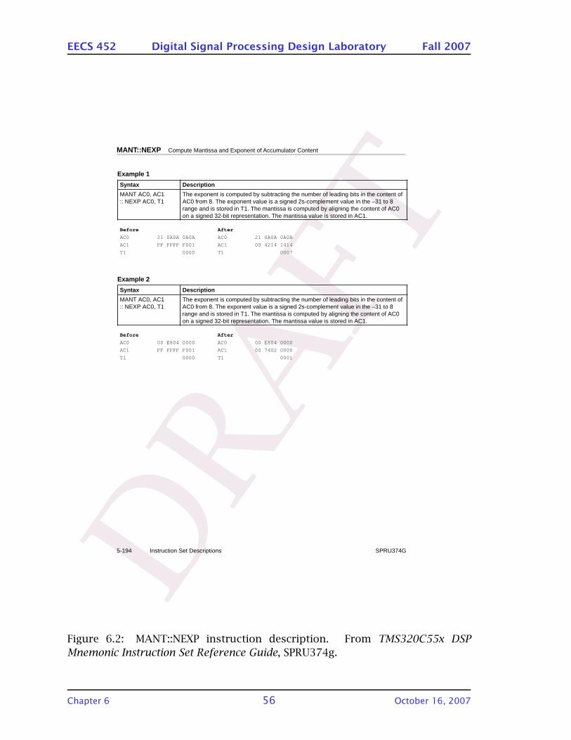
DRA
FT
EECS 452 Digital Signal Processing Design Laboratory Fall 2007
MANT::NEXP Compute Mantissa and Exponent of Accumulator Content
Instruction Set Descriptions5-194 SPRU374G
Example 1
Syntax Description
MANT AC0, AC1:: NEXP AC0, T1
The exponent is computed by subtracting the number of leading bits in the content ofAC0 from 8. The exponent value is a signed 2s-complement value in the –31 to 8range and is stored in T1. The mantissa is computed by aligning the content of AC0on a signed 32-bit representation. The mantissa value is stored in AC1.
Before After
AC0 21 0A0A 0A0A AC0 21 0A0A 0A0A
AC1 FF FFFF F001 AC1 00 4214 1414
T1 0000 T1 0007
Example 2
Syntax Description
MANT AC0, AC1:: NEXP AC0, T1
The exponent is computed by subtracting the number of leading bits in the content ofAC0 from 8. The exponent value is a signed 2s-complement value in the –31 to 8range and is stored in T1. The mantissa is computed by aligning the content of AC0on a signed 32-bit representation. The mantissa value is stored in AC1.
Before After
AC0 00 E804 0000 AC0 00 E804 0000
AC1 FF FFFF F001 AC1 00 7402 0000
T1 0000 T1 0001
Figure 6.2: MANT::NEXP instruction description. From TMS320C55x DSP
Mnemonic Instruction Set Reference Guide, SPRU374g.
Chapter 6 56 October 16, 2007
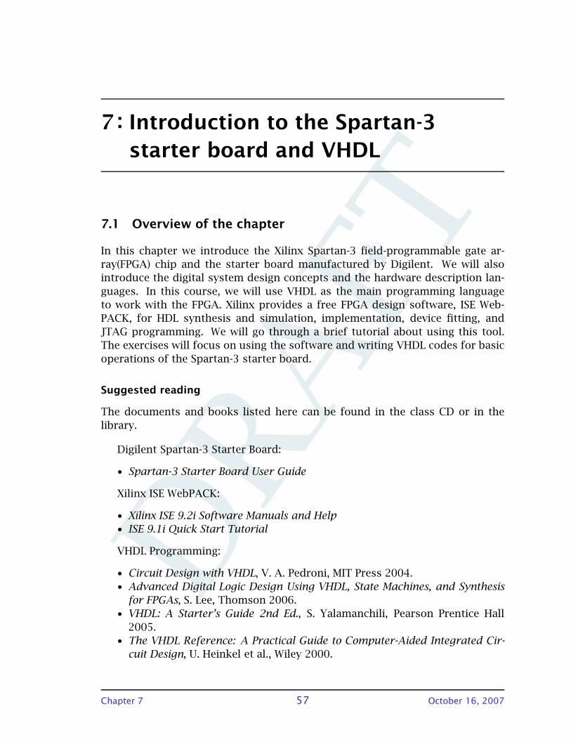
DRA
FT
7 : Introduction to the Spartan-3
starter board and VHDL
7.1 Overview of the chapter
In this chapter we introduce the Xilinx Spartan-3 field-programmable gate ar-
ray(FPGA) chip and the starter board manufactured by Digilent. We will also
introduce the digital system design concepts and the hardware description lan-
guages. In this course, we will use VHDL as the main programming language
to work with the FPGA. Xilinx provides a free FPGA design software, ISE Web-
PACK, for HDL synthesis and simulation, implementation, device fitting, and
JTAG programming. We will go through a brief tutorial about using this tool.
The exercises will focus on using the software and writing VHDL codes for basic
operations of the Spartan-3 starter board.
Suggested reading
The documents and books listed here can be found in the class CD or in the
library.
Digilent Spartan-3 Starter Board:
• Spartan-3 Starter Board User Guide
Xilinx ISE WebPACK:
• Xilinx ISE 9.2i Software Manuals and Help
• ISE 9.1i Quick Start Tutorial
VHDL Programming:
• Circuit Design with VHDL, V. A. Pedroni, MIT Press 2004.
• Advanced Digital Logic Design Using VHDL, State Machines, and Synthesis
for FPGAs, S. Lee, Thomson 2006.
• VHDL: A Starter’s Guide 2nd Ed., S. Yalamanchili, Pearson Prentice Hall
2005.
• The VHDL Reference: A Practical Guide to Computer-Aided Integrated Cir-
cuit Design, U. Heinkel et al., Wiley 2000.
Chapter 7 57 October 16, 2007
DRA
FT
EECS 452 Digital Signal Processing Design Laboratory Fall 2007
7.2 The Spartan-3 Starter Board
In this course, we will use the Spartan-3 Starter Board (1000K gates) as shown in
Figure 7.1. It is manufactured by Digilent (www.digilentinc.com). The Spartan-
3 FPGA chip on this board is manufactured by Xilinx (www.xilinx.com). The
manual and datasheet can be found online or in the class CD. You are recom-
mended to read the Spartan-3 Starter Kit Board User Guide for more detail infor-
mation.
Figure 7.1: The Spartan-3 starter board.
7.3 Xilinx ISE WebPACK
ISE™WebPACK™is a free design tool provided by Xilinx for FPGA and CPLD design
offering HDL synthesis and simulation, implementation, device fitting, and JTAG
programming. The current version is 8.2i with service pack 3. It can be down-
loaded from Xilinx website. You need to register an account at the Xilinx website
in order to download the software. The purpose of this part of the tutorial is to
guide you through the steps of creating a project using Xilinx ISE WebPACK. It
serves as a very simple way to get you start using the tool. Please refer to the
class handout for this part. Details are not mentioned. You should read ISE 8.2i
Quick Start Tutorial for complete instructions and information.
7.3.1 Tutorial
The purpose of this tutorial is to guide you through the steps of creating a
project using Xilinx ISE WebPACK. It serves as a very simple way to get you start
using the tool. Details are not mentioned. You should read ISE 8.2i Quick Start
Tutorial for complete instructions and information. The latest version of the
software 8.2i with service pack 3. It is free and you can download a copy from
the Xilinx website. You need to register an account at the Xilinx website in order
Chapter 7 58 October 16, 2007

DRA
FT
EECS 452 Digital Signal Processing Design Laboratory Fall 2007
to download the software.
Start Xilinx ISE 8.2i by clicking the icon on the desktop. The following window
will show up.
From the File menu, select New Project. The New Project Wizard window will
show up. Choose a Project Name and click Next.
Then we need to specify the Device Properties. Follow the settings as shown
below.
Next, we need to create a new source for the project. In the Create New Source
window, click on New Source. The following window will show up. Choose the
VHDL Module from the list and fill out the File Name. Check ”Add to project" and
click Next.
Chapter 7 59 October 16, 2007
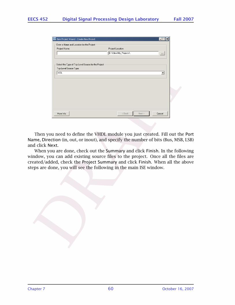
DRA
FT
EECS 452 Digital Signal Processing Design Laboratory Fall 2007
Then you need to define the VHDL module you just created. Fill out the Port
Name, Direction (in, out, or inout), and specify the number of bits (Bus, MSB, LSB)
and click Next.
When you are done, check out the Summary and click Finish. In the following
window, you can add existing source files to the project. Once all the files are
created/added, check the Project Summary and click Finish. When all the above
steps are done, you will see the following in the main ISE window.
Chapter 7 60 October 16, 2007

DRA
FT
EECS 452 Digital Signal Processing Design Laboratory Fall 2007
Now we finished creating a new project. Next we can edit the source file using
the ISE build-in editor.
Chapter 7 61 October 16, 2007
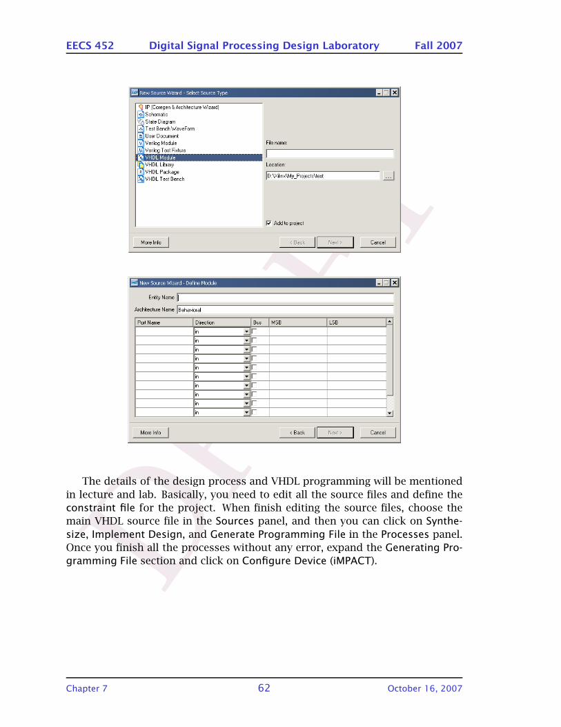
DRA
FT
EECS 452 Digital Signal Processing Design Laboratory Fall 2007
The details of the design process and VHDL programming will be mentioned
in lecture and lab. Basically, you need to edit all the source files and define the
constraint file for the project. When finish editing the source files, choose the
main VHDL source file in the Sources panel, and then you can click on Synthe-
size, Implement Design, and Generate Programming File in the Processes panel.
Once you finish all the processes without any error, expand the Generating Pro-
gramming File section and click on Configure Device (iMPACT).
Chapter 7 62 October 16, 2007
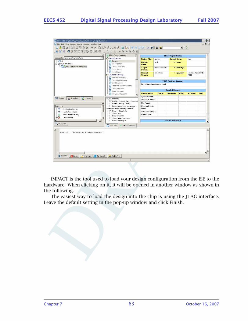
DRA
FT
EECS 452 Digital Signal Processing Design Laboratory Fall 2007
iMPACT is the tool used to load your design configuration from the ISE to the
hardware. When clicking on it, it will be opened in another window as shown in
the following.
The easiest way to load the design into the chip is using the JTAG interface.
Leave the default setting in the pop-up window and click Finish.
Chapter 7 63 October 16, 2007
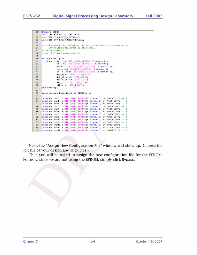
DRA
FT
EECS 452 Digital Signal Processing Design Laboratory Fall 2007
Next, the “Assign New Configuration File" window will show up. Choose the
.bit file of your design and click Open.
Then you will be asked to assign the new configuration file for the EPROM.
For now, since we are not using the EPROM, simply click Bypass.
Chapter 7 64 October 16, 2007
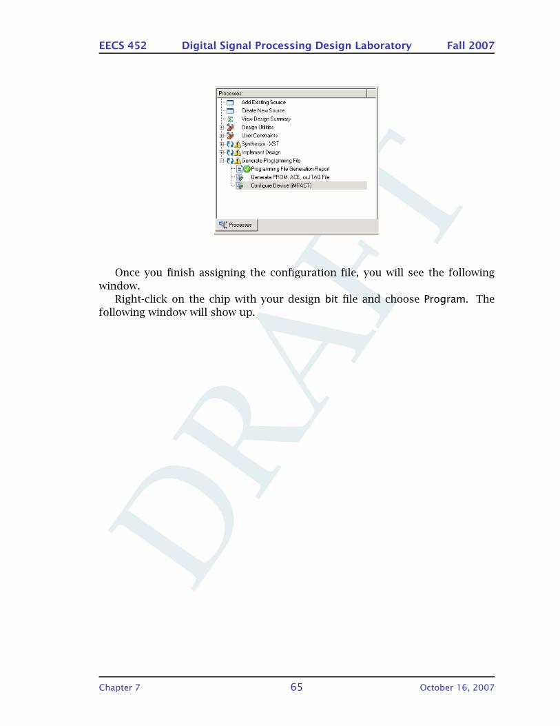
DRA
FT
EECS 452 Digital Signal Processing Design Laboratory Fall 2007
Once you finish assigning the configuration file, you will see the following
window.
Right-click on the chip with your design bit file and choose Program. The
following window will show up.
Chapter 7 65 October 16, 2007
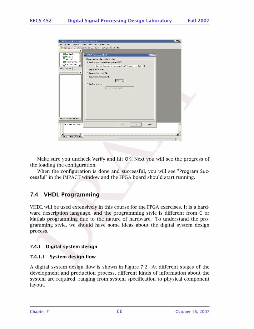
DRA
FT
EECS 452 Digital Signal Processing Design Laboratory Fall 2007
Make sure you uncheck Verify and hit OK. Next you will see the progress of
the loading the configuration.
When the configuration is done and successful, you will see ”Program Suc-
cessful" in the iMPACT window and the FPGA board should start running.
7.4 VHDL Programming
VHDL will be used extensively in this course for the FPGA exercises. It is a hard-
ware description language, and the programming style is different from C or
Matlab programming due to the nature of hardware. To understand the pro-
gramming style, we should have some ideas about the digital system design
process.
7.4.1 Digital system design
7.4.1.1 System design flow
A digital system design flow is shown in Figure 7.2. At different stages of the
development and production process, different kinds of information about the
system are required, ranging from system specification to physical component
layout.
Chapter 7 66 October 16, 2007
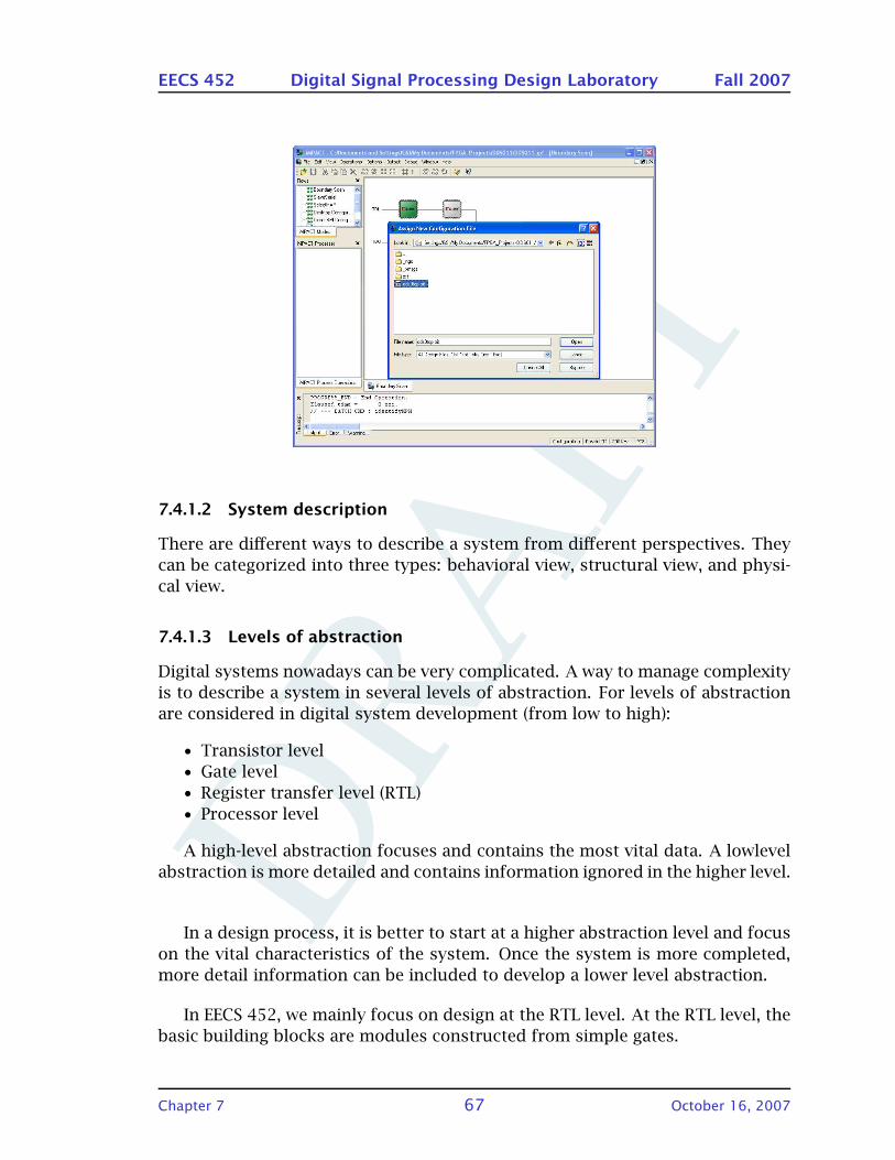
DRA
FT
EECS 452 Digital Signal Processing Design Laboratory Fall 2007
7.4.1.2 System description
There are different ways to describe a system from different perspectives. They
can be categorized into three types: behavioral view, structural view, and physi-
cal view.
7.4.1.3 Levels of abstraction
Digital systems nowadays can be very complicated. A way to manage complexity
is to describe a system in several levels of abstraction. For levels of abstraction
are considered in digital system development (from low to high):
• Transistor level
• Gate level
• Register transfer level (RTL)
• Processor level
A high-level abstraction focuses and contains the most vital data. A lowlevel
abstraction is more detailed and contains information ignored in the higher level.
In a design process, it is better to start at a higher abstraction level and focus
on the vital characteristics of the system. Once the system is more completed,
more detail information can be included to develop a lower level abstraction.
In EECS 452, we mainly focus on design at the RTL level. At the RTL level, the
basic building blocks are modules constructed from simple gates.
Chapter 7 67 October 16, 2007
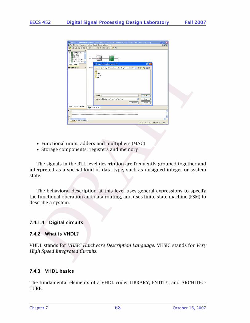
DRA
FT
EECS 452 Digital Signal Processing Design Laboratory Fall 2007
• Functional units: adders and multipliers (MAC)
• Storage components: registers and memory
The signals in the RTL level description are frequently grouped together and
interpreted as a special kind of data type, such as unsigned integer or system
state.
The behavioral description at this level uses general expressions to specify
the functional operation and data routing, and uses finite state machine (FSM) to
describe a system.
7.4.1.4 Digital circuits
7.4.2 What is VHDL?
VHDL stands for VHSIC Hardware Description Language. VHSIC stands for Very
High Speed Integrated Circuits.
7.4.3 VHDL basics
The fundamental elements of a VHDL code: LIBRARY, ENTITY, and ARCHITEC-
TURE.
Chapter 7 68 October 16, 2007
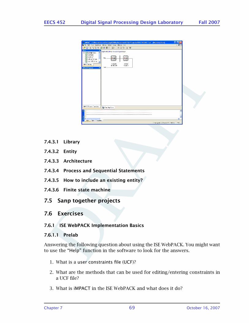
DRA
FT
EECS 452 Digital Signal Processing Design Laboratory Fall 2007
7.4.3.1 Library
7.4.3.2 Entity
7.4.3.3 Architecture
7.4.3.4 Process and Sequential Statements
7.4.3.5 How to include an existing entity?
7.4.3.6 Finite state machine
7.5 Sanp together projects
7.6 Exercises
7.6.1 ISE WebPACK Implementation Basics
7.6.1.1 Prelab
Answering the following question about using the ISE WebPACK. You might want
to use the “Help” function in the software to look for the answers.
1. What is a user constraints file (UCF)?
2. What are the methods that can be used for editing/entering constraints in
a UCF file?
3. What is iMPACT in the ISE WebPACK and what does it do?
Chapter 7 69 October 16, 2007
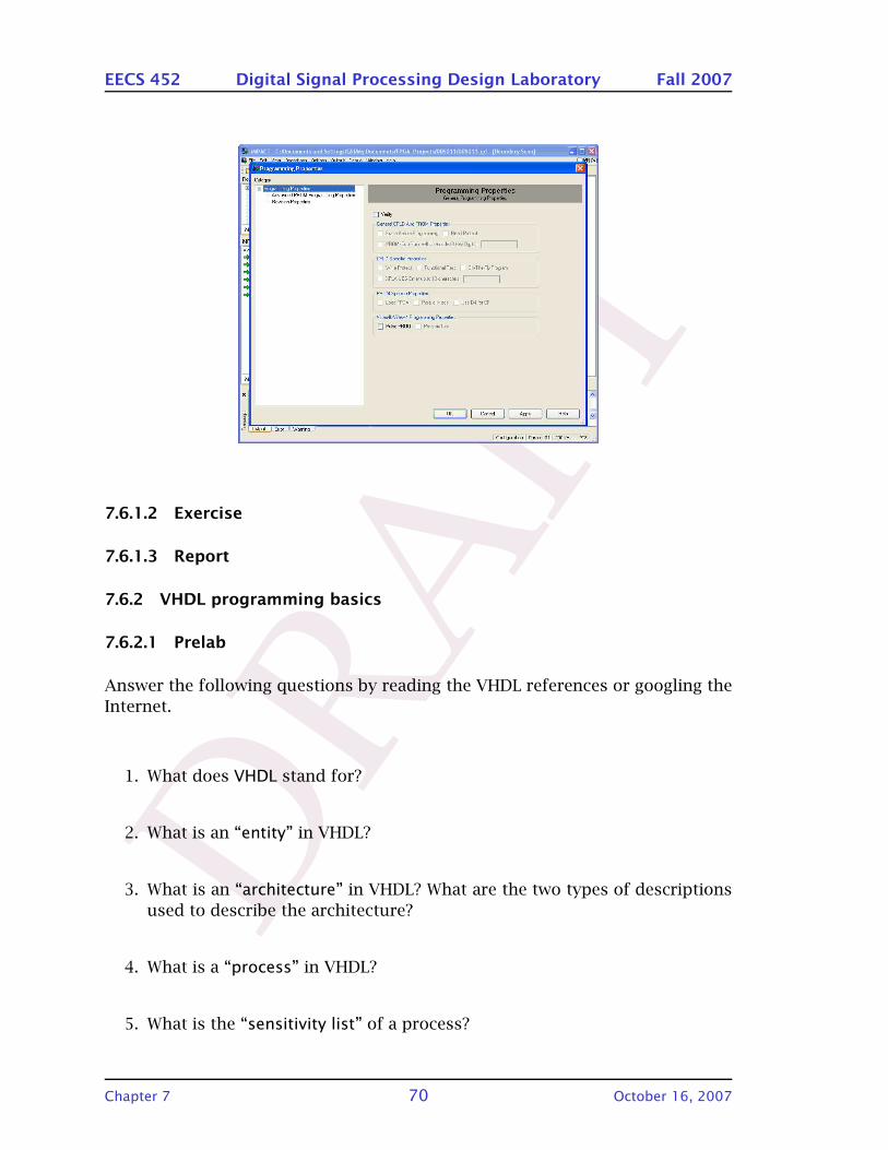
DRA
FT
EECS 452 Digital Signal Processing Design Laboratory Fall 2007
7.6.1.2 Exercise
7.6.1.3 Report
7.6.2 VHDL programming basics
7.6.2.1 Prelab
Answer the following questions by reading the VHDL references or googling the
Internet.
1. What does VHDL stand for?
2. What is an “entity” in VHDL?
3. What is an “architecture” in VHDL? What are the two types of descriptions
used to describe the architecture?
4. What is a “process” in VHDL?
5. What is the “sensitivity list” of a process?
Chapter 7 70 October 16, 2007

DRA
FT
EECS 452 Digital Signal Processing Design Laboratory Fall 2007
7.6.2.2 Exercise
7.6.2.3 Report
7.6.3 Spartan-3 Starter Board Basics
7.6.4 Prelab
Read the Spartan-3 Starter Kit Board User Guide and then answer the following
questions.
1. Is there a clock source on the Spartan-3 FPGA board? If so, what is the
clock rate?
2. What is the total size of on-chip block RAM of the Spartan-3 FPGA?
3. What is the total size of on-board SRAM of the starter board?
4. How many 40-pin expansion connectors are on the starter board?
5. What voltage can be outputted from the 40-pin connectors?
6. What are the pins connected to the 7-segment LEDs, LEDs, slide switches,
and push buttons, and B1 expansion connectors on the board?
7. There is only one set of pins for the 4 7-segment LED displays. How can we
control 4 of them use only one set of pins?
7.6.5 Exercise
None for this part.
Chapter 7 71 October 16, 2007

DRA
FT
EECS 452 Digital Signal Processing Design Laboratory Fall 2007
7.6.6 Report
None for this part.
7.6.7 LEDs and slide switches
7.6.7.1 Prelab
7.6.7.2 Exercise
In this part of the exercise, you will build a simple project to control the on/off
of the LEDs using the slide switches.
1. Start a new project in ISE.
2. Create a new VHDL module source file and add it to the project.
3. Specify an input bus of 8 bits (MSB: 7, LSB: 0) for the slide switches and a
output bus of 8 bits for the LEDs. After these steps, you should see the
code in the project navigator window as shown in Figure 8.1.
4. Declare two signals called “input” and “output” as 8-bit standard logic vec-
tors.
5. Write the code to assign the slide switch value to the signal “input”, assign
the signal “input” to the signal “output”, and assign the signal “output” to
the LED output. See Appendix ?? for the VHDL code.
Chapter 7 72 October 16, 2007
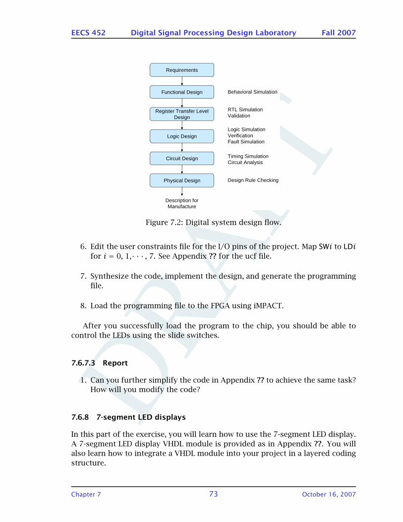
DRA
FT
EECS 452 Digital Signal Processing Design Laboratory Fall 2007
Requirements
Functional Design
Register Transfer Level Design
Logic Design
Circuit Design
Physical Design
Description for Manufacture
Behavioral Simulation
RTL SimulationValidation
Logic SimulationVerificationFault Simulation
Timing SimulationCircuit Analysis
Design Rule Checking
Figure 7.2: Digital system design flow.
6. Edit the user constraints file for the I/O pins of the project. Map SWi to LDi
for i = 0, 1,· · · , 7. See Appendix ?? for the ucf file.
7. Synthesize the code, implement the design, and generate the programming
file.
8. Load the programming file to the FPGA using iMPACT.
After you successfully load the program to the chip, you should be able to
control the LEDs using the slide switches.
7.6.7.3 Report
1. Can you further simplify the code in Appendix ?? to achieve the same task?
How will you modify the code?
7.6.8 7-segment LED displays
In this part of the exercise, you will learn how to use the 7-segment LED display.
A 7-segment LED display VHDL module is provided as in Appendix ??. You will
also learn how to integrate a VHDL module into your project in a layered coding
structure.
Chapter 7 73 October 16, 2007

DRA
FT
EECS 452 Digital Signal Processing Design Laboratory Fall 2007
7.6.8.1 Prelab
7.6.8.2 Exercise
7.6.8.3 Seven-Segment Display Module (SSD01.vhd)
This module is designed for using the four seven-segment displays. The signal
sel is a four-bit vector used to activate the 4 displays. sel(i) controls ssdi for
i = 0,1,2,3. “1” turns the display on the “0” turns it off. When sel=“0000”, the 4
seven-segment displays look like the following
ssd3 ssd2 ssd1 ssd0
To use ssd2, ssd1, and ssd0 to display 4, 5, 2, respectively, we set sel=“0111”,
ssd3=“xxxx”(any number), ssd2=“0100”, ssd1=“0101”, and ssd0=“0010”. The
seven-segment display will look like the following
ssd3 ssd2 ssd1 ssd0
Here is the list all the hex numbers that can be displayed using this module.
If you want to display something more, you need to modify it according to your
needs. See Appendix ?? for the VHDL code.
7.6.8.4 Use the Seven-Segment Display Module
1. Create a new project in ISE.
2. Create a new source file called “SSD_top” with the following I/O signals:
• mclk : input
• ssg : output bus (6 downto 0)
• an : inout bus (3 downto 0)
3. Declare the following signals:
Chapter 7 74 October 16, 2007
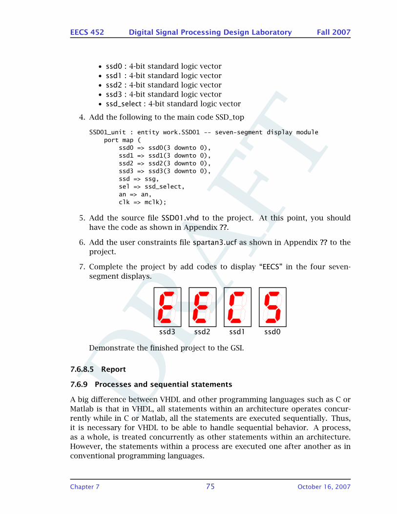
DRA
FT
EECS 452 Digital Signal Processing Design Laboratory Fall 2007
• ssd0 : 4-bit standard logic vector
• ssd1 : 4-bit standard logic vector
• ssd2 : 4-bit standard logic vector
• ssd3 : 4-bit standard logic vector
• ssd_select : 4-bit standard logic vector
4. Add the following to the main code SSD_top
SSD01_unit : entity work.SSD01 -- seven-segment display moduleport map (
ssd0 => ssd0(3 downto 0),ssd1 => ssd1(3 downto 0),ssd2 => ssd2(3 downto 0),ssd3 => ssd3(3 downto 0),ssd => ssg,sel => ssd_select,an => an,clk => mclk);
5. Add the source file SSD01.vhd to the project. At this point, you should
have the code as shown in Appendix ??.
6. Add the user constraints file spartan3.ucf as shown in Appendix ?? to the
project.
7. Complete the project by add codes to display “EECS” in the four seven-
segment displays.
ssd3 ssd2 ssd1 ssd0
Demonstrate the finished project to the GSI.
7.6.8.5 Report
7.6.9 Processes and sequential statements
A big difference between VHDL and other programming languages such as C or
Matlab is that in VHDL, all statements within an architecture operates concur-
rently while in C or Matlab, all the statements are executed sequentially. Thus,
it is necessary for VHDL to be able to handle sequential behavior. A process,
as a whole, is treated concurrently as other statements within an architecture.
However, the statements within a process are executed one after another as in
conventional programming languages.
Chapter 7 75 October 16, 2007
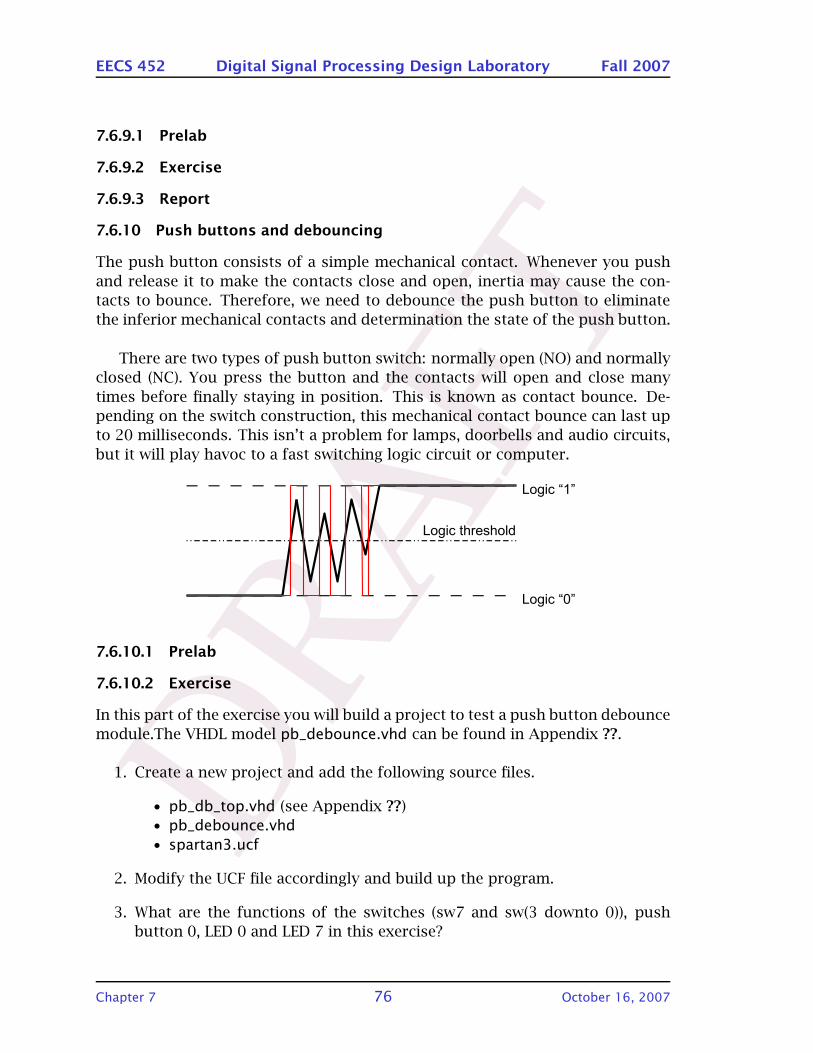
DRA
FT
EECS 452 Digital Signal Processing Design Laboratory Fall 2007
7.6.9.1 Prelab
7.6.9.2 Exercise
7.6.9.3 Report
7.6.10 Push buttons and debouncing
The push button consists of a simple mechanical contact. Whenever you push
and release it to make the contacts close and open, inertia may cause the con-
tacts to bounce. Therefore, we need to debounce the push button to eliminate
the inferior mechanical contacts and determination the state of the push button.
There are two types of push button switch: normally open (NO) and normally
closed (NC). You press the button and the contacts will open and close many
times before finally staying in position. This is known as contact bounce. De-
pending on the switch construction, this mechanical contact bounce can last up
to 20 milliseconds. This isn’t a problem for lamps, doorbells and audio circuits,
but it will play havoc to a fast switching logic circuit or computer.
7.6.10.1 Prelab
7.6.10.2 Exercise
In this part of the exercise you will build a project to test a push button debounce
module.The VHDL model pb_debounce.vhd can be found in Appendix ??.
1. Create a new project and add the following source files.
• pb_db_top.vhd (see Appendix ??)
• pb_debounce.vhd
• spartan3.ucf
2. Modify the UCF file accordingly and build up the program.
3. What are the functions of the switches (sw7 and sw(3 downto 0)), push
button 0, LED 0 and LED 7 in this exercise?
Chapter 7 76 October 16, 2007
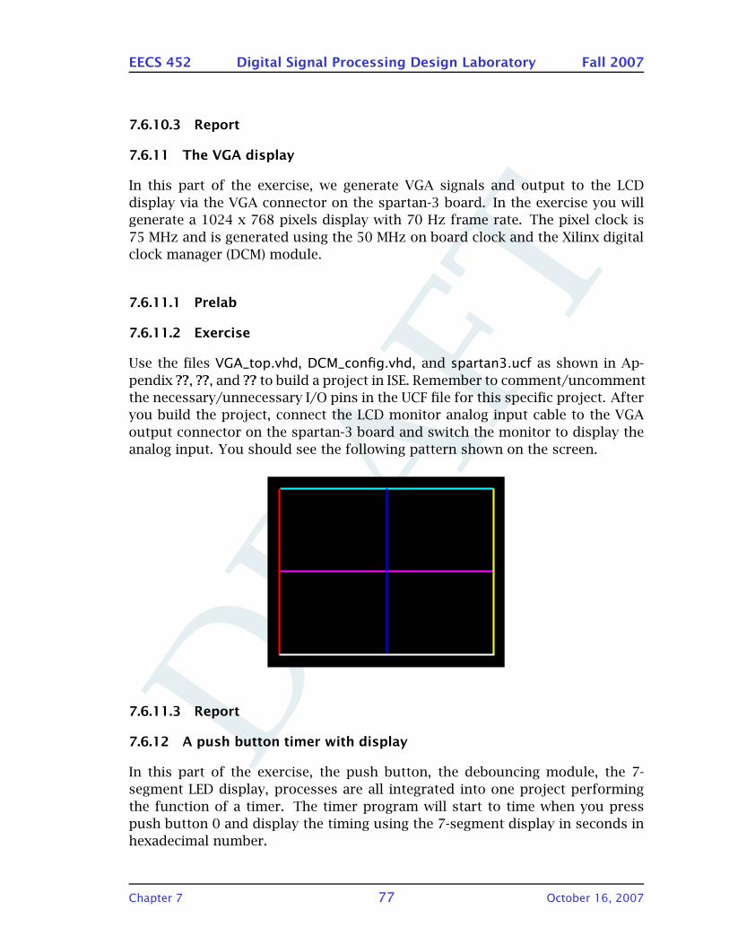
DRA
FT
EECS 452 Digital Signal Processing Design Laboratory Fall 2007
7.6.10.3 Report
7.6.11 The VGA display
In this part of the exercise, we generate VGA signals and output to the LCD
display via the VGA connector on the spartan-3 board. In the exercise you will
generate a 1024 x 768 pixels display with 70 Hz frame rate. The pixel clock is
75 MHz and is generated using the 50 MHz on board clock and the Xilinx digital
clock manager (DCM) module.
7.6.11.1 Prelab
7.6.11.2 Exercise
Use the files VGA_top.vhd, DCM_config.vhd, and spartan3.ucf as shown in Ap-
pendix ??, ??, and ?? to build a project in ISE. Remember to comment/uncomment
the necessary/unnecessary I/O pins in the UCF file for this specific project. After
you build the project, connect the LCD monitor analog input cable to the VGA
output connector on the spartan-3 board and switch the monitor to display the
analog input. You should see the following pattern shown on the screen.
7.6.11.3 Report
7.6.12 A push button timer with display
In this part of the exercise, the push button, the debouncing module, the 7-
segment LED display, processes are all integrated into one project performing
the function of a timer. The timer program will start to time when you press
push button 0 and display the timing using the 7-segment display in seconds in
hexadecimal number.
Chapter 7 77 October 16, 2007
DRA
FT
EECS 452 Digital Signal Processing Design Laboratory Fall 2007
7.6.12.1 Prelab
7.6.12.2 Exercise
1. Create a new project and add the following source files to the project.
• timer01.vhd (see Appendix ??)
• SSD01.vhd
• pb_debounce.vhd
• spartan3.ucf
2. You need to generate a 1 Hz clock using the on board 50 MHz clock. Theeasiest way is to use a counter. This part of the code is as the following
...when st_pb0_pushed =>
if pb_db(0) = ’1’ thennext_pb_clear <= "0001";next_state <= st_idle;
elsenext_clk_counter <= clk_counter + ????; -- counter used to generate 1Hz clockif clk_counter = ???? then
next_clk_counter <= X"0000000";next_counter <= counter + ????;
end if;next_display <= next_counter;next_state <= st_pb0_pushed;
end if;...
What should the missing parts marked with ???? be to make this work?
3. Find out what are the functions of push button 0 and push button 3 in the
project?
4. Fill the blanks (marked with ????) to connected to debouncing and 7-segment display modules to the top file.
push_buttons : entity work.pb_debounce -- push button debouncerport map (
pb_in => ????, -- input actual push buttonspb_out => ????, -- debounced push buttonpb_clear => ????, -- clears the button statereset => ????,clk => ????);
SSD01_unit : entity work.SSD01 -- seven-segment displayport map (
ssd0 => ????,ssd1 => ????,
Chapter 7 78 October 16, 2007
DRA
FT
EECS 452 Digital Signal Processing Design Laboratory Fall 2007
ssd2 => ????,ssd3 => ????,ssd => ????,sel => ????,an => ????,clk => ????);
5. Modify the UCF file accordingly.
6. Complete the exercise and demonstrate the result to the GSI.
7.6.12.3 Report
7.7 Code
To be added
Chapter 7 79 October 16, 2007
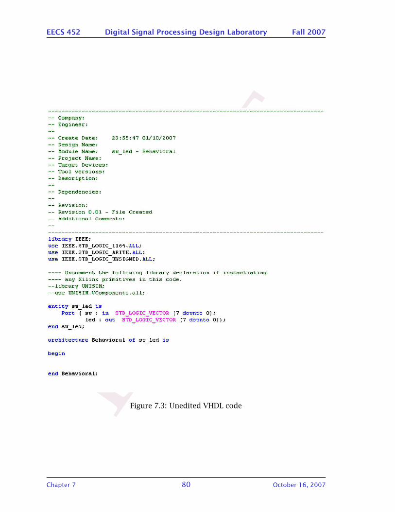
DRA
FT
EECS 452 Digital Signal Processing Design Laboratory Fall 2007
Figure 7.3: Unedited VHDL code
Chapter 7 80 October 16, 2007
DRA
FT
8 : Lab exercise 3 – basic operations
on Spartan-3 starter board
8.1 Introduction . . . . . . . . . . . . . . . . . . . . . . . . . . . . . . . . . . 82
8.2 Prelab . . . . . . . . . . . . . . . . . . . . . . . . . . . . . . . . . . . . . . 82
8.2.1 ISE WebPACK Implementation Basics . . . . . . . . . . . . . . . 83
8.2.2 VHDL programming basics . . . . . . . . . . . . . . . . . . . . . 83
8.2.3 Spartan-3 Starter Board Basics . . . . . . . . . . . . . . . . . . . 83
8.3 Exercise . . . . . . . . . . . . . . . . . . . . . . . . . . . . . . . . . . . . . 84
8.3.1 LEDs and slide switches . . . . . . . . . . . . . . . . . . . . . . . 84
8.3.2 7-segment LED displays . . . . . . . . . . . . . . . . . . . . . . . 84
8.3.2.1 Seven-Segment Display Module (SSD01.vhd) . . . . . 86
8.3.2.2 Use the Seven-Segment Display Module . . . . . . . . 86
8.3.3 Processes and sequential statements . . . . . . . . . . . . . . . 87
8.3.4 Push buttons and debouncing . . . . . . . . . . . . . . . . . . . 87
8.3.5 The VGA display . . . . . . . . . . . . . . . . . . . . . . . . . . . . 88
8.3.6 A push button timer with display . . . . . . . . . . . . . . . . . 89
8.4 Report . . . . . . . . . . . . . . . . . . . . . . . . . . . . . . . . . . . . . . 90
8.5 Listings . . . . . . . . . . . . . . . . . . . . . . . . . . . . . . . . . . . . . 91
8.5.1 sw_led.vhd . . . . . . . . . . . . . . . . . . . . . . . . . . . . . . . 91
8.5.2 sw_led.ucf . . . . . . . . . . . . . . . . . . . . . . . . . . . . . . . . 91
8.5.3 SSD01.vhd . . . . . . . . . . . . . . . . . . . . . . . . . . . . . . . 92
8.5.4 SSD_top.vhd . . . . . . . . . . . . . . . . . . . . . . . . . . . . . . 95
8.5.5 spartan3.ucf . . . . . . . . . . . . . . . . . . . . . . . . . . . . . . 96
8.5.6 pb_debounce.vhd . . . . . . . . . . . . . . . . . . . . . . . . . . . 97
8.5.7 pb_db_top.vhd . . . . . . . . . . . . . . . . . . . . . . . . . . . . . 99
8.5.8 VGA_top.vhd . . . . . . . . . . . . . . . . . . . . . . . . . . . . . . 100
8.5.9 DCM_config.vhd . . . . . . . . . . . . . . . . . . . . . . . . . . . . 103
8.5.10 timer01.vhd . . . . . . . . . . . . . . . . . . . . . . . . . . . . . . 105
Chapter 8 81 October 16, 2007
DRA
FT
EECS 452 Digital Signal Processing Design Laboratory Fall 2007
8.1 Introduction
In this lab exercise, we start to work with the Spartan-3 FPGA starter board. This
includes the use of the software tool Xilinx ISE WebPACK and the basic opera-
tions on the Spartan-3 starter board. The programing language we use in this
course for FPGA is VHDL. Unlike the C5510 DSP, the Spartan-3 FPGA does not
have pre-built structure/unit in it and is fully programmable. The starter board
has a lot of peripherals and user interface components. One of the objective of
this exercise is to get you familiar with the starter board components and their
functionalities. Basic VHDL programing is also one of the skills we would like to
equip you with in this lab exercise.
Suggested reading
The documents and books listed here can be found in the class CD or in the
library.
Digilent Spartan-3 Starter Board:
• Spartan-3 Starter Board User Guide
Xilinx ISE WebPACK:
• Xilinx ISE 9.2i Software Manuals and Help
• ISE 9.1i Quick Start Tutorial
VHDL Programming:
• Circuit Design with VHDL, V. A. Pedroni, MIT Press 2004.
• Advanced Digital Logic Design Using VHDL, State Machines, and Synthesis
for FPGAs, S. Lee, Thomson 2006.
• VHDL: A Starter’s Guide 2nd Ed., S. Yalamanchili, Pearson Prentice Hall
2005.
• The VHDL Reference: A Practical Guide to Computer-Aided Integrated Cir-
cuit Design, U. Heinkel et al., Wiley 2000.
8.2 Prelab
Prelabs are to be done individually and are to be handed in at the
start of the lab period. Handwritten work will not be graded.
Chapter 8 82 October 16, 2007
DRA
FT
EECS 452 Digital Signal Processing Design Laboratory Fall 2007
8.2.1 ISE WebPACK Implementation Basics
Answering the following question about using the ISE WebPACK. You might want
to use the “Help” function in the software to look for the answers.
1. What is a user constraints file (UCF)?
2. What are the methods that can be used for editing/entering constraints in
a UCF file?
3. What is iMPACT in the ISE WebPACK and what does it do?
8.2.2 VHDL programming basics
Answer the following questions by reading the VHDL references or googling the
Internet.
1. What does VHDL stand for?
2. What is an “entity” in VHDL?
3. What is an “architecture” in VHDL? What are the two types of descriptions
used to describe the architecture?
4. What is a “process” in VHDL?
5. What is the “sensitivity list” of a process?
8.2.3 Spartan-3 Starter Board Basics
Read the Spartan-3 Starter Kit Board User Guide and then answer the following
questions.
1. Is there a clock source on the Spartan-3 FPGA board? If so, what is the
clock rate?
2. What is the total size of on-chip block RAM of the Spartan-3 FPGA?
3. What is the total size of on-board SRAM of the starter board?
4. How many 40-pin expansion connectors are on the starter board?
5. What voltage can be outputted from the 40-pin connectors?
6. What are the pins connected to the 7-segment LEDs, LEDs, slide switches,
and push buttons, and B1 expansion connectors on the board?
7. There is only one set of pins for the 4 7-segment LED displays. How can we
control 4 of them use only one set of pins?
Chapter 8 83 October 16, 2007
DRA
FT
EECS 452 Digital Signal Processing Design Laboratory Fall 2007
8.3 Exercise
8.3.1 LEDs and slide switches
In this part of the exercise, you will use ISE WebPACK to build a simple project to
control the on/off of the LEDs using the slide switches. Do the following steps:
• Start a new project in ISE.
• Create a new VHDL module source file and add it to the project.
• Specify an input bus of 8 bits (MSB: 7, LSB: 0) for the slide switches and a
output bus of 8 bits for the LEDs. After these steps, you should see the
code in the project navigator window as shown in Figure 8.1.
• Declare two signals called “input” and “output” as 8-bit standard logic vec-
tors.
• Write the code to assign the slide switch value to the signal “input”, assign
the signal “input” to the signal “output”, and assign the signal “output” to
the LED output. See section 8.5.1 for the VHDL code.
• Edit the user constraints file for the I/O pins of the project. Map SWi to LDi
for i = 0, 1,· · · , 7. See section 8.5.2 for the ucf file.
• Synthesize the code, implement the design, and generate the programming
file.
• Load the programming file to the FPGA using iMPACT.
After you successfully load the program to the chip, you should be able to
control the LEDs using the slide switches.
Can you further simplify the code listed in section 8.5.1 to achieve the same
task? How will you modify the code?
8.3.2 7-segment LED displays
In this part of the exercise, you will learn how to use the 7-segment LED display.
A 7-segment LED display VHDL module is provided as in section 8.5.3. You will
also learn how to integrate a VHDL module into your project in a layered coding
structure.
Chapter 8 84 October 16, 2007

DRA
FT
EECS 452 Digital Signal Processing Design Laboratory Fall 2007
Figure 8.1: Unedited VHDL code
Chapter 8 85 October 16, 2007
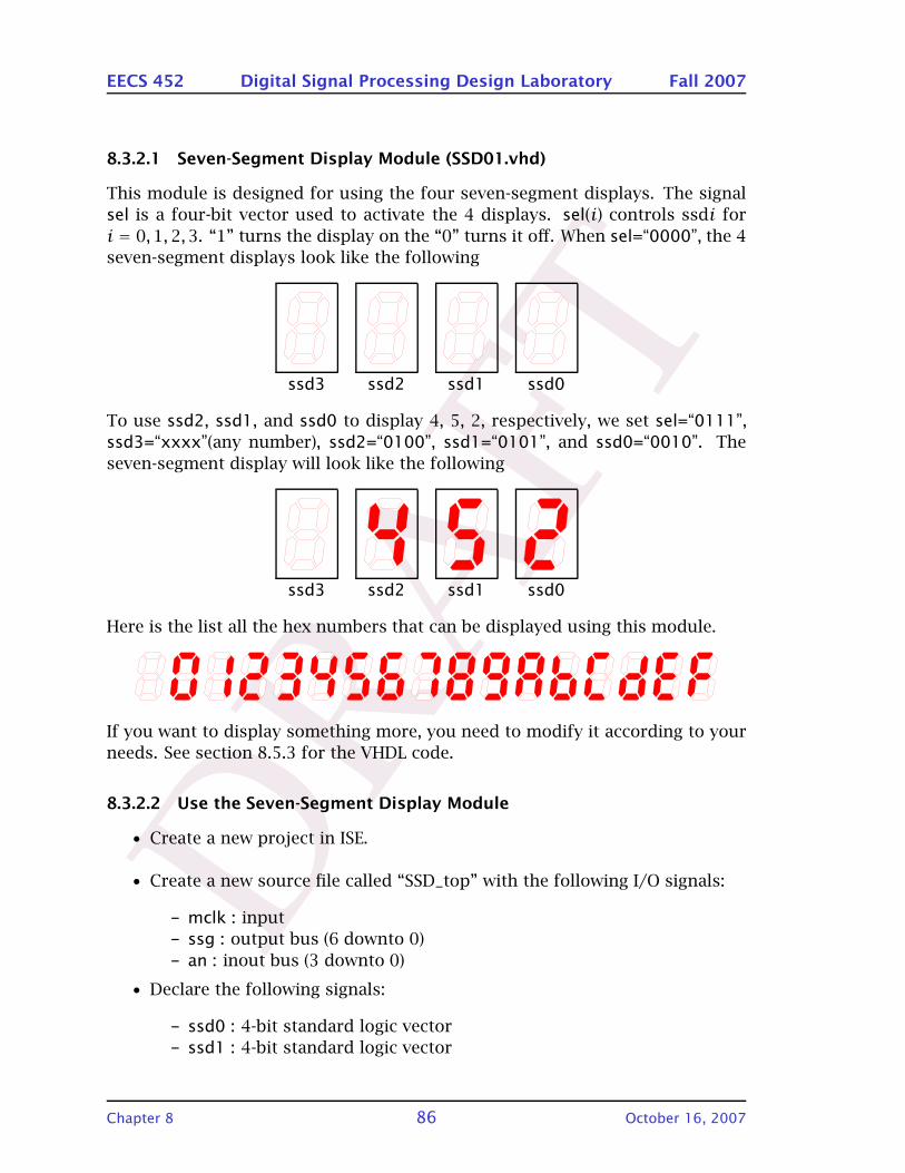
DRA
FT
EECS 452 Digital Signal Processing Design Laboratory Fall 2007
8.3.2.1 Seven-Segment Display Module (SSD01.vhd)
This module is designed for using the four seven-segment displays. The signal
sel is a four-bit vector used to activate the 4 displays. sel(i) controls ssdi for
i = 0,1,2,3. “1” turns the display on the “0” turns it off. When sel=“0000”, the 4
seven-segment displays look like the following
ssd3 ssd2 ssd1 ssd0
To use ssd2, ssd1, and ssd0 to display 4, 5, 2, respectively, we set sel=“0111”,
ssd3=“xxxx”(any number), ssd2=“0100”, ssd1=“0101”, and ssd0=“0010”. The
seven-segment display will look like the following
ssd3 ssd2 ssd1 ssd0
Here is the list all the hex numbers that can be displayed using this module.
If you want to display something more, you need to modify it according to your
needs. See section 8.5.3 for the VHDL code.
8.3.2.2 Use the Seven-Segment Display Module
• Create a new project in ISE.
• Create a new source file called “SSD_top” with the following I/O signals:
– mclk : input
– ssg : output bus (6 downto 0)
– an : inout bus (3 downto 0)
• Declare the following signals:
– ssd0 : 4-bit standard logic vector
– ssd1 : 4-bit standard logic vector
Chapter 8 86 October 16, 2007
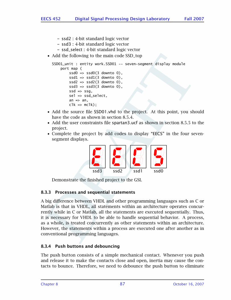
DRA
FT
EECS 452 Digital Signal Processing Design Laboratory Fall 2007
– ssd2 : 4-bit standard logic vector
– ssd3 : 4-bit standard logic vector
– ssd_select : 4-bit standard logic vector
• Add the following to the main code SSD_top
SSD01_unit : entity work.SSD01 -- seven-segment display moduleport map (
ssd0 => ssd0(3 downto 0),ssd1 => ssd1(3 downto 0),ssd2 => ssd2(3 downto 0),ssd3 => ssd3(3 downto 0),ssd => ssg,sel => ssd_select,an => an,clk => mclk);
• Add the source file SSD01.vhd to the project. At this point, you should
have the code as shown in section 8.5.4.
• Add the user constraints file spartan3.ucf as shown in section 8.5.5 to the
project.
• Complete the project by add codes to display “EECS” in the four seven-
segment displays.
ssd3 ssd2 ssd1 ssd0
Demonstrate the finished project to the GSI.
8.3.3 Processes and sequential statements
A big difference between VHDL and other programming languages such as C or
Matlab is that in VHDL, all statements within an architecture operates concur-
rently while in C or Matlab, all the statements are executed sequentially. Thus,
it is necessary for VHDL to be able to handle sequential behavior. A process,
as a whole, is treated concurrently as other statements within an architecture.
However, the statements within a process are executed one after another as in
conventional programming languages.
8.3.4 Push buttons and debouncing
The push button consists of a simple mechanical contact. Whenever you push
and release it to make the contacts close and open, inertia may cause the con-
tacts to bounce. Therefore, we need to debounce the push button to eliminate
Chapter 8 87 October 16, 2007
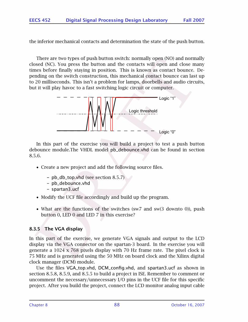
DRA
FT
EECS 452 Digital Signal Processing Design Laboratory Fall 2007
the inferior mechanical contacts and determination the state of the push button.
There are two types of push button switch: normally open (NO) and normally
closed (NC). You press the button and the contacts will open and close many
times before finally staying in position. This is known as contact bounce. De-
pending on the switch construction, this mechanical contact bounce can last up
to 20 milliseconds. This isn’t a problem for lamps, doorbells and audio circuits,
but it will play havoc to a fast switching logic circuit or computer.
In this part of the exercise you will build a project to test a push button
debounce module.The VHDL model pb_debounce.vhd can be found in section
8.5.6.
• Create a new project and add the following source files.
– pb_db_top.vhd (see section 8.5.7)
– pb_debounce.vhd
– spartan3.ucf
• Modify the UCF file accordingly and build up the program.
• What are the functions of the switches (sw7 and sw(3 downto 0)), push
button 0, LED 0 and LED 7 in this exercise?
8.3.5 The VGA display
In this part of the exercise, we generate VGA signals and output to the LCD
display via the VGA connector on the spartan-3 board. In the exercise you will
generate a 1024 x 768 pixels display with 70 Hz frame rate. The pixel clock is
75 MHz and is generated using the 50 MHz on board clock and the Xilinx digital
clock manager (DCM) module.
Use the files VGA_top.vhd, DCM_config.vhd, and spartan3.ucf as shown in
section 8.5.8, 8.5.9, and 8.5.5 to build a project in ISE. Remember to comment or
uncomment the necessary/unnecessary I/O pins in the UCF file for this specific
project. After you build the project, connect the LCD monitor analog input cable
Chapter 8 88 October 16, 2007
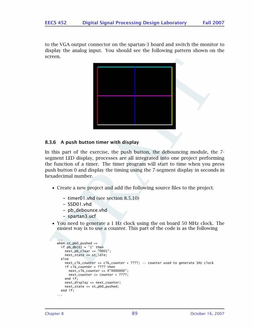
DRA
FT
EECS 452 Digital Signal Processing Design Laboratory Fall 2007
to the VGA output connector on the spartan-3 board and switch the monitor to
display the analog input. You should see the following pattern shown on the
screen.
8.3.6 A push button timer with display
In this part of the exercise, the push button, the debouncing module, the 7-
segment LED display, processes are all integrated into one project performing
the function of a timer. The timer program will start to time when you press
push button 0 and display the timing using the 7-segment display in seconds in
hexadecimal number.
• Create a new project and add the following source files to the project.
– timer01.vhd (see section 8.5.10)
– SSD01.vhd
– pb_debounce.vhd
– spartan3.ucf
• You need to generate a 1 Hz clock using the on board 50 MHz clock. Theeasiest way is to use a counter. This part of the code is as the following
...when st_pb0_pushed =>if pb_db(0) = ’1’ then
next_pb_clear <= "0001";next_state <= st_idle;
elsenext_clk_counter <= clk_counter + ????; -- counter used to generate 1Hz clockif clk_counter = ???? then
next_clk_counter <= X"0000000";next_counter <= counter + ????;
end if;next_display <= next_counter;next_state <= st_pb0_pushed;
end if;...
Chapter 8 89 October 16, 2007
DRA
FT
EECS 452 Digital Signal Processing Design Laboratory Fall 2007
What should the missing parts marked with ???? be to make this work?
• Find out what are the functions of push button 0 and push button 3 in the
project?
• Fill the blanks (marked with ????) to connected to debouncing and 7-segment display modules to the top file.
push_buttons : entity work.pb_debounce -- push button debouncerport map (
pb_in => ????, -- input actual push buttonspb_out => ????, -- debounced push buttonpb_clear => ????, -- clears the button statereset => ????,clk => ????);
SSD01_unit : entity work.SSD01 -- seven-segment displayport map (
ssd0 => ????,ssd1 => ????,ssd2 => ????,ssd3 => ????,ssd => ????,sel => ????,an => ????,clk => ????);
• Modify the UCF file accordingly.
• Complete the exercise and demonstrate the result to the GSI.
8.4 Report
In the report, record the results of each exercise. State what you did in the
exercise and your findings and comments. Answer the questions asked in each
exercise. Also include the section of codes you created or modified from the
given lab codes in order to make the programs work. Do not include the whole
lab codes.
Chapter 8 90 October 16, 2007
DRA
FT
EECS 452 Digital Signal Processing Design Laboratory Fall 2007
8.5 Listings
8.5.1 sw_led.vhd
------------------------------------------------------------------------------------ Company:-- Engineer:---- Create Date: 23:55:47 01/10/2007-- Design Name:-- Module Name: sw_led - Behavioral-- Project Name:-- Target Devices:-- Tool versions:-- Description:---- Dependencies:---- Revision:-- Revision 0.01 - File Created-- Additional Comments:------------------------------------------------------------------------------------library IEEE;use IEEE.STD_LOGIC_1164.ALL;use IEEE.STD_LOGIC_ARITH.ALL;use IEEE.STD_LOGIC_UNSIGNED.ALL;
---- Uncomment the following library declaration if instantiating---- any Xilinx primitives in this code.--library UNISIM;--use UNISIM.VComponents.all;
entity sw_led isPort ( sw : in STD_LOGIC_VECTOR (7 downto 0);
led : out STD_LOGIC_VECTOR (7 downto 0));end sw_led;
architecture Behavioral of sw_led is
signal input : std_logic_vector (7 downto 0);signal output : std_logic_vector (7 downto 0);
begin
input <= sw;output <= input;led <= output;
end Behavioral;
8.5.2 sw_led.ucf
NET "sw<0>" LOC = "F12";NET "sw<1>" LOC = "G12";NET "sw<2>" LOC = "H14";NET "sw<3>" LOC = "H13";NET "sw<4>" LOC = "J14";NET "sw<5>" LOC = "J13";NET "sw<6>" LOC = "K14";NET "sw<7>" LOC = "K13";
Chapter 8 91 October 16, 2007

DRA
FT
EECS 452 Digital Signal Processing Design Laboratory Fall 2007
NET "led<0>" LOC = "K12";NET "led<1>" LOC = "P14";NET "led<2>" LOC = "L12";NET "led<3>" LOC = "N14";NET "led<4>" LOC = "P13";NET "led<5>" LOC = "N12";NET "led<6>" LOC = "P12";NET "led<7>" LOC = "P11";
8.5.3 SSD01.vhd
------------------------------------------------------------------------------------ Company: UM EECS 452-- Engineer: Chih-Wei Wang---- Create Date: 16:35:23 10/07/2006-- Design Name:-- Module Name: 7seg_LED_display - Behavioral-- Project Name:-- Target Devices:-- Tool versions:-- Description:---- Dependencies:---- Revision:-- Revision 0.01 - File Created-- Additional Comments:------------------------------------------------------------------------------------library IEEE;use IEEE.STD_LOGIC_1164.ALL;use IEEE.STD_LOGIC_ARITH.ALL;use IEEE.STD_LOGIC_UNSIGNED.ALL;
---- Uncomment the following library declaration if instantiating---- any Xilinx primitives in this code.--library UNISIM;--use UNISIM.VComponents.all;
entity SSD01 isPort ( ssd0 : in STD_LOGIC_VECTOR (3 downto 0);
ssd1 : in STD_LOGIC_VECTOR (3 downto 0);ssd2 : in STD_LOGIC_VECTOR (3 downto 0);ssd3 : in STD_LOGIC_VECTOR (3 downto 0);ssd : out STD_LOGIC_VECTOR (6 downto 0);sel : in STD_LOGIC_VECTOR (3 downto 0);an : inout STD_LOGIC_VECTOR (3 downto 0);clk : in STD_LOGIC);
end SSD01;
architecture Behavioral of SSD01 is
constant num0 : STD_LOGIC_VECTOR(6 downto 0) := "0000001"; -- 0constant num1 : STD_LOGIC_VECTOR(6 downto 0) := "1001111"; -- 1constant num2 : STD_LOGIC_VECTOR(6 downto 0) := "0010010"; -- 2constant num3 : STD_LOGIC_VECTOR(6 downto 0) := "0000110"; -- 3constant num4 : STD_LOGIC_VECTOR(6 downto 0) := "1001100"; -- 4constant num5 : STD_LOGIC_VECTOR(6 downto 0) := "0100100"; -- 5constant num6 : STD_LOGIC_VECTOR(6 downto 0) := "0100000"; -- 6constant num7 : STD_LOGIC_VECTOR(6 downto 0) := "0001111"; -- 7constant num8 : STD_LOGIC_VECTOR(6 downto 0) := "0000000"; -- 8
Chapter 8 92 October 16, 2007

DRA
FT
EECS 452 Digital Signal Processing Design Laboratory Fall 2007
constant num9 : STD_LOGIC_VECTOR(6 downto 0) := "0001100"; -- 9constant num10 : STD_LOGIC_VECTOR(6 downto 0) := "0001000"; -- Aconstant num11 : STD_LOGIC_VECTOR(6 downto 0) := "1100000"; -- Bconstant num12 : STD_LOGIC_VECTOR(6 downto 0) := "0110001"; -- Cconstant num13 : STD_LOGIC_VECTOR(6 downto 0) := "1000010"; -- Dconstant num14 : STD_LOGIC_VECTOR(6 downto 0) := "0110000"; -- Econstant num15 : STD_LOGIC_VECTOR(6 downto 0) := "0111000"; -- F
signal ssd_0 : std_logic_vector(6 downto 0);signal ssd_1 : std_logic_vector(6 downto 0);signal ssd_2 : std_logic_vector(6 downto 0);signal ssd_3 : std_logic_vector(6 downto 0);signal ctr: std_logic_vector(12 downto 0);
begin
SSD_select : process(sel)beginif sel(0) = ’0’ then
ssd_0 <= "1111111";else
case ssd0 iswhen "0000" => ssd_0 <= num0;when "0001" => ssd_0 <= num1;when "0010" => ssd_0 <= num2;when "0011" => ssd_0 <= num3;when "0100" => ssd_0 <= num4;when "0101" => ssd_0 <= num5;when "0110" => ssd_0 <= num6;when "0111" => ssd_0 <= num7;when "1000" => ssd_0 <= num8;when "1001" => ssd_0 <= num9;when "1010" => ssd_0 <= num10;when "1011" => ssd_0 <= num11;when "1100" => ssd_0 <= num12;when "1101" => ssd_0 <= num13;when "1110" => ssd_0 <= num14;when others => ssd_0 <= num15;
end case;end if;if sel(1) = ’0’ then
ssd_1 <= "1111111";else
case ssd1 iswhen "0000" => ssd_1 <= num0;when "0001" => ssd_1 <= num1;when "0010" => ssd_1 <= num2;when "0011" => ssd_1 <= num3;when "0100" => ssd_1 <= num4;when "0101" => ssd_1 <= num5;when "0110" => ssd_1 <= num6;when "0111" => ssd_1 <= num7;when "1000" => ssd_1 <= num8;when "1001" => ssd_1 <= num9;when "1010" => ssd_1 <= num10;when "1011" => ssd_1 <= num11;when "1100" => ssd_1 <= num12;when "1101" => ssd_1 <= num13;when "1110" => ssd_1 <= num14;when others => ssd_1 <= num15;
end case;end if;if sel(2) = ’0’ then
ssd_2 <= "1111111";
Chapter 8 93 October 16, 2007
DRA
FT
EECS 452 Digital Signal Processing Design Laboratory Fall 2007
elsecase ssd2 iswhen "0000" => ssd_2 <= num0;when "0001" => ssd_2 <= num1;when "0010" => ssd_2 <= num2;when "0011" => ssd_2 <= num3;when "0100" => ssd_2 <= num4;when "0101" => ssd_2 <= num5;when "0110" => ssd_2 <= num6;when "0111" => ssd_2 <= num7;when "1000" => ssd_2 <= num8;when "1001" => ssd_2 <= num9;when "1010" => ssd_2 <= num10;when "1011" => ssd_2 <= num11;when "1100" => ssd_2 <= num12;when "1101" => ssd_2 <= num13;when "1110" => ssd_2 <= num14;when others => ssd_2 <= num15;
end case;end if;if sel(3) = ’0’ then
ssd_3 <= "1111111";else
case ssd3 iswhen "0000" => ssd_3 <= num0;when "0001" => ssd_3 <= num1;when "0010" => ssd_3 <= num2;when "0011" => ssd_3 <= num3;when "0100" => ssd_3 <= num4;when "0101" => ssd_3 <= num5;when "0110" => ssd_3 <= num6;when "0111" => ssd_3 <= num7;when "1000" => ssd_3 <= num8;when "1001" => ssd_3 <= num9;when "1010" => ssd_3 <= num10;when "1011" => ssd_3 <= num11;when "1100" => ssd_3 <= num12;when "1101" => ssd_3 <= num13;when "1110" => ssd_3 <= num14;when others => ssd_3 <= num15;
end case;end if;
end process SSD_select;
-- SSD main unitprocess (clk)beginif clk’event and clk = ’1’ then
if (ctr="0000000000000") thenif (an(3)=’0’) then
an(3) <= ’1’;ssd <= ssd_2; -- ssd2an(2) <= ’0’;
elsif (an(2)=’0’) thenan(2) <= ’1’;ssd <= ssd_1; -- ssd1an(1) <= ’0’;
elsif (an(1)=’0’) thenan(1) <= ’1’;ssd <= ssd_0; -- ssd0an(0) <= ’0’;
elsif (an(0)=’0’) thenan(0) <= ’1’;ssd <= ssd_3; -- ssd3
Chapter 8 94 October 16, 2007

DRA
FT
EECS 452 Digital Signal Processing Design Laboratory Fall 2007
an(3) <= ’0’;end if;
end if;ctr <= ctr+"0000000000001";if (ctr > "1000000000000") thenCTR <= "0000000000000";
end if;end if;
end process;
end Behavioral;
8.5.4 SSD_top.vhd
------------------------------------------------------------------------------------ Company:-- Engineer:---- Create Date: 22:45:27 01/11/2007-- Design Name:-- Module Name: SSD_top - Behavioral-- Project Name:-- Target Devices:-- Tool versions:-- Description:---- Dependencies:---- Revision:-- Revision 0.01 - File Created-- Additional Comments:------------------------------------------------------------------------------------library IEEE;use IEEE.STD_LOGIC_1164.ALL;use IEEE.STD_LOGIC_ARITH.ALL;use IEEE.STD_LOGIC_UNSIGNED.ALL;
---- Uncomment the following library declaration if instantiating---- any Xilinx primitives in this code.--library UNISIM;--use UNISIM.VComponents.all;
entity SSD_top isPort ( mclk : in STD_LOGIC;
ssg : out STD_LOGIC_VECTOR (6 downto 0);an : inout STD_LOGIC_VECTOR (3 downto 0));
end SSD_top;
architecture Behavioral of SSD_top is
signal ssd0 : std_logic_vector(3 downto 0);signal ssd1 : std_logic_vector(3 downto 0);signal ssd2 : std_logic_vector(3 downto 0);signal ssd3 : std_logic_vector(3 downto 0);signal ssd_select : std_logic_vector(3 downto 0);
begin
SSD01_unit : entity work.SSD01 -- seven-segment display moduleport map (ssd0 => ssd0(3 downto 0),
Chapter 8 95 October 16, 2007
DRA
FT
EECS 452 Digital Signal Processing Design Laboratory Fall 2007
ssd1 => ssd1(3 downto 0),ssd2 => ssd2(3 downto 0),ssd3 => ssd3(3 downto 0),ssd => ssg,sel => ssd_select,an => an,clk => mclk);
end Behavioral;
8.5.5 spartan3.ucf
# Spartan-3 User Constraints File: spartan3.ucf## 11Jan2007#
# oscillator clock (in)
NET "mclk" PERIOD = 20 ns HIGH 40 %;NET "mclk" LOC = "T9" | IOSTANDARD = LVCMOS33;
# push buttons
#NET "btn<0>" LOC = "M13" | IOSTANDARD = LVCMOS33;#NET "btn<1>" LOC = "M14" | IOSTANDARD = LVCMOS33;#NET "btn<2>" LOC = "L13" | IOSTANDARD = LVCMOS33;#NET "btn<3>" LOC = "L14" | IOSTANDARD = LVCMOS33;
# light emitting diodes
#NET "led<0>" LOC = "K12" | IOSTANDARD = LVCMOS33;#NET "led<1>" LOC = "P14" | IOSTANDARD = LVCMOS33;#NET "led<2>" LOC = "L12" | IOSTANDARD = LVCMOS33;#NET "led<3>" LOC = "N14" | IOSTANDARD = LVCMOS33;#NET "led<4>" LOC = "P13" | IOSTANDARD = LVCMOS33;#NET "led<5>" LOC = "N12" | IOSTANDARD = LVCMOS33;#NET "led<6>" LOC = "P12" | IOSTANDARD = LVCMOS33;#NET "led<7>" LOC = "P11" | IOSTANDARD = LVCMOS33;
# seven segment digit anodes
NET "an<0>" LOC = "D14" | IOSTANDARD = LVCMOS33;NET "an<1>" LOC = "G14" | IOSTANDARD = LVCMOS33;NET "an<2>" LOC = "F14" | IOSTANDARD = LVCMOS33;NET "an<3>" LOC = "E13" | IOSTANDARD = LVCMOS33;
# seven segment digit cathodes
NET "ssg<0>" LOC = "N16" | IOSTANDARD = LVCMOS33; # segment GNET "ssg<1>" LOC = "F13" | IOSTANDARD = LVCMOS33; # segment FNET "ssg<2>" LOC = "R16" | IOSTANDARD = LVCMOS33; # segment ENET "ssg<3>" LOC = "P15" | IOSTANDARD = LVCMOS33; # segment DNET "ssg<4>" LOC = "N15" | IOSTANDARD = LVCMOS33; # segment CNET "ssg<5>" LOC = "G13" | IOSTANDARD = LVCMOS33; # segment BNET "ssg<6>" LOC = "E14" | IOSTANDARD = LVCMOS33; # segment A#NET "ssg<7>" LOC = "P16" | IOSTANDARD = LVCMOS33; # dp(decimal point)
# slide switches
#NET "swt<0>" LOC = "F12" | IOSTANDARD = LVCMOS33;#NET "swt<1>" LOC = "G12" | IOSTANDARD = LVCMOS33;
Chapter 8 96 October 16, 2007
DRA
FT
EECS 452 Digital Signal Processing Design Laboratory Fall 2007
#NET "swt<2>" LOC = "H14" | IOSTANDARD = LVCMOS33;#NET "swt<3>" LOC = "H13" | IOSTANDARD = LVCMOS33;#NET "swt<4>" LOC = "J14" | IOSTANDARD = LVCMOS33;#NET "swt<5>" LOC = "J13" | IOSTANDARD = LVCMOS33;#NET "swt<6>" LOC = "K14" | IOSTANDARD = LVCMOS33;#NET "swt<7>" LOC = "K13" | IOSTANDARD = LVCMOS33;
# DB15 video connector
#NET "blu" LOC = "R11" | IOSTANDARD = LVCMOS33;#NET "grn" LOC = "T12" | IOSTANDARD = LVCMOS33;#NET "red" LOC = "R12" | IOSTANDARD = LVCMOS33;#NET "hs" LOC = "R9" | IOSTANDARD = LVCMOS33;#NET "vs" LOC = "T10" | IOSTANDARD = LVCMOS33;
8.5.6 pb_debounce.vhd
------------------------------------------------------------------------------------ Company:-- Engineer:---- Create Date: 18:12:27 10/16/2006-- Design Name:-- Module Name: pb_debounce - Behavioral-- Project Name:-- Target Devices:-- Tool versions:-- Description:---- Dependencies:---- Revision:-- Revision 0.01 - File Created-- Additional Comments:------------------------------------------------------------------------------------library IEEE;use IEEE.STD_LOGIC_1164.ALL;use IEEE.STD_LOGIC_ARITH.ALL;use IEEE.STD_LOGIC_UNSIGNED.ALL;
---- Uncomment the following library declaration if instantiating---- any Xilinx primitives in this code.--library UNISIM;--use UNISIM.VComponents.all;
entity pb_debounce isPort ( pb_in : in STD_LOGIC_VECTOR (3 downto 0);
pb_out : inout STD_LOGIC_VECTOR (3 downto 0);pb_clear : in STD_LOGIC_VECTOR (3 downto 0);reset : in STD_LOGIC;
clk : in STD_LOGIC);end pb_debounce;
architecture Behavioral of pb_debounce is
type t_state is (st_idle, st_pb0_pushed, st_pb1_pushed,st_pb2_pushed, st_pb3_pushed);
signal state : t_state := st_idle;
signal bounce_counter : std_logic_vector(19 downto 0);
signal next_state : t_state := st_idle;
Chapter 8 97 October 16, 2007

DRA
FT
EECS 452 Digital Signal Processing Design Laboratory Fall 2007
signal sr_pb0 : std_logic_vector(3 downto 0);signal sr_pb1 : std_logic_vector(3 downto 0);signal sr_pb2 : std_logic_vector(3 downto 0);signal sr_pb3 : std_logic_vector(3 downto 0);signal pb0 : std_logic_vector(1 downto 0); -- used as edge detectorsignal pb1 : std_logic_vector(1 downto 0);signal pb2 : std_logic_vector(1 downto 0);signal pb3 : std_logic_vector(1 downto 0);signal next_pb0 : std_logic_vector(1 downto 0);signal next_pb1 : std_logic_vector(1 downto 0);signal next_pb2 : std_logic_vector(1 downto 0);signal next_pb3 : std_logic_vector(1 downto 0);signal next_pb_out : std_logic_vector(3 downto 0) := "0000";
begin
process(clk, reset)begin
if reset = ’1’ thenstate <= st_idle;pb_out <= "0000";
elsif rising_edge(clk) thenif bounce_counter = 1000000 then
sr_pb0 <= sr_pb0(2 downto 0) & pb_in(0);sr_pb1 <= sr_pb1(2 downto 0) & pb_in(1);sr_pb2 <= sr_pb2(2 downto 0) & pb_in(2);sr_pb3 <= sr_pb3(2 downto 0) & pb_in(3);bounce_counter <= X"00000";
elsebounce_counter <= bounce_counter+1;
end if;state <= next_state;pb0 <= next_pb0;pb1 <= next_pb1;pb2 <= next_pb2;pb3 <= next_pb3;pb_out <= next_pb_out;
end if;end process;
process(state, pb_in)begin
next_state <= state;next_pb0 <= pb0(0) & (sr_pb0(3) and sr_pb0(2) and sr_pb0(1) and sr_pb0(0));next_pb1 <= pb1(0) & (sr_pb1(3) and sr_pb1(2) and sr_pb1(1) and sr_pb1(0));next_pb2 <= pb2(0) & (sr_pb2(3) and sr_pb2(2) and sr_pb2(1) and sr_pb2(0));next_pb3 <= pb3(0) & (sr_pb3(3) and sr_pb3(2) and sr_pb3(1) and sr_pb3(0));next_pb_out <= pb_out and (not pb_clear);
case state iswhen st_idle =>
if pb0 = "01" thennext_state <= st_pb0_pushed;
elsif pb1 = "01" thennext_state <= st_pb1_pushed;
elsif pb2 = "01" thennext_state <= st_pb2_pushed;
elsif pb3 = "01" thennext_state <= st_pb3_pushed;
end if;when st_pb0_pushed =>
next_pb_out <= pb_out(3) & pb_out(2) & pb_out(1) & ’1’;next_state <= st_idle;
Chapter 8 98 October 16, 2007
DRA
FT
EECS 452 Digital Signal Processing Design Laboratory Fall 2007
when st_pb1_pushed =>next_pb_out <= pb_out(3) & pb_out(2) & ’1’ & pb_out(0);next_state <= st_idle;
when st_pb2_pushed =>next_pb_out <= pb_out(3) & ’1’ & pb_out(1) & pb_out(0);next_state <= st_idle;
when st_pb3_pushed =>next_pb_out <= ’1’ & pb_out(2) & pb_out(1) & pb_out(0);next_state <= st_idle;
end case;end process;
end Behavioral;
8.5.7 pb_db_top.vhd
------------------------------------------------------------------------------------ Company:-- Engineer:---- Create Date: 14:52:45 11/29/2006-- Design Name:-- Module Name: pb_db_top - Behavioral-- Project Name:-- Target Devices:-- Tool versions:-- Description:---- Dependencies:---- Revision:-- Revision 0.01 - File Created-- Additional Comments:------------------------------------------------------------------------------------library IEEE;use IEEE.STD_LOGIC_1164.ALL;use IEEE.STD_LOGIC_ARITH.ALL;use IEEE.STD_LOGIC_UNSIGNED.ALL;
---- Uncomment the following library declaration if instantiating---- any Xilinx primitives in this code.--library UNISIM;--use UNISIM.VComponents.all;
entity pb_db_top isPort ( mclk : in STD_LOGIC;
btn : in STD_LOGIC_VECTOR (3 downto 0);swt : in STD_LOGIC_VECTOR (7 downto 0);led : out STD_LOGIC_VECTOR (7 downto 0));
end pb_db_top;
architecture Behavioral of pb_db_top is
signal reset : std_logic := ’0’;signal pb_db : std_logic_vector (3 downto 0) := "0000";signal pb_clear : std_logic_vector (3 downto 0) := "0000";
begin
led(6 downto 1) <= "000000";reset <= swt(7);
Chapter 8 99 October 16, 2007
DRA
FT
EECS 452 Digital Signal Processing Design Laboratory Fall 2007
pb_clear <= swt(3 downto 0);led(0) <= btn(0);
process(mclk,pb_db(0))begin
if rising_edge(mclk) thenif pb_db(0)=’1’ then
led(7) <= ’1’;else
led(7) <= ’0’;end if;
end if;end process;
push_buttons : entity work.pb_debounce -- push button debouncerport map (
pb_in => btn, -- input actual push buttonspb_out => pb_db, -- debounced push buttonpb_clear => pb_clear, -- clears the button statereset => reset,clk => mclk);
end Behavioral;
8.5.8 VGA_top.vhd
------------------------------------------------------------------------------------ Company:-- Engineer:---- Create Date: 00:29:09 11/16/2006-- Design Name:-- Module Name: VGA_top - Behavioral-- Project Name:-- Target Devices:-- Tool versions:-- Description:---- Dependencies:---- Revision:-- Revision 0.01 - File Created-- Additional Comments:------------------------------------------------------------------------------------library IEEE;use IEEE.STD_LOGIC_1164.ALL;use IEEE.STD_LOGIC_ARITH.ALL;use IEEE.STD_LOGIC_UNSIGNED.ALL;
---- Uncomment the following library declaration if instantiating---- any Xilinx primitives in this code.--library UNISIM;--use UNISIM.VComponents.all;
entity VGA_top isport( mclk : in std_logic;
red : out std_logic;grn : out std_logic;blu : out std_logic;hs : out std_logic;vs : out std_logic);
Chapter 8 100 October 16, 2007
DRA
FT
EECS 452 Digital Signal Processing Design Laboratory Fall 2007
end VGA_top;
architecture Behavioral of VGA_top is
---- VGA 640 x 480 @ 60Hz with 25MHz pixel clockconstant H_TOTAL : integer := 800; -- pixelsconstant H_DISP : integer := 640; -- pixelsconstant H_SYNC : integer := 96; -- pixelsconstant H_FPORCH : integer := 16; -- pixelsconstant H_BPORCH : integer := 48; -- pixels
constant V_TOTAL : integer := 521; -- linesconstant V_DISP : integer := 480; -- linesconstant V_SYNC : integer := 2; -- linesconstant V_FPORCH : integer := 10; -- linesconstant V_BPORCH : integer := 29; -- lines
constant CLK_MULTIPLY : integer := 1;constant CLK_DIVIDE : integer := 2;
-- VGA 1024 x 768 @ 70Hz with 75MHz pixel clock--constant H_TOTAL : integer := 1328; -- pixels--constant H_DISP : integer := 1024; -- pixels--constant H_SYNC : integer := 136; -- pixels--constant H_FPORCH : integer := 24; -- pixels--constant H_BPORCH : integer := 144; -- pixels----constant V_TOTAL : integer := 806; -- lines--constant V_DISP : integer := 768; -- lines--constant V_SYNC : integer := 6; -- lines--constant V_FPORCH : integer := 3; -- lines--constant V_BPORCH : integer := 29; -- lines----constant CLK_MULTIPLY : integer := 3;--constant CLK_DIVIDE : integer := 2;
signal clk0 : std_logic;signal clk75 : std_logic;signal clkin_IBUFG_out : std_logic;signal clk25 : std_logic;signal pclk : std_logic;
signal h_counter : integer range 0 to H_TOTAL := 0;signal v_counter : integer range 0 to V_TOTAL := 0;signal x : integer range 0 to H_DISP-1;signal y : integer range 0 to V_DISP-1;signal display_enable : std_logic;
begin
pclk <= clk25;
x <= h_counter-H_SYNC-H_BPORCH-1;y <= v_counter-V_SYNC-V_BPORCH;
VGA_display : process(display_enable)begin
if rising_edge(pclk) thenif display_enable = ’1’ then
if x = 0 thenred <= ’1’;grn <= ’0’;blu <= ’0’;
Chapter 8 101 October 16, 2007

DRA
FT
EECS 452 Digital Signal Processing Design Laboratory Fall 2007
--elsif x = 512 thenelsif x = H_DISP/2 then
red <= ’0’;grn <= ’0’;blu <= ’1’;
--elsif x = 1023 thenelsif x = H_DISP-1 then
red <= ’0’;grn <= ’1’;blu <= ’0’;
elsif y = 0 thenred <= ’0’;grn <= ’1’;blu <= ’1’;
--elsif y = 384 thenelsif y = V_DISP/2 then
red <= ’1’;grn <= ’0’;blu <= ’1’;
--elsif y = 767 thenelsif y = V_DISP-1 then
red <= ’1’;grn <= ’1’;blu <= ’1’;
elsered <= ’0’;grn <= ’0’;blu <= ’0’;
end if;else
red <= ’0’;grn <= ’0’;blu <= ’0’;
end if;end if;
end process VGA_display;
VGA_sync : process(pclk)begin
if rising_edge(pclk) then
h_counter <= h_counter+1;if h_counter = H_TOTAL then
h_counter <= 0;v_counter <= v_counter+1;if v_counter = V_TOTAL then
v_counter <= 0;end if;
end if;
if (h_counter >= H_SYNC + H_BPORCH) and(h_counter <= H_SYNC + H_BPORCH + H_DISP) and(v_counter >= V_SYNC + V_BPORCH) and(v_counter <= V_SYNC + V_BPORCH + V_DISP) thendisplay_enable <= ’1’;
elsedisplay_enable <= ’0’;
end if;
if h_counter < H_SYNC thenhs <= ’0’;
elsehs <= ’1’;
end if;
Chapter 8 102 October 16, 2007
DRA
FT
EECS 452 Digital Signal Processing Design Laboratory Fall 2007
if v_counter < V_SYNC thenvs <= ’0’;
elsevs <= ’1’;
end if;
end if;end process VGA_sync;
-- generate 25 MHz clock from 50 MHzclk_25MHz : process(clk0)begin
if rising_edge(clk0) thenclk25 <= not clk25;
end if;end process clk_25MHz;
-- generate 75 MHz clock from 50 MHzDCM_config : entity work.DCM_configport map( CLKIN_IN => mclk,
CLK0_OUT => clk0,CLKFX_OUT => clk75,CLKIN_IBUFG_OUT => clkin_IBUFG_out,RST_IN => ’0’);
end Behavioral;
8.5.9 DCM_config.vhd
---------------------------------------------------------------------------------- Copyright (c) 1995-2006 Xilinx, Inc. All rights reserved.---------------------------------------------------------------------------------- ____ ____-- / /\/ /-- /___/ \ / Vendor: Xilinx-- \ \ \/ Version : 8.2.03i-- \ \ Application : xaw2vhdl-- / / Filename : DCM_config.vhd-- /___/ /\ Timestamp : 11/16/2006 18:15:17-- \ \ / \-- \___\/\___\----Command: xaw2vhdl-st c:\Documents and Settings\GSI\Desktop\VGA\DCM_config.xaw c:\Documents and Settings\GSI\Desktop\VGA\DCM_co--Design Name: DCM_config--Device: xc3s200-ft256-4---- Module DCM_config-- Generated by Xilinx Architecture Wizard-- Written for synthesis tool: XST
library ieee;use ieee.std_logic_1164.ALL;use ieee.numeric_std.ALL;library UNISIM;use UNISIM.Vcomponents.ALL;
entity DCM_config isport ( CLKIN_IN : in std_logic;
RST_IN : in std_logic;CLKFX_OUT : out std_logic;CLKIN_IBUFG_OUT : out std_logic;
Chapter 8 103 October 16, 2007

DRA
FT
EECS 452 Digital Signal Processing Design Laboratory Fall 2007
CLK0_OUT : out std_logic);end DCM_config;
architecture BEHAVIORAL of DCM_config issignal CLKFB_IN : std_logic;signal CLKFX_BUF : std_logic;signal CLKIN_IBUFG : std_logic;signal CLK0_BUF : std_logic;signal GND1 : std_logic;component BUFG
port ( I : in std_logic;O : out std_logic);
end component;
component IBUFGport ( I : in std_logic;
O : out std_logic);end component;
-- Period Jitter (unit interval) for block DCM_INST = 0.06 UI-- Period Jitter (Peak-to-Peak) for block DCM_INST = 0.76 nscomponent DCM
generic( CLK_FEEDBACK : string := "1X";CLKDV_DIVIDE : real := 2.0;CLKFX_DIVIDE : integer := 1;CLKFX_MULTIPLY : integer := 4;CLKIN_DIVIDE_BY_2 : boolean := FALSE;CLKIN_PERIOD : real := 10.0;CLKOUT_PHASE_SHIFT : string := "NONE";DESKEW_ADJUST : string := "SYSTEM_SYNCHRONOUS";DFS_FREQUENCY_MODE : string := "LOW";DLL_FREQUENCY_MODE : string := "LOW";DUTY_CYCLE_CORRECTION : boolean := TRUE;FACTORY_JF : bit_vector := x"C080";PHASE_SHIFT : integer := 0;STARTUP_WAIT : boolean := FALSE;DSS_MODE : string := "NONE");
port ( CLKIN : in std_logic;CLKFB : in std_logic;RST : in std_logic;PSEN : in std_logic;PSINCDEC : in std_logic;PSCLK : in std_logic;DSSEN : in std_logic;CLK0 : out std_logic;CLK90 : out std_logic;CLK180 : out std_logic;CLK270 : out std_logic;CLKDV : out std_logic;CLK2X : out std_logic;CLK2X180 : out std_logic;CLKFX : out std_logic;CLKFX180 : out std_logic;STATUS : out std_logic_vector (7 downto 0);LOCKED : out std_logic;PSDONE : out std_logic);
end component;
beginGND1 <= ’0’;CLKIN_IBUFG_OUT <= CLKIN_IBUFG;CLK0_OUT <= CLKFB_IN;CLKFX_BUFG_INST : BUFG
port map (I=>CLKFX_BUF,
Chapter 8 104 October 16, 2007
DRA
FT
EECS 452 Digital Signal Processing Design Laboratory Fall 2007
O=>CLKFX_OUT);
CLKIN_IBUFG_INST : IBUFGport map (I=>CLKIN_IN,
O=>CLKIN_IBUFG);
CLK0_BUFG_INST : BUFGport map (I=>CLK0_BUF,
O=>CLKFB_IN);
DCM_INST : DCMgeneric map( CLK_FEEDBACK => "1X",
CLKDV_DIVIDE => 2.0,CLKFX_DIVIDE => 2,CLKFX_MULTIPLY => 3,CLKIN_DIVIDE_BY_2 => FALSE,CLKIN_PERIOD => 20.0,CLKOUT_PHASE_SHIFT => "NONE",DESKEW_ADJUST => "SYSTEM_SYNCHRONOUS",DFS_FREQUENCY_MODE => "LOW",DLL_FREQUENCY_MODE => "LOW",DUTY_CYCLE_CORRECTION => TRUE,FACTORY_JF => x"8080",PHASE_SHIFT => 0,STARTUP_WAIT => TRUE)
port map (CLKFB=>CLKFB_IN,CLKIN=>CLKIN_IBUFG,DSSEN=>GND1,PSCLK=>GND1,PSEN=>GND1,PSINCDEC=>GND1,RST=>RST_IN,CLKDV=>open,CLKFX=>CLKFX_BUF,CLKFX180=>open,CLK0=>CLK0_BUF,CLK2X=>open,CLK2X180=>open,CLK90=>open,CLK180=>open,CLK270=>open,LOCKED=>open,PSDONE=>open,STATUS=>open);
end BEHAVIORAL;
8.5.10 timer01.vhd
------------------------------------------------------------------------------------ Company:-- Engineer:---- Create Date: 23:37:58 10/28/2006-- Design Name:-- Module Name: timer01 - Behavioral-- Project Name:-- Target Devices:-- Tool versions:-- Description:--
Chapter 8 105 October 16, 2007
DRA
FT
EECS 452 Digital Signal Processing Design Laboratory Fall 2007
-- Dependencies:---- Revision:-- Revision 0.01 - File Created-- Additional Comments:------------------------------------------------------------------------------------library IEEE;use IEEE.STD_LOGIC_1164.ALL;use IEEE.STD_LOGIC_ARITH.ALL;use IEEE.STD_LOGIC_UNSIGNED.ALL;
---- Uncomment the following library declaration if instantiating
---- any Xilinx primitives in this code.--library UNISIM;--use UNISIM.VComponents.all;
entity timer01 isPort ( mclk : in STD_LOGIC;
btn : in STD_LOGIC_VECTOR (3 downto 0);ssg : out STD_LOGIC_VECTOR (6 downto 0);an : inout STD_LOGIC_VECTOR (3 downto 0));
end timer01;
architecture Behavioral of timer01 is
type t_state is (st_idle, st_pb0_pushed, st_pb1_pushed, st_pb2_pushed,st_pb3_pushed);
signal state : t_state := st_idle;signal next_state : t_state;
signal pb_db : std_logic_vector(3 downto 0);signal pb_clear : std_logic_vector(3 downto 0) := "0000";signal next_pb_clear : std_logic_vector(3 downto 0);
signal display : std_logic_vector(15 downto 0) := X"0000";signal next_display : std_logic_vector(15 downto 0);signal ssd_select : std_logic_vector(3 downto 0) := "1111";
signal reset : std_logic := ’0’;
signal counter : std_logic_vector(15 downto 0) := X"0000";signal next_counter : std_logic_vector(15 downto 0);
signal clk_counter : std_logic_vector(27 downto 0) := X"0000000";signal next_clk_counter : std_logic_vector(27 downto 0);
begin
process(mclk,reset)begin
if reset = ’1’ thenstate <= st_idle;
elsif rising_edge(mclk) thenstate <= next_state;pb_clear <= next_pb_clear;display <= next_display;counter <= next_counter;clk_counter <= next_clk_counter;
end if;end process;
Chapter 8 106 October 16, 2007
DRA
FT
EECS 452 Digital Signal Processing Design Laboratory Fall 2007
process(state,pb_db)begin
next_state <= state;next_pb_clear <= pb_clear;next_display <= display;next_counter <= counter;next_clk_counter <= clk_counter;
case state iswhen st_idle =>
if pb_db(0) = ’1’ thennext_pb_clear <= "0001";next_state <= st_pb0_pushed;
elsif pb_db(1) = ’1’ thennext_pb_clear <= "0010";next_state <= st_pb1_pushed;
elsif pb_db(2) = ’1’ thennext_pb_clear <= "0100";next_state <= st_pb2_pushed;
elsif pb_db(3) = ’1’ thennext_pb_clear <= "1000";next_state <= st_pb3_pushed;
end if;when st_pb0_pushed =>
if pb_db(0) = ’1’ thennext_pb_clear <= "0001";next_state <= st_idle;
elsenext_clk_counter <= clk_counter + ????; -- counter used to generate 1Hz clockif clk_counter = ???? then
next_clk_counter <= X"0000000";next_counter <= counter + ????;
end if;next_display <= next_counter;next_state <= st_pb0_pushed;
end if;when st_pb1_pushed =>
next_state <= st_idle;when st_pb2_pushed =>
next_state <= st_idle;when st_pb3_pushed => -- pb(3) used as "reset"
next_display <= X"0000";next_counter <= X"0000";next_clk_counter <= X"0000000";next_state <= st_idle;
end case;
end process;
push_buttons : entity work.pb_debounce -- push button debouncerport map (
pb_in => ????, -- input actual push buttonspb_out => ????, -- debounced push buttonpb_clear => ????, -- clears the button statereset => ????,clk => ????);
SSD01_unit : entity work.SSD01 -- seven-segment displayport map (
ssd0 => ????,ssd1 => ????,ssd2 => ????,ssd3 => ????,
Chapter 8 107 October 16, 2007

DRA
FT
EECS 452 Digital Signal Processing Design Laboratory Fall 2007
ssd => ????,sel => ????,an => ????,clk => ????);
end Behavioral;
Chapter 8 108 October 16, 2007

DRA
FT
9 : Working with Fixed Point
Computer arithmetic: the art of being precise about being imprecise.
Working with integers and thinking of them as if they were fractions.
Q notation and how to use it.
Ran out of summer. To be done in lecture. Sorry.
9.1 Examples
9.1.1 Calculating frequency tuning values
To be added.
9.1.2 Moving average filter
A useful and easily implemented finite impulse response filter is to form the
moving average of the current sample and the previous N − 1 values.
y[n] =1
N
N−1∑
k=0
x[n− k] n = 0,1,2, . . .
where N > 1.
The sum can be computed using two instruction times (independent of the
value of N) plus maybe two or three instruction times for loop overhead. Neither
the C5510 nor the Spartan-3 support a time efficient way of dividing by N.
Exercise 4 contains a demonstration program where 12-bit samples are:
• acquired by the Spartan-3 using a 1 MHz sample rate,
• sent to the C5510 via a bit-serial data link,
• sliding averaged, N = 100, by the C5510,
• with the result sent back to the Spartan-3,
• and fed to a 12-bit D/A converter using a 1 MHz sample rate.
Chapter 9 109 October 16, 2007
DRA
FT
EECS 452 Digital Signal Processing Design Laboratory Fall 2007
The purpose of this Chapter’s example is to examine some options for divid-
ing by N = 100.
Assumptions:
• The sample values are in two’s complement form.
• In the C5510 the 12-bit values are typically normalized to Q15 form. The
12-bit values are placed into the top 12 bits of a 16-bit word with the low
four bits set equal to 0. In order to simply things a little, the sample values
will be assumed to use 16 bits. The assumption being that obtaining good
accuracy for 16-bit values does the same for 12-bit values.
• Most positive sum value is 3276700, the most negative sum value is -
3276800.
• The value of N is equal to 100 and is fixed.
• The sum value is in a 32 bit word.
• More?
A reasonable question is “how precise is the result needed”? An another
question is whether the value of N = 100 is necessary. Could N = 128 could be
used instead. Division by 128 requires only a single multi-bit shift instruction.
Given that there is a vague highly important requirement for N = 100 how to
proceed?
One could simply figure out how to implement division. Division is an inverse
operation. Inverse operations are almost always more difficult to implement
than the forward operation. How about multiplying by 0.01?
0.010000 . . .10 = 0.00000010100011110101110000 . . .2
The decimal representation has an infinite number of zeros to the right. The
binary representation does not.
The worst case sum value, y[n], should fit into 16+7 = 23 bits but not into
22 bits. Because the original values are in Q15 format the it is reasonable that
the average value should also use the Q15 format.
One way to implement the multiplication of the sum by the above binary bit
pattern is
ave = 0;ave += value >> 6;ave += value >> 8;ave += value >> 12;ave += value >> 13;
Chapter 9 110 October 16, 2007
DRA
FT
EECS 452 Digital Signal Processing Design Laboratory Fall 2007
ave += value >> 14;ave += value >> 15;ave += value >> 17;
The next term would shift the value 19 places to the right. The result should
be zero. Oh, oh. What if the value was negative? The result won’t be zero. We
forgot to round. Ideally we should use convergent rounding but for the moment
let’s use two’s complement rounding. The corrected code becomes:
ave = 0;ave += (value + 32) >> 6;ave += (value + 128) >> 8;ave += (value + 2048) >> 12;ave += (value + 4096) >> 13;ave += (value + 8192) >> 14;ave += (value + 16384) >> 15;ave += (value + 65536) >> 17;
This might work acceptably well. The accumulation of the round off errors is
a concern. How about another try?
The previous try assumed the value was Q15. How about interpreting the
value as Q31?
A Q15 value can be made a Q31 value by shifting it left 16 bits. This is
equivalent to multiplying the bit pattern by 216.
0.01valueQ31 = valueQ15216 × 0.01 .
We can leave the starting bit pattern of “value” alone and instead multiply
0.01 by 216 and then use that result to multiply “value”. Doing so results in mul-
tiplying the original value by 1010001111.01011100002 . The C for the integer
part of the multiplication can be written as
ave = value;ave = (ave<<2) + value;ave = (ave<<4) + value;ave = (ave<<1) + value;ave = (ave<<1) + value;ave = (ave<<1) + value;
Alternately,
ave = ((((((value<<2)+value)<<4)+value)<<1)+value)<<1)+value;
Chapter 9 111 October 16, 2007
DRA
FT
EECS 452 Digital Signal Processing Design Laboratory Fall 2007
This requires five additions and five shift operations. In the C5510 the shifts
and the adds can be done simultaneously. The multiplication by 0.01 nominally
can be accomplished using five machine cycles.
If two’s complement rounding is acceptable, add 32768 to the result and shift
right 16 places to obtain the desired Q15 result.
The above is a variation on Horner’s method of efficient polynomial evalua-
tion. A side effect is that no bits are lost until the last step when converting the
Q31 value into Q15 form.
Let’s do a hand calculation. Even though we are thinking Q15 we can just as
well think that we are working with integers in Q0. The binary point is a booking
tool and we can put it where we want so long as we are careful and consistent.
Assume a “value” equal to 100000. The average will be 1000.
ave = 100000; // ave = value;ave = 500000; // ave = (ave<<2) + value;ave = 8100000; // ave = (ave<<4) + value;ave = 16300000; // ave = (ave<<1) + value;ave = 32700000; // ave = (ave<<1) + value;ave = 65500000; // ave = (ave<<1) + value;
The shift right of 16 bits corresponds to a divide by 65536. The result is
999.4506836, close. When this value is rounded the result is one off.
Let’s try adding the effects of the next four non-zero bits.
ave = value;ave = (ave<<2) + value;ave = (ave<<4) + value;ave = (ave<<1) + value;ave = (ave<<1) + value;ave = (ave<<1) + value; // 65500000ave = ave + (value>>2); // 65525000ave = ave + (value>>4); // 65431250ave = ave + (value>>5); // 65534375ave = ave + (value>>6); // 65535937
Dividing by 65536 gives 999.9990387. With rounding the result is the ex-
pected average value of 1000.
Prior to doing the first right shift by 2 bits step there were no truncations.
Prior to the the right shift operation the partial result was as accurate as possible
for the number of bits given.
A reasonable question “is how many shift and add steps are needed in order
maintain the maximum possible accuracy over the full range of sum values”.
Chapter 9 112 October 16, 2007
DRA
FT
EECS 452 Digital Signal Processing Design Laboratory Fall 2007
Have to think about this. A task left to be done. For now the procedure to be
followed (proceeding on a guess and a prayer) will be to use
ave = (((((((value<<2)+value)<<4)+value)<<1)+value)<<1)+value;low = (((((value>>1)+value)>>1)+value)>>2+value)>>2;ave = (ave+low+32768)>>16; // combine, round, convert to Q15
Two’s complement rounding is assumed to be adequate. Should also check
to verify proper operation for the maximum + and - values. Might have to add a
check in order to guard against the possibility of overflow.
Chapter 9 113 October 16, 2007

DRA
FTWasted space, consider adding helpful text to this chapter.

DRA
FT
10 : Fixed point homework exercise
Overview discussion. When due. What to do about setting up with the GSI for
demonstration of working solution.
Intent of the homework is to provide experience working with fixed point and
the display/debugging tools available with 5510 and S3SB.
We probably should be doing the same or very similar test calculations on
both the C5510 and the S3SB. For example implementing an NEXP :: MANT.
The basic needs later in the semester involve multiplying Qn and Qm values
and getting a Qr value. Demonstrate overflow, use and non use of saturation,
truncation, rounding and convergent rounding.
Possible to work at the C5510 using C (raw and with intrinsics) and/or as-
sembler. In the FPGA one is on their own and limited only by their imagination
and their abilities.
10.1 C5510
Uses CCS debugger to step through code and watch the register contents.
Cover:
• NEXP :: MANT• Rotations. Used for demodulation and modulation.
• How to do Q arithmetic at the C level.
• How to do Q arithmetic in assembler.
• Compare C assembler output with hand coded.
• ?
10.2 S3SB
Uses the switches, the extra switches, push buttons, LEDs and seven segment
displays.
Cover:
Chapter 10 115 October 16, 2007
DRA
FT
EECS 452 Digital Signal Processing Design Laboratory Fall 2007
• Use of VHDL generic feature to set word size.
• Simple bit serial addition/subtraction.
• Use of the bit serial-parallel multiplier.
• Do MAC related. Will be in the notes. How to make different?
• ?
Chapter 10 116 October 16, 2007

DRA
FT
11 : Bit–serial data movement between
whatevers
Consider the use of a 12-bit D/A converter by a microcomputer or FPGA. The
microcomputer/FPGA provides 12-bit values and a signal used to load the values
into the D/A’s registers.
One way to implement such a processor/converter combination is to have
the process provide 12 bits of data in parallel and a pulse to be used to strobe
the bits into a register located in the D/A. Not counting power and ground, 13
wires or connections are needed between the processor and the D/A. The logic
circuitry needed in the processor and the D/A converter is generally very simple.
Another approach to the system design is to serialize the data values and
send them a bit at a time from the processor to the D/A converter. There are
many ways such serial operation can be accomplished. Commonly encountered
techniques use from one line (again not including power and ground) to three
lines. Subsystems are needed in the processor and in the the D/A in order to
convert from parallel form, to serial form and back again.
The system costs of a parallel implementation consist mostly of: space on
the printed circuit board for the routing of the signal lines and the size of the
packages needed to support the number of signals (i.e., pins) on the processor
and on the D/A converter. For a 12-bit D/A converter there typically would
be ground, power, analog out, 12-data bits in and a strobe. A total of 16 pins.
Moving to a 16-bit converter would require four more pins as well as like number
of additional PCB traces.
A three wire bit-serial A/D or D/A device needs only six pins. Three pins for
the data interface, one for an input or output, one for power and one for ground.
The benefits include a smaller package (6 pins instead of 16). This results in a
small foot print on a printed circuit board and fewer wires to route than for a
parallel design. Moving from a 12-bit converter to a 16-bit converter can often
be accomplished by simply replacing 12-bit chip with a 16-bit chip without any
changes being needed to the printed circuit board. The costs associated with a
bit-serial interface include: additional logic in the processor and the D/A and
generally a lower maximum D/A sample rate. As we will see later in this chapter
the required logic is not all that significant and is easily (inexpensively) incorpo-
rated into a device’s silicon. For many applications the lower maximum possible
sample rate of a serial device as compared to a parallel device is not an issue.
Chapter 11 117 October 16, 2007
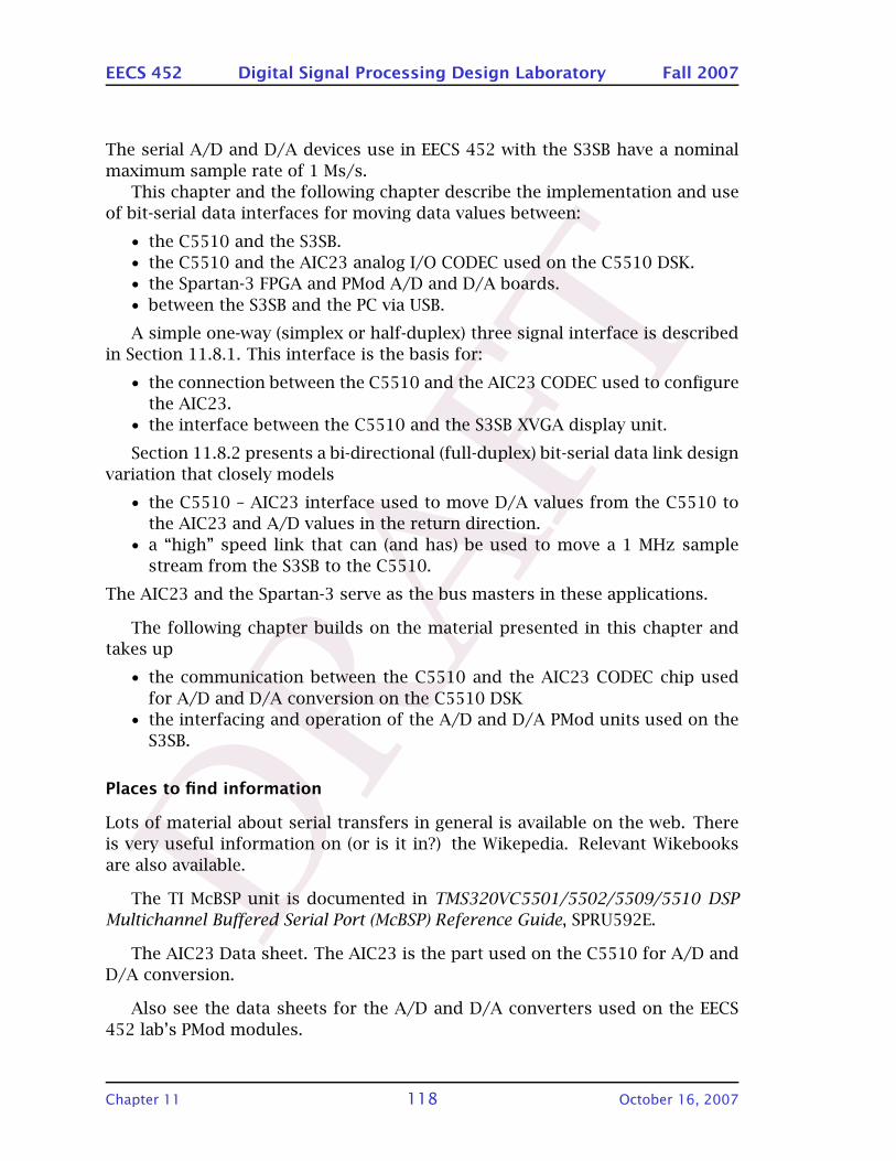
DRA
FT
EECS 452 Digital Signal Processing Design Laboratory Fall 2007
The serial A/D and D/A devices use in EECS 452 with the S3SB have a nominal
maximum sample rate of 1 Ms/s.
This chapter and the following chapter describe the implementation and use
of bit-serial data interfaces for moving data values between:
• the C5510 and the S3SB.
• the C5510 and the AIC23 analog I/O CODEC used on the C5510 DSK.
• the Spartan-3 FPGA and PMod A/D and D/A boards.
• between the S3SB and the PC via USB.
A simple one-way (simplex or half-duplex) three signal interface is described
in Section 11.8.1. This interface is the basis for:
• the connection between the C5510 and the AIC23 CODEC used to configure
the AIC23.
• the interface between the C5510 and the S3SB XVGA display unit.
Section 11.8.2 presents a bi-directional (full-duplex) bit-serial data link design
variation that closely models
• the C5510 – AIC23 interface used to move D/A values from the C5510 to
the AIC23 and A/D values in the return direction.
• a “high” speed link that can (and has) be used to move a 1 MHz sample
stream from the S3SB to the C5510.
The AIC23 and the Spartan-3 serve as the bus masters in these applications.
The following chapter builds on the material presented in this chapter and
takes up
• the communication between the C5510 and the AIC23 CODEC chip used
for A/D and D/A conversion on the C5510 DSK
• the interfacing and operation of the A/D and D/A PMod units used on the
S3SB.
Places to find information
Lots of material about serial transfers in general is available on the web. There
is very useful information on (or is it in?) the Wikepedia. Relevant Wikebooks
are also available.
The TI McBSP unit is documented in TMS320VC5501/5502/5509/5510 DSP
Multichannel Buffered Serial Port (McBSP) Reference Guide, SPRU592E.
The AIC23 Data sheet. The AIC23 is the part used on the C5510 for A/D and
D/A conversion.
Also see the data sheets for the A/D and D/A converters used on the EECS
452 lab’s PMod modules.
Chapter 11 118 October 16, 2007
DRA
FT
EECS 452 Digital Signal Processing Design Laboratory Fall 2007
11.1 Overview of bit-serial methods
A data interface generally has two aspects, a signal set and a protocol. We are
going to focus on a particular style of bit-serial interface sometimes loosely re-
ferred to as being serial peripheral interface (SPI), or SPI-like or SPI compatible
or . . . .
req_in
ack_out
d_outd_in
pull
(a)
demand driven channel
active passive
req_out
ack_in
req_in
ack_out
d_out d_in
push
(b)
data driven channel
active passive
req_out
ack_in
req_in
ack_out
d_out d_in
biput
(c)
bi-directional channel
active passive
d_outd_in
req_out
ack_in
Figure 11.1: Common dataflow and handshake configurations. a). b). c).
The common thread running through “SPI like” interface designs appears to
be
• the use of one (simplex) or two wires (full duplex) for data bits.
• a clock whose transitions are related to the data stream transitions. The
transmitter and the receiver are synchronous to each other,
• a pulse or level providing information about data word boundaries. This
waveform is used to establish data frame synchronization.
The protocol, the relationships between function and the waveforms, varies
significantly between devices.
Typically a one-way link, such as from a CPU to an A/D or D/A converter, will
use 3 signal lines or wires. Links such as one between the C5510 and the S3SB
might be duplex using four or more lines.
Figures 11.12 and 11.15 show the waveforms associated with two somewhat
different bit-serial interfaces that are used in EECS 452 to move data values be-
tween the C5510 and the S3SB.
Pretty much what happens is that device manufacturers attempt to make
their parts easy to work with for particular classes of applications. The processor
then has to do what is necessary in order to use the part.
When linking the C5510 to the Spartan-3 the C5510’s built in bit-serial sup-
port provides some structure that can be built on while the S3 is amorphous
Chapter 11 119 October 16, 2007
DRA
FT
EECS 452 Digital Signal Processing Design Laboratory Fall 2007
and pretty much can be made to do as desired. Both ends of the link are highly
configurable leading to having to choose among a large of possibilities. Life
sometimes is more simple if one does not have many choices.
11.1.1 The Serial Peripheral Interface
The serial peripheral interface (SPI).
• Nominally de facto standard.
• Synchronous serial data link.
• A Motorola (now Freescale) creation.
• Simplex or full Duplex
• Master/slave.
http://wikipedia.org/wiki/Serial_Peripheral_Interface_Bus.
A full duplex “SPI-like” interface uses four signal lines. One line supplies a
clock waveform that is used to determine event times on the other three lines.
One line is for data being transmitted from a device (TX). One line is for data
being received from a device (RX). The fourth line is to indicate the word bound-
aries (frame-sync) used by the data lines. In a processor/device system one of
the two entities is responsible for generating the clock and the frame-sync sig-
nal. This entity is referred to as the master and the other is referred to as the
slave.
The AIC23 CODEC present on the C5510 is a good illustration of the flexibility
that can be built into a device. Upon power on the AIC23 waits as a slave until
the processor programs the AIC23 configuration registers. This is done using a
half-duplex SPI port present specifically for this task. The AIC23 uses a second
port to move sample values to and from the processor (full duplex). In this case
the AIC23 is the master and controls the timing and the data transfers. The
configuration remains active and the characteristics of the second port (such as
sample rate) can be changed “on-the-fly”.
11.1.2 RS232
One of the earliest interfaces. Originally used between a phone modem and a
terminal. The RS-232 standard basically defines a set of signals, their function
and their electrical characteristics. It does not define things such as the con-
nector, word size, bit rates, character codes and the like. These have evolved
from practice. Early connectors used a 25-pin DB25 connector. Early in the PCs
history IBM implemented a signal subset using a 9-pin DB9 connector.
http://en.wikipedia.org/wiki/RS-232.
Chapter 11 120 October 16, 2007
DRA
FT
EECS 452 Digital Signal Processing Design Laboratory Fall 2007
Often the term RS232 loosely refers to a full duplex asynchronous data chan-
nel that uses signally typically found in real RS-232 devices.
Xilinx Application XAPP223 describes a UART implementation for use with
some of the (now) older FPGA families. It was written by Ken Chapman who
also created the PicoBlaze microcomputer. This gives a view of the UART at a
very basic VHDL level. EECS 452 projects have made use of the UART subsystem,
especially the 16 word FIFOs, contained in the PicoBlaze demonstration package.
11.1.3 Others
Combined clock and data.
High speed, differential signaling.
One wire.
Material to be added if/when used in lab.
11.1.4 Crossing clock domain boundaries
When communicating between independent devices such as the C5510 and the
S3 parts of the link operate using timing established by the C5510 and other
parts operate using timing established by the S3. In this case it is said that there
are two “clock domains”. There will be points where data needs to moved from
one domain into the other. These domain crossings need to be done with some
amount of care.
Consider a simple one bit D-register. Assume the D input is generated by the
C5510 and the clock generated by the Spartan-3. The two clocks are not related
in any particular way. Model that the value present on the D input is loaded into
the register on the rising edge of the clock input.
The D register has a period of time, the setup time, where the input must be
present prior to the clock rising edge in order to guarantee that the input value
is loaded into the register.
There is also a hold time where the D input has to be maintained following
the clock rising edge to guarantee proper operation. Generally the hold time is
0 ns.
The setup time is not (cannot be) zero. So, what happens if the D input
changes closer to the rising clock edge than it should? A condition termed
metastability can (and generally will) occur.
The register output can become neither a 0 nor a 1 but somewhere in between
and this condition can persist for as long as forever. When crossing between in-
dependent clock domains there is no way to guarantee that this will not happen.
However, there are things, very simple things, that a designer can do that will
reduce the probability of a missed clock tic will happen only once in day, or in
100 years or even the lifetime of the universe.
Chapter 11 121 October 16, 2007
DRA
FT
EECS 452 Digital Signal Processing Design Laboratory Fall 2007
Metastability is a real phenomenon. How to deal with it? Add delay. More to
come. For the present, use Google to learn more.
11.2 The TI McBSP bit-serial interface
TI has developed a bit-serial data transfer logic unit named Multichannel Buffered
Serial Port (McBSP). McBSP units are present across TI’s DSP product lines. The
C5510 DSP used in lab possesses three McBSP units.
Each McBSP unit supports two independently configurable bit-serial half-duplex
data ports, one for transmit and and one for receive. The two sub-ports can be
combined to function as a single full duplex port. Because of the creative rich-
ness of bit-serial interface designs in common use, TI has designed the McBSP
to be highly configurable. There are typically eleven 16-bit registers whose con-
tents have to be specified for any given application. Initially this is a daunting
task but after doing this a couple of times it becomes much less overwhelming.
As always, in order to become proficient it takes practice, practice, practice. TI
does provide a configuration tool as part of the DSP BIOS. The user fills in blanks
and the tool fills in the bits. HOWEVER, one still needs to know how to fill in the
blanks. Filling in the bits by hand is not all that difficult, as we will see.
Other manufacturers, facing the the same creative design richness, have equipped
their DSP devices with units having capabilities similar to those of the McBSP.
The FPGA designer also has to be able to work with a variety of interface struc-
tures but has the freedom (responsibility) to target the VHDL to work with the
component du jour. Bit serial interfaces are common and the person planning to
be a system designer and/or implementor needs to have a good understanding
of how to work with them.
The C5510 McBSP units are numbered 0, 1, and 2. Channel 0 is not used on
the DSK and is available for use via the peripheral connector.
The DSK uses McBSP channel 1 to initialize the AIC23. The C5510 is the
bus master. Once the AIC23 up and running channel can be used to reprogram
the AIC23 “on the fly". It is also possible to disconnect channel 1 from the
AIC23 and reroute its lines to the peripheral connector. Once the AIC23 has been
programmed many applications haven’t a need to change the configuration. For
these cases the channel 1 lines can then switched to the peripheral connector.
With care it probably is possible to switch the McBSP channel 1 lines between
the AIC23 and an external peripheral on an “as needed” basis.
Channel 2 is used by the DSK to move data back and forth between the C5510
and the AIC23 on a continuous basis. The AIC23 serves as the bus master. If the
AIC23 is not being used, McBSP 2 channel’s signal lines can also be rerouted to
the peripheral connector.
Chapter 11 122 October 16, 2007
DRA
FT
EECS 452 Digital Signal Processing Design Laboratory Fall 2007
The programming procedure used to redirect channels 1 and 2 from the
AIC23 to the peripheral connector involves the DSK’s CPLD and is not described
here. Consult the C5510 DSK Technical Reference Manual for information.
The C5510/S3SB systems in the lab have a cable connecting the C5510 exter-
nal peripheral interface (EPI) connector to the A2 40-pin connector on the S3SB.
A subset of the EPI signals are supported. Included are the six lines per McBSP
channel for channels 0 and 1. The signals connected by the EPI/A2 cable are
listed in Figure 11.5.
The two main sources for information about the McBSP system
• Introduction to McBSP, TI’s document number SPRU592E. This is a 285 page
document. The size indicates that some effort is going to be needed in
order to understand McBSP operation.
• TMS320VC5510 Fixed-Point Digital Signal Processor Data Manual, TI’s doc-
ument number SPRS607E. This documents the addresses of the McBSP reg-
isters in I/O space.
Because of its flexibility the McBSP is a very difficult device to internalize as a
whole. One needs to understand the range of applications that it is designed for
as well as its design and its operation. A reasonable way to develop the ability
to work with it is to read, study, SPRU592E and then apply the material to a few
simple projects. One reasonable starting point is writing C5510 support routines
for the AIC23. Another, the one used in this document, is to implement simple
data links between the C5510 and the Spartan-3. Data movement is an important
part of any DSP system and developing an understanding of the issues and some
of the ways such can be done is important.
As an aside, the McBSP represents only a small of the I/O support hardware
included in the C5510.
11.2.1 McBSP overview
The definitive McBSP document, SPRU592E, contains 285 pages. We only sketch
a basic overview. It is suggested that the entire contents of SPRU592E be at least
skimmed. The chapters that are most important to us are 2, 6, 7, 8 and 12. This
is not to imply that the other chapters are not important.
Figure 11.2 shows the overall structure of a single McBSP channel or unit.
Wording is a problem here. It feels uncomfortable to write “McBSP port” knowing
that it expands out to “Multichannel Buffered Serial Port port”.
Each McBSP nominally implements a full duplex bit-serial interface. A McBSP
unit is used to transmit and/or receive fixed length (such as 16 or 32 bit) values
using a bit serial link. These ports minimize the number of wires needed to
connect peripheral devices such as A/D and D/A converters to the C5510. This
Chapter 11 123 October 16, 2007
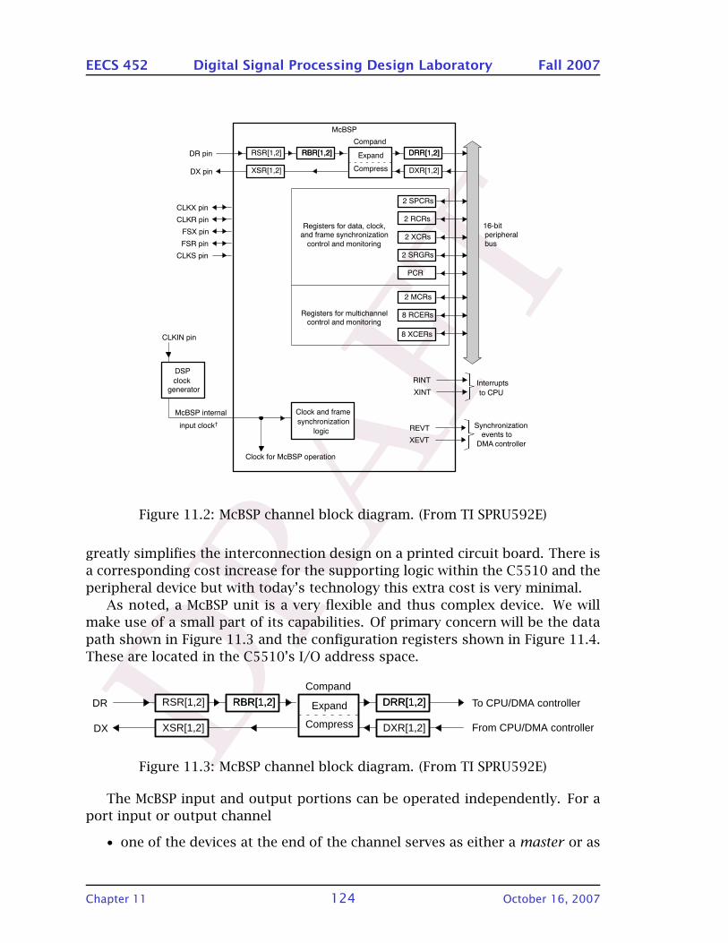
DRA
FT
EECS 452 Digital Signal Processing Design Laboratory Fall 2007
ÁÁÁÁÁÁÁÁÁÁÁÁ
ÁÁÁÁ
2 SRGRs
ÁÁÁÁÁÁÁÁ
ÁÁÁÁÁÁÁÁÁÁÁÁ
CLKS pin
FSR pin
FSX pin
CLKR pin
CLKX pin
DX pin
DR pin
XEVT
REVT
XINT
RINT
events to
Synchronization
Interrupts
bus
peripheral
16-bit
McBSP
Compand
RSR[1,2]
Compress
Expand
control and monitoring
and frame synchronization
PCR
8 RCERs
2 MCRs
2 XCRs
2 SPCRs
2 RCRs
XSR[1,2]
ÁÁÁÁÁÁÁÁ
RBR[1,2] DRR[1,2]
ÁÁÁÁÁÁÁÁDXR[1,2]
to CPU
DMA controller
DRR[1,2]
8 XCERs
RBR[1,2]
Registers for data, clock,
Registers for multichannelcontrol and monitoring
ÁÁÁÁÁÁÁÁÁÁÁÁÁÁÁÁÁÁÁÁ
DSP
clockgenerator
CLKIN pin
ÁÁÁÁÁÁÁÁÁÁÁÁÁÁÁÁÁÁÁÁ
McBSP internal
input clock†
Clock for McBSP operation
Clock and frame
synchronization
logic
Figure 11.2: McBSP channel block diagram. (From TI SPRU592E)
greatly simplifies the interconnection design on a printed circuit board. There is
a corresponding cost increase for the supporting logic within the C5510 and the
peripheral device but with today’s technology this extra cost is very minimal.
As noted, a McBSP unit is a very flexible and thus complex device. We will
make use of a small part of its capabilities. Of primary concern will be the data
path shown in Figure 11.3 and the configuration registers shown in Figure 11.4.
These are located in the C5510’s I/O address space.
ÁÁÁÁÁÁÁÁ
ÁÁÁÁ
ÁÁÁÁÁÁÁÁ
ÁÁÁÁÁÁÁÁÁÁÁÁÁÁÁDX
DR
Compand
RSR[1,2]
Compress
Expand
XSR[1,2]
ÁÁÁÁÁÁ
RBR[1,2] DRR[1,2]
ÁÁÁDXR[1,2]
DRR[1,2]RBR[1,2] To CPU/DMA controller
From CPU/DMA controller
Figure 11.3: McBSP channel block diagram. (From TI SPRU592E)
The McBSP input and output portions can be operated independently. For a
port input or output channel
• one of the devices at the end of the channel serves as either a master or as
Chapter 11 124 October 16, 2007

DRA
FT
EECS 452 Digital Signal Processing Design Laboratory Fall 2007
a slave,
• there is a line for transmitting data values in bit-serial form,
• the master generates a timing waveform that is to be used by the slave to
generate the bit-serial data,
• the master generates a frame-sync waveform that identifies a frame of sev-
eral n-bit values.
The McBSP system is extremely flexible and is intended for use in a large and
diverse number of applications. Because of this, a large number of decisions
need to be made regarding determining the control values for any particular
application. Once properly configured the McBSP runs well.
The key I/O space registers associated with a McBSP port are shown in Figure
11.4.
even addr odd addr Usage
DRR2 DRR1 Data Receive Registers
DXR2 DXR1 Data Transmit Registers
SPCR2 SPCR1 Serial Port Control Registers
RCR2 RCR1 Receive Control Registers
XCR2 XCR2 Transmit Control Registers
SRGR2 SRGR1 Sample Range Generator Registers
MCR2 MCR1 Multichannel Registers
PCR
Figure 11.4: Basic McBSP port control registers. The receive/transmit multichan-
nel enable registers are not shown.
Each register contains 16 bits. Registers are located in I/O address space in
such a way so that they can be read and written as 32-bit units. The McBSP port
0 register set starts at address 0x2800. The port 1 register set starts at 0x2C00and the port 2 register set starts at 0x3000.
For a more complete description of the McBSP see the TI McBSP manual, TI
document SPRU592E. It will be very helpful at this point if the reader has at least
scanned this document.
Because we are not going to be involved in making multichannel transfers
there are fifteen registers that we will be dealing with. There four registers used
for data movement, DRR1, DRR2, DXR1 and DXR2 registers. There are four con-
trol register used to determine how the channel operates, RCR1, RCR2, XCR1 and
XCR2. Two registers are used in setting transfer rates. The two multi-channel
control registers are only of interest because we will have to make sure that this
Chapter 11 125 October 16, 2007

DRA
FT
EECS 452 Digital Signal Processing Design Laboratory Fall 2007
feature is not active. The pin control register (PCR) controls the functions asso-
ciated with several of the channel’s external pins. The PCR is used to switch use
of specific McBSP I/O pins to use as general purpose I/O pins (GPIO pins).
11.2.2 Accessing the McBSP registers using C
The McBSP registers lie in I/O address space. Chapter 5 of TMS320C55x Opti-
mizing C/C++ Compiler User’s Guide (SPRU281E) describes how to access values
in I/O space.
We need to be able to read and write the registers associated with McBSP
ports 0, 1 and 2. It would be nice if we could refer to the McBSP registers by
name say as,
McBSP_reg(port, register_name)
where port could take on the values 0, 1, and 2 and register_name would be
the same used in the McBSP documentation.
This is easily accomplished using a header file to contain symbol and macro
definitions. A file, McBSP_452.h, was created for this purpose. Define state-
ments are used to define register names. For example:
#define McBSP_DRR1 0x1#define McBSP_DRR2 0x0
The string McBSP_ has been prepended in order make the register names being
defined very specific to the McBSP. This is considered a good practice. Unfortu-
nately, it also becomes quite the nuisance if the names are typed frequently.
The piece d’resitance in this effort is the macro definition:
#define McBSP_reg(port,register) \(*((ioport unsigned *)((port*0x0400u)+0x2800u+register)))
.
Using this macro we can write C statements of the form
McBSP_reg(1, McBSP_XCR1) = 0x4322;uTemp = McBSP_reg(1, McBSP_DRR1);
making both life easier and our code more readable. We could use a variable
rather than a constant to select the port making the code somewhat more gen-
eral.There are other choices that could have been made. One alternative to the
above approach would be to define C macros for each I/O memory address usedthe the various McBSP ports. A naming convention making use of the registernames found in the C5510 data manual would be quite reasonable. For example:
Chapter 11 126 October 16, 2007
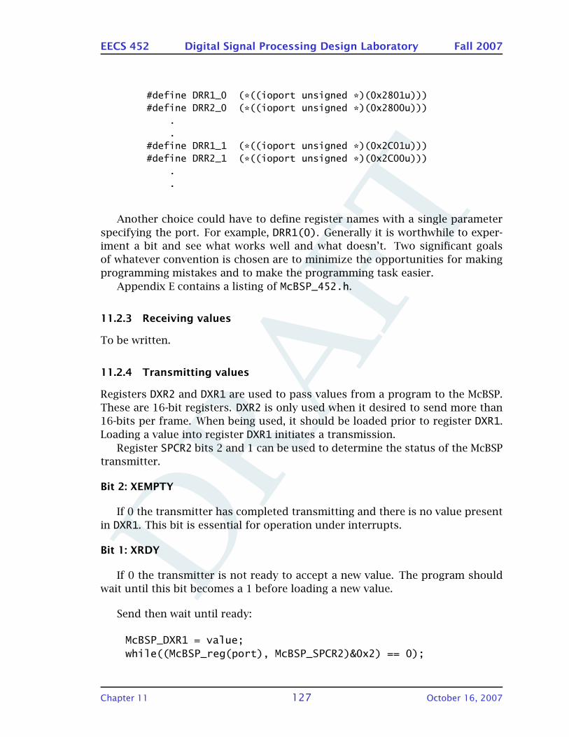
DRA
FT
EECS 452 Digital Signal Processing Design Laboratory Fall 2007
#define DRR1_0 (*((ioport unsigned *)(0x2801u)))#define DRR2_0 (*((ioport unsigned *)(0x2800u)))
.
.#define DRR1_1 (*((ioport unsigned *)(0x2C01u)))#define DRR2_1 (*((ioport unsigned *)(0x2C00u)))
.
.
Another choice could have to define register names with a single parameter
specifying the port. For example, DRR1(0). Generally it is worthwhile to exper-
iment a bit and see what works well and what doesn’t. Two significant goals
of whatever convention is chosen are to minimize the opportunities for making
programming mistakes and to make the programming task easier.
Appendix E contains a listing of McBSP_452.h.
11.2.3 Receiving values
To be written.
11.2.4 Transmitting values
Registers DXR2 and DXR1 are used to pass values from a program to the McBSP.
These are 16-bit registers. DXR2 is only used when it desired to send more than
16-bits per frame. When being used, it should be loaded prior to register DXR1.
Loading a value into register DXR1 initiates a transmission.
Register SPCR2 bits 2 and 1 can be used to determine the status of the McBSP
transmitter.
Bit 2: XEMPTY
If 0 the transmitter has completed transmitting and there is no value present
in DXR1. This bit is essential for operation under interrupts.
Bit 1: XRDY
If 0 the transmitter is not ready to accept a new value. The program should
wait until this bit becomes a 1 before loading a new value.
Send then wait until ready:
McBSP_DXR1 = value;while((McBSP_reg(port), McBSP_SPCR2)&0x2) == 0);
Chapter 11 127 October 16, 2007
DRA
FT
EECS 452 Digital Signal Processing Design Laboratory Fall 2007
Wait if not ready then send:
while((McBSP_reg(port, McBSP_SPCR2)&0x2) == 0);McBSP_reg(port, McBSP_DXR1) = value;
The latter approach allows the computer to compute while values are trans-
mitted waiting only when necessary.
11.3 RS232 on the C5510 DSK
Have Global Specialties dual channel RS232 daughter boards available. This sec-
tion remains to be worked on. Information about the DSK compatible RS232
boards can be found on the course web site.
11.4 Accessing the PC from the DSK
TI’s RTDX allows real-time data transfers. We don’t cover RTDX in this course.
One or two past projects have successfully used RTDX. One or two weren’t all
that successful.
C5510 C file read and writes access files on the PC. These break real time. So
does printf. There is either a problem reading and writing character data to
the PC, or some misunderstanding of how to do so. Use ASCII.
11.5 S3B Serial I/O
The Spartan-3 is relatively amorphous. One can pretty much do what one wants.
Generally, what is done is responsive. Generally a device being interfaced to has
a (hopefully) well defined interface which drives the VHDL design in the S3.
Life is a bit more complicated when interfacing the S3 to the C5510 McBSP.
The McBSP itself is highly configurable leading to the need to make lots of deci-
sions with little on which to base them.
The DSK and USB boards in the lab are connected using cables connecting the
DSK External Peripheral Connector (EPC) and the S3SB A2 connector. A 40-pin
cable is used. Only a subset of signals present on the EPC are connected.
Include a table giving the pin connected.
Chapter 11 128 October 16, 2007
DRA
FT
EECS 452 Digital Signal Processing Design Laboratory Fall 2007
11.6 S3SB RS232
The S3SB has a two channel RS232 level converter and one 9-pin RS232 connec-
tor. If necessary it should be possible to piggy-back a second connector onto the
existing one.
Xilinx’s Ken Chapman’s PicoBlaze demonstration design comes with a RS232
interface entity which also includes transmit and receive FIFO VHDL entities. The
PicoBlaze is described in Chapter 26.
11.7 Cables and connectors
11.7.1 S3SB A1 connector
EECS 452 usage is to not connect to this connector. The signals present on
this connector are also connected to the SRAM. The SRAM is used by the XVGA
display support. In effect, the XVGA display system is plugged into A1.
11.7.2 S3SB A2 connector to C5510 DSK EPI connector
Figure 11.5 shows the mapping from the C5510 DSK external peripheral inter-
face connector to pins on the FPGA.
11.7.3 S3SB B1 connector to MIB
Figure 11.6 shows the mapping of signals from the S3 FPGA to the socket posi-
tions on a MIB plugged into connector position B1. The convention used allows
ready mapping to the Nexys and Basys boards. The use of this naming conven-
tion is encouraged.
Figure 11.7 provides an alternate naming which maps directly to all MIB PMod
connectors.
Be careful when working with the MIB schematic. Digilent uses a convention
that reorders the pins on mating connectors. The connector labeled Peripheral
Board RA Female pin numbers match to the pins used on the S3SB socket. Nor-
mal EECS 452 usage is to mount a MIB on B1.
11.8 Examples:
One has to start somewhere. The following examples form a reasonable starting
point. Chapter 12 contains additional examples.
Chapter 11 129 October 16, 2007
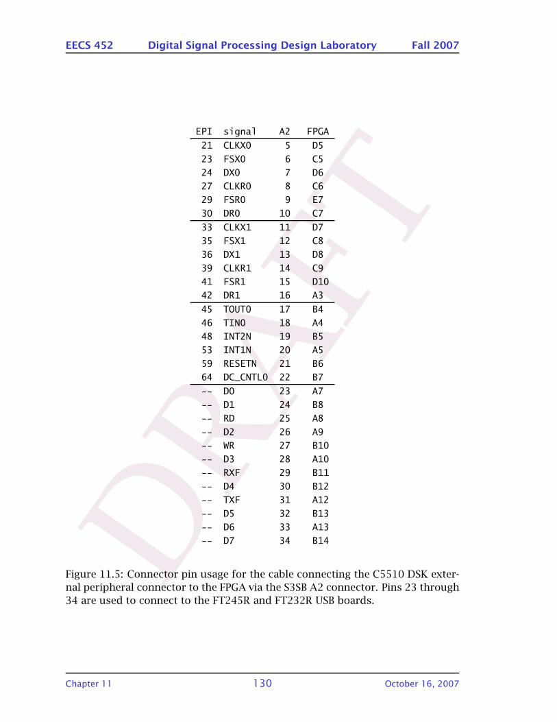
DRA
FT
EECS 452 Digital Signal Processing Design Laboratory Fall 2007
EPI signal A2 FPGA
21 CLKX0 5 D5
23 FSX0 6 C5
24 DX0 7 D6
27 CLKR0 8 C6
29 FSR0 9 E7
30 DR0 10 C7
33 CLKX1 11 D7
35 FSX1 12 C8
36 DX1 13 D8
39 CLKR1 14 C9
41 FSR1 15 D10
42 DR1 16 A3
45 TOUT0 17 B4
46 TIN0 18 A4
48 INT2N 19 B5
53 INT1N 20 A5
59 RESETN 21 B6
64 DC_CNTL0 22 B7
-- D0 23 A7
-- D1 24 B8
-- RD 25 A8
-- D2 26 A9
-- WR 27 B10
-- D3 28 A10
-- RXF 29 B11
-- D4 30 B12
-- TXF 31 A12
-- D5 32 B13
-- D6 33 A13
-- D7 34 B14
Figure 11.5: Connector pin usage for the cable connecting the C5510 DSK exter-
nal peripheral connector to the FPGA via the S3SB A2 connector. Pins 23 through
34 are used to connect to the FT245R and FT232R USB boards.
Chapter 11 130 October 16, 2007

DRA
FT
EECS 452 Digital Signal Processing Design Laboratory Fall 2007
# MIB sockets on B1 names compatible with Nexys and Basys
# PMod A : J1 on MIB to B1##NET "pmod_a<0>" LOC = "C10" | IOSTANDARD = LVCMOS33;#NET "pmod_a<1>" LOC = "E10" | IOSTANDARD = LVCMOS33;#NET "pmod_a<2>" LOC = "T3" | IOSTANDARD = LVCMOS33;#NET "pmod_a<3>" LOC = "C11" | IOSTANDARD = LVCMOS33;
# PMod B : J3 on MIB to B1##NET "pmod_b<0>" LOC = "R10" | IOSTANDARD = LVCMOS33;#NET "pmod_b<1>" LOC = "D12" | IOSTANDARD = LVCMOS33;#NET "pmod_b<2>" LOC = "T7" | IOSTANDARD = LVCMOS33;#NET "pmod_b<3>" LOC = "E11" | IOSTANDARD = LVCMOS33;
# PMod C : J5 on MIB to B1##NET "pmod_c<0>" LOC = "M6" | IOSTANDARD = LVCMOS33;#NET "pmod_c<1>" LOC = "C16" | IOSTANDARD = LVCMOS33;#NET "pmod_c<2>" LOC = "C15" | IOSTANDARD = LVCMOS33;#NET "pmod_c<3>" LOC = "D16" | IOSTANDARD = LVCMOS33;
# PMod D : J7 on MIB to B1##NET "pmod_d<0>" LOC = "F15" | IOSTANDARD = LVCMOS33;#NET "pmod_d<1>" LOC = "H15" | IOSTANDARD = LVCMOS33;#NET "pmod_d<2>" LOC = "G16" | IOSTANDARD = LVCMOS33;#NET "pmod_d<3>" LOC = "J16" | IOSTANDARD = LVCMOS33;
Figure 11.6: S3SB B1 PMod MIB socket connections.
Chapter 11 131 October 16, 2007
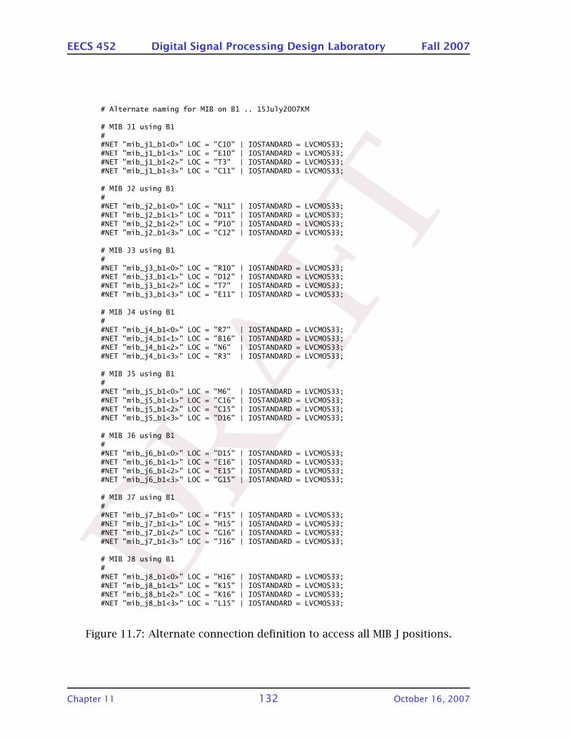
DRA
FT
EECS 452 Digital Signal Processing Design Laboratory Fall 2007
# Alternate naming for MIB on B1 .. 15July2007KM
# MIB J1 using B1##NET "mib_j1_b1<0>" LOC = "C10" | IOSTANDARD = LVCMOS33;#NET "mib_j1_b1<1>" LOC = "E10" | IOSTANDARD = LVCMOS33;#NET "mib_j1_b1<2>" LOC = "T3" | IOSTANDARD = LVCMOS33;#NET "mib_j1_b1<3>" LOC = "C11" | IOSTANDARD = LVCMOS33;
# MIB J2 using B1##NET "mib_j2_b1<0>" LOC = "N11" | IOSTANDARD = LVCMOS33;#NET "mib_j2_b1<1>" LOC = "D11" | IOSTANDARD = LVCMOS33;#NET "mib_j2_b1<2>" LOC = "P10" | IOSTANDARD = LVCMOS33;#NET "mib_j2_b1<3>" LOC = "C12" | IOSTANDARD = LVCMOS33;
# MIB J3 using B1##NET "mib_j3_b1<0>" LOC = "R10" | IOSTANDARD = LVCMOS33;#NET "mib_j3_b1<1>" LOC = "D12" | IOSTANDARD = LVCMOS33;#NET "mib_j3_b1<2>" LOC = "T7" | IOSTANDARD = LVCMOS33;#NET "mib_j3_b1<3>" LOC = "E11" | IOSTANDARD = LVCMOS33;
# MIB J4 using B1##NET "mib_j4_b1<0>" LOC = "R7" | IOSTANDARD = LVCMOS33;#NET "mib_j4_b1<1>" LOC = "B16" | IOSTANDARD = LVCMOS33;#NET "mib_j4_b1<2>" LOC = "N6" | IOSTANDARD = LVCMOS33;#NET "mib_j4_b1<3>" LOC = "R3" | IOSTANDARD = LVCMOS33;
# MIB J5 using B1##NET "mib_j5_b1<0>" LOC = "M6" | IOSTANDARD = LVCMOS33;#NET "mib_j5_b1<1>" LOC = "C16" | IOSTANDARD = LVCMOS33;#NET "mib_j5_b1<2>" LOC = "C15" | IOSTANDARD = LVCMOS33;#NET "mib_j5_b1<3>" LOC = "D16" | IOSTANDARD = LVCMOS33;
# MIB J6 using B1##NET "mib_j6_b1<0>" LOC = "D15" | IOSTANDARD = LVCMOS33;#NET "mib_j6_b1<1>" LOC = "E16" | IOSTANDARD = LVCMOS33;#NET "mib_j6_b1<2>" LOC = "E15" | IOSTANDARD = LVCMOS33;#NET "mib_j6_b1<3>" LOC = "G15" | IOSTANDARD = LVCMOS33;
# MIB J7 using B1##NET "mib_j7_b1<0>" LOC = "F15" | IOSTANDARD = LVCMOS33;#NET "mib_j7_b1<1>" LOC = "H15" | IOSTANDARD = LVCMOS33;#NET "mib_j7_b1<2>" LOC = "G16" | IOSTANDARD = LVCMOS33;#NET "mib_j7_b1<3>" LOC = "J16" | IOSTANDARD = LVCMOS33;
# MIB J8 using B1##NET "mib_j8_b1<0>" LOC = "H16" | IOSTANDARD = LVCMOS33;#NET "mib_j8_b1<1>" LOC = "K15" | IOSTANDARD = LVCMOS33;#NET "mib_j8_b1<2>" LOC = "K16" | IOSTANDARD = LVCMOS33;#NET "mib_j8_b1<3>" LOC = "L15" | IOSTANDARD = LVCMOS33;
Figure 11.7: Alternate connection definition to access all MIB J positions.
Chapter 11 132 October 16, 2007
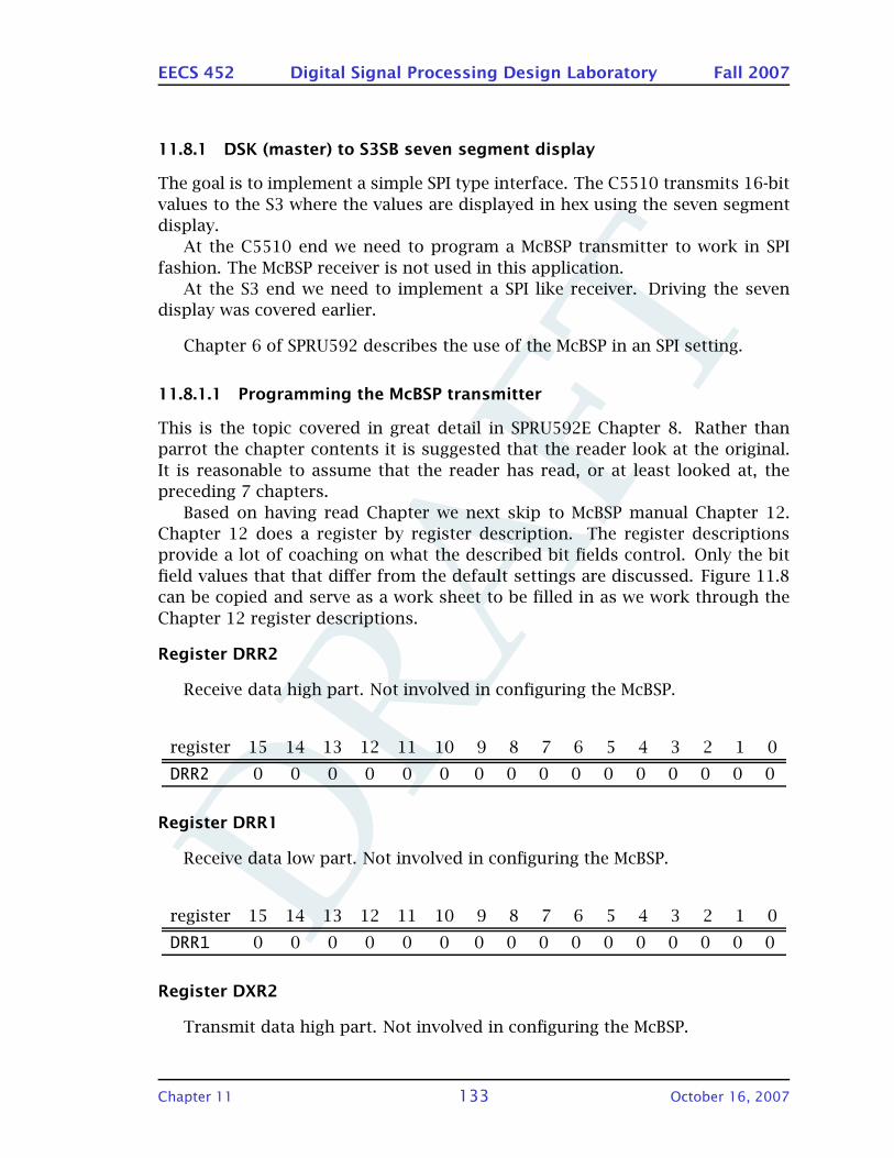
DRA
FT
EECS 452 Digital Signal Processing Design Laboratory Fall 2007
11.8.1 DSK (master) to S3SB seven segment display
The goal is to implement a simple SPI type interface. The C5510 transmits 16-bit
values to the S3 where the values are displayed in hex using the seven segment
display.
At the C5510 end we need to program a McBSP transmitter to work in SPI
fashion. The McBSP receiver is not used in this application.
At the S3 end we need to implement a SPI like receiver. Driving the seven
display was covered earlier.
Chapter 6 of SPRU592 describes the use of the McBSP in an SPI setting.
11.8.1.1 Programming the McBSP transmitter
This is the topic covered in great detail in SPRU592E Chapter 8. Rather than
parrot the chapter contents it is suggested that the reader look at the original.
It is reasonable to assume that the reader has read, or at least looked at, the
preceding 7 chapters.
Based on having read Chapter we next skip to McBSP manual Chapter 12.
Chapter 12 does a register by register description. The register descriptions
provide a lot of coaching on what the described bit fields control. Only the bit
field values that that differ from the default settings are discussed. Figure 11.8
can be copied and serve as a work sheet to be filled in as we work through the
Chapter 12 register descriptions.
Register DRR2
Receive data high part. Not involved in configuring the McBSP.
register 15 14 13 12 11 10 9 8 7 6 5 4 3 2 1 0
DRR2 0 0 0 0 0 0 0 0 0 0 0 0 0 0 0 0
Register DRR1
Receive data low part. Not involved in configuring the McBSP.
register 15 14 13 12 11 10 9 8 7 6 5 4 3 2 1 0
DRR1 0 0 0 0 0 0 0 0 0 0 0 0 0 0 0 0
Register DXR2
Transmit data high part. Not involved in configuring the McBSP.
Chapter 11 133 October 16, 2007

DRA
FT
EECS 452 Digital Signal Processing Design Laboratory Fall 2007
register 15 14 13 12 11 10 9 8 7 6 5 4 3 2 1 0
DRR2 0 0 0 0 0 0 0 0 0 0 0 0 0 0 0 0
DRR1 0 0 0 0 0 0 0 0 0 0 0 0 0 0 0 0
DXR2 0 0 0 0 0 0 0 0 0 0 0 0 0 0 0 0
DXR1 0 0 0 0 0 0 0 0 0 0 0 0 0 0 0 0
SPCR1 0 0 0 0 0 0 0 0 0 0 0 0 0 0 0 0
SPCR2 0 0 0 0 0 0 0 0 0 0 0 0 0 0 0 0
RCR1 0 0 0 0 0 0 0 0 0 0 0 0 0 0 0 0
RCR2 0 0 0 0 0 0 0 0 0 0 0 0 0 0 0 0
XCR1 0 0 0 0 0 0 0 0 0 0 0 0 0 0 0 0
XCR2 0 0 0 0 0 0 0 0 0 0 0 0 0 0 0 0
SRGR1 0 0 0 0 0 0 0 0 0 0 0 0 0 0 0 0
SRGR2 0 0 0 0 0 0 0 0 0 0 0 0 0 0 0 0
MCR1 0 0 0 0 0 0 0 0 0 0 0 0 0 0 0 0
MCR2 0 0 0 0 0 0 0 0 0 0 0 0 0 0 0 0
PCR 0 0 0 0 0 0 0 0 0 0 0 0 0 0 0 0
Figure 11.8: Template for setting up a McBSP channel register values.
register 15 14 13 12 11 10 9 8 7 6 5 4 3 2 1 0
DXR2 0 0 0 0 0 0 0 0 0 0 0 0 0 0 0 0
Register DXR1
Transmit data low part. Not involved in configuring the McBSP.
register 15 14 13 12 11 10 9 8 7 6 5 4 3 2 1 0
DXR1 0 0 0 0 0 0 0 0 0 0 0 0 0 0 0 0
Register SPCR1
Bit 0 is used to reset the McBSP channel receiver. If zero, the receiver is placed
into the reset state. The receiver should be held in the reset state while being
configured. For this exercise only the transmit portion of the McBSP channel is
being used.
Bits 12 and 11 are used to configure the clock stop mode. The effect of these
bits on the clock/data timing is illustrated in Figure 11.9. Slightly arbitrarily we
will set these bits to 11.
Chapter 11 134 October 16, 2007
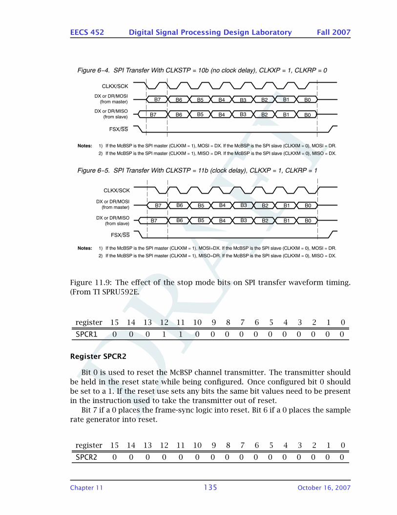
DRA
FT
EECS 452 Digital Signal Processing Design Laboratory Fall 2007
Figure 6 4. SPI Transfer With CLKSTP = 10b (no clock delay), CLKXP = 1, CLKRP = 0
ÁÁ
ÁÁÁÁ
ÁÁ
ÁÁÁÁ
B1B2B4 B3 B0B5B6B7
B0B1B2B3B4B5B6B7
FSX/SS
CLKX/SCK
ÁÁÁÁÁÁÁÁÁÁÁÁÁÁÁÁÁÁÁÁÁÁÁÁÁÁÁÁÁÁÁÁÁÁÁÁÁÁÁÁÁÁÁÁÁÁÁÁ
ÁÁÁÁÁÁÁÁÁÁÁÁÁÁÁÁÁÁÁÁÁÁÁÁÁÁÁÁÁÁÁÁÁÁÁÁÁÁÁÁÁÁÁÁÁÁÁÁ
DX or DR/MOSI
(from master)
DX or DR/MISO
(from slave)
Notes: 1) If the McBSP is the SPI master (CLKXM = 1), MOSI = DX. If the McBSP is the SPI slave (CLKXM = 0), MOSI = DR.
2) If the McBSP is the SPI master (CLKXM = 1), MISO = DR. If the McBSP is the SPI slave (CLKXM = 0), MISO = DX.
Figure 6 5. SPI Transfer With CLKSTP = 11b (clock delay), CLKXP = 1, CLKRP = 1
ÁÁÁÁÁÁÁÁÁÁÁÁÁÁÁÁÁÁÁÁÁÁÁÁÁÁÁÁÁÁÁÁÁÁÁÁÁÁÁÁÁÁÁÁÁÁÁÁ
B1B2B4 B3 B0B5B6B7
B0B1B2B3B4B5B6B7
FSX/SS
CLKX/SCK
ÁÁÁÁÁÁÁÁÁÁÁÁÁÁÁÁÁÁÁÁÁÁÁÁÁÁÁÁÁÁÁÁÁÁÁÁÁÁÁÁÁÁÁÁÁÁÁÁ
ÁÁ
ÁÁÁÁ
ÁÁÁDX or DR/MOSI
(from master)
DX or DR/MISO
(from slave)
Notes: 1) If the McBSP is the SPI master (CLKXM = 1), MOSI=DX. If the McBSP is the SPI slave (CLKXM = 0), MOSI = DR.
2) If the McBSP is the SPI master (CLKXM = 1), MISO=DR. If the McBSP is the SPI slave (CLKXM = 0), MISO = DX.
Figure 11.9: The effect of the stop mode bits on SPI transfer waveform timing.
(From TI SPRU592E.
register 15 14 13 12 11 10 9 8 7 6 5 4 3 2 1 0
SPCR1 0 0 0 1 1 0 0 0 0 0 0 0 0 0 0 0
Register SPCR2
Bit 0 is used to reset the McBSP channel transmitter. The transmitter should
be held in the reset state while being configured. Once configured bit 0 should
be set to a 1. If the reset use sets any bits the same bit values need to be present
in the instruction used to take the transmitter out of reset.
Bit 7 if a 0 places the frame-sync logic into reset. Bit 6 if a 0 places the sample
rate generator into reset.
register 15 14 13 12 11 10 9 8 7 6 5 4 3 2 1 0
SPCR2 0 0 0 0 0 0 0 0 0 0 0 0 0 0 0 0
Chapter 11 135 October 16, 2007
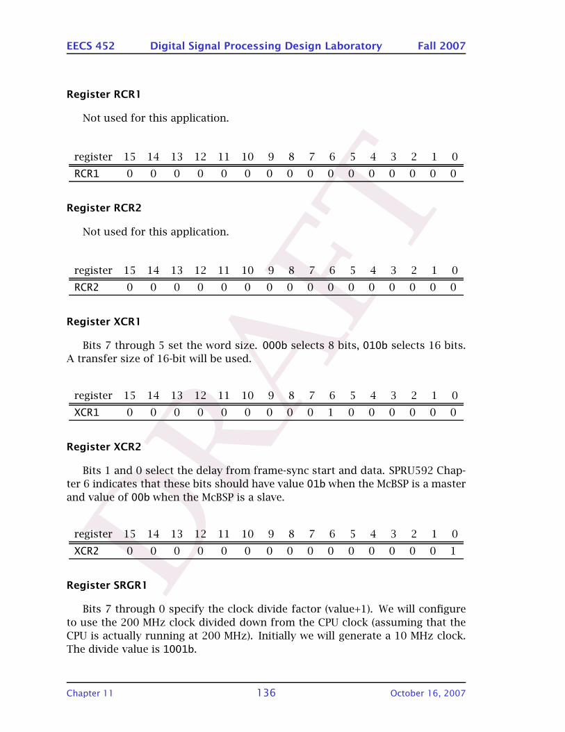
DRA
FT
EECS 452 Digital Signal Processing Design Laboratory Fall 2007
Register RCR1
Not used for this application.
register 15 14 13 12 11 10 9 8 7 6 5 4 3 2 1 0
RCR1 0 0 0 0 0 0 0 0 0 0 0 0 0 0 0 0
Register RCR2
Not used for this application.
register 15 14 13 12 11 10 9 8 7 6 5 4 3 2 1 0
RCR2 0 0 0 0 0 0 0 0 0 0 0 0 0 0 0 0
Register XCR1
Bits 7 through 5 set the word size. 000b selects 8 bits, 010b selects 16 bits.
A transfer size of 16-bit will be used.
register 15 14 13 12 11 10 9 8 7 6 5 4 3 2 1 0
XCR1 0 0 0 0 0 0 0 0 0 1 0 0 0 0 0 0
Register XCR2
Bits 1 and 0 select the delay from frame-sync start and data. SPRU592 Chap-
ter 6 indicates that these bits should have value 01b when the McBSP is a master
and value of 00b when the McBSP is a slave.
register 15 14 13 12 11 10 9 8 7 6 5 4 3 2 1 0
XCR2 0 0 0 0 0 0 0 0 0 0 0 0 0 0 0 1
Register SRGR1
Bits 7 through 0 specify the clock divide factor (value+1). We will configure
to use the 200 MHz clock divided down from the CPU clock (assuming that the
CPU is actually running at 200 MHz). Initially we will generate a 10 MHz clock.
The divide value is 1001b.
Chapter 11 136 October 16, 2007
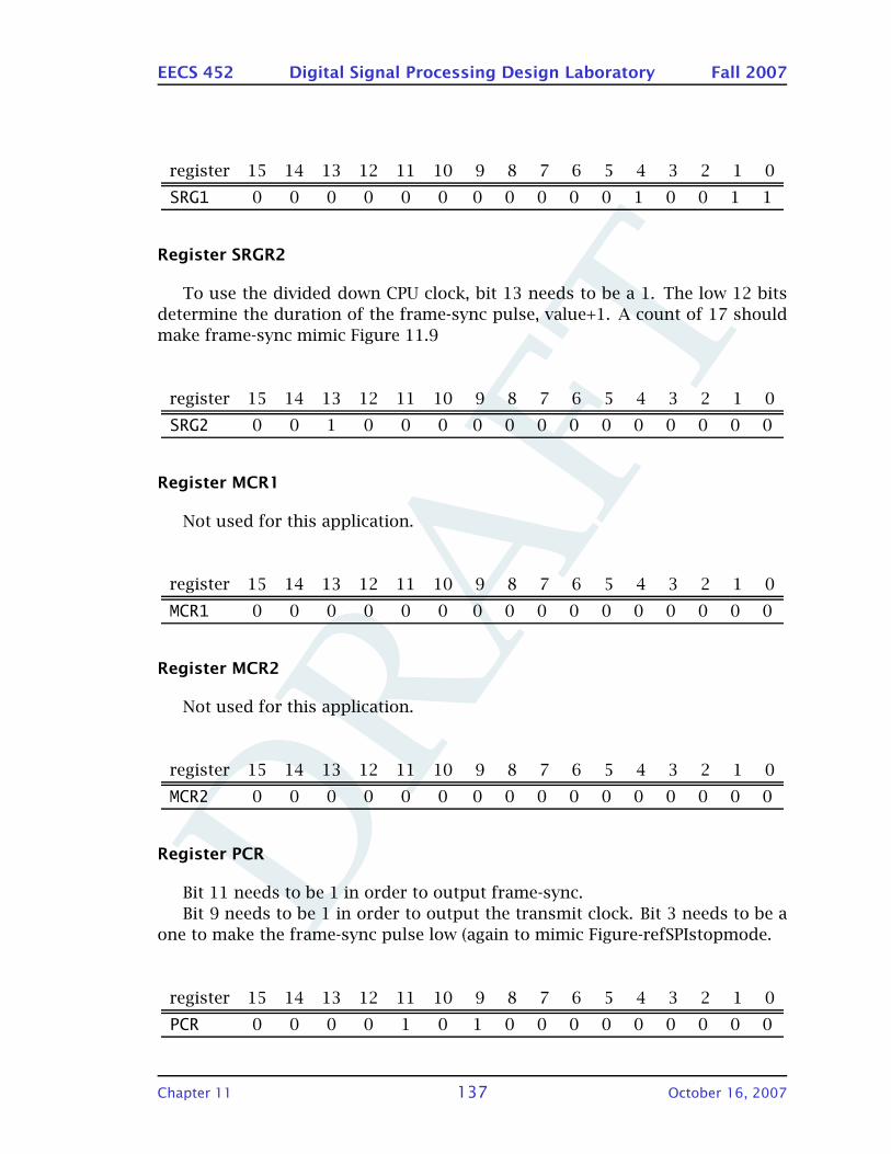
DRA
FT
EECS 452 Digital Signal Processing Design Laboratory Fall 2007
register 15 14 13 12 11 10 9 8 7 6 5 4 3 2 1 0
SRG1 0 0 0 0 0 0 0 0 0 0 0 1 0 0 1 1
Register SRGR2
To use the divided down CPU clock, bit 13 needs to be a 1. The low 12 bits
determine the duration of the frame-sync pulse, value+1. A count of 17 should
make frame-sync mimic Figure 11.9
register 15 14 13 12 11 10 9 8 7 6 5 4 3 2 1 0
SRG2 0 0 1 0 0 0 0 0 0 0 0 0 0 0 0 0
Register MCR1
Not used for this application.
register 15 14 13 12 11 10 9 8 7 6 5 4 3 2 1 0
MCR1 0 0 0 0 0 0 0 0 0 0 0 0 0 0 0 0
Register MCR2
Not used for this application.
register 15 14 13 12 11 10 9 8 7 6 5 4 3 2 1 0
MCR2 0 0 0 0 0 0 0 0 0 0 0 0 0 0 0 0
Register PCR
Bit 11 needs to be 1 in order to output frame-sync.
Bit 9 needs to be 1 in order to output the transmit clock. Bit 3 needs to be a
one to make the frame-sync pulse low (again to mimic Figure-refSPIstopmode.
register 15 14 13 12 11 10 9 8 7 6 5 4 3 2 1 0
PCR 0 0 0 0 1 0 1 0 0 0 0 0 0 0 0 0
Chapter 11 137 October 16, 2007
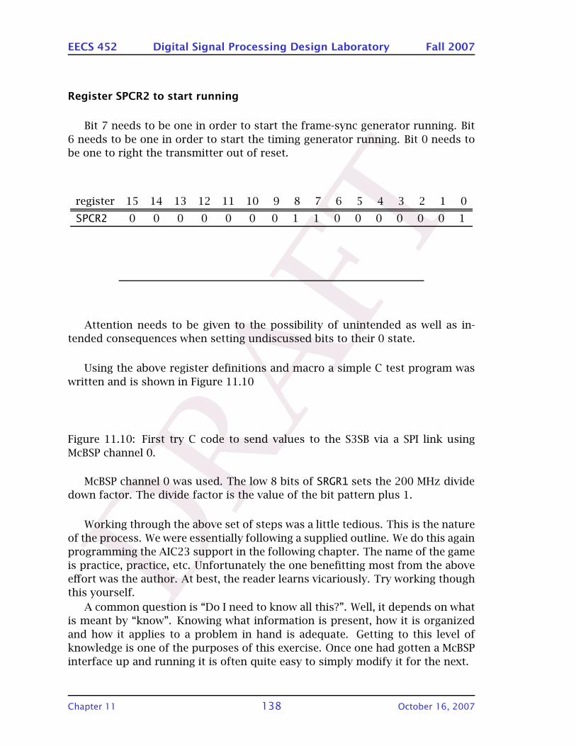
DRA
FT
EECS 452 Digital Signal Processing Design Laboratory Fall 2007
Register SPCR2 to start running
Bit 7 needs to be one in order to start the frame-sync generator running. Bit
6 needs to be one in order to start the timing generator running. Bit 0 needs to
be one to right the transmitter out of reset.
register 15 14 13 12 11 10 9 8 7 6 5 4 3 2 1 0
SPCR2 0 0 0 0 0 0 0 1 1 0 0 0 0 0 0 1
Attention needs to be given to the possibility of unintended as well as in-
tended consequences when setting undiscussed bits to their 0 state.
Using the above register definitions and macro a simple C test program was
written and is shown in Figure 11.10
Figure 11.10: First try C code to send values to the S3SB via a SPI link using
McBSP channel 0.
McBSP channel 0 was used. The low 8 bits of SRGR1 sets the 200 MHz divide
down factor. The divide factor is the value of the bit pattern plus 1.
Working through the above set of steps was a little tedious. This is the nature
of the process. We were essentially following a supplied outline. We do this again
programming the AIC23 support in the following chapter. The name of the game
is practice, practice, etc. Unfortunately the one benefitting most from the above
effort was the author. At best, the reader learns vicariously. Try working though
this yourself.
A common question is “Do I need to know all this?”. Well, it depends on what
is meant by “know”. Knowing what information is present, how it is organized
and how it applies to a problem in hand is adequate. Getting to this level of
knowledge is one of the purposes of this exercise. Once one had gotten a McBSP
interface up and running it is often quite easy to simply modify it for the next.
Chapter 11 138 October 16, 2007

DRA
FT
EECS 452 Digital Signal Processing Design Laboratory Fall 2007
11.8.1.2 VHDL to display bit-serial data
The cable system connecting the C5510 external peripheral connector and the
A2 connector on the SB3 does not have a convenient place to connect a scope in
order to visually inspect the McBSP waveforms. This is easily handled by echoing
the signals onto the MIB (at connector B1) J1 where a test point module can be
used to give easy access. Use a wire connected to MIB J9 as the scope probe
ground point.
Figure 11.11: First try VHDL code to copy the waveforms received from McBSP
channel zero via the A2 connector to PMod_a on B1. This allows the waveforms
received from the C5510 DSK to be observed using an oscilloscope.
Figure 11.11 contains a listing of the VHLD code used to route the signals
received from the DSK’s McBSP channel to PMod_a on the B1 connector. Trivially
simple.
Figure 11.12 shows the observed waveforms. No surprises. Any problems in
getting the correct values to display on the S3SB seven segment display will be
in the VHDL.
Figure 11.13 contains the top level VHDL code connecting the seven-segment
display support with a serial-to-parallel VHDL entity. Figure 11.14 contains the
VHDL for the serial-to-parallel definition.
Note how simple the logic design can be made by using the frame-sync signal.
The way the design is written it essentially is word size independent.
The signals received from the DSK are copied to PMod_a.
11.8.2 DSK/S3SB loop back exercise
This example uses the Spartan-3 as the bus master. C5510 McBSP channel 0 is
used as the slave. This exercise can be used as the starting point for support for
moving a single channel of 12-bit 1 MHz samples from the PMod-AD1 board to
the C5510.
In this example the clock runs continuously and the frame-sync waveform is
a one clock period duration pulse. The serialized data bits occupy the 16 clock
periods following the frame-sync pulse. The waveforms for this implementation
are shown in Figure 11.15.
The clock, frame-sync and transmitted data waveforms are generated by the
Spartan-3. The C5510 uses the clock and frame sync to generate the Spartan-
3’s “receive” waveform (the McBSP transmit waveform. The naming sometimes
get confusing). There appears to be an delay between the transmit and receive
waveforms of about 20 ns. The link was operated at 12.5 MHz in Figure 11.15 in
Chapter 11 139 October 16, 2007
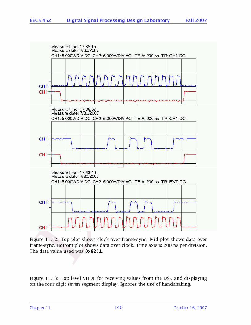
DRA
FT
EECS 452 Digital Signal Processing Design Laboratory Fall 2007
Figure 11.12: Top plot shows clock over frame-sync. Mid plot shows data over
frame-sync. Bottom plot shows data over clock. Time axis is 200 ns per division.
The data value used was 0x8251.
Figure 11.13: Top level VHDL for receiving values from the DSK and displaying
on the four digit seven segment display. Ignores the use of handshaking.
Chapter 11 140 October 16, 2007

DRA
FT
EECS 452 Digital Signal Processing Design Laboratory Fall 2007
Figure 11.14: Simple serial to parallel converter. Tailored to this example’s use
of frame-sync.
order to produce reasonably good looking plots. The link works reliability using
a 25 MHz clock. It does not work using a 50 MHz clock.
Because the timing is generated by the Spartan-3 there is only one clock do-
main in the FPGA. For this implementation, properly crossing the clock domain
boundary between the two boards is the responsibility of the McBSP.
In this example, the Spartan-3 controls when values are to be transferred.
A value is transmitted in each direction for each frame-sync. An application
beyond just loop-back testing might be for the Spartan-3 to take samples at a 1
MHz rate, send them to the C5510 to be filtered and then receive filtered values
back to be sent to a D/A converter.
Timing waveforms show that the data bit transitions occur on the rising edges
of the clock. The data is to be read using the falling edge. Because the Spartan-
3 is generating the clock it has the option of reading the received data values
using the rising edge. There is a causality chain that guarantees that this is safe
for the Spartan-3. The C5510 needs time to receive the clock and then act on
it. Conversely the C5510 cannot be sure that the data bits that is receives are
stable on the leading clock edge and must sample the data bits it receives using
the falling clock edges.
At the C5510 end this example the McBSP is programmed amost identically
as needed for moving data value between the AIC23 and the C5510. In this
case the AIC23 generates the sample clocks and needs to move the data values
in synchronism with the sample rate. It thus makes sense for it to be the bus
master.
Figure 11.16 shows the function used to configure McBSP channel 0 for this
example. The port number was hard coded. This should be changed so that the
function can be used with other ports. This example did not require changing
many control register bits from their default settings.
11.8.3 C5510 to S3SB half-duplex link with handshake
Used by the data path between the C5510 and the S3SB XVGA graphic display
system (Chapter 15). Display commands are generated by the C5510 and sent
via the McBSP to the S3SB for processing. The intent is to operate this path as
fast as possible. However not all commands take that same amount of time to
process. For example long lines take more time to draw than do short lines.
This is dealt with by using one of the unused McBSP receive lines as a hand-
shake signal. The XVGA support raises this line whenever it wants the C5510 to
Chapter 11 141 October 16, 2007

DRA
FT
EECS 452 Digital Signal Processing Design Laboratory Fall 2007
a
b
c
Figure 11.15: Loop back interface waveforms. Clock at 1.5 MHz. a) Top: data
sent by S3. Bottom: frame-sycn. Time scale: 200 ns/div. b) Top: data sent by
the C5510. Bottom: data sent by the S3. Time scale: 100 ns/div. c) Top: clock.
Bottom: frame-sync. Time scale: 100 ns/div. Data word was 0x8251.
Figure 11.16: Function used to set up McBSP channel for the loop back example.
Figure 11.17: The VHDL driver for use in the loop back example.
Chapter 11 142 October 16, 2007

DRA
FT
EECS 452 Digital Signal Processing Design Laboratory Fall 2007
wait up and then lowers it when the C5510 can resume. This is done by using
the PCR to reassign the chosen pin as a general purpose I/O pin. A small amount
of programming is needed in the C5510 to make use of this pin.
There can be more that one data value present in the McBSP pipeline before
the C5510 realizes it should wait up. Probably the easiest way to handle this is
to place a FIFO in the data path from the VHDL receive logic and the input to the
XVGA unit.
There are two components to the XVGA input interface design. The data link
and the handshake. The handshake consists of the single line used by the S3 to
tell the C5510 to hold off for a while.
void McBSP_plot(unsigned port, unsigned value)
while( ((McBSP_reg(port, McBSP_PCR))&0x0010)!=0 ); // wait on FPGA readywhile((McBSP_reg(port, McBSP_SPCR2)&0x0002) == 0); // wait on McBSP xmtr readyMcBSP_reg(port, McBSP_DXR1) = value; // send value to McBSP xmtr
The XVGA link uses a four wire interface. It can be used with the 40pin
EPI/A2 connection or using a “straight” 6-pin PMod type cable via the MIB. The
data link portion of the design is essentially identical to the that described in
Section 11.8.1. The needed changes in the McBSP configuration values can be
puzzled out from Figure 11.18
McBSP_reg(port, McBSP_SPCR2) = 0x0000; // stop xmtrMcBSP_reg(port, McBSP_SPCR1) = 0x1800; // clock stop mode, half cycle delayMcBSP_reg(port, McBSP_RCR1) = 0x0000;McBSP_reg(port, McBSP_RCR2) = 0x0000;McBSP_reg(port, McBSP_XCR1) = 0x0040; // 16-bit wordsMcBSP_reg(port, McBSP_XCR2) = 0x0000;McBSP_reg(port, McBSP_SRGR1) = 0x0004; // low 8 bits is clock divideMcBSP_reg(port, McBSP_SRGR2) = 0x2011;McBSP_reg(port, McBSP_MCR1) = 0x0000;McBSP_reg(port, McBSP_MCR2) = 0x0000;McBSP_reg(port, McBSP_PCR) = 0x1A08; // rcv as gpio inMcBSP_reg(port, McBSP_SPCR2) = 0x00C1; // start xmtr
Figure 11.18: The McBSP initialization for linking to the Spartan-3 XVGA support.
11.8.4 C5510/S3SB full duplex metastability demonstration
This example implements a full duplex link between the C5510 (master) and the
Spartan-2 (slave). Because the C5510 is the master it generates the frame-sync
and clock waveforms. The S3SB has a 50 MHz clock that it uses to clock the
FPGA logic. There are thus two clock domains in the Spartan-3.
Chapter 11 143 October 16, 2007

DRA
FT
EECS 452 Digital Signal Processing Design Laboratory Fall 2007
The link timing is controlled by the C5510 McBSP transmitter. The receive
clock and frame-sync lines are driven by the FPGA and are nominally copies of
the waveform generated by the McBSP transmitter.
The serial/deserial VHDL support in the Spartan-3 is driven by the C5510 data
clock. The movement of the transmit and receive data values is carefully coor-
dinated with the C5510 frame-sync event. A discussion of the timing involved
with these transfers needs to be added.
The FPGA receive logic generates a have-data waveform. This waveform rising
edges signal the reception of a data frame from the C5510. This waveform is
timed by the McBSP data clock. The S3 support living in the S3SB 50 MHz clock
domain looks for the rising edge.
One way to detect the have-data rising edge is to sample the waveform using
the 50 MHz clock. Comparing the sampled value to the current value should
allow determining when the waveform has changed state. For the rising edge, the
previous value should be a ’0’ and the current value a ’1’. Another approach
is to sample the have-data waveform using a two bit shift register in stead of a
single bit one and look for the rising edge using the register contents.
Checking into the performance difference of these two closely related edge
detection approaches is part of the upcoming lab exercise.
http://www.signalintegrity.com/Pubs/news/3_15.htm.
McBSP_reg(0, McBSP_SPCR1) = 0x0000; // stop rcvrMcBSP_reg(0, McBSP_SPCR2) = 0x0000; // stop xmtrMcBSP_reg(0, McBSP_RCR1) = 0x0040; // 1 16-bit wordMcBSP_reg(0, McBSP_RCR2) = 0x0001; // delay data 1 bitMcBSP_reg(0, McBSP_XCR1) = 0x0040; // 1 16-bit wordMcBSP_reg(0, McBSP_XCR2) = 0x0001; // delay data 1 bitMcBSP_reg(0, McBSP_SRGR1) = 0x0013; // low 8 bits divide clockMcBSP_reg(0, McBSP_SRGR2) = 0x2000;McBSP_reg(0, McBSP_MCR1) = 0x0000;McBSP_reg(0, McBSP_MCR2) = 0x0000;McBSP_reg(0, McBSP_PCR) = 0x0A00; // use of clock edges
McBSP_reg(0, McBSP_SPCR1) = 0x0001; // start rcvrMcBSP_reg(0, McBSP_SPCR2) = 0x00C1; // start xmtr
Figure 11.19: McBSP configuration setup for full duplex metastability demon-
stration. The McBSP is the timing master. The clock runs all the time. The
frame-sync duration is 1 clock period long. Data starts immediately following
the frame-sync.
Figure 11.19 lists the commands used to set up McBSP channel 0 for this
example. The transmitter generates the data clock and frame-sync waveforms.
Chapter 11 144 October 16, 2007
DRA
FT
EECS 452 Digital Signal Processing Design Laboratory Fall 2007
The receive clock and frame-sync are expected to be identical. However, it is the
responsibility of the FPGA to generate them. If had beein desired the receive
timing could have been independent of the transmit timing. Decisions on what
choices are made are driven by the application.
11.8.5 S3SB transfers to/from the PC
Uses a USB/RS-232 interface board, purchased from SparkFun. The board uses
the FT232R chip and is mounted on the EPI/A2 connector. This unit is new to
EECS 452 as this summer. A simple loop back interface was implemented in the
Spartan-3 and PC test program was written using Watcom-C.
The FT245R device presents a dual FIFO interface to the device end (the
FPGA). We have not been able to make this unit work as reliably as we would
like. The FT232R presents a bit serial RS232 like interface with two handshake
lines. Its VHDL interface is a bit more complicated that that needed for the
FT245R and includes two small FIFOs of its own. The PC end code used for test-
ing is identical. The FT232R simply runs and runs and runs. We have mounted
FT232R units on all of the C5510/S3SB system in the lab.
Current data rate is about 400,000 bits/second. The USB data rate is 12 Mb/s
and the RS232 end rate is 3 Mb/s. It should be possible to do better. The parallel
FIFO FT245 runs only about 10% faster.
A goal for this semester is to use this data path to allow MATLAB to exercise
a VHDL FFT butterfly design in order to verify proper operation and to evaluate
the effects of varying word size and truncation/rounding procedures.
Chapter 11 145 October 16, 2007

DRA
FTWasted space, consider adding helpful text to this chapter.

DRA
FT
12 : C5510 and S3SB A/D and D/A
conversion
The focus of this chapter is the interfacing and use of the A/D and D/A convert-
ers on the C5510 DSK and available for use on the S3SB.
The C5510 DSK uses the “TLV320AIC23 CODEC Stereo Audio CODEC, 8- to
96-kHz, With Integrated Headphone Amplifier” (data manual (SLWS106D) title.)
The term, codec derives from (compressor/decompressor). A codec typically
samples a waveform and compresses them in some non-linear way reducing
the bit rate. It also typically does the inverse. The AIC23 possesses two 16-bit
A/D converters and two 16-D/A converters. The compression/decompression
subsystem can be bypassed resulting allowing the part to act as a combined
dual channel A/D and dual channel D/A. This is a very flexible device and can be
configured under program control to operate in a number of ways.
There are numerous sections of the CCS help system that deal with both the
AIC23 interface and the McBSP. There are also code examples also included with
CCS. The associated header (.h) files are a valuable source of information.
The A/D and D/A converters available in the lab are mounted on small 6-
pin modules called PMods and were purchased from Digilent Inc. The Digilent
AD1 PMod provides two National Semiconductor 12-bit 1 MHz A/D converter de-
vices. The Digilent DA2 PMod provides two 12-bit 1 MHz D/A converter devices.
These are simple devices designed to be easy to be interfaced to and easy to be
controlled.
The C5510 AIC23 and the S3SB PMod units are powered using a single 3.3
Volt supply and use a bit-serial digital interface.
For the TI C5510 attention is given to
• the characteristics of the AIC23 CODEC chip,
• the user interface to the AIC23 implemented on C5510 DSK
• the TI McBSP bit-serial I/O interface,
• initializing the AIC23,
• controlling the data flow between the AIC223 and the C5510,
• accessing the TI sine ROM,
• direct digital synthesis (DDS) of a sine wave,
• dual-tone multi-frequency waveform generation,
• accessing files on the PC.
Chapter 12 147 October 16, 2007

DRA
FT
EECS 452 Digital Signal Processing Design Laboratory Fall 2007
For the Spartan-3 attention is given to
• the Digilent PMod A/D and D/A modules,
• bipolar analog waveforms using a single power supply,
• use of the S3 DCM to generate new clock frequencies,
• moving information across clock domain boundaries,
• creating a sinewave ROM using a block RAM (BRAM),
• direct digital synthesis of a sine wave,
• moving data between the S3SB and the PC.
Where to find helpful information
• The AIC23 data manual.
• The TI McBSP manual.
• The TI C5510 data manual.
• The MIB data sheet.
• The A/D PMod and A/D data sheets.
• The A/D PMod and D/A data sheets.
• Spartan-3 SB user manual.
• op-amp data sheet.
Details need to be added.
12.1 The C5510 and the AIC23 A/D–D/A
In order to understand and use the DSK’s AIC23 there are some basic questions
about the device itself that would be useful to have answered.
• How does one connect to it?
• What are the safe input levels?
• What is the input impedance?
• How is the input filtered?
• What are the expected output levels?
• What is the output impedance?
• How is the output filtered?
• What freedoms do we have in choosing the
– input and output sample rates,
– the number of input and output quantization levels,
– number formats,
• How is it configured and controlled?
• How are samples moved over the digital interface.
• What else?
Chapter 12 148 October 16, 2007
DRA
FT
EECS 452 Digital Signal Processing Design Laboratory Fall 2007
On the C5510 side we need to understand how the AIC23 is physically con-
nected, what hardware I/O support is present, and how to program the I/O sup-
port.
So how to proceed? A good place to start is the DSK’s data manual.
Consulting the TMS320VC5510DSK Technical Reference manual we find a
high level description of the AIC23 and its interface.
Consulting the data manual for the AIC23 we find that it is indeed a very
sophisticated device. The list of important features given in the data manual is
reproduced in Figure 12.1.
The C5510 DSK manual shows in its Figure 2-1 (reproduced here as Figure
12.2) that the AIC23 is interfaced to the DSK via two ports of the Buffered multi-
channel Serial Port (McBSP). McBSP port 1 is used for setting AIC23 control words
and McBSP port 2 is used to move stereo sample values values (two 16-bit values)
between the C5510 and the AIC23.
12.1.1 User connections to the AIC23
Input and output voltage levels and impedances should be of interest to a so-
phisticated user. Perhaps more to an unsophisticated one. This is material for
an exercise.
The schematic documenting the implementation of the AIC23 subsystem on
the C5510 DSK is contained in Figure 12.3. Components having the “value” NOPOP are not populated ( i.e., not present). The printed circuit board contains the
associated mounting pads for possible future addition of these parts.
The L1–L8 components (inductors) included in the circuit are ferrite beads.
These are used to add a small amount of inductance at RF frequencies. The
purpose is to reduce the possibility of the high clocks present on the DSK from
“getting into” to the audio waveforms. Included with the CCS DSK support is a
file giving a bill of materials (BOM) which lists all parts. This can consulted to
determine the supplier and part number of the parts used on the DSK. Doing
so for the beads and consulting the supplier’s data sheets show that at audio
frequencies the components can be reasonably modeled as 0 ohm resistors.
12.1.2 AIC23 internals
The CODEC is documented in a data manual, TLV320AIC23 Stereo Audio CODEC,
8- to 96-kHz, With Integrated Headphone Amplifier Data Manual, SLWS106D.
Checking the DSK schematics it determined that a 12 MHz clock is supplied to
the AIC23. The AIC23 uses this clock to set its internal timings. The sample rates
available for the A/D and the D/A converters are related but not necessarily the
Chapter 12 149 October 16, 2007

DRA
FT
EECS 452 Digital Signal Processing Design Laboratory Fall 2007
High-Performance Stereo Codec90-dB SNR Multibit Sigma-Delta ADC (A-weighted at 48 kHz)100-dB SNR Multibit Sigma-Delta DAC (A-weighted at 48 kHz)1.42 V U 3.6 V Core Digital Supply: Compatible With TI C54x DSP Core Voltages2.7 V U 3.6 V Buffer and Analog Supply: Compatible Both TI C54x DSP Buffer Voltages8-kHz U 96-kHz Sampling-Frequency Support
Software Control Via TI McBSP-Compatible Multiprotocol Serial Port2-wire-Compatible and SPI-Compatible Serial-Port ProtocolsGlueless Interface to TI McBSPs
Audio-Data Input/Output Via TI McBSP-Compatible Programmable Audio InterfaceI2S-Compatible Interface Requiring Only One McBSP for both ADC and DACStandard I2S, MSB, or LSB Justified-Data Transfers16/20/24/32-Bit Word LengthsAudio Master/Slave Timing Capability Optimized for TI DSPs (250/272fs), USB modeIndustry-Standard Master/Slave Support Provided Also (256/384 fs), Normal modeGlueless Interface to TI McBSPs
Integrated Total Electret-Microphone Biasing and Buffering SolutionLow-Noise MICBIAS pin at 3/4 AVDD for Biasing of Electret CapsulesIntegrated Buffer Amplifier With Tunable Fixed Gain of 1 to 5Additional Control-Register Selectable Buffer Gain of 0 dB or 20 dB
Stereo-Line InputsIntegrated Programmable Gain AmplifierAnalog Bypass Path of Codec
ADC Multiplexed Input for Stereo-Line Inputs and MicrophoneStereo-Line Outputs
Analog Stereo Mixer for DAC and Analog Bypass PathAnalog Volume Control With MuteHighly Efficient Linear Headphone Amplifier
30 mW into 32 . From a 3.3-V Analog Supply VoltageFlexible Power Management Under Total Software Control
23-mW Power Consumption During Playback ModeStandby Power Consumption <150 µWPower-Down Power Consumption <15 µW
IndustryŠs Smallest Package: 32-Pin TI Proprietary MicroStar Junior.25 mm2 Total Board Area28-Pin TSSOP Also Is Available (62 mm2 Total Board Area)
Ideally Suitable for Portable Solid-State Audio Players and Recorders
Figure 12.1: Features of the AIC23 codec listed in its data manual. (From the
AIC23 data manual.)
Chapter 12 150 October 16, 2007
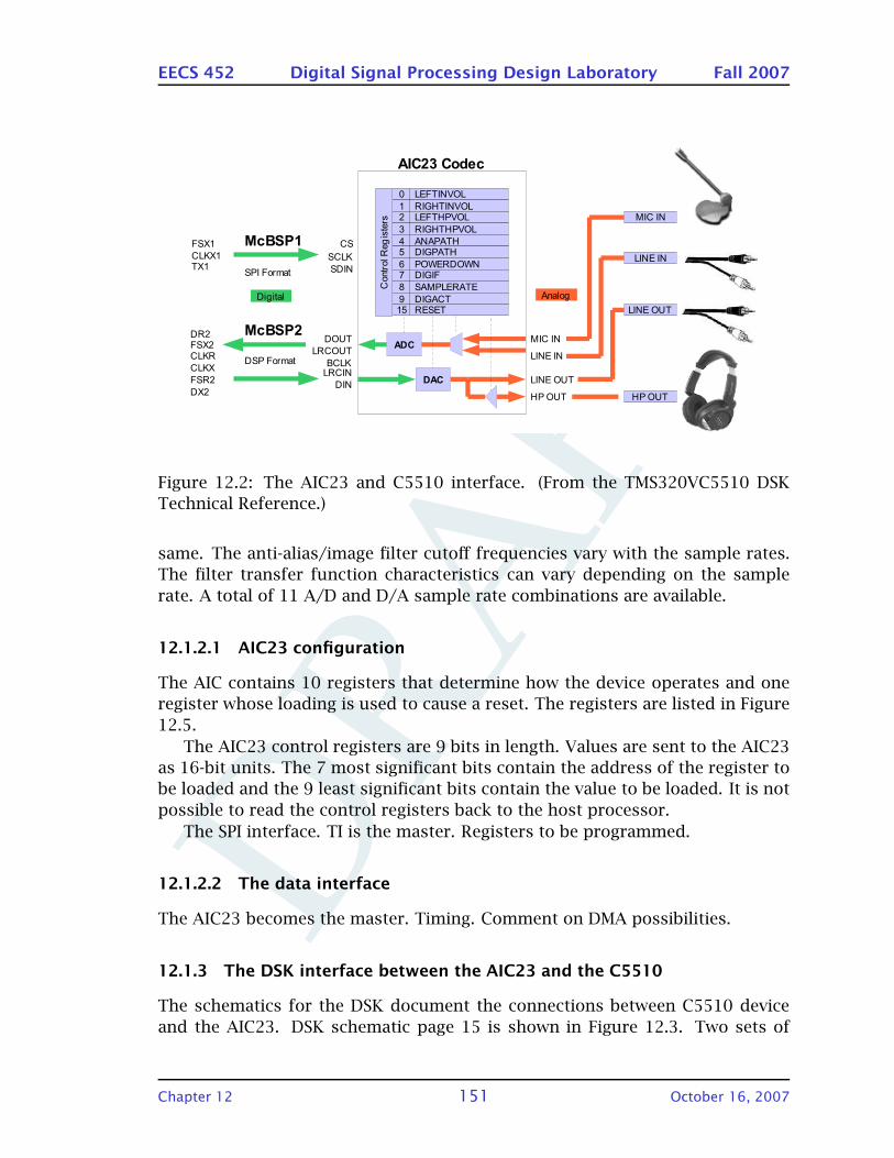
DRA
FT
EECS 452 Digital Signal Processing Design Laboratory Fall 2007
MIC IN
LINE IN
LINE OUT
HP OUT
ADC
DAC
McBSP2
DSP Format
0 LEFTINVOL
1 RIGHTINVOL2 LEFTHPVOL
3 RIGHTHPVOL
4 ANAPATH5 DIGPATH
6 POWERDOWN7 DIGIF
8 SAMPLERATE
9 DIGACT15 RESET
Contr
ol R
eg
iste
rsLRCINBCLK
DIN
DOUT
LRCOUTFSX2
DX2
CLKX
FSR2
CLKR
DR2
CS
SCLK
SDIN
McBSP1
SPI Format
FSX1
TX1CLKX1
AIC23 Codec
Digital Analog
MIC IN
LINE IN
LINE OUT
HP OUT
Figure 12.2: The AIC23 and C5510 interface. (From the TMS320VC5510 DSK
Technical Reference.)
same. The anti-alias/image filter cutoff frequencies vary with the sample rates.
The filter transfer function characteristics can vary depending on the sample
rate. A total of 11 A/D and D/A sample rate combinations are available.
12.1.2.1 AIC23 configuration
The AIC contains 10 registers that determine how the device operates and one
register whose loading is used to cause a reset. The registers are listed in Figure
12.5.
The AIC23 control registers are 9 bits in length. Values are sent to the AIC23
as 16-bit units. The 7 most significant bits contain the address of the register to
be loaded and the 9 least significant bits contain the value to be loaded. It is not
possible to read the control registers back to the host processor.
The SPI interface. TI is the master. Registers to be programmed.
12.1.2.2 The data interface
The AIC23 becomes the master. Timing. Comment on DMA possibilities.
12.1.3 The DSK interface between the AIC23 and the C5510
The schematics for the DSK document the connections between C5510 device
and the AIC23. DSK schematic page 15 is shown in Figure 12.3. Two sets of
Chapter 12 151 October 16, 2007
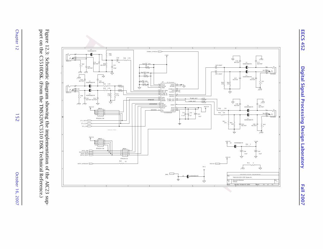
DRAFT
EEC
S452
Dig
ital
Sig
nal
Pro
cessin
gD
esig
nLab
ora
tory
Fall
2007
5
5
4
4
3
3
2
2
1
1
D D
C C
B B
A A
SPECTRUM DIGITAL INCORPORATED
Control Port
5 06 202 C
T M S3 20V C 551 0 D S P S tarte r K i t
B
15 1 5M on day , O c tob er 07 , 20 02
T itle
S ize D ocu m e nt N um b er R ev
D ate : Shee t o f
L L IN E_ O U T
RL IN E _O U T
AI C23LR C IN
A IC 23 C S
SPI M O D E
3 .3 V A
3. 3VA
A IC 3. 3V
A IC 3. 3V
A IC3. 3V
A IC3. 3V A IC3. 3V
R 12 0
C 260 .1 uF
+
C 2510 uF
+
C 1 91 0u F
R 26 4 .7K
R 252 .0K
R 28N O PO P
R 35 4. 7K
C 220 .1 uF
R 3 64. 7K
R 34 4. 7K
L 6H Z 08 05 E6 01 R
R 374 .7K
+
C 2 4 2 20 uF
+
C 2 3 2 20 uF
C 41
0 .1 uF
R 4 3
0
C 45N O PO P
C 4 0N O PO P
C 4 4N O PO P
L 7H Z 08 05 E6 01 R
+C 15
1 uF
C 39N O PO P
C 42
0 .1 uF
C 21
4 7p F
R 324 7K
J4
PH O N ES
3
4
21
C 384 70 nF
J 2
S tereo In
3
4
21
C 3 447 0n F
C 3 347 0n F
R 3 347 K
C 374 70 nF
+
C 4 3
10 uF
J 1
S tereo In
3
421
C 29
NO P O P
L 5H Z 08 05 E6 01 R
+
C 3110 uF
C 3 20. 1uF
R 39 1 00
R4 24 7K
C 3 6N O P O P
J3
PH O N ES
3
421
C 3 5N O PO P
R 4 14 7K
R 38
0
L 4H Z 08 05 E6 01 R PW PackageU7
T LV 320 A I C23
22
141115
25
3
45
21
24
23
109
28
16
17182019
26
1312
8
1
67
2
27
M O D E
A V d dH P G N D
A G N D
XT I/M C LK
B C L K
DIN
LR C IN
C S
S C L K
SD IN
R H P O U TL H P O U T
D G N D
VM ID
M IC _B IASM IC_IN
LL IN E_INRL IN E_IN
XT O
RL IN E _O UTLL IN E _O UT
H PV dd
B Vd d
D O U TL R C O U T
C LK O U T
D Vd d
C 30N O P O P
R 40 10 0
R N 16
R PA CK 4-3 3
12
34 5
6
78
R N 1 4
R P A C K 4-1 0K
1
234 5
67
8
R 44 2
C 1 8N O PO P
R 4 5 3 3
TP 11
L3H Z0 80 5E 60 1R
L8 H Z 08 05 E 6 01 R
C 20N O P O P
L 9 H Z0 80 5E 60 1R
R 27
0
L1H Z 0 80 5E 60 1R
R 31
0
C 2 7N O P O P
C 17N O P O P
C 2 8N O P O P
L2
H Z0 80 5E 60 1R
C 16N O PO P
R N 1 5
R P A C K 4-1 0K
1
234 5
67
8
+
C 46
10 uF
+
C 47
10 uF
C T L _C LK
CT L_ C S
C T L _D AT A
D AT A_ DIND AT A_S YN C IN
D AT A_ BC LK
D AT A _ D O U T
D AT A_S YN C O UT
C O D E C_S YS C LK
A IC 3.3V
G N D
Fig
ure
12.3
:Sch
em
atic
dia
gra
msh
ow
ing
the
imp
lem
en
tatio
nof
the
AIC
23
su
p-
port
on
the
C5510D
SK
.(F
rom
the
TM
S320V
C5510
DSK
Tech
nic
al
Refe
ren
ce.)
Chap
ter
12
15
2O
cto
ber
16
,2
00
7
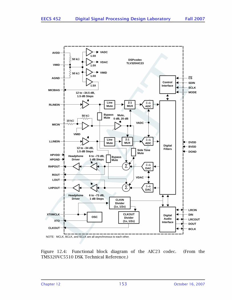
DRA
FT
EECS 452 Digital Signal Processing Design Laboratory Fall 2007
ControlInterface
DigitalFilters
DigitalAudio
Interface
Σ–∆DAC
Σ6 to –73 dB,1 dB Steps
HeadphoneDriver
Σ–∆DAC
Σ
6 to –73 dB,1 dB Steps
HeadphoneDriver
CLKOUTDivider
(1x, 1/2x)
OSC
CS
SDIN
SCLK
MODE
DVDD
BVDD
DGND
LRCIN
DIN
LRCOUT
DOUT
BCLK
AVDD
VMID
AGND
RLINEIN
LLINEIN
HPVDD
HPGND
RHPOUT
ROUT
LOUT
LHPOUT
XTI/MCLK
XTO
CLKOUT
DSPcodecTLV320AIC23
1.0X
1.0X
VADC
VMID
50 kΩ
50 kΩ
Σ–∆ADC
2:1MUX
VDAC
Σ–∆ADC
2:1MUX
Mute,0 dB, 20 dB
VMID
50 kΩ
10 kΩVADC
12 to –34.5 dB,1.5 dB Steps
1.0X
1.5X
VDAC
12 to –34 dB,1.5 dB Steps
MICBIAS
MICIN
CLKINDivider
(1x, 1/2x)
LineMute
LineMute
Side Tone Mute
BypassMute
BypassMute
NOTE: MCLK, BCLK, and SCLK are all asynchronous to each other.
Figure 12.4: Functional block diagram of the AIC23 codec. (From the
TMS320VC5510 DSK Technical Reference.)
Chapter 12 153 October 16, 2007
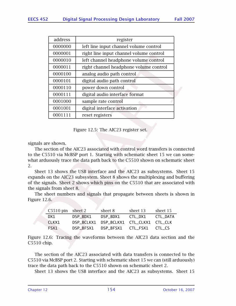
DRA
FT
EECS 452 Digital Signal Processing Design Laboratory Fall 2007
address register
0000000 left line input channel volume control
0000001 right line input channel volume control
0000010 left channel headphone volume control
0000011 right channel headphone volume control
0000100 analog audio path control
0000101 digital audio path control
0000110 power down control
0000111 digital audio interface format
0001000 sample rate control
0001001 digital interface activation
0001111 reset registers
Figure 12.5: The AIC23 register set.
signals are shown.
The section of the AIC23 associated with control word transfers is connected
to the C5510 via McBSP port 1. Starting with schematic sheet 15 we can some-
what arduously trace the data path back to the C5510 shown on schematic sheet
2.
Sheet 13 shows the USB interface and the AIC23 as subsystems. Sheet 15
expands on the AIC23 subsystem. Sheet 8 shows the multiplexing and buffering
of the signals. Sheet 2 shows which pins on the C5510 that are associated with
the signals from sheet 8.
The sheet numbers and signals that propagate between sheets is shown in
Figure 12.6.
C5510 pin sheet 2 sheet 8 sheet 13 sheet 15
DX1 DSP_BDX1 DSP_BDX1 CTL_DX1 CTL_DATA
CLKX1 DSP_BCLKX1 DSP_BCLKX1 CTL_CLKX1 CTL_CLK
FSX1 DSP_BFSX1 DSP_BFSX1 CTL_FSX1 CTL_CS
Figure 12.6: Tracing the waveforms between the AIC23 data section and the
C5510 chip.
The section of the AIC23 associated with data transfers is connected to the
C5510 via McBSP port 2. Starting with schematic sheet 15 we can (still arduously)
trace the data path back to the C5510 shown on schematic sheet 2.
Sheet 13 shows the USB interface and the AIC23 as subsystems. Sheet 15
Chapter 12 154 October 16, 2007
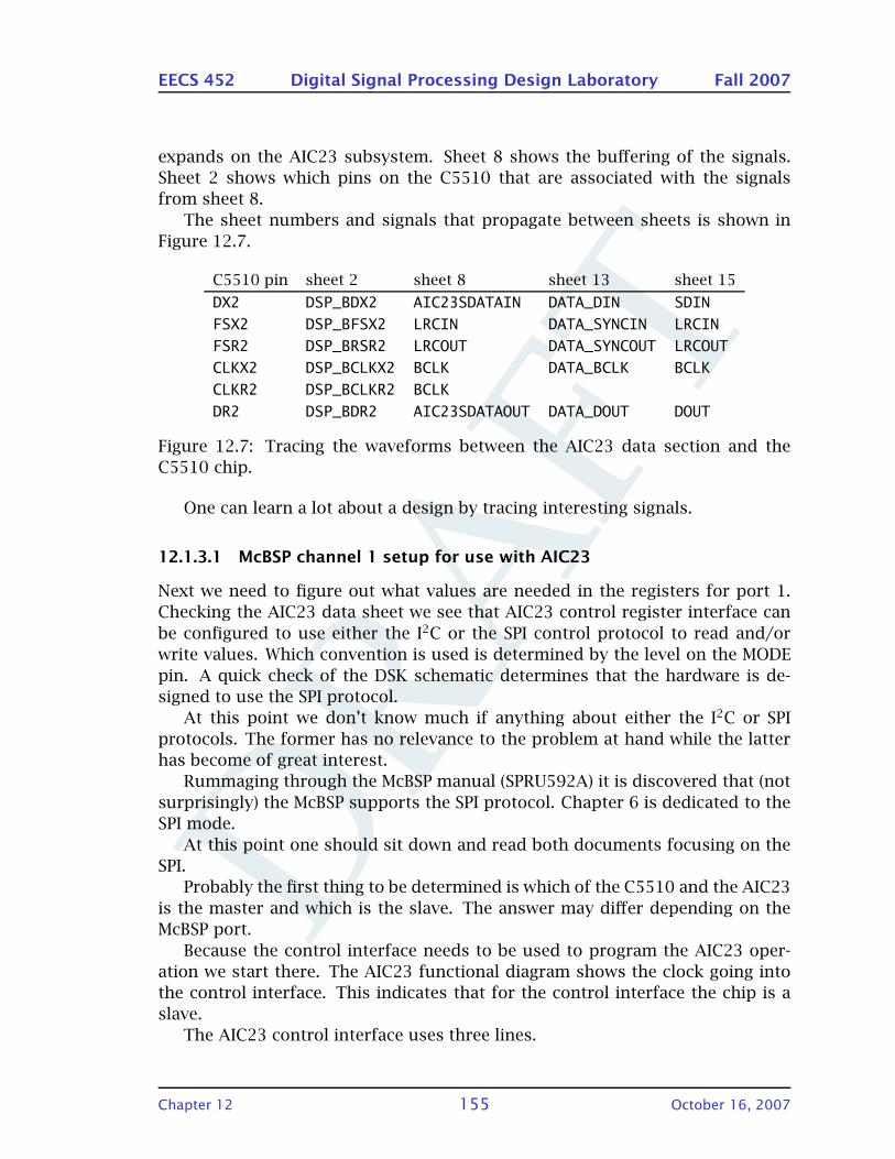
DRA
FT
EECS 452 Digital Signal Processing Design Laboratory Fall 2007
expands on the AIC23 subsystem. Sheet 8 shows the buffering of the signals.
Sheet 2 shows which pins on the C5510 that are associated with the signals
from sheet 8.
The sheet numbers and signals that propagate between sheets is shown in
Figure 12.7.
C5510 pin sheet 2 sheet 8 sheet 13 sheet 15
DX2 DSP_BDX2 AIC23SDATAIN DATA_DIN SDIN
FSX2 DSP_BFSX2 LRCIN DATA_SYNCIN LRCIN
FSR2 DSP_BRSR2 LRCOUT DATA_SYNCOUT LRCOUT
CLKX2 DSP_BCLKX2 BCLK DATA_BCLK BCLK
CLKR2 DSP_BCLKR2 BCLK
DR2 DSP_BDR2 AIC23SDATAOUT DATA_DOUT DOUT
Figure 12.7: Tracing the waveforms between the AIC23 data section and the
C5510 chip.
One can learn a lot about a design by tracing interesting signals.
12.1.3.1 McBSP channel 1 setup for use with AIC23
Next we need to figure out what values are needed in the registers for port 1.
Checking the AIC23 data sheet we see that AIC23 control register interface can
be configured to use either the I2C or the SPI control protocol to read and/or
write values. Which convention is used is determined by the level on the MODE
pin. A quick check of the DSK schematic determines that the hardware is de-
signed to use the SPI protocol.
At this point we don’t know much if anything about either the I2C or SPI
protocols. The former has no relevance to the problem at hand while the latter
has become of great interest.
Rummaging through the McBSP manual (SPRU592A) it is discovered that (not
surprisingly) the McBSP supports the SPI protocol. Chapter 6 is dedicated to the
SPI mode.
At this point one should sit down and read both documents focusing on the
SPI.
Probably the first thing to be determined is which of the C5510 and the AIC23
is the master and which is the slave. The answer may differ depending on the
McBSP port.
Because the control interface needs to be used to program the AIC23 oper-
ation we start there. The AIC23 functional diagram shows the clock going into
the control interface. This indicates that for the control interface the chip is a
slave.
The AIC23 control interface uses three lines.
Chapter 12 155 October 16, 2007
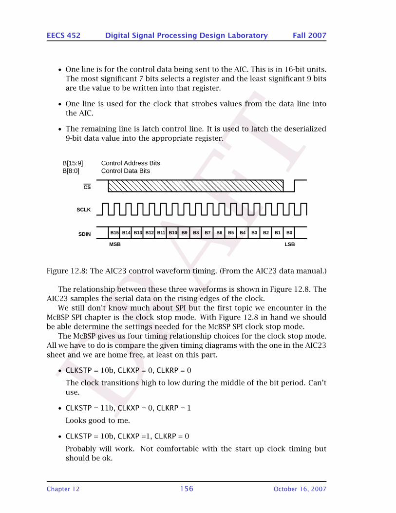
DRA
FT
EECS 452 Digital Signal Processing Design Laboratory Fall 2007
• One line is for the control data being sent to the AIC. This is in 16-bit units.
The most significant 7 bits selects a register and the least significant 9 bits
are the value to be written into that register.
• One line is used for the clock that strobes values from the data line into
the AIC.
• The remaining line is latch control line. It is used to latch the deserialized
9-bit data value into the appropriate register.
B[15:9] Control Address BitsB[8:0] Control Data Bits
B15 B14 B13 B12 B11 B10 B9 B8 B7 B6 B5 B4 B3 B2 B1 B0
ÎÎÎÎÎÎÎÎÎÎÎÎÎÎÎÎÎÎÎÎÎÎÎÎÎÎÎÎÎÎÎÎÎÎÎÎÎÎ
MSB LSB
CS
SCLK
SDIN
Figure 12.8: The AIC23 control waveform timing. (From the AIC23 data manual.)
The relationship between these three waveforms is shown in Figure 12.8. The
AIC23 samples the serial data on the rising edges of the clock.
We still don’t know much about SPI but the first topic we encounter in the
McBSP SPI chapter is the clock stop mode. With Figure 12.8 in hand we should
be able determine the settings needed for the McBSP SPI clock stop mode.
The McBSP gives us four timing relationship choices for the clock stop mode.
All we have to do is compare the given timing diagrams with the one in the AIC23
sheet and we are home free, at least on this part.
• CLKSTP = 10b, CLKXP = 0, CLKRP = 0
The clock transitions high to low during the middle of the bit period. Can’t
use.
• CLKSTP = 11b, CLKXP = 0, CLKRP = 1
Looks good to me.
• CLKSTP = 10b, CLKXP =1, CLKRP = 0
Probably will work. Not comfortable with the start up clock timing but
should be ok.
Chapter 12 156 October 16, 2007

DRA
FT
EECS 452 Digital Signal Processing Design Laboratory Fall 2007
• CLKSTP = 11b, CLKXP =1, CLKRP =1
Negative transitions at mid bit interval. Can’t use.
We will go with the second choice. We will use a 16-bit frame size.
Section 6.5 of the SPI manual is titled Procedure for Configuring a McBSP for
SPI Operation. This is followed by section 6.6 McBSP as the SPI Master. There
is useful information present here but not a step by step procedure that we can
follow. Let’s fast forward to section 8.2 and the immediately following sections.
Next we work through the outlined steps making programming notes as we
go. We are not using the receiver and so will not make any changes there.
In order to guarantee a known starting point we will load the McBSP registers
with the default values set into them after a hardware reset. These values are
documented in the McBSP manual.
The McBSP prepend is dropped for the moment to keep line lengths (and the
amount of typing) manageable.
McBSP_reg(1, SPCR1) = 0x0000;McBSP_reg(1, SPCR2) = 0x0000;McBSP_reg(1, RCR1) = 0x0000;McBSP_reg(1, RCR2) = 0x0000;McBSP_reg(1, XCR1) = 0x0000;McBSP_reg(1, XCR2) = 0x0000;McBSP_reg(1, SRGR1) = 0x00FF;McBSP_reg(1, SRGR2) = 0x2000;McBSP_reg(1, MCR1) = 0;McBSP_reg(1, MCR2) = 0;McBSP_reg(1, PCR) = 0;
Next we will follow the steps outlined in Chapter 8 of the McBSP manual for
configuring the port 1 transmitter. We will assume that the register contents are
unknown and only the particular bits involved with a setting are to be altered.
Such might be the case if we had previously programmed the receiver.
1. To reset the transmitter, sample generator and frame-sync logic
McBSP_reg(1, SPCR1) = McBSP_reg(1, SPCR1)&(~0x00C1);
2. Setting the transmitter pins to operate as McBSP pins:
This is done by setting PCR bit 13 to a zero.
McBSP_reg(1, PCR) = McBSP_reg(1, PCR)&(~0x2000);
Chapter 12 157 October 16, 2007

DRA
FT
EECS 452 Digital Signal Processing Design Laboratory Fall 2007
3. Disable digital loop back. This can be done by clearing bit 15 of SPCR1.
McBSP_reg(1, SPCR1) = McBSP_reg(1, SPCR1)&(~0x8000);
We might should define a symbol and avoid hard wiring constants into the
code.
4. Enable the clock stop mode bits in SPCR1.
Above we decided to use CLDSTP=11.
McBSP_reg(1, SPCR1) = (McBSP_reg(1, SPCR1)&(~0x1800))|0x1800;
We are a bit more general than needed here.
5. Enable/disable the transmit multichannel selection. Choosing disable.
McBSP_reg(1, MCR2) = McBSP_reg(1, MCR2)&(~0x0001);
Again we are more general than perhaps expected.
6. Choosing 1 or 2 phases for transmit. Choosing one phase.
McBSP_reg(1, XCR2) = McBSP_reg(1, XCR2)&(~0x8000);
7. Setting the transmit word length. Setting 16 bits.
McBSP_reg(1, XCR1) = (McBSP_reg(1, XCR1)&(~0x00E0))|0x0040;
8. Setting the transmit frame word length.
One value per frame is needed. Since we are only using one phase we only
need to set a value in XCR1.
McBSP_reg(1, XCR1) = McBSP_reg(1, XCR1)&(~0x7F00);
9. Enable/disable transmit frame sync ignore.
I think that this is a don’t care for this application.
10. Setting the transmit companding mode. Not for the control data values.
McBSP_reg(1, XCR2) = McBSP_reg(1, XCR2)&(~0x0014);
11. Setting the transmit data delay. Setting to 0 seems reasonable.
McBSP_reg(1, XCR2) = McBSP_reg(1, XCR2)&(~0x0003);
12. Setting the transmit DXENA mode. I don’t know. setting to 0 seems reason-
able.
McBSP_reg(1, SPCR1) = McBSP_reg(1, SPCR1)&(~0x0080);
13. Setting the transmit interrupt mode. Interrupts are later in the semester.
McBSP_reg(1, SPCR2) = McBSP_reg(1, SPCR2)&(~0x0030);
Chapter 12 158 October 16, 2007
DRA
FT
EECS 452 Digital Signal Processing Design Laboratory Fall 2007
14. Setting the transmit frame-sync mode. The discussion on this item indi-
cates doing the following operations for SPI use.
McBSP_reg(1, PCR) = McBSP_reg(1, PCR)|(0x0800);McBSP_reg(1, SRGR2) = McBSP_reg(1, SRGR2)&(~0x1000);
15. Setting the transmit frame-sync polarity. The AIC23 needs sync low.
McBSP_reg(1, PCR) = McBSP_reg(1, PCR)|(0x0008);
16. Setting the SRG frame-sync period and pulse width. The frame sync period
needs to be at least as the frame size. A value of 18 should work.
McBSP_reg(1, SRGR2) = (McBSP_reg(1, SRGR2)&(~0x00ff))|0x0013;McBSP_reg(1, SRGR1) = McBSP_reg(1, SRGR1)&(~0xff00);
17. Setting the transmit clock mode. The McBSP needs to generate.
McBSP_reg(1, PCR) = McBSP_reg(1, PCR)|(0x0200);
18. Setting the transmit clock polarity. This is the CLKXP signal which we de-
cided way above needs to be 0.
McBSP_reg(1, PCR) = McBSP_reg(1, PCR)&(~0x0002);
19. Setting the SRG clock divide down value. This is determines the clock rate
for the control data. The value divided down is C5510 clock (I think). As-
suming a max clock of 200 MHz if we divide by 200 we get a 1 MHz control
clock to the AIC23. Seems reasonable. A value of 128 gives a reasonable
clock rate and is easy to convert to binary.
McBSP_reg(1, SRGR1) = (McBSP_reg(1, SRGR1)&(~0x00ff))|0x0080;
20. Choosing an input clock. Want to use the CPU clock.
McBSP_reg(1, PCR) = McBSP_reg(1, PCR)&(~0x0080);McBSP_reg(1, SRGR2) = McBSP_reg(1, SRGR2)|0x2000;
21. Setting the input clock polarity. This involves setting the CLKSP, CLKXP and
CLKRP bits. The CLKSP bit is not used for this application.
McBSP_reg(1, PCR) = McBSP_reg(1, PCR)&(~0x0003);
22. Enable the transmitter.
McBSP_reg(1, SPCR2) = McBSP_reg(1, SPCR2)|0x00C1;
Away we go!
Chapter 12 159 October 16, 2007
DRA
FT
EECS 452 Digital Signal Processing Design Laboratory Fall 2007
Wow! We made it through the Chapter 8 transmitter check list. TI even
supplies forms to be filled out while going through this. They can be found in
the McBSP manual and are also available in the CCS help system. We will have to
go through this again for McBSP port 2, both for transmit and for receive.
Summarizing:
• SPCR1
McBSP_reg(1, SPCR1) = 0x0000;McBSP_reg(1, SPCR1) = McBSP_reg(1, SPCR1)&(~0x8000);McBSP_reg(1, SPCR1) = (McBSP_reg(1, SPCR1)&(~0x1800))|0x1800; McBSP_reg(1, SPCR1) =
• SPCR2
McBSP_reg(1, SPCR2) = 0x0000;McBSP_reg(1, SPCR1) = McBSP_reg(1, SPCR1)&(~0x00C1)McBSP_reg(1, SPCR2) = McBSP_reg(1, SPCR2)&(~0x0030);
• RCR1
McBSP_reg(1, RCR1) = 0x0000;
• RCR2
McBSP_reg(1, RCR2) = 0x0000;
• XCR1
McBSP_reg(1, XCR1) = 0x0000;McBSP_reg(1, XCR1) = (McBSP_reg(1, XCR1)&(~0x00E0))|0x0040;McBSP_reg(1, XCR1) = (McBSP_reg(1, XCR1)&(~0x7F00));
• XCR2
McBSP_reg(1, XCR2) = 0x0000;McBSP_reg(1, XCR2) = McBSP_reg(1, XCR2)&(~0x8000);McBSP_reg(1, XCR2) = McBSP_reg(1, XCR2)&(~0x0014);McBSP_reg(1, XCR2) = McBSP_reg(1, XCR2)&(~0x0003);
• SRGR1
McBSP_reg(1, SRGR1) = 0x00FF;McBSP_reg(1, SRGR1) = McBSP_reg(1, SRGR1)&(~0xff00);McBSP_reg(1, SRGR1) = (McBSP_reg(1, SRGR1)&(~0x00ff))|0x0080;
• SRGR2
McBSP_reg(1, SRGR2) = 0x2000;McBSP_reg(1, SRGR2) = McBSP_reg(1, SRGR2)&(~0x1000);McBSP_reg(1, SRGR2) = (McBSP_reg(1, SRGR2)&(~0x00ff)|0x0013;McBSP_reg(1, SRGR2) = McBSP_reg(1, SRGR2)|0x2000;
• MCR1
McBSP_reg(1, MCR1) = 0x0000;
Chapter 12 160 October 16, 2007

DRA
FT
EECS 452 Digital Signal Processing Design Laboratory Fall 2007
• MCR2
McBSP_reg(1, MCR2) = 0x0000;McBSP_reg(1, MCR2) = McBSP_reg(1, MCR2)&(~0x0001);
• PCR
McBSP_reg(1, PCR) = 0x0000;McBSP_reg(1, PCR) = McBSP_reg(1, PCR)&(~0x2000);McBSP_reg(1, PCR) = McBSP_reg(1, PCR)|(0x0800);McBSP_reg(1, PCR) = McBSP_reg(1, PCR)|(0x0008);McBSP_reg(1, PCR) = McBSP_reg(1, PCR)|(0x0200);McBSP_reg(1, PCR) = McBSP_reg(1, PCR)&(~0x0002);McBSP_reg(1, PCR) = McBSP_reg(1, PCR)&(~0x0080);McBSP_reg(1, PCR) = McBSP_reg(1, PCR)&(~0x0003);
This distills down to a more manageable:
McBSP_reg(1, McBSP_SPCR2) = 0x0000; // stop xmtrMcBSP_reg(1, McBSP_SPCR1) = 0x1800;McBSP_reg(1, McBSP_RCR1) = 0x0000;McBSP_reg(1, McBSP_RCR2) = 0x0000;McBSP_reg(1, McBSP_XCR1) = 0x0040;McBSP_reg(1, McBSP_XCR2) = 0x0000;McBSP_reg(1, McBSP_SRGR1) = 0x0080;McBSP_reg(1, McBSP_SRGR2) = 0x2011;McBSP_reg(1, McBSP_MCR1) = 0x0000;McBSP_reg(1, McBSP_MCR2) = 0x0000;McBSP_reg(1, McBSP_PCR) = 0x0A08;McBSP_reg(1, McBSP_SPCR2) = 0x00C1; // start xmtr
12.1.4 Using McBSP port 1 to initialize the AIC23
At this point we have the capability to send control values to the AIC23 using
McBSP serial port 1. There are 10 8-bit registers in the AIC23 that need to be
programmed.
Studying the DSK schematic and the AIC23 data manual we see that the AIC23
is supplied with a 12 MHz clock. The AIC23 can use this to set the sample rate.
The AIC23 audio data channel also has a DSP mode designed to connect directly
to TI DSP devices. Because the AIC23 is controlling the sample timing it makes
sense that it be the master for audio data transfers on McBSP port 2.
It makes sense to do as was done in Spectrum Digital’s example, tone.c, and
simply place the required 10 AIC23 setup values in an array and use a function
to send the array contents to the AIC23.
Chapter 12 161 October 16, 2007
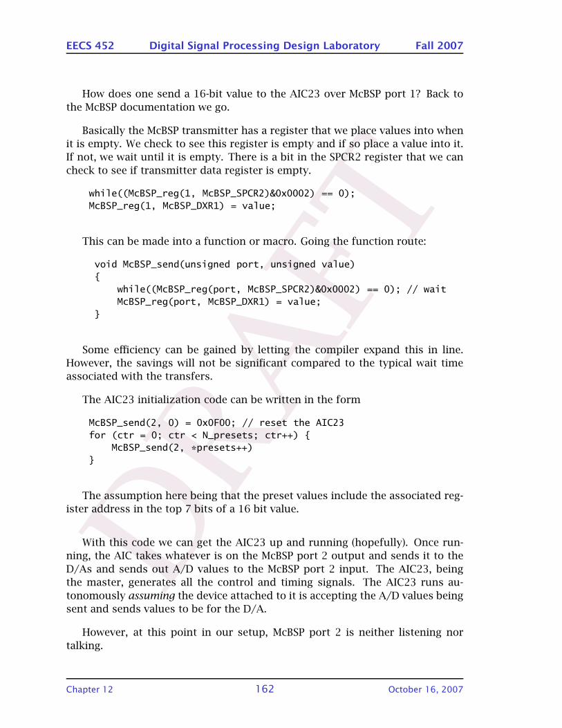
DRA
FT
EECS 452 Digital Signal Processing Design Laboratory Fall 2007
How does one send a 16-bit value to the AIC23 over McBSP port 1? Back to
the McBSP documentation we go.
Basically the McBSP transmitter has a register that we place values into when
it is empty. We check to see this register is empty and if so place a value into it.
If not, we wait until it is empty. There is a bit in the SPCR2 register that we can
check to see if transmitter data register is empty.
while((McBSP_reg(1, McBSP_SPCR2)&0x0002) == 0);McBSP_reg(1, McBSP_DXR1) = value;
This can be made into a function or macro. Going the function route:
void McBSP_send(unsigned port, unsigned value)
while((McBSP_reg(port, McBSP_SPCR2)&0x0002) == 0); // waitMcBSP_reg(port, McBSP_DXR1) = value;
Some efficiency can be gained by letting the compiler expand this in line.
However, the savings will not be significant compared to the typical wait time
associated with the transfers.
The AIC23 initialization code can be written in the form
McBSP_send(2, 0) = 0x0F00; // reset the AIC23for (ctr = 0; ctr < N_presets; ctr++)
McBSP_send(2, *presets++)
The assumption here being that the preset values include the associated reg-
ister address in the top 7 bits of a 16 bit value.
With this code we can get the AIC23 up and running (hopefully). Once run-
ning, the AIC takes whatever is on the McBSP port 2 output and sends it to the
D/As and sends out A/D values to the McBSP port 2 input. The AIC23, being
the master, generates all the control and timing signals. The AIC23 runs au-
tonomously assuming the device attached to it is accepting the A/D values being
sent and sends values to be for the D/A.
However, at this point in our setup, McBSP port 2 is neither listening nor
talking.
Chapter 12 162 October 16, 2007
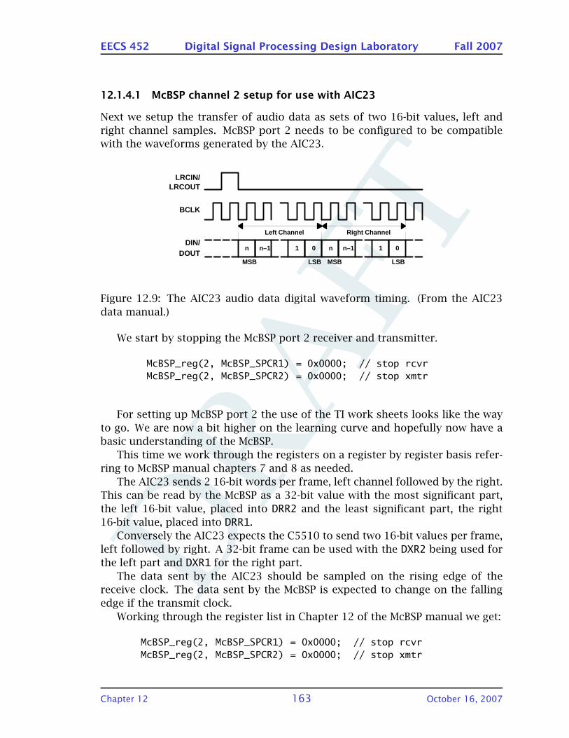
DRA
FT
EECS 452 Digital Signal Processing Design Laboratory Fall 2007
12.1.4.1 McBSP channel 2 setup for use with AIC23
Next we setup the transfer of audio data as sets of two 16-bit values, left and
right channel samples. McBSP port 2 needs to be configured to be compatible
with the waveforms generated by the AIC23.
LRCIN/
BCLK
DIN/n n–1 01 n–1n
Left Channel Right Channel
1 0
MSB LSB MSB LSB
LRCOUT
DOUT
Figure 12.9: The AIC23 audio data digital waveform timing. (From the AIC23
data manual.)
We start by stopping the McBSP port 2 receiver and transmitter.
McBSP_reg(2, McBSP_SPCR1) = 0x0000; // stop rcvrMcBSP_reg(2, McBSP_SPCR2) = 0x0000; // stop xmtr
For setting up McBSP port 2 the use of the TI work sheets looks like the way
to go. We are now a bit higher on the learning curve and hopefully now have a
basic understanding of the McBSP.
This time we work through the registers on a register by register basis refer-
ring to McBSP manual chapters 7 and 8 as needed.
The AIC23 sends 2 16-bit words per frame, left channel followed by the right.
This can be read by the McBSP as a 32-bit value with the most significant part,
the left 16-bit value, placed into DRR2 and the least significant part, the right
16-bit value, placed into DRR1.
Conversely the AIC23 expects the C5510 to send two 16-bit values per frame,
left followed by right. A 32-bit frame can be used with the DXR2 being used for
the left part and DXR1 for the right part.
The data sent by the AIC23 should be sampled on the rising edge of the
receive clock. The data sent by the McBSP is expected to change on the falling
edge if the transmit clock.
Working through the register list in Chapter 12 of the McBSP manual we get:
McBSP_reg(2, McBSP_SPCR1) = 0x0000; // stop rcvrMcBSP_reg(2, McBSP_SPCR2) = 0x0000; // stop xmtr
Chapter 12 163 October 16, 2007

DRA
FT
EECS 452 Digital Signal Processing Design Laboratory Fall 2007
McBSP_reg(2, McBSP_RCR1) = 0x00A0; // 2 16-bit words/frameMcBSP_reg(2, McBSP_RCR2) = 0x0000;McBSP_reg(2, McBSP_XCR1) = 0x00A0; // 2 16-bit words/frameMcBSP_reg(2, McBSP_XCR2) = 0x0000;McBSP_reg(2, McBSP_SRGR1) = 0x0000;McBSP_reg(2, McBSP_SRGR2) = 0x0000;McBSP_reg(2, McBSP_MCR1) = 0x0000;McBSP_reg(2, McBSP_MCR2) = 0x0000;McBSP_reg(2, McBSP_PCR) = 0x0003; // use of clock edges
McBSP_reg(2, McBSP_SPCR1) = 0x0001; // start rcvrMcBSP_reg(2, McBSP_SPCR2) = 0x00C1; // start xmtr
Looking at the non-zero bits that resulted it appears that life is much simpler
when the peripheral acts as the master. The above set of configuration values
was a lot easier figure out than the ones for the control channel!
12.1.4.2 Changing sample rates on the fly
The McBSP channel was written in a way that it can be used to change the con-
tents of any AIC23 register nominally at any time.
There are lab exercises where a sample rate other than 48 kHz is desired. In
(far) past semesters this was done by changing the AIC23 support code. This
often led to later exercises being run using an unexpected sample rate. In order
to minimize such surprises, sample rates other than 48 kHz should be changed
by programs that require such as part of their start-up prologue.
12.1.4.3 McBSP programming when using interrupts
The McBSP system will be run under interrupts in the real-time FFT exercise.
How to do this will be discussed in Chapter 23.
Chapter 12 164 October 16, 2007
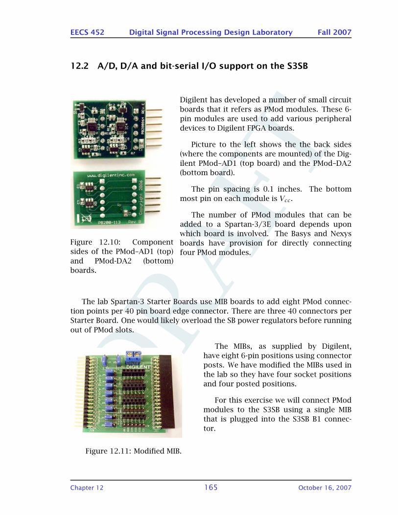
DRA
FT
EECS 452 Digital Signal Processing Design Laboratory Fall 2007
12.2 A/D, D/A and bit-serial I/O support on the S3SB
Figure 12.10: Component
sides of the PMod–AD1 (top)
and PMod-DA2 (bottom)
boards.
Digilent has developed a number of small circuit
boards that it refers as PMod modules. These 6-
pin modules are used to add various peripheral
devices to Digilent FPGA boards.
Picture to the left shows the the back sides
(where the components are mounted) of the Dig-
ilent PMod–AD1 (top board) and the PMod–DA2
(bottom board).
The pin spacing is 0.1 inches. The bottom
most pin on each module is Vcc .
The number of PMod modules that can be
added to a Spartan-3/3E board depends upon
which board is involved. The Basys and Nexys
boards have provision for directly connecting
four PMod modules.
The lab Spartan-3 Starter Boards use MIB boards to add eight PMod connec-
tion points per 40 pin board edge connector. There are three 40 connectors per
Starter Board. One would likely overload the SB power regulators before running
out of PMod slots.
Figure 12.11: Modified MIB.
The MIBs, as supplied by Digilent,
have eight 6-pin positions using connector
posts. We have modified the MIBs used in
the lab so they have four socket positions
and four posted positions.
For this exercise we will connect PMod
modules to the S3SB using a single MIB
that is plugged into the S3SB B1 connec-
tor.
Chapter 12 165 October 16, 2007
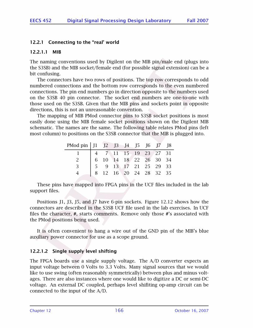
DRA
FT
EECS 452 Digital Signal Processing Design Laboratory Fall 2007
12.2.1 Connecting to the “real’ world
12.2.1.1 MIB
The naming conventions used by Digilent on the MIB pin/male end (plugs into
the S3SB) and the MIB socket/female end (for possible signal extension) can be a
bit confusing.
The connectors have two rows of positions. The top row corresponds to odd
numbered connections and the bottom row corresponds to the even numbered
connections. The pin end numbers go in direction opposite to the numbers used
on the S3SB 40 pin connector. The socket end numbers are one-to-one with
those used on the S3SB. Given that the MIB pins and sockets point in opposite
directions, this is not an unreasonable convention.
The mapping of MIB PMod connector pins to S3SB socket positions is most
easily done using the MIB female socket positions shown on the Digilent MIB
schematic. The names are the same. The following table relates PMod pins (left
most column) to positions on the S3SB connector that the MIB is plugged into.
PMod pin J1 J2 J3 J4 J5 J6 J7 J8
1 4 7 11 15 19 23 27 31
2 6 10 14 18 22 26 30 34
3 5 9 13 17 21 25 29 33
4 8 12 16 20 24 28 32 35
These pins have mapped into FPGA pins in the UCF files included in the lab
support files.
Positions J1, J3, J5, and J7 have 6-pin sockets. Figure 12.12 shows how the
connectors are described in the S3SB UCF file used in the lab exercises. In UCF
files the character, #, starts comments. Remove only those #’s associated with
the PMod positions being used.
It is often convenient to hang a wire out of the GND pin of the MIB’s blue
auxiliary power connector for use as a scope ground.
12.2.1.2 Single supply level shifting
The FPGA boards use a single supply voltage. The A/D converter expects an
input voltage between 0 Volts to 3.3 Volts. Many signal sources that we would
like to use swing (often reasonably symmetrically) between plus and minus volt-
ages. There are also instances where one would like to digitize a DC or semi-DC
voltage. An external DC coupled, perhaps level shifiting op-amp circuit can be
connected to the input of the A/D.
Chapter 12 166 October 16, 2007
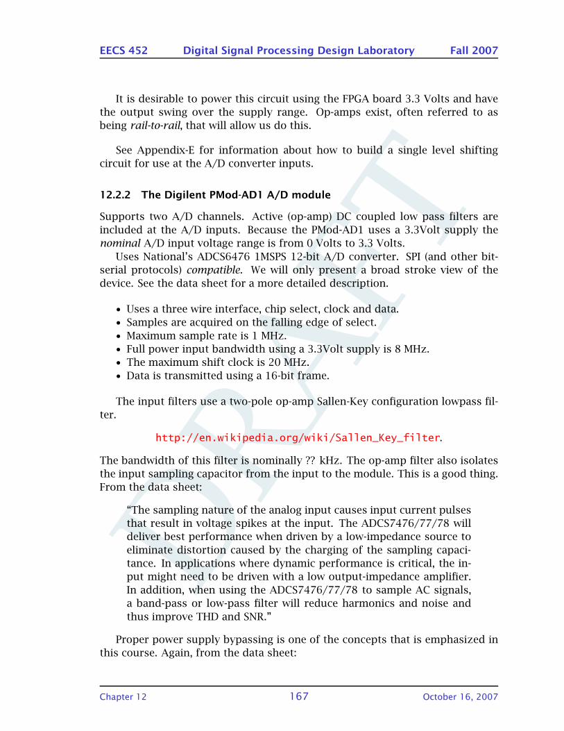
DRA
FT
EECS 452 Digital Signal Processing Design Laboratory Fall 2007
It is desirable to power this circuit using the FPGA board 3.3 Volts and have
the output swing over the supply range. Op-amps exist, often referred to as
being rail-to-rail, that will allow us do this.
See Appendix-E for information about how to build a single level shifting
circuit for use at the A/D converter inputs.
12.2.2 The Digilent PMod-AD1 A/D module
Supports two A/D channels. Active (op-amp) DC coupled low pass filters are
included at the A/D inputs. Because the PMod-AD1 uses a 3.3Volt supply the
nominal A/D input voltage range is from 0 Volts to 3.3 Volts.
Uses National’s ADCS6476 1MSPS 12-bit A/D converter. SPI (and other bit-
serial protocols) compatible. We will only present a broad stroke view of the
device. See the data sheet for a more detailed description.
• Uses a three wire interface, chip select, clock and data.
• Samples are acquired on the falling edge of select.
• Maximum sample rate is 1 MHz.
• Full power input bandwidth using a 3.3Volt supply is 8 MHz.
• The maximum shift clock is 20 MHz.
• Data is transmitted using a 16-bit frame.
The input filters use a two-pole op-amp Sallen-Key configuration lowpass fil-
ter.
http://en.wikipedia.org/wiki/Sallen_Key_filter.
The bandwidth of this filter is nominally ?? kHz. The op-amp filter also isolates
the input sampling capacitor from the input to the module. This is a good thing.
From the data sheet:
“The sampling nature of the analog input causes input current pulses
that result in voltage spikes at the input. The ADCS7476/77/78 will
deliver best performance when driven by a low-impedance source to
eliminate distortion caused by the charging of the sampling capaci-
tance. In applications where dynamic performance is critical, the in-
put might need to be driven with a low output-impedance amplifier.
In addition, when using the ADCS7476/77/78 to sample AC signals,
a band-pass or low-pass filter will reduce harmonics and noise and
thus improve THD and SNR.”
Proper power supply bypassing is one of the concepts that is emphasized in
this course. Again, from the data sheet:
Chapter 12 167 October 16, 2007
DRA
FT
EECS 452 Digital Signal Processing Design Laboratory Fall 2007
Positive supply pin. These pins should be connected to a quiet +2.7V
to +5.25V source and bypassed to GND with 0.1 tF and 1 tF monolithic
capacitors located within 1 cm of the power pin. The ADCS7476/77/78
uses this power supply as a reference, so it should be thoroughly by-
passed.
Note the maximum distance requirement.
12.2.2.1 PMod-AD1 pin assignments
Digital interface:
1 chip select,
2 A/D 1 data bit stream,
3 A/D 2 data bit stream,
4 shift clock,
5 ground,
6 Vcc.
Analog interface:
1 A/D 1 analog input,
2 ground,
3 A/D 2 analog input,
4 ground,
5 ground,
6 Vcc.
12.2.2.2 PMod-AD1 analog input
Note that if we aren’t using a 1 MHz sample rate, or there abouts, the anti-alias
filter isn’t anti-aliasing. The filter on the board is most likely there to simply limit
the bandwidth of the input waveform. For significantly lower sample rates we
would add an external filter. Later in this exercise we very much want to see what
happens when a waveform is aliased. There are communications applications
where one can exploit aliasing by using it to frequency shift a waveform.
12.2.2.3 Sample and SPI interface timings
Include DCM use.
Chapter 12 168 October 16, 2007
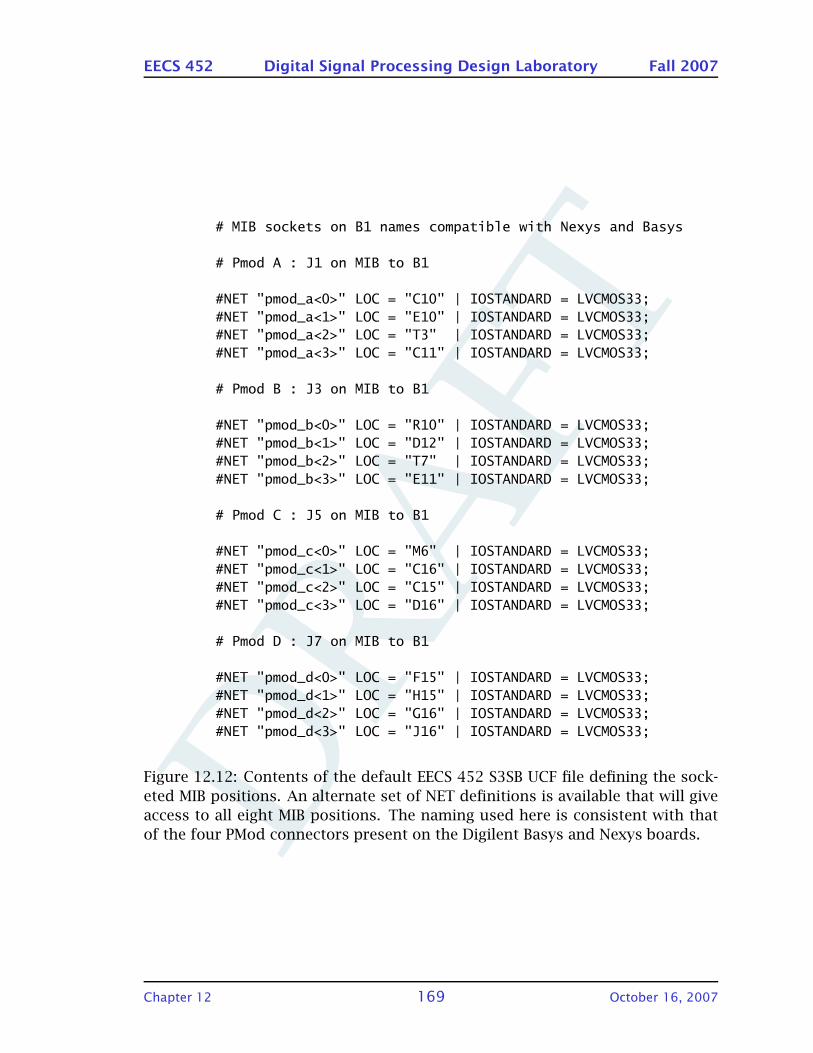
DRA
FT
EECS 452 Digital Signal Processing Design Laboratory Fall 2007
# MIB sockets on B1 names compatible with Nexys and Basys
# Pmod A : J1 on MIB to B1
#NET "pmod_a<0>" LOC = "C10" | IOSTANDARD = LVCMOS33;#NET "pmod_a<1>" LOC = "E10" | IOSTANDARD = LVCMOS33;#NET "pmod_a<2>" LOC = "T3" | IOSTANDARD = LVCMOS33;#NET "pmod_a<3>" LOC = "C11" | IOSTANDARD = LVCMOS33;
# Pmod B : J3 on MIB to B1
#NET "pmod_b<0>" LOC = "R10" | IOSTANDARD = LVCMOS33;#NET "pmod_b<1>" LOC = "D12" | IOSTANDARD = LVCMOS33;#NET "pmod_b<2>" LOC = "T7" | IOSTANDARD = LVCMOS33;#NET "pmod_b<3>" LOC = "E11" | IOSTANDARD = LVCMOS33;
# Pmod C : J5 on MIB to B1
#NET "pmod_c<0>" LOC = "M6" | IOSTANDARD = LVCMOS33;#NET "pmod_c<1>" LOC = "C16" | IOSTANDARD = LVCMOS33;#NET "pmod_c<2>" LOC = "C15" | IOSTANDARD = LVCMOS33;#NET "pmod_c<3>" LOC = "D16" | IOSTANDARD = LVCMOS33;
# Pmod D : J7 on MIB to B1
#NET "pmod_d<0>" LOC = "F15" | IOSTANDARD = LVCMOS33;#NET "pmod_d<1>" LOC = "H15" | IOSTANDARD = LVCMOS33;#NET "pmod_d<2>" LOC = "G16" | IOSTANDARD = LVCMOS33;#NET "pmod_d<3>" LOC = "J16" | IOSTANDARD = LVCMOS33;
Figure 12.12: Contents of the default EECS 452 S3SB UCF file defining the sock-
eted MIB positions. An alternate set of NET definitions is available that will give
access to all eight MIB positions. The naming used here is consistent with that
of the four PMod connectors present on the Digilent Basys and Nexys boards.
Chapter 12 169 October 16, 2007

DRA
FT
EECS 452 Digital Signal Processing Design Laboratory Fall 2007
P3
ADC
1Filter
FilterADC
2P4
P2
P1
P1: CS
P2: Data1
P3: Data 2
P4: Clk
P5: GND
P6: Vcc
P5
P6
J2 C
on
necto
r
J1 C
on
necto
r
Figure 12.13: PMod-AD1 block diagram. (From the Digilent PMod–AD1 user man-
ual.)
Figure 12.14: ADCS7476MSPS A/D converter timing diagram. (From the National
Semiconductor ADCS7476MSPS data sheet.)
Chapter 12 170 October 16, 2007
DRA
FT
EECS 452 Digital Signal Processing Design Laboratory Fall 2007
12.2.2.4 A bit-serial A/D interface implementation
12.2.3 The Digilent PMod-DA2 D/A module
12.2.3.1 PMod-DA2 pin assignments
GND
VCC
DAC121S101D/A
Converter
DAC121S101D/A
Converter
D2
D1
2 Sync,Clock
Analog Outputs
J1 C
onnecto
r
J2 C
onnecto
rFigure 12.15: PMod-DA2 block diagram. (From the Digilent PMod–DA2 user man-
ual.)
Digital interface:
1 sync,
2 D/A 1 data bit stream,
3 D/A 2 data bit stream,
4 shift clock,
5 ground,
6 Vcc.
Analog interface
1 D/A 1 analog output,
2 no connection,
3 D/A 2 analog output,
4 no connection,
5 ground,
6 Vcc.
12.2.3.2 D/A analog output
12.2.3.3 Load and SPI interface timings
The required relations between the clock, status and data waveforms is shown
in Figure 12.16.
Key things to note from the diagram and from the data sheet:
• The maximum clock rate is 30 MHz. We typically use a 50 MHz clock on
our Spartan-3 boards and sequence between states at this rate. We can
generate a 25 MHz clock using two 50 MHz states between transitions.
Chapter 12 171 October 16, 2007

DRA
FT
EECS 452 Digital Signal Processing Design Laboratory Fall 2007
20114906
Figure 12.16: DAC121S101 D/A converter timing diagram. (From the National
Semiconductor DAC121S101 data sheet.)
• The data bits are sampled by the DAC on the falling edges of the clock. The
data bits should be settled and stable at the time the DAC samples.
• The sync waveform expected to make its transitions on clock rising edges.
• The D/A clock expects 16 periods of the D/A clock starting on the falling
edge of the sync.
• The sync should be kept low the full 16 tics. Can then go high or stay low.
Needs to be high for no less than one DAC clock period.
• The first two bit clocked in are don’t cares. The next two bits are for con-
trol. If both are zero then “normal” operation results. The 12-bits to be
loaded into the DAC follow, most significant to least significant.
• The falling edge of the clock following the loading of the 16-th bit transfers
the shifted in value into the D/A output register.
12.2.3.4 A bit-serial D/A interface implementation
12.2.4 Connecting via a UCF file
12.2.5 Changing sample rates
Can use counters.
Can use DCMs.
Can use direct digital synthesis (DDS) to synthesize a clock. More on this in
Chapter 13.
12.3 Snap together projects
Work in progress. Not for this semester.
Chapter 12 172 October 16, 2007
DRA
FT
EECS 452 Digital Signal Processing Design Laboratory Fall 2007
This section is new this semester. Might be required, optional, or simply
a show and tell exercise. Would like to have this section included starting in
exercises 3 (2?) and on. Of course some planning will be needed so that the
pieces do pretty much “snap” together.
12.3.1 Project 1
Basic idea is to implement a data flow from the TI to the PC via the S3SB. Use
the TI to generate a DTMF waveform with one line lower than the other. Samples
sent over the McBSP to the S3SB. There they are used to multiply samples of a
carrier generated in the S3 using a DDS. Have to interpolate samples somehow.
The samples of the modulated carrier are sent to the PMod DA2. There they are
sampled using PMod AD1 using bandpass sampling to lower the sample rate.
The samples are then sent via USB to a file on the PC. There the spectrum can be
examined off-line (not realtime) using MATLAB.
12.3.2 Project 2
Listening tests to demonstrate effects of reducing the number of A/D and D/A
bits and the sample rate. How bad does 4000 Hz, one bit sampling sound. Simple
Delta/Sigma DAC demonstration.
Chapter 12 173 October 16, 2007

DRA
FTWasted space, consider adding helpful text to this chapter.
DRA
FT
13 : Direct Digital Waveform Synthesis
The focus of this chapter is the basic understanding and implementation of a
specific method of digital waveform synthesis called Direct Digital Synthesis,
DDS.
The advantages of digital techniques for waveform generation as compared
to analog methods include:
• repeatability of operation,
• repeatability from unit to unit,
• greater versatility (features),
• greater changeability (programmable),
• increased reliability,
• low sensitivity due to changes in temperature and aging,
• lower component costs,
• lower manufacturing costs.
Today’s technology makes possible the use of digital techniques in a vast
range of applications resulting in high performance low cost.
Although it is true that with digital systems there are inherent errors due
to finite word length, aliasing and imaging these errors can be guaranteed to
remain below certain levels by careful system design. Some of the highest quality
waveform generators available today use digital waveform synthesis techniques
to generate analog waveforms.
Arbitrary waveform generation is exclusively in the realm of digital signal
processing because it is extremely difficult (if not impossible) to synthesize ar-
bitrary waveforms using analog circuitry.
The most obvious limits on digital waveform synthesis are those imposed by
the speeds at which the digital logic can be clocked and by the performance of
the D/A converter.
Attainable digital processor/hardware operating speeds place an upper limit
on the analog frequencies that can be created using DDS. This limit has been
steadily increasing year-by-year. Analog Devices recently introduced a pair of
DDS chips (AD9910 and AD9912) that can generate sine waves at frequencies up
to 400 MHz. The analog output is accomplished using a on-chip 14-bit D/A con-
verter. The quantity 1000 price, as of July 2007, was slightly under $35. Higher
frequencies remain in the domain of analog techniques. One way to effectively
Chapter 13 175 October 16, 2007

DRA
FT
EECS 452 Digital Signal Processing Design Laboratory Fall 2007
extend a DDS device’s output frequency is to combine with an analog oscillator
and an analog frequency mixer. The combination is used to frequency shift the
DDS output to higher frequency bands.
13.1 References
Analog Devices DDS device data sheets
Analog Devices DDS handbook
Analog Devices web site, http://www.analog.com/ .
Books about DDS methods
Some journal articles.
13.2 Basic DDS operation
The basic steps involved in the direct digital synthesis (DDS) of a waveform are
readily stated:
• Program samples of the waveform to be generated into a read-only-memory
(ROM).
• Use a binary counter connected to the ROM address lines to generate se-
quential addresses.
• Clock the counter at a fixed rate.
• Connect the ROM output lines to a digital-to-analog (D/A) converter.
ÅçìåíÉê olj aL^
ë~ãéäÉÅäçÅâ
~ÇÇêÉëëäáåÉë
Ç~í~äáåÉë
~å~äçÖçìíéìí
k~ kÇ
Figure 13.1: Basic direct digital synthesizer block diagram.
As almost always there are a few details that need to be worried about. Figure
13.1 illustrates the basic hardware involved. The D/A output will generally be
followed by an anti-image filter (not shown).
If the waveform being generated is aperiodic (e.g., a burst) then some means
is needed to turn the D/A off once all of the samples have been converted.
Chapter 13 176 October 16, 2007
DRA
FT
EECS 452 Digital Signal Processing Design Laboratory Fall 2007
If the waveform is to be periodic (e.g., a sine wave) then it is reasonable to
program one period’s worth of samples into the ROM and design the counter so
that it resets once the samples for one period have been D/A converter. Often a
binary counter is used over its full numeric range giving the modulo-one period
effect for free.
We will focus on generating a periodic waveform, generally a sinusoid.
There many ways one can implement a DDS. We will use binary word sizes
and binary arithmetic. There are (or more accurately were) available commercial
waveform generators that based on the use of BCD arithmetic. The Rockland
Model 5100 was one.
Write the number of ROM address lines as Na. This supports 2Na ROM mem-
ory locations.
Let Nd be the number of ROM output bits. This supports 2Nd output levels.
The values programmed in the ROM are assumed to have been rounded.
The number of input bits possessed by the DAC is assumed to equal this. If a
ROM is used that has more bits than does the DAC that follows it the extra bits
can be ignored or used for some other task.
The sample clock frequency will be written as fs and is assumed to be non
time-varying.
The counter counts from zero to its maximum value of 2Na − 1 and then, in
effect, resets to zero and repeats. It is a reasonably simple matter to check ROM
addresses and make them modulo some value other than an integer power of
two.
For the case at hand, there are 2Na counts per period. The period of the
analog output waveform is
Tp =2Na
fs
with the resulting frequency being
fp =1
Tp=fs
2Na.
As an example, let NA = 10 and fs = 50 MHz. If the ROM is programmed with
samples of sine function then the resulting analog output is a sinusoid, sampled
1024 times per period and is at a frequency of 50,000,000/1024 = 48,828.125
Hz.
Chapter 13 177 October 16, 2007

DRA
FT
EECS 452 Digital Signal Processing Design Laboratory Fall 2007
The only controls of the analog output frequency are the the sample clock
and the number of address bits. The sample clock frequency is typically fixed
set and so is the ROM size.
What can be done to increase the number of choices?
~ÇÇÉê
ë~ãéäÉÅäçÅâ
êÉÖáëíÉê
k~MMKKKMMN
^
_
íç=olj
k~
k~
Figure 13.2: Counter block diagram.
Looking at the logic typically used to implement a counter logic contained in
Figure 13.2 some ideas come to mind:
• Add logic to shorten the counter cycle.
• Add bits to the low end of the counter. For example, adding two bits means
that it will take four clock tics in order to cause a change in the ROM ad-
dress. The D/A is effectively operated at a four times lower clock rate. The
output frequency is thus four times lower.
• Instead of having a clock tic advance the counter by one, advance it by
some other number.
• Do two or more of the above.
In the spirit of “there is no such thing as a free lunch”, there is going to be
price which generally paid in a change in the quality of the output waveform.
Consider changing the counter increment from 1 to NFTV. The counter, on
the average, will cycle through its count cycle NFTV times faster. As long the
waveform in the ROM is sampled at least times twice per cycle things are likely
OK. At least the possibility of OK exists.
On the average, the frequency of the analog output waveform will be
fp = NFTVfs
2NaHz.
Chapter 13 178 October 16, 2007
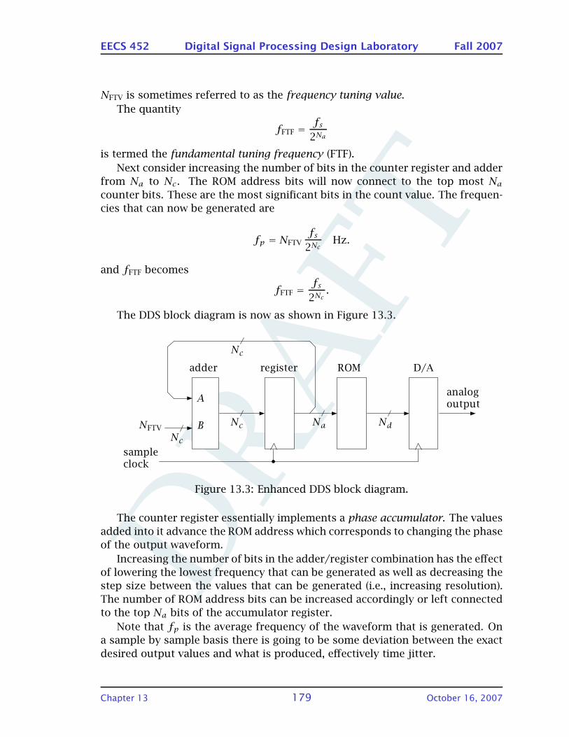
DRA
FT
EECS 452 Digital Signal Processing Design Laboratory Fall 2007
NFTV is sometimes referred to as the frequency tuning value.
The quantity
fFTF =fs
2Na
is termed the fundamental tuning frequency (FTF).
Next consider increasing the number of bits in the counter register and adder
from Na to Nc . The ROM address bits will now connect to the top most Nacounter bits. These are the most significant bits in the count value. The frequen-
cies that can now be generated are
fp = NFTVfs2Nc
Hz.
and fFTF becomes
fFTF =fs
2Nc.
The DDS block diagram is now as shown in Figure 13.3.
~ÇÇÉê
ë~ãéäÉÅäçÅâ
êÉÖáëíÉê
kÅ
^
_
oljkÅ
kÅ
k~ kÇ
aL^~å~äçÖçìíéìí
kcqs
Figure 13.3: Enhanced DDS block diagram.
The counter register essentially implements a phase accumulator. The values
added into it advance the ROM address which corresponds to changing the phase
of the output waveform.
Increasing the number of bits in the adder/register combination has the effect
of lowering the lowest frequency that can be generated as well as decreasing the
step size between the values that can be generated (i.e., increasing resolution).
The number of ROM address bits can be increased accordingly or left connected
to the top Na bits of the accumulator register.
Note that fp is the average frequency of the waveform that is generated. On
a sample by sample basis there is going to be some deviation between the exact
desired output values and what is produced, effectively time jitter.
Chapter 13 179 October 16, 2007

DRA
FT
EECS 452 Digital Signal Processing Design Laboratory Fall 2007
There are two issues that are of most concern at this point. The first is the
accuracy at which a given frequency be generated and the other is jitter in the
sample times used in the synthesis.
First consider the accuracy issue:
Using a step value other than one has significantly increased the num-
ber of frequencies that can be easily generated. However, the set of
frequencies that can be generated still has limits. For example, as-
sume fs = 48000, Nc = 8, and that a value of fp = 1000 Hz is desired.
Solving for NFTV gives
NFTV ≈256× 1000
48000≈ 5.333 · · · .
Using a value of 5 gives an error of 62.5 Hz. This is an error of about
6.3%.
For a given desired fp the maximum error in NFTV caused by rounding
will be ±0.5. This amount of error produces a frequency error in the
output of magnitude
fe =fs
2Nc+1Hz.
Increasing Nc increases the resolution with which fp can be set. How-
ever making Nc large relative to the value of Na causes a more stair-
step like analog output which gives rise to (likely) unwanted frequency
components. A similar situation exists with using too few bits in the
D/A converter word size. As is common, pushing down on one prob-
lem pops up another.
Now an example (with a bit of hand waving). Low cost crystal oscilla-
tors typically have a frequency accuracy of 0.01%. Assume that a DDS
is desired that has an accuracy of about that order. A typical clock
frequency might be 10 MHz. Assume that a nominal 1000.0000 Hz
frequency is desired.
fe = 10−4 =106
2Nc+1.
The phase accumulator should use at least Nc = 32 bits.
Next consider the jitter issue:
Chapter 13 180 October 16, 2007
DRA
FT
EECS 452 Digital Signal Processing Design Laboratory Fall 2007
Again, an example. Consider the situation where Na = Nc = 8 and
the values of fs and fp are such that NFTV = 3, precisely. This cor-
responds to a value of fp = 3fs/256. The ROM is programmed with
samples of one period of the sine function. The counter is started
with an initial value of zero. The desired zero crossings of the output
analog waveform locations are at clock tics 85 1/3, 170 2/3, and 256.
Only the last is possible. The ROM addresses selected at these sam-
ple times are 255, 254, and 0. The first two periods each have a zero
crossing slightly later than that of an ideal waveform. The amount of
error at the end of the third period is zero. This pattern repeats every
three cycles of the output waveform.
This jitter of the zero crossing times is in effect a phase/frequency
modulation that gives rise to artifacts in the spectrum of the synthe-
sized waveform. In many situations these are not of concern, how-
ever, there are applications (e.g., RF communications) where these
artifacts can interfere with signals significantly far away in frequency
from the one being generated.
There is much more to the topic of DDS generation than we can deal with
here. However one should be aware that for many applications one needs to
carefully select word sizes and sample rates. It might be necessary to even mod-
ify the design of the DDS hardware in order to reduce the amounts of artifacts
in the resulting output spectrum. There was a recent article in the IEEE Signal
Processing Magazine’s DSP Tips and Tricks column illustrating measures that
one can take in order to reduce waveform artifacts. The issue was volume 24,
number 4, July 2007.
Recapping:
• Nc is the number of bits in the phase accumulator. The accumulator has
2Nc states.
• NFTV is the frequency tuning value. This is a Nc-bit integer that is used to
set the frequency of the output sinewave.
• fs is the rate at which the contents of the phase accumulator are updated.
• Na is the number of bits used to address the sinewave table. There are
2Na values in the table. If Nc > Na, and very often this is the case, the top
most Na bits of the phase accumulator are used. In this situation the least
significant accumulator bits are not being used as address bits however
they do have an effect on the generated frequency.
• Nd is the number of bits used by the D/A converter to generate analog
values. There are 2Nd D/A output voltage levels.
Chapter 13 181 October 16, 2007
DRA
FT
EECS 452 Digital Signal Processing Design Laboratory Fall 2007
The smallest usable FTV value is 1. If this value is added to the contents of
the phase accumulator at the fs clock rate then the rate at which the accumulator
cycles is
fFTF =fs2Nc
. (13.1)
which is called the fundamental tuning frequency. (FTF).
For a desired output frequency, fp, the required frequency tuning value, NFTV
is
NFTV =fp2Nc
fs.
This is usually rounded to the nearest integer.
The DDS method of generating waveforms is approximate. The more bits
used, the larger the waveform table. The faster the counter is clocked the better
desired waveform can be approximated. Sources of waveform distortion include:
• The skipping of states in the phase accumulator. The frequency is as ad-
vertised being correct on the average.
• The use of a limited number address bits in the sine table.
• The use of a limited number of bits to represent sine values.
The designer of a DDS system must balance effects of these distortion sources
when deciding on the number of bits to be used by each component and update
frequency, fs to be used.
13.3 Modulating a DDS generated waveform
To amplitude modulate multiply the ROM contents by samples of the moduating
waveform with the result going to the D/A.
To accomplish phase modulation add samples of the modulating signal to
the counter output after the feedback and prior to the D/A.
To frequency modulate add samples of the modulating signal to the FTV.
As always, one must think carefully about the scalings and rates involved.
There is little substitute for knowing what you are doing.
13.4 Implementing a DDS in the C5510
In order to implement a DDS we need a table of sine values, an accumulator, a
clock source and a way to send values to the D/A converter. We have the choice
to work either in C or assembler.
The size of sine table is one of the major limiting factors in quality of the
analog output of the DDS waveform generator. The effective accuracy of the
sine table can be increased in a number of ways. These include:
Chapter 13 182 October 16, 2007
DRA
FT
EECS 452 Digital Signal Processing Design Laboratory Fall 2007
• increasing the table size,
• use a table containing only one quarter of a sine wave and use the symme-
tries of the sine function to use this table to generate values that a four
times longer full period table would hold,
• interpolating values between values in the table,
• not using a table and computing values directly.
13.5 Implementing a DDS in the Spartan-3
To be added
13.6 Measuring DDS artifact performance
In many communication system applications it is important that the spectrum
of the DDS output does not have significant energy at frequencies other than the
one being generated. “Significant” generally means “very low” relative to that of
the desired waveform. A system designer has to decide what “low” is. This most
likely based on conditions set down by a regulating agency such as the Federal
Communications Commission.
DDS units find application as generators of samples of a sine wave (as sub-
system component in a larger system) and as direct generators of analog wave-
forms. In the latter case the D/A converter can, and likely does, add artifacts of
its own.
There has been a significant amount of theoretical work done attempting pre-
dict the levels of the spectral contributions, termed artifacts or spurious lines,
by the number of bits used to quantize the waveform, the number samples per
period, the phase accumulator size, and synthesis jitter. (Give a reference or
two.)
The evaluation of the effects of generating a sine wave using the DDS method
is typically done in the frequency domain using DFTs. For this method to be
valid (i.e., work as hoped for) the number of values used in forming the DFT
must be chosen so that the waveform being analyzed is periodic. This is very
important!
Mathematically a data set containing N infinite precision samples from an
integer number of periods of a periodic waveform has non-zero values from
only the fundamental and possibly the harmonics.
If there are not a precisely integer number of periods of the waveform there
will be a phenomenon termed leakage. This is where signal energy leaks from
the signal frequencies into other frequencies. We will talk more about leakage
later in Chapter 23.
Chapter 13 183 October 16, 2007
DRA
FT
EECS 452 Digital Signal Processing Design Laboratory Fall 2007
We don’t have infinite precision samples so, from this error source alone, it
is likely that almost all values in the DFT output are non-zero. This is quanti-
zation noise. Using the simple statistics covered Chapter 2 we can estimate the
expected levels. The result can be used as a level at which it probably does not
make sense to require the other artifacts to be below.
Let’s forgo theory and investigate the artifact performance of DDS generators
by simulation and by capturing samples from actual implementations. If the
simulations and the implementations are correct the results should be identical.
A good place to start in planning a artifact hunt is by relating sample rates,
FTV values, output frequencies and DFT size.
Consider the situation where the DDS is implemented the C5510 using the
AIC23 48 kH sample rate. The C5510 works well using 32-bit C longs so the
phase accumulator will use 32 bits.
The attainable frequencies for a 32-bit accumulator direct digital synthesizer
implementation clocked at 48 kHz are
fo =NFTV × fs
2Nc=NFTV × 48000
232=NFTV × 3× 53
225.
The number of samples in M periods for a given value of fo is Mfs times the
waveform period 1/f0 :
Nf0 = fsM
fo=
48000M
fo.
The values of M and f0 have to be chosen so that Nf0 is an integer.
Let’s look at a few examples.
• For f0 = 1000 Hz we have
NFTV = 228/3 ≈ 89478485.33333.
This is not an integer. We cannot synthesize a sine wave at precisely 1000
Hz using these parameters. We can come close but that’s all. If a value
of FTV = 89478485 is used there is a frequency error of 3.725 × 10⁻⁶ Hz.
Most commonly encountered frequency sources are not this accurate. This
accuracy if probably good enough for most applications.
To have an integer number samples in Np periods using this value of NFTV
requires
N = Np ×232
89478485
be integer. The smallest value of Np for which this is so is 89478485. (The
numerator and the denominator are relatively prime.) Use of this value
results in a DFT of 232 values. This is not a very convenient size!
Chapter 13 184 October 16, 2007
DRA
FT
EECS 452 Digital Signal Processing Design Laboratory Fall 2007
• For fo = 1125 = 3 × 3 × 53 Hz we have FTV = 3 × 225. A value of Np is
required such that
NFTV = Np ×232
3× 225
be integer. A value of Np equal to 3 suffices. The number of sample values
needed for the DFT is then 128 (or an integer multiple of this value). If we
were to have a data set of 1024 samples which is an integer multiple of 128
we would use all 1024 values.
• A value fo = 984.375 = 21 × 3 × 53/23 Hz gives NFTV = 21 × 222 The
required Np needs to be such
N = Np ×232
21× 222
is integer. A value of Np equal to 21 suffices. The number of sample values
needed for the DFT is then 1024 (or an integer multiple of this value).
13.7 Other digital waveform generation techniques
Other methods of digital waveform generation exist.
• A polynomial approximation to the sine function could be used to calculate
value rather than look them up in a ROM.
• A recursive feedback circuit having its poles on the unit circle in the z-plane
can be used. Guaranteeing its startup and stability is a concern.
• An another method of calculating values of the sine and cosine functions
is via the use of CORDIC rotations.
• There must be other methods that we haven’t touched on.
13.8 Exercises
This chapter’s exercises deal with the implementation of sine wave generators
capable of generating sine waves with (practically) arbitrary frequencies up to a
maximum synthesizable frequency (MSF).
We will use an unsigned long as the phase accumulator. In the C5510 this
is a 32-bit value. The top most bits will be used to address entries in a table of
samples of one period of a sine wave. The AIC23 codec only allows a limited
number of clock rates. The sample values will be sent to the D/A clock at the
rate the D/A clock is programmed for.
Direct digital synthesis is simple in concept and implementation but less
simple in balancing design parameters. The 32-bit phase accumulator used in
Chapter 13 185 October 16, 2007
DRA
FT
EECS 452 Digital Signal Processing Design Laboratory Fall 2007
this exercise is representative of those used in practice. Phase accumulators
using 32 to 48 bits are typically found in practice. The update rate dictated by
use of the AIC23 however is much lower than normally used in actual practice.
The D/A used with the S3SB is capable of much higher sample rates but only has
12-bits.
Note: use of an integer power of 2 modulus binary phase accumulator has
been being assumed. By adding a little logic the modulus can be made to any
value less than 2Nc possibly giving more freedom in selecting frequencies. For
example, if the phase accumulator was made to operate using modulo-48000000
frequencies integer multiples of milliHertz could be generated.
Chapter 13 186 October 16, 2007
DRA
FT
14 : Exercise 4
14.1 Overview . . . . . . . . . . . . . . . . . . . . . . . . . . . . . . . . . . . . 189
14.2 Implementing DDS using the S3SB . . . . . . . . . . . . . . . . . . . . 190
14.2.1 Implementing a sine table in a Spartan-3 block RAM . . . . . 190
14.3 Prelab . . . . . . . . . . . . . . . . . . . . . . . . . . . . . . . . . . . . . . 192
14.3.1 Specific to the AIC23 . . . . . . . . . . . . . . . . . . . . . . . . . 192
14.3.2 Specific to the DSK & AIC23 . . . . . . . . . . . . . . . . . . . . . 193
14.3.3 Specific to the DDS/DTMF . . . . . . . . . . . . . . . . . . . . . . 193
14.3.4 Specific to the PMod AD1 module . . . . . . . . . . . . . . . . . 195
14.3.5 Specific to the PMod input op-amp circuit . . . . . . . . . . . . 196
14.3.5.1 Specific to S3SB DDS . . . . . . . . . . . . . . . . . . . . 196
14.3.6 Specific to the PMod DA2 module . . . . . . . . . . . . . . . . . 196
14.3.7 Specific to metastability . . . . . . . . . . . . . . . . . . . . . . . 196
14.4 Exercise . . . . . . . . . . . . . . . . . . . . . . . . . . . . . . . . . . . . . 197
14.4.1 Simple tone test . . . . . . . . . . . . . . . . . . . . . . . . . . . . 197
14.4.2 Listening tests . . . . . . . . . . . . . . . . . . . . . . . . . . . . . 197
14.4.3 DDS and DTMF waveform generator . . . . . . . . . . . . . . . 198
14.4.4 The PMod AD1 level shifting circuit . . . . . . . . . . . . . . . . 199
14.4.5 The PMod A/D–D/A loop . . . . . . . . . . . . . . . . . . . . . . 200
14.4.6 DTMF on the Spartan-3 Starter Board . . . . . . . . . . . . . . . 200
14.4.7 Use of Block RAM as ROM . . . . . . . . . . . . . . . . . . . . . . 200
14.4.8 Metastibility of a C5510-S3SB-C5510 loop . . . . . . . . . . . . 201
14.5 Listings . . . . . . . . . . . . . . . . . . . . . . . . . . . . . . . . . . . . . 201
14.5.1 McBSP_452.h . . . . . . . . . . . . . . . . . . . . . . . . . . . . . . 201
14.5.2 setup_codec.c . . . . . . . . . . . . . . . . . . . . . . . . . . . . . 202
14.5.3 C5510 tone generator: tone.c . . . . . . . . . . . . . . . . . . . . 203
14.5.4 MATLAB sine table generator . . . . . . . . . . . . . . . . . . . . 203
14.5.5 MATLAB Direct Digital Synthesizer . . . . . . . . . . . . . . . . . 203
14.5.6 quantization.c . . . . . . . . . . . . . . . . . . . . . . . . . . . . . 203
14.5.7 Listing for the C5510 delta/sigma modulator . . . . . . . . . . 203
14.5.8 Listing of MATLAB BRAM sine table generator . . . . . . . . . 203
14.5.9 Listings for the S3SB AD-DA test . . . . . . . . . . . . . . . . . . 204
14.5.9.1 Top level . . . . . . . . . . . . . . . . . . . . . . . . . . . 204
14.5.9.2 AD1 PMod support . . . . . . . . . . . . . . . . . . . . . 206
14.5.9.3 DA2 PMod support . . . . . . . . . . . . . . . . . . . . . 209
14.5.9.4 LED driver . . . . . . . . . . . . . . . . . . . . . . . . . . 211
14.5.9.5 Sample timing support . . . . . . . . . . . . . . . . . . 213
Chapter 14 187 October 16, 2007
DRA
FT
EECS 452 Digital Signal Processing Design Laboratory Fall 2007
14.5.9.6 DCM support . . . . . . . . . . . . . . . . . . . . . . . . 214
14.5.10Metastability demonstration C and VHDL . . . . . . . . . . . . 216
14.5.10.1Metastability demonstration C5510 main . . . . . . . 216
14.5.10.2Metastability C5510 codec setup . . . . . . . . . . . . 216
14.5.10.3Metastability demonstration top . . . . . . . . . . . . 216
14.5.10.4Metastability demonstration main VHDL . . . . . . . 218
14.5.10.5Metastability demonstration UCF file . . . . . . . . . 221
Chapter 14 188 October 16, 2007
DRA
FT
EECS 452 Digital Signal Processing Design Laboratory Fall 2007
Handwritten work will not be graded. Prelabs are to be done individually and
are to be handed in at the start of the lab period.
14.1 Overview
Serial data links, their implementation and use, are the primary subject of this
exercise. For multiple bit data transfers serial data links use fewer signal lines
than do bit-parallel links. Serial links require fewer pins on component packages
(making possible physically small components) as well as less signal routing ter-
ritory on printed circuit boards than do bit-parallel paths. On the down side
there is a lower data rate throughput than is possible using a multi-line par-
allel path. However, with careful design technique and modern components,
serial data rates in the Gbit/second range are possible (e.g., Xilinx’s Rocket I/O
operates at 3.5 Gb/s). Serial links can be used for many if not most “normal”
applications.
The exercise is superficial in some aspects (it does cover a lot of territory
in three hours) and less so in others. We go for breadth rather than depth in
our treatment. The main goal of the exercise is to acquaint you of the existence,
basic properties and basic operation of bit-serial interfaces and the A/D and D/A
devices available in the lab. It is quite likely that one or more of the team projects
will have need of such data links and will be able to use this exercise’s material
as a starting point. Once one has worked with and/or implemented a few simple
bit-serial interfaces the light bulb goes on and things become relatively straight
forward.
This exercise assumes that the material covered in Chapters 11, 12, and 13
has been read.
The TI manuals associated with this exercise are (include?):
• TMS320VC5510 DSK Technical Reference,
• TMS320VC5510 Fixed-Point Digital Signal Processor Data Manual,
SPRS076E,
• TLV320AIC23 Stereo Audio CODEC, 8- to 96-kHz, With Integrated Head-
phone Amplifier Data Manual, SLWS106C,
• TMS320VC5501/5502/5509/5510 DSP Multichannel Buffered Serial Port
(McBSP) Reference Guide, SPUR592A,
• TMS320C55x Optimizing C/C++ Compiler User’s Guide, SPRU281E.
You are urged to use these documents to fill any gaps in your understanding.
At least look at them before coming to lab.
Chapter 14 189 October 16, 2007
DRA
FT
EECS 452 Digital Signal Processing Design Laboratory Fall 2007
14.2 Implementing DDS using the S3SB
A simple DDS dual tone project is used to introduce the use of the PMod DA2
module. A slight detour is made to investigate how to initialize a block ram
(BRAM) in order to serve as a sine table ROM.
14.2.1 Implementing a sine table in a Spartan-3 block RAM
A Spartan-3 block RAMs contain 18432 bits and can be configured in a number
of ways. A BRAM is organized in two parts, data and parity. There is a parity bit
associated with every 8 bits. The parity bits are only parity if they are used that
way. The can also be used as normal memory, perhaps to extend a word size
from 16 bits to 18 bits.
When a BRAM is instantiation it is also initialized. The initiation values are
specified in the instantiation template. See Appendix-F.1 for an example. The
data and parity parts are initialized separately. We will be concerned only with
the data portion.
For initialization purposes the data portion is organized in terms of 32 256-
bit words (16384 bits). The 256-bit words go right to left with increasing bit
index.
In this exercise we will be using the BRAM with a 16-bit word size. A 256-bit
initialization would consist of 16-bits words going from right to left. In this case
a 256-bit word holds 16 16-bit values.
The following list of hex values was generated by a MATLAB program for use
in generating a 256 value sine table in a Spartan-3 FPGA block RAM.
800083248648896A8C8C8FAB92C895E298F99C0B9F1AA223A528A826AB1FAE11
Chapter 14 190 October 16, 2007
DRA
FT
EECS 452 Digital Signal Processing Design Laboratory Fall 2007
There were used by the same MATLAB program to generate the initialization
line
INIT_00 => X"AE11AB1FA826A528A2239F1A9C0B98F995E292C88FAB8C8C896A864883248000",
All of the punctuation on the above line is needed in order to simplify doing
copy-and-paste. The only (slightly) tricky part of the program design was setting
up the print statement loop to print 16 values on a line going from 16th to 1st
going left to right.
The MATLAB program used for the above was organized as follows:
• An array was generated containing the values that were to be sent to the
D/A converter. The values were rounded and scaled to be between -32767
and +32767. However they remain 64-bit floating point values within MATLAB.
• To make the values into offset binary form 32768 can be added. A check
should be made to insure that values were now in the range 1 through
32767.
• If instead, it is desired to output the sine table as 16-bit two’s complement
integers a different procedure is needed. The positive values map directly
into unsigned 16-bit integer bit patterns. The negative values need to be
mapped into their equivalent unsigned 16-bit values.
The (floating point) value -1 needs to have the same 16-bit pattern as 65535
which is 216 − 1. The value -2 needs to have the unsigned 16-bit equivalent
value of 216 − 2. So, if a value is negative the value in the array needs to
have 65536 added to it. Otherwise it is left unchanged. This generates
a set of values when printed as unsigned 16-bit integers will generate the
desired 2’s complement 16-bit bit patterns.
• A loop was used to print the values mimicking the Xilinx initialization for-
mat. The above line is the one generated for the first 16 values.
• The set of lines were copy-pasted into a copy of the Xilinx template replac-
ing the corresponding zero initialization lines.
The MATLAB script to accomplish this contained 13 non-blank lines (blank
lines were used as white space) including the limit checks and a sanity check on
one value.
The %04X format descriptor was used to print out four uppercase hex digits
with leading zeros.
The above procedure was simple to implement and facilitated a quick and
easy way to incorporate initialization values into the block RAM instantiation
template.
Chapter 14 191 October 16, 2007

DRA
FT
EECS 452 Digital Signal Processing Design Laboratory Fall 2007
14.3 Prelab
Handwritten work will not be graded. Prelabs are to be done individually
and are to be handed in at the start of the lab period.
14.3.1 Specific to the AIC23
The CODEC chip used on the C5510 is typically referred to as the AIC23. The full
TI part number for the part used on the DSK is TLV320AIC23PW. The PDF version
of the AIC23 data manual can be found on the class CD. It is also available
through the CCS help system and from TI’s web site.
The schematics of the C5510 DSK are contained in Spectrum Digital’s DSK
documentation. They are also contained in a PDF file accessible either directly
or through the Code Composer Studio help system.
The CCS help system also contains an excellent discussion of the interface
between the C5510 and the AIC23.
Spectrum Digital has supplied a large number code examples located under
\ti\examples. Several of the examples involve the use of the CODEC.
Making a check of the C5510DSK schematics it appears that the USB subsys-
tem is not documented, apparently for proprietary reasons. This subsystem is
of interest here only because it generates the clock for the AIC23.
1. What is the nominal operating analog supply voltage (AVDD)?
2. The AIC23 line inputs connect to variable gain amplifiers. What is the range
of gains that can be programmed and in what size steps (dB)?
3. What are the gain/attentuation settings that can be used with the line out-
puts? Using what size steps?
4. For a AIC23 programmed using the supplied code, what are the default
gain settings on the A/D and D/A converter for line-in and line-out?
5. For 8, 48 sample rates what are the 0.1 dB down frequencies of the input
and output filters. For the 96 kHz sample rate what are the 0.4 dB down
frequencies. How do these gain levers at these frequencies compare to the
gain levels at fs/2?
6. What AIC23 register is used to set the sample rate. What are the values
needed in order to set the 8, 48 and 96 kHz sample rates?
7. Many of the signal generators in the lab are capable of producing wave-
forms having a 20 Volt peak-to-peak amplitude. What is the most probable
result of applying such a waveform to either of the DSK’s input jacks?
Chapter 14 192 October 16, 2007

DRA
FT
EECS 452 Digital Signal Processing Design Laboratory Fall 2007
8. In the same vein, what is the most likely result of applying such a voltage
to one of the DSK’s output jacks?
14.3.2 Specific to the DSK & AIC23
1. There are four 3.5 mm phono jacks located on one side of the DSK as shown
in Figure 14.1 and are labeled J1 through J4.
Sketch and label the phone plug arrangement on the DSK used for analog
I/O and label their function (such as: line-in, speaker-out, etc.)Figure 14.1: Side view of the C5510DSK showing the phono jacks.
2. Is the line-in AC or DC coupled? If AC coupled what might be the low
frequency cutoff frequency be? If important, assume the signal source is a
voltage source.
3. Is the line-out AC or DC coupled? If AC coupled what might be the low
frequency cutoff frequency be? If important, assume the signal load is
1000 ohms.
4. For the AIC23 gain/attenuation settings programmed by setup_code.cwhat are
(a) the maximum amplitude of analog line input signal that does cause
sample values to clip.
(b) the maximum amplitude of the analog line output signal that can be
generated using 16-bit values.
For the above, if necessary, assume a 1000 Hz sine wave waveform.
14.3.3 Specific to the DDS/DTMF
Part of the exercise consists of generating DTMF frequencies used by a Touch-
Tone telephone. Direct digital synthesis will be used to generate the individual
tone. Pairs of tones will be summed to create the desired DTMF waveforms.
A table containing 256 samples of one period of the function is required by
the exercise. Write or locate a MATLAB script to generate such a table. Because
we will be working with signed 16-bit integer values the numbers returned by
Chapter 14 193 October 16, 2007
DRA
FT
EECS 452 Digital Signal Processing Design Laboratory Fall 2007
the MATLAB function need to be scaled . Multiply the sine values by 215 − 1 and
round prior to printing or writing the table to a file.
The following MATLAB fprintf statement will generate a list of values placing
8 signed integer numbers per line.
fprintf(’ %6d, %6d, %6d, %6d, %6d, %6d, %6d, %6d,\n’, samples);
Only minimal editing will be needed to move this table into your C code. The
64 value table used in the tone.c (Section 14.5.3) was generated this way.
Look up on the web the row and column frequencies used by DTMF. It would
be reasonable write the values down and put them into your prelab report.
Section 14.5.5 contains the C source code for a simple DDS. Longs are used
for setting the FTV and for the phase accumulator. The top bits of the phase
accumulator are used to address the sine table. The accumulator update rate is
48 kHz. The program is based on the DDS block diagram in Figure 13.3.
This program can be used as your starting DTMF point. The 64-value ta-
ble used by this program will be replaced by your 256 value table. Notice how
the program determines the table size. Other than replacing the table no other
changes need to be made to the remainder of the program in order to accom-
modate the new table. Well, actually one instruction does have to be changed. A
second synthesizer, consisting of a FTV value and an accumulator, can be readily
included within the existing loop structure.
In your DTMF program use the C5510 dip switches to enter the keypad num-
ber to generate the tones for. Entered binary values 1,2 and 3 correspond to row
1 keys 1,2,3. Entered values 4,5,6 correspond to row 2 keys 4,5,6. And so. Val-
ues of 0, 13,14,15 should produce no output. Sometimes the switches appear set
but are not. In those cases having the switches echoed in the LEDs is extremely
useful. Make this so.
DDS sine wave generation is approximate. The word size, table size and step-
ping frequency can have degrading effects on the resulting waveform. In many
cases there are steps that can be used to improve the quality of the waveform.
Quality, what is quality? Also if one is not careful with their test procedure the
results will more reflect badly on the measurement plan rather than on what is
being evaluated.
We will look at determining the spectra purity of the waveform being gener-
ated just prior to D/A. We don’t have the tools needed to do post D/A, at this
time. The evaluation procedure will to write sets of samples into PC files rather
than to the D/A. MATLAB programs can then be used to process the values and
generate plots of the results. Even this process can have its problems.
Write:
• a MATLAB script to read a list of numbers and print them, one value per
line. Both in and out. There are a number of ways that one can read a list
of numbers. One is to use fscanf statements or the load statement.
Chapter 14 194 October 16, 2007
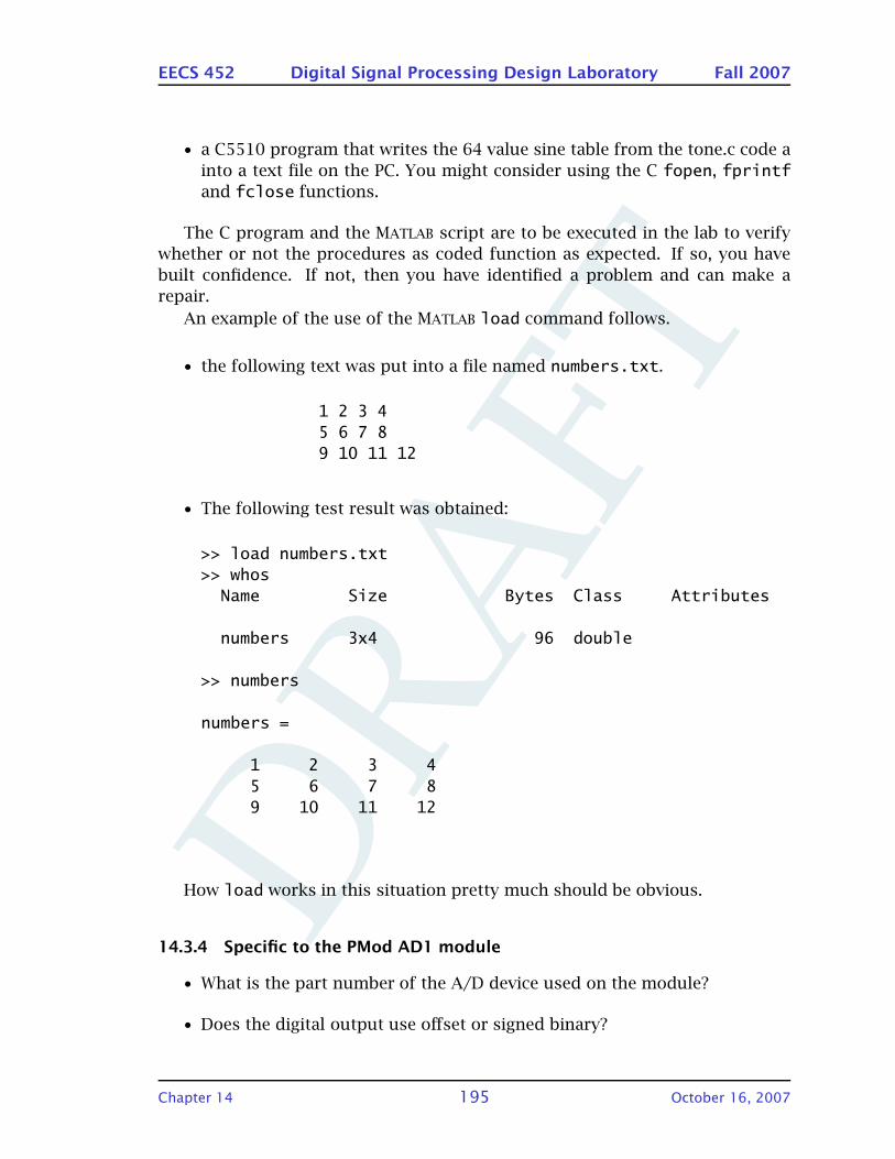
DRA
FT
EECS 452 Digital Signal Processing Design Laboratory Fall 2007
• a C5510 program that writes the 64 value sine table from the tone.c code a
into a text file on the PC. You might consider using the C fopen, fprintfand fclose functions.
The C program and the MATLAB script are to be executed in the lab to verify
whether or not the procedures as coded function as expected. If so, you have
built confidence. If not, then you have identified a problem and can make a
repair.
An example of the use of the MATLAB load command follows.
• the following text was put into a file named numbers.txt.
1 2 3 45 6 7 89 10 11 12
• The following test result was obtained:
>> load numbers.txt>> whosName Size Bytes Class Attributes
numbers 3x4 96 double
>> numbers
numbers =
1 2 3 45 6 7 89 10 11 12
How load works in this situation pretty much should be obvious.
14.3.4 Specific to the PMod AD1 module
• What is the part number of the A/D device used on the module?
• Does the digital output use offset or signed binary?
Chapter 14 195 October 16, 2007

DRA
FT
EECS 452 Digital Signal Processing Design Laboratory Fall 2007
14.3.5 Specific to the PMod input op-amp circuit
Design a gain of 1/2 level shifting amplifier. The circuit diagram and analysis
for such can be found in the appendices.
With one exception it should be possible to use only 10 kOhm resistors. The
exception can make use of two 10 kOhm resistors perhaps connected as a serial
or maybe as a parallel pair.
Draw a sketch layout your parts on the white board. Include the power unit
and the dual BNC PMod module.
In your prelab write-up include a diagram (can be a copy of the one in this
document or hand drawn) listing part values along with a copy of your layout
sketch.
In lab you will implement your (or your partner’s) circuit layout and connect
it to the A/D using a Digilent 6-pin cable. You should include this connection in
your drawing as well.
14.3.5.1 Specific to S3SB DDS
Write a MATLAB script to generate a BRAM initialization list. The format of this
list should allow ready cut and paste into a ROM entity. The waveform should
be an increasing ramp going from -32767 to 32767. The table should contain
256 16-bit values. As noted, it should be possible to write a suitable script in 10
lines or so of MATLAB instructions. lines.
In a later exercise this script can be used to convert FIR filter coefficients into
BRAM initialization vectors. So, give modularity and reusability some thought.
Include the script and a listing of what it produces in your pre-lab write-up.
This script and/or the values will be used in the lab exercise.
14.3.6 Specific to the PMod DA2 module
• What is the part number of the D/A device used on the module?
• Does the digital input use offset or signed binary?
14.3.7 Specific to metastability
• Briefly, what is metastability in electronics?
• “Current engineering solutions to this problem are” involve . . . . Finish the
preceding sentence from the Wikipedia.
Chapter 14 196 October 16, 2007
DRA
FT
EECS 452 Digital Signal Processing Design Laboratory Fall 2007
14.4 Exercise
The following VHDL related files are provided for this part of the exercise:
• ad_da_01_top.vhd (Top for AD in to DA out.)
• S3DCM.vhd (To change 50 MHz to 40 MHz.)
• DDS0top.vhd (DDS version 0 top.)
• DDS01.vhd (Connects DDS, DA, sine table.)
• DDSduo.vhd (Dual DDS implementation.)
• FTVin.vhd (Supplies two FTV values.)
• led_driver.vhd (Connects to LEDs.)
• pmod_AD1.vhd (Interface to AD PMod.)
• pmod_DA2V2.vhd (Interface to DA PMod.)
• sine_rom.vhd (Sine initialized BRAM.)
• timing.vhd (Simple clock down.)
• spartan.ucf (UCF file for S3.)
14.4.1 Simple tone test
Build and run the supplied simple tone.c program and verify that it does what
you expect. This lets you know whether things are working in general (or not). If
this can’t be made to work there isn’t any sense going on until it does work.
It will be necessary to create and build a tone project first. The following
files should be used:
• tone.c (the main)
• setup_codec.c• rts.lib (a library)
• EECS452.cmd (linker memory map description)
Depending upon your file organization it might also be necessary to modify
the path to McBSP_452.h.
Modify the code to change the sample rate to 96000 and verify whether or
not the output frequency doubles. Only line one of code needs to be added.
The tone.c program is a simple starter code that can be used to verify that
one can control the hardware sufficiently well to generate a simple tone on the
D/A convert output.
14.4.2 Listening tests
Build the supplied quantization.c program. You will need to include header,
library and AIC23 support when you do this.
Chapter 14 197 October 16, 2007

DRA
FT
EECS 452 Digital Signal Processing Design Laboratory Fall 2007
Set the number of bits used to 16 and the sample rate to 48 kH and verify
that everything is working reasonably will. Use the supplied MP3 of Jeff Daniels
reading Lincoln’s Gettysburg Address for testing.
Listen using the following:
• 16 bit samples at fs = 48 kHz.
• 1 bit samples at fs = 48 kHz.
• 1 bit samples at fs = 16 KHz.
• 16 bits at fs = 2 kHz.
• 1 bit samples at fs = 2 kHz.
The lines of code affecting the sample rate and number of bits are:
Bits = 1; // number of bits to useDivideBy = 3; // sample rate is 48000/DivideBy
This program operates the codec at a 48 kHz sample rate and reduces the
sample rate by discarding samples. This effectively removes the anti-alias and
anti-image filters. What you hear is a worst case. With the filters present the
intelligibility would be improved. However, the AIC23 wasn’t designed with very
low sample rates in mind and we simply have to do with worst case.
Later in the semester we will investigate Delta-Sigma (or is it Sigma-Delta?)
techniques to implement high quality A/D and D/A converters using 1-bit quan-
tized values. A simple Delta-Sigma modulator has been written for you that
generates a 16k bits per second binary waveform that can be listened to with-
out any further processing. Build and run this program, listen to the audio file
and contrast the quality against the “raw” 16-bit second 1-bit quality. You might
have to fiddle a little with the signal levels. But probably not.
There is a significant difference between the needs for high fidelity reproduc-
tion and for intelligible communication. In your report list the trial runs and
comment on the sound quality. Try to rank them.
14.4.3 DDS and DTMF waveform generator
Build and verify proper operation of the DDS32 program using the 256 value
sine table.
Test runs and files are to be made using frequencies of 1000 Hz, 1125 Hz,
and 984.375 Hz (one at a time).
• Run the program generating these frequencies and observe the outputs on
the scope, record the peak-to-peak voltage in each case and verify (as best
can) the frequency. This is to verify that things appear to be working.
• Modify the program to write out 1024 values of the waveform being gener-
ated.
Chapter 14 198 October 16, 2007
DRA
FT
EECS 452 Digital Signal Processing Design Laboratory Fall 2007
• For each of the above frequencies store 1024 points of your digital output
onto the PC. These will processed later using MATLAB.
Using your prelab DTMF code verify that it works as desired. The scope can
measure frequency. Indeed it can also show spectra. It might be handy to write
your code that it is easy to test the individual frequencies individually. Don’t
forget to think about what happens when you add two maximum value sine
waves.
Demonstrate your DTMF code to the GSI and convince him that it works. It
would be reasonable to mention how this was accomplished in the report.
The following can be done outside of the lab period.
• Using MATLAB plot the spectra of your data sets labeling the levels in dB re
1 volt RMS and the frequencies in Hz. This is assumes that you have appro-
priately scales the numbers contained in the files. Restrict the displayed dB
range to be on the order of 60 dB. The x-axis should go from −fs/2 to fs/2
in Hz. The DFTs also need to be normalized, FFT(data)/length(data).
If you are not sure about the scaling or what to expect write yourself a
simple MATLAB program to mimic the process and see if you produce what
you feel should be expected.
• Replot the data sets for each frequency using the largest number of points
(less than or equal to 1024) that will result in minimum leakage for that
frequency. Print the FFT sizes on your plots. MATLAB conveniently provides
support for arbitrary size DFTs.
Some of the plots will show a phenomenon termed leakage. Leakage occurs
when the frequency of the sampled sine wave is not a value that is a multiple
one over the duration of the data set.
Include the plots and your MATLAB code in your report. Are the values as
expected? If not, either your expectations or your measurement techniques or
both are in error.
14.4.4 The PMod AD1 level shifting circuit
Using a white block build the level shift op-amp circuit and use the signal gener-
ator and scope to verify that it works as expected. The bandwidth (3 dB) should
be an interesting thing to know. Is it consistent with the sample rates that we
plan to use?
The amplifier will be connected via a 6-pin cable to the PMod AD1 module.
The cable also carries 3.3V and ground. This can (and should be) used to power
your circuit. An external power supply is not needed!
Chapter 14 199 October 16, 2007

DRA
FT
EECS 452 Digital Signal Processing Design Laboratory Fall 2007
14.4.5 The PMod A/D–D/A loop
The purpose is to simply take samples and then reconstruct them. A simple
task that if we can’t successfully it makes no sense to move onto more complex
applications.
Using the supplied VHDL files generate a (hopefully working) VHDL entity
and load it into the Spartan-3. This entity simply takes samples and then echoes
them onto the D/A converter. The supplied top file is ad_da_01_top.vhd.
Use the signal generator at 1 kHz to experimentally determine the safe (non-
clipping) input levels.
Set the sample rate to 200 kHz using the switches and look at the quality of
the waveform and run some frequencies to demonstrate aliasing.
Use the level shifting amplifier with the input connected to the PC output.
Use the Gettysburg address as the program source. What problem happens. Try
a shunt resistor at the amplifier input. What would be a reasonable value to use
and why?
14.4.6 DTMF on the Spartan-3 Starter Board
In this part of the exercise you need to built a ISE project to implement the
DTMF function. The file DDS0_top.vhd is the top for this project. You will
need to fill in the missing code/values where you find ???? in the files. Mainly
in FTVin.vhd. The supplied code is set up to generate two single tone direct
digital synthesizers. Each is connected to a PMod DA2 DA converter. The fre-
quencies are determined using the S3SB slide switches. The FTV values used are
determined in FTVin.vhd. Check the frequencies using the oscilloscope.
Next combine the outputs of the two synthesizers into a DTFM waveform
and output this to both D/As. Verify that all is well on both channels using the
oscilloscope.
14.4.7 Use of Block RAM as ROM
Replace the block RAM initialization used in the sin_rom.vhd file with the ini-
tialization text that you generated in the prelab. Create a project to generate this
new output waveform. Observe the output waveform on an oscilloscope. Is the
period of the resulting waveform what you expected?
It should be interesting to listen to and compare the the sound outputs of
this program and the sine version.
Chapter 14 200 October 16, 2007
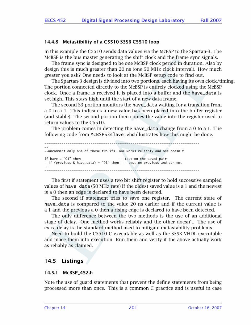
DRA
FT
EECS 452 Digital Signal Processing Design Laboratory Fall 2007
14.4.8 Metastibility of a C5510-S3SB-C5510 loop
In this example the C5510 sends data values via the McBSP to the Spartan-3. The
McBSP is the bus master generating the shift clock and the frame sync signals.
The frame sync is designed to be one McBSP clock period in duration. Also by
design this is much greater than 20 ns (one 50 MHz clock interval). How much
greater you ask? One needs to look at the McBSP setup code to find out.
The Spartan-3 design is divided into two portions, each having its own clock/timing.
The portion connected directly to the McBSP is entirely clocked using the McBSP
clock. Once a frame is received it is placed into a buffer and the have_data is
set high. This stays high until the start of a new data frame.
The second S3 portion monitors the have_data waiting for a transition from
a 0 to a 1. This indicates a new value has been placed into the buffer register
(and stable). The second portion then copies the value into the register used to
return values to the C5510.
The problem comes in detecting the have_data change from a 0 to a 1. The
following code from McBSPS3slave.vhd illustrates how this might be done.
-------------------------------------------------------------------------------------uncomment only one of these two ifs..one works reliably and one doesn’t
if have = "01" then -- test on the saved pair--if (previous & have_data) = "01" then -- test on previous and current-----------------------------------------------------------------------------------
The first if statement uses a two bit shift register to hold successive sampled
values of have_data (50 MHz rate) If the oldest saved value is a 1 and the newest
is a 0 then an edge is declared to have been detected.
The second if statement tries to save one register. The current state of
have_data is compared to the value 20 ns earlier and if the current value is
a 1 and the previous a 0 then a rising edge is declared to have been detected.
The only difference between the two methods is the use of an additional
stage of delay. One method works reliably and the other doesn’t. The use of
extra delay is the standard method used to mitigate metastability problems.
Need to build the C5510 C executable as well as the S3SB VHDL executable
and place them into execution. Run them and verify if the above actually work
as reliably as claimed.
14.5 Listings
14.5.1 McBSP_452.h
Note the use of guard statements that prevent the define statements from being
processed more than once. This is a common C practice and is useful in case
Chapter 14 201 October 16, 2007
DRA
FT
EECS 452 Digital Signal Processing Design Laboratory Fall 2007
other include files might themselves include this file.
14.5.2 setup_codec.c
The AIC23 codec is configured using a list of default values. These values are
contained in the array named AIC23_params. There are 10 values in this array,
one value for each control word in the AIC23 to be initialized. The AIC23 data
manual describes how to set the bits. The control words are sent from the C5510
over McBSP channel 1 in 16-bit units. The most significant 7 bits are used to
specify which control register is to be loaded and the low 9 bits are used to
supply the value to be loaded. One simple way to construct these 16-bit words is
to take the register address as an integer, shift this value left 7 bits and then add
the control bit values. For example to set the sample rate (using control register
8) to 48000 Hz any one of the following three forms (out of many possible) can
be used to form the necessary bit pattern:
• 0x1001,• 8*0x200+0x0001,• (8«9)+1.
The code supplied in this section uses the middle form.
It may be required to use a control setting that differs from the supplied
default. Sometimes it is necessary to change the operating parameters used by
the AIC23 several times while a program is executing. Because of the way the
AIC23 is interfaced to the C5510 using McBSP port 1 any of the control words
can be changed on the fly (i.e., in real time).
For example, assume that it is desired to set the sample rate to 96 kHz.
Once the AIC has been setup and running the following line of code can be used
change the sample rate to 96000 Hz.
McBSP_send(1, 8*0x200+0x001D);
A good place to place this line code is on the line immediately following the
call to the setup_codec function.
Actually, this call can be executed at any time in a program in order to change
the sample rate. The value of 0x001D would be changed in order to set a sample
rate other than 96000 Hz.
This procedure allows the values contained in the header file to be left un-
changed and eliminates having to create a new header file for each new applica-
tion.
Chapter 14 202 October 16, 2007
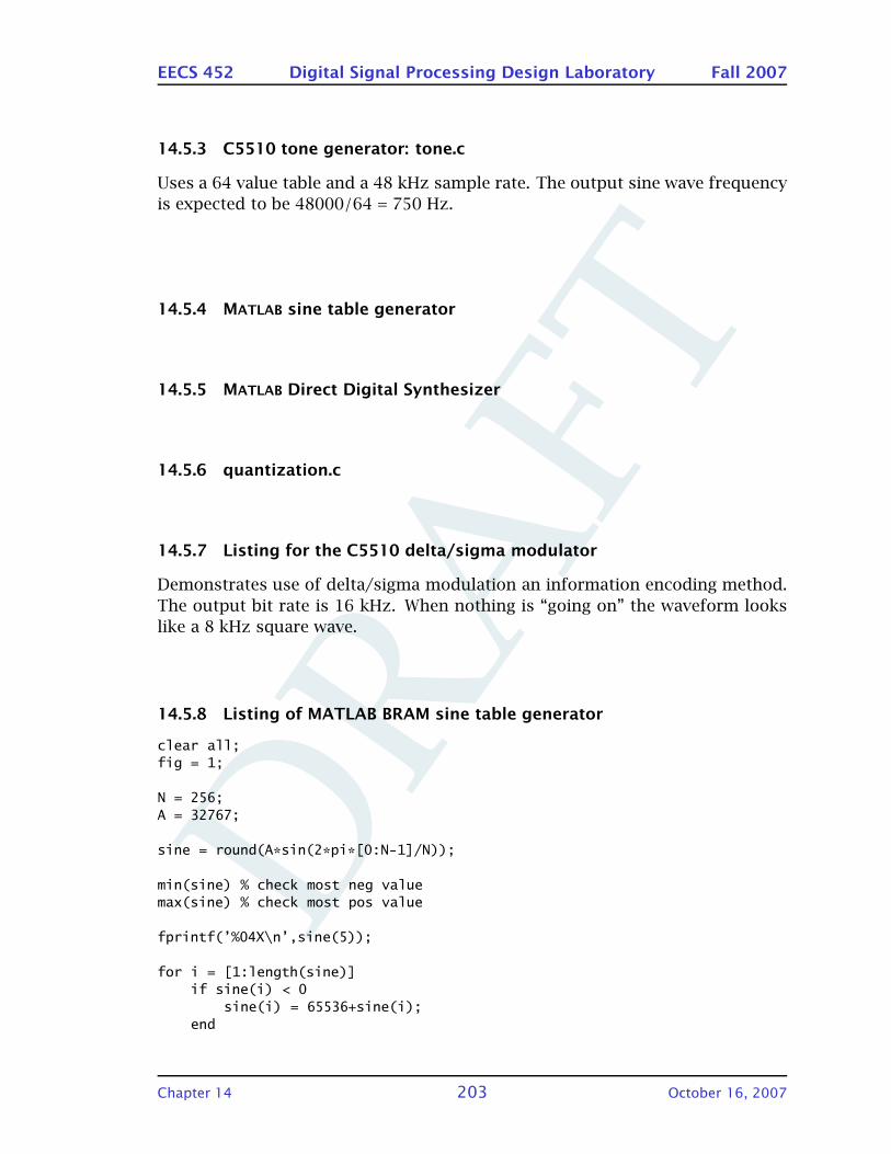
DRA
FT
EECS 452 Digital Signal Processing Design Laboratory Fall 2007
14.5.3 C5510 tone generator: tone.c
Uses a 64 value table and a 48 kHz sample rate. The output sine wave frequency
is expected to be 48000/64 = 750 Hz.
14.5.4 MATLAB sine table generator
14.5.5 MATLAB Direct Digital Synthesizer
14.5.6 quantization.c
14.5.7 Listing for the C5510 delta/sigma modulator
Demonstrates use of delta/sigma modulation an information encoding method.
The output bit rate is 16 kHz. When nothing is “going on” the waveform looks
like a 8 kHz square wave.
14.5.8 Listing of MATLAB BRAM sine table generator
clear all;fig = 1;
N = 256;A = 32767;
sine = round(A*sin(2*pi*[0:N-1]/N));
min(sine) % check most neg valuemax(sine) % check most pos value
fprintf(’%04X\n’,sine(5));
for i = [1:length(sine)]if sine(i) < 0
sine(i) = 65536+sine(i);end
Chapter 14 203 October 16, 2007
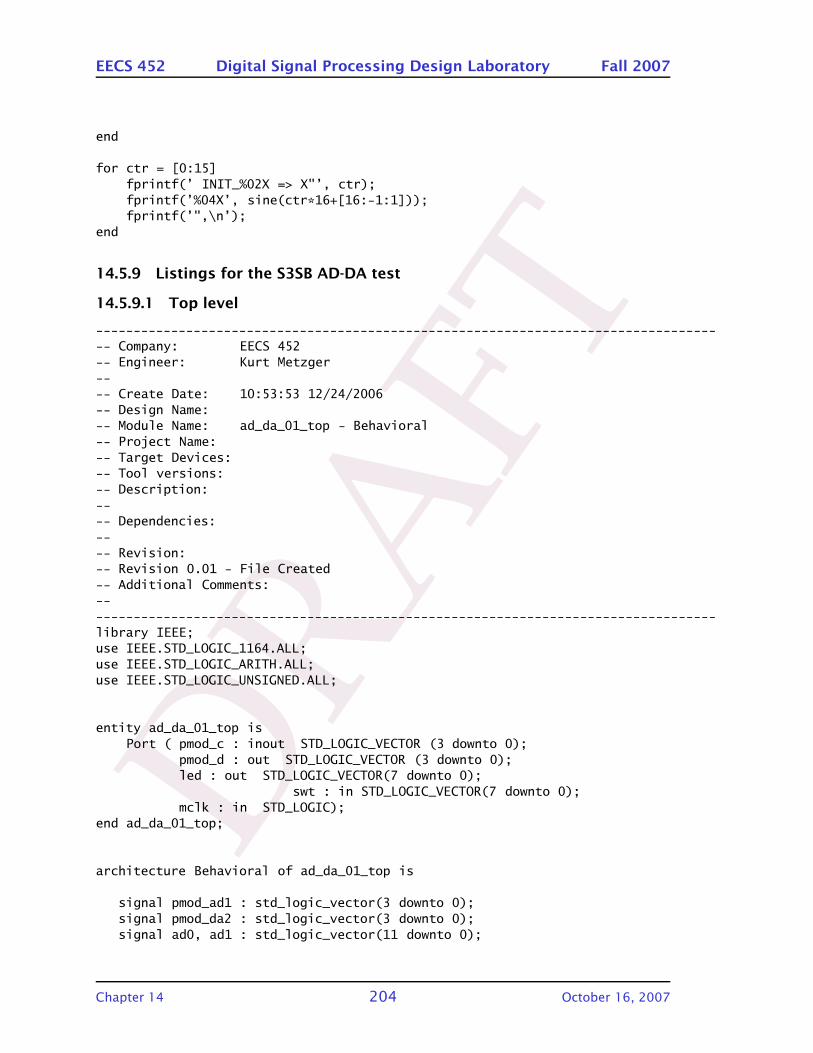
DRA
FT
EECS 452 Digital Signal Processing Design Laboratory Fall 2007
end
for ctr = [0:15]fprintf(’ INIT_%02X => X"’, ctr);fprintf(’%04X’, sine(ctr*16+[16:-1:1]));fprintf(’",\n’);
end
14.5.9 Listings for the S3SB AD-DA test
14.5.9.1 Top level
------------------------------------------------------------------------------------ Company: EECS 452-- Engineer: Kurt Metzger---- Create Date: 10:53:53 12/24/2006-- Design Name:-- Module Name: ad_da_01_top - Behavioral-- Project Name:-- Target Devices:-- Tool versions:-- Description:---- Dependencies:---- Revision:-- Revision 0.01 - File Created-- Additional Comments:------------------------------------------------------------------------------------library IEEE;use IEEE.STD_LOGIC_1164.ALL;use IEEE.STD_LOGIC_ARITH.ALL;use IEEE.STD_LOGIC_UNSIGNED.ALL;
entity ad_da_01_top isPort ( pmod_c : inout STD_LOGIC_VECTOR (3 downto 0);
pmod_d : out STD_LOGIC_VECTOR (3 downto 0);led : out STD_LOGIC_VECTOR(7 downto 0);
swt : in STD_LOGIC_VECTOR(7 downto 0);mclk : in STD_LOGIC);
end ad_da_01_top;
architecture Behavioral of ad_da_01_top is
signal pmod_ad1 : std_logic_vector(3 downto 0);signal pmod_da2 : std_logic_vector(3 downto 0);signal ad0, ad1 : std_logic_vector(11 downto 0);
Chapter 14 204 October 16, 2007
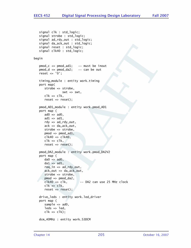
DRA
FT
EECS 452 Digital Signal Processing Design Laboratory Fall 2007
signal clk : std_logic;signal strobe : std_logic;signal ad_rdy_out : std_logic;signal da_ack_out : std_logic;signal reset : std_logic;signal clk40 : std_logic;
begin
pmod_c <= pmod_ad1; -- must be inoutpmod_d <= pmod_da2; -- can be outreset <= ’0’;
timing_module : entity work.timingport map(
strobe => strobe,swt => swt,
clk => clk,reset => reset);
pmod_AD1_module : entity work.pmod_AD1port map (
ad0 => ad0,ad1 => ad1,rdy => ad_rdy_out,ack => da_ack_out,strobe => strobe,pmod => pmod_ad1,clk40 => clk40,clk => clk,reset => reset);
pmod_DA2_module : entity work.pmod_DA2V2port map (
da0 => ad0,da1 => ad1,req_in => ad_rdy_out,ack_out => da_ack_out,strobe => strobe,pmod => pmod_da2,clk40 => clk, -- DA2 can use 25 MHz clockclk => clk,reset => reset);
drive_leds : entity work.led_driverport map (
sample => ad0,leds => led,clk => clk);
dcm_40MHz : entity work.S3DCM
Chapter 14 205 October 16, 2007
DRA
FT
EECS 452 Digital Signal Processing Design Laboratory Fall 2007
port map (CLKIN_IN => mclk,CLKFX_OUT => clk40,CLK0_OUT => clk) ;
end Behavioral;
14.5.9.2 AD1 PMod support
------------------------------------------------------------------------------------ Company:-- Engineer:---- Create Date: 15:42:43 12/24/2006-- Design Name:-- Module Name: pmod_AD1 - Behavioral-- Project Name:-- Target Devices:-- Tool versions:-- Description:---- Dependencies:---- Revision:-- Revision 0.01 - File Created-- Revision 0.02 - Modified sync to eliminate jitter KM 1-26-2007-- Additional Comments:------------------------------------------------------------------------------------library IEEE;use IEEE.STD_LOGIC_1164.ALL;use IEEE.STD_LOGIC_ARITH.ALL;use IEEE.STD_LOGIC_UNSIGNED.ALL;
entity pmod_AD1 isPort ( ad0 : out STD_LOGIC_VECTOR (11 downto 0); -- two’s complement
ad1 : out STD_LOGIC_VECTOR (11 downto 0); -- two’s complementrdy : out STD_LOGIC;ack : in STD_LOGIC;strobe : in STD_LOGIC;pmod : inout STD_LOGIC_VECTOR (3 downto 0);clk40 : in STD_LOGIC;clk : in STD_LOGIC;reset : in STD_LOGIC);
end pmod_AD1;
architecture Behavioral of pmod_AD1 is
Chapter 14 206 October 16, 2007
DRA
FT
EECS 452 Digital Signal Processing Design Laboratory Fall 2007
signal ad0r, ad1r : std_logic_vector(11 downto 0);signal ad0b, ad1b : std_logic_vector(11 downto 0);signal ctr : std_logic_vector(3 downto 0);signal sw_start : std_logic := ’0’;signal ad_active : std_logic := ’0’;signal ad_csa : std_logic := ’0’;signal ad_csb : std_logic := ’0’;signal ad_cs : std_logic;signal ad_clk : std_logic := ’1’;signal ad0_in, ad1_in : std_logic;
type t_state_conv is (conv_idle, start_bit, up_going);type t_state_sync is (sync_idle, sync_wait);signal state_sync : t_state_sync := sync_idle;signal state_conv : t_state_conv := conv_idle;
begin
ad0 <= (not ad0b(11)) & ad0b(10 downto 0); -- make 2’s complementad1 <= (not ad1b(11)) & ad1b(10 downto 0); -- make 2’s complementpmod <= ad_clk & ’Z’ & ’Z’ & ad_cs;ad0_in <= pmod(1);ad1_in <= pmod(2);ad_cs <= not (ad_csa or ad_csb);
process(ack, strobe, ad_active, ad_csb, clk, reset)begin
if reset = ’1’ thenrdy <= ’0’;sw_start <= ’0’;ad_csa <= ’0’;state_sync <= sync_idle;
elsif rising_edge(clk) thenif ack = ’1’ then
rdy <= ’0’;end if;case state_sync iswhen sync_idle =>
if strobe = ’1’ thenad0b <= ad0r; -- move sample to outputad1b <= ad1r; -- both a/d channelsrdy <= ’1’; -- set readysw_start <= ’1’; -- start next a/d cyclead_csa <= ’1’; -- cause a/d to go into holdstate_sync <= sync_wait;
end if;when sync_wait =>
if ad_csb = ’1’ then -- if cycle holding csad_csa <= ’0’; -- then this part can stop
end if;
Chapter 14 207 October 16, 2007

DRA
FT
EECS 452 Digital Signal Processing Design Laboratory Fall 2007
if ad_active = ’1’ then -- if a/d being clockedsw_start <= ’0’; -- then local handshakestate_sync <= sync_idle; -- and wait for next strobe
end if;end case;
end if;end process;
process(sw_start, clk40, reset)begin
if reset = ’1’ thenad0r <= X"000";ad1r <= X"000";ad_csb <= ’0’;ad_clk <= ’1’;ad_active <= ’0’;state_conv <= conv_idle;
elsif rising_edge(clk40) thencase state_conv iswhen conv_idle =>
if sw_start = ’1’ thenad_csb <= ’1’;ad_clk <= ’1’;ctr <= "0000";ad_active <= ’1’;state_conv <= start_bit;
end if;when start_bit =>
ad0r <= ad0r(10 downto 0) & ad0_in;ad1r <= ad1r(10 downto 0) & ad1_in;ad_clk <= ’0’;state_conv <= up_going;
when up_going =>ctr <= ctr+1;ad_clk <= ’1’;if ctr = 15 then
ad_active <= ’0’;ad_csb <= ’0’;state_conv <= conv_idle;
elsestate_conv <= start_bit;
end if;end case;
end if;end process;
end Behavioral;
Chapter 14 208 October 16, 2007
DRA
FT
EECS 452 Digital Signal Processing Design Laboratory Fall 2007
14.5.9.3 DA2 PMod support
------------------------------------------------------------------------------------ Company: EECS 452-- Engineer: Kurt Metzger---- Create Date: 12:41:54 12/24/2006-- Design Name:-- Module Name: pmod_DA2V2 - Behavioral-- Project Name:-- Target Devices:-- Tool versions:-- Description:---- Dependencies:---- Revision:-- Revision 0.01 - File Created-- Additional Comments:------------------------------------------------------------------------------------library IEEE;use IEEE.STD_LOGIC_1164.ALL;use IEEE.STD_LOGIC_ARITH.ALL;use IEEE.STD_LOGIC_UNSIGNED.ALL;
-- pmod_DA2 pmodule driver---- Expects 40 MHz input clock and uses this-- to tic the DA converter clock at 20 MHz.---- Illustrates single segment finite state machine.
entity pmod_DA2V2 isPort ( da0 : in STD_LOGIC_VECTOR (11 downto 0); -- two’s complement
da1 : in STD_LOGIC_VECTOR (11 downto 0); -- two’s complementreq_in : in STD_LOGIC;ack_out : out STD_LOGIC;strobe : in STD_LOGIC;pmod : out STD_LOGIC_VECTOR (3 downto 0);clk40 : in STD_LOGIC;clk : in STD_LOGIC;reset : in STD_LOGIC);
end pmod_DA2V2;
architecture Behavioral of pmod_DA2V2 is
signal d0r : std_logic_vector(11 downto 0) := X"000";signal d1r : std_logic_vector(11 downto 0) := X"000";signal d0 : std_logic_vector(15 downto 0) := X"0000";signal d1 : std_logic_vector(15 downto 0) := X"0000";
Chapter 14 209 October 16, 2007

DRA
FT
EECS 452 Digital Signal Processing Design Laboratory Fall 2007
signal da_active : std_logic := ’0’;signal da_clk : std_logic := ’1’;signal da_sync : std_logic := ’0’;signal ctr : std_logic_vector(3 downto 0);signal go_go : std_logic := ’0’;
type t_state_load is (idle_l, starta, startb, dobita, dobitb);type t_state_sync is (idle_s, wait_for_strobe, wait_for_active);signal state_load_da : t_state_load := idle_l;signal state_sync : t_state_sync := idle_s;
begin
pmod <= da_clk & d1(15) & d0(15) & da_sync; -- generate pmod signals for DA2 module
process(req_in, da_active, clk40, clk, reset)begin
if reset = ’1’ then -- initialize what needs to be initializedack_out <= ’0’;go_go <= ’0’;state_sync <= idle_s;
elsif rising_edge(clk) thenif req_in = ’0’ then
ack_out <= ’0’;end if;case state_sync iswhen idle_s =>
if req_in = ’1’ thend0r <= da0; -- save value to send to da 0d1r <= da1; -- save value to send to da 1ack_out <= ’1’; -- tell that values have been takenstate_sync <= wait_for_strobe;
end if;when wait_for_strobe =>
if strobe = ’1’ then -- tic that starts loading da’sgo_go <= ’1’; -- start loading the da’sstate_sync <= wait_for_active;
end if;when wait_for_active =>
if da_active = ’1’ thengo_go <= ’0’; -- loading has started .. clearstate_sync <= idle_s;
end if;end case;
end if;end process;
process(go_go, clk40, reset)begin
if reset = ’1’ thenda_active <= ’0’;
Chapter 14 210 October 16, 2007
DRA
FT
EECS 452 Digital Signal Processing Design Laboratory Fall 2007
da_clk <= ’1’;da_sync <= ’0’;state_load_da <= idle_l;
elsif rising_edge(clk40) thencase state_load_da iswhen idle_l =>
if go_go = ’1’ thend0 <= X"0" & (not d0r(11)) & d0r(10 downto 0) ; -- save value to send to dad1 <= X"0" & (not d1r(11)) & d1r(10 downto 0) ; -- save value to send to dada_active <= ’1’; -- signal conversion startda_sync <= ’1’; -- set da sync highctr <= "0000"; -- use to send 16 bitsstate_load_da <= starta;
end if;when starta =>
da_clk <= ’0’; -- falling edge will sample syncstate_load_da <= startb;
when startb =>da_sync <= ’0’; -- set da sync low and leave it thereda_clk <= ’1’; -- set da clk high againstate_load_da <= dobita;
when dobita =>da_clk <= ’0’; -- generate falling edge on da clkstate_load_da <= dobitb;
when dobitb =>da_clk <= ’1’; -- make da clk go high againd0 <= d0(14 downto 0) & ’0’; -- shift da 0’s valued1 <= d1(14 downto 0) & ’0’; -- shift da 1’s valuectr <= ctr+1; -- count this iteration on next ticif ctr = 15 then -- if at 15 loading is done
da_active <= ’0’; -- no longer activestate_load_da <= idle_l;
elsestate_load_da <= dobita; -- else keep looping
end if;end case;
end if;end process;
end Behavioral;
14.5.9.4 LED driver
------------------------------------------------------------------------------------ Company:-- Engineer:---- Create Date: 13:59:38 01/27/2007-- Design Name:-- Module Name: led_driver - Behavioral
Chapter 14 211 October 16, 2007
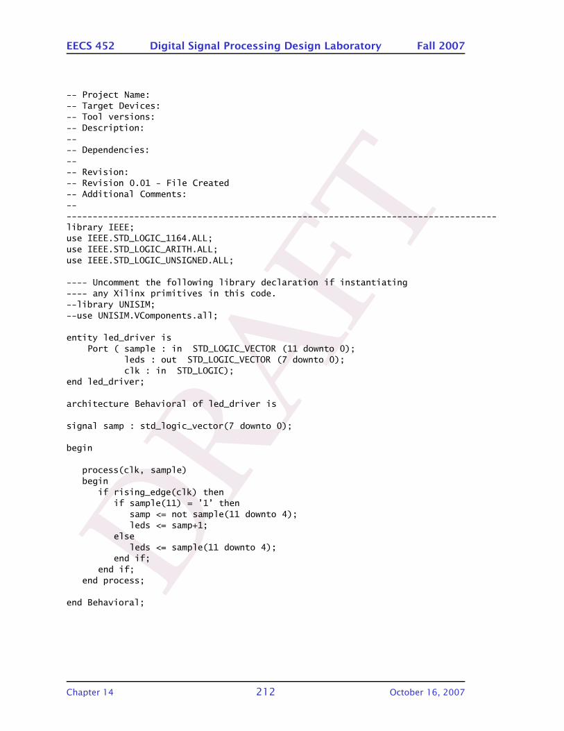
DRA
FT
EECS 452 Digital Signal Processing Design Laboratory Fall 2007
-- Project Name:-- Target Devices:-- Tool versions:-- Description:---- Dependencies:---- Revision:-- Revision 0.01 - File Created-- Additional Comments:------------------------------------------------------------------------------------library IEEE;use IEEE.STD_LOGIC_1164.ALL;use IEEE.STD_LOGIC_ARITH.ALL;use IEEE.STD_LOGIC_UNSIGNED.ALL;
---- Uncomment the following library declaration if instantiating---- any Xilinx primitives in this code.--library UNISIM;--use UNISIM.VComponents.all;
entity led_driver isPort ( sample : in STD_LOGIC_VECTOR (11 downto 0);
leds : out STD_LOGIC_VECTOR (7 downto 0);clk : in STD_LOGIC);
end led_driver;
architecture Behavioral of led_driver is
signal samp : std_logic_vector(7 downto 0);
begin
process(clk, sample)begin
if rising_edge(clk) thenif sample(11) = ’1’ then
samp <= not sample(11 downto 4);leds <= samp+1;
elseleds <= sample(11 downto 4);
end if;end if;
end process;
end Behavioral;
Chapter 14 212 October 16, 2007
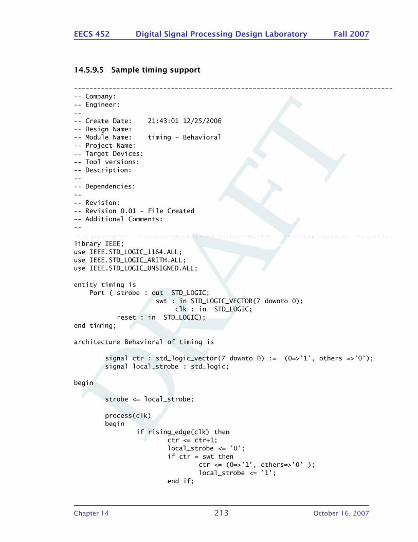
DRA
FT
EECS 452 Digital Signal Processing Design Laboratory Fall 2007
14.5.9.5 Sample timing support
------------------------------------------------------------------------------------ Company:-- Engineer:---- Create Date: 21:43:01 12/25/2006-- Design Name:-- Module Name: timing - Behavioral-- Project Name:-- Target Devices:-- Tool versions:-- Description:---- Dependencies:---- Revision:-- Revision 0.01 - File Created-- Additional Comments:------------------------------------------------------------------------------------library IEEE;use IEEE.STD_LOGIC_1164.ALL;use IEEE.STD_LOGIC_ARITH.ALL;use IEEE.STD_LOGIC_UNSIGNED.ALL;
entity timing isPort ( strobe : out STD_LOGIC;
swt : in STD_LOGIC_VECTOR(7 downto 0);clk : in STD_LOGIC;
reset : in STD_LOGIC);end timing;
architecture Behavioral of timing is
signal ctr : std_logic_vector(7 downto 0) := (0=>’1’, others =>’0’);signal local_strobe : std_logic;
begin
strobe <= local_strobe;
process(clk)begin
if rising_edge(clk) thenctr <= ctr+1;local_strobe <= ’0’;if ctr = swt then
ctr <= (0=>’1’, others=>’0’ );local_strobe <= ’1’;
end if;
Chapter 14 213 October 16, 2007
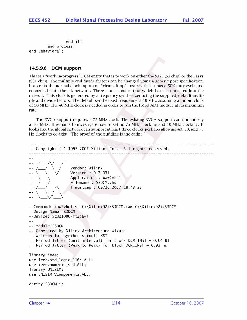
DRA
FT
EECS 452 Digital Signal Processing Design Laboratory Fall 2007
end if;end process;
end Behavioral;
14.5.9.6 DCM support
This is a “work-in-progress” DCM entity that is to work on either the S3SB (S3 chip) or the Basys
(S3e chip). The multiply and divide factors can be changed using a generic port specification.It accepts the normal clock input and “cleans-it-up”, insures that it has a 50% duty cycle and
connects it into the clk network. There is a second output which is also connected into thenetwork. This clock is generated by a frequency synthesizer using the supplied/default multi-
ply and divide factors. The default synthesized frequency is 40 MHz assuming an input clock
of 50 MHz. The 40 MHz clock is needed in order to run the PMod AD1 module at its maximumrate.
The XVGA support requires a 75 MHz clock. The existing XVGA support can run entirelyat 75 MHz. It remains to investigate how to set up 75 MHz clocking and 40 MHz clocking. It
looks like the global network can support at least three clocks perhaps allowing 40, 50, and 75
Hz clocks to co-exist. "The proof of the pudding is the eating."
---------------------------------------------------------------------------------- Copyright (c) 1995-2007 Xilinx, Inc. All rights reserved.---------------------------------------------------------------------------------- ____ ____-- / /\/ /-- /___/ \ / Vendor: Xilinx-- \ \ \/ Version : 9.2.03i-- \ \ Application : xaw2vhdl-- / / Filename : S3DCM.vhd-- /___/ /\ Timestamp : 09/20/2007 18:43:25-- \ \ / \-- \___\/\___\----Command: xaw2vhdl-st C:\Xilinx92i\S3DCM.xaw C:\Xilinx92i\S3DCM--Design Name: S3DCM--Device: xc3s1000-ft256-4---- Module S3DCM-- Generated by Xilinx Architecture Wizard-- Written for synthesis tool: XST-- Period Jitter (unit interval) for block DCM_INST = 0.04 UI-- Period Jitter (Peak-to-Peak) for block DCM_INST = 0.92 ns
library ieee;use ieee.std_logic_1164.ALL;use ieee.numeric_std.ALL;library UNISIM;use UNISIM.Vcomponents.ALL;
entity S3DCM is
Chapter 14 214 October 16, 2007
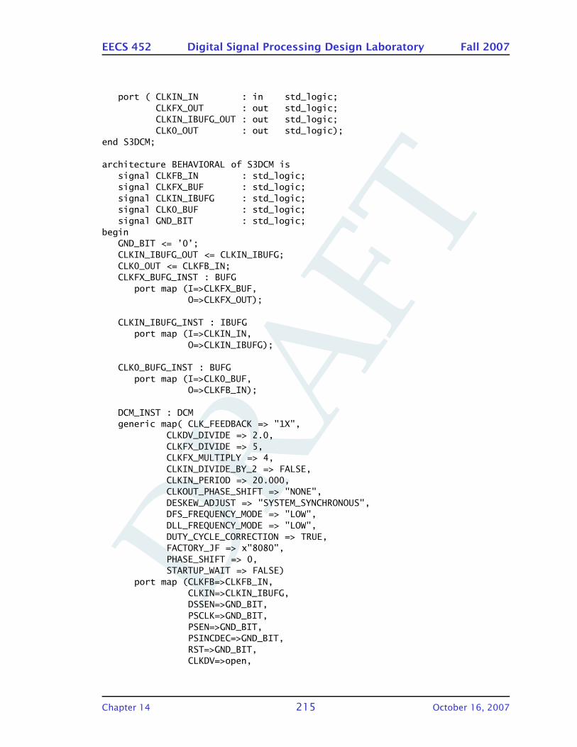
DRA
FT
EECS 452 Digital Signal Processing Design Laboratory Fall 2007
port ( CLKIN_IN : in std_logic;CLKFX_OUT : out std_logic;CLKIN_IBUFG_OUT : out std_logic;CLK0_OUT : out std_logic);
end S3DCM;
architecture BEHAVIORAL of S3DCM issignal CLKFB_IN : std_logic;signal CLKFX_BUF : std_logic;signal CLKIN_IBUFG : std_logic;signal CLK0_BUF : std_logic;signal GND_BIT : std_logic;
beginGND_BIT <= ’0’;CLKIN_IBUFG_OUT <= CLKIN_IBUFG;CLK0_OUT <= CLKFB_IN;CLKFX_BUFG_INST : BUFG
port map (I=>CLKFX_BUF,O=>CLKFX_OUT);
CLKIN_IBUFG_INST : IBUFGport map (I=>CLKIN_IN,
O=>CLKIN_IBUFG);
CLK0_BUFG_INST : BUFGport map (I=>CLK0_BUF,
O=>CLKFB_IN);
DCM_INST : DCMgeneric map( CLK_FEEDBACK => "1X",
CLKDV_DIVIDE => 2.0,CLKFX_DIVIDE => 5,CLKFX_MULTIPLY => 4,CLKIN_DIVIDE_BY_2 => FALSE,CLKIN_PERIOD => 20.000,CLKOUT_PHASE_SHIFT => "NONE",DESKEW_ADJUST => "SYSTEM_SYNCHRONOUS",DFS_FREQUENCY_MODE => "LOW",DLL_FREQUENCY_MODE => "LOW",DUTY_CYCLE_CORRECTION => TRUE,FACTORY_JF => x"8080",PHASE_SHIFT => 0,STARTUP_WAIT => FALSE)
port map (CLKFB=>CLKFB_IN,CLKIN=>CLKIN_IBUFG,DSSEN=>GND_BIT,PSCLK=>GND_BIT,PSEN=>GND_BIT,PSINCDEC=>GND_BIT,RST=>GND_BIT,CLKDV=>open,
Chapter 14 215 October 16, 2007
DRA
FT
EECS 452 Digital Signal Processing Design Laboratory Fall 2007
CLKFX=>CLKFX_BUF,CLKFX180=>open,CLK0=>CLK0_BUF,CLK2X=>open,CLK2X180=>open,CLK90=>open,CLK180=>open,CLK270=>open,LOCKED=>open,PSDONE=>open,STATUS=>open);
end BEHAVIORAL;
14.5.10 Metastability demonstration C and VHDL
14.5.10.1 Metastability demonstration C5510 main
14.5.10.2 Metastability C5510 codec setup
14.5.10.3 Metastability demonstration top
------------------------------------------------------------------------------------ Company: EECS 452-- Engineer: Kurt Metzger---- Create Date: 10:25:49 08/04/2007-- Design Name:-- Module Name: metastabletop - Behavioral-- Project Name:-- Target Devices:-- Tool versions:-- Description:---- Dependencies:---- Revision:-- Revision 0.01 - File Created-- Additional Comments:------------------------------------------------------------------------------------library IEEE;use IEEE.STD_LOGIC_1164.ALL;use IEEE.STD_LOGIC_ARITH.ALL;
Chapter 14 216 October 16, 2007
DRA
FT
EECS 452 Digital Signal Processing Design Laboratory Fall 2007
use IEEE.STD_LOGIC_UNSIGNED.ALL;
entity metastabletop isPort ( fsx0 : in STD_LOGIC;
clkx0 : in STD_LOGIC;dx0 : in STD_LOGIC;fsr0 : out STD_LOGIC;clkr0 : out STD_LOGIC;dr0 : out STD_LOGIC;pmod_a : out STD_LOGIC_VECTOR (3 downto 0);swt : in STD_LOGIC_VECTOR (7 downto 0);ssg : out STD_LOGIC_VECTOR (7 downto 0);an : inout STD_LOGIC_VECTOR (3 downto 0);led : out STD_LOGIC_VECTOR (7 downto 0);mclk : in STD_LOGIC);
end metastabletop;
architecture Behavioral of metastabletop is
signal clk : std_logic;signal reset : std_logic := ’0’;signal req_out : std_logic;signal ack_in : std_logic;signal data_rcvd : std_logic_vector(15 downto 0);signal data_send : std_logic_vector(15 downto 0);signal pmod_McB : std_logic_vector(3 downto 0);signal display_value : std_logic_vector(15 downto 0);type t_state is (s_idle, s_wait);signal state : t_state := s_idle;
begin
clk <= mclk;led <= data_rcvd(7 downto 0); -- flashing lights are neatdisplay_value <= data_rcvd;
-- connect to 40 pin cable McBSP lines
pmod_McB(0) <= fsx0; -- McBSP transmitter frame syncfsr0 <= fsx0; -- McBSP receiver frame syncpmod_McB(3) <= clkx0; -- McBSP transmitter shift clockclkr0 <= clkx0; -- McBSP receiver shift clockpmod_McB(1) <= dx0; -- McBSP transmitter output to FPGAdr0 <= pmod_McB(2); -- McBSP receiver input from FPGApmod_a <= pmod_McB; -- to allow using scope to watch
McB : entity work.McBSPS3slaveport map ( data_send => data_send, -- data to McBSP
data_rcvd => data_rcvd, -- data from McBSPreq_out => req_out, -- high when have value from McBSPack_in => ack_in, -- acknowledge data received
Chapter 14 217 October 16, 2007
DRA
FT
EECS 452 Digital Signal Processing Design Laboratory Fall 2007
pmod => pmod_McB, -- connect to PMod connecting FPGA/DSKclk => clk,reset => reset);
process(req_out, clk) -- send when ever you canbegin
if rising_edge(clk) thenif req_out = ’1’ then -- data received
data_send <= data_rcvd; -- echo it backack_in <= ’1’; -- did it
elseack_in <= ’0’;
end if;end if;
end process;
-- Chih-Wei’s seven segment support
SSD02_unit : entity work.SSD02port map ( ssd0 => display_value(3 downto 0),
ssd1 => display_value(7 downto 4),ssd2 => display_value(11 downto 8),ssd3 => display_value(15 downto 12),ssd => ssg,dp => "0000",sel => "1111",an => an,clk => clk);
end Behavioral;
14.5.10.4 Metastability demonstration main VHDL
------------------------------------------------------------------------------------ Company: EECS 452-- Engineer: Kurt Metzger---- Create Date: 10:28:21 08/04/2007-- Design Name:-- Module Name: McBSPS3slave - Behavioral-- Project Name:-- Target Devices:-- Tool versions:-- Description:---- Dependencies:---- Revision:-- Revision 0.01 - File Created-- Additional Comments:--
Chapter 14 218 October 16, 2007
DRA
FT
EECS 452 Digital Signal Processing Design Laboratory Fall 2007
----------------------------------------------------------------------------------library IEEE;use IEEE.STD_LOGIC_1164.ALL;use IEEE.STD_LOGIC_ARITH.ALL;use IEEE.STD_LOGIC_UNSIGNED.ALL;
entity McBSPS3slave isPort ( data_send : in STD_LOGIC_VECTOR (15 downto 0);
data_rcvd : out STD_LOGIC_VECTOR (15 downto 0);req_out : out STD_LOGIC;ack_in : in STD_LOGIC;pmod : inout STD_LOGIC_VECTOR (3 downto 0);clk : in STD_LOGIC;reset : in STD_LOGIC);
end McBSPS3slave;
architecture Behavioral of McBSPS3slave is
signal sr_rcv, sr_out, temp_send : std_logic_vector(15 downto 0);signal have_data : std_logic := ’0’;signal previous : std_logic := ’0’;signal have : std_logic_vector(1 downto 0);signal counter_r : std_logic_vector(3 downto 0);signal fsync, sclk, input : std_logic;signal frame_start : std_logic := ’0’;
type t_state_r is (idle_r, receive_r);signal state_r : t_state_r := idle_r;
begin
fsync <= pmod(0); -- McBSP fsx0input <= pmod(1); -- serial data from McBSPpmod(2) <= sr_out(15); -- serial data to McBSPsclk <= pmod(3); -- McBSP clkx
-- receive value from the McBSP
process(fsync, sclk)begin
if falling_edge(sclk) then -- this example’s data changes on risingsr_rcv <= sr_rcv(14 downto 0) & input;case state_r is
when idle_r =>if fsync = ’1’ then -- frame is starting
have_data <= ’0’;counter_r <= (others=>’0’);state_r <= receive_r;
end if;when receive_r =>
counter_r <= counter_r+1;
Chapter 14 219 October 16, 2007
DRA
FT
EECS 452 Digital Signal Processing Design Laboratory Fall 2007
if counter_r = 15 thendata_rcvd <= sr_rcv(14 downto 0) & input;have_data <= ’1’;temp_send <= data_send; -- syncs receiving and sendingstate_r <= idle_r;
end if;end case;
end if;end process;
-- handle the handshake with the user
process(have_data, clk)begin
if rising_edge(clk) then------------------------------------------------------------------------------------- uncomment only one of these two ifs..one works reliably and one doesn’t
if have = "01" then -- test on the saved pair-- if (previous & have_data) = "01" then -- test on previous and current-----------------------------------------------------------------------------------
req_out <= ’1’;end if;if ack_in = ’1’ then
req_out <= ’0’;end if;previous <= have_data; -- save only previous valuehave <= have(0) & have_data; -- save two previous values
end if;
end process;
-- send value to McBSP
process(sclk)begin
if falling_edge(sclk) thenif fsync = ’1’ then
frame_start <= ’1’;else
frame_start <= ’0’;end if;
end if;
if rising_edge(sclk) thenif frame_start = ’1’ then
sr_out <= temp_send;else
Chapter 14 220 October 16, 2007
DRA
FT
EECS 452 Digital Signal Processing Design Laboratory Fall 2007
sr_out <= sr_out(14 downto 0) & ’0’;end if;
end if;end process;
end Behavioral;
14.5.10.5 Metastability demonstration UCF file
# Spartan-3 User Constraints File: spartan3.ucf## 11Jan2007#
# oscillator clock (in)#NET "mclk" PERIOD = 20 ns HIGH 40 %;NET "mclk" LOC = "T9" | IOSTANDARD = LVCMOS33;
# push buttons##NET "btn<0>" LOC = "M13" | IOSTANDARD = LVCMOS33;#NET "btn<1>" LOC = "M14" | IOSTANDARD = LVCMOS33;#NET "btn<2>" LOC = "L13" | IOSTANDARD = LVCMOS33;#NET "btn<3>" LOC = "L14" | IOSTANDARD = LVCMOS33;
# light emitting diodes#NET "led<0>" LOC = "K12" | IOSTANDARD = LVCMOS33;NET "led<1>" LOC = "P14" | IOSTANDARD = LVCMOS33;NET "led<2>" LOC = "L12" | IOSTANDARD = LVCMOS33;NET "led<3>" LOC = "N14" | IOSTANDARD = LVCMOS33;NET "led<4>" LOC = "P13" | IOSTANDARD = LVCMOS33;NET "led<5>" LOC = "N12" | IOSTANDARD = LVCMOS33;NET "led<6>" LOC = "P12" | IOSTANDARD = LVCMOS33;NET "led<7>" LOC = "P11" | IOSTANDARD = LVCMOS33;
# seven segment digit anodes#NET "an<0>" LOC = "D14" | IOSTANDARD = LVCMOS33;NET "an<1>" LOC = "G14" | IOSTANDARD = LVCMOS33;NET "an<2>" LOC = "F14" | IOSTANDARD = LVCMOS33;NET "an<3>" LOC = "E13" | IOSTANDARD = LVCMOS33;
# seven segment digit cathodes#NET "ssg<0>" LOC = "N16" | IOSTANDARD = LVCMOS33; # segment GNET "ssg<1>" LOC = "F13" | IOSTANDARD = LVCMOS33; # segment FNET "ssg<2>" LOC = "R16" | IOSTANDARD = LVCMOS33; # segment ENET "ssg<3>" LOC = "P15" | IOSTANDARD = LVCMOS33; # segment D
Chapter 14 221 October 16, 2007
DRA
FT
EECS 452 Digital Signal Processing Design Laboratory Fall 2007
NET "ssg<4>" LOC = "N15" | IOSTANDARD = LVCMOS33; # segment CNET "ssg<5>" LOC = "G13" | IOSTANDARD = LVCMOS33; # segment BNET "ssg<6>" LOC = "E14" | IOSTANDARD = LVCMOS33; # segment ANET "ssg<7>" LOC = "P16" | IOSTANDARD = LVCMOS33; # dp(decimal point)
# slide switches##NET "swt<0>" LOC = "F12" | IOSTANDARD = LVCMOS33;#NET "swt<1>" LOC = "G12" | IOSTANDARD = LVCMOS33;#NET "swt<2>" LOC = "H14" | IOSTANDARD = LVCMOS33;#NET "swt<3>" LOC = "H13" | IOSTANDARD = LVCMOS33;#NET "swt<4>" LOC = "J14" | IOSTANDARD = LVCMOS33;#NET "swt<5>" LOC = "J13" | IOSTANDARD = LVCMOS33;#NET "swt<6>" LOC = "K14" | IOSTANDARD = LVCMOS33;#NET "swt<7>" LOC = "K13" | IOSTANDARD = LVCMOS33;
# DB15 video connector##NET "blu" LOC = "R11" | IOSTANDARD = LVCMOS33;#NET "grn" LOC = "T12" | IOSTANDARD = LVCMOS33;#NET "red" LOC = "R12" | IOSTANDARD = LVCMOS33;#NET "hs" LOC = "R9" | IOSTANDARD = LVCMOS33;#NET "vs" LOC = "T10" | IOSTANDARD = LVCMOS33;
# MIB sockets on B1 names compatible with Nexys and Basys
# Pmod A : J1 on MIB to B1#NET "pmod_a<0>" LOC = "C10" | IOSTANDARD = LVCMOS33;NET "pmod_a<1>" LOC = "E10" | IOSTANDARD = LVCMOS33;NET "pmod_a<2>" LOC = "T3" | IOSTANDARD = LVCMOS33;NET "pmod_a<3>" LOC = "C11" | IOSTANDARD = LVCMOS33;
# Pmod B : J3 on MIB to B1##NET "pmod_b<0>" LOC = "R10" | IOSTANDARD = LVCMOS33;#NET "pmod_b<1>" LOC = "D12" | IOSTANDARD = LVCMOS33;#NET "pmod_b<2>" LOC = "T7" | IOSTANDARD = LVCMOS33;#NET "pmod_b<3>" LOC = "E11" | IOSTANDARD = LVCMOS33;
# Pmod C : J5 on MIB to B1##NET "pmod_c<0>" LOC = "M6" | IOSTANDARD = LVCMOS33;#NET "pmod_c<1>" LOC = "C16" | IOSTANDARD = LVCMOS33;#NET "pmod_c<2>" LOC = "C15" | IOSTANDARD = LVCMOS33;#NET "pmod_c<3>" LOC = "D16" | IOSTANDARD = LVCMOS33;
# Pmod D : J7 on MIB to B1##NET "pmod_d<0>" LOC = "F15" | IOSTANDARD = LVCMOS33;#NET "pmod_d<1>" LOC = "H15" | IOSTANDARD = LVCMOS33;
Chapter 14 222 October 16, 2007
DRA
FT
EECS 452 Digital Signal Processing Design Laboratory Fall 2007
#NET "pmod_d<2>" LOC = "G16" | IOSTANDARD = LVCMOS33;#NET "pmod_d<3>" LOC = "J16" | IOSTANDARD = LVCMOS33;
# Alternate naming for MIB on B1 .. 15July2007KM
# MIB J1 using B1##NET "mib_j1_b1<0>" LOC = "C10" | IOSTANDARD = LVCMOS33;#NET "mib_j1_b1<1>" LOC = "E10" | IOSTANDARD = LVCMOS33;#NET "mib_j1_b1<2>" LOC = "T3" | IOSTANDARD = LVCMOS33;#NET "mib_j1_b1<3>" LOC = "C11" | IOSTANDARD = LVCMOS33;
# MIB J2 using B1##NET "mib_j2_b1<0>" LOC = "N11" | IOSTANDARD = LVCMOS33;#NET "mib_j2_b1<1>" LOC = "D11" | IOSTANDARD = LVCMOS33;#NET "mib_j2_b1<2>" LOC = "P10" | IOSTANDARD = LVCMOS33;#NET "mib_j2_b1<3>" LOC = "C12" | IOSTANDARD = LVCMOS33;
# MIB J3 using B1##NET "mib_j3_b1<0>" LOC = "R10" | IOSTANDARD = LVCMOS33;#NET "mib_j3_b1<1>" LOC = "D12" | IOSTANDARD = LVCMOS33;#NET "mib_j3_b1<2>" LOC = "T7" | IOSTANDARD = LVCMOS33;#NET "mib_j3_b1<3>" LOC = "E11" | IOSTANDARD = LVCMOS33;
# MIB J4 using B1##NET "mib_j4_b1<0>" LOC = "R7" | IOSTANDARD = LVCMOS33;#NET "mib_j4_b1<1>" LOC = "B16" | IOSTANDARD = LVCMOS33;#NET "mib_j4_b1<2>" LOC = "N6" | IOSTANDARD = LVCMOS33;#NET "mib_j4_b1<3>" LOC = "R3" | IOSTANDARD = LVCMOS33;
# MIB J5 using B1##NET "mib_j5_b1<0>" LOC = "M6" | IOSTANDARD = LVCMOS33;#NET "mib_j5_b1<1>" LOC = "C16" | IOSTANDARD = LVCMOS33;#NET "mib_j5_b1<2>" LOC = "C15" | IOSTANDARD = LVCMOS33;#NET "mib_j5_b1<3>" LOC = "D16" | IOSTANDARD = LVCMOS33;
# MIB J6 using B1##NET "mib_j6_b1<0>" LOC = "D15" | IOSTANDARD = LVCMOS33;#NET "mib_j6_b1<1>" LOC = "E16" | IOSTANDARD = LVCMOS33;#NET "mib_j6_b1<2>" LOC = "E15" | IOSTANDARD = LVCMOS33;#NET "mib_j6_b1<3>" LOC = "G15" | IOSTANDARD = LVCMOS33;
# MIB J7 using B1##NET "mib_j7_b1<0>" LOC = "F15" | IOSTANDARD = LVCMOS33;#NET "mib_j7_b1<1>" LOC = "H15" | IOSTANDARD = LVCMOS33;
Chapter 14 223 October 16, 2007
DRA
FT
EECS 452 Digital Signal Processing Design Laboratory Fall 2007
#NET "mib_j7_b1<2>" LOC = "G16" | IOSTANDARD = LVCMOS33;#NET "mib_j7_b1<3>" LOC = "J16" | IOSTANDARD = LVCMOS33;
# MIB J8 using B1##NET "mib_j8_b1<0>" LOC = "H16" | IOSTANDARD = LVCMOS33;#NET "mib_j8_b1<1>" LOC = "K15" | IOSTANDARD = LVCMOS33;#NET "mib_j8_b1<2>" LOC = "K16" | IOSTANDARD = LVCMOS33;#NET "mib_j8_b1<3>" LOC = "L15" | IOSTANDARD = LVCMOS33;
# UART connections to female DB9 connector J2##NET "tx_a" LOC = "R13" | IOSTANDARD = LVCMOS33;#NET "rx_a" LOC = "T13" | IOSTANDARD = LVCMOS33;
# McBSP0 connection using A2 connector#NET "fsx0" LOC = "C5" | IOSTANDARD = LVCMOS33;NET "clkx0" LOC = "D5" | IOSTANDARD = LVCMOS33;NET "dx0" LOC = "D6" | IOSTANDARD = LVCMOS33;NET "fsr0" LOC = "E7" | IOSTANDARD = LVCMOS33;NET "clkr0" LOC = "C6" | IOSTANDARD = LVCMOS33;NET "dr0" LOC = "C7" | IOSTANDARD = LVCMOS33;
# McBSP1 connection using A2 connector## to be added
# RAM##NET "ram_addr<0>" LOC = "L5" | IOSTANDARD = LVCMOS33;#NET "ram_addr<1>" LOC = "N3" | IOSTANDARD = LVCMOS33;#NET "ram_addr<2>" LOC = "M4" | IOSTANDARD = LVCMOS33;#NET "ram_addr<3>" LOC = "M3" | IOSTANDARD = LVCMOS33;#NET "ram_addr<4>" LOC = "L4" | IOSTANDARD = LVCMOS33;#NET "ram_addr<5>" LOC = "G4" | IOSTANDARD = LVCMOS33;#NET "ram_addr<6>" LOC = "F3" | IOSTANDARD = LVCMOS33;#NET "ram_addr<7>" LOC = "F4" | IOSTANDARD = LVCMOS33;#NET "ram_addr<8>" LOC = "E3" | IOSTANDARD = LVCMOS33;#NET "ram_addr<9>" LOC = "E4" | IOSTANDARD = LVCMOS33;#NET "ram_addr<10>" LOC = "G5" | IOSTANDARD = LVCMOS33;#NET "ram_addr<11>" LOC = "H3" | IOSTANDARD = LVCMOS33;#NET "ram_addr<12>" LOC = "H4" | IOSTANDARD = LVCMOS33;#NET "ram_addr<13>" LOC = "J4" | IOSTANDARD = LVCMOS33;#NET "ram_addr<14>" LOC = "J3" | IOSTANDARD = LVCMOS33;#NET "ram_addr<15>" LOC = "K3" | IOSTANDARD = LVCMOS33;#NET "ram_addr<16>" LOC = "K5" | IOSTANDARD = LVCMOS33;#NET "ram_addr<17>" LOC = "L3" | IOSTANDARD = LVCMOS33;#
Chapter 14 224 October 16, 2007
DRA
FT
EECS 452 Digital Signal Processing Design Laboratory Fall 2007
#NET "ram_we" LOC = "G3" | IOSTANDARD = LVCMOS33;#NET "ram_oe" LOC = "K4" | IOSTANDARD = LVCMOS33;##NET "ram_a_data<0>" LOC = "N7" | IOSTANDARD = LVCMOS33;#NET "ram_a_data<1>" LOC = "T8" | IOSTANDARD = LVCMOS33;#NET "ram_a_data<2>" LOC = "R6" | IOSTANDARD = LVCMOS33;#NET "ram_a_data<3>" LOC = "T5" | IOSTANDARD = LVCMOS33;#NET "ram_a_data<4>" LOC = "R5" | IOSTANDARD = LVCMOS33;#NET "ram_a_data<5>" LOC = "C2" | IOSTANDARD = LVCMOS33;#NET "ram_a_data<6>" LOC = "C1" | IOSTANDARD = LVCMOS33;#NET "ram_a_data<7>" LOC = "B1" | IOSTANDARD = LVCMOS33;#NET "ram_a_data<9>" LOC = "P8" | IOSTANDARD = LVCMOS33;#NET "ram_a_data<10>" LOC = "F2" | IOSTANDARD = LVCMOS33;#NET "ram_a_data<11>" LOC = "H1" | IOSTANDARD = LVCMOS33;#NET "ram_a_data<12>" LOC = "J2" | IOSTANDARD = LVCMOS33;#NET "ram_a_data<13>" LOC = "L2" | IOSTANDARD = LVCMOS33;#NET "ram_a_data<14>" LOC = "P1" | IOSTANDARD = LVCMOS33;#NET "ram_a_data<15>" LOC = "R1" | IOSTANDARD = LVCMOS33;##NET "ram_a_ce" LOC = "P7" | IOSTANDARD = LVCMOS33;#NET "ram_a_lb" LOC = "P6" | IOSTANDARD = LVCMOS33;#NET "ram_a_ub" LOC = "T4" | IOSTANDARD = LVCMOS33;##NET "ram_b_data<0>" LOC = "P2" | IOSTANDARD = LVCMOS33;#NET "ram_b_data<1>" LOC = "N2" | IOSTANDARD = LVCMOS33;#NET "ram_b_data<2>" LOC = "M2" | IOSTANDARD = LVCMOS33;#NET "ram_b_data<3>" LOC = "K1" | IOSTANDARD = LVCMOS33;#NET "ram_b_data<4>" LOC = "J1" | IOSTANDARD = LVCMOS33;#NET "ram_b_data<5>" LOC = "G2" | IOSTANDARD = LVCMOS33;#NET "ram_b_data<6>" LOC = "E1" | IOSTANDARD = LVCMOS33;#NET "ram_b_data<7>" LOC = "D1" | IOSTANDARD = LVCMOS33;#NET "ram_b_data<8>" LOC = "D2" | IOSTANDARD = LVCMOS33;#NET "ram_b_data<9>" LOC = "E2" | IOSTANDARD = LVCMOS33;#NET "ram_b_data<10>" LOC = "G1" | IOSTANDARD = LVCMOS33;#NET "ram_b_data<11>" LOC = "F5" | IOSTANDARD = LVCMOS33;#NET "ram_b_data<12>" LOC = "C3" | IOSTANDARD = LVCMOS33;#NET "ram_b_data<13>" LOC = "K2" | IOSTANDARD = LVCMOS33;#NET "ram_b_data<14>" LOC = "M1" | IOSTANDARD = LVCMOS33;#NET "ram_b_data<15>" LOC = "N1" | IOSTANDARD = LVCMOS33;##NET "ram_b_ce" LOC = "N5" | IOSTANDARD = LVCMOS33;#NET "ram_b_lb" LOC = "P5" | IOSTANDARD = LVCMOS33;#NET "ram_b_ub" LOC = "R4" | IOSTANDARD = LVCMOS33;
Chapter 14 225 October 16, 2007

DRA
FTWasted space, consider adding helpful text to this chapter.
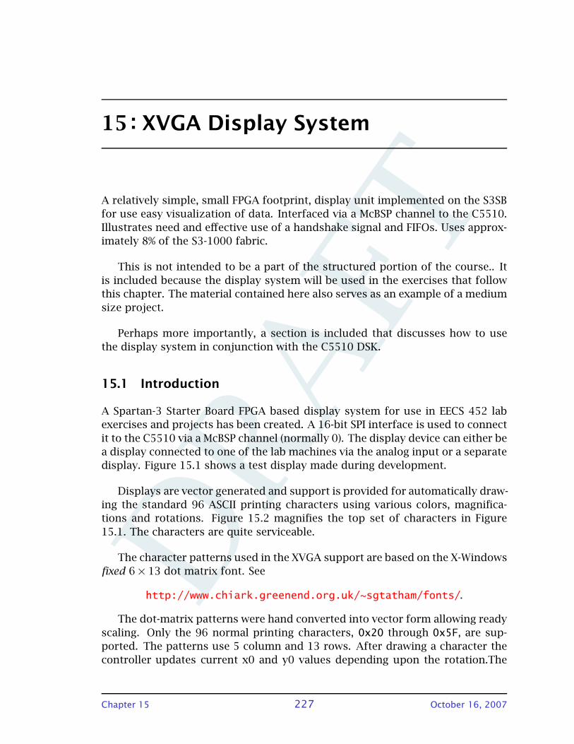
DRA
FT
15 : XVGA Display System
A relatively simple, small FPGA footprint, display unit implemented on the S3SB
for use easy visualization of data. Interfaced via a McBSP channel to the C5510.
Illustrates need and effective use of a handshake signal and FIFOs. Uses approx-
imately 8% of the S3-1000 fabric.
This is not intended to be a part of the structured portion of the course.. It
is included because the display system will be used in the exercises that follow
this chapter. The material contained here also serves as an example of a medium
size project.
Perhaps more importantly, a section is included that discusses how to use
the display system in conjunction with the C5510 DSK.
15.1 Introduction
A Spartan-3 Starter Board FPGA based display system for use in EECS 452 lab
exercises and projects has been created. A 16-bit SPI interface is used to connect
it to the C5510 via a McBSP channel (normally 0). The display device can either be
a display connected to one of the lab machines via the analog input or a separate
display. Figure 15.1 shows a test display made during development.
Displays are vector generated and support is provided for automatically draw-
ing the standard 96 ASCII printing characters using various colors, magnifica-
tions and rotations. Figure 15.2 magnifies the top set of characters in Figure
15.1. The characters are quite serviceable.
The character patterns used in the XVGA support are based on the X-Windows
fixed 6× 13 dot matrix font. See
http://www.chiark.greenend.org.uk/~sgtatham/fonts/.
The dot-matrix patterns were hand converted into vector form allowing ready
scaling. Only the 96 normal printing characters, 0x20 through 0x5F, are sup-
ported. The patterns use 5 column and 13 rows. After drawing a character the
controller updates current x0 and y0 values depending upon the rotation.The
Chapter 15 227 October 16, 2007
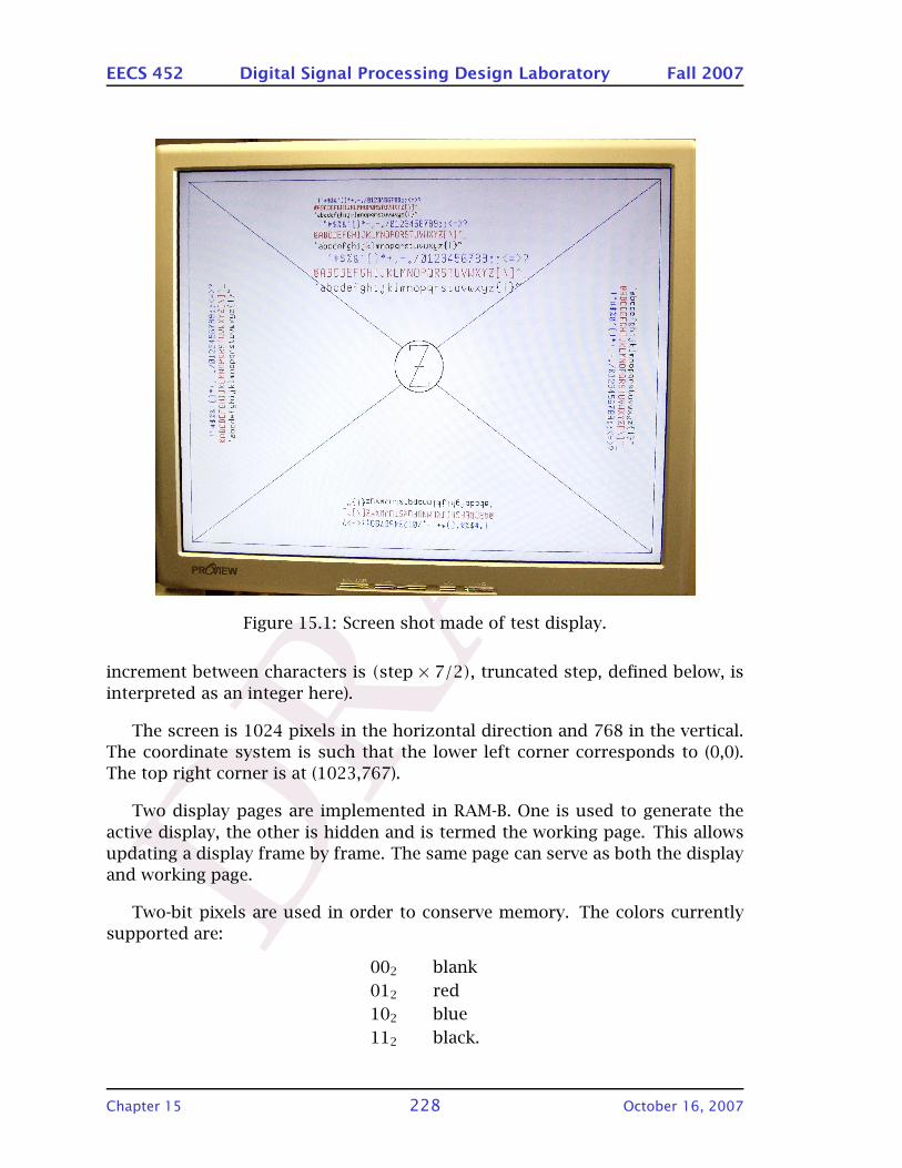
DRA
FT
EECS 452 Digital Signal Processing Design Laboratory Fall 2007
Figure 15.1: Screen shot made of test display.
increment between characters is (step × 7/2), truncated step, defined below, is
interpreted as an integer here).
The screen is 1024 pixels in the horizontal direction and 768 in the vertical.
The coordinate system is such that the lower left corner corresponds to (0,0).
The top right corner is at (1023,767).
Two display pages are implemented in RAM-B. One is used to generate the
active display, the other is hidden and is termed the working page. This allows
updating a display frame by frame. The same page can serve as both the display
and working page.
Two-bit pixels are used in order to conserve memory. The colors currently
supported are:
002 blank
012 red
102 blue
112 black.
Chapter 15 228 October 16, 2007
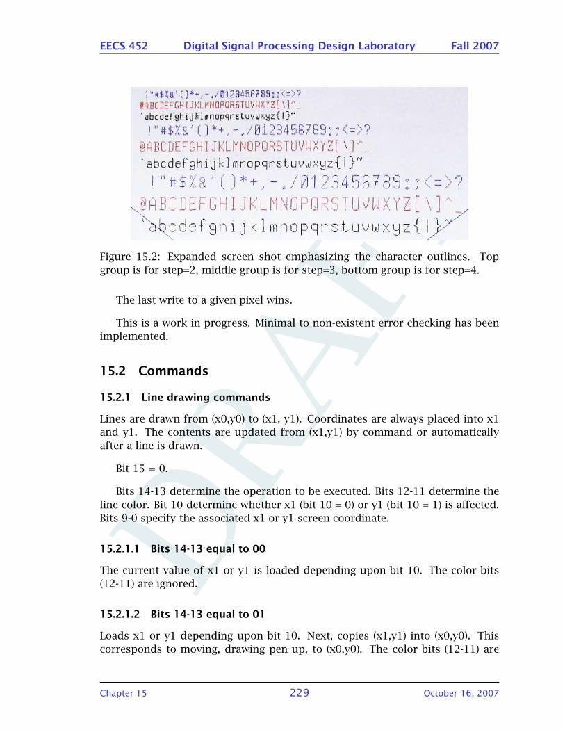
DRA
FT
EECS 452 Digital Signal Processing Design Laboratory Fall 2007
Figure 15.2: Expanded screen shot emphasizing the character outlines. Top
group is for step=2, middle group is for step=3, bottom group is for step=4.
The last write to a given pixel wins.
This is a work in progress. Minimal to non-existent error checking has been
implemented.
15.2 Commands
15.2.1 Line drawing commands
Lines are drawn from (x0,y0) to (x1, y1). Coordinates are always placed into x1
and y1. The contents are updated from (x1,y1) by command or automatically
after a line is drawn.
Bit 15 = 0.
Bits 14-13 determine the operation to be executed. Bits 12-11 determine the
line color. Bit 10 determine whether x1 (bit 10 = 0) or y1 (bit 10 = 1) is affected.
Bits 9-0 specify the associated x1 or y1 screen coordinate.
15.2.1.1 Bits 14-13 equal to 00
The current value of x1 or y1 is loaded depending upon bit 10. The color bits
(12-11) are ignored.
15.2.1.2 Bits 14-13 equal to 01
Loads x1 or y1 depending upon bit 10. Next, copies (x1,y1) into (x0,y0). This
corresponds to moving, drawing pen up, to (x0,y0). The color bits (12-11) are
Chapter 15 229 October 16, 2007
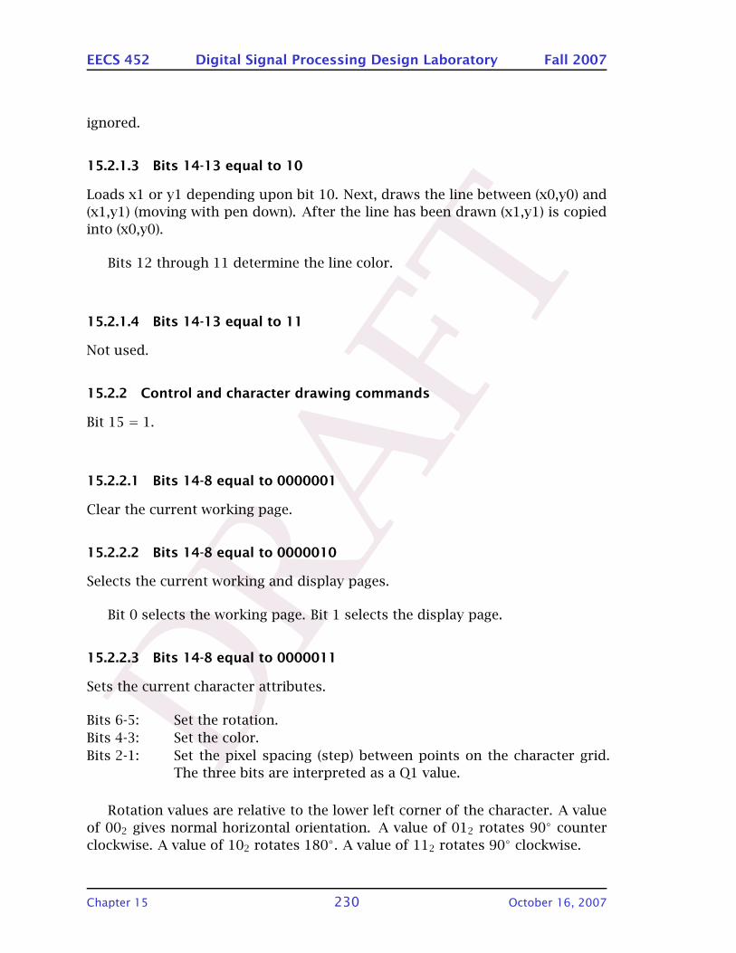
DRA
FT
EECS 452 Digital Signal Processing Design Laboratory Fall 2007
ignored.
15.2.1.3 Bits 14-13 equal to 10
Loads x1 or y1 depending upon bit 10. Next, draws the line between (x0,y0) and
(x1,y1) (moving with pen down). After the line has been drawn (x1,y1) is copied
into (x0,y0).
Bits 12 through 11 determine the line color.
15.2.1.4 Bits 14-13 equal to 11
Not used.
15.2.2 Control and character drawing commands
Bit 15 = 1.
15.2.2.1 Bits 14-8 equal to 0000001
Clear the current working page.
15.2.2.2 Bits 14-8 equal to 0000010
Selects the current working and display pages.
Bit 0 selects the working page. Bit 1 selects the display page.
15.2.2.3 Bits 14-8 equal to 0000011
Sets the current character attributes.
Bits 6-5: Set the rotation.
Bits 4-3: Set the color.
Bits 2-1: Set the pixel spacing (step) between points on the character grid.
The three bits are interpreted as a Q1 value.
Rotation values are relative to the lower left corner of the character. A value
of 002 gives normal horizontal orientation. A value of 012 rotates 90 counter
clockwise. A value of 102 rotates 180. A value of 112 rotates 90 clockwise.
Chapter 15 230 October 16, 2007

DRA
FT
EECS 452 Digital Signal Processing Design Laboratory Fall 2007
The step value adjusts the number of pixels between the points on the origi-
nal character grid. A value of 0102 results in a step of one pixel. This results in
a smallish character on the screen. A value of 0112 results in a nominal step of
1.5 pixels. This is results in a nicely sized character. A value of 1002 results in a
step size of 2 pixels. Etc.
15.2.3 Bits 14-8 equal to 0000100
Draws the character whose ASCII code is contained in bits 6 through 0.
15.3 In the C5510
The following code snippets are from the C5510 program used to develop and
test the XVGA display system.
15.3.1 Setting working and display pages
The following is called to switch between the working and display pages. After
the switch the new working page (the old display page) is cleared.
unsigned pages = 0x0001;
void XVGAinit()
TX_Put(0x8200+pages); // set work and display pagespages = 0x0003&(pages^0x0003); // switch which is whichTX_Put(0x8100); // clear working pagereturn;
15.3.2 Drawing lines
void GoTo(int x, int y)
TX_Put(x&0x03FF);TX_Put(0x2000|0x0400|(y&0x03FF));return;
void Draw(int color, int x, int y)
TX_Put(x&0x03FF);TX_Put(0x4000|0x0400|((color&0x3)<<11)|(y&0x03FF));
Chapter 15 231 October 16, 2007
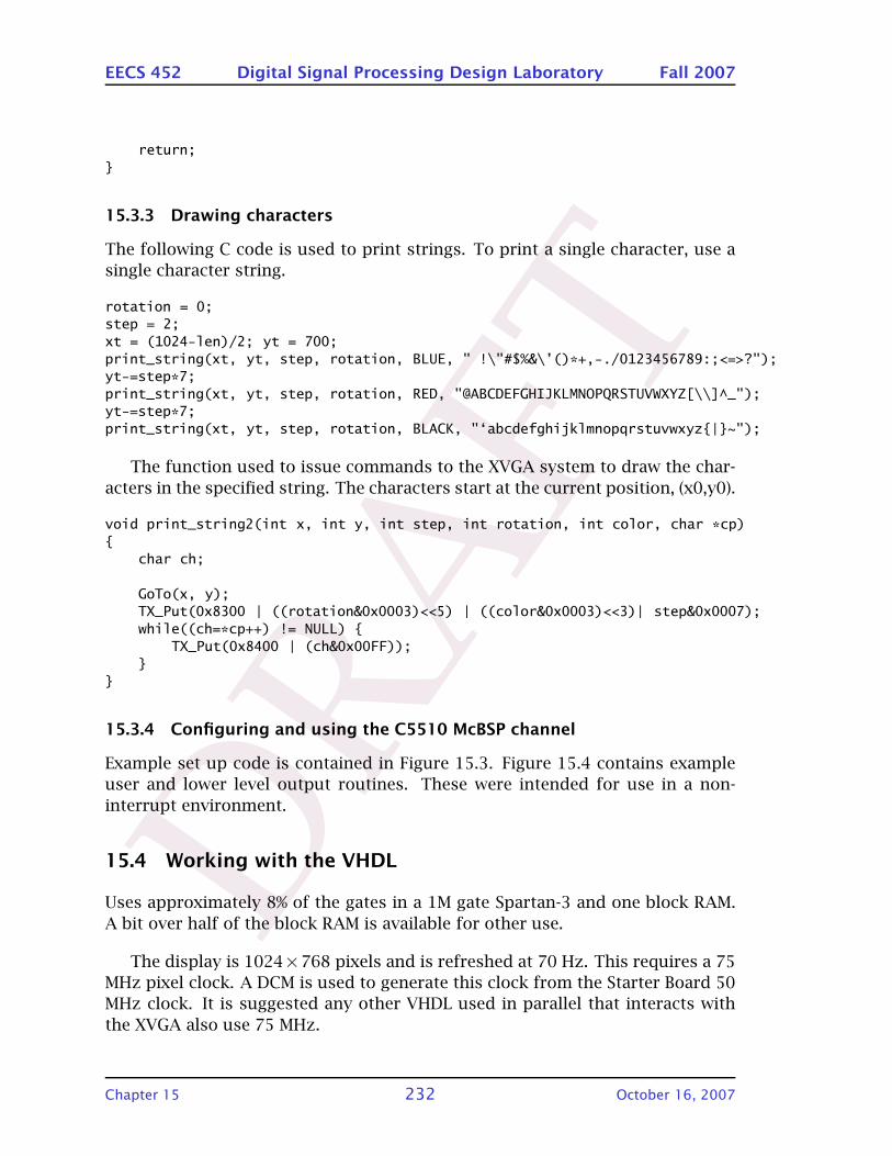
DRA
FT
EECS 452 Digital Signal Processing Design Laboratory Fall 2007
return;
15.3.3 Drawing characters
The following C code is used to print strings. To print a single character, use a
single character string.
rotation = 0;step = 2;xt = (1024-len)/2; yt = 700;print_string(xt, yt, step, rotation, BLUE, " !\"#$%&\’()*+,-./0123456789:;<=>?");yt-=step*7;print_string(xt, yt, step, rotation, RED, "@ABCDEFGHIJKLMNOPQRSTUVWXYZ[\\]^_");yt-=step*7;print_string(xt, yt, step, rotation, BLACK, "‘abcdefghijklmnopqrstuvwxyz|~");
The function used to issue commands to the XVGA system to draw the char-
acters in the specified string. The characters start at the current position, (x0,y0).
void print_string2(int x, int y, int step, int rotation, int color, char *cp)
char ch;
GoTo(x, y);TX_Put(0x8300 | ((rotation&0x0003)<<5) | ((color&0x0003)<<3)| step&0x0007);while((ch=*cp++) != NULL)
TX_Put(0x8400 | (ch&0x00FF));
15.3.4 Configuring and using the C5510 McBSP channel
Example set up code is contained in Figure 15.3. Figure 15.4 contains example
user and lower level output routines. These were intended for use in a non-
interrupt environment.
15.4 Working with the VHDL
Uses approximately 8% of the gates in a 1M gate Spartan-3 and one block RAM.
A bit over half of the block RAM is available for other use.
The display is 1024×768 pixels and is refreshed at 70 Hz. This requires a 75
MHz pixel clock. A DCM is used to generate this clock from the Starter Board 50
MHz clock. It is suggested any other VHDL used in parallel that interacts with
the XVGA also use 75 MHz.
Chapter 15 232 October 16, 2007
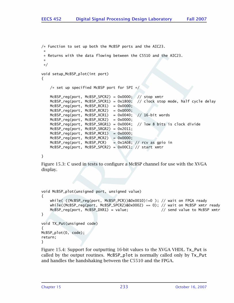
DRA
FT
EECS 452 Digital Signal Processing Design Laboratory Fall 2007
/* Function to set up both the McBSP ports and the AIC23.
** Returns with the data flowing between the C5510 and the AIC23.
**/
void setup_McBSP_plot(int port)
/* set up specified McBSP port for SPI */
McBSP_reg(port, McBSP_SPCR2) = 0x0000; // stop xmtrMcBSP_reg(port, McBSP_SPCR1) = 0x1800; // clock stop mode, half cycle delayMcBSP_reg(port, McBSP_RCR1) = 0x0000;McBSP_reg(port, McBSP_RCR2) = 0x0000;McBSP_reg(port, McBSP_XCR1) = 0x0040; // 16-bit wordsMcBSP_reg(port, McBSP_XCR2) = 0x0000;McBSP_reg(port, McBSP_SRGR1) = 0x0004; // low 8 bits is clock divideMcBSP_reg(port, McBSP_SRGR2) = 0x2011;McBSP_reg(port, McBSP_MCR1) = 0x0000;McBSP_reg(port, McBSP_MCR2) = 0x0000;McBSP_reg(port, McBSP_PCR) = 0x1A08; // rcv as gpio inMcBSP_reg(port, McBSP_SPCR2) = 0x00C1; // start xmtr
Figure 15.3: C used in tests to configure a McBSP channel for use with the XVGA
display.
void McBSP_plot(unsigned port, unsigned value)
while( ((McBSP_reg(port, McBSP_PCR))&0x0010)!=0 ); // wait on FPGA readywhile((McBSP_reg(port, McBSP_SPCR2)&0x0002) == 0); // wait on McBSP xmtr readyMcBSP_reg(port, McBSP_DXR1) = value; // send value to McBSP xmtr
void TX_Put(unsigned code)McBSP_plot(0, code);return;
Figure 15.4: Support for outputting 16-bit values to the XVGA VHDL. Tx_Put is
called by the output routines. McBSP_plot is normally called only by Tx_Putand handles the handshaking between the C5510 and the FPGA.
Chapter 15 233 October 16, 2007

DRA
FTWasted space, consider adding helpful text to this chapter.
DRA
FT
16 : Modulation and Demodulation
Moving information from one place in the spectrum to another. Uses DDS and
multiplier. Direct application of the Fourier Shifting Theorem.
Complex valued waveforms are simply pairs of real valued waveforms along
with a set of rules for working with them.
Chapter 16 235 October 16, 2007

DRA
FTWasted space, consider adding helpful text to this chapter.
DRA
FT
17 : Measuring Magnitude and Phase
Phase is always relative to something. So is magnitude, especially when ex-
pressed in decibels.
Includes material on arctangent approximations, quick-and-dirty (but how
dirty) magnitude approximations. Finishes with the CORDIC algorithm.
Chapter 17 237 October 16, 2007

DRA
FTWasted space, consider adding helpful text to this chapter.

DRA
FT
18 : Finite Impulse Response Filtering
Handling data movement (or minimizing it) is a key to successful implementa-
tion. The multiply-and-add operation is important as well. Will investigate FIR
implementation on the TI using parallel arithmetic and FIR implementation on
the S3SB using bit-serial arithmetic. Will also consider sample rate conversion
issues.Transfer function and group delay measurement.
Chapter 18 239 October 16, 2007

DRA
FTWasted space, consider adding helpful text to this chapter.
DRA
FT
19 : Lab exercise 5 – C5510 FIR filter
design and implementation
19.1 Introduction . . . . . . . . . . . . . . . . . . . . . . . . . . . . . . . . . . 242
19.2 Finite impulse response filters . . . . . . . . . . . . . . . . . . . . . . . 243
19.3 Transfer function measurement . . . . . . . . . . . . . . . . . . . . . 246
19.4 Group delay . . . . . . . . . . . . . . . . . . . . . . . . . . . . . . . . . . 248
19.4.1 Theory . . . . . . . . . . . . . . . . . . . . . . . . . . . . . . . . . . 248
19.4.2 Moving theory into practice . . . . . . . . . . . . . . . . . . . . . 250
19.5 C5510 exercise . . . . . . . . . . . . . . . . . . . . . . . . . . . . . . . . 251
19.5.1 Prelab . . . . . . . . . . . . . . . . . . . . . . . . . . . . . . . . . . 251
19.5.1.1 FIR filter . . . . . . . . . . . . . . . . . . . . . . . . . . . 251
19.5.1.2 The TF test program . . . . . . . . . . . . . . . . . . . . 253
19.5.1.3 Group delay . . . . . . . . . . . . . . . . . . . . . . . . . 254
19.5.2 Exercise . . . . . . . . . . . . . . . . . . . . . . . . . . . . . . . . . 255
19.5.2.1 FIR function testing . . . . . . . . . . . . . . . . . . . . 255
19.5.2.2 Measuring a transfer function . . . . . . . . . . . . . . 256
19.5.2.3 Group delay . . . . . . . . . . . . . . . . . . . . . . . . . 257
19.5.3 Report . . . . . . . . . . . . . . . . . . . . . . . . . . . . . . . . . . 257
19.6 Support documents and listings . . . . . . . . . . . . . . . . . . . . . . 257
19.6.1 TI DSPlib manual pages . . . . . . . . . . . . . . . . . . . . . . . 257
19.6.2 Intrinsics information . . . . . . . . . . . . . . . . . . . . . . . . 262
19.6.3 FIR function test program . . . . . . . . . . . . . . . . . . . . . . 274
19.6.4 myFIR.c starter code . . . . . . . . . . . . . . . . . . . . . . . . . 274
19.6.5 Source code for the DSPlib FIR function . . . . . . . . . . . . . 275
19.6.6 Source code for the TF test program . . . . . . . . . . . . . . . 279
Chapter 19 241 October 16, 2007
DRA
FT
EECS 452 Digital Signal Processing Design Laboratory Fall 2007
19.1 Introduction
This exercise has three basic parts:
• The generation (or more accurately, the completion) of a C-level FIR func-
tion and the comparison of its execution time to that of the TI DSPlib as-
sembly language equivalent.
• The combining of a DDS generator and the arctangent function into a pre-
liminary version of a transfer function (magnitude and phase) measure-
ment program.
• The planning and execution of a group delay measurement using the FIR
filter used in the first part and the transfer function code used in the sec-
ond.
The filter program used in this exercise uses the basic AIC23 codec support
sampling at a 48,000 Hz rate and sending values to the D/A at the same rate.
The development of a transfer function measurement program is started in
this exercise.Amplitude and phase are measured. Estimates of group delay can
be generated from the phase measurements.
Filters affect the amplitude and phase of applied waveforms. The most com-
mon use of a filter is to pass the energy in a given band of frequencies, essentially
unchanged, while at other frequencies energy is rejected.
If we filter sine waves at various frequencies and measure the relative phases
between the input and the output it is seen that this phase is frequency depen-
dent. If we filter a square wave using a relatively broadband filter we observe
that the transitions in the output waveform are (unsurprisingly) delayed from
those at the input of the filter. If the filtered wave shape is to be reasonably pre-
served it seems reasonable that each frequency component should be delayed
by the same amount. Changes in phase as a function of frequency can be related
to a quantity termed group delay. Filters having constant group delay as a func-
tion of frequency distort waveforms less than filters not having constant (as a
function of frequency) group delay.
Making a group delay measurement requires some thought and analysis or
problems will be encountered. It is easy to accidentally make a measurement
that gives the appearance of having negative delay through a filter. Some past
EECS 452 students, not realizing that negative delay is anomalous, have been
known to decide that there was some sort of a sign error and turn in the resulting
value anyway. If your expectation and a measurement differ significantly either
or both must be in error. When this happens it is educational to determine which
is in error and why.
Chapter 19 242 October 16, 2007
DRA
FT
EECS 452 Digital Signal Processing Design Laboratory Fall 2007
Nonconstant group delay as a function of frequency causes the bits in a
data communication to smear into each other. This smearing is termed inter-
symbol-interference (ISI). Most digital communication systems incorportate some
method of equalizing the delay in order to reduce ISI.
The group delay of a filter is an important concern when designing feedback
control systems. Too much delay can destabilize the system and lead to uncon-
trolled oscillation.
We will be measuring group delay in this exercise in order to gain experience
in understanding, planning and making a measurement and to test whether or
not our programs work as desired.
Exercise overview
• For a given filter specification use MATLAB’s fdatool to design a FIR filter.
• Capture the fdatool magnitude, phase and group delay plots.
• Save the filter coefficient values into a C header file.
• Use MATLAB to verify that the coefficients indeed give ripple levels that
reasonably closely match the desired levels.
• Modify the header file so that it can be “included” into FIRlab.c.
• Use the TI fir function to verify that the coefficients indeed produce a filter
as expected. Use signal generator and scope.
• Using timer or probe points determine the execution time per sample of
the TI fir code.
• Complete the inner loop of the myFIR and compile using O1 optimization.
Check the execution time required per sample. Repeat the check using O3
optimization.
• Verify the myFIR filter is working properly.
• Modify myFIR to use intrinsics. Time it and check if the filter is working
properly.
• Use TFmark1 to acquire transfer measurement data in a PC file.
• Complete the TFmark1 program group delay plot support and verify.
• Use the captured data to plot magnitude, phase group delay and compare
with values from fdatool.
19.2 Finite impulse response filters
The equation describing the operation of a finite impulse response (FIR) filter is
y[n] =M∑
i=0
b[i]x[n − i].
Chapter 19 243 October 16, 2007
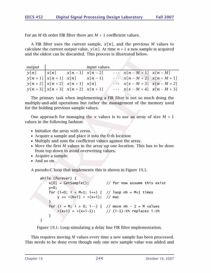
DRA
FT
EECS 452 Digital Signal Processing Design Laboratory Fall 2007
For an M-th order FIR filter there are M + 1 coefficient values.
A FIR filter uses the current sample, x[n], and the previous M values to
calculate the current output value, y[n]. At time n+1 a new sample is acquired
and the oldest can be discarded. This process is illustrated below.
output input values
y[n] x[n] x[n− 1] x[n− 2] · · · x[n −M + 1] x[n−M]y[n+ 1] x[n + 1] x[n] x[n− 1] · · · x[n −M + 2] x[n−M + 1]
y[n+ 2] x[n + 2] x[n+ 1] x[n] · · · x[x −M + 3] x[n−M + 2]
y[n+ 3] x[n + 3] x[n+ 2] x[n+ 1] · · · x[x −M + 4] x[n−M + 3]
The primary task when implementing a FIR filter is not so much doing the
multiply-and-add operations but rather the management of the memory used
for the holding previous sample values.
One approach for managing the x values is to use an array of size M + 1
values in the following fashion:
• Initialize the array with zeros.
• Acquire a sample and place it into the 0-th location
• Multiply and sum the coefficient values against the array.
• Move the first M values in the array up one location. This has to be done
from top down to avoid overwriting values.
• Acquire a sample.
• And so on.
A pseudo-C loop that implements this is shown in Figure 19.1.
while (forever) x[0] = GetSample(); // for now assume this existy=0;for (i=0; i < M+1; i++) // loop nh = M+1 times
y += *(b+i) * *(x+i); // macfor (i = M; i > 0; i--) // move nh - 1 = M values
*(x+i) = *(x+i-1); // (i-1)-th replaces i-th
Figure 19.1: Loop simulating a delay line FIR filter implementation.
This requires moving M values every time a new sample has been processed.
This needs to be done even though only one new sample value was added and
Chapter 19 244 October 16, 2007

DRA
FT
EECS 452 Digital Signal Processing Design Laboratory Fall 2007
only one old sample needed to be discarded. This can be very execution time
inefficient.
In general, the rule is “move pointers not data.” We will next look at using a
memory array to hold the sample values needed by a FIR filter.
The data structure most commonly used to implement the sample memory
needed by a FIR filter is the circular buffer (or array).
// The delay buffer array, db, contains nh+2 locations. Location// db[0] is used to hold the index-1 of the oldest sample present.// Initialize db[0] to 0.
#define DATA int
unsigned myFIR(DATA *x, // points to array of input valuesDATA *h, // points to coefficient valuesDATA *y, // points to where to put output valuesDATA *db, // points to the input delay bufferunsigned nx, // number of input values, n can equal 1unsigned nh) // number of coefficients
int i;DATA *ptr_d, *ptr_h;long LSum;
ptr_d = db + (*db + 1); // start at oldest in db arraywhile (nx--)
*ptr_d = *x++; // replace oldest with newestLSum=0L; // set sum to zeroptr_h = h; // initialize coefficient pointerfor (i=0; i < nh; i++) // loop nh times
LSum += *ptr_h++ * *ptr_d++; // use a mac type intrinsic????if (ptr_d > &db[nh+1]) ptr_d = &db[1];
*y++ = LSum>>15; // Q15 * Q15 => Q30 make Q15 .. intrinsic// may require changing this as well.
*db = ptr_d-db-1; // update db[0]return (0);
Figure 19.2: Straight forward circular buffer FIR implementation. Matches the
operation of the TI fir function. Looks good but some details need attending
to before it will work as intended.
The code in Figure 19.2 uses a circular buffer and isn’t very complex. It does
contain some program statements that need to be completed.
Chapter 19 245 October 16, 2007
DRA
FT
EECS 452 Digital Signal Processing Design Laboratory Fall 2007
This code is intended to mimic the TI fir function and thus uses the same
data organization and calling sequence.
In lecture we matched the delay buffer size to the number of coefficient val-
ues. The TI fir function uses a data buffer that contains NH+2 integers. NH is
the number of coefficient values in the FIR filter. The first location in the data
buffer array is used to hold the index-1 of the oldest value present in the delay
buffer. This allows the data buffer to serve as the memory of all of the relevant
information about of the state of the filter. Making the delay buffer one value
longer than the size of the filter is a clever thought. Doing this eliminates the
need for any special adjustment of the data pointer at the end of the calculation
loop.
The line
if (ptr_d > &db[nh+1]) ptr_d = &db[1];
checks to see if the ptr_d has gone beyond the array and, if it has, resets the
value to the first working location in the array. The line
LSum += *ptr_h++ * *ptr_d++;
gives the flavor of what needs to be done here but actually won’t work as writ-
ten (see corrective hint below). An alternative implementation is to use TI C5510
intrinsic functions for 16-bit fractional arithmetic. If this is done the shift by 15
positions might have to be changed to 16 or might be eliminated altogether.
Working at the C level, intrinsic functions can be used for the multiply and
add type operations. The end y value is required to be in Q15 format. Both the
sample values and filter coefficient values are expected to be Q15.
Here is a hint in case you want to do the math without intrinsics. The h and
d multiplication, as written above, needs to have one of the values cast to be
a long. This is necessary to have the product be a full 32 bit value. Doing so
generate a 32 bit result in Q30 form. There is no need to shift values to Q31
form. Just sum them. When the sum has been formed add a suitable value to
simulate doing two’s complement rounding and then shift the result to the right
by 15 bits. One should check the compiler output to make sure this works as
advertised. Though, it might be easier to just try it and see what happens.
19.3 Transfer function measurement
The basic system being implemented in this exercise is shown in Figure 19.3
Chapter 19 246 October 16, 2007
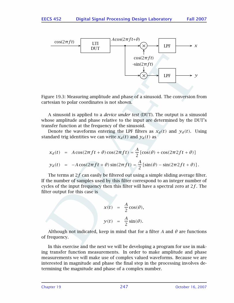
DRA
FT
EECS 452 Digital Signal Processing Design Laboratory Fall 2007
iqfarq
ÅçëEO⁄ÑíF ^ÅçëEO⁄ÑíH”Fimc
imc
ÅçëEO⁄ÑíFJëáåEO⁄ÑíF
ñ
ó
Figure 19.3: Measuring amplitude and phase of a sinusoid. The conversion from
cartesian to polar coordinates is not shown.
A sinusoid is applied to a device under test (DUT). The output is a sinusoid
whose amplitude and phase relative to the input are determined by the DUT’s
transfer function at the frequency of the sinusoid.
Denote the waveforms entering the LPF filters as xd(t) and yd(t). Using
standard trig identities we can write xd(t) and yd(t) as
xd(t) = A cos(2πft + θ) cos(2πft) =A
2[cos(θ)+ cos(2π2ft + θ)]
yd(t) = −A cos(2πft + θ) sin(2πft) =A
2[sin(θ)− sin(2π2ft + θ)] .
The terms at 2f can easily be filtered out using a simple sliding average filter.
If the number of samples used by this filter correspond to an integer number of
cycles of the input frequency then this filter will have a spectral zero at 2f . The
filter output for this case is
x(t) =A
2cos(θ),
y(t) =A
2sin(θ).
Although not indicated, keep in mind that for a filter A and θ are functions
of frequency.
In this exercise and the next we will be developing a program for use in mak-
ing transfer function measurements. In order to make amplitude and phase
measurements we will make use of complex valued waveforms. Because we are
interested in magnitude and phase the final step in the processing involves de-
termining the magnitude and phase of a complex number.
Chapter 19 247 October 16, 2007

DRA
FT
EECS 452 Digital Signal Processing Design Laboratory Fall 2007
In the earlier homework and labs we looked at writing an arctangent function
to determine angle phase associated with a complex number. In the immediately
previous lab we looked at the use of direct digital synthesis for the generation
of a sinusoid. In this lab we combine these tools to make transfer function
measurements.
The program in Section 19.6.6 was developed in stages with testing done at
each stage. The final stage uses a DDS to generate sine values that are sent
to the fir function. The filtered values are then multiplied by sine and cosine
values also generated using the same DDS code. The products are filtered and
converted into magnitude and phase values. We haven’t investigated fixed point
magnitude calculations yet so this part is done using floating point. Our fixed
point atan2 is used to determine the angle values.
The program in Section 19.6.6 does not operate in real time. This will come
later. In the next exercise we will use a D/A converter to generate an analog
waveform that is supplied to the filter whose transfer function is to be mea-
sured. The filtered results will be digitized and have their magnitude and phase
determined. Care will be needed to make sure that the measurement system
itself does not influence the measured values.
19.4 Group delay
19.4.1 Theory
The theory given here is more motivational than rigorous.
Group delay is defined as
τg(f ) = −1
2π
dθ(f)
dfseconds
where the phase is in radians and the frequency is in Hz. Recall, there are 2π
radians per cycle.
The group delay may vary as a function of frequency. This quantity describes
the amounts of delay that are encountered by a waveform at different frequen-
cies as it is filtered.
Where does this come from?
Consider a waveform having Fourier transform
S(f ) =1
2π
∫∞
−∞s(t)e−j2πftdt.
Chapter 19 248 October 16, 2007

DRA
FT
EECS 452 Digital Signal Processing Design Laboratory Fall 2007
If s(t) is delayed to become s(t − τ) then
Sτ(f ) =1
2π
∫∞
−∞s(t − τ)e−j2πftdt =
1
2π
∫∞
−∞s(t)e−j2πfte−j2πfτdt
If we filter s(t) using a filter with impulse response h(t) we have
sh(t) =∫ t
−∞s(τ)h(t − τ)dτ.
As you well know the Fourier transform of this expression is
Sh(f ) = S(f )H(f).
The filter transfer function H(f) can be written in terms of its magnitude and
phase
H(f) =∣
∣H(f)∣
∣ ejθh(f ).
If the phase relationship between the frequency components of the signal are to
be preserved meaning pure delay then we must have
θh(f ) = −2πfτ
Differentiating gives
dθh(f )
df= 2πτ.
In general dθh(f )/df will not be constant and will represent a frequency
dependent delay
τg(f ) = −1
2π
dθh(f )
df.
When dθh(f )/df is not constant then the filtered wave suffers phase distor-
tion.
The quantity
τg(f ) = −1
2π
dθh(f )
df
is referred to as being the filter’s group delay. If this quantity is independent of
frequency (constant) then the filter has a linear phase response.
Chapter 19 249 October 16, 2007

DRA
FT
EECS 452 Digital Signal Processing Design Laboratory Fall 2007
19.4.2 Moving theory into practice
The FIR filter to be designed using MATLAB for this exercise will be a linear phase
filter and thus will have constant group delay over its pass band. The frequency
region around the pass band is a good place to make a group delay measurement.
One should start by estimating the amount of delay to be expected in the
measurement. The most significant contributor is the FIR filter. There may be
other sources e.g., input or output buffering of values. If so their contributions
should be estimated and added with the FIR’s delay to obtain a value to use in
designing your measurement.
One needs to realize that the TF test program measures amplitude and phase
at specific frequencies. It is given a frequency range and the number of points at
which to make measurements. The TF program produces a simple output whose
results can be displayed using MATLAB. The program writes its measurement
values into a MATLAB compatible files that can be read using the MATLAB load
command. These values can then be further processed. Processing of TF test
program produced data is presently done as a post processing activity.
From freshman calculus we know that one can approximate derivatives using
small differences:
τg(f ) = −1
2π
dθ(f)
df≈ −
1
2π
∆θ
∆f.
When working with data one must be very careful about what units the data
is in and what units are required by the above equation.
For example:
τg(f ) = −dθr (ω)
dω
where θ is in radians and ω is radian frequency (ω = 2πf ). Changing units so
that θ is in degrees and the frequency is in Hz gives
τg(f ) = −1
360
dθd(f )
df
If we instead measure phase in terms of cycles rather than degrees and mea-
sure frequency in Hz then
τg(f ) = −dθc(f )
df
In planning the measurement, i.e., before making it, the frequency range
needs to be selected and the number of values to be acquired chosen. The phase
is a periodic waveform and when sampling it one needs to worry about aliasing
the measurement.
Chapter 19 250 October 16, 2007

DRA
FT
EECS 452 Digital Signal Processing Design Laboratory Fall 2007
The delay is made up of components associated with the input buffering, the
FIR filter itself, and the output buffering. Because the codec uses sigma-delta
A/D and D/A converters there is very some delay involved there as well. In
order to get a ballpark estimate assume 2 samples of delay due to the input
buffering, 73 samples of delay for the filter and 2 samples of delay due to the
output buffering. A better estimate would include codec delays as well.
For a 48,000 Hz sample rate the guessed delay is 77/48000, about 1.6 milli-
seconds. Assume we make a measurement near mid band at about 1500 Hz. If
we use a ∆f of 500 Hz (frequency range from 1250 to 1750 Hz) then we expect
to see a phase change in the vicinity of about
∆θd/360 = 0.0016× 500 = 0.8 cycles.
This a manageable number of cycles.
The key item that one needs to worry about is having a sufficient number
of frequency samples per cycle of phase so that the phase measurement is not
aliased. At least two samples per phase cycles are needed and good practice is
to use significantly more.
19.5 C5510 exercise
19.5.1 Prelab
Prelabs are to be done individually and are to be handed in at the
start of the lab period. Handwritten work will not be graded.
19.5.1.1 FIR filter
Using MATLAB’s FDATool (fdatool) design an equiripple FIR filter meeting the
following specification:
• sample rate of 48000 Hz,
• low pass transfer function,
• ripple in the pass band limited to 0.1 dB,
• low pass cutoff frequency of 3100 Hz,
• transition region from 3100 Hz to 4000 Hz,
• minimum attenuation in the stop band of 60 dB relative to the pass band,
• let FDATool determine the minimum number filter order.
The FIR filter order that FDATool finds should be somewhere near 145 (146
coefficient values). The number appears to vary slightly depending upon MATLAB
version being used.
Chapter 19 251 October 16, 2007
DRA
FT
EECS 452 Digital Signal Processing Design Laboratory Fall 2007
Enter the Full View Analysis mode using the white sheet icon located just
below (or nearly so) Window. Print copies of the Magnitude Response (dB),
Phase Response, Group Delay and Impulse Response for your prelab.
Print Preview allows control over the aspect ratio of the plot. I size the
displayed plot to have the proportions that I find pleasing and then use the
Print Preview Fix aspect ratio button to use this ratio for the printed out-
put. Export allows a plot to saved into a file using any one of a number of file
formats.
Poke around a bit in FDATool in order to develop a feel for it’s capabilities.
The Help system contains a lot of information.
FDATool used to be able to export coefficient values as Q15 (Fractional length:
15) 16-bit signed integer values. This was an easy way to get the coefficients into
the form needed for this exercise. However MATLAB features seem to come and
go and support for Q15 output no longer appears to be available. So we are on
our own.
Targets can be used to export the filter coefficient values in the form of a
C header file. Exporting as signed 16-bit integers makes the most sense for our
application. Do so using the file name: FIR145.h. The values are claimed to
have Fractional length: 15 which would make them Q15 in our parlance.
Before using this file it needs to be edited. Comment out the include state-
ment and change type int16_T to int. These two changes should be all the
changes needed for our use, however . . . . This file will be read using an include
statement by the FIRlab.c program.
The warning statement is a bit of worry. It claims that the coefficient values
have been truncated rather than rounded. The fix is stated to be to use the Filter
Design & Analysis Tool to design more accurate values. The FDATool is what we
are using. If we were doing this “for real” it would be reasonable to output the
coefficient values using a 32 bit format and round them (correctly) ourself. (Or
maybe figure out what we should have done this time.)
Make a copy of the coefficients file and edit so that is can be read into MATLAB
using the load command. The load command requires that all input lines contain
the same number of values. Add as many zero values as needed to make this so.
See Figure 19.4 for coaching on using load and converting the two dimensional
array into a vector.
Using coefficient values produce two plots One showing the ripple in the pass
band and the other showing the magnitude of the ripple in the stop band. This
will verify whether or not the truncated Q15 coefficient values produce a filter
Chapter 19 252 October 16, 2007

DRA
FT
EECS 452 Digital Signal Processing Design Laboratory Fall 2007
clear all;fig=1;
load data.txt; % load header b values[r,c] = size(data);b = reshape(data’,1,r*c); % transpose firstb = b(1:length(b)-7); % remove extra zeros
figure(fig); clf; fig=fig+1;subplot(3,1,1);plot(b); % plot coefficients
H = freqz(b,1,200); % calculate TF valuessubplot(3,1,2);plot(abs(H)); % plot transfer function
Figure 19.4: Example/starter MATLAB script for reading coefficient values. The
two plots are only meant as initial sanity checks.
having the desired pass and stop band ripple levels. If, not counting annotation,
it is taking much more than about ten lines of MATLAB to generate the plots, stop
and think. (MATLAB’s axis is very useful here.) It is assumed that the plots will
be included in the prelab write-up, maybe with some comments.
Modify the myFIR function contained in Figure 19.2. Use TI C intrinsics. Do
not attempt to check for an overflow. Simply return a value of 0 regardless
whether or not there was an overflow. See if you can see any ways that might
minimize the execution time. The definitions of the TI intrinsic functions con-
tained in TI’s C documentation are reproduced in the sections near the end of
this write-up.
The _smac intrinsic might be used to reasonably mimic the operation of
fir.asm. An alternative method of using standard C operations and applying
the cast that was suggested earlier. This may or may not be faster than using
the intrinsics. Both approaches will be investigated.
In your prelab write-up include: a listing of the source code for your myFIRfunctions (one version using intrinsics and the other version using an appropri-
ate cast), and a listing of your coefficient values.
19.5.1.2 The TF test program
The TF test program in Section 19.6.6 was developed in stages. Each stage built
on the previous. Each stage was written to verify understanding some aspect of
Chapter 19 253 October 16, 2007
DRA
FT
EECS 452 Digital Signal Processing Design Laboratory Fall 2007
system being designed. These were left in place in order to illustrate how one
might work one’s way into developing such an application.
• Test one looked at calculation the FTV values for given values of frequency
and sample rate and a 32-bit accumulator.
• Test two looked at accessing the sine table located in the C5510 ROM.
• Test three tested the use of a DDS to generate cosine/sine phased sinu-
soids. This was visually checked using the D/As to generate analog wave-
forms and using an oscilloscope view them.
• Test four used a 45-degree shifted sinusoid to verify understanding of how
to program the frequency shifting and integration. The frequency range
tested was from 10 Hz to 10 kHz in 10 Hz steps. The integration time was
0.1 seconds matching the use of the 10 Hz step size.
• Test five adds the myatan2 function for determining phase. The test trans-
fer function generated using the TI DSPlib fir function. Each output line is
of the output consists of frequency in Hz, magnitude in fraction form, and
phase from -1 to 1 half cycles. This format allows the file to be easily read
into a MATLAB program and plotted.
The author had to tease out from the TI documentation a lot of information
needed to write the program. In your prelab answer the following two questions.
• What is the memory address in bytes at which the C5510 ROM based sine
table is located?
• What bit in what status register is used to enable the accessing of the sine
table contained in the on-chip ROM?
The DDS used in this exercise makes use of a 32-bit accumulator. The DDS
update frequency, fs is 48000 Hz and contained in an unsigned long. The desired
frequency values, f , are in terms of Hz and are contained in an unsigned long.
The FTV value needed to generate a given frequency f is
FTV = 232 f
fs.
The ComputeFTV function is used to calculate FTV given fs and f . This function
illustrates how one can calculate FTV using simple (no division or multiplication)
operations. Take a look at the code and see if you can figure out how it does its
task. No response needed, just invest some time.
19.5.1.3 Group delay
• From your MATLAB efforts you should already know the theoretical group
delay of your filter.
Chapter 19 254 October 16, 2007
DRA
FT
EECS 452 Digital Signal Processing Design Laboratory Fall 2007
• List any other potential sources of delay that would affect your measure-
ment and give estimates of the associated delay. Check the AIC23 data
sheet to see if there are any significant delays associated with the A/D and
D/A converter (Hint: there are and the numbers are difficult to find, but
they do exist.)
• determine a measurement plan. This consists of the frequency range the
measurement is to be made over and the number of frequencies to be used.
Plan to make the measurement in the vicinity of 1 kHz.
19.5.2 Exercise
19.5.2.1 FIR function testing
You will be provided the source code for C test program shown in Appendix
19.6.3 to be used to test and time your FIR function and the FIR function from
the DSPlib.
Use profile points or the C5510 timer or both for measuring the function
execution times.
Do you know what clock rate your DSK is using? This is not an idle concern.
In the past there have been cases where the clock was changed as part of an
earlier lab and not reset. Does it matter when using the profiler? Does it matter
when using the timer?
• Place your filter coefficient values into a file named FIR145.h. The file con-
tents should be edited to place the values into an appropriately named
array.
• Test both of your C myFIR versions to make sure they are working properly.
Use the sinewave generator and oscilloscope for initial testing.
Test with the optimization level set to the -o3 level and debug support
turned off. The program does not have sufficient time to keep up with the
input data when not optimized and using a 48 kHz sample rate. Indeed
it would be educational to observe what the output waveform looks like
when the compilation is not optimized.
• Measure the execution time of both of your myFIR versions. (Your choice
how.) Measure the execution time both when compiled without any opti-
mization and when compiled using level -o3 optimization (along with de-
bug support off).
• Measure the execution time required by the DSPlib fir function.
Chapter 19 255 October 16, 2007
DRA
FT
EECS 452 Digital Signal Processing Design Laboratory Fall 2007
The operation of the assembly language fir function can be sped up by al-
most a factor of two by exploiting the filter symmetry and the special instruc-
tions included in the C5510 for this use. The energy consumed by the C5510
depends linearly on the CPU clock frequency. If you were implementing a sys-
tem to be powered using batteries you would like to run the processor as slow
as possible. Which filter would you recommend? The C versions or the assembly
language version?
19.5.2.2 Measuring a transfer function
Using Test 5 of the program in Section 19.6.6 generate output files for the fol-
lowing cases:
1. For the program as supplied.
2. Because the ripple in the filter transfer function can cause the filter output
to go above one the program uses a half amplitude cosine test signal. In
this step we look at whether or not this caution was justified.
The amplitude of the filter input is divided by 2 by the statement
data = cosine_value>>1;.
Eliminate this shift operation. This replaces the 1/2 amplitude input with
a unit amplitude input. The scaled factor used to normalize the magnitude
values
sf = 2.0*8192.0/((float)Nint*32768.0*32768.0);
needs to be reduced by a factor of two to compensate.
Generate a transfer function measurement file for this also.
The program takes a few minutes to make a run.
The name of the file used to hold the transfer function measurement is
Mark_I. After each run you should rename this using a suitable name for that
run. This file is generated in the directory that contains the executable. You may
have to hunt a bit to locate it.
Each line in this file contains three values. These values are the frequency
of the measurement in Hz, the amplitude normalized to unity for a unit input
sinusoid, and a phase angle in the range [-1/2, 1/2) cycle (a value of -1 corre-
sponds to a radian phase of −π radians). The file can be read using the MATLAB
statement
load ’myfilename’;
Chapter 19 256 October 16, 2007

DRA
FT
EECS 452 Digital Signal Processing Design Laboratory Fall 2007
where myfilename is the name of the file that you are processing. This result
in an array of the same name as your file. This can be copied into a fixed name
such as data which can then be used through out the script. This reduces the
amount of code that needs to be changed when changing between files.
Using subplot(4,1,n) produce a plot for each run.
1. For n = 1 plot the transfer function amplitude as a function of frequency
in Hz.
2. For n = 2 plot the transfer functions using dB. The plot y range should be
from -80 to 5 dB.
3. For n = 3 plot the phase as in the file as a function of frequency.
4. For n = 4 convert the phase to the range [−π,π) and unwrap it (use the
MATLAB function, unwrap) and plot as a function of frequency.
Include the plots and some relevant comments in your report.
19.5.2.3 Group delay
Use the transfer function measurement data set that you generated using the
half-amplitude sinewave to calculate the group delay of your filter design. Com-
pare this with the value found by MATLAB. Generally group delay is only of inter-
est over a filter’s passband(s). How close did your prediction come to measure-
ment? If warranted, rationalize a bit.
19.5.3 Report
Report on what you did, how you did it, and what the results were. Include
supporting documentation such as plots, program listings, etc. Give the grader
something on which to judge the quality of your work. Insightful observations
and discussion are a definite plus.
Include your execution time measurements including those of the DSPlib
function, the measured delay and with a plot of measured magnitude and phase,
and your program listings (myFIR, MATLAB, etc.).
19.6 Support documents and listings
19.6.1 TI DSPlib manual pages
See Figures 19.5, 19.6, 19.7 and 19.8. There are some inconsistencies between
the text and the illustrations.
Chapter 19 257 October 16, 2007
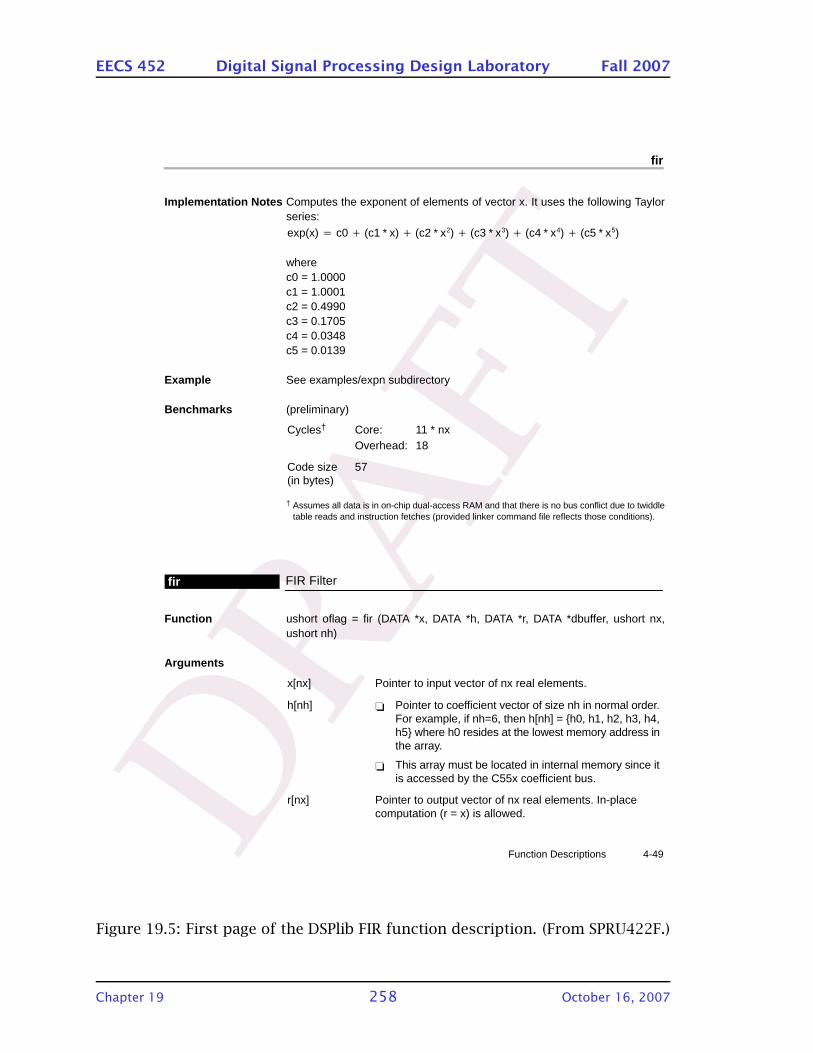
DRA
FT
EECS 452 Digital Signal Processing Design Laboratory Fall 2007
fir
4-49 Function Descriptions
Implementation Notes Computes the exponent of elements of vector x. It uses the following Taylorseries:
exp(x) c0 (c1 * x) (c2 * x2) (c3 * x3) (c4 * x4) (c5 * x5)
wherec0 = 1.0000c1 = 1.0001c2 = 0.4990c3 = 0.1705c4 = 0.0348c5 = 0.0139
Example See examples/expn subdirectory
Benchmarks (preliminary)
Cycles† Core: 11 * nxOverhead: 18
Code size(in bytes)
57
† Assumes all data is in on-chip dual-access RAM and that there is no bus conflict due to twiddletable reads and instruction fetches (provided linker command file reflects those conditions).
FIR Filterfir
Function ushort oflag = fir (DATA *x, DATA *h, DATA *r, DATA *dbuffer, ushort nx,ushort nh)
Arguments
x[nx] Pointer to input vector of nx real elements.
h[nh] Pointer to coefficient vector of size nh in normal order.For example, if nh=6, then h[nh] = h0, h1, h2, h3, h4,h5 where h0 resides at the lowest memory address inthe array.
This array must be located in internal memory since itis accessed by the C55x coefficient bus.
r[nx] Pointer to output vector of nx real elements. In-placecomputation (r = x) is allowed.
Figure 19.5: First page of the DSPlib FIR function description. (From SPRU422F.)
Chapter 19 258 October 16, 2007
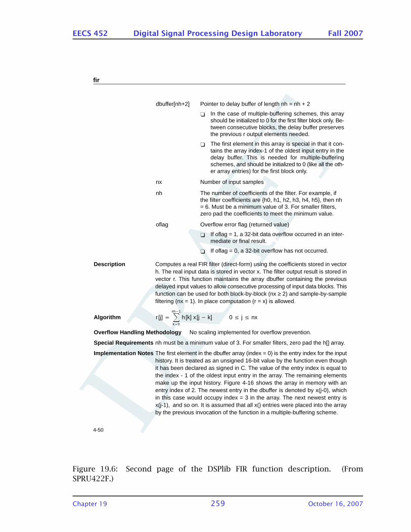
DRA
FT
EECS 452 Digital Signal Processing Design Laboratory Fall 2007
fir
4-50
dbuffer[nh+2] Pointer to delay buffer of length nh = nh + 2
In the case of multiple-buffering schemes, this arrayshould be initialized to 0 for the first filter block only. Be-tween consecutive blocks, the delay buffer preservesthe previous r output elements needed.
The first element in this array is special in that it con-tains the array index-1 of the oldest input entry in thedelay buffer. This is needed for multiple-bufferingschemes, and should be initialized to 0 (like all the oth-er array entries) for the first block only.
nx Number of input samples
nh The number of coefficients of the filter. For example, ifthe filter coefficients are h0, h1, h2, h3, h4, h5, then nh= 6. Must be a minimum value of 3. For smaller filters,zero pad the coefficients to meet the minimum value.
oflag Overflow error flag (returned value)
If oflag = 1, a 32-bit data overflow occurred in an inter-mediate or final result.
If oflag = 0, a 32-bit overflow has not occurred.
Description Computes a real FIR filter (direct-form) using the coefficients stored in vectorh. The real input data is stored in vector x. The filter output result is stored invector r. This function maintains the array dbuffer containing the previousdelayed input values to allow consecutive processing of input data blocks. Thisfunction can be used for both block-by-block (nx ≥ 2) and sample-by-samplefiltering (nx = 1). In place computation (r = x) is allowed.
Algorithm r [j] nh1
k0
h [k] x [j k] 0 j nx
Overflow Handling Methodology No scaling implemented for overflow prevention.
Special Requirements nh must be a minimum value of 3. For smaller filters, zero pad the h[] array.
Implementation Notes The first element in the dbuffer array (index = 0) is the entry index for the inputhistory. It is treated as an unsigned 16-bit value by the function even thoughit has been declared as signed in C. The value of the entry index is equal tothe index - 1 of the oldest input entry in the array. The remaining elementsmake up the input history. Figure 4-16 shows the array in memory with anentry index of 2. The newest entry in the dbuffer is denoted by x(j-0), whichin this case would occupy index = 3 in the array. The next newest entry isx(j-1), and so on. It is assumed that all x() entries were placed into the arrayby the previous invocation of the function in a multiple-buffering scheme.
Figure 19.6: Second page of the DSPlib FIR function description. (From
SPRU422F.)
Chapter 19 259 October 16, 2007
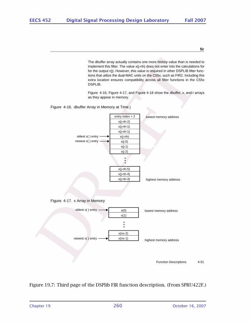
DRA
FT
EECS 452 Digital Signal Processing Design Laboratory Fall 2007
fir
4-51 Function Descriptions
The dbuffer array actually contains one more history value than is needed toimplement this filter. The value x(j-nh) does not enter into the calculations forfor the output r(j). However, this value is required in other DSPLIB filter func-tions that utilize the dual-MAC units on the C55x, such as FIR2. Including thisextra location ensures compatibility across all filter functions in the C55xDSPLIB.
Figure 4-16, Figure 4-17, and Figure 4-18 show the dbuffer, x, and r arraysas they appear in memory.
Figure 4-16. dbuffer Array in Memory at Time j
•••
x(j-nh-5)
lowest memory address
highest memory address
oldest x( ) entry
entry index = 2
x(j-nh-2)
x(j-nh-1)
x(j-nh-1)
x(j-nh)
x(j-0)
x(j-1)
x(j-2)
x(j-nh-4)
x(j-nh-3)
newest x( ) entry
Figure 4-17. x Array in Memory
•••
x(0)
x(nx-2)
lowest memory address
highest memory address
oldest x( ) entry
newest x( ) entry x(nx-1)
x(1)
Figure 19.7: Third page of the DSPlib FIR function description. (From SPRU422F.)
Chapter 19 260 October 16, 2007
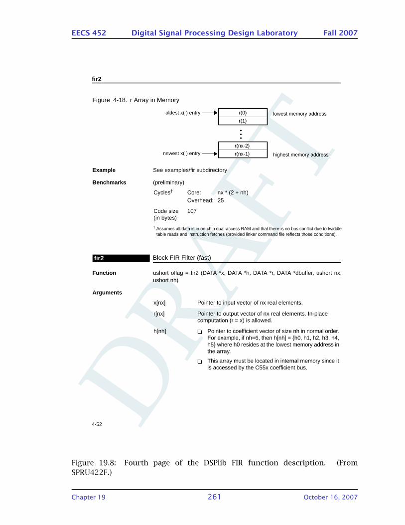
DRA
FT
EECS 452 Digital Signal Processing Design Laboratory Fall 2007
fir2
4-52
Figure 4-18. r Array in Memory
•••
r(nx-1)
lowest memory address
highest memory address
oldest x( ) entry
newest x( ) entry
r(0)
r(nx-2)
r(1)
Example See examples/fir subdirectory
Benchmarks (preliminary)
Cycles† Core: nx * (2 + nh)Overhead: 25
Code size(in bytes)
107
† Assumes all data is in on-chip dual-access RAM and that there is no bus conflict due to twiddletable reads and instruction fetches (provided linker command file reflects those conditions).
Block FIR Filter (fast)fir2
Function ushort oflag = fir2 (DATA *x, DATA *h, DATA *r, DATA *dbuffer, ushort nx,ushort nh)
Arguments
x[nx] Pointer to input vector of nx real elements.
r[nx] Pointer to output vector of nx real elements. In-placecomputation (r = x) is allowed.
h[nh] Pointer to coefficient vector of size nh in normal order.For example, if nh=6, then h[nh] = h0, h1, h2, h3, h4,h5 where h0 resides at the lowest memory address inthe array.
This array must be located in internal memory since itis accessed by the C55x coefficient bus.
Figure 19.8: Fourth page of the DSPlib FIR function description. (From
SPRU422F.)
Chapter 19 261 October 16, 2007

DRA
FT
EECS 452 Digital Signal Processing Design Laboratory Fall 2007
19.6.2 Intrinsics information
The material in this section is from the C55x C/C++ manual, SPRU281E.
Chapter 19 262 October 16, 2007
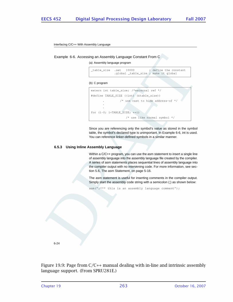
DRA
FT
EECS 452 Digital Signal Processing Design Laboratory Fall 2007
Interfacing C/C++ With Assembly Language
6-24
Example 6-6. Accessing an Assembly Language Constant From C
(a) Assembly language program
_table_size .set 10000 ; define the constant.global _table_size ; make it global
(b) C program
extern int table_size; /*external ref */
#define TABLE_SIZE ((int) (&table_size))
. /* use cast to hide address-of */
.
.
for (i-0; i<TABLE_SIZE; ++i)
/* use like normal symbol */
Since you are referencing only the symbol’s value as stored in the symboltable, the symbol’s declared type is unimportant. In Example 6-6, int is used.You can reference linker-defined symbols in a similar manner.
6.5.3 Using Inline Assembly Language
Within a C/C++ program, you can use the asm statement to insert a single lineof assembly language into the assembly language file created by the compiler.A series of asm statements places sequential lines of assembly language intothe compiler output with no intervening code. For more information, see sec-tion 5.6, The asm Statement, on page 5-16.
The asm statement is useful for inserting comments in the compiler output.Simply start the assembly code string with a semicolon (;) as shown below:
asm(” ;*** this is an assembly language comment ”);
Figure 19.9: Page from C/C++ manual dealing with in-line and intrinsic assembly
language support. (From SPRU281E.)
Chapter 19 263 October 16, 2007

DRA
FT
EECS 452 Digital Signal Processing Design Laboratory Fall 2007
Interfacing C/C++ With Assembly Language
6-25Run-Time Environment
Note: Using the asm Statement
Keep the following in mind when using the asm statement:
Be extremely careful not to disrupt the C/C++ environment. The compilerdoes not check or analyze the inserted instructions.
Inserting jumps or labels into C/C++ code can produce unpredictable re-sults by confusing the register-tracking algorithms that the code genera-tor uses.
Do not change the value of a C/C++ variable when using an asm state-ment.
Do not use the asm statement to insert assembler directives that changethe assembly environment.
6.5.4 Using Intrinsics to Access Assembly Language Statements
The compiler recognizes a number of intrinsic operators. Intrinsics are usedlike functions and produce assembly language statements that would other-wise be inexpressible in C/C++. You can use C/C++ variables with these intrin-sics, just as you would with any normal function. The intrinsics are specifiedwith a leading underscore, and are accessed by calling them as you do a func-tion. For example:
int x1, x2, y;y = _sadd(x1, x2);
Many of the intrinsic operators support saturation. During saturating arithme-tic, every expression which overflows is given a reasonable extremum value,either the maximum or the minimum value the expression can hold. Forinstance, in the above example, if x1==x2==INT_MAX, the expression over-flows and saturates, and y is given the value INT_MAX. Saturation is controlledby setting the saturation bit, ST1_SATD, by using these instructions:
BSET ST1_SATDBCLR ST1_SATD
The compiler must turn this bit on and off to mix saturating and non-saturatingarithmetic; however, it minimizes the number of such bit changing instructionsby recognizing blocks of instructions with the same behavior. For maximumefficiency, use saturating intrinsic operators for exactly those operations whereyou need saturated values in case of overflow, and where overflow can occur.Do not use them for loop iteration counters.
Figure 19.10: Page from C/C++ manual dealing with in-line and intrinsic assem-
bly language support. (From SPRU281E.)
Chapter 19 264 October 16, 2007
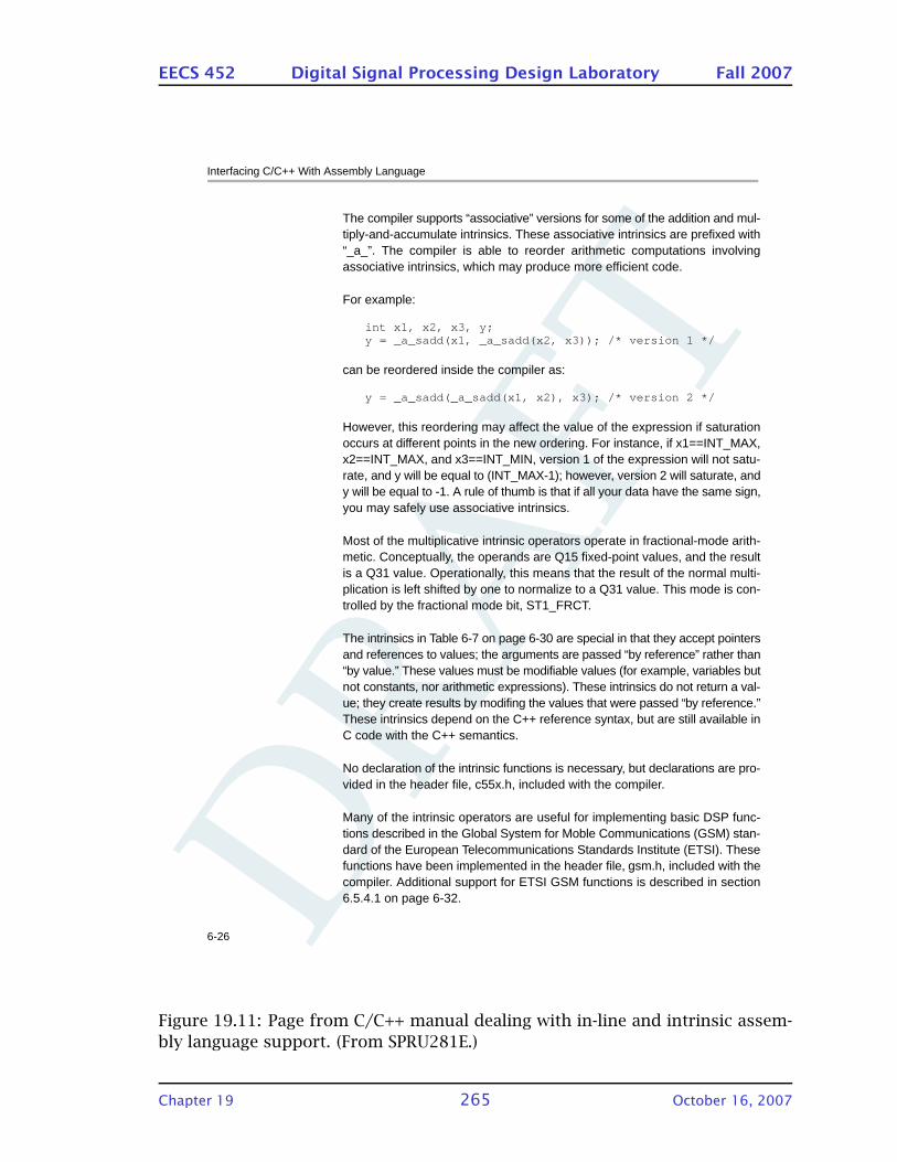
DRA
FT
EECS 452 Digital Signal Processing Design Laboratory Fall 2007
Interfacing C/C++ With Assembly Language
6-26
The compiler supports “associative” versions for some of the addition and mul-tiply-and-accumulate intrinsics. These associative intrinsics are prefixed with“_a_”. The compiler is able to reorder arithmetic computations involvingassociative intrinsics, which may produce more efficient code.
For example:
int x1, x2, x3, y;y = _a_sadd(x1, _a_sadd(x2, x3)); /* version 1 */
can be reordered inside the compiler as:
y = _a_sadd(_a_sadd(x1, x2), x3); /* version 2 */
However, this reordering may affect the value of the expression if saturationoccurs at different points in the new ordering. For instance, if x1==INT_MAX,x2==INT_MAX, and x3==INT_MIN, version 1 of the expression will not satu-rate, and y will be equal to (INT_MAX-1); however, version 2 will saturate, andy will be equal to -1. A rule of thumb is that if all your data have the same sign,you may safely use associative intrinsics.
Most of the multiplicative intrinsic operators operate in fractional-mode arith-metic. Conceptually, the operands are Q15 fixed-point values, and the resultis a Q31 value. Operationally, this means that the result of the normal multi-plication is left shifted by one to normalize to a Q31 value. This mode is con-trolled by the fractional mode bit, ST1_FRCT.
The intrinsics in Table 6-7 on page 6-30 are special in that they accept pointersand references to values; the arguments are passed “by reference” rather than“by value.” These values must be modifiable values (for example, variables butnot constants, nor arithmetic expressions). These intrinsics do not return a val-ue; they create results by modifing the values that were passed “by reference.”These intrinsics depend on the C++ reference syntax, but are still available inC code with the C++ semantics.
No declaration of the intrinsic functions is necessary, but declarations are pro-vided in the header file, c55x.h, included with the compiler.
Many of the intrinsic operators are useful for implementing basic DSP func-tions described in the Global System for Moble Communications (GSM) stan-dard of the European Telecommunications Standards Institute (ETSI). Thesefunctions have been implemented in the header file, gsm.h, included with thecompiler. Additional support for ETSI GSM functions is described in section6.5.4.1 on page 6-32.
Figure 19.11: Page from C/C++ manual dealing with in-line and intrinsic assem-
bly language support. (From SPRU281E.)
Chapter 19 265 October 16, 2007
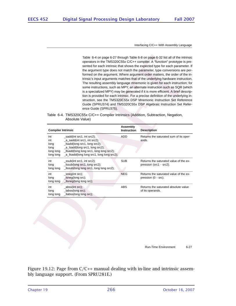
DRA
FT
EECS 452 Digital Signal Processing Design Laboratory Fall 2007
Interfacing C/C++ With Assembly Language
6-27Run-Time Environment
Table 6-4 on page 6-27 through Table 6-8 on page 6-32 list all of the intrinsicoperators in the TMS320C55x C/C++ compiler. A “function” prototype is pre-sented for each intrinsic that shows the expected type for each parameter. Ifthe argument type does not match the parameter, type conversions are per-formed on the argument. Where argument order matters, the order of the in-trinsic’s input arguments matches that of the underlying hardware instruction.The resulting assembly language mnemonic is given for each instruction; forsome instructions, such as MPY, an alternate instruction such as SQR (whichis a specialized MPY) may be generated if it is more efficient. A brief descrip-tion is provided for each intrinsic. For a precise definition of the underlying in-struction, see the TMS320C55x DSP Mnemonic Instruction Set ReferenceGuide (SPRU374) and TMS320C55x DSP Algebraic Instruction Set Refer-ence Guide (SPRU375).
Table 6-4. TMS320C55x C/C++ Compiler Intrinsics (Addition, Subtraction, Negation,Absolute Value)
Compiler IntrinsicAssembly Instruction Description
int _sadd(int src1, int src2);int _a_sadd(int src1, int src2);long _lsadd(long src1, long src2);long _a_lsadd(long src1, long src2);long long _llsadd(long long src1, long long src2);long long _a_llsadd(long long src1, long long src2);
ADD Returns the saturated sum of its oper-ands.
int _ssub(int src1, int src2);long _lssub(long src1, long src2);long long _llssub(long long src1, long long src2);
SUB Returns the saturated value of the ex-pression (src1 - src2).
int _sneg(int src);long _lsneg(long src);long long _llsneg(long long src);
NEG Returns the saturated value of the ex-pression (0 - src).
int _abss(int src);long _labss(long src);long long _llabss(long long src);
ABS Returns the saturated absolute valueof its operands.
Figure 19.12: Page from C/C++ manual dealing with in-line and intrinsic assem-
bly language support. (From SPRU281E.)
Chapter 19 266 October 16, 2007

DRA
FT
EECS 452 Digital Signal Processing Design Laboratory Fall 2007
Interfacing C/C++ With Assembly Language
6-28
Table 6-5. TMS320C55x C/C++ Compiler Intrinsics (Multiplication, Shifting)
Compiler IntrinsicAssembly Instruction Description
int _smpy(int src1, int src2);long _lsmpy(int src1, int src2);
MPY Returns the saturated fractional-modeproduct of its operands.
long _lsmpyr(int src1, int src2); MPYR Returns the saturated fractional-modeproduct of its operands, rounded as ifthe instrinsic _sround were used.
long _smac(long src1, int src2, int src3);long _a_smac(long src1, int src2, int src3);
MAC Returns the saturated sum of src1 andthe fractional-mode product of src2 andsrc3. Mode bit SMUL is also set.
long _smacr(long src1, int src2, int src3);long _a_smacr(long src1, int src2, int src3);
MACR Returns the saturated sum of src1 andthe fractional-mode product of src2 andsrc3. The sum is rounded as if theinstrinsic _sround were used. Mode bitSMUL is also set.
long _smas(long src1, int src2, int src3);long _a_smas(long src1, int src2, int src3);
MAS Returns the saturated difference of src1and the fractional-mode product of src2and src3. Mode bit SMUL is also set.
long _smasr(long src1, int src2, int src3);long _a_smasr(long src1, int src2, int src3);
MASR Returns the saturated difference of src1and the fractional-mode product of src2and src3. The sum is rounded as if theinstrinsic _sround were used. Mode bitSMUL is also set.
int _sshl(int src1, int src2);long _lsshl(long src1, int src2);
SFTS Returns the saturated value of the ex-pression (src1<<src2). If src2 is nega-tive, a right shift is performed instead.
int _shrs(int src1, int src2);long _lshrs(long src1, int src2);
SFTS Returns the saturated value of the ex-pression (src1>>src2). If src2 is nega-tive, a left shift is performed instead.
int _shl(int src1, int src2);long _lshl(long src1, int src2);long long _llshl(long long src1, int src2);
SFTS Returns the expression (src1<<src2). Ifsrc2 is negative, a right shift is per-formed instead. No saturation is per-formed.
Figure 19.13: Page from C/C++ manual dealing with in-line and intrinsic assem-
bly language support. (From SPRU281E.)
Chapter 19 267 October 16, 2007
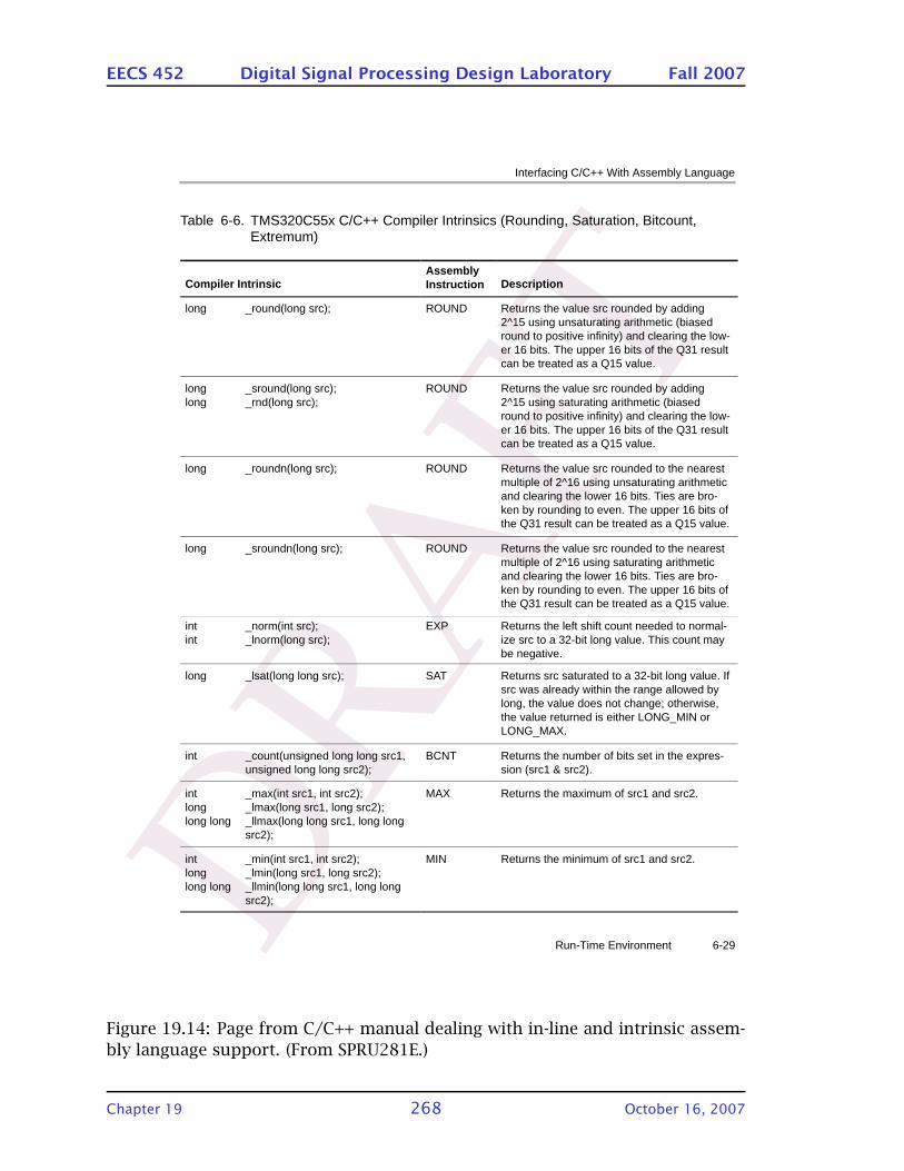
DRA
FT
EECS 452 Digital Signal Processing Design Laboratory Fall 2007
Interfacing C/C++ With Assembly Language
6-29Run-Time Environment
Table 6-6. TMS320C55x C/C++ Compiler Intrinsics (Rounding, Saturation, Bitcount,Extremum)
Compiler IntrinsicAssembly Instruction Description
long _round(long src); ROUND Returns the value src rounded by adding2^15 using unsaturating arithmetic (biasedround to positive infinity) and clearing the low-er 16 bits. The upper 16 bits of the Q31 resultcan be treated as a Q15 value.
long _sround(long src);long _rnd(long src);
ROUND Returns the value src rounded by adding2^15 using saturating arithmetic (biasedround to positive infinity) and clearing the low-er 16 bits. The upper 16 bits of the Q31 resultcan be treated as a Q15 value.
long _roundn(long src); ROUND Returns the value src rounded to the nearestmultiple of 2^16 using unsaturating arithmeticand clearing the lower 16 bits. Ties are bro-ken by rounding to even. The upper 16 bits ofthe Q31 result can be treated as a Q15 value.
long _sroundn(long src); ROUND Returns the value src rounded to the nearestmultiple of 2^16 using saturating arithmeticand clearing the lower 16 bits. Ties are bro-ken by rounding to even. The upper 16 bits ofthe Q31 result can be treated as a Q15 value.
int _norm(int src);int _lnorm(long src);
EXP Returns the left shift count needed to normal-ize src to a 32-bit long value. This count maybe negative.
long _lsat(long long src); SAT Returns src saturated to a 32-bit long value. Ifsrc was already within the range allowed bylong, the value does not change; otherwise,the value returned is either LONG_MIN orLONG_MAX.
int _count(unsigned long long src1, unsigned long long src2);
BCNT Returns the number of bits set in the expres-sion (src1 & src2).
int _max(int src1, int src2);long _lmax(long src1, long src2);long long _llmax(long long src1, long long
src2);
MAX Returns the maximum of src1 and src2.
int _min(int src1, int src2);long _lmin(long src1, long src2);long long _llmin(long long src1, long long
src2);
MIN Returns the minimum of src1 and src2.
Figure 19.14: Page from C/C++ manual dealing with in-line and intrinsic assem-
bly language support. (From SPRU281E.)
Chapter 19 268 October 16, 2007

DRA
FT
EECS 452 Digital Signal Processing Design Laboratory Fall 2007
Interfacing C/C++ With Assembly Language
6-30
Table 6-7. TMS320C55x C/C++ Compiler Intrinsics (Arithmetic With SideEffects)
Compiler IntrinsicAssembly Instruction Description
void _firs(int *, int *, int *, int&, long&);void _firsn(int *, int *, int *, int&, long&);
FIRSADDFIRSSUB
Perform the corresponding instruction as fol-lows:
int *p1, *p2, *p3, srcdst1;long srcdst2;..._firs(p1, p2, p3, srcdst1, srcdst2);_firsn(p1, p2, p3, srcdst1, srcdst2);
Which become (respectively):
FIRSADD *p1, *p2, *p3, srcdst1, srcdst2FIRSSUB *p1, *p2, *p3, srcdst1, srcdst2
Mode bits SATD, FRCT, and M40 are 0.
void _lms(int *, int *, int&, long&); LMS Perform the LMS instruction as follows:
int *p1, *p2, srcdst1;long srcdst2;..._lms (p1, p2, srcdst1, srcdst2);
Which becomes:
LMS *p1, *p2, srcdst1, srcdst2
Mode bits SATD, FRCT, RDM, and M40 are0.
Figure 19.15: Page from C/C++ manual dealing with in-line and intrinsic assem-
bly language support. (From SPRU281E.)
Chapter 19 269 October 16, 2007
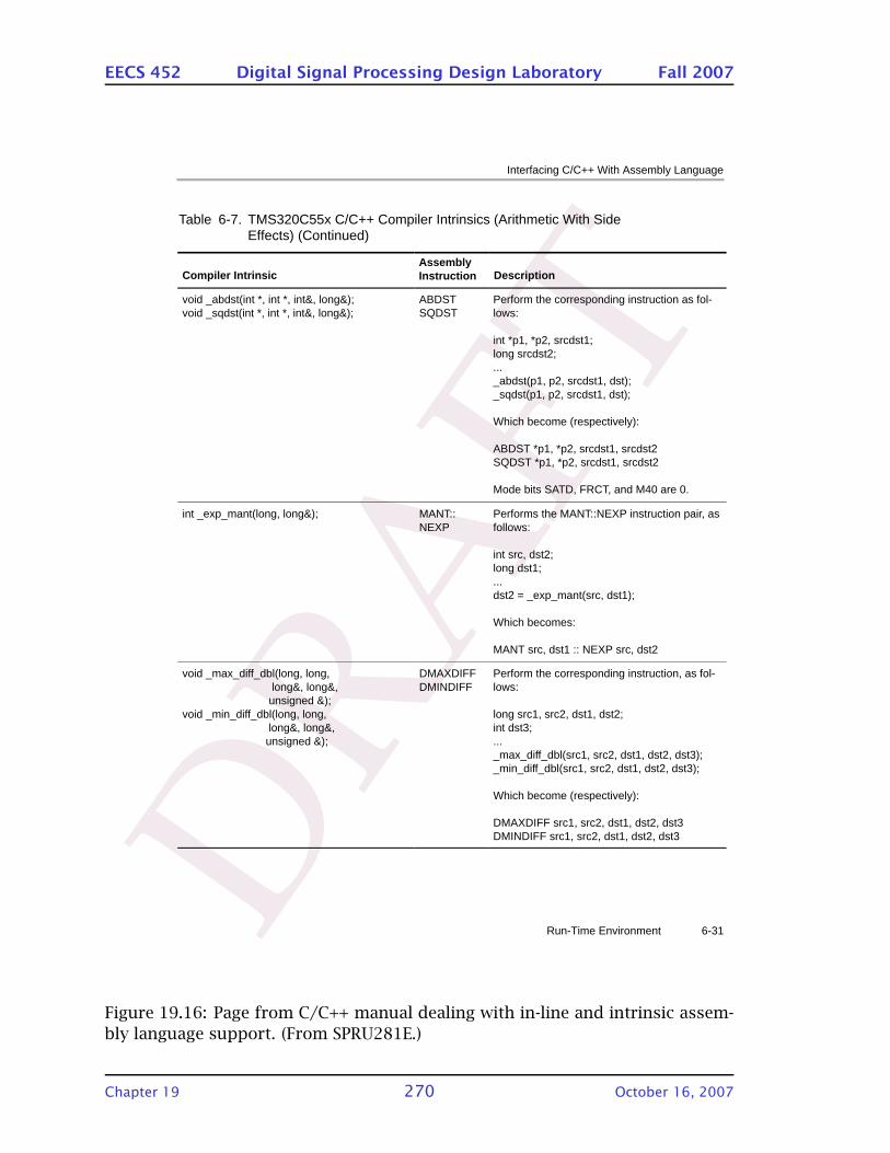
DRA
FT
EECS 452 Digital Signal Processing Design Laboratory Fall 2007
Interfacing C/C++ With Assembly Language
6-31Run-Time Environment
Table 6-7. TMS320C55x C/C++ Compiler Intrinsics (Arithmetic With SideEffects) (Continued)
Compiler Intrinsic DescriptionAssembly Instruction
void _abdst(int *, int *, int&, long&);void _sqdst(int *, int *, int&, long&);
ABDSTSQDST
Perform the corresponding instruction as fol-lows:
int *p1, *p2, srcdst1;long srcdst2;..._abdst(p1, p2, srcdst1, dst);_sqdst(p1, p2, srcdst1, dst);
Which become (respectively):
ABDST *p1, *p2, srcdst1, srcdst2SQDST *p1, *p2, srcdst1, srcdst2
Mode bits SATD, FRCT, and M40 are 0.
int _exp_mant(long, long&); MANT::NEXP
Performs the MANT::NEXP instruction pair, asfollows:
int src, dst2;long dst1;...dst2 = _exp_mant(src, dst1);
Which becomes:
MANT src, dst1 :: NEXP src, dst2
void _max_diff_dbl(long, long, long&, long&, unsigned &);void _min_diff_dbl(long, long, long&, long&, unsigned &);
DMAXDIFFDMINDIFF
Perform the corresponding instruction, as fol-lows:
long src1, src2, dst1, dst2;int dst3;..._max_diff_dbl(src1, src2, dst1, dst2, dst3);_min_diff_dbl(src1, src2, dst1, dst2, dst3);
Which become (respectively):
DMAXDIFF src1, src2, dst1, dst2, dst3DMINDIFF src1, src2, dst1, dst2, dst3
Figure 19.16: Page from C/C++ manual dealing with in-line and intrinsic assem-
bly language support. (From SPRU281E.)
Chapter 19 270 October 16, 2007
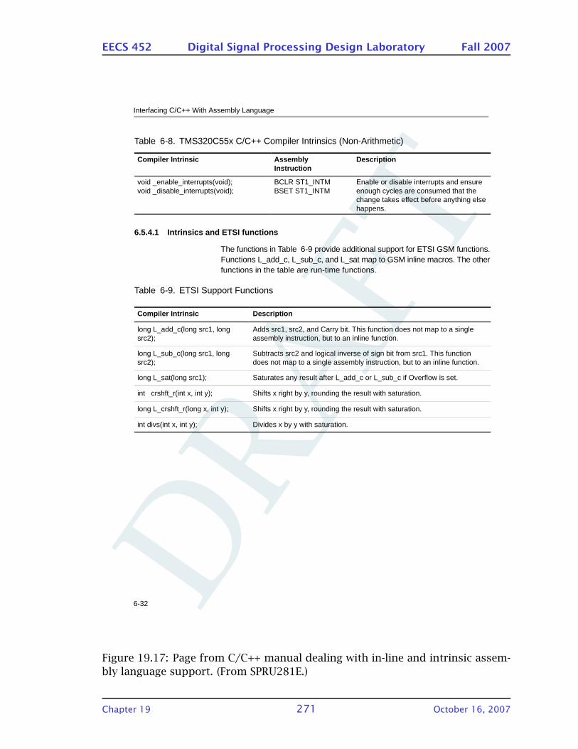
DRA
FT
EECS 452 Digital Signal Processing Design Laboratory Fall 2007
Interfacing C/C++ With Assembly Language
6-32
Table 6-8. TMS320C55x C/C++ Compiler Intrinsics (Non-Arithmetic)
Compiler Intrinsic Assembly Instruction
Description
void _enable_interrupts(void);void _disable_interrupts(void);
BCLR ST1_INTMBSET ST1_INTM
Enable or disable interrupts and ensureenough cycles are consumed that thechange takes effect before anything elsehappens.
6.5.4.1 Intrinsics and ETSI functions
The functions in Table 6-9 provide additional support for ETSI GSM functions.Functions L_add_c, L_sub_c, and L_sat map to GSM inline macros. The otherfunctions in the table are run-time functions.
Table 6-9. ETSI Support Functions
Compiler Intrinsic Description
long L_add_c(long src1, longsrc2);
Adds src1, src2, and Carry bit. This function does not map to a singleassembly instruction, but to an inline function.
long L_sub_c(long src1, longsrc2);
Subtracts src2 and logical inverse of sign bit from src1. This functiondoes not map to a single assembly instruction, but to an inline function.
long L_sat(long src1); Saturates any result after L_add_c or L_sub_c if Overflow is set.
int crshft_r(int x, int y); Shifts x right by y, rounding the result with saturation.
long L_crshft_r(long x, int y); Shifts x right by y, rounding the result with saturation.
int divs(int x, int y); Divides x by y with saturation.
Figure 19.17: Page from C/C++ manual dealing with in-line and intrinsic assem-
bly language support. (From SPRU281E.)
Chapter 19 271 October 16, 2007
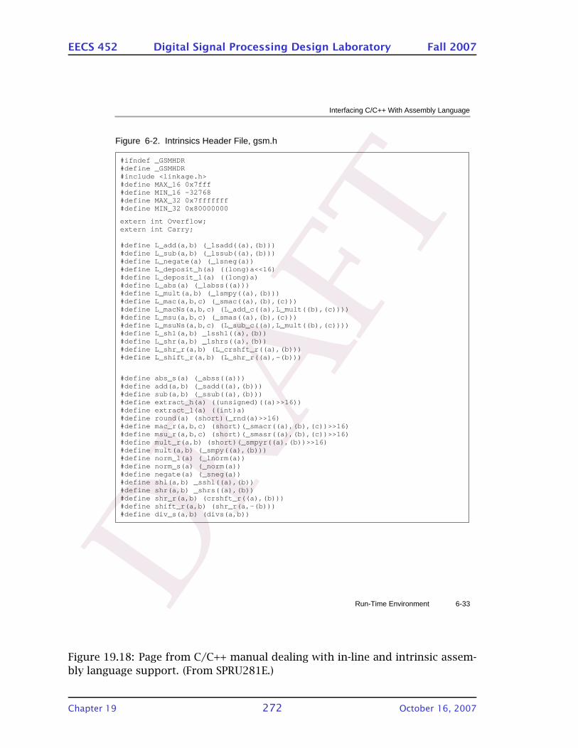
DRA
FT
EECS 452 Digital Signal Processing Design Laboratory Fall 2007
Interfacing C/C++ With Assembly Language
6-33Run-Time Environment
Figure 6-2. Intrinsics Header File, gsm.h
#ifndef _GSMHDR#define _GSMHDR#include <linkage.h>#define MAX_16 0x7fff#define MIN_16 -32768#define MAX_32 0x7fffffff#define MIN_32 0x80000000
extern int Overflow;extern int Carry;
#define L_add(a,b) (_lsadd((a),(b))) #define L_sub(a,b) (_lssub((a),(b))) #define L_negate(a) (_lsneg(a)) #define L_deposit_h(a) ((long)a<<16) #define L_deposit_l(a) ((long)a) #define L_abs(a) (_labss((a))) #define L_mult(a,b) (_lsmpy((a),(b))) #define L_mac(a,b,c) (_smac((a),(b),(c))) #define L_macNs(a,b,c) (L_add_c((a),L_mult((b),(c)))) #define L_msu(a,b,c) (_smas((a),(b),(c))) #define L_msuNs(a,b,c) (L_sub_c((a),L_mult((b),(c)))) #define L_shl(a,b) _lsshl((a),(b)) #define L_shr(a,b) _lshrs((a),(b)) #define L_shr_r(a,b) (L_crshft_r((a),(b))) #define L_shift_r(a,b) (L_shr_r((a),-(b)))
#define abs_s(a) (_abss((a))) #define add(a,b) (_sadd((a),(b))) #define sub(a,b) (_ssub((a),(b))) #define extract_h(a) ((unsigned)((a)>>16)) #define extract_l(a) ((int)a) #define round(a) (short)(_rnd(a)>>16) #define mac_r(a,b,c) (short)(_smacr((a),(b),(c))>>16) #define msu_r(a,b,c) (short)(_smasr((a),(b),(c))>>16) #define mult_r(a,b) (short)(_smpyr((a),(b))>>16) #define mult(a,b) (_smpy((a),(b))) #define norm_l(a) (_lnorm(a)) #define norm_s(a) (_norm(a)) #define negate(a) (_sneg(a)) #define shl(a,b) _sshl((a),(b)) #define shr(a,b) _shrs((a),(b)) #define shr_r(a,b) (crshft_r((a),(b))) #define shift_r(a,b) (shr_r(a,-(b))) #define div_s(a,b) (divs(a,b))
Figure 19.18: Page from C/C++ manual dealing with in-line and intrinsic assem-
bly language support. (From SPRU281E.)
Chapter 19 272 October 16, 2007
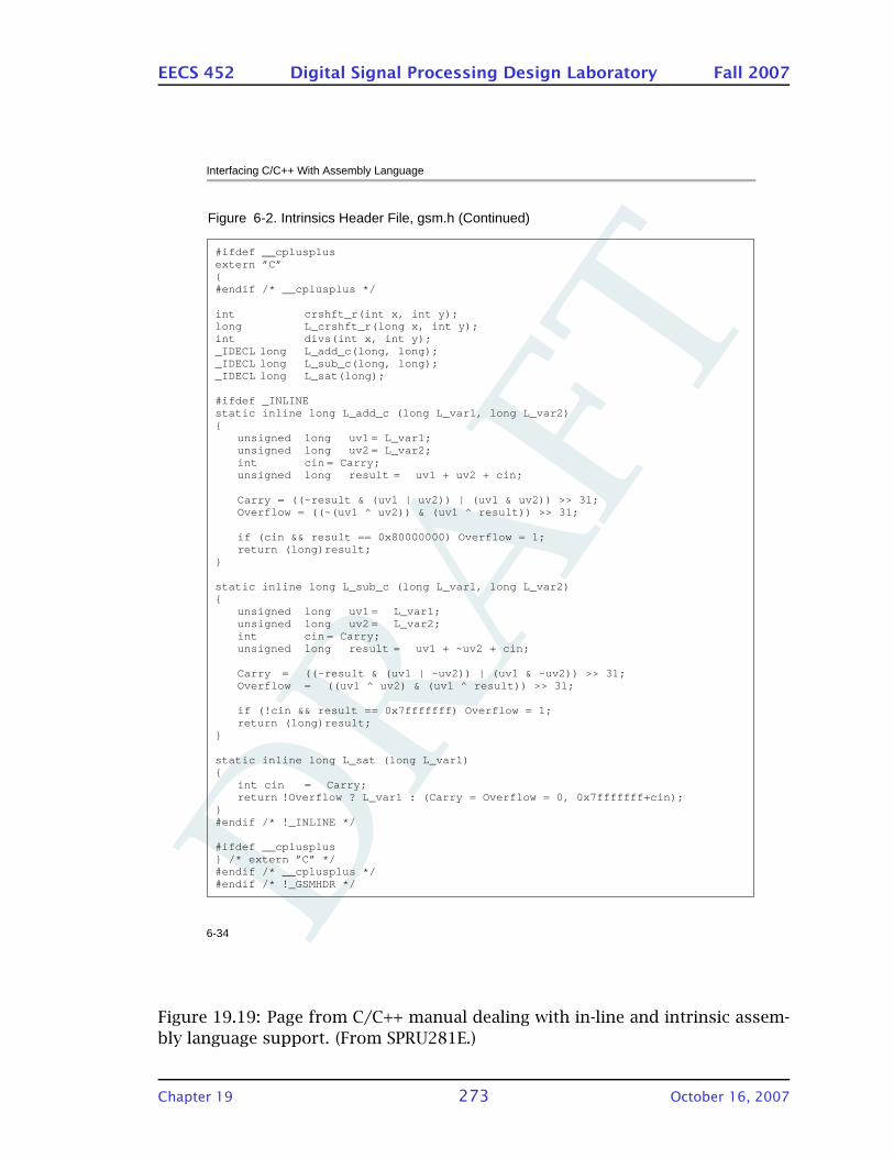
DRA
FT
EECS 452 Digital Signal Processing Design Laboratory Fall 2007
Interfacing C/C++ With Assembly Language
6-34
Figure 6-2. Intrinsics Header File, gsm.h (Continued)
#ifdef __cplusplusextern ”C”#endif /* __cplusplus */
int crshft_r(int x, int y);long L_crshft_r(long x, int y);int divs(int x, int y);_IDECL long L_add_c(long, long);_IDECL long L_sub_c(long, long);_IDECL long L_sat(long);
#ifdef _INLINEstatic inline long L_add_c (long L_var1, long L_var2)
unsigned long uv1 = L_var1;unsigned long uv2 = L_var2;int cin = Carry;unsigned long result = uv1 + uv2 + cin;
Carry = ((~result & (uv1 | uv2)) | (uv1 & uv2)) >> 31;Overflow = ((~(uv1 ^ uv2)) & (uv1 ^ result)) >> 31;
if (cin && result == 0x80000000) Overflow = 1;return (long)result;
static inline long L_sub_c (long L_var1, long L_var2)
unsigned long uv1 = L_var1;unsigned long uv2 = L_var2;int cin = Carry;unsigned long result = uv1 + ~uv2 + cin;
Carry = ((~result & (uv1 | ~uv2)) | (uv1 & ~uv2)) >> 31;Overflow = ((uv1 ^ uv2) & (uv1 ^ result)) >> 31;
if (!cin && result == 0x7fffffff) Overflow = 1;return (long)result;
static inline long L_sat (long L_var1)
int cin = Carry;return !Overflow ? L_var1 : (Carry = Overflow = 0, 0x7fffffff+cin);
#endif /* !_INLINE */
#ifdef __cplusplus /* extern ”C” */#endif /* __cplusplus */#endif /* !_GSMHDR */
Figure 19.19: Page from C/C++ manual dealing with in-line and intrinsic assem-
bly language support. (From SPRU281E.)
Chapter 19 273 October 16, 2007
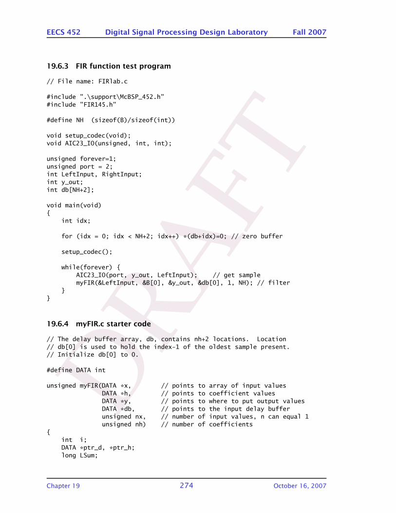
DRA
FT
EECS 452 Digital Signal Processing Design Laboratory Fall 2007
19.6.3 FIR function test program
// File name: FIRlab.c
#include ".\support\McBSP_452.h"#include "FIR145.h"
#define NH (sizeof(B)/sizeof(int))
void setup_codec(void);void AIC23_IO(unsigned, int, int);
unsigned forever=1;unsigned port = 2;int LeftInput, RightInput;int y_out;int db[NH+2];
void main(void)
int idx;
for (idx = 0; idx < NH+2; idx++) *(db+idx)=0; // zero buffer
setup_codec();
while(forever) AIC23_IO(port, y_out, LeftInput); // get samplemyFIR(&LeftInput, &B[0], &y_out, &db[0], 1, NH); // filter
19.6.4 myFIR.c starter code
// The delay buffer array, db, contains nh+2 locations. Location// db[0] is used to hold the index-1 of the oldest sample present.// Initialize db[0] to 0.
#define DATA int
unsigned myFIR(DATA *x, // points to array of input valuesDATA *h, // points to coefficient valuesDATA *y, // points to where to put output valuesDATA *db, // points to the input delay bufferunsigned nx, // number of input values, n can equal 1unsigned nh) // number of coefficients
int i;DATA *ptr_d, *ptr_h;long LSum;
Chapter 19 274 October 16, 2007
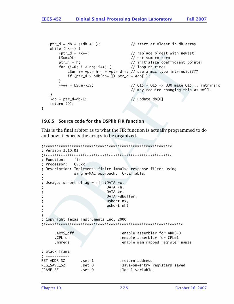
DRA
FT
EECS 452 Digital Signal Processing Design Laboratory Fall 2007
ptr_d = db + (*db + 1); // start at oldest in db arraywhile (nx--)
*ptr_d = *x++; // replace oldest with newestLSum=0L; // set sum to zeroptr_h = h; // initialize coefficient pointerfor (i=0; i < nh; i++) // loop nh times
LSum += *ptr_h++ * *ptr_d++; // use a mac type intrinsic????if (ptr_d > &db[nh+1]) ptr_d = &db[1];
*y++ = LSum>>15; // Q15 * Q15 => Q30 make Q15 .. intrinsic// may require changing this as well.
*db = ptr_d-db-1; // update db[0]return (0);
19.6.5 Source code for the DSPlib FIR function
This is the final arbiter as to what the FIR function is actually programmed to do
and how it expects the arrays to be organized.
;***********************************************************; Version 2.10.03;***********************************************************; Function: fir; Processor: C55xx; Description: Implements finite impulse response filter using; single-MAC approach. C-callable.;; Useage: ushort oflag = firs(DATA *x,; DATA *h,; DATA *r,; DATA *dbuffer,; ushort nx,; ushort nh);;; Copyright Texas instruments Inc, 2000;****************************************************************
.ARMS_off ;enable assembler for ARMS=0
.CPL_on ;enable assembler for CPL=1
.mmregs ;enable mem mapped register names
; Stack frame; -----------RET_ADDR_SZ .set 1 ;return addressREG_SAVE_SZ .set 0 ;save-on-entry registers savedFRAME_SZ .set 0 ;local variables
Chapter 19 275 October 16, 2007
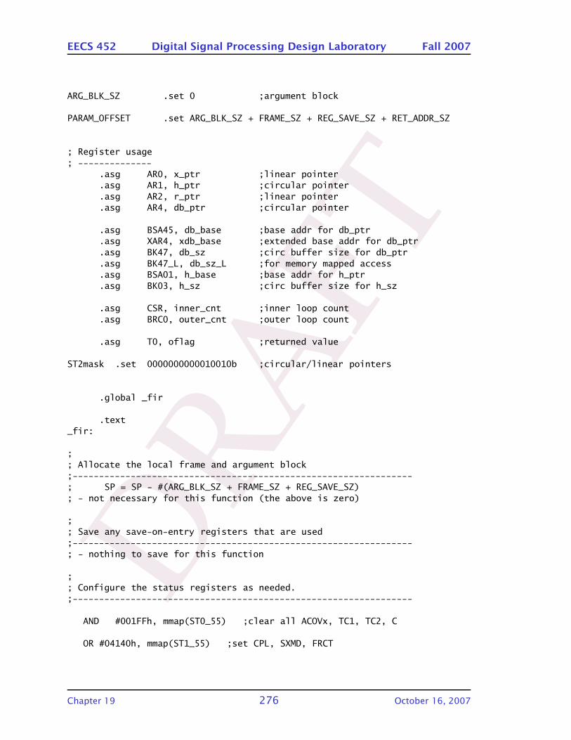
DRA
FT
EECS 452 Digital Signal Processing Design Laboratory Fall 2007
ARG_BLK_SZ .set 0 ;argument block
PARAM_OFFSET .set ARG_BLK_SZ + FRAME_SZ + REG_SAVE_SZ + RET_ADDR_SZ
; Register usage; --------------
.asg AR0, x_ptr ;linear pointer
.asg AR1, h_ptr ;circular pointer
.asg AR2, r_ptr ;linear pointer
.asg AR4, db_ptr ;circular pointer
.asg BSA45, db_base ;base addr for db_ptr
.asg XAR4, xdb_base ;extended base addr for db_ptr
.asg BK47, db_sz ;circ buffer size for db_ptr
.asg BK47_L, db_sz_L ;for memory mapped access
.asg BSA01, h_base ;base addr for h_ptr
.asg BK03, h_sz ;circ buffer size for h_sz
.asg CSR, inner_cnt ;inner loop count
.asg BRC0, outer_cnt ;outer loop count
.asg T0, oflag ;returned value
ST2mask .set 0000000000010010b ;circular/linear pointers
.global _fir
.text_fir:
;; Allocate the local frame and argument block;----------------------------------------------------------------; SP = SP - #(ARG_BLK_SZ + FRAME_SZ + REG_SAVE_SZ); - not necessary for this function (the above is zero)
;; Save any save-on-entry registers that are used;----------------------------------------------------------------; - nothing to save for this function
;; Configure the status registers as needed.;----------------------------------------------------------------
AND #001FFh, mmap(ST0_55) ;clear all ACOVx, TC1, TC2, C
OR #04140h, mmap(ST1_55) ;set CPL, SXMD, FRCT
Chapter 19 276 October 16, 2007
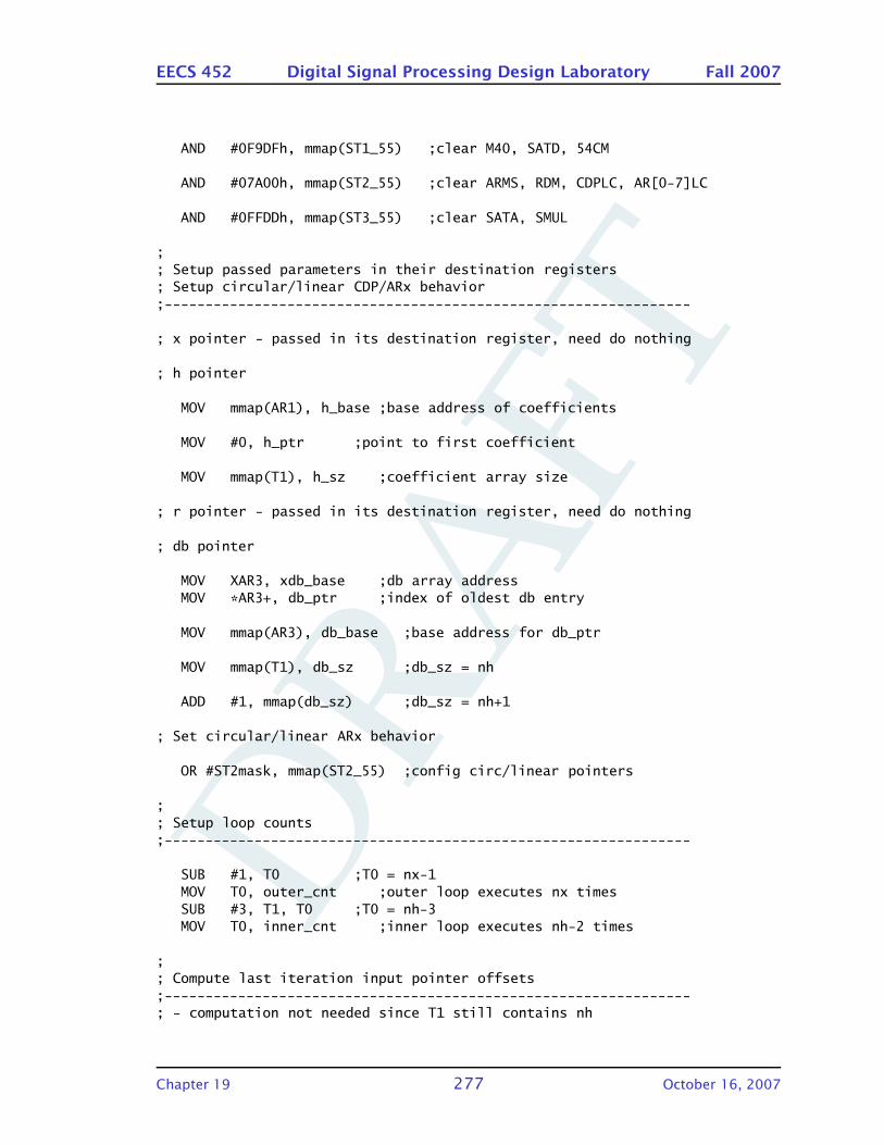
DRA
FT
EECS 452 Digital Signal Processing Design Laboratory Fall 2007
AND #0F9DFh, mmap(ST1_55) ;clear M40, SATD, 54CM
AND #07A00h, mmap(ST2_55) ;clear ARMS, RDM, CDPLC, AR[0-7]LC
AND #0FFDDh, mmap(ST3_55) ;clear SATA, SMUL
;; Setup passed parameters in their destination registers; Setup circular/linear CDP/ARx behavior;----------------------------------------------------------------
; x pointer - passed in its destination register, need do nothing
; h pointer
MOV mmap(AR1), h_base ;base address of coefficients
MOV #0, h_ptr ;point to first coefficient
MOV mmap(T1), h_sz ;coefficient array size
; r pointer - passed in its destination register, need do nothing
; db pointer
MOV XAR3, xdb_base ;db array addressMOV *AR3+, db_ptr ;index of oldest db entry
MOV mmap(AR3), db_base ;base address for db_ptr
MOV mmap(T1), db_sz ;db_sz = nh
ADD #1, mmap(db_sz) ;db_sz = nh+1
; Set circular/linear ARx behavior
OR #ST2mask, mmap(ST2_55) ;config circ/linear pointers
;; Setup loop counts;----------------------------------------------------------------
SUB #1, T0 ;T0 = nx-1MOV T0, outer_cnt ;outer loop executes nx timesSUB #3, T1, T0 ;T0 = nh-3MOV T0, inner_cnt ;inner loop executes nh-2 times
;; Compute last iteration input pointer offsets;----------------------------------------------------------------; - computation not needed since T1 still contains nh
Chapter 19 277 October 16, 2007
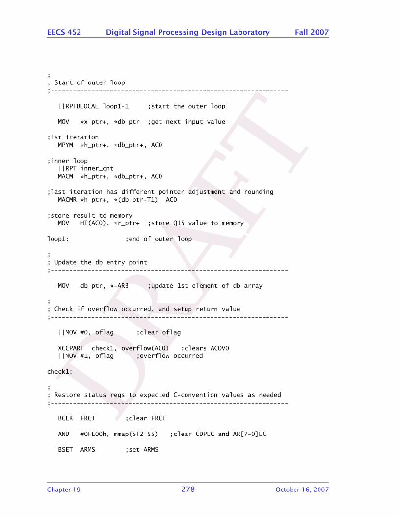
DRA
FT
EECS 452 Digital Signal Processing Design Laboratory Fall 2007
;; Start of outer loop;----------------------------------------------------------------
||RPTBLOCAL loop1-1 ;start the outer loop
MOV *x_ptr+, *db_ptr ;get next input value
;ist iterationMPYM *h_ptr+, *db_ptr+, AC0
;inner loop||RPT inner_cntMACM *h_ptr+, *db_ptr+, AC0
;last iteration has different pointer adjustment and roundingMACMR *h_ptr+, *(db_ptr-T1), AC0
;store result to memoryMOV HI(AC0), *r_ptr+ ;store Q15 value to memory
loop1: ;end of outer loop
;; Update the db entry point;----------------------------------------------------------------
MOV db_ptr, *-AR3 ;update 1st element of db array
;; Check if overflow occurred, and setup return value;----------------------------------------------------------------
||MOV #0, oflag ;clear oflag
XCCPART check1, overflow(AC0) ;clears ACOV0||MOV #1, oflag ;overflow occurred
check1:
;; Restore status regs to expected C-convention values as needed;----------------------------------------------------------------
BCLR FRCT ;clear FRCT
AND #0FE00h, mmap(ST2_55) ;clear CDPLC and AR[7-0]LC
BSET ARMS ;set ARMS
Chapter 19 278 October 16, 2007
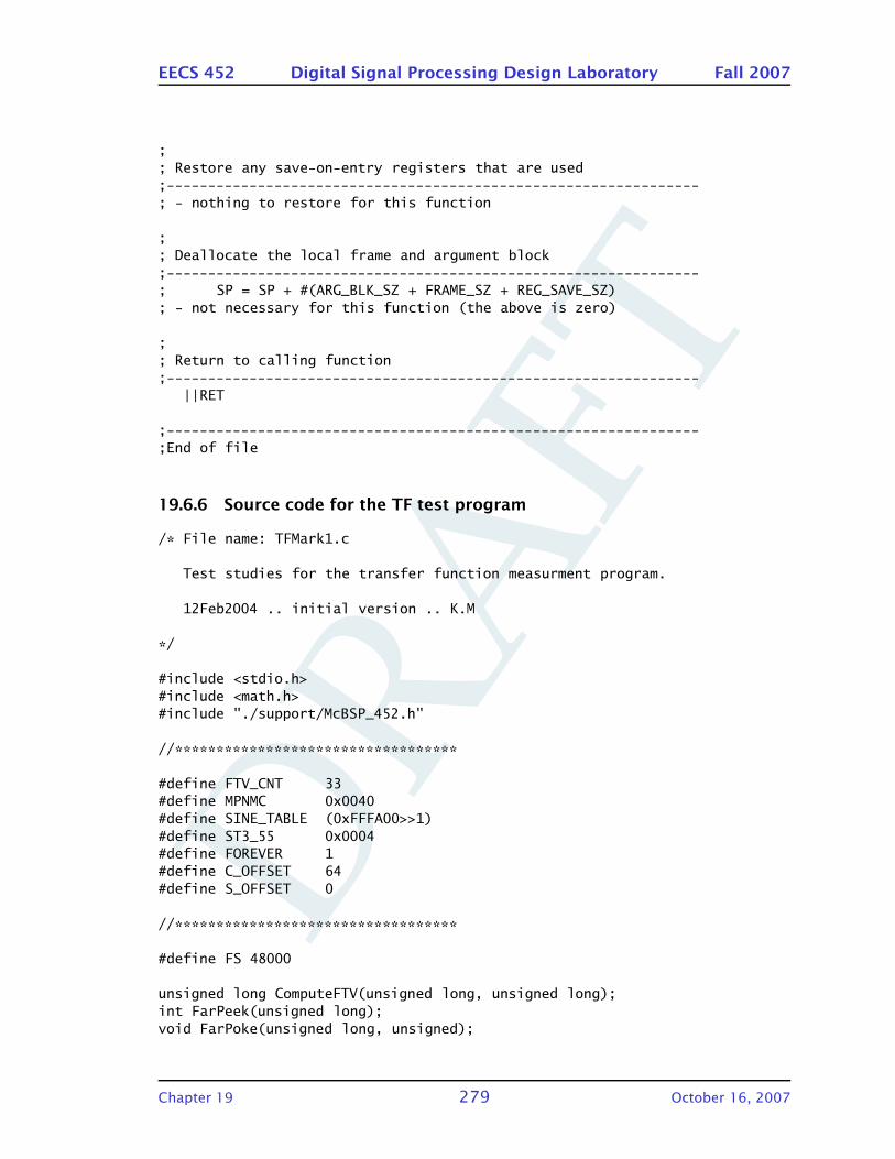
DRA
FT
EECS 452 Digital Signal Processing Design Laboratory Fall 2007
;; Restore any save-on-entry registers that are used;----------------------------------------------------------------; - nothing to restore for this function
;; Deallocate the local frame and argument block;----------------------------------------------------------------; SP = SP + #(ARG_BLK_SZ + FRAME_SZ + REG_SAVE_SZ); - not necessary for this function (the above is zero)
;; Return to calling function;----------------------------------------------------------------
||RET
;----------------------------------------------------------------;End of file
19.6.6 Source code for the TF test program
/* File name: TFMark1.c
Test studies for the transfer function measurment program.
12Feb2004 .. initial version .. K.M
*/
#include <stdio.h>#include <math.h>#include "./support/McBSP_452.h"
//**********************************
#define FTV_CNT 33#define MPNMC 0x0040#define SINE_TABLE (0xFFFA00>>1)#define ST3_55 0x0004#define FOREVER 1#define C_OFFSET 64#define S_OFFSET 0
//**********************************
#define FS 48000
unsigned long ComputeFTV(unsigned long, unsigned long);int FarPeek(unsigned long);void FarPoke(unsigned long, unsigned);
Chapter 19 279 October 16, 2007

DRA
FT
EECS 452 Digital Signal Processing Design Laboratory Fall 2007
void AIC23_IO(unsigned port, int LeftValue, int RightValue);int LeftInput, RightInput;
#include "FIR145.h"
#define NH (sizeof(B)/sizeof(int))int db[NH+2];
unsigned long fs = FS;unsigned long ftv;unsigned long sine_ptr;double pi=3.14159265;unsigned long ac;unsigned Nint = FS/10; // integrate for 0.1 secondsunsigned Nstart = (NH+2); // dependent on filter size!!long x32, y32;
int sin_tab[256];
unsigned int test = 5; // select which test to execute
void main(void)
unsigned st3_55;int idx, table, sine, data;int frac, value, value2;unsigned cosine_adr, sine_adr, sig_adr;int cosine_value, sine_value, sig_value;unsigned long f, utemp;double xflt, yflt, rflt, ang, sf;FILE *out;
for (idx = 0; idx < 256; idx++) sin_tab[idx] = (int)(32766*sin(2*pi*idx/256)+0.5);
/*****************************************************************************/
if (test == 1)
// test the generation of the FTV value
while (FOREVER) printf("enter f: ");scanf("%lu", &f);ftv = ComputeFTV(f, fs);
Chapter 19 280 October 16, 2007

DRA
FT
EECS 452 Digital Signal Processing Design Laboratory Fall 2007
printf("f: %6lu fs: %6lu ftv: %9lu\n", f, fs, ftv);
/******************************************************************************/
if (test == 2)
// test accessing the ROM based sine table
st3_55 = FarPeek(ST3_55); // read status register 3FarPoke(ST3_55, st3_55&(~MPNMC)); // enable the ROM in program space
sine_ptr = SINE_TABLE;for (idx = 0; idx < 128; idx++)
table = FarPeek(sine_ptr++);sine = (int)(32768*sin(2*pi*idx/256)+0.5);printf("idx: %6d sine: %6d table: %6d\n", idx, sine, table);
exit (0);
/*******************************************************************************/
if (test == 3)
// test DDS quadrature oscillator
printf("enter f: ");scanf("%lu", &f);ftv = ComputeFTV(f, fs);printf("f: %6lu fs: %6lu ftv: %9lu\n", f, fs, ftv);st3_55 = FarPeek(ST3_55); // read status register 3FarPoke(ST3_55, st3_55&(~MPNMC)); // enable the ROM in program space
// place cosine on left D/A and sine on right D/A
setup_codec();
ac = 0; // initialize the phase accumulator
while (FOREVER) cosine_adr = ((ac >> (32-8))+C_OFFSET)&0xFF;sine_adr = ((ac >> (32-8))+S_OFFSET)&0xFF;cosine_value = FarPeek(SINE_TABLE+cosine_adr);sine_value = FarPeek(SINE_TABLE+sine_adr);AIC23_IO(2, cosine_value, sine_value);ac += ftv; // advance the phase accumulator
Chapter 19 281 October 16, 2007
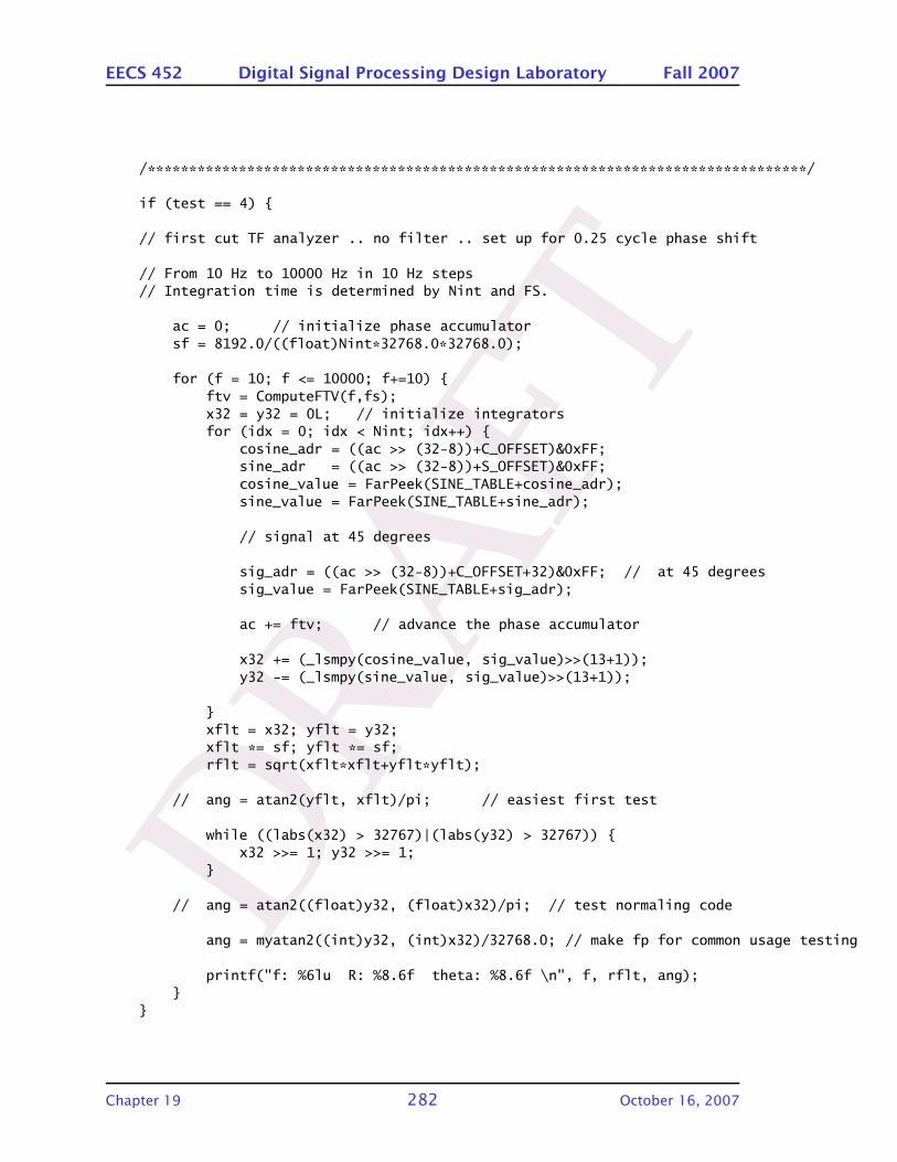
DRA
FT
EECS 452 Digital Signal Processing Design Laboratory Fall 2007
/*******************************************************************************/
if (test == 4)
// first cut TF analyzer .. no filter .. set up for 0.25 cycle phase shift
// From 10 Hz to 10000 Hz in 10 Hz steps// Integration time is determined by Nint and FS.
ac = 0; // initialize phase accumulatorsf = 8192.0/((float)Nint*32768.0*32768.0);
for (f = 10; f <= 10000; f+=10) ftv = ComputeFTV(f,fs);x32 = y32 = 0L; // initialize integratorsfor (idx = 0; idx < Nint; idx++)
cosine_adr = ((ac >> (32-8))+C_OFFSET)&0xFF;sine_adr = ((ac >> (32-8))+S_OFFSET)&0xFF;cosine_value = FarPeek(SINE_TABLE+cosine_adr);sine_value = FarPeek(SINE_TABLE+sine_adr);
// signal at 45 degrees
sig_adr = ((ac >> (32-8))+C_OFFSET+32)&0xFF; // at 45 degreessig_value = FarPeek(SINE_TABLE+sig_adr);
ac += ftv; // advance the phase accumulator
x32 += (_lsmpy(cosine_value, sig_value)>>(13+1));y32 -= (_lsmpy(sine_value, sig_value)>>(13+1));
xflt = x32; yflt = y32;xflt *= sf; yflt *= sf;rflt = sqrt(xflt*xflt+yflt*yflt);
// ang = atan2(yflt, xflt)/pi; // easiest first test
while ((labs(x32) > 32767)|(labs(y32) > 32767)) x32 >>= 1; y32 >>= 1;
// ang = atan2((float)y32, (float)x32)/pi; // test normaling code
ang = myatan2((int)y32, (int)x32)/32768.0; // make fp for common usage testing
printf("f: %6lu R: %8.6f theta: %8.6f \n", f, rflt, ang);
Chapter 19 282 October 16, 2007
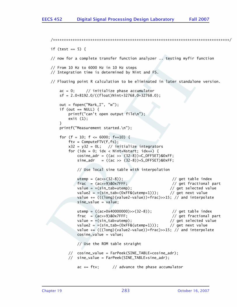
DRA
FT
EECS 452 Digital Signal Processing Design Laboratory Fall 2007
/********************************************************************************/
if (test == 5)
// now for a complete transfer function analyzer .. testing myfir function
// From 10 Hz to 6000 Hz in 10 Hz steps// Integration time is determined by Nint and FS.
// Floating point R calculation to be eliminated in later standalone version.
ac = 0; // initialize phase accumulatorsf = 2.0*8192.0/((float)Nint*32768.0*32768.0);
out = fopen("Mark_I", "w");if (out == NULL)
printf("can’t open output file\n");exit (1);
printf("Measurement started.\n");
for (f = 10; f <= 6000; f+=10) ftv = ComputeFTV(f,fs);x32 = y32 = 0L; // initialize integratorsfor (idx = 0; idx < Nint+Nstart; idx++)
cosine_adr = ((ac >> (32-8))+C_OFFSET)&0xFF;sine_adr = ((ac >> (32-8))+S_OFFSET)&0xFF;
// Use local sine table with interpolation
utemp = (ac>>(32-8)); // get table indexfrac = (ac>>9)&0x7FFF; // get fractional partvalue = *(sin_tab+utemp); // get selected valuevalue2 = *(sin_tab+(0xFF&(utemp+1))); // get next valuevalue += (((long)(value2-value))*frac)>>15; // and interpolatesine_value = value;
utemp = ((ac+0x40000000)>>(32-8)); // get table indexfrac = (ac>>9)&0x7FFF; // get fractional partvalue = *(sin_tab+utemp); // get selected valuevalue2 = *(sin_tab+(0xFF&(utemp+1))); // get next valuevalue += (((long)(value2-value))*frac)>>15; // and interpolatecosine_value = value;
// Use the ROM table straight
// cosine_value = FarPeek(SINE_TABLE+cosine_adr);// sine_value = FarPeek(SINE_TABLE+sine_adr);
ac += ftv; // advance the phase accumulator
Chapter 19 283 October 16, 2007
DRA
FT
EECS 452 Digital Signal Processing Design Laboratory Fall 2007
data = cosine_value>>1; // set effective max level to 0.5
myFIR(&data, &B[0], &sig_value, &db[0], 1, NH); // FIR filter
if (idx < Nstart) continue; // wait until filter memory is filled
x32 += (_lsmpy(cosine_value, sig_value) >> 13);y32 -= (_lsmpy(sine_value, sig_value) >> 13);
xflt = x32; yflt = y32;xflt *= sf; yflt *= sf;rflt = sqrt(xflt*xflt+yflt*yflt); // later make fixed point!!!
// Need to make x and y values 16 bit for myatan2
while ((labs(x32) > 32767)||(labs(y32) > 32767)) x32 >>= 1; y32 >>= 1;
ang = myatan2((int)y32, (int)x32)/32768.0; // make fp for common usage testing
if ((f-200*(f/200)) == 0) printf("%6ld\n",f);
// printf("f: %6lu R: %8.6f theta: %8.6f \n", f, rflt, ang);
fprintf(out, " %6lu %8.6f %8.6f\n", f, rflt, ang); // used for file output only
fclose(out);printf("\n Done!\n");
/*****************************************************************************/
// Function to compute 32 bit unsigned FTV value give f and fs
unsigned long ComputeFTV(unsigned long f, unsigned long fs)
unsigned idx;unsigned long ftv;
ftv = 0;
for (idx = 0; idx < FTV_CNT; idx++) if (f >= fs)
ftv = (ftv<<1)+1;f -= fs;
else ftv <<= 1;
Chapter 19 284 October 16, 2007
DRA
FT
EECS 452 Digital Signal Processing Design Laboratory Fall 2007
f <<= 1;if (f >= fs) ftv += 1;
return (ftv);
/****************************************************************************/
// Function used to send values to the D/A
/** places the two calling values into the McBSP transmitter buffer
* waits for a new sample to arrive
* places the sample value into LeftInput and RightInput
* then returns
*/
void AIC23_IO(unsigned port, int LeftValue, int RightValue)
McBSP_reg(port, McBSP_DXR2) = LeftValue;McBSP_reg(port, McBSP_DXR1) = RightValue;
while((McBSP_reg(port, McBSP_SPCR1)&0x0002) == 0); // wait for sample
LeftInput = McBSP_reg(2, McBSP_DRR2);RightInput = McBSP_reg(2, McBSP_DRR1);
Chapter 19 285 October 16, 2007

DRA
FTWasted space, consider adding helpful text to this chapter.
DRA
FT
20 : Lab exercise 5 – S3SB MAC entity
implementation
20.1 Introduction . . . . . . . . . . . . . . . . . . . . . . . . . . . . . . . . . . 288
20.1.1 Bit-serial multiplier . . . . . . . . . . . . . . . . . . . . . . . . . . 288
20.1.2 Bit-serial accumulator . . . . . . . . . . . . . . . . . . . . . . . . 289
20.2 The MAC test entity and its use . . . . . . . . . . . . . . . . . . . . . . 289
20.2.1 MAC entity port signals . . . . . . . . . . . . . . . . . . . . . . . 289
20.2.2 Spartan-3 board device usage . . . . . . . . . . . . . . . . . . . . 290
20.3 Discarding bits and rounding . . . . . . . . . . . . . . . . . . . . . . . 290
20.4 The exercise . . . . . . . . . . . . . . . . . . . . . . . . . . . . . . . . . . 292
20.4.1 The MAC entity . . . . . . . . . . . . . . . . . . . . . . . . . . . . 293
20.4.2 Adding convergent rounding . . . . . . . . . . . . . . . . . . . . 293
20.4.3 Extending the unit . . . . . . . . . . . . . . . . . . . . . . . . . . 294
20.5 Listings . . . . . . . . . . . . . . . . . . . . . . . . . . . . . . . . . . . . . 294
20.5.1 MAC test entity source code . . . . . . . . . . . . . . . . . . . . 294
20.5.2 The MAC entity VHDL . . . . . . . . . . . . . . . . . . . . . . . . 297
20.5.3 The serial-parallel multiplier entity VHDL . . . . . . . . . . . . 300
20.5.4 One-bit full adder entity VHDL . . . . . . . . . . . . . . . . . . . 302
Chapter 20 287 October 16, 2007

DRA
FT
EECS 452 Digital Signal Processing Design Laboratory Fall 2007
20.1 Introduction
This is the write-up for the VHDL portion of Lab Exercise 5.
é
~
Ä
∆ ∆∆ ∆
∆
~~ ~
ëáÖåÉñíÉåÇ
äëÄãëÄÄP ÄO
ÄO
N M
N M
Ä Ä
Ä Ä
∆ ∆ ∆
~ÄP
áåáíá~äáòÉ=~ää=ÇÉä~óë=íç=M j^`=çìíéìí
~ áåéìí Ä áåéìí
~ÅÅìãìä~íçê
U
j^`~ÇÇÉê=ëí~ÖÉ
~∆
ãëÄ äëÄ
Figure 20.1: Signed serial-parallel multiplier MAC entity block diagram (4-bit
word size shown).
The VHDL exercise is in two parts. In the first part the task is to implement
abit-serial 8-bit multiply-and-accumulate (MAC) entity. This is to be based on
the block diagram contained in Figure 20.1. The second part of the exercise
adds rounding and truncation support to the MAC entity.
The multiplier portion of the design is based on On a Bit-Serial Input and
Bit-Serial Output Multiplier, R. Gnanasekaran, IEEE Transactions on Computers,
Vol. C-32, No. 9, September 1983.
Lab exercise 5 is planned to combine the MAC using from this exercise with
parts of the Lab Exercise 4 VHDL (the A/D and D/A support along with a direct
digital synthesizer) to implement a finite impulse response (FIR) filter. The 8 bit
word size will be upgraded to 16 bits, so plan ahead.
20.1.1 Bit-serial multiplier
The bit-serial multiplier shown in the left side of Figure 20.1 is of the serial-
parallel form discussed in lecture. The a value is the multiplicand and the b
value is the multiplier. The unit does signed multiplication. Only four bits are
shown, this exercise implements 8, and in lab exercise 5 it expected that either
12 or 16 bits will be used.
Chapter 20 288 October 16, 2007

DRA
FT
EECS 452 Digital Signal Processing Design Laboratory Fall 2007
20.1.2 Bit-serial accumulator
The logic for the bit-serial accumulator is on the right side of 20.1. The output
of the multiplier is bit-serial, least significant bit first. This is added bit serial
wise to the shifted contents of the accumulator register. A single full adder with
a delay in the carry is sufficient to do the addition. The extra delay in between
the adder output and the accumulator is present for use when rounding (to be
added). With this delay present it requires 17 clock tics to add the multiplier
output to the accumulator.
The adder and accumulator require minimal logic making minimal demands
on use of FPGA fabric. The cost is higher execution time compared to a parallel
implementation. However, if the time is available the use of bit-serial logic can
allow use of smaller FPGA devices or increased computational ability for a given
size as compared to parallel logic.
20.2 The MAC test entity and its use
This section documents the expected MAC entity port signals and the use of
the Spartan-3 board switches and display. A Digilent 4 switch Pmod module is
expected to be attached to PMod port C.
20.2.1 MAC entity port signals
entity SP_MAC isPort ( a : in STD_LOGIC_VECTOR (7 downto 0);
b : in STD_LOGIC_VECTOR (7 downto 0);go : in STD_LOGIC;clear : in STD_LOGIC;round : in STD_LOGIC;ready : out STD_LOGIC;ac : out STD_LOGIC_VECTOR (15 downto 0);reset : in STD_LOGIC := ’0’;clk : in STD_LOGIC);
end SP_MAC;
Signal a is the multiplicand. b is the multiplier. go is a one clock period pulse
which triggers the operation of the MAC. clear is a one period pulse which sets
the MAC accumulator to zero, round is a level indicating whether or not the
current mac operation is to have its result rounded.
Signal ready is a one when the MAC entity is not working, a zero otherwise.
There is no need for this application to check the ready. Operation is very fast
Chapter 20 289 October 16, 2007
DRA
FT
EECS 452 Digital Signal Processing Design Laboratory Fall 2007
and we, as observers, are, relatively speaking, glacially slow. The ac lines connect
to the accumulator. The reset and clk are as normally.
20.2.2 Spartan-3 board device usage
Eight bit values are entered via the 8 slide switches. Sixteen bit values are shown
on the seven-segment display.
Push button function:
PB 0 do a MAC operation.
PB 1 load slide switch value into a-register.
PB 2 load slide switch value into b-register.
PB 3 clear the MAC accumulator.
PMod slide switch functions:
SW 1 show a-register in seven-segment display.
SW 2 show b-register in seven-segment display.
SW 3 round and truncate 16-bit MAC retaining the top 8-bits
on PB0 operations.
SW 4 not used.
The contents of the MAC are shown in the seven-segment display when all
switches are in the down position. The truncation step may or may not (the
more likely implementation) zero the low 8 bits of the MAC accumulator.
20.3 Discarding bits and rounding
Many DSP calculations involve using 16-bit (or some other word size) multi-
plications and additions. Multiplications result in word size bit growth. Gen-
erally somewhere during or at the end of a series of operations it is neces-
sary/desireable to store a 32-bit (or whatever) value back into a 16-bit word.
An example of the need to round in real life is when paying school and prop-
erty taxes. These are typically figured in terms of mils, i.e., one thousandths of
a dollar. Our coinage and banking system works in units that are a multiple of
one-hundredths of a dollar, commonly referred to as a cent or penny.
Figuring interest payments is another real-life application where the rounding
and discarding of digits is done.
Chapter 20 290 October 16, 2007
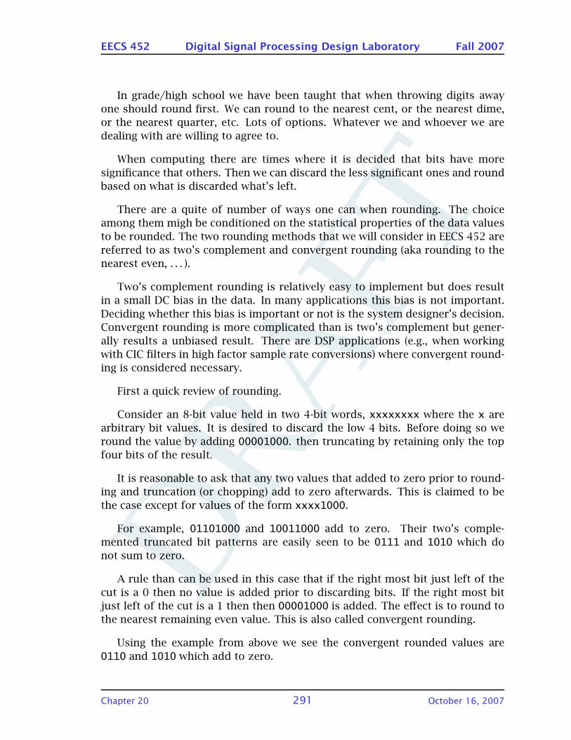
DRA
FT
EECS 452 Digital Signal Processing Design Laboratory Fall 2007
In grade/high school we have been taught that when throwing digits away
one should round first. We can round to the nearest cent, or the nearest dime,
or the nearest quarter, etc. Lots of options. Whatever we and whoever we are
dealing with are willing to agree to.
When computing there are times where it is decided that bits have more
significance that others. Then we can discard the less significant ones and round
based on what is discarded what’s left.
There are a quite of number of ways one can when rounding. The choice
among them migh be conditioned on the statistical properties of the data values
to be rounded. The two rounding methods that we will consider in EECS 452 are
referred to as two’s complement and convergent rounding (aka rounding to the
nearest even, . . . ).
Two’s complement rounding is relatively easy to implement but does result
in a small DC bias in the data. In many applications this bias is not important.
Deciding whether this bias is important or not is the system designer’s decision.
Convergent rounding is more complicated than is two’s complement but gener-
ally results a unbiased result. There are DSP applications (e.g., when working
with CIC filters in high factor sample rate conversions) where convergent round-
ing is considered necessary.
First a quick review of rounding.
Consider an 8-bit value held in two 4-bit words, xxxxxxxx where the x are
arbitrary bit values. It is desired to discard the low 4 bits. Before doing so we
round the value by adding 00001000. then truncating by retaining only the top
four bits of the result.
It is reasonable to ask that any two values that added to zero prior to round-
ing and truncation (or chopping) add to zero afterwards. This is claimed to be
the case except for values of the form xxxx1000.
For example, 01101000 and 10011000 add to zero. Their two’s comple-
mented truncated bit patterns are easily seen to be 0111 and 1010 which do
not sum to zero.
A rule than can be used in this case that if the right most bit just left of the
cut is a 0 then no value is added prior to discarding bits. If the right most bit
just left of the cut is a 1 then then 00001000 is added. The effect is to round to
the nearest remaining even value. This is also called convergent rounding.
Using the example from above we see the convergent rounded values are
0110 and 1010 which add to zero.
Chapter 20 291 October 16, 2007
DRA
FT
EECS 452 Digital Signal Processing Design Laboratory Fall 2007
Given a bit pattern xxxxx|xxxxxxxwhere | indicates the cut point (where the
bits to the right of the | are to be discarded) it can be established that we can
do convergent rounding followed by cutting by adding 00000|1000000 and dis-
carding the low 7 bits, unless we have a bit pattern of the form xxxx0|x000000.
In this situation, simply cut and discard. It should be clear how to generalize
this procedure to any word size and cut position.
j^`=çìíéìí
~ÅÅìãìä~íçê
U
j^`~ÇÇÉê=ëí~ÖÉ
∆
ãëÄ äëÄ
∆
∆ M
áåáíá~äáòÉ=~ää=ÇÉä~óë=íç=M∆
!"# $ %&'
Figure 20.2: Suggested logic for implementing convergent rounding. (4-bit word
size shown).
Convergent rounding can be thought of as being two’s complement rounding
followed by truncation where there a single special case to be dealt with. .
Figure 20.2 illustrates a logic that can be used to add convergent rounding to
Figure 20.1.
The detection of the low bit all zero string could have been accomplished by
anding high bits in the accumulator. The shown zero string detector works inde-
pendent of the number of bits being checked. This allows easy later modification
of where to round.
The round_now signal is a one only when the bit to be rounded is contained
in the delay immediately following the left most adder.
20.4 The exercise
The de-bounced push button, slide switch input and seven-segment VHDL en-
tities were documented in Lab Exercise 2 and are simply being reused in this
exercise.
Chapter 20 292 October 16, 2007
DRA
FT
EECS 452 Digital Signal Processing Design Laboratory Fall 2007
The PMod slide switches are read in as std_logic_vector(3 downto 0). A
zero is read when a switch is in the down position and one is read when a switch
is in the up position.
20.4.1 The MAC entity
You will be supplied with a non-rounding version of the MAC entity VHDL along
with the associated support files. The full adder entity needs completing but
otherwise all modules are operational.
Create a project using the supplied files and generate the bit file.
Load the bit file into the Spartan-3 board. Use a set of values that are sort of
the limits. As might be expected successive runs sum into the accumulator. As
noted above push button 3 can be used to clear the accumulator. The basic idea
is to run a few numbers through in order to gain familiarity with the buttons
and switches as well as build confidence.
20.4.2 Adding convergent rounding
Copy your MAC project into a different folder and use that as your starting point
for adding the convergent rounding logic. Modify the MAC VHDL so that when
the round line is high the value being shifted into the accumulator is convergent
rounded. The rounding is to be accomplished by, in effect, adding (or not) a one
in bit 7 of the accumulator. Because this a bit serial adder is being used the to
be added needs to occur at the right time.
Convergent rounding was discussed both in lecture and in the main Exercise
3 write-up. Basically one wants to place small amount of logic just prior to the
msb input of the accumulator shift register.
One possible logic design is shown in Figure 20.2.
Your GSI can give you some test cases to use for verifying correct operation.
Note that the way the supplied logic works only the bits at the bit position to be
rounded are modified. All of the bits to the right are unchanged. In the TI these
would also be zeroed. Generally this is not necessary if only the bits to the left
of the bit being rounded up are retained.
Once you have your Spartan-3 correctly rounding, demonstrate to your GSI.
Include your source code in you lab report. Also document the test cases that
you used and explain why you choose as you did, what the expected results were
and what your implementation produced.
Chapter 20 293 October 16, 2007

DRA
FT
EECS 452 Digital Signal Processing Design Laboratory Fall 2007
20.4.3 Extending the unit
If you have time and the inclination we expect to be using either a 12-bit or a 16-
bit MAC entity in lab 5 exercise. Can you produce a generic MAC with rounding
for arbitrary word sizes? Another feature that one might consider is to supply
the index of the MAC bit where the rounding 1 is being added just to its right.
In our case the rounding position was bit 8. The rounding one was added into
bit position 7.
The input values are saved in registers. The round control like should be
saved as well. Doing so would allow operation to proceed without requiring the
input data lines being held fixed. Something to do on the next revision iteration.
The design included here does not have any overflow detection support nor
the ability to saturate. The need for these abilities will be application dependent.
Adding their support adds to the complexity of the logic. The more general a
design, the more complex it is likely to be and the more difficult to understand
and use.
Xilinx has a MAC logic core available. It is available to us via the Core Gener-
ator included in WebPACK. The documentation is available on Xilinx’s web site.
Having done this exercise studying Xilinx’s MAC implementation should be in-
formative.
20.5 Listings
20.5.1 MAC test entity source code
This entity uses the two process state machine approach.
------------------------------------------------------------------------------------ Company: EECS 452-- Engineer: K.Metzger---- Create Date: 16:59:22 10/16/2006-- Design Name:-- Module Name: SP_MAC_test - Behavioral-- Project Name:-- Target Devices:-- Tool versions:-- Description:---- Dependencies:--
Chapter 20 294 October 16, 2007

DRA
FT
EECS 452 Digital Signal Processing Design Laboratory Fall 2007
-- Revision:-- Revision 0.01 - File Created-- 1.00 - Modified multiplier01 into SP_MAC_test 20Jan2007 KM-- Additional Comments:------------------------------------------------------------------------------------library IEEE;use IEEE.STD_LOGIC_1164.ALL;use IEEE.STD_LOGIC_ARITH.ALL;use IEEE.STD_LOGIC_UNSIGNED.ALL;
---- Uncomment the following library declaration if instantiating---- any Xilinx primitives in this code.--library UNISIM;--use UNISIM.VComponents.all;
entity SP_MAC_test isPort ( btn : in STD_LOGIC_VECTOR (3 downto 0);
-- led : out STD_LOGIC_VECTOR (7 downto 0);swt : in std_logic_vector(7 downto 0);pmod_c : in std_logic_vector(3 downto 0);ssg : out std_logic_vector(6 downto 0);an : inout std_logic_vector(3 downto 0);mclk : in STD_LOGIC);
end SP_MAC_test;
architecture Behavioral of SP_MAC_test is
signal a : std_logic_vector(7 downto 0);signal b : std_logic_vector(7 downto 0);signal ac : std_logic_vector(15 downto 0);signal display : std_logic_vector(15 downto 0);signal go : std_logic;
signal next_a : std_logic_vector(7 downto 0);signal next_b : std_logic_vector(7 downto 0);signal next_go : std_logic;signal ready : std_logic;signal reset : std_logic :=’0’;
signal pb_db : std_logic_vector(3 downto 0);signal pb_clear : std_logic_vector(3 downto 0);signal next_pb_clear : std_logic_vector(3 downto 0);
type t_state is (s_idle, s_go, s_done);signal state : t_state := s_idle;signal next_state : t_state := s_idle;signal sel : std_logic_vector(3 downto 0);signal clk : std_logic;
begin
Chapter 20 295 October 16, 2007
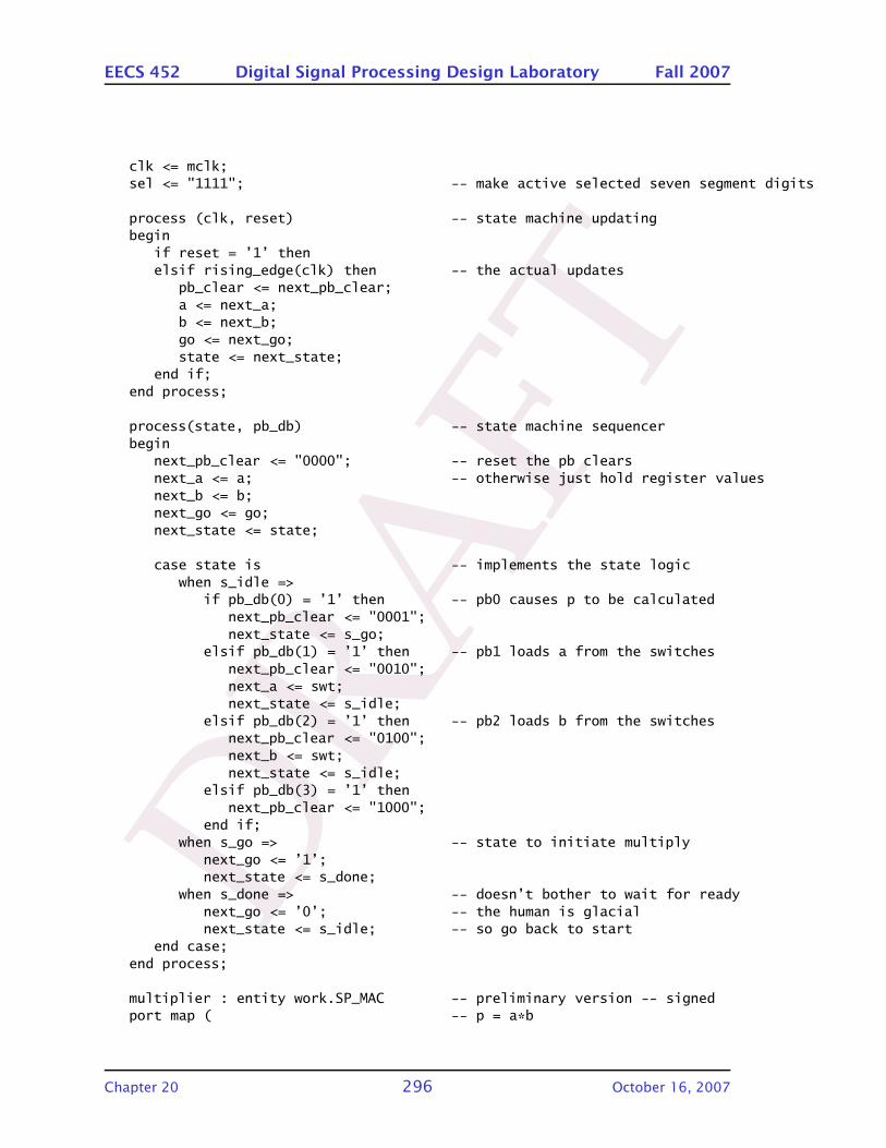
DRA
FT
EECS 452 Digital Signal Processing Design Laboratory Fall 2007
clk <= mclk;sel <= "1111"; -- make active selected seven segment digits
process (clk, reset) -- state machine updatingbegin
if reset = ’1’ thenelsif rising_edge(clk) then -- the actual updates
pb_clear <= next_pb_clear;a <= next_a;b <= next_b;go <= next_go;state <= next_state;
end if;end process;
process(state, pb_db) -- state machine sequencerbegin
next_pb_clear <= "0000"; -- reset the pb clearsnext_a <= a; -- otherwise just hold register valuesnext_b <= b;next_go <= go;next_state <= state;
case state is -- implements the state logicwhen s_idle =>
if pb_db(0) = ’1’ then -- pb0 causes p to be calculatednext_pb_clear <= "0001";next_state <= s_go;
elsif pb_db(1) = ’1’ then -- pb1 loads a from the switchesnext_pb_clear <= "0010";next_a <= swt;next_state <= s_idle;
elsif pb_db(2) = ’1’ then -- pb2 loads b from the switchesnext_pb_clear <= "0100";next_b <= swt;next_state <= s_idle;
elsif pb_db(3) = ’1’ thennext_pb_clear <= "1000";
end if;when s_go => -- state to initiate multiply
next_go <= ’1’;next_state <= s_done;
when s_done => -- doesn’t bother to wait for readynext_go <= ’0’; -- the human is glacialnext_state <= s_idle; -- so go back to start
end case;end process;
multiplier : entity work.SP_MAC -- preliminary version -- signedport map ( -- p = a*b
Chapter 20 296 October 16, 2007
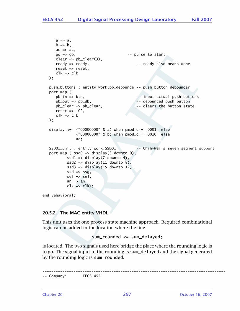
DRA
FT
EECS 452 Digital Signal Processing Design Laboratory Fall 2007
a => a,b => b,ac => ac,go => go, -- pulse to startclear => pb_clear(3),ready => ready, -- ready also means donereset => reset,clk => clk
);
push_buttons : entity work.pb_debounce -- push button debouncerport map (
pb_in => btn, -- input actual push buttonspb_out => pb_db, -- debounced push buttonpb_clear => pb_clear, -- clears the button statereset => ’0’,clk => clk
);
display <= ("00000000" & a) when pmod_c = "0001" else("00000000" & b) when pmod_c = "0010" elseac;
SSD01_unit : entity work.SSD01 -- Chih-Wei’s seven segment supportport map ( ssd0 => display(3 downto 0),
ssd1 => display(7 downto 4),ssd2 => display(11 downto 8),ssd3 => display(15 downto 12),ssd => ssg,sel => sel,an => an,clk => clk);
end Behavioral;
20.5.2 The MAC entity VHDL
This unit uses the one-process state machine approach. Required combinational
logic can be added in the location where the line
sum_rounded <= sum_delayed;
is located. The two signals used here bridge the place where the rounding logic is
to go. The signal input to the rounding is sum_delayed and the signal generated
by the rounding logic is sum_rounded.
------------------------------------------------------------------------------------ Company: EECS 452
Chapter 20 297 October 16, 2007
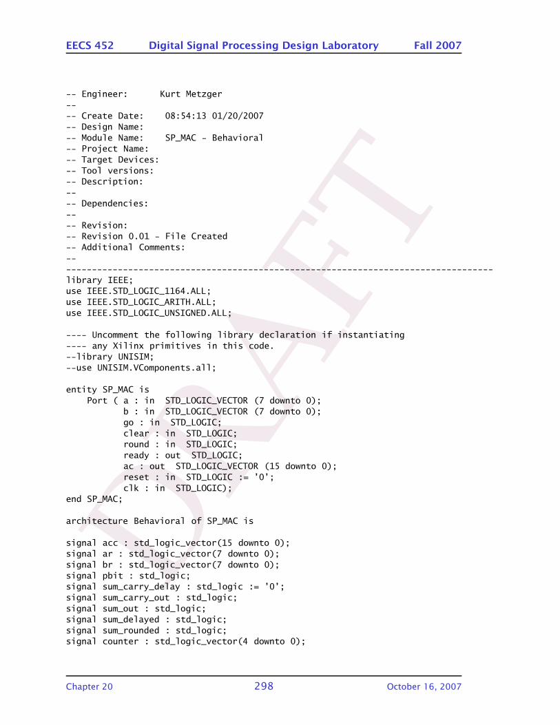
DRA
FT
EECS 452 Digital Signal Processing Design Laboratory Fall 2007
-- Engineer: Kurt Metzger---- Create Date: 08:54:13 01/20/2007-- Design Name:-- Module Name: SP_MAC - Behavioral-- Project Name:-- Target Devices:-- Tool versions:-- Description:---- Dependencies:---- Revision:-- Revision 0.01 - File Created-- Additional Comments:------------------------------------------------------------------------------------library IEEE;use IEEE.STD_LOGIC_1164.ALL;use IEEE.STD_LOGIC_ARITH.ALL;use IEEE.STD_LOGIC_UNSIGNED.ALL;
---- Uncomment the following library declaration if instantiating---- any Xilinx primitives in this code.--library UNISIM;--use UNISIM.VComponents.all;
entity SP_MAC isPort ( a : in STD_LOGIC_VECTOR (7 downto 0);
b : in STD_LOGIC_VECTOR (7 downto 0);go : in STD_LOGIC;clear : in STD_LOGIC;round : in STD_LOGIC;ready : out STD_LOGIC;ac : out STD_LOGIC_VECTOR (15 downto 0);reset : in STD_LOGIC := ’0’;clk : in STD_LOGIC);
end SP_MAC;
architecture Behavioral of SP_MAC is
signal acc : std_logic_vector(15 downto 0);signal ar : std_logic_vector(7 downto 0);signal br : std_logic_vector(7 downto 0);signal pbit : std_logic;signal sum_carry_delay : std_logic := ’0’;signal sum_carry_out : std_logic;signal sum_out : std_logic;signal sum_delayed : std_logic;signal sum_rounded : std_logic;signal counter : std_logic_vector(4 downto 0);
Chapter 20 298 October 16, 2007
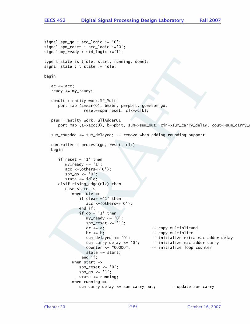
DRA
FT
EECS 452 Digital Signal Processing Design Laboratory Fall 2007
signal spm_go : std_logic := ’0’;signal spm_reset : std_logic :=’0’;signal my_ready : std_logic :=’1’;
type t_state is (idle, start, running, done);signal state : t_state := idle;
begin
ac <= acc;ready <= my_ready;
spmult : entity work.SP_Multport map (a=>ar(0), b=>br, p=>pbit, go=>spm_go,
reset=>spm_reset, clk=>clk);
psum : entity work.FullAdder01port map (a=>acc(0), b=>pbit, sum=>sum_out, cin=>sum_carry_delay, cout=>sum_carry_o
sum_rounded <= sum_delayed; -- remove when adding rounding support
controller : process(go, reset, clk)begin
if reset = ’1’ thenmy_ready <= ’1’;acc <=(others=>’0’);spm_go <= ’0’;state <= idle;
elsif rising_edge(clk) thencase state is
when idle =>if clear =’1’ then
acc <=(others=>’0’);end if;if go = ’1’ then
my_ready <= ’0’;spm_reset <= ’1’;ar <= a; -- copy multiplicandbr <= b; -- copy multipliersum_delayed <= ’0’; -- initialize extra mac adder delaysum_carry_delay <= ’0’; -- initialize mac adder carrycounter <= "00000"; -- initialize loop counterstate <= start;
end if;when start =>
spm_reset <= ’0’;spm_go <= ’1’;state <= running;
when running =>sum_carry_delay <= sum_carry_out; -- update sum carry
Chapter 20 299 October 16, 2007
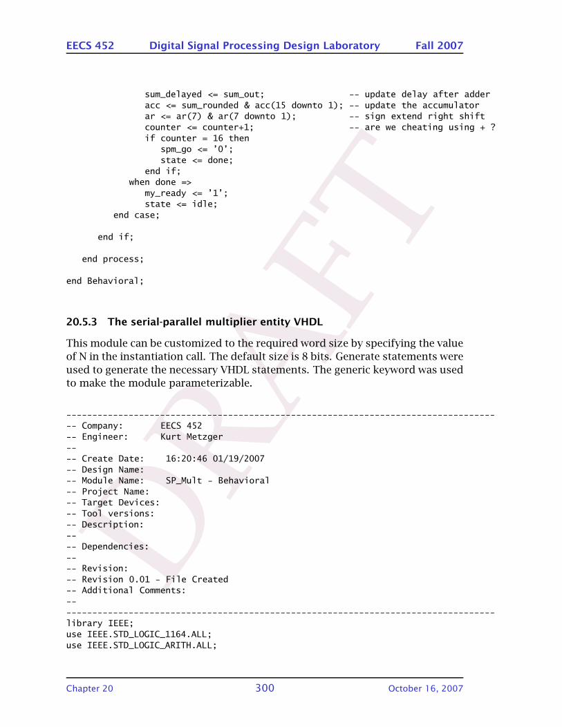
DRA
FT
EECS 452 Digital Signal Processing Design Laboratory Fall 2007
sum_delayed <= sum_out; -- update delay after adderacc <= sum_rounded & acc(15 downto 1); -- update the accumulatorar <= ar(7) & ar(7 downto 1); -- sign extend right shiftcounter <= counter+1; -- are we cheating using + ?if counter = 16 then
spm_go <= ’0’;state <= done;
end if;when done =>
my_ready <= ’1’;state <= idle;
end case;
end if;
end process;
end Behavioral;
20.5.3 The serial-parallel multiplier entity VHDL
This module can be customized to the required word size by specifying the value
of N in the instantiation call. The default size is 8 bits. Generate statements were
used to generate the necessary VHDL statements. The generic keyword was used
to make the module parameterizable.
------------------------------------------------------------------------------------ Company: EECS 452-- Engineer: Kurt Metzger---- Create Date: 16:20:46 01/19/2007-- Design Name:-- Module Name: SP_Mult - Behavioral-- Project Name:-- Target Devices:-- Tool versions:-- Description:---- Dependencies:---- Revision:-- Revision 0.01 - File Created-- Additional Comments:------------------------------------------------------------------------------------library IEEE;use IEEE.STD_LOGIC_1164.ALL;use IEEE.STD_LOGIC_ARITH.ALL;
Chapter 20 300 October 16, 2007

DRA
FT
EECS 452 Digital Signal Processing Design Laboratory Fall 2007
use IEEE.STD_LOGIC_UNSIGNED.ALL;
---- Uncomment the following library declaration if instantiating---- any Xilinx primitives in this code.--library UNISIM;--use UNISIM.VComponents.all;
entity SP_Mult isGeneric ( N : integer := 8);Port ( a : in STD_LOGIC;
b : in STD_LOGIC_VECTOR (N-1 downto 0);p : out STD_LOGIC;go : in STD_LOGIC;reset : in STD_LOGIC;clk : in STD_LOGIC);
end SP_Mult;
architecture Behavioral of SP_Mult is
signal asr : std_logic_vector(N-1 downto 0);signal delayin : std_logic_vector(N-1 downto 1);signal delayout : std_logic_vector(N-1 downto 1);signal carryin : std_logic_vector(N-1 downto 0);signal carryout : std_logic_vector(N-1 downto 0);signal ab : std_logic_vector(N-1 downto 0);
begin
ab <= b when a = ’1’ else (others=>’0’);
sp_mul: for i in 0 to N-1 generatebegin
right : if i = 0 generatesr : entity work.FullAdder01
port map (a=>delayout(i+1), b=>ab(i),cin=>carryout(i), cout=>carryin(i), sum=>p);
end generate right;
mid : if (0 < i) and (i < N-1) generatesr : entity work.FullAdder01
port map (a=>delayout(i+1), b=>ab(i),cin=>carryout(i), cout=>carryin(i), sum=>delayin(i));
end generate mid;
left : if i = N-1 generatesr : entity work.FullAdder01
port map (a=>delayout(i), b=>ab(i),cin=>carryout(i), cout=>carryin(i), sum=>delayin(i));
end generate left;
Chapter 20 301 October 16, 2007

DRA
FT
EECS 452 Digital Signal Processing Design Laboratory Fall 2007
end generate sp_mul;
process(clk, go)begin
if reset = ’1’ thendelayout <= (others=>’0’);carryout <= (others=>’0’);
elsif rising_edge(clk) and go = ’1’ thendelayout <= delayin;carryout <= carryin;
end if;end process;
end Behavioral;
20.5.4 One-bit full adder entity VHDL
It was found easiest to work with the full adder directly and not use an entity
specifically written for a one-bit serial adder (full adder with a register between
the carry out and the carry in).
------------------------------------------------------------------------------------ Company: EECS 452-- Engineer: One-bit full adder---- Create Date: 14:54:05 01/19/2007-- Design Name:-- Module Name: FullAdder01 - Behavioral-- Project Name:-- Target Devices:-- Tool versions:-- Description:---- Dependencies:---- Revision:-- Revision 0.01 - File Created-- Additional Comments:------------------------------------------------------------------------------------library IEEE;use IEEE.STD_LOGIC_1164.ALL;use IEEE.STD_LOGIC_ARITH.ALL;use IEEE.STD_LOGIC_UNSIGNED.ALL;
---- Uncomment the following library declaration if instantiating---- any Xilinx primitives in this code.--library UNISIM;
Chapter 20 302 October 16, 2007
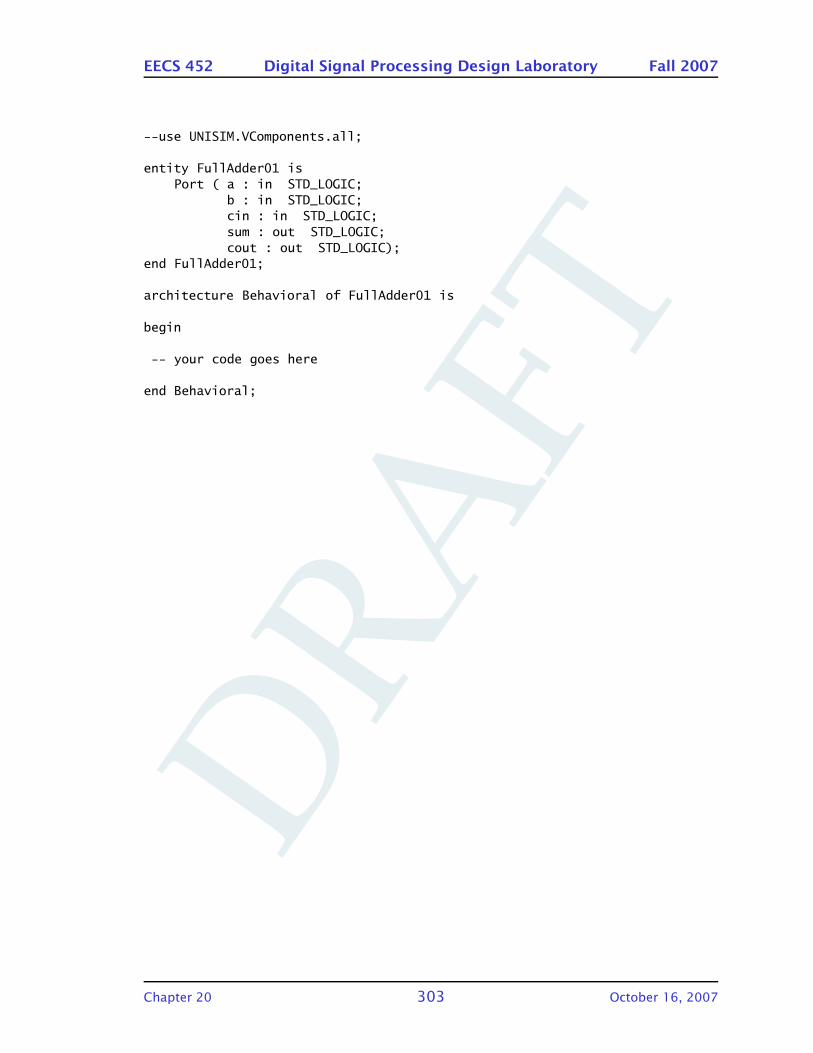
DRA
FT
EECS 452 Digital Signal Processing Design Laboratory Fall 2007
--use UNISIM.VComponents.all;
entity FullAdder01 isPort ( a : in STD_LOGIC;
b : in STD_LOGIC;cin : in STD_LOGIC;sum : out STD_LOGIC;cout : out STD_LOGIC);
end FullAdder01;
architecture Behavioral of FullAdder01 is
begin
-- your code goes here
end Behavioral;
Chapter 20 303 October 16, 2007

DRA
FTWasted space, consider adding helpful text to this chapter.
DRA
FT
21 : Infinite Impulse Response
Filtering
Use of biquad stages. Range of coefficient values. Elliptic filters require mini-
mal resources. Limit cycles. Transfer function and group delay measurement.
Recursive oscillators. single output—why stable? Sine/cosine output.
Chapter 21 305 October 16, 2007

DRA
FTWasted space, consider adding helpful text to this chapter.
DRA
FT
22 : Lab exercise 6 – IIR filter design
and implementation
22.1 Introduction . . . . . . . . . . . . . . . . . . . . . . . . . . . . . . . . . . 309
22.2 Infinite impulse response filters . . . . . . . . . . . . . . . . . . . . . . 310
22.2.1 Theory . . . . . . . . . . . . . . . . . . . . . . . . . . . . . . . . . . 310
22.3 Recursive sine/cosine oscillator . . . . . . . . . . . . . . . . . . . . . 311
22.3.1 Theory . . . . . . . . . . . . . . . . . . . . . . . . . . . . . . . . . . 311
22.4 Transfer function measurement . . . . . . . . . . . . . . . . . . . . . 314
22.5 C5510 . . . . . . . . . . . . . . . . . . . . . . . . . . . . . . . . . . . . . . 316
22.5.1 Prelab . . . . . . . . . . . . . . . . . . . . . . . . . . . . . . . . . . 316
22.5.2 The IIR filter . . . . . . . . . . . . . . . . . . . . . . . . . . . . . . 316
22.5.3 The sine/cosine oscillator . . . . . . . . . . . . . . . . . . . . . . 318
22.5.4 Measuring transfer functions . . . . . . . . . . . . . . . . . . . . 319
22.5.5 Exercise . . . . . . . . . . . . . . . . . . . . . . . . . . . . . . . . . 322
22.5.6 The TDF2 biquad IIR cascade . . . . . . . . . . . . . . . . . . . . 322
22.5.7 Sine/Cosine oscillator . . . . . . . . . . . . . . . . . . . . . . . . 331
22.5.8 Report . . . . . . . . . . . . . . . . . . . . . . . . . . . . . . . . . . 332
22.6 S3SB . . . . . . . . . . . . . . . . . . . . . . . . . . . . . . . . . . . . . . . 332
22.6.1 Prelab . . . . . . . . . . . . . . . . . . . . . . . . . . . . . . . . . . 332
22.6.2 Exercise . . . . . . . . . . . . . . . . . . . . . . . . . . . . . . . . . 332
22.6.3 Report . . . . . . . . . . . . . . . . . . . . . . . . . . . . . . . . . . 332
22.7 DSPlib IIRCAS5 manual pages . . . . . . . . . . . . . . . . . . . . . . . 332
22.8 List of codes . . . . . . . . . . . . . . . . . . . . . . . . . . . . . . . . . . 335
22.9 IIR Transfer function Mark 2 . . . . . . . . . . . . . . . . . . . . . . . . 335
22.10 IIR filter function test support . . . . . . . . . . . . . . . . . . . . . . . 341
22.11 myDF2IIR source code . . . . . . . . . . . . . . . . . . . . . . . . . . . . 346
22.12 IIRCAS5 source code . . . . . . . . . . . . . . . . . . . . . . . . . . . . . 348
22.13 myTDF2IIR source starter code . . . . . . . . . . . . . . . . . . . . . . 348
22.14 DisplayTest00 source code . . . . . . . . . . . . . . . . . . . . . . . . . 350
22.15 draw_characters source code . . . . . . . . . . . . . . . . . . . . . . . 356
22.16 setup_McBSP_plot source code . . . . . . . . . . . . . . . . . . . . . . 360
22.17 Output to XVGA via McBSP 0 source code . . . . . . . . . . . . . . . 362
22.18 Interrupt support, AIC23int_00.asm . . . . . . . . . . . . . . . . . . . 364
22.19 Interrupt vector . . . . . . . . . . . . . . . . . . . . . . . . . . . . . . . . 367
22.20 Interrupt support error, no_isr.asm . . . . . . . . . . . . . . . . . . . 368
Chapter 22 307 October 16, 2007

DRA
FT
EECS 452 Digital Signal Processing Design Laboratory Fall 2007
22.21 Main function for recursive sine/cosine oscillator . . . . . . . . . . 368
22.22 Starter code for recursive sine/cosine oscillator . . . . . . . . . . . 368
Chapter 22 308 October 16, 2007

DRA
FT
EECS 452 Digital Signal Processing Design Laboratory Fall 2007
22.1 Introduction
This exercise develops:
• the programming of a function to implement an IIR filter as a cascade of
biquad sections,
• the programming of a recursive frequency synthesizer (rather than a DDS)
that simultaneously generates sine and cosine phase sinusoids,
• the transfer function measurement code introduced in lab exercise 5. Use is
made of the interrupt system. With little or minor modification the updated
program can be used to make measurements on filters external to the DSK
(though not used in this way in the actual exercise).
Infinite impulse response filters were discussed extensively in lecture. The
purpose of the first portion of this exercise is to gain practical experience imple-
menting an IIR filter using a cascade of transposed direct form 2 biquad sections.
The use of a biquad section as a sinewave generator was discussed in lec-
ture. Basically an IIR filter is designed with its poles located on the unit circle,
implemented in software and started running by providing initial conditions.
The second part of the lab looks at a two delay stage circuit configuration that
simultaneously generates sine and cosine waveforms at the same frequency.
The Mark 1 transfer function program (used in lab exercise 5) was evolved
(into the Mark 2 version) for use in this exercise. The changes include:
• Interactive support for selection of the filter whose transfer function is to
be measured.
• Use of the D/A and A/D converters to generate the waveforms to be fil-
tered. This more closely represents the operation of a stand alone instru-
ment such as the National Instruments LabView system or the SigLab sys-
tem.
• Use of interrupts. The right channel output dedicated to the generation of
a cosine waveform using an interrupt driven direct digital synthesizer. This
frees up the application program from having dealing with the updating of
the DDS’s accumulator.
The Mark 2 program lacks graphic capability and relies on off-line processing
and plotting by MATLAB.
Many of the source files for this exercise can be found on the EECS 452 hand-
outs web page.
Chapter 22 309 October 16, 2007
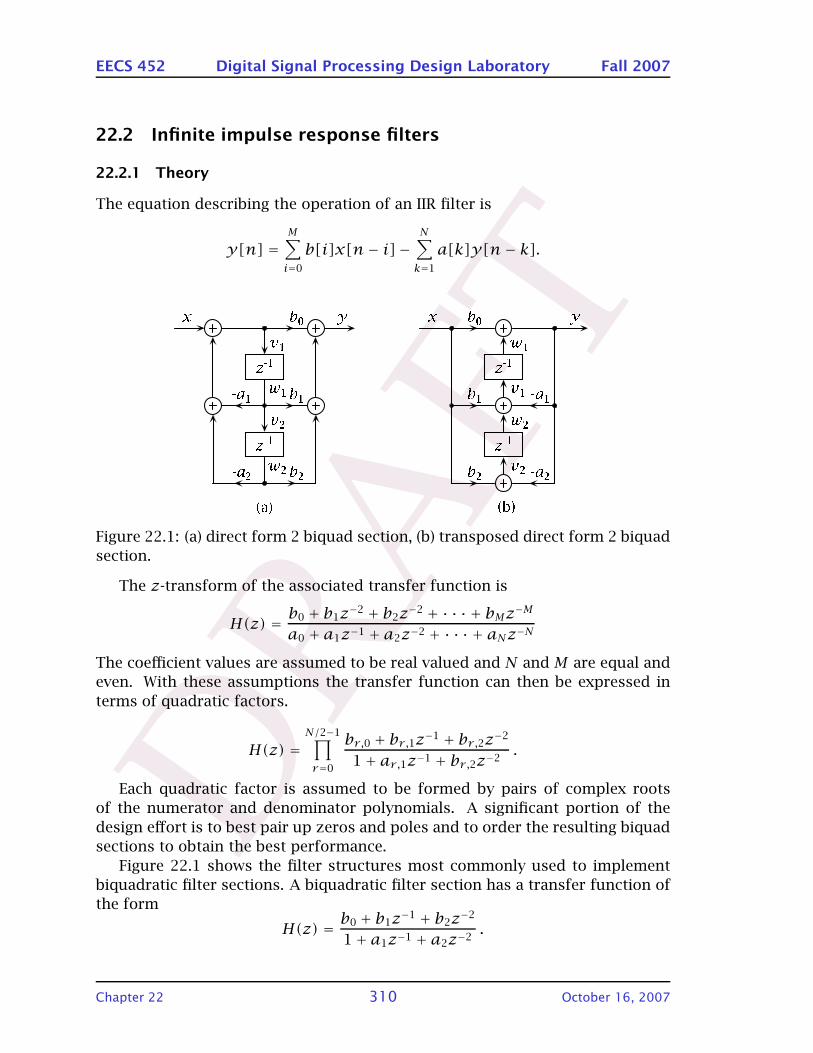
DRA
FT
EECS 452 Digital Signal Processing Design Laboratory Fall 2007
22.2 Infinite impulse response filters
22.2.1 Theory
The equation describing the operation of an IIR filter is
y[n] =M∑
i=0
b[i]x[n − i]−N∑
k=1
a[k]y[n − k].
()*()* ()*()*+,
-./ -0/ 12345 54 +67686126
123 +373+,+6+383 83 126737686
Figure 22.1: (a) direct form 2 biquad section, (b) transposed direct form 2 biquad
section.
The z-transform of the associated transfer function is
H(z) =b0 + b1z
−2 + b2z−2 + · · · + bMz−M
a0 + a1z−1 + a2z−2 + · · · + aNz−N
The coefficient values are assumed to be real valued and N and M are equal and
even. With these assumptions the transfer function can then be expressed in
terms of quadratic factors.
H(z) =N/2−1∏
r=0
br ,0 + br ,1z−1 + br ,2z−2
1+ ar ,1z−1 + br ,2z−2.
Each quadratic factor is assumed to be formed by pairs of complex roots
of the numerator and denominator polynomials. A significant portion of the
design effort is to best pair up zeros and poles and to order the resulting biquad
sections to obtain the best performance.
Figure 22.1 shows the filter structures most commonly used to implement
biquadratic filter sections. A biquadratic filter section has a transfer function of
the form
H(z) =b0 + b1z
−1 + b2z−2
1+ a1z−1 + a2z−2.
Chapter 22 310 October 16, 2007
DRA
FT
EECS 452 Digital Signal Processing Design Laboratory Fall 2007
The most commonly used biquad implementation is the direct form 2 (DF2),
Figure 22.1a. The transposed direct form 2 (TDF2) shown in Figure 22.1b appears
to be less commonly used. Both forms will be used in this lab exercise.
Most of our design work is going to be done for us by MATLAB. MATLAB ex-
presses transfer functions as a cascade of biquadratic section. MATLAB’s default
is that sections are ordered starting with the pole pair furthest from the unit
circle moving toward the pole pair being closest to the unit circle. Zeros are
matched starting with the one closest to the pole pair nearest the unit circle and
going toward the pole furthest to the unit circle.
This exercise will only consider lowpass filters. Somewhat arbitrarily, we will
set the gain of each biquad section to unity at 0 Hz. We will use a 16-bit word size
with Q15 format input samples and biquad coefficient values. Nominally there
should not be any numeric overflow problems when looking at the input to out-
put levels for the individual biquad sections. Howver this is not necessarily the
case when going from a biquad input to its internal delay stage inputs/outputs.
Our primary design concern is about overflows internal to the biquad cas-
cade. These can be a serious problem when using the DF2 biquad sections and
appears to be an almost non-existent problem when using the TDF2 biquad sec-
tions. There is a price to be paid for this robustness. The inner loop of a TDF2
filter code requires more instructions than does the DF2.
The TDF2 biquad section is relatively easy to program. Assume that tempo-
rary register T0 holds the input value to the current section and that temporary
register T1 holds the output value for the current section. The inner loop calcu-
lations are:
• T1 = w1 + b0T0,
• w1 = b1T0− a1T1+w2,
• w2 = b2T0− a2T1,
• T0 = T1.
Theoretically the magnitudes of the a1 and b1 values can be as large as 2.
Values one and greater in magnitude are not representable using a 16-bit word
size and the Q15 format. One way to handle large values, and retain use of
the Q15 format, is to use a1/2 and b1/2 and repeat the associated mac/masinstructions. The above inner loop does not show how to make use of a1/2 and
b1/2 values. Doing this correctly is part of your responsibility in this exercise.
22.3 Recursive sine/cosine oscillator
22.3.1 Theory
The digital feedback circuit shown in Figure 22.2a was introduced in lecture and
it’s operation analyzed. As an aid to determining the locations of the poles of
Chapter 22 311 October 16, 2007

DRA
FT
EECS 452 Digital Signal Processing Design Laboratory Fall 2007
its transfer function we can add a dummy input point. Redrawing this block
diagram adding provision for an input the result is the diagram shown in Figure
22.2b. The oscillator is started running by placing initial values into the two
delay stages and the input is set to zero.
òJN
òJN
O~
ó§å•
JN
(a)
òJN
òJN
O~
ó§å•
JN
ñxåz
(b)
Figure 22.2: (a) Second-order recursive oscillator block diagram. (b) Equivalent
second-order all pole filter.
For Figure 22.2b we have the general transfer function
H(z) =1
1+ a1z−1 + a2z−2.
The poles of this equation lie at a radius of√a2. For the block diagrams in
Figure 22.2 we have a2 = 1. The poles are on the unit circle. This is the situation
where we have an oscillator.
The relation between a and the frequency of oscillation, fo, for the oscillator
in Figure 22.2 is given by
2πfofs= cos−1(a).
Figure 22.3 contains the listing of a simple assembly language program that
implements such a oscillator.
Figure 22.4 contains the block diagram of a second order recursive oscillator
whose delay stage outputs are in cosine/sine phase relationship. The equations
describing the updating of the delay stage contents can be written in matrix form
as
[
w1[n+ 1]
w2[n+ 1]
]
=
[
cosθ cosθ + 1
cosθ − 1 cosθ
][
w1[n]
w2[n]
]
.
This is a more interesting oscillator than the one in Figure 22.2a. In Figure
22.2a the values in the second delay stage were simply one clock time delays of
Chapter 22 312 October 16, 2007
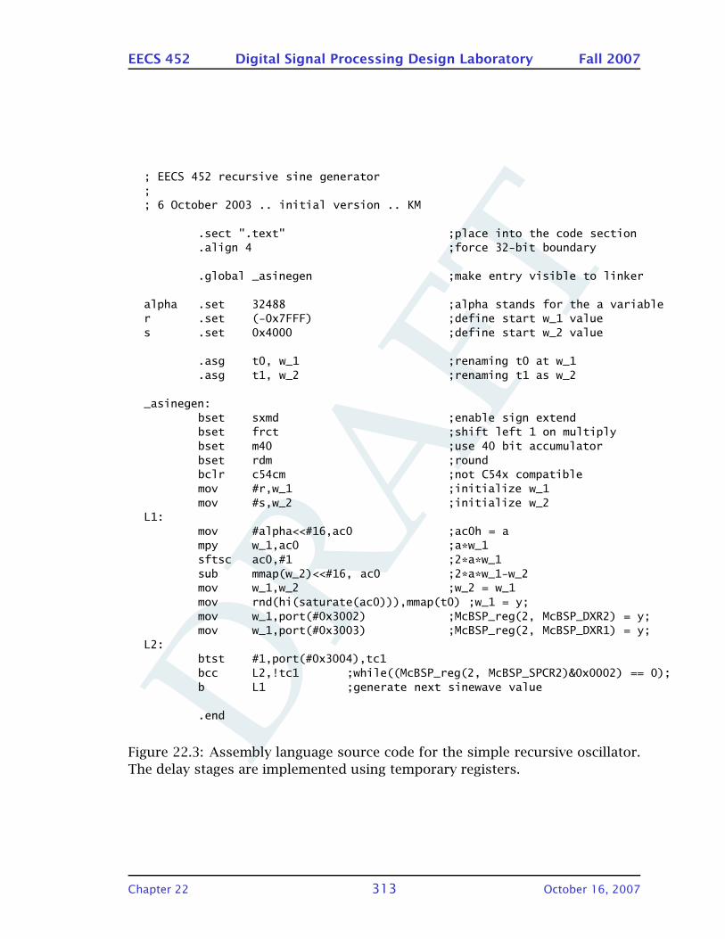
DRA
FT
EECS 452 Digital Signal Processing Design Laboratory Fall 2007
; EECS 452 recursive sine generator;; 6 October 2003 .. initial version .. KM
.sect ".text" ;place into the code section
.align 4 ;force 32-bit boundary
.global _asinegen ;make entry visible to linker
alpha .set 32488 ;alpha stands for the a variabler .set (-0x7FFF) ;define start w_1 values .set 0x4000 ;define start w_2 value
.asg t0, w_1 ;renaming t0 at w_1
.asg t1, w_2 ;renaming t1 as w_2
_asinegen:bset sxmd ;enable sign extendbset frct ;shift left 1 on multiplybset m40 ;use 40 bit accumulatorbset rdm ;roundbclr c54cm ;not C54x compatiblemov #r,w_1 ;initialize w_1mov #s,w_2 ;initialize w_2
L1:mov #alpha<<#16,ac0 ;ac0h = ampy w_1,ac0 ;a*w_1sftsc ac0,#1 ;2*a*w_1sub mmap(w_2)<<#16, ac0 ;2*a*w_1-w_2mov w_1,w_2 ;w_2 = w_1mov rnd(hi(saturate(ac0))),mmap(t0) ;w_1 = y;mov w_1,port(#0x3002) ;McBSP_reg(2, McBSP_DXR2) = y;mov w_1,port(#0x3003) ;McBSP_reg(2, McBSP_DXR1) = y;
L2:btst #1,port(#0x3004),tc1bcc L2,!tc1 ;while((McBSP_reg(2, McBSP_SPCR2)&0x0002) == 0);b L1 ;generate next sinewave value
.end
Figure 22.3: Assembly language source code for the simple recursive oscillator.
The delay stages are implemented using temporary registers.
Chapter 22 313 October 16, 2007

DRA
FT
EECS 452 Digital Signal Processing Design Laboratory Fall 2007
òJN
òJN Åçë”
ïN
ïO
JN
Figure 22.4: Sine/cosine 2nd order recursive oscillator.
those in the first delay stage. In the oscillator shown in Figure 22.4 the values in
the two delay stages are shifted 90 degrees relative to each other.
This oscillator can be used to generate quadrature phase sine and cosine val-
ues for use in communication system modulators and demodulators. A draw-
back is that the output levels of the two stages differ. This can be remedied by
determining the relationship (say by using MATLAB or by deriving the defining
equations) and scaling the smaller of the two levels.
The relation between θ and the output frequency fo for the oscillator in Fig-
ure 22.4 is
θ =2πfo
fs.
The starter source code for the quadrature oscillator is contained in Section
22.22.
22.4 Transfer function measurement
We continue the development of the transfer function code introduced in Exer-
cise 5.
The TFMark2 program version still supports measuring transfer functions of
a filter co-resident in the DSK. The filter support has now been expanded on and
encapsulated in a separate program module. The transfer function measurement
now uses analog input to the filter and processes the resulting analog output.
The program is moving from being essentially a simulation to being an actual
Chapter 22 314 October 16, 2007
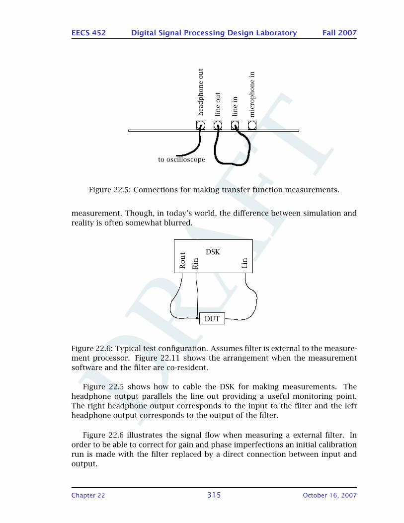
DRA
FT
EECS 452 Digital Signal Processing Design Laboratory Fall 2007
ãáÅêç
éÜçå
É=áå
äáåÉ=á
å
äáåÉ=ç
ìí
ÜÉ~Ç
éÜçå
É=çìí
íç=çëÅáääçëÅçéÉ
Figure 22.5: Connections for making transfer function measurements.
measurement. Though, in today’s world, the difference between simulation and
reality is often somewhat blurred.
arq
oçìí
oáå
iáå
aph
Figure 22.6: Typical test configuration. Assumes filter is external to the measure-
ment processor. Figure 22.11 shows the arrangement when the measurement
software and the filter are co-resident.
Figure 22.5 shows how to cable the DSK for making measurements. The
headphone output parallels the line out providing a useful monitoring point.
The right headphone output corresponds to the input to the filter and the left
headphone output corresponds to the output of the filter.
Figure 22.6 illustrates the signal flow when measuring a external filter. In
order to be able to correct for gain and phase imperfections an initial calibration
run is made with the filter replaced by a direct connection between input and
output.
Chapter 22 315 October 16, 2007
DRA
FT
EECS 452 Digital Signal Processing Design Laboratory Fall 2007
For the situation when the filter is co-resident with the measurement software
(see Figure 22.11) this is accomplished by simply not calling the filter code and
simply echoing the right input onto the left output. The TFMark2 program has
mode selectable from the keyboard to do this.
The TFMark2 program has four test configurations that can be selected from
the user console. These are
0 The filter transfer function measurement mode. Allows the user to select
which filter to use and generates a measurement file output.
1 A test to see if the DDS is running correctly. The DDS cosine output is
available on the right D/A output. The program also echoes the right A/D
input on the left D/A output.
2 A test to observe the DDS cosine on the right output and the DDS sine on
the left output.
3 Used when running the filters and not making a transfer function measure-
ment. The left input is filtered with the result being placed onto the left
output. The filter to be used is interactively selected using the console
input.
22.5 C5510
22.5.1 Prelab
Prelabs are to be done individually and are to be handed in at the
start of the lab period. Handwritten work will not be graded.
22.5.2 The IIR filter
Using MATLAB’s FDATool design three IIR filters meeting the following specifica-
tion:
• sample rate of 48000 Hz,
• low pass transfer function.
• ripple in the pass band limited to 0.1 dB,
• low pass cutoff frequency of 3100 Hz,
• transition region from 3100 Hz to 4000 Hz
• minimum attenuation in the stop band of 60 dB relative to the pass band.
The filter designs are to be of the following types:
• Chebyshev Type 1 IIR having even order,
Chapter 22 316 October 16, 2007
DRA
FT
EECS 452 Digital Signal Processing Design Laboratory Fall 2007
• Chebyshev Type 2 IIR having even order,
• Elliptic IIR having even order.
The MATLAB Chebyshev Type 1 and 2 filter designs might be of odd order. If
so, uncheck the “minimum order” box and enter the next largest even value for
the order. It is easier for us to work with even order filters than otherwise. When
specifying the filter order you will will need give some thought to the meaning of
the requested parameter values. By specifying a filter size greater than minimum
needed to meet the above needs you have the freedom to specify the parameter
of most interest and allow the filter to exceed the specification elsewhere. The
aspect most important to the filter design will vary depending on the filter type.
Export the designs to MAT files. I named mine, Cheby1, Cheby2, and
Elliptic. The current versions of MATLAB export the coefficients of second
order sections (SOS). The older versions of MATLAB export the numerator and
denominator polynomials of the overall transfer function.
Write a MATLAB script to read in your MAT files. It may be that your version
of MATLAB exported to SOS form. If not, use tf2sos to convert the full transfer
function coefficients to second-order-section (SOS) coefficients.
For each biquad section determine the 0 Hz gain. Normalize the numerator
values so that each section has unit gain at 0 Hz.
Each row of the SOS matrix contains the coefficients for a second order sec-
tion. The coefficients are ordered:
b0 b1 b2 1 a1 a2
To normalize the DC gain of a section to unity multiply the b values for that
section by
(1+a1+a2)/(b0+b1+b2)
This isn’t the most clever normalization but it will do for our purposes. Quite
often the 0 Hz gain is at a value corresponding to the ripple minimum. The effect
of our normalization will to cause the resulting filter to have ripple gain peaks
slightly greater than one.
Integerize the second order coefficient values by multiplying by 215 and round.
This puts them into integer values which can be interpreted as fractions in the
Q15 format. Some of the values may have magnitude greater than 32767. That’s
ok for now. When we move the values into to our test program they will be
placed into 32-bit long arrays. This avoids our having to deal with this situation
until later in our program.
Print, or more usefully, write the coefficient values to a memory stick or a
floppy disk. Order the scaled and integerized values in the order
b0,b1,b2,a1,a2
Chapter 22 317 October 16, 2007

DRA
FT
EECS 452 Digital Signal Processing Design Laboratory Fall 2007
Place each section’s five coefficient values on a single line. My MATLAB script used
fprintf(’%8d, %8d, %8d, %8d, %8d,\n’, ...Qmysos(idx, 1), Qmysos(idx,2), Qmysos(idx,3), Qmysos(idx,5), Qmysos(idx,6));
This format will greatly facilitate getting the coefficient values into the Code
Composer Studio based source code.
The source code for the DF2 example used in class has been placed onto
the EECS 452 handouts web page, myDF2IIR.asm. An edited version has also
been prepared for you. This is to serve as the starting point for your TDF2 filter
function, myTDF2IIR.asm. The location where your code will go has been iden-
tified with the comment “here be dragons”. Update the file’s history by adding a
comment at the start of the file indicating your name, date, and whatever.
The iircas5 and myDF2IIR functions make use of parallel operations. For
your DF2 code do not initially attempt to do this. Go for simple and get it right.
Later, if you wish, optimize.
The iircas5 and myDF2IIR functions each order the a and b coefficient val-
ues as necessary in order to optimize the code. That is, the order is determined
by the code not the reverse. You should also do so for your TDF2 SOS implemen-
tation. What is meant is that you should use the coefficient values in order that
is most natural when you write your code. The order needed will be described
to the FilterSetup function located in the FilterWrapper.c file.
The myTDF2IIR ordering will most likely differ from that used by the other
functions. The resulting order can be obtained with a simple modification of the
FilterSetup.c code.
For this part of the prelab:
• Turn in a list of integerized coefficient values for the Chebyshev types 1
and 2 and the elliptic filter designs designs. Don’t forget to identify which
is which.
It will be useful to have the values saved in a text file on a USB flash drive
or a floppy or be able to readily generate them in lab so they can be cut and
pasted.
• Turn in in a listing of your transposed direct form 2 inner loop assembly
language statements.
22.5.3 The sine/cosine oscillator
Simulate the operation of the sine/cosine oscillator in Figure 22.4 using MATLAB.
The starting values and coefficient values that you need can be determined
Chapter 22 318 October 16, 2007
DRA
FT
EECS 452 Digital Signal Processing Design Laboratory Fall 2007
by looking at the source code contained in this write-up. Produce a plot show-
ing the operation corresponding to approximately 8 cycles of the sine/cosine
waveforms. (You need to use the values found in the source code found in this
write-up to determine the expected output frequency. Divide this into the sam-
ple frequency to determine the number of samples per cycle.) Use the MATLAB
subplot format 2 rows and 1 column for the plots. Put the w1 output on the top
plot and the w2 output on the lower plot.
Label your plots. Note what the peak-to-peak values are for each waveform.
Modify your MATLAB script to simulate the saturation of values to the range
[−1,1]. Plot these as above. There will be a startup period when the oscillator is
not yet working. Determine where the oscillator has settled into normal opera-
tion. Use this region to determine the amplitudes of the w1 and w2 waveforms.
The ratio of these values will be useful in scaling the smaller level waveform in
your assembly language implementation.
It’s not part of the prelab but it would seem to be a good idea to figure out
how to complete the code given in Section 22.22 before coming to lab. This file
is available on the EECS 452 handouts web page. Hint: use saturating moves
when updating the two delay registers.
22.5.4 Measuring transfer functions
Write a MATLAB script that:
• Reads in a TFMark2 transfer function data set. This file is in ASCII with each
line representing a measurement at a frequency. The values on a given line
are:
– Frequency in Hz.
– R magnitude from the right channel input.
– R magnitude from the left channel input.
– Angle from the right channel input. Range is from minus one half
cycle (equal to -1) to plus one half cycle (equal to +1).
– Angle from the left channel input. Range as for the right channel input
value.
• Plots the relative gain in dB over the range -80 dB to 0 dB. Use subplot(3,1,1).
• Plots the relative angle in cycles. You have to convert values to radians,
unwrap, and then difference. Plot using subplot(3,1,2).
• Calculates the associated delay in terms of sample time counts (1/48000 =
1 count). Plot using subplot(3,1,3). Don’t forget to label your plots.
Chapter 22 319 October 16, 2007
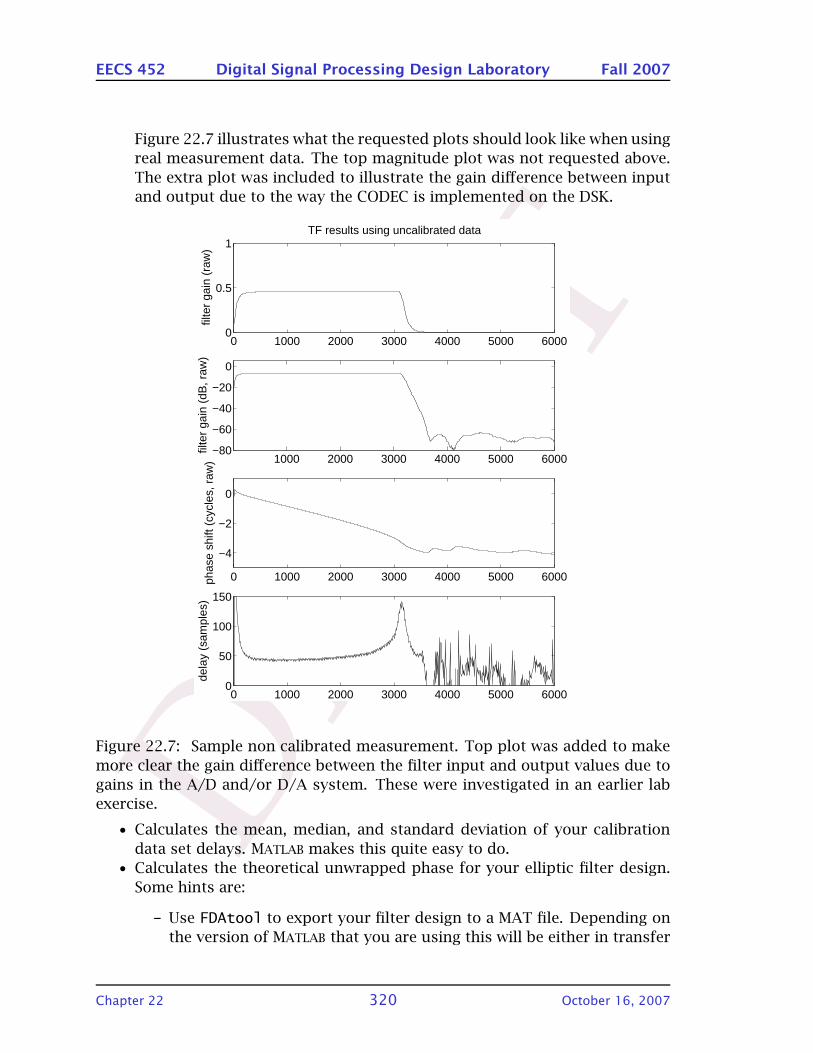
DRA
FT
EECS 452 Digital Signal Processing Design Laboratory Fall 2007
Figure 22.7 illustrates what the requested plots should look like when using
real measurement data. The top magnitude plot was not requested above.
The extra plot was included to illustrate the gain difference between input
and output due to the way the CODEC is implemented on the DSK.
0 1000 2000 3000 4000 5000 60000
0.5
1
filte
r ga
in (
raw
)
TF results using uncalibrated data
1000 2000 3000 4000 5000 6000−80
−60
−40
−20
0
filte
r ga
in (
dB, r
aw)
0 1000 2000 3000 4000 5000 6000
−4
−2
0
phas
e sh
ift (
cycl
es, r
aw)
0 1000 2000 3000 4000 5000 60000
50
100
150
dela
y (s
ampl
es)
Figure 22.7: Sample non calibrated measurement. Top plot was added to make
more clear the gain difference between the filter input and output values due to
gains in the A/D and/or D/A system. These were investigated in an earlier lab
exercise.
• Calculates the mean, median, and standard deviation of your calibration
data set delays. MATLAB makes this quite easy to do.
• Calculates the theoretical unwrapped phase for your elliptic filter design.
Some hints are:
– Use FDAtool to export your filter design to a MAT file. Depending on
the version of MATLAB that you are using this will be either in transfer
Chapter 22 320 October 16, 2007
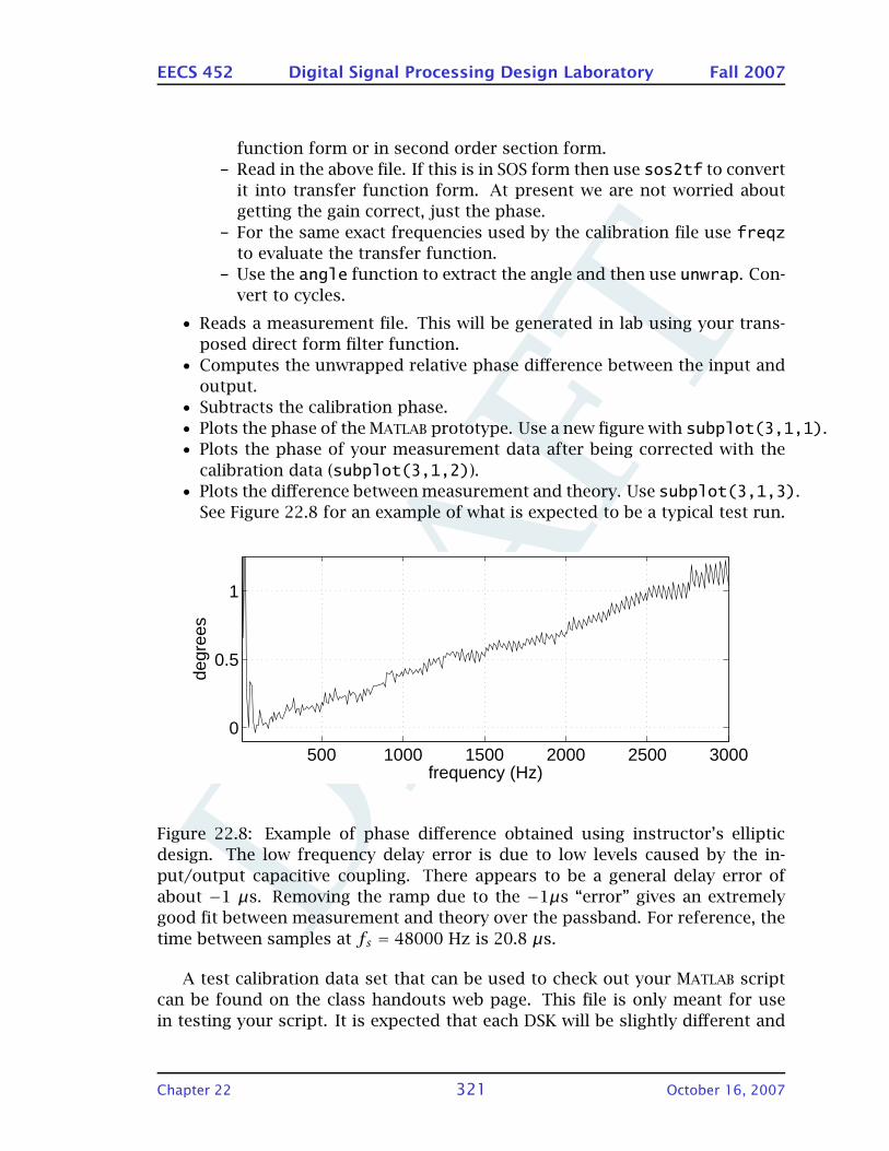
DRA
FT
EECS 452 Digital Signal Processing Design Laboratory Fall 2007
function form or in second order section form.
– Read in the above file. If this is in SOS form then use sos2tf to convert
it into transfer function form. At present we are not worried about
getting the gain correct, just the phase.
– For the same exact frequencies used by the calibration file use freqzto evaluate the transfer function.
– Use the angle function to extract the angle and then use unwrap. Con-
vert to cycles.
• Reads a measurement file. This will be generated in lab using your trans-
posed direct form filter function.
• Computes the unwrapped relative phase difference between the input and
output.
• Subtracts the calibration phase.
• Plots the phase of the MATLAB prototype. Use a new figure with subplot(3,1,1).
• Plots the phase of your measurement data after being corrected with the
calibration data (subplot(3,1,2)).
• Plots the difference between measurement and theory. Use subplot(3,1,3).
See Figure 22.8 for an example of what is expected to be a typical test run.
500 1000 1500 2000 2500 3000
0
0.5
1
degr
ees
frequency (Hz)
Figure 22.8: Example of phase difference obtained using instructor’s elliptic
design. The low frequency delay error is due to low levels caused by the in-
put/output capacitive coupling. There appears to be a general delay error of
about −1 µs. Removing the ramp due to the −1µs “error” gives an extremely
good fit between measurement and theory over the passband. For reference, the
time between samples at fs = 48000 Hz is 20.8 µs.
A test calibration data set that can be used to check out your MATLAB script
can be found on the class handouts web page. This file is only meant for use
in testing your script. It is expected that each DSK will be slightly different and
Chapter 22 321 October 16, 2007
DRA
FT
EECS 452 Digital Signal Processing Design Laboratory Fall 2007
that you will make a calibration run in lab for your particular system. It would
be interesting to see how much DSK to DSK variation exists.
22.5.5 Exercise
The basic concepts being explored in this lab exercise consist of:
• Implementation of a transposed direct form 2 biquad filter code. Includes
dealing with the range of the a1 and b1 coefficient vales, looking at the
effects of internal overflows (they really can occur).
• Comparison of the behavior of the TI IIRCAS5, the myIIRCAS5 code devel-
oped in lecture, and your TDF2 code.
• How well the Chebyshev 1, Chebyshev 2 and Elliptic designs perform.
• Basic concepts involved in making transfer function measurements.
• Implementation and testing of a quadrature recursive oscillator.
Note: when modifying your code for a particular test, such as removing sat-
uration, don’t forget to restore the code afterward. Guess what happens if you
don’t and come back later to make other tests.
22.5.6 The TDF2 biquad IIR cascade
The main activities consist of:
1. Implementing a TDF2 biquad IIR function (myTDF2IIR) using assembly lan-
guage.
2. Investigating overflow behavior of the two DF2 functions and your TDF2
function when implementing the elliptic filter design.
3. Using your MATLAB script to plot the transfer function of the elliptic filter
design using the myTDF2IIR function.
4. Measure “the” group delay of the elliptic IIR filter.
The FilterSetup function contained in FilterWrapper.c has provision for
mapping a second order section coefficient list from the
b0, b1, b2, a1, a2
Chapter 22 322 October 16, 2007
DRA
FT
EECS 452 Digital Signal Processing Design Laboratory Fall 2007
ordering to an arbitrary order. It should be clear from the listing how this is
done. Look at the support for the direct form functions iircas5 and myDF2IIR.
You will have to reorder the coefficient values in a similar manner for your ver-
sion of the myDFT2IIR function.
There will be problems with the a1 coefficient values, and possibly for the b1values for at least one of the IIR filter designs. There will be at least one value
having magnitude greater than 1.
This will be handled by modifying the TI iircas5 code to accept a value
of a1/2 and b1/2. This is your responsibility! You might consider adding a
masm instruction for one coefficient and macm instruction for the other. You will
have to pay particular attention to the addressing modes being used in the in-
structions you are augmenting. Your added instructions must not modify the
addresses being used by the existing instructions! If uncertain (and you prob-
ably will be), check the addressing mode descriptions in the TMS320C55x DSP
Mnemonic Instruction Set Reference Guide or in TMS320C55x DSP CPU Reference
Guide.
The myDF2IIR code was written with a1 and b1 scaling problem in mind and
assumes that a1/2 and b1/2 values are supplied in the call.
Similar unscaling instructions are to be incorporated into your myTDF2IIRfunction.
In the pre-lab you were asked to use MATLAB to generate sets of filter values
using Q15 format without regard to word size. These values will be placed into
long (32-bit) arrays. Where should be obvious by studying the FilterSetupcode. There is a specific array to be used by each of the three filter designs you
were asked to generate.
The division by 2 of the a1 and b1 values is done in the reordering process
supported in the FilterSetup code. The 32-bit long values are converted to 16
bit Q15 form in the reordering process. The a1 and b1 values are divided by 2
as part of the reordering.
A renamed and stripped down version of myDF2IIR.asm has been provided
for use as your myTDF2IIR starting point. All you need to do is to supply the
instructions needed in the inner loop. This file can also be found on the EECS
452 handouts web page and is present on the lab machines in the Lab6 directory.
This code does not require the data buffer to be aligned onto any particular
boundary. However, the db array in the test program needs to be aligned prop-
erly because it is shared by functions that do require it. This has been done for
you.
Chapter 22 323 October 16, 2007
DRA
FT
EECS 452 Digital Signal Processing Design Laboratory Fall 2007
Adding a single instruction inside the inner loop of the assembly language
FIR function has a significant effect on its execution time. However, for the IIR
filter functions there already are present a significant number of instructions in
the inner loop. The effect of adding one or two instructions is less severe.
The calling sequences of fir, iircas5, myDF2IIR, and myTDF2IIR are almost
compatible making it easy to switch between functions. In past DSPlib versions
the location of the nx parameter in the function calls was identical for the FIR
and IIR functions. For some reason TI decided this wasn’t necessary for the C55x
DSPlib.
The source files to be incorporated into the project (make) file for this week’s
laboratory exercise include:
• AIC23int_00.asm, interrupt support
• DisplayTest00.c, draws plot backgrounds
• draw_characters.c, PostScript character drawing.
• FilterWrapper.c, module with filter support
• fir.asm• iircas5.asm• intvec.asm, generic interrupt vector
• myatan2.asm• myDF2IIR.asm• myTDF2IIR.asm• no_isr.asm• setup_codec.c, initializes McBSP and AIC23 to run
• setup_McBSP_plot.c, sets up McBSP channel 0.
• TFMark2.c, the main program.
• XVGA.c,
The run time support library and a linker command file will be needed as
well. The TFMark2 program uses the small memory model.
Because we are supplying our own interrupt vector there is the potential of
a conflict at build time with the interrupt vector contained in the RTS library.
When this happens the error message
error: can’t allocate vectors
will result.
The work around is to use the compiler’s option to specify the link order.
Simply select all the modules and add them to the link list. Then drag and drop
the RTS library so that it is last on the list.
Chapter 22 324 October 16, 2007
DRA
FT
EECS 452 Digital Signal Processing Design Laboratory Fall 2007
The FilterSetup function in FilterWrapper.c is interactive. The filter se-
lection can be easily changed by stopping the program, reloading and restarting.
Be careful when setting the A/D input levels so as to not over drive the DSK
analog input. The input level to the DF2 filter functions needs to be reduced
by a significant factor relative to the largest safe usable input level for TDF2 in
order to insure proper operation (no overflow). To help in establishing the input
level the FilterSetup program provides a pass through mode sending samples
directly from the A/D input to the D/A output.
The filter support code puts the filtered output onto the left D/A channel
(white cable) and echoes the input samples onto the right D/A channel (red
cable). These can be readily monitored by connecting the scope to the DSK’s
headphone output.
This version of the transfer function program has four user selectable modes:
0 The normal measurement mode. A jumper cable is used to connect the line
out to the line in. The DDS output is placed on the right channel output.
The right channel input goes to the selected filter. The filter output is
placed onto the left channel output. This then goes to the left channel
input. This arrangement allows the A/D and D/A support circuitry and
delays to be calibrated out of the measurement data.
1 The right line input is echoed onto the left line output. The DDS is still
present on the right line output.
2 The DDS cosine output is present on the right line output. The DDS sine
output is present on the left line output.
3 The DDS output is present on the right line output. The left line input
connects to the filter input. The filter output goes to the left line output.
This allows using an external oscillator to check filter operation.
It is very helpful to monitor the program outputs on an oscilloscope using
the headphone jack. The headphone outputs essentially parallel the line output
signals. Most cable problems (generally opens) are very apparent if one monitors
the D/A output levels.
As the first step in the lab exercise use TFMark2 mode 0 with the no-filter
filtering sub mode to obtain a data set for use in calibrating the system when a
filter is not present. The line outputs have to be connected to the line inputs for
this measurement. Use a shift amount of 0.
Chapter 22 325 October 16, 2007

DRA
FT
EECS 452 Digital Signal Processing Design Laboratory Fall 2007
The default file name is tfmeas and will be located in the debug subdirectory.
Move this file into your working directory and rename it calibration. This is a
text file and can be inspected to make sure all went well with the measurement.
Of the three filter types being implemented in this exercise the elliptic is
the most robust followed by the Chebyshev 2 and then the Chebyshev 1. It
is recommended that you use the elliptic coefficients when initially testing and
debugging your TDF2 function.
For the Elliptic filter design:
0 0.5 1 1.5 2
x 104
0
10
20
mag
nitu
de
frequency (Hz)
elliptic DF2 max of internal TF magnitudes
max: 25.775
Figure 22.9: DF2 elliptic filter maximums of filter input to delay stage outputs.
Note that the frequency axis is in units of 104 Hz.
0 0.5 1 1.5 2
x 104
0
0.5
1
mag
nitu
de
frequency (Hz)
elliptic TDF2 max of internal TF magnitudes
max: 0.979
Figure 22.10: TDF2 elliptic filter maximums of filter input to delay stage outputs.
Note that the frequency axis is in units of 104 Hz.
Recall,
Chapter 22 326 October 16, 2007
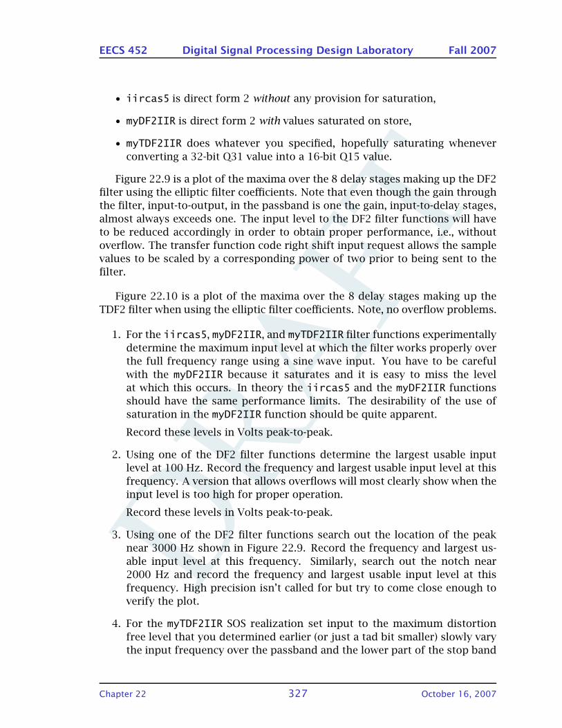
DRA
FT
EECS 452 Digital Signal Processing Design Laboratory Fall 2007
• iircas5 is direct form 2 without any provision for saturation,
• myDF2IIR is direct form 2 with values saturated on store,
• myTDF2IIR does whatever you specified, hopefully saturating whenever
converting a 32-bit Q31 value into a 16-bit Q15 value.
Figure 22.9 is a plot of the maxima over the 8 delay stages making up the DF2
filter using the elliptic filter coefficients. Note that even though the gain through
the filter, input-to-output, in the passband is one the gain, input-to-delay stages,
almost always exceeds one. The input level to the DF2 filter functions will have
to be reduced accordingly in order to obtain proper performance, i.e., without
overflow. The transfer function code right shift input request allows the sample
values to be scaled by a corresponding power of two prior to being sent to the
filter.
Figure 22.10 is a plot of the maxima over the 8 delay stages making up the
TDF2 filter when using the elliptic filter coefficients. Note, no overflow problems.
1. For the iircas5, myDF2IIR, and myTDF2IIR filter functions experimentally
determine the maximum input level at which the filter works properly over
the full frequency range using a sine wave input. You have to be careful
with the myDF2IIR because it saturates and it is easy to miss the level
at which this occurs. In theory the iircas5 and the myDF2IIR functions
should have the same performance limits. The desirability of the use of
saturation in the myDF2IIR function should be quite apparent.
Record these levels in Volts peak-to-peak.
2. Using one of the DF2 filter functions determine the largest usable input
level at 100 Hz. Record the frequency and largest usable input level at this
frequency. A version that allows overflows will most clearly show when the
input level is too high for proper operation.
Record these levels in Volts peak-to-peak.
3. Using one of the DF2 filter functions search out the location of the peak
near 3000 Hz shown in Figure 22.9. Record the frequency and largest us-
able input level at this frequency. Similarly, search out the notch near
2000 Hz and record the frequency and largest usable input level at this
frequency. High precision isn’t called for but try to come close enough to
verify the plot.
4. For the myTDF2IIR SOS realization set input to the maximum distortion
free level that you determined earlier (or just a tad bit smaller) slowly vary
the input frequency over the passband and the lower part of the stop band
Chapter 22 327 October 16, 2007
DRA
FT
EECS 452 Digital Signal Processing Design Laboratory Fall 2007
and determine the range of frequencies (if any) at which the filter output
distorts. There should not be any distortion over the filter operating band.
If there is it may be necessary to reduce the input level slightly. If the
distortion continues to exist there is a problem.
Even though the TDF2, at least nominally, works at all frequencies with-
out distortion using a sine input this does not mean that it will not have
distortion caused by internal overflow when using other waveforms.
The Fourier series for a unit amplitude square wave has a fundamental
having amplitude of 4/π . Using such an input it is, in effect, possible to
overdrive the filter with an input that has maximum peak value near unity.
Use a square wave having the same peak-to-peak range as the sine wave
used above and investigate (and report on the results) whether or not the
TDF2 filter indeed shows the effects of overflow over its passband. See
if you can determine the relation between the maximum safe level square
wave and the maximum safe level sine wave amplitudes? Try to character-
ize the overflow caused distortion for each of the four configurations being
considered. Some will be more acceptable than others. Sketches would be
of use here.
A way to help yourself to better see when there is an overflow is to remove
the saturate statements in your code. This should make it more apparent
when the filter experiencing an overflow situation.
5. Use the profiler and record the execution time of the iircas5, myDF2IIR,
and myTDF2IIR functions for the elliptic design. In your report comment
on the differences.
6. Acquire data to allow you to determine the transfer function of the elliptic
TDF2 IIR filter. Use TFMark2 mode 0 to make the measurement.
For the Chebyshev type 1 filter design:
• Run TFMark2 mode 3 using the Chebyshev type 1 for the myDF2IIR and
myTDF2IIR SOS filter types.
What we want to do is examine the behavior of the two filter types when
implementing our Chebyshev type 1 filter. Does one implementation work
better than the other (what is better?). Is there a significant operational
difference at low, medium or high input levels?
Operate the two filter types at varying input amplitudes and frequencies
and notice how the behavior seems to change. Comment on what you ob-
serve.
Chapter 22 328 October 16, 2007
DRA
FT
EECS 452 Digital Signal Processing Design Laboratory Fall 2007
For the Chebyshev type 2 filter design:
• Using one of the DF2 SOS filter functions determine the input level at which
the filter works properly over it’s passband and a bit into the stop band.
Record this level in volts peak-to-peak.
• For our TDF2 SOS realization repeat the above. It might be useful to remove
the saturation operation in order to see more clearly when saturation oc-
curs.
• Experiment a bit with the input levels for the DF2 and TDF2 designs and
sweep the test frequency over the pass band and a little into the stop band.
Are there any significant problems or artifacts that are observed?
The design and implementation of FIR and IIR filters is a basic bread-and-
butter task for the DSP professional. This exercise and the previous one (FIR)
provided experience in this task. Even though it looks like we have run through
a large number of situations we have only scratched the surface of the topic.
Key considerations involved in implementing an IIR filter are:
• Choice of filter transfer function.
• Filter topology.
• How the arithmetic is performed.
Given a simple lowpass filter specification MATLAB provided us with three vi-
able choices for a transfer function. Lacking any additional constraints the ellip-
tic transfer function appears to have provided the least complex implementation
and the best performance.
There are an infinite number of ways in which a given transfer function can be
implemented. We want one that works and works well. The DF2 is probably the
most commonly implemented form. We found that the transposed form is more
likely to work better. What is the cost in program complexity and is it worth it?
The answers appear to be not much more and yes. However, it should be noted
that there were places in the TDF2 code where word size was reduced from 32-
bits to 16-bits opening avenues for quantization noise to enter the system. We
have may paid a price in noise performance for our robust operation. At this
point we really don’t know. A complete analysis would be a good topic for a
more advanced course.
Note that the iircas5 library function makes full use of the guard bits but
neglects to saturate the results of the computations. The function returns a flag
indicating whether or not an overflow has occurred. Generally this information
is received too late to be very useful.
Chapter 22 329 October 16, 2007
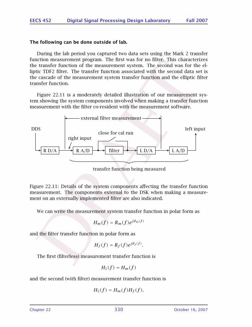
DRA
FT
EECS 452 Digital Signal Processing Design Laboratory Fall 2007
The following can be done outside of lab.
During the lab period you captured two data sets using the Mark 2 transfer
function measurement program. The first was for no filter. This characterizes
the transfer function of the measurement system. The second was for the el-
liptic TDF2 filter. The transfer function associated with the second data set is
the cascade of the measurement system transfer function and the elliptic filter
transfer function.
Figure 22.11 is a moderately detailed illustration of our measurement sys-
tem showing the system components involved when making a transfer function
measurement with the filter co-resident with the measurement software.
o=aL^ o=^La ÑáäíÉê i=aL^ i=^La
aapêáÖÜí=áåéìí
äÉÑí=áåéìíÅäçëÉ=Ñçê=Å~ä=êìå
íê~åëÑÉê=ÑìåÅíáçå=ÄÉáåÖ=ãÉ~ëìêÉÇ
ÉñíÉêå~ä=ÑáäíÉê=ãÉ~ëìêÉãÉåí
Figure 22.11: Details of the system components affecting the transfer function
measurement. The components external to the DSK when making a measure-
ment on an externally implemented filter are also indicated.
We can write the measurement system transfer function in polar form as
Hm(f ) = Rm(f )ejθm(f )
and the filter transfer function in polar form as
Hf (f ) = Rf (f )ejθf (f ).
The first (filterless) measurement transfer function is
H1(f ) = Hm(f )
and the second (with filter) measurement transfer function is
H2(f ) = Hm(f )Hf (f ).
Chapter 22 330 October 16, 2007

DRA
FT
EECS 452 Digital Signal Processing Design Laboratory Fall 2007
Clearly
Hf (f ) =H2(f )
H1(f )=R2(f )
R1(f )ej[θ2(f )−θ1(f )] .
Using your data compute Hf (F). Use the program that you wrote for the
prelab to plotHf (f )magnitudes, phase and delay. Also plot the phase difference
between the computed Hf (f ) and the values predicted by calculation of the
transfer function using MATLAB.
As part of your report include:
• Include the listing of your working assembler TDF2 filter code.
• Include transfer function plots that you made
• Comment on the performances of the DF2 and TDF2 filters. This might
include:
– How their operation is affected by the addition of saturation when
saving the accumulator contents into a 16-bit word.
– Which one would you choose for an application and why?
• Include any waveform sketches that you might have made.
• Compare this week’s IIR and last week’s FIR timings. Did the IIR filter
execute significantly faster or slower that the equivalent FIR filter?
• Include the results and calculations for the measurements (and MATLAB
calculations) for the Elliptic filter.
With the possible exception of overflow effects there should be no difference
between the DF2 and TDF2 IIR filter transfer functions.
22.5.7 Sine/Cosine oscillator
Using the starter code given in Section 22.22 add the instructions required to
implement the recursive sine/cosine oscillator shown in Figure 22.4 . Focus get-
ting your code correct. Optimization in the form of parallel instructions and the
like can be done later, if you like, once your program works. The code in Section
22.22 and 22.3 differ in where the delay stage contents are located. In Figure
22.3 the delay stages, w_1 and w_2 are implemented in temporary registers. In
Section 22.22 the delay stages are implemented in data memory. Data memory
is addressed differently. For example, to multiply the contents of w_1 by the
cosine constant placing the product into ac0 one would write
mpy *(#w_1),#cosine,ac0
Chapter 22 331 October 16, 2007
DRA
FT
EECS 452 Digital Signal Processing Design Laboratory Fall 2007
Q15 scaling is to be used. It should be apparent how to implement multipli-
cation by 1+ cosθ (which in general does not fit into 16-bit Q15 form). Hint: use
the fact that multiplication is distributive over addition.
The symbol cosine in the given code corresponds to cosθ.
Run your oscillator. The value supplied for cosine is the same value as
alpha used in generating a 1000 Hz waveform by the simple oscillator in Figure
22.2. Do you get the same frequency?
The outputs from the two stages have different amplitudes. One essentially
swings between ±1 and the other has a significantly smaller swing. Modify your
code to scale the smaller value prior to displaying it. Scale it to be as large as
possible without distorting. Use your MATLAB simulation results to set the scale
factor. You likely will need represent the scale factor using Q11. The oscillator
stage values are Q15. With the frct bit set the results of multiply instructions
are shifted left one bit position. Thus multiplying a Q15 value by a Q11 value
results in a Q(26+1) value. How does one put this back into Q15 before sending
it to the D/A?
Remove the saturate statements that are being used to keep the oscillator
stable. Note what happens to the waveforms.
22.5.8 Report
Beyond what was requested above, basically report on what you did, how you did
it, and what the results were. Include supporting documentation such as plots,
program listings, etc. Give the grader something on which to judge the quality
of your work. Insightful observations and discussion are a definite plus.
Include listings of your programs.
22.6 S3SB
We have/had good intentions, however . . .
22.6.1 Prelab
22.6.2 Exercise
22.6.3 Report
22.7 DSPlib IIRCAS5 manual pages
See Figures 22.12, 22.13 for the DSPlib IIRCAS5 documentation.
Chapter 22 332 October 16, 2007
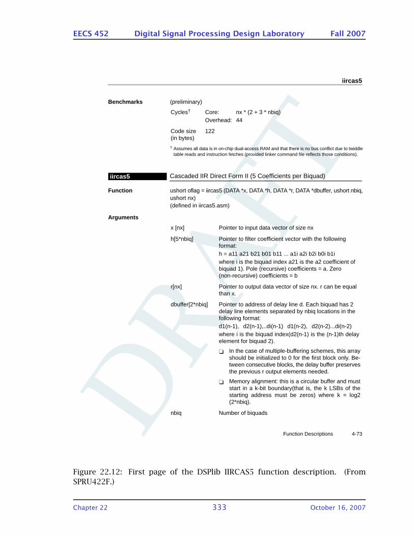
DRA
FT
EECS 452 Digital Signal Processing Design Laboratory Fall 2007
iircas5
4-73 Function Descriptions
Benchmarks (preliminary)
Cycles† Core: nx * (2 + 3 * nbiq)Overhead: 44
Code size(in bytes)
122
† Assumes all data is in on-chip dual-access RAM and that there is no bus conflict due to twiddletable reads and instruction fetches (provided linker command file reflects those conditions).
Cascaded IIR Direct Form II (5 Coefficients per Biquad)iircas5
Function ushort oflag = iircas5 (DATA *x, DATA *h, DATA *r, DATA *dbuffer, ushort nbiq,ushort nx)(defined in iircas5.asm)
Arguments
x [nx] Pointer to input data vector of size nx
h[5*nbiq] Pointer to filter coefficient vector with the followingformat:h = a11 a21 b21 b01 b11 ... a1i a2i b2i b0i b1iwhere i is the biquad index a21 is the a2 coefficient ofbiquad 1). Pole (recursive) coefficients = a. Zero(non-recursive) coefficients = b
r[nx] Pointer to output data vector of size nx. r can be equalthan x.
dbuffer[2*nbiq] Pointer to address of delay line d. Each biquad has 2delay line elements separated by nbiq locations in thefollowing format:d1(n-1), d2(n-1),..di(n-1) d1(n-2), d2(n-2)...di(n-2)where i is the biquad index(d2(n-1) is the (n-1)th delayelement for biquad 2).
In the case of multiple-buffering schemes, this arrayshould be initialized to 0 for the first block only. Be-tween consecutive blocks, the delay buffer preservesthe previous r output elements needed.
Memory alignment: this is a circular buffer and muststart in a k-bit boundary(that is, the k LSBs of thestarting address must be zeros) where k = log2(2*nbiq).
nbiq Number of biquads
Figure 22.12: First page of the DSPlib IIRCAS5 function description. (From
SPRU422F.)
Chapter 22 333 October 16, 2007
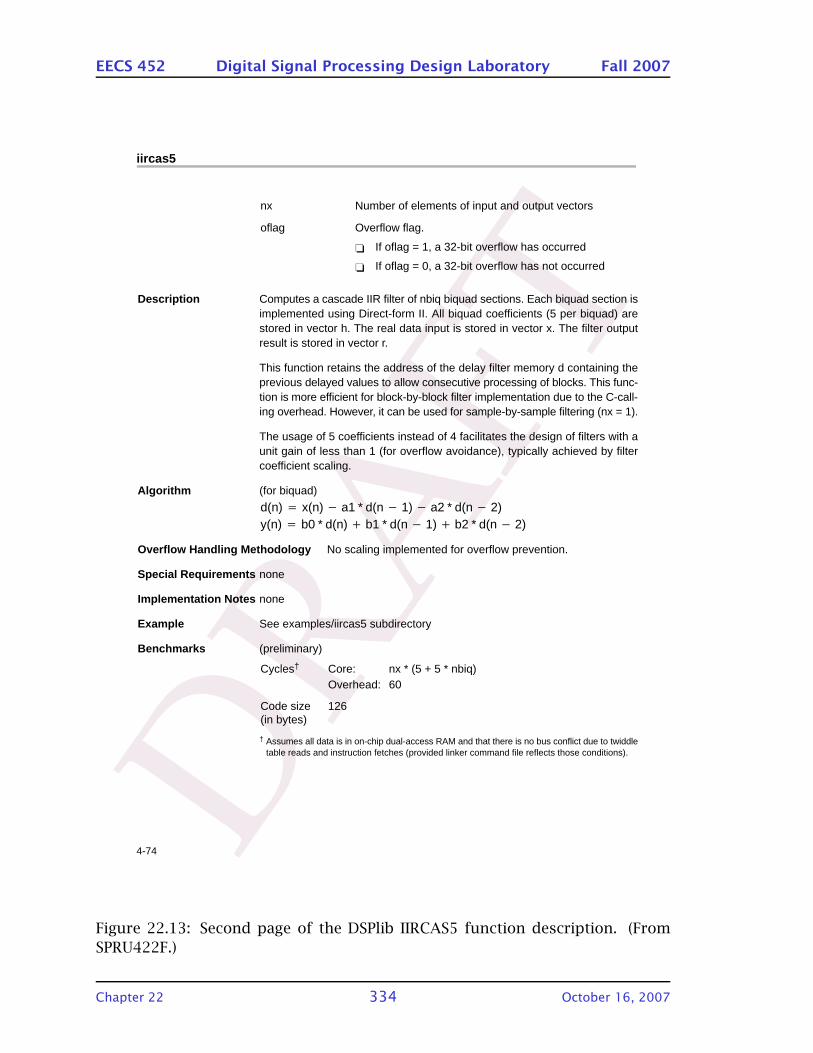
DRA
FT
EECS 452 Digital Signal Processing Design Laboratory Fall 2007
iircas5
4-74
nx Number of elements of input and output vectors
oflag Overflow flag.
If oflag = 1, a 32-bit overflow has occurred
If oflag = 0, a 32-bit overflow has not occurred
Description Computes a cascade IIR filter of nbiq biquad sections. Each biquad section isimplemented using Direct-form II. All biquad coefficients (5 per biquad) arestored in vector h. The real data input is stored in vector x. The filter outputresult is stored in vector r.
This function retains the address of the delay filter memory d containing theprevious delayed values to allow consecutive processing of blocks. This func-tion is more efficient for block-by-block filter implementation due to the C-call-ing overhead. However, it can be used for sample-by-sample filtering (nx = 1).
The usage of 5 coefficients instead of 4 facilitates the design of filters with aunit gain of less than 1 (for overflow avoidance), typically achieved by filtercoefficient scaling.
Algorithm (for biquad)
d(n) x(n) a1 * d(n 1) a2 * d(n 2)y(n) b0 * d(n) b1 * d(n 1) b2 * d(n 2)
Overflow Handling Methodology No scaling implemented for overflow prevention.
Special Requirements none
Implementation Notes none
Example See examples/iircas5 subdirectory
Benchmarks (preliminary)
Cycles† Core: nx * (5 + 5 * nbiq)Overhead: 60
Code size(in bytes)
126
† Assumes all data is in on-chip dual-access RAM and that there is no bus conflict due to twiddletable reads and instruction fetches (provided linker command file reflects those conditions).
Figure 22.13: Second page of the DSPlib IIRCAS5 function description. (From
SPRU422F.)
Chapter 22 334 October 16, 2007

DRA
FT
EECS 452 Digital Signal Processing Design Laboratory Fall 2007
22.8 List of codes
22.9 IIR Transfer function Mark 2
/* File name: TFMark2.c
Test studies for the transfer function measurment program.
12Feb2004 .. initial version (TFMark1) .. K.M29Feb2004 .. modified for lab 6 .. KM13Oct2007 .. XVGA display added .. KM14Oct2007 .. PostScript output added .. KM
*/
#include <stdio.h>#include <math.h>#include "../../TI_support/McBSP_452.h"
//**********************************
#define FTV_CNT 33#define FOREVER 1#define FS 48000
//**********************************
char myID[] = "TFMark2(14Oct07) ";
char label[100] = "";unsigned long ComputeFTV(unsigned long, unsigned long);void display_initialize(void);void plot_dB_init(int, float, float, float, float, float, float, float, float);void plot_angle_init(int, float, float, float, float, float, float, float, float);void GoToData(int, float, float);void DrawToData(int, int, float, float);void display_close(void);
// interrupt support definitions
extern unsigned long ftv;extern volatile int AIC_LeftIn, AIC_RightIn, AIC_LeftOut, AIC_RightOut;extern volatile int Icos, Qsin, AIC_flag;
char str_shift[]="shift ";
unsigned long fs = FS;
double pi=3.14159265;unsigned long ac;
Chapter 22 335 October 16, 2007
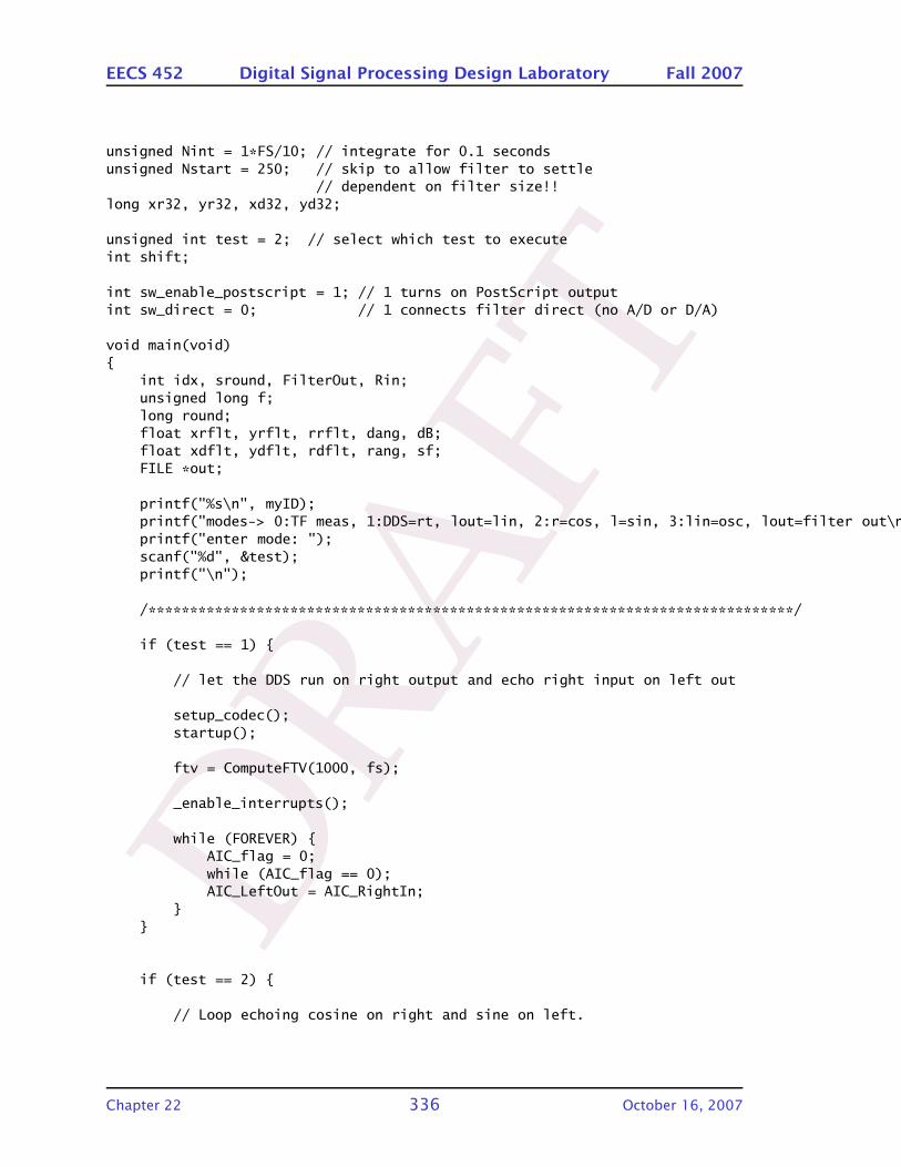
DRA
FT
EECS 452 Digital Signal Processing Design Laboratory Fall 2007
unsigned Nint = 1*FS/10; // integrate for 0.1 secondsunsigned Nstart = 250; // skip to allow filter to settle
// dependent on filter size!!long xr32, yr32, xd32, yd32;
unsigned int test = 2; // select which test to executeint shift;
int sw_enable_postscript = 1; // 1 turns on PostScript outputint sw_direct = 0; // 1 connects filter direct (no A/D or D/A)
void main(void)
int idx, sround, FilterOut, Rin;unsigned long f;long round;float xrflt, yrflt, rrflt, dang, dB;float xdflt, ydflt, rdflt, rang, sf;FILE *out;
printf("%s\n", myID);printf("modes-> 0:TF meas, 1:DDS=rt, lout=lin, 2:r=cos, l=sin, 3:lin=osc, lout=filter out\n");printf("enter mode: ");scanf("%d", &test);printf("\n");
/*****************************************************************************/
if (test == 1)
// let the DDS run on right output and echo right input on left out
setup_codec();startup();
ftv = ComputeFTV(1000, fs);
_enable_interrupts();
while (FOREVER) AIC_flag = 0;while (AIC_flag == 0);AIC_LeftOut = AIC_RightIn;
if (test == 2)
// Loop echoing cosine on right and sine on left.
Chapter 22 336 October 16, 2007
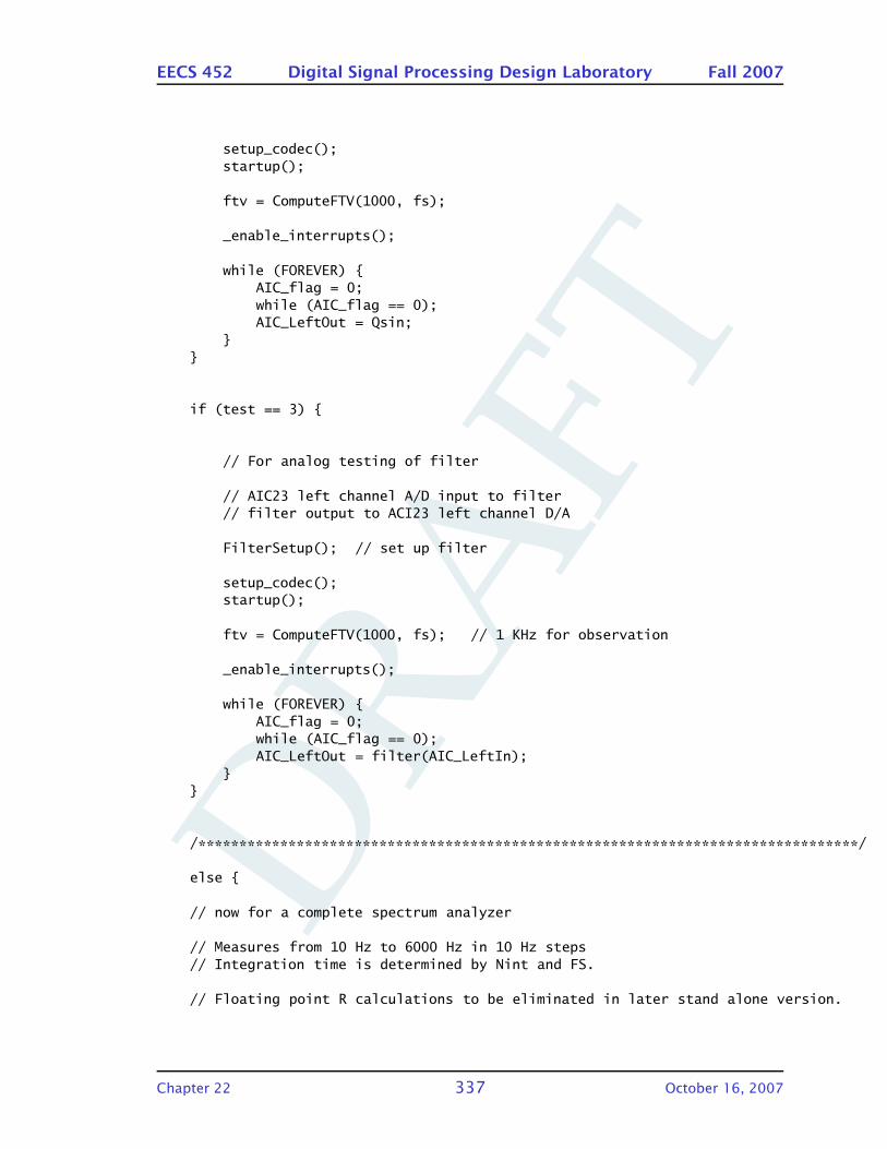
DRA
FT
EECS 452 Digital Signal Processing Design Laboratory Fall 2007
setup_codec();startup();
ftv = ComputeFTV(1000, fs);
_enable_interrupts();
while (FOREVER) AIC_flag = 0;while (AIC_flag == 0);AIC_LeftOut = Qsin;
if (test == 3)
// For analog testing of filter
// AIC23 left channel A/D input to filter// filter output to ACI23 left channel D/A
FilterSetup(); // set up filter
setup_codec();startup();
ftv = ComputeFTV(1000, fs); // 1 KHz for observation
_enable_interrupts();
while (FOREVER) AIC_flag = 0;while (AIC_flag == 0);AIC_LeftOut = filter(AIC_LeftIn);
/********************************************************************************/
else
// now for a complete spectrum analyzer
// Measures from 10 Hz to 6000 Hz in 10 Hz steps// Integration time is determined by Nint and FS.
// Floating point R calculations to be eliminated in later stand alone version.
Chapter 22 337 October 16, 2007
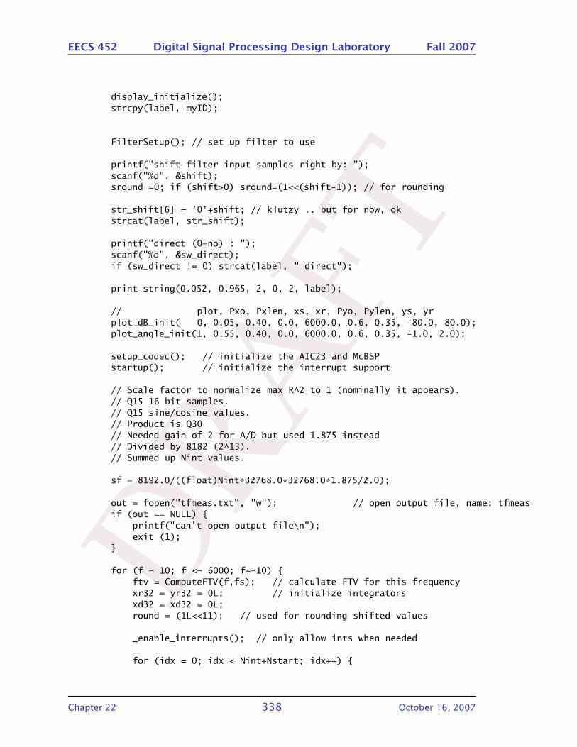
DRA
FT
EECS 452 Digital Signal Processing Design Laboratory Fall 2007
display_initialize();strcpy(label, myID);
FilterSetup(); // set up filter to use
printf("shift filter input samples right by: ");scanf("%d", &shift);sround =0; if (shift>0) sround=(1<<(shift-1)); // for rounding
str_shift[6] = ’0’+shift; // klutzy .. but for now, okstrcat(label, str_shift);
printf("direct (0=no) : ");scanf("%d", &sw_direct);if (sw_direct != 0) strcat(label, " direct");
print_string(0.052, 0.965, 2, 0, 2, label);
// plot, Pxo, Pxlen, xs, xr, Pyo, Pylen, ys, yrplot_dB_init( 0, 0.05, 0.40, 0.0, 6000.0, 0.6, 0.35, -80.0, 80.0);plot_angle_init(1, 0.55, 0.40, 0.0, 6000.0, 0.6, 0.35, -1.0, 2.0);
setup_codec(); // initialize the AIC23 and McBSPstartup(); // initialize the interrupt support
// Scale factor to normalize max R^2 to 1 (nominally it appears).// Q15 16 bit samples.// Q15 sine/cosine values.// Product is Q30// Needed gain of 2 for A/D but used 1.875 instead// Divided by 8182 (2^13).// Summed up Nint values.
sf = 8192.0/((float)Nint*32768.0*32768.0*1.875/2.0);
out = fopen("tfmeas.txt", "w"); // open output file, name: tfmeasif (out == NULL)
printf("can’t open output file\n");exit (1);
for (f = 10; f <= 6000; f+=10) ftv = ComputeFTV(f,fs); // calculate FTV for this frequencyxr32 = yr32 = 0L; // initialize integratorsxd32 = xd32 = 0L;round = (1L<<11); // used for rounding shifted values
_enable_interrupts(); // only allow ints when needed
for (idx = 0; idx < Nint+Nstart; idx++)
Chapter 22 338 October 16, 2007
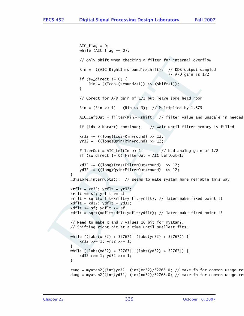
DRA
FT
EECS 452 Digital Signal Processing Design Laboratory Fall 2007
AIC_flag = 0;while (AIC_flag == 0);
// only shift when checking a filter for internal overflow
Rin = ((AIC_RightIn+sround)>>shift); // DDS output sampled// A/D gain is 1/2
if (sw_direct != 0) Rin = ((Icos+(sround<<1)) >> (shift+1));
// Corect for A/D gain of 1/2 but leave some head room
Rin = (Rin << 1) - (Rin >> 3); // Multiplied by 1.875
AIC_LeftOut = filter(Rin)<<shift; // filter value and unscale in needed
if (idx < Nstart) continue; // wait until filter memory is filled
xr32 += ((long)Icos*Rin+round) >> 12;yr32 -= ((long)Qsin*Rin+round) >> 12;
FilterOut = AIC_LeftIn << 1; // had analog gain of 1/2if (sw_direct != 0) FilterOut = AIC_LeftOut+1;
xd32 += ((long)Icos*FilterOut+round) >> 12;yd32 -= ((long)Qsin*FilterOut+round) >> 12;
_disable_interrupts(); // seems to make system more reliable this way
xrflt = xr32; yrflt = yr32;xrflt *= sf; yrflt *= sf;rrflt = sqrt(xrflt*xrflt+yrflt*yrflt); // later make fixed point!!!xdflt = xd32; ydflt = yd32;xdflt *= sf; ydflt *= sf;rdflt = sqrt(xdflt*xdflt+ydflt*ydflt); // later make fixed point!!!
// Need to make x and y values 16 bit for myatan2.// Shifting right bit at a time until smallest fits.
while ((labs(xr32) > 32767)||(labs(yr32) > 32767)) xr32 >>= 1; yr32 >>= 1;
while ((labs(xd32) > 32767)||(labs(yd32) > 32767))
xd32 >>= 1; yd32 >>= 1;
rang = myatan2((int)yr32, (int)xr32)/32768.0; // make fp for common usage testingdang = myatan2((int)yd32, (int)xd32)/32768.0; // make fp for common usage testing
Chapter 22 339 October 16, 2007
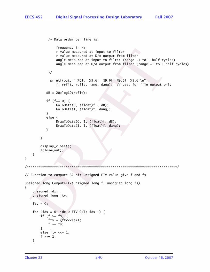
DRA
FT
EECS 452 Digital Signal Processing Design Laboratory Fall 2007
/* Data order per line is:
frequency in Hzr value measured at input to filterr value measured at D/A output from filterangle measured at input to filter (range -1 to 1 half cycles)angle measured at D/A output from filter (range -1 to 1 half cycles)
*/
fprintf(out, " %6lu %9.6f %9.6f %9.6f %9.6f\n",f, rrflt, rdflt, rang, dang); // used for file output only
dB = 20*log10(rdflt);
if (f==10) GoToData(0, (float)f , dB);GoToData(1, (float)f, dang);
else
DrawToData(0, 1, (float)f, dB);DrawToData(1, 1, (float)f, dang);
display_close();fclose(out);
/*****************************************************************************/
// Function to compute 32 bit unsigned FTV value give f and fs
unsigned long ComputeFTV(unsigned long f, unsigned long fs)
unsigned idx;unsigned long ftv;
ftv = 0;
for (idx = 0; idx < FTV_CNT; idx++) if (f >= fs)
ftv = (ftv<<1)+1;f -= fs;
else ftv <<= 1;f <<= 1;
Chapter 22 340 October 16, 2007
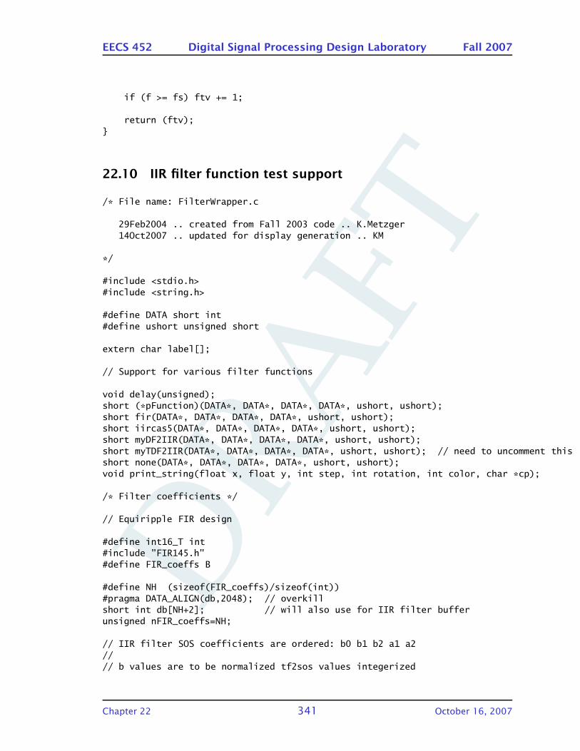
DRA
FT
EECS 452 Digital Signal Processing Design Laboratory Fall 2007
if (f >= fs) ftv += 1;
return (ftv);
22.10 IIR filter function test support
/* File name: FilterWrapper.c
29Feb2004 .. created from Fall 2003 code .. K.Metzger14Oct2007 .. updated for display generation .. KM
*/
#include <stdio.h>#include <string.h>
#define DATA short int#define ushort unsigned short
extern char label[];
// Support for various filter functions
void delay(unsigned);short (*pFunction)(DATA*, DATA*, DATA*, DATA*, ushort, ushort);short fir(DATA*, DATA*, DATA*, DATA*, ushort, ushort);short iircas5(DATA*, DATA*, DATA*, DATA*, ushort, ushort);short myDF2IIR(DATA*, DATA*, DATA*, DATA*, ushort, ushort);short myTDF2IIR(DATA*, DATA*, DATA*, DATA*, ushort, ushort); // need to uncomment thisshort none(DATA*, DATA*, DATA*, DATA*, ushort, ushort);void print_string(float x, float y, int step, int rotation, int color, char *cp);
/* Filter coefficients */
// Equiripple FIR design
#define int16_T int#include "FIR145.h"#define FIR_coeffs B
#define NH (sizeof(FIR_coeffs)/sizeof(int))#pragma DATA_ALIGN(db,2048); // overkillshort int db[NH+2]; // will also use for IIR filter bufferunsigned nFIR_coeffs=NH;
// IIR filter SOS coefficients are ordered: b0 b1 b2 a1 a2//// b values are to be normalized tf2sos values integerized
Chapter 22 341 October 16, 2007

DRA
FT
EECS 452 Digital Signal Processing Design Laboratory Fall 2007
// after multiplying by 2^15.//// a values are to be tf2sos values integerized after// multiplying by 2^15. Except does not include the a0 values.//// Sections are ordered from input to output.
// define names for the IIR SOS coefficient column positions
#define b0 0#define b1 1#define b2 2#define a1 3#define a2 4
// Chebyshev 1 IIR design .. your values go here!
long C1_coeffs[] =;
unsigned nC1_coeffs = (sizeof(C1_coeffs)/sizeof(long));
// Chebyshev 2 IIR design .. your values go here!
long C2_coeffs[] = ;
unsigned nC2_coeffs = (sizeof(C2_coeffs)/sizeof(long));
// Elliptic IIR design .. your values go here!
long El_coeffs[] = // 1481, 2581, 1481, -45021, 17796, // test values using the// 8147, 5622, 8147, -33995, 23142, // FDAtool default design// 17616, 1500, 17616, -24248, 28212, // parameters and elliptic// 23728, -3146, 23728, -19933, 31474 // your elliptic goes here;
unsigned nEl_coeffs = (sizeof(El_coeffs)/sizeof(long));
short int *ptr_coeffs;short int coeffs[5*24]; // to hold IIR coeffs...make sure correct size or larger !!!!short int FilterType;
ushort nSections;
void FilterSetup(void)
int IIRtype, TFtype, idx;long* sections;
Chapter 22 342 October 16, 2007
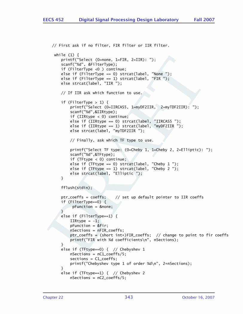
DRA
FT
EECS 452 Digital Signal Processing Design Laboratory Fall 2007
// First ask if no filter, FIR filter or IIR filter.
while (1) printf("Select (0=none, 1=FIR, 2=IIR): ");scanf("%d", &FilterType);if (FilterType <0 ) continue;else if (FilterType == 0) strcat(label, "None ");else if (FilterType == 1) strcat(label, "FIR ");else strcat(label, "IIR ");
// If IIR ask which function to use.
if (FilterType > 1) printf("Select (0=IIRCAS5, 1=myDF2IIR, 2=myTDF2IIR): ");scanf("%d",&IIRtype);if (IIRtype < 0) continue;else if (IIRtype == 0) strcat(label, "IIRCAS5 ");else if (IIRtype == 1) strcat(label, "myDF2IIR ");else strcat(label, "myTDF2IIR ");
// Finally, ask which TF type to use.
printf("Select TF type: (0=Cheby 1, 1=Cheby 2, 2=Elliptic): ");scanf("%d",&TFtype);if (TFtype < 0) continue;else if (TFtype == 0) strcat(label, "Cheby 1 ");else if (TFtype == 1) strcat(label, "Cheby 2 ");else strcat(label, "Elliptic ");
fflush(stdin);
ptr_coeffs = coeffs; // set up default pointer to IIR coeffsif (FilterType==0)
pFunction = &none;else if (FilterType==1)
IIRtype = -1;pFunction = &fir;nSections = nFIR_coeffs;ptr_coeffs = (short int*)FIR_coeffs; // change to point to fir coeffsprintf("FIR with %d coefficients\n", nSections);
else if (TFtype==0) // Chebyshev 1
nSections = nC1_coeffs/5;sections = C1_coeffs;printf("Chebyshev type 1 of order %d\n", 2*nSections);
else if (TFtype==1) // Chebyshev 2
nSections = nC2_coeffs/5;
Chapter 22 343 October 16, 2007
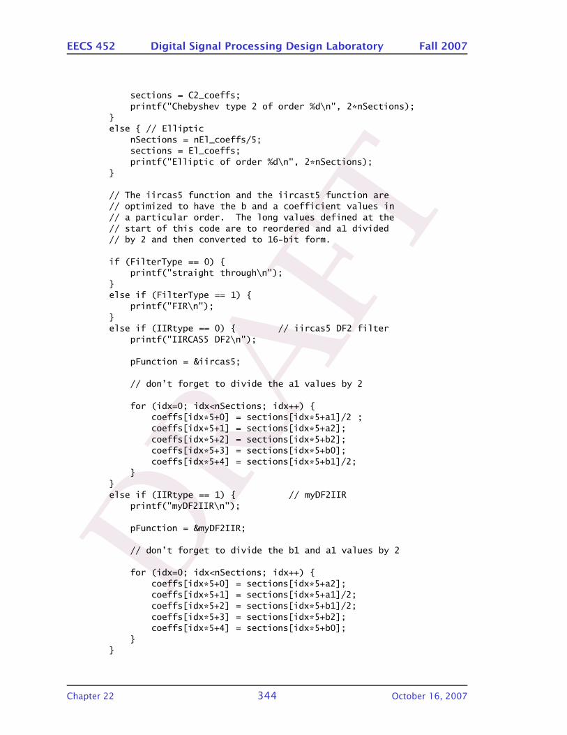
DRA
FT
EECS 452 Digital Signal Processing Design Laboratory Fall 2007
sections = C2_coeffs;printf("Chebyshev type 2 of order %d\n", 2*nSections);
else // Elliptic
nSections = nEl_coeffs/5;sections = El_coeffs;printf("Elliptic of order %d\n", 2*nSections);
// The iircas5 function and the iircast5 function are// optimized to have the b and a coefficient values in// a particular order. The long values defined at the// start of this code are to reordered and a1 divided// by 2 and then converted to 16-bit form.
if (FilterType == 0) printf("straight through\n");
else if (FilterType == 1)
printf("FIR\n");else if (IIRtype == 0) // iircas5 DF2 filter
printf("IIRCAS5 DF2\n");
pFunction = &iircas5;
// don’t forget to divide the a1 values by 2
for (idx=0; idx<nSections; idx++) coeffs[idx*5+0] = sections[idx*5+a1]/2 ;coeffs[idx*5+1] = sections[idx*5+a2];coeffs[idx*5+2] = sections[idx*5+b2];coeffs[idx*5+3] = sections[idx*5+b0];coeffs[idx*5+4] = sections[idx*5+b1]/2;
else if (IIRtype == 1) // myDF2IIR
printf("myDF2IIR\n");
pFunction = &myDF2IIR;
// don’t forget to divide the b1 and a1 values by 2
for (idx=0; idx<nSections; idx++) coeffs[idx*5+0] = sections[idx*5+a2];coeffs[idx*5+1] = sections[idx*5+a1]/2;coeffs[idx*5+2] = sections[idx*5+b1]/2;coeffs[idx*5+3] = sections[idx*5+b2];coeffs[idx*5+4] = sections[idx*5+b0];
Chapter 22 344 October 16, 2007
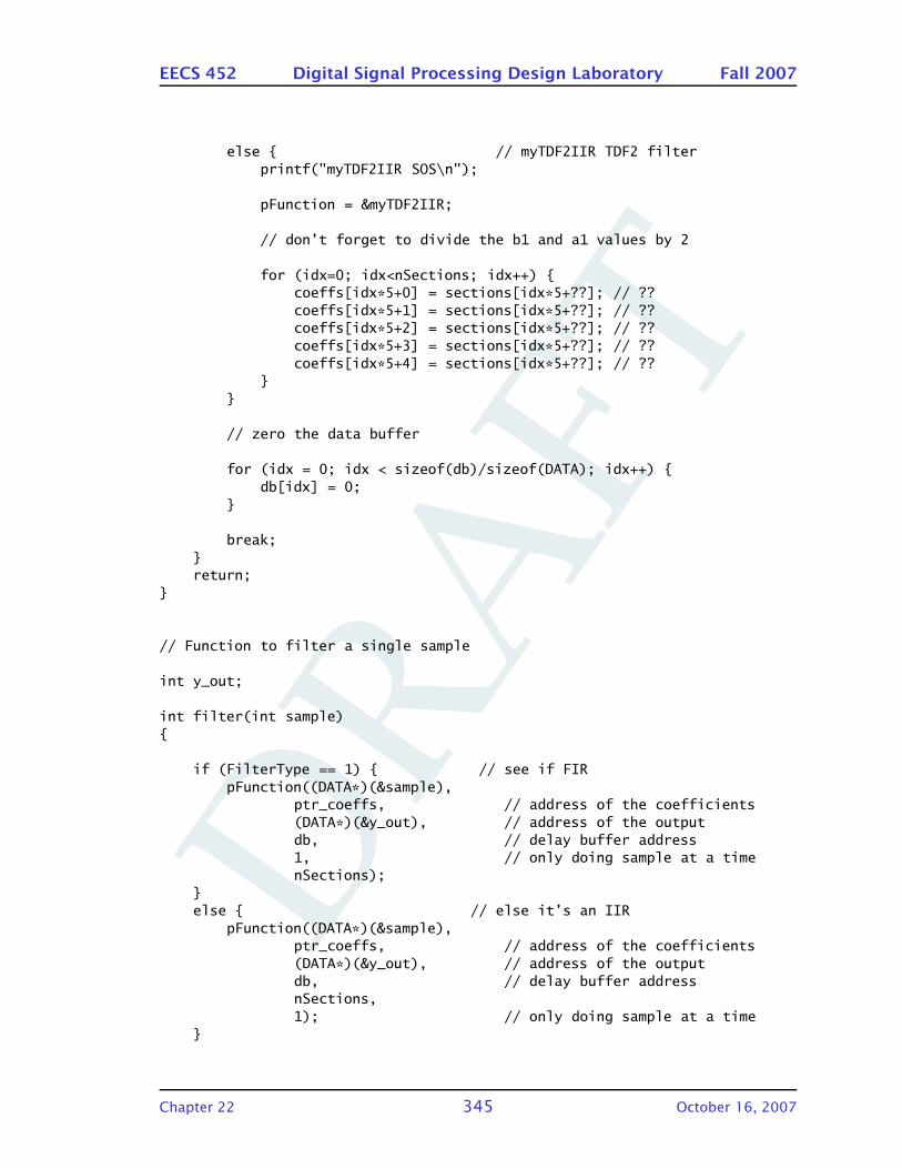
DRA
FT
EECS 452 Digital Signal Processing Design Laboratory Fall 2007
else // myTDF2IIR TDF2 filterprintf("myTDF2IIR SOS\n");
pFunction = &myTDF2IIR;
// don’t forget to divide the b1 and a1 values by 2
for (idx=0; idx<nSections; idx++) coeffs[idx*5+0] = sections[idx*5+??]; // ??coeffs[idx*5+1] = sections[idx*5+??]; // ??coeffs[idx*5+2] = sections[idx*5+??]; // ??coeffs[idx*5+3] = sections[idx*5+??]; // ??coeffs[idx*5+4] = sections[idx*5+??]; // ??
// zero the data buffer
for (idx = 0; idx < sizeof(db)/sizeof(DATA); idx++) db[idx] = 0;
break;return;
// Function to filter a single sample
int y_out;
int filter(int sample)
if (FilterType == 1) // see if FIRpFunction((DATA*)(&sample),
ptr_coeffs, // address of the coefficients(DATA*)(&y_out), // address of the outputdb, // delay buffer address1, // only doing sample at a timenSections);
else // else it’s an IIR
pFunction((DATA*)(&sample),ptr_coeffs, // address of the coefficients(DATA*)(&y_out), // address of the outputdb, // delay buffer addressnSections,1); // only doing sample at a time
Chapter 22 345 October 16, 2007
DRA
FT
EECS 452 Digital Signal Processing Design Laboratory Fall 2007
return (y_out);
/* Support for unfiltered operation */
short none(DATA* in,DATA* coeffs,DATA* out,DATA* dbuff,ushort nh,ushort nx)
unsigned idx;
for (idx = 0; idx < nx; idx++) *out = *in;return (0);
22.11 myDF2IIR source code
; File name: myDF2IIR.asm;; 19Oct2003 .. created as a learning experience code study .. KM;; on call we have; ar0 ptr_x; ar1 ptr_h; ar2 ptr_y; ar3 ptr_d; T0 nbiq; T1 nx
.c54cm_off ;don’t want compatible with c54
.ARMS_on ;enable assembler for ARMS=1
.CPL_on ;enable assembler for CPL=1
.asg ar0,ptr_x
.asg ar1,ptr_h
.asg xar1,xptr_h
.asg xar7,txptr_h
.asg ar2,ptr_y
.asg ar3,ptr_w
.asg xar3,xptr_w
.asg xar6,txptr_w
.asg T0,nbiq
.asg T1,nx
.asg 0001100000000000b,my_ST0_55
.asg 0110100100000000b,my_ST1_55
Chapter 22 346 October 16, 2007
DRA
FT
EECS 452 Digital Signal Processing Design Laboratory Fall 2007
.asg 1001000000000000b,my_ST2_55
.asg 0001000000000010b,my_ST3_55
.sect ".text" ;place into the code section
.align 4 ;force 32-bit boundary
.global _myDF2IIR ;make entry visible to linker
_myDF2IIR:psh mmap(st0_55) ; save machine statepsh mmap(st1_55) ; by saving all fourpsh mmap(st2_55) ; status registerspsh mmap(st3_55) ; on the system stackpsh T3 ; probably don’t need thispshboth txptr_h ; save the xars use to hold resetpshboth txptr_w ; address of coeffs and delays
mov #my_ST0_55,mmap(st0_55) ; now configure the machinemov #my_ST1_55,mmap(st1_55) ; a generic set of values thatmov #my_ST2_55,mmap(st2_55) ; still need a bit of tweekingmov #my_ST3_55,mmap(st3_55) ; close to reset state
bset sxmd ; enable sign extendbset frct ; shift left 1 on multiplybset m40 ; use 40 bit accumulatorbset rdm ; round to nearestbclr c54cm ; not C54x compatiblebclr satd ; disable saturation in D-unitbclr sata ; disable saturation in A-unit
sub #1,nx ; hardware needs nx-1 for loop countsub #1,nbiq ; hardware needs nbiq-1 for loop countmov nx,mmap(brc0) ; set up outer loop count..T1 is free nowmov nbiq,mmap(brc1) ; set up inner loop count..T0 is free nowmov xptr_w,txptr_w ; save ptr_w initial valuemov xptr_h,txptr_h ; save ptr_h initial value
rptblocal L_outer-1mov *ptr_x+<<#16,ac0 ; get sample value into acrptblocal L_inner-1 ; loop through sections
masm T3=*ptr_w+,*ptr_h+,ac0 ; ac0 = x-a2*w2, T3=w2mas *ptr_w,*ptr_h,ac0 ; ac0 = x-a2*w2-w1*a1/2||mov T3,T0 ; move w2 into T0masm T3=*ptr_w-,*ptr_h+,ac0 ; ac0 = x-a2*w2-a1*w1, T3=w1mov rnd(hi(saturate(ac0))),mmap(T1) ;v1mpym *ptr_h+,T3,ac0 ; ac0 = w1*b1/2||mov T3,*ptr_w+ ; move w1 into w2sfts ac0,#1 ; assuming b1/2 was suppliedmacm *ptr_h+,T0,ac0 ; ac0 = b1*w1+b2*w2||mov T1,*ptr_w+ ; move v1 into w1
Chapter 22 347 October 16, 2007
DRA
FT
EECS 452 Digital Signal Processing Design Laboratory Fall 2007
macm *ptr_h+,T1,ac0 ; ac0 = b1*w1+b2*w2+b0*v1; ac0 contains input to next section
L_inner:mov rnd(hi(saturate(ac0))),*ptr_y+ ; filter cascade output valuemov txptr_w,xptr_w ; reset xptr_wmov txptr_h,xptr_h ; reset xptr_h
L_outer:popboth txptr_w ; restore xar used to hold reset addresspopboth txptr_h ; restore xar used to hold reset addresspop T3 ; restore contents of T3pop mmap(st3_55) ; restore the four status registerspop mmap(st2_55)pop mmap(st1_55)pop mmap(st0_55)ret
22.12 IIRCAS5 source code
22.13 myTDF2IIR source starter code
; File name: myTDF2IIR.asm;; 19Oct2003 .. created as a learning experience code study .. KM;; on call we have; ar0 ptr_x; ar1 ptr_h; ar2 ptr_y; ar3 ptr_d; T0 nbiq; T1 nx
.c54cm_off ;don’t want compatible with c54
.ARMS_on ;enable assembler for ARMS=1
.CPL_on ;enable assembler for CPL=1
.asg ar0,ptr_x
.asg ar1,ptr_h
.asg xar1,xptr_h
.asg xar7,txptr_h
.asg ar2,ptr_y
.asg ar3,ptr_w
.asg xar3,xptr_w
.asg xar6,txptr_w
.asg T0,nbiq
Chapter 22 348 October 16, 2007
DRA
FT
EECS 452 Digital Signal Processing Design Laboratory Fall 2007
.asg T1,nx
.asg 0001100000000000b,my_ST0_55
.asg 0110100100000000b,my_ST1_55
.asg 1001000000000000b,my_ST2_55
.asg 0001000000000010b,my_ST3_55
.sect ".text" ;place into the code section
.align 4 ;force 32-bit boundary
.global _myTDF2IIR ;make entry visible to linker
_myTDF2IIR:psh mmap(st0_55) ; save machine statepsh mmap(st1_55) ; by saving all fourpsh mmap(st2_55) ; status registerspsh mmap(st3_55) ; on the system stackpsh T3 ; probably don’t need thispshboth txptr_h ; save the xars use to hold resetpshboth txptr_w ; address of coeffs and delays
mov #my_ST0_55,mmap(st0_55) ; now configure the machinemov #my_ST1_55,mmap(st1_55) ; a generic set of values thatmov #my_ST2_55,mmap(st2_55) ; still need a bit of tweekingmov #my_ST3_55,mmap(st3_55) ; close to reset state
bset sxmd ; enable sign extendbset frct ; shift left 1 on multiplybset m40 ; use 40 bit accumulatorbset rdm ; round to nearestbclr c54cm ; not C54x compatiblebclr satd ; disable saturation in D-unitbclr sata ; disable saturation in A-unit
sub #1,nx ; hardware needs nx-1 for loop countsub #1,nbiq ; hardware needs nbiq-1 for loop countmov nx,mmap(brc0) ; set up outer loop count..T1 is free nowmov nbiq,mmap(brc1) ; set up inner loop count..T0 is free nowmov xptr_w,txptr_w ; save ptr_w initial valuemov xptr_h,txptr_h ; save ptr_h initial value
rptblocal L_outer-1mov *ptr_x+,?? ; get sample value into ??rptblocal L_inner-1 ; loop through sections
; here be dragons
L_inner:mov ??,*ptr_y+ ; filter cascade output valuemov txptr_w,xptr_w ; reset xptr_wmov txptr_h,xptr_h ; reset xptr_h
Chapter 22 349 October 16, 2007

DRA
FT
EECS 452 Digital Signal Processing Design Laboratory Fall 2007
L_outer:popboth txptr_w ; restore xar used to hold reset addresspopboth txptr_h ; restore xar used to hold reset addresspop T3 ; restore contents of T3pop mmap(st3_55) ; restore the four status registerspop mmap(st2_55)pop mmap(st1_55)pop mmap(st0_55)ret
22.14 DisplayTest00 source code
Preliminary support for generating the magnitude and phase plots using the
Spartan-3 XVGA display system.
/* Display support for lab exercises
12Oct2007 .. initial development started .. KM
*/
#include <stdio.h>#include <stdlib.h>
extern int need_stroke, sw_print_string, sw_enable_postscript;int PSoffset;
void print_string(float x, float y, int step, int rotation, int color, char *cp);
void display_initialize(void);void plot_dB_init(int, float, float, float, float, float, float, float, float);void plot_angle_init(int, float, float, float, float, float, float, float, float);void GoToData(int, float, float);void DrawToData(int, int, float, float);void GoToSheet(float, float);void DrawToSheet(int, float, float);void DrawHorizontalGridLine(int p_n, int color, float xend, float value, char *string);void TicXAxis(int p_n, int color, float xloc, char *string);void LabelXAxis(int p_n, char *string);void LabelYAxis(int p_n, char *string, int offset);void print_string(float, float, int, int, int, char *);#define XS 1024#define YS 768
FILE *post;
struct PLOT float Pxs; // plot x start .. sheet fraction
Chapter 22 350 October 16, 2007
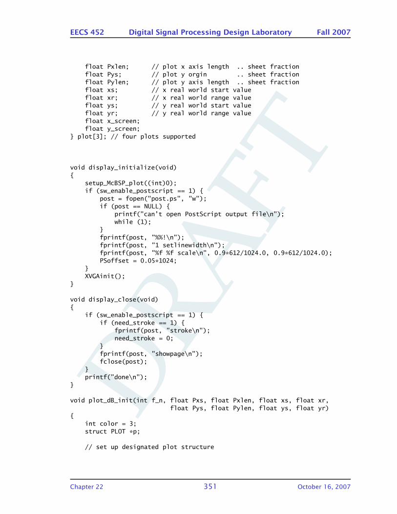
DRA
FT
EECS 452 Digital Signal Processing Design Laboratory Fall 2007
float Pxlen; // plot x axis length .. sheet fractionfloat Pys; // plot y orgin .. sheet fractionfloat Pylen; // plot y axis length .. sheet fractionfloat xs; // x real world start valuefloat xr; // x real world range valuefloat ys; // y real world start valuefloat yr; // y real world range valuefloat x_screen;float y_screen;
plot[3]; // four plots supported
void display_initialize(void)
setup_McBSP_plot((int)0);if (sw_enable_postscript == 1)
post = fopen("post.ps", "w");if (post == NULL)
printf("can’t open PostScript output file\n");while (1);
fprintf(post, "%%!\n");fprintf(post, "1 setlinewidth\n");fprintf(post, "%f %f scale\n", 0.9*612/1024.0, 0.9*612/1024.0);PSoffset = 0.05*1024;
XVGAinit();
void display_close(void)
if (sw_enable_postscript == 1) if (need_stroke == 1)
fprintf(post, "stroke\n");need_stroke = 0;
fprintf(post, "showpage\n");fclose(post);
printf("done\n");
void plot_dB_init(int f_n, float Pxs, float Pxlen, float xs, float xr,float Pys, float Pylen, float ys, float yr)
int color = 3;struct PLOT *p;
// set up designated plot structure
Chapter 22 351 October 16, 2007
DRA
FT
EECS 452 Digital Signal Processing Design Laboratory Fall 2007
p = &plot[f_n];
p->Pxs = Pxs;p->Pxlen = Pxlen;p->xs = xs;p->xr = xr;p->Pys = Pys;p->Pylen = Pylen;p->ys = ys;p->yr = yr;
// draw axes
GoToData(f_n, xs, ys); // left y-axisDrawToData(f_n, color, xs, ys+yr);
// Do horizontal dB grid
DrawHorizontalGridLine(f_n, color, 6000, -80, "-80");DrawHorizontalGridLine(f_n, color, 6000, -60, "-60");DrawHorizontalGridLine(f_n, color, 6000, -40, "-40");DrawHorizontalGridLine(f_n, color, 6000, -20, "-20");DrawHorizontalGridLine(f_n, color, 6000, 0, " 0");TicXAxis(f_n, color, 0.0, "0");TicXAxis(f_n, color, 1000.0, "1000");TicXAxis(f_n, color, 2000.0, "2000");TicXAxis(f_n, color, 3000.0, "3000");TicXAxis(f_n, color, 4000.0, "4000");TicXAxis(f_n, color, 5000.0, "5000");TicXAxis(f_n, color, 6000.0, "6000");LabelXAxis(f_n, "Frequency (Hz)");LabelYAxis(f_n, "Gain (dB)", 3);
void plot_angle_init(int f_n, float Pxs, float Pxlen, float xs, float xr,float Pys, float Pylen, float ys, float yr)
int color = 3;struct PLOT *p;
p = &plot[f_n];
p->Pxs = Pxs;p->Pxlen = Pxlen;p->xs = xs;p->xr = xr;p->Pys = Pys;p->Pylen = Pylen;p->ys = ys;p->yr = yr;
Chapter 22 352 October 16, 2007
DRA
FT
EECS 452 Digital Signal Processing Design Laboratory Fall 2007
// draw axes
GoToData(f_n, xs, ys); // left y-axisDrawToData(f_n, color, xs, ys+yr);
// Do angle grid
DrawHorizontalGridLine(f_n, color, 6000, -1.00, "-1.00");DrawHorizontalGridLine(f_n, color, 6000, -0.75, "-0.75");DrawHorizontalGridLine(f_n, color, 6000, -0.50, "-0.50");DrawHorizontalGridLine(f_n, color, 6000, -0.25, "-0.25");DrawHorizontalGridLine(f_n, color, 6000, 0.00, " 0");DrawHorizontalGridLine(f_n, color, 6000, 0.25, " 0.25");DrawHorizontalGridLine(f_n, color, 6000, 0.50, " 0.50");DrawHorizontalGridLine(f_n, color, 6000, 0.75, " 0.75");DrawHorizontalGridLine(f_n, color, 6000, 1.00, " 1.00");TicXAxis(f_n, color, 0.0, "0");TicXAxis(f_n, color, 1000.0, "1000");TicXAxis(f_n, color, 2000.0, "2000");TicXAxis(f_n, color, 3000.0, "3000");TicXAxis(f_n, color, 4000.0, "4000");TicXAxis(f_n, color, 5000.0, "5000");TicXAxis(f_n, color, 6000.0, "6000");LabelXAxis(f_n, "Frequency (Hz)");LabelYAxis(f_n, "Angle (half cycles)", 5);
void LabelYAxis(int p_n, char *string, int offset)
float cdx, cdy, x, y, n, step = 2;struct PLOT *p;
p = &plot[p_n];cdx = 3.0*step/XS; cdy = 5.5*step/YS;n = strlen(string);
x = p->Pxs - offset*cdx - cdy;y = p->Pys + p->Pylen/2 - (n+1)*cdx/2;
print_string(x, y, step, 1, 3, string);
void LabelXAxis(int p_n, char *string)
float cdx, cdy, x, y, n, step = 2;struct PLOT *p;
p = &plot[p_n];
Chapter 22 353 October 16, 2007
DRA
FT
EECS 452 Digital Signal Processing Design Laboratory Fall 2007
cdx = 3.0*step/XS; cdy = 5.5*step/YS;n = strlen(string);
x = p->Pxs + p->Pxlen/2;y = p->Pys;
print_string(x-(n+1)*cdx/2, y-3.5*cdy, step, 0, 3, string);
void TicXAxis(int p_n, int color, float xloc, char *string)
float cdx, cdy, x, y, n, step = 2;struct PLOT *p;
p = &plot[p_n];cdx = 3.0*step/XS; cdy = 5.5*step/YS;n = strlen(string);
x = p->Pxs + p->Pxlen*(xloc - p->xs)/p->xr;y = p->Pys;
GoToSheet(x, y);DrawToSheet(color, x, y-cdy/2);
print_string(x-(n+1)*cdx/2, y-2*cdy, step, 0, 3, string);
void DrawHorizontalGridLine(int p_n, int color, float xend, float value, char *string)
float cdx, cdy, x, y, n, step = 2;struct PLOT *p;
p = &plot[p_n];cdx = 3.0*step/XS; cdy = 5.5*step/YS;x = p->Pxs;y = p->Pys + p->Pylen*(value - p->ys)/p->yr;GoToSheet(x-cdx, y);x = p->Pxs + p->Pxlen*(xend - p->xs)/p->xr;DrawToSheet(color, x, y);n = strlen(string)+2;print_string(p->Pxs-n*cdx, y-cdy/2, step, 0, 3, string);
void GoToData(int f_n, float Px, float Py)
float fraction, Fx, Fy;struct PLOT *p;
p = &plot[f_n];
Chapter 22 354 October 16, 2007
DRA
FT
EECS 452 Digital Signal Processing Design Laboratory Fall 2007
fraction = (Px - p->xs)/p->xr;Fx = p->Pxs+fraction*p->Pxlen;fraction = (Py-p -> ys)/p->yr;Fy = p->Pys+fraction*p->Pylen;GoToSheet(Fx, Fy);p->x_screen = Fx;p->y_screen = Fy;
void DrawToData(int f_n, int color, float Px, float Py)
float fraction, Fx, Fy;struct PLOT *p;
p = &plot[f_n];GoToSheet(p->x_screen, p->y_screen);
fraction = (Px - p->xs)/p->xr;Fx = p->Pxs+fraction*p->Pxlen;fraction = (Py - p->ys)/p->yr;Fy = p->Pys+fraction*p->Pylen;DrawToSheet(color, Fx, Fy);p->x_screen = Fx;p->y_screen = Fy;
void print_string(float x, float y, int step, int rotation, int color, char *cp)
char ch, *cptr;
cptr = cp;GoToSheet(x, y);TX_Put(0x8300 | ((rotation&0x0003)<<5) | ((color&0x0003)<<3)| step&0x0007);while((ch=*cptr++) != NULL)
TX_Put(0x8400 | (ch&0x00FF));if (sw_enable_postscript != 0)
sw_print_string = 1;print_string_ps((int)(x*XS+0.5), (int)(y*YS+0.5), step, rotation, color, cp);sw_print_string = 0;
void GoToSheet(float Sx, float Sy)
GoTo((int)(Sx*XS+0.5), (int)(Sy*YS+0.5));
void DrawToSheet(int color, float Sx, float Sy)
Draw(color, (int)(Sx*XS+0.5), (int)(Sy*YS+0.5));
Chapter 22 355 October 16, 2007
DRA
FT
EECS 452 Digital Signal Processing Design Laboratory Fall 2007
22.15 draw_characters source code
This is a slightly modified version of the test code used to develop the Spartan-3
character generator FPGA entity. It is used here to generate matching characters
for the PostScript output.
#include <stdio.h>#include <stdlib.h>
#define Xsize 1024#define Ysize 768#define RED 1#define BLUE 2#define BLACK 3
#define STEP 2
int step=STEP;
int L_space[]=8+2,2, -1; // 32int L_exclaim[]=8+2,10, 2,4, 8+2,2, 2,2, -1;int L_quote[]=8+1,10, 1,8, 8+3,10, 3,8, -1;int L_sharp[]=8+1,9, 1,3, 8+3,9, 3,3, 8+0,5, 4,5, 8+0,7, 4,7, -1; //35int L_dollar[]=8+0,3, 3,3, 4,4, 4,5, 3,6, 1,6, 0,7, 0,8, 1,9, 4,9, 8+2,10, 2,2, -1;int L_percent[]=8+4,10, 0,2, 8+1,10, 2,9, 1,8, 0,9, 1,10, 8+3,4, 4,3, 3,2, 2,3, 3,4, -1;int L_amper[]=8+4,2, 0,7, 0,8, 1,9, 2,9, 3,8, 3,6, 0,5, 0,3, 1,2, 2,2, 4,4, -1;int L_prime[]=8+2,10, 2,9, 1,8, -1; // 39int L_lparen[]=8+3,11, 2,10, 1,9, 1,3, 2,2, 3,1, -1; // 40int L_rparen[]=8+1,11, 2,10, 3,9, 3,3, 2,2, 1,1, -1; // 41int L_ast[]=8+2,10, 2,6, 8+0,9, 4,7, 8+0,7, 4,9, -1; // 42int L_plus[]=8+0,6, 4,6, 8+2,8, 2,4, -1; // 43int L_comma[]=8+2,3, 2,2, 1,1, -1; // 44int L_minus[]=8+0,6, 4,6, -1; // 45int L_period[]=8+1,2, 2,3, 3,2, 2,1, 1,2, -1; // 46int L_divide[]=8+4,10, 0,2, -1; // 47int L_0[]=8+0,3, 0,9, 1,10, 3,10, 4,9, 4,3, 3,2, 1,2, 0,3, 8+4,10, 0,2, -1; // 48int L_1[]=8+0,8, 2,10, 2,2, 8+0,2, 4,2, -1; // 49int L_2[]=8+0,8, 0,9, 1,10, 3,10, 4,9, 4,7, 0,3, 0,2, 4,2, -1; // 50int L_3[]=8+0,9, 1,10, 3,10, 4,9, 4,7, 3,6, 1,6, 8+3,6, 4,5, 4,3, 3,2, 1,2, 0,3, -1; // 51int L_4[]=8+3,2, 3,10, 0,5, 0,4, 4,4, -1; // 52int L_5[]=8+4,10, 0,10, 0,6, 2,7, 3,7, 4,6, 4,3, 3,2, 1,2, 0,3, -1; // 53int L_6[]=8+4,9, 3,10, 1,10, 0,9, 0,3, 1,2, 3,2, 4,3, 4,5, 3,6, 2,6, 0,5, -1; // 54int L_7[]=8+0,10, 4,10, 2,6, 1,2, 8+1,6, 3,6, -1; // 55int L_8[]=8+1,2, 3,2, 4,3, 4,5, 3,6, 1,6, 0,5, 0,3, 1,2, 8+1,6, 0,7, 0,9, 1,10, 3,10, 4,9, 4,7,int L_9[]=8+0,3, 1,2, 3,2, 4,3, 4,9, 3,10, 1,10, 0,9, 0,7, 1,6, 3,6, 4,7, -1; // 57
Chapter 22 356 October 16, 2007
DRA
FT
EECS 452 Digital Signal Processing Design Laboratory Fall 2007
int L_colon[]=8+1,2, 2,3, 3,2, 2,1, 1,2, 8+1,7, 2,8, 3,7, 2,6, 1,7, -1; // 58int L_semi[]=8+1,1, 2,2, 2,3, 8+1,7, 2,8, 3,7, 2,6, 1,7, -1; // 59int L_langle[]=8+4,10, 0,6, 4,2, -1; // 60int L_equal[]=8+0,4, 4,4, 8+0,7, 4,7, -1; //61int L_rangle[]=8+0,10, 4,6, 0,2, -1; // 62int L_qmark[]=8+0,8, 0,9, 1,10, 3,10, 4,9, 4,7, 3,6, 2,5, 2,4, 8+2,2, 2,2, -1; // 63
int L_at[]=8+4,3, 3,2, 1,2, 0,3, 0,9, 1,10, 3,10, 4,9, 4,5, 3,5, 2,4, 1,5, 1,7, 2,8, 3,7,int L_A[]=8+0,2, 0,8, 2,10, 4,8, 4,2, 8+0,5, 4,5, -1;int L_B[]=8+0,2, 3,2, 4,3, 4,3, 4,5, 3,6, 1,6, 8+1,2, 1,10, 8+0,10, 3,10, 4,9, 4,7, 3,6,int L_C[]=8+4,3, 3,2, 1,2, 0,3, 0,9, 1,10, 3,10, 4,9, -1;int L_D[]=8+0,10, 3,10, 4,9, 4,3, 3,2, 0,2, 8+1,2, 1,10, -1;int L_E[]=8+4,2, 0,2, 0,10, 4,10, 8+0,6, 3,6, -1;int L_F[]=8+0,2, 0,10, 4,10, 8+0,6, 3,6, -1;int L_G[]=8+4,9, 3,10, 1,10, 0,9, 0,3, 1,2, 3,2, 4,3, 4,5, 3,5, -1;int L_H[]=8+0,10, 0,2, 8+4,10, 4,2, 8+0,6, 4,6, -1;int L_I[]=8+1,2, 3,2, 8+2,2, 2,10, 8+1,10, 3,10, -1;int L_J[]=8+0,3, 1,2, 2,2, 3,3, 3,10, 8+2,10, 4,10, -1;int L_K[]=8+0,2, 0,10, 8+0,5, 4,9, 4,10, 8+0,6, 4,3, 4,2, -1;int L_L[]=8+0,10, 0,2, 4,2, -1;int L_M[]=8+0,2, 0,10, 2,6, 4,10, 4,2, -1;int L_N[]=8+0,2, 0,10, 4,2, 4,10, -1;int L_O[]=8+0,3, 0,9, 1,10, 3,10, 4,9, 4,3, 3,2, 1,2, 0,3, -1;int L_P[]=8+0,2, 0,10, 3,10, 4,9, 4,7, 3,6, 0,6, -1;int L_Q[]=8+0,3, 0,9, 1,10, 3,10, 4,9, 4,3, 3,2, 1,2, 0,3, 8+2,4, 4,2, -1;int L_R[]=8+0,2, 0,10, 3,10, 4,9, 4,7, 3,6, 0,6, 8+1,6, 4,3, 4,2, -1;int L_S[]=8+0,3, 1,2, 3,2, 4,3, 4,5, 3,6, 1,6, 0,7, 0,9, 1,10, 3,10, 4,9, -1;int L_T[]=8+2,2, 2,10, 8+0,10, 4,10, -1;int L_U[]=8+0,10, 0,3, 1,2, 3,2, 4,3, 4,10, -1;int L_V[]=8+0,10, 0,7, 2,2, 4,7, 4,10, -1;int L_W[]=8+0,10, 0,2, 2,5, 4,2, 4,10, -1;int L_X[]=8+0,10, 4,2, 8+4,10, 0,2, -1;int L_Y[]=8+0,10, 2,6, 2,2, 8+4,10, 2,6, -1;int L_Z[]=8+0,9, 0,10, 4,10, 0,2, 4,2, 4,3, 8+1,6, 3,6, -1;int L_lbrack[]=8+3,11, 1,11, 1,1, 3,1, -1; // 91int L_bslash[]=8+1,10, 4,2, -1; // 92int L_rbrack[]=8+1,11, 3,11, 3,1, 1,1, -1; // 93int L_caret[]=8+0,8, 2,10, 4,8, -1; // 94int L_under[]=8+0,1, 4,1, -1; // 95
int L_backprime[]=8+2,10, 2,9, 3,8, -1; // 96int L_a[]=8+1,7, 3,7, 4,6, 4,2, 8+4,3, 2,2, 1,2, 0,3, 0,4, 1,5, 4,5, -1; // 97int L_b[]=8+0,10, 0,2, 8+0,3, 1,2, 3,2, 4,3, 4,6, 3,7, 1,7, 0,6, -1;int L_c[]=8+4,6, 3,7, 1,7, 0,6, 0,3, 1,2, 3,2, 4,3, -1;int L_d[]=8+4,10, 4,2, 8+4,3, 3,2, 1,2, 0,3, 0,6, 1,7, 3,7, 4,6, -1;int L_e[]=8+4,3, 3,2, 1,2, 0,3, 0,6, 1,7, 3,7, 4,6, 4,5, 0,5, -1;int L_f[]=8+4,9, 3,10, 2,10, 1,9, 1,2, 8+0,6, 2,6, -1;int L_g[]=8+0,1, 1,0, 3,0, 4,1, 4,6, 3,7, 1,7, 0,6, 0,4, 1,3, 3,3, 4,4, -1;int L_h[]=8+0,10,0,2, 8+0,6, 2,7, 3,7, 4,6, 4,2, -1;int L_i[]=8+1,2, 3,2, 8+2,2,2,7,1,7, 8+2,9, 2,9, -1;int L_j[]=8+0,2, 0,1, 1,0, 2,0, 3,1, 3,7, 2,7, 8+3,9, 3,9, -1;
Chapter 22 357 October 16, 2007
DRA
FT
EECS 452 Digital Signal Processing Design Laboratory Fall 2007
int L_k[]=8+1,2, 1,10, 8+4,2, 1,5, 4,7, -1;int L_l[]=8+1,2, 3,2, 8+2,2, 2,10, 1,10, -1;int L_m[]=8+0,2, 0,6, 1,7, 2,6, 2,2, 8+2,6, 3,7, 4,6, 4,2, -1;int L_n[]=8+0,2, 0,7, 8+0,6, 2,7, 3,7, 4,6, 4,2, -1;int L_o[]=8+0,3, 0,6, 1,7, 3,7, 4,6, 4,3, 3,2, 1,2, 0,3, -1;int L_p[]=8+0,0, 0,7, 8+0,6, 1,7, 3,7, 4,6, 4,4, 3,3, 0,3, -1;int L_q[]=8+4,0, 4,7, 8+4,6, 3,7, 1,7, 0,6, 0,4, 1,3, 4,3, -1;int L_r[]=8+0,2, 0,7, 8+0,6, 2,7, 3,7, 4,6, -1;int L_s[]=8+0,3, 1,2, 3,2, 4,3, 3,4, 2,5, 1,5, 0,6, 1,7, 3,7, 4,6, -1;int L_t[]=8+0,7, 2,7, 8+1,9, 1,3, 2,2, 3,2, 4,3, -1;int L_u[]=8+0,7, 0,3, 1,2, 3,2, 4,3, 8+4,2, 4,7, -1;int L_v[]=8+0,7, 0,5, 2,2, 4,5, 4,7, -1;int L_w[]=8+0,7, 0,3, 1,2, 2,3, 2,5, 8+2,3, 3,2, 4,3, 4,7, -1;int L_x[]=8+0,7, 4,2, 8+4,7, 0,2, -1;int L_y[]=8+0,7, 0,4, 1,3, 3,3, 4,4, 4,7, 8+4,4, 4,1, 3,0, 1,0, 0,1, -1;int L_z[]=8+0,7, 4,7, 0,2, 4,2, -1;int L_lbrace[]=8+4,11, 3,11, 2,10, 2,7, 0,6, 2,5, 2,2, 3,1, 4,1, -1;int L_vbar[]=8+2,2, 2,10, -1; // 124int L_rbrace[]=8+0,11, 1,11, 2,10, 2,7, 4,6, 2,5, 2,2, 1,1, 0,1, -1; // 125int L_tilde[]=8+0,8, 0,9, 1,10, 3,8, 4,9, 4,10, -1; // 126int L_rub[]=8+2,2, -1; // 127
int *cptrs[] = L_space, L_exclaim, L_quote, L_sharp, L_dollar, L_percent, L_amper, L_prime,L_lparen, L_rparen, L_ast, L_plus, L_comma, L_minus, L_period, L_divide,L_0, L_1, L_2, L_3, L_4, L_5, L_6, L_7,L_8, L_9, L_colon, L_semi, L_langle, L_equal, L_rangle, L_qmark,L_at, L_A, L_B, L_C, L_D, L_E, L_F, L_G,L_H, L_I, L_J, L_K, L_L, L_M, L_N, L_O,L_P, L_Q, L_R, L_S, L_T, L_U, L_V, L_W,L_X, L_Y, L_Z, L_lbrack, L_bslash, L_rbrack, L_caret, L_under,L_backprime, L_a, L_b, L_c, L_d, L_e, L_f, L_g,L_h, L_i, L_j, L_k, L_l, L_m, L_n, L_o,L_p, L_q, L_r, L_s, L_t, L_u, L_v, L_w,L_x, L_y, L_z, L_lbrace, L_vbar, L_rbrace, L_tilde, L_rub;
int xx, yy, *cptr;int sw_no_draw = 0;int str_length = 0;
int getxy(int st, int rotation)
int xv, itemp;
xv = *cptr++; yy = *cptr++;if(xv < 0) return(-1);
xx = xv&0x07;
Chapter 22 358 October 16, 2007

DRA
FT
EECS 452 Digital Signal Processing Design Laboratory Fall 2007
xx = ((st*xx+1)>>1);yy = ((st*yy+1)>>1);
switch (rotation) case 1 : itemp = xx;
xx = -yy;yy = itemp;break;
case 2 : xx = -xx;yy = -yy;break;
case 3 : itemp = xx;xx = yy;yy = -itemp;break;
default : break;
if (xv > 7) return(1); // penupreturn(0); // pendown
void scale_draw_char(int x, int y, float sf, int color, char ch)
int sw;
ch = ch-32;cptr = cptrs[ch];if(getxy(2, 0) < 0) return;xx = sf*(xx-2)+0.5;yy = sf*(yy-6)+0.5;GoTo(x+xx, y+yy);while((sw=getxy(2, 0))>=0)
xx = sf*(xx-2)+0.5;yy = sf*(yy-6)+0.5;if(sw!=0)
GoTo(x+xx, y+yy); else
Draw(color, x+xx, y+yy);
void dr_char(int x, int y, int st, int rotation, int color, int *cp)
int sw, itemp;
cptr = cp;if( getxy(st, rotation) < 0 ) return;
Chapter 22 359 October 16, 2007

DRA
FT
EECS 452 Digital Signal Processing Design Laboratory Fall 2007
if(sw_no_draw != 1) GoTo(x+xx, y+yy);
while((sw=getxy(st, rotation))>=0) if(sw!=0)
if(sw_no_draw != 1) GoTo(x+xx, y+yy); else
if(sw_no_draw != 1) Draw(color, x+xx, y+yy);itemp = x+xx;if(itemp>str_length) str_length = itemp;
void draw_char(int x, int y, int st, int rotation, int color, char ch)
int *ptr;
ch = ch-32;ptr = cptrs[ch];dr_char(x, y, st, rotation, color, ptr);
void print_string_ps(int x, int y, int step, int rotation, int color, char *cp)
char ch;int dx;
dx = (7*step)/2;
while((ch=*cp++) != NULL) draw_char(x, y, step, rotation, color, ch);switch (rotation)
case 1: y += dx; break;case 2: x -= dx; break;case 3: y -= dx; break;default : x += dx;
22.16 setup_McBSP_plot source code
Sets up McBSP channel 0 for use with the Spartan-3 SB XVGA entity.
/* EECS 452 McBSP/AIC23 basic paradigm example support
** 12Jul03 .. initial version .. KM
* 24Apr07 .. McBSP plot version .. KM
Chapter 22 360 October 16, 2007
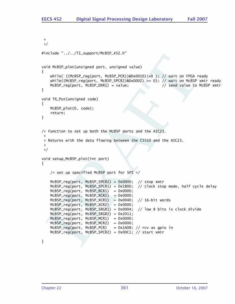
DRA
FT
EECS 452 Digital Signal Processing Design Laboratory Fall 2007
**/
#include "../../TI_support/McBSP_452.h"
void McBSP_plot(unsigned port, unsigned value)
while( ((McBSP_reg(port, McBSP_PCR))&0x0010)!=0 ); // wait on FPGA readywhile((McBSP_reg(port, McBSP_SPCR2)&0x0002) == 0); // wait on McBSP xmtr readyMcBSP_reg(port, McBSP_DXR1) = value; // send value to McBSP xmtr
void TX_Put(unsigned code)
McBSP_plot(0, code);return;
/* Function to set up both the McBSP ports and the AIC23.
** Returns with the data flowing between the C5510 and the AIC23.
**/
void setup_McBSP_plot(int port)
/* set up specified McBSP port for SPI */
McBSP_reg(port, McBSP_SPCR2) = 0x0000; // stop xmtrMcBSP_reg(port, McBSP_SPCR1) = 0x1800; // clock stop mode, half cycle delayMcBSP_reg(port, McBSP_RCR1) = 0x0000;McBSP_reg(port, McBSP_RCR2) = 0x0000;McBSP_reg(port, McBSP_XCR1) = 0x0040; // 16-bit wordsMcBSP_reg(port, McBSP_XCR2) = 0x0000;McBSP_reg(port, McBSP_SRGR1) = 0x0004; // low 8 bits is clock divideMcBSP_reg(port, McBSP_SRGR2) = 0x2011;McBSP_reg(port, McBSP_MCR1) = 0x0000;McBSP_reg(port, McBSP_MCR2) = 0x0000;McBSP_reg(port, McBSP_PCR) = 0x1A08; // rcv as gpio inMcBSP_reg(port, McBSP_SPCR2) = 0x00C1; // start xmtr
Chapter 22 361 October 16, 2007
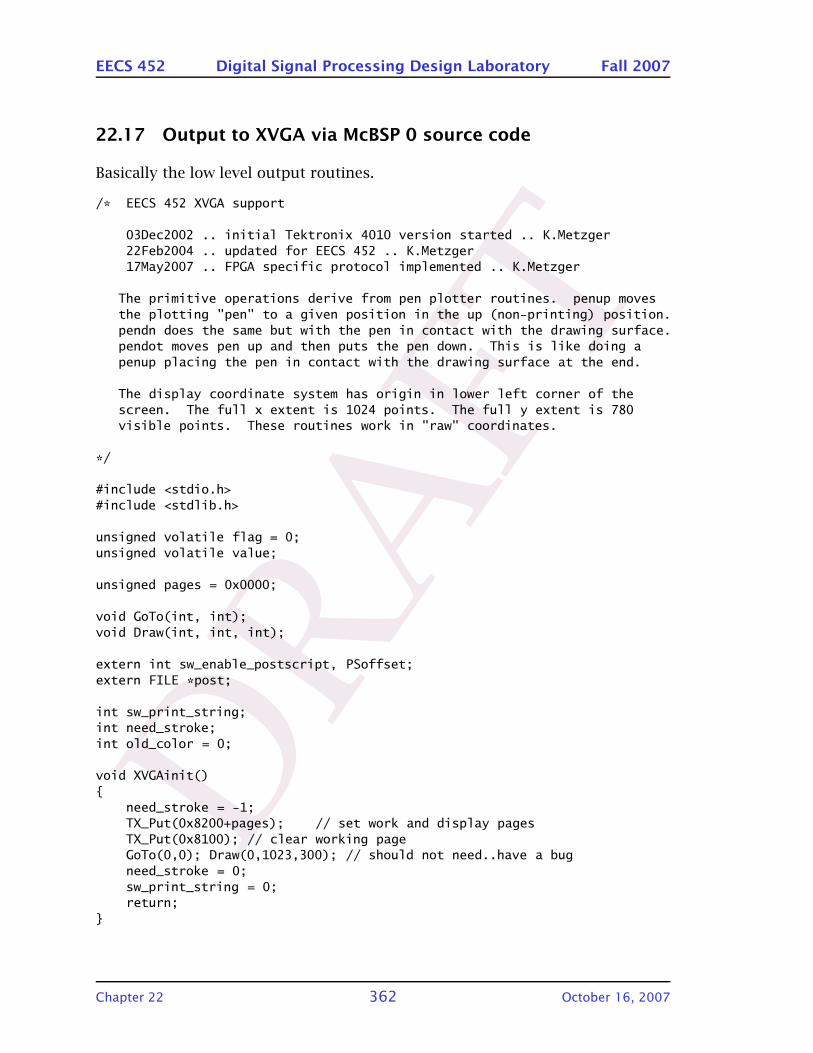
DRA
FT
EECS 452 Digital Signal Processing Design Laboratory Fall 2007
22.17 Output to XVGA via McBSP 0 source code
Basically the low level output routines.
/* EECS 452 XVGA support
03Dec2002 .. initial Tektronix 4010 version started .. K.Metzger22Feb2004 .. updated for EECS 452 .. K.Metzger17May2007 .. FPGA specific protocol implemented .. K.Metzger
The primitive operations derive from pen plotter routines. penup movesthe plotting "pen" to a given position in the up (non-printing) position.pendn does the same but with the pen in contact with the drawing surface.pendot moves pen up and then puts the pen down. This is like doing apenup placing the pen in contact with the drawing surface at the end.
The display coordinate system has origin in lower left corner of thescreen. The full x extent is 1024 points. The full y extent is 780visible points. These routines work in "raw" coordinates.
*/
#include <stdio.h>#include <stdlib.h>
unsigned volatile flag = 0;unsigned volatile value;
unsigned pages = 0x0000;
void GoTo(int, int);void Draw(int, int, int);
extern int sw_enable_postscript, PSoffset;extern FILE *post;
int sw_print_string;int need_stroke;int old_color = 0;
void XVGAinit()
need_stroke = -1;TX_Put(0x8200+pages); // set work and display pagesTX_Put(0x8100); // clear working pageGoTo(0,0); Draw(0,1023,300); // should not need..have a bugneed_stroke = 0;sw_print_string = 0;return;
Chapter 22 362 October 16, 2007
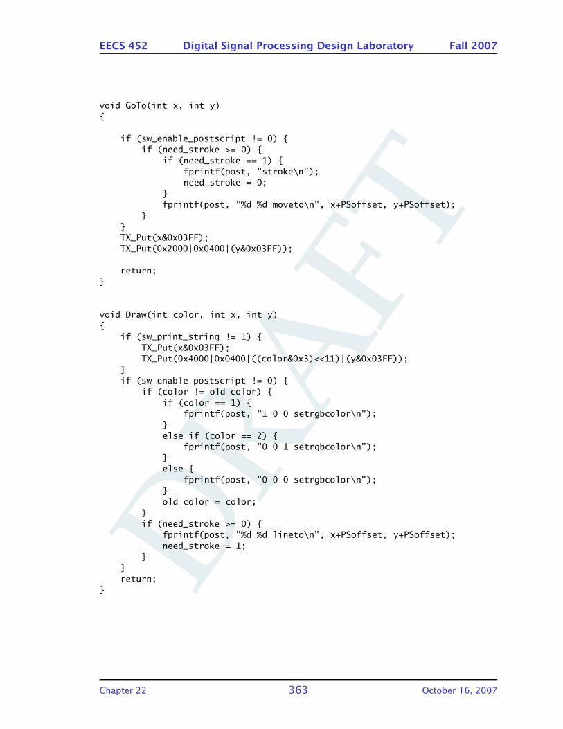
DRA
FT
EECS 452 Digital Signal Processing Design Laboratory Fall 2007
void GoTo(int x, int y)
if (sw_enable_postscript != 0) if (need_stroke >= 0)
if (need_stroke == 1) fprintf(post, "stroke\n");need_stroke = 0;
fprintf(post, "%d %d moveto\n", x+PSoffset, y+PSoffset);
TX_Put(x&0x03FF);TX_Put(0x2000|0x0400|(y&0x03FF));
return;
void Draw(int color, int x, int y)
if (sw_print_string != 1) TX_Put(x&0x03FF);TX_Put(0x4000|0x0400|((color&0x3)<<11)|(y&0x03FF));
if (sw_enable_postscript != 0)
if (color != old_color) if (color == 1)
fprintf(post, "1 0 0 setrgbcolor\n");else if (color == 2)
fprintf(post, "0 0 1 setrgbcolor\n");else
fprintf(post, "0 0 0 setrgbcolor\n");old_color = color;
if (need_stroke >= 0)
fprintf(post, "%d %d lineto\n", x+PSoffset, y+PSoffset);need_stroke = 1;
return;
Chapter 22 363 October 16, 2007
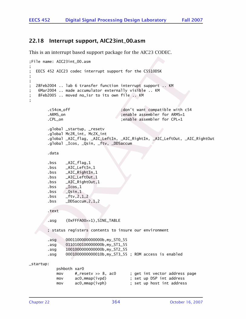
DRA
FT
EECS 452 Digital Signal Processing Design Laboratory Fall 2007
22.18 Interrupt support, AIC23int_00.asm
This is an interrupt based support package for the AIC23 CODEC.
;File name: AIC23int_00.asm;; EECS 452 AIC23 codec interrupt support for the C5510DSK;;; 28Feb2004 .. lab 6 transfer function interrupt support .. KM; 6Mar2004 .. made accumulator externally visible .. KM; 8Feb2005 .. moved no_isr to its own file .. KM;
.c54cm_off ;don’t want compatible with c54
.ARMS_on ;enable assembler for ARMS=1
.CPL_on ;enable assembler for CPL=1
.global _startup, _resetv
.global Mc2R_int, Mc2X_int
.global _AIC_flag, _AIC_LeftIn, _AIC_RightIn, _AIC_LeftOut, _AIC_RightOut
.global _Icos, _Qsin, _ftv, _DDSaccum
.data
.bss _AIC_flag,1
.bss _AIC_LeftIn,1
.bss _AIC_RightIn,1
.bss _AIC_LeftOut,1
.bss _AIC_RightOut,1
.bss _Icos,1
.bss _Qsin,1
.bss _ftv,2,1,2
.bss _DDSaccum,2,1,2
.text
.asg (0xFFFA00>>1),SINE_TABLE
; status registers contents to insure our environment
.asg 0001100000000000b,my_ST0_55
.asg 0110100100000000b,my_ST1_55
.asg 1001000000000000b,my_ST2_55
.asg 0001000000000010b,my_ST3_55 ; ROM access is enabled
_startup:pshboth xar0mov #_resetv >> 8, ac0 ; get int vector address pagemov ac0,mmap(ivpd) ; set up DSP int addressmov ac0,mmap(ivph) ; set up host int address
Chapter 22 364 October 16, 2007
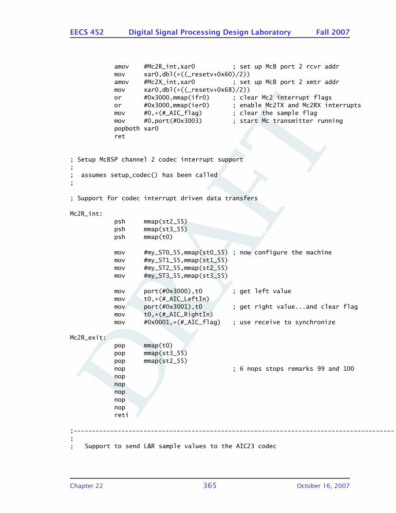
DRA
FT
EECS 452 Digital Signal Processing Design Laboratory Fall 2007
amov #Mc2R_int,xar0 ; set up McB port 2 rcvr addrmov xar0,dbl(*((_resetv+0x60)/2))amov #Mc2X_int,xar0 ; set up McB port 2 xmtr addrmov xar0,dbl(*((_resetv+0x68)/2))or #0x3000,mmap(ifr0) ; clear Mc2 interrupt flagsor #0x3000,mmap(ier0) ; enable Mc2TX and Mc2RX interruptsmov #0,*(#_AIC_flag) ; clear the sample flagmov #0,port(#0x3003) ; start Mc transmitter runningpopboth xar0ret
; Setup McBSP channel 2 codec interrupt support;; assumes setup_codec() has been called;
; Support for codec interrupt driven data transfers
Mc2R_int:psh mmap(st2_55)psh mmap(st3_55)psh mmap(t0)
mov #my_ST0_55,mmap(st0_55) ; now configure the machinemov #my_ST1_55,mmap(st1_55)mov #my_ST2_55,mmap(st2_55)mov #my_ST3_55,mmap(st3_55)
mov port(#0x3000),t0 ; get left valuemov t0,*(#_AIC_LeftIn)mov port(#0x3001),t0 ; get right value...and clear flagmov t0,*(#_AIC_RightIn)mov #0x0001,*(#_AIC_flag) ; use receive to synchronize
Mc2R_exit:pop mmap(t0)pop mmap(st3_55)pop mmap(st2_55)nop ; 6 nops stops remarks 99 and 100nopnopnopnopnopreti
;---------------------------------------------------------------------------------------;; Support to send L&R sample values to the AIC23 codec
Chapter 22 365 October 16, 2007
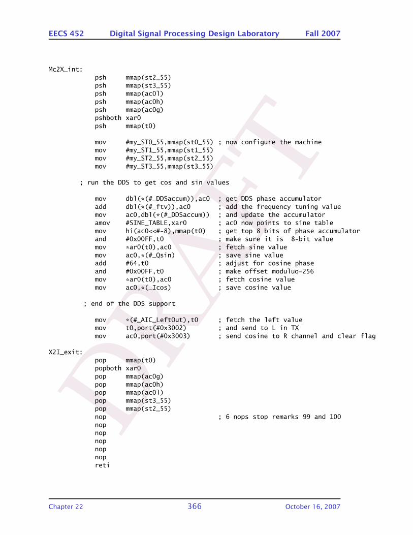
DRA
FT
EECS 452 Digital Signal Processing Design Laboratory Fall 2007
Mc2X_int:psh mmap(st2_55)psh mmap(st3_55)psh mmap(ac0l)psh mmap(ac0h)psh mmap(ac0g)pshboth xar0psh mmap(t0)
mov #my_ST0_55,mmap(st0_55) ; now configure the machinemov #my_ST1_55,mmap(st1_55)mov #my_ST2_55,mmap(st2_55)mov #my_ST3_55,mmap(st3_55)
; run the DDS to get cos and sin values
mov dbl(*(#_DDSaccum)),ac0 ; get DDS phase accumulatoradd dbl(*(#_ftv)),ac0 ; add the frequency tuning valuemov ac0,dbl(*(#_DDSaccum)) ; and update the accumulatoramov #SINE_TABLE,xar0 ; ac0 now points to sine tablemov hi(ac0<<#-8),mmap(t0) ; get top 8 bits of phase accumulatorand #0x00FF,t0 ; make sure it is 8-bit valuemov *ar0(t0),ac0 ; fetch sine valuemov ac0,*(#_Qsin) ; save sine valueadd #64,t0 ; adjust for cosine phaseand #0x00FF,t0 ; make offset moduluo-256mov *ar0(t0),ac0 ; fetch cosine valuemov ac0,*(_Icos) ; save cosine value
; end of the DDS support
mov *(#_AIC_LeftOut),t0 ; fetch the left valuemov t0,port(#0x3002) ; and send to L in TXmov ac0,port(#0x3003) ; send cosine to R channel and clear flag
X2I_exit:pop mmap(t0)popboth xar0pop mmap(ac0g)pop mmap(ac0h)pop mmap(ac0l)pop mmap(st3_55)pop mmap(st2_55)nop ; 6 nops stop remarks 99 and 100nopnopnopnopnopreti
Chapter 22 366 October 16, 2007
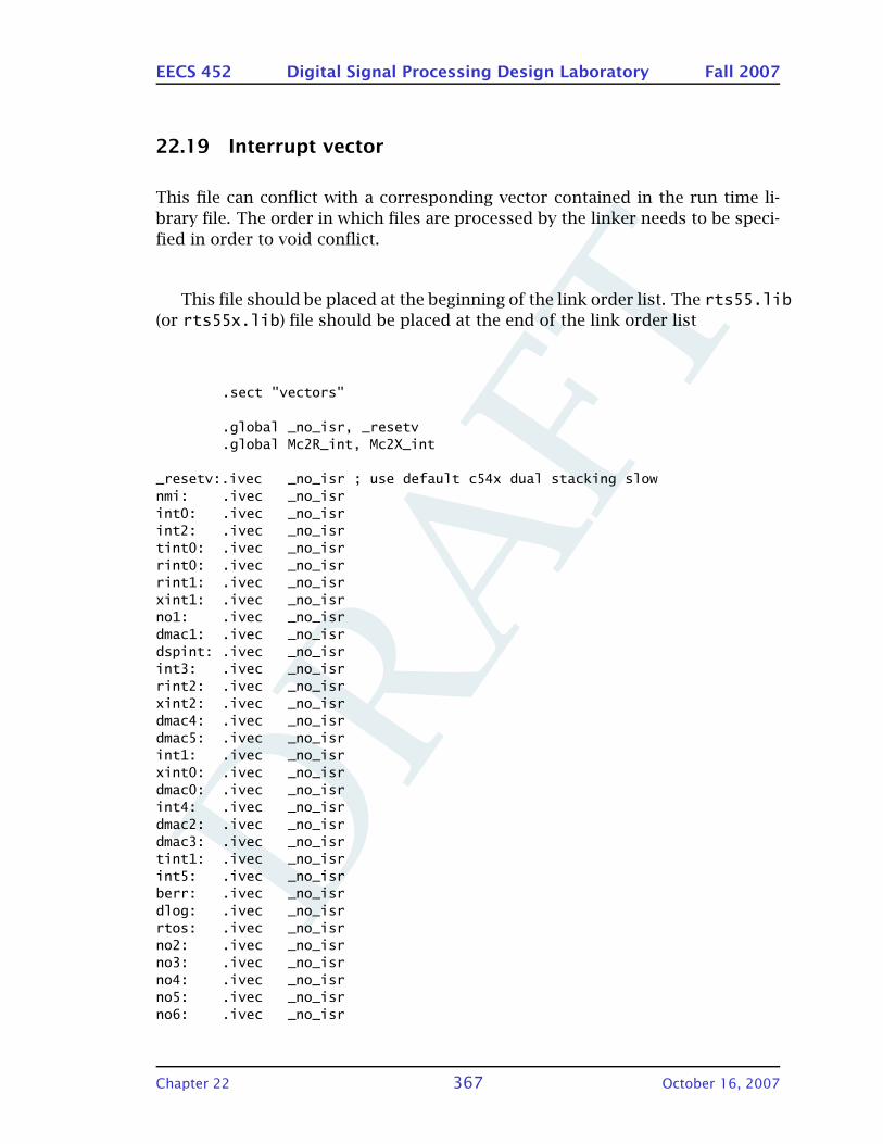
DRA
FT
EECS 452 Digital Signal Processing Design Laboratory Fall 2007
22.19 Interrupt vector
This file can conflict with a corresponding vector contained in the run time li-
brary file. The order in which files are processed by the linker needs to be speci-
fied in order to void conflict.
This file should be placed at the beginning of the link order list. The rts55.lib(or rts55x.lib) file should be placed at the end of the link order list
.sect "vectors"
.global _no_isr, _resetv
.global Mc2R_int, Mc2X_int
_resetv:.ivec _no_isr ; use default c54x dual stacking slownmi: .ivec _no_isrint0: .ivec _no_isrint2: .ivec _no_isrtint0: .ivec _no_isrrint0: .ivec _no_isrrint1: .ivec _no_isrxint1: .ivec _no_isrno1: .ivec _no_isrdmac1: .ivec _no_isrdspint: .ivec _no_isrint3: .ivec _no_isrrint2: .ivec _no_isrxint2: .ivec _no_isrdmac4: .ivec _no_isrdmac5: .ivec _no_isrint1: .ivec _no_isrxint0: .ivec _no_isrdmac0: .ivec _no_isrint4: .ivec _no_isrdmac2: .ivec _no_isrdmac3: .ivec _no_isrtint1: .ivec _no_isrint5: .ivec _no_isrberr: .ivec _no_isrdlog: .ivec _no_isrrtos: .ivec _no_isrno2: .ivec _no_isrno3: .ivec _no_isrno4: .ivec _no_isrno5: .ivec _no_isrno6: .ivec _no_isr
Chapter 22 367 October 16, 2007

DRA
FT
EECS 452 Digital Signal Processing Design Laboratory Fall 2007
22.20 Interrupt support error, no_isr.asm
This file contains the support for interrupts that are not supported. Any time an
interrupt occurs for a device which has not been properly supported a branch is
made to _no_isr. This prevents the computer wandering too far.
;File name: no_isr.asm;; EECS 452 unsupported interrupt support for the C5510DSK;; 8Feb2005 .. no_isr placed into its own file .. KM;
.c54cm_off ;don’t want compatible with c54
.ARMS_on ;enable assembler for ARMS=1
.CPL_on ;enable assembler for CPL=1
.global _no_isr ;make visible to outside world
.text
_no_isr: b _no_isr
22.21 Main function for recursive sine/cosine oscillator
void main(void)
setup_codec();bsinegen();
22.22 Starter code for recursive sine/cosine oscillator
The source file is named bsinegen.asm.
; EECS 452 recursive sine/cosine generator;; 6 Oct 2003 .. initial version .. KM; 12 Oct 2003 .. sine/cosineine version .. KM; 2 Nov 2003 .. repairs .. KM
.data
.bss w_1,1 ; delay stage 1 in data memory
.bss w_2,1 ; delay stage 2 in data memory
Chapter 22 368 October 16, 2007
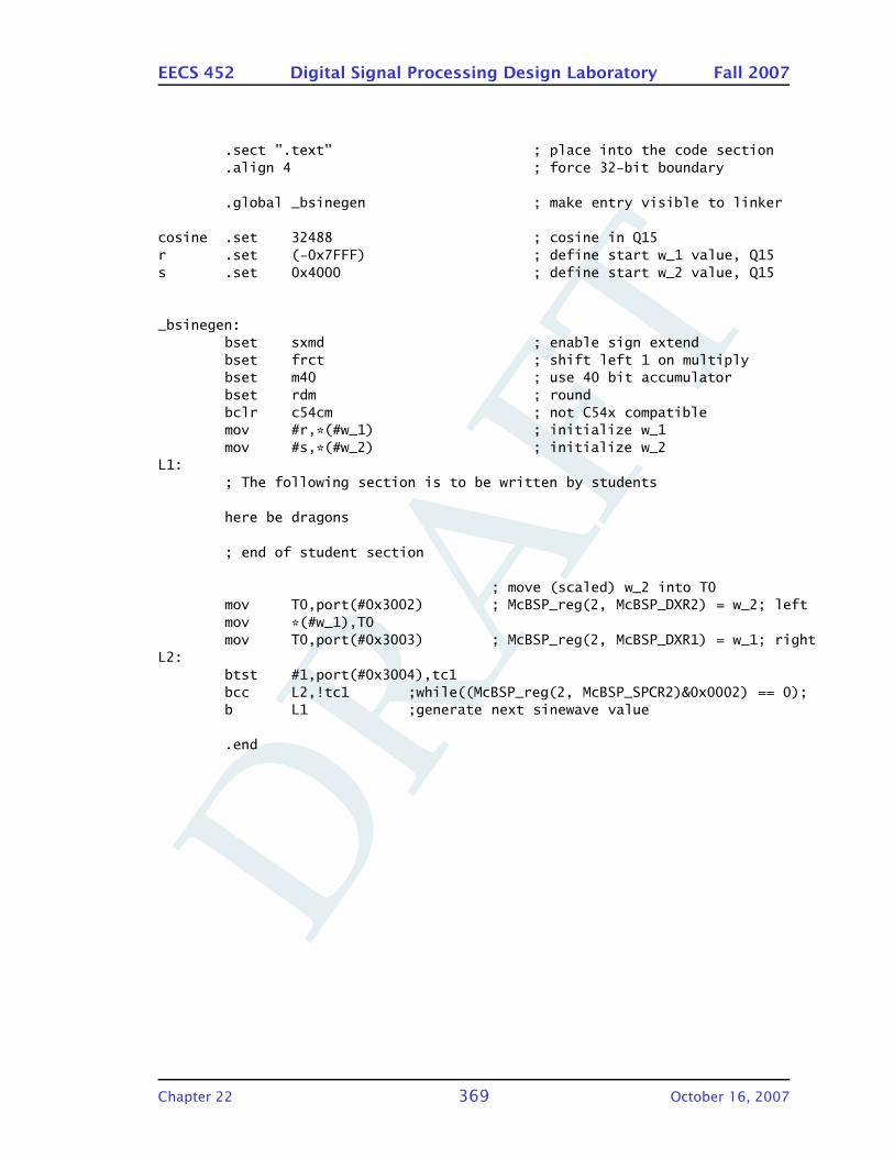
DRA
FT
EECS 452 Digital Signal Processing Design Laboratory Fall 2007
.sect ".text" ; place into the code section
.align 4 ; force 32-bit boundary
.global _bsinegen ; make entry visible to linker
cosine .set 32488 ; cosine in Q15r .set (-0x7FFF) ; define start w_1 value, Q15s .set 0x4000 ; define start w_2 value, Q15
_bsinegen:bset sxmd ; enable sign extendbset frct ; shift left 1 on multiplybset m40 ; use 40 bit accumulatorbset rdm ; roundbclr c54cm ; not C54x compatiblemov #r,*(#w_1) ; initialize w_1mov #s,*(#w_2) ; initialize w_2
L1:; The following section is to be written by students
here be dragons
; end of student section
; move (scaled) w_2 into T0mov T0,port(#0x3002) ; McBSP_reg(2, McBSP_DXR2) = w_2; leftmov *(#w_1),T0mov T0,port(#0x3003) ; McBSP_reg(2, McBSP_DXR1) = w_1; right
L2:btst #1,port(#0x3004),tc1bcc L2,!tc1 ;while((McBSP_reg(2, McBSP_SPCR2)&0x0002) == 0);b L1 ;generate next sinewave value
.end
Chapter 22 369 October 16, 2007

DRA
FTWasted space, consider adding helpful text to this chapter.
DRA
FT
23 : Working with FFTs
The FFT is the DSP journeyman’s stock in trade. One should, must know how to
use. Should also know how to implement.
Some tasks and/or things to think about:
• Generate real time display in FPGA.
• Baseband and centered at a frequency.
• Computing magnitudes in dBs.
• Scaling based on the noise floor.
• Scaling methods.
• Test FPGA butterfly performance using PC to S3SB USB link.
Yet another FFT implementation? Why?
The yaFFT implementation was primarily done as a learning exercise, a VHDL
étude. The end result was nominally to be incorporated into two EECS 452 lab ex-
ercises, one doing real-time spectrum analysis and display and the other imple-
menting an orthogonal frequency division multiplexed (OFDM) communication
system.
A goal is to implement yaFFT using bit-serial arithmetic on the Digilent Spartan-
3 Starter Boards used in the EECS 452 lab.
The primary references for this work were [?] and more to come. Work was
started on this memo on May 7, 2007 and has progressed in fits and starts.
23.0.1 Comments on levels of abstraction
As computers have become more powerful and commonly available so has the
levels at which design is conducted have become more abstract.
At our chosen VHDL behavioral level of abstraction, there are lower levels,
gates, transistors, device geometries and the like. The lower levels can be ex-
plored by reading books such as [?].
23.0.2 Comments on the design process
Design is generally a holistic process. Some times there is a well defined starting
point, sometimes many.
Chapter 23 371 October 16, 2007
DRA
FT
EECS 452 Digital Signal Processing Design Laboratory Fall 2007
One has a general goal that is to be attained, maybe some ideas of how to get
there but uncertainty is also, at least initially, often rampant. One pokes here and
there trying to develop a overall understanding what needs to be done and how.
Eventually enough pieces come together that allow one to start implementation.
A key to success is knowing what what one knows and what one does not
know, and thank-you D. Rumsfeld, worrying about what one does not know isn’t
known. One can work on the know unknowns. The unknown unknowns will
generally eventually make themselves apparent. They can be helped out with
this by doing paper designs and and coding small feasibility studies.
A problem with engineering education is that once the holistic processes has
been completed and the total system is understood and implemented the result
is presented in a linear fashion just as if it had been thought about that way.
The designer has his technical baggage, some good and useful, some not.
What one does is directed by experience and inclination. Books and technical
articles can be used to augment experience. Such need to be found, read, and
internalized. Google is very handy helping locate material. Being persistent
and clever in choosing keywords are both important. Checking recent journals
found on the second floor to find relevant articles is also useful. Their included
references provide more pointers into the literature. If you don’t know how to
search out useful information, well maybe, there is a known unknown!
At some point one needs to start.
The presentation in this memo is a meld of the holistic and linear. One might
say a hodgepodge or chaotic.
23.1 The real-time spectrum analyzer and display
When I became involved in EECS 452 many years ago there was a lab exercise
that used a Motorola DSP to acquire data sets, form the DFTs using a FFT code
and generate a real-time display. The display device was a “standard” oscillo-
scope. The evaluation board being used then had a two channel D/A output.
One channel was used to trigger a display scan and the other to produce the
plot. As the DSP devices have been upgraded the code has been also migrated
and updated. The FFTs were always done using canned code supplied by the
board manufacturers. A constant was the display device.
The last three semesters we have been slowly phasing in the use of field
programmable gate arrays (FPGAs) as adjuncts to the TI DSP processors currently
being used (TMS320VC5510). This semester we have become more aggressive
about the use of FPGAs for doing DSP.
The C5510 code forms a 1024 value FFT. Without too much effort this FFT
size can be expanded to 8192 values. The FFT code uses the TI DSPlib CFFT32
routine, no scaling.
Chapter 23 372 October 16, 2007
DRA
FT
EECS 452 Digital Signal Processing Design Laboratory Fall 2007
23.1.1 Implementing an FFT on the Spartan-3 Starter Board
Xilinx has available an FFT entity in their core generator. Free. There also are
FFT entities available on the OpenCores web site, http://www.opencores.org.
Why not use one of these? This feels like being given a fish. I want to learn how
to fish. Perhaps I want to be able to move on to other ponds. Maybe I want to
better understand how to use FPGA resources. I do want to learn how to think
about what is needed in order to create such entities.
Anyway, in order to not stray too far, the basic design goal is to implement
and use an FFT entity on the S3-SB. It should, at a minimum, be able to form
1024 value FFTs.
This section assumes a basic understanding about radix-2 and/or radix-4
decimation-in-time algorithms and a bit of knowledge about the S-3 and its
Starter Board.
23.1.2 Memory needs
The AIC23 Codec chip used on the C5510 DSK produces 16-bit samples. The
high speed (1 MSPS) A/D Pmod module produces 12-bit samples. We will design
for a 16-bit sample. The 12-bit samples will be converted into 16 bit form by
simply placing them into the top 12 bits of a 16-bit word (low bits set to 0).
The S3 Block RAM contain 18K bits and can be configured to use varying word
sizes. The lab systems use the S3-1000 chip which contain 24 BRAM blocks.
It is desired to generate a display having a dynamic range sufficient to dis-
plays levels down to, or near, the noise floor caused by quantization noise. In
terms of A/D counts (quanta) the quantization noise variance is σ 2 = 1/12 bit2.
When using the standard DFT definition (1/N factor on the inverse transform)
and making some basic simple assumptions about the nature of quantization
noise, the variance of the noise on the frequency values (or spectral lines, or
lines) is N times the input quantization noise. Similarly the amplitudes of the
signal lines increases by a factor of N as well.
A quick aside. Assuming real valued data the signal-to-noise ratio on a given
line of amplitude A at the input is:
SNR = KN2A2
Nσ 2= K
NA2
(1/12).
The K factor is to account for any constants that show up when is being more
careful. There is a processing gain, relative to quantization noise, that increases
as N increases.
Consider N an integer power of two, N = 2M . For a 1024 value (point) FFT,
M = 10 and sixteen bit values can grow to 26 bits (larger is possible, but not too
Chapter 23 373 October 16, 2007
DRA
FT
EECS 452 Digital Signal Processing Design Laboratory Fall 2007
much larger). The noise variance also grows by a factor N as well. However, there
isn’t anything smaller than the noise level that makes sense to display. So, the
through is to scale the FFT values by√N that the variance of the quantization
noise contributions are reduced by 1/N becoming once gain 1/12 bit. Doing this
reduces the growth of the signal lines to 21 bits for a 1024 point FFT.
The basic DIT radix-2 FFT algorithm can be performed in place.
If we choose a word size of 24 bits then complex values require 48 bits. Three
16 bit by 1024 word BRAMs can safely be used to hold the input, intermediate
and final values.
Another memory need is for the twiddle factor values,
WnN = e
−j2πn/N = cos(2πn/N)− j sin(2πn/N), n = 0,1, . . . ,N − 1.
Various methods exist that can be used to calculate values on demand. Al-
ternatively the needed values can simply placed into a ROM and read as needed.
We will pursue the ROM reading technique.
The largest word size usable with a single BRAM is 18-bits. Let’s use it and
investigate the cost later. The problem to worry about is the effect of the num-
ber of bits used to represent the cos/sin values on the noise level and perhaps
spurious signal outputs. Actually I’m cheating here. I’ve already run some simu-
lations using MATLAB and have decided to accept a slight increase in noise level.
If the final implementation doesn’t work as expected, it won’t be the final one.
For N = 1024 two BRAMs can be used, one for the cosine and one for the
-sine. Better, one BRAM can be used to hold, say, cosine and -sine values can be
read by using the a shifted value of index.
Peeking ahead it is found that only the first N/2 values of the above set of
values are needed. One idea is to partition the ROM placing the cosine values in
one half and the -sine values on the other half. Because the BRAM ROMs are dual
port cosine and sine values can be read simultaneously.
A unwritten (until this point) want is to actually have supported FFT sizes to
at least 2048 points.
The cosine and sine waveforms are shifts of each other and have lots of sym-
metry. If we know the values of the sine over the first quarter cycle (n=0,1,. . . ,
N/4-1), the values over a full cycle can easily be determined. Using a 1024 word
BRAM as the twiddle factor memory we can in effect generate twiddle factors for
transforms of up to 4096 points.
How to do this (i.e., what’s our cost)? Assume a P word table containing
samples of sin(2πn/4P), n = 0,1, . . . , P − 1. Sketching the sine and cosine
waveforms (eventual figures) one finds for m = 0,1, . . . ,4P that
Chapter 23 374 October 16, 2007
DRA
FT
EECS 452 Digital Signal Processing Design Laboratory Fall 2007
− sin(2πm/4P) = −table(m mod P/4) for 0 ≤m < P/4− 1,
= −table(P/4− (m mod P/4)) for P/4 ≤m < P/2− 1,
= +table(m mod P/4) for P/2 ≤m < 3P/4− 1,
= +table(P/4− (m mod P/4)) for 3P/4 ≤m < P − 1,
cos(2πm/4P) = +table(P/4− (m mod P/4)) for 0 ≤m < P/4− 1,
= −table(m mod P/4) for P/4 ≤m < P/2− 1,
= −table(P/4− (m mod P/4)) for P/2 ≤m < 3P/4− 1,
= +table(m mod P/4) for 3P/4 ≤m < P − 1 .
Comments:
Only sine and cosine values for m though P/2− 1 are needed by the
FFT.
It might be reasonable to program the ROM using − sin rather than
+ sin.
The addressing logic should be simpler placing a half period in the
ROM (for a given sized ROM this reduces the largest usable value of
N by half).
For values of N < 4096 there will be left over BRAM which can be
used elsewhere. The S3 BRAM is dual ported simplifying independent
use of free space by another application.
All values in the ROM have the same sign allowing use of a Q18 num-
ber format. Sine/cosine values are effectively 19-bits.
The P/4-0 value is basically 1 and need not actually be stored in the
table.
There are ways that can be used to do away of use of a table and there
are ways to interpolate between values. One can trade between ROM,
logic support hardware and designer effort. A 1024 point quarter pe-
riod table should be relatively susceptible to interpolation to higher
densities. An interesting project would to investigate the relation be-
tween table size, number size, interpolation method and accuracy.
Having opened the door to considering values of N > 1024 we need to deter-
mine how this affects the memory needs. A 24-bit word size and gain scaling by
a factor of 1/√
2 is assumed.
First checking for problems with a 24-bit word size. For N = 2048 we have
a nominal maximum output level of 16 + 5.5 = 21.5 bits. No problem. For
N = 4096 we have a nominal maximum output level of 16+ 6 = 22 bits. Again,
no problem.
Chapter 23 375 October 16, 2007

DRA
FT
EECS 452 Digital Signal Processing Design Laboratory Fall 2007
Next checking data set storage needs. N = 1024 data fits exactly into 3 BRAM
units, N = 2048 data fits into 6 BRAM units and N = 4096 data fits into 12 BRAM
units. There lab S3SB systems possess 24 BRAM units. Once again, no problem.
When the data to be transformed is real valued it is possible to use a N/4
complex valued point DFT/FFT to compute the DFT/FFT of a N real valued data
set.
One still does need the N valued twiddle factor values. This is done by prop-
erly placing half of the sample values into the real part and the other half into
the imaginary part of the values to be transformed. A processing is pass in made
through the N/2 DFT results to calculate the final values. Assuming conjugate
symmetry in the frequency domain, the inverse DFT?FFT can be accomplished in
like manner.
When working with real data, the spectrum is conjugate symmetric around
0 Hz. A basic baseband spectrum analyzer needs only display the positive fre-
quencies. The above half size transform method easily generates only these.
Basically taking N real value samples into N/2 complex values corresponding
the positive frequency portion of the spectrum. There is a nominal reduction of
transform time of one-half as well. Nominal because of the need of one more
pass through the data to get the positive frequency portion of the N transform.
There are many applications, such as IF processing in a software defined
radio (SDR) where one has complex data and the above procedure is not useful.
What to choose to do? This is a first effort. Probably should keep it reason-
ably straight forward, leave something to do in a future effort (extra credit?). So,
somewhat arbitrarily, decide to:
Use a half period table of Q19 sine values that fits into a single BRAM
unit. This supports transform sizes up to 2048 points. Take the
transform of complex data. The data memory will then use 6 BRAM
units.
23.1.3 Whose arithmetic support to use?
The VHDL support will implement add/subtract logic directly. Or we can use
our own. The S3 has off-fabric 18 bit multipliers, 24 in our hardware. Or we can
implement our own. Decide to:
Use VHDL +/- sparingly, pretty much implement our own add/sub/multiply
circuits, use bit serial arithmetic.
Learning how things work and how to make them work. Can always up a level
or two in abstraction later.
Chapter 23 376 October 16, 2007
DRA
FT
EECS 452 Digital Signal Processing Design Laboratory Fall 2007
23.1.4 Estimated execution time
A guess at this point is that using bit-serial arithmetic it should be possible to
do a radix-2 butterfly calculation in, say, 50 clock tics or less. Ignoring trivial
cases, there are N log2(N)/2 butterflies per transform. For N = 1024 there are
5120 butterfly evaluations at a total cost of 256,000 clock tics. For a 50 MHz
clock this corresponds to a transform time of 5.12 ms. If we were continuously
flowing samples without gaps the maximum sample rate would be 200 kHz. The
current lab exercise uses the AIC23 codec at a sample rate of 48 kHz. For this
application, all appears well.
23.2 The OFDM communication system
An end of the structured exercises OFDM motivated lab exercise has been on the
want list for the last several semesters. This exercise would combine significant
parts of the preceding lab exercises into a single application. In Winter 2007
term a combined group, EECS 452 and EECS 555 implemented a 802.11a-like
OFDM transmitter and receiver. This was done using a 24 kHz carrier and a
ultrasonic acoustic channel. Based on the experience gained by this group a
goal for summer 2007 is to create a corresponding lab exercise. A side effect is
expected to be to shaping what is done in the earlier labs to lead readily toward
this application.
23.2.1 Implementing a model OFDM system
The two key problems when implementing an OFDM communication system are
synchronization and tracking of clocks between the transmitter and receiver. To
some extend the IFFT and DFT are minor concerns. However, focus in this note
is on the IFFT and FFT aspects.
23.2.2 IFFT and FFT needs
802.11a basically implies use of a 64 point IFFT at the receiver and a 64 point
FFT at the receiver. However, larger transforms can be used as long as the same
spectral lines are produced.
Why would one want to use an IFFT having more than 64-values?
At the transmitter the IFFT values will eventually feed a D/A converter. The
D/A process results in images centered at multiples of the sample rate. In a
channelized system these images will interfere with waveforms in nearby chan-
nels. To minimize this there will be analog filters at the D/A output. The higher
the D/A sample rate the further separated the images will be and the easier the
filtering task to accomplish.
Chapter 23 377 October 16, 2007
DRA
FT
EECS 452 Digital Signal Processing Design Laboratory Fall 2007
Many OFDM systems follow the IFFT by sample rate up conversion. This
typically consists of doing a interleaved zero fill followed by a digital filter. The
zero filling process increases the effective sample rate and the filter remove
images. Even in this process the task of the filter is eased if the sample rate
prior to zero filling is increased. One way to accomplish this is to simple use a
large IFFT. If the resources are available to use a sufficiently large IFFT the need
for the digital filter might be eliminated. Reasonable alternate IFFT sizes are 128
and 256. The large IFFTs essentially bandlimited interpolate the samples that
would be produced by a 64 point IFFT.
In order to better illustrate the filtering needs discussed above, the OFDM lab
exercise system will use 64 and 128 point IFFTs and no following digital filter.
It should be possible to put a tuned front end on the real spectrum analyzer
and show the spectrum as seen at the D/A converter output. At the least we
presently have the capability to spool a 1 MHz sample stream to the C5510 DSK.
We can capture data sets and use C5510 to write them to a PC file for processing
and display using MATLAB.
Reference [?] is an extremely good source of information on sample rate con-
version.
23.3 Review of the DFT and the FFT
With a touch of arrogance I initially decided to implement the FFTs and IFFTs
using radix-4 butterflies. Radix-2 was too “simple”. “Anyone” could do radix-
2. I got as far as looking at implementing the radix-4 butterfly in VHDL. On
reflection I decided that maybe life would be a bit simpler and more clear if
radix-2 were used instead. This is not to mean that people are not implementing
radix-4 or even radix-8 based hardware, just that radix-4 might have too many
trees in its forest for our intended use. I left the radix-4 material in the memo so
I could find it later, if I wanted to, and because it might be of interest to someone
downstream. The radix-4 discussion was written prior to the radix-2 discussion.
I don’t know which suffers because of the order used.
23.3.1 The DFT
Given a set of N values, x[n], n = 0,1, . . . ,N −1, the Discrete Fourier Transform
(DFT) of this set is
X[k] =N−1∑
n=0
x[n]e−j2πkn/N , k = 0,1,2, . . . ,N − 1.
The inverse Discrete Fourier Transform (IDFT) is
Chapter 23 378 October 16, 2007
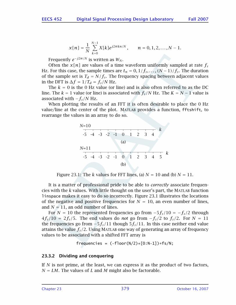
DRA
FT
EECS 452 Digital Signal Processing Design Laboratory Fall 2007
x[n] =1
N
N−1∑
k=0
X[k]ej2πkn/N , n = 0,1,2, . . . , N − 1.
Frequently e−j2π/N is written as WN .
Often the x[n] are values of a time waveform uniformly sampled at rate fsHz. For this case, the sample times are tn = 0,1/fs, . . . , (N−1)/fs . The duration
of the sample set is Td = N/fs . The frequency spacing between adjacent values
in the DFT is ∆f = 1/Td = fs/N Hz.
The k = 0 is the 0 Hz value (or line) and is also often referred to as the DC
line. The k = 1 value (or line) is associated with fs/N Hz. The K = N − 1 value is
associated with −fs/N Hz.
When plotting the results of an FFT it is often desirable to place the 0 Hz
value/line at the center of the plot. MATLAB provides a function, fftshift, to
rearrange the values in an array to do so.
JR QE~F
JR QEÄF
RJQ JP JO JN M N O P
JQ JP JO JN M N O PkZNM
kZNN
â
â
Figure 23.1: The k values for FFT lines, (a) N = 10 and (b) N = 11.
It is a matter of professional pride to be able to correctly associate frequen-
cies with the k values. With little thought on the user’s part, the MATLAB function
linspace makes it easy to do so incorrectly. Figure 23.1 illustrates the locations
of the negative and positive frequencies for N = 10, an even number of lines,
and N = 11, an odd number of lines.
For N = 10 the represented frequencies go from −5fs/10 = −fs/2 through
4fs/10 = 2fs/5. The end values do not go from −fs/2 to fs/2. For N = 11
the frequencies go from −5fs/11 though 5fs/11. In this case neither end value
attains the value fs/2. Using MATLAB one way of generating an array of frequency
values to be associated with a shifted FFT array is
frequencies = (-floor(N/2)+[0:N-1])*fs/N;
23.3.2 Dividing and conquering
If N is not prime, at the least, we can express it as the product of two factors,
N = LM . The values of L and M might also be factorable.
Chapter 23 379 October 16, 2007

DRA
FT
EECS 452 Digital Signal Processing Design Laboratory Fall 2007
One can count from 0 to N − 1 by writing n in the form
n =mL+ l, 0 ≤m ≤M − 1, 0 ≤ l ≤ L− 1
or alternatively
n = lM +m, 0 ≤m ≤M − 1, 0 ≤ l ≤ L− 1.
These these two indexings express a one-dimensional list of values in two
dimensional form. For each value of n there is a unique set of values, l and m
such that n = f(l,m). Only the simple linear combinations of l and m listed
above are considered here.
If we write the DFT replacing values n using one of these representations and
k using the other we have
X[qL+ p] =L−1∑
l=0
M−1∑
m=0
x[lM +m]W (lM+m)(qL+p)N ,
=L−1∑
l=0
M−1∑
m=0
x[lM +m]W lqLMN W
lpMN W
mqLN W
mpN ,
=M−1∑
m=0
WmpN
L−1∑
l=0
x[lM +m]W lpL
WmqM ,
where 0 ≤ l, p ≤ L− 1 and 0 ≤m,q ≤M − 1.
Let xm(l), m = 0,1, . . . ,M − 1, be the set of L sample values formed by
starting at the m-th sample and taking every M-th. Write Xm[p] the DFT of the
m-th set. Then
X[qL + p] =M−1∑
m=0
(
WmpN Xm[p]
)
WmqM . (23.1)
Next we work through the steps indicated by the above equation.
The re-sampled data values can be thought of as having been reordered in
the form of a M × L array
x[0] x[M] x[2M] · · · x[(L− 1)M]
x[1] x[M + 1] x[2M + 1] · · · x[(L− 1)M + 1]...
......
...
x[M − 1] x[2M − 1] x[3M − 1] · · · x[L− 1] .
The L-value DFTs are formed of each row.
X0[0] X0[1] X0[2] · · · X0[L− 1]
X1[0] X1[1] X1[2] · · · X1[L− 1]...
......
...
XM−1[0] XM−1[1] XM−1 · · · XM−1[L− 1] .
Chapter 23 380 October 16, 2007
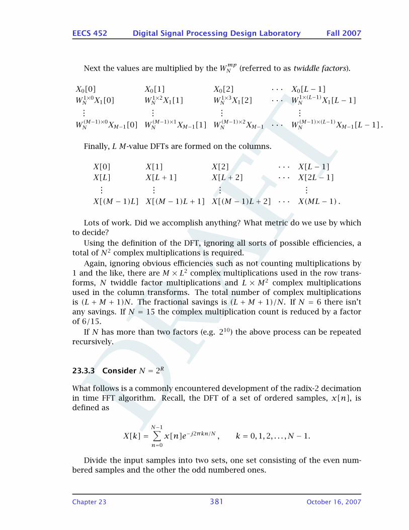
DRA
FT
EECS 452 Digital Signal Processing Design Laboratory Fall 2007
Next the values are multiplied by the WmpN (referred to as twiddle factors).
X0[0] X0[1] X0[2] · · · X0[L− 1]
W 1×0N X1[0] W 1×2
N X1[1] W 1×3N X1[2] · · · W
1×(L−1)N X1[L− 1]
......
......
W(M−1)×0N XM−1[0] W
(M−1)×1N XM−1[1] W
(M−1)×2N XM−1 · · · W
(M−1)×(L−1)N XM−1[L− 1] .
Finally, L M-value DFTs are formed on the columns.
X[0] X[1] X[2] · · · X[L− 1]
X[L] X[L+ 1] X[L+ 2] · · · X[2L − 1]...
......
...
X[(M − 1)L] X[(M − 1)L+ 1] X[(M − 1)L+ 2] · · · X(ML− 1) .
Lots of work. Did we accomplish anything? What metric do we use by which
to decide?
Using the definition of the DFT, ignoring all sorts of possible efficiencies, a
total of N2 complex multiplications is required.
Again, ignoring obvious efficiencies such as not counting multiplications by
1 and the like, there are M × L2 complex multiplications used in the row trans-
forms, N twiddle factor multiplications and L × M2 complex multiplications
used in the column transforms. The total number of complex multiplications
is (L +M + 1)N. The fractional savings is (L +M + 1)/N. If N = 6 there isn’t
any savings. If N = 15 the complex multiplication count is reduced by a factor
of 6/15.
If N has more than two factors (e.g. 210) the above process can be repeated
recursively.
23.3.3 Consider N = 2R
What follows is a commonly encountered development of the radix-2 decimation
in time FFT algorithm. Recall, the DFT of a set of ordered samples, x[n], is
defined as
X[k] =N−1∑
n=0
x[n]e−j2πkn/N , k = 0,1,2, . . . ,N − 1.
Divide the input samples into two sets, one set consisting of the even num-
bered samples and the other the odd numbered ones.
Chapter 23 381 October 16, 2007

DRA
FT
EECS 452 Digital Signal Processing Design Laboratory Fall 2007
X[k] =N/2−1∑
m=0
x[2m]e−j2πk2m/N +N/2−1∑
m=0
x[2m + 1]e−j2πk(2m+1)/N ,
=N/2−1∑
m=0
x[2m]e−j2πkm/(N/2) + e−j2πk/NN/2−1∑
m=0
x[2m + 1]e−j2πkm/(N/2).
The N point DFT has been converted into a weighted sum of two N/2 point
DFTs. Doing a brute force count of complex multiplications, the original DFT
requires N2, the split version N2/4+N. The number of complex multiplications
has been reduced.
The splitting process can be done again on the two N/2 point DFTs. This
results in four N/4 value DFTs. Moving between splitting levels sometimes is
referred to as moving between layers of the computation. For a N = 2R value
DFT there will be R = log2(N) layers.
Figure 23.2 illustrates the computational flow for N = 8. 23.3 illustrates the
tQ
tQ
tQ
tQ
tM
tM
tM
tM
tS
tM
tN
tP
tQ
tR
tS
tO
tT
tM
tO
tQ
tS
tM
tO
tQ
ñM
ñQ
ñO
ñS
ñN
ñR
ñP
ñT
uM
uN
uO
uP
uQ
uR
uS
uT
Figure 23.2: Computational flow for a decimation in time FFT, N = 8. The N
subscripts on the Ws are not shown.
computational flow for N = 8. Note that
e−jπm(k+N/2)/(N/2) = −e−j2πmk/(N/2).
Chapter 23 382 October 16, 2007
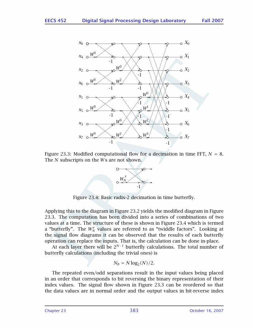
DRA
FT
EECS 452 Digital Signal Processing Design Laboratory Fall 2007
tM
tM
tM
tM
tM
JN
JN
ñM
ñQ
ñO
ñS
ñN
ñR
ñP
ñT
uM
uN
uO
uP
uQ
uR
uS
uT
JN
JN
JN
JN
tM
tN
tP
tO
tO
tM
tO
JN
JN
JN
JN
JN
JN
Figure 23.3: Modified computational flow for a decimation in time FFT, N = 8.
The N subscripts on the Ws are not shown.
tk
JN
ê
Figure 23.4: Basic radix-2 decimation in time butterfly.
Applying this to the diagram in Figure 23.2 yields the modified diagram in Figure
23.3. The computation has been divided into a series of combinations of two
values at a time. The structure of these is shown in Figure 23.4 which is termed
a “butterfly”. The W rN values are referred to as “twiddle factors”. Looking at
the signal flow diagrams it can be observed that the results of each butterfly
operation can replace the inputs. That is, the calculation can be done in-place.
At each layer there will be 2N−1 butterfly calculations. The total number of
butterfly calculations (including the trivial ones) is
Nb = N log2(N)/2.
The repeated even/odd separations result in the input values being placed
in an order that corresponds to bit reversing the binary representation of their
index values. The signal flow shown in Figure 23.3 can be reordered so that
the data values are in normal order and the output values in bit-reverse index
Chapter 23 383 October 16, 2007
DRA
FT
EECS 452 Digital Signal Processing Design Laboratory Fall 2007
order with the in-place capability retained. In place calculation is not possible
for normal order input and output indices. We will place the data into bit-reverse
order prior to transforming giving the resulting output values in normal order.
23.3.3.1 Radix-2 FFT pseudo-code
Using Figure 23.3 we can create a word description of a subroutine/hardware for
calculating a DIT FFT. The block diagram was developed working from right to
left. We now work from left to right.
• Loop over R layers counting r = 0,1, . . . , R − 1.
• At layer r there are 2N−r−1 2r+1 point DFTs to be formed. For example, at
layer 0 there N/2 2 point DFTs to be formed. These are generated from
the bit-reversed indexed input samples. The calculation is in place with the
results serving as the inputs to the layer 1 calculation. The value ofW 0N is 1.
The butterflies use only additions and subtractions. These are referred to
trivial butterflies. The spacing between butterfly inputs is one. The spacing
between FFTs is 2.
• At layer one there will be 2N−2 FFTs to be formed having size 4. The twiddle
factor values in involved are 1 and j. Again only addition and subtractions
are needed. The butterflies at this layer are also considered trivial. The
spacing between butterfly inputs is 2. The separation between FFTs is 4.
• And so on.
This leads to the pseudo code (sort of C with complex arithmetic):
nFFTs = N/2; FFTsize = 2;for(r = 0; r < R; r++)
for(fft = 0; fft < nFFTs; fft++) for(butterfly = 0; butterfly < (FFTsize/2); butterfly++)
top_index = fft*FFTsize+butterfly;bot_index = top_index+(FFTsize/2);w_index = butterfly*nFFTs;temp = W[w_index]*data[bot_index];data[bot_index] = data[top_index]-temp; // update bot first!data[top_index] = data[top_index]+temp; // now update top
nFFTs = (nFFTs/2); FFTsize = (FFTsize*2);
The above pseudo-code was used to create a test program in C which was
used to verify the desired result.
Chapter 23 384 October 16, 2007
DRA
FT
EECS 452 Digital Signal Processing Design Laboratory Fall 2007
The FFT is formed using three loops. The outer loop moves the processing
left to right a layer at a time. The next loop is over the number of DFTs being
formed for the current layer. The inner loop evaluates the butterflies associated
with the current sub-FFT. This code illustrates the loop control structure, the
data and twiddle factor indexing and butterfly structure.
Next, we rewrite the above code making it more VHDL friendly.
nFFTs = N/2; FFTsize = 2;for(r = 0; r < R; r++)
FFTstart = 0;for(fft = 0; fft < nFFTs; fft++)
w_index = 0;for(butterfly = 0; butterfly < (FFTsize/2); butterfly++)
top_index = FFTstart+butterfly;bot_index = top_index+(FFTsize/2);temp = W[w_index]*data[bot_index];data[bot_index] = data[top_index]-temp; // update bot first!data[top_index] = data[top_index]+temp; // now update topw_index = w_index+nFFTs;
FFTstart = FFTstart+FFTsize;
nFFTs = (nFFTs>>1); FFTsize = (FFTsize<<1); // shifts are easy to do
Multiplications associated with index calculations have been replaced by ad-
ditions. The values of FFTsize/2 are are essentially free at the VHDL level (why
might one think this?).
23.3.3.2 Implementing the DIT radix-2 butterfly
The radix-2 butterfly is shown in Figure 23.4. It requires one complex multi-
plier and two adders. These are to be implemented using bit-serial arithmetic.
Normally the product two complex numbers a+ jb and c + jd is written
(a+ jb)(c + jd) = ac − bd+ j(bc + ad).
There are four real multiplication and two add/subtract operations.
The number of multiplications can be reduced to three,
(a+ jb)(c + jd) = a(c − d)+ (a− b)d+ j[b(c + d)+ (a− b)d].
Other three multiplier orderings are possible, for example [?],
(a+ jb)(c + jd) = a(c + d)− d(a+ b)+ j[a(c + d)− c(a− b)].
There is even a relatively recent patent (cite) that appears to patent a three
multiplier hardware configuration. I believe there is prior art [?].
Chapter 23 385 October 16, 2007
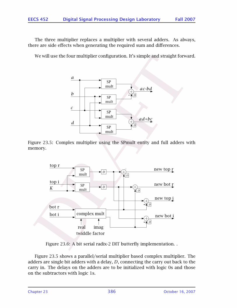
DRA
FT
EECS 452 Digital Signal Processing Design Laboratory Fall 2007
The three multiplier replaces a multiplier with several adders. As always,
there are side effects when generating the required sum and differences.
We will use the four multiplier configuration. It’s simple and straight forward.
a
pmãìäí
pmãìäí
pmãìäí
pmãìäí
~
Ä
Å
Ç
~ÅJÄÇ
~ÇHÄÅa
Figure 23.5: Complex multiplier using the SPmult entity and full adders with
memory.
a
a
apmãìäí
pmãìäíh a
íçé ê
íçé á
Äçí êÄçí á ÅçãéäÉñ ãìäí
åÉï=íçé ê
åÉï=íçé á
åÉï=Äçí ê
åÉï=Äçí á
a
a
íïáÇÇäÉ=Ñ~ÅíçêêÉ~ä áã~Ö
Figure 23.6: A bit serial radix-2 DIT butterfly implementation. .
Figure 23.5 shows a parallel/serial multiplier based complex multiplier. The
adders are single bit adders with a delay, D, connecting the carry out back to the
carry in. The delays on the adders are to be initialized with logic 0s and those
on the subtractors with logic 1s.
Chapter 23 386 October 16, 2007
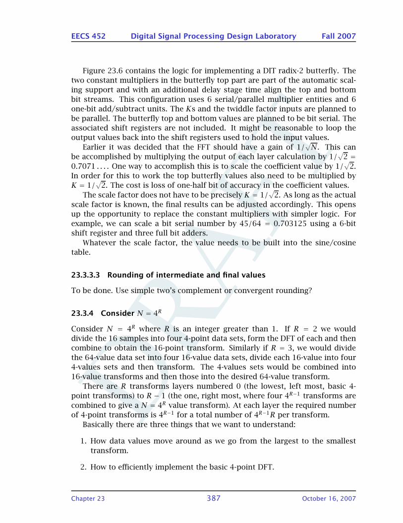
DRA
FT
EECS 452 Digital Signal Processing Design Laboratory Fall 2007
Figure 23.6 contains the logic for implementing a DIT radix-2 butterfly. The
two constant multipliers in the butterfly top part are part of the automatic scal-
ing support and with an additional delay stage time align the top and bottom
bit streams. This configuration uses 6 serial/parallel multiplier entities and 6
one-bit add/subtract units. The Ks and the twiddle factor inputs are planned to
be parallel. The butterfly top and bottom values are planned to be bit serial. The
associated shift registers are not included. It might be reasonable to loop the
output values back into the shift registers used to hold the input values.
Earlier it was decided that the FFT should have a gain of 1/√N. This can
be accomplished by multiplying the output of each layer calculation by 1/√
2 =0.7071 . . . . One way to accomplish this is to scale the coefficient value by 1/
√2.
In order for this to work the top butterfly values also need to be multiplied by
K = 1/√
2. The cost is loss of one-half bit of accuracy in the coefficient values.
The scale factor does not have to be precisely K = 1/√
2. As long as the actual
scale factor is known, the final results can be adjusted accordingly. This opens
up the opportunity to replace the constant multipliers with simpler logic. For
example, we can scale a bit serial number by 45/64 = 0.703125 using a 6-bit
shift register and three full bit adders.
Whatever the scale factor, the value needs to be built into the sine/cosine
table.
23.3.3.3 Rounding of intermediate and final values
To be done. Use simple two’s complement or convergent rounding?
23.3.4 Consider N = 4R
Consider N = 4R where R is an integer greater than 1. If R = 2 we would
divide the 16 samples into four 4-point data sets, form the DFT of each and then
combine to obtain the 16-point transform. Similarly if R = 3, we would divide
the 64-value data set into four 16-value data sets, divide each 16-value into four
4-values sets and then transform. The 4-values sets would be combined into
16-value transforms and then those into the desired 64-value transform.
There are R transforms layers numbered 0 (the lowest, left most, basic 4-
point transforms) to R − 1 (the one, right most, where four 4R−1 transforms are
combined to give a N = 4R value transform). At each layer the required number
of 4-point transforms is 4R−1 for a total number of 4R−1R per transform.
Basically there are three things that we want to understand:
1. How data values move around as we go from the largest to the smallest
transform.
2. How to efficiently implement the basic 4-point DFT.
Chapter 23 387 October 16, 2007
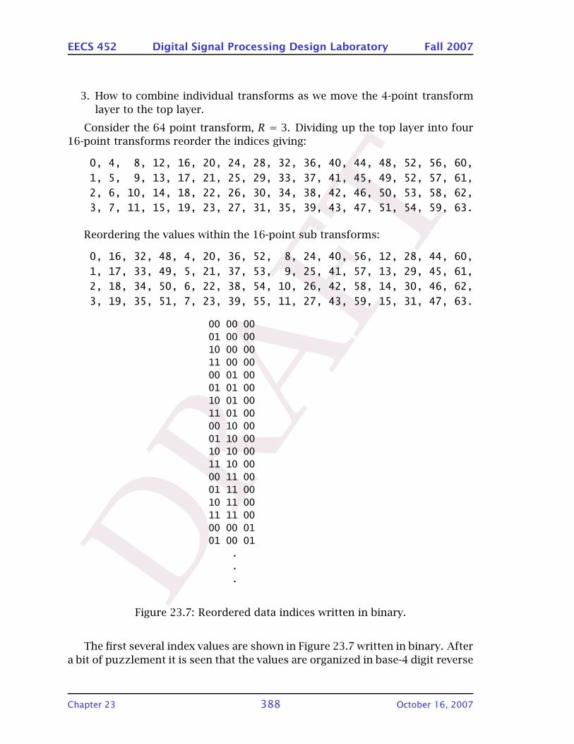
DRA
FT
EECS 452 Digital Signal Processing Design Laboratory Fall 2007
3. How to combine individual transforms as we move the 4-point transform
layer to the top layer.
Consider the 64 point transform, R = 3. Dividing up the top layer into four
16-point transforms reorder the indices giving:
0, 4, 8, 12, 16, 20, 24, 28, 32, 36, 40, 44, 48, 52, 56, 60,
1, 5, 9, 13, 17, 21, 25, 29, 33, 37, 41, 45, 49, 52, 57, 61,
2, 6, 10, 14, 18, 22, 26, 30, 34, 38, 42, 46, 50, 53, 58, 62,
3, 7, 11, 15, 19, 23, 27, 31, 35, 39, 43, 47, 51, 54, 59, 63.
Reordering the values within the 16-point sub transforms:
0, 16, 32, 48, 4, 20, 36, 52, 8, 24, 40, 56, 12, 28, 44, 60,
1, 17, 33, 49, 5, 21, 37, 53, 9, 25, 41, 57, 13, 29, 45, 61,
2, 18, 34, 50, 6, 22, 38, 54, 10, 26, 42, 58, 14, 30, 46, 62,
3, 19, 35, 51, 7, 23, 39, 55, 11, 27, 43, 59, 15, 31, 47, 63.
00 00 0001 00 0010 00 0011 00 0000 01 0001 01 0010 01 0011 01 0000 10 0001 10 0010 10 0011 10 0000 11 0001 11 0010 11 0011 11 0000 00 0101 00 01
.
.
.
Figure 23.7: Reordered data indices written in binary.
The first several index values are shown in Figure 23.7 written in binary. After
a bit of puzzlement it is seen that the values are organized in base-4 digit reverse
Chapter 23 388 October 16, 2007
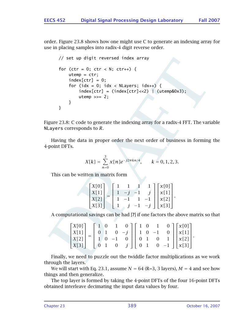
DRA
FT
EECS 452 Digital Signal Processing Design Laboratory Fall 2007
order. Figure 23.8 shows how one might use C to generate an indexing array for
use in placing samples into radix-4 digit reverse order.
// set up digit reversed index array
for (ctr = 0; ctr < N; ctr++) utemp = ctr;index[ctr] = 0;for (idx = 0; idx < NLayers; idx++)
index[ctr] = (index[ctr]<<2) | (utemp&0x3);utemp >>= 2;
Figure 23.8: C code to generate the indexing array for a radix-4 FFT. The variable
NLayers corresponds to R.
Having the data in proper order the next order of business in forming the
4-point DFTs.
X[k] =3∑
n=0
x[n]e−j2πkn/4, k = 0,1,2,3.
This can be written in matrix form
X[0]
X[1]
X[2]
X[3]
=
1 1 1 1
1 −j −1 j
1 −1 1 −1
1 j −1 −j
x[0]
x[1]
x[2]
x[3]
.
A computational savings can be had [?] if one factors the above matrix so that
X[0]
X[1]
X[2]
X[3]
=
1 0 1 0
0 1 0 −j1 0 −1 0
0 1 0 j
1 0 1 0
1 0 −1 0
0 1 0 1
0 1 0 −1
x[0]
x[1]
x[2]
x[3]
.
Finally, we need to puzzle out the twiddle factor multiplications as we work
through the layers.
We will start with Eq. 23.1, assume N = 64 (R=3, 3 layers), M = 4 and see how
things and then generalize.
The top layer is formed by taking the 4-point DFTs of the four 16-point DFTs
obtained interleave decimating the input data values by four.
Chapter 23 389 October 16, 2007

DRA
FT
EECS 452 Digital Signal Processing Design Laboratory Fall 2007
X[p] =3∑
m=0
X0[p]
X[L+ p] =3∑
m=0
WpNX1[p]W
m4
X[2L+ p] =3∑
m=0
W2pN X2[p]W
2m4
X[3L+ p] =3∑
m=0
W3pN X2[p]W
3m4
xézMu
uNxéz
Oxézu
Pxézu
xiHézu
xézu
uxOiHézuxPiHéz
Ntk
é
tkOé
tkPé
Q=éçáåíacq
Figure 23.9: Twiddle factor weighted radix-4 butterfly.
Figure 23.9 shows a block diagram representation of these equations.
At the last layer (layer 2) there are four 16-point DFTs that have to be com-
bined into one 64-point FFT. The value of N is 64 and the p values range from 0
through 15.
At layer 1 there four 16-point DFTs that have to be formed. Each is to be
formed from four 4-point DFTs. For each the value of N is 16 and the p values
range from 0 through 3.
At layer 0 there are sixteen 4-point DFTs that need to be formed. For each
the value of p is 0. The twiddle factors are all equal to 1.
Extrapolating to arbitrary R, let r be the layer count running from 0 at the
4-point DFT layer to R − 1 at the final layer.
At layer R − 1 there will be four 4R−1 value DFTs that will combined into a
single N = 4R value DFT.
At layer R − 2 there are four N = 4R−1 value DFTs that need to be formed.
Each from four 4R−2 value DFTs.
And so on.
Chapter 23 390 October 16, 2007
DRA
FT
EECS 452 Digital Signal Processing Design Laboratory Fall 2007
When implementing the transform one starts at layer 0 and works toward
layer R−1. At layer 0 there are 4R−1 four point DFTs that need to be formed. At
layer 1 there will be 4R−2 16 point DFTs formed. At layer 2, 4R−3 64 value DFTs
formed. At layer R − 1 only one 4R value DFT is formed. In general, at layer r ,
0 ≤ r ≤ R − 1, the number of DFTs to be formed is 4R−r−1 each of size 4r+1.
At layer r the size of the DFT being formed is Nr = 4r+1. The twiddle factor
values used areWmpNr wherem = 0,1,2,3 and 0 ≤ p ≤ 4r−1. Often one has avail-
able a size N = 4R twiddle factor table. Recall that WNr = exp(−j2π/Nr ). The
value of Nr can easily be changed by multiplying numerator and denominator of
the complex exponential by the same factor. In particular
mp
4r+1×
4R−r−1
4R−r−1=mp4R−r−1
4R.
Using a fixed 4R value table the twiddle factor values needed at layer r are
Wmp4r = Wmp4R−r−1
4R .
The values of km used to index the table need only be shifted left by 2(R−r−1)
bits in order to use the larger table. An alternative is to multiply the values of
mp by 4R−r−1 which also is the number of DFTs being formed at layer r .
loop on layer, rloop on number of DFTs being formed by this layer
loop on butterflys in DFT sizedo radix-4 butterfly
end loopend loop
end loop
A test program was written using floating point. Appendix 23.5 contains the
C source code. The program uses “random” numbers and writes the input and
output values into files for verification using MATLAB. No attempt was made to
exploit efficiencies. The basic goal was to get the loop indexing correct and the
twiddled radix-4 butterfly to work properly. Somewhat surprisingly the FFT code
worked on the first try.
23.3.5 What about the inverse?
To be written.
23.4 Radix-2 FFT development first steps
A “reasonable” amount of time was spent in sketching on a legal pad various
ways the yaFFT2 entity might be implemented. When doing the paper studies
the following considerations were kept in mind.
Chapter 23 391 October 16, 2007

DRA
FT
EECS 452 Digital Signal Processing Design Laboratory Fall 2007
• One reason for doing this project is to gain experience. This is a starter
project. It is expected that mistakes and, maybe, a few not so good de-
cisions will be made. It expected that, eventually, a new version will be
created based upon experience gained from this version.
• As a first FFT project, it should be useful but not complicated. Get it right
first, go for performance later.
• Initial testing will be either use either the C5510 linked via McBSP/SPI or
MATLAB on a PC using a USB/FIFO interface, or both.
• The design will divided into modules with low intercommunication needs.
The serial/parallel radix-2 butterfly appears to require minimal FPGA resources.
Its main drawback is the number of clock tics that it needs. One way to speed up
its performance is to use multiple units. If there were two units one unit could
be doing its arithmetic while the other was being loaded and unloaded.
With this thought in mind the yaFFT2 entity will be implemented using a
single butterfly unit but using a bus structure that will hopefully permit ready
addition of additional butterfly units. Figure 23.10 illustrates the organization
being thought about.
ÄìííÉêÑäó ÄìííÉêÑäó Ç~í~ãÉãçêó
íïáÇÇäÉãÉãçêó
~ÇÇêÉëë Ç~í~
Ç~í~~ÇÇêÉëë
ÅçåíêçääÉê
Åçåíêçä=ëáÖå~äëåçí=ëÜçïå
ÉñíÉêå~ä
ó~ccqO=Éåíáíó
Figure 23.10: Initial block diagram for the yaFFt2 entity showing basic address-
ing and data flow. Control signals not shown (well, actually not defined at this
point).
Design generally balances thought versus action. Too little thought generally
results in a lot of useless action. To much thought and nothing is accomplished,
at least not at a useful rate.
Anyway, the itch for action is present, it’s going to be scratched. A reasonable
starting point is to implement the butterfly entity along with the twiddle factor
memory and a rudimentary controller. A USB/FIFO controller will be used to
move data and commands between the FPGA and a PC (most likely via a MATLAB
test program).
Chapter 23 392 October 16, 2007
DRA
FT
EECS 452 Digital Signal Processing Design Laboratory Fall 2007
23.4.1 Butterfly entity
• 48-bit bidirectional data/twiddle bus.
• load signal to copy 36-bit complex twiddle factor into twiddle factor regis-
ter.
• load signal to copy 48-bit complex data value into shift register.
• request line to initiate processing.
• ack/ready line to acknowledge start of processing and when it has been
completed.
• output enable line to place contents of the 48-bit result register onto the
data lines.
• reset and clock lines.
The lab spmult entity will be used to implement the multipliers.
23.4.2 Twiddle factor ROM
MATLAB will be used to generate the initialization portion of the twiddle BRAM
entity. 1024 18-bit values of one half period of the sine function will be stored
using a single block RAM. The values will be scaled by 1/√
2.
23.4.3 USB/FIFO controller
Unit purchased from SparkFun. Implements a USB to 8-bit FIFO link. Drivers for
the Pc are included that can be used to develop control/access software. At the
other end the unit looks like two FIFOs, one for data from the PC and one for
data to the FIFO.
23.4.4 Testing and the results
Chapter 23 393 October 16, 2007

DRA
FT
EECS 452 Digital Signal Processing Design Laboratory Fall 2007
23.5 Radix-4 floating point FFT test C code
Chapter 23 394 October 16, 2007
DRA
FT
24 : Lab exercise 7 – real-time Fast
Fourier Transform
24.1 Introduction . . . . . . . . . . . . . . . . . . . . . . . . . . . . . . . . . . 396
24.2 C5510 exercise . . . . . . . . . . . . . . . . . . . . . . . . . . . . . . . . 396
24.2.1 Prelab . . . . . . . . . . . . . . . . . . . . . . . . . . . . . . . . . . 396
24.2.2 Exercise . . . . . . . . . . . . . . . . . . . . . . . . . . . . . . . . . 397
24.2.3 Things to be done . . . . . . . . . . . . . . . . . . . . . . . . . . . 398
24.2.4 Some things that might be done . . . . . . . . . . . . . . . . . . 398
24.2.5 Report . . . . . . . . . . . . . . . . . . . . . . . . . . . . . . . . . . 402
24.3 S3SB exercise . . . . . . . . . . . . . . . . . . . . . . . . . . . . . . . . . . 403
24.3.1 Prelab . . . . . . . . . . . . . . . . . . . . . . . . . . . . . . . . . . 403
24.3.2 Exercise . . . . . . . . . . . . . . . . . . . . . . . . . . . . . . . . . 403
24.3.3 Report . . . . . . . . . . . . . . . . . . . . . . . . . . . . . . . . . . 403
24.4 Other versions are available . . . . . . . . . . . . . . . . . . . . . . . . 403
24.4.1 Large memory model 8K data set size . . . . . . . . . . . . . . 403
24.4.2 1K version generating display on a PC . . . . . . . . . . . . . . 405
24.5 TI DSPlib manual pages . . . . . . . . . . . . . . . . . . . . . . . . . . . 405
24.6 List of codes . . . . . . . . . . . . . . . . . . . . . . . . . . . . . . . . . . 405
24.6.1 RTFFT.c . . . . . . . . . . . . . . . . . . . . . . . . . . . . . . . . . 405
24.6.2 rsquared64.asm . . . . . . . . . . . . . . . . . . . . . . . . . . . . 410
24.6.3 log2_64.asm . . . . . . . . . . . . . . . . . . . . . . . . . . . . . . 410
24.6.4 Buffered I/O support for the AIC23 . . . . . . . . . . . . . . . . 410
24.6.5 Interrupt vector . . . . . . . . . . . . . . . . . . . . . . . . . . . . 415
24.6.6 Interrupt support error, no_isr.asm . . . . . . . . . . . . . . . . 415
Chapter 24 395 October 16, 2007
DRA
FT
EECS 452 Digital Signal Processing Design Laboratory Fall 2007
24.1 Introduction
Lab exercise 7 involves implementation and use of FFT real time spectrum anal-
yser/display.
Uses the XVGA display system.
C5510 portion
Pretty much based on current lab. Acquired data, take FFT and display in real
time. Investigate leakage and windowing.
S3SB portion
Really want to be at the point where we, at the least, do the butterfly in the S3
and link via USB to MATLAB in order to evaluate numeric performance. Look at
effects of number of bits in rotator, kept after mac, rounding method.
Suggested reading
24.2 C5510 exercise
24.2.1 Prelab
Prelabs are to be done individually and are to be handed in at the
start of the lab period. Handwritten work will not be graded.
1. What is the name of the variable that is used in RTFFT.c to choose between
windowed and non-windowed (actually rectangular window) processing?
2. What is the name of the variable that is used in RTFFT.c to choose between
a Hamming window and a Chebyshev window?
3. What is the name of the array that is to be used to hold Q15 values for a
Chebyshev window?
4. Use MATLAB and generate a set of window weights in Q15 format for the
Chebyshev window (MATLAB’s chebwin function) with a R value of 100 (the
default value). These are for use in RTFFT.c. Use the value of N is as used
in the version whose listing is included in this write-up.
5. Give some thought on what you are going to for “free choice” portion of
this exercise. Gather what materials that you feel will help. Write a brief
description on what you plan to attempt and why you believe you will suc-
ceed. Coordinate your choice with your lab partner. You may both turn in
the same response to this particular part of the prelab.
Chapter 24 396 October 16, 2007
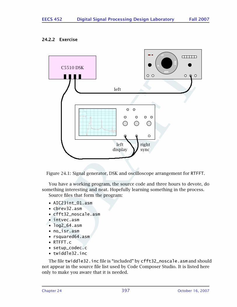
DRA
FT
EECS 452 Digital Signal Processing Design Laboratory Fall 2007
24.2.2 Exercise
`RRNM aph
äÉÑí
äÉÑíÇáëéä~ó
êáÖÜíëóåÅ
9: ;<<=>>?@
Figure 24.1: Signal generator, DSK and oscilloscope arrangement for RTFFT.
You have a working program, the source code and three hours to devote, do
something interesting and neat. Hopefully learning something in the process.
Source files that form the program:
• AIC23int_01.asm• cbrev32.asm• cfft32_noscale.asm• intvec.asm• log2_64.asm• no_isr.asm• rsquared64.asm• RTFFT.c• setup_codec.c• twiddle32.inc
The file twiddle32.inc file is “included” by cfft32_noscale.asm and should
not appear in the source file list used by Code Composer Studio. It is listed here
only to make you aware that it is needed.
Chapter 24 397 October 16, 2007

DRA
FT
EECS 452 Digital Signal Processing Design Laboratory Fall 2007
You will also have to incorporate the RTS library and a linker command file.
See the set of files supplied in the folder named lab7. As always, make a copy
of the files to work with in your user directory.
Because we are supplying our own interrupt vector there is the potential of
a conflict at build time with the interrupt vector contained in the RTS library.
When this happens the error message
error: can’t allocate vectors
will result.
The work around is to use the compilers option to specify the link order.
Simply select all the modules and add them to the link list. Then drag and drop
the RTS library so that it is last on the list.
24.2.3 Things to be done
1. How much time does it take RTFFT to generate the display using floating
point and the C library log10 function?
2. How much time does it take to generate the display using the fixed point
R2 and approximate log2 functions?
3. Add program support to read the DIP switches to allow manual setting of
the switch variables used to select between windowed and un-windowed
displays and for the windowed displays between the Hamming and Cheby-
shev windows. Also support the switch variable used to select between
floating point and fixed point display generation.
4. Install the Chebyshev window coefficient values that you generated for the
pre-lab. Look at the displays generated using the rectangle, Hamming, and
Chebyshev R=100 windows. Demonstrate to your lab instructor your pro-
cessing when using the Chebyshev window.
5. Modify the program in some manner to increase it’s performance, utility,
ease of use, etc. The grade on this part of the lab will depend on the appar-
ent effort and success that you achieve. Do something nontrivial and the
points awarded will match. Some ideas are given in the following section.
24.2.4 Some things that might be done
• In lecture a equiripple polynomial approximation to log2(m) was found
and a suggested (untried) set of instructions to implement it was shown.
This approximation is also the focus of a homework problem using MATLAB
Chapter 24 398 October 16, 2007
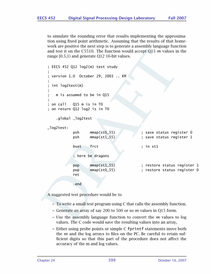
DRA
FT
EECS 452 Digital Signal Processing Design Laboratory Fall 2007
to simulate the rounding error that results implementing the approxima-
tion using fixed point arithmetic. Assuming that the results of that home-
work are positive the next step is to generate a assembly language function
and test it on the C5510. The function would accept Q15 m values in the
range [0.5,1) and generate Q12 16-bit values.
; EECS 452 Q12 log2(m) test study;; version 1.0 October 29, 2003 .. KM;; int log2test(m);; m is assumed to be in Q15;; on call Q15 m is in T0; on return Q12 log2 is in T0
.global _log2test
_log2test:psh mmap(st0_55) ; save status register 0psh mmap(st1_55) ; save status register 1
bset frct ; in st1
; here be dragons
pop mmap(st1_55) ; restore status register 1pop mmap(st0_55) ; restore status register 0ret
.end
A suggested test procedure would be to
– To write a small test program using C that calls the assembly function.
– Generate an array of say 200 to 500 or so m values in Q15 form.
– Use the assembly language function to convert the m values to log
values. The C code would save the resulting values into an array,
– Either using probe points or simple C fprintf statements move both
the m and the log arrays to files on the PC. Be careful to retain suf-
ficient digits so that this part of the procedure does not affect the
accuracy of the m and log values.
Chapter 24 399 October 16, 2007

DRA
FT
EECS 452 Digital Signal Processing Design Laboratory Fall 2007
– Use MATLAB to read the files, compute log2 values using the same m
values used on the C5510, compare the C5510 generated log2 values
producing an error plot,
– Compare the error plots generated using the C5510 data against the
error plot made for the homework.
– Assuming all goes well, modify log2_64 to use the polynomial and
test. Don’t forget that an extra shift will probably be needed because
log2_64 puts out Q9 values. The resulting function will be produc-
ing values as accurate as possible for the given number format. A
noteworthy achievement!
• The oscilloscope display hops about depending upon the values displayed.
This is caused by the AIC23 codec output being AC coupled. The average
of the display voltage must be zero. For example, if the display contains
a predominance of negative values the display shifts up to compensate.
At present the portion of the display between the end of the display values
and the start of the immediately following data (gap) is set to zero. It might
be possible to compute the DC value of the active portion of the display and
set the level of the gap to result in an zero DC level. The expectation is that
this would minimize the display hopping around.
• The program presently uses all available samples to generate successive
displays. No samples are ever lost. This means a data set starts up at
what ever point the previous one ended at. This causes a jumping round
of the display that could be reduced if one triggered the data acquisition
in the same manner as are oscilloscopes. This would involved monitoring
the data stream waiting for the input voltage to traverse a threshold level
either in the positive or negative going direction.
• The cbitrev32 function requires alignment of the FFT results in order to
work properly. How difficult is removing this restriction? Removal is cer-
tainly possible, what is the cost in execution time and is it worth it?
• The cfft32 function is probably “no holds barred” optimized code. The
program makes use of a pre-computed twiddle factor table. In addition to
taking up room in memory this table is probably the limiting factor in the
size of DFT that can be formed. There are many simple algorithms that
use a very small table of twiddle factor seeds and recursively calculate the
values as needed. This adds time overhead but does free up memory. It is
a very common situation where one can, in a sense, make a trade between
memory and execution time. How difficult would it be to modify cfft32 to
make use of a much smaller table?
Chapter 24 400 October 16, 2007

DRA
FT
EECS 452 Digital Signal Processing Design Laboratory Fall 2007
• The oscilloscope presently done include an indication of the range of dB
being displayed. A simple stair step pattern can be appended (or post-
pended) to each display to allow dB levels to be fairly easily determined.
The display currently (I believe) covers an impressive approximate 192 dB
range. Diplays steps of say 40 dB should allow useful interpretation of the
levels being displayed.
• The cfft2 function presently is limited to forming DFTs of 1024 complex
values or less. The present display program acquires real valued data and
converts to complex form by appending zero imaginary parts. After the
DFT has been formed the negative frequency components are discarded
and only the positive frequency DFT values are used to form the display.
An algorithm exists that allows one to use a N complex valued DFT to be
used to compute the DFT of a 2N real valued data set. Basically the N value
DFT is one layer short of forming the full DFT. The algorithm makes one
pass through the N value DFT to complete the 2N valued result. Only the
positive frequency values need to be computed.
• There are better ways to do this but· · · . At present the right channel is
used to trigger the oscilloscope display synchronizing the C5510 with the
oscilloscope display. This can also be done using the display itself. If the
right channel can be freed up then it can be used for other tasks.
For example it can be used to output a sinusoid for use in making transfer
function measurements. Data can be acquired on both the left and right
channels. Rather than generate a sinusoid pseudo-random noise can be
produced and statistical signal processing techniques can be used to make
broadband transfer and coherence measurements.
• There appears to be so much time left over from acquiring the data and
generating the display one should be able to implement digital filters in the
C5510 as part of the program itself and display transfer functions without
ever having to put samples though the AIC23.
• The only (non-rectangle) windowing supported by the program in its cur-
rent state is the Hamming window. This window has a simple mathematical
form and is easily generated using the standard C floating point functions.
Two window functions that have been found fairly effective are the Cheby-
shev and the Kaiser window. The Kaiser window being considered by many
as the most superior among superior windows.
It should be easy to generate, say, Chebyshev window weights for say 256,
512 and 1024 for data sets and simply build them into the program. A
more elegant solution to compute them as needed. Once computed there
is no need to recompute them until the data set size is changed.
Chapter 24 401 October 16, 2007
DRA
FT
EECS 452 Digital Signal Processing Design Laboratory Fall 2007
• The C5510 DSK is quite limited in supporting interactive user input. How-
ever there are four DIP switches that could be used to control the program
operation in real time. For example two switches could be used to select be-
tween four possible window functions. Rectangle (no window), Hamming,
Chebyshev, and one other would be good choices. Or, perhaps the fourth
setting could be used for some other action.
With some imagination and thought (both of which the current author is
lacking) other uses can be found for the remaining two switches.
• The way the AIC23 input and output is presently programmed the left and
right values move lock step with each other. The program can be organized
to buffer either or both the input and output splitting the left and right
channel data. This might be useful when setting up for making transfer
function measurements.
• The program as presently configured is operating using a 48 kHz data rate.
The A/D and D/A portions of the AIC23 are delta-sigma converters. I’m
quite surprised that pulses one or two sample times long are being gen-
erated as well as they are. Possibly one way to improve the display is to
repeat display values. In order to do this would require to drop the input
sample rate while keeping the display rate high. This is easily done by
simply skipping every second sample. Each display value can be repeated
twice, hopefully improving the display. This does reduce the display from
0 to 24 kHz to 0 to 12 kHz. Adequate for many tasks. Keeping one sam-
ple and skipping two drops the sample rate to 16 kHz giving a Nyquist
frequency of 8 kHz. Useful for many telephony applications.
• There are no doubt many other modifications that can be done to the cur-
rent software that result in useful program. Use your imagination. Experi-
ment.
24.2.5 Report
Provide information and detail sufficient to convince the grader that you deserve
a good grade for the exercise. If you deviate from you prelab plan note how and
why. It is likely that what you do will change from the prelab once you actually
start working with the actual code and ideas occur. The idea is for the prelab to
give some structure to your efforts but not so much structure that you are in a
straight jacket.
Chapter 24 402 October 16, 2007
DRA
FT
EECS 452 Digital Signal Processing Design Laboratory Fall 2007
24.3 S3SB exercise
24.3.1 Prelab
24.3.2 Exercise
24.3.3 Report
24.4 Other versions are available
This section contains information that is not directly relevant to this exercise.
It is included here for completeness and to make the information available for
potential use by projects.
In addition to the analyzer code used in this lab exercise there exist two
variations.
• A large memory model analyzer that supports FFT sizes up to 8K values.
• A simple modification of the lab code that generates its display on a PC run-
ning a terminal emulator (TeraTerm) that supports Tektronix 4010 graph-
ics.
It should also be possible to readily modify the code to use an 8K complex
FFT to calculate the spectra of a 16K real valued data set. Information on how to
do so can be found in many DSP texts and will be touched on in lecture.
24.4.1 Large memory model 8K data set size
A check of the TI 32-bit FFT code indicated that the size FFT size limit is deter-
mined by the size of the twiddle factor table contained in the twiddle32.incfile.
The contents of the TI twiddle32.inc factor file were studied and a MATLAB
script written to generate larger tables using the same format. This script is
included in Figure 24.2.
This script generates an assembly language (.asm) file rather than an include
(.inc) file. The code supplied by TI built the twiddle table into the assembly
of the FFT code using an include file. Changing the maximum size of the table
required reassembling the FFT code. Given an FFT object module (.obj) there
was no easy way to determine the maximum size FFT it supported. The decision
was to assemble the twiddle factor table separately from the FFT code. This was
accomplished without having to make any modifications to the TI FFT code. A
Chapter 24 403 October 16, 2007
DRA
FT
EECS 452 Digital Signal Processing Design Laboratory Fall 2007
% Script to compute cfft32 twiddle factor table%% 10apr2004 .. initial version .. K.Metzger
clear all;
M = 13; % 13 => 8192 size tableMB = M-1;
N = 2^M;ang = pi/N; % table values use this step sizesf = 2^31-1;fid = fopen(’twiddle32.asm’,’w’);fprintf(fid, ’;***************************************\n’);fprintf(fid, ’; EECS 452 V1.0 10Apr2004 .. KM\n’);fprintf(fid, ’;***************************************\n’);fprintf(fid, ’ .sect "SARAM2 ; place into second on-chip SA RAM block"\n’);fprintf(fid, ’ .def _twiddle32\n’);fprintf(fid, ’_twiddle32:\n’);
for idx = 0:N-1ridx = 0;test = idx;for idx2 = 0:M-1 % bit reverse the index value
if mod(test,2) == 1ridx = 2*ridx+1;
elseridx = 2*ridx;
endtest = floor(test/2);
endc = cos(ang*ridx);chex = round(sf*c);if chex < 0 chex = chex+2^32; endfprintf(fid, ’ .long 0x%08x ; [%d]; %.6f\n’, chex, ridx, c);
s = sin(ang*ridx);shex = round(sf*s);if shex < 0 shex = shex+2^32; endfprintf(fid, ’ .long 0x%08x ; [%d]; %.6f\n’, shex, ridx, s);
end
fclose(fid);
Figure 24.2: MATLAB script used to generate large FFT twiddle factor tables.
Chapter 24 404 October 16, 2007
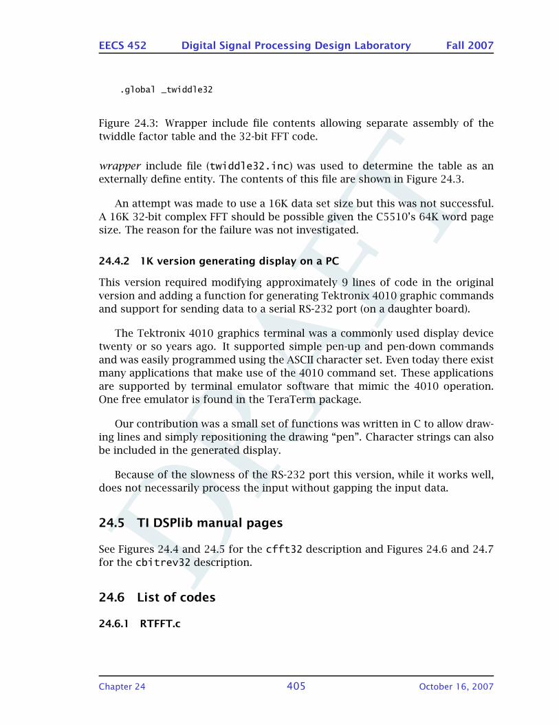
DRA
FT
EECS 452 Digital Signal Processing Design Laboratory Fall 2007
.global _twiddle32
Figure 24.3: Wrapper include file contents allowing separate assembly of the
twiddle factor table and the 32-bit FFT code.
wrapper include file (twiddle32.inc) was used to determine the table as an
externally define entity. The contents of this file are shown in Figure 24.3.
An attempt was made to use a 16K data set size but this was not successful.
A 16K 32-bit complex FFT should be possible given the C5510’s 64K word page
size. The reason for the failure was not investigated.
24.4.2 1K version generating display on a PC
This version required modifying approximately 9 lines of code in the original
version and adding a function for generating Tektronix 4010 graphic commands
and support for sending data to a serial RS-232 port (on a daughter board).
The Tektronix 4010 graphics terminal was a commonly used display device
twenty or so years ago. It supported simple pen-up and pen-down commands
and was easily programmed using the ASCII character set. Even today there exist
many applications that make use of the 4010 command set. These applications
are supported by terminal emulator software that mimic the 4010 operation.
One free emulator is found in the TeraTerm package.
Our contribution was a small set of functions was written in C to allow draw-
ing lines and simply repositioning the drawing “pen”. Character strings can also
be included in the generated display.
Because of the slowness of the RS-232 port this version, while it works well,
does not necessarily process the input without gapping the input data.
24.5 TI DSPlib manual pages
See Figures 24.4 and 24.5 for the cfft32 description and Figures 24.6 and 24.7
for the cbitrev32 description.
24.6 List of codes
24.6.1 RTFFT.c
Chapter 24 405 October 16, 2007

DRA
FT
EECS 452 Digital Signal Processing Design Laboratory Fall 2007
cfft32
4-19 Function Descriptions
32-Bit Forward Complex FFTcfft32
Function void cfft32 (LDATA *x, ushort nx, type);
Arguments
x[2*nx] Pointer to input vector containing nx complex elements (2*nxreal elements) in normal-order. On output, vector x containsthe nx complex elements of the FFT(x) in bit-reversed order.Complex numbers are stored in the interleaved Re-Imformat.
nx Number of complex elements in vector x. Must be between 4and 1024.
type FFT type selector. Types supported:
If type = SCALE, scaled version selected
If type = NOSCALE, non-scaled version selected
Description Computes a complex nx-point FFT on vector x, which is in normal order. Theoriginal content of vector x is destroyed in the process. The nx complex ele-ments of the result are stored in vector x in bit-reversed order.
Algorithm (DFT)
y[k] 1(scale factor)
nx1
i0
x[i] 2 * * i * knx j sin2 * * i * k
nx Overflow Handling Methodology If scale==1, scaling before each stage is implemented for over-
flow prevention.
Special Requirements This function requires the inclusion of fine “twiddle.inc” which contains the
twiddle table (automatically included).
Data memory alignment (reference cfft.cmd in examples/cfft32 directory):
Alignment of input database address: (n+1) LSBs must be zeros,where n=log2(nx).
Ensure t hat the entire array fits within a 64K boundary (the largestpossible array addressable by the 16-bit auxiliary register).
For best performance, the data buffer has to be in a DARAM block.
Implementation Notes Radix-2 DIT version of the FFT algorithm is implemented. The imple-
mentation is optimized for MIPS, not for code size.
If scale == 0, the first two stages are combined and implemented in radix-4for MIPS optimization.
Figure 24.4: First page of the DSPlib CFFT32 function description. (From
SPRU422F.)
Chapter 24 406 October 16, 2007
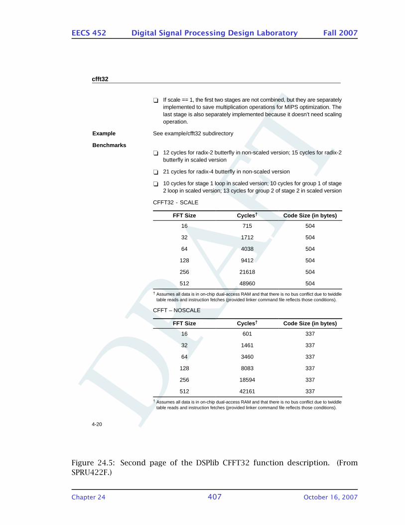
DRA
FT
EECS 452 Digital Signal Processing Design Laboratory Fall 2007
cfft32
4-20
If scale == 1, the first two stages are not combined, but they are separatelyimplemented to save multiplication operations for MIPS optimization. Thelast stage is also separately implemented because it doesn’t need scalingoperation.
Example See example/cfft32 subdirectory
Benchmarks 12 cycles for radix-2 butterfly in non-scaled version; 15 cycles for radix-2
butterfly in scaled version
21 cycles for radix-4 butterfly in non-scaled version
10 cycles for stage 1 loop in scaled version; 10 cycles for group 1 of stage2 loop in scaled version; 13 cycles for group 2 of stage 2 in scaled version
CFFT32 - SCALE
FFT Size Cycles † Code Size (in bytes)
16 715 504
32 1712 504
64 4038 504
128 9412 504
256 21618 504
512 48960 504
† Assumes all data is in on-chip dual-access RAM and that there is no bus conflict due to twiddletable reads and instruction fetches (provided linker command file reflects those conditions).
CFFT – NOSCALE
FFT Size Cycles † Code Size (in bytes)
16 601 337
32 1461 337
64 3460 337
128 8083 337
256 18594 337
512 42161 337
† Assumes all data is in on-chip dual-access RAM and that there is no bus conflict due to twiddletable reads and instruction fetches (provided linker command file reflects those conditions).
Figure 24.5: Second page of the DSPlib CFFT32 function description. (From
SPRU422F.)
Chapter 24 407 October 16, 2007
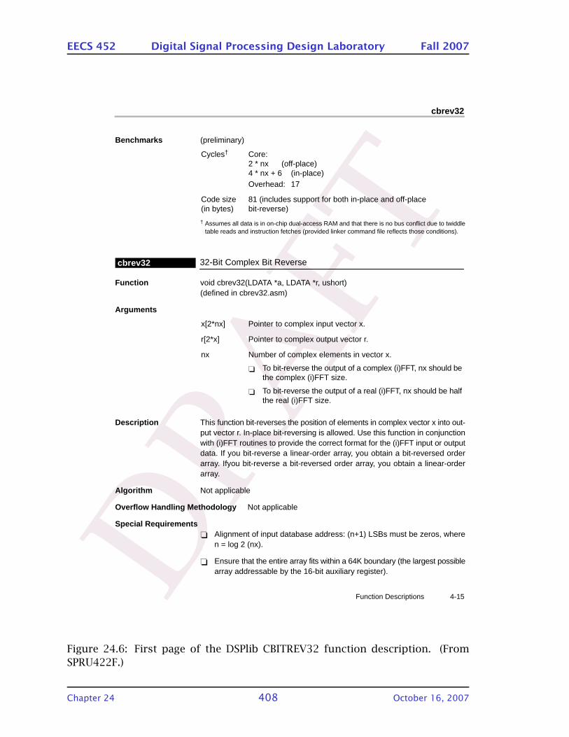
DRA
FT
EECS 452 Digital Signal Processing Design Laboratory Fall 2007
cbrev32
4-15 Function Descriptions
Benchmarks (preliminary)
Cycles† Core:2 * nx (off-place)4 * nx + 6 (in-place)Overhead: 17
Code size(in bytes)
81 (includes support for both in-place and off-placebit-reverse)
† Assumes all data is in on-chip dual-access RAM and that there is no bus conflict due to twiddletable reads and instruction fetches (provided linker command file reflects those conditions).
32-Bit Complex Bit Reversecbrev32
Function void cbrev32(LDATA *a, LDATA *r, ushort)(defined in cbrev32.asm)
Arguments
x[2*nx] Pointer to complex input vector x.
r[2*x] Pointer to complex output vector r.
nx Number of complex elements in vector x.
To bit-reverse the output of a complex (i)FFT, nx should bethe complex (i)FFT size.
To bit-reverse the output of a real (i)FFT, nx should be halfthe real (i)FFT size.
Description This function bit-reverses the position of elements in complex vector x into out-put vector r. In-place bit-reversing is allowed. Use this function in conjunctionwith (i)FFT routines to provide the correct format for the (i)FFT input or outputdata. If you bit-reverse a linear-order array, you obtain a bit-reversed orderarray. Ifyou bit-reverse a bit-reversed order array, you obtain a linear-orderarray.
Algorithm Not applicable
Overflow Handling Methodology Not applicable
Special Requirements Alignment of input database address: (n+1) LSBs must be zeros, where
n = log 2 (nx).
Ensure that the entire array fits within a 64K boundary (the largest possiblearray addressable by the 16-bit auxiliary register).
Figure 24.6: First page of the DSPlib CBITREV32 function description. (From
SPRU422F.)
Chapter 24 408 October 16, 2007
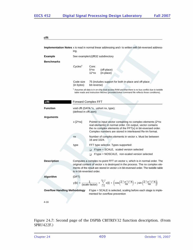
DRA
FT
EECS 452 Digital Signal Processing Design Laboratory Fall 2007
cfft
4-16
Implementation Notes x is read in normal linear addressing and r is written with bit-reversed address-ing.
Example See example/c(i)fft32 subdirectory
Benchmarks
Cycles† Core:5*nx (off-place)11*nx (in-place)
Code size(in bytes)
75 (includes support for both in-place and off-placebit-reverse)
† Assumes all data is in on-chip dual-access RAM and that there is no bus conflict due to twiddletable reads and instruction fetches (provided linker command file reflects those conditions).
Forward Complex FFTcfft
Function void cfft (DATA *x, ushort nx, type);(defined in cfft.asm)
Arguments
x [2*nx] Pointer to input vector containing nx complex elements (2*nxreal elements) in normal order. On output, vector containsthe nx complex elements of the FFT(x) in bit-reversed order.Complex numbers are stored in interleaved Re-Im format.
nx Number of complex elements in vector x. Must be between16 and 1024.
type FFT type selector. Types supported:
If type = SCALE, scaled version selected
If type = NOSCALE, non-scaled version selected
Description Computes a complex nx-point FFT on vector x, which is in normal order. Theoriginal content of vector x is destroyed in the process. The nx complex ele-ments of the result are stored in vector x in bit-reversed order. The twiddle tableis in bit-reversed order.
Algorithm (DFT)
y [k] 1(scale factor)
nx1
i0
x [i] cos2 * * i * knx j sin 2 * * i * k
nx
Overflow Handling Methodology If type = SCALE is selected, scaling before each stage is imple-mented for overflow prevention
Figure 24.7: Second page of the DSPlib CBITREV32 function description. (From
SPRU422F.)
Chapter 24 409 October 16, 2007

DRA
FT
EECS 452 Digital Signal Processing Design Laboratory Fall 2007
24.6.2 rsquared64.asm
24.6.3 log2_64.asm
24.6.4 Buffered I/O support for the AIC23
;File name: AIC23int_01.asm;; EECS 452 buffered AIC23 codec support for the C5510DSK;;; 11Oct2003 .. initial version .. K.Metzger; 11Apr2004 .. made small/large model independent .. KM; 8Feb2005 .. move no_isr to its own file .. KM;
.c54cm_off ;don’t want compatible with c54
.ARMS_on ;enable assembler for ARMS=1
.CPL_on ;enable assembler for CPL=1
.mmregs ;enable mem mapped register names
.global _startup, _no_isr, _resetv, _c_int00
.global Mc2R_int, Mc2X_int
.global _AD_flag, _DA_flag
.global _Mc2X_put, _Mc2X_put_setup
.global _Mc2R_get, _Mc2R_get_setup
.data
.bss Mc2X_buf_adr,2,1,4 ; aligned
.bss Mc2X_app_buf_off,1
.bss Mc2X_int_buf_off,1
.bss Mc2X_buf_size,1
.bss Mc2X_counter,1
.bss Mc2X_running_flag,1
.bss Mc2R_buf_adr,2,1,4 ; aligned
.bss Mc2R_app_buf_off,1
.bss Mc2R_int_buf_off,1
.bss Mc2R_buf_size,1
.bss Mc2R_counter,1
.text
.asg 0001100000000000b,my_ST0_55
Chapter 24 410 October 16, 2007

DRA
FT
EECS 452 Digital Signal Processing Design Laboratory Fall 2007
.asg 0110100100000000b,my_ST1_55
.asg 1001000000000000b,my_ST2_55
.asg 0001000000000010b,my_ST3_55
; Setup McBSP channel 2 codec interrupt support;; for now assumes setup_codec() has been called;
_startup:pshboth xar0mov #_resetv >> 8, ac0 ; get int vector address pagemov ac0,mmap(ivpd) ; set up DSP int addressmov ac0,mmap(ivph) ; set up host int addressamov #Mc2R_int,xar0 ; set up McB port 2 rcvr addrmov xar0,dbl(*((_resetv+0x60)/2))amov #Mc2X_int,xar0 ; set up McB port 2 xmtr addrmov xar0,dbl(*((_resetv+0x68)/2))or #0x3000,mmap(ifr0) ; clear Mc2 interrupt flagsor #0x3000,mmap(ier0) ; enable Mc2TX and Mc2RX interruptsmov #0,port(#0x3003) ; start Mc transmitter runningpopboth xar0ret
; Support for codec interrupt driven data transfers
Mc2R_int:psh mmap(st3_55)psh mmap(T0)psh mmap(T1)pshboth xar0pshboth xar1mov #my_ST0_55,mmap(st0_55) ; now configure the machinemov #my_ST1_55,mmap(st1_55)mov #my_ST2_55,mmap(st2_55)mov #my_ST3_55,mmap(st3_55)
amov #Mc2R_buf_adr,xar1 ; get buffer address addressmov *ar1(Mc2R_counter-Mc2R_buf_adr),T0 ; get # L&R values in buffermov *ar1(Mc2R_buf_size-Mc2R_buf_adr),T1 ; get number allowedcmp T0==T1,TC1 ; if equal fullbcc R2I_LA,!TC1 ; branch if roommov port(#0x3001),T0 ; clears the receive flagb Mc2R_exit ; and exits...samples onto the floor
R2I_LA:mov dbl(*ar1), xar0 ; get buffer addressadd *ar1(Mc2R_int_buf_off-Mc2R_buf_adr),ar0 ; and calculate where to placeadd *ar1(Mc2R_int_buf_off-Mc2R_buf_adr),ar0 ; pairs of valuesmov port(#0x3000),T0 ; get left value
Chapter 24 411 October 16, 2007

DRA
FT
EECS 452 Digital Signal Processing Design Laboratory Fall 2007
mov T0,*ar0+ ; and place into buffermov port(#0x3001),T0 ; get right value...and clear flagmov T0,*ar0 ; place into bufferadd #1,*ar1(Mc2R_counter-Mc2R_buf_adr) ; increment count of pairs presentmov *ar1(Mc2R_int_buf_off-Mc2R_buf_adr),T0 ; now update offset circularlyadd #1,T0 ; incrementcmp T0==T1,TC1 ; see if needs to be reset to buffer startbcc R2I_LB,!TC1 ; branch if notmov #0,T0 ; reset to buffer start
R2I_LB:mov T0,*ar1(Mc2R_int_buf_off-Mc2R_buf_adr) ; and update in memory
Mc2R_exit:popboth xar1popboth xar0pop mmap(T1)pop mmap(T0)pop mmap(st3_55)nop ; 6 nops stops remarks 99 and 100nopnopnopnopnopreti
; Support to fetch codec sample values L&R pair
_Mc2R_get:pshboth xar2 ; use it, save itpshboth xar3 ; use it, save itamov #Mc2R_buf_adr,xar3 ; get in sample buffer address address
Mc2R_wait:mov *ar3(Mc2R_counter-Mc2R_buf_adr),T0 ; get count of pairs in bufferbcc Mc2R_wait,T0==#0 ; wait if there aren’t anymov dbl(*ar3),xar2 ; set up buffer addressadd *ar3(Mc2R_app_buf_off-Mc2R_buf_adr),ar2 ; we are working with pairsadd *ar3(Mc2R_app_buf_off-Mc2R_buf_adr),ar2mov *ar2+,T0 ; fetch L valuemov T0,*ar0 ; and place in caller’s locationmov *ar2,T0 ; fetch R valuemov T0,*ar1 ; and place in caller’s locationsub #1,*ar3(Mc2R_counter-Mc2R_buf_adr) ; indivisible decrement of countmov *ar3(Mc2R_app_buf_off-Mc2R_buf_adr),T0 ; now update offset circularlyadd #1,T0 ; incrementmov *ar3(Mc2R_buf_size-Mc2R_buf_adr),T1 ; get limiting valuecmp T0==T1,TC1 ; if equal need to reset to 0bcc R2_LA,!TC1 ; branch if not equalmov #0,T0 ; zero to start of buffer
R2_LA:mov T0,*ar3(Mc2R_app_buf_off-Mc2R_buf_adr) ; and update in memorypopboth xar3
Chapter 24 412 October 16, 2007
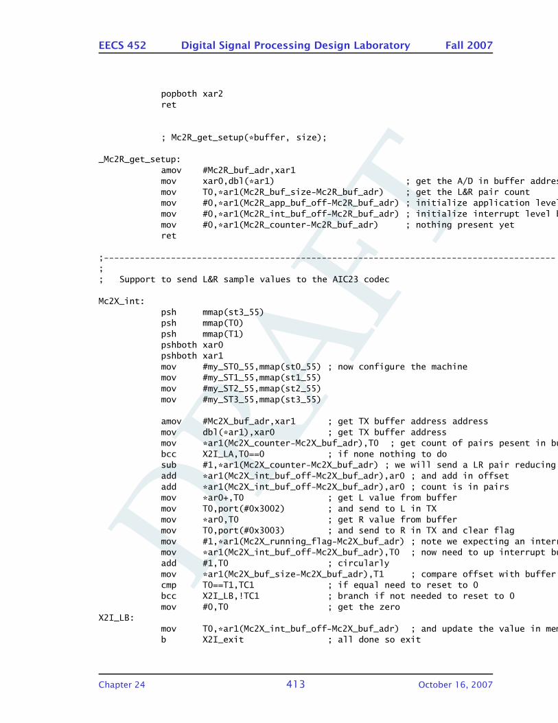
DRA
FT
EECS 452 Digital Signal Processing Design Laboratory Fall 2007
popboth xar2ret
; Mc2R_get_setup(*buffer, size);
_Mc2R_get_setup:amov #Mc2R_buf_adr,xar1mov xar0,dbl(*ar1) ; get the A/D in buffer addressmov T0,*ar1(Mc2R_buf_size-Mc2R_buf_adr) ; get the L&R pair countmov #0,*ar1(Mc2R_app_buf_off-Mc2R_buf_adr) ; initialize application levelmov #0,*ar1(Mc2R_int_buf_off-Mc2R_buf_adr) ; initialize interrupt level buffermov #0,*ar1(Mc2R_counter-Mc2R_buf_adr) ; nothing present yetret
;---------------------------------------------------------------------------------------;; Support to send L&R sample values to the AIC23 codec
Mc2X_int:psh mmap(st3_55)psh mmap(T0)psh mmap(T1)pshboth xar0pshboth xar1mov #my_ST0_55,mmap(st0_55) ; now configure the machinemov #my_ST1_55,mmap(st1_55)mov #my_ST2_55,mmap(st2_55)mov #my_ST3_55,mmap(st3_55)
amov #Mc2X_buf_adr,xar1 ; get TX buffer address addressmov dbl(*ar1),xar0 ; get TX buffer addressmov *ar1(Mc2X_counter-Mc2X_buf_adr),T0 ; get count of pairs pesent in bufferbcc X2I_LA,T0==0 ; if none nothing to dosub #1,*ar1(Mc2X_counter-Mc2X_buf_adr) ; we will send a LR pair reducingadd *ar1(Mc2X_int_buf_off-Mc2X_buf_adr),ar0 ; and add in offsetadd *ar1(Mc2X_int_buf_off-Mc2X_buf_adr),ar0 ; count is in pairsmov *ar0+,T0 ; get L value from buffermov T0,port(#0x3002) ; and send to L in TXmov *ar0,T0 ; get R value from buffermov T0,port(#0x3003) ; and send to R in TX and clear flagmov #1,*ar1(Mc2X_running_flag-Mc2X_buf_adr) ; note we expecting an interruptmov *ar1(Mc2X_int_buf_off-Mc2X_buf_adr),T0 ; now need to up interrupt bufferadd #1,T0 ; circularlymov *ar1(Mc2X_buf_size-Mc2X_buf_adr),T1 ; compare offset with buffercmp T0==T1,TC1 ; if equal need to reset to 0bcc X2I_LB,!TC1 ; branch if not needed to reset to 0mov #0,T0 ; get the zero
X2I_LB:mov T0,*ar1(Mc2X_int_buf_off-Mc2X_buf_adr) ; and update the value in memoryb X2I_exit ; all done so exit
Chapter 24 413 October 16, 2007

DRA
FT
EECS 452 Digital Signal Processing Design Laboratory Fall 2007
X2I_LA:mov #0,*ar1(Mc2X_running_flag-Mc2X_buf_adr) ; note we are not expecting an interrupt
X2I_exit:popboth xar1popboth xar0pop mmap(T1)pop mmap(T0)pop mmap(st3_55)nop ; 6 nops stop remarks 99 and 100nopnopnopnopnopreti
; Application level function to send L&R values to DAC;; 32 bit value in AC0 left in high right in low
_Mc2X_put:mov T0,mmap(ac0h) ; save left valuemov T1,mmap(ac0l) ; save right value
XL2_LC:amov #Mc2X_buf_adr,xar1 ; point to buffer address addressmov *ar1(Mc2X_counter-Mc2X_buf_adr),T0 ; number values presentmov *ar1(Mc2X_buf_size-Mc2X_buf_adr),T1 ; number of spaces availablecmp T0==T1,TC1 ; see if they are equalbcc XL2_LC,TC1 ; wait if no roommov dbl(*ar1),xar0 ; get buffer addressadd *ar1(Mc2X_app_buf_off-Mc2X_buf_adr),ar0add *ar1(Mc2X_app_buf_off-Mc2X_buf_adr),ar0 ; two word offset neededmov HI(ac0),*ar0+ ; store left value into buffermov ac0,*ar0 ; store right value into bufferbset intm ; disable interruptsadd #1,*ar1(Mc2X_counter-Mc2X_buf_adr) ; increment countmov *ar1(Mc2X_running_flag-Mc2X_buf_adr),T0bcc X2_LA,T0!=0 ; branch if xmtr runningintr #0xD ; trigger the interrupt if not
X2_LA:bclr intm ; reenable interruptsmov *ar1(Mc2X_app_buf_off-Mc2X_buf_adr),T0; ; now update buffer offsetadd #1,T0 ; incrementcmp T0==T1,TC1 ; may need to resetbcc X2_LB,!TC1 ; not yetmov #0,T0 ; put back to buffer start
X2_LB:mov T0,*ar1(Mc2X_app_buf_off-Mc2X_buf_adr) ; update the putting offset
X2_exit:ret
Chapter 24 414 October 16, 2007
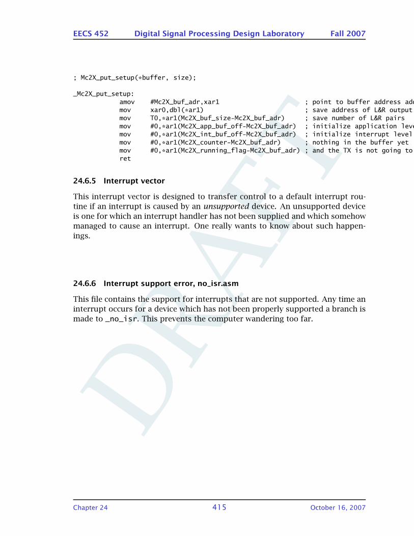
DRA
FT
EECS 452 Digital Signal Processing Design Laboratory Fall 2007
; Mc2X_put_setup(*buffer, size);
_Mc2X_put_setup:amov #Mc2X_buf_adr,xar1 ; point to buffer address addressmov xar0,dbl(*ar1) ; save address of L&R outputmov T0,*ar1(Mc2X_buf_size-Mc2X_buf_adr) ; save number of L&R pairsmov #0,*ar1(Mc2X_app_buf_off-Mc2X_buf_adr) ; initialize application levelmov #0,*ar1(Mc2X_int_buf_off-Mc2X_buf_adr) ; initialize interrupt levelmov #0,*ar1(Mc2X_counter-Mc2X_buf_adr) ; nothing in the buffer yetmov #0,*ar1(Mc2X_running_flag-Mc2X_buf_adr) ; and the TX is not going toret
24.6.5 Interrupt vector
This interrupt vector is designed to transfer control to a default interrupt rou-
tine if an interrupt is caused by an unsupported device. An unsupported device
is one for which an interrupt handler has not been supplied and which somehow
managed to cause an interrupt. One really wants to know about such happen-
ings.
24.6.6 Interrupt support error, no_isr.asm
This file contains the support for interrupts that are not supported. Any time an
interrupt occurs for a device which has not been properly supported a branch is
made to _no_isr. This prevents the computer wandering too far.
Chapter 24 415 October 16, 2007

DRA
FTWasted space, consider adding helpful text to this chapter.
DRA
FT
25 : Acoustic OFDM Communication
System
Almost the ultimate DSP application. FFTs, filtering, sample rate conversion up
and down, modulation, demodulation and much much more. Whan to buy one?
Not planned as a lab exercise but if a student wants to treat it as such, well
. . .
Chapter 25 417 October 16, 2007

DRA
FTWasted space, consider adding helpful text to this chapter.

DRA
FT
26 : PicoBlaze
Introduction and overview of Ken Chapman’s PicoBlaze microcomputer for Xil-
inx FPGAs.
Does not duplicate the existing documentation but does give a short overview
and gives pointers to the documentation on the course CD. Also gives the in-
structions for down loading the executable directly into the FPGA without having
to create a new bit file. This results in a huge time savings when debugging the
program code.
Chapter 26 419 October 16, 2007

DRA
FTWasted space, consider adding helpful text to this chapter.
DRA
FT
A : Listings of common TI units
Include the .cmd file and other assembler and C files that have common use.
Chapter 1 421 October 16, 2007

DRA
FTWasted space, consider adding helpful text to this chapter.
DRA
FT
B : Listings of common VHDL units
This appendix contains listings of the VLHD entities and other VHDL associated
files that are planned to be common across the lab exercises.
B.1 Spartan-3 Starter Board UCF file
B.2 Digital clock manager (DCM) entity
This entity was generated by the Xilinx software. It was modified to allow ready
specification of the clock multiply and divide factors. There is a clock in, a reset
is usually connected to a logic ’0’, and a clock out. The clock out is generated
by one of the global clock buffers.
This unit appears to work correctly when used with either the Spartan-3 or
Spartan-3E FPGA and does not seem to be sensitive to either the chip size or the
package.
B.3 16xN FIFO
The FIFO is 16 words by N bits. This is a modification of the FIFO entity that Ken
Chapman uses in the UART support supplied with the PicoBlaze.
The two modifications were: making the number of bits in the word size
generic, and, adding an almost full signal (becomes a one when there is one
location available). The almost full signal operation has not yet been tested.
The implementation is at a very low level, i.e., very to the basic FPGA archi-
tecture. Chapman fits the FIFO into as a small part of the FPGA as is possible.
A great piece of code to study in order to see how this can be done. Note the
patent warning included in the code.
Chapter 2 423 October 16, 2007

DRA
FTWasted space, consider adding helpful text to this chapter.

DRA
FT
C : Listings for Chapter 7 : Spartan-3
Starter Board
Text, formatting and includes will go here.
Chapter 3 425 October 16, 2007

DRA
FTWasted space, consider adding helpful text to this chapter.
DRA
FT
D : Listings for Chapter 9 : Fixed
point arithmetic
Listings and other materials go here.
Chapter 4 427 October 16, 2007

DRA
FTWasted space, consider adding helpful text to this chapter.

DRA
FT
E : Chapter 12 appendices : Serial
peripherals and data transfers
E.1 Single supply level shifting circuit
A recurring problem when working with single supply devices such as theA/D
converter used on the PMod board is driving them with zero referenced inputs
which swing between positive and negative voltage levels. This note analyzes
an op-amp circuit that can be used to shift a zero volt referenced input to a
reference equal to one-half the supply voltage.
The resistors included in the workstation boxes have an accuracy of ±5%.
This means there will be a small amount of level shift and gain error. In a more
“real” situation one might to use more accurate resistors or an integrated circuit
designed specifically for this application.
The output impedance of any signal source used with this circuit will also
have an effect.
E.1.1 Analysis
The op-amp in Figure E.1 is assumed to be powered using the same supply volt-
age, vs as the devices that follow it.
oN
oO
oQ
oP
oR
H
J
îáîç
îë
î~
Figure E.1: Single supply op-amp level shifting circuit.
Chapter 5 429 October 16, 2007

DRA
FT
EECS 452 Digital Signal Processing Design Laboratory Fall 2007
Summing the currents flowing into the positive input’s node gives
vi − vaR3
+vs − vaR5
=va
R4
viR3+vsR5= va
(
1
R3+
1
R4+
1
R5
)
va =(
vi
R3+vs
R5
)
R3R4R5
R3R4 + R3R5 + R4R5
The voltage between the plus and input nodes is assumed to be zero. Giving
vo = vaR1 + R2
R1
vo =(
viR3+vsR5
)
R3R4R5(R1 + R2)
R1 (R3R4 + R3R5 + R4R5)
The gain to vs is
gs =R3R4(R1 + R2)
R1 (R3R4 + R3R5 + R4R5)
The gain to vi is
gi = gsR5
R3.
The equation for gs gives the relation
gsR1 (R3R4 + R3R5 + R4R5) = R3R4(R1 + R2) .
The goal in this note is to center the output level at vs/2 which gives
(R3R4 + R3R5 + R4R5)
R3R4=
2(R1 + R2)
R1.
1+R5
R4+R5
R3= 2
(
1+R2
R1
)
The values of R3 and R5 are related by the desired signal gain gi.
R5
R4+ 2gi = 1+
2R2
R1
If R4 = R5 then
gi =R2
R1.
Chapter 5 430 October 16, 2007
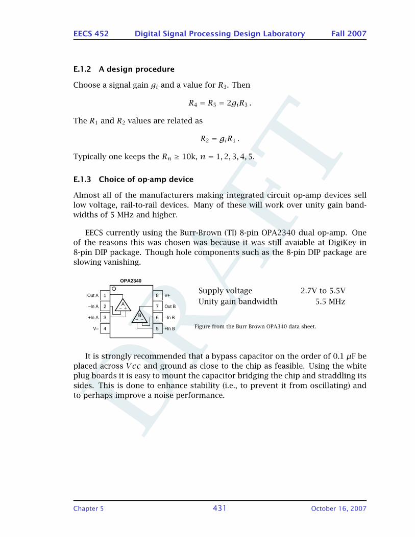
DRA
FT
EECS 452 Digital Signal Processing Design Laboratory Fall 2007
E.1.2 A design procedure
Choose a signal gain gi and a value for R3. Then
R4 = R5 = 2giR3 .
The R1 and R2 values are related as
R2 = giR1 .
Typically one keeps the Rn ≥ 10k, n = 1,2,3,4,5.
E.1.3 Choice of op-amp device
Almost all of the manufacturers making integrated circuit op-amp devices sell
low voltage, rail-to-rail devices. Many of these will work over unity gain band-
widths of 5 MHz and higher.
EECS currently using the Burr-Brown (TI) 8-pin OPA2340 dual op-amp. One
of the reasons this was chosen was because it was still avaiable at DigiKey in
8-pin DIP package. Though hole components such as the 8-pin DIP package are
slowing vanishing.
1
2
3
4
8
7
6
5
V+
Out B
–In B
+In B
Out A
–In A
+In A
V–
OPA2340
A
B
Supply voltage 2.7V to 5.5V
Unity gain bandwidth 5.5 MHz
Figure from the Burr Brown OPA340 data sheet.
It is strongly recommended that a bypass capacitor on the order of 0.1 µF be
placed across Vcc and ground as close to the chip as feasible. Using the white
plug boards it is easy to mount the capacitor bridging the chip and straddling its
sides. This is done to enhance stability (i.e., to prevent it from oscillating) and
to perhaps improve a noise performance.
Chapter 5 431 October 16, 2007
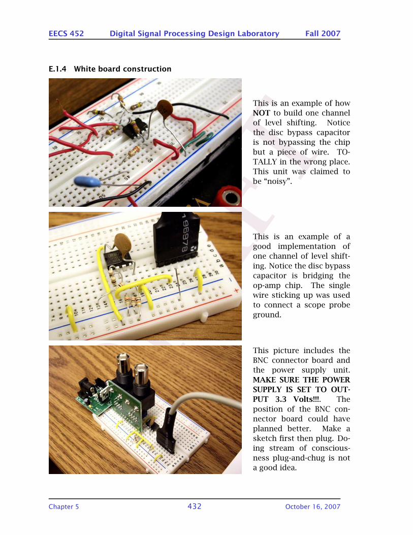
DRA
FT
EECS 452 Digital Signal Processing Design Laboratory Fall 2007
E.1.4 White board construction
This is an example of how
NOT to build one channel
of level shifting. Notice
the disc bypass capacitor
is not bypassing the chip
but a piece of wire. TO-
TALLY in the wrong place.
This unit was claimed to
be “noisy”.
This is an example of a
good implementation of
one channel of level shift-
ing. Notice the disc bypass
capacitor is bridging the
op-amp chip. The single
wire sticking up was used
to connect a scope probe
ground.
This picture includes the
BNC connector board and
the power supply unit.
MAKE SURE THE POWER
SUPPLY IS SET TO OUT-
PUT 3.3 Volts!!!. The
position of the BNC con-
nector board could have
planned better. Make a
sketch first then plug. Do-
ing stream of conscious-
ness plug-and-chug is not
a good idea.
Chapter 5 432 October 16, 2007
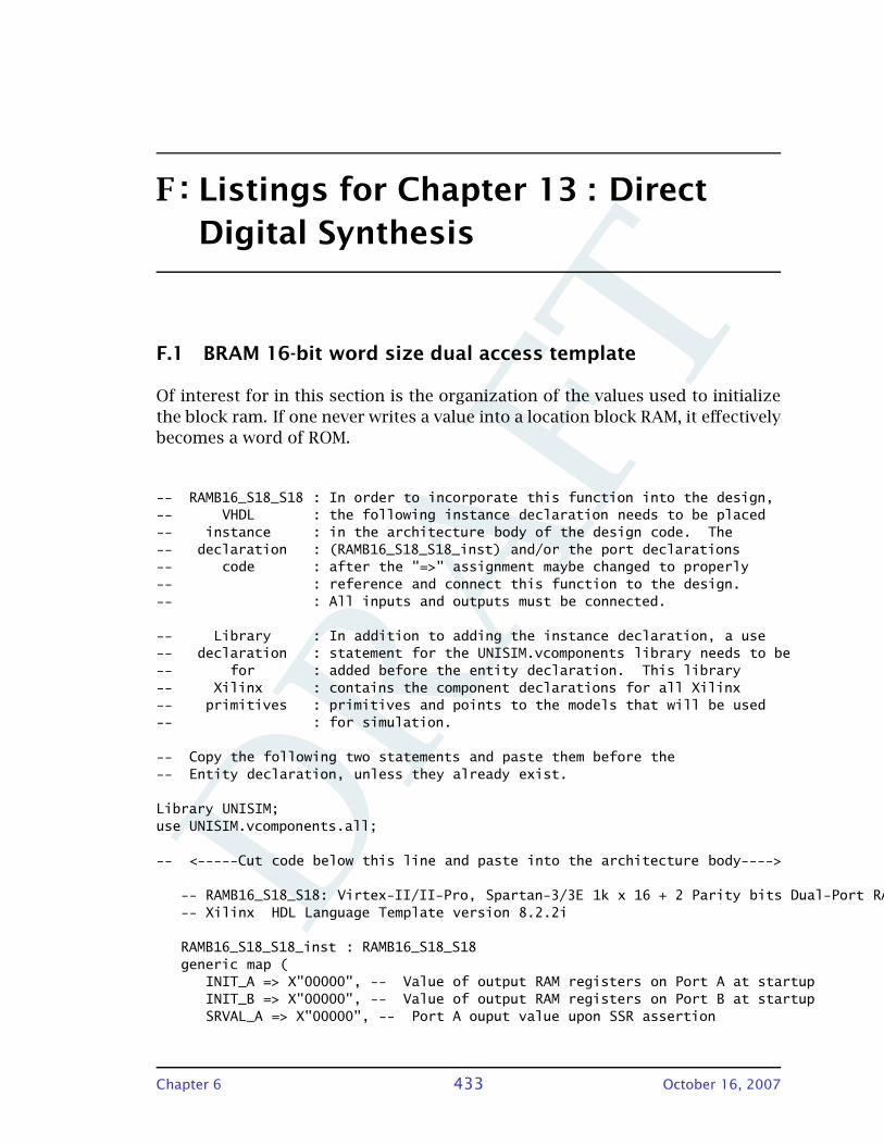
DRA
FT
F : Listings for Chapter 13 : Direct
Digital Synthesis
F.1 BRAM 16-bit word size dual access template
Of interest for in this section is the organization of the values used to initialize
the block ram. If one never writes a value into a location block RAM, it effectively
becomes a word of ROM.
-- RAMB16_S18_S18 : In order to incorporate this function into the design,-- VHDL : the following instance declaration needs to be placed-- instance : in the architecture body of the design code. The-- declaration : (RAMB16_S18_S18_inst) and/or the port declarations-- code : after the "=>" assignment maybe changed to properly-- : reference and connect this function to the design.-- : All inputs and outputs must be connected.
-- Library : In addition to adding the instance declaration, a use-- declaration : statement for the UNISIM.vcomponents library needs to be-- for : added before the entity declaration. This library-- Xilinx : contains the component declarations for all Xilinx-- primitives : primitives and points to the models that will be used-- : for simulation.
-- Copy the following two statements and paste them before the-- Entity declaration, unless they already exist.
Library UNISIM;use UNISIM.vcomponents.all;
-- <-----Cut code below this line and paste into the architecture body---->
-- RAMB16_S18_S18: Virtex-II/II-Pro, Spartan-3/3E 1k x 16 + 2 Parity bits Dual-Port RAM-- Xilinx HDL Language Template version 8.2.2i
RAMB16_S18_S18_inst : RAMB16_S18_S18generic map (
INIT_A => X"00000", -- Value of output RAM registers on Port A at startupINIT_B => X"00000", -- Value of output RAM registers on Port B at startupSRVAL_A => X"00000", -- Port A ouput value upon SSR assertion
Chapter 6 433 October 16, 2007
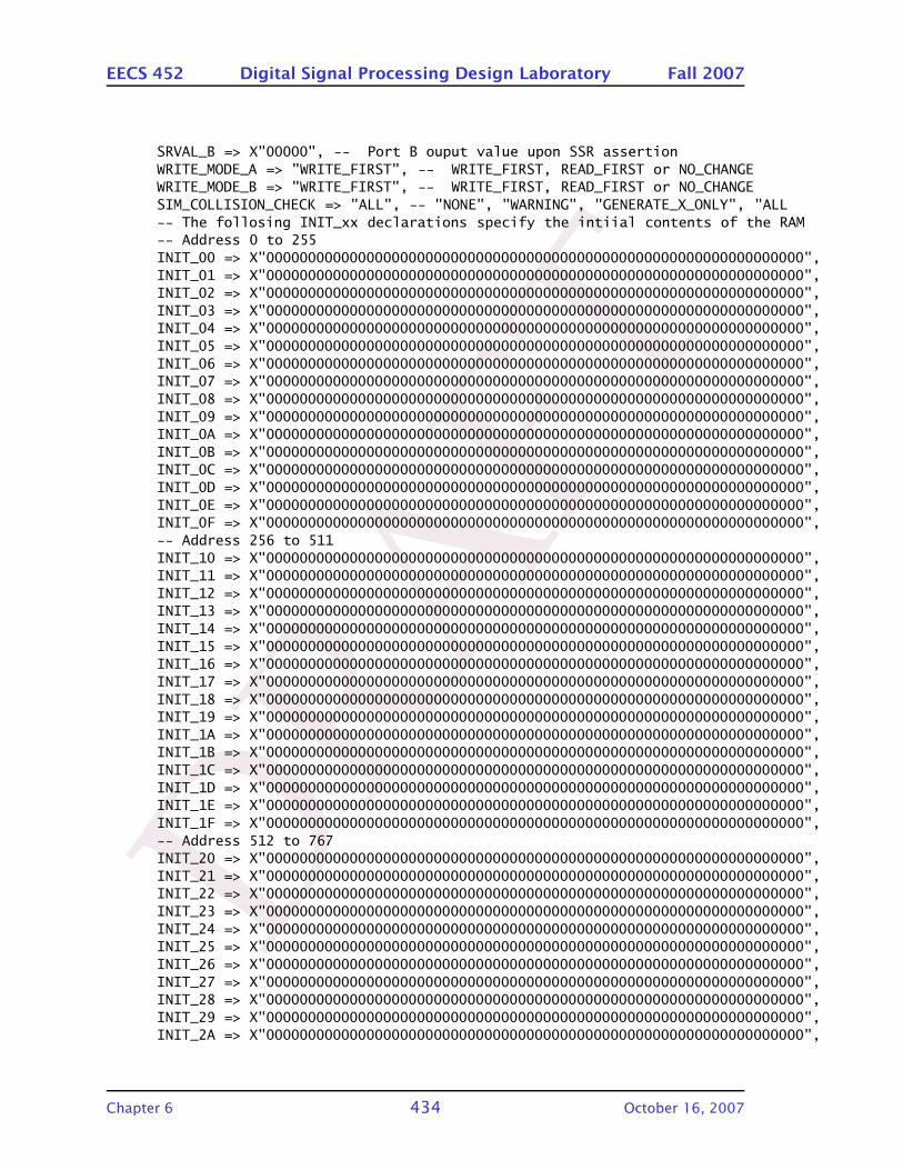
DRA
FT
EECS 452 Digital Signal Processing Design Laboratory Fall 2007
SRVAL_B => X"00000", -- Port B ouput value upon SSR assertionWRITE_MODE_A => "WRITE_FIRST", -- WRITE_FIRST, READ_FIRST or NO_CHANGEWRITE_MODE_B => "WRITE_FIRST", -- WRITE_FIRST, READ_FIRST or NO_CHANGESIM_COLLISION_CHECK => "ALL", -- "NONE", "WARNING", "GENERATE_X_ONLY", "ALL-- The follosing INIT_xx declarations specify the intiial contents of the RAM-- Address 0 to 255INIT_00 => X"0000000000000000000000000000000000000000000000000000000000000000",INIT_01 => X"0000000000000000000000000000000000000000000000000000000000000000",INIT_02 => X"0000000000000000000000000000000000000000000000000000000000000000",INIT_03 => X"0000000000000000000000000000000000000000000000000000000000000000",INIT_04 => X"0000000000000000000000000000000000000000000000000000000000000000",INIT_05 => X"0000000000000000000000000000000000000000000000000000000000000000",INIT_06 => X"0000000000000000000000000000000000000000000000000000000000000000",INIT_07 => X"0000000000000000000000000000000000000000000000000000000000000000",INIT_08 => X"0000000000000000000000000000000000000000000000000000000000000000",INIT_09 => X"0000000000000000000000000000000000000000000000000000000000000000",INIT_0A => X"0000000000000000000000000000000000000000000000000000000000000000",INIT_0B => X"0000000000000000000000000000000000000000000000000000000000000000",INIT_0C => X"0000000000000000000000000000000000000000000000000000000000000000",INIT_0D => X"0000000000000000000000000000000000000000000000000000000000000000",INIT_0E => X"0000000000000000000000000000000000000000000000000000000000000000",INIT_0F => X"0000000000000000000000000000000000000000000000000000000000000000",-- Address 256 to 511INIT_10 => X"0000000000000000000000000000000000000000000000000000000000000000",INIT_11 => X"0000000000000000000000000000000000000000000000000000000000000000",INIT_12 => X"0000000000000000000000000000000000000000000000000000000000000000",INIT_13 => X"0000000000000000000000000000000000000000000000000000000000000000",INIT_14 => X"0000000000000000000000000000000000000000000000000000000000000000",INIT_15 => X"0000000000000000000000000000000000000000000000000000000000000000",INIT_16 => X"0000000000000000000000000000000000000000000000000000000000000000",INIT_17 => X"0000000000000000000000000000000000000000000000000000000000000000",INIT_18 => X"0000000000000000000000000000000000000000000000000000000000000000",INIT_19 => X"0000000000000000000000000000000000000000000000000000000000000000",INIT_1A => X"0000000000000000000000000000000000000000000000000000000000000000",INIT_1B => X"0000000000000000000000000000000000000000000000000000000000000000",INIT_1C => X"0000000000000000000000000000000000000000000000000000000000000000",INIT_1D => X"0000000000000000000000000000000000000000000000000000000000000000",INIT_1E => X"0000000000000000000000000000000000000000000000000000000000000000",INIT_1F => X"0000000000000000000000000000000000000000000000000000000000000000",-- Address 512 to 767INIT_20 => X"0000000000000000000000000000000000000000000000000000000000000000",INIT_21 => X"0000000000000000000000000000000000000000000000000000000000000000",INIT_22 => X"0000000000000000000000000000000000000000000000000000000000000000",INIT_23 => X"0000000000000000000000000000000000000000000000000000000000000000",INIT_24 => X"0000000000000000000000000000000000000000000000000000000000000000",INIT_25 => X"0000000000000000000000000000000000000000000000000000000000000000",INIT_26 => X"0000000000000000000000000000000000000000000000000000000000000000",INIT_27 => X"0000000000000000000000000000000000000000000000000000000000000000",INIT_28 => X"0000000000000000000000000000000000000000000000000000000000000000",INIT_29 => X"0000000000000000000000000000000000000000000000000000000000000000",INIT_2A => X"0000000000000000000000000000000000000000000000000000000000000000",
Chapter 6 434 October 16, 2007
DRA
FT
EECS 452 Digital Signal Processing Design Laboratory Fall 2007
INIT_2B => X"0000000000000000000000000000000000000000000000000000000000000000",INIT_2C => X"0000000000000000000000000000000000000000000000000000000000000000",INIT_2D => X"0000000000000000000000000000000000000000000000000000000000000000",INIT_2E => X"0000000000000000000000000000000000000000000000000000000000000000",INIT_2F => X"0000000000000000000000000000000000000000000000000000000000000000",-- Address 768 to 1023INIT_30 => X"0000000000000000000000000000000000000000000000000000000000000000",INIT_31 => X"0000000000000000000000000000000000000000000000000000000000000000",INIT_32 => X"0000000000000000000000000000000000000000000000000000000000000000",INIT_33 => X"0000000000000000000000000000000000000000000000000000000000000000",INIT_34 => X"0000000000000000000000000000000000000000000000000000000000000000",INIT_35 => X"0000000000000000000000000000000000000000000000000000000000000000",INIT_36 => X"0000000000000000000000000000000000000000000000000000000000000000",INIT_37 => X"0000000000000000000000000000000000000000000000000000000000000000",INIT_38 => X"0000000000000000000000000000000000000000000000000000000000000000",INIT_39 => X"0000000000000000000000000000000000000000000000000000000000000000",INIT_3A => X"0000000000000000000000000000000000000000000000000000000000000000",INIT_3B => X"0000000000000000000000000000000000000000000000000000000000000000",INIT_3C => X"0000000000000000000000000000000000000000000000000000000000000000",INIT_3D => X"0000000000000000000000000000000000000000000000000000000000000000",INIT_3E => X"0000000000000000000000000000000000000000000000000000000000000000",INIT_3F => X"0000000000000000000000000000000000000000000000000000000000000000",-- The next set of INITP_xx are for the parity bits-- Address 0 to 255INITP_00 => X"0000000000000000000000000000000000000000000000000000000000000000",INITP_01 => X"0000000000000000000000000000000000000000000000000000000000000000",-- Address 256 to 511INITP_02 => X"0000000000000000000000000000000000000000000000000000000000000000",INITP_03 => X"0000000000000000000000000000000000000000000000000000000000000000",-- Address 512 to 767INITP_04 => X"0000000000000000000000000000000000000000000000000000000000000000",INITP_05 => X"0000000000000000000000000000000000000000000000000000000000000000",-- Address 768 to 1023INITP_06 => X"0000000000000000000000000000000000000000000000000000000000000000",INITP_07 => X"0000000000000000000000000000000000000000000000000000000000000000")
port map (DOA => DOA, -- Port A 16-bit Data OutputDOB => DOB, -- Port B 16-bit Data OutputDOPA => DOPA, -- Port A 2-bit Parity OutputDOPB => DOPB, -- Port B 2-bit Parity OutputADDRA => ADDRA, -- Port A 10-bit Address InputADDRB => ADDRB, -- Port B 10-bit Address InputCLKA => CLKA, -- Port A ClockCLKB => CLKB, -- Port B ClockDIA => DIA, -- Port A 16-bit Data InputDIB => DIB, -- Port B 16-bit Data InputDIPA => DIPA, -- Port A 2-bit parity InputDIPB => DIPB, -- Port-B 2-bit parity InputENA => ENA, -- Port A RAM Enable InputENB => ENB, -- PortB RAM Enable InputSSRA => SSRA, -- Port A Synchronous Set/Reset Input
Chapter 6 435 October 16, 2007
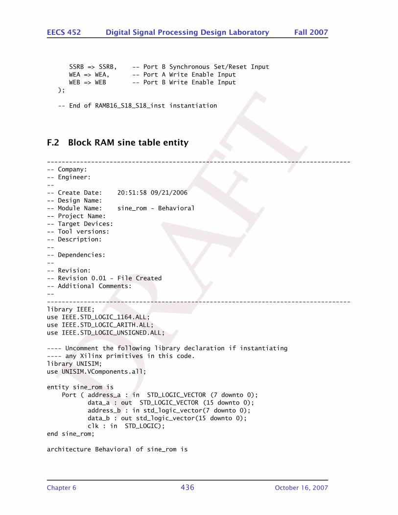
DRA
FT
EECS 452 Digital Signal Processing Design Laboratory Fall 2007
SSRB => SSRB, -- Port B Synchronous Set/Reset InputWEA => WEA, -- Port A Write Enable InputWEB => WEB -- Port B Write Enable Input
);
-- End of RAMB16_S18_S18_inst instantiation
F.2 Block RAM sine table entity
------------------------------------------------------------------------------------ Company:-- Engineer:---- Create Date: 20:51:58 09/21/2006-- Design Name:-- Module Name: sine_rom - Behavioral-- Project Name:-- Target Devices:-- Tool versions:-- Description:---- Dependencies:---- Revision:-- Revision 0.01 - File Created-- Additional Comments:------------------------------------------------------------------------------------library IEEE;use IEEE.STD_LOGIC_1164.ALL;use IEEE.STD_LOGIC_ARITH.ALL;use IEEE.STD_LOGIC_UNSIGNED.ALL;
---- Uncomment the following library declaration if instantiating---- any Xilinx primitives in this code.library UNISIM;use UNISIM.VComponents.all;
entity sine_rom isPort ( address_a : in STD_LOGIC_VECTOR (7 downto 0);
data_a : out STD_LOGIC_VECTOR (15 downto 0);address_b : in std_logic_vector(7 downto 0);data_b : out std_logic_vector(15 downto 0);clk : in STD_LOGIC);
end sine_rom;
architecture Behavioral of sine_rom is
Chapter 6 436 October 16, 2007
DRA
FT
EECS 452 Digital Signal Processing Design Laboratory Fall 2007
signal DOA, DOB : std_logic_vector(15 downto 0);signal ADDRA, ADDRB : std_logic_vector(9 downto 0);
begin
ADDRA <= "00" & address_a;data_a <= DOA(15 downto 0);ADDRB <= "00" & address_b;data_b <= DOB(15 downto 0);
-- RAMB16_S18_S18: Virtex-II/II-Pro, Spartan-3/3E 1k x 16 + 2 Parity bits Dual-Port RAM-- Xilinx HDL Language Template version 8.2.2i
RAMB16_S18_S18_inst : RAMB16_S18_S18generic map (
INIT_A => X"00000", -- Value of output RAM registers on Port A at startupINIT_B => X"00000", -- Value of output RAM registers on Port B at startupSRVAL_A => X"00000", -- Port A ouput value upon SSR assertionSRVAL_B => X"00000", -- Port B ouput value upon SSR assertionWRITE_MODE_A => "WRITE_FIRST", -- WRITE_FIRST, READ_FIRST or NO_CHANGEWRITE_MODE_B => "WRITE_FIRST", -- WRITE_FIRST, READ_FIRST or NO_CHANGESIM_COLLISION_CHECK => "ALL", -- "NONE", "WARNING", "GENERATE_X_ONLY", "ALL-- The follosing INIT_xx declarations specify the intiial contents of the RAM-- Address 0 to 255
INIT_00 => X"AE11AB1FA826A528A2239F1A9C0B98F995E292C88FAB8C8C896A864883248000",INIT_01 => X"D842D5F5D39BD133CEBFCC3FC9B4C71CC47AC1CEBF17BC56B98CB6BAB3DFB0FB",INIT_02 => X"F504F3B5F254F0E2EF5EEDC9EC23EA6DE8A6E6CFE4E8E2F1E0EBDED7DCB3DA82",INIT_03 => X"FFF5FFD8FFA6FF61FF09FE9CFE1DFD89FCE3FC29FB5CFA7CF989F884F76BF641",INIT_04 => X"F76BF884F989FA7CFB5CFC29FCE3FD89FE1DFE9CFF09FF61FFA6FFD8FFF5FFFF",INIT_05 => X"DCB3DED7E0EBE2F1E4E8E6CFE8A6EA6DEC23EDC9EF5EF0E2F254F3B5F504F641",INIT_06 => X"B3DFB6BAB98CBC56BF17C1CEC47AC71CC9B4CC3FCEBFD133D39BD5F5D842DA82",INIT_07 => X"83248648896A8C8C8FAB92C895E298F99C0B9F1AA223A528A826AB1FAE11B0FB",INIT_08 => X"51EF54E157DA5AD85DDD60E663F567076A1E6D3870557374769679B87CDC8000",INIT_09 => X"27BE2A0B2C652ECD314133C1364C38E43B863E3240E943AA467449464C214F05",INIT_0A => X"0AFC0C4B0DAC0F1E10A2123713DD1593175A19311B181D0F1F152129234D257E",INIT_0B => X"000B0028005A009F00F7016401E30277031D03D704A405840677077C089509BF",INIT_0C => X"0895077C0677058404A403D7031D027701E3016400F7009F005A0028000B0001",INIT_0D => X"234D21291F151D0F1B181931175A159313DD123710A20F1E0DAC0C4B0AFC09BF",INIT_0E => X"4C214946467443AA40E93E323B8638E4364C33C131412ECD2C652A0B27BE257E",INIT_0F => X"7CDC79B87696737470556D386A1E670763F560E65DDD5AD857DA54E151EF4F05",
-- Address 256 to 511INIT_10 => X"0000000000000000000000000000000000000000000000000000000000000000",INIT_11 => X"0000000000000000000000000000000000000000000000000000000000000000",INIT_12 => X"0000000000000000000000000000000000000000000000000000000000000000",INIT_13 => X"0000000000000000000000000000000000000000000000000000000000000000",INIT_14 => X"0000000000000000000000000000000000000000000000000000000000000000",INIT_15 => X"0000000000000000000000000000000000000000000000000000000000000000",INIT_16 => X"0000000000000000000000000000000000000000000000000000000000000000",INIT_17 => X"0000000000000000000000000000000000000000000000000000000000000000",INIT_18 => X"0000000000000000000000000000000000000000000000000000000000000000",
Chapter 6 437 October 16, 2007
DRA
FT
EECS 452 Digital Signal Processing Design Laboratory Fall 2007
INIT_19 => X"0000000000000000000000000000000000000000000000000000000000000000",INIT_1A => X"0000000000000000000000000000000000000000000000000000000000000000",INIT_1B => X"0000000000000000000000000000000000000000000000000000000000000000",INIT_1C => X"0000000000000000000000000000000000000000000000000000000000000000",INIT_1D => X"0000000000000000000000000000000000000000000000000000000000000000",INIT_1E => X"0000000000000000000000000000000000000000000000000000000000000000",INIT_1F => X"0000000000000000000000000000000000000000000000000000000000000000",-- Address 512 to 767INIT_20 => X"0000000000000000000000000000000000000000000000000000000000000000",INIT_21 => X"0000000000000000000000000000000000000000000000000000000000000000",INIT_22 => X"0000000000000000000000000000000000000000000000000000000000000000",INIT_23 => X"0000000000000000000000000000000000000000000000000000000000000000",INIT_24 => X"0000000000000000000000000000000000000000000000000000000000000000",INIT_25 => X"0000000000000000000000000000000000000000000000000000000000000000",INIT_26 => X"0000000000000000000000000000000000000000000000000000000000000000",INIT_27 => X"0000000000000000000000000000000000000000000000000000000000000000",INIT_28 => X"0000000000000000000000000000000000000000000000000000000000000000",INIT_29 => X"0000000000000000000000000000000000000000000000000000000000000000",INIT_2A => X"0000000000000000000000000000000000000000000000000000000000000000",INIT_2B => X"0000000000000000000000000000000000000000000000000000000000000000",INIT_2C => X"0000000000000000000000000000000000000000000000000000000000000000",INIT_2D => X"0000000000000000000000000000000000000000000000000000000000000000",INIT_2E => X"0000000000000000000000000000000000000000000000000000000000000000",INIT_2F => X"0000000000000000000000000000000000000000000000000000000000000000",-- Address 768 to 1023INIT_30 => X"0000000000000000000000000000000000000000000000000000000000000000",INIT_31 => X"0000000000000000000000000000000000000000000000000000000000000000",INIT_32 => X"0000000000000000000000000000000000000000000000000000000000000000",INIT_33 => X"0000000000000000000000000000000000000000000000000000000000000000",INIT_34 => X"0000000000000000000000000000000000000000000000000000000000000000",INIT_35 => X"0000000000000000000000000000000000000000000000000000000000000000",INIT_36 => X"0000000000000000000000000000000000000000000000000000000000000000",INIT_37 => X"0000000000000000000000000000000000000000000000000000000000000000",INIT_38 => X"0000000000000000000000000000000000000000000000000000000000000000",INIT_39 => X"0000000000000000000000000000000000000000000000000000000000000000",INIT_3A => X"0000000000000000000000000000000000000000000000000000000000000000",INIT_3B => X"0000000000000000000000000000000000000000000000000000000000000000",INIT_3C => X"0000000000000000000000000000000000000000000000000000000000000000",INIT_3D => X"0000000000000000000000000000000000000000000000000000000000000000",INIT_3E => X"0000000000000000000000000000000000000000000000000000000000000000",INIT_3F => X"0000000000000000000000000000000000000000000000000000000000000000",-- The next set of INITP_xx are for the parity bits-- Address 0 to 255INITP_00 => X"0000000000000000000000000000000000000000000000000000000000000000",INITP_01 => X"0000000000000000000000000000000000000000000000000000000000000000",-- Address 256 to 511INITP_02 => X"0000000000000000000000000000000000000000000000000000000000000000",INITP_03 => X"0000000000000000000000000000000000000000000000000000000000000000",-- Address 512 to 767INITP_04 => X"0000000000000000000000000000000000000000000000000000000000000000",INITP_05 => X"0000000000000000000000000000000000000000000000000000000000000000",
Chapter 6 438 October 16, 2007

DRA
FT
EECS 452 Digital Signal Processing Design Laboratory Fall 2007
-- Address 768 to 1023INITP_06 => X"0000000000000000000000000000000000000000000000000000000000000000",INITP_07 => X"0000000000000000000000000000000000000000000000000000000000000000")
port map (DOA => DOA, -- Port A 16-bit Data OutputDOB => DOB, -- Port B 16-bit Data Output
-- DOPA => DOPA, -- Port A 2-bit Parity Output-- DOPB => DOPB, -- Port B 2-bit Parity Output
ADDRA => ADDRA, -- Port A 10-bit Address InputADDRB => ADDRB, -- Port B 10-bit Address InputCLKA => CLK, -- Port A ClockCLKB => CLK, -- Port B ClockDIA => X"0000", -- Port A 16-bit Data InputDIB => X"0000", -- Port B 16-bit Data InputDIPA => "00", -- Port A 2-bit parity InputDIPB => "00", -- Port-B 2-bit parity InputENA => ’1’, -- Port A RAM Enable InputENB => ’1’, -- PortB RAM Enable InputSSRA => ’0’, -- Port A Synchronous Set/Reset InputSSRB => ’0’, -- Port B Synchronous Set/Reset InputWEA => ’0’, -- Port A Write Enable InputWEB => ’0’ -- Port B Write Enable Input
);
-- End of RAMB16_S18_S18_inst instantiation
end Behavioral;
Chapter 6 439 October 16, 2007

DRA
FTWasted space, consider adding helpful text to this chapter.