Fall 2006 JHU EE787 MMIC Design Student Projects ...jpenn3/MMICProjects2006.pdfFall 2006 JHU EE787...
130
Fall 2006 JHU EE787 MMIC Design Student Projects Supported by TriQuint, and Agilent Eesof Professors John Penn and Dr. Michel Reece Low Noise Amplifier 1 (Low Power)–N. Hughes & L. Macejka Low Noise Amplifier 2– Dave Sokol Phase Shifter – Dave Wendland Small Signal Amp – C. Wedderburn Power Amplifier 2 – Ben Myers & Niral Patel Power Amplifier 1 – Peter Smith Voltage Controlled Osc. – Dimitrios Loizos Vector Modulator – Jonathan Egan
Transcript of Fall 2006 JHU EE787 MMIC Design Student Projects ...jpenn3/MMICProjects2006.pdfFall 2006 JHU EE787...

Fall 2006 JHU EE787 MMIC Design Student Projects
Supported by TriQuint, and Agilent Eesof
Professors John Penn and Dr. Michel Reece Low Noise Amplifier 1 (Low Power)–N. Hughes & L. Macejka Low Noise Amplifier 2– Dave Sokol
Phase Shifter – Dave Wendland Small Signal Amp – C. Wedderburn
Power Amplifier 2 – Ben Myers & Niral Patel Power Amplifier 1 – Peter Smith
Voltage Controlled Osc. – Dimitrios Loizos Vector Modulator – Jonathan Egan

S-Band Low Power Low Noise Amplifier
By: Noah Hughes
Larry Macejka
Microwave Monolithic Integrated Circuit (MMIC) Design Class
Johns Hopkins University
Fall 2006

TABLE OF CONTENTS Abstract.............................................................................................................................. 3 Introduction....................................................................................................................... 3 Design ................................................................................................................................. 4 Requirements& Trade-Offs ............................................................................................. 5 Schematic ........................................................................................................................... 7 Linear Simulations............................................................................................................ 8
S_Parameters................................................................................................................... 8 Noise Figure.................................................................................................................... 8 Stability ........................................................................................................................... 9 DC Annotation .............................................................................................................. 11
Non-Linear Simulation: ................................................................................................. 12 Power Output ................................................................................................................ 12
Layout .............................................................................................................................. 13 Test Plan .......................................................................................................................... 13
Test Procedures............................................................................................................. 14 S-parameter Measurement........................................................................................ 14 Noise Figure Measurement....................................................................................... 14 Compression Point Measurement ............................................................................. 14
Conclusion ....................................................................................................................... 14
2

Abstract
The design of a MMIC low power low noise amplifier (LNA) circuit will be described in this paper. The amplifier design is based on the requirements of an S-band duplex transceiver and designed to operate with very low power. The LNA operates with a DC power consumption of approximately 17mW drawing 5.14mA at 3.3 V. The amplifier has a 1dB bandwidth of ~500MHz around the required 2305 to 2497 MHz operating range. The noise figure of the LNA is less than the design requirement of 3dB and the gain reaches 27dB under the operating bandwidth. In addition the output port match exceeds –15dB and the input port match is better than –10dB. The stability of the amplifier is unconditionally stable between 0.5 and 5 GHz. This design is placed in the 60 X 60 mil Anachip layout as required the Triquint for fabrication.
Introduction
This report will focus on the design, simulation, layout, optimization and test plan for the low power low noise amplifier. The LNA is at the front end of the S-band receiver providing the first stage of amplification after the antenna and adding as little noise as possible, shown in Figure 2. The design consists of a two-stage amplifier design powered by two positive 3.3V sources, shown in Figure 1. Two 4 X 15um (60um) EMODE FETs are used in the amplifier due to their higher gain and lower noise figure. The output and intermediate matching networks are used to ensure a proper match and maximum gain, while the input-matching network sets the noise figure for the amplifier. Finally a feedback network is used on each of the amplifier stages to broaden the gain, stabilize the amplifier and reduce power consumption.
IMN InterstageMatchw/ DC
Isolation
60 m FET OMN
Resistive Divider
RF Input50
RF Output50
Dropping
Resistor
+3.3V Input +3.3V Input
Vg = +0.5 V
60 m FET
Vd = +1.5 V
DC Voltage is brought in on two separate pads.
Vd = +1.5 V
Block Diagram of Low Power LNA MMIC Design
Figure 1: Two Stage Low Power LNA
3

Figure 2: Duplex Transceiver System
Design
Originally the LNA design was focused on reducing the power consumption of the amplifier to a level where it could be powered by a battery. To achieve this both stages of the amplifier were stabilized using a resistor and capacitor to provide a feedback path between the drain and gate. Initially there was concern the feedback path on the first stage of the amplifier would increase the noise figure above the
4

requirement, but we later found this to be not the case. With the two FET’s stabilized two identical single stage LNAs were designed using ideal components. The input matching circuit of amplifier was tuned to produce the best noise figure possible, while the output matching circuit was tuned to the best VSWR. As an initial cut at the design the two stages were cascaded together. The results of this initial simulation were favorable resulting in a noise figure of ~1.8dB and a gain of ~30dB across the design band, which removed our concern of the feedback network. At that point the number and size of components in the matching networks was taken into account especially the intermediate matching network, which consisted of 2 inductors and 2 capacitors. Both the intermediate and output matching networks were retuned to a shunt inductor and series capacitor topology. This provided an effective RF disconnect between the power input and the RF trace and reduced the number of components to two apiece.
After the ideal design produced favorable simulation results, the ideal components were replaced with Triquint components and simulated again. Initially the circuit had to be retuned due to differences between the Triquint and ideal models. The extra resistance in the Triquint models also increased the noise figure slightly to ~2dB and reduced the gain to ~27dB, but still remained well within design margin. At this point a flaw in the design was discovered. The two drain power supplies could not be combined together on the chip without causing the amplifier to become unstable. To alleviate this problem a resistive divider was installed on one of the drain sources allowing it to provide both gate voltages as well as one of the drain supplies. This allowed the amplifier chip to only require two 3.3V power supply lines from the same power supply.
With this problem out of the way, the iterative layout and interconnect simulation process began. The two stage LNA was initially layed out with just the components. The amplifier’s interconnect was added in later according to the orientation and placement of the components. Special consideration was taken to ensure the trace width of the amplifier’s interconnect did not violate any current carrying restrictions, given that most of the circuit was routed on Metal 0. Once a reasonable layout was created, the microstrip interconnect was placed in a simulation along with the rest of the amplifier. This resulted in multiple iterations of tuning the circuit in the simulation and then changing the layout accordingly. In the end, a favorable compromise was achieved that resulted in an error free layout and a simulation that passed all of the design requirements.
Requirements& Trade-Offs Requirement
Parameter Desired Goal Expected Performance
Frequency 2305 – 2497MHz 2305 - 2497 Bandwidth 800MHz 800 MHz Gain >20dB 27.5 dB
5

6
Noise Figure < 4dB 3dB 2.258 dB Gain Ripple +/-1dB +/-1dB
Input VSWR: 1.78:1Input/Output VSWR
1.5:1 Output VSWR: 1.01:1
Voltage Supply 3.3V 3.3V Power Dissipation 10mW per stage 16.96mW two stage
Amp Size/ Packaging 60 X 60 mil Chip 60 X 60 mil Chip Trade Offs/ Optimization
Many trade offs in the design were required even in the early stages. While stabilizing the FET in the design, we had many choices including using series or shunt resistors as well as an inductor between the FET source and ground. Unfortunately all of these forced us to drop voltage across resistors and thus increase the power consumption of the amplifier drastically. In order to avoid this, a feedback structure was used using a resistor and capacitor in series between the gate and drain of the FET. The downside of the feedback stability method was the additional noise that would be “fed back” to the input of the LNA. Fortunately after finishing the design, the noise figure increased only slightly and was well below the 3dB requirement.
The other major trade off dealt with the bias structure in the amplifier. Originally the LNA required 4 separate voltage supply inputs of +0.5V and +1.5V (2 each). The design became unstable if the voltage inputs were connected together on chip. To overcome this design flaw, resistive dividers were added to the input of the voltage supply to serve a dual purpose. First the resistive dividers reduce the 3.3V input supply to the required 1.5V for the drain bias and second it taps off the 1.5V and reduces it to the required 0.5V gate bias. Using this method the number of supply voltages required was reduced to two inputs of +3.3V. The remaining two voltage supplies could have been combined on chip via a resistor, but after performing a preliminary layout the two voltage supplies were on opposite sides. This prohibited the combination of the last two voltage supplies on chip.

Vout
Vin
7.145 nH equiv13.27 nH equiv
5.45 nH equiv
tqped_mrindL13
LVS_Ind="LVS_Value"l2=290 uml1=296 umn=19s=10 umw=10 um
tqped_capC21c=0.6804 pF
tqped_sviaV7
tqped_includeNET
capmod=1Statistical_Info=OnStatistical_Analysis=OffGate_Leakage=Nominaltau_gd=SlowkRhv=1.0kMIM=1.0kIs=1.0kRni=1.0kRsh=1.0Vp_vari=0
TQPEDNetlis t Inc lude
tqped_sviaV1
tqped_via1V22
M E 0
M E 1
tqped_via1V20
M E 0
M E 1
tqped_via1V23M
E0
ME
1
tqped_via1V21
M E 0
M E 1
tqped_via1V19
ME
0
ME
1
tqped_capC15c=2 pF
tqped_via1V18
ME0
ME1
tqped_via1V17
ME0
ME1
tqped_via1V16
M E 0
M E 1
tqped_resR18
w=10 umR=740 Ohm
tqped_mrindL11
LVS_Ind="LVS_Value"l2=300 uml1=300 umn=16
tqped_sviaV15
tqped_sviaV14
tqped_padP12
tqped_padP11
tqped_capC19c=10 pF
tqped_sviaV6
tqped_padP2
tqped_resR17
w=10 umR=665 Ohm
tqped_padP1
tqped_sviaV9
tqped_sviaV8
tqped_padP6
tqped_padP5
tqped_padP3
tqped_padP4
tqped_resR19
w=2 umR=2100 Ohm
tqped_ehssQ2
Ng=4W=15 um
tqped_resR13
w=2 umR=2000 Ohm
tqped_capC20c=0.25 pF
tqped_capC18c=10 pF
tqped_resR16
w=2 umR=3455 Ohmtqped_res
R15
w=2 umR=2000 Ohm
tqped_mrindL12
LVS_Ind="LVS_Value"l2=310 uml1=310 umn=27s=8 umw=8 um
tqped_sviaV4
tqped_ehssQ1
Ng=4W=15 um
tqped_resR14
w=2 umR=2100 Ohm
tqped_capC17c=0.25 pF
tqped_capC16c=10 pF
tqped_resR12
w=2 umR=2000 Ohm
tqped_capC14c=0.51 pF
tqped_capC13c=20 pF
7
Schematic

Linear Simulations S_Parameters
1.0 1.5 2.0 2.5 3.0 3.5 4.0 4.50.5 5.0
-40
-20
0
20
-60
40
freq, GHz
dB(S
(2,1
))
m3m6
dB(S
(1,1
)) m2
dB(S
(2,2
))
m1
m7
m3freq=dB(S(2,1))=25.988
2.700GHz
m6freq=dB(S(2,1))=26.740
2.000GHzm2freq=dB(S(1,1))=-10.985
2.300GHzm1freq=dB(S(2,2))=-44.148
2.300GHz
m7freq=dB(S(2,2))=-22.626
2.400GHz
Noise Figure
1.0 1.5 2.0 2.5 3.0 3.5 4.0 4.50.5 5.0
5
10
15
20
0
25
freq, GHz
nf(
2)
m4
NF
min
m4freq=nf(2)=2.258
2.400GHz
8
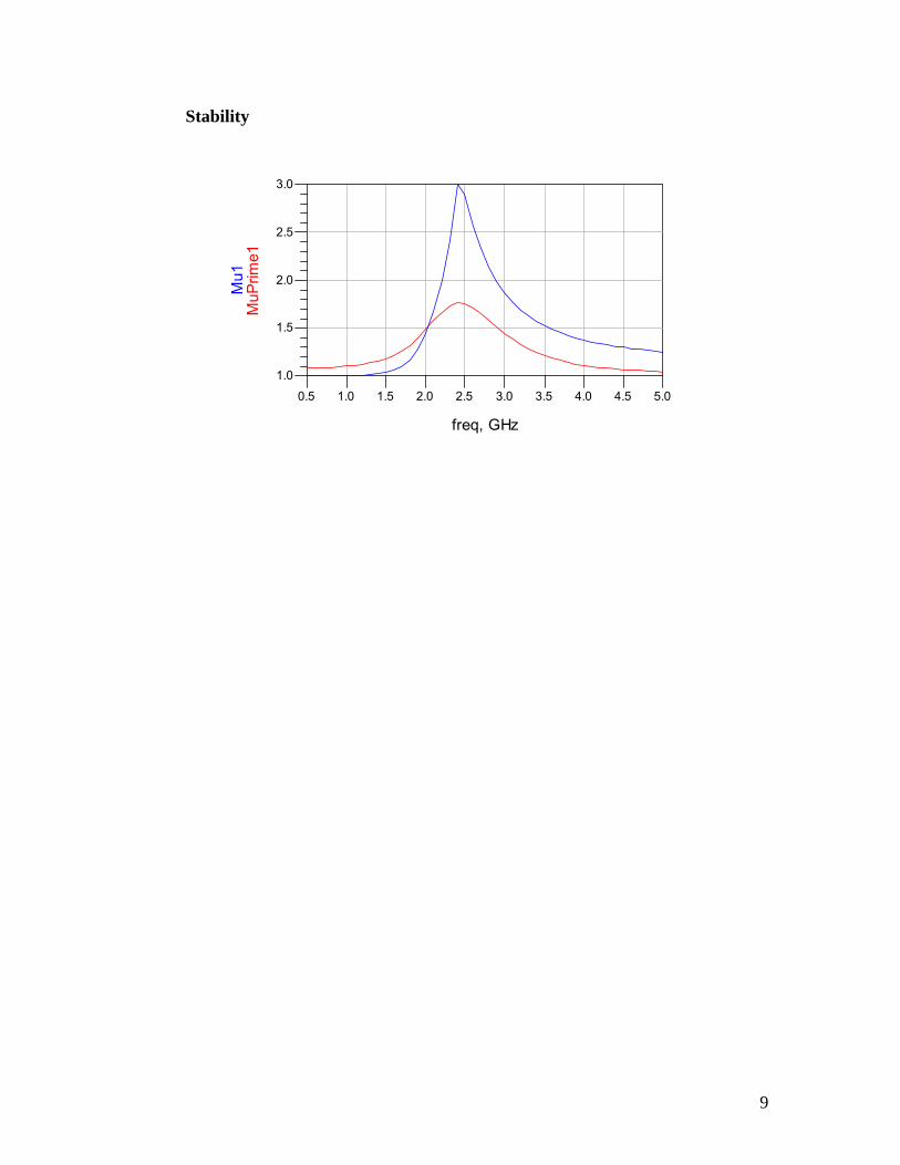
Stability
9
1.0 1.5 2.0 2.5 3.0 3.5 4.0 4.50.5 5.0
1.5
2.0
2.5
1.0
3.0
freq, GHz
Prim
Mu
e1M
u1


11
59.5 uV
59.5 uV
59.5 uV
3.30 V
3.30 V3.30 V
550 mV
550 mV550 mV550 mV
550 mV
550 mV
550 mV1.50 V
1.50 V
1.50 V 0 V
0 V
0 V
0 V
0 V
1.50 V1.50 V1.50 V
3.30 V
3.30 V
3.30 V
0 VVout
0 VVin 1.50 V
1.50 V1.50 V1.50 V
1.50 V 1.50 V1.49 V1.49 V
1.49 V
1.49 V
1.49 V 1.49 V
1.50 V
1.50 V
1.50 V
550 mV
550 mV
550 mV
550 mV
550 mV
550 mV
1.49 V1.49 V
550 mV
550 mV550 mV
550 mV
550 mV550 mV
550 mV550 mV
1.50 V
550 mV
0 V
0 V
0 V
0 V7.145 nH equiv
13.27 nH equiv
1.50 V
53.5 uV
5.45 nH equiv
-2.71 mAV_DCSRC1Vdc=3.3 V
-2.43 mAV_DCSRC2Vdc=3.3 V
0 A
tqped_padP120 A
tqped_sviaV14
0 A
TermTerm2
Z=50 OhmNum=2
0 ATermTerm1
Z=50 OhmNum=1 -2.43 mA
tqped_mrindL13
LVS_Ind="LVS_Value"l2=290 uml1=296 umn=19s=10 umw=10 um
0 Atqped_capC21c=0.6804 pF
2.71 mA
tqped_sviaV7
tqped_includeNET
capmod=1Statistical_Info=OnStatistical_Analysis=OffGate_Leakage=Nominaltau_gd=SlowkRhv=1.0kMIM=1.0kIs=1.0kRni=1.0kRsh=1.0Vp_vari=0
TQPEDNetlist Include
0 A
tqped_sviaV1
-2.43 mA
tqped_via1V22
M E 0
M E 1
-2.43 mAtqped_via1V20
M E 0
M E 1
2.43 mA
tqped_via1V23M
E0
ME
1
0 Atqped_via1V21
M E 0
M E 1
0 Atqped_via1V19
ME
0
ME
1
0 A
tqped_capC15c=2 pF
0 A
tqped_via1V18
ME0
ME1
0 A
tqped_via1V17
ME0
ME1
2.43 mAtqped_via1V16
M E 0
M E 1-2.43 mAtqped_resR18
w=10 umR=740 Ohm
0 A tqped_mrindL11
LVS_Ind="LVS_Value"l2=300 uml1=300 umn=16
0 A
tqped_sviaV15
0 A
tqped_padP11
0 A
tqped_capC19c=10 pF
0 A
tqped_sviaV6
0 A
tqped_padP2
-2.71 mAtqped_resR17
w=10 umR=665 Ohm
0 A
tqped_padP1
0 A
tqped_sviaV9
0 A
tqped_sviaV8
0 A
tqped_padP6
0 Atqped_padP5
0 A
tqped_padP30 A
tqped_padP4
0 Atqped_resR19
w=2 umR=2100 Ohm
2.43 mA
-2.43 mA
89.7 pA
tqped_ehssQ2
Ng=4W=15 um
-89.7 pA
tqped_resR13
w=2 umR=2000 Ohm
0 Atqped_capC20c=0.25 pF
0 Atqped_capC18c=10 pF
-275 uA tqped_resR16
w=2 umR=3455 Ohm
275 uAtqped_resR15
w=2 umR=2000 Ohm
-2.43 mAtqped_mrindL12
LVS_Ind="LVS_Value"l2=310 uml1=310 umn=27s=8 umw=8 um
2.43 mA
tqped_sviaV4
2.43 mA
-2.43 mA
89.8 pA
tqped_ehssQ1
Ng=4W=15 um
0 Atqped_resR14
w=2 umR=2100 Ohm
0 Atqped_capC17c=0.25 pF
0 A
tqped_capC16c=10 pF
-89.8 pAtqped_resR12
w=2 umR=2000 Ohm
0 A
tqped_capC14c=0.51 pF
0 Atqped_capC13c=20 pF
DC Annotation

Non-Linear Simulation: Power Output
-35 -30 -25 -20 -15-40 -10
-10
0
10
-20
20
RFpow er
dBm
:,1])
(Vou
t[: m9m11
Line
arC
ompr
essi
on m8m10
m9indep(m9)=plot_vs(dBm(Vout[::,1]), RFpower)=0.064
-26.000
m10RFpower=Compression=2.816
-24.000
m8RFpower=Compression=1.253
-26.000
m11indep(m11)=plot_vs(dBm(Vout[::,1]), RFpower)=0.500
-24.000
12

Layout
Test Plan
The following test equipment is necessary to test the full extent of this Low Power LNA Design:
3.3V Power Supply with Needle Probe Network Analyzer Cables and Ground Signal Ground (GSG) Probes Calibration Substrate for MMIC Testing Noise Figure Meter RF Signal Generator (capable of generating frequencies in 2-3 GHz range) Power Meter or Spectrum Analyzer
13

Test Procedures
S-parameter Measurement 1.) Calibrate the network analyzer from 1 GHz to 10GHz. 2.) Connect the 3.3V needle probe to the DC pads on the MMIC labeled “V+”.
The order in which they are connected is not important. 3.) Slowly increase the voltage to 3.3V to determine that the amplifier is working
correctly. 4.) Verify that the total current draw on the power supply is around 5.13 mA. 5.) Connect the input GSG Probes on the “IN” pads on the chip. 6.) Connect the output GSG Probes on the “OUT” pads on the chip. 7.) Measure the S-Parameter data measurements and save them to a disk.
Noise Figure Measurement Using the configuration of the MMIC mentioned in the S-parameter measurement, proceed to do the following: 1.) Remove the SMA cable from the port labeled “OUT” on the GSG Probe. 2.) Connect the Noise Figure Meter to the SMA port on the GSG Probe. 3.) Remove the SMA cable from the port labeled “IN” on the GSG Probe. 4.) Connect the noise source to the GSG Probe on the “IN” side of the MMIC. 5.) Use the Noise Figure Meter to take a measurement.
Compression Point Measurement Using the configuration of the MMIC mentioned in the Noise Figure Measurement, proceed to do the following: 1.) Remove the SMA cable from the port labeled “OUT” on the GSG Probe. 2.) Connect the Power Meter to the SMA port on the GSG Probe. 3.) Remove the SMA cable from the port labeled “IN” on the GSG Probe. 4.) Connect a signal generator to the GSG Probe on the “IN” side of the MMIC
making sure that the RF output of the device is off or around –80 dBm. 5.) Set the signal generator to 2.4 GHz. 6.) Beginning at –40 dBm, sweep the power input at 1 dB steps. Measure the
power output at each interval. 7.) Whenever the output does not increase by 1 dB with respect to the input
power, you have reached the 1 dB compression point. Determining what exact value this compression point occurs at can be either done using interpolation or Microsoft Excel.
Conclusion
Testing the low power LNA should have at least 20dB gain. The gain flatness should be less than 1 dB over a band of 500 MHz measured from the center frequency (2305 to 2497 MHz). Also, the Input match should have around –10.9dB of loss at 2.4 GHz and the output match should have around -44dB of loss at 2.3 GHz. The power consumption should be somewhere around 16.96 mW (taking the measured current and multiplying it by the supply voltage).
14

Two Bit Phase Shifter
JHU MMIC ProjectEE525.787 FALL 2006
David J. Wendland

JHU December 4, 2006 MMIC Two Bit Phase Shifter David J. Wendland
2
Introduction
• A MMIC two bit phase shifter was designed, simulated and laid out on a 60 mil x60 mil GaAs substrate.
• The circuit will be fabricated by TriQint.

JHU December 4, 2006 MMIC Two Bit Phase Shifter David J. Wendland
3
Design Philosophy• The topology of the design was set such that there was a
relative phase shift through the net work when compared to the zero or though path. The phase shifter consist of three sections.
– Control– 90 degree shift– 180 degree shift
• The control section consist of circuitry to convert positive 5 volt control voltage to the appropriate voltages to the phase switches.
• The 90 and 180 degree shift secitions are the same except for the amount of phase shift provided by each section.
• Each phase shift section consists of a positive phase network and a negative phase network.
• The through path passes through the positive phase network of each sectin.
• Lets walk though the 90 degree phase section.• The 90 degree phase shift section consists of a positive 45
deg. phase shift network and a negative 45 deg. phase shift network. If the through path is set through the positive phase shift network. There will be a 90 degree relative phase when the path switches, from the +45 degree network to the -45 degree network.
• With the above described topology, the phase of the through path is arbitrary and is not important for the relative phase shift.
• The 180 degree phase shift is achieved the same way but using +/-90degree networks
tqped_capC25c=2.55 pF
tqped_capC24c=2.55 pF
tqped_sviaV1
tqped_mrindL10
l2=272 uml1=284 umn=21
tqped_sviaV5
tqped_capC29c=.51 pF
tqped_mrindL15
l2=157 uml1=240 umn=13
tqped_capC28c=.51 pF
-45
+45
+ 45 DegreeNetwork
-45 DegreeNetwork

JHU December 4, 2006 MMIC Two Bit Phase Shifter David J. Wendland
4
Design Philosophy
tqped_capC25c=2.55 pF
tqped_capC24c=2.55 pF
tqped_sviaV1
tqped_mrindL10
l2=272 uml1=284 umn=21
tqped_sviaV5
tqped_capC29c=.51 pF
tqped_mrindL15
l2=157 uml1=240 umn=13
tqped_capC28c=.51 pF
+ 45 DegreeNetwork -45 Degree
Network
-45
+45
-90
+90

JHU December 4, 2006 MMIC Two Bit Phase Shifter David J. Wendland
5
Design Philosophy• Emode transistor were
used to take advantage of the positive gate bias– Can use single positive
supply• Dmode transistor were
used to convert +5V to the desired gate voltage– Smaller than resistors– Save space in voltage
dividers.– FET sized to provide:
• 2mA for 45/90 bit• 4mA for +5V bias
PortP6
tqped_resR64
tqped_resR63
V_DCSRC7
90_shift
PortP7
tqped_sviaV7
V_DCSRC2Vdc=VGS_45 V
tqped_resR47
w=5 umR=500 Ohm
tqped_phssQ11
Ng=2W=5 um
tqped_padP2
Dmode FET in voltage divider

JHU December 4, 2006 MMIC Two Bit Phase Shifter David J. Wendland
6
Logic Table
55270
50180
0590
000
Bit 90Bit 45Phase Shift
55270
50180
0590
000
Bit 90Bit 45Phase Shift

JHU December 4, 2006 MMIC Two Bit Phase Shifter David J. Wendland
7
Simulation/Layout• The phase shifter was first developed with ideal
components• TriQuint components were then substituted and retuned• The components were then inserted into the layout,
positioned and interconnects added• The interconnects of the critical paths were simulated
using microstrip elements in the schematic.• Critical interconnects consist of:
– Connections between switches, capacitors and inductors of the phase shift elements.
• Interconnect between the 90 degree phase shift section, 180 degree section and pads were not simulated since those paths do not affect the relative phase shift.

JHU December 4, 2006 MMIC Two Bit Phase Shifter David J. Wendland
8
Two Bit Phase Shifter Schematic with Interconnects
65.0 uV
65.0 uVGROUND_90 65.0 uV
3.87 mV
3.87 mV3.87 mV3.87 mV 3.87 mV
112 uVGround
1.00 V
1.00 V90_shift
0 V
5 V5 V
5 V
5 V
5 V 5 V
1.00 V
1.00 V1.00 V
1.00 V1.00 V 1.00 V180_shift
3.82 mV3.82 mV
3.82 mV
3.82 mV
3.82 mV
5 V
5 V
5 V
954 mVPos5_supply
0 V
0 V 0 V
3.87 mV
Neg 45 Degree Shift
0 V
1.04 mV1.04 mV
0 V
1.04 mV1.04 mV
1.04 mV 1.04 mV
22.8 nV22.8 nV 22.8 nV
1.04 mV1.04 mV1.04 mV
1.04 mV1.04 mV
0 V
1.04 mV
1.04 mV
1.03 mV
1.03 mV
0 V 0 V 0 V
1.03 mV
0 V
1.03 mV1.03 mV
1.03 mV
1.03 mV
1.03 mV
1.03 mV
1.03 mV
1.03 mV
0 V
1.04 mV22.8 nV 1.03 mV
22.8 nV 22.8 nV
1.03 mVPhase_out1
1.00 V
1.00 V
1.00 V180_shift
1.00 V
22.8 nVGND3
22.8 nV1.04 mV 1.03 mV
3.82 mV
Neg 90 Degree Shift65.0 uVGROUND_90
1.03 mV
1.03 mV1.03 mV
1.03 mV
1.03 mV 0 V0 V0 V
1.00 V
1.04 mV 1.04 mV
3.82 mV
Pos 90 Degree Shift
22.8 nVGND3
112 uVGround
22.7 nV
1.03 mVPhase_out1
3.87 mV
1.00 V
954 mVPos5_supply
1.00 V90_shift
Pos 45 Degree Shift
270180900
-2.01 mA
V_DCSRC6Vdc=VGS_90 V
0 A
tqped_padP5
2.01 mA
0 A
-10.1 fA
tqped_phssQ12
Ng=2W=5 um
2.01 mA
tqped_resR62
w=5 umR=500 Ohm
2.96 mA
tqped_sviaV17
950 uAtqped_resR60
w=5 umR=1 kOhm
950 uA
-950 uA
757 nA
tqped_ehssQ10
Ng=6W=50 um
17.0 fA
tqped_resR57
w=5 umR=1 kOhm
0 A
-17.0 fA
17.0 fA
tqped_ehssQ9
Ng=6W=50 um
-1.78 fA
MLINTL13
L=40 umW=20 um
VARVAR4
VGS_90=5VGS_45=5
EqnVarVAR
VAR3
VGS_90=5VGS_45=0
EqnVarVAR
VAR2
VGS_90=0VGS_45=5
EqnVarVAR
VAR1
VGS_90=0VGS_45=0
EqnVar
5.07 mA
tqped_sviaV7 -759 nA
tqped_resR49
w=5 umR=1 kOhm
0 A
tqped_sviaV1
S_ParamSP2
Step=0.1 GHzStop=2.5 GHzStart=2.3 GHz
S-PARAMETERS
ParamSweepSweep2
Step=5Stop=5Start=0SimInstanceName[6]=SimInstanceName[5]=SimInstanceName[4]=SimInstanceName[3]=SimInstanceName[2]=SimInstanceName[1]="SP2"SweepVar="VGS_45"
PARAMETER SWEEP
ParamSweepSweep3
Step=5Stop=5Start=0SimInstanceName[6]=SimInstanceName[5]=SimInstanceName[4]=SimInstanceName[3]=SimInstanceName[2]="Sweep2"SimInstanceName[1]="SP2"SweepVar="VGS_90"
PARAMETER SWEEP
0 A
tqped_padP1
0 Atqped_padP2
0 A
tqped_padP3 0 A
TermTerm1
Z=50 OhmNum=1
-17.3 fA
tqped_resR53
w=5 umR=1 kOhm
MSUBMetal_2
Cond1="tqped_TwoMe"Rough=0 umTanD=0T=0 umHu=1.0e+036 umCond=1.0E+50Mur=1Er=12.9H=100 um
MSub
MSUBmetal_1
Cond1="tqped_OneMe"Rough=0 umTanD=0T=0 umHu=1.0e+036 umCond=1.0E+50Mur=1Er=12.9H=100 um
MSub
MSUBMetal_zero
Cond1="tqped_ZeroMe"Rough=0 umTanD=0T=0 umHu=1.0e+036 umCond=1.0E+50Mur=1Er=12.9H=100 um
MSub
0 A
tqped_capC33
w=46 umc=1.25 pF
0 A
tqped_capC32
w=46 umc=1.25 pF
209 nA tqped_mrindL14
l2=237 uml1=231 umn=16
0 AMLINTL14
L=32 umW=10 um
273 nA
MLINTL8
L=70 umW=10 um
-273 nA
MLINTL9
L=100 umW=10 um
0 A
tqped_capC29c=.51 pF
0 AMLINTL2
L=53.3 umW=10 um
0 AMLINTL1
L=53.3 umW=10 um
0 AMLINTL3
L=67.7 umW=10 um
0 AMLINTL4
L=67.7 umW=10 um
273 nAtqped_mrindL15
l2=157 uml1=240 umn=13
0 AMLINTL10
L=184.5 umW=20 um
0 A
tqped_sviaV5
0 A
MLINTL11
L=94 umW=22 um
0 A
tqped_capC28c=.51 pF
273 nA
MLINTL7
L=25.5 umW=10 um
-273 nA
MLINTL6
L=70 umW=10 um
273 nA
-1.03 uA
759 nA
tqped_ehssQ2
Ng=6W=50 um
S_ParamSP1
Step=.009 GHzStop=5 GHzStart=.5 GHz
S-PARAMETERS
VARVAR5
C_neg90=1.3C_pos90=1.32C_pos45=2.55Cneg45=0.51
EqnVar
0 Atqped_mrindL10
l2=272 uml1=284 umn=21
0 Atqped_capC30c=1.38 pF
0 Atqped_capC31c=1.38 pF
0 A
tqped_mrindL13
l2=220 uml1=219 umn=18
-758 nA tqped_resR56
w=5 umR=1 kOhm
1.03 uAtqped_sviaV19
0 AMLINTL17
L=17 umW=20 um
0 AMLINTL16
L=62.5 umW=10 um
0 AMLINTL15
L=32 umW=10 um
0 AMLINTL12
L=40 umW=20 um
-17.0 fA
tqped_resR54
w=5 umR=1 kOhm
759 nA tqped_resR55
w=5 umR=1 kOhm
-209 nA
-549 nA
758 nA
tqped_ehssQ7
Ng=6W=50 um
0 A
tqped_sviaV21
0 AMLINTL23
L=140 umW=40 um
0 AMLINTL22
L=33 umW=40 um
0 ATermTerm2
Z=50 OhmNum=2
0 A
-17.0 fA
17.0 fA
tqped_ehssQ6
Ng=6W=50 um
209 nA
-968 nA
759 nA
tqped_ehssQ8
Ng=6W=50 um
0 A
tqped_padP4
968 nA
tqped_resR59
w=5 umR=1 kOhm
0 Atqped_capC34c=6 pF
-209 nA
MLINTL19
L=50 umW=10 um
209 nA
MLINTL21
L=30 umW=10 um
-209 nA
MLINTL20
L=50 umW=10 um
209 nA
MLINTL18
L=50 umW=10 um
0 A
-17.3 fA
17.3 fA
tqped_ehssQ1
Ng=6W=50 um
0 A
-17.3 fA
17.3 fA
tqped_ehssQ3
Ng=6W=50 um
950 uA
-950 uA
757 nA
tqped_ehssQ5
Ng=6W=50 um
-273 nA
-486 nA
759 nA
tqped_ehssQ4
Ng=6W=50 um
1.03 uA
tqped_sviaV10
2.01 mA
0 A
-10.1 fA
tqped_phssQ11
Ng=2W=5 um
tqped_includeNET
capmod=1Statistical_Info=OnStatistical_Analysis=OffGate_Leakage=Nominaltau_gd=SlowkRhv=1.0kMIM=1.0kIs=1.0kRni=1.0kRsh=1.0Vp_vari=0
TQPEDNetlist Include
-2.01 mA
V_DCSRC2Vdc=VGS_45 V
-4.02 mAV_DCSRC4Vdc=5 V
4.02 mA 0 A
-20.2 fA
tqped_phssQ13
Ng=2W=10 um
1.03 uAtqped_resR51
w=5 umR=1 kOhm
1.03 uA
tqped_resR52
w=5 umR=1 kOhm
17.3 fA tqped_resR48
w=5 umR=1 kOhm
759 nA
tqped_resR50
w=5 umR=1 kOhm
2.12 mA tqped_resR42
w=5 umR=450 Ohm
950 uAtqped_resR44
w=5 umR=1 kOhm
2.01 mAtqped_resR47
w=5 umR=500 Ohm
0 Atqped_capC35c=10 pF
0 Atqped_capC24c=2.55 pF
0 Atqped_capC25c=2.55 pF
0 AMLINTL5
L=17.9 umW=20 umSubst="metal_1"

JHU December 4, 2006 MMIC Two Bit Phase Shifter David J. Wendland
9
Two Bit Phase Shifter
65.0 uV
65.0 uVGROUND_90 65.0 uV
3.87 mV
3.87 mV3.87 mV3.87 mV 3.87 mV
112 uVGround
1.00 V
1.00 V90_shift
0 V
5 V5 V
5 V
5 V
5 V 5 V
1.00 V
1.00 V1.00 V
1.00 V1.00 V 1.00 V180_shift
3.82 mV3.82 mV
3.82 mV
3.82 mV
3.82 mV
5 V
5 V
5 V
954 mVPos5_supply
0 V
0 V 0 V
3.87 mV
Neg 45 Degree Shift
0 V
1.04 mV1.04 mV
0 V
1.04 mV1.04 mV
1.04 mV 1.04 mV
22.8 nV22.8 nV 22.8 nV
1.04 mV1.04 mV1.04 mV
1.04 mV1.04 mV
0 V
1.04 mV
1.04 mV
1.03 mV
1.03 mV
0 V 0 V 0 V
1.03 mV
0 V
1.03 mV1.03 mV
1.03 mV
1.03 mV
1.03 mV
1.03 mV
1.03 mV
1.03 mV
0 V
1.04 mV22.8 nV 1.03 mV
22.8 nV 22.8 nV
1.03 mVPhase_out1
1.00 V
1.00 V
1.00 V180_shift
1.00 V
22.8 nVGND3
22.8 nV1.04 mV 1.03 mV
3.82 mV
Neg 90 Degree Shift65.0 uVGROUND_90
1.03 mV
1.03 mV1.03 mV
1.03 mV
1.03 mV 0 V0 V0 V
1.00 V
1.04 mV 1.04 mV
3.82 mV
Pos 90 Degree Shift
22.8 nVGND3
112 uVGround
22.7 nV
1.03 mVPhase_out1
3.87 mV
1.00 V
954 mVPos5_supply
1.00 V90_shift
Pos 45 Degree Shift
270180900
-2.01 mA
V_DCSRC6Vdc=VGS_90 V
0 A
tqped_padP5
2.01 mA
0 A
-10.1 fA
tqped_phssQ12
Ng=2W=5 um
2.01 mA
tqped_resR62
w=5 umR=500 Ohm
2.96 mA
tqped_sviaV17
950 uAtqped_resR60
w=5 umR=1 kOhm
950 uA
-950 uA
757 nA
tqped_ehssQ10
Ng=6W=50 um
17.0 fA
tqped_resR57
w=5 umR=1 kOhm
0 A
-17.0 fA
17.0 fA
tqped_ehssQ9
Ng=6W=50 um
-1.78 fA
MLINTL13
L=40 umW=20 um
VARVAR4
VGS_90=5VGS_45=5
EqnVarVAR
VAR3
VGS_90=5VGS_45=0
EqnVarVAR
VAR2
VGS_90=0VGS_45=5
EqnVarVAR
VAR1
VGS_90=0VGS_45=0
EqnVar
5.07 mA
tqped_sviaV7 -759 nA
tqped_resR49
w=5 umR=1 kOhm
0 A
tqped_sviaV1
S_ParamSP2
Step=0.1 GHzStop=2.5 GHzStart=2.3 GHz
S-PARAMETERS
ParamSweepSweep2
Step=5Stop=5Start=0SimInstanceName[6]=SimInstanceName[5]=SimInstanceName[4]=SimInstanceName[3]=SimInstanceName[2]=SimInstanceName[1]="SP2"SweepVar="VGS_45"
PARAMETER SWEEP
ParamSweepSweep3
Step=5Stop=5Start=0SimInstanceName[6]=SimInstanceName[5]=SimInstanceName[4]=SimInstanceName[3]=SimInstanceName[2]="Sweep2"SimInstanceName[1]="SP2"SweepVar="VGS_90"
PARAMETER SWEEP
0 A
tqped_padP1
0 Atqped_padP2
0 A
tqped_padP3 0 A
TermTerm1
Z=50 OhmNum=1
-17.3 fA
tqped_resR53
w=5 umR=1 kOhm
MSUBMetal_2
Cond1="tqped_TwoMe"Rough=0 umTanD=0T=0 umHu=1.0e+036 umCond=1.0E+50Mur=1Er=12.9H=100 um
MSub
MSUBmetal_1
Cond1="tqped_OneMe"Rough=0 umTanD=0T=0 umHu=1.0e+036 umCond=1.0E+50Mur=1Er=12.9H=100 um
MSub
MSUBMetal_zero
Cond1="tqped_ZeroMe"Rough=0 umTanD=0T=0 umHu=1.0e+036 umCond=1.0E+50Mur=1Er=12.9H=100 um
MSub
0 A
tqped_capC33
w=46 umc=1.25 pF
0 A
tqped_capC32
w=46 umc=1.25 pF
209 nA tqped_mrindL14
l2=237 uml1=231 umn=16
0 AMLINTL14
L=32 umW=10 um
273 nA
MLINTL8
L=70 umW=10 um
-273 nA
MLINTL9
L=100 umW=10 um
0 A
tqped_capC29c=.51 pF
0 AMLINTL2
L=53.3 umW=10 um
0 AMLINTL1
L=53.3 umW=10 um
0 AMLINTL3
L=67.7 umW=10 um
0 AMLINTL4
L=67.7 umW=10 um
273 nAtqped_mrindL15
l2=157 uml1=240 umn=13
0 AMLINTL10
L=184.5 umW=20 um
0 A
tqped_sviaV5
0 A
MLINTL11
L=94 umW=22 um
0 A
tqped_capC28c=.51 pF
273 nA
MLINTL7
L=25.5 umW=10 um
-273 nA
MLINTL6
L=70 umW=10 um
273 nA
-1.03 uA
759 nA
tqped_ehssQ2
Ng=6W=50 um
S_ParamSP1
Step=.009 GHzStop=5 GHzStart=.5 GHz
S-PARAMETERS
VARVAR5
C_neg90=1.3C_pos90=1.32C_pos45=2.55Cneg45=0.51
EqnVar
0 Atqped_mrindL10
l2=272 uml1=284 umn=21
0 Atqped_capC30c=1.38 pF
0 Atqped_capC31c=1.38 pF
0 A
tqped_mrindL13
l2=220 uml1=219 umn=18
-758 nA tqped_resR56
w=5 umR=1 kOhm
1.03 uAtqped_sviaV19
0 AMLINTL17
L=17 umW=20 um
0 AMLINTL16
L=62.5 umW=10 um
0 AMLINTL15
L=32 umW=10 um
0 AMLINTL12
L=40 umW=20 um
-17.0 fA
tqped_resR54
w=5 umR=1 kOhm
759 nA tqped_resR55
w=5 umR=1 kOhm
-209 nA
-549 nA
758 nA
tqped_ehssQ7
Ng=6W=50 um
0 A
tqped_sviaV21
0 AMLINTL23
L=140 umW=40 um
0 AMLINTL22
L=33 umW=40 um
0 ATermTerm2
Z=50 OhmNum=2
0 A
-17.0 fA
17.0 fA
tqped_ehssQ6
Ng=6W=50 um
209 nA
-968 nA
759 nA
tqped_ehssQ8
Ng=6W=50 um
0 A
tqped_padP4
968 nA
tqped_resR59
w=5 umR=1 kOhm
0 Atqped_capC34c=6 pF
-209 nA
MLINTL19
L=50 umW=10 um
209 nA
MLINTL21
L=30 umW=10 um
-209 nA
MLINTL20
L=50 umW=10 um
209 nA
MLINTL18
L=50 umW=10 um
0 A
-17.3 fA
17.3 fA
tqped_ehssQ1
Ng=6W=50 um
0 A
-17.3 fA
17.3 fA
tqped_ehssQ3
Ng=6W=50 um
950 uA
-950 uA
757 nA
tqped_ehssQ5
Ng=6W=50 um
-273 nA
-486 nA
759 nA
tqped_ehssQ4
Ng=6W=50 um
1.03 uA
tqped_sviaV10
2.01 mA
0 A
-10.1 fA
tqped_phssQ11
Ng=2W=5 um
tqped_includeNET
capmod=1Statistical_Info=OnStatistical_Analysis=OffGate_Leakage=Nominaltau_gd=SlowkRhv=1.0kMIM=1.0kIs=1.0kRni=1.0kRsh=1.0Vp_vari=0
TQPEDNetlist Include
-2.01 mA
V_DCSRC2Vdc=VGS_45 V
-4.02 mAV_DCSRC4Vdc=5 V
4.02 mA 0 A
-20.2 fA
tqped_phssQ13
Ng=2W=10 um
1.03 uAtqped_resR51
w=5 umR=1 kOhm
1.03 uA
tqped_resR52
w=5 umR=1 kOhm
17.3 fA tqped_resR48
w=5 umR=1 kOhm
759 nA
tqped_resR50
w=5 umR=1 kOhm
2.12 mA tqped_resR42
w=5 umR=450 Ohm
950 uAtqped_resR44
w=5 umR=1 kOhm
2.01 mAtqped_resR47
w=5 umR=500 Ohm
0 Atqped_capC35c=10 pF
0 Atqped_capC24c=2.55 pF
0 Atqped_capC25c=2.55 pF
0 AMLINTL5
L=17.9 umW=20 umSubst="metal_1"
-45
+45
-90
+90

JHU December 4, 2006 MMIC Two Bit Phase Shifter David J. Wendland
10
Neg 45 Degree Shift
90_shift
GND3
Phase_out1
Pos 45 Degree Shift
tqped_padP3
TermTerm1
Z=50 OhmNum=1
tqped_resR53
w=5 umR=1 kOhm
MLINTL8
L=70 umW=10 um
MLINTL9
L=100 umW=10 um
tqped_capC29c=.51 pF
MLINTL2
L=53.3 umW=10 um
MLINTL1
L=53.3 umW=10 um
MLINTL3
L=67.7 umW=10 um
MLINTL4
L=67.7 umW=10 um
tqped_mrindL15
l2=157 uml1=240 umn=13
MLINTL10
L=184.5 umW=20 um
tqped_sviaV5
MLINTL11
L=94 umW=22 um
tqped_capC28c=.51 pF
MLINTL7
L=25.5 umW=10 um
MLINTL6
L=70 umW=10 um
tqped_ehssQ2
Ng=6W=50 um
tqped_mrindL10
l2=272 uml1=284 umn=21
tqped_ehssQ1
Ng=6W=50 um
tqped_ehssQ3
Ng=6W=50 um
tqped_ehssQ5
Ng=6W=50 um
tqped_ehssQ4
Ng=6W=50 um
tqped_sviaV7
tqped_sviaV10
tqped_resR51
w=5 umR=1 kOhm
tqped_resR52
w=5 umR=1 kOhm
tqped_resR48
w=5 umR=1 kOhm
tqped_resR50
w=5 umR=1 kOhm
tqped_capC35c=10 pF
tqped_capC24c=2.55 pF
tqped_capC25c=2.55 pF
tqped_resR49
w=5 umR=1 kOhm tqped_svia
V1
MLINTL5
L=17.9 umW=20 umSubst="metal_1"
90 Degree Phase Shift

JHU December 4, 2006 MMIC Two Bit Phase Shifter David J. Wendland
11
Phase_out1
180_shift
GND3
Neg 90 Degree ShiftGROUND_90
Pos 90 Degree Shift
tqped_capC33
w=46 umc=1.25 pF
tqped_capC32
w=46 umc=1.25 pF
tqped_mrindL14
l2=237 uml1=231 umn=16
MLINTL14
L=32 umW=10 um
tqped_capC30c=1.38 pF
tqped_capC31c=1.38 pF
tqped_mrindL13
l2=220 uml1=219 umn=18
tqped_resR56
w=5 umR=1 kOhm
tqped_sviaV19
MLINTL13
L=40 umW=20 um
MLINTL17
L=17 umW=20 um
MLINTL16
L=62.5 umW=10 um
MLINTL15
L=32 umW=10 um
MLINTL12
L=40 umW=20 um
tqped_resR54
w=5 umR=1 kOhm
tqped_resR55
w=5 umR=1 kOhm
tqped_resR57
w=5 umR=1 kOhm
tqped_resR60
w=5 umR=1 kOhm
tqped_sviaV17
tqped_ehssQ10
Ng=6W=50 um
tqped_ehssQ9
Ng=6W=50 um
tqped_ehssQ7
Ng=6W=50 um
tqped_sviaV21
MLINTL23
L=140 umW=40 um
MLINTL22
L=33 umW=40 um
TermTerm2
Z=50 OhmNum=2
tqped_ehssQ6
Ng=6W=50 um
tqped_ehssQ8
Ng=6W=50 um
tqped_padP4
tqped_resR59
w=5 umR=1 kOhm
tqped_capC34c=6 pF
MLINTL19
L=50 umW=10 um
MLINTL21
L=30 umW=10 um
MLINTL20
L=50 umW=10 um
MLINTL18
L=50 umW=10 um
180 Degree Phase Shift

JHU December 4, 2006 MMIC Two Bit Phase Shifter David J. Wendland
12
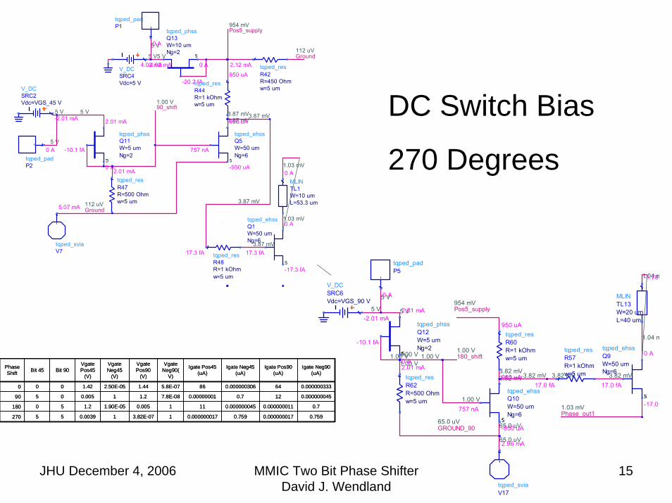
DC Switch Bias
Zero Degrees/Ref1.50 V
1.50 V1.50 V1.50 V
Ground
0 V
0 V 0 V
5 V
5 V
5 V
86.1 mV
86.1 mV
80.7 uVGround
1.42 V
1.65 VPos5_supply
24.9 uV90_shift
3.67 mA
tqped_sviaV7
0 A
tqped_padP1
0 A
tqped_padP2
0 A
MLINTL1
L=53.3 umW=10 um
0 A
-86.0 uA
86.0 uA
tqped_ehssQ1
Ng=6W=50 um
1.71 nA
-1.71 nA
-207 fA
tqped_ehssQ5
Ng=6W=50 um
-112 nA
0 A
1.83 aA
tqped_phssQ11
Ng=2W=5 um
112 nA
V_DCSRC2Vdc=VGS_45 V
-3.97 mAV_DCSRC4Vdc=5 V
3.97 mA 0 A
-20.1 fA
tqped_phssQ13
Ng=2W=10 um
86.0 uA tqped_resR48
w=5 umR=1 kOhm
3.67 mA tqped_resR42
w=5 umR=450 Ohm
150 uA
tqped_resR44
w=5 umR=1 kOhm
-112 nA
tqped_resR47
w=5 umR=500 Ohm
GROUND_90
0 V0 V
0 V
583 nV
583 nV583 nV
583 nV583 nV583 nV180_shift
1.50 V1.50 V
1.50 V 1.50 V
1.65 VPos5_supply
128 m
128 mVPhase_out1
128 m
1.44 V
86.0 uA
tqped_sviaV17
-2.62 nA
tqped_resR62
w=5 umR=500 Ohm
2.62 nA
V_DCSRC6Vdc=VGS_90 V
0 A
tqped_padP5
-2.62 nA
0 A
0 A
tqped_phssQ12
Ng=2W=5 um
150 uA
tqped_resR60
w=5 umR=1 kOhm
1.72 nA
-1.72 nA
-207 fA
tqped_ehssQ10
Ng=6W=50 um
64.1 uA
tqped_resR57
w=5 umR=1 kOhm
0 A
-64.1
64.1 uA
tqped_ehssQ9
Ng=6W=50 um
0 A
MLINTL13
L=40 umW=20 um
0.7590.0000000170.7590.00000001713.82E-0710.003955270
0.70.0000000110.0000000451110.0051.90E-051.250180
0.000000045120.70.000000017.8E-081.210.0050590
0.000000333640.000000306865.8E-071.442.50E-051.42000
Igate Neg90 (uA)
Igate Pos90 (uA)
Igate Neg45 (uA)
Igate Pos45 (uA)
VgateNeg90(
V)
VgatePos90
(V)
VgateNeg45
(V)
VgatePos45
(V)Bit 90Bit 45Phase
Shift

JHU December 4, 2006 MMIC Two Bit Phase Shifter David J. Wendland
13
DC Switch Bias
90 Degrees5.00 mV
5.00 mV5.00 mV5.00 mV
132 uVGround
5 V
5 V 5 V
5 V
5 V
5 V
6.73 mV
6.73 mV
132 uVGround
5.00 mV
1.24 VPos5_supply
1.00 V90_shift
5.98 mA
tqped_sviaV7
0 A
tqped_padP1
0 A
tqped_padP2
0 A
MLINTL1
L=53.3 umW=10 um
0 A
10.2 fA
-10.2 fA
tqped_ehssQ1
Ng=6W=50 um
1.23 mA
-1.23 mA
751 nA
tqped_ehssQ5
Ng=6W=50 um
2.01 mA
0 A
-10.1 fA
tqped_phssQ11
Ng=2W=5 um
-2.01 mA
V_DCSRC2Vdc=VGS_45 V
-4.00 mAV_DCSRC4Vdc=5 V
4.00 mA 0 A
-20.1 fA
tqped_phssQ13
Ng=2W=10 um
-10.2 fA tqped_resR48
w=5 umR=1 kOhm
2.75 mA tqped_resR42
w=5 umR=450 Ohm
1.23 mA
tqped_resR44
w=5 umR=1 kOhm
2.01 mA
tqped_resR47
w=5 umR=500 Ohm
252 nVGROUND_90
0 V0 V
0 V
77.6 nV180_shift
1.21 V1.21 V
1.21 V 1.21 V
1.24 VPos5_supply
6.81 m
6.78 mVPhase_out1
6.81 m
1.20 V
11.4 uA
tqped_sviaV17
-348 pA
tqped_resR62
w=5 umR=500 Ohm
348 pA
V_DCSRC6Vdc=VGS_90 V
0 A
tqped_padP5
-348 pA
0 A
0 A
tqped_phssQ12
Ng=2W=5 um
23.6 uA
tqped_resR60
w=5 umR=1 kOhm
1.55 nA
-1.55 nA
-207 fA
tqped_ehssQ10
Ng=6W=50 um
12.1 uA
tqped_resR57
w=5 umR=1 kOhm
0 A
-12.1
12.1 uA
tqped_ehssQ9
Ng=6W=50 um
0 A
MLINTL13
L=40 umW=20 um
0.7590.0000000170.7590.00000001713.82E-0710.003955270
0.70.0000000110.0000000451110.0051.90E-051.250180
0.000000045120.70.000000017.8E-081.210.0050590
0.000000333640.000000306865.8E-071.442.50E-051.42000
Igate Neg90 (uA)
Igate Pos90 (uA)
Igate Neg45 (uA)
Igate Pos45 (uA)
VgateNeg90(
V)
VgatePos90
(V)
VgateNeg45
(V)
VgatePos45
(V)Bit 90Bit 45Phase
Shift
0.7590.0000000170.7590.00000001713.82E-0710.003955270
0.70.0000000110.0000000451110.0051.90E-051.250180
0.000000045120.70.000000017.8E-081.210.0050590
0.000000333640.000000306865.8E-071.442.50E-051.42000
Igate Neg90 (uA)
Igate Pos90 (uA)
Igate Neg45 (uA)
Igate Pos45 (uA)
VgateNeg90(
V)
VgatePos90
(V)
VgateNeg45
(V)
VgatePos45
(V)Bit 90Bit 45Phase
Shift

JHU December 4, 2006 MMIC Two Bit Phase Shifter David J. Wendland
14
DC Switch Bias
180 Degrees1.21 V
1.21 V1.21 V1.21 V
60.4 uVGround
0 V
0 V 0 V
5 V
5 V
5 V
11.5 mV
11.5 mV
60.4 uVGround
1.20 V
1.24 VPos5_supply
18.6 uV90_shift
2.75 mA
tqped_sviaV7
0 A
tqped_padP1
0 A
tqped_padP2
-14.2 fA
MLINTL1
L=53.3 umW=10 um
0 A
-11.4 uA
11.4 uA
tqped_ehssQ1
Ng=6W=50 um
1.55 nA
-1.55 nA
-207 fA
tqped_ehssQ5
Ng=6W=50 um
-83.6 nA
0 A
1.37 aA
tqped_phssQ11
Ng=2W=5 um
83.6 nA
V_DCSRC2Vdc=VGS_45 V
-4.00 mAV_DCSRC4Vdc=5 V
4.00 mA 0 A
-20.1 fA
tqped_phssQ13
Ng=2W=10 um
11.4 uA tqped_resR48
w=5 umR=1 kOhm
2.75 mA tqped_resR42
w=5 umR=450 Ohm
23.5 uA
tqped_resR44
w=5 umR=1 kOhm
-83.6 nA
tqped_resR47
w=5 umR=500 Ohm
71.4 uV
71.4 uVGROUND_90 71.4 uV
5 V5 V
5 V
1.00 V
1.00 V1.00 V
1.00 V1.00 V1.00 V180_shift
4.94 mV4.94 mV
4.94 mV 4.94 mV
1.24 VPos5_supply
6.81 m
6.81 mVPhase_out1
6.81 m
4.94 mV
3.24 mA
tqped_sviaV17
2.01 mA
tqped_resR62
w=5 umR=500 Ohm
-2.01 mA
V_DCSRC6Vdc=VGS_90 V
0 A
tqped_padP5
2.01 mA
0 A
-10.1 fA
tqped_phssQ12
Ng=2W=5 um
1.23 mA
tqped_resR60
w=5 umR=1 kOhm
1.23 mA
-1.23 mA
751 nA
tqped_ehssQ10
Ng=6W=50 um
-11.0 fA
tqped_resR57
w=5 umR=1 kOhm
0 A
11.0 f
-11.0 fA
tqped_ehssQ9
Ng=6W=50 um
0 A
MLINTL13
L=40 umW=20 um
0.7590.0000000170.7590.00000001713.82E-0710.003955270
0.70.0000000110.0000000451110.0051.90E-051.250180
0.000000045120.70.000000017.8E-081.210.0050590
0.000000333640.000000306865.8E-071.442.50E-051.42000
Igate Neg90 (uA)
Igate Pos90 (uA)
Igate Neg45 (uA)
Igate Pos45 (uA)
VgateNeg90(
V)
VgatePos90
(V)
VgateNeg45
(V)
VgatePos45
(V)Bit 90Bit 45Phase
Shift
0.7590.0000000170.7590.00000001713.82E-0710.003955270
0.70.0000000110.0000000451110.0051.90E-051.250180
0.000000045120.70.000000017.8E-081.210.0050590
0.000000333640.000000306865.8E-071.442.50E-051.42000
Igate Neg90 (uA)
Igate Pos90 (uA)
Igate Neg45 (uA)
Igate Pos45 (uA)
VgateNeg90(
V)
VgatePos90
(V)
VgateNeg45
(V)
VgatePos45
(V)Bit 90Bit 45Phase
Shift
JHU December 4, 2006 MMIC Two Bit Phase Shifter David J. Wendland
15
DC Switch Bias
270 Degrees3.87 mV
3.87 mV3.87 mV3.87 mV
112 uVGround
5 V
5 V 5 V
5 V
5 V
5 V
1.03 mV
1.03 mV
112 uVGround
3.87 mV
954 mVPos5_supply
1.00 V90_shift
5.07 mA
tqped_sviaV7
0 A
tqped_padP1
0 A
tqped_padP2
0 A
MLINTL1
L=53.3 umW=10 um
0 A
-17.3 fA
17.3 fA
tqped_ehssQ1
Ng=6W=50 um
950 uA
-950 uA
757 nA
tqped_ehssQ5
Ng=6W=50 um
2.01 mA
0 A
-10.1 fA
tqped_phssQ11
Ng=2W=5 um
-2.01 mA
V_DCSRC2Vdc=VGS_45 V
-4.02 mAV_DCSRC4Vdc=5 V
4.02 mA 0 A
-20.2 fA
tqped_phssQ13
Ng=2W=10 um
17.3 fA tqped_resR48
w=5 umR=1 kOhm
2.12 mA tqped_resR42
w=5 umR=450 Ohm
950 uA
tqped_resR44
w=5 umR=1 kOhm
2.01 mA
tqped_resR47
w=5 umR=500 Ohm
65.0 uV
65.0 uVGROUND_90 65.0 uV
5 V5 V
5 V
1.00 V
1.00 V1.00 V
1.00 V1.00 V1.00 V180_shift
3.82 mV3.82 mV
3.82 mV 3.82 mV
954 mVPos5_supply
1.04 m
1.03 mVPhase_out1
1.04 m
3.82 mV
-2.01 mA
V_DCSRC6Vdc=VGS_90 V
0 A
tqped_padP5
2.01 mA
0 A
-10.1 fA
tqped_phssQ12
Ng=2W=5 um
2.01 mA
tqped_resR62
w=5 umR=500 Ohm
2.96 mA
tqped_sviaV17
950 uA
tqped_resR60
w=5 umR=1 kOhm
950 uA
-950 uA
757 nA
tqped_ehssQ10
Ng=6W=50 um
17.0 fA
tqped_resR57
w=5 umR=1 kOhm
0 A
-17.0
17.0 fA
tqped_ehssQ9
Ng=6W=50 um
-1.78
MLINTL13
L=40 umW=20 um
0.7590.0000000170.7590.00000001713.82E-0710.003955270
0.70.0000000110.0000000451110.0051.90E-051.250180
0.000000045120.70.000000017.8E-081.210.0050590
0.000000333640.000000306865.8E-071.442.50E-051.42000
Igate Neg90 (uA)
Igate Pos90 (uA)
Igate Neg45 (uA)
Igate Pos45 (uA)
VgateNeg90(
V)
VgatePos90
(V)
VgateNeg45
(V)
VgatePos45
(V)Bit 90Bit 45Phase
Shift
0.7590.0000000170.7590.00000001713.82E-0710.003955270
0.70.0000000110.0000000451110.0051.90E-051.250180
0.000000045120.70.000000017.8E-081.210.0050590
0.000000333640.000000306865.8E-071.442.50E-051.42000
Igate Neg90 (uA)
Igate Pos90 (uA)
Igate Neg45 (uA)
Igate Pos45 (uA)
VgateNeg90(
V)
VgatePos90
(V)
VgateNeg45
(V)
VgatePos45
(V)Bit 90Bit 45Phase
Shift

JHU December 4, 2006 MMIC Two Bit Phase Shifter David J. Wendland
16
Two Bit Phase Shifter Layout on 60mil x 60 mil GaAs Substrate

JHU December 4, 2006 MMIC Two Bit Phase Shifter David J. Wendland
17
Design Specification
• Frequency: 2305 MHz to 2497 MHz• Insertion loss: Less than 4dB (3dB Goal)• Insertion Balance: +/- 1dB• Phase shift: 90 and 180 degrees steps• VSWR, 50 Ohms: Less than 1.5:1• Supply Voltage: +/- 5 Volts• Control Voltage: TTL(goal); or 0, -5V• Size: 60x60 mil ANACHIP

JHU December 4, 2006 MMIC Two Bit Phase Shifter David J. Wendland
18
Achieved Specification• The Specification of VSWR better then 1.5:1 was not
achieved.• A VSWR better then 1.8:1 was achieved
• Frequency(1.8:1 VSWR): 2300 MHz to 2642 MHz• 1.8:1 VSWR Bandwidth: 342 MHz• Insertion loss: 3.77 dB (2300 to 2500 MHz)
3.96 dB (2300 to 2642 MHz) • Insertion Balance: 0.45 dB (2300 to 2500 MHz)
0.68 dB (2300 to 2642 MHz)

JHU December 4, 2006 MMIC Two Bit Phase Shifter David J. Wendland
19
Two Bit Phase Shifter Input VSWR
1.0
1.1
1.2
1.3
1.4
1.5
1.6
1.7
1.8
1.9
2.0
2000 2100 2200 2300 2400 2500 2600 2700 2800 2900 3000
Frequency (MHz)
VSW
RVSWR Zero VSWR 90 VSWR 180 VSWR 270

JHU December 4, 2006 MMIC Two Bit Phase Shifter David J. Wendland
20
Two Bit Phase Shifter Output VSWR
1.0
1.1
1.2
1.3
1.4
1.5
1.6
1.7
1.8
1.9
2.0
2000 2100 2200 2300 2400 2500 2600 2700 2800 2900 3000
Frequency (MHz)
VSW
RVSWR Zero VSWR 90 VSWR 180 VSWR 270

JHU December 4, 2006 MMIC Two Bit Phase Shifter David J. Wendland
21
Two Bit Phase Shifter Insertion Loss (S21)
-10
-9
-8
-7
-6
-5
-4
-3
-2
-1
0
2000 2100 2200 2300 2400 2500 2600 2700 2800 2900 3000
Frequency (MHz)
INse
rtio
n Lo
ss (d
B)
Zero Deg/ ref 90 Deg 180 Deg 270 Deg

JHU December 4, 2006 MMIC Two Bit Phase Shifter David J. Wendland
22
Achieved Specification• Phase Shift: 90 and 180 degrees step
• Phase Flatness (2300 to 2500 MHz):– 90 Degree Shift -- 0.15 Deg.– 180 Degree Shift -- 1.4 Deg.– 270 Degree Shift -- 0.15 Deg.
• Phase Flatness (2300 to 2642 MHz):– 90 Degree Shift -- 0.53 Deg.– 180 Degree Shift -- 1.40 Deg.– 270 Degree Shift -- 0.49 Deg

JHU December 4, 2006 MMIC Two Bit Phase Shifter David J. Wendland
23
Two Bit Phase Shifter Unwrap Phase (S21)
-200-180-160-140-120-100-80-60-40-20
020406080
100120140160180200
2000 2100 2200 2300 2400 2500 2600 2700 2800 2900 3000
Frequency (MHz)
Deg
rees
Unwrap Zero unwrap 90 UnWrap 180 Unwrap 270

JHU December 4, 2006 MMIC Two Bit Phase Shifter David J. Wendland
24
Two Bit Phase Shifter; Phase Difference
-300
-270
-240
-210
-180
-150
-120
-90
-60
2000 2100 2200 2300 2400 2500 2600 2700 2800 2900 3000
Frequency (MHz)
Deg
rees
Diff 90 Diff 180 Diff 270

JHU December 4, 2006 MMIC Two Bit Phase Shifter David J. Wendland
25
Two Bit Phase Shifter: Normalized Phase Difference
-2.0
-1.5
-1.0
-0.5
0.0
0.5
1.0
1.5
2.0
2300
2320
2340
2360
2380
2400
2420
2440
2460
2480
2500
2520
2540
2560
2580
2600
2620
2640
Frequency (MHz)
Phas
e (d
egre
es)
norm diff90 norm diff180 norm diff270

JHU December 4, 2006 MMIC Two Bit Phase Shifter David J. Wendland
26
Two Bit Phase Shifter; Phase Difference = 90 Degrees
2498.0, -90.3
2399.0, -90.2
2300.0, -90.1
-95
-94
-93
-92
-91
-90
-89
-88
-87
-86
-85
2000 2100 2200 2300 2400 2500 2600 2700 2800 2900 3000
Frequency (MHz)
Deg
rees

JHU December 4, 2006 MMIC Two Bit Phase Shifter David J. Wendland
27
Two Bit Phase Shifter; Phase Difference = 180 Degrees
2498.0, -179.62399.0, -179.8
2300.0, -181.0
-185
-184
-183
-182
-181
-180
-179
-178
-177
-176
-175
2000 2100 2200 2300 2400 2500 2600 2700 2800 2900 3000
Frequency (MHz)
Deg
rees

JHU December 4, 2006 MMIC Two Bit Phase Shifter David J. Wendland
28
Two Bit Phase Shifter; Phase Difference = 270 Degrees
2498.0, -269.02399.0, -269.2
2300.0, -270.3
-275
-274
-273
-272
-271
-270
-269
-268
-267
-266
-265
2000 2100 2200 2300 2400 2500 2600 2700 2800 2900 3000
Frequency (MHz)
Deg
rees

JHU December 4, 2006 MMIC Two Bit Phase Shifter David J. Wendland
29
Achieved Specification
• Control Voltage is TTL (zero and +5V)• Supply Voltage is +5 Volts
• Design fit on the 60 x 60 mil ANACHIP

JHU December 4, 2006 MMIC Two Bit Phase Shifter David J. Wendland
30
Things to look at• Pay more attention to input VSWR
– Concentrated on phase and insertion loss• Switch size
– Used default transistor size– A smaller switch may work as well while conserving
space• Wide Banding
– Use two series 45 Deg element instead of a single 90 deg. element
• Switch gate voltage– Changed depending on phase selected

JHU December 4, 2006 MMIC Two Bit Phase Shifter David J. Wendland
31
DC Gate Bias
0.7590.0000000170.7590.00000001713.82E-0710.003955270
0.70.0000000110.0000000451110.0051.90E-051.250180
0.000000045120.70.000000017.8E-081.210.0050590
0.000000333640.000000306865.8E-071.442.50E-051.42000
Igate Neg90 (uA)
Igate Pos90 (uA)
Igate Neg45 (uA)
Igate Pos45 (uA)
VgateNeg90(
V)
VgatePos90
(V)
VgateNeg45
(V)
VgatePos45
(V)Bit 90Bit 45Phase
Shift

Backup Slides

JHU December 4, 2006 MMIC Two Bit Phase Shifter David J. Wendland
33
Two Bit Phase Shifter Unwrap Phase (S21)
-400
-300
-200
-100
0
100
200
300
400
500
500 1000 1500 2000 2500 3000 3500 4000 4500 5000
Frequency (MHz)
Deg
rees
Unwrap Zero unwrap 90 UnWrap 180 Unwrap 270

JHU December 4, 2006 MMIC Two Bit Phase Shifter David J. Wendland
34
Two Bit Phase Shifter Input Return Loss (S11)
-30
-25
-20
-15
-10
-5
0
2000 2100 2200 2300 2400 2500 2600 2700 2800 2900 3000
Frequency (MHz)
Ret
urn
Loss
(dB
)Zero Deg/ ref 90 Deg 180 Deg 270 Deg

JHU December 4, 2006 MMIC Two Bit Phase Shifter David J. Wendland
35
Two Bit Phase Shifter Output Return Loss (S22)
-30
-25
-20
-15
-10
-5
0
2000 2100 2200 2300 2400 2500 2600 2700 2800 2900 3000
Frequency (MHz)
Ret
urn
Loss
(dB
)Zero Deg/ ref 90 Deg 180 Deg 270 Deg

JHU December 4, 2006 MMIC Two Bit Phase Shifter David J. Wendland
36
Two Bit Phase Shifter Input Return Loss (S11)
-30
-25
-20
-15
-10
-5
0
500 1000 1500 2000 2500 3000 3500 4000 4500 5000
Frequency (MHz)
Ret
urn
Loss
(dB
)Zero Deg/ ref 90 Deg 180 Deg 270 Deg

JHU December 4, 2006 MMIC Two Bit Phase Shifter David J. Wendland
37
Two Bit Phase Shifter Output Return Loss (S22)
-50
-45
-40
-35
-30
-25
-20
-15
-10
-5
0
500 1000 1500 2000 2500 3000 3500 4000 4500 5000
Frequency (MHz)
Ret
urn
Loss
(dB
)Zero Deg/ ref 90 Deg 180 Deg 270 Deg

JHU December 4, 2006 MMIC Two Bit Phase Shifter David J. Wendland
38
2.1 2.2 2.3 2.4 2.5 2.6 2.7 2.8 2.92.0 3.0
86
87
88
89
90
91
92
93
94
85
95
freq, GHz
unw
rap(
phas
e(ya
dPS
_ref
..S(2
,1))
)-un
wra
p(ph
ase(
S(2
,1)
m13m14m15
90 Deg
m13freq=unwrap(phase(yadPS_ref..S(2,1)))-unwrap(phase(S(2,1)))=90.163
2.300GHz
m14freq=unwrap(phase(yadPS_ref..S(2,1)))-unwrap(phase(S(2,1)))=90.226
2.399GHz
m15freq=unwrap(phase(yadPS_ref..S(2,1)))-unwrap(phase(S(2,1)))=90.292
2.498GHz
2.1 2.2 2.3 2.4 2.5 2.6 2.7 2.8 2.92.0 3.0
176
177
178
179
180
181
182
183
184
175
185
freq, GHz
unw
rap(
phas
e(ya
dPS
_ref
..S(2
,1))
)-un
wra
p(ph
ase(
S(2
,1
m13m14m15
180 Deg
m13freq=unwrap(phase(yadPS_ref..S(2,1)))-unwrap(phase(S(2,1)))=180.981
2.300GHz
m14freq=unwrap(phase(yadPS_ref..S(2,1)))-unwrap(phase(S(2,1)))=179.830
2.399GHz
m15freq=unwrap(phase(yadPS_ref..S(2,1)))-unwrap(phase(S(2,1)))=179.612
2.498GHz
2.1 2.2 2.3 2.4 2.5 2.6 2.7 2.8 2.92.0 3.0
266
267
268
269
270
271
272273
274
265
275
freq, GHz(ph
ase
(ya
dP
S_
ref..
S(2
,1))
)-(p
ha
se(S
(2,1
)))
m13m14m15
270Deg
m13freq=(phase(yadPS_ref..S(2,1)))-(phase(S(2,1)))=270.347
2.300GHz
m14freq=(phase(yadPS_ref..S(2,1)))-(phase(S(2,1)))=269.202
2.399GHz
m15freq=(phase(yadPS_ref..S(2,1)))-(phase(S(2,1)))=269.032
2.498GHz

JHU December 4, 2006 MMIC Two Bit Phase Shifter David J. Wendland
39
1 2 3 40 5
-100
0
100
-200
200
Sweep2.SP2.SP.VGS_90
phas
e(S
we
ep2.
SP
2.S
P.S
(2,1
))
m5
m6
m7
m8
m5indep(m5)=plot_vs(phase(Sweep2.SP2.SP.S(2,1)), Sweep2.SP2.SP.VGS_90)=140.318freq=2.300000GHz, VGS_45=0.000000
0.000
m6ind Delta=dep Delta=-90.136freq=2.300000GHz, VGS_45=5.000000delta mode ON
0.000
m7ind Delta=dep Delta=-180.981freq=2.300000GHz, VGS_45=0.000000delta mode ON
5.000
m8ind Delta=dep Delta=-270.322freq=2.300000GHz, VGS_45=5.000000delta mode ON
5.000
1 2 3 40 5
-100
0
100
-200
200
Sweep2.SP2.SP.VGS_90
pha
se(S
we
ep2
.SP
2.S
P.S
(2,1
))m1
m2
m3
m4
m1indep(m1)=plot_vs(phase(Sweep2.SP2.SP.S(2,1)), Sweep2.SP2.SP.VGS_90)=130.621freq=2.400000GHz, VGS_45=0.000000
0.000
m2ind Delta=dep Delta=-90.208freq=2.400000GHz, VGS_45=5.000000delta mode ON
0.000
m3ind Delta=dep Delta=-179.823freq=2.400000GHz, VGS_45=0.000000delta mode ON
5.000
m4ind Delta=dep Delta=-269.175freq=2.400000GHz, VGS_45=5.000000delta mode ON
5.000
1 2 3 40 5
-100
0
100
-200
200
Sweep2.SP2.SP.VGS_90
phas
e(S
we
ep2.
SP
2.S
P.S
(2,1
))
m9
m10
m11
m12
m9indep(m9)=plot_vs(phase(Sweep2.SP2.SP.S(2,1)), Sweep2.SP2.SP.VGS_90)=121.706freq=2.500000GHz, VGS_45=0.000000
0.000
m10ind Delta=dep Delta=-90.285freq=2.500000GHz, VGS_45=5.000000delta mode ON
0.000
m11ind Delta=dep Delta=-179.617freq=2.500000GHz, VGS_45=0.000000delta mode ON
5.000
m12ind Delta=dep Delta=-269.028freq=2.500000GHz, VGS_45=5.000000delta mode ON
5.000
1 2 3 40 5
-16
-15
-14
-13
-12
-11
-17
-10
freq=2.300GHz, VGS_45=0.000
freq=2.300GHz, VGS_45=5.000
freq=2.400GHz, VGS_45=0.000
freq=2.400GHz, VGS_45=5.000
freq=2.500GHz, VGS_45=0.000
freq=2.500GHz, VGS_45=5.000
Sweep2.SP2.SP.VGS_90
dB(S
wee
p2.S
P2.
SP
.S(1
,1))
Input Return Loss (S11)
1 2 3 40 5
-3.7
-3.6
-3.5
-3.4
-3.8
-3.3
freq=2.300GHz, VGS_45=0.000
freq=2.300GHz, VGS_45=5.000
freq=2.400GHz, VGS_45=0.000freq=2.400GHz, VGS_45=5.000freq=2.500GHz, VGS_45=0.000
freq=2.500GHz, VGS_45=5.000
Sweep2.SP2.SP.VGS_90
dB(S
wee
p2.S
P2.
SP
.S(2
,1))
Through Loss (S21)

S-Band Power Amplifier MMIC
Ben Myers Niral Patel
525.787 MMIC Design
Prof. Penn, Dr. Reece
JHU Fall 2006

Abstract This report describes the design, simulation and layout of a two-stage GaAs MMIC power amplifier, operating at S-band from 2.305 to 2.497 GHz as the final pre-radiator element of a transmit chain which forms part of a wireless communications (WCS) transceiver system. The power amplifier design was a class project for Johns Hopkins University’s MMIC Design Course (525.787), Fall 2006. The GaAs process used was Triquint Semiconductor’s TQPED process. 1. Introduction Typical modern RF and microwave transmitter designs feature an integrated-circuit power amplifier directly behind the radiating element (whether single-antenna or phased-array element), for maximum RF power output and efficiency. For the power amplifier design described here, the power output specified was 20 dBm with 18 dB of stage gain and > 20% power-added efficiency (PAE). The initial circuit design was carried out in Agilent’s Advanced Design System software. The designers at first hoped to use a single TQPED 50um x 6 gain stage. It became apparent, however, that while the 18 dB gain spec could be met with a single stage, it was not possible to simultaneously achieve 20 dBm of output power, 20-25% PAE at 1dB compression, and maintain unconditional stability in this way. Therefore the designers shifted to a two-stage topology, a 25um x 6 pre-driver followed by a 50um x 6 power output stage, which was the final choice of DFET transistor selection.
2. Circuit Design Turning to the details of the design, the designers considered a single bias voltage input but ultimately rejected this option in order to avoid complications in the layout. Both stages’ drains are biased at +5.2 V and both gates at -0.1 V. To meet the power-output and PAE specifications, the designers traded against output matching, resulting in an output VSWR of 4:1-6:1 (S22 of 3-4 dB), which though exceeding the input and output VSWR spec of 1.5:1, did not present a significant system performance risk since the PA output will “see” only the transmit radiator, which can be matched to a specific impedance more easily than other system components. A load-pull analysis of the power-amp output is included with this report, which illustrates where on the Smith Chart the best Pout and PAE performance was achieved in terms of impedance seen by the design. Once the designers settled on the two-stage configuration, they created ideal input and output stabilization and matching networks in ADS for each stage, using TriQuint’s models. Stringing the stages together and verifying the gain and PAE performance, the

designers noted that the interstage matching (pre-driver OMN, power stage IMN) totaled two inductors and two capacitors but provided a relatively small impedance transform in terms of the Smith chart. Eliminating both inductors and retaining one small interstage capacitor, they obtained a significant layout area savings. With the ideal-element circuit created, the designers began the process of inserting TriQuint TQPED inductors, capacitors and resistors while at the same time initiating the layout on a 60 mil x 60 mil ANACHIP die. Large-value RF choke inductors on the bias lines, and DC blocking capacitors at the input and output, consumed the most real estate. Fortunately, the designers had been able to use relatively small capacitors and inductors for input, interstage and output matching, allowing for compaction of the active stages in the center of the layout. Working iteratively between ADS’s Schematic and Layout windows and making use of its design synchronization feature, the designers completed the layout in the 60 mil x 60 mil area with relatively few DRC and LVS errors. Some issues that the designers corrected included: drain voltage traces that needed to be widened for current-handling capacity (changed from metal0 to metal1) and making sure that all substrate vias matched up between the schematic and layout.
Table 1: Simulated Design Performance
Spec Spec Value Simulated (TQPED) Operating Band 2.305 – 2.497 GHz 2.3 to 2.5 GHz Bandwidth 0.8 GHz “ “ “ Output Power 20 dBm 21.6 dBm Gain 18 dB ~ 28 dB over band PAE > 20% @ 1dB compression,
goal 25% 23.2% @ 1 dB compression
VSWR < 1.5:1, input and output Input ~ 1.05:1, output ~ 5:1
Supply Voltage +5 / -5 V +5 V, -0.1 V Size 60 x 60 mil 60 x 60 mil Design is unconditionally stable, 0.5 to 5 GHz. Full charts for all simulated parameters are attached to this report.

Schematic A schematic of the final design is shown below in Figure 1. The first stage consists of a 150um periphery. Two stabilizing resistors are used on the input so as to minimize loss in power. Single L-C network stage is used on the input, while on the output, an interstage match was adopted to improve bandwidth and reduce components. The second stage consists of a 300um periphery part. Again, two stabilizing resistors are used on the input and an L-C matching network on the output of the transistor. For both parts, approximately 5V is connected to the drain and -0.1V on the gate.
Figure 1. Final Schematic with Triquint Elements
Figure 2. DC Schematic

Simulations The second stage is critical as far as getting maximum power out. The first stage as mentioned before is really just for meeting the gain requirement. Since the heart of this design is the power amplifier, special attention is given to the second stage of this power amplifier MMIC. We will start by looking at this second stage, show in the schematic above. We matched the output of the power amplifier using Cripps method. That is, we determine the Cripps resistance from the DC load line. We find this to be around 70Ω. The real part of our output match needs to match this resistance and we must resonate out the imaginary part. Upon doing so, we obtain values similar to what’s in the schematic. A simulation of the second stage verifies that we are achieving the maximum power out of the part. The require output power is at 21.3dBm with ideal parts and 20.5dBm after the power amplifier is complete with real components.
Figure 3. Second Stage’s Dynamic Load Line showing maximum power out
Figure 4. Stage 2: OMN obtained using Cripps method

Figure 5. Second Stage’s PAE
With some spare time we wanted to demonstrate ADS’s Load Pull Analysis capability and see how close our match using Cripps method was to it. In previous design courses, the designers had use G-CAD, a design/layout software which allowed one to look at contours of constant power on the Smith Chart. A similar attempt is made here with ADS. We start out with the schematic shown below, which can be obtained from ADS’s Design Examples.
Figure 6. ADS Load Pull Schematic Modified from Design Examples

Figure 7. 2nd Stage Match from Load Pull Simulation
We show that both methods of matching for maximum output power correlate reasonably well in ADS software. The load pull shows a power match at normalized impedance of 1.49+j0.76 ohms, and the Cripps method showed a power match at normalized impedance of 1.34+j0.92 ohms. The PAE is off slightly, since it is very sensitive to power level, as evident for the slope of the curve. While plotting the contours is a quicker method in terms of the number of steps and the amount of time needed to synthesize a match, they are both useful in verifying performance. However, since the Cripps method is more of an approximation, if the models were correct, the load pull analysis would probably be more trustworthy. Now that we have completed giving an overview of the highlights of the power amplifier design, we will present the final simulations verifying the power amplifier design. We show from the below simulations, the 1dB compression is at an output power of 20.5dBm, as hoped to be over 20dBm. The PAE here is 28%, which shows we passed the goal of 25%. The overall performance is expected since we are using a part that just meets the needs of our power requirements. If DC power usage is not a critical parameter, one can certainly use larger parts. However, the designers found large VSWR issues with a larger part.

Figure 8. Final Power Amp-Output Power curve
Figure 8 shows the challenge of achieving the 1.5:1 VSWR spec on the output. For a power amplifier this is expected. With more matching components, this can be improved or made closer to 50ohms. Using a larger part to improve match and gain can be done, however this is at the expense of maximum power, which is not always desirable, but is certainly an option based on system needs.
Figure 9. Input and Output VSWR

Figure 10. Output Return Loss
Figure 11. Amplifier Gain
Figure 12. Stability Analysis showing unconditional stability

Figure 13. Input Return Loss and Isolation
Figure 14. Power Amplifier PAE
Figure 15. Final Schematic showing DC currents and voltages

Table 2.0. Summary of Performance
Gate Voltage
Drain Voltage
G-S-G RFIN
G-S-G RFOUT
Figure 16. Layout Test Plan After MMIC chips are fabricated by Triquint, laboratory testing will begin. The Ground-Signal-Ground pads for RFINPUT and RFOUTPUT should be compatible with the test probe leads. We will make our measurements using the Cascade probe station and the HP8510 network analyzer.

DC bias pads are labeled with the appropriate voltages required: +5.2V for drain voltagand -0.1V for gate voltage.
e
Test Equipment
2 Power Supplies (VDRAIN=5.2V, VG=-.1V) ork Analyzer
Model 43 wafer probe station
Agilent 8510 Netw Cascade
Spectrum analyzer Test Procedure It is safe practice to terminate RF ports before DC power up
Power up device in proper sequence analyzer to desired range (including 2.3-2.5GHz) using proper
Note that output port. Network analyzers can be
Measur Use spe
Calibrate network
calibration standards (SOLT: short, open, load, thru). attenuation may be needed fordamaged with high power inputs e S-parameters. ctrum analyzer to look at power level of fundamental and harmonics
Conclusion In summary, we were able to design and lay out on a 60mil x60mil chip, a 2 stage power
0.5dBm output power (at 1dB compression) and 28dB gain. Some areas look out for are process variation shifts. Not a lot of margin is available if one truly
ld s shown to be unconditionally stable from .5-
GHz.
we o this again, here are a few things to look into:
– We could have done more of a power match than a match for 50ohms. ning gain requirements
ance variation due to process variation
amplifier with 2toneeds a minimum of 20dBm output power. However, gain should not be a problem. Also, output match was a significant struggle and neglected in this design since we did not want to stray for an ideal match for maximum power out. To solve some of these troubles, a larger transistor can be used Other than this, we the power amplifier should work as expected and performance shoube solid across the band. The design wa5 There were some lessons learned and things to try out if more time were available. If had to d
• Create match from load pull and compare performance • 1st stage was treated more as a gain stage
– This would have helped efficiency while maintai• Improve OMN
– Reconfigure layout – Add more components/matching stages to improve VSWR
• Look at perform

– Sensitivity of performance on component changes
All in all, w w nd many issues of considerati w it. Also, very useful was the load pull analysis,
hich is something we would recommend this powerful technique to use in the Power
– Is the design robust?
e ere able to learn a lot in MMIC design and layout aon hen laying out a circu
wAmplifier homework for future students to take advantage of.

The Johns Hopkins University 525.787.91 MMIC Design Part time Engineering Program for Professionals Fall 2006
MMIC VCO Design
Dimitrios Loizos
Abstract
This report describes the design of a MMIC VCO, meant to operate at a frequency range of 2305 to 2497 MHz, with output power higher than +7dBm, a control voltage between 0 and 0.4V and a single voltage supply of 5V. The design process used was the TQPED, offered from TriQuint and layout and simulations were done using Agilent’s ADS package. The report goes through the steps required to design a VCO using the reflection method and presents simulations results that predict operation according to the design specifications. Care has been also taken to keep phase noise low. Instructors: Dr. Michel Reece Mr. John Penn
Dorsey Center December 2006

1. Introduction
The MMIC VCO has been designed to be part of a duplex transceiver system meant to be used for the S-band wireless communications service (WCS) and industrial, scientific, and medical (ISM) frequencies. A schematic of the architecture can be found in Fig. 1. More specifically, the design specifications for the VCO require that it operates between 2305 and 2497 MHz. In the transmitter part, the VCO is used to generate the carrier frequency of the transmitted signal, whereas in the receiver part it is used for demodulation. In the transmitter end the VCO drives an I/Q Vector Modulator, whereas in the receiver part an I/Q Vector Demodulator. More details about the architecture of the transceiver can be found in [1].
Figure 1. Architecture of the duplex transceiver system operating at WCS and ISM frequencies
Emphasis on this report is given mainly to the steps needed to design the VCO. As will be
discussed in the next Section, the first step is the choice of the architecture. Then, a varactor with a widely tunable capacitance and a fairly small parasitic resistance is needed to achieve a wide frequency tuning range without deteriorating the quality factor of the resonator, parallel to which it is attached. The choice of the resonator is probably the most important part in the VCO, since it is the network that will determine the phase noise of the oscillator. Appropriate biasing is then needed to achieve the desired output power. Finally, a good output matching network is needed to provide an interface with next stages that will guarantee oscillation.

2. Design approach Several architectures exist for designing VCOs. Based on the application and the
specifications of the specific MMIC VCO, the Colpitts architecture was chosen, because of its simple design and fairly good characteristics. Moreover, the use of only one transistor in the topology was appealing in keeping the phase noise low. The Colpitts topology can be seen in Fig. 2, with two possible configurations: one with the feedback from source to gate, and the other with feedback from drain to source. Either topology can be used, however notice that the feedback needs to be positive, i.e., feedback from drain to gate will not lead to oscillations.
C1
C2
1/gm
C1
C2
1/gm
Figure 2. Basic Colpitts configurations
The FET effectively decouples the resonator from the load. In the case of feedback from
source to gate the output has to be taken at the drain, whereas for drain-source feedback, the load should be connected at the gate. Since a specification of the design was to maximize the output power, the load had to be connected to the drain, and this is why the topology of Fig. 2(a) was chosen.
CC11C=25 pF
tqped_capC8c=2.9 pF t
tqped_capC7c=2.2 pF t
tqped_capC10c=25 pF
tqped_resR4
w=40 umR=80 Ohm
tqped_resR3
w=40 umR=11 Ohm
tqped_sviaV2
tqped_sviaV1
DC_FeedDC_Feed1
TermTerm1
Z=50 OhmNum=1
TermTerm2
Z=50 OhmNum=2
tqped_phssQ2
Ng=6W =50 um
I_ProbeI_Probe1
V_DCSRC1Vdc=5 V
Fig.3 FET biasing Fig. 4. Basic Colpitts topology
A D-mode pHEMT was used for the design, so as to simplify biasing; just a resistor parallel
to C2 suffices. If an E-mode pHEMT were to be used, either a second voltage source would be
(a) (b)

needed, or a resistive divider at the gate had to be incorporated, increasing noise in the architecture. In order to maximize the output power while keeping noise low, the FET was chosen to operate at IDSS/2 and a VDS of 2.5 (half that of the voltage supply). In order to find the value of the resistor that had to be connected parallel to C2, a dc analysis of the FET was performed, providing the IDS vs VDS curves of the device. As shown in Fig. 3, IDSS is around 56mA (VGS=0), and for IDSS/2 and VDS=2.5V, a VGS of -0.3V is required. In order to achieve a VDS of 2.5V, an extra resistor was connected at the drain, providing the appropriate voltage drop. A schematic with the basic topology and the two biasing resistors can be seen in Fig. 4.
The inductor has not been yet added to the design and the 0V dc voltage at the gate is provided through a dc feed element. The first step in building the oscillator will be to maximize instability of the design. A figure of instability, as described in [2], is the farthest point of the output mapping circle, called MaxMP2, which is equal to μ', the load stability factor. The output mapping circle basically shows the maximum degree of instability in the circuit, assuming that an appropriate load (the load that maximizes instability) has been connected to the input port. Therefore, the first step in the design is to tune capacitors C1 and C2, so as to achieve a maximum value at the output mapping circle, for the center frequency of 2.4GHz. The initial values of these capacitors were chosen such as to provide oscillations at 2.4GHz when connected to an inductor of value around 3-4nH. Note also that the equivalent capacitance connected to the inductor is the series combination of C1 and C2.
CC12C=25 pFtqped_m rind
L5
LVS_Ind="LVS_Value"n=20s=10 umw=10 um
tqped_capC7c=2.2 pF t
tqped_capC8c=3.1 pF t
TermTerm2
Z=50 OhmNum=2
tqped_resR4
w=40 umR=80 Ohm
tqped_capC11c=25 pF
tqped_capC10c=25 pF
tqped_sv iaV3
tqped_sv iaV2
tqped_sv iaV1
tqped_ehssQ3
Ng=10W =50 um tqped_res
R3
w=40 umR=11 Ohm
V_DCTuningVdc=Vcont V
DC_FeedDC_Feed1
TermTerm 1
Z=50 OhmNum =1
tqped_phssQ2
Ng=6W =50 um
I_ProbeI_Probe1
V_DCSRC1Vdc=5 V
Fig. 5. Schematic with the varactor added
Next step was to add the varactor to the design, as shown in Fig. 5. The varactor had to be
implemented on chip and therefore a diode connected pHEMT, reversely biased was used. As known, diodes operate as variable capacitors when reversely biased. The capacitance is nonlinearly controlled by the bias voltage. Objective here was to find an appropriate device that would have a small capacitance so that the final oscillation frequency does not divert considerably for the center frequency of 2.4GHz, but also with as low as possible losses. Ideally, the tuning voltage range has to be large, so that a small variation in the voltage does not result to

a big variation in capacitance. Several devices were simulated, however, the one with the better response was found to be the E-mode pHEMT with 10 fingers of 50μm each (Fig. 6). The response of this device is shown in Fig. 7 for a frequency range of 0.5 to 2.4GHz and for a bias of 0V, along with the response of its equivalent model, that of an RC network. As can be seen from Fig. 6, the losses are fairly small. Simulations at different voltage biases (up to -1V) demonstrated even smaller losses.
RR2R=4 Ohm t
RR5R=2800 Ohm t
CC2C=0.5 pF t
V_DCSRC1Vdc=0 V tqped_ehss
Q1
Ng=10W =50 um
CC1C=0.08 pF
DC_BlockDC_Block1
RR1R=2000 Ohm
S_ParamSP1
Step=0.05 GHzStop=5 GHzStart=0.5 GHz
S-PARAMETERS
TermTerm 2
Z=50 OhmNum=2
TermTerm 1
Z=50 OhmNum=1
freq (500.0MHz to 5.000GHz)
S(1,
1)S(
2,2)
Fig. 6. E-mode varactor and equivalent model Fig. 7. Varactor frequency response
The varactor was placed parallel to the C1-C2 network and tuning of C1-C2 was done so as
to achieve a maximum value for MaxMP2. The bias of the varactor was set at 0.24V (note that the varactor has been connected in a way inverse to that of Fig. 6 and that is why positive voltages are used), which was the bias at which we would like to have our center frequency. It should also be noted that the bias voltage at the gate of the varactor was applied through a big inductor instead of a resistor. This was done so as to reduce the noise introduce by the bias feed network.
Then, the inductor was added to the design in place of the dc feed (Fig. 8). The choice of the type of resonator is very important when designing a VCO, since it is the main part that affects phase noise [3-5]. Crystals and ceramic resonators have excellent phase noise; however these are devices that need to be added externally to the MMIC and therefore could not be used. For on chip implementation, two basic topologies were considered. One was the only-C network, basically a gyrator with a capacitance on one end, seen as an inductance on the other end, and connected in parallel to a capacitor, and the simple LC tank. The only-C network although smaller in size and very common in CMOS design, has the drawback of high phase noise. This is the main reason that the simple LC tank was finally implemented.
The topology was simulated as a one port element, and tuning of the C1-C2 capacitors and the inductor was performed so as to achieve the highest S11 at a frequency of 2.4GHz. Assuming a purely resistive load at the drain, we would like S11 to be purely real. This can be done by adding an output matching network at the drain that will rotate S11 to a real value. In general, oscillations will start at the point where the imaginary parts of the drain impedance and the load impedance are opposite and the real part of the negative drain impedance is absolutely greater than that of the real part of the load impedance. For our design, we chose not to add the extra matching network, knowing that oscillations will start at a frequency slightly different than where S11 has its maximum value.
Having designed the resonator part of the oscillator, we have to consider the values of its negative impedance and determine the output matching network so as to guarantee that when a 50Ω load is connected, oscillations will start and will be sustained. The output matching network was the equivalent T of a λ/4 transmission line, that would transform the 50Ω load to a lower

impedance at the drain of the FET. Usually, the negative resistance needs to be at least 3 times larger than that of the load. For this case the matching network shown in Fig. 9 was employed and tuning of the L and C values was done until the condition for oscillation was met.
VoutCC12C=25 pF
tqped_m rindL5
LVS_Ind="LVS_Value"n=20s=10 umw=10 um
tqped_capC7c=2.1 pF t
tqped_capC8c=4.6 pF t
tqped_capC11c=25 pF
tqped_capC10c=25 pF
tqped_sv iaV4
TermTerm 1
Z=50 OhmNum =1
tqped_m rindL7
LVS_Ind="LVS_Value"n=16s=10 umw=10 um
tqped_sv iaV3
tqped_sv iaV2
V_DCSRC2Vdc=5 V
I_ProbeI_Probe2
tqped_phssQ5
Ng=6W =50 um
V_DCTuning1Vdc=Vcont V tqped_res
R3
w=40 umR=11 Ohm
tqped_resR4
w=40 umR=80 Ohm
tqped_ehssQ4
Ng=10W =50 um
tqped_sv iaV1
Fig. 8. Topology with the dc feed replaced by an inductor
CC16C=25 pFtqped_mrind
L5
LVS_Ind="LVS_Value"n=20s=10 umw=10 um
T ermT erm1
Z=50 OhmNum=1
tqped_capC10c=4.6 pF t
tqped_capC9c=2.1 pF ttqped_pad
P3
tqped_padP2
tqped_padP1
tqped_capC15c=C1 pF
tqped_capC14c=C1 pF
tqped_sviaV6
tqped_mrindL8
LVS_Ind="LVS_Value"n=14s=10 umw=10 um
RR7R=50 Ohm
T ermT erm2
Z=50 OhmNum=2
tqped_capC12c=25 pF
tqped_capC13c=25 pF
tqped_sviaV5
tqped_mrindL7
LVS_Ind="LVS_Value"n=16s=10 umw=10 um
tqped_sviaV3
tqped_sviaV2
V_DCSRC2Vdc=5 V
I_ProbeI_Probe2
tqped_phssQ5
Ng=6W =50 um
V_DCT uning1Vdc=Vcont V tqped_res
R4
w=40 umR=11 Ohm
tqped_resR5
w=40 umR=80 Ohm
tqped_ehssQ4
Ng=10W =50 um
tqped_sviaV1
Fig. 9. Topology with output matching network
3. Simulation Results
Simulation results from several steps of the VCO design, as well as of the whole topology are
provided in this section. Maximization of the output mapping circle for the frequency of 2.4GHz is shown in Fig. 10, after appropriate tuning of the values of capacitors C1 and C2, for the schematic of Fig. 5. Fig. 11 shows maximization of the value of S11 after adding the inductor to the design (Fig. 8).

In order to check that oscillations will start, at several frequencies, the schematic of Fig. 9 was simulated for different values of the biasing voltage of the varactor. Using the notation of Fig. 9 for the numbering of the ports, the objective here was that for the frequencies where imag(Z1+Z2)=0, real(Z1+Z2) had to be negative. This means that at the frequencies where the reactive part of the impedance of the load is cancelled from the impedance of the FET network, the overall resistance is negative and voltage starts to build up.
indep(Map2Circle1) (0.000 to 51.000)
Map
2Circ
le1
m1
m1indep(m1)=Map2Circle1=364.160 / -108.013freq=2.400000GHzimpedance = Z0 * (-0.998 - j0.005)
36
freq (2.400GHz to 2.400GHz)
S(1,
1)
m1
m1freq=S(1,1)=16.112 / -156.581impedance = Z0 * (-0.891 - j0.044)
2.400GHz
Fig. 10. Maximizing MaxMP2 Fig. 11. Maximizing output reflection coefficient
Fig. 12(a) shows simulation results for a varactor biasing voltage of 0.28V. The sum of the imaginary parts is 0 close to 2.4GHz and at that frequency the sum of the real parts is negative; therefore, oscillations will start and will be sustained close to that frequency. Fig. 12(b) depicts simulation results for the case of a varactor biasing voltage of 0.4V and indicates that simulations will start around 2.24GHz. Finally, Fig. 12(c) corresponds to a biasing voltage of 0V and indicates oscillations around 2.56GHz. Note that in all these plots, the sum of the imaginary parts becomes zero only at one point in the range between 0.5 and 5GHz. In Fig. 12(c), the sum of the imaginary parts is very close to 0 also at 1.8GHz. However, even if it crossed the 0 point, oscillations would not start since the sum of the real parts at that point is positive.
Simulations, so far, have been performed using the nonlinear simulator built-in ADS. Another set of simulations was performed using the Harmonic Balance Simulator of ADS. The concept in that simulator is slightly different than the non-linear one. Here, oscillation at an unknown frequency ω is assumed and the nonlinear parts of the design are represented by their describing functions [6]. An osc-port element is introduced at some point of the closed loop and the solver finds the point at which the total phase of the loop is 360o and checks if the gain is positive. If it’s not, then no oscillations are sustained; if it is, then we have oscillations and the solver can provide estimates of the output power, harmonics, output waveforms, phase noise and other desired values.
An interesting point when using the Harmonic Balance solver is that the result for the oscillating frequency was different than that gotten from the nonlinear simulator. This can be due to several reasons. The first and probably the most possible is that the nonlinear simulator finds the frequency at which oscillations will start. However, the actual frequency where oscillations will be sustained is slightly different. The second reason is that in harmonic balance simulation there are several assumptions made in order to derive the describing functions, and this might hide phenomena that the nonlinear simulator is taking into account. Testing of the actual MMIC might help reveal which approach is more correct.

1.0 1.5 2.0 2.5 3.0 3.5 4.0 4.50.5 5.0
-300
-200
-100
0
100
-400
200
freq, GHz
real
(Zin
1)+r
eal(Z
in2)
m4
imag
(Zin
1)+i
mag
(Zin
2)
m3
m4freq=real(Zin1)+real(Zin2)=-48.423
2.380GHzm3freq=imag(Zin1)+imag(Zin2)=4.238
2.380GHz
1.0 1.5 2.0 2.5 3.0 3.5 4.0 4.50.5 5.0
-150
-100
-50
0
50
100
-200
150
freq, GHz
real
(Zin
1)+r
eal(Z
in2)
m4
imag
(Zin
1)+i
mag
(Zin
2)
m3
m4freq=real(Zin1)+real(Zin2)=-28.943
2.240GHzm3freq=imag(Zin1)+imag(Zin2)=2.442
2.240GHz
1.0 1.5 2.0 2.5 3.0 3.5 4.0 4.50.5 5.0
-200
-100
0
100
200
-300
300
freq, GHz
real
(Zin
1)+r
eal(Z
in2)
m4
imag
(Zin
1)+i
mag
(Zin
2)
m3
m4freq=real(Zin1)+real(Zin2)=-103.114
2.560GHzm3freq=imag(Zin1)+imag(Zin2)=-1.854
2.560GHz
Fig. 12. Simulation results using the nonlinear solver for varactor biasing voltages of (a) 0.28V, (b) 0.4V and (c) 0V
Fig. 13(a)-(c) depicts simulation results using the harmonic balance simulator. Frequencies are shifted down by 200MHz compared to the non-linear simulator. Output power is always greater than 7dBm and for several biases greater than even 10dBm. Phase noise is also good, being less than -110dBc at 1MHz for all oscillating frequencies.
m1harmindex=dBm(Vout)=10.993
1
1 2 3 4 5 6 7 80 9
-20
-10
0
10
-30
20
harmindex
dBm
(Vou
t)
m1m1harmindex=dBm(Vout)=10.993
1 m2noisefreq=pnmx=-114.948
1.000MHz
1E2 1E3 1E4 1E51E1 1E6
-100
-50
0
-150
50
noisef req, Hz
pnm
x, d
Bc
m2
m2noisefreq=pnmx=-114.948
1.000MHz
Eqn OSC_freq = vco_step5_triquint_mstrips_2.HB1.HB.freq[1] OSC_f req
2.069E9
m1harmindex=dBm(Vout)=9.678
1
1 2 3 4 5 6 7 80 9
-40
-30
-20
-10
0
-50
10
harmindex
dBm
(Vou
t)
m1
m1harmindex=dBm(Vout)=9.678
1 m2noisefreq=pnmx=-109.020
1.000MHz
1E2 1E3 1E4 1E51E1 1E6
-100
-50
0
-150
50
noisef req, Hz
pnm
x, d
Bc
m2
m2noisefreq=pnmx=-109.020
1.000MHz
Eqn OSC_freq = vco_step5_triquint_mstrips_2.HB1.HB.freq[1] OSC_f req
2.036E9
Fig. 13. Simulation results using the harmonic balance solver for varactor biasing voltages of (a) 0.28V and (b) 0.4V
(a) (b)
(c)
(a)
(b)

m1harmindex=dBm(Vout)=12.068
1
1 2 3 4 5 6 7 80 9
-20
-10
0
10
-30
20
harmindex
dBm
(Vou
t)
m1m1harmindex=dBm(Vout)=12.068
1 m2noisefreq=pnmx=-120.1 dBc
1.000MHz
1E2 1E3 1E4 1E51E1 1E6
-100
-50
0
-150
50
noisef req, Hz
pnm
x, d
Bc
m2
m2noisefreq=pnmx=-120.1 dBc
1.000MHz
Eqn OSC_freq = vco_step5_triquint_mstrips_2.HB1.HB.freq[1] OSC_f req
2.237E9
Fig. 13. Simulation results using the harmonic balance solver for varactor biasing voltage of (c) 0V
4. Schematic and Layout
The total schematic, without the tlines representing the interconnects, is shown in Fig. 14.
The dc solution has been annotated.
0 VVout
5 V5 V
5 V
5 V
400 mV400 mV
605 uV605 uV605 uV
303 mV303 mV
164 pV 164 pV400 mV
400 mV400 mV
0 V0 V 0 V
2.80 V2.80 V
0 V
0 V
4.83 pV
164 pV
164 pV
164 pV
164 pV
164 pV
5 V
0 A
tqped_padP3
0 A
tqped_padP2
0 Atqped_padP1
0 A
tqped_capC9c=2.1 pF t
0 A
tqped_capC10c=4.6 pF t
219 pA tqped_mrindL5
LVS_Ind="LVS_Value"n=20s=10 umw=10 um
0 Atqped_capC15c=C1 pF
0 Atqped_capC14c=C1 pF
0 A
tqped_sviaV6
0 Atqped_mrindL8
LVS_Ind="LVS_Value"n=14s=10 umw=10 um
0 ARR7R=50 Ohm
0 Atqped_capC12c=25 pF
0 A
tqped_capC13c=25 pF
219 pA
tqped_sviaV4
381 fAOscPortOsc1
MaxLoopGainStep=FundIndex=1Steps=10NumOctaves=2Z=1.1 OhmV=
219 pAtqped_mrindL7
LVS_Ind="LVS_Value"n=16s=10 umw=10 um
0 A
tqped_sviaV3
27.5 mA
tqped_sviaV2
-27.5 mAV_DCSRC2Vdc=5 V
-27.5 mA I_ProbeI_Probe2
27.5 mA
-27.5 mA
-381 fA
tqped_phssQ5
Ng=6W=50 um
-219 pAV_DCTuning1Vdc=Vcont V
27.5 mAtqped_resR4
w=40 umR=11 Ohm
27.5 mAtqped_resR5
w=40 umR=80 Ohm
-109 pA
0 A
219 pA
tqped_ehssQ4
Ng=10W=50 um
0 A
tqped_sviaV1
Fig. 14. Overall schematic
The layout of the circuit is shown in Fig. 15. DRC and LVS checks were performed and
passed.
5. Test Plan For testing, 2 DC probes and 1 RF probe are needed. Place, a DC probe to the terminal
labeled “+5V” and apply 5V of voltage. Place a second DC probe to the terminal labeled “Vtune”, and apply a voltage ranging from 0V to 0.4V. Connect an RF probe (GSG) to the terminal labeled “out” (output of the oscillator) and measure the signal on a Spectrum Analyzer. Once the center frequency has been found, limit the span to 5-10MHz and measure the power at
(c)

the fundamental frequency as well as phase noise. Preset the instrument to its default settings, find the harmonics and measure the power of the 2nd and 3rd one. Fill out the table below: Vtune (V) fo (GHz) Power @
fo (dBm) Power @ 2fo (dBm)
Power @ 3fo (dBm)
Phase noise @ 100kHz (dBc)
Phase noise @ 1MHz (dBc)
Fig. 15. Layout of the VCO

6. Conclusion
A MMIC VCO has been designed using the reflection method. The steps towards designing the VCO have been outlined starting from the architecture, then the choice of the resonator and varactor and finally the output matching network. Simulations have been performed both with the nonlinear simulator and the harmonic balance one. Differences in the results have been found and possible reasons for that have been provided. The final schematic and layout have been demonstrated as well as a plan for future testing. Testing will be critical in determining the actual oscillation frequency as well as output power and noise figure, and check the how well these figures compare to the simulation results.
References [1] M. Reece, J. Penn, “MMIC Design EE 525.787 Fall 2006 Student Projects”, Part time Engineering Program for Professionals, The Johns Hopkins University, 2006. [2] M. L. Edwards, S. Cheng, “Gee-Cad Tutorials: Voltage Controlled Oscillator (VCO)”. [3] U. L. Rohde, A. K. Poddar, G. Bock, “The Design of Modern Microwave Oscillators for Wireless Applications Theory and Optimization”, J. Wiley & Sons, June 2005. [4] B. Razavi, “RF Microelectronics”, Prentice Hall, 1997. [5] T. H. Lee, “Planar Microwave Engineering: A Practical Guide to Theory, Measurement, and Circuits”, Cambridge University Press, 2004. [6] H. Khalil, “Nonlinear Systems”, Prentice Hall, 2001.

2.4 GHz MMIC LNA Design Project
Designer: David C. Sokol Date: December 3, 2006

1 Abstract This report describes the design of a 2.4 GHz monolithic microwave integrated circuit (MMIC) low noise amplifier (LNA). This amplifier is the first stage of a receive array for the S-band wireless communications service (WCS) and industrial, scientific, and medical (ISM) frequencies. 2 Goals The purpose of this project was to design a 2.4 GHz MMIC LNA based on the following performance criteria: Center Frequency: 2.4 GHz Noise Figure: 2dB Gain: 20dB DC Voltage Supply: single +5V VSWR: <1.5:1 input and output (-14dB) Input IP3: >+5dBm The layout must also fit on a TriQuint 60 mil by 60 mil die with a substrate thickness of 100 microns. The circuit must be designed and simulated using the ADS with the TriQuint TQPED component library. 3 Specifications The circuit, as designed, will operate with the following specifications: Center Frequency: 2.4 GHz Noise Figure: 1.868dB Gain: 25.9dB DC Voltage Supply: single +5V VSWR: better than -17dB Input IP3: >+5dBm 4 Tradeoffs Gain and stability are traditionally the tradeoffs in any microwave amplifier design. Also, the noise figure may be increased, depending on the DC resistance configured at the input for DC biasing. 5 Design Approach The E-mode (EHSS) FET topology was chosen because of the single, positive voltage design criterion. The D-mode FET topology, which is the only other choice, would have required both a positive and negative voltage supply. The E-mode FET topology was also

chosen due to the lower noise figure and higher gain when biased under comparable conditions, as compared to the D-mode FET topology. The primary parameter of interest is achieving a low noise figure and, secondarily, a high gain. The following graphic (Figure 1) illustrates the circuit used to determine the appropriate input matching reflection, S11, to attain these amplifier characteristics: FIGURE 1 – Optimum Gain / Noise Figure Simulation Circuit

The following graphic (Figure 2) illustrates the results of the noise figure/gain simulation: FIGURE 2 – Optimum Gain / Noise Figure Circles
The optimum trade-off between low noise figure and gain occurs when the input matching circuit matches the impedance near the two markers listed above. It is shown that we will expect a gain of 16 dB or 39.8 and a noise figure of 0.65 dB or 1.16 for a single stage implementation. In cascade, the theoretical gain and gain of the cascade of two identical stages would be 32 dB and 1.16 + [(1.16 - 1) / (39.8)] = 0.66 dB. The replacement of ideal components with real components will increase the noise figure of the circuit. Clearly the design goals will not be met for the gain criterion with a single stage. Therefore, a two-stage design will be designed and implemented. The IV curves for the E-mode FET were simulated using ADS. These curves gave insight into the current and voltage swings typical of these FETs usage in an amplification scenario. The following graphic (Figure 3) illustrates the ADS circuit used to test the FET’s IV mode characteristics:

FIGURE 3 – E-mode FET IV Curves Schematic
The following graphic (Figure 4) illustrates the results of the IV simulation: FIGURE 4 – E-mode FET IV Curves
These results show that a drain-to-source voltage (VDS) of 2.6V with a gate-to-source voltage of 0.58V would be a good choice to allow the FET to operate in the saturation region – a necessary condition for amplification. Typical drain-to-source currents would be around 0.017 A at the operating point. These values allow the DC characteristics of the LNA to be known for design purposes.

With an understanding of the input matching characteristics of the LNA design and the DC voltage characteristics needed to operate the amplifier, a two-stage design was implemented. The following graphic (Figure 5) illustrates the two-stage design: FIGURE 5 – MMIC LNA Schematic Using Ideal Components
The EHSS (E-mode) FETs employed in the circuit are the standard 300 μm (6x50μm) package. A 100pF capacitor was used to isolate DC between the two stages. An output matching circuit was also designed to match the conjugate of the output reflection coefficient for each stage. With further analysis, the output matching network of the input stage, the input matching network of the output stage and the 100pF blocking capacitor were replaced with a single 20pF blocking capacitor to reduce the complexity of the circuit. The source inductors connected to both sources were replaced with TriQuint spiral inductors and tuned such that unconditional stability was insured for each individual stage. Therefore, the cascade of the two stages would be unconditionally stable. The following graphic (Figure 6) illustrates the test circuit: FIGURE 6 – Input Stage Stability Schematic

Note that the second stage has been disconnected and the 50 ohm termination placed at the output of the first stage. The following graphic (Figure 7) illustrates the results when a 100 x 100 micron, 8-loop spiral inductor was used as the source inductor: FIGURE 7 – Input Stage Stability Simulation Results

The input stage circuitry is therefore shown to be unconditionally stable when using this source inductor. The same inductor was used for a stability analysis of the second stage. The following graphic (Figure 8) illustrates the results: FIGURE 8 – Output Stage Stability Simulation Results
The output stage circuitry is also shown to be unconditionally stable with the 100 x 100, 8-turn spiral inductor connected at the source of the FET. While the resistor divider networks at the input of each stage produced a minimal noise figure of 1.6 dB overall, an initial layout of the circuit showed that the 7800 Ohm resistors would cause placement of the other components to be difficult. The 7800 and 800 ohm resistors were replaced with 2000 and 260 ohm resistors at the input. This can be seen in the previous single-stage stability simulations. Also note that the drain resistor was reduced from 400 ohms to 130 ohms to maintain the DC current through the drains, as noted in the IV curves. The next graphic (Figure 9) shows the final two-stage LNA circuit with the previous enhancements implemented:

FIGURE 9 – MMIC LNA Schematic Using TriQuint Components
To conserve space, the blocking capacitors were reduced to 20pF and the inter-stage matching capacitor was also reduced to 10pF. The shunt capacitor was reduced to 0.4pF for input matching purposes. The following graphic (Figure 10) illustrates the return loss (S11 and S22), gain (S21), stability, noise figure and input/output match: FIGURE 10 – MMIC LNA Simulated Return Loss, Gain, Noise Figure and Stability

It can be seen that with real TriQuint components used, the previous circuit will meet both the noise figure (1.828 dB) and gain (25.9 dB) requirements of the project. The circuit will also have an input VSWR of -49.6 dB and an output VSWR of -17 dB. The optimal input VSWR was obtained by adjusting the shunt capacitor size at the input. It is also shown that the circuit will also be unconditionally stable across the frequency band from 2 to 3 GHz. The input power of the LNA circuit was swept from -30 to 2 dBm while the output was terminated with a 50 ohm resistance. The following graphic (Figure 11) illustrates the results of the sweep: FIGURE 11 – Swept Power Response of MMIC LNA
It can be seen the input third order intercept point will be greater than +5dBm. The results from +2 to +5dBm could not be simulated as the simulation did not converge, however the trend in the chart in the upper right-hand corner indicates that the convergence point will be beyond +5dBm. The following graphic (Figure 12) illustrates the final layout of the aforementioned two-stage LNA design:

FIGURE 12 – TriQuint Layout of MMIC LNA
The line widths for the Metal0 layers (appearing in red) were increased to allow for the current levels predicted in the DC annotation of the simulated circuit. +5 Volts is applied to the green pad labeled “5 Volts” in the upper left-hand corner of the circuit. The input to the LNA is the green ground-signal-ground pad area shown in the upper left-hand corner of the circuit. The output of the LNA is the green ground-signal-ground pad area in the lower right-hand corner of the circuit. 6 Test Procedure The input frequency should be swept from 2.0 to 3.0 GHz. The input power level should be kept between -30 and -8dBm to assure that the higher order harmonics do not overtake the strength of the fundamental. Within this frequency band and input power level, the gain should be between 20 and 25dB, as simulated. After the network analyzer is calibrated, the S11, S22 and S21 parameters should be measured when the frequency is

swept from 2 to 3 GHz. The noise figure should also be measured across this frequency band to corroborate the design. 7 Conclusion The previously described MMIC LNA circuit should meet the requirements specified at the beginning of the report. One source of improvement would be if the input bias circuits’ impedances could have been increased. This would effectively improve the noise figure of the circuit without any noticeable degradation in any of the other performance parameters. These resistor values were optimized so that the circuit could fit within the die region.

The Johns Hopkins University Whiting School of Engineering
525.787 MMIC Design, Fall 2006
Instructors John Penn and Dr. Michel Reece
High Efficiency, Medium Power Amplifier
Peter L. Smith

MMIC Design 525.787 Fall ‘06 High Efficiency, Medium Power Amplifier Peter L. Smith
Table of Contents
1. Abstract 3 2. Introduction 3 3. Design Approach 4
3.1. Power Amp 4 3.1.1. Determine Bias Point, PAE, and RCripps 4 3.1.2. Add Bias Circuitry 5 3.1.3. Stabilize 5 3.1.4. Matching Network 6
3.2. Driver Amp 8 3.2.1. Determine Bias Point 8 3.2.2. Add Bias Circuitry 9 3.2.3. Stabilize 9 3.2.4. Matching Network 10
4. High Efficiency Medium Power Amplifer 12 4.1. Schematic 13 4.2. Simulations 14 4.3. Layout 16 4.4. Test Plans 16
5. Lessons Learned, Summary 17 6. Conclusion 17
Table of Figures and Tables Figure 1. Dmode FET IV Curves with Power Amp Bias 4 Figure 2. PA Bias Circuitry 5 Figure 3. Power Amp Schematic 6 Figure 4. Voltage Domain Performance of the Power Amp 7 Figure 5. Power Domain Performance of the Power Amp 7 Figure 6. Bias and Load Line for the Driver Amp 8 Figure 7. Driver Amp Bias Circuitry 9 Figure 8. Driver Amp Schematic 10 Figure 9. Voltage Domain Performance of the Driver Amp 11 Figure 10. Power Domain Performance of the Driver Amp 12 Figure 11. Two Stage Power Amp Schematic 13 Figure 12. Voltage Domain Performance of the Amp 2 Stage 14 Figure 13. Power Domain Performance of the 2 Stage Amp 15 Figure 15. 2 Stage Power Amp Layout 16 Table 1. Summary of Two Stage Power Amp Performance 17
Page 2 of 17

MMIC Design 525.787 Fall ‘06 High Efficiency, Medium Power Amplifier Peter L. Smith
1. Abstract
This paper describes the design and simulated performance of a two stage power
amp. The simulation was performed using ADS. The associated layout is also provided. The critical design parameter is power added efficiency (PAE). A PAE of 21% was attained.
2. Introduction
Design a high efficiency, medium power amplifier using TriQuint 6x50 0.5μm Dmode PHEMTs (TQPED PHSS). Use on chip drain and gate bias networks, output matching network, and input matching network. The goal is efficiency to get the most RF output power for a given DC consumption (i.e. battery life). Try to attain the following specified values. REQUENCY: 2.305-2.497 GHz GAIN, small signal: threshold 18 dB, objective 20 dB GAIN RIPPLE: ± 0.5 dB max OUTPUT POWER: > TBD POWER ADDED EFFICIENCY: > threshold 20 % @ 1 dB compression,
objective 25 % @ 1 dB compression VSWR, 50 Ω: < 1.5:1 input & output SUPPLY VOLTAGE: signal voltage supply at +3.3 V, goal (3 to 3.6 V range)
Page 3 of 17

MMIC Design 525.787 Fall ‘06 High Efficiency, Medium Power Amplifier Peter L. Smith
3. Design Approach
The overarching design strategy will be to use two stages. We’ll begin by designing the output stage, biased at approximately Imax/2 (~ 55 mA). This will be the power amp. Next we’ll add a second stage biased to attain spec (~ 15–20% Idss). This will be the driver amp. Finally we’ll put the two stages together and simplify the inter-stage topology as much as possible.
3.1. Power Amp
3.1.1. Determine Bias Point, PAE, and RCripps
Setting Vds to 3.3 V we see in Figure (1) that Vgs equal 0 V is a reasonable bias point. It also has the advantage of very simple bias circuitry.
1 2 3 4 5 6 70 8
50
100
0
150
Figure 1. Dmode FET IV Curves with Power Amp Bias
From the load line we see that ΔVDS is 2x(3.3 – 0.65)V = 5.2 V and Δ IDS is about 120 mA. So the RF output power should be around 78 mW. The device power consumption is 196 mW, giving a Power Added Efficiency (PAE) of approximately 39 %. Rcripps is given by ΔVDS / Δ IDS which equals 43.3 Ω.
VGS=-1.000VGS=-0.800VGS=-0.600
VGS=-0.400
VGS=-0.200
VGS=-5.551E-17
VGS=0.200
VGS=0.400
VGS=0.600VGS=0.700
VDS
IDS
.i, m
A
m1
m1VDS=IDS.i=0.060VGS=-5.551115E-17
3.300
3.300 0.196
VDSDevice PowerConsumption, Watts
Values at bias point indicated by marker m1.Move marker to update.
Page 4 of 17

MMIC Design 525.787 Fall ‘06 High Efficiency, Medium Power Amplifier Peter L. Smith
3.1.2. Add Bias Circuitry
In the design of the bias circuits we want to use the largest inductance and capacitance feasible. For our application feasibility is determined by the percentage of chip area an element requires. After some bitter experience it is found that a 15 pF capacitor and 3 nH inductor are close to the larger end of what will fit on the square chip. (If we had more time we would have experimented with what fits on the largest chip, just to allow for the largest possible inductor and capacitor values; but that actually takes much more time than one would at first think – at least for a neophyte such as myself) This bias circuitry is illustrated in Figure (2).
1.31 mV
1.31 mV 1.31 mV 1.31 mV0 V 1.31 mV
3.30 V
1.31 mV
1.31 mV1.31 mV
1.31 mV
1.31 mV
3.30 V3.30 V
3.30 V0 V
3.30 V
3.30 V
3.30 V 0 V
0 Atqped_capC15c=15 pF
0 ATermTerm1
Z=50 OhmNum=1
S_ParamSP1
Step=0.001 GHzStop=2.401 GHzStart=2.401 GHz
S-PARAMETERS
tqped_includeNET
TQPEDNetlist Include
-59.5 mAV_DCSRC3Vdc=3.3000 V
0 A
tqped_padP5
59.5 mA
tqped_sviaV9
301 fA
LL5L=3.07 nH
59.5 mA
LL3L=1.0 mH
0 Atqped_capC14c=15 pF
0 Atqped_capC7c=15 pF t
59.5 mA
LL4L=3.07 nH
0 A
tqped_padP4
0 A
TermTerm2
Z=50 OhmNum=2
0 A
tqped_sviaV11
59.5 mA
-59.5 mA
-301 fA
tqped_phssQ1
Ng=6W=50 um
Figure 2. PA Bias Circuitry
Note the pads will be used for testing the DC bias on the chip.
3.1.3. Stabilize
Using the tuner, we find that a 120 Ω shunt resistor on the input stabilizes the device from 0.1 GHz to 20 GHz.
Page 5 of 17

MMIC Design 525.787 Fall ‘06 High Efficiency, Medium Power Amplifier Peter L. Smith
3.1.4. Matching Network
We use “Cripps Method” to get the output matching circuit. The impedance looking into the output of the amplifier is equivalent to a 2.9 nH shunt inductor (Lds) in parallel with a 323 Ω shunt resistor (Rds), which gives a Z22 of 5.866 + j43.159 Ω. We want to resonate out the reactance and add a load resistance of Rcripps as determined in (3.1.1). Doing this causes the Z22 looking into the circuit to be 21.976 - j21.648 Ω. That is, we will use the Smith chart to select the circuit corresponding to the path going from 21.976 + j21.648 Ω to 50 Ω and which uses the most reasonable values while avoiding the edges of the Smith chart. Using the smith chart program we find that a 206.8 pH series inductor followed by a 1.502 pF shunt capacitor provide that Cripps output matching circuit. We place these in the ADS schematic and then find that Z11 is given by 57.693 + j46.875 Ω. We conjugate match this value. That is, design the input matching circuitry to map 57.693 + j46.875 Ω to 50 Ω. Doing this yields 1.223 pF shunt capacitor followed by a 3.172 nH series inductor. At the first pass, the output VSWR shows a problem. It is found to be 6.45. Changing the output match in order to lower the output VSWR to 1.5, results in an unacceptable PAE of around 1.5 %. Adding an output matching circuit results in a VSWR of at least 3.5 and decreases the PAE from around 30% to 15%. As PAE is the critical parameter, we’ll accept whatever VSWR we get and assume the chip is connected to an isolator on the output. With the 100 Ohm shunt resistor and matching circuitry we arrive at the power amp illustrated in Figure (3).
S_StabCircleS_StabCircle1
SStabCircle
tqped_includeNET
TQPEDNetlist Include
L_StabCircleL_StabCircle1
LStabCircle
MuPrimeMuPrime1
MuPrime
MuMu1
Mu
TermTerm2
Z=50 ONum=tqped_cap
C16c=1.493 pF
LL6L=205.2 pH
TermTerm1
Z=50 OhmNum=1 tqped_cap
C18c=2.828 pF t
tqped_capC17c=5.81 pF t
tqped_padP5
LL7L=3.07 nH
tqped_capC7c=15 pF t
tqped_resR2
w=10 umR=120 Ohm t
S_ParamSP1
Step=0.001 GHzStop=2.5 GHzStart=2.3 GHz
S-PARAMETERS
V_DCSRC3Vdc=3.3000 V
tqped_capC15c=15 pF
PwrGainPwrGain1
PwrGain
VSWRVSWR1VSWR1=vswr(S11)
VSWR
VSWRVSWR2VSWR2=vswr(S22)
VSWR
LL3L=1.0 mH
LL5L=3.07 nH
tqped_sviaV9
tqped_capC14c=15 pF
LL4L=3.07 nH
tqped_padP4
tqped_sviaV11
tqped_phssQ1
Ng=6W=50 um
Figure 3. Power Amp Schematic
Page 6 of 17

MMIC Design 525.787 Fall ‘06 High Efficiency, Medium Power Amplifier Peter L. Smith
The VSWR, S12, and power gain are provided in Figure (4).
2.32 2.34 2.36 2.38 2.40 2.42 2.44 2.46 2.482.30 2.50
-29.8
-29.7
-29.6
-29.5
-29.4
-29.3
-29.9
-29.2
Figure 4. Voltage Domain Performance of the Power Amp Note, VSWR1 is input VSWR and VSWR2 is output side VSWR (looking into the output). Note that we have insufficient gain, hence the need for the driver amp. The load line, power out, and PAE are provided in Figure (5).
Figure 5. Power Domain Performance of the Power Amp
freq, GHz
dB
(S(1
,2))
1.1
1.2
1.3
1.4
1.5
1.0
1.6
2.32 2.34 2.36 2.38 2.40 2.42 2.44 2.46 2.482.30 2.50
freq, GHz
VS
WR
1
2.32 2.34 2.36 2.38 2.40 2.42 2.44 2.46 2.482.30 2.50
5.5
6.0
6.5
7.0
5.0
7.5
freq, GHz
VS
WR
2
17.0
17.1
17.2
17.3
17.4
17.5
16.9
17.6
2.32 2.34 2.36 2.38 2.40 2.42 2.44 2.46 2.482.30 2.50
freq, GHz
Pw
rGa
in1
-8 -6 -4 -2 0-10 2
10
20
30
0
40
RFpower
PA
E1
1 2 3 4 5 6 70 8
0.05
0.10
0.00
0.15
ts(Vds)
ts(-
I_P
robe
1.i)
VDS
Dm
odeI
V..
IDS
.i, A
8
10
12
14
16
18
6
20
-8 -6 -4 -2 0-10 2
RFpower
dBm
(Vou
t[::
,1])
Page 7 of 17

MMIC Design 525.787 Fall ‘06 High Efficiency, Medium Power Amplifier Peter L. Smith
Note that the 1 dB of compression occur at approximately at 2 dBm RF power in. At this point RF power out is 18 dBm, and PAE is 31%. Thus, we would like the drive amp to be linear up until a little beyond 2 dBm, since we don’t want it to compress before the powe amp.
3.2. Driver Amp
3.2.1. Determine Bias Point
For the driver amp we will seek gain with minimal DC power. This may be accomplished with the load line shown in Figure (6).
Figure 6. Bias and Load Line for the Driver Amp From the load line we see that ΔVDS is 2x(2.758 – 0.25)V = 5.0 V and Δ IDS is about 20 mA. So the RF output power should be around 12.54 mW. The device power consumption is 25 mW.
50
100
0
150
1 2 3 4 5 6 70 8
VGS=-0.942VGS=-0.742VGS=-0.542
VGS=-0.342
VGS=-0.142
VGS=0.058
VGS=0.258
VGS=0.458
VGS=0.658VGS=0.700
VDS
IDS
.i, m
A
m1
m1VDS=IDS.i=9.014mVGS=-0.542000
2.758
2.758 0.025
VDSDevice PowerConsumption, Watts
Values at bias point indicated by marker m1.Move marker to update.
Page 8 of 17

MMIC Design 525.787 Fall ‘06 High Efficiency, Medium Power Amplifier Peter L. Smith
3.2.2. Add Bias Circuitry
We will accomplish this bias with the circuitry illustrated in Figure (7).
199 uV199 uV 199 uV 199 uV 199 uV
199 uV
199 uV199 uV
199 uV
199 uV
3.30 V
3.30 V
3.30 V
3.30 V 0 V
3.30 V
542 mV
542 mV
542 mV542 mV
542 mV
0 V
3.30 V3.30 V
3.30 V
0 V
3.30 V
384 fA
LL19L=3.07 nH
0 A
tqped_padP5
0 A
tqped_capC15c=15 pF
tqped_includeNET
TQPEDNetlist Include
0 A
TermTerm2
Z=50 OhmNum=2
9.03 mA
tqped_sviaV80 A
tqped_capC21c=15 pF
-9.03 mA
tqped_resR3
w=30 umR=60 Ohm
0 Atqped_capC16c=15 pF
0 A
TermTerm1
Z=50 OhmNum=1
9.03 mA
LL18L=3.07 nH
0 Atqped_capC14c=15 pF
0 A
tqped_sviaV11
-9.03 mA
V_DCSRC3Vdc=3.3000 V
9.03 mA
LL17L=1.0 mH
S_ParamSP1
Step=0.001 GHzStop=2.5 GHzStart=2.3 GHz
S-PARAMETERS
0 A
tqped_padP1
0 A
tqped_padP6
9.03 mA
-9.03 mA
-384 fA
tqped_phssQ2
Ng=6W=50 um
Figure 7. Driver Amp Bias
3.2.3. Stabilize
We will use two different stabilizing topologies. In the first topology a drain feed back consisting of a 15 pF capacitor and a 270 Ω resistor to stabilize the driver from 2.3 to 2.5 GHz. In the second a topology a 97 Ω shunt resistor on the gate and a 10 Ω series resistor on the drain.
Page 9 of 17

MMIC Design 525.787 Fall ‘06 High Efficiency, Medium Power Amplifier Peter L. Smith
3.2.4. Matching Network
Notice that the gain for the power amp peaks at approximately 2.34 GHz. So we will design the driver amp to have peak gain at 2.46 GHz. The combined gain will then have less ripple over the band. As we are designing for maximum gain, we will conjugate match the input and output. For the input we will match the conjugate the center of the available gain circle to 50 Ω. For the output we will match the conjugate the center of the power gain circle to 50 Ω. The resulting circuit is illustrated in Figure (8). L
L17L=1.0 mH
V_DCSRC3Vdc=3.3000 V
S-PARAMETERS
Figure 8. Drive Amp Schematic
Note that this is the second stabilizing topology. It turns out that the first topology had approximately the same VSWR, but 5 dB less gain. The voltage domain performance for our driver amp is provided in Figure (9).
S_StabCircleS_StabCircle1
SStabCircle
L_StabCircleL_StabCircle1
LStabCircle
GpCircleGpCircle1
GpCircle
GaCircleGaCircle1
GaCircle
MuPrimeMuPrime1
MuPrime
MuMu1
Mu
PwrGainPwrGain1
PwrGain
VSWRVSWR1VSWR1=vswr(S11)
VSWR
VSWRVSWR2VSWR2=vswr(S22)
VSWR
tqped_includeNET
TQPEDNetlist Include
S_ParamSP2
Step=0.00 GHzStop=2.46 GHzStart=2.46 GHz
S-PARAMETERS
S_ParamSP1
Step=0.001 GHzStop=2.5 GHzStart=2.3 GHz
tqped_sviaV11
tqped_capC14c=15 pF
LL18L=3.07 nH
tqped_padP1 Term
Term2
Z=50 OhmNum=2
tqped_sviaV8
TermTerm1
Z=50 OhmNum=1 tqped_res
R5
w=11 umR=10 Ohm t
tqped_capC15c=1.316 pF
tqped_padP5
tqped_capC23c=0.832 pF
tqped_capC16c=15 pF
tqped_capC25c=3.246 pF
tqped_capC24c=1.363 pF
tqped_resR4
w=11 umR=97 Ohm t
tqped_phssQ2
Ng=6W=50 um
tqped_padP6
LL19L=3.07 nH tqped_res
R3
w=30 umR=60 Ohm
tqped_capC21c=15 pF
Page 10 of 17

MMIC Design 525.787 Fall ‘06 High Efficiency, Medium Power Amplifier Peter L. Smith
2.32 2.34 2.36 2.38 2.40 2.42 2.44 2.46 2.482.30 2.50
2
4
6
8
0
10
Figure 9. Voltage Domain Performance for the Driver Amp with R3 Equal 60 Ω VSWR is larger than desired, but as we said above, we’ll have to live with it. The peak power gain is at the correct frequency. The power domain performance is provided in Figure (10).
freq, GHz
VS
WR
1
-24
-22
-20
-26
-18
2.32 2.34 2.36 2.38 2.40 2.42 2.44 2.46 2.482.30 2.50
freq, GHz
dB
(S(1
,2))
2.32 2.34 2.36 2.38 2.40 2.42 2.44 2.46 2.482.30 2.50
16
10
12
14
8
freq, GHz
Pw
rGa
in1
2
4
6
0
8
2.32 2.34 2.36 2.38 2.40 2.42 2.44 2.46 2.482.30 2.5
freq, GHz
VS
WR
2
0
Page 11 of 17

MMIC Design 525.787 Fall ‘06 High Efficiency, Medium Power Amplifier Peter L. Smith
Figure 10. Power Domain Performance for the Driver Amp with R3 Equal 60 Ω
Note that we don’t get into compression until beyond 8 dBm. This can be adjusted by changing R3. It was found that while the power domain performance was greatly affected by the value of the source resistor, R3, the voltage domain performance was not. Hence, this will be the major parameter for tuning the composite, 2-stage amplifier. I’m not sure that this load line is as healthy as it could be. I was expecting it to be more linear. I’m not sure what affects this will have on the two-stage performance. 4. High Efficiency, Medium Power Amplifier
We put the driver amp before the power amp in a schematic and simplify. We add together the two parallel intermediate capacitors. When we try to remove the power amp’s gate blocking capacitor we encounter stability problems so we’ll leave it in. We experiment with the driver amp’s source resistor to ground in order to maximize the PAE. We find the 28 Ω performs the best.
-8 -6 -4 -2 0 2 4 6 8 10-10 12
2
4
6
8
0
10
RFpower
dBm
(Vou
t[::,1
])
2
4
6
0
8
-8 -6 -4 -2 0 2 4 6 8 10-10 12
RFpower
PA
E1
-0.05
0.00
0.05
0.10
-0.10
0.15
ts(I
_Pro
be1.
i)
0 1 2 3 4 5 6 7-1 8
ts(Vdd)-ts(Vss)VDS
Dm
odeI
V..I
DS
.i, A
Page 12 of 17

MMIC Design 525.787 Fall ‘06 High Efficiency, Medium Power Amplifier Peter L. Smith
4.1. Schematic
The schematic for the final design is given in Figure (11).
Figure 11. Two Stage Power Amp Schematic
VssDA
VdsPAVddDA
Vin
Vout
RF Input
RF
Outpu t
Set these v alues:
tqped_capC38c=5.81 pF t
tqped_capC39c=15 pF t
tqped_resR11
w=10 umR=120 Ohm t
tqped_resR13
w=11 umR=10 Ohm t
tqped_resR14
w=11 umR=97 Ohm t tqped_res
R12
w=10 umR=23 Ohm t
tqped_capC48c=15 pF
HarmonicBalanceHB2
Sav edEquationName[3]="Zload"Sav edEquationName[2]="RFpower"Sav edEquationName[1]="RFf req"Order[1]=5Freq[1]=RFf req
HARMONIC BALANCE
PAEPAE1PAE1=pae(Vout,0,Vin,0,3.3,0,I_Probe8.i,I_Probe7.i,I_ProbePA.i + I_ProbeDA.i,1,1)
PAE
I_ProbeI_ProbeDA
I_ProbeI_ProbePA
tqped_capC37c=15 pF
LL25
R=L=1.0 mHV_DC
SRC6Vdc=3.3000 V
tqped_capC47c=15 pF
tqped_includeNET
TQPEDNetlist Include
I_ProbeI_Probe7
I_ProbeI_Probe8
P_1TonePORT2
Freq=RFf reqP=dbmtow(RFpower)Z=50 OhmNum=2
TermTerm2
Z=ZloadNum=2
Display Templatedisptemp2"HB1Tone"
TempDisp
VARVAR2
Zload=50RFpower=-10 _dBmRFf req=2.4 GHz
EqnVar
V_DCSRC7Vdc=3.3000 V
LL30
R=L=1.0 mH
tqped_padP17
LL32L=3.07 nH
tqped_sv iaV20
tqped_padP13
tqped_sv iaV17
LL26L=3.07 nH
tqped_phssQ6
Ng=6W=50 um
tqped_padP18
tqped_capC46c=15 pF
LL31L=3.07 nH
tqped_capC45c=15 pF
tqped_capC44c=0.832 pF
tqped_padP16
tqped_capC43c=1.363 pF
tqped_capC42c=1.316 pF
tqped_sv iaV19
tqped_capC41c=6.074 pF
LL29L=3.07 nH
LL28L=3.07 nH
tqped_capC40c=1.493 pF
LL27L=205.2 pH
tqped_padP15
tqped_sv iaV18
tqped_padP14
tqped_phssQ5
Ng=6W=50 um
In the next stage of development we’ll combine the two DC sources into one DC source. Currently, when I do this, the design becomes extremely unstable. Even if the shunt capacitor is increased to 60 pF and the series inductor is increased to 1 H. Note that the PAE DC current is the sum of both sources.
Page 13 of 17

MMIC Design 525.787 Fall ‘06 High Efficiency, Medium Power Amplifier Peter L. Smith
4.2. Simulations
The voltage domain simulation is provided in Figure (12).
Figure 12. Voltage Domain Performance of the Two Stage Power Amplifier The VSWRs are out of the desired performance bounds. There is more than enough gain now. There is 2.5 dB of ripple instead of the desired 0.5 dB. The power domain performance is provided in Figure (13).
2.32 2.34 2.36 2.38 2.40 2.42 2.44 2.46 2.482.30 2.50
2
3
4
1
5
freq, GHz
VS
WR
1
-55
-54
-53
-52
-56
-51
2.32 2.34 2.36 2.38 2.40 2.42 2.44 2.46 2.482.30 2.50
freq, GHz
dB
(S(1
,2))
2.32 2.34 2.36 2.38 2.40 2.42 2.44 2.46 2.482.30 2.50
28.0
28.5
29.0
29.5
30.0
30.5
27.5
31.0
freq, GHz
Pw
rGa
in1
2.8
3.0
3.2
3.4
2.6
3.6
2.32 2.34 2.36 2.38 2.40 2.42 2.44 2.46 2.482.30 2.50
freq, GHz
VS
WR
2
Page 14 of 17

MMIC Design 525.787 Fall ‘06 High Efficiency, Medium Power Amplifier Peter L. Smith
0.00
0.05
0.10
-0.05
0.15
Figure 13. Power Domain Performance of the Two-Stage Amplifier Note that the driver stage is not compressing. This performance produced the best ratio of RF power out to DC power in, through tuning the source resistor to ground on the driver amp. The output power at the one dB compression point is 17 dBm. The PAE 21%.
-28 -26 -24 -22 -20 -18 -16 -14 -12-30 -10
5
10
15
0
20
RFpower
dB
m(V
ou
t[::
,1])
1 2 3 4 5 6 70 8
0.00
0.05
0.10
-0.05
0.15
ts(VdsPA)
ts(-
I_P
rob
eP
A.i)
VDS
Dm
od
eIV
..ID
S.i,
A
1 2 3 4 5 6 70 8
ts(-
I_P
rob
eD
A.i)
ts(VddDA)-ts(VssDA)VDS
Dm
od
eIV
..ID
S.i,
A
5
10
15
20
25
0
30
-3 -28 -26 -24 -22 -20 -18 -16 -14 -120 -10
RFpower
PA
E1
Page 15 of 17

MMIC Design 525.787 Fall ‘06 High Efficiency, Medium Power Amplifier Peter L. Smith
4.3. Layout
The layout is illustrated in Figure (14).
Figure 14. Two Stage Power Amp Layout (The bias checking pads are circled in red.)
4.4. Test Plans
Assuming that I can acquire suitable matching circuitry I will precede as follows. First I will set the DC inputs to 3.3 V with no input RF power and measure the VSWRs. Next, I will use the extra pads to check the bias to see if it is correct. Then I will slowly increase the input RF power while measuring the power out and gain to see how closely, if at all, it matches the expected power out and gain.
Page 16 of 17

MMIC Design 525.787 Fall ‘06 High Efficiency, Medium Power Amplifier Peter L. Smith
5. Lessons Learned and Things I Would Have Done If I Had More Time
1. In the next stage of development we’ll combine the two DC sources into one DC source. Currently, when I do this, the design becomes extremely unstable.
2. I need to consider another method of minimizing gain ripple. 3. I would like to vary the various parameters, such as input voltage, capacitance
values, inductance values, resistance values, in order to test for sensitivity. 4. I would like to implement the microstrip to get a better estimate of performance. 5. I would like to try the Emode transistor. 6. I would like to find a better biasing scheme.
6. Conclusion
A high efficiency, medium power amplifier was designed using TriQuint 6x50 0.5μm Dmode PHEMTs (TQPED PHSS). On chip drain and gate bias networks, output matching network, and input matching networks were implemented. The goal was maximum efficiency to get the most RF output power for a given DC consumption (i.e. battery life). The resulting performance is summarized in Table (1).
Table 1. Summary of Two Stage Power Amp Performance Desired Attained
REQUENCY 2.305-2.497 GHz 2.305-2.497 GHz GAIN threshold 18 dB, objective 20 dB 30.5 dB peak, 28.8 dB min
GAIN RIPPLE 0.5 dB 2.5 dB OUTPUT POWER TBD 17 dBm, 1 dB compression
PAE threshold 20% @ 1 dB, objective 25% @ 1 dB 21%
VSWR, 50 Ω 1.5:1 input & output 4.8 max input, 3.5 max output SUPPLY
VOLTAGE +3.3 V signal voltage supply at,
goal (3 to 3.6 V range) +3.3 V
Page 17 of 17

Vector Modulator Final Report
MMIC Design EE787
Fall 2006
Design Name: jhu06vmd
Jonathan Egan

1. Abstract A 2.4 GHz vector modulator using TriQuint’s 0.5μm PHEMT process was designed and simulated. This MMIC vector modulator is capable of outputting a QPSK modulated signal with as low as 6dB of insertion loss. Two voltage supplies, one for in-phase (I) and one for quadrature (Q), are used to modulate the signal. The device is able to handle an input power greater than 0dBm. It has a VSWR of less than 1.4:1.

2. Introduction The vector modulator that is described in this paper provides a compact, low power, and moderate loss way to QPSK modulate a signal. It is designed to operate in the S-band using wireless communications service (WCS) and industrial, scientific, and medical (ISM) frequencies (2.305 – 2.497 GHz). The states of the vector modulator are achieved by changing the voltage of the I and Q inputs to different combinations of +0.5V and -0.7V. For example by setting the I and Q inputs both to +0.5V there will be a 45° phase shift. Though any point inside the four corners can be obtained as well. The corner points fall at ±45° and ±135° with a constant amplitude for QPSK. The design was done on GaAs using TriQuint’s 0.5μm PHEMT process. The simulations and layout were done using Agilent’s Advanced Design System (ADS). All the data presented in this paper is simulated using TriQuint’s design kit components. All the components in the design are lumped elements, because of the size of a wavelength relative to the chip dimensions. Much more detail will be provided including expected performance plots throughout the paper.

3. Design Approach The goal for the vector modulator design was to QPSK modulate a signal to be transmitted. The basics of the design came from a paper written by J. Penn, see references. The design uses a 90° hybrid at the input to split the signal in I and Q with the isolated port terminated. Then a variable attenuator is used to adjust the amplitude of the I and Q signals independently. As described in Penn’s paper, the variable attenuators are reflective attenuators using a 90° hybrid and two FET transistors as the variable resistors. Then the two signals are added together yielding a phase and amplitude shifted signal. Though for QPSK the amplitudes are the same, but the phases are 90° apart starting at 45°. I started the design by creating a simulation of the basic building blocks of the vector modulator. I used ADS system passive components for the 90° hybrid and Wilkinson splitter as is similar to the simple schematic shown in section 5. I used this to explore the learn how to operate the vector modulator. I discovered that the vector modulator can be used for any amplitude and phase based modulation schemes, since any point inside most extreme points can be used. The downfall of using point closed to the origin than the corners is the loss is very high. This is explained in more detail in the following paragraphs. From there I designed the blocks using ideal lumped elements. Because of the limitation of space and the small size of a MMIC, transmission lines could not be used. So I converted the design of the 90° hybrid and Wilkinson splitter to lumped elements using the Pi network model. At this point I chose a transistor size that was a compromise between resistance and capacitance for the variable attenuator. The transistor acts as variable resistor using the gate voltage to tune it. The reflective attenuators are key to changing the amplitude and phase of the signal. They work by adjusting the amount of mismatch-induced reflection caused by the variable resistors. The signal enters the 90° hybrid then splits equally with a 90° phase shift on the one port. When the resistor is an open circuit or a short circuit all the power is reflected back to the hybrid. It is then combined at the isolated port, theoretically having no loss. When the resistors are 50Ω, assuming this is a 50Ω system, none of the power is reflected the resistor dissipates it all. Therefore there is maximum attenuation when the resistors are 50Ω. In the case of this design the transistors have a nominal resistance and a maximum resistance. This is why the insertion loss of this design is a minimum of 6dB. Also the capacitance of the transistors causes the insertion loss to vary with frequency. The balance of resistance and capacitance in the transistors is explained in section 3.2.
In 0°
90°Iso
Figure 3-1: A diagram of a reflective attenuator using a 90° hybrid and two variable resistors.

I then replace the ideal components with TriQuint models and converted ideal inductors to spiral inductors. I then optimizing each piece of the design for insertion loss, return loss, and phase in the case of the 90° hybrid. I paid special attention to the phase flatness of the 90° hybrids, because the accuracy of the phase is important to avoid excess loss in the reflective attenuators. If the two signals are not 90° apart they will not complete combine at one port and completely cancel at the other. When adding interconnect, I used metal 2 where ever I could. Because of metal 2’s thickness it would be the lowest loss metal without stacking two layers. Since the frequency is only 2.4GHz the skin depth is quite large relative to the metal thickness. Metal 2 would give the maximum amount of skin depths to avoid excess attenuation. Also when connecting the pieces of the design together I used 35μm wide line, where possible, to reduce loss and lower inductance. At this point in the design I decided to add capacitors between the reflective attenuators and the Wilkinson splitter. These caps simply, rotate the phase of the constellation so that the corners are at ±45° and ±135°. Finally I made modifications required to properly layout the design to fit on the 60 x 120 mil chip. During layout I chose to share some vias to conserve space. I chose to keep the layout symmetric putting the input and output on the 120μm sides of the chip and the I and Q on the 60μm sides. I also needed to put vias at the ground pads at the edge of the chip for the input and output. This is described further in section 3.2.
3.1 Specifications vs Goals
All specifications are met or the expected performance is better.
Expected PerformanceSpecs Goal Max from SimulationFrequency 2.305 - 2.497 GHz > 2.305 - 2.497 GHzIsolation 16dB 10dB > 20dBLoss 7dB 10dB 10dB MaxRF Input Power 0dBm 0dBm MinVSWR 1.5:1 2.5:1 1.4:1Supply Voltage 0 - 5V Variable +0.5V, -0.7V
Specified Performance
3.2 Tradeoffs
When picking a transistor for the variable attenuator part of the vector modulator, there was a tradeoff of the drain to source resistance and capacitance. As the size of a transistor gets larger, resistance reduces, thus lower loss, but the capacitance get larger as well. The converse is true for a small sized transistor.

Another tradeoff I dealt with was in the layout. A design rule for vias is that they can not be as close to the edge of the chip as the pads. At the input and output of the layout I did not have room to put vias on the inside of the ground probe pads. The trade off was making room by moving the input 90° hybrid and Wilkinson splitter closer together, increasing the chance of coupling of the input to the output bypassing the attenuators or running long lines from vias to the pads. I opted for the latter choice for two reasons. One is that the lines required to connect the vias to the pads are long, they are still a tiny fraction of a wavelength at 2.4GHz and since I used 50Ω line there shouldn’t be any extra inductance causing a problem. The second reason is that since we have vias, when the chip is mounted in a package the ground pads do not need to be used. So the risk is coupling weighted much heavier than moving the vias.

4. Simulations In the design of the vector modulator I ran three different simulations. One is a single 2.4GHz small single S-parameter simulation to generate a constellation digram. Two is a swept frequency small single S-parameter simulation to check the loss and VSWR of the device. The third is a harmonic balance simulation to measure the output power.
-0.4 -0.3 -0.2 -0.1 0.0 0.1 0.2 0.3 0.4-0.5 0.5
freq (2.400GHz to 2.400GHz)
Constellation Diagram
I = +0.5V, Q=+0.5V
I = -0.7V, Q=+0.5V
I = -0.7V, Q=-0.7V
I = +0.5V, Q=-0.7V
Figure 4-1: The constellation diagram shows the QPSK modulated output signal. Displayed is S21 on a polar plot at 2.4GHz.
Constellation Diagram with All Points
-0.4 -0.3 -0.2 -0.1 0.0 0.1 0.2 0.3 0.4-0.5 0.5
freq (2.400GHz to 2.400GHz) Figure 4-2: Since the input to the I and Q ports is a DC voltage, any point inside the corners is possible.

2.32 2.34 2.36 2.38 2.40 2.42 2.44 2.46 2.482.30 2.50
-12
-11
-10
-9
-8
-7
-6
-13
-5
freq, GHz
Gai
n (d
B)
Gain at the 4 Extreme States
Figure 4-3: The insertion loss of vector modulator plotted over frequency shows the amplitude slope when the transistors are at a high impedance state because of the capacitance. The greatest loss is less than 10dB, which is within the spec.
2.32 2.34 2.36 2.38 2.40 2.42 2.44 2.46 2.482.30 2.50
1.5
1.0
2.0
VS
WR
(dB
)
VSWR at the 4 Extreme States
freq, GHz Figure 4-4: The VSWR of the vector modulator in all states is less than 1.4:1, which is better than the spec.

-8 -6 -4 -2 0 2 4 6 8-10 10
-15
-10
-5
0
-20
5
RF Power In (dBm)
RF
Po
we
r O
ut (
dB
m)
RF Power In vs Out
Figure 4-5: The vector modulator can handle an input power of 0dBm as stated in the spec. Only the I=-0.7V, Q=-0.7V case has any gain compression over this input range.
2.32 2.34 2.36 2.38 2.40 2.42 2.44 2.46 2.482.30 2.50
-15
-10
-5
-20
0
Isol
atio
n (d
B)
RF to I/Q Isolation
freq, GHz
Figure 4-6: The RF to I/Q isolation is too high for ADS to calculate it. So it should be better than the spec of 16dB.

5. Schematic Simple Schematic
PortP2Num =2
PortP1Num =1 Wilkenson
X4
Hybrid90degreeX3
-900
IN ISO
Hybrid90degreeX2-90
0
IN ISO
Hybrid90degreeX1
-90
0IN
ISO
tqped_phssQ5
Ng=3 tW=50 um t
PhaseShiftSMLPS1
ZRef=50. OhmPhase=12 t
tqped_phssQ1
Ng=3 tW=50 um t
tqped_phssQ6
Ng=3 tW=50 um t tqped_phss
Q7
Ng=3 tW=50 um t
RR1R=50 Ohm
RR7R=2000 Ohm
RR6R=2000 Ohm
V_DCVIVdc=VI
V_DCVQVdc=VQ
RR8R=2000 Ohm
RR9R=2000 Ohm

Final design schematic
Vin
Vout
DC_BlockDC_Block1
TermTerm3
Z=50 OhmNum=3
Hy brid90degree_TQ_inputX15
-90
0IN
ISO
Hy brid90degree_TQX14
-900
IN ISO
Hy brid90degree_TQX13-90
0
IN ISO
MLINTL3
L=292 um tW=35.0 umSubst="MSub2"
MLINTL6
L=391 um tW=35.0 umSubst="MSub2"
MLINTL5
L=374 um tW=35.0 umSubst="MSub2"
MLINTL4
L=307 um tW=35.0 umSubst="MSub2"
tqped_resR14
w=10 umR=2000 Ohm
tqped_resR13
w=10 umR=2000 Ohm
tqped_resR12
w=10 umR=2000 Ohmtqped_res
R11
w=10 umR=2000 Ohm
tqped_padP2
tqped_padP1
tqped_sv iaV2
tqped_sv iaV1
tqped_phssQ7
Ng=5 tW=50 um t
tqped_phssQ6
Ng=5 tW=50 um t
tqped_phssQ5
Ng=5 tW=50 um ttqped_phss
Q1
Ng=5 tW=50 um t
MLINTL1
L=739 um tW=35.0 umSubst="MSub2"
MLINTL2
L=550 um tW=35.0 umSubst="MSub2"
tqped_capC1c=4.2 pF t
tqped_capC2c=4.2 pF t
Wilkenson_TQX8
tqped_resR10
w=10 umR=50 Ohm
V_DCVQVdc=VQ
P_nTonePORT1
P[1]=polar(dbmtow(RFpower),0)Freq[1]=2.4 GHzZ=50 OhmNum=1
V_DCVIVdc=VI
TermTerm2
Z=50 OhmNum=2

Input 90° hybrid Variable Attenuator 90° hybrid
tqped_m rindL6
LVS_Ind="LVS_Value"l2=259 um tl1=218 um tn=15s=10 um tw=10 um t
tqped_capC5c=3.15 pF t
tqped_capC8c=3.15 pF t
tqped_m rindL9
LVS_Ind="LVS_Value"l2=190 um tl1=200 um t
n=15s=10 um tw=10 um t
tqped_m rindL8
LVS_Ind="LVS_Value"l2=190 um tl1=200 um tn=15s=10 um tw=10 um t
tqped_mrindL5
LVS_Ind="LVS_Value"l2=259 um tl1=218 um tn=15s=10 um tw=10 um t
tqped_capC7c=3.1 pF t
tqped_capC6c=3.15 pF t
PortP2Num=2
tqped_via2V10
ME1
ME2
tqped_sviaV2
PortP3Num=3
tqped_via2V12
ME1
ME2
tqped_sviaV6
tqped_via2V17
ME1
ME2
MCROSOCros4
W4=10 umW3=20 umW2=25 umW1=69 umSubst="MSub2"
tqped_via2V15
M E1
M E2
tqped_via2V16M
E1
ME
2
tqped_via2V11
ME
1
ME
2
tqped_via2V8M
E1
ME
2
PortP4Num=4
PortP1Num =1
tqped_via2V14M
E1
ME
2
MCROSOCros3
W4=10 umW3=10 umW2=69 umW1=25 umSubst="MSub2"
M CROSOCros1
W4=20 umW3=10 umW2=25 umW1=69 umSubst="MSub2"
tqped_sviaV1
tqped_sviaV5
MCROSOCros2
W4=20 umW3=20 umW2=69 umW1=25 umSubst="M Sub2"
tqped_capC7c=3.1 pF t
tqped_capC8c=3.1 pF t
tqped_capC5c=3.1 pF t
tqped_capC6c=3.1 pF t
tqped_mrindL5
LVS_Ind="LVS_Value"l2=259 um tl1=218 um tn=15s=10 um tw=10 um t tqped_mrind
L6
LVS_Ind="LVS_Value"l2=259 um tl1=218 um tn=15s=10 um tw=10 um t
tqped_mrindL9
LVS_Ind="LVS_Value"l2=190 um tl1=200 um tn=15s=10 um tw=10 um t
tqped_mrindL8
LVS_Ind="LVS_Value"l2=190 um tl1=200 um tn=15s=10 um tw=10 um t
tqped_via2V7
ME1
ME2
tqped_via2V12M
E1
ME
2
tqped_via2V11
ME
1
ME
2
tqped_via2V10
ME
1
ME
2
tqped_via2V9
ME 1
ME 2
tqped_via2V8M
E1
ME
2
PortP4Num=4
PortP3Num=3
PortP2Num=2
PortP1Num=1
tqped_via2V14M
E1
ME
2
tqped_via2V13
ME
1
ME
2
MCROSOCros3
W4=10 umW3=20 umW2=25 umW1=69 umSubst="MSub2"
MCROSOCros1
W4=10 umW3=20 umW2=25 umW1=69 umSubst="MSub2"
tqped_sviaV2
tqped_sviaV1
tqped_sviaV6
tqped_sviaV5
MCROSOCros4
W4=20 umW3=10 umW2=25 umW1=69 umSubst="MSub2"
MCROSOCros2
W4=20 umW3=20 umW2=25 umW1=69 umSubst="MSub2"
Wilkinson splitter
tqped_sviaV1
MCROSOCros1
W4=20 umW3=10.0 umW2=20 umW1=10.0 umSubst="MSub1"
MLINT L42
L=70.200000 umW=10 umSubst="MSub1"
MT EE_ADST ee1
W3=10 umW2=10 umW1=10 umSubst="MSub1"
MT EE_ADST ee2
W3=10 umW2=10 umW1=10 umSubst="MSub1"
MLINTL50
L=23.733 umW=10 umSubst="MSub1"
MLINT L43
L=95.0 umW=10.0 umSubst="MSub2"
MLINTL45
L=39.8 umW=10 umSubst="MSub1"
MLINTL44
L=95.0 umW=10.0 umSubst="MSub2"
MLINTL46
L=39.8 umW=10 umSubst="MSub1"
MLINTL49
L=23.267 umW=10 umSubst="MSub1"
tqped_resR2
w=10 umR=100 Ohm
tqped_capC5c=1.8 pF t
tqped_capC7c=0.94 pF t
tqped_mrindL5
l2=260 um tl1=260 um tn=20s=10 um tw=10 um t
tqped_capC6c=0.94 pF t
tqped_mrindL4
l2=260 um tl1=260 um tn=20s=10 um tw=10 um t
MLINTL51
L=41.300000 umW=10 umSubst="MSub1"
PortP2Num=2
PortP1Num=1
PortP3Num=3

6. Layout I
RFin
RFout
Q
I
RFin
RFout
Q

7. Test Plan
7.1 Equipment list Vector Network Analyzer 2 DC supplies
7.2 Test Procedure
7.2.1 Calibrate the network analyzer from at least 2.3 to 2.5 GHz with 201 points.
7.2.2 Set up the chip on the probe station using two GSG probes and two single pin DC probes. The placement of the probes is labeled on the layout see section 0.
7.2.3 Apply voltage to the I and Q ports using the table below. Other voltages, between +0.5V and -0.7V for either port, can be investigated.
Phase Table
Voltage I Voltage QPhase shift (degrees)
0.5 0.5 45-0.7 0.5 135-0.7 -0.7 -1350.5 -0.7 -45

8. Summary and Conclusions The vector modulator described in this paper is capable of QPSK modulating a signal from 2.305 to 2.497 GHz. It makes use of FET transistors to vary the phase and amplitude of the signal. The I and Q inputs to the vector modulator range from +0.5V to -0.7V. The small size and frequency range should make this a chip an important component of an S-band wireless system.
9. References Penn, John E. “A Balanced Ka-Band Vector Modulator MMIC.” Microwave Journal, June 2005.

MMIC Design of a Small Signal Amplifier
Cosburn Wedderburn jr 12/11/2006
1

Abstract IN this design we are interested in developing a small signal amplifier (SSA). The design will encompass a two stage topology. Each stage will use 300um devices. The goal is to reach a gain 20dB. All design simulations will be accomplished in ADS 2005. In this paper there will be a step by step short discussion of the approach to the final design. Each stage will be discussed in detail. We will discuss the order of development for stage one followed by the development of stage two. Introduction There is a need to create a small signal amplifier that will put of a gain requirement of 20dB. It appears that our single device is capable of delivering more that 20 dB of small signal gain. It appears that the first attempt at designing an SSA for 20dB would be to use a single stage to accomplish this task. We will discuss later on in the conclusion that it is not a good idea to squeeze the life out of one device. This SSA will use two stages. We arbitrarily use a 300um triquint device that we got from school. (in a real world application the device would be measured and characterized such that the small signal gain is obvious. To start the design, the device is biased with Vgs of -0.5v and Vds at 5v. See fig1 for IV curves. Design Approach To start we simulate GMax of the 300um device. It appears that we can get more than enough gain for designing the first stage. A series RLC feedback network is inserted between the gate and drain to reduce the gain to a level of about 15 dB. See fig1b. In this attempt at lowering the gain, we realize that some gain will be lost when the stages are cascaded. The large resistor value (~700ohm) in the series RLC feedback helps control the level of the low frequency gain and stability of the device. See fig1c & fig1d. The there is also a resistor at the gate of stage one device. This resistor helps with stability as well as raising and lowering the high end gain. Observing figure 1d we clearly have enough gain in our frequency band of interest (10dB). Our next step is to design the matching networks. Looking at the device drain impedance we see approximately 56+j44ohm. We want to match to the conjugate or 56-j44 ohm. Observing the location of the drain impedance on the smith chart we can match the drain to 50 ohm with a series inductance and some shunt capacitance. See fig 2a.
2

1 2 3 40 5
20
40
60
0
80
tqped_sviaV10
tqped_resR8
w=11 umR=18.75 Ohm t
tqped_resR7
w=11 umR=717 Ohm
tqped_capC46c=1.6926 pF
tqped_mrindL57
LVS_Ind="LVS_Value"l2=300 uml1=300 umn=24s=6 umw=6 um
tqped_mrindL53
LVS_Ind="LVS_Value"l2=205 uml1=205 umn=22s=6 umw=6 um
tqped_mrindL55
LVS_Ind="LVS_Value"l2=158 uml1=158 umn=20s=6 umw=6 um
tqped_mrindL56
LVS_Ind="LVS_Value"l2=300 uml1=300 umn=24s=6 umw=6 um
tqped_mrindL49
LVS_Ind="LVS_Value"l2=86 uml1=86 umn=5s=8 umw=8 umtqped_phss
Q3
Ng=6W=50 um
DC_FET1.VDS
IDS
.i, m
A
Fig1a Fig1b
2 4 6 80 10
1
2
3
4
0
5
2 4 6 80 10
5
10
15
0
20
freq, GHz
Sta
bFa
ct1
freq, GHz
Max
Ga
in1
Fig 1c Fig 1d The results of the series inductor can be shown in the figure below.
freq (2.000GHz to 4.000GHz)
S(2
,2)
2 4 6 80 10
TermTerm2Z=50 Ohm
tqped_sviaV16
tqped_mrindL58
LVS_Ind="LVS_Value"l2=200 uml1=200 umn=10s=6 umw=6 um
-10
-5
-15
0
freq, GHz
dB
(S(2
,2))
Fig 2a Fig2b Fig2c
We are now interested in matching the input of our device to 50 ohm. The impedance of the gate with the feedback and stability resistor attached reads 39.7-j67ohm. See fig3a.
3

tqped_sviaV17
tqped_mrindL47
LVS_Ind="LVS_Value"l2=180 uml1=180 umn=13s=6 umw=6 um
tqped_capC36c=1.172 pF -t
tqped_mrindL46
LVS_Ind="LVS_Value"l2=208 uml1=208 umn=23s=6 umw=6 um
tqped_sviaV5
TermTerm1Z=50 Ohm
tqped_capC35c=3.2375 pF -t
2 4 6 80 1
0
-10
-5
-15
0
freq, GHz
dB
(S(1
,1))
freq (2.000GHz to 4.000GHz)
S(1
,1)
Fig 3a Fig3b Fig3c The conjugate impedance transformation from the gate to 50ohm can be accomplished with a series inductor and capacitor and some shunt capacitance. See fig3b. The response of the first single stage amplifier is showed in fig 4a and fig 4b.
2 4 6 80 10
-10
-5
0
5
10
15
-15
20
freq, GHz
dB
(S(1
,1))
dB
(S(2
,1))
dB
(S(2
,2))
tqped_sviaV4
tqped_capC39
c=0.3053 pF -t
tqped_mrindL48
LVS_Ind="LVS_Value"l2=90 um
l1=90 umn=10s=6 um
w=6 um
tqped_mrindL49
LVS_Ind="LVS_Value"l2=86 um
l1=86 umn=5s=8 um
w=8 um
tqped_capC35c=3.2375 pF -t
Term
Term1Z=50 Ohm
tqped_sviaV5
tqped_mrindL46
LV S_Ind="LVS_Value"l2=208 um
l1=208 umn=23s=6 um
w=6 um
tqped_capC36c=1.172 pF -t
tqped_mrind
L47
LVS_Ind="LVS_Value"l2=180 um
l1=180 umn=13
s=6 umw=6 um
tqped_sviaV17
tqped_sviaV16
TermTerm2Z=50 Ohm
tqped_res
R8
w=11 umR=28.91 Ohm -t
V_DC
SRC4Vdc=-0.5 V
tqped_svia
V21
tqped_sviaV20
V _DCS RC3V dc=5.0 V
tqped_sviaV8
tqped_cap
C42c=20 pF
tqped_capC46
c=1.6926 pF t
tqped_mrindL55
LVS_Ind="LVS_Value"l2=158 um tl1=158 um t
n=20s=6 umw=6 um
tqped_resR7
w=11 umR=717 Ohm t
tqped_mrind
L53
LVS_Ind="LVS_Value"l2=205 um
l1=205 umn=22
s=6 umw=6 um
tqped_svia
V10
tqped_mrind
L57
LVS_Ind="LVS_Value"
l2=300 uml1=300 umn=24
s=6 umw=6 um
tqped_mrind
L56
LVS_Ind="LVS_Value"
l2=300 uml1=300 umn=24
s=6 umw=6 um
tqped_phss
Q3
Ng=6W=50 um
VARVAR8
l1aaa=6.14706
l1=3.43589 ol3b=5.53124 ol3=0.204582 o
l2x=1.02368 ol2=5.55758 oc3=3.79594 o
c2x=2.51356 oc2=0.429643 oc4=5.18996 o
c1=0.200676 o
EqnVar
tqped_cap
C44c=20 pF
tqped_sviaV9
Fig 4a Fig4b
This first stage has a gain of approximately 12~13dB and bandwidth of 2-4GHz. At first glance the response of input and output matching networks appears to need tuning. Since the second stage will be cascaded the elements of the matching networks will be optimized as a last step. The first stage OMN needed two additional elements to facilitate the impedance match to the second stage. At this point we will begin the design of the second stage. The second stage is treated like a new single stage amplifier design. The device is biased at the same bias points as stage one. A series RLC feedback network is employed in the second stage also. The feedback network for the second stage is used to lower the gain further to approximately 10dB. The shape of the response of the entire two stage cascaded amplifier is governed by the second stage device. The resistor in this feedback network is approximately 265ohm which lowers gain more than the 700ohm resistor in stage one feedback. There is also a series resistor at the gate of device 2. Resistor is added to the gate as an initial attempt to stabilize the device. It is observed that the resistor also helped flatten the gain response at the high end when tuned (looking at Gmax). The stability in this design is primarily controlled by the feedback. In the plot below shows the device with out any stabilizing network. Adding an RLC feedback network between the gate and drain stabilizes the device. Observing figure 5b we can see the effects of the feedback on stability.
4

2 4 6 80 10
5
10
0
15
freq, GHz
Max
Gai
n1
Fig5a Fig5b In designing the matching networks for stage two we follow the same procedure for stage one. The impedance is observed at the gate and drain of the device. Looking at the drain of the device the impedance is approximately 59+j23.6 ohms. The impedance necessary to transform the device drain to 50 Ohms can be in any combination of series inductors/ capacitors, shunt caps/inductors.
freq (2.000GHz to 4.000GHz)
S(2
,2)
2 4 6 80 10
-15
-10
-5
-20
0
freq, GHz
dB
(S(2
,2))
tqped_mrindL45
LVS_Ind="LVS_Value"l2=185 uml1=185 umn=8s=10 umw=10 um
tqped_mrindL44
LVS_Ind="LVS_Value"l2=201 uml1=201 umn=11s=6 umw=6 um
tqped_sviaV2
tqped_capC33c=1.078 pF -t
tqped_capC34c=1.02 pF -t
tqped_capC32c=2.1684 pF -t
tqped_sviaV1
tqped_mrindL43
LVS_Ind="LVS_Value"l2=239 uml1=239 umn=11s=6 umw=6 um
TermTerm2Z=50 Ohm
tqped_sviaV16
Fig6a Fig6b Fig6c In this approach I chose a low pass configuration that transforms the conjugate of the drain to 50ohms. At this point the impedance at the gate is observed to read 58 + j46 Ohm. This impedance can be viewed in fig 7a below on the smith chart.
freq (2.000GHz to 4.000GHz)
S(1
,1)
2 4 6 80 10
-10
-8
-6
-4
-2
-12
0
freq, GHz
dB(S
(1,1
))
tqped_mrindL54
LVS_Ind="LVS_Value"l2=210 uml1=210 umn=12s=6 umw=6 um
tqped_sviaV5
TermTerm1Z=50 Ohm
tqped_capC38c=1.8 pF
tqped_sviaV3
tqped_capC37c=0.295 pF
Fig 7a Fig 7b Fig 7c
To transform the conjugate of this impedance to 50ohm, a series inductance and shunt capacitance is used. The single stage as well as the results is shown in figure 8a and figure 8b. At first glance we can see that the total gain between stage one and stage two will give us the gain and bandwidth that we need.
2 4 6 80 10
1
2
3
4
0
5
freq, GHz
Sta
bFac
t1
1
2
3
4
0
5
2 4 6 80 10
freq, GHz
Sta
bF
act1
5

TermTerm2Z=50 Ohm
tqped_mrindL54
LVS_Ind="LVS_Value"l2=210 uml1=210 umn=12s=6 umw=6 um
tqped_capC37c=0.295 pF
tqped_sviaV3
tqped_capC38c=1.8 pF
TermTerm1Z=50 Ohm
tqped_sviaV5
tqped_mrindL45
LVS_Ind="LVS_Value"l2=185 uml1=185 umn=8s=10 umw=10 um
tqped_sviaV16
tqped_mrindL43
LVS_Ind="LVS_Value"l2=239 uml1=239 umn=11s=6 umw=6 um
tqped_sviaV1
tqped_capC32c=2.1684 pF -t
tqped_capC34c=1.02 pF -t
tqped_capC33c=1.078 pF -t
tqped_sviaV2
tqped_mrindL44
LVS_Ind="LVS_Value"l2=201 uml1=201 umn=11s=6 umw=6 um
tqped_resR6
w=11 umR=10 Ohm
tqped_capC45c=2.35 pF t
tqped_mrindL50
LVS_Ind="LVS_Value"l2=205 um tl1=205 um tn=24s=6 umw=6 um
tqped_resR5
w=11 umR=265 Ohm t
tqped_sviaV7
tqped_mrindL59
LVS_Ind="LVS_Value"l2=300 uml1=300 umn=24s=6 umw=6 um
tqped_mrindL58
LVS_Ind="LVS_Value"l2=300 uml1=300 umn=24s=6 umw=6 um
tqped_sviaV14
tqped_sviaV15
tqped_sviaV13
V_DCSRC2Vdc=5.0 V
tqped_phssQ2
Ng=6W=50 um
tqped_capC40c=20.16926 pF
tqped_sviaV6
V_DCSRC1Vdc=-0.5 V
tqped_capC41c=20.16926 pF
2 4 6 80 10
-10
-5
0
5
-15
10
freq, GHz
dB(S
(1,1
))dB
(S(2
,2))
dB(S
(2,1
))
Fig 8a Fig8b In order to meet our design specification the stage one and stage two amplifiers are cascaded. The final two stage circuit is optimized to improve on the overall response.
2 4 6 80 10
-15
-10
-5
0
5
10
15
20
-20
25
freq, GHz
dB(S
(2,1
))dB
(S(1
,1))
dB(S
(2,2
))
2 4 6 80 10
2
3
4
1
5
freq, GHz
Sta
bF
act
1
Fig 9a Fig 9b
tqped_s v iaV5
Te rmTe rm 1Z=50 Ohm
tqped_c apC35c =3.237 5 pF t
tq ped_s v iaV1 7
tqped_ m rindL46
LVS_In d="LVS_Va lue"l2=208 uml1=208 umn=23s =6 umw=6 um
tqped_c apC36c =1.172 pF t
tqped _m rindL47
LVS_ Ind="LVS_ Value"l2=18 0 uml1=18 0 umn=13s =6 u mw=6 u m
tqped_s v iaV8
tqped_c apC42c =20 pF
tqped _m rindL56
LVS_Ind="LVS_Value"l2=30 0 uml1=30 0 umn=24s =6 u mw=6 u m
tqped _resR8
w=11 umR=18 .75 Ohm t
tqped _resR7
w=11 umR=71 7 Ohm
tqped_c apC44c =20 pF
tqped_phs sQ3
Ng=6W=50 um
tqped _m rindL55
LVS_Ind="LVS_Value"l2=15 8 uml1=15 8 umn=20s =6 u mw=6 u m
tqped_m rindL53
LVS_Ind="LVS_Valu e"l2=205 u ml1=205 u mn=22s =6 umw=6 um
tq ped_m rindL5 7
LVS_Ind="LVS_Value"l2 =300 uml1 =300 umn=24s =6 umw=6 um
tqp ed_c apC46c =1 .6926 pF
tqped_s v iaV10
tqped_ m rindL49
LVS_In d="LVS_Value"l2=86 uml1=86 umn=5s =8 umw=8 um
tqpe d_s v iaV3
VARVAR7
l3aa=2.936 -t ol3bb=4.824 -t ol3a=2.8 1995 ol2a=1.8 3216 oc 3a=0.7 54782 oc 2aa=3 .04694 oc 2a=4.1 44 -t o
EqnVar
tq ped_c apC37c =0.295 pF
tqped_m rindL54
LVS_Ind ="LVS_Val ue"l2=210 u ml1=210 u mn=12s =6 umw=6 um
tq ped_s v iaV7
tqpe d_c apC41c =2 0.16926 p F
tqped_s v i aV6
tqped _c apC40c =20.16926 pF
tqped_phs sQ2
Ng=6W=50 um
V_DCSRC2Vdc =5.0 V
tqped_s v iaV15
tqpe d_s v iaV14
tqped_m rindL59
LVS_Ind="LVS_Valu e"l2=300 u ml1=300 u mn=24s =6 umw=6 um
tqpe d_m rindL50
LVS_Ind="LVS_Value"l2=2 08 uml1=2 08 umn=2 4s =6 umw=6 um
tqped_re sR6
w=11 umR=10 Ohm
tqped_c apC45c =1.169 26 pF
tqped_resR5
w=11 umR=170 Ohm
tqpe d_m rindL58
LVS_ Ind="LVS_ Value"l2=3 00 uml1=3 00 umn=24s =6 umw=6 um
tqped_s v i aV13
V_DCSRC1Vdc =-0 .5 V
tqped_s v iaV1
tqped _c apC34c =1.0 2 pF t
tqped_s v iaV2
tqped_ c apC33c =1.07 8 pF t
tqp ed_m rindL43
LVS_Ind="LVS_Value"l2=239 uml1=239 umn=1 1s =6 umw=6 um
tqped_c apC32c =2.168 4 pF t
tq ped_m rin dL 44
L VS_Ind="L VS_Value"l2 =201 uml1 =201 umn =11s =6 umw=6 um
tqped_ m rindL45
LVS_In d="LVS_Va lue"l2=185 uml1=185 umn=8s =10 u mw=10 u m
tqped_s v iaV16
TermTerm 2Z=5 0 Ohm
tqped_c apC39c =0.3053 p F t
tqp ed_m rindL4 8
LVS_Ind="LVS_Value"l2=90 uml1=90 umn=10s =6 umw=6 um
tqp ed_s v iaV4
tqped_ c apC38c =1.8 p F
VARVAR8
l1aa a=6.1470 6l1=3 .43589 o l3b=5.53124 ol3=0 .204582 ol2x =1.02368 ol2=5 .55758 o c 3=3.79594 o c 2x =2.51356 oc 2=0.429643 oc 4=5.18996 o c 1=0.200676 o
EqnVar
tqped _s v iaV9
Fig 10
6

v d
342 uVv s
-500 mV
769 f Atqped_sv iaV13
769 f A
V_DCSRC1Vdc=-0.5 V
-31.0 mAtqped_sv iaV14
-31.0 mA
V_DCSRC2Vdc=5.0 V
15.5 mA
-15.5 mA
-385 f A
tqped_phssQ3
Ng=6W=50 um
-384 f A tqped_resR8
w=11 umR=18.75 Ohm t
15.5 mA
tqped_sv iaV10
15.5 mA
-15.5 mA
-385 f A
tqped_phssQ2
Ng=6W=50 um-384 f A tqped_res
R6
w=11 umR=10 Ohm
15.5 mA
tqped_sv iaV15
DC schematic
Gate bias -0.5vgs
Drain bias 5vds
RF in GSG
RF out GSG
Layout
Test Plan RF testing 100 MHz to 10GHz 100MHz steps S11, S12, S21, S22 DC Bias Vds 5V Vgs -0.5V
7

In summary, we designed an SSA with a small signal gain of 20dB. Each stage is designed individually and integrated into one amplifier. The input and output return loss could be better. The trade-off is the bandwidth. In conclusion, there were a few lessons learned in the design of the SSA of which only the most important one will be discussed here. One important consideration is that it easier to use two devices instead of one device when maximum gain as well as bandwidth is important. This design we were successful in meeting the design requirements for a two stage SSA.
8