
Exploiting Nonlinearities in MEMS: Applications to Energy ...
249
Exploiting Nonlinearities in MEMS: Applications to Energy Harvesting and RF Communication Jeremy Scerri Department of Microelectronics and Nanoelectronics Faculty of ICT University of Malta September 2019 Submitted in partial fulfillment of the requirements for the degree of Doctor of Philosophy
Transcript of Exploiting Nonlinearities in MEMS: Applications to Energy ...

Exploiting Nonlinearities in MEMS:
Applications to Energy Harvesting
and RF Communication
Jeremy Scerri
Department of Microelectronics and Nanoelectronics
Faculty of ICT
University of Malta
September 2019
Submitted in partial fulfillment of the requirements for the degree of
Doctor of Philosophy

2

iii
ABSTRACT
Traditionally, in engineering, nonlinear behaviour is avoided, however engineering
applications that are intended to create a nonlinear relationship between inputs and
outputs also exist. In this thesis, it is shown that exploiting nonlinear phenomena in
MEMS design is instrumental in providing counter intuitive solutions to an
application involving a vibrational energy harvester and another two designs with
applications to communication signal processing.
Vibrational energy harvesters at MEMS scale are generally a challenge since at these
scales resonant frequencies are in the kHz range and this makes them insensitive to
the lower frequencies that are more abundant in the environment. One solution is
to include a nonlinear spring such that the harvester becomes sensitive to
broadband base excitations. In this work, one such broadband harvester is designed
by making use of a ‘quintic’ stiffness, buckling (bistable) spring.
The novel aspect in this work can be attributed to the topological arrangement of
the two buckling beams and the mass. The arrangement allows only the required
beam modes to dominate and together with the designed beam boundary
conditions, it is possible to replace the non-linear partial differential equation model
(resulting from continuum mechanics) with a simpler nonlinear differential
equation. It is demonstrated that this simpler model can still capture the salient
characteristics of the complex buckling behaviour; replacing complex finite element
analysis simulations with simple numerical solutions of differential equations and
hastening the design process. Although the design was constrained geometrically to
satisfy this simpler mathematical model, it is demonstrated that these constraints
do not impinge negatively on the harvesting capabilities. The harvester has a power
destiny of 0.13 mW cm-3 at 3.5g ms-2 at 560 Hz of vibrational excitation.

iv
The second design involves a torsionally vibrating plate which is capable of binary
phase shift keying demodulation. This plate is driven by electrostatic forces and
electrostatics provide signal mixing. The target application is demodulation of
signals encoded according to the 802.15.4 standard which describes a low data rate
BPSK signalling with a carrier frequency of 868 MHz and a chip rate of 300 kchips/s.
It is shown that the torsional plate has a damped resonant frequency of 1.54 MHz
and this being greater than the 3rd harmonic of the data rate recovers the baseband
signal successfully with 20 V peak of actuation voltages. At normal temperature and
pressure, the resulting Q-factor was found to be 60 which narrows the frequency
response and as a result the baseband signal recovered is slightly oscillatory. This
same torsional plate is investigated under higher actuation voltages and it is shown
that when actuation voltages exceed 75 V, nonlinear spring behaviour dominates
the response and chaotic trajectories in phase-space appear. At these higher
voltages, this device can be used for different purposes, for example, as a hardware
random number generation and a chaotic carrier generator. One drawback of using
electrostatics for mixing purposes is that apart from the required pure mixing
components, spurious products also appear. This is due to the quadratic
relationship in the electrostatic interaction and these would need to be filtered out
mechanically. However, it is shown that with a differential electrostatic drive using
the same torsional plate, these spurious products are attenuated and the resulting
plate displacement becomes practically proportional to pure signal mixing. This
relaxes the bandwidth-selectivity trade-off in the mechanical filtering and
consequently relieves some of the dimensional constraints of the torsional plate.
With this possibility, an in-phase/quadrature mixer is designed that is able to
demodulate different quadrature amplitude modulated signals with drive voltage
levels at 17 Vrms, a footprint of around 40,000 µm2 and giving output voltage levels
of 0.18 Vrms for the in-phase and quadrature signals.

v
Two features are considered novel in this design; the width of application and the
ability to approximate pure mixing. These features are a result of the adopted
torsional topology.
In the final design, also related to communication signal processing, a MEMS device
is presented that is able to convert a BPSK signal to a simpler amplitude shift keying
modulation scheme. Although the structure involves also rotational motion, the
topology is very different and much more complex than the designs mentioned
previously. A mathematical model was developed and validated against finite
element analysis simulation results and this was used to obtain optimised
dimensions using a hybrid particle swarm optimisation algorithm. The design, with
a footprint of 2.9 mm2, was fabricated and experimentally validated. It was tested
with carrier frequencies ranging from 174 kHz to 1 MHz at a binary phase shift
keying (BPSK) data rate of 6.6 kbps and with carrier amplitudes of 9.7 V, resulting
in an amplitude shift keying (ASK) modulation index of 0.79 at the output sensors
and a power consumption of 2.9 𝜇W.
The novelty of this device is that it provides a MEMS solution for BPSK to ASK
conversion, a function that has always been realised in CMOS as the first stage to
BPSK demodulation. The device is capable of meeting current specification
requirements (data rates, power consumption and footprint) for implantable
medical devices. It is demonstrated that the power consumption is low enough such
that it provides an attractive alternative to CMOS realisations. Moreover, being a
MEMS, has potential for integration with MEMS sensors and harvesters in wireless
sensor network nodes.

vi
ACKNOWLEDGEMENTS
Throughout these years I have received a great deal of support from my supervisor,
Prof. Ivan Grech, whose expertise and ideas proved invaluable to keep me on track
and motivated.

vii
Dedicated to my family,
my parents and in-laws,
my two sons and especially, my wife Annalisa.

viii
CONTENTS
Author Contributions .............................................................................................................. xxiii
1. Introduction .................................................................................................................... 1
1.1 Motivation .................................................................................................................................. 2
1.1.1 MEMS Integration and RF Signal Processing ............................................................. 3
1.1.2 MEMS for Energy Harvesting ............................................................................................ 6
1.2 Existing Research Problems ................................................................................................ 8
1.3 Proposed Solutions that address the Research Problems ....................................... 8
1.4 Thesis Outline ........................................................................................................................... 9
2. Literature Review ....................................................................................................... 11
2.1 Background Literature on Nonlinearities .................................................................... 11
2.2 Nonlinearities due to the External Fields ..................................................................... 14
2.3 Electrostatic nonlinearities and Signal Mixing ........................................................... 15
2.3.1 Mixers and Image Rejection ............................................................................................ 19
2.3.2 Zero IF mixers or direct downconverters .................................................................. 20
2.3.3 The IQ mixer or Quadrature Downconverter .......................................................... 21
2.3.4 MEMS mixers ......................................................................................................................... 22
2.3.5 Electro-Mechanical Mixing.............................................................................................. 23
2.3.6 Electro-Thermal Mixing .................................................................................................... 25
2.3.7 BPSK to ASK conversion .................................................................................................... 28
2.3.8 Sensing Strategies ............................................................................................................... 29
2.4 Geometric Nonlinearities and Vibrational Energy Harvesting ............................ 30
2.5 Modelling and Validation Approach in nonlinear MEMS ....................................... 32
3. RF frontend functions in MetalMUMPs ............................................................... 33
3.1 A MEMS BPSK Demodulator .............................................................................................. 34
3.1.1 The Mechanical Structure ................................................................................................ 35
3.1.2 Torsional Oscillations of a Plate.................................................................................... 36
3.1.3 Modelling and Analysis ..................................................................................................... 37

ix
3.1.4 Frequency Content of the Input Force ........................................................................ 37
3.1.5 Mechanical Filtering .......................................................................................................... 39
3.1.6 Current Sensing at the Polysilicon electrode ........................................................... 41
3.1.7 Simulations and Results .................................................................................................... 43
3.1.8 Investigation of Potential Complex Dynamics ........................................................ 46
3.1.9 Development of the Mathematical Model ................................................................. 46
3.1.10 Behaviour by Region of Operation ............................................................................ 51
3.2 Suppression of Spurious Products in an Electrostatic Downconverter ........... 57
3.2.1 Frequency Perspective ....................................................................................................... 58
3.2.2 Prototype Design Dimensions and Simulation Results ........................................ 64
3.2.3 Low-IF IQ mixing ................................................................................................................. 66
3.2.4 Numerical Simulations ...................................................................................................... 72
3.3 Parasitic Insensitive Sensing ............................................................................................. 76
3.4 Conclusions .............................................................................................................................. 76
4. Bistable Vibrational Energy Harvester in SINTEF moveMEMS .................. 78
4.1 Introduction ............................................................................................................................. 78
4.2 Design within SINTEF process constraints ................................................................. 79
4.3 Mathematical Model ............................................................................................................. 82
4.3.1 Design Approach .................................................................................................................. 87
4.4 PZT Harvester Model validation against FEA ............................................................. 89
4.4.1 Validation of the Static Response ................................................................................. 89
4.4.2 Validation of the Harmonic Response ........................................................................ 92
4.4.3 MATLAB Dynamic Response Simulations ................................................................. 95
4.5 Conclusions ........................................................................................................................... 100
5. BPSK to ASK Converter in SOIMUMPs ............................................................... 102
5.1 Introduction .......................................................................................................................... 102
5.2 Design Requirements ........................................................................................................ 103
5.3 Design Approach - constraints and the resulting topology ................................ 105
5.4 Mathematical model .......................................................................................................... 109

x
5.4.1 Actuation ............................................................................................................................... 109
5.4.2 Spring Stiffness ................................................................................................................... 113
5.4.3 Static Equilibria and Pull-In ......................................................................................... 116
5.4.4 Mechanical Dynamics ...................................................................................................... 117
5.4.5 Actuation Capacitance and Instantaneous Power .............................................. 123
5.4.6 Displacement Sensing and Complete System Model ........................................... 124
5.4.7 Output ASK Modulation Index and Fringe Capacitance ................................... 129
5.5 Optimisation Towards the Design Objectives ......................................................... 131
5.5.1 Dimensionality and FEA Validation .......................................................................... 132
5.5.2 Dimensional Optimisation using MATLAB ............................................................. 134
5.5.3 Design Validation using MATLAB............................................................................... 139
5.6 Experimental Validation .................................................................................................. 143
5.6.1 Geometric and Capacitive Measurements............................................................... 143
5.6.2 Transient and Modulation Index Measurements ................................................. 149
5.6.3 Device Power Consumption ........................................................................................... 152
5.7 Conclusions ........................................................................................................................... 157
6. Conclusions and Further Work ............................................................................ 159
6.1 Torsional Plate in MetalMUMPs .................................................................................... 160
6.2 Buckling Spring for Broadband Vibrational Energy Harvester ........................ 163
6.3 BPSK to ASK conversion in MEMS ............................................................................... 164
6.4 Further Work ....................................................................................................................... 165
References ........................................................................................................................... 170
Appendices .......................................................................................................................... 187

xi
LIST OF TABLES
Table 3.1: Breakdown of force components around 0 Hz as in equation (3.5). ........ 39
Table 3.2: Mode types and frequency, Q factor and damped resonant frequency. .. 43
Table 3.3:Parameter values for the Non-linear model ........................................................ 49
Table 3.4: Equilibrium points for the linear and non-linear models ............................. 50
Table 3.5: Design Steps for IQ mixing......................................................................................... 72
Table 4.1: Variables describing the beam motion................................................................. 83
Table 4.2: Fs – y1 Quintic Polynomial coefficients ................................................................. 91
Table 5.1: Design Objectives....................................................................................................... 104
Table 5.2: Design Process ............................................................................................................ 106
Table 5.3: Coefficients of the resulting degree 7 polynomial ........................................ 117
Table 5.4: Linear vs. Nonlinear Spring Stiffness and Overall linearity ...................... 128
Table 5.5: Dimensions Table ...................................................................................................... 132
Table 5.6: Constrained and Unconstrained design specification targets .................. 134
Table 5.7: Constrained functions as targets for design specifications ....................... 136
Table 5.8: Valid Ranges for design dimensions .................................................................. 136
Table 5.9: The final dimensions (µm) and resulting design specifications .............. 139
Table 5.10: The manufactured dimensions in (µm) – as measured............................ 146
Table 5.11: The actual (as manufactured) device specifications ................................. 151
Table 6.1: Broadening of functionality by harnessing cubic nonlinearity ................ 161

xii
LIST OF FIGURES
Figure 1.1: Photo of an embedded resonator, [6] ................................................................... 4
Figure 1.2: An all-MEMS receiver front end, [9] ...................................................................... 5
Figure 1.3: Multi-band/Multi-mode SDR architecture, [11] ............................................... 5
Figure 2.1: A perfect multiplier followed by a filter ............................................................. 16
Figure 2.2: Phase detector response of an ideal multiplier [68] ..................................... 17
Figure 2.3: (a) DC offset affects ∆ϕ at which no output is obtained and voltage
magnitude. .................................................................................................................................. 18
Figure 2.4: High-Side injection gives Fi = Fd + 2Fif and mirrors the IF spectrum ..... 19
Figure 2.5: The superheterodyne downconvertor ............................................................... 20
Figure 2.6: Frequency folding when FLO = FRF ......................................................................... 21
Figure 2.7: The basic topology of an IQ mixer ........................................................................ 22
Figure 2.8: The MEMS designed by [83] ................................................................................... 25
Figure 2.9: The dome mixer, [85], a) showing actuation b) showing mode shape .. 26
Figure 2.10: Structure used and electrodes for mixing [87]. ............................................ 27
Figure 3.1: The MetalMUMPs layers, smallest gap between conductors is 1.45 µm
......................................................................................................................................................... 33
Figure 3.2: The complete S1 structure showing metal layers in violet ........................ 36
Figure 3.3: Section through S1; view from bottom showing only one tether. ........... 36
Figure 3.4: Schematic diagram of the torsional BPSK demodulator depicting the bias
and excitation scheme required for mixing, filtering and sensing. ...................... 37
Figure 3.5: The spectrum of the electrostatic force generated and the required
mechanical bandwidth for adequate reconstruction. ................................................ 39

xiii
Figure 3.6: FEA result for damping force coefficient against frequency for the
torsional plate taking into account squeezed film effects. ....................................... 41
Figure 3.7: Differential setup for sensing using a DCA........................................................ 42
Figure 3.8: Currents at the outputs for both positive and negative DC biasing ........ 44
Figure 3.9: Displacement against frequency. .......................................................................... 44
Figure 3.10: The displacement has a strong 3rd and 4th harmonic. ................................ 45
Figure 3.11: The system structure .............................................................................................. 47
Figure 3.12: The force curve for static displacements as large as 0.4 µm ................... 47
Figure 3.13: The EPs as a function of Vdc, red lines for unstable, black for stable. ... 50
Figure 3.14: Phase portrait, Poincaré map and spectrum for 726 kHz and Vdc =100 V
......................................................................................................................................................... 53
Figure 3.15: Phase portrait, Poincaré map and spectrum for 635 kHz and Vdc =100 V
......................................................................................................................................................... 54
Figure 3.16: Phase portrait, Poincaré map and spectrum for 468 kHz and Vdc =100 V
......................................................................................................................................................... 55
Figure 3.17: Autocorrelation of chaotic time series ............................................................. 56
Figure 3.18: Histogram of displacement samples for chaotic time series ................... 57
Figure 3.19: Actuation with one pair of electrodes .............................................................. 59
Figure 3.20: Torque frequency components with a single pair of actuation electrodes
......................................................................................................................................................... 59
Figure 3.21: Proposed torsional plate having both differential drive and sense ..... 60
Figure 3.22: Torque Frequency Components with two pairs of actuation electrodes
......................................................................................................................................................... 61

xiv
Figure 3.23: Section through the proposed structure showing two pairs of actuation
electrodes .................................................................................................................................... 61
Figure 3.24: The whole structure has drive torque proportional to the product v1v2
......................................................................................................................................................... 63
Figure 3.25: The electrical sensing circuitry. .......................................................................... 63
Figure 3.26: The final device showing details of both polysilicon and nickel
electrodes .................................................................................................................................... 64
Figure 3.27: Differential current in nA vs. frequency in kHz. ........................................... 65
Figure 3.28: The core structure that provides actuation and sensing. ......................... 67
Figure 3.29: The complete structure consists of two mixing structures. .................... 68
Figure 3.30: The design steps and their effect on the frequency content.................... 71
Figure 3.31: vi (green), vq (red) and output (blue-atan2) showing the 4 levels
representing [00,01,10,11]. ................................................................................................. 74
Figure 3.32: vi (green), vq (red) and output (Blue-atan2) shows 2 levels representing
[0,0,0,1,1]..................................................................................................................................... 75
Figure 4.1: SINTFEF piezoVolume Process Overview ......................................................... 79
Figure 4.2: The mechanical schematic showing the proof mass M and the two
compliant springs .................................................................................................................... 80
Figure 4.3: Vibrational mode, FEA mesh and layering detail on spring ....................... 81
Figure 4.4: Buckling modes, even modes suppressed by connecting two beams [143]
......................................................................................................................................................... 82
Figure 4.5: The correct buckling sequence, only mode 1 and mode 3 involved. ...... 82
Figure 4.6: Fs - y1 curve for large Q with a mode 2 constrained beam [143] .............. 84
Figure 4.7: Electrical force component in the vertical direction ..................................... 86
xv
Figure 4.8: Using eq. (4.13) to determine h and t ................................................................. 89
Figure 4.9: The Force-Displacement (y1) asymmetric curve obtained using FEA ... 90
Figure 4.10: Strain energy vs. displacement showing a maximum of 25 nJ at the
unstable point ............................................................................................................................ 91
Figure 4.11: Speed-Displacement phase portrait and y1(t) for base acceleration of
0.001g at fi giving 8.8 µm peaks ......................................................................................... 93
Figure 4.12: Current i(t) µA and Power P(t) µW and their respective RMS values in
title. ................................................................................................................................................ 93
Figure 4.13: Output current (i) and power (P) ratios of FEA-to-model RMS ............. 94
Figure 4.14: A high energy orbit producing 0.2 µW of power with spring force-
displacement and equilibria in superposition. ............................................................. 95
Figure 4.15: Trajectories in state-space with B = 9 mN/(m/s) and no inertial frame
acceleration ................................................................................................................................ 98
Figure 4.16: Driving the harvester away from resonance exposes chaotic
trajectories. ................................................................................................................................. 99
Figure 5.1: Block diagram of the converter showing design properties and objectives
...................................................................................................................................................... 104
Figure 5.2: Extract from SOIMUMPs handbook [24], showing the process layers 105
Figure 5.3: Actuation and sense capacitors, solid lines are fixed plates, while dashed
are moving ............................................................................................................................... 107
Figure 5.4: Two rotor designs - a) Radial vs. b) Orthogonal comb fingers .............. 108
Figure 5.5: The final octagonal layout showing comb finger insets and electrical
schematic.................................................................................................................................. 108
Figure 5.6: Octagon dimensions – one side, showing the i th finger ............................ 110
Figure 5.7: Schematic showing actuation with BPSK input ........................................... 112

xvi
Figure 5.8: Torque levels for ASK and BPSK, dashed lines are in-phase, solid in anti-
phase .......................................................................................................................................... 113
Figure 5.9: Linear (left) vs. Non-linear (right) spring designs ...................................... 114
Figure 5.10: H-Fixture that provides control on axial and transverse stiffness, [153]
...................................................................................................................................................... 115
Figure 5.11: Cantilever spring showing transverse and axial displacements ......... 116
Figure 5.12 Finger section showing electric field .............................................................. 123
Figure 5.13: Parameters affecting modulation index, M ................................................. 130
Figure 5.14: Sample run – PSO convergence, verbose and results .............................. 137
Figure 5.15: Narrow vs. broad optimality property .......................................................... 138
Figure 5.16: Response from DE model ................................................................................... 140
Figure 5.17: Displacement (until pull-in) vs. actuation voltage for increasing na . 141
Figure 5.18: Final layout showing SOI layer and connections ...................................... 142
Figure 5.19: Experimental setup .............................................................................................. 144
Figure 5.20: Device microphotograph and laser profilometry on comb................... 145
Figure 5.21: SEM photograph showing cantilever spring width at 8.5 µm .............. 145
Figure 5.22: SEM photograph showing comb gap of 2.55 µm ....................................... 146
Figure 5.23: Capacitance measurements between each electrode ............................. 147
Figure 5.24: Actual measurements vs. linear and cubic stiffness for CS1 and CS2. . 148
Figure 5.25: Optical microscope images showing comb gap change for increasing
voltage ....................................................................................................................................... 149
Figure 5.26: Experimental measurement of transient and its superposition on
output ASK ............................................................................................................................... 150

xvii
Figure 5.27: a) Solid line is simulation, points are experimental b) ASK output signal
for ∆𝑉𝑅𝑀𝑆 = 8.4 V - experimental ............................................................................... 151
Figure 5.28: Actuation current measurement setup ......................................................... 153
Figure 5.29: Current and power consumption for ∆𝑉𝑟𝑚𝑠 = 7.3 V and 𝑓𝑐 = 174 kHz.
...................................................................................................................................................... 153
Figure 5.30: Current and power consumption for ∆𝑉𝑟𝑚𝑠 = 13 V and 𝑓𝑐 = 174 kHz.
...................................................................................................................................................... 154
Figure 5.31: Velocity Squared Signal for a 0.5 kHz data rate and 13 V RMS actuation
...................................................................................................................................................... 155
Figure 5.32: Velocity Squared Signal for a 1.5 kHz data rate and 13 V RMS actuation
...................................................................................................................................................... 156
Figure 5.33: Velocity Squared Signal for a 6 kHz data rate and 13 V RMS actuation
...................................................................................................................................................... 156
Figure 5.34: The actuation current (blue), average current (green) and power
(purple) ..................................................................................................................................... 157
Figure 6.1 Time series and histogram for 468 kHz and Vdc =100 V ............................ 160
Figure 6.2: Torque frequency components arising from the -v1 (dotted) and v1 (solid)
pads. ........................................................................................................................................... 162
Figure 6.3: Rotor central weight design: Wanted mode (left) and Unwanted mode
(right) ........................................................................................................................................ 167
Figure 6.4: The design that failed to release anchor supports (encircled) .............. 168
Figure 0.1: The overall SIMULINK block setup ................................................................... 196
Figure 0.2: The modulator block .............................................................................................. 196
Figure 0.3: The MEMS block ....................................................................................................... 197
Figure 0.4: Electrostatics ‘I’ in MEMS block ......................................................................... 197

xviii
Figure 0.5: Electrostatics ‘Q’ in MEMS block ........................................................................ 197
Figure 0.6: Plate Dynamics Angle in MEMS block .............................................................. 198
Figure 0.7: Plate angle to delta Cn block in MEMS block ................................................. 198
Figure 0.8: Sensing side UP block in MEMS block .............................................................. 198
Figure 0.9: ADC and DSP block .................................................................................................. 199

xix
LIST OF ABBREVIATIONS AND ACRONYMS
ADC Analogue to Digital Conversion
AM Amplitude Modulation
ASK Amplitude Shift Keying
BPSK Binary Phase Shift Keying
CMOS Complementary Metal Oxide Semiconductor
DAC Digital to Analogue Conversion
DAE Differential Algebraic Equations
DE Differential Equations
DoF Degree of Freedom
FEA Finite Element Analysis
FSK Frequency Shift Keying
IC Integrated Circuit
IF Intermediate Frequency
IMD Implantable Medical Device
IoT Internet of Things
IQ In-Phase/Quadrature
LO Local Oscillator
MEMS Micro Electro-Mechanical Systems
NTP Normal Temperature and Pressure
OOK On-Off Keying
PDE Partial Differential Equations

xx
PLL Phase Locked Loop
PM Phase Modulation
PSK Phase Shift Keying
PSO Particle Swarm Optimisation
PZT Lead Zirconate Titanate
QAM Quadrature Amplitude Modulation
QPSK Quadrature Phase Shift Keying
RF Radio Frequency
RFID Radio Frequency Identification
RMS Root Mean Square
SEM Scanning Electron Microscope
SFD Squeeze Film Damping
SOI Silicon on Oxide
VEH Vibrational Energy Harvester
WSN Wireless Sensor Network
xxi
LIST OF APPENDICES
Appendix 3.1 Dynamics Simulations – MATLAB Script ................................................... 188
Appendix 3.2 Equilibrium Points – MATLAB Script .......................................................... 193
Appendix 3.3 Simulink Implementation of IQ mixer ........................................................ 196
Appendix 4.1 Transient Response - MATLAB Scripts ...................................................... 200
Appendix 5.1 Resultant Stiffness .............................................................................................. 205
Appendix 5.2 Equilibria – MATLAB Script ............................................................................ 206
Appendix 5.3 - Total inertia of N/2 fingers ........................................................................... 208
Appendix 5.4 Change in fringe Capacitance - MATLAB Script ...................................... 210
Appendix 5.5 Monotonicity in Sensing ................................................................................... 212
Appendix 5.6 Modulation Index, n and Fringe Capacitance - MATLAB Script ........ 213
Appendix 5.7 PSO - MATLAB Scripts ....................................................................................... 214
Appendix 5.8 Dynamics – inputs to output - MATLAB Scripts...................................... 221

xxii

xxiii
LIST OF PAPERS
Parts of this dissertation have been published in peer reviewed conferences and
journals:
1. ‘A MEMS BPSK Demodulator - Micromechanical Mixing and Filtering using MetalMUMPs',
9th PRIME Conference, Villach, Austria, pp. 113-116, 2013.
2. 'Versatility provided by an electrostatic torsional microstructure as a consequence of its
complex dynamics', IET Electronic Letters, vol. 50, no. 4, pp. 303-304, 2014.
3. 'Reduced order model for a MEMS PZT vibrational energy harvester exhibiting buckling
bistability', IET Electronic Letters, vol. 51, no. 5, pp. 409-411, 2015.
4. 'Suppression of spurious products in an electrostatic RF MEMS downconverter having
differential drive and sense', 18th Melecon Conference, Limassol, Cyprus, 2016.
5. 'A MEMS Low-IF IQ-Mixer in MetalMUMPS: Modelling and Simulation', ICECS 2017
Proceedings, Batumi, Georgia, 2017.
6. 'Exploiting nonlinearities to improve the linear region in an electrostatic MEMS
demodulator', 14th Conference on PhD Research in Microelectronics and Electronics (PRIME
2018), Prague, Czech Republic, 2018. – This paper received the Gold Leaf Award.
7. 'A MEMS BPSK to ASK Converter', Microelectronics International Journal, Emerald Insight,
Vol. 36 Issue 1, DOI: 10.1108/MI-06-2018-0039, 2019.
8. ‘Dimensional Optimisation of a MEMS BPSK to ASK Converter in SOIMUMPs’, Integration,
the VLSI Journal, Vol. 67, 2019. DOI: 10.1016/j.vlsi.2019.03.002
Author Contributions
The author took the leading role in the writing of all the papers from inception to
design, analysis, mathematical modelling, simulation and experimental validation
(Papers 6 to 8).

Introduction
September 2019 Jeremy Scerri 1
1. INTRODUCTION
This thesis presents MEMS designs with applications to RF communication and
energy harvesting whose feasibility relies on avoiding nonlinearities when
unwanted and exploiting them efficiently when required. The MEMS for RF
communication focuses on a device capable of converting Binary Phase Shift Keying
(BPSK) to Amplitude Shift Keying (ASK) and involves electrostatic actuation which
is nonlinear with voltage. This nonlinearity gives the required frequency mixing. The
MEMS for Energy Harvesting is intended to capture vibrational energy, makes use
of the piezoelectric effect and has a bistable spring for improved bandwidth. In both
designs, the displacement statics and dynamics are carefully controlled by adding
an adequate nonlinear spring.
The origin of nonlinearities in MEMS is due to many factors and due to their small
size, nonlinearities are generally exacerbated. It is common practice to add to the
linear elastic force a force that is proportional to the cube of the displacement, 𝑥3.
This is added even when the system is well within the intrinsic linear stress-strain
relationship. The reason behind this addition would typically be due to the effect of
external nonlinear potentials (e.g. electrostatic force) and geometric effects

Introduction
September 2019 Jeremy Scerri 2
(e.g. clamped beams, initial curvature). This additive term is enough to change the
behaviour from that involving simple harmonic motion to a Duffing system [1].
Additionally, nonlinearities may arise in practical experimental realisations due to
the manner with which the device is actuated and sensed and the manner with
which it is clamped/bonded to the surrounding material. Damping mechanisms can
also change from linear, that is, proportional to the velocity , to nonlinear.
Whenever it is reasonable to add cubic spring stiffness terms, it is also reasonable
to add a nonlinear damping term such that damping increases with amplitude.
1.1 Motivation
The primary reason for the successful commercialisation of MEMS devices is their
size. The size has a direct impact on cost and also on device power consumption.
Moreover, when structures are scaled down, not all physical phenomena are scaled
down in proportion and this opens up new possibilities in virtually all domains, be
it electrical, thermal and also mechanical.
One area that is benefitting from MEMS technology is the development of Wireless
Sensor Networks (WSN). The miniaturisation of WSN nodes due to MEMS has made
remarkable progress. A sensor node would generally include four subsystems: the
wireless transceiver, the microcontroller, a sensor and the power management
module. Nodes require an energy source and can be powered from ambient sources
through optical cells, piezoelectric crystals, thermoelectric elements or
electromagnetic waves [2]. Meanwhile, communication standards like the ZigBee®
have been well developed to address the typical low data rates and low energy
consumption for sensor nodes. MEMS can offer solutions for the energy harvesting
module, for the sensing module and for the transceiver modules of a sensor node.
Having more than one module in MEMS will potentially aid in keeping to the small
size constraints of WSN nodes [3]. A related specialist area that could benefit from
such integration is that of implantable medical devices (IMD). Such applications

Introduction
September 2019 Jeremy Scerri 3
have different design constraints and one special requirement is that of maximum
power transfer. The choice of digital modulation scheme is critical to maximise
power transfer. BPSK is usually chosen since it is of constant amplitude and if ASK
is adopted, it is used with a low modulation depth [4].
In [5], the capability to build multiple sensors using a modified CMOS fabrication
process is demonstrated. Building multiple MEMS structures with different
functions on the same substrate is generally called multi-MEMS. Such a fabrication
approach allows for greater integration than having to use multiple ICs each
dedicated to sense different environmental conditions.
The two avenues of investigation in this dissertation are motivated by the possibility
of integrating not only multiple sensors, but also vibrational energy harvesters and
RF signal processors in MEMS.
1.1.1 MEMS Integration and RF Signal Processing
The miniaturization of mechanical vibrating structures lends itself naturally to high
frequency communication applications. RF transceivers make use of building blocks
such as amplifiers, mixers and oscillators (active circuits) and also matching
networks and filters (passive networks). MEMS technology in RF/microwave
systems is playing a big role in component integration. This can be done on-chip in
contrast to, for example, having externally mounted quartz crystals (Fig. 1.1).

Introduction
September 2019 Jeremy Scerri 4
Figure 1.1: Photo of an embedded resonator, [6]
Although it is nowadays common practice to integrate active circuits on silicon, full
integration of filters was hindered by the expected performance requirements.
When a radio channel - with bandwidths in the order of kHz - needs to be filtered at
a receiver frontend and this channel is centered at GHz frequencies the Quality
Factor (Q) of this filter becomes prohibitively high. Relaxing this constraint can be
achieved with the Superheterodyne receiver, by filtering at RF and then down
converting to a lower frequency and then filtering again at the IF for channel
selection. This reduces the Q factor required but is still difficult to obtain with
inductors and capacitors integrated on silicon. Hence, this is practically done by
filtering off-chip either with a ceramic or quartz crystal, surface acoustic wave
(SAW), and more recently film bulk acoustic resonator (FBAR) filters. These can
achieve Q’s up to 10,000. However, off-chip filtering hinders miniaturization, low
power operation and also low-cost production. With the advent of MEMS
technology, micromechanical filters that had the potential for high Q were proposed
as early as 1992 [7].
Using MEMS structures to replace parts of the traditional RF frontend architectures
has been the subject of investigation in recent years [8], [9], [10]. Fig. 1.2 shows one
such proposed RF frontend which employs MEMS. This is in essence a low-IF radio
and is called a MEMS channel-selectable architecture. It employs an RF image reject

Introduction
September 2019 Jeremy Scerri 5
filter, a fixed micromechanical resonator LO, and a switchable array of IF
micromechanical mixer filters.
Figure 1.2: An all-MEMS receiver front end, [9]
More recently, Software Defined Radio (SDR) frontend architectures which pass on
most of the analogue signal processing into the digital domain are being put forward
(Fig. 1.3).
Figure 1.3: Multi-band/Multi-mode SDR architecture, [11]

Introduction
September 2019 Jeremy Scerri 6
However, as can be seen in Fig. 1.3, IQ mixers are still required in analogue form as
ADC/DAC requirements (bandwidth and resolution) and power consumption
requirements are still prohibitive for an entirely digital SDR.
MEMS in RF frontends provide further new possibilities especially when it comes to
combining transceiver stages within a single structure, stages which are
traditionally implemented with separate transceiver modules [12]. A mixer
designed as a MEMS has this potential of incorporating within it other functions,
[13], [14] and [15] and this would also be an asset to RF frontend component
integration and miniaturisation.
The designs described in Chapter 3 and 5 provide MEMS solutions to RF frontend
functions. The designs provide a range of functionalities, from mixer-filters, IQ
mixers, BPSK demodulators and BPSK to ASK conversion. All designs involve a
mechanical structure that is actuated using electrostatics and whose resulting
displacement is sensed through a capacitive gap change.
1.1.2 MEMS for Energy Harvesting
More recently, WSN technological progress has taken on a new urgency as the
Internet of Things (IoT) is becoming one of the underlying modern ‘smart’
application that makes use of distributed remote sensing abilities. Development of
zero-power or power-autonomous technologies able to scavenge energy from the
environment and turn it into electricity will fill a technological gap that is currently
limiting widespread adoption of IoT applications. With this state of affairs, the
miniaturisation of energy harvesters that make use of MEMS technology has great
potential to satisfy the main requirements for IoT, namely, energy-autonomy,
miniaturization and integration.
Furthermore, MEMS devices usually interact with fields and forces that are not
necessarily electromagnetic, such as mechanical, piezoelectric and thermoelectric

Introduction
September 2019 Jeremy Scerri 7
forces. This breadth in the application domains has also promoted MEMS technology
as a valid option for miniaturisation of energy harvesters [16].
For vibrational energy harvesters, miniaturisation is an issue because of two
reasons. A smaller mass implies smaller kinetic energy and hence less power output
available. Moreover, with smaller dimensions of spring structures, the resonant
frequency will typically be in the kHz region which is much higher than what is
commonly available – a few hundred Hz – in environmental vibrations. There have
been attempts to tackle the latter problem by making use of frequency
up-conversion [17] and non-linear vibrations [18], and also efforts that make use of
compliant structures [19].
Non-linear vibratory systems make use of bistability and multistability. These are
generally desirable properties in mechanical structures used for energy harvesting.
With a plurality of equilibrium points, a vibrational system can achieve broadband
capabilities. In literature, one can find many ways to achieve bistability, [20]. In [21],
a theoretically extensive treatment of the behaviour of buckling beams and their
combination to obtain compliant multistable systems is presented.
Achieving broadband sensitivity in MEMS vibrational energy harvesters is essential,
as without broadband, such small structures would only be sensitive to frequencies
in the kHz region. Having MEMS scale vibrational energy harvesters is instrumental
in the integration and miniaturisation of WSN nodes, however, at MEMS scales these
would need to harness intrinsic, by-design nonlinearities for broadband
sensitivities.
The design described in Chapter 4 achieves broadband capability with the use of a
buckling spring. With this bistable spring, the device becomes sensitive to excitation
frequencies far lower than the natural frequency of the encastré spring and is able
to harvest energy at relatively low excitation frequencies. Moreover, the complex
static and dynamic behaviour of this encastré buckling spring could be described
with a simplified model which reduced simulation time.

Introduction
September 2019 Jeremy Scerri 8
1.2 Existing Research Problems
In this work, two challenges in MEMS research are investigated; the first is of a
generic nature and targets the limitations and constraints for design optimisation in
MEMS, the second avenue of investigation looks into the potential of integrating RF
frontend functions by adopting MEMS implementations. These two avenues are
described in more detail hereunder:
1. MEMS are, by their nature, cross-domain devices and obtaining a good
understanding of the behaviour of a MEMS device is traditionally achieved
by modelling using finite element techniques in a multi-physics environment.
This however comes at a high computational cost and in many cases, this
prohibits extensive simulation runs in a cross-domain environment. In
practice, high computational cost would in turn hinder the possibility to use
algorithms for design optimisation.
2. Currently, BPSK to ASK convertors that satisfy Implantable Medical Device
(IMD) specifications are realised in CMOS. IMDs consist of multiple
subsystems and apart from the RF frontend, IMDs would also typically have
sensors and energy harvesters. With miniaturisation, many such sensors and
energy harvesters are being successfully implemented in MEMS. The
prospect of having a BPSK to ASK converter also implemented in MEMS
would offer the IMD system designer better integration prospects for IMD
subsystems.
1.3 Proposed Solutions that address the Research Problems
Solutions to these two research challenges are provided as follows:
1. Numerical solutions to differential algebraic equations (DAEs) modelling a
BPSK demodulator were able to show that for high actuation voltages the

Introduction
September 2019 Jeremy Scerri 9
device can be used for a variety of other functions. This revealed potential
avenues for integration (Chapter 3).
2. A DAE model (Chapter 4) that accurately predicts the energy harvesting
capabilities of a broadband bistable vibrational energy harvester could be
used to:
a. Cut the design and optimisation time drastically.
b. Control the nonlinear stiffness to obtain broadband capabilities and
harness excitation frequencies below its resonant point.
3. Designed, fabricated and validated the DAE model of a BPSK to ASK
converter. This device is capable of conversion at data rates, power
consumption and modulation index relevant to current IMD requirements.
Being in MEMS, it offers an alternative to CMOS implementations and
provides new integration prospects (Chapter 5).
1.4 Thesis Outline
This dissertation investigates how nonlinear behaviour can be captured effectively
in the mathematical model and how nonlinearities can be exploited for effective
MEMS design. Two areas of application are considered (energy harvesting and RF
communications), however, the main area of investigation, which also includes
experimental validation, is the RF communications one.
The writeup is divided in 6 chapters. In the first chapter, the reader is introduced to
electrostatic actuation, sensing and displacement and the nonlinearities arising
from them. Here, the research challenges and the proposed solutions are outlined.
Chapter 2 is a literature review on nonlinearities in general, with particular focus to
the two application areas. Chapter 3 presents a rotational structure designed using
the MetalMUMPs® [22] manufacturing process which could be used for several
communication signal processing functions. Three functions are described, a BPSK
demodulator, a downconverter and an IQ mixer. Analytical models are proposed and
finite element validation is performed to confirm functionality. This section also

Introduction
September 2019 Jeremy Scerri 10
includes analysis that shows that this device can be used for other purposes
including energy harvesting. Chapter 4 presents a bistable vibrational energy
harvesting device designed using the SINTEF® [23] manufacturing process and
includes an analytical model and numerical simulations. Chapter 5 presents the
design, optimisation process, fabrication and experimental validation of a BPSK to
ASK converter fabricated using the SOIMUMPs® [24] manufacturing process.
Chapter 6 concludes by looking at the results to provide a critical assessment of the
contributions.

Literature Review
September 2019 Jeremy Scerri 11
2. LITERATURE REVIEW
In this chapter, a review of recent developments on different facets involving
nonlinear manifestations in MEMS and their use is presented. The first section of the
review gives the broader picture and describes the primary root causes for
nonlinearities and their nature and also mathematical modelling approaches. In the
subsequent sub-sections, exploitation of nonlinear behaviour both for RF and
energy harvesting applications is reviewed, as these are the two main areas of
investigation of this thesis.
2.1 Background Literature on Nonlinearities
All devices (evidently in all physical domains) present nonlinear behaviour at large
drives, and the research community, across the whole scientific spectrum, is dealing
with nonlinear mechanics [25], [26]. MEMS are no exception and nonlinear
manifestations in their behaviour is ubiquitous. Nonlinear spring stiffness and
damping mechanisms are exemplified in [27], [28], nonlinear capacitive, resistive
and inductive circuit elements in [29], [30], and nonlinear forces on surfaces, in
fluids and in the electric and magnetic domains in [31], [32], [33], [34].
Nonlinearities in the mechanical domain can be mainly attributed to two sources:
(a) geometric and (b) material. In general, a geometrical nonlinearity is a result of
having a nonlinear stress-strain relation or a large deformation while material
nonlinearities are attributed to the combined or individual load level and load
history. Material nonlinearities are also generally classified as rate dependent and
rate independent.
For modelling purposes, in most cases, simplifying the problem to a linear
differential equation set would still give acceptable solutions and in turn, tackling

Literature Review
September 2019 Jeremy Scerri 12
the harder nonlinear differential equations could be avoided. However, there will
always be some cases in which such a simplification, that makes use of a linear
differential equation set, results in incorrect solutions. These cases are difficult to
pinpoint beforehand and the discrepancies would only come out when an
experimental validation exercise is performed.
In 1890, Poincare´ placed differential equations in a new light and provided his
geometrical interpretations. He also applied this new technique on celestial
mechanics [35]. The Poincare´ map, a diagram which is produced by sampling the
state space at discrete time intervals, set Poincare´ in a position to reveal chaotic
behaviour in dynamic systems. In a paper by Lorenz [36], the chaotic response was
investigated. In this work, he proposed the now well known ‘Lorenz equations’ to
model the dynamics of the atmosphere and discovered the Lorenz attractor and also
chaos in fluids. Chaotic behaviour in nonlinear systems is nowadays a major area of
study, is also known as the physics of chaos [25] and has also made it to the popular
science bookshelves [37].
For the engineer, nonlinearities are an important design parameter. When a device
is intended to operate in a linear fashion, these nonlinearities are problematic as
they limit the dynamic range of operation [38]. Conversely, nonlinearities can be
exploited for frequency mixing as described in [39], synchronization [40], using
bifurcation points for amplification [41], parametric amplification [42], [43] and
also drive [44], amplifier noise suppression in oscillators [45], [46] and [47] and
mass detection [48]. Particularly in [49], it was shown that the Van der Pol oscillator
[50] could be realised in the mechanical domain by making use of nonlinear
damping.
From the scientific point of view, a MEMS exhibiting nonlinear behaviour is in effect
a realization of the Duffing oscillator, that is, a mechanical system having a spring
stiffness term ∝ 𝑥3, where 𝑥 is displacement. The Duffing oscillator is of great
interest to the scientific community since many systems can be modelled using the

Literature Review
September 2019 Jeremy Scerri 13
same dynamic equations [51]. The mathematical model is relatively simple and, in
many cases, an analytical solution can be found. Moreover, the Duffing system is able
to reveal the theoretical properties in dynamics that are commonly observed in
experimental studies like memory effects [1] and dynamical switching [52], [53]
and [54].
Understanding the nature of these nonlinearities is of utmost importance [54].
Electrostatic actuation is in itself a nonlinear drive and has been investigated
thoroughly in literature [55], [56]. In [25], [40] and [47], an 𝑥2 term in the damping
and its effect on the nonlinear behaviour is discussed.
Furthermore, even if the stiffness and damping mechanisms are independent of the
stress/strain (a perfectly elastic material), nonlinear behaviour in mechanical
devices still manifests itself and this is captured effectively with the Duffing model.
The origin of this nonlinearity is due to structural constraints [57], [58] and apart
from the cubic stiffness term, in general, it will require a force in proportion to the
displacement squared [59], [60]. Less intuitively are the addition of nonlinear terms
related to inertia [61], [62], [63]. In such cases, the Duffing equation is able to
capture the characteristics such that theoretical predictions agree with
measurements. However, this does not make the mechanical system under
investigation a Duffing oscillator since it is in essence a model fitting exercise.
Nevertheless, the majority of the experimental work (supported with theory) has
been done around the Duffing model problem ([38], [39], [41], [45], [46], [48], [64]),
with the majority of the experiments performed in the driven regime ([38], [60],
[64], [65]). This can be attributed to the simplicity of the model. Theoretically,
modelling a nonlinear problem and taking into account the full complexity of the
system is generally very challenging and as long as a simpler Duffing model captures
the observed behaviour, these complex analytical models are replaced with this
simpler model. Most of the experiments are in the driven regime to get natural
amplification through the system’s Q factor.

Literature Review
September 2019 Jeremy Scerri 14
The most sophisticated analytical models are based on continuum mechanics. These
result in a system of coupled nonlinear equations which describe the mechanical
dynamics of the device [58]. These coupled nonlinear equations are not dealt with
directly and techniques like the Galerkin procedure are usually employed such that
the system of equations is reduced to a one-dimensional problem [58], [62].
2.2 Nonlinearities due to the External Fields
Several external fields contribute towards the resulting forces which act between
two electrodes that form a capacitor. Casimir’s and Van der Waals’ interactions are
inversely proportional to the third and fourth power of the gap and are relevant only
for very small gaps [66]. The electrostatic force is effectively a result of an external
potential which acts on any suspended mechanical structure in MEMS. This force is
proportional to 1/(𝑑 + 𝑥)2 with 𝑑 being the nominal gap and 𝑥 the deviation away
from the nominal position. If this force acts on a linear spring 𝑘𝑥 and without
considering any other nonlinear effects, the resulting equation of motion (using
power series expansion), would have terms in 𝑥, 𝑥2 and 𝑥3.
Due to these terms, for mechanical devices that employ capacitively coupled
electrodes and hence electrostatic interactions, the stable range of operation will be
limited [33]. In [33], the authors took a generic system made up of a clamped-
clamped gold beam where this beam is capacitively coupled to a statically fixed
electrode and investigated the range of stability. Discrepancies between theory and
observation were reported. They attributed this mismatch between theory and
observation to the metal electrodes structural instabilities.
In [31], electrostatically driven MEMS devices were analysed and these exhibited
bifurcation phenomena which resulted in snapping instabilities. In this work,
model-based servo feedback was used to study the snapping instability. Using
servoing, the range for stable displacement was increased to 67% of the nominal
gap.

Literature Review
September 2019 Jeremy Scerri 15
In [67], the authors managed to design an actuator which was able to close the gap
in a stable manner up until 80% of the original gap. This is well beyond the voltage
control and charge control limits. The authors used a negative capacitance solution
to achieve this. This entailed the use of a closed loop system that removed the charge
when the actuator capacitance increased. In a second design, the parallel-plate
actuator was stabilized while tipping. In this secondary design, they report a
maximum deflection of 1.4 𝜇m equivalent to 91% of the nominal gap with a voltage
of 3 V.
In [30], an impact resonator was shown to exhibit both chaotic and periodic
oscillations. In this investigation, the effect of: parasitic capacitances, air damping,
the resistors (used for charging and discharging) and the DC voltages on the
experimental results were reported.
In [32], a bistable MEMS oscillator was studied and the experimental results were
compared to theoretical predictions. In this publication, the authors confirmed the
existence of a strange attractor in the designed MEMS structure by comparing model
response to experimental results.
The electrostatic force is also proportional to the drive voltage squared. This
nonlinear property lends itself to achieve frequency mixing and is reviewed
thoroughly in the following section.
2.3 Electrostatic nonlinearities and Signal Mixing
In signal processing, a signal mixer or multiplier is a device that takes two signals as
input and is intended to multiply these signals to produce an output with a different
frequency content. Figure 2.1 shows a perfect multiplier followed by a filter. The
filter rejects the high frequency component if the mixer is intended for down
conversion (receiving end) and rejects low frequencies if it is intended for up
conversion (transmission side).

Literature Review
September 2019 Jeremy Scerri 16
Figure 2.1: A perfect multiplier followed by a filter
The output port (Intermediate Frequency) of the perfect multiplier contains the sum
and difference of the input signal frequencies, that is, the Radio Frequency (RF) and
the Local Oscillator (LO) as described by equation (2.1);
𝑣𝐼𝐹 =𝐴(𝑡)𝐴𝐿𝑂
2cos((𝜔𝐿𝑂 + 𝜔𝑅𝐹)𝑡 + ∆𝜙) + cos((𝜔𝐿𝑂 − 𝜔𝑅𝐹)𝑡 + ∆𝜙) (2.1)
where 𝐴(𝑡) is the RF signal amplitude, 𝐴𝐿𝑂 is the local oscillator amplitude and ∆𝜙
is the phase difference between RF and LO signals.
The perfect multiplier can be used to generate a signal component at 𝜔𝐿𝑂 + 𝜔𝑅𝐹 and
𝜔𝐿𝑂 − 𝜔𝑅𝐹 and also at DC in proportion to the phase difference ∆𝜙. If 𝜔𝐿𝑂 = 𝜔𝑅𝐹 and
the remaining high frequency term is filtered out, the output would be dependent
only on the phase difference. In doing so, equation (2.1) reduces further to equation
(2.2). This is called a zero IF downconvertor or a direct conversion receiver.
𝑣𝐼𝐹 =𝐴(𝑡)𝐴𝐿𝑂
2cos(∆𝜙) (2.2)
Equation (2.2) implies that 𝑣𝐼𝐹 will be fixed depending on the cosine of the phase
difference. Zero readings for 𝑣𝐼𝐹 will be obtained for phase differences of 𝑛𝜋 2⁄ with
𝑛 = ±1, ±3,… .
Moreover, peak values are obtained for ∆𝜙 = 𝑛𝜋 where 𝑛 = 0, ±1,±2,… . This
relationship is nonlinear and worse still it is not monotonic over 2𝜋 of phase
difference.
Literature Review
September 2019 Jeremy Scerri 17
The derivative of equation (2.2) gives 𝐾𝑑 =𝑑𝑣𝐼𝐹
𝑑𝑡 as a function of ∆𝜙 as in equation
(2.3).
𝐾𝑑(∆𝜙) ∝ sin (∆𝜙) (2.3)
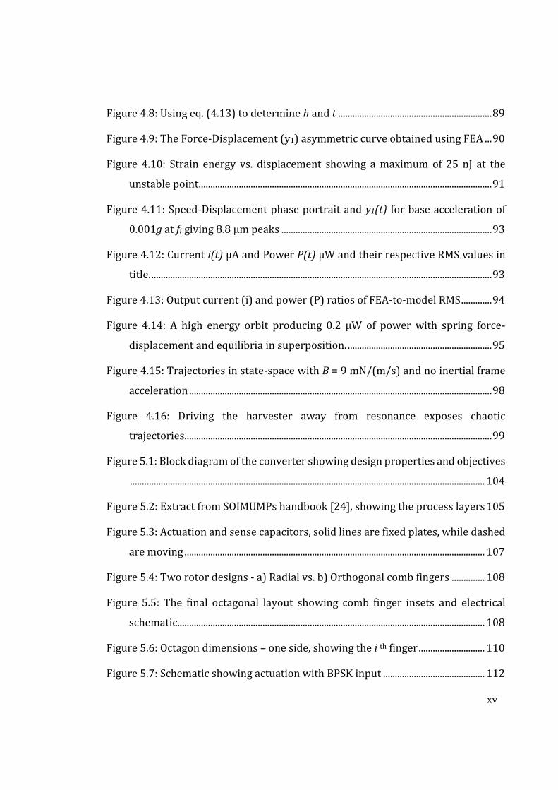
This gives a maximum sensitivity when the phase difference is 𝜋/2 and if 𝑑 percent
of deviation from linearity is tolerated, the region of ‘linear’ operation ∆𝜙 ± 𝛿𝜙
about ∆𝜙 = 𝜋/2 would be as in equation (2.4) [68].
𝑙𝑖𝑛𝑒𝑎𝑟 𝑟𝑒𝑔𝑖𝑜𝑛 = 𝜋/2 ± √6𝑑
100 (2.4)
The characteristics of the ideal multiplier can hence be depicted as in Figure 2.2,
which is far from an idealistic linear relationship.
Figure 2.2: Phase detector response of an ideal multiplier [68]
Figure 2.3 shows two manifestations resulting from the non-ideal characteristics of
a multiplier. These are the dc offset, which in practice would be a result of mixer

Literature Review
September 2019 Jeremy Scerri 18
asymmetry, and mixer-induced phase shift resulting from discrepancies in the
electrical length from the LO-to-IF port and the RF-to-IF port.
(a) DC offset (b) Mixer-induced phase shift
Figure 2.3: (a) DC offset affects ∆ϕ at which no output is obtained and voltage magnitude.
(b) The relative phase being affected by mixer induced phase shift. [68]
If the phase difference, ∆𝜙, between RF and LO is not constant and is a function of
time, the RF signal could carry information in the phase change which technique is
known as phase modulation (PM). This is described by (2.5);
𝑣𝑅𝐹(𝑡) = 𝐴𝑐𝑜𝑠(𝜔𝑅𝐹𝑡 + 𝑘𝑝𝑣𝑚(𝑡)) (2.5)
where 𝑘𝑝is the change in carrier phase per volt or phase sensitivity in rad/volt,
𝑣𝑚(𝑡) the message signal, ∆𝜙(𝑡) = 𝑘𝑝𝑣𝑚(𝑡) and 𝜙𝑑 = 𝑘𝑝|𝑣𝑚(𝑡)|𝑚𝑎𝑥 is defined as the
maximum phase deviation from the unmodulated value. Furthermore, in literature,
one can distinguish between Narrowband and Wideband PM with narrowband
associated with 𝜙𝑑 ≤ 0.25.
It can be shown that narrowband PM has a similar frequency spectrum as that of AM
modulation and hence the message signal can be demodulated using a mixer. For
wideband phase demodulation, the PLL or an IQ mixer can be employed.

Literature Review
September 2019 Jeremy Scerri 19
2.3.1 Mixers and Image Rejection
Undesired signals due to the mixing process which can get into the radio signal path
are called the image frequencies, 𝐹𝑖 . Figure 2.4 shows how an image frequency
reappears in the band of the IF filter superimposed on the desired frequency 𝐹𝑑 .
Figure 2.4: High-Side injection gives Fi = Fd + 2Fif and mirrors the IF spectrum
One solution to this problem is to have several IF stages (Figure 2.5). Choosing the
first IF frequency to be higher than the highest desired frequency 𝐹𝑑 would place the
image frequency 𝐹𝑖 very high and out of band where it can be filtered off and
rejected.

Literature Review
September 2019 Jeremy Scerri 20
Figure 2.5: The superheterodyne downconvertor
However, this comes at a cost since the IF filter must be very high in frequency with
a high Q factor which is expensive. The frequency of the first LO must also be very
high which is again expensive and more sections of down conversion must be used
in order to get to baseband.
2.3.2 Zero IF mixers or direct downconverters
Zero IF mixers or direct downconverters (homodyne) have already been mentioned
(𝜔𝐿𝑂 = 𝜔𝑅𝐹) but the discussion was limited to having a single harmonic as the RF
signal i.e. the phase difference ∆𝜙(𝑡) was a constant.
When the phase difference is varying like in PM, as the LO frequency approaches the
RF centre frequency, the IF output signal crosses the 0 Hz boundary and its spectrum
is folded back from DC to half the bandwidth, jeopardizing its content as shown in
Figure 2.6.
Literature Review
September 2019 Jeremy Scerri 21
Figure 2.6: Frequency folding when FLO = FRF
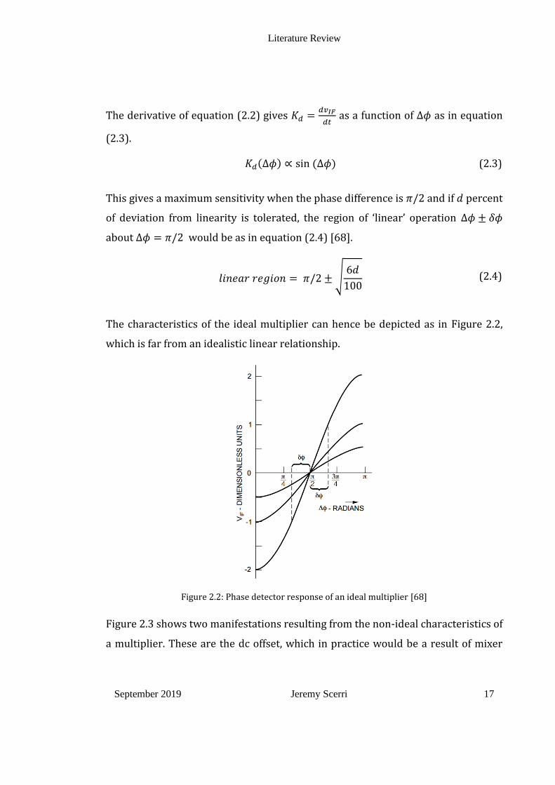
This problem and the fact that the image frequency is translated to baseband
together with the signal of interest makes this setup problematic. Moreover, since
the IF is at DC, the mixer DC offset needs to be dealt with.
2.3.3 The IQ mixer or Quadrature Downconverter
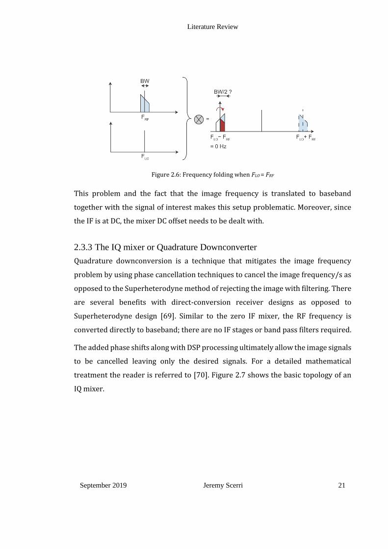
Quadrature downconversion is a technique that mitigates the image frequency
problem by using phase cancellation techniques to cancel the image frequency/s as
opposed to the Superheterodyne method of rejecting the image with filtering. There
are several benefits with direct-conversion receiver designs as opposed to
Superheterodyne design [69]. Similar to the zero IF mixer, the RF frequency is
converted directly to baseband; there are no IF stages or band pass filters required.
The added phase shifts along with DSP processing ultimately allow the image signals
to be cancelled leaving only the desired signals. For a detailed mathematical
treatment the reader is referred to [70]. Figure 2.7 shows the basic topology of an
IQ mixer.

Literature Review
September 2019 Jeremy Scerri 22
Figure 2.7: The basic topology of an IQ mixer
This topology requires two LOs with 90 degrees phase difference. The DC offset
problem can be mitigated by using a low IF frequency rather than zero IF as this
does not place the band of interest at DC. In theory, using this setup, image
frequencies will be cancelled but in practice there would always be some mismatch
or imbalance of the gain and/or phase in the I/Q paths. Consequently, the image
suppression would be far from complete.
2.3.4 MEMS mixers
As mentioned in Sections 2.3.1 to 2.3.3, there are definite advantages associated
with using a zero IF downconvertor or homodyne receiver over the heterodyne
alternative. Direct conversion requires less hardware (one less mixer than
heterodyne) and hence cost and size are reduced. Another added benefit is that the
homodyne receiver makes use of a low pass filter instead of a high-Q bandpass filter.
One objective of this work is to investigate the effectiveness of replacing discrete
electrical components making up the mixer and filter in a homodyne receiver with
a MEMS structure that serves the purpose of demodulation.

Literature Review
September 2019 Jeremy Scerri 23
Many receiver stages have been replaced with MEMS parts: antennas [71], switches
[72], [73], filters [74], mixers [75] and LO oscillators [76]. Still, integrating each
component in one chip is challenging [77], [78].
It has been demonstrated [15], [79] that micromechanical resonators can also be
utilised as mixer-filters thus eliminating the need for channel filtering at GHz while
retaining the benefits of high mechanical Q. In RF MEMS literature, the word ‘mixer’
is loosely interchangeable with ‘mixer-filter’, sometimes also referred to as ‘mixlers’.
If the structure intrinsically selects a specific range of frequencies apart from mixing,
it is a mixer-filter. MEMS mixer-filters exploit the nonlinearity of the electrostatic
force with the drive voltage in the electromechanical resonators, down converting
GHz RF input signals to excite MHz mechanical resonance for IF filtering. Mechanical
displacement is then capacitively sensed into an IF output. Mixing and filtering are
achieved simultaneously.
Although software reconfiguration is the ultimate goal in multi-band radios, power
and dynamic range limitations require some of the reconfiguration to take place in
the RF front end [12], [80]. As already shown in Figure 1.2, MEMS mixer filters have
the potential to be key components in future reconfigurable multi-band single-chip
radio.
The following sections will distinguish between electrostatically actuated
electromechanical mixers and thermally actuated electro thermal mixers.
2.3.5 Electro-Mechanical Mixing
The mixer-filter designed in [15], is made up of two identical resonators connected
by a highly resistive coupling beam. The resonators are 18.8 × 8 𝜇𝑚. They vibrate
in the vertical direction when the carrier is on the RF electrode and the local
oscillator applied at the anchors at both ends of the input resonator. It is reported
that resonance is at 𝜔𝑜 = 37 MHz which is the same as the intermediate frequency.
This mixer-filter requires a 200 MHz local oscillator. The reported capacitive gap

Literature Review
September 2019 Jeremy Scerri 24
between the resonator and the input/output electrodes is 32.5 𝜂𝑚 which ensures a
high electromechanical coupling. Mixing is achieved electrostatically and the air gap
was reduced to one third of what was reported in a previous work on resonators
[81].
The RF signal frequency ranges from 233 to 242 MHz and it is mixed with the LO
signal giving output frequency in the range of 33 MHz to 42 MHz, centered at
37 MHz, which is the resonance frequency and the required IF frequency.
Frequency tuning of the resonators is also possible by using two separate electrodes.
For the output signal, a DC bias is required on the output resonators which generates
the output IF signal on the output electrode. The reported conversion and insertion
loss are 13 dB with through measurement at -72 dBm and mixer output at 85 dBm,
with a noise floor of -100 dBm. The process of fabrication is quite intricate and is
custom designed with specific surfactants to remove residues from the small
capacitive gap.
Downconversion performance has been improved by Koskenvuori and Tittonen
[82], [83] and [84]. Their structure takes advantage of parametric resonance of two
double-ended tuning forks (DETF). The structure has a mechanical coupling beam
similar to that used in the previous work [15]. This isolates the IF output from the
RF input. The LO signal is fed directly to the input DETF structure via a 170 𝜂𝑚
capacitive coupling gap, Figure 2.8.

Literature Review
September 2019 Jeremy Scerri 25
Figure 2.8: The MEMS designed by [83]
In [82], the same authors present a downconversion method which does away with
the LO input. The side bands are specifically chosen to match two Eigen frequencies
of the same resonator. Such a mixer requires no local oscillator. The latest paper by
the same group [84] shows that by exciting the DETF at twice resonance (instead of
some LO frequency), they would be effectively modulating the spring constant at
twice resonance and the downconversion would happen by ‘self-mixing’.
2.3.6 Electro-Thermal Mixing
Electrothermal mixing is another method of signal mixing. In [85], a dome shaped
resonator is employed to implement a mixer. The advantage of electrothermal
actuation over electrostatic actuation is that it does not require the fabrication of
nanometre capacitive gaps. The diameter of the dome is about 30 µm. When the RF
signal is applied to a gold thin-film resistor with 250 mV DC bias, the Joule heating
causes the out-of-plane deflection. When the AC current through the micro heater
matches the resonator frequency, the heat is modulated and dissipated at a
compatible rate as the mechanical resonance - the resonator has smaller thermal
mass and thus a smaller time constant. Figure 2.9a shows the actuation current path

Literature Review
September 2019 Jeremy Scerri 26
while Figure 2.9b shows the dome mode shape. Equation (2.6) describes how the
change in temperature Δ𝑇 and hence the expansion is being modulated by the RF
signal.
Δ𝑇 ∝𝑉𝑟𝑓2
𝑅∝(𝑉𝑑𝑐 + 𝑉1 sin(𝜔1𝑡) + 𝑉2 sin(𝜔2𝑡))
2
𝑅 (2.6)
Expanding the squared bracket in equation (2.6) reveals the dependency to sum and
difference frequency components. The resonant frequency of the dome will be
matched to the difference: 𝐹𝑟𝑓 − 𝐹𝐿𝑂 .
The quality factor, Q, varies between 3,000 and 10,000 in vacuum but in air (at NTP)
it is about 100. The resonance frequency, 𝑓𝑟𝑒𝑠 is 12.7 MHz which is purposely
matched to the mechanical resonance.
a) b)
Figure 2.9: The dome mixer, [85], a) showing actuation b) showing mode shape

Literature Review
September 2019 Jeremy Scerri 27
The local oscillator frequency is set at 60 MHz. The input to the resonator is the sum
of the chosen carrier frequency, 𝑓𝑐 at 72.7 MHz. This configuration takes advantage
of two tones offset from the carrier frequency for the test signals. The key is that the
gold resistor acts as the frequency translator and the coupled resonator works as a
post mixing filter. In this paper, measurement and validation was performed using
optical profilometry.
Subsequently, in [86], a 70 µm × 3 µm gold strip on the resonator was used to serve
as a micro heater and another identical size strip acted as a piezoresistor implanted
in the resonator. This was an improvement since sensing was integrated in the same
device. The membrane deflection causes strain on the doped silicon strip. The
change of the resistance is proportional to the corresponding strain. For the same
-20 dBm drive, the in-band insertion loss is improved from -65 dB to -35 dB when
the resonator is coupled to an operational amplifier.
The most recent work by the same authors on electrothermal mixers is [87].
Figure 2.10 shows the most recent work on MEMS thermal mixer that takes
advantage of the thermal expansion property of a bimorph resonator. Figure 2.10
inset shows a scanning electron microscope (SEM) image of the structure.
Figure 2.10: Structure used and electrodes for mixing [87].

Literature Review
September 2019 Jeremy Scerri 28
An aluminium strip is deposited on the silicon carbide in a cantilever beam
structure. This structure shows a maximum vibration amplitude of 62 nm at a
resonant frequency of 944.49 kHz. This frequency is achieved when two frequencies
of 𝑓1 at 1200 kHz and 𝑓2 at 255 kHz are applied to the two independent aluminium
electrodes. While 𝑓1 is fixed, 𝑓2 is swept to find the resonance frequency by varying
the difference between the two signals in 10 kHz interval. With a cantilever length
of 200 µm, the resonant frequency lowers to 89.37 kHz.
2.3.7 BPSK to ASK conversion
Due to their simplicity, BPSK and ASK are adopted in many standards that are
implemented for low-cost passive transmitters. These modulation schemes are
popular in standards like the Medical Implant Communication System (MICS) and
Medical Data Service (MEDS) for biomedical applications and also Near Field
Communication (NFC) standards A and B. Such standards are designed for passive
transmitters and constant amplitude modulation schemes (FSK/PSK) are preferred
for energy (and data) transmission. When ASK is adopted, it is common practice to
make use of a modulation index M that is close to unity. This index is defined as the
ratio of smallest to highest modulated carrier amplitude and is purposely kept high
such that the passive listener does not lose power.
A BPSK to ASK converter is generally used as a first step to digital detection. In
particular, for medical implants, ASK is the preferred modulation scheme [4] as its
demodulation requires simple hardware, small size and less power consumption.
However, PSK and FSK offer a constant power RF signal which is preferred for a
passive listener. A BPSK to ASK converter can be used for the frontend of an
implantable device such that BPSK signalling (which has constant power) is used to
carry wireless data (and power) across the skin but this is immediately converted
to ASK for eventual demodulation and processing using simpler hardware.

Literature Review
September 2019 Jeremy Scerri 29
No literature is found on BPSK to ASK conversion using MEMS. To-date, such a
function can only be realised in manufacturing using CMOS technology. In [88], two
circuits for BPSK to ASK conversion are proposed with the aim of reducing the
components required for such function. The authors trade performance with
simplicity of implementation such that low-cost makes it attractive to RFIDs and
sensor networks. In [89], the same application area is considered and the BPSK to
ASK converter is used as a first stage to the envelope detector. Here again, making
use of a BPSK to ASK converter, as a distinct first stage, is given preference over
alternative options such that complexity and power is kept low. In [90], [91], the
authors present a BPSK demodulator which is based on a BPSK to ASK first stage,
and report that the prototype consumes 228 𝜇W of power with sub-GHz carrier. In
[92], an ultra-low power transceiver with a BPSK downlink for a semi-active RFID
sensor node is presented. Even here, the BPSK signal is first converted to ASK and
then the signal is down converted to baseband with an envelope detector. The
authors break down the power consumption of the downlink, giving 204 𝜇W
dissipation for the BPSK to ASK stage and 69 𝜇W for the envelope detector; this had
sub-GHz carrier and data rates up to 10 Mb/s. To achieve low power consumption
and circuit simplification, all the results reported in [88], [89], [90], [91], [92] are
based on the BPSK to ASK architecture, first introduced in [93], [94].
2.3.8 Sensing Strategies
In order to physically extract the baseband signal from the modulated RF signal, a
way to measure the displacement of a MEMS device is required. This can take many
forms: a cantilever beam, a cantilever beam with an attached plate, a fixed-fixed
microbeam or even a tethered microplate. Currently, there are three popular
displacement sensing methods for MEMS applications: capacitive sensing,
piezoresistive sensing and piezoelectric sensing. Each sensing mechanism can be
built and implemented on a bulk silicon substrate.

Literature Review
September 2019 Jeremy Scerri 30
The main challenge is in sensing displacement effectively while minimising losses
and footprint. The work in [15] measures the signal by capacitive coupling which
requires voltage driving circuitry. The work in [86] integrates piezoresistive sensing
methods. Piezoresistive sensing measures the change of resistance - which is
proportional to the change of displacement - by measuring current. It drifts with
temperature, requires external driving circuitry and consumes power when there is
no incoming RF signal. In [85] and [87], optical methods are used such as a probe
station and a vibrometer. Optical sensing is in general used only for feasibility
studies. In piezoelectric sensing, the voltage change is measured due to change in
displacement. Strain sensitivity up to 5 𝑉/𝜇𝜖 is achievable. The piezoelectric sensing
method requires no external driving circuitry but at steady-state; the absolute
displacement is not detectable due to the high pass nature of the piezoelectric
material.
2.4 Geometric Nonlinearities and Vibrational Energy Harvesting
Traditionally, the operating principle of a vibrational energy harvester (VEH) relies
on linear resonance. The assumption here is that the input frequency to the device
carries just one harmonic, that is, a fixed frequency. To maximise the energy flow
from the environment to the electric device, the beam parameters can be tuned such
that the modal frequencies, in particular the first, is close, ideally equal, to the base
excitation frequency. Using resonance to amplify the beam oscillations is beneficial,
however, this comes at a cost when it comes to achieving broadband
responsiveness. In practice, in VEH design, damping is kept very low to improve the
gain at resonance but this would generally give a high-quality factor resulting in a
relatively narrow bandwidth.
In contrast, excitations available in the environment are generally not harmonic in
nature; they would have a wide spectral content and can also be time-varying in that
the frequency content changes with time. This makes it very challenging to tune a

Literature Review
September 2019 Jeremy Scerri 31
linear VEH to match the excitation frequency and results in inefficient transduction
of energy.
As a solution to this problem, initial designs featured tuneable VEHs and made use
of arrays of harvesters such that the full range of input excitations could be made
use of. For tuning, both passive and active designs were used to alter the
fundamental mode to match the dominant frequency of vibration [95], [96], [97],
[98], [99], [100], [101]. It soon became clear that the efficiency for stochastic inputs
or rapidly varying frequency sweeps made energy harvesting unreasonable [95].
This is more so since external power would be required to tune and this has an
impact on the net efficiency. Alternatively, if tuning is not considered, the designs
make use of arrays of harvesters such that at least one device was close to the
dominant vibrational frequency [98], [100], [101]. This however impacted
negatively on the energy density and scalability prospects.
The drive to achieve wider coupling between a harmonic oscillator and the (broad)
excitation frequencies has driven many researchers to exploit nonlinearities to
improve on VEHs efficiency. As mentioned earlier, geometric/structural
nonlinearities arise for large deformations [102]. Furthermore, nonlinearities can
also be the result of nonlinear relationships in the electromechanical coupling
mechanism, for example, in piezoelectricity [103]. However, such nonlinearities are
not easily exploited for energy harvesting purposes as they are not easily modified
and are intrinsic to the process. The intentional introduction of nonlinearities in the
design has been the target of more recent investigations. Nonlinearities by design
means the introduction of a feature such that one could control the nature and
magnitude of the nonlinearity for improved VEH efficiency. Two techniques can be
found in literature; one introduces a controlled magnetic force and the other a
controlled mechanical restoring force [104], [105], [106], [107]. These have been
shown to widen the bandwidth of the VEH and hence improve transduction to tap
realistic, widely available environmental excitations.

Literature Review
September 2019 Jeremy Scerri 32
Further review of how geometric or structural nonlinearities can be employed to
widen the bandwidth of a VEH can be found in Section 4.1.
2.5 Modelling and Validation Approach in nonlinear MEMS
Predicting static and dynamic response accurately for a system that has several
nonlinear contributions is a rather difficult task. Generally, the approach to arrive at
an adequate mathematical model requires several small steps, each involving a
validation step. A case study that involves RF-MEMS which exemplifies this process
of improvement in small steps is described in [108], [109], [110], [111], [112], [113],
[114] and [115]. In this study, the authors start by investigating pull-in in the
presence of structural (geometric) nonlinearities [108]. In [109] to [111], the
numerical approaches adopted are validated experimentally. In [112] and [113], the
authors shift their focus on the dynamics and in [114] and [115] both the
electrostatic and geometric nonlinearity are considered in the model
simultaneously.

RF frontend functions in MetalMUMPs
September 2019 Jeremy Scerri 33
3. RF FRONTEND FUNCTIONS
IN METALMUMPS
In this chapter, a mechanical structure that is able to serve several RF frontend
functions is presented. It consists of a plate supported by two tethers and able to
vibrate in torsion. The actuation/drive mechanism is electrostatic in nature and
makes use of the smallest gap possible in the MetalMUMPs fabrication process [22].
The layers and critical dimensions are shown in Figure 3.1.
Figure 3.1: The MetalMUMPs layers, smallest gap between conductors is 1.45 µm
The chapter is divided in two main sections, 3.1 and 3.2; these describe how the
design proposed attains its functionality.
In Section 3.1, the proposed structure is designed to give displacements in response
to BPSK signalling. Displacement sensing is also achieved using the same pivoted
plate. At the end of this section, the magnitude of the actuation signals is investigated
and boundaries for linear and non-linear dynamic characteristics are determined.

RF frontend functions in MetalMUMPs
September 2019 Jeremy Scerri 34
In Section 3.2, a similar torsional plate, but having more electrode pairs for actuation
and also for sensing, is designed such that unwanted frequency components
generated by electrostatic mixing are suppressed. This section concludes with an
application to low-IF IQ mixing.
3.1 A MEMS BPSK Demodulator
Electrostatically driven torsional structures have been used extensively since one of
their first successful appearance [116] which involved driving a mirror in the
1980’s. In [116], the plate undergoing torsional vibrations was used both as the
mirror and as the electrostatic actuator.
As shown in [117], the switching speed of such micro-mirrors has come a long way
since then. The first structure considered in this paper has dimensions within the
same order of magnitude of [117]. The major differences are the manufacturing
process, the application, and in [117], the mirror undergoing angular movement has
mechanical stops.
Modelling of electrostatic torsional actuation is described in [118]. One of the results
given in [118] is the maximum angular rotation before pull-in occurs. As described
in Section 3.1.3, the plate dimensions and voltages were selected such that pull-in
does not occur.
A considerable amount of work to achieve signal mixing in the mechanical domain
has also been carried out using CMOS commercial fabrication [119], [120], [121] and
[122]. This process is called CMOS-MEMS. These solutions have the advantage that
they can be embedded within CMOS circuitry. The process involves standard CMOS
fabrication followed by an anisotropic etch. Subsequently, a final release step
involving a combination of DRIE and isotropic silicon etch is used to release the
structure. In [120], it was claimed that mixing for frequencies in the range of 10 MHz
to 3.2 GHz was successfully demonstrated. The electrostatic gap used was 1.3 µm.

RF frontend functions in MetalMUMPs
September 2019 Jeremy Scerri 35
In all these CMOS-MEMS structures, the mixing is performed electrostatically and
the output is then mechanically filtered with the cantilever structure.
In [15], mixing is also achieved electrostatically, but here, a clamped-clamped beam
is used. This beam is mechanically coupled with a similar clamped-clamped beam to
achieve filtering. In this case, a polysilicon surface-micromachining process was
used with electrostatic gaps ranging from 325 Å to 1000 Å. Successful mixing at
200 MHz was reported.
The mixing and filtering structure presented here employs a relatively large
capacitive gap at 1.45 µm (Figure 3.1). The target application is BPSK demodulation
encoded as in IEEE 802.15.4 which describes a low data rate wireless personal area
network protocol. This standard has a carrier of 868 MHz with a data signal at
300 kchips/s which constrains the mechanical structure to have a bandwidth of at
least 900 kHz (3rd harmonic of data).
Section 3.1.7 details simulation results that demonstrate the feasibility of such a
structure to demodulate BPSK signals as described in the IEEE 802.15.4 standard.
3.1.1 The Mechanical Structure
The smallest achievable gap between conductors in the MetalMUMPs fabrication
process is 1.45 µm. This is the gap between the nickel layer, hereon referred to as
metal, and the polysilicon layer. The polysilicon is encapsulated within top and
bottom nitride layers.
The smallest gaps achievable in the horizontal directions, between metals and/or
polysilicon, are larger at 5 µm. Hence, a structure that vibrated in the vertical gap
between the metal and the polysilicon was designed. Out of the total electrostatic
gap ‘𝑑’ of 1.45 µm, only 1.1 µm of vertical movement is allowed as there is 0.35 µm
of nitride above the polysilicon.

RF frontend functions in MetalMUMPs
September 2019 Jeremy Scerri 36
3.1.2 Torsional Oscillations of a Plate
Figure 3.2 to Figure 3.4 show how actuation and sensing were achieved in the
designed structure (S1). On the actuation side, the biased RF signal at the metal
interacts with the biased LO signal to produce a force on the plate. In turn, this force
drives the plate into torsional oscillations. On the sensing side, a current is generated
at the polysilicon output electrode by interacting with the metal above it which is
DC biased. The output signal is also filtered by the low-pass vibration characteristics
of the plate structure. The overall dimensions of the nitride plate are 60 µm × 35 µm
with the axis of rotation being parallel to the longer side. The area of the polysilicon
electrodes is 250 µm2 and each tether is 15 µm wide.
Figure 3.2: The complete S1 structure showing metal layers in violet
Figure 3.3: Section through S1; view from bottom showing only one tether.

RF frontend functions in MetalMUMPs
September 2019 Jeremy Scerri 37
Figure 3.4: Schematic diagram of the torsional BPSK demodulator depicting the bias and excitation
scheme required for mixing, filtering and sensing.
3.1.3 Modelling and Analysis
In the first part of this section, some theoretical background on electrostatic mixing
is presented. This theory is then applied to the mixing of the LO signal and the BPSK
modulated RF signal, and the frequency components of the resulting input force are
discussed. In the second part, the mechanical filtering is used to shape the input
spectrum and in the last section, current sensing at the output electrode is shown to
provide the required data signal.
3.1.4 Frequency Content of the Input Force
The LO frequency is set to be the same as the BPSK carrier frequency so that the
conversion of the modulated signal is performed in one step (direct conversion). In
general, the LO and RF are not necessarily in phase, hence, 𝛼 ≠ 0 in (3.1). The LO
signal is DC biased by 𝑉𝑑𝑐𝐿𝑂 volts and 𝜔 rad/s is the carrier frequency. For BPSK, the
phase in the RF signal has two distinct values and the modulated BPSK signal with
DC bias can be formulated as in (3.2).
𝑣𝐿𝑂(𝑡) = 𝑉𝐿𝑂 cos(𝜔𝑡 + 𝛼) + 𝑉𝑑𝑐𝐿𝑂 (3.1)
and

RF frontend functions in MetalMUMPs
September 2019 Jeremy Scerri 38
𝑣𝑅𝐹(𝑡) = 𝑉𝑅𝐹(2𝑑(𝑡) − 1) cos(𝜔𝑡) + 𝑉𝑑𝑐𝑅𝐹 (3.2)
where,
𝑑(𝑡) (∈ [0,1]) represents the binary data signal for integer durations of 𝑛𝑇. For the
lowest data rate specified in the 802.15.4 standard which has a chip rate of
300 kchips/s, the pulse duration would be 𝑇 = 1/300000 s and
𝜔 = 2𝜋(868) 𝑀𝑟𝑎𝑑/𝑠. Denoting the vertical displacement of the electrodes by
𝑥(𝑡) µm, the absolute permittivity in air by 휀 and the effective electrode area in µm,
𝐴𝑒 then the force at the input side would be described by (3.3).
𝐹𝑖𝑛(𝑡) = −휀𝐴𝑒
2(𝑑 + 𝑥(𝑡))2[𝑣𝐿𝑂(𝑡) − 𝑣𝑅𝐹(𝑡)]
2 (3.3)
If we further simplify by assuming that 𝑥(𝑡) ≪ 𝑑, that is, the spring stiffness stays
constant, and letting 𝑉𝐿𝑂 = 𝑉𝑑𝑐𝐿𝑂 = 𝑉𝑅𝐹 = 𝑉𝑑𝑐𝑅𝐹 = 𝑉 and substituting (3.1) and (3.2)
in (3.3), we get (3.4):
𝐹𝑖𝑛(𝑡) = 𝐸 (𝐷2 − 𝐵2
2) 𝑐𝑜𝑠(2𝜔𝑡) + 𝐵𝐷𝑠𝑖𝑛(2𝜔𝑡) + (
𝐷2 + 𝐵2
2) (3.4)
where, 𝐷 = 2𝑑(𝑡) − 1 − 𝑐𝑜𝑠𝛼, 𝐵 = 𝑠𝑖𝑛𝛼 and 𝐸 = −𝜀𝐴𝑒 𝑉
2
2𝑑2.
Equation (3.4) has three terms; the first two have bandwidths centered on 2𝜔 while
the last term is centered on 0 Hz. All these components can be seen in Figure 3.5. We
are interested in the baseband part of the input force as the other components are
very high and will be mechanically filtered out. Table 3.1 further breaks down the
last term as expressed in (3.5):
𝐸[2𝑑2(𝑡) − 2(1 − 𝑐𝑜𝑠𝛼)𝑑(𝑡) + 1 + 𝑐𝑜𝑠𝛼] (3.5)
The bandwidth of the data signal 𝑑(𝑡) is inversely proportional to the pulse duration
𝑇. While theoretically, the bandwidth of the data signal is infinite (pulse train), we

RF frontend functions in MetalMUMPs
September 2019 Jeremy Scerri 39
aim to capture information up to its 3rd harmonic which dictates the bandwidth of
the mechanical filtering required (Section 3.1.5).
Table 3.1: Breakdown of force components around 0 Hz as in equation (3.5).
Centre Freq. Term Bandwidth
0 Hz ]cos1)(2[ 2 ++tdE Bandwidth of )(td
0 Hz )(]cos1[2 tdE −− Bandwidth of )(td
Figure 3.5: The spectrum of the electrostatic force generated and the required mechanical
bandwidth for adequate reconstruction.
3.1.5 Mechanical Filtering
For small oscillations, the rectangular tether’s torsional spring constant can be
calculated using (3.6) [123].
𝑘𝑡 = 𝑘1𝐺(2𝑎)3(2𝑒) (3.6)
where, 𝑒 × 𝑎 are the tether section dimensions of 15 × 0.8 µm, 𝐼 the moment of
inertia of the plate about the tether pivot line and 𝐺 the modulus of rigidity of the
plate. The parameter 𝑘1 is a function of the ratio 𝑒/𝑎 and is tabled in [9]. The
dimensions of the plate were selected such that the plate’s natural frequency is in

RF frontend functions in MetalMUMPs
September 2019 Jeremy Scerri 40
the region of 𝑓𝑛 =1
2𝜋√𝑘𝑡/𝐼 =2 MHz. As required, for the data rate under
consideration, this is higher than the 3rd harmonic of 900 kHz. A simplified 2nd order
linear model, which includes damping with damping coefficient 𝑏, is described by
(3.7).
𝐼 + 𝑏 + 𝑘𝑡𝜃 = 𝐹𝑖𝑛(𝑡) (3.7)
When damping is taken into consideration, the resonant frequency 𝑓𝑟 would be
lower (see results section). Having selected 𝑓𝑛 at least two times greater than the
3rd harmonic of 𝑑(𝑡) would still provide a substantial safety margin.
In general, damping can be divided in two categories: thermoelastic effects and fluid
damping. The dominant form of damping is determined by the Knudsen number
[124]. In [124], the nonlinear relationship between the viscous damping coefficient,
gap and pressure is clearly seen, especially for gaps less than 0.8 𝜇m. However, in
much of the reviewed literature related to resonators with gaps larger than 0.8 𝜇m,
the effects of damping is assumed to be dominated by a viscous damping coefficient
and thermoelastic effects were ignored.
Due to the squeeze film effect, for low enough frequencies, the air can escape around
the moving plate with little resistance but for high frequencies, the air is held in
position due to its own inertia and it compresses resulting in a spring force.
Air does not move around much and damping gets lower as is shown in Figure 3.6.
All FEA simulations included also squeeze-film damping effects due to the small gaps
involved (1.45 𝜇𝑚). Air at NTP has a mean free path, 𝜆, of 68 nm. This gap and mean
free path give a Knudsen number of 0.047. This means that the continuous
assumption for the fluid medium does not hold as the value of 0.047 is within a
transitional regime [125].
The damping coefficient is a function of frequency and the value adopted for
MATLAB simulations, 𝑏 = 2.83 𝜇N/ms-1, is that occurring at the resonant frequency
of the structure (2 MHz).

RF frontend functions in MetalMUMPs
September 2019 Jeremy Scerri 41
Figure 3.6: FEA result for damping force coefficient against frequency for the torsional plate taking
into account squeezed film effects.
From [123], pull-in would occur when 𝜃𝑝 ≈ 0.4404 𝑔/𝐿, with 𝐿 being half the width
of the plate (35/2) µm. Hence, for structure S1, 𝜃𝑝 = 0.027𝑟 , which means that
approximately a maximum vertical displacement of 470 nm is permissible.
3.1.6 Current Sensing at the Polysilicon electrode
At the output side, the polysilicon electrode is moving within the electrostatic field
generated between itself and the metal above which is DC biased by 𝑉𝐷𝐶. This
induces a current at the polysilicon output electrode which can be eventually
converted into voltage via a suitable amplifier.
The distances between the two high frequency inputs (LO and RF) and the output
electrode are small and capacitive parasitic coupling at high frequency is bound to
occur.
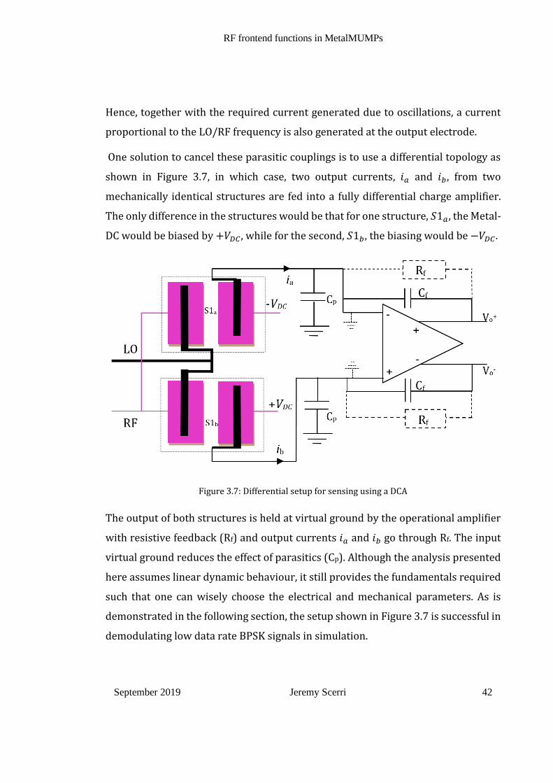
RF frontend functions in MetalMUMPs
September 2019 Jeremy Scerri 42
Hence, together with the required current generated due to oscillations, a current
proportional to the LO/RF frequency is also generated at the output electrode.
One solution to cancel these parasitic couplings is to use a differential topology as
shown in Figure 3.7, in which case, two output currents, 𝑖𝑎 and 𝑖𝑏, from two
mechanically identical structures are fed into a fully differential charge amplifier.
The only difference in the structures would be that for one structure, 𝑆1𝑎, the Metal-
DC would be biased by +𝑉𝐷𝐶, while for the second, 𝑆1𝑏 , the biasing would be −𝑉𝐷𝐶.
Figure 3.7: Differential setup for sensing using a DCA
The output of both structures is held at virtual ground by the operational amplifier
with resistive feedback (Rf) and output currents 𝑖𝑎 and 𝑖𝑏 go through Rf. The input
virtual ground reduces the effect of parasitics (Cp). Although the analysis presented
here assumes linear dynamic behaviour, it still provides the fundamentals required
such that one can wisely choose the electrical and mechanical parameters. As is
demonstrated in the following section, the setup shown in Figure 3.7 is successful in
demodulating low data rate BPSK signals in simulation.

RF frontend functions in MetalMUMPs
September 2019 Jeremy Scerri 43
3.1.7 Simulations and Results
This section presents the results of the FEA simulations using CoventorWare®.
Table 3.2 summarizes the mechanical results.
Table 3.2: Mode types and frequency, Q factor and damped resonant frequency.
Mode Freq. (MHz) Mode Type Q factor / Damped Resonant Freq. (MHz)
1.57 Not Torsional Not required
2.01 Torsional 60 / 1.54
4.05 Not Torsional Not required
4.96 Not Torsional Not required
7.15 Not Torsional Not required
The required mode should be a torsional mode as shown in Figure 3.2. The modes
closest to the one required are not torsional in nature and cannot be excited with
the input actuating signals. A mechanical/electrostatic simulation with driving
voltages of 20 V peak was performed and the generated signals were analysed.
Due to the strong parasitic coupling between the output electrode and the RF/LO
signals, the two current graphs are almost linear in nature. These are the output
currents from S1a and S1b respectively, as shown in Figure 3.8. This linearity breaks
down at resonance due to the larger displacements (Figure 3.9). If these currents
are subtracted, the differential output current required (Figure 3.8a) can be
converted into voltage through the DCA setup shown in Figure 3.7.
For S1, this voltage would contain enough harmonics from 𝑑(𝑡) for successful
reconstruction / demodulation. Even though the DC content is highly attenuated due
to the substantial Q factor, this does not present a problem as the 32-bit chips used
in the 802.15.4 modulation scheme do not have any DC content. The maximum
displacement in this response does not exceed 6 nm which is well within the pull-in
region as determined in [126].

RF frontend functions in MetalMUMPs
September 2019 Jeremy Scerri 44
Figure 3.8: Currents at the outputs for both positive and negative DC biasing
Figure 3.9: Displacement against frequency.

RF frontend functions in MetalMUMPs
September 2019 Jeremy Scerri 45
The FEA analysis provides sufficient information to characterize the torsional plate
dynamics and also the electrical and electrostatic properties of the setup. With this
information, a linear mathematical model was implemented in MATLAB and the
vertical displacement of the moving electrodes was investigated for the data signal
𝑑(𝑡). Figure 3.10 shows the resulting response. This mathematical model was
validated against FEA data and found to give the same displacements and currents.
Figure 3.10: The displacement has a strong 3rd and 4th harmonic.
Note: Settling barely happens within 1 chip time (1.67 µs)
The maximum displacement in this response does not exceed 6 nm. This is well
within the pull-in region as determined in [126]. However, the sensing current
generated is very small, at around 5 nA. Nevertheless, this design provides a proof-
of-concept and shows that with the MetalMUMPs fabrication process, a torsional
vibratory structure can be built to successfully demodulate a low data rate BPSK
signal with a carrier frequency of 868 MHz and a chip rate of 300 kchips/s.

RF frontend functions in MetalMUMPs
September 2019 Jeremy Scerri 46
The drive to include extra functionality in portable devices is always increasing and
one way of providing this is by having structures that can be used for different
applications. This MEMS device is one such structure as is shown in the following
sections.
3.1.8 Investigation of Potential Complex Dynamics
Having a good mathematical model is instrumental in accurate prediction of the
different modes of operation. Modelling the dynamics of MEMS resonators is
extensively covered in literature [127], [128], [129] and [130]. Numerical solutions
that involve distributed models and FEA provide the best description of system
behaviour but are computationally expensive. Assumptions are taken to develop
non-linear systems of equations that are able to give a good enough approximation.
Whenever the modes of vibration are sufficiently different and far apart in their
frequencies, it is common to ignore all modes except the most prominent one.
Further assumptions are taken on modelling the spring behaviour. A linear,
quadratic and cubic spring stiffness term is considered in [127] while in [128] only
the linear and cubic terms are included. Inhomogeneity of the silicon structure and
geometric nonlinearities are often responsible for this behaviour [127]. When it
comes to damping, the behaviour is more complex. As already mentioned in Section
3.1.5, the dominant form of damping is determined by the Knudsen number [124]
and the damping coefficient is a function of frequency which also contributes to
nonlinearities. In this section, a non-linear model is developed and the dynamical
behaviour under different input conditions is investigated.
3.1.9 Development of the Mathematical Model
For the derivation of the mathematical model, the same structure was considered
but actuation was simplified and only one signal was used to drive the mechanism
into oscillation as shown in Figure 3.11.

RF frontend functions in MetalMUMPs
September 2019 Jeremy Scerri 47
Figure 3.11: The system structure
Using FEA, the spring nonlinearity for large displacements was investigated and the
resulting force-displacement diagram is shown in Figure 3.12.
Figure 3.12: The force curve for static displacements as large as 0.4 µm
For ‘large’ displacements (order of magnitude of the gap), the spring force could be
described by (3.8) (least squares polynomial fit), while for the BPSK demodulator
region of operation, a linear spring model suffices i.e. (3.9).

RF frontend functions in MetalMUMPs
September 2019 Jeremy Scerri 48
𝐹𝑧 = 19000𝑥3 + 10−9𝑥 (3.8)
𝐹𝑧 = 10−9𝑥 (3.9)
Substituting the nonlinear spring model (3.8) and the driving electrostatic force
(3.3) in the dynamic model (3.7) and also converting rotational to linear
displacements, the following model, (3.10), is proposed for the mechanical part:
= −𝑏
𝐼 −
𝑘𝑡𝐼𝑥 −
𝑘3𝐼𝑥3 +
휀𝐴𝑒𝑟2
2𝐼(
𝑣2𝑑 − 𝑥
)2
− (𝑣1
𝑑 + 𝑥)2
(3.10)
where 𝑥 is the vertical displacement at electrode P1 (refer to Figure 3.11), 𝑣1 is the
voltage between electrodes P1 and N1, 𝑣2 is the voltage between electrodes P2 and
N2, 𝑘3 is the cubic spring stiffness, 𝑟 is the distance from the pivot to the centre of
the Nickel electrode and 𝐼 is the moment of inertia of the plate about the pivot. Also,
from Figure 3.11, 𝑣1 = 𝑉𝑑𝑐 + 𝑉𝑎𝑐cos (𝜔𝑡) and 𝑣2 = 𝑉𝑑𝑐.
Model (3.10) is nonlinear due to the cubic stiffness term and the electrostatic forces
and describes only the rotational mode of vibration. The damping coefficient is a
function of frequency as shown in Figure 3.6. For the following analysis, it is
assumed constant as the primary scope for this analysis is to determine different
response modes depending on the location of the static equilibrium points (EPs).
The location of these EPs is independent of the damping coefficient. For easier
identification of the location of these EPs in time domain simulations, a smaller
coefficient of damping than the one determined in Figure 3.6 was used. A separate
damping simulation run was performed at a reduced atmospheric pressure (100 Pa)
and ambient temperature that gave a smaller damping coefficient. The estimated
parameters are listed in Table 3.3.

RF frontend functions in MetalMUMPs
September 2019 Jeremy Scerri 49
Table 3.3:Parameter values for the Non-linear model
Parameter Value Units Description
d 1.45 µm Nominal Gap
I 2.71 × 10⁻²¹ 𝑘𝑔𝑚2 Moment of inertia
Ae 250 𝜇𝑚2 Effective area
b 5 × 10⁻¹⁶ 𝑁𝑠𝑚−1 Viscous Damping
k3 19000 𝑁/𝑚3 Cubic Stiffness
kt 10−9 𝑁/𝑚 Linear Stiffness
r 10−5 m Radius of rotation
𝑣1 𝑉𝑑𝑐+ 𝑉𝑎𝑐cos (𝜔𝑡)
volts AC actuation
𝑣2 𝑉𝑑𝑐 volts DC actuation
With the values in Table 3.3, the resulting DE is stiff and confirming that the MATLAB
solution was actually correct was problematic. Using the ‘ode15s’ differential
equation solver in MATLAB the solution time step was determined by trial and error
until repeatability in the solutions was observed. Appendix 3.1 gives the MATLAB
implementation. The static behaviour of the structure was first investigated and this
was done by applying a range of biasing voltages, 𝑉𝑑𝑐 and letting 𝑉𝑎𝑐 = = = 0.
This gives the net force, 𝐹𝑛𝑒𝑡, on the structure as in (3.11).
𝐹𝑛𝑒𝑡 = −𝑘𝑡𝐼𝑥 −
𝑘3𝐼𝑥3 +
휀𝐴𝑒𝑟2𝑉𝑑𝑐
2
2𝐼(
1
𝑑 − 𝑥)2
− (1
𝑑 + 𝑥)2
(3.11)
Solving 𝐹𝑛𝑒𝑡 = 0, the equilibrium points (EPs), x*, were obtained. Furthermore, by
evaluating 𝜕𝐹𝑛𝑒𝑡
𝜕𝑥|𝑥=𝑥∗
the nature of the EP can be classified as stable, unstable or a
saddle point. Comparison of the EPs for both models are listed in Table 3.4.

RF frontend functions in MetalMUMPs
September 2019 Jeremy Scerri 50
Table 3.4: Equilibrium points for the linear and non-linear models
The nature of the equilibrium points was analysed further, Appendix 3.2 gives
MATLAB code for this investigation. Figure 3.13b shows how the equilibrium points’
position and nature vary as the DC actuation voltage is increased. The DE’s are
second order and the phase portraits are two dimensional with state vector
𝒑 = [𝑥 ]𝑇 .
Figure 3.13: The EPs as a function of Vdc, red lines for unstable, black for stable.
Note: a) 𝑥 − phase portrait with 𝑉𝑑𝑐 = 20 𝑉 shows 3 EPs, two are saddle and one is stable.
b) Location (x) and type of equilibrium points vs. Vdc.
c) 𝑥 − phase portrait with 𝑉𝑑𝑐 = 110 𝑉 shows 5 EPs, three are saddle and two are stable.
𝑉𝑑𝑐 = 20 𝑉
𝑉𝑑𝑐 = 25 𝑉
𝑉𝑑𝑐 = 25 𝑉
𝑉𝑑𝑐 = 25 𝑉
𝑉𝑑𝑐
= 110 𝑉
𝑉𝑑𝑐
= 110 𝑉
𝑉𝑑𝑐
= 110 𝑉
𝑉𝑑𝑐
= 110 𝑉
a)
a)
a)
a)
b)
b)
b)
b)
c)
b)
b)
b)

RF frontend functions in MetalMUMPs
September 2019 Jeremy Scerri 51
When the device was operated in the linear (20 volts) region for BPSK
demodulation, there was only one equilibrium point and two saddle points (Figure
3.13a) with the latter two describing the pull in region. However, when the voltage
exceeds 75 volts, the behaviour changes drastically and the system becomes bistable
(Figure 3.13c). Figure 3.13a and Figure 3.13c show trajectories for different initial
conditions with 𝑉𝑎𝑐 = 0 giving a constant (static) input.
Analysing the dynamic behaviour when the system is harmonically driven, that is,
𝑉𝑎𝑐 ≠ 0, one would find no equilibrium points unless ω = 0. Alternatively, the
non-autonomous system can be reduced to an autonomous one by increasing the
dimensionality by one. Hence, by defining a new state 𝑝3 = 𝜔𝑡, a three state
𝒑 = [𝑥 𝜔𝑡]𝑇 system (3.12) is obtained.
=
(
1
2
3)
=
(
𝑝2
−𝑏
𝐼𝑝2 −
𝑘𝑡𝐼𝑝1 −
𝑘3𝐼𝑝13 +
𝜖𝐴𝑒𝑟2
2𝐼(
𝑉𝑑𝑐𝑑 − 𝑝1
)2
− (𝑉𝑑𝑐 + 𝑉𝑎𝑐𝑐𝑜𝑠(𝑝3)
𝑑 + 𝑝1)2
𝜔 )
(3.12)
3.1.10 Behaviour by Region of Operation
The overall behaviour of the plate is primarily dictated by the DC biasing voltages.
The frequency and amplitude of the driving signal also play a role but as can be seen
in Figure 3.13, the EPs are dependent on Vdc. Solving (3.11) for the EPs can give up
to 7 EPs, two of which are neglected since they lie outside the possible range of
movement. For Vdc < 75 V (region 1), the plate has one stable and two unstable EPs,
the latter two demarcating the pull-in regions. For small displacements, the
dynamics in this region are similar to what one would expect if (3.10) did not have

RF frontend functions in MetalMUMPs
September 2019 Jeremy Scerri 52
nonlinear terms. For 75 < Vdc < 188 V (region 2), the plate becomes bistable. The
horizontal position is not stable anymore, and the pull-in phenomenon is more
prominent, with only a maximum displacement of 1 µm at 170 V, before pull-in
occurs. This region can give rise to chaotic dynamics. For Vdc > 188 V (region 3),
there are no stable EPs in the system and the plate snaps to one of the nickel
electrodes.
Chaotic Dynamics and Region 2: Chaotic oscillators and chaotic systems have been
used to generate chaotic carriers to secure communications [131]. Region 2 merits
further investigation. By the Poincaré-Bendixson theorem, a strange attractor can
be ruled out for a 2D system. However, a 2D non-autonomous system can be
regarded as a 3D system (3.12) and this can give rise to chaotic trajectories. In region
2, the system is bistable and with a high enough 𝑉𝑎𝑐, the trajectory will traverse
across the two stable EPs through a saddle at (0,0). This is similar to a Duffing system
and by changing the forcing frequency 𝜔, a route to chaos (Figure 3.14 to Figure
3.16) through period doublings (Figure 3.15) was found. The driving voltage 𝑉𝑑𝑐,
was kept at 100 V which is higher than 75 V. This guaranteed that the system was in
the bistable region and the two stable equilibrium points were at ±0.2 𝜇𝑚 from the
horizontal position.
For the three different driving frequencies investigated, two simulations were
executed. These two simulations only differed slightly in the initial conditions (blue
and red traces in figures). This was done such that when the behaviour is chaotic as
in Figure 3.16, the trajectories deviate, showing the susceptibility to differing initial
conditions. What is interesting in these experiments is the fact that at particular
frequencies, the trajectories took irregular and chaotic paths which had a wide
frequency response.

RF frontend functions in MetalMUMPs
September 2019 Jeremy Scerri 53
Figure 3.14: Phase portrait, Poincaré map and spectrum for 726 kHz and Vdc =100 V
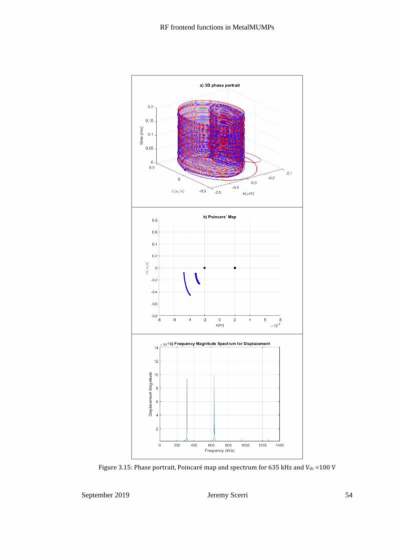
RF frontend functions in MetalMUMPs
September 2019 Jeremy Scerri 54
Figure 3.15: Phase portrait, Poincaré map and spectrum for 635 kHz and Vdc =100 V

RF frontend functions in MetalMUMPs
September 2019 Jeremy Scerri 55
Figure 3.16: Phase portrait, Poincaré map and spectrum for 468 kHz and Vdc =100 V

RF frontend functions in MetalMUMPs
September 2019 Jeremy Scerri 56
The simulation time for the results shown in Figure 3.14 to Figure 3.16 was of
0.1 ms (sampled at 300 MHz). The driving frequency was lowered from 726 kHz
until the period doubling phenomenon was encountered at 635 kHz. The frequency
was lowered further and eventually chaotic behaviour was observed at 468 kHz.
Supporting evidence for chaotic behaviour is in the broad spectrum obtained in
Figure 3.16c, in the distribution of points on the Poincaré Map (Figure 3.16b) and
also in the divergence of the blue and red traces (different initial conditions).
Although the response is chaotic, it is not, as defined in [132], extensively chaotic. As
a result, the autocorrelation function for the displacement 𝑥(𝑡) (Figure 3.17) is
significantly different from an impulse function while the distribution (Figure 3.18)
is not quite uniform.
Figure 3.17: Autocorrelation of chaotic time series

RF frontend functions in MetalMUMPs
September 2019 Jeremy Scerri 57
Figure 3.18: Histogram of displacement samples for chaotic time series
For true random number generators employed for cryptographic applications, a
uniform distribution is required. This means that unless the sampling frequency is
taken down to below resonance, the time series would still have some periodic
content.
3.2 Suppression of Spurious Products in an Electrostatic
Downconverter
Downconverters are building blocks in Superheterodyne receivers. Down
converting involves mixing and filtering stages and these are conventionally
implemented as two distinct stages. It has already been demonstrated in Section 3.1
with reference to [15], [84], [133], [122] and [134] how mixing and filtering can be
accomplished by a single device in MEMS. Such structures are referred to as mixlers

RF frontend functions in MetalMUMPs
September 2019 Jeremy Scerri 58
in [15], [84], [134] and mixer-filters [133], [122], [134]. In [135], a symbol for such
a mixer filter device is also proposed. The main benefit of having two functions
within one structure is that mismatches between the mixing and filtering stages are
eliminated.
One important performance metric for a mixer is the conversion loss (CL). The
reported CL in literature varies wildly with values ranging from 125dB [134] to as
low as 13.8 dB in [135] and even -30 dB (a gain) in [84]. In[135], the steepness of
the pass band was increased by combining several structures which increased the
order of the filter.
Another important distinction found in literature is the process employed. In [122],
[133] and [134], mixers are developed in CMOS-MEMS while [15], [84] use other
MEMS dedicated processes. In [122], it is shown how CMOS-MEMS mixers can be
combined to achieve a Hartley image rejection formation. All these reviews have one
thing in common - mixing is performed electrostatically.
In this section, a novel technique employing a differential electrostatic drive is
presented such that the unwanted frequency components resulting from the
quadratic electrostatic relationship are eliminated without using filtering.
Conventionally, the products are suppressed using filtering [15], [83], [136] but this
requires a high selectivity bandpass filter which imposes a constraint on the
bandwidth. With the elimination of this filter, the bandwidth-selectivity trade-off
can be relaxed.
3.2.1 Frequency Perspective
As described by (3.3) the expression for electrostatic force, 𝐹𝑖𝑛, can be simplified for
small (𝑥(𝑡) ≪ 𝑑) oscillations and letting 𝐾 = −𝜀𝐴𝑒
2𝑑2, (3.3) reduces to (3.13).
𝐹𝑖𝑛 = 𝐾[𝑣𝑟𝑓 − 𝑣𝑙𝑜]2= 𝐾[𝑣𝑟𝑓
2 − 2𝑣𝑟𝑓𝑣𝑙𝑜 + 𝑣𝑙𝑜2 ] (3.13)

RF frontend functions in MetalMUMPs
September 2019 Jeremy Scerri 59
This setup (Figure 3.19) was used for actuation of the BPSK demodulator. As
described by (3.13), the resulting torque frequency components on the torsional
plate using a single pair of electrodes would be as in Figure 3.20. For
downconversion to be effective, the frequency of interest would be at 𝑓𝑙𝑜 − 𝑓𝑟𝑓 and
mechanical resonance would need to be designed to coincide with this frequency.
An appropriate mechanical Q factor is also required that needs to satisfy two
conditions: meeting data bandwidth requirements and having sufficient roll-off so
as to supress all the unwanted frequency components that are generated by the
electrostatic interaction.
Figure 3.19: Actuation with one pair of electrodes
Figure 3.20: Torque frequency components with a single pair of actuation electrodes

RF frontend functions in MetalMUMPs
September 2019 Jeremy Scerri 60
Alternatively, to achieve perfect mixing, the squared terms in (3.13) would need to
be eliminated in some other way. One method of achieving this (without filtering) is
by subtracting another force 𝐹2, given in (3.14) from (3.13).
𝐹2 = 𝐾[𝑣𝑟𝑓 + 𝑣𝑙𝑜]2= 𝐾[𝑣𝑟𝑓
2 + 2𝑣𝑟𝑓𝑣𝑙𝑜 + 𝑣𝑙𝑜2 ] (3.14)
In this manner, 𝐹𝑛𝑒𝑡 = 𝐹𝑖𝑛 − 𝐹2 = −4𝐾𝑣𝑟𝑓𝑣𝑙𝑜 which results in a perfect product. The
layout, which involves two pairs of actuation electrodes, is shown in Figure 3.21 and
the resulting frequency components are shown in Figure 3.22. The schematic in
Figure 3.23 shows a section through the proposed structure identifying the
respective materials in the MetalMUMPs® process.
Figure 3.21: Proposed torsional plate having both differential drive and sense

RF frontend functions in MetalMUMPs
September 2019 Jeremy Scerri 61
Figure 3.22: Torque Frequency Components with two pairs of actuation electrodes
Figure 3.23: Section through the proposed structure showing two pairs of actuation electrodes
This structure produces two counteracting torque components and since the two
sides of the pivot differ only by the sign of 𝑣𝑙𝑜 , the net driving torque, T, would be as
in (3.15).
𝑇(𝑡) = −4𝑟𝐾𝑣𝑙𝑜𝑣𝑟𝑓 (3.15)
Under static conditions, this torque would be acting against the torsional spring
produced at the pivot. Hence, the plate angle 𝜃 would be proportional to the driving
torque. Note that since there are no DC biasing voltages, the plate oscillates about

RF frontend functions in MetalMUMPs
September 2019 Jeremy Scerri 62
the horizontal position. Including dynamic terms and neglecting cubic stiffness
terms, a simple differential equation similar to (3.7) can be used as a model.
For sufficient plate displacement and eventual sensing, mechanical resonance of the
plate should still be designed to coincide with the frequency content of the driving
torque such that the mechanical structure acts as a bandpass filter. As described in
Section 3.1.5, the resonant frequency of a plate in torsional oscillations depends on
the modulus of rigidity of the torsional tether, the moment of inertia of the plate and
the pivot section dimensions. The resulting driving torque, eq. (3.15), has frequency
components at 𝑓𝑚 = 𝑓𝑟𝑓 − 𝑓𝑙𝑜 , 𝑓𝑝 = 𝑓𝑟𝑓 + 𝑓𝑙𝑜 as well as a DC component due to phase
differences. Figure 3.22 shows how using a differential drive (subtraction)
eliminates the components at 2𝑓𝑟𝑓 and 2𝑓𝑙𝑜 . Since the unwanted frequency
components are suppressed by the differential drive setup the constraint on the Q
factor of the mechanical filter to filter out these frequencies is relaxed.
Figure 3.24 shows a plan view of the whole structure including the drive and sense
electrodes. The plate undergoing torsional vibrations has six polysilicon pads. The
middle two will be driving the plate as these interact with the nickel beam above as
shown in section in Figure 3.23. The outer polysilicon conductors, H1 and H2, are
the two differential outputs which interact with the DC biasing voltages +V and –V
above them. The horizontal dashed centre line shows the pivot line. Note again that
by placing both a +V and –V above and below the pivot line, it is guaranteed that the
plate oscillates about the horizontal position which is important for pull-in reasons.
In practice, the amplitudes of 𝑣1 and −𝑣1 can be separately adjusted to cater for
mismatch in capacitances on the sensing electrodes. These mismatches can arise
both due to unequal pad areas and also due to any plate curvature induced by
residual stresses.

RF frontend functions in MetalMUMPs
September 2019 Jeremy Scerri 63
Figure 3.24: The whole structure has drive torque proportional to the product v1v2
Note: Benefit of symmetries: (a) minimise drive to sense parasitic coupling and (b) ensure
oscillations about horizontal to keep away from pull-in.
Figure 3.25 is the electrical equivalent circuit. The currents 𝑖1 and 𝑖2 are fed into a
differential charge amplifier (DCA) having an output voltage 𝑣𝑜 . Placing the sense
pads on both sides of the drive and using a differential topology provides a
significant advantage in that parasitically coupled high-frequency signals appear as
a common-mode signal at the amplifier’s input and are therefore rejected. This
makes it possible to have only one structure as opposed to [122].
Figure 3.25: The electrical sensing circuitry.
Note: The darker lines on each capacitor show the moving polysilicon pads. They move in anti-phase
on either side of the capacitive bridge. The currents generated are inputs to the fully differential
charge amplifier.

RF frontend functions in MetalMUMPs
September 2019 Jeremy Scerri 64
3.2.2 Prototype Design Dimensions and Simulation Results
This mixer can be used as a downconvertor stage within a Superheterodyne
receiver. The design process starts by identifying the required IF, which frequency
should be matched to the resonant frequency of the plate. The bandwidth
requirements need to be met by controlling damping. For the purpose of the
simulation, the chosen IF, dimensions and the resulting Q factor are very close to
what is required for typical AM downconversion to the IF stage. For an IF of 380 kHz
following the same calculations as in Section 3.1, the required plate dimensions are
174 × 110 µm with a tether width of 45 µm for the pivot. Figure 3.26a shows a top
view of the whole structure. The semi-transparent electrodes are the nickel
electrodes. Figure 3.26b shows the plate vibration mode. As can be clearly deduced
from this figure, there are four pads making up the differential voltage pair of 𝑉𝐿𝑂
and −𝑉𝐿𝑂. This was needed such that the plate is allowed to achieve this mode of
oscillation.
a) Top view – 5 nickel electrodes
(transparent)
b) Polysilicon electrodes on vibrating
plate
Figure 3.26: The final device showing details of both polysilicon and nickel electrodes
Using CoventorWare®, the required torsional mode frequency was confirmed at
𝑓𝑟 = 378 kHz. With an RF carrier 𝑣𝑅𝐹 = 25sin (2𝜋𝑓𝑟𝑓𝑡) with 𝑓𝑟𝑓 = 1 MHz, two LO
signals are required: 𝑣𝐿𝑂 = 25 sin (2𝜋(𝑓𝑟𝑓 − 𝑓𝑟)𝑡) and −𝑣𝑙𝑜 . This setup generates a
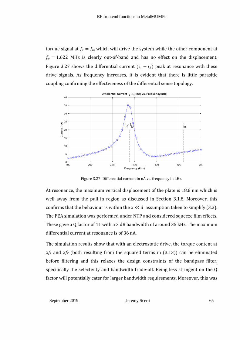
RF frontend functions in MetalMUMPs
September 2019 Jeremy Scerri 65
torque signal at 𝑓𝑟 = 𝑓𝑚 which will drive the system while the other component at
𝑓𝑝 = 1.622 MHz is clearly out-of-band and has no effect on the displacement.
Figure 3.27 shows the differential current (𝑖1 − 𝑖2) peak at resonance with these
drive signals. As frequency increases, it is evident that there is little parasitic
coupling confirming the effectiveness of the differential sense topology.
Figure 3.27: Differential current in nA vs. frequency in kHz.
At resonance, the maximum vertical displacement of the plate is 18.8 nm which is
well away from the pull in region as discussed in Section 3.1.8. Moreover, this
confirms that the behaviour is within the 𝑥 ≪ 𝑑 assumption taken to simplify (3.3).
The FEA simulation was performed under NTP and considered squeeze film effects.
These gave a Q factor of 11 with a 3 dB bandwidth of around 35 kHz. The maximum
differential current at resonance is of 36 nA.
The simulation results show that with an electrostatic drive, the torque content at
2f1 and 2f2 (both resulting from the squared terms in (3.13)) can be eliminated
before filtering and this relaxes the design constraints of the bandpass filter,
specifically the selectivity and bandwidth trade-off. Being less stringent on the Q
factor will potentially cater for larger bandwidth requirements. Moreover, this was

RF frontend functions in MetalMUMPs
September 2019 Jeremy Scerri 66
achieved with one single structure as opposed to using two devices for differential
sensing as proposed for the BPSK demodulator.
In the following section, a more complex RF function, an IQ mixer, is implemented.
The design builds upon the findings of this section.
3.2.3 Low-IF IQ mixing
Recently, Software Defined Radio (SDR) architectures which transfer most of the
analogue signal processing into the digital domain are being put forward. However,
IQ mixers are still required in analogue form as ADC/DAC requirements (bandwidth
and resolution) and power consumption requirements are still prohibitive for an
entirely digital SDR [137]. Although the ultimate goal in multi band radios is
software reconfiguration, power and dynamic range limitations require some of the
reconfiguration to take place in the RF frontend [137], [138].
Some undesired signals which can get into the radio signal path due to the mixing
process are those which occur at image frequencies. One solution is to have several
IF stages in a superheterodyne architecture. This comes at a cost as the IF filter must
be high in frequency with a high Q factor. Translating the RF frequency to baseband
directly is also possible which is known as the homodyne or zero-IF architecture.
For phase and frequency modulated signals, this option needs to provide quadrature
outputs since half the bandwidth is folded back about DC which jeopardises its
content. Moreover, a zero-IF architecture suffers from DC offset errors. This
problem is mitigated if rather than translating directly to baseband, a low-IF
architecture is adopted. The signal is then down converted to baseband in the digital
domain. A low-IF setup comprises the advantages of both heterodyne and
homodyne receivers. In literature, one can find two main strategies in MEMS mixer
designs: electrostatically actuated and thermally actuated mixers. The work
presented here describes an electromechanical structure that is actuated and
sensed electrostatically.

RF frontend functions in MetalMUMPs
September 2019 Jeremy Scerri 67
To realise an IQ mixer, two structures similar in layout as in Figure 3.26 are
employed, however, some of the electrodes are used for a different purpose. The
layout is shown in Figure 3.28.
a) b) c)
Figure 3.28: The core structure that provides actuation and sensing.
Note: a) Differential sensing of the capacitance gap, 𝑣𝑖 = 𝑣𝑖1 − 𝑣𝑖2 , b) Actuation is through
electrostatic interaction in middle electrodes, which changes the gap by ± xi and ± xq for the in-phase
and quadrature structures respectively, c) The layout for the in-phase signal; a similar structure is
used for the quadrature signal.
The fixed nickel electrode in the middle is fed with the RF signal, 𝑣𝑟𝑓, and interacts
with the two electrodes underneath it (Figure 3.28b) which are fed with the local
oscillator signal, 𝑣𝑙𝑜 , and its inverse −𝑣𝑙𝑜 . The other four fixed nickel electrodes are
connected to a DC supply 𝑉𝑑𝑐 through a high resistance 𝑅 (Figure 3.28a). These
generate the sensing voltages in response to the gap change of the oscillating
grounded polysilicon electrodes on the tethered plate underneath.
Figure 3.28c is only showing one path in a quadrature mixer. For a quadrature
mixer, two such structures are needed as shown in Figure 3.29. Suffixes ‘i’ and ‘q’
denote in-phase and quadrature respectively.

RF frontend functions in MetalMUMPs
September 2019 Jeremy Scerri 68
Figure 3.29: The complete structure consists of two mixing structures.
Note: Local oscillator signals provided in quadrature, top path shows the in-phase while the bottom
one shows the quadrature output.
In the analysis performed for the differential drive (eq. (3.13) to (3.15)), it was
assumed that the change in gap, 𝑥, is very small compared to the nominal gap 𝑑. For
the following analysis, this assumption is relaxed such that a more detailed
understanding of the amount of suppression achieved is determined. Considering
solely the in-phase structure, the electrostatic torque, 𝑇𝑖, acting on the plate can be
described with (3.16).

RF frontend functions in MetalMUMPs
September 2019 Jeremy Scerri 69
𝑇𝑖 = 𝑟휀𝐴𝑒2((𝑣𝑟𝑓 − 𝑣𝑙𝑜
𝑑 − 𝑥𝑖)2
− (𝑣𝑟𝑓 + 𝑣𝑙𝑜
𝑑 + 𝑥𝑖)2
) (3.16)
The ideal mixer would provide a torque in proportion to the product 𝑣𝑟𝑓𝑣𝑙𝑜.
Substituting 𝑛 = 𝑑/𝑥𝑖 in (3.16), (3.17) is obtained.
𝑇𝑖 = −𝑟𝐾𝑛2
(𝑛−1)2(𝑃(𝑛)𝑣𝑟𝑓
2 + 𝑃(𝑛)𝑣𝑙𝑜2 − 2(2 − 𝑃(𝑛))𝑣𝑙𝑜𝑣𝑟𝑓) (3.17)
where 𝑃(𝑛) = 4𝑛/(𝑛2 + 2𝑛 + 1), and for small displacement 𝑥𝑖 , (𝑛 → ∞), 𝑃(𝑛)
approaches zero giving ideal mixing, (3.18).
lim𝑛→∞
𝑇𝑖 ≈ −4𝑟𝐾(𝑣𝑙𝑜𝑣𝑟𝑓) (3.18)
Sensing the resulting movement of the plate could be achieved in several ways. As
described in the previous section and Figure 3.25, the constant voltage approach
using a differential charge amplifier (DCA) is one option. However, in the
subsequent discussion, an analogue option that attempts to keep a constant charge
on the output capacitances is investigated. This makes use of an appropriately sized
resistor, R, as in Figure 3.28a and Figure 3.29. The design constraints imposed by
this sensing strategy and its drawbacks (compared to a DCA) are subsequently
discussed.
The transfer function relating the quadrature voltage signals to displacement is in
effect a high pass RC filter.
Biasing through a large resistor results in a large RC time constant that
approximates a constant charge condition. Analysis of the RC filter with time varying
C(t) gives (3.19),
𝑖 =1
𝑅𝐶(𝑉𝑑𝑐 − 𝑣𝑖 (1 + 𝑅
𝑑𝐶
𝑑𝑡)) (3.19)

RF frontend functions in MetalMUMPs
September 2019 Jeremy Scerri 70
where 𝑣𝑖 represents the voltage at the fixed nickel electrode. In this setup, we can
represent the capacitance between fixed and moving electrodes on both sides (side
1 and side 2) of the differential sensing gaps with 𝐶1,2(𝑥𝑖) =𝜀𝐴
𝑑±𝑥𝑖, with xi(t) obtained
from the solution of the DE representing the dynamics and A the capacitive sensing
area. Substituting 𝐶1,2(𝑥𝑖) in (3.19) gives (3.20) whose solution is for both voltages
𝑣𝑖1,2 across the sensing plates:
𝑣1,2 = −[𝑑 ± 𝑥𝑖𝑅휀𝐴
∓𝑖
𝑑 ± 𝑥𝑖] 𝑣𝑖1,2 + (
𝑑 ± 𝑥𝑖𝑅휀𝐴
)𝑉𝑑𝑐 (3.20)
These relationships model actuation and sensing for the in-phase mixer with 𝑣𝑖 in
Figure 3.29 being 𝑣𝑖1 − 𝑣𝑖2. These would need to be duplicated for the quadrature
mixer to give 𝑇𝑞(∝ 𝑣𝑙𝑜90𝑣𝑟𝑓), 𝑥𝑞 and 𝑣𝑞1,2.
The low-IF downconverting mixer gives the required output content at 𝜔𝑟𝑓 − 𝜔𝑙𝑜.
Figure 3.30 breaks down the design process and constraints from the frequency
domain perspective into four steps. Step 1 shows the electrostatic actuation,
whereby due to the quadratic nature of this phenomenon, four frequency torque
components are generated. In Step 2, by having a large n (x << d) as described in
(3.17) and (3.18), the torque components at 2𝜔𝑙𝑜and 2𝜔𝑟𝑓 are attenuated. Step 3
shows the mechanical bandwidth (torque to displacement) centred around the low
frequency component of the mixing components and Step 4 shows the high pass
filtering effect of the RC sensing stage, the stage where displacement is converted to
voltage.

RF frontend functions in MetalMUMPs
September 2019 Jeremy Scerri 71
Figure 3.30: The design steps and their effect on the frequency content
In Step 3, the geometric parameters that regulate mechanical resonance √(k/I) of a
torsional plate can be found in Section 3.1.5. Finite Element Analysis (FEA) in
CoventorWare® confirmed these relationships and an estimate of the viscous
damping coefficient which included squeeze film effects at NTP could be obtained at
the mode of interest. For the sensing step, Step 4, the frequency transfer function
can be obtained from a linearised model of one RC filter, (3.21). From (3.21), the
differential setup output vi approaches ±2𝑥𝑖𝑉𝑑𝑐/𝑑 for large R. A large R is required
such that pole frequency 𝜔𝑅𝐶 = 1/𝑅𝐶 is kept below the frequency of interest thus
maximising the output. Table 3.5 summarises the design procedure.
𝑉𝑖1,2𝑋𝑖
= ±𝑗𝜔𝑉𝑑𝑐
𝑑(𝑗𝜔 + 1/𝑅𝐶) (3.21)

RF frontend functions in MetalMUMPs
September 2019 Jeremy Scerri 72
Table 3.5: Design Steps for IQ mixing
Design Step Aim Method
1 Create mixing components Electrostatic drive
2 Suppress even harmonics Keep 𝑛 = 𝑑/𝑥𝑖 large
3 Centre resonance on low IF Dimension plate/tether as in Section
3.1.5
4 Maximise sensing gain Keep 1/𝑅𝐶 below the IF frequency
Employing a large resistance for sensing also generates thermal noise on the four
quadrature output voltages. The resistor can be represented as an ideal resistor in
series with a voltage source, 𝑣𝑛, with noise power spectral density of
𝐺𝑥(𝑓) = 2𝑘𝑇𝑅 V2/Hz where 𝑘 is Boltzman’s constant and 𝑇 is the temperature in
Kelvin. It can be demonstrated that the RMS voltage appearing on the four
quadrature voltages, across the capacitive gap C, is independent of R and equal to
√𝑘𝑇
𝐶 V. This implies that for smaller capacitances the noise voltage increases (RC low
pass filter bandwidth gets wider). This noise level would need to be orders of
magnitude smaller than the RMS levels of the four quadrature output voltage
signals.
3.2.4 Numerical Simulations
The FEA simulations performed in CoventorWare® are the same as those presented
in Section 3.1.3 as the plate dimensions are the same (Figure 3.26). The required
static and dynamic specifications were used to fix the plate dimensions using the
equations in Section 3.1.5. The electrostatic force generated by the input signals,
together with the second order differential equation that modelled the plate
dynamics, were validated against the results obtained using FEA. Once the

RF frontend functions in MetalMUMPs
September 2019 Jeremy Scerri 73
mathematical model was validated, the full IQ mixer model was implemented in
SIMULINK (Appendix 3.3) for further analysis.
For simulation, an RF carrier frequency of 𝑓𝑟𝑓 = 1 MHz was selected for both BPSK
and QPSK/4-QAM modulation schemes. The local oscillator frequency was fixed to
𝑓𝑙𝑜 = 622 kHz and the mechanical resonant frequency, 𝑓𝑟 , was designed such that it
coincides with 𝑓𝑟 = 𝑓𝑟𝑓 − 𝑓𝑙𝑜 = 378 kHz = 𝑓𝑖𝑓 , the IF frequency. The bit rate adopted
for both simulations was that of 100 kbps. The FEA viscous damping simulation
included squeeze film effects and, at NTP and at this resonant mode of 378 kHz, gave
a damping factor ζ of 0.045. The RF and LO voltages used were the same at 17 volts
RMS. These actuation voltage levels resulted in a peak vertical displacement of the
plate of 19 nm. This gave n = 1.45 µm / 19 nm = 76 satisfying requirements for Step
2 for the suppression of eve harmonics. Moreover, having such a small peak
displacement (compared to the gap), operation is kept away from the electrostatic
pull in region and also justifies neglecting the spring cubic stiffness behaviour. With
19 nm peak displacement, the plate experiences a peak torque of 1640 pNm. This
amount of torque is in agreement with what (3.18) gives for r = 25 µm, d = 1.45 µm
and Ae = 2500 µm2. These are the dimensions, related to actuation, adopted.
On the sensing side, the sensing area was larger at a A = 5500 µm2. This gives a
sensing capacitance of 𝐶𝑠 = 34 fF. For 𝜔𝑅𝐶 < 𝜔𝑟𝑓 − 𝜔𝑙𝑜 to be satisfied, requires a
biasing resistor of 12.5 MΩ or greater. The ‘constant’ charge sensing setup gives
sensing voltages approaching ±2𝑥𝑖𝑉𝑑𝑐/𝑑 = ±0.26 volts, for 𝑉𝐷𝐶 = 10 volts and a
peak sensing current of 35 nA.
With the dimensions of the sensing area A and gap d, the resulting RMS noise voltage
due to the biasing resistor is several orders of magnitude smaller than the sensing
voltages of 0.26 V. This means that the ‘constant’ charge sensing strategy is a viable
option for this IQ mixer.

RF frontend functions in MetalMUMPs
September 2019 Jeremy Scerri 74
Simulations in SIMULINK (Appendix 3.3) with equations (3.18) and (3.20) were
executed. The mechanical static and dynamic behaviour were captured with a
bandpass filter for both the in-phase and the quadrature structures. The voltage
levels of the four quadrature output signals (𝑣𝑖1, 𝑣𝑖2, 𝑣𝑞1and 𝑣𝑞2) agreed with the
±0.26 V limiting levels for large R. The I and Q paths were recombined using the
‘atan2’ function to simulate digital reconstruction of the QAM signal under test.
Figure 3.31 shows simulated outputs for a QPSK signal consisting of a repeating
[00,01,10,11] pattern and Figure 3.32 shows the output for a BPSK signal consisting
of a repeating [0,0,0,1,1] pattern.
Figure 3.31: vi (green), vq (red) and output (blue-atan2) showing the 4 levels representing
[00,01,10,11].

RF frontend functions in MetalMUMPs
September 2019 Jeremy Scerri 75
Figure 3.32: vi (green), vq (red) and output (Blue-atan2) shows 2 levels representing [0,0,0,1,1]
An IQ mixer can be considered as a universal demodulator. These simulations show
that this RF frontend function can be obtained by a torsionally oscillating structure
within the fabrication constraints of the MetalMUMPs process. The important design
decisions that lead to the successful generation of the I and Q signals are described
and summarised in Table 3.5.
The use of differential local oscillator signals as well as restraining oscillations to
small amplitudes were instrumental in attenuating quadratic terms resulting from
the electrostatic interaction. This relaxed the design constraints for the mechanical
bandwidth as clarified in Figure 3.22 and Figure 3.30 (Step 2). The trade-offs for
positioning the mechanical resonance on the low-IF frequency while keeping
sufficient capacitance area to satisfy the pole placement requirements for the
sensing RC filter are clearly portrayed in the frequency domain showing the design
steps in Figure 3.30.
RF frontend functions in MetalMUMPs
September 2019 Jeremy Scerri 76
3.3 Parasitic Insensitive Sensing
Using a constant charge sensing strategy requires a reasonably high resistance and
has its problems. Realisation of high resistance resistors in a small footprint is
challenging. In [139], a 13 MΩ resistor was developed using a simple differential pair
with diode-connected MOSFETs driven in the subthreshold region of the MOSFETs
in 0.35-µm CMOS. It occupied an area of 105 µm x 110 µm. For the IQ mixer, four are
required with a total area of 46,200 µm2 which is two to three times the size of the
two torsional plates for the IQ mixer. Moreover, using a constant charge sensing
strategy does not cancel out parasitic capacitances.
The sensible way to eliminate parasitic capacitances is by using a DCA for sensing as
in Figure 3.7. Two DCAs are required, one for the in-phase and another one for the
quadrature paths. This will eliminate parasitics and can be implemented in 0.18-µm
CMOS [140] with a similar footprint (42,000 µm2) as the four resistors.
The constant voltage approach, using DCA’s, does not impose the high pass filtering
stage (Step 4 in Figure 3.30) on the required signal and has also the added advantage
of eliminating the parasitic capacitances.
3.4 Conclusions
The use of a torsional vibration structure for BPSK demodulation is innovative. It
was demonstrated that this structure had an undamped resonant frequency of
2 MHz and can successfully demodulate a low data rate BPSK signal with a carrier
frequency of 868 MHz and a chip rate of 300 kchips/s. These specifications satisfied
the ZigBee standard for low data rate, wireless personal area networks.
The same structure was investigated under higher actuation voltages (> 75 V). It
was shown that the device exhibits bistability and it has potential for applications
involving random number generation (RNG) for crypto systems [141] and also as
chaotic carrier generators for secure communications [142].

RF frontend functions in MetalMUMPs
September 2019 Jeremy Scerri 77
Furthermore, using a differential drive on the same torsional vibratory plate
configuration, suppression of unwanted frequency components resulting from the
quadratic relationship in the electrostatic force was implemented by controlling the
parameter 𝑛 = 𝑑/𝑥𝑖 . With 𝑛 = 76, suppression was sufficient and this relaxed the Q
factor-bandwidth requirements for the downconverting mixer and also for the IQ
mixer designs. The IQ mixer model was validated with FEA simulations and
implemented in SIMULINK. With these simulations, various QAM signalling schemes
were successfully demodulated.

Bistable Vibrational Energy Harvester in SINTEF moveMEMS
September 2019 Jeremy Scerri 78
4. BISTABLE VIBRATIONAL
ENERGY HARVESTER IN
SINTEF MOVEMEMS
This work investigates the design of a vibrational energy harvester whose ability to
vibrate for a broad range of input frequencies is attributed to a highly nonlinear
spring. The goal was to design a broadband vibrational energy harvester and to
develop a mathematical model that could replace computationally expensive FEA
simulations. The SINTEF process was used; this process has a PZT layer of 2 𝜇m and
can cater for larger proof masses than is possible with MetalMUMPs. The analysis
builds on modelling techniques developed in Sections 3.1.8 and 3.1.10 which deal
with large displacements and cubic stiffness.
4.1 Introduction
To achieve broadband vibrational sensitivity the design employed a buckling spring.
This buckling spring gives two stable positions or bistability. Bistability and
multistability are desirable properties in mechanical structures used for energy
harvesting. Having a plurality of equilibrium points, a vibrational system can exhibit
small amplitude vibrations about each equilibrium position, however, given enough
energy, it would snap through between the stable equilibria.
The main objective of this broadband vibrational energy harvester (BVEH) design
was that accurate estimates of the mechanical and electrical behaviour could be
obtained from a mathematical model which replaces the complex and time
consuming FEA simulations.

Bistable Vibrational Energy Harvester in SINTEF moveMEMS
September 2019 Jeremy Scerri 79
In literature, one can find many ways to achieve bistability [20]. In [21], a
theoretically extensive treatment of the behaviour of buckling beams and their
combination to obtain compliant multistable systems is presented.
In this work, the focus was on systems that are bistable due to buckling of clamped-
clamped beams. Modelling of beam dynamics involves PDEs that give as a solution
the time evolution of the displacement at any point on the beam, 𝑦(𝑥, 𝑡). This is a
continuous system, that is, one having infinite degrees of freedom (DoF). A reduced
order model is one which has a (small) finite number of DoF. The proposed
mechanical design, together with results in [143] and some justified
approximations, make it possible to quickly fix dimensions in the design process and
to accurately predict behaviour with a simpler non-linear 3rd order differential
equation. In [144], the mechanical structure considered is very similar to what is
proposed here and also exhibits asymmetric bistability. However, harvesting in
[144] is achieved electrostatically. Promising experimental results are reported but
no attempt to model with a system of differential equations was performed as a
replacement to FEA.
4.2 Design within SINTEF process constraints
The SINTEF piezoVolume process was adopted. Since it has a relatively thick
piezoelectric layer, this enabled the conversion of mechanical to electrical energy.
The SINTEF process is able to deposit 2 𝜇m of Lead Zirconium Titanate (PZT) which
is a material with one of the highest coupling coefficients. The overall wafer
thickness is of 379 𝜇m as detailed in Figure 4.1.
Figure 4.1: SINTFEF piezoVolume Process Overview

Bistable Vibrational Energy Harvester in SINTEF moveMEMS
September 2019 Jeremy Scerri 80
In the structure under study, the PZT layer is operated in the d31 mode. The proposed
structure obtains bistability with a simple compliant mechanism intended to
respond to linear vibrations. Figure 4.2 is the schematic showing the mechanical
structure employed.
Figure 4.2: The mechanical schematic showing the proof mass M and the two compliant springs
In this figure, the two beams holding the proof mass, M, and having an initial stress-
free first buckling mode shape, 𝑦0, are shown. Equation (4.1) describes this initial
shape of the two compliant springs having a mid-span height of ℎ.
𝑦0(𝑥) =ℎ
2(1 − cos (
2𝜋𝑥
𝑙)) (4.1)
where 𝑥 and 𝑙 are as shown in Figure 4.2. The beam displacement is represented by
𝑦(𝑥, 𝑡). The acceleration of the mass, , is made up of two components: 𝑏 the
device’s base acceleration and 1 the acceleration of the beam at mid-span, which

Bistable Vibrational Energy Harvester in SINTEF moveMEMS
September 2019 Jeremy Scerri 81
results in = 𝑏 +1. In terms of absolute displacement, this relationship becomes
𝑤 = 𝑤𝑏 + 𝑦1 + 𝑦0.
Figure 4.3 shows the FEA 1st mode shape and frequency, the meshing used for the
FEA analysis and detail of the material layering on the top side of the spring is shown
in the inset. Inset also shows the PZT poling direction, ‘3’ and the main strain
direction, ‘1’.
Figure 4.3: Vibrational mode, FEA mesh and layering detail on spring
Since two compliant beams are used, and they are connected at mid-span, the 2nd
buckling mode (Figure 4.4) is suppressed. Moreover, the ratio 𝑄 =ℎ
𝑡 with 𝑡 being
the beam thickness, is kept greater than 4
√3 ; this guarantees that the beam would
buckle in mode 1 and mode 3 only [143] as shown in Figure 4.5.
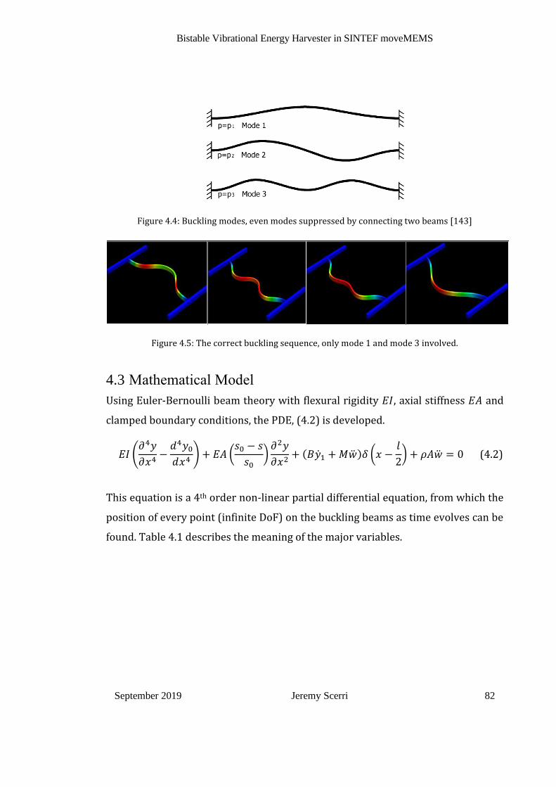
Bistable Vibrational Energy Harvester in SINTEF moveMEMS
September 2019 Jeremy Scerri 82
Figure 4.4: Buckling modes, even modes suppressed by connecting two beams [143]
Figure 4.5: The correct buckling sequence, only mode 1 and mode 3 involved.
4.3 Mathematical Model
Using Euler-Bernoulli beam theory with flexural rigidity 𝐸𝐼, axial stiffness 𝐸𝐴 and
clamped boundary conditions, the PDE, (4.2) is developed.
𝐸𝐼 (𝜕4𝑦
𝜕𝑥4−𝑑4𝑦0𝑑𝑥4
) + 𝐸𝐴 (𝑠0 − 𝑠
𝑠0)𝜕2𝑦
𝜕𝑥2+ (𝐵1 +𝑀)𝛿 (𝑥 −
𝑙
2) + 𝜌𝐴 = 0 (4.2)
This equation is a 4th order non-linear partial differential equation, from which the
position of every point (infinite DoF) on the buckling beams as time evolves can be
found. Table 4.1 describes the meaning of the major variables.

Bistable Vibrational Energy Harvester in SINTEF moveMEMS
September 2019 Jeremy Scerri 83
Table 4.1: Variables describing the beam motion
Variable Description
𝑦(𝑥, 𝑡) Vertical position of any point on the beam
𝑠(𝑡) Length of the beam
𝑦1(𝑡) Mass displacement from 𝑦0(𝑥) at mid-span
𝑤(𝑡) Absolute mass displacement
𝛿(𝑥) Dirac delta function
The δ represents the Dirac delta function, s is the length of arc of the beam and s0 the
as-designed length of arc of the beam. The parameters B, M, A and ρ are the damping
coefficient, mass, beam section area and density respectively.
A simpler model could be found since the proof mass 𝑀 was attached to the
mid-span which eliminated the dependency of the mass’s vertical movement 𝑦1 on
𝑥.
The considerations that led to a simpler model were:
• For small oscillations about the two stable buckled positions, the system
behaves as a linear Spring-Mass-Damper and a second order system was
hence adopted.
• To cater for the nonlinear buckling behaviour linear stiffness of the form,
𝐾𝑦1was replaced with a nonlinear function 𝐹𝑠(𝑦1).
• From FEA static analysis, it was found that at least a 5th order polynomial was
required to model the spring behaviour.
• A force-voltage coupling term was included to model electrical stiffening.
The proposed reduced order model is given in (4.3).

Bistable Vibrational Energy Harvester in SINTEF moveMEMS
September 2019 Jeremy Scerri 84
𝑀(1 + 𝑏) + 𝐵1 + 𝐹𝑠(𝑦1) + 𝐹𝑣(𝑣, 𝑦1) = 0 (4.3)
The first term, 𝑀(1 + 𝑏), is the mass inertia due to the base and beam mid-point
accelerations. The inertia of the beams was neglected as it is negligible when
compared to the proof mass, 𝑀. Damping forces are primarily viscous in nature, 𝐵1,
and are assumed to be acting at mid-span and in proportion to the beam mid-span
velocity 1.
The stiffness, 𝐹𝑠(𝑦1), of a buckling spring can be approximated [143] with a three-
segment, piecewise linear function for a high Q as in Figure 4.6.
Figure 4.6: Fs - y1 curve for large Q with a mode 2 constrained beam [143]
However, here, a quintic polynomial as in (4.4) was fitted.
𝐹𝑠(𝑦1) = 𝐾1𝑦1 +𝐾2𝑦12 + 𝐾3𝑦1
3 + 𝐾4𝑦14 + 𝐾5𝑦1
5 (4.4)
Having the spring stiffness expressed as a continuous function is convenient for
dynamic analysis. The coefficients of this polynomial representing the spring
stiffness are estimated from an FEA static analysis simulation run. This polynomial
model has three real roots, two of which represent stable equilibrium positions
while the third is unstable. According to [143], these occur at 𝑦1 = 0 = 𝑦𝑖 and
𝑦1 = 1.99ℎ = 𝑦𝑖𝑖𝑖 for the stable equilibria and 𝑦1 = −4ℎ/3 = 𝑦𝑖𝑖 for the unstable
one. This results in a spring that exhibits asymmetric bistability. In [143], analytical
𝐹𝑠
y1
ybot
fbot
ytop
ftop
yii yiii
yi

Bistable Vibrational Energy Harvester in SINTEF moveMEMS
September 2019 Jeremy Scerri 85
approximate expressions for 𝑓𝑡𝑜𝑝, 𝑦𝑡𝑜𝑝, 𝑦𝑏𝑜𝑡 and 𝑓𝑏𝑜𝑡 are provided, from which, the
‘linear’ spring stiffnesses around the two stable equilibria could be estimated. A
better estimate of the stiffness around 𝑦𝑖 and 𝑦𝑖𝑖𝑖 was obtained by taking the
derivative of the Fs - y1 curve at these two positions. With the beam having mode 2
constrained, the approximate analytical expression for 𝐹𝑠(𝑦1) provided in [143] can
be adopted, as reproduced in (4.5).
𝐹𝑠 ≈𝐸𝐼ℎ
𝑙3𝐴 (
𝑦1ℎ)3
+ 𝐴(𝐿 + 𝐶) (𝑦1ℎ)2
+ 𝐴𝐿𝐶 (𝑦1ℎ) + 8𝜋4 − 6𝜋4 (
𝑦1ℎ) (4.5)
where 𝐸 is the modulus of elasticity, 𝐼 = 𝑏𝑡3/12 is the second moment of area of the
beam, with 𝑏 being the SINTEF silicon depth of 377 𝜇m, 𝐴 =3𝜋4𝑄2
2,
𝐿 = −3
2+√
1
4−
4
3𝑄2 and 𝐶 = −
3
2−√
1
4−
4
3𝑄2.
Although (4.5) is an approximation, closed form expressions for the gradient at the
two stable equilibria could be obtained by evaluating 𝐾𝑖 =𝑑𝐹𝑠
𝑑𝑦1|𝑦1=𝑦𝑖
and
𝐾𝑖𝑖𝑖 =𝑑𝐹𝑠
𝑑𝑦1|𝑦1=𝑦𝑖𝑖𝑖
. These give the linearised stiffnesses of the spring at the as-
designed position, 𝐾𝑖 and at the buckled position, 𝐾𝑖𝑖𝑖.
𝐾𝑖 =𝐸𝐼𝜋4
𝑙3(3𝑄2 − 4)
(4.6)
𝐾𝑖𝑖𝑖 = 𝐾𝑖/2 (4.7)
Equations (4.6) & (4.7) are applicable for one beam only and hence for small
oscillations about the stable positions, the respective resonant frequencies would
be 𝑓𝑖 = 1/2𝜋√2𝐾𝑖/𝑀 and 𝑓𝑖𝑖𝑖 = 𝑓𝑖/√2.
The last term in (4.3), 𝐹𝑣(𝑣, 𝑦1), describes the electrical stiffness due to strain of the
PZT layer. Under small field conditions, the behaviour of the PZT material is
described by (4.8).

Bistable Vibrational Energy Harvester in SINTEF moveMEMS
September 2019 Jeremy Scerri 86
(𝑇𝐷) = (
𝑐 −𝑒31𝑒31 휀 ) (
𝑆𝐸) (4.8)
The PZT coefficient 𝑒31 is the piezo-stress constant (N/Vm). D is the dielectric
displacement (C/m2), T the developed stress (N/m2) in the mechanical displacement
direction, S the applied strain in the mechanical displacement direction and E the
applied electric field (V/m) across the PZT layer of thickness 𝑡𝑝. The modulus of
elasticity and the absolute permittivity of PZT are represented by c and 휀
respectively.
The term that describes how the electrical field induces stress in the material comes
from the first row of (4.8) and is 𝑇𝑒 = −𝑒31𝐸 with 𝐸 = 𝑣/𝑡𝑝, 𝑣 being the voltage
across the PZT layer of thickness 𝑡𝑝. This stress is in the ‘1’ direction, that is, along
the length of the beam. The vertical component of this stress contributes to a force
on the proof mass as shown in Figure 4.7.
Figure 4.7: Electrical force component in the vertical direction
The angle subtended by the beam with the horizontal, 𝜃, can be considered to be
small since the ratio ℎ/𝑙 is small, hence the vertical force due to electrical field would
be 𝑒31𝐸𝐴𝑠𝜃 where 𝐴𝑠 is the PZT cross sectional area, 𝑡 × 𝑡𝑝 giving the term 𝑒31𝑡𝑣𝜃 =
𝐹𝑣(𝑣, 𝑦1) with 𝑦1 = 𝑙/2 𝑡𝑎𝑛 𝜃 − ℎ.
This term, 𝐹𝑣(𝑣, 𝑦1), describes how a voltage across the PZT layer generates a force
on the proof mass, however the reverse process is also occurring and is the one
required to provide an output current 𝑖 across a load resistor 𝑅𝑙 . From the second
row of (4.8), (4.9) is obtained,
Ɵ
𝑒31𝐸𝐴𝑠
𝑒31𝐸𝐴𝑠𝑠𝑖𝑛𝜃
l
h

Bistable Vibrational Energy Harvester in SINTEF moveMEMS
September 2019 Jeremy Scerri 87
𝐷 =𝑞
𝐴𝑝= 𝑒31
𝑠 − 𝑠0𝑠0
+ 휀𝐸 (4.9)
where 𝑞 is the charge, 𝐴𝑝 is the piezo layer capacitive area, 𝑙 × 𝑡, 𝑠0 is the beam arc
length and 𝑠 is the instantaneous beam arc length, both determined using the length
of arc integral to a first order approximation on (4.1). Taking the derivative of (4.9)
to obtain an expression for current and re-arranging gives (4.10).
=1
𝐶𝑝𝐴𝑝𝑒31
𝑠0−𝑣
𝑅𝑙 (4.10)
where 𝐶𝑝 = 휀𝐴𝑝
𝑡𝑝, 𝑣
𝑅𝑙= 𝑖 and
𝑠0≈
𝜋2
2𝑙(𝑦1+𝑦0)1
𝑙+𝜋2
4𝑙𝑦02
.
In summary, the PDE which describes the mechanical behaviour, eq. (4.2), was
replaced with equations (4.3) and (4.4) which is a nonlinear DE describing the
position of the proof mass. Electro-mechanical coupling was included in (4.3) as 𝐹𝑣 .
The DE that describes how the strain on the PZT layer results in an output voltage 𝑣
is given by (4.10).
4.3.1 Design Approach
One of the most important design specifications for a vibrational energy harvester
is the frequency or bandwidth for which the harvester is sensitive to. As shown in
Figure 4.6, the spring stiffness characteristic is asymmetric and this gives different
resonant frequencies at the two stable positions with 𝑓𝑖 > 𝑓𝑖𝑖𝑖. Such an asymmetric
bistable energy harvester would be sensitive to vibrations at 𝑓𝑖 and below.
Fixing the dimensions in the design shown in Figure 4.2 such that it is sensitive to a
particular frequency range can be done by substituting (4.6) in 𝑓𝑖 = 1/2𝜋√2𝐾𝑖/𝑀
to obtain (4.11).

Bistable Vibrational Energy Harvester in SINTEF moveMEMS
September 2019 Jeremy Scerri 88
𝑓𝑖 =1
2𝜋√2𝐸𝐼𝜋4(3𝑄2 − 4)
𝑀𝑙3
(4.11)
Substituting 𝐼 =𝑏𝑡3
12 and 𝑀 = 𝜌𝑛𝑎2𝑏 gives (4.12);
𝜌𝑛𝑎2𝑏 =2E𝑏𝜋4(3𝑄2 − 4)
12(2𝜋𝑓𝑖)2(𝑡
𝑙)3
(4.12)
where 𝜌 is the density of silicon and n is the aspect ratio of the proof mass, that is,
length/width. One dimension that can be fixed without affecting the overall
footprint of the harvester is the proof mass’s width ‘𝑎’. This can be fixed to be the
same as the beam length 𝑙 giving (4.13):
𝑓𝑖−2 =
24𝜌
E𝜋2(3𝑄2 − 4)𝑡3. 𝑛𝑙5 (4.13)
Equation (4.13) together with the condition for buckling, that is, 𝑄 = ℎ/𝑡 > 4/√3
can give the dimensions for a set of design specifications. For the SINTEF process,
with E =130.2 GPa and 𝜌 =2311 kg/m3, fixing either 𝑡 or ℎ would in turn fix the
gradient of the straight line 𝑓𝑖−2 vs. 𝑛𝑙5. This procedure could either be used to fix
𝑛𝑙5 if the base excitation frequency is known or vice versa.
Equation (4.13) can be represented graphically as in Figure 4.8. If, for example, the
harvester is required to be used at frequencies up to 1500 Hz (𝑓𝑖), the horizontal line
at 𝑓𝑖−2 can be drawn and an intersection point with any of the straight lines
originating at the origin can be used as a design point. In Figure 4.8, for
𝑓𝑖 = 1500 Hz, if a beam thickness of 5 𝜇𝑚 and initial curvature height ℎ = 28 𝜇𝑚 are
selected, a resulting beam length of 𝑙 = 3 mm and proof mass aspect ratio of 𝑛 =
0.478 guarantee that the required 𝑓𝑖is obtained and that snap through occurs. These
result in a total proof mass of 𝑀 = 3.77 𝜇𝑔.

Bistable Vibrational Energy Harvester in SINTEF moveMEMS
September 2019 Jeremy Scerri 89
Figure 4.8: Using eq. (4.13) to determine h and t
4.4 PZT Harvester Model validation against FEA
For model validation purposes, an upper frequency, 𝑓𝑖 , of 1500 Hz was selected
together with a beam thickness 𝑡 of 5 𝜇𝑚 and 𝑄 of 6. Using the design process
described in Section 4.3.1, these guaranteed snap through would occur and required
a beam length 𝑙 = 3.15 mm and an aspect ratio 𝑛 = 0.41. With these parameters, the
proof mass was 3.61 𝜇g, beam moment of inertia 3.792 × 10⁻²¹ kgm2. The linear
spring stiffnesses (for 2 beams) around the two stable positions were found to be
𝐾𝑖 = 320 N/m and 𝐾𝑖𝑖𝑖 = 160 N/m from (4.6) and (4.7) respectively. These resulted
in 𝑓𝑖𝑖𝑖 = 1060 Hz.
4.4.1 Validation of the Static Response
Figure 4.9 shows the force-displacement relationship obtained using
CoventorWare® (solid line) for a static analysis simulation. With ℎ = 30 𝜇m, the
total deflection for 𝑦1 is 60 𝜇m. For such a simulation in CoventorWare®, one cannot
solve for an arbitrary initial displacement directly. Instead, one needs to increase

Bistable Vibrational Energy Harvester in SINTEF moveMEMS
September 2019 Jeremy Scerri 90
the displacement in small steps from zero and restart the analysis from the resultant
displacement found in the previous simulation run. In this manner, the simulation
will not fail easily because defining the initial displacement resolves the large
non-linearity of buckling.
Figure 4.9: The Force-Displacement (y1) asymmetric curve obtained using FEA
FEA results gave stiffness gradients at 𝑦𝑖 and 𝑦𝑖𝑖𝑖 at 𝐾𝑖 = 329.9 N/m and
𝐾𝑖𝑖𝑖 = 165 N/m. These are sufficiently close to the theoretical estimates.
From FEA modal simulations, the resonant modes at the two stable equilibria were
found to be 𝑓𝑖 = 1585 𝐻𝑧 and 𝑓𝑖𝑖𝑖 = 1100 𝐻𝑧. Both these numbers are within 5% of
the analytical model predictions.
For dynamic predictions on MATLAB, a quintic polynomial was fitted (Figure 4.9 –
dotted line) to the force displacement graph with the coefficients as listed in
Table 4.2.

Bistable Vibrational Energy Harvester in SINTEF moveMEMS
September 2019 Jeremy Scerri 91
Table 4.2: Fs – y1 Quintic Polynomial coefficients
Coefficient Value
𝐾1 3.270 × 10²
𝐾2 -3.175× 10⁷
𝐾3 1.222 × 10¹²
𝐾4 -2.137× 10¹⁶
𝐾5 1.388 × 10²⁰
The minimum energy, 𝐸𝑚𝑖𝑛, required for snap-through (well-to-well jumping) to
occur is the area under the force-displacement curve between 𝑦𝑖 and 𝑦𝑖𝑖 and can be
calculated using (4.14).
𝐸𝑚𝑖𝑛 = ∫ 𝐹𝑠(𝑦1) 𝑑𝑦1
𝑦𝑖𝑖
0
(4.14)
For this device, as can be seen in Figure 4.10, the amount of energy required for
snap-through is 25 nJ. This means that -neglecting damping - any initial condition
that has a total energy (strain and kinetic) greater than 25 nJ would have enough
potential for well-to-well jumping.
Figure 4.10: Strain energy vs. displacement showing a maximum of 25 nJ at the unstable point

Bistable Vibrational Energy Harvester in SINTEF moveMEMS
September 2019 Jeremy Scerri 92
4.4.2 Validation of the Harmonic Response
Validation of the dynamic and electrical characteristics was done only for harmonic
oscillations around 𝑦𝑖 and 𝑦𝑖𝑖𝑖. Confirming the validity when snap-through occurs is
more challenging due to the sensitivity to initial conditions and due to the
computationally intensive FEA simulations required. The following FEA and
MATLAB simulations were all designed to stay away from 𝑦𝑖𝑖, hence, this exercise
will be confirming model validity for harmonic oscillations around 𝑦𝑖, 𝑦𝑖𝑖𝑖 or both
(high energy orbits). Testing of the electrical parameters was done by neglecting
mechanical damping. The simulations involved providing a sinusoidal acceleration
at 𝑓𝑖 = 1585 Hz to the inertial frame of 0.001g (𝑏 in (4.3)) both in MATLAB and in
CoventorWare® and comparing the amplitude of vibrations obtained and also
electrical current and power generated. Figure 4.11 and Figure 4.12
Figure 4.12 show one such harmonic simulation in MATLAB. The phase portrait in this
figure shows the three equilibrium positions marked with an ‘•’. In the steady state,
the oscillations reached a peak displacement of 8.8 𝜇𝑚. Once this peak displacement
was determined, a second simulation in MATLAB was performed with an initial
condition on displacement of 8.8 𝜇𝑚. The initial position of the beam displacement
is marked with a red ‘*’. In this simulation, the oscillations’ peak stayed at 8.8 𝜇m
giving 𝑖𝑅𝑀𝑆 = 0.087 𝜇A and 𝑃𝑅𝑀𝑆 = 0.0023 𝜇𝑊 across a load resistance 𝑅𝑙 of 250 kΩ.
In this simulation, which investigated harmonic behaviour, the value of the load
resistance, 𝑅𝑙 , was chosen arbitrarily as there is no internal resistance (mechanical
damping) to which this needs to be matched for maximum power transfer. For
maximum power transfer the internal resistance (mechanical damping) and the
external load would need to be equalised [145].
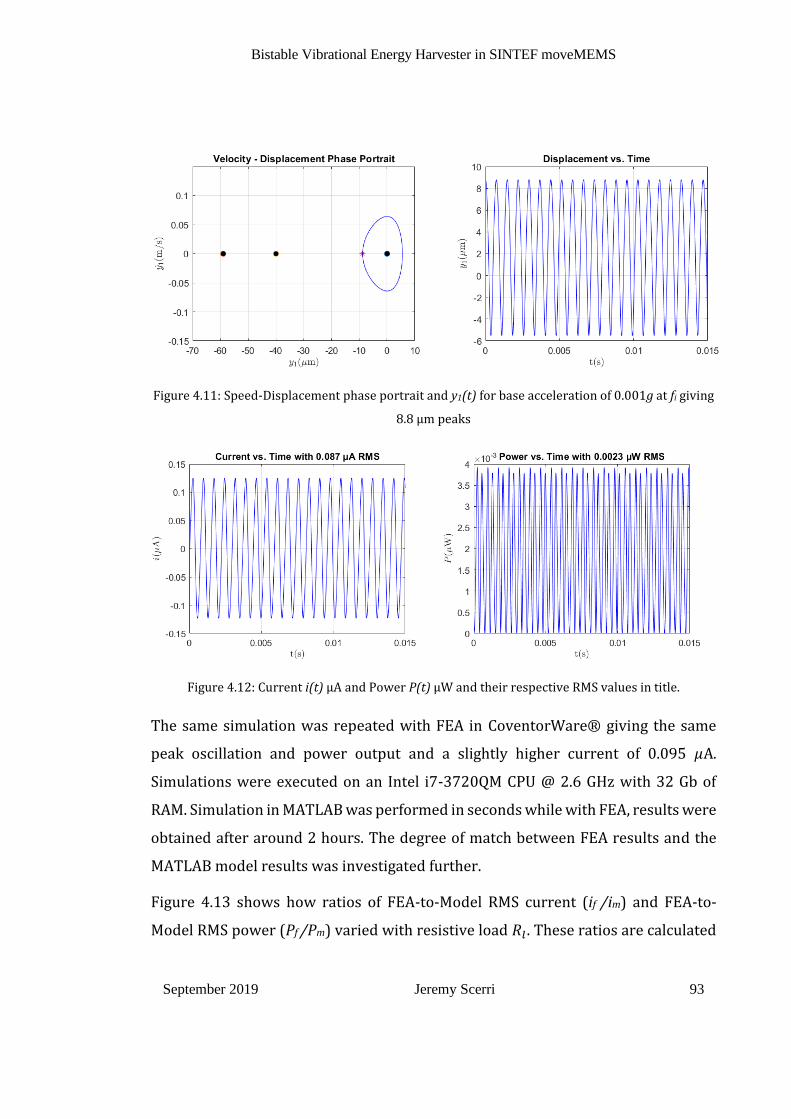
Bistable Vibrational Energy Harvester in SINTEF moveMEMS
September 2019 Jeremy Scerri 93
Figure 4.11: Speed-Displacement phase portrait and y1(t) for base acceleration of 0.001g at fi giving
8.8 µm peaks
Figure 4.12: Current i(t) µA and Power P(t) µW and their respective RMS values in title.
The same simulation was repeated with FEA in CoventorWare® giving the same
peak oscillation and power output and a slightly higher current of 0.095 𝜇A.
Simulations were executed on an Intel i7-3720QM CPU @ 2.6 GHz with 32 Gb of
RAM. Simulation in MATLAB was performed in seconds while with FEA, results were
obtained after around 2 hours. The degree of match between FEA results and the
MATLAB model results was investigated further.
Figure 4.13 shows how ratios of FEA-to-Model RMS current (if /im) and FEA-to-
Model RMS power (Pf /Pm) varied with resistive load 𝑅𝑙 . These ratios are calculated

Bistable Vibrational Energy Harvester in SINTEF moveMEMS
September 2019 Jeremy Scerri 94
for two orbits in the 𝑦1 − 1 state space around 𝑦𝑖 at two different amplitudes
5.66 𝜇𝑚 and 6.17 𝜇𝑚.
Figure 4.13: Output current (i) and power (P) ratios of FEA-to-model RMS
As can be seen in Figure 4.13, the model predictions for power and current are
acceptable for loads below 500 kΩ.
The mathematical model developed was also able to predict behaviour for high
energy orbits which are orbits about the two equilibrium points in the 1 − 𝑦1 space
as shown in Figure 4.14. As can be seen, the high energy orbit was achieved for a low
(compared to 𝑓𝑖 and 𝑓𝑖𝑖𝑖) driving frequency of 560 Hz. Being bistable, the broadband
capabilities were also confirmed. The response was achieved with a base
acceleration of 3.5 g. For this simulation, a load resistance of 1.5 MΩ was used
through which a current of 0.23 𝜇A RMS was driven resulting in a voltage of 0.37 V
RMS and power generation of 0.2 𝜇W.

Bistable Vibrational Energy Harvester in SINTEF moveMEMS
September 2019 Jeremy Scerri 95
Figure 4.14: A high energy orbit producing 0.2 µW of power with spring force-displacement and
equilibria in superposition.
When compared to the FEA model, the reduced order model (eq. (4.3), (4.4) and
(4.10)) simulated in MATLAB proved very accurate in predicting both the harmonic
behaviour around 𝑦𝑖 and 𝑦𝑖𝑖𝑖 and also the static behaviour. For the harmonic
behaviour, it gives reasonable estimates for power, current and voltage for different
loads. The estimation error starts exceeding 10% for loads larger than 1 MΩ. The
increase in error for larger resistive load can be attributed to the fact that the
capacitance dominates in the model for larger 𝑅𝑙 (Eq. (4.10)) and the mathematical
model does not include fringe field effects.
As shown in Figure 4.14, for the harmonic orbits around the two stable equilibria,
the harvester generated a power density of 0.13 mW cm-3 at 3.5g ms-2 at 560 Hz and
produced d31 open circuit voltages of 0.6 V.
4.4.3 MATLAB Dynamic Response Simulations
The same MATLAB implementation (Appendix 4.1) was used to investigate
transients and dynamics that included viscous damping. This could be done once the
static and harmonic behaviour of the mathematical model implemented in MATLAB
were investigated and found to be a reasonably accurate alternative to

Bistable Vibrational Energy Harvester in SINTEF moveMEMS
September 2019 Jeremy Scerri 96
computationally expensive FEA simulations. The Q-factor of the harvester, which is
dependent on both fluid and structural damping, is a critical parameter that dictates
the transient behaviour. The viscous damping component is commonly controlled
by packaging in a vacuum or controlled atmosphere, however, structural damping
(thermoelastic and anchor losses) is more difficult to control.
Typically, in MEMS, viscous air damping is the dominant damping mechanism [146].
In the energy harvester design, the air gaps involved are very large when compared
to the mean free path of air, giving a high Knudsen number. This implies that the
damping coefficient as a result of air damping can be obtained by making use of a
fluid dynamics simulation in the continuum mechanics regime. This would give the
appropriate Q factor due to gas damping. Further simulations that include anchor
and thermoelastic losses (structural) would give the total Q factor for this design.
Consequently, the dominant damping mechanism would be determined and typical
ranges for damping coefficient could be adopted for transients’ simulations. Actual
determination of the Q factor for this harvester was not performed however the
effect of changes in damping coefficient, B, was investigated. For MEMS devices with
similar dimensions, proof mass and operated at NTP [144], the coefficient of viscous
friction, B, would be in the mN/(m/s) range.
Figure 4.15 shows simulation runs with a damping coefficient, 𝐵, of 9 mN/(m/s) and
no inertial frame acceleration (input) for different initial strain conditions. This
simulation clearly shows the three equilibrium positions, their attractive properties
and the unstable nature of the one at 𝑦𝑖𝑖 = −40 𝜇m.

Bistable Vibrational Energy Harvester in SINTEF moveMEMS
September 2019 Jeremy Scerri 97
a)
b)
c)

Bistable Vibrational Energy Harvester in SINTEF moveMEMS
September 2019 Jeremy Scerri 98
d)
e)
Figure 4.15: Trajectories in state-space with B = 9 mN/(m/s) and no inertial frame acceleration
The trajectories shown in Figure 4.15c and Figure 4.15d have a large enough initial
strain potential energy such that well-to-well jumping occurs while Figure 4.15e
shows the repulsive (unstable) nature of 𝑦𝑖𝑖.
Figure 4.16 shows phase portrait trajectories when a base excitation frequency of
1547 Hz is introduced on the inertial frame. This frequency was chosen to be slightly
away from resonance, 𝑓𝑖 = 1585 Hz, on purpose such that beats, period doublings
and chaotic behaviour can be demonstrated. The damping coefficient, B, was
lowered to 0.009 mN/(m/s) such that this behaviour manifests itself more easily. In
practice, such a value for B might be achieved by operating under vacuum. The initial
condition for all the three runs in Figure 4.16 was kept the same at [0 µm 0 µm/s].

Bistable Vibrational Energy Harvester in SINTEF moveMEMS
September 2019 Jeremy Scerri 99
The reference frame acceleration amplitude is increased in steps of 5g starting at 5g
in Figure 4.16a.
a)
b)
c)
Figure 4.16: Driving the harvester away from resonance exposes chaotic trajectories.
In Figure 4.16a and Figure 4.16b the beat phenomenon is evident. In Figure 4.16c, it
is quite clear that the frequency content of 𝑦1(𝑡) has frequencies at 𝑓𝑖 and 𝑓𝑖𝑖𝑖 and

Bistable Vibrational Energy Harvester in SINTEF moveMEMS
September 2019 Jeremy Scerri 100
also frequency content below both resonant points. These low frequencies are due
to the high energy orbits that encompass both stable equilibrium points. This
behaviour is what enables the energy harvester to be responsive to broadband
inertial frame excitations.
4.5 Conclusions
In this work, a buckling nonlinear spring was designed to exhibit asymmetric
bistability. This is a desirable property in energy harvesters as it makes them
sensitive to a broader range of frequencies. This provided dynamics with three
equilibrium points. Three equilibrium points can be modelled with a cubic spring,
however, to improve the fitness with what is observed in FEA (and in theory for a
‘high’ Q value) a quintic spring with three real roots was used.
The model is very accurate in predicting both the harmonic behaviour around 𝑦𝑖 and
𝑦𝑖𝑖𝑖 and also the static behaviour. For the former, it gives reasonable estimates for
power, current and voltage generated for different load values. The estimation error
varies between 5% (𝑅𝑙 < 500 𝑘Ω) and 10% for larger 𝑅𝑙 values. For larger 𝑅𝑙 , the
capacitance dominates in (4.10) and this larger error in the model can be reduced if
fringe field effects are taken into account.
The device was operated in the d31 mode. With electrical damping only, the device,
designed for validation purposes, achieved a power density of 0.13 mW cm-3 @ 3.5g
ms-2 @ 560 Hz and produced d31 open circuit voltages of 0.6 V. Sensitivity to a
frequency this low (560 Hz) without a buckling spring would entail the use of either
longer beams or a larger proof mass which in turn would result in a smaller power
density. The device is responsive to a broad range of frequencies as the two resonant
modes (𝑓𝑖 and 𝑓𝑖𝑖𝑖) are in the 1 kHz to 1.5 kHz range but is also responsive to
frequencies on the 0.5 kHz range.
FEA of buckling spring mechanisms is computationally expensive and is, in practice,
not feasible to perform around the unstable equilibrium point due to solution
Bistable Vibrational Energy Harvester in SINTEF moveMEMS
September 2019 Jeremy Scerri 101
convergence issues. The design topology adopted permitted the use of a simple
nonlinear DE model which in turn enabled simulations to be performed in seconds.
This hastens further investigation into design optimisation as several runs with
different geometries could be executed in realistic timeframes. The innovative
aspect in this work is the topology that enabled simpler modelling. This employed
two clamped-clamped buckling springs connected (through the proof mass) from
their mid-span to suppress mode 2 buckling (Figure 4.4). The closest design
topology found in literature is described in [144]. The design in [144], makes use of
four, fixed-pinned buckling beams and these are used in an electrostatic harvester.
The authors limited themselves to FEA, no attempt was performed to amend the
topology such that it is conducive to being analysed with a relatively simple DE as
opposed to FEA.

BPSK to ASK Converter in SOIMUMPs
September 2019 Jeremy Scerri 102
5. BPSK TO ASK CONVERTER
IN SOIMUMPS
5.1 Introduction
The work presented in this chapter builds upon knowledge gained in the designs,
modelling and simulations carried out in Chapters 3 and 4. The objective here is to
design and build a device that can take a BPSK signal and a carrier as inputs,
demodulate the bit stream and generate an ASK signal that carries the same bit
stream, hence, a BPSK to ASK converter. One of the important metrics that measure
the quality of the ASK output signal is the depth of modulation or alternatively the
modulation index. In the subsequent analysis, the latter metric is used. The
demodulation step still makes use of electrostatic mixing, however, here, a different
MUMPs process was employed: the SOIMUMPs fabrication process.
The SOIMUMPs fabrication process makes use of Silicon-on-Insulator (SOI)
technology. It was selected for designing the BPSK to ASK converter since the main
advantage of having such a converter in MEMS is the potential for integration. As
described in [147], SOI is the best candidate for successful co-integration between
MEMS and CMOS. This book mentions numerous SOI sensors that are termed “CMOS
compatible”. Nevertheless, most of them use layers which are non-inherent in a
standard IC fabrication or use steps which are far too complicated to be
co-integrated with CMOS circuits. However, a few have been actually produced in
standard CMOS processes; these are termed by the author as CMOS-SOI technology.
It has been widely demonstrated that MEMS structures lend themselves easily to
integration of functions [148] and can replace filtering and mixing in transceivers.

BPSK to ASK Converter in SOIMUMPs
September 2019 Jeremy Scerri 103
Having a BPSK to ASK converter implemented in MEMS can be advantageous for
certain applications like WSN nodes. Miniaturization of WSN nodes is essential for
mass adoption and such nodes are already making use of MEMS energy harvesters
and MEMS sensors. Finding solutions to RF digital detection in MEMS can provide
new avenues to integrate the sensor/s, transceiver and power management
modules in one MEMS fabrication step. For a WSN node, this is beneficial for
lowering costs and miniaturization. In Section 17.4 of [2], a case study, involving a
multi-MEMS structure which combined several MEMS structure functions on one
single substrate, is demonstrated. The result is a MEMS-based multisensory chip
that gives a WSN solution having greater simplicity of operation, lower costs and
simpler utilization for a reliable data collection from a great number of sensors.
The rest of this chapter is organized as follows: Sections 5.2 and 5.3 describe the
design requirements, approach and the topology adopted. Once the general layout
is fixed, the mathematical model governing the static and dynamic behaviour is
derived in Section 5.4. Section 5.5 discusses dimensional optimisation in MATLAB
while Section 5.6 describes experimental validation. Finally, Section 5.7 gives the
concluding remarks and limitations of this work.
5.2 Design Requirements
Implantable medical devices are divided in two categories, those that have only
control functions and those that perform real time monitoring. For control
functions, the required bandwidth is only that of a few kHz. In literature [149], one
can find that carrier frequencies used range from 1 MHz to 10 MHz and the most
popular modulation schemes are ASK (with high modulation index) and On-Off
Keying (OOK). These modulation schemes are employed because of their simplicity,
however, constant amplitude schemes like FSK and PSK are preferred due to the
constant power they provide to the passive receiver. A BPSK to ASK converter can
be used such that wireless transmission is carried out using BPSK signalling but

BPSK to ASK Converter in SOIMUMPs
September 2019 Jeremy Scerri 104
eventual processing can proceed using ASK modulation. With this application in
mind, the design objectives shown in Figure 5.1 and listed in Table 5.1 are formulated.
Figure 5.1: Block diagram of the converter showing design properties and objectives
Table 5.1: Design Objectives
Design Property Design Objective
Voltage that gives maximum deflection Δ𝑉 ≤ 14 𝑉 RMS
Data rate 𝑓𝑑 > 2 kHz
Carrier frequency 0.1 ≤ 𝑓𝑐 ≤ 1 MHz.
Modulation Index 𝑀 ≤ 0.85 at maximum deflection
ASK Output voltage 𝑣𝑝 > 500 mV RMS.
Low power consumption Requires lowest possible air damping and in
turn lowest capacitive area and 𝐶𝑎.
Linearity between sensing capacitance,
𝐶𝑠 and input voltage, ∆𝑉.
Requires finding the correct balance
between cubic and linear stiffness
Smallest footprint Requires lowest possible values for 𝑟 and 𝑞

BPSK to ASK Converter in SOIMUMPs
September 2019 Jeremy Scerri 105
5.3 Design Approach - constraints and the resulting topology
The SOIMUMPs fabrication process has its design rules. This process has a silicon
layer with thickness, t, of either 10 µm or 25 µm insulated from the substrate by an
oxide layer, hence named Silicon-on-Oxide (SOI) as in Figure 5.2.
Figure 5.2: Extract from SOIMUMPs handbook [24], showing the process layers
In this work, dimensional optimisation of the geometrical features was performed
after the general topology was arrived at by trial and error while adhering to the
SOIMUMPs design rule constraints. As is discussed in the following paragraphs,
several topology layouts were considered in the initial trial and error process. This
high-level design process was not delegated to machine algorithms. Delegation of
such high-level design functions to machine algorithms is an area which is at its
infancy as reviewed in [150] and experimented with in Autodesk’s Dreamcatcher
Project.
In SOIMUMPs, the dimensions of the 2D SOI mask would define the device’s function
completely if the underlying substrate is etched completely. To make use of a
metaheuristic optimisation algorithm, the intricacies of the physical phenomena
governing the behaviour of this parametric MEMS topology had to be developed and
validated. Validation was performed using FEA with CoventorWare®. Once the
mathematical relationships were validated, a hybrid dimensional optimisation
algorithm was used to satisfy the design objectives while staying within the design
constraints. This overall design approach is summarised in Table 5.2. In this table,
in design step 5, the particle swarm optimisation technique can be tuned such that

BPSK to ASK Converter in SOIMUMPs
September 2019 Jeremy Scerri 106
an acceptable trade-off can be found between getting results in reasonable time
whilst obtaining a sufficiently good solution[151].
Table 5.2: Design Process
Design Step Details
1 Overall topology was arrived at by intuition while adhering to the SOIMUMPs design rules and best practices as detailed in the SOIMUMPs handbook [24].
2 Mathematical model is developed capturing both statics and dynamics.
3 Validation and refinement of the mathematical model using FEA under different domains.
4 Formalization of the design objectives.
5 Use particle swarm optimisation (PSO) to find a sufficiently good solution in reasonable time.
6
Starting close to good solutions use sequential quadratic programming (SQP) to improve the accuracy of these good solutions through MATLAB’s fmincon function and to confirm the broad optimality property.
7 Validate using MATLAB for dynamics and FEA.
In an electrostatic mixer, mixing is achieved by applying two signals, v1 and v2, to the
plates of a capacitor. One plate is fixed while the other is free to move; this is the
actuation capacitance, CA. The force generated between the plates is proportional to
the voltage squared which force is used to create a displacement. The resulting force
has a component at the sum of frequencies and one at the difference. For the BPSK
to ASK converter, the BPSK signal requires demodulation to baseband first and
hence, the frequencies of the two input signals are kept the same. This results in a
component at double the frequency and one at base band but only the latter is within
the mechanical bandwidth.
On the sensing side, two capacitances are designed in such a way that when one gap
widens, the other gap narrows. The sensing capacitances are CS1 and CS2. The arrows

BPSK to ASK Converter in SOIMUMPs
September 2019 Jeremy Scerri 107
in Figure 5.3 show the movement directions of the actuation and sensing plates.
With the SOIMUMPs process, it is not possible to create two SOI structures that are
electrically isolated while being mechanically connected. This implies that while v1
and v2 are used to actuate the device, v1 will be detected at S1 and S2.
Unless otherwise stated, the letters ‘a’ and ‘s’ as suffixes to variables denote
actuation side and sensing side respectively.
Figure 5.3: Actuation and sense capacitors, solid lines are fixed plates, while dashed are moving
The structure needs to respond as fast as possible to incoming data. Displacement
has to happen within the time for 1 bit. Hence, settling time will determine the
highest bit rate possible and an underdamped, close-to-critical response is
preferred. Mechanically, this requires compromises on the inertia, spring constant
and damping coefficient. Moreover, capacitive area and displacement for both
actuation and sensing need to be kept in check. For actuation and sensing gaps to
make use of the smallest available gap - 2 µm in SOIMUMPs - a rotational setup was
adopted. If linear motion design was considered, a smaller gap for the stoppers
would have had to be used resulting in design rule violation. With a rotational setup,
the actuation and sensing gaps could be kept at the minimum while the stoppers’
gap are also at the minimum, with the stoppers being positioned at a larger radial
distance. This amplifies the movement such that the stoppers close the gap first.
Moreover, to make use of the smallest gap allowed, the specifications require that
the gaps are in the orthogonal direction. Hence, Figure 5.4(a) would have to make

BPSK to ASK Converter in SOIMUMPs
September 2019 Jeremy Scerri 108
use of a larger gap, while the layout in Figure 5.4(b) could go down to the smallest
gap.
Figure 5.4: Two rotor designs - a) Radial vs. b) Orthogonal comb fingers
Making use of orthogonal combs implies that under rotation, the capacitive gap does
not remain parallel. For this effect to be negligible (< 0.01% of nominal capacitance),
the radius of the combs has to be greater than 600 µm [152] for a finger length of
100 µm (the maximum length allowed for a 2 µm structure).
Although SOIMUMPs allows for designs of non-Manhattan geometries, the process
also requires that all vertices in the layout are on a 0.25 µm grid. Because of this, the
circular layout was approximated with an octagonal layout (Figure 5.5).
Electrical Schematic: Springs not shown for clarity
Figure 5.5: The final octagonal layout showing comb finger insets and electrical schematic

BPSK to ASK Converter in SOIMUMPs
September 2019 Jeremy Scerri 109
Figure 5.5 shows the topology for the converter. As discussed, this rotational
octagonal setup was able to respect fabrication constraints while making use of the
smallest possible gap, g, of 2 µm. The rotor is supported with four cantilevers; there
are two stator combs for actuation (electrically connected, 𝑣2) and two stator combs
for sensing (S1 and S2). All combs have finger gaps g and ng as shown in Figure 5.5
insets.
The two actuation combs have a total capacitance of 𝐶𝑎 and electrostatic attraction
from both, drives the rotor anti-clockwise. Both combs close the gap on actuation.
This displacement is detected at the two sensing combs, however, on actuation,
sensing is differential with 𝐶𝑆1 increasing and 𝐶𝑆2 decreasing.
5.4 Mathematical model
In this section, the development of the mathematical model for the whole system,
from inputs to output, is described. A critical review of this model and its use for
optimization is presented in Section 5.5.
For actuation, two combs located on either side of the structure are used. These two
combs are electrically connected to 𝑣2. This signal interacts with 𝑣2 on the rotor
combs. The number of fingers on each stator comb is 𝑁𝑎. Since the two 𝑣2 stator
combs are on opposite sides, the finger gaps are in such a way that the force
generated produces a combined anti-clockwise torque on the rotor to achieve
rotation. As shown in Figure 5.5 inset, there are two gaps that control the generated
force - the force produced by the larger gap should ideally be negligible. The larger
gap ‘𝑛𝑎𝑔𝑎’ is a multiple of the smaller gap ‘𝑔𝑎’ where 𝑛𝑎 – the multiplier – is an
important design parameter.
5.4.1 Actuation
The same finger comb setup as in Figure 5.5 inset diagram was used for actuation.
Hence, the net force per finger 𝛥𝐹𝑓 can be described with (5.1);
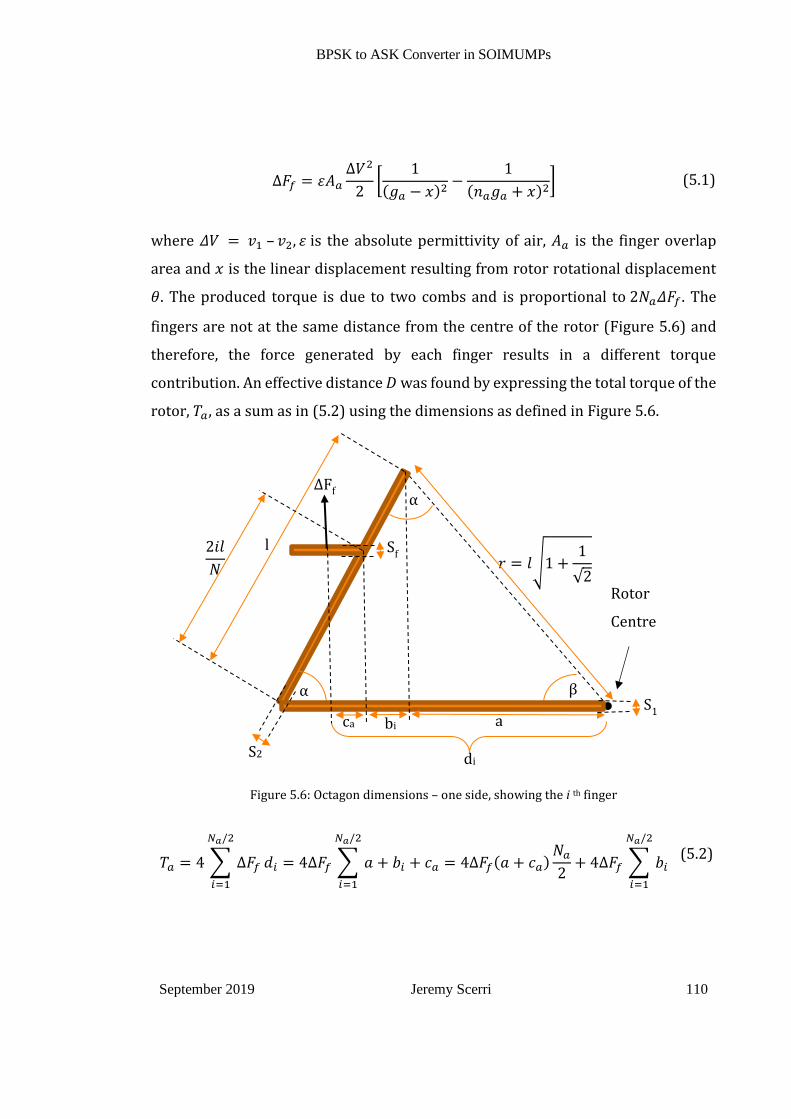
BPSK to ASK Converter in SOIMUMPs
September 2019 Jeremy Scerri 110
∆𝐹𝑓 = 휀𝐴𝑎∆𝑉2
2[
1
(𝑔𝑎 − 𝑥)2−
1
(𝑛𝑎𝑔𝑎 + 𝑥)2] (5.1)
where 𝛥𝑉 = 𝑣1 – 𝑣2, 휀 is the absolute permittivity of air, 𝐴𝑎 is the finger overlap
area and 𝑥 is the linear displacement resulting from rotor rotational displacement
𝜃. The produced torque is due to two combs and is proportional to 2𝑁𝑎𝛥𝐹𝑓 . The
fingers are not at the same distance from the centre of the rotor (Figure 5.6) and
therefore, the force generated by each finger results in a different torque
contribution. An effective distance 𝐷 was found by expressing the total torque of the
rotor, 𝑇𝑎, as a sum as in (5.2) using the dimensions as defined in Figure 5.6.
Figure 5.6: Octagon dimensions – one side, showing the i th finger
𝑇𝑎 = 4 ∑ ∆𝐹𝑓
𝑁𝑎/2
𝑖=1
𝑑𝑖 = 4∆𝐹𝑓 ∑ 𝑎+ 𝑏𝑖 + 𝑐𝑎
𝑁𝑎/2
𝑖=1
= 4∆𝐹𝑓(𝑎 + 𝑐𝑎)𝑁𝑎2+ 4∆𝐹𝑓 ∑ 𝑏𝑖
𝑁𝑎/2
𝑖=1
(5.2)
𝑟 = 𝑙√1 +1
√2
ca bi a
l 2𝑖𝑙
𝑁
α
di
α
β
S2
S1
Sf
ΔFf
Rotor
Centre

BPSK to ASK Converter in SOIMUMPs
September 2019 Jeremy Scerri 111
A closed form expression for the actuation torque, 𝑇𝑎, can be obtained by evaluating
the sum for 𝑏𝑖 in (5.2). This gives 𝑏𝑖 = 𝑙 𝑐𝑜𝑠𝛼 (𝑁𝑎 − 2𝑖)/𝑁𝑎 and substituting this in
(5.2) gives (5.3),
𝑇𝑎 = 2𝑁𝑎∆𝐹𝑓(𝑎 + 𝑐𝑎 +𝑙
2cos𝛼) (5.3)
with the resulting effective distance of 𝐷 = 𝑎 + 𝑐𝑎 +𝑙
2𝑐𝑜𝑠𝛼, where 𝛼 =
3𝜋
8 for an
octagon and 𝑐𝑎is half the finger length (Figure 5.6).
Two ∆𝑉 signals will be investigated, one for actuation with ASK and the other for
actuation with BPSK (shown in Figure 5.7). Actuation with ASK is achieved by letting
𝑣1 and 𝑣2 as in (5.4) and (5.5),
𝑣1 = 𝑉1 cos(𝜔𝑐𝑡) + 𝑘 (5.4)
𝑣2 = (1 − 𝑑(𝑡))𝑉2cos (𝜔𝑐𝑡 + 𝜙) (5.5)
where 𝜔𝑐 is the carrier angular frequency, 𝑘 is a DC shift on the carrier, 𝜙 is the
phase shift between the ASK signal and the carrier, 𝑉1 and 𝑉2 the respective
amplitudes and 𝑑(𝑡) ∈ [0,1] is the binary data. A more realistic definition for 𝑑(𝑡) is
as in (5.6), where 𝑡𝑑 = 1/𝑓𝑑 with 𝑓𝑑 being the data frequency in Hertz. This definition
removes the sharp transitions.
𝑑(𝑡) =
1 − 𝑒−𝑡5𝑡𝑑 0 ≤ 𝑡 < 𝑡𝑑/2
𝑒−𝑡5𝑡𝑑 𝑡𝑑/2 ≤ 𝑡 < 𝑡𝑑
𝑑(𝑡 − 𝑡𝑑) 𝑡 ≥ 𝑡𝑑
(5.6)
The actuation torque, 𝑇𝑎, can be determined by substituting (5.1) and (5.4) to (5.6)
in (5.3). For small displacements, 𝑥 ≪ 𝑔, 𝑇𝑎 is proportional to ∆𝑉2 and ignoring the
torque components generated at 𝜔𝑐 and above, the ASK torque would be as in (5.7).

BPSK to ASK Converter in SOIMUMPs
September 2019 Jeremy Scerri 112
𝑇𝐴𝑆𝐾 ∝ 𝑉1𝑉2(1 − 𝑑)𝑐𝑜𝑠𝜙 +𝑉12
2+ 𝑘2 +
(1 − 𝑑)2𝑉22
2 (5.7)
The torque component generated by a BPSK signal can be obtained by switching
(5.5) with (5.8).
𝑣2 = (2𝑑(𝑡) − 1)𝑉2cos (𝜔𝑐𝑡 + 𝜙) (5.8)
This results in (5.9).
𝑇𝐵𝑃𝑆𝐾 ∝ 𝑉1𝑉2(2𝑑 − 1)𝑐𝑜𝑠𝜙 +𝑉12
2+ 𝑘2 +
(2𝑑 − 1)2𝑉22
2 (5.9)
Figure 5.7: Schematic showing actuation with BPSK input
Figure 5.8 shows how 𝑇𝐴𝑆𝐾 and 𝑇𝐵𝑃𝑆𝐾 change with 𝑑 and 𝑘 for 𝜑 = 0 (dashed line)
and 𝜑 = 𝜋 (solid line) if 𝑉1 = 𝑉2. It is evident that the largest change in torque level
– 𝛥𝑇𝑎 – occurs with BPSK input when signal changes phase with respect to the
carrier, in this case, 𝛥𝑇𝐵𝑃𝑆𝐾 = 2𝑉22 (Nm). For ASK, 𝛥𝑇𝐴𝑆𝐾 = 0.5𝑉2
2 (Nm) for an in-
phase carrier and 𝛥𝑇𝐴𝑆𝐾 = 1.5𝑉22 (Nm) for an anti-phase carrier. Moreover, for ASK,

BPSK to ASK Converter in SOIMUMPs
September 2019 Jeremy Scerri 113
if no carrier is presented at 𝑣1 port giving 𝑣1 = 𝑘 (instead of (5.4)), the rotor is still
actuated but with a 𝛥𝑇𝐴𝑆𝐾 of 0.5𝑉22 (Nm).
Figure 5.8: Torque levels for ASK and BPSK, dashed lines are in-phase, solid in anti-phase
The electrical components 𝑅𝑖 and 𝐶𝑝 (shown dashed in Figure 5.7) are the isolation
resistance and the parasitic capacitance intrinsic in the MEMS device while 𝐿𝑚 and
𝑅𝑚 are external passive components whose relevance to the sensing test set-up is
discussed in Sections 5.4.6 and 5.4.7. Electrically, the same four passive components
(in parallel) are also connected to S2 - this is not shown in Figure 5.7.
5.4.2 Spring Stiffness
Two cantilever spring designs were considered, with the first one having an anchor
in the middle of the rotor as in Figure 5.9 left. This produced a linear relationship
between torque and displacement. The second design – the one adopted – was also
a cantilever spring, however, the anchor was outside of the rotor (Figure 5.9 right).
With this design, the cantilevers not only offered transverse stiffness but also axial

BPSK to ASK Converter in SOIMUMPs
September 2019 Jeremy Scerri 114
stiffness due to elongation. As a result, the torque-displacement characteristics are
non-linear as this spring has a cubic stiffness term. This offered more design
flexibility as is discussed in Section 5.4.6.
Figure 5.9: Linear (left) vs. Non-linear (right) spring designs
For the linear stiffness case, four octagon vertices were at mid-span of a four
clamped-clamped beam springs of length 2𝑟. In this case, the spring force generated
at mid-span of each beam is Tr/4r with 𝑇𝑟 being the restoring toque. Equation (5.10)
gives the deflection, x, at mid-span:
𝑥 = 𝑇𝑟𝑟2/96𝐸𝐼 (5.10)
where I = tw3/12 is the second moment of area of the spring rectangular section, E
the Young’s modulus and, w the spring width and beam depth, t, is fixed by the SOI
thickness. From (5.10), the rotational deflection θ of the rotor would be:
𝜃 = 𝑇𝑟/(4𝑘𝑟2) (5.11)
where k = 192EI / (2r)3 is the transverse stiffness of each clamped-clamped beam
and 4kr2 the resulting rotational linear stiffness.

BPSK to ASK Converter in SOIMUMPs
September 2019 Jeremy Scerri 115
Alternatively, a hardening spring, that is, a cubic stiffness term together with the
linear term for the total restoring torque is provided by the four springs as in Figure
5.9 (right) described by (5.12),
𝑇𝑟 = 𝑘𝑙𝜃 + 𝑘𝑐𝜃3 (5.12)
where 𝑘𝑙 and 𝑘𝑐 are the linear and cubic stiffness coefficients respectively. Design
optimization would require finding adequate ratios of 𝑘𝑙/𝑘𝑐 . In [153], an H-shaped
spring fixture as in Figure 5.10, was used to control the axial and transverse
stiffnesses, effectively controlling 𝑘𝑙/𝑘𝑐. This option was studied but was not
adopted as it was deducted that the range of 𝑘𝑙/𝑘𝑐 required could be achieved
without the H fixture.
Figure 5.10: H-Fixture that provides control on axial and transverse stiffness, [153]
The ratios for 𝑘𝑙/𝑘𝑐 have to be physically realizable and the alternative spring layout
that provides cubic stiffness is employed as shown in Figure 5.11. In this new layout,
each cantilever spring of length 𝑞 offers transverse stiffness 𝑘𝑡 = 12𝐸𝐼/𝑞3, however,
this layout offers also axial stiffness as the spring is prone to elongation apart from
bending. Hence, a component of axial stiffness 𝑘𝑎 = 𝐸(𝑡𝑤)/𝑞 contributes towards
rotor rotation and the resulting total torque is (5.13),
𝑇𝑟 = 4(𝑘𝑡𝑥 + 𝑘𝑎∆𝑞𝛾)𝑟 (5.13)
where ∆𝑞 is the spring elongation and 𝛾 is the angle subtended by the spring as
shown in Figure 5.11.

BPSK to ASK Converter in SOIMUMPs
September 2019 Jeremy Scerri 116
Figure 5.11: Cantilever spring showing transverse and axial displacements
Replacing linear with rotational displacement and ∆𝑞 with an approximation of
𝑟𝜃(𝑟𝜃/𝑞)2/2 (see Appendix 5.1) results in (5.14).
𝑇𝑟 = 4𝑘𝑡𝑟2𝜃 + (
2𝑘𝑎𝑟4
𝑞2)𝜃3 (5.14)
5.4.3 Static Equilibria and Pull-In
At equilibrium, 𝑇𝑎 = 𝑇𝑟, (5.15);
2𝑁𝑎∆𝐹𝑓𝐷 = 4𝑘𝑡(𝑟𝜃)𝑟 + 2𝑘𝑎(𝑟𝜃)3𝑟/𝑞2 (5.15)
Replacing 𝑟𝜃 with x, and ∆𝐹𝑓 with (5.1) results in (5.16);
4𝑘𝑡𝑥 +2𝑘𝑎𝑥
3
𝑞2− 휀𝐴𝑎𝑁𝑎 (
𝐷
𝑟)∆𝑉2 [
1
(𝑔𝑎 − 𝑥)2−
1
(𝑛𝑎𝑔𝑎 + 𝑥)2] = 0 (5.16)
Re-arranging this equation gives a polynomial of degree 7 with the coefficients given
in Table 5.3, where 𝑘𝑙𝑙 = 4𝑘𝑡 and 𝑘𝑐𝑙 = 2𝑘𝑎/𝑞2.
Stopper
Stopper
Stopper
Stopper

BPSK to ASK Converter in SOIMUMPs
September 2019 Jeremy Scerri 117
Table 5.3: Coefficients of the resulting degree 7 polynomial
Degree Coefficient
𝑥0 −𝑔𝑎2𝑝∆𝑉2(𝑛𝑎
2 − 1)
𝑥1 𝑔𝑎4𝑘𝑙𝑙𝑛𝑎
2 − 2𝑔𝑎휀𝐴𝑎𝑁𝑎 (𝐷
𝑟) (𝑛𝑎 + 1)∆𝑉
2
𝑥2 −2𝑔𝑎𝑘𝑙𝑙𝑛𝑎(𝑛𝑎 − 1)
𝑥3 𝑔𝑎2(𝑘𝑐𝑙𝑔𝑎
2𝑛𝑎2 + 𝑘𝑙𝑙(𝑛𝑎
2 − 4𝑛𝑎 + 1))
𝑥4 2𝑔𝑎(𝑛𝑎 − 1)(𝑘𝑙𝑙 − 𝑛𝑎𝑔𝑎2𝑘𝑐𝑙)
𝑥5 𝑘𝑐𝑙𝑔𝑎2(𝑛𝑎
2 − 4𝑛𝑎 + 1) + 𝑘𝑙𝑙
𝑥6 2𝑘𝑐𝑙𝑔𝑎(𝑛𝑎 − 1)
𝑥7 𝑘𝑐𝑙
The solution to this polynomial gives the stable and unstable equilibria – some being
physically inadmissible – for different actuation voltage ∆𝑉. Appendix 5.2 gives
MATLAB code for the stable solutions for varying 𝑛𝑎 and ∆𝑉.
It is worth noting how the pull-in position, 𝑥𝑝𝑖, changes with 𝑛𝑎. For a two-plate
electrostatic actuator, assuming linear spring behaviour, pull-in occurs when
𝑥𝑝𝑖 = 𝑔𝑎/3 if 𝑘𝑎 ≈ 0. In this design, each rotor finger is acted upon from two
opposite sides meaning there is interaction between two gaps. Intuitively, if 𝑛𝑎 ≫ 1,
𝑥𝑝𝑖 → 𝑔𝑎/3 as this would place one plate far away from the rotor finger. This implies
that for maximum travel 𝑛𝑎 should be large. On the contrary for 𝑛𝑎 → 1+,
𝑥𝑝𝑖 < 𝑔𝑎/3. Figure 5.17 shows how 𝑥𝑝𝑖 changes with gap multiplier 𝑛𝑎.
5.4.4 Mechanical Dynamics
Analysis of dynamics requires determination of rotor inertia and damping forces.
The rotor is octagonal in shape and a closed form expression of the inertia of one

BPSK to ASK Converter in SOIMUMPs
September 2019 Jeremy Scerri 118
side could be derived. With reference to Figure 5.6, each octagon side contains a
radial support beam of width S1, a side strut of width 𝑆2 and 𝑁/2 fingers of width 𝑆𝑓.
These three components have moment of inertia 𝐽1, 𝐽2, and 𝐽𝑓 , and masses 𝑚1, 𝑚2
and 𝑁𝑚𝑓/2 respectively. They are rotationally symmetric and contribute to the total
rotor inertia 𝐽 (5.17).
𝐽 = 8(𝐽1 + 𝐽2 + 𝐽𝑓) (5.17)
For the radial support beam, only half of the width needs be considered, that is, 𝑆1/2,
which gives 𝐽1 as in (5.18);
𝐽1 =1
12
𝑚1
2((𝑆12)2
+ 𝑟2) +𝑚1
2(𝑟
2)2
(5.18)
where the first term is inertia of a cube about the edge and the second term is due
to the parallel axis shift theorem. Similarly, for the side strut, 𝐽2 is as in (5.19).
𝐽2 =1
12𝑚2(𝑆2
2 + 𝑙2) + 𝑚2 (𝑟2 − (
𝑙
2)2
) (5.19)
The total inertia (5.20) of 𝑁/2 fingers is also found by summing the individual finger
inertias taking into consideration that each had a different amount of ‘shift’ from the
origin (Appendix 5.3),
𝐽𝑓 =(𝑁𝑎𝑚𝑓𝑎
+ 𝑁𝑠𝑚𝑓𝑠)
4𝑓(𝛽)[(𝑆𝑓2 + 4𝑐2
12)𝑓(𝛽) + 4(𝑎2 + 𝑐2 + 2𝑎𝑐)
+ 6(𝑎 + 𝑐)𝑙𝑐𝑜𝑠𝛼 +7𝑙2 cos2 𝛼
3]
(5.20)
where 𝑓(𝛽) =𝛽2
sin2(𝛽/2) and 2𝛼 + 𝛽 = 𝜋.
BPSK to ASK Converter in SOIMUMPs
September 2019 Jeremy Scerri 119
Having an analytical closed form expression for 𝐽, the resonant frequency 𝜔𝑛 for
small oscillations (such that cubic stiffness is negligible) could be evaluated with
(5.21).
𝜔𝑛 = √4𝑘𝑡𝑟2
𝐽=2𝑟
𝑞√𝐸𝑡𝑤3
𝐽 (5.21)
With the capacitive gaps that could be achieved in SOIMUMPs, mechanical damping
is dominated by squeeze film damping (SFD) [154], [155]. In this case, the gas is
forced to squeeze in and out of the space between fingers. This squeeze film effect is
much more important than intrinsic material damping. When the characteristic flow
lengths become small, such that they become comparable to the molecular mean
free path of the gas, the condition is called rarefied gas flow. As a measure of the
amount of rarefaction, the Knudsen number, which is a ratio of the molecular mean
free path 𝜆 to the characteristic length of the flow h is used, (5.22).
𝐾𝑛 =𝜆
ℎ (5.22)
Using this measure, for 𝐾𝑛 < 0.001 gas flows can be treated in the classical
framework of continuum fluid mechanics [154], that is, Reynolds equation with
no-slip boundary condition. In the range 0.001 < 𝐾𝑛 < 0.1, Reynolds equation is still
valid but slip boundary condition must be applied and for larger 𝐾𝑛, statistical
approaches are required. For SOIMUMPs with the smallest gap possible and at
normal temperature and pressure, 𝐾𝑛 = 0.033 meaning Reynolds equation is still
valid but flows need to be corrected for the slip at the walls. The simplest way of
achieving this is by replacing the viscosity, 𝜇, by an effective viscosity
𝜇𝑒𝑓𝑓 = 𝜇/(1 + 6𝐾𝑛) in the Reynolds equation [156]. This is subject to active
research and one can find several expressions for 𝜇𝑒𝑓𝑓, usually of the form
𝜇/(1 + 𝑓(𝐾𝑛)), [154] and [155]. One of the most recent expressions, which is able to

BPSK to ASK Converter in SOIMUMPs
September 2019 Jeremy Scerri 120
capture squeeze film damping behaviour even with high Knudsen numbers, is given
in [157]. It is reproduced here for convenience, (5.23) and (5.24),
𝜇𝑒𝑓𝑓 =𝜉
6Π𝜇 (5.23)
where 𝜉 = √𝜋/(2𝐾𝑛), which is sometimes referred to as the inverse Knudsen
number [158] and Π defined as in (5.24),
Π =𝜉
6+2 − 𝛼
√𝜋𝑙𝑛 (
1
𝜉+ 2.18) +
𝛼
0.642+(1 − 𝛼)(𝜉 + 2.395)
2 + 1.12𝛼𝜉−1.26 + 10𝛼𝜉
1 + 10.98𝜉
+𝑒−
𝜉5
8.77
(5.24)
with 𝛼 being the tangential momentum accommodation coefficient. In [158], it is
shown that this equation is not sensitive to the choice of 𝛼 if chosen in the region
0 ≤ 𝛼 ≤ 1.
In SFD, the damping force 𝐹𝑑 consists of two parts [125], [154]: the viscous and
elastic damping forces (5.25),
𝐹𝑑 = 𝑏𝑙 + 𝑏𝑘𝑧 (5.25)
where 𝑏𝑙 and 𝑏𝑘 are the coefficients for viscous and elastic damping forces
respectively and 𝑧 represents linear displacement. A dimensionless number that
compares these two damping mechanisms is called the squeeze number 𝜎 defined
as:
𝜎 =12𝜇𝑒𝑓𝑓𝜔𝐿
2
𝑝ℎ0 (5.26)
where 𝐿 is the characteristic length, ℎ0 is the distance between the parallel plates, 𝑝
and 𝜇𝑒𝑓𝑓 are the air pressure and dynamic viscosity respectively. There exists a
cut-off squeeze number, 𝜎𝑐 , (5.27) where the viscous and elastic damping forces are

BPSK to ASK Converter in SOIMUMPs
September 2019 Jeremy Scerri 121
equal. For 𝜎 < 𝜎𝑐, the viscous damping is dominant while for 𝜎 > 𝜎𝑐, the elastic
damping is dominant [125],
𝜎𝑐 = 𝜋2 [1 + (
𝑊
𝐿)2
] (5.27)
with 𝑊 being the plate width which for SOIMUMPs can be either 10 µm or 25 µm.
Equating 5.24 and 5.25, one gets the cut-off frequency as in (5.28).
𝜔𝑐𝑜 =𝜋2 [1 + (
𝑊𝐿 )
2
] ℎ02𝑝
12𝜇𝑒𝑓𝑓𝑊2
(5.28)
Considering NTP and the SOIMUMPs’ constraints, the lowest value for this cut-off
frequency would be 5.9 MHz (@ 𝑊 = 25 𝜇𝑚, 𝐿 = 100 𝜇𝑚 and ℎ0 = 2 𝜇𝑚). The data
rate dictates the mechanical bandwidth and the target is in the low kHz range as
discussed in Section 5.2. This means that operation will be well below the cut-off
frequency and hence the dominant SFD force is due to viscous damping only, that is,
𝑏𝑙. Expressions for 𝑏𝑙 for 𝜔 ≪ 𝜔𝑐𝑜 are given in [125] and [154], as in (5.29),
𝑏𝑙 = 𝜇𝑒𝑓𝑓𝐿 (𝑊
ℎ0)3
𝛽 (5.29)
where 𝛽 = 1 − 0.58(𝑊/𝐿) is a dimensionless factor related to the aspect ratio of the
plates. For a strip plate, that is, 𝑊 ≪ 𝐿, 𝛽 → 1. Adapting (5.38) to include the wider
(𝑛𝑔) and narrower (𝑔) gaps in both actuation and sensing combs gives the total
linear viscous damping coefficient in 𝑁𝑠/𝑚,
𝑏𝑇 = 2𝑁𝑎𝑙𝑜𝑎 [𝜇𝑒𝑓𝑓𝑎 (𝑡
𝑔𝑎)3
+𝜇𝑒𝑓𝑓𝑎𝑛 (𝑡
𝑛𝑎𝑔𝑎)3
] 𝛽𝑎
+ 2𝑁𝑠𝑙𝑜𝑠 [𝜇𝑒𝑓𝑓𝑠 (𝑡
𝑔𝑠)3
+𝜇𝑒𝑓𝑓𝑠𝑛 (𝑡
𝑛𝑠𝑔𝑠)3
] 𝛽𝑠
(5.30)

BPSK to ASK Converter in SOIMUMPs
September 2019 Jeremy Scerri 122
where the first bracketed term is the contribution from the actuation combs and the
second bracketed term from the sensing combs, 𝑙𝑜 is the rotor to stator comb finger
overlap length. The effective viscosity for the smaller actuation, larger actuation,
smaller sensing and larger sensing gaps, are denoted by 𝜇𝑒𝑓𝑓𝑎, 𝜇𝑒𝑓𝑓𝑎𝑛, 𝜇𝑒𝑓𝑓𝑠 and
𝜇𝑒𝑓𝑓𝑠𝑛 respectively. These are different since the Knudsen number depends on the
gaps. 𝛽𝑎 and 𝛽𝑠 are 1 − 0.58(𝑡/𝑙𝑜𝑎) and 1 − 0.58(𝑡/𝑙𝑜𝑠) respectively. If 𝑛 ≫ 1, the
contribution from the wider gaps can be neglected.
Equation (5.25) refers to linear displacement and forces. Transforming linear to
rotational motion and changing forces to torques in (5.25) gives the total rotational
viscous damping coefficient in 𝑁𝑚/𝑟𝑎𝑑 𝑠−1, (5.31).
𝑏 = 𝑟2𝑏𝑇 (5.31)
With equations (5.30) and (5.31), SFD behaviour can be captured and the
mechanical dynamic model can be developed (5.32).
𝐽 + 𝑏 + 4𝑘𝑡𝑟2𝜃 + (
2𝑘𝑎𝑟4
𝑞2)𝜃3 = 𝑇𝑎 (5.32)
For this application, the actuation torque, 𝑇𝑎, could be modelled with a step function.
For the resulting displacement to follow the step input as closely as possible, critical
damping is required, meaning a quality factor, 𝑄, of 0.5. For small oscillations and
neglecting the cubic stiffness, such a response can be achieved if 𝑏 = 𝑏𝑐𝑟 (5.33). The
settling time (5% criterion), 𝑡𝑠, would be as in (5.34) giving a maximum data rate of
𝑓𝑑 = 1/2𝑡𝑠 Hz.
𝑏𝑐𝑟 = 4√𝑘𝑡𝑟2𝐽 =4𝑟
𝑞√𝐸𝑡𝑤3𝐽 (5.33)
𝑡𝑠 ≈ 4(2𝐽
𝑏) (5.34)

BPSK to ASK Converter in SOIMUMPs
September 2019 Jeremy Scerri 123
A state space model for the mechanical system can be obtained by defining state
vector 𝒑 = [𝑥 ]𝑇 . Substituting 𝑥 for 𝑟𝜃 and 𝒑 in (5.32) results in (5.35).
=
[
𝑝2
−𝑏
𝐽𝑝2 −
4𝑘𝑡𝑟2
𝐽𝑝1 −
2𝑘𝑎𝑟2
𝑞2𝐽𝑝13 +
𝑁𝑎𝐷휀𝐴𝑎𝑟
𝐽∆𝑉2
(𝑛𝑎𝑔𝑎 + 𝑝1)2 − (𝑔𝑎 − 𝑝1)
2
((𝑔𝑎 − 𝑝1)(𝑛𝑎𝑔𝑎 + 𝑝1))2 ]
(5.35)
5.4.5 Actuation Capacitance and Instantaneous Power
The actuation capacitance per rotor finger, 𝐶𝑓𝑎(𝑥), is made up of the four
components shown in Figure 5.12, giving the total actuation capacitance 𝐶𝑎(𝑥) =
2𝑁𝑎𝐶𝑓𝑎(𝑥) = 2𝑁𝑎([𝐶𝑔(𝑥) + 𝐶𝑓𝑔(𝑥)] + [𝐶𝑛𝑔(𝑥) + 𝐶𝑓𝑛𝑔(𝑥)]).
Figure 5.12 Finger section showing electric field
In literature, many different formulae for computing fringing fields can be found. In
[159], the authors make a comparative exercise and propose an improved formula,
replicated here for convenience (5.36),
𝐶(𝑔) = 휀𝑡
𝑔[1 +
𝑔
𝜋𝑡+𝑔
𝜋𝑡𝑙𝑛 (
2𝜋𝑡
𝑔) +
𝑔
𝜋𝑡𝑙𝑛(1 +
2𝑆𝑓
𝑔+ 2√
𝑆𝑓
𝑔+𝑆𝑓2
𝑔2)] (5.36)
where t is the thickness of the finger, 𝑔 is the gap and 𝑆𝑓 is the finger width. This
gives the total capacitance, C, per unit length. Adapting this for both the smaller
and the larger gaps gives (5.37),

BPSK to ASK Converter in SOIMUMPs
September 2019 Jeremy Scerri 124
𝐶𝑎(𝑥) = 2𝑁𝑎𝐶𝑓𝑎(𝑥) = 2𝑁𝑎𝐶(𝑔𝑎 − 𝑥) + 𝐶(𝑛𝑎𝑔a + 𝑥)𝑙𝑜𝑎 (5.37)
where 𝑙𝑜𝑎is the finger overlap length.
With this capacitance model, the instantaneous actuating current, 𝑖𝑎(𝑡), flowing
from 𝑣2 to 𝑣1 could be obtained. This current is the sum flowing through 𝐶𝑎(𝑡) and
the isolation resistance, 𝑅𝑖, the resistance present between the two electrodes. This
is described with (5.38),
𝑖𝑎(t) =𝑑
𝑑𝑡(𝐶𝑎(t)∆𝑉(𝑡)) + ∆𝑉(𝑡)/𝑅𝑖 = [𝐶𝑎(t)∆(t) + ∆𝑉(𝑡)𝑎(𝑡)] + ∆𝑉(𝑡)/𝑅𝑖 (5.38)
from which, the instantaneous actuation power could be computed with (5.39).
𝑃𝑎(t) = 𝑖𝑎(t)∆𝑉(𝑡) (5.39)
Equation (5.38) can be combined in matrix form with (5.35) by defining another
state, 𝑝3 = 𝑖𝑎(𝑡), giving (5.40).
3 = 𝐶𝑎∆ + 𝑎∆𝑉 + ∆(2𝑎 + 1/𝑅𝑖) (5.40)
From (5.38), it can be seen that the absolute/nominal values for the actuation
capacitance and voltages are contributing to instantaneous power dissipation,
however, their rate of change is also a contributor.
Using the state space model (5.35) and 𝐶𝑎(𝑥) as in (5.37), a numerical solution to 𝑎
can be found.
5.4.6 Displacement Sensing and Complete System Model
The rotor is rotationally symmetric and the capacitance on the sensing combs varies
according to 𝑥(𝑡). The sensing comb finger layout is similar to the actuation comb
layout, however, a different gap 𝑔𝑠, gap multiplier 𝑛𝑠 and number of fingers 𝑁𝑠 are
defined. Hence, the actuation capacitance per rotor finger, 𝐶𝑓𝑎(𝑥, 𝑛𝑎 , 𝑔𝑎) in (5.37)

BPSK to ASK Converter in SOIMUMPs
September 2019 Jeremy Scerri 125
will be replaced with 𝐶𝑓𝑠(𝑥, 𝑛𝑠, 𝑔𝑠) for the sensing capacitance per rotor finger. The
total capacitance per sensor comb is expressed in (5.41),
𝐶𝑠1(𝑥) = 𝑁𝑠𝐶𝑓𝑠(𝑥) = 𝑁𝑠𝐶(𝑔𝑠 − 𝑥) + 𝐶(n𝑠𝑔𝑠 + 𝑥)𝑙𝑜𝑠 (5.41)
for the closing gap sensor, while the opening gap sensing capacitance would be
𝐶𝑆2(𝑥) = 𝐶𝑆1(−𝑥). From (5.36), an expression for the fringe capacitance only can
be extracted (5.42),
𝐶𝑓𝑟𝑖𝑛𝑔𝑒(𝑔) =휀
𝜋[1 + 𝑙𝑛 (
2𝜋𝑡
𝑔) + 𝑙𝑛(1 +
2𝑆𝑓
𝑔+ 2√
𝑆𝑓
𝑔+𝑆𝑓2
𝑔2)] 𝑙𝑜𝑠
(5.42)
from which the total fringe capacitance per rotor finger would be as in (5.43).
𝐶𝑓𝑟𝑖𝑛𝑔𝑒 = 𝐶𝑓𝑟𝑖𝑛𝑔𝑒(𝑔 − 𝑥) + 𝐶𝑓𝑟𝑖𝑛𝑔𝑒(𝑛𝑔 + 𝑥) (5.43)
Using (5.43), it can be shown (Appendix 5.4) that the fringe capacitances are a
substantial part of the overall capacitance for typical dimensions used in MEMS,
however, the change in fringe capacitances over the full range of motion
(0 < 𝑥 < 𝑔/3) is negligible (<3%). This means that a simpler equation can be used
to give a nominal (fixed) fringe capacitance, 𝐶𝑓𝑜, across the whole range of motion
by putting 𝑥 = 0 (5.44).
𝐶𝑓𝑟𝑖𝑛𝑔𝑒 ≈ C𝑓𝑜 = 𝐶𝑓𝑟𝑖𝑛𝑔𝑒(𝑔) + 𝐶𝑓𝑟𝑖𝑛𝑔𝑒(𝑛𝑔) (5.44)
This simplifies (5.41) to give (5.45). This simplification is of benefit for further
analysis and also for the optimisation process.
𝐶𝑠1(𝑥) = 𝑁𝑠휀𝑡𝑙𝑜𝑠 1
𝑛𝑠𝑔𝑠 + 𝑥+
1
𝑔𝑠 − 𝑥 + 𝐶𝑓𝑜 (5.45)
It is required that both 𝐶𝑠1(𝑥) and 𝐶𝑠2(𝑥) (= 𝐶𝑠1(−𝑥)) are monotonic over the full
range of motion. Hence, their respective minimum must not occur within
0 < 𝑥 < 𝑔𝑠/3. Using (5.45), this requires that 𝑛𝑠 > 5/3 (Appendix 5.5).

BPSK to ASK Converter in SOIMUMPs
September 2019 Jeremy Scerri 126
The change in sensing capacitive gap modulates the current, 𝑖𝑠(𝑡), passing through
it. Several methods could be employed to measure this current and in Figure 5.7, a
passive solution as a test set-up, is shown. This is the same ‘constant’ charge
approach adopted in Section 3.2 for the IQ mixer design with the difference that the
parasitic capacitance (cables and probes) is eliminated using an external inductor.
From this figure, the sensing capacitive reactance, 𝑋𝐶𝑠 , is in series with the total
impedance, 𝑍𝑇 , made up of four components in parallel. The output voltage 𝑣𝑝 is
obtained by potential division using 𝑋𝐶𝑠 and 𝑍𝑇 .
The impedance 𝑍𝑇 is made up of the isolation resistance, 𝑅𝑖, the probes/cabling
parasitic capacitance, 𝐶𝑝, an external inductor, 𝐿𝑚, intended to resonate (at 𝑓𝑐) with
the parasitic capacitance while 𝑅𝑚 is a resistive load. This load would dictate the
gain (potential division) and also the cut-off frequency of the resulting high-pass
filter.
The sensing current and the potential division setup (Figure 5.7) is described by
(5.46) or (5.47).
𝑖𝑠(t) =𝑑
𝑑𝑡(𝐶𝑠(𝑡)(𝑣1(𝑡) − 𝑣𝑝(𝑡))) (5.46)
𝑖𝑠(t) = 𝑝𝐶𝑝 +𝑅𝑚 + 𝑅𝑖𝑅𝑚𝑅𝑖
𝑣𝑝 +1
𝐿𝑚∫𝑣𝑝𝑑𝑡 (5.47)
Defining another 5 states as 𝑝4 = 𝜔𝑐𝑡, 𝑝5 = 𝜔𝑑𝑡, 𝑝6 = 𝑖𝑠, 𝑝7 = 𝑣𝑝 and 𝑝8 = 𝑝,
substituting these in (5.47) and combining them with (5.35) and (5.40), the
complete state space model for the system can be described by (5.48),
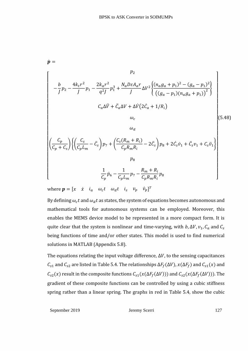
BPSK to ASK Converter in SOIMUMPs
September 2019 Jeremy Scerri 127
=
[
𝑝2
−𝑏
𝐽𝑝2 −
4𝑘𝑡𝑟2
𝐽𝑝1 −
2𝑘𝑎𝑟2
𝑞2𝐽𝑝13 +
𝑁𝑎𝐷휀𝐴𝑎𝑟
𝐽∆𝑉2
(𝑛𝑎𝑔𝑎 + 𝑝1)2 − (𝑔𝑎 − 𝑝1)
2
((𝑔𝑎 − 𝑝1)(𝑛𝑎𝑔𝑎 + 𝑝1))2
𝐶𝑎∆ + 𝑎∆𝑉 + ∆(2𝑎 + 1/𝑅𝑖)
𝜔𝑐
𝜔𝑑
(𝐶𝑝
𝐶𝑝 + 𝐶𝑠) (
𝐶𝑠𝐶𝑝𝐿𝑚
− 𝑠)𝑝7 + (𝐶𝑠(𝑅𝑚 + 𝑅𝑖)
𝐶𝑝𝑅𝑚𝑅𝑖− 2𝑠)𝑝8 + 2𝐶1 + 𝑠𝑣1 + 𝐶𝑠1
𝑝8
1
𝐶𝑝6 −
1
𝐶𝑝𝐿𝑚𝑝7 −
𝑅𝑚 + 𝑅𝑖𝐶𝑝𝑅𝑚𝑅𝑖
𝑝8]
(5.48)
where 𝒑 = [𝑥 𝑖𝑎 𝜔𝑐𝑡 𝜔𝑑𝑡 𝑖𝑠 𝑣𝑝 𝑝]𝑇
By defining 𝜔𝑐𝑡 and 𝜔𝑑𝑡 as states, the system of equations becomes autonomous and
mathematical tools for autonomous systems can be employed. Moreover, this
enables the MEMS device model to be represented in a more compact form. It is
quite clear that the system is nonlinear and time-varying, with 𝑏, ∆𝑉, 𝑣1, 𝐶𝑎 and 𝐶𝑠
being functions of time and/or other states. This model is used to find numerical
solutions in MATLAB (Appendix 5.8).
The equations relating the input voltage difference, ∆𝑉, to the sensing capacitances
𝐶𝑠1 and 𝐶𝑠2 are listed in Table 5.4. The relationships ∆𝐹𝑓(∆𝑉), 𝑥(∆𝐹𝑓) and 𝐶𝑠1(𝑥) and
𝐶𝑠2(𝑥) result in the composite functions 𝐶𝑠1(𝑥(∆𝐹𝑓(∆𝑉))) and 𝐶𝑠2(𝑥(∆𝐹𝑓(∆𝑉))). The
gradient of these composite functions can be controlled by using a cubic stiffness
spring rather than a linear spring. The graphs in red in Table 5.4, show the cubic

BPSK to ASK Converter in SOIMUMPs
September 2019 Jeremy Scerri 128
stiffness option. The reason for having a higher nonlinear behaviour for 𝐶𝑠1 than for
𝐶𝑠2 can be understood by observing that ∆𝐹𝑓(∆𝑉) has increasing positive gradient
like 𝐶𝑠1 while 𝐶𝑠2 has decreasing negative gradient for 𝑥 > 0.
Controlling the ratio of linear-to-cubic stiffness to linearise the gradient of the
composite relationship is dealt with in Section 5.5.2 which describes the process of
optimising the design parameters.
Table 5.4: Linear vs. Nonlinear Spring Stiffness and Overall linearity
Equation No. and Description Nature of relationship
Actuation voltage to Electrostatic
force
5.1: ∆𝐹𝑓(∆𝑉)
Electrostatic force to Linear
Tangential Displacement
5.11: 𝑥(∆𝐹𝑓) – linear stiffness
5.14: 𝑥(∆𝐹𝑓) – cubic stiffness
Linear Tangential Displacement
to Sensing Capacitances
5.45: 𝐶𝑠1(𝑥) and 𝐶𝑠2(𝑥) =
𝐶𝑠1(−𝑥)
∆𝐹𝑓
∆𝐹𝑓
∆𝐹𝑓
∆𝐹𝑓
𝑥
𝑥
𝑥
𝑥 𝐶𝑠1
𝐶𝑠1
𝐶𝑠1
𝐶𝑠1
∆𝑉
∆𝑉
∆𝑉
∆𝑉
∆𝐹𝑓
∆𝐹𝑓
∆𝐹𝑓
∆𝐹𝑓
𝐶𝑠2
𝑥

BPSK to ASK Converter in SOIMUMPs
September 2019 Jeremy Scerri 129
Composite Relationship
𝐶𝑠1(𝑥(∆𝐹𝑓(∆𝑉)))
Composite Relationship
𝐶𝑠2(𝑥(∆𝐹𝑓(∆𝑉)))
5.4.7 Output ASK Modulation Index and Fringe Capacitance
The modulation index 𝑀 is defined as the ratio of smallest to highest modulated
carrier amplitude. In this section the dependency of 𝑀 on sensing parameters is
determined. With reference to the schematic shown in Figure 5.7, when the
inductance, 𝐿𝑚 and parasitic capacitance 𝐶𝑝 resonate, their reactances cancel out;
when this happens, 𝑍𝑇 = 𝑅𝑇 , whose value would be primarily dictated by the load
resistor 𝑅𝑚 as the isolation resistance 𝑅𝑖 is typically very high. In the frequency
domain, the resulting transfer function would be as in(5.49).
𝑣𝑝
𝑣1=
𝑅𝑚𝑅𝑚 + 𝑗𝑋𝐶𝑠
(5.49)
The modulation index would then be;
𝑀 =|𝑣𝑝𝐴𝑣1|
|𝑣𝑝𝐵𝑣1|
⁄ = √𝑅𝑚2 + 𝑋𝐶𝑠𝐵
2
𝑅𝑚2 + 𝑋𝐶𝑠𝐴2 = √
𝑅𝑚2 + 𝑋𝐶𝑠𝐵2
𝑅𝑚2 + 𝑒2𝑋𝐶𝑠𝐵2 (5.50)

BPSK to ASK Converter in SOIMUMPs
September 2019 Jeremy Scerri 130
where the suffixes ‘A’ and ‘B’ here denote two different sensing gaps with ‘A’ being
the larger gap resulting in 𝑋𝐶𝑠𝐴 = 𝑒𝑋𝐶𝑠𝐵 or equivalently 𝐶𝑠𝐵 = 𝑒𝐶𝑠𝐴 where 𝑒 > 1.
For the case where 𝐶𝑠𝐴 is the nominal gap capacitance (𝑥 = 0) and 𝐶𝑠𝐵 is larger
(0 < 𝑥 <𝑔𝑠
3), using the simpler model for the sensing capacitance (5.45), 𝑒 would be
as in (5.51).
𝑒 =𝑁𝑠휀𝑡𝑙𝑜𝑠
1𝑛𝑠𝑔𝑠 + 𝑥
+1
𝑔𝑠 − 𝑥 + 𝐶𝑓𝑜
𝑁𝑠휀𝑡𝑙𝑜𝑠 1
𝑛𝑠𝑔𝑠+1𝑔𝑠 + 𝐶𝑓𝑜
(5.51)
Defining 𝐶𝑟 = 𝐶𝑓𝑜/ [ 𝑁𝑠휀𝑡𝑙𝑜𝑠 1
𝑛𝑠𝑔𝑠+
1
𝑔𝑠] and 𝑓 = 3𝑥/𝑔𝑠 for 0 < 𝑓 < 1, (5.52) is
obtained.
𝑒 =𝐶𝑟(𝑓
2 + 3𝑓(𝑛𝑠 − 1)) − 9𝑛𝑠(𝐶𝑟 + 1)
(𝑓 − 3)(𝐶𝑟 + 1)(𝑓 + 3𝑛𝑠)
(5.52)
Equation (5.52) gives 𝑒, which is unitless and is a function of 𝐶𝑟 , the ratio of fringe
capacitance to nominal capacitance, 𝑓 which is the displacement 𝑥 in terms of the
maximum, that is, 𝑥 = 𝑔𝑠/3 and also 𝑛𝑠. This equation together with (5.50) describe
how the selected design affects the modulation index - Figure 5.13.
Figure 5.13: Parameters affecting modulation index, M
increasing 𝐶𝑟
increasing 𝐶𝑟
increasing 𝐶𝑟
increasing 𝐶𝑟
𝐶𝑟
𝐶𝑟
𝐶𝑟
𝐶𝑟

BPSK to ASK Converter in SOIMUMPs
September 2019 Jeremy Scerri 131
The graphs in Figure 5.13 are asymptotic to 𝑀 = 2/3 for large 𝑛 and zero fringe
capacitance, which comes about from the maximum displacement allowable, 𝑥𝑝𝑖 (at
pull-in). Equations (5.52) and (5.50) are implemented in MATLAB script as given in
Appendix 5.6.
In this section, the relationships between the geometric parameters and the
underlying physical phenomena were presented in detail. As can be observed, there
is a large number of design variables whose effect on the required specifications is
very often contradictory and hence, a compromise is required. One parameter that
would need to be selected wisely is the gap multiplier 𝑛.
The following bulleted list gives some observations of the direct effect this
parameter has on some of the design requirements.
• 𝑛𝑎 ≫ 1 guarantees 𝑥𝑚𝑎𝑥 → 𝑔𝑎/3
• 𝑛𝑎 ≫ 1 keeps voltages low if and only if the number of fingers, 𝑁𝑎, is kept the
same. For the latter to be satisfied, a larger footprint is required which in turn
increases the inertia.
• For the same footprint, if 𝑛𝑎 or 𝑛𝑠 are increased, rotor would have less fingers
lowering the inertia 𝐽.
• If the inertia is kept the same and 𝑛𝑎 or 𝑛𝑠 are increased, viscous friction 𝑏
due to SFD decreases giving a longer settling time 𝑡𝑠.
• 𝑛𝑠 must be greater than 5/3 for monotonicity in sensing.
• Increasing 𝑛𝑠 improves the modulation index M.
5.5 Optimisation Towards the Design Objectives
The determination of the geometric dimensions that satisfied the design objectives
for such a complex structure required a computational approach which was carried
out in MATLAB. The first steps involved confirming that MATLAB functions which
modelled static behaviour were in fact accurate – when compared to FEA – over the
whole range of motion. In particular, functions that represented the electrostatic
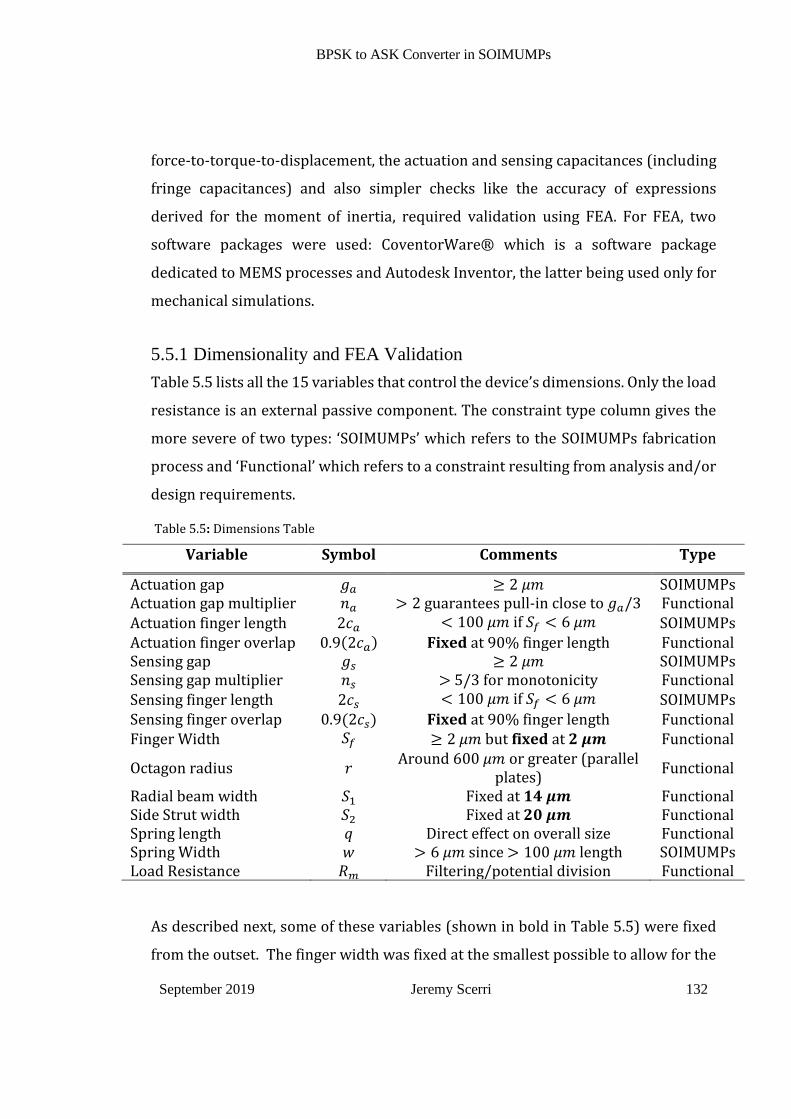
BPSK to ASK Converter in SOIMUMPs
September 2019 Jeremy Scerri 132
force-to-torque-to-displacement, the actuation and sensing capacitances (including
fringe capacitances) and also simpler checks like the accuracy of expressions
derived for the moment of inertia, required validation using FEA. For FEA, two
software packages were used: CoventorWare® which is a software package
dedicated to MEMS processes and Autodesk Inventor, the latter being used only for
mechanical simulations.
5.5.1 Dimensionality and FEA Validation
Table 5.5 lists all the 15 variables that control the device’s dimensions. Only the load
resistance is an external passive component. The constraint type column gives the
more severe of two types: ‘SOIMUMPs’ which refers to the SOIMUMPs fabrication
process and ‘Functional’ which refers to a constraint resulting from analysis and/or
design requirements.
Table 5.5: Dimensions Table
Variable Symbol Comments Type
Actuation gap 𝑔𝑎 ≥ 2 𝜇𝑚 SOIMUMPs Actuation gap multiplier 𝑛𝑎 > 2 guarantees pull-in close to 𝑔𝑎/3 Functional Actuation finger length 2𝑐𝑎 < 100 𝜇𝑚 if 𝑆𝑓 < 6 𝜇𝑚 SOIMUMPs Actuation finger overlap 0.9(2𝑐𝑎) Fixed at 90% finger length Functional Sensing gap 𝑔𝑠 ≥ 2 𝜇𝑚 SOIMUMPs Sensing gap multiplier 𝑛𝑠 > 5/3 for monotonicity Functional Sensing finger length 2𝑐𝑠 < 100 𝜇𝑚 if 𝑆𝑓 < 6 𝜇𝑚 SOIMUMPs Sensing finger overlap 0.9(2𝑐𝑠) Fixed at 90% finger length Functional Finger Width 𝑆𝑓 ≥ 2 𝜇𝑚 but fixed at 𝟐 𝝁𝒎 Functional
Octagon radius 𝑟 Around 600 𝜇𝑚 or greater (parallel
plates) Functional
Radial beam width 𝑆1 Fixed at 𝟏𝟒 𝝁𝒎 Functional Side Strut width 𝑆2 Fixed at 𝟐𝟎 𝝁𝒎 Functional Spring length 𝑞 Direct effect on overall size Functional Spring Width 𝑤 > 6 𝜇𝑚 since > 100 𝜇𝑚 length SOIMUMPs Load Resistance 𝑅𝑚 Filtering/potential division Functional
As described next, some of these variables (shown in bold in Table 5.5) were fixed
from the outset. The finger width was fixed at the smallest possible to allow for the

BPSK to ASK Converter in SOIMUMPs
September 2019 Jeremy Scerri 133
maximum capacitive area to be achieved. This capacitance could still be controlled
by the gap and gap multipliers. The octagon side and radial beam widths were fixed
such that no unwanted modes of vibration could manifest themselves. Fixing of
these variables served also the purpose of dimensionality reduction. In effect, the
optimisation problem was now reduced to a 10-dimensional one. From these ten
design parameters, only 𝑅𝑚, the load resistance, is an electrical parameter; the rest,
𝑔𝑎, 𝑛𝑎 , 𝑐𝑎, 𝑔𝑠, 𝑛𝑠 , 𝑐𝑠, 𝑟, 𝑞 and 𝑤 are all geometric in nature and they define the
converter geometry completely.
A 3D solid model of the rotor was designed using Autodesk Inventor employing
parametric dimensioning. Parametric dimensioning allowed for changes to be
affected quickly while respecting the required geometric constraints. This 3D model
was used to perform a corner simulation and to confirm the accuracy of the total
rotor inertia, J, the resonant frequency, 𝜔𝑛, force-to-rotational displacement, 𝜃(∆𝐹),
and the actuation and sensing capacitances 𝐶𝑎 and 𝐶𝑠 ((5.37) and (5.41))
relationships. The latter two relationships were subsequently evaluated in
CoventorWare® by applying 0 V at the stator combs and increasing rotor voltage
(in steps of 0.1 V) in a ‘MemElectro’ parametric study. The displacement and change
in capacitance were found to be in agreement with the solution to (5.16), (5.37) and
(5.41).
The change in fringe capacitance due to change in gap, up to pull-in, was also
confirmed to be negligible. Equation (5.16), which gives the equilibrium (stable and
unstable) position for different ∆𝑉, was solved numerically in MATLAB. It is a 7th
order polynomial and attention was given to extract only the stable solution up until
pull-in. The numerical solution obtained in MATLAB for pull-in was also validated
against FEA results for corner dimensions.
The damping coefficient equations (5.30) and (5.31) were tested for validity using
CoventorWare®. FEA simulations at NTP were performed which included SFD. The
tangential momentum accommodation coefficient, 𝛼, was taken at 0.6 [157] and the
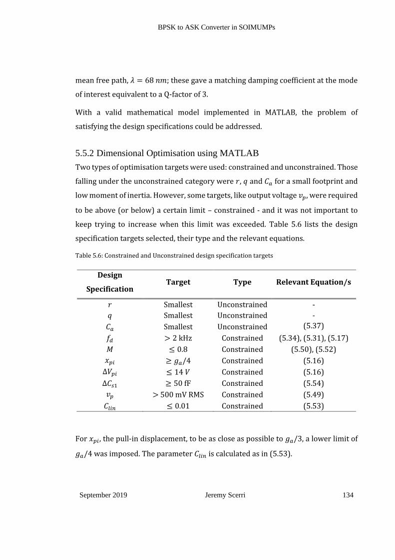
BPSK to ASK Converter in SOIMUMPs
September 2019 Jeremy Scerri 134
mean free path, 𝜆 = 68 𝑛𝑚; these gave a matching damping coefficient at the mode
of interest equivalent to a Q-factor of 3.
With a valid mathematical model implemented in MATLAB, the problem of
satisfying the design specifications could be addressed.
5.5.2 Dimensional Optimisation using MATLAB
Two types of optimisation targets were used: constrained and unconstrained. Those
falling under the unconstrained category were 𝑟, 𝑞 and 𝐶𝑎 for a small footprint and
low moment of inertia. However, some targets, like output voltage 𝑣𝑝, were required
to be above (or below) a certain limit – constrained - and it was not important to
keep trying to increase when this limit was exceeded. Table 5.6 lists the design
specification targets selected, their type and the relevant equations.
Table 5.6: Constrained and Unconstrained design specification targets
Design
Specification Target Type Relevant Equation/s
𝑟 Smallest Unconstrained -
𝑞 Smallest Unconstrained -
𝐶𝑎 Smallest Unconstrained (5.37) 𝑓𝑑 > 2 kHz Constrained (5.34), (5.31), (5.17)
𝑀 ≤ 0.8 Constrained (5.50), (5.52)
𝑥𝑝𝑖 ≥ 𝑔𝑎/4 Constrained (5.16)
Δ𝑉𝑝𝑖 ≤ 14 𝑉 Constrained (5.16)
∆𝐶𝑠1 ≥ 50 fF Constrained (5.54)
𝑣𝑝 > 500 mV RMS Constrained (5.49)
𝐶𝑙𝑖𝑛 ≤ 0.01 Constrained (5.53)
For 𝑥𝑝𝑖, the pull-in displacement, to be as close as possible to 𝑔𝑎/3, a lower limit of
𝑔𝑎/4 was imposed. The parameter 𝐶𝑙𝑖𝑛 is calculated as in (5.53).

BPSK to ASK Converter in SOIMUMPs
September 2019 Jeremy Scerri 135
𝐶𝑙𝑖𝑛 = 𝑠𝑡𝑑𝑒𝑣 (𝑑2𝐶𝑠𝑑∆𝑉2
)|∆𝑉>4
(5.53)
This is a measure of how far 𝐶𝑠(∆𝑉) is from perfect linearity for the range
4 < ∆𝑉 < ∆𝑉𝑝𝑖, where 𝑠𝑡𝑑𝑒𝑣 signifies standard deviation. If 𝐶𝑠(∆𝑉) is perfectly
linear, then 𝑑2𝐶𝑠
𝑑∆𝑉2= 0 giving 𝑠𝑡𝑑𝑒𝑣 (
𝑑2𝐶𝑠
𝑑∆𝑉2) = 0 as well. The inclusion of this design
specification was instrumental in finding the correct transverse to axial spring
stiffness ratios, hence, finding the correct nonlinear spring that improved overall
linearity. The carrier frequency for optimisation simulations was chosen at
𝑓𝑐 = 1 MHz.
Particle Swarm Optimization was adopted since it falls under the evolutionary
techniques which are more capable of solving multi-objective functions as described
in [160] and PSO gave positive results with minimum iterations in [151]. The PSO
routine was implemented in MATLAB (Appendix 5.7).
From Table 5.6, the objective function to be minimised is then the linear
combination:
𝑓(𝑔𝑎, 𝑛𝑎 , 𝑐𝑎, 𝑔𝑠, 𝑛𝑠 , 𝑐𝑠, 𝑟, 𝑞, 𝑤, 𝑅𝑚) = 𝑤1𝑟 + 𝑤2𝑞 + 𝑤3𝐶𝑎 + 𝑤𝑑∑0.5(𝐹𝑖 + 1)
7
𝑖=1
(5.54)
where [𝑤1 𝑤2 𝑤3 𝑤𝑑] are positive weights in proportion to the importance of each
individual variable. Equal importance is achieved with [𝑤1 𝑤2 𝑤3 𝑤𝑑] ≈
[1667 2183 5.5611 1]. These numbers, which give equal importance, scale the
optimisation surface equally and are determined by taking the reciprocal of the
expected value of each variable. The functions 𝐹𝑖 are listed in Table 5.7 where sgn
signifies the sign function and the ranges for design variables are listed in
Table 5.8.

BPSK to ASK Converter in SOIMUMPs
September 2019 Jeremy Scerri 136
Table 5.7: Constrained functions as targets for design specifications
Function Name Function
𝐹1 𝑠𝑔𝑛(2000 − 𝑓𝑑)
𝐹2 𝑠𝑔𝑛(𝑀 − 0.8)
𝐹3 𝑠𝑔𝑛(𝑔𝑎/4 − 𝑥𝑝𝑖)
𝐹4 𝑠𝑔𝑛(∆𝑉𝑝𝑖 − 14)
𝐹5 𝑠𝑔𝑛(50 × 10−15 − ∆𝐶𝑠1)
𝐹6 𝑠𝑔𝑛(0.5 − 𝑣𝑝)
𝐹7 𝑠𝑔𝑛(𝐶𝑙𝑖𝑛 − 0.01)
Table 5.8: Valid Ranges for design dimensions
Parameter Min Max
𝑔𝑎 2 𝜇𝑚 6 𝜇𝑚
𝑛𝑎 2 6
2𝑐𝑎 2*(30 𝜇𝑚) 2*(50 𝜇𝑚)
𝑔𝑠 2 𝜇𝑚 6 𝜇𝑚
𝑛𝑠 5/3 6
2𝑐𝑠 2*(30 𝜇𝑚) 2*(50 𝜇𝑚)
𝑟 500 𝜇𝑚 700 𝜇𝑚
𝑞 400 𝜇𝑚 500 𝜇𝑚
𝑤 6 𝜇𝑚 15 𝜇𝑚
𝑅𝑚 1 k Ω 1000 k Ω
Figure 5.14 presents a sample run. It shows how the objective function is minimised
in twenty iterations for a PSO run starting with approximately equal linear weights
and also gives the resulting geometric dimensions and resulting design specification
values. PSO has several controlling parameters with the most important being the
swarm size (100 particles were used), maximum number of iterations (set at 100),

BPSK to ASK Converter in SOIMUMPs
September 2019 Jeremy Scerri 137
inertia (ranged from 0.4 to 0.9) and acceleration factor (set at 2). Number of runs
was set to 5 and the best run would be given as output. The parallel processing
toolbox was not made use of and execution took around 10 minutes on an Intel i7-
3720QM CPU @ 2.6 GHz with 32 Gb of RAM. Appendix 5.7 provides the MATLAB
scripts.
By changing the objective function weights, several realisable solutions could be
found with the PSO technique. These PSO solutions were all valid however given that
the SOIMUMPs tolerances are of 0.25 𝜇𝑚 and the smallest allowable features are of
2 𝜇𝑚, it was imperative to select only PSO solutions that remained ‘optimal’ within
the whole tolerance range to guarantee a broadly optimal solution. Instead of
testing the acceptable solutions obtained from PSO, by performing a Monte Carlo
simulation, an alternative approach was used.
Figure 5.14: Sample run – PSO convergence, verbose and results
PSO solutions were tested for broad optimality by feeding PSO solutions to
MATLAB’s fmincon function with the ‘SQP’ option and using also the MultiStart
function. Essentially, this involved a second optimisation process that starts by
generating a uniformly distributed, random set of start points close

BPSK to ASK Converter in SOIMUMPs
September 2019 Jeremy Scerri 138
(< 10% change) to the optimal solution given by PSO. Those that always converged
on the same point were discarded indicating a ‘narrowly optimal case’.
Specifically, if the PSO stage gives a set, 𝑆, of 𝑛 satisfactory solutions, that is,
𝑆 = 𝑆1 𝑆2 𝑆3… 𝑆𝑛, uniformly distributed noise (±5%) is added to each of these
solutions to generate 𝑁 different starting points per solution. Hence, the sets of
initial points 𝐼 = 𝑆1𝑁 𝑆2𝑁 𝑆3𝑁 … 𝑆𝑛𝑁 are generated to be used for the
subsequent local search. Minimisation (using SQP) of the objective function is
performed starting from these different sets.
If a high percentage of runs from an initial point set, say 𝑆1𝑁, re-converge on 𝑆1, this
solution is considered ‘narrowly optimal solution’ and 𝑆1 is discarded. Figure 5.15
shows this concept in one-dimension. If the value of the objective function is highly
sensitive to changes in the dimension, a minor change in the dimension can easily
result in not satisfying the objective threshold. In this way, a PSO solution that was
broadly optimal within SOIMUMPs tolerances could be selected. The final
dimensions and resulting design targets selected for manufacturing are listed in
Table 5.9.
Figure 5.15: Narrow vs. broad optimality property

BPSK to ASK Converter in SOIMUMPs
September 2019 Jeremy Scerri 139
Table 5.9: The final dimensions (µm) and resulting design specifications
Final
Dimensions
𝒈𝒂 𝒏𝒂 𝒄𝒂 𝒈𝒔 𝒏𝒔 𝒄𝒔 𝒓 𝒒 𝒘 𝑹𝒎
2 3 50 2 3 50 598 458 9 700 kΩ
Final Design
Specifications
𝑪𝒂 𝒇𝒅 𝑴 𝒙𝒑𝒊 ∆𝑽𝒑𝒊 ∆𝑪𝒔𝟏 𝒗𝒑 𝑪𝒍𝒊𝒏
2.0 pF 3.3 kHz 0.77 0.32ga 11 V 250 fF 0.5 V 0.01
5.5.3 Design Validation using MATLAB
Further simulations were performed with the final dimensions both with FEA and
also in MATLAB (ode23s and ode15i solvers) to include dynamics (Appendix 5.8).
Figure 5.16 shows the dynamic response for actuation with BPSK. The BSPK signal,
𝑣2, and the carrier signal, 𝑣1 used are described in (5.55) and (5.56).
𝑣2 = 7.6𝑠𝑔𝑛(sin(2𝜋(3300𝑡)) cos (2𝜋(174000𝑡)) (5.55)
and
𝑣1 = 7.6cos (2𝜋(174000𝑡)) (5.56)
These voltage signals give an out of phase ∆𝑉 of 15.2 𝑉𝑝𝑘 (10.75 𝑉𝑟𝑚𝑠). Figure 5.16a
gives the resulting rotor displacement (solid line) for one cycle of 𝑓𝑑 . The dashed line
is ∆𝑉 for one cycle. BPSK and carrier are out of phase for the first 0.15 ms and
in-phase from 0.15 ms to 0.3 ms.
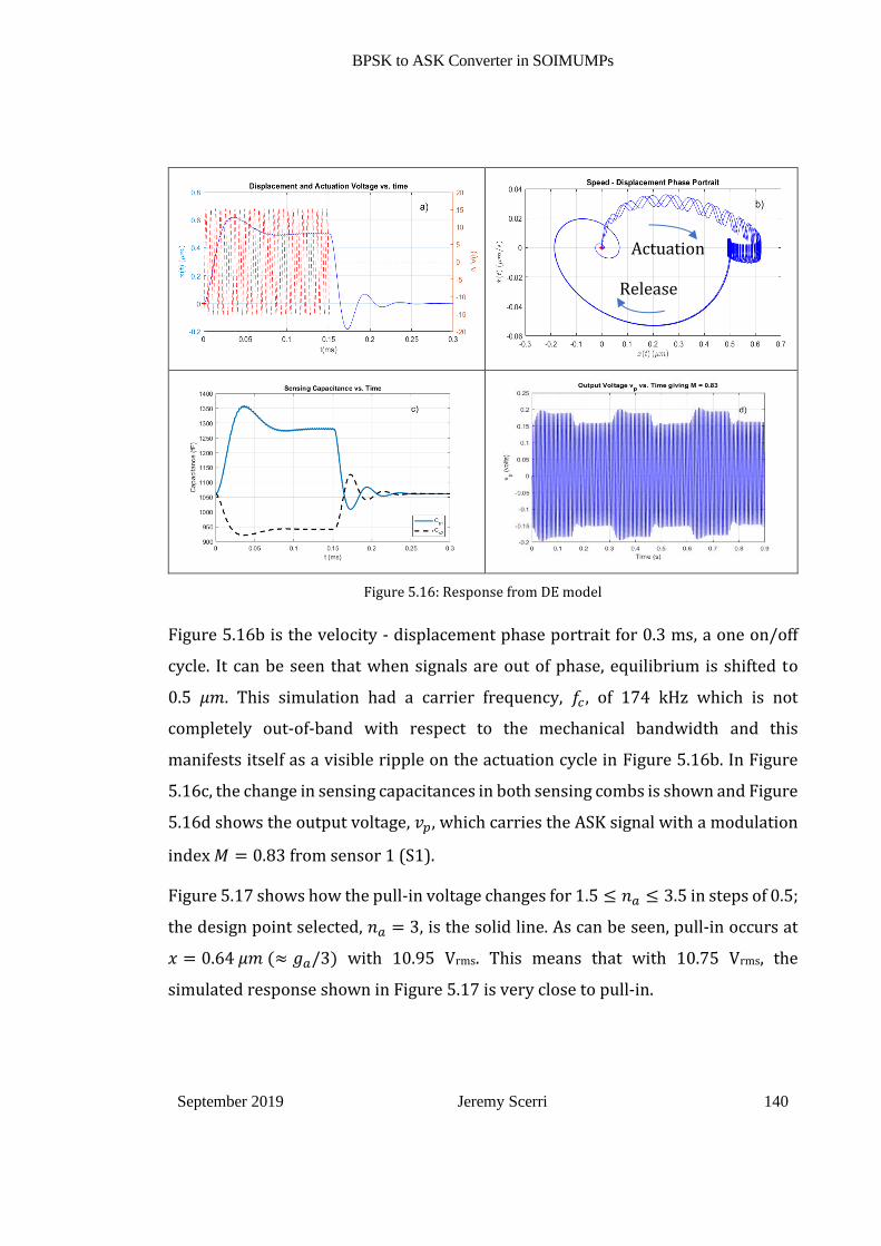
BPSK to ASK Converter in SOIMUMPs
September 2019 Jeremy Scerri 140
Figure 5.16: Response from DE model
Figure 5.16b is the velocity - displacement phase portrait for 0.3 ms, a one on/off
cycle. It can be seen that when signals are out of phase, equilibrium is shifted to
0.5 𝜇𝑚. This simulation had a carrier frequency, 𝑓𝑐 , of 174 kHz which is not
completely out-of-band with respect to the mechanical bandwidth and this
manifests itself as a visible ripple on the actuation cycle in Figure 5.16b. In Figure
5.16c, the change in sensing capacitances in both sensing combs is shown and Figure
5.16d shows the output voltage, 𝑣𝑝, which carries the ASK signal with a modulation
index 𝑀 = 0.83 from sensor 1 (S1).
Figure 5.17 shows how the pull-in voltage changes for 1.5 ≤ 𝑛𝑎 ≤ 3.5 in steps of 0.5;
the design point selected, 𝑛𝑎 = 3, is the solid line. As can be seen, pull-in occurs at
𝑥 = 0.64 𝜇𝑚 (≈ 𝑔𝑎/3) with 10.95 Vrms. This means that with 10.75 Vrms, the
simulated response shown in Figure 5.17 is very close to pull-in.
Actuation
Release

BPSK to ASK Converter in SOIMUMPs
September 2019 Jeremy Scerri 141
Figure 5.17: Displacement (until pull-in) vs. actuation voltage for increasing na
Figure 5.18a shows the complete SOI layer for one device with all the polysilicon
tracks for connections. Figure 5.18b shows the complete layout of the IC with each
IC having six devices. The bottom three devices had an alternative anchoring
solution which failed to release completely the rotor and could not be used.
Figure 5.18c is a close up of the rotor showing details of the gold layer which was
used to improve the conductivity of the polysilicon tracks. The trench etching can
also be seen in blue.
Increasing n
Increasing n
Pull-In Markers
Increasing n
Simulation at 10.75 Vrms
Increasing n

BPSK to ASK Converter in SOIMUMPs
September 2019 Jeremy Scerri 142
Figure 5.18: Final layout showing SOI layer and connections
Note: a) One device having total area of 2.9 mm2, b) The whole IC layout with 6 devices and c)
Close-up of one rotor
a) b) Top
Bottom
c)

BPSK to ASK Converter in SOIMUMPs
September 2019 Jeremy Scerri 143
5.6 Experimental Validation
The design made use of geometric features that are at the limits of the SOIMUMPs
process capabilities. The process constraints that limited reducing further the
power consumption and increasing further the data rate are related to the maximum
feature length and minimum feature size as given in Table 2.2 in the SOIMUMPs
handbook [24]. This constraint gives unlimited feature length for feature sizes
greater than 6 𝜇m while limiting the feature length to a maximum of 100 𝜇m for the
minimum feature size allowable of 2 𝜇m. Since finger lengths and widths were at
these limits and spring width was slightly greater than 6 𝜇m, it was imperative that
thorough visual inspection and dimensional measurements were performed. Actual
sizing of the device could be obtained from these measurements and simulation
response with these manufactured dimensions would be compared with
experimental response.
5.6.1 Geometric and Capacitive Measurements
The manufactured device was found to have two measurements which were at the
lowest of the process tolerance range. The finger widths were found to be smaller
than designed by 0.5 𝜇𝑚 having an average width of 1.5 𝜇𝑚. This resulted in larger
comb gaps at 2.5 𝜇𝑚 (larger by 25%) which gave 𝑛 = 2.6 (still > 5/3). The springs
cantilever width 𝑤 was also found smaller at 8.5 𝜇𝑚 instead of 9 𝜇𝑚.
The experimental setup is shown in Figure 5.19 and device microphotograph in
Figure 5.20, while Figure 5.21 and Figure 5.22 show scanning electron microscope
photographs with widths of cantilever spring and fingers respectively.

BPSK to ASK Converter in SOIMUMPs
September 2019 Jeremy Scerri 144
Figure 5.19: Experimental setup
MEMS Electrically Grounded Using
Carbon Tape S1 S2
v1
v2

BPSK to ASK Converter in SOIMUMPs
September 2019 Jeremy Scerri 145
Figure 5.20: Device microphotograph and laser profilometry on comb
Figure 5.21: SEM photograph showing cantilever spring width at 8.5 µm

BPSK to ASK Converter in SOIMUMPs
September 2019 Jeremy Scerri 146
Figure 5.22: SEM photograph showing comb gap of 2.55 µm
Table 5.10 shows the manufactured dimensions (shaded found different from
designed). The finger lengths (2𝑐𝑎, 2𝑐𝑠), octagon radius (𝑟) and spring length (𝑞)
were found to be as designed.
Table 5.10: The manufactured dimensions in (µm) – as measured
Manufactured
Dimensions
𝒈𝒂 𝒏𝒂 𝒄𝒂 𝒈𝒔 𝒏𝒔 𝒄𝒔 𝒓 𝒒 𝒘
2.5 2.6 50 2.5 2.6 50 598 458 8.5
Capacitance measurements were performed with an LCR meter (Agilent E4980A) at
2 MHz with 256-point averaging. Measurements were repeatable to within 1 fF.
Figure 5.23 gives the measured values of the three capacitances, one for actuation
𝐶𝑎 (between 𝑣1rotor comb and 𝑣2 stator combs), and the two for sensing,
𝐶𝑠1(between 𝑣1rotor comb and 𝑆1 stator comb) and 𝐶𝑠2(between 𝑣1rotor comb and
𝑆2 stator comb). It also shows the parasitics between the three stators which are
negligible.
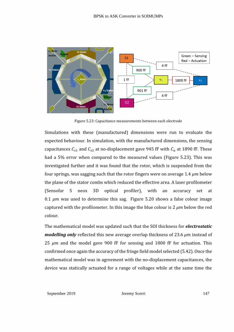
BPSK to ASK Converter in SOIMUMPs
September 2019 Jeremy Scerri 147
Figure 5.23: Capacitance measurements between each electrode
Simulations with these (manufactured) dimensions were run to evaluate the
expected behaviour. In simulation, with the manufactured dimensions, the sensing
capacitances 𝐶𝑠1 and 𝐶𝑠2 at no-displacement gave 945 fF with 𝐶𝑎 at 1890 fF. These
had a 5% error when compared to the measured values (Figure 5.23). This was
investigated further and it was found that the rotor, which is suspended from the
four springs, was sagging such that the rotor fingers were on average 1.4 𝜇𝑚 below
the plane of the stator combs which reduced the effective area. A laser profilometer
(Sensofar S neox 3D optical profiler), with an accuracy set at
0.1 𝜇𝑚 was used to determine this sag. Figure 5.20 shows a false colour image
captured with the profilometer. In this image the blue colour is 2 𝜇𝑚 below the red
colour.
The mathematical model was updated such that the SOI thickness for electrostatic
modelling only reflected this new average overlap thickness of 23.6 𝜇𝑚 instead of
25 𝜇𝑚 and the model gave 900 fF for sensing and 1800 fF for actuation. This
confirmed once again the accuracy of the fringe field model selected (5.42). Once the
mathematical model was in agreement with the no-displacement capacitances, the
device was statically actuated for a range of voltages while at the same time the

BPSK to ASK Converter in SOIMUMPs
September 2019 Jeremy Scerri 148
sensing capacitances were measured. These measurements are shown in
Figure 5.24.
Figure 5.24: Actual measurements vs. linear and cubic stiffness for CS1 and CS2.
Linearity, 𝐶𝑙𝑖𝑛, was still satisfactory at less than 0.01, however, the gradient of
𝐶𝑠(Δ𝑉) and consequently ∆𝐶𝑠1 was smaller due to the larger gaps.
With the actual dimensions, pull-in occurred at 13.00 V in simulation and at 13.78 V
in the lab. Figure 5.25 shows close-up on the sensing comb with optical microscope
under different actuation voltages with the one in Figure 5.25d being almost at
pull-in.
a) 0 volts: smaller gap = 2.5 𝜇𝑚
b) 4.6 volts: smaller gap = 2.3 𝜇𝑚

BPSK to ASK Converter in SOIMUMPs
September 2019 Jeremy Scerri 149
c) 9.2 volts: smaller gap = 2.0 𝜇𝑚
d) 13.7 volts: smaller gap = 1.7 𝜇𝑚
Figure 5.25: Optical microscope images showing comb gap change for increasing voltage
5.6.2 Transient and Modulation Index Measurements
As regards transient characteristics and the damping model adopted in simulation
(with the manufactured dimensions), a Q-factor of 3 was obtained. This agreed with
the transient characteristics observed in the lab (Figure 5.26a). The transient has a
settling time (2% criterion) of 150 𝜇𝑠. Figure 5.26b shows inputs 𝑣1 (the carrier
signal - (5.4)) in blue and 𝑣2 (the BPSK signal - (5.8)) in yellow transitioning on the
green digital signal. Their amplitudes are of 6 V, giving an effective peak when in
anti-phase of 12 V which in turn is equivalent to ∆𝑉𝑟𝑚𝑠 = 8.4 V. The optimal value
for load resistance, 𝑅𝑚, with the manufactured dimensions was found to be 1 MΩ in
simulation (larger than 700 kΩ -
Table 5.9) and this resistive load was adopted for experimentation. Figure 5.26c
shows the resulting output ASK signal, 𝑣𝑝, which signal shows the transient
(encircled) and has a modulation index, 𝑀, of 0.96. This transient/settling time
resulted in the possibility to convert at 3.3 kHz (6.6 kbps) and possibly higher.

BPSK to ASK Converter in SOIMUMPs
September 2019 Jeremy Scerri 150
Figure 5.26: Experimental measurement of transient and its superposition on output ASK
Figure 5.27a gives the simulated vs. lab measurements readings of the modulation
index for increasing actuation voltage ∆𝑉. There is a slight mismatch in modulation
index between simulations and experimental values at the higher voltage levels.
This is related to the mismatch in experimental and simulation pull-in voltage. The
last experimental point at pull-in (represented with a cross) could not be measured.
Figure 5.27b shows the output ASK signal from S1 having a modulation index
M = 0.96, for ∆𝑉𝑅𝑀𝑆 = 8.4 V at a data rate of 3.3 kHz (6.6 kbps) and a carrier
frequency 𝑓𝑐 of 174 kHz. An 𝐿𝑚 of 3.3 mH was used to mitigate the effect of the probe
and coaxial cable parasitic capacitances, 𝐶𝑝, of 260 pF. These resonate at the carrier
frequency of 174 kHz = 1/2𝜋√𝐿𝑚𝐶𝑝.

BPSK to ASK Converter in SOIMUMPs
September 2019 Jeremy Scerri 151
a) b)
Figure 5.27: a) Solid line is simulation, points are experimental b) ASK output signal for
∆𝑉𝑅𝑀𝑆 = 8.4 V - experimental
Table 5.11 gives the actual (as manufactured) specifications. When these are
compared to the design specifications achievable with the optimal dimensions
(
Table 5.9), it is clear that there is some degradation in performance due to the finger
and spring widths not being exactly as designed. Nonetheless, the manufactured
device’s specifications are still within the original design specifications (Table 5.6).
This is attributed to the optimisation refinement step that chose a solution that was
broadly optimal to minimise the sensitivity to manufacturing tolerances.
Table 5.11: The actual (as manufactured) device specifications
Device
Specifications
𝑪𝒂 𝒇𝒅 𝑴 𝒙𝒑𝒊 ∆𝑽𝒑𝒊 ∆𝑪𝒔𝟏 𝒗𝒑 𝑪𝒍𝒊𝒏
1.8 pF 3.3 kHz 0.79 0.32ga 13.78 V 50 fF 0.5 V 0.0098
A metric that can be used to evaluate the accuracy of the model would need to
capture both the static and dynamic characteristics that have a direct effect on the
design specifications. The cubic spring stiffness, the actuation and sensing
capacitances and their change upon rotor movement together with the fringe

BPSK to ASK Converter in SOIMUMPs
September 2019 Jeremy Scerri 152
capacitance have a direct effect on the modulation index, 𝑀. In view of this, 𝑀 was
chosen to form part of the fitness metric. The dynamics of the model have a direct
effect on the achievable data rate due to the settling time, 𝑡𝑠. On a physical level, this
depends on the damping and damping model adopted. Taking this into account, a
simple metric that is still capable of capturing the overall complex behaviour can be
defined as in (5.57),
𝐹 = √∑(𝑀𝑒𝑖−𝑀𝑠𝑖
)2 /𝑁 + 𝑌(𝑡𝑠𝑒 − 𝑡𝑠𝑠)
2𝑁
𝑖=1
(5.57)
where the suffixes ‘e’ and ‘s’ denote experimental and simulated respectively. The
first term is the summation of the ‘error squared’ in 𝑀 values shown in Figure 5.27a
(with N being the number of points) and the second term is the ‘error squared’ of
the settling time. For standardisation purposes (weighing), the correct value of 𝑌
would need to be ( 𝑡⁄ )2 ,that is, ratio of averages squared. This is a standardised
Euclidean distance metric, hence, the smaller, the better the accuracy of the model.
This metric was evaluated on the actual dimensions found on the prototype device
(Table 5.11) and gave a value of F = 0.0163 which indicates a very small error
between simulation and experimental results.
5.6.3 Device Power Consumption
The manufactured device’s power consumption was measured and compared with
simulation results. For simulation purposes, the total dissipative power was
obtained by adding the electrical average power calculated from (5.39) and the
mechanical average power by integrating the damping force term in (5.35).
The current going into the actuation combs, 𝑖𝑎, was measured using a
transimpedance amplifier (OP275GP op-amp) with a 100 kΩ feedback resistor, 𝑅𝑓 .
Readings for power consumption for different data rates at a carrier frequency of

BPSK to ASK Converter in SOIMUMPs
September 2019 Jeremy Scerri 153
174 kHz were taken and compared to results in simulation. The measurement setup
is shown in Figure 5.28.
Figure 5.28: Actuation current measurement setup
Figure 5.29: Current and power consumption for ∆𝑉𝑟𝑚𝑠 = 7.3 V and 𝑓𝑐 = 174 kHz.

BPSK to ASK Converter in SOIMUMPs
September 2019 Jeremy Scerri 154
Figure 5.30: Current and power consumption for ∆𝑉𝑟𝑚𝑠 = 13 V and 𝑓𝑐 = 174 kHz.
As can be seen in Figure 5.29 and Figure 5.30, for these experiments, data rates up
to 6 kHz (12 kbps) (above the design point of 3.3 kHz (6.6 kbps)) were tested. Going
beyond the 3.3 kHz meant that the mechanical dynamics would not have enough
time to reach the steady state. However, the output ASK signal was not compromised
completely and at high data rates (up to 12 kbps) the two output ASK levels could
still be easily distinguished even though the transient would not have completely
settled.
The mathematical model gives a linear relationship for data rates up to around
1.5 kHz (3 kbps) for both actuation voltages considered. Up to 1.5 kHz, when
∆𝑉𝑟𝑚𝑠= 7.3 V, the dissipative power follows a gradient of 373 nW/kHz and when
∆𝑉𝑟𝑚𝑠= 13 V, the dissipative power follows a gradient of 1200 nW/kHz. For both
levels of actuation voltage, the intercept of this linear section (at the lowest data
rate) is the power dissipated across the isolation resistance 𝑅𝑖. The dotted line in
cyan represents the power dissipated electrically in 𝑅𝑖; this power dissipation is
constant for all data rates. The black dotted line represents the power dissipated

BPSK to ASK Converter in SOIMUMPs
September 2019 Jeremy Scerri 155
due to mechanical damping. This increases as the data rate increases. if and only if
the displacement settles completely within the time of 1-bit.
In simulation, the total power dissipated was obtained by adding the electrical and
mechanical dissipation. The simulation total however, does not keep increasing at
the same rate of the solid black line which depicts the total power dissipation for the
linear case. This is because when the data rate exceeds 2 kHz, the settling time (2%
criterion) of the mechanical transient is less than the time of 1-bit. At around
𝑓𝑑 = 2 kHz, the data bit changes state before steady state is reached and for data rates
above this point, linearity starts to break down. This explains the deviation from
linearity (black solid line) of both the simulated (blue line) and the measured (red
asterisk) power dissipation.
This can be explored in more detail by looking at the velocity squared signal in
Figure 5.31 to Figure 5.33. In Figure 5.31 and Figure 5.32, mechanical displacement
settles completely in the time for 1-bit and proportionality in the mechanical power
dissipation (area per second) is maintained. However, at 6 kHz (Figure 5.33) the
input data rate is high and mechanical displacement does not settle within the time
for 1-bit, hence, giving a larger power dissipation albeit at a smaller rate of increase.
Figure 5.31: Velocity Squared Signal for a 0.5 kHz data rate and 13 V RMS actuation

BPSK to ASK Converter in SOIMUMPs
September 2019 Jeremy Scerri 156
Figure 5.32: Velocity Squared Signal for a 1.5 kHz data rate and 13 V RMS actuation
Figure 5.33: Velocity Squared Signal for a 6 kHz data rate and 13 V RMS actuation
Moreover, for 7.3 V < ∆𝑉𝑟𝑚𝑠 < 13 V, the power was also found to be linear with
∆𝑉𝑟𝑚𝑠 and hence the ratio of 100 nW/kHz/V of ∆𝑉𝑟𝑚𝑠 at 𝑓𝑐 = 174 kHz can describe
power consumption for data rates below 1.5 kHz (3 kbps). At higher data rates, up
to 6 kHz (12 kbps), this ratio is lower at around 64 nW/kHz/V.
Figure 5.34 shows oscilloscope signals for an actuation signal of ∆𝑉𝑟𝑚𝑠 = 7.3 V. The
data signal (data rate of 6 kbps) is shown in red for reference. The blue signal is the
current, 𝑖𝑎, while the green signal is the same 𝑖𝑎 averaged over several cycles. The

BPSK to ASK Converter in SOIMUMPs
September 2019 Jeremy Scerri 157
power signal is shown in purple. This signal has a non-zero average which gives the
total dissipative power of the converter.
Figure 5.34: The actuation current (blue), average current (green) and power (purple)
5.7 Conclusions
With this prototype, it was shown that a BPSK signal can be converted to an ASK
signal with a mechanical structure. Only two external electrical passive components
were required to obtain measurable signal levels: an inductor and a load resistor.
The mathematical model developed included several nonlinearities. The overall
static and dynamic behaviour of the mathematical model was tested in simulation
and validated with FEA results. The same mathematical model was used to find
dimensions that satisfied design constraints using a hybrid optimisation technique.
Actual measurements on the manufactured device were found to be in very good
agreement with the simulation results. This is attributed to the rigorous analysis
involving the nonlinear spring design and model, the inclusion of fringe capacitances
in the comb fingers and the estimation of the viscous damping coefficient that
included squeeze film effects with the effective viscosity.

BPSK to ASK Converter in SOIMUMPs
September 2019 Jeremy Scerri 158
The best (smallest) modulation index for the ASK output signal was of 0.79 (with
0.77 as designed). This was achieved with carrier and BPSK signals at 9.7 volts peak
(∆𝑉𝑟𝑚𝑠 = 13.78) and conversion was successful with data rates higher than the
design point of 𝑓𝑑 = 3.3 kHz (6.6 kbps), and carriers ranging from 100 kHz to 1 MHz.
At the design point, the power consumption follows the ratio of 64 nW/kHz/V of
∆𝑉𝑟𝑚𝑠 at 𝑓𝑐 = 174 kHz which gives 2.9 𝜇W for a data rate of 6.6 kbps at the best
modulation index. The device footprint is only 2.9 mm2. This is far smaller than the
device described in [93] which had an area of 49 mm2. However, in [93], both the
data rate and carrier frequencies where higher.

Conclusions and Further Work
September 2019 Jeremy Scerri 159
6. CONCLUSIONS AND
FURTHER WORK
Traditionally, device designers steer clear of nonlinear behaviour, however, recently
one can find several devices that make use of nonlinear dynamics that are under
development. In this work, the complexity of interactions between static and
dynamic nonlinear behaviour was modelled using DEs or more generally DAEs.
DAEs were shown to be able to capture all the required physical phenomena
together with the geometric relationships and process constraints.
In the presented designs, several nonlinear phenomena and interactions were
modelled. These included nonlinearities in the drive, sense, damping, fringe
capacitance and stiffness, all of which can be broadly categorised as either
external/field or geometric in nature.
Electrostatic differential drive and displacement sensing through differential
capacitance were two nonlinear phenomena that were exploited for the RF designs.
These provided successful demodulation/mixing and also spurious product
suppression. Mixing using electrostatics is well reported in literature. However,
making use of a differential drive on a torsional plate to suppress unwanted
frequency components and giving almost pure mixing without the use of filtering is
novel. This relaxes design constraints on the mechanical filtering aspect.
One nonlinearity that was exploited throughout all of the presented designs
(including the VEH) was the nonlinear spring stiffness.

Conclusions and Further Work
September 2019 Jeremy Scerri 160
6.1 Torsional Plate in MetalMUMPs
As investigated in Section 3.1, at low actuation voltages, the torsional vibratory plate
can be used as a filter and/or a mixer or even as a BPSK demodulator. Target
applications for such a device capable of performing BPSK demodulation would be
low-rate, wireless personal area networks (LR-WPANs) such as those described in
the IEEE 802.15.4 standard onto which the ZigBee standard is based. The designed
MEMS is able to mix the Radio Frequency (RF) and Local Oscillator (LO) signals
electrostatically and also filter this mixed signal prior to electrostatic sensing. The
use of a torsional vibration structure for BPSK demodulation is innovative. It was
demonstrated that this structure had an undamped resonant frequency of 2 MHz
and can successfully demodulate a low data rate BPSK signal with a carrier
frequency of 868 MHz and a chip rate of 300 kchips/s.
For higher actuation voltages (> 75 V), the device exhibits bistability and it has
potential for applications involving hardware random number generation (RNG) for
crypto systems [141] and also as chaotic carrier generators for secure
communications [142]. Although the response in this region is chaotic, it is not, as
defined in [132], extensively chaotic. As a result, the distribution in Figure 6.1 is not
uniform.
Figure 6.1 Time series and histogram for 468 kHz and Vdc =100 V
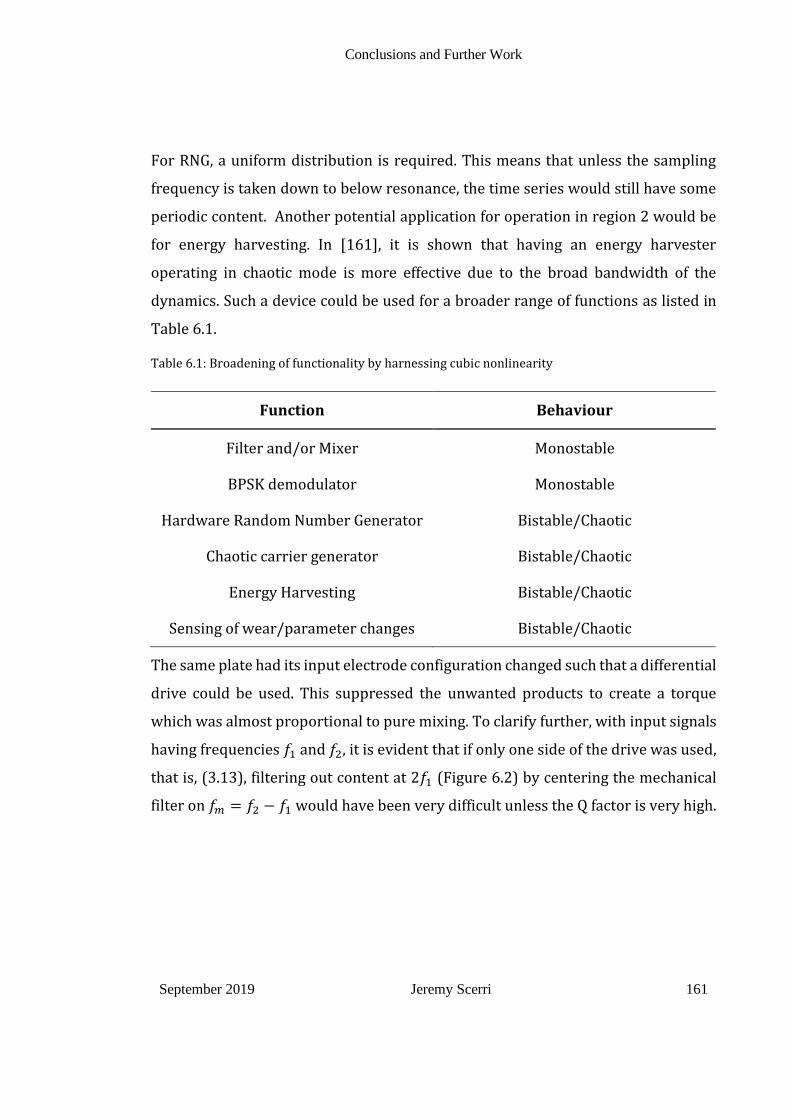
Conclusions and Further Work
September 2019 Jeremy Scerri 161
For RNG, a uniform distribution is required. This means that unless the sampling
frequency is taken down to below resonance, the time series would still have some
periodic content. Another potential application for operation in region 2 would be
for energy harvesting. In [161], it is shown that having an energy harvester
operating in chaotic mode is more effective due to the broad bandwidth of the
dynamics. Such a device could be used for a broader range of functions as listed in
Table 6.1.
Table 6.1: Broadening of functionality by harnessing cubic nonlinearity
Function Behaviour
Filter and/or Mixer Monostable
BPSK demodulator Monostable
Hardware Random Number Generator Bistable/Chaotic
Chaotic carrier generator Bistable/Chaotic
Energy Harvesting Bistable/Chaotic
Sensing of wear/parameter changes Bistable/Chaotic
The same plate had its input electrode configuration changed such that a differential
drive could be used. This suppressed the unwanted products to create a torque
which was almost proportional to pure mixing. To clarify further, with input signals
having frequencies 𝑓1 and 𝑓2, it is evident that if only one side of the drive was used,
that is, (3.13), filtering out content at 2𝑓1 (Figure 6.2) by centering the mechanical
filter on 𝑓𝑚 = 𝑓2 − 𝑓1 would have been very difficult unless the Q factor is very high.

Conclusions and Further Work
September 2019 Jeremy Scerri 162
Figure 6.2: Torque frequency components arising from the -v1 (dotted) and v1 (solid) pads.
Upon subtraction, the pairs in the dotted boxes cancel out, f2/f1 is at 3/10. Note that
when 3𝑓1 ≈ 𝑓2 the required content at 𝑓𝑚 = 𝑓2 − 𝑓1 ≈ 2𝑓1. In [133] and [135], the
electrostatic drive does not intrinsically cancel the content at 2𝑓1 and 2𝑓2. As a result,
in [133], the device had to be operated in vacuum to increase the Q factor to 786,
impinging negatively on the bandwidth and increasing costs. Another benefit of
having eliminated 2𝑓1 and 2𝑓2 before filtering is that ratios of 𝑓2/𝑓1 close to 1/3 can
be used as well. This means that for downconversion of an incoming RF signal at 𝑓2,
one needs only select 𝑓1 based upon 𝑓𝑟 = 𝑓𝑚 = 𝑓2 − 𝑓1, relaxing the constraint on
𝑓2/𝑓1.
The IQ mixer described in Section 3.2.3 took advantage of the differential drive and
spurious product suppression, as a result, the results add significant improvement
to the BPSK demodulator described in Section 3.1, in several ways:
a) The BPSK demodulator dealt only with coherent demodulation while the IQ
mixer is applicable for general QAM demodulation and does not require a
fixed phase difference.
b) By using a differential drive, the mechanical Q-factor-bandwidth constraint
was relaxed and as shown in Figure 6.2 provides flexibility in design choices.
c) Differential sensing was implemented on the same plate and hence the
possibility of having mismatch between the differential sensing pads was
minimised.

Conclusions and Further Work
September 2019 Jeremy Scerri 163
6.2 Buckling Spring for Broadband Vibrational Energy Harvester
The VEH designed in SINTEF made use of a buckling/bistable spring which required
a quintic stiffness model. It was shown that due to this nonlinear stiffness, the device
could be driven in the chaotic regime making it responsive to a broad range of base
excitation frequencies. In general, smaller VEHs result in higher resonant
frequencies, frequencies which are higher than what is naturally available as
excitation frequencies. However, with a bistable VEH, the structure was responsive
to low frequencies (simulated at 560 Hz), frequencies below resonance (1.06 kHz
and 1.5 kHz), making the MEMS VEH a viable option.
Simulations to verify broadband sensitivity were performed for a wide range of
excitation levels, frequencies and loads but this was always done whilst keeping
away from 𝑦𝑖𝑖 (the unstable equilibrium point) such that snap-through is avoided.
Confirming the validity when snap-through occurs is more challenging due to the
sensitivity to initial conditions and to the computationally intensive FEA simulations
required. Even though direct validation near the unstable equilibrium point were
not performed, confidence in the accuracy of the mathematical model was still
obtained since having modelled accurately the direction field in phase-space
(1 − 𝑦1), this model would be able to give reasonable predictions for trajectories
passing close to 𝑦𝑖𝑖.
Using this mathematical model, as implemented in MATLAB, both the 𝐹𝑠 − 𝑦1curve
(static) and the harmonic orbits are generated in seconds. For comparison, FEA
simulation to obtain the 𝐹𝑠 − 𝑦1curve took around 96 hours (on an 8–core, i7,
2.6 GHz machine with 32 Gb of RAM), and generated 60 Gb of data. On the same
machine, FEA simulation for a harmonic orbit close to a stable equilibrium point
takes around 2 hours. If the design requirements are changed, the FEA simulation
would require a full redesign and re-run while with this model, a whole range of
options can be simulated in seconds.

Conclusions and Further Work
September 2019 Jeremy Scerri 164
6.3 BPSK to ASK conversion in MEMS
In the final design involving the BPSK to ASK converter, the spring was designed to
have a controlled amount of axial stiffness and this, together with the transverse
component, also resulted in a net cubic stiffness spring. In this design, the cubic
stiffness was not introduced with particular dynamics in mind but it was used to
linearize the overall static response/gain characteristics related to the output ASK
modulation index. Although counter intuitive, linearizing the static behaviour using
a nonlinear spring was shown to be effective.
Although nonlinear design was shown to be of benefit, tackling all the
considerations inherent in device design, such as fabrication tolerances and design
robustness, was a challenge. This was overcome by having a mathematical model
with which the design optimisation process could be hastened. A MATLAB model
was also developed, validated with CoventorWare®’s FEA results and this enabled
the MATLAB model to be used to iterate through design improvements quickly.
In particular for this design, the mathematical model in MATLAB which had around
15 independent parameters and around 6 design constraints was run iteratively
using a hybrid PSO algorithm. The second step in the hybrid PSO technique sieved
through PSO solutions and gave one which was broadly optimal. This was
instrumental in manufacturing a device which was still functional even though it had
up to 25% error in some crucial dimensions.
Both the size and power consumption of the device make it a potential alternative
to BPSK-to-ASK CMOS realisations. All of the BPSK demodulators referenced in [88]
to [92], make use of a BPSK-to-ASK first stage and only one, [92], goes below a total
of 1 mW (631 𝜇W) of power consumption. Moreover, only [92] gives a breakdown
of the power consumption per stage and the authors report that the BPSK-to-ASK
stage consumed 204 𝜇W. This was tested at 10 Mb/s of data rate. The MEMS BPSK
to ASK converter is not able to reach these high data rates primarily due to the ‘large’
rotor inertia 𝐽 (equation (5.34)) and due to this limitation, it was tested at 6.6 kbps.

Conclusions and Further Work
September 2019 Jeremy Scerri 165
However, the power consumption is two orders of magnitude lower (2.9 𝜇W) than
what is reported in [92] and for IMD applications, that are only about transmitting
‘command data packages’ as opposed to applications that require high data rates
(visual prosthesis), a data rate of 6.6 kbps is adequate. In [2], (Section 12.5.3) it was
reported that recently typical power consumption per telemetry channel for
implantable systems with a 1 kHz bandwidth is about 1 to 5 𝜇W for advanced
implantable systems. These specifications are within the range achieved with the
MEMS BPSK-to-ASK converter.
As a result, the designed MEMS BPSK-to-ASK converter satisfies data rates required
for low data rate IMD applications with an attractive low power consumption. This
offers a new ‘all-MEMS’ avenue for system level designers.
6.4 Further Work
Although the torsional plate for BPSK demodulation was investigated using FEA
simulations, no attempt was performed to model damping using squeezed film
equations (considered for the BPSK to ASK converter). Having a complete analytical
model allows for easier and faster dimensional optimisation which can potentially
result in meeting better functional specifications.
When the torsional plate was used for IQ mixing with differential sensing, the IQ
mixer still required two devices, one for the in-phase and one for the quadrature
paths. Further investigation should be performed to find ways to minimise potential
mismatch between the two devices possibly by using different biasing resistors. To
gain more confidence in the dynamic operation of the IQ mixer further studies
involving higher actuation voltages should be performed (similar to Section 3.1.8)
such that the limits for linear stiffness for this size of plate is determined.
The IQ mixer took advantage of differential actuation such that the unwanted
products are suppressed before mechanical filtering and relaxing the Q factor-
bandwidth trade-off in the process. The parameter that is critical to the degree of
Conclusions and Further Work
September 2019 Jeremy Scerri 166
suppression is 𝑛 = 𝑑/𝑥𝑖 . Having a complete analytical model (including damping) for
the torsional plate will make it possible to optimise to minimise 𝑛.
The vibrational energy harvester made use of a buckling spring. The VEH spring is
intended to buckle at frequencies in the range of 0.5 kHz. An in-depth study into
fatigue failure should be performed such that the lifetime of such a device is
investigated and maximised.
The torsional plate device in MetalMUMPs and the VEH in SINTEF were not
fabricated and the models were only validated against FEA simulations; fabrication
and experimental validation should be performed.
The methodology adopted to design the BPSK-to-ASK converter made use of some
automation in the optimisation process, however, the degree of automation could
be increased. Obtaining a robust design for a relatively complex MEMS structure
with a moderate degree of automation was achieved with a hybrid optimisation
approach which tested for broad optimality. Robustness can be broadly defined as
the insensitivity of the solution to process variability. This was achieved by sieving
through PSO solutions by using MATLAB’s fmincon and Multistart functions (to
generate start points) and looking at whether this optimisation step led to a cluster
of solutions or not. If this second optimisation step gave a sparse solution set, then,
it meant that it is robust to process variation. The effectiveness of this hybrid
optimisation technique was confirmed when the manufactured device was found to
have critical dimensions that were up to 25% away from nominal, but the device’s
specifications were still satisfied. The first optimisation step involved the use of PSO
techniques and this was selected, as it was reported in literature, that it is adequate
for relatively complex MEMS structures. One feature of the PSO implementation that
made it easier to obtain ‘good’ solutions in ‘reasonable’ time was the distinction
between constrained and unconstrained optimisation targets.

Conclusions and Further Work
September 2019 Jeremy Scerri 167
Further work should involve the development of an interface between MATLAB and
3D modelling software such that the final solution could be verified with FEA
seamlessly.
As for the mathematical model, rotor sagging should be investigated and included
such that the correct resultant capacitive area is obtained. At the centre of the rotor,
a square shaped structure was designed to reinforce the four radial support beams.
These four beams together with the square shaped central structure had the
purpose of eliminating unwanted planar modes of vibration and also to shift the
vertical mode of vibration (Figure 6.3) away from the required mode’s resonant
point. The dimensions for the central part of the rotor were arrived at by trial and
error. Alternative topologies, for the central rotor design that satisfy the mode
shifting requirements for unwanted modes and to minimise rotor sagging, should
be investigated. The design (shown at bottom of Figure 5.18b) which has an anchor
in the centre of the rotor that failed to release completely between the substrate and
fingers (encircled in Figure 6.4), can be modified to eliminate this problem. This will
in turn eliminate rotor sagging and the unwanted vertical mode shown in Figure 6.3.
Figure 6.3: Rotor central weight design: Wanted mode (left) and Unwanted mode (right)

Conclusions and Further Work
September 2019 Jeremy Scerri 168
Figure 6.4: The design that failed to release anchor supports (encircled)
Alternative functionalities for this device should also be tested to include:
a. ASK detection and OOK to ASK conversion which is desirable for NFC-B
applications.
b. Phase Modulation to Amplitude modulation - analogue conversion.
c. Possible operation under vacuum which could also be used for frequency
shifting or mixing.
d. A QPSK to 4-level ASK, however this requires two devices and a quarter
wavelength delay line for phase discrimination.
An investigation into the possibility of improving the data rate and reducing the
power consumption should be performed by relaxing SOIMUMPs minimum feature
Conclusions and Further Work
September 2019 Jeremy Scerri 169
size constraints. This of course would require an alternative fabrication process.
However, such an investigation would give an understanding of how this device
would perform if scaled down. Particular attention would need to be given to
understand how damping phenomena change upon scaling such that the noise
boundary is determined.
As for sensing, the test set-up (inductor 𝐿𝑚 and load 𝑅𝑚, Figure 5.7) was only
intended to provide a way to measure the response with ease. For practical use,
a BPSK-to-ASK convertor would precede an ASK demodulator, hence, it would need
to be interfaced with an ASK demodulator circuit and therefore satisfy the ASK
demodulator input specifications.
The BPSK-to-ASK convertor was able to give ASK with modulation index as low as
0.79, output voltage level of 0.5 V RMS, data rates up to 12 kbps with carrier
frequencies up to 1 MHz. In literature, one can find ASK demodulators that accept
input signal levels as low as 0.25 V [162] and modulation index as high as 0.9 [163],
with footprints ranging from 0.16 mm2 [163] to 0.29 mm2 [164]. All literature
reviewed on ASK demodulators [162], [163], [164], [165], [166] and [167] describe
implementations that are able to work with carriers at 1 MHz or lower and could
handle a data rate of 12 kbps. This means that current ASK demodulators
specifications are in line with what the BPSK-to-ASK convertor provides as output
with the adopted test set-up.
In practice, the probes and coaxial cables used for testing, and which are responsible
for the large parasitic capacitance 𝐶𝑝 of 260 pF, will not be there. This would also
change the required inductance for resonance. With a smaller parasitic capacitance
(in the region of 10 fF), the carrier frequency could be increased into the GHz range
while requiring an inductor in the nH range for resonance to cancel the parasitics.
This would decrease the footprint of the inductor required and is favourable for the
output specifications of the BPSK-to-ASK converter.

References
September 2019 Jeremy Scerri 170
REFERENCES
[1] A. A. Batista, F. A. Oliveira, and H. N. Nazareno, “Duffing oscillators: Control
and memory effects,” Phys. Rev. E, vol. 77, no. 6, p. 066216, Jun. 2008.
[2] D. Uttamchandani, Handbook of MEMS for wireless and mobile applications.
Woodhead Pub, 2013.
[3] S. N. Ihtianov and A. Luque, Smart sensors and MEMS, I ntelligent devices and
microsystems for industrial applications. Woodhead Publishing Limited, 2014.
[4] M. A. Hannan, S. M. Abbas, S. A. Samad, and A. Hussain, “Modulation techniques
for biomedical implanted devices and their challenges.,” Sensors (Basel)., vol.
12, no. 1, pp. 297–319, 2012.
[5] M. Hautefeuille, B. O’Flynn, F. H. Peters, and C. O’Mahony, “Development of a
Microelectromechanical System (MEMS)-Based Multisensor Platform for
Environmental Monitoring,” Micromachines, vol. 2, no. 4, pp. 410–430, Nov.
2011.
[6] “SiTime, Silicon MEMS Oscillators and Clock Generators | SiTime.” [Online].
Available: https://www.sitime.com/. [Accessed: 07-Jun-2019].
[7] C. Sciences and B. Sensor, “Micro Electromechanical Filters for Signal
Processing,” 1992.
[8] C. T. Nguyen and D. Mto, “RF MEMS in Wireless Architectures,” pp. 416–420,
2005.
[9] H. Wan-Thai, “RF MEMS Experience Growing Popularity.” Wireless Systems
Design, 2003.
[10] M. Chapman, “The Impact of MEMS on Cellular Phone Architectures.”
Microwave Journal, 2006.

References
September 2019 Jeremy Scerri 171
[11] K. Rawat and M. S. Hashmi, “Dual-Band RF Circuits and Components for Multi-
Standard Software Defined Radios,” no. February, 2012.
[12] A. S. Hussaini, R. Abd-Alhameed, and J. Rodriguez, “Tunable RF filters: Survey
and beyond,” 2011 18th IEEE Int. Conf. Electron. Circuits, Syst. ICECS 2011, pp.
512–515, 2011.
[13] J. Scerri, I. Grech, E. Gatt, and O. Casha, “A MEMS BPSK Demodulator,” vol. 1,
no. Figure 1, pp. 0–3.
[14] J. Scerri, I. Grech, E. Gatt, and O. Casha, “Suppression of spurious products in
an electrostatic RF MEMS downconverter having differential drive and sense,”
pp. 2–5.
[15] M. M. Mixlers, A. Wong, C. T. Nguyen, and S. Member, “Micromechanical Mixer-
Filters (‘Mixlers’),” vol. 13, no. 1, pp. 100–112, 2004.
[16] J. Iannacci, “Microsystem based Energy Harvesting (EH-MEMS): Powering
pervasivity of the Internet of Things (IoT) – A review with focus on
mechanical vibrations,” J. King Saud Univ. - Sci., Jun. 2017.
[17] L. Tang, Y. Yang, and C. K. Soh, “Toward Broadband Vibration-based Energy
Harvesting,” J. Intell. Mater. Syst. Struct., vol. 21, no. 18, pp. 1867–1897, Dec.
2010.
[18] J. Twiefel and H. Westermann, “Survey on broadband techniques for vibration
energy harvesting,” J. Intell. Mater. Syst. Struct., vol. 24, no. 11, pp. 1291–1302,
Jul. 2013.
[19] B. B. Cherry, L. L. Howell, and B. D. Jensen, “Evaluating three-dimensional
effects on the behavior of compliant bistable micromechanisms,” J.
Micromechanics Microengineering, vol. 18, p. 095001, 2008.
[20] N. Elvin and A. Erturk, Advances in energy harvesting methods, vol.
9781461457. 2013.

References
September 2019 Jeremy Scerri 172
[21] Y. S. Oh and S. Kota, “Synthesis of multistable equilibrium compliant
mechanisms using combinations of bistable mechanisms,” J. Mech. Des., vol.
131, no. 2, p. 021002, 2009.
[22] A. Cowen and B. Dudley, “MetalMUMPs design handbook,” MEMSCAP Inc., …,
2013.
[23] “SINTEF piezoMEMS.” [Online]. Available:
https://www.sintef.no/projectweb/piezomems/. [Accessed: 21-Jan-2019].
[24] K. Miller, A. Cowen, G. Hames, and B. Hardy, “SOIMUMPs design handbook,”
MEMScAP Inc., Durham, pp. 0–25, 2004.
[25] H. G. Schuster and Wiley InterScience (Online service), Reviews of nonlinear
dynamics and complexity. Wiley-VCH, 2008.
[26] J. F. Rhoads, S. W. Shaw, and K. L. Turner, “Nonlinear Dynamics and Its
Applications in Micro-and Nanoresonators,” 2010.
[27] L. R. Carley et al., “Single-chip computers with microelectromechanical
systems-based magnetic memory (invited),” J. Appl. Phys., vol. 87, no. 9, p.
6680, Apr. 2000.
[28] S. G. Adams, F. Bertsch, and N. C. MacDonald, “Independent tuning of the linear
and nonlinear stiffness coefficients of a micromechanical device,” in
Proceedings of Ninth International Workshop on Micro Electromechanical
Systems, pp. 32–37.
[29] H. Zhou, K. K. Tan, and T. H. Lee, “Micro-positioning of linear piezoelectric
motors based on a learning nonlinear PID controller,” in Proceedings of the
39th IEEE Conference on Decision and Control (Cat. No.00CH37187), vol. 1, pp.
913–918.
[30] J. Bienstman, R. Puers, and J. Vandewalle, “Periodic and chaotic behaviour of
the autonomous impact resonator,” in Proceedings MEMS 98. IEEE. Eleventh

References
September 2019 Jeremy Scerri 173
Annual International Workshop on Micro Electro Mechanical Systems. An
Investigation of Micro Structures, Sensors, Actuators, Machines and Systems
(Cat. No.98CH36176), pp. 562–567.
[31] M. S-C Lu, G. K. Fedder, and S. Member, “Position Control of Parallel-Plate
Microactuators for Probe-Based Data Storage,” J.
MICROELECTROMECHANICAL Syst., vol. 13, no. 5, p. 759, 2004.
[32] Y. C. Wang, S. G. Adams, J. S. Thorp, N. C. MacDonald, P. Hartwell, and F. Bertsch,
“Chaos in MEMS, parameter estimation and its potential application,” IEEE
Trans. Circuits Syst. I Fundam. Theory Appl., vol. 45, no. 10, pp. 1013–1020,
1998.
[33] E. Buks and M. L. Roukes, “Metastability and the Casimir effect in
micromechanical systems,” Europhys. Lett., vol. 54, no. 2, pp. 220–226, Apr.
2001.
[34] Yi-Kuen Lee, J. Deval, P. Tabeling, and Chih-Ming Ho, “Chaotic mixing in
electrokinetically and pressure driven micro flows,” in Technical Digest.
MEMS 2001. 14th IEEE International Conference on Micro Electro Mechanical
Systems (Cat. No.01CH37090), pp. 483–486.
[35] I. Peterson, Newton’s clock : chaos in the solar system. W.H. Freeman and Co,
1993.
[36] L. E. N, “Deterministic Nonperiodic Flow,” J. Atmos. Sci., vol. 20, p. 130, 1963.
[37] J. Gleick, Chaos : making a new science. Penguin, 1988.
[38] H. W. C. Postma, I. Kozinsky, A. Husain, and M. L. Roukes, “Dynamic range of
nanotube- and nanowire-based electromechanical systems,” Appl. Phys. Lett.,
vol. 86, no. 22, p. 223105, May 2005.
[39] A. Erbe, H. Krömmer, A. Kraus, R. H. Blick, G. Corso, and K. Richter, “Mechanical
mixing in nonlinear nanomechanical resonators,” Appl. Phys. Lett., vol. 77, no.

References
September 2019 Jeremy Scerri 174
19, p. 3102, Nov. 2000.
[40] M. C. Cross, A. Zumdieck, R. Lifshitz, and J. L. Rogers, “Synchronization by
Nonlinear Frequency Pulling,” Phys. Rev. Lett., vol. 93, no. 22, p. 224101, Nov.
2004.
[41] R. Almog, S. Zaitsev, O. Shtempluck, and E. Buks, “High intermodulation gain
in a micromechanical Duffing resonator,” Appl. Phys. Lett., vol. 88, no. 21, p.
213509, May 2006.
[42] D. Rugar and P. Grütter, “Mechanical parametric amplification and
thermomechanical noise squeezing,” Phys. Rev. Lett., vol. 67, no. 6, pp. 699–
702, Aug. 1991.
[43] A. N. Cleland, “Thermomechanical noise limits on parametric sensing with
nanomechanical resonators,” New J. Phys., vol. 7, no. 1, pp. 235–235, Nov.
2005.
[44] M.-F. Yu, G. J. Wagner, R. S. Ruoff, and M. J. Dyer, “Realization of parametric
resonances in a nanowire mechanical system with nanomanipulation inside a
scanning electron microscope,” Phys. Rev. B, vol. 66, no. 7, p. 073406, Aug.
2002.
[45] D. S. Greywall, B. Yurke, P. A. Busch, A. N. Pargellis, and R. L. Willett, “Evading
amplifier noise in nonlinear oscillators,” Phys. Rev. Lett., vol. 72, no. 19, pp.
2992–2995, May 1994.
[46] B. Yurke, D. S. Greywall, A. N. Pargellis, and P. A. Busch, “Theory of amplifier-
noise evasion in an oscillator employing a nonlinear resonator,” Phys. Rev. A,
vol. 51, no. 5, pp. 4211–4229, May 1995.
[47] R. Almog, S. Zaitsev, O. Shtempluck, and E. Buks, “Noise Squeezing in a
Nanomechanical Duffing Resonator,” Phys. Rev. Lett., vol. 98, no. 7, p. 078103,
Feb. 2007.

References
September 2019 Jeremy Scerri 175
[48] E. Buks and B. Yurke, “Mass detection with a nonlinear nanomechanical
resonator,” Phys. Rev. E, vol. 74, no. 4, p. 046619, Oct. 2006.
[49] M. Zalalutdinov et al., “Autoparametric optical drive for micromechanical
oscillators,” Appl. Phys. Lett., vol. 79, no. 5, pp. 695–697, Jul. 2001.
[50] B. VAN DER POL and J. VAN DER MARK, “Frequency Demultiplication,” Nature,
vol. 120, no. 3019, pp. 363–364, Sep. 1927.
[51] G. Gabrielse, H. Dehmelt, and W. Kells, “Observation of a Relativistic, Bistable
Hysteresis in the Cyclotron Motion of a Single Electron,” Phys. Rev. Lett., vol.
54, no. 6, pp. 537–539, Feb. 1985.
[52] C. Stambaugh and H. B. Chan, “Noise-activated switching in a driven nonlinear
micromechanical oscillator,” Phys. Rev. B, vol. 73, no. 17, p. 172302, May 2006.
[53] J. S. Aldridge and A. N. Cleland, “Noise-Enabled Precision Measurements of a
Duffing Nanomechanical Resonator,” Phys. Rev. Lett., vol. 94, no. 15, p. 156403,
Apr. 2005.
[54] I. Kozinsky, H. W. C. Postma, O. Kogan, A. Husain, and M. L. Roukes, “Basins of
Attraction of a Nonlinear Nanomechanical Resonator,” Phys. Rev. Lett., vol. 99,
no. 20, p. 207201, Nov. 2007.
[55] S. K. De and N. R. Aluru, “Complex Oscillations and Chaos in Electrostatic
Microelectromechanical Systems under Superharmonic Excitations,” Phys.
Rev. Lett., vol. 94, no. 20, p. 204101, May 2005.
[56] S. K. De and N. R. Aluru, “Complex Nonlinear Oscillations in Electrostatically
Actuated Microstructures,” J. MICROELECTROMECHANICAL Syst., vol. 15, no.
2, p. 355, 2006.
[57] D. G. Fertis, Nonlinear mechanics. CRC Press, 1999.
[58] A. H. Nayfeh and D. T. Mook, Nonlinear oscillations. Wiley, 1979.
[59] L. D. (Lev D. Landau and E. M. (Evgenii M. Lifshit s, Mechanics. Butterworth-

References
September 2019 Jeremy Scerri 176
Heinemann, 1996.
[60] V. Kaajakari, T. Mattila, A. Oja, and H. Seppa, “Nonlinear Limits for Single-
Crystal Silicon Microresonators,” J. Microelectromechanical Syst., vol. 13, no. 5,
pp. 715–724, Oct. 2004.
[61] M. R. M. C. Da Silva, “Non-linear flexural-flexural-torsional-extensional
dynamics of beams—I. Formulation,” Int. J. Solids Struct., vol. 24, no. 12, pp.
1225–1234, Jan. 1988.
[62] M. I. Younis, E. M. Abdel-Rahman, and A. Nayfeh, “A reduced-order model for
electrically actuated microbeam-based MEMS,” J. Microelectromechanical
Syst., vol. 12, no. 5, pp. 672–680, Oct. 2003.
[63] A. N. Cleland, Foundations of Nanomechanics : From Solid-State Theory to
Device Applications. Springer Berlin Heidelberg, 2003.
[64] A. Husain et al., “Nanowire-based very-high-frequency electromechanical
resonator,” Appl. Phys. Lett., vol. 83, no. 6, pp. 1240–1242, Aug. 2003.
[65] E. Collin, J. Kofler, S. Lakhloufi, S. Pairis, Y. M. Bunkov, and H. Godfrin, “Metallic
coatings of microelectromechanical structures at low temperatures: Stress,
elasticity, and nonlinear dissipation,” J. Appl. Phys., vol. 107, no. 11, p. 114905,
Jun. 2010.
[66] S. Liu, a Davidson, and Q. Lin, “Simulation studies on nonlinear dynamics and
chaos in a MEMS cantilever control system,” J. Micromechanics
Microengineering, vol. 14, no. 7, pp. 1064–1073, 2004.
[67] J. I. Seeger and B. E. Boser, “Negative capacitance for control of gap-closing
electrostatic actuators,” in TRANSDUCERS ’03. 12th International Conference
on Solid-State Sensors, Actuators and Microsystems. Digest of Technical Papers
(Cat. No.03TH8664), vol. 1, pp. 484–487.
[68] S. R. Kurtz, “Mixers as Phase Detectors,” Commun. Edge, vol. Vol. 5 No., 2001.

References
September 2019 Jeremy Scerri 177
[69] R. Soni and E. Newman, “The benefits of direct-conversion receiver designs.”
Electronics Products Online Magazine, 2009.
[70] E. Rubiola, “Tutorial on the double balanced mixer,” Femto-St Institute, CNRS
Univ. e Fr. Comt´ e, Besan¸ con, Fr., 2008.
[71] D. E. Anagnostou et al., “Design , Fabrication , and Measurements of an
Reconfigurable Antenna,” vol. 54, no. 2, pp. 422–432, 2006.
[72] E. R. Brown, “RF-MEMS Switches for Reconfigurable Integrated Circuits,” vol.
46, no. 11, pp. 1868–1880, 1998.
[73] G. M. Rebeiz and J. B. Muldavin, “Gabriel M. Rebeiz, Jeremy B. Muldavin,” pp.
59–71, 2001.
[74] P. Blondy and D. Peroulis, “Handling RF Power: The Latest Advances in RF-
MEMS Tunable Filters,” no. February, pp. 24–38, 2013.
[75] M. Koskenvuori and I. Tittonen, “Towards Micromechanical Radio : Overtone
Excitations of a Microresonator Through the Nonlinearities of the Second and
Third Order,” vol. 17, no. 2, pp. 363–369, 2008.
[76] B. Kim, R. H. O. Iii, K. Smart, and K. E. Wojciechowski, “MEMS Resonators with
Extremely Low Vibration and Shock Sensitivity,” 2011.
[77] G. M. Rebeiz, “RF MEMS for Low Power Wireless Communications,” p. 9500.
[78] G. M. Rebeiz, “RF MEMS: Theory, Design and Technology.” Wiley-Interscience,
Hoboken, N.J., 2003.
[79] A. Uranga et al., “Fully integrated MIXLER based on VHF CMOS-MEMS
clamped-clamped beam resonator,” Electron. Lett., vol. 43, no. 8, p. 452, 2007.
[80] T. Mukherjee et al., “Reconfigurable MEMS-enabled RF Circuits for Spectrum
Sensing,” pp. 4–7.
[81] K. Wang, A. Wong, S. Member, and C. T. Nguyen, “VHF Free – Free Beam High-

References
September 2019 Jeremy Scerri 178
Q,” vol. 9, no. 3, pp. 347–360, 2000.
[82] A. A. Physical, M. Koskenvuori, and I. Tittonen, “GHz-range FSK-reception with
microelectromechanical resonators,” vol. 351, pp. 346–351, 2008.
[83] M. Koskenvuori and I. Tittonen, “Parametrically amplified
microelectromechanical mixer,” Proc. IEEE Int. Conf. Micro Electro Mech. Syst.,
no. 1, pp. 1044–1047, 2008.
[84] M. Koskenvuori and I. Tittonen, “Improvement of the Conversion
Performance of a Resonating Multimode Microelectromechanical Mixer-Filter
Through Parametric Amplification,” vol. 28, no. 11, pp. 970–972, 2007.
[85] R. B. Reichenbach et al., “Third-order intermodulation in a micromechanical
thermal mixer,” J. Microelectromechanical Syst., vol. 14, no. 6, pp. 1244–1252,
2005.
[86] R. B. Reichenbach, M. Zalalutdinov, J. M. Parpia, and H. G. Craighead, “RF MEMS
Oscillator with Integrated Resistive Transduction,” vol. 27, no. 10, pp. 805–
807, 2006.
[87] E. Mastropaolo, I. Gual, and R. Cheung, “Silicon carbide electrothermal mixer-
filters,” vol. 46, no. 1, pp. 1–2, 2010.
[88] M. A. Tarar and Z. Chen, “Injection-Locked Phase-Locked Loop for BPSK
Coherent Demodulation: Theory and Design,” in 2007 International
Symposium on Signals, Systems and Electronics, 2007, pp. 387–390.
[89] Y.-T. Lo, C.-E. Liu, and J.-F. Kiang, “Injection-Locked-Based BPSK Demodulator
in RFID Tag.”
[90] Q. Zhu and Y. Xu, “A 228 $\mu$W 750 MHz BPSK Demodulator Based on
Injection Locking,” IEEE J. Solid-State Circuits, vol. 46, no. 2, pp. 416–423, Feb.
2011.
[91] Q. Zhu and Y. Xu, “A 228µW injection locked ring oscillator based BPSK

References
September 2019 Jeremy Scerri 179
demodulator in 65nm CMOS,” in 2010 IEEE Radio Frequency Integrated
Circuits Symposium, 2010, pp. 497–500.
[92] Q. Zhu, R. Berenguer, and Y. Xu, “Ultra low power 900MHz/225MHz
transceiver based on injection locking for a semi-active RFID sensor node,” in
2011 IEEE 54th International Midwest Symposium on Circuits and Systems
(MWSCAS), 2011, pp. 1–4.
[93] J. M. Lopez-Villegas and J. J. SieiroCordoba, “BPSK to ASK Signal Conversion
Using Injection-Locked Oscillators—Part I: Theory,” IEEE Trans. Microw.
Theory Tech., vol. 53, no. 12, pp. 3757–3766, Dec. 2005.
[94] J. M. Lopez-Villegas, J. G. Macias-Montero, J. A. Osorio, J. Cabanillas, N. Vidal,
and J. Samitier, “BPSK to ASK signal conversion using injection-locked
oscillators-part II: experiment,” IEEE Trans. Microw. Theory Tech., vol. 54, no.
1, pp. 226–234, Jan. 2006.
[95] P. Mohanty, D. A. Harrington, K. L. Ekinci, Y. T. Yang, M. J. Murphy, and M. L.
Roukes, “Intrinsic dissipation in high-frequency micromechanical
resonators,” Phys. Rev. B, vol. 66, no. 8, p. 085416, Aug. 2002.
[96] M. Liao, M. Toda, L. Sang, S. Hishita, S. Tanaka, and Y. Koide, “Energy
dissipation in micron- and submicron-thick single crystal diamond
mechanical resonators,” Appl. Phys. Lett., vol. 105, no. 25, p. 251904, Dec.
2014.
[97] H. Hosaka, K. Itao, and S. Kuroda, “Damping characteristics of beam-shaped
micro-oscillators,” Sensors Actuators A Phys., vol. 49, no. 1–2, pp. 87–95, Jun.
1995.
[98] R. Lifshitz and M. L. Roukes, “Thermoelastic Damping in Micro- and Nano-
Mechanical Systems,” Sep. 1999.
[99] V. T. Srikar and S. D. Senturia, “Thermoelastic damping in fine-grained
polysilicon flexural beam resonators,” J. Microelectromechanical Syst., vol. 11,

References
September 2019 Jeremy Scerri 180
no. 5, pp. 499–504, Oct. 2002.
[100] Wenjing Ye, Xin Wang, W. Hemmert, D. Freeman, and J. White, “Air damping
in laterally oscillating microresonators: A numerical and experimental study,”
J. Microelectromechanical Syst., vol. 12, no. 5, pp. 557–566, Oct. 2003.
[101] W. Zhang and K. Turner, “Frequency dependent fluid damping of micro/nano
flexural resonators: Experiment, model and analysis,” Sensors Actuators A
Phys., vol. 134, no. 2, pp. 594–599, Mar. 2007.
[102] K. Y. Yasumura et al., “Quality factors in micron- and submicron-thick
cantilevers,” J. Microelectromechanical Syst., vol. 9, no. 1, pp. 117–125, Mar.
2000.
[103] J. V. Clark and K. S. J. Pister, “Modeling, Simulation, and Verification of an
Advanced Micromirror Using SUGAR,” J. Microelectromechanical Syst., vol. 16,
no. 6, pp. 1524–1536, Dec. 2007.
[104] R. C. Batra, M. Porfiri, and D. Spinello, “Review of modeling electrostatically
actuated microelectromechanical systems,” Smart Mater. Struct., vol. 16, no. 6,
pp. R23–R31, Dec. 2007.
[105] R. Costa Castelló, A. M. Shkel, and A. Fargas Marquès, “Modelling the
electrostatic actuation of MEMS: state of the art 2005.,” 2005.
[106] S. K. De and N. R. Aluru, “Full-Lagrangian Schemes for Dynamic Analysis of
Electrostatic MEMS,” J. Microelectromechanical Syst., vol. 13, no. 5, pp. 737–
758, Oct. 2004.
[107] R. M. Lin and W. J. Wang, “Structural dynamics of microsystems—current
state of research and future directions,” Mech. Syst. Signal Process., vol. 20, no.
5, pp. 1015–1043, Jul. 2006.
[108] M. Gh Munteanu et al., “GEOMETRICAL NONLINEARITIES OF
ELECTROSTATICALLY ACTUATED MICROBEAMS.”

References
September 2019 Jeremy Scerri 181
[109] A. Ballestra, E. Brusa, G. De Pasquale, M. Gh. Munteanu, and A. Soma, “RF-
MEMS beam components: FEM modelling and experimental identification of
pull-in in presence of residual stress,” in 2008 Symposium on Design, Test,
Integration and Packaging of MEMS/MOEMS, 2008, pp. 232–235.
[110] A. Ballestra, E. Brusa, M. Gh Munteanu, and A. Somà, “Experimental
characterization of electrostatically actuated in-plane bending of
microcantilevers,” Microsyst. Technol., vol. 14, no. 7, pp. 909–918, Jul. 2008.
[111] E. Brusa, A. Della Gaspera, and M. Gh Munteanu, Validation of Compact Models
of Microcantilever Actuators for RF-MEMS Application. 2008.
[112] E. Brusa, F. De Bona, A. Gugliotta, and A. Somà, “Modeling and Prediction of
the Dynamic Behaviour of Microbeams Under Electrostatic Load,” Analog
Integr. Circuits Signal Process., vol. 40, no. 2, pp. 155–164, Aug. 2004.
[113] A. Soma’, E. Brusa, F. DE BONA, and A. DELLA SCHIAVA, “Model synthesis of
structural dynamics for electrostatic microactuators,” pp. 87–91, 2004.
[114] E. Brusa and M. G. Munteanu, “Coupled-field FEM nonlinear dynamics analysis
of continuous microsystems by non-incremental approach,” Analog Integr.
Circuits Signal Process., vol. 48, no. 1, pp. 7–14, Jul. 2006.
[115] P. Bettini, E. Brusa, M. Munteanu, R. Specogna, and F. Trevisan, “Innovative
Numerical Methods for Nonlinear MEMS: the Non-Incremental FEM vs. the
Discrete Geometric Approach,” 2008.
[116] K. E. Petersen, “Silicon Torsional Scanning Mirror,” IBM J. Res. Dev., vol. 24, no.
5, pp. 631–637, Sep. 1980.
[117] G. N. Nielson, R. H. Olsson, P. R. Resnick, and O. B. Spahn, “High-Speed MEMS
Micromirror Switching,” in 2007 Conference on Lasers and Electro-Optics
(CLEO), 2007, pp. 1–2.
[118] G. N. Nielson and G. Barbastathis, “Dynamic Pull-In of Parallel-Plate and

References
September 2019 Jeremy Scerri 182
Torsional Electrostatic MEMS Actuators,” J. Microelectromechanical Syst., vol.
15, no. 4, pp. 811–821, Aug. 2006.
[119] J. L. Lopez et al., “Mixing in a 220MHz CMOS-MEMS,” Circuits Syst. 2007. ISCAS
2007. IEEE Int. Symp., pp. 2630–2633, 2007.
[120] F. Chen, J. Brotz, U. Arslan, C. Lo, T. Mukherjee, and K. F. Gary, “CMOS-MEMS
Resonant Rf mixer-filters,” Int. confererence Micro Electro Mech. Syst. (MEMS),
IEEE, pp. 24–27, 2005.
[121] J. Stillman, “CMOS MEMS Resonant Mixer-Filters by,” 2003.
[122] U. Arslan, “CMOS-MEMS Downconversion Mixer-Filters,” 2005.
[123] Louis L. Bucciarelli Jr., “Engineering Mechanics of Solids: A first course in
Engineering.” [Online]. Available: https://ocw.mit.edu/courses/civil-and-
environmental-engineering/1-050-solid-mechanics-fall-2004/readings/.
[Accessed: 23-Jan-2019].
[124] L. Mol, L. Rocha, E. Cretu, and R. Wolffenbuttel, “Rarefied Gas Squeezed-Film
Damping Measurements At Constant Knudsen Numbers,” Paginas.Fe.Up.Pt,
pp. 2–5.
[125] J. J. G. Barroso, O. Bruls, C. Berli, and A. Cardona, “Modelling of the squeeze film
air damping in MEMS,” 2009.
[126] G. N. Nielson and G. Barbastathis, “Dynamic pull-in of parallel-plate and
torsional electrostatic MEMS actuators,” J. Microelectromechanical Syst., vol.
15, no. 4, pp. 811–821, 2006.
[127] R. M. C. Mestrom, R. H. B. Fey, J. T. M. Van Beek, K. L. Phan, and H. Nijmeijer,
“Nonlinear Oscillations in Mems Resonators,” Eurosensors XX Conf., no. 4, pp.
5–8.
[128] W. Zhang, R. Baskaran, and K. L. Turner, “Effect of cubic nonlinearity on auto-
parametrically amplified resonant MEMS mass sensor,” Sensors Actuators A

References
September 2019 Jeremy Scerri 183
Phys., vol. 102, no. 1–2, pp. 139–150, Dec. 2002.
[129] Q. Shin, A. Qiu, Y. Su, and R. Shi, “Nonlinear oscillation characteristics of MEMS
resonator,” in 2010 IEEE International Conference on Mechatronics and
Automation, 2010, pp. 1250–1253.
[130] Y. C. Wang, S. G. Adams, J. S. Thorp, N. C. MacDonald, P. Hartwell, and F. Bertsch,
“Chaos in MEMS, parameter estimation and its potential application,” IEEE
Trans. Circuits Syst. I Fundam. Theory Appl., vol. 45, no. 10, pp. 1013–1020,
1998.
[131] A. Jimenez-Triana, Z. Guchuan, and L. Saydy, “Chaos synchronization of an
electrostatic MEMS resonator in the presence of parametric uncertainties,”
Am. Control Conf. (ACC), 2011, no. 1, pp. 5115–5120, 2011.
[132] Q. Chen, L. Huang, Y.-C. Lai, C. Grebogi, and D. Dietz, “Extensively Chaotic
Motion in Electrostatically Driven Nanowires and Applications,” Nano Lett.,
vol. 10, no. 2, pp. 406–413, Feb. 2010.
[133] Fang Chen, J. Brotz, U. Arslan, ChiuDg-Cheng Lo, T. Mukherjec, and G. K.
Fedder, “CMOS-MEMS resonant RF mixer-filters,” in 18th IEEE International
Conference on Micro Electro Mechanical Systems, 2005. MEMS 2005., pp. 24–
27.
[134] J. L. Lopez et al., “Mixing in a 220MHz CMOS-MEMS,” in 2007 IEEE
International Symposium on Circuits and Systems, 2007, pp. 2630–2633.
[135] J. E. Ramstad and O. Soeraasen, “Higher order FFSFR coupled
micromechanical mixer-filters integrated in CMOS,” in NORCHIP 2010, 2010,
pp. 1–4.
[136] G. K. Fedder, “CMOS-MEMS Resonant Mixer-Filters,” vol. 2, no. c, pp. 5–8, 2005.
[137] G. Sklivanitis, A. Gannon, S. N. Batalama, and D. A. Pados, “Addressing next-
generation wireless challenges with commercial software-defined radio

References
September 2019 Jeremy Scerri 184
platforms,” IEEE Commun. Mag., vol. 54, no. 1, pp. 59–67, Jan. 2016.
[138] L. Goeller and D. Tate, “A Technical Review of Software Defined Radios: Vision,
Reality, and Current Status,” in 2014 IEEE Military Communications
Conference, 2014, pp. 1466–1470.
[139] S. Asai, K. Ueno, T. Asai, and Y. Amemiya, “High-resistance resistor consisting
of a subthreshold CMOS differential pair,” IEICE Trans. Electron., vol. E93-C,
no. 6, pp. 741–746, 2010.
[140] H. Lee et al., “Charge amplifier with an enhanced frequency response for SPM-
based data storage,” IEEE Trans. Circuits Syst. II Express Briefs, vol. 57, no. 9,
pp. 691–695, 2010.
[141] K. W. TANG, W. K. S. TANG, and K. F. MAN, “A CHAOS-BASED PSEUDO-
RANDOM NUMBER GENERATOR AND ITS APPLICATION IN VOICE
COMMUNICATIONS,” Int. J. Bifurc. Chaos, vol. 17, no. 03, pp. 923–933, Mar.
2007.
[142] A. Jimenez-Triana, Guchuan Zhu, and L. Saydy, “Chaos synchronization of an
electrostatic MEMS resonator in the presence of parametric uncertainties,” in
Proceedings of the 2011 American Control Conference, 2011, pp. 5115–5120.
[143] J. Qiu, J. H. Lang, and A. H. Slocum, “A curved-beam bistable mechanism,” J.
Microelectromechanical Syst., vol. 13, no. 2, pp. 137–146, 2004.
[144] S. D. Nguyen, E. Halvorsen, and I. Paprotny, “Bistable springs for wideband
microelectromechanical energy harvesters,” Appl. Phys. Lett., vol. 102, no. 2,
2013.
[145] H. Toshiyoshi, S. Ju, H. Honma, C. Ji, and H. Fujita, “MEMS vibrational energy
harvesters,” Sci. Technol. Adv. Mater., vol. 0, no. 0, 2019.
[146] M. Gologanu, C. G. Bostan, V. Avramescu, and O. Buiu, “Damping effects in
MEMS resonators,” Proc. Int. Semicond. Conf. CAS, vol. 1, no. October 2016, pp.

References
September 2019 Jeremy Scerri 185
67–76, 2012.
[147] J. (Jean) Laconte, D. Flandre, and J.-P. Raskin, Micromachined thin-film sensors
for SOI-CMOS co-integration. Springer, 2006.
[148] M. A. Erismis, “A micromechanical analogue mixer with dynamic
displacement amplification,” Int. J. Electron., pp. 1–13, Jan. 2018.
[149] Yamu Hu and M. Sawan, “A fully integrated low-power BPSK demodulator for
implantable medical devices,” IEEE Trans. Circuits Syst. I Regul. Pap., vol. 52,
no. 12, pp. 2552–2562, Dec. 2005.
[150] C. E. Perez, The deep learning A1 playbook : strategy for disruptive artificial
intelligence. .
[151] J. Lake et al., “Particle swarm optimization for design of MEMS resonators with
low thermoelastic dissipation,” in 2013 Transducers & Eurosensors XXVII: The
17th International Conference on Solid-State Sensors, Actuators and
Microsystems (TRANSDUCERS & EUROSENSORS XXVII), 2013, pp. 1456–1459.
[152] B. R. Patla, “Small Angle Approximation for Non-parallel Plate Capacitors with
Applications in Experimental Gravitation,” Aug. 2012.
[153] S. Boisseau, G. Despesse, A. Bouhadjar, and A. Seddik, “Adjustable Nonlinear
Springs to Improve Efficiency of Vibration Energy Harvesters.”
[154] M. Bao and H. Yang, “Squeeze film air damping in MEMS,” Sensors Actuators A
Phys., vol. 136, no. 1, pp. 3–27, May 2007.
[155] A. K. Pandey, R. Pratap, and F. S. Chau, “Effect of Pressure on Fluid Damping in
MEMS Torsional Resonators with Flow Ranging from Continuum to Molecular
Regime,” Exp. Mech., vol. 48, no. 1, pp. 91–106, Feb. 2008.
[156] S. D. Senturia, Microsystem Design, vol. 49, no. 0. 2001.
[157] W. Yang, H. Li, A. N. Chatterjee, I. (Abe) M. Elfadel, I. E. Ocak, and T. Zhang, “A
novel approach to the analysis of squeezed-film air damping in

References
September 2019 Jeremy Scerri 186
microelectromechanical systems,” J. Micromechanics Microengineering, vol.
27, no. 1, p. 015012, Jan. 2017.
[158] W.-L. Li, “Analytical modelling of ultra-thin gas squeeze film,” Nanotechnology,
vol. 10, no. 4, pp. 440–446, Dec. 1999.
[159] V. Leus and D. Elata, “Fringing Field effect in electrostatic actuators,” 2004.
[160] P. Wang, Q. Lu, and Z. Fan, “Evolutionary design optimization of MEMS: a
review of its history and state-of-the-art,” Cluster Comput., pp. 1–7, Mar. 2018.
[161] R. L. H. and K. W. Wang, “A review of the recent research on vibration energy
harvesting via bistable systems,” Smart Mater. Struct., vol. 22, p. 23001, 2013.
[162] W. Liu, Y. Li, and C. Zhang, “A Self-Adaptive Low-Voltage Current Mode ASK
Demodulator for RFID Tags,” Semicond. Technol., pp. 2–7, 2009.
[163] G. Gudnason, “A low-power ASK demodulator for inductively coupled
implantable electronics,” Eur. Solid-State Circuits Conf., pp. 385–388, 2000.
[164] A. M. Barú, H. Valdenegro, C. Rossi, F. Silveira, C. Person, and M. Barú, “An ASK
Demodulator in CMOS Technology,” 1998.
[165] Z. Siheng and C. Gu, “A 5.8 GHz CMOS ASK demodulator for the China
electronic toll collection system,” IEEE Int. Conf. Microw. Technol. Comput.
Electromagn., pp. 264–266, 2011.
[166] C. H. Hsu, S. Bin Tseng, Y. J. Hsieh, and C. C. Wang, “One-time-implantable
spinal cord stimulation system prototype,” IEEE Trans. Biomed. Circuits Syst.,
vol. 5, no. 5, pp. 490–498, 2011.
[167] Y. Hsueh and U. F. Chio, “A C-LESS ASK DEMODULATOR FOR IMPLANTABLE
NEURAL INTERFACING CHIPS,” IEEE Int. Symp. Circuits Syst., pp. IV-57., 2004.

Appendices
September 2019 Jeremy Scerri 187
APPENDICES
APPENDIX 3.1 DYNAMICS SIMULATIONS – MATLAB SCRIPT ....................................................... 188
APPENDIX 3.2 EQUILIBRIUM POINTS – MATLAB SCRIPT ............................................................. 193
APPENDIX 3.3 SIMULINK IMPLEMENTATION OF IQ MIXER ............................................................. 196
APPENDIX 4.1 TRANSIENT RESPONSE - MATLAB SCRIPTS .......................................................... 200
APPENDIX 5.1 RESULTANT STIFFNESS .............................................................................................. 205
APPENDIX 5.2 EQUILIBRIA – MATLAB SCRIPT .............................................................................. 206
APPENDIX 5.3 - TOTAL INERTIA OF N/2 FINGERS ........................................................................... 208
APPENDIX 5.4 CHANGE IN FRINGE CAPACITANCE - MATLAB SCRIPT ......................................... 210
APPENDIX 5.5 MONOTONICITY IN SENSING ...................................................................................... 212
APPENDIX 5.6 MODULATION INDEX, N AND FRINGE CAPACITANCE - MATLAB SCRIPT............ 213
APPENDIX 5.7 PSO - MATLAB SCRIPTS ......................................................................................... 214
APPENDIX 5.8 DYNAMICS – INPUTS TO OUTPUT - MATLAB SCRIPTS .......................................... 221
Appendices
September 2019 Jeremy Scerri 188
APPENDIX 3.1 DYNAMICS SIMULATIONS – MATLAB
SCRIPT
Main Program:
clear all; close all; w0=1.1407e+07; global wratio; wratio=0.258; %0.258%driving freq = wratio*w0 %0.4 same period,0.35
double period, initcond1=[-4.4815e-7 0.1469 1*w0]; %x x_dot startingomega %initcond1=[-0.003e-6 0 1*w0]; %x x_dot startingomega duration=0.0002; timestep=3.3333e-9; %3.3333e-11 [t,y1] = ode15s('tormixercubedrevb',[0:timestep:duration], initcond1);
initset1x=y1(:,1); initset1y=y1(:,2); initset1z=y1(:,3); initcond2=[-4.5e-7 0.1469 1*w0]; %x x_dot startingomega %initcond2=[0.0e-6 0 1*w0]; %x x_dot startingomega [t1,y2] = ode15s('tormixercubedrevb',[0:timestep:duration], in-
itcond2); initset2x=y2(:,1); initset2y=y2(:,2); initset2z=y2(:,3); % if length(initset1x)>length(initset2x) initset1x=initset1x(1:length(initset2x)) initset1y=initset1y(1:length(initset2y)) initset1z=initset1z(1:length(initset2z)) elseif length(initset1x)<length(initset2x) initset2x=initset1x(1:length(initset1x)) initset2y=initset1y(1:length(initset1y)) initset2z=initset1z(1:length(initset1z)) end %
%Lyapunov Exponent diffx=abs(initset1x-initset2x); logdiffx=log(diffx); diffy=abs(initset1y-initset2y); logdiffy=log(diffy); diffz=abs(initset1z-initset2z); logdiffz=log(diffz); subplot(221);plot(logdiffx); xlabel('t'); ylabel('LE1'); title('LE1 - x'); subplot(222);plot(logdiffy); xlabel('t'); ylabel('LE2'); title('LE2 - y'); subplot(223);plot(logdiffz);

Appendices
September 2019 Jeremy Scerri 189
xlabel('t');
ylabel('LE3');
title('LE3 - z');
figure;
subplot(221)
plot(initcond1(1),initcond1(2),'r*');grid on;
hold on;
plot(initcond2(1),initcond2(2),'b*');grid on;
hold on;
plot(y1(:,1),y1(:,2),'r-');
hold on;
plot(y2(:,1),y2(:,2),'-b');
xlabel('x(t)');
ylabel('y(t)');
title('Phase Plane Portrait for tormixer -- y(t) vs. x(t)');
subplot(222)
plot(initcond1(1),initcond1(3),'r*');grid on;
hold on;
plot(initcond2(1),initcond2(3),'b*');grid on;
hold on;
plot(y1(:,1),y1(:,3),'r-');
hold on;
plot(y2(:,1),y2(:,3),'-');
xlabel('x(t)');
ylabel('z(t)');
title('Phase Plane Portrait for tormixer -- z(t) vs. x(t)');
subplot(223)
plot(initcond1(2),initcond1(3),'r*');
hold on;
plot(initcond2(2),initcond2(3),'b*');
hold on;
plot(y1(:,2),y1(:,3),'r-');grid on;
hold on;
plot(y2(:,2),y2(:,3),'-');grid on;
subplot(224)
plot(t,initset1x,'r-');grid on;
hold on;
plot(t,initset2x,':');grid on;
xlabel('t');
ylabel('x(t)');
figure;
plot3(y1(:,1)*1e6,y1(:,2),t*1e3,'r-');grid on;
hold on;
plot3(y2(:,1)*1e6,y2(:,2),t*1e3,'b-');grid on;
hold on;
plot3(initcond1(1)*1e6,initcond1(2),0/1e3,'r*');
hold on;
plot3(initcond2(1)*1e6,initcond2(2),0/1e6,'b*');

Appendices
September 2019 Jeremy Scerri 190
xlabel('x(\mum)');
ylabel('$\dotx$(m/s)', 'Interpreter','latex');
% ylabel('xdot(m/s)');
zlabel('time (ms)');
title('a) 3D phase portrait');
totalsamples=duration/timestep;
%points=600; %should be related to suspected resonance
poincarestep=round(((2*pi)/(wratio*w0))/timestep);%ceil(totalsam-
ples/points);
points=ceil(totalsamples/poincarestep);
for n=1:points
current=n*poincarestep;
if (current<totalsamples)
xy1(n,:)=[initset1x(current),initset1y(current)];
xy2(n,:)=[initset2x(current),initset2y(current)];
end
end
figure;
%remove transient (9 points always?)
xy1=xy1([9:points-1],:);
xy2=xy2([9:points-1],:);
scatter(xy1(:,1),xy1(:,2),'r.');
hold on;
scatter(xy2(:,1),xy2(:,2),'b.');hold on;
axis([-8e-7 8e-7 -0.8 0.8]);
grid on;
xlabel('x(m)');
ylabel('$\dotx$(m/s)', 'Interpreter','latex');
title('b) Poincare` Map')
plot(-2e-7,0,'Marker','o','MarkerFaceColor','black');
plot(2e-7,0,'Marker','o','MarkerFaceColor','black');
maxim=6.5e-7;
minim=-6.5e-7;
discr=ceil(255*(xy2(:,1) - minim*ones(1,length(xy2))')./((maxim-
minim)*ones(1,length(xy2))'))
[a,b]=hist(discr,128);
a=a/256;
divide=log(a)/(log(256));
divide(divide==-Inf)=100; %get rid of -Inf
entropy=sum(-a.*divide)
%
figure;
for all=1:30:length(y1)
plot(y1(all,1),y1(all,2),'r*');grid on;
axis([-1.5e-7 1.5e-7 -15 15]);
hold on;
plot(y2(all,1),y2(all,2),'b*');

Appendices
September 2019 Jeremy Scerri 191
%axis([-1.5e-7 1.5e-7 -15 15])
hold on;
drawnow;
%pause(0.002);
clf
%plot(y1(all,1),y1(all,2),'w*');
%hold on;
%plot(y2(all,1),y2(all,2),'w*');
%hold on;
end
xlabel('x(t)');
ylabel('y(t)');
zlabel('z(t)');
title('3D phase portrait of tormixer');
%
figure;
plot(xcorr(initset1x,initset1x));
grid on;
xlabel('Samples');
figure;
hist(initset1x,256);xlabel('x(m)');
ylabel('Samples');
figure;
f=[0:(1/timestep)/(duration/timestep+1):(1/(2*timestep))];
freq=fft(initset1x);
plot(f/1000,(abs(freq(1:length(freq)/2+1,:))));grid on;
ylabel('Displacement Magnitude');
xlabel('Frequency (kHz)');
title('c) Frequency Magnitude Spectrum for Displacement')
xaxis([0 14e2]);

Appendices
September 2019 Jeremy Scerri 192
The system of DEs function: ‘tormixercubedrevb.m’:
function dy = tormixercubedrevb(t,y)
global wratio;
dy = zeros(3,1);
w0=1.1407e+07;
I = 1.716e-21;
r = 10e-6;
b = 7e-16; %8e-16
w=wratio*w0; %0.24 %possible candidates
kt=1.0e-9;
k3=1.9e4;
E=1.26*8.854e-12;
A=250e-12;
V1=100; %2
V2=100; %2
d=1.45e-6;
gamma=(V1^2)/((2*kt)/(E*r));
dy(1) = y(2);
dy(2) = -(b/I)*y(2)-(kt/I)*y(1)-(k3/I)*y(1)^3+(E*A*(r^2)/(2*I))*(-
((V1+100*cos(y(3)))/(d+y(1)))^2+(V2/(d-y(1)))^2);
dy(3) = w;

Appendices
September 2019 Jeremy Scerri 193
APPENDIX 3.2 EQUILIBRIUM POINTS – MATLAB SCRIPT
clear all;
close all;
I = 2.713e-21;%8.116e-22;%2.713e-21;%
r = 10e-6;
b = 5e-16;
%w=7.6045e6;
kt=1.0e-9;
k3=1.9e4;
E=1.26*8.854e-12;
A=250e-12;
V1=0.4;
V2=5;
d=1.45e-6;
posV2=0;
posV1=0;
allreal=[0,0];
for V2=0:0.01:1
posV2=posV2+1;
posV1=0;
for V1=0:0.01:1
posV1=posV1+1;
V1c=V1;
V2c=V2;
gamma=(2)/((r^2) * E*A);
a7=gamma*k3;
a6=0;
a5=kt*gamma-(2*(d^2)*gamma*k3);
a4=0;
a3=(d^2)*gamma*((d^2)*k3-2*kt);
a2=V1c^2 -V2c^2;
a1=d*(kt*gamma*d^3 - 2*V1c^2-2*V2c^2);
a0=d^2*(V1c^2-V2c^2);
x=roots([a7 a6 a5 a4 a3 a2 a1 a0])
trueall=0;
for allroots=1:length(x)
if (abs(imag(x(allroots)))==0)&&(abs(real(x(allroots)))<1.45e-6)
%real equilibrium point
trueall=trueall+1;
end
end
if trueall==3
allreal(length(allreal)+1,:)=[V1c,V2c];
end
%Check type of equilibrium point
stablerealwithin=NaN;
unstablerealwithin=NaN;
for allroots=1:length(x)

Appendices
September 2019 Jeremy Scerri 194
if (abs(imag(x(allroots)))==0) %real equilibrium point
dFdx=-kt+(r^2)*E*A*((V2c^2)/(d-x(allroots))^3 +
(V1c^2)/((d+x(allroots))^3));
if (dFdx<0)
sprintf('Eq. point @ %g is stable',x(allroots))
if (abs(x(allroots))<1.45e-6)
stablerealwithin=x(allroots);
end
elseif (dFdx>0)
sprintf('Eq. point @ %g is unstable',x(allroots))
else
sprintf('Eq. point @ %g is a saddle',x(allroots))
end
end
end
V1axis(posV1,posV2)=V1;
V2axis(posV1,posV2)=V2;
Xstar(posV1,posV2)=stablerealwithin;
end
end
%
subplot(1,2,1);mesh(V1axis,V2axis,Xstar);grid on;
subplot(1,2,2);
contour(V1axis,V2axis,Xstar,500);grid on;
set(gca,'DataAspectRatio',[1 1 1]);
figure;
%
xdist=[-5e-6:0.01e-6:5e-6];
step=0;
start=0;
last=230;
res=1;
steps=(last-start)/res;
eqpoint=NaN(steps,7);
eqtype=NaN(steps,7);
for V2=start:res:last
step=step+1;
%posV2=posV2+1;
%posV1=0;
%for V1=5:2:300
%posV1=posV1+1;
%V1c=V1;
V2c=V2;
V1c=V2;

Appendices
September 2019 Jeremy Scerri 195
gamma=(2)/((r^2) * E*A); a7=gamma*k3; a6=0; a5=kt*gamma-(2*(d^2)*gamma*k3); a4=0; a3=(d^2)*gamma*((d^2)*k3-2*kt); a2=V1c^2 -V2c^2; a1=d*(kt*gamma*d^3 - 2*V1c^2-2*V2c^2); a0=d^2*(V1c^2-V2c^2);
fx=a7*xdist.^7+a6*xdist.^6+a5*xdist.^5+a4*xdist.^4+a3*xdist.^3+a2*xdis
t.^2+a1*xdist+a0; allroots=roots([a7 a6 a5 a4 a3 a2 a1 a0]); % clf; for y=1:length(allroots) if (abs(imag(allroots(y)))==0)&&(abs(allroots(y))<1.45e-6) %%removes
eq points outside possible region dfdx=-7*a7*allroots(y)^6-6*a6*allroots(y)^5-5*a5*allroots(y)^4-
4*a4*allroots(y)^3-3*a3*allroots(y)^2-2*a2*allroots(y)-a1; if dfdx>=0 % plot(allroots(y),0,'ro'); %red=unstable=1 eqpoint(step,y)=allroots(y); eqtype(step,y)=1; else % plot(allroots(y),0,'go'); %green=stable=0 eqpoint(step,y)=allroots(y); eqtype(step,y)=0; end hold on; end end end figure; for h=1:steps for t=1:7 if eqtype(h,t)==1
scatter([h*res+start],eqpoint(h,t),13.9,'k.','MarkerFaceColor','k');ho
ld on;grid on; elseif eqtype(h,t)==0
scatter([h*res+start],eqpoint(h,t),30,'ks','MarkerFaceColor','k');hold
on;grid on; end end end axis([0 200 -1.5e-6 1.5e-6]); xlabel('V_d_c (V)'); ylabel('x (m)'); title('\itEquilibria positions v.s. Biasing Voltages','FontSize',12) %end

Appendices
September 2019 Jeremy Scerri 196
APPENDIX 3.3 SIMULINK IMPLEMENTATION OF IQ MIXER
Figure 0.1: The overall SIMULINK block setup
Figure 0.2: The modulator block

Appendices
September 2019 Jeremy Scerri 197
Figure 0.3: The MEMS block
Figure 0.4: Electrostatics ‘I’ in MEMS block
Figure 0.5: Electrostatics ‘Q’ in MEMS block

Appendices
September 2019 Jeremy Scerri 198
Figure 0.6: Plate Dynamics Angle in MEMS block
Figure 0.7: Plate angle to delta Cn block in MEMS block
Figure 0.8: Sensing side UP block in MEMS block

Appendices
September 2019 Jeremy Scerri 199
Figure 0.9: ADC and DSP block

Appendices
September 2019 Jeremy Scerri 200
APPENDIX 4.1 TRANSIENT RESPONSE - MATLAB SCRIPTS
Main Program:
clear all; close all; global Amp; global w; global Rl; global M; PZTpermittivity=1600*8.854e-12; %F/m
M = 3.45e-6;%3.304945E-06; Rl=15.6e6; Amp=5*9.81; w=2*pi*560; %1350 and 10g snaps initcond1=[42.86e-6 0.00 0]; %x x_dot voltage
duration=0.015; timestep=1e-6; %3.3333e-11 options = odeset('RelTol',1e-15,'AbsTol',[1e-15 1e-15 1e-15]); [t,y1] = ode45('fullpztharmonic',[0:timestep:duration],
initcond1,options); initset1x=y1(:,1); %y1 initset1y=y1(:,2); %y1_dot initset1z=y1(:,3); %voltage e31=-4.1;%-4.1;%-4.1; %PZT specs as in FEA Ap=2*0.003*5e-6; As=5e-6*2e-6; tp=2e-6; y0=30e-6; l=0.003; mechelec=rms((abs((y0-initset1x)./(sqrt((l/2)^2+(y0-
initset1x).^2)))).*((As*e31/tp).*initset1z)) mech=rms(initset1x.*(1.38790871920078E+20*initset1x.^4-
2.13681849422879E+16*initset1x.^3+1.22217715950131E+12*initset1x.^2-
3.17475576007519E+7.*initset1x+3.27875225599993E+2))
figure; subplot(231); plot(-initcond1(1)*10^6,initcond1(2),'r*');grid on; hold on; plot(0,0,'r*');grid on; hold on; plot(-59,0,'r*');grid on; hold on; %plot(initcond2(1),initcond2(2),'b*');grid on; %hold on; plot(-y1(:,1)*10^6,y1(:,2),'r-'); %hold on;

Appendices
September 2019 Jeremy Scerri 201
xlabel('y_1(um)'); ylabel('y_1_d_o_t'); title('Phase Portrait'); axis([-70 10 -0.15 0.15]);
subplot(232) plot(t,10^6*initset1x,'r-');grid on; xlabel('t'); ylabel('y1(um)'); subplot(233) plot(t,10^6*(initset1z/Rl),':');grid on; xlabel('t'); currentrmsuA=10^6*rms(initset1z/Rl) ylabel('i(uA)'); str = sprintf('i= %f uA',currentrmsuA); title(str); subplot(234) plot(t,10^6*(initset1z.^2/Rl),':');grid on; xlabel('t'); powerrmsuW=10^6*rms(initset1z.^2/Rl) ylabel('P(uW)'); str = sprintf('P= %f uW',powerrmsuW); title(str); subplot(235) plot(t,10^6*initset1z,':');grid on; xlabel('t'); rmsvoltuV=10^6*rms(initset1z) ylabel('V(uV)'); str = sprintf('RMSvolt= %f uV',rmsvoltuV); title(str); Energy=trapz(initset1z.^2/Rl) n=100; figure; tita=(y0-initset1x)./(sqrt((l/2)^2+(y0-initset1x).^2)); %-y(1) to get
deacresing angle as y(1) increases (downward) subplot(511); plot(t(1:n),tita(1:n)); title('tita'); subplot(512); plot(t(1:n),initset1x(1:n)); title('y1'); subplot(513); plot(t(1:n),initset1y(1:n));

Appendices
September 2019 Jeremy Scerri 202
title('y1dot');
subplot(514); plot(t(1:n-1),diff(initset1y(1:n))); title('y1dotdot');
forcemid=initset1x(1:n).*(1.38790871920078E+20*initset1x(1:n).^4-
2.13681849422879E+16*initset1x(1:n).^3+1.22217715950131E+12*initset1x(
1:n).^2-3.17475576007519E+7*initset1x(1:n)+3.27875225599993E+2); subplot(515); plot(t(1:n),forcemid(1:n)); title('midpoint force fd mechanical only');
figure subplot(511); plot(t(1:n),initset1z(1:n)); title('volt');
subplot(512); plot(t(1:n),initset1z(1:n).*tita(1:n).*(Ap*e31/tp)); title('force due volt');
K1=3.27875225599993E+2; K2=-3.17475576007519E+7; K3=1.22217715950131E+12; K4=-2.13681849422879E+16; K5=1.38790871920078E+20; StrainE=(K5/6).*(y1(:,1).^6)+(K4/5).*(y1(:,1).^5)+(K3/4).*(y1(:,1).^4)
+(K2/3).*(y1(:,1).^3)+(K1/2).*(y1(:,1).^2); KE=0.5*M.*y1(:,2).^2; Store=KE+StrainE; Diss=0; figure; subplot(2,2,1); plot(t,StrainE*1e9);grid on; xlabel('t'); ylabel('Strain Energy(nJ)'); subplot(2,2,2); plot(t,KE*1e9);grid on; xlabel('t'); ylabel('KE(nJ)'); subplot(2,2,3); plot(t,Store*1e9);grid on; xlabel('t'); ylabel('Total Stored E(nJ)'); subplot(2,2,4); Einput=0.5*M.*((Amp/w)*sin(w*t)).^2; plot(t,ones(1,length(t))*1e12*rms(Einput));grid on; xlabel('t'); ylabel('Input rms E (pJ)'); tita=abs((y0-(y1(:,1))))./(sqrt((l/2)^2+(y0-(y1(:,1).^2))))

Appendices
September 2019 Jeremy Scerri 203
s0=(l+((pi*y0/2)^2)/l); speedS=((pi^2)/(2*l)).*(y1(:,1)+y0).*y1(:,2)/s0; Poutrms=2*1e6*rms((0.5*Rl*(e31*As/tp).^2.*speedS.^2)); figure; xlabel('y_1(um)'); ylabel('y_1_d_o_t'); title('Phase Portrait'); %axis([-70 10 -0.15 0.15]); Forced=1000*(y1(:,1).*(1.38790871920078E+20*y1(:,1).^4-
2.13681849422879E+16*y1(:,1).^3+1.22217715950131E+12*y1(:,1).^2-
3.17475576007519E+7*y1(:,1)+3.27875225599993E+2)) [ax,h1,h2]=plotyy(-y1(:,1)*10^6,y1(:,2),-y1(:,1)*10^6,Forced);grid on;
set(h1, 'linestyle', '-','color','blue') set(h2,'linestyle', '.','color','black') set(ax(1),'YLim',[-0.18 0.18]) set(ax(1),'YTick',[-0.18:0.06:0.18]) set(ax(2),'YLim',[-1.5 1.5]) set(ax(2),'YTick',[-1.5:0.5:1.5]) set(ax,'XLim',[-70 10]) axes(ax(1)); ylabel('y_1_d_o_t(m/s)'); axes(ax(2)); ylabel('Force(mN)'); hold on; plot(0,0,'r*');grid on; hold on; plot(-58.5,0,'r*');grid on; hold on; plot(-initcond1(1)*10^6,initcond1(2),'r*');grid on; xlabel('y_1(um)');

Appendices
September 2019 Jeremy Scerri 204
The system of DEs function: ‘fullpztharmonic.m’:
function dy = fullpztharmonic(t,y)
dy = zeros(3,1);
global Amp;
global w;
global Rl;
global M;
B =0;%9e-19;%9e-19;%9e-03; %8e-16
Cp=1.72e-10;
e31=-4.1;%-4.1;%-4.1; %PZT specs as in FEA
Ap=2*0.003*5e-6; %2 beams times length l=3mm and beam thickness t=5um
As=5e-6*2e-6;
tp=2e-6; % piezo layer thickness
y0=30e-6;
l=0.003;
s0=(l+((pi*y0/2)^2)/l);
dy(1) = y(2); %positive y(1) means moving downwards from y0 -
according to F-d curve on excel
dy(2) = -(B/M)*y(2)-(y(1)*(1.38790871920078E+20*y(1)^4-
2.13681849422879E+16*y(1)^3+1.22217715950131E+12*y(1)^2-
3.17475576007519E+7*y(1)+3.27875225599993E+2))/M-(abs((y0-
y(1))/(sqrt((l/2)^2+(y0-y(1))^2))))*((As*e31/tp)*y(3))/M-Amp*cos(w*t);
dy(3) = (1/Cp)*(Ap*e31*((((pi^2)/(2*l))*(y(1)+y0)*y(2)))/s0-y(3)/Rl);
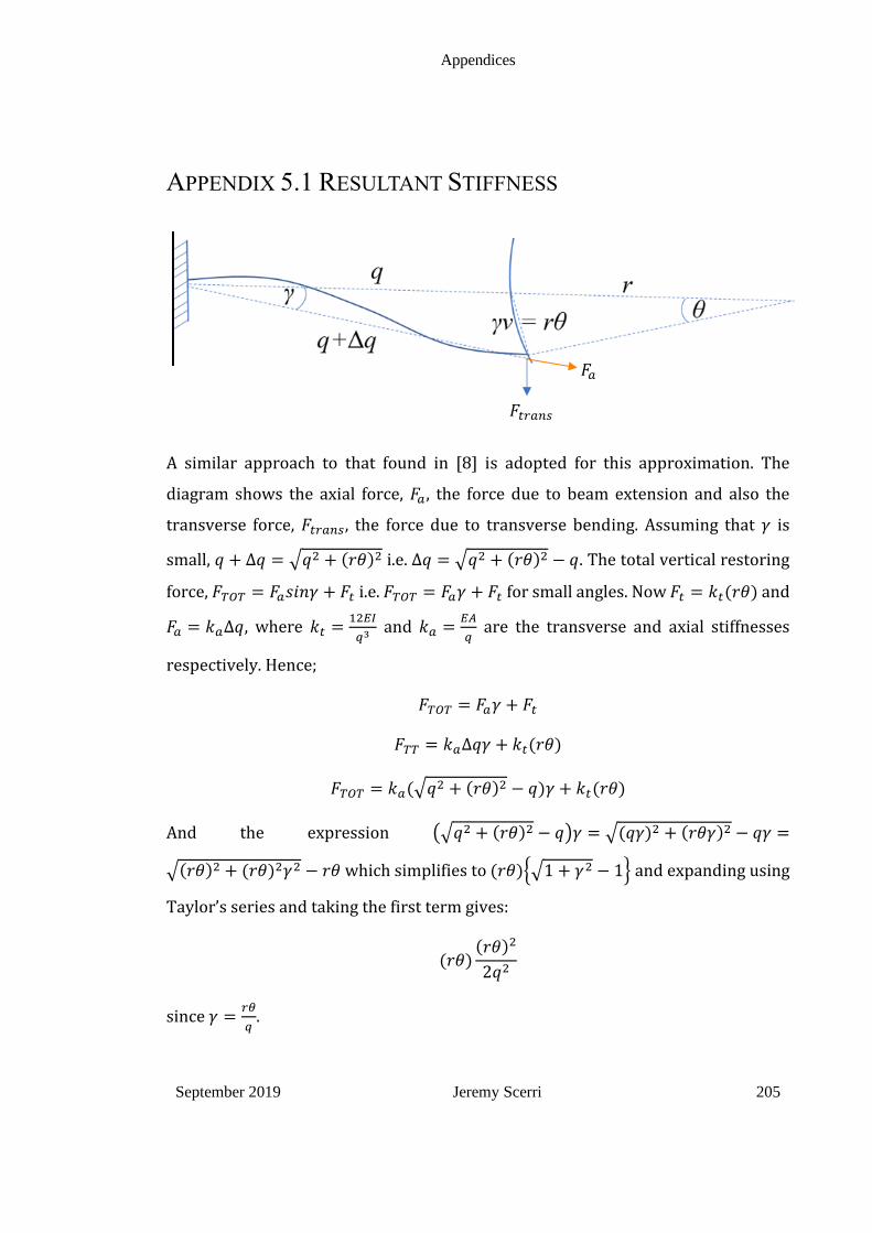
Appendices
September 2019 Jeremy Scerri 205
APPENDIX 5.1 RESULTANT STIFFNESS
A similar approach to that found in [8] is adopted for this approximation. The
diagram shows the axial force, 𝐹𝑎 , the force due to beam extension and also the
transverse force, 𝐹𝑡𝑟𝑎𝑛𝑠, the force due to transverse bending. Assuming that 𝛾 is
small, 𝑞 + ∆𝑞 = √𝑞2 + (𝑟𝜃)2 i.e. ∆𝑞 = √𝑞2 + (𝑟𝜃)2 − 𝑞. The total vertical restoring
force, 𝐹𝑇𝑂𝑇 = 𝐹𝑎𝑠𝑖𝑛𝛾 + 𝐹𝑡 i.e. 𝐹𝑇𝑂𝑇 = 𝐹𝑎𝛾 + 𝐹𝑡 for small angles. Now 𝐹𝑡 = 𝑘𝑡(𝑟𝜃) and
𝐹𝑎 = 𝑘𝑎∆𝑞, where 𝑘𝑡 =12𝐸𝐼
𝑞3 and 𝑘𝑎 =
𝐸𝐴
𝑞 are the transverse and axial stiffnesses
respectively. Hence;
𝐹𝑇𝑂𝑇 = 𝐹𝑎𝛾 + 𝐹𝑡
𝐹𝑇𝑇 = 𝑘𝑎∆𝑞𝛾 + 𝑘𝑡(𝑟𝜃)
𝐹𝑇𝑂𝑇 = 𝑘𝑎(√𝑞2 + (𝑟𝜃)2 − 𝑞)𝛾 + 𝑘𝑡(𝑟𝜃)
And the expression (√𝑞2 + (𝑟𝜃)2 − 𝑞)𝛾 = √(𝑞𝛾)2 + (𝑟𝜃𝛾)2 − 𝑞𝛾 =
√(𝑟𝜃)2 + (𝑟𝜃)2𝛾2 − 𝑟𝜃 which simplifies to (𝑟𝜃)√1 + 𝛾2 − 1 and expanding using
Taylor’s series and taking the first term gives:
(𝑟𝜃)(𝑟𝜃)2
2𝑞2
since 𝛾 =𝑟𝜃
𝑞.
𝐹𝑎
𝐹𝑡𝑟𝑎𝑛𝑠

Appendices
September 2019 Jeremy Scerri 206
APPENDIX 5.2 EQUILIBRIA – MATLAB SCRIPT
clear all; close all; for n=1.5:0.5:3.5 n eps=8.85e-12;A=2.25e-9; %g=2.5e-6; % actual g=2e-6; % as designed %netF=eps*A*(V1-V2).^2*(1/g^2 - 1/(n*g)^2)/2; %force per finger %plot(t,netF);grid on; N=71;r=598e-6;c=50e-6;l=458e-6; alpha=(67.5)*pi/180; a=r-l*cos(alpha); D=(a+c+(l/2)*cos(alpha)); % totalT=2*N*netF*D; % plot(t,totalT);grid on; E=1.69e11;t=25e-6;q=458e-6; %w=8.4e-6; %actual w=9e-6; %design ka=vpa(E*(t*w)/q); I=vpa(t*w^3/12); kt=vpa(12*E*I/q^3); kll=vpa(4*kt); %linear displacement kcl=vpa(2*ka/q^2); %cubic displacement a7=kcl; a6=vpa(2*g*(n-1)*kcl); a5=vpa(kll+kcl*g^2*((n-1)^2-2*n)); a4=vpa(2*g*(n-1)*(kll-n*g^2*kcl)); a3=vpa(g^2*kll*((n-1)^2-2*n)+n^2*g^4*kcl); a2=vpa(-2*n*g^3*kll*(n-1)); V2=0; data=[0 0 0 0 0 0 0 0]; maxV=16; for V1=9:0.003:11.7 p=((D/r)*2*N*eps*A/2); %p=(2*N*eps*A/2); a1=vpa(n^2*g^4*kll-2*p*g*(n+1)*(V1-V2)^2); a0=vpa(-p*(V1-V2)^2*g^2*(n^2-1)); x=roots([a7 a6 a5 a4 a3 a2 a1 a0])*1e6; trueall=0; for allroots=1:length(x) %if (abs(imag(x(allroots)))==0) %if (abs(imag(x(allroots)))==0)&&(abs(real(x(allroots)))<2) %real
equilibrium point realone=real(x(allroots));

Appendices
September 2019 Jeremy Scerri 207
%end
realroots=x(find(imag(x)==0));
end
data=[data;[V1 realroots' NaN(1,7-length(realroots))]];
end
if n==3
plot(data([3:length(data)],1),abs(data([3:length(data)],[4])),'LineWid
th',3);
else
plot(data([3:length(data)],1),abs(data([3:length(data)],[4])),'--
','LineWidth',1);
end
axis([0 maxV -g*0e6 g*1e6]);
title('Graph of Equilbrium Points vs. Actuation Voltage');
%xlabel(sprintf('0 v < V < %g v',maxV)); % x-axis label
xlabel('RMS \DeltaV (volts)'); % x-axis label
ylabel('Displacement in \mum'); % y-axis label
grid on;
hold on;
end
axis([9 11.7 0.15 1.15]);
pl=[10.89,0.6468;10.95,0.6398;11.04,0.6264;11.21,0.6033;11.6,0.5605]
plot(pl(:,1),pl(:,2),'ro','markers',8)
plot(10.75,0.5055,'r.','markers',30)

Appendices
September 2019 Jeremy Scerri 208
APPENDIX 5.3 - TOTAL INERTIA OF N/2 FINGERS
Referring to Figure 5.6, the moment of inertia of one finger about its centroid is
𝐽𝑖 = (1
12)𝑚𝑓(𝑆𝑓
2 + (2𝑐)2). Using the parallel-axis shift theorem this can be translated
to the rotor centre, however, each individual finger is at a different distance.
Moreover, it would be enough to sum N/4 fingers, from octagon vertex to middle of
side strut and double due to symmetry.
An expression for the distance from the centroid of the ith finger to the centre of the
rotor is as in 𝑝𝑖;
𝑝𝑖 = (𝑎 + 𝑏𝑖 + 𝑐)𝑐𝑜𝑠 (2𝛽𝑖
𝑁),
where 𝑏𝑖 = 𝑙𝑐𝑜𝑠𝛼 (𝑁−2𝑖
𝑁)
An expression for the average value of 𝑐𝑜𝑠 (2𝛽𝑖
𝑁) can be found by
4
𝑁∫ 𝑐𝑜𝑠 (
2𝛽𝑖
𝑁) 𝑑𝑖
𝑁/4
0=
2
𝛽𝑠𝑖𝑛 (
𝛽
2). This gives an approximate value for 𝑝𝑖 as follows:
𝑝𝑖 ≈ (𝑎 + 𝑏𝑖 + 𝑐)2
𝛽𝑠𝑖𝑛 (
𝛽
2).
Hence using the parallel-axis shift theorem on the ith finger we get;
𝐽𝑖 = (1
12)𝑚𝑓(𝑆𝑓
2 + (2𝑐)2) + 𝑚𝑓𝑝𝑖2
and for N/2 fingers;
𝐽𝑓 = 2∑ [(1
12)𝑚𝑓(𝑆𝑓
2 + (2𝑐)2) + 𝑚𝑓𝑝𝑖2]
𝑁/4
𝑖=1
Expanding this expression and substituting 𝑝𝑖 gives;

Appendices
September 2019 Jeremy Scerri 209
𝐽𝑓 =𝑁
2[𝑚𝑓
12(𝑆𝑓
2 + (2𝑐)2 +4𝑚𝑓 sin (
𝛽2⁄ )
𝛽2(𝑎2 + 𝑐2 + 2𝑎𝑐)]
+8𝑚𝑓 sin
2 (𝛽2⁄ )
𝛽2∑ [𝑏𝑖
2 + 2(𝑎 + 𝑐)𝑏𝑖]𝑁/4
𝑖=1
with
∑ [𝑏𝑖2] =
7𝑁𝑙2 cos2 𝛼
48
𝑁4
𝑖=1
∑ [2(𝑎 + 𝑐)𝑏𝑖]𝑁/4
𝑖=1=3𝑁(𝑎 + 𝑐)𝑙𝑐𝑜𝑠𝛼
8
giving;
𝐽𝑓 =(𝑁𝑎𝑚𝑓𝑎
+ 𝑁𝑠𝑚𝑓𝑠)
4𝑓(𝛽)[(𝑆𝑓2 + 4𝑐2
12)𝑓(𝛽) + 4(𝑎2 + 𝑐2 + 2𝑎𝑐) + 6(𝑎 + 𝑐)𝑙𝑐𝑜𝑠𝛼
+7𝑙2 cos2 𝛼
3]
where 𝑓(𝛽) =𝛽2
sin2(𝛽/2)

Appendices
September 2019 Jeremy Scerri 210
APPENDIX 5.4 CHANGE IN FRINGE CAPACITANCE -
MATLAB SCRIPT
This script makes use of (5.36) and (5.37) to calculate the change in fringe
capacitance for a typical change in gap. As is shown in the figure provided for full
travel (1/3 gap) the fringe capacitance changes only by less than 5 fF.

Appendices
September 2019 Jeremy Scerri 211
clear all;
close all;
eps=8.8500e-12;
t=23.6e-6; %misalignment - gravity?
%% fringing field effect in electrostatic actuators vitaly leus and
david elata
%equation 10 on page 11
%actual measured
g=2.548e-6;
n=2.511;
fw=1.568e-6; %finger width
% %designed
% g=2e-6;
% n=3;
% fw=2e-6; %finger width
fl=87e-6; %finger length
Cfr1=70*eps*(t*(fl)/g)*(1+(g/(pi*t))*(1+log(2*pi*t/g))+...
(g/(pi*t)*log(1+(2*fw)/g+...
2*sqrt((fw)/g + ((fw)/g)^2))));
Cfr2=71*eps*(t*(fl)/(n*g))*(1+((n*g)/(pi*t))*(1+log(2*pi*t/(n*g)))+...
((n*g)/(pi*t)*log(1+(2*fw)/(n*g)+...
2*sqrt((fw)/(n*g) + ((fw)/(n*g))^2))));
total=Cfr1+Cfr2
withoutfringe=71*eps*((t*(fl)/g)+(t*(fl)/(n*g)))
display(sprintf('This is static, fringe changes with moevement'));
x=linspace(0,g/3,100); Cfr1=70*eps*(t*(fl)./(g-x)).*(1+((g-x)/(pi*t)).*(1+log(2*pi*t./(g-
x)))+... ((g-x)/(pi*t).*log(1+(2*fw)./(g-x)+... 2*sqrt((fw)./(g-x) + ((fw)./(g-x)).^2)))); Cfr2=71*eps*(t*(fl)./(n*g+x)).*(1+((n*g+x)./(pi*t)).*(1+log(2*pi*t./(n
*g+x)))+... ((n*g+x)./(pi*t).*log(1+(2*fw)./(n*g+x)+... 2*sqrt((fw)./(n*g+x) + ((fw)./(n*g+x)).^2)))); plot(x/g,1e15*Cfr1);grid on; title('Capacitance (including fringe) on the narrow gaps - (g-x)'); figure;plot(x/g,1e15*Cfr2);grid on; title('Capacitance (including fringe) on the wider gaps - (ng+x)'); withoutfringe=71*eps*((t*(fl)./(g-x))+(t*(fl)./(n*g+x))); figure;plot(x/g,1e15*(Cfr1+Cfr2),x/g,1e15*withoutfringe);grid on; title('Total on Cs1 - with and without fringe'); figure;plot(x/g,1e15*(Cfr1+Cfr2-withoutfringe));grid on; changeinfringe=max(Cfr1+Cfr2-withoutfringe)-min(Cfr1+Cfr2-
withoutfringe); averagefringe=mean(Cfr1+Cfr2-withoutfringe); title(sprintf('Cs1 fringe, with overall change of %g fF and nominal of
%g fF',changeinfringe*1e15,averagefringe*1e15)); xlabel('Normalised Displacement - x/g'); ylabel('Fringe Capacitance (fF)');

Appendices
September 2019 Jeremy Scerri 212
APPENDIX 5.5 MONOTONICITY IN SENSING
As can be seen in the figure provided, for 0 ≤ 𝑥 ≤ 𝑔𝑠/3, 𝐶𝑠1is monotonic however
𝐶𝑠2 has a minimum occurring within this range.
From (5.45), 𝐶𝑠2can be obtained since 𝐶𝑠2(𝑥) = 𝐶𝑠1(−𝑥).
𝐶𝑠2(𝑥) = 𝑁𝑠휀𝑡𝑙𝑜𝑠 1
𝑛𝑠𝑔𝑠 − 𝑥+
1
𝑔𝑠 + 𝑥 + 𝐶𝑓𝑜
Equating the gradient, 𝑑𝐶𝑠2/𝑑𝑥 to zero to determine the minimum location gives;
𝑑𝐶𝑠2𝑑𝑥
= 𝑘 𝑙𝑛 (𝑔𝑠 + 𝑥
𝑛𝑠𝑔𝑠 − 𝑥) = 0
where 𝑘 is a constant.
This requires that 𝑥 = 𝑔𝑠/2(𝑛𝑠 − 1) and to guarantee that this is true for the whole
range of travel up until 𝑥 = 𝑔𝑠/3, 𝑛𝑠 > 5/3.

Appendices
September 2019 Jeremy Scerri 213
APPENDIX 5.6 MODULATION INDEX, N AND FRINGE
CAPACITANCE - MATLAB SCRIPT
clear all;
close all;
mrange=0:0.1:1;
x_on_g=1/3; %max disp = 1/3
f=1; %f=1 means x=f*g/3 i.e. max disp
Cnom=0.9e-12;
fc=177000;
Xc1=1/(2*pi*fc*Cnom)
R=33e3;
for m=mrange
n=1.0:0.1:7;
r=(m.*(f^2+3*f*(n-1))-9*(m+1).*n)./((f-3)*(m+1).*(f+3*n)); %WRITEUP
M=sqrt((R^2+((1./r)*Xc1).^2)./(R^2+Xc1.^2));
plot(n,M);hold on;grid on;
end
title(sprintf('M vs. n for increasing Fringe Capacitance, f = %g',f));
LEG=legend(num2str(mrange'),'location','northeast');
LEG.FontSize = 8;
ylabel('Modulation Index - M');
xlabel('Comb fingers gap ratio - n');
n=2.511;
m=195/900;
n=2.511;
f=1;
r=(m*(f^2+3*f*(n-1))-9*(m+1)*n)/((f-3)*(m+1)*(f+3*n));
Cnom=0.9e-12;
fc=177000;
Xc0=1/(2*pi*fc*Cnom)
Xcmax=(1/r)*Xc0
R=33e3;
ModIndex=sqrt((R^2+(Xcmax).^2)./(R^2+Xc0.^2))

Appendices
September 2019 Jeremy Scerri 214
APPENDIX 5.7 PSO - MATLAB SCRIPTS
Main Program:
tic
clc
clear all
close all
rng default
global t E ep rho xpi ga J Na Ns b datarateactual Cs1min delCs1
Mactual gain MaxV alpha;
ep=8.85e-12;
E=1.69e11;
t=25e-6; %
alpha=(67.5)*pi/180;
rho=2.5e-15*(1e6)^3;
%[ r , q , w, ca , cs, ga, gs, Sf,
na, ns, Rm]
LB=[598e-6 ,400e-6 ,6e-6 ,30e-6, 30e-6, 2e-6 , 2e-6 , 2e-6 , 2
, 1.7 , 1000]; %lower bounds of variables
UB=[700e-6 ,500e-6 ,15e-6 ,50e-6, 50e-6, 6e-6 ,6e-6 , 5e-6 , 6
, 6 , 1000000]; %upper bounds of variables
% pso parameters values
m=length(LB); % number of variables
n=30; % population size
wmax=0.9; % inertia weight
wmin=0.4; % inertia weight
c1=2; % acceleration factor
c2=2; % acceleration factor
% pso main program----------------------------------------------------
start
maxite=20; % maximum number of iteration
maxrun=5; % maximum number of runs need to be
for run=1:maxrun
run
% pso initialization----------------------------------------------
start
for i=1:n
for j=1:m
x0(i,j)=(LB(j)+rand()*(UB(j)-LB(j)));
end
end
x=x0 % initial population
v=0.1*x0; % initial velocity
for i=1:n
f0(i,1)=ofun(x0(i,:));
end
[fmin0,index0]=min(f0);
pbest=x0; % initial pbest
gbest=x0(index0,:); % initial gbest
% pso initialization----------------------------------------------
--end

Appendices
September 2019 Jeremy Scerri 215
% pso algorithm---------------------------------------------------
start
ite=1;
tolerance=1;
while ite<=maxite && tolerance>10^-12
w=wmax-(wmax-wmin)*ite/maxite; % update inertial weight
% pso velocity updates
for i=1:n
for j=1:m
v(i,j)=w*v(i,j)+c1*rand()*(pbest(i,j)-x(i,j))...
+c2*rand()*(gbest(1,j)-x(i,j));
end
end
% pso position update
for i=1:n
for j=1:m
x(i,j)=x(i,j)+v(i,j);
end
end
% handling boundary violations
for i=1:n
for j=1:m
if x(i,j)<LB(j)
x(i,j)=LB(j);
elseif x(i,j)>UB(j)
x(i,j)=UB(j);
end
end
end
% evaluating fitness
for i=1:n
f(i,1)=ofun(x(i,:));
end
% updating pbest and fitness
for i=1:n
if f(i,1)<f0(i,1)
pbest(i,:)=x(i,:);
f0(i,1)=f(i,1);
end
end
[fmin,index]=min(f0); % finding out the best particle
ffmin(ite,run)=fmin; % storing best fitness
ffite(run)=ite; % storing iteration count
% updating gbest and best fitness

Appendices
September 2019 Jeremy Scerri 216
if fmin<fmin0 gbest=pbest(index,:); fmin0=fmin; end
% calculating tolerance if ite>100; tolerance=abs(ffmin(ite-100,run)-fmin0) end
% displaying iterative results if ite==1 disp(sprintf('Run Iteration Best particle Objective
fun')); end disp(sprintf('%g %8g %8g
%8.4f',run,ite,index,fmin0)); ite=ite+1; end % pso algorithm------------------------------------------------end fvalue=ofun(gbest); fff(run)=fvalue; rgbest(run,:)=gbest; disp(sprintf('--------------------------------------')); end % pso main program-------------------------------------------------end disp(sprintf('\n')); disp(sprintf('********************************************************
*')); disp(sprintf('Final Results-----------------------------')); [bestfun,bestrun]=min(fff) best_variables=rgbest(bestrun,:) disp(sprintf('********************************************************
*')); toc % PSO convergence characteristic plot(ffmin(1:ffite(bestrun),bestrun),'-k'); xlabel('Iteration'); ylabel('Fitness function value'); title('PSO convergence characteristic') %#####################################################################
##### ret=ofun(best_variables) disp(sprintf('%gum %gum %gum %gum %gum %gum %gum %gum %g %g %gOhms'
,best_variables(1)*1e6,best_variables(2)*1e6,best_variables(3)*1e6,bes
t_variables(4)*1e6,best_variables(5)*1e6,best_variables(6)*1e6,best_va
riables(7)*1e6,best_variables(8)*1e6,best_variables(9),best_variables(
10),best_variables(11))); disp(sprintf('%g*gap %gV J=%g %g %g b=%g %gHz %gfF %gfF M=%g Gain=%g
\r\n' ,xpi/ga, MaxV, J, Na, Ns, b, datarateactual, Cs1min*1e15,
delCs1*1e15, Mactual, gain));

Appendices
September 2019 Jeremy Scerri 217
The Objective function: ‘ofun.m’
function f=ofun(X)
global t E ep rho xpi ga J Na Ns b datarateactual Cs1min delCs1
Mactual gain MaxV alpha;
ep=8.85e-12;
E=1.69e11;
alpha=(67.5)*pi/180;
rho=2.5e-15*(1e6)^3;
r=X(1);
q=X(2);
w=X(3);
ca=X(4);
cs=X(5);
ga=X(6);
gs=X(7);
Sf=X(8);
na=X(9);
ns=X(10);
Rm=X(11);
% constraints (all constraints must be converted into <=0 type)
% if there is no constraints then comments all c0 lines below
l=r/sqrt(1+1/sqrt(2));
Na=2*ceil(l/(2*Sf+ga+na*ga)); %two octagon sides
Ns=2*ceil(l/(2*Sf+gs+ns*gs)); %two octagon sides
loa=0.9*2*ca;
Aa=t*(loa); % 90% of finger length
a=r-l*cos(alpha);
D=(a+ca+(l/2)*cos(alpha));
ka=(E*(t*w)/q);
I=(t*w^3/12); %second moment of area of spring section
kt=(12*E*I/q^3);
[MaxV,xdisp]=equilibriumpoints(na,ga,D,r,Na,Aa,ep,ka,q,kt);
xpi=max(xdisp); %pull in
los=0.9*2*cs;% 90% of finger length
Cfo=Fringe(gs,Sf,los,t)+Fringe(ns*gs,Sf,los,t); %fringe for sensing
Cs1=Ns*ep*t*los*(1./(ns*gs+xdisp)+1./(gs-xdisp))+Cfo; %Cs1(x) - check
linearity
Cs2=Ns*ep*t*los*(1./(ns*gs-xdisp)+1./(gs+xdisp))+Cfo; %Cs2(x) - check
linearity
S1=10e-6;
S2=10e-6;
m1=rho*r*S1*t;
m2=rho*l*S2*t;
mfs=rho*2*cs*t*Sf;
mfa=rho*2*ca*t*Sf;
J1=(1/12)*(m1/2)*((S1/2)^2+r^2)+(m1/2)*(r/2)^2;
J2=(1/12)*(m2)*((S2)^2+l^2)+(m2)*((r)^2-(l/2)^2);
beta=pi-2*alpha;

Appendices
September 2019 Jeremy Scerri 218
fbeta=(beta^2)/(sin(beta/2))^2; Jf=((Na*mfa+Ns*mfs)/(4*fbeta))*((Sf^2+4*ca^2)*fbeta/12+4*(a^2+ca^2+2*a
*ca)+6*(a+ca)*l*cos(alpha)+(7*(l*cos(alpha))^2)/3); J=8*(J1+J2+Jf);
betaa=1-0.58*(t/loa);betas=1-0.58*(t/los); bT=2*Na*loa*(effvisco(ga)*(t/ga)^3+effvisco(na*ga)*(t/(na*ga))^3)*beta
a+2*Ns*los*(effvisco(gs)*(t/gs)^3+effvisco(ns*gs)*(t/(ns*gs))^3)*betas
; b=r^2*bT; settlingtimeactual=5*(2*J/b); datarateactual=1/(2*settlingtimeactual);
fc=1e6; Cs1max=max(Cs1); Cs1min=min(Cs1); delCs1=Cs1max-Cs1min; XCsb=1/(2*pi*fc*Cs1max); f=1; Cr=Cfo/(Ns*ep*t*los*(1/(ns*gs)+1/gs)); e=(Cr*(f^2+3*f*(ns-1))-9*ns*(Cr+1))/((f-3)*(Cr+1)*(f+3*ns)); Mactual=sqrt((Rm^2+XCsb^2)/(Rm^2+e^2*XCsb^2));
segment=floor((length(xdisp))/3); V1=linspace(0,0.1*length(Cs1),length(Cs1)); diffV11=diff(V1(segment:2*segment))'; diffV12=diff(V1(floor(length(xdisp))-segment:floor(length(xdisp))))'; gain=Rm/sqrt(Rm^2+XCsb^2); c0=[];c=[]; c0(1)=3000-datarateactual;%<0 - 3000<datarateactual c0(2)=Rm^2*(1-(0.85)^2)+XCsb^2*(1-(0.85*e)^2);%<0 - equivalent to
%ceq(2)=Mactual-0.75; c0(3)=(ga/4)-xpi;%<0 - ga/4<xpi c0(4)=MaxV-14;%<0 - MaxV<14 c0(5)=(100e-15)-delCs1;%<0 c0(6)=0.05-Rm/sqrt(Rm^2+XCsb^2);%<0 - 0.5<Rm/sqrt(Rm^2+XCsb^2) % objective function (minimization) Cfoa=Fringe(ga,Sf,loa,t)+Fringe(na*ga,Sf,loa,t); %fringe for actuation Ca=2*Na*ep*t*loa*(1./(na*ga)+1./(ga))+Cfoa; %Cs1(x) - check linearity of=r/(600e-6)+q/(500e-6)+Ca/(1e-12);%+Mactual; % defining penalty for each constraint for i=1:length(c0) if c0(i)>0 c(i)=1; else c(i)=0; end end penalty=1; % penalty on each constraint violation f=of+penalty*sum(c); % fitness function return

Appendices
September 2019 Jeremy Scerri 219
The Effective viscosity function: ‘effvisco.m’
function [ueff]=effvisco(g)
lambdi=68e-9; %mean free path at NTP
Kn=lambdi/g;
xi=sqrt(pi)/(2*Kn);
uair=1.81e-5; %alpha=0.6 - W Yang
ueff=(xi*uair/6)/(xi/6+((2-0.6)/sqrt(pi))*log(1/xi+2.18)+0.6/0.642+(1-
0.6)*(xi+2.395)/(2+1.12*0.6*xi)-(1.26+10*0.6*xi)/(1+10.98*xi)+exp(-
xi/5)/8.77);
The Equilibrium Point function: ‘equilibriumpoints.m’
function [MaxV,xdisp]=equilibriumpoints(na,ga,D,r,Na,Aa,ep,ka,q,kt)
kll=(4*kt); %linear displacem,ent
kcl=(2*ka/q^2); %linear displacement
a7=kcl;
a6=(2*ga*(na-1)*kcl);
a5=(kll+kcl*ga^2*((na-1)^2-2*na));
a4=(2*ga*(na-1)*(kll-na*ga^2*kcl));
a3=(ga^2*kll*((na-1)^2-2*na)+na^2*ga^4*kcl);
a2=(-2*na*ga^3*kll*(na-1));
V2=0;
V1=0;
curr=1;
loc=1;
data=[0 0 0 0 0 0 0 0];
n=0;
while (data(curr,loc)>=0)
V1=V1+0.1;
p=((D/r)*2*Na*ep*Aa/2);
a1=(na^2*ga^4*kll-2*p*ga*(na+1)*(V1-V2)^2);
a0=(-p*(V1-V2)^2*ga^2*(na^2-1));
xr=roots([a7 a6 a5 a4 a3 a2 a1 a0])*1e6;
trueall=0;
for allroots=1:length(xr)
%realone=real(x(allroots));
trueall=trueall+1;
realroots=xr(find(imag(xr)==0));
end
data=[data;[V1 realroots' NaN(1,7-length(realroots))]];
[curr,k]=size(data);
if V1==0.1
loc=find(data(curr,[2:k-1])<((ga*1e6)/3)&data(curr,[2:k-1])>=0);
end
end
MaxV=max(data(:,1));
xdisp=(1e-6)*data(1:length(data(:,loc))-1,loc+1);

Appendices
September 2019 Jeremy Scerri 220
The Fringe Capacitance function: ‘Fringe.m’
function [Cfo]=Fringe(g,Sf,los,t)
global ep;
Cfo=(ep/pi)*(1+log(2*pi*t/g)+log(1+(2*Sf/g)+2*sqrt(Sf/g+(Sf/g)^2)))*lo
s;

Appendices
September 2019 Jeremy Scerri 221
APPENDIX 5.8 DYNAMICS – INPUTS TO OUTPUT - MATLAB
SCRIPTS
Main Program:
clear all;
close all;
global wd k v1 v2 wc cubicspringON modulatedata phi BPSK b J r g kt n
C Cd Cdd Cp L Ri Rm Cm a V2 V2d V2dd timestep;
b=1.3e-10;
J=(1.85e-15);r=598e-6;
g=2.5e-6;n=2.6;
%g=2e-6;n=3; %parameters designed
data=[0 0 0 0 0];
E=1.69e11;t=25e-6;
w=8.4e-6; %actual device
%w=9e-6; %PARAMETERS DESIGNED
q=458e-6;ka=(E*(t*w)/q);I=(t*w^3/12);
kt=(12*E*I/q^3);
eps=8.85e-12;A=2.25e-9;N=71;Cf=119e-15;
% simulation paramters
simpar=[ 1 7.6 1 3.3e3 1 7.6 0 0
0.0009 0 171.82e3 0]; % 3.3kHz data BPSK on 177kHz as v1 and
fc=simpar(11);
fd=simpar(4);
v1=simpar(2); % data amplitude
v2=simpar(6); % carrier amplitude, 0 switches off carrier,
switchsense=simpar(12);
cubicspringON=simpar(1);% 1 = ON, 0 = OFF
modulatedata=simpar(3); % 1 or 0: 0 gives input as baseband, 1
modulates on wc
wd=2*pi*fd;
BPSK=simpar(5); %1 switches on BPSK and off ASK
k=simpar(7);
phi=simpar(8);
%freq response
freq=[0 0];
duration=3*(1/fd); %duration is integer multiple of data freq. 3x
timestep=(1/fc)/500; %/500
spec=zeros(floor(duration/timestep)+1,1);
wc=2*pi*fc;
initcond1=[0 0 wd wc]; %x x_dot startingomega
[t2,y1] = ode23s('actuationDE',[0:timestep:duration], initcond1);
%%
figure;
subplot(221)
plot(initcond1(1),initcond1(2),'r*');grid on;
hold on;
plot(y1(:,1)*1e6,y1(:,2),'b');

Appendices
September 2019 Jeremy Scerri 222
minx=-0.4; maxx=2.5; miny=-0.15; maxy=0.15; xrange=[minx:1e-8:maxx]; yrange=[miny:0.001:maxy]; axis([minx maxx miny maxy]); %xlabel('x(t) in \mum'); xlabel('$x(t)\, in\, \mu m$','interpreter','latex'); ylabel('$\dotx(t)$','interpreter','latex');
title('Phase Plane Portrait for tormixer -- x dot(t) vs. x(t)');
subplot(222) yyaxis left plot(0,initcond1(1),'r*');grid on; hold on; [unwanted wanted]=v1minusv2(t2,1,1); yyaxis right plot(t2*1e3,wanted,'r--'); ylabel('\Delta V(t)'); hold on; yyaxis left plot(t2*1e3,y1(:,1)*1e6,'b'); %y1(:,1) is the displacement ylabel('$x(t)\, in\, \mu m$','interpreter','latex'); xlabel('time in ms'); title(sprintf('x(t) vs. t'));
subplot(223) plot(0,initcond1(2),'r*'); hold on; plot(t2,y1(:,2),'b');grid on; xlabel('time'); ylabel('x dot(t)'); title('x dot(t) vs. t');
subplot(224) plot3(y1(:,1),y1(:,2),t2,'b');grid on; hold on; plot3(initcond1(1),initcond1(2),0,'r*'); xlabel('x(t)'); ylabel('y(t)'); zlabel('time'); title('3D phase portrait of tormixer');
%wanted is del V
instaForce=((7.9224e-22)*(r))*((wanted).^2).*(((n*g+y1(:,1)).^2-(g-
y1(:,1)).^2)./((g-y1(:,1)).*(n*g+y1(:,1))).^2);
figure;

Appendices
September 2019 Jeremy Scerri 223
title(sprintf('v1 and v2, difference and diff^2')); subplot(141) plot(t2,BPSK*v1*cos(modulatedata*wc*t2+(square(wd*t2)+1)/2*pi)+(1-
BPSK)*cos(modulatedata*wc*t2).*(v1*square(wd*t2)+v1)/2);grid on; subplot(142) V2=v2*cos(wc*t2+phi)+k; plot(t2,V2);grid on; subplot(143); plot(t2,wanted);grid on; subplot(144); plot(t2,wanted.^2);grid on;
x=y1(:,1); Ca=eps*A*2*N*(1./(n*g+x)+1./(g-x))+2*Cf; Cad=diff(Ca)./diff(t2); Cad=[Cad;Cad(length(Cad))]; wantfilt=filter(1/600, [1 1/600-1], wanted); wanted_d=diff(wantfilt)./diff(t2); wanted_d=[wanted_d;wanted_d(length(wanted_d))]; Actuationcurrent=Ca.*wanted_d+Cad.*wantfilt+wantfilt/(310e6); figure;plot(Actuationcurrent);grid on; rmsactuation=rms(Actuationcurrent); title(sprintf('Actuation RMS Current is %g nA',rmsactuation*1e9)); xlabel('Time'); ylabel('Current (nA)');
figure; Cs1=eps*A*N*(1./(n*g+x)+1./(g-x))+Cf; %closing - extra 120fF
parasitics Cs2=eps*A*N*(1./(n*g-x)+1./(g+x))+Cf; %opening - extra 120fF
parasitics graph1=plot(t2*1e3,Cs1*10^15,t2*1e3,Cs2*10^15,'--k');grid on; ylabel('Capacitance (fF)'); xlabel('time (ms)'); legend('Cs1','Cs2'); set(graph1,'LineWidth',2);
if switchsense==1 C=Cs2; %opening elseif switchsense==0 C=Cs1; %closing end
Cd=diff(C)./diff(t2); Cd=[Cd;Cd(length(Cd))]; Cdd=diff(Cd)./diff(t2); Cdd=[Cdd;Cdd(length(Cdd))]; V2d=diff(V2)./diff(t2); V2d=[V2d;V2d(length(V2d))];

Appendices
September 2019 Jeremy Scerri 224
V2dd=diff(V2d)./diff(t2); V2dd=[V2dd;V2dd(length(V2dd))]; %actuation power sig=simpar(2)*[(1-exp(-t2(1:(length(t2)/6))/6e-6));(exp(-
t2((1:length(t2)/6))/6e-6))]; Ca=((100e-15)/0.721)*(-1e13*C+9)+1.8e-12; wsig=[sig;sig;sig;zeros(1,(length(Ca)-3*length(sig)))']; Cad=diff(Ca)./diff(t2); %newwanted=conv(wsig,(1/1000)*ones(1,1000)); wantedd=diff(wsig)./diff(t2); Pa1=wsig.*Ca.*[wantedd;wantedd(length(wantedd))]; Pa2=wsig.*wsig.*[Cad;Cad(length(Cad))]; Pa3=wsig.*wsig/(210e6); Pat=Pa1+Pa2+Pa3; rmsPat=rms(Pat) rmsPat=rms(Pa1)+rms(Pa2)+rms(Pa3); rmsPa1=rms(Pa1)/rmsPat*100 rmsPa2=rms(Pa2)/rmsPat*100 rmsPa3=rms(Pa3)/rmsPat*100 subplot(2,2,1);plot(Pa1);subplot(2,2,2);plot(Pa2);subplot(2,2,3);plot(
Pa3);subplot(2,2,4);plot(Pat); %%%%%%%%%%%%%%%%%%%%%%%%%
Ri=210e2; Reqvp=0.3; Xs1=1/(2*pi*fc*1060e-15);%1060 fF is nominal sense cap Cs1 Rm=(Reqvp*Xs1/v2)/sqrt(1-(Reqvp/v2)^2); Cm=5e-13;%1e-10; a=(Ri+Rm)/(Ri*Rm);Cp=260e-13;%Cp=260e-12; L=1e-4; %remove - small number to be used with capaciive load only Ct=Cm+Cp; XPX=((2*pi*fc*Ct))*(2*pi*fc*L) s=1/(2*pi*fc*1050e-15); u=1/(2*pi*fc*900e-15); delVp=(s/sqrt(s^2+a^2)-u/sqrt(u^2+a^2))*v2; besta=((s*u)^(1/3))*sqrt(u^(2/3)+s^(2/3)); delVpbest=(s/sqrt(s^2+besta^2)-u/sqrt(u^2+besta^2))*v2; bestRm=Ri/(besta*Ri-1); initcond1=[0 0 0]; %i vp vpdot
[t1,S] = ode23s('sensingDE',[0:timestep:duration], initcond1); region1=floor(1.5*(1/fd)/timestep); large=max(S(region1-500:region1,2))-min(S(region1-500:region1,2)); region2=floor(2*(1/fd)/timestep); small=max(S(region2-500:region2,2))-min(S(region2-500:region2,2)); M=small/large; if M>1

Appendices
September 2019 Jeremy Scerri 225
M=1/M; end figure; plot(t1,S(:,2),'b');grid on;hold on; currentRMS=rms(S(1:floor((1/fd)/timestep),1)) powerRMS=currentRMS^2*(1/a); display(sprintf('RMS Power across sense resistors is %g
uW',powerRMS*1e6)); rmsmechpowerdamp=(b/r)*mean(y1(:,2).^2); display(sprintf('RMS Power in mechanical [damping x vel^2] is %g
uW',rmsmechpowerdamp*1e6)); % figure; plot(((region1-500)*timestep),max(S(region1-500:region1,2)),'r.',
'markers', 30);hold on; plot(((region1)*timestep),max(S(region1-500:region1,2)),'r.',
'markers', 30);hold on; plot(((region1-500)*timestep),min(S(region1-500:region1,2)),'r.',
'markers', 30);hold on; plot(((region1)*timestep),min(S(region1-500:region1,2)),'r.',
'markers', 30);hold on; plot(((region2-500)*timestep),max(S(region2-500:region2,2)),'r.',
'markers', 30);hold on; plot(((region2)*timestep),max(S(region2-500:region2,2)),'r.',
'markers', 30);hold on; plot(((region2-500)*timestep),min(S(region2-500:region2,2)),'r.',
'markers', 30);hold on; plot(((region2)*timestep),min(S(region2-500:region2,2)),'r.',
'markers', 30); title(sprintf('fc = %g kHz M = %g Pa = %.2f pW V1/V2 = %.2f v fd =
%g',fc/1000,M,rmsmechpowerdamp*1e12,vol,fd)); xlabel('Time (s)'); ylabel('v_p (volts)'); figure;plot(S(:,1)); title('current'); display(sprintf('Linear Damping coeff. experimental = %g',(b)));
ueff=0.84*1.81e-5;%effective viscosity lfinger=100e-6; factor = 1-0.58*(t/lfinger); %squeeze film dampingcoeffmodel = (4*N)*factor*ueff*lfinger*(t/g)^3; b_theory=(r^2)*dampingcoeffmodel; display(sprintf('Linear Damping coeff. theoretical = %g',(b_theory))); gzita=(b_theory/r)/(2*sqrt(4*(r)*kt*(J/r))) %b/(2*sqrt(k*m)); Q=1/(2*gzita);
Appendices
September 2019 Jeremy Scerri 226
Function ‘actuationDE.m’:
function [dy] = phaseportrait3D(t,y)
global wd cubicspringON wc b J r g kt n;
dy=zeros(4,1);
[wanted unwanted]=v1minusv2(1,y(3),y(4));
dy(1)=y(2);
dy(2)=-(b/J)*y(2)-(4*(r^2/J)*kt)*y(1)-
(738821561082)*cubicspringON*(r^2/J)*y(1)^3+...
((7.9224e-22)*(r/J))*((wanted).^2)*(((n*g+y(1))^2-(g-y(1))^2)/((g-
y(1))*(n*g+y(1)))^2);
dy(3)=wd;
dy(4)=wc;
Function ‘sensingDE.m’:
function dy = sensingDE(t1,y)
global C Cd Cdd V2 V2d V2dd L Cp a timestep;
dy=zeros(3,1);
i=(floor(t1/timestep)+1);
dy(1)=Cp/(Cp+C(i))*((2*Cd(i)*V2d(i)+Cdd(i)*V2(i)+C(i)*V2dd(i))+(C(i)/(
Cp*L)-Cdd(i))*y(2)+((C(i)*a)/Cp-2*Cd(i))*y(3));
dy(2)=y(3);
dy(3)=(1/Cp)*dy(1)-(a/Cp)*y(3)-(1/(Cp*L))*y(2);
Function ‘v1minusv2.m’:
function [formodel forplotting]=v1minusv2(t,wdt,wct)
global wd modulatedata k v1 wc v2 phi BPSK
formodel= [BPSK*v1*cos(modulatedata*wct +(square(wdt )+1)/2*pi)+(1-
BPSK)*cos(modulatedata*wct )*(v1*square(wdt )+v1)/2-(v2*cos(wct+phi
)+k)];
forplotting=[BPSK*v1*cos(modulatedata*wc*t+(square(wd*t)+1)/2*pi)+(1-
BPSK)*cos(modulatedata*wc*t).*(v1*square(wd*t)+v1)/2-
(v2*cos(wc*t+phi)+k)];


![[3.4]_Fiber Nonlinearities](https://static.fdocuments.net/doc/165x107/55cf8e81550346703b92da6f/34fiber-nonlinearities.jpg)