
Experion PKS Series C I/O User's Guide
604
Experion PKS Series C I/O User's Guide EPDOC-X126-en-430B March 2014 Release 430
-
Upload
rostyslav-kudlak -
Category
Documents
-
view
1.982 -
download
86
description
Experion PKS Series C I/O User's Guide
Transcript of Experion PKS Series C I/O User's Guide
Experion PKSSeries C I/O User's Guide
EPDOC-X126-en-430BMarch 2014
Release 430

Document Release Issue DateEPDOC-X126-en-430B 430 1 March 2014
DisclaimerThis document contains Honeywell proprietary information. Information contained herein is to be used solelyfor the purpose submitted, and no part of this document or its contents shall be reproduced, published, ordisclosed to a third party without the express permission of Honeywell International Sàrl.
While this information is presented in good faith and believed to be accurate, Honeywell disclaims the impliedwarranties of merchantability and fitness for a purpose and makes no express warranties except as may be statedin its written agreement with and for its customer.
In no event is Honeywell liable to anyone for any direct, special, or consequential damages. The informationand specifications in this document are subject to change without notice.
Copyright 2013 - Honeywell International Sàrl
2 www.honeywell.com
Contents
1 About this guide ................................................................................................................................... 171.1 Intended audience ............................................................................................................................................. 181.2 Prerequisite Skills ............................................................................................................................................. 191.3 References ......................................................................................................................................................... 201.4 Terms and acronyms ......................................................................................................................................... 21
2 Series C I/O Purpose ............................................................................................................................ 232.1 Comparing Process Manager I/O and Series C I/O .......................................................................................... 242.2 What is Series C I/O? ....................................................................................................................................... 252.3 Series C Pulse Input Module (SCPIM) ............................................................................................................. 26
2.3.1 Features of PIM ................................................................................................................................. 262.3.2 Comparison between Series A and Series C PIM ............................................................................. 26
2.4 What is Universal Input/Output (UIO) Module? .............................................................................................. 282.4.1 Features of UIO ................................................................................................................................. 282.4.2 New UIO features in R430 ................................................................................................................ 282.4.3 Differences between UIO channels and existing Series C AI, AO, DI, and DO modules ................ 29
2.5 What is Low Level Analog Input (LLAI) Module ........................................................................................... 302.5.1 Difference between AI-LLMUX and AI-LLAI modules Cx-PAIM01 and Cx-PAIM51 .................. 30
3 Series C I/O Planning and Design ....................................................................................................... 313.1 General Planning References ............................................................................................................................ 32
3.1.1 Series C I/O appearance ..................................................................................................................... 323.1.2 Series C I/O features .......................................................................................................................... 32
3.2 Series C I/O and C300 topology ....................................................................................................................... 353.2.1 Examining the topology rules ............................................................................................................ 35
3.3 Supported Series C I/O modules ....................................................................................................................... 373.3.1 Compatibility matrix between AI modules and differential AI modules .......................................... 393.3.2 Compatibility matrix between AO modules and differential AO modules ....................................... 393.3.3 Difference between AI-HART modules Cx-PAIH01 and Cx-PAIH51 .............................................. 403.3.4 Difference between AO-HART modules Cx-PAOH01 and Cx-PAOH51 ......................................... 403.3.5 Difference between bussed low voltage Digital Input modules Cx-PDIL01 and Cx-PDIL51 .......... 413.3.6 Difference between low voltage Digital Output modules Cx-PDOB01 and Cx-PDOD51 ............... 413.3.7 Difference between AI-LLMUX and AI-LLAI modules Cx-PAIM01 and Cx-PAIM51 .................. 413.3.8 Identifying supported Series C I/O modules ..................................................................................... 41
3.4 Supported Series C I/O options ........................................................................................................................ 433.4.1 Inspecting the Series C I/O library .................................................................................................... 433.4.2 Inspecting IOM function blocks ........................................................................................................ 433.4.3 Inspecting channel function blocks ................................................................................................... 443.4.4 Defining module containment ........................................................................................................... 453.4.5 Temperature derating for UIO ........................................................................................................... 453.4.6 Internal dissipation calculation for UIO ............................................................................................ 463.4.7 Temperature derating curves for UIO ................................................................................................ 46
3.5 I/O Link performance specifications ................................................................................................................ 483.5.1 Reviewing Link Unit utilization ........................................................................................................ 483.5.2 Reducing I/O Link traffic .................................................................................................................. 493.5.3 Event collection ................................................................................................................................. 493.5.4 PV and Back calculation scanning .................................................................................................... 49
3
4 Series C I/O Installation and Upgrades .............................................................................................. 514.1 Installation Declarations ................................................................................................................................... 52
4.1.1 Introduction ........................................................................................................................................ 524.1.2 I/O Link Address Jumpers ................................................................................................................. 534.1.3 Cabling ............................................................................................................................................... 53
4.2 Installing the Series C IOTA on the carrier ...................................................................................................... 554.3 Mounting the I/O module on the IOTA ............................................................................................................ 574.4 Grounding and power considerations - IOTA boards ....................................................................................... 58
4.4.1 Testing for power ............................................................................................................................... 584.5 Connecting IOMs and field devices through I/O Termination Assemblies ...................................................... 604.6 Powering the Series C system ........................................................................................................................... 644.7 Fusing - Series C IOTA boards ......................................................................................................................... 65
5 Series C IOTA Pinouts ......................................................................................................................... 675.1 Analog Input IOTA Models CC-TAIX01, CC-TAIX11 ................................................................................... 68
5.1.1 Field wiring and module protection - Analog Input module ............................................................. 705.1.2 Two-wire transmitter wiring - Analog Input module ......................................................................... 715.1.3 Non two-wire transmitter wiring - Analog Input module .................................................................. 715.1.4 Custom wiring - Analog Input module .............................................................................................. 715.1.5 Analog Input wiring reference table .................................................................................................. 755.1.6 Allowable field wiring resistance - Analog Input module ................................................................. 765.1.7 IOTA board and connections - Analog Input module ........................................................................ 76
5.2 Analog Input non-HART/HARTIOTA Models Cx-TAIX51, Cx-TAIX61 ....................................................... 795.2.1 Field wiring and module protection - Analog Input HART module ................................................. 805.2.2 Two-wire transmitter wiring - Analog Input HART module ............................................................. 815.2.3 Standard and self-powered two-wire transmitter wiring - Analog Input HART module .................. 815.2.4 Self-powered 3-wire transmitter (system ground) - Analog Input HART module ............................ 825.2.5 Analog Input HART module wiring reference table ......................................................................... 835.2.6 Allowable field wiring resistance - Analog Input HART module ..................................................... 835.2.7 IOTA board and connections - Analog Input HART module ............................................................ 83
5.3 Non-HART Analog Input IOTA (Models CC-TAIN01, CC-TAIN11) ............................................................. 855.3.1 Field wiring and module protection - non-HART Analog Input module .......................................... 865.3.2 Two-wire transmitter wiring - non-HART Analog Input module ...................................................... 875.3.3 Standard and self-powered two-wire transmitter wiring - non-HART Analog Input module ........... 875.3.4 Self-powered 3-wire transmitter (system ground) - non-HART Analog Input module .................... 885.3.5 Non-HART Analog Input module wiring reference table ................................................................. 895.3.6 Allowable field wiring resistance - non-HART Analog Input module .............................................. 895.3.7 IOTA board and connections - non-HART Analog Input module ..................................................... 89
5.4 Differential Analog input IOTA (Models CC-TAID01 and CC-TAID11) ....................................................... 925.4.1 Compatible IOTA models for differential analog input and output channels .................................... 925.4.2 Standard and self-powered two-wire transmitter wiring - Differential Analog input module .......... 925.4.3 Custom wiring - Differential Analog input module ........................................................................... 945.4.4 Jumper configuration for differential configuration - Differential Analog input module ................. 995.4.5 IOTA board and connections - Differential Analog input module .................................................. 101
5.5 Analog Output IOTA Models CC-TAOX01, CC-TAOX11, CC-TAON01 and CC-TAON11 ....................... 1055.5.1 Field wiring and module protection - Analog Output module ........................................................ 1055.5.2 IOTA board and connections - Analog Output module ................................................................... 1055.5.3 Non-HART Analog Output IOTA (Models CC-TAON01, CC-TAON11) ...................................... 1085.5.4 IOTA board and connections - non-HART Analog Output module ................................................ 108
5.6 Analog Output HART IOTA Models Cx-TAOX51, Cx-TAOX61 ................................................................. 1125.6.1 Field wiring and module protection - Analog Output HART module ............................................. 1125.6.2 IOTA board and connections - Analog Output HART module ....................................................... 112
5.7 Low Level Analog Input Mux (LLMUX) IOTA Models CC-TAIM01 .......................................................... 1165.7.1 Field wiring and module protection - Low Level Analog Input Mux (LLMUX) module .............. 1165.7.2 IOTA board and connections - Low Level Analog Input Mux (LLMUX) module ......................... 116
CONTENTS
4 www.honeywell.com
5.8 Digital Input High Voltage IOTA Models CC-TDI110, CC-TDI120, CC-TDI220, CC-TDI230 .................. 1205.8.1 Field wiring and module protection - Digital Input High Voltage module ...................................... 1205.8.2 IOTA board and connections - Digital Input High Voltage module ................................................ 120
5.9 Digital Input 24V IOTA Models CC-TDIL01, CC-TDIL11 .......................................................................... 1255.9.1 Field wiring and module protection - Digital Input 24V module (CC-TDIL01, CC-TDIL11) ....... 1255.9.2 Using DI 24V module (CC-TDIL01, CC-TDIL11) channels to report system alarms ................... 1295.9.3 Connecting the Power System alarm cable for RAM Charger Assembly 51199932-200 ............... 130
5.10 Digital Input 24V IOTA Models Cx - TDIL51, Cx - TDIL61 ..................................................................... 1335.10.1 Field wiring and module protection - Digital Input 24V module (Cx - TDIL51, Cx - TDIL61) .. 1335.10.2 Using DI 24V module (Cx - TDIL51, Cx - TDIL61) channels to report system alarms .............. 136
5.11 Digital Output 24V IOTA Models CC-TDOB01, CC-TDOB11 .................................................................. 1395.11.1 Field wiring and module protection - Digital Output 24V module (CC-TDOB01, CC-
TDOB11) ............................................................................................................................................. 1395.11.2 IOTA board and connections - Digital Output 24V module (CC-TDOB01, CC-TDOB11) ......... 139
5.12 Digital Output 24V IOTA Models Cx-TDOD51, Cx-TDOD61 ................................................................... 1445.12.1 Field wiring and module protection - Digital Output 24V (Cx-TDOD51, Cx-TDOD61) ............ 1445.12.2 IOTA board and connections - Digital Output 24V (Cx-TDOD51, Cx-TDOD61) ....................... 144
5.13 Digital Output Relay Module IOTA Models CC-TDOR01, CC-TDOR11 .................................................. 1495.14 Digital Output Relay Extender board Models CC-SDOR01 ........................................................................ 151
5.14.1 DO Relay cover ............................................................................................................................. 1535.14.2 To mount the DO Relay cover ....................................................................................................... 153
5.15 Speed Protection Module IOTA Model CC-TSP411 .................................................................................... 1555.15.1 SPM Input wiring .......................................................................................................................... 157
5.16 Servo Valve Positioner Module IOTA Models CC-TSV211 ........................................................................ 1625.16.1 SVPM Input wiring ........................................................................................................................ 164
5.17 Universal Input/Output IOTA Models CC-TUIO01 and CC-TUIO11 ......................................................... 1705.17.1 UIO channel configured as Analog Input ...................................................................................... 1725.17.2 Allowable field wiring resistance - UIO - Analog Input channel .................................................. 1745.17.3 UIO channel configured as Analog Output ................................................................................... 1745.17.4 UIO channel configured as Digital Input ....................................................................................... 1755.17.5 UIO channel configured as Digital Output .................................................................................... 1765.17.6 DO channel wiring configuration for ganging ............................................................................... 177
5.18 Pulse Input Module IOTA Model CC-TPIX11 ............................................................................................. 1795.19 Upgrading Firmware in Series C I/O components ....................................................................................... 181
6 Series C PIM connectivity .................................................................................................................. 1836.1 PIM connectivity block diagram .................................................................................................................... 1846.2 Field device output stage types ....................................................................................................................... 1866.3 PIM resistor bias terminal blocks ................................................................................................................... 187
6.3.1 Inserting and removing resistors ...................................................................................................... 1876.4 TB1 signal definitions ..................................................................................................................................... 1896.5 TB1 pin assignments ....................................................................................................................................... 1906.6 TB2 pin assignments for internal/external field sensor power ....................................................................... 191
6.6.1 Restrictions/limitations while using TB2 ........................................................................................ 1916.6.2 Verifying the connection .................................................................................................................. 1926.6.3 Examples to illustrate sensor power connections through TB2 ....................................................... 193
6.7 TB3 pin assignment for fast cutoff relays ....................................................................................................... 1966.7.1 Key points on relays ........................................................................................................................ 196
6.8 About enabling pulse proving in PIM ............................................................................................................ 1986.9 TB4 pin assignment for Prover Pulse Bus ...................................................................................................... 2006.10 Using Prover Pulse Bus with optocoupler .................................................................................................... 2016.11 Connecting PIM with ST500 dual-pulse simulator (Swinton Technology) ................................................. 204
6.11.1 Differential manner ........................................................................................................................ 2046.11.2 Single-ended manner ..................................................................................................................... 205
6.12 Connecting PIM with dual stream devices ................................................................................................... 206
CONTENTS
5
6.13 Connecting PIM with other sensor types ...................................................................................................... 2076.14 Selecting PIM input threshold ...................................................................................................................... 2096.15 Recommended cable types ........................................................................................................................... 210
6.15.1 Tips on cable usage ........................................................................................................................ 210
7 Rail-Mounted Universal Input/Output (UIO) Module ........................................................................ 2117.1 Physical description of rail-mounted UIO module assembly ......................................................................... 2127.2 Input/output Link (IOL) management ............................................................................................................ 2147.3 Single Mode FOE for rail-mounted UIO ........................................................................................................ 2157.4 System wiring ................................................................................................................................................. 2167.5 Power supply requirements ............................................................................................................................. 218
7.5.1 Fused Terminal Block ...................................................................................................................... 2197.5.2 Circuit Breaker ................................................................................................................................. 219
7.6 Agency approvals ........................................................................................................................................... 2207.7 Environmental Conditions .............................................................................................................................. 2217.8 Rail-mounted UIO module assembly ............................................................................................................. 222
7.8.1 Assembling the base tray ................................................................................................................. 2227.9 Mounting base tray assembly on DIN rail ...................................................................................................... 2267.10 Mounting UIO module on the IOTA ............................................................................................................ 2297.11 Grounding and power connections ............................................................................................................... 2317.12 Wiring connections ....................................................................................................................................... 233
7.12.1 Connceting wires and cables ......................................................................................................... 2337.13 Removing rail-mounted UIO module ........................................................................................................... 2397.14 Replaceable spare parts ................................................................................................................................. 240
8 Series C I/O Configuration Form Reference .................................................................................... 2418.1 Determining Series C I/O block redundancy .................................................................................................. 2428.2 Switchover and Secondary readiness .............................................................................................................. 2438.3 Failure conditions and switchover .................................................................................................................. 2448.4 Configuration tools to create control strategies .............................................................................................. 2458.5 Configuring the Main tab - IOM block ........................................................................................................... 2468.6 Configuring Server History tab - IOM block ................................................................................................. 2498.7 Configuring Server Displays tab - IOM block ............................................................................................... 2518.8 Configuring Control Confirmation tab - IOM block ...................................................................................... 2538.9 Configuring Identification tab - IOM block ................................................................................................... 2558.10 Configuring QVCS tab - IOM block ............................................................................................................ 2578.11 Configuring the Calibration tab - IOM block ............................................................................................... 2598.12 Configuring HART Status tab - IOM block ................................................................................................. 2618.13 Configuring the Configuration tab - Channel block ..................................................................................... 2628.14 Configuring the Configuration tab - PI channel block ................................................................................. 2638.15 Configuring Channel Configuration tab - UIO module block ...................................................................... 2658.16 Configuring the Configuration tab - UIO DI channel block ......................................................................... 267
8.16.1 Configuring the DI channel for pulse counting ............................................................................. 2678.17 Configuring the Configuration tab - UIO DO channel block ....................................................................... 268
8.17.1 Configuring the DO channel for ganging ...................................................................................... 2688.18 Configuring HART Configuration tab - Channel block ............................................................................... 2708.19 Configuring HART Device Status tab - Channel block ................................................................................ 2728.20 Configuring HART Identification tab - Channel block ................................................................................ 2738.21 Configuring HART Variables tab - Channel block ....................................................................................... 2758.22 Configuring HART Notifications tab - Channel block ................................................................................. 2778.23 Configuring Dependencies tab - Channel block ........................................................................................... 2788.24 Configuring Template Defining tab - Channel block ................................................................................... 279
9 Series C I/O Configuration ................................................................................................................. 2819.1 Adding an IOM to Project .............................................................................................................................. 282
9.1.1 Using the File menu method ............................................................................................................ 282
CONTENTS
6 www.honeywell.com
9.1.2 Using the drag and drop method ...................................................................................................... 2839.2 Assigning an IOM to an IOLINK using the Assignment dialog box ............................................................. 2859.3 Adding an IOC block to a Control Module using the Project tab .................................................................. 2869.4 Adding an IOC block to a Control Module using the Library tab .................................................................. 2889.5 Assigning an IOC block to an IOM using the Function Block Assignment Dialog box ................................ 290
9.5.1 Default naming conventions of I/O channel .................................................................................... 2919.5.2 Identification of unused I/O channels .............................................................................................. 2919.5.3 Identification of ganged DO channels ............................................................................................. 292
9.6 Unassigning an IOC block from an IOM using the Function Block Assignment Dialog box ....................... 2959.7 Field Calibration of the AI and AO modules .................................................................................................. 2979.8 Defining Channel blocks ................................................................................................................................ 298
9.8.1 Common features of I/O channel blocks ......................................................................................... 2989.8.2 Defining Mode and Attribute settings ............................................................................................. 2989.8.3 Defining load attributes ................................................................................................................... 2999.8.4 Defining Fault State Handling and Fault Option settings ................................................................ 2999.8.5 FAULTED state and IOM hard failure ............................................................................................ 3019.8.6 Defining PV Source selection settings ............................................................................................ 3029.8.7 Defining the REDTAG settings ....................................................................................................... 3039.8.8 Enabling HART in HART 6.0 and later version devices ................................................................. 3039.8.9 Features and capabilities - HART 6.0 and later version devices ..................................................... 3039.8.10 Parameters exposed after HART is enabled .................................................................................. 3059.8.11 Comparing parameters between Series C and PMIO .................................................................... 3069.8.12 Parameter values not copied during Block Copy .......................................................................... 306
9.9 Defining AI Channel Blocks .......................................................................................................................... 3079.9.1 Determining PV Characterization - AI Channel blocks .................................................................. 3089.9.2 Determining Linear Conversion - AI Channel blocks ..................................................................... 3099.9.3 Determining Square Root Conversion - AI Channel blocks ........................................................... 3109.9.4 Determining Thermal Conversion - AI Channel blocks .................................................................. 3119.9.5 Open Wire Detection - AI Channel blocks ...................................................................................... 3129.9.6 Checking and Filtering PV Range - AI Channel blocks .................................................................. 3129.9.7 Comparing parameters between Series C and PMIO that support AI ............................................. 312
9.10 Defining AO Channel Blocks ....................................................................................................................... 3149.10.1 Determining Direct/Reverse Output - AO Channel blocks ........................................................... 3149.10.2 Determining Output Characterization - AO Channel blocks ......................................................... 3159.10.3 Determining Calibration Compensation - AO Channel blocks ..................................................... 3159.10.4 Determining Modes - AO Channel blocks .................................................................................... 3169.10.5 Determining Output Verification - AO Channel blocks ................................................................ 3169.10.6 Comparing parameters between Series C and PMIO that support AO ......................................... 316
9.11 Defining DI Channel Blocks ......................................................................................................................... 3179.11.1 Determining Status Digital Input channel - DI Channel blocks .................................................... 3179.11.2 Determining Latched Digital Input channel - DI Channel blocks ................................................. 3189.11.3 Comparing parameters between Series C and PMIO that support DI ........................................... 3189.11.4 Open Wire Detection - DI Channel blocks .................................................................................... 318
9.12 Defining DO Channel Blocks ....................................................................................................................... 3209.12.1 Determining Status Output type - DO Channel blocks ................................................................. 3219.12.2 Determining Pulse Width Modulated (PWM) Output type ........................................................... 3219.12.3 Determining On-Pulse and Off-Pulse Output type - DO Channel blocks ..................................... 3219.12.4 Determining Initialization Request Flag - DO Channel blocks ..................................................... 3229.12.5 Determining Modes - DO Channel blocks .................................................................................... 3239.12.6 Determining Output Verification - DO Channel blocks ................................................................ 3239.12.7 Determining Over-current protection - DO Channel blocks ......................................................... 3239.12.8 Comparing parameters between Series C and PMIO that support DO ......................................... 323
9.13 Electronic Short-Circuit Protection (DO-24V only) ..................................................................................... 3259.13.1 Non-redundant Configuration ........................................................................................................ 325
CONTENTS
7
9.13.2 Redundant Configuration ............................................................................................................... 3259.13.3 Electronic Short-Circuit Fault Recovery ....................................................................................... 3269.13.4 To clear the short-circuit fault: ....................................................................................................... 326
9.14 Defining SP-AI Channel Blocks ................................................................................................................... 3279.14.1 Determining PV Characterization - SP-AI Channel blocks .......................................................... 3279.14.2 Determining Linear Conversion - SP-AI Channel blocks ............................................................. 3289.14.3 Determining Square Root Conversion - SP-AI Channel blocks .................................................... 3299.14.4 Open Wire Detection - SP-AI Channel blocks .............................................................................. 3299.14.5 Checking and Filtering PV Range - SP-AI Channel blocks .......................................................... 330
9.15 Defining SP-AO Channel Blocks ................................................................................................................. 3319.15.1 Determining Direct/Reverse Output - SP-AO Channel blocks ..................................................... 3329.15.2 Determining Output Characterization - SP-AO Channel blocks ................................................... 3329.15.3 Determining Calibration Compensation - SP-AO Channel blocks ............................................... 3339.15.4 Determining Modes - SP-AO Channel blocks ............................................................................... 3339.15.5 Determining Output Verification - SP-AO Channel blocks .......................................................... 333
9.16 Defining SP-DI Channel Blocks ................................................................................................................... 3349.16.1 Determining Status Digital Input Channel - SP-DI Channel blocks ............................................. 3349.16.2 Determining Latched Digital Input Channel - SP-DI Channel blocks .......................................... 3359.16.3 Open Wire Detection - SP-DI Channel blocks .............................................................................. 335
9.17 Defining SP-DO Channel Blocks ................................................................................................................. 3369.17.1 Determining Status Output type - SP-DO Channel blocks ............................................................ 3379.17.2 Determining On - Pulse Output type - SP-DO Channel blocks ..................................................... 3379.17.3 Determining Initialization Request Flag - SP-DO Channel blocks ............................................... 3399.17.4 Determining Modes - SP-DO Channel blocks ............................................................................... 3399.17.5 Fail-safe configuration - SP-DO Channel blocks .......................................................................... 339
9.18 Defining SP-SPEED Channel Blocks ........................................................................................................... 3409.18.1 PV computation for speed measurement ....................................................................................... 3409.18.2 Configuring the SP_SPEED channel to measure speed ................................................................ 3419.18.3 Determining PV Source Selection - SP-SPEED Channel blocks .................................................. 3419.18.4 Detecting Speed Input Failure ....................................................................................................... 3429.18.5 Detecting Reverse Rotation ........................................................................................................... 3429.18.6 Measuring flow in the turbine flow meters .................................................................................... 3429.18.7 Configuring the SP_SPEED channel to measure the flow ............................................................ 342
9.19 Defining SP-SPDVOTE Channel Blocks ..................................................................................................... 3449.19.1 Voting Logic Algorithm Execution ................................................................................................ 344
9.20 Defining SVP-AI Channel block .................................................................................................................. 3469.20.1 Determining PV Characterization if SENSRTYP is configured as 'LVDT' or 'RVDT' or
'Resolver' .............................................................................................................................................. 3469.20.2 Determining PV Source Selection - SVP-AI Channel blocks ....................................................... 3489.20.3 Determining Linear Conversion - SVP-AI Channel blocks .......................................................... 3489.20.4 Determining PV Characterization if SENSRTYP is configured other than 'LVDT' or 'RVDT'
or Resolver ........................................................................................................................................... 3499.20.5 Determining Square Root Conversion - SVP-AI Channel blocks ................................................. 3499.20.6 Detecting Open Wire - SVP-AI Channel blocks ........................................................................... 3509.20.7 Checking and Filtering PV Range - SVP-AI Channel blocks ....................................................... 3509.20.8 Configuring the SVP_AI channel for angular measurement using Resolver ................................ 3509.20.9 Configuring angle offset value ...................................................................................................... 351
9.21 Defining SVP-DI Channel Block ................................................................................................................. 3529.21.1 Determining Status Digital Input Channel - SVP-DI Channel blocks .......................................... 3529.21.2 Determining Latched Digital Input Channel - SVP-DI Channel blocks ....................................... 3539.21.3 Low Latency Mode - SVP-DI Channel blocks .............................................................................. 3539.21.4 Open Wire Detection - SVP-DI Channel blocks ........................................................................... 353
9.22 Defining SVP-Regulatory Control Block ..................................................................................................... 3549.22.1 PV and SP Processing .................................................................................................................... 3549.22.2 PV handling when PVSTS is BAD ............................................................................................... 355
CONTENTS
8 www.honeywell.com
9.22.3 Set Point (SP) Limit checking ....................................................................................................... 3559.22.4 Determining and handling modes .................................................................................................. 3569.22.5 Initial Control Processing .............................................................................................................. 3569.22.6 Control Initialization ...................................................................................................................... 3579.22.7 Algorithms ..................................................................................................................................... 3579.22.8 Output biasing process ................................................................................................................... 3579.22.9 Time-out monitoring ...................................................................................................................... 3589.22.10 Time-out processing .................................................................................................................... 3589.22.11 Anti-reset windup status .............................................................................................................. 3589.22.12 Mode shedding on timeout .......................................................................................................... 3599.22.13 Output Processing ........................................................................................................................ 3599.22.14 Bad Control Processing ............................................................................................................... 3599.22.15 Output Limiting ........................................................................................................................... 3609.22.16 Windup processing and handling ................................................................................................. 360
9.23 Defining SVP-AO Channel Block ................................................................................................................ 3629.23.1 Determining Output Characterization - SVP-AO Channel block .................................................. 3629.23.2 Determining Direct/Reverse Output - SVP-AO Channel block .................................................... 3649.23.3 Determining Modes - SVP-AO Channel block ............................................................................. 365
9.24 Defining UIO Channel Blocks ...................................................................................................................... 3669.24.1 Example configuration for DO channel ganging ........................................................................... 3669.24.2 Example configuration for pulse counting functionality ............................................................... 367
10 Series C I/O Loading ........................................................................................................................ 36910.1 Loading an IOLINK ..................................................................................................................................... 370
10.1.1 Upload error conditions ................................................................................................................. 37010.2 Loading the IOM block the first time ........................................................................................................... 371
10.2.1 Loading with the IOM block missing on the IOLINK .................................................................. 37310.2.2 Reloading the IOM block from Project or Monitoring .................................................................. 37310.2.3 Reviewing IOM re-configuration rules ......................................................................................... 374
10.3 Common I/O block load activities ................................................................................................................ 37510.3.1 Uploading the I/O block ................................................................................................................ 37510.3.2 Update to Project ........................................................................................................................... 37510.3.3 Reviewing the Update function ..................................................................................................... 37510.3.4 Using IOM Checkpoint .................................................................................................................. 375
10.4 Loading a CM ............................................................................................................................................... 37610.4.1 Upload error conditions ................................................................................................................. 37610.4.2 Reloading the CM from Project or Monitoring ............................................................................. 37610.4.3 Upload error conditions ................................................................................................................. 376
10.5 Setting Priority IOMs ................................................................................................................................... 37710.5.1 To set the Priority IOM .................................................................................................................. 377
11 Series C I/O Operations ................................................................................................................... 38111.1 Reviewing the Series C I/O block icons in Control Builder ......................................................................... 38211.2 Reviewing the IOLINK block icons in Control Builder ............................................................................... 38311.3 Reviewing the block icons in Control Builder .............................................................................................. 38411.4 Reviewing the channel icons in Control Builder .......................................................................................... 38511.5 Series C I/O LED Descriptions ..................................................................................................................... 38611.6 Powering up the IOM ................................................................................................................................... 38811.7 Activating a control strategy from the Monitoring tab ................................................................................. 389
11.7.1 Starting an IOM ............................................................................................................................. 38911.7.2 Issuing Shutdown command .......................................................................................................... 389
11.8 Activating HART .......................................................................................................................................... 39111.8.1 Assigning a channel to HART - Series C ....................................................................................... 39111.8.2 Enabling HART Alarm and Events - Series C ............................................................................... 39111.8.3 Disabling HART Alarm and Events .............................................................................................. 391
CONTENTS
9
11.8.4 Migrating HART IO modules to/from non-HART IO modules .................................................... 39211.8.5 Migrating between different Model Numbers of Modules without HART ................................... 392
11.9 IOM configuration values not copied during Block Copy operation ........................................................... 39411.10 SOE Scenarios ............................................................................................................................................ 395
11.10.1 Input chatter scenario ................................................................................................................... 39511.10.2 PVCHGDLY scenarios ................................................................................................................ 39611.10.3 PV State Change event Regeneration .......................................................................................... 396
11.11 SOE Events configuration ........................................................................................................................... 39711.11.1 SOE Events .................................................................................................................................. 397
11.12 DIMODE and OWDENBL related scenarios ............................................................................................. 39811.12.1 Low Latency Mode ...................................................................................................................... 39911.12.2 OWDENBL changes in Project View .......................................................................................... 399
11.13 Enabling pulse proving in Pulse Input Module .......................................................................................... 40011.14 Enabling Fast Cutoff mechanism in PI channel block ................................................................................ 40211.15 Monitoring I/O modules ............................................................................................................................. 404
11.15.1 Main tab - DI channel block ........................................................................................................ 40411.15.2 AI Status Data tab ........................................................................................................................ 40411.15.3 AO Status Data tab ...................................................................................................................... 40511.15.4 DI Status Data tab ........................................................................................................................ 40611.15.5 DO Status Data tab ...................................................................................................................... 40711.15.6 Status Data tab ............................................................................................................................. 40811.15.7 PIM Status Data tab ..................................................................................................................... 40911.15.8 Maintenance tab ........................................................................................................................... 41011.15.9 UIO Maintenance tab ................................................................................................................... 41111.15.10 Box Soft Failures tab ................................................................................................................. 41211.15.11 Channel Soft Failures tab ........................................................................................................... 41311.15.12 HART Device Status tab - Channel block ................................................................................. 41411.15.13 HART Identification tab - Channel block .................................................................................. 41511.15.14 HART Variables tab - Channel block ......................................................................................... 417
11.16 Calibrating the DC output voltage for a Meanwell redundant system ....................................................... 42011.17 Calibrating the DC output voltage for a non-redundant Meanwell system ................................................ 42111.18 Calibrating the DC output voltage for a Phoenix redundant power system ............................................... 42211.19 Power up the COTS power system ............................................................................................................. 423
12 Series C I/O Link Fiber Optic Extenders (FOE) .............................................................................. 42512.1 Overview of multi-mode FOE ...................................................................................................................... 426
12.1.1 Fiber Optic Extender assembly ...................................................................................................... 42612.1.2 FOE features .................................................................................................................................. 42712.1.3 Fiber Optic redundancy ................................................................................................................. 42812.1.4 Hazardous environment ................................................................................................................. 42812.1.5 FOE assembly certification details ................................................................................................ 429
12.2 FOE Installation ............................................................................................................................................ 43012.2.1 Handling components - ESD ......................................................................................................... 43012.2.2 Work practices ............................................................................................................................... 43012.2.3 Hazardous areas ............................................................................................................................. 43012.2.4 Operations ...................................................................................................................................... 43012.2.5 Checking and Maintenance ............................................................................................................ 43012.2.6 Installation ..................................................................................................................................... 430
12.3 Component mounting sequence .................................................................................................................... 43212.3.1 Mounting the IOTA ....................................................................................................................... 43212.3.2 Mounting the FOE module onto the IOTA .................................................................................... 43212.3.3 Connecting the FOE module's power cable to the module ............................................................ 43212.3.4 Removing the FOE IOTA F1 fuse ................................................................................................. 43312.3.5 Mounting the FOE module/IOTA assembly to the carrier ............................................................ 43312.3.6 Connecting the IOLINK interface cable to the FOE module ........................................................ 434
CONTENTS
10 www.honeywell.com
12.3.7 Re-installing the FOE IOTA F1 fuse ............................................................................................. 43412.3.8 Connecting the fiber optic cables to the FOE module ................................................................... 43412.3.9 FOE connection rules .................................................................................................................... 43512.3.10 LED indicators ............................................................................................................................. 435
12.4 Defining the Fiber Optic topology ................................................................................................................ 43712.4.1 FOE capacity ................................................................................................................................. 43712.4.2 Required hardware ......................................................................................................................... 43712.4.3 Fiber Optic Extender interface cable ............................................................................................. 43812.4.4 Fiber optic cable - length factors ................................................................................................... 43812.4.5 FOE topologies - Daisy chain topology ......................................................................................... 43812.4.6 FOE topologies - Star topology ..................................................................................................... 43812.4.7 Maximum flight delay times .......................................................................................................... 43912.4.8 Fiber optic budget considerations .................................................................................................. 43912.4.9 Standard I/O link extender maximum cable span calculation ....................................................... 43912.4.10 Available standard I/O link extender optical power .................................................................... 43912.4.11 Losses in splices ........................................................................................................................... 44012.4.12 Honeywell ST-type connector cable assemblies .......................................................................... 44012.4.13 Link A and B cable length differences ........................................................................................ 44012.4.14 Allowable standard I/O Link extender cable signal loss ............................................................. 440
12.5 Single mode fiber optic extender ................................................................................................................. 44112.5.1 Key features of single mode FOE .................................................................................................. 44112.5.2 Key features of single mode converter .......................................................................................... 44212.5.3 Single mode FOE installation ........................................................................................................ 44212.5.4 Mounting the single mode FOE on the DIN rail ........................................................................... 44312.5.5 Single mode FOE IOLINK interface cable details ........................................................................ 44412.5.6 Single mode FOE IOLINK connection ......................................................................................... 44412.5.7 FOE fiber connections ................................................................................................................... 44612.5.8 Power connection details for the single mode FOE on IOTA ....................................................... 44612.5.9 Connecting the power cables to the single mode FOE on DIN rail ............................................... 44712.5.10 Using Meanwell/Phoenix Contact power supply ........................................................................ 44712.5.11 Using TDI power supply .............................................................................................................. 44812.5.12 Replacing the FOE fuse on the terminal block when FOE is mounted on DIN rail .................... 44912.5.13 Removing the FOE module from the DIN rail ............................................................................ 44912.5.14 Single mode FOE configuration .................................................................................................. 44912.5.15 Pull High/Low resistor setting ..................................................................................................... 44912.5.16 DIP switch settings ...................................................................................................................... 450
12.6 Defining the single mode fiber optic topology ............................................................................................. 45112.6.1 FOE capacity ................................................................................................................................. 45112.6.2 Required hardware ......................................................................................................................... 45112.6.3 Fiber Optic Extender interface cable ............................................................................................. 45112.6.4 Fiber optic cable - length factors ................................................................................................... 45212.6.5 Standard I/O link extender maximum cable span calculation ....................................................... 45212.6.6 Available standard I/O link extender optical power ...................................................................... 45212.6.7 Losses in splices ............................................................................................................................ 45212.6.8 Link A and B cable length differences .......................................................................................... 45312.6.9 Allowable standard I/O Link extender cable signal loss ............................................................... 453
13 Series C I/O Migrating from PMIO to Series C I/O ......................................................................... 45513.1 Determining Series C I/O vs. PMIO functionality ....................................................................................... 45613.2 Migrating channels blocks from PMIO to Series C I/O ............................................................................... 458
14 Series C I/O Troubleshooting .......................................................................................................... 46114.1 Self-test diagnostics at power-up .................................................................................................................. 46214.2 IOLINK - loss of communication problems ................................................................................................. 46314.3 IOLINK - re-establishing communications .................................................................................................. 464
CONTENTS
11

14.4 FOE Troubleshooting ................................................................................................................................... 46514.4.1 Loss of power ................................................................................................................................ 46514.4.2 Loss of communication .................................................................................................................. 466
15 Series C I/O Maintenance ................................................................................................................ 46715.1 Series C recommended spares ...................................................................................................................... 468
15.1.1 IOM removal and installation under power ................................................................................... 46815.2 Replacing a Series C IOTA ........................................................................................................................... 47415.3 Replacing an I/O module .............................................................................................................................. 47515.4 FOE recommended spares ............................................................................................................................ 47615.5 FOE Maintenance ......................................................................................................................................... 477
15.5.1 Replacing the FOE IOTA F1 fuse .................................................................................................. 47715.5.2 Replacing the FOE fuse on the terminal block when FOE is mounted on DIN rail ...................... 47715.5.3 Replacing the FOE module on the IOTA ....................................................................................... 47715.5.4 Removing the FOE module from the DIN rail .............................................................................. 47815.5.5 Removing the FOE assembly from the carrier .............................................................................. 47815.5.6 Hazardous Area Cable Requirements ............................................................................................ 47915.5.7 Cable jacket Building Code Requirements .................................................................................... 47915.5.8 Cable temperature variation considerations ................................................................................... 47915.5.9 Spare fiber cable recommendation ................................................................................................ 480
16 Series C Power Sub-System Connections and Alarm Indications .............................................. 48116.1 Series C DC Power Connections and Indicators .......................................................................................... 482
16.1.1 Terminal block connections - Meanwell power system ................................................................. 48716.1.2 Terminal block connections - Phoenix power system ................................................................... 488
16.2 Series C Power Sub-System LED Indications .............................................................................................. 49016.2.1 Series C Power Sub-System LED indications - Meanwell power system ..................................... 49116.2.2 Series C Power Sub-System LED indications - Phoenix power system ....................................... 491
16.3 Series C Power Sub-System Alarm Contacts and LED Activation Levels .................................................. 492
17 Series C I/O Alarms and Failures .................................................................................................... 49317.1 Reviewing IOM alarms generated by the C300 ........................................................................................... 494
17.1.1 HART alarms/events ...................................................................................................................... 49417.1.2 Field device status notifications ..................................................................................................... 49417.1.3 HALARMENABLE ...................................................................................................................... 494
17.2 Reviewing IOM soft failures ........................................................................................................................ 49517.2.1 01 STCOVRUN ............................................................................................................................. 49517.2.2 02 REQOFLOW ............................................................................................................................ 49517.2.3 06 FTAMISSG ............................................................................................................................... 49517.2.4 07 EECKSMER ............................................................................................................................. 49617.2.5 08 EECNTERR .............................................................................................................................. 49617.2.6 09 EEFLAGER .............................................................................................................................. 49617.2.7 21 INPTFAIL ................................................................................................................................. 49717.2.8 23 OUTPUTFL .............................................................................................................................. 49717.2.9 24 STCKLIM ................................................................................................................................. 49717.2.10 26 DIAGCTFL ............................................................................................................................. 49717.2.11 31 FTAMSMCH .......................................................................................................................... 49817.2.12 32 VZERO-FL ............................................................................................................................. 49817.2.13 33 BADRJVAL ............................................................................................................................ 49817.2.14 36 FTA1FAIL ............................................................................................................................... 49817.2.15 37 FTA2FAIL ............................................................................................................................... 49917.2.16 38 CALBABRT ........................................................................................................................... 49917.2.17 39 BADCALRF ........................................................................................................................... 49917.2.18 41 VREFFAIL .............................................................................................................................. 50017.2.19 42 ADOUTUDF .......................................................................................................................... 50017.2.20 43 ADOUTCAL .......................................................................................................................... 500
CONTENTS
12 www.honeywell.com

17.2.21 44 BADFLREG ........................................................................................................................... 50017.2.22 45 BDSNDLTC ............................................................................................................................ 50117.2.23 46 BDOUTBFR ........................................................................................................................... 50117.2.24 47 VCALFAIL ............................................................................................................................. 50117.2.25 48 F1NOTCAL ............................................................................................................................ 50117.2.26 49 F2NOTCAL ............................................................................................................................ 50117.2.27 50 F1COM_FL ............................................................................................................................ 50217.2.28 51 F2COM_FL ............................................................................................................................ 50217.2.29 52 F1_IDERR .............................................................................................................................. 50217.2.30 53 F2_IDERR .............................................................................................................................. 50317.2.31 54 F1VREFFL ............................................................................................................................. 50317.2.32 55 F2VREFFL ............................................................................................................................. 50317.2.33 56 F1CAL_FL ............................................................................................................................. 50317.2.34 57 F2CAL_FL ............................................................................................................................. 50417.2.35 58 LOSTSYNC ............................................................................................................................ 50417.2.36 59 WRITENBL ............................................................................................................................ 50417.2.37 60 MLTINPFL ............................................................................................................................. 50417.2.38 61 REDNDIAG ........................................................................................................................... 50517.2.39 63 WRONG_HW ......................................................................................................................... 50517.2.40 64 HWFIFOFL ............................................................................................................................ 50517.2.41 65 PRVRAMFL ........................................................................................................................... 50517.2.42 66 SOECLKFL ............................................................................................................................ 50617.2.43 67 PVVALDFL ............................................................................................................................ 50617.2.44 68 SOECNTFL ............................................................................................................................ 50617.2.45 69 DTPATHFL ............................................................................................................................. 50617.2.46 70 DTPATHTO ............................................................................................................................ 50617.2.47 71 STMACHFL ........................................................................................................................... 50717.2.48 72 PIFAULTY .............................................................................................................................. 50717.2.49 161 HMODEM1 .......................................................................................................................... 50717.2.50 162 HMODEM2 .......................................................................................................................... 50717.2.51 163 HMODEM3 .......................................................................................................................... 50817.2.52 164 HMODEM4 .......................................................................................................................... 50817.2.53 165 HDIAGTO ............................................................................................................................ 50817.2.54 166 HSTACKHI .......................................................................................................................... 50817.2.55 167 FTA3FAIL ............................................................................................................................. 50917.2.56 168 FTA4FAIL ............................................................................................................................. 50917.2.57 169 F3NOTCAL .......................................................................................................................... 50917.2.58 170 F4NOTCAL .......................................................................................................................... 50917.2.59 171 F3COMFL ............................................................................................................................ 51017.2.60 172 F4COMFL ............................................................................................................................ 51017.2.61 173 F3IDERR .............................................................................................................................. 51017.2.62 174 F4IDERR .............................................................................................................................. 51117.2.63 175 F3VREFFL ........................................................................................................................... 51117.2.64 176 F4VREFFL ........................................................................................................................... 51117.2.65 177 F3CALFL .............................................................................................................................. 51117.2.66 178 F4CALFL ............................................................................................................................. 51217.2.67 179 OPENWIRE .......................................................................................................................... 51217.2.68 180 DOVRCRNT ........................................................................................................................ 51217.2.69 181 FTAPOWFL .......................................................................................................................... 51217.2.70 182 DPADIAFAIL ....................................................................................................................... 51317.2.71 183 RDBKRGDIAGFL ............................................................................................................... 51317.2.72 184 WDTDIAGFAIL ................................................................................................................... 51317.2.73 185 RLYEXTBDMSSNG ............................................................................................................ 51417.2.74 186 REDHWFAIL ....................................................................................................................... 514
CONTENTS
13
17.2.75 187 HARTCHANFAIL ................................................................................................................ 51417.3 IOM hard failures ......................................................................................................................................... 51517.4 IOM Behavior during Hard Failures ............................................................................................................. 51617.5 Getting further assistance ............................................................................................................................. 517
17.5.1 Guidelines for requesting support .................................................................................................. 517
18 Series C I/O Galvanically Isolated / Intrinsically Safe Hardware .................................................. 51918.1 GI/IS IOTA models ....................................................................................................................................... 520
18.1.1 Line-Fault Detection (LFD) - Digital Input GI/IS only ................................................................. 52118.1.2 Hazardous environment ................................................................................................................. 521
19 GI/IS Power and Grounding Requirements .................................................................................... 52319.1 Grounding and power considerations -GI/IS IOTA boards .......................................................................... 524
19.1.1 Testing for power for GI/IS ........................................................................................................... 52419.1.2 Testing for power at the GI/IS IOTA screw ................................................................................... 52419.1.3 Testing for power at 24V bus bar top terminal for the GI/IS ......................................................... 524
20 GI/IS Installation ............................................................................................................................... 52720.1 GI/IS Shield Connection Options ................................................................................................................. 52820.2 Installing the GI/IS IOTA onto the carrier .................................................................................................... 52920.3 Installing the IOM onto the GI/IS IOTA ...................................................................................................... 53020.4 Installing the isolator .................................................................................................................................... 531
20.4.1 Precautions ..................................................................................................................................... 53120.4.2 Preparing the isolator for installation ............................................................................................ 53220.4.3 Installing the isolator ..................................................................................................................... 532
20.5 Setting Operation mode through Digital Input isolator DIP switches .......................................................... 53320.6 MTL4510 ...................................................................................................................................................... 53420.7 MTL4511 / 4516 / 4517 ................................................................................................................................ 53620.8 Field Wiring Connections ............................................................................................................................. 537
20.8.1 Isolator plug-in capability .............................................................................................................. 53720.8.2 Isolator removal ............................................................................................................................. 53720.8.3 Screw-clamp terminals .................................................................................................................. 537
20.9 Screw-terminal wiring .................................................................................................................................. 538
21 GI/IS IOTA Pinouts ............................................................................................................................ 53921.1 GI/IS Analog Input IOTA Model CC-GAIX11 ............................................................................................ 540
21.1.1 CC-GAIX11 Analog Input IOTA .................................................................................................. 54021.1.2 CC-GAIX11 Analog Input IOTA connection diagram .................................................................. 541
21.2 GI/IS Analog Input IOTA Model CC-GAIX21 ............................................................................................ 54221.2.1 CC-GAIX21 Analog Input IOTA .................................................................................................. 54221.2.2 CC-GAIX21 Analog Input IOTA connection diagram .................................................................. 54221.2.3 Analog Input supported isolators ................................................................................................... 54321.2.4 MTL4541 / 4544 ............................................................................................................................ 54421.2.5 MTL4575 ....................................................................................................................................... 54421.2.6 Testing Temperature Converter- MTL4575 ................................................................................... 54521.2.7 Default configuration ..................................................................................................................... 54521.2.8 Configuration using PCS45/PCL45 ............................................................................................... 54521.2.9 Field Wiring Input Signals ............................................................................................................. 54621.2.10 Field Wiring Input Signals ........................................................................................................... 546
21.3 Analog Output GI/IS IOTAs ......................................................................................................................... 54721.4 GI/IS Analog Output IOTA Model CC-GAOX11 ........................................................................................ 548
21.4.1 CC-GAOX11 Analog Output IOTA .............................................................................................. 54821.4.2 CC-GAOX11 Analog Output IOTA connection diagram ............................................................. 549
21.5 GI/IS Analog Output IOTA Model CC-GAOX21 ........................................................................................ 55021.5.1 CC- GAOX21 Analog Output IOTA ............................................................................................. 55021.5.2 CC-GAOX21 Analog Output IOTA connection diagram ............................................................. 550
CONTENTS
14 www.honeywell.com
21.5.3 Analog Output supported isolators ................................................................................................ 55121.6 24 Vdc Digital Input GI/IS IOTAs ............................................................................................................... 552
21.6.1 Input signal phase and IOTA features ............................................................................................ 55221.7 GI/IS Digital Input IOTA Model CC-GDIL01 ............................................................................................. 553
21.7.1 CC-GDIL01 Digital Input IOTA ................................................................................................... 55321.7.2 CC-GDIL01 Digital Input IOTA connection diagram ................................................................... 554
21.8 GI/IS Digital Input IOTA Model CC-GDIL11 ............................................................................................. 55521.8.1 CC-GDIL11 Digital Input IOTA ................................................................................................... 55621.8.2 CC-GDIL11 Digital Input IOTA connection diagram ................................................................... 557
21.9 GI/IS Digital Input IOTA Model CC-GDIL21 ............................................................................................. 55821.9.1 CC-GDIL21 Digital Input IOTA ................................................................................................... 55821.9.2 Model CC-GDIL21 Digital Input IOTA connection diagram ....................................................... 55821.9.3 Digital Input supported isolators (MTL4510 / 4511 / 4516 / 4517) .............................................. 55921.9.4 Digital Input isolator characteristics .............................................................................................. 559
21.10 GI/IS Digital Output IOTA Model CC-GDOL11 ....................................................................................... 56121.10.1 CC-GDOL11 Digital Output IOTA ............................................................................................. 56121.10.2 CC-GDOL11 Digital Output IOTA ............................................................................................. 563
21.11 GI/IS Digital I/O Expander Model CC-SDXX01 ....................................................................................... 565
22 PCS45 Configuration Software ....................................................................................................... 56722.1 PCS45 Operating Modes .............................................................................................................................. 569
22.1.1 Data format .................................................................................................................................... 56922.1.2 Data flow ....................................................................................................................................... 56922.1.3 Temperature converter ................................................................................................................... 56922.1.4 PC-link - PCL45 and PCL45USB ................................................................................................. 57022.1.5 Export and Print file ....................................................................................................................... 57022.1.6 Damping and smoothing ................................................................................................................ 57122.1.7 Alarm signals ................................................................................................................................. 57122.1.8 Trip output value ............................................................................................................................ 57222.1.9 Menus ............................................................................................................................................ 572
22.2 Troubleshooting the PSC45 software ........................................................................................................... 57822.2.1 Interface error ................................................................................................................................ 57822.2.2 Configuration error ........................................................................................................................ 57822.2.3 Device defective or causing problems error .................................................................................. 57822.2.4 Device exception status error ......................................................................................................... 579
23 GI/IS Maintenance ............................................................................................................................ 58123.1 GI/IS recommended spares ........................................................................................................................... 58223.2 Repair ............................................................................................................................................................ 58523.3 Replacing an GI/IS IOTA ............................................................................................................................. 58623.4 Replacing an IOM on the GI/IS IOTA .......................................................................................................... 58823.5 Replacing the isolator ................................................................................................................................... 58923.6 Replacing fuses on a GI/IS IOTA ................................................................................................................. 590
24 GI/IS Troubleshooting ...................................................................................................................... 59125 ATEX Information ............................................................................................................................. 593
25.1 General .......................................................................................................................................................... 59425.1.1 Installation ..................................................................................................................................... 59425.1.2 Inspection and maintenance ........................................................................................................... 59425.1.3 Repair ............................................................................................................................................. 59425.1.4 Marking .......................................................................................................................................... 594
25.2 Isolators safety parameters ........................................................................................................................... 596
26 Notices .............................................................................................................................................. 59726.1 Documentation feedback .............................................................................................................................. 59826.2 How to report a security vulnerability .......................................................................................................... 599
CONTENTS
15

26.3 Support and other contacts ............................................................................................................................ 60026.4 Training classes ............................................................................................................................................. 603
CONTENTS
16 www.honeywell.com

1 About this guide
The procedures in this guide are intended to give you the ability to perform basic tasks with the Series C I/Osuch as configuring hardware devices, continuous control strategies. Respective forms are displayed to illustratea procedure/concept only.
Revision history
Revision Date DescriptionA December 2013 Initial release of the document.
B March 2014 Updated the electrical ratings for the single mode IO linkextender.
17

1.1 Intended audienceThis guide is intended for the following users:
• Persons responsible for system planning, initial hardware installation, and control strategy configuration• Operators who help to maintain control system operations on a day-by-day basis• Service persons responsible for routine maintenance of control hardware, and who diagnose and repair
faults.
1 ABOUT THIS GUIDE
18 www.honeywell.com

1.2 Prerequisite SkillsIt is assumed that you should have some knowledge of Experion control systems and experience of working in aMicrosoft Windows environment.
1 ABOUT THIS GUIDE
19
1.3 ReferencesListed here are the documents that contain general information for planning and implementing control hardwareand network communications in your Experion system:
• Control Hardware Planning Guide - Provides general information to assist you in planning and design ofcontrol hardware in an Experion system. Control hardware includes C200 Controllers, Series A Chassis I/Oand FIMs, also, all I/O families, (except Series C I/O). It includes some supervisory network considerationsfor general reference.
• C300 Controller Guide - This guide provides information that will assist you in planning and designingactivities, as well as the installation, operation, and troubleshooting of Series C300 Controllers in anExperion system.
• Series C Fieldbus Interface Module (FIM) User Guide - Provides planning and implementation guide for theSeries C Fieldbus Interface Module.
• Fault Tolerant Ethernet Overview and Implementation Guide - Provides basic installation instructions andconfiguration requirements for a Fault Tolerant Ethernet (FTE) network and its components.
• Fault Tolerant Ethernet Installation and Service Guide - Contains instructions for installing and configuringa Fault Tolerant Ethernet (FTE) node. The guide includes troubleshooting and service information for anFTE node.
• Fault Tolerant Ethernet Bridge Implementation Guide - Provides information for implementing a FaultTolerant Ethernet supervisory network through the FTE Bridge module. It includes module installation,configuration, operation and service data.
• Process Manager I/O Troubleshooting and Maintenance Guide - Guide features notification messages (softfail codes and hard fail codes), service procedures and parts lists for PM I/O control hardware.
1 ABOUT THIS GUIDE
20 www.honeywell.com
1.4 Terms and acronymsThe following table summarizes the terms and type representation conventions used in this guide.
Table 1: Terms and conventions
Term/conventions Meaning ExampleClick Click left mouse button once. (Assumes
cursor is positioned on object orselection.)
Click the Browse button.
Double-click Click left mouse button twice in quicksuccession. (Assumes cursor ispositioned on object or selection.)
Double click the Station icon.
Drag Press and hold left mouse button whiledragging cursor to new screen locationand then release the button. (Assumescursor is positioned on object orselection to be moved.)
Drag the PID function block onto theControl Drawing.
Right-click Click right mouse button once.(Assumes cursor is positioned on objector selection.)
Right-click the AND function block.
<F1> Keys to be pressed are displayed inangle brackets.
Press <F1> to view the online Help.
<Ctrl>+<C> Keys to be pressed together aredisplayed with a plus sign.
Press <Ctrl>+<C> to close the window.
File->New Shows menu selection as menu namefollowed by menu selection
Click File->New to start new drawing.
>D:\setup.exe< Data to be keyed in at prompt or in anentry field.
Key in this path location >D:\setup.exe<.
1 ABOUT THIS GUIDE
21

1 ABOUT THIS GUIDE
22 www.honeywell.com

2 Series C I/O Purpose
Series C I/O Modules, along with I/O Termination Assemblies (IOTAs), perform module diagnostics input andoutput scanning and processing on all field I/O data and events. To allow a more efficient use of Controllerresources, I/O processing is performed separately from control processing functions so that:
• I/O sample rates are completely independent of I/O quantity, controller loading, processing, and alarming• allows more efficient use of advanced Control Processor capability, and• provides for future I/O expansion.
Related topics“Comparing Process Manager I/O and Series C I/O” on page 24“What is Series C I/O?” on page 25“Series C Pulse Input Module (SCPIM)” on page 26“What is Universal Input/Output (UIO) Module?” on page 28“What is Low Level Analog Input (LLAI) Module” on page 30
23

2.1 Comparing Process Manager I/O and Series C I/OThe following list compares previous features of the Process Manager I/O and the Series C I/O:
• Non-Volatile Memory:
– In the PM, memory was maintained over a power cycle within the I/O card itself.– With the Series C I/O, the configuration memory information is restored from the C300 controller at
power-up of the I/O Module.• IOL - The Series C I/O link runs at twice the speed of the PMIO I/O Link. Each C300 I/O Link can be
configured to provide Series-C or PMIO link speeds.• Series C I/O fully supports HART I/O. This includes the use of Secondary HART Variables as control
parameters.• Separation of Primary from Secondary modules:
– In the PM, the Primary and Secondary I/O Electronics modules could be separated, placed in differentcabinets, and/or powered by different power systems.
– Series C I/O does not have this capability.• Series C Permits Zone 2 mounting of the Controller and I/O• In PMIO, the configuration memory is maintained only if a battery backup is installed.
2 SERIES C I/O PURPOSE
24 www.honeywell.com

2.2 What is Series C I/O?The Experion Series C I/O modules are an expanding family of traditional and special function input/outputsignal interface devices. They supports local software configuration. These I/O modules share the same formfactor as the C300 Controller and reside on the same type of common mounting system as other Series Ccomponents.
2 SERIES C I/O PURPOSE
25
2.3 Series C Pulse Input Module (SCPIM)The Experion Series C PIM is an interface between C300 Controller that enables high-accuracy pulse countingof pulse streams from rotating machinery such as turbines, flow meters, and densitometers. High-accuracy andrepeatable measurement capability make the PIM well suited for metering and custody transfer applications.
The PIM has eight input channels. Out of the eight channels, some may be single consuming one channel ordual consuming 2 adjacent channels. The last 2 channels (channel 7 and channel 8) can also be configured asdistinct Fast Cutoff using the two output channels on the module.
Each input channel has a 32-bit counter to perform pulse counting and frequency calculation. In addition, whenthese channels are configured as single input channels, these eight channels also have a second 32-bit timer forpulse period and pulse width measurement.
2.3.1 Features of PIMThe following are some of key the features of PIM.
• Supports IOM redundancy.• Supports redundant module communications with the controller via IO link.• Supports simulation with SIM-C300 – The input value can be substituted by a program and/or UniSim using
the SIMVALUE parameter.• Supports high accuracy frequency, period, and pulse width measurement.• Provides hardware support for Meter Suite applications.• Provides connections to power field devices or pulse pre-amplifiers.• Supports pulse multiplexing that enables good pulses from a dual pulse input pair to be copied to the Prover
output interface.• Supports Dual Pulse Integrity in accordance with ISO6551:1996 Level A, which is required to support
interfacing of custody transfer meters with pulse outputs.• Provides the flexibility of configuring the eight input channels as single input, dual input, or a combination
of both single and dual input channels . For example you can configure the channels as;
– 2 single input channels, 3 dual input channels or– 6 single input channels, 1 dual input channels.
For information on PIM specifications, refer to the Specifications document available on the Honeywell OnlineSupport site.
2.3.2 Comparison between Series A and Series C PIMThe following table lists some of the differences between the Series A and Series C pulse input modules.
Series C PIM Series A PIMShares the same form factor as the Series C I/O family. Requires two form factors to use with C300 controller; series
A for the Pulse Input and the series C form factor for thecontroller and other I/O modules.
Supports IOM redundancy. Does not support IOM redundancy.
Supports Dual Pulse Integrity to support interfacing ofcustody transfer meters with pulse outputs.
Does not support Dual Pulse Integrity.
Supports pulse multiplexing that enables good pulsesfrom a dual pulse input pair to be copied to the Proveroutput interface.
Does not support pulse multiplexing.
2 SERIES C I/O PURPOSE
26 www.honeywell.com

Series C PIM Series A PIMSupports pulse length measurement in all channels. Does not support pulse length measurement in the last two
channels.
Supports configuration of all eight channels through useof PICHANNEL block.
Needs two blocks for configuring channels:
• Pulse Input Channel block for configuring the first sixchannels.
• Pulse Input Channel with Fast Cutoff block forconfiguring the last two channels.
The last two channels can be configured as Pulse Inputchannel types or Pulse Input with Fast Cutoff channeltypes.
The last two channels can be configured only as Pulse Inputwith Fast Cutoff channel types.
2 SERIES C I/O PURPOSE
27
2.4 What is Universal Input/Output (UIO) Module?With R410, an Universal Input/Output (UIO) module is introduced that enables you to configure the input/output channels within a single IOM. The UIO module supports 32 channels. Each channel can independentlybe configured as one of the following types.
• Analog Input channel (0-20mA or 4-20mA)• Analog Output channel (0-20mA or 4-20mA)• Digital Input channel (with or without broke-wire detection)• Digital Output channel (with or without broke-wire detection)
The UIO channels and device blocks are compatible with existing Series C AI, AO, DI, and DO channels andblocks. In addition, each analog channel in the UIO module can be configured to support HART input/outputfunctionality.
2.4.1 Features of UIOThe following list illustrates the key features of the UIO module.
• Supports optional IOM redundancy.• Supports simulation with SIM-C300.• Supports HART functionality for AI and AO channel types.• Supports multiple channel type configurations.• Operates in an extended temperature range (-40 degree Celsius to +70 degree Celsius).• Supports the ability to monitor the current, minimum, and maximum temperatures.• Supports remote control when it is located within 10 kilometers from the controller.• Supports open wire detection.• Supports DO channel ganging from R430 onwards.• Supports pulse counting functionality from R430 onwards.
Note: For information about the UIO specification, refer to the latest Specification and Technical documentavailable on the Honeywell Online Support site.
2.4.2 New UIO features in R430
Support for DO channel gangingThe UIO-DO channel is now enhanced to support ganging for enabling the delivery of more current output tothe field (maximum current output of up to 2.0 Amperes). This is accomplished using the existing UIOhardware. DO channel ganging simply requires software configuration of up to four adjacent DO channels ofthe UIO module and appropriate channel wiring accordingly.
Attention• Up to four DO channels can be ganged at a time.• UIO-channel 32 cannot be ganged with channel 1.
Support for pulse counting functionalityUIO module supports pulse counting functionality. UIO-DI channel is enhanced to support pulse counting up to10 KHz of input pulse frequency. However, only four DI channels (that is channel 15 to 18) are allowed tosupport pulse counting functionality in a UIO module. To enable pulse counting in the DI channel, Digital InputType parameter must be configured as "Accum" from the Configuration tab of the DI channel.
2 SERIES C I/O PURPOSE
28 www.honeywell.com

AttentionOnly the UIO channels 15, 16, 17, 18 are enhanced to support pulse counting functionality.
2.4.3 Differences between UIO channels and existing Series C AI, AO, DI, and DO modulesThe following table lists some of the differences between the UIO and the existing Series C AI, AO, DI, andDO modules.
UIO module Series C AI, AO, DI, and DO modulesSupports temperature range between -40 degree Celsius to+70 degree Celsius
Supports temperature range between 0 degree Celsius to+50 degree Celsius
Supports multiple channel type configuration Supports unique channel type configuration
2 SERIES C I/O PURPOSE
29

2.5 What is Low Level Analog Input (LLAI) ModuleStarting with R430, a new Series C compliant Low Level Analog Input (LLAI) Module is introduced anddesigned to operate with the low voltage devices such as Thermocouples and RTDs. The AI-LLAI modulesupports 16 channels and accepts temperature inputs in the range of millivolts (mV).
This AI-LLAI module is identical to the existing Series C AI-LLMUX module except that the number ofchannels supported by the AI-LLAI module is reduced to 16 channels. Unlike the AI-LLMUX module, the fieldinputs can be directly connected to the AI-LLAI IOTA since it has its own IOTA. In addition, the AI-LLAImodule supports a new RTD input type, that is, CU50Rtd. A new library is introduced in the standard library as"AI-LLAI."
Features of AI-LLAIThe following are some of the key features of AI-LLAI.
• Supports up to 16 RTDs or Thermocouple inputs.• Operates in an extended temperature range (-40 degree Celsius to +70 degree Celsius).• Supports a new RTD input type, CU50Rtd.• Supports configurable Open Thermocouple Detection (OTD).• Supports 1 second PV scanning with OTD protection.
NoteAI-LLAI module does not support the following features.
• Remote cold junction capability• User defined table
2.5.1 Difference between AI-LLMUX and AI-LLAI modules Cx-PAIM01 and Cx-PAIM51
AI-LLMUX module Cx-PAIM01 AI-LLAI module Cx-PAIM51Supports 64 input channels. Supports 16 input channels.
Supports the following RTD types.
• Pt: 100 ohm DIN 4376• Pt: 100 ohm JIS C-1604• Ni: 120 ohm ED #7• Cu: 10 ohm SEER
Supports a new RTD type, CU50Rtd, in addition to the RTDtypes supported by the AI-LLMUX.
Supports field calibration Field calibration is not required.
Supports remote cold junction capability. Does not support remote cold junction.
Supports user defined table. Does not support user defined table.
Requires an external HPM FTA to connect the field inputs toIOTA.
Field inputs can be directly connected to the IOTA.
Supports cold junction compensation range, –20 to +60degree Celsius.
Supports cold junction compensation range, –40 to +70degree Celsius.
Supports the operating temperature between 0 to +60 degreeCelsius.
Supports the operating temperature between –40 to +70degree Celsius.
2 SERIES C I/O PURPOSE
30 www.honeywell.com
3 Series C I/O Planning and Design
This guide is intended to provide general information to assist you in planning and designing the installation ofyour Experion Series C I/O.
Related topics“General Planning References” on page 32“Series C I/O and C300 topology” on page 35“Supported Series C I/O modules” on page 37“Supported Series C I/O options” on page 43“I/O Link performance specifications” on page 48
31
3.1 General Planning ReferencesRefer to the following documents for planning and design details for the Experion system in general and theFault Tolerant Ethernet supervisory network. For the sake of brevity, this Guide does not repeat the applicablegeneral guidelines, considerations, and cautions that are covered in these other Guides.
• Control Hardware Planning Guide• Server and Client Planning Guide• Fault Tolerant Ethernet Overview and Implementation Guide
TipFor complete Series C Control System Hardware Configuration planning information, refer to the Control HardwarePlanning Guide.
3.1.1 Series C I/O appearanceThe layout of Series C components supports enhanced heat management and provides a 30% reduction inoverall size (space required to mount the hardware) versus the equivalent Process Manger set.
3.1.2 Series C I/O featuresThe features of Series C I/O include:
• IO Module design - tilted 18 degrees off center:
– provides for better heat distribution– allows for efficient field wiring
• Combination of I/O Module and Field terminations in the same area. The I/O Module is mounted on theIOTA, which reduces cabinet space and eliminates items such as FTA connection cables.
• Redundancy is done directly on the IOTA by simply adding a second IOM to the IOTA (with the exceptionof the C300 controller).
For complete feature/functions for the following modules/IOTAs, refer to the Experion Series C I/OSpecifications document.
Table 2: Series C features
I/O module/IOTA Feature/functionAnalog Input w/HART • Extensive self-diagnostics
• Optional redundancy• HART capable, multi-variable instruments• Fast (50ms) loop scan• PV protection through a broken-wire detection diagnostic
– All channels configured for 4-20 mA inputs can detect broken field wires. A softfailure alerts the maintenance staff for corrective action.
• Non-incendive field power
– Non-incendive power for 4-20 mA loops is provided with no externalmarshalling.
Analog Input non-HART • Extensive self-diagnostics• Optional redundancy• Fast (50ms) loop scan• Non-incendive field power
3 SERIES C I/O PLANNING AND DESIGN
32 www.honeywell.com
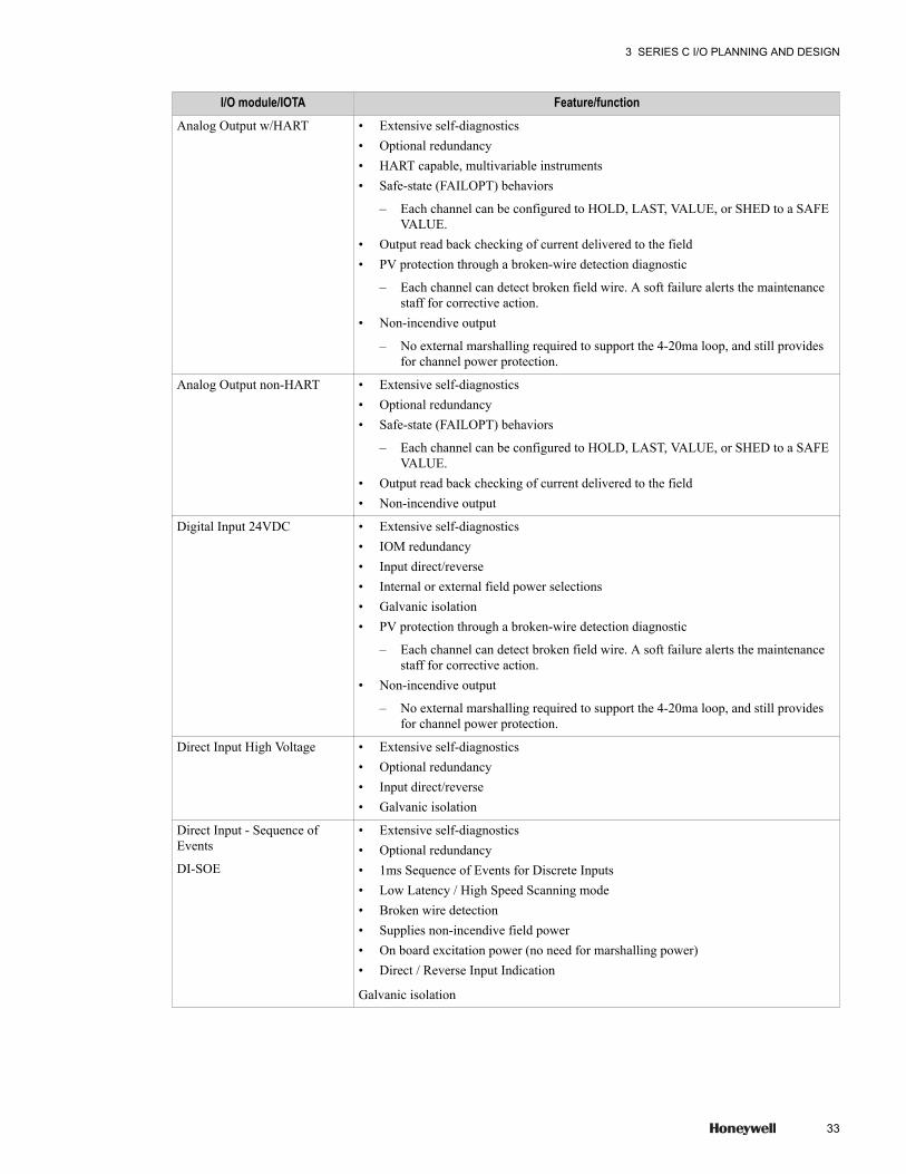
I/O module/IOTA Feature/functionAnalog Output w/HART • Extensive self-diagnostics
• Optional redundancy• HART capable, multivariable instruments• Safe-state (FAILOPT) behaviors
– Each channel can be configured to HOLD, LAST, VALUE, or SHED to a SAFEVALUE.
• Output read back checking of current delivered to the field• PV protection through a broken-wire detection diagnostic
– Each channel can detect broken field wire. A soft failure alerts the maintenancestaff for corrective action.
• Non-incendive output
– No external marshalling required to support the 4-20ma loop, and still providesfor channel power protection.
Analog Output non-HART • Extensive self-diagnostics• Optional redundancy• Safe-state (FAILOPT) behaviors
– Each channel can be configured to HOLD, LAST, VALUE, or SHED to a SAFEVALUE.
• Output read back checking of current delivered to the field• Non-incendive output
Digital Input 24VDC • Extensive self-diagnostics• IOM redundancy• Input direct/reverse• Internal or external field power selections• Galvanic isolation• PV protection through a broken-wire detection diagnostic
– Each channel can detect broken field wire. A soft failure alerts the maintenancestaff for corrective action.
• Non-incendive output
– No external marshalling required to support the 4-20ma loop, and still providesfor channel power protection.
Direct Input High Voltage • Extensive self-diagnostics• Optional redundancy• Input direct/reverse• Galvanic isolation
Direct Input - Sequence ofEvents
DI-SOE
• Extensive self-diagnostics• Optional redundancy• 1ms Sequence of Events for Discrete Inputs• Low Latency / High Speed Scanning mode• Broken wire detection• Supplies non-incendive field power• On board excitation power (no need for marshalling power)• Direct / Reverse Input Indication
Galvanic isolation
3 SERIES C I/O PLANNING AND DESIGN
33
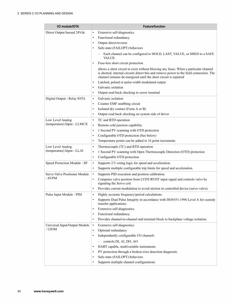
I/O module/IOTA Feature/functionDirect Output bussed 24Vdc • Extensive self-diagnostics
• Functional redundancy• Output direct/reverse• Safe-state (FAILOPT) behaviors
– Each channel can be configured to HOLD, LAST, VALUE, or SHED to a SAFEVALUE.
• Fuse-less short circuit protection
allows a short circuit to exist without blowing any fuses. When a particular channelis shorted, internal circuits detect this and remove power to the field connection. Thechannel remains de-energized until the short circuit is repaired
• Latched, pulsed or pulse-width modulated output• Galvanic isolation• Output read back checking to screw terminal
Digital Output - Relay IOTA • Galvanic isolation• Counter EMF snubbing circuit• Isolated dry contact (Form A or B)• Output read back checking on system side of driver
Low Level Analog(temperature) Input - LLMUX
• TC and RTD operation• Remote cold junction capability• 1 Second PV scanning with OTD protection• Configurable OTD protection (See below)• Temperature points can be added in 16 point increments
Low Level Analog(temperature) Input - LLAI
• Thermocouple (TC) and RTD operation• 1 Second PV scanning with Open Thermocouple Detection (OTD) protection• Configurable OTD protection
Speed Protection Module - SP • Supports 2/3 voting logic for speed and acceleration.• Supports multiple configurable trip limits for speed and acceleration.
Servo Valve Positioner Module- SVPM
• Supports PID execution and position calibration.• Computes valve position from LVDT/RVDT input signal and controls valve by
signaling the Servo coil.• Provides current modulation to avoid stiction in controlled device (servo valve).
Pulse Input Module - PIM • Highly accurate frequency/period calculations.• Supports Dual Pulse Integrity in accordance with ISO6551:1996 Level A for custody
transfer applications.• Extensive self-diagnostics.• Functional redundancy.• Provides channel-to-channel and terminal block to backplane voltage isolation.
Universal Input/Output Module- UIOM
• Extensive self-diagnostics• Optional redundancy• Independently configurable I/O channels
– controls DI, AI, DO, AO• HART capable, multivariable instruments• PV protection through a broken-wire detection diagnostic• Safe-state (FAILOPT) behaviors• Supports multiple channel configurations
3 SERIES C I/O PLANNING AND DESIGN
34 www.honeywell.com
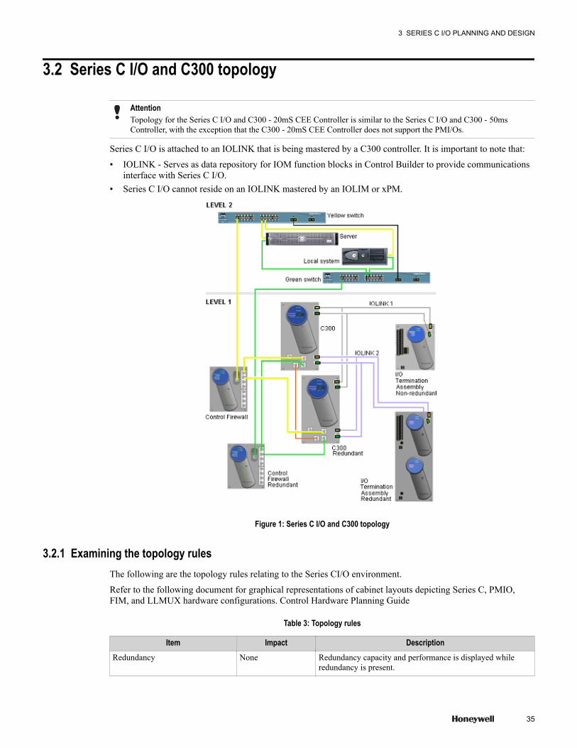
3.2 Series C I/O and C300 topology
AttentionTopology for the Series C I/O and C300 - 20mS CEE Controller is similar to the Series C I/O and C300 - 50msController, with the exception that the C300 - 20mS CEE Controller does not support the PMI/Os.
Series C I/O is attached to an IOLINK that is being mastered by a C300 controller. It is important to note that:
• IOLINK - Serves as data repository for IOM function blocks in Control Builder to provide communicationsinterface with Series C I/O.
• Series C I/O cannot reside on an IOLINK mastered by an IOLIM or xPM.
Figure 1: Series C I/O and C300 topology
3.2.1 Examining the topology rulesThe following are the topology rules relating to the Series CI/O environment.
Refer to the following document for graphical representations of cabinet layouts depicting Series C, PMIO,FIM, and LLMUX hardware configurations. Control Hardware Planning Guide
Table 3: Topology rules
Item Impact DescriptionRedundancy None Redundancy capacity and performance is displayed while
redundancy is present.
3 SERIES C I/O PLANNING AND DESIGN
35
Item Impact DescriptionSwitchover Same as PM I/O Series C I/O hardware and/or software can switchover,
recover, and resume full view in a timeframe no greater thanPM I/O.
Initialization All Series C I/O
per C300
Can be initialized in 60 seconds (+/- 25%) after cabinet-levelloss power loss.
1 I/O module Can be initialized in 10 seconds (+/- 25%) after IOM levelloss power loss.
Multiple I/O Links 2 Design allows the use of multiple Series C I/O Links in thesame cabinet.
I/O Link performance None I/O Link networks perform at the current distance and IOPcount specifications.
I/O Link capacity 40 max Maximum of 40 redundant IOMs per link
(for either Series C I/O or PM I/O).
IOMs / C300 64 max Maximum of 64 redundant IOMs per C300, using both links
(for either Series C I/O or PM I/O).
Series C and
PM I/O - combined
64 Design supports Series C and PM I/O FTAs in the same sideof the cabinet. Current configuration prevents IOTA and FTAsin the same column.
3 SERIES C I/O PLANNING AND DESIGN
36 www.honeywell.com
3.3 Supported Series C I/O modulesThe list of I/O modules below can be used on a Series C IOLINK. The IOLINK contains a function that enablesprogramming and reprogramming the executable image (rather than substitution of a removable hardwarecomponent). The preferred method of delivery of the image is over the IOLINK.
TipSeries C IOLINK cannot contain any PM I/O IOPs.
C300 IOLINK block parameter IOLINKTYPE is used to determine if the IOLINK supports either Series C I/O orPM I/O.
Table 4: Available I/O modules
IOM model names IOM block name Description # ofchnls
Similar to PMIOtype
IOP model names
CU-PAIH01
CC-PAIH01
AI-HART High Level Analog Input withHART
(supports differential inputs ononly channel 13 through channel16)
Refer to Attention
16 HLAIHART
CC-PAIH02 AI-HART High Level Analog Input withHART
((supports differential inputs on all16 channel)
16 HLAIHART
CC-PAIX02 AI-HART High Level Analog Input withDifferential/Single-ended non-HART
(supports differential inputs on all16 channels)
16 HLAI
CC-PAIX01 AI-HL High Level Analog Input withDifferential non-HART
(supports differential inputs ononly channel 13 through channel16)
Refer to Attention
16 HLAI
CU-PAIN01
CC-PAIN01
AI-HL High Level Analog Input withnon-HART
16 HLAI
CC-PAIH51 AI-HART 1 Modem, High Level AnalogInput with HART
16 HLAIHART
CU-PAON01
CC-PAON01
AO Analog Output with non-HART 16 AO16
CU-PAOX01
CC-PAOX01
AO Analog Output with non-HART
Refer to Attention
16 AO16
CU-PAIM01
CC-PAIM01
AI-LLMUX1 Low Level Analog Input Mux 64 LLMUX
CC-PAIM51 AI-LLAI Low Level Analog Input Mux 16 LLAI
3 SERIES C I/O PLANNING AND DESIGN
37
IOM model names IOM block name Description # ofchnls
Similar to PMIOtype
IOP model names
CU-PAOH01
CC-PAOH01
AO-HART Analog Output with HART 16 AO16HART
CC-PAOH51 AO-HART 1 Modem, Analog Output withHART
16 AO16HART
CU-PDIH01
CC-PDIH01
DI-HV High Voltage Digital Input (IOMsupports both 120 and 240 voltsAC)
32 DI
CU-PDIL01
CC-PDIL01
DI-24 Low Voltage Digital Input (24volts DC)
32 DI
or
DI24V
CC-PDIL51 DI-24 Low Voltage, Digital Input (24volts DC)
32 DI
CU-PDIS01
CC-PDIS01
DI-SOE Low Voltage Digital Input (24volts DC)
32 DISOE Mx-PDIS12
CU-PDOB01
CC-PDOB01
DO-24B2 Bussed Low Voltage DigitalOutput (24 volts DC)
32 DO_32
CC-PDOD51 DO-24B Bussed Low Voltage, DigitalOutput (24 volts DC)
32 DO32
CU-PSOE01
CC-PSOE01
DI-SOE Low Voltage Digital Input SOE(24 volts DC)
32 DISOE
CC-PSP401 SP Speed Protection 26
CC-PSV201 SVP Servo Valve Positioner 8
CC-PPIX01 PIM Pulse Input Module 8 PI IOP
CC-PUIO01 UIO Universal Input/Output Module 32
NOTES:
1. There are two models of High Level Analog Input such as, CU-PAIX01 and CU-PAIN01. The ModuleHardware and the corresponding IOTAs are different and CU-PAIN01 is a new model. From the perspectiveof configuration and implementation, both High Level Analog Input models use the same IOM Block suchas, AI-HL. It must be noted that the two models utilize the same configuration; online migration is notpossible as mixed redundant pair is not possible. There are two models of Analog Output such as, CU-PAOX01 and CU-PAON01. Hence, similarly configuration, implementation, and interoperability constraintsapply and CU-PAON01 is the new model.
2. Two new models of AI-HART (CC-PAIH02) and AI-HL (CC-PAIX02) modules are introduced to replacethe older models of the AI-HART (CC-PAIH01) and AI-HL (CC-PAIX01) modules. The new modelssupport both single-ended and differential inputs.
3. With R410, a new model of HART Analog Input CC-PAIH51 is introduced. The HART Analog Input CC-PAIH51 and Cx-PAIH01 use the same IOM block, that is, AI-HART. The configuration and implementationmentioned in note 1 applies to the HART Analog Input module.
4. With R410, a new model of HART Analog Output CC-PAOH51 is introduced. The HART Analog OutputCC-PAOH51 and Cx-PAOH01 use the same IOM block, that is., AO-HART. The configuration andimplementation mentioned in note 1 applies to the HART Analog Output module.
5. With R410, a new model of Digital Input 24V DC CC-PDIL51 is introduced. The Digital Input 24V DC CC-PDIL51 and Cx-PDIL01 use the same IOM block, that is, DI-24. The configuration and implementationmentioned in note 1 applies to the Digital Input 24V module.
3 SERIES C I/O PLANNING AND DESIGN
38 www.honeywell.com
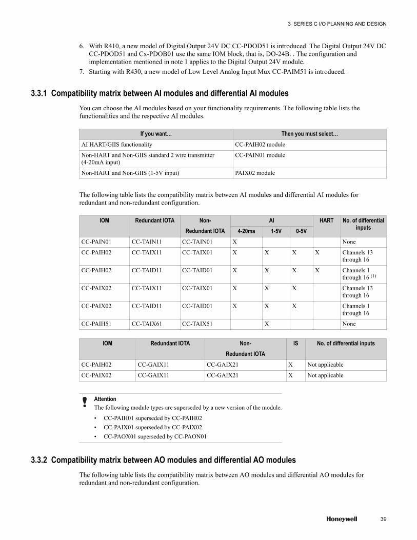
6. With R410, a new model of Digital Output 24V DC CC-PDOD51 is introduced. The Digital Output 24V DCCC-PDOD51 and Cx-PDOB01 use the same IOM block, that is, DO-24B. . The configuration andimplementation mentioned in note 1 applies to the Digital Output 24V module.
7. Starting with R430, a new model of Low Level Analog Input Mux CC-PAIM51 is introduced.
3.3.1 Compatibility matrix between AI modules and differential AI modulesYou can choose the AI modules based on your functionality requirements. The following table lists thefunctionalities and the respective AI modules.
If you want… Then you must select…AI HART/GIIS functionality CC-PAIH02 module
Non-HART and Non-GIIS standard 2 wire transmitter(4-20mA input)
CC-PAIN01 module
Non-HART and Non-GIIS (1-5V input) PAIX02 module
The following table lists the compatibility matrix between AI modules and differential AI modules forredundant and non-redundant configuration.
IOM Redundant IOTA Non-Redundant IOTA
AI HART No. of differentialinputs4-20ma 1-5V 0-5V
CC-PAIN01 CC-TAIN11 CC-TAIN01 X None
CC-PAIH02 CC-TAIX11 CC-TAIX01 X X X X Channels 13through 16
CC-PAIH02 CC-TAID11 CC-TAID01 X X X X Channels 1through 16 (1)
CC-PAIX02 CC-TAIX11 CC-TAIX01 X X X Channels 13through 16
CC-PAIX02 CC-TAID11 CC-TAID01 X X X Channels 1through 16
CC-PAIH51 CC-TAIX61 CC-TAIX51 X None
IOM Redundant IOTA Non-Redundant IOTA
IS No. of differential inputs
CC-PAIH02 CC-GAIX11 CC-GAIX21 X Not applicable
CC-PAIX02 CC-GAIX11 CC-GAIX21 X Not applicable
AttentionThe following module types are superseded by a new version of the module.
• CC-PAIH01 superseded by CC-PAIH02• CC-PAIX01 superseded by CC-PAIX02• CC-PAOX01 superseded by CC-PAON01
3.3.2 Compatibility matrix between AO modules and differential AO modulesThe following table lists the compatibility matrix between AO modules and differential AO modules forredundant and non-redundant configuration.
3 SERIES C I/O PLANNING AND DESIGN
39
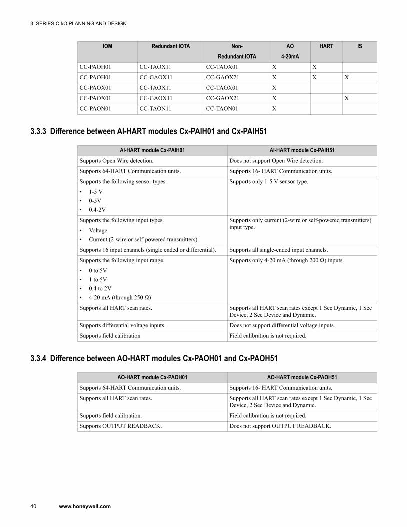
IOM Redundant IOTA Non-Redundant IOTA
AO4-20mA
HART IS
CC-PAOH01 CC-TAOX11 CC-TAOX01 X X
CC-PAOH01 CC-GAOX11 CC-GAOX21 X X X
CC-PAOX01 CC-TAOX11 CC-TAOX01 X
CC-PAOX01 CC-GAOX11 CC-GAOX21 X X
CC-PAON01 CC-TAON11 CC-TAON01 X
3.3.3 Difference between AI-HART modules Cx-PAIH01 and Cx-PAIH51
AI-HART module Cx-PAIH01 AI-HART module Cx-PAIH51Supports Open Wire detection. Does not support Open Wire detection.
Supports 64-HART Communication units. Supports 16- HART Communication units.
Supports the following sensor types.
• 1-5 V• 0-5V• 0.4-2V
Supports only 1-5 V sensor type.
Supports the following input types.
• Voltage• Current (2-wire or self-powered transmitters)
Supports only current (2-wire or self-powered transmitters)input type.
Supports 16 input channels (single ended or differential). Supports all single-ended input channels.
Supports the following input range.
• 0 to 5V• 1 to 5V• 0.4 to 2V• 4-20 mA (through 250 Ω)
Supports only 4-20 mA (through 200 Ω) inputs.
Supports all HART scan rates. Supports all HART scan rates except 1 Sec Dynamic, 1 SecDevice, 2 Sec Device and Dynamic.
Supports differential voltage inputs. Does not support differential voltage inputs.
Supports field calibration Field calibration is not required.
3.3.4 Difference between AO-HART modules Cx-PAOH01 and Cx-PAOH51
AO-HART module Cx-PAOH01 AO-HART module Cx-PAOH51Supports 64-HART Communication units. Supports 16- HART Communication units.
Supports all HART scan rates. Supports all HART scan rates except 1 Sec Dynamic, 1 SecDevice, 2 Sec Device and Dynamic.
Supports field calibration. Field calibration is not required.
Supports OUTPUT READBACK. Does not support OUTPUT READBACK.
3 SERIES C I/O PLANNING AND DESIGN
40 www.honeywell.com
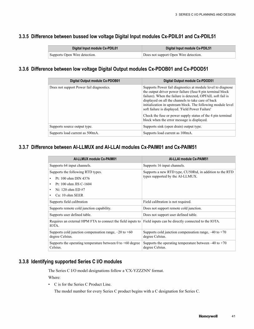
3.3.5 Difference between bussed low voltage Digital Input modules Cx-PDIL01 and Cx-PDIL51
Digital Input module Cx-PDIL01 Digital Input module Cx-PDIL51Supports Open Wire detection. Does not support Open Wire detection.
3.3.6 Difference between low voltage Digital Output modules Cx-PDOB01 and Cx-PDOD51
Digital Output module Cx-PDOB01 Digital Output module Cx-PDOD51Does not support Power fail diagnostics. Supports Power fail diagnostics at module level to diagnose
the output driver power failure (fuse/4 pin terminal blockfailure). When the failure is detected, OPFAIL soft fail isdisplayed on all the channels to take care of backinitialization in upstream block. The following module levelsoft failure is displayed. 'Field Power Failure'
Check the fuse or power supply status of the 4 pin terminalblock when the error message is displayed.
Supports source output type. Supports sink (open drain) output type.
Supports load current as 500mA. Supports load current as 100mA.
3.3.7 Difference between AI-LLMUX and AI-LLAI modules Cx-PAIM01 and Cx-PAIM51
AI-LLMUX module Cx-PAIM01 AI-LLAI module Cx-PAIM51Supports 64 input channels. Supports 16 input channels.
Supports the following RTD types.
• Pt: 100 ohm DIN 4376• Pt: 100 ohm JIS C-1604• Ni: 120 ohm ED #7• Cu: 10 ohm SEER
Supports a new RTD type, CU50Rtd, in addition to the RTDtypes supported by the AI-LLMUX.
Supports field calibration Field calibration is not required.
Supports remote cold junction capability. Does not support remote cold junction.
Supports user defined table. Does not support user defined table.
Requires an external HPM FTA to connect the field inputs toIOTA.
Field inputs can be directly connected to the IOTA.
Supports cold junction compensation range, –20 to +60degree Celsius.
Supports cold junction compensation range, –40 to +70degree Celsius.
Supports the operating temperature between 0 to +60 degreeCelsius.
Supports the operating temperature between –40 to +70degree Celsius.
3.3.8 Identifying supported Series C I/O modulesThe Series C I/O model designations follow a 'CX-YZZZNN' format.
Where:
• C is for the Series C Product Line.
The model number for every Series C product begins with a C designation for Series C.
3 SERIES C I/O PLANNING AND DESIGN
41
• X is U or C
(U = Standard Assembly and C = Corrosion Protected Assembly)• Y is either C, E, F, G, H, K, M, P, PW, S or T
– C = Control Processor– E = Enclosure– F = FTE– G = GI/IS Termination Assembly– H = Hazardous Interface– K = Cabling– M = Mechanical– P = I/O Module– PW = Power– S = Custom Interface– T = Termination Assembly
• ZZZ is a particular function or model.• NN is a series of model and can be used as additional model information -
NN +10 = Redundant complement to an IOTA.
3 SERIES C I/O PLANNING AND DESIGN
42 www.honeywell.com
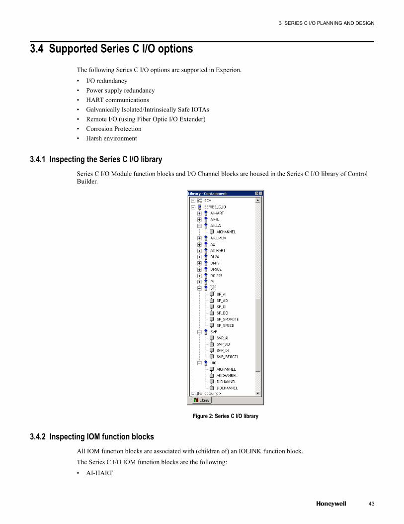
3.4 Supported Series C I/O optionsThe following Series C I/O options are supported in Experion.
• I/O redundancy• Power supply redundancy• HART communications• Galvanically Isolated/Intrinsically Safe IOTAs• Remote I/O (using Fiber Optic I/O Extender)• Corrosion Protection• Harsh environment
3.4.1 Inspecting the Series C I/O librarySeries C I/O Module function blocks and I/O Channel blocks are housed in the Series C I/O library of ControlBuilder.
Figure 2: Series C I/O library
3.4.2 Inspecting IOM function blocksAll IOM function blocks are associated with (children of) an IOLINK function block.
The Series C I/O IOM function blocks are the following:
• AI-HART
3 SERIES C I/O PLANNING AND DESIGN
43

• AI-HL• AI-LLMUX• AI-LLAI• AO• AO-HART• DI-24• DI-HV• DISOE• DO-24B• SP• SVP• PI• UIO
3.4.3 Inspecting channel function blocksThe Series C I/O Channel function blocks are the following:
Table 5: Series C I/O channel function blocks
Channel block name Associated with IOM blocksAICHANNEL • AI-HART
• AI-HL• AI-LLMUX1
• AI-LLAI• UIO
AOCHANNEL • AO• AO-HART• UIO
DICHANNEL • DI-HV• DI-24• DI-SOE• UIO
DOCHANNEL • DO-24B2
• UIO
SP_AI
SP_AO
SP_DI
SP_DO
SP_SPDVOTE
SP_SPEED
• SP
SVP_AI
SVP_AO
SVP_REGCTL
SVP_DI
• SVP
3 SERIES C I/O PLANNING AND DESIGN
44 www.honeywell.com

Channel block name Associated with IOM blocksPICHANNEL • PI
3.4.4 Defining module containmentAn individual channel within a Series C I/O block is often abbreviated as an IOC block. While an IOC blockmust be 'contained in' a Control Module (CM) in Control Builder, the IOC block actually resides within theassociated IOM device. This means you change the execution state (EXECSTATE) of a CM independent of theIOC's point execution state (PTEXECST).
Figure 3: Execution State
Figure 4: Point Execution State
3.4.5 Temperature derating for UIOThe maximum outside module temperature must be limited depending on the internal dissipation.
3 SERIES C I/O PLANNING AND DESIGN
45
Attention• Airflow through the module is assumed to be natural convection.• Ensure that the UIO modules are installed in the correct position. A UIO module must be mounted in the upright
position.
To determine the maximum acceptable outside module temperature for a typical configuration, perform thefollowing steps.
1. Perform the Internal Dissipation Calculation for UIO.
a. Determine and record the actual configuration data.b. Calculate the totals per dissipation contributor.c. Add the totals of the previous step to determine the internal dissipation.
2. Using the Temperature Derating Curves for UIO, determine the maximum acceptable outside moduletemperature.
3.4.6 Internal dissipation calculation for UIOTo calculate the maximum outside module temperature, you require the IO configuration. The maximumdissipation caused by the kernel logic of the UIO module is a fixed value. The other dissipation contributionsdepend on the channel configuration.
Dissipation contributor Max. dissipation perchannel (W)
Number of configuredchannels
Dissipation (W)
Kernel logic 5.5
DI w/ OWD; field impedance ≥ 5 kΩ 0.01
DI; closed contact; 3.5mA 0.085
AI; I < 24mA; Current limited by field 0.05
AI; I > 24mA; Current limited by UIO * 0.49
DO; I < 0.3A 0.115
DO; I < 0.5A 0.305
AO; 500 Ω field impedance; I < 23mA 0.225
AO; 250 Ω field impedance; I < 23 mA 0.335
AO; field impedance < 250 Ω; I < 23 mA 0.47
AO; field impedance < 250 Ω; I < 20 mA 0.42
Total Power Dissipation (W)
Max. outside module temperature °C
* Analog input current above 24mA must be avoided. Field devices for the analog input must be configured todrive current below 24mA. For example, 3.5mA, for sensor fault conditions to minimize the UIO internal powerdissipation. The thin-line derating curve need to be taken when you are using current above 24mA.
3.4.7 Temperature derating curves for UIOThe following graph displays the maximum outside module temperature versus the internal power dissipation.
3 SERIES C I/O PLANNING AND DESIGN
46 www.honeywell.com
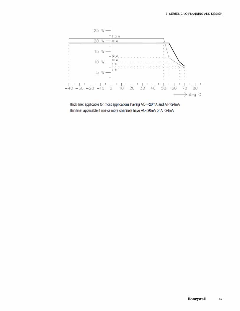
3 SERIES C I/O PLANNING AND DESIGN
47
3.5 I/O Link performance specificationsThe concept of a Link Unit (LU) was introduced with PM I/O where a LU was defined as being roughlyequivalent to one parameter read (or write) per second.
With the introduction of Series C I/O, the transmission rate of data on an IOLINK configured with Series C I/Ois now double that of PM I/O.
AttentionThe Specification and Technical information is subject to change without notice and is superseded by information inapplicable Experion product Specification and Technical data documents. Hence, for each Experion release, you arerecommended to refer the applicable Specification and Technical data documents.
Table 6: Transmission rate of data on an I/O Link
I/O type Link rate per second Link Units per secondPM I/O 1 parameter read or write 1000
Series C I/O 1 parameter read or write 2000
TipIf your configuration exceeds 2000 LUs on a Series C I/O IOLINK, then an I/O Link Access Overrun can occur.This type of overrun occurs when parameter reads and writes are not completed within their cycle time. Thisindicates too many parameter access requests were attempted through the I/O Link.
The IOLINK function block generates a '439, IOLINK Process Data collection Overrun' alarm when an I/O Linkoverrun occurs.
Note: Refer to Turbine Control User's Guide for I/O link performance specification of the SPM and SVPM.
3.5.1 Reviewing Link Unit utilizationThe Link Unit utilization cycle rate varies depending on the type of block being used. The following tabledefines the specifications for the various blocks.
Table 7: Link Unit utilization rates
Block names Data processing Link Units per cycletime
Cycle time
Every primary IOM Event Collection 1 500 ms
Every secondary IOM Event Collection 1 500 ms
DI-xxx IOM blocks PV Scanning 1.75 IOM block's SCANRATE
DO-xxx IOM blocks BACKCALC Scanning 1.25 IOM block's SCANRATE
AI-xxx IOM blocks PV Scanning 5 IOM block's SCANRATE
AO-xxx IOM blocks BACKCALC Scanning 5 IOM block's SCANRATE
AOCHANNEL OP Store 1 OP connector's CMExecution Rate
status output for DOCHANNEL SO Store 1 SO connector's CMExecution Rate
Pulse width modulation forDOCHANNEL
BACKCALC Scanning 1 IOM block's SCANRATE
3 SERIES C I/O PLANNING AND DESIGN
48 www.honeywell.com

Block names Data processing Link Units per cycletime
Cycle time
Pulse width modulation forDOCHANNEL
OP Store 1 OP connector's CMExecution Rate
3.5.2 Reducing I/O Link trafficIf I/O Link overruns persist, you reduce the I/O Link traffic by:
• Increasing the value of the IOM's Scanning Rate parameter [SCANRATE]
(i.e. increasing the time interval between IOM scans)• Increase the Execution Period of Control Modules containing Output Channel blocks• Reducing the number of IOMs configured• Split the IOMs across multiple IOLINKS• Check for presence of an address 'Chattering ' alarm events
TipLink IDs are only detected on their corresponding modules.
• Modules with Link ID 1 cannot detect Link ID 2.• Modules with Link ID 2 cannot detect Link ID 1.
3.5.3 Event collectionUnder normal conditions, every IOM configured on the I/O Link, whether primary or secondary, uses LinkUnits for event collection. This activity is periodic and can be accounted for, however; conditions in whichnumerous events and alarms are generated are unpredictable and may cause transient I/O Link overruns anddelays in display updates. These transient overruns clear once the rush of events and alarms are collected.
3.5.4 PV and Back calculation scanningThe following I/O parameters are automatically scanned by the C300 as soon as the IOM block is loaded.
Table 8: I/O parameters scanned when the IOM is loaded
IOM block Scanned parametersAI-xxx PV, PVSTS
AO-xxx OP, INITREQ
DI-xxx PVFL, BADPVFL
DO-xxx SO, INITREQ, OP
The number of AI and DI channel blocks contained within CMs or SCMs:
• does not increase LU consumption.
The DO channel blocks contained in CMs and SCMs:
• does also not increase LU consumption for Back Calculation scanning, but LU consumption increases foreach OP or SO store.
3 SERIES C I/O PLANNING AND DESIGN
49

3 SERIES C I/O PLANNING AND DESIGN
50 www.honeywell.com

4 Series C I/O Installation and Upgrades
The Experion R300 release utilizes new hardware designs including those for the controllers, I/O modules, andswitches. The information contained in this section defines how to establish the various hardware connectionsand Series C I/O firmware.
To review planning the entire Series C Control System, refer to the Control Hardware Planning Guide'sPlanning Your Series C Control System.
Related topics“Installation Declarations” on page 52“Installing the Series C IOTA on the carrier” on page 55“Mounting the I/O module on the IOTA” on page 57“Grounding and power considerations - IOTA boards” on page 58“Connecting IOMs and field devices through I/O Termination Assemblies” on page 60“Powering the Series C system” on page 64“Fusing - Series C IOTA boards” on page 65
51
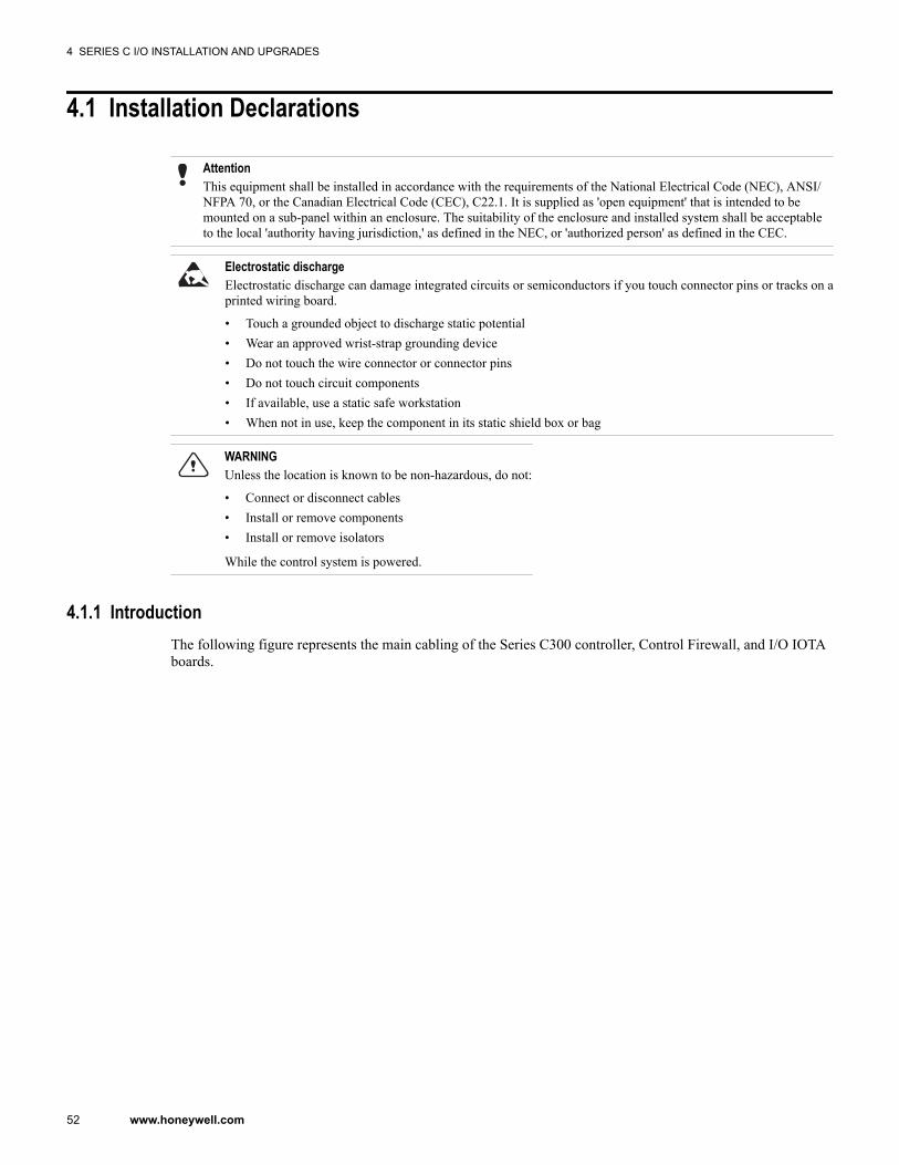
4.1 Installation Declarations
AttentionThis equipment shall be installed in accordance with the requirements of the National Electrical Code (NEC), ANSI/NFPA 70, or the Canadian Electrical Code (CEC), C22.1. It is supplied as 'open equipment' that is intended to bemounted on a sub-panel within an enclosure. The suitability of the enclosure and installed system shall be acceptableto the local 'authority having jurisdiction,' as defined in the NEC, or 'authorized person' as defined in the CEC.
Electrostatic dischargeElectrostatic discharge can damage integrated circuits or semiconductors if you touch connector pins or tracks on aprinted wiring board.
• Touch a grounded object to discharge static potential• Wear an approved wrist-strap grounding device• Do not touch the wire connector or connector pins• Do not touch circuit components• If available, use a static safe workstation• When not in use, keep the component in its static shield box or bag
WARNINGUnless the location is known to be non-hazardous, do not:
• Connect or disconnect cables• Install or remove components• Install or remove isolators
While the control system is powered.
4.1.1 IntroductionThe following figure represents the main cabling of the Series C300 controller, Control Firewall, and I/O IOTAboards.
4 SERIES C I/O INSTALLATION AND UPGRADES
52 www.honeywell.com
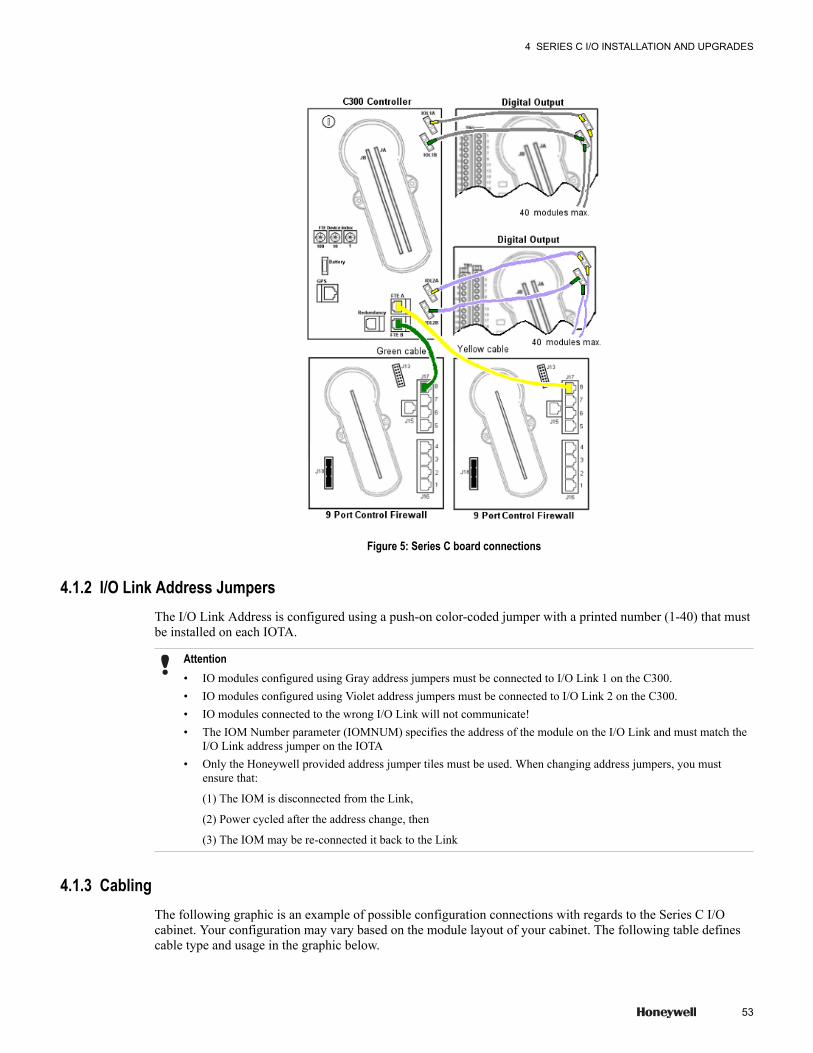
Figure 5: Series C board connections
4.1.2 I/O Link Address JumpersThe I/O Link Address is configured using a push-on color-coded jumper with a printed number (1-40) that mustbe installed on each IOTA.
Attention• IO modules configured using Gray address jumpers must be connected to I/O Link 1 on the C300.• IO modules configured using Violet address jumpers must be connected to I/O Link 2 on the C300.• IO modules connected to the wrong I/O Link will not communicate!• The IOM Number parameter (IOMNUM) specifies the address of the module on the I/O Link and must match the
I/O Link address jumper on the IOTA• Only the Honeywell provided address jumper tiles must be used. When changing address jumpers, you must
ensure that:
(1) The IOM is disconnected from the Link,
(2) Power cycled after the address change, then
(3) The IOM may be re-connected it back to the Link
4.1.3 CablingThe following graphic is an example of possible configuration connections with regards to the Series C I/Ocabinet. Your configuration may vary based on the module layout of your cabinet. The following table definescable type and usage in the graphic below.
4 SERIES C I/O INSTALLATION AND UPGRADES
53

Table 9: Series C I/O cable types
Cable Color PurposeFTE -A Yellow Connect controller to firewall (point-to-point)
FTE - B Green Connect controller to firewall (point-to-point)
FTE - Redundant Orange Private path between primary and secondary controller (point-to-point)
IOL1A Grey/yellow Connect controller to I/O
IOL1B Grey/green Connect controller to I/O
IOL2A Violet/yellow Connect primary controller to secondary controller and then to I/O
IOL2B Violet/green Connect primary controller to secondary controller and then to I/O
Figure 6: Series C cabling
4 SERIES C I/O INSTALLATION AND UPGRADES
54 www.honeywell.com

4.2 Installing the Series C IOTA on the carrier
• You can use a redundant IOTA to support a non-redundant Series C IOM application. Just be sure to installthe non-redundant Series C IOM in the primary location on the IOTA.
• Be sure the enclosure is connected to a protective earth ground using #8 AWG solid copper wire. Thereshould be metal to metal contact between the grounding bus bar and the enclosure as well as the carrier.
PrerequisitesCarrier for mounting IOTA is installed in a cabinet or desired mounting location.
• Power supply is installed.• Control firewall is installed.• All wiring and pre-fabricated cables are available and labeled as applicable.• Be sure all power is turned off at the installation location.• You have the mounting hardware supplied with the components.
Mounting the IOTA• Select desired mounting location on carrier and align mounting holes in IOTA with screw-hole locations on
the carrier. Be sure component side of IOTA is facing up.6 inch IOTA board 4 mounting screws
9 inch IOTA board 6 mounting screws 12 inch IOTA board
AttentionWhen mounting the either the 9 or 12 inch IOTA board, it is recommended to secure the three mounting screws onone side (either left or right) and then secure the other side.
Securing the four corner screws and the two middle screws may cause bowing of the board and impact thealignment of the IOTA board to the carrier holes and is not recommended.
CAUTIONThe IOTA power and ground screws can bind during installation or removal if the mounting screws are fullysecured before the power/ground screws are installed.
Recommended sequence:
1. Secure the IOTA to the carrier tightening the IOTA's mounting screws only half-way. Insert the spacersand washers between bottom of IOTA and top of carrier.
2. Install the 24V (power) and ground (common) screws fully into the bus bars, torquing the screws to 5-inch pounds.
3. Finish installing the IOTA by tightening the IOTA's mounting screws only full-way, torquing thescrews to 3-inch pounds
4 SERIES C I/O INSTALLATION AND UPGRADES
55
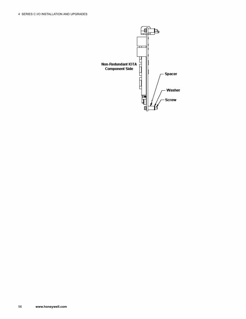
4 SERIES C I/O INSTALLATION AND UPGRADES
56 www.honeywell.com
4.3 Mounting the I/O module on the IOTA
PrerequisitesIt is recommended to attach the IOTA board to the carrier prior to mounting the module to the IOTA. Thefollowing also needs to be established:
• IOTA is mounted on the carrier rack.• Power supply is installed.• Control firewall is installed.• All wiring and pre-fabricated cables are available and labeled as applicable.• Be sure all power is turned off at the installation location.• You have the mounting hardware supplied with the components.
Mounting the module1 Insert the module onto IOTA board making sure that the circuit board mates properly with the IOTA board
connector.2 Secure the module to the:
• IOTA board - with two screws located at each side of the plastic cover.• Carrier - with the long gray plastic screw located on the module's face.
CAUTIONOnly use a #2 Phillips screw-driver to carefully loosen or tighten the long gray plastic screw. Do not use eithera #1 Phillips screw-driver or a battery-powered screw-driver to remove or install the plastic screw as this candamage the screw head.
4 SERIES C I/O INSTALLATION AND UPGRADES
57
4.4 Grounding and power considerations - IOTA boardsThe Series C cabinet allows mounted carriers that support the attachment of the IOTA boards. By making theseconnections, power, and chassis, grounding is provided to the IOTA board.
4.4.1 Testing for power
CAUTIONExtreme care must be taken when testing for power at the Series C bus bars. Improper testing can result in anelectrical short circuit, which will impact all modules attached to the channel carrier assembly.
Never use a test probe at an unattached IOTA's 24V screw hole. The probe can potentially touch the back channelassembly causing a short circuit.
The following locations are recommended for testing power:
Preferred location if IOTAs are attached
• Center of the screw that attaches the IOTA to the 24V bus bar.
Preferred location if IOTAs are NOT attached.
• Center of the screw of top connection terminal for power cable.
Testing for power at IOTA screw1 Insert the test probe at the center of the screw that attaches the IOTA to the 24V power connection.2 This concludes this procedure.
Testing for power at 24V bus bar top terminal1 Carefully pull the red cap from the top of the terminal. It remains attached to the power cable.
• Insert the test probe at the center of the screw to the 24V power terminal.2 Carefully pull the black cap from the top of the terminal. It remains attached to the ground cable.
Insert the test probe at the center of the screw to the COM ground terminal.3 Replace the both caps.4 This concludes this procedure.
4 SERIES C I/O INSTALLATION AND UPGRADES
58 www.honeywell.com
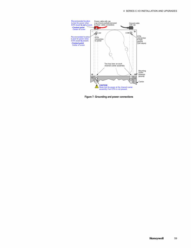
Figure 7: Grounding and power connections
4 SERIES C I/O INSTALLATION AND UPGRADES
59

4.5 Connecting IOMs and field devices through I/O TerminationAssemblies
All connections between IOMs and field devices are through I/O Termination Assemblies (IOTAs). IOTAs aresometimes connected to ancillary hardware that pre-conditions the signal for use in Experion.
The following table defines the relationship between IOM type and the ancillary hardware.
Table 10: IOM types and ancillary hardware
If IOM type is Then the ancillary hardwareDO
Digital Output
takes the output signal and drives a set of relays
AI LLMUX can be one to four Field Termination Assemblies.
These FTA's pre-condition and package the signals before they are received by the IOTA.
To simplify system hardware selection and to minimize spare parts requirements, IOMs can be used withvarious types of IOTAs. The following table provides a list of IOMs, their associated IOTAs, and ancillaryhardware. All IOM models listed within the same cell can be installed on any of the IOTAs listed in the adjacentcell.
AttentionConnecting Series C IOM's into a Galvanically Isolated / Intrinsically Safe (GI/IS) environment requires specificGI/IS IOTAs.
Refer to the following for GI/IS IOTAs and the IOMs they support: “GI/IS IOTA models” on page 520
Table 11: IOMs, IOTAs, and ancillary cards
IOM block type IOM modelnumber
IOTA model number IOTA description 7 IOTA supported FTAsor ancillary cards
AI-HART Cx-PAIH01
Refer to Attention
Cx-TAIX01 AI, non-redundant None
Cx-TAIX11 AI, redundant None
Cx-GAIX11 AI, GI-IS, non-redundant MTL4541
MTL4575
Cx-GAIX21 AI, GI-IS, redundant MTL4544
CC-TAID01 Analog Input, Non-redundant, 16 ch.differential
Cx-PAIH51 Cx-TAIX51 AI, non-redundant None
Cx-TAIX61 AI, redundant None
AI-HART
Differential/
Single-ended
CC-PAIH02 Cx-TAIX01 Analog Input, Non-redundant, 4 ch.differential
None
Cx-TAIX11 Analog Input, Redundant, 4 ch.differential
None
Cx-GAIX11 Analog Input, GI-IS, Redundant, nodifferential, 4-20 mA only
MTL4544
Cx-GAIX21 Analog Input, GI-IS, Non-redundant,no differential, 4-20 mA only
MTL4541
MTL4575
CC-TAID11 Analog Input, Redundant, 16 ch.differential
None
4 SERIES C I/O INSTALLATION AND UPGRADES
60 www.honeywell.com
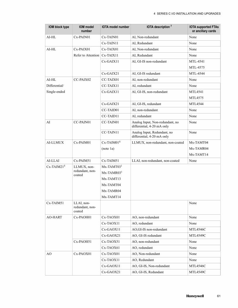
IOM block type IOM modelnumber
IOTA model number IOTA description 7 IOTA supported FTAsor ancillary cards
AI-HL Cx-PAIN01 Cx-TAIN01 AI, Non-redundant None
Cx-TAIN11 AI, Redundant None
AI-HL Cx-PAIX01
Refer to Attention
Cx-TAIX01 AI, Non-redundant None
Cx-TAIX11 AI, Redundant None
Cx-GAIX11 AI, GI-IS non-redundant MTL-4541
MTL-4575
Cx-GAIX21 AI, GI-IS redundant MTL-4544
AI-HL
Differential/
Single-ended
CC-PAIX02 CC-TAIX01 AI, non-redundant None
CC-TAIX11 AI, redundant None
Cx-GAIX11 AI, GI-IS, non-redundant MTL4541
MTL4575
Cx-GAIX21 AI, GI-IS, redundant MTL4544
CC-TAID01 AI, non-redundant None
CC-TAID11 AI, redundant None
AI CC-PAIN01 CC-TAIN01 Analog Input, Non-redundant, nodifferential, 4-20 mA only
None
CC-TAIN11 Analog Input, Redundant, nodifferential, 4-20 mA only
None
AI-LLMUX Cx-PAIM01 Cx-TAIM014
(note 1a)
LLMUX, non-redundant, non-coated Mx-TAMT04
Mx-TAMR04
Mx-TAMT14
AI-LLAI Cx-PAIM51 Cx-TAIM51 LLAI, non-redundant, non-coated None
Cx-TAIM215 LLMUX, non-redundant, non-coated
Mx-TAMT031
Mx-TAMR031
Mx-TAMT13
Mx-TAMT04
Mx-TAMR04
Mx-TAMT14
Cx-TAIM51 LLAI, non-redundant, non-coated
None
AO-HART Cx-PAOH01 Cx-TAOX01 AO, non-redundant None
Cx-TAOX11 AO, redundant None
Cx-GAOX11 AO,GI-IS non-redundant MTL4546C
Cx-GAOX21 AO, GI-IS redundant MTL4549C
Cx-PAOH51 Cx-TAOX51 AO, non-redundant None
Cx-TAOX61 AO, redundant None
AO Cx-PAOX01 Cx-TAOX01 AO, Non-redundant None
Cx-TAOX11 AO, Redundant None
Cx-GAOX11 AO, GI-IS, Non-redundant MTL4546C
Cx-GAOX21 AO, GI-IS, Redundant MTL4549C
4 SERIES C I/O INSTALLATION AND UPGRADES
61
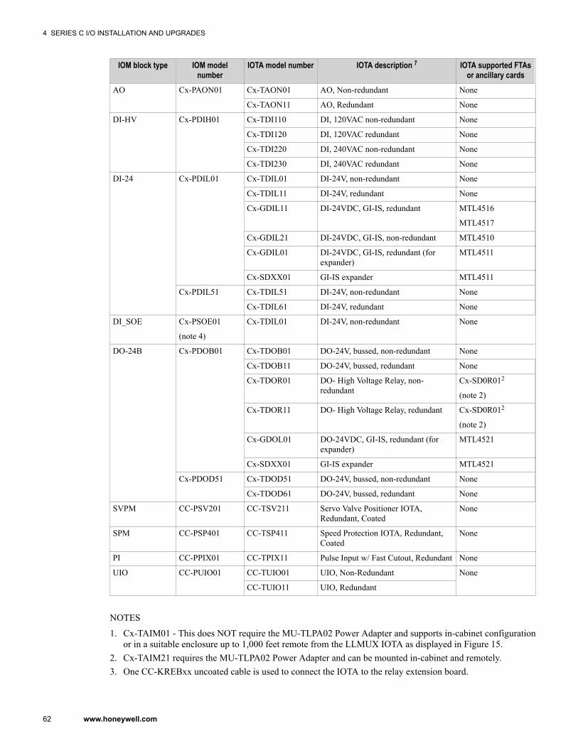
IOM block type IOM modelnumber
IOTA model number IOTA description 7 IOTA supported FTAsor ancillary cards
AO Cx-PAON01 Cx-TAON01 AO, Non-redundant None
Cx-TAON11 AO, Redundant None
DI-HV Cx-PDIH01 Cx-TDI110 DI, 120VAC non-redundant None
Cx-TDI120 DI, 120VAC redundant None
Cx-TDI220 DI, 240VAC non-redundant None
Cx-TDI230 DI, 240VAC redundant None
DI-24 Cx-PDIL01 Cx-TDIL01 DI-24V, non-redundant None
Cx-TDIL11 DI-24V, redundant None
Cx-GDIL11 DI-24VDC, GI-IS, redundant MTL4516
MTL4517
Cx-GDIL21 DI-24VDC, GI-IS, non-redundant MTL4510
Cx-GDIL01 DI-24VDC, GI-IS, redundant (forexpander)
MTL4511
Cx-SDXX01 GI-IS expander MTL4511
Cx-PDIL51 Cx-TDIL51 DI-24V, non-redundant None
Cx-TDIL61 DI-24V, redundant None
DI_SOE Cx-PSOE01
(note 4)
Cx-TDIL01 DI-24V, non-redundant None
DO-24B Cx-PDOB01 Cx-TDOB01 DO-24V, bussed, non-redundant None
Cx-TDOB11 DO-24V, bussed, redundant None
Cx-TDOR01 DO- High Voltage Relay, non-redundant
Cx-SD0R012
(note 2)
Cx-TDOR11 DO- High Voltage Relay, redundant Cx-SD0R012
(note 2)
Cx-GDOL01 DO-24VDC, GI-IS, redundant (forexpander)
MTL4521
Cx-SDXX01 GI-IS expander MTL4521
Cx-PDOD51 Cx-TDOD51 DO-24V, bussed, non-redundant None
Cx-TDOD61 DO-24V, bussed, redundant None
SVPM CC-PSV201 CC-TSV211 Servo Valve Positioner IOTA,Redundant, Coated
None
SPM CC-PSP401 CC-TSP411 Speed Protection IOTA, Redundant,Coated
None
PI CC-PPIX01 CC-TPIX11 Pulse Input w/ Fast Cutout, Redundant None
UIO CC-PUIO01 CC-TUIO01 UIO, Non-Redundant None
CC-TUIO11 UIO, Redundant
NOTES
1. Cx-TAIM01 - This does NOT require the MU-TLPA02 Power Adapter and supports in-cabinet configurationor in a suitable enclosure up to 1,000 feet remote from the LLMUX IOTA as displayed in Figure 15.
2. Cx-TAIM21 requires the MU-TLPA02 Power Adapter and can be mounted in-cabinet and remotely.3. One CC-KREBxx uncoated cable is used to connect the IOTA to the relay extension board.
4 SERIES C I/O INSTALLATION AND UPGRADES
62 www.honeywell.com
4. One CC-KREBxx coated cable is used to connect the IOTA to the relay extension board.5. Bussed IOM (PDOB01) is used for both bussed outputs and relay outputs, however, only relay outputs
require the additional card.6. Redundantly configured IOMs must be installed on a redundant IOTA.7. Non-redundant IOMs can be installed on non-redundant and redundant IOTAs. However, when installed on
a redundant IOTA, non-redundant IOMs must be installed in the upper IOM slot of the redundant IOTA.8. The IOTA type used for Series C IO DI-24V is used with the DI-SOE IOM also.9. Non-redundant differential IOTA (CC-TAID01) length is 9', non-redundant IOTA (CC-TAIX01 and CC-
TAIN01) length is 6', and differential redundant IOTAs (CC-TAID11, CC-TAIN11, and CC-TAIX11) lengthis 12'.
10. A third level of connector is available for all differential mode connections as an extension of channel 13through 16 terminals for all 16 channels.
11. Differential configuration does not require any custom wiring as the IOTAs (CC-TAID01 and CC-TAID11)performs it internally.
12. Two new models of AI-HART (CC-PAIH02) and AI-HL (CC-PAIX02) modules are introduced to replacethe older models of the AI-HART (CC-PAIH01) and AI-HL (CC-PAIX01) modules. The new modelssupport both single-ended and differential inputs.
13. With R410, new models of AI-HART (Cx-PAIH51), AO-HART (Cx-PAOH51), DI-24V (Cx-PDIL51), andDO-24B2 (Cx-PDOD51) are introduced.
4 SERIES C I/O INSTALLATION AND UPGRADES
63
4.6 Powering the Series C systemPower systems for the Series C control hardware provides:
• optional redundant power supplies with separate mains power feeds• optional system battery backup is also available, and• a memory RAM battery is provided to supply memory retention power for the C300 Controller
The capabilities and options available with the Series-C power system are very similar to those available withthe Process Manager Power System.
Refer to the Series C Power Supply in the C300 Controller User Guide additional power system information.
4 SERIES C I/O INSTALLATION AND UPGRADES
64 www.honeywell.com
4.7 Fusing - Series C IOTA boardsSeries-C I/O modules are constructed to support normal field failures, wiring errors and conditions such as ashorted wire. All Series-C IOTAs contain at least one fuse that provides protection for catastrophic errors in theIOTA, IOM and other elements of the Series-C system. In normal operation as well as many abnormaloperations, the fuse element should not blow.
The following attributes apply to all Series-C I/O modules:
• 24V DC power is protected by a fuse mounted on the IOTA.• For redundant IOTAs, a fuse is provided for each IOM. If one fuse element were to blow, the partner IOM
continues to operate.
AttentionIn virtually all instances of normal field failure, the I/O module will recover without any maintenance action such asreplacing a component or fuse.
To access the parts information for the fuses associated with each board and module, refer to “Series Crecommended spares” on page 468 in the Recommended Spare Parts section.
4 SERIES C I/O INSTALLATION AND UPGRADES
65

4 SERIES C I/O INSTALLATION AND UPGRADES
66 www.honeywell.com

5 Series C IOTA Pinouts
Related topics“Analog Input IOTA Models CC-TAIX01, CC-TAIX11” on page 68“Analog Input non-HART/HARTIOTA Models Cx-TAIX51, Cx-TAIX61” on page 79“Non-HART Analog Input IOTA (Models CC-TAIN01, CC-TAIN11)” on page 85“Differential Analog input IOTA (Models CC-TAID01 and CC-TAID11)” on page 92“Analog Output IOTA Models CC-TAOX01, CC-TAOX11, CC-TAON01 and CC-TAON11” on page 105“Analog Output HART IOTA Models Cx-TAOX51, Cx-TAOX61” on page 112“Low Level Analog Input Mux (LLMUX) IOTA Models CC-TAIM01” on page 116“Digital Input High Voltage IOTA Models CC-TDI110, CC-TDI120, CC-TDI220, CC-TDI230” on page 120“Digital Input 24V IOTA Models CC-TDIL01, CC-TDIL11” on page 125“Digital Input 24V IOTA Models Cx - TDIL51, Cx - TDIL61” on page 133“Digital Output 24V IOTA Models CC-TDOB01, CC-TDOB11” on page 139“Digital Output 24V IOTA Models Cx-TDOD51, Cx-TDOD61” on page 144“Digital Output Relay Module IOTA Models CC-TDOR01, CC-TDOR11” on page 149“Digital Output Relay Extender board Models CC-SDOR01” on page 151“Speed Protection Module IOTA Model CC-TSP411” on page 155“Servo Valve Positioner Module IOTA Models CC-TSV211” on page 162“Universal Input/Output IOTA Models CC-TUIO01 and CC-TUIO11” on page 170“Pulse Input Module IOTA Model CC-TPIX11” on page 179“Upgrading Firmware in Series C I/O components” on page 181
67
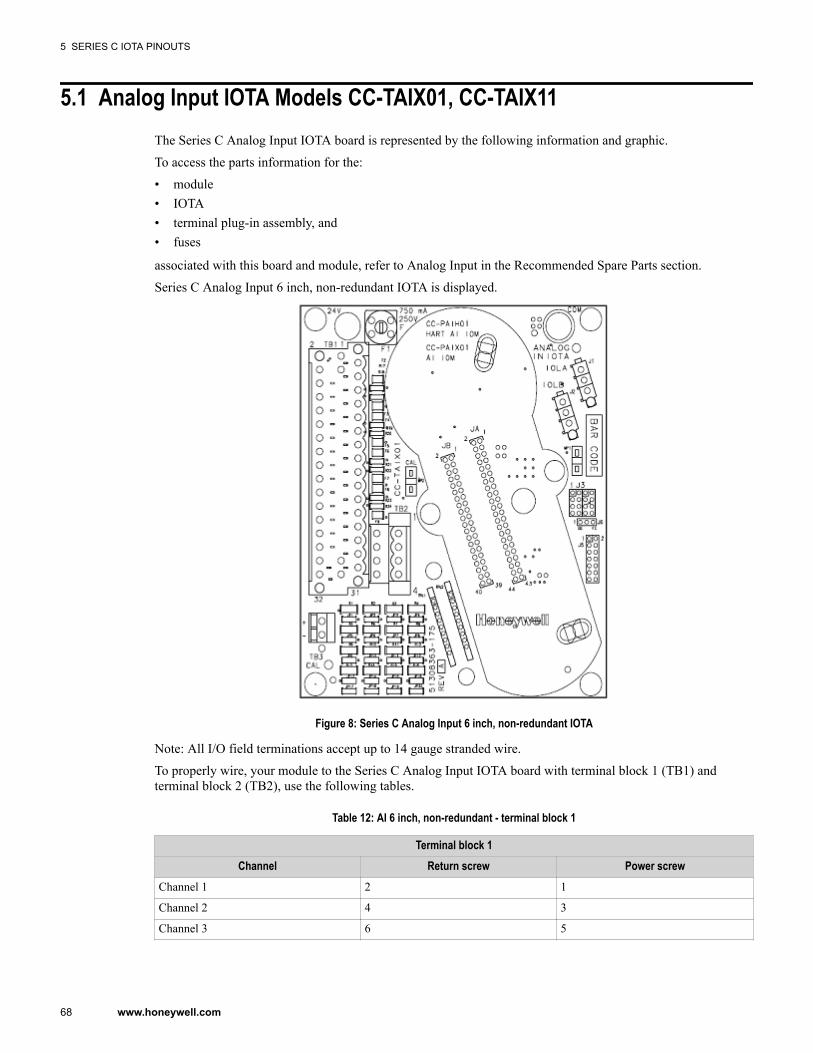
5.1 Analog Input IOTA Models CC-TAIX01, CC-TAIX11The Series C Analog Input IOTA board is represented by the following information and graphic.
To access the parts information for the:
• module• IOTA• terminal plug-in assembly, and• fuses
associated with this board and module, refer to Analog Input in the Recommended Spare Parts section.
Series C Analog Input 6 inch, non-redundant IOTA is displayed.
Figure 8: Series C Analog Input 6 inch, non-redundant IOTA
Note: All I/O field terminations accept up to 14 gauge stranded wire.
To properly wire, your module to the Series C Analog Input IOTA board with terminal block 1 (TB1) andterminal block 2 (TB2), use the following tables.
Table 12: AI 6 inch, non-redundant - terminal block 1
Terminal block 1Channel Return screw Power screw
Channel 1 2 1
Channel 2 4 3
Channel 3 6 5
5 SERIES C IOTA PINOUTS
68 www.honeywell.com
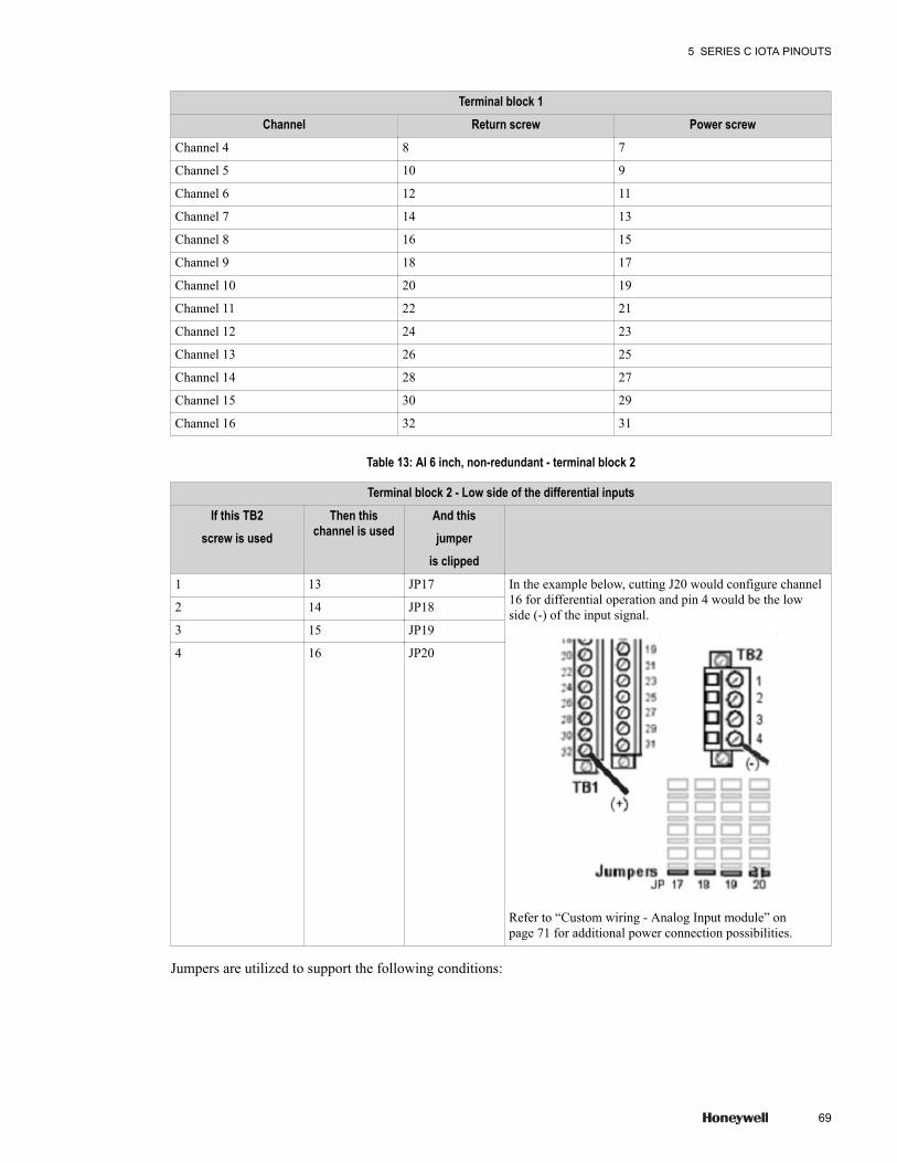
Terminal block 1Channel Return screw Power screw
Channel 4 8 7
Channel 5 10 9
Channel 6 12 11
Channel 7 14 13
Channel 8 16 15
Channel 9 18 17
Channel 10 20 19
Channel 11 22 21
Channel 12 24 23
Channel 13 26 25
Channel 14 28 27
Channel 15 30 29
Channel 16 32 31
Table 13: AI 6 inch, non-redundant - terminal block 2
Terminal block 2 - Low side of the differential inputsIf this TB2
screw is usedThen this
channel is usedAnd thisjumper
is clipped1 13 JP17 In the example below, cutting J20 would configure channel
16 for differential operation and pin 4 would be the lowside (-) of the input signal.
Refer to “Custom wiring - Analog Input module” onpage 71 for additional power connection possibilities.
2 14 JP18
3 15 JP19
4 16 JP20
Jumpers are utilized to support the following conditions:
5 SERIES C IOTA PINOUTS
69
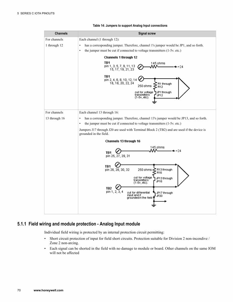
Table 14: Jumpers to support Analog Input connections
Channels Signal screwFor channels
1 through 12
Each channel (1 through 12):
• has a corresponding jumper. Therefore, channel 1's jumper would be JP1, and so forth.• the jumper must be cut if connected to voltage transmitters (1-5v. etc.)
For channels
13 through 16
Each channel 13 through 16:
• has a corresponding jumper. Therefore, channel 13's jumper would be JP13, and so forth.• the jumper must be cut if connected to voltage transmitters (1-5v. etc.)
Jumpers J17 through J20 are used with Terminal Block 2 (TB2) and are used if the device isgrounded in the field.
5.1.1 Field wiring and module protection - Analog Input moduleIndividual field wiring is protected by an internal protection circuit permitting:
• Short circuit protection of input for field short circuits. Protection suitable for Division 2 non-incendive /Zone 2 non-arcing.
• Each signal can be shorted in the field with no damage to module or board. Other channels on the same IOMwill not be affected
5 SERIES C IOTA PINOUTS
70 www.honeywell.com
5.1.2 Two-wire transmitter wiring - Analog Input moduleThe AI IOM/IOTA is optimized for use with classic two-wire transmitters. All 16 channels can accept inputsfrom two-wire transmitters without any special wiring or jumper options.
The standard usage is to:
• reserve the first 12 channels of the AI IOM/IOTA for classic two-wire transmitters, and• use the last 4 channels of the IOM/IOTA to interface any of the supported input styles (including two-wire
transmitters).
Depending on the input style applied to channels 13 through 16, you may need to cut jumpers on the IOTA andapply wiring to the TB2 terminal block on the IOTA. This is discussed in detail in the following sections.
5.1.3 Non two-wire transmitter wiring - Analog Input moduleThe IOTA is pre-engineered (without custom wiring) to accept sources that are not two-wire transmitters, butyou must use channels 13 through 16.
When sources other than two-wire transmitters are to be interfaced and you have more than 4 per IOTAs, then:
• the first four must be interfaced to channels 13 through 16, and• the remainder may be able to interface to channels 1 through 12 (depending on input style) but you must
perform some degree of custom wiring.
NOTE: There are some input styles that simply cannot be applied to channels 1 through 12 - if that applies toyou then you will likely need to purchase an additional IOM/IOTA.
CAUTIONThe jumpers on the IOTA are non-repairable; once cut, they stay cut. Careful planning is a must.
5.1.4 Custom wiring - Analog Input moduleCustom wiring means:
• using additional wires to TB2 (beyond their intended purpose for channels 13 through 16)• and/or using wires to another termination area in the cabinet engineered on a project-basis.
Some of the styles (other than two-wire transmitter):
• can be applied to channels 1 through 12 with the use of custom wiring.• Other cannot be applied to channels 1 through 12 at all.
5 SERIES C IOTA PINOUTS
71
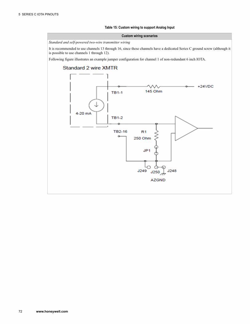
Table 15: Custom wiring to support Analog Input
Custom wiring scenariosStandard and self-powered two-wire transmitter wiring
It is recommended to use channels 13 through 16, since these channels have a dedicated Series C ground screw (although itis possible to use channels 1 through 12).
Following figure illustrates an example jumper configuration for channel 1 of non-redundant 6 inch IOTA.
5 SERIES C IOTA PINOUTS
72 www.honeywell.com
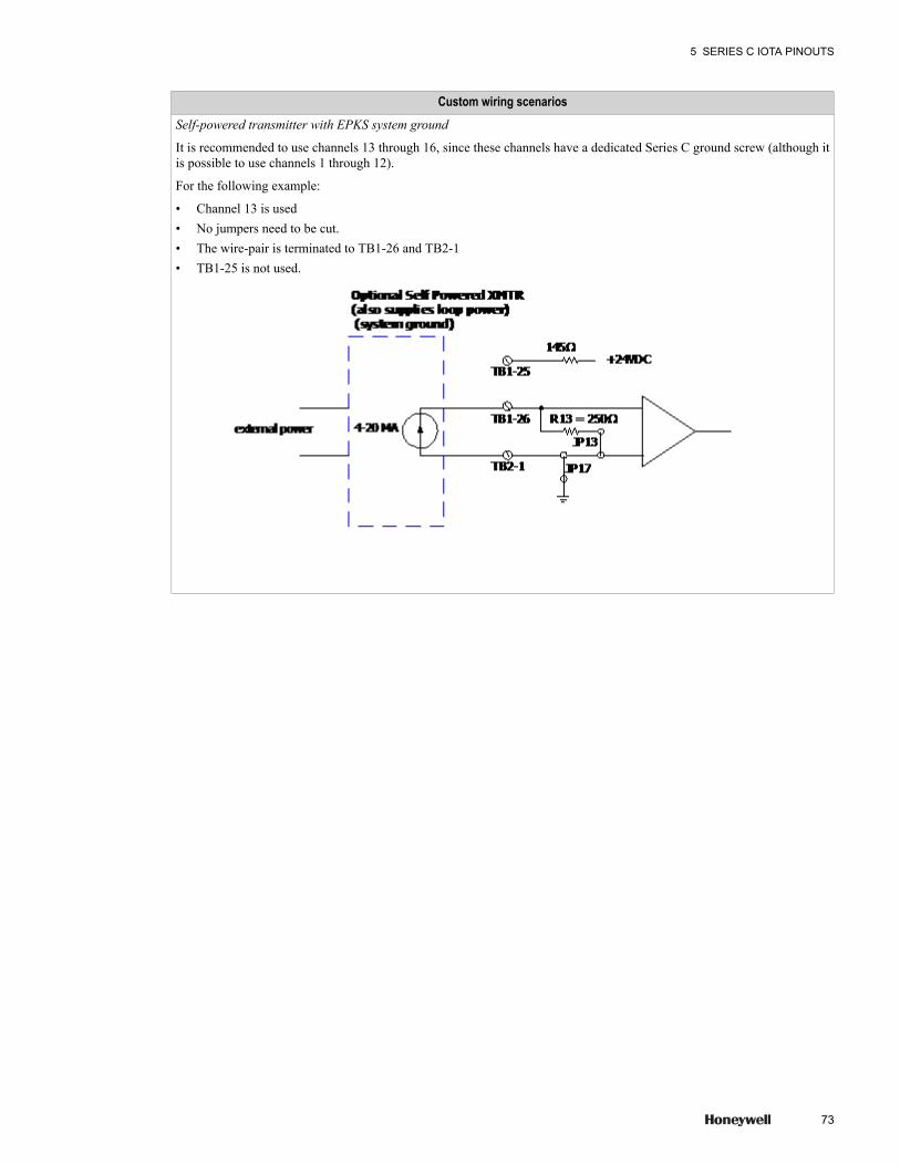
Custom wiring scenariosSelf-powered transmitter with EPKS system ground
It is recommended to use channels 13 through 16, since these channels have a dedicated Series C ground screw (although itis possible to use channels 1 through 12).
For the following example:
• Channel 13 is used• No jumpers need to be cut.• The wire-pair is terminated to TB1-26 and TB2-1• TB1-25 is not used.
5 SERIES C IOTA PINOUTS
73
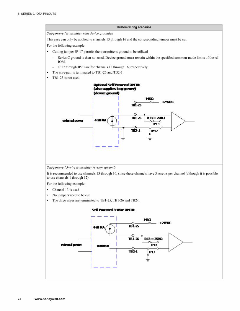
Custom wiring scenariosSelf-powered transmitter with device grounded
This case can only be applied to channels 13 through 16 and the corresponding jumper must be cut.
For the following example:
• Cutting jumper JP-17 permits the transmitter's ground to be utilized
– Series C ground is then not used. Device ground must remain within the specified common-mode limits of the AIIOM.
– JP17 through JP20 are for channels 13 through 16, respectively.• The wire-pair is terminated to TB1-26 and TB2-1.• TB1-25 is not used.
Self-powered 3-wire transmitter (system ground)
It is recommended to use channels 13 through 16, since these channels have 3 screws per channel (although it is possibleto use channels 1 through 12).
For the following example:
• Channel 13 is used• No jumpers need to be cut• The three wires are terminated to TB1-25, TB1-26 and TB2-1
5 SERIES C IOTA PINOUTS
74 www.honeywell.com
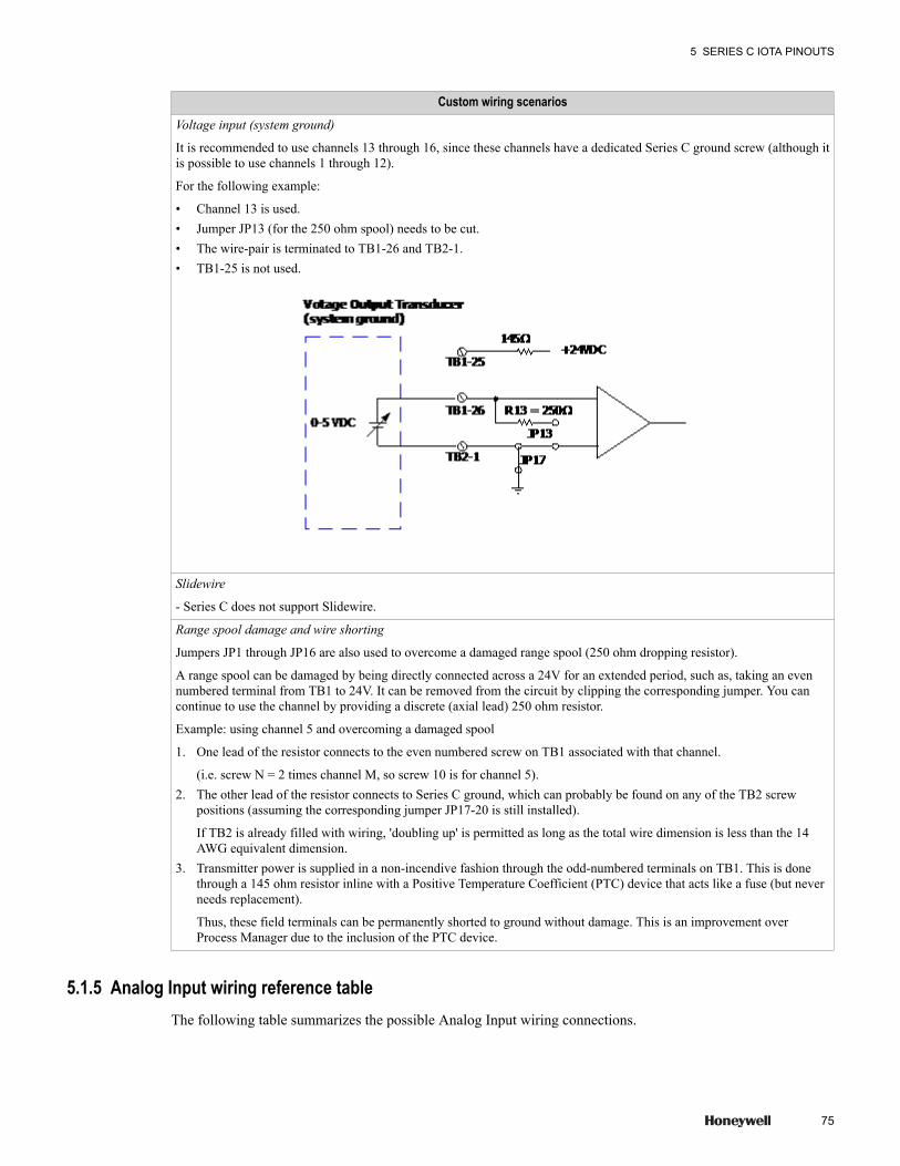
Custom wiring scenariosVoltage input (system ground)
It is recommended to use channels 13 through 16, since these channels have a dedicated Series C ground screw (although itis possible to use channels 1 through 12).
For the following example:
• Channel 13 is used.• Jumper JP13 (for the 250 ohm spool) needs to be cut.• The wire-pair is terminated to TB1-26 and TB2-1.• TB1-25 is not used.
Slidewire
- Series C does not support Slidewire.
Range spool damage and wire shorting
Jumpers JP1 through JP16 are also used to overcome a damaged range spool (250 ohm dropping resistor).
A range spool can be damaged by being directly connected across a 24V for an extended period, such as, taking an evennumbered terminal from TB1 to 24V. It can be removed from the circuit by clipping the corresponding jumper. You cancontinue to use the channel by providing a discrete (axial lead) 250 ohm resistor.
Example: using channel 5 and overcoming a damaged spool
1. One lead of the resistor connects to the even numbered screw on TB1 associated with that channel.
(i.e. screw N = 2 times channel M, so screw 10 is for channel 5).2. The other lead of the resistor connects to Series C ground, which can probably be found on any of the TB2 screw
positions (assuming the corresponding jumper JP17-20 is still installed).
If TB2 is already filled with wiring, 'doubling up' is permitted as long as the total wire dimension is less than the 14AWG equivalent dimension.
3. Transmitter power is supplied in a non-incendive fashion through the odd-numbered terminals on TB1. This is donethrough a 145 ohm resistor inline with a Positive Temperature Coefficient (PTC) device that acts like a fuse (but neverneeds replacement).
Thus, these field terminals can be permanently shorted to ground without damage. This is an improvement overProcess Manager due to the inclusion of the PTC device.
5.1.5 Analog Input wiring reference tableThe following table summarizes the possible Analog Input wiring connections.
5 SERIES C IOTA PINOUTS
75
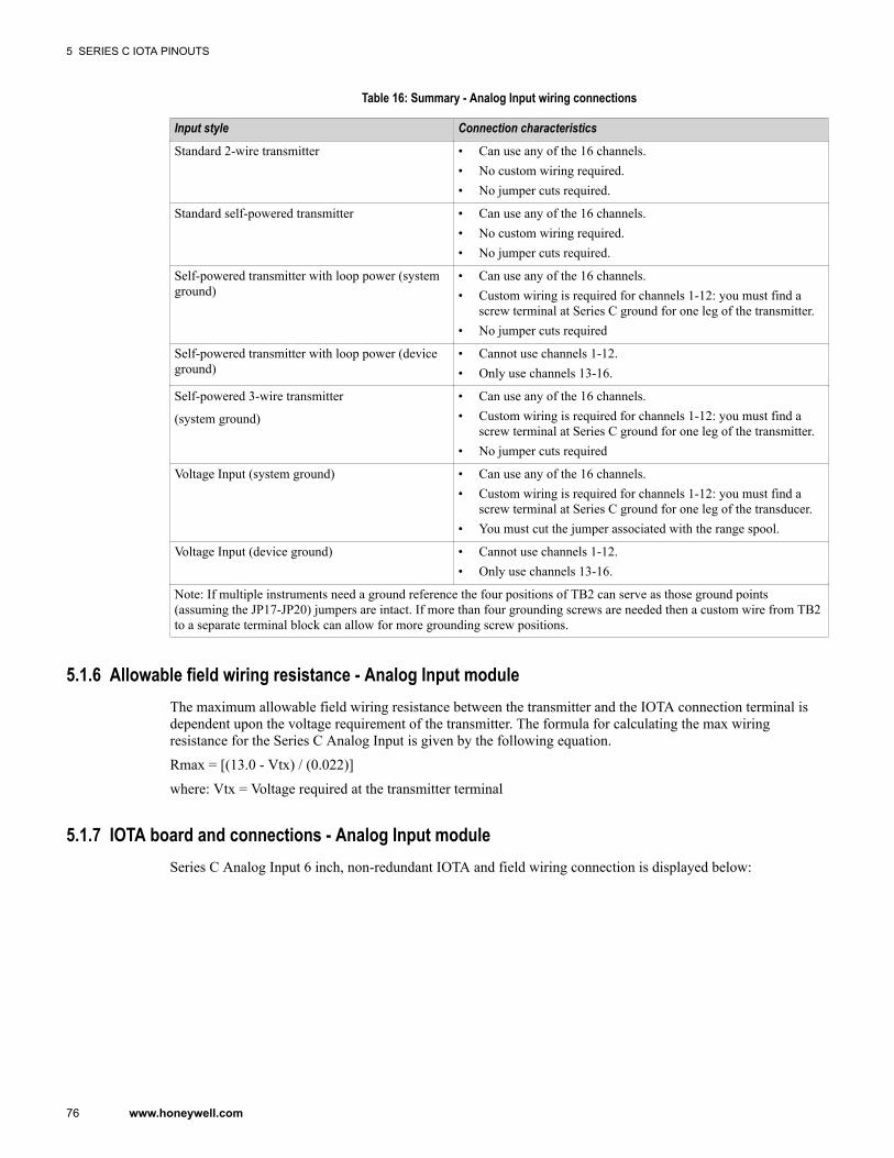
Table 16: Summary - Analog Input wiring connections
Input style Connection characteristicsStandard 2-wire transmitter • Can use any of the 16 channels.
• No custom wiring required.• No jumper cuts required.
Standard self-powered transmitter • Can use any of the 16 channels.• No custom wiring required.• No jumper cuts required.
Self-powered transmitter with loop power (systemground)
• Can use any of the 16 channels.• Custom wiring is required for channels 1-12: you must find a
screw terminal at Series C ground for one leg of the transmitter.• No jumper cuts required
Self-powered transmitter with loop power (deviceground)
• Cannot use channels 1-12.• Only use channels 13-16.
Self-powered 3-wire transmitter
(system ground)
• Can use any of the 16 channels.• Custom wiring is required for channels 1-12: you must find a
screw terminal at Series C ground for one leg of the transmitter.• No jumper cuts required
Voltage Input (system ground) • Can use any of the 16 channels.• Custom wiring is required for channels 1-12: you must find a
screw terminal at Series C ground for one leg of the transducer.• You must cut the jumper associated with the range spool.
Voltage Input (device ground) • Cannot use channels 1-12.• Only use channels 13-16.
Note: If multiple instruments need a ground reference the four positions of TB2 can serve as those ground points(assuming the JP17-JP20) jumpers are intact. If more than four grounding screws are needed then a custom wire from TB2to a separate terminal block can allow for more grounding screw positions.
5.1.6 Allowable field wiring resistance - Analog Input moduleThe maximum allowable field wiring resistance between the transmitter and the IOTA connection terminal isdependent upon the voltage requirement of the transmitter. The formula for calculating the max wiringresistance for the Series C Analog Input is given by the following equation.
Rmax = [(13.0 - Vtx) / (0.022)]
where: Vtx = Voltage required at the transmitter terminal
5.1.7 IOTA board and connections - Analog Input moduleSeries C Analog Input 6 inch, non-redundant IOTA and field wiring connection is displayed below:
5 SERIES C IOTA PINOUTS
76 www.honeywell.com
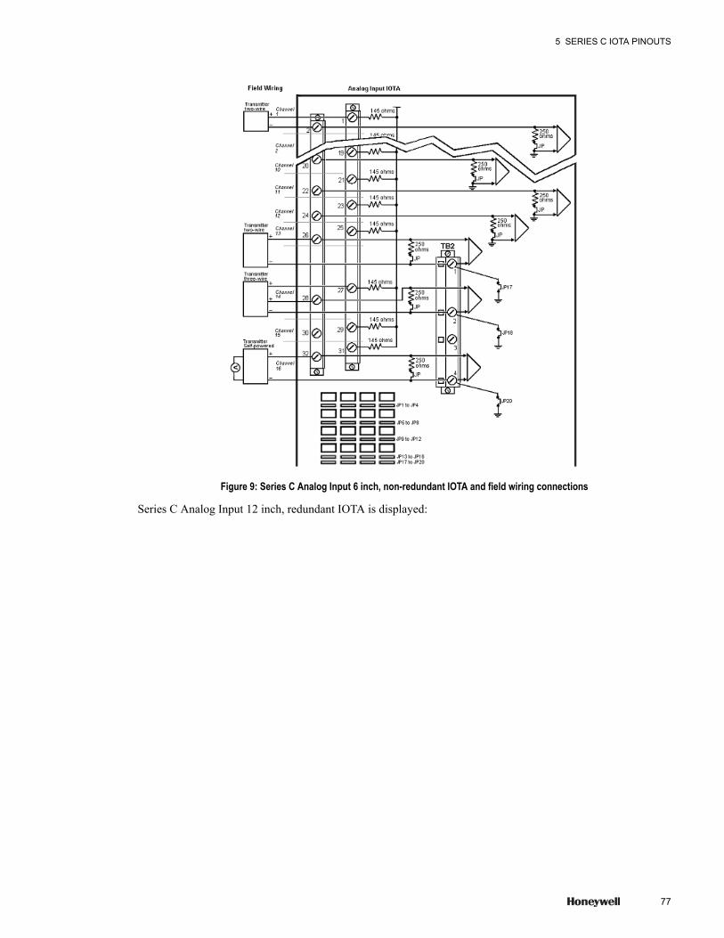
Figure 9: Series C Analog Input 6 inch, non-redundant IOTA and field wiring connections
Series C Analog Input 12 inch, redundant IOTA is displayed:
5 SERIES C IOTA PINOUTS
77
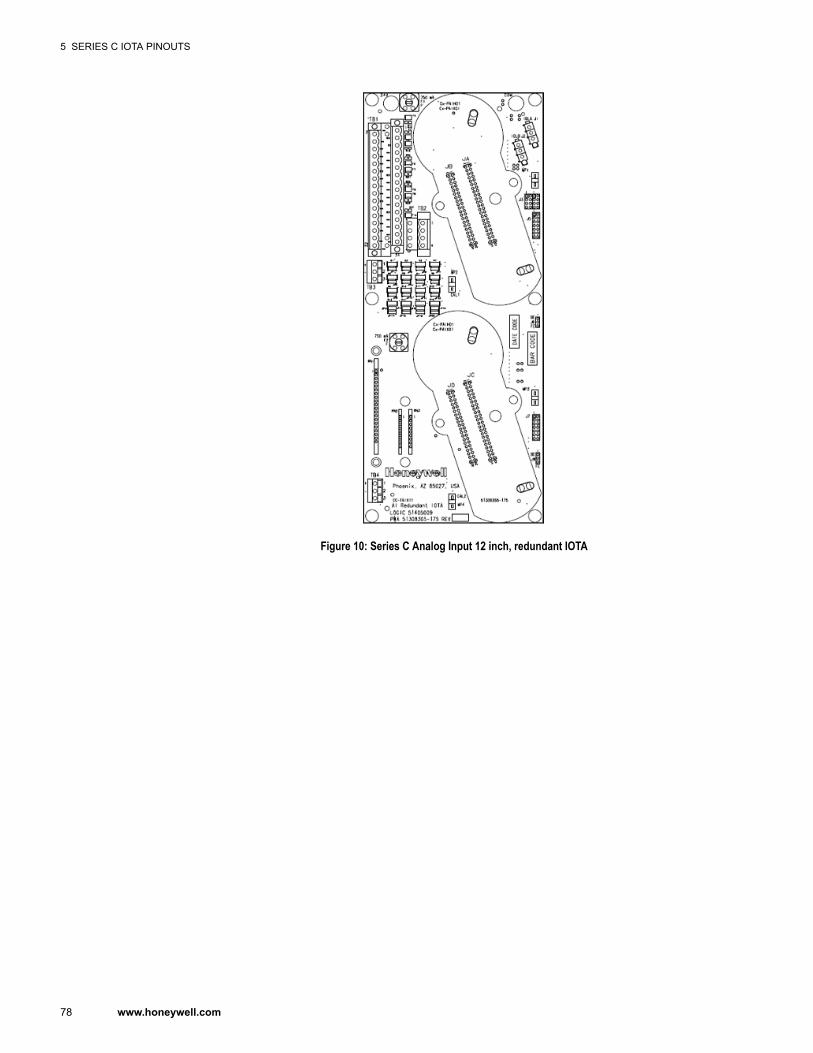
Figure 10: Series C Analog Input 12 inch, redundant IOTA
5 SERIES C IOTA PINOUTS
78 www.honeywell.com
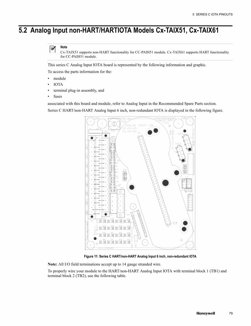
5.2 Analog Input non-HART/HARTIOTA Models Cx-TAIX51, Cx-TAIX61
NoteCx-TAIX51 supports non-HART functionality for CC-PAIH51 module. Cx-TAIX61 supports HART functionalityfor CC-PAIH51 module.
This series C Analog Input IOTA board is represented by the following information and graphic.
To access the parts information for the:
• module• IOTA• terminal plug-in assembly, and• fuses
associated with this board and module, refer to Analog Input in the Recommended Spare Parts section.
Series C HART/non-HART Analog Input 6 inch, non-redundant IOTA is displayed in the following figure.
Figure 11: Series C HART/non-HART Analog Input 6 inch, non-redundant IOTA
Note: All I/O field terminations accept up to 14 gauge stranded wire.
To properly wire your module to the HART/non-HART Analog Input IOTA with terminal block 1 (TB1) andterminal block 2 (TB2), use the following table.
5 SERIES C IOTA PINOUTS
79
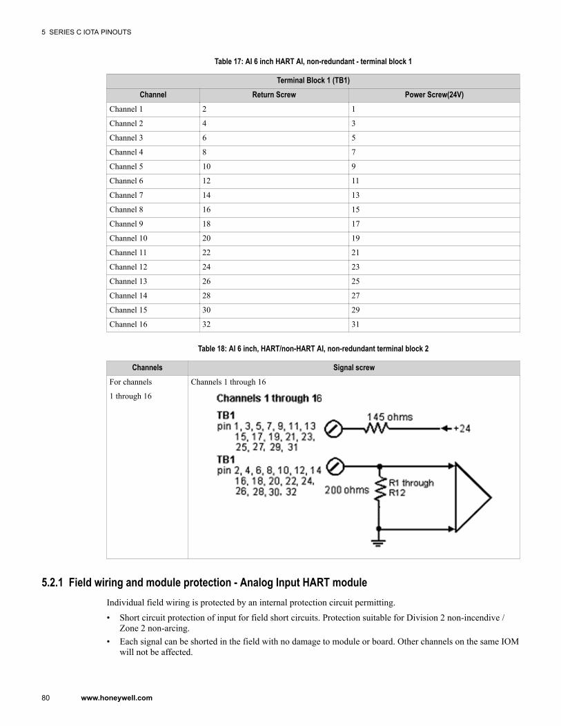
Table 17: AI 6 inch HART AI, non-redundant - terminal block 1
Terminal Block 1 (TB1)Channel Return Screw Power Screw(24V)
Channel 1 2 1
Channel 2 4 3
Channel 3 6 5
Channel 4 8 7
Channel 5 10 9
Channel 6 12 11
Channel 7 14 13
Channel 8 16 15
Channel 9 18 17
Channel 10 20 19
Channel 11 22 21
Channel 12 24 23
Channel 13 26 25
Channel 14 28 27
Channel 15 30 29
Channel 16 32 31
Table 18: AI 6 inch, HART/non-HART AI, non-redundant terminal block 2
Channels Signal screwFor channels
1 through 16
Channels 1 through 16
5.2.1 Field wiring and module protection - Analog Input HART moduleIndividual field wiring is protected by an internal protection circuit permitting.
• Short circuit protection of input for field short circuits. Protection suitable for Division 2 non-incendive /Zone 2 non-arcing.
• Each signal can be shorted in the field with no damage to module or board. Other channels on the same IOMwill not be affected.
5 SERIES C IOTA PINOUTS
80 www.honeywell.com
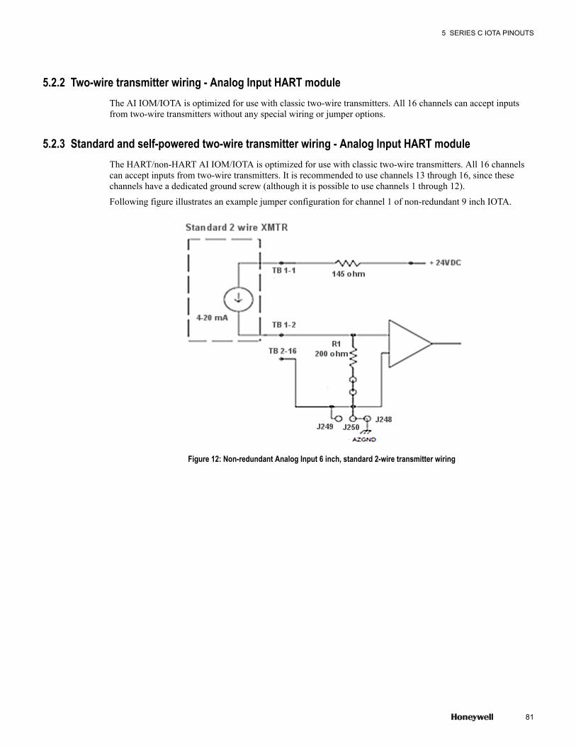
5.2.2 Two-wire transmitter wiring - Analog Input HART moduleThe AI IOM/IOTA is optimized for use with classic two-wire transmitters. All 16 channels can accept inputsfrom two-wire transmitters without any special wiring or jumper options.
5.2.3 Standard and self-powered two-wire transmitter wiring - Analog Input HART moduleThe HART/non-HART AI IOM/IOTA is optimized for use with classic two-wire transmitters. All 16 channelscan accept inputs from two-wire transmitters. It is recommended to use channels 13 through 16, since thesechannels have a dedicated ground screw (although it is possible to use channels 1 through 12).
Following figure illustrates an example jumper configuration for channel 1 of non-redundant 9 inch IOTA.
Figure 12: Non-redundant Analog Input 6 inch, standard 2-wire transmitter wiring
5 SERIES C IOTA PINOUTS
81
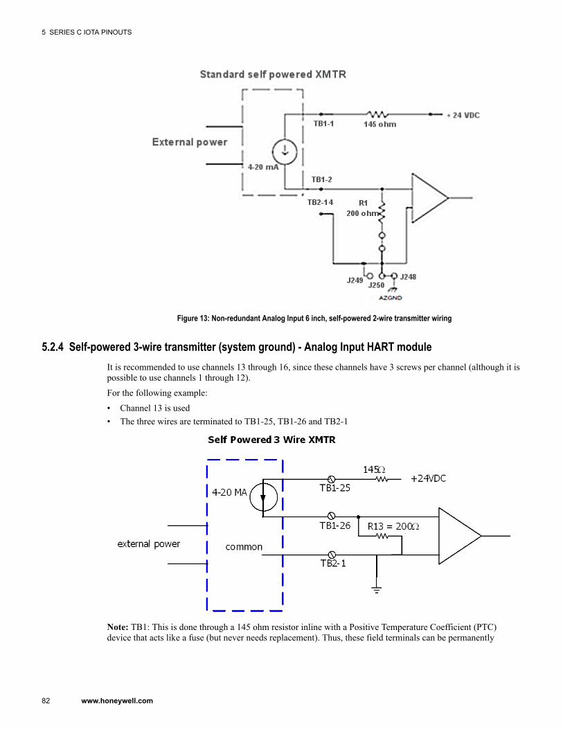
Figure 13: Non-redundant Analog Input 6 inch, self-powered 2-wire transmitter wiring
5.2.4 Self-powered 3-wire transmitter (system ground) - Analog Input HART moduleIt is recommended to use channels 13 through 16, since these channels have 3 screws per channel (although it ispossible to use channels 1 through 12).
For the following example:
• Channel 13 is used• The three wires are terminated to TB1-25, TB1-26 and TB2-1
Note: TB1: This is done through a 145 ohm resistor inline with a Positive Temperature Coefficient (PTC)device that acts like a fuse (but never needs replacement). Thus, these field terminals can be permanently
5 SERIES C IOTA PINOUTS
82 www.honeywell.com
shorted to ground without damage. This is an improvement over Process Manager due to the inclusion of thePTC device.
5.2.5 Analog Input HART module wiring reference tableThe following table summarizes the possible Analog Input wiring connections.
Table 19: Summary - Analog Input wiring connections
Input style Connection characteristicsStandard 2-wire transmitter • Can use any of the 16 channels.
• No custom wiring required.
Standard self-powered transmitter • Can use any of the 16 channels.• No custom wiring required.
Self-powered transmitter with loop power(systemground)
• Can use any of the 16 channels.• Custom wiring is required for channels 1-12: you must find a
screw terminal at ground for one leg of the transmitter.
Self-powered 3-wire transmitter
(system ground)
• Can use any of the 16 channels.• Custom wiring is required for channels 1-12: you must find a
screw terminal at ground for one leg of the transmitter.
5.2.6 Allowable field wiring resistance - Analog Input HART moduleThe maximum allowable field wiring resistance between the transmitter and the IOTA connection terminal isdependent upon the voltage requirement of the transmitter. The formula for calculating the max wiringresistance for the Analog Input is given by the following equation.
Rmax = [(13.0 - Vtx) / (0.022)]
where: Vtx = Voltage required at the transmitter terminal
5.2.7 IOTA board and connections - Analog Input HART moduleSeries C Analog Input 6 inch, non-redundant IOTA and field wiring connection is displayed in the followingimage.
5 SERIES C IOTA PINOUTS
83
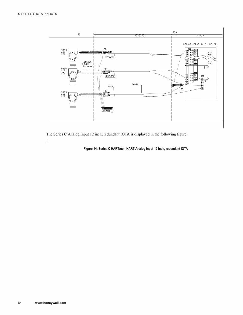
The Series C Analog Input 12 inch, redundant IOTA is displayed in the following figure.
Figure 14: Series C HART/non-HART Analog Input 12 inch, redundant IOTA
5 SERIES C IOTA PINOUTS
84 www.honeywell.com
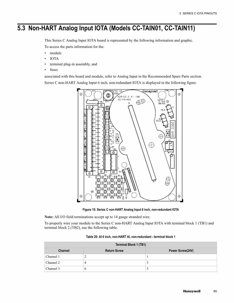
5.3 Non-HART Analog Input IOTA (Models CC-TAIN01, CC-TAIN11)This Series C Analog Input IOTA board is represented by the following information and graphic.
To access the parts information for the:
• module• IOTA• terminal plug-in assembly, and• fuses
associated with this board and module, refer to Analog Input in the Recommended Spare Parts section.
Series C non-HART Analog Input 6 inch, non-redundant IOTA is displayed in the following figure.
Figure 15: Series C non-HART Analog Input 6 inch, non-redundant IOTA
Note: All I/O field terminations accept up to 14 gauge stranded wire.
To properly wire your module to the Series C non-HART Analog Input IOTA with terminal block 1 (TB1) andterminal block 2 (TB2), use the following table.
Table 20: AI 6 inch, non-HART AI, non-redundant - terminal block 1
Terminal Block 1 (TB1)Channel Return Screw Power Screw(24V)
Channel 1 2 1
Channel 2 4 3
Channel 3 6 5
5 SERIES C IOTA PINOUTS
85
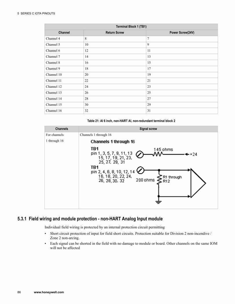
Terminal Block 1 (TB1)Channel Return Screw Power Screw(24V)
Channel 4 8 7
Channel 5 10 9
Channel 6 12 11
Channel 7 14 13
Channel 8 16 15
Channel 9 18 17
Channel 10 20 19
Channel 11 22 21
Channel 12 24 23
Channel 13 26 25
Channel 14 28 27
Channel 15 30 29
Channel 16 32 31
Table 21: AI 6 inch, non-HART AI, non-redundant terminal block 2
Channels Signal screwFor channels
1 through 16
Channels 1 through 16
5.3.1 Field wiring and module protection - non-HART Analog Input moduleIndividual field wiring is protected by an internal protection circuit permitting
• Short circuit protection of input for field short circuits. Protection suitable for Division 2 non-incendive /Zone 2 non-arcing.
• Each signal can be shorted in the field with no damage to module or board. Other channels on the same IOMwill not be affected
5 SERIES C IOTA PINOUTS
86 www.honeywell.com

5.3.2 Two-wire transmitter wiring - non-HART Analog Input moduleThe AI IOM/IOTA is optimized for use with classic two-wire transmitters. All 16 channels can accept inputsfrom two-wire transmitters without any special wiring or jumper options.
5.3.3 Standard and self-powered two-wire transmitter wiring - non-HART Analog Input moduleThe non-HART AI IOM/IOTA is optimized for use with classic two-wire transmitters. All 16 channels canaccept inputs from two-wire transmitters. It is recommended to use channels 13 through 16, since thesechannels have a dedicated Series C ground screw (although it is possible to use channels 1 through 12).
Following figure illustrates an example jumper configuration for channel 1 of non-redundant 9 inch IOTA.
Figure 16: Non-redundant Analog Input 9 inch, standard 2-wire transmitter wiring
5 SERIES C IOTA PINOUTS
87
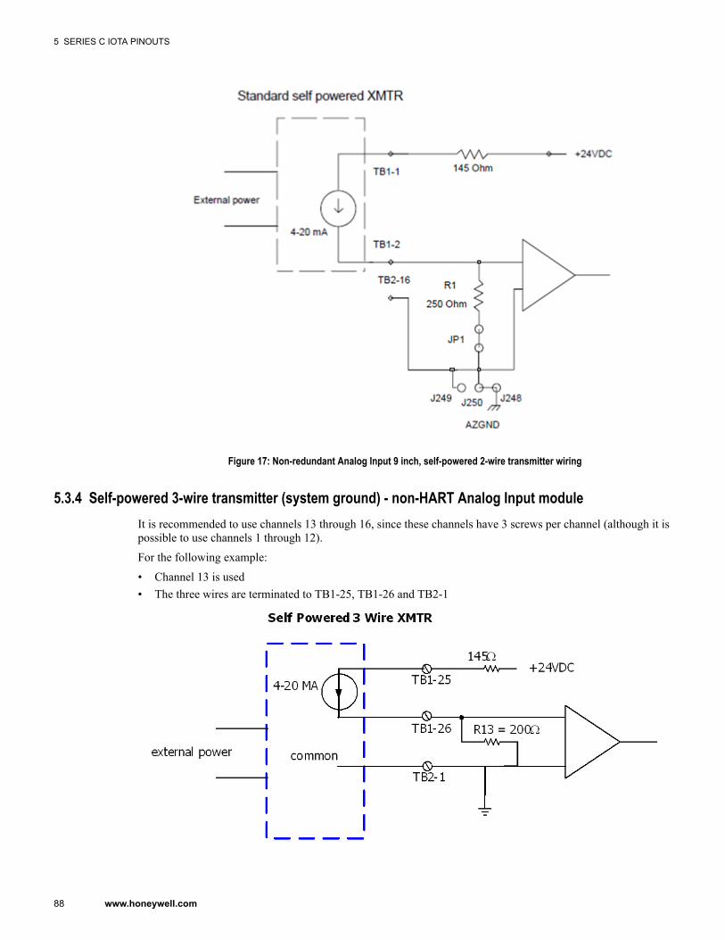
Figure 17: Non-redundant Analog Input 9 inch, self-powered 2-wire transmitter wiring
5.3.4 Self-powered 3-wire transmitter (system ground) - non-HART Analog Input moduleIt is recommended to use channels 13 through 16, since these channels have 3 screws per channel (although it ispossible to use channels 1 through 12).
For the following example:
• Channel 13 is used• The three wires are terminated to TB1-25, TB1-26 and TB2-1
5 SERIES C IOTA PINOUTS
88 www.honeywell.com

Note: TB1: This is done through a 145 ohm resistor inline with a Positive Temperature Coefficient (PTC)device that acts like a fuse (but never needs replacement). Thus, these field terminals can be permanentlyshorted to ground without damage. This is an improvement over Process Manager due to the inclusion of thePTC device.
5.3.5 Non-HART Analog Input module wiring reference tableThe following table summarizes the possible Analog Input wiring connections.
Table 22: Summary - Analog Input wiring connections
Input style Connection characteristicsStandard 2-wire transmitter • Can use any of the 16 channels.
• No custom wiring required.
Standard self-powered transmitter • Can use any of the 16 channels.• No custom wiring required.
Self-powered transmitter with loop power(systemground)
• Can use any of the 16 channels.• Custom wiring is required for channels 1-12: you must find a
screw terminal at Series C ground for one leg of the transmitter.
Self-powered 3-wire transmitter
(system ground)
• Can use any of the 16 channels.• Custom wiring is required for channels 1-12: you must find a
screw terminal at Series C ground for one leg of the transmitter.
5.3.6 Allowable field wiring resistance - non-HART Analog Input moduleThe maximum allowable field wiring resistance between the transmitter and the IOTA connection terminal isdependent upon the voltage requirement of the transmitter. The formula for calculating the max wiringresistance for the Series C Analog Input is given by the following equation.
Rmax = [(13.0 - Vtx) / (0.022)]
where: Vtx = Voltage required at the transmitter terminal
5.3.7 IOTA board and connections - non-HART Analog Input moduleSeries C Analog Input 6 inch, non-redundant IOTA and field wiring connection is displayed in the followingimage.
5 SERIES C IOTA PINOUTS
89
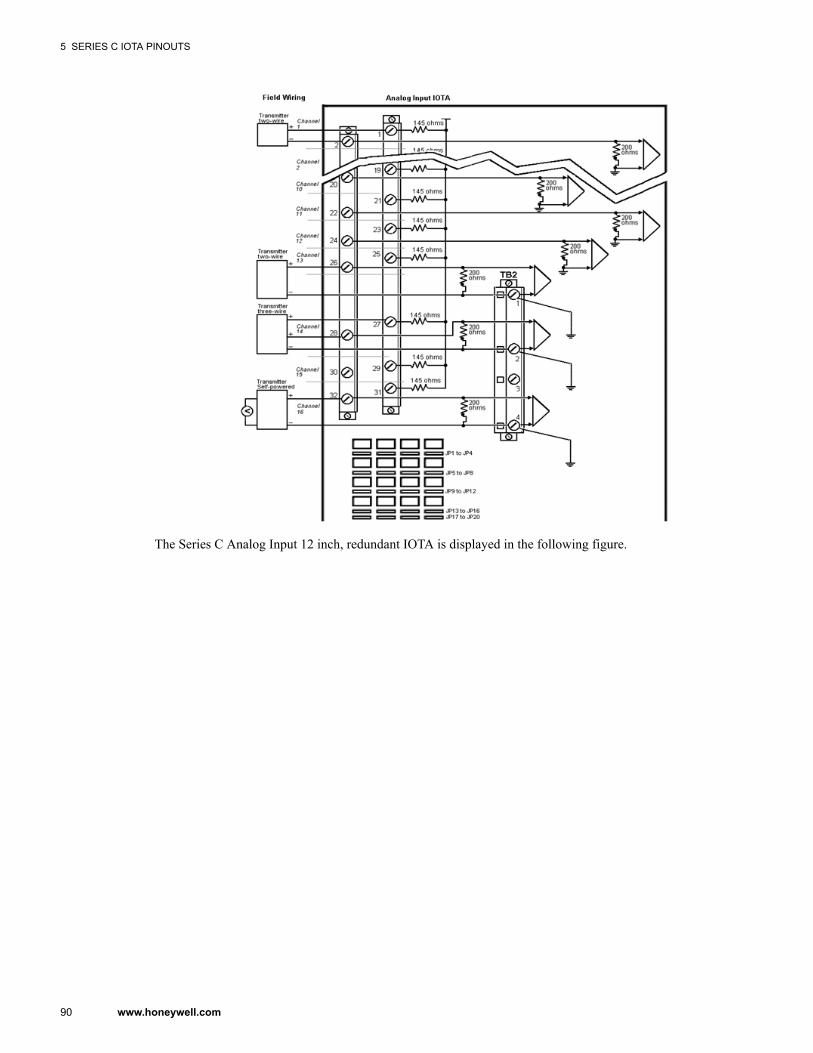
The Series C Analog Input 12 inch, redundant IOTA is displayed in the following figure.
5 SERIES C IOTA PINOUTS
90 www.honeywell.com
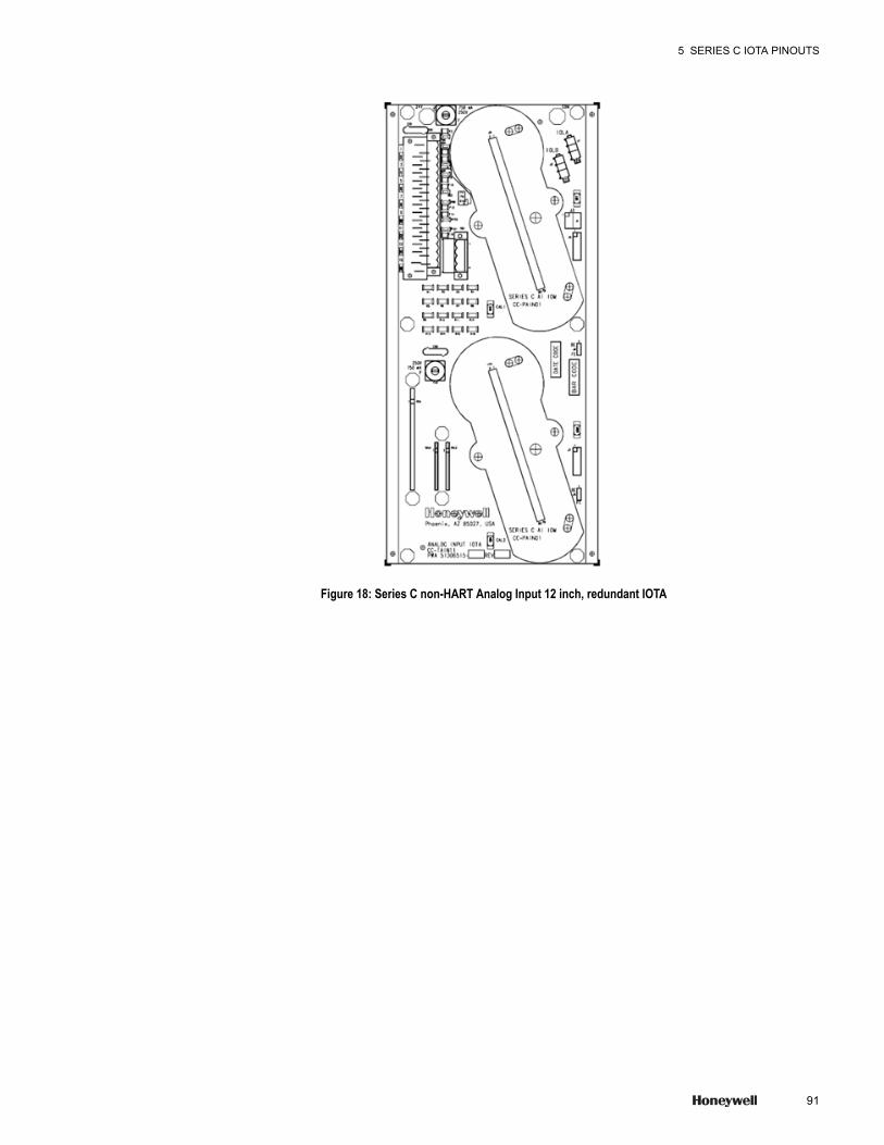
Figure 18: Series C non-HART Analog Input 12 inch, redundant IOTA
5 SERIES C IOTA PINOUTS
91
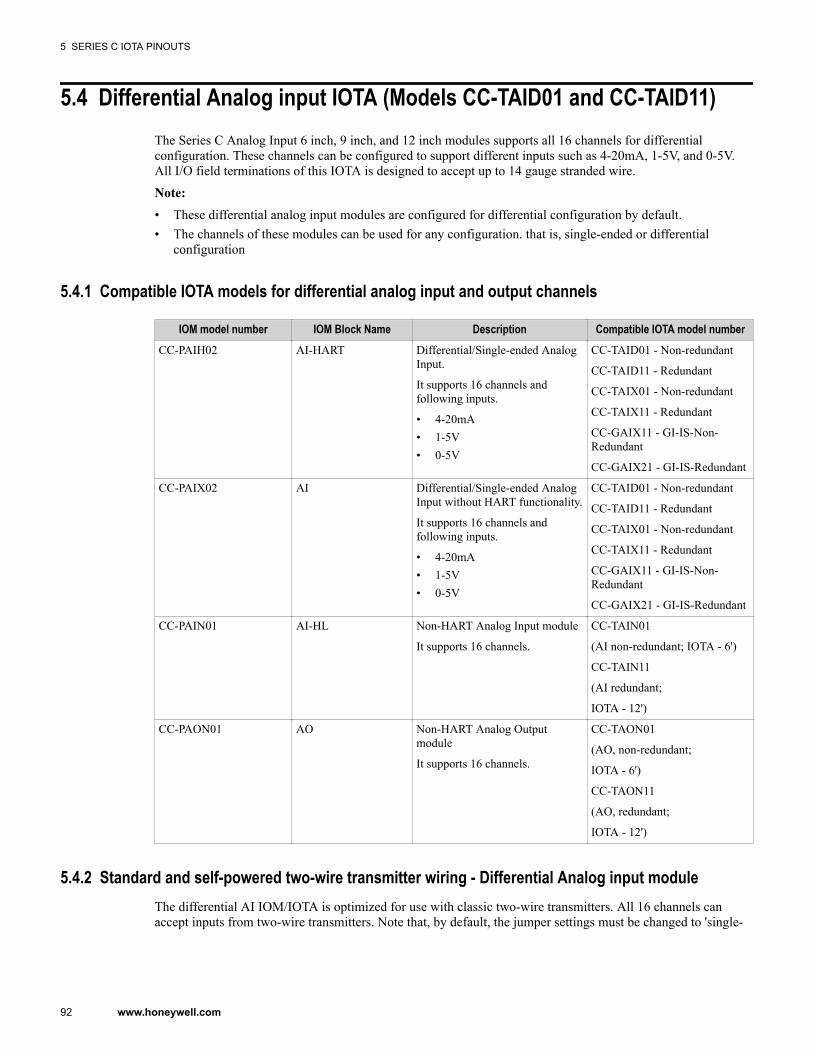
5.4 Differential Analog input IOTA (Models CC-TAID01 and CC-TAID11)The Series C Analog Input 6 inch, 9 inch, and 12 inch modules supports all 16 channels for differentialconfiguration. These channels can be configured to support different inputs such as 4-20mA, 1-5V, and 0-5V.All I/O field terminations of this IOTA is designed to accept up to 14 gauge stranded wire.
Note:• These differential analog input modules are configured for differential configuration by default.• The channels of these modules can be used for any configuration. that is, single-ended or differential
configuration
5.4.1 Compatible IOTA models for differential analog input and output channels
IOM model number IOM Block Name Description Compatible IOTA model numberCC-PAIH02 AI-HART Differential/Single-ended Analog
Input.
It supports 16 channels andfollowing inputs.
• 4-20mA• 1-5V• 0-5V
CC-TAID01 - Non-redundant
CC-TAID11 - Redundant
CC-TAIX01 - Non-redundant
CC-TAIX11 - Redundant
CC-GAIX11 - GI-IS-Non-Redundant
CC-GAIX21 - GI-IS-Redundant
CC-PAIX02 AI Differential/Single-ended AnalogInput without HART functionality.
It supports 16 channels andfollowing inputs.
• 4-20mA• 1-5V• 0-5V
CC-TAID01 - Non-redundant
CC-TAID11 - Redundant
CC-TAIX01 - Non-redundant
CC-TAIX11 - Redundant
CC-GAIX11 - GI-IS-Non-Redundant
CC-GAIX21 - GI-IS-Redundant
CC-PAIN01 AI-HL Non-HART Analog Input module
It supports 16 channels.
CC-TAIN01
(AI non-redundant; IOTA - 6')
CC-TAIN11
(AI redundant;
IOTA - 12')
CC-PAON01 AO Non-HART Analog Outputmodule
It supports 16 channels.
CC-TAON01
(AO, non-redundant;
IOTA - 6')
CC-TAON11
(AO, redundant;
IOTA - 12')
5.4.2 Standard and self-powered two-wire transmitter wiring - Differential Analog input moduleThe differential AI IOM/IOTA is optimized for use with classic two-wire transmitters. All 16 channels canaccept inputs from two-wire transmitters. Note that, by default, the jumper settings must be changed to 'single-
5 SERIES C IOTA PINOUTS
92 www.honeywell.com
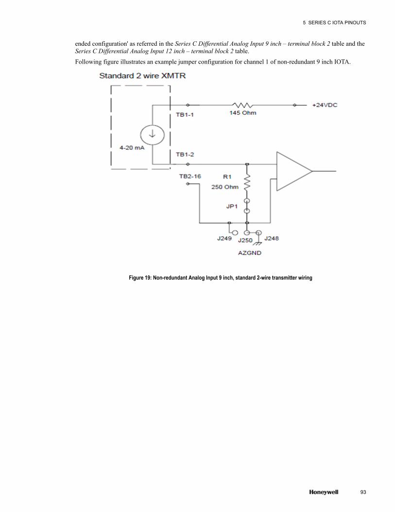
ended configuration' as referred in the Series C Differential Analog Input 9 inch – terminal block 2 table and theSeries C Differential Analog Input 12 inch – terminal block 2 table.
Following figure illustrates an example jumper configuration for channel 1 of non-redundant 9 inch IOTA.
Figure 19: Non-redundant Analog Input 9 inch, standard 2-wire transmitter wiring
5 SERIES C IOTA PINOUTS
93

Figure 20: Non-redundant Analog Input 9 inch, self-powered 2-wire transmitter wiring
5.4.3 Custom wiring - Differential Analog input module
AttentionFor differential HART transmitter, you can use only channel number 13 to 16. For non-HART differential transmitter,you can use all 16 channels in both differential mode and single-ended mode.
Custom wiring scenarios are explained in the following table.
5 SERIES C IOTA PINOUTS
94 www.honeywell.com
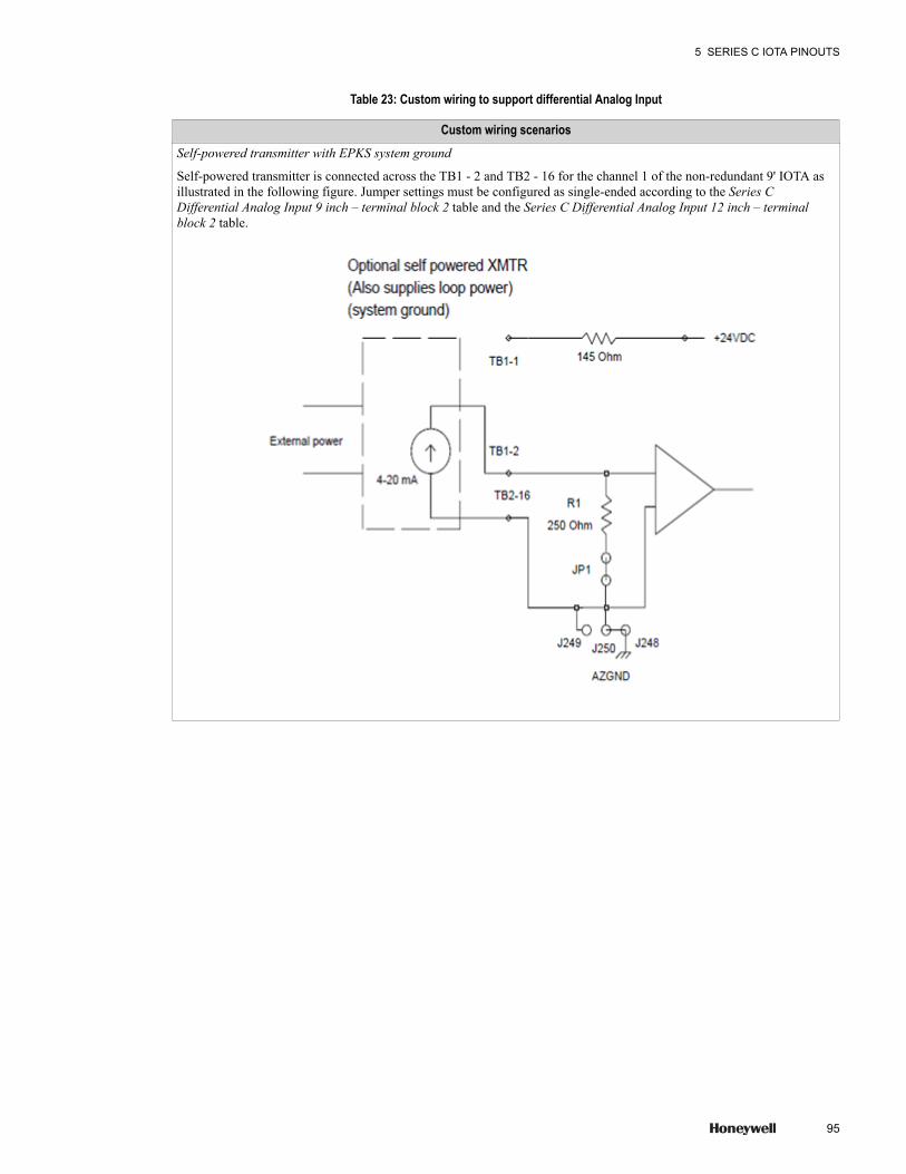
Table 23: Custom wiring to support differential Analog Input
Custom wiring scenariosSelf-powered transmitter with EPKS system ground
Self-powered transmitter is connected across the TB1 - 2 and TB2 - 16 for the channel 1 of the non-redundant 9' IOTA asillustrated in the following figure. Jumper settings must be configured as single-ended according to the Series CDifferential Analog Input 9 inch – terminal block 2 table and the Series C Differential Analog Input 12 inch – terminalblock 2 table.
5 SERIES C IOTA PINOUTS
95
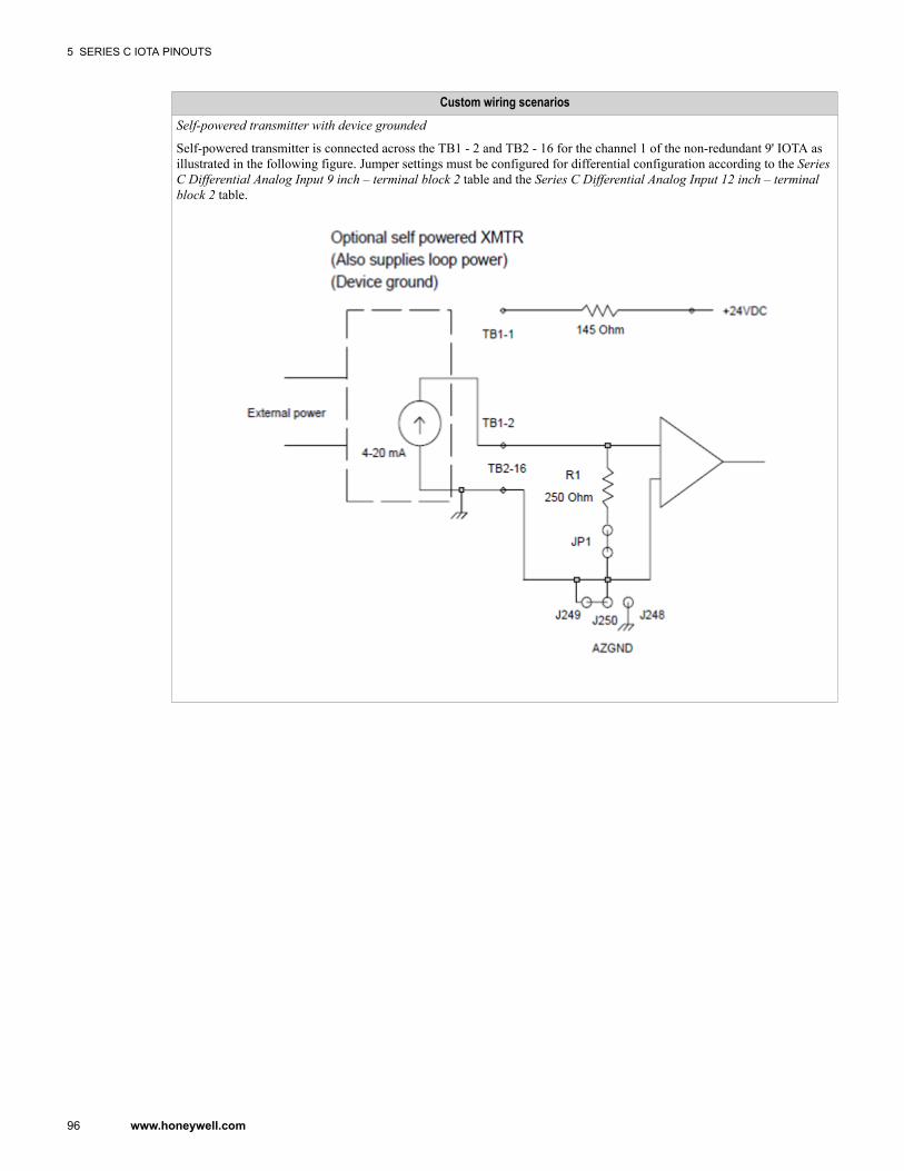
Custom wiring scenariosSelf-powered transmitter with device grounded
Self-powered transmitter is connected across the TB1 - 2 and TB2 - 16 for the channel 1 of the non-redundant 9' IOTA asillustrated in the following figure. Jumper settings must be configured for differential configuration according to the SeriesC Differential Analog Input 9 inch – terminal block 2 table and the Series C Differential Analog Input 12 inch – terminalblock 2 table.
5 SERIES C IOTA PINOUTS
96 www.honeywell.com
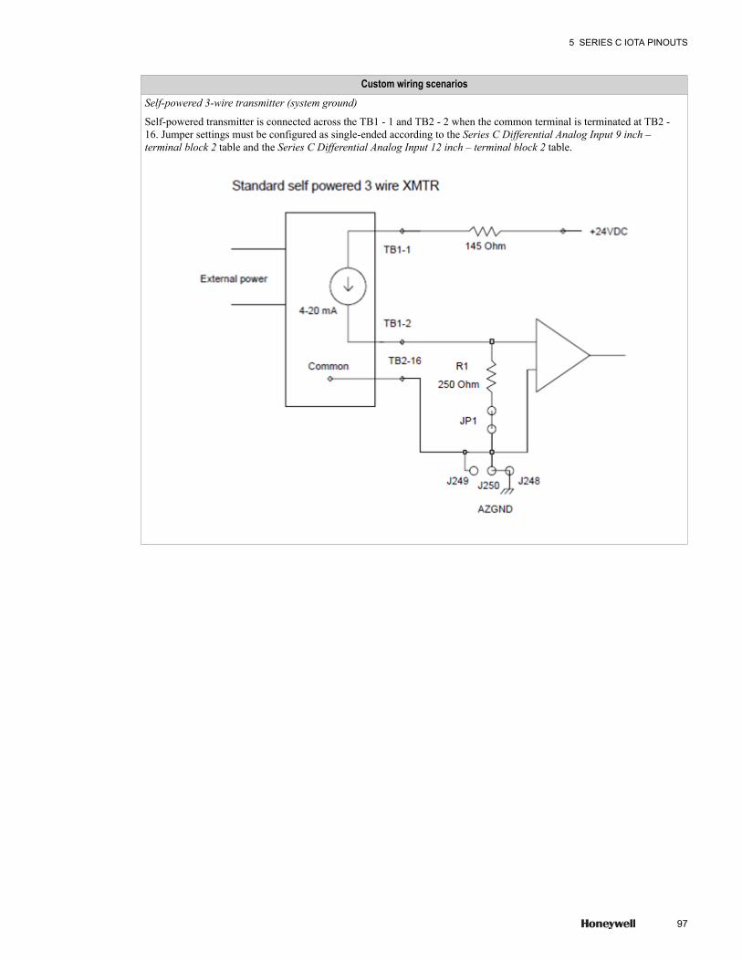
Custom wiring scenariosSelf-powered 3-wire transmitter (system ground)
Self-powered transmitter is connected across the TB1 - 1 and TB2 - 2 when the common terminal is terminated at TB2 -16. Jumper settings must be configured as single-ended according to the Series C Differential Analog Input 9 inch –terminal block 2 table and the Series C Differential Analog Input 12 inch – terminal block 2 table.
5 SERIES C IOTA PINOUTS
97
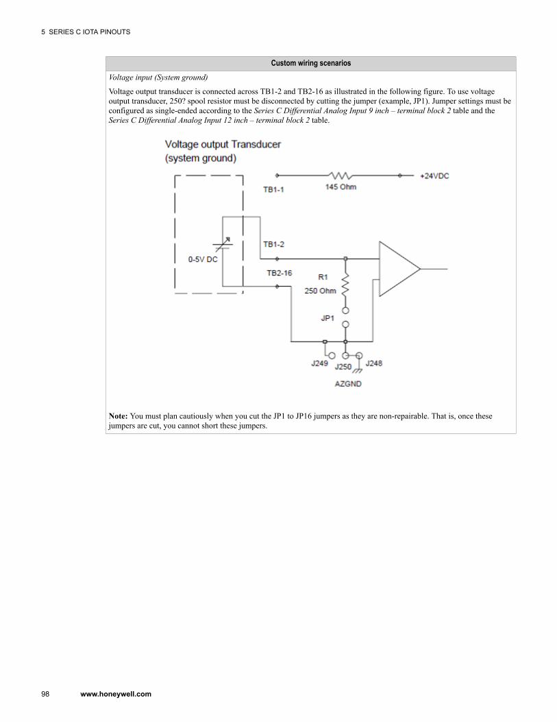
Custom wiring scenariosVoltage input (System ground)
Voltage output transducer is connected across TB1-2 and TB2-16 as illustrated in the following figure. To use voltageoutput transducer, 250? spool resistor must be disconnected by cutting the jumper (example, JP1). Jumper settings must beconfigured as single-ended according to the Series C Differential Analog Input 9 inch – terminal block 2 table and theSeries C Differential Analog Input 12 inch – terminal block 2 table.
Note: You must plan cautiously when you cut the JP1 to JP16 jumpers as they are non-repairable. That is, once thesejumpers are cut, you cannot short these jumpers.
5 SERIES C IOTA PINOUTS
98 www.honeywell.com

Custom wiring scenariosVoltage input (Device ground)
Voltage output transducer is connected across TB1-2 and TB2-16 as illustrated in the following figure. To use voltageoutput transducer, 250? spool resistor must be disconnected by cutting the jumper (example, JP1). Jumper settings must beconfigured for differential configuration according to the Series C Differential Analog Input 9 inch – terminal block 2 tableand the Series C Differential Analog Input 12 inch – terminal block 2 table.
Note: You must plan cautiously when you cut the JP1 to JP16 jumpers as they are non-repairable. That is, once thesejumpers are cut, you cannot short these jumpers.
Slide Wire: Series C does not support Slidewire.
5.4.4 Jumper configuration for differential configuration - Differential Analog input moduleJumper configuration for the non-redundant differential AI channel is illustrated in the following figure. Eachchannel is associated with 250? 'range spool' or 'dropping resistor' for sources that deliver 4-20mA. In addition,one jumper and three jumper pins are provided for each channel.
Example: channel 1 consists of JP1, J248, and J249.
5 SERIES C IOTA PINOUTS
99
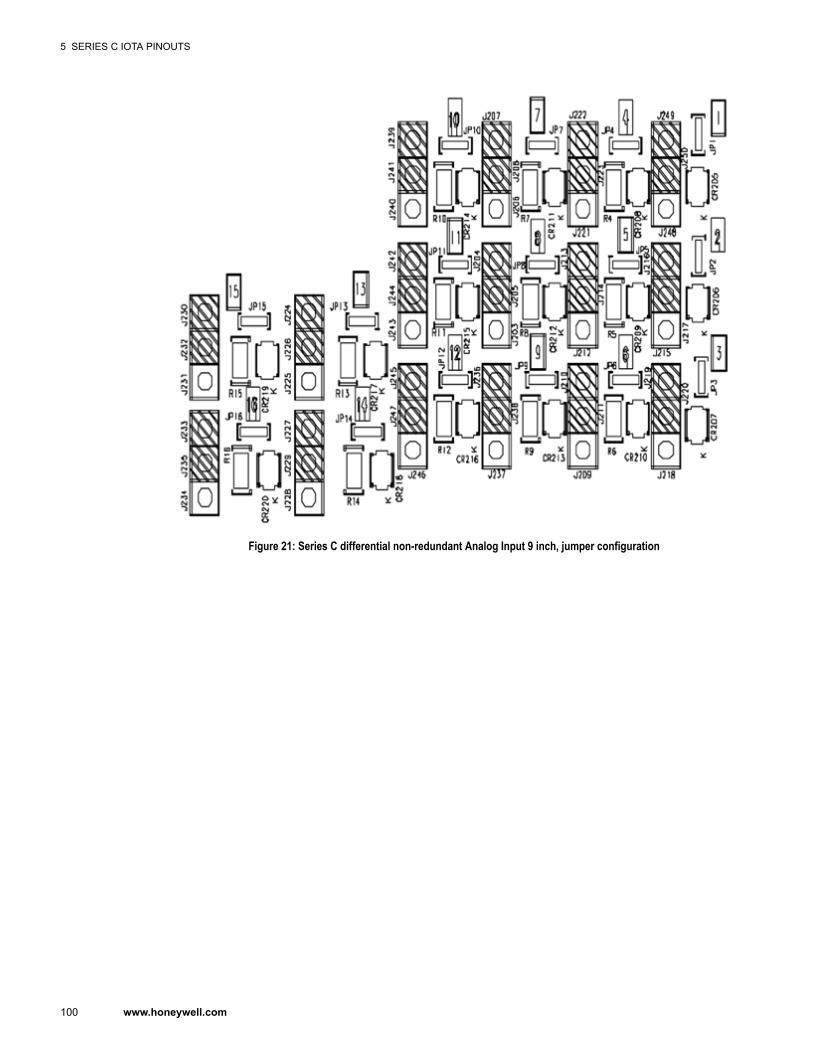
Figure 21: Series C differential non-redundant Analog Input 9 inch, jumper configuration
5 SERIES C IOTA PINOUTS
100 www.honeywell.com
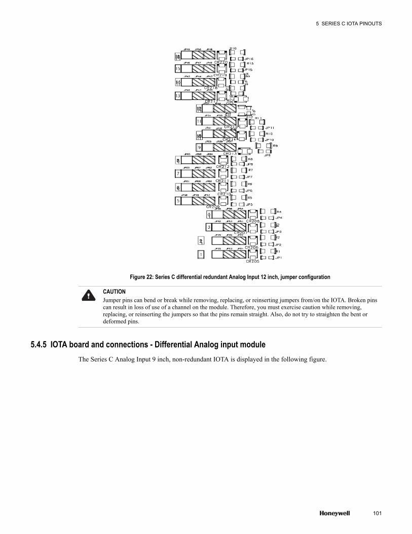
Figure 22: Series C differential redundant Analog Input 12 inch, jumper configuration
CAUTIONJumper pins can bend or break while removing, replacing, or reinserting jumpers from/on the IOTA. Broken pinscan result in loss of use of a channel on the module. Therefore, you must exercise caution while removing,replacing, or reinserting the jumpers so that the pins remain straight. Also, do not try to straighten the bent ordeformed pins.
5.4.5 IOTA board and connections - Differential Analog input moduleThe Series C Analog Input 9 inch, non-redundant IOTA is displayed in the following figure.
5 SERIES C IOTA PINOUTS
101
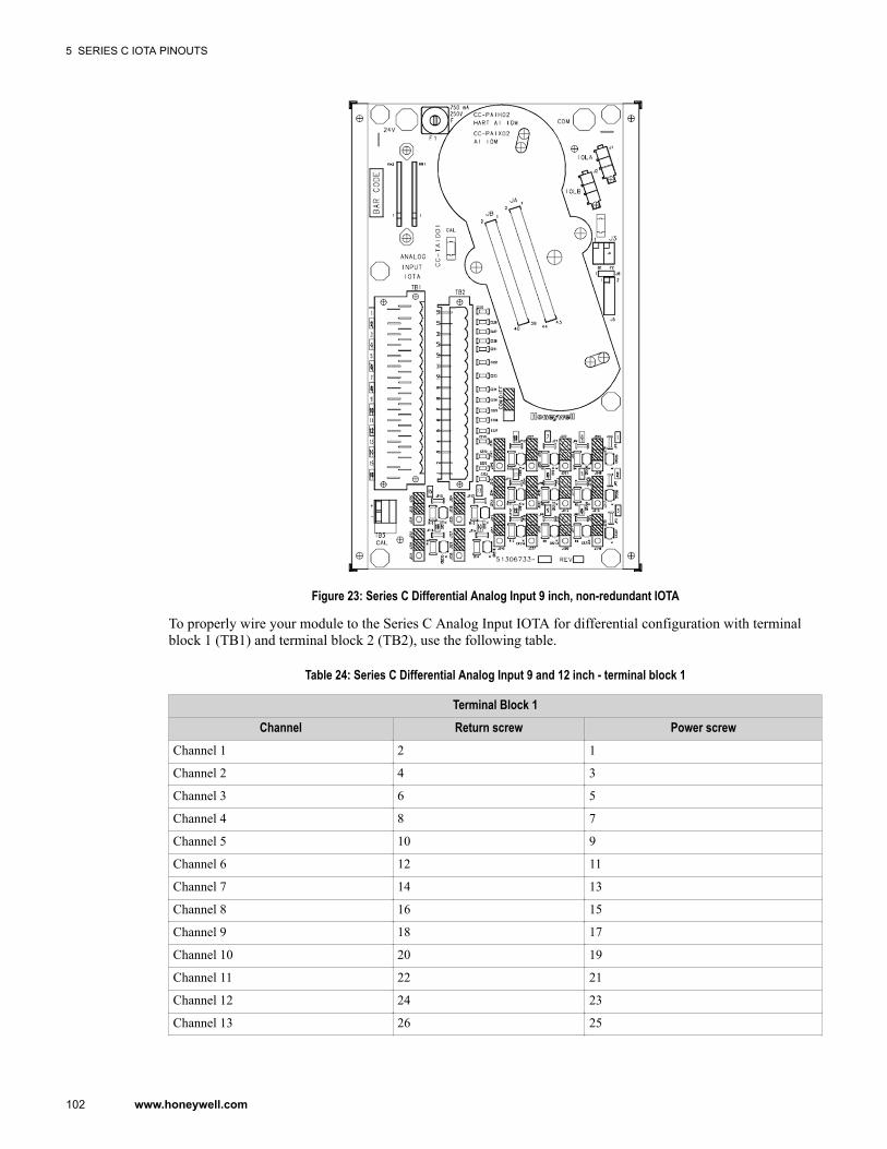
Figure 23: Series C Differential Analog Input 9 inch, non-redundant IOTA
To properly wire your module to the Series C Analog Input IOTA for differential configuration with terminalblock 1 (TB1) and terminal block 2 (TB2), use the following table.
Table 24: Series C Differential Analog Input 9 and 12 inch - terminal block 1
Terminal Block 1Channel Return screw Power screw
Channel 1 2 1
Channel 2 4 3
Channel 3 6 5
Channel 4 8 7
Channel 5 10 9
Channel 6 12 11
Channel 7 14 13
Channel 8 16 15
Channel 9 18 17
Channel 10 20 19
Channel 11 22 21
Channel 12 24 23
Channel 13 26 25
5 SERIES C IOTA PINOUTS
102 www.honeywell.com
Terminal Block 1Channel Return screw Power screw
Channel 14 28 27
Channel 15 30 29
Channel 16 32 31
Attention• Three pin jumper labels are different for 9' and 12' IOTAs.• All channels available in these IOTAs are configured for differential mode by default. If a shorting jumper is not
present, that channel is configured in differential mode. If you want to modify the configuration from differentialmode to single ended mode, refer to these to short the pair of jumpers.
Table 25: Series C Differential Analog Input 9 inch - terminal block 2
Terminal Block 2CC-TAID01 IOTA
If TB2 screw is… Then, the channel is… And the pair of jumper to be short fordifferential configuration
And the pair of jumper to be shortfor single ended configuration
1 16 J233 - J235 J234 - J235
2 15 J230 - J232 J231 - J232
3 14 J227 - J229 J228 - J229
4 13 J224 - J226 J225 - J226
5 12 J245 - J247 J246 - J247
6 11 J242 - J244 J243 - J244
7 10 J239 - J241 J240 - J241
8 9 J236 - J238 J237 - J238
9 8 J204 - J205 J203 - J205
10 7 J207 - 208 J206 - J208
11 6 J210 - J211 J209 - J211
12 5 J213 - J214 J212 - J214
13 4 J222 - J223 J221 - J223
14 3 J219 - J220 J218 - J220
15 2 J216 - J217 J215 - J217
16 1 J249 - J250 J248 - J250
Table 26: Series C Differential Analog Input 12 inch - terminal block 2
Terminal Block 2CC-TAID11 IOTAIf TB2 screw is… Then, the channel is… And the pair of jumper to be short
for differential configurationAnd the pair of jumper to be short
for single ended configuration1 16 JP21 - JP23 JP22 - JP23
2 15 JP24 - JP26 JP25 - P26
3 14 JP51 - JP53 JP52 - JP53
4 13 JP54 - JP56 JP55 - JP56
5 SERIES C IOTA PINOUTS
103
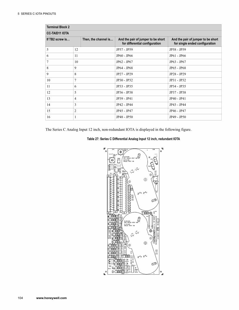
Terminal Block 2CC-TAID11 IOTAIf TB2 screw is… Then, the channel is… And the pair of jumper to be short
for differential configurationAnd the pair of jumper to be short
for single ended configuration5 12 JP57 - JP59 JP58 - JP59
6 11 JP60 - JP66 JP61 - JP66
7 10 JP62 - JP67 JP63 - JP67
8 9 JP64 - JP68 JP65 - JP68
9 8 JP27 - JP29 JP28 - JP29
10 7 JP30 - JP32 JP31 - JP32
11 6 JP33 - JP35 JP34 - JP35
12 5 JP36 - JP38 JP37 - JP38
13 4 JP39 - JP41 JP40 - JP41
14 3 JP42 - JP44 JP43 - JP44
15 2 JP45 - JP47 JP46 - JP47
16 1 JP48 - JP50 JP49 - JP50
The Series C Analog Input 12 inch, non-redundant IOTA is displayed in the following figure.
Table 27: Series C Differential Analog Input 12 inch, redundant IOTA
5 SERIES C IOTA PINOUTS
104 www.honeywell.com

5.5 Analog Output IOTA Models CC-TAOX01, CC-TAOX11, CC-TAON01and CC-TAON11
This Series C Analog Output IOTA board is represented by the following information and graphics.
To access the parts information for the:
• module• IOTA• terminal plug-in assembly, and• fuses
associated with this board and module, refer to Analog Ouput in the Recommended Spare Parts section.
5.5.1 Field wiring and module protection - Analog Output moduleThe Analog Output module provides an output current range of 0ma, and 2.9 mA through 21.1 mA based on therequested Analog Output by the Series-C controller. The output current including the HART modulated signal,does not exceed 22.5mA.
• Short circuit protection of field short circuits. Protection suitable for Division 2 non-incendive / Zone 2 non-arcing.
• Each field wiring pair can be shorted together without damage to the module or IOTA. Other channels in thesame module(s) will not be affected.
• A +30 Vdc source can be continuously applied across the OUT+ to OUT- terminals of the IOTA withoutdamage to either module(s) or IOTA (i.e. with the positive lead of the source connected to OUT+ and thenegative lead connected to OUT-). To prevent damage to the IOTA surge protection diodes, the current mustbe limited to 500 mAdc if the source is applied in the reverse polarity (i.e. with the positive lead of thesource attached to OUT-, negative lead attached to OUT+). This 500 mAdc restriction does not apply in thepositive polarity case.
5.5.2 IOTA board and connections - Analog Output moduleSeries C Analog Output 6 inch, non-redundant IOTA is displayed.
5 SERIES C IOTA PINOUTS
105
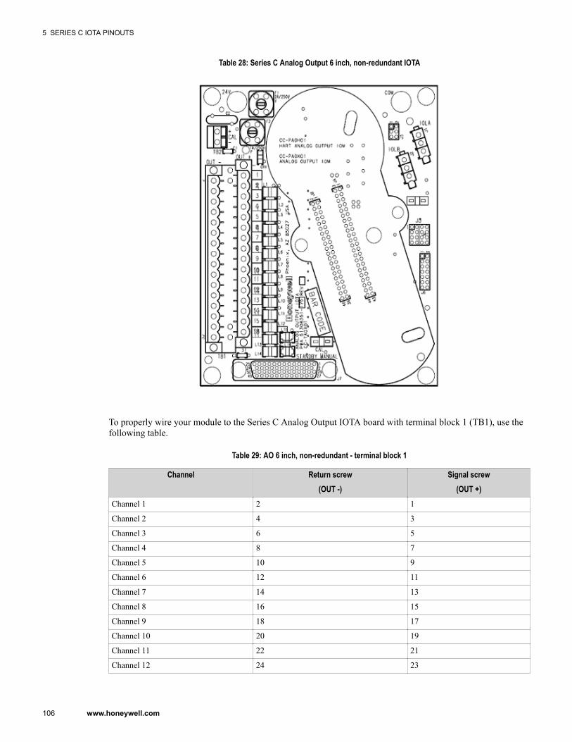
Table 28: Series C Analog Output 6 inch, non-redundant IOTA
To properly wire your module to the Series C Analog Output IOTA board with terminal block 1 (TB1), use thefollowing table.
Table 29: AO 6 inch, non-redundant - terminal block 1
Channel Return screw(OUT -)
Signal screw(OUT +)
Channel 1 2 1
Channel 2 4 3
Channel 3 6 5
Channel 4 8 7
Channel 5 10 9
Channel 6 12 11
Channel 7 14 13
Channel 8 16 15
Channel 9 18 17
Channel 10 20 19
Channel 11 22 21
Channel 12 24 23
5 SERIES C IOTA PINOUTS
106 www.honeywell.com
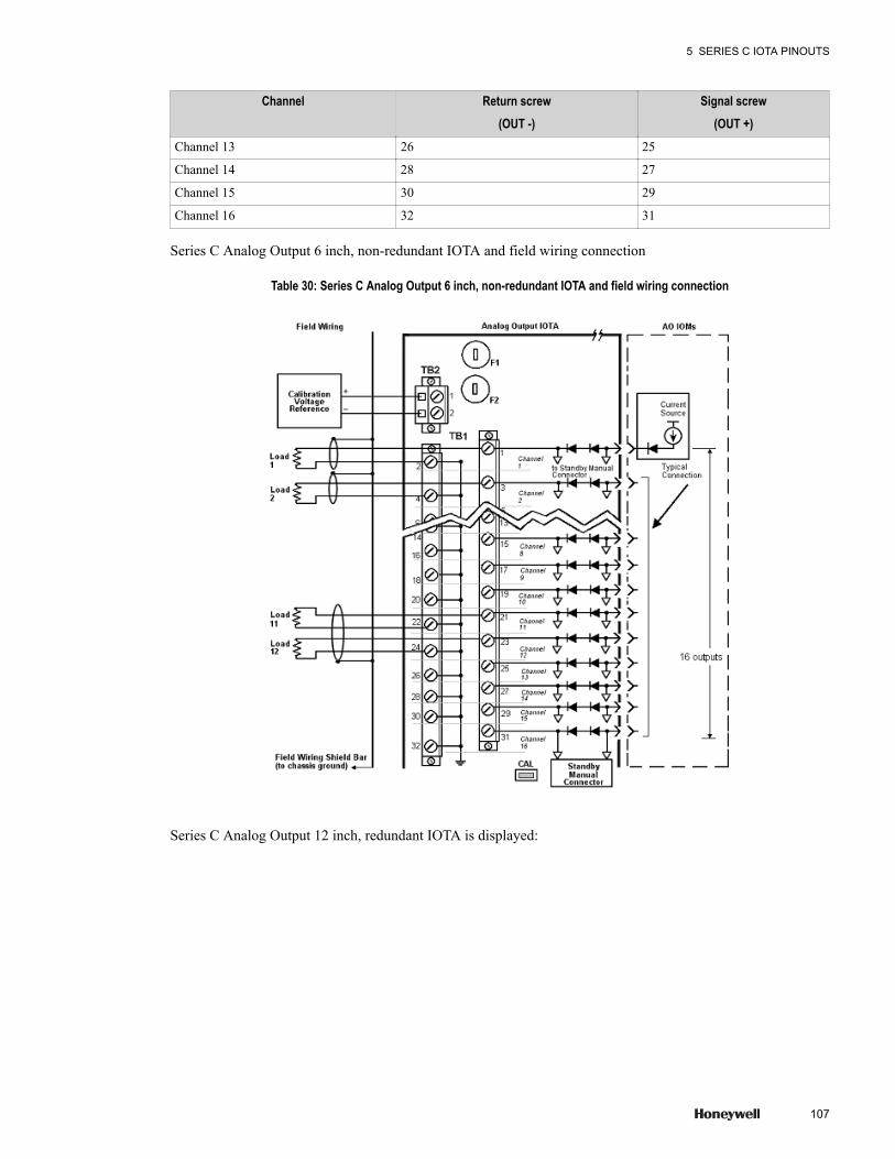
Channel Return screw(OUT -)
Signal screw(OUT +)
Channel 13 26 25
Channel 14 28 27
Channel 15 30 29
Channel 16 32 31
Series C Analog Output 6 inch, non-redundant IOTA and field wiring connection
Table 30: Series C Analog Output 6 inch, non-redundant IOTA and field wiring connection
Series C Analog Output 12 inch, redundant IOTA is displayed:
5 SERIES C IOTA PINOUTS
107
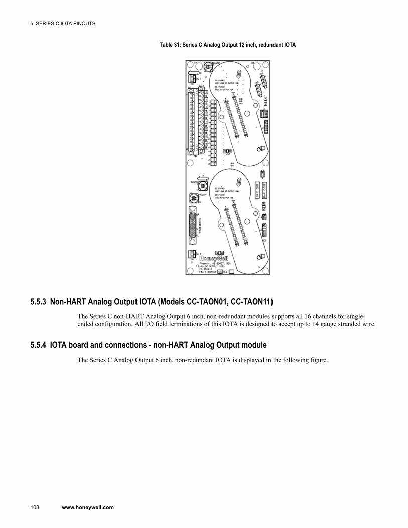
Table 31: Series C Analog Output 12 inch, redundant IOTA
5.5.3 Non-HART Analog Output IOTA (Models CC-TAON01, CC-TAON11)The Series C non-HART Analog Output 6 inch, non-redundant modules supports all 16 channels for single-ended configuration. All I/O field terminations of this IOTA is designed to accept up to 14 gauge stranded wire.
5.5.4 IOTA board and connections - non-HART Analog Output moduleThe Series C Analog Output 6 inch, non-redundant IOTA is displayed in the following figure.
5 SERIES C IOTA PINOUTS
108 www.honeywell.com
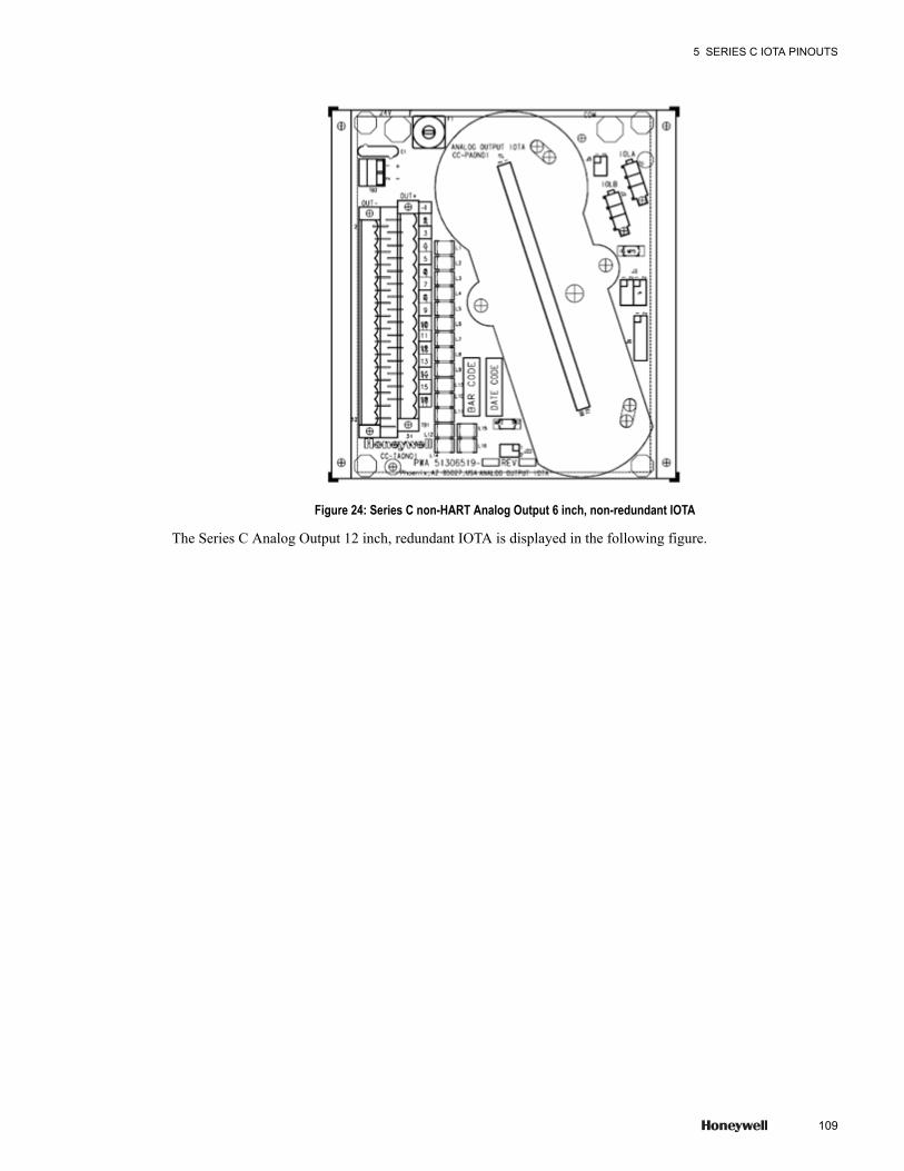
Figure 24: Series C non-HART Analog Output 6 inch, non-redundant IOTA
The Series C Analog Output 12 inch, redundant IOTA is displayed in the following figure.
5 SERIES C IOTA PINOUTS
109
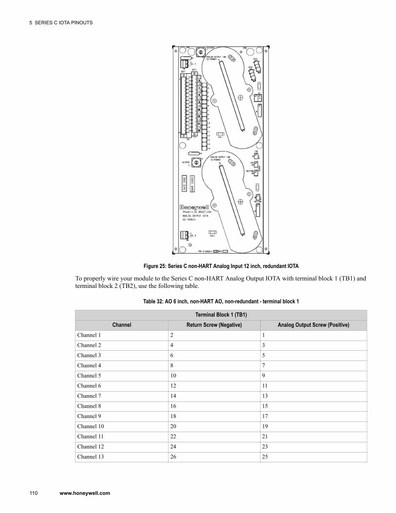
Figure 25: Series C non-HART Analog Input 12 inch, redundant IOTA
To properly wire your module to the Series C non-HART Analog Output IOTA with terminal block 1 (TB1) andterminal block 2 (TB2), use the following table.
Table 32: AO 6 inch, non-HART AO, non-redundant - terminal block 1
Terminal Block 1 (TB1)Channel Return Screw (Negative) Analog Output Screw (Positive)
Channel 1 2 1
Channel 2 4 3
Channel 3 6 5
Channel 4 8 7
Channel 5 10 9
Channel 6 12 11
Channel 7 14 13
Channel 8 16 15
Channel 9 18 17
Channel 10 20 19
Channel 11 22 21
Channel 12 24 23
Channel 13 26 25
5 SERIES C IOTA PINOUTS
110 www.honeywell.com

Terminal Block 1 (TB1)Channel Return Screw (Negative) Analog Output Screw (Positive)
Channel 14 28 27
Channel 15 30 29
Channel 16 32 31
Note:
TB1: 32 pin connector - screw block
• 16 channels positive output terminals must be connected through upper-side of 32 pin connector.• 16 channels negative output terminals must be connected through lower-side of 32 pin connector.
The field wiring connection for Series C non-HART Analog Input 6 inch, non-redundant IOTA is identical tothe Series C Analog Input 6 inch, non-redundant IOTA. For more information about the field wiring, refer to “IOTA board and connections - Analog Output module” on page 105.
5 SERIES C IOTA PINOUTS
111
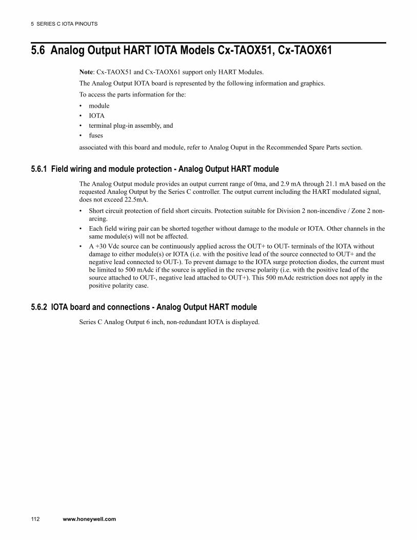
5.6 Analog Output HART IOTA Models Cx-TAOX51, Cx-TAOX61Note: Cx-TAOX51 and Cx-TAOX61 support only HART Modules.
The Analog Output IOTA board is represented by the following information and graphics.
To access the parts information for the:
• module• IOTA• terminal plug-in assembly, and• fuses
associated with this board and module, refer to Analog Ouput in the Recommended Spare Parts section.
5.6.1 Field wiring and module protection - Analog Output HART moduleThe Analog Output module provides an output current range of 0ma, and 2.9 mA through 21.1 mA based on therequested Analog Output by the Series C controller. The output current including the HART modulated signal,does not exceed 22.5mA.
• Short circuit protection of field short circuits. Protection suitable for Division 2 non-incendive / Zone 2 non-arcing.
• Each field wiring pair can be shorted together without damage to the module or IOTA. Other channels in thesame module(s) will not be affected.
• A +30 Vdc source can be continuously applied across the OUT+ to OUT- terminals of the IOTA withoutdamage to either module(s) or IOTA (i.e. with the positive lead of the source connected to OUT+ and thenegative lead connected to OUT-). To prevent damage to the IOTA surge protection diodes, the current mustbe limited to 500 mAdc if the source is applied in the reverse polarity (i.e. with the positive lead of thesource attached to OUT-, negative lead attached to OUT+). This 500 mAdc restriction does not apply in thepositive polarity case.
5.6.2 IOTA board and connections - Analog Output HART moduleSeries C Analog Output 6 inch, non-redundant IOTA is displayed.
5 SERIES C IOTA PINOUTS
112 www.honeywell.com
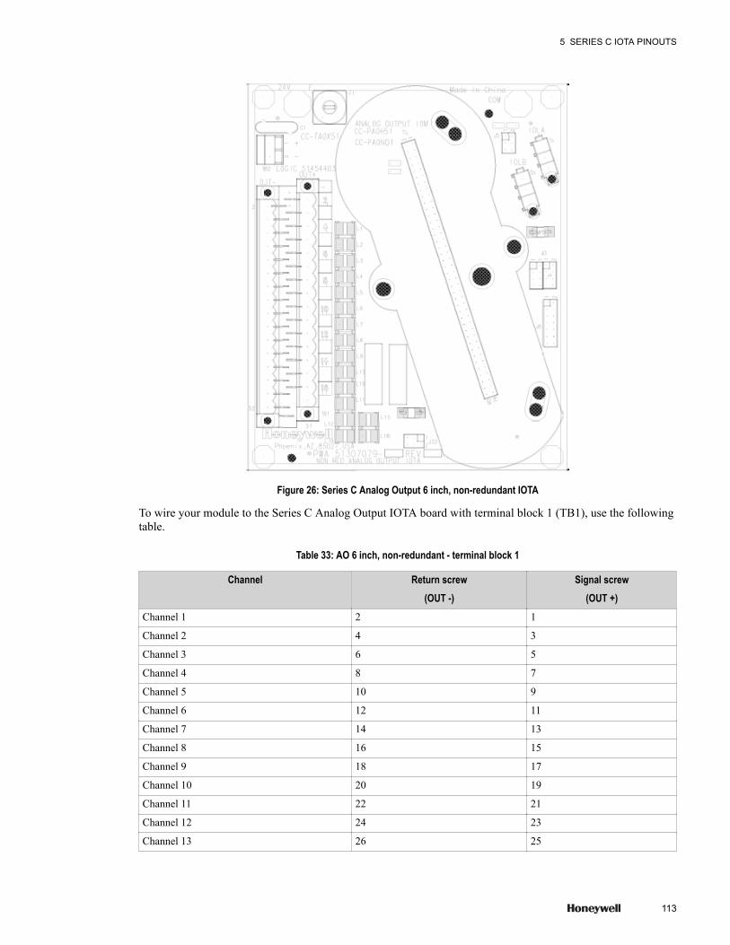
Figure 26: Series C Analog Output 6 inch, non-redundant IOTA
To wire your module to the Series C Analog Output IOTA board with terminal block 1 (TB1), use the followingtable.
Table 33: AO 6 inch, non-redundant - terminal block 1
Channel Return screw(OUT -)
Signal screw(OUT +)
Channel 1 2 1
Channel 2 4 3
Channel 3 6 5
Channel 4 8 7
Channel 5 10 9
Channel 6 12 11
Channel 7 14 13
Channel 8 16 15
Channel 9 18 17
Channel 10 20 19
Channel 11 22 21
Channel 12 24 23
Channel 13 26 25
5 SERIES C IOTA PINOUTS
113
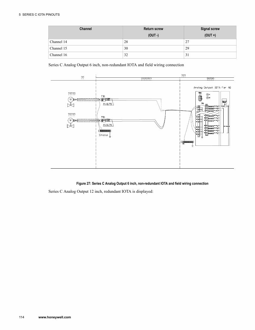
Channel Return screw(OUT -)
Signal screw(OUT +)
Channel 14 28 27
Channel 15 30 29
Channel 16 32 31
Series C Analog Output 6 inch, non-redundant IOTA and field wiring connection
Figure 27: Series C Analog Output 6 inch, non-redundant IOTA and field wiring connection
Series C Analog Output 12 inch, redundant IOTA is displayed:
5 SERIES C IOTA PINOUTS
114 www.honeywell.com

Figure 28: Series C Analog Output 12 inch, redundant IOTA
5 SERIES C IOTA PINOUTS
115

5.7 Low Level Analog Input Mux (LLMUX) IOTA Models CC-TAIM01The Series C Low Level Mux IOTA board is represented by the following information and graphics.
To access the parts information for the:
• module• IOTA• connector block assembly, and• fuses
associated with this board and module, refer to Low Level Analog Input in the Recommended Spare Partssection.
5.7.1 Field wiring and module protection - Low Level Analog Input Mux (LLMUX) moduleThe LLMUX module provides power and communications to up to four Low Level Mux FTAs. Each FTA isprotected by a specific fuse. Additionally, a main fuse protects the module's power path to all FTAs.
The following applies to fusing for LLMUX:
Fuse Functionality DescriptionF1 Power to module electronics FUSE, 1 Amp, 125V,
Quick Blo, 5x20mmF2 Switched power to all FTAs
F3 Power to FTA 1 only FUSE, 0.25 Amp,
Quick Blo, 5x20mmF4 Power to FTA 2 only
F5 Power to FTA 3 only
F6 Power to FTA 4 only
Fuses 1 and 2
• The primary purpose of the main electronics fuse (F1) is to protect the module electronics. The primary roleof the main FTA fuse (F2) is to isolate the power path from the module electronics and prevent a shortcircuit in the FTA power path from impacting the entire system.
Fuses 3 through 6
• A simultaneous failure of multiple FTAs can blow the common FTA fuse.• A short circuit on a power cable to an FTA or a short in an FTA will blow the IOTA fuse for that FTA, but
not affect any of the other FTAs or their fuses.
5.7.2 IOTA board and connections - Low Level Analog Input Mux (LLMUX) moduleSeries C Low Level 6 inch, non-redundant IOTA is displayed.
5 SERIES C IOTA PINOUTS
116 www.honeywell.com
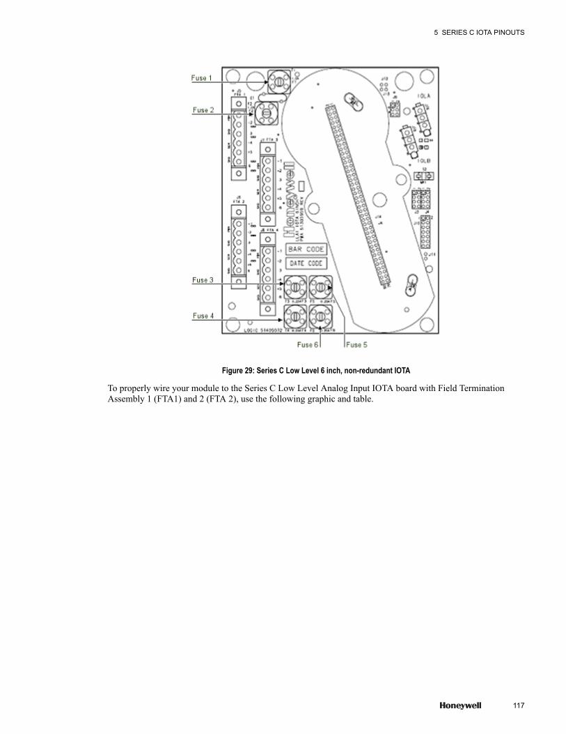
Figure 29: Series C Low Level 6 inch, non-redundant IOTA
To properly wire your module to the Series C Low Level Analog Input IOTA board with Field TerminationAssembly 1 (FTA1) and 2 (FTA 2), use the following graphic and table.
5 SERIES C IOTA PINOUTS
117
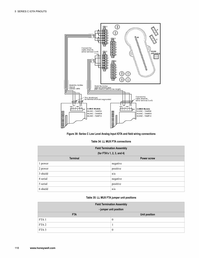
Figure 30: Series C Low Level Analog Input IOTA and field wiring connections
Table 34: LL MUX FTA connections
Field Termination Assembly(for FTA's 1, 2, 3, and 4)
Terminal Power screw1 power negative
2 power positive
3 shield n/a
4 serial negative
5 serial positive
6 shield n/a
Table 35: LL MUX FTA jumper unit positions
Field Termination Assembly- jumper unit position
FTA Unit positionFTA 1 0
FTA 2 1
FTA 3 0
5 SERIES C IOTA PINOUTS
118 www.honeywell.com

Field Termination Assembly- jumper unit position
FTA Unit positionFTA 4 1
5 SERIES C IOTA PINOUTS
119
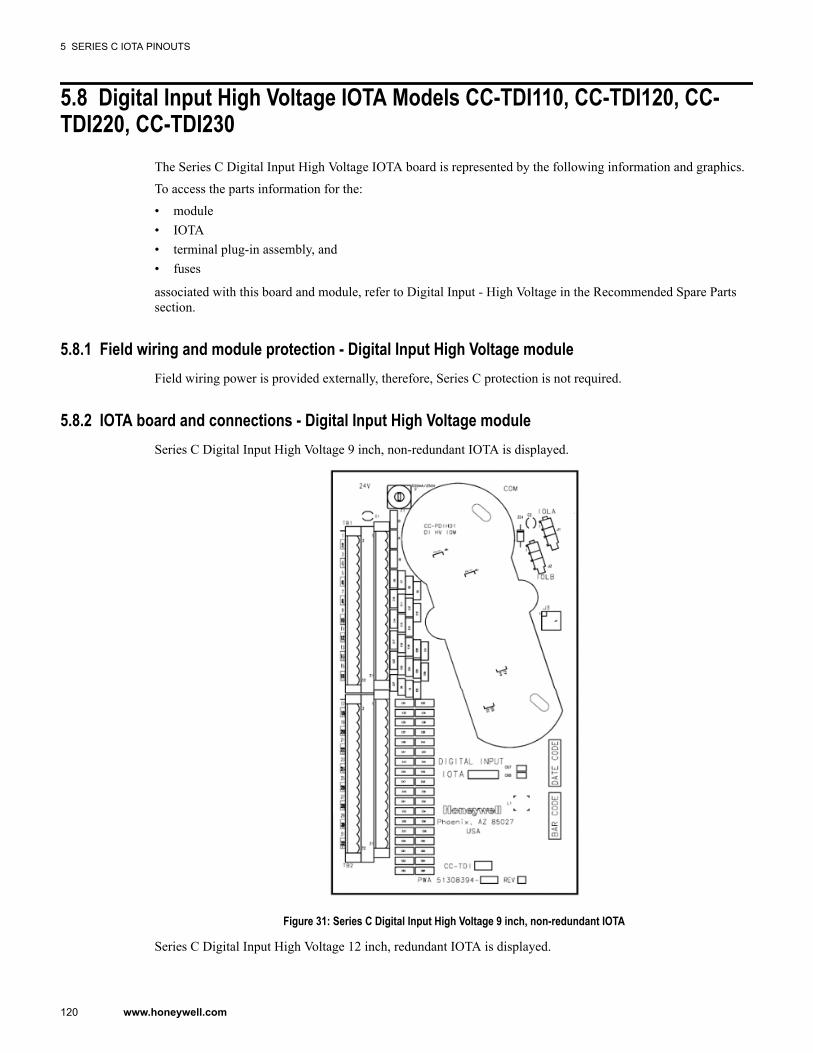
5.8 Digital Input High Voltage IOTA Models CC-TDI110, CC-TDI120, CC-TDI220, CC-TDI230
The Series C Digital Input High Voltage IOTA board is represented by the following information and graphics.
To access the parts information for the:
• module• IOTA• terminal plug-in assembly, and• fuses
associated with this board and module, refer to Digital Input - High Voltage in the Recommended Spare Partssection.
5.8.1 Field wiring and module protection - Digital Input High Voltage moduleField wiring power is provided externally, therefore, Series C protection is not required.
5.8.2 IOTA board and connections - Digital Input High Voltage moduleSeries C Digital Input High Voltage 9 inch, non-redundant IOTA is displayed.
Figure 31: Series C Digital Input High Voltage 9 inch, non-redundant IOTA
Series C Digital Input High Voltage 12 inch, redundant IOTA is displayed.
5 SERIES C IOTA PINOUTS
120 www.honeywell.com
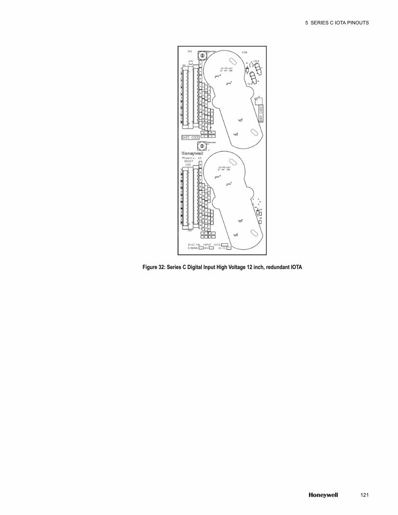
Figure 32: Series C Digital Input High Voltage 12 inch, redundant IOTA
5 SERIES C IOTA PINOUTS
121
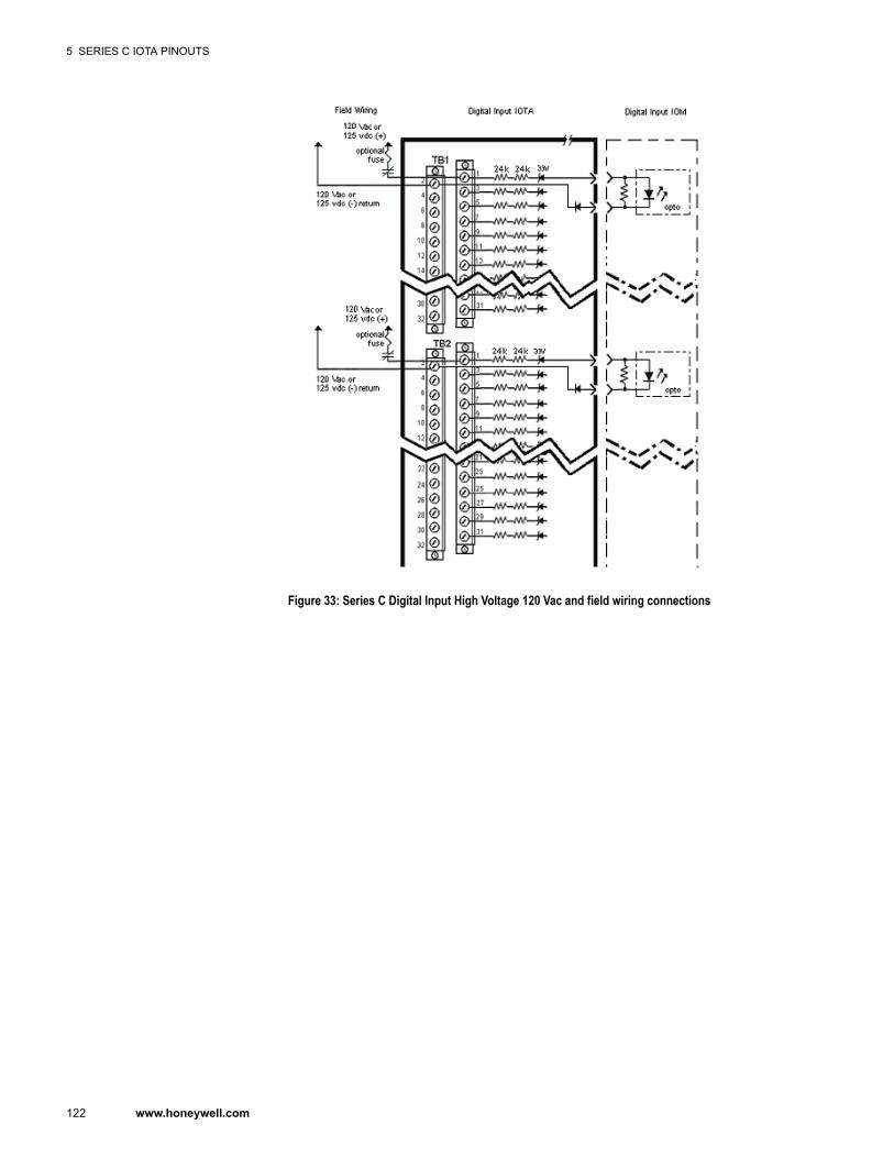
Figure 33: Series C Digital Input High Voltage 120 Vac and field wiring connections
5 SERIES C IOTA PINOUTS
122 www.honeywell.com
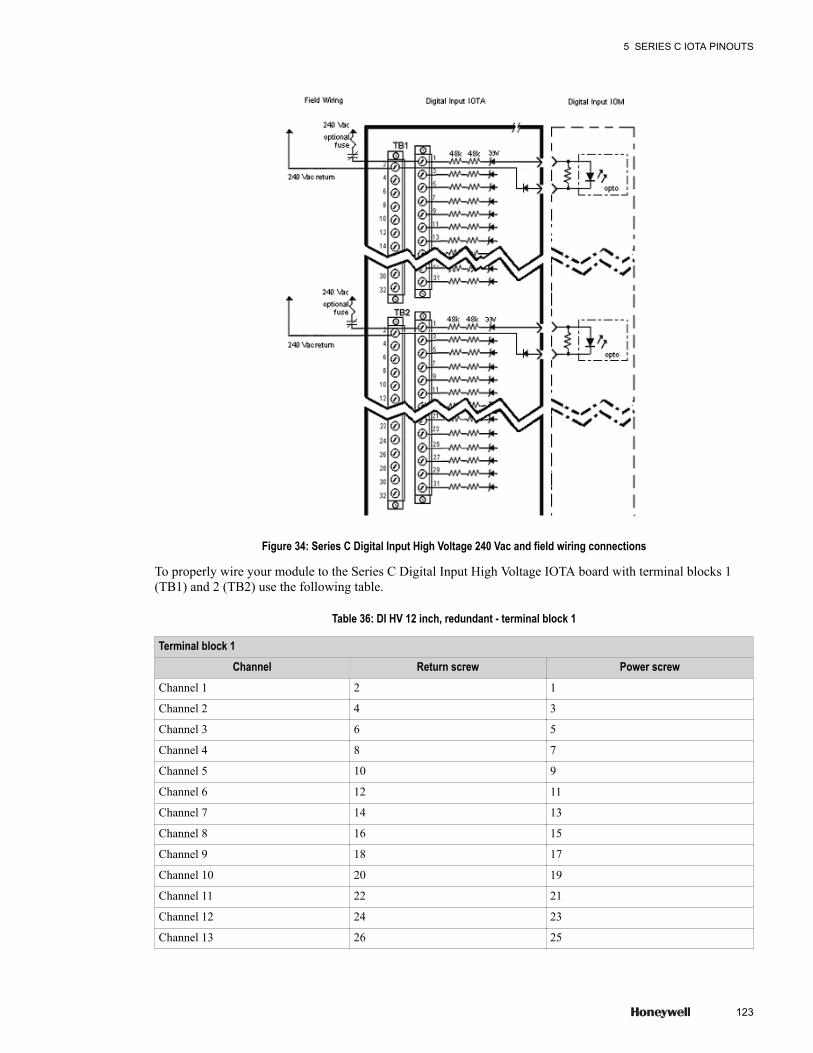
Figure 34: Series C Digital Input High Voltage 240 Vac and field wiring connections
To properly wire your module to the Series C Digital Input High Voltage IOTA board with terminal blocks 1(TB1) and 2 (TB2) use the following table.
Table 36: DI HV 12 inch, redundant - terminal block 1
Terminal block 1Channel Return screw Power screw
Channel 1 2 1
Channel 2 4 3
Channel 3 6 5
Channel 4 8 7
Channel 5 10 9
Channel 6 12 11
Channel 7 14 13
Channel 8 16 15
Channel 9 18 17
Channel 10 20 19
Channel 11 22 21
Channel 12 24 23
Channel 13 26 25
5 SERIES C IOTA PINOUTS
123
Terminal block 1Channel Return screw Power screw
Channel 14 28 27
Channel 15 30 29
Channel 16 32 31
Table 37: DI HV 12 inch, redundant - terminal block 2
Terminal block 2Channel Return screw Power screw
Channel 17 2 1
Channel 18 4 3
Channel 19 6 5
Channel 20 8 7
Channel 21 10 9
Channel 22 12 11
Channel 23 14 13
Channel 24 16 15
Channel 25 18 17
Channel 26 20 19
Channel 27 22 21
Channel 28 24 23
Channel 29 26 25
Channel 30 28 27
Channel 31 30 29
Channel 32 32 31
5 SERIES C IOTA PINOUTS
124 www.honeywell.com
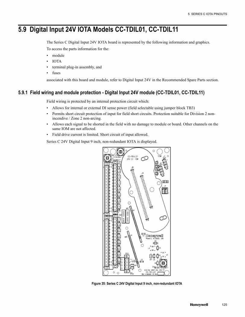
5.9 Digital Input 24V IOTA Models CC-TDIL01, CC-TDIL11The Series C Digital Input 24V IOTA board is represented by the following information and graphics.
To access the parts information for the:
• module• IOTA• terminal plug-in assembly, and• fuses
associated with this board and module, refer to Digital Input 24V in the Recommended Spare Parts section.
5.9.1 Field wiring and module protection - Digital Input 24V module (CC-TDIL01, CC-TDIL11)Field wiring is protected by an internal protection circuit which:
• Allows for internal or external DI sense power (field selectable using jumper block TB3)• Permits short circuit protection of input for field short circuits. Protection suitable for Division 2 non-
incendive / Zone 2 non-arcing.• Allows each signal to be shorted in the field with no damage to module or board. Other channels on the
same IOM are not affected.• Field drive current is limited. Short circuit of input allowed.
Series C 24V Digital Input 9 inch, non-redundant IOTA is displayed.
Figure 35: Series C 24V Digital Input 9 inch, non-redundant IOTA
5 SERIES C IOTA PINOUTS
125
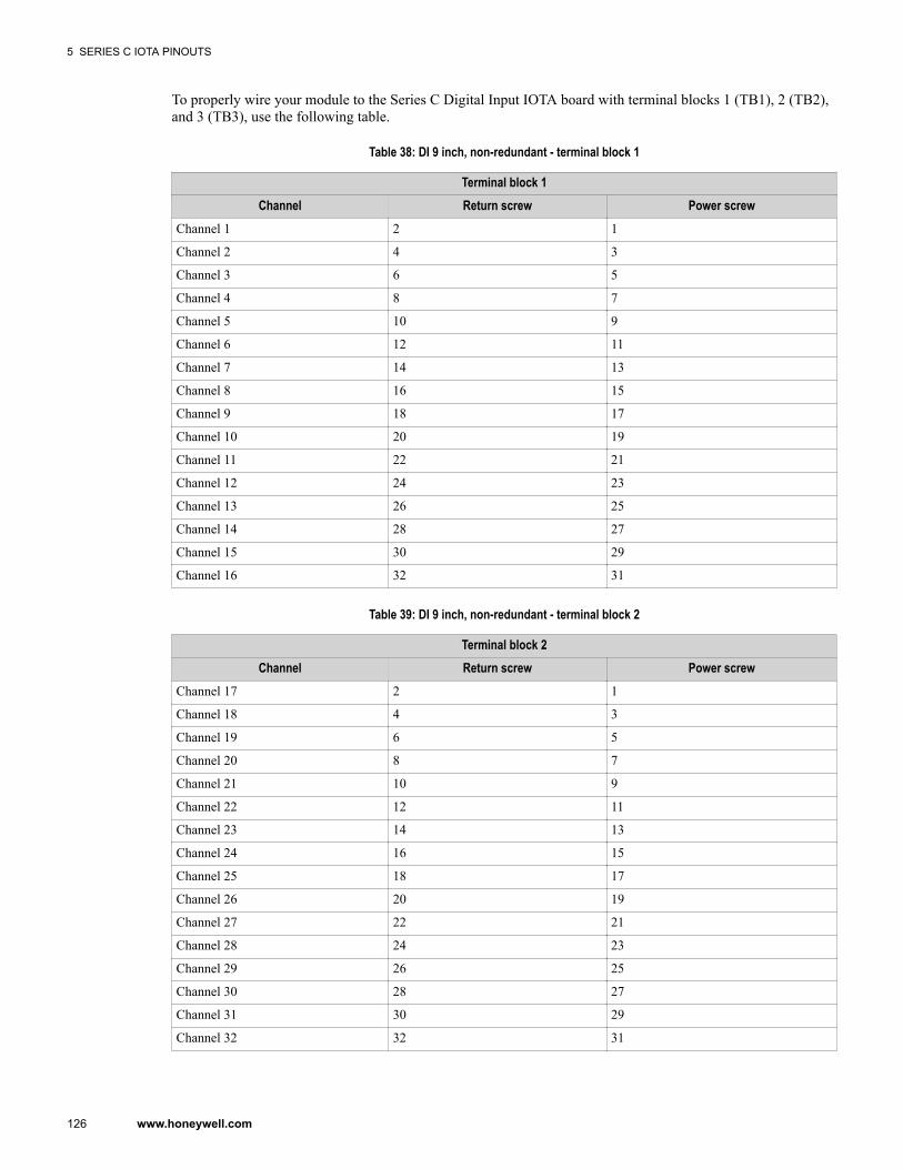
To properly wire your module to the Series C Digital Input IOTA board with terminal blocks 1 (TB1), 2 (TB2),and 3 (TB3), use the following table.
Table 38: DI 9 inch, non-redundant - terminal block 1
Terminal block 1Channel Return screw Power screw
Channel 1 2 1
Channel 2 4 3
Channel 3 6 5
Channel 4 8 7
Channel 5 10 9
Channel 6 12 11
Channel 7 14 13
Channel 8 16 15
Channel 9 18 17
Channel 10 20 19
Channel 11 22 21
Channel 12 24 23
Channel 13 26 25
Channel 14 28 27
Channel 15 30 29
Channel 16 32 31
Table 39: DI 9 inch, non-redundant - terminal block 2
Terminal block 2Channel Return screw Power screw
Channel 17 2 1
Channel 18 4 3
Channel 19 6 5
Channel 20 8 7
Channel 21 10 9
Channel 22 12 11
Channel 23 14 13
Channel 24 16 15
Channel 25 18 17
Channel 26 20 19
Channel 27 22 21
Channel 28 24 23
Channel 29 26 25
Channel 30 28 27
Channel 31 30 29
Channel 32 32 31
5 SERIES C IOTA PINOUTS
126 www.honeywell.com
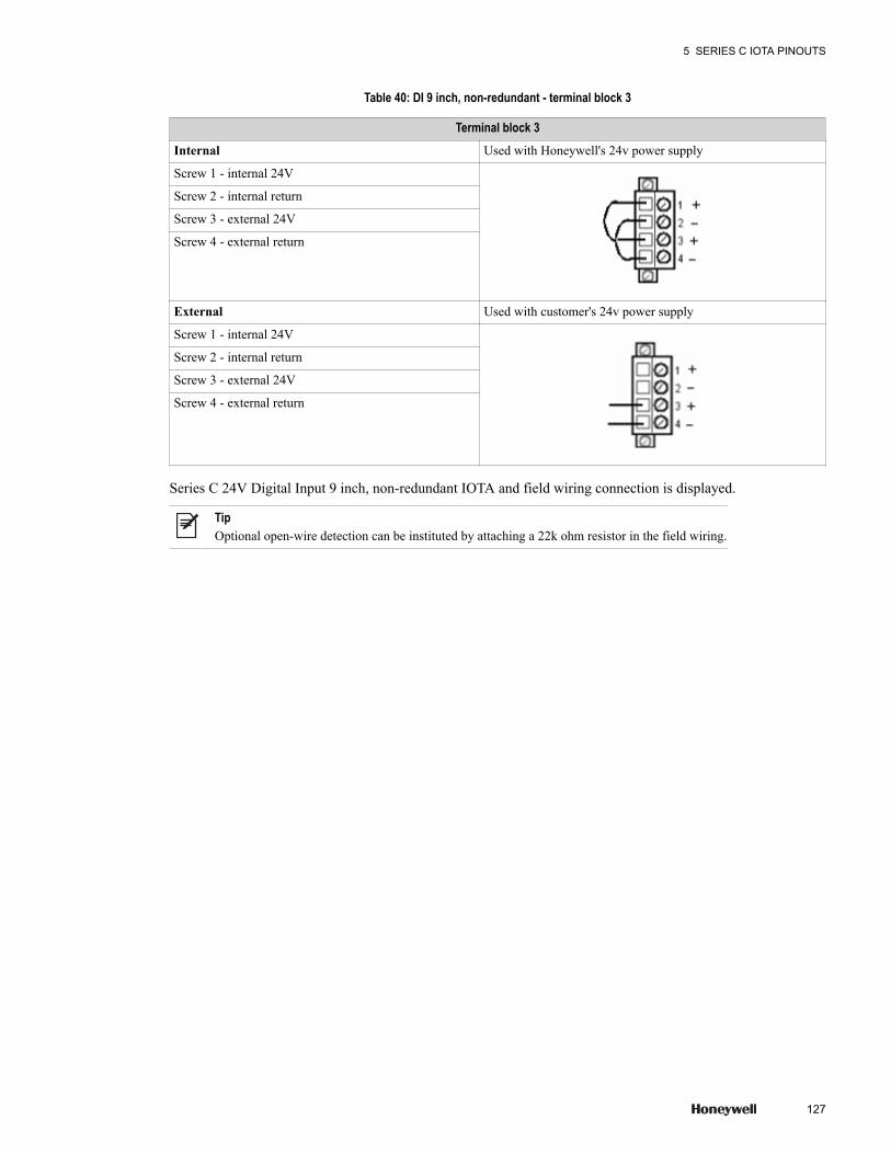
Table 40: DI 9 inch, non-redundant - terminal block 3
Terminal block 3Internal Used with Honeywell's 24v power supply
Screw 1 - internal 24V
Screw 2 - internal return
Screw 3 - external 24V
Screw 4 - external return
External Used with customer's 24v power supply
Screw 1 - internal 24V
Screw 2 - internal return
Screw 3 - external 24V
Screw 4 - external return
Series C 24V Digital Input 9 inch, non-redundant IOTA and field wiring connection is displayed.
TipOptional open-wire detection can be instituted by attaching a 22k ohm resistor in the field wiring.
5 SERIES C IOTA PINOUTS
127
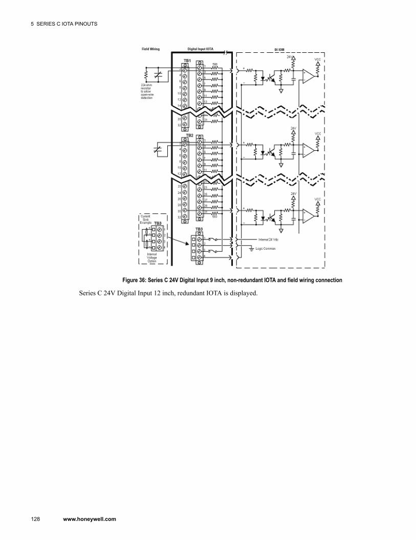
Figure 36: Series C 24V Digital Input 9 inch, non-redundant IOTA and field wiring connection
Series C 24V Digital Input 12 inch, redundant IOTA is displayed.
5 SERIES C IOTA PINOUTS
128 www.honeywell.com
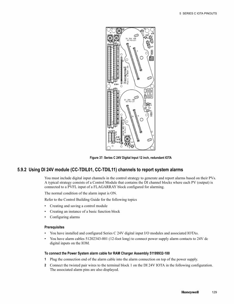
Figure 37: Series C 24V Digital Input 12 inch, redundant IOTA
5.9.2 Using DI 24V module (CC-TDIL01, CC-TDIL11) channels to report system alarmsYou must include digital input channels in the control strategy to generate and report alarms based on their PVs.A typical strategy consists of a Control Module that contains the DI channel blocks where each PV (output) isconnected to a PVFL input of a FLAGARRAY block configured for alarming.
The normal condition of the alarm input is ON.
Refer to the Control Building Guide for the following topics
• Creating and saving a control module• Creating an instance of a basic function block• Configuring alarms
Prerequisites• You have installed and configured Series C 24V digital input I/O modules and associated IOTAs.• You have alarm cables 51202343-001 (12-foot long) to connect power supply alarm contacts to 24V dc
digital inputs on the IOM.
To connect the Power System alarm cable for RAM Charger Assembly 51199932-1001 Plug the connection end of the alarm cable into the alarm connection on top of the power supply.2 Connect the twisted pair wires to the terminal block 1 on the DI 24V IOTA in the following configuration.
The associated alarm pins are also displayed.
5 SERIES C IOTA PINOUTS
129
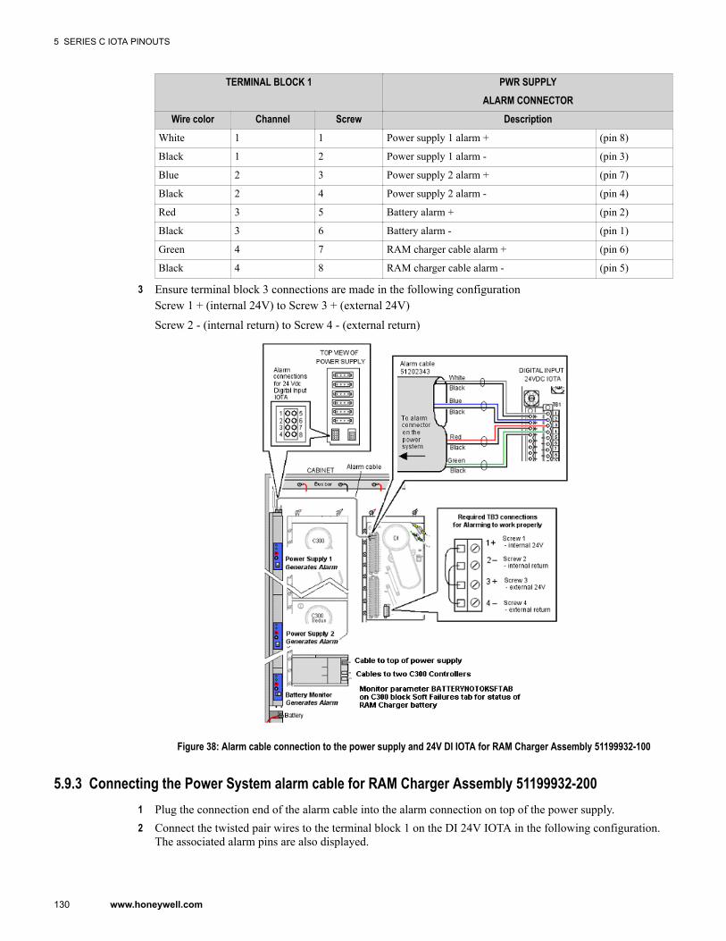
TERMINAL BLOCK 1 PWR SUPPLYALARM CONNECTOR
Wire color Channel Screw DescriptionWhite 1 1 Power supply 1 alarm + (pin 8)
Black 1 2 Power supply 1 alarm - (pin 3)
Blue 2 3 Power supply 2 alarm + (pin 7)
Black 2 4 Power supply 2 alarm - (pin 4)
Red 3 5 Battery alarm + (pin 2)
Black 3 6 Battery alarm - (pin 1)
Green 4 7 RAM charger cable alarm + (pin 6)
Black 4 8 RAM charger cable alarm - (pin 5)
3 Ensure terminal block 3 connections are made in the following configurationScrew 1 + (internal 24V) to Screw 3 + (external 24V)
Screw 2 - (internal return) to Screw 4 - (external return)
Figure 38: Alarm cable connection to the power supply and 24V DI IOTA for RAM Charger Assembly 51199932-100
5.9.3 Connecting the Power System alarm cable for RAM Charger Assembly 51199932-2001 Plug the connection end of the alarm cable into the alarm connection on top of the power supply.2 Connect the twisted pair wires to the terminal block 1 on the DI 24V IOTA in the following configuration.
The associated alarm pins are also displayed.
5 SERIES C IOTA PINOUTS
130 www.honeywell.com
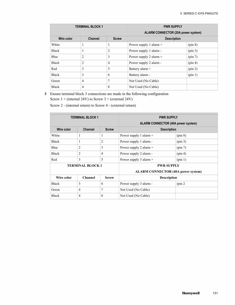
TERMINAL BLOCK 1 PWR SUPPLYALARM CONNECTOR (20A power system)
Wire color Channel Screw DescriptionWhite 1 1 Power supply 1 alarm + (pin 8)
Black 1 2 Power supply 1 alarm - (pin 3)
Blue 2 3 Power supply 2 alarm + (pin 7)
Black 2 4 Power supply 2 alarm - (pin 4)
Red 3 5 Battery alarm + (pin 2)
Black 3 6 Battery alarm - (pin 1)
Green 4 7 Not Used (No Cable)
Black 4 8 Not Used (No Cable)
3 Ensure terminal block 3 connections are made in the following configurationScrew 1 + (internal 24V) to Screw 3 + (external 24V)
Screw 2 - (internal return) to Screw 4 - (external return)
TERMINAL BLOCK 1 PWR SUPPLYALARM CONNECTOR (40A power system)
Wire color Channel Screw DescriptionWhite 1 1 Power supply 1 alarm + (pin 8)
Black 1 2 Power supply 1 alarm - (pin 3)
Blue 2 3 Power supply 2 alarm + (pin 7)
Black 2 4 Power supply 2 alarm - (pin 4)
Red 3 5 Power supply 3 alarm + (pin 1)
TERMINAL BLOCK 1 PWR SUPPLY
ALARM CONNECTOR (40A power system)
Wire color Channel Screw Description
Black 3 6 Power supply 3 alarm - (pin 2
Green 4 7 Not Used (No Cable)
Black 4 8 Not Used (No Cable)
5 SERIES C IOTA PINOUTS
131
Figure 39: Alarm cable connection to the power supply and 24V DI IOTA for RAM Charger Assembly 51199932-200
5 SERIES C IOTA PINOUTS
132 www.honeywell.com
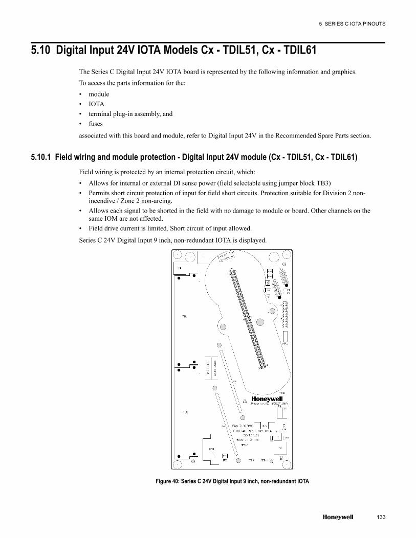
5.10 Digital Input 24V IOTA Models Cx - TDIL51, Cx - TDIL61The Series C Digital Input 24V IOTA board is represented by the following information and graphics.
To access the parts information for the:
• module• IOTA• terminal plug-in assembly, and• fuses
associated with this board and module, refer to Digital Input 24V in the Recommended Spare Parts section.
5.10.1 Field wiring and module protection - Digital Input 24V module (Cx - TDIL51, Cx - TDIL61)Field wiring is protected by an internal protection circuit, which:
• Allows for internal or external DI sense power (field selectable using jumper block TB3)• Permits short circuit protection of input for field short circuits. Protection suitable for Division 2 non-
incendive / Zone 2 non-arcing.• Allows each signal to be shorted in the field with no damage to module or board. Other channels on the
same IOM are not affected.• Field drive current is limited. Short circuit of input allowed.
Series C 24V Digital Input 9 inch, non-redundant IOTA is displayed.
Figure 40: Series C 24V Digital Input 9 inch, non-redundant IOTA
5 SERIES C IOTA PINOUTS
133

To wire your module to the Series C Digital Input IOTA board with terminal blocks 1 (TB1), 2 (TB2), and 3(TB3), use the following table.
Table 41: DI 9 inch, non-redundant - terminal block 1
Terminal block 1Channel Return screw Power screw
Channel 1 2 1
Channel 2 4 3
Channel 3 6 5
Channel 4 8 7
Channel 5 10 9
Channel 6 12 11
Channel 7 14 13
Channel 8 16 15
Channel 9 18 17
Channel 10 20 19
Channel 11 22 21
Channel 12 24 23
Channel 13 26 25
Channel 14 28 27
Channel 15 30 29
Channel 16 32 31
Table 42: DI 9 inch, non-redundant - terminal block 2
Terminal block 2Channel Return screw Power screw
Channel 17 2 1
Channel 18 4 3
Channel 19 6 5
Channel 20 8 7
Channel 21 10 9
Channel 22 12 11
Channel 23 14 13
Channel 24 16 15
Channel 25 18 17
Channel 26 20 19
Channel 27 22 21
Channel 28 24 23
Channel 29 26 25
Channel 30 28 27
Channel 31 30 29
Channel 32 32 31
5 SERIES C IOTA PINOUTS
134 www.honeywell.com
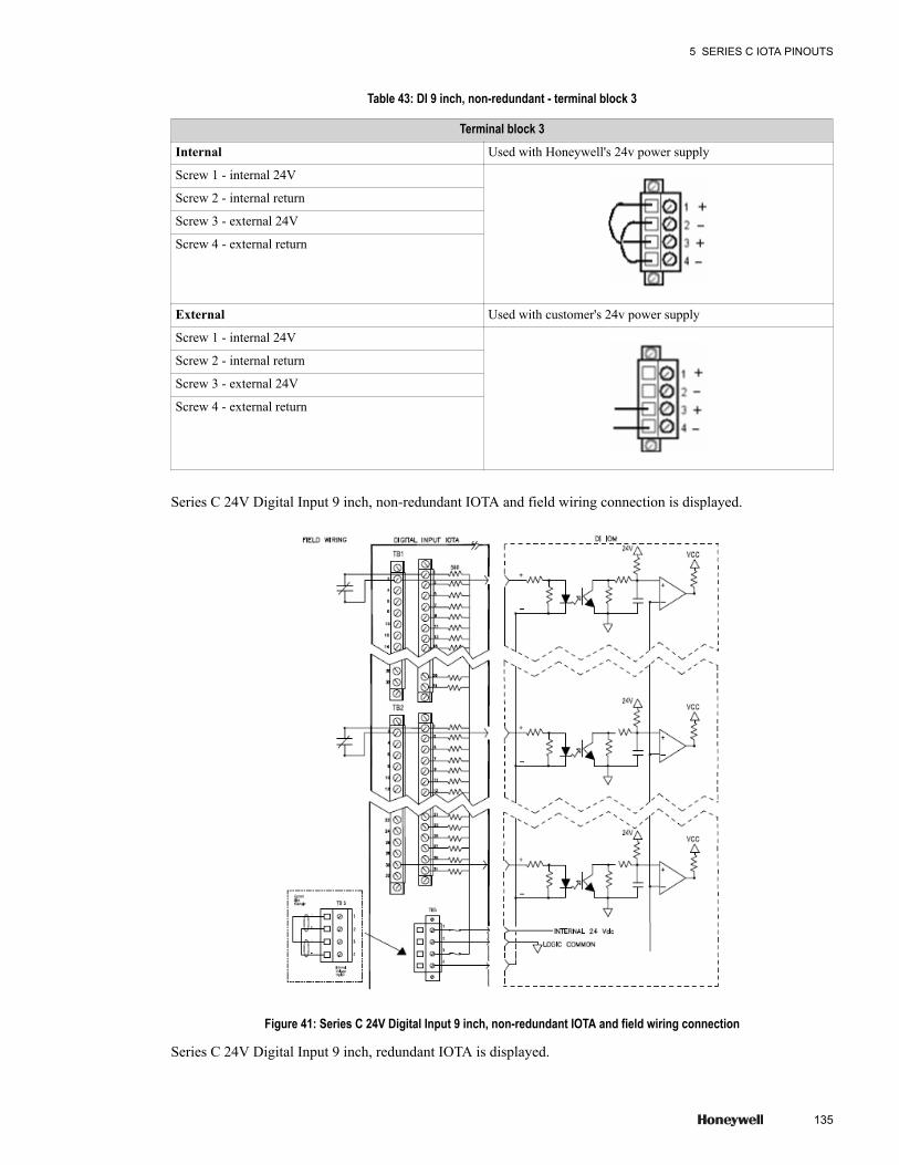
Table 43: DI 9 inch, non-redundant - terminal block 3
Terminal block 3Internal Used with Honeywell's 24v power supply
Screw 1 - internal 24V
Screw 2 - internal return
Screw 3 - external 24V
Screw 4 - external return
External Used with customer's 24v power supply
Screw 1 - internal 24V
Screw 2 - internal return
Screw 3 - external 24V
Screw 4 - external return
Series C 24V Digital Input 9 inch, non-redundant IOTA and field wiring connection is displayed.
Figure 41: Series C 24V Digital Input 9 inch, non-redundant IOTA and field wiring connection
Series C 24V Digital Input 9 inch, redundant IOTA is displayed.
5 SERIES C IOTA PINOUTS
135

Figure 42: Series C 24V Digital Input 9 inch, redundant IOTA
5.10.2 Using DI 24V module (Cx - TDIL51, Cx - TDIL61) channels to report system alarmsYou must include digital input channels in the control strategy to generate and report alarms based on their PVs.A typical strategy consists of a Control Module that contains the DI channel blocks where each PV (output) isconnected to a PVFL input of a FLAGARRAY block configured for alarming.
The normal condition of the alarm input is ON.
Refer to the Control Building Guide for the following topics
• Creating and saving a control module• Creating an instance of a basic function block• Configuring alarms
Prerequisites• You have installed and configured Series C 24V digital input I/O modules and associated IOTAs.• You have alarm cables 51202343-001 (12-foot long) to connect power supply alarm contacts to 24V dc
digital inputs on the IOM.
To connect the Power System alarm cable for RAM Charger Assembly 51199932-2001 Plug the connection end of the alarm cable into the alarm connection on top of the power supply.2 Connect the twisted pair wires to the terminal block 1 on the DI 24V IOTA in the following configuration.
The associated alarm pins are also displayed.
5 SERIES C IOTA PINOUTS
136 www.honeywell.com
TERMINAL BLOCK 1 PWR SUPPLYALARM CONNECTOR (20A power system)
Wire color Channel Screw DescriptionWhite 1 1 Power supply 1 alarm + (pin 8)
Black 1 2 Power supply 1 alarm - (pin 3)
Blue 2 3 Power supply 2 alarm + (pin 7)
Black 2 4 Power supply 2 alarm - (pin 4)
Red 3 5 Battery alarm + (pin 2)
Black 3 6 Battery alarm - (pin 1)
Green 4 7 Not Used (No Cable)
Black 4 8 Not Used (No Cable)
3 Ensure terminal block 3 connections are made in the following configurationScrew 1 + (internal 24V) to Screw 3 + (external 24V)
Screw 2 - (internal return) to Screw 4 - (external return)
TERMINAL BLOCK 1 PWR SUPPLYALARM CONNECTOR (40A power system)
Wire color Channel Screw DescriptionWhite 1 1 Power supply 1 alarm + (pin 8)
Black 1 2 Power supply 1 alarm - (pin 3)
Blue 2 3 Power supply 2 alarm + (pin 7)
Black 2 4 Power supply 2 alarm - (pin 4)
Red 3 5 Power supply 3 alarm + (pin 1)
TERMINAL BLOCK 1 PWR SUPPLY
ALARM CONNECTOR (40A power system)
Wire color Channel Screw Description
Black 3 6 Power supply 3 alarm - (pin 2
Green 4 7 Not Used (No Cable)
Black 4 8 Not Used (No Cable)
5 SERIES C IOTA PINOUTS
137
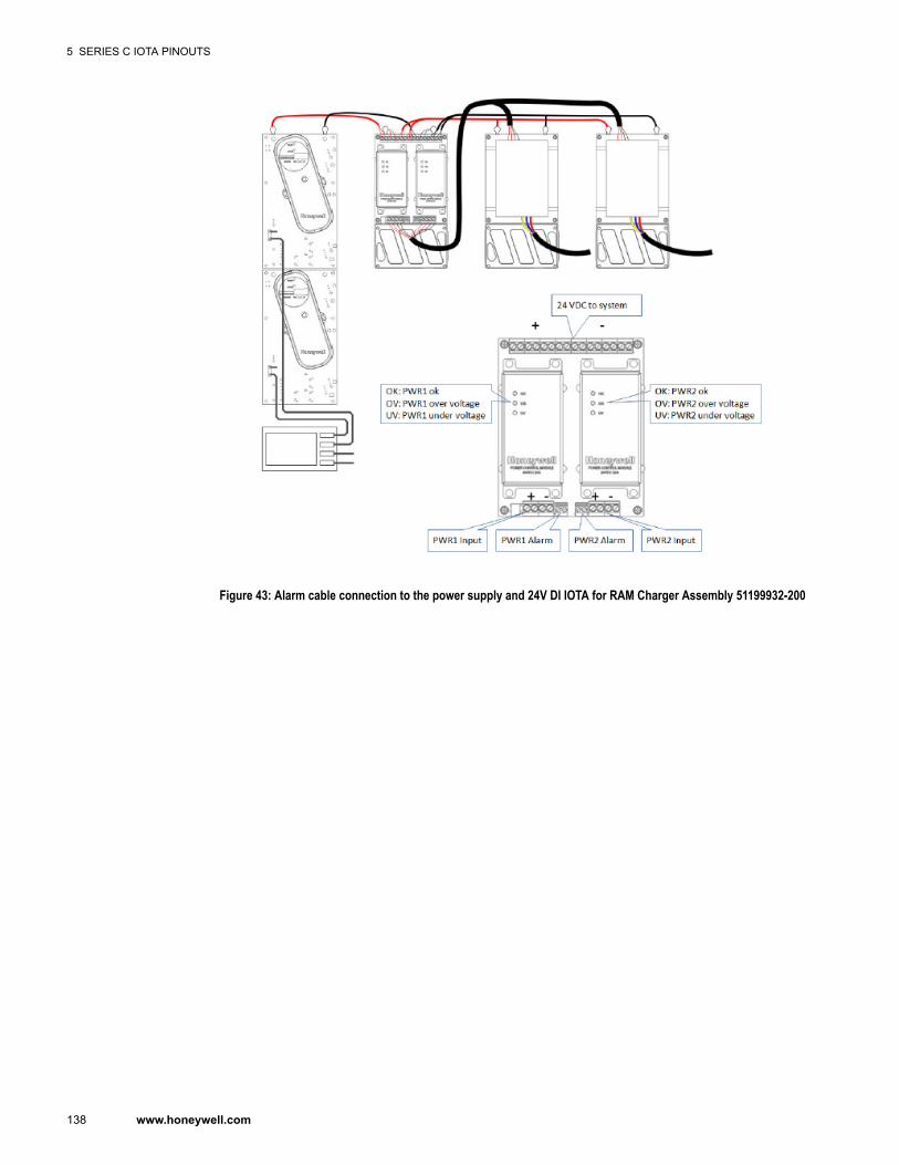
Figure 43: Alarm cable connection to the power supply and 24V DI IOTA for RAM Charger Assembly 51199932-200
5 SERIES C IOTA PINOUTS
138 www.honeywell.com
5.11 Digital Output 24V IOTA Models CC-TDOB01, CC-TDOB11
CAUTIONWhen wiring the Digital Output 24V ensure that the external power is not reversed or the IOM will be damaged.
The Series C Digital Output 24V IOTA board is represented by the following information and graphics.
To access the parts information for the:
• module• IOTA• terminal plug-in assembly, and• fuses
associated with this board and module, refer to Digital Output 24V in the Recommended Spare Parts section.
5.11.1 Field wiring and module protection - Digital Output 24V module (CC-TDOB01, CC-TDOB11)The Digital Output 24Volt Module provides a unique and highly functional output power protection method.When a short occurs in the field, the following occurs:
• the output circuits sense the over-current condition and shut down the output• the shut down of the point places the mode of the point into Manual• an Over-current Soft Failure is generated
This failure is maintained until the short circuit condition is repaired and the point is again supplying the propercurrent.
Only one channel is affected at a time. If multiple channels are affected, they are individually shut down. Anychannels that do not have a short circuit condition are unaffected.
• Thermal protection alarm if short in field of > 0.5A.
5.11.2 IOTA board and connections - Digital Output 24V module (CC-TDOB01, CC-TDOB11)Series C 24V Digital Output 9 inch, non-redundant IOTA is displayed.
5 SERIES C IOTA PINOUTS
139
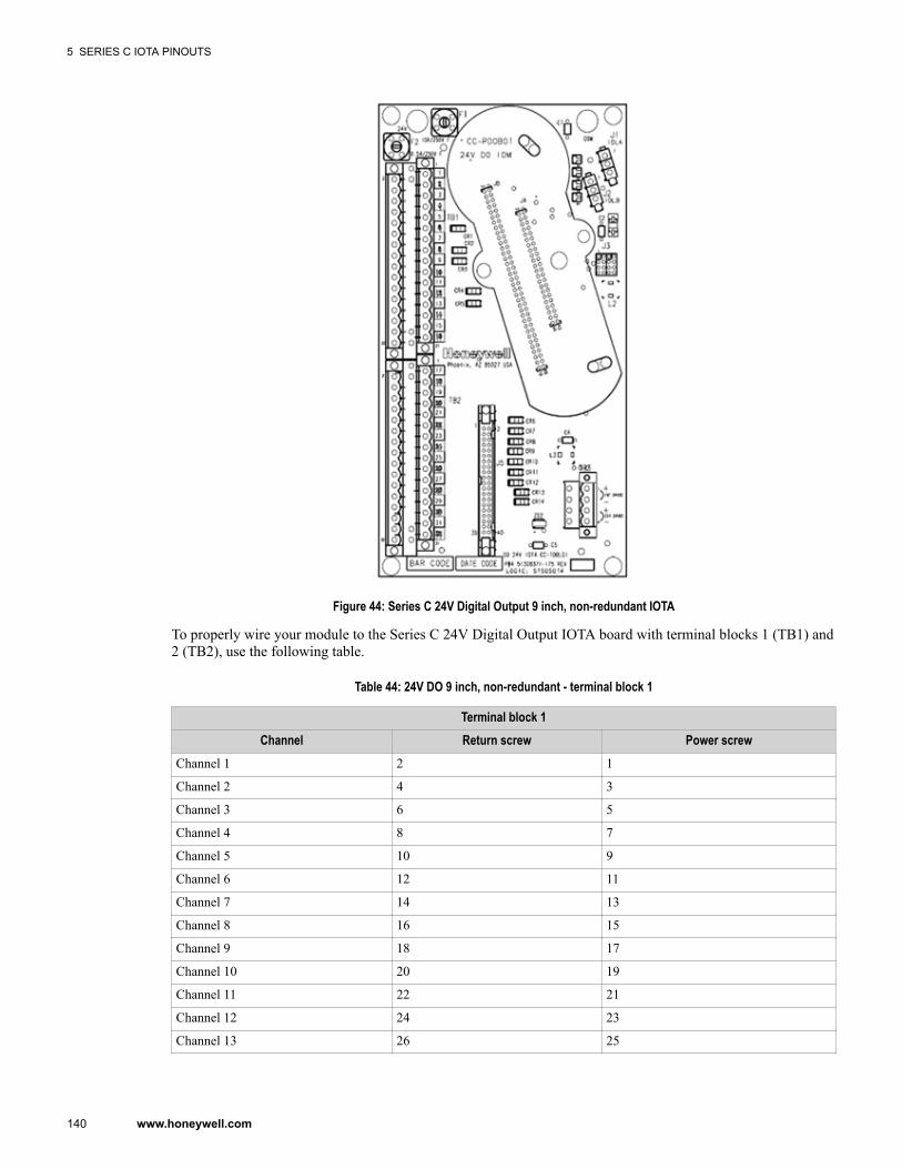
Figure 44: Series C 24V Digital Output 9 inch, non-redundant IOTA
To properly wire your module to the Series C 24V Digital Output IOTA board with terminal blocks 1 (TB1) and2 (TB2), use the following table.
Table 44: 24V DO 9 inch, non-redundant - terminal block 1
Terminal block 1Channel Return screw Power screw
Channel 1 2 1
Channel 2 4 3
Channel 3 6 5
Channel 4 8 7
Channel 5 10 9
Channel 6 12 11
Channel 7 14 13
Channel 8 16 15
Channel 9 18 17
Channel 10 20 19
Channel 11 22 21
Channel 12 24 23
Channel 13 26 25
5 SERIES C IOTA PINOUTS
140 www.honeywell.com
Terminal block 1Channel Return screw Power screw
Channel 14 28 27
Channel 15 30 29
Channel 16 32 31
Table 45: 24V DO 9 inch, non-redundant - terminal block 2
Terminal block 2Channel Return screw Power screw
Channel 17 2 1
Channel 18 4 3
Channel 19 6 5
Channel 20 8 7
Channel 21 10 9
Channel 22 12 11
Channel 23 14 13
Channel 24 16 15
Channel 25 18 17
Channel 26 20 19
Channel 27 22 21
Channel 28 24 23
Channel 29 26 25
Channel 30 28 27
Channel 31 29 28
Channel 32 32 31
Table 46: 24V DO 9 inch, non-redundant - terminal block 3
Terminal block 3Internal Used with Honeywell's provided 24v power supply
Screw 1 - internal 24V
Screw 2 - internal return
Screw 3 - external 24V
Screw 4 - external return
External Used with customer's provided 24v power supply
5 SERIES C IOTA PINOUTS
141
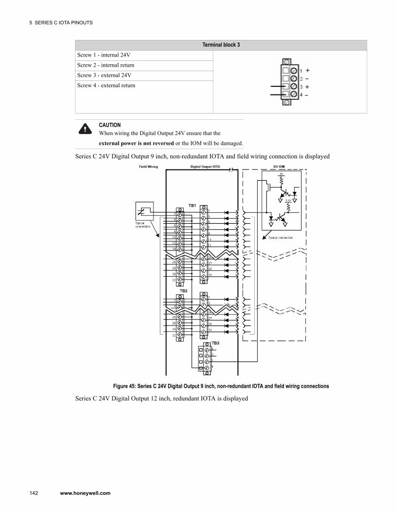
Terminal block 3Screw 1 - internal 24V
Screw 2 - internal return
Screw 3 - external 24V
Screw 4 - external return
CAUTIONWhen wiring the Digital Output 24V ensure that the
external power is not reversed or the IOM will be damaged.
Series C 24V Digital Output 9 inch, non-redundant IOTA and field wiring connection is displayed
Figure 45: Series C 24V Digital Output 9 inch, non-redundant IOTA and field wiring connections
Series C 24V Digital Output 12 inch, redundant IOTA is displayed
5 SERIES C IOTA PINOUTS
142 www.honeywell.com

Figure 46: Series C 24V Digital Output 12 inch, redundant IOTA
5 SERIES C IOTA PINOUTS
143
5.12 Digital Output 24V IOTA Models Cx-TDOD51, Cx-TDOD61
CAUTIONWhen wiring the Digital Output 24V ensure that the external power is not reversed or the IOM will be damaged.
The Series C Digital Output 24V IOTA board is represented by the following information and graphics.
To access the parts information for the:
• module• IOTA• terminal plug-in assembly, and• fuses
associated with this board and module, refer to Digital Output 24V in the Recommended Spare Parts section.
5.12.1 Field wiring and module protection - Digital Output 24V (Cx-TDOD51, Cx-TDOD61)The Digital Output 24Volt Module provides a unique and highly functional output power protection method.When a short occurs in the field, the following occurs.
• The output circuits sense the over-current condition and shut down the output.• The shut down of the point places the mode of the point into Manual.• An Over-current Soft Failure is generated.
This failure is maintained until the short circuit condition is repaired and the point is again supplying the propercurrent.
Only one channel is affected at a time. If multiple channels are affected, they are individually shut down. Anychannels that do not have a short circuit condition are unaffected.
• Each channel in a DO module can handle a maximum load of 100mA.
5.12.2 IOTA board and connections - Digital Output 24V (Cx-TDOD51, Cx-TDOD61)Series C 24V Digital Output 9 inch, non-redundant IOTA is displayed.
5 SERIES C IOTA PINOUTS
144 www.honeywell.com
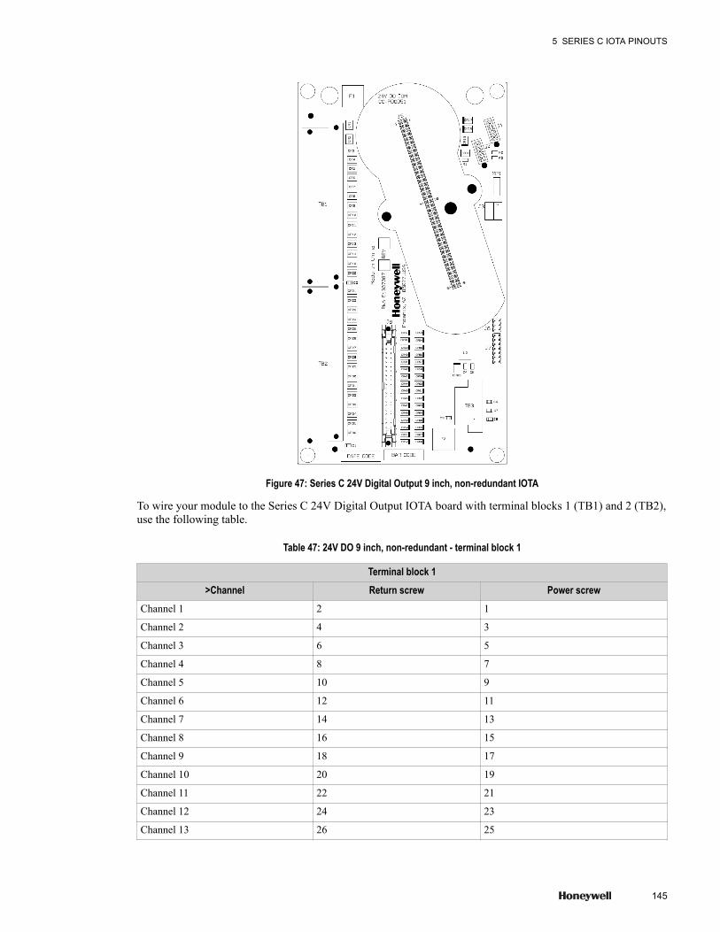
Figure 47: Series C 24V Digital Output 9 inch, non-redundant IOTA
To wire your module to the Series C 24V Digital Output IOTA board with terminal blocks 1 (TB1) and 2 (TB2),use the following table.
Table 47: 24V DO 9 inch, non-redundant - terminal block 1
Terminal block 1>Channel Return screw Power screw
Channel 1 2 1
Channel 2 4 3
Channel 3 6 5
Channel 4 8 7
Channel 5 10 9
Channel 6 12 11
Channel 7 14 13
Channel 8 16 15
Channel 9 18 17
Channel 10 20 19
Channel 11 22 21
Channel 12 24 23
Channel 13 26 25
5 SERIES C IOTA PINOUTS
145

Terminal block 1>Channel Return screw Power screw
Channel 14 28 27
Channel 15 30 29
Channel 16 32 31
Table 48: 24V DO 9 inch, non-redundant - terminal block 2
Terminal block 2Channel Return screw Power screw
Channel 17 2 1
Channel 18 4 3
Channel 19 6 5
Channel 20 8 7
Channel 21 10 9
Channel 22 12 11
Channel 23 14 13
Channel 24 16 15
Channel 25 18 17
Channel 26 20 19
Channel 27 22 21
Channel 28 24 23
Channel 29 26 25
Channel 30 28 27
Channel 31 29 28
Channel 32 32 31
Table 49: 24V DO 9 inch, non-redundant - terminal block 3
Terminal block 3Internal Used with Honeywell's provided 24v power supply
Screw 1 - internal 24V
Screw 2 - internal return
Screw 3 - external 24V
Screw 4 - external return
External Used with customer's provided 24v power supply
5 SERIES C IOTA PINOUTS
146 www.honeywell.com
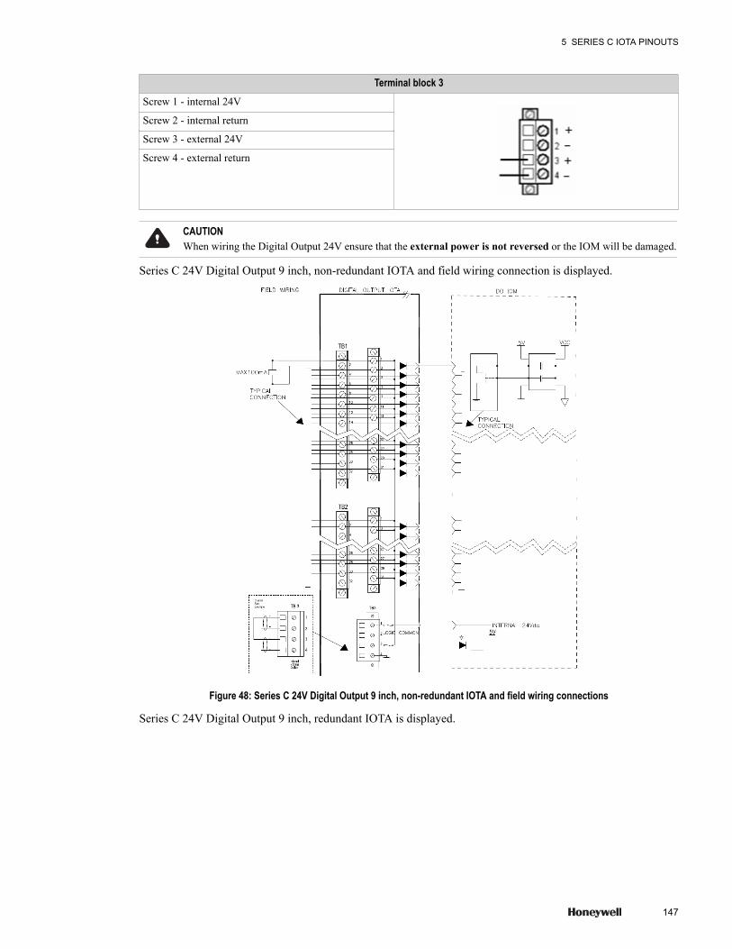
Terminal block 3Screw 1 - internal 24V
Screw 2 - internal return
Screw 3 - external 24V
Screw 4 - external return
CAUTIONWhen wiring the Digital Output 24V ensure that the external power is not reversed or the IOM will be damaged.
Series C 24V Digital Output 9 inch, non-redundant IOTA and field wiring connection is displayed.
Figure 48: Series C 24V Digital Output 9 inch, non-redundant IOTA and field wiring connections
Series C 24V Digital Output 9 inch, redundant IOTA is displayed.
5 SERIES C IOTA PINOUTS
147

Figure 49: Series C 24V Digital Output 9 inch, redundant IOTA
5 SERIES C IOTA PINOUTS
148 www.honeywell.com
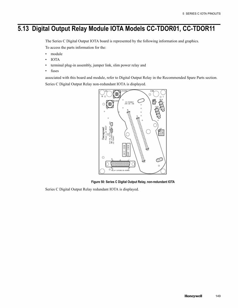
5.13 Digital Output Relay Module IOTA Models CC-TDOR01, CC-TDOR11The Series C Digital Output IOTA board is represented by the following information and graphics.
To access the parts information for the:
• module• IOTA• terminal plug-in assembly, jumper link, slim power relay and• fuses
associated with this board and module, refer to Digital Output Relay in the Recommended Spare Parts section.
Series C Digital Output Relay non-redundant IOTA is displayed.
Figure 50: Series C Digital Output Relay, non-redundant IOTA
Series C Digital Output Relay redundant IOTA is displayed.
5 SERIES C IOTA PINOUTS
149
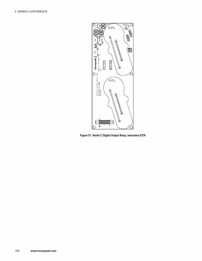
Figure 51: Series C Digital Output Relay, redundant IOTA
5 SERIES C IOTA PINOUTS
150 www.honeywell.com
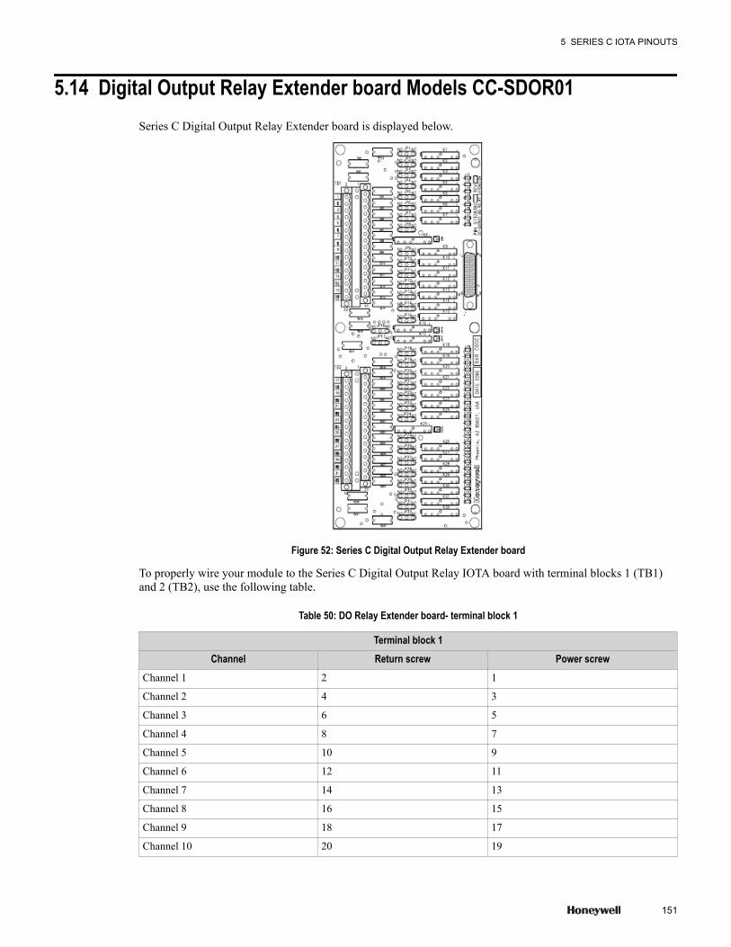
5.14 Digital Output Relay Extender board Models CC-SDOR01Series C Digital Output Relay Extender board is displayed below.
Figure 52: Series C Digital Output Relay Extender board
To properly wire your module to the Series C Digital Output Relay IOTA board with terminal blocks 1 (TB1)and 2 (TB2), use the following table.
Table 50: DO Relay Extender board- terminal block 1
Terminal block 1Channel Return screw Power screw
Channel 1 2 1
Channel 2 4 3
Channel 3 6 5
Channel 4 8 7
Channel 5 10 9
Channel 6 12 11
Channel 7 14 13
Channel 8 16 15
Channel 9 18 17
Channel 10 20 19
5 SERIES C IOTA PINOUTS
151

Terminal block 1Channel Return screw Power screw
Channel 11 22 21
Channel 12 24 23
Channel 13 26 25
Channel 14 28 27
Channel 15 30 29
Channel 16 32 31
Table 51: DO Relay Extender board- terminal block 2
Terminal block 2Channel Return screw Power screw
Channel 17 2 1
Channel 18 4 3
Channel 19 6 5
Channel 20 8 7
Channel 21 10 9
Channel 22 12 11
Channel 23 14 13
Channel 24 16 15
Channel 25 18 17
Channel 26 20 19
Channel 27 22 21
Channel 28 24 23
Channel 29 26 25
Channel 30 28 27
Channel 31 29 28
Channel 32 32 31
Series C Digital Output Relay Extender board and field wiring connection is displayed.
5 SERIES C IOTA PINOUTS
152 www.honeywell.com
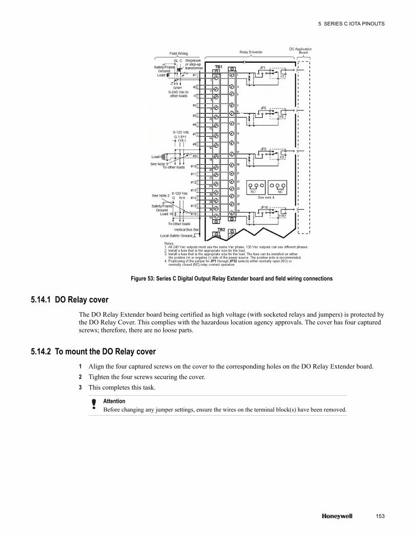
Figure 53: Series C Digital Output Relay Extender board and field wiring connections
5.14.1 DO Relay coverThe DO Relay Extender board being certified as high voltage (with socketed relays and jumpers) is protected bythe DO Relay Cover. This complies with the hazardous location agency approvals. The cover has four capturedscrews; therefore, there are no loose parts.
5.14.2 To mount the DO Relay cover1 Align the four captured screws on the cover to the corresponding holes on the DO Relay Extender board.2 Tighten the four screws securing the cover.3 This completes this task.
AttentionBefore changing any jumper settings, ensure the wires on the terminal block(s) have been removed.
5 SERIES C IOTA PINOUTS
153

Figure 54: Series C Digital Output Relay Cover
5 SERIES C IOTA PINOUTS
154 www.honeywell.com
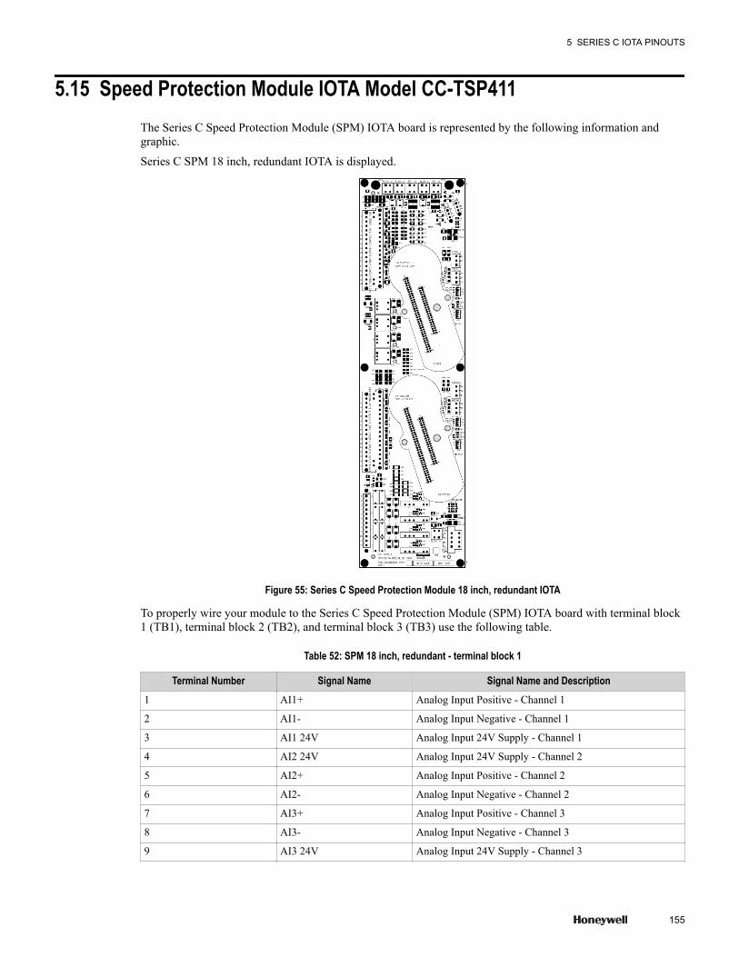
5.15 Speed Protection Module IOTA Model CC-TSP411The Series C Speed Protection Module (SPM) IOTA board is represented by the following information andgraphic.
Series C SPM 18 inch, redundant IOTA is displayed.
Figure 55: Series C Speed Protection Module 18 inch, redundant IOTA
To properly wire your module to the Series C Speed Protection Module (SPM) IOTA board with terminal block1 (TB1), terminal block 2 (TB2), and terminal block 3 (TB3) use the following table.
Table 52: SPM 18 inch, redundant - terminal block 1
Terminal Number Signal Name Signal Name and Description1 AI1+ Analog Input Positive - Channel 1
2 AI1- Analog Input Negative - Channel 1
3 AI1 24V Analog Input 24V Supply - Channel 1
4 AI2 24V Analog Input 24V Supply - Channel 2
5 AI2+ Analog Input Positive - Channel 2
6 AI2- Analog Input Negative - Channel 2
7 AI3+ Analog Input Positive - Channel 3
8 AI3- Analog Input Negative - Channel 3
9 AI3 24V Analog Input 24V Supply - Channel 3
5 SERIES C IOTA PINOUTS
155
Terminal Number Signal Name Signal Name and Description10 AI4 24V Analog Input 24V Supply - Channel 4
11 AI4+ Analog Input Positive - Channel 4
12 AI4- Analog Input Negative - Channel 4
13 AI5+ Analog Input Positive - Channel 5
14 AI5- Analog Input Negative - Channel 5
15 AI5 24V Analog Input 24V Supply - Channel 5
16 AI6 24V Analog Input 24V Supply - Channel 6
17 AI6+ Analog Input Positive - Channel 6
18 AI6- Analog Input Negative - Channel 6
19 AI7+ Analog Input Positive - Channel 7
20 AI7- Analog Input Negative - Channel 7
21 AI7 24V Analog Input 24V Supply - Channel 7
22 AI8 24V Analog Input 24V Supply - Channel 8
23 AI8+ Analog Input Positive - Channel 8
24 AI8- Analog Input Negative - Channel 8
25 PASS1+ Passive Speed Sensor Input Positive - Channel 1
26 PASS1- Passive Speed Sensor Input Negative - Channel 1
27 PASS2+ Passive Speed Sensor Input Positive - Channel 2
28 PASS2- Passive Speed Sensor Input Negative - Channel 2
29 PASS3+ Passive Speed Sensor Input Positive - Channel 3
30 PASS3- Passive Speed Sensor Input Negative - Channel 3
31 PASS4+ Passive Speed Sensor Input Positive - Channel 4
32 PASS4- Passive Speed Sensor Input Negative - Channel 4
Table 53: SPM 18 inch, redundant - terminal block 2
Terminal Number Signal Name Signal Name and Description1 ACT1+ Active Speed Sensor 1 Positive - Channel 1
2 ACT1- Active Speed Sensor 1 Negative - Channel 1
3 ACT1 24V Active Speed Sensor 24V Supply - Channel 1
4 ACT2 24V Active Speed Sensor 24V Supply - Channel 2
5 ACT2+ Active Speed Sensor 2 Positive - Channel 2
6 ACT2- Active Speed Sensor 2 Negative - Channel 2
7 ACT3+ Active Speed Sensor 3 Positive - Channel 3
8 ACT3- Active Speed Sensor 3 Negative - Channel 3
9 ACT3 24V Active Speed Sensor 24V Supply - Channel 3
10 ACT4 24V Active Speed Sensor 24V Supply - Channel 4
11 ACT4+ Active Speed Sensor 4 Positive - Channel 4
12 ACT4- Active Speed Sensor 4 Negative - Channel 4
13 DI1 24V Digital Input 1, 24V Field Supply
14 DI1 Digital Input 1 - Channel 1
15 DI2 24V Digital Input 2, 24V Field Supply
5 SERIES C IOTA PINOUTS
156 www.honeywell.com
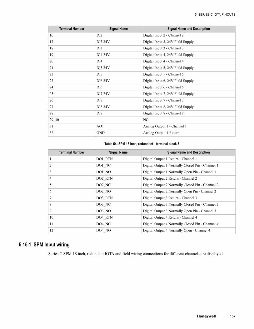
Terminal Number Signal Name Signal Name and Description16 DI2 Digital Input 2 - Channel 2
17 DI3 24V Digital Input 3, 24V Field Supply
18 DI3 Digital Input 3 - Channel 3
19 DI4 24V Digital Input 4, 24V Field Supply
20 DI4 Digital Input 4 - Channel 4
21 DI5 24V Digital Input 5, 24V Field Supply
22 DI5 Digital Input 5 - Channel 5
23 DI6 24V Digital Input 6, 24V Field Supply
24 DI6 Digital Input 6 - Channel 6
25 DI7 24V Digital Input 7, 24V Field Supply
26 DI7 Digital Input 7 - Channel 7
27 DI8 24V Digital Input 8, 24V Field Supply
28 DI8 Digital Input 8 - Channel 8
29, 30 NC
31 AO1 Analog Output 1 - Channel 1
32 GND Analog Output 1 Return
Table 54: SPM 18 inch, redundant - terminal block 3
Terminal Number Signal Name Signal Name and Description1 DO1_RTN Digital Output 1 Return - Channel 1
2 DO1_NC Digital Output 1 Normally Closed Pin - Channel 1
3 DO1_NO Digital Output 1 Normally Open Pin - Channel 1
4 DO2_RTN Digital Output 2 Return - Channel 2
5 DO2_NC Digital Output 2 Normally Closed Pin - Channel 2
6 DO2_NO Digital Output 2 Normally Open Pin - Channel 2
7 DO3_RTN Digital Output 3 Return - Channel 3
8 DO3_NC Digital Output 3 Normally Closed Pin - Channel 3
9 DO3_NO Digital Output 3 Normally Open Pin - Channel 3
10 DO4_RTN Digital Output 4 Return - Channel 4
11 DO4_NC Digital Output 4 Normally Closed Pin - Channel 4
12 DO4_NO Digital Output 4 Normally Open - Channel 4
5.15.1 SPM Input wiringSeries C SPM 18 inch, redundant IOTA and field wiring connections for different channels are displayed.
5 SERIES C IOTA PINOUTS
157
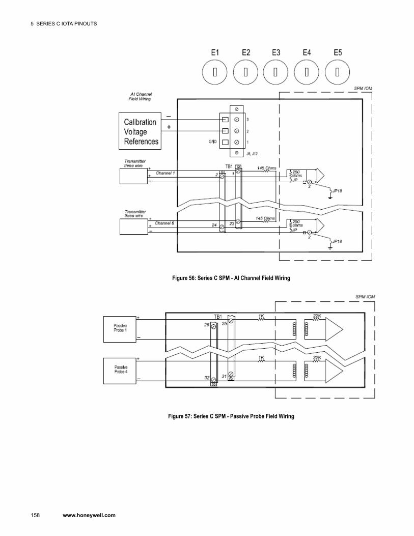
Figure 56: Series C SPM - AI Channel Field Wiring
Figure 57: Series C SPM - Passive Probe Field Wiring
5 SERIES C IOTA PINOUTS
158 www.honeywell.com

Figure 58: Series C SPM - Active Probe Field Wiring
Figure 59: Series C SPM - DI Channel Field Wiring
5 SERIES C IOTA PINOUTS
159
Figure 60: Series C SPM - AO Channel Field Wiring
Figure 61: Series C SPM - DO Channel Field Wiring
SPM FusesFollowing table explains about fuses for the SPM.
Fuses Application CircuitE1 ACTIVE PROBE 24V
E2 AI 24V
E3 BOTTOM IOM 24V
5 SERIES C IOTA PINOUTS
160 www.honeywell.com

Fuses Application CircuitE4 INTERNAL 24V
E5 TOP IOM 24V
E6 EXTERNAL 24V
For detailed information about the jumper settings of the SPM refer to Turbine Control User's Guide.
5 SERIES C IOTA PINOUTS
161
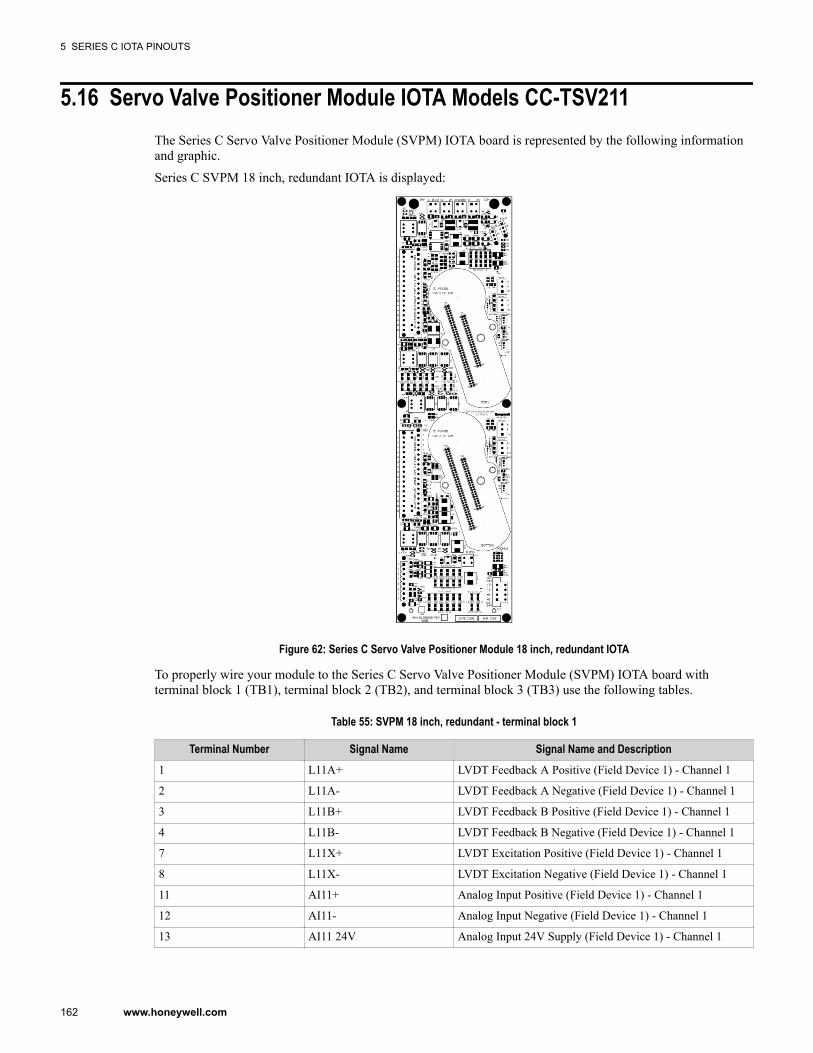
5.16 Servo Valve Positioner Module IOTA Models CC-TSV211The Series C Servo Valve Positioner Module (SVPM) IOTA board is represented by the following informationand graphic.
Series C SVPM 18 inch, redundant IOTA is displayed:
Figure 62: Series C Servo Valve Positioner Module 18 inch, redundant IOTA
To properly wire your module to the Series C Servo Valve Positioner Module (SVPM) IOTA board withterminal block 1 (TB1), terminal block 2 (TB2), and terminal block 3 (TB3) use the following tables.
Table 55: SVPM 18 inch, redundant - terminal block 1
Terminal Number Signal Name Signal Name and Description1 L11A+ LVDT Feedback A Positive (Field Device 1) - Channel 1
2 L11A- LVDT Feedback A Negative (Field Device 1) - Channel 1
3 L11B+ LVDT Feedback B Positive (Field Device 1) - Channel 1
4 L11B- LVDT Feedback B Negative (Field Device 1) - Channel 1
7 L11X+ LVDT Excitation Positive (Field Device 1) - Channel 1
8 L11X- LVDT Excitation Negative (Field Device 1) - Channel 1
11 AI11+ Analog Input Positive (Field Device 1) - Channel 1
12 AI11- Analog Input Negative (Field Device 1) - Channel 1
13 AI11 24V Analog Input 24V Supply (Field Device 1) - Channel 1
5 SERIES C IOTA PINOUTS
162 www.honeywell.com
Terminal Number Signal Name Signal Name and Description14 AI12 24V Analog Input 24V Supply (Field Device 2) - Channel 2
15 AI12+ Analog Input Positive (Field Device 2) - Channel 2
16 AI12- Analog Input Negative (Field Device 2) - Channel 2
19 SO11+ Servo Output Coil 1 (Field Device 1) Positive - Channel 1
20 SO11- Servo Output Coil 1 (Field Device 1) Negative - Channel 1
21 SO12+ Servo Output Coil 1 (Field Device 2) Positive - Channel 2
22 SO12- Servo Output Coil 1 (Field Device 2) Negative - Channel 2
25 L12A+ LVDT Feedback A Positive (Field Device 2) - Channel 2
26 L12A- LVDT Feedback A Negative (Field Device 2) - Channel 2
27 L12B+ LVDT Feedback B Positive (Field Device 2) - Channel 2
28 L12B- LVDT Feedback B Negative (Field Device 2) - Channel 2
31 L12X+ LVDT Excitation Positive (Field Device 2) - Channel 2
32 L12X- LVDT Excitation Negative (Field Device 2) - Channel 2
5, 6, 9, 10, 17, 18, 23, 24, 29,30
NC
Table 56: SVPM 18 inch, redundant - terminal block 2
Terminal Number Signal Name Signal Name and Description1 L21A+ LVDT Feedback A Positive (Field Device 1) - Channel 1
2 L21A- LVDT Feedback A Negative (Field Device 1) - Channel 1
3 L21B+ LVDT Feedback B Positive (Field Device 1) - Channel 1
4 L21B- LVDT Feedback B Negative (Field Device 1) - Channel 1
7 L21X+ LVDT Excitation Positive (Field Device 1) - Channel 1
8 L21X- LVDT Excitation Negative (Field Device 1) - Channel 1
11 AI21+ Analog Input Positive (Field Device 1) - Channel 1
12 AI21- Analog Input Negative (Field Device 1) - Channel 1
13 AI21 24V Analog Input 24V Supply (Field Device 1) - Channel 1
14 AI22 24V Analog Input 24V Supply (Field Device 2) - Channel 2
15 AI22+ Analog Input Positive (Field Device 2) - Channel 2
16 AI22- Analog Input Negative (Field Device 2) - Channel 2
19 SO21+ Servo Output Coil 2 (Field Device 1) Positive - Channel 1
20 SO21- Servo Output Coil 2 (Field Device 1) Negative - Channel 1
21 SO22+ Servo Output Coil 2 (Field Device 2) Positive - Channel 2
22 SO22- Servo Output Coil 2 (Field Device 2) Negative - Channel 2
25 L22A+ LVDT Feedback A Positive (Field Device 2) - Channel 2
26 L22A- LVDT Feedback A Negative (Field Device 2) - Channel 2
27 L22B+ LVDT Feedback B Positive (Field Device 2) - Channel 2
28 L22B- LVDT Feedback B Negative (Field Device 2) - Channel 2
31 L22X+ LVDT Excitation Positive (Field Device 2) - Channel 2
32 L22X- LVDT Excitation Negative (Field Device 2) - Channel 2
5 SERIES C IOTA PINOUTS
163
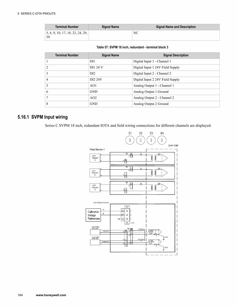
Terminal Number Signal Name Signal Name and Description5, 6, 9, 10, 17, 18, 23, 24, 29,30
NC
Table 57: SVPM 18 inch, redundant - terminal block 3
Terminal Number Signal Name Signal Description1 DI1 Digital Input 1 - Channel 1
2 DI1 24 V Digital Input 1 24V Field Supply
3 DI2 Digital Input 2 - Channel 2
4 DI2 24V Digital Input 2 24V Field Supply
5 AO1 Analog Output 1 - Channel 1
6 GND Analog Output 1 Ground
7 AO2 Analog Output 2 - Channel 2
8 GND Analog Output 2 Ground
5.16.1 SVPM Input wiringSeries C SVPM 18 inch, redundant IOTA and field wiring connections for different channels are displayed.
5 SERIES C IOTA PINOUTS
164 www.honeywell.com
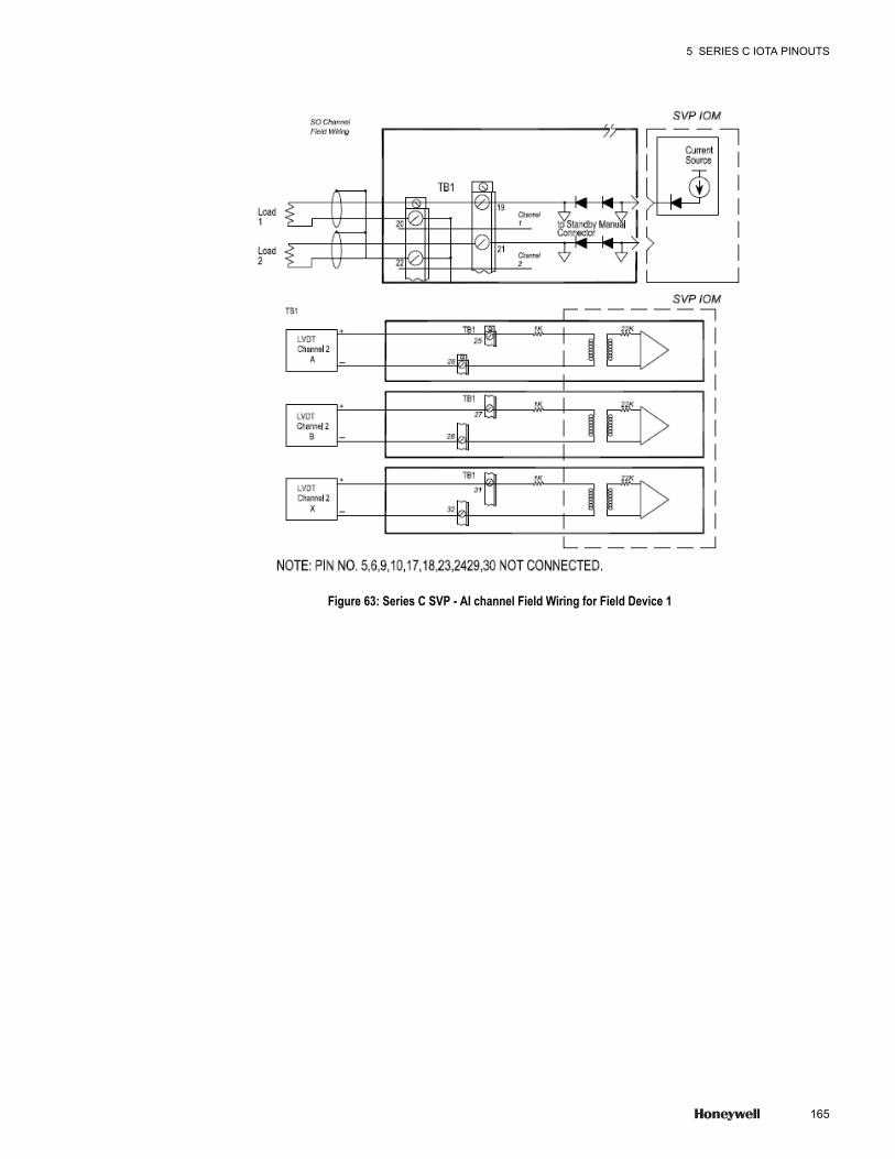
Figure 63: Series C SVP - AI channel Field Wiring for Field Device 1
5 SERIES C IOTA PINOUTS
165
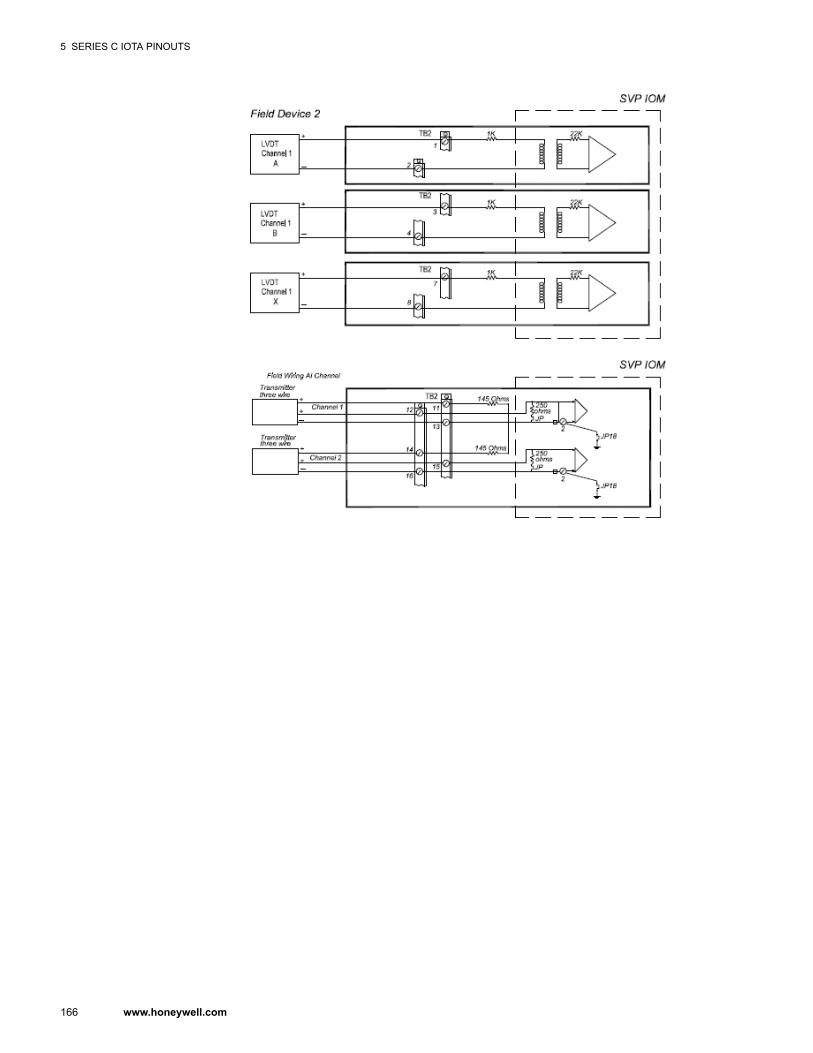
5 SERIES C IOTA PINOUTS
166 www.honeywell.com
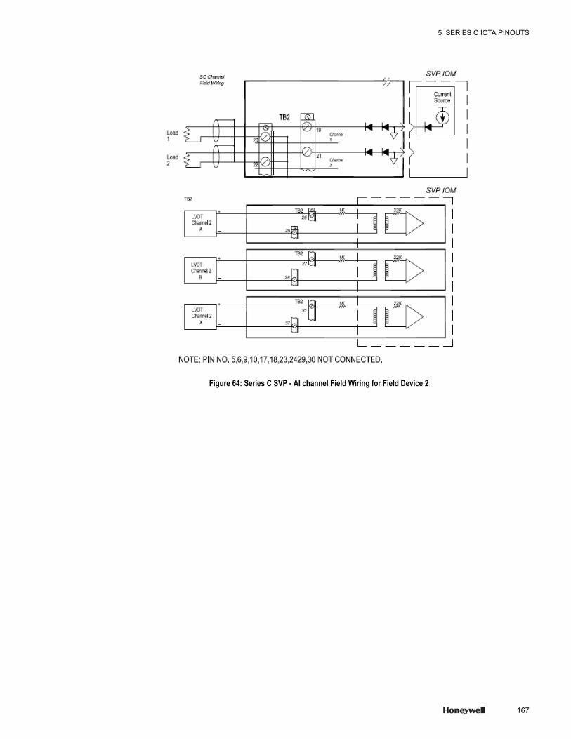
Figure 64: Series C SVP - AI channel Field Wiring for Field Device 2
5 SERIES C IOTA PINOUTS
167
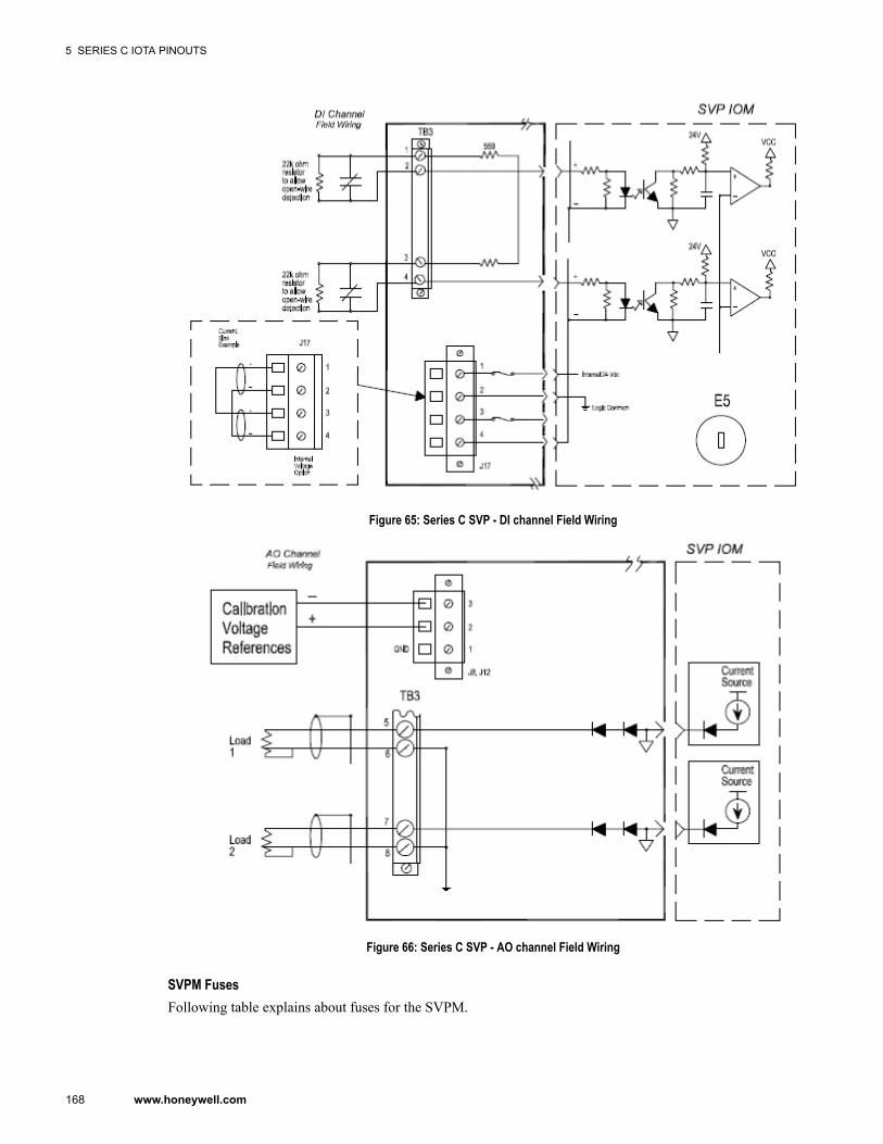
Figure 65: Series C SVP - DI channel Field Wiring
Figure 66: Series C SVP - AO channel Field Wiring
SVPM FusesFollowing table explains about fuses for the SVPM.
5 SERIES C IOTA PINOUTS
168 www.honeywell.com

Fuses Application CircuitE1 AI Field Device Supply, 24V
E2 BOTTOM IOM 24V
E3 INTERNAL 24V - DI
E4 TOP IOM 24V
E5 EXTERNAL 24V - DI
For detailed information about the jumper settings of the SVPM channels, refer to Turbine Control User'sGuide.
5 SERIES C IOTA PINOUTS
169
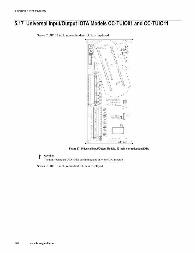
5.17 Universal Input/Output IOTA Models CC-TUIO01 and CC-TUIO11
Series C UIO 12 inch, non-redundant IOTA is displayed.
Figure 67: Universal Input/Output Module, 12 inch, non-redundant IOTA
AttentionThe non-redundant UIO IOTA accommodates only one UIO module.
Series C UIO 18 inch, redundant IOTA is displayed.
5 SERIES C IOTA PINOUTS
170 www.honeywell.com
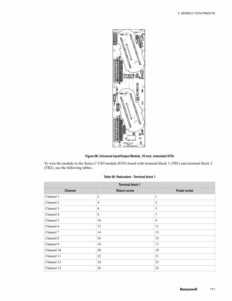
Figure 68: Universal Input/Output Module, 18 inch, redundant IOTA
To wire the module to the Series C UIO module IOTA board with terminal block 1 (TB1) and terminal block 2(TB2), use the following tables.
Table 58: Redundant - Terminal block 1
Terminal block 1Channel Return screw Power screw
Channel 1 2 1
Channel 2 4 3
Channel 3 6 5
Channel 4 8 7
Channel 5 10 9
Channel 6 12 11
Channel 7 14 13
Channel 8 16 15
Channel 9 18 17
Channel 10 20 19
Channel 11 22 21
Channel 12 24 23
Channel 13 26 25
5 SERIES C IOTA PINOUTS
171
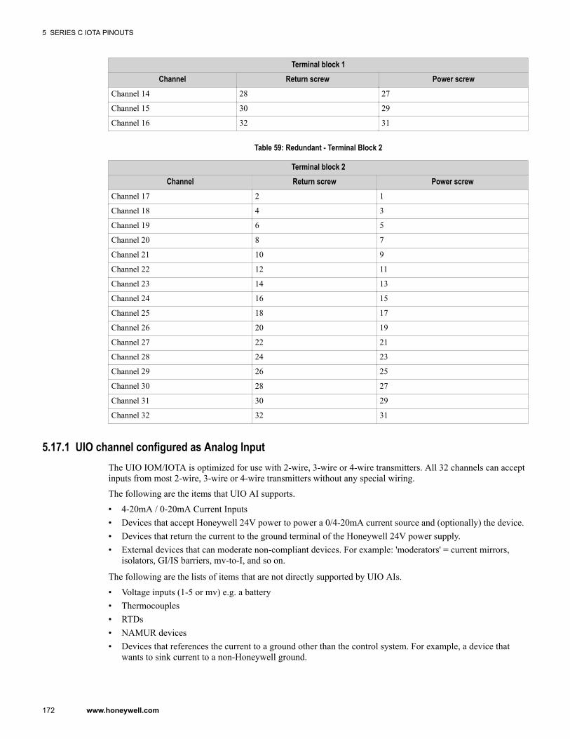
Terminal block 1Channel Return screw Power screw
Channel 14 28 27
Channel 15 30 29
Channel 16 32 31
Table 59: Redundant - Terminal Block 2
Terminal block 2Channel Return screw Power screw
Channel 17 2 1
Channel 18 4 3
Channel 19 6 5
Channel 20 8 7
Channel 21 10 9
Channel 22 12 11
Channel 23 14 13
Channel 24 16 15
Channel 25 18 17
Channel 26 20 19
Channel 27 22 21
Channel 28 24 23
Channel 29 26 25
Channel 30 28 27
Channel 31 30 29
Channel 32 32 31
5.17.1 UIO channel configured as Analog InputThe UIO IOM/IOTA is optimized for use with 2-wire, 3-wire or 4-wire transmitters. All 32 channels can acceptinputs from most 2-wire, 3-wire or 4-wire transmitters without any special wiring.
The following are the items that UIO AI supports.
• 4-20mA / 0-20mA Current Inputs• Devices that accept Honeywell 24V power to power a 0/4-20mA current source and (optionally) the device.• Devices that return the current to the ground terminal of the Honeywell 24V power supply.• External devices that can moderate non-compliant devices. For example: 'moderators' = current mirrors,
isolators, GI/IS barriers, mv-to-I, and so on.
The following are the lists of items that are not directly supported by UIO AIs.
• Voltage inputs (1-5 or mv) e.g. a battery• Thermocouples• RTDs• NAMUR devices• Devices that references the current to a ground other than the control system. For example, a device that
wants to sink current to a non-Honeywell ground.
5 SERIES C IOTA PINOUTS
172 www.honeywell.com
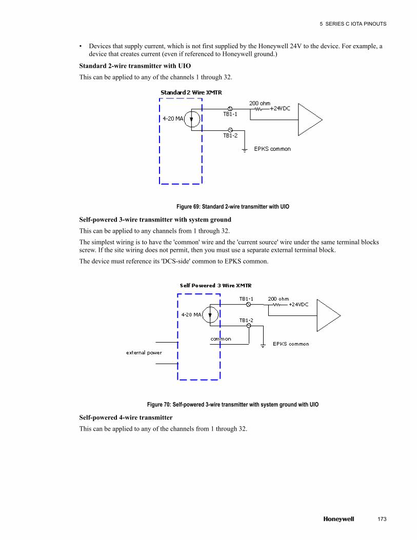
• Devices that supply current, which is not first supplied by the Honeywell 24V to the device. For example, adevice that creates current (even if referenced to Honeywell ground.)
Standard 2-wire transmitter with UIOThis can be applied to any of the channels 1 through 32.
Figure 69: Standard 2-wire transmitter with UIO
Self-powered 3-wire transmitter with system groundThis can be applied to any channels from 1 through 32.
The simplest wiring is to have the 'common' wire and the 'current source' wire under the same terminal blocksscrew. If the site wiring does not permit, then you must use a separate external terminal block.
The device must reference its 'DCS-side' common to EPKS common.
Figure 70: Self-powered 3-wire transmitter with system ground with UIO
Self-powered 4-wire transmitterThis can be applied to any of the channels from 1 through 32.
5 SERIES C IOTA PINOUTS
173
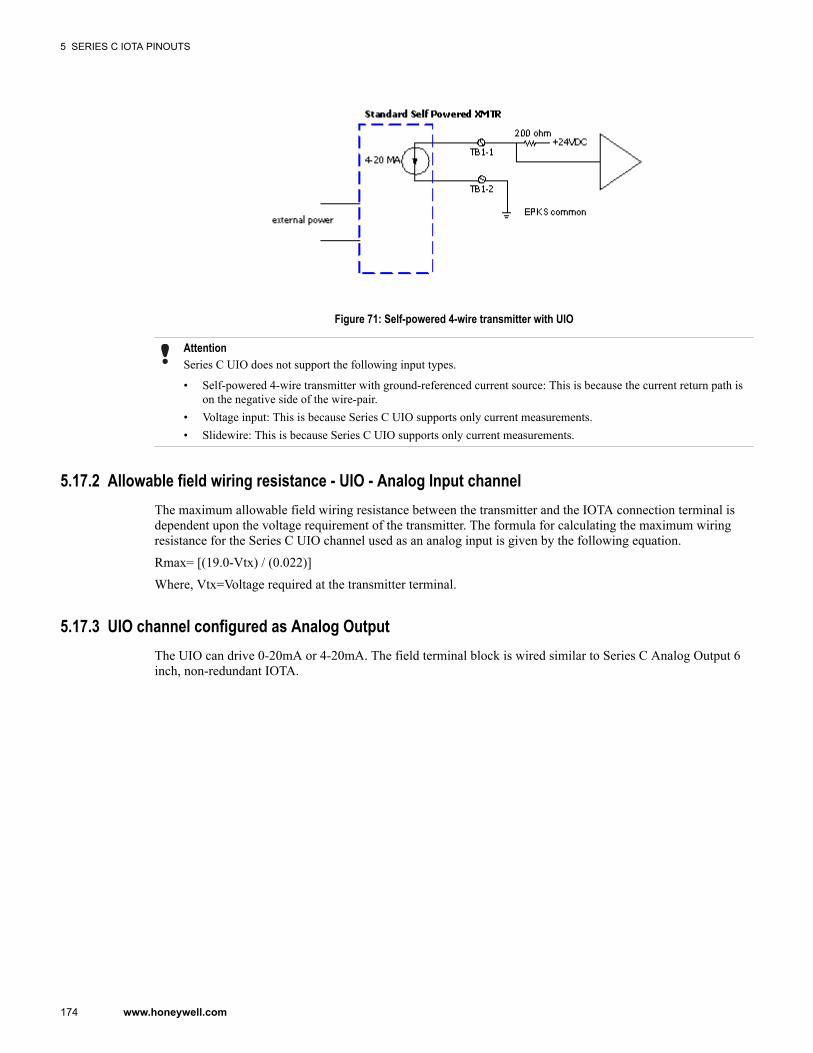
Figure 71: Self-powered 4-wire transmitter with UIO
AttentionSeries C UIO does not support the following input types.
• Self-powered 4-wire transmitter with ground-referenced current source: This is because the current return path ison the negative side of the wire-pair.
• Voltage input: This is because Series C UIO supports only current measurements.• Slidewire: This is because Series C UIO supports only current measurements.
5.17.2 Allowable field wiring resistance - UIO - Analog Input channelThe maximum allowable field wiring resistance between the transmitter and the IOTA connection terminal isdependent upon the voltage requirement of the transmitter. The formula for calculating the maximum wiringresistance for the Series C UIO channel used as an analog input is given by the following equation.
Rmax= [(19.0-Vtx) / (0.022)]
Where, Vtx=Voltage required at the transmitter terminal.
5.17.3 UIO channel configured as Analog OutputThe UIO can drive 0-20mA or 4-20mA. The field terminal block is wired similar to Series C Analog Output 6inch, non-redundant IOTA.
5 SERIES C IOTA PINOUTS
174 www.honeywell.com
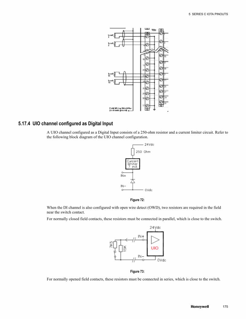
5.17.4 UIO channel configured as Digital InputA UIO channel configured as a Digital Input consists of a 250-ohm resistor and a current limiter circuit. Refer tothe following block diagram of the UIO channel configuration.
Figure 72:
When the DI channel is also configured with open wire detect (OWD), two resistors are required in the fieldnear the switch contact.
For normally closed field contacts, these resistors must be connected in parallel, which is close to the switch.
Figure 73:
For normally opened field contacts, these resistors must be connected in series, which is close to the switch.
5 SERIES C IOTA PINOUTS
175
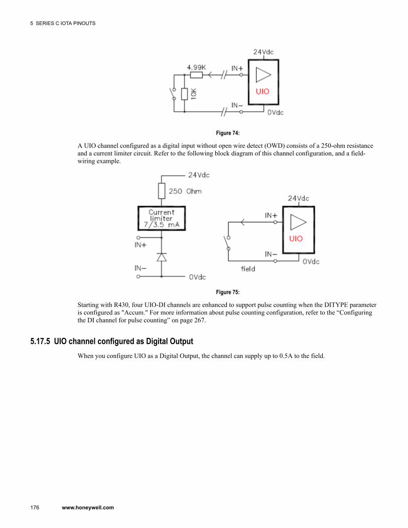
Figure 74:
A UIO channel configured as a digital input without open wire detect (OWD) consists of a 250-ohm resistanceand a current limiter circuit. Refer to the following block diagram of this channel configuration, and a field-wiring example.
Figure 75:
Starting with R430, four UIO-DI channels are enhanced to support pulse counting when the DITYPE parameteris configured as "Accum." For more information about pulse counting configuration, refer to the “Configuringthe DI channel for pulse counting” on page 267.
5.17.5 UIO channel configured as Digital OutputWhen you configure UIO as a Digital Output, the channel can supply up to 0.5A to the field.
5 SERIES C IOTA PINOUTS
176 www.honeywell.com

Figure 76: UIO as a Digital Output
Starting with R430, the UIO-DO channel is enhanced to support ganging. For more information about DOchannel ganging configuration, refer to the “Configuring the DO channel for ganging” on page 268.
5.17.6 DO channel wiring configuration for gangingYou can configure a set of two, three, or four DO channels to deliver up to 1 Ampere, 1.5 Amperes, or 2Amperes current to the field.
A two-pin branch with a pitch of 0.2 inches (5.08mm) can be used for interconnecting two DO channels. Forexample, Weidmuller part number can be used for interconnecting the DO channels. The following table liststhe part number and the pins branch for interconnecting the DO channels.
Pins Part number No.of DO channels Two pinsTwo pins branch Weidmuller LPA QB 2 2
Three pins branch Weidmuller LPA QB 3 3
Four pins branch Weidmuller LPA QB 4 4
The field wire must be connected with one of the OUT pins (together with the branch). One of the OUT pinscan be used for connecting the return field wire. The following figure illustrates the different ways to join theDO channels.
• Two DO channels with a two pin branch• Three DO channels with a three pin branch
5 SERIES C IOTA PINOUTS
177
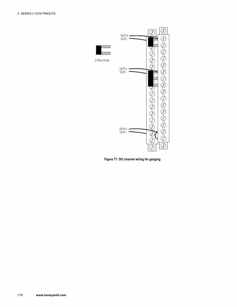
Figure 77: DO channel wiring for ganging
5 SERIES C IOTA PINOUTS
178 www.honeywell.com
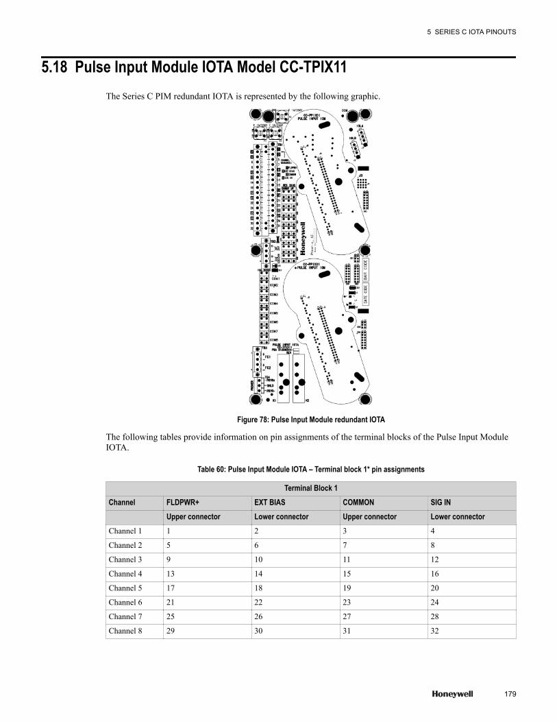
5.18 Pulse Input Module IOTA Model CC-TPIX11The Series C PIM redundant IOTA is represented by the following graphic.
Figure 78: Pulse Input Module redundant IOTA
The following tables provide information on pin assignments of the terminal blocks of the Pulse Input ModuleIOTA.
Table 60: Pulse Input Module IOTA – Terminal block 1* pin assignments
Terminal Block 1Channel FLDPWR+ EXT BIAS COMMON SIG IN
Upper connector Lower connector Upper connector Lower connectorChannel 1 1 2 3 4
Channel 2 5 6 7 8
Channel 3 9 10 11 12
Channel 4 13 14 15 16
Channel 5 17 18 19 20
Channel 6 21 22 23 24
Channel 7 25 26 27 28
Channel 8 29 30 31 32
5 SERIES C IOTA PINOUTS
179
* see text on IOTA for pin numbering.
Table 61: Pulse Input Module IOTA – Terminal block 2 * pin assignments
Pin number Description1 + INT 24V
2 – INT 24V
3 + EXT 12V/24V
4 – EXT 12V/24V
* see text on IOTA for pin numbering.
Table 62: Pulse Input Module IOTA – Terminal block 3 * pin assignments
Pin number Description1 FC1 + (high side)
2 FC1 – (low side)
3 FC2 + (high side)
4 FC2 – (low side)
* see text on IOTA for pin numbering.
Table 63: Pulse Input Module IOTA – Terminal block 4 * pin assignments
Pin number Description1 PRVR+
2 Shield (screen)
3 PRVR–
* see text on IOTA for pin numbering.
Refer to the section “Series C PIM connectivity” on page 183 for information on connecting PIM.
5 SERIES C IOTA PINOUTS
180 www.honeywell.com

5.19 Upgrading Firmware in Series C I/O componentsRefer to the Upgrading firmware in Series C I/O components section in the Control Hardware and I/O ModuleFirmware Guide.
5 SERIES C IOTA PINOUTS
181

5 SERIES C IOTA PINOUTS
182 www.honeywell.com

6 Series C PIM connectivity
This chapter contains information related to PIM channel terminal blocks and PIM connectivity details. Thischapter contains information on connecting PIM to various components such as field sensor power, fast cutoffrelays, Prover Pulse Bus, ST500 dual-pulse simulation.
Related topics“PIM connectivity block diagram” on page 184“Field device output stage types” on page 186“PIM resistor bias terminal blocks” on page 187“TB1 signal definitions” on page 189“TB1 pin assignments” on page 190“TB2 pin assignments for internal/external field sensor power” on page 191“TB3 pin assignment for fast cutoff relays” on page 196“About enabling pulse proving in PIM” on page 198“TB4 pin assignment for Prover Pulse Bus” on page 200“Using Prover Pulse Bus with optocoupler” on page 201“Connecting PIM with ST500 dual-pulse simulator (Swinton Technology)” on page 204“Connecting PIM with dual stream devices” on page 206“Connecting PIM with other sensor types” on page 207“Selecting PIM input threshold” on page 209“Recommended cable types” on page 210
183
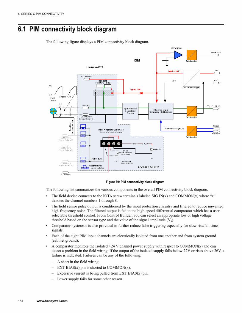
6.1 PIM connectivity block diagramThe following figure displays a PIM connectivity block diagram.
Figure 79: PIM connectivity block diagram
The following list summarizes the various components in the overall PIM connectivity block diagram.
• The field device connects to the IOTA screw terminals labeled SIG IN(x) and COMMON(x) where “x”denotes the channel numbers 1 through 8.
• The field sensor pulse output is conditioned by the input protection circuitry and filtered to reduce unwantedhigh-frequency noise. The filtered output is fed to the high-speed differential comparator which has a user-selectable threshold control. From Control Builder, you can select an appropriate low or high voltagethreshold based on the sensor type and the value of the signal amplitude (Vs).
• Comparator hysteresis is also provided to further reduce false triggering especially for slow rise/fall timesignals.
• Each of the eight PIM input channels are electrically isolated from one another and from system ground(cabinet ground).
• A comparator monitors the isolated +24 V channel power supply with respect to COMMON(x) and candetect a problem in the field wiring. If the output of the isolated supply falls below 22V or rises above 26V, afailure is indicated. Failures can be any of the following;
– A short in the field wiring.– EXT BIAS(x) pin is shorted to COMMON(x).– Excessive current is being pulled from EXT BIAS(x) pin.– Power supply fails for some other reason.
6 SERIES C PIM CONNECTIVITY
184 www.honeywell.com

If a failure occurs, the soft failure is reported in Control Builder and Station.
AttentionIn redundant PIM modules, after a switchover, if the alarm for the reported channel still persists on the new primary,this most likely indicates a problem in the field wiring.
6 SERIES C PIM CONNECTIVITY
185
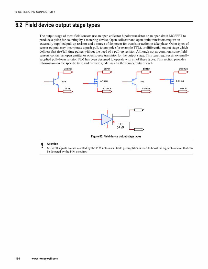
6.2 Field device output stage typesThe output stage of most field sensors use an open collector bipolar transistor or an open drain MOSFET toproduce a pulse for counting by a metering device. Open collector and open drain transistors require anexternally supplied pull-up resistor and a source of dc power for transistor action to take place. Other types ofsensor outputs may incorporate a push-pull, totem pole (for example TTL), or differential output stage whichdelivers fast rise/fall time pulses without the need of a pull-up resistor. Although not as common, some fieldsensors contain an open emitter or open source transistor for the output stage. This type requires an externallysupplied pull-down resistor. PIM has been designed to operate with all of these types. This section providesinformation on the specific type and provide guidelines on the connectivity of each.
Figure 80: Field device output stage types
AttentionMillivolt signals are not counted by the PIM unless a suitable preamplifier is used to boost the signal to a level that canbe detected by the PIM circuitry.
6 SERIES C PIM CONNECTIVITY
186 www.honeywell.com
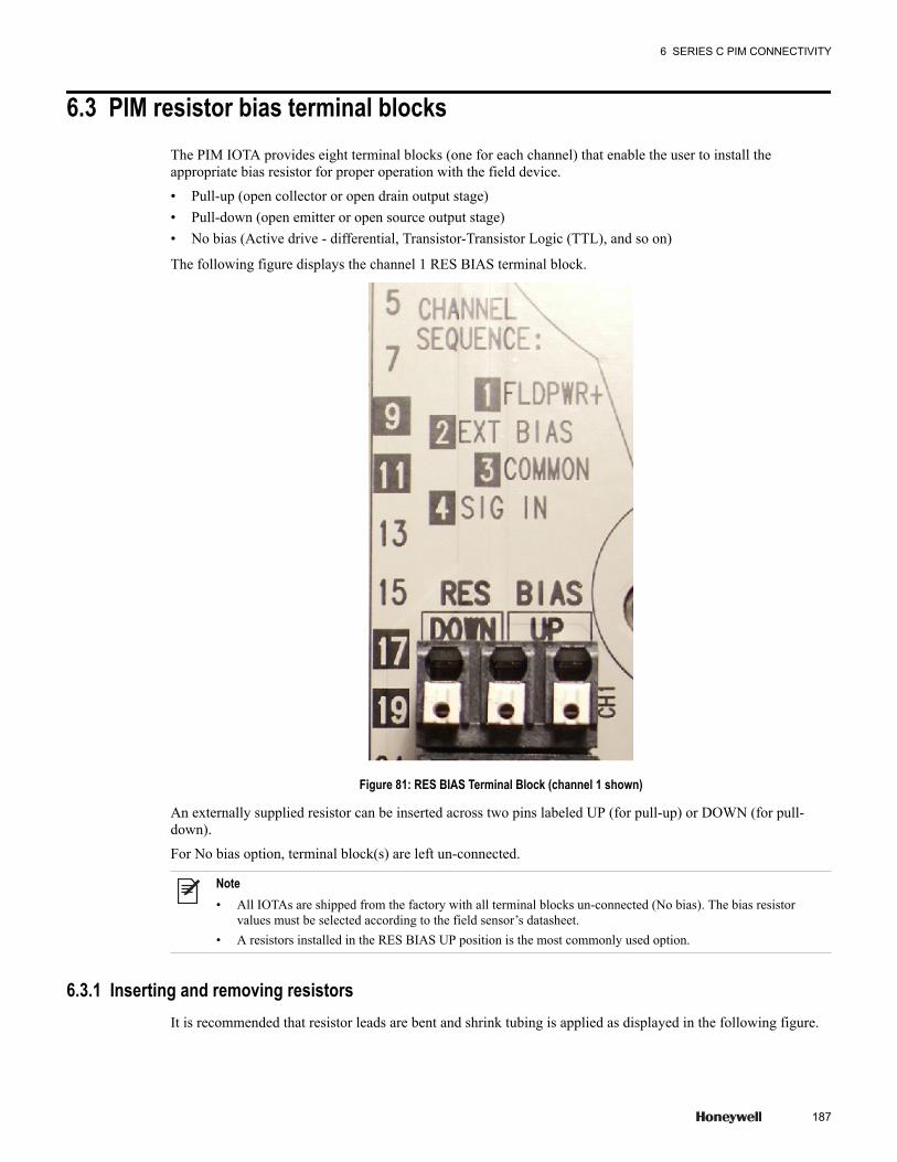
6.3 PIM resistor bias terminal blocksThe PIM IOTA provides eight terminal blocks (one for each channel) that enable the user to install theappropriate bias resistor for proper operation with the field device.
• Pull-up (open collector or open drain output stage)• Pull-down (open emitter or open source output stage)• No bias (Active drive - differential, Transistor-Transistor Logic (TTL), and so on)
The following figure displays the channel 1 RES BIAS terminal block.
Figure 81: RES BIAS Terminal Block (channel 1 shown)
An externally supplied resistor can be inserted across two pins labeled UP (for pull-up) or DOWN (for pull-down).
For No bias option, terminal block(s) are left un-connected.
Note• All IOTAs are shipped from the factory with all terminal blocks un-connected (No bias). The bias resistor
values must be selected according to the field sensor’s datasheet.• A resistors installed in the RES BIAS UP position is the most commonly used option.
6.3.1 Inserting and removing resistorsIt is recommended that resistor leads are bent and shrink tubing is applied as displayed in the following figure.
6 SERIES C PIM CONNECTIVITY
187

Figure 82: Recommended way of insulating resistor leads and bending them
For inserting the resistor, firmly press the resistor all the way into the holes. The locking mechanism inside theterminal block locks the resistor in place automatically.
For removing the resistor, gently press the white unlocking buttons.
6 SERIES C PIM CONNECTIVITY
188 www.honeywell.com

6.4 TB1 signal definitionsEach of the eight channels is composed of a group of four signals. The following table provides information onthe signal definitions.
Table 64: TB1 signal definitions
Pin name Input/output
Description
SIG IN Input This pin is used to connect to field sensor’s pulse output positive pin.
COMMON Input This pin is used to connect to field sensor’s pulse output negative pin.
You can also use this pin for the negative return of the FIELD PWR or EXT BIAS.
EXT BIAS Output This pin is used with pull-up resistor supplied by the user. The open circuit voltage of this pin isapproximately 23 Vdc and can source up to 25 mA. This means that the pull-up resistor value mustbe no lower than 920 ohms.
This pin can also be a source of isolated power not to exceed the above values.
You can leave the EXT BIAS pin un-connected if not required.
FLDPWR+ Output Positive source of power from connector TB2.
This pin is used to power field sensor(s) with +24 Vdc from the Series C system, or optionallyfrom an external power source.
When the source of field power is the Series C +24V system supply, the negative terminal is tied tothe Series C cabinet ground. Since the sensor signal common, COMMON(x), is used for the powerreturn, the field sensor is no longer isolated.
If more than one pulse input channel uses field power, the channels are no longer isolated from oneanother because of the shared return at pins COMMON(x).
FLDPWR+ 1 through 8 are electrically connected to each other on circuit board. This means theyare bussed.
6 SERIES C PIM CONNECTIVITY
189
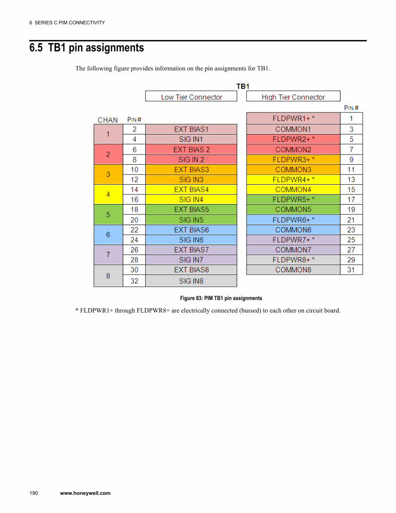
6.5 TB1 pin assignmentsThe following figure provides information on the pin assignments for TB1.
Figure 83: PIM TB1 pin assignments
* FLDPWR1+ through FLDPWR8+ are electrically connected (bussed) to each other on circuit board.
6 SERIES C PIM CONNECTIVITY
190 www.honeywell.com

6.6 TB2 pin assignments for internal/external field sensor powerThe following table provides information on the 4-pin connector TB2 pin assignments.
Table 65: PIM TB2 pin assignments
Pin number Description1 + INT 24V
2 - INT 24V
3 + EXT 12V/24V
4 - EXT 12V/24V
The PIM IOTA allows field sensor powering from either the Series C System +24 V internal system supply orfrom an external user supplied power source.
6.6.1 Restrictions/limitations while using TB2The following figure displays the internal/external sensor power circuit diagram.
Figure 84: PIM TB2 – Internal/external sensor power circuit diagram
You must be aware of the following restrictions/limitations while using TB2.
• Only a dc source with polarity indicated in the above diagram can be used because of diode steering andreverse polarity protection.
• If an external source is used, the applied dc voltage must be +30 V or less. This is because there is a 33 Vtransient protection diode on the IOTA circuit board which could potentially be damaged if the supplyexceeds 33V. (VR1 in the above diagram).
• F3 is a fast type fuse rated for 1A/250V. When the internal system supply is selected, the maximum currentmust be less than this value to avoid fuse rupture.
• You must provide fusing when an external supply is utilized (fusing from external supply is not shown in theabove diagram).
• The diodes are rated at 1A, do not exceed this value.
6 SERIES C PIM CONNECTIVITY
191

• You can choose between the internal or external source. However, both cannot be used at the same time.• If an application does not require field sensor power through TB2, completely disconnect all wiring from
TB2 including jumper wires.
You can use the following connector in conjunction with TB2. The following figure displays the terminal blockfor channel 1. There are similar connectors for the remaining channels.
Figure 85: ISOL/BUSSED terminal blocks
In the default configuration (as shipped from factory), the COM(x) (signal returns) for all the eight channels areelectrically isolated from each other and from system power return. Based on the topology required, you canchoose to connect the signal return to the system power return (TB2 pin 4) by installing a jumper across theterminal block for the required channel.
6.6.2 Verifying the connectionThe following figure displays the LED DS1 on the IOTA.
6 SERIES C PIM CONNECTIVITY
192 www.honeywell.com
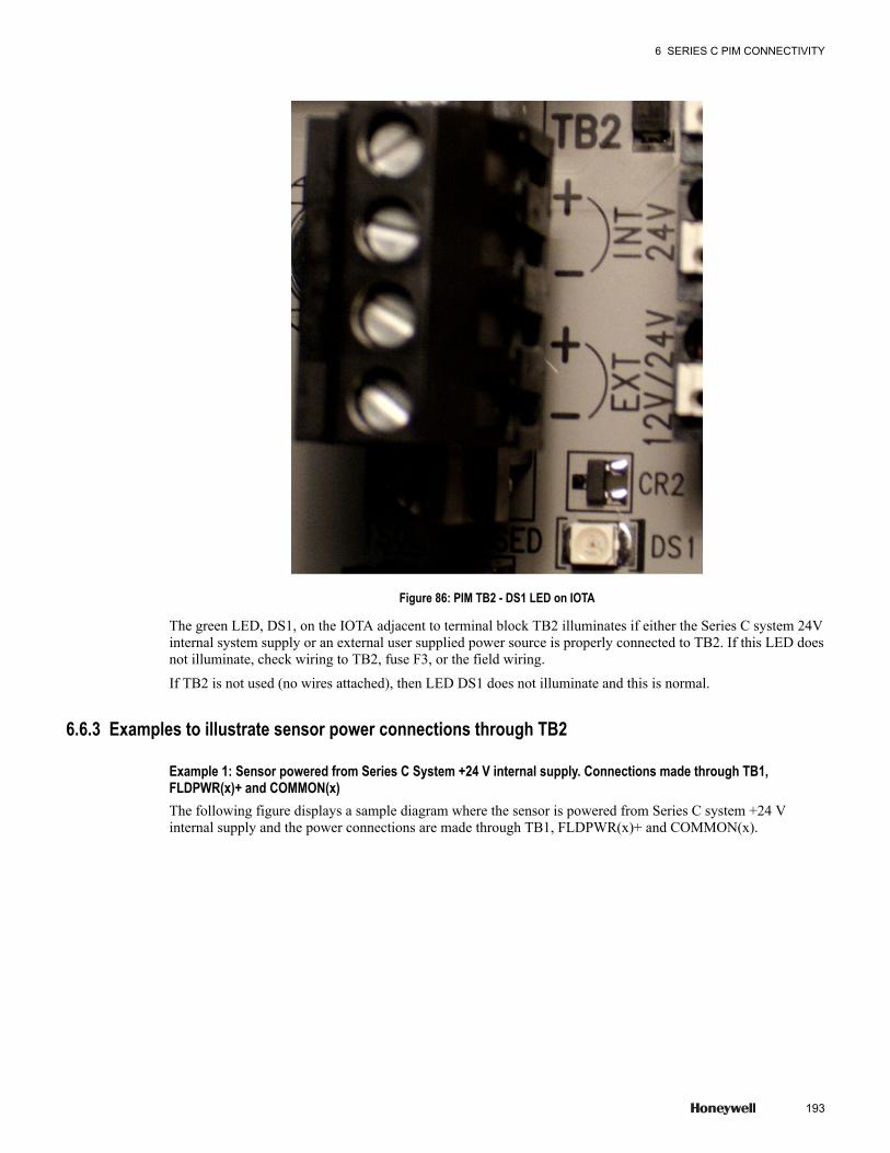
Figure 86: PIM TB2 - DS1 LED on IOTA
The green LED, DS1, on the IOTA adjacent to terminal block TB2 illuminates if either the Series C system 24Vinternal system supply or an external user supplied power source is properly connected to TB2. If this LED doesnot illuminate, check wiring to TB2, fuse F3, or the field wiring.
If TB2 is not used (no wires attached), then LED DS1 does not illuminate and this is normal.
6.6.3 Examples to illustrate sensor power connections through TB2
Example 1: Sensor powered from Series C System +24 V internal supply. Connections made through TB1,FLDPWR(x)+ and COMMON(x)The following figure displays a sample diagram where the sensor is powered from Series C system +24 Vinternal supply and the power connections are made through TB1, FLDPWR(x)+ and COMMON(x).
6 SERIES C PIM CONNECTIVITY
193
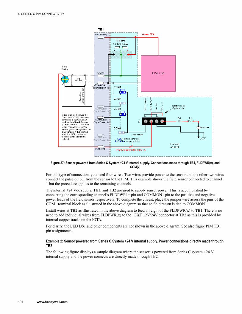
Figure 87: Sensor powered from Series C System +24 V internal supply. Connections made through TB1, FLDPWR(x), andCOM(x)
For this type of connection, you need four wires. Two wires provide power to the sensor and the other two wiresconnect the pulse output from the sensor to the PIM. This example shows the field sensor connected to channel1 but the procedure applies to the remaining channels.
The internal +24 Vdc supply, TB1, and TB2 are used to supply sensor power. This is accomplished byconnecting the corresponding channel’s FLDPWR1+ pin and COMMON1 pin to the positive and negativepower leads of the field sensor respectively. To complete the circuit, place the jumper wire across the pins of theCOM1 terminal block as illustrated in the above diagram so that so field return is tied to COMMON1.
Install wires at TB2 as illustrated in the above diagram to feed all eight of the FLDPWR(x) to TB1. There is noneed to add individual wires from FLDPWR(x) to the +EXT 12V/24V connector at TB2 as this is provided byinternal copper tracks on the IOTA.
For clarity, the LED DS1 and other components are not shown in the above diagram. See also figure PIM TB1pin assignments.
Example 2: Sensor powered from Series C System +24 V internal supply. Power connections directly made throughTB2The following figure displays a sample diagram where the sensor is powered from Series C system +24 Vinternal supply and the power connects are directly made through TB2.
6 SERIES C PIM CONNECTIVITY
194 www.honeywell.com
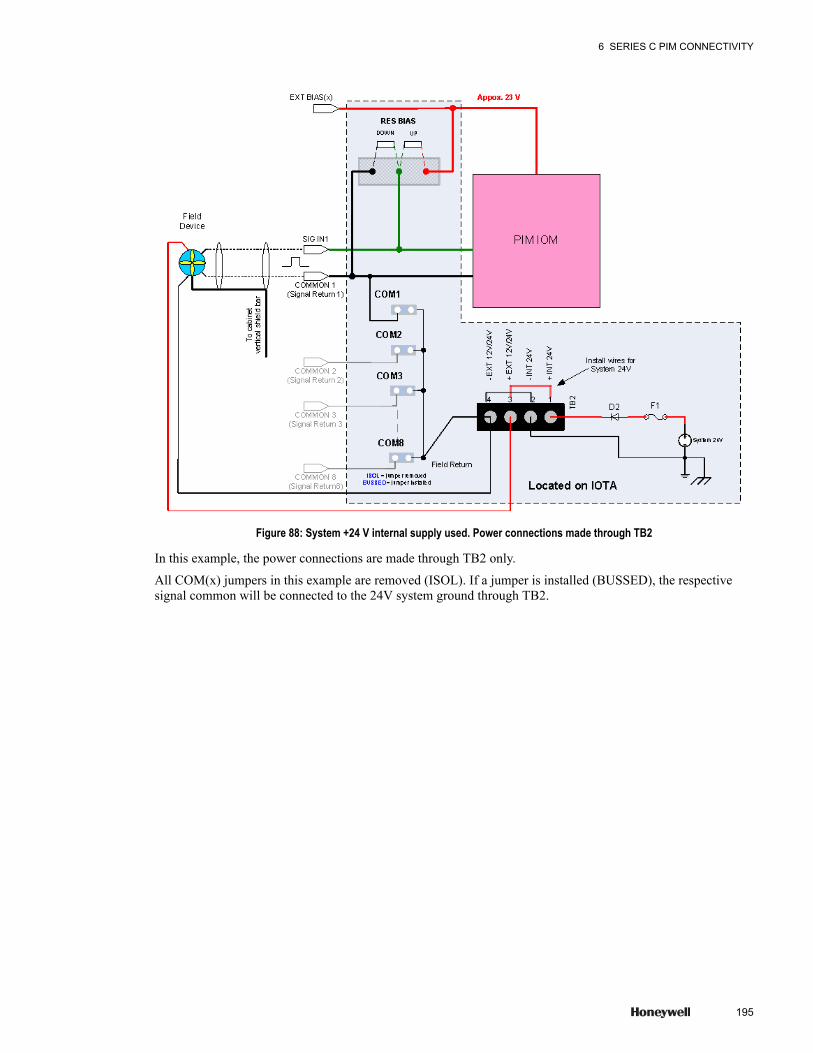
Figure 88: System +24 V internal supply used. Power connections made through TB2
In this example, the power connections are made through TB2 only.
All COM(x) jumpers in this example are removed (ISOL). If a jumper is installed (BUSSED), the respectivesignal common will be connected to the 24V system ground through TB2.
6 SERIES C PIM CONNECTIVITY
195
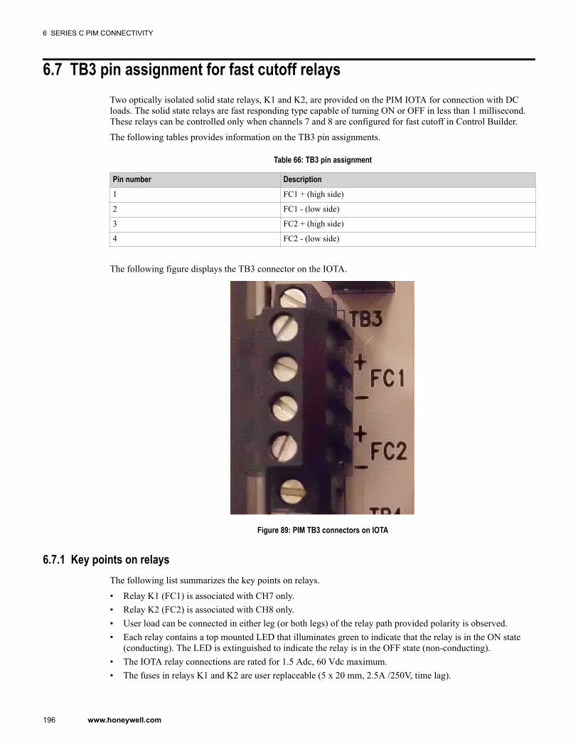
6.7 TB3 pin assignment for fast cutoff relaysTwo optically isolated solid state relays, K1 and K2, are provided on the PIM IOTA for connection with DCloads. The solid state relays are fast responding type capable of turning ON or OFF in less than 1 millisecond.These relays can be controlled only when channels 7 and 8 are configured for fast cutoff in Control Builder.
The following tables provides information on the TB3 pin assignments.
Table 66: TB3 pin assignment
Pin number Description1 FC1 + (high side)
2 FC1 - (low side)
3 FC2 + (high side)
4 FC2 - (low side)
The following figure displays the TB3 connector on the IOTA.
Figure 89: PIM TB3 connectors on IOTA
6.7.1 Key points on relaysThe following list summarizes the key points on relays.
• Relay K1 (FC1) is associated with CH7 only.• Relay K2 (FC2) is associated with CH8 only.• User load can be connected in either leg (or both legs) of the relay path provided polarity is observed.• Each relay contains a top mounted LED that illuminates green to indicate that the relay is in the ON state
(conducting). The LED is extinguished to indicate the relay is in the OFF state (non-conducting).• The IOTA relay connections are rated for 1.5 Adc, 60 Vdc maximum.• The fuses in relays K1 and K2 are user replaceable (5 x 20 mm, 2.5A /250V, time lag).
6 SERIES C PIM CONNECTIVITY
196 www.honeywell.com
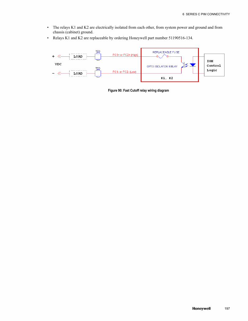
• The relays K1 and K2 are electrically isolated from each other, from system power and ground and fromchassis (cabinet) ground.
• Relays K1 and K2 are replaceable by ordering Honeywell part number 51190516-134.
Figure 90: Fast Cutoff relay wiring diagram
6 SERIES C PIM CONNECTIVITY
197
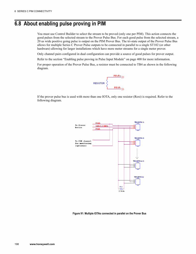
6.8 About enabling pulse proving in PIMYou must use Control Builder to select the stream to be proved (only one per PIM). This action connects thegood pulses from the selected stream to the Prover Pulse Bus. For each good pulse from the selected stream, a20 us wide positive going pulse is output on the PIM Prover Bus. The tri-state output of the Prover Pulse Busallows for multiple Series C Prover Pulse outputs to be connected in parallel to a single ST102 (or otherhardware) allowing for larger installations which have more meter streams for a single meter prover.
Only channel pairs configured in dual configuration can provide a source of good pulses for prover output.
Refer to the section “Enabling pulse proving in Pulse Input Module” on page 400 for more information.
For proper operation of the Prover Pulse Bus, a resistor must be connected to TB4 as shown in the followingdiagram.
If the prover pulse bus is used with more than one IOTA, only one resistor (Rext) is required. Refer to thefollowing diagram.
Figure 91: Multiple IOTAs connected in parallel on the Prover Bus
6 SERIES C PIM CONNECTIVITY
198 www.honeywell.com
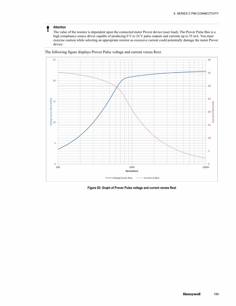
AttentionThe value of the resistor is dependent upon the connected meter Prover device (user load). The Prover Pulse Bus is ahigh compliance source driver capable of producing 0 V to 24 V pulse outputs and currents up to 35 mA. You mustexercise caution while selecting an appropriate resistor as excessive current could potentially damage the meter Proverdevice.
The following figure displays Prover Pulse voltage and current verses Rext.
Figure 92: Graph of Prover Pulse voltage and current verses Rext
6 SERIES C PIM CONNECTIVITY
199
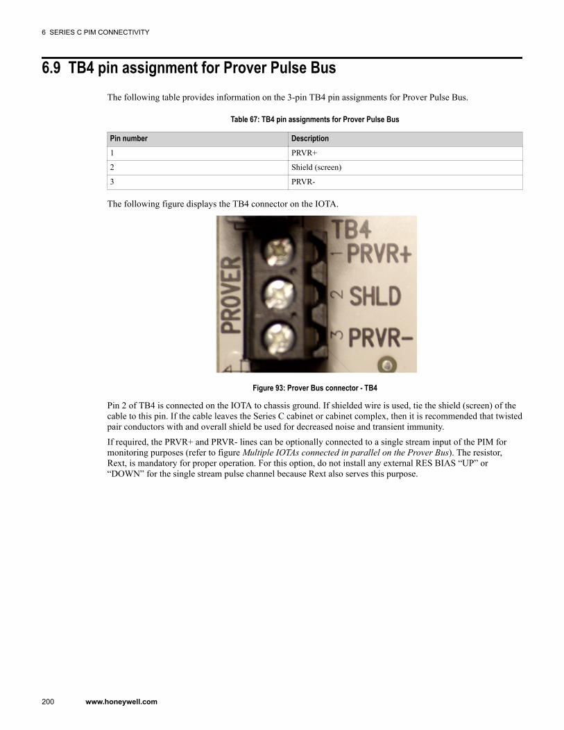
6.9 TB4 pin assignment for Prover Pulse BusThe following table provides information on the 3-pin TB4 pin assignments for Prover Pulse Bus.
Table 67: TB4 pin assignments for Prover Pulse Bus
Pin number Description1 PRVR+
2 Shield (screen)
3 PRVR-
The following figure displays the TB4 connector on the IOTA.
Figure 93: Prover Bus connector - TB4
Pin 2 of TB4 is connected on the IOTA to chassis ground. If shielded wire is used, tie the shield (screen) of thecable to this pin. If the cable leaves the Series C cabinet or cabinet complex, then it is recommended that twistedpair conductors with and overall shield be used for decreased noise and transient immunity.
If required, the PRVR+ and PRVR- lines can be optionally connected to a single stream input of the PIM formonitoring purposes (refer to figure Multiple IOTAs connected in parallel on the Prover Bus). The resistor,Rext, is mandatory for proper operation. For this option, do not install any external RES BIAS “UP” or“DOWN” for the single stream pulse channel because Rext also serves this purpose.
6 SERIES C PIM CONNECTIVITY
200 www.honeywell.com

6.10 Using Prover Pulse Bus with optocouplerYou can connect the Prover Bus to an optocoupler (such as the input stage of a ST102) as displayed in thefollowing diagram.
Figure 94: Illustration of using Prover Pulse Bus with Optocoupler
Since the Prover Pulse Bus is a high compliance driver and can source 35 mA, an additional series resistor “Rs”is required to limit the current into the photo diode to a safe value. The value of “Rs” can be selected so that themanufacturing ratings are not exceeded.
The following tables provide information on the approximate values of “Rs” for selected photodiode currentswith “Rext” equal to 1 k ohms and 2.2 k ohms respectively. For all of the values listed in the tables, the powerrating for “Rs” is ½ watt.
Conditions: Rext = 1k, photodiode VFWD= 1.2 V
Desired photodiode current (mA) Rext (ohms) Voltage difference at PRVR+ minus PRVR- Standard 5% Value of Rs (ohms)5 1 K 20.57 V 3.9 k
10 1 K 18.95 V 1.8 k
15 1 K 15.91 V 1 k
20 1 K 12.36 V 560
Conditions: Rext = 2.2 k, photodiode VFWD = 1.2 V
Desired photodiode current (mA) Rext (ohms) Voltage difference at PRVR+ minus PRVR- Standard 5% Value of Rs (ohms)5 2.2 K 21.35 V 3.9 k
10 2.2 K 21.05 V 2 k
15 2.2 K 20.71 V 1.3 k
20 2.2 K 19.2 V 910
Use the following graph to determine the “Rs” values for any given photodiode current.
6 SERIES C PIM CONNECTIVITY
201
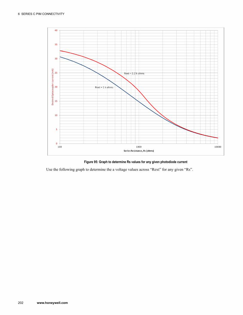
Figure 95: Graph to determine Rs values for any given photodiode current
Use the following graph to determine the a voltage values across “Rext” for any given “Rs”.
6 SERIES C PIM CONNECTIVITY
202 www.honeywell.com

Figure 96: Graph to determine voltage values across Rext for given Rs
6 SERIES C PIM CONNECTIVITY
203

6.11 Connecting PIM with ST500 dual-pulse simulator (SwintonTechnology)
You can connect PIM with ST500 dual-pulse simulator in a differential manner as well as a single-endedmanner.
6.11.1 Differential mannerThe following diagram displays connecting a Swinton Technology, ST500 dual-pulse simulator, to the PIMIOTA in a differential manner.
Figure 97: Connecting PIM with ST500 dual-pulse simulator – differential manner
In this example, channel 1 and channel 2 are displayed. The ST500 rear panel switches need to be set to the dV(differential voltage) position. The PIM channel blocks can be configured as single stream, or dual stream.When dual stream is chosen, the PIM utilizes dual pulse error detection per ISO 6551. It is important to ensurethat RES BIAS UP option is not used for the channels connected to ST500 since ST500 uses a differentialdriver output stage and a pull-up will interfere with the signal quality and potentially damage the ST500. Also,ensure that COM(x) terminal blocks for the channels connected to ST500 are configured for ISOL position(jumpers removed) for fully isolated operation. Otherwise, the A! will be shorted to B! and cause signalcorruption.
6 SERIES C PIM CONNECTIVITY
204 www.honeywell.com

6.11.2 Single-ended mannerThe following diagram displays connecting a Swinton Technology, ST500 dual-pulse simulator, to the PIMIOTA in a single-ended manner.
Figure 98: Connecting PIM with ST500 dual-pulse simulator - Single-ended manner
The difference between the differential and the single-ended connectivity is that the 0V pin of the ST500 driverconnects to the COMMON(x) pins of the PIM IOTA. This arrangement forces the COMMON 1 and COMMON2 to be electrically connected through the ST500. In this connection, A, A!, B, or B! can be connected to theSIG IN(x) pins of the IOTA. In the above diagram, SIG IN(x) is arbitrarily connected to A and B, whichmaintains the default phase 90-degree relationship.
6 SERIES C PIM CONNECTIVITY
205
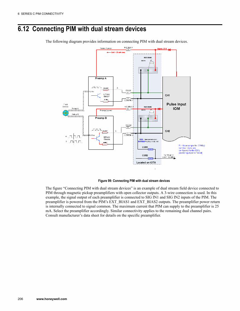
6.12 Connecting PIM with dual stream devicesThe following diagram provides information on connecting PIM with dual stream devices.
Figure 99: Connecting PIM with dual stream devices
The figure “Connecting PIM with dual stream devices” is an example of dual stream field device connected toPIM through magnetic pickup preamplifiers with open collector outputs. A 3-wire connection is used. In thisexample, the signal output of each preamplifier is connected to SIG IN1 and SIG IN2 inputs of the PIM. Thepreamplifier is powered from the PIM’s EXT_BIAS1 and EXT_BIAS2 outputs. The preamplifier power returnis internally connected to signal common. The maximum current that PIM can supply to the preamplifier is 25mA. Select the preamplifier accordingly. Similar connectivity applies to the remaining dual channel pairs.Consult manufacturer’s data sheet for details on the specific preamplifier.
6 SERIES C PIM CONNECTIVITY
206 www.honeywell.com
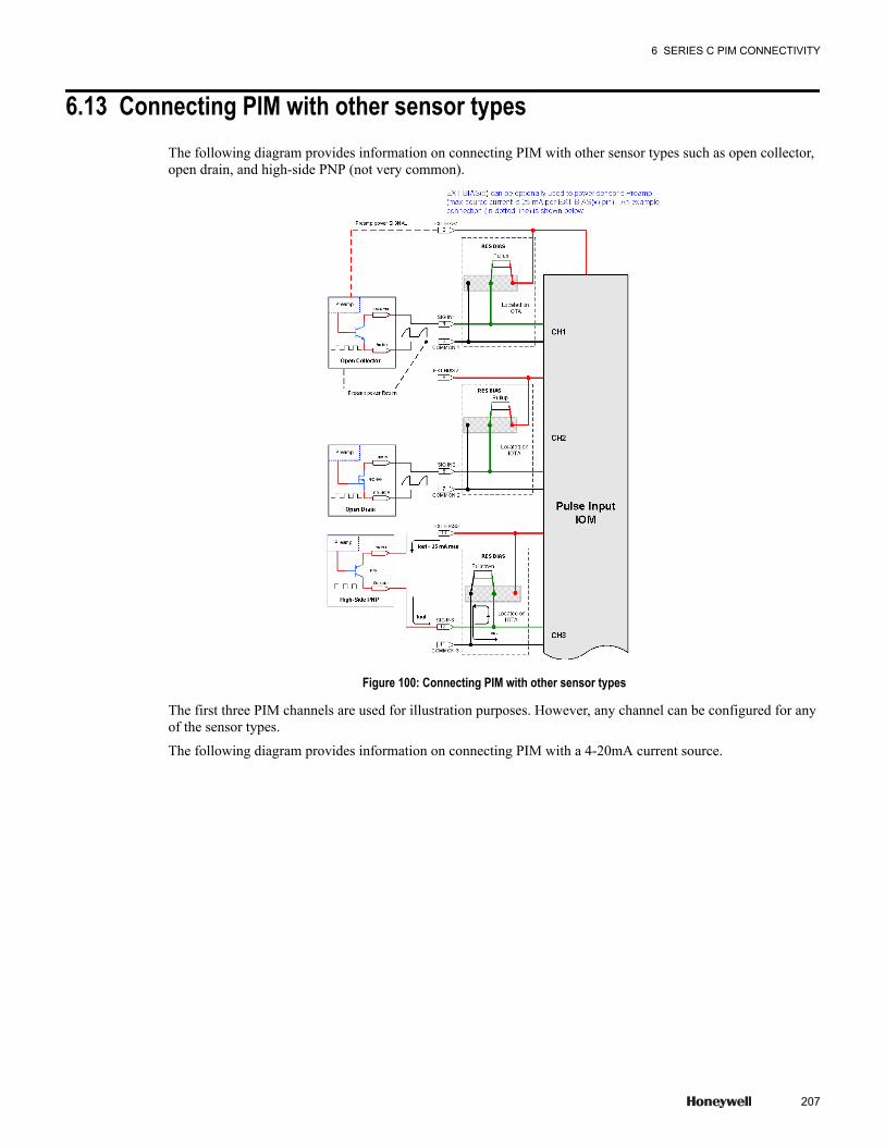
6.13 Connecting PIM with other sensor typesThe following diagram provides information on connecting PIM with other sensor types such as open collector,open drain, and high-side PNP (not very common).
Figure 100: Connecting PIM with other sensor types
The first three PIM channels are used for illustration purposes. However, any channel can be configured for anyof the sensor types.
The following diagram provides information on connecting PIM with a 4-20mA current source.
6 SERIES C PIM CONNECTIVITY
207
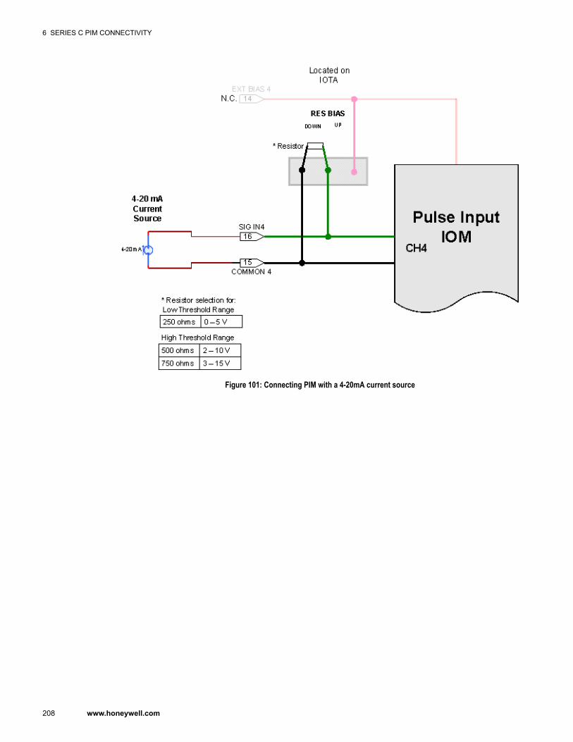
Figure 101: Connecting PIM with a 4-20mA current source
6 SERIES C PIM CONNECTIVITY
208 www.honeywell.com
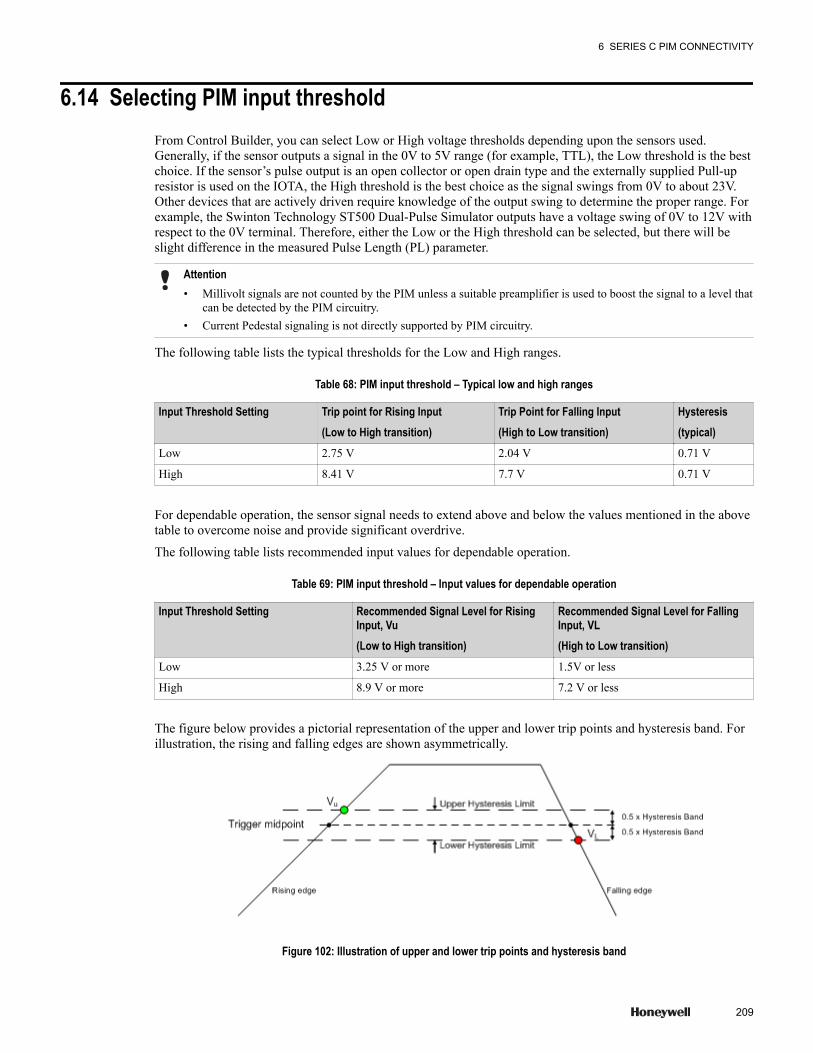
6.14 Selecting PIM input thresholdFrom Control Builder, you can select Low or High voltage thresholds depending upon the sensors used.Generally, if the sensor outputs a signal in the 0V to 5V range (for example, TTL), the Low threshold is the bestchoice. If the sensor’s pulse output is an open collector or open drain type and the externally supplied Pull-upresistor is used on the IOTA, the High threshold is the best choice as the signal swings from 0V to about 23V.Other devices that are actively driven require knowledge of the output swing to determine the proper range. Forexample, the Swinton Technology ST500 Dual-Pulse Simulator outputs have a voltage swing of 0V to 12V withrespect to the 0V terminal. Therefore, either the Low or the High threshold can be selected, but there will beslight difference in the measured Pulse Length (PL) parameter.
Attention• Millivolt signals are not counted by the PIM unless a suitable preamplifier is used to boost the signal to a level that
can be detected by the PIM circuitry.• Current Pedestal signaling is not directly supported by PIM circuitry.
The following table lists the typical thresholds for the Low and High ranges.
Table 68: PIM input threshold – Typical low and high ranges
Input Threshold Setting Trip point for Rising Input(Low to High transition)
Trip Point for Falling Input(High to Low transition)
Hysteresis(typical)
Low 2.75 V 2.04 V 0.71 V
High 8.41 V 7.7 V 0.71 V
For dependable operation, the sensor signal needs to extend above and below the values mentioned in the abovetable to overcome noise and provide significant overdrive.
The following table lists recommended input values for dependable operation.
Table 69: PIM input threshold – Input values for dependable operation
Input Threshold Setting Recommended Signal Level for RisingInput, Vu(Low to High transition)
Recommended Signal Level for FallingInput, VL(High to Low transition)
Low 3.25 V or more 1.5V or less
High 8.9 V or more 7.2 V or less
The figure below provides a pictorial representation of the upper and lower trip points and hysteresis band. Forillustration, the rising and falling edges are shown asymmetrically.
Figure 102: Illustration of upper and lower trip points and hysteresis band
6 SERIES C PIM CONNECTIVITY
209
6.15 Recommended cable typesThis section provides recommendations on proper types of external cabling that should be used with the PIM.Honeywell does not provide PIM interface cables. You must select cables per your requirements.
The following Belden cable types can be used with PIM.
• Blue Hose Series – 9463, 9463F, 3072F, 89463, 9463DB and so on)• Brilliance Series (multi-conductor) – 8774
However, you can use similar cables from other manufacturers.
6.15.1 Tips on cable usage
Multi-conductor CablesMulti-conductor cables may be used to allow for a single run (for example, home run cable). However, only usecables with individually shielded twisted pairs to minimize crosstalk and false counting of pulses from onechannel to another within the cable bundle. At a minimum, the selected cable should have individually shieldedtwisted pairs with 100% foil shield coverage. Preferably, a foil plus overall braid provides more shieldingeffectiveness. Wire selection is critical for pulse counting performance, therefore select appropriate cables.
For fast counting, low capacitance is also desirable so that the pulse fidelity (pulse distortion) at longer cablelengths is not be compromised.
A mix of multi-conductor and individual cable runs can be used with PIM.
EMI/RFI ConsiderationsFor best EMI/RFI performance, use cables that have a braided shield (55% or greater coverage). Some cablesare double shielded with a braid over foil. This provides the best performance if the environment is EMI harsh.Proper grounding of the shields is necessary to obtain best performance.
Shield (screen) terminationThe shields (screen) of the cable carrying the pulse signals from the sensor to the PIM IOTA can be grounded ateither end or both ends (double termination). If low frequency ground loops are a problem in the plant, tying theshield to ground at one end may be a better choice to minimize common mode noise and interference. If theground system/grid of the plant does not have ground loops or the run from the PIM IOTA to the sensor is short,then double termination is often preferable.
6 SERIES C PIM CONNECTIVITY
210 www.honeywell.com
7 Rail-Mounted Universal Input/Output (UIO) Module
The Rail-Mounted Universal Input/Output module is designed to mount the Series C Universal Input/Outputmodule vertically on a 35 mm TS-35 DIN (Deutsches Institut für Normung) rail. The entire mountingarrangement is used in non-standard Honeywell cabinets, and wall mount standalone scenarios.
Attention• You should not mount the rail-mounted UIO module horizontally on a DIN rail.• The mounting of Input/Output Termination Assembly (IOTA) and power supply for rail-mounted UIO module is
identical to the mounting of IOTA and power supply for Series C I/O modules.
The rail-mounted UIO has the following categories.
• Mechanical – This category is used for holding the IOTAs/IOMs that can be mounted outside the standardHoneywell cabinet with provision for routing the system cables.
• Electrical – This category is used for providing an interface to connect ground and power from externalpower supply to the IOTA screw terminals in non-standard Honeywell cabinets where bus bars are notpresent. The interface has Printed Wiring Assembly (PWA), which also includes Reverse polarity,Electrostatic discharge (ESD) and Surge protections complying with CE standards.
BenefitsThe following are the benefits of rail-mounted UIO module.
• Space consumption is less.• Cost-effective since there is no investment required for cabinets to mount the module.• Relocation of components is simple and easy.
Related topics“Physical description of rail-mounted UIO module assembly” on page 212“Input/output Link (IOL) management” on page 214“Single Mode FOE for rail-mounted UIO” on page 215“System wiring” on page 216“Power supply requirements” on page 218“Agency approvals” on page 220“Environmental Conditions” on page 221“Rail-mounted UIO module assembly” on page 222“Mounting base tray assembly on DIN rail” on page 226“Mounting UIO module on the IOTA” on page 229“Grounding and power connections” on page 231“Wiring connections” on page 233“Removing rail-mounted UIO module” on page 239“Replaceable spare parts” on page 240
211
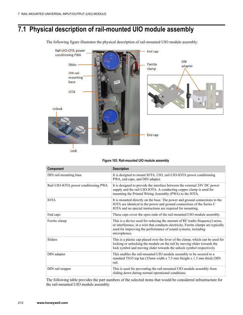
7.1 Physical description of rail-mounted UIO module assemblyThe following figure illustrates the physical description of rail-mounted UIO module assembly.
Figure 103: Rail-mounted UIO module assembly
Component DescriptionDIN rail-mounting base It is designed to mount IOTA, UIO, rail-UIO-IOTA power conditioning
PWA, end caps, and DIN adapter.
Rail-UIO-IOTA power conditioning PWA It is designed to provide the interface between the external 24V DC powersupply and the rail-UIO-IOTA. A conducting copper clamp is used formounting the Printed Wiring Assembly (PWA) to the IOTA.
IOTA It is mounted directly on the base. The power and ground connections to theIOTA are identical to the power and ground connections of the Series CIOTA and no special instructions are required for mounting.
End caps These caps cover the open ends of the rail-mounted UIO module assembly.
Ferrite clamp This is a device used for reducing the amount of RF (radio frequency) noise,or interference, in a wire that conducts electricity. Ferrite clamps are typicallyused for improving the performance of sound systems, includingmicrophones.
Sliders This is a plastic cap placed over the lever of the clamp, which can be used forlocking or unlocking the module on the rail by moving slider towards thelock symbol and moving slider towards the unlock symbol respectively.
DIN adapter This enables the rail-mounted UIO module assembly to be secured to astandard TS35 top hat (35mm width x 7.5 mm Height x 1.5 mm thick) DINrail.
DIN rail stopper This is used for preventing the rail-mounted UIO module assembly fromsliding down during normal operational conditions.
The following table provides the part numbers of the selected items that would be considered infrastructure forthe rail-mounted UIO module assembly.
7 RAIL-MOUNTED UNIVERSAL INPUT/OUTPUT (UIO) MODULE
212 www.honeywell.com
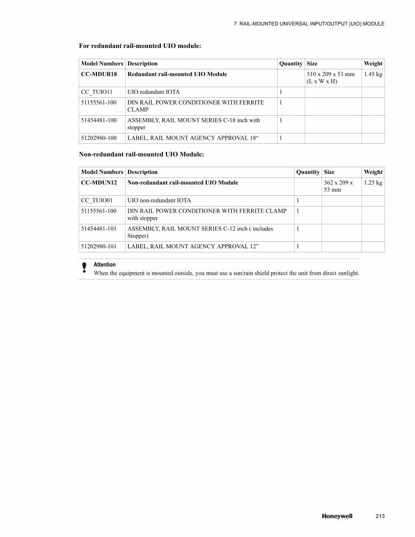
For redundant rail-mounted UIO module:
Model Numbers Description Quantity Size Weight
CC-MDUR18 Redundant rail-mounted UIO Module 510 x 209 x 53 mm(L x W x H)
1.45 kg
CC_TUIO11 UIO redundant IOTA 1
51155561-100 DIN RAIL POWER CONDITIONER WITH FERRITECLAMP
1
51454481-100 ASSEMBLY, RAIL MOUNT SERIES C-18 inch withstopper
1
51202980-100 LABEL, RAIL MOUNT AGENCY APPROVAL 18“ 1
Non-redundant rail-mounted UIO Module:
Model Numbers Description Quantity Size Weight
CC-MDUN12 Non-redundant rail-mounted UIO Module 362 x 209 x53 mm
1.25 kg
CC_TUIO01 UIO non-redundant IOTA 1
51155561-100 DIN RAIL POWER CONDITIONER WITH FERRITE CLAMPwith stopper
1
51454481-101 ASSEMBLY, RAIL MOUNT SERIES C-12 inch ( includesStopper)
1
51202980-101 LABEL, RAIL MOUNT AGENCY APPROVAL 12” 1
AttentionWhen the equipment is mounted outside, you must use a sun/rain shield protect the unit from direct sunlight.
7 RAIL-MOUNTED UNIVERSAL INPUT/OUTPUT (UIO) MODULE
213
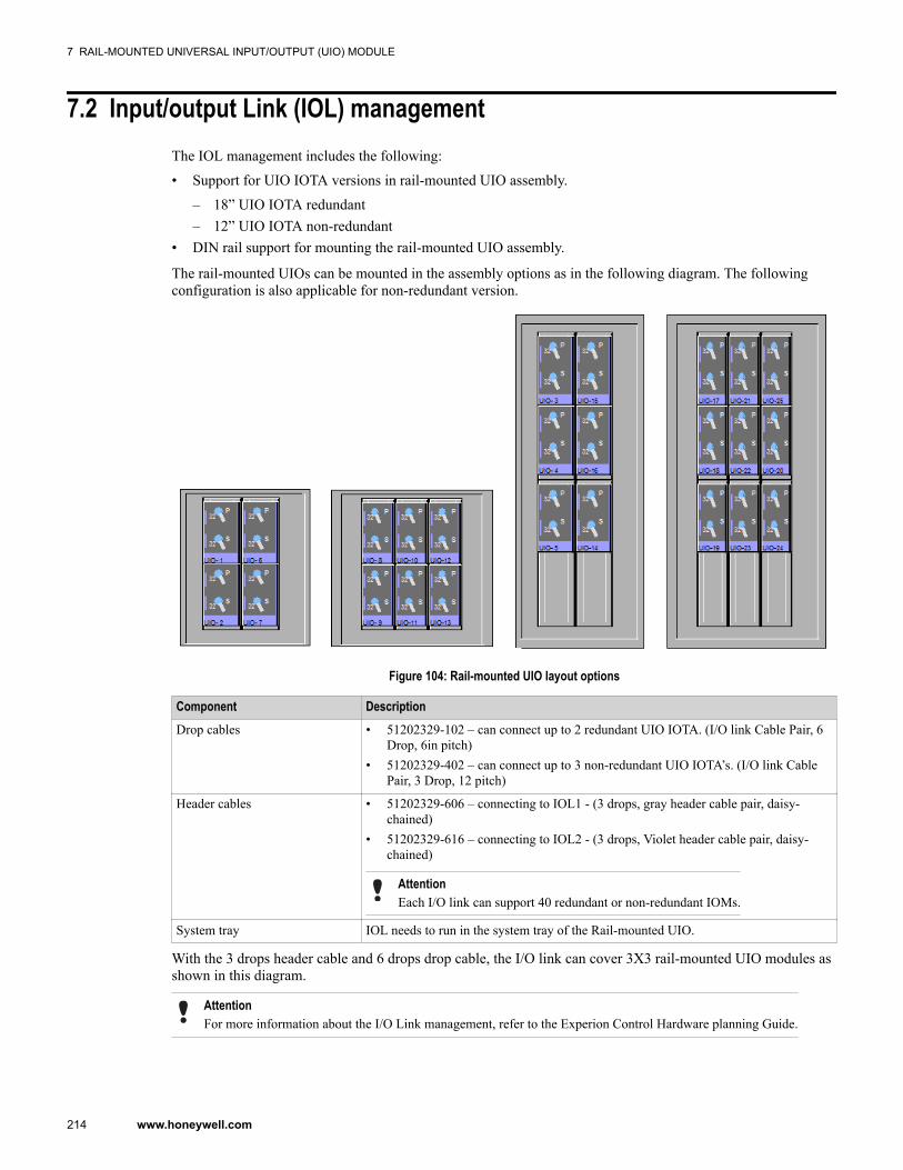
7.2 Input/output Link (IOL) managementThe IOL management includes the following:
• Support for UIO IOTA versions in rail-mounted UIO assembly.
– 18” UIO IOTA redundant– 12” UIO IOTA non-redundant
• DIN rail support for mounting the rail-mounted UIO assembly.
The rail-mounted UIOs can be mounted in the assembly options as in the following diagram. The followingconfiguration is also applicable for non-redundant version.
Figure 104: Rail-mounted UIO layout options
Component DescriptionDrop cables • 51202329-102 – can connect up to 2 redundant UIO IOTA. (I/O link Cable Pair, 6
Drop, 6in pitch)• 51202329-402 – can connect up to 3 non-redundant UIO IOTA’s. (I/O link Cable
Pair, 3 Drop, 12 pitch)
Header cables • 51202329-606 – connecting to IOL1 - (3 drops, gray header cable pair, daisy-chained)
• 51202329-616 – connecting to IOL2 - (3 drops, Violet header cable pair, daisy-chained)
AttentionEach I/O link can support 40 redundant or non-redundant IOMs.
System tray IOL needs to run in the system tray of the Rail-mounted UIO.
With the 3 drops header cable and 6 drops drop cable, the I/O link can cover 3X3 rail-mounted UIO modules asshown in this diagram.
AttentionFor more information about the I/O Link management, refer to the Experion Control Hardware planning Guide.
7 RAIL-MOUNTED UNIVERSAL INPUT/OUTPUT (UIO) MODULE
214 www.honeywell.com
7.3 Single Mode FOE for rail-mounted UIOThe Single Mode Fiber Optic I/O Link Extender (SMFOE) is used for the Rail-mounted UIO, as this has a DINrail-mountable option.
AttentionFOE is mandatory for the installation and system wiring for Rail-mounted UIO.
FOE is placed inside the cabinet on the remote group side and also placed inside the cabinet on the control roomside.
• FOE Component Options: MOXA SMFOE option consists of the following parts.
– ICF-1150-S-SC-T, MOXA FOE Module, quantity - 2– 51155436-100- Install kit, IOL Extender on DIN Rail, quantity -1
• The MOXA FOEs clip to a DIN rail and they are laterally secured by end brackets. See Figure: DC powerline wiring through system tray in the section “Wiring connections” on page 233 for illustration.
• Lower-left or right corner of the cabinet is ideal for mounting the FOE.• One SMFOE is used for connecting to a matrix of 3X3 rail-mounted UIO network or lower. Refer to the
figures in the section “System wiring” on page 216 for illustration.• SMFOE can extend the I/O link up to 10 KM.• Temperature specification of MOXA SMFOE is -40 to +85 degC.
7 RAIL-MOUNTED UNIVERSAL INPUT/OUTPUT (UIO) MODULE
215
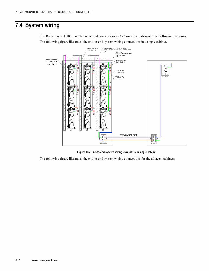
7.4 System wiringThe Rail-mounted UIO module end to end connections in 3X3 matrix are shown in the following diagrams.
The following figure illustrates the end-to-end system wiring connections in a single cabinet.
Figure 105: End-to-end system wiring - Rail-UIOs in single cabinet
The following figure illustrates the end-to-end system wiring connections for the adjacent cabinets.
7 RAIL-MOUNTED UNIVERSAL INPUT/OUTPUT (UIO) MODULE
216 www.honeywell.com
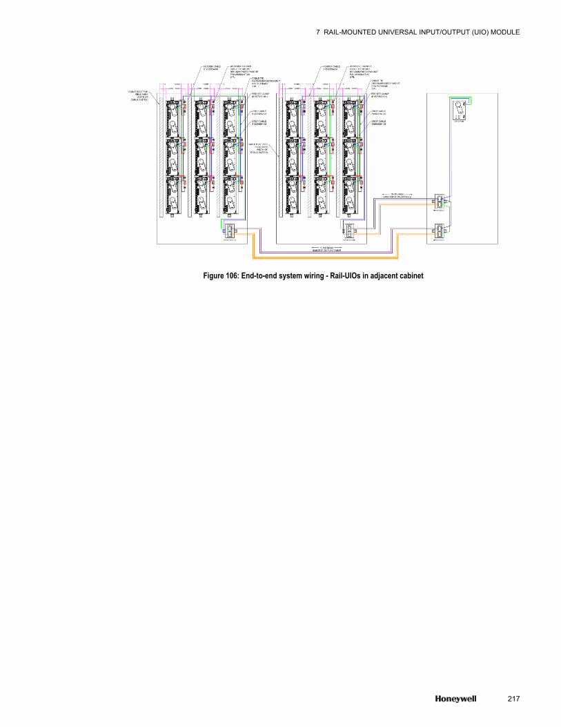
Figure 106: End-to-end system wiring - Rail-UIOs in adjacent cabinet
7 RAIL-MOUNTED UNIVERSAL INPUT/OUTPUT (UIO) MODULE
217
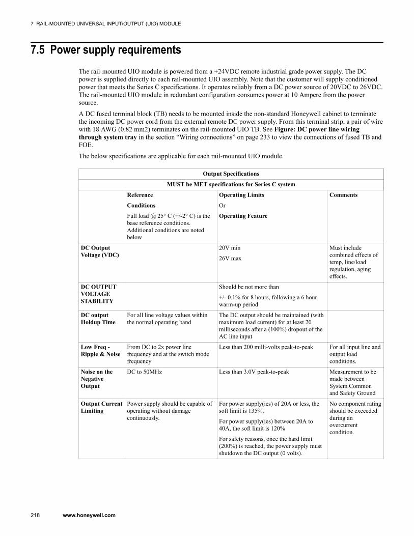
7.5 Power supply requirementsThe rail-mounted UIO module is powered from a +24VDC remote industrial grade power supply. The DCpower is supplied directly to each rail-mounted UIO assembly. Note that the customer will supply conditionedpower that meets the Series C specifications. It operates reliably from a DC power source of 20VDC to 26VDC.The rail-mounted UIO module in redundant configuration consumes power at 10 Ampere from the powersource.
A DC fused terminal block (TB) needs to be mounted inside the non-standard Honeywell cabinet to terminatethe incoming DC power cord from the external remote DC power supply. From this terminal strip, a pair of wirewith 18 AWG (0.82 mm2) terminates on the rail-mounted UIO TB. See Figure: DC power line wiringthrough system tray in the section “Wiring connections” on page 233 to view the connections of fused TB andFOE.
The below specifications are applicable for each rail-mounted UIO module.
Output Specifications
MUST be MET specifications for Series C system
Reference
Conditions
Full load @ 25° C (+/-2° C) is thebase reference conditions.Additional conditions are notedbelow
Operating Limits
Or
Operating Feature
Comments
DC OutputVoltage (VDC)
20V min
26V max
Must includecombined effects oftemp, line/loadregulation, agingeffects.
DC OUTPUTVOLTAGESTABILITY
Should be not more than
+/- 0.1% for 8 hours, following a 6 hourwarm-up period
DC outputHoldup Time
For all line voltage values withinthe normal operating band
The DC output should be maintained (withmaximum load current) for at least 20milliseconds after a (100%) dropout of theAC line input
Low Freq -Ripple & Noise
From DC to 2x power linefrequency and at the switch modefrequency
Less than 200 milli-volts peak-to-peak For all input line andoutput loadconditions.
Noise on theNegativeOutput
DC to 50MHz Less than 3.0V peak-to-peak Measurement to bemade betweenSystem Commonand Safety Ground
Output CurrentLimiting
Power supply should be capable ofoperating without damagecontinuously.
For power supply(ies) of 20A or less, thesoft limit is 135%.
For power supply(ies) between 20A to40A, the soft limit is 120%
For safety reasons, once the hard limit(200%) is reached, the power supply mustshutdown the DC output (0 volts).
No component ratingshould be exceededduring anovercurrentcondition.
7 RAIL-MOUNTED UNIVERSAL INPUT/OUTPUT (UIO) MODULE
218 www.honeywell.com
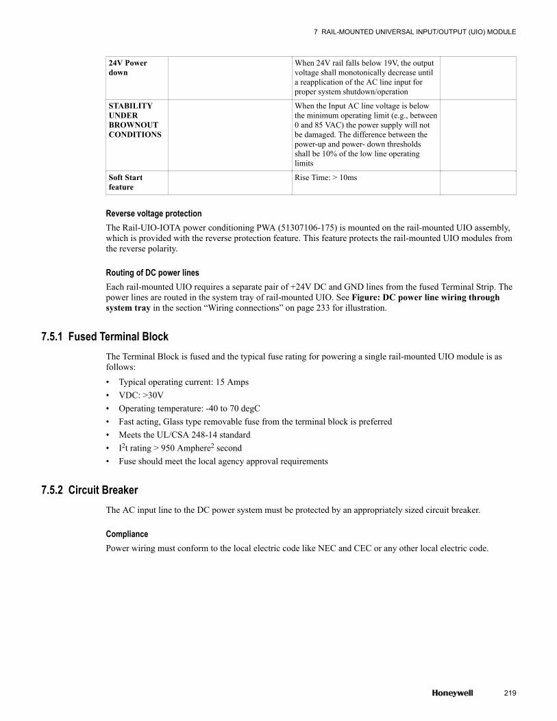
24V Powerdown
When 24V rail falls below 19V, the outputvoltage shall monotonically decrease untila reapplication of the AC line input forproper system shutdown/operation
STABILITYUNDERBROWNOUTCONDITIONS
When the Input AC line voltage is belowthe minimum operating limit (e.g., between0 and 85 VAC) the power supply will notbe damaged. The difference between thepower-up and power- down thresholdsshall be 10% of the low line operatinglimits
Soft Startfeature
Rise Time: > 10ms
Reverse voltage protectionThe Rail-UIO-IOTA power conditioning PWA (51307106-175) is mounted on the rail-mounted UIO assembly,which is provided with the reverse protection feature. This feature protects the rail-mounted UIO modules fromthe reverse polarity.
Routing of DC power linesEach rail-mounted UIO requires a separate pair of +24V DC and GND lines from the fused Terminal Strip. Thepower lines are routed in the system tray of rail-mounted UIO. See Figure: DC power line wiring throughsystem tray in the section “Wiring connections” on page 233 for illustration.
7.5.1 Fused Terminal BlockThe Terminal Block is fused and the typical fuse rating for powering a single rail-mounted UIO module is asfollows:
• Typical operating current: 15 Amps• VDC: >30V• Operating temperature: -40 to 70 degC• Fast acting, Glass type removable fuse from the terminal block is preferred• Meets the UL/CSA 248-14 standard• I2t rating > 950 Amphere2 second• Fuse should meet the local agency approval requirements
7.5.2 Circuit BreakerThe AC input line to the DC power system must be protected by an appropriately sized circuit breaker.
CompliancePower wiring must conform to the local electric code like NEC and CEC or any other local electric code.
7 RAIL-MOUNTED UNIVERSAL INPUT/OUTPUT (UIO) MODULE
219

7.6 Agency approvalsThe rail-mounted UIO has the following agency approvals. These agency markings are applied on the Rail-UIOproduct level and not on the non-standard cabinets in which Rail-UIO are mounted.
• CE and CTick: Applicable at individual component level - Power conditioner PWA and Base tray• HAZLOC (Class 1/Div 2) - CSA, FM, ATEX, IECx: Applicable at rail-mounted UIO product level.
7 RAIL-MOUNTED UNIVERSAL INPUT/OUTPUT (UIO) MODULE
220 www.honeywell.com
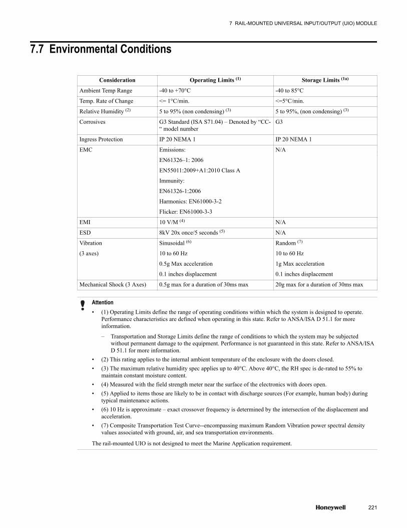
7.7 Environmental Conditions
Consideration Operating Limits (1) Storage Limits (1a)
Ambient Temp Range -40 to +70°C -40 to 85°C
Temp. Rate of Change <= 1°C/min. <=5°C/min.
Relative Humidity (2) 5 to 95% (non condensing) (3) 5 to 95%, (non condensing) (3)
Corrosives G3 Standard (ISA S71.04) – Denoted by “CC-“ model number
G3
Ingress Protection IP 20 NEMA 1 IP 20 NEMA 1
EMC Emissions:
EN61326–1: 2006
EN55011:2009+A1:2010 Class A
Immunity:
EN61326-1:2006
Harmonics: EN61000-3-2
Flicker: EN61000-3-3
N/A
EMI 10 V/M (4) N/A
ESD 8kV 20x once/5 seconds (5) N/A
Vibration
(3 axes)
Sinusoidal (6)
10 to 60 Hz
0.5g Max acceleration
0.1 inches displacement
Random (7)
10 to 60 Hz
1g Max acceleration
0.1 inches displacement
Mechanical Shock (3 Axes) 0.5g max for a duration of 30ms max 20g max for a duration of 30ms max
Attention• (1) Operating Limits define the range of operating conditions within which the system is designed to operate.
Performance characteristics are defined when operating in this state. Refer to ANSA/ISA D 51.1 for moreinformation.
– Transportation and Storage Limits define the range of conditions to which the system may be subjectedwithout permanent damage to the equipment. Performance is not guaranteed in this state. Refer to ANSA/ISAD 51.1 for more information.
• (2) This rating applies to the internal ambient temperature of the enclosure with the doors closed.• (3) The maximum relative humidity spec applies up to 40°C. Above 40°C, the RH spec is de-rated to 55% to
maintain constant moisture content.• (4) Measured with the field strength meter near the surface of the electronics with doors open.• (5) Applied to items those are likely to be in contact with discharge sources (For example, human body) during
typical maintenance actions.• (6) 10 Hz is approximate – exact crossover frequency is determined by the intersection of the displacement and
acceleration.• (7) Composite Transportation Test Curve--encompassing maximum Random Vibration power spectral density
values associated with ground, air, and sea transportation environments.
The rail-mounted UIO is not designed to meet the Marine Application requirement.
7 RAIL-MOUNTED UNIVERSAL INPUT/OUTPUT (UIO) MODULE
221
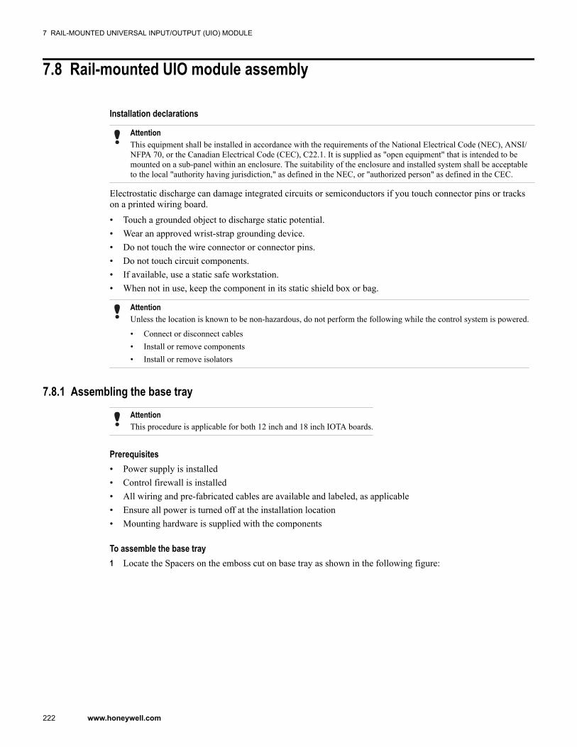
7.8 Rail-mounted UIO module assembly
Installation declarations
AttentionThis equipment shall be installed in accordance with the requirements of the National Electrical Code (NEC), ANSI/NFPA 70, or the Canadian Electrical Code (CEC), C22.1. It is supplied as "open equipment" that is intended to bemounted on a sub-panel within an enclosure. The suitability of the enclosure and installed system shall be acceptableto the local "authority having jurisdiction," as defined in the NEC, or "authorized person" as defined in the CEC.
Electrostatic discharge can damage integrated circuits or semiconductors if you touch connector pins or trackson a printed wiring board.
• Touch a grounded object to discharge static potential.• Wear an approved wrist-strap grounding device.• Do not touch the wire connector or connector pins.• Do not touch circuit components.• If available, use a static safe workstation.• When not in use, keep the component in its static shield box or bag.
AttentionUnless the location is known to be non-hazardous, do not perform the following while the control system is powered.
• Connect or disconnect cables• Install or remove components• Install or remove isolators
7.8.1 Assembling the base tray
AttentionThis procedure is applicable for both 12 inch and 18 inch IOTA boards.
Prerequisites• Power supply is installed• Control firewall is installed• All wiring and pre-fabricated cables are available and labeled, as applicable• Ensure all power is turned off at the installation location• Mounting hardware is supplied with the components
To assemble the base tray1 Locate the Spacers on the emboss cut on base tray as shown in the following figure:
7 RAIL-MOUNTED UNIVERSAL INPUT/OUTPUT (UIO) MODULE
222 www.honeywell.com
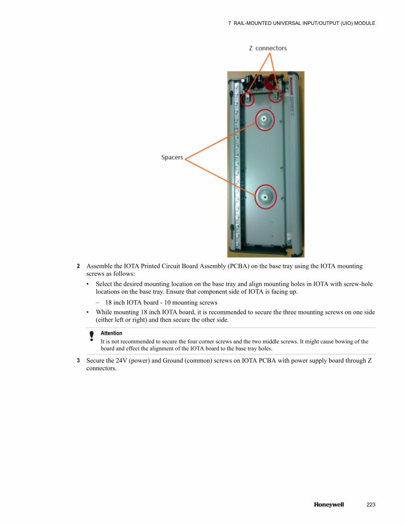
2 Assemble the IOTA Printed Circuit Board Assembly (PCBA) on the base tray using the IOTA mountingscrews as follows:• Select the desired mounting location on the base tray and align mounting holes in IOTA with screw-hole
locations on the base tray. Ensure that component side of IOTA is facing up.
– 18 inch IOTA board - 10 mounting screws• While mounting 18 inch IOTA board, it is recommended to secure the three mounting screws on one side
(either left or right) and then secure the other side.
AttentionIt is not recommended to secure the four corner screws and the two middle screws. It might cause bowing of theboard and effect the alignment of the IOTA board to the base tray holes.
3 Secure the 24V (power) and Ground (common) screws on IOTA PCBA with power supply board through Zconnectors.
7 RAIL-MOUNTED UNIVERSAL INPUT/OUTPUT (UIO) MODULE
223
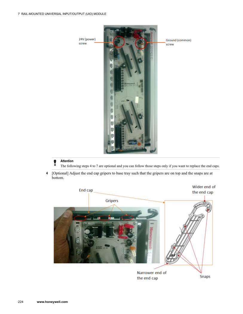
AttentionThe following steps 4 to 7 are optional and you can follow those steps only if you want to replace the end caps.
4 [Optional] Adjust the end cap gripers to base tray such that the gripers are on top and the snaps are atbottom.
7 RAIL-MOUNTED UNIVERSAL INPUT/OUTPUT (UIO) MODULE
224 www.honeywell.com
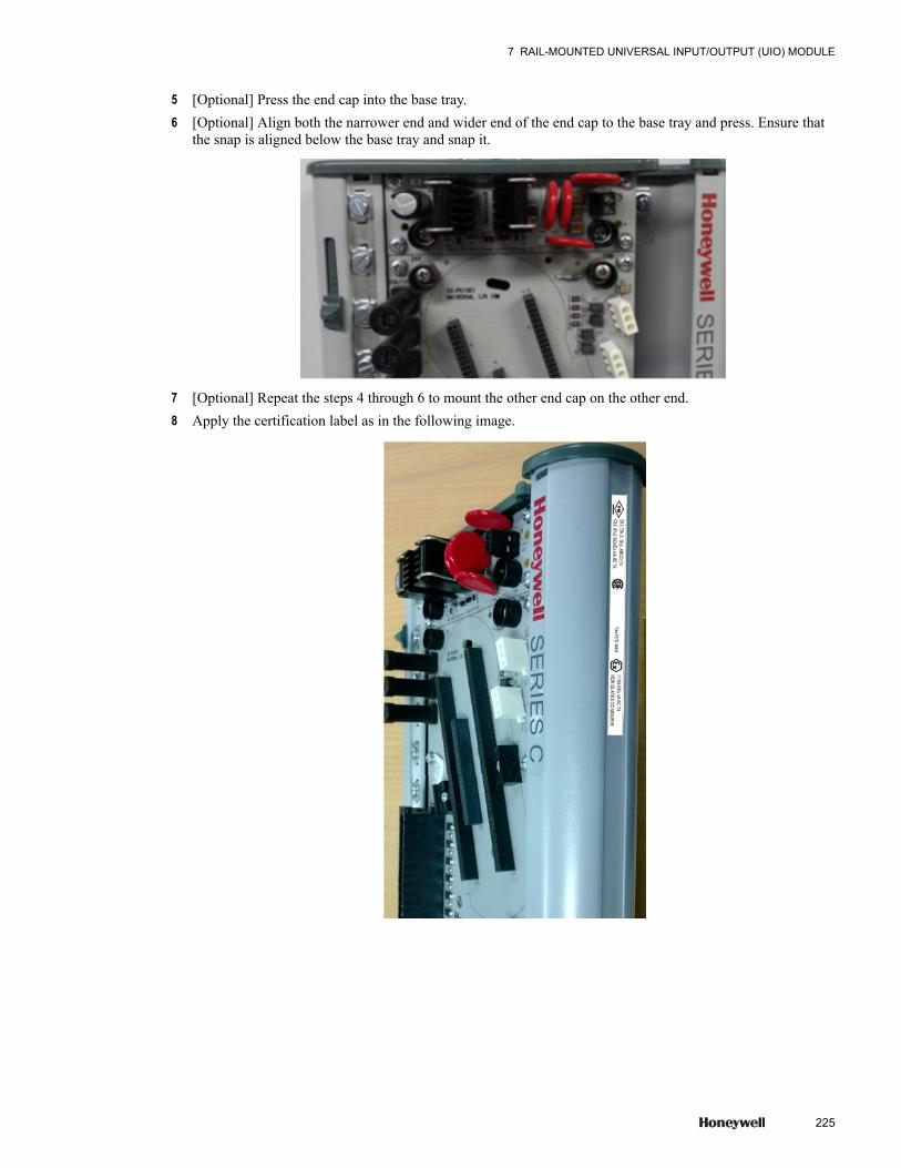
5 [Optional] Press the end cap into the base tray.6 [Optional] Align both the narrower end and wider end of the end cap to the base tray and press. Ensure that
the snap is aligned below the base tray and snap it.
7 [Optional] Repeat the steps 4 through 6 to mount the other end cap on the other end.8 Apply the certification label as in the following image.
7 RAIL-MOUNTED UNIVERSAL INPUT/OUTPUT (UIO) MODULE
225
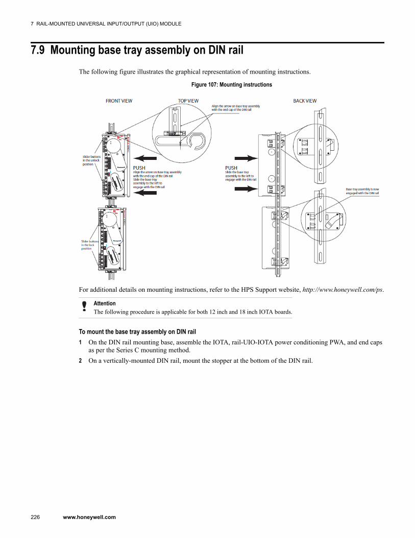
7.9 Mounting base tray assembly on DIN railThe following figure illustrates the graphical representation of mounting instructions.
Figure 107: Mounting instructions
For additional details on mounting instructions, refer to the HPS Support website, http://www.honeywell.com/ps.
AttentionThe following procedure is applicable for both 12 inch and 18 inch IOTA boards.
To mount the base tray assembly on DIN rail1 On the DIN rail mounting base, assemble the IOTA, rail-UIO-IOTA power conditioning PWA, and end caps
as per the Series C mounting method.2 On a vertically-mounted DIN rail, mount the stopper at the bottom of the DIN rail.
7 RAIL-MOUNTED UNIVERSAL INPUT/OUTPUT (UIO) MODULE
226 www.honeywell.com
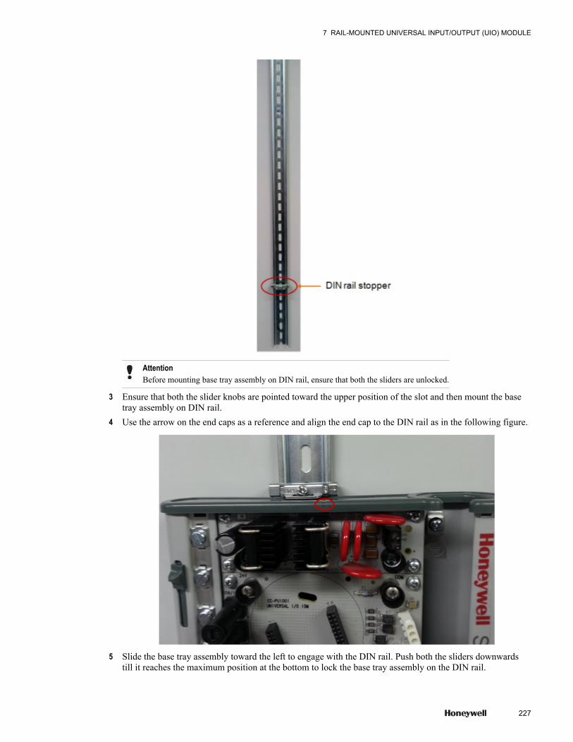
AttentionBefore mounting base tray assembly on DIN rail, ensure that both the sliders are unlocked.
3 Ensure that both the slider knobs are pointed toward the upper position of the slot and then mount the basetray assembly on DIN rail.
4 Use the arrow on the end caps as a reference and align the end cap to the DIN rail as in the following figure.
5 Slide the base tray assembly toward the left to engage with the DIN rail. Push both the sliders downwardstill it reaches the maximum position at the bottom to lock the base tray assembly on the DIN rail.
7 RAIL-MOUNTED UNIVERSAL INPUT/OUTPUT (UIO) MODULE
227

6 Push the base tray assembly down till it supports on the DIN rail stopper.7 Mount another DIN rail stopper on the top of the base tray assembly to fix the base tray tightly.8 Mount the UIO module on IOTA base tray. For more details about mounting the UIO module, refer to the
section Mounting UIO module on the IOTA.9 Connect the system cables (IOLINK cables, power supply cables, and the grounding wires) on the right of
the rail-mounted UIO module. In addition, connect the field wire cables through cable duct on the left of therail-mounted UIO module. For more details about wiring connections, refer to the section Wiringconnections.
7 RAIL-MOUNTED UNIVERSAL INPUT/OUTPUT (UIO) MODULE
228 www.honeywell.com
7.10 Mounting UIO module on the IOTA
Prerequisites• IOTA is mounted on the base tray• Power supply is installed• Control firewall is installed• All wiring and pre-fabricated cables are available and labeled as applicable• Ensure that power is turned off at the location of UIO installation• Mounting hardware is supplied with the components
To mount UIO module on IOTA1 Insert the UIO module into IOTA board and ensure that the circuit board matches properly with the IOTA
board connector.2 Secure the module to the:
• IOTA board - with two screws located at each side of the plastic cover.• Base tray - with the long gray plastic screw located at the front of the module. This is applicable only if
this provision exists.
Attention• Ensure that the lifting lever, which is available with the UIO module, should be in vertical position to ensure
proper insertion of the IOM with the IOTA.• Only use a #2 Phillips screwdriver to carefully loosen or tighten the long gray plastic screw. Do not use either
a #1 Phillips screwdriver or a battery-powered screwdriver to remove or install the plastic screw as this candamage the screw head.
7 RAIL-MOUNTED UNIVERSAL INPUT/OUTPUT (UIO) MODULE
229
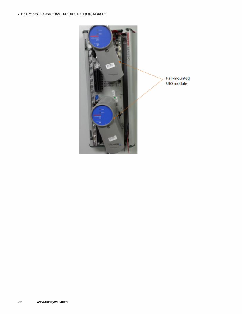
7 RAIL-MOUNTED UNIVERSAL INPUT/OUTPUT (UIO) MODULE
230 www.honeywell.com
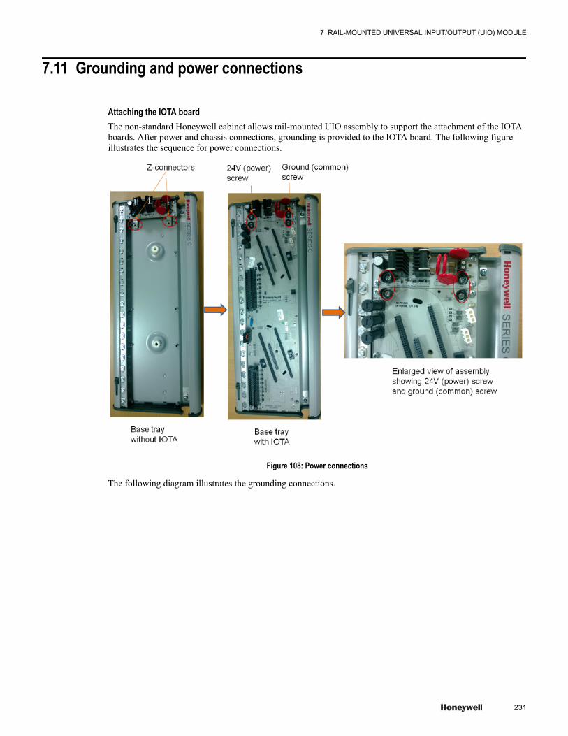
7.11 Grounding and power connections
Attaching the IOTA boardThe non-standard Honeywell cabinet allows rail-mounted UIO assembly to support the attachment of the IOTAboards. After power and chassis connections, grounding is provided to the IOTA board. The following figureillustrates the sequence for power connections.
Figure 108: Power connections
The following diagram illustrates the grounding connections.
7 RAIL-MOUNTED UNIVERSAL INPUT/OUTPUT (UIO) MODULE
231
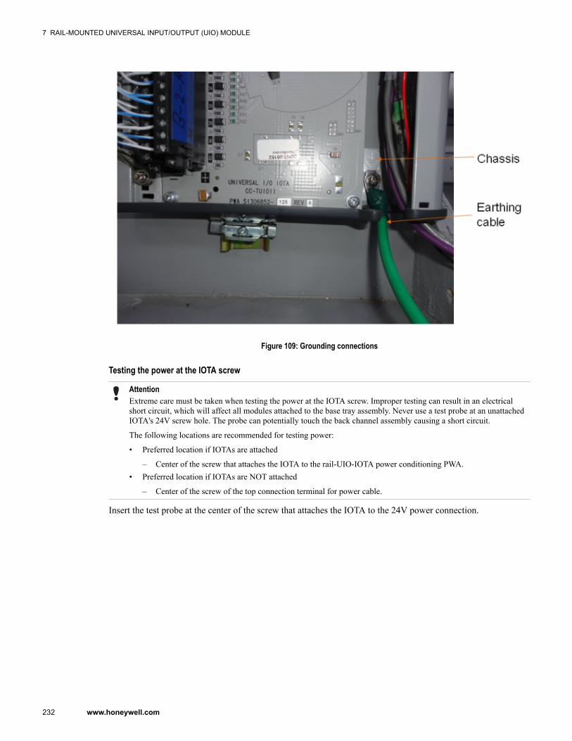
Figure 109: Grounding connections
Testing the power at the IOTA screw
AttentionExtreme care must be taken when testing the power at the IOTA screw. Improper testing can result in an electricalshort circuit, which will affect all modules attached to the base tray assembly. Never use a test probe at an unattachedIOTA's 24V screw hole. The probe can potentially touch the back channel assembly causing a short circuit.
The following locations are recommended for testing power:
• Preferred location if IOTAs are attached
– Center of the screw that attaches the IOTA to the rail-UIO-IOTA power conditioning PWA.• Preferred location if IOTAs are NOT attached
– Center of the screw of the top connection terminal for power cable.
Insert the test probe at the center of the screw that attaches the IOTA to the 24V power connection.
7 RAIL-MOUNTED UNIVERSAL INPUT/OUTPUT (UIO) MODULE
232 www.honeywell.com
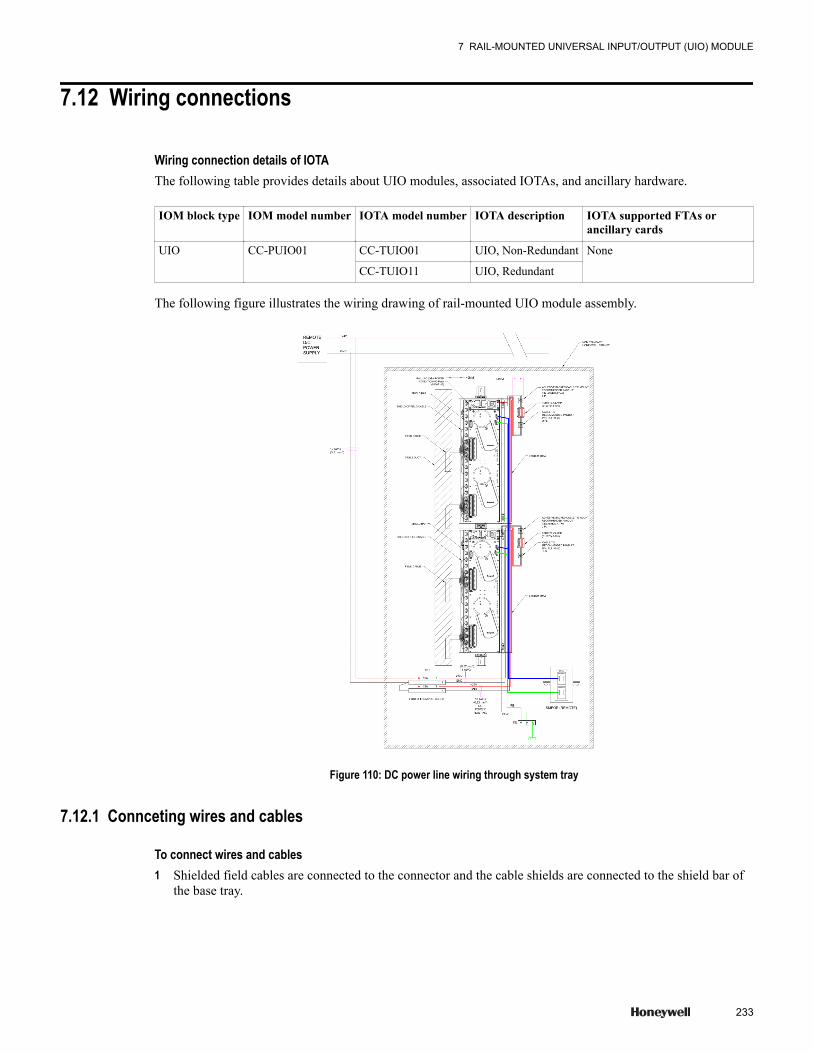
7.12 Wiring connections
Wiring connection details of IOTAThe following table provides details about UIO modules, associated IOTAs, and ancillary hardware.
IOM block type IOM model number IOTA model number IOTA description IOTA supported FTAs orancillary cards
UIO CC-PUIO01 CC-TUIO01 UIO, Non-Redundant None
CC-TUIO11 UIO, Redundant
The following figure illustrates the wiring drawing of rail-mounted UIO module assembly.
Figure 110: DC power line wiring through system tray
7.12.1 Connceting wires and cables
To connect wires and cables1 Shielded field cables are connected to the connector and the cable shields are connected to the shield bar of
the base tray.
7 RAIL-MOUNTED UNIVERSAL INPUT/OUTPUT (UIO) MODULE
233

2 Connect IOLINK cable A and IOLINK cable B to the connectors respectively on the IOTA board. Ensurethat all IOLINK cables and power cables are pulled through the cable duct in the base tray.
7 RAIL-MOUNTED UNIVERSAL INPUT/OUTPUT (UIO) MODULE
234 www.honeywell.com
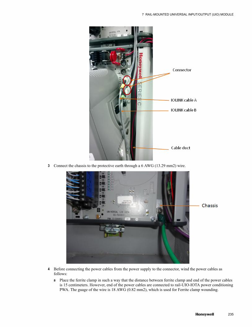
3 Connect the chassis to the protective earth through a 6 AWG (13.29 mm2) wire.
4 Before connecting the power cables from the power supply to the connector, wind the power cables asfollows:a Place the ferrite clamp in such a way that the distance between ferrite clamp and end of the power cables
is 15 centimeters. However, end of the power cables are connected to rail-UIO-IOTA power conditioningPWA. The guage of the wire is 18 AWG (0.82 mm2), which is used for Ferrite clamp wounding.
7 RAIL-MOUNTED UNIVERSAL INPUT/OUTPUT (UIO) MODULE
235

b Place the power cables on the ferrite clamp as shown in the following figure.
c Wind the power cables on the ferrite clamp as shown in the following figure.
7 RAIL-MOUNTED UNIVERSAL INPUT/OUTPUT (UIO) MODULE
236 www.honeywell.com
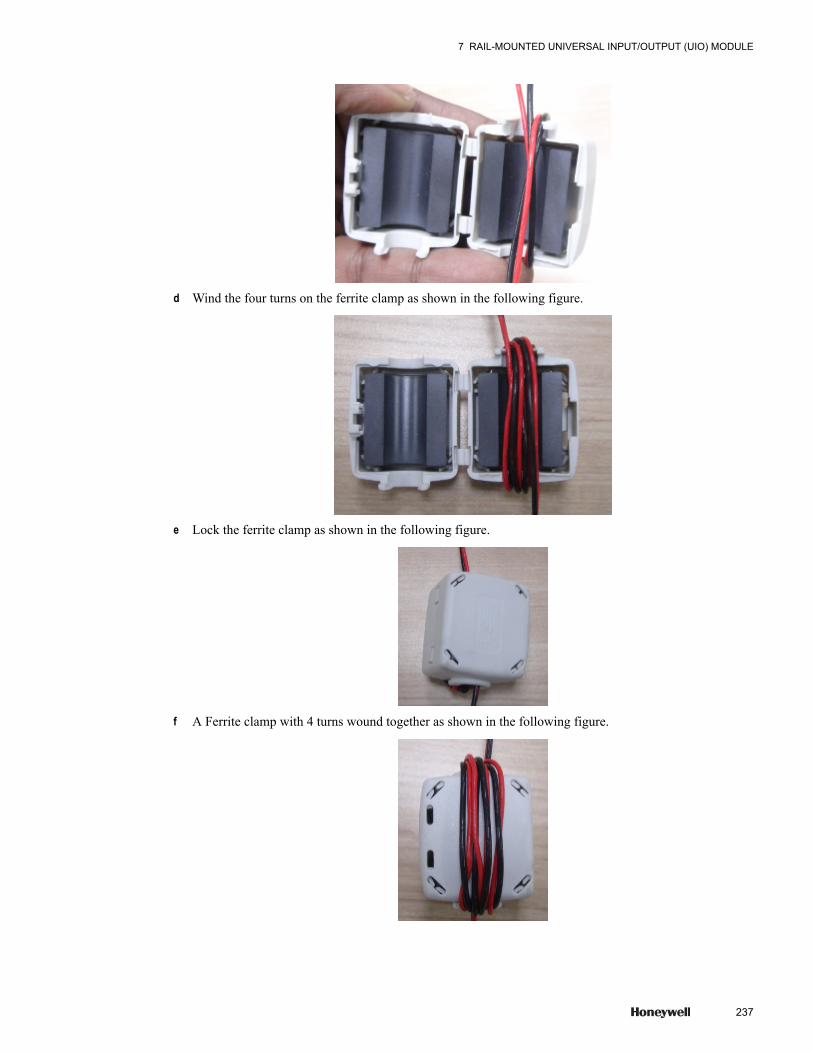
d Wind the four turns on the ferrite clamp as shown in the following figure.
e Lock the ferrite clamp as shown in the following figure.
f A Ferrite clamp with 4 turns wound together as shown in the following figure.
7 RAIL-MOUNTED UNIVERSAL INPUT/OUTPUT (UIO) MODULE
237
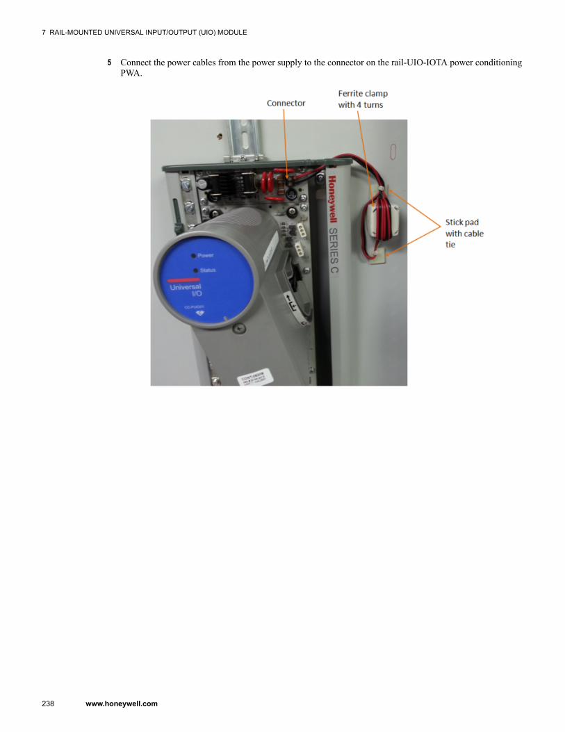
5 Connect the power cables from the power supply to the connector on the rail-UIO-IOTA power conditioningPWA.
7 RAIL-MOUNTED UNIVERSAL INPUT/OUTPUT (UIO) MODULE
238 www.honeywell.com

7.13 Removing rail-mounted UIO module
PrerequisitesBefore removing the rail-mounted UIO module, consider the following:
• Remove all the field wire cables that are connected to the module.• Remove ground wires.• Remove the power supply connections from the assembly.
To remove rail-mounted UIO module1 Push both the sliders upward till it reaches the maximum position to unlock the module on the DIN rail.
2 Slide the rail-mounted UIO module assembly towards the right to disengage from the DIN rail and removeit.
7 RAIL-MOUNTED UNIVERSAL INPUT/OUTPUT (UIO) MODULE
239
7.14 Replaceable spare partsThe following table lists the replaceable spare parts.
Part number Spare part name
51307106-175 RAIL UIO-IOTA POWER INPUT-PWA
51507343-101 FERR RND CBL SNAP 8.5-10.5MM GRY
51454430-100 BASE, SERIES C MOUNTING FOR 18" IOTA
51307110-100 END CAP, BASE, TOP, SERIES C MOUNTING
51307110-101 END CAP, BASE, BOTTOM, SERIES C MOUNTING
51307156-100 ASSEMBLY, DIN ADAPTER, SERIES C MOUNTING
51454430-101 BASE, SERIES C MOUNTING FOR 12" IOTA
7 RAIL-MOUNTED UNIVERSAL INPUT/OUTPUT (UIO) MODULE
240 www.honeywell.com
8 Series C I/O Configuration Form Reference
When an IOM block is placed on the Project tab in Control Builder, its associated channel blocks are assignedto the IOM. The following applies to that IOM block:
• You assign each IOM to the IOLINK block (that represents the I/O Link network on which the IOMresides).
• All of the common configuration parameters specific to IOMs are located on the Main Tab of the IOM'sconfiguration form.
• 'Grayed' parameters are either view-only runtime parameters or non-applicable configuration parameters• The QVCS tab becomes visible when this option is obtained and enabled.
Related topics“Determining Series C I/O block redundancy” on page 242“Switchover and Secondary readiness” on page 243“Failure conditions and switchover” on page 244“Configuration tools to create control strategies” on page 245“Configuring the Main tab - IOM block” on page 246“Configuring Server History tab - IOM block” on page 249“Configuring Server Displays tab - IOM block” on page 251“Configuring Control Confirmation tab - IOM block” on page 253“Configuring Identification tab - IOM block” on page 255“Configuring QVCS tab - IOM block” on page 257“Configuring the Calibration tab - IOM block” on page 259“Configuring HART Status tab - IOM block” on page 261“Configuring the Configuration tab - Channel block” on page 262“Configuring the Configuration tab - PI channel block” on page 263“Configuring Channel Configuration tab - UIO module block” on page 265“Configuring the Configuration tab - UIO DI channel block” on page 267“Configuring the Configuration tab - UIO DO channel block” on page 268“Configuring HART Configuration tab - Channel block” on page 270“Configuring HART Device Status tab - Channel block” on page 272“Configuring HART Identification tab - Channel block” on page 273“Configuring HART Variables tab - Channel block” on page 275“Configuring HART Notifications tab - Channel block” on page 277“Configuring Dependencies tab - Channel block” on page 278“Configuring Template Defining tab - Channel block” on page 279
241

8.1 Determining Series C I/O block redundancyThe IOM blocks represent instances of the I/O Module hardware that reside on the I/O Link network. There is aspecific IOM block for each I/O Module type supported in Experion.
The IOM block is used to:
• configure the network address (the IOMNUM) of the IOM device.
– If the IOM is configured to be redundant, you enter only one IOMNUM. In either case, only one block iscreated which handles communication to and from both physical IOMs.
– The hardware design uses a set of push-in IOMNUM identifiers to reduce the chance of duplicateIOMNUMs on the same link.
– Each IOM block generates system events and alarms for soft failures, IOM synchronization, and IOMswitchover.
Figure 111: Defining redundancy from the Main tab
8 SERIES C I/O CONFIGURATION FORM REFERENCE
242 www.honeywell.com
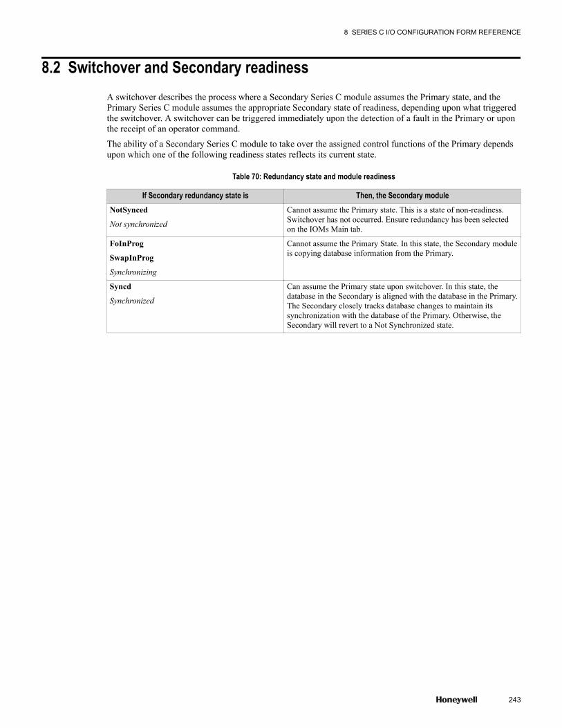
8.2 Switchover and Secondary readinessA switchover describes the process where a Secondary Series C module assumes the Primary state, and thePrimary Series C module assumes the appropriate Secondary state of readiness, depending upon what triggeredthe switchover. A switchover can be triggered immediately upon the detection of a fault in the Primary or uponthe receipt of an operator command.
The ability of a Secondary Series C module to take over the assigned control functions of the Primary dependsupon which one of the following readiness states reflects its current state.
Table 70: Redundancy state and module readiness
If Secondary redundancy state is Then, the Secondary moduleNotSynced
Not synchronized
Cannot assume the Primary state. This is a state of non-readiness.Switchover has not occurred. Ensure redundancy has been selectedon the IOMs Main tab.
FoInProg
SwapInProg
Synchronizing
Cannot assume the Primary State. In this state, the Secondary moduleis copying database information from the Primary.
Syncd
Synchronized
Can assume the Primary state upon switchover. In this state, thedatabase in the Secondary is aligned with the database in the Primary.The Secondary closely tracks database changes to maintain itssynchronization with the database of the Primary. Otherwise, theSecondary will revert to a Not Synchronized state.
8 SERIES C I/O CONFIGURATION FORM REFERENCE
243

8.3 Failure conditions and switchover
AttentionWhen any failure that results in a switchover occurs in a Secondary module, the Secondary module losessynchronization.
In addition to the failure conditions, this event is reported as diagnostic notification:
• Loss of view of redundant partner on network.• Loss of private path connection from Primary to Secondary (lonely event).
The following table identifies failure conditions that result in a switchover and those that do not.
Table 71: Failure conditions that result in switchover
Failure conditions that result in a switchover Failure conditions that do notresult in a switchover
Power to Primary module fails. One or all cables fail.
An IOLINK to the Primary Series C module islost.
One or all network conditioners fail.
Primary Series C module fails. All supplied power to the link fails.
8 SERIES C I/O CONFIGURATION FORM REFERENCE
244 www.honeywell.com
8.4 Configuration tools to create control strategiesThe Experion Control Builder application creates control strategies that use Series C I/O data. In developing avalid control strategy, the following activities are required to be supported by Control Builder:
• create hardware blocks,• associate blocks,• assign modules,• assign devices, and• load components.
Regardless of what tool is used to configure Series C I/O, the IOM must be present during configuration load. Ifthe IOM is not present load errors will occur and a subsequent reload or checkpoint restore will be required.
Refer to the Control Building Guide to create control strategies.
8 SERIES C I/O CONFIGURATION FORM REFERENCE
245
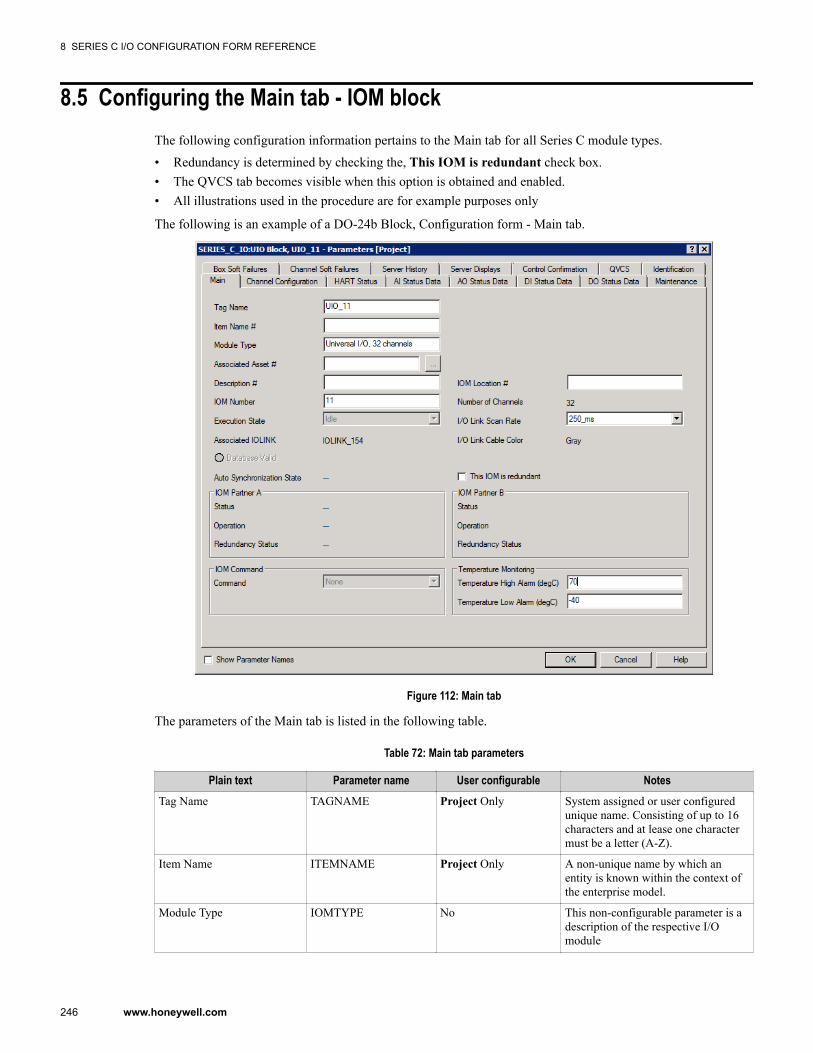
8.5 Configuring the Main tab - IOM blockThe following configuration information pertains to the Main tab for all Series C module types.
• Redundancy is determined by checking the, This IOM is redundant check box.• The QVCS tab becomes visible when this option is obtained and enabled.• All illustrations used in the procedure are for example purposes only
The following is an example of a DO-24b Block, Configuration form - Main tab.
Figure 112: Main tab
The parameters of the Main tab is listed in the following table.
Table 72: Main tab parameters
Plain text Parameter name User configurable NotesTag Name TAGNAME Project Only System assigned or user configured
unique name. Consisting of up to 16characters and at lease one charactermust be a letter (A-Z).
Item Name ITEMNAME Project Only A non-unique name by which anentity is known within the context ofthe enterprise model.
Module Type IOMTYPE No This non-configurable parameter is adescription of the respective I/Omodule
8 SERIES C I/O CONFIGURATION FORM REFERENCE
246 www.honeywell.com
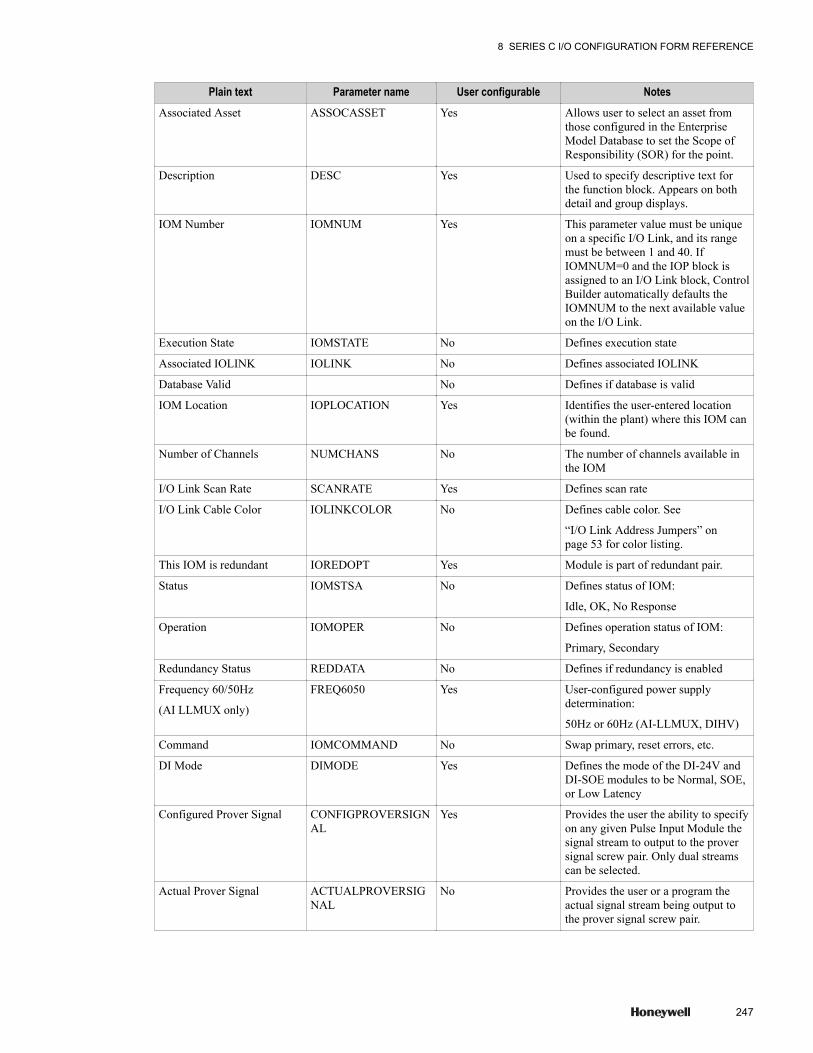
Plain text Parameter name User configurable NotesAssociated Asset ASSOCASSET Yes Allows user to select an asset from
those configured in the EnterpriseModel Database to set the Scope ofResponsibility (SOR) for the point.
Description DESC Yes Used to specify descriptive text forthe function block. Appears on bothdetail and group displays.
IOM Number IOMNUM Yes This parameter value must be uniqueon a specific I/O Link, and its rangemust be between 1 and 40. IfIOMNUM=0 and the IOP block isassigned to an I/O Link block, ControlBuilder automatically defaults theIOMNUM to the next available valueon the I/O Link.
Execution State IOMSTATE No Defines execution state
Associated IOLINK IOLINK No Defines associated IOLINK
Database Valid No Defines if database is valid
IOM Location IOPLOCATION Yes Identifies the user-entered location(within the plant) where this IOM canbe found.
Number of Channels NUMCHANS No The number of channels available inthe IOM
I/O Link Scan Rate SCANRATE Yes Defines scan rate
I/O Link Cable Color IOLINKCOLOR No Defines cable color. See
“I/O Link Address Jumpers” onpage 53 for color listing.
This IOM is redundant IOREDOPT Yes Module is part of redundant pair.
Status IOMSTSA No Defines status of IOM:
Idle, OK, No Response
Operation IOMOPER No Defines operation status of IOM:
Primary, Secondary
Redundancy Status REDDATA No Defines if redundancy is enabled
Frequency 60/50Hz
(AI LLMUX only)
FREQ6050 Yes User-configured power supplydetermination:
50Hz or 60Hz (AI-LLMUX, DIHV)
Command IOMCOMMAND No Swap primary, reset errors, etc.
DI Mode DIMODE Yes Defines the mode of the DI-24V andDI-SOE modules to be Normal, SOE,or Low Latency
Configured Prover Signal CONFIGPROVERSIGNAL
Yes Provides the user the ability to specifyon any given Pulse Input Module thesignal stream to output to the proversignal screw pair. Only dual streamscan be selected.
Actual Prover Signal ACTUALPROVERSIGNAL
No Provides the user or a program theactual signal stream being output tothe prover signal screw pair.
8 SERIES C I/O CONFIGURATION FORM REFERENCE
247
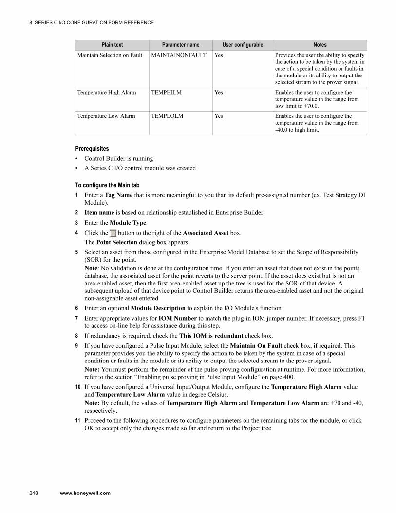
Plain text Parameter name User configurable NotesMaintain Selection on Fault MAINTAINONFAULT Yes Provides the user the ability to specify
the action to be taken by the system incase of a special condition or faults inthe module or its ability to output theselected stream to the prover signal.
Temperature High Alarm TEMPHILM Yes Enables the user to configure thetemperature value in the range fromlow limit to +70.0.
Temperature Low Alarm TEMPLOLM Yes Enables the user to configure thetemperature value in the range from-40.0 to high limit.
Prerequisites• Control Builder is running• A Series C I/O control module was created
To configure the Main tab1 Enter a Tag Name that is more meaningful to you than its default pre-assigned number (ex. Test Strategy DI
Module).2 Item name is based on relationship established in Enterprise Builder3 Enter the Module Type.4 Click the button to the right of the Associated Asset box.
The Point Selection dialog box appears.5 Select an asset from those configured in the Enterprise Model Database to set the Scope of Responsibility
(SOR) for the point.Note: No validation is done at the configuration time. If you enter an asset that does not exist in the pointsdatabase, the associated asset for the point reverts to the server point. If the asset does exist but is not anarea-enabled asset, then the first area-enabled asset up the tree is used for the SOR of that device. Asubsequent upload of that device point to Control Builder returns the area-enabled asset and not the originalnon-assignable asset entered.
6 Enter an optional Module Description to explain the I/O Module's function7 Enter appropriate values for IOM Number to match the plug-in IOM jumper number. If necessary, press F1
to access on-line help for assistance during this step.8 If redundancy is required, check the This IOM is redundant check box.9 If you have configured a Pulse Input Module, select the Maintain On Fault check box, if required. This
parameter provides you the ability to specify the action to be taken by the system in case of a specialcondition or faults in the module or its ability to output the selected stream to the prover signal.Note: You must perform the remainder of the pulse proving configuration at runtime. For more information,refer to the section “Enabling pulse proving in Pulse Input Module” on page 400.
10 If you have configured a Universal Input/Output Module, configure the Temperature High Alarm valueand Temperature Low Alarm value in degree Celsius.Note: By default, the values of Temperature High Alarm and Temperature Low Alarm are +70 and -40,respectively.
11 Proceed to the following procedures to configure parameters on the remaining tabs for the module, or clickOK to accept only the changes made so far and return to the Project tree.
8 SERIES C I/O CONFIGURATION FORM REFERENCE
248 www.honeywell.com

8.6 Configuring Server History tab - IOM blockThe following configuration information pertains to the Server History tab for the following modules:
• AI-HART• AI-HL• AI-LLMUX• AI-LLAI• AO• AO-HART• DI-HV• DI-24• DI-SOE• DO-24B• SP• SVP• PIM• UIOAll illustrations used in the procedure are for example purposes only
The following is an example of a DO-24B Block, Configuration form - Server History tab.
Figure 113: Server History tab
The parameters of the Server History tab are listed in the following table.
8 SERIES C I/O CONFIGURATION FORM REFERENCE
249
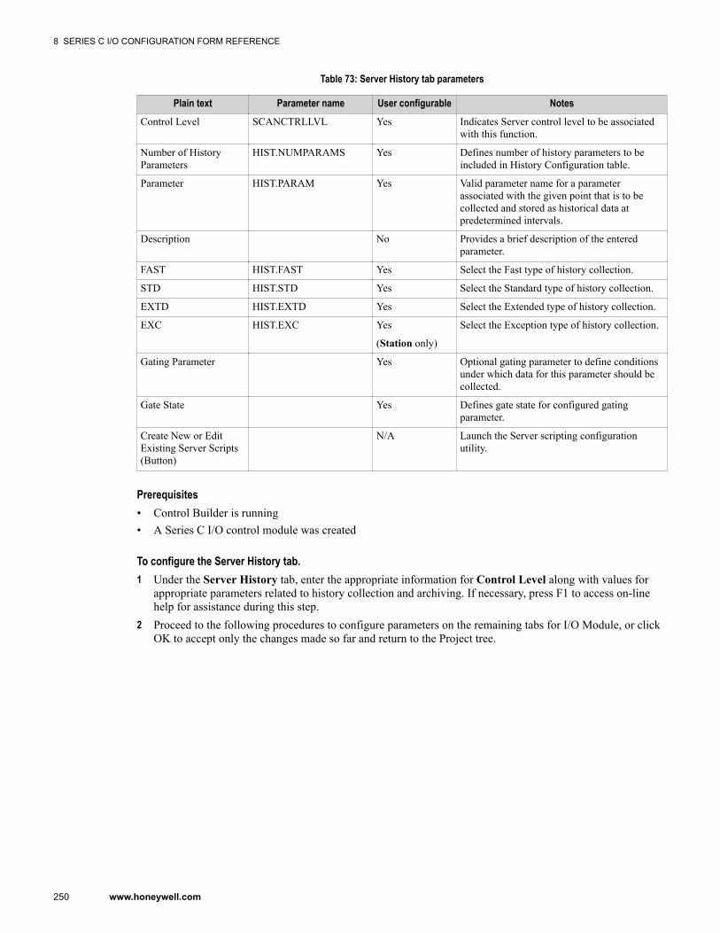
Table 73: Server History tab parameters
Plain text Parameter name User configurable NotesControl Level SCANCTRLLVL Yes Indicates Server control level to be associated
with this function.
Number of HistoryParameters
HIST.NUMPARAMS Yes Defines number of history parameters to beincluded in History Configuration table.
Parameter HIST.PARAM Yes Valid parameter name for a parameterassociated with the given point that is to becollected and stored as historical data atpredetermined intervals.
Description No Provides a brief description of the enteredparameter.
FAST HIST.FAST Yes Select the Fast type of history collection.
STD HIST.STD Yes Select the Standard type of history collection.
EXTD HIST.EXTD Yes Select the Extended type of history collection.
EXC HIST.EXC Yes
(Station only)
Select the Exception type of history collection.
Gating Parameter Yes Optional gating parameter to define conditionsunder which data for this parameter should becollected.
Gate State Yes Defines gate state for configured gatingparameter.
Create New or EditExisting Server Scripts(Button)
N/A Launch the Server scripting configurationutility.
Prerequisites• Control Builder is running• A Series C I/O control module was created
To configure the Server History tab.1 Under the Server History tab, enter the appropriate information for Control Level along with values for
appropriate parameters related to history collection and archiving. If necessary, press F1 to access on-linehelp for assistance during this step.
2 Proceed to the following procedures to configure parameters on the remaining tabs for I/O Module, or clickOK to accept only the changes made so far and return to the Project tree.
8 SERIES C I/O CONFIGURATION FORM REFERENCE
250 www.honeywell.com

8.7 Configuring Server Displays tab - IOM blockThe following configuration information pertains to the Server Displays Failure tab for the following modules:
• AI-HART• AI-HL• AI-LLMUX• AI-LLAI• AO• AO-HART• DI-HV• DI-24• DI-SOE• DO-24B• SP• SVP• PIM• UIOAll illustrations used in the procedure are for example purposes only
The following is an example of a DO-24B Block, Configuration form - Server Displays tab.
Figure 114: Server Display tab
The parameters of the Server Displays tab are listed in the following table.
8 SERIES C I/O CONFIGURATION FORM REFERENCE
251
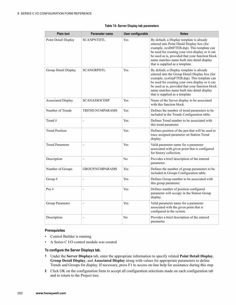
Table 74: Server Display tab parameters
Plain text Parameter name User configurable NotesPoint Detail Display SCANPNTDTL Yes By default, a Display template is already
entered into Point Detail Display box (forexample, sysDtlFTEB.dsp). This template canbe used for creating your own display or it canbe used as is, provided that your function blockname matches name built into detail displaythat is supplied as a template.
Group Detail Display SCANGRPDTL Yes By default, a Display template is alreadyentered into the Group Detail Display box (forexample, sysGrpFTEB.dsp). This template canbe used for creating your own display or it canbe used as is, provided that your function blockname matches name built into detail displaythat is supplied as a template
Associated Display SCANASSOCDSP Yes Name of the Server display to be associatedwith this function block.
Number of Trends TREND.NUMPARAMS Yes Defines the number of trend parameters to beincluded in the Trends Configuration table.
Trend # - Yes Defines Trend number to be associated withthis trend parameter
Trend Position Yes Defines position of the pen that will be used totrace assigned parameter on Station Trenddisplay.
Trend Parameter - Yes Valid parameter name for a parameterassociated with given point that is configuredfor history collection.
Description - No Provides a brief description of the enteredparameter.
Number of Groups GROUP.NUMPARAMS Yes Defines the number of group parameters to beincluded in Groups Configuration table.
Group # - Yes Defines Group number to be associated withthis group parameter.
Pos # - Yes Defines number of position configuredparameter will occupy in the Station Groupdisplay.
Group Parameter - Yes Valid parameter name for a parameterassociated with the given point that isconfigured in the system.
Description - No Provides a brief description of the enteredparameter.
Prerequisites• Control Builder is running• A Series C I/O control module was created
To configure the Server Displays tab.1 Under the Server Displays tab, enter the appropriate information to specify related Point Detail Display,
Group Detail Display, and Associated Display along with values for appropriate parameters to defineTrends and Groups for display. If necessary, press F1 to access on-line help for assistance during this step
2 Click OK on the configuration form to accept all configuration selections made on each configuration taband to return to the Project tree.
8 SERIES C I/O CONFIGURATION FORM REFERENCE
252 www.honeywell.com

8.8 Configuring Control Confirmation tab - IOM blockThe Control Confirmation tab is common to all configuration forms for tagged blocks in Control Builder. If youhave an optional Electronic Signature license, you can configure electronic signature information for the taggedblock through this tab on the block's configuration form in Control Builder.
The Electronic Signature function aligns with the identical Electronic Signatures function that is initiatedthrough Quick Builder and Station for Server points.
When this block is loaded to a controller,
• its control confirmation configuration (electronic signatures) is also loaded to the Server• you can view the control confirmation configuration for this tagged object in Station and also make changes
to it.
– If you make changes through Station, you must initiate an Upload or Upload with Contents functionthrough the Controller menu in Control Builder for the object in the Monitoring tab to synchronizechanges in the Engineering Repository Database (ERDB).
The following configuration information pertains to the Control Confirmation tab for all Series CI/O modules.
Control Confirmation is enabled by checking the Control Confirmation check box.
All illustrations used in the procedure are for example purposes only
The following is an example of a DO-24B Block, Configuration form - Control Confirmation tab.
Figure 115: Control Confirmation tab
8 SERIES C I/O CONFIGURATION FORM REFERENCE
253
Prerequisites• Control Builder is running• A Series C I/O control module was created
To configure the Control Confirmation tab.1 Under the Control Confirmation tab, check or clear the Control Confirmation check box. If necessary,
press F1 to access on-line help for assistance during this step.2 If the Control Confirmation check box is checked, the Electronic Signature Type drop-down list is
enabled, with the options to select:• NONE• SINGLE• DOUBLE
3 Proceed to the following procedures to configure parameters on the remaining tabs for I/O Module, or clickOK to accept only the changes made so far and return to the Project tree.
8 SERIES C I/O CONFIGURATION FORM REFERENCE
254 www.honeywell.com
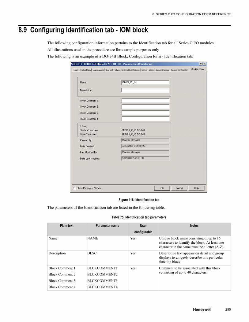
8.9 Configuring Identification tab - IOM blockThe following configuration information pertains to the Identification tab for all Series C I/O modules.
All illustrations used in the procedure are for example purposes only
The following is an example of a DO-24B Block, Configuration form - Identification tab.
Figure 116: Identification tab
The parameters of the Identification tab are listed in the following table.
Table 75: Identification tab parameters
Plain text Parameter name Userconfigurable
Notes
Name NAME Yes Unique block name consisting of up to 16characters to identify the block. At least onecharacter in the name must be a letter (A-Z).
Description DESC Yes Descriptive text appears on detail and groupdisplays to uniquely describe this particularfunction block
Block Comment 1
Block Comment 2
Block Comment 3
Block Comment 4
BLCKCOMMENT1
BLCKCOMMENT2
BLCKCOMMENT3
BLCKCOMMENT4
Yes Comment to be associated with this blockconsisting of up to 40 characters.
8 SERIES C I/O CONFIGURATION FORM REFERENCE
255

Plain text Parameter name Userconfigurable
Notes
Library - No Identifies Control Builder Library that is sourceof template.
System Template - No Identifies System Template that is source forthis block.
Base Template - No Identifies Base Template that is used for thisblock.
Created By CREATEDBY No Identifies user who created block, if operatorsecurity is implemented. Otherwise, may justshow Default login.
Date Created DATECREATED No Shows date and time template was created. Ifthis block is in Version Control System, showsdate and time initial version of template wascreated.
Last Modified By MODIFIEDBY No Identifies user who made last modifications toblock, if operator security is implemented.Otherwise, may just show default login. If thisblock is in Version Control System,modifications apply to last version of block.
Date Last Modified VERSIONDATE No Shows date and time last modification wasmade to block's configuration. If this block is inVersion Control System, modification date andtime applies to last version of block.
Prerequisites• Control Builder is running• A Series C I/O control module was created
8 SERIES C I/O CONFIGURATION FORM REFERENCE
256 www.honeywell.com

8.10 Configuring QVCS tab - IOM blockQualification and Version Control System (QVCS) provides version management for all tagged objects and acustomer defined lifecycle management.
The following configuration information pertains to the QVCS tab for the following modules:
• AI-HART• AI-HL• AI-LLMUX• AI-LLAI• AO• AO-HART• DI-HV• DI-24• DI-SOE• DO-24B• SP• SVP• PIM• UIO
Note: No user-defined configuration setting on the QVCS tab.
All illustrations used in the procedure are for example purposes only
The following is an example of a DI-24 Block, Configuration form - QVCS tab.
8 SERIES C I/O CONFIGURATION FORM REFERENCE
257
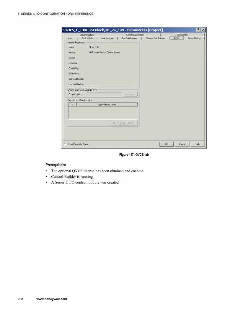
Figure 117: QVCS tab
Prerequisites• The optional QVCS license has been obtained and enabled• Control Builder is running• A Series C I/O control module was created
8 SERIES C I/O CONFIGURATION FORM REFERENCE
258 www.honeywell.com
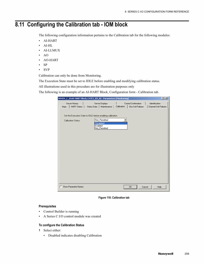
8.11 Configuring the Calibration tab - IOM blockThe following configuration information pertains to the Calibration tab for the following modules:
• AI-HART• AI-HL• AI-LLMUX• AO• AO-HART• SP• SVP
Calibration can only be done from Monitoring.
The Execution State must be set to IDLE before enabling and modifying calibration status.
All illustrations used in this procedure are for illustration purposes only
The following is an example of an AI-HART Block, Configuration form - Calibration tab.
Figure 118: Calibration tab
Prerequisites• Control Builder is running• A Series C I/O control module was created
To configure the Calibration Status1 Select either:
• Disabled indicates disabling Calibration
8 SERIES C I/O CONFIGURATION FORM REFERENCE
259

• Enabled indicates enabling Calibration
Not Permitted indicates the Execution State of the IOM is still in the RUN state, which does not allow youto select Disable or Enable. Changing the Execution State of the IOM to IDLE allow you to modify theCalibration Status.
2 Proceed to the following procedures to configure parameters on the remaining tabs for the module, or clickOK to accept only the changes made so far and return to the Project tree.
8 SERIES C I/O CONFIGURATION FORM REFERENCE
260 www.honeywell.com
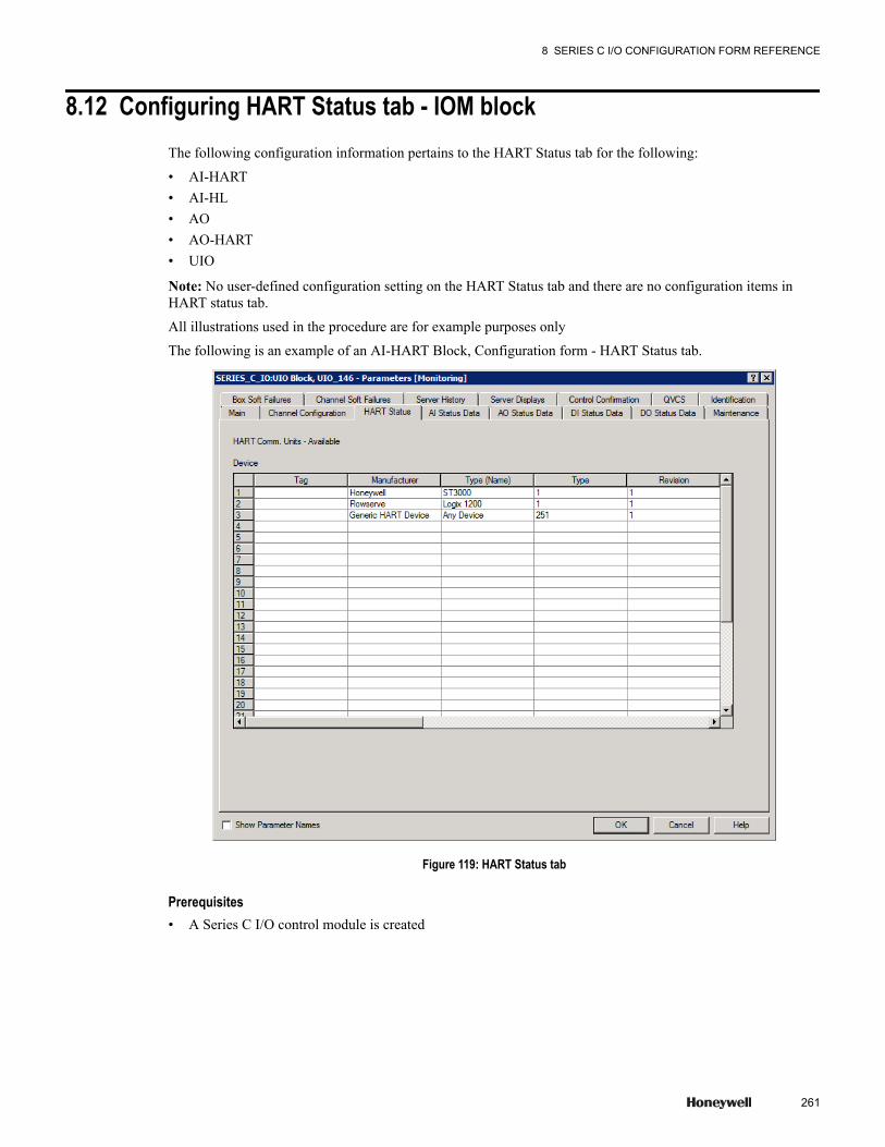
8.12 Configuring HART Status tab - IOM blockThe following configuration information pertains to the HART Status tab for the following:
• AI-HART• AI-HL• AO• AO-HART• UIO
Note: No user-defined configuration setting on the HART Status tab and there are no configuration items inHART status tab.
All illustrations used in the procedure are for example purposes only
The following is an example of an AI-HART Block, Configuration form - HART Status tab.
Figure 119: HART Status tab
Prerequisites• A Series C I/O control module is created
8 SERIES C I/O CONFIGURATION FORM REFERENCE
261
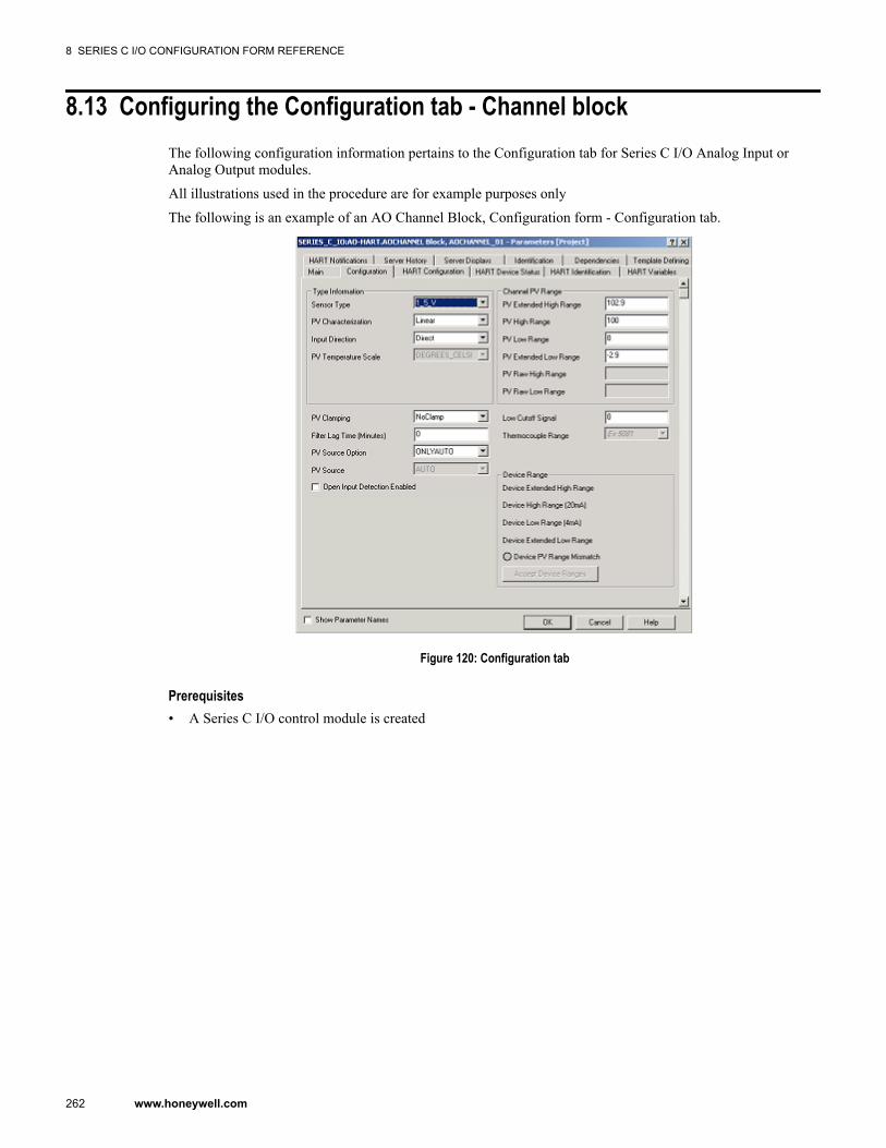
8.13 Configuring the Configuration tab - Channel blockThe following configuration information pertains to the Configuration tab for Series C I/O Analog Input orAnalog Output modules.
All illustrations used in the procedure are for example purposes only
The following is an example of an AO Channel Block, Configuration form - Configuration tab.
Figure 120: Configuration tab
Prerequisites• A Series C I/O control module is created
8 SERIES C I/O CONFIGURATION FORM REFERENCE
262 www.honeywell.com
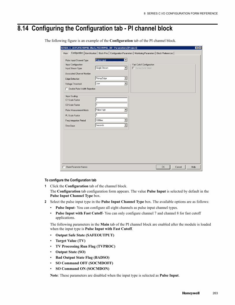
8.14 Configuring the Configuration tab - PI channel blockThe following figure is an example of the Configuration tab of the PI channel block.
To configure the Configuration tab1 Click the Configuration tab of the channel block.
The Configuration tab configuration form appears. The value Pulse Input is selected by default in thePulse Input Channel Type box.
2 Select the pulse input type in the Pulse Input Channel Type box. The available options are as follows:• Pulse Input- You can configure all eight channels as pulse input channel types.• Pulse Input with Fast Cutoff- You can only configure channel 7 and channel 8 for fast cutoff
applications.
The following parameters in the Main tab of the PI channel block are enabled after the module is loadedwhen the input type is Pulse Input with Fast Cutoff.• Output Safe State (SAFEOUTPUT)• Target Value (TV)• TV Processing Run Flag (TVPROC)• Output State (SO)• Bad Output State Flag (BADSO)• SO Command OFF (SOCMDOFF)• SO Command ON (SOCMDON)
Note: These parameters are disabled when the input type is selected as Pulse Input.
8 SERIES C I/O CONFIGURATION FORM REFERENCE
263

3 Select the input stream type in the Input Stream Type box. You can select one of the following:• Single Stream - You can select this option for all channels.• Dual Stream - You can select this option only for odd-numbered channels.
When you configure a channel for Dual Stream, its associated even-numbered channel number appears inthe Associated Channel Number box.
For example, if you have configured channel 1 for dual stream, the channel number 2 appears in theAssociated Channel number box.
Attention• When you select the pulse input channel type as Pulse Input with Fast Cutoff for Fast Cutoff channels
(channel 7 and channel 8), Single Stream is selected by default and is non-editable.• When you select the pulse input channel type as Pulse Input, you can configure Dual Stream on the Fast
Cutoff channels (channel 7 and channel 8).• Dual Stream option is not applicable for Fast Cutoff channels (channel 7 and channel 8) when the Pulse
Input Channel type as Pulse Input with Fast Cutoff. In this scenario, the option Single Stream is selectedby default and is non-editable.
• If you select the Input Stream Type as Dual Stream for odd-numbered channels, then you cannot configuretheir associated even numbered channels. For example, if you have configured channel 1 as Dual Stream, youcannot configure channel 2. In addition, the associated channel does not appear in the tree view if you haveconfigured the channel for Dual Stream.
• If the CM already contains the even-numbered channel and you try to configure its associated odd-numberedchannel as Dual Stream, an error message appears. You need to delete the associated even-numbered channelfrom the CM. For example, if a CM contains channel 3 and channel 4, and you try to configure channel 3 asDual Stream, an error message appears. You need to delete channel 4 to configure channel 3 as Dual Stream.
• When a channel is configured for Dual Stream, the Status Data tab of the PIM does not display any values forthe associated channel in the Monitoring view. For example, if you have configured channel 3 for DualStream, the channel 4 row in the Status Data tab does not display any values.
4 Select the Enable Pulse Width Rejection check box if you want the pulse widths less than a specifiedduration to be excluded from counting.Note: Refer to the Series C Spec and Tech data for the specific duration.
5 Refer to the Control Builder Parameter Reference document for more information on configuring otherparameters.
6 Click OK.
8 SERIES C I/O CONFIGURATION FORM REFERENCE
264 www.honeywell.com
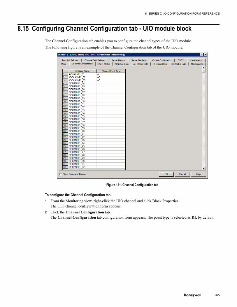
8.15 Configuring Channel Configuration tab - UIO module blockThe Channel Configuration tab enables you to configure the channel types of the UIO module.
The following figure is an example of the Channel Configuration tab of the UIO module.
Figure 121: Channel Configuration tab
To configure the Channel Configuration tab1 From the Monitoring view, right-click the UIO channel and click Block Properties.
The UIO channel configuration form appears.2 Click the Channel Configuration tab.
The Channel Configuration tab configuration form appears. The point type is selected as DI, by default.
8 SERIES C I/O CONFIGURATION FORM REFERENCE
265
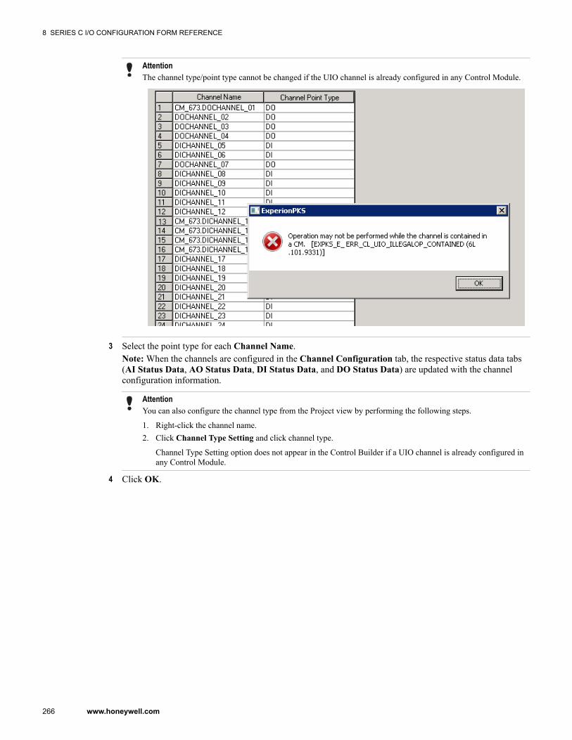
AttentionThe channel type/point type cannot be changed if the UIO channel is already configured in any Control Module.
3 Select the point type for each Channel Name.Note: When the channels are configured in the Channel Configuration tab, the respective status data tabs(AI Status Data, AO Status Data, DI Status Data, and DO Status Data) are updated with the channelconfiguration information.
AttentionYou can also configure the channel type from the Project view by performing the following steps.
1. Right-click the channel name.2. Click Channel Type Setting and click channel type.
Channel Type Setting option does not appear in the Control Builder if a UIO channel is already configured inany Control Module.
4 Click OK.
8 SERIES C I/O CONFIGURATION FORM REFERENCE
266 www.honeywell.com
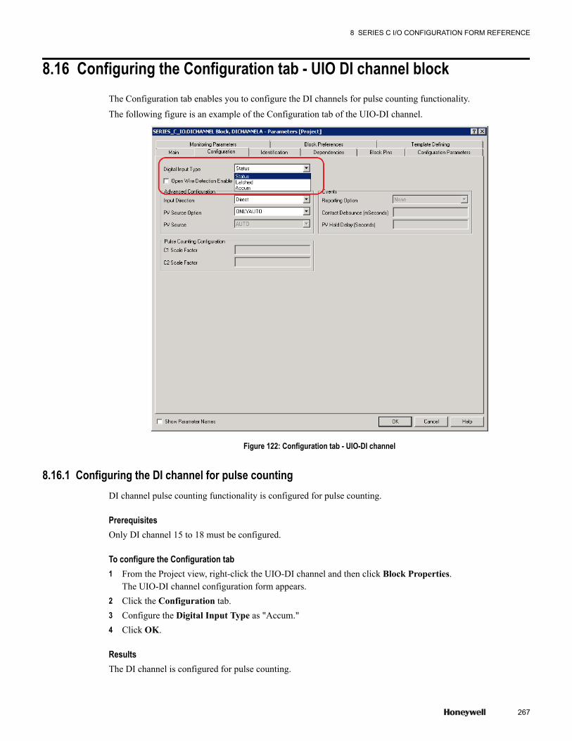
8.16 Configuring the Configuration tab - UIO DI channel blockThe Configuration tab enables you to configure the DI channels for pulse counting functionality.
The following figure is an example of the Configuration tab of the UIO-DI channel.
Figure 122: Configuration tab - UIO-DI channel
8.16.1 Configuring the DI channel for pulse countingDI channel pulse counting functionality is configured for pulse counting.
PrerequisitesOnly DI channel 15 to 18 must be configured.
To configure the Configuration tab1 From the Project view, right-click the UIO-DI channel and then click Block Properties.
The UIO-DI channel configuration form appears.2 Click the Configuration tab.3 Configure the Digital Input Type as "Accum."4 Click OK.
ResultsThe DI channel is configured for pulse counting.
8 SERIES C I/O CONFIGURATION FORM REFERENCE
267
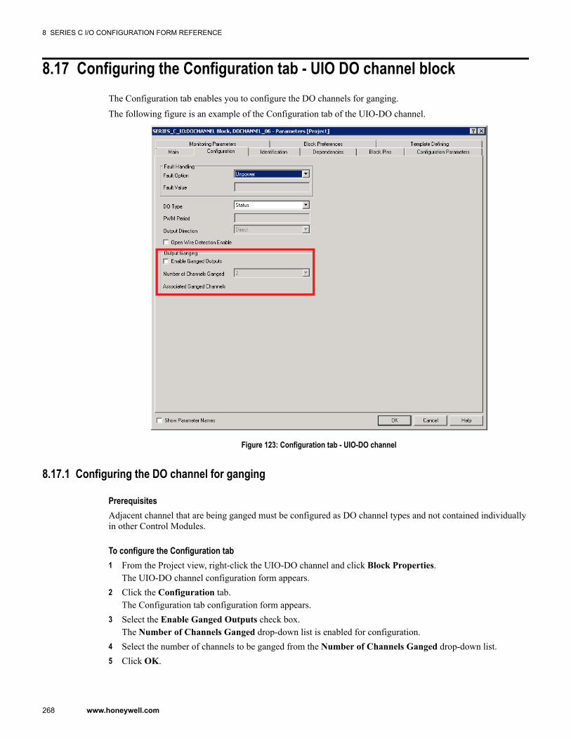
8.17 Configuring the Configuration tab - UIO DO channel blockThe Configuration tab enables you to configure the DO channels for ganging.
The following figure is an example of the Configuration tab of the UIO-DO channel.
Figure 123: Configuration tab - UIO-DO channel
8.17.1 Configuring the DO channel for ganging
PrerequisitesAdjacent channel that are being ganged must be configured as DO channel types and not contained individuallyin other Control Modules.
To configure the Configuration tab1 From the Project view, right-click the UIO-DO channel and click Block Properties.
The UIO-DO channel configuration form appears.2 Click the Configuration tab.
The Configuration tab configuration form appears.3 Select the Enable Ganged Outputs check box.
The Number of Channels Ganged drop-down list is enabled for configuration.4 Select the number of channels to be ganged from the Number of Channels Ganged drop-down list.5 Click OK.
8 SERIES C I/O CONFIGURATION FORM REFERENCE
268 www.honeywell.com

ResultsThe DO channel is configured for ganging.
8 SERIES C I/O CONFIGURATION FORM REFERENCE
269
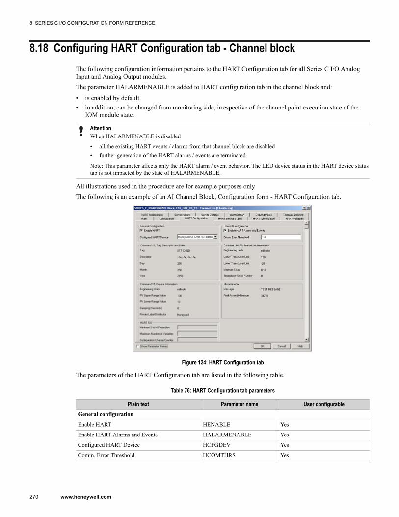
8.18 Configuring HART Configuration tab - Channel blockThe following configuration information pertains to the HART Configuration tab for all Series C I/O AnalogInput and Analog Output modules.
The parameter HALARMENABLE is added to HART configuration tab in the channel block and:
• is enabled by default• in addition, can be changed from monitoring side, irrespective of the channel point execution state of the
IOM module state.
AttentionWhen HALARMENABLE is disabled
• all the existing HART events / alarms from that channel block are disabled• further generation of the HART alarms / events are terminated.
Note: This parameter affects only the HART alarm / event behavior. The LED device status in the HART device statustab is not impacted by the state of HALARMENABLE.
All illustrations used in the procedure are for example purposes only
The following is an example of an AI Channel Block, Configuration form - HART Configuration tab.
Figure 124: HART Configuration tab
The parameters of the HART Configuration tab are listed in the following table.
Table 76: HART Configuration tab parameters
Plain text Parameter name User configurableGeneral configuration
Enable HART HENABLE Yes
Enable HART Alarms and Events HALARMENABLE Yes
Configured HART Device HCFGDEV Yes
Comm. Error Threshold HCOMTHRS Yes
8 SERIES C I/O CONFIGURATION FORM REFERENCE
270 www.honeywell.com
Plain text Parameter name User configurableCommand 13, tag descriptor and date
Tag HTAG No
Descriptor HDESC No
Day HDAY No
Month HMONTH No
Year HYEAR No
Command 14, tag descriptor and date
Engineering Units HTDEU No
Upper Transducer Limit HTDURL No
Lower Transducer Limit HTDLRL No
Minimum Span HTDMINSPAN No
Transducer Serial Number HTDSN No
Prerequisites• A Series C I/O control module is created
8 SERIES C I/O CONFIGURATION FORM REFERENCE
271
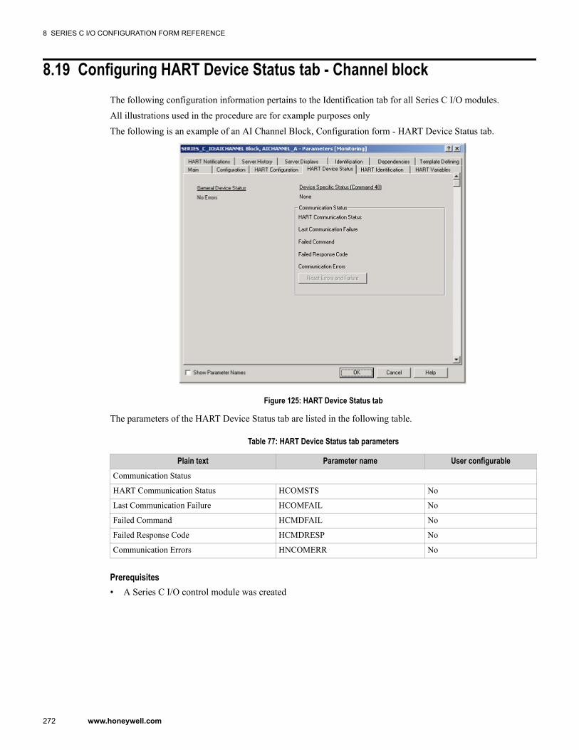
8.19 Configuring HART Device Status tab - Channel blockThe following configuration information pertains to the Identification tab for all Series C I/O modules.
All illustrations used in the procedure are for example purposes only
The following is an example of an AI Channel Block, Configuration form - HART Device Status tab.
Figure 125: HART Device Status tab
The parameters of the HART Device Status tab are listed in the following table.
Table 77: HART Device Status tab parameters
Plain text Parameter name User configurableCommunication Status
HART Communication Status HCOMSTS No
Last Communication Failure HCOMFAIL No
Failed Command HCMDFAIL No
Failed Response Code HCMDRESP No
Communication Errors HNCOMERR No
Prerequisites• A Series C I/O control module was created
8 SERIES C I/O CONFIGURATION FORM REFERENCE
272 www.honeywell.com
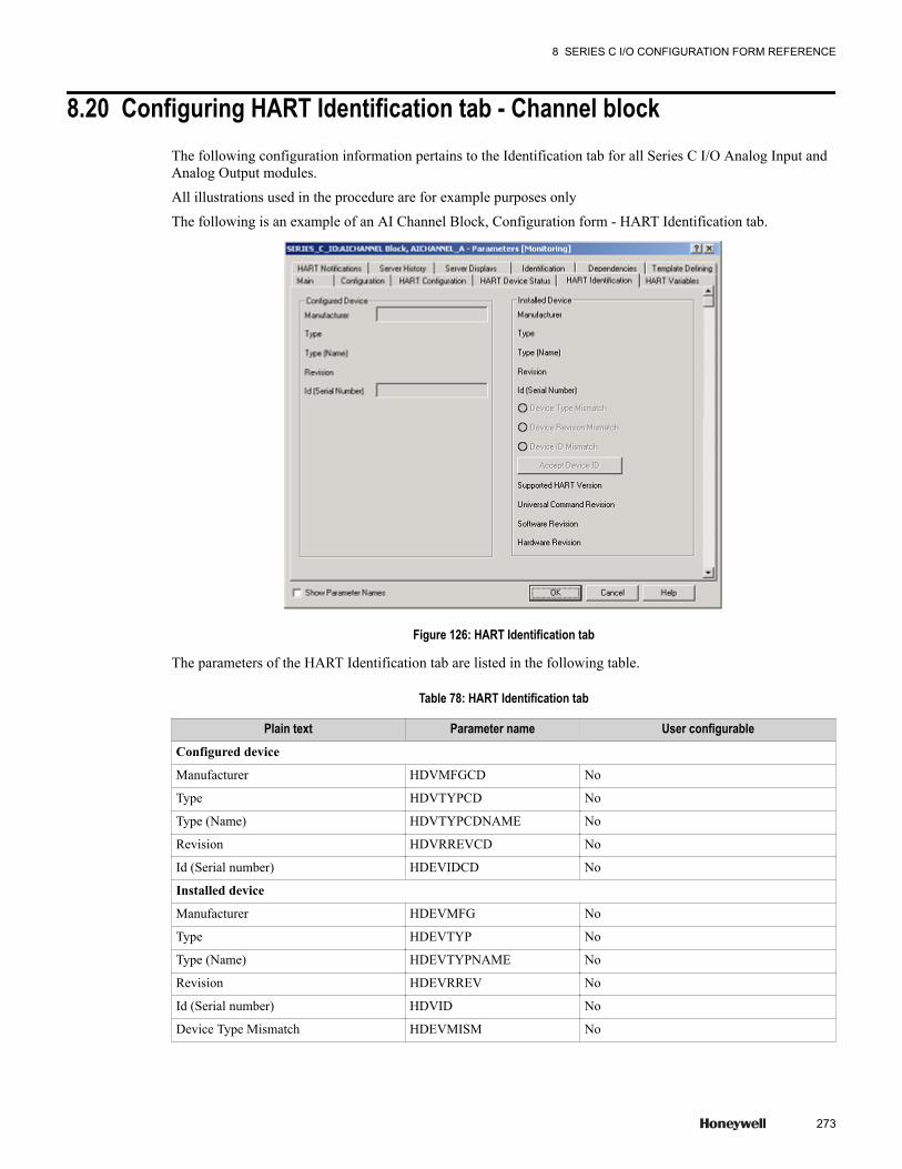
8.20 Configuring HART Identification tab - Channel blockThe following configuration information pertains to the Identification tab for all Series C I/O Analog Input andAnalog Output modules.
All illustrations used in the procedure are for example purposes only
The following is an example of an AI Channel Block, Configuration form - HART Identification tab.
Figure 126: HART Identification tab
The parameters of the HART Identification tab are listed in the following table.
Table 78: HART Identification tab
Plain text Parameter name User configurableConfigured device
Manufacturer HDVMFGCD No
Type HDVTYPCD No
Type (Name) HDVTYPCDNAME No
Revision HDVRREVCD No
Id (Serial number) HDEVIDCD No
Installed device
Manufacturer HDEVMFG No
Type HDEVTYP No
Type (Name) HDEVTYPNAME No
Revision HDEVRREV No
Id (Serial number) HDVID No
Device Type Mismatch HDEVMISM No
8 SERIES C I/O CONFIGURATION FORM REFERENCE
273

Plain text Parameter name User configurableDevice Revision Mismatch HREVMISM No
Device ID Mismatch HDEVIDFL No
Accept Device ID ACCEPTDEV No
Supported HART Version HARTVERSION No
Universal Command Revision HUCMREV No
Software Revision HSWREV No
Hardware Revision HHWREV No
Prerequisites• Control Builder is running• A Series C I/O control module was created
8 SERIES C I/O CONFIGURATION FORM REFERENCE
274 www.honeywell.com

8.21 Configuring HART Variables tab - Channel blockThe following configuration information pertains to the Identification tab for all Series C I/O Analog Input orAnalog Output modules.
All illustrations used in the procedure are for example purposes only
The following is an example of an AI Channel Block, Configuration form - HART Variables tab.
Figure 127: HART Variables tab
The parameters of the HART Variables tab are listed in the following table.
Table 79: HART Variables tab parameters
Plain text Parameter name User configurableScan HART Variables HSCANCFG Yes
Dynamic variables
Name HDYNNAME Yes
Variable Code HDYNDVC Yes
Descriptor HDYNDSC Yes
Value HDYNVAL Yes
Units HDYNEU Yes
Device variables
Name HSLOTNAME No
Variable Code HSLOTDVC Yes
Descriptor HSLOTDSC Yes
Value HSLOTVAL No
Units HSLOTEU No
8 SERIES C I/O CONFIGURATION FORM REFERENCE
275

Prerequisites• Control Builder is running• A Series C I/O control module was created
8 SERIES C I/O CONFIGURATION FORM REFERENCE
276 www.honeywell.com
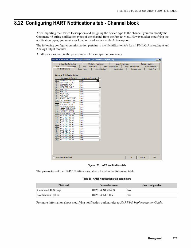
8.22 Configuring HART Notifications tab - Channel blockAfter importing the Device Description and assigning the device type to the channel, you can modify theCommand 48 string notification types of the channel from the Project view. However, after modifying thenotification types, you must user Load or Load values while Active option.
The following configuration information pertains to the Identification tab for all PM I/O Analog Input andAnalog Output modules.
All illustrations used in the procedure are for example purposes only
Figure 128: HART Notifications tab
The parameters of the HART Notifications tab are listed in the following table.
Table 80: HART Notifications tab parameters
Plain text Parameter name User configurableCommand 48 Strings HCMD48STRINGS No
Notification Option HCMD48NOTIFY Yes
For more information about modifying notification option, refer to HART I/O Implementation Guide.
8 SERIES C I/O CONFIGURATION FORM REFERENCE
277
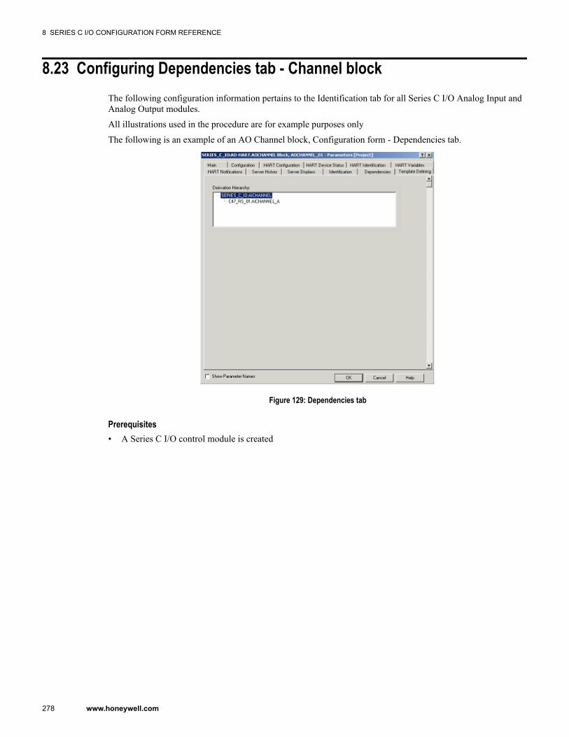
8.23 Configuring Dependencies tab - Channel blockThe following configuration information pertains to the Identification tab for all Series C I/O Analog Input andAnalog Output modules.
All illustrations used in the procedure are for example purposes only
The following is an example of an AO Channel block, Configuration form - Dependencies tab.
Figure 129: Dependencies tab
Prerequisites• A Series C I/O control module is created
8 SERIES C I/O CONFIGURATION FORM REFERENCE
278 www.honeywell.com
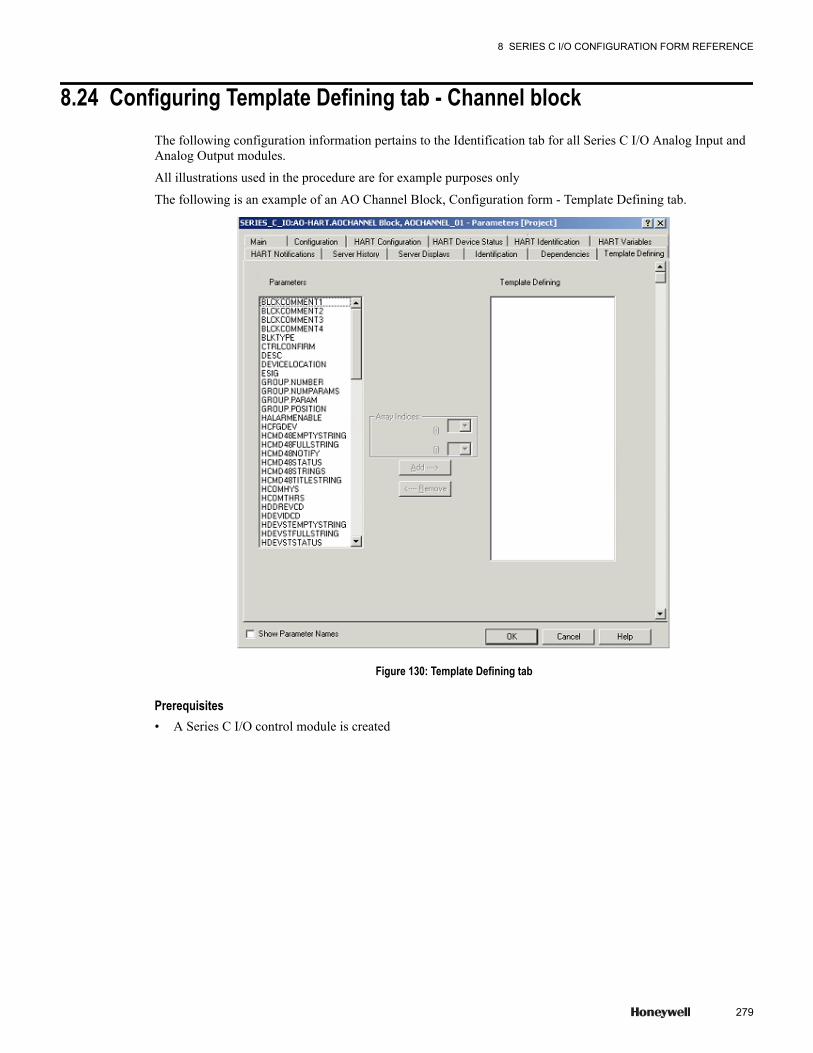
8.24 Configuring Template Defining tab - Channel blockThe following configuration information pertains to the Identification tab for all Series C I/O Analog Input andAnalog Output modules.
All illustrations used in the procedure are for example purposes only
The following is an example of an AO Channel Block, Configuration form - Template Defining tab.
Figure 130: Template Defining tab
Prerequisites• A Series C I/O control module is created
8 SERIES C I/O CONFIGURATION FORM REFERENCE
279

8 SERIES C I/O CONFIGURATION FORM REFERENCE
280 www.honeywell.com

9 Series C I/O Configuration
Related topics“Adding an IOM to Project” on page 282“Assigning an IOM to an IOLINK using the Assignment dialog box” on page 285“Adding an IOC block to a Control Module using the Project tab” on page 286“Adding an IOC block to a Control Module using the Library tab” on page 288“Assigning an IOC block to an IOM using the Function Block Assignment Dialog box” on page 290“Unassigning an IOC block from an IOM using the Function Block Assignment Dialog box” on page 295“Field Calibration of the AI and AO modules” on page 297“Defining Channel blocks” on page 298“Defining AI Channel Blocks” on page 307“Defining AO Channel Blocks” on page 314“Defining DI Channel Blocks” on page 317“Defining DO Channel Blocks” on page 320“Electronic Short-Circuit Protection (DO-24V only)” on page 325“Defining SP-AI Channel Blocks” on page 327“Defining SP-AO Channel Blocks” on page 331“Defining SP-DI Channel Blocks” on page 334“Defining SP-DO Channel Blocks” on page 336“Defining SP-SPEED Channel Blocks” on page 340“Defining SP-SPDVOTE Channel Blocks” on page 344“Defining SVP-AI Channel block” on page 346“Defining SVP-DI Channel Block” on page 352“Defining SVP-Regulatory Control Block” on page 354“Defining SVP-AO Channel Block” on page 362“Defining UIO Channel Blocks” on page 366
281
9.1 Adding an IOM to ProjectThe following IOMs are added to the Project tab using the either the File menu method or the Drag and Dropmethod:
• AI-HART - High Analog Input, HART Capable, 16 channels• AI-HL - High Level Input, 16 channels• AI-LLMUX - Low Level Analog Input Mux, 64 channels• AI-LLAI - Low Level Analog Input Mux, 16 channels• AO - Analog Output, 16 channels• AO-HART - Analog Output, HART Capable, 16 channels• DI-24 - Low Voltage (24VDC) Digital Input, 32 channels• DI-HV - High Voltage Digital Input, 32 channels• DI-SOE - Digital Input - Sequence of Events, 32 channels• DO-24B - Bussed Low Voltage Digital Output, 32 channels• SP - Speed Protection Module, 26 channels• SVP - Servo Valve Positioner Module, 8 channels• PIM - Pulse Input Module• UIO - Universal I/O, 32 channels
9.1.1 Using the File menu methodTo add an IOM to the Project tab by the File menu method:1 Click File > New > I/O Modules > Series C I/O.
Result: A list of the available Series C I/O block types is displayed.2 Select a block types from the drop down list. A Block Parameters configuration form is displayed
9 SERIES C I/O CONFIGURATION
282 www.honeywell.com
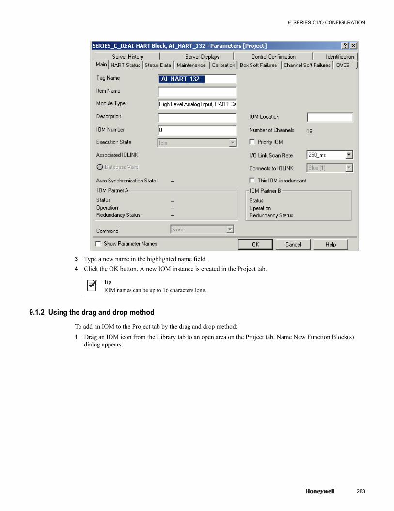
3 Type a new name in the highlighted name field.4 Click the OK button. A new IOM instance is created in the Project tab.
TipIOM names can be up to 16 characters long.
9.1.2 Using the drag and drop methodTo add an IOM to the Project tab by the drag and drop method:1 Drag an IOM icon from the Library tab to an open area on the Project tab. Name New Function Block(s)
dialog appears.
9 SERIES C I/O CONFIGURATION
283
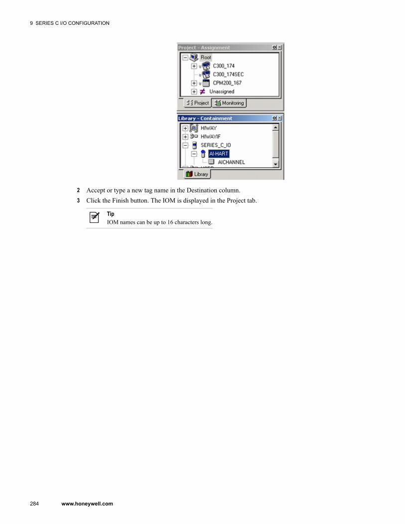
2 Accept or type a new tag name in the Destination column.3 Click the Finish button. The IOM is displayed in the Project tab.
TipIOM names can be up to 16 characters long.
9 SERIES C I/O CONFIGURATION
284 www.honeywell.com

9.2 Assigning an IOM to an IOLINK using the Assignment dialog boxTo assign an IOM to an IOLINK function block using the Assignment Dialog Box:1 Click the Assign button in the tool bar. The Execution Environment Assignment dialog appears.
2 Select an IOM module from the Available Modules area.3 Click the Assign button. The IOM is loaded to the Assign To: area4 Click the Close button to complete the assignment.
TipThe IOM is assigned to an IOLINK function block in the manner as CM blocks are assigned to a CEEC300function block.
You can also drag and drop the IOM from the Project tab to the IOLINK function block.
9 SERIES C I/O CONFIGURATION
285

9.3 Adding an IOC block to a Control Module using the Project tab
Attention• The SP and SVP IOC function blocks assignment to a Control Module (CM) succeeds only if the CM executes in
the CEE of C300 - 20mS CEE Controller.• In a PIM, if you have configured the odd-numbered channels for Dual Stream, you cannot add its associated
channels (even-numbered channels) into the CM. In addition, the associated channels do not appear in the treeview. For example, if you have configured channel 1 for Dual Stream, then channel 2 does not appear in the treeview.
When an IOM block is created in the Project tab, all of its associated IOC blocks are also created. Clicking the +(plus sign) for the IOM expands the tree down to the IOC level. You can drag and drop the IOC blocks intoControl Modules. The Series C I/O IOC block parameters can then be wired to other blocks in the same manneras existing Experion function blocks.
Prerequisites• Control Builder is running• Controller was created, CM was created, IOM was added and assigned to an IOLINK
To add an IOC to a Control Module1 Click the + (plus sign) to expand the IO in the Project tab.
You can also select the tag name in the following ways.
• Select Library mode and type the initial characters of a tag name.• Using the Search Option tool bar
– Type the initial few characters of a tag name in the Search Option tool bar. A list of all matching tagnames appears.
– Select the tag name and click
If the tag exists, the tree expands and the specified tag name is highlighted.
For more information on searching the tags, see Control Building User's Guide.2 Drag an IOC to into the Control Module. The cursor changes to denote an IOC is captured and available for
placement in to the CM control window.
9 SERIES C I/O CONFIGURATION
286 www.honeywell.com
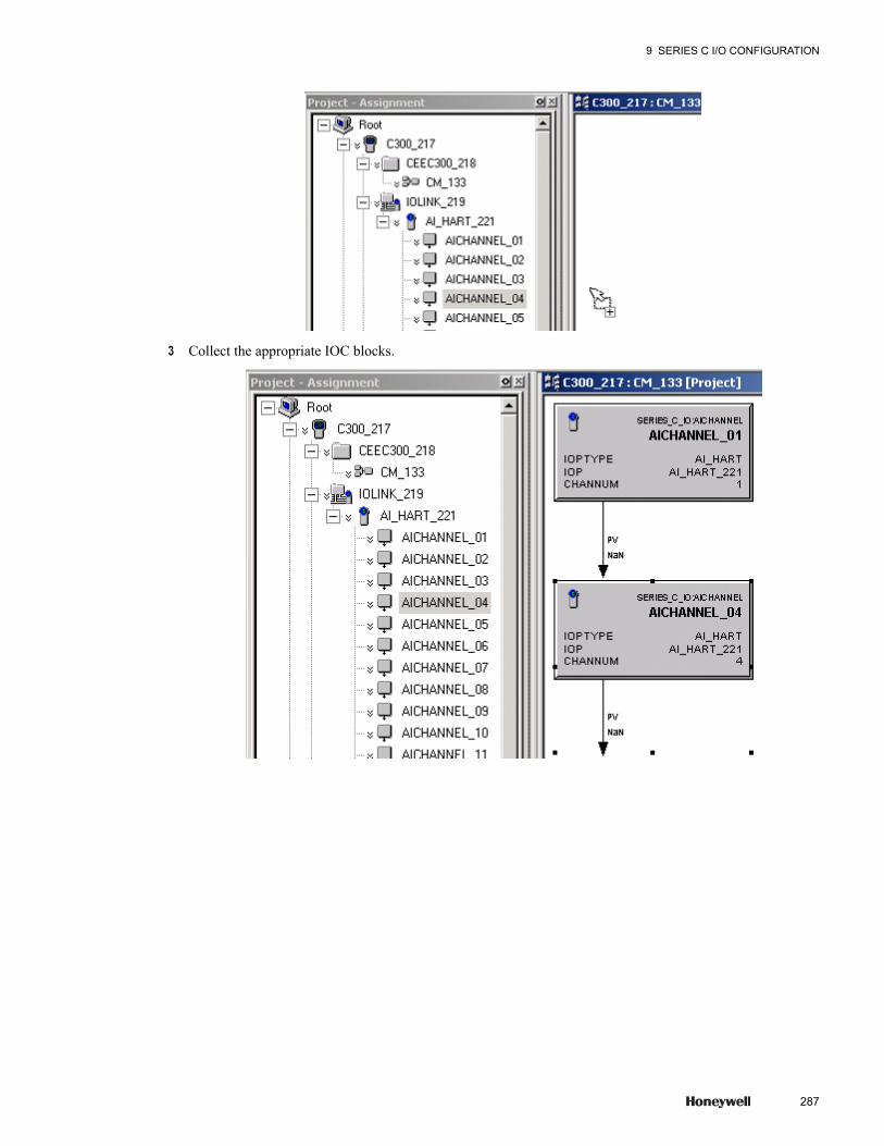
3 Collect the appropriate IOC blocks.
9 SERIES C I/O CONFIGURATION
287
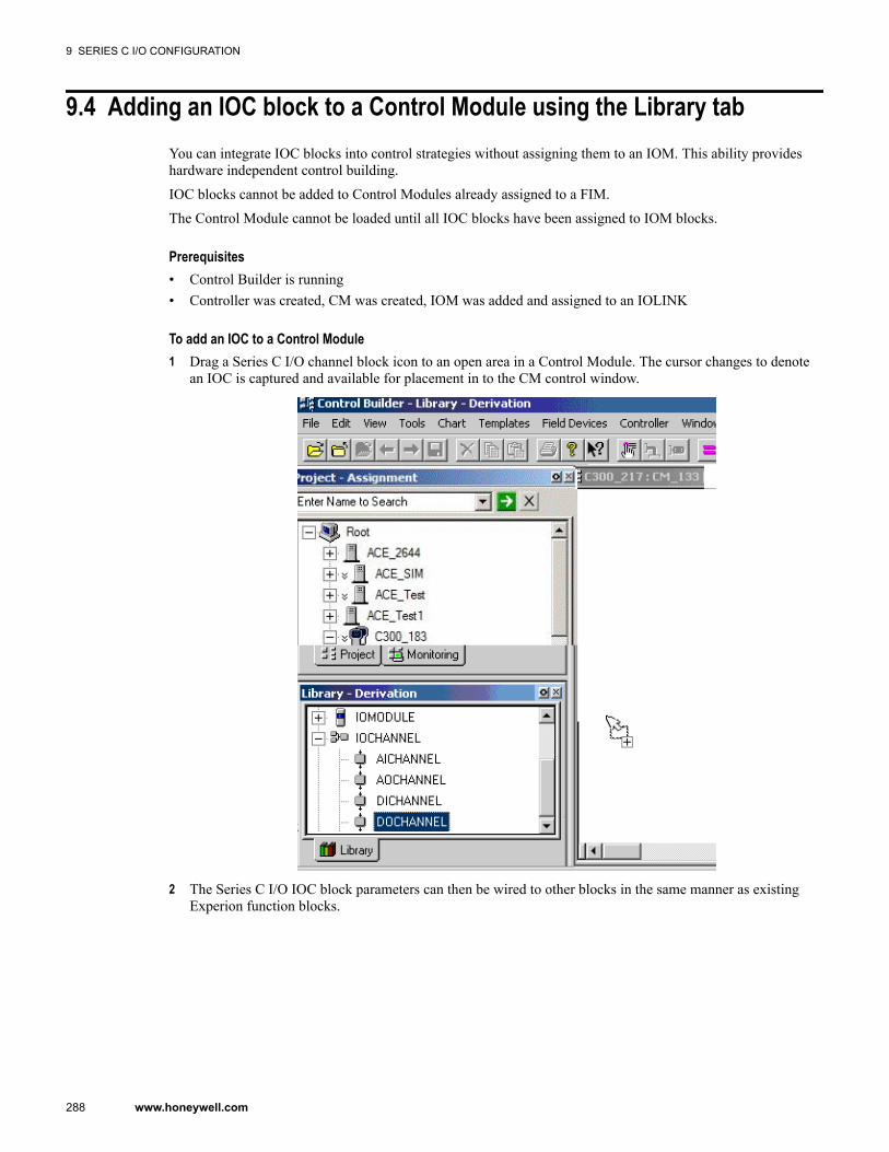
9.4 Adding an IOC block to a Control Module using the Library tabYou can integrate IOC blocks into control strategies without assigning them to an IOM. This ability provideshardware independent control building.
IOC blocks cannot be added to Control Modules already assigned to a FIM.
The Control Module cannot be loaded until all IOC blocks have been assigned to IOM blocks.
Prerequisites• Control Builder is running• Controller was created, CM was created, IOM was added and assigned to an IOLINK
To add an IOC to a Control Module1 Drag a Series C I/O channel block icon to an open area in a Control Module. The cursor changes to denote
an IOC is captured and available for placement in to the CM control window.
2 The Series C I/O IOC block parameters can then be wired to other blocks in the same manner as existingExperion function blocks.
9 SERIES C I/O CONFIGURATION
288 www.honeywell.com
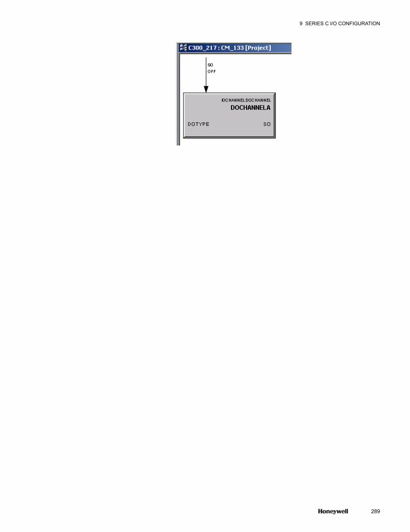
9 SERIES C I/O CONFIGURATION
289
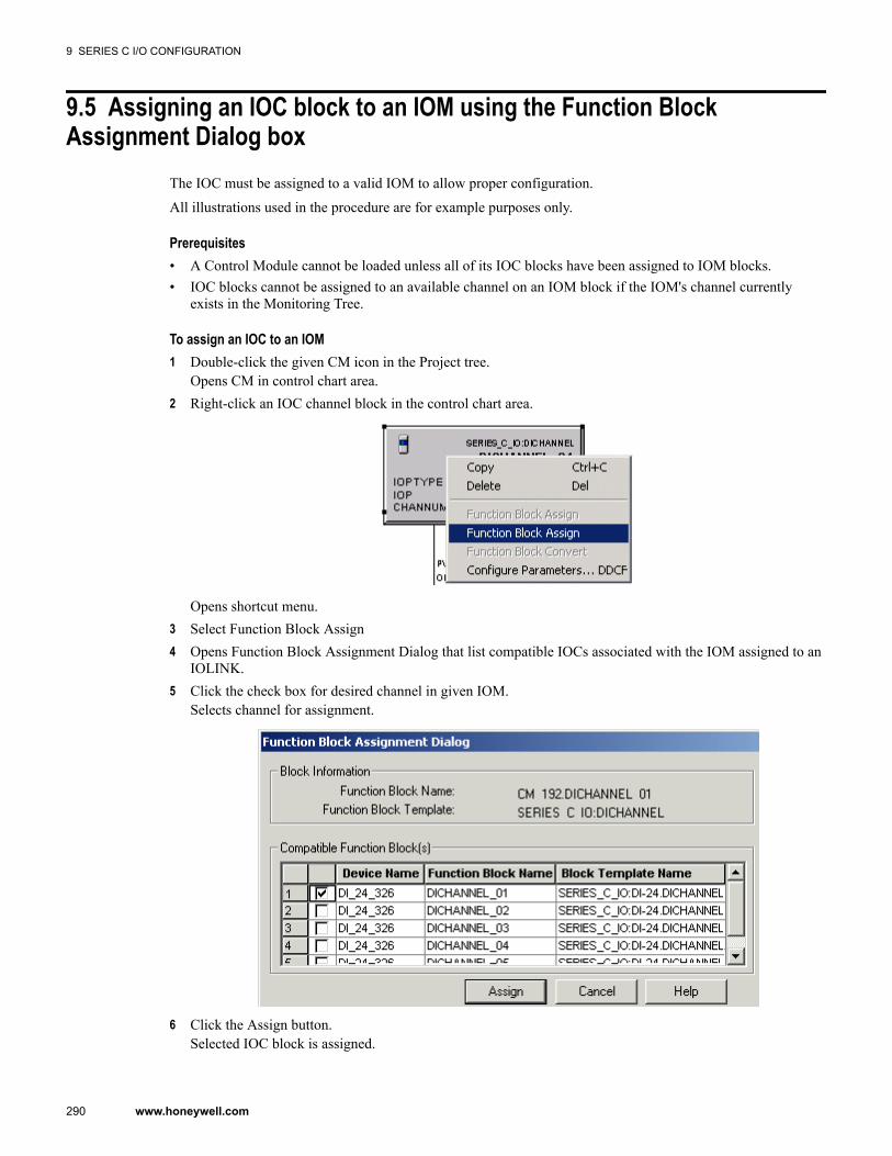
9.5 Assigning an IOC block to an IOM using the Function BlockAssignment Dialog box
The IOC must be assigned to a valid IOM to allow proper configuration.
All illustrations used in the procedure are for example purposes only.
Prerequisites• A Control Module cannot be loaded unless all of its IOC blocks have been assigned to IOM blocks.• IOC blocks cannot be assigned to an available channel on an IOM block if the IOM's channel currently
exists in the Monitoring Tree.
To assign an IOC to an IOM1 Double-click the given CM icon in the Project tree.
Opens CM in control chart area.2 Right-click an IOC channel block in the control chart area.
Opens shortcut menu.3 Select Function Block Assign4 Opens Function Block Assignment Dialog that list compatible IOCs associated with the IOM assigned to an
IOLINK.5 Click the check box for desired channel in given IOM.
Selects channel for assignment.
6 Click the Assign button.Selected IOC block is assigned.
9 SERIES C I/O CONFIGURATION
290 www.honeywell.com
Note: For identification of unused I/O channels, see, “Identification of unused I/O channels” on page 291.7 Click the dialog close button to complete the assignment.
Confirmation dialog appears.8 Click the Yes button to accept the changes.
Function Block Assignment Dialog box closes.
9.5.1 Default naming conventions of I/O channelIn the Control Builder tree view, by default, I?O channel naming convention is '<I/OTYPECHANNEL>_<CHANNEL NUMBER>'. For example, the names appear as - AICHANNEL_01,AICHANNEL_02, and so on. When assigned to a CM, the channel name changes to '<CM name>.<I/OTYPECHANNEL>_<CHANNEL NUMBER>.' For example, the name changes to CM1.AICHANNEL_01.You can also rename the I/O channel after assignment.
9.5.2 Identification of unused I/O channelsPrior to R410, identifying unused I/O channels was not easy since I/O channels retained their last modifiednames even after unassignment or deletion. With R410, I/O channel names return to their default names afterunassignment or deletion; thereby making the identification of unused I/O channels simpler.
The following table lists the differences in identifying the unused I/O channels prior to R410 and in R410 andlater.
Channel type and scenarios Behavior prior to R410 Behavior in R410 and laterPMI/O or Series C I/O channels -Deletion of an assigned channel,unassignment of a channel, deletion ofa CM that contains a channel
No change in channel name.
For example, if 'AICHANNEL_01' isrenamed as 'AICHANNEL_TEST' afterassignment, the channel name does notchange in any of the scenariosmentioned.
• Before channel assignment
• After assignment and renaming of achannel
• After unassignment or deletion ofan assigned channel or afterdeletion of a CM that contains achannel
Channel name changes to its defaultname.
For example, if 'AICHANNEL_01' isrenamed as 'AICHANNEL_TEST' afterassignment, the channel name changesto 'AICHANNEL_01' in all thescenarios mentioned.
However, in the Chart view, thechannel name is retained as'AICHANNEL_TEST.'
• Before channel assignment
• After assignment and renaming of achannel
• After unassignment or deletion ofan assigned channel or afterdeletion of a CM that contains achannel
9 SERIES C I/O CONFIGURATION
291
Channel type and scenarios Behavior prior to R410 Behavior in R410 and laterHART-enabled I/O channels - Deletionof an assigned channel, unassignmentof a channel, deletion of a CM thatcontains a channel
No change in channel name or HARTicon in any of the scenarios mentioned.
• Before channel assignment
• After assignment and renaming of achannel
• After unassignment or deletion ofan assigned channel or afterdeletion of a CM that contains achannel
HART icon changes to the default icontype for the channel in all the scenariosmentioned.
• Before channel assignment
• After assignment and renaming of achannel
• After unassignment or deletion ofan assigned channel or afterdeletion of a CM that contains achannel
Note: In R410 and later, in case the channel name conflicts during any of the scenarios mentioned '_1' is suffixed with thechannel name. For example, if 'AICHANNEL_01' already exists in the unassigned list, the channel name is changed to'AICHANNEL_01_1.'
9.5.3 Identification of ganged DO channelsWhen the DO channels are ganged together, the name of the DO channel in which ganging is configured isreplaced with the Control Module name in the Project view. For example, if the DO channels 7 to 10 are gangedthen the name of the DO channel 10 is replaced as CMname.DOchannel7. In addition, the remaining DOchannels disappear in the Project view.
9 SERIES C I/O CONFIGURATION
292 www.honeywell.com
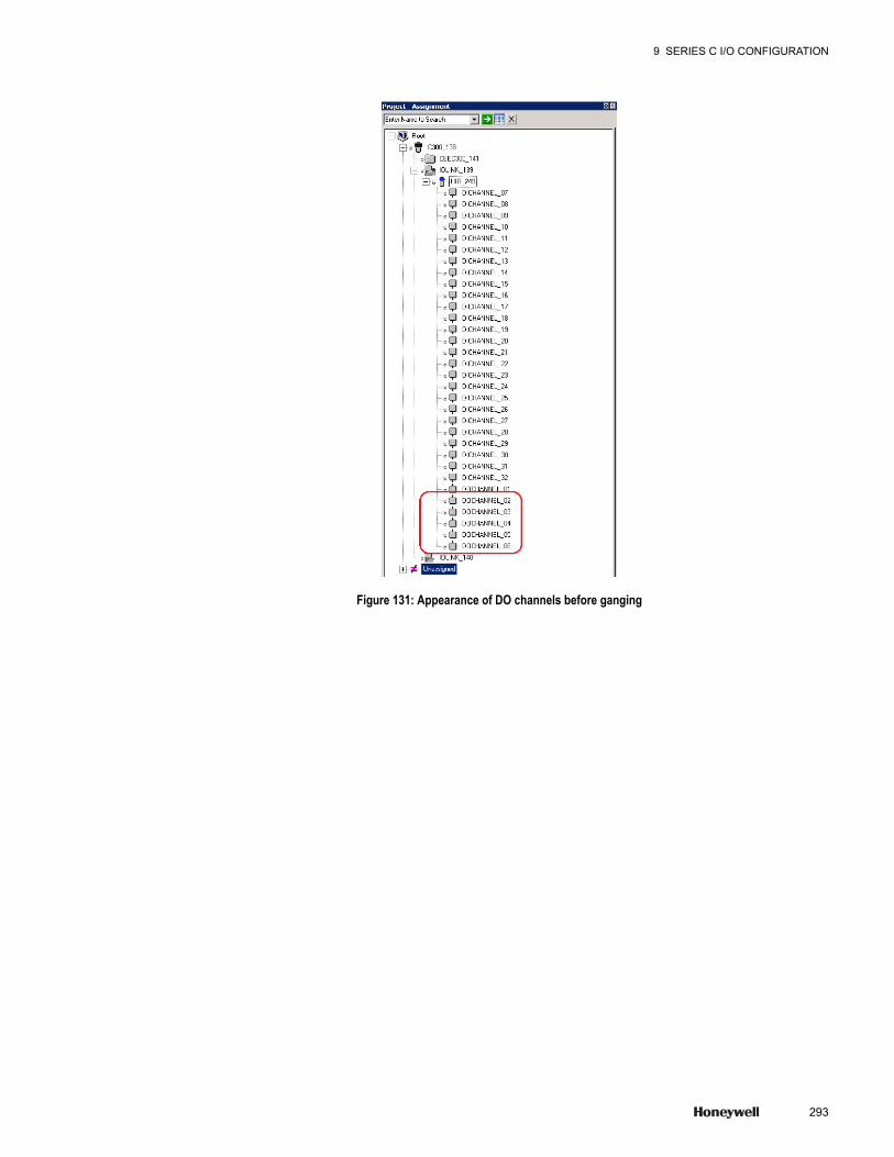
Figure 131: Appearance of DO channels before ganging
9 SERIES C I/O CONFIGURATION
293

Figure 132: Appearance of DO channels after ganging
9 SERIES C I/O CONFIGURATION
294 www.honeywell.com

9.6 Unassigning an IOC block from an IOM using the Function BlockAssignment Dialog box
An IOC function block can be unassigned from an IOM. Unassigned IO channels are available for reassigningonly after the CM is saved.
All illustrations used in the procedure are for example purposes only.
Prerequisites• IOC blocks cannot be unassigned if the IOC currently exists in the Monitoring Tree.
To unassign an IOC from an IOM1 Double-click given CM in the Project tree.
Opens CM in control chart area.
Right-click the IOC channel block.
Opens shortcut menu.2 Select Function Block Unassign
Opens Function Block Assignment Dialog that list compatible IOCs associated with the IOM assigned to anIOLINK
3 Click to clear the box for desired channel in given IOM.A check mark is removed.
4 Click the Assign button.Selected IOC block is unassigned.
9 SERIES C I/O CONFIGURATION
295

5 Click the dialog close button to complete the assignment.Confirmation dialog appears.
6 Click the Yes button to accept the changes.Function Block Assignment Dialog box closes.
9 SERIES C I/O CONFIGURATION
296 www.honeywell.com

9.7 Field Calibration of the AI and AO modulesThis section describes the field calibration procedure for the AI-HL, AI-HART, AO, and AO-HART modules.
AttentionConfiguration mismatch warning message appears when you configure CALIBSTS parameter and loads AO-HARTmodule FB to AO-HART (Cx-PAOH51) module or AI-HART module FB to one modem AI-HART (Cx-PAIH51)module.
To perform field calibration of the AI-HL, AI-HART, AO and AO HART modules1 From the IOM block Main tab, set the Execution State (IOMSTATE parameter) to IDLE.2 From the Calibration tab, set the Calibration State (CALIBSTS parameter) to Enabled. Verify the IOM
status LED is switched off indicating that IOM has entered calibration mode.NOTE: Both the top and bottom modules enter a calibration mode in a redundant configuration.
3 Connect the calibration voltage source to IOTA terminal block TB3 (and TB4 if redundant) and adjust thevoltage to 5Vdc (4.9995 - 5.0005Vdc).NOTE: CAL terminals blocks are marked as TB2 and TB3 in the case of AO.
4 Short the two calibration pads marked as CAL1 (and CAL2 if redundant) in the IOTA.Result: The LED blinks two times and switches off.
5 Short the CAL pads again.Result: The LED blinks three times and the IOM automatically reboots within a few seconds.
6 Check that :• CALIBSTS has changed automatically back to Disabled state,• IOMSTATE is IDLE, and• the status LED is steady green.
If the status LED is blinking, check for any CALBABRT softfail that indicates bad calibration.7 Disconnect the calibration voltage-source wiring and inform the operator that the IOM field calibration is
complete.
AttentionUIO channels do not require the field calibration.
9 SERIES C I/O CONFIGURATION
297
9.8 Defining Channel blocksEach Series C I/O channel (IOC) block represents a single I/O point within an I/O module (which can be eitherinput or output). There are certain attributes and parameters that are common to all I/O channel blocks. TheSeries C IOC block has a point execution state, similar to the PM IOC block. This allows for easy re-configuration of a single channel without disrupting the operation of the entire IOM.
TipIn the TPS environment, a channel block is equivalent to one slot in the IO processor.
Each IOC block must have an 'assignment' block and 'containment' block in order for it to be loadable. Thefollowing table describes these blocks.
Table 81: I/O Channel block type
Block name DescriptionAssignment IOC is associated with a specific slot number on an IOM block
Containment IOC exists in a Control Module
9.8.1 Common features of I/O channel blocksThere are certain attributes and parameters that are common to all I/O channel blocks. The following sectionidentifies these common features.
9.8.2 Defining Mode and Attribute settingsThe MODE parameter determines the operating mode for the channel block. These modes apply to both DO andAO channel blocks.
Operators are only permitted to change MODE if:
• MODEPERM is set to Permit, and• REDTAG is set to Off
Note: Mode Permissive = Indicates if the operator can change the mode of a function block Red Tag - Allowsthe user to set the FB as being 'out-of-service'; this indicates that the FB or the associated control strategy needsrepair, or is being repaired.
The following modes apply to the MODE parameter.
Table 82: Mode parameter - channel block
Operating mode DescriptionManual (Man) Provides direct control over the output value of the channel, regardless of any continuous
control strategy.
Cascade (Cas) Data point receives its output value from a primary data point.
The MODEATTR (mode attribute) parameter determines who has authority to change certain parameters on thefunction block.
The following modes apply to the MODEATTR parameter.
9 SERIES C I/O CONFIGURATION
298 www.honeywell.com
Table 83: Mode Attribute parameter - channel block
Operating mode DescriptionOperator Operator supplies the output value and mode for the channel
(operator access level).
Program Program supplies the output value and mode for the channel
(program access level).
9.8.3 Defining load attributesWhen defining the load attributes, the channel block copies:
• the Normal Mode parameter (NMODE) into the MODE parameter, and• the Normal Mode attribute (NMODATTR) into the MODEATTR parameter
CONSIDERATIONS:
Possible entries for the NMODE parameter:
• Man• Cas• None
Possible entries for the NMODATTR parameter
• Operator• Program• None
To define the channel block and copy the NMODE (normal mode) and NMODATTR attributes1 Press the NORM button on the integrated keyboard (IKB).
OR
Press the Operator Entry Panel (OEP) at the operator station.2 The content of the NMODE is copied into the MODE parameter and becomes the mode for the channel
block.The content of the NMODATTR is also copied into the MODEATTR parameter and becomes the mode forthe channel block.
9.8.4 Defining Fault State Handling and Fault Option settingsAO and DO channel blocks are configured so that 'if the communication between the controller and the I/Omodule is disrupted for 10 to 20 seconds,' the upstream control strategy is assumed to have failed. TheFAULTOPT parameter allows you to specify the behavior of an individual output when a fault condition exists.
Table 84: Channel block fault conditions and results
Fault conditions exist when ResultLoss of communications due to:
• C300 failure• IOLEE failure• Dual IOL cable failure
CEE failure, but IOLEE is up and running
All outputs on the IOM, regardless of their PTEXESTvalue, transition to their respective FAULTOPT states,within 8 seconds.
9 SERIES C I/O CONFIGURATION
299
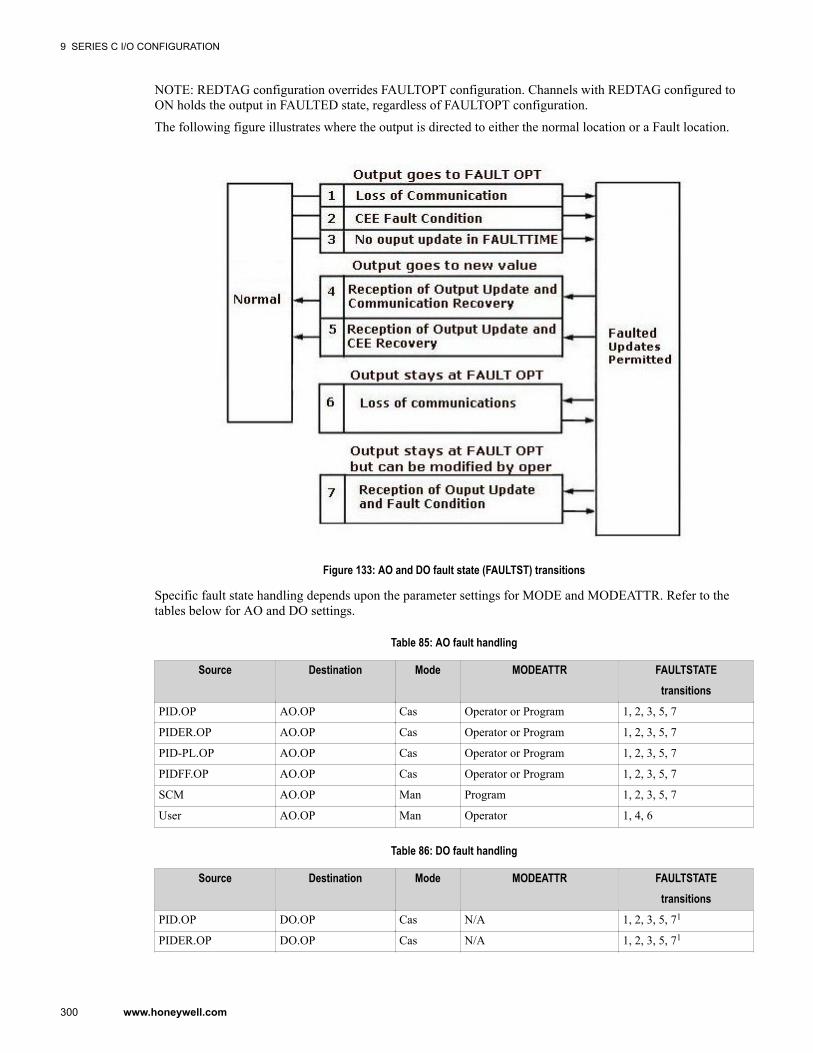
NOTE: REDTAG configuration overrides FAULTOPT configuration. Channels with REDTAG configured toON holds the output in FAULTED state, regardless of FAULTOPT configuration.
The following figure illustrates where the output is directed to either the normal location or a Fault location.
Figure 133: AO and DO fault state (FAULTST) transitions
Specific fault state handling depends upon the parameter settings for MODE and MODEATTR. Refer to thetables below for AO and DO settings.
Table 85: AO fault handling
Source Destination Mode MODEATTR FAULTSTATEtransitions
PID.OP AO.OP Cas Operator or Program 1, 2, 3, 5, 7
PIDER.OP AO.OP Cas Operator or Program 1, 2, 3, 5, 7
PID-PL.OP AO.OP Cas Operator or Program 1, 2, 3, 5, 7
PIDFF.OP AO.OP Cas Operator or Program 1, 2, 3, 5, 7
SCM AO.OP Man Program 1, 2, 3, 5, 7
User AO.OP Man Operator 1, 4, 6
Table 86: DO fault handling
Source Destination Mode MODEATTR FAULTSTATEtransitions
PID.OP DO.OP Cas N/A 1, 2, 3, 5, 71
PIDER.OP DO.OP Cas N/A 1, 2, 3, 5, 71
9 SERIES C I/O CONFIGURATION
300 www.honeywell.com
Source Destination Mode MODEATTR FAULTSTATEtransitions
PID-PL.OP DO.OP Cas N/A 1, 2, 3, 5, 71
PIDFF.OP DO.OP Cas N/A 1, 2, 3, 5, 71
PosProp.
RAISETIME
DO.OFFPULSE Cas N/A 1, 2, 3, 5, 72
PosProp.
LOWERTIME
DO.OFFPULSE Cas N/A 1, 2, 3, 5, 72
PosProp.
RAISETIME
DO.ONPULSE Cas N/A 1, 2, 3, 5, 72
Posprop.
LOWERTIME
DO.ONPULSE Cas N/A 1, 2, 3, 5, 72
DevCtl.PO DO.OFFPULSE Cas N/A 1, 2, 3, 5, 7
DevCtl.PO DO.ONPULSE Cas N/A 1, 2, 3, 5, 7
DevCtl.DO DO.SO Cas N/A 1, 2, 3, 5, 7
Logic DO.SO Cas N/A 1, 2, 3, 5, 7
SCM DO.OP Man Program 1, 2, 3, 5, 7
SCM DO.SO Man Program 1, 2, 3, 5, 7
User DO.OP Man Operator 1, 4, 6
User DO.SO Man Operator 1, 4, 6
The FAULTOPT parameter determines the behavior of an individual output value when a fault condition exists.The following modes apply to the FAULTOPT parameter:
Table 87: FAULTOPT parameter settings
Operating mode Description AO channels DO channelsHold Holds output at last good value Applicable to all
configurationsApplicable to all configurations
Unpower Output goes to an unpowered value Applicable to allconfigurations
Applicable to all configurations
Power Output goes to a powered value Not applicable to AOchannels
Not applicable to DO channels forPWM operation.
Use Fault Value Output goes to the value specifiedby the FAULTVALUE parameter
Not applicable to DO channelconfigured for STATUS,ONPULSE or OFFPULSEoperation.
The FAULTOPT configuration also defines the state of the output in case of total IOM hard failure also. Thisfeature is mainly applicable to the DO channels configured for STATUS operation.
9.8.5 FAULTED state and IOM hard failureTotal IOM hard failure means:
• dual IOM failure in the case of redundant setup• assumes that there is no disruption 24V power to the I/O modulesThe following table summarizes the state of the output for all applicable output configurations in the case oftransitioning to FAULTED state or on total IOM failure.
9 SERIES C I/O CONFIGURATION
301
Table 88: IOM hard failure and output state
Unpower Power
Hold Fault value
AO
Faulted state 0mA Not applicable Hold last good OP value Hold configured value
Total IOMFailure
0mA Not applicable 0mA 0mA
DO STATUS
Faulted state Drive LOW Drive HIGH Hold last good SO value Not applicable
Total IOMFailure
Drive LOW Drive HIGH Hold last good SO value Not applicable
DO PWM
Faulted state Drive LOW Not applicable Continues of PWM as perthe last good Op value.
Continues of PWM as perthe configured value.
Total IOMFailure
Drive LOW Not applicable Terminates the PWM anddrive LOW.
Terminates the PWM anddrive LOW.
DO ONPULSE/OFFPULSE
Faulted state Drive LOW Drive HIGH Proceeds to the normalcompletion of any on-going pulse and holdquiescent state.
Not applicable
Total IOMFailure
Drive LOW Drive HIGH Terminates any on-goingpulse immediately andhold quiescent state.
Not applicable
9.8.6 Defining PV Source selection settingsThe PVSOURCE parameter allows you to determine the source of the PV for the data channel.
Table 89: PV Source settings
If PVSOURCE is
Auto
• AI channel's Range Checking and Filtering circuit provides PV, or• DI channel's PVAUTO parameter provides PV
Man
• PV can be entered manually, or
Sub
• PV can come from a sequence program
Additionally, the PVSRCOPT parameter determines if it is permissible to change the PV source to a sourceother than Auto.
The following modes apply to the PVSRCOPT parameter.
9 SERIES C I/O CONFIGURATION
302 www.honeywell.com
Table 90: PVSRCOPT settings
Operating mode DescriptionOnlyAuto allows the PV to be set only Automatically
All allows the manual setting of PV
9.8.7 Defining the REDTAG settingsThe REDTAG parameter allows you to set channel as being 'out of service' indicating that this channel or itsassociated control loops needs repair, or is being repaired. Once a channel is put in the red tag condition, itsoutput is frozen at the last value.
REDTAG can only be set and cleared when:
• MODE = MAN• MODATTR = Operator
Table 91: REDTAG settings
When channel is placed in REDTAGcondition
Result
Channel output is frozen at last value (including MODE and MODATTR)
The value of OP takes precedence over the FAULTOPT settings.
Channels • cannot be deleted• can be reloaded
- the load produces errors for PNTTYPE, MODE, and
MODEATTR because the parameters could not be
set on the load.
9.8.8 Enabling HART in HART 6.0 and later version devicesThe HART Protocol compliments traditional 4-20mA analog signaling and supports two way digitalcommunications to intelligent process control devices. Applications include:
• remote process variable interrogation,• cyclical access to process data, parameter setting, and• diagnostics.
For more information, visit www.hartcomm.org.
9.8.9 Features and capabilities - HART 6.0 and later version devicesHART 6.0 and later version device features and capabilities are designed to:
• improve support for multi-variable and valve / actuator type devices;• enhance status and diagnostics,• increase interoperability;• extended commissioning / troubleshooting capabilities; and• security measures to confirm any configuration change.
HART 6.0 and later version device functionality that is supported in Series C through Control Builder includesthe following:
9 SERIES C I/O CONFIGURATION
303
Function DescriptionDevice variable classification Provides master applications with a simple mechanism to determine the number and type
of process related variables (pressure, temperature, etc.) within a device.
Extended device status Provides additional device status alerts such as 'Device Needs Maintenance.'
Device variable status Enables field devices to self-validate and report on the quality of the data in thecommand response (good, poor, bad, fixed).
Long Tag New Long Tag with international (ISO Latin 1) characters allows consistentimplementation of the longer tag names required by many industry users. Thespecifications currently reflect the length of this tag to be 32 characters.
Configuration change counter Improved mechanism for master applications to determine that a field deviceconfiguration has been changed. Protects integrity of plant configuration databases.
Device Families Establishes standard commands and status indicators for devices based on the type ofprocess measurement. Initial Device Families include Temperature and PID Control.
Transducer Trim Commands New Common Practice commands for performing transducer trim (calibration)operations.
Sub-Devices Simple mechanism using Common Practice Commands to support 'HART device withina HART device' functionality. Potential uses include flow computers and multi-channeltemperature devices.
Block Data Transfer An updated mechanism to support the movement of large blocks of data, such as deviceconfiguration information, between masters and field devices.
Catch Device Variable Simple mechanism to support the sharing of process data between field devices on thesame HART network. Allows a listening field device to capture process data fromanother field device to be used in calculations such as tank gauging, flow computers orPID control functions.
Write Device Variable New Command to support forcing the digital value for any Device Variable to a specificvalue to aid in commissioning and troubleshooting.
Lock Device New Commands to allow a master application to lock the 'local' front panel of a fielddevice while performing remote configuration functions.
Squawk and Find Device New commands to support commissioning and troubleshooting of HART devices inmulti-drop and multi-pair cable installations.
Series C I/O IOMs do not have an independent HART device block. Instead, the HART data is fully containedwithin an AI or AO block and:
• enabled when HENABLE parameter is set to TRUE (This is done on the AI channel block HARTConfiguration tab)
• becomes an Experion 'tagged' entity and can generate alarms based on its 'tagged' name in Station.
When AI and AO channel blocks are enabled, five additional HART tabs become exposed. These tabs are usedexclusively for details about the attached HART device and are identical for AI and AO channels. These tabsare:
HART Configuration HART Identification HART Notifications
HART Device Status HART Variables
9 SERIES C I/O CONFIGURATION
304 www.honeywell.com
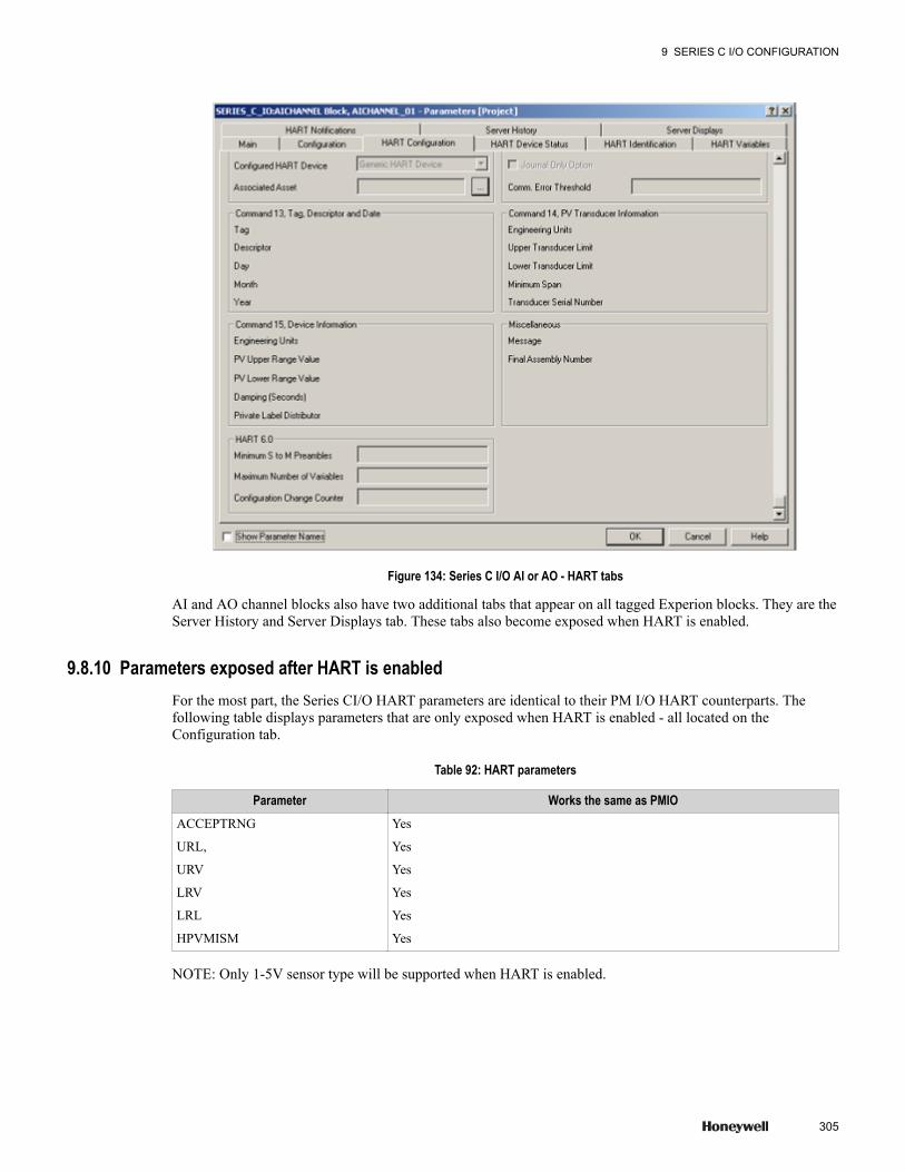
Figure 134: Series C I/O AI or AO - HART tabs
AI and AO channel blocks also have two additional tabs that appear on all tagged Experion blocks. They are theServer History and Server Displays tab. These tabs also become exposed when HART is enabled.
9.8.10 Parameters exposed after HART is enabledFor the most part, the Series CI/O HART parameters are identical to their PM I/O HART counterparts. Thefollowing table displays parameters that are only exposed when HART is enabled - all located on theConfiguration tab.
Table 92: HART parameters
Parameter Works the same as PMIOACCEPTRNG
URL,
URV
LRV
LRL
HPVMISM
Yes
Yes
Yes
Yes
Yes
Yes
NOTE: Only 1-5V sensor type will be supported when HART is enabled.
9 SERIES C I/O CONFIGURATION
305
9.8.11 Comparing parameters between Series C and PMIOHPVCHAR, which is used in PM I/O, is not used in Series C I/O. PVCHAR are used instead, and only validenumerations (depending on the settings for HENABLE and IOM TYPE) are displayed to you.
Some HART parameters are only valid for HART Protocol Version 6. Series C IOMs support HART 6.0 andlater version device features such as Extended Device Status, Configuration Change Counter, Variable Statusand Classification Codes. The current release of Series C I/O supports these HART 6.0 and later version deviceparameters:
Parameter Tab DescriptionHMAXDEVVARS Indicates the last device variable code supported by the device. Information
can be used by the host applications.
HNCFGCHG Configuration change counter is a counter maintained by HART 6.0 and laterversion device which is incremented every time configuration is changed. Thisis improvement over the single 'configuration changed bit' in previous HARTreleases
HNSMMINPRE Minimum number of preamble bytes to be sent with the response from deviceto the IOM. Series C IOMs take advantage of this configuration if supportedby the device to minimize the bytes sent from device in response messages.
HDYNCC Variables Dynamic / device variable classification code
HDYNST Variables Dynamic / device variable classification code
HSLOTCC Variables Dynamic / device variable classification code
HSLOTST Variables Dynamic / device variable classification code
9.8.12 Parameter values not copied during Block CopyIOP and CHANNUM are the only configuration parameter values not copied during a Block Copy operation.
9 SERIES C I/O CONFIGURATION
306 www.honeywell.com
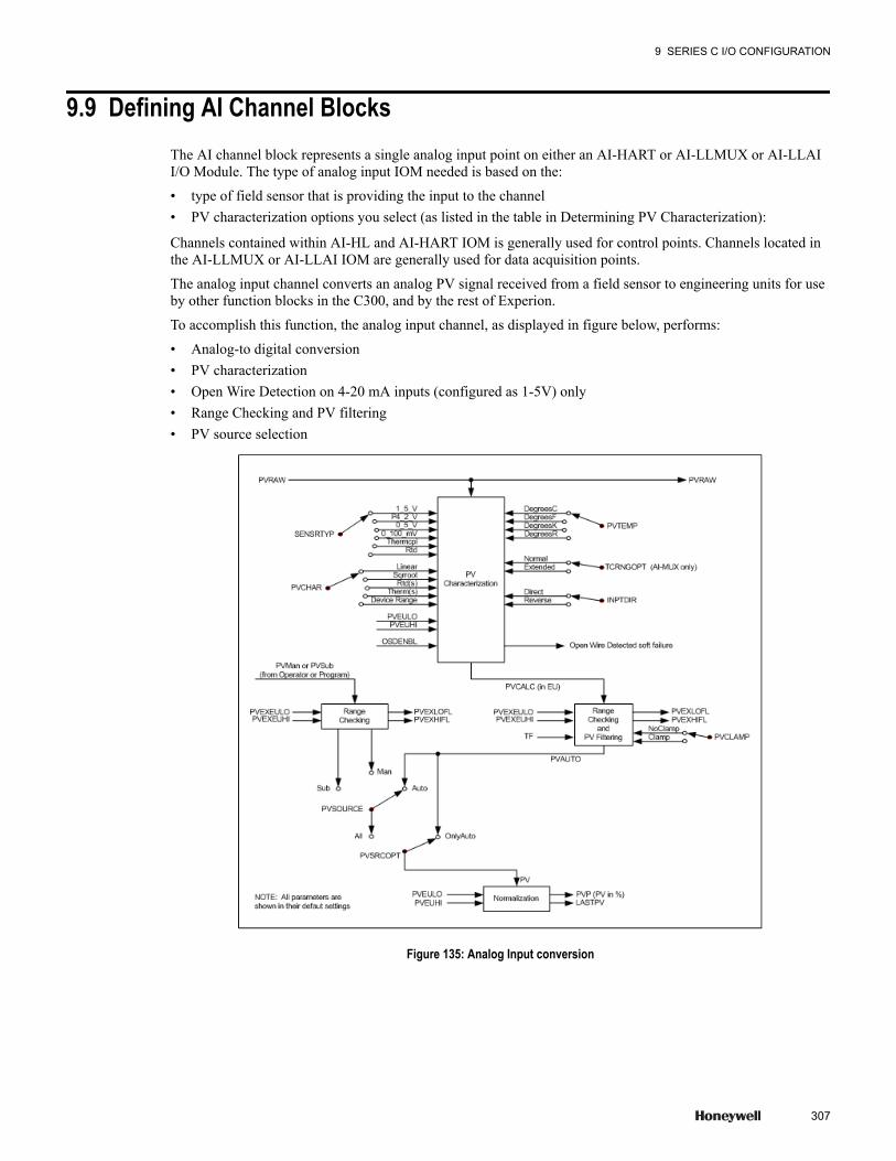
9.9 Defining AI Channel BlocksThe AI channel block represents a single analog input point on either an AI-HART or AI-LLMUX or AI-LLAII/O Module. The type of analog input IOM needed is based on the:
• type of field sensor that is providing the input to the channel• PV characterization options you select (as listed in the table in Determining PV Characterization):
Channels contained within AI-HL and AI-HART IOM is generally used for control points. Channels located inthe AI-LLMUX or AI-LLAI IOM are generally used for data acquisition points.
The analog input channel converts an analog PV signal received from a field sensor to engineering units for useby other function blocks in the C300, and by the rest of Experion.
To accomplish this function, the analog input channel, as displayed in figure below, performs:
• Analog-to digital conversion• PV characterization• Open Wire Detection on 4-20 mA inputs (configured as 1-5V) only• Range Checking and PV filtering• PV source selection
Figure 135: Analog Input conversion
9 SERIES C I/O CONFIGURATION
307
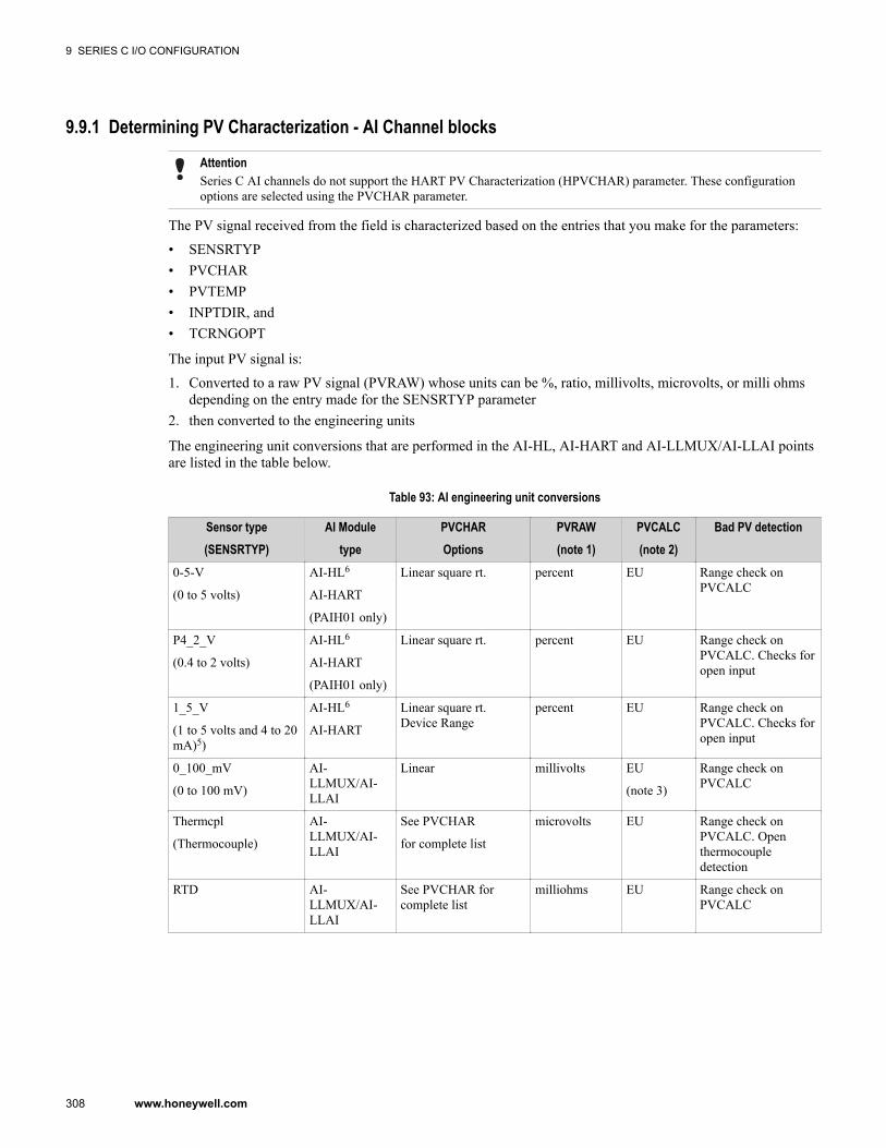
9.9.1 Determining PV Characterization - AI Channel blocks
AttentionSeries C AI channels do not support the HART PV Characterization (HPVCHAR) parameter. These configurationoptions are selected using the PVCHAR parameter.
The PV signal received from the field is characterized based on the entries that you make for the parameters:
• SENSRTYP• PVCHAR• PVTEMP• INPTDIR, and• TCRNGOPT
The input PV signal is:
1. Converted to a raw PV signal (PVRAW) whose units can be %, ratio, millivolts, microvolts, or milli ohmsdepending on the entry made for the SENSRTYP parameter
2. then converted to the engineering units
The engineering unit conversions that are performed in the AI-HL, AI-HART and AI-LLMUX/AI-LLAI pointsare listed in the table below.
Table 93: AI engineering unit conversions
Sensor type(SENSRTYP)
AI Moduletype
PVCHAROptions
PVRAW(note 1)
PVCALC(note 2)
Bad PV detection
0-5-V
(0 to 5 volts)
AI-HL6
AI-HART
(PAIH01 only)
Linear square rt. percent EU Range check onPVCALC
P4_2_V
(0.4 to 2 volts)
AI-HL6
AI-HART
(PAIH01 only)
Linear square rt. percent EU Range check onPVCALC. Checks foropen input
1_5_V
(1 to 5 volts and 4 to 20mA)5)
AI-HL6
AI-HART
Linear square rt.Device Range
percent EU Range check onPVCALC. Checks foropen input
0_100_mV
(0 to 100 mV)
AI-LLMUX/AI-LLAI
Linear millivolts EU
(note 3)
Range check onPVCALC
Thermcpl
(Thermocouple)
AI-LLMUX/AI-LLAI
See PVCHAR
for complete list
microvolts EU Range check onPVCALC. Openthermocoupledetection
RTD AI-LLMUX/AI-LLAI
See PVCHAR forcomplete list
milliohms EU Range check onPVCALC
9 SERIES C I/O CONFIGURATION
308 www.honeywell.com
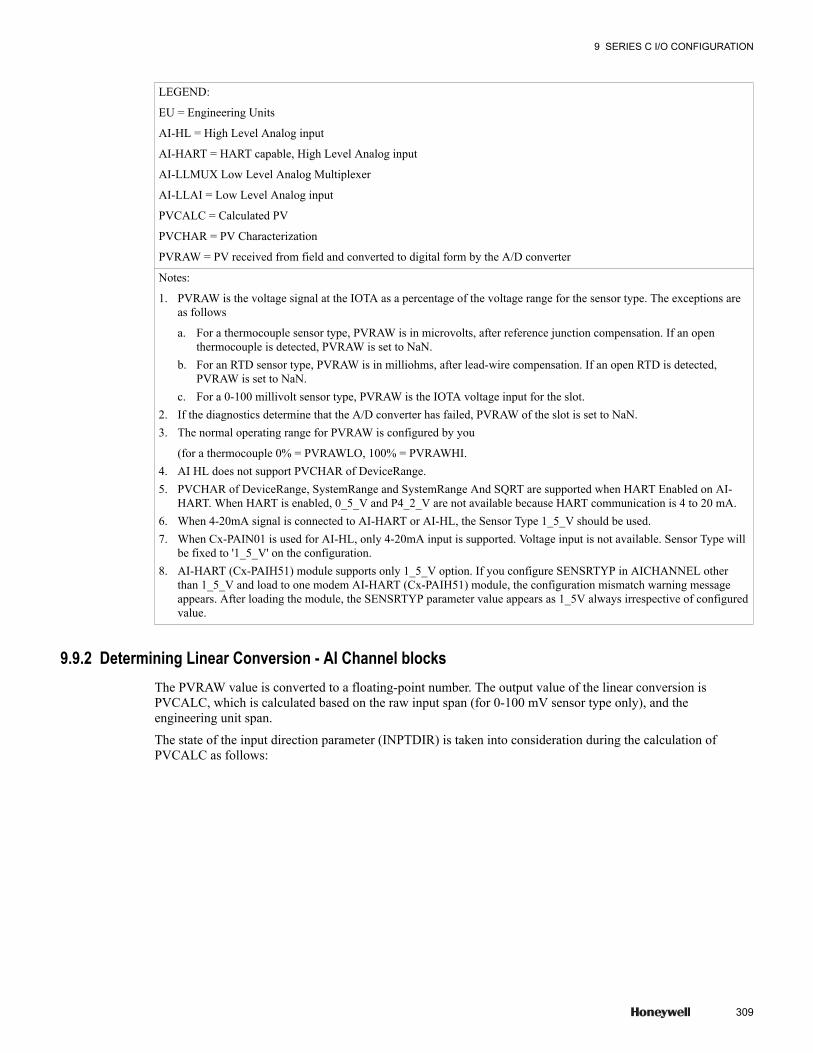
LEGEND:
EU = Engineering Units
AI-HL = High Level Analog input
AI-HART = HART capable, High Level Analog input
AI-LLMUX Low Level Analog Multiplexer
AI-LLAI = Low Level Analog input
PVCALC = Calculated PV
PVCHAR = PV Characterization
PVRAW = PV received from field and converted to digital form by the A/D converter
Notes:
1. PVRAW is the voltage signal at the IOTA as a percentage of the voltage range for the sensor type. The exceptions areas follows
a. For a thermocouple sensor type, PVRAW is in microvolts, after reference junction compensation. If an openthermocouple is detected, PVRAW is set to NaN.
b. For an RTD sensor type, PVRAW is in milliohms, after lead-wire compensation. If an open RTD is detected,PVRAW is set to NaN.
c. For a 0-100 millivolt sensor type, PVRAW is the IOTA voltage input for the slot.2. If the diagnostics determine that the A/D converter has failed, PVRAW of the slot is set to NaN.3. The normal operating range for PVRAW is configured by you
(for a thermocouple 0% = PVRAWLO, 100% = PVRAWHI.4. AI HL does not support PVCHAR of DeviceRange.5. PVCHAR of DeviceRange, SystemRange and SystemRange And SQRT are supported when HART Enabled on AI-
HART. When HART is enabled, 0_5_V and P4_2_V are not available because HART communication is 4 to 20 mA.6. When 4-20mA signal is connected to AI-HART or AI-HL, the Sensor Type 1_5_V should be used.7. When Cx-PAIN01 is used for AI-HL, only 4-20mA input is supported. Voltage input is not available. Sensor Type will
be fixed to '1_5_V' on the configuration.8. AI-HART (Cx-PAIH51) module supports only 1_5_V option. If you configure SENSRTYP in AICHANNEL other
than 1_5_V and load to one modem AI-HART (Cx-PAIH51) module, the configuration mismatch warning messageappears. After loading the module, the SENSRTYP parameter value appears as 1_5V always irrespective of configuredvalue.
9.9.2 Determining Linear Conversion - AI Channel blocksThe PVRAW value is converted to a floating-point number. The output value of the linear conversion isPVCALC, which is calculated based on the raw input span (for 0-100 mV sensor type only), and theengineering unit span.
The state of the input direction parameter (INPTDIR) is taken into consideration during the calculation ofPVCALC as follows:
9 SERIES C I/O CONFIGURATION
309
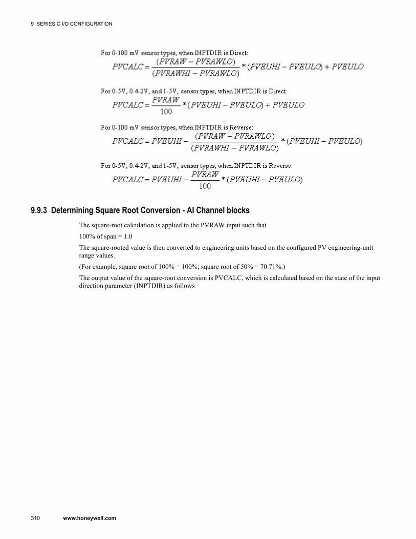
9.9.3 Determining Square Root Conversion - AI Channel blocksThe square-root calculation is applied to the PVRAW input such that
100% of span = 1.0
The square-rooted value is then converted to engineering units based on the configured PV engineering-unitrange values.
(For example, square root of 100% = 100%; square root of 50% = 70.71%.)
The output value of the square-root conversion is PVCALC, which is calculated based on the state of the inputdirection parameter (INPTDIR) as follows
9 SERIES C I/O CONFIGURATION
310 www.honeywell.com

9.9.4 Determining Thermal Conversion - AI Channel blocksThermal linearization is performed on thermocouple and RTD input types. All thermocouples (#therm) listed inthe PVCHAR parameter definition, are supported by the analog input point. The range of the thermocouple typeused with the AI-LLMUX/AI-LLAI channel can be increased by selecting Extended as the entry for theTCRNGOPT parameter.
The AI-LLMUX/AI-LLAI channels calculate the reference junction compensation from the measured referencejunction output level. This value is stored and then later converted back to microvolts, with respect to 0 degreesC, for each thermocouple that is to be compensated. The cold-junction reference compensation (PVREFJN)parameter is expressed in microvolts for the specified thermocouple and is added to the microvolt value forPVRAW.
All RTDs (*RTD) listed in the PVCHAR parameter definition, are supported by the analog input point:
For an RTD, the AI-LLMUX/AI-LLAI channels calculate the lead-wire compensation and then subtract thevalue from PVRAW. The maximum allowable lead-wire resistance and intrinsic safety barrier resistance for theRTDs are listed in the table below.
Table 94: RTD lead wire characteristics
Maximum allowable lead resistance -Note 1
(units are ohms)
Maximum allowable intrinsic safetybarrier resistance(units are ohms)
RTD type Entire loop Per leg Entire loop Per legPt:100 DIN characterization 20 10 18 18
Pt:100 JIS characterization 20 10 18 18
Ni: 120 Edison type 7 characterization 20 10 18 18
Cu: 10 SEER Standard characterization 20 10 0 0
9 SERIES C I/O CONFIGURATION
311

Maximum allowable lead resistance -Note 1
(units are ohms)
Maximum allowable intrinsic safetybarrier resistance(units are ohms)
RTD type Entire loop Per leg Entire loop Per legCu: 50 Ohm characterization 20 10 18 18
Note 1: Proper compensation for lead-wire resistance depends on the resistance being equal in each leg of the RTD. Thisincludes resistance due to lead-wire resistance and intrinsic safety barriers. No provision is made to compensate for lead-wire resistance mismatch or intrinsic safety-barrier resistance mismatch. Both the lead resistance and the intrinsic-safety-barrier resistance are allowed simultaneously when connected to an RTD in a Division 1 area.
9.9.5 Open Wire Detection - AI Channel blocksThe open wire diagnostic detects and annunciates broken field wires. In addition, a seemingly valid PV from achannel diagnosed as having a broken-wire will not be made available (thus preventing incorrect control action).Open Wire Detection is available with AI-HART module.
If open wire detection is enabled (OWDENBL = ON) and the IOM detects the broken-wire condition, then
• Soft Failure 179 'Open Wire Detected' is generated, and• PVRAW and PVAUTO will consequently be set to NaN.
AttentionOpen wire detection is not supported in AI-HART (Cx-PAIH51) module. The configuration mismatch warningmessage appears when you select the OWDENBL option and loads AICHANNEL FB to AI-HART (Cx-PAIH51)module. After loading the module, the channel can be activated. However, the OWDENBL parameter value appears as'FALSE.'
9.9.6 Checking and Filtering PV Range - AI Channel blocksPV range checking ensures that the PVCALC output of PV characterization is within the limits defined byparameters PVEXEULO and PVEXEUHI. If either of the limits is violated, the output of the PVAUTO is set toNaN if clamping has not been specified. If clamping has been specified, the output of the PVAUTO is clampedto PVEXEUHI or PVEXEULO, except when PVRAW, PVCALC, and PVAUTO will consequently be set toNaN.
AttentionHoneywell recommends you to configure the current for HLAI (CC-TAIX01) modules from -6.9% to +102.9% of the4-to-20 mA range. If you configure the current above +102.9% then the PVEXEUHI goes to NaN.
If the range-checked and filtered value is less than the value specified by the user-configured LOCUTOFFparameter, the final output called PVAUTO is forced to PVEULO.
First-order filtering is performed on PVCALC, as specified by the user through parameter TF (filter lag time).
9.9.7 Comparing parameters between Series C and PMIO that support AIThe following parameters are:
• specific to AI and found on various tabs on the AI channel block, and• work identically to the same named PM I/O counterparts.
AI supported parameters for current Series C I/Othat work identically to the same named PM I/O parameters
SENSRTYP PVCLAMP DECONF PVSRCOPT
9 SERIES C I/O CONFIGURATION
312 www.honeywell.com
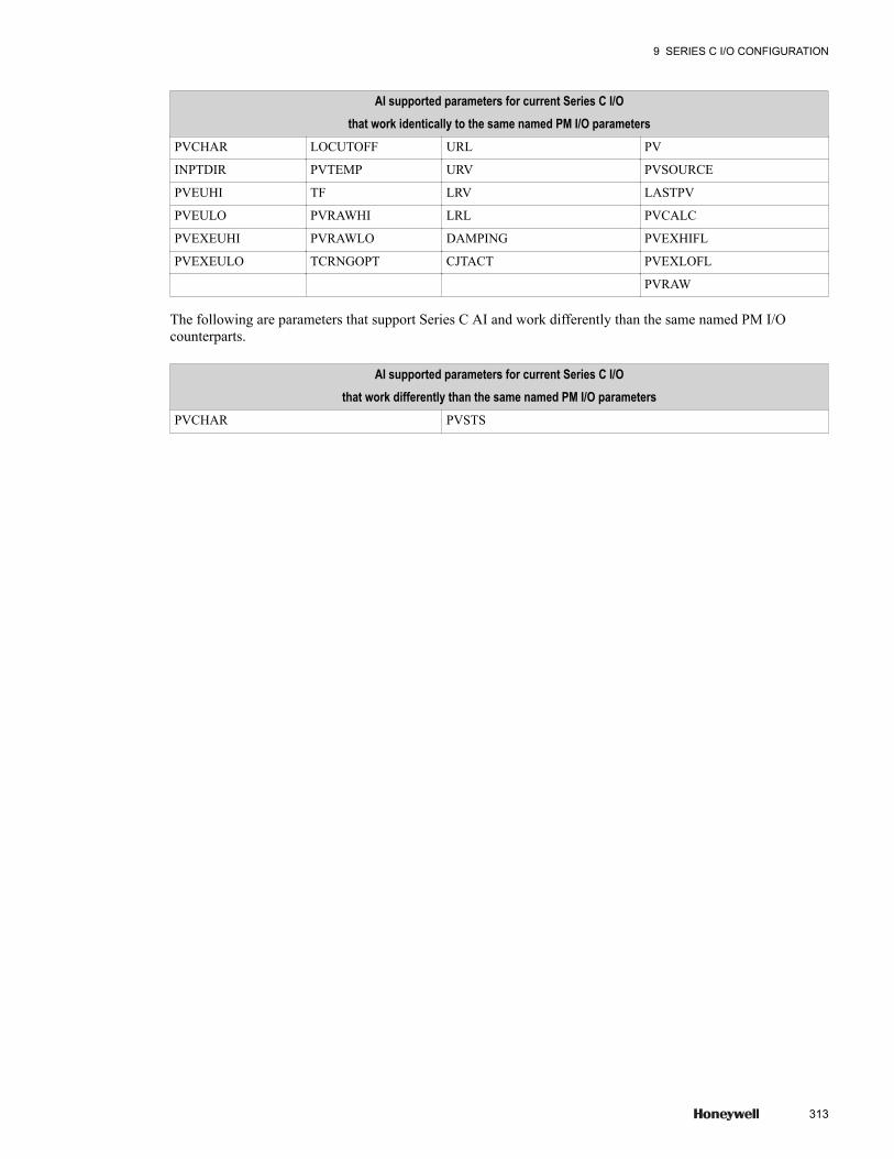
AI supported parameters for current Series C I/Othat work identically to the same named PM I/O parameters
PVCHAR LOCUTOFF URL PV
INPTDIR PVTEMP URV PVSOURCE
PVEUHI TF LRV LASTPV
PVEULO PVRAWHI LRL PVCALC
PVEXEUHI PVRAWLO DAMPING PVEXHIFL
PVEXEULO TCRNGOPT CJTACT PVEXLOFL
PVRAW
The following are parameters that support Series C AI and work differently than the same named PM I/Ocounterparts.
AI supported parameters for current Series C I/Othat work differently than the same named PM I/O parameters
PVCHAR PVSTS
9 SERIES C I/O CONFIGURATION
313

9.10 Defining AO Channel BlocksThe AO channel block represents a single analog output point on the AO-HART Modules. The AO channelblock converts the output value (OP) to a 4-20 mA output signal for operating final control elements such asvalves and actuators in the field. The OP parameter value can be controlled from an Experion regulatory point,the operator, or an SCM.
To convert the OP value to a 4-20 mA signal, the AO channel performs:
• Direct/Reverse Output Function• Nonlinear Output Characterization
The following is a functional diagram of the analog output channel block.
Figure 136: Analog Output conversion
9.10.1 Determining Direct/Reverse Output - AO Channel blocksThe OPTDIR parameter allows you to specify whether the output of the data point is:
• direct acting (where 4 mA = 0%, and 20 mA = 100%), or• reverse acting (where 4 mA = 100%, and 20 mA = 0%).
The default mode is direct acting.
9 SERIES C I/O CONFIGURATION
314 www.honeywell.com
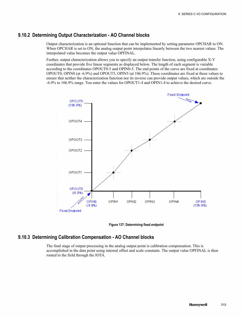
9.10.2 Determining Output Characterization - AO Channel blocksOutput characterization is an optional function that can be implemented by setting parameter OPCHAR to ON.When OPCHAR is set to ON, the analog output point interpolates linearly between the two nearest values. Theinterpolated value becomes the output value OPFINAL.
Further, output characterization allows you to specify an output transfer function, using configurable X-Ycoordinates that provide five linear segments as displayed below. The length of each segment is variableaccording to the coordinates OPOUT0-5 and OPIN0-5. The end points of the curve are fixed at coordinatesOPOUT0, OPIN0 (at -6.9%) and OPOUT5, OPIN5 (at 106.9%). These coordinates are fixed at these values toensure that neither the characterization function nor its inverse can provide output values, which are outside the-6.9% to 106.9% range. You enter the values for OPOUT1-4 and OPIN1-4 to achieve the desired curve.
Figure 137: Determining fixed endpoint
9.10.3 Determining Calibration Compensation - AO Channel blocksThe final stage of output processing in the analog output point is calibration compensation. This isaccomplished in the data point using internal offset and scale constants. The output value OPFINAL is thenrouted to the field through the IOTA.
9 SERIES C I/O CONFIGURATION
315
9.10.4 Determining Modes - AO Channel blocksThe MODE parameter determines the operating mode for the channel block. The following operating modes areapplicable to the both AO and DO channel blocks:
• Manual (Man) - provides the operator or the program with direct control over the output value of thechannel, regardless of any continuous control strategy.
• Cascade (Cas) - data point receives its output value from a primary data point.
9.10.5 Determining Output Verification - AO Channel blocksOutputs are verified by periodically reading back the value on the output screw and comparing the read backvalue with the database value. This includes an independent A-to-D conversion for the read back value.
9.10.6 Comparing parameters between Series C and PMIO that support AOThe following parameters are:
• specific to AO and found on various tabs on the AO channel block, and• work identically to the same named PM I/O counterparts.
AO supported parameters for current Series C I/Othat work identically to the same named PM I/O parameters
OPTDIR INITVAL
OPCHAR OPFINAL
OPOUT1, OPOUT2, OPOUT3, OPOUT4 COMMFAILFL
OPIN1, OPIN2, OPIN3, OPIN4 OPIN0, OPOUT0
OP OPIN5, OPOUT5
9 SERIES C I/O CONFIGURATION
316 www.honeywell.com
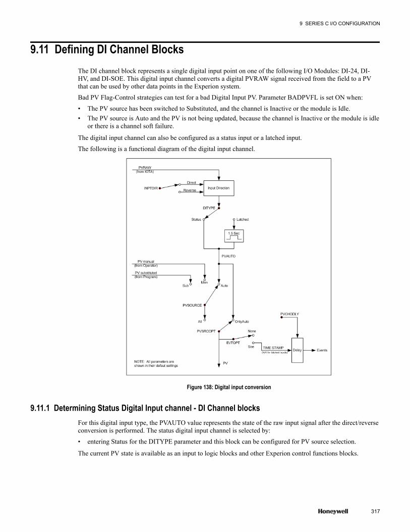
9.11 Defining DI Channel BlocksThe DI channel block represents a single digital input point on one of the following I/O Modules: DI-24, DI-HV, and DI-SOE. This digital input channel converts a digital PVRAW signal received from the field to a PVthat can be used by other data points in the Experion system.
Bad PV Flag-Control strategies can test for a bad Digital Input PV. Parameter BADPVFL is set ON when:
• The PV source has been switched to Substituted, and the channel is Inactive or the module is Idle.• The PV source is Auto and the PV is not being updated, because the channel is Inactive or the module is idle
or there is a channel soft failure.
The digital input channel can also be configured as a status input or a latched input.
The following is a functional diagram of the digital input channel.
Figure 138: Digital input conversion
9.11.1 Determining Status Digital Input channel - DI Channel blocksFor this digital input type, the PVAUTO value represents the state of the raw input signal after the direct/reverseconversion is performed. The status digital input channel is selected by:
• entering Status for the DITYPE parameter and this block can be configured for PV source selection.
The current PV state is available as an input to logic blocks and other Experion control functions blocks.
9 SERIES C I/O CONFIGURATION
317
PV Source Selection - The PV source parameter (PVSOURCE) option determines the source of the PV for astatus input channel. The source can be:
• the PV input from the field (PVRAW),• the PV state entered by the operator (PV manual), or• it can be supplied by a user program (PV substituted).
PVSOURCE has no effect on the latched options of the digital input channel. If PVSOURCE is AUTO, PVtracks PVRAW.
9.11.2 Determining Latched Digital Input channel - DI Channel blocksTo capture the occurrence of momentary digital inputs, such as from push buttons, the digital input channel isconfigured as a latched input.
Configuring the channel as latched is accomplished by setting:
• DITYPE to Latched.
When configured as a latched input channel, an input pulse that is on for a minimum of 40 milliseconds islatched true for 1.5 seconds. This ensures that any control function block that needs to monitor this inputexecutes at least once during the time that the signal is latched on.
When the DITYPE is set latch, the EVTOPT cannot be SOE and vice versa.
9.11.3 Comparing parameters between Series C and PMIO that support DIThe following parameters are:
• specific to DI and found on various tabs on the DI channel block, and• work identically to the same named PM I/O counterparts.
DI supported parameters for current Series C I/Othat work identically to the same named PM I/O parameters
DITYPE PVRAW
PV BADPVFL
The following are parameters that support Series C DI and work differently than the same named PM I/Ocounterparts.
DI supported parameters for current Series C I/Othat work differently than the same named PM I/O parameters
PVSTS
9.11.4 Open Wire Detection - DI Channel blocksThe open wire diagnostic detects and annunciates broken field wires. In addition, a seemingly valid PV from achannel diagnosed as having a broken-wire will not be made available (thus preventing incorrect control action).
The Digital Input module requires the installation of a bleed resistor (approx. 22k ohm) at the switching devicebetween the 24VDC source and the terminal providing the switched signal. If this resistor is not installed andopen wire detection is enabled (OWDENBL = ON) a false open wire alarm will be generated whenever theinput device is not closed (i.e., PVRAW = OFF).
If open wire detection is enabled (OWDENBL = ON) and the IOM detects the broken-wire condition, then
• PVCALC will be NaN, in which case, PVAUTO will be NaN.
9 SERIES C I/O CONFIGURATION
318 www.honeywell.com

• Soft Failure 179 'Open Wire Detected' is generated, and• PVRAW and PVAUTO will consequently be set to OFF.
Note that Open Wire Detection is supported only with the 24VDC IOTAs and not for the following:
• The high voltage DI modules• The DI-SOE module• The GI-IS IOTAs
If a GI-IS IOTA (CC-GDILxx) is used, open wire detection as described above may not be used.
• In these cases, OWDENBL must be set to OFF for all channels.• As an alternative to Series C open wire detection, you may use the Line Fault Detection (LFD) feature of the
MTL Switch/Proximity Detector Interfaces.
– If LFD is enabled (through a switch on the device) for any channel, two resistors must be installed: a 22kohm resistor across the switch and a 680-ohm resistor in series with the power supply lead. This featuredetects both open and short circuits. When LFD is enabled and a line fault is detected the MTL deviceilluminates an LED indicator and forces the channel data to OFF.
– If a MTL4510, MTL4511, or MTL4516 device is used, there is no indication to EPKS.– If the MTL4517 is used channel 31 is energized to ON. Note that for the MTL4517 if any channel has
LFD enabled channel 31 is not available for use as a general purpose input - for the other three deviceschannel 31 is always available.
AttentionOpen wire detection is not supported in DI (Cx-PDIL51) module. The configuration mismatch warning messageappears when you select the OWDENBL option and loads DICHANNEL FB to AI-HART (Cx-PDIL51) module.After loading the module, the channel can be activated. However, the OWDENBL parameter value appears as'FALSE.'
9 SERIES C I/O CONFIGURATION
319
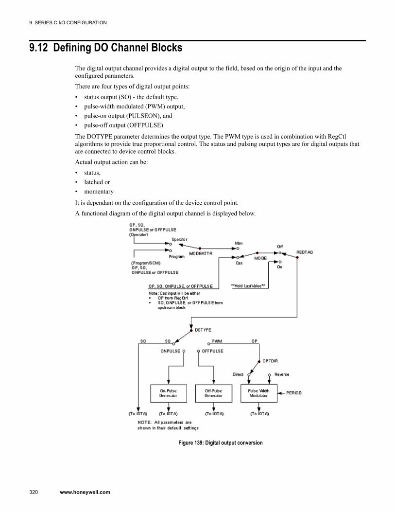
9.12 Defining DO Channel BlocksThe digital output channel provides a digital output to the field, based on the origin of the input and theconfigured parameters.
There are four types of digital output points:
• status output (SO) - the default type,• pulse-width modulated (PWM) output,• pulse-on output (PULSEON), and• pulse-off output (OFFPULSE)
The DOTYPE parameter determines the output type. The PWM type is used in combination with RegCtlalgorithms to provide true proportional control. The status and pulsing output types are for digital outputs thatare connected to device control blocks.
Actual output action can be:
• status,• latched or• momentary
It is dependant on the configuration of the device control point.
A functional diagram of the digital output channel is displayed below.
Figure 139: Digital output conversion
9 SERIES C I/O CONFIGURATION
320 www.honeywell.com
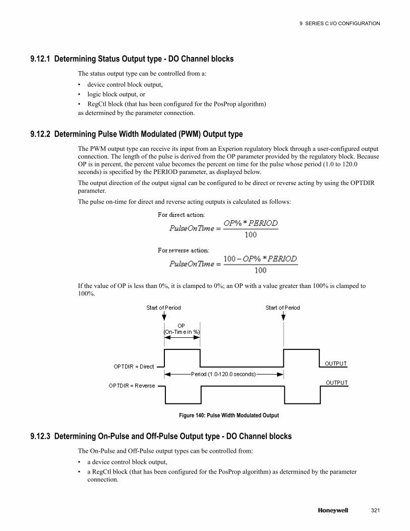
9.12.1 Determining Status Output type - DO Channel blocksThe status output type can be controlled from a:
• device control block output,• logic block output, or• RegCtl block (that has been configured for the PosProp algorithm)as determined by the parameter connection.
9.12.2 Determining Pulse Width Modulated (PWM) Output typeThe PWM output type can receive its input from an Experion regulatory block through a user-configured outputconnection. The length of the pulse is derived from the OP parameter provided by the regulatory block. BecauseOP is in percent, the percent value becomes the percent on time for the pulse whose period (1.0 to 120.0seconds) is specified by the PERIOD parameter, as displayed below.
The output direction of the output signal can be configured to be direct or reverse acting by using the OPTDIRparameter.
The pulse on-time for direct and reverse acting outputs is calculated as follows:
If the value of OP is less than 0%, it is clamped to 0%; an OP with a value greater than 100% is clamped to100%.
Figure 140: Pulse Width Modulated Output
9.12.3 Determining On-Pulse and Off-Pulse Output type - DO Channel blocksThe On-Pulse and Off-Pulse output types can be controlled from:
• a device control block output,• a RegCtl block (that has been configured for the PosProp algorithm) as determined by the parameter
connection.
9 SERIES C I/O CONFIGURATION
321

Pulsed operation (pulse on or pulse-off) can be obtained by linking the output connections to the ONPULSE andOFFPULSE parameters, respectively.
Figure 141: On-Pulse and Off-Pulse Output types
TipStandalone DO channels configured for On-Pulse or Off-Pulse are not supported. These blocks must have aparameter connection to an upstream block. SCM writes or other writes using Program access level are notpermitted.
The Status Output (SO) setting is impacted by the ONPULSE and OFFPULSE parameters as indicated in thefollowing table.
Table 95: Status Output settings
Parameter Status Output (SO) setting If SO is set to 0.0ONPULSE On - for specified duration SO is immediately set to OFF
OFFPULSE Off - for specified duration SO is immediately set to ON
To provide consistent and safe behavior, the following occurs when setting DOTYPE to either ONPULSE orOFF PULSE.
Table 96: Setting DOTYPE to ONPULSE or OFFPULSE
If ThenMODE is MAN the ONPULSE and OFFPULSE parameters only accept operator writes.
(Program access level writes and NOT all other writes are accepted.)
operator access level writes to SO are accepted and writing SO terminates anactive pulse.
PTEXECST is ACTIVE changing MODE to CAS sets the output to the quiescent state
PTEXECST is ACTIVE always sets the output to the quiescent state
9.12.4 Determining Initialization Request Flag - DO Channel blocksThe request to initialize a DO channel is accomplished through the INITREQ or PWMINITREQ parameters.
9 SERIES C I/O CONFIGURATION
322 www.honeywell.com

Table 97: DO channel initialization
The following is setto ON
And
INITREQ • Control strategies in Experion cannot manipulate the output.• Device Control blocks and Position Proportional control algorithms are automatically forced to
initialize when outputting to a Digital Output channel.• When one or more of the following is true:
– the IOMSTATE is IDLE, or– StandbyMan is Active, or– PTEXECST is INACTIVE– channel MODE is set to MAN, or– there is a soft failure and the point is not working
NOTE: Device Control blocks and Position Proportional control algorithms are automatically forcedto initialize when outputting to a Digital Output channel whose INITREQ is ON
9.12.5 Determining Modes - DO Channel blocksThe MODE parameter determines the operating mode for the channel block. The following operating modes areapplicable to the both DO and AO channel blocks:
• Manual (Man) - provides the operator or the program with direct control over the output value of thechannel, regardless of any continuous control strategy.
• Cascade (CAS) - data point receives its output value from a primary data point.
TipOperators are only permitted to change MODE if MODEPERM is set to Permit and REDTAG is set to off.
9.12.6 Determining Output Verification - DO Channel blocksOutputs are verified by periodically reading back the value on the output screw and comparing the read backvalue with the database value. This includes an output wiggle (for the safety system) to prove they are not stuckin any one state.
9.12.7 Determining Over-current protection - DO Channel blocksDigital outputs are protected from inadvertent over-current conditions. If a DO channel consumes more currentthan it should the IOM posts a soft failure and sheds to manual control. Supervisor intervention is required toreturn the channel to normal operation. Over-current conditions are typically the result of a shorted device orcapable.
9.12.8 Comparing parameters between Series C and PMIO that support DOThe following parameters are:
• specific to DO and found on various tabs on the DO channel block.• work identically to the same named PM I/O counterparts.
DO supported parameters for current Series C I/Othat work identically to the same named PM I/O parameters
OPTDIR SOINITVAL COMMFAILFL
9 SERIES C I/O CONFIGURATION
323

DO supported parameters for current Series C I/Othat work identically to the same named PM I/O parameters
SO ONPULSE, OFFPULSE PERIOD
SOREADFAIL OP, OPINITVAL
9 SERIES C I/O CONFIGURATION
324 www.honeywell.com
9.13 Electronic Short-Circuit Protection (DO-24V only)The behavior of the Series C Digital Output - 24V with Electronic Short Circuit Protection (in the presence ofwiring faults) causes a DO channel that draws more current than is permitted, to activate the IOM hardware'selectronic short-circuit protection mechanism causing that channel to go unpowered. The feature applies tothese specific model numbers:
• CC-PDOB01 Digital Output IO Module (IOM) (32 channels at 24V)• CC-TDOB01 DO IOTA (32 channels at 24V)• CC-TDOB11 DO IOTA Redundant (32 channels at 24V)
9.13.1 Non-redundant ConfigurationWhen the electronic short-circuit protection mechanism activates and the channel goes unpowered the non-redundant IOM:
• detects the output inconsistency and generates Soft Failure 23 - Failure in OP circuit/field wiring detected byAO/DO
• detects the over current and generates: Soft Failure 180 - Output Short Circuit Detected• sets:
– the output to unpowered– Shed Mode to Manual control.– Shed ModeAttr to Operator.
You should expect to see:
• Two Soft Failures
– Soft Failure 23 - Failure in OP circuit/field wiring detected by AO/DO– Soft Failure 180 - Output Short Circuit Detected
• The output unpowered• The channel in Manual mode
9.13.2 Redundant ConfigurationThe firmware in a Primary IOM of a redundant pair notices the output miscompare and signals the SecondaryIOM to assume the role of the Primary IOM (assuming the Secondary is synced).
The most common cause for the DO over-current is a failure in the field there is a minor probability that theIOM itself might be the cause of the problem. Given this, it is a common behavior for Series C IOMs to alwaysswitchover in an attempt to localize the fault.
TipNote that the Primary switchover in most cases is done before actually experiencing the over current condition.
If the cause for the DO over-current is a failure in the field, then the new Primary will see the same outputmiscompare problem, and react like a non-redundant module would - it will:
• Detect the output miscompare generate Soft Failure 23 - Failure in OP circuit/field wiring detected byAO/DO.
• Detect the over current and generate Soft Failure 180 - Output Short Circuit Detected• Set the output to unpowered.• Shed Mode to Manual control.• Shed ModeAttr to Operator.
9 SERIES C I/O CONFIGURATION
325
You should expect to see:
• One Soft Failure posted from the former Primary:• Soft Failure 23 - Failure in OP circuit/field wiring detected by AO/DO• A IOM Failover event
The following are likely if the fault was in the field:
– Two Soft Failures posted by the new Primary:
Soft Failure 23 - Failure in OP circuit/field wiring detected by AO/DO Soft Failure 180 - Output ShortCircuit Detected
– The output unpowered– The channel in Manual mode– The former Primary's output miscompare Soft Failure will Return To Normal once both modules
synchronize.
9.13.3 Electronic Short-Circuit Fault RecoveryTo return the channel to normal operation the shorted device or shorted wiring must be corrected.
9.13.4 To clear the short-circuit fault:
CAUTIONImmediately after the IOM detects the fault and the DO Channel is set to OFF, it should be safe to performmaintenance action.
Once the DO channel is set ON, no maintenance action can occur.
1 Find and clear the wiring fault. This must be done prior to attempting to restore the DO channel to on-control.NOTE: The fault may exist at various locations including the IOM, IOTA, external field devices and wiringconnecting these devices. After attempting to clear the fault at any of these locations, Step 2 below should befollowed.
2 Once the actual fault has been cleared, your appropriate plant personnel can restore the DO Channel tonormal operation by setting the DO while still in Manual or setting the mode to Cascade and resuming DOwrites (programmatically based on user strategy).
3 This concludes this procedure.
9 SERIES C I/O CONFIGURATION
326 www.honeywell.com
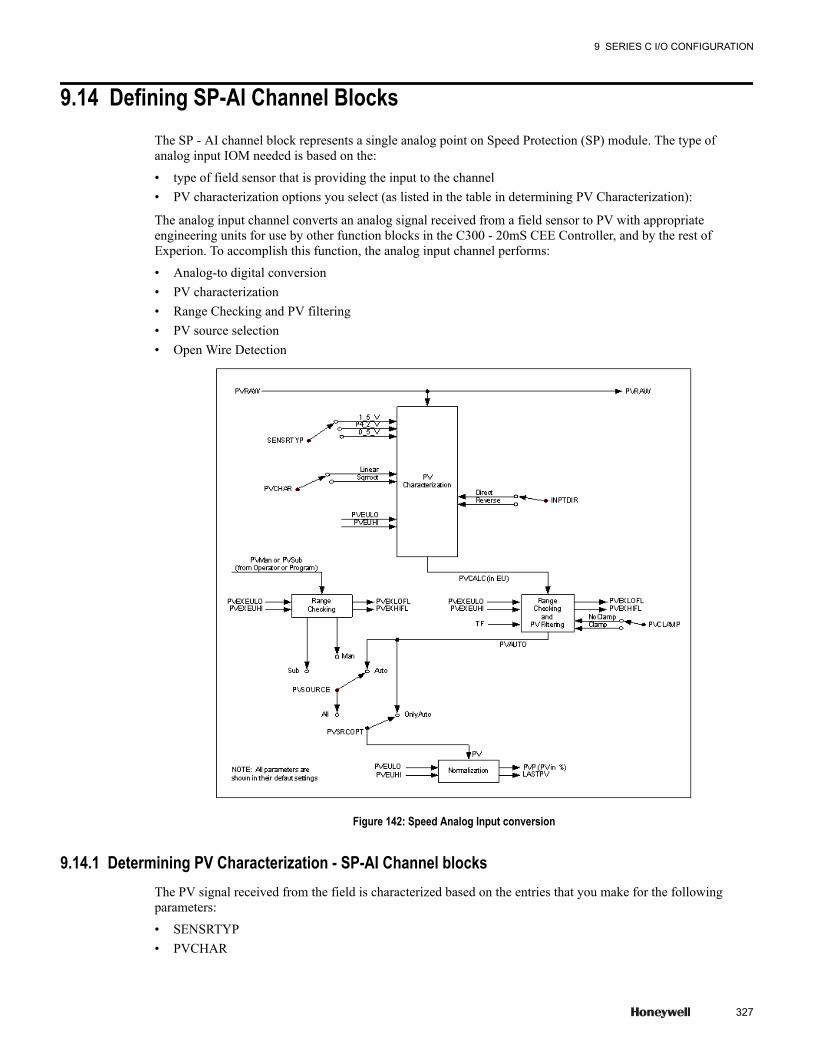
9.14 Defining SP-AI Channel BlocksThe SP - AI channel block represents a single analog point on Speed Protection (SP) module. The type ofanalog input IOM needed is based on the:
• type of field sensor that is providing the input to the channel• PV characterization options you select (as listed in the table in determining PV Characterization):
The analog input channel converts an analog signal received from a field sensor to PV with appropriateengineering units for use by other function blocks in the C300 - 20mS CEE Controller, and by the rest ofExperion. To accomplish this function, the analog input channel performs:
• Analog-to digital conversion• PV characterization• Range Checking and PV filtering• PV source selection• Open Wire Detection
Figure 142: Speed Analog Input conversion
9.14.1 Determining PV Characterization - SP-AI Channel blocksThe PV signal received from the field is characterized based on the entries that you make for the followingparameters:
• SENSRTYP• PVCHAR
9 SERIES C I/O CONFIGURATION
327
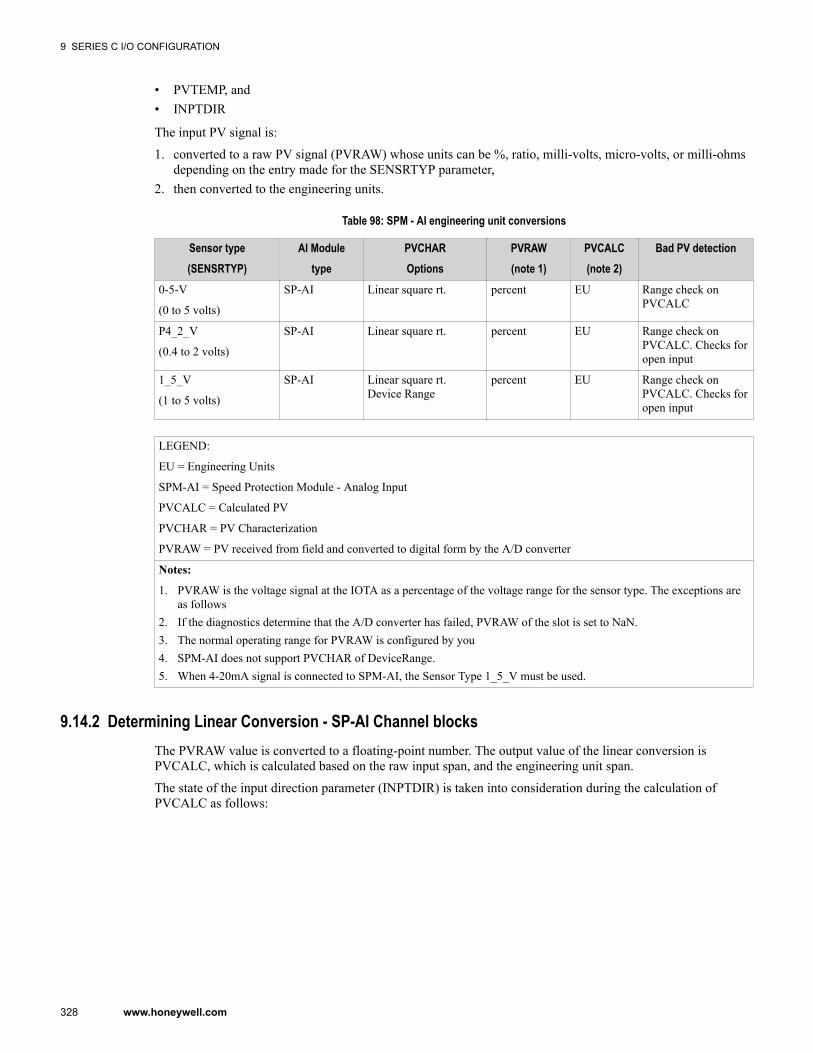
• PVTEMP, and• INPTDIR
The input PV signal is:
1. converted to a raw PV signal (PVRAW) whose units can be %, ratio, milli-volts, micro-volts, or milli-ohmsdepending on the entry made for the SENSRTYP parameter,
2. then converted to the engineering units.
Table 98: SPM - AI engineering unit conversions
Sensor type(SENSRTYP)
AI Moduletype
PVCHAROptions
PVRAW(note 1)
PVCALC(note 2)
Bad PV detection
0-5-V
(0 to 5 volts)
SP-AI Linear square rt. percent EU Range check onPVCALC
P4_2_V
(0.4 to 2 volts)
SP-AI Linear square rt. percent EU Range check onPVCALC. Checks foropen input
1_5_V
(1 to 5 volts)
SP-AI Linear square rt.Device Range
percent EU Range check onPVCALC. Checks foropen input
LEGEND:
EU = Engineering Units
SPM-AI = Speed Protection Module - Analog Input
PVCALC = Calculated PV
PVCHAR = PV Characterization
PVRAW = PV received from field and converted to digital form by the A/D converter
Notes:
1. PVRAW is the voltage signal at the IOTA as a percentage of the voltage range for the sensor type. The exceptions areas follows
2. If the diagnostics determine that the A/D converter has failed, PVRAW of the slot is set to NaN.3. The normal operating range for PVRAW is configured by you4. SPM-AI does not support PVCHAR of DeviceRange.5. When 4-20mA signal is connected to SPM-AI, the Sensor Type 1_5_V must be used.
9.14.2 Determining Linear Conversion - SP-AI Channel blocksThe PVRAW value is converted to a floating-point number. The output value of the linear conversion isPVCALC, which is calculated based on the raw input span, and the engineering unit span.
The state of the input direction parameter (INPTDIR) is taken into consideration during the calculation ofPVCALC as follows:
9 SERIES C I/O CONFIGURATION
328 www.honeywell.com
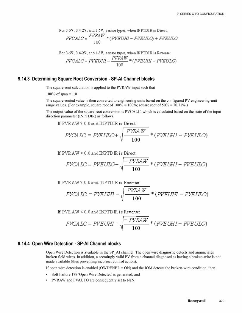
9.14.3 Determining Square Root Conversion - SP-AI Channel blocksThe square-root calculation is applied to the PVRAW input such that
100% of span = 1.0
The square-rooted value is then converted to engineering units based on the configured PV engineering-unitrange values. (For example, square root of 100% = 100%; square root of 50% = 70.71%.)
The output value of the square-root conversion is PVCALC, which is calculated based on the state of the inputdirection parameter (INPTDIR) as follows.
9.14.4 Open Wire Detection - SP-AI Channel blocksOpen Wire Detection is available in the SP_AI channel. The open wire diagnostic detects and annunciatesbroken field wires. In addition, a seemingly valid PV from a channel diagnosed as having a broken-wire is notmade available (thus preventing incorrect control action).
If open wire detection is enabled (OWDENBL = ON) and the IOM detects the broken-wire condition, then
• Soft Failure 179 'Open Wire Detected' is generated, and• PVRAW and PVAUTO are consequently set to NaN.
9 SERIES C I/O CONFIGURATION
329

9.14.5 Checking and Filtering PV Range - SP-AI Channel blocksPV range checking ensures that the PVCALC output of PV characterization is within limits defined byparameters PVEXEULO and PVEXEUHI. If either of the limits is violated and clamping is not specified, theoutput of PVAUTO is set to NaN. If clamping has been specified, the output of PVAUTO is clamped toPVEXEUHI or PVEXEULO, except when PVRAW, PVCALC, and PVAUTO are consequently set to NaN.
If the range-checked and filtered value is less than the value specified by the user-configured LOCUTOFFparameter, the final output PVAUTO is forced to PVEULO.
You can perform first-order filtering on PVCALC, through parameter TF (filter lag time).
9 SERIES C I/O CONFIGURATION
330 www.honeywell.com
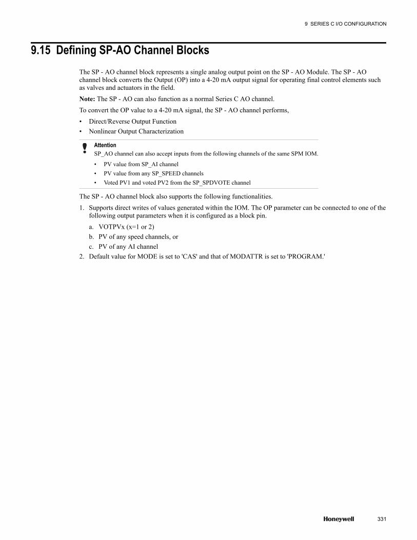
9.15 Defining SP-AO Channel BlocksThe SP - AO channel block represents a single analog output point on the SP - AO Module. The SP - AOchannel block converts the Output (OP) into a 4-20 mA output signal for operating final control elements suchas valves and actuators in the field.
Note: The SP - AO can also function as a normal Series C AO channel.
To convert the OP value to a 4-20 mA signal, the SP - AO channel performs,
• Direct/Reverse Output Function• Nonlinear Output Characterization
AttentionSP_AO channel can also accept inputs from the following channels of the same SPM IOM.
• PV value from SP_AI channel• PV value from any SP_SPEED channels• Voted PV1 and voted PV2 from the SP_SPDVOTE channel
The SP - AO channel block also supports the following functionalities.
1. Supports direct writes of values generated within the IOM. The OP parameter can be connected to one of thefollowing output parameters when it is configured as a block pin.
a. VOTPVx (x=1 or 2)b. PV of any speed channels, orc. PV of any AI channel
2. Default value for MODE is set to 'CAS' and that of MODATTR is set to 'PROGRAM.'
9 SERIES C I/O CONFIGURATION
331
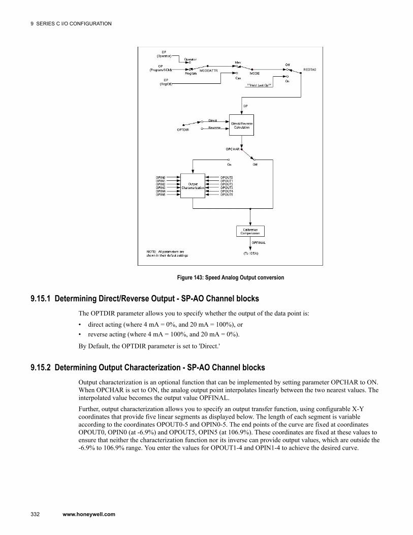
Figure 143: Speed Analog Output conversion
9.15.1 Determining Direct/Reverse Output - SP-AO Channel blocksThe OPTDIR parameter allows you to specify whether the output of the data point is:
• direct acting (where 4 mA = 0%, and 20 mA = 100%), or• reverse acting (where 4 mA = 100%, and 20 mA = 0%).
By Default, the OPTDIR parameter is set to 'Direct.'
9.15.2 Determining Output Characterization - SP-AO Channel blocksOutput characterization is an optional function that can be implemented by setting parameter OPCHAR to ON.When OPCHAR is set to ON, the analog output point interpolates linearly between the two nearest values. Theinterpolated value becomes the output value OPFINAL.
Further, output characterization allows you to specify an output transfer function, using configurable X-Ycoordinates that provide five linear segments as displayed below. The length of each segment is variableaccording to the coordinates OPOUT0-5 and OPIN0-5. The end points of the curve are fixed at coordinatesOPOUT0, OPIN0 (at -6.9%) and OPOUT5, OPIN5 (at 106.9%). These coordinates are fixed at these values toensure that neither the characterization function nor its inverse can provide output values, which are outside the-6.9% to 106.9% range. You enter the values for OPOUT1-4 and OPIN1-4 to achieve the desired curve.
9 SERIES C I/O CONFIGURATION
332 www.honeywell.com

Figure 144: Determining fixed endpoint
9.15.3 Determining Calibration Compensation - SP-AO Channel blocksThe final stage of output processing in the analog output point is calibration compensation. This isaccomplished in the data point using internal offset and scale constants. The output value OPFINAL is thenrouted to the field through the IOTA.
9.15.4 Determining Modes - SP-AO Channel blocksThe MODE parameter determines the operating mode for the channel block. The following operating modes areapplicable to SPM - AO and SPM - DO channel blocks:
• Manual (Man) - provides the operator or the program with direct control over the output value of thechannel, regardless of any continuous control strategy.
• Cascade (CAS) - data point receives its output value from a primary data point.• Normal - reflects the NMODEATTR and NMODE parameter values, which was configured.
9.15.5 Determining Output Verification - SP-AO Channel blocksOutputs are verified by periodically reading back the value on the output screw and comparing the read backvalue with the database value. This includes an independent A-to-D conversion for the read back value.
9 SERIES C I/O CONFIGURATION
333
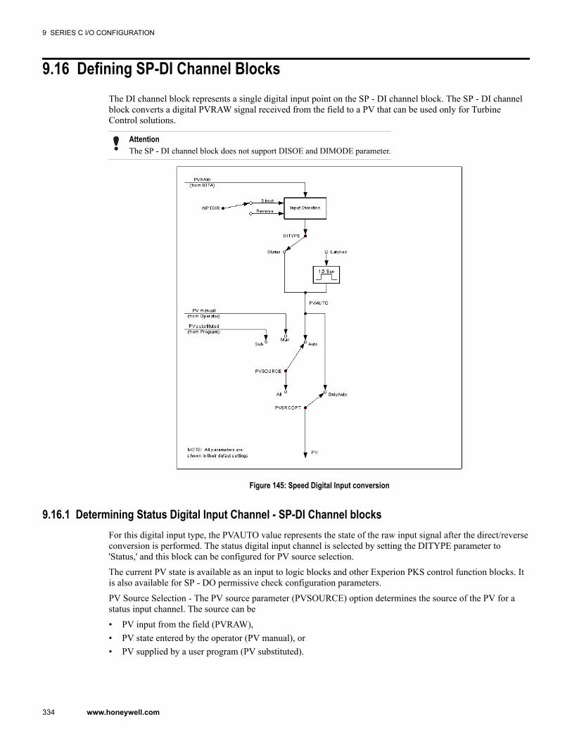
9.16 Defining SP-DI Channel BlocksThe DI channel block represents a single digital input point on the SP - DI channel block. The SP - DI channelblock converts a digital PVRAW signal received from the field to a PV that can be used only for TurbineControl solutions.
AttentionThe SP - DI channel block does not support DISOE and DIMODE parameter.
Figure 145: Speed Digital Input conversion
9.16.1 Determining Status Digital Input Channel - SP-DI Channel blocksFor this digital input type, the PVAUTO value represents the state of the raw input signal after the direct/reverseconversion is performed. The status digital input channel is selected by setting the DITYPE parameter to'Status,' and this block can be configured for PV source selection.
The current PV state is available as an input to logic blocks and other Experion PKS control function blocks. Itis also available for SP - DO permissive check configuration parameters.
PV Source Selection - The PV source parameter (PVSOURCE) option determines the source of the PV for astatus input channel. The source can be
• PV input from the field (PVRAW),• PV state entered by the operator (PV manual), or• PV supplied by a user program (PV substituted).
9 SERIES C I/O CONFIGURATION
334 www.honeywell.com

PVSOURCE has no effect on the DITYPE of the digital input channel if PVSOURCE is AUTO, and PV tracksPVRAW.
9.16.2 Determining Latched Digital Input Channel - SP-DI Channel blocksTo capture the occurrence of momentary digital inputs, such as from push buttons, the digital input channel isconfigured as a latched input.
Configuring the channel as latched is accomplished by setting:
• DITYPE to 'Latched'
When the digital input channel is configured as a latched input channel, an input pulse that is ON for aminimum of 5 milliseconds is latched TRUE for 1.5 seconds. This ensures that any control function block, thatneeds to monitor this input, executes at least once during the time that the signal is latched.
9.16.3 Open Wire Detection - SP-DI Channel blocksThe SP - DI channel supports open wire diagnostics to detect and annunciate broken field wires. In addition, PVis displayed as 'BAD' to prevent incorrect control action.
Ensure that a bleed resistor (~ 22k ohm) resistor is installed at the switching device providing the switchedsignal. If this resistor is not installed and open wire detection is enabled (OWDENBL = ON), a false open wirealarm is generated whenever the input device is not closed (i.e., PVRAW = OFF).
If open wire detection is enabled and the IOM detects the broken-wire condition,
• Soft Failure 179 'Open Wire Detected' is generated, and• PVRAW and PVAUTO is set to OFF
The DI channel supports PV flag with reset option, which can be used as an interlock option in the SPD - DOchannel block.
Note: When PV is set to 'OFF,' PV.FLWRST is still set to 'ON' until you set RESETTRIP to 'ON.'
9 SERIES C I/O CONFIGURATION
335

9.17 Defining SP-DO Channel BlocksThe digital output channel provides a digital output to the field, based on the origin of the input and theconfigured parameters.
There are two types of digital output points:
• status output (SO) - the default type, and• on-pulse output (ONPULSE)
AttentionNormally Open (NO), Normally Closed (NC), and RTN are provided for four relay contacts for customizedconfigurations. You must use appropriately rated fuses in the relay output."
The DOTYPE parameter determines the output type. The status and on pulse output types are for digital outputsthat are connected to device control blocks.
Actual output action can be any one of the following depending on the configuration of the device control point.
• status or• latched
The SP - DO channel block supports multiple interlock checks prior to DO change. Eight interlock checkparameters are available and are set to 'OFF' by default. The interlock check parameters can be connected withany one of the following flags.
• PV and PV.FLWRST of any DI Channel block of the same SP IOM only.• XXXX. FL, where XXXX can be any one of - VOTPVxHIALM, VOTROCxPOSHIALM,
VOTPVxHHALM or VOTROCxPOSHHALM - x=1 and 2, of local SP - SPDVOTE channel.• XXXX. FLWRST, where XXXX can be any one of VOTPVxHHALM or VOTROCxPOSHHALM - x=1
and 2, of local SP - SPDVOTE channel.• YYYY. FL, where YYYY can be any one of PVHIALM, ROCPOSHIALM, PVHHALM or
ROCPOSHHALM of local SP - SPEED channel.• YYYY. FLWRST, where YYYY can be any one of PVHHALM or ROCPOSHHALM of local SP - SPEED
channel.
Attention• The interlock parameters (I1 to I8) that are not connected are not used for interlock processing.• The response time of the DO trip achieved using the interlock configuration is faster than that of the alarms
reported using any function blocks such as FLAG or DIGACQ blocks. Hence, the TripValue displayed in theStation for the Data Acquisition Block alarms and the PV at the time when the DO was tripped may notnecessarily be same.
• LastTripReason parameter does not hold the value when the SPM power cycle happens. To retain theLastTripReason value, perform the following:
1. connect the alarm flags that are configured as interlocks to a FirstOut block2. Use the same alarm flags for determining the interlock, which caused the trip in SPM.
A functional diagram of the digital output channel is displayed.
9 SERIES C I/O CONFIGURATION
336 www.honeywell.com
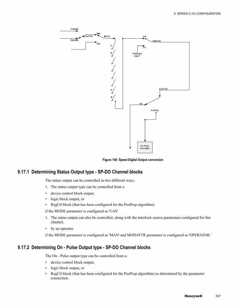
Figure 146: Speed Digital Output conversion
9.17.1 Determining Status Output type - SP-DO Channel blocksThe status output can be controlled in two different ways.
1. The status output type can be controlled from a
• device control block output,• logic block output, or• RegCtl block (that has been configured for the PosProp algorithm)
if the MODE parameter is configured as 'CAS'
1. The status output can also be controlled, along with the interlock source parameters configured for thischannel,
• by an operator
if the MODE parameter is configured as 'MAN' and MODATTR parameter is configured as 'OPERATOR.'
9.17.2 Determining On - Pulse Output type - SP-DO Channel blocksThe On - Pulse output type can be controlled from a:
• device control block output,• logic block output, or• RegCtl block (that has been configured for the PosProp algorithm) as determined by the parameter
connection.
9 SERIES C I/O CONFIGURATION
337
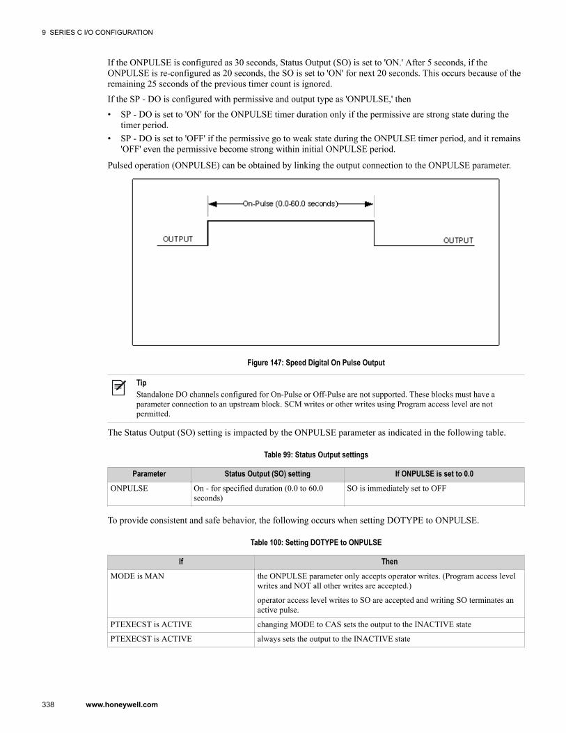
If the ONPULSE is configured as 30 seconds, Status Output (SO) is set to 'ON.' After 5 seconds, if theONPULSE is re-configured as 20 seconds, the SO is set to 'ON' for next 20 seconds. This occurs because of theremaining 25 seconds of the previous timer count is ignored.
If the SP - DO is configured with permissive and output type as 'ONPULSE,' then
• SP - DO is set to 'ON' for the ONPULSE timer duration only if the permissive are strong state during thetimer period.
• SP - DO is set to 'OFF' if the permissive go to weak state during the ONPULSE timer period, and it remains'OFF' even the permissive become strong within initial ONPULSE period.
Pulsed operation (ONPULSE) can be obtained by linking the output connection to the ONPULSE parameter.
Figure 147: Speed Digital On Pulse Output
TipStandalone DO channels configured for On-Pulse or Off-Pulse are not supported. These blocks must have aparameter connection to an upstream block. SCM writes or other writes using Program access level are notpermitted.
The Status Output (SO) setting is impacted by the ONPULSE parameter as indicated in the following table.
Table 99: Status Output settings
Parameter Status Output (SO) setting If ONPULSE is set to 0.0ONPULSE On - for specified duration (0.0 to 60.0
seconds)SO is immediately set to OFF
To provide consistent and safe behavior, the following occurs when setting DOTYPE to ONPULSE.
Table 100: Setting DOTYPE to ONPULSE
If ThenMODE is MAN the ONPULSE parameter only accepts operator writes. (Program access level
writes and NOT all other writes are accepted.)
operator access level writes to SO are accepted and writing SO terminates anactive pulse.
PTEXECST is ACTIVE changing MODE to CAS sets the output to the INACTIVE state
PTEXECST is ACTIVE always sets the output to the INACTIVE state
9 SERIES C I/O CONFIGURATION
338 www.honeywell.com
9.17.3 Determining Initialization Request Flag - SP-DO Channel blocksThe request to initialize a SP - DO channel is accomplished through the INITREQ or PWMINITREQparameters.
Table 101: SP - DO channel initialization
If ThenINITREQ is set toON
• Control strategies in Experion cannot manipulate the output.• Device Control blocks and Position Proportional control algorithms are automatically forced to
initialize when sending output to a SP - DO channel.• When one or more of the following is true:
– the IOMSTATE is IDLE, or– StandbyMan is Active, or– PTEXECST is INACTIVE– channel MODE is set to MAN, or– there is a soft failure and the point is not working
NOTE: Device Control blocks and Position Proportional control algorithms are automatically forcedto initialize when sending output to a SP - DO channel whose INITREQ is ON.
9.17.4 Determining Modes - SP-DO Channel blocksThe MODE parameter determines the operating mode for the channel block. The following operating modes areapplicable to the SP - DO and SP - AO channel blocks:
• Manual (Man) - provides the operator or the program with direct control over the output value of thechannel, regardless of any continuous control strategy.
• Cascade (CAS) - data point receives its output value from a primary data point.
Tip• The default value of MODATTR is OPERATOR.• The default value of MODE is MAN.
9.17.5 Fail-safe configuration - SP-DO Channel blocksThe recommended fail-safe configuration for the SP_DO channel is:
• READY flag of DO is set 'ON' for normal operation only if all the interlocks are met.• READY flag of DO is set to 'OFF' for trip operation if there is any failure in any of the interlocks.
9 SERIES C I/O CONFIGURATION
339
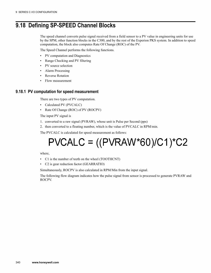
9.18 Defining SP-SPEED Channel BlocksThe speed channel converts pulse signal received from a field sensor to a PV value in engineering units for useby the SPM, other function blocks in the C300, and by the rest of the Experion PKS system. In addition to speedcomputation, the block also computes Rate Of Change (ROC) of the PV.
The Speed Channel performs the following functions.
• PV computation and Diagnostics• Range Checking and PV filtering• PV source selection• Alarm Processing• Reverse Rotation• Flow measurement
9.18.1 PV computation for speed measurementThere are two types of PV computation.
• Calculated PV (PVCALC)• Rate Of Change (ROC) of PV (ROCPV)
The input PV signal is
1. converted to a raw signal (PVRAW), whose unit is Pulse per Second (pps)2. then converted to a floating number, which is the value of PVCALC in RPM/min.
The PVCALC is calculated for speed measurement as follows:
where,
• C1 is the number of teeth on the wheel (TOOTHCNT)• C2 is gear reduction factor (GEARRATIO)
Simultaneously, ROCPV is also calculated in RPM/Min from the input signal.
The following flow diagram indicates how the pulse signal from sensor is processed to generate PVRAW andROCPV.
9 SERIES C I/O CONFIGURATION
340 www.honeywell.com
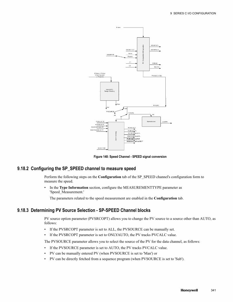
Figure 148: Speed Channel - SPEED signal conversion
9.18.2 Configuring the SP_SPEED channel to measure speedPerform the following steps on the Configuration tab of the SP_SPEED channel's configuration form tomeasure the speed.
• In the Type Information section, configure the MEASUREMENTTYPE parameter as'Speed_Measurement.'
The parameters related to the speed measurement are enabled in the Configuration tab.
9.18.3 Determining PV Source Selection - SP-SPEED Channel blocksPV source option parameter (PVSRCOPT) allows you to change the PV source to a source other than AUTO, asfollows:
• If the PVSRCOPT parameter is set to ALL, the PVSOURCE can be manually set.• If the PVSRCOPT parameter is set to ONLYAUTO, the PV tracks PVCALC value.
The PVSOURCE parameter allows you to select the source of the PV for the data channel, as follows:
• If the PVSOURCE parameter is set to AUTO, the PV tracks PVCALC value.• PV can be manually entered PV (when PVSOURCE is set to 'Man') or• PV can be directly fetched from a sequence program (when PVSOURCE is set to 'Sub').
9 SERIES C I/O CONFIGURATION
341

9.18.4 Detecting Speed Input FailureThe speed channel's input may fail due to sensor failure, open wire or if the wheel moves away from sensors,and so on. In such scenarios,
• if previous speed PV is less than 200 RPM, speed channel
– sets PV to 0, and– generates the 'No Pulse Input' soft failure,
and the speed channel's 'Zero Speed Detection Flag' is set to 'ON'.
• if previous speed PV is greater than 200 RPM, speed channel
– sets PV to NaN, and– generates 'No Pulse Input' soft failure,
and the speed channel's 'Zero Speed Detection Flag' is not set to 'ON'.
9.18.5 Detecting Reverse RotationReverse rotation is checked by monitoring the phase lag between SP_SPEED channels. Following is the pre-requisite to detect the reverse rotation during installation.
• Two SP_SPEED channels that are used for reverse rotation detection are mounted to have a 90 degree (+/-10degree tolerance) phase difference between the pulses.
Note: If the phase difference between the pulses from SPEED channels changes substantially, reverse rotationdetection may not work. In this scenario, the probe positions may need to be adjusted.
The direction of positive turbine rotation is recorded during normal turbine operation when the turbine speedexceeds 500 RPM. The reverse rotation flag is set to ON when there is a phase change observed consistentlybetween the two speed channels for few rotations.
9.18.6 Measuring flow in the turbine flow metersWith R410, SP_SPEED channel can be configured to measure the flow in the turbine flow meters. The flow PVis computed using the following formula.
where the Timebase can be configured as any one of the following:
• /Second, Timebase = 1• /Minute, Timebase = 60• /Hour, Timebase = 3600• /Day, Timebase = 86400
9.18.7 Configuring the SP_SPEED channel to measure the flowPerform the following steps on the Configuration tab of the SP_SPEED channel's configuration form tomeasure the flow in the turbine flow meters.1 In the Type Information section, configure the MEASUREMENTTYPE parameter as 'Flow_Measurement.'
The parameters related to the flow measurement are enabled in the Configuration tab.
9 SERIES C I/O CONFIGURATION
342 www.honeywell.com
2 In the PV Configuration section, configure TIMEBASE parameter as any one of the following based onyour requirement.• \Second• \Minute• \Hour• \Day
3 In the Flow Information section, ensure that the ORDEROFKFACTOR parameter is configured as '1stOrder.'
4 In the Flow Information section, type the value of the KFACTOR as required for flow meter.
9 SERIES C I/O CONFIGURATION
343
9.19 Defining SP-SPDVOTE Channel BlocksThe SP - SPDVOTE channel block accepts multiple inputs (PV1, PV2, PV3, and PV4) from the SP - SPEEDblock of the parent IOM to compute Voted PVs (VOTPV1 and VOTPV2) and Voted ROCs (VOTROC1 andVOTROC2). It generates alarms such as over speed/acceleration, for the Voted PV or ROC.
AttentionYou are recommended to use the DATAACQ block for generating alarms such as over speed, over acceleration, underspeed, and under acceleration, using the SP_SPEED and SP_SPDVOTE PV parameters.
The Voted PV can be connected to
• any function blocks that are running in C300 - 20mS CEE Controller, or• OP parameter of SP - AO channel in the same SPM.
The SP-SPDVOTE channel allows you to configure all flags for generating alarms or processing control logic.
The output pins can be connected to the interlock parameters of the parent IOM's SP - DO channel and it can beused as a trip signal.
AttentionSP_SPDVOTE block pins PV1, PV2, PV3, and PV4 accept connections only from the PV pins of local SP_SPEEDchannel block pins. All other connections to PV1, PV2, PV3 and PV4 pins of SP_SPDVOTE logic block are blocked.
9.19.1 Voting Logic Algorithm ExecutionThere are two different pairs of output.
• Voted PVs (VOTPV1 and VOTPV2)• Voted ROCs (VOTROC1 and VOTROC2)
These output are obtained by processing the inputs received from the SPEED block. The inputs are processedusing the voting logic. This block supports two groups of voting logic.
• Voting Logic Group 1• Voting Logic Group 2
A maximum of 3 channels can be configured as part of each voting group. The selection is based onGRPxVOTCHENB[1..4], where x = 1 or 2.
AttentionIf the total number of valid inputs is less than the configured inputs (GRPxMIN), the VOTPVx (x = 1, or 2) is set toNaN.
It is possible to configure the same channel to both voting groups.
The algorithm sets
• The flag - (GRPxIGNORD x=1, 2) indicating if any of the inputs is ignored by the voting logic.• The Individual flags for each input indicating if it was ignored (GRPxIGNORDFL [1..4] x=1, 2).
The voted PV processing is explained as follows.
9 SERIES C I/O CONFIGURATION
344 www.honeywell.com

Figure 149: Voting logic algorithm execution
To configure the voting logic algorithm, perform the following steps.
1. Select Median (MED) as the voting algorithm (set VOTALGx = Med). The VOTALGx is set to 'NONE' bydefault. When 'NONE' is selected, the processing of voted PV, ROC and alarm processing is disabled for thatparticular group.
2. Select the number of channels for specific voting logic group using GRPxVOTCHENB[1..4] parameter,where x = 1 or 2.
3. Select the number of minimum valid inputs using GRPxNMIN parameter, where x=1, 2. The GRPxNMINparameter can be 1, 2 or 3.
4. If the GRPxNMIN is set as 3, the output of the voting block (VOTPVx) is the median of the 1, 2, and 3inputs.
Note: If any of the Speed channel's PV is NaN, the output of the voting block (VOTPVx) is also NaN, andVOTPVxSTS = BAD.
5. If the GRPxNMIN is set as 2, the output of the voting block (VOTPVx) is based on 'MEDOPT parameterstatus.' The MEDOPT parameter can be 'MIN' or 'MAX'
Note: If any of the Speed channel's PV is NaN, the output of the voting block (VOTPVx) is also NaN,VOTPVxSTS = BAD
AttentionSame combination of channels must not be configured for voting logic groups.
Example:
If the channel 1, 2, and 3 is configured for the voting logic group 1, the same channels must not configured for thevoting logic group 2.
9 SERIES C I/O CONFIGURATION
345
9.20 Defining SVP-AI Channel blockThe SVP - AI channel block represents a single analog point on Servo Valve Positioner (SVP) module. The typeof analog input IOM needed is based on the:
• type of field sensor that is providing input to the channel• PV characterization options you select (as listed in the table 'Determining PV Characterization'):
AttentionIn SVPM, position inputs in the input channels must be configured using the SENSRTYP parameter.
The analog input channel converts an analog signal received from a field sensor to PV with appropriateengineering units for use by other function blocks in the C300 - 20mS CEE Controller and by the rest ofExperion. To accomplish this function, the analog input channel, performs:
• Analog-to digital conversion• PV characterization• Range checking and PV filtering• PV source selection• Open wire detection
9.20.1 Determining PV Characterization if SENSRTYP is configured as 'LVDT' or 'RVDT' or 'Resolver'The PV signal received from the field is characterized based on the entries that you make for the SENSRTYPparameter.
The input PV signal is converted to a raw PV signal (PVRAW) whose units can be % in case of LVDT/RVDTand degree in case of Resolver.
9 SERIES C I/O CONFIGURATION
346 www.honeywell.com
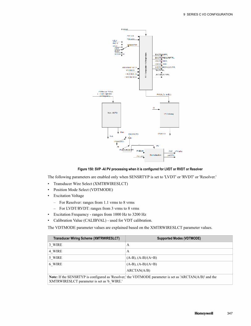
Figure 150: SVP -AI PV processing when it is configured for LVDT or RVDT or Resolver
The following parameters are enabled only when SENSRTYP is set to 'LVDT' or 'RVDT' or 'Resolver.'
• Transducer Wire Select (XMTRWIRESLCT)• Position Mode Select (VDTMODE)• Excitation Voltage
– For Resolver: ranges from 1.1 vrms to 8 vrms– For LVDT/RVDT: ranges from 3 vrms to 8 vrms
• Excitation Frequency - ranges from 1000 Hz to 3200 Hz• Calibration Value (CALIBVAL) - used for VDT calibration.
The VDTMODE parameter values are explained based on the XMTRWIRESLCT parameter values.
Transducer Wiring Scheme (XMTRWIRESLCT) Supported Modes (VDTMODE)3_WIRE A
4_WIRE A
5_WIRE (A-B), (A-B)/(A+B)
6_WIRE (A-B), (A-B)/(A+B)
ARCTAN(A/B)
Note: If the SENSRTYP is configured as 'Resolver,' the VDTMODE parameter is set as 'ARCTAN(A/B)' and theXMTRWIRESLCT parameter is set as '6_WIRE.'
9 SERIES C I/O CONFIGURATION
347
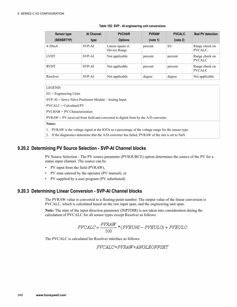
Table 102: SVP - AI engineering unit conversions
Sensor type(SENSRTYP)
AI Channeltype
PVCHAROptions
PVRAW(note 1)
PVCALC(note 2)
Bad PV detection
4-20mA SVP-AI Linear square rt.Device Range
percent EU Range check onPVCALC.
LVDT SVP-AI Not applicable percent percent Range check onPVCALC
RVDT SVP-AI Not applicable percent percent Range check onPVCALC
Resolver SVP-AI Not applicable degree degree Not applicable
LEGEND:
EU = Engineering Units
SVP-AI = Servo Valve Positioner Module - Analog Input
PVCALC = Calculated PV
PVCHAR = PV Characterization
PVRAW = PV received from field and converted to digital form by the A/D converter
Notes:
1. PVRAW is the voltage signal at the IOTA as a percentage of the voltage range for the sensor type.2. If the diagnostics determine that the A/D converter has failed, PVRAW of the slot is set to NaN.
9.20.2 Determining PV Source Selection - SVP-AI Channel blocksPV Source Selection - The PV source parameter (PVSOURCE) option determines the source of the PV for astatus input channel. The source can be
• PV input from the field (PVRAW),• PV state entered by the operator (PV manual), or• PV supplied by a user program (PV substituted).
9.20.3 Determining Linear Conversion - SVP-AI Channel blocksThe PVRAW value is converted to a floating-point number. The output value of the linear conversion isPVCALC, which is calculated based on the raw input span, and the engineering unit span.
Note: The state of the input direction parameter (INPTDIR) is not taken into consideration during thecalculation of PVCALC for all sensor types except Resolver as follows:
The PVCALC is calculated for Resolver interface as follows:
9 SERIES C I/O CONFIGURATION
348 www.honeywell.com
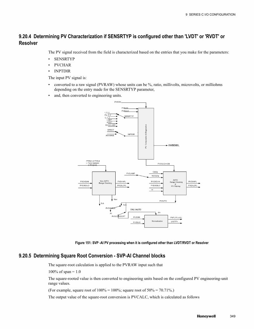
9.20.4 Determining PV Characterization if SENSRTYP is configured other than 'LVDT' or 'RVDT' orResolver
The PV signal received from the field is characterized based on the entries that you make for the parameters:
• SENSRTYP• PVCHAR• INPTDIRThe input PV signal is:
• converted to a raw signal (PVRAW) whose units can be %, ratio, millivolts, microvolts, or milliohmsdepending on the entry made for the SENSRTYP parameter,
• and, then converted to engineering units.
Figure 151: SVP -AI PV processing when it is configured other than LVDT/RVDT or Resolver
9.20.5 Determining Square Root Conversion - SVP-AI Channel blocksThe square-root calculation is applied to the PVRAW input such that
100% of span = 1.0
The square-rooted value is then converted to engineering units based on the configured PV engineering-unitrange values.
(For example, square root of 100% = 100%; square root of 50% = 70.71%.)
The output value of the square-root conversion is PVCALC, which is calculated as follows
9 SERIES C I/O CONFIGURATION
349
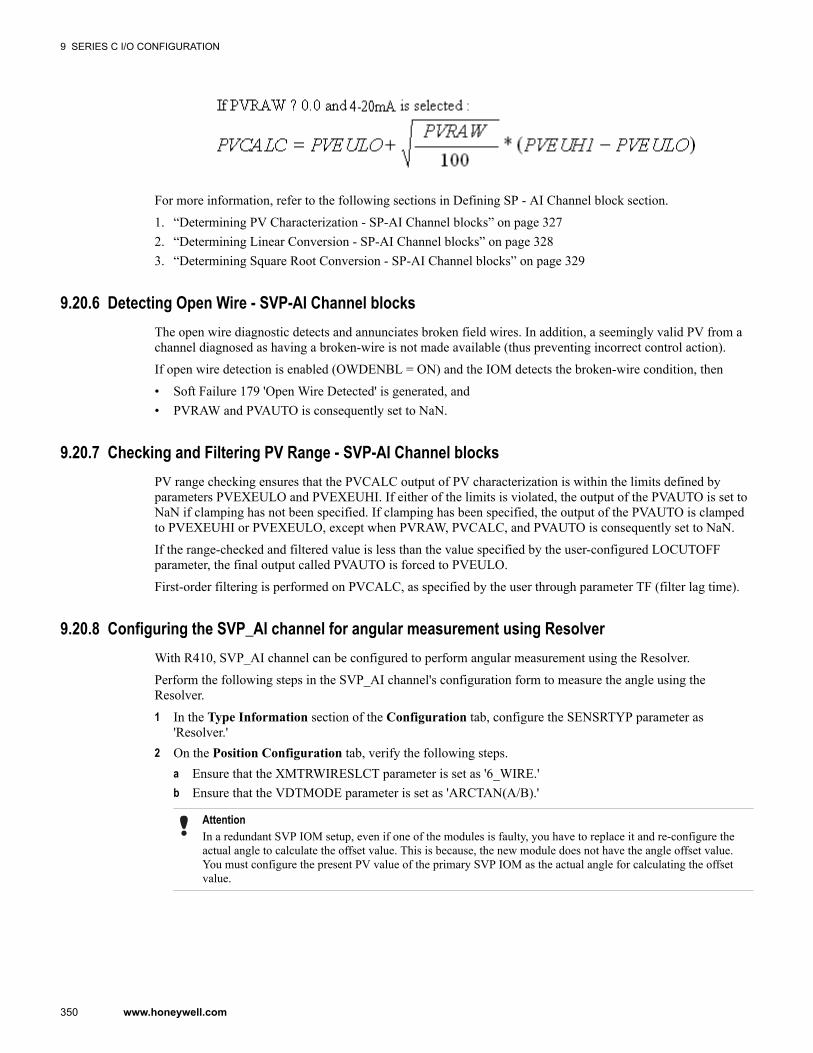
For more information, refer to the following sections in Defining SP - AI Channel block section.
1. “Determining PV Characterization - SP-AI Channel blocks” on page 3272. “Determining Linear Conversion - SP-AI Channel blocks” on page 3283. “Determining Square Root Conversion - SP-AI Channel blocks” on page 329
9.20.6 Detecting Open Wire - SVP-AI Channel blocksThe open wire diagnostic detects and annunciates broken field wires. In addition, a seemingly valid PV from achannel diagnosed as having a broken-wire is not made available (thus preventing incorrect control action).
If open wire detection is enabled (OWDENBL = ON) and the IOM detects the broken-wire condition, then
• Soft Failure 179 'Open Wire Detected' is generated, and• PVRAW and PVAUTO is consequently set to NaN.
9.20.7 Checking and Filtering PV Range - SVP-AI Channel blocksPV range checking ensures that the PVCALC output of PV characterization is within the limits defined byparameters PVEXEULO and PVEXEUHI. If either of the limits is violated, the output of the PVAUTO is set toNaN if clamping has not been specified. If clamping has been specified, the output of the PVAUTO is clampedto PVEXEUHI or PVEXEULO, except when PVRAW, PVCALC, and PVAUTO is consequently set to NaN.
If the range-checked and filtered value is less than the value specified by the user-configured LOCUTOFFparameter, the final output called PVAUTO is forced to PVEULO.
First-order filtering is performed on PVCALC, as specified by the user through parameter TF (filter lag time).
9.20.8 Configuring the SVP_AI channel for angular measurement using ResolverWith R410, SVP_AI channel can be configured to perform angular measurement using the Resolver.
Perform the following steps in the SVP_AI channel's configuration form to measure the angle using theResolver.1 In the Type Information section of the Configuration tab, configure the SENSRTYP parameter as
'Resolver.'2 On the Position Configuration tab, verify the following steps.
a Ensure that the XMTRWIRESLCT parameter is set as '6_WIRE.'b Ensure that the VDTMODE parameter is set as 'ARCTAN(A/B).'
AttentionIn a redundant SVP IOM setup, even if one of the modules is faulty, you have to replace it and re-configure theactual angle to calculate the offset value. This is because, the new module does not have the angle offset value.You must configure the present PV value of the primary SVP IOM as the actual angle for calculating the offsetvalue.
9 SERIES C I/O CONFIGURATION
350 www.honeywell.com
9.20.9 Configuring angle offset valueThe PVRAW parameter in SVP_AI channel displays the raw value of the measured angle from the Resolver. Anoffset can be applied to the raw angle using the parameters ACTUALANGLE and APPLYOFFSET.
To add an offset to the raw angle and indicate the same in PV, perform the following steps.1 In the Resolver Angle Offset section of the Position Configuration tab, enter the actual angular position in
the Actual Angle (ACTUALANGLE) box.2 Click APPLYOFFSET.
The offset value is internally calculated and is retained even if the SVP module is powered off
Consider that the Resolver PV displays 30 degree and you want to modify the actual angle as 75 degree. Inthis scenario, configure ACTUALANGLE as 75 degree and click APPLYOFFSET. As a result, the PVdisplays 75 degrees by internally applying a new offset to PVRAW.
9 SERIES C I/O CONFIGURATION
351
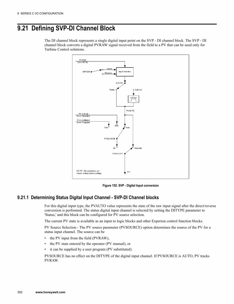
9.21 Defining SVP-DI Channel BlockThe DI channel block represents a single digital input point on the SVP - DI channel block. The SVP - DIchannel block converts a digital PVRAW signal received from the field to a PV that can be used only forTurbine Control solutions.
Figure 152: SVP - Digital Input conversion
9.21.1 Determining Status Digital Input Channel - SVP-DI Channel blocksFor this digital input type, the PVAUTO value represents the state of the raw input signal after the direct/reverseconversion is performed. The status digital input channel is selected by setting the DITYPE parameter to'Status,' and this block can be configured for PV source selection.
The current PV state is available as an input to logic blocks and other Experion control function blocks.
PV Source Selection - The PV source parameter (PVSOURCE) option determines the source of the PV for astatus input channel. The source can be
• the PV input from the field (PVRAW),• the PV state entered by the operator (PV manual), or• it can be supplied by a user program (PV substituted).
PVSOURCE has no effect on the DITYPE of the digital input channel. If PVSOURCE is AUTO, PV tracksPVRAW.
9 SERIES C I/O CONFIGURATION
352 www.honeywell.com
9.21.2 Determining Latched Digital Input Channel - SVP-DI Channel blocksTo capture the occurrence of momentary digital inputs, such as from push buttons, the digital input channel isconfigured as a latched input.
Configuring the channel as latched is accomplished by setting:
• DITYPE to 'Latched'
When configured as a latched input channel, an input pulse that is on for a minimum of 5 milliseconds is latchedTRUE for 1.5 seconds. This ensures that any control function block, that needs to monitor this input, executes atleast once during the time that the signal is latched.
9.21.3 Low Latency Mode - SVP-DI Channel blocksThe DIMODE parameter is not supported in SVP-IOM. The DI channel's inputs are sampled and processedevery 5 msec to meet latency requirements.
9.21.4 Open Wire Detection - SVP-DI Channel blocksThe SVP - DI channel supports open wire diagnostics to detect and annunciate broken field wires. In addition, avalid PV from a channel, which is received diagnosed as having a broken-wire, is made unavailable.
Ensure that a bleed resistor (~ 22k ohm) resistor is installed at the switching device providing the switchedsignal. If a resistor is not installed and open wire detection is enabled (OWDENBL = ON), a false open wirealarm is generated whenever the input device is not closed (i.e., PVRAW = OFF).
If open wire detection is enabled and the IOM detects the broken-wire condition,
• Soft Failure 179 'Open Wire Detected' is generated, and• PVRAW and PVAUTO is consequently set to OFF
9 SERIES C I/O CONFIGURATION
353
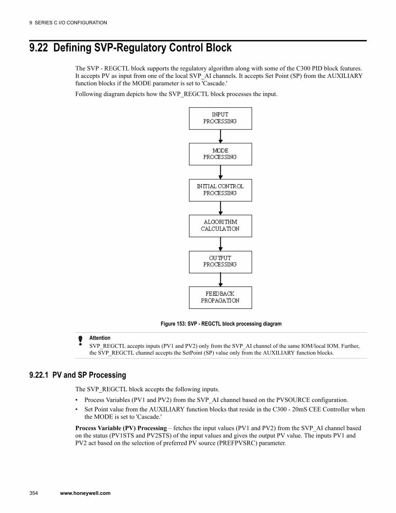
9.22 Defining SVP-Regulatory Control BlockThe SVP - REGCTL block supports the regulatory algorithm along with some of the C300 PID block features.It accepts PV as input from one of the local SVP_AI channels. It accepts Set Point (SP) from the AUXILIARYfunction blocks if the MODE parameter is set to 'Cascade.'
Following diagram depicts how the SVP_REGCTL block processes the input.
Figure 153: SVP - REGCTL block processing diagram
AttentionSVP_REGCTL accepts inputs (PV1 and PV2) only from the SVP_AI channel of the same IOM/local IOM. Further,the SVP_REGCTL channel accepts the SetPoint (SP) value only from the AUXILIARY function blocks.
9.22.1 PV and SP ProcessingThe SVP_REGCTL block accepts the following inputs.
• Process Variables (PV1 and PV2) from the SVP_AI channel based on the PVSOURCE configuration.• Set Point value from the AUXILIARY function blocks that reside in the C300 - 20mS CEE Controller when
the MODE is set to 'Cascade.'
Process Variable (PV) Processing – fetches the input values (PV1 and PV2) from the SVP_AI channel basedon the status (PV1STS and PV2STS) of the input values and gives the output PV value. The inputs PV1 andPV2 act based on the selection of preferred PV source (PREFPVSRC) parameter.
9 SERIES C I/O CONFIGURATION
354 www.honeywell.com

Set Point (SP) Processing – obtains the SP value from the AUXILIARY function blocks when the MODE isset to 'Cascade' and processes it to perform SP limit checking, SP value must be within the engineering unitrange defined by PVEUHI and PVEULO.
9.22.2 PV handling when PVSTS is BAD1. If the PVxSTS (x=1, 2) is set to 'BAD',
• the PVSTSFL.BAD is set to 'ON' in the SVP_REGCTL channel,• MODE is set to 'MAN' in the SVP_AO channel.• the calculated variable (CV) is set to 'NaN' to invoke Bad Control processing.• the BADCTLFL is set to 'High.'
Note:• When the PV is 'Bad,' AO Mode change is prohibited until PVSTS returns to 'Normal' if the MODE was in
'Shed.'• When the PV returns to 'Normal,' the channel remains in 'Manual' mode if the MODE was in 'Shed.' You
must manually change the MODE to 'Normal.'
1. If the PVxSTS (x=1, 2) is set to 'Normal',
• the PV value is normal in SVP_AI channel, and• the PVSTSFL.NORM is set to 'ON' in the SVP_REGCTL channel.
9.22.3 Set Point (SP) Limit checkingThis ensures that the SP value does not exceed the configured limits. The limits are
• SPHILM - SP high limit• SPLOLM - SP low limit
The limit values can be changed only if the status of the channel is 'InActive.' If the SP limits are changed, thenetwork Anti-Reset Windup status (ARWNET) is recalculated.
If the SP value is beyond the range specified by SPHILM and SPLOLM limits,
• the SP is clamped to the appropriate limit, and• the appropriate 'limit exceeded' flag (SPHIFL or SPLOFL) is set.
Following table explains about the SVP_REGCTL block behavior when the SP value exceeds the limits(SPHILM and SPLOLM) and the tolerance (SPTOL).
Table 103: SVP - REGCTL SetPoint processing
Scenario Limits Exceeded Tolerance Exceeded (SPTOL) SVP_REGCTL BehaviorRaise or Lower keys Yes Yes A warning message displays
as 'SP value is clamped.'
Yes No A warning message displaysas 'SP value is clamped.'
No Yes SP value is set to a newvalue without confirming thetolerance.
No No SP value is set to a newvalue.
9 SERIES C I/O CONFIGURATION
355
9.22.4 Determining and handling modesMode identifies the source of stores that is accepted by the inputs (SP and OP) of a SVP_REGCTL block.SVP_REGCTL block supports two modes of operation.
MODE = Manual (Man)The OP can be stored by the operator. The SVP_REGCTL holds its last OP value instead of computing the OPvalue, and sets input windup status (ARWNET) to 'HiLo.'
Note:• The SVP_REGCTL does not initialize when its mode is changed.• The SVP_REGCTL block does not support 'AUTO' mode, and you can store the SP value to the when the
MODE is set to 'MAN.'
MODE=Cascade (CAS)The SVP_REGCTL block obtains its input from the AUXILIARY function blocks, and calculates OP.
Mode Attribute (MODEATTR)Lets you set the block's mode attribute. MODEATTR determines if values to the output (OP) can be storedwhen the block's MODE is 'MAN.' The MODEATTR can be
• OPERATOR - only operator can store the value to OP or SP as specified by MODE.• PROGRAM - this mode is not allowed, as the SVP_REGCTL block does not accept the input from SCM.The default selection is OPERATOR.
Permit Operator Mode Changes (MODEPERM)Lets you specify if operators are permitted to make MODE changes or not. The default is 'Enabled' (selected). Astore to MODE does not change the NORMMODE.
Normal Mode (NORMMODE) and Normal Mode Attribute (NORMMODEATTR)NORMMODE - Lets you specify the MODE of the SVP_REGCTL block derived at runtime. You canconfigure the NORMMODE and NORMMODEATTR values by clicking 'NORM' in the Station Display.
The supported selections for the NORMMODE are:
• NONE• CAScade• MANualThe default selection is 'NONE.'
NORMMODEATTR - Lets you specify the mode attribute (MODEATTR) when the Control to Normalfunction is initiated through the Station display.
The supported selections for the NORMMODEATTR are:
• NONE• OPERATOR• PROGRAMThe default selection is 'NONE.'
9.22.5 Initial Control ProcessingThis function directly fetches the OP (INITVAL) value from the SVP_AO block to the SVP_REGCTL block. Inthe SVP_AO block, the OP value can be changed when the MODE is set to 'MAN.' Based on the OP value from
9 SERIES C I/O CONFIGURATION
356 www.honeywell.com
the SVP_AO block, this function performs initialization and windup activities for the SVP_REGCTL block. Inaddition, it sets the SVP_REGCTL output range (CVEUHI and CVEULO) to the SVP_AO block output range.
9.22.6 Control InitializationThe SVP_REGCTL block brings initialization requests from its secondary through BACKCALCIN. In addition,the secondary may propagate one shot initialization requests to this block. This function requests a primary toinitialize by updating the corresponding INITREQ and INITVAL parameters. Normally, the SVPREGCTLblock's OP is initialized to the SVP_AO's initialization value. However, if the initialization value exceeds theOP limits, this function clamps the OP to the violated limit.
Initial Control Processing performs the following processing, based on the value of INITMAN.
• When INITMAN changes from 'Off' to 'On': Requests the SVP_REGCTL block's windup status to berecalculated and later propagated to the primary.
• When INITMAN is 'ON': Initializes the SVP_REGCTL block's output (OP).• When INITMAN changes from 'On' to 'Off': Initializes the SVP_REGCTL block's output (OP), and
requests its windup status to be recalculated.
This function requests the primary to initialize itself if any one of the following is true:
• SVP_REGCTL block is inactive.• SVP_REGCTL is in initialization.• SVP_REGCTL is not in the Cascade.• CVEUHI or CVEULO are Bad.
9.22.7 Algorithms
AttentionSAFEOP and OUTIND parameters are not supported for SVP_REGCTL channel.
The SVP_REGCTL block executes the following algorithms.
• Equation A (Eq A) algorithm - supports time-out processing and time-out monitoring.• Equation E (Eq E) algorithm - supports both time-out processing and output biasing.
9.22.8 Output biasing processThis function enforces an output bias to the calculated Controlled Variable (CV).
The OPBIAS is the sum of the user-specified fixed bias (OPBIAS.FIX) and a calculated floating bias(OPBIAS.FLOAT). The purpose of the floating bias is to provide a bump less transfer when the function blockinitializes or changes mode as long as the SVP_REGCTL channel is the first initializable channel.
If the algorithm is configured as Equation E, the output bias (OPBIAS) is added to the algorithm's CalculatedValue (CV) and the result is stored in CV. CV is later checked against the OP limits and then if the limits are notexceeded CV is copied to the output.
• OPBIAS is recomputed under the following conditions to avoid a bump in the output. (Note that theSVP_REGCTL channel only applies OPBIAS.FLOAT to the output for the latter two conditions, when it isthe first initializable block.)
– When the function block starts up (that is, goes Active).– When the function block initializes (for example, the secondary requests initialization).– When the mode changes to Cascade.
9 SERIES C I/O CONFIGURATION
357
AttentionWhen MODE is ' ;Manual,' OPBIAS is not used (because OP is not calculated). Consequently, when MODE changesto Manual, OPBIAS is not recomputed.
• You can store to OPBIAS only if the function block is inactive or MODE is 'Manual.' Hence, prevent abump in OP is prevented when the bias is changed.
• When you store values to OPBIAS, the following occurs.
– Total bias (OPBIAS) and fixed bias (OPBIAS.FIX) are both set to a new value.• There are no limit checks applied when you store the OPBIAS. However, after the bias is added to the
calculated variable (CV), the result is compared against the OP limits and clamped, if necessary.• You can store to OPBIAS.FIX only if the function block is inactive and SVP_REGCTL is configured with
the control algorithm equation as 'E.' When you store to OPBIAS.FIX, the following occurs.
– Total bias (OPBIAS) and fixed bias (OPBIAS.FIX) are both set to a new value.
9.22.9 Time-out monitoringIf MODE is set to 'Cascade,' SVP_REGCTL channel monitors its SP input value (that is, primary input) fortime-out. If a valid SP value is not received within the predefined time, the SVP_REGCTL channel invokestime-out processing. The time-out time (in seconds) is specified by TMOUTTIME.
• Enable time-out monitoring by setting TMOUTTIME to a non-zero value.• Disable time-out monitoring by setting TMOUTTIME to zero.
9.22.10 Time-out processingA time-out can occur for several reasons communication error, inactivation of primary block, and so on. If aninput times-out, SVP_REGCTL channel performs setting a time-out flag (TMOUTFL), requesting the primaryblock to initialize, and shedding the SVP_REGCTL channel to a predefined mode (TMOUTMODE).
If MODE is set to 'Cascade' and the SP time-out, the SVP_REGCTL channel performs the following:
• Sets a time-out flag (TMOUTFL).• Requests the primary to initialize.
AttentionIn SVP_REGCTL channel, the primary can be an ENHGENLIN block and AUXILIARY Function block fromC300-20mS CEE Controller and no initialization happens to it.
The SVP_REGCTL block supports mode-shedding on time out. In such cases, SVP_REGCTL sheds the modeto 'Manual,' and the mode does not return to 'Cascade,' even if the primary block returns a valid value.
9.22.11 Anti-reset windup statusThe SVP_REGCTL channel maintains anti-reset windup status for its output (ARWOP) and each of itsinitializable inputs (ARWNET). ARWOP indicates if OP can be raised or lowered. When ARWNET is set to'Hilo,' stores to SP are not limited, rather this is the status propagated to the primary. The only limiting anti-resetwindup status ever does is to stop integral action in one or both directions on regulatory channels.
The SVP_REGCTL channel uses ARWOP parameter to restrict integral control. When ARWOP contains avalue other than 'Normal,' the SVP_REGCTL channel stops integral control in the windup direction. Integral,proportional, and derivative control continues in the other direction. However, Windup status has no impact onproportional and derivative control.
9 SERIES C I/O CONFIGURATION
358 www.honeywell.com
9.22.12 Mode shedding on timeoutThe SVP_REGCTL block sheds the MODE to 'MAN' in case of manual intervention. Accordingly, theSVP_REGCTL does not change the MODE to 'CAS' while fetching a good value from the primary.
Attention• While disconnecting the IOLINK cables, INITREQ parameter of SVP_AO channel configured as 'Incremental' is
set to 'ON' and INITMAN parameter of SVP_REGCTL channel is set to 'ON'. Hence, SP timeout does not occurand the MODE parameter of the SVP_REGCTL channel does not shed to Timeout mode, and the MODEparameter of the SVP_AO channel is set to 'MAN'.
• The shedding of MODE to 'MAN' is dependent on the SP timeout configuration. If the SP timeout is configured as1 second, the SVP_REGCTL sheds MODE to 'MAN' on IOLINK cable removal or controller RRR duringcommunication failure. However, if the SP timeout is configured to a value other than 1 second, SVP_REGCTLdoes not shed its mode during communication failure (IOLINK cable removal or RRR of controller).
9.22.13 Output ProcessingOutput Processing derives a control output value (OP) from the calculated variable (CV). It involves thefollowing functions:
• OP limiting and clamping• OP direction
AttentionSVP_REGCTL channel OP value can only be connected to the OP of the SVP_AO channel when the OPACTIONparameter is configured as 'Incremental.'
9.22.14 Bad Control ProcessingThis function helps to take a decision when the CV changed from good-to-bad or bad-to-good.
If the CV is 'Bad'The CV can be set to 'NaN' if the SVP_REGCTL PV is bad or the CV range (CVEUHI/CVEULO) is bad.
The SVP_REGCTL block performs the following actions when the CV changes from good-to-bad.
• Sets BADCTLFL to 'ON' to indicate that a Bad Control condition exists.
Tip• The SVP_REGCTL block performs the following when the CV is set to 'Bad.'
• requests its primary to initialize if the MODE is shed to 'MAN.'• indicates to its primary that it is wound-up (ARWET = HiLo) and does not request the primary to initialize if the
MODE is not shed to 'MAN.'• CV is prohibited to change its value until CV returns to good if the MODE was shed to 'MAN.'
• The SVP_REGCTL block performs the following when the CV changes from 'Bad' to 'Good.'
• remains at 'MAN' mode and continuously sends INITREQ to it primary if the MODE sheds to 'MAN.' You mustchange the SVP_REGCTL's MODE to normal.
• clears it wind-up condition and performs a one-shot initialization if the MODE is not shed to 'MAN.' Inaddition, it requests the primary to perform the one-shot initialization.
If the CV is 'Good'The SVP_REGCTL block determines if the CV is represented in terms of percentage or engineering units(EUs). If the CV is in EUs, it is converted to percentage.
9 SERIES C I/O CONFIGURATION
359
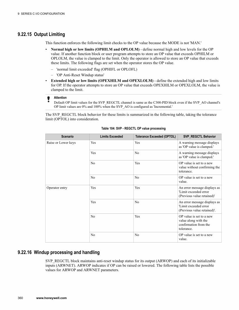
9.22.15 Output LimitingThis function enforces the following limit checks to the OP value because the MODE is not 'MAN.'
• Normal high or low limits (OPHILM and OPLOLM) - define normal high and low levels for the OPvalue. If another function block or user program attempts to store an OP value that exceeds OPHILM orOPLOLM, the value is clamped to the limit. Only the operator is allowed to store an OP value that exceedsthese limits. The following flags are set when the operator stores the OP value.
– 'normal limit exceeded' flag (OPHIFL or OPLOFL)– 'OP Anti-Reset Windup status'
• Extended high or low limits (OPEXHILM and OPEXLOLM) - define the extended high and low limitsfor OP. If the operator attempts to store an OP value that exceeds OPEXHILM or OPEXLOLM, the value isclamped to the limit.
AttentionDefault OP limit values for the SVP_REGCTL channel is same as the C300-PID block even if the SVP_AO channel'sOP limit values are 0% and 100% when the SVP_AO is configured as 'Incremental.'
The SVP_REGCTL block behavior for these limits is summarized in the following table, taking the tolerancelimit (OPTOL) into consideration.
Table 104: SVP - REGCTL OP value processing
Scenario Limits Exceeded Tolerance Exceeded (OPTOL) SVP_REGCTL BehaviorRaise or Lower keys Yes Yes A warning message displays
as 'OP value is clamped.'
Yes No A warning message displaysas 'OP value is clamped.'
No Yes OP value is set to a newvalue without confirming thetolerance.
No No OP value is set to a newvalue.
Operator entry Yes Yes An error message displays as'Limit exceeded error(Previous value retained)'
Yes No An error message displays as'Limit exceeded error(Previous value retained)'.
No Yes OP value is set to a newvalue along with theconfirmation from thetolerance.
No No OP value is set to a newvalue.
9.22.16 Windup processing and handlingSVP_REGCTL block maintains anti-reset windup status for its output (ARWOP) and each of its initializableinputs (ARWNET). ARWOP indicates if OP can be raised or lowered. The following table lists the possiblevalues for ARWOP and ARWNET parameters.
9 SERIES C I/O CONFIGURATION
360 www.honeywell.com
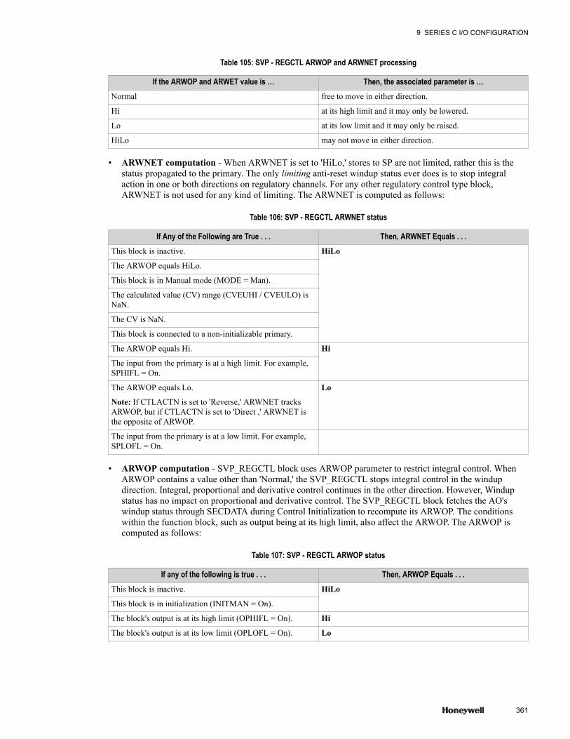
Table 105: SVP - REGCTL ARWOP and ARWNET processing
If the ARWOP and ARWET value is … Then, the associated parameter is …Normal free to move in either direction.
Hi at its high limit and it may only be lowered.
Lo at its low limit and it may only be raised.
HiLo may not move in either direction.
• ARWNET computation - When ARWNET is set to 'HiLo,' stores to SP are not limited, rather this is thestatus propagated to the primary. The only limiting anti-reset windup status ever does is to stop integralaction in one or both directions on regulatory channels. For any other regulatory control type block,ARWNET is not used for any kind of limiting. The ARWNET is computed as follows:
Table 106: SVP - REGCTL ARWNET status
If Any of the Following are True . . . Then, ARWNET Equals . . .This block is inactive. HiLo
The ARWOP equals HiLo.
This block is in Manual mode (MODE = Man).
The calculated value (CV) range (CVEUHI / CVEULO) isNaN.
The CV is NaN.
This block is connected to a non-initializable primary.
The ARWOP equals Hi. Hi
The input from the primary is at a high limit. For example,SPHIFL = On.
The ARWOP equals Lo.
Note: If CTLACTN is set to 'Reverse,' ARWNET tracksARWOP, but if CTLACTN is set to 'Direct ,' ARWNET isthe opposite of ARWOP.
Lo
The input from the primary is at a low limit. For example,SPLOFL = On.
• ARWOP computation - SVP_REGCTL block uses ARWOP parameter to restrict integral control. WhenARWOP contains a value other than 'Normal,' the SVP_REGCTL stops integral control in the windupdirection. Integral, proportional and derivative control continues in the other direction. However, Windupstatus has no impact on proportional and derivative control. The SVP_REGCTL block fetches the AO'swindup status through SECDATA during Control Initialization to recompute its ARWOP. The conditionswithin the function block, such as output being at its high limit, also affect the ARWOP. The ARWOP iscomputed as follows:
Table 107: SVP - REGCTL ARWOP status
If any of the following is true . . . Then, ARWOP Equals . . .This block is inactive. HiLo
This block is in initialization (INITMAN = On).
The block's output is at its high limit (OPHIFL = On). Hi
The block's output is at its low limit (OPLOFL = On). Lo
9 SERIES C I/O CONFIGURATION
361
9.23 Defining SVP-AO Channel BlockSVP_AO channel supports unipolar and bipolar current outputs in addition to the standard 4-20mA analogoutput. It converts the output value (OP) to the output signal for operating the final control elements, such asvalves and actuators, in the field. It accepts inputs only from ENHGENLIN block executing in the C300 - 20mSCEE Controller.
To convert the OP value to a configured signal value, the SVP_AO channel performs
• Direct/Reverse Output Function• Nonlinear Output Characterization
Note: Unipolar/bipolar does not support direction function and non-linear output characterization.
Attention• SVP_AO channel accepts inputs from the AUXILIARY function blocks only if the OPACTION parameter is
configured as 'FullValue.' SVP_AO channel accepts inputs from the SVP_REGCTL channel, the ENHGENLINblock, and the AUXILIARY function blocks when the OPACTION parameter is configured as 'Incremental.'
• Both SVPM channels must have the same output type. The output type can be 4-20mA outputs or coil outputs.There are no mutual dependencies in the coil outputs. The two channels can have unipolar or bipolar currents anddifferent ranges of outputs.
9.23.1 Determining Output Characterization - SVP-AO Channel blockOutput characterization can be implemented only if the OPACTION parameter is configured as 'FullValue.'
The OP value is calculated when the OPACTION parameter is configured as 'FullValue' as follows:
9 SERIES C I/O CONFIGURATION
362 www.honeywell.com
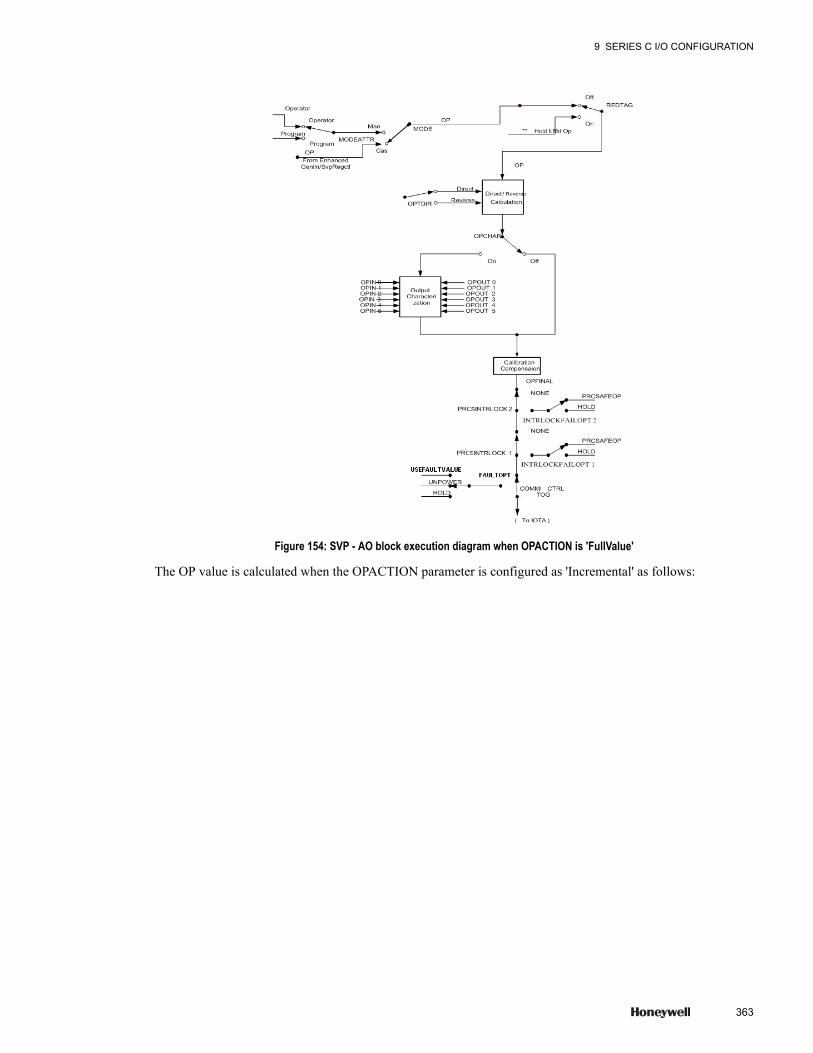
Figure 154: SVP - AO block execution diagram when OPACTION is 'FullValue'
The OP value is calculated when the OPACTION parameter is configured as 'Incremental' as follows:
9 SERIES C I/O CONFIGURATION
363
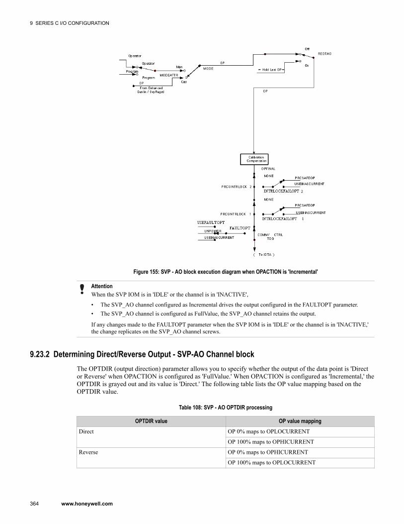
Figure 155: SVP - AO block execution diagram when OPACTION is 'Incremental'
AttentionWhen the SVP IOM is in 'IDLE' or the channel is in 'INACTIVE',
• The SVP_AO channel configured as Incremental drives the output configured in the FAULTOPT parameter.• The SVP_AO channel is configured as FullValue, the SVP_AO channel retains the output.
If any changes made to the FAULTOPT parameter when the SVP IOM is in 'IDLE' or the channel is in 'INACTIVE,'the change replicates on the SVP_AO channel screws.
9.23.2 Determining Direct/Reverse Output - SVP-AO Channel blockThe OPTDIR (output direction) parameter allows you to specify whether the output of the data point is 'Director Reverse' when OPACTION is configured as 'FullValue.' When OPACTION is configured as 'Incremental,' theOPTDIR is grayed out and its value is 'Direct.' The following table lists the OP value mapping based on theOPTDIR value.
Table 108: SVP - AO OPTDIR processing
OPTDIR value OP value mappingDirect OP 0% maps to OPLOCURRENT
OP 100% maps to OPHICURRENT
Reverse OP 0% maps to OPHICURRENT
OP 100% maps to OPLOCURRENT
9 SERIES C I/O CONFIGURATION
364 www.honeywell.com
9.23.3 Determining Modes - SVP-AO Channel blockThe MODE parameter determines the operating mode for the channel block. The following operating modes areapplicable to the both AO and DO channel blocks:
• Manual (Man) - provides the operator or the program with direct control over the output value of thechannel, regardless of any continuous control strategy.
• Cascade (CAS) - data point receives its output value from a primary data point.
However, if the OPACTION is configured as 'Incremental' and MODE is changed to 'MAN,' the AO drivesOPBIASCURRENT, until the operator manually enters a new OP value.
Attention• MODE is set to 'SHED' if the SVPM is restarted.• The SVP IOM shortly loses synchronization and resynchronizes when the MODE of SVP_AO channel sheds to
'MAN.' This scenario is applicable to only when the SVP_AO channel is configured as 'Incremental.' Due to this,the soft failures are regenerated on the secondary SVP IOM.
9 SERIES C I/O CONFIGURATION
365
9.24 Defining UIO Channel BlocksThe functionality of the UIO channel blocks is identical to that of the existing AI, AO, DI, and DO channelblocks. Depending on the channel configuration in the UIO module, each channel block represents one of theAI, AO, DI, and DO channel block.
For more information about each channel blocks, refer to the following sections in this document.
• AI channel block - “Defining AI Channel Blocks”• AO channel block - “Defining AO Channel Blocks”• DI channel block - “Defining DI Channel Blocks”• DO channel block - “Defining DO Channel Blocks”
9.24.1 Example configuration for DO channel ganging
To configure the DO channel for ganging1 Click File > New >I/O Modules > Series_C_I_O > UIO – Universal I/O, 32 channels.
The UIO module appears in the Project view under the Unassigned items.2 Assign the UIO module to an IOLINK that is configured as "SERIES_C_IO_TYPE."3 From the Project view, right-click the UIO channel and then click Block Properties.
The UIO channel configuration form appears.4 Click the Channel Configuration tab.
The Channel Configuration tab configuration form appears. The point type is selected as DI, by default.5 Configure the Channel Point Type as DO for which ganging needs to be enabled.
AttentionAn error message appears if you try to change the channel type when the channel is configured in any ControlModule.
6 Click OK.7 Click File > New > Control Module.
The Control Module chart opens.8 Drag the DO channel from the Project view to the Control Module chart.9 Double-click the DO channel.
The DO channel configuration form appears.10 Click the Configuration tab.
The Configuration tab configuration form appears.11 Select the Enable Ganged Outputs check box.
The Number of Channels Ganged drop-down list is enabled for configuration.12 Select the number of channels to be ganged from the Number of Channels Ganged drop-down list.
You may encounter errors if one of the following scenarios exists.
• Adjacent channel is not configured as DO channel.• DO channel, which needs to be configured for ganging, is already configured in any Control Module.
13 Click OK.14 Save and close the Control Module chart.15 Assign and load the Control Module.
Results<replace with description of results>
9 SERIES C I/O CONFIGURATION
366 www.honeywell.com

9.24.2 Example configuration for pulse counting functionality
To configure DI channel for pulse counting functionality1 Click File > New >I/O Modules > Series_C_I_O > UIO – Universal I/O, 32 channels.
The UIO module appears in the Project view under the Unassigned items.2 Assign the UIO module to an IOLINK that is configured as "SERIES_C_IO_TYPE."3 Click File > New > Control Module.
The Control Module chart opens.4 Drag the DI channel (15 to 18) from the Project view to the Control Module chart.5 Double-click the DI channel.
The DI channel configuration form appears.6 Click the Configuration tab.
The Configuration tab configuration form appears.7 Configure the Digital Input Type as "Accum."8 Click OK.9 Save and close the Control Module chart.10 Assign and load the Control Module.
Results<replace with description of results>
9 SERIES C I/O CONFIGURATION
367

9 SERIES C I/O CONFIGURATION
368 www.honeywell.com
10 Series C I/O Loading
Experion provides the ability to build control strategies offline, without being connected to the actual controllercomponents. The process of transferring the Control Strategy to the actual working components in the field iscalled the load operation.
The load operation:
• copies configuration data from the control strategy that is stored in the Engineering Repository Database(ERDB) to the assigned controller component in the system architecture
• assures that the planned system matches the actual one• confirms that the communication addresses and physical location assignments specified for components
through Control Builder configuration match the actual addresses and locations of components in the system
Related topics“Loading an IOLINK” on page 370“Loading the IOM block the first time” on page 371“Common I/O block load activities” on page 375“Loading a CM” on page 376“Setting Priority IOMs” on page 377
369

10.1 Loading an IOLINKThe C300 block must be loaded before any assigned IOM blocks. Loading the C300 block automatically loadsits associated configured IOLINK function blocks.
Refer to Loading IOLINK in the C300 Controller User Guide for information about loading the C300 block andcorresponding IOLINK block.
10.1.1 Upload error conditionsThe following conditions return/reload operation errors:
• The C300 is not present.• The IOM is not present.• The CM is ACTIVE.• The IOM's Execution State is RUN and the IOC block's Point Execution State is ACTIVE.
10 SERIES C I/O LOADING
370 www.honeywell.com

10.2 Loading the IOM block the first timeAll illustrations used in the procedure are for example purposes only.
To load the IOM blocks properly:
• The IOM blocks must be loaded prior to loading any Control Modules that contain associated channelblocks. This operation loads all loadable configuration parameters (residing in either the C300 or the IOMdevice).
• The load returns errors if the C300 or IOM or both are not present.
The figure below shows a simplified graphical representation of what happens during the load operation.
Figure 156: Loading the IOM block the first time
Prerequisites• This procedure assumes that I/O Modules are installed and capable of communicating with the Server.
Use the following general procedure to load an Input/Output Module (IOM). The load procedure is similar forall I/O signal-handling components.
To load the IOM1 Click desired CEE block icon in Project tab.
Selects and highlights the component.
10 SERIES C I/O LOADING
371
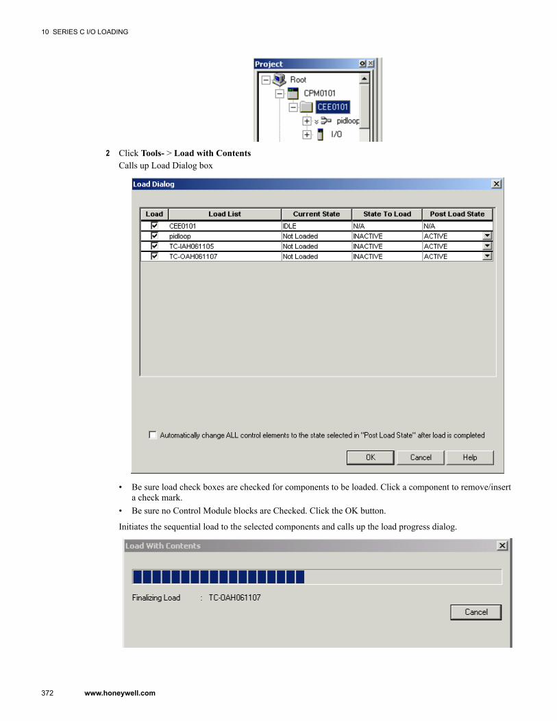
2 Click Tools- > Load with ContentsCalls up Load Dialog box
• Be sure load check boxes are checked for components to be loaded. Click a component to remove/inserta check mark.
• Be sure no Control Module blocks are Checked. Click the OK button.
Initiates the sequential load to the selected components and calls up the load progress dialog.
10 SERIES C I/O LOADING
372 www.honeywell.com
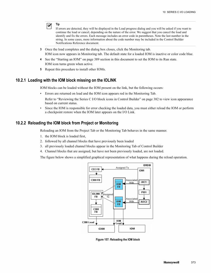
TipIf errors are detected, they will be displayed in the Load progress dialog and you will be asked if you want tocontinue the load or cancel, depending on the nature of the error. We suggest that you cancel the load andidentify and fix the errors. Each message includes an error code in parentheses. Note the last number in thestring. In some cases, more information about the code number may be included in the Control BuilderNotifications Reference document.
3 Once the load completes and the dialog box closes, click the Monitoring tab.IOM icon now appears in Monitoring tab. The default state for a loaded IOM is inactive or color code blue.
4 See the “Starting an IOM” on page 389 section in this document to set the IOM to its Run state.IOM icon turns green when active.
5 Repeat this procedure to install other IOMs.
10.2.1 Loading with the IOM block missing on the IOLINKIOM blocks can be loaded without the IOM present on the link, but the following occurs:
• Errors are returned on load and the IOM icon appears red in the Monitoring Tab.
Refer to “Reviewing the Series C I/O block icons in Control Builder” on page 382 to view icon appearancebased on current status.
• Since the IOM is responsible for error checking the loaded data, you must either reload the IOM or performa checkpoint restore when the IOM later appears on the I/O Link.
10.2.2 Reloading the IOM block from Project or MonitoringReloading an IOM from the Project Tab or the Monitoring Tab behaves in the same manner.
1. the IOM block is loaded first,2. followed by all channel blocks that have previously been loaded3. all previously loaded channel blocks appear in the Monitoring Tab of Control Builder4. Channel blocks that are assigned, but have not been previously loaded, are not loaded.
The figure below shows a simplified graphical representation of what happens during the reload operation.
Figure 157: Reloading the IOM block
10 SERIES C I/O LOADING
373
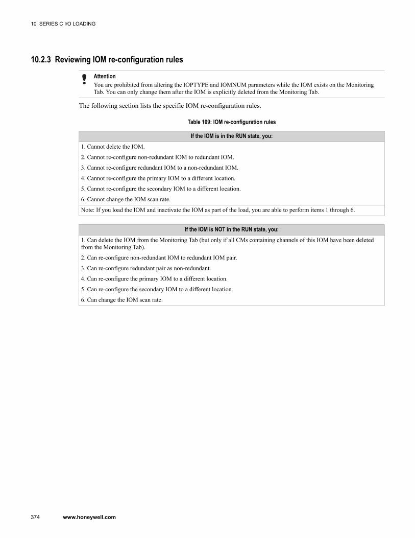
10.2.3 Reviewing IOM re-configuration rules
AttentionYou are prohibited from altering the IOPTYPE and IOMNUM parameters while the IOM exists on the MonitoringTab. You can only change them after the IOM is explicitly deleted from the Monitoring Tab.
The following section lists the specific IOM re-configuration rules.
Table 109: IOM re-configuration rules
If the IOM is in the RUN state, you:1. Cannot delete the IOM.
2. Cannot re-configure non-redundant IOM to redundant IOM.
3. Cannot re-configure redundant IOM to a non-redundant IOM.
4. Cannot re-configure the primary IOM to a different location.
5. Cannot re-configure the secondary IOM to a different location.
6. Cannot change the IOM scan rate.
Note: If you load the IOM and inactivate the IOM as part of the load, you are able to perform items 1 through 6.
If the IOM is NOT in the RUN state, you:1. Can delete the IOM from the Monitoring Tab (but only if all CMs containing channels of this IOM have been deletedfrom the Monitoring Tab).
2. Can re-configure non-redundant IOM to redundant IOM pair.
3. Can re-configure redundant pair as non-redundant.
4. Can re-configure the primary IOM to a different location.
5. Can re-configure the secondary IOM to a different location.
6. Can change the IOM scan rate.
10 SERIES C I/O LOADING
374 www.honeywell.com
10.3 Common I/O block load activities
10.3.1 Uploading the I/O blockUpload of Series C I/O blocks does not differ from the upload of other Experion blocks. All loadable parametervalues are read from the IOM and updated in the Monitoring database.
The upload operation uploads data for the selected objects from the controller to the Monitoring EngineeringRepository Database (ERDB). Upload of data for the selected objects from the server to the ERDB also can beperformed.
Usually, after performing an upload to the database, you should also update the data to Project so that both theMonitoring and the Project databases agree.
Refer to Using Upload command in the Control Building Guide for information about uploading.
10.3.2 Update to ProjectUpdate to Project Series C I/O blocks does not differ from update to Project of other Experion blocks. Allloadable parameter values are copied from the Monitoring tab to the Project tab.
10.3.3 Reviewing the Update functionA major part of the hierarchical building, CM/SCM containment allows the user to contain CM(s) or /SCM(s)into another CM.
If a projected CM/SCM is updated to project:
• All its projected parameters are checked to ensure that the projection chain downwards to the origin is valid,which includes the validation of both origin parameters and projected connections.
• Read only connections are not updated to project directly. Only projected connections will be updated.• In addition, the Update operation fails for any reason, the projected parameter will remain, but the origins of
the projected parameter will be emptied.
10.3.4 Using IOM CheckpointCheckpoint of Series C I/O blocks does not differ from checkpoint of other blocks being checkpointed.
Refer to Checkpoint Replaces Snapshot in the Control Building Guide to review checkpoint information.
10 SERIES C I/O LOADING
375
10.4 Loading a CM
Attention1. If a CM containing SP_SPDVOTE block is loaded without connection configured to its PV pins,
a. By default, the voting algorithm considers the PV values as 'BAD',b. Corresponding alarms are generated.
2. If a CM containing SVP_REGCTL block is loaded without any connection configured to its PV pins (PV1 andPV2),
a. By default, the PID algorithm considers the PV values as 'BAD',b. Corresponding flags and BADCTLFL are set.
The CM load operation loads the CM block and standard blocks to the assigned CEE function block and loadthe contained IOC block parameters to the IOM device.
Refer to Loading a CM in the Control Building Guide for information about loading a Control Module and itsassociated Control Execution Environment (CEE). The load procedure is similar for all control environmentrelated components.
10.4.1 Upload error conditionsThe following conditions return/reload operation errors:
• The C300 is not present.• The IOM is not present.• The CM is ACTIVE.• The IOM's Execution State is RUN and the IOC block's Point Execution State is ACTIVE.
10.4.2 Reloading the CM from Project or MonitoringReloading a CM from the Monitoring Tab or the Project Tab:
• reloads IOC blocks to their associated IOM devices, and• reloads the standard Experion blocks within the CM to the assigned CEE
10.4.3 Upload error conditionsThe following conditions return/reload operation errors:
• The C300 is not present.• The IOM is not present.• The CM is ACTIVE.• The IOM's Execution State is RUN and the IOC block's Point Execution State is ACTIVE.
10 SERIES C I/O LOADING
376 www.honeywell.com
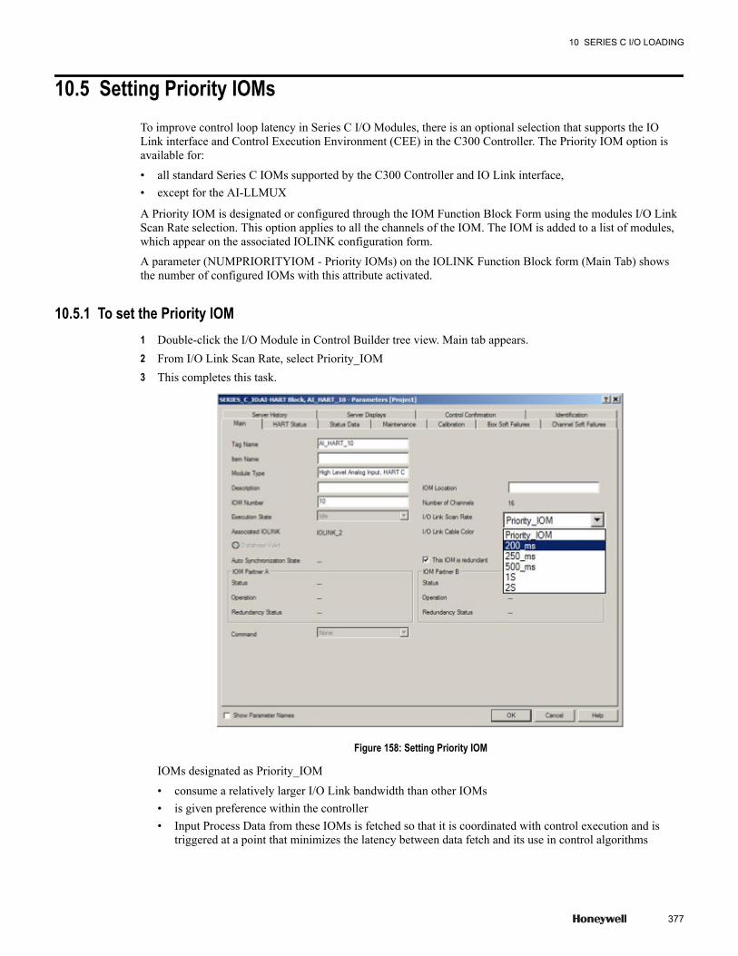
10.5 Setting Priority IOMsTo improve control loop latency in Series C I/O Modules, there is an optional selection that supports the IOLink interface and Control Execution Environment (CEE) in the C300 Controller. The Priority IOM option isavailable for:
• all standard Series C IOMs supported by the C300 Controller and IO Link interface,• except for the AI-LLMUX
A Priority IOM is designated or configured through the IOM Function Block Form using the modules I/O LinkScan Rate selection. This option applies to all the channels of the IOM. The IOM is added to a list of modules,which appear on the associated IOLINK configuration form.
A parameter (NUMPRIORITYIOM - Priority IOMs) on the IOLINK Function Block form (Main Tab) showsthe number of configured IOMs with this attribute activated.
10.5.1 To set the Priority IOM1 Double-click the I/O Module in Control Builder tree view. Main tab appears.2 From I/O Link Scan Rate, select Priority_IOM3 This completes this task.
Figure 158: Setting Priority IOM
IOMs designated as Priority_IOM
• consume a relatively larger I/O Link bandwidth than other IOMs• is given preference within the controller• Input Process Data from these IOMs is fetched so that it is coordinated with control execution and is
triggered at a point that minimizes the latency between data fetch and its use in control algorithms
10 SERIES C I/O LOADING
377
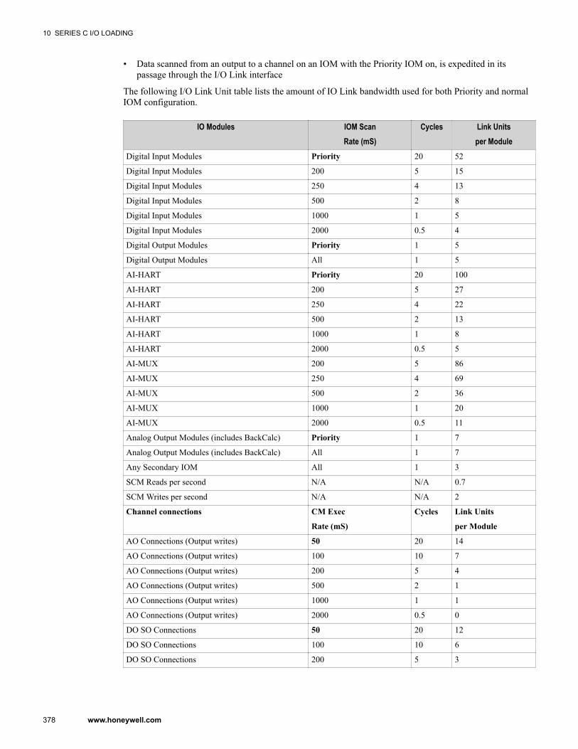
• Data scanned from an output to a channel on an IOM with the Priority IOM on, is expedited in itspassage through the I/O Link interface
The following I/O Link Unit table lists the amount of IO Link bandwidth used for both Priority and normalIOM configuration.
IO Modules IOM ScanRate (mS)
Cycles Link Unitsper Module
Digital Input Modules Priority 20 52
Digital Input Modules 200 5 15
Digital Input Modules 250 4 13
Digital Input Modules 500 2 8
Digital Input Modules 1000 1 5
Digital Input Modules 2000 0.5 4
Digital Output Modules Priority 1 5
Digital Output Modules All 1 5
AI-HART Priority 20 100
AI-HART 200 5 27
AI-HART 250 4 22
AI-HART 500 2 13
AI-HART 1000 1 8
AI-HART 2000 0.5 5
AI-MUX 200 5 86
AI-MUX 250 4 69
AI-MUX 500 2 36
AI-MUX 1000 1 20
AI-MUX 2000 0.5 11
Analog Output Modules (includes BackCalc) Priority 1 7
Analog Output Modules (includes BackCalc) All 1 7
Any Secondary IOM All 1 3
SCM Reads per second N/A N/A 0.7
SCM Writes per second N/A N/A 2
Channel connections CM Exec
Rate (mS)
Cycles Link Units
per Module
AO Connections (Output writes) 50 20 14
AO Connections (Output writes) 100 10 7
AO Connections (Output writes) 200 5 4
AO Connections (Output writes) 500 2 1
AO Connections (Output writes) 1000 1 1
AO Connections (Output writes) 2000 0.5 0
DO SO Connections 50 20 12
DO SO Connections 100 10 6
DO SO Connections 200 5 3
10 SERIES C I/O LOADING
378 www.honeywell.com

IO Modules IOM ScanRate (mS)
Cycles Link Unitsper Module
DO SO Connections 500 2 1
DO SO Connections 1000 1 1
DO SO Connections 2000 0.5 0
DO PWM Connections 50 20 30
DO SO Connections 200 5 3
DO SO Connections 500 2 1
DO SO Connections 1000 1 1
DO SO Connections 2000 0.5 0
DO PWM Connections 50 20 30
DO PWM Connections 100 10 15
DO PWM Connections 200 5 8
DO PWM Connections 500 2 3
DO PWM Connections 1000 1 2
DO PWM Connections 2000 0.5 1
10 SERIES C I/O LOADING
379

10 SERIES C I/O LOADING
380 www.honeywell.com

11 Series C I/O Operations
The following section describes the typical activities that you may be required to perform during normaloperations while using Control Builder.
381

11.1 Reviewing the Series C I/O block icons in Control BuilderAfter loading the containing CM, the I/O channel block icon appears in the Control Builder monitoring tree. Itexists under the containing CM and under the assigned IOM block. In the case of redundancy, a secondary IOMis visible in the monitoring tree.
TipThe icon's appearance is based on the ICONSTATE parameter
Table 110: Channel block icons
If icon is . . . Then, it represents . . .COMM error or CONFIG mismatch error - Primary State
red Non-redundant
both red No primary or secondary
front red
back yellow
No primary, secondary not synched
RUN - Primary State
green Non-redundant.
both green Primary, synchronized
front green
back yellow
Primary, secondary not synched
front green back red Primary, no secondary
IDLE - Primary State
blue Non-redundant
both blue Primary, synched
front blue
back yellow
Primary, secondary not synched
front blue
back red
Primary, no secondary
No Database and IDLE - Primary State
yellow Non-redundant
both yellow Primary, secondary may or may not be synched
front yellow
back red
Primary, no secondary
11 SERIES C I/O OPERATIONS
382 www.honeywell.com
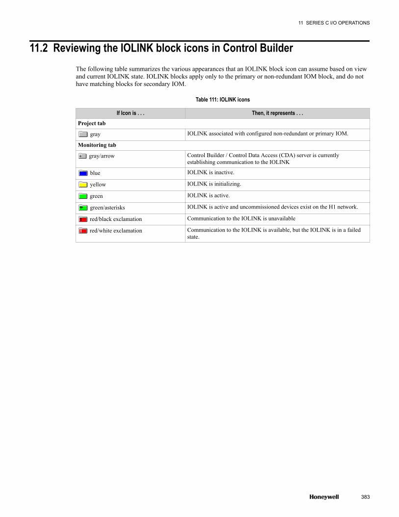
11.2 Reviewing the IOLINK block icons in Control BuilderThe following table summarizes the various appearances that an IOLINK block icon can assume based on viewand current IOLINK state. IOLINK blocks apply only to the primary or non-redundant IOM block, and do nothave matching blocks for secondary IOM.
Table 111: IOLINK icons
If Icon is . . . Then, it represents . . .Project tab
gray IOLINK associated with configured non-redundant or primary IOM.
Monitoring tab
gray/arrow Control Builder / Control Data Access (CDA) server is currentlyestablishing communication to the IOLINK
blue IOLINK is inactive.
yellow IOLINK is initializing.
green IOLINK is active.
green/asterisks IOLINK is active and uncommissioned devices exist on the H1 network.
red/black exclamation Communication to the IOLINK is unavailable
red/white exclamation Communication to the IOLINK is available, but the IOLINK is in a failedstate.
11 SERIES C I/O OPERATIONS
383

11.3 Reviewing the block icons in Control BuilderThe following table summarizes the various appearances that a block icon can assume based on view andcurrent block state. The faceplate of the block will vary to reflect the block type.
Table 112: Block icons
If Icon is . . . Then, it represents . . .Project tab
gray Block added to Project.
Monitoring tab
gray/arrow Control Builder / Control Data Access (CDA) server is currentlyestablishing communication to the block.
green Block is active
blue Block is inactive
red/exclamation Block is offnet. Communications with the block is unavailable.
11 SERIES C I/O OPERATIONS
384 www.honeywell.com
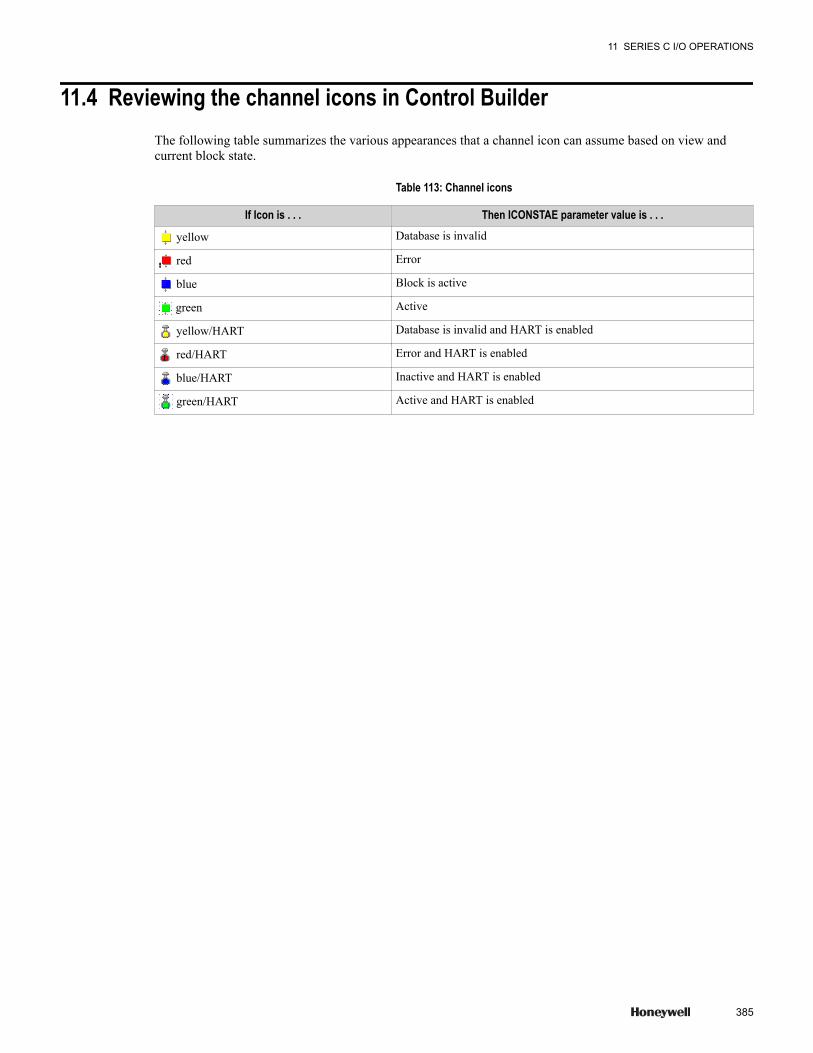
11.4 Reviewing the channel icons in Control BuilderThe following table summarizes the various appearances that a channel icon can assume based on view andcurrent block state.
Table 113: Channel icons
If Icon is . . . Then ICONSTAE parameter value is . . .
yellow Database is invalid
red Error
blue Block is active
green Active
yellow/HART Database is invalid and HART is enabled
red/HART Error and HART is enabled
blue/HART Inactive and HART is enabled
green/HART Active and HART is enabled
11 SERIES C I/O OPERATIONS
385
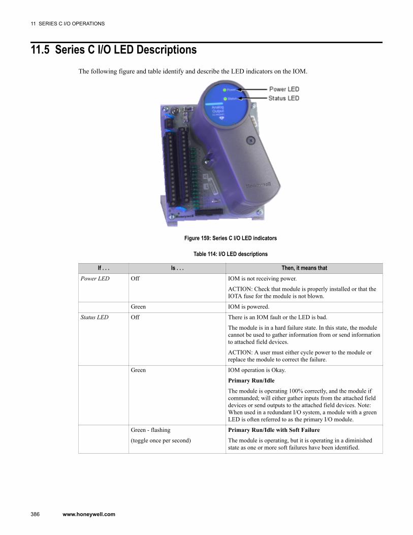
11.5 Series C I/O LED DescriptionsThe following figure and table identify and describe the LED indicators on the IOM.
Figure 159: Series C I/O LED indicators
Table 114: I/O LED descriptions
If . . . Is . . . Then, it means thatPower LED Off IOM is not receiving power.
ACTION: Check that module is properly installed or that theIOTA fuse for the module is not blown.
Green IOM is powered.
Status LED Off There is an IOM fault or the LED is bad.
The module is in a hard failure state. In this state, the modulecannot be used to gather information from or send informationto attached field devices.
ACTION: A user must either cycle power to the module orreplace the module to correct the failure.
Green IOM operation is Okay.
Primary Run/Idle
The module is operating 100% correctly, and the module ifcommanded; will either gather inputs from the attached fielddevices or send outputs to the attached field devices. Note:When used in a redundant I/O system, a module with a greenLED is often referred to as the primary I/O module.
Green - flashing
(toggle once per second)
Primary Run/Idle with Soft Failure
The module is operating, but it is operating in a diminishedstate as one or more soft failures have been identified.
11 SERIES C I/O OPERATIONS
386 www.honeywell.com
If . . . Is . . . Then, it means thatAmber The module is either not configured or operating as a
secondary.
Not Configured - The module has not been configured.
Secondary - The module is operating 100% correctly as thesecondary module. This does not imply that it is synchronizedwith the primary IOM.
Amber - flashing
(toggle once per second)
Not Configured with Soft Failure - The module has not beenconfigured and is operating with one or more active softfailures.
Secondary with Soft Failure- The module is operating as thesecondary module in a diminished state as one or more softfailures have been identified.
Red Power-on - The device is in a non-standard, transient stateand not controlling any part of your plant or process.
Module has just started and power-on self-test is running.During this time, there is no communication to the module.
Red - flashing
(toggle once per second)
The device is in a non-standard, transient state and notcontrolling any part of your plant or process.
Alive, Ready for Firmware Upgrade - The module is readyto receive an update to its internal programming instructions.
Red - fast flashing,
(toggle one quarter (1/4) second)
The device is in a non-standard, transient state and notcontrolling any part of your plant or process.
Alive, Firmware Upgrade in Progress - The module isreceiving an update to its internal programming instructions.Do not remove power to the module.
Off Failed - The module has hard failed. The module is no longercommunicating and must be power cycled or replaced.
DO channels transition to the configured fault state. If fieldpower is lost, all outputs go unpowered.
AO channels will go unpowered.
11 SERIES C I/O OPERATIONS
387
11.6 Powering up the IOMUpon power up, the IOM:
• is set to IDLE state with an invalid database (DBVALID = INVALID)• remains in this state until the IOLINK function block (C300) instructs it to change. This is due to the fact
that the C300 contains all of the IOM's configuration information.
If the IOM was:
• never previously loaded, the IOM:
– remains IDLE with an invalid database.• previously was loaded, then
– the C300 reloads the IOM, and restores it to the last state before power down occurred.
Therefore, upon powering up the IOM:
• any previously loaded channel blocks are reloaded and• the IOM and channel blocks are set to idle, or run as they were previously set before the IOM lost power.
11 SERIES C I/O OPERATIONS
388 www.honeywell.com
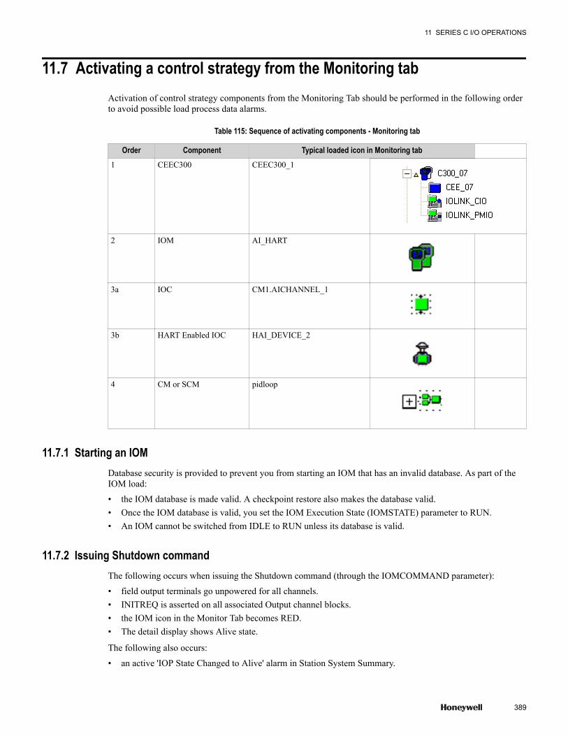
11.7 Activating a control strategy from the Monitoring tabActivation of control strategy components from the Monitoring Tab should be performed in the following orderto avoid possible load process data alarms.
Table 115: Sequence of activating components - Monitoring tab
Order Component Typical loaded icon in Monitoring tab1 CEEC300 CEEC300_1
2 IOM AI_HART
3a IOC CM1.AICHANNEL_1
3b HART Enabled IOC HAI_DEVICE_2
4 CM or SCM pidloop
11.7.1 Starting an IOMDatabase security is provided to prevent you from starting an IOM that has an invalid database. As part of theIOM load:
• the IOM database is made valid. A checkpoint restore also makes the database valid.• Once the IOM database is valid, you set the IOM Execution State (IOMSTATE) parameter to RUN.• An IOM cannot be switched from IDLE to RUN unless its database is valid.
11.7.2 Issuing Shutdown commandThe following occurs when issuing the Shutdown command (through the IOMCOMMAND parameter):
• field output terminals go unpowered for all channels.• INITREQ is asserted on all associated Output channel blocks.• the IOM icon in the Monitor Tab becomes RED.• The detail display shows Alive state.
The following also occurs:
• an active 'IOP State Changed to Alive' alarm in Station System Summary.
11 SERIES C I/O OPERATIONS
389

• the Status LED of the IOP flashes RED.
11 SERIES C I/O OPERATIONS
390 www.honeywell.com
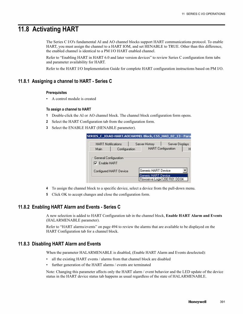
11.8 Activating HARTThe Series C I/O's fundamental AI and AO channel blocks support HART communications protocol. To enableHART, you must assign the channel to a HART IOM, and set HENABLE to TRUE. Other than this difference,the enabled channel is identical to a PM I/O HART enabled channel.
Refer to “Enabling HART in HART 6.0 and later version devices” to review Series C configuration form tabsand parameter availability for HART.
Refer to the HART I/O Implementation Guide for complete HART configuration instructions based on PM I/O.
11.8.1 Assigning a channel to HART - Series C
Prerequisites• A control module is created
To assign a channel to HART1 Double-click the AI or AO channel block. The channel block configuration form opens.2 Select the HART Configuration tab from the configuration form.3 Select the ENABLE HART (HENABLE parameter).
4 To assign the channel block to a specific device, select a device from the pull-down menu.5 Click OK to accept changes and close the configuration form.
11.8.2 Enabling HART Alarm and Events - Series CA new selection is added to HART Configuration tab in the channel block, Enable HART Alarm and Events(HALARMENABLE parameter).
Refer to “HART alarms/events” on page 494 to review the alarms that are available to be displayed on theHART Configuration tab for a channel block.
11.8.3 Disabling HART Alarm and EventsWhen the parameter HALARMENABLE is disabled, (Enable HART Alarm and Events deselected):
• all the existing HART events / alarms from that channel block are disabled• further generation of the HART alarms / events are terminated
Note: Changing this parameter affects only the HART alarm / event behavior and the LED update of the devicestatus in the HART device status tab happens as usual regardless of the state of HALARMENABLE.
11 SERIES C I/O OPERATIONS
391
To disable HART Alarm and Events:1 Double-click the AI or AO channel block. The channel block configuration form opens.2 Select the HART Configuration tab from the configuration form.3 Deselect the Enable HART Alarm and Events (HALARMENABLE parameter).
11.8.4 Migrating HART IO modules to/from non-HART IO modulesAlthough AI-HART and AI-HL (Cx-PAIX01) uses the same IOTA, migration must be performed offlinebecause the block configuration is different for both modules. The hardware change is only the modulereplacement. The firmware image is same for both modules.
The AO-HART and AO (Cx-PAOX01) migration is identical to the AI-HART and AI-HL migration.
Prerequisites• Not all channels of the module are HART-enabled.• Assume the new IOM would use the same IOM address. The difference of PAIX-01 and PAIN-01 is noted.
To migrate a non-HART module to/from HART module1 From Control Builder, inactivate the IO Module and Channels.2 From the Monitoring view, inactivate and delete all CMs that contain the IO channels.3 Delete the IOM block from the Monitoring view.4 From the Project view, note the IOM address and change it to some unused address.5 Create the new IOM block and set the address to the one you noted.6 For each IO channel, un-assign the existing IOM and assign the new IOM using the same channel slot.7 Delete the old IOM from Project view.8 Replace the hardware. That is, the IO Module /and the IOTA.
• If the AI-HL is PAIN-01, replace the IOTA also. Set the address accordingly.• If the IOTA is redundant, replace the both IO Modules.
9 Load the appropriate firmware from CTools.10 Load the IOM.11 Load the CMs.12 Activate the IO Module, Channels and CMs.
11.8.5 Migrating between different Model Numbers of Modules without HARTMigration between Cx-PAIX01 and Cx-PAIN01 is off-line because the IOTAs are different. It is impossible tomount the different model numbers on one IOTA. However, block configuration (IOM FB and IOC FB) is thesame.
Migration between Cx-PAOX01 and Cx-PAON01 is similar.
The following is step-by-step instruction to migrate between different model numbers of modules withoutHART:
PrerequisitesAssume that all AI channels are 4-20mA.
To migrate between Model Numbers of Modules without HART1 Inactivate the IOM and its channels.
11 SERIES C I/O OPERATIONS
392 www.honeywell.com

2 Replace the hardware and the IOTA. The IOM address must remain the same.3 Load the appropriate firmware using C Tools.4 Load the IOM block.5 Activate the IOM and its channels.
11 SERIES C I/O OPERATIONS
393

11.9 IOM configuration values not copied during Block Copy operationThe following subset of the IOM configuration parameter values are not copied during a Block Copy operation.
Uncopied IOM configuration parameters during a Block CopyIOLINKNAME IOLINKNUM IOMNUM CHNLNAME
11 SERIES C I/O OPERATIONS
394 www.honeywell.com
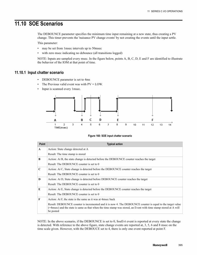
11.10 SOE ScenariosThe DEBOUNCE parameter specifies the minimum time input remaining at a new state, thus creating a PVchange. This timer prevents the 'nuisance PV change events' by not creating the events until the input settle.
This parameter:
• may be set from 1msec intervals up to 50msec• with zero msec indicating no debounce (all transitions logged)
NOTE: Inputs are sampled every msec. In the figure below, points A, B, C, D, E and F are identified to illustratethe behavior of the IOM at that point of time.
11.10.1 Input chatter scenario• DEBOUNCE parameter is set to 4ms• The Previous valid event was with PV = LOW.• Input is scanned every 1msec.
Figure 160: SOE input chatter scenario
Point Typical actionA Action: State change detected at A
Result: The time stamp is stored
B Action: At B, the state change is detected before the DEBOUNCE counter reaches the target
Result: The DEBOUNCE counter is set to 0
C Action: At C, State change is detected before the DEBOUNCE counter reaches the target
Result: The DEBOUNCE counter is set to 0
D Action: At D, State change is detected before DEBOUNCE counter reaches the target
Result: The DEBOUNCE counter is set to 0
E Action: At E, State change is detected before the DEBOUNCE counter reaches the target
Result: The DEBOUNCE counter is set to 0
F Action: At F, the state is the same as it was at 4msec back
Result: DEBOUNCE counter is incremented and it is now 4. The DEBOUNCE counter is equal to the target value(=4msec) and the state is same as that when the time stamp was stored, an Event with time stamp stored at A willbe posted
NOTE: In the above scenario, if the DEBOUNCE is set to 0, SoeEvt event is reported at every state the changeis detected. With reference to the above figure, state change events are reported at, 3, 5, 6 and 8 msec on thetime scale given. However, with the DEBOUCE set to 4, there is only one event reported at point F.
11 SERIES C I/O OPERATIONS
395
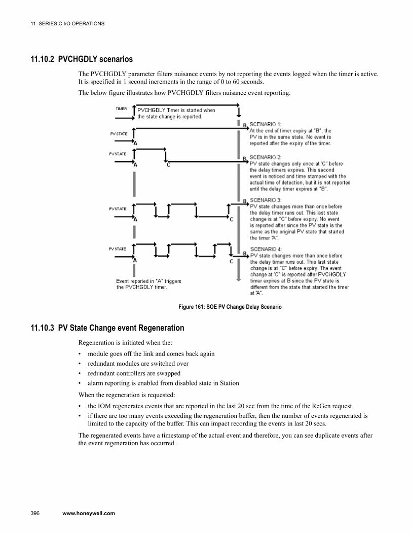
11.10.2 PVCHGDLY scenariosThe PVCHGDLY parameter filters nuisance events by not reporting the events logged when the timer is active.It is specified in 1 second increments in the range of 0 to 60 seconds.
The below figure illustrates how PVCHGDLY filters nuisance event reporting.
Figure 161: SOE PV Change Delay Scenario
11.10.3 PV State Change event RegenerationRegeneration is initiated when the:
• module goes off the link and comes back again• redundant modules are switched over• redundant controllers are swapped• alarm reporting is enabled from disabled state in Station
When the regeneration is requested:
• the IOM regenerates events that are reported in the last 20 sec from the time of the ReGen request• if there are too many events exceeding the regeneration buffer, then the number of events regenerated is
limited to the capacity of the buffer. This can impact recording the events in last 20 secs.
The regenerated events have a timestamp of the actual event and therefore, you can see duplicate events afterthe event regeneration has occurred.
11 SERIES C I/O OPERATIONS
396 www.honeywell.com
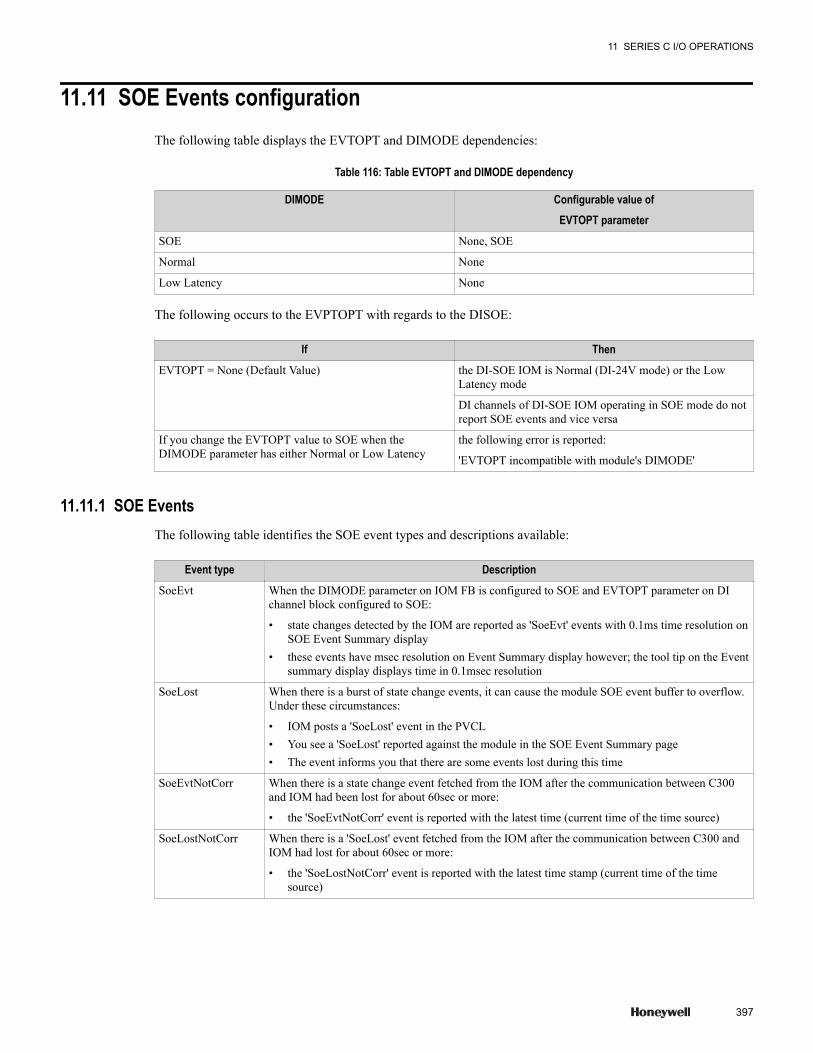
11.11 SOE Events configurationThe following table displays the EVTOPT and DIMODE dependencies:
Table 116: Table EVTOPT and DIMODE dependency
DIMODE Configurable value ofEVTOPT parameter
SOE None, SOE
Normal None
Low Latency None
The following occurs to the EVPTOPT with regards to the DISOE:
If ThenEVTOPT = None (Default Value) the DI-SOE IOM is Normal (DI-24V mode) or the Low
Latency mode
DI channels of DI-SOE IOM operating in SOE mode do notreport SOE events and vice versa
If you change the EVTOPT value to SOE when theDIMODE parameter has either Normal or Low Latency
the following error is reported:
'EVTOPT incompatible with module's DIMODE'
11.11.1 SOE EventsThe following table identifies the SOE event types and descriptions available:
Event type DescriptionSoeEvt When the DIMODE parameter on IOM FB is configured to SOE and EVTOPT parameter on DI
channel block configured to SOE:
• state changes detected by the IOM are reported as 'SoeEvt' events with 0.1ms time resolution onSOE Event Summary display
• these events have msec resolution on Event Summary display however; the tool tip on the Eventsummary display displays time in 0.1msec resolution
SoeLost When there is a burst of state change events, it can cause the module SOE event buffer to overflow.Under these circumstances:
• IOM posts a 'SoeLost' event in the PVCL• You see a 'SoeLost' reported against the module in the SOE Event Summary page• The event informs you that there are some events lost during this time
SoeEvtNotCorr When there is a state change event fetched from the IOM after the communication between C300and IOM had been lost for about 60sec or more:
• the 'SoeEvtNotCorr' event is reported with the latest time (current time of the time source)
SoeLostNotCorr When there is a 'SoeLost' event fetched from the IOM after the communication between C300 andIOM had lost for about 60sec or more:
• the 'SoeLostNotCorr' event is reported with the latest time stamp (current time of the timesource)
11 SERIES C I/O OPERATIONS
397
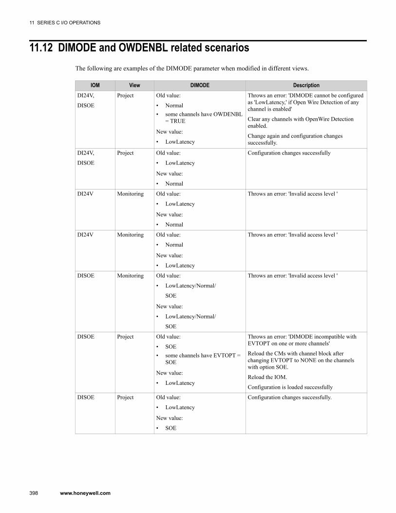
11.12 DIMODE and OWDENBL related scenariosThe following are examples of the DIMODE parameter when modified in different views.
IOM View DIMODE DescriptionDI24V,
DISOE
Project Old value:
• Normal• some channels have OWDENBL
= TRUE
New value:
• LowLatency
Throws an error: 'DIMODE cannot be configuredas 'LowLatency,' if Open Wire Detection of anychannel is enabled'
Clear any channels with OpenWire Detectionenabled.
Change again and configuration changessuccessfully.
DI24V,
DISOE
Project Old value:
• LowLatency
New value:
• Normal
Configuration changes successfully
DI24V Monitoring Old value:
• LowLatency
New value:
• Normal
Throws an error: 'Invalid access level '
DI24V Monitoring Old value:
• Normal
New value:
• LowLatency
Throws an error: 'Invalid access level '
DISOE Monitoring Old value:
• LowLatency/Normal/
SOE
New value:
• LowLatency/Normal/
SOE
Throws an error: 'Invalid access level '
DISOE Project Old value:
• SOE• some channels have EVTOPT =
SOE
New value:
• LowLatency
Throws an error: 'DIMODE incompatible withEVTOPT on one or more channels'
Reload the CMs with channel block afterchanging EVTOPT to NONE on the channelswith option SOE.
Reload the IOM.
Configuration is loaded successfully
DISOE Project Old value:
• LowLatency
New value:
• SOE
Configuration changes successfully.
11 SERIES C I/O OPERATIONS
398 www.honeywell.com

11.12.1 Low Latency ModeWhen the DIMODE parameter in DI24V and DI-SOE IOM FB is set to LowLatency, the channel's inputs aresampled and processed every 5 msec for better response times when using Discrete Loops that require lowlatency responses. In the case of DI-SOE, SOE event generation is not supported when DIMODE isLowLatency. This mode will also not support Open Wire Detection.
11.12.2 OWDENBL changes in Project ViewThe following Open Wire Detection changes occur when the initial value of DIMODE = LowLatency DIMODEand is modified:
• Changing the OWDENBL parameter value to TRUE is not allowed in LowLatency and SOE modes.• If this is done, the following error is displayed: 'Open Wire Detection cannot be enabled if DIMODE of IO
Module is configured as LowLatency or SOE.'
11 SERIES C I/O OPERATIONS
399
11.13 Enabling pulse proving in Pulse Input ModuleTo improve metering accuracy, turbine meters used for custody transfer purposes are often “proved” in situusing the real process fluid at the correct flow rate. When a meter is being proved, its flow is diverted such thatthe prover is downstream and in series with the meter. Thus the same flow passes through the meter and theprover in series.
The prover is basically a length of pipe. Inside the pipe is a sphere which is driven around the pipe by thepressure of the flow. In a bi-directional prover, the sphere can move in the forward or reverse direction asdetermined by the position of the 4-way valve. As the sphere moves around the pipe, it passes sphere detectionswitches. The swept volumes between all sphere switch combinations (that is 1 and 3, 1 and 4, 2 and 3 and 2and 4) are determined offline and are known extremely accurately. The sphere switches are used to turn on andoff a copy of the good pulses from the meter being proved. Thus a total number of pulses can be obtained versusa known swept volume and so the actual K factor of the meter being proved can be determined.
Prerequisites• The PI channel is configured for Dual Stream.• The PIM module is loaded.
To enable pulse proving in PIM1 Double-click the PIM in the Monitoring view.
The PIM module configuration form appears.
2 Enter the configured prover signal (signal stream to output to the prover signal screw pair on a given PImodule) in the Configured Prover Signal box. The possible channel numbers that you can enter are 0, 1, 3,5, or 7.
11 SERIES C I/O OPERATIONS
400 www.honeywell.com

The actual prover signal (the actual signal stream being output to the prover signal screw pair) appears in theActual Prover Signal box. The possible channel numbers that can appear are 0, 1, 3, 5, or 7.
3 Click OK.
11 SERIES C I/O OPERATIONS
401

11.14 Enabling Fast Cutoff mechanism in PI channel block
Prerequisites• Channel 7 and/or channel 8 are configured for Fast Cutoff operation.• Pulse Input Module is loaded.
The following figure illustrates a sample PI channel block Main tab configuration form from the Monitoringview.
To enable the Fast Cutoff configuration1 Double-click the PI channel block (channel 7 or 8) from the Monitoring view. The Configuration form
appears.Note: The following parameters are enabled if you have selected the pulse input type as Pulse Input withFast Cutoff.
• Output Safe State (SAFEOUTPUT)• Target Value (TV)• TV Processing Run Flag (TVPROC)• Output State (SO)• Bad Output State Flag (BADSO)• SO Command OFF (SOCMDOFF)• SO Command ON (SOCMDON)
2 Reset the accumulated value.You can reset the accumulated value using the RESETFL (Reset Command Flag).
3 Set the Output State value to a non-safe state value.
11 SERIES C I/O OPERATIONS
402 www.honeywell.com

4 Enter the target value in the Target Value box.Note:
• When you enter a target value and if the Output State is set to the non-safe state value, fast cutofffunctionality is enabled. When fast cutoff functionality is enabled, TVPROC parameter is set to ON.
• When the accumulated value reaches or exceeds the target value, the hardware sets the output to theconfigured safe state.
AttentionAfter the target value has been stored, the fast cutoff functionality is disabled and the TVPROC is set to OFF ifany of the following is true.
• The Output State is set to the safe-state. This occurs in the following scenarios:
– The PIM block is inactivated.– A communication fault occurs.– Output State is manually set by the operator.– Output State is set by another block.
• The accumulated value is reset.• The accumulated value reaches the target value.
5 Refer to the Control Builder Parameter Reference document for more information on other parameters.6 Click OK.
11 SERIES C I/O OPERATIONS
403
11.15 Monitoring I/O modules
11.15.1 Main tab - DI channel blockFrom the Monitoring view, you can only monitor the parameters of the channels that are configured for pulsecounting functionality.
The following is an example of the DI channel block configured for pulse counting functionality.
Figure 162: Main tab —UIO-DI channel
As illustrated in the figure, the parameters listed in the Pulse Counting Operation section can be monitored.
11.15.2 AI Status Data tabYou can only monitor the parameters of the channels that are configured as AI from the Channel Configurationtab.
The following is an example of the AI channel block configured in the UIO module.
11 SERIES C I/O OPERATIONS
404 www.honeywell.com

Figure 163: AI Status Data tab
As illustrated in the figure, channel 5 is configured as AI channel in the UIO module.
11.15.3 AO Status Data tabFrom the Monitoring view, you can only monitor the parameters of the channels that are configured as AO inthe Channel Configuration tab.
The following is an example of the AO channel block configured in the UIO module.
11 SERIES C I/O OPERATIONS
405
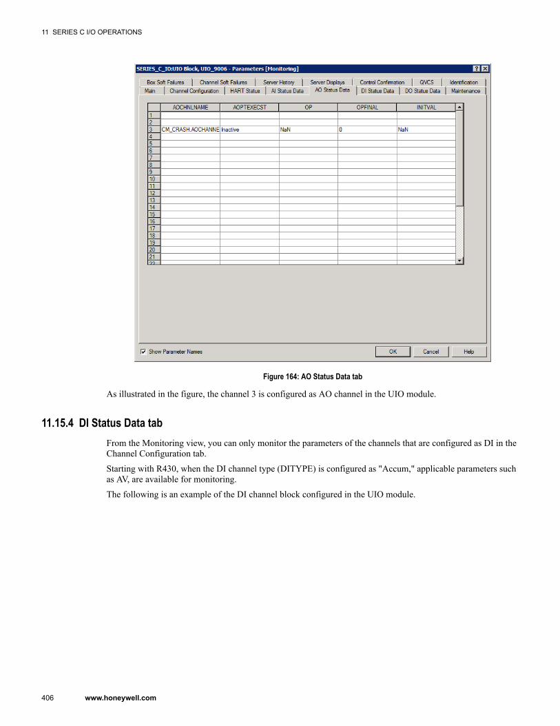
Figure 164: AO Status Data tab
As illustrated in the figure, the channel 3 is configured as AO channel in the UIO module.
11.15.4 DI Status Data tabFrom the Monitoring view, you can only monitor the parameters of the channels that are configured as DI in theChannel Configuration tab.
Starting with R430, when the DI channel type (DITYPE) is configured as "Accum," applicable parameters suchas AV, are available for monitoring.
The following is an example of the DI channel block configured in the UIO module.
11 SERIES C I/O OPERATIONS
406 www.honeywell.com
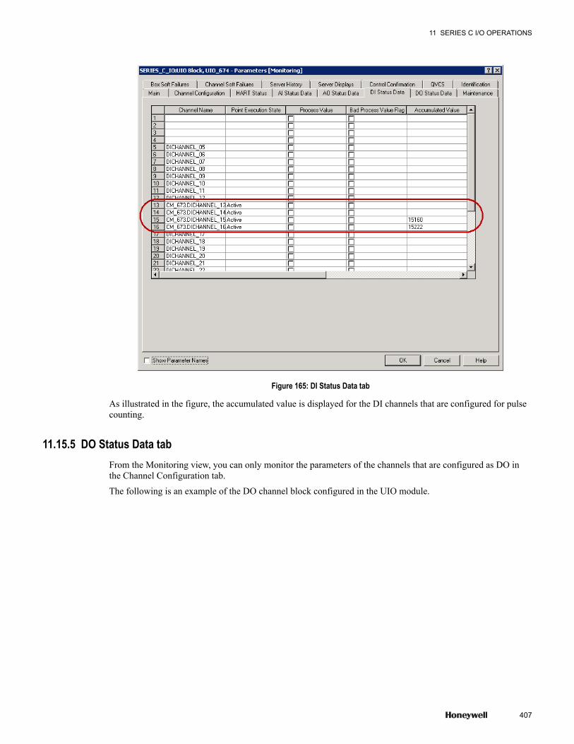
Figure 165: DI Status Data tab
As illustrated in the figure, the accumulated value is displayed for the DI channels that are configured for pulsecounting.
11.15.5 DO Status Data tabFrom the Monitoring view, you can only monitor the parameters of the channels that are configured as DO inthe Channel Configuration tab.
The following is an example of the DO channel block configured in the UIO module.
11 SERIES C I/O OPERATIONS
407

Figure 166: DO Status Data tab
As illustrated in the figure, the channel 1 is configured ganging in the UIO module.
11.15.6 Status Data tabYou cannot configure any Status Data tab parameters from the Project view. You can only monitor theparameters from the Monitoring view. You can only monitor the status of the following I/O modules from theMonitoring view.
• AI-HART• AI-HL• AI-LLMUX• AI-LLAI• AO• AO-HART• DI-HV• DI-24• DI-SOE• DO-24B• SP• SVP• PIM
The following is an example of a DO-24B Block, Configuration form - Status Data tab.
11 SERIES C I/O OPERATIONS
408 www.honeywell.com
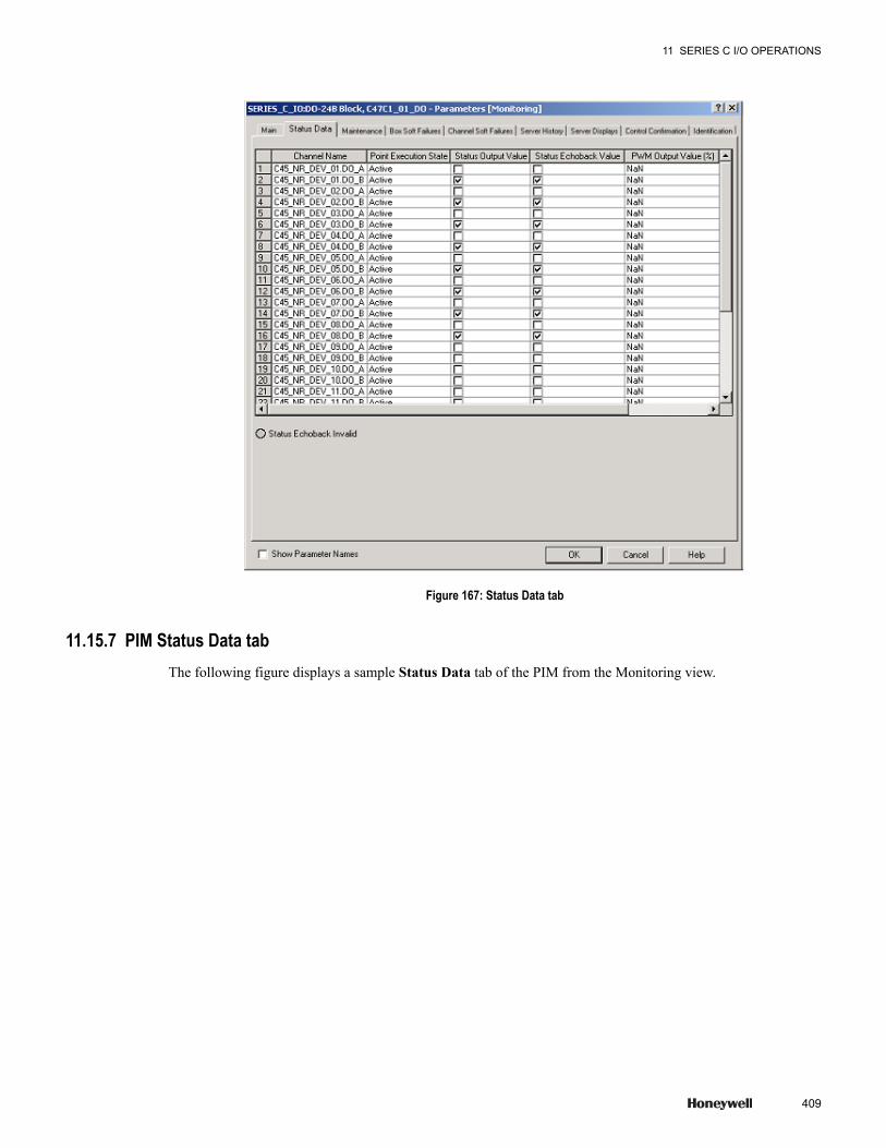
Figure 167: Status Data tab
11.15.7 PIM Status Data tabThe following figure displays a sample Status Data tab of the PIM from the Monitoring view.
11 SERIES C I/O OPERATIONS
409

Figure 168: Status Data tab of a PIM
As illustrated, channel 3 is configured for Dual Stream. Therefore, the row for channel 4 does not display anyvalues.
11.15.8 Maintenance tabThe following configuration information pertains to the Maintenance tab for the following module types:
• AI-HART• AI-HL• AI-LLMUX• AI-LLAI• AO• AO-HART• DI-HV• DI-24• DI-SOE• DO-24B• SP• SVP• PIM• UIOMaintenance can only be done from Monitoring.
11 SERIES C I/O OPERATIONS
410 www.honeywell.com
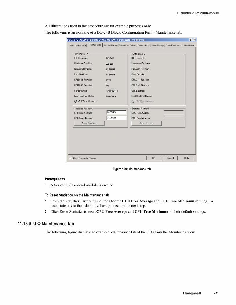
All illustrations used in the procedure are for example purposes only
The following is an example of a DO-24B Block, Configuration form - Maintenance tab.
Figure 169: Maintenance tab
Prerequisites• A Series C I/O control module is created
To Reset Statistics on the Maintenance tab1 From the Statistics Partner frame, monitor the CPU Free Average and CPU Free Minimum settings. To
reset statistics to their default values, proceed to the next step.2 Click Reset Statistics to reset CPU Free Average and CPU Free Minimum to their default settings.
11.15.9 UIO Maintenance tabThe following figure displays an example Maintenance tab of the UIO from the Monitoring view.
11 SERIES C I/O OPERATIONS
411
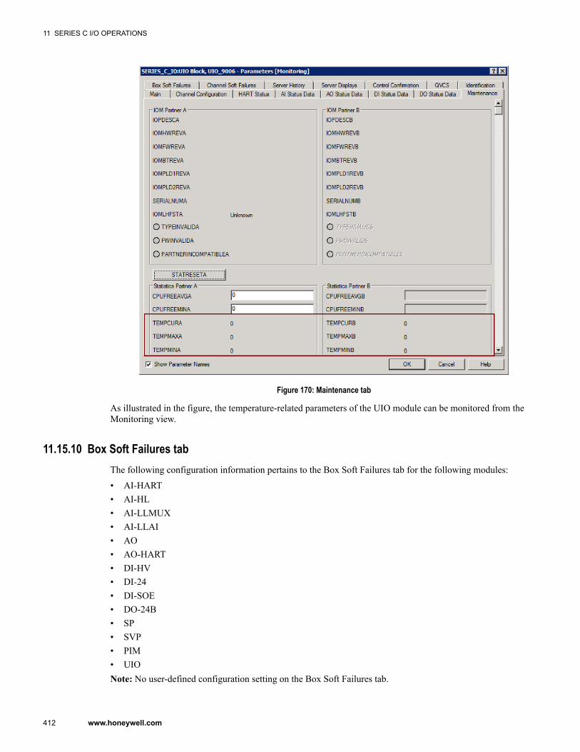
Figure 170: Maintenance tab
As illustrated in the figure, the temperature-related parameters of the UIO module can be monitored from theMonitoring view.
11.15.10 Box Soft Failures tabThe following configuration information pertains to the Box Soft Failures tab for the following modules:
• AI-HART• AI-HL• AI-LLMUX• AI-LLAI• AO• AO-HART• DI-HV• DI-24• DI-SOE• DO-24B• SP• SVP• PIM• UIONote: No user-defined configuration setting on the Box Soft Failures tab.
11 SERIES C I/O OPERATIONS
412 www.honeywell.com
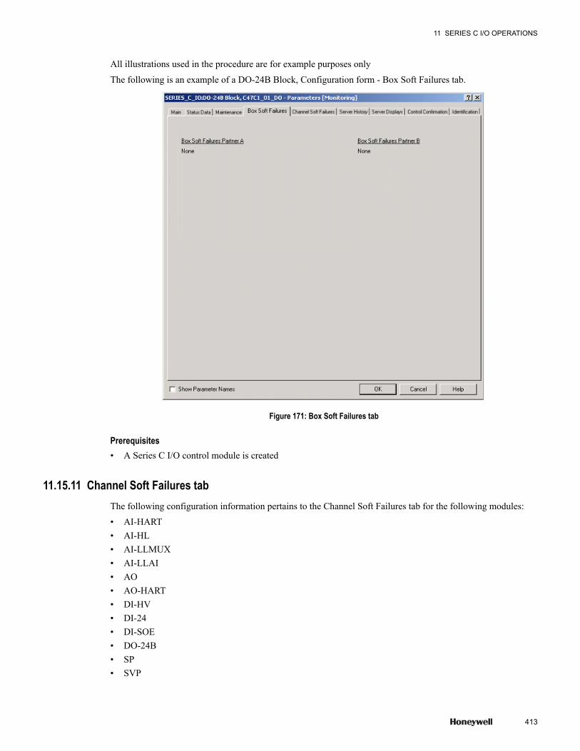
All illustrations used in the procedure are for example purposes only
The following is an example of a DO-24B Block, Configuration form - Box Soft Failures tab.
Figure 171: Box Soft Failures tab
Prerequisites• A Series C I/O control module is created
11.15.11 Channel Soft Failures tabThe following configuration information pertains to the Channel Soft Failures tab for the following modules:
• AI-HART• AI-HL• AI-LLMUX• AI-LLAI• AO• AO-HART• DI-HV• DI-24• DI-SOE• DO-24B• SP• SVP
11 SERIES C I/O OPERATIONS
413
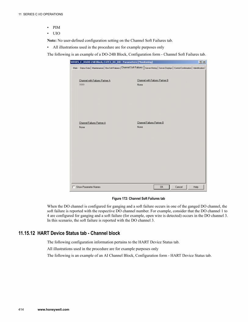
• PIM• UIO
Note: No user-defined configuration setting on the Channel Soft Failures tab.
• All illustrations used in the procedure are for example purposes only
The following is an example of a DO-24B Block, Configuration form - Channel Soft Failures tab.
Figure 172: Channel Soft Failures tab
When the DO channel is configured for ganging and a soft failure occurs in one of the ganged DO channel, thesoft failure is reported with the respective DO channel number. For example, consider that the DO channel 1 to4 are configured for ganging and a soft failure (for example, open wire is detected) occurs in the DO channel 3.In this scenario, the soft failure is reported with the DO channel 3.
11.15.12 HART Device Status tab - Channel blockThe following configuration information pertains to the HART Device Status tab.
All illustrations used in the procedure are for example purposes only
The following is an example of an AI Channel Block, Configuration form - HART Device Status tab.
11 SERIES C I/O OPERATIONS
414 www.honeywell.com
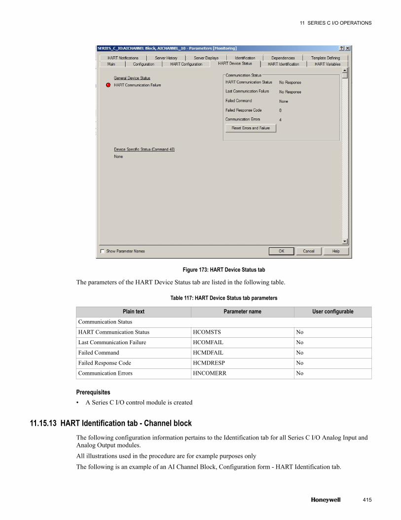
Figure 173: HART Device Status tab
The parameters of the HART Device Status tab are listed in the following table.
Table 117: HART Device Status tab parameters
Plain text Parameter name User configurableCommunication Status
HART Communication Status HCOMSTS No
Last Communication Failure HCOMFAIL No
Failed Command HCMDFAIL No
Failed Response Code HCMDRESP No
Communication Errors HNCOMERR No
Prerequisites• A Series C I/O control module is created
11.15.13 HART Identification tab - Channel blockThe following configuration information pertains to the Identification tab for all Series C I/O Analog Input andAnalog Output modules.
All illustrations used in the procedure are for example purposes only
The following is an example of an AI Channel Block, Configuration form - HART Identification tab.
11 SERIES C I/O OPERATIONS
415
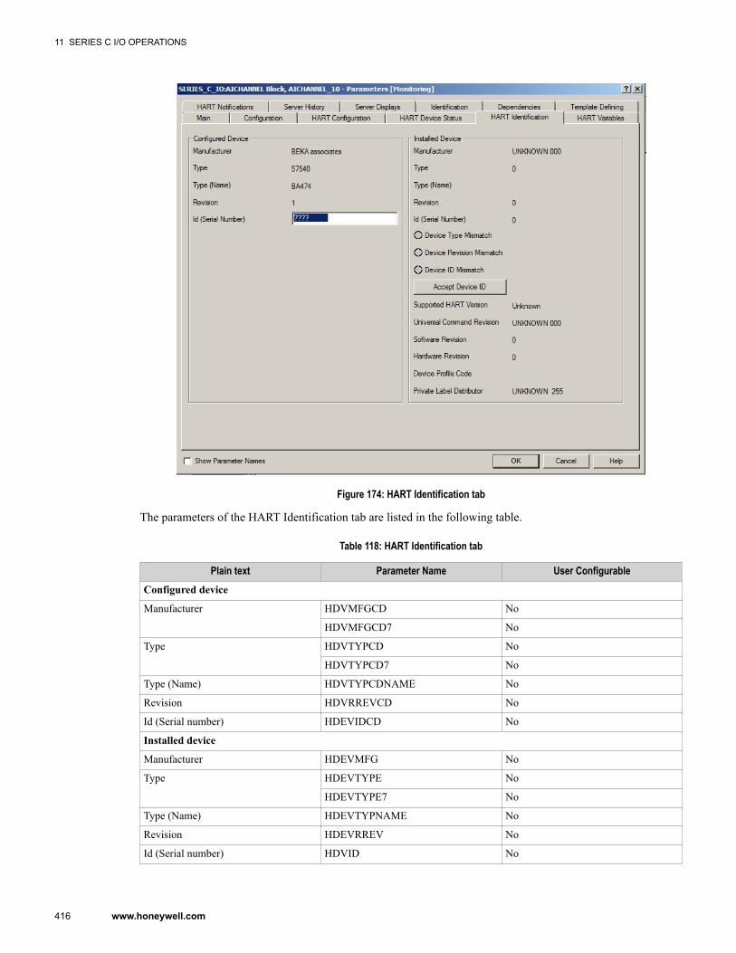
Figure 174: HART Identification tab
The parameters of the HART Identification tab are listed in the following table.
Table 118: HART Identification tab
Plain text Parameter Name User ConfigurableConfigured device
Manufacturer HDVMFGCD No
HDVMFGCD7 No
Type HDVTYPCD No
HDVTYPCD7 No
Type (Name) HDVTYPCDNAME No
Revision HDVRREVCD No
Id (Serial number) HDEVIDCD No
Installed device
Manufacturer HDEVMFG No
Type HDEVTYPE No
HDEVTYPE7 No
Type (Name) HDEVTYPNAME No
Revision HDEVRREV No
Id (Serial number) HDVID No
11 SERIES C I/O OPERATIONS
416 www.honeywell.com
Plain text Parameter Name User ConfigurableDevice Type Mismatch HDEVMISM No
Device Revision Mismatch HREVMISM No
Device ID Mismatch HDEVIDFL No
Accept Device ID ACCEPTDEV No
Supported HART Version HARTVERSION No
Universal Command Revision HUCMREV No
Software Revision HSWREV No
Hardware Revision HHWREV No
Device Profile Code HDEVPROFILE No
Private Label Distributor HPVTLDST No
Prerequisites• Control Builder is running• A Series C I/O control module was created
11.15.14 HART Variables tab - Channel blockThe following configuration information pertains to the Identification tab for all Series C I/O Analog Input orAnalog Output modules.
All illustrations used in the procedure are for example purposes only
The following is an example of an AI Channel Block, Configuration form - HART Variables tab.
11 SERIES C I/O OPERATIONS
417

Figure 175: HART Variables tab
The parameters of the HART Variables tab are listed in the following table.
Table 119: HART Variables tab parameters
Plain text Parameter name User configurableScan HART Variables HSCANCFG No
Dynamic variables
Name HDYNNAME Yes
Variable Code HDYNDVC Yes
Descriptor HDYNDSC Yes
Value HDYNVAL Yes
Units HDYNEU Yes
Device variables
Name HSLOTNAME Yes
Variable Code HSLOTDVC Yes
Descriptor HSLOTDSC Yes
Value HSLOTVAL Yes
Units HSLOTEU Yes
Slot0 Data Time Stamp SLOT0TS No
11 SERIES C I/O OPERATIONS
418 www.honeywell.com

Prerequisites• Control Builder is running• A Series C I/O control module was created
11 SERIES C I/O OPERATIONS
419
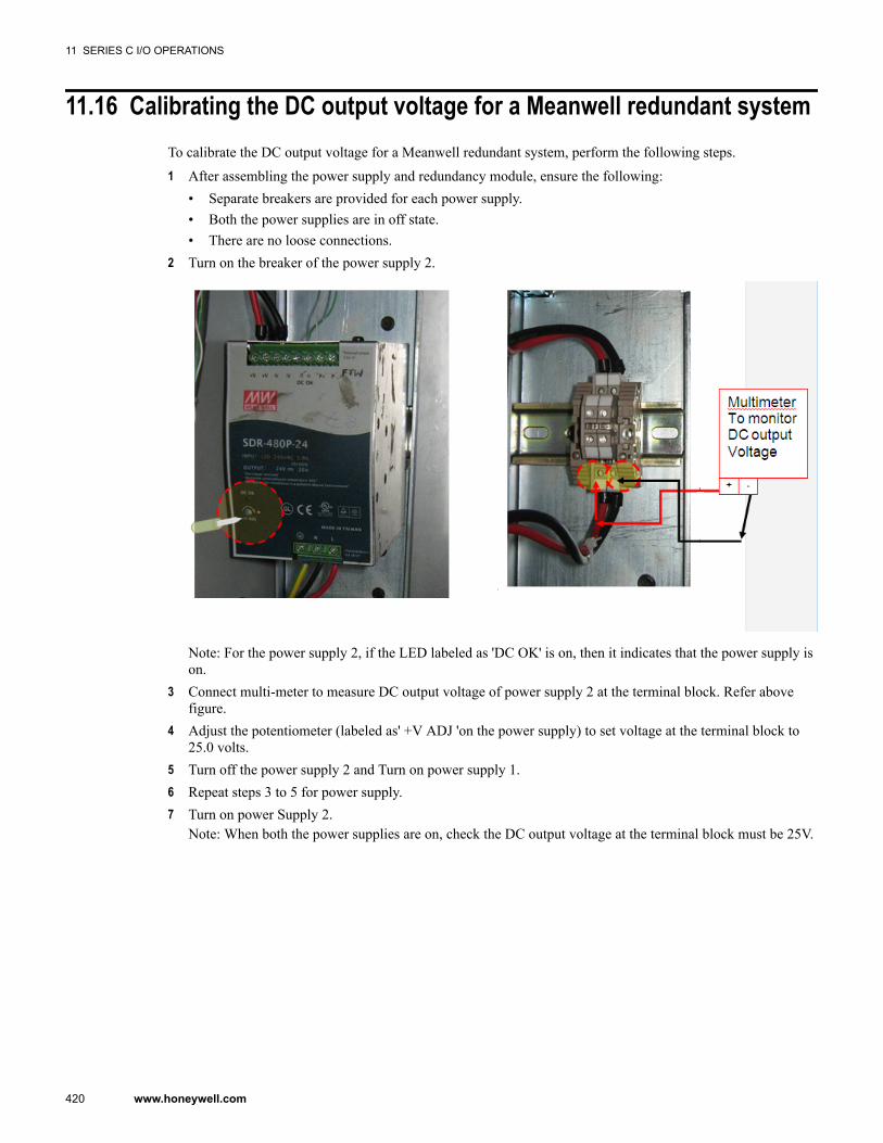
11.16 Calibrating the DC output voltage for a Meanwell redundant systemTo calibrate the DC output voltage for a Meanwell redundant system, perform the following steps.1 After assembling the power supply and redundancy module, ensure the following:
• Separate breakers are provided for each power supply.• Both the power supplies are in off state.• There are no loose connections.
2 Turn on the breaker of the power supply 2.
Note: For the power supply 2, if the LED labeled as 'DC OK' is on, then it indicates that the power supply ison.
3 Connect multi-meter to measure DC output voltage of power supply 2 at the terminal block. Refer abovefigure.
4 Adjust the potentiometer (labeled as' +V ADJ 'on the power supply) to set voltage at the terminal block to25.0 volts.
5 Turn off the power supply 2 and Turn on power supply 1.6 Repeat steps 3 to 5 for power supply.7 Turn on power Supply 2.
Note: When both the power supplies are on, check the DC output voltage at the terminal block must be 25V.
11 SERIES C I/O OPERATIONS
420 www.honeywell.com

11.17 Calibrating the DC output voltage for a non-redundant Meanwellsystem
To calibration the DC output voltage for a non-redundant Meanwell system, perform the following steps.1 After assembling the power supply in a non-redundant power system, ensure the following:
• Separate breaker is provided for power supply.• Power supply is in off state.
2 Turn on the breaker of the power supply 2.Note: For the power supply 2, if the LED labeled as 'DC OK' is on, then it indicates that the power supply ison.
3 Connect multi-meter to measure DC output voltage of power supply 2 at the terminal block.4 Adjust the potentiometer (labeled as' +V ADJ 'on the power supply) to set voltage at the terminal block to
25.0 volts.
11 SERIES C I/O OPERATIONS
421
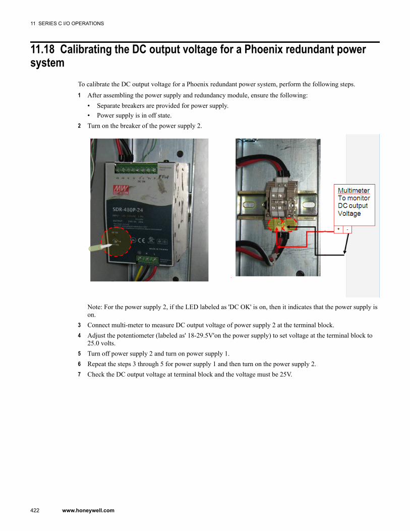
11.18 Calibrating the DC output voltage for a Phoenix redundant powersystem
To calibrate the DC output voltage for a Phoenix redundant power system, perform the following steps.1 After assembling the power supply and redundancy module, ensure the following:
• Separate breakers are provided for power supply.• Power supply is in off state.
2 Turn on the breaker of the power supply 2.
Note: For the power supply 2, if the LED labeled as 'DC OK' is on, then it indicates that the power supply ison.
3 Connect multi-meter to measure DC output voltage of power supply 2 at the terminal block.4 Adjust the potentiometer (labeled as' 18-29.5V'on the power supply) to set voltage at the terminal block to
25.0 volts.5 Turn off power supply 2 and turn on power supply 1.6 Repeat the steps 3 through 5 for power supply 1 and then turn on the power supply 2.7 Check the DC output voltage at terminal block and the voltage must be 25V.
11 SERIES C I/O OPERATIONS
422 www.honeywell.com
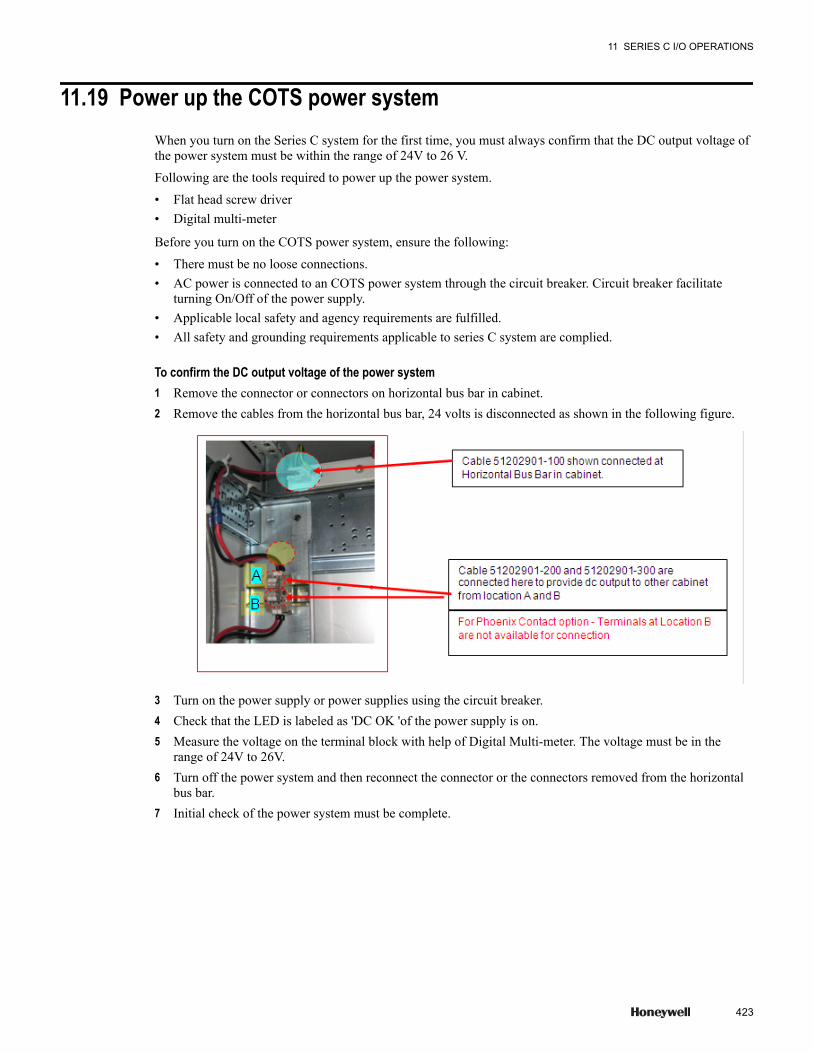
11.19 Power up the COTS power systemWhen you turn on the Series C system for the first time, you must always confirm that the DC output voltage ofthe power system must be within the range of 24V to 26 V.
Following are the tools required to power up the power system.
• Flat head screw driver• Digital multi-meter
Before you turn on the COTS power system, ensure the following:
• There must be no loose connections.• AC power is connected to an COTS power system through the circuit breaker. Circuit breaker facilitate
turning On/Off of the power supply.• Applicable local safety and agency requirements are fulfilled.• All safety and grounding requirements applicable to series C system are complied.
To confirm the DC output voltage of the power system1 Remove the connector or connectors on horizontal bus bar in cabinet.2 Remove the cables from the horizontal bus bar, 24 volts is disconnected as shown in the following figure.
3 Turn on the power supply or power supplies using the circuit breaker.4 Check that the LED is labeled as 'DC OK 'of the power supply is on.5 Measure the voltage on the terminal block with help of Digital Multi-meter. The voltage must be in the
range of 24V to 26V.6 Turn off the power system and then reconnect the connector or the connectors removed from the horizontal
bus bar.7 Initial check of the power system must be complete.
11 SERIES C I/O OPERATIONS
423

11 SERIES C I/O OPERATIONS
424 www.honeywell.com
12 Series C I/O Link Fiber Optic Extenders (FOE)
The Fiber Option Extender modules support the extension of the I/O link beyond the Series C Cabinet with theC300, enabling remote applications of the Series C I/O.
The following two types of FOEs are qualified to be used with Experion depending on the distance between thecontroller and the IO modules.
• Multi-mode FOE• Single mode FOE
You can select the appropriate FOE based on your requirement.
Related topics“Overview of multi-mode FOE” on page 426“FOE Installation” on page 430“Component mounting sequence” on page 432“Defining the Fiber Optic topology” on page 437“ Single mode fiber optic extender” on page 441“Defining the single mode fiber optic topology” on page 451
425
12.1 Overview of multi-mode FOEThe Fiber Optic module and IOTA board are built exclusively for Honeywell by a third party company. With aSeries C I/O Link Fiber Optic Extender (FOE) module, the ability exists to connect the C300 controller toremote:
• Series C I/O and• PM I/O
The FOE has the following capabilities:
• To connect one local cabinet to two remote I/O sites.
– If more than two remote sites exist, multiple FOE modules may be installed in the local cabinet.• Has two fiber optic ports sets, FO1 and FO2,
– each set having both a receive (Rx) and transmit (Tx) connector.• An IOLINK connector for connecting to the copper IOL.
Note: The same FOE module cannot be used for both types Series C and PM I/O concurrently.
The following FOE connections can be made:
Fiber optic portconnections
• Series C: FOE modules to FOE modules• PM I/O: FOE modules to PM I/O Link Extender
IOLINK (copper)connections
• Series C: FOE modules to copper IOLINK
12.1.1 Fiber Optic Extender assemblyThe Fiber Optic Extender assembly consists of components that include the FOE module and the FOE IOTAboard, along with the FOE interface cable. This assembly is installed in a control cabinet on vertically mountedcarriers, specially designed for Series C control hardware. The following figure shows the features of the FOEand its associated IOTA board.
12 SERIES C I/O LINK FIBER OPTIC EXTENDERS (FOE)
426 www.honeywell.com
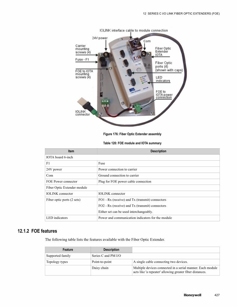
Figure 176: Fiber Optic Extender assembly
Table 120: FOE module and IOTA summary
Item DescriptionIOTA board 6-inch
F1 Fuse
24V power Power connection to carrier
Com Ground connection to carrier
FOE Power connector Plug for FOE power cable connection
Fiber Optic Extender module
IOLINK connector IOLINK connector
Fiber optic ports (2 sets) FO1 - Rx (receive) and Tx (transmit) connectors
FO2 - Rx (receive) and Tx (transmit) connectors
Either set can be used interchangeably.
LED indicators Power and communication indicators for the module
12.1.2 FOE featuresThe following table lists the features available with the Fiber Optic Extender.
Feature DescriptionSupported family Series C and PM I/O
Topology types Point-to-point A single cable connecting two devices.
Daisy chain Multiple devices connected in a serial manner. Each moduleacts like 'a repeater' allowing greater fiber distances.
12 SERIES C I/O LINK FIBER OPTIC EXTENDERS (FOE)
427
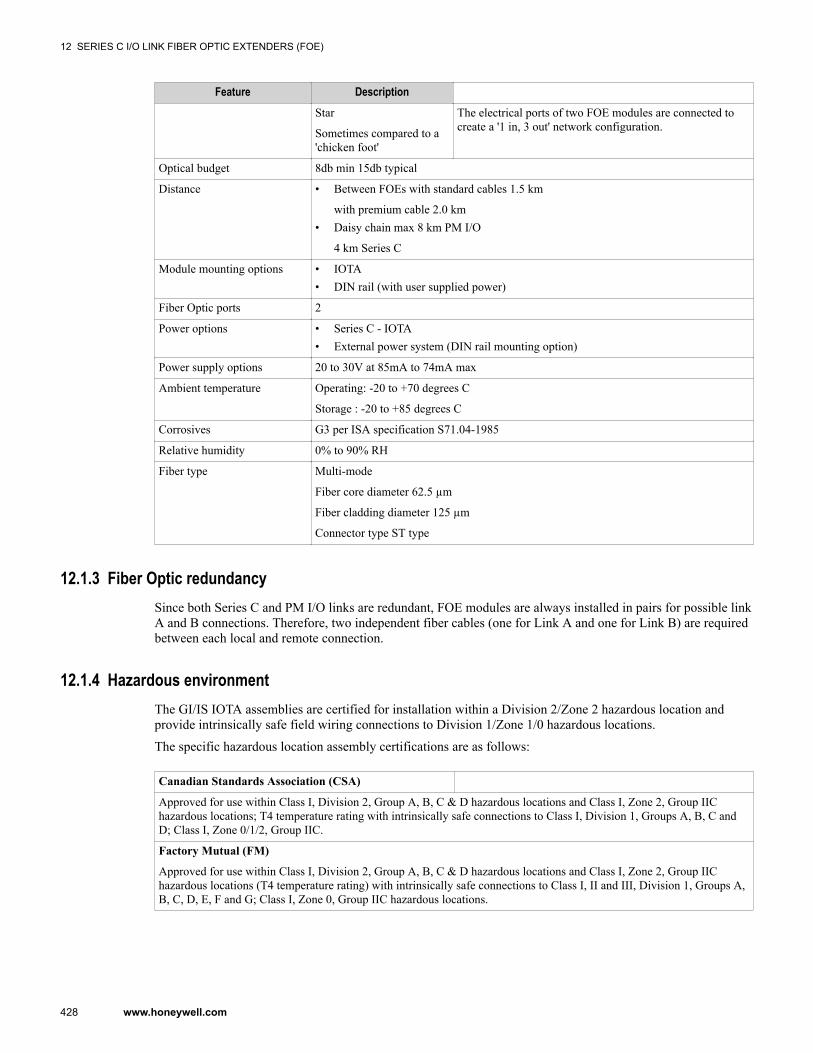
Feature DescriptionStar
Sometimes compared to a'chicken foot'
The electrical ports of two FOE modules are connected tocreate a '1 in, 3 out' network configuration.
Optical budget 8db min 15db typical
Distance • Between FOEs with standard cables 1.5 km
with premium cable 2.0 km• Daisy chain max 8 km PM I/O
4 km Series C
Module mounting options • IOTA• DIN rail (with user supplied power)
Fiber Optic ports 2
Power options • Series C - IOTA• External power system (DIN rail mounting option)
Power supply options 20 to 30V at 85mA to 74mA max
Ambient temperature Operating: -20 to +70 degrees C
Storage : -20 to +85 degrees C
Corrosives G3 per ISA specification S71.04-1985
Relative humidity 0% to 90% RH
Fiber type Multi-mode
Fiber core diameter 62.5 µm
Fiber cladding diameter 125 µm
Connector type ST type
12.1.3 Fiber Optic redundancySince both Series C and PM I/O links are redundant, FOE modules are always installed in pairs for possible linkA and B connections. Therefore, two independent fiber cables (one for Link A and one for Link B) are requiredbetween each local and remote connection.
12.1.4 Hazardous environmentThe GI/IS IOTA assemblies are certified for installation within a Division 2/Zone 2 hazardous location andprovide intrinsically safe field wiring connections to Division 1/Zone 1/0 hazardous locations.
The specific hazardous location assembly certifications are as follows:
Canadian Standards Association (CSA)
Approved for use within Class I, Division 2, Group A, B, C & D hazardous locations and Class I, Zone 2, Group IIChazardous locations; T4 temperature rating with intrinsically safe connections to Class I, Division 1, Groups A, B, C andD; Class I, Zone 0/1/2, Group IIC.
Factory Mutual (FM)
Approved for use within Class I, Division 2, Group A, B, C & D hazardous locations and Class I, Zone 2, Group IIChazardous locations (T4 temperature rating) with intrinsically safe connections to Class I, II and III, Division 1, Groups A,B, C, D, E, F and G; Class I, Zone 0, Group IIC hazardous locations.
12 SERIES C I/O LINK FIBER OPTIC EXTENDERS (FOE)
428 www.honeywell.com

ATEX
Approved for use Zone 2, Group IIC hazardous locations (T4 temperature rating) with intrinsically safe connections toZone 0, Group IIC hazardous locations.
12.1.5 FOE assembly certification detailsThe individual elements of the code are explained by reference to the items below.
• Class I, Division 2, Groups A, B, C, D• Class I, Zone 2, AEX nA IIC• II 3G EEx nA IIC• ATEX EEx nA IIC T4
12 SERIES C I/O LINK FIBER OPTIC EXTENDERS (FOE)
429
12.2 FOE InstallationThe procedures in this guide assume that you have completed all pertinent planning activities as outlined in theControl Hardware Planning Guide.
12.2.1 Handling components - ESDElectrostatic discharge can damage integrated circuits or semiconductors if you touch the connector pins.
Electrostatic dischargeFollow these guidelines when you handle a module:
• Touch a grounded object to discharge static potential,• Wear an approved wrist-strap grounding device,• Do not touch the connector pins,• If available, use a static safe workstation
12.2.2 Work practicesBefore installation, follow these work practices when performing general tasks:
• Ensure that all installation work is to be carried out in accordance with local standards, codes of practice andsite regulations and any other special requirements stated in this manual.
• Check that all module functions are correct for the application• Take care to avoid damaging the pins at all connector interfaces• Ensure that AC mains supplies have been isolated.• It is recommended that some form of mechanical assistance is used for lifting and supporting the enclosure
when installing it.
12.2.3 Hazardous areasThis subsection describes the considerations that should be given to Zone 2 and Division 2 hazardousenvironments of the equipment prior to its installation.
Work activities in a Zone 2 and Division 2 hazardous area are restricted in order to avoid ignition of explosivegas/air mixtures.
12.2.4 OperationsThe equipment must only be installed, operated and maintained by trained competent personnel.
12.2.5 Checking and MaintenanceThe installation and maintenance must be carried out in accordance with all appropriate international, nationaland local standard codes of practice and site regulations in accordance with the instructions contained in thismanual.
12.2.6 InstallationThe installation must comply with the appropriate European, national and local regulations, which may includereference to the IEC code of practice IEC 60079-14. In addition, particular industries or end users may havespecific requirements relating to the safety of their installations and these requirements must be met. For the
12 SERIES C I/O LINK FIBER OPTIC EXTENDERS (FOE)
430 www.honeywell.com

majority of installations the Directive 1999/92/EC [the ATEX Directive - safety of installations] is alsoapplicable.
12 SERIES C I/O LINK FIBER OPTIC EXTENDERS (FOE)
431
12.3 Component mounting sequenceIt is required that the installation be done in the following sequence:
1. Mount the IOTA2. Mount the FOE module onto the IOTA3. Connect the FOE module's power cable to the module4. Remove the IOTA F1 fuse.5. Mount the FOE module assembly to the carrier6. Connect the I/O link cable.7. Re-install the IOTA F1 fuse.
12.3.1 Mounting the IOTAFor installation purposes, it is assumed that the mounting channel is already fitted in a cabinet or enclosure thatprovides a suitable environment for the IOTA and its associated equipment. The IOTA is normally supplied withthe FOE fitted. However, the following mounting instructions can be used irrespective of whether the IOTA hasthe FOE fitted or not.
To mount the IOTA1 Mount the IOTA on the channel in appropriate orientation.2 Secure each of the fixing screw with its spacer and plastic retaining washer beneath the board.3 Position the IOTA and then secure it using the four fixing screws.
12.3.2 Mounting the FOE module onto the IOTA
PrerequisitesIt is required to attach the FOE module to the IOTA prior to its mounting to the carrier. The following alsoneeds to be established:
All wiring and pre-fabricated cables are available and labeled as applicable.
To mount the module onto the IOTA1 Align the FOE screws (located on the flange) with the holes on the IOTA.2 Tighten the four screws that attach the base of the FOE module to the IOTA board (using a Phillips screw-
driver).3 Connect the power cable from the IOTA board to the connector at the bottom of the module.4 This completes the procedure.
12.3.3 Connecting the FOE module's power cable to the moduleTypically, the FOE power cable does not require any adjustment or maintenance. If there is a power issue withthe FOE module, a loose or disconnected power cable may be the cause. If the power cable is damaged theIOTA board requires replacing.
PrerequisitesBefore connecting the FOE module's power cable to the module:
Refer to FOE connection rules.
12 SERIES C I/O LINK FIBER OPTIC EXTENDERS (FOE)
432 www.honeywell.com
To reconnect the FOE power cable to the module1 Ensure the power cable connector is properly aligned with the plug on the module.2 Press the plug firmly into the connector.3 Using a small slotted screwdriver, fasten the screws on the cable connector to the FOE module.4 This completes the procedure.
12.3.4 Removing the FOE IOTA F1 fuse
AttentionPrior to installing or servicing the FOE assembly (FOE module on the IOTA) to the carrier, the F1 fuse needs to beremoved. After mounting the FOE assembly to the carrier and securing the power and ground screws, the F1 fuse canbe re-installed.
To remove the FOE IOTA F1 fuse1 Using a small slotted screwdriver, place the tip into the slot on the fuse cap (The cap is the fuse holder).2 Rotate the cap counter clockwise, a quarter-turn. Remove the cap that also holds the fuse.
Place the fuse aside in a stable location for reuse.3 This completes the procedure.
12.3.5 Mounting the FOE module/IOTA assembly to the carrier
PrerequisitesBefore installing the FOE module/IOTA assembly in the cabinet, ensure that:
All wiring and pre-fabricated cables are available.
AttentionPrior to installing or servicing the FOE assembly (FOE module on the IOTA) to the carrier, the F1 fuse needs to beremoved. After mounting the FOE assembly to the carrier and securing the power and ground screws, the F1 fuse canbe re-installed.
To mount the FOE module/IOTA assembly to the carrier1 Ensure the F1 fuse is removed.2 Select the desired mounting location on the carrier and align the mounting holes in the IOTA with the screw-
hole locations on the carrier.6 inch IOTA board 4 mounting screws
Be sure the component side of the IOTA is facing up.3 Using a #2 Phillips screwdriver, secure the FOE assembly to carrier.4 Tighten the two power screws, connecting the IOTA board to the vertical bus bars on the channel carrier
assembly:• +24 V power screw• Com ground screw
5 This completes the procedure.
12 SERIES C I/O LINK FIBER OPTIC EXTENDERS (FOE)
433
12.3.6 Connecting the IOLINK interface cable to the FOE module
AttentionThe lOLINK interface cable should be connected to the FOE module before it is powered up.
PrerequisitesBefore connecting the FOE module's IOL interface cable to the module:
• Refer to FOE connection rules.
To connect the IOLINK interface cable to the FOE module1 Ensure the IOLINK interface cable connector is properly aligned with the connector on the FOE module.2 Press plug firmly into the connector.3 Fasten the screws on the cable connector to the FOE module.4 This completes the procedure.
12.3.7 Re-installing the FOE IOTA F1 fuse
AttentionPrior to installing or servicing the FOE assembly (FOE module on the IOTA) to the carrier, the F1 fuse needs to beremoved. After mounting the FOE assembly to the carrier and securing the power and ground screws, the F1 fuse canbe re-installed.
To re-install the FOE IOTA F1 fuse1 Place the fuse in the fuse holder and insert it back into the fuse container on the IOTA board.2 Tighten the fuse cap rotating it clockwise a quarter-turn, using a small slotted screwdriver.3 This completes the procedure.
12.3.8 Connecting the fiber optic cables to the FOE module
AttentionUnused optical ports should always have protective covers on them to prevent dust and other contaminants fromaccumulating on the glass fiber optic interfaces.
Fiber-optic ST-type connectors may be removed, or replaced, while active and in a Zone 2 or Division 2 hazardousarea.
PrerequisitesBefore connecting the FOE module's power cable to the module:
Refer to FOE connection rules.
To connect the FOE cables to the FOE module1 Ensure the terminal caps are removed from the ST optical ports on the FOE module. If the terminal caps are
still attached, rotate the cap counter-clockwise to disengage the cap from the locking tab.
12 SERIES C I/O LINK FIBER OPTIC EXTENDERS (FOE)
434 www.honeywell.com
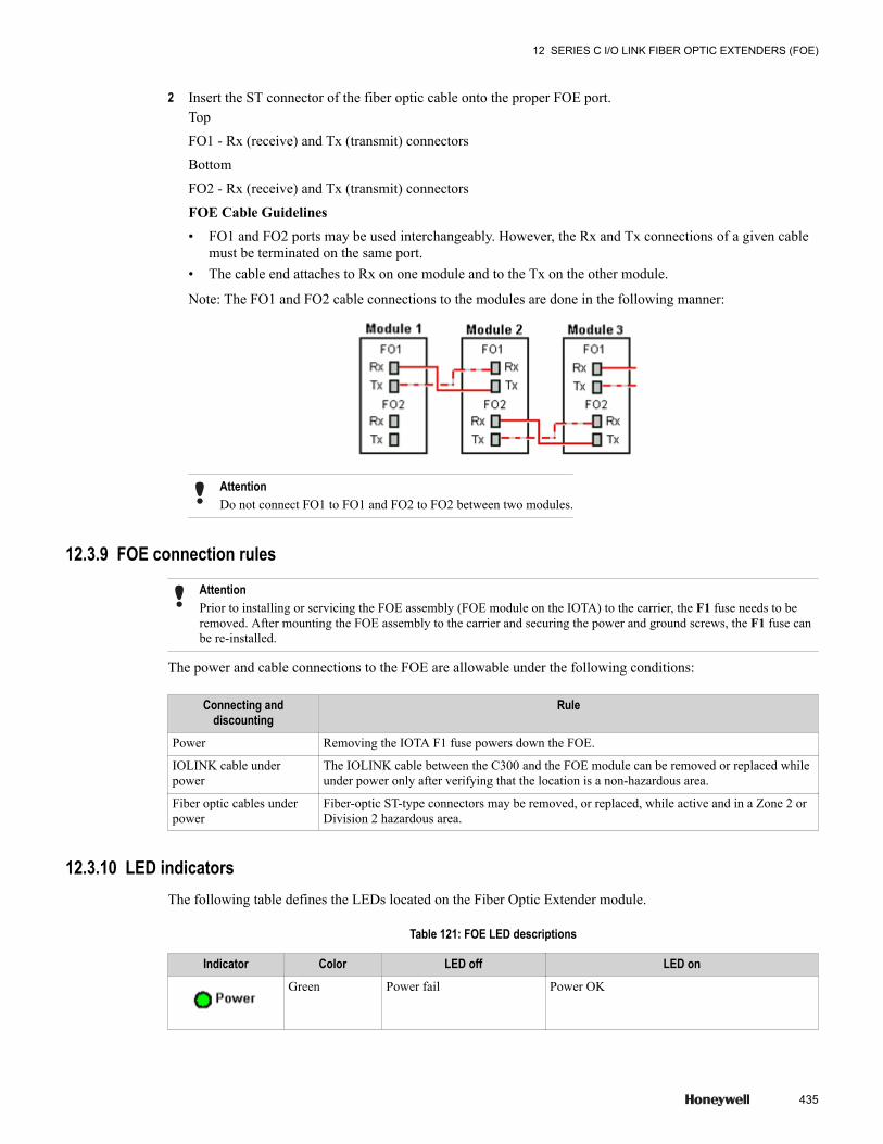
2 Insert the ST connector of the fiber optic cable onto the proper FOE port.Top
FO1 - Rx (receive) and Tx (transmit) connectors
Bottom
FO2 - Rx (receive) and Tx (transmit) connectors
FOE Cable Guidelines• FO1 and FO2 ports may be used interchangeably. However, the Rx and Tx connections of a given cable
must be terminated on the same port.• The cable end attaches to Rx on one module and to the Tx on the other module.
Note: The FO1 and FO2 cable connections to the modules are done in the following manner:
AttentionDo not connect FO1 to FO1 and FO2 to FO2 between two modules.
12.3.9 FOE connection rules
AttentionPrior to installing or servicing the FOE assembly (FOE module on the IOTA) to the carrier, the F1 fuse needs to beremoved. After mounting the FOE assembly to the carrier and securing the power and ground screws, the F1 fuse canbe re-installed.
The power and cable connections to the FOE are allowable under the following conditions:
Connecting anddiscounting
Rule
Power Removing the IOTA F1 fuse powers down the FOE.
IOLINK cable underpower
The IOLINK cable between the C300 and the FOE module can be removed or replaced whileunder power only after verifying that the location is a non-hazardous area.
Fiber optic cables underpower
Fiber-optic ST-type connectors may be removed, or replaced, while active and in a Zone 2 orDivision 2 hazardous area.
12.3.10 LED indicatorsThe following table defines the LEDs located on the Fiber Optic Extender module.
Table 121: FOE LED descriptions
Indicator Color LED off LED onGreen Power fail Power OK
12 SERIES C I/O LINK FIBER OPTIC EXTENDERS (FOE)
435

Indicator Color LED off LED onYellow Communication signal not
presentCommunication signal present on Rx channel
Yellow Communication signal notpresent
Communication signal present on Rx channel
Yellow Communication signal notpresent
Communication signal present on RS485 port.
12 SERIES C I/O LINK FIBER OPTIC EXTENDERS (FOE)
436 www.honeywell.com
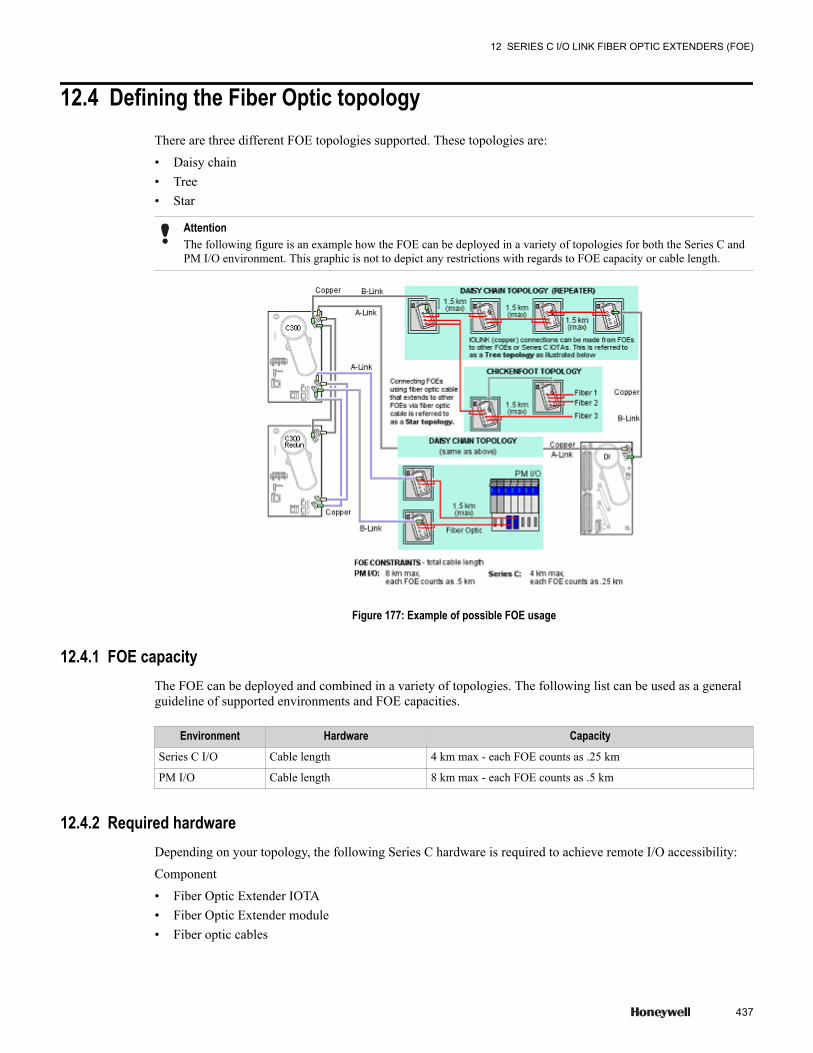
12.4 Defining the Fiber Optic topologyThere are three different FOE topologies supported. These topologies are:
• Daisy chain• Tree• Star
AttentionThe following figure is an example how the FOE can be deployed in a variety of topologies for both the Series C andPM I/O environment. This graphic is not to depict any restrictions with regards to FOE capacity or cable length.
Figure 177: Example of possible FOE usage
12.4.1 FOE capacityThe FOE can be deployed and combined in a variety of topologies. The following list can be used as a generalguideline of supported environments and FOE capacities.
Environment Hardware CapacitySeries C I/O Cable length 4 km max - each FOE counts as .25 km
PM I/O Cable length 8 km max - each FOE counts as .5 km
12.4.2 Required hardwareDepending on your topology, the following Series C hardware is required to achieve remote I/O accessibility:
Component
• Fiber Optic Extender IOTA• Fiber Optic Extender module• Fiber optic cables
12 SERIES C I/O LINK FIBER OPTIC EXTENDERS (FOE)
437
FOE interface cables - 0.5M length for both Series C & PM I/O
• Gray (pair) for IOL1• Violet (pair) for IOL2
12.4.3 Fiber Optic Extender interface cableThe Series cable has a different electrical keying than its PM I/O counterpart. Therefore, the specific cable typemust be used for each I/O family.
AttentionThe proper interface cable must be used for either the Series C or the PM I/O topology. Use of the incorrect cable willresult in faulty and/or corrupted IOL communications.
The fiber link is a passive subsystem and is essentially transparent to the system operation. It does not increaseor decrease traffic or impact other capabilities of the I/O system. In addition, the following designations occurfor these cables:
Cable Cable color A-link tab color B-link tab colorIOL1 Gray Yellow green
IOL2 Violet Yellow green
12.4.4 Fiber optic cable - length factorsThe maximum run of the fiber optic cables is limited by the optical power budget of 8db. Standard cablessupport 1.5 km while premium cable supports 2 km runs.
12.4.5 FOE topologies - Daisy chain topologyA daisy chain topology allows the remote I/O connection to be extended and can be utilized several times - ifmaximum flight delay times of data passing between the C300 controller and I/O are not exceeded.
When Series C daisy chaining,
the electrical port requires no interface cable to be attached. This applies if:
• daisy chaining Series-C link traffic, and• I/O is not present at the repeating location.
When PM I/O daisy-chaining,
an interface cable must always be connected to the electrical port. This is because the cable keys the FOE for the PM modeof operation
A repeater function also extends the remote I/O similar to the daisy chain technique, but relies on the opticalports of two FOE modules to provide the interconnection.
12.4.6 FOE topologies - Star topologyThis technique uses interconnected FOEs to allow a single incoming fiber cable to star to multiple remote sites.It can also be referred to as a chicken-foot topology.
12 SERIES C I/O LINK FIBER OPTIC EXTENDERS (FOE)
438 www.honeywell.com
12.4.7 Maximum flight delay timesThe I/O link communication protocol imposes a constraint between the C300 controller and the most distant I/Olocation, known as maximum flight delay time. This places a limit on the combined number of FOEs, andcumulative fiber cable length permitted in any IOL path. This constraint varies for:
Series C - maximum cable length is 4km
Each FOE (except for the local site) subtracts an additional .25km
PM I/O - maximum cable length is 8km
Each FOE (except for the local site) subtracts an additional .50km
12.4.8 Fiber optic budget considerations
AttentionFitting terminations to fiber optic cable requires special equipment and techniques. In order to obtain the best results, atrained person should perform this operation in accordance with the manufacturer's instructions. For these reasons, thefollowing installation instructions do not include detailed procedures for this process.
Testing of the quality (loss) of the terminations should be carried out at each stage.
12.4.9 Standard I/O link extender maximum cable span calculationThe following calculation MUST be used to ensure that the number of planned splices and the cable choicesupports the necessary cable span distance.
The maximum cable span calculation (in km) is as follows:
Max Span = (Available Optical Power - Losses in Splices)/(Max Loss per Cable Type)
The calculations or values for each of the above variables are described below.
12.4.10 Available standard I/O link extender optical powerThe available optical power calculation is as follows:
Transmit Power - Minimum Receiver Sensitivity - Power Loss Over Time =
Available Optical Power
where for a Standard I/O Link Extender:
Transmit Power = - 16.0 dB
Minimum Receiver Sensitivity = - 24.0 dB
Power Loss Over Time = 2.5 dB
Example calculation for a Standard I/O Link Extender using 62.5 micron cable:
(- 16.0 dB) - (- 24.0 dB) - (2.5 dB) = 5.5 dB Available Optical Power
AttentionBecause the maximum transmitter output level is -7 dB, and the maximum receiver input level is -10 dB, the receivermay be overdriven on a short link and may require a 3 dB attenuator. Connector allowances for the transmitter andreceiver are included in the above power declaration.
12 SERIES C I/O LINK FIBER OPTIC EXTENDERS (FOE)
439
12.4.11 Losses in splicesThe table below is used for the following Losses in Splices calculation.
Losses in Splices = Number of Splices x Maximum Loss per Splice
Standard Extender I/O cable type Average Lossper type (dB)
Maximum lossper type (dB)
Fusion 0.2 0.3
Mechanical 0.3 0.5
ST-connector 0.5 0.9
Examples: Max. span calculation for cables with fusion or mechanical splices:
Variable values: Available optical power = 5.5 dB, two splices.
Two fusion splices (5.5 dB) - (2 splices x 0.3 dB max loss per splice) / (4 dB/km) = 1.22 km
Two mechanical splices: (5.5 dB) - (2 splices x 0.5 dB max loss per splice) / (4 dB/km) = 1.12 km
12.4.12 Honeywell ST-type connector cable assembliesHoneywell can provide short fiber optic ST-type connector cable assemblies. You order by part number andcable length.
12.4.13 Link A and B cable length differencesThe maximum difference in fiber optic cable length between Link A and Link B must be less than 500 meters(1640 feet) to limit the communications delay difference between Link A and Link B.
12.4.14 Allowable standard I/O Link extender cable signal lossThe Standard I/O Link Extender cable:
• Must have a total signal loss equal to or less than -5.5 dB at a wavelength of 850 nanometers.• Fiber loss is measured at 22 degrees C ±3 degrees and is usually stated as a mean value.• Individual fiber losses may be as much as 25% greater than the mean.
12 SERIES C I/O LINK FIBER OPTIC EXTENDERS (FOE)
440 www.honeywell.com
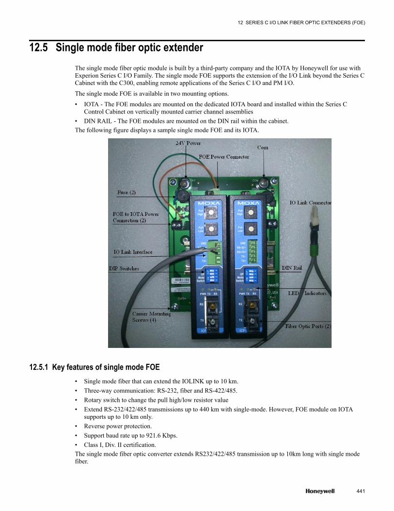
12.5 Single mode fiber optic extenderThe single mode fiber optic module is built by a third-party company and the IOTA by Honeywell for use withExperion Series C I/O Family. The single mode FOE supports the extension of the I/O Link beyond the Series CCabinet with the C300, enabling remote applications of the Series C I/O and PM I/O.
The single mode FOE is available in two mounting options.
• IOTA - The FOE modules are mounted on the dedicated IOTA board and installed within the Series CControl Cabinet on vertically mounted carrier channel assemblies
• DIN RAIL - The FOE modules are mounted on the DIN rail within the cabinet.The following figure displays a sample single mode FOE and its IOTA.
12.5.1 Key features of single mode FOE• Single mode fiber that can extend the IOLINK up to 10 km.• Three-way communication: RS-232, fiber and RS-422/485.• Rotary switch to change the pull high/low resistor value• Extend RS-232/422/485 transmissions up to 440 km with single-mode. However, FOE module on IOTA
supports up to 10 km only.• Reverse power protection.• Support baud rate up to 921.6 Kbps.• Class I, Div. II certification.The single mode fiber optic converter extends RS232/422/485 transmission up to 10km long with single modefiber.
12 SERIES C I/O LINK FIBER OPTIC EXTENDERS (FOE)
441
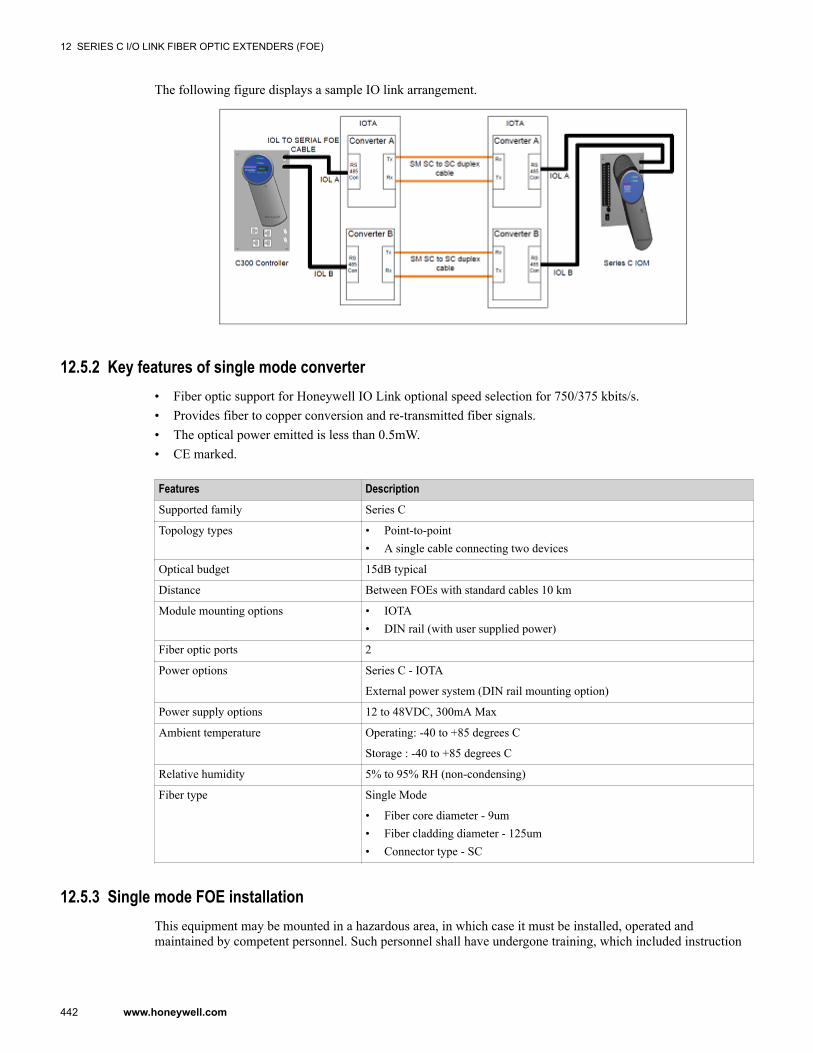
The following figure displays a sample IO link arrangement.
12.5.2 Key features of single mode converter• Fiber optic support for Honeywell IO Link optional speed selection for 750/375 kbits/s.• Provides fiber to copper conversion and re-transmitted fiber signals.• The optical power emitted is less than 0.5mW.• CE marked.
Features DescriptionSupported family Series C
Topology types • Point-to-point• A single cable connecting two devices
Optical budget 15dB typical
Distance Between FOEs with standard cables 10 km
Module mounting options • IOTA• DIN rail (with user supplied power)
Fiber optic ports 2
Power options Series C - IOTA
External power system (DIN rail mounting option)
Power supply options 12 to 48VDC, 300mA Max
Ambient temperature Operating: -40 to +85 degrees C
Storage : -40 to +85 degrees C
Relative humidity 5% to 95% RH (non-condensing)
Fiber type Single Mode
• Fiber core diameter - 9um• Fiber cladding diameter - 125um• Connector type - SC
12.5.3 Single mode FOE installationThis equipment may be mounted in a hazardous area, in which case it must be installed, operated andmaintained by competent personnel. Such personnel shall have undergone training, which included instruction
12 SERIES C I/O LINK FIBER OPTIC EXTENDERS (FOE)
442 www.honeywell.com
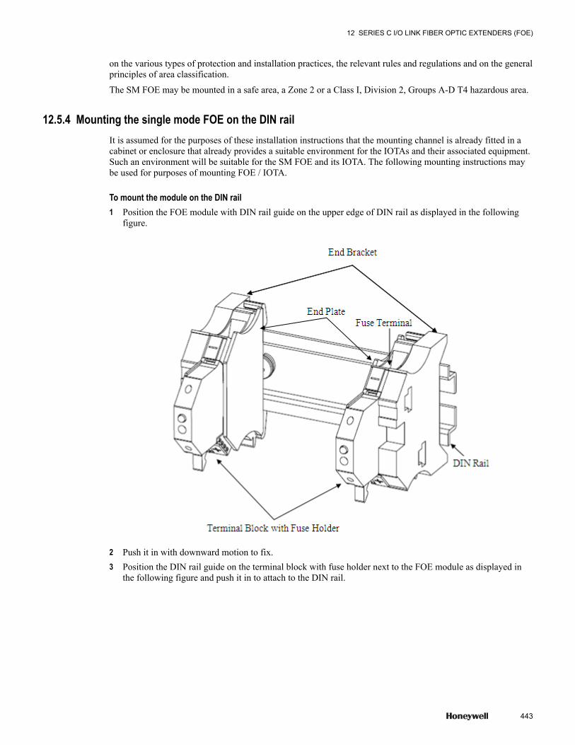
on the various types of protection and installation practices, the relevant rules and regulations and on the generalprinciples of area classification.
The SM FOE may be mounted in a safe area, a Zone 2 or a Class I, Division 2, Groups A-D T4 hazardous area.
12.5.4 Mounting the single mode FOE on the DIN railIt is assumed for the purposes of these installation instructions that the mounting channel is already fitted in acabinet or enclosure that already provides a suitable environment for the IOTAs and their associated equipment.Such an environment will be suitable for the SM FOE and its IOTA. The following mounting instructions maybe used for purposes of mounting FOE / IOTA.
To mount the module on the DIN rail1 Position the FOE module with DIN rail guide on the upper edge of DIN rail as displayed in the following
figure.
2 Push it in with downward motion to fix.3 Position the DIN rail guide on the terminal block with fuse holder next to the FOE module as displayed in
the following figure and push it in to attach to the DIN rail.
12 SERIES C I/O LINK FIBER OPTIC EXTENDERS (FOE)
443
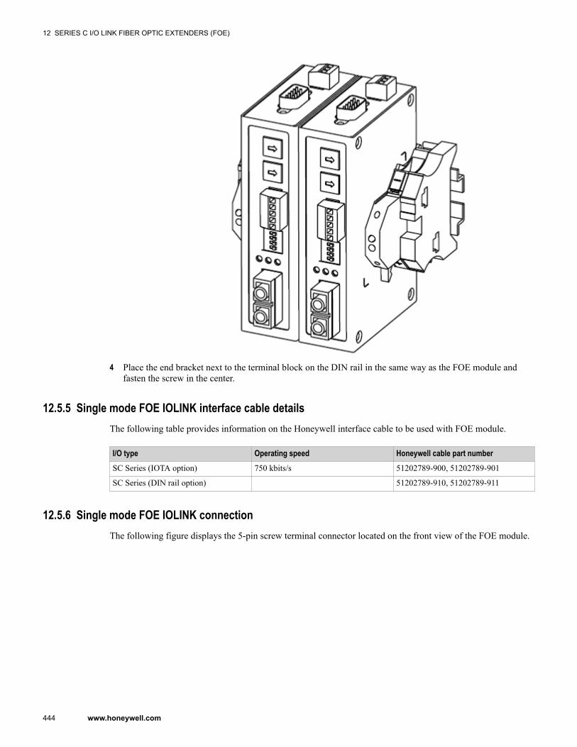
4 Place the end bracket next to the terminal block on the DIN rail in the same way as the FOE module andfasten the screw in the center.
12.5.5 Single mode FOE IOLINK interface cable detailsThe following table provides information on the Honeywell interface cable to be used with FOE module.
I/O type Operating speed Honeywell cable part numberSC Series (IOTA option) 750 kbits/s 51202789-900, 51202789-901
SC Series (DIN rail option) 51202789-910, 51202789-911
12.5.6 Single mode FOE IOLINK connectionThe following figure displays the 5-pin screw terminal connector located on the front view of the FOE module.
12 SERIES C I/O LINK FIBER OPTIC EXTENDERS (FOE)
444 www.honeywell.com

To make the connection, connect the free ends of the IO Link cable 51202789-9xx into the 5-pin screw terminalconnector on the front face of the FOE module.
Refer to the following table to connect the IO link cable into the 5-pin screw terminal connector.
Pin FOE Terminal Description Cable cover color1 GND Ground No cover
2 D- DATA - Clear
3 D+ DATA + Black
4 Not to be connected NA NA
5 Not to be connected NA NA
The following figure displays the IO link cable on the FOE interface.
12 SERIES C I/O LINK FIBER OPTIC EXTENDERS (FOE)
445
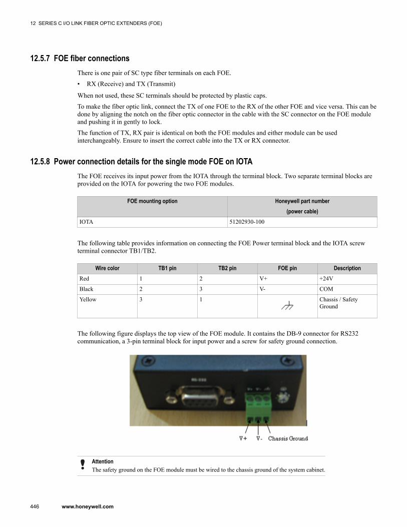
12.5.7 FOE fiber connectionsThere is one pair of SC type fiber terminals on each FOE.
• RX (Receive) and TX (Transmit)
When not used, these SC terminals should be protected by plastic caps.
To make the fiber optic link, connect the TX of one FOE to the RX of the other FOE and vice versa. This can bedone by aligning the notch on the fiber optic connector in the cable with the SC connector on the FOE moduleand pushing it in gently to lock.
The function of TX, RX pair is identical on both the FOE modules and either module can be usedinterchangeably. Ensure to insert the correct cable into the TX or RX connector.
12.5.8 Power connection details for the single mode FOE on IOTAThe FOE receives its input power from the IOTA through the terminal block. Two separate terminal blocks areprovided on the IOTA for powering the two FOE modules.
FOE mounting option Honeywell part number(power cable)
IOTA 51202930-100
The following table provides information on connecting the FOE Power terminal block and the IOTA screwterminal connector TB1/TB2.
Wire color TB1 pin TB2 pin FOE pin DescriptionRed 1 2 V+ +24V
Black 2 3 V- COM
Yellow 3 1 Chassis / SafetyGround
The following figure displays the top view of the FOE module. It contains the DB-9 connector for RS232communication, a 3-pin terminal block for input power and a screw for safety ground connection.
AttentionThe safety ground on the FOE module must be wired to the chassis ground of the system cabinet.
12 SERIES C I/O LINK FIBER OPTIC EXTENDERS (FOE)
446 www.honeywell.com
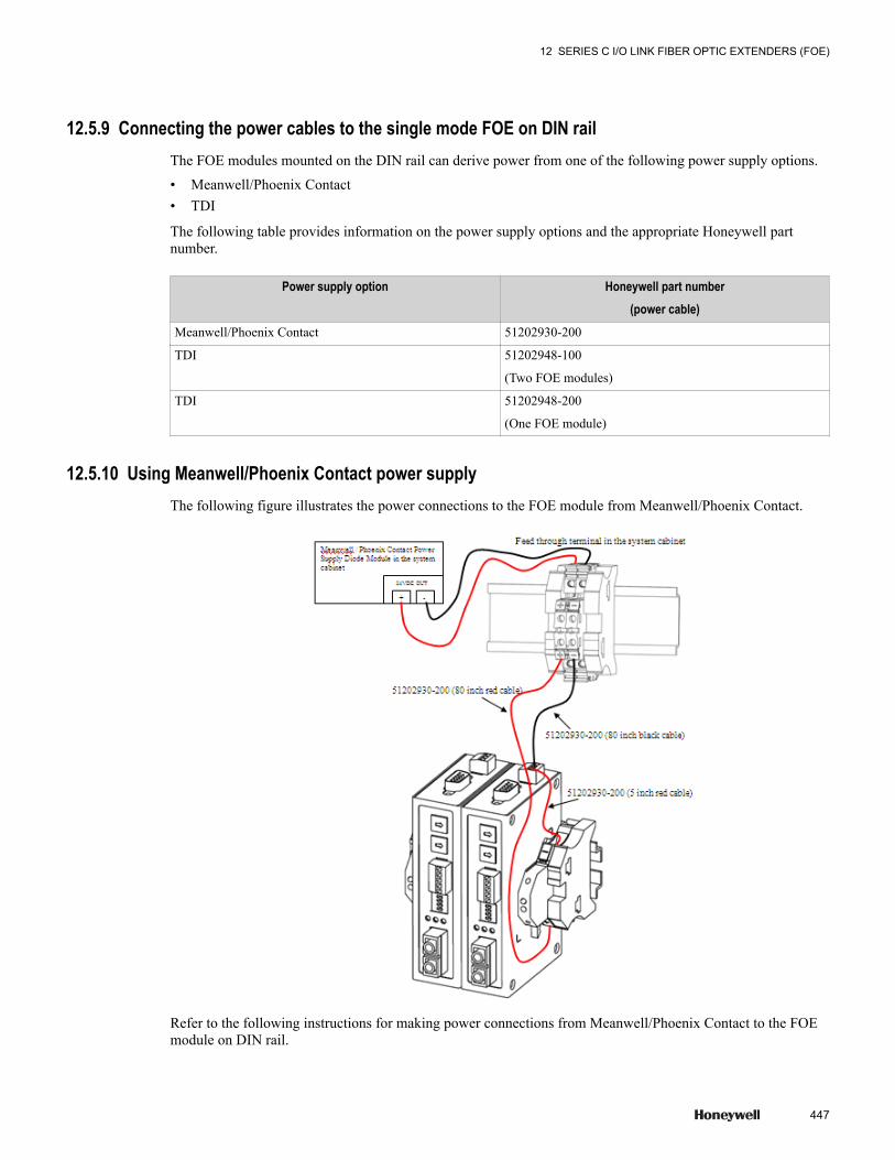
12.5.9 Connecting the power cables to the single mode FOE on DIN railThe FOE modules mounted on the DIN rail can derive power from one of the following power supply options.
• Meanwell/Phoenix Contact• TDI
The following table provides information on the power supply options and the appropriate Honeywell partnumber.
Power supply option Honeywell part number(power cable)
Meanwell/Phoenix Contact 51202930-200
TDI 51202948-100
(Two FOE modules)
TDI 51202948-200
(One FOE module)
12.5.10 Using Meanwell/Phoenix Contact power supplyThe following figure illustrates the power connections to the FOE module from Meanwell/Phoenix Contact.
Refer to the following instructions for making power connections from Meanwell/Phoenix Contact to the FOEmodule on DIN rail.
12 SERIES C I/O LINK FIBER OPTIC EXTENDERS (FOE)
447
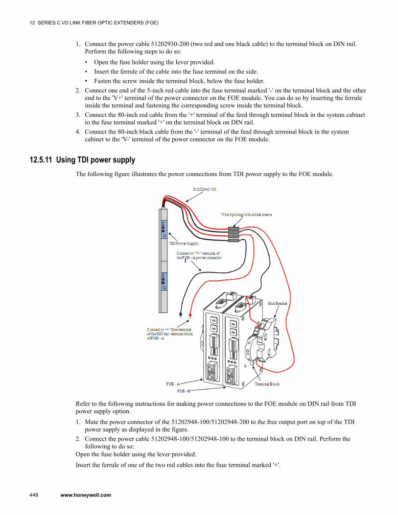
1. Connect the power cable 51202930-200 (two red and one black cable) to the terminal block on DIN rail.Perform the following steps to do so:
• Open the fuse holder using the lever provided.• Insert the ferrule of the cable into the fuse terminal on the side.• Fasten the screw inside the terminal block, below the fuse holder.
2. Connect one end of the 5-inch red cable into the fuse terminal marked '-' on the terminal block and the otherend to the 'V+' terminal of the power connector on the FOE module. You can do so by inserting the ferruleinside the terminal and fastening the corresponding screw inside the terminal block.
3. Connect the 80-inch red cable from the '+' terminal of the feed through terminal block in the system cabinetto the fuse terminal marked '+' on the terminal block on DIN rail.
4. Connect the 80-inch black cable from the '-' terminal of the feed through terminal block in the systemcabinet to the 'V-' terminal of the power connector on the FOE module.
12.5.11 Using TDI power supplyThe following figure illustrates the power connections from TDI power supply to the FOE module.
Refer to the following instructions for making power connections to the FOE module on DIN rail from TDIpower supply option.
1. Mate the power connector of the 51202948-100/51202948-200 to the free output port on top of the TDIpower supply as displayed in the figure.
2. Connect the power cable 51202948-100/51202948-100 to the terminal block on DIN rail. Perform thefollowing to do so:
Open the fuse holder using the lever provided.
Insert the ferrule of one of the two red cables into the fuse terminal marked '+'.
12 SERIES C I/O LINK FIBER OPTIC EXTENDERS (FOE)
448 www.honeywell.com
Fasten the corresponding screw inside the terminal block, below the fuse holder.
1. Connect one of the two black cables to the 'V-' terminal of the power connector on the FOE module.2. Connect one of the free ends of the 5-inch red cable into the '-' fuse terminal of the terminal block on DIN
rail and the other end to the 'V+' terminal of the power connector on the FOE module.3. Repeat steps 2 through 4 to make power connections to the other FOE module.
12.5.12 Replacing the FOE fuse on the terminal block when FOE is mounted on DIN railTo replace the FOE fuse on the terminal block when the FOE is mounted on the DIN rail1 Using the lever provided on the terminal block, open the fuse holder.2 Remove the fuse from the fuse holder.3 Replace the fuse by positioning it in the fuse holder, press and fit.4 Close the fuse holder and press the lever to lock.
12.5.13 Removing the FOE module from the DIN railTo remove the FOE module from the DIN rail1 Power down the FOE module by opening the fuse holder of the terminal block using the lever and removing
the fuse2 Remove all the cables before detaching the FOE modules. Perform the following steps to do so.
a Unscrew and remove the cable (HPN 51202930-200) running from the feed through terminal of thesystem cabinet to the '+' fuse terminal of the terminal block (Meanwell/Phoenix Contact power supplyonly).
b Remove the power connector of the cable (HPN 51202948-100/51202948-200) from the power supplyby releasing the lock in the side and pulling it out gently (TDI power supply only).
c Unfasten the screw of the '-' fuse terminal of the terminal block on DIN rail and remove the cable.d Unfasten the screw of the 'V+' terminal of power connector on the FOE module and remove the cable.e Unfasten the screw of the '-' terminal of the feed through terminal block and remove the cable.f Unfasten the screw of the 'V-' terminal of power connector on the FOE module and remove the cable.g Remove the fiber optic cables from the FOE module by pulling it out gently.h Unscrew and remove the I/O Link cable (HPN 51202789-910 / 51202789-911) from the FOE module or
remove the I/O Link connector by pulling it out.3 Unfasten the screw in the center of the end bracket and remove it by slightly lifting and pulling it out.4 Push the FOE module slightly downwards and slide it out at the lower edge of DIN rail.
WARNINGPowering off both FOE modules accidently may halt the IOL communication completely and can lead todangerous situation in plant. You must ensure to turn off the power of suspected FOE and should remove itwithout disturbing the functional FOE. Ensure to notify plant operators while performing this operation.
12.5.14 Single mode FOE configurationRotary switches are provided on the FOE module to set the Pull High/Low resistor settings. The DIP switchesare provided for setting the FOE operating mode.
12.5.15 Pull High/Low resistor settingThe Pull High/Low resistors are provided on the FOE module for impedance matching which may vary withmulti-drop or daisy-chain connection. The default settings are 1K for both the switches. To set a different value,
12 SERIES C I/O LINK FIBER OPTIC EXTENDERS (FOE)
449
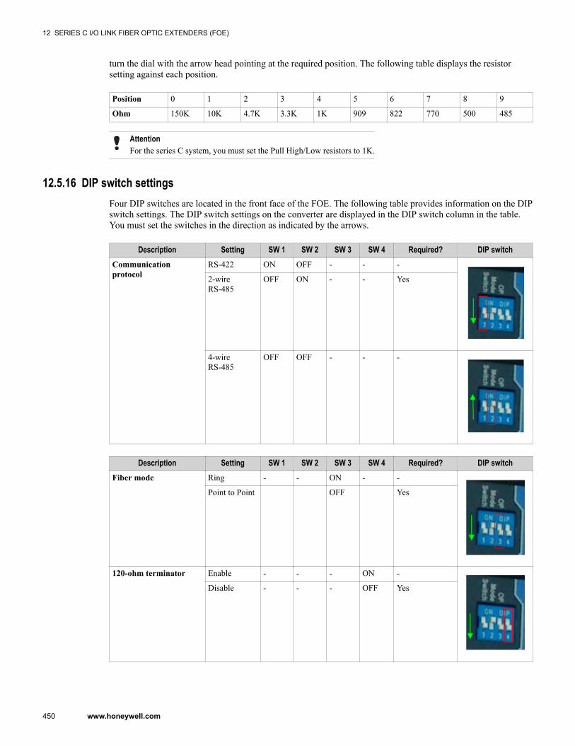
turn the dial with the arrow head pointing at the required position. The following table displays the resistorsetting against each position.
Position 0 1 2 3 4 5 6 7 8 9
Ohm 150K 10K 4.7K 3.3K 1K 909 822 770 500 485
AttentionFor the series C system, you must set the Pull High/Low resistors to 1K.
12.5.16 DIP switch settingsFour DIP switches are located in the front face of the FOE. The following table provides information on the DIPswitch settings. The DIP switch settings on the converter are displayed in the DIP switch column in the table.You must set the switches in the direction as indicated by the arrows.
Description Setting SW 1 SW 2 SW 3 SW 4 Required? DIP switchCommunicationprotocol
RS-422 ON OFF - - -
2-wireRS-485
OFF ON - - Yes
4-wireRS-485
OFF OFF - - -
Description Setting SW 1 SW 2 SW 3 SW 4 Required? DIP switchFiber mode Ring - - ON - -
Point to Point OFF Yes
120-ohm terminator Enable - - - ON -
Disable - - - OFF Yes
12 SERIES C I/O LINK FIBER OPTIC EXTENDERS (FOE)
450 www.honeywell.com
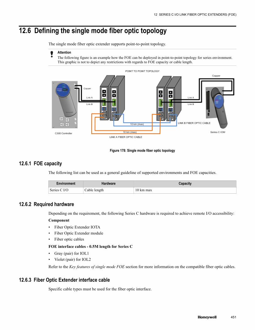
12.6 Defining the single mode fiber optic topologyThe single mode fiber optic extender supports point-to-point topology.
AttentionThe following figure is an example how the FOE can be deployed in point-to-point topology for series environment.This graphic is not to depict any restrictions with regards to FOE capacity or cable length.
Figure 178: Single mode fiber optic topology
12.6.1 FOE capacityThe following list can be used as a general guideline of supported environments and FOE capacities.
Environment Hardware CapacitySeries C I/O Cable length 10 km max
12.6.2 Required hardwareDepending on the requirement, the following Series C hardware is required to achieve remote I/O accessibility:
Component• Fiber Optic Extender IOTA• Fiber Optic Extender module• Fiber optic cables
FOE interface cables - 0.5M length for Series C• Gray (pair) for IOL1• Violet (pair) for IOL2
Refer to the Key features of single mode FOE section for more information on the compatible fiber optic cables.
12.6.3 Fiber Optic Extender interface cableSpecific cable types must be used for the fiber optic interface.
12 SERIES C I/O LINK FIBER OPTIC EXTENDERS (FOE)
451
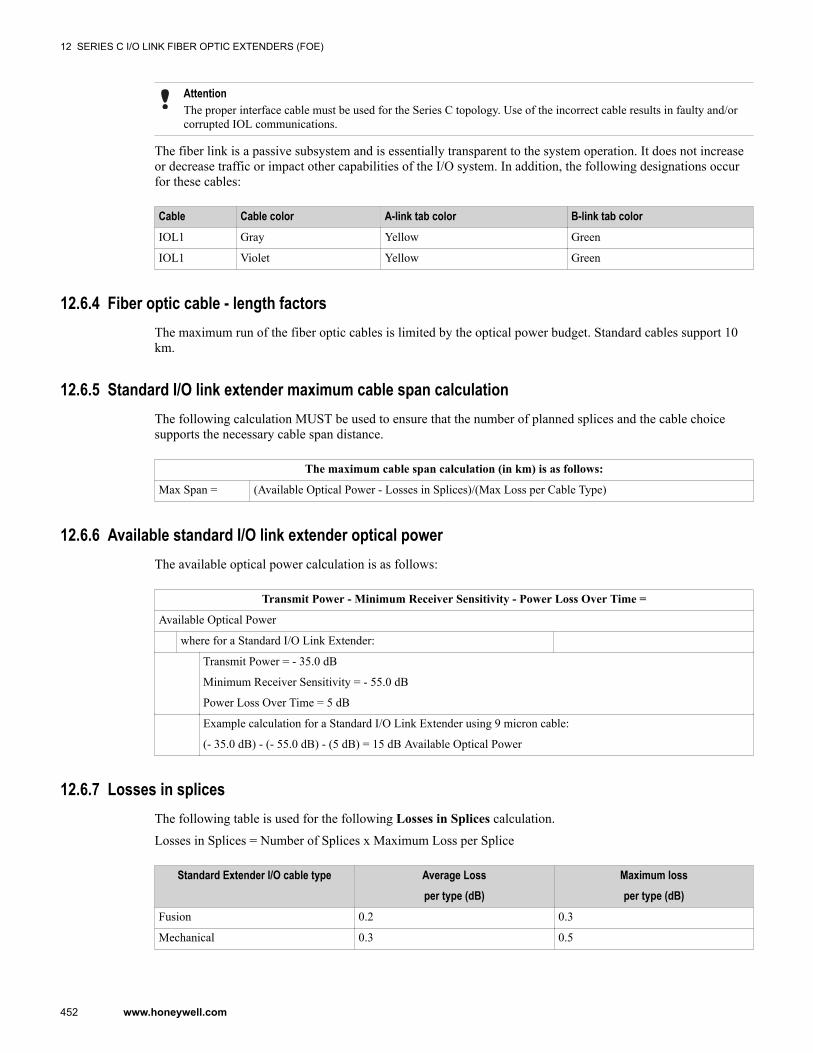
AttentionThe proper interface cable must be used for the Series C topology. Use of the incorrect cable results in faulty and/orcorrupted IOL communications.
The fiber link is a passive subsystem and is essentially transparent to the system operation. It does not increaseor decrease traffic or impact other capabilities of the I/O system. In addition, the following designations occurfor these cables:
Cable Cable color A-link tab color B-link tab colorIOL1 Gray Yellow Green
IOL1 Violet Yellow Green
12.6.4 Fiber optic cable - length factorsThe maximum run of the fiber optic cables is limited by the optical power budget. Standard cables support 10km.
12.6.5 Standard I/O link extender maximum cable span calculationThe following calculation MUST be used to ensure that the number of planned splices and the cable choicesupports the necessary cable span distance.
The maximum cable span calculation (in km) is as follows:
Max Span = (Available Optical Power - Losses in Splices)/(Max Loss per Cable Type)
12.6.6 Available standard I/O link extender optical powerThe available optical power calculation is as follows:
Transmit Power - Minimum Receiver Sensitivity - Power Loss Over Time =
Available Optical Power
where for a Standard I/O Link Extender:
Transmit Power = - 35.0 dB
Minimum Receiver Sensitivity = - 55.0 dB
Power Loss Over Time = 5 dB
Example calculation for a Standard I/O Link Extender using 9 micron cable:
(- 35.0 dB) - (- 55.0 dB) - (5 dB) = 15 dB Available Optical Power
12.6.7 Losses in splicesThe following table is used for the following Losses in Splices calculation.
Losses in Splices = Number of Splices x Maximum Loss per Splice
Standard Extender I/O cable type Average Lossper type (dB)
Maximum lossper type (dB)
Fusion 0.2 0.3
Mechanical 0.3 0.5
12 SERIES C I/O LINK FIBER OPTIC EXTENDERS (FOE)
452 www.honeywell.com
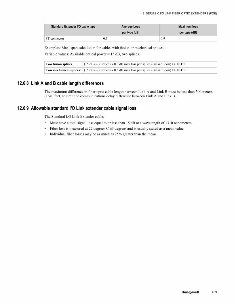
Standard Extender I/O cable type Average Lossper type (dB)
Maximum lossper type (dB)
ST-connector 0.3 0.9
Examples: Max. span calculation for cables with fusion or mechanical splices:
Variable values: Available optical power = 15 dB, two splices.
Two fusion splices (15 dB) - (2 splices x 0.3 dB max loss per splice) / (0.4 dB/km) >> 10 km
Two mechanical splices: (15 dB) - (2 splices x 0.5 dB max loss per splice) / (0.4 dB/km) >> 10 km
12.6.8 Link A and B cable length differencesThe maximum difference in fiber optic cable length between Link A and Link B must be less than 500 meters(1640 feet) to limit the communications delay difference between Link A and Link B.
12.6.9 Allowable standard I/O Link extender cable signal lossThe Standard I/O Link Extender cable:
• Must have a total signal loss equal to or less than 15 dB at a wavelength of 1310 nanometers.• Fiber loss is measured at 22 degrees C ±3 degrees and is usually stated as a mean value.• Individual fiber losses may be as much as 25% greater than the mean.
12 SERIES C I/O LINK FIBER OPTIC EXTENDERS (FOE)
453

12 SERIES C I/O LINK FIBER OPTIC EXTENDERS (FOE)
454 www.honeywell.com

13 Series C I/O Migrating from PMIO to Series C I/O
Related topics“Determining Series C I/O vs. PMIO functionality” on page 456“Migrating channels blocks from PMIO to Series C I/O” on page 458
455
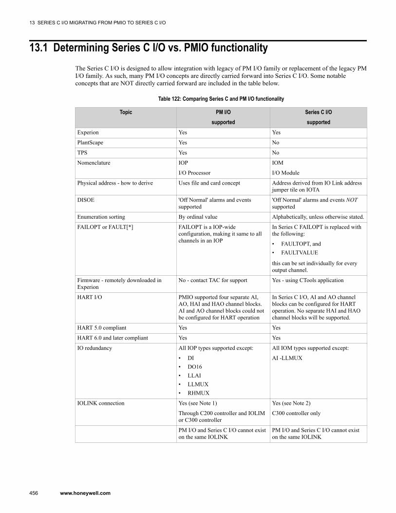
13.1 Determining Series C I/O vs. PMIO functionalityThe Series C I/O is designed to allow integration with legacy of PM I/O family or replacement of the legacy PMI/O family. As such, many PM I/O concepts are directly carried forward into Series C I/O. Some notableconcepts that are NOT directly carried forward are included in the table below.
Table 122: Comparing Series C and PM I/O functionality
Topic PM I/Osupported
Series C I/Osupported
Experion Yes Yes
PlantScape Yes No
TPS Yes No
Nomenclature IOP
I/O Processor
IOM
I/O Module
Physical address - how to derive Uses file and card concept Address derived from IO Link addressjumper tile on IOTA
DISOE 'Off Normal' alarms and eventssupported
'Off Normal' alarms and events NOTsupported
Enumeration sorting By ordinal value Alphabetically, unless otherwise stated.
FAILOPT or FAULT[*] FAILOPT is a IOP-wideconfiguration, making it same to allchannels in an IOP
In Series C FAILOPT is replaced withthe following:
• FAULTOPT, and• FAULTVALUE
this can be set individually for everyoutput channel.
Firmware - remotely downloaded inExperion
No - contact TAC for support Yes - using CTools application
HART I/O PMIO supported four separate AI,AO, HAI and HAO channel blocks.AI and AO channel blocks could notbe configured for HART operation
In Series C I/O, AI and AO channelblocks can be configured for HARToperation. No separate HAI and HAOchannel blocks will be supported.
HART 5.0 compliant Yes Yes
HART 6.0 and later compliant Yes Yes
IO redundancy All IOP types supported except:
• DI• DO16• LLAI• LLMUX• RHMUX
All IOM types supported except:
AI -LLMUX
IOLINK connection Yes (see Note 1)
Through C200 controller and IOLIMor C300 controller
Yes (see Note 2)
C300 controller only
PM I/O and Series C I/O cannot existon the same IOLINK
PM I/O and Series C I/O cannot existon the same IOLINK
13 SERIES C I/O MIGRATING FROM PMIO TO SERIES C I/O
456 www.honeywell.com
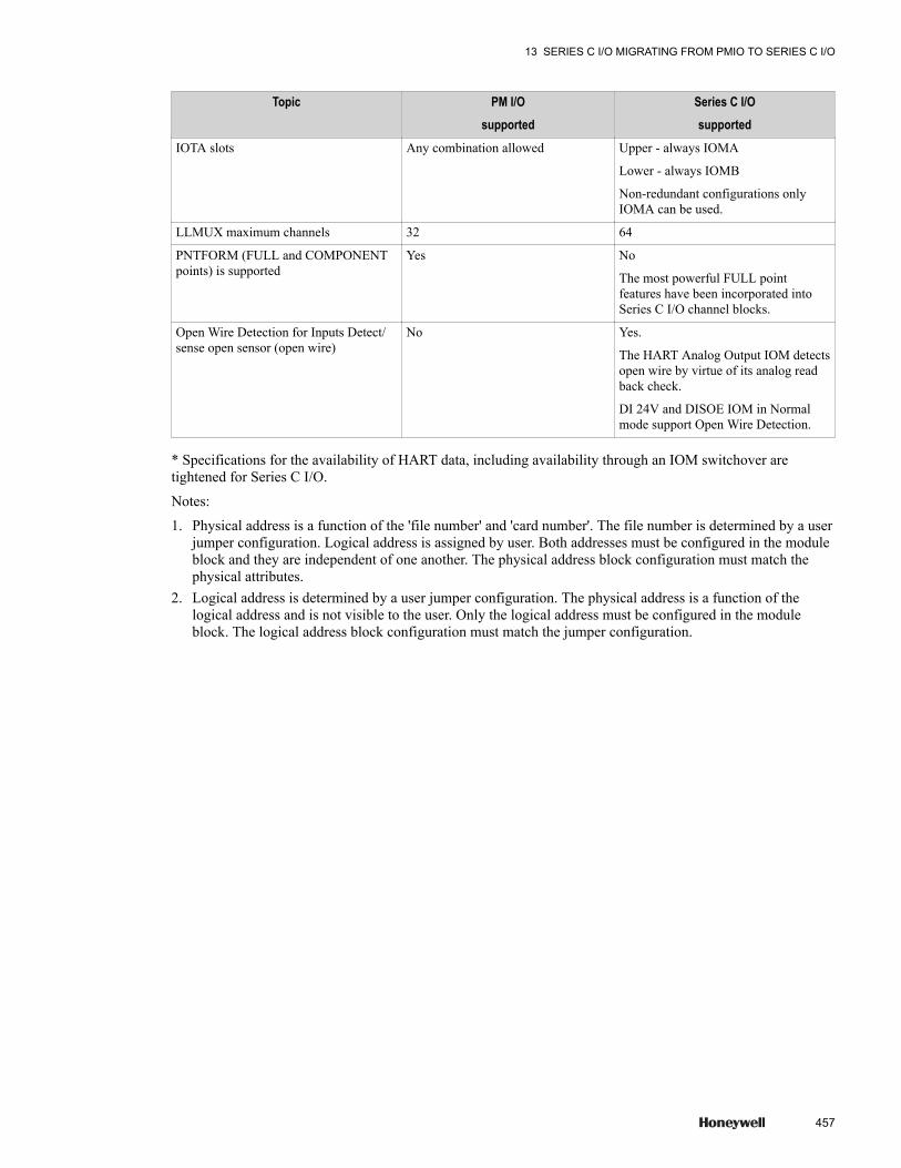
Topic PM I/Osupported
Series C I/Osupported
IOTA slots Any combination allowed Upper - always IOMA
Lower - always IOMB
Non-redundant configurations onlyIOMA can be used.
LLMUX maximum channels 32 64
PNTFORM (FULL and COMPONENTpoints) is supported
Yes No
The most powerful FULL pointfeatures have been incorporated intoSeries C I/O channel blocks.
Open Wire Detection for Inputs Detect/sense open sensor (open wire)
No Yes.
The HART Analog Output IOM detectsopen wire by virtue of its analog readback check.
DI 24V and DISOE IOM in Normalmode support Open Wire Detection.
* Specifications for the availability of HART data, including availability through an IOM switchover aretightened for Series C I/O.
Notes:
1. Physical address is a function of the 'file number' and 'card number'. The file number is determined by a userjumper configuration. Logical address is assigned by user. Both addresses must be configured in the moduleblock and they are independent of one another. The physical address block configuration must match thephysical attributes.
2. Logical address is determined by a user jumper configuration. The physical address is a function of thelogical address and is not visible to the user. Only the logical address must be configured in the moduleblock. The logical address block configuration must match the jumper configuration.
13 SERIES C I/O MIGRATING FROM PMIO TO SERIES C I/O
457
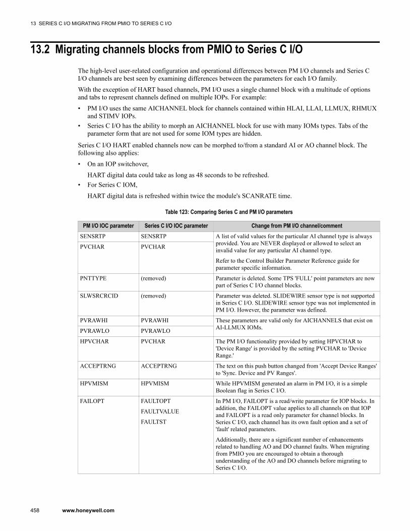
13.2 Migrating channels blocks from PMIO to Series C I/OThe high-level user-related configuration and operational differences between PM I/O channels and Series CI/O channels are best seen by examining differences between the parameters for each I/O family.
With the exception of HART based channels, PM I/O uses a single channel block with a multitude of optionsand tabs to represent channels defined on multiple IOPs. For example:
• PM I/O uses the same AICHANNEL block for channels contained within HLAI, LLAI, LLMUX, RHMUXand STIMV IOPs.
• Series C I/O has the ability to morph an AICHANNEL block for use with many IOMs types. Tabs of theparameter form that are not used for some IOM types are hidden.
Series C I/O HART enabled channels now can be morphed to/from a standard AI or AO channel block. Thefollowing also applies:
• On an IOP switchover,
HART digital data could take as long as 48 seconds to be refreshed.• For Series C IOM,
HART digital data is refreshed within twice the module's SCANRATE time.
Table 123: Comparing Series C and PM I/O parameters
PM I/O IOC parameter Series C I/O IOC parameter Change from PM I/O channel/commentSENSRTP SENSRTP A list of valid values for the particular AI channel type is always
provided. You are NEVER displayed or allowed to select aninvalid value for any particular AI channel type.
Refer to the Control Builder Parameter Reference guide forparameter specific information.
PVCHAR PVCHAR
PNTTYPE (removed) Parameter is deleted. Some TPS 'FULL' point parameters are nowpart of Series C I/O channel blocks.
SLWSRCRCID (removed) Parameter was deleted. SLIDEWIRE sensor type is not supportedin Series C I/O. SLIDEWIRE sensor type was not implemented inPM I/O. However, the parameter was defined.
PVRAWHI PVRAWHI These parameters are valid only for AICHANNELS that exist onAI-LLMUX IOMs.PVRAWLO PVRAWLO
HPVCHAR PVCHAR The PM I/O functionality provided by setting HPVCHAR to'Device Range' is provided by the setting PVCHAR to 'DeviceRange.'
ACCEPTRNG ACCEPTRNG The text on this push button changed from 'Accept Device Ranges'to 'Sync. Device and PV Ranges'.
HPVMISM HPVMISM While HPVMISM generated an alarm in PM I/O, it is a simpleBoolean flag in Series C I/O.
FAILOPT FAULTOPT
FAULTVALUE
FAULTST
In PM I/O, FAILOPT is a read/write parameter for IOP blocks. Inaddition, the FAILOPT value applies to all channels on that IOPand FAILOPT is a read only parameter for channel blocks. InSeries C I/O, each channel has its own fault option and a set of'fault' related parameters.
Additionally, there are a significant number of enhancementsrelated to handling AO and DO channel faults. When migratingfrom PMIO you are encouraged to obtain a thoroughunderstanding of the AO and DO channels before migrating toSeries C I/O.
13 SERIES C I/O MIGRATING FROM PMIO TO SERIES C I/O
458 www.honeywell.com
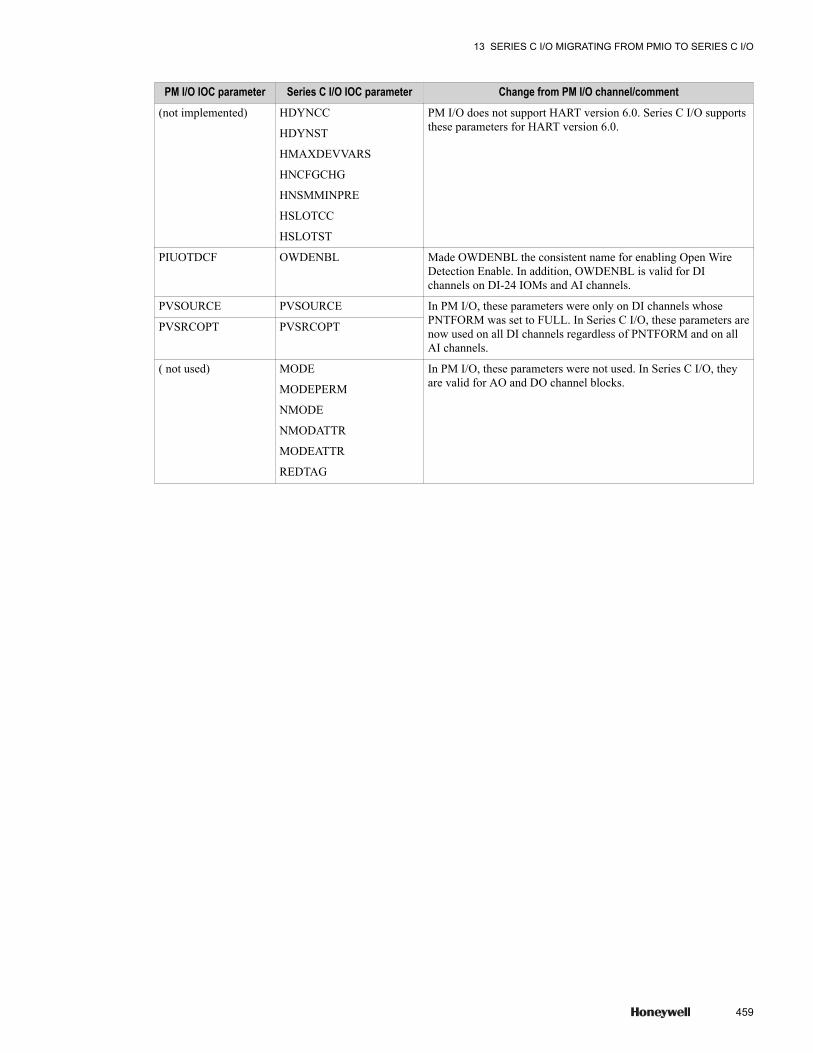
PM I/O IOC parameter Series C I/O IOC parameter Change from PM I/O channel/comment(not implemented) HDYNCC
HDYNST
HMAXDEVVARS
HNCFGCHG
HNSMMINPRE
HSLOTCC
HSLOTST
PM I/O does not support HART version 6.0. Series C I/O supportsthese parameters for HART version 6.0.
PIUOTDCF OWDENBL Made OWDENBL the consistent name for enabling Open WireDetection Enable. In addition, OWDENBL is valid for DIchannels on DI-24 IOMs and AI channels.
PVSOURCE PVSOURCE In PM I/O, these parameters were only on DI channels whosePNTFORM was set to FULL. In Series C I/O, these parameters arenow used on all DI channels regardless of PNTFORM and on allAI channels.
PVSRCOPT PVSRCOPT
( not used) MODE
MODEPERM
NMODE
NMODATTR
MODEATTR
REDTAG
In PM I/O, these parameters were not used. In Series C I/O, theyare valid for AO and DO channel blocks.
13 SERIES C I/O MIGRATING FROM PMIO TO SERIES C I/O
459

13 SERIES C I/O MIGRATING FROM PMIO TO SERIES C I/O
460 www.honeywell.com

14 Series C I/O Troubleshooting
This section offers checks that you can make to help isolate a problem. The checks are arranged in no particularorder.
Related topics“Self-test diagnostics at power-up” on page 462“IOLINK - loss of communication problems” on page 463“IOLINK - re-establishing communications” on page 464“FOE Troubleshooting” on page 465
461
14.1 Self-test diagnostics at power-up
TipUnlike C300, the Series C I/O modules do not have an alphanumeric display for displaying test codes.
Series C I/O modules run the following self-tests (transparent to the user) every time the module boots upfollowing a power-on, reset, or reboot.
• After the hardware and memory initializations AI, AO, and LLMUX IOMs reload the FPGA (field-programmable gate array) image from the flash memory to the FPGA.
• All IOMs check the validity of the application image by computing the CRC (Cyclic Redundancy Check) ofthe flash memory where application image is stored. If the CRC comparison is valid, the module transfers tothe application mode. Otherwise, the module stays in the boot mode waiting for a firmware downloadoperation.
• In the application mode hardware and memory is re-initialized for application operation and module ID setby the address jumpers is checked.
Modules then execute a series of self-diagnostics as listed below (any failure-detected results in hard fail ofthe IOM.)
– CPU: Checks the CPU registers by writing and reading back specific patterns and execution of a set oflogical operations.
– RAM contents: Test patterns are written and read back to all RAM locations. This test ensures that eachRAM bit can store and retrieve 0 and 1 without any error.
– Address lines: CPU address lines are tested by walking 1's and 0's. This test ensures that each addresslines can be changed independent of others.
– Flash contents: CRC of the application image is checked again.– Stack: A test pattern is written to the top of the stack, which is confirmed read back. This pattern is used
for the background stack diagnostics during normal operation of the module.
During the normal operation, the above self-diagnostics run as low-priority background activity.
• Application specific database objects are created and task scheduler is initialized. Watchdog circuitry andIOL are enabled and normal operation of the module begins.
• There are application specific diagnostic routines that run during the normal operation, which normally runsat a higher rate and priority. Examples of application specific diagnostics are:
– Checking the integrity of calibration data– Redundancy diagnostics in redundantly configured modules– Reference voltage tests in analog modules– Open wire detection– Short circuit detection in DO modules
14 SERIES C I/O TROUBLESHOOTING
462 www.honeywell.com
14.2 IOLINK - loss of communication problemsIOMs can experience a loss of communication with the IOLINK function block for several reasons. The twomost common reasons are:
• the C300 losing power, or• a fault in the IOLINK cable
Whenever an IOM can no longer communicate with a C300, the channels contained within the IOM use thefollowing:
• FAULT parameters
– FAULTOPT, and– FAULTVALUE
• and a separate IOM internal fail-safe timeout to ensure that the channel is in the appropriate fail-safe setting.
14 SERIES C I/O TROUBLESHOOTING
463
14.3 IOLINK - re-establishing communicationsOnce communication between a C300 and an IOM is re-established, the C300 determines if the databasesbetween the C300 and IOM are identical. If they are different and the IOM's DBVALID flag is true, (indicatingthat the IOM configuration has been maintained through the period of loss of communication), then the C300uploads the configuration from the IOM.
If the IOM's DBVALID is false (indicating the IOM configuration is not maintained through the period ofcommunication) and if C300 has a copy of last valid IOM configuration, then the C300 downloads theconfiguration to the IOM. This warm restore mechanism replaces the warm start mechanism in PM IOPs.
14 SERIES C I/O TROUBLESHOOTING
464 www.honeywell.com
14.4 FOE TroubleshootingThis section identifies some common problems with the Fiber Optic Extender and describes how you might fixthem.
AttentionPrior to installing or servicing the FOE assembly (FOE module on the IOTA) to the carrier, the F1 fuse needs to beremoved. After mounting the FOE assembly to the carrier and securing the power and ground screws, the F1 fuse canbe re-installed.
The Fiber Optic Extender does not exhibit a large number of errors that are directly attributed to the FOE.Knowledge of your system's setup is critical in determining the potential source of disruption to communicationand process. Failures beyond the point of the FOE may indicate a functionality issue with the FOE.
14.4.1 Loss of powerThe isolator has lost power supply communications to I/O has failed.
Diagnostic checkPower to the isolators has failed. Communications to I/O has been discontinued.
• System Alarm Summary alarms displayed• Green LED on isolator is off.
CausePower fuse is blown on the GI/IS IOTA.
SolutionIf there is no obvious reason for the failure of the fuse on the GI/IS IOTA, then the isolator must be suspected ofhaving a fault and must be replaced and its functionality checked in a non-hazardous area. If the isolator isknown not to be the reason for the failure of the fuse, then it is permitted to replace the fuse without isolatingthe power to the IOTA.
CauseC300 controller has lost power.
SolutionRefer to C300 'Loss of power' instructions.
CauseMain power source has been disconnected or shut down either manually or temporarily by brownout or blackoutcondition.
SolutionRe-connect the main power source or turn it On or wait for temporary brownout or blackout condition to pass.
CauseThe 24 Vdc power supply failed or power cable has been disconnected or failed.
SolutionReplace the 24 Vdc power supply or re-connect/replace the power cable.
14 SERIES C I/O TROUBLESHOOTING
465
14.4.2 Loss of communicationThe remote I/O communication is lost or behaving erratically. The Fiber Optic Extender module yellow LEDsare not on/blinking.
Diagnostic checkRemote I/O communications is lost.
• System Alarm Summary alarms displayed• Green LED on FOE module is on.• Yellow LED on FOE module is off• Erratic behavior of I/O connections/communications beyond a specific FOE.
CausePossible loose cable connection:
SolutionCheck the following cable connections:
• IOLINK CABLE
– From C300 to FOE module IOLINK connector• Fiber optic cable
– From FOE module to FOE module– From FOE module to PM I/O Link Extender card
CausePower is lost to the FOE module, C300 controller or entire control cabinet.
SolutionRefer to 'Loss of power' troubleshooting information.
CauseFOE module is malfunctioning.
SolutionReplace FOE module.
14 SERIES C I/O TROUBLESHOOTING
466 www.honeywell.com

15 Series C I/O Maintenance
Related topics“Series C recommended spares” on page 468“Replacing a Series C IOTA” on page 474“Replacing an I/O module” on page 475“FOE recommended spares” on page 476“FOE Maintenance” on page 477
467
15.1 Series C recommended sparesThe following table provides replacement parts, or parts that you may want to keep on hand for backup.
15.1.1 IOM removal and installation under powerThe IOM has been designed to permit removal and installation under power (RIUP) without damaging themodule or interrupting IOTA communications. Notice should be taken on how this may impact the activeprocess.
CAUTIONWe recommend that you proceed with extreme caution whenever replacing any component in a control system. Besure the system is offline or in a safe operating mode.
Component replacements may also require corresponding changes in the control strategy configuration throughControl Builder, as well as downloading appropriate data to the replaced component.
Refer to “Replacing an I/O module” on page 475 for IOM replacement and cautionary information.
Table 124: Recommended spare parts
Part name Part number DescriptionANALOG INPUT
Series C AI IOM CC- PAIH01 Series C Analog Input Module
CC-PAIH02 Series C HART Differential Analog Input Module
CC-PAIX02 Series C non-HART Differential Analog Input Module
CC-PAIN01 Series C non-HART Analog Input Module
CC-PAIH51 Series C Analog Input Module
IOTA
Non-Redundant. IOTA CC- TAIX01
51308363-175
Analog Input, non-redundant, coated
Cx-TAIX51
51306979-175
Analog Input, non-redundant, coated
Redundant. IOTA CC- TAIX11
51308365-175
Analog Input, redundant, coated
Terminal plug-in assembly
16-terminal block plug-inassembly
51506273-216 2 per IOTA
4-terminal block plug-inassembly
51506269-204 1 per IOTA
Fuses
Description Part number Quantity Referencedesignator
Function
Fuse 750 mA, 5x20,fast acting
51190582-175 1 per non-red.IOTA
F1 The fuse covers the IOM andthe power feeds to the fieldwiring. A blown fuse interruptspower to these.
15 SERIES C I/O MAINTENANCE
468 www.honeywell.com
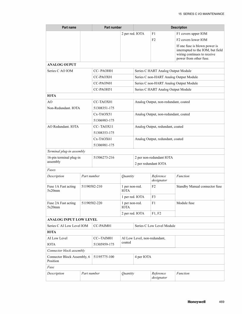
Part name Part number Description2 per red. IOTA F1
F2
F1 covers upper IOM
F2 covers lower IOM
If one fuse is blown power isinterrupted to the IOM, but fieldwiring continues to receivepower from other fuse.
ANALOG OUPUT
Series C AO IOM CC- PAOH01 Series C HART Analog Output Module
CC-PAOX01 Series C non-HART Analog Output Module
CC-PAON01 Series C non-HART Analog Output Module
CC-PAOH51 Series C HART Analog Output Module
IOTA
AO
Non-Redundant. IOTA
CC-TAOX01
51308351-175
Analog Output, non-redundant, coated
Cx-TAOX51
51306983-175
Analog Output, non-redundant, coated
AO Redundant. IOTA CC- TAOX11
51308353-175
Analog Output, redundant, coated
Cx-TAOX61
51306981-175
Analog Output, redundant, coated
Terminal plug-in assembly
16-pin terminal plug-inassembly
51506273-216 2 per non-redundant IOTA
2 per redundant IOTA
Fuses
Description Part number Quantity Referencedesignator
Function
Fuse 1A Fast acting5x20mm
51190582-210 1 per non-red.IOTA
F2 Standby Manual connector fuse
1 per red. IOTA F3
Fuse 2A Fast acting5x20mm
51190582-220 1 per non-red.IOTA
F1 Module fuse
2 per red. IOTA F1, F2
ANALOG INPUT LOW LEVEL
Series C AI Low Level IOM CC-PAIM01 Series C Low Level Module
IOTA
AI Low Level
IOTA
CC--TAIM01
51305959-175
AI Low Level, non-redundant,coated
Connector block assembly
Connector Block Assembly, 6Position
51195775-100 4 per IOTA
Fuse
Description Part number Quantity Referencedesignator
Function
15 SERIES C I/O MAINTENANCE
469
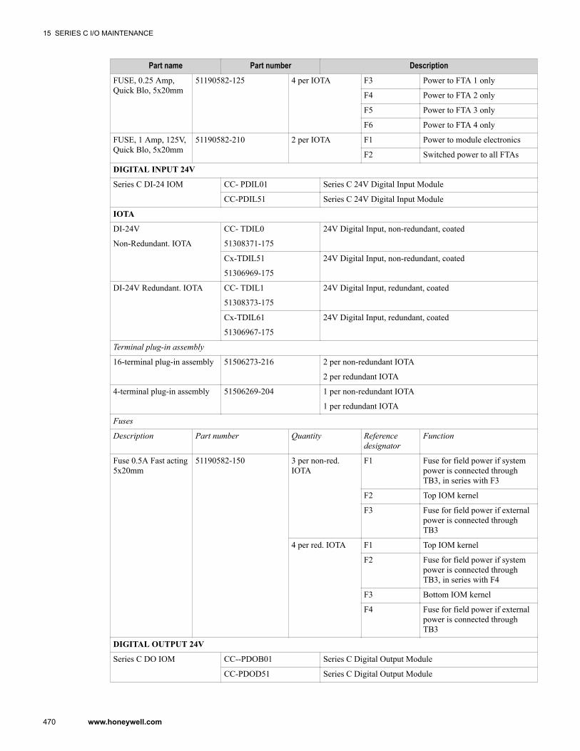
Part name Part number DescriptionFUSE, 0.25 Amp,Quick Blo, 5x20mm
51190582-125 4 per IOTA F3 Power to FTA 1 only
F4 Power to FTA 2 only
F5 Power to FTA 3 only
F6 Power to FTA 4 only
FUSE, 1 Amp, 125V,Quick Blo, 5x20mm
51190582-210 2 per IOTA F1 Power to module electronics
F2 Switched power to all FTAs
DIGITAL INPUT 24V
Series C DI-24 IOM CC- PDIL01 Series C 24V Digital Input Module
CC-PDIL51 Series C 24V Digital Input Module
IOTA
DI-24V
Non-Redundant. IOTA
CC- TDIL0
51308371-175
24V Digital Input, non-redundant, coated
Cx-TDIL51
51306969-175
24V Digital Input, non-redundant, coated
DI-24V Redundant. IOTA CC- TDIL1
51308373-175
24V Digital Input, redundant, coated
Cx-TDIL61
51306967-175
24V Digital Input, redundant, coated
Terminal plug-in assembly
16-terminal plug-in assembly 51506273-216 2 per non-redundant IOTA
2 per redundant IOTA
4-terminal plug-in assembly 51506269-204 1 per non-redundant IOTA
1 per redundant IOTA
Fuses
Description Part number Quantity Referencedesignator
Function
Fuse 0.5A Fast acting5x20mm
51190582-150 3 per non-red.IOTA
F1 Fuse for field power if systempower is connected throughTB3, in series with F3
F2 Top IOM kernel
F3 Fuse for field power if externalpower is connected throughTB3
4 per red. IOTA F1 Top IOM kernel
F2 Fuse for field power if systempower is connected throughTB3, in series with F4
F3 Bottom IOM kernel
F4 Fuse for field power if externalpower is connected throughTB3
DIGITAL OUTPUT 24V
Series C DO IOM CC--PDOB01 Series C Digital Output Module
CC-PDOD51 Series C Digital Output Module
15 SERIES C I/O MAINTENANCE
470 www.honeywell.com
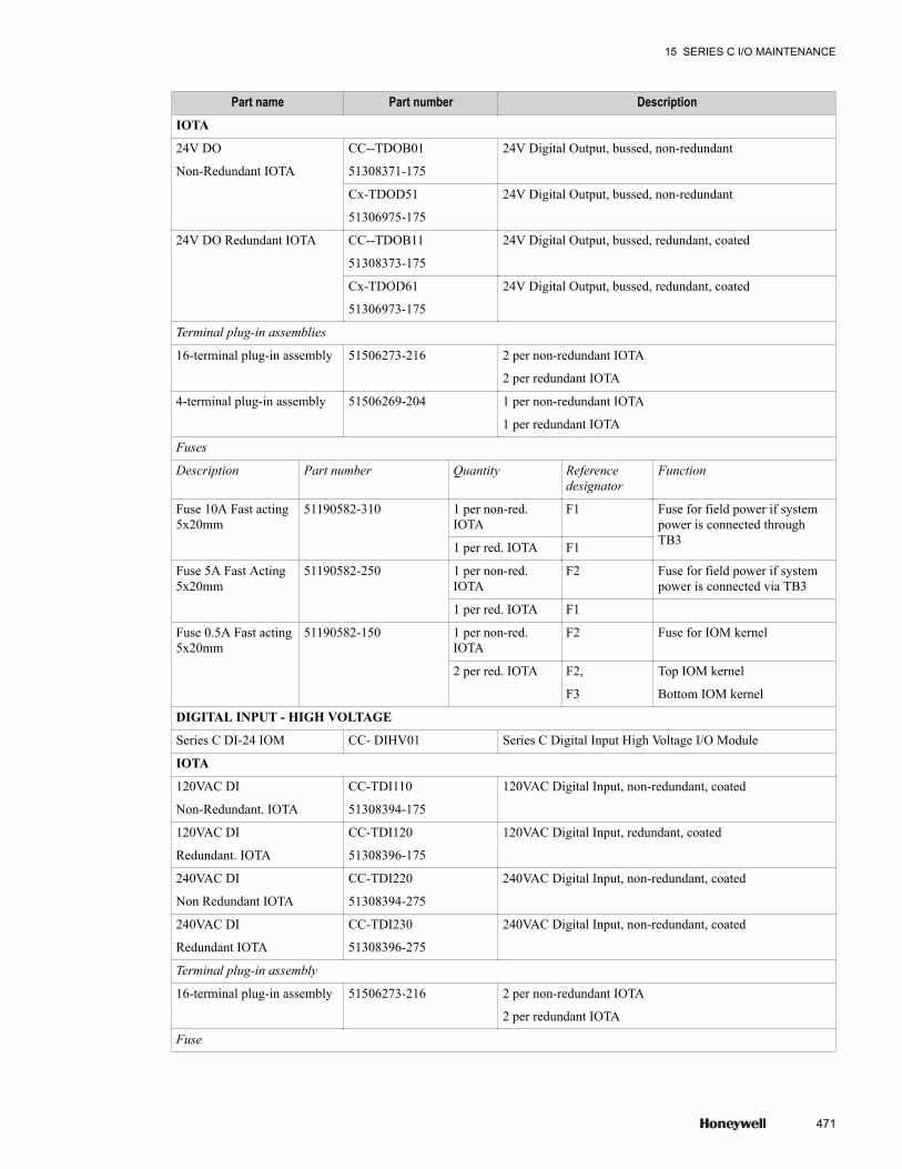
Part name Part number DescriptionIOTA
24V DO
Non-Redundant IOTA
CC--TDOB01
51308371-175
24V Digital Output, bussed, non-redundant
Cx-TDOD51
51306975-175
24V Digital Output, bussed, non-redundant
24V DO Redundant IOTA CC--TDOB11
51308373-175
24V Digital Output, bussed, redundant, coated
Cx-TDOD61
51306973-175
24V Digital Output, bussed, redundant, coated
Terminal plug-in assemblies
16-terminal plug-in assembly 51506273-216 2 per non-redundant IOTA
2 per redundant IOTA
4-terminal plug-in assembly 51506269-204 1 per non-redundant IOTA
1 per redundant IOTA
Fuses
Description Part number Quantity Referencedesignator
Function
Fuse 10A Fast acting5x20mm
51190582-310 1 per non-red.IOTA
F1 Fuse for field power if systempower is connected throughTB31 per red. IOTA F1
Fuse 5A Fast Acting5x20mm
51190582-250 1 per non-red.IOTA
F2 Fuse for field power if systempower is connected via TB3
1 per red. IOTA F1
Fuse 0.5A Fast acting5x20mm
51190582-150 1 per non-red.IOTA
F2 Fuse for IOM kernel
2 per red. IOTA F2,
F3
Top IOM kernel
Bottom IOM kernel
DIGITAL INPUT - HIGH VOLTAGE
Series C DI-24 IOM CC- DIHV01 Series C Digital Input High Voltage I/O Module
IOTA
120VAC DI
Non-Redundant. IOTA
CC-TDI110
51308394-175
120VAC Digital Input, non-redundant, coated
120VAC DI
Redundant. IOTA
CC-TDI120
51308396-175
120VAC Digital Input, redundant, coated
240VAC DI
Non Redundant IOTA
CC-TDI220
51308394-275
240VAC Digital Input, non-redundant, coated
240VAC DI
Redundant IOTA
CC-TDI230
51308396-275
240VAC Digital Input, non-redundant, coated
Terminal plug-in assembly
16-terminal plug-in assembly 51506273-216 2 per non-redundant IOTA
2 per redundant IOTA
Fuse
15 SERIES C I/O MAINTENANCE
471
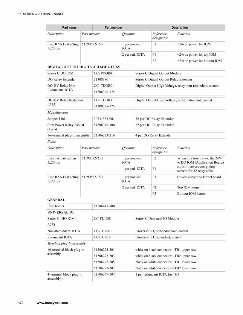
Part name Part number DescriptionDescription Part number Quantity Reference
designatorFunction
Fuse 0.5A Fast acting5x20mm
51190582-150 1 per non-red.IOTA
F1 +24vdc power for IOM
2 per red. IOTA F1 +24vdc power for top IOM
F2 +24vdc power for bottom IOM
DIGITAL OUTPUT HIGH VOLTAGE RELAY
Series C DO IOM CC- PDOB01 Series C Digital Output Module
DO Relay Extender 51308380 Series C Digital Output Relay Extender
DO-HV Relay Non-Redundant. IOTA
CC- TDOR01
51308376-175
Digital Output High Voltage, relay, non-redundant, coated
DO-HV Relay Redundant.IOTA
CC- TDOR11
51308378-175
Digital Output High Voltage, relay, redundant, coated
Miscellaneous
Jumper Link 30731551-001 32 per DO Relay Extender
Slim Power Relay 24VDC(Tyco)
51506348-100 32 per DO Relay Extender
16-terminal plug-in assembly 51506273-216 4 per DO Relay Extender
Fuses
Description Part number Quantity Referencedesignator
Function
Fuse 1A Fast acting5x20mm
51190582-210 1 per non-red.IOTA
F2 When this fuse blows, the 24Vto DO IOM (Application Board)stops. It covers energizingcurrent for 32 relay coils.1 per red. IOTA F1
Fuse 0.5A Fast acting5x20mm
51190582-150 1 per non-red.IOTA
F1 Covers current to kernel board.
2 per red. IOTA F2 Top IOM kernel
F3 Bottom IOM kernel
GENERAL
Fuse holder 51506443-100
UNIVERSAL IO
Series C UIO IOM CC-PUIO01 Series C Universal IO Module
IOTA
Non-Redundant. IOTA CC-TUIO01 Universal IO, non-redundant, coated
Redundant IOTA CC-TUIO11 Universal IO, redundant, coated
Terminal plug-in assembly
16-terminal block plug-inassembly
51506273-301
51506273-303
51506273-305
51506273-307
white on black connector - TB1 upper row
white on black connector - TB2 upper row
black on white connector - TB1 lower row
black on white connector - TB2 lower row
4-terminal block plug-inassembly
51506269-104 1 per redundant IOTA for TB3
15 SERIES C I/O MAINTENANCE
472 www.honeywell.com
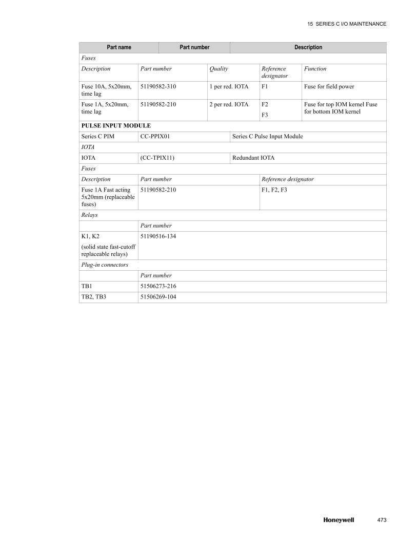
Part name Part number DescriptionFuses
Description Part number Quality Referencedesignator
Function
Fuse 10A, 5x20mm,time lag
51190582-310 1 per red. IOTA F1 Fuse for field power
Fuse 1A, 5x20mm,time lag
51190582-210 2 per red. IOTA F2
F3
Fuse for top IOM kernel Fusefor bottom IOM kernel
PULSE INPUT MODULE
Series C PIM CC-PPIX01 Series C Pulse Input Module
IOTA
IOTA (CC-TPIX11) Redundant IOTA
Fuses
Description Part number Reference designator
Fuse 1A Fast acting5x20mm (replaceablefuses)
51190582-210 F1, F2, F3
Relays
Part number
K1, K2
(solid state fast-cutoffreplaceable relays)
51190516-134
Plug-in connectors
Part number
TB1 51506273-216
TB2, TB3 51506269-104
15 SERIES C I/O MAINTENANCE
473
15.2 Replacing a Series C IOTA
AttentionReplacing the Series C IOTA requires that the IOM be in an inactive off-process state.
WARNINGReplacing a GI/IS IOTA and all associated activities may only be performed when the area has been determined tobe non-hazardous.
To replace a Series C IOTA1 To remove the I/O module, refer to the following procedure 2 Label and disconnect all cables from the IOTA board connectors.3 To remove the IOTA board do the following:
CAUTIONThe IOTA power and ground screws can bind during installation or removal if the mounting screws are fullysecured before the power/ground screws are installed.
Recommended sequence:
1. Remove the IOTA from the carrier by loosening the IOTA's mounting screws only half-way.2. Remove the screw from the left side of the IOTA board that connects to the 24 Vdc bus bar.3. Remove the screw from the right side of the IOTA board that connects to the GND bus bar.4. Completely remove the IOTA's mounting screws5. Place screws, washers and spacers in a secure place for potential reuse.
4 Mount the new I/O IOTA board on the carrier, and refer to the following procedure .5 Insert the I/O module onto IOTA board making sure that the I/O circuit board mates properly with the IOTA
board connector.Refer to the following procedure, .
6 The I/O module boots-up into IDLE state.7 In Control Builder, perform a 'Load with Contents'.
15 SERIES C I/O MAINTENANCE
474 www.honeywell.com
15.3 Replacing an I/O module
CAUTIONWe recommend that you proceed with extreme caution whenever replacing any component in a control system. Besure the system is offline or in a safe operating mode.
Component replacements may also require corresponding changes in the control strategy configuration throughControl Builder, as well as downloading appropriate data to the replaced component.
PrerequisitesYou have logged onto Control Builder with sufficient security level to make control strategy changes.
• You can remove and install the Series C IOM under power.• Be sure you take ESD hazard precautions when handling the module and IOTA.
To replace an I/O module1 Loosen the screws:
• at each side of the plastic cover that secures the I/O module to the IOTA board, and• the long gray plastic screw located on the module's face. It is not necessary to completely remove this
screw.
CAUTIONOnly use a #2 Phillips screwdriver to carefully loosen or tighten the long gray plastic screw. Do not use eithera #1 Phillips screwdriver or a battery-powered screwdriver to remove or install the plastic screw as this candamage the screw head.
2 Remove the I/O module from the IOTA board and connector.3 Insert the new I/O module onto IOTA board making sure that the I/O circuit board mates properly with the
IOTA board connector.4 Secure the module to the:
• IOTA board
using the two metal screws at the plastic cover
tightening the long gray plastic screw. See CAUTION in Step 1.• Carrier - with the long screw that is inserted into the hole on the face of the module's plastic cover.
The new I/O module boots-up to the IDLE state.5 Load firmware which is the same version as was running in the old controller.6 In Control Builder, perform a 'Load with Contents".
15 SERIES C I/O MAINTENANCE
475
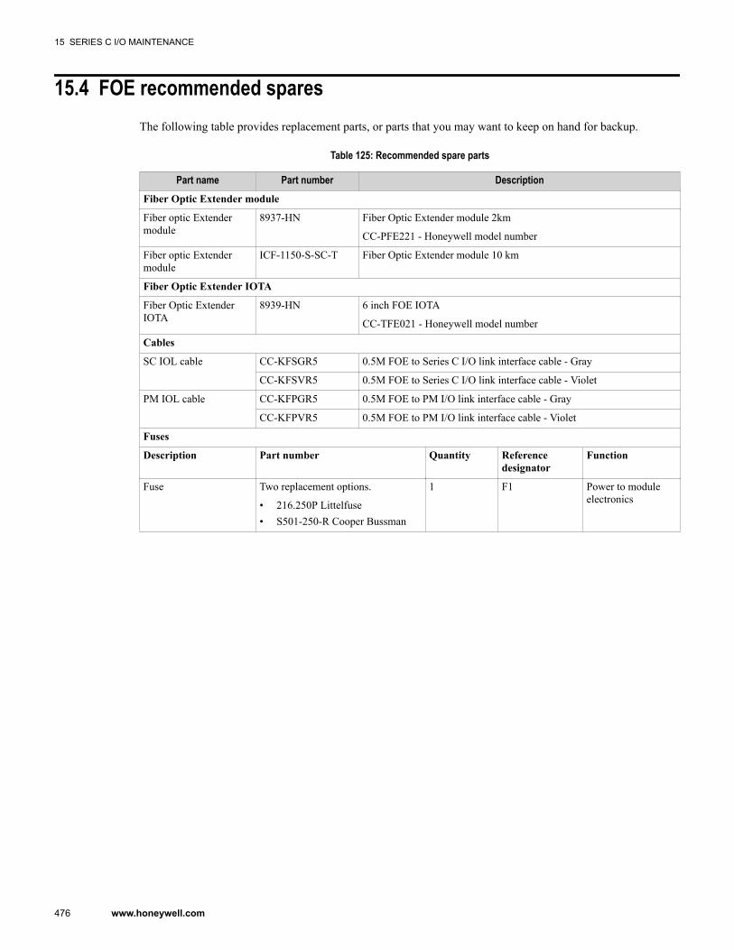
15.4 FOE recommended sparesThe following table provides replacement parts, or parts that you may want to keep on hand for backup.
Table 125: Recommended spare parts
Part name Part number DescriptionFiber Optic Extender module
Fiber optic Extendermodule
8937-HN Fiber Optic Extender module 2km
CC-PFE221 - Honeywell model number
Fiber optic Extendermodule
ICF-1150-S-SC-T Fiber Optic Extender module 10 km
Fiber Optic Extender IOTA
Fiber Optic ExtenderIOTA
8939-HN 6 inch FOE IOTA
CC-TFE021 - Honeywell model number
Cables
SC IOL cable CC-KFSGR5 0.5M FOE to Series C I/O link interface cable - Gray
CC-KFSVR5 0.5M FOE to Series C I/O link interface cable - Violet
PM IOL cable CC-KFPGR5 0.5M FOE to PM I/O link interface cable - Gray
CC-KFPVR5 0.5M FOE to PM I/O link interface cable - Violet
Fuses
Description Part number Quantity Referencedesignator
Function
Fuse Two replacement options.
• 216.250P Littelfuse• S501-250-R Cooper Bussman
1 F1 Power to moduleelectronics
15 SERIES C I/O MAINTENANCE
476 www.honeywell.com
15.5 FOE MaintenanceRemote I/O requires a minimum of maintenance. A regular inspection program is advised, but the frequency ofinspections depends largely upon the environmental conditions in which the equipment normally operates.
The following should be periodically checked:
• all cables and wires attached to the FOE module• evidence of any tampering or unauthorized modifications
The FOE module and IOTA cannot be repaired by the user and must be replaced with an equivalent certifiedproduct. Repairs should only be carried out by the manufacturer.
15.5.1 Replacing the FOE IOTA F1 fuseRefer to the FOE recommended spares section in this document for the proper replacement fuse to be used.
AttentionPrior to installing or servicing the FOE assembly (FOE module on the IOTA) to the carrier, the F1 fuse needs to beremoved. After mounting the FOE assembly to the carrier and securing the power and ground screws, the F1 fuse canbe re-installed.
To replace the FOE IOTA F1 fuse1 Using a small slotted screwdriver, place the tip into the slot on the fuse cap (The cap is the fuse holder).2 Rotate the cap counter clockwise, a quarter-turn. Remove cap that also holds the fuse.3 Replace the fuse in the fuse holder and insert back into the fuse container on the IOTA board.4 Tighten the fuse cap rotating it clockwise a quarter-turn using the screwdriver.5 This completes the procedure.
15.5.2 Replacing the FOE fuse on the terminal block when FOE is mounted on DIN rail
To replace the FOE fuse on the terminal block when the FOE is mounted on the DIN rail1 Using the lever provided on the terminal block, open the fuse holder.2 Remove the fuse from the fuse holder.3 Replace the fuse by positioning it in the fuse holder, press and fit.4 Close the fuse holder and press the lever to lock.
15.5.3 Replacing the FOE module on the IOTAIf the FOE module needs replacing or requires mounting on the IOTA, do the following.
PrerequisitesThe IOTA has been previously removed or is missing from the IOTA board
AttentionPrior to installing or servicing the FOE assembly (FOE module on the IOTA) to the carrier, the F1 fuse needs to beremoved. After mounting the FOE assembly to the carrier and securing the power and ground screws, the F1 fuse canbe re-installed.
15 SERIES C I/O MAINTENANCE
477
To replace the FOE module on the IOTA1 Align the FOE screws (located on the flange) with the holes on the IOTA.2 Tighten the four screws that attach the base of the FOE module to the IOTA board (using a small Phillips
screwdriver).3 Connect the power cable from the IOTA board to the connector at the bottom of the module.4 This completes the procedure.
15.5.4 Removing the FOE module from the DIN rail
To remove the FOE module from the DIN rail1 Power down the FOE module by opening the fuse holder of the terminal block using the lever and removing
the fuse2 Remove all the cables before detaching the FOE modules. Perform the following steps to do so.
a Unscrew and remove the cable (HPN 51202930-200) running from the feed through terminal of thesystem cabinet to the '+' fuse terminal of the terminal block (Meanwell/Phoenix Contact power supplyonly).
b Remove the power connector of the cable (HPN 51202948-100/51202948-200) from the power supplyby releasing the lock in the side and pulling it out gently (TDI power supply only).
c Unfasten the screw of the '-' fuse terminal of the terminal block on DIN rail and remove the cable.d Unfasten the screw of the 'V+' terminal of power connector on the FOE module and remove the cable.e Unfasten the screw of the '-' terminal of the feed through terminal block and remove the cable.f Unfasten the screw of the 'V-' terminal of power connector on the FOE module and remove the cable.g Remove the fiber optic cables from the FOE module by pulling it out gently.h Unscrew and remove the I/O Link cable (HPN 51202789-910 / 51202789-911) from the FOE module or
remove the I/O Link connector by pulling it out.3 Unfasten the screw in the center of the end bracket and remove it by slightly lifting and pulling it out.4 Push the FOE module slightly downwards and slide it out at the lower edge of DIN rail.
WARNINGPowering off both FOE modules accidently may halt the IOL communication completely and can lead todangerous situation in plant. You must ensure to turn off the power of suspected FOE and should remove itwithout disturbing the functional FOE. Ensure to notify plant operators while performing this operation.
15.5.5 Removing the FOE assembly from the carrierIf the FOE assembly needs replacing and therefore, requires removal from the carrier, do the following.
AttentionPrior to installing or servicing the FOE assembly (FOE module on the IOTA) to the carrier, the F1 fuse needs to beremoved. After mounting the FOE assembly to the carrier and securing the power and ground screws, the F1 fuse canbe re-installed.
To remove the FOE assembly from the carrier1 Using a #2 Phillips screw-driver, loosen the two power screws, connecting the IOTA board to the vertical
bus bars on the channel carrier assembly:• +24 V power screw• Com ground screw
2 Disconnect the IOLINK cable from the end that attaches to either the C300 or I/O IOTA.
15 SERIES C I/O MAINTENANCE
478 www.honeywell.com
3 Remove the FOE assembly from the carrier using a #2 Phillips screwdriver.4 This completes the procedure.
15.5.6 Hazardous Area Cable RequirementsFor U.S. installations, section 770-53 (d) of NEC Article 770 states that 'Cables installed in hazardous(classified) locations shall be any type indicated in Table 770-53.' This table is reproduced below.
Cable type Permitted substitutionsOFNP None
OFCP OFNP
OFNR OFNP
OFCR OFNP, OFCP, OFNR
OFNG, OFN OFNP, OFNR
OFCG, OFC OFNP, OFCP, OFNR, OFNG, OFN
The cable types are described in the following table:
Cablemarking
Cable type Reference(NEC Article 770)
OFNP Nonconductive optical fiber plenum cable 770-51(a) and 770-53(a)
OFCP Conductive optical fiber plenum cable 770-51(a) and 770-53(a)
OFNR Nonconductive optical fiber riser cable 770-51(b) and 770-53(b)
OFCR Conductive optical fiber riser cable 770-51(b) and 770-53(b)
OFNG Nonconductive optical fiber general-purpose cable 770-51(c) and 770-53(c)
OFCG Conductive optical fiber general-purpose cable 770-51(c) and 770-53(c)
OFN Nonconductive optical fiber general-purpose cable 770-51(d) and 770-53(c)
OFC Conductive optical fiber general-purpose cable 770-51(d) and 770-53(c)
Nonconductive fiber optic cable is defined as cable containing no metallic members and no other electricallyconductive materials.
Conductive fiber optic cable is defined as cable containing non-current-carrying
conductive members such as metallic strength members, metallic vapor barriers and metallic armor or sheath.
15.5.7 Cable jacket Building Code RequirementsBuilding code requirements frequently do not allow cables with polyethylene jackets. Jackets of polyvinylchloride are frequently restricted to conduits, while fluoropolymer or other approved jacked material is requiredfor use in cable trays and air plenums. Cable with suitable jacket material must be selected for the application.
15.5.8 Cable temperature variation considerationsWhere ambient temperature variations are 20°C or greater on a daily basis, the life of the fibers can besignificantly reduced. In applications where the ambient temperature is not controlled, loose buffered cable mustbe specified.
15 SERIES C I/O MAINTENANCE
479

15.5.9 Spare fiber cable recommendationA minimum of two cable fibers is required for each link, one for transmit and one for receive. The followingcharacteristics apply to fiber optic cable spares:
• As insurance against future damage, such as fiber breakage, or encountering excessive loss in any one fiber,the inclusion of spare fibers is recommended. 100% cable replacement is recommended.
• Indoor 62.5 Micron Cable is used for indoor cabling. Indoor cables are available with 2, 4, or 6 fibers.• Outdoor 62.5 Micron Cable is used for outdoor cabling. Outdoor aerial and direct burial cables are available
with 4, 6, or 8 fibers.
15 SERIES C I/O MAINTENANCE
480 www.honeywell.com

16 Series C Power Sub-System Connections andAlarm Indications
Related topics“Series C DC Power Connections and Indicators” on page 482“Series C Power Sub-System LED Indications” on page 490“Series C Power Sub-System Alarm Contacts and LED Activation Levels” on page 492
481
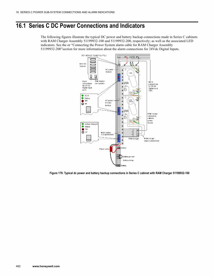
16.1 Series C DC Power Connections and IndicatorsThe following figures illustrate the typical DC power and battery backup connections made in Series C cabinetswith RAM Charger Assembly 51199932-100 and 51199932-200, respectively; as well as the associated LEDindicators. See the or “Connecting the Power System alarm cable for RAM Charger Assembly51199932-200”section for more information about the alarm connections for 24Vdc Digital Inputs.
Figure 179: Typical dc power and battery backup connections in Series C cabinet with RAM Charger 51199932-100
16 SERIES C POWER SUB-SYSTEM CONNECTIONS AND ALARM INDICATIONS
482 www.honeywell.com
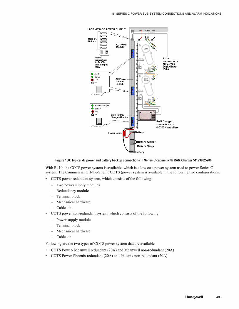
Figure 180: Typical dc power and battery backup connections in Series C cabinet with RAM Charger 51199932-200
With R410, the COTS power system is available, which is a low cost power system used to power Series Csystem. The Commercial Off-the-Shelf ( COTS )power system is available in the following two configurations.
• COTS power redundant system, which consists of the following:
– Two power supply modules– Redundancy module– Terminal block– Mechanical hardware– Cable kit
• COTS power non-redundant system, which consists of the following:
– Power supply module– Terminal block– Mechanical hardware– Cable kit
Following are the two types of COTS power system that are available.
• COTS Power- Meanwell redundant (20A) and Meanwell non-redundant (20A)• COTS Power-Phoenix redundant (20A) and Phoenix non-redundant (20A)
16 SERIES C POWER SUB-SYSTEM CONNECTIONS AND ALARM INDICATIONS
483

The following figure displays the connection diagram for COTS Power-Meanwell redundant system.
The following diagram displays the connection diagram for COTS power-Phoenix redundant system.
16 SERIES C POWER SUB-SYSTEM CONNECTIONS AND ALARM INDICATIONS
484 www.honeywell.com

The following diagram displays the connection diagram for COTS Power Meanwell non-redundant system.
16 SERIES C POWER SUB-SYSTEM CONNECTIONS AND ALARM INDICATIONS
485

The following diagram displays connection for the COTS power-Phoenix non-redundant system.
16 SERIES C POWER SUB-SYSTEM CONNECTIONS AND ALARM INDICATIONS
486 www.honeywell.com
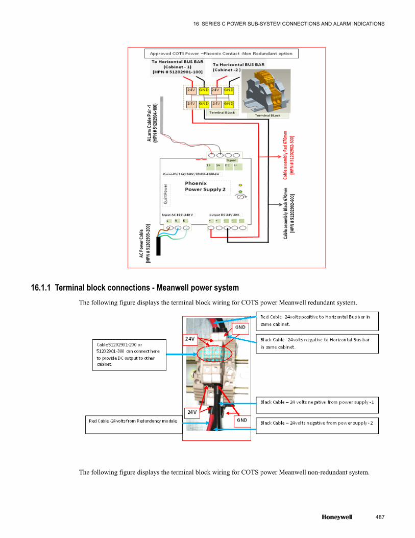
16.1.1 Terminal block connections - Meanwell power systemThe following figure displays the terminal block wiring for COTS power Meanwell redundant system.
The following figure displays the terminal block wiring for COTS power Meanwell non-redundant system.
16 SERIES C POWER SUB-SYSTEM CONNECTIONS AND ALARM INDICATIONS
487

16.1.2 Terminal block connections - Phoenix power systemThe following figure displays the terminal block wiring for COTS power Phoenix redundant system.
The following figure displays the terminal block wiring for COTS power Phoenix non-redundant system.
16 SERIES C POWER SUB-SYSTEM CONNECTIONS AND ALARM INDICATIONS
488 www.honeywell.com
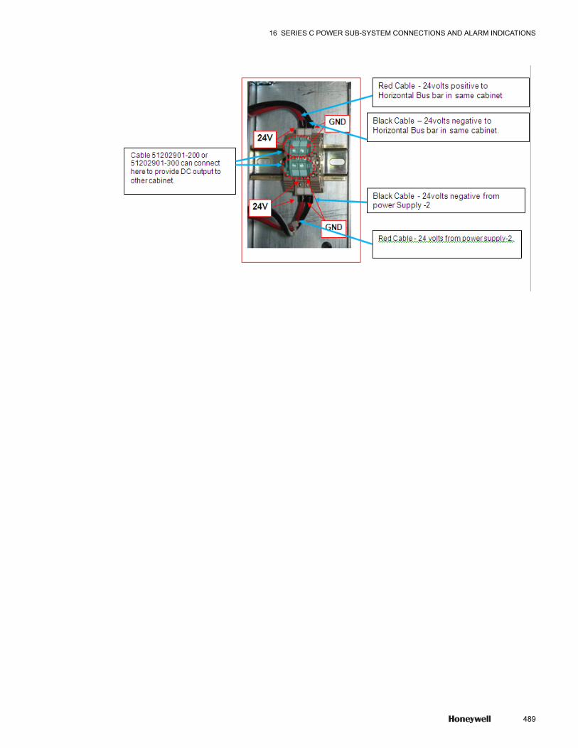
16 SERIES C POWER SUB-SYSTEM CONNECTIONS AND ALARM INDICATIONS
489
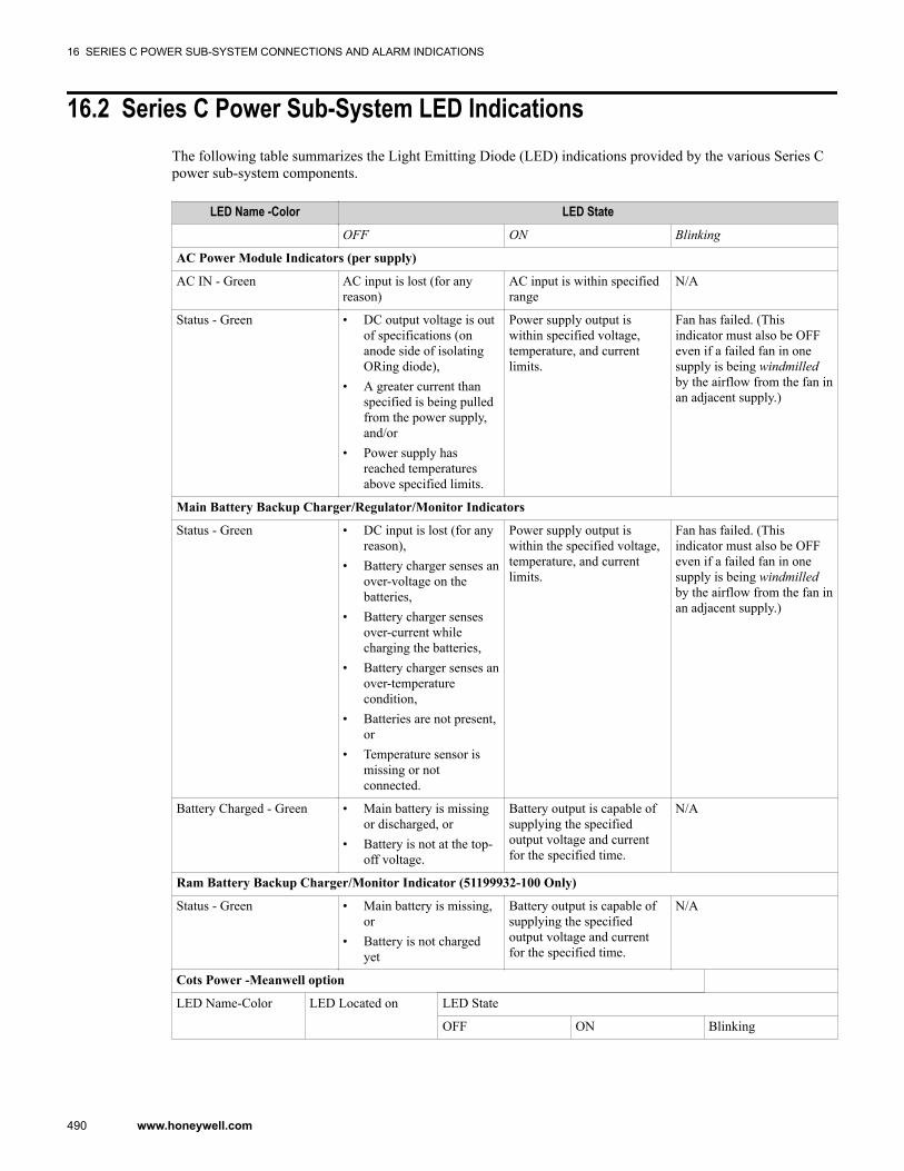
16.2 Series C Power Sub-System LED IndicationsThe following table summarizes the Light Emitting Diode (LED) indications provided by the various Series Cpower sub-system components.
LED Name -Color LED StateOFF ON Blinking
AC Power Module Indicators (per supply)
AC IN - Green AC input is lost (for anyreason)
AC input is within specifiedrange
N/A
Status - Green • DC output voltage is outof specifications (onanode side of isolatingORing diode),
• A greater current thanspecified is being pulledfrom the power supply,and/or
• Power supply hasreached temperaturesabove specified limits.
Power supply output iswithin specified voltage,temperature, and currentlimits.
Fan has failed. (Thisindicator must also be OFFeven if a failed fan in onesupply is being windmilledby the airflow from the fan inan adjacent supply.)
Main Battery Backup Charger/Regulator/Monitor Indicators
Status - Green • DC input is lost (for anyreason),
• Battery charger senses anover-voltage on thebatteries,
• Battery charger sensesover-current whilecharging the batteries,
• Battery charger senses anover-temperaturecondition,
• Batteries are not present,or
• Temperature sensor ismissing or notconnected.
Power supply output iswithin the specified voltage,temperature, and currentlimits.
Fan has failed. (Thisindicator must also be OFFeven if a failed fan in onesupply is being windmilledby the airflow from the fan inan adjacent supply.)
Battery Charged - Green • Main battery is missingor discharged, or
• Battery is not at the top-off voltage.
Battery output is capable ofsupplying the specifiedoutput voltage and currentfor the specified time.
N/A
Ram Battery Backup Charger/Monitor Indicator (51199932-100 Only)
Status - Green • Main battery is missing,or
• Battery is not chargedyet
Battery output is capable ofsupplying the specifiedoutput voltage and currentfor the specified time.
N/A
Cots Power -Meanwell option
LED Name-Color LED Located on LED State
OFF ON Blinking
16 SERIES C POWER SUB-SYSTEM CONNECTIONS AND ALARM INDICATIONS
490 www.honeywell.com
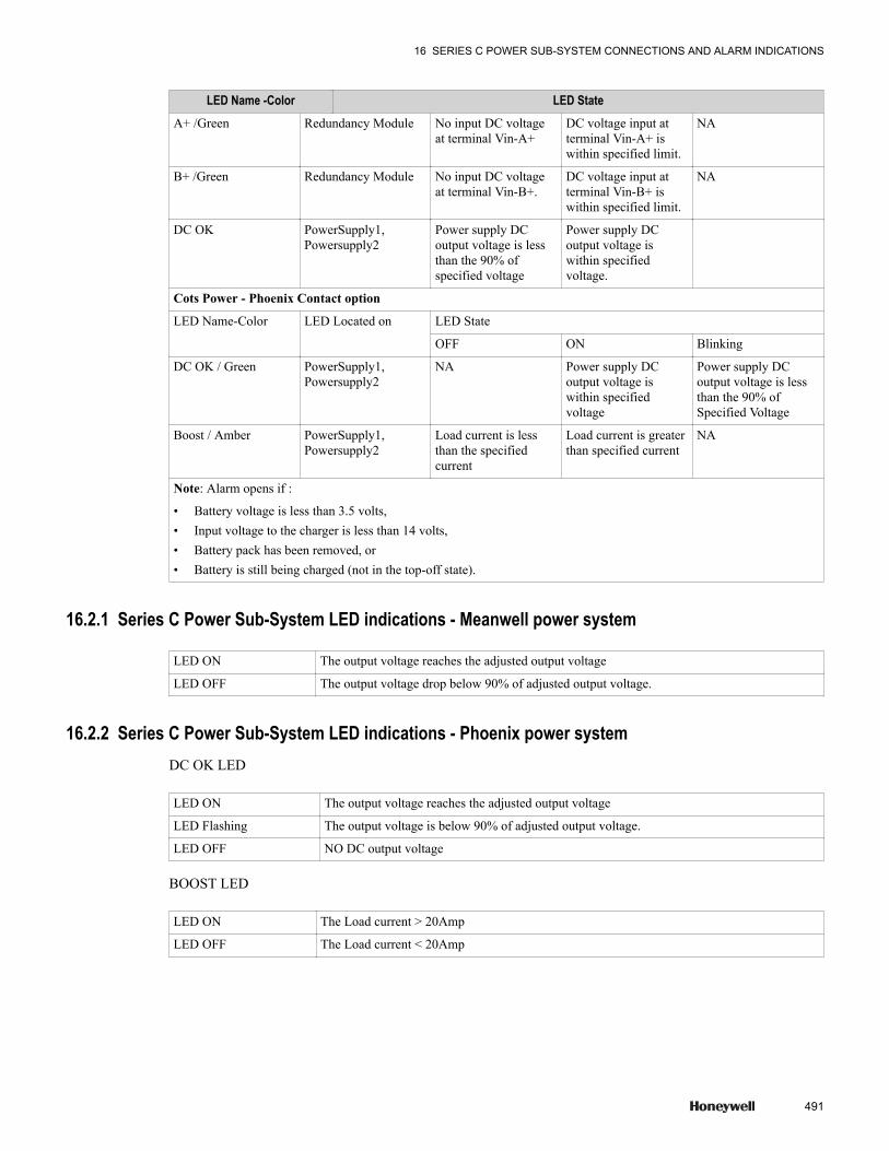
LED Name -Color LED StateA+ /Green Redundancy Module No input DC voltage
at terminal Vin-A+DC voltage input atterminal Vin-A+ iswithin specified limit.
NA
B+ /Green Redundancy Module No input DC voltageat terminal Vin-B+.
DC voltage input atterminal Vin-B+ iswithin specified limit.
NA
DC OK PowerSupply1,Powersupply2
Power supply DCoutput voltage is lessthan the 90% ofspecified voltage
Power supply DCoutput voltage iswithin specifiedvoltage.
Cots Power - Phoenix Contact option
LED Name-Color LED Located on LED State
OFF ON Blinking
DC OK / Green PowerSupply1,Powersupply2
NA Power supply DCoutput voltage iswithin specifiedvoltage
Power supply DCoutput voltage is lessthan the 90% ofSpecified Voltage
Boost / Amber PowerSupply1,Powersupply2
Load current is lessthan the specifiedcurrent
Load current is greaterthan specified current
NA
Note: Alarm opens if :
• Battery voltage is less than 3.5 volts,• Input voltage to the charger is less than 14 volts,• Battery pack has been removed, or• Battery is still being charged (not in the top-off state).
16.2.1 Series C Power Sub-System LED indications - Meanwell power system
LED ON The output voltage reaches the adjusted output voltage
LED OFF The output voltage drop below 90% of adjusted output voltage.
16.2.2 Series C Power Sub-System LED indications - Phoenix power systemDC OK LED
LED ON The output voltage reaches the adjusted output voltage
LED Flashing The output voltage is below 90% of adjusted output voltage.
LED OFF NO DC output voltage
BOOST LED
LED ON The Load current > 20Amp
LED OFF The Load current < 20Amp
16 SERIES C POWER SUB-SYSTEM CONNECTIONS AND ALARM INDICATIONS
491

16.3 Series C Power Sub-System Alarm Contacts and LED ActivationLevels
Each power supply and the main battery backup regulator/charger, and the RAM battery backup charger providean alarm contact. The alarm contact opens if any of the LED indicators listed in the previous section are not inthe normal (ON) state. The alarm contact is electrically isolated from all other circuitry so that it can be seriesconnected by the user with alarms in other devices.
Use a hermetically sealed electromechanical relay. The alarm contacts are rated for 24 Volts ac or dc at 0 to 65mA non-inductive load. An alarm condition is signaled by an open contact (1000 ohms or more); and a no alarmcondition is signaled by a closed contact (10 ohms or less).
The following table provides a functional description of the activation levels for a given LED indicator.
LED Name Functional DescriptionAC Power Module Indicators (per supply)
AC IN The LED turns ON when the AC input voltage is sufficient to start the unit. This isguaranteed to occur when the input voltage has risen to 85 Vac, but it could occur at a lowervoltage, depending on output loading and unit-to-unit variations. Once the unit starts, theLED remains ON through the entire AC input voltage range. The LED will turn OFF at thepoint where the power supply shuts down. For a fully loaded supply, this is guaranteed not tooccur until the input voltage descends below 85 Vac. This voltage can be considerably lower,if the unit is lightly loaded and depending on unit-to-unit variations. The unit does not shutdown when the AC input range is exceeded unless there is a failure in the power supply.
Status The LED turns ON when output voltage is within the operating range. The LED turns OFFwhen the DC voltage is increased to above 26.4 Vdc and the power supply shuts down due toan over-voltage condition. (Based on manufacturer's tests, the actual data range for over-voltage is 26.4 to 30 Vdc.) The LED turns OFF during output overload, which is reachedwhen the load is increased to over 26 A and results in the unit shutting down.
Main Battery Backup Charger/Regulator/Monitor Indicators
Status The LED turns ON when both the input and battery voltages are within operating range. TheLED will remain ON until the battery reaches the Low-Voltage Drop-out point (32 Vdc) andthe unit turns OFF along with the LED (output will still be regulated at 25 Vdc during batterydischarge). The LED turns OFF when the battery voltage is above 45.5 Vdc. (Based onmanufacturer's tests, the actual data range for over-voltage is 45.5 to 48.5 Vdc.)
Battery Charged The LED operation is based on both battery charge voltage and battery charge current. Thebattery charge voltage must be above 40 Vdc and the battery charge current must be below 1A for the LED to be ON. If both of these conditions are not met, the LED will be OFF.
16 SERIES C POWER SUB-SYSTEM CONNECTIONS AND ALARM INDICATIONS
492 www.honeywell.com

17 Series C I/O Alarms and Failures
Related topics“Reviewing IOM alarms generated by the C300” on page 494“Reviewing IOM soft failures” on page 495“IOM hard failures” on page 515“IOM Behavior during Hard Failures” on page 516“Getting further assistance” on page 517
493
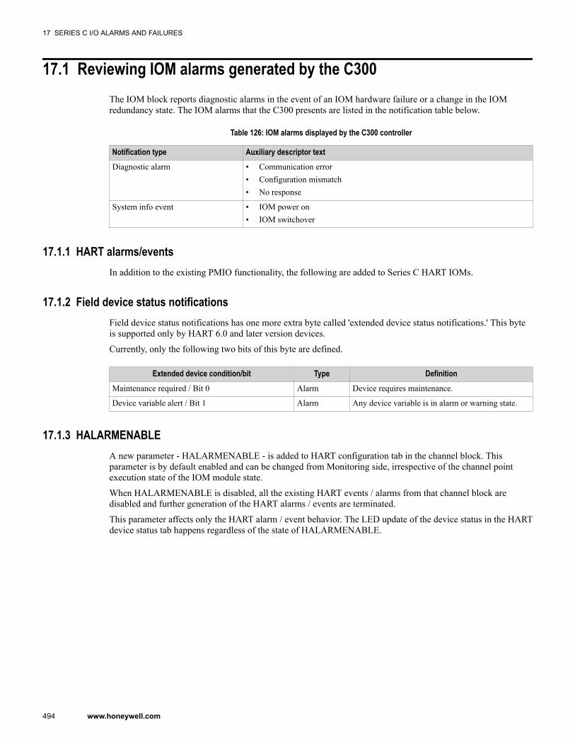
17.1 Reviewing IOM alarms generated by the C300The IOM block reports diagnostic alarms in the event of an IOM hardware failure or a change in the IOMredundancy state. The IOM alarms that the C300 presents are listed in the notification table below.
Table 126: IOM alarms displayed by the C300 controller
Notification type Auxiliary descriptor textDiagnostic alarm • Communication error
• Configuration mismatch• No response
System info event • IOM power on• IOM switchover
17.1.1 HART alarms/eventsIn addition to the existing PMIO functionality, the following are added to Series C HART IOMs.
17.1.2 Field device status notificationsField device status notifications has one more extra byte called 'extended device status notifications.' This byteis supported only by HART 6.0 and later version devices.
Currently, only the following two bits of this byte are defined.
Extended device condition/bit Type DefinitionMaintenance required / Bit 0 Alarm Device requires maintenance.
Device variable alert / Bit 1 Alarm Any device variable is in alarm or warning state.
17.1.3 HALARMENABLEA new parameter - HALARMENABLE - is added to HART configuration tab in the channel block. Thisparameter is by default enabled and can be changed from Monitoring side, irrespective of the channel pointexecution state of the IOM module state.
When HALARMENABLE is disabled, all the existing HART events / alarms from that channel block aredisabled and further generation of the HART alarms / events are terminated.
This parameter affects only the HART alarm / event behavior. The LED update of the device status in the HARTdevice status tab happens regardless of the state of HALARMENABLE.
17 SERIES C I/O ALARMS AND FAILURES
494 www.honeywell.com
17.2 Reviewing IOM soft failuresThe IOM reports device soft failures to Experion Server and located on the Control Builder configuration formsunder the Soft Failures tab.
The table below lists all IOM soft failures and identifies those that appear within Experion. Since Series C I/O isnot slated for use with TPS, soft failures related to TPS are not be provided by Series C I/O modules.
The SOFTFAIL1A, SOFTFAIL1B, SOFTFAIL2A and SOFTFAIL2B parameters are used to view an IOM's softfailures. For a list of channels in failure, use the CHNLWFAILA and CHNLWFAILB parameters.
17.2.1 01 STCOVRUNSample time clock overrun
Diagnostic checkInvestigate a possible I/O Link problem
CauseSample time clock overrun
SolutionInvestigate a possible I/O Link problem or excessive IOL activity. Check C300, IOL cables, IOMs and IOLbudgets. Call TAC if the alarm persists or repeatedly occurs.
17.2.2 02 REQOFLOWIOP task request overflow - excessive IOL activity
Diagnostic checkCheck IOL activity
CauseIOP task request overflow - excessive IOL activity
SolutionCall TAC for assistance.
17.2.3 06 FTAMISSGLLMUX, power adaptor, or DO Relay IOM config. is missing relay adapter board
Diagnostic checkCheck for missing items defined below.
CauseIf LLMUX, power adapter missing or if DO Relay IOM configuration is missing relay adapter board.
17 SERIES C I/O ALARMS AND FAILURES
495
SolutionInstall the FTA or relay adapter. If an FTA is present, replace the FTA or check the FTA cable. (Note: For theLLMux, this code refers to the Power Adapter assembly. RTD and TC FTAs are diagnosed by error Codes 50and 51.)
17.2.4 07 EECKSMEREEPROM checksum error - IOM probably not calibrated
Diagnostic checkEEPROM checksum error - IOM probably not calibrated
CauseEEPROM (used to hold calibration information in Analog Input and Analog Output IOPs) checksum failure. Itusually means an Analog Output IOM is not calibrated properly.
SolutionCalibrate the Analog Input or Analog Output IOM (refer to the 'IOM Calibration Procedures' section for theprocedure). If the error persists, replace the IOM.
17.2.5 08 EECNTERREEPROM counter error-too many writes
Diagnostic checkCheck EEPROM counter.
CauseEEPROM counter error. The number of writes to EEPROM has exceeded the safe number (10,000). This couldalso indicate the IOM has not been calibrated because a virgin EEPROM will fail this test.
SolutionCalibrate the Analog Input or Analog Output IOM (refer to the 'IOM Calibration Procedures' section for theprocedure). If the error persists, replace the IOM.
17.2.6 09 EEFLAGEREEPROM flag error - incomplete EEPROM write resulting in uncalibrated IOM
Diagnostic checkCheck EEPROM.
CauseEEPROM flag error - incomplete EEPROM write resulting in uncalibrated IOM.
SolutionCalibrate the Analog Input or Analog Output IOM (refer to the 'IOM Calibration Procedures' section for theprocedure). If the error persists, replace the IOM.
17 SERIES C I/O ALARMS AND FAILURES
496 www.honeywell.com
17.2.7 21 INPTFAILInput point failed diagnostic
Diagnostic check
CauseInput point failed diagnostic
Solution
17.2.8 23 OUTPUTFLFailure in output circuit / field wiring detected by AO or DO.
Diagnostic checkCheck field wiring and the fuses on the IOTA.
CauseFailure in output circuit / field wiring detected by AO or DO.
SolutionCheck field wiring and the fuses on the IOTA. If it is good, try replacing the IOTA and/or the appropriate IOMcard.
17.2.9 24 STCKLIMIOM firmware stack usage is dangerously close to its limit.
Diagnostic checkStack reaching limit.
CauseIOM firmware stack usage is dangerously close to its limit.
SolutionReduce activity on this IOM - inactivate control strategies. Call TAC for assistance.
17.2.10 26 DIAGCTFLIOM diagnostic circuit failure
Diagnostic checkIOM diagnostic circuit failure.
CauseIOM diagnostic circuit failure.
17 SERIES C I/O ALARMS AND FAILURES
497
For AI IOM, 'noise' on the input may cause this error.
SolutionReset the IOM. If reset does not clear the error, replace the appropriate IOM.
For AI IOM, check for 'noise' on the input.
17.2.11 31 FTAMSMCHLLMUX FTA type mismatch with channel configuration.
Diagnostic checkCheck channel block configuration.
CauseLLMUX FTA type mismatch with channel configuration.
SolutionRe-configure the channel block or replace the FTA.
17.2.12 32 VZERO-FLZero reference voltage out of range in AI and AO IOMs
Diagnostic checkZero reference failure.
CauseZero reference voltage out of range in AI and AO IOMs
SolutionReplace the IOM.
17.2.13 33 BADRJVALReference junction value bad
Diagnostic check
CauseReference junction value bad
Solution
17.2.14 36 FTA1FAILLLMUX :FTA 1 has a soft failure
17 SERIES C I/O ALARMS AND FAILURES
498 www.honeywell.com

Diagnostic checkCheck LLMUX FTA 1
CauseLLMUX FTA 1 has a soft failure.
SolutionCheck LLMUX FTA 1
17.2.15 37 FTA2FAILLLMUX FTA 2 has a soft failure
Diagnostic checkCheck LLMUX FTA 2
CauseLLMUX FTA 2 has a soft failure.
SolutionCheck LLMUX FTA 2
17.2.16 38 CALBABRTCalibration of a module has aborted due to a failure
Diagnostic check
CauseCalibration of a module has aborted due to a failure
Solution
17.2.17 39 BADCALRFInternal calibration test voltages out of range.
Diagnostic checkNone - Internal calibration test voltages out of range.
CauseInternal calibration test voltages out of range.
SolutionReplace AI or AO IOM.
17 SERIES C I/O ALARMS AND FAILURES
499
17.2.18 41 VREFFAILReference voltage out of range
Diagnostic checkCheck reference voltage
CauseInternal 5V reference out of range in AI or internal AA55 reference test failed in the case of DI.
SolutionReplace the AI or DI IOM.
17.2.19 42 ADOUTUDFAnalog to digital conversion on this Analog Input channel is out of range.
Diagnostic checkCheck input wiring.
CauseAnalog to digital conversion on this Analog Input channel is out of range.
SolutionCheck the input wiring at the IOTA; possible open contact. Otherwise, replace the IOM.
17.2.20 43 ADOUTCALAI or AO IOM is out of calibration.
Diagnostic checkCheck AI or AO IOM calibration
CauseAI or AO IOM is out of calibration.
SolutionCalibrate or replace the IOM (refer to the 'IOP Calibration Procedures' section).
17.2.21 44 BADFLREGAO module failure selection register is bad
Diagnostic check
CauseAO module failure selection register is bad
17 SERIES C I/O ALARMS AND FAILURES
500 www.honeywell.com
Solution
17.2.22 45 BDSNDLTCSecondary latch failure
Diagnostic check
CauseSecondary latch failure
Solution
17.2.23 46 BDOUTBFROutput disable buffer failure.
Diagnostic check
CauseOutput disable buffer failure
Solution
17.2.24 47 VCALFAILCalibration reference voltage out of range.
Diagnostic check
CauseCalibration reference voltage out of range
Solution
17.2.25 48 F1NOTCALFTA1 not calibrated.
Diagnostic check
CauseFTA1 not calibrated
Solution
17.2.26 49 F2NOTCALFTA2 not calibrated.
17 SERIES C I/O ALARMS AND FAILURES
501
Diagnostic check
CauseFTA2 not calibrated
Solution
17.2.27 50 F1COM_FLLLMUX FTA 1 communication failure.
Diagnostic checkLLMUX FTA 1 communication failure.
CauseLLMUX FTA 1 communication failure.
SolutionCheck the connection from the Power Adapter to FTA 1. If the FTA is missing, install the FTA. If the FTA ispresent, replace the FTA.
17.2.28 51 F2COM_FLLLMUX FTA 2 communication failure.
Diagnostic checkLLMUX FTA 2 communication failure 2.
CauseLLMUX FTA 2 communication failure.
SolutionCheck the connection from the Power Adapter to FTA 2. If the FTA is missing, install the FTA. If the FTA ispresent, replace the FTA.
17.2.29 52 F1_IDERRLLMUX FTA 1 identification failure.
Diagnostic checkLLMUX FTA 1 identification failure.
CauseLLMUX FTA 1 identification failure.
SolutionVerify/correct the FTA pinning.
17 SERIES C I/O ALARMS AND FAILURES
502 www.honeywell.com

17.2.30 53 F2_IDERRLLMUX FTA 2 identification failure.
Diagnostic checkLLMUX FTA 2 identification failure.
CauseFTA 2 identification failure
SolutionVerify/correct the FTA pinning.
17.2.31 54 F1VREFFLLLMUX FTA 1 reference voltage failure
Diagnostic checkLLMUX FTA 1 reference voltage failure
CauseLLMUX FTA 1 reference voltage failure
SolutionReplace the FTA.
17.2.32 55 F2VREFFLLLMUX FTA 2 reference voltage failure
Diagnostic checkLLMUX FTA 2 reference voltage failure
CauseLLMUX FTA 2 reference voltage failure
SolutionReplace the FTA.
17.2.33 56 F1CAL_FLLLMUX FTA 1 calibration failure.
Diagnostic checkLLMUX FTA 1 calibration failure.
17 SERIES C I/O ALARMS AND FAILURES
503
CauseLLMUX FTA 1 calibration failure.
SolutionRe-calibrate the FTA.
17.2.34 57 F2CAL_FLLLMUX FTA 2 calibration failure.
Diagnostic checkLLMUX FTA 2 calibration failure.
CauseLLMUX FTA 2 calibration failure.
SolutionRe-calibrate the FTA.
17.2.35 58 LOSTSYNCIOP lost synchronization with its primary
Diagnostic check
CauseIOP lost synchronization with its primary
Solution
17.2.36 59 WRITENBLAO/DO write enable protection failure.
Diagnostic check
CauseAO/DO write enable protection failure
Solution
17.2.37 60 MLTINPFLMultiple input failure detected.
Diagnostic check
CauseMultiple input failure detected
17 SERIES C I/O ALARMS AND FAILURES
504 www.honeywell.com
Solution
17.2.38 61 REDNDIAGRedundancy hardware diagnostic failure.
Diagnostic checkRedundancy hardware diagnostic failure.
CauseRedundancy hardware diagnostic failure.
SolutionReplace the IOMs one at a time following database synchronization.
17.2.39 63 WRONG_HWIO redundancy configured on non-supportive hardware rev.
Diagnostic check
CauseIO redundancy configured on non-supportive hardware rev
Solution
17.2.40 64 HWFIFOFLHardware FIFO diagnostic failed - PVs set BAD - replace IOP.
Diagnostic check
CauseHardware FIFO diagnostic failed - PVs set BAD - replace IOP
Solution
17.2.41 65 PRVRAMFLPrivate RAM diagnostic failed - PVs set BAD - replace IOP.
Diagnostic check
CausePrivate RAM diagnostic failed - PVs set BAD - replace IOP
17 SERIES C I/O ALARMS AND FAILURES
505
Solution
17.2.42 66 SOECLKFLSOE clock failed - PVs set BAD - replace IOP
Diagnostic check
CauseSOE clock failed - PVs set BAD - replace IOP
Solution
17.2.43 67 PVVALDFLPV validation diagnostic failed - PVs set BAD - replace IOP.
Diagnostic check
CausePV validation diagnostic failed - PVs set BAD - replace IOP
Solution
17.2.44 68 SOECNTFLSOE counter diagnostic failed - PVs set BAD - replace IOP.
Diagnostic check
CauseSOE counter diagnostic failed - PVs set BAD - replace IOP
Solution
17.2.45 69 DTPATHFLData path failure.
Diagnostic check
CauseData path failure
Solution
17.2.46 70 DTPATHTOData path time out.
17 SERIES C I/O ALARMS AND FAILURES
506 www.honeywell.com
Diagnostic check
CauseData path time out
Solution
17.2.47 71 STMACHFLState machine diagnostic failure - PVs set BAD - replace IOP.
Diagnostic check
CauseState machine diagnostic failure - PVs set BAD - replace IOP
Solution
17.2.48 72 PIFAULTYBad personality image.
Diagnostic check
CauseBad personality image
Solution
17.2.49 161 HMODEM1HART hardware error detected against DUART channel 1 or modem 1.
Diagnostic checkNone - HART hardware error detected
CauseHART hardware error detected against DUART channel 1 or modem 1.
SolutionReplace the IOM.
17.2.50 162 HMODEM2HART hardware error detected against DUART channel 2 or modem 2.
Diagnostic checkNone - HART hardware error detected
17 SERIES C I/O ALARMS AND FAILURES
507

CauseHART hardware error detected against DUART channel 2 or modem 2.
SolutionReplace the IOM.
17.2.51 163 HMODEM3HART hardware error detected against DUART channel 3 or modem 3.
Diagnostic checkNone - HART hardware error detected
CauseHART hardware error detected against DUART channel 3 or modem 3.
SolutionReplace the IOM.
17.2.52 164 HMODEM4HART hardware error detected against DUART channel 4 or modem 4.
Diagnostic checkNone - HART hardware error detected
CauseHART hardware error detected against DUART channel 4 or modem 4.
SolutionReplace the IOM.
17.2.53 165 HDIAGTOHART processor diagnostic task under-run.
Diagnostic check
CauseHART processor diagnostic task under-run.
Solution
17.2.54 166 HSTACKHIHART processor program stack above 90% usage level.
17 SERIES C I/O ALARMS AND FAILURES
508 www.honeywell.com
Diagnostic check
CauseHART processor program stack above 90% usage level.
Solution
17.2.55 167 FTA3FAILLLMUX: FTA 3 has a Soft failure.
Diagnostic checkCheck FTA 3.
CauseLLMUX: FTA 3 has a Soft failure.
SolutionCheck FTA 3. This soft failure is introduced in Series C.
17.2.56 168 FTA4FAILLLMUX: FTA 4 has a Soft failure.
Diagnostic checkCheck FTA 4.
CauseLLMUX: FTA 4 has a Soft failure.
SolutionCheck FTA 4. This soft failure is introduced in Series C.
17.2.57 169 F3NOTCALFTA3 not calibrated.
Diagnostic check
CauseFTA3 not calibrated
Solution
17.2.58 170 F4NOTCALFTA 4 not calibrated.
17 SERIES C I/O ALARMS AND FAILURES
509
Diagnostic check
CauseFTA4 not calibrated
Solution
17.2.59 171 F3COMFLLLMUX FTA 3 communication failure.
Diagnostic checkLLMUX FTA 3 communication failure.
CauseLLMUX FTA 3 communication failure.
SolutionCheck the connection from the Power Adapter to FTA 1. If the FTA is missing, install the FTA. If the FTA ispresent, replace the FTA. This soft failure is introduced in Series C.
17.2.60 172 F4COMFLLLMUX FTA 4 communication failure.
Diagnostic checkLLMUX FTA 4 communication failure.
CauseLLMUX FTA 4 communication failure.
SolutionCheck the connection from the Power Adapter to FTA 2. If the FTA is missing, install the FTA. If the FTA ispresent, replace the FTA. This soft failure is introduced in Series C.
17.2.61 173 F3IDERRLLMUX FTA 3 identification failure.
Diagnostic checkVerify/correct the FTA pinning.
CauseLLMUX FTA 3 identification failure.
SolutionVerify/correct the FTA pinning. This soft failure is introduced in Series C.
17 SERIES C I/O ALARMS AND FAILURES
510 www.honeywell.com
17.2.62 174 F4IDERRLLMUX FTA 4 identification failure.
Diagnostic checkVerify/correct the FTA pinning.
CauseLLMUX FTA 4 identification failure.
SolutionVerify/correct the FTA pinning. This soft failure is introduced in Series C.
17.2.63 175 F3VREFFLLLMUX FTA 3 reference voltage failure.
Diagnostic checkNone
CauseLLMUX FTA 3 reference voltage failure.
SolutionReplace the FTA. This soft failure is introduced in Series C.
17.2.64 176 F4VREFFLLLMUX FTA 4 reference voltage failure.
Diagnostic checkNone
CauseLLMUX FTA 4 reference voltage failure.
SolutionReplace the FTA. This soft failure is introduced in Series C.
17.2.65 177 F3CALFLLLMUX FTA 3 calibration failure.
Diagnostic checkCheck FTA calibration
17 SERIES C I/O ALARMS AND FAILURES
511
CauseLLMUX FTA 3 calibration failure.
SolutionRe-calibrate the FTA. This soft failure is introduced in Series C.
17.2.66 178 F4CALFLLLMUX FTA 4 calibration failure.
Diagnostic checkCheck FTA calibration
CauseLLMUX FTA 4 calibration failure.
SolutionRe-calibrate the FTA. This soft failure is introduced in Series C.
17.2.67 179 OPENWIREOpen wire / sensor detected.
Diagnostic checkCheck the field wiring and IOTA connections.
CauseOpen wire / sensor detected.
SolutionCheck the field wiring and IOTA connections.
17.2.68 180 DOVRCRNTDO channel detected a short circuit or over current situation.
Diagnostic checkCheck the field wiring and IOTA connections.
CauseDO channel detected a short circuit or over current situation.
SolutionCheck the field wiring and IOTA connections.
17.2.69 181 FTAPOWFLLLMUX IOM is not able to power the FTAs.
17 SERIES C I/O ALARMS AND FAILURES
512 www.honeywell.com
Diagnostic checkLLMUX IOM is not able to power the FTAs.
CauseLLMUX IOM is not able to power the FTAs.
SolutionReplace the IOM. This soft failure is introduced in Series C.
17.2.70 182 DPADIAFAILIOL Address Diag Failure
Diagnostic checkIOL address diagnostic failure
CauseIOL address diagnostic failure
SolutionCheck IOM number at device index switch. Ensure correct assignment. If not correct, reset to correct deviceindex number. Reset IOM.
17.2.71 183 RDBKRGDIAGFLReadback Register Diagnostic Failure
Diagnostic checkReadback register diagnostic failure
CauseReadback register diagnostic failure
SolutionInternal hardware problem. Replace the IOM.
17.2.72 184 WDTDIAGFAILWatch Dog Timer Diagnostic Failure
Diagnostic checkWatch Dog Timer diagnostic failure
CauseWatch Dog Timer diagnostic failure
SolutionReplace the module.
17 SERIES C I/O ALARMS AND FAILURES
513
17.2.73 185 RLYEXTBDMSSNGRelay Extension Board Missing
Diagnostic checkRelay Extension Board missing
CauseRelay Extension Board missing
SolutionEnsure Relay Board is properly installed.
17.2.74 186 REDHWFAILRedundancy hardware failure
Diagnostic check
CauseRedundancy Hardware Failure
Solution
17.2.75 187 HARTCHANFAILIOM or IOTA HART channel failure.
Diagnostic check
CauseIOM or IOTA HART Channel Failure
Solution
17 SERIES C I/O ALARMS AND FAILURES
514 www.honeywell.com
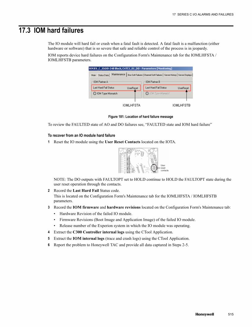
17.3 IOM hard failuresThe IO module will hard fail or crash when a fatal fault is detected. A fatal fault is a malfunction (eitherhardware or software) that is so severe that safe and reliable control of the process is in jeopardy.
IOM reports device hard failures on the Configuration Form's Maintenance tab for the IOMLHFSTA /IOMLHFSTB parameters.
Figure 181: Location of hard failure message
To review the FAULTED state of AO and DO failures see, “FAULTED state and IOM hard failure”
To recover from an IO module hard failure1 Reset the IO module using the User Reset Contacts located on the IOTA.
NOTE: The DO outputs with FAULTOPT set to HOLD continue to HOLD the FAULTOPT state during theuser reset operation through the contacts.
2 Record the Last Hard Fail Status code.This is located on the Configuration Form's Maintenance tab for the IOMLHFSTA / IOMLHFSTBparameters.
3 Record the IOM firmware and hardware revisions located on the Configuration Form's Maintenance tab:• Hardware Revision of the failed IO module.• Firmware Revisions (Boot Image and Application Image) of the failed IO module.• Release number of the Experion system in which the IO module was operating.
4 Extract the C300 Controller internal logs using the CTool Application.5 Extract the IOM internal logs (trace and crash logs) using the CTool Application.6 Report the problem to Honeywell TAC and provide all data captured in Steps 2-5.
17 SERIES C I/O ALARMS AND FAILURES
515

17.4 IOM Behavior during Hard FailuresWhen the IOM hard fails and switch over to the Secondary does not take place:
• For a DO module:
– all field output terminals for channels with DOTYPE = STATUS go to the configured fault state.– the field output terminals for channels with other DOTYPE go unpowered.
• For an AO module, all field output terminals go unpowered• INITREQ is asserted on all associated Output Channel Blocks• the IOM icon in the Monitor tab becomes RED• the Detail Display shows No Response
There also is:
• an active 'IOP State Changed to No Response' alarm in Station System Summary.• the Status LED of the IOP is OFF.
The following codes can appear for the IOMLHFSTA and IOMLHFSTB parameters.
Table 127: IOM hard failures
Code Name Cause/description AI AO DI DO LLMUX00 UNKNOWN Unknown failure. X X X X X
01 POWERDOWN IOM was powered down or a loss of 24vpower to the IOM was detected
X X X X X
02 INVPRGEXEC Invalid program execution X X X X X
04 RAMCNTERR RAM contents diagnostics failed X X X X X
05 RAMADRERR RAM address diagnostics failed X X X X X
06 DPAERROR IOM was changed while the IOM ispowered
X X X X X
09 IOLJABBER IOL jabber circuit fired X X X X X
11 BADPGJMP Illegal value case control in the IOMfirmware
X X X X X
17 DMT_TMOUT Dead man cell timer expired. IOMfirmware task scheduling corrupted.
X X X X X
25 OPCNTRLHW
FAIL
Output control hardware failure X X
26 AOOTPTMUX
FAIL
AO output control MUX failure X
27 ASCRCFAIL Flash contents diagnostics failed X X X X X
31 STCKOVRUN IOM firmware stack overrun X X X X X
32 WDTTIMEOUT IOM firmware watchdog timeout X X X X X
35 IOMUSER
RESET
User triggered reset X X X X X
17 SERIES C I/O ALARMS AND FAILURES
516 www.honeywell.com
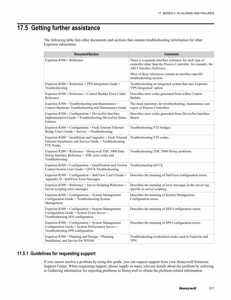
17.5 Getting further assistanceThe following table lists other documents and sections that contain troubleshooting information for otherExperion subsystems.
Document/Section CommentsExperion R300 > Reference There is a separate interface reference for each type of
controller other than the Process Controller, for example, theASEA Interface Reference.
Most of these references contain an interface-specifictroubleshooting section.
Experion R300 > Reference > TPS Integration Guide >Troubleshooting
Troubleshooting an integrated system that uses Experion'TPS Integration' option.
Experion R300 > Reference > Control Builder Error CodesReference
Describes error codes generated from within ControlBuilder.
Experion R300 > Troubleshooting and Maintenance >Control Hardware Troubleshooting and Maintenance Guide
The main repository for troubleshooting, maintenance andrepair of Process Controllers.
Experion R300 > Configuration > DeviceNet InterfaceImplementation Guide > Troubleshooting DeviceNet StatusFailures
Describes error codes generated from DeviceNet InterfaceBoard.
Experion R300 > Configuration > Fault Tolerant EthernetBridge User's Guide > Service > Troubleshooting
Troubleshooting FTE bridges.
Experion R300 > Installation and Upgrades > Fault TolerantEthernet Installation and Service Guide > TroubleshootingFTE Nodes
Troubleshooting FTE nodes.
Experion R300 > Reference > Honeywell TDC 3000 DataHiway Interface Reference > TDC error codes andTroubleshooting
Troubleshooting TDC 3000 Hiway problems.
Experion R300 > Configuration > Qualification and VersionControl System User Guide > QVCS Troubleshooting
Troubleshooting QVCS.
Experion R300 > Configuration > SafeView User's Guide >Appendix D - SafeView Error Messages
Describes the meaning of SafeView configuration errors.
Experion R300 > Reference > Server Scripting Reference >Server scripting error messages
Describes the meaning of error messages in the server logspecific to server scripting.
Experion R300 > Configuration > System ManagementConfiguration Guide > Troubleshooting SystemManagement
Describes the meaning of System ManagementConfiguration errors.
Experion R300 > Configuration > System ManagementConfiguration Guide > System Event Server >Troubleshooting SES configuration
Describes the meaning of SES Configuration errors.
Experion R300 > Configuration > System ManagementConfiguration Guide > System Performance Server >Troubleshooting SPS configuration
Describes the meaning of SPS Configuration errors.
Experion R300 > Planning and Design > Planning,Installation, and Service for WS360
Troubleshooting workstation nodes used in Experion andTPN.
17.5.1 Guidelines for requesting supportIf you cannot resolve a problem by using this guide, you can request support from your Honeywell SolutionsSupport Center. When requesting support, please supply as many relevant details about the problem by referringto Gathering information for reporting problems to Honeywell to obtain the problem-related information.
17 SERIES C I/O ALARMS AND FAILURES
517

17 SERIES C I/O ALARMS AND FAILURES
518 www.honeywell.com
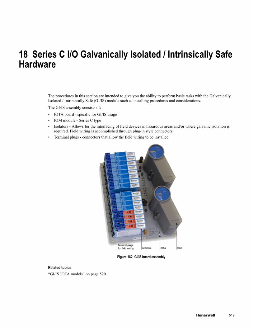
18 Series C I/O Galvanically Isolated / Intrinsically SafeHardware
The procedures in this section are intended to give you the ability to perform basic tasks with the GalvanicallyIsolated / Intrinsically Safe (GI/IS) module such as installing procedures and considerations.
The GI/IS assembly consists of:
• IOTA board - specific for GI/IS usage• IOM module - Series C type• Isolators - Allows for the interfacing of field devices in hazardous areas and/or where galvanic isolation is
required. Field wiring is accomplished through plug-in style connectors.• Terminal plugs - connectors that allow the field wiring to be installed
Figure 182: GI/IS board assembly
Related topics“GI/IS IOTA models” on page 520
519
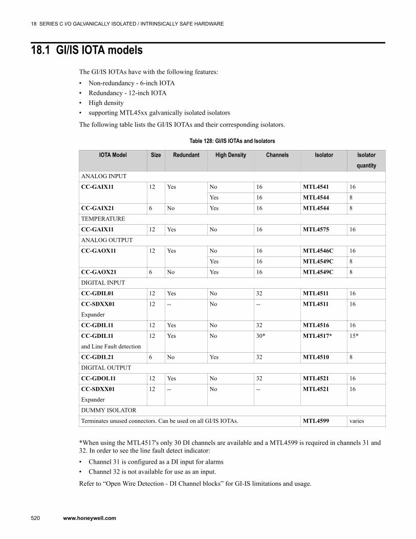
18.1 GI/IS IOTA modelsThe GI/IS IOTAs have with the following features:
• Non-redundancy - 6-inch IOTA• Redundancy - 12-inch IOTA• High density• supporting MTL45xx galvanically isolated isolators
The following table lists the GI/IS IOTAs and their corresponding isolators.
Table 128: GI/IS IOTAs and Isolators
IOTA Model Size Redundant High Density Channels Isolator Isolatorquantity
ANALOG INPUT
CC-GAIX11 12 Yes No 16 MTL4541 16
Yes 16 MTL4544 8
CC-GAIX21 6 No Yes 16 MTL4544 8
TEMPERATURE
CC-GAIX11 12 Yes No 16 MTL4575 16
ANALOG OUTPUT
CC-GAOX11 12 Yes No 16 MTL4546C 16
Yes 16 MTL4549C 8
CC-GAOX21 6 No Yes 16 MTL4549C 8
DIGITAL INPUT
CC-GDIL01 12 Yes No 32 MTL4511 16
CC-SDXX01
Expander
12 -- No -- MTL4511 16
CC-GDIL11 12 Yes No 32 MTL4516 16
CC-GDIL11
and Line Fault detection
12 Yes No 30* MTL4517* 15*
CC-GDIL21 6 No Yes 32 MTL4510 8
DIGITAL OUTPUT
CC-GDOL11 12 Yes No 32 MTL4521 16
CC-SDXX01
Expander
12 -- No -- MTL4521 16
DUMMY ISOLATOR
Terminates unused connectors. Can be used on all GI/IS IOTAs. MTL4599 varies
*When using the MTL4517's only 30 DI channels are available and a MTL4599 is required in channels 31 and32. In order to see the line fault detect indicator:
• Channel 31 is configured as a DI input for alarms• Channel 32 is not available for use as an input.
Refer to “Open Wire Detection - DI Channel blocks” for GI-IS limitations and usage.
18 SERIES C I/O GALVANICALLY ISOLATED / INTRINSICALLY SAFE HARDWARE
520 www.honeywell.com

18.1.1 Line-Fault Detection (LFD) - Digital Input GI/IS onlyIn the event of an open or shorted circuit in the field wiring, the resistance sensed at the input to the GalvanicIsolation Module is a high value. This permits the readback of the Digital Input IOMs to detect the open orshorted field circuit and indicate a wiring problem to the user.
An open wire is defined as a resistance of 7k ohms, or greater and shorted wire is defined as less than 55-ohmsresistance.
The following GI/IS isolators support line fault detection for Digital Input:
• MTL4510 has LED indicator on isolator when line fault detection occurs• MTL4511 has LED indicator on isolator when line fault detection occurs• MTL4516 has LED indicator on isolator when line fault detection occurs• MTL4517 has LED indicator on isolator and reports line fault detection back to the system
IF LFD is enabled (through a switch on the device) for any channel two resistors must be installed - a 22kresistor across the switch 680 resistor in series with the power supply lead. This feature detects both open andshort circuits.
18.1.2 Hazardous environmentThe GI/IS IOTA assemblies are certified for installation within a Division 2/Zone 2 hazardous location andprovide intrinsically safe field wiring connections to Division 1/Zone 1/0 hazardous locations.
The specific hazardous location assembly certifications are as follows:
Canadian Standards Association (CSA)
Approved for use within Class I, Division 2, Group A, B, C & D hazardous locations and Class I, Zone 2, Group IIChazardous locations; T4 temperature rating with intrinsically safe connections to Class I, Division 1, Groups A, B, C andD; Class I, Zone 0/1/2, Group IIC.
Factory Mutual (FM)
Approved for use within Class I, Division 2, Group A, B, C & D hazardous locations and Class I, Zone 2, Group IIChazardous locations (T4 temperature rating) with intrinsically safe connections to Class I, II and III, Division 1, Groups A,B, C, D, E, F and G; Class I, Zone 0, Group IIC hazardous locations.
ATEX
Approved for use Zone 2, Group IIC hazardous locations (T4 temperature rating) with intrinsically safe connections toZone 0, Group IIC hazardous locations.
18 SERIES C I/O GALVANICALLY ISOLATED / INTRINSICALLY SAFE HARDWARE
521

18 SERIES C I/O GALVANICALLY ISOLATED / INTRINSICALLY SAFE HARDWARE
522 www.honeywell.com

19 GI/IS Power and Grounding Requirements
The power requirement for the IOTAs is a nominal +24 Vdc.
Related topics“Grounding and power considerations -GI/IS IOTA boards” on page 524
523
19.1 Grounding and power considerations -GI/IS IOTA boardsThe Series C cabinet allows mounted carriers that support the attachment of the IOTA boards. By making theseconnections, power and chassis grounding is provided to the IOTA board.
19.1.1 Testing for power for GI/IS
CAUTIONExtreme care should be taken when testing for power at the Series C bus bars. Improper testing can result in anelectrical short, which will impact all modules attached to the channel carrier assembly.
Never use a test probe at an unattached IOTA's 24V screw hole. The probe can potentially touch the back channelassembly causing a short.
The following locations are recommended for testing power:
Preferred location if IOTAs are attached
• Center of the screw that attaches the IOTA to the 24V bus bar.
Preferred location if IOTAs are NOT attached.
• Center of the screw of top connection terminal for power cable.
WARNINGTesting for power at the Series C bus bars must only be conducted when the area has been verified to benonhazardous.
19.1.2 Testing for power at the GI/IS IOTA screwRefer to the Caution above at “Testing for power” on page 581 Insert the test probe at the center of the screw that attaches the IOTA to the 24V power connection.2 Verify that a nominal +24V dc is present.3 This concludes this procedure.
19.1.3 Testing for power at 24V bus bar top terminal for the GI/IS
WARNINGTesting for power at the Series C bus bars must only be conducted when the area has been verified to benonhazardous.
Refer to Caution above at “Testing for power” on page 58.1 Carefully pull the red cap from the top of the terminal. It remains attached to the power cable.
• Insert the test probe at the center of the screw to the 24V power terminal.2 Carefully pull the black cap from the top of the terminal. It remains attached to the ground cable.
Insert the test probe at the center of the screw to the COM ground terminal.3 Replace the both caps.4 This concludes this procedure.
19 GI/IS POWER AND GROUNDING REQUIREMENTS
524 www.honeywell.com
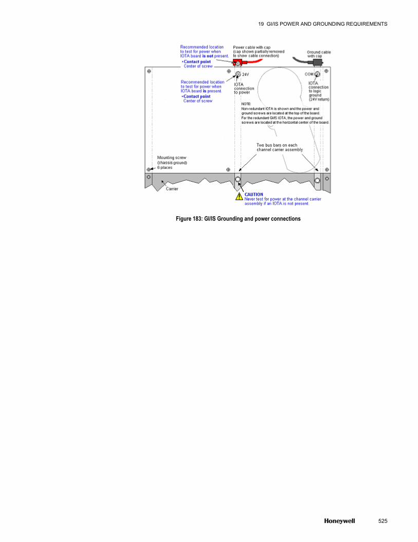
Figure 183: GI/IS Grounding and power connections
19 GI/IS POWER AND GROUNDING REQUIREMENTS
525

19 GI/IS POWER AND GROUNDING REQUIREMENTS
526 www.honeywell.com

20 GI/IS Installation
Related topics“GI/IS Shield Connection Options” on page 528“Installing the GI/IS IOTA onto the carrier” on page 529“Installing the IOM onto the GI/IS IOTA” on page 530“Installing the isolator” on page 531“Setting Operation mode through Digital Input isolator DIP switches” on page 533“MTL4510” on page 534“MTL4511 / 4516 / 4517” on page 536“Field Wiring Connections” on page 537“Screw-terminal wiring” on page 538
527
20.1 GI/IS Shield Connection OptionsShielded field wiring is not required for any of the Series C GI/IS IOTAs. If shielded field wiring is used, theshield connections must follow these rules:
1. The shield must only be terminated at one end. That is, if the shield is terminated at the field device, it mustnot be terminated in the cabinet, and vice versa.
2. If the shield is to be terminated in the cabinet, the connection must be made to the vertical shield bar to theleft of the IOTA tray.
3. Any shield bars used for GI/IS shields must be used for GI/IS wiring only, and must be connected to adedicated IS ground system."
20 GI/IS INSTALLATION
528 www.honeywell.com
20.2 Installing the GI/IS IOTA onto the carrierThe mounting of the GI/IS IOTA is similar to the standard Series C IOTA with the exception that there is anadditional set of mounting screws to accommodate the wider GI/IS IOTA. You select the desired mountinglocation on carrier and then align the mounting holes in the IOTA with screw-hole locations on the carrier.
TipThe IOMs and isolators should be removed prior to installing the IOTA onto the carrier. This allows for easierinstallation of the IOTA.
• 6 inch GI/IS IOTA board 6 mounting screws• 12 inch GI/IS IOTA board 9 mounting screws
When mounting the 12 inch IOTA board, it is recommended to:
• secure the mounting screws on one side (either left or right)• secure the mounting screws in the middle• and then secure the other side
AttentionSecuring the corner screws and then the middle screws may cause bowing of the board and impact the alignment ofthe IOTA board to the carrier holes and is not recommended.
Refer to the following instructions to see how the IOTA is mounted: .
Refer to the following graphic to see how GI/IS IOTA board is mounted: “Figure 183: GI/IS Grounding andpower connections”.
20 GI/IS INSTALLATION
529

20.3 Installing the IOM onto the GI/IS IOTAThe mounting of the IOM on a GI/IS IOTA is similar to mounting the IOM on the standard Series C IOTA.
Refer to the following instructions to see how the IOM is mounted on the IOTA: .
20 GI/IS INSTALLATION
530 www.honeywell.com
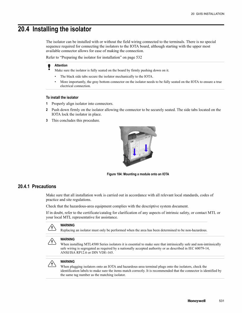
20.4 Installing the isolatorThe isolator can be installed with or without the field wiring connected to the terminals. There is no specialsequence required for connecting the isolators to the IOTA board, although starting with the upper mostavailable connector allows for ease of making the connection.
Refer to “Preparing the isolator for installation” on page 532
AttentionMake sure the isolator is fully seated on the board by firmly pushing down on it.
• The black side tabs secure the isolator mechanically to the IOTA.• More importantly, the gray bottom connector on the isolator needs to be fully seated on the IOTA to ensure a true
electrical connection.
To install the isolator1 Properly align isolator into connectors.2 Push down firmly on the isolator allowing the connector to be securely seated. The side tabs located on the
IOTA lock the isolator in place.3 This concludes this procedure.
Figure 184: Mounting a module onto an IOTA
20.4.1 PrecautionsMake sure that all installation work is carried out in accordance with all relevant local standards, codes ofpractice and site regulations.
Check that the hazardous-area equipment complies with the descriptive system document.
If in doubt, refer to the certificate/catalog for clarification of any aspects of intrinsic safety, or contact MTL oryour local MTL representative for assistance.
WARNINGReplacing an isolator must only be performed when the area has been determined to be non-hazardous.
WARNINGWhen installing MTL4500 Series isolators it is essential to make sure that intrinsically safe and non-intrinsicallysafe wiring is segregated as required by a nationally accepted authority or as described in IEC 60079-14,ANSI/ISA RP12.6 or DIN VDE-165.
WARNINGWhen plugging isolators onto an IOTA and hazardous-area terminal plugs onto the isolators, check theidentification labels to make sure the items match correctly. It is recommended that the connector is identified bythe same tag number as the matching isolator.
20 GI/IS INSTALLATION
531
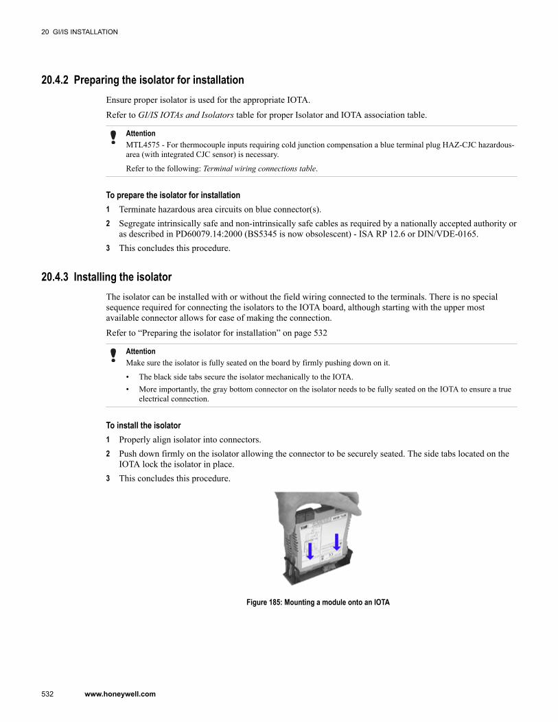
20.4.2 Preparing the isolator for installationEnsure proper isolator is used for the appropriate IOTA.
Refer to GI/IS IOTAs and Isolators table for proper Isolator and IOTA association table.
AttentionMTL4575 - For thermocouple inputs requiring cold junction compensation a blue terminal plug HAZ-CJC hazardous-area (with integrated CJC sensor) is necessary.
Refer to the following: Terminal wiring connections table.
To prepare the isolator for installation1 Terminate hazardous area circuits on blue connector(s).2 Segregate intrinsically safe and non-intrinsically safe cables as required by a nationally accepted authority or
as described in PD60079.14:2000 (BS5345 is now obsolescent) - ISA RP 12.6 or DIN/VDE-0165.3 This concludes this procedure.
20.4.3 Installing the isolatorThe isolator can be installed with or without the field wiring connected to the terminals. There is no specialsequence required for connecting the isolators to the IOTA board, although starting with the upper mostavailable connector allows for ease of making the connection.
Refer to “Preparing the isolator for installation” on page 532
AttentionMake sure the isolator is fully seated on the board by firmly pushing down on it.
• The black side tabs secure the isolator mechanically to the IOTA.• More importantly, the gray bottom connector on the isolator needs to be fully seated on the IOTA to ensure a true
electrical connection.
To install the isolator1 Properly align isolator into connectors.2 Push down firmly on the isolator allowing the connector to be securely seated. The side tabs located on the
IOTA lock the isolator in place.3 This concludes this procedure.
Figure 185: Mounting a module onto an IOTA
20 GI/IS INSTALLATION
532 www.honeywell.com
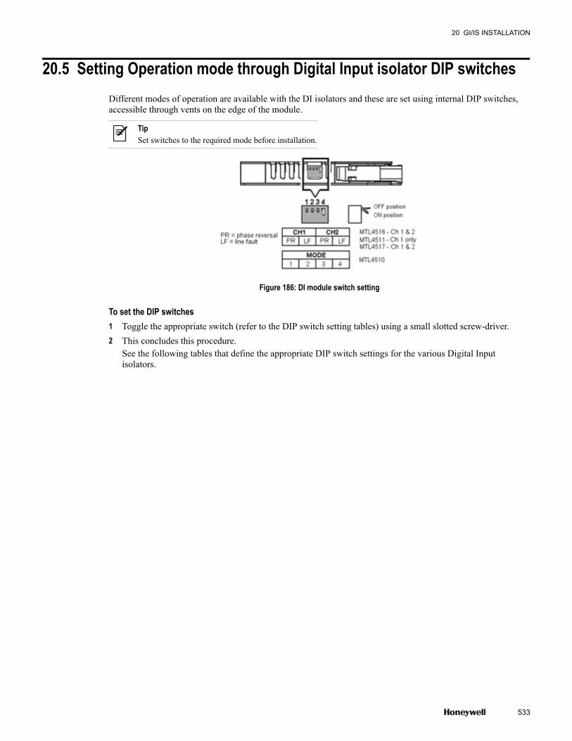
20.5 Setting Operation mode through Digital Input isolator DIP switchesDifferent modes of operation are available with the DI isolators and these are set using internal DIP switches,accessible through vents on the edge of the module.
TipSet switches to the required mode before installation.
Figure 186: DI module switch setting
To set the DIP switches1 Toggle the appropriate switch (refer to the DIP switch setting tables) using a small slotted screw-driver.2 This concludes this procedure.
See the following tables that define the appropriate DIP switch settings for the various Digital Inputisolators.
20 GI/IS INSTALLATION
533

20.6 MTL4510This four-channel digital isolator has solid state output switches in a safe-area that respond to input switches in ahazardous area. The way they respond depends upon the switch settings.
Table 129: MTL4510 isolator DIP switch settings
Mode o/p 1 SW1-4 o/p 2 o/p 3 o/p 4 I/p type0 0000 chA chB chC chD switch
1 0001 chA rev. chB chC chD
2 0010 chA chB rev chC chD
3 0011 chA chB chC rev chD
4 0100 chA chB chC chD rev
5 0101 chA rev chB chC rev chD
6 0110 chA chB rev chC chD rev
7 0111 chA rev chB rev chC rev chD rev
8 1000 chA chB chC chD prox detector +LFD9 1001 chA rev chB chC chD
10 1010 chA chB rev chC chD
11 1011 chA chB chC rev chD
12 1100 chA chB chC chD rev
13 1101 chA rev chB chC rev chD
14 1110 chA chB rev chC chD rev
15 1111 chA rev chB rev chC rev chD rev
Table 130: Module input/output operation
Operation Input value Directacting
Reverse acting LFD LED Relay/ output MTL4511/MTL4717LFD relay
Normal <1.2mA On - On Off De-energized /On
De-energized
>2.1mA On - On On Energized / Off De-energized
<1.2mA - On On On Energized / Off De-energized
>2.1mA - On On Off De-energized /On
De-energized
Broken line <50uA On - On Off De-energized /On
Energized
<50uA - On On Off De-energized /On
Energized
<50uA On - Off Off De-energized /On
De-energized
<50uA - On Off On Energized / Off De-energized
Shorted line 6.5mA On - On Off De-energized /On
Energized
6.5mA - On On Off De-energized /On
Energized
20 GI/IS INSTALLATION
534 www.honeywell.com

Operation Input value Directacting
Reverse acting LFD LED Relay/ output MTL4511/MTL4717LFD relay
6.5mA On - Off On Energized / Off De-energized
6.5mA - On Off Off De-energized /On
De-energized
20 GI/IS INSTALLATION
535
20.7 MTL4511 / 4516 / 4517For switch sensor inputs, with LFD selected, make sure resistors (22k ohms and 680 ohms) are fitted.
Table 131: MTL4511 isolator DIP switch settings
Mode Functionality0 0000 Phase reversal and LFD not enabled
1 1000 Phase reversal enabled
2 0100 Line Fault Detection enabled
Table 132: MTL4516 isolator DIP switch settings
Mode Functionality0 0000 Phase reversal and LFD not enabled
1 0001 Ch1 Phase reversal enabled
2 0010 Ch1 Line Fault Detection enabled
3 0100 Ch2 Phase reversal enabled
4 1000 Ch2 Line Fault Detection enabled
Table 133: MTL4517 isolator DIP switch settings
Mode Functionality0 0000 Phase reversal and LFD not enabled
1 0001 Ch1 Phase reversal enabled
2 0010 Ch1 Line Fault Detection enabled
3 0100 Ch2 Phase reversal enabled
4 1000 Ch2 Line Fault Detection enabled
20 GI/IS INSTALLATION
536 www.honeywell.com
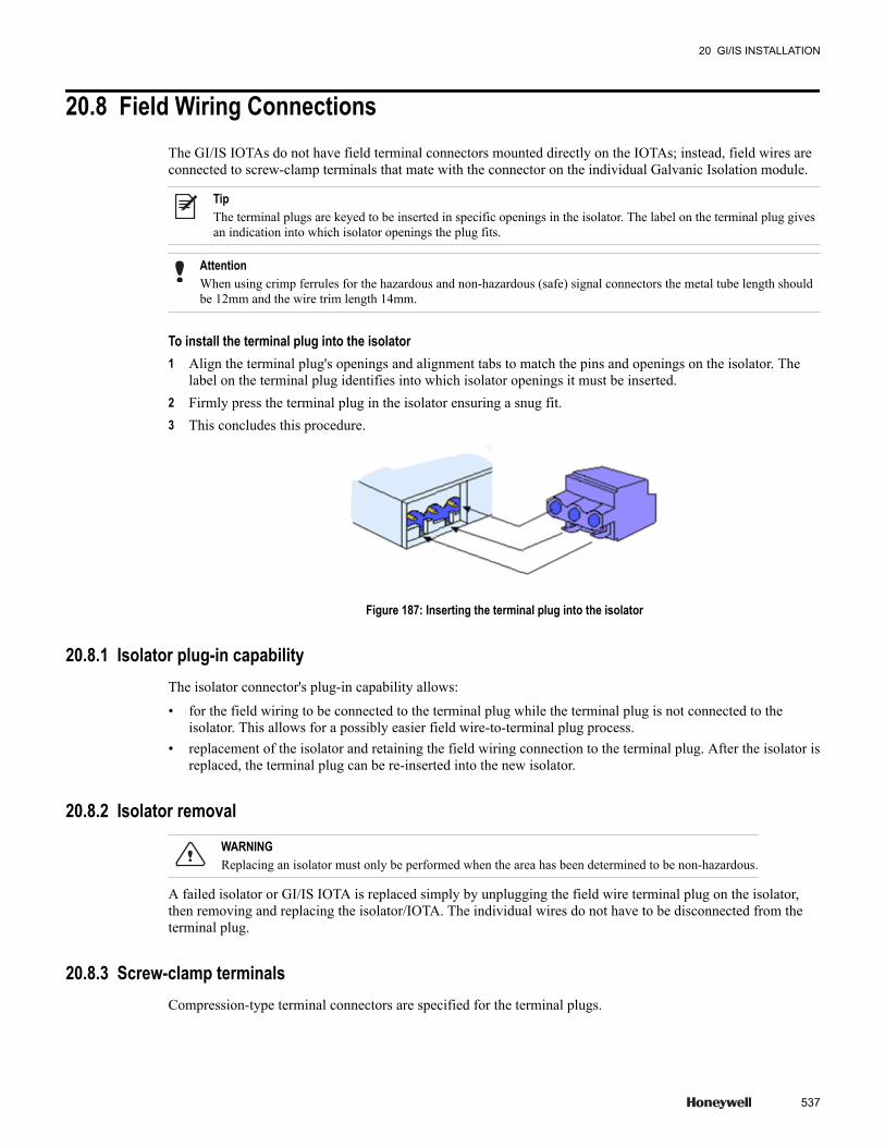
20.8 Field Wiring ConnectionsThe GI/IS IOTAs do not have field terminal connectors mounted directly on the IOTAs; instead, field wires areconnected to screw-clamp terminals that mate with the connector on the individual Galvanic Isolation module.
TipThe terminal plugs are keyed to be inserted in specific openings in the isolator. The label on the terminal plug givesan indication into which isolator openings the plug fits.
AttentionWhen using crimp ferrules for the hazardous and non-hazardous (safe) signal connectors the metal tube length shouldbe 12mm and the wire trim length 14mm.
To install the terminal plug into the isolator1 Align the terminal plug's openings and alignment tabs to match the pins and openings on the isolator. The
label on the terminal plug identifies into which isolator openings it must be inserted.2 Firmly press the terminal plug in the isolator ensuring a snug fit.3 This concludes this procedure.
Figure 187: Inserting the terminal plug into the isolator
20.8.1 Isolator plug-in capabilityThe isolator connector's plug-in capability allows:
• for the field wiring to be connected to the terminal plug while the terminal plug is not connected to theisolator. This allows for a possibly easier field wire-to-terminal plug process.
• replacement of the isolator and retaining the field wiring connection to the terminal plug. After the isolator isreplaced, the terminal plug can be re-inserted into the new isolator.
20.8.2 Isolator removal
WARNINGReplacing an isolator must only be performed when the area has been determined to be non-hazardous.
A failed isolator or GI/IS IOTA is replaced simply by unplugging the field wire terminal plug on the isolator,then removing and replacing the isolator/IOTA. The individual wires do not have to be disconnected from theterminal plug.
20.8.3 Screw-clamp terminalsCompression-type terminal connectors are specified for the terminal plugs.
20 GI/IS INSTALLATION
537
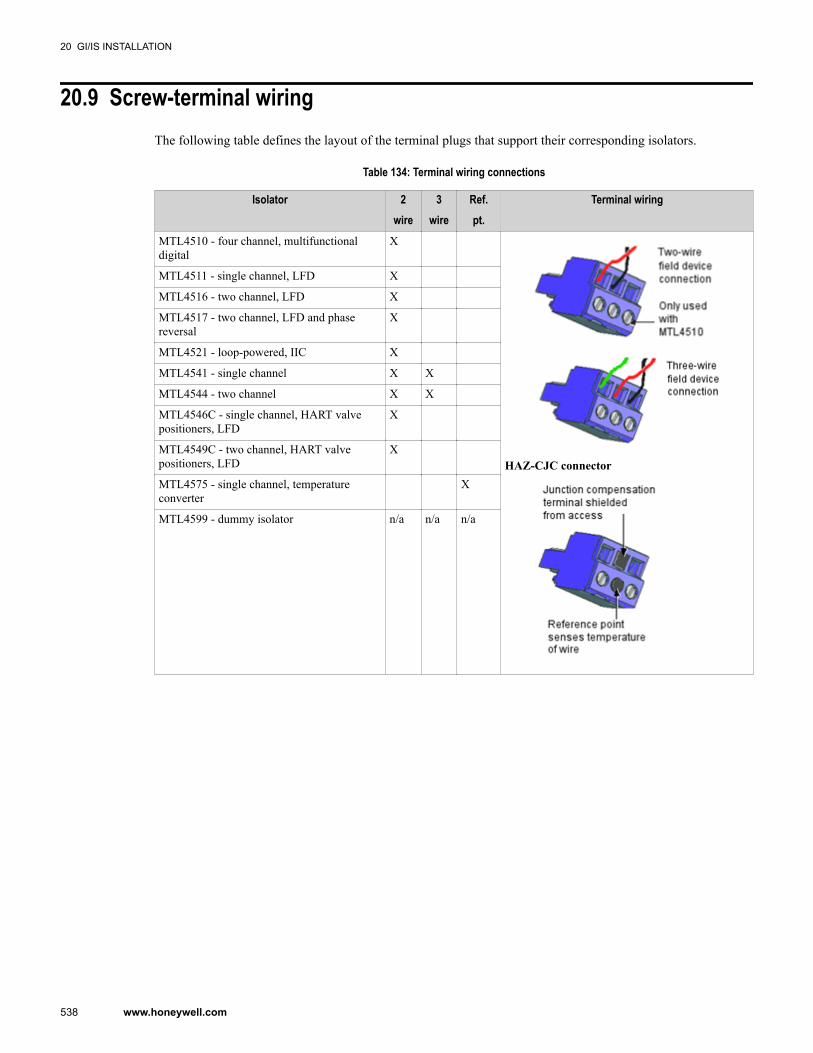
20.9 Screw-terminal wiringThe following table defines the layout of the terminal plugs that support their corresponding isolators.
Table 134: Terminal wiring connections
Isolator 2wire
3wire
Ref.pt.
Terminal wiring
MTL4510 - four channel, multifunctionaldigital
X
HAZ-CJC connector
MTL4511 - single channel, LFD X
MTL4516 - two channel, LFD X
MTL4517 - two channel, LFD and phasereversal
X
MTL4521 - loop-powered, IIC X
MTL4541 - single channel X X
MTL4544 - two channel X X
MTL4546C - single channel, HART valvepositioners, LFD
X
MTL4549C - two channel, HART valvepositioners, LFD
X
MTL4575 - single channel, temperatureconverter
X
MTL4599 - dummy isolator n/a n/a n/a
20 GI/IS INSTALLATION
538 www.honeywell.com
21 GI/IS IOTA Pinouts
Related topics“GI/IS Analog Input IOTA Model CC-GAIX11” on page 540“GI/IS Analog Input IOTA Model CC-GAIX21” on page 542“Analog Output GI/IS IOTAs” on page 547“GI/IS Analog Output IOTA Model CC-GAOX11” on page 548“GI/IS Analog Output IOTA Model CC-GAOX21” on page 550“24 Vdc Digital Input GI/IS IOTAs” on page 552“GI/IS Digital Input IOTA Model CC-GDIL01” on page 553“GI/IS Digital Input IOTA Model CC-GDIL11” on page 555“GI/IS Digital Input IOTA Model CC-GDIL21” on page 558“GI/IS Digital Output IOTA Model CC-GDOL11” on page 561“GI/IS Digital I/O Expander Model CC-SDXX01” on page 565
539
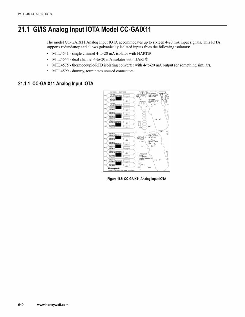
21.1 GI/IS Analog Input IOTA Model CC-GAIX11The model CC-GAIX11 Analog Input IOTA accommodates up to sixteen 4-20 mA input signals. This IOTAsupports redundancy and allows galvanically isolated inputs from the following isolators:
• MTL4541 - single channel 4-to-20 mA isolator with HART®• MTL4544 - dual channel 4-to-20 mA isolator with HART®• MTL4575 - thermocouple/RTD isolating converter with 4-to-20 mA output (or something similar).• MTL4599 - dummy, terminates unused connectors
21.1.1 CC-GAIX11 Analog Input IOTA
Figure 188: CC-GAIX11 Analog Input IOTA
21 GI/IS IOTA PINOUTS
540 www.honeywell.com
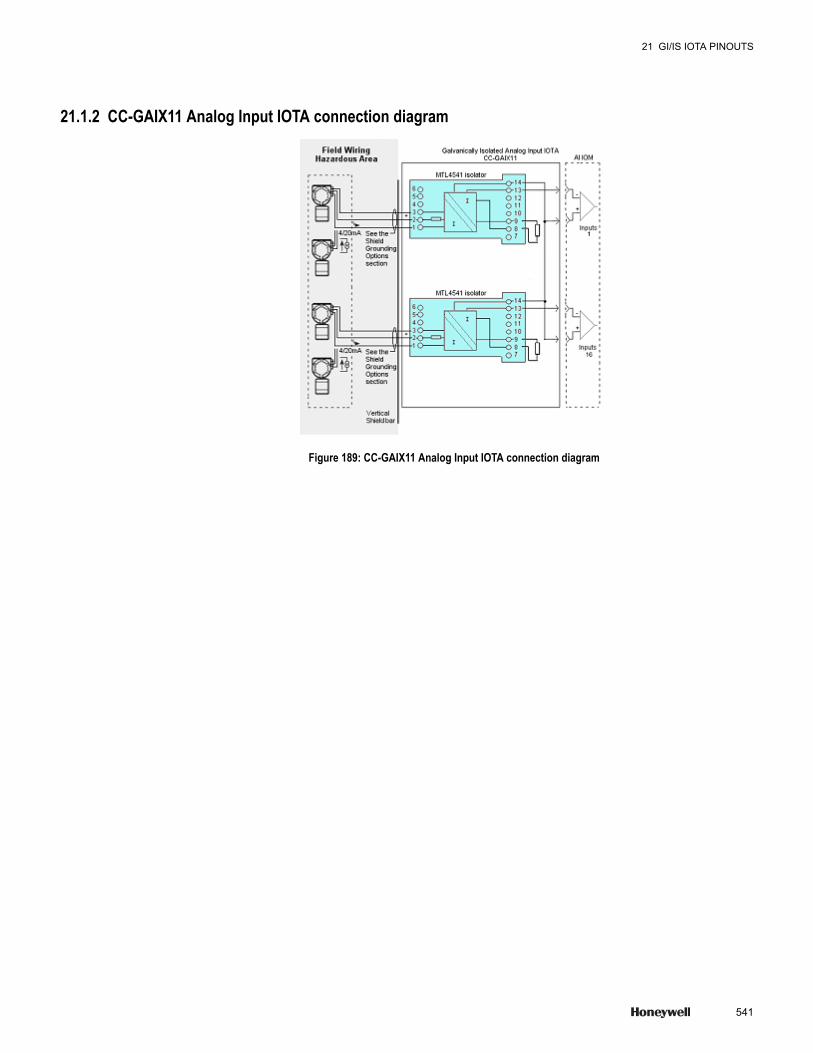
21.1.2 CC-GAIX11 Analog Input IOTA connection diagram
Figure 189: CC-GAIX11 Analog Input IOTA connection diagram
21 GI/IS IOTA PINOUTS
541
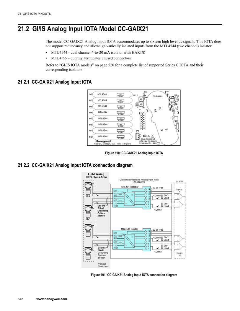
21.2 GI/IS Analog Input IOTA Model CC-GAIX21The model CC-GAIX21 Analog Input IOTA accommodates up to sixteen high level dc signals. This IOTA doesnot support redundancy and allows galvanically isolated inputs from the MTL4544 (two channel) isolator.
• MTL4544 - dual channel 4-to-20 mA isolator with HART®• MTL4599 - dummy, terminates unused connectors
Refer to “GI/IS IOTA models” on page 520 for a complete list of supported Series C IOTA and theircorresponding isolators.
21.2.1 CC-GAIX21 Analog Input IOTA
Figure 190: CC-GAIX21 Analog Input IOTA
21.2.2 CC-GAIX21 Analog Input IOTA connection diagram
Figure 191: CC-GAIX21 Analog Input IOTA connection diagram
21 GI/IS IOTA PINOUTS
542 www.honeywell.com
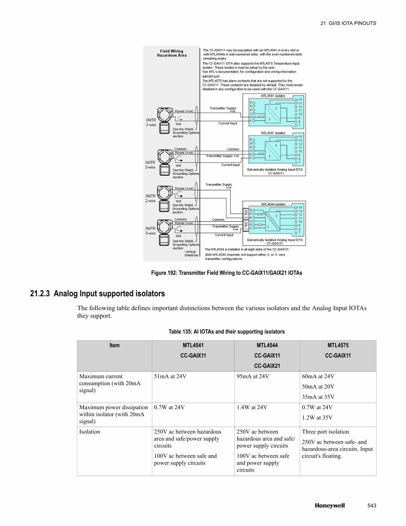
Figure 192: Transmitter Field Wiring to CC-GAIX11/GAIX21 IOTAs
21.2.3 Analog Input supported isolatorsThe following table defines important distinctions between the various isolators and the Analog Input IOTAsthey support.
Table 135: AI IOTAs and their supporting isolators
Item MTL4541CC-GAIX11
MTL4544CC-GAIX11CC-GAIX21
MTL4575CC-GAIX11
Maximum currentconsumption (with 20mAsignal)
51mA at 24V 95mA at 24V 60mA at 24V
50mA at 20V
35mA at 35V
Maximum power dissipationwithin isolator (with 20mAsignal)
0.7W at 24V 1.4W at 24V 0.7W at 24V
1.2W at 35V
Isolation 250V ac between hazardousarea and safe/power supplycircuits
100V ac between safe andpower supply circuits
250V ac betweenhazardous area and safe/power supply circuits
100V ac between safeand power supplycircuits
Three port isolation
250V ac between safe- andhazardous-area circuits. Inputcircuit's floating.
21 GI/IS IOTA PINOUTS
543
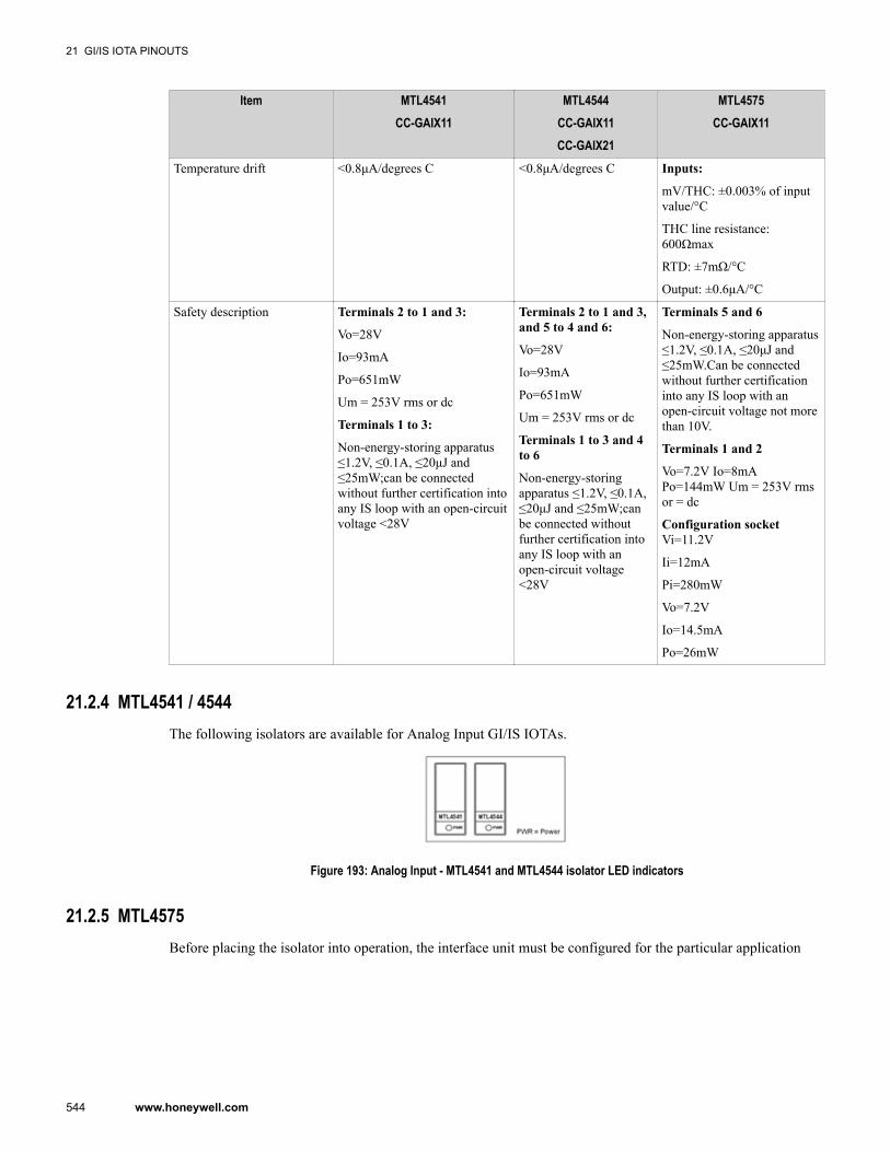
Item MTL4541CC-GAIX11
MTL4544CC-GAIX11CC-GAIX21
MTL4575CC-GAIX11
Temperature drift <0.8μA/degrees C <0.8μA/degrees C Inputs:
mV/THC: ±0.003% of inputvalue/°C
THC line resistance:600Ωmax
RTD: ±7mΩ/°C
Output: ±0.6μA/°C
Safety description Terminals 2 to 1 and 3:
Vo=28V
Io=93mA
Po=651mW
Um = 253V rms or dc
Terminals 1 to 3:
Non-energy-storing apparatus≤1.2V, ≤0.1A, ≤20μJ and≤25mW;can be connectedwithout further certification intoany IS loop with an open-circuitvoltage <28V
Terminals 2 to 1 and 3,and 5 to 4 and 6:
Vo=28V
Io=93mA
Po=651mW
Um = 253V rms or dc
Terminals 1 to 3 and 4to 6
Non-energy-storingapparatus ≤1.2V, ≤0.1A,≤20μJ and ≤25mW;canbe connected withoutfurther certification intoany IS loop with anopen-circuit voltage<28V
Terminals 5 and 6
Non-energy-storing apparatus≤1.2V, ≤0.1A, ≤20μJ and≤25mW.Can be connectedwithout further certificationinto any IS loop with anopen-circuit voltage not morethan 10V.
Terminals 1 and 2
Vo=7.2V Io=8mAPo=144mW Um = 253V rmsor = dc
Configuration socketVi=11.2V
Ii=12mA
Pi=280mW
Vo=7.2V
Io=14.5mA
Po=26mW
21.2.4 MTL4541 / 4544The following isolators are available for Analog Input GI/IS IOTAs.
Figure 193: Analog Input - MTL4541 and MTL4544 isolator LED indicators
21.2.5 MTL4575Before placing the isolator into operation, the interface unit must be configured for the particular application
21 GI/IS IOTA PINOUTS
544 www.honeywell.com

Figure 194: Temperature - MTL4575 isolator LED indicators
21.2.6 Testing Temperature Converter- MTL45751. Connect a link between terminals 1 and 5.2. Connect 2-wire transmitter between terminals 2(+ve) and 4(-ve). Both outputs will now repeat the current in
the transmitter loop.
(Note: HART data is transferred through channel 1)3. This completes this procedure.
The following table lists the isolator's LED status and description.
Table 136: MTL4575, power and status information
LED status DescriptionON Unit working normally
Slow flash Output of 1mA, module in low alarm or downscale drive
Fast flash Output of 21mA, module in high alarm or upscale drive
Off No power to unit
21.2.7 Default configurationUnless ordered differently, every MTL4575 module is supplied with the following default configuration.
• Input Type K thermocouple• Linearization enabled• Units degrees C• CJ Compensation enabled• Damping value 0 seconds• Smoothing value 0 seconds• Output zero 0 degrees C• Output span 250 degrees C• Tag and description fields blank• Open circuit alarm set high (upscale)• Transmitter failure alarm set low (downscale)• CJ failure alarm set low (downscale)• Line frequency 50Hz
21.2.8 Configuration using PCS45/PCL45The PCS45 software, used in conjunction with PCL45 serial link, is the method to configure the MTL4575isolators. Instructions are contained within the configuration software.
Refer to the following: “PCS45 Configuration Software”.
21 GI/IS IOTA PINOUTS
545

21.2.9 Field Wiring Input SignalsEach Galvanic Isolation Module on the AI IOTA provides a floating dc source for energizing conventional 2-wire or 3-wire, 4-20 mA transmitters. The Galvanic Isolation Module accurately converts the input current intoa 1 to 5 volt output signal to the associated IOM.
21.2.10 Field Wiring Input SignalsEach Galvanic Isolation Module on the AI IOTA provides a floating dc source for energizing conventional 2-wire or 3-wire, 4-20 mA transmitters. The Galvanic Isolation Module accurately converts the input current intoa 1 to 5 volt output signal to the associated IOM.
21 GI/IS IOTA PINOUTS
546 www.honeywell.com

21.3 Analog Output GI/IS IOTAsThe galvanically isolated Analog Output (AO) IOTAs isolate up to sixteen 4-20 mA signals that can drivecurrent-to-pressure (I/P) transducers, position actuators, or any load between 90 and 800 ohms from theassociated Analog Output IOM. Additionally, bi-directional HART® communications with 4-20mA fielddevices and HART® hand-held communicators are supported.
The GI/IS Analog Output (AO) IOTAs provide the following features:
• An Intrinsically Safe (IS) interface directly to hazardous-area processes• Galvanic Isolation (GI) eliminating the high integrity ground required for Zener barriers• Compact design for reduced cabinet space• A reduced total installed cost compared to separate Zener barrier or isolator approaches• The plug-in MTL isolators on the IOTAs, incorporate both the galvanic isolation and intrinsic safety
functions and additionally provide:
– Single loop integrity (MTL4546C)– Ease of maintenance– Simplified wiring, because hazardous field wiring can be brought directly to the isolators on the IOTAs,
eliminating the need for separate IS barriers
Two models are available:
CC-GAOX11 - Redundant Analog Output IOTA
CC-GAOX21 - Non-Redundant Analog Output IOTA
21 GI/IS IOTA PINOUTS
547

21.4 GI/IS Analog Output IOTA Model CC-GAOX11The model CC-GAOX11 Analog Output IOTA provides up to sixteen 4-20 mA output channels. This IOTAsupports redundancy and accepts the following GI/IS isolators:
• MTL4546C - one channel HART® with open wire detection• MTL4549C - two channel HART® with open wire detection• MTL4599 - dummy, terminates unused connectors
Refer to “GI/IS IOTA models” on page 520 for a complete list of supported Series C IOTA and theircorresponding isolators.
21.4.1 CC-GAOX11 Analog Output IOTA
Figure 195: CC-GAOX11 Analog Output IOTA
21 GI/IS IOTA PINOUTS
548 www.honeywell.com
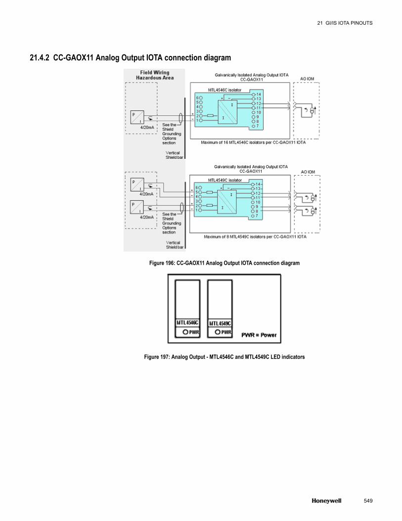
21.4.2 CC-GAOX11 Analog Output IOTA connection diagram
Figure 196: CC-GAOX11 Analog Output IOTA connection diagram
Figure 197: Analog Output - MTL4546C and MTL4549C LED indicators
21 GI/IS IOTA PINOUTS
549

21.5 GI/IS Analog Output IOTA Model CC-GAOX21The model CC-GAOX21 Analog Output IOTA provides up to sixteen 4-20 mA output channels. This IOTAdoes not support redundancy and accepts only the dual-channel GI/IS isolator below:
• MTL4549C - two channel HART® with open wire detection.• MTL4599 - dummy, terminates unused connectors
Refer to “GI/IS IOTA models” on page 520 for a complete list of supported Series C IOTA and theircorresponding isolators.
21.5.1 CC- GAOX21 Analog Output IOTA
Figure 198: CC-GAOX21 Analog Output IOTA
21.5.2 CC-GAOX21 Analog Output IOTA connection diagram
Figure 199: CC-GAOX21 Analog Output IOTA connection diagram
21 GI/IS IOTA PINOUTS
550 www.honeywell.com
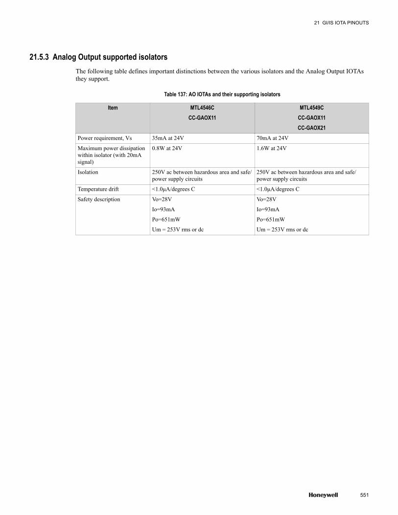
21.5.3 Analog Output supported isolatorsThe following table defines important distinctions between the various isolators and the Analog Output IOTAsthey support.
Table 137: AO IOTAs and their supporting isolators
Item MTL4546CCC-GAOX11
MTL4549CCC-GAOX11CC-GAOX21
Power requirement, Vs 35mA at 24V 70mA at 24V
Maximum power dissipationwithin isolator (with 20mAsignal)
0.8W at 24V 1.6W at 24V
Isolation 250V ac between hazardous area and safe/power supply circuits
250V ac between hazardous area and safe/power supply circuits
Temperature drift <1.0μA/degrees C <1.0μA/degrees C
Safety description Vo=28V
Io=93mA
Po=651mW
Um = 253V rms or dc
Vo=28V
Io=93mA
Po=651mW
Um = 253V rms or dc
21 GI/IS IOTA PINOUTS
551

21.6 24 Vdc Digital Input GI/IS IOTAsThe galvanically isolated Digital Input (DI) IOTAs isolate up to thirty-two 24V signals that allows galvanicallyisolated inputs from-switches and proximity detectors.
21.6.1 Input signal phase and IOTA featuresThe phase of the input signals is selectable on the model CC-GDIL01, CC-GDIL11 and CC-GDIL21 IOTAs,allowing the alarm condition to be chosen for either state of the sensor. This is accomplished with two switches,one for each input on the top of the galvanic isolators.
21 GI/IS IOTA PINOUTS
552 www.honeywell.com
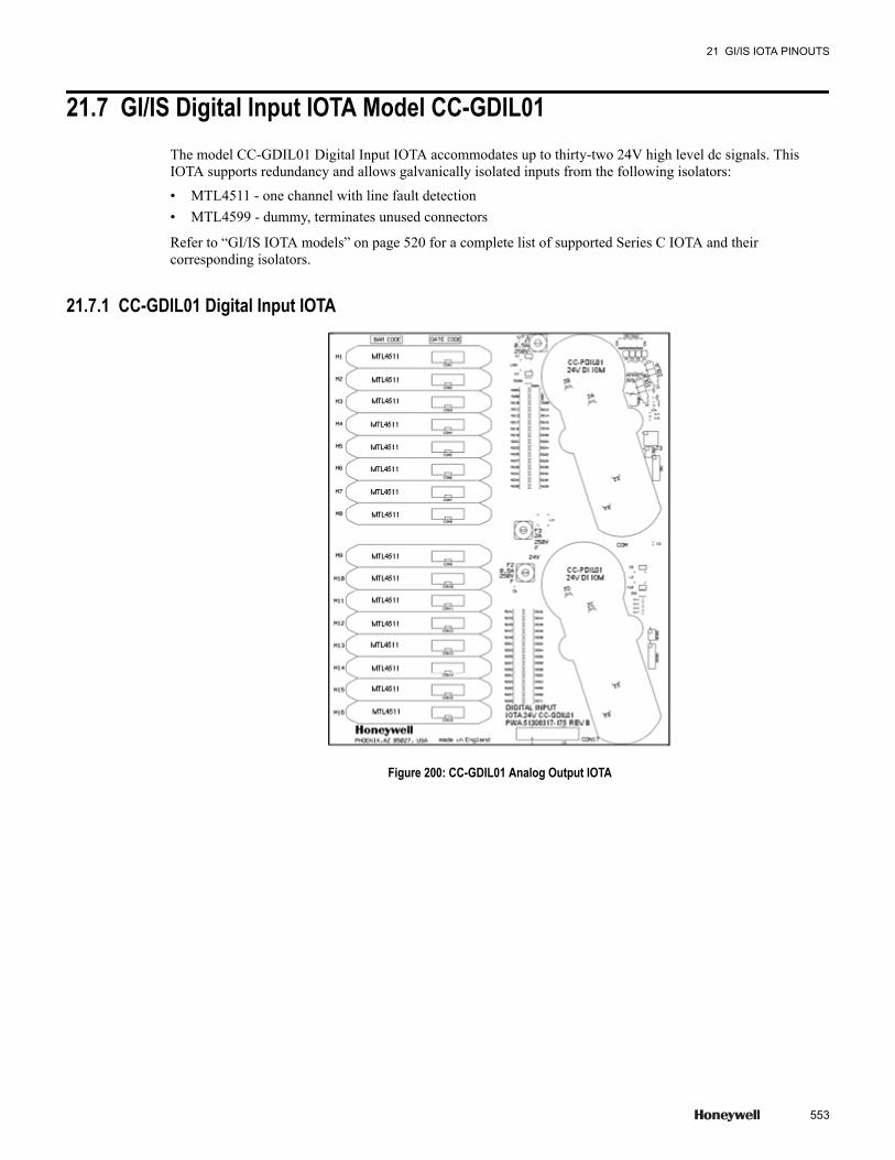
21.7 GI/IS Digital Input IOTA Model CC-GDIL01The model CC-GDIL01 Digital Input IOTA accommodates up to thirty-two 24V high level dc signals. ThisIOTA supports redundancy and allows galvanically isolated inputs from the following isolators:
• MTL4511 - one channel with line fault detection• MTL4599 - dummy, terminates unused connectors
Refer to “GI/IS IOTA models” on page 520 for a complete list of supported Series C IOTA and theircorresponding isolators.
21.7.1 CC-GDIL01 Digital Input IOTA
Figure 200: CC-GDIL01 Analog Output IOTA
21 GI/IS IOTA PINOUTS
553

21.7.2 CC-GDIL01 Digital Input IOTA connection diagram
Figure 201: CC-GDIL01 Analog Output IOTA connection diagram
21 GI/IS IOTA PINOUTS
554 www.honeywell.com

21.8 GI/IS Digital Input IOTA Model CC-GDIL11The model CC-GDIL11 Digital Input IOTA accommodates up to thirty-two 24V high level dc signals. ThisIOTA supports redundancy and allows galvanically isolated inputs from the following isolators:
• MTL4516 - two channel with line fault detection• MTL4517 - two channel with line fault detection and phase reversal• MTL4599 - dummy, terminates unused connectors
Refer to “GI/IS IOTA models” on page 520 for a complete list of supported Series C IOTA and theircorresponding isolators.
The model CC-GDIL11 Digital Input (DI) IOTA accommodates up to 32 switch or proximity detector inputsfrom a hazardous area, isolates the signals, and presents them to the associated 24 Vdc Digital Input IOM in asafe area. The IOTA is similar to the model CC-GDIL01 IOTA, except the phase of the galvanic isolator's inputto output signals are not selectable on the module, and the module's signal outputs are solid-state, instead ofcontacts. In addition, the IOTA has no auxiliary output connector.
Figure 202: CC-GDIL11 DI and isolator usage
21 GI/IS IOTA PINOUTS
555
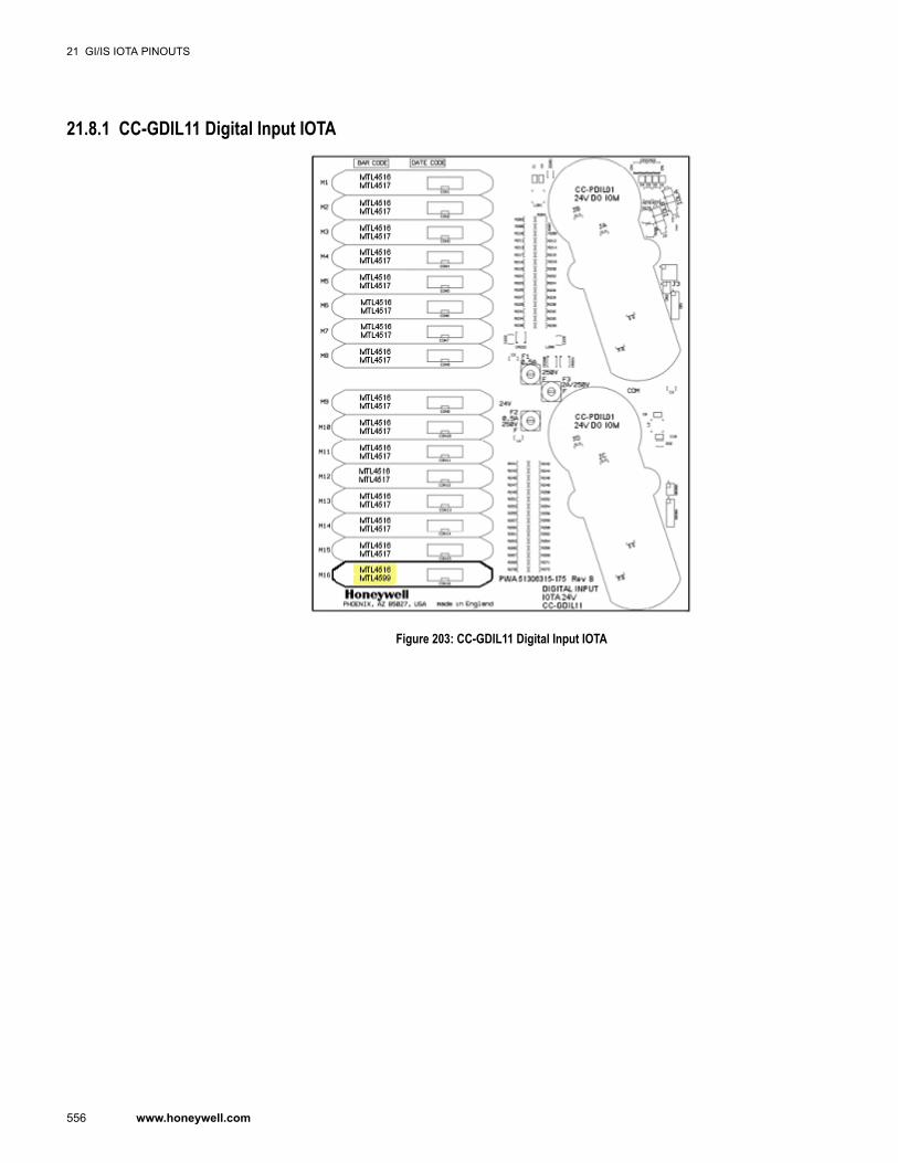
21.8.1 CC-GDIL11 Digital Input IOTA
Figure 203: CC-GDIL11 Digital Input IOTA
21 GI/IS IOTA PINOUTS
556 www.honeywell.com
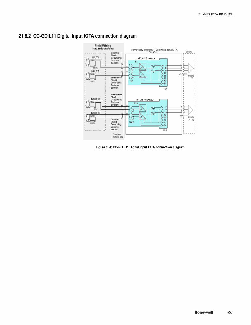
21.8.2 CC-GDIL11 Digital Input IOTA connection diagram
Figure 204: CC-GDIL11 Digital Input IOTA connection diagram
21 GI/IS IOTA PINOUTS
557
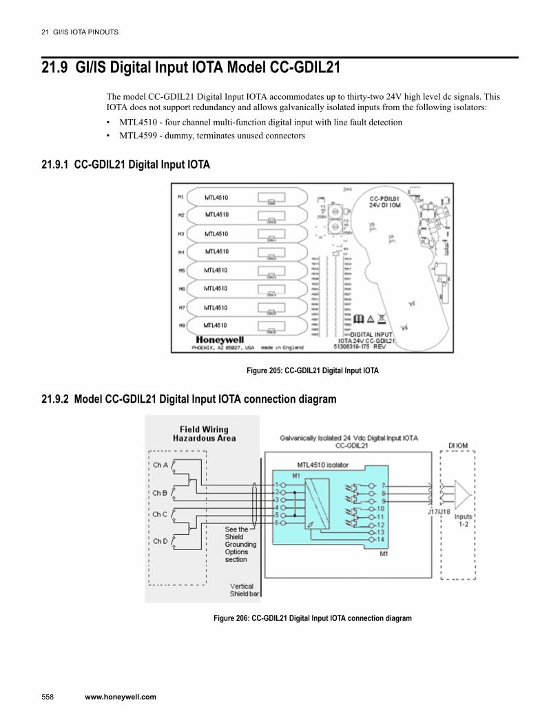
21.9 GI/IS Digital Input IOTA Model CC-GDIL21The model CC-GDIL21 Digital Input IOTA accommodates up to thirty-two 24V high level dc signals. ThisIOTA does not support redundancy and allows galvanically isolated inputs from the following isolators:
• MTL4510 - four channel multi-function digital input with line fault detection• MTL4599 - dummy, terminates unused connectors
21.9.1 CC-GDIL21 Digital Input IOTA
Figure 205: CC-GDIL21 Digital Input IOTA
21.9.2 Model CC-GDIL21 Digital Input IOTA connection diagram
Figure 206: CC-GDIL21 Digital Input IOTA connection diagram
21 GI/IS IOTA PINOUTS
558 www.honeywell.com
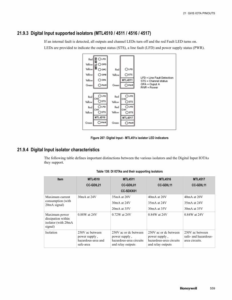
21.9.3 Digital Input supported isolators (MTL4510 / 4511 / 4516 / 4517)If an internal fault is detected, all outputs and channel LEDs turn off and the red Fault LED turns on.
LEDs are provided to indicate the output status (STS), a line fault (LFD) and power supply status (PWR).
Figure 207: Digital Input - MTL451x isolator LED indicators
21.9.4 Digital Input isolator characteristicsThe following table defines important distinctions between the various isolators and the Digital Input IOTAsthey support.
Table 138: DI IOTAs and their supporting isolators
Item MTL4510CC-GDIL21
MTL4511CC-GDIL01CC-SDXX01
MTL4516CC-GDIL11
MTL4517CC-GDIL11
Maximum currentconsumption (with20mA signal)
30mA at 24V 35mA at 20V
30mA at 24V
20mA at 35V
40mA at 20V
35mA at 24V
30mA at 35V
40mA at 20V
35mA at 24V
30mA at 35V
Maximum powerdissipation withinisolator (with 20mAsignal)
0.88W at 24V 0.72W at 24V 0.84W at 24V 0.84W at 24V
Isolation 250V ac betweenpower supply ,hazardous-area andsafe-area
250V ac or dc betweenpower supply ,hazardous-area circuitsand relay outputs
250V ac or dc betweenpower supply ,hazardous-area circuitsand relay outputs
250V ac betweensafe- and hazardous-area circuits.
21 GI/IS IOTA PINOUTS
559

Item MTL4510CC-GDIL21
MTL4511CC-GDIL01CC-SDXX01
MTL4516CC-GDIL11
MTL4517CC-GDIL11
Safety description Vo = 10.5V
Io = 14mA
Po = 37mW
Um = 253V rms
or dc
Vo = 10.5V
Io = 14mA
Po = 37mW
Um = 253V rms
or dc
Vo = 10.5V
Io = 14mA
Po = 37mW
Um = 253V rms
or dc
Vo = 10.5V
Io = 14mA
Po = 37mW
Um = 253V rms
or dc
21 GI/IS IOTA PINOUTS
560 www.honeywell.com
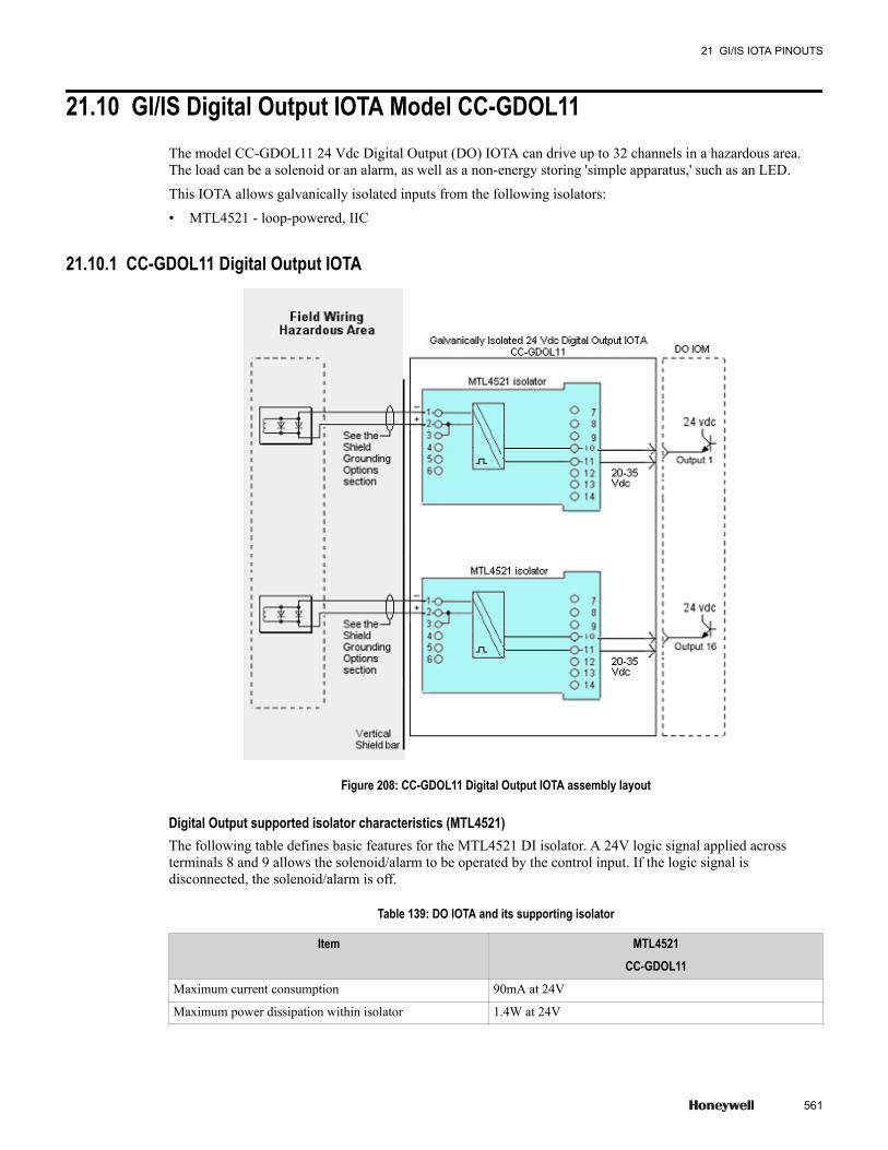
21.10 GI/IS Digital Output IOTA Model CC-GDOL11The model CC-GDOL11 24 Vdc Digital Output (DO) IOTA can drive up to 32 channels in a hazardous area.The load can be a solenoid or an alarm, as well as a non-energy storing 'simple apparatus,' such as an LED.
This IOTA allows galvanically isolated inputs from the following isolators:
• MTL4521 - loop-powered, IIC
21.10.1 CC-GDOL11 Digital Output IOTA
Figure 208: CC-GDOL11 Digital Output IOTA assembly layout
Digital Output supported isolator characteristics (MTL4521)The following table defines basic features for the MTL4521 DI isolator. A 24V logic signal applied acrossterminals 8 and 9 allows the solenoid/alarm to be operated by the control input. If the logic signal isdisconnected, the solenoid/alarm is off.
Table 139: DO IOTA and its supporting isolator
Item MTL4521CC-GDOL11
Maximum current consumption 90mA at 24V
Maximum power dissipation within isolator 1.4W at 24V
21 GI/IS IOTA PINOUTS
561
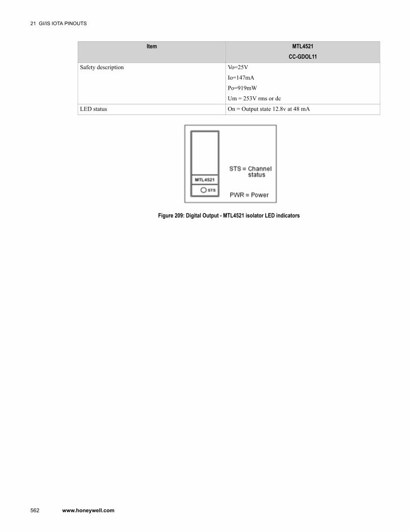
Item MTL4521CC-GDOL11
Safety description Vo=25V
Io=147mA
Po=919mW
Um = 253V rms or dc
LED status On = Output state 12.8v at 48 mA
Figure 209: Digital Output - MTL4521 isolator LED indicators
21 GI/IS IOTA PINOUTS
562 www.honeywell.com
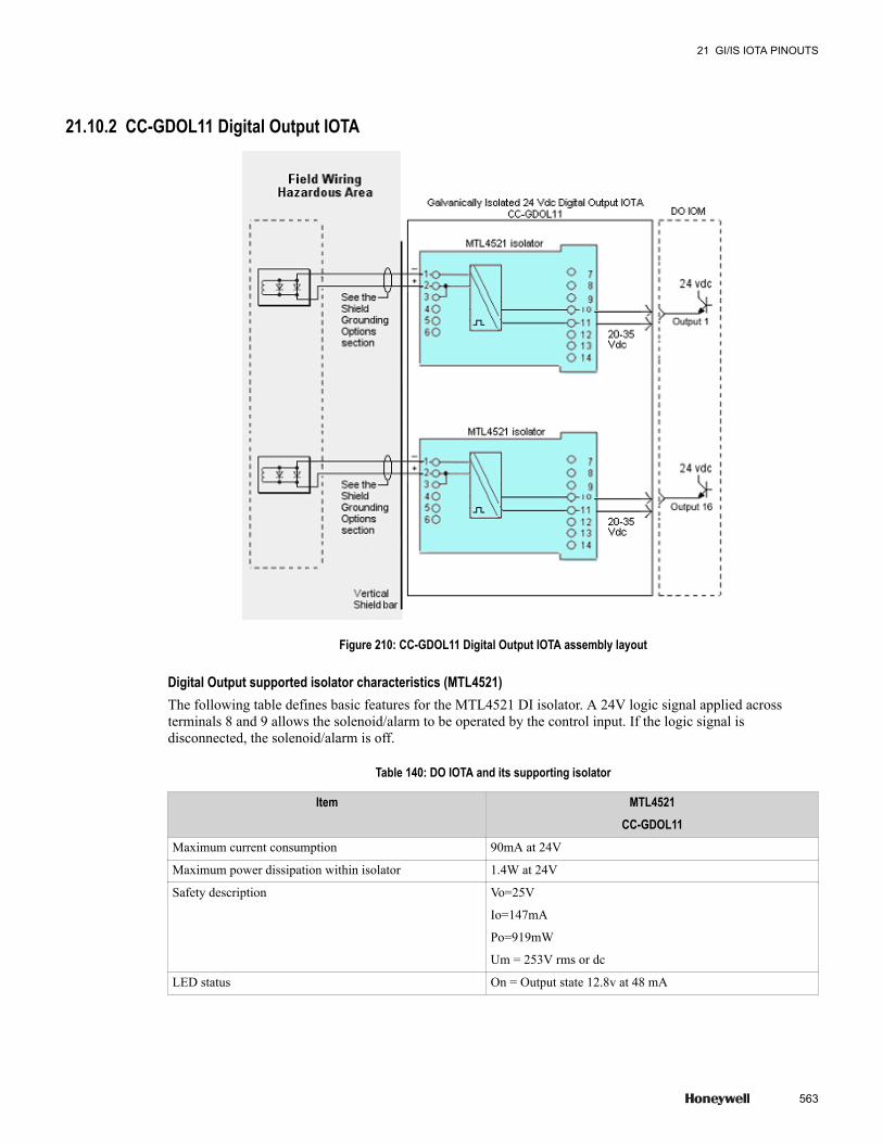
21.10.2 CC-GDOL11 Digital Output IOTA
Figure 210: CC-GDOL11 Digital Output IOTA assembly layout
Digital Output supported isolator characteristics (MTL4521)The following table defines basic features for the MTL4521 DI isolator. A 24V logic signal applied acrossterminals 8 and 9 allows the solenoid/alarm to be operated by the control input. If the logic signal isdisconnected, the solenoid/alarm is off.
Table 140: DO IOTA and its supporting isolator
Item MTL4521CC-GDOL11
Maximum current consumption 90mA at 24V
Maximum power dissipation within isolator 1.4W at 24V
Safety description Vo=25V
Io=147mA
Po=919mW
Um = 253V rms or dc
LED status On = Output state 12.8v at 48 mA
21 GI/IS IOTA PINOUTS
563

Figure 211: Digital Output - MTL4521 isolator LED indicators
21 GI/IS IOTA PINOUTS
564 www.honeywell.com
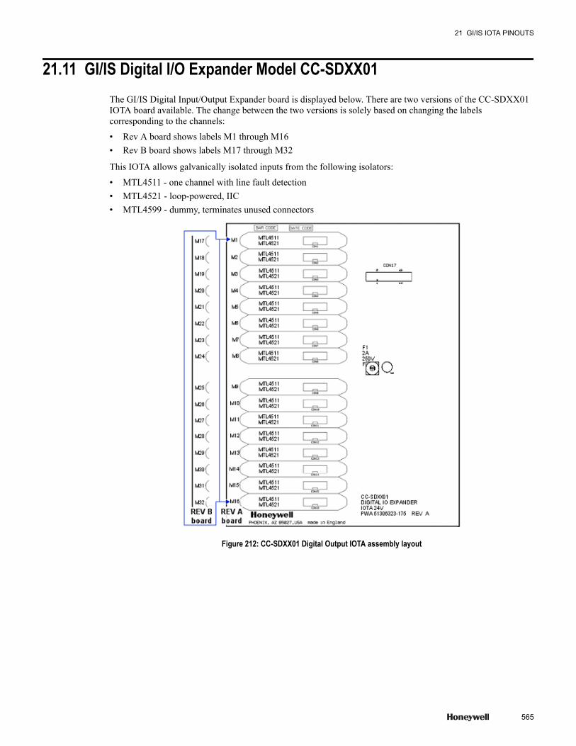
21.11 GI/IS Digital I/O Expander Model CC-SDXX01The GI/IS Digital Input/Output Expander board is displayed below. There are two versions of the CC-SDXX01IOTA board available. The change between the two versions is solely based on changing the labelscorresponding to the channels:
• Rev A board shows labels M1 through M16• Rev B board shows labels M17 through M32
This IOTA allows galvanically isolated inputs from the following isolators:
• MTL4511 - one channel with line fault detection• MTL4521 - loop-powered, IIC• MTL4599 - dummy, terminates unused connectors
Figure 212: CC-SDXX01 Digital Output IOTA assembly layout
21 GI/IS IOTA PINOUTS
565

21 GI/IS IOTA PINOUTS
566 www.honeywell.com

22 PCS45 Configuration Software
The PC-Configuration software (PCS45) allows the configuration of the MTL4575 Temperature converterisolator. Data is transmitted from the PC to the temperature converter through the PC-link PCL45 (USB).
WARNINGNot FM or CSA approved
The MTL PCL45USB pc link to the MTL4575 Temperature Converter is not approved by either FM or CSA.Therefore, the device cannot be used in North America (or those locations requiring FM or CSA) unless both:
• the area where the cabinet is located (or the 4575 Converter) and• the field devices connected to the 4575 converter are verified to be nonhazardous.
ATEX Certified
The PCL45USB is ATEX certified; however, the certification only applies to the outputs of the link that allow it tobe connected to the 4575 with field wiring connections installed (and the field devices can be located in Zone 0 orZone 1).
The ATEX certification for the link:
• does not allow the link to be located in a Zone 2 locations• the cabinet, and or the 4575, must be within a verified nonhazardous location for the link to be connected to
the 4575 Converter.
Parameters can be configured, for example sensor type, measuring range and alarm signals. These can then besaved and later used to configure other MTL4575s isolators.
For diagnostic purposes, the software allows the user to:
• look at the input and output values or• monitor parameters over a period of timeExample: The output can be set to various currents, without affecting the input, allowing the safe areaequipment to be checked or calibrated.
Operating PCS45 in Demo mode maintains all the functionality of the software but requires no connection to atemperature converter.
Related topics“PCS45 Operating Modes” on page 569
567

“Troubleshooting the PSC45 software” on page 578
22 PCS45 CONFIGURATION SOFTWARE
568 www.honeywell.com

22.1 PCS45 Operating ModesThe following operating modes are selectable.
Mode DescriptionOffline No connection is made between the software and the isolator. Therefore, changes in the
configuration of the software will not be downloaded to the isolator.
Online A connection is made between the software and the isolator. Any changes made to theconfiguration of the isolator are downloaded immediately to that isolator. The data seen in thesoftware is identical to that in the isolator.
Demo The 'on-line' operation and the data exchange with the transmitter are simulated. This modecan be used for training purposes.
Edit In the 'off-line' operation, the configuration data can be edited and saved into a file on thehard drive or disk. This mode can be used in order to generate the configuration for severaltransmitters in the project phase.
Restricted access The configuration details for the isolator can only be viewed or printed. Editing of theconfiguration settings is not allowed. Files can be loaded into the software, but when files aresaved they have the filename 'DEMO.D45," this cannot be altered.
Full access Full access is required when configuration changes to the isolator are to be made. To save theconfiguration file, any filename can be used.
Note: The software doesn't always indicate the operational mode it is currently in.
22.1.1 Data formatPCS45 software saves configuration data as a .D45 file extension.
22.1.2 Data flowThe PCS45 software creates and manages a copy of the transmitter's configuration data string on the computerand controls the exchange of this data between the computer/disk and the transmitter. The data flow between thecopies of this data structure depends upon the operational mode.
Within the PCS45 application the following occurs:
• Various displays within the application enable the contents of these data structures to be viewed and altered.• After a change has been made and accepted the data values are tested before the data is transferred to the
data structure.• A copy of the configuration data held in the software can be saved into or accepted from a file at any time,
but the operation mode will always change to 'off-line.'
In the 'off line' mode, no data is automatically transferred between the software and the temperatureconverter.
• When changes have been accepted in the 'online' operation mode, data is transmitted straight into the non-volatile memory of the temperature converter.
If there are any errors during this data transfer the operation mode changes to 'off-line' because coherentconfigurations cannot be expected.
• In the demo mode, data is not transferred to the temperature converter, and any exchange is simulated.
22.1.3 Temperature converterThe temperature converter takes an mV or signal from either a thermocouple or RTD in hazardous area, andconverts this to a 4/20mA signal in the safe area.
22 PCS45 CONFIGURATION SOFTWARE
569
The isolator is programmable by the PCS45 software and PCL45 hardware, which configures input types,output spans, alarms, etc.
22.1.4 PC-link - PCL45 and PCL45USBThe PC-link:
• Allows data to be exchanged between the PC and the Temperature converter.• Is ATEX certified. This allows the configuration of the MTL4575 isolator while remaining part of the
hazardous area circuit.
The PCL45USB device:
• Is powered from the computer and is ready for communication immediately after the physical connectionhas been established.
The PCL45 device:
• Is powered from the RS232 and from the Temperature converter data lines.• The serial port on a computer must be able to supply ± 8Vat 3mA.
TipA minimum connection time of 15 seconds has to be allowed before data can be exchanged between the PC and theisolator.
22.1.5 Export and Print fileThe export and print file is composed of the current isolator configuration settings. The following is an exampleof an export and/or print file.
Converter type: MTL5073
Manufacturer's ident. MTL Group
Software revision 7
Hardware revision 7.000
Tag name DEMO
Descriptor DESCRIPTION
Date 15.12.99
Input type E type THC
Process units °C
Linearization on
Cold Jm. Comp. on
Point 4mA 10.0 °C
Point 20mA 200.0 °C
Damping time constant 0.0 s
Smoothing time constant 2 s
Filter frequency 50 Hz
Open circuit alarm level off
Cold Jm failure alarm off
Transmitter failure alarm off
Created on: 21/8/00
22 PCS45 CONFIGURATION SOFTWARE
570 www.honeywell.com
22.1.6 Damping and smoothingDamping and smoothing are both filter functions, which are configurable, and have different effects on the waythe input signal is processed.
• Damping causes conventional single-pole, low-pass filtering that is similar to an R-C network.• Smoothing causes a more 'intelligent' damping where small changes (noise) are heavily suppressed and large
(tendency) changes are processed normally.
Although, high damping values will greatly suppress noise and make the output signal stable, it causes a slowresponse time. The smoothing function avoids this disadvantage by removing the filtering while there are verylarge signal changes on the input.
Higher damping values are recommended for slow input signals requiring high levels of stability, while fastsignals require lower damping values. If in doubt, some experimentation will yield the best results.
22.1.7 Alarm signalsAlarm signals can be configured to drive analog output currents outside the working range.
• The low alarm changes the output current to 1.00 mA and• The high alarm changes the current to 21.00mA.
There are three types of fault that trigger an alarm response:
• O/C Alarm - alarm is signaled if an open circuit in the field is detected.• Tx Fail - alarm signaled if a fault is detected.• Cj Fail - alarm signaled if a fault is detected with the Cj sensor.
Meanwell power systemTo monitor the DC voltage, a free relay contact is provided labeled as 'DC OK.'
Relay contact close The output voltage reaches the adjusted output voltage
Relay contact open The output voltage below 90% of adjusted output voltage.
Relay Contact Ratings - 60V dc/0.3Amp
30V dc/1Amp
30V ac /0.5 Amp
The alarm signal can be connected to external circuit or can be connected to Series C Digital Input module.
Phoenix power systemTo monitor the DC output voltage a free Relay contact is provided .It is numbered as 13, 14 with sign of relaycontact.
Relay contact closed The output voltage reaches the adjusted output voltage
Relay contact open The output voltage drop below 90% of adjusted output voltage.
Relay Contact Ratings - 30 volts dc/1Amp
30 volts ac /1Amp
The alarm signal can be connected with external circuit or can be connected to Series C Digital Input module.
22 PCS45 CONFIGURATION SOFTWARE
571
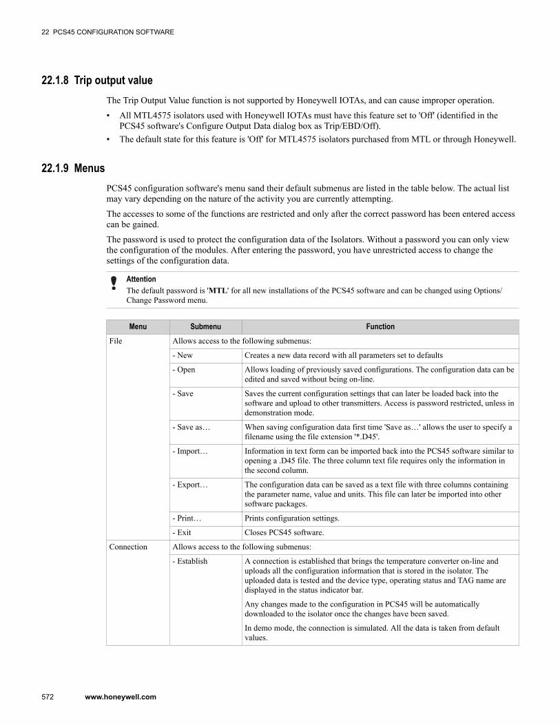
22.1.8 Trip output valueThe Trip Output Value function is not supported by Honeywell IOTAs, and can cause improper operation.
• All MTL4575 isolators used with Honeywell IOTAs must have this feature set to 'Off' (identified in thePCS45 software's Configure Output Data dialog box as Trip/EBD/Off).
• The default state for this feature is 'Off' for MTL4575 isolators purchased from MTL or through Honeywell.
22.1.9 MenusPCS45 configuration software's menu sand their default submenus are listed in the table below. The actual listmay vary depending on the nature of the activity you are currently attempting.
The accesses to some of the functions are restricted and only after the correct password has been entered accesscan be gained.
The password is used to protect the configuration data of the Isolators. Without a password you can only viewthe configuration of the modules. After entering the password, you have unrestricted access to change thesettings of the configuration data.
AttentionThe default password is 'MTL' for all new installations of the PCS45 software and can be changed using Options/Change Password menu.
Menu Submenu FunctionFile Allows access to the following submenus:
- New Creates a new data record with all parameters set to defaults
- Open Allows loading of previously saved configurations. The configuration data can beedited and saved without being on-line.
- Save Saves the current configuration settings that can later be loaded back into thesoftware and upload to other transmitters. Access is password restricted, unless indemonstration mode.
- Save as… When saving configuration data first time 'Save as…' allows the user to specify afilename using the file extension '*.D45'.
- Import… Information in text form can be imported back into the PCS45 software similar toopening a .D45 file. The three column text file requires only the information inthe second column.
- Export… The configuration data can be saved as a text file with three columns containingthe parameter name, value and units. This file can later be imported into othersoftware packages.
- Print… Prints configuration settings.
- Exit Closes PCS45 software.
Connection Allows access to the following submenus:
- Establish A connection is established that brings the temperature converter on-line anduploads all the configuration information that is stored in the isolator. Theuploaded data is tested and the device type, operating status and TAG name aredisplayed in the status indicator bar.
Any changes made to the configuration in PCS45 will be automaticallydownloaded to the isolator once the changes have been saved.
In demo mode, the connection is simulated. All the data is taken from defaultvalues.
22 PCS45 CONFIGURATION SOFTWARE
572 www.honeywell.com
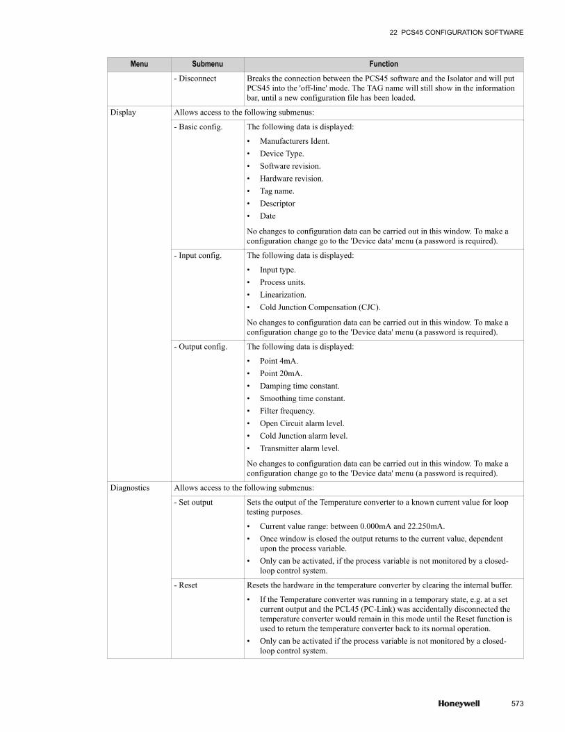
Menu Submenu Function- Disconnect Breaks the connection between the PCS45 software and the Isolator and will put
PCS45 into the 'off-line' mode. The TAG name will still show in the informationbar, until a new configuration file has been loaded.
Display Allows access to the following submenus:
- Basic config. The following data is displayed:
• Manufacturers Ident.• Device Type.• Software revision.• Hardware revision.• Tag name.• Descriptor• Date
No changes to configuration data can be carried out in this window. To make aconfiguration change go to the 'Device data' menu (a password is required).
- Input config. The following data is displayed:
• Input type.• Process units.• Linearization.• Cold Junction Compensation (CJC).
No changes to configuration data can be carried out in this window. To make aconfiguration change go to the 'Device data' menu (a password is required).
- Output config. The following data is displayed:
• Point 4mA.• Point 20mA.• Damping time constant.• Smoothing time constant.• Filter frequency.• Open Circuit alarm level.• Cold Junction alarm level.• Transmitter alarm level.
No changes to configuration data can be carried out in this window. To make aconfiguration change go to the 'Device data' menu (a password is required).
Diagnostics Allows access to the following submenus:
- Set output Sets the output of the Temperature converter to a known current value for looptesting purposes.
• Current value range: between 0.000mA and 22.250mA.• Once window is closed the output returns to the current value, dependent
upon the process variable.• Only can be activated, if the process variable is not monitored by a closed-
loop control system.
- Reset Resets the hardware in the temperature converter by clearing the internal buffer.
• If the Temperature converter was running in a temporary state, e.g. at a setcurrent output and the PCL45 (PC-Link) was accidentally disconnected thetemperature converter would remain in this mode until the Reset function isused to return the temperature converter back to its normal operation.
• Only can be activated if the process variable is not monitored by a closed-loop control system.
22 PCS45 CONFIGURATION SOFTWARE
573
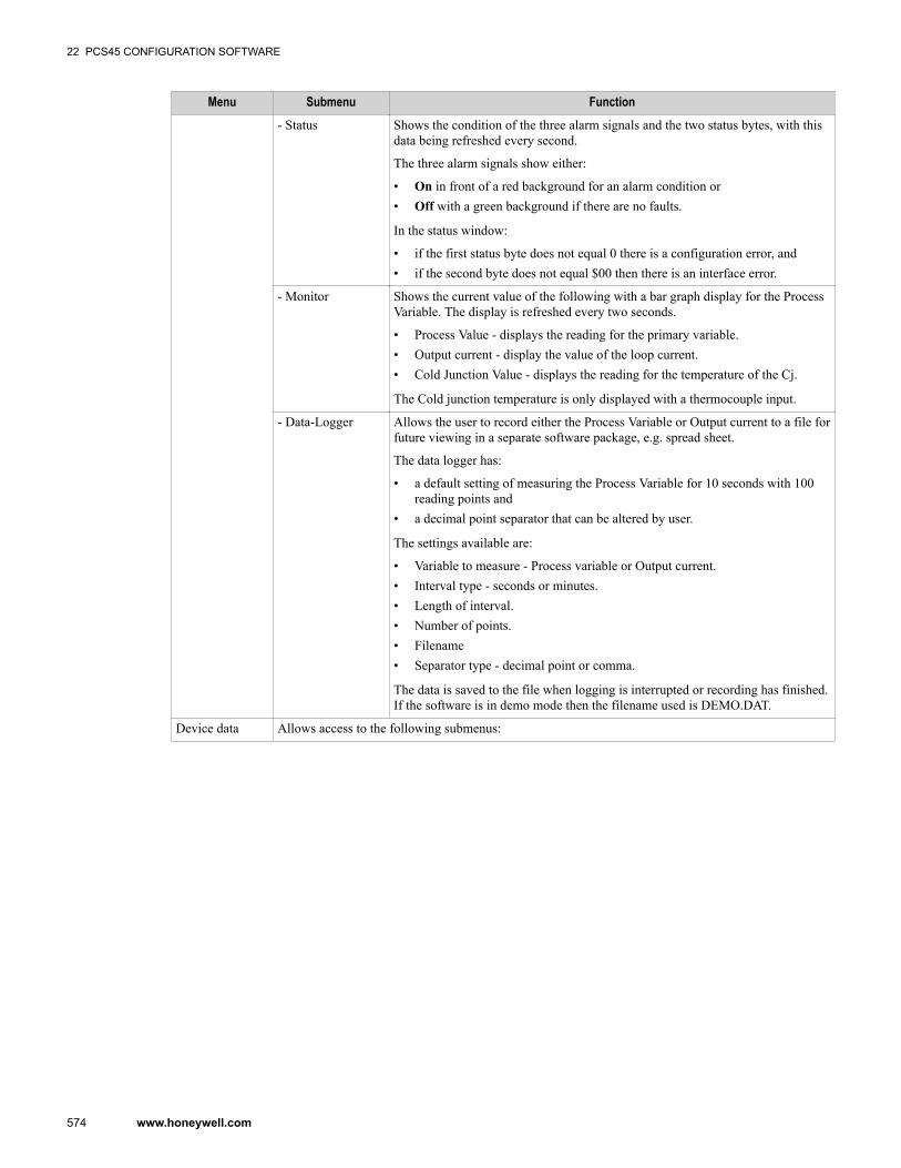
Menu Submenu Function- Status Shows the condition of the three alarm signals and the two status bytes, with this
data being refreshed every second.
The three alarm signals show either:
• On in front of a red background for an alarm condition or• Off with a green background if there are no faults.
In the status window:
• if the first status byte does not equal 0 there is a configuration error, and• if the second byte does not equal $00 then there is an interface error.
- Monitor Shows the current value of the following with a bar graph display for the ProcessVariable. The display is refreshed every two seconds.
• Process Value - displays the reading for the primary variable.• Output current - display the value of the loop current.• Cold Junction Value - displays the reading for the temperature of the Cj.
The Cold junction temperature is only displayed with a thermocouple input.
- Data-Logger Allows the user to record either the Process Variable or Output current to a file forfuture viewing in a separate software package, e.g. spread sheet.
The data logger has:
• a default setting of measuring the Process Variable for 10 seconds with 100reading points and
• a decimal point separator that can be altered by user.
The settings available are:
• Variable to measure - Process variable or Output current.• Interval type - seconds or minutes.• Length of interval.• Number of points.• Filename• Separator type - decimal point or comma.
The data is saved to the file when logging is interrupted or recording has finished.If the software is in demo mode then the filename used is DEMO.DAT.
Device data Allows access to the following submenus:
22 PCS45 CONFIGURATION SOFTWARE
574 www.honeywell.com
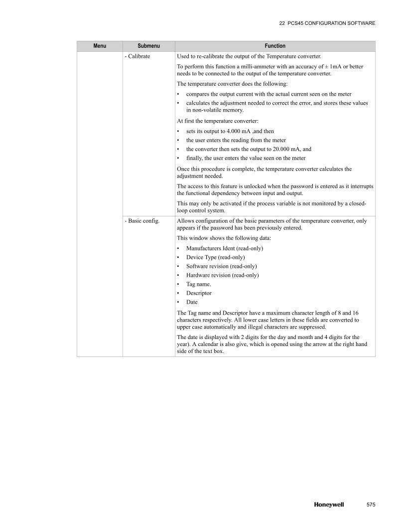
Menu Submenu Function- Calibrate Used to re-calibrate the output of the Temperature converter.
To perform this function a milli-ammeter with an accuracy of ± 1mA or betterneeds to be connected to the output of the temperature converter.
The temperature converter does the following:
• compares the output current with the actual current seen on the meter• calculates the adjustment needed to correct the error, and stores these values
in non-volatile memory.
At first the temperature converter:
• sets its output to 4.000 mA ,and then• the user enters the reading from the meter• the converter then sets the output to 20.000 mA, and• finally, the user enters the value seen on the meter
Once this procedure is complete, the temperature converter calculates theadjustment needed.
The access to this feature is unlocked when the password is entered as it interruptsthe functional dependency between input and output.
This may only be activated if the process variable is not monitored by a closed-loop control system.
- Basic config. Allows configuration of the basic parameters of the temperature converter, onlyappears if the password has been previously entered.
This window shows the following data:
• Manufacturers Ident (read-only)• Device Type (read-only)• Software revision (read-only)• Hardware revision (read-only)• Tag name.• Descriptor• Date
The Tag name and Descriptor have a maximum character length of 8 and 16characters respectively. All lower case letters in these fields are converted toupper case automatically and illegal characters are suppressed.
The date is displayed with 2 digits for the day and month and 4 digits for theyear). A calendar is also give, which is opened using the arrow at the right handside of the text box.
22 PCS45 CONFIGURATION SOFTWARE
575
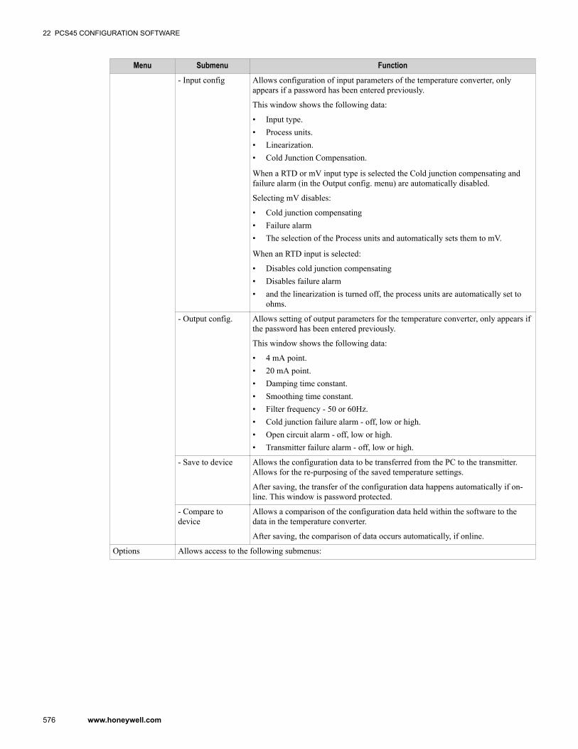
Menu Submenu Function- Input config Allows configuration of input parameters of the temperature converter, only
appears if a password has been entered previously.
This window shows the following data:
• Input type.• Process units.• Linearization.• Cold Junction Compensation.
When a RTD or mV input type is selected the Cold junction compensating andfailure alarm (in the Output config. menu) are automatically disabled.
Selecting mV disables:
• Cold junction compensating• Failure alarm• The selection of the Process units and automatically sets them to mV.
When an RTD input is selected:
• Disables cold junction compensating• Disables failure alarm• and the linearization is turned off, the process units are automatically set to
ohms.
- Output config. Allows setting of output parameters for the temperature converter, only appears ifthe password has been entered previously.
This window shows the following data:
• 4 mA point.• 20 mA point.• Damping time constant.• Smoothing time constant.• Filter frequency - 50 or 60Hz.• Cold junction failure alarm - off, low or high.• Open circuit alarm - off, low or high.• Transmitter failure alarm - off, low or high.
- Save to device Allows the configuration data to be transferred from the PC to the transmitter.Allows for the re-purposing of the saved temperature settings.
After saving, the transfer of the configuration data happens automatically if on-line. This window is password protected.
- Compare todevice
Allows a comparison of the configuration data held within the software to thedata in the temperature converter.
After saving, the comparison of data occurs automatically, if online.
Options Allows access to the following submenus:
22 PCS45 CONFIGURATION SOFTWARE
576 www.honeywell.com

Menu Submenu Function- Change password The password is used to protect the configuration data of the Isolators.
Without a password:
• You can only view the configuration of the modules.
After entering the password:
• You have unrestricted access to change configuration settings.
Default password for PCS45 software is MTL
To change the password:
1. Select Options, Change Password.2. Enter the current password. You will then be asked to enter the new password
and confirm this new password. Once the new password has been accepted, itis stored permanently onto the PC.
Note: The password is not case sensitive.
- Language Enables the software to be configured for the following languages.
• English• German• French
- Port selection With the PCS45 application running, the PCL45 USB connected and this optionselected the correct port is automatically scanned.
Allows you to configure the serial port, If the PCL45 PC-link is used.
To select a port:
1. Choose Options < Port selection2. Select one of the listed ports (ex. COM1) Note: The software detects which
serial ports are available, but it is up to the user to ensure the correct serialport is being used.
Note: Care has also to be taken to ensure the data lines can supply ± 8V @ 3mA,to the PC-link PCL45.
The application may operate in Demo mode. This mode maintains all thefunctionality of the software but does not require a connection to the temperatureconverter.
- Error indication Allows selection of the following errors to be displayed:
• Defect• Disturbed• Exception
Help Allows access to the following submenus:
- Contents Open embedded help file for the software
- Online Help Provides Online Help info
- Information Displays support and software version information
22 PCS45 CONFIGURATION SOFTWARE
577
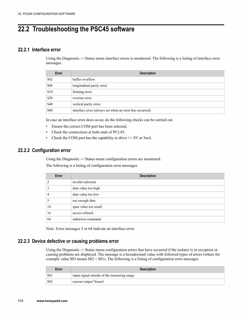
22.2 Troubleshooting the PSC45 software
22.2.1 Interface errorUsing the Diagnostic -> Status menu interface errors is monitored. The following is a listing of interface errormessages.
Error Description$02 buffer overflow
$08 longitudinal parity error.
$10 framing error.
$20 overrun error.
$40 vertical parity error.
$80 interface error (always set when an error has occurred).
In case an interface error does occur, do the following checks can be carried out.
• Ensure the correct COM port has been selected.• Check the connections at both ends of PCL45.• Check the COM port has the capability to drive +/- 8V at 3mA.
22.2.2 Configuration errorUsing the Diagnostic -> Status menu configuration errors are monitored.
The following is a listing of configuration error messages.
Error Description2 invalid selection
3 data value too high
4 data value too low
5 not enough data
14 span value too small
16 access refused
64 unknown command
Note: Error messages 5 or 64 indicate an interface error.
22.2.3 Device defective or causing problems errorUsing the Diagnostic -> Status menu configuration errors that have occurred if the isolator is in exception orcausing problems are displayed. The message is a hexadecimal value with followed types of errors (where forexample value $03 means $02 + $01). The following is a listing of configuration error messages
Error Description$01 input signal outside of the measuring range
$02 current output 'frozen'
22 PCS45 CONFIGURATION SOFTWARE
578 www.honeywell.com
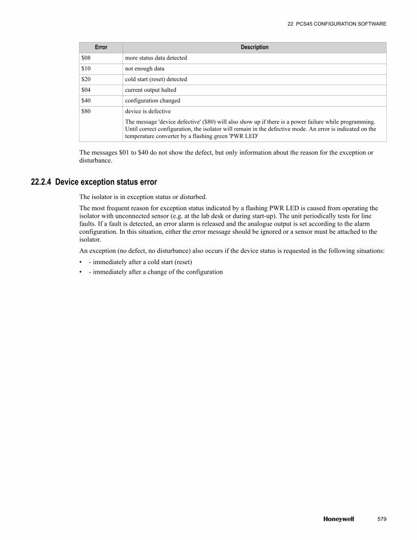
Error Description$08 more status data detected
$10 not enough data
$20 cold start (reset) detected
$04 current output halted
$40 configuration changed
$80 device is defective
The message 'device defective' ($80) will also show up if there is a power failure while programming.Until correct configuration, the isolator will remain in the defective mode. An error is indicated on thetemperature converter by a flashing green 'PWR LED'
The messages $01 to $40 do not show the defect, but only information about the reason for the exception ordisturbance.
22.2.4 Device exception status errorThe isolator is in exception status or disturbed.
The most frequent reason for exception status indicated by a flashing PWR LED is caused from operating theisolator with unconnected sensor (e.g. at the lab desk or during start-up). The unit periodically tests for linefaults. If a fault is detected, an error alarm is released and the analogue output is set according to the alarmconfiguration. In this situation, either the error message should be ignored or a sensor must be attached to theisolator.
An exception (no defect, no disturbance) also occurs if the device status is requested in the following situations:
• - immediately after a cold start (reset)• - immediately after a change of the configuration
22 PCS45 CONFIGURATION SOFTWARE
579

22 PCS45 CONFIGURATION SOFTWARE
580 www.honeywell.com

23 GI/IS Maintenance
Related topics“GI/IS recommended spares” on page 582“Repair” on page 585“Replacing an GI/IS IOTA” on page 586“Replacing an IOM on the GI/IS IOTA” on page 588“Replacing the isolator” on page 589“Replacing fuses on a GI/IS IOTA” on page 590
581
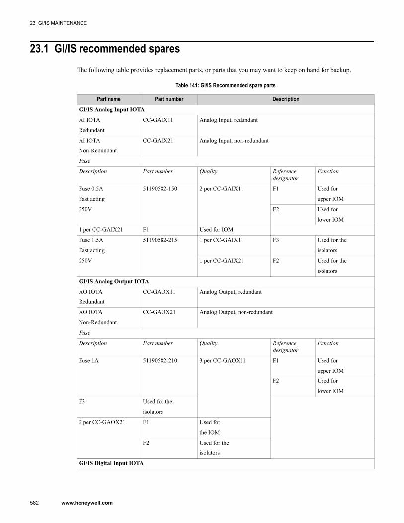
23.1 GI/IS recommended sparesThe following table provides replacement parts, or parts that you may want to keep on hand for backup.
Table 141: GI/IS Recommended spare parts
Part name Part number DescriptionGI/IS Analog Input IOTA
AI IOTA
Redundant
CC-GAIX11 Analog Input, redundant
AI IOTA
Non-Redundant
CC-GAIX21 Analog Input, non-redundant
Fuse
Description Part number Quality Referencedesignator
Function
Fuse 0.5A
Fast acting
250V
51190582-150 2 per CC-GAIX11 F1 Used for
upper IOM
F2 Used for
lower IOM
1 per CC-GAIX21 F1 Used for IOM
Fuse 1.5A
Fast acting
250V
51190582-215 1 per CC-GAIX11 F3 Used for the
isolators
1 per CC-GAIX21 F2 Used for the
isolators
GI/IS Analog Output IOTA
AO IOTA
Redundant
CC-GAOX11 Analog Output, redundant
AO IOTA
Non-Redundant
CC-GAOX21 Analog Output, non-redundant
Fuse
Description Part number Quality Referencedesignator
Function
Fuse 1A 51190582-210 3 per CC-GAOX11 F1 Used for
upper IOM
F2 Used for
lower IOM
F3 Used for the
isolators
2 per CC-GAOX21 F1 Used for
the IOM
F2 Used for the
isolators
GI/IS Digital Input IOTA
23 GI/IS MAINTENANCE
582 www.honeywell.com

Part name Part number DescriptionDI IOTA
Redundant
CC-GDIL01 Digital Input, redundant
DI IOTA
Redundant
CC-GDIL11 Digital Input, redundant
DI IOTA
Redundant
CC-GDIL21 Digital Input, non-redundant
Fuse
Description Part number Quality Referencedesignator
Function
Fuse 0.5A 51190582-150 2 per CC-GDIL01 F1 Used for
upper IOM
F2 Used for
lower IOM
2 per CC-GDIL11 F1 Used for
upper IOM
F2 Used for
lower IOM
1 per CC-GDIL21 F1 Used for the IOM
Fuse 2A 51190582-220 1 per CC-GDIL01 F3 Used for the
isolators
1 per CC-GDIL11 F3 Used for the
isolators
Fuse 1AF 51190582-210 1 per CC-GDIL21 F2 Used for the
isolators
GI/IS Digital Output IOTA
DO IOTA
Redundant
CC-GDOL11 Digital Output, redundant
Fuse
Description Part number Quality Referencedesignator
Function
Fuse 5A 51190582-250 1 per CC-GDOL21 F1 Used for the IOM
F2 Used for the
isolators
GI/IS Digital I/O Expander IOTA
Digital I/OI
Expander
CC-SDXX01 Digital Input/Output Expander
Fuse
Description Part number Quality Referencedesignator
Function
Fuse 2A 51190582-220 1 per CC-SDXX01 F1 Used for the
isolators
MTL GI/IS isolator
23 GI/IS MAINTENANCE
583
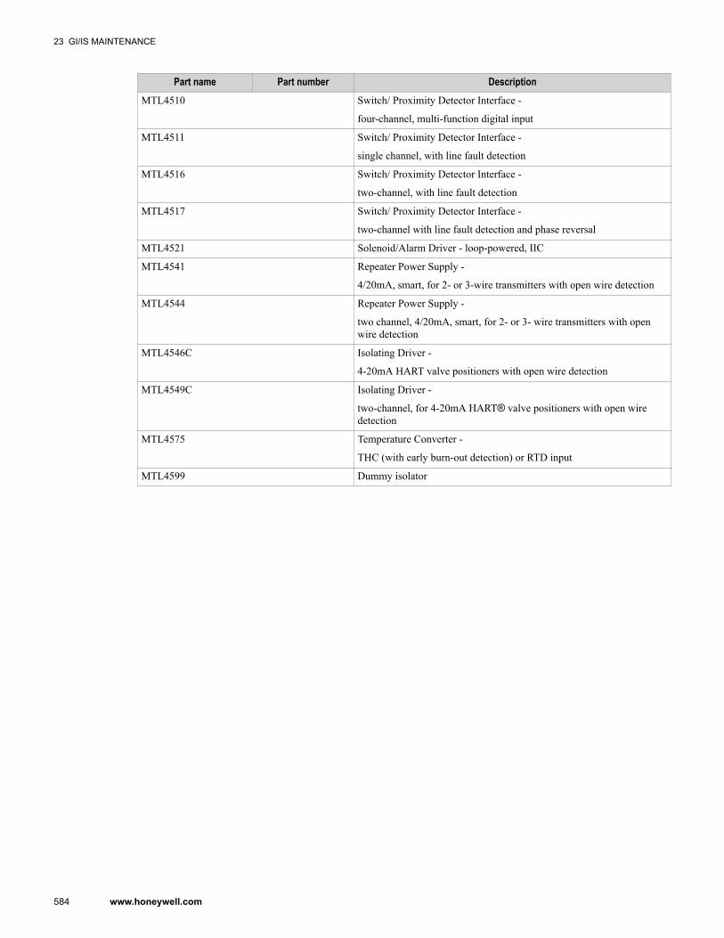
Part name Part number DescriptionMTL4510 Switch/ Proximity Detector Interface -
four-channel, multi-function digital input
MTL4511 Switch/ Proximity Detector Interface -
single channel, with line fault detection
MTL4516 Switch/ Proximity Detector Interface -
two-channel, with line fault detection
MTL4517 Switch/ Proximity Detector Interface -
two-channel with line fault detection and phase reversal
MTL4521 Solenoid/Alarm Driver - loop-powered, IIC
MTL4541 Repeater Power Supply -
4/20mA, smart, for 2- or 3-wire transmitters with open wire detection
MTL4544 Repeater Power Supply -
two channel, 4/20mA, smart, for 2- or 3- wire transmitters with openwire detection
MTL4546C Isolating Driver -
4-20mA HART valve positioners with open wire detection
MTL4549C Isolating Driver -
two-channel, for 4-20mA HART® valve positioners with open wiredetection
MTL4575 Temperature Converter -
THC (with early burn-out detection) or RTD input
MTL4599 Dummy isolator
23 GI/IS MAINTENANCE
584 www.honeywell.com

23.2 RepairThe isolator and IOTA cannot be repaired by the user and must be replaced with an equivalent certified product.Repairs should only be carried out by the manufacturer
23 GI/IS MAINTENANCE
585
23.3 Replacing an GI/IS IOTA
WARNINGReplacing a GI/IS IOTA and all associated activities may only be performed when the area has been determined tobe non-hazardous.
CAUTIONWe recommend that you proceed with extreme caution whenever replacing any component in a control system. Besure the system is offline or in a safe operating mode.
Component replacements may also require corresponding changes in the control strategy configuration throughControl Builder, as well as downloading appropriate data to the replaced component.
The replacing of the GI/IS IOTA is different from the replacing the standard Series C IOTA with regards to thefollowing areas:
• the isolators and terminal plugs must be moved to the new IOTA, and• there is an additional set of mounting screws to accommodate the wider GI/IS IOTA.
AttentionReplacing the GI/IS IOTA requires that the IOM is in an inactive off-process state.
To replace an GI/IS IOTA1 Loosen the screws:
• at each side of the plastic cover that secures the I/O module to the IOTA board, and• the long gray plastic screw located on the module's face. It is not necessary to completely remove this
screw.
CAUTIONOnly use a #2 Phillips screw-driver to carefully loosen or tighten the long gray plastic screw. Do not use eithera #1 Phillips screw-driver or a battery powered screw-driver to remove or install the plastic screw as this candamage the screw head.
2 Remove the I/O module from the IOTA board and connector.3 Label and disconnect all cables from the IOTA connectors.4 Note which terminal plugs are connected to which isolator/channel to make reconnection easier after the
IOTA is replaced.Remove the terminal plugs (retaining the field wiring) from the isolators.
Do not remove the isolators at this time.5 Loosen the screws that secure the IOTA board to the carrier and remove the IOTA board.
To remove 24 V power to the IOTA board do the following:
• Loosen the screw from the left side of the IOTA board that connects to the 24 Vdc bus bar.• Loosen the screw from the right side of the IOTA board that connects to the GND bus bar.
6 Mount new I/O IOTA board on the carrier at the same position as the old IOTA board. Secure with screws.7 Move the isolators from the old IOTA to the new IOTA preserving the original configuration.8 Attach the appropriate terminal plugs to the appropriate isolators.9 Reconnect the cables (removing labels if they were utilized) to the IOTA connectors10 To reconnect power to the IOTA board through the COM and 24 Vdc bus bars, do the following:
• Install screw through right side of IOTA board to tap into the GND bus bar of carrier.• Install screw through left side of IOTA board to tap into the 24 V bus bar of carrier.
23 GI/IS MAINTENANCE
586 www.honeywell.com

11 Insert the I/O module onto IOTA board making sure that the I/O circuit board mates properly with the IOTAboard connector.Secure the module to the:
• IOTA board - with two screws located at each side of the plastic cover.• Carrier - with the long screw that is inserted into the hole on the face of the module's plastic cover.
12 The I/O module will boot-up into IDLE state.13 In Control Builder, perform a 'Load with Contents'.
Refer to the following instructions to see how to replace a Series C IOTA: “Replacing a Series C IOTA” onpage 474
23 GI/IS MAINTENANCE
587
23.4 Replacing an IOM on the GI/IS IOTA
CAUTIONWe recommend that you proceed with extreme caution whenever replacing any component in a control system. Besure the system is offline or in a safe operating mode.
Component replacements may also require corresponding changes in the control strategy configuration throughControl Builder, as well as downloading appropriate data to the replaced component.
The removing of the IOM on a GI/IS IOTA is similar to removing the IOM on the standard Series C IOTA.
Refer to the following instructions to see how the IOM is removed on the IOTA: “Replacing an I/O module” onpage 475.
23 GI/IS MAINTENANCE
588 www.honeywell.com
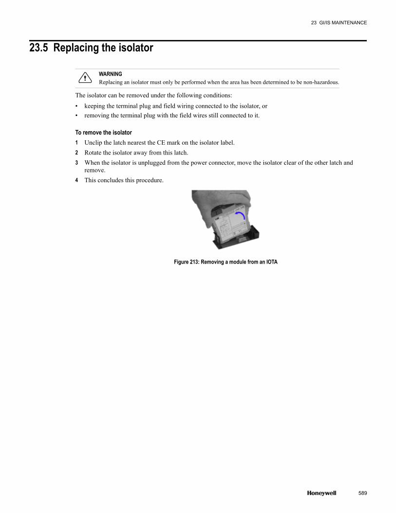
23.5 Replacing the isolator
WARNINGReplacing an isolator must only be performed when the area has been determined to be non-hazardous.
The isolator can be removed under the following conditions:
• keeping the terminal plug and field wiring connected to the isolator, or• removing the terminal plug with the field wires still connected to it.
To remove the isolator1 Unclip the latch nearest the CE mark on the isolator label.2 Rotate the isolator away from this latch.3 When the isolator is unplugged from the power connector, move the isolator clear of the other latch and
remove.4 This concludes this procedure.
Figure 213: Removing a module from an IOTA
23 GI/IS MAINTENANCE
589
23.6 Replacing fuses on a GI/IS IOTARefer to the GI/IS recommended spares section in this document for the proper replacement fuse.
WARNINGReplacing any GI/IS IOTA fuse must only be performed when the area has been determined to be non-hazardous.
To replace fuses on a GI/IS IOTA1 Using a small slotted screw-driver, place the tip into the slot on the fuse cap.2 Rotate the cap counter clockwise, a quarter-turn. Remove the cap that also holds the fuse.3 Remove the fuse, ensuring an appropriate replacement is available. Properly discard the defective fuse.4 Insert the fuse in the cap and replace the fuse holder on the IOTA board.5 Tighten the fuse cap by rotating it clockwise a quarter-turn using the screw-driver.6 This completes the procedure.
23 GI/IS MAINTENANCE
590 www.honeywell.com

24 GI/IS Troubleshooting
This section identifies some common problems with the GI/IS and describes how you might fix them.
591

24 GI/IS TROUBLESHOOTING
592 www.honeywell.com

25 ATEX Information
Related topics“General” on page 594“Isolators safety parameters” on page 596
593
25.1 GeneralThe following information is in accordance with the Essential Health and Safety Requirements (Annex II) of theEU Directive 94/9/EC [the ATEX Directive - safety of apparatus] and is provided for those locations where theATEX Directive is applicable.
In common with all other electrical apparatus installed in hazardous areas, the GI/IS assembly must only beinstalled, operated and maintained by competent personnel. Such personnel shall have undergone training,which included instruction on the various types of protection and installation practices, the relevant rules andregulations, and on the general principles of area classification. Appropriate refresher training shall be given ona regular basis. [See clause 4.2 of EN 60079-17].
This apparatus meets the requirements of associated electrical apparatus in accordance with EN 50020 and EN50014. Additionally, the apparatus meets the Category 3 requirements of protection 'n' in accordance with EN50021
This apparatus provides protection against all the relevant additional hazards referred to in Annex II of theDirective, such as those in clause 1.2.7.
25.1.1 InstallationThe installation must comply with the appropriate European, national and local regulations, which may includereference to the IEC code of practice IEC 60079-14. In addition, particular industries or end users may havespecific requirements relating to the safety of their installations and these requirements must be met. For themajority of installations the Directive 1999/92/EC [the ATEX Directive - safety of installations] is alsoapplicable.
25.1.2 Inspection and maintenanceInspection and maintenance should be carried out in accordance with European, national and local regulationswhich may refer to the IEC standard IEC 60079-17. In addition, specific industries or end users may havespecific requirements, which should also be met.
25.1.3 RepairThe isolator and IOTA cannot be repaired by the user and must be replaced with an equivalent certified product.Repairs should only be carried out by the manufacturer
25.1.4 MarkingMTL4500 Series isolators carry approval certificate numbers.
Each device is also CE marked with the Notified Body Identification Number of 1180 and carries the followinginformation:
• Company logo• Company Name and Address• Product Number and Name• Certificate Number• Ex Classification (where applicable)• Schematic diagram• Safety description parameters• Ambient temperature range
25 ATEX INFORMATION
594 www.honeywell.com
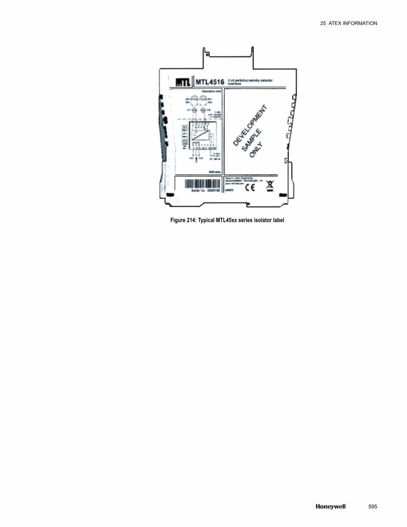
Figure 214: Typical MTL45xx series isolator label
25 ATEX INFORMATION
595
25.2 Isolators safety parameters
Table 142: MTL4500 safety parameters
Model Terminals V mA mWMTL4510 10.5 14 37
MTL4511 10.5 14 37
MTL4516 10.5 14 37
MTL4517 10.5 14 37
MTL4521 25 14 37
MTL4541 28 93 651
MTL4544 28 93 651
MTL4546C 28 93 651
MTL4549C 28 93 651
MTL4599 Non-energy storing
MTL4575 5 & 6 Non-energy storing
1& 2 7.2 8 144
config Vi = 11.2 Li = 12 Pi = 280
Vo = 7.2 Lo = 14.5 Po= 26
25 ATEX INFORMATION
596 www.honeywell.com

26 Notices
TrademarksExperion®, PlantScape®, SafeBrowse®, TotalPlant®, and TDC 3000® are registered trademarks of HoneywellInternational, Inc.
OneWireless™ is a trademark of Honeywell International, Inc.
Other trademarksMicrosoft and SQL Server are either registered trademarks or trademarks of Microsoft Corporation in theUnited States and/or other countries.
Trademarks that appear in this document are used only to the benefit of the trademark owner, with no intentionof trademark infringement.
Third-party licensesThis product may contain or be derived from materials, including software, of third parties. The third partymaterials may be subject to licenses, notices, restrictions and obligations imposed by the licensor. The licenses,notices, restrictions and obligations, if any, may be found in the materials accompanying the product, in thedocuments or files accompanying such third party materials, in a file named third_party_licenses on the mediacontaining the product, or at http://www.honeywell.com/ps/thirdpartylicenses.
597

26.1 Documentation feedbackYou can find the most up-to-date documents on the Honeywell Process Solutions support website at:
http://www.honeywellprocess.com/supportIf you have comments about Honeywell Process Solutions documentation, send your feedback to:
[email protected] this email address to provide feedback, or to report errors and omissions in the documentation. Forimmediate help with a technical problem, contact your local Honeywell Process Solutions Customer ContactCenter (CCC) or Honeywell Technical Assistance Center (TAC) listed in the “Support and other contacts”section of this document.
26 NOTICES
598 www.honeywell.com
26.2 How to report a security vulnerabilityFor the purpose of submission, a security vulnerability is defined as a software defect or weakness that can beexploited to reduce the operational or security capabilities of the software.
Honeywell investigates all reports of security vulnerabilities affecting Honeywell products and services.
To report a potential security vulnerability against any Honeywell product, please follow the instructions at:
https://honeywell.com/pages/vulnerabilityreporting.aspx
Submit the requested information to Honeywell using one of the following methods:
• Send an email to [email protected].
or• Contact your local Honeywell Process Solutions Customer Contact Center (CCC) or Honeywell Technical
Assistance Center (TAC) listed in the “Support and other contacts” section of this document.
26 NOTICES
599
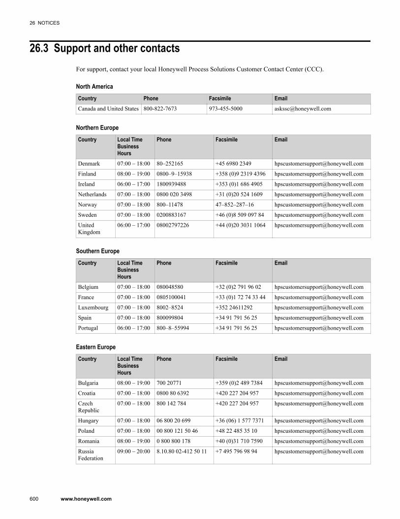
26.3 Support and other contactsFor support, contact your local Honeywell Process Solutions Customer Contact Center (CCC).
North America
Country Phone Facsimile EmailCanada and United States 800-822-7673 973-455-5000 [email protected]
Northern Europe
Country Local TimeBusinessHours
Phone Facsimile Email
Denmark 07:00 – 18:00 80–252165 +45 6980 2349 [email protected]
Finland 08:00 – 19:00 0800–9–15938 +358 (0)9 2319 4396 [email protected]
Ireland 06:00 – 17:00 1800939488 +353 (0)1 686 4905 [email protected]
Netherlands 07:00 – 18:00 0800 020 3498 +31 (0)20 524 1609 [email protected]
Norway 07:00 – 18:00 800–11478 47–852–287–16 [email protected]
Sweden 07:00 – 18:00 0200883167 +46 (0)8 509 097 84 [email protected]
UnitedKingdom
06:00 – 17:00 08002797226 +44 (0)20 3031 1064 [email protected]
Southern Europe
Country Local TimeBusinessHours
Phone Facsimile Email
Belgium 07:00 – 18:00 080048580 +32 (0)2 791 96 02 [email protected]
France 07:00 – 18:00 0805100041 +33 (0)1 72 74 33 44 [email protected]
Luxembourg 07:00 – 18:00 8002–8524 +352 24611292 [email protected]
Spain 07:00 – 18:00 800099804 +34 91 791 56 25 [email protected]
Portugal 06:00 – 17:00 800–8–55994 +34 91 791 56 25 [email protected]
Eastern Europe
Country Local TimeBusinessHours
Phone Facsimile Email
Bulgaria 08:00 – 19:00 700 20771 +359 (0)2 489 7384 [email protected]
Croatia 07:00 – 18:00 0800 80 6392 +420 227 204 957 [email protected]
CzechRepublic
07:00 – 18:00 800 142 784 +420 227 204 957 [email protected]
Hungary 07:00 – 18:00 06 800 20 699 +36 (06) 1 577 7371 [email protected]
Poland 07:00 – 18:00 00 800 121 50 46 +48 22 485 35 10 [email protected]
Romania 08:00 – 19:00 0 800 800 178 +40 (0)31 710 7590 [email protected]
RussiaFederation
09:00 – 20:00 8.10.80 02-412 50 11 +7 495 796 98 94 [email protected]
26 NOTICES
600 www.honeywell.com
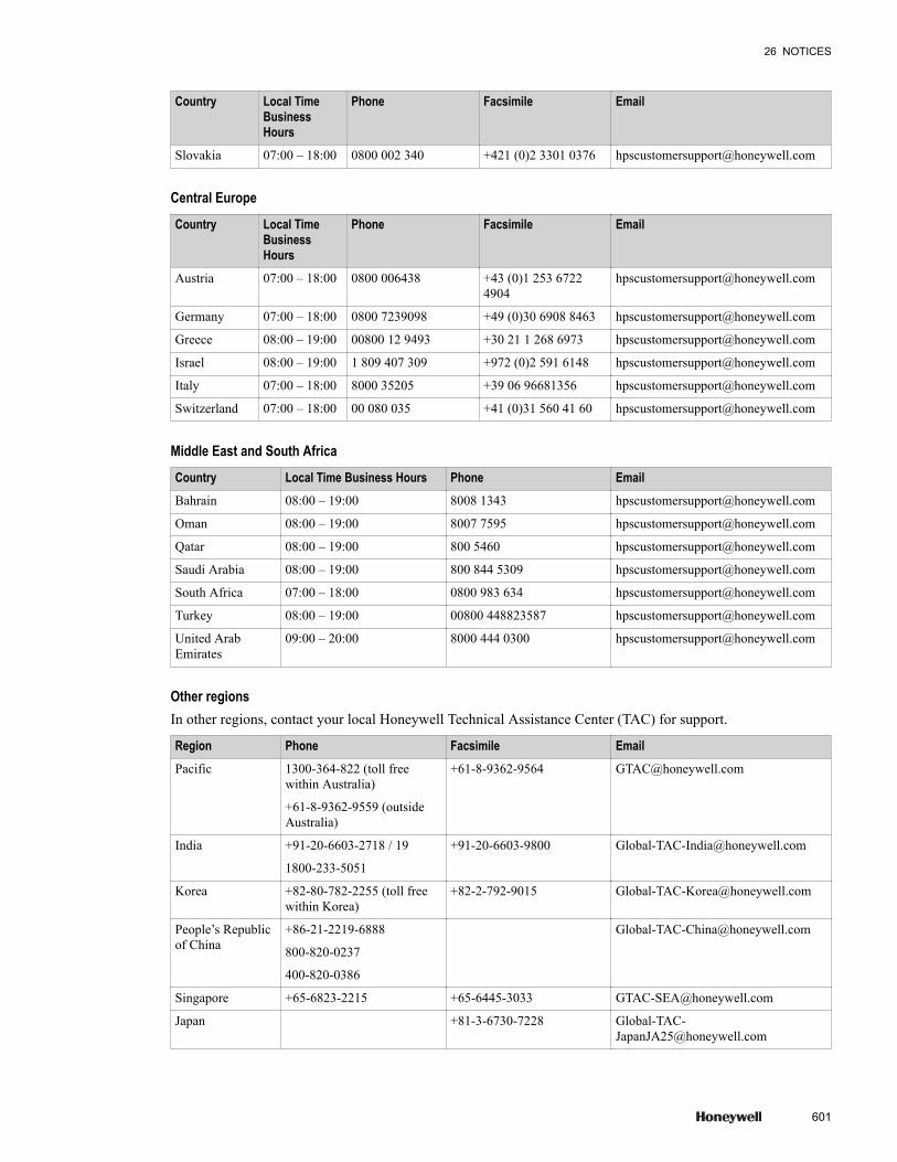
Country Local TimeBusinessHours
Phone Facsimile Email
Slovakia 07:00 – 18:00 0800 002 340 +421 (0)2 3301 0376 [email protected]
Central Europe
Country Local TimeBusinessHours
Phone Facsimile Email
Austria 07:00 – 18:00 0800 006438 +43 (0)1 253 67224904
Germany 07:00 – 18:00 0800 7239098 +49 (0)30 6908 8463 [email protected]
Greece 08:00 – 19:00 00800 12 9493 +30 21 1 268 6973 [email protected]
Israel 08:00 – 19:00 1 809 407 309 +972 (0)2 591 6148 [email protected]
Italy 07:00 – 18:00 8000 35205 +39 06 96681356 [email protected]
Switzerland 07:00 – 18:00 00 080 035 +41 (0)31 560 41 60 [email protected]
Middle East and South Africa
Country Local Time Business Hours Phone EmailBahrain 08:00 – 19:00 8008 1343 [email protected]
Oman 08:00 – 19:00 8007 7595 [email protected]
Qatar 08:00 – 19:00 800 5460 [email protected]
Saudi Arabia 08:00 – 19:00 800 844 5309 [email protected]
South Africa 07:00 – 18:00 0800 983 634 [email protected]
Turkey 08:00 – 19:00 00800 448823587 [email protected]
United ArabEmirates
09:00 – 20:00 8000 444 0300 [email protected]
Other regionsIn other regions, contact your local Honeywell Technical Assistance Center (TAC) for support.
Region Phone Facsimile EmailPacific 1300-364-822 (toll free
within Australia)
+61-8-9362-9559 (outsideAustralia)
+61-8-9362-9564 [email protected]
India +91-20-6603-2718 / 19
1800-233-5051
+91-20-6603-9800 [email protected]
Korea +82-80-782-2255 (toll freewithin Korea)
+82-2-792-9015 [email protected]
People’s Republicof China
+86-21-2219-6888
800-820-0237
400-820-0386
Singapore +65-6823-2215 +65-6445-3033 [email protected]
Japan +81-3-6730-7228 [email protected]
26 NOTICES
601

World Wide WebHoneywell Process Solutions support website:
http://www.honeywellprocess.com/support
ElsewhereContact your nearest Honeywell office.
26 NOTICES
602 www.honeywell.com

26.4 Training classesHoneywell holds technical training classes on Experion PKS. These classes are taught by experts in the field ofprocess control systems. For more information about these classes, contact your Honeywell representative, orsee http://www.automationcollege.com.
26 NOTICES
603

26 NOTICES
604 www.honeywell.com


