
Experimental Study on Electromigration by Using Blech ...
90
Experimental Study on Electromigration by Using Blech Structure by Yaqian Zhang A thesis submitted to the Delft University of Technology in partial fulfillment of the requirements for the degree of Master of Science in Electrical Engineering to be defended publicly on Monday, August 24 st , 2020 at 03:00 PM. Thesis committee: Prof. dr. ir. G. Zhang Dr.ir. S. Vollebregt Dr.ir. O. Isabella Prof. dr. ir. Xuejun Fan Ir. Zhen Cui
Transcript of Experimental Study on Electromigration by Using Blech ...

Experimental Study on Electromigration
by Using Blech Structure
by
Yaqian Zhang
A thesis submitted to the Delft University of Technology in partial fulfillment
of the requirements for the degree of
Master of Science in Electrical Engineering
to be defended publicly on Monday, August 24st, 2020 at 03:00 PM.
Thesis committee: Prof. dr. ir. G. Zhang
Dr.ir. S. Vollebregt
Dr.ir. O. Isabella
Prof. dr. ir. Xuejun Fan
Ir. Zhen Cui

I
Abstract
In the advanced semiconductor industry, modern electronic devices are expected
to realize complex functions with minimized size, which requires an increase in the
density of on-chip interconnects. To meet this demand, the dimension of interconnects
is reduced and it requires the narrowing of metal interconnects to carry the increasing
current density. With such a developing trend, electromigration is one of the significant
reliability challenges for electronic devices. Although lots of works focus on the
formulation and simulation for electromigration, they are not complete and consistent
with experimental results. Recently, A fully-coupled and self-consistent
electromigration theory was developed by Cui et al, but new and extensive experimental
data and analysis are needed to further validate their theoretical results.
This research work focuses on the experimental study on electromigration (EM),
and the aim is to investigate the different effects on EM. The Blech structure was
proposed as our experimental structure. The fabrication of Blech structure is conducted
at the EKL cleanroom, and main structures with various dimensions are fabricated by
employing sputtering technique for deposition and lithography for defining patterns.
The measurement is carried out by accelerated tests with high current stress and at
elevated temperature. Experimental results are characterized and analyzed by different
tools, such as Keyence 3D laser profilometer and scanning electron microscope
With the current density of 1 × 10¹⁰𝐴/𝑚2 and temperature of 250 , the result
shows that the critical length under certain conditions is 10 μm, and longer stripes have
larger drift lengths and a shorter time to form voids in electromigration. Furthermore,
it is found that with elevated temperature, the drift length increases and the
electromigration lifetime decreases. In addition, the covered SiN passivation layer only
for the annealed Al stripes suppresses electromigration and this is because the annealing
process improves the coalescence of grain in Al film, reducing the defects at the grain
boundary and finally forming a denser microstructure. The influence of the atmosphere
on electromigration indicates that the additional oxide on Al interconnects increases
that actual current stress and results in a short electromigration lifetime. In general,
present experimental results were consistent with existing results in the literature, but
several problems are still unsolved, which will be part of our future work.
Keywords: electromigration, aluminum, Blech structure, reliability, interconnects.

II
III
Acknowledgments
When I write this final part of my thesis, I realize that my two-year master study at
Delft University of Technology is almost to end. I still remember the first time I came
to Delft with the beautiful sunset and visited the campus full of excitement. I have
benefited a lot from these two years of study, while it could not have been made possible
without the help of many others. Thanks to their company and support, I can
successfully finish my studies.
First of all, I want to express my sincere gratitude towards my supervisors and
promotors Prof. Guoqi Zhang and Prof. Xuejun Fan for their encouragement, valuable
advice, and for giving me an opportunity to explore the field of electromigration. I
would especially want to thank Prof. Fan for his rigorous attitude in scientific research,
which influenced me a lot.
I am really grateful to my daily supervisors dr.ir. S. Vollebregt and MSc Zhen Cui.
Thanks for their patience, nice discussion about obtained results, and the support for
my thesis, from the structure of the thesis to the revision of each chapter, which helped
me a lot. Here, a special thank goes to Cui for encouraging and supervising me every
day, besides, without his wonderful simulation results, I could not successfully finish
my work.
For this project most of the time I worked in the cleanroom, so I want to thanks all
EKL engineers, but especially Tom Scholtes for his support on cleanroom processing
and useful advice when I got stuck. I also thank Robert Verhoeven for providing me a
part-time job in EKL which has enriched my campus experience.
I want to express my gratitude to ECTM researchers who helped me. I would first
thank dr.ing. H.W. van Zeijl for discussion the obtained results and fixing errors in the
cleanroom. I will never forget the help received from my colleges and friends, Jiarui
Mo, Dong Hu, Dayang Xiao, Jord Claessen, Mahdieh Shojaei Baghini and dr. B.
Morana, especially thank Jiarui Mo, Dong Hu for supports on my work and life. Thanks
to their accompany and encouragement, I could keep a good attitude all the time.
Finally, the greatest thank goes to my parents for their support and understanding.
They always stand by my side and care about my health, especially during the pandemic
of coronavirus. I think they are the source of my faith and power.
Delft, August 2020
Yaqian Zhang

IV

V
Content
Chapter 1. Introduction ....................................................................................................................... 1
1.1 What’s electromigration .............................................................................................. 1
1.2 History of EM research ............................................................................................... 3
1.3 Goal and objectives ..................................................................................................... 5
1.4 Outline ......................................................................................................................... 5
Chapter 2. Review of EM in Micron-Scale Interconnect ...................................................... 8
2.1 Theory of electromigration .......................................................................................... 8
2.2 Experimental studies ................................................................................................. 11
2.3 Failure analysis of electromigration .......................................................................... 19
Chapter 3. Structure Design and Fabrication....................................................................... 23
3.1 Test structures review ................................................................................................ 23
3.2 Structure design ......................................................................................................... 26
3.3 Fabrication process .................................................................................................... 37
Chapter 4. Measurement Procedure .................................................................................... 44
4.1 Measurement setup .................................................................................................... 44
4.2 EM test condition ...................................................................................................... 46
4.3 Test process ............................................................................................................... 47
4.4 Characterization methods .......................................................................................... 47
Chapter 5. Result on EM Tests ............................................................................................ 49
5.1 Design of experiment ................................................................................................ 49
5.2 Experimental study on the impact of conductor length on EM ................................. 50
5.3 Experimental study on the impact of temperature on EM ......................................... 53
5.4 Experimental study on the impact of annealing on EM ............................................ 56
5.4 Experimental study on the impact of the passivation layer on EM ........................... 59
5.6 Experimental study on the impact of oxide on EM ................................................... 62
Chapter 6. Conclusion and Future work .............................................................................. 66
6.1 Conclusion ................................................................................................................. 66
6.2 Recommendations and future work ........................................................................... 68
Appendices .......................................................................................................................... 70
A Process flowcharts ........................................................................................................... 70
Reference ............................................................................................................................. 79

6
1
Chapter 1. Introduction
1.1 What’s electromigration
Electromigration (EM) is an enhanced mass transport process caused by the
momentum transfer between electrons and metal atoms when the conductor is stressed
with a high electrical current density. This significant mass transport can cause the
depletion of atoms at the cathode side to form voids, and the accumulation of atoms at
the anode side to form hillocks, as shown in Figure 1.1. Finally, those voids and hillocks
can lead to the formation of open connections or short circuits of interconnects.
(a)
(b)

2
Figure 1.1. SEM graph of electromigration in the Al interconnect; (a) voids induced by
electromigration at the cathode side; (b) hillocks induced by electromigration at the anode side.
According to the International Technology Roadmap for Semiconductors (ITRS)
2014 Update [1-2], the density of on-chip interconnects increases from generation to
generation of modern integrated circuits. This requires the narrowing of metal
interconnects which will in turn have to carry an increasing current density, as shown
in Figure 1.2. This causes electromigration to become one of the significant reliability
challenges for electrical devices. To make matters worse, the decrease in cross-sectional
area of the interconnects also means a reduction in allowed critical sizes of voids within
the metal line, which will cause a reduction in allowed current densities for required
interconnect reliability. Furthermore, the total length of interconnects per IC will
continue to increase. As a consequence, reliability requirements per length unit of the
wires need to increase to maintain overall IC reliability. This development trend is
contradicted by the future decrease in interconnect reliability due to electromigration.
Thus, The ITRS states that not known solutions are available for the EM-related
reliability requirements that we will face in the near future (Figure1.2, red barrier). The
limitation of electromigration on interconnects can no longer be overlooked.
Figure 1.2. Evolution of required and maximum current densities in IC interconnect [1-2].

3
1.2 History of EM research
Before electromigration (EM) became one of the main reliability problems in the
modern integrated circuit industry, it has been for a long time only of academic
importance. As early as 1861, Gerardin observed the electromigration phenomenon [3].
Then, in 1959 Fiks first published his studies on electromigration [4]. Later that year,
Huntington and his group [5] found that electromigration was a process of mass
transport, caused by the momentum transformation between moving electrons and
metal ions, and they proposed that the electron wind is the driving force for
electromigration.
In later studies, people generally realized that electromigration is a complex multi-
physics process. In 2003, Arnaud [6] et al. found that a large temperature gradient
existed in the void-nucleation area. By experimental research, Nguyen et al. observed
that various temperature gradients of metal interconnects caused the difference of media
time to failure [7]. According to previous studies, Cher [8] and his co-workers analyzed
the effects of electronic wind, stress gradient and temperature gradient on a system of
interconnects, and concluded that the effect of temperature gradient on the formation
of voids is as important as the stress gradient. Besides, with the continuous development
of experimental technology, people start to investigate the electromigration in multi-
scale, such as micro-level and nano-level interconnects. Previously, it was thought that
only the dimensions and geometries of interconnects were influencing factors. However,
the microstructure of metal materials also plays an important role in the effect of
electromigration lifetime, which will be discussed in our work.
With the ongoing shrinking of the interconnection line-width of electronic devices,
people have found that using pure aluminum is not able to effectively solve this problem.
The Al interconnects containing 4% Cu were proved to have a better EM lifetime,
approximate 70 times higher than the life-time of pure Al [9]. The longest lifetime of
Al alloys was found with 12% Cu [10]. In addition to copper, magnesium, and
chromium alloyed with Al have been found to have a better electromigration resistance.
To meet the demand of complex multilayer structures and in order to reduce feature

4
sizes in integrated circuits, Al-based alloys have been replaced by lower electrical
resistivity materials. Copper has come to the attention of researchers, because of its
excellent electrical conductivity, which can improve the circuit speed, and provide more
reliability in ICs due to higher melting temperature and better current carrying
capability. The first company to apply copper as the interconnect material in their
products was IBM in 1997. After that, the Cu-based interconnects were widely used by
companies to improve chip density and performance. Due to different material
properties, the processing of aluminum- and copper-based interconnections are
significantly different. The damascene process technology is used for the fabrication of
copper-based interconnections[11-13]. And the key steps in this process are
electroplating technique and chemical mechanical polishing technique. Since the
electroplated copper has a larger grain size, resulting in bamboo or near bamboo
microstructure, the diffusion path along grain boundaries for atoms transport is reduced.
Thus, the surface or interface is the dominant diffusing path, improving the interface
properties of copper became an important way to suppress electromigration.
In addition, EM modeling also is important. V. Sukharev and his group [14-16]
simulated the electromigration process of multilayer interconnects and proposed a
physical model based on electromigration failure, which can be used to predict the
location of void nucleation. Later that year, the EM model was optimized by Cher [17]
et al. In this model, the vertical diffusion of Joule heat in the interconnect was
considered so that it can be used to more accurately predict the location of void
formation in narrow interconnects. However, the optimization of EM simulation models
never stops. F. Cacho [18] and others found that when considering the effect of the
atomic concentration gradient, the predicted EM lifetime corresponds to the real results.
In later years, the mathematical physical model of electromigration considering the
interaction of electronic wind, stress gradient, temperature gradient, and atomic
concentration gradient was proposed [19-20].

5
1.3 Goal and objectives
In the past few years, there have been many works focusing on the formulation and
simulation of electromigration. Although amazing development has been made on the
fundamental understanding of electromigration, these models are not able to be
consistent with experimental results. Recently, Zhen Cui et al. [21] developed a fully-
coupled and self-consistent electromigration theory, which includes the effects of the
gradients of concentration, stress, temperature, and the electron wind force. In his work,
1-D numerical solutions of a metal line under totally confined configuration and stress-
free configuration are provided. Although the predictions are consistent with the
original test data presented by Blech, new and extensive experimental data and analysis
are needed to further validate their theoretical predictions.
The main goal of the present work is to experimentally study the EM and provide
experimental data to validate our theoretical model. The objectives of the present work
are summarized as follows,
1. Build up a platform to conduct EM testing at the micro-level.
2. Investigate the effects of metal length on EM.
3. Investigate the effects of the passivation layer on EM.
4. Investigate the effects of testing temperature on EM.
1.4 Outline
In this thesis, the experimental study on electromigration by using Blech’s structure
is introduced, and the thesis consists of six chapters, a brief introduction of every
chapter is given as follows:
Chapter 2 is a review of electromigration study in micro-scale interconnection,
including the experimental studies on Al-based interconnects and the basic theory of
EM.
In Chapter 3, a brief review of the testing structure used for EM is given. Based on
Blech’s structure, the structure design in the present study is introduced. The fabrication

6
process is illustrated in detail.
Chapter 4 gives an introduction of measurement equipment and characterization
methods used in our work.
In Chapter 5, EM results with different variations of the structure are obtained. The
discussion, combining theoretical analysis and experimental results, are given.
After discussion experimental results, a conclusion will be drawn in Chapter 6, and
a recommendation for future work is given.

7

8
Chapter 2. Review of EM in Micron-Scale Interconnect
This chapter introduces the development of electromigration in pure metal
interconnects. In Section 2.1, a review of the theoretical studies on EM is given. The
experimental studies on EM are given in Section 2.2. In this section, the different
impacts on EM in the micro-level will be discussed and it includes the Al-based
metallization and Cu-based interconnects.
2.1 Theory of electromigration
Electromigration is a process of mass transport in the current-carrying metal wire
under the driving forces generated by an electric field. On a single metal ion, the net
electromigration force (𝐹𝑛𝑒𝑡 ) can be divided into two opposing microscopic forces.
These forces are called, direct force (𝐹𝑑𝑖𝑟𝑒𝑐𝑡) and ‘electron wind’ force (𝐹𝑤𝑖𝑛𝑑). The
direct force, also called electric field force, is an electrostatic force on a positive metal
ion in the opposite direction to the electron flow under the influence of an applied
electric field. The idea of the ‘electron wind’ was first proposed by F. Skaupy in 1914
[21]. The electrons, driven by the external field, in conductors are scattered by point
defects, and the resulting momentum transfer per unit time from scattering electrons to
the impurities leads to the so-called ‘wind force’.
The total electromigration driving force on a metal ion can be written as [22-25],
𝐹𝑛𝑒𝑡 = 𝐹𝑑𝑖𝑟𝑒𝑐𝑡 + 𝐹𝑤𝑖𝑛𝑑 = (𝑍𝑑𝑖𝑟𝑒𝑐𝑡 + 𝑍𝑤𝑖𝑛𝑑)𝑒𝐸 = 𝑍∗𝑒𝐸 (2.2)
where 𝑍∗ = 𝑍𝑑𝑖𝑟𝑒𝑐𝑡 + 𝑍𝑤𝑖𝑛𝑑 is referred to as the effective valence (or effective charge
number) and represents a parameter that comprises the quantum-mechanical effects of
the electromigration phenomenon, 𝑍𝑤𝑖𝑛𝑑 is related to the magnitude and the direction
of the momentum exchange between conducting electrons and point defects, 𝑍𝑑𝑖𝑟𝑒𝑐𝑡 is
the direct valence related to the nominal valence of the metallic ion when shielding
processes are absent, 𝑒 is the elementary charge, 𝐸 is the applied electric field. The
sign of the effective valence (𝑍∗) determines the nature of the transport mechanism.
The negative value in the equation means the transport direction is consistent with the
electron flow. The following Figure 2.1 shows the two opposing contributions of the
electromigration driving force.

9
Figure 2.1. Two opposing microscopic forces on a metal ion [25].
Finally, the atomic flux induced by the electrical field can be expressed as following
equation [25],
𝑱 =
𝐷𝐶𝑍∗𝑒𝐸
𝑘𝐵𝑇=
𝐷𝐶𝑍∗𝑒𝜌𝑗
𝑘𝐵𝑇
(2.2)
where 𝑘𝐵 is the Boltzmann’s constant, 𝑇 is the temperature, C is the atomic
concentration, 𝜌 is the resistivity, 𝑗 is the current density, and D is the diffusion
coefficient related to temperature as expressed in following Arrhenius equation,
𝐷 = 𝐷0exp (
−𝐸𝑎
𝑘𝐵𝑇)
(2.3)
where 𝐷0 is the pre-exponential factor and 𝐸𝑎 is the activation energy.
If a metal atom moves to the end of the metal line, under the impact of
electromigration, a vacancy will be left at the other end of the line [26]. Because of the
different volumes between atoms and vacancies, in the lattice site, volumetric
relaxations will occur [27], which results in a volume contraction caused by vacancy
accumulation at the cathode, on the other side, vacancy depletion produces a volume
expansion [28]. Thus, there is mechanical stress gradient along the interconnect length.
The stress caused by this gradient is so-called EM induced non-uniform stress [29-31],
also known as backflow stress. The direction of this atomic backflow is opposite to the
atomic flux induced by electromigration [30]. Therefore, under certain conditions, the
opposite flow equals the atomic flux due to electromigration, the damage will stop.
When the metal line is covered by the passivation layer or capping layer, there will
be mechanical constraints on the interconnect metal, which further results in the

10
evolution of mechanical stress. It was shown that different passivation materials have
different impacts on EM, it depends on the type of stress caused by passivation layers,
for example, the interfacial compressive stress will decrease the diffusion rate and
suppress the EM [32].
However, the backflow stress is not the only source of stress gradient, another
distribution is due to the difference in thermal expansion between the metal material
and surrounding materials [33-36].
Here, atomic flux induced by stress gradient can be expressed by the following
equation [8],
𝑱 = Ω
𝐷𝐶
𝑘𝐵𝑇
𝜕𝜎
𝜕𝑥
(2.4)
where Ω is atomic volume, 𝜎 is the hydrostatic stress.
In addition, the driving force induced by the temperature gradient is also an
important factor that needed to be considered in EM. One of the sources of the
temperature gradient is Joule heating in conductors. Joule heating is defined by the
process that the current passes through the electrical conductor and produces thermal
energy. Another source of the temperature gradient is the geometry of interconnects.
For example, line-via structures, the via and the testing line play different roles and
have different temperature. Lloyd [37] and Schwarzenberger et al. [38] confirmed the
correlation between temperature gradient and EM failure. The result indicated that at
the point with high temperature gradient, EM failure was typically observed, on the
other side, at the site with uniform temperature, the EM failure was randomly found.
During the accelerated EM test, it is quite easy to produce the temperature gradient by
Joule heating in interconnects.
The atomic flux from temperature gradient induced driving force can be expressed
as [8],
𝑱 = −
𝐷𝐶𝑄∗
𝑘𝐵𝑇2
𝜕𝑇
𝜕𝑥
(2.5)
where 𝑄∗ is the coefficient of heat transfer (eV).

11
Generally, from the above discussion, three different driving forces on EM are
introduced, including the electron wind force, stress gradient, and temperature gradient.
2.2 Experimental studies
To study the electromigration failure behavior, the usage of accelerated tests is
necessary, in which failure times are commonly less than 1000 hours. As indicated by
Black’s equation [39], the lifetime of an interconnect can be reduced by either
increasing the current density or by increasing the temperature. Usually, the EM tests
are carried out using simple structures. The commonly used structure includes the
Blech’s structure [29,30] the NIST (National Institute of Standards and Technology)
structure [40-42], the SWEAT (Standard Wafer-level Electromigration Acceleration
Test) structure [43], and the line-via test structure. The details of those structures will
be introduced in Sec. X. In the past decades, many experimental works demonstrated
that EM is a multi-physics problem that is controlled by various factors, including
mechanical stress, temperature, chemical potential.
2.1.1 The impact of mechanical stress
Blech was one of the first to explain the origin of the stress gradient during
electromigration [29,30], and such a force is commonly called “Back Stress”. In his
experiments [44], Al stripes were patterned on a TiN film, as shown in Figure 2.2.
Since Al has better conductivity than TiN, the load current mostly flows through the
Al stripes.
Figure 2.2. Blech testing structure
By experimental results, he indicated that the average drift velocity has a linear

12
correlation with the current density and found that the product of the strip length and
critical current density is constant which is called the threshold-length product. Here,
the critical current density means when the loading current density is below this value,
the drift cannot be detected. In order to figure out the influence factor of threshold
current density, he proposed the geometry of a series of Al lines with different lengths
(from 10 𝜇m to 100 𝜇m) deposited on the TiN layer, as shown in Figure 2.3. After
loading 3.7 × 10⁵ 𝐴/𝑐𝑚2 for 15h at 350 ˚C, the result showed that the threshold
current density has a negative relationship with strip length (for the length range from
30 𝜇m to 150 𝜇m). And under the same current density, the longer stripes show lager
voids at cathode. Then he carried out the measurement at a temperature between 200
to 550 and found that the threshold length product depends on temperature. In
addition, he also investigated the effect of covering layer on drift velocity of EM, and
from Figure 2.4, it showed that the entirely enclosed covering layer on Al stripes can
suppress electromigration.
Figure 2.3. SEM image of Al stripes with varying lengths after the passage of
3.7 × 10⁵ 𝐴/𝑐𝑚2 for 15 h.

13
Figure 2.4. Average drift velocity of covered and uncovered samples
Generally, Blech’s contribution to EM studies can be summarized by three concepts:
the ‘‘Blech Threshold’’, the ‘‘Blech Length’’, and the ‘‘Blech Condition’’.
Blech condition: To explain this phenomenon, Blech suggested that the
electromigration can be fully stopped when the driving force induced by the difference
of mechanical stress at two sides of strip exactly equals to the electron wind force, it
shows a balanced state, so-called Blech condition,
𝑍∗𝑒𝜌𝑗 + Ω
∆𝜎
∆𝑥= 0
(2.6)
Where Ω is the atomic volume, ∆𝜎 ∆𝑥 ⁄ is equal to ∆𝜎𝑥𝑥 which is the stress
difference, 𝑒𝑍∗is defined as the effective change, and 𝑗 is the loading current density.
Blech threshold: Integrating the above equation over the length of the metal line
and assuming the critical failure condition is the maximum stress that the metal line can
withstand, a critical product of metal line length and current density can be obtained as
follows,
(𝑗𝐿)𝑐 =
(𝜎𝑚𝑎𝑥 − 𝜎𝑚𝑖𝑛)Ω
𝑍∗𝑒𝜌
(2.6)
below which the electromigration flux can entirely be balanced by the stress-induced
counter flux of atoms at the steady-state condition. This critical product is called the
Blech product.

14
Blech length: For a certain current density, there exists a critical length (Lc) for an
Al stripe, below which, the mass transport of electromigration can totally be suppressed.
Currently, adding a barrier to divide the entire interconnect into several short segments
below “Blech length” is still used as a design rule for interconnects.
Later that year, in order to figure out the reason behind the drift flow behavior,
Blech designed a new structure with a large pad covered with Si3N4 [45]. After the
passage of 4.5 × 10⁵𝐴/𝑐𝑚2 for 19 hours at 350 , the aluminum atoms drift into
large contact pads, as shown in Figure 2.4 (left side). After placing this stripe at 350
without loading current for 762 hours, it was found that the aluminum atoms moved
back, as shown in Figure 2.5 (right side). This phenomenon can be explained by the
difference in free energy. During the current passage, the large pad serves as a reservoir
and elastically stores parts of the aluminum atoms, which causes the free energy
difference between the pad and the metal line. When the load is stopped, the uniform
stress creates the backflow and the edge of the aluminum film slowly moves to the
uncovered metal line.
Figure 2.5. Blech’s backflow experiments.
Except for the “back stress”, the thermal stress, resulting from the difference in
thermal expansion between the passivation and metal upon cooling from high
deposition temperatures, is the other source of mechanical stress. Numerous

15
experimental observations have shown [46] that tensile stress induced by thermal
mismatch increases the possibility of failure. The increased thickness and rigidity of the
passivation layer prevent the relaxation of thermal stress, which results in dielectric
cracking and metal extrusion.
2.1.2 The impact of microstructure
With continuous research on EM, people found that various crystal lattice structures
of metallization have different effects on the electromigration failure mechanism. The
most common microstructures in interconnects are polycrystalline, near-bamboo, and
bamboo, as shown in Figure 2.6 [47].
Figure 2.6. Three common microstructures in Al samples
From the above picture, the feature of the polycrystalline microstructure is mainly
based on its grain boundaries and the crystal lattice is dominant in Bamboo structures.
Generally, the crystal lattice structure of interconnects depends on the grain size or its
linewidth, for example, ‘bamboo’ microstructure is defined as the case that the
linewidth of interconnects is less than its grain size.
Numerous studies indicated that there is a certain relationship between grain size
and EM lifetime, for example, J. Cho and C. V. Thompson observed that the median
time to failure can be affected by the ratio of grain size and linewidth [48]. The bamboo
structure of metal interconnects provides a better improvement of EM reliability, which
is because in the structure there are fewer grain boundaries and no continuous diffusion
paths that are used for atoms transport exist in the direction of the current flow. As a

16
result, the vacancy nucleation time is prolonged and the EM lifetime is increased. The
related literature analyzed the influence of the diffusion path on the reliability of EM
by studying different microstructures of interconnect, which further verifies the
previous conclusion [49].
2.1.2 The impact of the metal interface
The main diffusion paths in metallic interconnect include bulk diffusion, grain
boundary diffusion, and interface diffusion. As shown in Table 2.1, the different
diffusion paths show different activation energies for atomic diffusion in Cu
interconnects.
Table 2.1. The activation energy of different diffusivity paths in Cu interconnects [50].
From Table 2.1, the diffusion path along the Cu surface has the lowest activation
energy and the activation energy for diffusion in the bulk is the highest. The interface
between copper and the capping layer is known to be the dominant diffusion pathway
in damascene interconnects [51]. Hence, improving interface characteristics is an
effective way to suppress EM in interconnects. This was demonstrated in many
experiments that narrow copper stripes with capping layer and passivation have longer
EM lifetime [5]. In general, there are two methods to achieve it, using chemical reaction
[52-54] or physical treatment [55] to remove Cu oxides, and adding different capping
layers on the copper surface.
Surface treatments can be divided into two categories, physical removal, and
chemical reaction. Normally, Ar sputtering process is used for physical cleaning and
oxidation-reduction reaction under the plasma process is the principal of chemical
treatment.
Adding a capping layer, such as SiN and SiC, etc., on the top of copper has a

17
positive effect on the adhesion properties of the interconnect surface and they directly
influence the rate of EM. It could be simply explained that the transport of atoms along
a tightly bonded interface is more difficult and the harder the transport is, the slower
diffusion will be. The experimental result from M.W. Lane and his group [56] verified
that interfacial diffusion can be suppressed by adhesion and reactive bonds at the
interface. Therefore, a series of experiments about the capping layer on copper wires
have been carried out.
Hu, C-K, and his coworkers investigated the effect of copper lines covered with
Ta/TaN, SiNx, and SiCxNyHz layers [57]. The result showed that a Ta/TaN metal
capping layer has a better influence on lifetime and the activation energy increases from
0.87 eV for the bare metal interconnect to 1.4 eV.
Figure 2.7 shows the resistance change of samples with different capping layers
such as Pd, CoWP, and CoSnP, and uncoated samples over time [58]. For bare metal
lines, the resistance sharply increases in less than 200 hours but increases significantly
slower for covered samples; after 2200 hours the resistance only increased by 10%. It
is clear that the capping layer significantly prolongs the electromigration lifetime. From
Energy-Dispersive X-ray Spectroscopy (EDS) figures, it shows the signal of Cu enters
the CoWP layer, in other words, a small amount of Cu atoms is combined with CoWP.
It can be considered that the CoWP layer effectively suppresses the diffusion of
electromigration along with the interface and improves the electromigration life.

18
Figure 2.7. The resistance change of samples with or without a passivation layer
Finally, Yan, M.Y. et al. [59] studied the effect of Cu surface coated with 20 nm
Cu3Sn metal layer. The result showed that the metal coating layer can effectively
suppress the diffusion of Cu atoms along the surface, and increase the electromigration
lifetime by an order of magnitude.
2.1.3 Current crowding effect
Normally, when atoms are in a region with higher current density, the atomic
transport speed will be faster which results in the acceleration of void formation.
Corners are typically a current crowding zone, especially corners with a right angle,
where current density can be extremely high.
The first FEM simulation on the current crowding effect with 2D structures was
carried out by Kwok and his coworkers [60]. In his study, the current and temperature
distribution was given in a multi-level interconnect. In a stud structure, he found that
the aspect ratio of interconnects was related to current crowding, the narrower width
and the higher aspect ratio result in the increasing of current density. And in a via
structure, the current crowding is found to increase with an increasing step angle due to
the thinning down of the step cross-section, as shown in Figure 2.8, a cross-section of
a via structure with a step angle of 60°.
Figure 2.8. Cross-section view of a via structure
With the demand of complex structures in ICs, the simulation for 2D geometries are
not able to meet the requirement, a 3D FEM simulation on current crowding was given

19
by Weide et al. [61] In his work, the effect of different via shapes, such as the circular,
square and oval like via, on the peak current density was discussed. The results
indicated that the circular like via had the largest current density and the oval-like via
had the least current density. In addition, the experiment results showed that in a
traditional unfilled via, the electromigration lifetime depends on the diameter of the via
hole [62]. However, in a tungsten-filled via structure, the diameter no longer plays a
role and the reason is not clear. These two structures are shown in the following Figure
2.9.
Figure 2.9. Left: The structure of traditional non-filled via. Right: The structure of tungsten-
filled via [62].
Actually, in a current crowding area, since the current and temperature are coupled
in the interconnect, the temperature distribution is also inconsistent, which induces the
thermo-mechanical stress in corners. Hence, there are several effects in the
interconnect in the current crowding region.
2.3 Failure analysis of electromigration
The failure analysis typically is used for the sample after the accelerated EM test.
Various analytical methods can be used to realize failure analysis, such as the optical
microscope, scanning electron microscope (SEM), Focused ion beam (FIB-SEM),
transmission electron microscope (TEM), and electrical resistance measurement.
FIB-SEM is used for cutting the test sample and observe the cross-section of the

20
structure. The information about the surface topography of the sample is given by SEM.
The details about these two tools will be introduced in Chapter 4.
TEM has a better resolution than SEM, so for the sample of line-width below 0.2
mm TEM is the best choice. The working principle of TEM is similar to the light
microscope. The major difference is that light microscopes use light rays to focus and
produce an image while the TEM uses a beam of electrons to focus on the specimen, to
produce an image. In addition, for the very thin sample, the high energy beam from
TEM can shine through the sample, and the features such as the crystal structure and
features in the structure like dislocations and grain boundaries can be observed.
The electrical resistance measurement is used to determine the EM failure. Since
the change of resistance in metal line is found to be strongly dependent on voids
nucleation which is equivalent to a slight increase of resistance in experiments [63], we
can use the change of resistance to identify the degree of electromigration.
In order to study the electrical properties of metal interconnects the usage of
resistivity measurement techniques is necessary, in which the bulk resistivity is
commonly concerned. The bulk resistivity ρ of conductors or semiconductors depends
on carrier drift. According to Ohm's law, the conductivity is explained as the ratio of
current density to electric field intensity. Thus, by measuring the voltage drop along the
sample with the sourcing current is the fast method to calculate bulk resistivity of the
material. Unfortunately, for metal or other conductors, the magnitude of resistivity is
pretty low and this requires accurate measurement. The simplest way to test resistivity
can introduce potential errors such as contact resistance, noise and lead resistance. And
with the shrinking size of device structures, contact resistance becomes more
considerable, and eliminating the effect of contact resistance is crucial. Thus, there are
two main test methods still acceptable today, namely four point probe and Van der Pauw
technique, as shown in Figure 2.10, which are valid to minimize these errors.

21
(a)
(b)
Figure 2.10. (a) schematic of Four-Point Probe measurement; (b) schematic of Van der Pauw
method.

22

23
Chapter 3. Structure Design and Fabrication
In this chapter, a review of test structures used in electromigration will be
introduced at first. It includes the Blech test structure, NIST structure, SWEAT
structure and Line-via structure. Then a detailed discussion about all experimental
structures in our work is given, also the purpose of each designed structure is indicated.
3.1 Test structures review
3.1.1 Blech test structure
There are various types of test structures used in EM testing. One of the simplest
structures probably is “Blech’s structure”. As shown in Figure 3.1, the Al stripe is
directly patterned on the TiN film. As Al is a better conductor than TiN, the majority of
the current will detour from the TiN and go through Al stripes. By using this simple
structure, we can determine the critical length, critical threshold, and drift velocity
induced by electromigration.
Figure 3.1. Schematic of Blech structure. [44]
3.1.2 NIST structure
In 1987, considering the effect of the geometry of metal lines and temperature
gradients on EM lifetime, Schafft [64] designed a new structure for resistance
measurements, that is consist of a straight long line and four terminal structures, as
shown in Figure.3.2. In standard NIST guidelines, a metal stripe with a length more
than 800 um is suggested, to avoid the short line effect and thermal interferences from
two pads. However, in this structure, the inconsistent width of the pad and metal line

24
( ratio of width is 2 to 1 ) leads to two different microstructures within the device, i.e.
bamboo structure and cluster/ bamboo mixed structure, which results in mostly failures
presenting themselves at the end of the pad [65]. To avoid this, various modified test
patterns based on NIST structures were proposed later [66, 67], for example, the width
of the pads is much larger than the width of the metal lines. The other flaw of the NIST
test structure is that there are no significant macroscopic flux divergences and, therefore,
experiments always indicate unrealistically long times-to-failure.
Figure 3.2. Schematic of NIST structure. []
3.1.3 SWEAT structure
Another commonly used test structure for electromigration is the SWEAT structure
(Standard Wafer-level Electromigration Acceleration Test) proposed by B. J. Root and
T. Turner [68]. In this structure, a series of metal stripes with two different widths are
connected, as shown in Figure 3.3 [69]. Due to the inconsistency of the geometry, the
narrow lines show higher current density and temperature, in which electromigration
failure occurs. One of the advantages of such a structure is that it enables one to do
multiple EM tests in one case until one of the narrow lines fails. In addition, this
structure also can be modified to study the effect of current crowding on EM.

25
Figure 3.3. Schematic of SWEAT structure [69].
3.3.4 Line-via structure
Above-mentioned Blech, NIST and SWEAT test structures consist of a single level
planar metallization. However, in reality, a multilevel interconnection system is
required. For example, most of the copper-based metal interconnects use a line–via test
structure [70], as shown in Figures 3.4 and 3.5. The EM test on sample of Figure 3.4 (a)
is known as “M1 testing” and EM test on sample of Figure 3.4 (b) is known as “M2
testing”. The dummy lines are used to conduct electrical current to the testing line. For
the M1 testing line, the voids occur at the anode side. For the M2 testing line, the voids
may occur at the bottom of the via or the end of the line and via. For three level line-
via structure, as shown in Figure 3.5, the different current conditions may cause voids
formation at various places.
(a) (b)
Figure 3.4. Cross-section view of Line-via structure [70].

26
Figure 3.5. Cross-section view of Line-via structure with three levels [70].
3.2 Structure design
By comparing those popular structures used in the EM test and considering our
fabrication capability, the Blech structure is selected in the present work. The layout of
the mask design in this work is shown in Figure 3.6. Various structures are designed to
investigate various influential factors for electromigration, such as the effects of
mechanical stress, the microstructures of metal materials, the interface/surface of the
interconnects, the boundary condition, and current crowding on electromigration.

27
Figure 3.6. Top view of mask design.
In general, the structure consists of a Si layer, SiO2 layer, TiN layer, and Al
layer, as shown in the following Figure 3.7. The silicon dioxide layer is patterned
on the silicon surface because the oxidation layer performs a good adhesion to
silicon and provides an excellent electrical isolation layer for the structure. A
conducting layer is required at the bottom of the Al film and its resistivity should
be higher than the testing wire. Besides, a barrier layer is needed to avoid the
atomic diffusion between the dioxide surface and the Al layer. Compared with
different materials, the titanium nitride layer is selected as the inter-media layer
between Al and SiO2.

28
Figure 3.7. Cross-section view of our structure
3.2.1 The structure to measure the drift length
Figure 3.8 shows the structure to measure the drift length. It consists of two parts,
metal pads and test lines. To obtain good repeatability and statistics analysis, the long
test line is composed of Al stripes repeated five times. In order to avoid forming voids
within two big contact pads, the size of the pads is much wider than the metal strip.
Besides, a contact pad with a 45-degree bevel is applied to prevent current crowding
effect.
In the present study, various dimensions of the structure are designed, as
summarized in Table 3.1. First, to investigate the effect of Al length on void length
induced by EM, Al stripes with four different lengths, 10 µm, 30 µm, 60 µm and 100
µm are designed. Second, to determine the critical length of electromigration, Al stripes
with 5 µm, 10 µm, 15 µm, 20 µm and 25 µm are designed. Thirdly, to further investigate
the effect of width on electromigration, four different widths: 3 µm, 5 µm, 10 µm and
15 µm, are included in our design. In addition to variations of the width and the length
of the stripes within a single die, the thickness of the testing line is also varied using
different wafers, in order to study its impact on electromigration. As the grain size of
aluminum is ~ 300 nm, we choose 200 nm, 400 nm, 600 nm as the thickness of the Al
metal layer to obtain different microstructures, i.e. bamboo structure and near bamboo
structure.
Table 3.1. Dimensions design of our structure

29
Factor
Length (µm) 5 10 15 20 25 30 60 100
Width (µm) 3 5 10 15
Thickness (nm) 200 400 600
Figure 3.8. Top view of the structure used for drift length investigation
3.2.2 The structure to investigate the effect of the passivation layer
Apart from the classical Blech’s structure, the structure that includes a bare Al stripe
and an Al stripe covered by Si3N4 in the same line is added in our mask, to investigate
the effect of the passivation layer on EM within a single experiment. As shown in Figure
3.10 (a), the right part of the metal line is completely covered by a passivation layer
and the other side is exposed. For Figure 3.10 (b), a partly covered aluminum stripe and
a bare Al strip are given. In section 5.4, the effect of the passivation layer on EM will
be discussed.

30
(a)
(b)
Figure 3.10. The structures for investigation passivation layer on EM: (a) completely covered
structure (b) partly cover structure.
3.2.3 The structure to investigate the effect of boundary conditions on EM
The diffusion boundary condition is one of the important factors on EM. Figure
3.11 (a) and (b) show structures with two different diffusion boundary conditions, 𝐽𝑎=
0 and 𝐽𝑎 = 𝐶(constant), respectively. The length of the Al stripe is 800 𝜇m and the
width is 5 𝜇m. For the structure shown in Figure 3.11 (b), two large pads are directly
connected to the metal strip, playing a role as a reservoir for atomic diffusion. Thus, the

31
atomic flux in the metal interconnect is the same as in the metal pad.
(a)
(b)
Figure 3.11. (a) The structure of metal strip with atomic flux 𝐽𝑎 = 0; (b) The structure of
metal stripe with atomic flux 𝐽𝑎 = Constant.
3.2.4 The structure to investigate the effect of current crowding
In our measurements, a relatively large loading current density is applied, which
may cause a local temperature increase and can bring unexpected instability to the

32
system. To analyze this effect, a simulation with COMSOL was carried out, where the
current density was simulated with three different geometries of the contact pads, pads
with a right angle, with 45-degree bevel and with fillets (Figure 3.12 (a), (b) and (c),
respectively). The simulation results show that the contact pads with fillets can
effectively suppress the current crowding effect. Thus, we also included the following
three structures to investigate such effects on electromigration.
(a)
(b)

33
(c)
Figure 3.12. (a)The structure of contact pads with right angle; (b) The structure of contact
pads with 45-degree bevel; (c) The structure of contact pads with fillets.
3.2.5 The structure to investigate the effect of non-uniform current density
By altering the width of the metal lines, we could obtain a non-uniform current
density in the whole stripe, as shown in Figure 3.15.
(a)
(b)

34
Figure 3.15. (a) The structure of triangle metal strip; (b) The structure of ladder-shaped
metal strip.
3.2.6 The structure to in-situ measure the resistance
All the previous structures only allow for measuring the voltage over the entire line.
In our work, the four-point probe structure is used to monitor the resistance change of
Al stripes during electromigration. This structure consists of contact pads, test stripes
and connecting wires, in which two large pads at the end of the stripe are connected to
the ammeter to provide required current, and the voltage drop is measured by the two
other pads. Since the input resistance in the voltmeter is large, the voltage drop on the
connecting wires can be disregarded. The load current only flows through the pads at
the end of the metal stripe, as shown in Figure 3.16. The metal pad is designed to be
300 × 300 𝜇𝑚2, And the test line is designed with four different lengths, 10 µm, 30
µm, 60 µm and 100 µm.
Figure 3.16. Four-point resistor test structure
3.2.7 The structure to measure the sheet and contact resistances
For the sheet resistance measurement of different layers, the Van der Pauw structure
is employed, as shown in Figure 3.17.

35
Figure 3.17. Van der Pauw resistor test structure.
Since the titanium nitride also serves as a part of the conductor line, the contact
resistance between test stripes and titanium nitride becomes one of the important
electrical properties. Due to complex components, the theoretical calculation of contact
resistance cannot be accurate. Thus, we chose two main test structures, a Cross Kelvin
test structure and transmission line model test structure, to directly achieve this
measurement. As shown in Figure 3.18, in the Cross Kelvin structure two different
metal layers are stacked together on the isolation layer with a contact area connecting
them.

36
Figure 3.18. Cross Kelvin test structure
The specific contact resistance is given by,
𝜌𝑐 = 𝑅𝑐𝐴𝑐
(3.1)
Where 𝐴𝑐 is the area of contact window and 𝑅𝑐 is contact resistance measured by
Ohm’s law.
The structure of the transmission line model is shown in Figure. 3.8 Similarly with
Kelvin structure, given the width (W) of metal strip and the distance (𝐿𝑖) between two
adjacent contacts, when contact resistance (𝑅𝑐) can be expressed by,
𝑅𝑖 =𝜌𝑠𝐿𝑖
𝑊+ 2𝑅𝑐
(3.2)
Where 𝜌𝑠 is layer sheet resistivity, 𝑅𝑖 is resistance changes between two adjacent
contacts.

37
Figure 3.19. TLM test structure
3.3 Fabrication process
The fabrication steps to prepare the samples are presented here. The Blech’s
structure is mainly composed of three layers from bottom to top, connecting layer (TiN),
conductor layer and the passivation layer. Hence, three different masks are prepared
during the fabrication step.
3.3.1 The basic techniques
All fabrication steps are completed in the cleanroom of EKL. The basic fabrication
techniques used in our process are,
1. Photolithography
The photolithography technique is based on the principle of optical-chemical
reaction. Essentially, the process of the photoresist (photosensitive material)
serves as the intermediation to transfer image information from the photomask
to wafers. Three main steps are included in this technique: coating, exposure
and developing. In our work, we use an EVG120 to automatically complete
coating and development steps and the wafer stepper (ASML PAS 5500/80) is
used to create 52 dies of the same patterns on one wafer.
2. Etching

38
The pattern etching is an important step in the interconnection technology of
integrated circuits. The purpose of this step is to form the required pattern by
selectively removing the material in the unmasked area. The main etching
methods are wet etching and dry etching. Wet etching is an isotropic process by
using liquid chemicals or etchants to remove material. Due to its property, it is
not easy to control the time to accurately pattern without removing material
underneath the masked area. However, this process has a high selectivity and
etching rate.
On the other side, dry etching is anisotropic, which means etching only occurs
in the vertical direction. The advantages of dry etching are accurate control of
pattern size and automatic detection of the etching endpoint. Primarily, dry
etching can be divided into three types by different reaction methods. Plasma
etching and reactive ion etching (RIE) are common techniques used in
semiconductor manufacturing. In our work, wet etching is used for aluminum
layer and patterns on the titanium nitride layer are transferred by dry etching,
the same is used for the contact openings of the passivation layer. Here the
reason we use wet etching to pattern Al is that the etching selectivity to TiN is
limited.
3. Chemical vapor deposition
Chemical vapor deposition technology is a process that uses gas or vapor
mixture to generate chemical reactions and transport reactions on a substrate
then deposit thin film. Commonly used CVD methods are plasma chemical
vapor deposition (PECVD) and low pressure chemical vapor deposition
(LPCVD). In the LPCVD technique, the high temperature is adopted to form
high-quality film, on the other side, deposition temperature in the PECVD
process is much lower but the deposited film has a poor step coverage compared
to LPCVD process. In our work, considering the melting temperature of
aluminum we choose the PECVD technique to grow the passivation film.
4. Sputtering
The sputtering deposition is one of physical vapor deposition (PVD) process

39
techniques, and it is widely used in the semiconductor industry. In this process,
the ions generated by gas discharge bombard a metal target by applying an
electric field, so that the atoms or molecules of the target are knocked out and
are deposited on the substrate surface. Argon is commonly used as the sputtering
gas and RF or DC is applied power, during the process. In our work, we use
Radio Frequency (RF) sputtering for the growth of pure aluminum And for the
deposition of the TiN layer, the reactive sputtering with N2 and Ar is employed.
3.4.2 Process flow
The process starts from a p-type 525 𝜇 m single side polished wafer that is
commonly used as a test wafer in the cleanroom. To provide markers for subsequent
exposure steps, the standard zero-layer process is necessary. A SiO2 layer is deposited
on the wafer surface to be served as an isolation layer, as shown in Figure 3.20. Since
the quality of the oxidation layer is not important in our process, the wet oxidation
technique is selected to reduce processing time, and the desired thickness is 300 nm.
Figure 3.20.
Next, the titanium nitride layer is deposited on the SiO2 layer at 300 by using
reactive sputtering, as shown in Figure 3.21. In this process, the reactive gas (N2) and
vapor phase titanium react to form the titanium nitride at the vacuum chamber. This
process also forms TiN at the target, which can cause the formation of a non-uniform
concentration between the top wafer and the bottom wafer in a batch. In order to avoid
this problem, a dummy wafer is added after each processed wafer with a clean recipe
e.g. Ti_in_Between_300C. Then the pattern is transferred by using photolithography
and dry etching. The etching process is realized by plasma etcher Omega 201 with the

40
recipe “TINTISVO”, the etching time can be calculated by recent etching data from the
logbook.
Figure 3.21.
Referring to Figure 3.7, the metal interconnect layer is on the top of the TiN layer.
During the measurement, the loading current first flows through TiN and then goes
through the Al line, so it is important to form a good contact interface between TiN and
Al to reduce the contact resistivity. According to research by S. Logothetidi et al. the
oxidation layer is formed on the TiN layer surface even in the room temperature, so
before Al deposition, a hot sputtering etch (HSE) process is used to remove the oxide.
This step is used not only for etching but also for pre annealing. Then the wafer is
transferred to another chamber where 200 nm pure aluminum is deposited at 300 .
The patterning process is performed after deposition to form the structure of
interconnect lines and contact pads, as shown in Figure 3.22. The etchant normally used
for this is PES 77-19-04 and the etching rate is approximately 170 nm/min.
Figure 3.22.

41
The deposition of the passivation layer is a required step for some impacts
investigation. As shown in Figure 3.23, the Si3N4 is deposited by PECVD with a mixture
of N2, SiH4 and NH3 at a temperature of 400 and the process pressure is 2.8 Torr.
Referring to the logbook, the deposition time is calculated. After the Si3N4 deposition,
the patterning of the Si3N4 layer is obtained by using the third mask to form contact
openings on the pads.
Figure 3.23.
Due to the limitation of measurement devices, our test process only can be done
with small chips. So the dicing process is used and diced chips are 10 × 10 𝜇𝑚 size.
In order to protect the aluminum from damage during process, a UV protect foil is used.
The following picture (Figure 3.24) shows the diced chip.
Figure 3.24. The diced chip

42

43

44
Chapter 4. Measurement Procedure
In this chapter, the preparation of the EM test is introduced, including the
measurement setup, test process, the condition of EM accelerated test and the
characterization methods.
4.1 Measurement setup
Under the normal working conditions, the electromigration process in interconnects
is very slow, typically the lifetime is from several years to several decades. It is quite
difficult to effectively estimate the lifetime and reliability of interconnects in a short
time under the conventional loading condition. Thus, an accelerated test is adopted. The
accelerated test is a method that shortens the experiment periods by increasing stressing
conditions without changing the failure mechanism. In this work, we need a setup that
is able to provide the high current density and high temperature in order to accelerate
failure. Temperature and current density are typically used as accelerated factors for the
EM test and it is confirmed that altering these two factors will not change the failure
mechanism. It is known that the bare aluminum is easy to react with oxygen and form
the native oxide layer on the surface at room temperature, in addition, at elevated
temperatures it is possible to form additional oxidation which is undesired in our work.
Thus, a vacuum pump is required to create a vacuum test condition. The measurement
setup is consist of three parts:
1. A micro probe station (MPS): NEXTRON MPS is used for the in-situ
measurement of electrical and optical properties of the devices. Three parts are
included in the MPS, a hotplate, a pressure chamber and four micro-probes, as
shown in Figure 4.2. The hotplate is connected to a temperature control via a
computer and provides a working temperature up to 750 . Due to the limited
volume of the pressure chamber, only the die-level samples can be tested. The
probes used for electrical measurement have spring-assisted clamping, which

45
avoids losing stability in gas flow and scanning experiments. The probes have
different materials, here, the tungsten-based probe tip is used.
Figure 4.2. The composition of MPS
2. A vacuum pump: Figure 4.3 shows the PFEIFFER vacuum system, which is
used for providing high vacuum pressure (range from 10-1 to 10-4 Pa)

46
Figure 4.3. PFEIFFER vacuum system
3. A source meter for electrical measurement: a Keithley 2612B is connected to
the probe station by four coaxial connectors and it is used to provide the
required high current density and real-time monitoring of the voltage. The
measurement can be programmed by using the software ‘ Keithley Test Script
Builder ’.
4.2 EM test condition
Since the interconnects are greatly affected by current density and temperature,
increasing the current density and test temperature is used for the accelerated test.
Selecting an appropriate acceleration condition is important to the experimental results.
Based on the results of simulation and literature, in order to study the relationship
between the electromigration and applied temperature, the selected temperatures are
200 , 250 , 300 and 350 the loading current density is 1 × 10¹⁰ 𝐴/𝑚2 . In
addition, we could also study the impact of current density at 250 and the current

47
density is 0.5 × 10¹⁰ 𝐴/𝑚2, 0.8 × 10¹⁰ 𝐴/𝑚2 and 1 × 10¹⁰ 𝐴/𝑚2.
4.3 Test process
The electromigration experiment has a long test period, in our work, it requires 20
hours. The test data will be automatically recorded by the program and saved on the
computer. The measurement steps are described as follows:
1. Before EM accelerated test, an initial characterization test of samples is
required by the Keyence 3D laser profilometer and SEM.
2. The sample is fixed on the hotplate of MPS by two/ four probes and the vacuum
pump is turned on to avoid oxygen in the chamber.
3. When the pressure in the chamber is low enough, heat up the sample to the
desired temperature.
4. Set the required current value and start the program. During the measurement,
the sample voltage is monitored and recorded in real-time, the sampling
frequency is 20 seconds/ time.
4.4 Characterization methods
SEM is a characterization method using a high power electron beam to observe
samples on the micro- and nanometer level. Typically, the energy of the electron beam
is range from several 𝑘𝑒𝑉 to 30 𝑘𝑒𝑉. As the electrons interact with the sample and
generate secondary electrons. Secondary electrons will be detected and used for the
images formation of the surface topography. For our experiments, we mainly study the
surface properties of aluminum stripes, so the low energy of the electron beam is used
to get accurate images. Figure 4.4 shows the SEM in the cleanroom.

48
Figure 4.4 Philips FEI XL 50
Keyence 3D Laser Scanning Microscopy, as shown in Figure 4.5, can be used for imaging
and measurement. It couples a laser with an optical microscope to create high-resolution
images. The 3D image is created by the height information based on reflected light intensity
from the sample.
Figure 4.5. Keyence 3D laser scanning microscopy.

49
Chapter 5. Result on EM Tests
In this chapter, a brief introduction about the design of experiment will be given
first, then the impact of different parameters on EM is discussed.
5.1 Design of experiment
Typically, when we study the EM at the micro-scale, there are various input factors
that simultaneously affect the results. Design of experiment (DOE) is a technique that
can determine the individual and interactive effects of various factors that can influence
the output results of measurements. In our work, the impact of different parameters on
EM is studied and only a single parameter is varied at a time, as the experiment designs
shown in the following Table 5.1 and Table 5.2. According to the Blech experiment, the
thickness range of the Al layer is from 200 nm to 1 µm, the test temperature is from
200°C to 550 °C and the current density is 4 × 10⁹𝐴/𝑚2 . In the initial test, the
experiment was carried out at 200 ° C and 250 ° C and it was found that the
electromigration was relatively slow at 200 °C, so the 250 °C is set as the temperature
baseline. In addition, We tested 400 nm thickness samples and found that it would
exceed our safety voltage, so finally, we chose 200 nm thickness Al for most of our
experiments. And the loaded current stress guided by simulation result is
1 × 10¹⁰𝐴/𝑚2.
Table 5.1. Input factor in our DOE.
Input factor
V1 Thickness of conductor layer
V2 Length of conductor
V3 Test ambient environment
V4 Test temperature
V5 Thickness of passivation layer
V6 Thermal treatment
Table 5.2. The information on test samples.
Sample V1 (nm) V2 (µm) V3 V4 (°C) V5 (nm) V6 (°C)
#1 200 5/10/15/20/25 air 250 - -
#2 200 10/30/60/100 air 250 - -

50
#3 200 5/10/15/20/25 vacuum 250 - -
#4 200 10/30/60/100 vacuum 250 - -
#5 200 10/30/60/100 vacuum 200 - -
#6 200 10/30/60/100 vacuum 300 - -
#7 200 5/10/15/20/25 vacuum 300 - 400
#8 200 10/30/60/100 vacuum 300 - 400
#9 200 10/30/60/100 vacuum 250 300 400
#10 200 200/200 vacuum 300 800 400
#11 400 200/200 vacuum 300 900 400
5.2 Experimental study on the impact of conductor length on EM
In Section 2.1.1, we have stated that in the results of Blech experiments, it is found
that the drift velocity of EM was inversely proportional to the stripe length and the
longer stripe has a larger void at the cathode and higher drift velocity. Besides, based
on the equation (2.6) proposed in the “Blech Condition”, the critical length of stripes is
defined as the length that when the stripe length is below it there is no electromigration
failure. Hence, the critical length is an important factor of design structures.
5.2.1 Investigate the critical length under certain condition
As shown in Figure 5.1, in order to find the critical length, Al stripes with five
different lengths (5/ 10/ 15/ 20/ 25 μm) were patterned on a thin TiN layer. The
accelerated test is carried out under the current density 𝐽 = 1 × 10¹⁰𝐴/𝑚2 at 250 .
As shown in Figure 5.1, after loading the current for 10 hours in a vacuum, the 5 μm
(left end of the stripe) and 10 μm stripes do not show any signs of electromigration and
for the stripes above 10 μm, obvious voids can be observed at the cathode. Thus, an
approximate critical length under a certain condition has been found, the threshold
length is 10 μm.
Figure 5.1. Drift of Al stripes with five different lengths after passage of 1 × 10¹⁰𝐴/𝑚2 for 10

51
hours.
5.2.2 Investigate average drift length
The movement of Al atoms from the cathode to the anode implies an opposite drift
of vacancies from the anode to the cathode. As a result, the vacancy accumulates at the
cathode of the Al segments and form voids. Thus, the drift velocity can be defined as
the ratio of drift length to drift time and the drift length here can be assumed as the
average length of voids.
To study the relation between drift velocity and Al stripe length, four different
lengths of Al segments are powered in series, as shown in Figure 5.2. The length of
each stripe from the left to right are 10 μm, 30 μm 60 μm and 100 μm. The test condition
is current density 𝐽 = 1 × 10¹⁰𝐴/𝑚2 at 250 . To observe the process of
electromigration over time, we record the Al stripe in an initial state and different
periods after applying the loading current, as shown in Figure 5.2. It can be seen that
there is no obvious electromigration at 30 mins, but a small void is observed at 1 hr for
the Al stripes with a length of 10, 30, 60 μm. Also, after 20 hours we find that the void
of 100 μm metal stipe is larger than that of 60 μm stripe.
Figure 5.2. Drift of Al stripes with varying lengths at different times.
Using the microscope the drift length is measured, which is shown in Figure 5.3.

52
Figure 5.3. Measurement of drift length for Al stripes with different lengths after 20 hours.
To reduce measurement errors and get more accurate results, five different groups
of samples are tested for 20 hours and the test results are given in Table 5.3.
Table 5.3. the measurement result of drift length for each sample.
Conductors length(μm)
Drift length (μm)
10 30 60 100
Sample 1 - 3.078 3.357 4.383
Sample 2 - 3.046 3.917 3.855
Sample 3 - 3.326 3.824 4.290
Sample 4 - 3.575 3.738 3.792
Sample 5 - 3.320 3.873 4.215
Average - 3.269 3.742 4.107
The impact of conductor length on the average drift length can be clearly observed
in Figure 5.4. In addition, in this Figure, the simulation result from Cui’s model is given
by a solid blue and red line for 10 hours and 20 hours. The simulation model is based
on Blech theory, in the literature [45] the net drift velocity for long stripes can be
express by,
𝑉 = 𝑉𝑒𝑚 − 𝑉𝐵𝐹 (5.1)
Where 𝑉𝑒𝑚 is electromigration drift velocity, 𝑉𝑒𝑚 =𝐷
𝑘𝐵𝑇𝑍∗𝑒𝜌𝑗 and 𝑉𝐵𝐹 is the
backflow induced by the concentration gradient, 𝑉𝐵𝐹 =𝐷
𝑘𝐵𝑇
∆𝐶
𝐿. L is the stripe length, C
is the vacancy concentration difference between the two ends of the strip. The drift
length (𝐿𝑑) is given by,
𝐿𝑑 = ∫ 𝑉 𝑑𝑡𝑡
𝑜
(5.2)
Where 𝑡 is electromigration time. From the equation, it can be seen that with the
increasing of conductor length, the backflow velocity will reduce and the net drift
velocity is increasing, which results in the increase of drift length.

53
Figure 5.4 shows that the longer strip has the increasing drift length and when the
length is up to 100 μm, the drift velocity almost reaches saturation, which matches the
simulation predictions and it is consistent with the conclusion in literature.
Figure 5.4. The relation between average drift length and conductor length. The current density
was 1 × 10¹⁰𝐴/𝑚2 at 250 for 10 and 20 hours.
5.3 Experimental study on the impact of temperature on EM
The temperature has a significant effect on EM. On the one hand, higher
temperature means the faster diffusion rate of Al atom, which can accelerate the EM
process. On the other hand, if the temperature distribution along the Al stripe length is
non-uniformed, the atom will migrate driven by the temperature gradient, which will
also affect the EM process. The latter effect is not the main topic in the present study.
Thus, in this section, four groups of samples are heated up to 200 , 250 , and 300 ,
350 , respectively, to investigate the effect of uniform temperature on EM The
experiment is carried out under the current density 𝐽 = 1 × 10¹⁰𝐴/𝑚2 for 20 hours.
The experiment results for these 4 samples are shown in Figure 5.5, the sample tested
at 350 shows the largest voids for 30, 60 and 100 μm stripes and in some samples,
we could clearly observe the voids at the cathode of 10 μm stripe, which indicates that

54
the critical length for 350 is below 10 μm. In literature, it reported that the threshold
length product was found to be a function of temperature and the threshold length
product increases with the decreasing temperature [44].
Figure 5.5. Drift of three sets of Al stripes from 200 to 350
All the experiments are performed for 4 groups of samples to reduce the
measurement error. Based on the test data, the relationship between drift length and the
temperature is given in Figure 5.6. It can be seen that for 100 μm stripes the drift length
increases with elevated temperature.
Figure 5.6. The relationship between drift length and temperature.

55
According to 𝑉𝑒𝑚 =𝐷
𝑘𝐵𝑇𝑍∗𝑒𝜌𝑗, the calculated diffusivity at the different temperatures
is given in Table 5.4.
Temperature (K) Diffusivity (m2/s)
#1 #2 #3 #4
500 4.91E-16 5.22E-16 6.15E-16 6.99E-16
550 1.38E-15 1.58E-15 1.67E-15 1.91E-15
600 3.71E-15 4.46E-15 4.63E-15 5.01E-15
650 6.90E-15 8.22E-15 8.22E-15 9.18E-15
Table 5.4. Diffusivity at different temperatures.
From the above result, we could also determine the Arrhenius equation of the
diffusion coefficient at different temperatures. The Arrhenius equation is given in
equation (5.1),
𝐷 = 𝐷0𝑒𝑥𝑝(−𝐸𝑎/𝑘𝑇) (5.3)
𝐼𝑛(𝐷) = −𝐸𝑎
𝑘𝑇+ 𝐼𝑛(𝐷0)
Where D is the diffusion coefficient, 𝐷0 is the pre-exponential factor, 𝐸𝑎 is the
activation energy, 𝑘𝐵 is the Boltzmann’s constant and 𝑇 is the temperature.
By calculating, the function of this curve is 𝑦 = 5.77𝑥 + 23.52, which is shown
in Figure 5.7. the pre-exponential factor (𝐷0 ) and the activation energy (𝐸𝑎 ) are
obtained through the slope and vertical intercept, 𝐷0 = 6.1 𝐸 − 11 𝑚2/𝑠 and 𝐸𝑎 =
0.5 𝑒𝑉. In literature, Al interconnect has the activation energy of 0.5 𝑒𝑉 with grain
boundary dominated diffusion as the failure mechanism [70], which is constant with
our result. But the pre-exponential factor in our result is two orders of magnitude less
than that in literature, this may be because their value is calculated for bulk Al and the
Al in our experiment is a thin film.

56
Figure 5.7. The relation between -In(D) and 1/T.
5.4 Experimental study on the impact of annealing on EM
Annealing is a heat treatment process for metal materials in which the metal is
heated up to a certain temperature, kept for the required time, and then slowly cooled.
Post annealing is a critical step in film fabrication, it can enhance the properties of thin-
film by affecting the phase of the material and altering the microstructure. The
annealing process can be divided into three phases, recovery, recrystallization, and the
growth of grains. When the annealed temperature is low or at the initial phase of the
annealing process, it can cause the removal of dislocations and internal stresses. Figure
5.8 shows an SEM micrograph of a nonannealed stripe (a) and an annealed (annealed
30 mins at 400 ) stripe (b). From the Figure, a few small hillocks randomly formed
at the Al surface can be observed and the boundary between grain and grain becomes
blurred. In addition, the size of the grain does not significantly change.

57
(a)
(b)
Figure 5.8. SEM micrograph of Al stripes (a) sample before annealed; (b) sample after annealing.
In our experiment, the 200 nm thickness Al film is selected and the samples are
annealed at 400 for 30 mins. The current density and test temperature as control
variables are kept the same as in the previous experiment, 1 × 10¹⁰𝐴/𝑚2 and 250 .
The test results after 10 hours and 20 hours are given in Figure 5.9. In this plot, there
are no obvious voids at the cathode of the stripe, however, the hillocks at the anode can
be clearly seen. To explain this result, an SEM micrograph of the left edge of the 60 μm
strip is given in Figure 5.10. It can be seen that small grooves exist between the grains
and they are not able to form larger voids as previously observed.
(a)

58
(b)
Figure 5.9. Plots of unannealed (a) and annealed (b) samples after 10 hours and 20 hours.
Figure 5.10. SEM micrograph of the cathode of annealed Al stripes after passage of
1 × 10¹⁰𝐴/𝑚2 for 20 hours.
To accelerate the experiment, we increase the test temperature to 300 and keep
the value of the current density. Figure 5.11 shows that after 10 hours the grooves
become small voids at the edge of Al stripe.
Figure 5.11. The 3D plot of annealed samples at 300 for 10 hours.
In general, the annealing process can be used to prolong the EM lifetime.
According to MD simulation performed by Zhen Cui, as shown in Figure 5.12, this is
because the annealing process improves the coalescence of grain in Al film, reducing
the defects at the grain boundary and forming a denser microstructure, compared to the
non-annealed Al film.

59
(a)
(b)
Figure 5.12. MD simulation results for the impact of annealing process on microstructure.
5.4 Experimental study on the impact of the passivation layer on EM
In Section 2.2, we discussed the impact of mechanical stress on electromigration,

60
when the conductor line is covered by the passivation layer, the stripes are subject to
mechanical constraints imposed by the surrounding layers. Because of the rigidity of
the passivation layer, the accumulations of material at the anode are suppressed and
ideally, the volume of the conductor line cannot be changed, which decreases the
vacancy diffusion rate and increases the electromigration lifetime.
In our work, an 800 nm SiN passivation layer is deposited on the 200 nm Al film.
The test is under 250 for 5 hours and 10 hours and the loading current is the same
as in previous experiments. It is quite difficult to observe the voids at the cathode for
the Al stripe covered with a passivation layer, considering the properties of SiN film,
we use the optical microscope to obtain a better observation. As shown in Figure 5.13,
the top stripe shows the bare Al after 5 hours and the result of Al covered with the
passivation layer is the bottom line. From the Figure, we can observe the voids at the
cathode of bare Al stripes and for metal lines covered with SiN, the light region at the
edge of the stripe represents the formed voids.
Figure 5.13. Comparison diagram of 200 nm thickness samples uncovered and covered SiN
passivation layer.
By comparing the voids on different lengths of Al stripes, we find that the voids
under these two conditions are similar, in other words, the passivation layer appears to
not suppress EM. However, this result is not consistent with the conclusion of the
literature.
In order to determine the reason behind this, we consider that the defects in the
microstructure of materials may simultaneously affect the result., Which was discussed
in previous Section 2.1.2 and we decide to anneal the sample at 400 for 30 mins.
We have previously shown that the time to form voids for annealed Al is longer
than the non-annealed sample. Thus, in order to accelerate the experiments, the test
temperature is increased to 300 . Figure 5.14 shows the top view of this test structure,
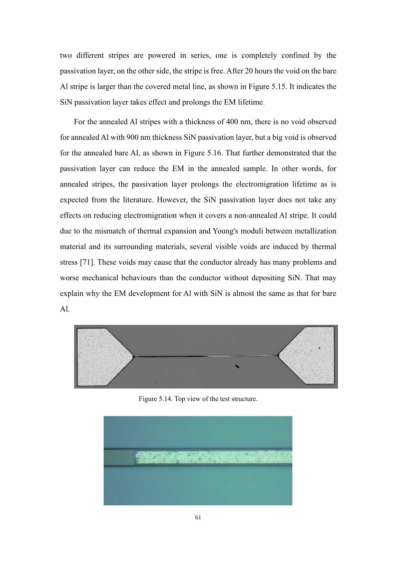
61
two different stripes are powered in series, one is completely confined by the
passivation layer, on the other side, the stripe is free. After 20 hours the void on the bare
Al stripe is larger than the covered metal line, as shown in Figure 5.15. It indicates the
SiN passivation layer takes effect and prolongs the EM lifetime.
For the annealed Al stripes with a thickness of 400 nm, there is no void observed
for annealed Al with 900 nm thickness SiN passivation layer, but a big void is observed
for the annealed bare Al, as shown in Figure 5.16. That further demonstrated that the
passivation layer can reduce the EM in the annealed sample. In other words, for
annealed stripes, the passivation layer prolongs the electromigration lifetime as is
expected from the literature. However, the SiN passivation layer does not take any
effects on reducing electromigration when it covers a non-annealed Al stripe. It could
due to the mismatch of thermal expansion and Young's moduli between metallization
material and its surrounding materials, several visible voids are induced by thermal
stress [71]. These voids may cause that the conductor already has many problems and
worse mechanical behaviours than the conductor without depositing SiN. That may
explain why the EM development for Al with SiN is almost the same as that for bare
Al.
Figure 5.14. Top view of the test structure.

62
(a)
(b)
Figure 5.15. Drift of 200 nm thickness samples after 20 hours at 300 , (a) the full covered Al
stripe. (b) the bare Al stripe.
(a)
(b)
Figure 5.16. Drift of 400 nm thickness samples after 3.5 hours at 300 , (a) the full covered Al
stripe. (b) the bare Al stripe.
5.6 Experimental study on the impact of oxide on EM
It is known that when aluminum is exposed to air, a thin oxide film will form on
the surface even at room temperature. Usually, the thickness of the oxidation layer is
from 1 to 10 nm, but the development of thickness significantly depends on the

63
temperature and the environment. Considering our test condition is at high temperature
and high current density, the oxide on the Al surface could be an important factor on
EM. In this experiment, the temperature, load current density, length of the conductor,
and test time are as control variables, while the test ambient environment (V3) is the
only input variable. After 10 hours the Al stripe which is exposed to air shows much
larger voids at the cathode compared to the metal line in a vacuum, as shown in Figure
5.17.
To explain this, the TLM structure (Figure 3.19) is used to monitor the resistance
change for the certain Al stripe. From the above discussion, we found that there was no
electromigration for 10 μm stripe in a vacuum, and the resistance change of 10 μm
stripe in a vacuum in Figure 5.18 (green line) showed that the resistance remains
unchanged after 16 hours, which indicates that no voids form at the cathode of the stripe.
However, the resistance change for the 10 μm Al stripe in air shows a different tendency,
as shown in Figure 5.18 (red line), the resistance keeps increasing and the resistance
change exceeds 50% after 16 hours. In Figure 5.18, the 10 μm stripe in the air has no
signs of electromigration. Because of this, we conclude that the resistance increases
only as a result of the growth of aluminum oxide on the surface. The growth of the
oxidation layer means the reduction of aluminum layer and the decrease of the cross-
section for the aluminum layer. Thus, a higher current density actually is applied to Al
stripes. As a result, much faster EM failure occurs.
Figure 5.17. Drift of two groups of samples in a vacuum (top) and in the air (bottom) after 10
hours.

64
Figure 5.18. Resistance change for two sets of 10 μm Al stripes.

65

66
Chapter 6. Conclusion and Future work
A brief review of the work that has been done in previous chapters will be given
first. Then, several recommendations for future work will be discussed.
6.1 Conclusion
The main goal of this work was to experimentally study EM and provide
experimental data to validate our theoretical model. It is known that electromigration is
a complex multi-physics process, including electrical, thermal, mechanical, and
chemical aspects. However, the reported work on the formulation and modeling is not
complete and not consistent with experimental results. A fully-coupled and self-
consistent electromigration theory was proposed by Cui et al, and to validate their
theoretical result, our experiment used the simplest test structure, the so-called “Blech
structure”, and adopted the accelerated test method with high temperature and current
stress.
Electromigration is a multi-scale problem, the structure we designed not only takes
into account the effect of dimensions of interconnect at the macro-level, but also the
influence of microstructure of metal on electromigration. In addition, different
electrical measurement structures were designed using four-point measurement to
achieve accurate failure analysis.
The fabrication of our basic structures, together with test structures is a two mask
process and masks are used to pattern the TiN and Al layers. The main structure consists
of a Si layer, SiO2 layer, TiN layer, and Al layer. Sputtering deposition, one of the PVD
process techniques, was used for the deposition of metal and plasma etching and wet
etching were used to etch TiN layer and Al layer, respectively. Besides, the additional
covered passivation layer SiN was deposited by PECVD and etched by plasma etcher
using a third mask.
The accelerated EM test was carried out under certain current stress at an elevated
temperature. When used as control variables, the current density is 1 × 10¹⁰𝐴/𝑚2 and

67
the temperature is 250 . First, we studied the impact of conductor length on EM and
the measurement results are summarized as follow,
1. The critical length under 1 × 10¹⁰𝐴/𝑚2 at 250 was found to be 10 μm
2. Longer stripes have lager drift length and a shorter time failure for
electromigration.
Above experimental results match the simulation prediction performed by Zhen Cui
and is consistent with the results in Blech experiments.
To investigate the impact of temperature on EM, the setup is heated up from 200
to 350. With the elevated temperature, the drift length increases and the
electromigration lifetime decreases. By using the experiment data, the Arrhenius
equation of the diffusion coefficient at different temperatures was obtained. And
according to the expression of the fitting curve, the active energy of the Al film
was 0.5 𝑒𝑉 and pre-exponential factor was 6.1 𝐸 − 11 𝑚2/𝑠. The activation energy is
consistent with the value in literature.
In addition, the effect of the SiN passivation layer on EM was studied. Interestingly,
it was found that the SiN passivation layer does not take any effects on reducing
electromigration when it covers a non-annealed Al stripe. However, for the annealed Al
stripe, the SiN passivation layer could obviously decrease the EM process. According
to MD simulation performed by Zhen Cui, this is because the annealing process
improves the coalescence of grain in Al film, reducing the defects at the grain boundary
and forming a denser microstructure, compared to the non-annealed Al film.
Furthermore, we also found that the additional oxidation on the Al surface at
elevated temperature can reduce the thickness of Al film and increase the actual current
density loaded in the sample, resulting in a shorter EM lifetime for a test performed
under ambient pressure instead of vacuum.
In general, present experimental results were consistent with existing results in the
literature, and we also discovered that the effects of passivation layer on EM are
dependent on the annealing condition of Al stripe. The platform established in the
present study can be continually used for our future studies on EM.

68
6.2 Recommendations and future work
Due to time constraints, several problems and results are not able to be solved and
explained in this work, therefore, future work is needed to continue and develop this
study. Additional experiments and measurements that would be interesting to be
performed are briefly discussed as follow.
1. Based on the reviewed literature, various structures are designed to investigate
different impacts on EM, however, we are not able to carry on EM tests for all structures,
for example, the structures for studying impact of current crowding effect and inter-
diffusion on EM should be achieved in the future.
2. According to our results from Section 5.4, samples with 400 nm thickness showed
larger voids than the 200 nm thickness Al stripes. While, in order to investigate the
impact of conductor thickness, more tests with different thickness samples are
necessary to perform.
3. In Section 5.4, we found that the covered samples without thermal treatment are
not able to take effect on suppressing electromigration. In literature, due to the
mismatch of thermal expansion and Young's moduli between metallization material and
its surrounding materials, several visible voids are induced by thermal stress. These
voids may cause that the conductor already has many problems and worse mechanical
behaviors than the conductor without depositing SiN. That may explain why the EM
development for Al with SiN is almost the same as that for bare Al. However, more
evidence is necessary to verify this theory and explain our results.
4. As we discussed in Section 5.3, the SEM micrograph shows that after annealing
the Al microstructure becomes denser and several hillocks are formed on the surface,
but we were not able to use tools to characterize it.
5. In our work, each EM test time takes more than 10 hours, which makes it difficult
for us to accomplish a large number of tests in a short time. To be more efficient, the
test structure should be improved.

69

70
Appendices
A Process flowcharts
Run number: EC2426
Contamination: None
CLEANING : HNO3 99% and 69.5% (OPTIONAL)
Clean 10 minutes in fuming nitric acid at ambient temperature. This will
dissolve organic materials.
Use wet bench "HNO3 99% (Si)" and the carrier with the white dot.
Rinse Rinse in the Quick Dump Rinser with the standard program until the
resistivity is 5 M.
Clean 10 minutes in concentrated nitric acid at 110 °C. This will dissolve metal
particles.
Use wet bench "HNO3 69,5% 110C (Si)" and the carrier with the white
dot.
Rinse Rinse in the Quick Dump Rinser with the standard program until the
resistivity is 5 M.
Dry Use the Semitool "rinser/dryer" with the standard program, and the white
carrier with a red dot.
COATING
Use the coater station of the EVG120 system to coat the wafers with photoresist.
The process consists of:
a treatment with HMDS (hexamethyldisilazane) vapor, with nitrogen as a carrier
gas
spin coating of Shipley SPR3012 positive resist, dispensed by a pump
a soft bake at 95 C for 90 seconds
an automatic edge bead removal with a solvent
Always check the relative humidity (48 ± 2 %) in the room before coating and follow
the instructions for this equipment.
Use program "Co - 3012 - zero layer". There will be a larger edge bead removal.
EXPOSURE
Processing will be performed on the ASML PAS5500/80 automatic wafer stepper.
Follow the operating instructions from the manual when using this machine.
Expose masks COMURK, with job "ZEFWAM" and the correct exposure energy 125

71
mJ/cm2
This results in alignment markers for the stepper and contact aligner.
DEVELOPING
Use the developer station of the EVG120 system to develop the wafers. The process
consists of:
a post-exposure bakes at 115 C for 90 seconds
developing with Shipley MF322 with a single puddle process
a hard bake at 100 C for 90 seconds
Use program "Dev - SP".
INSPECTION: Linewidth and overlay
Visually inspect the wafers through a microscope and check the line width and
overlay. No resist residues are allowed.
PLASMA ETCHING: Alignment markers (URK’s) in Silicon
Use the Trikon mega 201 plasma etcher.
Follow the operating instructions from the manual when using this machine.
It is not allowed to change the process conditions and times from the etch recipe!
Use sequence URK_NPD (with a platen temperature of 20 ºC) to etch 120 nm deep
ASM URK's into the Si.
Process conditions from chamber recipe URK_ETCH:
Step Gasses & flows Pressure Platen
RF ICP RF
Platen
temp. Etch time
1.
breakthrough CF4/O2 = 40/20 sccm 5 mTorr 60 W 500 W 20 °C 0'10"
2. bulk etch Cl2/HBr = 80/40 sccm 60
mTorr 20 W 500 W 20 °C 0'40"
LAYER STRIPPING: Photoresist
Strip resist Use the Tepla Plasma 300 system to remove the photoresist in an oxygen
plasma.
Follow the instructions specified for the Tepla stripper and use the quartz
carrier.
Use program 1: 1000 watts power and automatic endpoint detection +
2 min. over etching.
CLEANING: HNO3 99% and 69.5%
Clean 10 minutes in fuming nitric acid at ambient temperature. This will
dissolve organic materials.
Use wet bench "HNO3 99% (Si)" and the carrier with the white dot.
Rinse Rinse in the Quick Dump Rinser with the standard program until the

72
resistivity is 5 M.
Clean 10 minutes in concentrated nitric acid at 110 °C. This will dissolve metal
particles.
Use wet bench "HNO3 69,5% 110 C (Si)" and the carrier with the white
dot.
Rinse Rinse in the Quick Dump Rinser with the standard program until the
resistivity is 5 M.
Dry Use the Semitool "rinser/dryer" with the standard program, and the white
carrier with a red dot
WET OXIDATION: 300nm thermal SiO2
Furnace tube: C1 Program name: WETOX
Total time:
PROCESS TEMPERATURE (in ⁰C)
GAS &
FLOWS (in
liter/min)
TIME (in
minutes) REMARKS
boat in 800
nitrogen:
3.0
oxygen:0.3
5
stabilize 800
nitrogen:
3.0
oxygen:0.3
10
heat up +10 ⁰C/min
nitrogen:
3.0
oxygen:0.3
30
stabilize 1100
nitrogen:
3.0
oxygen:0.3
10
purge 1100
nitrogen:
3.0
oxygen:2.2
5
1
oxidation 1100
nitrogen:
2.25
oxygen:3.8
5
16 min 15.8 s
cool down -10 ⁰C/min nitrogen:
3.0 55
boat out 800 nitrogen:
3.0 5

73
MEASUREMENT: OXIDE THICKNESS
Use the Leitz MPV-SP measurement system to measure the oxide thickness:
Program: Th. SiO2 on Si, >50nm auto5pts
Expected thickness: 300 nm
Measured thickness :
TiN PVD DEPOSITION
Use the TRIKON SIGMA sputter coater for the deposition of the TiN metal layer on
the process wafers.
Follow the operating instructions from the manual when using this machine.
Use recipe TiN_300nm_300 to sputter a 0.3 μm thick layer of TiN. Add dummy
wafers in between (Ti_inbetween_300C) as required. Temperature is 300 °C
Perform a target clean
Visual inspection: the metal layer must look shiny with gold-brown color.
COATING AND BAKING
Use the EVG 120 wafertrack to coat the wafers with resist, and follow the instructions
specified for this equipment.
The process consists of a treatment with HMDS (hexamethyldisilazane) vapor with
nitrogen as a carrier gas,
spin coating with Shipley SPR3012 positive photoresist, and a soft bake at 95degC for
90 seconds.
Always check the temperature of the hotplate and the relative humidity (48 ± 2 %) in
the room first.
Use coating Co – 3012 – 1.4µm.
ALIGNMENT AND EXPOSURE
Processing will be performed on the ASM PAS 5500/80 automatic wafer-stepper.
Follow the operating instructions from the manual when using this machine.
Energy = TBD mJ/cm2 (Perform E-F matrix)
DEVELOPING
Use the developer station of the EVG120 system to develop the wafers. The process
consists of:
a post-exposure bake at 115 C for 90 seconds
developing with Shipley MF322 with a single puddle process
a hard bake at 100 C for 90 seconds
Always follow the instructions for this equipment.
Use program "1-Dev - SP"
INSPECTION: Linewidth and overlay
Visually inspect the wafers through a microscope, and check the linewidth. No resist
residues are allowed.

74
PLASMA ETCHING OF TITANNIUM NITRIDE
Use the Trikon mega 201 plasma etcher to etch titanium ntride
Follow the operating instructions from the manual when using this machine.
The process conditions of the etch program may not be changed !
Use sequence TINTISVO and set the platen temperature to 25 . Check the time
is set for 2min 30 sec to etch 300nm TiN (from the logbook)
INSPECTION
Visually inspect the wafers through a microscope, and check if the patterns are
indeed existed. No residues are allowed.
LAYER STRIPPING: Photoresist
Strip resist Use the Tepla Plasma 300 system to remove the photoresist in an oxygen
plasma.
Follow the instructions specified for the Tepla stripper and use the quartz
carrier.
Use program 1: 1000 watts power and automatic endpoint detection + 2
min. over etching.
CLEANING: HNO3 99% (Metals)
Clean 10 minutes in concentrated nitric acid.
Use wet bench "HNO3 99% (Metals)" and the carrier with the red and
yellow dots.
Rinse Rinse in the Quick Dump Rinser with the standard program until the
resistivity is 5 M.
Dry Use the Semitool "rinser/dryer" with the standard program, and the white
carrier with a black dot.
MEASURENMENT : TIN THICKNESS
Use the DEKTAK profilometer for stepheight measurements on the wafer of your batch.
Mwasure on the bondflaps.
Following the operating instructions from the manual when using this machine.
Stepheight:
ALUMINIUM SPUTTERING
Use the TRIKON SIGMA sputter coater for the deposition of an aluminum metal layer
on the wafers.
The target must exist of 99% Al and 1% Si, and deposition must be done at 350 °C.
Follow the operating instructions from the manual when using this machine.
Use recipe ““AlSi_200_RF_300C” to sputter a 200nm thick aluminum layer at
temperature 350 .
Note: Check the wafers after aluminum deposition. Metal residuals should be not
present on the edge neither on the frontside nor the backside of the wafer.

75
COATING AND BAKING
Use the coater station of the EVG120 system to coat the wafers with photoresist.
The process consists of:
a treatment with HMDS (hexamethyldisilazane) vapor, with nitrogen as a carrier
gas
spin coating of Shipley SPR3012 positive resist, dispensed by a pump
a soft bake at 95 C for 90 seconds
an automatic edge bead removal with a solvent
Always check the relative humidity (48 ± 2 %) in the room before coating, and
follow the instructions for this equipment.
Use program "Co - 3012 – 2.1µm".
ALIGNMENT AND EXPOSURE
Alignment and exposure will be done with the ASML PAS5500/80 automatic wafer
stepper.. Follow the operating instructions from the manual when using this machine.
DEVELOPING
Use the developer station of the EVG120 system to develop the wafers. The process
consists of:
a post-exposure bake at 115 C for 90 seconds
developing with Shipley MF322 with a single puddle process
a hard bake at 100 C for 90 seconds
Always follow the instructions for this equipment.
Use program "Dev – SP”
INSPECTION: Linewidth and overlay
Visually inspect the wafers through a microscope, and check the line width and
overlay. No resist residues are allowed
WET ETCHING OF ALUMINUM
Etch Use wet bench “Al etch (35 C)” and the carrier with the yellow dot. The bath
contains PES at temperature 35 C. A typical etch rate of Al is 170 nm/min.
Time 1 minutes and 20 seconds.(first with test wafer)
Rinse Rinse in Quick Dumo Rinser with the standard program until the resistivity is
5 MΩ.
Etch Use wet bench “Poly-Si etch” and the carrier with the green dot to remove the
1 % silicon.
Time 30 seconds.
Rinse Rinse in Quick Dumo Rinser with the standard program until the resistivity is
5 MΩ.
Dry Use the “Avenger Ultra-Pure 6” rinser/dryer with standard program, and the white
carrier with a black dot.
INSPECTION: No Aluminum residues are allowed on the etched area()

76
LAYER STRIPPING: Photoresist
Strip resist Use the Tepla Plasma 300 system to remove the photoresist in an oxygen
plasma.
Follow the instructions specified for the Tepla stripper, and use the quartz carrier.
Use program 1: 1000 watts power and automatic endpoint detection + 2 min. over
etching.
CLEANING: HNO3 99% (Metals)
Clean 10 minutes in concentrated nitric acid.
Use wet bench "HNO3 99% (Metals)" and the carrier with the red and
yellow dots.
Rinse Rinse in the Quick Dump Rinser with the standard program until the
resistivity is 5 M.
Dry Use the Semitool "rinser/dryer" with the standard program, and the white
carrier with a black dot.
PECVD SiN 300 nm
Use the Novellus Concept One PECVD reactor.
Check Gases
Use group: (recipe xxx STSiN) to deposit a 300 nm thick SiN layer.
Follow the operating instructions from the manual when using this machine.
Change time to get the right thickness according to logbook. (14sec)
MEASUREMENT: OXIDE THICKNESS
Use the Leitz MPV-SP measurement system to measure the oxide thickness:
Program: PECVD SiN on Al
Expected thickness: 300 nm
Measured thickness :
COATING AND BAKING
Use the coater station of the EVG120 system to coat the wafers with photoresist. The
process consists of:
a treatment with HMDS (hexamethyldisilazane) vapor, with nitrogen as a carrier
gas
spin coating of Shipley SPR3012 positive resist, dispensed by a pump
a soft bake at 95 C for 90 seconds
an automatic edge bead removal with a solvent
Always check the relative humidity (48 ± 2 %) in the room before coating, and follow
the instructions for this equipment.
Use program " Co - 3012 – 2.1µm ".
ALIGNMENT AND EXPOSURE
Alignment and exposure will be done with the ASML PAS5500/80 automatic wafer
stepper.. Follow the operating instructions from the manual when using this machine.

77
DEVELOPING
Use the developer station of the EVG120 system to develop the wafers. The process
consists of:
a post-exposure bake at 115 C for 90 seconds
developing with Shipley MF322 with a single puddle process
a hard bake at 100 C for 90 seconds
Use program "Dev – SP”
INSPECTION: Linewidth and overlay
Visually inspect the wafers through a microscope, and check the line width and
overlay. No resist residues are allowed
DRY ETCHING SILICION NITRIDE
Use the Drytek Triode 384T plasma etcher.
Follow the operating instructions from the manual when using this machine.
It is not allowed to change the process conditions from the etch recipe, except for
the etch times!
Use recipe SCRATCH to etch the silicon nitride layer with a soft landing on the layer
underneath (need new recipe)
Process conditions from recipe SCRATCH:
Step Gasses & flows Pressure RF power He
pressure Etch time
1. bulk etch
(RIE) C2F6=65 sccm 130m Torr 250W 8 Torr
2 landing step C2F6=65 sccm 130m Torr 100W 8 Torr
INSPECTION
Visually inspect the wafers through a microscope, and check if the vias are indeed
open. No residues are allowed.
MEASUREMENT: SILICION NITRIDE THICKNESS (optional)
Use the Leitz MPV-SP measurement to measure the left TiN layer thickness:
Program:
Nitride thickness:
LAYER STRIPPING: Photoresist
Use the Tepla Plasma 300 system to remove the photoresist in an oxygen plasma.
Follow the instructions specified for the Tepla stripper, and use the quartz carrier.
Use program 1: 1000 watts power and automatic endpoint detection + 2 min.
CLEANING: HNO3 99% (Metals)
Cleaning 10 minutes in concentrated nitric acid.
Use wet bench "HNO3 99% (Metals)" and the carrier with the red and
yellow dots.
Rinse Rinse in the Quick Dump Rinser with the standard program until the

78
resistivity is 5 M.
Dry Use the Semitool "rinser/dryer" with the standard program, and the white
carrier with a black dot.
MEASUREMENT: SIN etching optimization
Use the Keyence microscope for stepheight measurements on the wafers of your batch.
Following the operating instructions from the manual when using this machine.
ALLOYING
Furnace no : C4 Program name : ALLOY1 Total time : 50 min
PROCESS TEMPERATUR
E
(in °C)
GASSES &
FLOWS
(in liter/min)
TIME
(in
minutes)
REMARKS
boat in 400 nitrogen: 3.0
5
stabilize 1 400 nitrogen: 3.0
5
stabilize2 400 nitrogen: 3.0
10
alloying 400 nitrogen: 3.0
hydrogen: 0.3
20
purge 400 nitrogen: 3.0
5
boat out 400 nitrogen: 3.0
5

79
Reference
[1] International Technology Roadmap for Semiconductors (ITRS), 2013 edn.
(2014), http://www.itrs2.net/itrs-reports.html. Last retrieved on 1 Jan 2018
[2] International Technology Roadmap for Semiconductors (ITRS 2.0), 2015 edn.
(2016), http://www.itrs2.net/itrs-reports.html. Last retrieved on 1 Jan 2018.
[3] K.J. Puttlitz, K. A. Statler, Handbook of Lead-Free Solder Technology for
Microelectronic Assemblies, CRC Press, 2004.
[4] V.B. Fiks, On the mechanism of the mobility of ions in metals, Sov. Phys. Solid
State 1 (1959) 14.
[5] H.B. Hunitington, A. R. Grone. Current-induced maker motion gold wires[J].
Physics Chem Solids, 1961, 1(1): 76-97.
[6] L. Arnaud, T. Berger, G. Reimhold. Evidence of grain-boundary versus
interface diffusion in electromigration experiments in copper damascene
interconnects[J]. Appl. Phys, 2003, 93(1): 192.
[7] H.V. Nguyen, C. Salm, et al. Fast temperature Cycling and electromigration
induced thin film cracking in multilevel interconnection :experiments and modeling[J].
Microelectronics Reliability, 2002, 42(10): 1415.
[8] Cher Ming Tan, Arijit Roy. Investigation of the temperature and stress gradients
on accelerated EM test for Cu narrow interconnects[J]. Thin Solid Films, 2006, 40(10):
289.
[9] Shine, M. C., D'heurle, F. M. (1971). Activation Energy for Electromigration in
Aluminium Films Alloyed with Copper. IBM Journal of Research and Development,
15(5), 378-383. doi:10.1147/rd.155.0378.
[10] Gangulee, A., & D'heurle, F. M. (1971). Effect of Alloy Additions on
Electromigration Failures in Thin Aluminium Films. Applied Physics Letters, 19(3),
76-77. doi:10.1063/1.1653828.
[11] M.F. Chow, W.L. Guthrie, F.B. Kaufman, US Patent 4,702,792 (1987).
[12] M.M. Chow et al., US Patent 4,789,648 (1988).
[13] J.W. Carr et al., US Patent 4,954,142 (1990).
[14] Valeriy Sukharev, Ehrenfried Zschech. A model for electromigration-induced
degradation mechanisms in dual-inlaid copper interconnects: Effect of interface
bonding strength[J]. Appl. Physics, 2004, 96(11): 6337-6343.
[15] Valeriy Sukharev. Physically-Based Simulation of Electromigration Induced
Failures in Copper Dual-Damascene Interconnect[J]. IEEE International Symposium
on Quality Electronic Design, 2005, 24(9): 1326-1334.
[16] Valeriy Sukharev, Ehrenfried Zschech, William D.Nix. A model for
electromigration-induced degradation mechanisms in dual-inlaid copper
interconnects: Effect of microstructure[J]. Appl. Physics, 2007, 102(5): 223-226.
[17] Cher Ming Tan, Yue jin hou, Wei Li. Revisit to the finite element modeling
of electromigration narrow interconnects[J]. Journal of Applied Physics, 2007, 102(3):
278-279.
[18] F. Cacho, V. Fiori, L. Doyen, C. Chappaz, C. Tavernier et al., Electromigration

80
induced failure mechanism: Multiphysics model and correlation with experiments,
EuroSimE 2008, International Conference on Thermal, Mechanical and Multi-Physics
Simulation and Experiments in Microelectronics and Micro-Systems, 2008.
[19] R.L. de Orio, H. Ceric, S. Selberherr. Physically Based models of
electromigration: From Black’s equation to modern TCAD models[J]. Microelectronics
Reliability, 2010, 50(2): 775-789.
[20] I. Avci, et al. Computational analysis of mechanical and electromigration
reliability problems[J]. IEEE International Interconnect Technology Conference
Proceedings, 2012, 12(3): 1-3.
[21] Skaupy, F. (1914). Die Elektrizitatsleitung in Metallen. Verhandl. Deut. Phys.
Ges., 16:156.
[22] W. B. Fiks. On the mechanism of the mobility of ions in metals. Sov. Phys.
Solid State, 1, 14-28 (1959).
[23] R. Landauer, J. W. F. Woo. Driving Force in Electromigration. Physical
Review B, 1974, 10, 1266-1271.
[24] A. Lodder. The Driving Force in Electromigration. Physica A, 1989, 158, 723-
739.
[25] L. J. Sham. Microscopic Theory of Driving Force in electromigration.
Physical Review B, 1975. 12, 3142-3149.
[26] Tan, C. M., Gan, Z., Li, W., and Hou, Y. (2011). Applications of Finite Element
Methods for Reliability Studies on ULSI Interconnections. Springer Series in
Reliability Engineering. Springer-Verlag London, 1st edition.
[27] Cacho, F. and Federspiel, X. (2011). Modeling of Electromigration
Phenomena. In Kim, C.-U., editor, Electromigration in Thin Films and Electronic
Devices, Woodhead Publishing Series in Electronic and Optical Materials, 3-44.
Woodhead Publishing.
[28] de Orio, R. L. (2010). Electromigration Modeling and Simulation. Dissertation,
Technischen Universitaet Wien, Fakultaet fuer Elektrotechnik und Informationstechnik.
[29] I.A. Blech, C. Herring, Stress generation by electromigration, Appl. Phys. Lett.
29 (1976) 131–133.
[30] I.A. Blech, K.L. Tai, Measurement of stress gradients generated by
electromigration, Appl. Phys. Lett. 30 (1976) 387–389.
[31] R.O. Williams, Diffusion of vacancies under stress a gradient, Acta Metall. 5
(1957) 55–56.
[32] 26] J. Lloyd, K.P. Rodbell, in: G.C. Schwartz, K.V. Srikrishnan (Eds.),
Handbook of Semiconductor Interconnection Technology, 2006, pp. 471–520.
[33] C.-Y. Li, P. Børgesen, T.D. Sullivan, Stress-migration related electromigration
damage mechanism in passivated, narrow interconnects, Appl.
Phys. Lett. 59 (1991) 1464–1466.
[34] P. Børgesen, M.A. Korhonen, C.-Y. Li, Stress and current induced voiding in
passivated metal lines, Thin Solid Films 220 (1992) 8–13.
[35] J.R. Lolyd, Electromigration in thin film conductors, Semicond. Sci. Technol.
12 (1997) 1177–1185.
[36] J.R. Lloyd, Electromigration in integrated circuit conductors, J. Phys. D: Appl.

81
Phys. 32 (1999) R109–R118.
[37] J.R. Lloyd, M. Shatzkes, D.C. Challaner, Kinetic study of electromigration
failure in Cr/Al–Cu thin film conductors covered with polyimide
and the problem of the stress dependent activation energy, in: Proceedings of the
IRPS, IEEE, 1988, pp. 216–225.
[38] A.P. Schwarzenberger, C.A. Ross, J.E. Evetts, A.L. Greer, Electromigration in
the presence of a temperature gradient: experimental study and modeling, J. Electron.
Mater. 17 (1988) 473–478.
[39] J.R. Black, Electromigration–a brief survey and some recent results, IEEE
Trans. Electron Devices ED-16 4 (1969) 338–347
[40] H.A. Schafft, T.C. Staton, J. Mandel, J.D. Shott, Reproduciblity of
electromigration measurements, IEEE Trans. Electron Devices ED-34 (1987) 673–681.
[41] H.A. Schafft, Thermal analysis of electromigration test structures, IEEE Trans.
Electron Devices ED-34 (1987) 664–672.
[42] ASTM Standard Guide for Design of Flat, Straight-Line Test Structures for
Detecting Metallization Open-Circuit or Resistance-Increase Failure Due to
Electromigration, F 1259-89, Annual Book of ASTM Standards, vol. 10.04
[43] B.J. Root, T. Turner, Wafer-level electromigration tests for production
monitoring, in: Proceedings of the IRPS, IEEE, 1985, pp. 100–107.
[44] I.A. Blech, Electromigration in thin aluminum films on titanium nitride, J.
Appl. Phys. 47 (1976) 1203–1208.
[45] Blech, I. (1998). Diffusional back flows during electromigration. Acta
Materialia, 46(11), 3717-3723. doi:10.1016/s1359-6454(97)00446-1.
[46] J. Lloyd, J.J. Clement, Thin Solid Films 262 (1) (1995) 135–141.
[47] Fu X, Forster J, Yu J, Gopalraja P, Bhatnagar A, Ahn S, et al. Advanced
preclean for integration of PECVD SiCOH (k < 2.5) dielectrics with copper
metallization beyond 45 nm technology. In: IEEE International Interconnect
Technology Conference Proceedings. 2006. pp. 51-53.
[48] J. Cho, C.V. Thompson, Electromigration-induced failures in interconnects
with bimodal grain size distributions, J. Electron. Mater. 19 (1990)1207.
[49] Hau-Riege, C. and Thompson, C. (2001). Electromigration in Cu
interconnects with very different grain structures. Applied Physics Letters, 78(22),
pp.3451-3453.
[50] J.R. Lloyd, New age electromigration testing[C], International Integrated
Reliability Workshop. Lake Tahoe, CA, 2002.
[51] J.R. Lloyd, J. Clemens, S. Snede, Copper metallization reliability,
Microelectron. Reliab. 39 (1999) 1595–1602.
[52]Fu X, Forster J, Yu J, Gopalraja P, Bhatnagar A, Ahn S, et al. Advanced
preclean for integration of PECVD SiCOH (k < 2.5) dielectrics with copper
metallization beyond 45 nm technology. In: IEEE International Interconnect
Technology Conference Proceedings. 2006. pp. 51-53.
[53] Chang YM, Leu J, Lin BH, Wang YL, Cheng YL. Comparison of H2 and NH3
treatments for copper interconnects. Advances in Materials Science and Engineering.
2013;2013:7. Article ID: 825195.

82
[54] Baklanov MR, Shamiryan DG, Tokei Z, Beyer GP, Conard T,
Vanhaelemeersch S, et al. Characterization of Cu surface cleaning by hydrogen plasma,
Journal of Vacuum Science & Technology B. 2001;19:1201-1211.
[55] Tokei Z, Lanckmans F, Van den bosch G, Van Hove M, Maex K, Bender H, et
al. Reliability of copper dual damascene influenced by pre-clean. In: IEEE International
Symposium on the Physical and Failure Analysis of Integrated Circuits. 2002. pp. 118-
123.
[56] M.W. Lane, E.G. Linger, J.R. Lloyd, Relationship between interfacial
adhesion and electromigration in Cu metallization, J. Appl. Phys. 93(2003) 1417–1421.
[57] Hu, C.-K. Capping Layer Effects on Electromigration in Narrow Cu Lines.
AIP Conference Proceedings. 2004.97-111.
[58] Hu, C.-K., et al., Reduced electromigration of Cu wires by surface coating.
Applied Physics Letters. 2002. 81(10) 1782-1784.
[59] Yan, M. Y, et al. Effect of Cu3Sn coatings on electromigration lifetime
improvement of Cu dual-damascene interconnects. Applied Physics Letters, 87(21),
211103.
[60] T. Kwok, T. Nguyen, P. Ho, S. Yip, Current density and temperature
distributions in multilevel interconnection with studs and vias, in: Proceedings of the
IRPS, IEEE, 1987, pp. 130–135.
[61] K. Weide, W. Hasse, Three-dimensional simulations of temperature and
current density distribution in a via structure, in: Proceedings of the IRPS, IEEE, 1992,
pp. 361–365.
[62] F. Matsuoka, H. Iwai, K. Hama, H. Itoh, R. Nakata, T. Nakakubo, K. Maeguchi,
K. Kanzaki, Electromigration reliability for a tungsten-filled via hole structure, IEEE
Tnans. Electron Devices 37 (1990) 562–568.
[63] Orio, R. D., Ceric, H., & Selberherr, S. (2012). Electromigration failure
in a copper dual-damascene structure with a through silicon via. Microelectronics
Reliability, 52(9-10), 1981-1986. doi:10.1016/j.microrel.2012.07.021
[64] H.A. Schafft, T.C. Staton, J. Mandel, J.D. Shott, Reproduciblity of
electromigration measurements, IEEE Trans. Electron Devices ED-34 (1987) 673–681.
[65] H.A. Schafft, Thermal analysis of electromigration test structures, IEEE Trans.
Electron Devices ED-34 (1987) 664–672.
[66] ASTM Standard Guide for Design of Flat, Straight-Line Test Structures for
Detecting Metallization Open-Circuit or Resistance-Increase Failure Due to
Electromigration, F 1259-89, Annual Book of ASTM Standards, vol. 10.04.
[67] ASTM Standard Test Method for Determining the Average Width and Cross-
Sectional Area of a Straight, Thin-Film Metal Line, F 1261-89, Annual Book of ASTM
Standards, vol. 10.04.
[68] B.J. Root, T. Turner, Wafer-level electromigration tests for production
monitoring, in: Proceedings of the IRPS, IEEE, 1985, pp. 100–107.
[69] F. Giroux, C. Gounelle, P. Mortini, G. Ghibaudo, Wafer-level electromigration
tests on NIST and SWEAT structures, in: Proceedings of the International Conference
on Microelectronic Test Structures, vol. 8, IEEE, 1995, pp. 229–232.
[70] Cher Ming Tan, Arijit Roy, Electromigration in ULSI interconnects.

83
[71] Okabayashi, H. (1993). Stress-induced void formation in metallization for
integrated circuits. Materials Science and Engineering: R: Reports, 11(5), 191-241.
doi:10.1016/0927-796x(93)90008-Q.
![!!!Faszination blech kapitel2[1]](https://static.fdocuments.net/doc/165x107/58ceb5c31a28abb2218b5b41/faszination-blech-kapitel21.jpg)


![[Q]oi~ Leo Blech](https://static.fdocuments.net/doc/165x107/6156fae4a097e25c764faaa5/qoi-leo-blech.jpg)


