Green Chemistry Using Bismuth Compounds: Bismuth(III) Triflate

Electromigration in Bismuth
THESIS
submitted in partial fulfillment of therequirements for the degree of
MASTER OF SCIENCEin
PHYSICS
Author : Thomas Ruytenberg, BScStudent ID : s1061488Supervisors : Dr. Johannes Jobst
Dr. ir. Sense Jan van der Molen2nd corrector : Prof. Dr. Jan Aarts
Leiden, The Netherlands, August 18, 2015


Electromigration in Bismuth
Thomas Ruytenberg, BSc
Huygens-Kamerlingh Onnes Laboratory, Leiden UniversityP.O. Box 9500, 2300 RA Leiden, The Netherlands
August 18, 2015
Abstract
Electromigration in bismuth is studied as a way to createbismuth(111) bilayers. Temperature-dependent electromigrationmeasurements have been performed and a model incorporatingJoule heating is used to describe those. An activation energy for
diffusion between 100 and 180 meV is found. Furthermore, in-situelectromigration experiments have been performed in a scanning
electron microscope. This allowed us to link events in theconductance traces of bismuth constrictions during
electromigration to visual features. Specifically, remerging of thebismuth electrodes was found to cause increases in conduction.


Contents
1 Introduction 11.1 Topological insulators 21.2 Bismuth bilayers 21.3 Electromigration 3
2 Setup 72.1 Hardware 72.2 Samples 102.3 Software 10
3 Results 153.1 Temperature-dependent electromigration 15
3.1.1 Electromigration measurements 153.1.2 Critical current density and voltage 183.1.3 Electromigration model fitting 19
3.2 In-situ electromigration in SEM 233.3 Constriction width dependency 26
4 Conclusion 29
5 Outlook 31
A Lithography on mica 33
B Methods and recipes 35B.1 Recipes 35
B.1.1 General sample fabrication 35B.1.2 Mica lithography 36
B.2 Feedback settings 37
v


Chapter 1Introduction
During the search for more computing power, several non-conventionalalternatives to transistor computers have been proposed. Many of theseproposals, contain entangled quantum bits which store quantum informa-tion. Such a ’quantum computer’ would be able to perform huge parallelcalculations. Another proposal for a new kind of computing scheme isspintronics [1], where electrons are not physically transferred through re-sistive media, but just the spin in which the information will be encoded.Development of such computers could result in a new information revo-lution by dramatically increasing computing speed.
Since a couple of years, a new class of electronic material named topologi-cal insulators, have become the subject of an active field of research. Thesetopological insulators, which are insulating in the bulk but conductive onthe edge (2D) or surface (3D), could have promising applications in bothspintronics and quantum computers in general. [2, 3]
Many different materials and system geometries have been proposed astopological insulators. Examples for 3D topological insulators are Bi2Se3 [4],Bi2Te3 [5], Bi1−xSbx [6] and SnTe [7], while CdTe/HgTe/CdTe [8] and bi-layer Bi [9] provide 2D systems. The latter, a bismuth(111) bilayer, isparticularly interesting, since it is the only one proposed to contain theseproperties at room temperature.
In this thesis, a study on electromigration in bismuth is described as a way
1

2 Introduction
to create bismuth(111) bilayers. This first chapter serves as a basic intro-duction in topological insulators, bismuth bilayers and electromigration.In Ch. 2 the setup and measurement scheme is described in detail. Ch. 3presents and discusses the performed experiments. In Ch. 5 an outlook onthe project is given. Finally, this thesis is concluded with Ch. 4.
1.1 Topological insulators
Topological insulators are electronic materials which are insulating in thebulk, but electronically conductive at the edge (2D) or surface (3D). InFig. 1.1, a typical band structure for 2D topological insulators is shown.The band structure shows a band gap with two spin-split surface states,connecting the bulk conduction band to the valence band. Those surfacestates are topologically protected by time-reversal symmetry. [10]
Figure 1.1: Typical band structure of a 2D topological insulator. Within the bandgap, two spin-split (green and blue arrow) topologically protected surface statesare present. Adapted from Ref. [10].
1.2 Bismuth bilayers
Due to the high spin-orbit coupling, bismuth is an interesting elementas a basis for many topological insulators. [10] In 2006 Murakami pre-
2

1.3 Electromigration 3
dicted that bismuth(111) bilayers are topological insulators at room tem-perature. [9] There are however quite some experimental difficulties ingrowing exactly a bilayer of bismuth. Two of these difficulties are the poly-crystallinity of grown bismuth on SiO2 and the oxidation of bismuth whenexposed to air.
However, some groups have succeeded in fabricating thin bismuth filmsand showing topological insulator properties. For example, Zhu et al.found evidence for topologically protected surface states on (10-70 bilay-ers thick) bismuth films. [11] These bismuth films were epitaxially grownon silicon(111).
Using an scanning tunneling microscope, Sabater et al. studied conduc-tance of bismuth nanocontacts. [12] These conductance measurements wereperformed while the bismuth nanocontacts were being exfoliated with thescanning tunneling microscope tip. In the conductance traces, which werea function of exfoliation length, plateaus were observed at the conductancequantum G0. This provides evidence that the bismuth nanocontacts wereexfoliated bilayers.
In 2011, Hirahara et al. successfully created a bismuth bilayer by depo-sition on Bi2Te3. [13] Bi2Te3 was used since both materials form in layerswith a hexagonal lattice of similar lattice constant. However, interactionsbetween the bismuth bilayer and the Bi2Te3 are present. Therefore it wouldbe interesting to study bismuth bilayers on an insulator like SiO2.
In this thesis we will study another approach to create a bismuth bilayeron SiO2. Instead of depositing exactly a bilayer, a thicker layer of bismuthis deposited, and then thinned down using electromigration.
1.3 Electromigration
Electromigration is a process, in which atoms migrate and move under theinfluence of both a direct force and an electron ’wind force’. [14–16] Thedirect force is the electrostatic force exercised by the electric field on un-screened ions in the material. The presence and magnitude of this forceis however still disputed. [17, 18] The wind force is the force produced bythe electrons transferring momentum to the atoms upon collision. Current
3

4 Introduction
density is therefore an important parameter in this process. Typical cur-rent densities during electromigration are in the range of 106-108 A/cm2. [16,19]
Another important parameter in electromigration is the atom diffusivity.A higher diffusivity will result in increased electromigration. The diffu-sion rates of bismuth atoms in this system are mainly influenced by twoparameters. First, polycrystallinity makes the atom diffusion by electro-migration highly anisotropic. The diffusion can take place on differentinterfaces of grains and three types of diffusion can be distinguished ac-cordingly: bulk, surface and grain boundary diffusion. [20] For electromi-gration in copper for example, surface diffusion plays a huge role, while inaluminum it is mainly diffusion along the grain boundary that contributesto electromigration. For bismuth this is unknown. Second, temperatureinfluences diffusion via a certain activation energy, i.e. diffusion is moreeasily activated at a higher temperature. This is particularly important astemperature increases in devices on which electromigration is performeddue to Joule heating. The local high current density heats up the devicedue to Ohmic dissipation.
Due to Joule heating the local temperature of devices on which electromi-gration is performed, is not equal to the temperature of the environment.For bismuth thin films specifically, Joule heating influences electromigra-tion in twofold: it increases atom diffusivity and electrical resistivity goesdown with increased temperature. [21] If in a voltage-controlled electro-migration process a constant voltage is applied, the current density willstill increase due to Joule heating. Therefore, an electromigration measure-ment will always need a feedback mechanism to prevent device failure. InCh. 2.3 such a feedback mechanism and a measurement scheme for thelocal temperature is presented.
Although electomigration does not occur in macroscopic electronics, dueto the fact that high current densities are not easily attained in such de-vices, it is a process that takes place in integrated circuits. In these inte-grated circuits, where interconnect feature sizes down to tens of nanome-ters are used, electromigration becomes a serious issue. Therefore, electro-migration is of main interest for microelectronic engineers, because it canthin out and destroy interconnects in integrated circuits. [15, 20] Knowl-edge about diffusion rates can be utilized to fabricate devices with a re-duced susceptibility to electromigration. For example, aluminum linesthat are thinner than the grain size (so-called bamboo lines), only have
4

1.3 Electromigration 5
grain boundaries perpendicular to the current flow. Therefore, electromi-gration is strongly reduced in those devices. [22, 23] These methods arecommonly used in integrated circuits nowadays.
Electromigration specifically in bismuth has been reported in a single studyin literature. Sangiao et al. showed in 2013 that electromigration can beperformed on bismuth constrictions. [24] These constrictions had a widthof 150 nm. During electromigration on these devices, subquantum con-duction steps were observed. The authors explain these steps in termsof the large Fermi wavelength for semimetals compared to normal met-als. Bismuth atomic contacts will have a diameter much smaller than theirFermi wavelength Therefore, for small enough contacts, only tunnelingwill contribute to the conductance, the authors note.
5


Chapter 2Setup
2.1 Hardware
In order to perform electromigration measurements, we developed a ded-icated setup to fulfill the following set of requirements.
• The measurements need to be performed in high vacuum. This is ofgreat importance, since elevated temperatures due to Joule heatingcauses a high oxidation rate of the bismuth devices in air. Since weare studying thin layers of bismuth, these could oxidize quickly atatmospheric pressures. To create the vacuum, an airtight stainlesssteel chamber was chosen in combination with a membrane pumpand a turbomolecular pump. This combination allows for pressuresdown to 10−6 mbar.
• The temperature of the samples are to be controlled within the rangeof 20C to 250C. This temperature range has been chosen to staywell below the melting temperature of bismuth (272C). Tempera-tures lower than room temperature are not of interest to this work,since electromigration is reduced for low temperatures. We use a700 W heating pad (rated up to 300C in air) in combination witha PID controller (Eurotherm, 3216) for control. Samples are mounted8 mm over the heating pad, such that they are facing the heating pad.
7

8 Setup
This way they are not only heated by conduction through a mount-ing system, but also via heat radiation.
The PID controller uses a K-type thermocouple to measure the tem-perature. Since an on-sample temperature measurement is not eas-ily available, the thermocouple is placed in free-space between theheating pad and the sample. A temperature calibration has been con-ducted, where the temperature indicated by the thermocouple in freespace was compared to a Pt100 sensor glued to a sample with silverpaint. The temperature was increased step-wise, and it can be seenfrom Fig. 2.1, that the temperature measured by the thermocouple,does not deviate more than 10C from the sample temperature.
• In order to make electrical contact to the sample, and allow for easysample exchange, 24-pin ceramic side-brazed DIP chip-carriers (Ky-ocera, KD-SB0809) are used. They are combined with a high-temperatureDIP socket (Aries Electronics, 24-6554-18) which is rated up to a tem-perature of 250C. Furthermore, a 24-pin vacuum feedthrough and24-pin BNC breakout box were used, giving full electrical controlover all 24-pins of the chip-carrier.
Figure 2.1: Temperature calibration of setup. In blue the setpoint of the controlleris shown, which is increased step-wise. Black shows the measured temperatureby the PID controller using a free space thermocouple, which follows the setpointclosely. In red the actual temperature on the sample is shown, which is measuredby a Pt100 sensor glued on the the sample using silver paint. At 5.5 hours, the set-point is decreased to 0C, after which the setup cools down with a characteristictime of about an hour.
8

2.1 Hardware 9
Figure 2.2: a) The vacuum chamber of the setup. On the right side of the cham-ber the turbomolecular pump is mounted. On the left chamber opening, a 24-pin electrical feedthrough with break-out box, the heating pad and thermocouplefeedthroughs and a vacuum pressure gauge are mounted. In the chamber a heat-ing pad with a sample mount is placed, which is depicted in detail in Fig. b)and Fig. c). Figs. b) and c) show respectively an unmounted and mounted chipcarrier-socket assembly. The green/white wire is the K-type thermocouple, in-serted between the sample and the heating pad.
9

10 Setup
2.2 Samples
Samples used in this study are made using a two-step electron beam litho-graphy (EBL) process with subsequent deposition of chromium/gold (4 nm/20 nm) and bismuth (50 nm), respectively. Each sample hosts twelveidentical structures. They consist of a bismuth layer with an in-plane con-striction of 500 nm width. Gold contacts are connected to this constriction,where electromigration takes place, in a four-point geometry in order toaccurately measure its conductance. A detailed recipe for sample fabrica-tion can be found in App. B.1.1. During this project, more than 20 sampleshave been fabricated using this recipe.
Figure 2.3: Sample design. a) shows a sample, wirebonded in the chip carrier. Inb), one of the twelve devices is shown. c) shows the bismuth layer, pattered usinga second EBL step and aligned with high precision on the gold contacts using thefour crosses in the image. Finally in d) the bismuth constriction itself is depicted.The width of this constriction is 500 nm.
2.3 Software
The electromigration process itself is controlled by a Labview program,which was initially written by Martin de Wit. [21] The program interfaceswith a PCI DAQ-card to apply a bias over the bismuth constriction and tomeasure the conductance in four-point geometry.
For controlled electromigration, the applied bias is regulated by a feedbackscheme, introduced by Strachan et al. [25] The feedback scheme works byapplying a voltage ramp as bias. At the same time the current is measuredand the conductance is deduced, as shown in Fig. 2.4. When the conduc-tance drops by more than a certain percentage (typically 2%) with respectto the maximum conductance during the last 20 seconds, the feedback isactivated. Activating the feedback will reset the voltage ramp.
10

2.3 Software 11
(a) (b)
Figure 2.4: (a) typical IV-curves of an electromigration experiment. (b) the de-duced conductance curve in G0 = 2 e2/h (blue), also mentioned as normal-biasconductance, increases due to Joule heating and decreases stepwise due to elec-tromigration. The low-bias curve (red), follows the steps but does not show heat-ing effects. (see main text)
However, the applied voltage ramp is not just a linear ramp. It consistsof a linear ramp with a (typical) slope of 4 mV/s, which is interruptedfor 150 ms once every second, as depicted in Fig. 2.5. During this 150 msinterruption, a low-bias is applied to let the constriction cool down andat the end of this low-bias period, a low-bias conduction measurement isperformed. This low-bias conduction measurement is therefore not influ-enced by Joule heating of the constriction. Fig. 2.4b shows the differencebetween the normal-bias (blue) and low-bias (red) conductance. The dif-ference between the two curves is solely attributed to a temperature dif-ference due to Joule heating. If the conductance as a function of tempera-ture is known, the local temperature of the constriction can be determinedfrom this difference. For bismuth films of 40 nm thickness, resistance as afunction of temperature was measured by Martin de Wit. [21] From thosemeasurements, he deduced the following equation for the local tempera-ture.
Tlocal = T − 5.2× 10²(RN
RL− 1) + 1.3× 10³(
RN
RL− 1)2 (2.1)
Where RN and RL stand for the normal-bias and low-bias resistance re-spectively. The deduced local temperature of the measurements in Fig. 2.4is depicted in Fig. 2.6.
11

12 Setup
Figure 2.5: The applied voltage ramp. In blue, a typical voltage ramp of 4 mV/sis shown during which normal-bias conduction measurements are performed.During the red intervals, the constriction is cooling down and at the end of thoseintervals, a low-bias conduction measurement is performed. This low-bias con-duction measurement excludes the influence of Joule heating.
Figure 2.6: Calculated local temperature from the measurement in Fig. 2.4 usingEq. 3.4.
Because the feedback is activated when the normal-bias conduction dropsa certain percentage, the electromigration happens bit by bit such that atypical experiment in the described setup takes a couple of hours. Thetimescale of the experiments is mainly determined by the speed of thevoltage ramp. The speed of the voltage ramp itself is restricted by the sam-pling speed of the conductance, which in our case is limited to 10 Hz by thesoftware feedback scheme. Other ways of implementing controlled elec-tromigration using feedback are hardware controlled or using an FPGA. [26,27] Using an FPGA, Kanamaru et al. showed that extremely fast controlledelectromigration can be performed on timescales of 200 ms and shorter.
12

2.3 Software 13
Finally, after the electromigration experiment has been conducted, typi-cally a nanogap has been created in the constriction. These gaps are usu-ally between 10 and 50 nm in width. Fig. 2.7 shows an image of such ananogap in a 500 nm wide constriction.
Figure 2.7: A typical nanogap created after an electromigration experiment. Theshown constriction is 500 nm in width.
13

Chapter 3Results
3.1 Temperature-dependent electromigration
3.1.1 Electromigration measurements
In Ch. 1.3, the role of Joule heating during electromigration was discussed.In this section, the role of temperature during electromigration in bismuthspecifically will be treated. In order to investigate the role of tempera-ture on electromigration, temperature-dependent electromigration mea-surements have been performed. All these measurements were performedaccording to the scheme described in Ch. 2.3.
In Fig. 3.1, six measurements are shown in which the low-bias conductancewas measured during electromigration for different temperatures. Thesemeasurements allow for the following observations:
• Not all devices start with the same conduction value, although theyhave the same dimensions.
• Jumps upwards in conduction are observed in both the 298 K and the408 K trace. For the 298 K trace, the measurement was stopped afterincreasing conductivity for multiple feedback cycles in a row.
15

16 Results
• Most devices broke abruptly below 10 G0 (1 G0 = 2 e2/h).
• The 329 K trace went down to low levels of a few G0, ending at avalue of 2 G0. In Fig. 3.2, a zoom-in of this part of the trace is shown.
Figure 3.1: Low-bias conduction traces, measured during the electromigrationprocess for different temperatures.
From these observations four conclusions can be done. Firstly, the fact thatnot all devices start with the same conduction is attributed to the polycrys-tallinity of the devices. Although the constictions have the same dimen-sions, they do not have the same grain layout. Grain size in the bismuthfilms range from 50 to 200 nm with an average of 150 nm. Since the con-striction is 500 nm in width, only a few grains fit inside the constriction.A single grain more or less could make up for the differences in startingconduction seen between the devices.
Secondly, the upward jumps in conductance traces cannot be explainedusing the electromigration description from Ch. 1.3. In Ch. 3.2 a follow-up
16

3.1 Temperature-dependent electromigration 17
Figure 3.2: A zoom-in of the 329 K trace from Fig 3.1. At the blue arrows, thefeedback speed was decreased. The red dotted line serves as a guide to the eyesat 2.0 G0.
experiment is described, which attributes the jumps to remerging of thecreated nanogap by electromigration.
Thirdly, the fact that most devices broke abruptly below 10 G0 is attributedto the feedback being activated too late. The 10 Hz feedback cycle couldbe too slow during the last steps of electromigration.
A fourth and last conclusion is on Fig. 3.2. Multiple plateaus are visible inthis figure. During the points in time of the blue arrows, the feedback sen-sitivity was decreased because it was being activated too often, not allow-ing for electromigration. Therefore, the plateaus before the blue arrows arenot thought to be a physical property during the electromigration, but anexperimental artifact. The last two plateaus however, show steep jumpstowards these plateaus. Also the plateau at 2 G0 seems to be exact. There-fore, these plateaus might contain interesting physics. A two hour stayof this particular device in a 10−6 mbar vacuum, caused the device to de-teriorate, after which it did not conduct anymore. In Fig. 3.3 the creatednanogap for this device is shown. An interesting observation that can bedone is that there is still material left in the gap. The exact composition ofthis material is not exactly known, but most probably this is bismuth ox-ide. This would be the natural oxide which is already present on the bis-muth layer before electromigration, but falls down when bismuth atomsare migrating underneath this oxide layer.
17

18 Results
Figure 3.3: Created nanogap in the device on which the 329 K measurement wasdone. Material seems to be present in the nanogap, although the device does notconduct anymore.
3.1.2 Critical current density and voltage
To further analyze the data in Fig. 3.1, a look is taken at the critical currentdensity; the current density at which the electromigration process starts.This is done by taking the current of the point in time where the feedbackis first activated during the whole measurement. This point is the onlypoint in time where the constriction dimensions are still known exactlyand therefore the only point where we can determine the current density.The critical current densities for the traces depicted in Fig. 3.1 are shownin Fig. 3.4.
Figure 3.4: Critical current densities of the measurements in Fig. 3.1.
The critical current densities in Fig. 3.4 show quite some spread and the a
18

3.1 Temperature-dependent electromigration 19
definite trend cannot be observed. A possible reason for the spread is theused feedback scheme. Feedback is not always triggered at the very mo-ment the electromigration starts, but only when a change in conductionis measured. Electromigration could already have started, while the volt-age is still ramping up, but feedback is not triggered yet. Another reasoncould be the polycrystallinity of the bismuth films. Because of this poly-crystallinity, all devices have a different starting value for the conduction.In order to correct for this, the critical current can be normalized to thestarting conduction. This will result in the critical voltage, which is shownin Fig. 3.5.
Figure 3.5: Measured critical voltage for the measurements in Fig. 3.1.
The critical voltage shows a definite trend, except for the measurement at436 K. Examination of the device at which the 436 K measurement was per-formed, showed that complete dewetting had occurred. This could havebeen caused by the PID feedback of the heater overshooting to tempera-tures just above the melting temperature of bismuth, which is at 544.7 K.Therefore this data point will be discarded in the rest of this study.
3.1.3 Electromigration model fitting
To fit a model to the critical voltage, we will first describe the process ofelectromigration mathematically. Electromigration can be described bywriting down all contributing fluxes and forces. This is usually done bygiving the atoms an effective charge and letting them drift in the appliedelectric field. [14–16]
19

20 Results
We will follow the method and notation of Ref. [16], where the atom fluxis given as
~Jm =α
T(j− jmin)e−Ea/kbT (3.1)
where α ≡ cD0Z∗eρ/κ, with j the electron current density, jmin the mini-mum current density required for the electromigration process to start, Eathe activation energy for atom diffusion from the atom lattice, D0 and c arethe bismuth diffusion constant and concentration, Z∗ the effective chargeof the bismuth atoms and ρ the density of bismuth.
jmin can be described in terms of the maximum stress build-up over lengthL at which plastic deformation in the atom lattice starts to appear, and thusmass transport. [16]
jmin =Ω∆σmax
|Z∗|eρL(3.2)
where Ω is the atomic volume of the bismuth unit cell, ∆σmax is the re-quired stress for plastic deformation and L the length over which thisstress is built up.
Not all the parameters for jmin are known exactly, but it can be approxi-mated: the atomic volume can be taken as Ω = 0.176 nm3 [28], the plasticdeformation stress as ∆σmax ≈ 3× 10³ N/cm2 [29] and the effective chargeas Z∗ ∼ 1. If the stress build-up length is assumed to be around the bis-muth grain size L ≈ 150 nm, an approximate value for the minimum cur-rent density of jmin ≈ 2× 10⁷ A/cm2 is found. This value agrees with liter-ature values, which give minimum current densities of 106-108 A/cm2. [16,19]
Fitting Eq. 3.1 to the data in Fig. 3.5 can be performed by setting the bis-muth mass flux~Jm equal to unity [16] and substituting j = V
dρ . This resultsin an equation for V,
V = dρ(Tα
eEa/kbT + jmin) (3.3)
20
3.1 Temperature-dependent electromigration 21
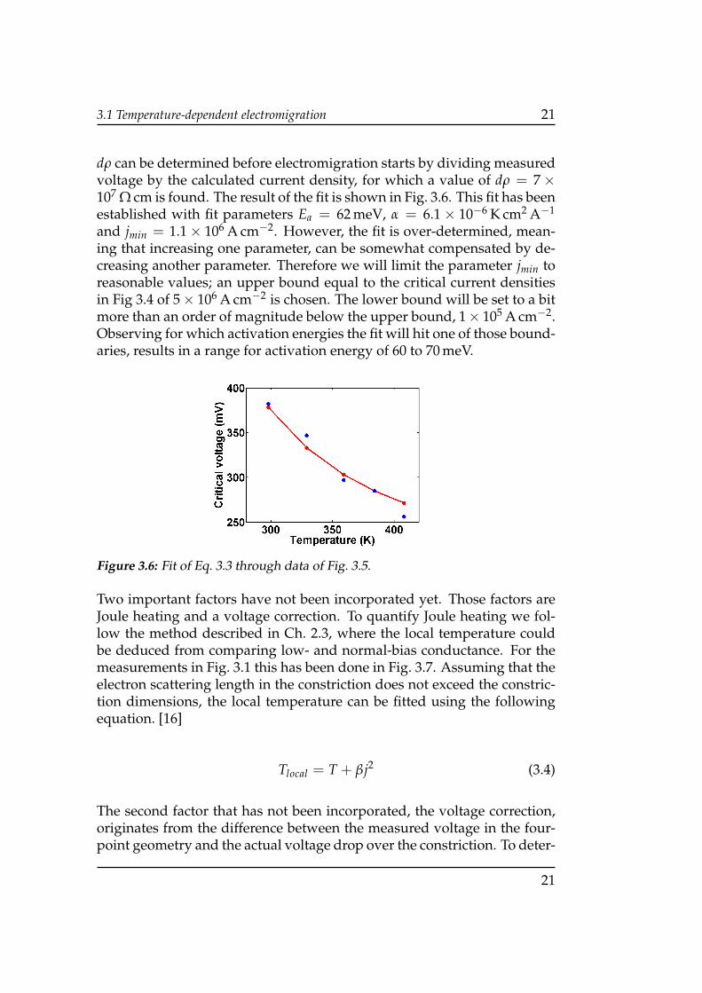
dρ can be determined before electromigration starts by dividing measuredvoltage by the calculated current density, for which a value of dρ = 7×10⁷ Ω cm is found. The result of the fit is shown in Fig. 3.6. This fit has beenestablished with fit parameters Ea = 62 meV, α = 6.1× 10⁻⁶ K cm2 A−1
and jmin = 1.1× 10⁶ A cm−2. However, the fit is over-determined, mean-ing that increasing one parameter, can be somewhat compensated by de-creasing another parameter. Therefore we will limit the parameter jmin toreasonable values; an upper bound equal to the critical current densitiesin Fig 3.4 of 5× 10⁶ A cm−2 is chosen. The lower bound will be set to a bitmore than an order of magnitude below the upper bound, 1× 10⁵ A cm−2.Observing for which activation energies the fit will hit one of those bound-aries, results in a range for activation energy of 60 to 70 meV.
Figure 3.6: Fit of Eq. 3.3 through data of Fig. 3.5.
Two important factors have not been incorporated yet. Those factors areJoule heating and a voltage correction. To quantify Joule heating we fol-low the method described in Ch. 2.3, where the local temperature couldbe deduced from comparing low- and normal-bias conductance. For themeasurements in Fig. 3.1 this has been done in Fig. 3.7. Assuming that theelectron scattering length in the constriction does not exceed the constric-tion dimensions, the local temperature can be fitted using the followingequation. [16]
Tlocal = T + βj2 (3.4)
The second factor that has not been incorporated, the voltage correction,originates from the difference between the measured voltage in the four-point geometry and the actual voltage drop over the constriction. To deter-
21

22 Results
(a) (b)
Figure 3.7: a) Local temperatures as a function of current density. The local tem-perature is derived by looking at the difference in conduction for normal-bias andlow-bias conduction measurements. The curves in blue show each a new deviceat a different base temperature on which electromigration was performed. In red,fits to Eq. 3.4 are shown with β = (3.1± 1.2)× 10−12 K cm4 A−2. b) Local temper-ature at the critical current density as a function of base temperature.
mine this difference, a COMSOL simulation has been performed. In thissimulation, the constriction and a part of the bismuth towards the goldcontacts have been modeled and a voltage bias is set over this model. Theresulting potential map is depicted in Fig. 3.8. The simulation shows thatthe voltage drop over the actual constriction is approximately 60% of themeasured bias.
(a) (b)
Figure 3.8: a) A SEM image of a bismuth constriction, showing the area beingsimulated in COMSOL. b) The COMSOL simulation, depicting the potential dropover the bismuth constriction. The left and right edge are set to 0 and 1 V respec-tively.
22

3.2 In-situ electromigration in SEM 23
Correcting for both Joule heating and the voltage correction is done inFig. 3.9. Obtained fit parameters are Ea = 113 meV, α = 3.7× 10⁻⁵ K cm2 A−1
and jmin = 6.7× 10⁵ A cm−2. Using the same boundary conditions for jminas before, a range for Ea is obtained from 100 to 180 meV.
Figure 3.9: Fit of Eq. 3.3 through data of Fig. 3.5, using the local temperature andvoltage correction.
3.2 In-situ electromigration in SEM
In Ch. 3.1 it was shown that the electromigration process is more dy-namic than one would expect according to the model in Ch. 1.3. For ex-ample, jumps upward in conduction were measured during electromigra-tion, a feature that is not incorporated in the model. Furthermore, imageswere shown which were taken after electromigration had occurred. Theseimages could however not tell anything about the time evolution of anelectromigration-created nanogap. In this chapter, a further look is takeninto what dynamics are present during electromigration.
One of the few ways to further investigate what processes are going on, isto visually take a look at the device during electromigration. This cannotbe done optically, because the feature size is smaller than the diffractionlimit, but it can be done using a SEM. For this purpose a SEM with electri-cal feedthroughs was used. Electromigration was performed on devices inthe SEM, and after every feedback loop in the electromigration software, apicture was taken. This allows for detecting changes in the devices on thecrystal grain level.
23

24 Results
In Fig. 3.10 stills from a movie of electromigration in SEM are shown inchronological order. The number in the upper right corner of every imageis the conductance value at that point in time in units of G0. In Fig. 3.10 (b)till (d), single grains are seen to electromigrate. An interesting observationin (d) is that is seems like there is a second layer underneath the elec-tromigrated grains, which might be conducting. In (e) the conductancehas dropped to 0.5 G0 and in the next still the conductance jumped up to18.0 G0, which we can visually link to the remerging of the two electrodesby a small bismuth bridge (indicated by red marker in (f)). In (g) thisbridge is seen to be mobile and moving downwards until breaking againin (h). (i) shows a reordering of the crystal structure with respect to (h).This is an interesting event, since the reordered crystal looks uniform inthe image. This indicates that this could be a crystalline piece of bismuth.Such area could form the basis for a bilayer of a more significant size. Fi-nally the last two figures show a widening of the gap to huge dimensions.
An explanation for the remerging of the electrodes in Fig. 3.10 (f) is field-emission-induced electromigration, a process under study by the group ofShirakashi. [30–33]. In this process, the field emission current is inducedby the electrostatic field. This causes locally high current densities andtherefore material can be deposited towards the gap from one of the elec-trodes. However, the exact opposite argument can be given for materialmoving away from the gap on the other electrode. In Ref. [31], merging ofa nanogap of 44 nm is shown. During this process, a voltage of 23 V wasapplied with a corresponding current of 0.83 nA. Since in the experimentsdescribed in this thesis, voltages two orders of magnitude lower are used,field-emission-induced electromigration is deemed unlikely.
Another, more plausible, explanation for electrode remerging is field-enhancedsurface diffusion. In the nanogap high electric field are present. This couldenhance the diffusion along the edge of the nanogaps towards the oppo-site side of the nanogap. This way remerging of the nanogap could beexplained.
The aftermath of the whole electromigration experiment in Fig. 3.10 is de-picted in Fig. 3.11. Shown is a zoom-out of the area in Fig. 3.10. Identifiableby the white stripe is the left border of the area in which the experimenthas been performed. Also visible is electromigration outside this area. Apossible explanation for the electromigration just outside the area of theexperiment is a build-up of carbon due to the scanning electron beam. Ifthis carbon layer becomes thick enough it will become conducting. The
24

3.2 In-situ electromigration in SEM 25
Figure 3.10: Stills from a movie of electromigration performed in SEM in chrono-logical order. The upper right number shows the conduction value in G0. The left(right) electrode is the anode (cathode). The red marker in (f) shows a bismuthbridge, which reconnects the bismuth electrodes.
25

26 Results
highest current density will then occur just besides the deposited carbonlayer. A conductive carbon layer can also explain why the huge gap inFig. 3.10 (k) is still conductive.
Another remarkable feature is the bump seen on the cathode side of Fig. 3.11.Possibly the material from the gap has been deposited here. Unfortunately,no images prior to electromigration including this area were taken to con-firm this.
Figure 3.11: Zoom-out of the device electromigrated in Fig. 3.10. The electromi-gration far left of the constriction could have been caused by a possible carbonlayer, deposited by the scanning electron beam.
3.3 Constriction width dependency
During the studies in this thesis, many devices have been electromigrated.A random selection of SEM images of created nanogaps is shown in Fig. 3.12.All the nanogaps are positioned in the middle of the constriction and noobvious anode-cathode-asymmetry is observed. An explanation for thenanogaps appearing in the middle of the constriction is first, the fact thatthe current density is at a maximum at that point, and second, that Jouleheating is most pronounced there because of this current density.
Our collaborators from The National Centre for High Resolution ElectronMicroscopy at Delft University performed electromigration on thin bis-
26

3.3 Constriction width dependency 27
muth wires. These wires are 200 nm wide, 1 µm in length and 50 nm high.The connections to this wire are also made of a 50 nm thick bismuth layer.In contrast to our findings, they observe a pronounced anode-cathode-asymmetry. Electromigration is observed to take place a few hundrednanometers outside the wire in the bismuth contacts, and always on thecathode side.
Figure 3.12: SEM images of bismuth constrictions after electromigration. Al-though it is unknown which side of the electrodes the anode/cathode side is, nosignificant asymmetries are observed. All the constrictions are between 500 nmand 600 nm in width.
A possible explanation for electromigration not occurring in the constric-tion itself could be that the linewidth is on the order of the bismuth grainsize. Therefore these lines could be bamboo lines which where explainedin Ch. 1.3. The lines could therefore have a reduced susceptibility to elec-tromigration, hence the electromigration would occur just outside the pat-terned lines.
27
28 Results
An attempt was done to create samples in Leiden with the same layout asin Delft. This resulted in devices with lines of 2 µm in length and a widthof 400 nm. On five of those structures electromigration was performed.In all devices electromigration occurred in the lines and not on one of theelectrodes. A possible explanation for this could be that the lines were notthin enough, and that the bamboo regime was not reached.
No consistent anode-cathode-asymmetry has been observed in Leiden elec-tromigration experiments.
28

Chapter 4Conclusion
We have studied electromigration in bismuth constrictions. Temperature-dependent electromigration measurement have been performed, whichhave been analyzed in terms of critical current and critical voltage. Localtemperatures have been deducted using a normal/low-bias measurementscheme. Using these local temperatures, a model including Joule heatingprovided a method of describing those measurements. This way the acti-vation energy for diffusion is estimated to be between 100 and 180 meV.
In the temperature-dependent electromigration measurements, upwardjumps in conductance were observed. By performing in-situ electromi-gration in a SEM, the origin of those jumps was resolved, as they werefound to be correlated with electrode remerging within the bismuth layer.Furthermore it was observed that during electromigration crystal reorder-ing might take place, possibly creating areas of crystalline bismuth. Thiscould form a basis for a bismuth bilayer.
Finally, a study was performed on anode-cathode-asymmetry as a func-tion of constriction width. In Delft anode-cathode-asymmetry was ob-served on bismuth wires with dimensions of 200 nm in width and 1 µmin length. This asymmetry manifested itself by electromigration only be-ing observed on the cathode side of the wire. After electromigration onbismuth wires in Leiden with dimensions of 400 nm in width and 2 µm inlength, anode-cathode-asymmetry was not observed. Furthermore, dur-ing this whole study, such an asymmetry was not consistently observed.
29


Chapter 5Outlook
In the studies presented in this thesis, polycrystallinity of the studied bis-muth films has posed challenges regarding reproduciblility on a devicelevel. In Ch. 3.2, where the electromigration was done in-situ in SEM,crystal reordering was observed. This crystal reordering possibly createda crystalline layer, which was larger than the bismuth grain size. Such alayer could form a perfect basis for a bismuth bilayer. However, it is un-known how reproducible the formation of such layers is. Therefore, wepropose two approaches in which polycrystallinity does not play a role.
As a first approach, we propose to use crystalline bismuth(111) flakes,which can be extracted from bismuth crystals. When those flakes are de-posited on a substrate, they can be contacted using lithography. The mainchallenge for applying this method, is the creation of proper flakes. Flakescreated by using a scalpel on a bismuth crystal should be thin and smallwith dimension of the order of the constrictions used in this thesis (500by 50 nm). Flakes created using the proposed method will create a lot ofbigger flakes in the order of tens of micrometers. A proper pre-selection inSEM should be done to successfully do electromigration on flakes.
A second approach to do electromigration in which polycrystallinity shouldbe excluded, is to fabricate bamboo lines. Since these lines are only a singlegrain in width, there should not be any variation in the starting conduc-tance of the devices. In order to fabricate bamboo lines, widths of 100 nmshould be sufficient.
31

32 Outlook
During the in-situ electromigration experiment in the SEM, problems withcarbon build-up were encountered. This degraded the resolution of theSEM images drastically. For a future in-situ imaging experiment, a SEMwith a better vacuum could be used. Another option would be to do theseexperiments in a transmission electron microscope, where both the reso-lution and the vacuum are higher.
32
Appendix ALithography on mica
Measurements performed by Urata indicated that evaporation of bismuthon mica could decrease polycrystallinity of the bismuth thin film. [34]Therefore, an attempt was done to perform nanolithography on mica. Thisopposes a challenge due to the electrical insulating properties, renderingelectron beam lithography (EBL) difficult.
A way to cope with the insulating properties of the mica substrate, is spin-coating a conductive polymer on top of the resist, PEDOT:PSS. This shouldallow charges, which could build-up on the surface of the mica, to diffuseto the ground. Two examples of EBL done using PEDOT:PSS are shown inFig. A.1.
Both examples show large areas where the resist has been exposed, whileit should not have been exposed. This can be attributed to charge build-up. PEDOT:PSS turns out to be inefficient as a way to counter this chargebuild-up.
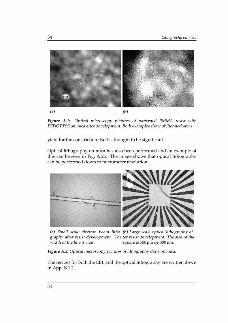
In Fig. A.1b another interesting observation can be done. The small scaledose test itself seems to be patterned without any problem. Therefore, analternative way to perform the lithography might be to do large contactparts (up to micrometer scale) with optical lithography, and the smallerpatterns with EBL. To test if this approach could work, a constriction hasbeen patterned on mica using EBL in Fig. A.2a. The image shows that onmicrometer sized features, charge build-up still plays a role. However, the
33
34 Lithography on mica
(a) (b)
Figure A.1: Optical microscopy pictures of patterned PMMA resist withPEDOT:PSS on mica after development. Both examples show obliterated areas.
yield for the constriction itself is thought to be significant.
Optical lithography on mica has also been performed and an example ofthis can be seen in Fig. A.2b. The image shows that optical lithographycan be performed down to micrometer resolution.
(a) Small scale electron beam litho-graphy after resist development. Thewidth of the line is 5 µm.
(b) Large scale optical lithography af-ter resist development. The size of thesquare is 500 µm by 500 µm.
Figure A.2: Optical microscopy pictures of lithography done on mica.
The recipes for both the EBL and the optical lithography are written downin App. B.1.2.
34

Appendix BMethods and recipes
B.1 Recipes
B.1.1 General sample fabrication
• Clean Si/SiO2 substrate by ultrasonication in demiwater, acetoneand IPA subsequently for 2 minutes each.
• First lithographic step for electrical contacts:
– Spincoat PMMA 200 KDa at 4000 RPM for 60 seconds, bake at180C for 100 seconds.
– Spincoat PMMA 950 KDa at 4000 RPM for 60 seconds, bake at180C for 100 seconds.
– Expose at a dose of 600 µC cm−2.
– develop for 40 seconds in MIBK:IPA/1:3 and stop in IPA.
– Evaporate 4 nm chromium at a rate of 0.1 A s−1.
– Evaporate 20 nm gold at a rate of 1.0 A s−1.
– Lift-off in acetone and optionally use an ultrasonic bath withcare.
• Second lithographic step for bismuth constrictions:
35

36 Methods and recipes
– Spincoat PMMA 950 KDa at 4000 RPM for 60 seconds, bake at180C for 100 seconds.
– Expose at a dose of 300 µC cm−2.
– develop for 50 seconds in MIBK:IPA/1:3 and stop in IPA.
– Evaporate bismuth at a rate of 1.0 A s−1.
– Lift-off in acetone.
B.1.2 Mica lithography
• Optical lithography:
– Cleave mica substrate
– Spincoat highly viscous positive tone photoresist (ma-P 1275) at4000 RPM for 60 seconds, bake at 200C for 120 seconds .
– UV exposure at a dose of 6-8 mW for 90 seconds.
– Develop in AR 300-47 until structures are fully developed. Checkthis visually, it will take about 10 minutes. Stop in demiwater.
– Evaporate 20 nm gold at a rate of 1.0 A s−1.
– Lift-off in acetone and optionally use an ultrasonic bath withcare.
• Second lithographic step for bismuth constrictions:
– Spincoat PMMA 950 KDa at 4000 RPM for 60 seconds, bake at180C for 100 seconds.
– Spincoat PEDOT:PSS
– Expose at a dose of 250 µC cm−2.
– Wash with demiwater for PEDOT:PSS removal
– Develop for 40 seconds in MIBK:IPA/1:3 and stop in IPA.
– Evaporate bismuth at a rate of 1.0 A s−1.
– Lift-off in acetone.
36

B.2 Feedback settings 37
B.2 Feedback settings
For all the electromigration measurements in this thesis, the labview pro-gram ’Electromigration v20.vi’was used with the start settings depicted inFig. B.1.
Figure B.1: Settings used at the start of an electromigration measurement. To startthe measurement, the ’Max voltage(V)’ setting is set to 5. During the electromi-gration the feedback threshold ’Th%’ is increased if necessary.
37


References
[1] S. A. Wolf, D. D. Awschalom, R. A. Buhrman, J. M. Daughton, S. vonMolnar, M. L. Roukes, A. Y. Chtchelkanova, and D. M. Treger, Spin-tronics: A Spin-Based Electronics Vision for the Future, Science 294, 1488(2001).
[2] T. Yokoyama and S. Murakami, Spintronics and spincaloritronics intopological insulators, Physica E: Low-dimensional Systems andNanostructures 55, 1 (2014).
[3] A. Mellnik et al., Spin-transfer torque generated by a topological insulator,Nature 511, 449 (2014).
[4] H. Zhang, C.-X. Liu, X.-L. Qi, X. Dai, Z. Fang, and S.-C. Zhang, Topo-logical insulators in Bi2Se3, Bi2Te3 and Sb2Te3 with a single Dirac cone onthe surface, Nature physics 5, 438 (2009).
[5] Y. L. Chen, J. G. Analytis, J.-H. Chu, Z. K. Liu, S.-K. Mo, X. L. Qi, H. J.Zhang, D. H. Lu, X. Dai, Z. Fang, S. C. Zhang, I. R. Fisher, Z. Hus-sain, and Z.-X. Shen, Experimental Realization of a Three-DimensionalTopological Insulator, Bi2Te3, Science 325, 178 (2009).
[6] J. C. Y. Teo, L. Fu, and C. L. Kane, Surface states and topological invari-ants in three-dimensional topological insulators: Application to Bi1−xSbx,Phys. Rev. B 78, 045426 (2008).
[7] T. H. Hsieh, H. Lin, J. Liu, W. Duan, A. Bansil, and L. Fu, Topologicalcrystalline insulators in the SnTe material class, Nature communications3, 982 (2012).
[8] M. Konig, S. Wiedmann, C. Brune, A. Roth, H. Buhmann, L. W.Molenkamp, X.-L. Qi, and S.-C. Zhang, Quantum Spin Hall InsulatorState in HgTe Quantum Wells, Science 318, 766 (2007).
39

40 References
[9] S. Murakami, Quantum Spin Hall Effect and Enhanced Magnetic Re-sponse by Spin-Orbit Coupling, Phys. Rev. Lett. 97, 236805 (2006).
[10] M. Z. Hasan and C. L. Kane, Colloquium : Topological insulators, Rev.Mod. Phys. 82, 3045 (2010).
[11] K. Zhu et al., The emergence of topologically protected surface states inepitaxial Bi (111) thin films, arXiv preprint arXiv:1403.0066 (2014).
[12] C. Sabater, D. Gosalbez-Martınez, J. Fernandez-Rossier, J. G. Rodrigo,C. Untiedt, and J. J. Palacios, Topologically Protected Quantum Transportin Locally Exfoliated Bismuth at Room Temperature, Phys. Rev. Lett. 110,176802 (2013).
[13] T. Hirahara, G. Bihlmayer, Y. Sakamoto, M. Yamada, H. Miyazaki,S.-i. Kimura, S. Blugel, and S. Hasegawa, Interfacing 2D and 3D Topo-logical Insulators: Bi(111) Bilayer on Bi2Te3, Phys. Rev. Lett. 107, 166801(2011).
[14] H. Huntington and A. Grone, Current-induced marker motion in goldwires, Journal of Physics and Chemistry of Solids 20, 76 (1961).
[15] D. Pierce and P. Brusius, Electromigration: A review, MicroelectronicsReliability 37, 1053 (1997).
[16] M. L. Trouwborst, S. J. van der Molen, and B. J. van Wees, The role ofJoule heating in the formation of nanogaps by electromigration, Journal ofApplied Physics 99, (2006).
[17] A. Verbruggen, Fundamental questions in the theory of electromigration,IBM Journal of Research and Development 32, 93 (1988).
[18] R. Landauer, Comment on Lodder’s “exact” electromigration theory, SolidState Communications 72, 867 (1989).
[19] I. A. Blech and E. S. Meieran, Electromigration in Thin Al Films, Journalof Applied Physics 40, 485 (1969).
[20] K. N. Tu, Recent advances on electromigration in very-large-scale-integration of interconnects, Journal of Applied Physics 94, 5451 (2003).
[21] M. de Wit, Towards a Bilayer of Bismuth as a Topological Insulator at RoomTemperature, Master’s thesis, Leiden University, 2014.
[22] C.-K. Hu, R. Rosenberg, and K. Y. Lee, Electromigration path in Cu thin-film lines, Applied Physics Letters 74, 2945 (1999).
[23] J. Cho and C. V. Thompson, Grain size dependence of electromigration-induced failures in narrow interconnects, Applied Physics Letters 54,2577 (1989).
40

References 41
[24] S. Sangiao, J. M. Michalik, L. Casado, M. C. Martinez-Velarte,L. Morellon, M. R. Ibarra, and J. M. De Teresa, Conductance steps inelectromigrated Bi nanoconstrictions, Phys. Chem. Chem. Phys. 15, 5132(2013).
[25] D. R. Strachan, D. E. Smith, D. E. Johnston, T.-H. Park, M. J. Therien,D. A. Bonnell, and A. T. Johnson, Controlled fabrication of nanogaps inambient environment for molecular electronics, Applied Physics Letters86, (2005).
[26] Z. M. Wu, M. Steinacher, R. Huber, M. Calame, S. J. van der Molen,and C. Schonenberger, Feedback controlled electromigration in four-terminal nanojunctions, Applied Physics Letters 91, (2007).
[27] Y. Kanamaru, M. Ando, and J.-i. Shirakashi, Ultrafast feedback-controlled electromigration using a field-programmable gate array, Journalof Vacuum Science & Technology B 33, (2015).
[28] P. Cucka and C. S. Barrett, The crystal structure of Bi and of solid solutionsof Pb, Sn, Sb and Te in Bi, Acta Crystallographica 15, 865 (1962).
[29] V. Skudnov, L. Sokolov, A. Gladkikh, and V. Solenov, Mechanical prop-erties of bismuth at different temperature and strain rates, Metal Scienceand Heat Treatment 11, 981 (1969).
[30] Y. Tomoda, K. Takahashi, M. Hanada, W. Kume, and J.-i. Shirakashi,Fabrication of nanogap electrodes by field-emission-induced electromigra-tion, Journal of Vacuum Science & Technology B 27, 813 (2009).
[31] S. Kayashima, K. Takahashi, M. Motoyama, and J. Shirakashi, Wide-range control of tunnel resistance on metallic nanogaps using migration,Journal of Physics: Conference Series 100, 052022 (2008).
[32] S. Ueno, Y. Tomoda, W. Kume, M. Hanada, K. Takiya, and J. ichi Shi-rakashi, Field-emission-induced electromigration method for the integra-tion of single-electron transistors, Applied Surface Science 258, 2153(2012), International Vacuum Congress (IVC-18).
[33] W. Kume, Y. Tomoda, M. Hanada, and J.-I. Shirakashi, Fabricationof Single-Electron Transistors Using Field-Emission-Induced Electromigra-tion, Journal of Nanoscience and Nanotechnology 10, 7239 (2010).
[34] T. Urata, The road to a single bi-layer bismuth as a 2 dimensional topologicalinsulator, Master’s thesis, Leiden University, 2014.
41