Experimental Study of MOS Capacitors as Wireless … · MOS capacitor is used in passive state,...
75
Experimental Study of MOS Capacitors as Wireless Radiation Dose Sensors by Madusudanan Srinivasan Gopalan A Thesis Presented in Partial Fulfillment of the Requirements for the Degree Master of Science Approved November 2010 by the Graduate Supervisory Committee: Hugh Barnaby, Chair Keith Holbert Hongyu Yu ARIZONA STATE UNIVERSITY December 2010
Transcript of Experimental Study of MOS Capacitors as Wireless … · MOS capacitor is used in passive state,...

Experimental Study of MOS Capacitors as Wireless Radiation Dose Sensors
by
Madusudanan Srinivasan Gopalan
A Thesis Presented in Partial Fulfillment
of the Requirements for the Degree
Master of Science
Approved November 2010 by the
Graduate Supervisory Committee:
Hugh Barnaby, Chair
Keith Holbert
Hongyu Yu
ARIZONA STATE UNIVERSITY
December 2010

i
ABSTRACT
The RADiation sensitive Field Effect Transistor (RADFET) has been
conventionally used to measure radiation dose levels. These dose sensors are
calibrated in such a way that a shift in threshold voltage, due to a build-up of
oxide-trapped charge, can be used to estimate the radiation dose. In order to
estimate the radiation dose level using RADFET, a wired readout circuit is
necessary. Using the same principle of oxide-trapped charge build-up, but by
monitoring the change in capacitance instead of threshold voltage, a wireless dose
sensor can be developed. This RADiation sensitive CAPacitor (RADCAP)
mounted on a resonant patch antenna can then become a wireless dose sensor.
From the resonant frequency, the capacitance can be extracted which can be
mapped back to estimate the radiation dose level. The capacitor acts as both
radiation dose sensor and resonator element in the passive antenna loop. Since the
MOS capacitor is used in passive state, characterizing various parameters that
affect the radiation sensitivity is essential. Oxide processing technique, choice of
insulator material, and thickness of the insulator, critically affect the dose
response of the sensor. A thicker oxide improves the radiation sensitivity but
reduces the dynamic range of dose levels for which the sensor can be used. The
oxide processing scheme primarily determines the interface trap charge and
oxide-trapped charge development; controlling this parameter is critical to
building a better dose sensor.

ii
DEDICATION
To my family

iii
ACKNOWLEDGMENTS
I would like to express my sincere gratitude to my advisor Dr. Hugh
Barnaby, for his continuous support and invaluable guidance, during the course of
the work. His patience and trust in my capabilities helped me to overcome the
pressure of unsuccessful experiments. I am grateful to Dr. Keith Holbert and Dr.
Hongyu Yu, my committee members, for their time and efforts to review my
work. I would like to thank Barry Wilkens and David Wright for helping me
conduct the proton beam experiments and patiently accommodating my
experiments on their schedule. I would like to specially thank Craig Birtcher who
wire-bonded innumerable samples for my experiments.
I take this opportunity to thank Achal Kathuria, Jonathon Oiler and Ivan
Sanchez Esqueda for helping me with the experiments and constructive
discussions I had with them
I am indebted to my family for their unconditional love and emotional
support throughout my graduate studies. I would also like to thank my room
mates Jagdish, Rajesh, Siva and Jaiganesh for their company and emotional
support throughout.

iv
TABLE OF CONTENTS
Page
LIST OF TABLES ............................................................................................. vii
LIST OF FIGURES .......................................................................................... viii
CHAPTER
1 INTRODUCTION .......................................................................................... 1
1.1 Historical background .............................................................. 1
1.2 Motivation .............................................................................. 1
1.3 Thesis outline and organization ................................................ 2
2 ELECTRICAL RESPONSE OF MOS CAPACITORS TO RADIATION ........ 4
2.1 Introduction ............................................................................. 4
2.2 Parametric shifts due to ionizing radiation ................................ 5
3 RADFET DOSIMETERS ............................................................................... 8
3.1 Introduction ............................................................................. 8
3.2 Principle of operation .............................................................. 8
3.3 RADFET readout circuit ........................................................ 10
3.4 Modes of operation ................................................................ 12
3.4.1 Biased mode ................................................................... 12
3.4.2 Unbiased mode ............................................................... 13
3.5 Parametric dependencies ........................................................ 14
3.5.1 Oxide thickness ............................................................... 14
3.5.2 Oxide processing technique ............................................. 14
3.6 Limitations of RADFET dosimeter ........................................ 15

v
CHAPTER Page
3.7 Low dose resolution .............................................................. 17
3.8 Post-irradiation behavior ........................................................ 17
3.9 Major applications ................................................................. 18
3.10 Advantages of RADFET dosimeter ...................................... 18
4 MOS CAPACITORS AS RADIATION DOSE SENSORS ........................... 20
4.1 Introduction ........................................................................... 20
4.2 Design of wireless sensor system ........................................... 20
4.3 Energy band diagram of MOS capacitor ................................. 21
4.4 Ideal MOS capacitor threshold voltage ................................... 23
4.5 MOS capacitance – voltage Behavior ..................................... 26
4.6 Non-Ideal capacitance – voltage Behavior .............................. 29
4.6.1 Fixed oxide charge- Qf .................................................... 29
4.6.2 Interface trap charge- Qit ................................................. 30
4.7 Extraction of oxide-trapped charge and interface trap charge
from C-V curve.................................................................... 31
5 THE DOSE PERFORMANCE OF THE RADCAP ....................................... 33
5.1 Processing technique ............................................................. 33
5.1.1 Wet oxidation and dry oxidation ..................................... 33
5.1.1.1 Experiment results .................................................... 35
5.1.2 Thermally grown high quality oxide................................ 41
5.1.2.1 Fabrication steps ....................................................... 41
5.1.2.2 Experiment results .................................................... 43

vi
CHAPTER Page
5.2 Dielectric material ................................................................. 46
5.2.1 Experiment results .......................................................... 48
5.3 Impact of oxide thickness ...................................................... 52
5.3.1 Experiment results .......................................................... 52
5.4 Post-irradiation behavior ........................................................ 54
5.5 Discussion on initial precursor hole trap density ..................... 56
6 CONCLUSION ............................................................................................ 58
REFERENCES .................................................................................................. 59

vii
LIST OF TABLES
Table Page
1. Comparison of sensitivity at zero bias for different oxide processing
schemes ........................................................................................ 15
2. Advantages and disadvantages of conventional dosimeters ............... 19
3. Comparison of properties of silicon nitride and silicon dioxide ......... 47
4. Loss of oxide-trapped charge and midgap voltage shifts resulting
from room temperature annealing .................................................. 56
5. Initial precursor hole trap density estimated from simulation for
various processing schemes ........................................................... 56

viii
LIST OF FIGURES
Figure Page
1. Illustration of transport of carriers in oxide ........................................ 5
2. Impact of oxide-trapped charge and interface trap charge on C-V
curves ............................................................................................. 7
3. Cross section of the RADFET dosimeter ........................................... 9
4. Illustration of shift in gate voltage in a p-channel RADFET due to
radiation ....................................................................................... 10
5. Measurement setup used to read out the threshold voltage of the
RADFET ...................................................................................... 11
6. Fractional charge yield as function of dose for different ionizing
radiation ....................................................................................... 13
7. Data showing the erasure of oxide-trapped charge due to high
temperature annealing ................................................................... 16
8. Energy band diagram of ideal MOS capacitor ................................. 22
9. Energy band diagram of MOS capacitor showing potentials and
spatial dimension .......................................................................... 23
10. Schematic representation of MOS capacitor .................................... 26
11. Comparison of ideal MOS C-V curve with experimental data .......... 28
12. Comparison of experimental data with non ideal MOS C-V curve ... 29
13. Illustration of interface states at different biasing conditions in an
MOS capacitor .............................................................................. 31
ix
Figure Page
14. Pre-irradiation and post-irradiation C-V curves of RADCAP with
100 nm (dry) oxide thickness......................................................... 36
15. Pre-irradiation and post-irradiation C-V curves of RADCAP with
200 nm (wet) oxide thickness ........................................................ 36
16. Experimental data of normalized oxide-trapped charge density of
RADCAP with 100 nm (dry) and 200 nm (wet) oxide thickness ..... 37
17. Experimental data of normalized interface trap density of
RADCAP with 100 nm (dry) and 200 nm (wet) oxide thickness ..... 38
18. Comparison of oxide-trapped charge per unit area for RADCAP
with 200 nm oxide thickness (wet) obtained from simulation and
experimental data .......................................................................... 39
19. Comparison of oxide-trapped charge per unit area for RADCAP
with 100 nm oxide thickness (dry) obtained from simulation and
experimental data .......................................................................... 40
20. Comparison of midgap voltage shifts for RADCAP with 200 nm
oxide thickness (wet) obtained from simulation and experimental
data .............................................................................................. 40
21. Comparison of midgap voltage shifts for RADCAP with 100 nm
oxide thickness (dry) obtained from simulation and experimental
data .............................................................................................. 41
22. Fabrication steps to manufature capacitors using SOI wafers ........... 42

x
Figure Page
23. Package containing RADCAPs with high quality oxide and the
proton beam chamber used for irradiation ...................................... 43
24. Experimental data showing radiation response of RADCAP with
high quality oxide ......................................................................... 44
25. Capacitance versus dose map for RADCAP with high quality
oxide ............................................................................................ 45
26. Comparison of oxide-trapped charge per unit area for RADCAP
with high quality oxide obtained from simulation and experimental
data .............................................................................................. 46
27. Pre-irradiation and post-irradiation C-V curves of RADCAP with
silicon nitride as insulator .............................................................. 48
28. Pre-irradiation and post-irradiation C-V curves of RADCAP with
silicon dioxide as insulator ............................................................ 49
29. Comparison of normalized oxide-trapped charge density of silicon
nitride and silicon dioxide RADCAP samples as a function of dose 50
30. Ratio of oxide-trapped charge density of silicon dioxide and silicon
nitride RADCAP samples as a function of dose ............................. 50
31. Comparison of oxide-trapped charge per unit area for silicon
nitride RADCAP obtained from simulation and experimental data . 51
32. Comparison of normalized oxide-trapped charge per unit area for
RADCAPs with 100 nm, 200 nm oxide thickness as a function of
dose .............................................................................................. 53

xi
Figure Page
33. Comparison of normalized interface state charge per unit area for
RADCAPs with 100 nm, 200 nm oxide thickness as a function
of dose ......................................................................................... 54
34. Comparison of annealing behavior observed in RADCAPs
manufactured using different processing techniques ....................... 55

1
Chapter 1
INTRODUCTION
1.1 Historical background
The RADiation sensitive Field Effect Transistor (RADFET) has been used
as a radiation dose sensor for the past 30 years [1-3]. They find their use in
various applications like unmanned satellites, nuclear industry and radiotherapy.
These sensors measure total ionizing dose through radiation induced threshold
voltage shifts. These shifts are due to build-up of fixed charge in the sensitive gate
oxide during radiation exposure [2-5]. The dose sensitivity and dynamic range of
these sensors have been well studied [3-9]. As compared to other conventional
techniques, these sensors are fairly low power [5], and are easily integrated into
electronic instrumentation. Nevertheless RADFETs require some power to
operate and, in most applications, are wired directly to readout circuitry which
must be resistant to radiation damage. Efforts to develop wireless radiation dose
sensors have gained momentum especially in the field of radiotherapy. RADPOS,
a wireless dose sensor, uses an RF position system to record dose and position
within the patient simultaneously [7]. The cost of these systems limits their usage
in other general purpose radiation detection applications. Defense and nuclear
security applications also benefit from the use of wireless radiation sensors, where
remote, convert detection at standoff range are much desired features.
1.2 Motivation
The threat of an attack with radiological or nuclear materials has increased
so much that monitoring the movement of radioactive material is imperative.

2
Unfortunately critical gaps exist in the ability to detect and disrupt pathways for
these types of Weapons of Mass Destruction (WMDs). While active detection
methodologies provide some advantage in this arena, neutron or gamma
radiography comes at the cost of introducing additional man-made radiation.
Moreover, the complexities of active systems make them difficult to be used
unattended or without being revealed. Ideally these systems should be somewhat
low in cost, small in size, require little to no power and operate wirelessly. This
would allow an array of such sensors to be embedded into surface coatings and used
to monitor a multitude of pathways for hazardous nuclear material in and out of
the country. Such attributes would also be advantageous for medical applications,
particularly sensors monitoring radiation dose during cancer radiotherapy. For
example, a detector mesh conforming to a tumor volume could be constructed of
miniaturized passive detectors to provide real time verification of the radiation
dose delivered. This type of in-vivo dose verification could significantly reduce
the possibility of overdose to healthy tissue and minimize the possibility of severe
misadministration of high dose rate radiation.
A sensor with these specifications may be realized with a solid state
RADiation sensitive CAPacitor (RADCAP) mounted on a resonant patch antenna.
In order to develop the RADCAP it is necessary to understand and control the
different parameters influencing its radiation sensitivity.
1.3 Thesis outline and organization
The organization of the thesis is as follows: Chapter 2 presents the general
impact of radiation on the operation of solid state MOS capacitors. Chapter 3

3
reviews the operating principle of the RADFET dosimeter. Chapter 4 presents the
technique to use RADCAP as a radiation dose sensor that can be used for remote
wireless sensing applications. The influence of different parameters on the
operation and sensitivity of MOS capacitors to ionizing radiation is discussed in
Chapter 5. Chapter 6 summarizes the key contribution of this thesis.

4
Chapter 2
ELECTRICAL RESPONSE OF MOS CAPACITORS TO RADIATION
2.1 Introduction
The major impact of radiation on MOS devices is the build-up of fixed
charge in the insulator beneath the gate of the device. Due to build-up of fixed
charge, the electrical characteristics of the device changes. Most modern MOS
structures have silicon dioxide (SiO2) as the insulator. When a MOS device is
exposed to ionizing radiation, energy is deposited in the oxide. The amount of
energy deposited depends on the Linear Energy Transfer (LET) of the primary or
secondary particles that pass through the oxide material. This energy creates
electron-hole pairs which move under the influence of the applied electric field.
Since the mobility of electrons in oxides is much higher than holes, electrons are
swept out by the applied or intrinsic electric field while holes move slowly in the
direction of the field. Some of the holes become trapped in the oxide and form
fixed positive charge. This charge causes the flat-band voltage of the MOS system
to change, which, for the MOS capacitor, is manifested as a negative shift in the
capacitance vs. voltage (C-V) curve. The damage caused by irradiation is
dependent on temperature, oxide thickness, applied field and oxide processing
techniques.
One of the most important factors affecting the dose response of a MOS
system is the Si/SiO2 interfacial properties. As oxides are grown, oxygen diffuses
to the interface where it reacts with the bulk silicon. Not all of silicon atoms at the
interface are oxidized which leaves some dangling bonds at the interface. These

5
dangling bonds at the interface give rise to interface states in the band gap which
affect the shape of the C-V curve. In addition to dangling bonds, oxygen
vacancies in the bulk of the dielectric, typically result during processing. The
vacancies are considered to be the primary precursor defects which trap holes
during radiation exposure. It is important to study the impact of different
oxidation techniques on the formation of interface traps and oxygen vacancies
since they determine the radiation sensitivity of the MOS capacitor.
2.2 Parametric shifts due to ionizing radiation
Fig. 1. Illustration of transport of carriers in oxide
The processes involved in the generation, transport and trapping of holes
are illustrated in Fig. 1 [11]. Holes, after being generated in the oxide transport
through hopping processes in the presence of the electric field. Depending on the
direction of the field, holes move either towards or away from Si/SiO2 interface.

6
When the electric field across the oxide points towards the Si/SiO2 interface the
impact of ionizing radiation is maximized. After the holes reach the interface,
they get trapped in oxygen vacancies and cause voltage shifts in the C-V curve.
Most vacancies are close to but not at the interface [11] and are very sensitive to
oxide processing conditions. In some cases, holes can react with other species in
the oxide. These species, typically protons, can transport to the interface and
create interface traps, which cause deleterious effects in MOS C-V curves.
The presence of oxide-trapped charge and interface traps alters the C-V
characteristics of a MOS capacitor. The threshold voltage of a MOS capacitor is
given as
)t(VVV th0thth , (2.1)
where 0thV is the threshold before irradiation and )t(Vth is the shift caused by
radiation. This change in threshold voltage, has the following contributions
)t(V)t(V)t(V ITOTth , (2.2)
where )t(VOT is the shift in threshold voltage due to trapped holes (i.e., oxide-
trapped charge), while the change, )t(VIT , is due to charged interface traps.
Trapped holes and interface traps both contribute to, not only threshold voltage
alterations, but the total voltage shift observed in the C-V curves. The voltage
shift due to oxide-trapped charge and interface trap charge can be expressed as
)t(NC
qV OT
oxOT , (2.3)

7
ox
ITIT
C
)t)(Q(V , (2.4)
where q is the electronic charge and Cox is the oxide capacitance per unit area.
Positive oxide-trapped charge (NOT) always causes negative (left) shifts in the
C-V curve. Interface traps contribute to net negative or positive charge at the
Si/SiO2 interface depending on the position of the Fermi level relative to the
intrinsic energy level at the interface. Consequently, the threshold voltage offset is
directly proportional to the number of holes trapped in the deep traps near the
interface and the net contribution from charged interface states, QIT.
Fig. 2. Impact of oxide-trapped charge and interface trap charge on C-V curves
Fig. 2 shows the simulation results for pre-irradiation and post-irradiation shift
only due oxide-trapped charge which is ∆VOT in Equation 2.3. The shift reported
in the figure is at a radiation dose level of 100 krad. Fig. 2 also shows the effects
of charged interface states QIT in the silicon band gap contributing to the change
in shape of the curve. The above parameters and their dependence are very
important as they characterize the post-irradiation behavior of the device.

8
Chapter 3
RADFET DOSIMETERS
3.1 Introduction
A conventional way to measure the amount of dose is by using a
RADiation sensitive Field Effect Transistor (RADFET) [1]. The RADFET
dosimeter was developed in 1970 and has been widely used in the aerospace,
medicinal and nuclear industries. The dosimeter is a MOS field effect transistor
specially designed to trap holes in the insulator beneath the gate, but not exhibit
measurable interface trap buildup. The electrical shift in the threshold voltage of
the RADFET is calibrated to measure ionizing radiation dose. The RADFET is
typically engineered such that its threshold voltage shifts linearly over the wide
range of dose levels. The RADFET dosimeter became popular since it is compact
and can be readily included with other electronic instrumentation. They typically
find their usage as wired radiation dose sensors with readout circuits attached to
them.
3.2 Principle of operation
Fig. 3 is an illustration of RADFET cross-section. Like all MOSFETs, it is
composed of a MOS capacitor separating drain and source terminals. The
controlling gate terminal is deposited above an insulator, which is usually an
amorphous oxide film (or oxide-nitride composite) with a thickness of around 0.1-
0.2 µm [2]. Similar to the radiation process described in the previous chapter for
the MOS capacitor, holes generated in the oxide get trapped in the oxide and
cause a shift in the threshold voltage (∆VT) of the device. The buildup of net

9
positive oxide-trapped charge (NOT) is a function of the total dose, D, the oxide
film thickness, tox and gate bias during irradiation. To first order, NOT buildup can
be assumed to be proportional to D and tox. The functional relationship of NOT to
gate bias is more complex but it is monotonically increasing.
Fig. 3. Cross section of the RADFET dosimeter
The relationship between threshold voltage and the above parameters is
given by [3]
)t(g)N(fqNt
V i0ox
OToxT , (3.1)
where NOT is the density of positive trapped charge during irradiation, q is the
electronic charge, εox is the dielectric constant of oxide, ε0 is the permittivity of
free space, f(Ni) is the term to account for the effects of interface traps, and g(t) is
trapped charge annealing term. The shift in threshold voltage is linear until it
begins to saturate at a particular dose. The saturation dose is a function of the
density of trapping sites (oxygen vacancies) in oxide and gate bias under

10
irradiation. Fig. 4 shows the shift in the drain current vs. gate voltage (ID-VG)
characteristics of a p-channel RADFET [3]. As previously mentioned this shift is
monitored to sense the radiation dose exposure at the RADFET’s spatial location.
Fig. 4. Illustration of shift in gate voltage in a p-channel RADFET due to
radiation
3.3 RADFET readout circuit
The unit to measure the dose of ionizing radiation is the rad, which
denotes the energy absorbed per unit mass in the target material. The RADFET
dosimeter can be used to sense dose levels in the order of tens of rads to kilorad
levels [3]. The dosimeter can be designed to give a linear shift in threshold
voltage, VT as a function of dose for the required range of dose levels. The change
in the threshold voltage is typically obtained by monitoring the source voltage at
fixed drain current ID through the device. A simple readout configuration is shown
in Fig. 5. The circuit contains a constant current source ISS and measures the
change in gate-to-source voltage, which is a function of the threshold voltage.

11
Fig. 5. Measurement setup used to read out the threshold voltage of the RADFET
The technique to measure the shift in threshold voltage is to calculate the
source to gate voltage (VSG) that is required to obtain ID through the device [4].
The drain current ID through the device is given by the following equation
21t1SG
'pradpre,D |)V|V(
L
WKI , (3.2)
22t2SG
'pradpost,D |)V|V(
L
WKI , (3.3)
where oxp'p C
2
1K , µp is the mobility of holes, Cox is the oxide capacitance per
unit area, ID,pre-rad is the drain current prior to irradiation, ID,post-rad is the drain
current after irradiation, VSG1 is the source to gate voltage prior to irradiation, Vt1
is the threshold voltage prior to irradiation, VSG2 is the source to gate voltage post-

12
irradiation, Vt2 is the threshold voltage post-irradiation, W, L are channel width
and length of the RADFET respectively. The drain current through the device is
kept constant using the current source ISS. By equating the right hand side of
Equations 3.2 and 3.3, the following equation is obtained
22t2SG
'p
21t1SG
'p |)V|V(
L
WK|)V|V(
L
WK . (3.4)
Cancelling the common terms and taking square root on both sides,
|V||V|VV 1t2t1SG2SG . (3.5)
The change in VSG at different dose levels that produces ID is a direct
representation of shift in threshold voltage ∆VT thereby enabling easy read out of
the dose level.
3.4 Modes of operation
3.4.1 Biased mode
In order to improve the hole trapping efficiency in oxide, a fixed electric
field is applied during irradiation. This field improves the charge yield for the
same dose levels thereby resulting in an increase in oxide-trapped charge buildup
∆NOT. The applied electric field also extends the linearity of the threshold voltage
shift [5] as a function of dose. As the internal field caused by the space charge
opposes the applied field, carriers do not separate as readily and this can result in
saturation of ∆NOT with dose. The general principle to design a RADFET dose
sensor working in the presence of electric field is to reduce the thickness of oxide
thereby increasing the electric field [5]. The thinner oxide yields higher electric
fields but inherently is less radiation sensitive compared to thicker oxides. The

13
tradeoff is to use a slightly thinner oxide with bias thereby improving the dynamic
range of the dosimeter sacrificing its sensitivity.
3.4.2 Unbiased mode
The unbiased mode is used in applications where the sensitivity can be
sacrificed for improved dynamic range of the sensor. This enables the sensor to
measure high doses and work in the absence of electric field, power supply etc. In
order to read out the dose value, wired processing circuitry is typically utilized.
The general principle to design sensors working in unbiased mode is to increase
their oxide thickness [6, 7] thereby improving its sensitivity.
Fig. 6. Fractional charge yield as function of dose for different ionizing radiation
Shown in Fig. 6 is the charge yield curve for different ionizing radiation
sources as a function of electric field [11]. The yield at zero bias is lower and this
impacts the sensitivity of the dosimeter.

14
3.5 Parametric dependencies
3.5.1 Oxide thickness
The sensitivity of the dose sensor is directly proportional to the thickness
of the oxide. In order to make dosimeters that are more sensitive to radiation, the
thickness of oxide tox, is a critical parameter. The trapped hole density NOT is
controlled by the density of precursor traps, ND, in the oxide. As noted above
these precursors are typically oxygen vacancies. From [2] it is known that the
thickness tox is proportional to NOT, implying that an increase in oxide thickness
results in a better radiation sensitive device. The oxide thickness cannot be
increased indefinitely, because this would reduce the electric field and hence the
charge yield.
3.5.2 Oxide processing technique
The oxide film in the RADFET controls the sensitivity and stability of the
dosimeter. Higher sensitivity is quantified by large changes in trapped charge for
a given radiation dose. This requires the control of charged species in the oxide
[8] namely ionic impurity, hole and electron traps and interface states at the
silicon/insulator interface. The different processing schemes that are used to grow
oxides are wet oxidation, dry oxidation and chemical vapor deposition. Dry
oxidation is used for thinner oxides while wet oxidation is used for thicker oxides.
Table 1 from [8] compares the sensitivity of oxide at zero bias based on their
thickness and processing scheme.

15
Tox, µm Oxide type Sensitivity at zero bias,
mV/rad
0.12 Dry O2 0.06
0.2 Dry O2 0.18
0.25 Wet O2 0.16
0.5 Wet O2 0.5
0.85 Wet O2 1.2
0.9 Wet O2 1.28
0.94 Wet O2 1.64
1.12 Dry + CVD 2.4
1.26 Wet O2 2.2
Table 1. Comparison of sensitivity at zero bias for different oxide processing
schemes
It can be seen from the table that thicker oxides are more sensitive than thinner
oxides. Chemical vapor deposition (CVD) yields highly radiation sensitive oxides
but results in poor uniformity in thickness [8]. A very good control of the process
is essential to make a radiation sensor that meets the required specifications.
3.6 Limitations of RADFET dosimeter
A dose sensor is characterized by its measurement accuracy and minimum
measurable dose level that indicates the sensor’s sensitivity. Read time
instabilities, temperature and noise limit the usage of RADFET as a reliable dose
sensor under certain conditions. Read time instabilities are due to the creation of
interface states at the silicon/insulator interface. The threshold voltage shift ∆VT
is known to drift up [3-5] immediately after the read bias is applied. This
contributes to about 1% error in the total ∆VT measured. This error can be reduced
by reading the measurements from the device a few minutes after applying the
read bias. The threshold voltage of the RADFET decreases with increasing
temperature. The threshold voltage shifts seen before and after irradiation also
have an error due to variation in temperature and this impacts the measurement

16
accuracy. The error caused by temperature fluctuations can be reduced by biasing
the device at 0DI which is the zero temperature coefficient point [9]. The
sensitivity of the sensor is severely impacted if the operating temperature of the
ambient is above 150◦C. The trapped positive charge in the insulator is annihilated
by heating the sample to 250-300◦C for 45 minutes and results in erasure of the
stored charge. Fig. 7 shows the results of high temperature annealing on irradiated
devices and it can be seen that the oxide-trapped charge is erased as shown by a
shift in C-V characteristic. The final factor limiting the minimum measurable dose
is the signal to noise ratio. The 1/f noise limits the performance of the dose sensor
at low dose levels. From [5] it is known that an increase in area reduces the noise
contribution and yields an improvement factor of greater than 50.
Fig. 7. Data showing the erasure of oxide-trapped charge due to high temperature
annealing

17
3.7 Low dose resolution
The readout circuit can process threshold voltage changes of around 1 mV
very accurately. However, due to the drift of the threshold voltage when the read
bias is applied [3-5], a 1 mV shift in threshold voltage cannot be used as a signal.
The initial drift depends on the properties of the silicon/insulator interface and is
present at all temperatures. The readout circuitry can have the correction circuit
since this drift is well modeled and predictable. In order to estimate the resolution
for low doses, the drift is measured and corrected. A fraction of this drift
multiplied by 10 is the minimum acceptable threshold voltage shift that is
processed. RADFET dosimeters typically can measure dose levels of the order of
one rad very easily and by using thicker oxide, this value can be decreased
further.
3.8 Post-irradiation behavior
Even after the irradiation stops the threshold voltage continues to drift
with time. The magnitude of the drift depends on temperature, applied bias during
and after irradiation and total dose of exposure. The drift of the threshold voltage
is due to tunneling of electrons from the substrate which annihilate trapped holes
and slow states at the silicon/insulator interface. The electron tunneling is highly
dependent on the oxide processing scheme and is known to decrease with thicker
oxides [5]. The fading phenomenon is reproducible and can be taken into account
enabling proper calibration. This fading effect is enhanced by low dose rate [10]
and degrades the accuracy of the dosimeter.

18
3.9 Major applications
The RADFET dosimeter finds its major application in aerospace industry.
The first dosimeter used in a space application was in 1978 [5] and it has been
used ever since. The information from the dosimeter can be used to assess the
radiation-induced changes in device circuit’s performance thereby predicting its
failure point. The RADFET dosimeter also finds its application in the nuclear
industry. Since the dose levels to be measured range from 1 krad to 1 Mrad [5]
they are used in biased mode to provide real-time dose readings. One of the other
major applications of the RADFET is in radiotherapy to measure the amount of
dose delivered. In-vivo dosimetry is used in radiotherapy departments to check
the amount of dose delivered to the patient. The major impetus that has been
driving the use of RADFET dosimeter is its better accuracy and lower cost.
3.10 Advantages of RADFET dosimeter
The electrical nature of the output signal combined with its relatively
small size and ease of manufacturing motivate the use of RADFET dosimeters.
The measurement of dose information from the sensor is non-destructive and the
oxide surface holds the charge for several years without fading off. There is no
external circuit needed to store the dose information. Since the sensing signal is a
change in the threshold voltage, the power dissipation of the sensor is very small
and makes it attractive compared to its counterparts which need high voltage
power supplies [3]. Table 2 summarizes the advantages and disadvantages of
conventional dosimeters [3].

19
CLASS OF
DOSIMETER
DATA
PROVIDED
ADVANTAGES DISADVANTAGES
Ionization
Tubes
rad (air) Standard
Medium
Good Signal
Needs HV power
supply, Large
Scintillators flux Precise Needs HV power
supply, Large
Silicon diodes flux Small, remote
reading
Very small signals
TLDs rad (LiF) Small Destructive read, not
remote reading
Glass rad (Si,O,X) Small dc signal Optics required
Plastic rad (C,H) Small dc signal Optics required
MOS rad(SiO2) Ultra small dc
signal
Accuracy at low
doses, requires
electrical bias
Other space
charge methods
rad Dc signal, wide
choice of
medium
Development
required
Table 2. Advantages and disadvantages of conventional dosimeters

20
Chapter 4
MOS CAPACITORS AS RADIATION DOSE SENSORS
4.1 Introduction
In the past decade, which has seen many technological advancements and
breakthroughs, the risk of nuclear attack has significantly gone up. With the
establishment of the Domestic Nuclear Detection Office (DNDO) in 2005, the
U.S. Department of Homeland Security is tasked with development of a “robust”
and “layered” system to guard against attacks on the Nation involving the use of
nuclear or radiological devices. The DNDO specifies that the “layered” defense
should include capabilities to detect illicit movement of nuclear and radiological
material overseas and to enhance domestic detection and interdiction efforts. One
approach to detect radiation despite shielding is to physically locate detection
devices in the vehicle during transit, thereby increasing the time-integrated signal.
Passive detection systems may address these concerns by enabling the installation
of large distributed sensor networks that are unattended and “hidden.”
4.2 Design of wireless sensor system
One passive sensor that may be suitable for these types of detection
systems is a micro-chip composed of a resonant patch antenna which is loaded by
a RADiation-sensitive CAPacitor (RADCAP). The capacitor operates as an
ionizing radiation detector in ways similar to the RADFET. The capacitively-
loaded patch resonator chip can be illuminated by sweeping an RF source over a
bandwidth of frequencies. The capacitor is designed such that the nominal value
resonates the patch antenna at the center frequency of the RF sweep. The value of

21
the capacitance at the antenna terminals is therefore a function of ionizing
radiation dose. As the source sweeps over the band, the antenna array receives the
energy and scatters it back out towards the source. The electromagnetic signature
of the device is recorded by a specially designed receiver, the RF interrogator.
The peak of reflected response is at the frequency of resonance. Since the
properties of the antenna are known, the capacitance at the antenna terminals is
easily calculated from the resonant frequency. This capacitance, in turn, is used to
find the ionizing radiation dose. The novelty of the design is in using a single
capacitor to act as both an ionizing radiation detector and resonator element in a
passive patch antenna loop. In order to build a capacitor that is sensitive to
radiation, one has to understand the operation of a MOS capacitor and the various
parameters that could be important to improve its sensitivity.
4.3 Energy band diagram of MOS capacitor
The energy band diagram of an ideal MOS capacitor is shown in Fig. 8.
Aluminum forms the metal gate with silicon dioxide forming the insulator and the
p-type Si is the semiconductor. The aluminum work function Alq is the
difference between free electron energy level 0E and the Fermi level AlfE . The
silicon work function is
)EE(qq fcSiSi , (4.1)
where Siq is the silicon work function, Siq is the electron affinity of silicon, Ec
and Ef are the conduction band and valence band energy levels respectively. The
metal has a higher work function than semiconductor and the electrons will
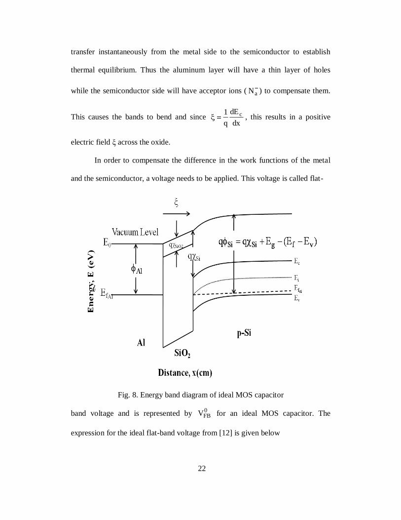
22
transfer instantaneously from the metal side to the semiconductor to establish
thermal equilibrium. Thus the aluminum layer will have a thin layer of holes
while the semiconductor side will have acceptor ions ( aN ) to compensate them.
This causes the bands to bend and since dx
dE
q
1 c , this results in a positive
electric field ξ across the oxide.
In order to compensate the difference in the work functions of the metal
and the semiconductor, a voltage needs to be applied. This voltage is called flat-
Fig. 8. Energy band diagram of ideal MOS capacitor
band voltage and is represented by 0FBV for an ideal MOS capacitor. The
expression for the ideal flat-band voltage from [12] is given below
23
}q
)EE(Eq{V
vfgSimsm
0FB , (4.2)
where m is the metal work function, s is the semiconductor work function, q is
the electronic charge, Eg is the band gap of silicon, Ef and Ev are the Fermi level
and valence band energy level of silicon respectively.
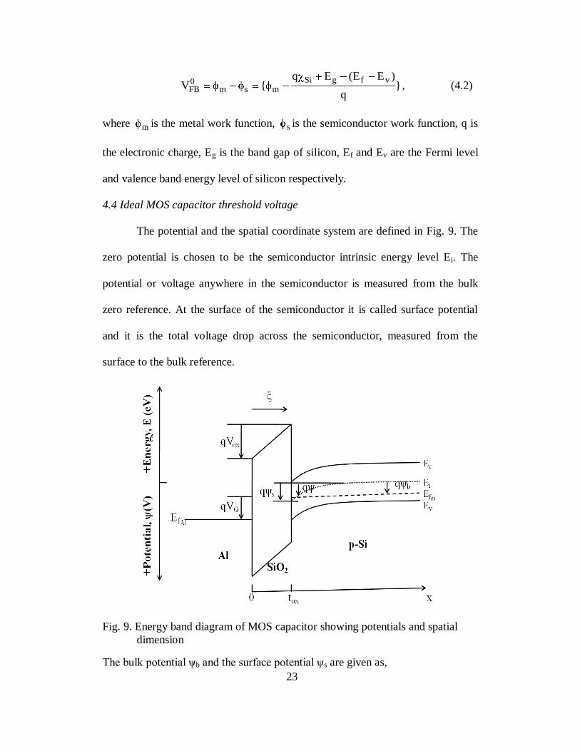
4.4 Ideal MOS capacitor threshold voltage
The potential and the spatial coordinate system are defined in Fig. 9. The
zero potential is chosen to be the semiconductor intrinsic energy level Ei. The
potential or voltage anywhere in the semiconductor is measured from the bulk
zero reference. At the surface of the semiconductor it is called surface potential
and it is the total voltage drop across the semiconductor, measured from the
surface to the bulk reference.
Fig. 9. Energy band diagram of MOS capacitor showing potentials and spatial
dimension
The bulk potential ψb and the surface potential ψs are given as,

24
q)E)bulk(E( fib , (4.3)
q))tx(E)bulk(E( oxiis , (4.4)
where Ei(bulk) is the intrinsic energy level in the bulk of the semiconductor,
Ei(x=tox) is the intrinsic energy level at the semiconductor surface. For a p-type
Al/SiO2/p-Si MOS capacitor, a positive gate bias has to be applied in order to
invert the semiconductor surface. The gate voltage VG applied to the MOS
capacitor is given as,
sox0FBG VVV , (4.5)
where Vox is the voltage drop across the oxide and ψs is the surface potential.
Gauss’s law can be used to estimate the voltage drop across the gate oxide Vox.
From Gauss’s law the surface integral of electric flux density is equal to charge
enclosed and is given by
daQ , (4.6)
where Q is the charge, ε is the permittivity, ξ is the electric field. From the
integral in Equation 4.6,
AQ oxoxsc , (4.7)
where εox is the permittivity of silicon dioxide, ξox is the electric field across the
oxide and A is the cross-sectional area of the MOS capacitor. The electric field in
the oxide is given as
A
Q
ox
scox . (4.8)
The space charge in the semiconductor Qsc is given as

25
||Nq4AQ baSisc , (4.9)
where εSi is the permittivity of silicon, aN is the ionized acceptor impurity
concentration. At the Si/SiO2 interface, the electric flux density has to be
continuous and this gives
SiSioxoxyields
Siox DD . (4.10)
Dox and DSi are the electric flux density on the oxide and semiconductor sides
respectively. The potential ψox is the integration of the electric field and is given
as
dx)x( oxox . (4.11)
Evaluating the above integral and substituting the boundary condition ψ(tox) = ψs
gives
xt)x( oxoxoxsox for 0 < x < tox, (4.12)
where ψs is the surface potential in semiconductor, tox is the thickness of oxide.
The potential across the oxide Vox is the difference in the potential at x=0 and
x=tox
oxoxoxoxoxox t)t()0(V . (4.13)
By substituting for ξox from Equation 4.8 and Qsc from Equation 4.9, the above
expression becomes
ox
bSioxaoxox
||tqN4tV . (4.14)
The ideal threshold voltage of the MOS capacitor is given as

26
0FBoxtGT VVVV , (4.15)
where VT is the threshold voltage of the MOS capacitor, VG is the applied gate
voltage and ψt is the surface potential at threshold voltage. By using ψt = 2|ψb| and
substituting Vox from Equation 4.14, the threshold voltage of the p-type MOS
capacitor is given as
oxox
aSibb
0FBT
t
N||q4||2VV . (4.16)
4.5 MOS capacitance – voltage behavior
The MOS system consists of a series combination of oxide capacitance
Cox and semiconductor capacitance CSi. Fig. 10 is a schematic representation of
the MOS capacitor.
Fig. 10. Schematic representation of MOS capacitor
The gate to bulk voltage applied to the MOS capacitor is given by
soxox
'Si0
FBGB tQ
VV , (4.17)

27
where VGB is the gate to bulk voltage, 'SiQ is the semiconductor charge per unit
area. The total capacitance of the MOS capacitor is given as
'Si
'ox
'dif C
1
C
1
C
1, (4.18)
where 'difC is the differential capacitance per unit area of the MOS capacitor,
'oxC and '
SiC are the oxide and silicon capacitance per unit area respectively. The
semiconductor charge per unit area is given as
)e(eeqN2Q tst
2
tstSia'Si
t
s
t
b
t
s
, (4.19)
where t is the thermal voltage, ψs and ψb are given by Equations 4.3 and 4.4.
The thermal voltage is given as q
kTt , where k is Boltzmann constant, T is the
temperature. When the semiconductor is in accumulation region i.e |ψs| > 3 t ,
then the differential capacitance Cdif’ (acc) is approximately equal to oxide
capacitance.
)cm/F(C)acc(C 2'ox
'dif . (4.20)
The flat band capacitance Cdif’ (FB) corresponds to the value when the bands are
flat and is given by the equation
)cm/F(Lt
1)FB(C 2
Si
D
ox
ox
'dif , (4.21)

28
where
a2
SiD
Nq
kTL is the Debye length, εSi is the permittivity of silicon, k is
Boltzmann constant, T is the temperature. The inversion capacitance Cdif’ (inv)
corresponds to the value when ψs = 2|ψb| and there is maximum depletion in the
semiconductor region. The capacitance is given by the equation
)cm/F(xt
1)inv(C 2
Si
d
ox
ox
'dif
max
. (4.22)
Fig. 11 is the comparison of normalized C-V curve calculated using the analytical
equations 4.12-4.14 and experimental data. The figure shows that the ideal
equation does not match with experimental data. This is due to non-idealities in
the oxide which introduce traps near the interface which when occupied causes
deviation from the ideal behavior.
Fig. 11. Comparison of ideal MOS C-V curve with experimental data

29
4.6 Non-ideal capacitance – voltage Behavior
4.6.1 Fixed oxide charge- Qf
The oxide is not ideal and typically has some fixed charge which is likely
to have been introduced during the oxide growth. The fixed oxide charge Qf is
very near the silicon/insulator interface and this changes the flat-band voltage to
oxox
f0FBFB
t
QVV . The gate to bulk voltage of the MOS capacitor becomes
sox
'Siox
oxox
f0FBGB
Qt
t
QVV . (4.23)
From the above equation it can be seen that the gate voltage required to measure
the same effective capacitance is shifted by ox
foxQt. This shift depends on the
polarity of the charge and can shift the C-V curve to the left or right.
Fig. 12. Comparison of experimental data with non ideal MOS C-V curve

30
Shown in Fig. 12 is the comparison of C-V curve obtained using the analytical
equation including the impact of fixed oxide charge and experimental data. It can
be seen that the experimental data match very well with the analytical model.
4.6.2 Interface trap charge- Qit
Another non-ideality is introduced because of dangling bonds in the
silicon/insulator interface. These dangling bonds introduce energy levels
distributed throughout the forbidden band gap which are called surface states or
interface states [12] shown in Fig. 13(a). Fig. 13(b) represents an n-type MOS
capacitor biased in inversion and the Fermi level at the surface lies close to Ev. All
energy levels below the Fermi level are filled with electrons while all energy
levels above are empty. So in case (b) no interface state if filled and assuming that
the interface states are donor-like in nature, the net charge per unit area QIT will
be positive. In Fig. 13(c) the MOS capacitor is biased in accumulation and it can
be seen that all the interface states are occupied by electrons. If all the donor-like
interface states are occupied by electron then there is no contribution of interface
trap charge. The interface trap charge contribution depends on the bias condition
of the MOS capacitor. The shift in the gate to bulk voltage due to interface trap
charge is given as
ox
ITGB
C
QV , (4.24)
where QIT is the net contribution of interface trap charge and Cox is the oxide
capacitance per unit area.

31
Fig. 13. Illustration of interface states at different biasing conditions in an MOS
capacitor
4.7 Extraction of oxide-trapped charge and interface trap charge from C-V curve
In order to extract the oxide-trapped charge NOT and interface traps, NIT,
the technique described from [13] is used. Flat-band, midgap and strong inversion
capacitance are identified and these correspond to a surface potential ψs of 0, b
and b2 . The total voltage shift is given as
ITOT NNtotal VVV , (4.25)
where OTNV is the net voltage shift due to oxide-trapped charge QOT and
ITNV
is the net voltage shift due to interface trap charge QIT .The assumption made for
the extraction is that the interface states in the upper half of the band gap are
acceptor like and those in the lower half are donor like. The total voltage shift at
midgap gives OTNV since at midgap there is no charge contribution from the

32
interface states. The voltage stretch out from midgap to inversion gives ITNV ,
which is the shift due to the occupied interface states between midgap and
inversion.

33
Chapter 5
THE DOSE PERFORMANCE OF THE RADCAP
5.1 Processing technique
5.1.1 Wet oxidation and dry oxidation
Thermal oxidation is a way to grow a layer of silicon dioxide of desired
thickness on the surface of a semiconductor wafer. An oxidizing agent diffuses
into the wafer at high temperatures and results in the formation of silicon dioxide,
thereby determining the rate of growth of oxide. Thermal oxidation is performed
at a temperature of around 800◦C to 1200
◦C using two different oxidizing agents.
Wet oxidation uses water vapor as the oxidizing agent while molecular oxygen is
used for dry oxidation. The oxidizing ambient also contains several percent of
hydrogen chloride which is used to remove the metal ions from the oxide. The
reaction for oxidation, wet and dry respectively, is as follows
(5.1)
and
(5.2)
The Si in the above reaction is supplied by the substrate while the oxygen or
water vapor is available from the ambient. The main difference between the above
reactions is the oxide growth rate. Dry oxidation is preferred over wet oxidation
for thinner oxides (<100 nm). This is due the fact that it introduces less water
molecules inside the oxide. Since wet oxidation has faster growth rate it is usually
preferred over dry oxides for thicker oxides (>200 nm). The drawback of wet
oxidation is that it leaves dangling bonds at the interface and results in low

34
density oxides [8]. Mobile ions (sodium) can degrade the performance of MOS
capacitors and to immobilize them hydrogen chloride or trichloroethylene is
introduced. They also tend to increase the rate of oxidation thereby forming a
positive feedback for oxidation.
For the works, RADCAPs were prepared by growing oxides using dry
oxidation and wet oxidation to see their impact on the dose response. An earlier
work [14] suggested that the mechanism involved in the interface state
development is the same but the magnitude is much smaller in thermally grown
dry oxides as compared to wet oxides. The difference is primarily due to the
different amounts of water incorporated in the oxide during processing. Since the
water related species is primarily responsible for the interface trap buildup, a
difference in processing will have a huge impact on the dose response of the
sample. The reaction from [14] is as follows
, (5.3)
, (5.4)
where DB is the dangling Si bond and OH is the interstitial species. These
reactions suggest that the water molecules may passivate a bare dangling bond
and release an H or OH atom. Both of the above mentioned reactions are feasible
at room temperature. The mechanism for interface trap buildup involves protons
moving under the influence of a positive gate bias towards the interface where
they break a Si-OH or Si-H bond to leave behind a dangling Si- bond that forms
the interface trap [15].

35
5.1.1.1 Experiment results
RADCAP samples with two different oxide thicknesses – 100 nm and
200 nm were prepared for an experimental assessment of the impact of oxide
processing on dose response. Dry oxidation was used to grow oxide on the
100 nm samples while wet oxidation was used for 200 nm samples. These
capacitors were irradiated with 60
Co irradiations under a gate bias of 5V and their
corresponding C-V curves were recorded at different dose levels of 20 krad,
100 krad and 279 krad. In order to make sure that there is no sample to sample
variation, C-V curves were recorded on 14 samples in total (7 with 100 nm oxide
thickness and 7 with 200 nm oxide thickness). In order to eliminate the parasitic
capacitance introduced by the measurement setup, the capacitance was
normalized with respect to its accumulation capacitance value (Caccum). The
normalized C-V curves of the 100 nm and 200 nm samples are shown in Figs. 14
and 15 respectively. It can be seen from C-V curves that the RADCAPs with
200 nm oxide thickness show more interface states than their 100 nm counterparts
at higher dose levels.

36
Fig. 14. Pre-irradiation and post-irradiation C-V curves of RADCAP with 100 nm
(dry) oxide thickness
Fig. 15. Pre-irradiation and post-irradiation C-V curves of RADCAP with 200 nm
(wet) oxide thickness

37
The buildup of oxide-trapped charge as a function of radiation dose level
is given by
D)E(ftgN oxyox0OT , (5.5)
where g0 is the initial electron-hole pair volume density, tox is the oxide thickness,
fy(Eox) is the fractional hole yield and D is the total radiation dose. The change in
oxide-trapped charge ∆NOT and interface trap density ∆NIT was extracted from
experimental data to estimate the dose sensitivity. These values were normalized
with respect to oxide thickness and fractional hole yield in order to provide a fair
comparison of the processing scheme. Figs. 16 and 17 show the normalized
oxide-trapped charge and interface trap density of RADCAPs with 100 nm and
200 nm oxide thickness.
Fig. 16. Experimental data of normalized oxide-trapped charge density of
RADCAP with 100 nm (dry) and 200 nm (wet) oxide thickness

38
Fig. 17. Experimental data of normalized interface trap density of RADCAP with
100 nm (dry) and 200 nm (wet) oxide thickness
The normalized oxide-trapped charge density is nearly the same in both
the samples indicating that the number of hole trapping precursor sites is very
similar. The 100 nm samples show lower interface trap density than the 200 nm
samples, but not a large difference. The small difference is most likely due to the
presence of H species in the wet oxidized samples which are responsible for the
interface state charge [17-20]. Interface traps impact the shape of the C-V curve
and degrade the performance of the dose sensor thus the dry oxidized RADCAP is
somewhat better for dosimetry.
The initial precursor hole trap density in both oxides can be estimated
using Radiation Effects Module (REM) present in Silvaco device simulator. MOS
capacitors with similar oxide thicknesses as the experimental samples were used
in the simulation. The initial precursor hole trap density was 1018
cm-3
for both
39
samples with 100 nm and 200 nm oxide thicknesses. Figs. 18 and 19 compare the
change in oxide-trapped charge ∆NOT estimated using simulation against
experimental data for samples having oxide thickness of 100 nm and 200 nm. As
can be seen, the simulation data match very well with the experimental data
indicating that the initial precursor hole trap density extracted using simulations is
close to the experimental value.
Fig. 18. Comparison of oxide-trapped charge per unit area for RADCAP with
200 nm oxide thickness (wet) obtained from simulation and experimental
data
In order to further validate the simulation results, C-V curves were
simulated for the 100 nm and 200 nm oxide samples with the ∆NOT values
extracted from simulation. The midgap voltage shifts obtained from simulation
were compared against experimental data. Figs. 20 and 21 compare the midgap
voltage as function of dose obtained using simulation and experiments for
samples with 100 nm and 200 nm oxide thickness. The simulations match very

40
well with experimental data validating the accuracy of the selected precursor
density estimated using simulations.
Fig. 19. Comparison of oxide-trapped charge per unit area for RADCAP with
100 nm oxide thickness (dry) obtained from simulation and experimental
data
Fig. 20. Comparison of midgap voltage shifts for RADCAP with 200 nm oxide
thickness (wet) obtained from simulation and experimental data

41
Fig. 21. Comparison of midgap voltage shifts for RADCAP with 100 nm oxide
thickness (dry) obtained from simulation and experimental data
5.1.2 Thermally grown high quality oxide
5.1.2.1 Fabrication steps
In order to study the dose sensitivity of a thermally grown high quality
oxide, RADCAPs were manufactured using p-type SOI wafers. SOI wafers were
chosen so that the device silicon layer can be kept very thin thereby reducing the
series resistance. This type of process is ideal for the proposed capacitively-
loaded wireless sensor application described earlier. The oxide in these wafers
was 2 µm thick. The fabrication steps are summarized in Fig. 22. The first step is
to deposit silicon nitride on both sides of the wafer using Low Pressure Chemical
Vapor Deposition (LPCVD). In order to form the capacitor the silicon underneath

42
the silicon dioxide layer has to be etched. A photo resist is patterned on the
backside of the wafer to enable removal of the silicon nitride layer.
Fig. 22. Fabrication steps to manufature capacitors using SOI wafers
Step 2 consists of Reactive Ion Etch (RIE) using potassium hydroxide (KOH)
to remove backside silicon layer. KOH etch is used to remove most of the silicon
far away from the oxide layer. Since KOH aggressively attacks the oxide causing
reductions in its thickness, silicon wet etch (TMAH) is used to remove the silicon
close to the oxide layer. In step 3, a photo resist pattern is used on the top side to
enable removing silicon nitride using reactive ion etch. Aluminum contacts are

43
formed on both sides of the capacitor by sputtering and this forms step 4. In order
to remove the unwanted aluminum from other portions of the wafer, a photo resist
is patterned on the top side which forms step 5. After etching out the aluminum,
Post Metallization Annealing (PMA) is done in the presence of nitrogen for 10
minutes.
5.1.2.2 Experiment results
The capacitors manufactured using the fabrication steps described above
was exposed to a 700 keV proton beam to study their dose response and
performance as dose sensor. The flux rate of the ion beam was 3.98 1010
cm-2
sec-1
. As these capacitors are expected to be used as passive dose sensors no bias
was applied while exposing them to the proton beam.
Fig. 23. Package containing RADCAPs with high quality oxide and the proton
beam chamber used for irradiation
Fig. 23 shows photographs of the packaged capacitor and the radiation chamber
used to irradiate the parts. Under the irradiation condition the charge yield is very

44
low and most of the electron hole pairs created is lost to geminate recombination
[11].
Fig. 24 shows the results of the proton beam irradiation. The capacitors
show a left shift as a result of oxide-trapped charge and this shift increases as a
function of dose.
Fig. 24. Experimental data showing radiation response of RADCAP with high
quality oxide
Even though the charge yield is low for 700 keV proton beam [11]
substantial voltage shifts can be seen in the data indicating the radiation
sensitivity of these capacitors. Fig. 25 shows capacitance as a function of dose at a
gate to body bias of 8V. It can be seen that the capacitance changes as a function
of dose which can be used in the system design described in section 4.2. This
change of capacitance gives a difference in the resonant frequency that can be
mapped back to find the dose level.

45
There are various parameters that control the dose sensitivity and dynamic
range of the sensor. The above described sensor has a dynamic range of 600 krad
for the proton beam.
Fig. 25. Capacitance versus dose map for RADCAP with high quality oxide
For the system described in section 4.2, the capacitance at zero bias must
change as a function of dose. From Fig. 24 it can be seen that, at zero bias there is
no change in capacitance due to ionizing radiation. This is due to the fact that the
threshold voltage prior to irradiation is too high. In order to shift the C-V curves
in Fig. 24 to the left, the doping of the device silicon in the SOI wafer can be
reduced thereby resulting is lower threshold voltage.
In order to quantatively analyze the effectiveness of the dose senor, the
change in oxide-trapped charge ∆NOT was extracted from the experimental data.
The initial precursor hole trap density in the oxide estimated using the REM

46
module of Silvaco device simulator is 1.5 1016
cm-3
. Fig. 26 shows the
comparison of oxide-trapped charge as a function of dose estimated using
simulation against experimental data. It can be seen from Fig. 26 that the change
in oxide-trapped charge, ∆NOT, begins to saturate at higher doses indicating that
most of the trapping sites have been filled with holes. This sets a limit on the
dynamic range of doses this capacitor can be used as a dose sensor. The data also
show no interface traps indicating that with proper control, thermal oxidation can
yield high quality oxides that can be used as better dose sensors.
Fig. 26. Comparison of oxide-trapped charge per unit area for RADCAP with
high quality oxide obtained from simulation and experimental data
5.2 Dielectric material
In order to study further the effects of different dielectric materials,
RADCAPs with silicon nitride and silicon dioxide as gate insulators were

47
manufactured. Silicon dioxide capacitors were prepared using the dry oxidation
technique described in section 5.1. Silicon nitride was deposited on silicon using
Low Pressure Chemical Vapor Deposition (LPCVD). Silicon nitride dielectrics
deposited using LPCVD had up to 8% hydrogen in them. These capacitors along
with other oxide samples were packaged and exposed to 60
Co radiations. Their
C-V curves were recorded at dose levels of 20 krad, 100 krad and 279 krad. The
electron hole pair generation in the dielectric is controlled by the following
equation
fp
3 E
1LET
scm
ehp#, (5.6)
where ρ is the density of silicon nitride, f is the flux, and Ep is the energy
needed to produce an electron hole pair in nitride. Table 3 from [21] provides a
comparison of properties of silicon nitride and silicon dioxide.
PARAMETER Silicon Nitride Silicon dioxide
Ep 10.8 eV/ehp 17.4 eV/ehp
LET (60
Co-700 kev) 2.457 MeV/(mg/cm2) 2.171 MeV/(mg/cm
2)
ρ 3.1 g/cm3 2.2 g/cm
3
Table 3. Comparison of properties of silicon nitride and silicon dioxide
Comparing the above quantities, silicon nitride samples have 2.5 times
higher generation rate as compared to silicon dioxide samples. As a result, for the
same dose, the number of electron-hole pairs produced in silicon nitride is twice
as much as in silicon dioxide. The trapping mechanism involved in silicon nitride
samples is discussed in [22, 23]. Even though the generation rate is higher for
silicon nitride samples, the dose sensitivity also depends on the number of
precursor defect densities where the holes can be trapped.

48
5.2.1 Experiment results
Figs. 27 and 28 show the experimental data obtained from 60
Co irradiation
experiment. The C-V curves suggests that the silicon nitride samples show
saturated levels at a dose of 100 krad while the silicon dioxide samples show
linear increase up to 300 krad. This suggests that the dynamic range of silicon
nitride samples is less than the silicon dioxide counterparts.
Fig. 27. Pre-irradiation and post-irradiation C-V curves of RADCAP with silicon
nitride as insulator
49
Fig. 28. Pre-irradiation and post-irradiation C-V curves of RADCAP with silicon
dioxide as insulator
In order to compare their efficiency as dose sensors, the change in oxide-
trapped charge was extracted as a function of dose and normalized with respect to
oxide thickness. The data of silicon dioxide samples were corrected to take
fractional hole yield into account. It can be seen from Fig. 29 that silicon dioxide
samples show more change in oxide-trapped charge ∆NOT for the same dose
levels than silicon nitride samples. Also the silicon nitride samples show no shift
in the C-V curve after the 100 krad indicating that its dynamic range is limited by
the number of trapping sites.

50
Fig. 29. Comparison of normalized oxide-trapped charge density of silicon nitride
and silicon dioxide RADCAP samples as a function of dose
Fig. 30. Ratio of normalized oxide-trapped charge density of silicon dioxide and
silicon nitride RADCAP samples as a function of dose

51
Shown in Fig. 30 is the ratio of oxide-trapped charge density of silicon
dioxide and silicon nitride samples. It can be seen that the ratio is monotonically
increasing indicating that the oxide samples show more trapping efficiency than
the silicon nitride samples even at higer dose levels. It is thus recommended to
use silicon dioxide when the dose sensor is to be used for high dose levels.
Although silicon nitride requires lower energy for electopn-hole pair generation
reduced number of trapping sites impacts its dose sensitivity. It can be seen from
the C-V curves that both silicon dioxide and silicon nitride samples show very
little interface trap charge. The stretch out of the curves from midgap to inversion
is almost the same at all dose levels. The initial precursor hole trap density in the
silicon nitride sample is estimated using the REM module of Silvaco device
simulator to be 4 1017
cm-3
.
Fig. 31. Comparison of oxide-trapped charge per unit area for silicon nitride
RADCAP obtained from simulation and experimental data

52
Fig. 31 compares the oxide-trapped charge obtained using simulation and
experiments for the silicon nitride samples. The simulation results match closely
with the experimental data validating the initial precursor hole trap density
estimated using simulations is close to experimental value.
5.3 Impact of oxide thickness
Thickness of oxide is a critical parameter that affects the total oxide-
trapped charge density in the sample [3-7]. The radiation induced midgap voltage
shift, ∆Vmg is directly proportional to tox2
[11] and this follows from the basic
equation, Q = CV. The charge, Q is proportional to tox while C is inversely
proportional to tox. In order to improve the dynamic range of the dose sensor, the
change in capacitance at fixed bias should continue for widest range of dose
levels. This presents a tradeoff between dose sensitivity and dynamic range. The
thickness of oxide should be small to improve the dynamic range so that for the
same increase in dose level, the change in midgap voltage is less which reflects in
small ∆C change. But the thinner oxide is more radiation hardened as compared to
the thicker oxide.
5.3.1 Experiment results
The change in oxide-trapped charge and interface trap density were
extracted from experimental data and normalized with respect to fractional hole
yield fy(Eox). Figs. 32 and 33 compare the normalized oxide-trapped charge and
interface trap density for RADCAP samples with 100 nm and 200 nm oxide
thickness.

53
Fig. 32. Comparison of normalized oxide-trapped charge per unit area for
RADCAPs with 100 nm, 200 nm oxide thickness as a function of dose
From Figs. 32 and 33 it can be seen that the 200 nm samples show both higher
interface traps as well as more oxide-trapped charge. It can be clearly seen that
the 200 nm oxide samples are more radiation sensitive, trapping more oxide
charge as compared to their 100 nm counterparts for the same dose levels. Also
the thicker oxide has more interface traps that affect the shape of the C-V curve
and thereby impacting the dose sensor’s performance. Previous studies indicate
that the radiation induced interface trap density is reduced in thinner oxides [24-
30]. So in the thinner oxides, the amount of interface traps produced even at very
large doses is less.

54
Fig. 33. Comparison of normalized interface state charge per unit area for
RADCAPs with 100 nm, 200 nm oxide thickness as a function of dose
5.4 Post-irradiation behavior
An effective dose sensor should hold the charge in its insulator layer even
after irradiation stops and should present very little charge loss over time. In order
to characterize the sensors manufactured using different processing techniques,
the samples were annealed at room temperature with no bias after exposing them
to ionizing radiations. Fig. 34 shows the post irradiation annealing behavior
observed in different samples. It can be seen that all the samples show loss of
oxide-trapped charge irrespective of their processing scheme. The capacitors
manufactured using dry oxidation and wet oxidation show annealing of interface
traps produced during irradiation and loss of oxide-trapped charge.

55
Fig. 34. Comparison of annealing behavior observed in RADCAPs manufactured
using different processing techniques
The reason for annealing is that the fields produced due to oxide-trapped
charge cause electrons to be injected from the substrate that compensates the
trapped holes thereby causing the flat-band voltage to recover. Table 4
summarizes the loss of oxide-trapped charge and midgap voltage shifts resulting
from room temperature annealing. In order to improve the dosimeter, the loss of
oxide-trapped charge over time has to be reduced.

56
INSULATOR
TYPE
PROCESSING
TECHNIQUE
MIDGAP
VOLTAGE
SHIFT,
|∆Vmg|, V
OXIDE-TRAPPED
CHARGE LOST DUE
TO ANNEALING,
∆NOT, cm-2
SiO2 Wet Oxidation 4.5 4.85 x 10¹¹
SiO2 Dry Oxidation 2.5 5.39 x 10¹¹
Si3N4 Chemical Vapor Desposition
2 5.19 x 10¹⁰
SiO2 Industry grown
thermal oxide
1 1.08 x 10¹⁰
Table 4. Loss of oxide-trapped charge and midgap voltage shifts resulting from
room temperature annealing
5.5 Discussion on initial precursor hole trap density
The initial precursor hole trap density in the oxide can provide a fair
comparison of sensitivity of dose sensor to radiation. It helps to understand the
radiation dose sensitivity of different materials and various processing schemes.
The initial precursor hole trap density determines the rate of buildup of trapped
charge in insulator and dose level at which the buildup saturates. It predicts the
dynamic range of dose levels for which the dose sensor would provide a change in
capacitance thereby working as a radiation dose sensor. The initial precursor hole
trap density estimated using simulations are summarized in Table 5
INSULATOR TYPE PROCESSING
TECHNIQUE
INITIAL HOLE
TRAP DENSITY,
cm-3
SiO2 Wet Oxidation 1018
SiO2 Dry Oxidation 1018
Si3N4 Chemical Vapor
Desposition
4 x 10¹⁷
SiO2 Industry grown thermal
oxide
1.5 x 10¹⁶
Table 5. Initial precursor hole trap density estimated from simulation for various
processing schemes

57
The simulation results suggest that the initial precursor hole trap density is
same for the natively grown silicon dioxide samples, irrespective of their
processing method. Thermal oxides grown in the industry have initial precursor
hole trap density that is two orders of magnitude lower when compared to the
samples grown at ASU. The silicon nitride samples prepared using CVD
technique has about 2.5 times lower initial precursor hole trap density as
compared to the silicon dioxide samples grown at ASU. The estimate of initial
precursor hole trap density is important as it predicts the dynamic range for which
the MOS capacitor continues to develop oxide-trapped charge thereby providing a
capacitance change. The precursor hole trap density influences the sensitivity of
the insulator to radiation in addition to other parameters like temperature, electric
field, oxide thickness. Since the RADCAP is used in an unbiased condition its
sensitivity is critically influenced and controlled by the initial precursor hole trap
density in the insulator.
The RADCAP can be used as a wireless dose sensor if the parameters
described above can be controlled efficiently. The advantage of this system is that
it is passive, low cost, small and easy to manufacture. It incorporates all the
advantages of RADFET in addition to providing a wireless method to sense
radiation. With the need for cheap wireless radiation sensing getting impetus, this
technique can provide robust wireless radiation dose sensors.

58
Chapter 6
CONCLUSION
The effect of oxide processing scheme, choice of insulator material and
oxide thickness have been studied. Wet oxidation and dry oxidation introduce the
same number of initial precursor hole trap density which characterizes the oxide-
trapped charge build-up. Due to the presence of water species, wet oxidation
introduces slightly higher levels of interface traps at the same dose levels as
compared to dry oxidation. Radiation response of industry grown thermal oxides
show reduced amount of initial precursor hole trap density as compared to
natively grown counterparts. The impact of silicon nitride as insulator material in
the place of oxide showed saturated levels of oxide-trapped charge at a radiation
dose of 100 krad which severely impact the dynamic range of the dose sensor. In
order to use the sensor at high dose levels, the rate of build-up of oxide-trapped
charge should be small thereby continuing to show a change in capacitance
detectable at higher dose ranges. A tradeoff exists between dynamic range and
thickness of oxide in building a radiation dose sensor. A thicker oxide is much
more radiation sensitive than thinner oxide but saturates much earlier than
similarly processed thinner oxide thereby having a reduced dynamic range. It is
necessary to understand this tradeoff in order to build RADCAP dosimeter for
various applications.
59
REFERENCES
[1] R.C.Hughes , "Theory of response of radiation sensing field-effect transistors
in zero bias operation",J.Appl Phys, Vol 60, 1216-1217, 1986
[2] A.G. Holmes-Siedle, "The space charge dosimeter: general principle of a new
method of radiation dosimetry",Nucl Instrum Meth,pp 169-179, 1974
[3] A.G. Holmes-Siedle, Leonard Adams,"RADFET: A review of the use of
Metal-Oxide-Silicon devices as integrating dosimeters",Rad. Phys and chem,
Vol 28, no.2, pp 235-244, 1986
[4] G.Ristic,S. Golubovic and M.Pejovic,"pMOS transisitors for dosimetric
applications",Electron. Lett, Vol 29, pp 1644-1646, 1993
[5] G.Sarrabayrouse and S.Siskos,"Radiation dose Measurements using
MOSFETs", IEEE Instr and Mes Magazine, pp 26-34, 1998
[6] N.Kumurdjian and G.Sarrabayhouse,"Unbiased Metal Oxide Semiconductor
ionising radiation dosimeter", Rad. Protection Dosimetry,Vol 61, pp 19-24,
1995
[7] A.G. Holmes-Siedle, Paul Menary, Phil Sharpe, John.A.Mills,"RADFET
devices are they coming of age?", Scope, pp 21-27, 2010
[8] A. Holmes-Siedle, L. Adams and G. Ensell," MOS dosimeters - improvement
of responsivity",Rad and its Effects on Dev and Sys, pp 65-69, 1991
[9] M.Soubra, J. Cygler and G.Mackay," Evaluation of a dual bias dual metal
oxide-silicon semiconductor field effect transistor detector as radiation
dosimeter", Med Phys, Vol 21, pp 567-572, 1994
[10] H.P.Hjalmarson, R.L.Pease, S.C.Witczak, M.R.Shaneyfelt, J.R.Schwank,
A.H.Edwards, C.E.Hembree, and T.R. Mattsson, “Mechanisms of radiation

60
dose-rate sensitivity of bipolar transistors,” IEEE Trans Nucl. Sci, vol. 50,
p.1901, 2003
[11] T.R.Oldham,"Total Ionizing Dose Effects in MOS Oxides and
Devices",IEEE Trans on Nucl Sci, Vol 50, pp 483-499, 2003
[12] Craig Casey Jr,"Devices for Integrated Circuits",John Wiley & Sons
Inc,1999
[13] P.S.Winokur, J.R. Schwank, P.J. Mcwhorter, P.V. Dressendorfer, and D.C.
Turpin,"Correlating the radiation response of MOS capacitors and
transistors",IEEE Trans on Nucl Sci, Vol NS-31, pp 1453-1460, Dec 1984
[14] F.B.Mclean,"A Framework For Understanding Radiation-Induced Interface
States in Sio2 MOS Structures",IEEE Trans.Nucl.Sci.,vol. NS-27,
no.6,pp.1651-1657, Dec1980
[15] C.T. Sah, IEEE Trans. Nucl. Sci., NS-23, pp.1563-68, Dec. 1976
[16] I.G. Batyrev, D.M.Fleetwood, R.D.Schrimpf, S.T.Pantelides,"The role of
water in the radiation response of wet and dry oxides", Rad and its effects on
Components and Sys., pp 1-6, Sept 2007
[17] S. N. Rashkeev, D. M. Fleetwood, R. D. Schrimpf, and S. T. Pantelides,
"Effects of hydrogen motion on interface trap formation and annealing,"
IEEE Trans Nucl. Sci., vol. 51, pp. 3158-3165, 2004
[18] N. S. Saks and D. B. Brown, “Interface trap formation via the two-stage H
process,” IEEE Trans. Nucl. Sci., vol. 36, no. 6, pp. 1848–1857, Dec. 1989
[19] P. S.Winokur and H. E. Boesch, Jr., “Interface-state generation in radiation-
hard oxides,” IEEE Trans. Nucl. Sci., vol. NS-27, p. 1647, 1980S. N.
Rashkeev, D. M. Fleetwood, R. D. Schrimpf, and S. T. Pantelides, "Effects
of hydrogen motion on interface trap formation and annealing," IEEE Trans
Nucl. Sci., vol. 51, pp. 3158-3165, 2004

61
[20] H.Edwin Boesch Jr , F. Barry Mclean, “Hole Transport and Trapping in
Field Oxides,"IEEE Trans Nucl Sci,vol NS-32, no.6, Dec 1985
[21] G. C. Messenger, M. S. Ash,"The Effects of Radiation on Electronic
Systems", 2nd edition, Van Nostrand Reinhold, NY, 1992.
[22] Bob H Yun,"Electron and hole transport in CVD Si3N4 films", Appl Phys
Letters, Vol 27, pp 256-258, 1975
[23] Z.A.Weinberg,"Hole Conduction in Si3N4 films on Si", Appl Phys Letters,
Vol 29, pp 617-619, 1976
[23] Z.A.Weinberg,"Hole Conduction in Si3N4 films on Si", Appl Phys Letters,
Vol 29, pp 617-619, 1976
[24] K.Naruke, M.Yoshida, K.Maeguchi and H.Tango,”Radiation-Induced
Interface States of Poly-Si Gate MOS Capacitors using Low Temperture
Gate Oxidation”,IEEE Trans on Nucl. Sci,NS-30, pp 4054-58, 1983
[25] J.M.Benedetto,H.E.Boesch,F.B.Mclean,"Hole Removal in thin-gate
MOSFET by Tunneling", IEEE Trans on Nucl. Sci,NS-32, pp 3916-20, 1985
[26] T.P.Ma,"Oxide thickness dependence of electron‐ induced surface states in
MOS structures",Appl Phys Letter,Vol 27, pp 615
[27] C.R.Viswanathan, J.Maserjian," Model for Thickness Dependence of
Radiation Charging in MOS Structures", IEEE Trans on Nucl. Sci,NS-23, pp
1540-45, 1976
[28] N.S.Saks, M.G. Ancona and J.A. Modolo," Generation of Interface States by
Ionizing Radiation in Very Thin MOS Oxides", IEEE Trans on Nucl. Sci,NS-
33, pp 1185-90, 1986
[29] S.Share, A.Epstein, V.Kulmar, W.E. Dahlkeand W.Haller,"Effects of
Ionizing Radiation on the thin oxide (20-1500Å)",J. Appl Phys,Vol 45, pp
4894

62
[30] T.P.Ma and R.C. Barker,"Effect of gamma-ray irradiation on the surface
states of MOS tunnel junctions",J. Appl Phys,Vol 45, pp 317