Overview Charge-coupled Devices - courses.cs.washington.edu · Overview Charge-coupled devices: MOS...
8
1 Charge-coupled Devices 2 Overview Charge-coupled devices: MOS capacitors Charge transfer Architectures Color Limitations 3 Charge-coupled devices The most popular image recording technology for 3D photography is the charge-coupled device (CCD). Image is readily digitized CCD cells respond linearly to irradiance • But, camera makers often re-map the values to correct for TV monitor gamma or to behave like film Available at low cost Key elements: Photodetector Charge transfer mechanism A MOS capacitor can do both of these… 4 MOS capacitor Negative gate voltage: Majority carriers (holes) plentiful, and the gate behaves like a capacitor that stores positive charge near the oxide.
Transcript of Overview Charge-coupled Devices - courses.cs.washington.edu · Overview Charge-coupled devices: MOS...

1
Charge-coupled Devices
2
Overview
Charge-coupled devices:
MOS capacitors
Charge transfer
Architectures
Color
Limitations
3
Charge-coupled devices
The most popular image recording technology for 3D photography is the charge-coupled device (CCD).
Image is readily digitized
CCD cells respond linearly to irradiance
• But, camera makers often re-map the values to correct for TV monitor gamma or to behave like film
Available at low cost
Key elements:
Photodetector
Charge transfer mechanism
A MOS capacitor can do both of these…
4
MOS capacitor
Negative gate voltage:
Majority carriers (holes) plentiful, and the gate behaves like a capacitor that stores positive charge near the oxide.

5
MOS capacitor in deep depletion
Positive gate voltage:
No minority carriers (electrons) to balance the voltage.
Holes are repelled, leaving negative charged ions in the depletion region.
Voltage drop in the silicon is like an empty bucket waiting to be filled by electrons. Bucket depth is proportional to applied voltage.
6
MOS capacitor in weak inversion
Positive gate voltage + new electrons:
Electrons are made available through a process such as photoelectric generation of hole-electron pairs.
Electrons in the depletion region move to the oxide surface.
The addition of electrons is equivalent to filling the bucket.
7
Photo-conversion
Depletion regions in semiconductors collecting electrons and holes:
A diode has an inherent depletion region without applying a voltage. Can be used as a photodiode.
When a MOS capacitor is biased into depletion, it can collect charge generated by photons.
8
Charge transfer
By manipulating voltages of neighboring cells, we can move a bucket of charge one gate to the right.
9
Three-phase clocking system
With three gates, we can move disjoint charge packets along a linear array of CCD’s.
Since all charge must be able to fit in one bucket, gate usage withing a cell is 33%.
One cell
10
Four-phase clocking system
Four gates requires more space than three, but the charge capacity is greater.
Here, all charge must fit into two buckets, giving a gate usage of 50%.
One cell
11
Two-phase clocking system
By varying gate structure, it is possible to use two gates per cell:
The efficiency is down to 25%, but by narrowing horizontal thickness of the blocking portion (left side) of each gate, it is possible to get ~40%.
One cell
12
Linear array sensors
(a) Linear imager
(b) Bilinear imager
(c) Qudralinear imager

13
Full frame CCD
Q: What shortcoming(s) does this design have?
14
Frame transfer (FT) CCD
Q: What shortcoming(s) does this design have?
15
Interline transfer (IT) CCD
covered MOS gate
photodiode
Q: What shortcoming(s) does this design have?
16
Frame interline transfer (FIT) CCD’s
Q: What shortcoming(s) does this design have?
17
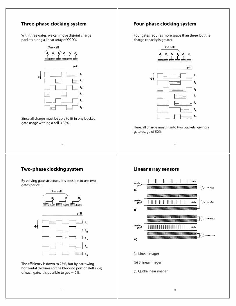
A closer look...
Interline transfer CCD(SEM photograph)
Frame transfer CCD
18
Interlacing
Interlaced
Progressive
19
Interlacing (cont’d)
By manipulating gate voltages, we can redefine cells.
In the FT CCD above, positive voltages define the charge collecting regions.
By shifting positive voltages, the cells shift vertically.
20
Spectral response
Typical spectral response of a linear MOS CCD imager:
Note the strong response in the infrared. An infrared filter (“hot mirror”) is typically necessary.
21
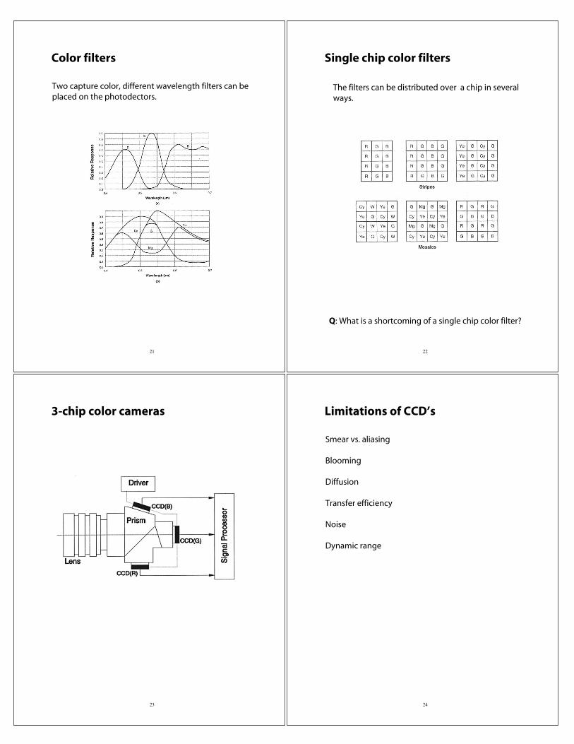
Color filters
Two capture color, different wavelength filters can be placed on the photodectors.
22
Single chip color filters
The filters can be distributed over a chip in several ways.
Q: What is a shortcoming of a single chip color filter?
23
3-chip color cameras
24
Limitations of CCD’s
Smear vs. aliasing
Blooming
Diffusion
Transfer efficiency
Noise
Dynamic range

25
Blooming
Over-exposure causes charges to leak into neighboring cells.
Can be reduced with “anti-blooming” technology.
Blooming
26
Example: smear and blooming
27
Diffusion
Electrons generated outside the depletion region may wander into neighboring cells.
28
Noise
Here is a diagram of the CCD sensing process:
Q: What kind of noise sources might you expect?

29
Dark current and photon shot noise
Electron-hole pairs are generated according to:
where:
I = irradiance of the light
tINT = integration time
They are also generated due to thermal agitation, yielding a “dark current”:
where:
T = temperature
K = Boltzmann’s constant
E∆ = energy constant that depends on materials
∆−2 /E kTdark INTn t T e
photon INTn t I
30
Dark current and photon shot noise
The electron generation process is a discrete counting process with unknown arrival times.
Such processes are described by Poisson statistics.
For a variable X obeying Poisson statistics:
σ2 = µ
Q: How should noise vary over an image?
Q: What happens to signal-to-noise (SNR) as signal increases?
31
Shot noise example
Original image
Variance (x32)
32
Bibliography
Holst, G., CCD Arrays Cameras and Displays, SPIE Optical Engineering Press, Bellingham, Washington, 1998.
Muller, R. and Kamins, T. Device Electronics for Integrated Circuits, 2nd Edition. John Wiley and Sons, New York, 1986.
Theuwissen, A. Solid-State Imaging with Charge-Coupled Devices. Kluwer Academic Publishers, Boston, 1995.