EVALUATION OF RADIO FREQUENCY CMOS INTEGRATED CIRCUIT TECHNOLOGY
175
EVALUATION OF RADIO FREQUENCY CMOS INTEGRATED CIRCUIT TECHNOLOGY FOR WIRELESS LOCAL AREA NETWORK APPLICATIONS By XI LI A DISSERTATION PRESENTED TO THE GRADUATE SCHOOL OF THE UNIVERSITY OF FLORIDA IN PARTIAL FULFILLMENT OF THE REQUIREMENTS FOR THE DEGREE OF DOCTOR OF PHILOSOPHY UNIVERSITY OF FLORIDA 2003
Transcript of EVALUATION OF RADIO FREQUENCY CMOS INTEGRATED CIRCUIT TECHNOLOGY

EVALUATION OF RADIO FREQUENCY CMOS INTEGRATED CIRCUITTECHNOLOGY FOR WIRELESS LOCAL AREA NETWORK APPLICATIONS
By
XI LI
A DISSERTATION PRESENTED TO THE GRADUATE SCHOOLOF THE UNIVERSITY OF FLORIDA IN PARTIAL FULFILLMENT
OF THE REQUIREMENTS FOR THE DEGREE OFDOCTOR OF PHILOSOPHY
UNIVERSITY OF FLORIDA
2003

ii
ACKNOWLEDGMENTS
First, I would like to thank my advisor, Professor Kenneth O, for his guidance
and encouragement throughout this Ph.D. work. I am deeply grateful to him for giv-
ing me the opportunity to be a part of the SiMICS group and for leading me into the
wireless transceiver project which eventually resulted in my employment at Intersil.
I would also like to thank Professors Eisenstadt, Fox, and Liu for serving on my commit-
tee. I want to extend special thanks to Dr. Brent Myers, for making the project for this
Ph.D. work possible, for constant and generous support during the project, and for serving
on my committee.
I would like to thank my mentors and colleagues at Intersil Corporation: John
Prentice for being the mentor during my summer internship and providing circuit knowl-
edge; Tom Brogan and Dan Yannette for RF receiver and synthesizer design help; Clay
Frace and Richard Kovacs for technical support in the lab; Mir Faiz and Charlie Carothers
for MLF packaging help; Jim Paviol for system knowledge; Jim Furino for management
support. I am also indebted to previous and current fellow students of SiMICS research
group at the University of Florida. Their support and friendship have been a great help.
Finally, I would like to thank my parents, my sister, my wife, and God. They are
the source of my strength and the reason of my endeavor.

. . .ii
. . .
. . .1
. . .1
. . .2 .2 . . .3 . . .4
. .6
. . . .6
. . .6. . .8 .10 . .11. . .1212 .13 . .14. .16
18
. .18.21.21 .21 .24.26. . .28 .28 .29
TABLE OF CONTENTS
page
ACKNOWLEGMENTS . . . . . . . . . . . . . . . . . . . . . . . . . . . . . . . . . . . . . . . . . . . . . . . .
ABSTRACT. . . . . . . . . . . . . . . . . . . . . . . . . . . . . . . . . . . . . . . . . . . . . . . . . . . . . . . . . vii
CHAPTER
1 INTRODUCTION. . . . . . . . . . . . . . . . . . . . . . . . . . . . . . . . . . . . . . . . . . . . . . . . . .
1.1 Wireless LAN Technology and Market . . . . . . . . . . . . . . . . . . . . . . . . . . 1.2 Proposed CMOS Wireless LAN Transceiver IC . . . . . . . . . . . . . . . . . . .
1.2.1 Integrated Circuits (IC’s) for Wireless LAN . . . . . . . . . . . . . . . . . .1.2.2 Research Goals and Milestones . . . . . . . . . . . . . . . . . . . . . . . . . .
1.3 Overview of the Dissertation. . . . . . . . . . . . . . . . . . . . . . . . . . . . . . . . . . .
2 IC TECHNOLOGIES FOR WIRELESS LAN . . . . . . . . . . . . . . . . . . . . . . . . . . . . .
2.1 Technology Options . . . . . . . . . . . . . . . . . . . . . . . . . . . . . . . . . . . . . . . . . 2.1.1 Silicon RF Technologies . . . . . . . . . . . . . . . . . . . . . . . . . . . . . . . 2.1.2 GaAs Technologies. . . . . . . . . . . . . . . . . . . . . . . . . . . . . . . . . . . .
2.2 Figures of Merit of Various RF IC Technologies . . . . . . . . . . . . . . . . . . .2.3 BJT and MOSFET Device Physics Comparison . . . . . . . . . . . . . . . . . . .2.4 Why RF CMOS? . . . . . . . . . . . . . . . . . . . . . . . . . . . . . . . . . . . . . . . . . . . .
2.4.1 Availability and Accessibility . . . . . . . . . . . . . . . . . . . . . . . . . . . . .2.4.2 Cost, Yield and Integration Level. . . . . . . . . . . . . . . . . . . . . . . . . .2.4.3 Performance Advantages . . . . . . . . . . . . . . . . . . . . . . . . . . . . . . .2.4.4 RF CMOS Scenarios . . . . . . . . . . . . . . . . . . . . . . . . . . . . . . . . . .
3 CMOS AND SIGE RF RECEIVER BUILDING BLOCKS. . . . . . . . . . . . . . . . . . . .
3.1 PRISM II System Overview . . . . . . . . . . . . . . . . . . . . . . . . . . . . . . . . . . .3.2 Low Noise Amplifier (LNA) . . . . . . . . . . . . . . . . . . . . . . . . . . . . . . . . . . . .
3.2.1 LNA Introduction . . . . . . . . . . . . . . . . . . . . . . . . . . . . . . . . . . . . . . 3.2.2 CMOS and SiGe LNA Design . . . . . . . . . . . . . . . . . . . . . . . . . . . .3.2.3 CMOS LNA Performance . . . . . . . . . . . . . . . . . . . . . . . . . . . . . . .3.2.4 Comparison of CMOS and SiGe LNA’s . . . . . . . . . . . . . . . . . . . .
3.3 Receive Mixer . . . . . . . . . . . . . . . . . . . . . . . . . . . . . . . . . . . . . . . . . . . . . . 3.3.1 Receive Mixer Introduction . . . . . . . . . . . . . . . . . . . . . . . . . . . . . .3.3.2 CMOS and SiGe Rx Mixer Design . . . . . . . . . . . . . . . . . . . . . . . .
iii

.30 .32 .35
37
. . .37
. .37 .38 . .40 . .41 . .42. .43 . .44. .45 .5051 . .54 .54. .59. . .63
.64
. . .64. .64. .64. .65. . .65 .67 .69. . .71 .71.73.76 . .78.78.79.81 .83
. .84
. . .84 . .85. . .87 . .87
3.3.3 LO Converter and Buffer . . . . . . . . . . . . . . . . . . . . . . . . . . . . . . . .3.3.4 Comparison of CMOS and SiGe Rx Mixers . . . . . . . . . . . . . . . . .3.3.5 Summary of Rx Mixer Design . . . . . . . . . . . . . . . . . . . . . . . . . . . .
4 Q OF RF TUNED CIRCUITS IN DIFFERENT IC TECHNOLOGIES . . . . . . . . . .
4.1 The Impact of Q . . . . . . . . . . . . . . . . . . . . . . . . . . . . . . . . . . . . . . . . . . . . 4.1.1 Q of Simple Second Order System. . . . . . . . . . . . . . . . . . . . . . . . 4.1.2 The Impact of Q on Tuned RF Circuit Design . . . . . . . . . . . . . . . .
4.2 Q and Different IC Technologies . . . . . . . . . . . . . . . . . . . . . . . . . . . . . . .4.2.1 BJT and MOS Capacitances . . . . . . . . . . . . . . . . . . . . . . . . . . . . .4.2.2 Series Resonant Circuits . . . . . . . . . . . . . . . . . . . . . . . . . . . . . . . .4.2.3 Parallel Resonant Circuits . . . . . . . . . . . . . . . . . . . . . . . . . . . . . .
4.3 Process Variations of IC Technologies . . . . . . . . . . . . . . . . . . . . . . . . . .4.3.1 Process Variations of BJT and CMOS Technologies. . . . . . . . . . 4.3.2 MOS Corner Models for RF tuned circuits . . . . . . . . . . . . . . . . . .4.3.3 RF-fast/slow Models vs. Digital-fast/slow Models . . . . . . . . . . . . .
4.4 RF Tuned Circuit Under Process Variations. . . . . . . . . . . . . . . . . . . . . .4.4.1 CMOS and BJT LNA’s under Process Variations . . . . . . . . . . . . .4.4.2 Impact of Temperature on BJT and CMOS Process Variations. .
4.5 Conclusion . . . . . . . . . . . . . . . . . . . . . . . . . . . . . . . . . . . . . . . . . . . . . . . . .
5 Q-BASED DESIGN APPROACH: AN EXAMPLE . . . . . . . . . . . . . . . . . . . . . . . .
5.1 Q-based Design Approach . . . . . . . . . . . . . . . . . . . . . . . . . . . . . . . . . . . . 5.1.1 Introduction . . . . . . . . . . . . . . . . . . . . . . . . . . . . . . . . . . . . . . . . . 5.1.2 The Foundation of Q-based Design Approach . . . . . . . . . . . . . . . 5.1.3 Starting Point of Q-based Design . . . . . . . . . . . . . . . . . . . . . . . . .
5.2 Cascoded LNA Example . . . . . . . . . . . . . . . . . . . . . . . . . . . . . . . . . . . . . 5.2.1 Q-based Design for BJT LNA . . . . . . . . . . . . . . . . . . . . . . . . . . . .5.2.2 Q-based Design for MOS LNA . . . . . . . . . . . . . . . . . . . . . . . . . . .
5.3 Q-based Noise Analysis . . . . . . . . . . . . . . . . . . . . . . . . . . . . . . . . . . . . . . 5.3.1 Introduction to Noise Analysis . . . . . . . . . . . . . . . . . . . . . . . . . . . .5.3.2 BJT LNA Noise Analysis . . . . . . . . . . . . . . . . . . . . . . . . . . . . . . . . 5.3.3 MOS LNA Noise Analysis . . . . . . . . . . . . . . . . . . . . . . . . . . . . . . .
5.4 Q-based Linearity Analysis . . . . . . . . . . . . . . . . . . . . . . . . . . . . . . . . . . . .5.4.1 Introduction to Linearity Analysis . . . . . . . . . . . . . . . . . . . . . . . . . 5.4.2 BJT LNA Linearity. . . . . . . . . . . . . . . . . . . . . . . . . . . . . . . . . . . . . 5.4.3 MOS LNA Linearity. . . . . . . . . . . . . . . . . . . . . . . . . . . . . . . . . . . .
5.5 Comparison of CMOS and BJT LNA from Q-based Design Analysis . .
6 CMOS FREQUENCY SYNTHESIZER. . . . . . . . . . . . . . . . . . . . . . . . . . . . . . . . .
6.1 Introduction . . . . . . . . . . . . . . . . . . . . . . . . . . . . . . . . . . . . . . . . . . . . . . . . 6.2 CMOS Frequency Synthesizer Overview. . . . . . . . . . . . . . . . . . . . . . . . .6.3 CMOS Prescaler Design. . . . . . . . . . . . . . . . . . . . . . . . . . . . . . . . . . . . . .
6.3.1 Prescaler Top Schematic . . . . . . . . . . . . . . . . . . . . . . . . . . . . . . .
iv

.88. .91.92 . .94 .94 .95 . .96 . .97. . .98. .99.101
.103.104.10606
107 .108
.112.113116.119123126128 .132.133.133 .133.133 .135 .138.141
42
. .142 .143143145146
6.3.2 Divide by 4/5 Synchronous Counter . . . . . . . . . . . . . . . . . . . . . . .6.3.3 Asynchronous Counter . . . . . . . . . . . . . . . . . . . . . . . . . . . . . . . . . 6.3.4 Divide-by-4/5 Control . . . . . . . . . . . . . . . . . . . . . . . . . . . . . . . . . .
6.4 Rest of the Frequency Divider . . . . . . . . . . . . . . . . . . . . . . . . . . . . . . . . .6.4.1 SCL to CMOS Converter . . . . . . . . . . . . . . . . . . . . . . . . . . . . . . . .6.4.2 Digital Counters (A/B Counters) . . . . . . . . . . . . . . . . . . . . . . . . . .6.4.3 Phase Frequency Detector (PFD) and Charge Pump (CP) . . . . . .6.4.4 PFD and CP Design . . . . . . . . . . . . . . . . . . . . . . . . . . . . . . . . . . .
6.5 CMOS Frequency Synthesizer Measurement Results . . . . . . . . . . . . . 6.5.1 CMOS Synthesizer Output Spectrum. . . . . . . . . . . . . . . . . . . . . . 6.5.2 Summary of FS Performance . . . . . . . . . . . . . . . . . . . . . . . . . . . .
7 CMOS TRANSMITTER BUILDING BLOCKS AND TRANSCEIVER DESIGN 103
7.1 CMOS Transmitter Chain . . . . . . . . . . . . . . . . . . . . . . . . . . . . . . . . . . . . .7.2 CMOS Tx Mixer Design . . . . . . . . . . . . . . . . . . . . . . . . . . . . . . . . . . . . . . 7.3 CMOS Transmitter Amplifier . . . . . . . . . . . . . . . . . . . . . . . . . . . . . . . . . .
7.3.1 CMOS Transmitter Amplifier Schematic. . . . . . . . . . . . . . . . . . . .17.3.2 TXA Simulation Results. . . . . . . . . . . . . . . . . . . . . . . . . . . . . . . . .
7.4 CMOS RF Transceiver (TRx) Design . . . . . . . . . . . . . . . . . . . . . . . . . . .
8 CHARACTERIZATION OF CMOS TRANSCEIVER AND WLAN RADIO . . . .112
8.1 Measurement of CMOS RF Transceiver . . . . . . . . . . . . . . . . . . . . . . . . .8.1.1 LNA measurement results . . . . . . . . . . . . . . . . . . . . . . . . . . . . . . 8.1.2 Rx Mixer Measurement Results . . . . . . . . . . . . . . . . . . . . . . . . . . .8.1.3 CMOS TRx Receiver Chain Measurement Results . . . . . . . . . . . 8.1.4 Tx Amplifier Measurement Results . . . . . . . . . . . . . . . . . . . . . . . .8.1.5 Tx Mixer Measurement Results . . . . . . . . . . . . . . . . . . . . . . . . . . .8.1.6 CMOS TRx Transmitter Chain Measurement Results . . . . . . . . . .
8.2 Summary of CMOS RF Transceiver Design and Measurement . . . . . .8.3 CMOS TRx In PRISM II.5 Radio . . . . . . . . . . . . . . . . . . . . . . . . . . . . . . .
8.3.1 Introduction . . . . . . . . . . . . . . . . . . . . . . . . . . . . . . . . . . . . . . . . . 8.3.2 Measurement Setup . . . . . . . . . . . . . . . . . . . . . . . . . . . . . . . . . . .8.3.3 CMOS Radio Setup . . . . . . . . . . . . . . . . . . . . . . . . . . . . . . . . . . . 8.3.4 Transmitter Measurement Results . . . . . . . . . . . . . . . . . . . . . . . .8.3.5 Receiver Measurement Results . . . . . . . . . . . . . . . . . . . . . . . . . .
8.4 Summary of the Characterization of CMOS Transceiver . . . . . . . . . . .
9 SUMMARY AND FUTURE WORK . . . . . . . . . . . . . . . . . . . . . . . . . . . . . . . . . . . .1
9.1 Summary . . . . . . . . . . . . . . . . . . . . . . . . . . . . . . . . . . . . . . . . . . . . . . . . . . 9.2 Future Work and Direction . . . . . . . . . . . . . . . . . . . . . . . . . . . . . . . . . . . .
9.2.1 CMOS Transceiver with a T/R Switch. . . . . . . . . . . . . . . . . . . . . .9.2.2 Transceiver with On-chip PA . . . . . . . . . . . . . . . . . . . . . . . . . . . . .9.2.3 Transceiver with Integrated IF Transceiver . . . . . . . . . . . . . . . . . .
v

148
.148149 .151
52
.153. .156156157 .158
59
. .159 . .161
. .163
.166
APPENDIX
A BJT AND MOSFET DEVICE PHYSICS. . . . . . . . . . . . . . . . . . . . . . . . . . . . . . . . .
A.1 Why Does the BJT Have Exponential I-V Relation? . . . . . . . . . . . . . . . A.2 Why Does the MOSFET Have Square Law I-V Relation? . . . . . . . . . . .A.3 Field Effect Transistor and Square Law. . . . . . . . . . . . . . . . . . . . . . . . . .
B INPUT IMPEDANCE OF BJT AND MOS LNA’S . . . . . . . . . . . . . . . . . . . . . . . . .1
B.1 Input Impedance of A Transistor with Degeneration . . . . . . . . . . . . . . . B.2 Approximation Cases . . . . . . . . . . . . . . . . . . . . . . . . . . . . . . . . . . . . . . . .
B.2.1 Scenario #1: Miller Capacitance is Small. . . . . . . . . . . . . . . . . . . .B.2.2 Scenario #2: Miller Theorem . . . . . . . . . . . . . . . . . . . . . . . . . . . . .B.2.3 Scenario #3: Cascode Circuits . . . . . . . . . . . . . . . . . . . . . . . . . . .
C BJT AND MOS LNA NOISE PARAMETERS . . . . . . . . . . . . . . . . . . . . . . . . . . . .1
C.1 BJT Noise Parameters . . . . . . . . . . . . . . . . . . . . . . . . . . . . . . . . . . . . . . .C.2 MOS Noise Parameters . . . . . . . . . . . . . . . . . . . . . . . . . . . . . . . . . . . . . .
LIST OF REFERENCES. . . . . . . . . . . . . . . . . . . . . . . . . . . . . . . . . . . . . . . . . . . . . . .
BIOGRAPHICAL SKETCH. . . . . . . . . . . . . . . . . . . . . . . . . . . . . . . . . . . . . . . . . . . . .
vi
tre-
ching
Area
eless
e
main
ologies
con-
ently,
lar
stor
ran-
Abstract of Dissertation Presented to the Graduate Schoolof the University of Florida in Partial Fulfillment of theRequirements for the Degree of Doctor of Philosophy
EVALUATION OF RADIO FREQUENCY CMOS INTEGRATED CIRCUITTECHNOLOGY FOR WIRELESS LOCAL AREA NETWORK APPLICATIONS
By
Xi Li
May 2003
Chair: Kenneth K. OMajor Department: Electrical and Computer Engineering
Radio frequency (RF) and microwave communications market has enjoyed
mendous growth over the last decade. Wireless technology is now capable of rea
virtually every location on the face of the earth. Over the recent years, wireless Local
Network (LAN) technology has emerged as a leader among technologies for wir
internet access.
Lowering the cost of wireless LAN (WLAN) hardware is critical in allowing th
general public to have access to WLAN technology and push the technology for
stream acceptance. To date, silicon-based processes have been the dominant techn
in developing WLAN chipsets due to their lower cost compared to compound semi
ductor processes like gallium arsenide (GaAs) MESFET and HBT technologies. Pres
most of the RF integrated circuits (IC’s) in the market are built using silicon (Si) bipo
junction transistor (BJT) or silicon-germanium (SiGe) hetero-junction bipolar transi
(HBT) technologies. Recent speed improvements of digital sub-micron bulk CMOS t
vii

bove
nol-
BT
ans-
le
nding
ese
tions.
that
bias
cir-
and
re are
s and
is pre-
sign.
er, is
noise
, fab-
ional
hip is
the
sistors have also made it feasible to implement RF circuits operating at 1 GHz and a
in CMOS technologies. Potentially, by exploiting the economy of scale, CMOS tech
ogy could provide even lower cost solutions than the Si bipolar and SiGe H
technologies. This dissertation evaluated the feasibility of implementing a 2.4-GHz tr
ceiver for wireless LAN applications in a 0.25-µm CMOS process which has comparab
over-all performance as a commercial SiGe HBT transceiver and developed understa
of observed differences.
CMOS low noise amplifier (LNA) and mixer are first designed and tested as th
two receiver components usually have more stringent and challenging specifica
Their performance is compared to that of SiGe BJT LNA and mixer. It is shown
CMOS LNA and mixer can match the SiGe performance with a 15 to 20% increase in
current, indicating that a full CMOS transceiver chip is feasible. CMOS and BJT RF
cuits are compared at fundamental device physics level as well as process
manufacturing level. MOS and BJT device variations due to process and temperatu
evaluated for RF tuned circuits with different Q values. Based on these discussion
LNA design experience, a unique design methodology, Q based design approach,
sented. It is believed that this approach can significantly reduce the risk of RF IC de
Next, a frequency synthesizer, which is the most complex component of the transceiv
realized in the CMOS process. The desired frequency locking is achieved with phase
close to that of the SiGe synthesizer. Finally the entire CMOS transceiver is designed
ricated and characterized. All the circuit blocks on the CMOS transceiver are funct
and their performance is close to that of the SiGe transceiver. The CMOS prototype c
also incorporated in a commercial IEEE 802.11b WLAN system (PRISM II.5). For
viii

he
5%
ut the
first time, PRISM II.5 WLAN with a CMOS transceiver is successfully demonstrated. T
performance of the CMOS and SiGe radios is close with CMOS radio consuming
more current than that for the SiGe radio. The success of this dissertation points o
direction of higher integration and opens the door for many possible future works.
ix

tre-
g vir-
rious
ess of
] and
ed.
d the
h as
bring-
) is
lterna-
ver
logy
net-
The
re-
uses;
CHAPTER 1INTRODUCTION
1.1 Wireless LAN Technology and Market
Radio frequency (RF) and microwave communications market has enjoyed
mendous growth over the last decade. Wireless technology is now capable of reachin
tually every location on the face of the earth. Cellular telephones, pagers and other va
wireless products have become an important part of our everyday life. Since the succ
the Ethernet project at Xerox’s Palo Alto Research Center in the early 1970’s [Met76
other similar digital protocols, the local area network (LAN) technology has blossom
Numerous LANs have been installed in both the public and private sectors aroun
world, forming one of the integral parts of the Internet. Standard LAN protocols, suc
Ethernet, can operate at fairly high speeds with inexpensive connection hardware,
ing digital networking to almost any computer. A wireless local area network (WLAN
a flexible data communications system implemented as an extension to, or as an a
tive for wired LAN. Using RF technology, wireless LANs transmit and receive data o
the air, minimizing the need for wired connections. Therefore, wireless LAN techno
is able to combine data connectivity with user mobility, and offer simple and flexible
work installation with reduced cost of ownership and enhanced network scalability.
WLANs are used in a variety of environments: “Vertical,” which includes factory, wa
house, and retail; “Enterprise,” which includes corporate and academia camp
1

2
nd
tro-
s the
rds for
edia
me
EE
pread
ISM
the
hen,
based
ter-
en-
s).
hnol-
ost
ased
tion
“SOHO,” Small Office/Home office; and “Consumer,” emerging home networking a
beyond [Lou97, Pav00].
In June, 1997, the Institute of Electrical and Electronics Engineers (IEEE) in
duced the first internationally recognized standard for WLANs: IEEE 802.11. It serve
same purpose as the IEEE 802.3 standard for wired Ethernet: establishing standa
vendor to vendor interoperability. IEEE 802.11 specifies the physical layer and m
access control (MAC) layer within a WLAN scheme. The MAC protocol is a sche
called carrier sense multiple access collision avoidance (CSMA/CA), similar to its IE
802.3 predecessor. Three physical layers were originally offered: direct sequence s
spectrum (DSSS), frequency hopping spread spectrum (FHSS) (both use 2.4 GHz
band), and infrared. In 1999, the IEEE 802.11 Wireless LAN working group ratified
802.11b standard which delivers up to 11 Mb/s in the 2.4 GHz ISM band. Since t
IEEE 802.11b WLAN based products have formed the mainstream. Today, 802.11b
WLAN is penetrating into a number of new markets, including, coffee kiosks, airport
minals, and home networking.
1.2 Proposed CMOS Wireless LAN Transceiver IC
1.2.1 Integrated Circuits (IC’s) for Wireless LAN
In order to deliver the WLAN technology, high integration and low cost are ess
tial in reducing the bill of materials (BOM) for original equipment manufacturers (OEM
Silicon-based RF process technologies can exploit the highly developed silicon tec
ogy with a larger wafer size (potentially 300 mm wafer diameter) to provide lower c
solutions in an operating frequency range where III-V compound semiconductor b
technologies have traditionally dominated. As a matter of fact, silicon bipolar junc

3
BT)
speed
le to
ially,
cost
ks to
ica-
5-
s of
this
ogies
it
in a
me
will
the
11b
this
rison
iver
transistor (Si BJT) and silicon-germanium hetero-junction bipolar transistor (SiGe H
technologies have emerged as the dominant force in this marketplace. Recent
improvements of digital sub-micron bulk CMOS transistors have also made it feasib
implement RF circuits operating at 1 GHz and above in CMOS technologies. Potent
by exploiting the economy of scale, CMOS technology could provide even lower
solutions than the Si bipolar and SiGe HBT technologies. This Ph.D. research see
evaluate the feasibility of implementing a 2.4-GHz transceiver for wireless LAN appl
tions which has comparable over-all performance as a SiGe HBT transceiver in a 0.2µm
CMOS process. Through this project, understanding of the performance limitation
CMOS and SiGe bipolar technologies for wireless applications will be developed and
understanding will be used to assess the breadth of applicability for CMOS technol
in communication applications.
1.2.2 Research Goals and Milestones
This Ph.D. work will develop a low noise amplifier (LNA), receive and transm
mixers, a frequency synthesizer, and a power amplifier driver operating at 2.4 GHz
0.25-µm CMOS process. These blocks will be housed in a 44 pin Micro Lead Fra
(MLF) package and tested on the PC board for PRISM II.5. Finally, all the RF blocks
be integrated into one transceiver chip. The CMOS transceiver will be equivalent to
SiGe HBT transceiver. The prototype CMOS chip will be incorporated into a 802.
wireless LAN radio and the whole system will be evaluated.
Since the CMOS transceiver is functionally equivalent to its SiGe counterpart,
research will provide a unique opportunity to make almost an apple-to-apple compa
of the capabilities of CMOS and SiGe HBT technologies for wireless LAN transce

4
tics
s and
ill be
ess the
ans-
arch
its are
Hz
re-
SiGe
S RF
. The
dif-
nique
elieved
r the
plex
chain
char-
ation
applications. In addition, understanding of the limitations of RF circuit characteris
such as noise, linearity, gain, power consumption, signal isolation, process variation
others in CMOS and bipolar technologies will be developed and compared. These w
used to understand and explain the transceiver-level comparison results, and to ass
critical advantages of each technology.
1.3 Overview of the Dissertation
The dissertation focuses on the IC implementation of various RF blocks and tr
ceivers in CMOS technology. In Chapter 1, the background and motivation of this rese
are presented. In Chapter 2, various IC technologies are introduced and their mer
compared for WLAN application. In Chapter 3, the overall RF system of a 2.4 G
WLAN is discussed and the design of two receiver building blocks, LNA and mixer is p
sented. Their measurement results are compared to the ones of a commercial
transceiver chip. In Chapter 4, BJT RF device of SiGe BiCMOS process and the MO
device of CMOS process are compared in terms of process/temperature variations
impact of component variations in different IC technologies on RF tuned circuits with
ferent Q values is assessed. In Chapter 5, using LNA design as an example, a u
design methodology, Q based design approach is developed and presented. It is b
that this approach will help to start the design on the right track and significantly lowe
risk of RF IC design. In Chapter 6, the frequency synthesizer which is the most com
component of the transceiver is described. In Chapter 7, the design of the transmitter
is discussed and the overall CMOS transceiver design is presented. In Chapter 8, the
acterization of the CMOS wireless transceiver chip is shown and the radio level evalu

5
last
out.
of the WLAN system with the prototype CMOS chip is also demonstrated. In the
chapter, the Ph.D. work is summarized and the future work and direction are pointed

ions
heap
ther
’s),
bigger
and
.
ring
con
f
w 1
a
poly
tances
CHAPTER 2IC TECHNOLOGIES FOR WIRELESS LAN
2.1 Technology Options
One of the main reasons behind the “explosion” of the wireless communicat
market in the 1990’s is the advance and development of IC technologies that deliver c
and reliable RF circuits. RF applications like amplifiers, oscillators, mixers and o
active circuits all depend on high quality transistors. Traditionally (before the 1980
these transistors are realized in a discrete manner. They are less reliable, occupy
board area and hard to integrate. A typical transceiver usually requires tens of IC’s
hundreds of discrete components which occupy a lot of real estate on the PC board
2.1.1 Silicon RF Technologies
One of the greatest achievements of twentieth century civilization is the matu
and industrialization of silicon integrated circuit technology. In the late 1980’s, the sili
bipolar RF technologies were able to provide npn transistors with a transit frequencyT of
about 10 GHz to serve the basic transceiver function for cellular applications belo
GHz. During the 1990’s, the fT was improved to above 20 GHz [Sev00]. Fig. 2-1 shows
cross section of a modern RF Si bipolar junction transistor (BJT) featuring double
base and emitter which significantly reduce the parasitic capacitances and resis
compared to the old technology shown in Fig. 2-2 [Nin01].
6

7
eam
OS
hest
e for
ess
olar
a 20
the
istor
tro-
of 50
Figure 2-1 Double poly Si bipolar npn transistor
Figure 2-2 Conventional bipolar transistor, old technology
BiCMOS technology combines the npn bipolar technology and the mainstr
CMOS technology to fabricate npn transistors used for RF application as well as nM
and pMOS transistors used for digital circuitry on the same wafer. It offers the hig
integration level in transceiver IC design and is believed to be a strong candidat
“Radio-on-chip” IC’s. Most of the companies that developed a npn RF bipolar proc
eventually went on to build a BiCMOS process around the npn transistor. A pure bip
process is becoming obsolete due to its limitation of the level of integration. There is
to 30% cost increase for BiCMOS compared to a pure CMOS process.
Research in epitaxial techniques such as chemical vapor deposition (CVD) in
eighties had prompted the development of a silicon hetero-junction bipolar trans
(HBT) structure, namely, the silicon-germanium bipolar transistor (SiGe HBT). By in
ducing germanium (Ge) into the npn base region, as shown in Fig. 2-3, performance

8
fully
licon
logy.
RF
cir-
come
rch.
ices
tably
tions
), a
sists
ri-
’s at
GHz fT can be easily realized. A great advantage of SiGe technology is that, it is
compatible with the main stream CMOS process. This makes it very attractive to si
foundries around the world and SiGe BiCMOS has become the dominant RF techno
Figure 2-3 A cross section of SiGe HBT [Har95]
Besides Si and SiGe, Lateral Double Diffused MOS (LDMOS) is another Si
technology. However, it is not widely accepted and its use is confined only to power
cuits. CMOS process technology, on the other hand, is most available. It has be
increasingly promising for RF applications and that is the main reason for this resea
2.1.2 GaAs Technologies
Many important applications such as optoelectronics and millimeter-wave dev
are best suited with compound semiconductors. Their physical properties, most no
large and direct bandgap and high electron mobility, make them unique in applica
where use of silicon is currently not possible. Traditionally, GaAs (gallium arsenide
III-V compound semiconductor (III-V means it is a binary compound because it con
of two different elements, gallium from column III and arsenic from column V of the pe
odic table), has been well established as a common material for commercial MMIC
9
and
illi-
asic
high
s; sec-
ables
native
te-
frequencies above 1 or 2 GHz [Goy95]. Other III-V compounds like GaP, InP, InSb
GaN are also interesting materials for applications in a wide frequency range from m
meter-wave to blue light.
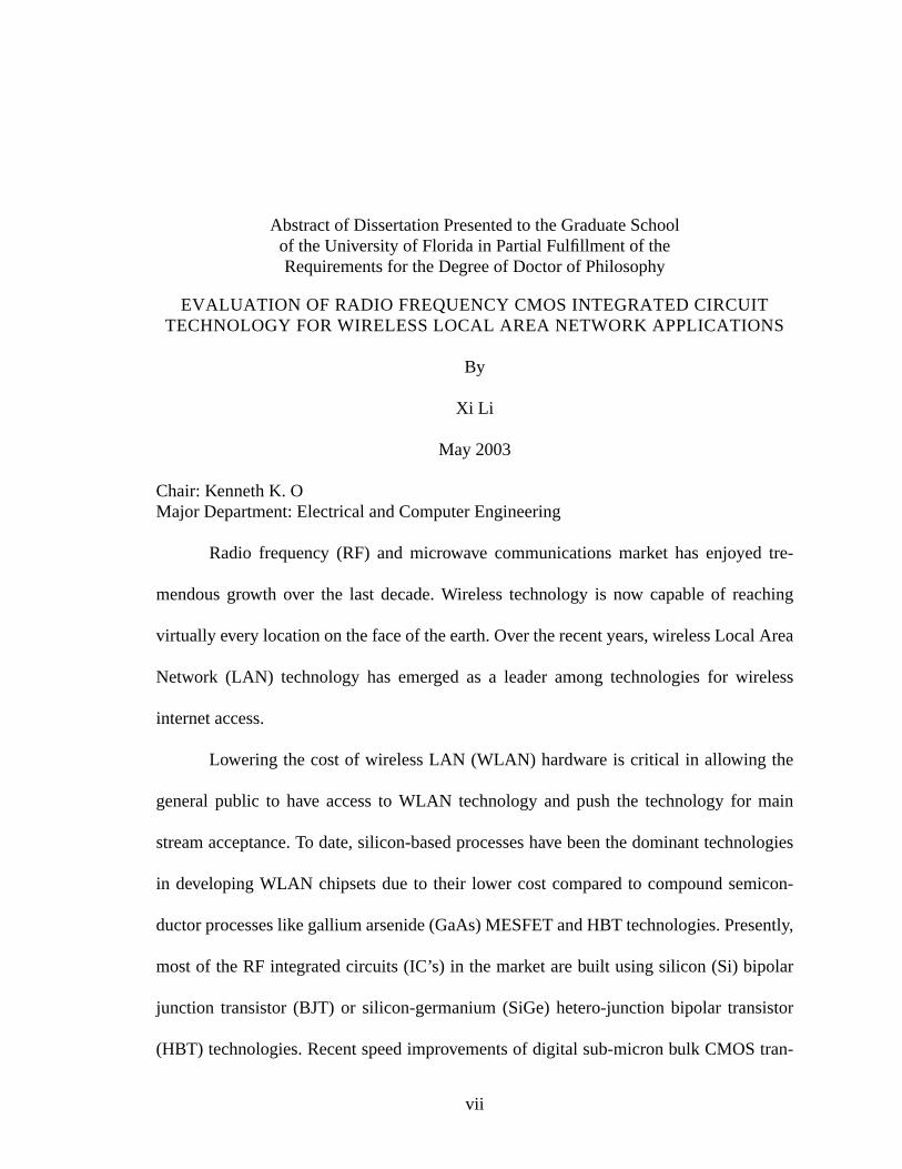
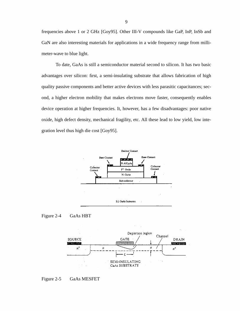
To date, GaAs is still a semiconductor material second to silicon. It has two b
advantages over silicon: first, a semi-insulating substrate that allows fabrication of
quality passive components and better active devices with less parasitic capacitance
ond, a higher electron mobility that makes electrons move faster, consequently en
device operation at higher frequencies. It, however, has a few disadvantages: poor
oxide, high defect density, mechanical fragility, etc. All these lead to low yield, low in
gration level thus high die cost [Goy95].
Figure 2-4 GaAs HBT
Figure 2-5 GaAs MESFET
10
GaAs
y95,
and
gra-
ple-
s. The
nity
ear-
ese
pro-
s
iz
all
here
tech-
OS
Wire-
There are two GaAs processes that are commonly used in RF applications:
HBT, and GaAs MESFET. Fig. 2-4 and 2-5 illustrate these two technologies.
2.2 Figures of Merit of Various RF IC Technologies
The optimum RF IC technology choice is still a subject of heated debate [Go
Lar96, Mon97, Lar98, Ulf98, Sev00]. The ultimate figures of merit may be the cost
time to market which are determined by a wide variety of factors, including yield, inte
tion level, process availability and even engineering resources. Most commercial im
mentations of wireless systems are realized in a mixture of technologies these day
key transistor technology figures of merit for RF and microwave applications are u
current gain frequency fT, maximum power gain frequency fmax, minimum noise figure, 1/
f noise corner frequency, maximum power added efficiency (for power amplifier), lin
ity, and reliability.
Table 2-1 lists some typical figures of merits of Si and GaAs technologies. Th
numbers are constantly evolving as the technology advances. The Si BJT/BiCMOS
cess quoted here is Intersil UHF2 0.6-µm BiCMOS process [Hem00]; the SiGe proces
quoted here is an IBM 0.25−µm foundry process [Har01]; GaAs data are from Mon
[Mon97] and CMOS data are from Chew et al. [Che01].
For Wireless LAN applications at 2.4 GHz ISM band, these technologies are
adequate in terms of speed and noise. Silicon technologies are clearly the choice
because of their lower cost and higher level of integration. The question is which Si
nology should be used, BJT/BiCMOS or CMOS? Both Si BiCMOS and SiGe BiCM
technologies have been employed in designing the commercial chipset at a leading

11
out
ca-
ol-
ction
.
RF
The
T’s
acter-
from
less LAN semiconductor company. It is the purpose of this Ph.D. research to find
whether CMOS technology is suitable for the same task.
2.3 BJT and MOSFET Device Physics Comparison
We have narrowed it down to two candidate IC technologies for WLAN appli
tions: silicon BiCMOS technology (including SiGe BiCMOS) and silicon CMOS techn
ogy. It is the high speed devices in these two technologies, i.e., the npn bipolar jun
transistor (BJT) and nMOSFET device that determine the performance of RF circuits
Before we embark on the task of comparing MOSFET and BJT circuits for
application, it is prudent to briefly visit the fundamental physics of these two devices.
operation of BJT’s is based on the physics of junctions (pn junctions) while MOSFE
are basically field (voltage) controlled conductors. Table 2-2 compares the basic char
istics of BJT and MOSFET devices. In Appendix A, these two devices are examined
a very fundamental physics point of view.
Table 2-1 Typical Figures of Merit of Various RF IC Technologies
Si BJT/BiCMOS
SiGe BJT/BiCMOS
GaAs HBTGaAs
MESFETSi CMOS
FeatureSize
0.6µm 0.25µm 2 µm 0.5µm 0.25µm
PeakfT
27 GHz 47 GHz 50 GHz 30 GHz ~ 40 GHz
Peakfmax
37 GHz 65 GHz 70 GHz 60 GHz ~ 50 GHz
MinimumN.F. @ 2GHz
1.0 dB 0.5 dB 1.5 dB 0.3 dB ~ 1.5 dB
1/f noisecorner
102 - 103 Hz 102 - 103 Hz 1-10 kHz ~ 10 MHz ~ 1 MHz
BreakdownBVceo/BVds
3.8 V 3.35 V 15 V 10 V ~ 3-5 V

12
and
t have
rs up
ere is
merit
ng all
semi-
most
tor
es to
d the
her
e
2.4 Why RF CMOS?
Why RF CMOS? Can and will CMOS replace bipolar transistors in all analog
RF applications? Will bipolar technology be obsoleted? These are the questions tha
been asked in numerous conferences for the past few years [Gil98]. Often this sti
emotional debates between bipolar aficionados and CMOS evangelists. Until now, th
no sign that these questions or debates will go away in the near future and certainly
discussions.
2.4.1 Availability and Accessibility
Without a question, CMOS is the most available and accessible process amo
semiconductor IC technologies. A wide range of CMOS processes are offered by
conductor foundries around the world. CMOS is the absolute technology choice for
digital applications which comprise the majority of annual worldwide semiconduc
sales. Because of this, CMOS will continue to be the dominant technology for decad
come. And that is the No. 1 advantage of CMOS process over Bipolar or BiCMOS an
main reason behind “RF CMOS.” The dominant position of CMOS will also bring ot
Table 2-2 Device Physics Comparison of BJT and MOSFET
BJT MOSFET
Carriers Minority Carriers Majority Carrier
CurrentMechanism
Diffusion Current Drift Current
I-V Charac-teristic
Exponential Square Law
Major Noise Shot noise Thermal noise
Oxide No Yes
1/f noise small large due to the presence of oxid

13
nvest-
com-
sili-
using
her
pure
tran-
ently,
olar
s that
ack-
if we
y not
ess is
r to
refore
f that,
ample
lize
olar
advantages as well, for example, largest pool of engineering resources and capital i
ment.
2.4.2 Cost, Yield and Integration Level
The main appeal of CMOS preached by its advocates is its relative lower cost
bined with high levels of integration, or transistor packing densities (# of transistors /
con area). Bipolar transistor process is more prone to defect density than a process
only majority carrier devices [Gil98]. Therefore, CMOS process will always have hig
yield which contributes to lower cost per die. On top of that, as mentioned earlier,
bipolar processes are rarely seen these days due to its low integration level. Bipolar
sistors are often realized in a BiCMOS process which requires more masks, consequ
added cost.
However, if we listen to the other side of the story, the one presented by Bip
fans, the cost advantage of CMOS process may not be that big. One argument i
[Gil98], many RF or analog chips are quite small, by the time costs associated with p
age and testing are included, the price tag on the RF chips are not too different. And
include all the digital chips in a wireless system, the cost advantage of RF CMOS ma
be realized at all in a wireless chipset. There is more: an RF or analog CMOS proc
different compared to its pure digital counterpart. It requires more masks in orde
deliver good quality passive components like resistors, capacitors and inductors. The
the CMOS cost advantage associated with masks may be hard to realize. On top o
bipolar transistors match better than MOSFETs; its performance advantages (for ex
low 1/f noise) may help to integrate more circuits (for example VCO) on chip or rea
lower cost architecture (like direct conversion radio). All these seem to support Bip

14
over
hog-
nless
rtion
purely
sive
ere RF
ages
p-
or
ectly
y pre-
MOS
while
y MOS
fans’ claim: there is no significantly distinctive cost advantage of CMOS process
Bipolar or BiCMOS.
We believe RF CMOS does pose a cost advantage over BiCMOS for same lit
raphy node technologies. However, this cost advantage may not be fully realized u
for the case of Radio or System on Chip (RoC or SoC) where wafer cost is a large po
of the total system cost; or, for the case where RF transceiver can be designed in a
low cost digital CMOS process where additional masks related to high quality pas
components are not needed. A more comprehensive discussion on the scenarios wh
CMOS will have distinctive advantages is presented in section 2.4.4.
2.4.3 Performance Advantages
There is no doubt that bipolar transistors offer a lot of performance advant
over MOSFETs in RF and analog applications. To name a few here:
1. large gm/I ratio that is important to specifications like gain and power consum
tion; (gm/I of MOSFET will never exceed that of a bipolar transistor [Abo00].)
2. BJT’s have lower 1/f noise than MOSFET’s; low 1/f noise is critical in oscillat
design and low jitter applications;
3. Bipolar transistors have better device matching on the same die. This is dir
related to I/Q match, hence the quality of the radio system;
4. Bipolar transistors have analog characteristics that are accurate thus highl
dictable [Gil98] and easily modeled, compared to hard-to-model deep sub-micron C
transistor behaviors. Modern BJT devices have model parameters less than thirty
deep sub-micron CMOS devices have model parameters exceed hundreds and ever
15
ccu-
T’s
sis-
only
lock
volt-
here
f them
tial
ns.
pre-
er 3,
istive
-room.
nta-
geometry requires a different model. Even with that, RF CMOS modeling is still not a
rate in predicting impedance and noise figure;
5. Bipolar transistors can be biased at relatively large voltage than MOSFE
without reliability concern due to hot carrier degradation [Liq01]. For RF bipolar tran
tors, the collector-emitter voltage Vce can be as high as Vcc. While for deep sub-micron
MOSFET’s, the drain-source voltage Vds may have to be biased substantially below VDD
for analog application. The device lifetime of a 0.18µm gate length MOSFET biased in
saturation at Vds= VDD will be much less than 10 years. The same VDD can guarantee 10
year lifetime for digital circuits because the transistors act as digital switches. They
stay in saturation when the switches are in transition, which is a small portion of the c
cycle. RF or analog CMOS circuits may be forced to operate at a lower power supply
age, consequently provide less head-room or leg-room compared to bipolar circuits.
However, bipolar transistors are not superior to MOSFET’s in every aspect. T
are a few interesting performance advantages that CMOS transistors possess. One o
is linearity [Gil98]. (The linearity of SiGe BJT’s is better than Si BJT’s.) The exponen
I-V law is detrimental to transistors in low distortion, medium/large signal applicatio
This is especially important in mixer design where signals have been amplified by the
ceding LNA, and the linearity requirement is stringent. As demonstrated in Chapt
large emitter degeneration is employed in bipolar transistors to achieve high IP3. Besides
decreasing the gain, inductive degeneration requires large silicon area while res
degeneration, although it occupies a smaller area, adds extra noise and reduces leg
The other advantage of CMOS is a complementary pMOS device. Its RF/IF impleme
16
ntage,
ology.
in
here
ill it
are
sce-
the
stem)
hip
rtion
ng in
n-
S and
nar-
OS
used
will
e trans-
om-
tions have not been explored at all. So, put aside all the argument about cost adva
CMOS still possess a few, if not many, performance edges over a pure bipolar techn
2.4.4 RF CMOS Scenarios
After all the discussions and arguments, the future of “RF CMOS” still lies
whether it can deliver cheaper commercial RF chips, or to put it simple, when and w
can RF CMOS chips have a significant advantage over Bipolar or BiCMOS ones? W
ever?
The answer is, of course, “yes!”, but not in every wireless application. There
scenarios where it would be beneficial to implement the radio in CMOS, and there are
narios where it would be prudent to stay with Bipolar/BiCMOS. For example, when
integration level becomes high enough in some wireless system that “Radio (or Sy
on Chip” (RoC) is desirable, a chipset may in fact be just one big chip plus a few off-c
components or small supporting chips, then, the die cost of that chip will be a large po
of the whole system cost. A 30% reduction on wafer cost may translate into 15% savi
the overall Bill of Materials (BOM), which will give a significant edge to CMOS chip ve
dors. Other scenarios may include some (low end) radio systems where both CMO
BiCMOS are more than adequate, which leads to the “golden rule” of RF CMOS sce
ios: if CMOS can do it, there is no need for BiCMOS.
It is the goal of this Ph.D. research to find out whether we can design a CM
transceiver that is functionally equivalent to a commercial SiGe BiCMOS transceiver
in an IEEE 802.11b high rate Wireless LAN chipset [Pav00]. The CMOS transceiver
be housed in the same package, measured on the same PC board as that of the SiG
ceiver. Thus, the project will provide a unique opportunity to make a more controlled c

17
AN
ges of
heir
rtation
” is
ment.
parison of the capabilities of CMOS and SiGe BiCMOS technologies for wireless L
transceiver applications. In addition, the performance advantages and disadvanta
each technology will be analyzed in detail using different RF building blocks and t
impact on RF system performance is investigated. The results presented in this disse
should provide guidance in identifying situations or scenarios where using “RF CMOS
an advantage, and help IC companies select the right technology for product develop

rsil
stud-
.
m-
on-
), I/
iver
for
CHAPTER 3CMOS AND SIGE RF RECEIVER BUILDING BLOCKS
3.1 PRISM II System Overview
The IEEE 802.11b high data rate WLAN has been implemented with the Inte
PRISM (Personal Radio using ISM bands) chipset [Pav00]. The benchmark product
ied here is the PRISM II.5 (or PRISM II) chipset. A concept diagram is shown below
Figure 3-1 PRISM II system concept diagram
The PRISM II WLAN chipset provides a complete solution from antenna to co
puter for 11 Mbps WLAN systems. The chipset comprises five IC’s, 2.4 GHz RF/IF C
verter and Synthesizer (RF/IF Converter), 2.4 GHz Power Amplifier with Detector (PA
Q MODEM and Synthesizer (IF MODEM), Baseband Processor with Rake Rece
(BBP) and Medium Access Controller (MAC). (The analog front end is identical
PA
Antenna
BBP/MACMODEM
IFPLLFreq.Syn.
LO
RF/IF Converter
18
19
, 2
eiver
f band
RF/IF
to an
O.
F fre-
sig-
nally
e
ived
l to IF
AC
iver
-
of
om
xi-
here
e LC
PRISM II and PRISM II.5. The difference is PRISM II.5 integrates the BBP and MAC
separate IC’s in PRISM II chipset, into one IC, reducing the IC counts to four.)
The system employs a traditional superheterodyne architecture. On the rec
side, the antenna is routed to a ceramic band pass filter (BPF) which attenuates out o
signals as well as the 1.7 GHz image signals. The received signal then goes to the
chip which converts the signal at an RF frequency of 2.400 to 2.484 GHz (ISM band)
IF frequency of 374 MHz. An RF synthesizer is included in the IC with an off-chip VC
On the transmitter side, the same RF/IF chip converts the signal at 374MHz to an R
quency in the ISM band. A PA then boosts the signal to around 17 dBm. The outgoing
nal after the PA goes through a T/R switch, BPF and antenna diversity switch, and fi
reaches the antenna.
A differential 374 MHz SAW filter with 8 dB loss follows the RF/IF converter. Th
main function of this SAW filter is channel selection. The IF chip converts the rece
signal after SAW to baseband (receiver) or modulates the baseband transmit signa
(transmitter). The BBP implements the IEEE 802.11 CCK modulation while the M
serves as a digital interface between the 11 Mbps data and computer/controller.
The RF/IF converter is the focus of this dissertation. It is a half duplex transce
realized in a SiGe BiCMOS process with a peak npn fT of 50 GHz. The receiver chain fea
tures a low noise amplifier (LNA), followed by a down conversion mixer. The output
LNA is not connected to the Rx mixer input directly on-chip. The RF output signal fr
LNA goes off-chip first and then back on-chip to the Rx mixer input. This provides fle
bility of system design since an off-chip Image Rejection Filter (IRF) can be placed
to boost the image rejection if necessary. The IRF can be a ceramic filter or a simpl

20
II,
BPF
band
ined
most
ost LC
pli-
t.
po-
the
low pass filter or notch filter depending on kinds of image rejection required. In PRISM
the IF frequency is chosen such that the image frequency falls into a quiet band. The
after the antenna provides 45 dB rejection at the image frequency. The narrow
response of LNA and Rx mixer delivers additional 15 dB image rejection. The comb
60 dB image rejection will be able to knock down the jammer at the image frequency
of the time. Based on the system requirement, a designer can choose a simple low c
filter or choose not to use an IRF at all.
Figure 3-2 Transceiver (RF/IF converter) chip components
The transmit (Tx) chain consists of an up conversion mixer and a transmit am
fier (TXA). Again, the output of Tx mixer goes off-chip, then back on-chip to TXA inpu
A BPF may be placed after Tx mixer, prior to TXA, to attenuate various spurious com
nents like LO, image, and their harmonics, out of the Tx mixer output. Alternatively, if
PLLFreq.Syn.
LO Input
LNA
Rx Mixer
Tx MixerTXA
To SAW Filter
IRF
BPF
RF in
RF out

21
tted,
oop
gle
nals
iver
the
TXA output goes to another BPF before PA, the BPF preceding TXA can be omi
which is the case in PRISM II.
The remaining circuitry of the RF/IF converter comprises an RF Phase Lock L
(PLL) frequency synthesizer. Since the VCO is off-chip and usually LO input is sin
ended, on-chip LO buffers are designed to convert and deliver the differential LO sig
to Rx mixer, Tx mixer and prescaler, respectively.
3.2 Low Noise Amplifier (LNA)
3.2.1 LNA Introduction
Low Noise Amplifier (LNA) usually serves as the first active stage of the rece
chain. Its high gain and relative low noise help to lower the overall noise figure of
receiver by reducing the impact of noise from subsequent stages [Poz01].
3.2.2 CMOS and SiGe LNA Design
Fig. 3-3 shows the schematic of a CMOS LNA.
Figure 3-3 CMOS LNA schematic
i_bias
rf_in
Vcc
rf_out
400/0.24
300/0.24
0.4 nH
3.2 nH
2pF
On-chip
C2
C1
22
ing
tive
om-
and
wer
has
itor
eas-
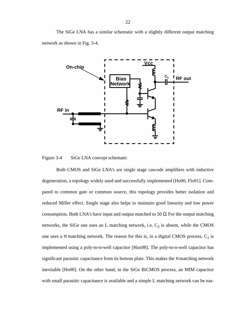
The SiGe LNA has a similar schematic with a slightly different output match
network as shown in Fig. 3-4.
Figure 3-4 SiGe LNA concept schematic
Both CMOS and SiGe LNA’s are single stage cascode amplifiers with induc
degeneration, a topology widely used and successfully implemented [Ho00, Flo01]. C
pared to common gate or common source, this topology provides better isolation
reduced Miller effect. Single stage also helps to maintain good linearity and low po
consumption. Both LNA’s have input and output matched to 50Ω. For the output matching
networks, the SiGe one uses an L matching network, i.e, C2 is absent, while the CMOS
one uses aπ matching network. The reason for this is, in a digital CMOS process, C1 is
implemented using a poly-to-n-well capacitor [Hun98]. The poly-to-n-well capacitor
significant parasitic capacitance from its bottom plate. This makes theπ matching network
inevitable [Ho00]. On the other hand, in the SiGe BiCMOS process, an MIM capac
with small parasitic capacitance is available and a simple L matching network can be
Vcc
BiasNetwork
RF in
RF out
On-chip
C1

23
ing
hat of
ns-
were
cir-
ddle.
ds of
The
d up in
ily implemented. Theπ matching network brings an extra degree of freedom in match
therefore eases the design of output matching network. It also allows higher Q than t
an L matching network.
As the first step of this research project, (before building the entire CMOS tra
ceiver), a stand-alone CMOS LNA was built and its silicon measurement results
compared to those of the SiGe LNA, which is a part of the SiGe transceiver chip. Both
cuits are housed in a 44 pin Micro Lead Frame (MLF) package with an exposed pa
Fig. 3-5 shows a micro-photograph of the stand-alone CMOS LNA, it is 1100µm X 1000
µm. The active areas of the two LNA’s are very close and both are pad limited. The pa
the CMOS LNA have the same size and similar spacing as those of the SiGe LNA.
pad arrangement, function and orientation are also the same, so they can be bonde
the same 44 pin MLF package with the same pinout.
Figure 3-5 A micro-photograph of the CMOS LNA
M1, M2 Ls
C1,
Ld
C2
Ld
C1
C2
Ls
M1
M2
i_bias Vcc
RF in
Out

24
rans-
OS
st of an
OS
. 3-7
OS-
the
is will
small
ne’s
OS
3.2.3 CMOS LNA Performance
The CMOS LNA was tested on the same PC board designed for the SiGe t
ceiver. Table 3-1 lists the measured results of CMOS and SiGe LNA’s. Most of the CM
specs are close to or exceed those of the SiGe ones, and this is achieved at the co
additional 1.1 mA, or roughly 15% increase in bias current. The bias current of CM
LNA was chosen to match the SiGe LNA performance.
Fig. 3-6 shows the measured CMOS LNA S-parameters and noise figure. Fig
shows the measured CMOS LNA Pout versus Pin plots. The IIP3 and IP1dB of CMOS LNA
are 4.8 dB and 4.2 dB higher than those for the SiGe one. This is expected since M
FET’s are generally more linear than BJT’s under the similar bias condition. Lastly,
circuit can also be made to operate at the same supply current as the SiGe one. Th
result in a 0.05 dB increase in noise figure and 0.5 dB decrease in gain, which are
differences.
The overall performance of the stand-alone CMOS LNA matches the SiGe o
with a slight increase in power consumption. This design will be ported into the CM
transceiver with no major changes when the full chip CMOS transceiver is realized.
Table 3-1 CMOS and SiGe LNA Performance Comparison
f0 = 2.45 GHz CMOS LNA SiGe LNA
50-Ω NF 2.88 dB 2.86 dB
Bias Current 8.1 mA 7.0 mA
Transducer Gain 15.1 dB 15.9 dB
S11 -14.2 dB -12.7 dB
S22 -20.2 dB -16.0 dB
S12 < -34 < -30
IIP3 2.2 dBm -2.6 dBm
IP1dB -7.0 dBm -11.2 dBm

25
A
Figure 3-6 Measured CMOS LNA S-parameters and Noise Figure
Figure 3-7 The output 1dB compression point and IP3 measurement for the CMOS LN
2 2.1 2.2 2.3 2.4 2.5 2.6 2.7 2.8 2.9 3−25
−20
−15
−10
−5
0
5
10
15
20
Frequency (GHz)
S−
para
met
ers,
NF
(dB
)S22S11
Transducer GainNoise Figure
2.88 dB
−30 −25 −20 −15 −10 −5 0 5 10−80
−70
−60
−50
−40
−30
−20
−10
0
10
20
30
Pin (dBm)
PL
(dB
m)
26
and
lytical
ore
oth
ly as
s-
r-
put
et-
3.2.4 Comparison of CMOS and SiGe LNA’s
The CMOS LNA was designed to meet the specifications of the SiGe LNA
measurement results seem to agree with simulations. It certainly merits some ana
discussion. Here we would like to present a brief analysis and explanation. A m
detailed discussion will be presented in chapter 5.
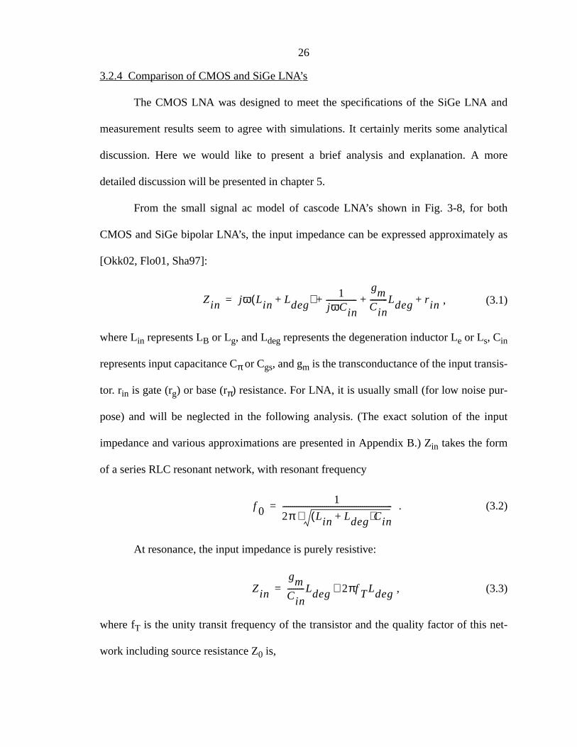
From the small signal ac model of cascode LNA’s shown in Fig. 3-8, for b
CMOS and SiGe bipolar LNA’s, the input impedance can be expressed approximate
[Okk02, Flo01, Sha97]:
, (3.1)
where Lin represents LB or Lg, and Ldegrepresents the degeneration inductor Le or Ls, Cin
represents input capacitance Cπ or Cgs, and gm is the transconductance of the input transi
tor. rin is gate (rg) or base (rπ) resistance. For LNA, it is usually small (for low noise pu
pose) and will be neglected in the following analysis. (The exact solution of the in
impedance and various approximations are presented in Appendix B.) Zin takes the form
of a series RLC resonant network, with resonant frequency
. (3.2)
At resonance, the input impedance is purely resistive:
, (3.3)
where fT is the unity transit frequency of the transistor and the quality factor of this n
work including source resistance Z0 is,
Zin jω Lin Ldeg+( ) 1jωCin----------------
gmCin---------Ldeg r in+ + +=
f 01
2π Lin Ldeg+( )Cin⋅----------------------------------------------------------=
Zin
gmCin---------Ldeg 2πf TLdeg∼=

27
of
. (3.4)
The effective Gm of the tuned RLC resonant network is:
. (3.5)
Figure 3-8 Small signal model of cascode LNA’s
The gm/I ratio of CMOS is lower than that of bipolar [Abo00]. The dc currents
two LNA’s are close; therefore, the gm of CMOS LNA input transistor is lower than the
Qin1
2πf oCin Z0 2πf TLdeg+( )⋅------------------------------------------------------------------------ 1
4π f 0Cin-----------------------∼=
Gm Qin gm⋅∼
E1
E1
Z0
Z0
Zin
Zin
Le
Lb
Ls
Lg
Cbypass
Cbypass
Leff
LeffCeff
Ceff Reff
Reff

28
sis
n do,
, an
ent to
Q of
mpli-
ology
er-
e of
to
mixer
LNA
tive
SiGe LNA’s. However, SiGe LNA adopted a Qin lower than the CMOS one, resulting in a
similar overall effective Gm for both LNA’s. (The reason why BJT LNA has a lower Qin
will be discussed in chapter 4.)
Effective Gm and the load seen at the cascode collector/drain Reff, determine the
overall power gain:
. (3.6)
Both LNA’s have similar Reff, therefore their power gains are close. The analy
brings up a general question: how do we deal with low gm/I of CMOS as gm/I of MOSFET
will never reach that of a bipolar transistor? Generally there are three things we ca
first, consuming more current; second, utilizing a larger load (At high frequencies
inductive load is more often used than a resistive load, increasing the load is equival
increasing the Q of the inductor when the inductance is fixed); third, increasing the
tuned circuit; by carefully balancing these three things, CMOS can match SiGe RF a
fier performance with a small increase in power consumption. Furthermore, as techn
advances, gm/I of MOSFET will increase [Abo00]. Operating the device near weak inv
sion will also help to reduce power consumption. All these point to a promising futur
CMOS implementation of LNA’s or RF amplifiers.
3.3 Receive Mixer
3.3.1 Receive Mixer Introduction
Mixer is another important block in the receiver chain. Its main function is
achieve frequency conversion. In a superheterodyne receiver, the Receive (Rx)
down converts the signal at RF frequency to IF frequency. Since it is placed after the
which has a gain around 15 to 20 dB, mixer usually requires a high linearity. An ac
GT Gm2
Reff Rs⋅ ⋅∼
29
lps to
ple-
is a
atic,
npn
val-
istive
d
mixer achieves the frequency conversion as well as provides gain, therefore it he
maintain the high gain and low noise figure of the overall receiver. A popular IC im
mentation of the active mixer is a Gilbert mixer.
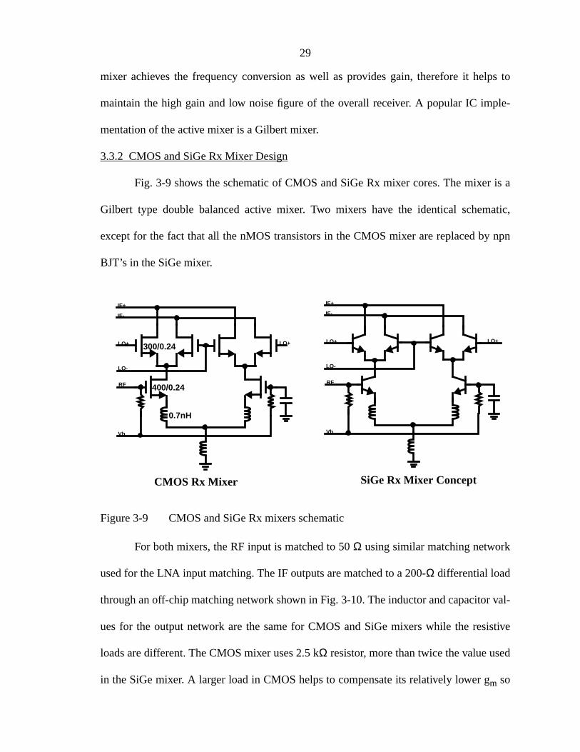
3.3.2 CMOS and SiGe Rx Mixer Design
Fig. 3-9 shows the schematic of CMOS and SiGe Rx mixer cores. The mixer
Gilbert type double balanced active mixer. Two mixers have the identical schem
except for the fact that all the nMOS transistors in the CMOS mixer are replaced by
BJT’s in the SiGe mixer.
Figure 3-9 CMOS and SiGe Rx mixers schematic
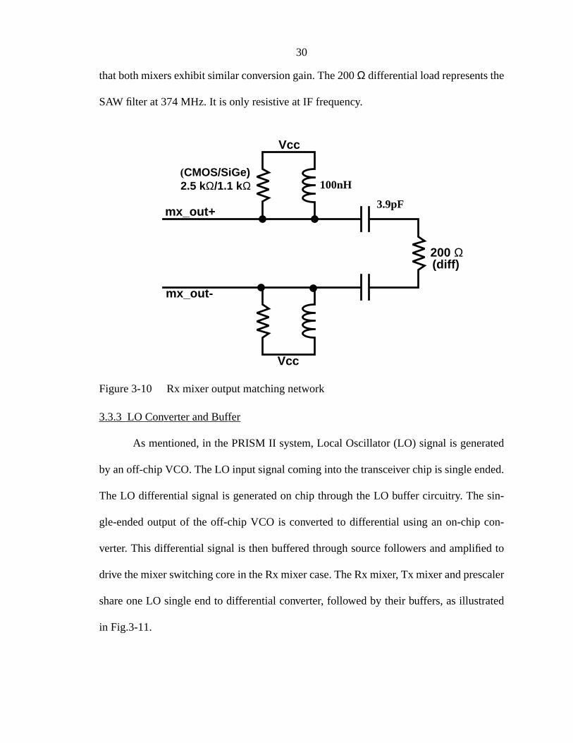
For both mixers, the RF input is matched to 50Ω using similar matching network
used for the LNA input matching. The IF outputs are matched to a 200-Ω differential load
through an off-chip matching network shown in Fig. 3-10. The inductor and capacitor
ues for the output network are the same for CMOS and SiGe mixers while the res
loads are different. The CMOS mixer uses 2.5 kΩ resistor, more than twice the value use
in the SiGe mixer. A larger load in CMOS helps to compensate its relatively lower gm so
IF+
IF-
LO+
LO-
RF
Vb
LO+
IF+
IF-
LO+
LO-
RF
Vb
LO+300/0.24
400/0.24
0.7nH
CMOS Rx Mixer SiGe Rx Mixer Concept
30
ted
ed.
sin-
on-
d to
aler
ated
that both mixers exhibit similar conversion gain. The 200Ω differential load represents the
SAW filter at 374 MHz. It is only resistive at IF frequency.
Figure 3-10 Rx mixer output matching network
3.3.3 LO Converter and Buffer
As mentioned, in the PRISM II system, Local Oscillator (LO) signal is genera
by an off-chip VCO. The LO input signal coming into the transceiver chip is single end
The LO differential signal is generated on chip through the LO buffer circuitry. The
gle-ended output of the off-chip VCO is converted to differential using an on-chip c
verter. This differential signal is then buffered through source followers and amplifie
drive the mixer switching core in the Rx mixer case. The Rx mixer, Tx mixer and presc
share one LO single end to differential converter, followed by their buffers, as illustr
in Fig.3-11.
200 Ω
mx_out+
mx_out-
Vcc
(diff)
Vcc
(CMOS/SiGe)2.5 kΩ/1.1 kΩ 100nH
3.9pF

31
nta-
river
ctive
LO
wer
. This
the
II.
Figure 3-11 LO Converter/Buffer concept diagram
Fig. 3-12 shows the CMOS converter/buffer schematic. The circuit impleme
tions of the SiGe counterparts are similar. The only difference is the load of the d
(amplifier). In the SiGe chip a resistive load is used while in the CMOS case an indu
load is employed to deliver a larger LO swing. As explained in section 3.3.4, a large
swing is important for CMOS mixer performance. The inductive load renders a narro
band response in contrast to the wide band response for a circuit with a resistive load
however, will not pose a problem, since for a given radio, the IF frequency is fixed in
superheterodyne architecture, and the system bandwidth is only 83 MHz in PRISM
Rx Mixer
Tx Mixer
LO Bufferfor RMx
LO Bufferfor TMx
LO S/DConverter
LO Bufferfor Prescaler
To Prescaler
PLL Freq. Syn.
On-chip
LO Input
SAW Filter
RMx in
TMx out

32
ding
icon
of the
, the
ilding
ip, we
wed
tire
Figure 3-12 CMOS LO Buffer Schematic
3.3.4 Comparison of CMOS and SiGe Rx Mixers
Similar to the LNA case, as the first step of this research project, (before buil
the entire CMOS transceiver), a stand-alone CMOS Rx mixer was built and its sil
measurement results were compared to those of the SiGe Rx mixer, which is a part
SiGe transceiver chip. The reason to build stand-alone CMOS LNA and Rx mixer is
receiver component specifications are usually more stringent and challenging. By bu
stand-alone circuits and comparing its hardware results with the SiGe transceiver ch
are able to assess the feasibility and difficulty of the project. Consequently this allo
more reliable estimation of the amount of the work and realistic planning of the en
chip.
Vb
Vb1
Vb1
LO
Vcc
Out+
Out-
Vb1
Vb1Vb1
Source FollowerS/D Converter Driver (Amplifier)

33
the
hib-
igher
O
of a
gnal
ersus
at in
Fig. 3-13 shows a micro-photograph of the CMOS mixer. The die size of
CMOS mixer is 1500µm X 1100µm.
Figure 3-13 A micro-photograph of the CMOS Rx mixer.
Table 3-2 lists the measurement results of the two mixers. The CMOS mixer ex
its approximately the same gain and return losses. The SSB noise figure is 1.5 dB h
for the CMOS mixer. An explanation for this is, for the CMOS mixer, with sinusoidal L
signals, the switching core transistors are simultaneously on for a larger portion
period than its SiGe bipolar counterpart. Even though for the CMOS mixer, the LO si
is designed to have twice the magnitude as that of the bipolar one, namely, 0.3 V v
0.15 V, the amount of time when both switching transistors are on is still larger than th
Mx Core S/D Conv. and SF
LO Driver
Vb
Vb1
Vb1
LO
Vcc
Out+
Out-
Vb1
Vb1Vb1
IF+
IF-
LO+
LO-
RF
Vb
LO+
Mx Core
S/D Conv. SF Driver
Com Inductor
34
es
is
ffer
ter,
er
and
r and
rent
n
duc-
0.7
in in
l for
the bipolar differential pair switches. Additionally, the CMOS LO buffer chain consum
a total 8 mA current, of which, 3 mA is for the single-end to differential converter, 1 mA
for the source follower and 4 mA is for the driver. On the other hand, the SiGe LO bu
chain consumes only 5 mA, of which, 2 mA is for the single end to differential conver
1mA is for the emitter follower and 2 mA is for the driver. A large LO swing at the mix
switching core is critical to CMOS mixer performance (for both the conversion gain
noise figure). This is a reason that the bias current of the CMOS buffer chain is highe
its LO driver utilizes an inductive load while its SiGe counterpart consumes lower cur
and employs a resistive load.
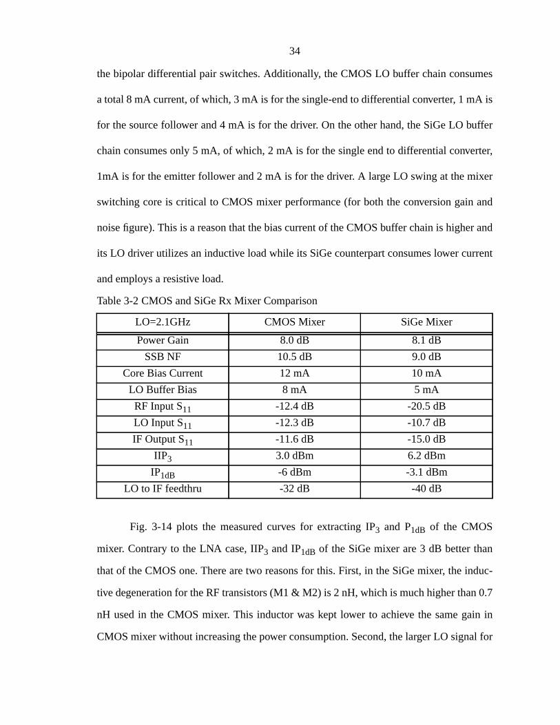
Fig. 3-14 plots the measured curves for extracting IP3 and P1dB of the CMOS
mixer. Contrary to the LNA case, IIP3 and IP1dB of the SiGe mixer are 3 dB better tha
that of the CMOS one. There are two reasons for this. First, in the SiGe mixer, the in
tive degeneration for the RF transistors (M1 & M2) is 2 nH, which is much higher than
nH used in the CMOS mixer. This inductor was kept lower to achieve the same ga
CMOS mixer without increasing the power consumption. Second, the larger LO signa
Table 3-2 CMOS and SiGe Rx Mixer Comparison
LO=2.1GHz CMOS Mixer SiGe Mixer
Power Gain 8.0 dB 8.1 dB
SSB NF 10.5 dB 9.0 dB
Core Bias Current 12 mA 10 mA
LO Buffer Bias 8 mA 5 mA
RF Input S11 -12.4 dB -20.5 dB
LO Input S11 -12.3 dB -10.7 dB
IF Output S11 -11.6 dB -15.0 dB
IIP3 3.0 dBm 6.2 dBm
IP1dB -6 dBm -3.1 dBm
LO to IF feedthru -32 dB -40 dB

35
the
istors
ce.
Rx
olar
hip
: the
com-
e due
the CMOS mixer introduces a larger signal at twice the LO frequency (2-LO signal) on
drain node of the RF transistors. This 2-LO signal is coupled to the gates of RF trans
through Cgd of the MOS transistors and is known to degrade the linearity performan
Despite the slightly inferior noise figure and IIP3, the CMOS mixer still satisfies the Rx
mixer specifications for the PRISM II system.
Figure 3-14 The output 1dB compression point and IP3 measurement for CMOS
Mixer
3.3.5 Summary of Rx Mixer Design
The stand-alone CMOS Rx mixer exhibits similar performance as its SiGe bip
counterpart. This CMOS Rx mixer design will be ported into the CMOS transceiver c
with no major changes. One adjustment will be made from a system point of view
common mode inductor will be replaced by a current source. The reason is that, this
mon mode inductor tends to pick up low frequency noise and spurs from the substrat
−35 −30 −25 −20 −15 −10 −5 0 5 10−70
−60
−50
−40
−30
−20
−10
0
10
20
Pin (dBm)
PL
(dB
m)

36
ows
to its relative large area. (It’s a large inductor, shown in Fig. 3-13.) This adjustment shlittle impact on mixer performance in simulation.

cir-
ut of
plifiers
ially
t to
pply
ce.
ons.
ith a
ver-
ency
CHAPTER 4Q OF RF TUNED CIRCUITS IN DIFFERENT IC TECHNOLOGIES
4.1 The Impact of Q
From the LNA design analysis, we can see the importance of Q of the tuned
cuit. The tuned matching networks are desired in RF circuits because they reject o
band unwanted signals and consume less power compared to broadband am
[Okk02]. However, the Q of the matching network can not be arbitrarily large, espec
for integrated circuits. IC manufacturing exhibits significant process variations from lo
lot, wafer to wafer, and die to die. On top of that, variations due to temperature, su
voltage, packaging, PC board environment, etc. will all affect RF circuit performan
Therefore, the Q of the RF circuits should be sufficiently low to withstand these variati
A proper selection of Q value is a key for circuit yield and system integrity.
4.1.1 Q of Simple Second Order System
Typically, matching networks can be modeled as second order systems w
transfer function as [Okk02]:
. (4.1)
A radio system is usually designed to work in a certain frequency range. The o
all frequency response of the amplifiers in a radio is required to be flat in that frequ
H jω( ) 1
1 jQω
ω0-------
ω0ω-------–
+
-------------------------------------------∼
37

38
1.
ess,
range. Usually, it is specified as +/- 0.5 dB over a certain frequency range (∆ω). Gain flat-
ness of +/- 0.5 dB over∆ω is the 1-dB band width requirement, as illustrated in Fig. 4-
Figure 4-1 Frequency response and Q of the network
4.1.2 The Impact of Q on Tuned RF Circuit Design
Let’s assume power gain is approximately proportional to |Hin(jω)|2|Hout(jω)|2 in
an LNA. Furthermore, for simplicity, let |Hin(jω)| = |Hout(jω)|, and assume all the fre-
quency response of the circuit comes from these two terms. To satisfy the gain flatn
, (4.2)
or,
. (4.3)
Since∆ω/2 is set for a system, the only unknown is Q. Solving for Q,
. (4.4)
0.5 dB
Higher Q
0.5 dB
∆ω
10 H j ωO∆ω2
--------+
4
1dB–=log
H j ωO∆ω2
--------+
10
140------–
k= =
Q
1
k2
----- 1–
ωo∆ω2
--------+
ωo----------------------
ωo
ωo∆ω2
--------+----------------------–
2-----------------------------------------------------------=

39
n not
pter
is a
nd, a
2].
ders
flat-
Eq.
tuning
.45
f 2.45
orst
idth of
The gain flatness sets the Q for the input and output matching networks. Q ca
be arbitrarily high. From the CMOS and SiGe BJT LNA comparison discussion in cha
3, increasing Q or increasing current can help to increase the overall Gm, consequently
increase gain. So, higher Q is beneficial to lower power consumption, and there
trade-off between power consumption and bandwidth of a receiver. On the other ha
circuit with high Q networks is more sensitive to component variations [Flo01, Okk0
This is a serious issue in IC implementation, where process variation typically ren
more than 10% change of passive component values.
Figure 4-2 Component variation and Q
For example, in a 802.11b radio system, if the LNA is required to have gain
ness of +/- 0.5 dB from 2.4 GHz to 2.5 GHz, without any component variations, from
(4.4) Q should be less than 8.5. Now, suppose the components which determine the
characteristics (i.e. L and C) are controlled within +/- 10%. If the LNA is centered at 2
GHz, in the worst case the tuned frequency could be as high as 2.695 GHz (110% o
GHz) or as low as 2.205 GHz (90% of 2.45 GHz). To make sure that even in the w
case, the design satisfies the gain flatness requirement, it must have an 1-dB bandw
No variationHigh Q
With variationLow Q
100 MHz
0.5 dB
0.5 dB
Worst Cases

40
g-
uit
ari-
iGe
pro-
er for
tion,
rent
e of
cir-
cir-
NA
r
ower
ess
will
nol-
2 x (2.45 GHz x 10% + (2.5 GHz -2.4 GHz)/2) = 590 MHz as illustrated in Fig. 4-2. Plu
ging 590 MHz back into Eq. (4.4) as∆ω, we find out that Q should be less than 1.5.
4.2 Q and Different IC Technologies
If the Q of a network is too high that the component variations affect the circ
performance more, then the overall wafer yield will become lower. In the LNA comp
son discussion, we found out that CMOS LNA has a higher input Q than that of the S
BJT LNA. A logical question from there is that, is it because BJT devices have more
cess variations that they have to be designed with a lower Q, or is it because in ord
CMOS technology to match the performance of SiGe BJT under similar bias condi
the Q of the input network has to be higher? The different circuit Q values for diffe
technologies have to be justified: lower Q of BJT circuits may render the advantag
higher gm/I ratio of bipolar transistor useless; on the other hand, higher Q of CMOS
cuits may undermine the very nature of choosing RF CMOS if the high Q lowers the
cuit yield and raises the cost.
If the resistance value is fixed in the RLC resonant circuit, (like in the case of L
input matching where the resistance is fixed at 50Ω), for a series resonant circuit, lowe
capacitance or higher inductance implies higher Q; for a parallel resonant circuit, l
capacitance or higher inductance means lower Q.
Before we get into the discussion of which technology will have more proc
variations or enable use of higher Q circuits, let’s first examine which technology
likely to have lower capacitances so we know for series or parallel circuits which tech
ogy will more likely to have a higher Q design.

41
ch-
e key
f a
BJT
ill
r
4.2.1 BJT and MOS Capacitances
Which technology will more likely to have a small capacitance, BJT or MOS te
nology? The answer is MOSFET. This can be demonstrated by looking at one of th
figures of merit of CMOS and bipolar technologies, the unity gain frequency fT which can
be expressed as [Gra93],
(4.5)
where CT is Cπ + Cµ ~ Cπ in BJT’s and Cgs+ Cgd~ Cgs in MOSFET’s; gm is the transcon-
ductance and in a bipolar transistor, it is always,
or (4.6)
at room temperature. While in a long channel MOSFET, gm is,
or . (4.7)
The gm/I ratio of a MOSFET (4.7) is always smaller than and will never exceed that o
BJT (4.6) [Abo00]. Therefore, Eq. (4.5) indicates that, for an nMOS and an npn
exhibiting the same speed (fT), if they are biased under the same current, MOSFET w
have a smaller gm consequently smaller capacitance, i.e., it is more likely to have Cgs <
Cπ. This is further illustrated in table 4-1. Two devices exhibiting the same fT are picked
from two technologies. In CMOS technologies, a high fT is achieved through a smalle
Cgs, while in bipolar technologies the same fT is obtained through a higher gm[Man01].
f T1
2π------
gmCT--------⋅≅
gm
I cVT--------=
gmI c------- 1
VT--------
qkT------ 0.038V
1–∼= =
gm µnCoxWL----- V( GS Vth– )=
gmI D------- 2
VGS Vth–---------------------------=

42
nant
tial
of the
sonant
T
en-
4.2.2 Series Resonant Circuits
Since MOSFET’s are more likely to have smaller capacitance, for series reso
circuits like the LNA input, CMOS circuits are more prone to higher Q design, a poten
hidden performance disadvantage that can not be seen in chapter 3 until the details
actual circuits are revealed here. Extra care should be taken in RF CMOS series re
circuit design to ensure proper selection of Q value.
Let’s look at the example of our LNA input matching. Rewriting Eq. (3.3) of Zin,
the input impedance of LNA is,
. (4.8)
In both BJT and MOS LNA’s, Zin should be matched to (50Ω - rg or rb). (rg or rb is small
for well-designed LNA therefore they can be neglected.) We realize that Ldeg is the same
in the CMOS and bipolar LNA design (Ls, Le ~ 0.4 nH), therefore CMOS and SiGe BJ
LNA should have the same fT. Since both LNA’s are biased under similar current, gm of
CMOS will be lower than that of SiGe BJT. Consequently, the input capacitance Cin of
CMOS LNA is smaller; hence, CMOS LNA exhibits higher Q and is potentially more s
sitive to component variations.
Table 4-1 Characteristics of an nMOS and a bipolar npn
Parameters 0.18µm CMOS Parameter 0.3µm Si BJT
Cgs 92 fF Cπ 230 fF
fT 43 GHz fT 43 GHz
gm 30 mA/V gm 100 mA/V
IDS/W ~ 50µA/µm IC/LE ~ 80µA/µm
Width W ~ 70µm Emitter width LE ~ 30µm
Zin
gmCin---------Ldeg 2πf TLdeg∼=

43
1].
t
ted
ness.
C
an a
? Not
vari-
aci-
ally
as an
vious
r; or,
A detailed analysis on MOS LNA Q and input matching can be found in [Flo0
There, an alternative input quality factor independent of Ls is defined as
. (4.9)
Assuming in Eq. (3.1), inductors, Cin and fT all have tolerance of 10%, to satisfy inpu
matching S11 < -10 dB, Qgsshould be less than 2.3 [Flo01]. In section 4.1.2, we estima
Q of all the matching networks in LNA should be less than 1.5 to ensure the gain flat
This is consistent with Qgsestimate here because Qgs is roughly twice the Q of LNA input
matching network including the source resistance. It is prudent to recommend a Qgs of no
more than 3 for 2.4 GHz LNA input design.
The above analysis indicates that, for the same speed performance, sincein is
larger for a BJT series resonant circuit (BJT LNA input), it has lower Q. Does this me
BJT RF circuit poses an advantage in terms of process variations since its Q is lower
necessarily, this is only true if, for the same Q, BJT devices exhibit the same process
ations as MOS devices.
4.2.3 Parallel Resonant Circuits
In a parallel resonant RLC circuit, for a fixed parallel resistance, a lower cap
tance means lower Q which will give MOSFET circuits some advantage. This usu
occurs is the case of multi-stage RF circuitry in Fig.4-3, where the previous stage h
inductor load and the ensuing stage is the input of a transistor. For example, the pre
stage could be the LNA and the ensuing stage could be the input of the receive mixe
the previous stage could be the first stage of a two-stage amplifier, etc.
Qgs1
ωoCgsZ0----------------------=

44
r,
r
uc-
f the
tors
e one
ay
ts in
10%
f pro-
s sec-
If there is no fixed resistor in parallel with the capacitor or inducto
. Therefore, the Q of the resonant LC circuit will follow the smalle
one of the Q’s of capacitor and the inductor. In an IC environment, it is usually the ind
tor Q which is smaller. The Q of the parallel resonant tank is determined by the Q o
on-chip inductor. A high Q inductor is not always desired: circuits using such induc
are less tolerant to process variations.
Figure 4-3 Parallel resonant circuit in RF IC’s
4.3 Process Variations of IC Technologies
From the analyses in previous sections, we realize that process variations ar
of the main reasons to design tuned circuits with low Q. Different technologies m
exhibit different levels of process variations. For the same Q, two tuned RLC circui
BJT and MOSFET may have a different component value shift. The assumption of
component value shift is somewhat rough and over-simplified. Detailed assessment o
cess variations in different technologies should be conducted and is carried out in thi
1Qtotal----------------- 1
QL------- 1
QC--------+=
Vcc
by-pass cap
On-chipinductor
Previous Stage Current Stage
Parasitic resistanceof the on-chip inductor
Equivalent Resonant Circuit

45
e are
ogy
f two
r
ere
CVD
e
hys-
tion. The discussion is restricted to BJT and MOSFET technologies only, since thes
the two technologies of interest for WLAN applications. However, the methodol
developed here is generic and can be applied to other IC technologies. Variations o
key figures of merits, fT and Cπ (or Cgs) for BJT and MOSFET devices are evaluated.
4.3.1 Process Variations of BJT and CMOS Technologies
For a BJT, the peak fT is proportional toτf. For a good BJT device (high emitte
efficiency),τf is close to base transit timeτB which is related to base width WB. Therefore
we have
(4.10)
where Dn is the diffusion constant andυ is 2 for constant base doping.υ can be much
larger than 2 for graded doping where the built-in electric field is large. However, th
exists a limit for the smallestτf that can be achieved,
(4.11)
where vs is the saturation velocity of electron. Either way, the control of WB will deter-
mine the variations of fT and the control of WB is limited by ion implantation. (For SiGe,
WB variations depend on the thickness control of epitaxial layer deposited using a
process). For modern high performance Si or SiGe BJT’s, WB is on the order of 50 nm or
less. The control of WB is a vertical challenge which will not benefit much from th
lithography advancement.
For MOSFET’s, the variations of peak fT and Cgsare related to W and L which are
limited by lithography, and thickness control of the thermal oxidation process. The p
τ f
WB2
νDn-----------≅
τ f min,WB2vs---------≅
46
SiGe
da-
ve
oxide
ver,
d L,
vice
og-
er W
is
order
cess
ith
ET’s
ed
ics of process variations behind BJT and MOS transistors are quite different. For
BJT, it’s the SiGe epitaxial deposition while for MOS, it is lithography and thermal oxi
tion. CVD epitaxial layer deposition with a linearly graded Ge profile is likely to ha
more process variations because it is harder to control compared to thermally grown
thickness. Foundry supplied corner model data suggested that the variations of WB can be
around 20% for SiGe BJT’s; while only 5% for MOSFET gate oxide thickness. Howe
for MOSFET, there is also variations associated with the device dimension W an
termedδL or δW. δL or δW is usually 10% of the lithography resolution, 0.025µm in the
case of a 0.25µm CMOS technology. The process variations associated with de
dimension (δL/L or δW/W) depends strongly on device size (W and L) because the lith
raphy resolution stays the same for both large and small devices. Devices with larg
and L will exhibit much less process variations (percentage wise,δL/L or δW/W) than
devices with smaller W and L. Usually the design rules are set that the minimum W
much larger than the lithography resolution (0.6µm in 0.25µm CMOS process used). On
top of that, MOS devices used for analog or RF applications are usually wide (on the
of tens or hundreds of microns). Therefore, the variation of W,δW/W is usually much less
than 1%. The variation of L, on the other hand, is one of the main contributors for pro
variations of RF or analog MOSFET’s. Clearly, if MOSFET devices are designed w
large gate length, their process variations will be much smaller. For example, MOSF
with L of 0.5 µm exhibit gate length variation of only 5% (δL/L), compared to 10% of
MOSFET’s with L of 0.25µm. However, large gate length device exhibits slower spe
thus not favored for RF circuits.

47
ns.
teral
tions
tion.
have
ocess
ver
-
e
dels
rsus
both
nce
ulated
s 4-2
,
,
The scaling down in lithography certainly helps to alleviate MOSFET variatio
The vertical device (BJT) does not benefit as much from technology scaling as the la
device (MOS). All these seem to indicate that MOSFET’s can have less process varia
than BJT’s, especially if the device gate length is larger than the lithography resolu
However, it would be impetuous to jump into the conclusion that BJT devices always
more process variations than MOSFET’s. The real comparison should always be pr
by process, or foundry by foundry.
Figures 4-4 to 4-7 show the simulated MOS and BJT LNA input transistors o
process variations. The CMOS process is a 0.25-µm process from a leading CMOS
foundry while BJT process is 0.35-µm SiGe BiCMOS process from a leading SiGe BiC
MOS foundry. Every stripe of MOSFET device is 100µm/0.24µm (gate W/L). Every
stripe of BJT device is 10µm/0.44µm (emitter length/emitter width). The devices ar
biased at 7 mA current and are simulated with fast-fast, nominal, slow-slow corner mo
provided by the foundry. fT and the capacitance of the input transistors are plotted ve
the number of stripes of the unit device. The 7 mA current is close to the current of
BJT and MOS LNA’s discussed in chapter 3.
A MOS device and a BJT device providing the same nominal input capacita
around 0.7 pF are picked as input transistors and their dc operating points are sim
under different corner models supplied by the foundries. Results are shown in table
and 4-3. For MOS input transistor, fT and Cgs worst case variations are 13% and 3%
respectively; for BJT input transistor, fT and Cπ worst case variations are 27% and 21%
respectively.
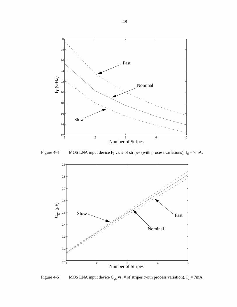
48
Figure 4-4 MOS LNA input device fT vs. # of stripes (with process variations), Id = 7mA.
Figure 4-5 MOS LNA input device Cgs vs. # of stripes (with process variation), Id = 7mA.
1 2 3 4 512
14
16
18
20
22
24
26
28
30
Number of Stripes
f T (
GH
z)
Fast
Nominal
Slow
1 2 3 4 50.1
0.2
0.3
0.4
0.5
0.6
0.7
0.8
0.9
Number of Stripes
Cgs
(pF
)
Fast
Nominal
Slow

49
Figure 4-6 BJT LNA input device fT vs. # of stripes (with process variation), Ic = 7mA.
Figure 4-7 BJT LNA input device Cπ vs. # of stripes (with process variation), Ic = 7mA.
1 2 3 4 540
50
60
70
80
90
100
Number of Stripes
f T (
GH
z)
Fast
Nominal
Slow
1 2 3 4 50.4
0.5
0.6
0.7
0.8
0.9
1
Number of Stripes
Cπ
(pF
)
FastNominal
Slow

50
cess
tch-
be
It seems that for the two processes in comparison, MOSFET’s have less pro
variations than BJT’s. This, however, needs further investigation.
4.3.2 MOS Corner Models for RF tuned circuits
The analysis above certainly bodes well for CMOS technology in terms of ma
ing the CMOS amplifier gain with that of BJT amplifier. Bottom line is: it is the gmQ that
determines the gain, not gm alone. RF circuits in technology with less variations can
Table 4-2 A 400µm/0.24µm nMOS biased at 7mA under different corner models
Parameters Nominal Fast SlowWorst-casevariations
Cgs (fF) 658 636 678 3%
gm (mA/V) 63.9 69.8 58.6 9%
Vth (V) 0.503 0.439 0.567 33%
Vgs-Vth (V) 0.185 0.166 0.203 11%
fT ~ gm/C(GHz)
15.5 17.5 13.8 13%
Table 4-3 A 27µm/0.44µm npn biased at 7mA under different corner models
Parameters Nominal fast slowWorst-casevariations
Cπ (fF) 668 530 790 21%
Vbe (V) 0.877 0.858 0.904 3%
Intrinsic rb(Ω)
9 12 6 33%
Extrinsic rb(Ω)
6 3 9 33%
Total rb (Ω) 15 15 15 ~ 0%
τf (nS) 2.3 1.75 2.8 24%
β 89 235 29 164%
rπ (Ω) 335 883 109 164%
fT ~ gm/C(GHz)
64 81 54 27%

51
r-
-
er
orner
ndry
ow (or
y are
cor-
ency.
as
dels
st and
dig-
od-
gate
s
thick-
s not
designed with higher Q, therefore, a better gmQ product which leads to better gain per cu
rent.
It was found out in section 4.3.1, that the 0.25-µm CMOS has less process varia
tions than the 0.35-µm BiCMOS technology in simulations. This claim needs to be furth
investigated before drawing conclusions. The first thing under the microscope is the c
models of MOSFET’s used in the simulation. The corner models supplied by the fou
are based on digital CMOS processes. Two ends of the corners, fast (or best) and sl
worst) models are distinguished by the current driving capability of the devices. The
termed digital-fast and digital-slow models in the rest of the discussion.
For RF applications, the digital-fast and digital-slow models do not reflect the
ner scenarios of RF circuits. RF circuits have tuned response with respect to frequ
Therefore, capacitance and peak fT rather than current driving capability should be used
the criteria to assess the corner situations of RF circuits.
A new MOSFET modeling scheme that provides correct RF CMOS corner mo
is proposed here. New corner models based upon the new scheme are called RF-fa
RF-slow models. As we can see in the following section, they are quite different from
ital-fast and digital-slow corner models.
4.3.3 RF-fast/slow Models vs. Digital-fast/slow Models
The difference between the new RF corner models and the old digital corner m
els lies in the representation of two key process parameters, oxide thickness and
length as shown in table 4-4 where L and Tox are the nominal values of oxide thicknes
and gate length. Digital-fast model represent the case with the thinnest gate oxide
ness and narrowest gate length. It has the highest current driving capability. Yet it doe

52
pac-
e is
tab-
th
tances
nput
dels.
have the highest fT because the effects of thin gate oxide and narrow gate length on ca
itance tend to cancel each other.
To further illustrate the difference between two corner models, an exampl
shown here. At 7mA, a MOS device with a number of stripes of 4 (400µm/0.24µm) exhib-
its nominal Qin around 1. The operating point of this device under different models is
ulated in table 4-5. Capacitances and fT of different size devices are also simulated wi
the two models. The results are obvious: using the new corner models, the capaci
and fT varies much more than predicted by the old corner models. For a nominal i
capacitance around 0.7 pF, for MOS input transistor, fT and Cgs worst case variations are
22% and 14%, respectively; they are much larger than 6% and 4% from digital mo
However, still less than 27% and 21% of BJT device variations.
Table 4-4 RF corner models vs. Digital corner models
Parameters RF-fast RF-slow Digital-fast Digital-slow
Oxide thickness Tox + δTox Tox - δTox Tox - δTox Tox + δTox
Gate length L -δL L + δL L - δL L + δL
Capacitance Smallest Largest
gm Largest Smallest
fT ~ gm/C fastest slowest
Table 4-5 A 400µm/0.24µm nMOS biased at 7mA under different corner models
Parameters Nominal RF-fast RF-slow Digital-fast Digital-slow
Cgs (fF) 658 576 751 636 678
gm (mA/V) 63.9 68.8 58.9 69.8 58.6
Vth (V) 0.503 0.439 0.566 0.439 0.567
Vgs-Vth (V) 0.185 0.168 0.202 0.166 0.203
fT ~ gm/C(GHz)
15.5 19 12.5 17.5 13.8

53
Figure 4-8 MOS LNA Input Device fT vs. # of Stripes (with Process Variation), Id = 7mA.
Figure 4-9 MOS LNA Input Device Cgs vs. # of Stripes (with Process Variation), Id = 7mA.
1 2 3 4 510
15
20
25
30
35
Number of Stripes
f T (
GH
z) Fast, digital
Nominal
Slow, digital
Fast, RF
Slow, RF
1 2 3 4 50.1
0.2
0.3
0.4
0.5
0.6
0.7
0.8
0.9
1
Number of Stripes
Cgs
(pF
)
Fast, digitalNominal
Slow, digital
Fast, RF
Slow, RF

54
els is
not
worst
y be
will
for-
pera-
the
of
are
to be
sets
e
erate
mA.
ndry
/-5%
Figures 4-8 and 4-9 show the capacitances and fT varying as a function of the num-
ber of stripes under different corner models. The difference between two corner mod
significant. The discussion here points out that the corners supplied by foundry is
modeled from an RF perspective. Often corner models are employed to simulate the
case scenarios. If the corner situations are not modeled correctly, the circuit ma
designed with Q too high or too optimistic. The whole circuit performance and yield
be affected.
4.4 RF Tuned Circuit Under Process Variations.
In order to more fully understand the impact of various variations on circuit per
mance and the relationship between Q and immunity to variations, process and tem
ture variations of a simple LNA are simulated with corner model sweep to investigate
circuit level performance.
4.4.1 CMOS and BJT LNA’s under Process Variations
The basic LNA circuit in Fig. 4-10 is chosen for this purpose. Input matching
CMOS and BJT LNA’s under process variations is compared. Again, the two LNA’s
biased at 7 mA dc current. For a fair comparison, the Q of the input matching are set
the same under nominal condition for two LNA’s. A nominal Q of 1 is chosen and this
the input transistor nominal capacitance (Cgsor Cπ) to be around 0.65 pF at 2.45 GHz. Th
input is matched under the nominal condition, i.e. the input inductor and the degen
inductor values are set to match the input port to 50Ω. The LNA is then simulated under
different transistor corner models while maintaining the total current unchanged at 7
(For MOS LNA, the newly developed RF corner models are used, replacing the fou
provided digital corner models.) The off-chip inductor value is assumed to have a +

55
ared
rd etc.
50
sment
shift. An S11 of -15 dB is set to be the specification. This number is conservative comp
to -10 dB because other variations associated with temperature, package, PC boa
have not been considered. For example, a transceiver chip is supposed to be in aΩ
environment. However, the transmission line impedance has variation. Instead of 50Ω, it
is possible to get 46Ω or 55Ω due to the variations in PC board manufacturing.
Figure 4-10 Basic BJT and CMOS cascode LNA’s used in process variation asses
Figure 4-11 S11 of MOS LNA, Q of 1, nominal, digital and RF corner models
E1
Z0
Le
Cbypass
RL
OutputMatching
Vcc
E1
Z0
Ls
Cbypass
RL
OutputMatching
Vcc
LgLb
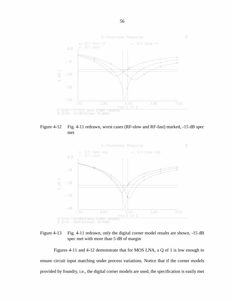
56
spec
5 dB
dels
met
Figure 4-12 Fig. 4-11 redrawn, worst cases (RF-slow and RF-fast) marked, -15 dBmet
Figure 4-13 Fig. 4-11 redrawn, only the digital corner model results are shown, -1spec met with more than 5 dB of margin
Figures 4-11 and 4-12 demonstrate that for MOS LNA, a Q of 1 is lowenough to
ensure circuit input matching under process variations. Notice that if the corner mo
provided by foundry, i.e., the digital corner models are used, the specification is easily
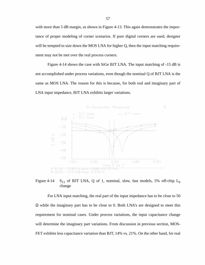
57
por-
igner
ire-
is
s the
rt of
o 50
this
hange
OS-
r real
with more than 5 dB margin, as shown in Figure 4-13. This again demonstrates the im
tance of proper modeling of corner scenarios. If pure digital corners are used, des
will be tempted to size down the MOS LNA for higher Q, then the input matching requ
ment may not be met over the real process corners.
Figure 4-14 shows the case with SiGe BJT LNA. The input matching of -15 dB
not accomplished under process variations, even though the nominal Q of BJT LNA i
same as MOS LNA. The reason for this is because, for both real and imaginary pa
LNA input impedance, BJT LNA exhibits larger variations.
Figure 4-14 S11 of BJT LNA, Q of 1, nominal, slow, fast models, 5% off-chip Lbchange
For LNA input matching, the real part of the input impedance has to be close t
Ω while the imaginary part has to be close to 0. Both LNA’s are designed to meet
requirement for nominal cases. Under process variations, the input capacitance c
will determine the imaginary part variations. From discussion in previous section, M
FET exhibits less capacitance variation than BJT, 14% vs. 21%. On the other hand, fo

58
JT
r
ance
ce and
How-
A,
their
ms
ut
e 4-15
can
lower
part of the input impedance, fT change is the main factor for variations. MOSFET and B
have similar worst case fT variations with BJT slightly worse, 22% vs. 27%. However, fo
BJT LNA, gmfT/Le only gives part of the real impedance, the other part is base resist
rb, and the equivalent resistance from rπ (which is in parallel with Cπ). From table 4-3, the
total base resistance does not change much because the intrinsic base resistan
extrinsic base resistance are moving at opposite direction under process variations.
ever, rπ does change a lot asβ shows more than 150% variations. Therefore, for BJT LN
both its real and imaginary parts of input impedance have larger variations than
MOSFET LNA counterparts. Consequently the input matching of BJT LNA perfor
worse under process variations.
Figure 4-15 BJT LNA with lower input Q, met -15 dB specification
In order for BJT LNA to meet the -15 dB input matching specification, its inp
transistor has to be resized to lower Q to accommodate the process variations. Figur
demonstrates that for an input Q of 0.65 or an input capacitance of 1 pF, BJT LNA
meet the input matching specifications. Of course, there is some gain penalty with

59
for
BJT
ls:
tions
arac-
nd,
NA’s
tions.
to
) are
Q. As shown in Fig. 4-16, BJT LNA transducer gain is 24 dB for a Q of 1 vs. 21.5 dB
a Q of 0.65. In order to accommodate more process variations associated with
devices, BJT LNA has to be designed with less Q, consequently less gmQ product or less
gain. This will bring the gain of BJT and MOS LNA’s in parity.
Figure 4-16 Transducer gain of BJT LNA with different input Q’s, nominal modeleft, Q of 1, right, Q of 0.65.
4.4.2 Impact of Temperature on BJT and CMOS Process Variations
The discussion in last section indicates that CMOS devices exhibits less varia
than BJT’s. Temperature changes will contribute more to process variations. The ch
teristics of BJT is closely related to temperature. For example, gm of BJT circuits is pro-
portional to 1/T under ITAT biasing. The characteristics of MOSFET, on the other ha
do not change much compared to BJT devices. To illustrate this, the BJT and MOS L
discussed in last section are re-simulated with both temperature and process varia
For simplicity, the 5% off-chip inductor value changes are not considered.
Fig. 4-17 shows the BJT LNA input matching under both temperature (-40 C
100 C) and process variations for an input Q of 1. The worst cases (slow/fast, 100 C

60
tch-
ess
are
nd the
ever,
redrawn in Fig. 4-18. Apparently temperature variations make the BJT LNA input ma
ing worse.
Figure 4-17 BJT LNA (Q of 1) input matching under both temperature and procvariations
Figure 4-18 Previous figure redrawn, worst cases marked
LNA’s with different input Q values are also simulated. Their input matchings
tabulated in tables 4-6 and 4-7. The temperature makes the matching more difficult a
general trend is that when the input Q is lowered, the matching becomes better. How

61
ther
JT
can-
ching
rst
for BJT LNA’s, there is an optimal Q value. Once this optimal value is reached, fur
lowering Q will not buy much matching benefit. The reason for this is, for medium Q B
LNA’s, the effect of rπ is still in play: the equivalent resistance from rπ and gmfT/Le are
moving in opposite directions (table 4-3) under process variations and their variations
cel each other out for the real part of the input impedance. Therefore the input mat
variation is alleviated. However, at lower Q, the equivalent resistance from rπ is essen-
tially 0 because the parallel capacitance is very large. The variations due to rπ and gmfT/Le
are not cancelled and the S11 variations become larger.
Figure 4-19 S11 of MOS LNA with process and temperature variations, only the wocases are shown, still meet the -15 dB specification
Table 4-6 BJT LNA’s under both temperature and process variations
Nominal input Q 1.2 1 0.65 0.5
Nominal Cin 0.58 pF 0.67 pF 1 pF 1.3 pF
Worst case S11 with processvariations
-11 dB (slow) -14.6 dB(slow)
-16.1 dB(fast)
-14.7 dB(fast)
Worst case S11 with both Tand process variations
-8.5 dB (fast/100C)
-13.5 dB (fast100 C)
-14 dB (fast/-40C)
-12 dB (fast/-40C)

62
aria-
. Fig.
aria-
g is
ut
not
t of
antly
f
st Q
Compared to BJT devices, MOSFET’s fare much better under temperature v
tions as their parameters depend on geometry rather than minority carrier junction
4-19 shows the MOS LNA with nominal Q of 1 under both process and temperature v
tions, plus 5% off-chip inductor variations. Comparing to Fig. 4-12, the input matchin
only slightly worse and still meets the -15 dB specification.
Table 4-7 tabulates the input matching of MOS LNA with different nominal inp
Q under both process and temperature variations (5% off-chip inductor variation is
included). RF corner models are employed in the simulations.
As we can see, in order for BJT LNA to exhibit the same input matching as tha
MOS LNA under process and temperature variations, its input Q has to be signific
lower. For example, for a requirement of S11 less than -13.5 dB, MOS LNA can be
designed with a Q of 2while the largest Q allowed for BJT LNA is only 1, half of that o
the MOS LNA. Table 4-8 lists the input matching requirement that mandates the highe
allowed in both BJT and MOS LNA’s.
Table 4-7 MOS LNA’s under both temperature and process variations
Nominalinput Q
4 2 1.5 1 0.5
Nominal Cin 0.17 pF 0.34 pF 0.45 pF 0.67 pF 1.3 pF
Worst S11with processvariations
-8.3 dB(slow)
-13.72 dB(slow)
-16.8 dB(fast)
-17.3 dB(slow)
-23.5 dB(fast)
Worst S11with both Tand processvariations
-8.3 dB(slow/25C)
-13.70 dB(slow 100C)
-15.8 dB(fast -40 C)
-17.2 dB(slow 100 C)
-21.2 dB(fast -40C)

63
MOS
varia-
eliver
as a
tions
ussion
com-
e vari-
er Q
f
4.5 Conclusion
This chapter compares the BJT RF device of SiGe BiCMOS process and the
RF device of CMOS process from a brand new perspective: process/temperature
tions. RF chips designed in either process have to withstand these variations to d
high yield, consequently viable solution in a real world. For RF CMOS to compete
viable process for WLAN or other RF applications, its process/temperature varia
need to be evaluated and compared to those of SiGe BiCMOS processes. The disc
presented in this chapter suggests that, for the CMOS and SiGe BiCMOS processes
pared here, CMOS devices exhibit an advantage in terms of process and temperatur
ations against BJT’s. Therefore CMOS RF tuned circuits can be designed with high
values than BJT tuned circuits. This will bring the gmQ products consequently the gain o
CMOS and BJT RF circuits close to parity at a given power consumption.
Table 4-8 MOS and BJT LNA highest Q allowed for different input matching criteria
Input matching requirement S11 < -8.3 dB S11< -13.5 dB S11 < -15 dB
Highest Q allowed for BJTLNA
1.2 1 Can never meetthe criterion
Highest Q allowed for MOSLNA
4 2 1.5

. For
uff-
n their
n the
A in
noise
ased
nt-end
erall
uld be
pper
ar-
us to
CHAPTER 5Q-BASED DESIGN APPROACH: AN EXAMPLE
5.1 Q-based Design Approach
5.1.1 Introduction
Most of the RF front-end components in an RF transceiver are tuned circuits
example, LNA, transmit amplifier (TXA), input and output stages of mixers, and LO b
ers. Tuned circuits reject out of band unwanted signals and consume less power tha
broadband counterparts. They are desired in all band-limited wireless systems.
Q factor is the most important parameter of tuned circuits, as demonstrated i
analysis of Q of a second order system, and the analysis of input matching of LN
chapter 4. Based upon this, a Q-based design approach is developed [Okk02]. Low
amplifiers realized in both BJT and MOS transistors are used to illustrate the Q-b
design approach. This approach can easily be extended to the cases of other RF fro
circuits.
5.1.2 The Foundation of Q-based Design Approach
The foundation of Q based design approach is, in order to maintain the ov
robustness of a band-limited wireless system, the tuned response of the circuits sho
able to withstand component variations (especially in IC circuits). This poses an u
limit on Q. By plotting gain, noise or linearity with respect to Q, the trade-offs among v
ious specifications can be examined and a proper Q can be selected. This will enable
design the initial transistor sizes and set simulations on the right track.
64

65
e is
pecifi-
tant
sing
sub-
uter
pro-
into
and
5.1.3 Starting Point of Q-based Design
The starting point of Q-based design is to identify a unit device. This unit devic
then scaled under constant current or other restricting factors depending on design s
cations. The Q of the circuit varies with the scaling of the unit device. The impor
parameters of LNA (Gain, Noise Figure, Linearity) can be plotted versus the Q u
MATLAB. A proper selection of Q is made based upon these plots.
It should be emphasized that this analysis is not and should not be viewed as a
stitute for computer simulation like SPICE. Rather, it is a great starting point of comp
simulation and represents the intelligent part of the design phase. Modern simulation
grams provide a powerful tool for analog and RF circuit design. However, jumping
extensive simulation without understanding the behavior of circuit is a dangerous
inefficient practice.
5.2 Cascoded LNA Example
Figure 5-1 BJT (Left) and MOS (Right) cascode LNA’s
E1
Z0
Le
Cbypass
RL
OutputMatching
Vcc
E1
Z0
Ls
Cbypass
RL
OutputMatching
Vcc
LgLb
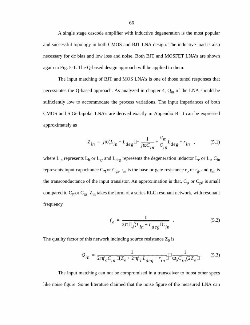
66
ular
also
own
that
both
sed
ant
pecs
can
A single stage cascode amplifier with inductive degeneration is the most pop
and successful topology in both CMOS and BJT LNA design. The inductive load is
necessary for dc bias and low loss and noise. Both BJT and MOSFET LNA’s are sh
again in Fig. 5-1. The Q-based design approach will be applied to them.
The input matching of BJT and MOS LNA’s is one of those tuned responses
necessitates the Q-based approach. As analyzed in chapter 4, Qin of the LNA should be
sufficiently low to accommodate the process variations. The input impedances of
CMOS and SiGe bipolar LNA’s are derived exactly in Appendix B. It can be expres
approximately as
, (5.1)
where Lin represents Lb or Lg, and Ldegrepresents the degeneration inductor Le or Ls, Cin
represents input capacitance Cπ or Cgs, rin is the base or gate resistance rb or rg, and gm is
the transconductance of the input transistor. An approximation is that, Cµ or Cgd is small
compared to Cπ or Cgs. Zin takes the form of a series RLC resonant network, with reson
frequency
. (5.2)
The quality factor of this network including source resistance Z0 is
. (5.3)
The input matching can not be compromised in a transceiver to boost other s
like noise figure. Some literature claimed that the noise figure of the measured LNA
Zin jω Lin Ldeg+( ) 1jωCin----------------
gmCin---------Ldeg r in+ + +=
f o1
2π Lin Ldeg+( )Cin⋅----------------------------------------------------------=
Qin1
2πf oCin Zo 2πf TLdeg r in+ +( )⋅------------------------------------------------------------------------------------- 1
ωoCin 2Zo( )-------------------------------∼=
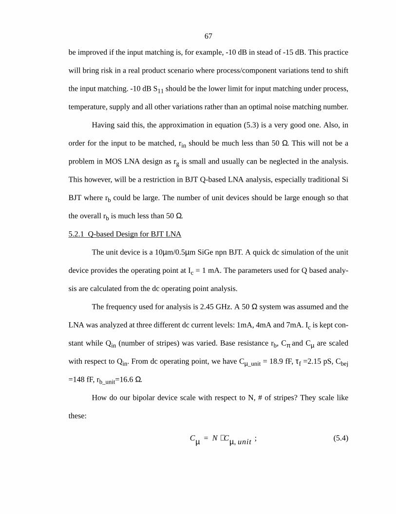
67
tice
shift
s,
mber.
, in
is.
l Si
that
t
ly-
e
like
be improved if the input matching is, for example, -10 dB in stead of -15 dB. This prac
will bring risk in a real product scenario where process/component variations tend to
the input matching. -10 dB S11 should be the lower limit for input matching under proces
temperature, supply and all other variations rather than an optimal noise matching nu
Having said this, the approximation in equation (5.3) is a very good one. Also
order for the input to be matched, rin should be much less than 50Ω. This will not be a
problem in MOS LNA design as rg is small and usually can be neglected in the analys
This however, will be a restriction in BJT Q-based LNA analysis, especially traditiona
BJT where rb could be large. The number of unit devices should be large enough so
the overall rb is much less than 50Ω.
5.2.1 Q-based Design for BJT LNA
The unit device is a 10µm/0.5µm SiGe npn BJT. A quick dc simulation of the uni
device provides the operating point at Ic = 1 mA. The parameters used for Q based ana
sis are calculated from the dc operating point analysis.
The frequency used for analysis is 2.45 GHz. A 50Ω system was assumed and th
LNA was analyzed at three different dc current levels: 1mA, 4mA and 7mA. Ic is kept con-
stant while Qin (number of stripes) was varied. Base resistance rb, Cπ and Cµ are scaled
with respect to Qin. From dc operating point, we have Cµ_unit = 18.9 fF,τf =2.15 pS, Cbej
=148 fF, rb_unit=16.6Ω.
How do our bipolar device scale with respect to N, # of stripes? They scale
these:
; (5.4)Cµ N C⋅ µ unit,=
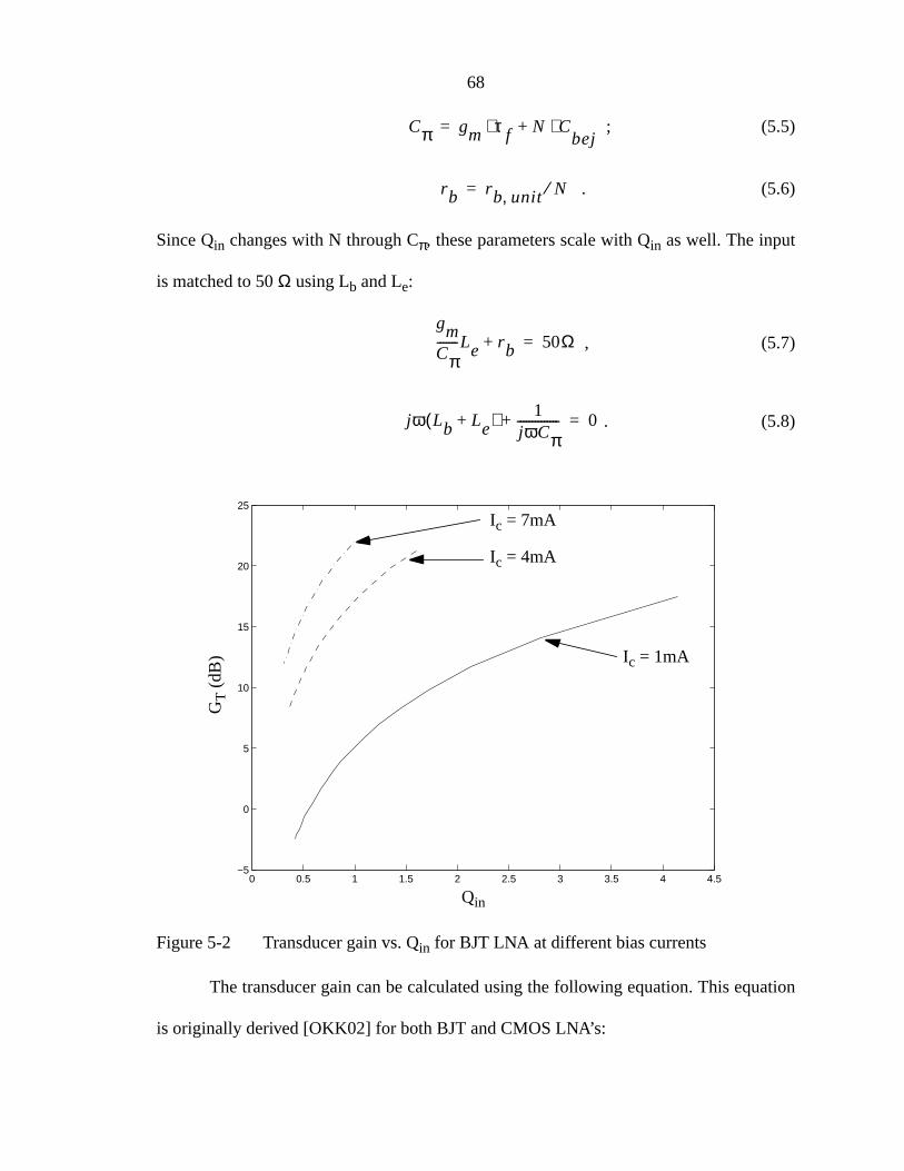
68
ation
; (5.5)
. (5.6)
Since Qin changes with N through Cπ, these parameters scale with Qin as well. The input
is matched to 50Ω using Lb and Le:
, (5.7)
. (5.8)
Figure 5-2 Transducer gain vs. Qin for BJT LNA at different bias currents
The transducer gain can be calculated using the following equation. This equ
is originally derived [OKK02] for both BJT and CMOS LNA’s:
Cπ gm τ f⋅ N+ C⋅bej
=
rb rb unit, N⁄=
gmCπ-------Le rb+ 50Ω=
jω Lb Le+( ) 1jωCπ--------------+ 0=
0 0.5 1 1.5 2 2.5 3 3.5 4 4.5−5
0
5
10
15
20
25
Qin
GT (
dB)
Ic = 7mA
Ic = 4mA
Ic = 1mA

69
a
n
and
cale
(5.9)
Fig. 5-2 shows transducer gain vs. Qin curves using Eq. (5.9). Transducer gain follows
general trend: it increases as Qin increases. Also note that for higher current or higher gm,
Qin can be lower for a given GT. At 7 mA, Qin is always smaller than 1. This is unique i
the case of BJT: Cπ depends on current (or gm), higher current (or gm) limits the lowest Cπ
hence highest Qin.
5.2.2 Q-based Design for MOS LNA
The unit device for Q based analysis is a 100µm/0.24µm nMOS transistor. A quick
dc simulation on the unit device provides the operating point at Id = 1 mA. The parameters
used for Q based analysis are calculated from the dc operating point analysis.
Once again, the frequency used for analysis is 2.45 GHz, a 50Ω system was
assumed, and the LNA was analyzed at three different dc current levels: 1mA, 4mA
7mA. The drain current Id is kept constant while Qin (number of stripes) was varied. Cgs
and Cgd are calculated. The input is matched to 50Ω through Lg and Ls. Qin of the LNA
and the transducer gain are then calculated.
From the dc operating point analysis, we have Cgs_unit= 141.3 fF, Cgd_unit= 31 fF,
andβ_unit=0.0709. How do MOS devices scale with respect to N, # of stripes? They s
differently compared to BJT devices: the device width W scales with N and
; (5.10)
; (5.11)
; (5.12)
GT 4gm2
RsZoQin2
Qout2
=
Cgd N C⋅ gd unit,=
Cgs N C⋅ gs unit,=
β µn CoxWL----- N∝⋅ ⋅=

70
m-
ation
ly
ne-
. (5.13)
Since Qin changes with N through Cgs, these parameters also scale with Qin.
Figure 5-3 Transducer gain vs. Qin for MOS LNA at different bias currents
Note the difference between the MOS and BJT cases is that gm does not change in
BJT LNA while Cgs (Cin) does not change with current and scales linearly with the nu
ber of stripes in a MOSFET. The equation to calculate the transducer gain is still equ
(5.9). Fig. 5-3 shows the transducer gain vs. Qin for the MOS LNA at different bias cur-
rents. The MOS LNA transducer gain follows the same trend as BJT LNA. GT increases as
Qin increases. However, in the MOS LNA case, Qin depends on the number of stripes on
and is not limited by current. At high current levels, MOS LNA power gain can still be
fit from higher Qin.
gm 2I d β⋅ N∝=
0 0.5 1 1.5 2 2.5 3 3.5 4 4.5 52
4
6
8
10
12
14
16
18
20
22
Qin
GT (
dB)
Id = 7mA
Id = 4mA
Id = 1mA

71
analy-
lysis,
a93],
Fig.
uiva-
nt
circuit
5.3 Q-based Noise Analysis
5.3.1 Introduction to Noise Analysis
Before the Q based noise analysis is discussed, a review of some basic noise
sis concepts is in order. People tend to get lost in the complex algebra of noise ana
especially RF noise analysis. The underlying mechanism is actually quite simple.
The noise analysis is usually expressed in terms of equivalent input noise [Gr
which gives the same output noise as the noisy circuit being analyzed, as shown in
5-4.
Figure 5-4 Equivalent input noise generators
The noise performance of any two-port network can be represented by two eq
lent input noise generators, as illustrated in the figure above. Sva, or expressed as , is
the noise voltage power spectral density; Sia or expressed as , is the noise curre
power spectral density. They may be correlated and they represent the noise of the
for any source impedance. If the source impedance is Zs = Rs + jXs, then the noise factor
of the circuit can be expressed as
. (5.14)
~Sva
Sia NoiselessNoisy
vi2
i i2
F 1vi i i Zs⋅+
2
4kT Rs∆f-------------------------------+=

72
form
e
f a
cus-
volt-
current
mped-
en G
This noise factor can be further expressed, equivalently, in impedance
[Flo01],
; (5.15)
or, in admittance form [Gon97]
. (5.16)
Clearly there is minimum F with regard to Bs, when Bs is equal to -Bc. In terms of Gs, (if
Gu and Rn are non-zero), because the Gu/Gs term decreases but Rn(Gs+Gc)2/Gs term
increases as Gs goes up, there is also a value of Gs for which F is minimized. So, there is
an optimal Zs for which F is minimum, or Fmin. The reason for this is quite simple: ther
are twocompeting factors as impedance Zs changes, one increases as Zs increases (Gs
decreases), it is proportional to Gu which is related to ; the other
decreases as Zs increases (Gs decreases), it is proportional to Rn which is related to
. Two competing factors in noise contribution result in the existence o
minimum.
Going back to the origins of two noise generators and , the above dis
sion is consistent with why they are in the noise analysis in the first place: the noise
age source represents the case when the source impedance is zero while the noise
source represents the case when the source impedance is infinity. For any other i
ances, both noise sources contribute to the equivalent input noise of the circuit. Whs
goes up, noise voltage contributes less while noise current contributes more; when Gs goes
down, noise voltage contributes more while noise current contributes less.
F 1RuRs------
GnRs------- Rs Rc+( )2 Xs Xc+( )2++ +=
F 1GuGs-------
RnGs------ Gs Gc+( )2 Bs Bc+( )2++ +=
i iu2
4kTGu∆f=
vi2
4kT Rn∆f=
vi2
i i2

73
ither
domi-
ation
pen-
rt) that
n in
T
and
l
The noise analysis can be greatly simplified if one of the noise generators (e
voltage or current generator) can be ignored. This is especially true when there is a
nant noise source in the device, as in the case of MOSFET. However, this simplific
does not apply to Fmin analysis. As pointed out in [Sha97], Fmin will approach zero (does
not exist) if only one of noise generators is included. It is the existence of both inde
dent voltage noise source and independent current noise source (uncorrelated pa
gives the two competing factors eventually lead to the existence of Fmin.
5.3.2 BJT LNA Noise Analysis
First, let’s look at the BJT small signal model including noise sources as show
Fig. 5-5.
Figure 5-5 BJT small signal model including noise sources
BJT major noise sources include: thermal noise of rb, ; base shot
noise ; collector shot noise . Putting this model in the BJ
cascode LNA, we can work out the equivalent input referred noise generators
.
For a BJT LNA, Lb is usually off-chip and effectively without noise. The tota
input referred noise is
, (5.17)
ro
+vπ
-
ccscπ
rb
rπ
cµ
ic2ib
2
vrb2
gmvπ
vrb2
4kT rb∆f=
ib2
2qIb∆f= ic2
2qIc∆f=
vi2
i i2
vni vi i i Zo jωLb+( )⋅+=

74
With
pect to
ith
and the noise factor can be expressed as
. (5.18)
The noise parameters Fmin, Gn, Zopt = Ropt + jXopt (impedance form) can all be derived
once the noise generators and are known. They are done in Appendix C.
these parameters at hand, the noise figure and parameters can be plotted with res
Qin. Figs. 5-6, 7, and 8 are plots of BJT LNA noise figure and minimum noise figure w
respect to Qin for different currents.
Figure 5-6 BJT Noise Figure, NFmin vs. Qin at Ic = 1mA
F 1vni
2
vs2
--------------+=
vi2
i i2
0 0.5 1 1.5 2 2.5 3 3.5 4 4.50.5
1
1.5
2
2.5
3
3.5
4
4.5
Qin
NF
and
NF m
in (
dB)
NFmin
NF

75
Figure 5-7 BJT Noise Figure, NFmin vs. Qin at Ic = 4mA
Figure 5-8 BJT Noise Figure, NFmin vs. Qin at Ic = 7mA
0.2 0.4 0.6 0.8 1 1.2 1.4 1.6 1.80.5
1
1.5
2
2.5
3
3.5
Qin
NF
and
NF m
in (
dB)
NFmin
NF
0.3 0.4 0.5 0.6 0.7 0.8 0.9 11
1.5
2
2.5
3
3.5
Qin
NF
and
NF m
in (
dB)
NFmin
NF

76
ig.
e lay-
ise
OS-
ually
16),
ed to
5.3.3 MOS LNA Noise Analysis
First, let’s look at MOS small signal model including noise sources shown in F
5-9. They include thermal noise of gate resistance rg, , gate induced
noise and channel thermal noise .
Figure 5-9 MOS small signal model with noise sources
Of these three noise sources, gate resistance is usually very small provided th
out is decent, so the noise of rg is small. Gate induced noise is also a secondary no
source compared to channel thermal noise which is the dominant noise source in M
FET. This is quite different compared to BJT where all three noise sources are eq
important.
Using the admittance form, the noise parameters Fmin, Rn, Yopt = Gopt + j Bopt, can
be derived [Sha97]. These are done in Appendix C (the effect of Ls is not considered in the
derivation as Ls is usually quite small). With these parameters at hand, using Eq. (5.
the noise figure can be calculated. In the calculation, the input of the LNA is assum
be matched with Lg and Ls as shown in Fig. 5-1. Zs is 50Ω + jω(Lg+Ls) and the admit-
tance Ys = Gs + jBs is the inverse of input impedance, 1/Zs. Figs. 5-10, 11, and 12 show
the noise figure with respect to Qin at varying dc bias.
vrg2
4kT rg∆f=
ig2
id2
4kTγgdo∆f=
ro
+cgs
-
rgcgd
i2di2g
v2rg
gmvgs
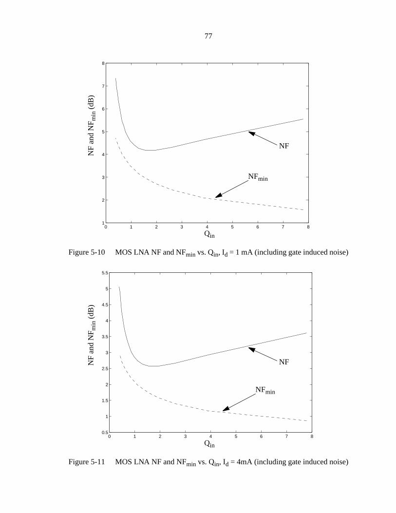
77
)
)
Figure 5-10 MOS LNA NF and NFmin vs. Qin, Id = 1 mA (including gate induced noise
Figure 5-11 MOS LNA NF and NFmin vs. Qin, Id = 4mA (including gate induced noise
0 1 2 3 4 5 6 7 81
2
3
4
5
6
7
8
Qin
NF
and
NF m
in (
dB)
NFmin
NF
0 1 2 3 4 5 6 7 80.5
1
1.5
2
2.5
3
3.5
4
4.5
5
5.5
Qin
NF
and
NF m
in (
dB)
NFmin
NF

78
)
f a
iate
ing
ac-
ary
d at
ar-
Figure 5-12 MOS LNA NF and NFmin vs. Qin, Id = 7mA (including gate induced noise
5.4 Q-based Linearity Analysis
5.4.1 Introduction to Linearity Analysis
Linearity is as important as noise figure in that linearity sets the upper limit o
radio dynamic range while noise figure sets the lower limit. Amplifiers and mixers dev
from their linear behavior due to violation of the small signal approximation result
from saturation of the transistor or non-linearity of the diffusion, junction and MOS cap
itances. Often IP3 is used to specify the LNA linearity. Large signal models are necess
for linearity analyses.
For both BJT and MOS cascode LNA’s, we assume that the linearity is limite
the input. The output non-linearity like clipping doesn’t happen until the input non-line
0 1 2 3 4 5 6 7 80.5
1
1.5
2
2.5
3
3.5
4
4.5
Qin
NF
and
NF m
in (
dB)
NFmin
NF

79
leave
be
ent,
ity is already reached. This is somewhat true if the supply voltage is large enough to
a sufficient headroom, which is the case in both of our LNA’s.
5.4.2 BJT LNA Linearity
For BJT LNA linearity analysis [OKK02], the large signal collector current can
expressed as
, (5.19)
where, IC is the dc component, and ic(t) is the time varying component.
(5.20)
(5.21)
. (5.22)
Assuming that non-linearity is limited by the exponential nature of the collector curr
the Vbe corresponding to the IP3 is
. (5.23)
This is referred to the base-emitter junction voltage. For IIP3, we are interested in referring
this voltage to the input of the LNA,
. (5.24)
The IIP3 of the BJT LNA is
iC I C ic t( )+=
iC βoI B t( ) β≅ oI BSe
Vbe υbe t( )+VT
-----------------------------
=
βo= I B 1υbe
VT--------
12!-----
υbe
VT--------
2 13!-----
υbe
VT--------
3…+ + + +
αo α1υbe α2υbe2 α3υbe
3 …+ + + +( )=
vIP3( )be
43---
α1α3------- 2 2VT 2.8VT= = =
vIP3( )in
vIP3( )be
2Qin-----------------------=

80
e of
of
. (5.25)
The result of Eq.(5.25) is quite simple and somewhat surprising: the IIP3 is related directly
to Qin, not directly to current. Increasing the current may not result in direct increas
linearity. (Of course increasing the current would lower the Qin of LNA.) A more efficient
way to boost IIP3 is to lower the overall Qin. Fig. 5-13 plots the IIP3 of BJT LNA versus
Qin for different current levels: the IIP3 of higher current LNA can be the same as that
the low current LNA as long as they exhibit the same Qin.
Figure 5-13 BJT LNA IIP3 vs. Qin, three currents
IIP3
vIP3( )in2
2Zo----------------------
VT2
Qin2
Zo⋅---------------------= =
0 0.5 1 1.5 2 2.5 3 3.5 4 4.5−35
−30
−25
−20
−15
−10
−5
Qin
IIP3
(dB
m)
Ic=7mAIc=4mAIc=1mA
81
.
age,
hibit
a per-
s
, the
ty
re
alyze
5.4.3 MOS LNA Linearity
Following the BJT linearity analysis, IIP3 of the MOS LNA can also be computed
Compared to collect current of BJT which depends exponentially on the input volt
MOSFET drain current with square law dependency on the input voltage should ex
better linearity performance. First, let us assume that the transistor drain current fits
fect square law. The large signal drain current is
, (5.26)
where, ID is the dc component, and id(t) is the time varying component:
and . The transient large signal drain current can be expressed a
(5.27)
. (5.28)
There is no third order term in Eq. (5.28). This says for a perfect square law device
MOS LNA will not have any third order non-linearity. MOSFET third order non-lineari
stems from Id-Vgs deviating from the square law! To the first order, MOSFET’s are mo
linear than BJT’s.
Second order effect, like mobility degradation will affect the MOS LNA IP3. In
[Hua98], a model based on mobility saturation is presented and is implemented to an
the IP3 of mixers. The drain current can be expressed as
(5.29)
iD I D id t( )+=
I D12---βV
GT
2=
VGT
VGS Vth–=
iD I D id t( )+12---β VGS Vth–( ) vgs t( )+[ ]2= =
I D β VGS Vth–( ) vgs t( ) 12---β vgs t( )[ ]2+⋅+=
I D12---β
VGS Vth–[ ]2
1 θ VGS Vth–( )+------------------------------------------=

82
i-
we
where vGS is the transient vGS(t). The mobility degradation is represented in the denom
nator term.θ is a technology dependent parameter. For the 0.25µm CMOS process used
in for this dissertation,θ is ~ 0.7 V-1. Using Taylor expansion and the same approach
used in BJT IP3 analysis, we have
. (5.30)
Again, this is referred to the gate source voltage. For IIP3, this voltage should be referred
back to the input of the LNA, and
. (5.31)
Figure 5-14 MOS LNA IIP3 vs. Qin, when mobility degradation model is included
vIP3( )gs
8VGT
3θ--------------=
vIP3( )in
vIP3( )gs
2Qin-----------------------=
0 0.5 1 1.5 2 2.5 3 3.5 4 4.5 5−20
−15
−10
−5
0
5
Qin
IIP3
(dB
m) Id = 7mA
Id = 4mA
Id = 1mA

83
-
etter
s for
AN
than
. For
e bias
MOS
y for
Q
ess
OS-
The IIP3 of the MOS LNA is
. (5.32)
The IIP3 vs. Qin curves for the MOS LNA are shown in Fig. 5-14. MOS LNA fol
lows the same Qin trend as BJT LNA, i.e., lower Qin leads to better IIP3. However, IIP3 of
MOS LNA increases as we increase the current and the MOS LNA generally has b
IIP3 than its BJT counterpart.
5.5 Comparison of CMOS and BJT LNA from Q-based Design Analysis
Qin based design approach is a useful tool to compare different IC technologie
RF circuits and is helpful in gaining insight on the evaluation of technologies for WL
chip-set or other RF systems.
The analyses in chapter 4 point out that BJT circuits require use of smaller Q
MOSFET circuits to accommodate its larger process and temperature variations
example, to meet the requirement of input matching of less than -13.5 dB at the sam
current, MOS LNA can have Qin of 2 while BJT LNA can only have Qin of 1. Qin based
design approach in this chapter demonstrates that at higher Q, the gain deficiency of
circuit is compensated. Also at higher Q, other specifications like noise and linearit
MOS LNA are close to or exceed those of BJT circuits at lower Q. From the roughin
based design approach estimate in this chapter, at Qin of 2 MOS LNA exhibits gain of 18
dB, IIP3 of -8 dBm and noise figure of 2.2 dB while at Qin of 0.9 BJT LNA exhibits gain
of 21 dB, IIP3 of -18 dBm and noise figure of 2.2 dB. The trade-off between Q (or proc
variations) and specifications like gain, linearity shows performance parity between M
FET and BJT. These illustrate the promising potential of RF CMOS technology.
IIP3
vIP3( )in2
2Zo----------------------=

m for
smit
ator
, fre-
w fre-
the
ency
s and
ness,
The
any
lter
The
plits
pres-
e by
rence
CHAPTER 6CMOS FREQUENCY SYNTHESIZER
6.1 Introduction
Oscillator and Frequency Synthesizer (FS) are key elements in a radio syste
providing a controlled frequency source for receive signal down conversion and tran
signal up conversion. A simple transistor oscillator, or a voltage controlled oscill
(VCO) does not have the required frequency stability and low phase noise. Therefore
quency synthesis is necessary to derive the accurate high frequency from a precise lo
quency crystal oscillator. Phase Lock Loops (PLL) are often employed to provide
negative feedback in FS [Poz01]. A VCO itself can be viewed as part of the frequ
synthesizer, though quite often FS is integrated with other components like amplifier
mixers into one transceiver chip, and a VCO is left off-chip to ensure system robust
as in the case of PRISM II.
Fig. 6-1 shows the frequency synthesizer concept diagram in PRISM II radio.
FS is an Integer-N charge pump PLL. It is a popular architecture for wireless FS in m
communication systems due to its simplicity. The VCO, crystal oscillator and loop fi
are off chip while the rest of the FS is part of the RF/IF Converter transceiver chip.
LO signal out of the VCO is first buffered (As discussed in chapter 3, the LO signal s
into three paths, one of them goes to Rx mixer, one goes to Tx mixer, and one goes to
caler) before it goes into the frequency divider which comprises a dual modulus divid
32/33 prescaler and programmable digital counters. The divided signal and the refe
84

85
up and
sets
f the
s its
VCO
built
mpli-
hree
the
signal are compared by a Phase/Frequency Detector (PFD) which generates the
down pulse signals to control the charge pump. (A three wire programmable interface
up all the digital control words for counters, PFD and charge pump.) The output o
charge pump is filtered through an off-chip low pass filter before it enters the VCO a
control voltage. The entire loop forms a negative feedback loop hence stabilizes the
output.
Figure 6-1 Frequency Synthesizer concept diagram
In SiGe FS, the prescaler is made of bipolar transistors while the rest are
using MOSFETs. The CMOS FS design focused on divide by 32/33 prescaler and si
fied the other low frequency digital part of the FS.
6.2 CMOS Frequency Synthesizer Overview
Fig. 6-2 shows the CMOS synthesizer top cell. Due to limited resources, the t
wire interface is not included. The division ratios (bits) of A counter and B counter of
VCO
Loop Filter
LO Buffer
N/N+1PrescalerCounters
Prog. A/B
fdiv
DetectorPhase/Frequency up
dn
ChargePump
CrystalOscillator
Divider
fref
Onchip RF/IF Converter

86
y this
f A
nal
r are
ling,
programmable counters are fixed except the first bit of each counter. Consequentl
CMOS FS can only change division ratio by 2 bits. (through 2 pins: A, the first bit o
counter and B, the first bit of B counter.)
Figure 6-2 CMOS Frequency Synthesizer top schematic
The reference signal comes from an off-chip 44 MHz crystal oscillator, the fi
reference frequency at PFD was set to be 250 kHz. A reference buffer and counte
designed to divide 44 MHz reference signal down to 250 kHz. To reduce cross coup
Vcc lines for different blocks use separate pins.
LO
LOb
LO ConvBuffer
LOin
CLK
CLK b
MC
Prescaler
Out
Outb
SCL toCMOS
In
Inb
Out
CLK
A1
B1
Prog
MC
Divout
Counter
RefBuffer
In
Inb
Out RefCounter
OutCLK
Div
Ref
PFDsign
PFDCPoutCP
A
B
REFin
REFinb

87
of a
ana-
6.3 CMOS Prescaler Design
6.3.1 Prescaler Top Schematic
Fig. 6-3 shows the prescaler top schematic.
Figure 6-3 Divide-by-32/33 prescaler top schematic
The prescaler is a dual module divide by 32/33 analog divider. It consists
divide by 4/5 synchronous counter followed by three asynchronous counters. These
log counters are designed using Source Coupled Logic (SCL) [Hun00, Flo01].
Divide-by 4/5SynchronousCounter
Qb
QD0
D1
φ φb
DFF1Qb
QD
Db
φ φb
DFF2Qb
QD0
D1
φ φb
DFF3C
Cb
Cb
C
φ
φb
TFF1Cb
C
φ
φb
TFF2Cb
C
φ
φb
TFF3Out-
Out+
8/9
32/33
16/17
MC
4/5
ModulusControl
CLK
CLK b
Div 4/5Control
AsynchronousCounters

88
by
is
nc-
ig.
6.3.2 Divide by 4/5 Synchronous Counter
The concept of divide by 4/5 is illustrated in Fig. 6-4, which is similar to divide
2/3 mechanism [Yan98, Yan99]. When MC is high, this circuit divides by 4; when MC
low, it divides by 5.
Figure 6-4 Divide by 4/5 concept
In the analog implementation of divide by 4/5 synchronous counter, the OR fu
tion and the D-flip flop (DFF) are combined into one circuit block, called OR_DFF. In F
6-3, DFF1 and DFF3 are OR_DFF’s while DFF2 is a simple DFF.
Figure 6-5 D Flip Flop of synchronous counter schematic
Q
Q
D Q
Q
D Q
Q
D
MC(Modulus Control)
1 2 3
DFF1DFF3DFF2
Qb
QD
Db
φ φb
DFF2 Q
QD
DD-Latch
CK CK
Master Slave
φ φb
Q
QD
DD-Latch
CK CK
D
Db
Q
Qb

89
ave
OS
ere
input
nal is
nd
e
tion to
Fig. 6-5 shows the schematic of DFF2, or a D-flip flop, which is a master sl
configuration of two SCL D latches. Fig. 6-6 shows the schematic of SCL D latch. PM
loads instead of resistive loads are used for SCL [Hun00].
Figure 6-6 SCL D Latch schematic
The OR DFF schematic is shown in Fig. 6-7. Unlike the simple DFF case wh
the input signals are differential and symmetrical, the OR function requires that the
signals compare their levels with a reference voltage to determine whether the sig
high or low. In SCL logic, the signal swing is low and its DC value tends to shift arou
due to process variations or changes in VCC, load resistance or DC bias voltage. On th
other hand, it is not an easy task to get an accurate reference voltage on-chip. A solu
this is the circuitry that sets up the reference voltage VB shown in Fig. 6-7, which has been
also used in the SiGe transceiver chip.
Q
QD
DD-Latch
CK CK
bias
biasQ Q
D D
CK CK
Vcc

90
Figure 6-7 OR DFF schematic
bias
D1 VB
φ
Vcc
bias
Q Q
Vcc
D0
bias
VB
Vcc
Sets upVB
bias
Vcc
bias
C Cb
Output Buffer
Qb
QD0
D1
φ φb
DFF1C
Cb
φb
φb φ
Qb
QD0
D1
φ φb
DFF3OR
(No Output Buffer)

91
ions.
ith
m the
nous
phase
mas-
l sen-
ecting
].
ge
as in
tran-
fre-
The circuit that sets up the reference voltage VB on-chip works this way. The cur-
rent source M21 has half the width of the latch current source M9. Therefore, it has half of
the current of the latch while maintain the same load and VCC. The logic high of the latch
is VCC, the logic low is VCC - I Rload, and VB is VCC - I Rload / 2, right in the middle of
logic high and low, independent of supply voltage, current, or load resistance variat
The output buffer in Fig. 6-7 is only present in DFF1 (not in DFF3), which interfaces w
the asynchronous counters. The buffer helps to isolate the synchronous counter fro
asynchronous counters and to set up the DC bias of the first divider of the asynchro
counters.
6.3.3 Asynchronous Counter
The asynchronous counter consists of three cascaded 2:1 dividers with dual
inputs and outputs. Each divider, shown in Fig. 6-8, comprises two SCL latches in a
ter slave configuration. TFF represents TFF1, or TFF2, or TFF3. Cascading two leve
sitive latches in a master slave configuration results in an edge triggered DFF. Conn
the outputs of a DFF back to its inputs with inverted phase forms a 2:1 divider [Flo01
An output buffer is used in every TFF divider to interface with the following sta
and the Modulus Control (MC) logic circuit. The latch assumes the same schematic
the DFF of the synchronous counter, however, the transistor sizes are different. Each
sistor in every divider is optimized for low current consumption and a high operating
quency range.

92
of a
hro-
gether
Figure 6-8 Asynchronous counter schematic
6.3.4 Divide-by-4/5 Control
A dual modulus (large numbers like 32/33, 128/129) prescaler usually consists
dual modulus (small numbers like 2/3, 4/5) synchronous counter followed by a async
nous counter. The synchronous counter and asynchronous counter need to work to
to achieve the dual modulus operation.
Master Slave
φ φb
Q
QD
DD-Latch
CK CK
Cb
C
φ
φb
TFF
Cb
CBuffer
Q
QD
DD-Latch
CK CK
bias
biasQ Q
D D
CK CK
Vcc
bias
Vcc
bias
C Cb
Output

93
onous
sion,
n in
one
Figure 6-9 Divide-by-32/33 prescaler top schematic redrawn
Even number divisions are easy to realize and understand. When the synchr
counter divides by 4, the prescaler naturally divides by 32. For the odd number divi
Divide-by-4/5 Control unit has to come into play. For example, in the prescaler, redraw
Fig. 6-9, the divide by 33 action is accomplished by seven cycles of divide by 4 and
Divide-by 4/5SynchronousCounter
Qb
QD0
D1
φ φb
DFF1Qb
QD
Db
φ φb
DFF2Qb
QD0
D1
φ φb
DFF3C
Cb
Cb
C
φ
φb
TFF1Cb
C
φ
φb
TFF2Cb
C
φ
φb
TFF3Out-
Out+
8/9
32/33
16/17
MC
4/5
ModulusControl
CLK
CLK b
Div 4/5Control
AsynchronousCounters
This control unit tells the div-4/5synchronous counter when to divideby 4, when to divide by 5.
Modulus control signal (MC) fromdigital counters, it tells the prescalerwhen to divide by 32, when to divide by 33.
When this node ishigh, syn counterdivide by 4; whenit is low, div by 5.

94
us
of
ich
-4/5
chro-
ider
using
CL
3V
cycle of divide by 5. Divide-by-4/5 Control is the circuit block that tells the synchrono
counter when to divide by 4, and when to divide by 5.
The Modulus Control (MC) signal from digital counters (A/B counters) is one
the inputs of Divide-by-4/5 Control (MC node in Fig. 6-9). It tells the prescaler wh
division ratio it is supposed to pick, 32 or 33. The 4/5 node is the output of Divide-by
Control, as well as the input to the synchronous counter. When 4/5 is high, the syn
nous counter divides by 4; when 4/5 is low, the synchronous counter divides by 5.
6.4 Rest of the Frequency Divider
As mentioned earlier in Fig. 6-1, a dual modulus prescaler is one part of the div
of a frequency synthesizer (FS). In the SiGe FS, the rest of the divider is designed
MOSFETs, and those circuits are simplified and ported into the CMOS FS.
6.4.1 SCL to CMOS Converter
The divided down signals out of the prescaler are still analog SCL signals. An S
to CMOS converter in Fig. 6-10 converts them into CMOS digital signals. To use the
supply voltage in the system, high voltage MOSFETs (3.3V devices) are employed.
Figure 6-10 SCL to CMOS converter schematic

95
A,
nd B
d A
aler is
(A)
ulus
the
ly, B
am
ro-
hain
6.4.2 Digital Counters (A/B Counters)
The total division ratio for a dual module prescaler with A/B counters is NB+
where the prescaler divides by N/N+1, and A and B are counts of A, B counters. A a
counters are sometimes called program counter and swallow counter, respectively.
Fig. 6-11 illustrates the concept of a divider with a dual modulus prescaler an
and B counters. The output of the prescaler clocks both A and B counters. The presc
set to divide by N+1 first and the divider chain divides by A(N+1). When the swallow
counter is full, it ceases counting and sets the prescaler to divide by N through Mod
Control (MC) signal. Now only the program (B) counter is clocked but by this time
program (B) counter has already counted up to A. (For A, B counters to work proper
must always be larger than A.) So the divider chain divides by (B-A)N until the progr
(B) counter is full. When program (B) counter is full, it resets both the swallow and p
grammable counters and the cycle repeats. The overall division ratio of the divider c
is, therefore, (B-A)N + A(N+1) = NB +A.
Figure 6-11 Divider with dual modulus prescaler concept diagram
Divide by N/N+1Prescaler
fdiv
Swallow (A) CounterDivide by A
Program (B) CounterDivide by B
Modulus Control Signal(MC)
LO
CLK
To PFD
Reset

96
h
cy is
420.
n to
er-
set
fre-
s set
nd-
lps
nd
at
of the
as
e dif-
In PRISM II radio, RF is from 2.4 GHz to 2.48 GHz, IF is 374.25 MHz, whic
results in an LO of 2025 MHz to 2105 MHz. The final synthesizer reference frequen
set to 250 kHz out of system considerations. The total division ratio is from 8100 to 8
The off-chip crystal oscillator comes in at 44 MHz. A reference counter divides it dow
250 kHz. The total division ratio is fixed at 176 (44 MHz / 250 kHz = 176) for the ref
ence counter.
The serial interface was not included in this design. The total division ratio is
for an LO around 2082 MHz. This number is picked to be in the middle of the VCO
quency range. The prescaler is divide-by 32/33, B is set to be 260 (or 261), while A i
to be 8 (or 9). The total division ratio is NB+A=8328, 8329, 8360, 8361, the correspo
ing LO frequencies are, 2082 MHz, 2082.25 MHz, 2090 MHz, 2090.25 MHz. This he
to test the synthesizer functionality in the absence of serial interface.
6.4.3 Phase Frequency Detector (PFD) and Charge Pump (CP)
The final Charge Pump (CP) current for PRISM II is 1 mA and the loop ba
width of the low pass filter is 1 kHz. The whole PLL simulation is very time consuming
SPICE level. The PFD and CP are simulated separately with respect to other circuits
PLL.
The PRISM II off-chip loop filter components were used in the simulation
shown in Fig. 6-12. Two input signals are square waves with a period of 4µS (250 kHz).
They both have rise and fall time of 1nS, and the pulse width is 15 nS. There is a phas
ference between the two pulses. Transient voltages on CP output node and VCO VCTRL
node are monitored as outputs.

97
. The
uses
vider
” is a
e
ole
gain
goes
].
Figure 6-12 PFD and CP Simulation top schematic
6.4.4 PFD and CP Design
Simple CP and PFD are implemented here and shown in Figs. 6-13 and 6-14
PFD consists of 4 NAND RS flip-flops. The basic operation is: the reference pulse ca
the output to change in a positive direction unless the output is already positive; the di
pulse causes a negative transition unless the output is already negative. “sign_pfd
multiplexer (MUX) circuit controlled by the word “PFD_sign”. The MUX can reverse th
outputs of the PFD, i.e., UP to DOWN, DOWN to UP, which keeps the wh
phase-locked loop a negative feedback loop even if the VCO sign is reversed. (VCO
may have a negative sign, i.e., the output frequency goes down as the control voltage
up.) The delay circuitry is used to correct the deadzone problem of the PFD [Hun00
Div
Ref
PFDsign
PFDCPoutCP VCO Vctrl
Div
Ref
PFDsign
PFDUPB
DOWNCharge
UPB
DOWN
Pump CPout
On-chip

98
RF
parts
Figure 6-13 Phase Frequency Detector (PFD) schematic
Figure 6-14 Charge Pump (CP) schematic
6.5 CMOS Frequency Synthesizer Measurement Results
As mentioned, a frequency Synthesizer (FS) is the most complex circuit in the
transceiver chip. The CMOS FS has thousands of transistors even though its digital
delay circuit
MUX

99
ld a
is
6-15
the
ter
have been greatly simplified. From a research point of view, it is prudent to bui
stand-alone silicon before embark on the task of building the full chip. A CMOS FS
built in a 0.25µm CMOS and its silicon measurement results are shown here. Fig.
shows a micro-photograph of the CMOS synthesizer. The die size is 1300µm by 1800
µm.
Figure 6-15 A Micro-photograph of CMOS Frequency Synthesizer
6.5.1 CMOS Synthesizer Output Spectrum
Figs. 6-16 to 6-19 depict the output spectra of the CMOS synthesizer. With
change of a 2 bit word: the first bit of A counter (A = 8 or 9), and the first bit of B coun
B Counter
ReferenceCounter
Prescaler
LO Buffer
A Counter
PFD andCharge Pump

100
kHz.
(B = 260 or 261). The output frequency is (NB+A) times the reference frequency 250For example, with A = 8, B = 261, fout= (261x32+8) x250 kHz = 2.09 GHz.
Figure 6-16 CMOS Synthesizer output locked at 2.082 GHz (A=8, B=260)
Figure 6-17 CMOS Synthesizer output locked at 2.082250 GHz (A=9, B=260)

101
M II,
erall
Figure 6-18 CMOS Synthesizer output locked at 2.090 GHz (A=8, B=261)
Figure 6-19 CMOS Synthesizer output locked at 2.090250 GHz (A=9, B=261)
6.5.2 Summary of FS Performance
Table 6-1 summarizes the CMOS and SiGe synthesizer performance. In PRIS
the loop bandwidth is 1 kHz. Phase noise from the VCO contributes most to the ov

102
ivider,
sizers
OS
current
synthesizer phase noise above 1kHz. The rest of the phase noise comes from the d
charge pump, and loop filter. The close-in phase noise of the CMOS and SiGe synthe
is close: it is at -80 dBc/Hz and -82.7 dBc/Hz at 10 kHz offset, respectively. The CM
prescaler consumes more current than its SiGe counterpart because it needs more
than BJT prescaler to function at high frequencies.
Table 6-1 CMOS and SiGe RF Synthesizer Comparison Table
Parameters CMOS SiGe
LO Frequency 2082 MHz 1800 to 2220 MHz
Reference Frequency 44/0.25 MHz same
A counter division 8 or 9 0-127
B counter division 260 or 261 3-2047
Charge Pump Current 1 mA same
Prescaler Current 9.7 mA 6 mA
Phase Noise (10kHz) -80 dBc/Hz -82.7 dBc/Hz

itter
tter
er 3,
be
LO,
ut
II, as
CHAPTER 7CMOS TRANSMITTER BUILDING BLOCKS AND TRANSCEIVER DESIGN
7.1 CMOS Transmitter Chain
The transmitter consists of an up-conversion mixer (Tx mixer) and a transm
amplifier (TXA), or a pre-PA amplifier. Usually noise figure is not a concern in transmi
design while linearity and gain are important. Recalling the system overview in chapt
the output of Tx mixer goes off-chip, then back on-chip to TXA input. A BPF may
placed after Tx Mixer, prior to TXA, to attenuate various spurious components like
image, and their harmonics out of the Tx mixer output. Alternatively, if the TXA outp
goes to another BPF before PA, this BPF can be omitted, which is the case in PRISM
illustrated in Fig. 7-1.
Figure 7-1 PRISM II Transmitter Chain concept diagram
LO Input
Tx MixerTXA
To Rx Mixer
To PLLFreq.Syn.
PA
BPF
(BPF)
To Switch/Antenna
RF/IF Converter
103
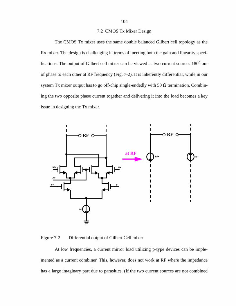
104
the
eci-
our
a key
le-
dance
bined
7.2 CMOS Tx Mixer Design
The CMOS Tx mixer uses the same double balanced Gilbert cell topology as
Rx mixer. The design is challenging in terms of meeting both the gain and linearity sp
fications. The output of Gilbert cell mixer can be viewed as two current sources 180o out
of phase to each other at RF frequency (Fig. 7-2). It is inherently differential, while in
system Tx mixer output has to go off-chip single-endedly with 50Ω termination. Combin-
ing the two opposite phase current together and delivering it into the load becomes
issue in designing the Tx mixer.
Figure 7-2 Differential output of Gilbert Cell mixer
At low frequencies, a current mirror load utilizing p-type devices can be imp
mented as a current combiner. This, however, does not work at RF where the impe
has a large imaginary part due to parasitics. (If the two current sources are not com
at RF
RF
IF-
LO-
IF+
LO+LO+
dc
RF
RF+ RF-
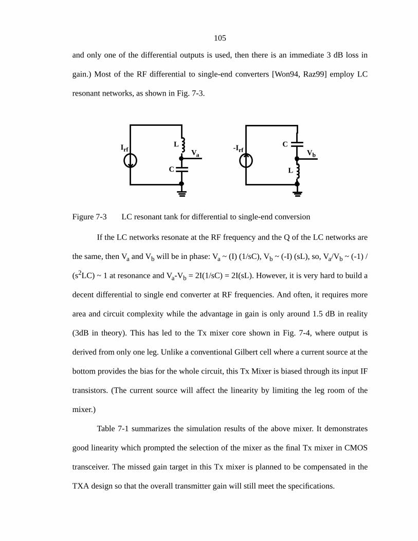
105
ss in
LC
are
more
ality
t is
t the
t IF
the
rates
OS
in the
and only one of the differential outputs is used, then there is an immediate 3 dB lo
gain.) Most of the RF differential to single-end converters [Won94, Raz99] employ
resonant networks, as shown in Fig. 7-3.
Figure 7-3 LC resonant tank for differential to single-end conversion
If the LC networks resonate at the RF frequency and the Q of the LC networks
the same, then Va and Vb will be in phase: Va ~ (I) (1/sC), Vb ~ (-I) (sL), so, Va/Vb ~ (-1) /
(s2LC) ~ 1 at resonance and Va-Vb = 2I(1/sC) = 2I(sL). However, it is very hard to build a
decent differential to single end converter at RF frequencies. And often, it requires
area and circuit complexity while the advantage in gain is only around 1.5 dB in re
(3dB in theory). This has led to the Tx mixer core shown in Fig. 7-4, where outpu
derived from only one leg. Unlike a conventional Gilbert cell where a current source a
bottom provides the bias for the whole circuit, this Tx Mixer is biased through its inpu
transistors. (The current source will affect the linearity by limiting the leg room of
mixer.)
Table 7-1 summarizes the simulation results of the above mixer. It demonst
good linearity which prompted the selection of the mixer as the final Tx mixer in CM
transceiver. The missed gain target in this Tx mixer is planned to be compensated
TXA design so that the overall transmitter gain will still meet the specifications.
I rf Va-I rf Vb
L
C
C
L

106
on-
eat
.
uses
the
Figure 7-4 CMOS Tx mixer core schematic
7.3 CMOS Transmitter Amplifier
The Transmitter Amplifier (TXA) is a single stage, common source cascode c
figuration, very similar to LNA topology. Primary design goals include output power gr
than + 6dBm, gain above 15 dB while limit current consumption as much as possible
7.3.1 CMOS Transmitter Amplifier Schematic
Fig. 7-5 shows the schematic of the CMOS transmitter amplifier. The output
the sameπ matching network as the LNA. Power gain is the primary design goal of
Table 7-1 Summary of CMOS Tx Mixer Simulation Results
CMOS (Simulated) SiGe (Measured) PRISM II Specs
LO/IF Frequency 2.1 GHz/375 MHz same same
Power Gain 5 dB 9 dB 9 dB
Core Icc 16 mA 10 mA 11 mA
Output matching(RF)
< -10 dB -27.4 dB VSWR < 2:1
OP1dB -5.5 dBm -3.5 dBm -6 dBm
OIP3 +3 dBm Not Avail. +4 dBm
LO to RF feedthru -33 dB -35 dB Not Avail.
IF to RF feedthru -41 dB Not Avail. Not Avail.
Vb
IF-
LO+
LO-
IF+
LO+
Vcc
RFout

107
ctive
asso-
for
the
The
TXA and as mentioned earlier, noise figure is not a big concern. Therefore, the indu
degeneration was not present (There is no stability problem or linearity degradation
ciated with this, at least in simulation.) and an on-chip 3.2 nH inductor was included
input matching.
Figure 7-5 TXA schematic
7.3.2 TXA Simulation Results
Table 7-2 summarizes the TXA simulation results and compares them with
SiGe specifications. The gain is around 20 dB while the total current is below 16 mA.
gain deficiency at Tx mixer stage is compensated here.
Table 7-2 Summary of CMOS TXA Simulation Results (f0 = 2.45 GHz)
CMOS (Simulated) SiGe (Measured) PRISM II Specs
Power Gain 19.9 dB 16.7 dB 15 dB
OP1dB +6 dBm +7 dBm +6 dBm
OIP3 +17 dBm Not Avail. +16 dBm
TXA Icc 16 mA 15 mA 11 mA
Input Matching < -10 dB < -10 dB VSWR < 2:1
Output Matching < -10 dB < -10 dB VSWR < 2:1
Vcc
RFout
BiasNetwork
RFin

108
f the
gies.
7.4 CMOS RF Transceiver (TRx) Design
The CMOS TRx was designed to have the similar size and pinout as that o
SiGe bipolar version (Table 7-3) so better comparison can be made for two technolo
Figure 7-6 CMOS TRx pinout
Table 7-3 CMOS and SiGe Transceiver Comparison
Parameters CMOS SiGe
Package 44 pin MLF same
Components LNA, Rx and Tx Mixers, PAdriver, Synthesizer.
same, plus ITAT/PTAT bias,control pins.
Chip Area 2500µm X 2500µm 2563µm X 2563µm
Pad separation 150µm 136µm
RMx_o-
TMx_in-
N/U
N/U
N/U
LO_in
LO_vcc
TLO_vcc
N/U
TMx_out
TMx_vcc
LNA_b
N/U
Rx_in
N/U
A_0
PRE_vcc
g_pmos
TXA_vcc
N/U
TXA_out
N/U
LNA
_vcc
N/U
LNA
_out
N/U
LO_b
RM
x_b
PR
E_b
RLO
_vcc
RM
x_in
TM
x_in
+
RM
x_O
+
N/U
TX
A_in
N/U
TM
x_b
TX
A_b
CP
_b
RE
F_by
SY
N_vdd
RE
F_in
CP
_vdd
CP
_out
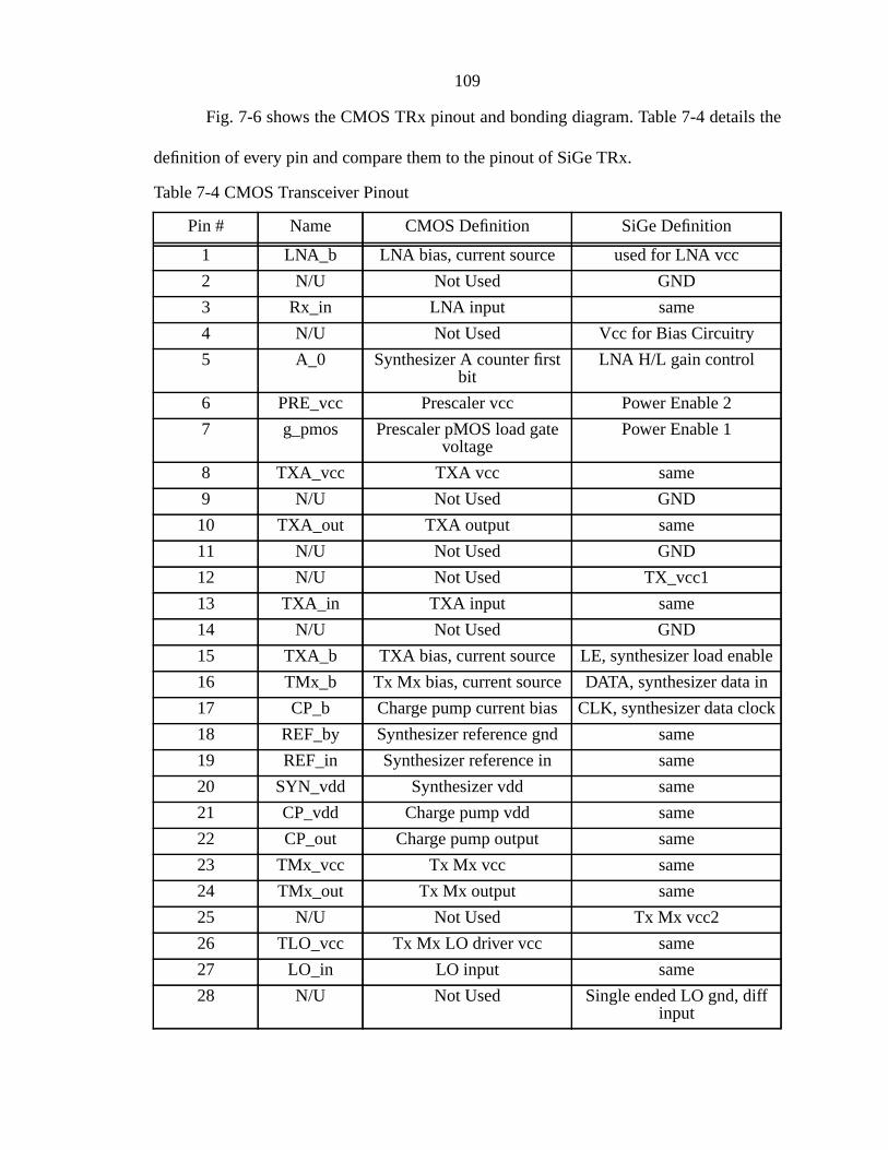
109
the
le
ck
Fig. 7-6 shows the CMOS TRx pinout and bonding diagram. Table 7-4 details
definition of every pin and compare them to the pinout of SiGe TRx.
Table 7-4 CMOS Transceiver Pinout
Pin # Name CMOS Definition SiGe Definition
1 LNA_b LNA bias, current source used for LNA vcc
2 N/U Not Used GND
3 Rx_in LNA input same
4 N/U Not Used Vcc for Bias Circuitry
5 A_0 Synthesizer A counter firstbit
LNA H/L gain control
6 PRE_vcc Prescaler vcc Power Enable 2
7 g_pmos Prescaler pMOS load gatevoltage
Power Enable 1
8 TXA_vcc TXA vcc same
9 N/U Not Used GND
10 TXA_out TXA output same
11 N/U Not Used GND
12 N/U Not Used TX_vcc1
13 TXA_in TXA input same
14 N/U Not Used GND
15 TXA_b TXA bias, current source LE, synthesizer load enab
16 TMx_b Tx Mx bias, current source DATA, synthesizer data in
17 CP_b Charge pump current bias CLK, synthesizer data clo
18 REF_by Synthesizer reference gnd same
19 REF_in Synthesizer reference in same
20 SYN_vdd Synthesizer vdd same
21 CP_vdd Charge pump vdd same
22 CP_out Charge pump output same
23 TMx_vcc Tx Mx vcc same
24 TMx_out Tx Mx output same
25 N/U Not Used Tx Mx vcc2
26 TLO_vcc Tx Mx LO driver vcc same
27 LO_in LO input same
28 N/U Not Used Single ended LO gnd, diffinput

110
and
lay-
driv-
erent
nt.
Table 7-5 compares the component area of different circuit blocks of CMOS
SiGe transceiver. This is a very rough estimation from layout since most of the circuit
out is not rectangular and the boundary of different blocks is hard to define. The LO
ers for RMx and TMx are counted as part of the respective mixers. The areas for diff
blocks are close for CMOS and SiGe transceivers though their layout is quite differe
29 N/U Not Used LO vcc
30 LO_vcc LO vcc Rx LO driver vcc
31 N/U Not Used GND
32 TMx_in- Tx Mx diff input - same
33 RMx_o- Rx Mx diff output - same
34 RMx_o+ Rx Mx diff output + same
35 TMx_in+ Tx Mx diff input + same
36 RMx_in Rx Mx RF signal input same
37 RLO_vcc Rx LO driver vcc Prescaler vcc
38 PRE_b Prescaler current bias ITAT bias resistor 1
39 RMx_b Rx Mx current bias PTAT bias resistor
40 LO_b LO buffer bias Bias circuitry vcc
41 N/U Not Used ITAT bias resistor 2
42 LNA_out LNA output same
43 N/U Not Used GND
44 LNA_vcc LNA vcc same
Table 7-5 CMOS and SiGe transceivers component area breakdown
CMOS SiGe
LNA (mm2) 0.44 0.36
Rx Mixer (mm2) 1.19 0.97
Tx Mixer (mm2) 1.03 0.81
TXA (mm2) 0.36 0.28
Synthesizer (mm2) 1.1 1.12
LO Buffer (mm2) 0.28 0.09
Total Area (mm2) 6.25 6.55
Table 7-4 CMOS Transceiver Pinout
Pin # Name CMOS Definition SiGe Definition

111
edi-
one.
e
.
Table 7-6 summarizes the simulated CMOS transceiver performance. An imm
ate observation is that the current consumption of CMOS TRx is 30% more than SiGe
Most of this is due to the low gm/I ratio of CMOS compared to SiGe bipolar. A mor
advanced technology (0.18µm vs. 0.25µm CMOS) is expected to alleviate this problem
Table 7-6 2.4 GHz CMOS Transceiver Performance
CMOS (Simulated orMeasured)
SiGe (Measured)
LNA (Gain/NF/IIP3/Current)
15 dB / 3 dB0 dBm / 8 mA
16 dB / 3 dB-2 dBm / 7 mA
Rx Mixer(Gain/NF/IIP3/Current)
8 dB / 11 dB+ 3 dBm / 12 mA
8 dB / 8 dB+ 6 dBm / 10 mA
Tx Mixer(Gain/OP1dB/Current)
5 dB / -6 dBm16 mA
9 dB / -4 dBm10 mA
TXA(Gain/OP1dB/Current)
19 dB / +6 dBm16 mA
16 dB / +7 dBm15 mA
Synthesizer (Phase Noise/Prescaler Current)
-80 dBc/Hz (10 kHz)10 mA
-83 dBc/Hz (10 kHz)6 mA
Total Current: Excl. offchip(Rx/Tx)
Rx: 41 mATx: 56 mA
Rx: 32 mATx: 41 mA

the
the
OS
e
CHAPTER 8CHARACTERIZATION OF CMOS TRANSCEIVER AND WLAN RADIO
8.1 Measurement of CMOS RF Transceiver
The main purpose of this dissertation is to explore the feasibility of designing
RF transceiver of PRISM II chipset using a CMOS technology. The realization of
whole transceiver (TRx) in CMOS is a critical milestone of this dissertation. The CM
TRx was designed in the TSMC 0.25-µm CMOS process. Fig. 8-1 shows a picture of th
fabricated silicon.
Figure 8-1 Micro-photograph of CMOS RF transceiver chip
LNATXA
FS
RMx
TMx
LO Buffer
112

113
same
anged
were
an
. A
f this
toward
in is
tran-
The chip was packaged in the 44 pin MLF package as planned and put on the
evaluation board used for SiGe chip. The values of some off-chip components are ch
to accommodate the matching of CMOS transceiver. The RF characteristics of chip
measured and compared to simulation and SiGe bipolar chip.
As shown in Fig. 8-2, most of the individual RF circuits in the RF transceiver c
be tested separately.
Figure 8-2 RF/IF Converter Chip Components
8.1.1 LNA measurement results
The performance of this LNA is worse than the previous stand-alone one
change was made in this LNA: the input transistor was sized up by 20%. The goal o
change is to bias the transistor closer to threshold therefore get better gm consequently bet-
ter noise figure under the same bias current. The measurements indicate changes
the opposite direction: the noise figure is worse, almost 0.5 dB higher, and the ga
lower by 1 dB. There are two possible reasons. First, while the increase of the input
PLLFreq.Syn.
LO Input
LNA
Rx Mixer
Tx MixerTXA
To SAW FilterRF in
RF out

114
the
re
-alone
rs
sistor size brings up gm, it also increases the input capacitance consequently lowers
input Q. The final gmQ product may be lowered, which will result in worse noise figu
and gain. Second, since the transceiver was fabricated in a different 0.25-µm run, the pro-
cess variations may put the performance of the chip at worse case compared to stand
chip.
Figure 8-3 LNA S-parameters
The LNA is measured at a VDD of 3V. Figs. 8-3 and 8-4 show the S-paramete
and Noise Figure of the LNA. For 9 mA current, the transducer gain (S21) is around 14.5
dB. Transducer gain changes less than 0.1 dB when VDD changes from 3.3 V to 2.7 V.

115
not
Digital circuits do not affect LNA gain either. Turning on frequency synthesizer doesaffect the LNA s-parameters. However, itdoesaffect the Noise Figure of the LNA. NF is
increased from 3.3 dB to 3.5 dB when synthesizer is on.
Figure 8-4 LNA Noise Figure
Table 8-1 LNA Performance Comparison
f0 = 2.45 GHz LNA in CMOS TRxStand-aloneCMOS LNA
SiGe LNA
50-Ω NF 3.28 dB 2.88 dB 2.86 dB
Bias Current 9 mA 8.1 mA 7.0 mA
Transducer Gain 14.5 dB 15.1 dB 15.9 dB
S11 -8.3 dB -14.2 dB -12.7 dB
S22 -14.7 dB -20.2 dB -16.0 dB
S12 < -27 < -34 < -30
IIP3 0.3 dBm 2.2 dBm -2.6 dBm
IP1dB -8.5 dBm -7.0 dBm -11.2 dBm
Input transistor size 500µm/0.24µm 400µm/ 0.24µm Not Appl.

116
uilt
has
one
RMx
d by
tor is
r the
ions
n-
mA
is is
Table 8-1 compares the LNA in the CMOS transceiver with previously b
stand-alone CMOS LNA and the SiGe LNA. The change of the input transistor size
deteriorated the LNA performance in every category.
8.1.2 Rx Mixer Measurement Results
The RMx of CMOS TRx was also based upon the previously built stand-al
RMx. The transistor size, load are the same for the two. One adjustment made on
(part of the TRx), as shown in Fig. 8-5, is that the common mode inductor was replace
an nMOS current source. From a system point of view, the large common mode induc
prone to picking up low frequency noise from the substrate.
Figure 8-5 Two Rx mixers
Compared to stand-alone RMx, there is one big difference in measurement fo
RMx in TRx: the LO frequency is set by the on-chip synthesizer now. The bias condit
for the two are very similar though, total RMx current is 16.1 mA, of which 12 mA is co
sumed by switching core, 4 mA by source follower and LO driver (this is close to 16
in simulation); LO diff/single end converter plus prescaler buffer consumes 9.6 mA (th
IF+
IF-
LO+
LO-
RF
Vb
LO+300/0.24
400/0.24
0.7nH
Stand-alone Rx Mixer Rx Mixer in CMOS TRx
IF+
IF-
LO+
LO-
RF
Vb
LO+300/0.24
400/0.24
0.7nH

117
la-
than
han
stead
d -6
r LO
tions
Fig-
DSB
o the
s, the
3 mA more than 6.5 mA in simulation); prescaler 6.5 mA (this is close to 6 mA in simu
tion). Charge pump 1 mA, same as simulation. The performance of this RMx is worse
the previous built stand-alone RMx. The RMx exhibits a gain of 5.6 dB, 2.4 dB lower t
the stand-alone RMx. The reason is that, now the LO is generated from the VCO in
of a signal source, the VCO has fixed output power resulting in LO input power aroun
dBm; where in stand-alone RMx measurement this LO can be adjusted to highe
power, -3 dBm or higher, which helps to boost the CMOS mixer gain. Process varia
may also bring some performance deterioration.
Fig. 8-6 and 8-7 show the input and output matching as well as the DSB Noise
ure of the RMx. S11, the RF input, is matched at 2.4 to 2.5 GHz; S22, the IF output, is
matched at 375 MHz. Both input and output are well matched (less than -10 dB). The
Noise Figure is 8.2 dB, which translates to a SSB NF around 11.2 dB. That is close t
previous stand-alone RMx NF. Table 8-2 compares the performance of three mixer
RMx in TRx, stand-alone RMx and the SiGe RMx.
Table 8-2 Rx Mixer Performance Comparison
RMx in CMOS TRxStand-aloneCMOS RMx
SiGe RMx
Power Gain 5.6 dB 8.0 dB 8.1 dB
SSB Noise Figure 11.2 dB 10.5 dB 9.0 dB
RF input and IF out-put matching
< -10 dB < -10 dB < -10 dB
Core Current 12 mA 12 mA 10 mA
IIP3 2.0 dBm 3.0 dBm 6.2 dBm
IP1dB -8.0 dBm -6.0 dBm -3.1 dBm
LO to IFfeedthrough
-46 dB -32 dB -40 dB
RF to IF feedthrough -12 dB -14 dB Not Avail.
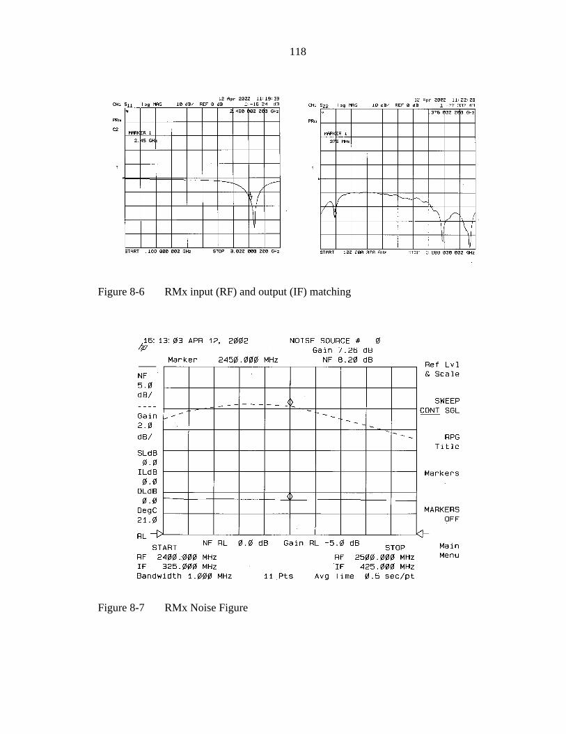
118
Figure 8-6 RMx input (RF) and output (IF) matching
Figure 8-7 RMx Noise Figure
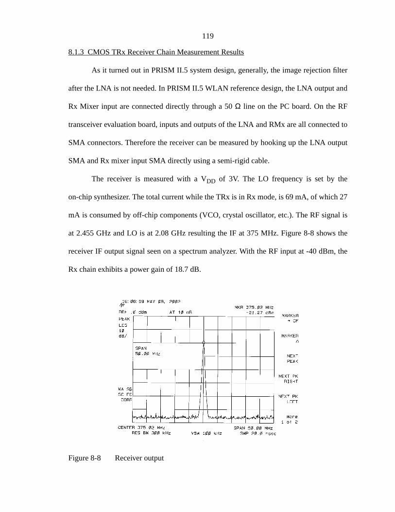
119
lter
nd
ed to
utput
27
al is
the
, the
8.1.3 CMOS TRx Receiver Chain Measurement Results
As it turned out in PRISM II.5 system design, generally, the image rejection fi
after the LNA is not needed. In PRISM II.5 WLAN reference design, the LNA output a
Rx Mixer input are connected directly through a 50Ω line on the PC board. On the RF
transceiver evaluation board, inputs and outputs of the LNA and RMx are all connect
SMA connectors. Therefore the receiver can be measured by hooking up the LNA o
SMA and Rx mixer input SMA directly using a semi-rigid cable.
The receiver is measured with a VDD of 3V. The LO frequency is set by the
on-chip synthesizer. The total current while the TRx is in Rx mode, is 69 mA, of which
mA is consumed by off-chip components (VCO, crystal oscillator, etc.). The RF sign
at 2.455 GHz and LO is at 2.08 GHz resulting the IF at 375 MHz. Figure 8-8 shows
receiver IF output signal seen on a spectrum analyzer. With the RF input at -40 dBm
Rx chain exhibits a power gain of 18.7 dB.
Figure 8-8 Receiver output

120
Bm,
Hz
age
ncy,
tput
fre-
re),
ejec-
The
er was
than
Fig. 8-9 shows a wider spectra of the receiver output. The LO signal is at -51 d
a rejection of 45 dB; RF signal is at -37.5 dBm, a gain of 2.5 dB; the signal at 1.705 G
is the result of mixing RF and 2 LO, 2 LO - RF = 1.705 GHz, it’s at -58 dBm.
.
Figure 8-9 Rx output spectra
Due to the tuned response of LNA and RMx, the receiver will provide some im
rejection. Fig. 8-10 is the spectrum at IF output when the RF input is at image freque
1.705 GHz, with a power of -40 dBm. The output is at the same 375 MHz IF, the ou
power is -38.5 dBm, demonstrating that the Rx chain has gain of 1.5 dB at image
quency. It’s 17 dB less than the signal gain (which will have small impact on noise figu
or exhibits 17 dB image rejection, bringing more image rejection besides the 45 dB r
tion from the front-end bandpass filter or additional image rejection filter.
Fig. 8-11 shows the single side-band (SSB) noise figure of the receiver.
receiver has a SSB noise figure of 5.1 dB. During the measurement, a bandpass filt
placed in front of the Rx. The filter has 1.2 dB loss at the signal frequency, and more

121
40 dB rejection at the image frequency. Figs. 8-12 and 8-13 show the P1dB and IP3 plots of
the receiver.
Figure 8-10 Receiver output when RF is at the image frequency
Figure 8-11 Rx chain noise figure
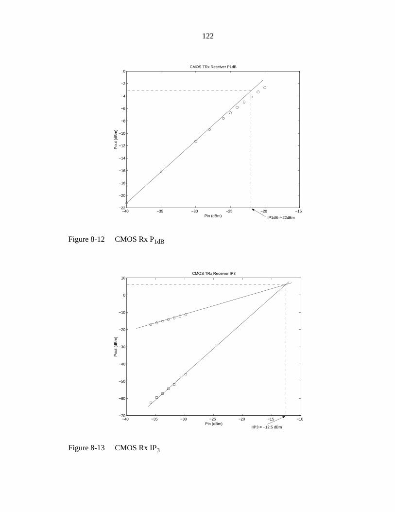
122
Figure 8-12 CMOS Rx P1dB
Figure 8-13 CMOS Rx IP3
−40 −35 −30 −25 −20 −15−22
−20
−18
−16
−14
−12
−10
−8
−6
−4
−2
0CMOS TRx Receiver P1dB
Pin (dBm)
Pou
t (dB
m)
IP1dB=−22dBm
−40 −35 −30 −25 −20 −15 −10−70
−60
−50
−40
−30
−20
−10
0
10CMOS TRx Receiver IP3
Pin (dBm)
Pou
t (dB
m)
IIP3 = −12.5 dBm

123
eiver
ure.
OS
and
ore
all
A
a sim-
cern
The
Table 8-3 tabulates the CMOS and SiGe Rx chain performance. CMOS rec
has 6 dB lower gain (3dB less each from LNA and mixer) and 1.5 dB worse noise fig
The IIP3 and IP1dB of the two receivers are close. The total receiver current for CM
transceiver is 42 mA, including current consumption of LNA, synthesizer, LO buffer
RMx, excluding power consumption by all the off-chip components, it is 10 mA m
than its SiGe counterpart.
* Including LNA, Synthesizer, LO Buffer and RMx, excluding power consumption bythe off-chip components.
8.1.4 Tx Amplifier Measurement Results
Fig. 8-14 shows the schematic of CMOS and SiGe TXA’s. The CMOS TX
assumes a single stage, common source cascode configuration and the SiGe TXA is
ple one transistor common emitter amplifier. Usually the noise figure is not a huge con
in transmitter design so both TXA’s are matched with an on-chip inductor at the input.
gain and linearity of TXA is much lower than simulation.
Table 8-3 Receiver Performance Comparison
CMOS Rx SiGe Rx
Power Gain 18.7 dB 25 dB
Power Gain at Image 1.5 dB Not Avail.
Image Rejection (No Filter) -17.2 dBc -14 dBc
Noise Figure 5.1 dB (SSB) 3.7 dB (SSB)
RF input and IF outputmatching
< -10 dB < -10 dB
Input IP3 -12.5 dBm -12 dBm
Input P1dB -22 dBm -23 dBm
LO to IF feedthrough -45 dB Not Avail.
RF to IF feedthrough 2.5 dB Not Avail.
Total Rx Current * 42 mA 32 mA
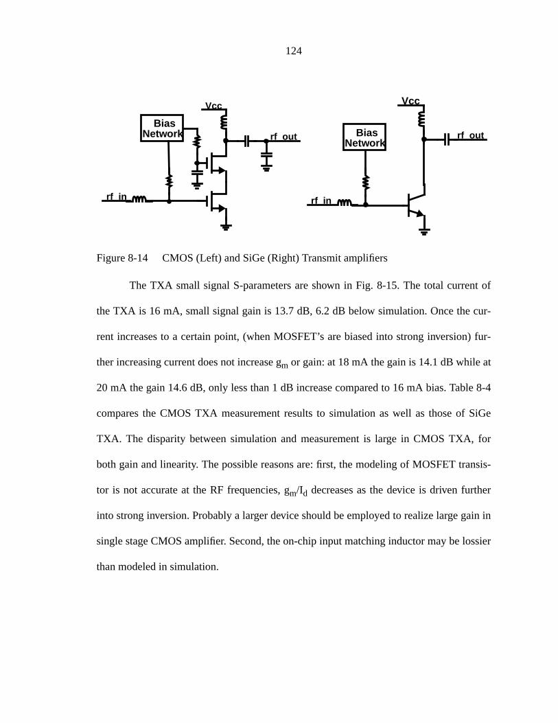
124
t of
ur-
) fur-
t
e 8-4
SiGe
for
nsis-
er
ain in
ssier
Figure 8-14 CMOS (Left) and SiGe (Right) Transmit amplifiers
The TXA small signal S-parameters are shown in Fig. 8-15. The total curren
the TXA is 16 mA, small signal gain is 13.7 dB, 6.2 dB below simulation. Once the c
rent increases to a certain point, (when MOSFET’s are biased into strong inversion
ther increasing current does not increase gm or gain: at 18 mA the gain is 14.1 dB while a
20 mA the gain 14.6 dB, only less than 1 dB increase compared to 16 mA bias. Tabl
compares the CMOS TXA measurement results to simulation as well as those of
TXA. The disparity between simulation and measurement is large in CMOS TXA,
both gain and linearity. The possible reasons are: first, the modeling of MOSFET tra
tor is not accurate at the RF frequencies, gm/Id decreases as the device is driven furth
into strong inversion. Probably a larger device should be employed to realize large g
single stage CMOS amplifier. Second, the on-chip input matching inductor may be lo
than modeled in simulation.
Vcc
rf_out BiasNetwork
rf_in
Vcc
BiasNetwork
rf_out
rf_in

125
Figure 8-15 TXA Small Signal S-parameters
Table 8-4 Tx Amplifier Performance Comparison
CMOS TXAMeasurement
CMOS TXAsimulation
SiGe TXA
Power Gain 13.7 dB 19.9 dB 16.7 dB
Input and outputmatching
< -10 dB < -10 dB < -10 dB
Core Current 16 mA 16 mA 15 mA
OIP3 9.0 dBm 16.0 dBm Not Avail.
OP1dB 2.0 dBm 6.0 dBm 7.0 dBm

126
lter is
r run-
o be
dB
8.1.5 Tx Mixer Measurement Results
The output of the Tx mixer (TMx) is matched on-chip to 50Ω. The input of TMx
shares the same matching network as the output of the RMx because the IF SAW fi
shared by both Rx and Tx chains. The LO frequency is set by the on-chip synthesize
ning at 2.082 GHz. The IF input is -30 dBm at 375 MHz. The RF output is measured t
-26.5 dBm at 2.457 GHz as shown in Fig. 8-16. The TMx exhibits a gain of 3.5 dB, 1.5
lower than simulation. Fig. 8-17 shows the TMx RF output matching.
Figure 8-16 TMx output spectrum
Figure 8-17 TMx RF output matching

127
Figs. 8-18 and 8-19 show the IP3 and P1dB measurements at the mixer output.
Figure 8-18 TMx P1dB
Figure 8-19 TMx IP3
−35 −30 −25 −20 −15 −10 −5−35
−30
−25
−20
−15
−10
−5CMOS Tx Mixer P1dB
Pin (dBm)
Pou
t (dB
m)
OP1dB =−7.5 dBm
−25 −20 −15 −10 −5 0−70
−65
−60
−55
−50
−45
−40
−35
−30
−25
−20
−15
−10
−5
0
5
10CMOS Tx Mixer IP3
Pin (dBm)
Pou
t (dB
m)
OIP3 =2 dBm

128
on-
age
A
2.5
es-
aler
tion.
ng Tx
n-
es
Hz.
. The
RF
Table 8-5 shows the comparison of CMOS and SiGe TMx. CMOS mixer dem
strates good IF-RF feedthrough, < -45 dB. LO to RF feedthrough is -28 dB. The im
output (at 1.7 GHz) has -2 dB gain. The total current of TMx is 23 mA, of which 17.5 m
is consumed by the mixer core, 5.5 mA by the source follower and LO driver (this is
mA more than a total of 20.5 mA in simulation); LO diff/single-end converter plus pr
caler buffer consumes 11.6 mA (this is 5 mA more than 6.5 mA in simulation); presc
6.5 mA (this is close to 6 mA in simulation); charge pump 1 mA, the same as simula
8.1.6 CMOS TRx Transmitter Chain Measurement Results
Same as in the receiver measurements, the transmitter is formed by connecti
Mixer output and TXA input directly off-chip using a semi-rigid cable on the RF/IF co
verter evaluation board. At VDD of 3V, the Tx chain of the CMOS transceiver consum
55 mA. The IF is at 375 MHz and LO is at 2.08 GHz resulting an RF signal at 2.455 G
Figure 8-20 shows the measured RF output spectrum, with the IF input at -35 dBm
Tx chain exhibits power gain of 17.5 dB. Figure 8-21 shows a wider spectrum of the
Table 8-5 Tx Mixer Performance Comparison
CMOS TMxCMOS TMxsimulation
SiGe TMx
Power Gain 3.5 dB 5 dB 9 dB
IF input and RF out-put matching
< -10 dB < -10 dB < -10 dB
Core Current 17.5 mA 16 mA 10 mA
OIP3 +2.0 dBm +3.0 dBm Not Avail.
OP1dB -7.5 dBm -5.5 dBm -6 dBm
LO to RFfeedthrough
-28 dB -33 dB Not Avail.
IF to RF feedthrough < -45 dB -41 dB Not Avail.
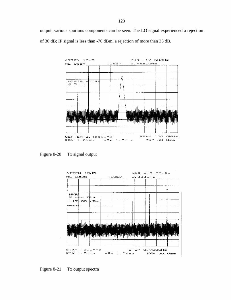
129
jection
output, various spurious components can be seen. The LO signal experienced a reof 30 dB; IF signal is less than -70 dBm, a rejection of more than 35 dB.
Figure 8-20 Tx signal output
Figure 8-21 Tx output spectra

130
ency
re-
ponse.
Fig. 8-22 shows the RF output spectrum at 1.705 GHz, where the image frequ
(LO - IF) is located. With IF input of -35 dBm, the Tx has gain of 1.7 dB at image f
quency. A 15 dB (17.5 dB - 1.7 dB) image rejection is obtained due to the tuned res
Figure 8-22 Tx image output
Figure 8-23 CMOS Tx P1dB
−35 −30 −25 −20 −15 −10−20
−18
−16
−14
−12
−10
−8
−6
−4
−2
0
2
4CMOS TRx Transmitter P1dB
Pin (dBm)
Pou
t (dB
m)
OP1dB =1.5 dBm

131
s
of the
t of
Figure 8-24 CMOS Tx IP3
Fig. 8-23 and 24 are the Tx IP3 and P1dB plots. Notice that in the Tx, these spec
are defined at the output instead of the input. Table 8-6 compares the performance
CMOS and SiGe Tx chain. The power gain of the CMOS Tx is 7.5 dB lower than tha
Table 8-6 Transmitter Performance Comparison
CMOS Tx SiGe Tx
Power Gain 17.5 dB 25 dB
Power Gain at Image 1.7 dB Not Avail.
Image Rejection -15.8 dBc Not Avail.
IF input and RF outputmatching
< -10 dB < -10 dB
Output IP3 12 dBm 14 dBm
Output P1dB 1.5 dBm 4 dBm
LO to RF feedthrough -30 dB -25 dB
IF to RF feedthrough < -35 dB Not Avail.
Total Tx Current 55 mA 41 mA
−30 −25 −20 −15 −10 −5 0−60
−55
−50
−45
−40
−35
−30
−25
−20
−15
−10
−5
0
5
10
15
20CMOS TRx Transmitter IP3
Pin (dBm)
Pou
t (dB
m)
OIP3 =12 dBm

132
he
the
ood
n the
f the
syn-
parity
rge.
d for
per
es to
d to
-
.
, the
the SiGe Tx. The lower power gain will limit the CMOS radio total Tx output power if t
PA cannot compensate missed gain.
8.2 Summary of CMOS RF Transceiver Design and Measurement
The design of the CMOS RF transceiver is successful with all the blocks on
chip functioning well. However, the overall performance of the transceiver is not as g
as expected. On the receiver side, LNA and RMx performance is slightly worse tha
previous built stand-alone ones. Although process variations could explain some o
performance difference. Some design issues like the re-size of the LNA and on-chip
thesizer generated LO are part of the reason as well. On the transmitter side, the dis
between the performance of measured and simulated TMx and TXA is relatively la
The main reason is the modeling accuracy for RF CMOS devices. The models use
simulation are the foundry provided BSIM models for digital applications. The pro
modeling of the RF devices has become increasingly important as RF CMOS striv
compete with Si or SiGe BiCMOS processes.
The technology scaling will certainly help the cause of RF CMOS. Compare
the 50 GHz SiGe BiCMOS process used for the SiGe transceiver, the 0.25-µm CMOS is
still much slower. Moving to 0.18-µm will bring speed parity to the SiGe BiCMOS pro
cess. Table 8-7 compares the 0.18-µm and 0.25-µm CMOS technology [Abo00, Che01]
The benefit of speed and noise is obvious. On top of that, for 2.4GHz applications
Table 8-7 Comparison of 0.18-µm and 0.25-µm CMOS processes
Parameters 0.18-µm CMOS 0.25-µm CMOS
Peak fT (GHz) 55 40
gm/Id ratio (V-1) 30 15
NFmin (dB) 1.2 1.4

133
ed in
rger
fer
Hz
BJT
radio.
r as a
box,
l gen-
are
ure,
acket
s are
tion,
as
unted
speed of 0.18-µm CMOS process leaves room for better process variations (discuss
chapter 4) and hot-electron reliability if the RF device is designed with gate length la
than the minimum. As the 0.18-µm CMOS becomes main stream digital process, its wa
price will start to drop. All these will give competitive edge to CMOS process for 2.4 G
applications.
8.3 CMOS TRx In PRISM II.5 Radio
8.3.1 Introduction
As an ultimate evaluation of CMOS transceiver and the comparison between
and CMOS RF circuits, the CMOS transceiver part has been measured in a PRISM
8.3.2 Measurement Setup
Two laptops are used in the setup, one acting as a radio transmitter, the othe
receiver. A radio link is established between them. The Tx is shielded in a metal
attenuators are mounted on the box to control the Tx output power. An external signa
erator produces the jammer signals. Two software, LANEVAL and Prism Test Utility,
used for radio evaluation.
Unlike the chip level testing, where specifications like S-parameters, Noise Fig
linearity are measured, for 802.11b WLAN system (a packet radio system) testing, P
Error Rate (PER) is used as criterion to measure the radios. Two PRISM II.5 card
used to benchmark the SiGe radio. Specifications like Rx sensitivity, image rejec
adjacent channel rejection; Tx spectral mask, output RMS power are measured.
8.3.3 CMOS Radio Setup
To measure the CMOS radio, SiGe TRx chip on one PRISM II.5 card w
detached or bypassed. Shown in Fig. 8-25, an impedance transformer (1:4) was mo

134
axial
in and
t-end
on the board right after the SAW filter (which has 200Ω differential impedance) and a
coaxial probe with SMA connector was soldered to the transformer. Two more co
probes with SMA connector are soldered on the board: one connected to the Tx cha
goes into the PA, and the other connected to the Rx chain and routed out of the fron
band pass filter.
Figure 8-25 Radio measurement setup
PA
IF BBPMAC
SAW(diff.)
RF
Coaxial with SMA
4:1 Transformer
PRISM II.5 Board
Plug-inJack
SiGe TRxdetached
Attenuator0 - 100 dB
Another PRISM II.5 CardActing as T/Rx to Completethe Radio Link
Cables
RF/IF Eval Boardwith CMOS TRx Chip
IF Port
RF Port
BPF
This forms one radioThis is another radio
This emulatesthe link betweentwo radios

135
kets
ere
Rx)
.5,
ht,
8.3.4 Transmitter Measurement Results
During the measurements, the radio with CMOS TRx transmits 1000 byte pac
at 11Mbps. The signal is fed into a Tektronix Wireless Communication Analyzer wh
constellation, EVM and eye pattern are measured. The original PRISM II.5 (SiGe T
signals are also measured for comparison.
Fig. 8-26 shows the EVM measurement of CMOS and SiGe transmitters.
Figure 8-26 Left, EVM of radio transmitter with a CMOS TRx, ~ 5.3%, around -25dB; Right, EVM of PRISM II.5 radio transmitter with a SiGe TRx, ~ 5.3%around -25.5 dB.
Figure 8-27 Left, Constellation diagram of radio transmitter with a CMOS TRx; RigConstellation diagram of PRISM II.5 radio transmitter with a SiGe TRx.

136
ye
trans-
ous
. 8-29
han-
.
putter
Figure 8-28 Left, Eye Pattern of radio transmitter with a CMOS TRx; Right, EPattern of PRISM II.5 radio transmitter with a SiGe TRx.
Figures 8-27 and 8-28 demonstrate the constellations and eye patterns of the
mitted signal. The Prism Test Utility software can program the Tx to transmit continu
wave signals. The output spectrum can be seen on a spectrum analyzer. Shown in Fig
is the transmit output spectra of the two radios. Fig. 8-30 demonstrates the Adjacent C
nel Power Ratio (ACPR) or the spectral mask of the transmitted signal of both radios
Figure 8-29 Left, output spectrum of Radio Transmitter with a CMOS TRx, outpower 13.1 dBm; Right, output spectrum of PRISM II.5 Radio Transmitwith a SiGe TRx, output power 13.2 dBm.
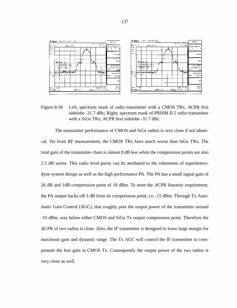
137
rsttter
nti-
The
also
tero-
ain of
ent,
to-
und
the
n for
m-
ios is
Figure 8-30 Left, spectrum mask of radio transmitter with a CMOS TRx, ACPR fisidelobe -31.7 dBc; Right, spectrum mask of PRISM II.5 radio transmiwith a SiGe TRx, ACPR first sidelobe -31.7 dBc.
The transmitter performance of CMOS and SiGe radios is very close if not ide
cal. Yet from RF measurement, the CMOS TRx fares much worse than SiGe TRx.
total gain of the transmitter chain is almost 8 dB less while the compression points are
2.5 dB worse. This radio level parity can be attributed to the robustness of superhe
dyne system design as well as the high performance PA. The PA has a small signal g
26 dB and 1dB compression point of 18 dBm. To meet the ACPR linearity requirem
the PA output backs off 3 dB from its compression point, i.e., 15 dBm. Through Tx Au
matic Gain Control (AGC), that roughly puts the output power of the transmitter aro
-10 dBm, way below either CMOS and SiGe Tx output compression point. Therefore
ACPR of two radios is close. Also, the IF transmitter is designed to leave large margi
maximum gain and dynamic range. The Tx AGC will control the IF transmitter to co
pensate the less gain in CMOS Tx. Consequently the output power of the two rad
very close as well.

138
cket
the
card
the
of the
ls,
mea-
ER is
. Fig.
data
pec-
ard.
I.5
nels.
for
8.3.5 Receiver Measurement Results
Packet Error Rate (PER) is the criterion to evaluate the performance of a pa
radio like 802.11b radios. LANEVAL program can calculate PER when the radio is in
receiving mode. As shown in Fig. 8-25, during the measurement, one PRISM II.5
transmits at 11 Mbps at full power, the signal is routed through attenuators where
attenuation ranges from 0 to 120 dB. The attenuated signal goes into the antenna
receiver radio (with CMOS TRx). Through monitoring PER at different signal leve
specifications like sensitivity, image rejection, adjacent channel rejection can be
sured. Usually for one PER measurement, 10,000 packets are counted and their P
averaged. Generally, if the PER is above 8%, the radio is considered out of reception
8-31 shows the measured receiver sensitivity of the two WLAN radios at 11 Mbps
rate. The CMOS and SiGe radios have Rx sensitivity of -81 dBm and -84 dBm res
tively. Both of them are much better than the -76 dBm required by the 802.11b stand
Figure 8-31 Left, CMOS radio sensitivity, @ 11 Mbps, -81 dBm; Right, PRISM ISiGe radio sensitivity, @ 11 Mbps, -84 dBm.
Adjacent channel rejection is tested with a 25-MHz separation between chan
The desired channel input power is set to be -78 dBm for the CMOS radio, -80 dBm
−90−80−70−60−50−40−30−20−1000
10
20
30
40
50
60
70
80CMOS Radio Sensitivity
Pin(dBm)
PE
R (
%)
−90−80−70−60−50−40−30−20−1000
10
20
30
40
50
60
70
80PRISM II.5 (SiGe TRx) Radio Sensitivity
Pin (dBm)
PE
R (
%)

139
igher
PER)
rying
GHz)
er-
d to
ignal
of the
ower
Bm)
ely.
tion,el
e -78
2 IF
the
the SiGe radio, (@2.462 GHz, channel 11). The input power is chosen to be 3 dB h
than the sensitivity level to ensure that the radios are in good reception (no residual
before the jammer signals are applied. The PER of the radios is measured while va
the power of CW on the adjacent channel. The jammer on adjacent channel (@2.437
is 11 Mbps CCK modulated signal in CW form. An Arbitrary Wave Form generator gen
ates the I & Q channel CCK baseband signals. The I & Q signals are then up-converte
signal at the adjacent channel through vector modulation using a Rhode & Schwartz s
generator. Fig. 8-32 shows the receiver adjacent channel rejection performance
CMOS and SiGe radios. The PER is larger than 8% when the adjacent channel p
exceeds -30 dBm for both radios. This gives the image rejection of (-30 dBm) - (-78 d
= 48 dBc, and (-30 dBm) - (-80 dBm) = 50 dBc for CMOS and SiGe radios, respectiv
Figure 8-32 Adjacent channel rejection: Left, CMOS radio adjacent channel rejec(-30 dBm) - (-78 dBm) = 48 dBc; Right, PRISM II.5 radio adjacent channrejection, (-30 dBm) - (-80 dBm) = 50 dBc.
For image rejection test, again, the desired channel input power is set to b
dBm for the CMOS radio, -80 dBm for the SiGe radio. The image is generated at RF -
= 2.462 GHz - 2x374 MHz = 1.714 GHz for channel 11 (2.462 GHz). The PER of
−50 −45 −40 −35 −30 −250
5
10
15
20
25
30
35
40
45
50CMOS Radio Adjacent Channel Rejection
Adjacent Channel Power (dBm)
PE
R (
%)
−50 −45 −40 −35 −30 −250
5
10
15
20
25
30
35
40
45
50PRISM II.5 (SiGe TRx) Adjacent Channel Rejection
Adjacent Channel Power (dBm)
PE
R (
%)

140
ows
n 8%
of 61
) --
ith a
radios is measured while varying the power of CW at image frequency. Fig. 8-33 sh
the receiver image rejection performance of the two radios. The PER is larger tha
when the image power exceeds -17 dBm and -27 dBm, resulting in image rejection
dB and 53 dB for CMOS and SiGe radios respectively.
Figure 8-33 Receiver image rejection: Left, CMOS radio image rejection, (-17 dBm(-78 dBm) = 61 dB; Right, PRISM II.5 radio image rejection, (-27 dBm)(-80 dBm) = 53 dB.
Table 8-7 summarizes and compares the performance of the PRISM II radio w
CMOS transceiver chip and the radio with SiGe transceiver chip.
Table 8-8 Radio (802.11b) Performance Comparison
CMOS Radio PRISM II.5 (SiGe) Radio
Rx Sensitivity(11 Mbps, 8% PER)
-81 dBm -84 dBm
Rx Image Rejection 61 dB 53 dB
Rx Adjacent ChannelRejection
48 dBc 50 dBc
Tx Output Power 13.1 dBm 13.2 dBm
Tx Output Spectral Mask(1st sidelobe)
-31.7 dBc -31.7 dBc
Tx Output EVM -25.5 dB -25.5 dB
−50 −45 −40 −35 −30 −25 −20 −15 −100
5
10
15
20
25
30CMOS Radio Image Rejection
Image Power (dBm)
PE
R (
%)
−50 −45 −40 −35 −30 −25 −200
5
10
15
20
25
30PRISM II.5 Radio Image Rejection
Image Power (dBm)
PE
R (
%)

141
its
o the
igher
fre-
hesiz-
rent
Tx
dio is
radio.
EE
hould
“RF
8.4 Summary of the Characterization of CMOS Transceiver
A CMOS RF transceiver for 802.11b WLAN application is designed in a 0.25-µm
CMOS technology. The CMOS transceiver is incorporated in a WLAN system and
radio performance is evaluated.The performance of the two radios is close due t
robustness of superheterodyne radio design. The CMOS transceiver has slightly h
noise figure and lower power gain than the SiGe one. The loop bandwidth of the PLL
quency synthesizer is set to be 1 kHz. Phase noises of the CMOS and SiGe PLL synt
ers are -81 dBc/Hz and -83 dBc/Hz at 10 kHz offset, respectively. The total cur
consumption of CMOS transceivers is 10 mA (in the Rx mode) and 15 mA (in the
mode) more than its SiGe counterpart. When the power consumption of the entire ra
considered, CMOS radio consumes less than 5% more current than that for the SiGe
The -81 dBm CMOS receiver sensitivity is 5 dB better than what’s required by the IE
802.11b standard. Moving to a 0.18-µm CMOS technology will most likely bring CMOS
chip RF performance close to or exceed that of the SiGe chip. The results suggest it s
be possible to replace the SiGe transceiver with low cost CMOS transceivers and
CMOS” is viable in delivering 2.4 GHz WLAN chip-set solution.

nt-
OS
ared
le to
g RF
pli-
01].
howed
unter-
tation
abri-
overall
red to
is the
RF
ual
are
CHAPTER 9SUMMARY AND FUTURE WORK
9.1 Summary
The first part of the dissertation studied the feasibility and difficulty of impleme
ing a CMOS transceiver by building and testing individual blocks. Stand-alone CM
LNA and Rx mixer were first built and the silicon measurement results were comp
with their SiGe counterparts. The comparison indicates that CMOS blocks are ab
meet the RF specifications of the receiver. CMOS transistors are adequate in buildin
amplifiers and mixers with decent noise figure and power consumption for WLAN ap
cations. The comparison of CMOS and SiGe LNA and mixer was summarized in [Li
Next, a stand-alone CMOS frequency synthesizer was designed. Measurements s
that the synthesizer works well and achieves comparable performance as its SiGe co
part.
Based on the success of these individual blocks, the second part of the disser
work focused on the realization of RF transceiver in CMOS. The chip was designed, f
cated, packaged and put on the PC board for evaluation. Measurements indicate an
decent design with all the blocks functioning. The results were analyzed and compa
simulations as well as the SiGe chip results. One of the key results this chip provided
impact of digital circuitry (Frequency synthesizer) on the performance of individual
blocks (LNA, Mixers and TXA). This result can not be obtained in the study of individ
blocks and will provide valuable guidance to future transceiver design. The mixers
142

143
there
LNA
een
ISM
OS
ios is
peti-
mon-
te-
future
and
he T/R
them.
, the
measured with LO set by the on-chip synthesizer. The output spectrum is clean and
is no significant degradation on noise figure due to the synthesizer. However, the
measurement indicates that turning on the synthesizerdoesaffect the Noise Figure of the
LNA. NF is increased from 3.3 dB to 3.5 dB when the synthesizer is on.
As an ultimate evaluation of the CMOS transceiver and the comparison betw
the SiGe BJT and CMOS RF circuits, the CMOS transceiver was incorporated in a PR
radio and the whole WLAN system was evaluated. The IEEE 802.11b radio with a CM
chip is successfully demonstrated. The performance of the CMOS and SiGe rad
close. This work has provided experimental results supporting the feasibility and com
tiveness of CMOS technology for WLAN applications.
9.2 Future Work and Direction
The successful implementation of the CMOS transceiver and the robust de
stration of WLAN system with the CMOS chip opens the door for a higher level of in
gration. Within the same superheterodyne transceiver architecture, a few possible
works are suggested.
9.2.1 CMOS Transceiver with a T/R Switch
A CMOS Transceiver with T/R switch can be designed based upon [Hua01]
the CMOS transceiver presented in this dissertation. One natural issue arises when t
switch is placed on the same chip as the transceiver, that is, the interface between
On a PC board where the T/R switch and TRx are in separate chips, for example
PRISM II system in Fig. 9-1, the interface is 50Ω.

144
p. If
cted
r PA
PA,
: a
e
ca-
w of
9-2.
ood
the
Figure 9-1 PRISM II RF transceiver and T/R switch interface
The situation could be different if the T/R switch and TRx are on the same chi
the Single Pole Double Throw (SPDT) switch is integrated with the single pole conne
to one pin which eventually leads to antenna, one throw for LNA and another throw fo
or TXA, the impedance of the interface between switch and LNA, or switch and TXA/
will not be 50Ω. This is because the LNA requires off-chip component for matching
piece of transmission line and a shunt cap. (On-chip 50Ω matching is not desirable as th
on-chip inductor will degrade the LNA noise figure.)
A PA with more than 20 dBm output power is needed for general WLAN appli
tions. This usually requires an off-chip PA. In this case, the interface between one thro
the SPST switch and PA output has to be 50Ω. A natural scheme to integrate the T/R
switch with the TRx is to treat the T/R switch as a stand-alone circuit, shown in Fig.
The CMOS T/R switch takes advantage of MOSFET being naturally a g
switch. The design of a transceiver with an on-chip T/R switch will bring the state of
rf_in2pF
LNA
TXA
Antenna
50 Ω
50 Ω 50 Ω
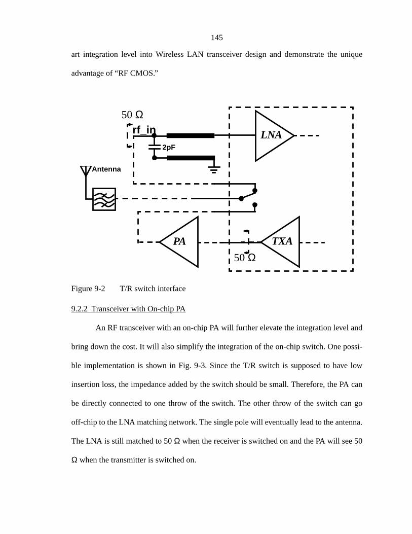
145
ique
nd
si-
low
A can
go
na.
50
art integration level into Wireless LAN transceiver design and demonstrate the un
advantage of “RF CMOS.”
Figure 9-2 T/R switch interface
9.2.2 Transceiver with On-chip PA
An RF transceiver with an on-chip PA will further elevate the integration level a
bring down the cost. It will also simplify the integration of the on-chip switch. One pos
ble implementation is shown in Fig. 9-3. Since the T/R switch is supposed to have
insertion loss, the impedance added by the switch should be small. Therefore, the P
be directly connected to one throw of the switch. The other throw of the switch can
off-chip to the LNA matching network. The single pole will eventually lead to the anten
The LNA is still matched to 50Ω when the receiver is switched on and the PA will see
Ω when the transmitter is switched on.
rf_in
2pF
LNA
TXA
Antenna
50 Ω
50 Ω
PA

146
ious
g
mit
may
un-
OS.
the
Figure 9-3 CMOS Transceiver with integrated PA and T/R switch
This system requires a good design on both the PA and T/R switch. The prev
work shows a P1dB of the on-chip T/R switch around 18 dBm without off-chip matchin
[Hua01]. This limits the total power out of the PA; consequently the entire radio trans
power which may not be acceptable for WLAN access point. However, this system
still be a viable low-cost WLAN solution for mobiles.
9.2.3 Transceiver with Integrated IF Transceiver
Another opportunity for integration is the IF section of the radio. There is no f
damental difficulty in doing so as all the circuits in the IF section are realizable in CM
The IF output of the RF transceiver can go off-chip to the SAW filter and come back to
IF section of the chip, as shown in Fig. 9-4.
rf_in
2pF
LNA
PA
Antenna
50Ω
50 Ω

147
ieved
T/R
Figure 9-4 A chip integrating both RF and IF transceivers
The highest level of integration for a superheterodyne transceiver can be ach
by incorporating the concepts in Figs. 9-3 and 9-4. A CMOS chip integrating a PA, a
switch, RF and IF sections will demonstrate the ultimate power of “RF CMOS.”
LO IF section
Combined RF and IF Chip
To BBP/MAC
SAW

e I-
here
text-
ably
ore
vation
n at
(per
tion
hey
APPENDIX ABJT AND MOSFET DEVICE PHYSICS
The I-V characteristics of BJT’s and MOSFET’s are mathematically simple. Th
V characteristics of BJT’s are exponential and those of MOSFET’s are square law. T
must be simple physics behind the simple exponential or square law. Most of the
books emphasize on how to quantitatively derive the I-V equation. A simple, prefer
one-sentence answer to questions like “Why exponential?” or “Why square law?” is m
desirable. This discussion reveals more physics than a lengthy mathematical deri
and compares two devices on a more fundamental level.
A.1 Why Does the BJT Have Exponential I-V Relation?
In an npn BJT, the minority diffusion current density can be expressed as,
(A.1)
where D is the diffusion constant. is proportional to minority carrier concentratio
the base depletion edge of base-emitter junction,
(A.2)
where W is the base width. The carrier concentration n(0), or the number of carriers
unit volume) in a semiconductor is determined by Density of States of the conduc
band and the Fermi-Dirac distribution. In the case of minority carriers in silicon, t
reduce to an exponential,
J qDxd
dn=
xddn
xddn n 0( )
W-----------∝
148
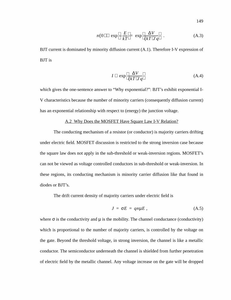
149
of
ial I-
rent)
ting
cause
ET’s
n. In
d in
y)
on
tallic
tration
ped
. (A.3)
BJT current is dominated by minority diffusion current (A.1). Therefore I-V expression
BJT is
(A.4)
which gives the one-sentence answer to “Why exponential?”: BJT’s exhibit exponent
V characteristics because the number of minority carriers (consequently diffusion cur
has an exponential relationship with respect to (energy) the junction voltage.
A.2 Why Does the MOSFET Have Square Law I-V Relation?
The conducting mechanism of a resistor (or conductor) is majority carriers drif
under electric field. MOSFET discussion is restricted to the strong inversion case be
the square law does not apply in the sub-threshold or weak-inversion regions. MOSF
can not be viewed as voltage controlled conductors in sub-threshold or weak-inversio
these regions, its conducting mechanism is minority carrier diffusion like that foun
diodes or BJT’s.
The drift current density of majority carriers under electric field is
, (A.5)
whereσ is the conductivity andµ is the mobility. The channel conductance (conductivit
which is proportional to the number of majority carriers, is controlled by the voltage
the gate. Beyond the threshold voltage, in strong inversion, the channel is like a me
conductor. The semiconductor underneath the channel is shielded from further pene
of electric field by the metallic channel. Any voltage increase on the gate will be drop
n 0( ) EkT------–
∆VkT( ) q⁄
------------------ exp=exp∝
I∆V
kT( ) q⁄------------------
exp∝
J σE qnµE= =

150
nd the
ld is
ich
ence
e an
nduc-
across the gate oxide. The relationship between number of carriers in the channel a
gate voltage is linear, same as that of an ideal capacitor,
or (A.6)
where VGT is (VG - Vth). Considering the effects of drain voltage,
(A.7)
where y is the direction from source (y = 0) to drain (y = L), and Vc(y) is the voltage along
the channel. Substituting Eq. (A.7) into Eq. (A.5) and remembering that electric fie
the derivative of potential ,
. (A.8)
Integrating Eq. (A.7) along y direction yields,
. (A.9)
In saturation , so
in saturation. (A.10)
Eq. (A.10) is the MOSFET square law. It is the natural result of Eq. (A.6), wh
states that the conductivity is proportional to effective control voltage. The one-sent
answer to “Why square law?” is, MOSFET’s exhibit square law because it acts lik
ideal capacitor where the channel (one side of the capacitor) is a conductor whose co
tivity is proportional to control voltage.
δQ C δV⋅= Q qn C VGT⋅= =
n y( ) VGT Vc y( )–( )∝
Eyd
dV y( )
ydd
n y( )∝ ∝
J n y( )∝yd
dn y( )⋅
J L⋅ nsource2
ndrain2
–∝
ndrain2
0=
J nsource2
VGT2∝ ∝

151
inear
phys-
of its
gate
m fur-
volt-
elow
rtially
r, the
why
n far
se in
idth)
yond
cross
Eq.
with
tor pn
of the
A.3 Field Effect Transistor and Square Law
From the above discussion, the mechanism for a square law device is the l
relationship between gate control voltage and number of carriers in the channel. The
ics behind this is that, once the MOSFET is turned on (strong inversion), the nature
channel is metallic. A further voltage increase on the gate will be dropped across the
and channel (gate oxide). The semiconductor underneath the channel is shielded fro
ther penetration of electric field by the metallic channel. The existing of the threshold
age, Vth, is a key measure when the metallic channel has been established. B
threshold voltage or in sub-threshold region, the voltage on the gate is dropped pa
across the oxide, partially across the semiconductor underneath. In semiconducto
relationship between the number of carriers and voltage drop is exponential. That is
in sub-threshold region, MOSFET’s behave like BJT’s.
In strong inversion, when the conduction and valence bands are bent dow
enough that surface potentialψS = 2 ψB, the semiconductor is effectively shielded from
further penetration of the electric field by the inversion layer. Even a very small increa
the band bending (corresponding to a very small increase in the depletion layer w
results in a very large increase in the charge density within the inversion layer. Be
threshold voltage, in strong inversion, most of the increase in gate voltage will drop a
the oxide, with a tiny little across semiconductor to supply “enough” carriers to satisfy
(A.6). One instant conclusion is that, the number of carriers in a MOSFET channel (
respect to gate voltage) can never exceed the number of carriers in a semiconduc
junction (with respect to voltage across the junction) because, the latter is the supply
former. Therefore, gm/I ratio of a MOSFET will always be lower than that of a BJT.

ode
code
as
. B-3.
APPENDIX BINPUT IMPEDANCE OF BJT AND MOS LNA’S
During the analyses of both BJT and MOS LNA’s, the input impedance of casc
LNA’s with inductive degeneration was needed. For example, the input stage of a cas
BJT LNA can be represented as Fig. B-1.
Figure B-1 Small signal representation of a BJT Cascode LNA input
The MOSFET LNA has the similar small signal model only simpler: rg (rb) can be
neglected and rπ is infinite. The above model can be further generalized and simplified
Fig. B-2. In analyzing the input impedance, Zb can be absorbed into Zo and the input
impedance calculation is reduced to finding the input impedance of the circuit in Fig
gmvπ
+
-vπ ro1
rπ
rb
cπ
cµ
Substrate
ccs
Le
LbZ0
E1
Zin, amp
Zin2
Cascode Transistor
152
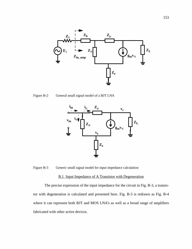
153
sis-
. B-4
ifiers
Figure B-2 General small signal model of a BJT LNA
Figure B-3 Generic small signal model for input impedance calculation
B.1 Input Impedance of A Transistor with Degeneration
The precise expression of the input impedance for the circuit in Fig. B-3, a tran
tor with degeneration is calculated and presented here. Fig. B-3 is redrawn as Fig
where it can represent both BJT and MOS LNA’s as well as a broad range of ampl
fabricated with other active devices.
gmvπ
Zπ
ZµZ0
E1
Zin, amp
ZL
Ze
Zb
gmvπZπ
Zµ vc
ZL
Ze
ve
viniπ
iin iµ

154
Figure B-4 Generalized small signal model of a transistor with degeneration
Using KVL and KCL, the basic equations are
, (B.1)
, (B.2)
where v1 and v3 are
, (B.3)
. (B.4)
In addition,
, (B.5)
where v2 can be expressed as
. (B.6)
Substituting Eqs. (B.3) and (B.4) into (B.2),
(B.7)
gmv1Z1
Z2 v2
ZL
Z3
v3
vini1
iin i2
+
-
v1
i in i1 i2+=
vin v1 v3+=
v1 i1 Z1⋅=
v3 i1 gmv1+( ) Z3⋅=
vin v1 v2+=
v2 i2 gm– v1( ) ZL⋅=
vin i1 Za⋅=
155
where Za is
. (B.8)
Substituting Eqs. (B.3) and (B.6) into (B.5),
. (B.9)
For three equations (B.1), (B.7) and (B.9), there are four unknowns, vin, iin, i1 and
i2. These three equations can be solved to obtain iin in terms of vin consequently the input
impedance Zin.
Re-writing (B.7),
. (B.10)
Substituting (B.10) into (B.9),
, (B.11)
or
. (B.12)
Substituting Eqs. (B.10) and (B.12) into (B.1),
(B.13)
or
(B.14)
Za Z1 1 gmZ1+( ) Z3⋅+=
vin i2 Z2 ZL+( )⋅ i1gmZ1ZL–=
i1
vinZa-------=
vin i2 Z2 ZL+( )⋅vinZa-------gmZ1ZL–=
i2
vinZ2 ZL+-------------------- 1
gmZ1ZLZa
----------------------+
⋅=
i in vin1
Za------
Za gmZ1ZL+
Za Z2 ZL+( )⋅------------------------------------+
⋅=
Zin
vini in-------
Za Z2 ZL+( )⋅
Z2 ZL Za gmZ1ZL+ + +--------------------------------------------------------------= =

156
ith
and
where Za is
. (B.15)
Equation (B.14) is the exact solution of the input impedance of a transistor w
degeneration.
B.2 Approximation Cases
In several scenarios, including the LNA cases, approximation can be applied
Eq. (B.14) can be reduced into some familiar equations.
B.2.1 Scenario #1: Miller Capacitance is Small
If the Miller capacitor of the transistor (Cµ or Cgd) is very small, i.e., Z2 >> all the
other Z’s, then equation (B.14) can be reduced to
(B.16)
and we know Za is the exact solution of the input impedance of the circuit in Fig. B-5.
Figure B-5 Small Miller effect approximation
Za Z1 1 gmZ1+( ) Z3⋅+=
Zin
Za Z2 ZL+( )⋅
Z2 ZL Za gmZ1ZL+ + +--------------------------------------------------------------
ZaZ2Z2
--------------≅ Za= =
gmv1Z1
ZL
Z3
vin
iin
+
-
v1
157
NA,
t of
se of
-
Eq. (B.16) is also the approximation we use throughout Chapter 4. For BJT L
this is a very good approximation because modern SiGe BJT has small Cµ. For MOS
LNA, this is also a good approximation because for a 0.25-µm CMOS process,
. In scenario #3, it is shown that for cascode LNA’s, even when the effec
Cgd is included, the input impedance predicted by (B.21) is close to (B.16).
B.2.2 Scenario #2: Miller Theorem
Let us see what happens to (B.14) if there is no degeneration. This is the ca
Miller theorem.
If Z3 = 0, then Za = Z1 and Eq. (B.14) becomes
. (B.17)
Multiplying both the numerator and denominator of Eq. (B.17) by 1/Z1Z2,
. (B.18)
The application of Miller’s theorem requires that Cµ or Cgs must be small so that the cur
rent going through it is much smaller compared to gmv1. This is equivalent to .
Eq. (B.18) becomes
(B.19)
in which Z2(1+gmZL) is the Miller impedance.
Cgd13---Cgs≈
Zin
Za Z2 ZL+( )⋅
Z2 ZL Za gmZ1ZL+ + +--------------------------------------------------------------
Z1 Z2 ZL+( )⋅
Z2 ZL Z1 gmZ1ZL+ + +--------------------------------------------------------------= =
Zin
1 ZL Z2⁄+( )
1Z1------ 1
ZLZ2---------+
1
Z2------ 1 gmZL+( )+
-------------------------------------------------------------------------=
ZLZ2------- 1«
Zin1
1Z1------
1Z2------ 1 gmZL+( )+
--------------------------------------------------≅ Z1 Z2 1 gmZL+( )⋅||=
158
gate
t-
se to
lower
et us
cas-
B.2.3 Scenario #3: Cascode Circuits
Cascode circuit helps to alleviate the Miller effect by adding a common base/
transistor between input and output. ZL is 1/gm2 instead of the large load seen at the ou
put. gm2 is the transconductance of the common base/gate transistor and is very clo
gm1(gm), for BJT LNA gm2 = gm1; for MOSFET LNA, gm2 is slightly less than gm1
because the cascode device is often chosen to be smaller than the input device for
parasitic capacitance at the output and optimal noise match [Flo01]. For simplicity, l
assume gm2 = gm1 (gm). Eq. (B.14) becomes
. (B.20)
Also, for cascode circuit, which further reduces (B.20) into
. (B.21)
Equation (B.21) is the input impedance expression for the general cascode circuit. In
code LNA design, the emitter/source degeneration (Z3) consists of a small inductor only.
Therefore, from Eq. (B.15), , and Eq. (B.21) becomes
. (B.22)
Eq. (B.22) says that the input impedance is approximately Cgs// 2Cgd or Cπ // 2Cµ for cas-
code LNA’s [Okk02].
Zin
Za Z2 ZL+( )⋅
Z2 ZL Za gmZ1ZL+ + +--------------------------------------------------------------
Za Z2 ZL+( )⋅
Z2 ZL Za Z1+ + +-----------------------------------------------= =
ZL Z2«
Zin
Za1 Za Z1+( ) Z2⁄+---------------------------------------------≅
Za Z1≅
Zin
Z11 2Z1 Z2⁄+------------------------------≅ 1
1 Z1⁄ 2 Z2⁄+----------------------------------=
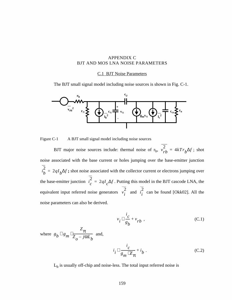
ction
over
the
the
APPENDIX CBJT AND MOS LNA NOISE PARAMETERS
C.1 BJT Noise Parameters
The BJT small signal model including noise sources is shown in Fig. C-1.
Figure C-1 A BJT small signal model including noise sources
BJT major noise sources include: thermal noise of rb, ; shot
noise associated with the base current or holes jumping over the base-emitter jun
; shot noise associated with the collector current or electrons jumping
the base-emitter junction . Putting this model in the BJT cascode LNA,
equivalent input referred noise generators and can be found [Okk02]. All
noise parameters can also be derived.
, (C.1)
where and,
. (C.2)
Lb is usually off-chip and noise-less. The total input referred noise is
ro
+vπ
-
ccscπ
rb
rπ
cµ
ic2ib
2
vrb2
gmvπ
vrb2
4kT rb∆f=
ib2
2qIb∆f=
ic2
2qIc∆f=
vi2
i i2
vi
icgb------ vrb+≅
gb gm
ZπZo jωLb–--------------------------⋅≅
i i
icgm Zπ⋅------------------- ib+≅
159

160
, (C.3)
and the noise factor can be expressed as,
. (C.4)
The noise parameters Fmin, Gn, Zopt = Ropt + jXopt (impedance form) can be
derived once Eqs. (C.1) and (C.2) are found [Okk02].
, (C.5)
, (C.6)
, (C.7)
, (C.8)
where
, (C.9)
and
vni vi i i Zo jωLb+( )⋅+=
F 1vni
2
vs2
--------------+ 1
rb
2Zo2
gm Zπ⋅ 2-------------------------
gm Zo2 ω2
Lb2
+ ⋅
2β---------------------------------------------+ +
Zo-----------------------------------------------------------------------------------------+= =
Gn
gm
2 gmZπ2
------------------------gm2βo---------+=
Xopt X– cor
1cπω----------
1gmZπ
2
βo---------------------+
------------------------------≅=
Ropt
RuGn------- Rcor
2+=
Fmin 1 2Gn Rcor Ropt+( )+=
Rcor rb
βo
gmLeCπ
--------------
βo gmZπ2
+----------------------------------+=

161
hey
ators
F
. (C.10)
C.2 MOS Noise Parameters
The MOS small signal model including noise sources is shown in Fig. C-2. T
include thermal noise of gate resistance rg,
, (C.11)
gate induced noise
(C.12)
and channel thermal noise
. (C.13)
Figure C-2 MOS small signal model with noise sources
From Eqs. (C.11), (C.12) and (C.13), the equivalent input referred noise gener
and can be found [Sha97]. Using the admittance form, the noise parametersmin,
Rn, Yopt = Gopt + j Bopt, can be expressed as
Ru rb
gm
gmLeCπ
-------------- 2
Xπ Xe–( )2+
2 gmZπ2 βo+
----------------------------------------------------------------------+=
vrg2
4kT rg∆f=
ig2
4kTδω2
Cgs2
5gdo--------------------
∆f=
id2
4kTγgdo∆f=
ro
+cgs
-
rgcgd
i2di2g
v2rg
gmvgs
vi2
i i2

162
, (C.14)
, (C.15)
, (C.16)
(C.17)
where,γ ~ 2/3 to 2,δ is 2γ, α ~ 1, and c ~ 0.395.
Rnγ
α gm⋅---------------=
Bopt ωCgs 1 α cδ5γ------+–=
Gopt αωCgsδ5γ------ 1 c
2–( )=
Fmin 1 2Rn Gopt Gc+( )+ 1 2RnGopt+= =

l-
m-
rtze,
,
d
sics,
nol-
inor-
LIST OF REFERENCES
[Abo00] Abou-Allam, E., Manku, T., Ting, M. and Obrecht, M.: Impact of Technoogy Scaling on CMOS RF Devices and Circuits.IEEE Custom IntegratedCircuits Conference, Orlando, pp. 361-364, 2000.
[Che01] Chew, K., Chu, S. and Leung, C.: Driving CMOS into the Wireless Comunications Arena with Technology Scaling.IEEE Custom Integrated Cir-cuits Conference, San Diego, pp. 571-574, 2001.
[Flo99] Floyd, B., Metha, J., Gamero, C. and O, K.: A 900-MHz, 0.8-µm CMOSLow Noise Amplifier with 1.2-dB Noise Figure.IEEE Custom IntegratedCircuits Conference, San Diego, pp. 661-664, 1999.
[Flo01] Floyd, B.: A CMOS Wireless Interconnect System for multigigaheClock Distribution. Ph. D. Dissertation, University of Florida, GainesvillFL, 2001.
[Gil98] Gilbert, B.: Why Bipolar?1998, http://www.edtn.com/analog/barrie2.htmJan 2001.
[Goy95] Goyal, R.:High-Frequency Analog Integrated Circuit Design. New York,John Wiley & Sons, Inc., 1995.
[Gra93] Gray, P. and R. G. Meyer, R.:Analysis and Design of Analog IntegrateCircuits, 3rd edition. New York, John Wiley & Sons, Inc., 1993.
[Har95] Harame, D.: Si/SiGe epitaxial-base transistors - Part I: Materials, phyand circuits.IEEE Trans. Electron Devices, vol. 42, pp. 469-482, 1995.
[Har01] Harame, D.: Current Status and Future Trends of SiGe BiCMOS Techogy. IEEE Trans. Electron Devices, vol. 48, pp. 2575-2594, 2001.
[Hem99] Hemmenway, D.: UHF2: a 0.6µm, 25 GHz BiCMOS technology formixed signal, wireless communications applications.SPIE MicroelectronicManufacturing Symposium, 1999.
[Ho00] Ho, Y.: Implementation and improvement for RF low noise amplifiersconventional CMOS technologies. Ph. D. Dissertation, University of Flida, Gainesville, FL, 2000.
163

164
ess
cyof
a-
r
oftch-
/
for-
[Hua98] Huang, Q. and Ohguro, T.: Scaling down to deep submicron,”IEEE Jour-nal of Solid State Circuits, Vol. 36, No. 3, pp. 486, July, 1998.
[Hua01] Huang, F. and O, K.: A 0.5-µm T/R Switch for 900-MHz Wireless Appli-cations.IEEE Journal of Solid State Circuits, Vol. 33, No. 7, pp. 486,March 2001.
[Hun98] Hung, C. and O, K.: High-Q capacitors implemented in a CMOS procfor low-power wireless applications.IEEE Trans. Microwave Theory andTechniques, vol. 46, pp. 505-511, May 1998.
[Hun00] Hung, C.: Investigation of a multi-GHz single-chip CMOS PLL frequensynthesizer for wireless applications. Ph. D. Dissertation, UniversityFlorida, Gainesville, FL, 2000.
[Lar96] Larson, L.:RF and Microwave Circuit Design for Wireless Communictions, Boston, Artech House, Inc., 1996.
[Lar98] Larson, L.: Integrated Circuit Technology Options for RFICs.IEEE J.Solid State Circuits, Vol. 33, pp. 387-399, March 1998.
[Li01] Li, X. and O, K.: A Comparison of CMOS and SiGe LNA’s and Mixers foWireless LAN Application.IEEE Custom Integrated Circuits Conference,San Diego, pp. 531-534, 2001.
[Liq01] Li, Q. and Oates, A.: RF Circuit Performance Degradation Due to SBreakdown and Hot-Carrier Effect in Deep-Submicrometer CMOS Tenology.IEEE Transactions on Microwave Theory and Techniques, Vol. 48,pp. 1546-1551, 2001.
[Lou97] Lough, D., Blankenship T. and Krizman K.:A Short Tutorial on WirelessLANs and IEEE 802.11,1997, http://computer.org/students/lookingsummer97/ieee802.htm, Jan 2001.
[Man01] Manku, T.: RF CMOS Devices and Circuits.IEEE Custom Integrated Cir-cuits Conference, San Diego, Short Course Notes, 2001.
[Met76] Metcalfe, R. and Boggs, D.: Ethernet: Distributed Packet SwitchingLocal Computer Networks.Communications of the Association for Computing Machinery, Vol. 19, pp. 395-404, July 1976.
[Mon97] Moniz, J.: Is SiGe the Future of GaAs for RF Applications?IEEE GaAs ICSymposium Technical Digest, pp. 229-231, 1997.

165
lar
s. In
.
li-
er.
a-
for-
129ille,
udo
[Nin01] Ning, T.: History and Future Perspective of the Modern Silicon BipoTransistor.IEEE Transactions on Electron Devices, Vol. 48, pp. 2485-2491, 2001.
[Okk02] O, K.:Bipolar Low Noise Amplifier (LNA) Design. Lecture Notes, 2002.
[Pav00] Paviol, J., Andren, C. and Fakatselis, J.: Wireless Local Area NetworkMicrowave and RF Handbook,CRC Press, 2001.
[Poz01] Pozar, D.:Microwave and RF Design of Wireless Systems. New York, JohnWiley & Sons, Inc., 2001.
[Raz98] Razavi, B.:RF Microelectronics, Upper Saddle River, Prentice-Hall, 1998
[Raz99] Razavi, B.: A 900-MHz/1.8-GHz CMOS Transmitter for Dual-Band Appcation. IEEE Journal of Solid-State Circuits, vol.34, pp.573-579, May1999.
[Sev00] Sevenhans, J.: Silicon Radio Integration.IEEE Custom Integrated CircuitsConference, Orlando, pp. 333-340, 2000.
[Sha97] Shaeffer D. and Lee, T.: A 1.5-V, 1.5-GHz CMOS low noise amplifiIEEE J. Solid-State Circuits, vol. 32, pp. 745-759, May 1997.
[Ulf98] Konig, U.: SiGe & GaAs as Competitive Technologies for RF Applictions.Proceedings of BCTM, pp. 87-92, 1998.
[Won94] Wong, A. and Wong, M.: Current combiner enhances active mixer permance.Microwaves & RF, pp. 156, March 1994.
[Yan98] Yan, H.: Design techniques to improve performance of divide-by-128/dual modulus prescalers. M.E. Thesis, University of Florida, GainesvFL, 1998.
[Yan99] Yan, H and O. K.: A high-speed CMOS dual-phase dynamic-pseNMOS ([DP]2) latch and its application in a dual-modulus prescaler.IEEEJ. Solid State Circuits, vol. 34, no. 10, pp. 1400-1404, Oct. 1999.
166
BIOGRAPHICAL SKETCH
Xi Li was born in Shanghai, China, in August, 1969. He received the B.S. in phys-
ics from Peking University in 1991, and the M.S. in electrical and computer engineering
from the University of Florida in 1999. Since 1997, he has been working on his graduate
degrees in the Silicon Microwave Integrated Circuits and Systems (SiMICS) Research
Group, at the Department of Electrical and Computer Engineering of University of Flor-
ida. During the summer of 1998, he worked for Rockwell Semiconductor (now Jazz Semi-
conductor), Newport Beach, California, in the area of semiconductor Bipolar and
BiCMOS process development, as a summer intern. During the summer of 1999, he
worked for Harris Semiconductor (now Intersil Corporation), Palm Bay, Florida, in the
area of RF IC design, as a summer intern. Since 2000, he has been with the Mixed Signal
and RF IC design group at Intersil Corporation in Palm Bay, Florida, as an IC design engi-
neer.