EVAL-AD7294 User Guide - analog.com · Changes to the Main Window Section, ... This option is...
25
EVAL-AD7294 User Guide UG-1004 One Technology Way • P.O. Box 9106 • Norwood, MA 02062-9106, U.S.A. • Tel: 781.329.4700 • Fax: 781.461.3113 • www.analog.com Evaluating the AD7294 12-Bit Monitor and Control System with Multichannel ADC, DACs, Temperature Sensor, and Current Sense FEATURES Full featured evaluation board for the AD7294 Graphical user interface (GUI) software with USB control Can be powered entirely from the USB port or by an external power source Various link options EVALUATION KIT CONTENTS EVAL-AD7294 evaluation board EVAL-AD7294 evaluation board software CD USB A to mini B cable EQUIPMENT NEEDED Bench top power supply Connector cables DOCUMENTS NEEDED AD7294 data sheet GENERAL DESCRIPTION This user guide describes the functionality and setup of the EVAL-AD7294 evaluation board for the AD7294 (TFQP package), which is a 12-bit monitoring and control device with multichannel ADC, four 12-bit DACs, temperature sensors, and current sensors. The AD7294 is a highly integrated solution that offers all the functionality necessary for precise control of the power amplifier in cellular base station applications. Full details about the AD7294 are available in the AD7294 data sheet, which is available from Analog Devices, Inc., and should be consulted in conjunction with this user guide when using this evaluation board. EVAL-AD7294 EVALUATION BOARD PHOTOGRAPH 07922-101 Figure 1.
Transcript of EVAL-AD7294 User Guide - analog.com · Changes to the Main Window Section, ... This option is...

EVAL-AD7294 User Guide UG-1004
One Technology Way • P.O. Box 9106 • Norwood, MA 02062-9106, U.S.A. • Tel: 781.329.4700 • Fax: 781.461.3113 • www.analog.com
Evaluating the AD7294 12-Bit Monitor and Control System with Multichannel ADC, DACs,
Temperature Sensor, and Current Sense
FEATURES Full featured evaluation board for the AD7294 Graphical user interface (GUI) software with USB control Can be powered entirely from the USB port or by an external
power source Various link options
EVALUATION KIT CONTENTS EVAL-AD7294 evaluation board EVAL-AD7294 evaluation board software CD USB A to mini B cable
EQUIPMENT NEEDED Bench top power supply Connector cables
DOCUMENTS NEEDED AD7294 data sheet
GENERAL DESCRIPTION This user guide describes the functionality and setup of the EVAL-AD7294 evaluation board for the AD7294 (TFQP package), which is a 12-bit monitoring and control device with multichannel ADC, four 12-bit DACs, temperature sensors, and current sensors. The AD7294 is a highly integrated solution that offers all the functionality necessary for precise control of the power amplifier in cellular base station applications.
Full details about the AD7294 are available in the AD7294 data sheet, which is available from Analog Devices, Inc., and should be consulted in conjunction with this user guide when using this evaluation board.
EVAL-AD7294 EVALUATION BOARD PHOTOGRAPH
0792
2-10
1
Figure 1.
UG-1004 EVAL-AD7294 User Guide
Rev. A | Page 2 of 25
TABLE OF CONTENTS Features .............................................................................................. 1 Evaluation Kit Contents ................................................................... 1 Equipment Needed ........................................................................... 1 Documents Needed .......................................................................... 1 General Description ......................................................................... 1 EVAL-AD7294 Evaluation Board Photograph .............................. 1 Revision History ............................................................................... 2 Evaluation Board Hardware ............................................................ 3
Power Supplies .............................................................................. 3 Links ............................................................................................... 4 Sockets ........................................................................................... 6 Connectors .................................................................................... 6
Getting Started .................................................................................. 7 Summary of the Setup Sequence ................................................ 7 Installing the Software ................................................................. 7 Connecting the USB Cable.......................................................... 8 Verifying the Links and Powering Up the Evaluation Board . 8 Evaluating the EVAL-AD7294 ..................................................... 9
Using the Software .......................................................................... 10 Main Window ............................................................................. 10
Configuration Window ............................................................. 10 Register Map Window ............................................................... 11 Device Address Information Window..................................... 11 Read Channel Window.............................................................. 12 Alert Manager Window ............................................................. 14 External Temperature Sensor Offset Calibration Window .. 15 Load DAC Window.................................................................... 15
Frequently Asked Questions ......................................................... 17 How Can a User Confirm the Hardware Has Been Correctly Installed on the Computer? ...................................................... 17 During the Installation, the Cannot Install this Hardware Message Appears. When Clicking Finish, the Hardware Installation Error Message Appears. What Does the User Do Next? ............................................................................................ 17
Layout and Configuration Guidelines ......................................... 19 Power Supply Decoupling and Grounding ............................. 19
Evaluation Board Schematics and Artwork ................................ 20 Ordering Information .................................................................... 24
Bill of Materials ........................................................................... 24
REVISION HISTORY 8/2016—Rev. 0 to Rev. A Deleted Applications Section .......................................................... 1 Added Evaluation Kit Contest Section, Equipment Needed Section, and Documents Needed Section ..................................... 1 Changes to General Description Section and Figure 1 ............... 1 Changes to the Power Supplies Section ......................................... 3 Changes to Links Section and Table 1 ........................................... 4 Changes to Table 2 ............................................................................ 5 Changes to Sockets Section and Table 3 ........................................ 5 Changes to Summary of the Setup Sequence Section, Stalling the Software Section, Figure 2 Caption, Figure 3 Caption, and Figure 4 Caption ............................................................................... 7 Changes to Connecting the USB Cable Section, Verifying the Links and Powering Up the Evaluation Board Section, and Figure 8 Caption ............................................................................... 8 Changes to and Evaluating the EVAL-AD7294 Section Title .......... 9 Changes to the Main Window Section, Device Menu Section, ADC Menu Section, and Configuration Window Section ....... 10
Changes to Register Map Window Section and Device Address Information Window Section ....................................................... 11 Changes to the Read Channel Window Section......................... 12 Changes to the Alert Manager Window Section ........................ 14 Changes to External Temperature Sensor Offset Calibration Window Section, Changes to Load DAC Window Section, and Figure 24 Caption ........................................................................... 15 Changes to How Can a User Confirm the Hardware Has Been Correctly Installed on the Computer? Section, During the Installation, the Cannot Install this Hardware Message Appears, When Clicking Finish, the Hardware Installation Error Message Appears. What Does the User Do Next? Section, and Figure 30 Caption ............................................................................................ 17 Change to Figure 34 ....................................................................... 20 4/2009—Revision 0: Initial Version
EVAL-AD7294 User Guide UG-1004
Rev. A | Page 3 of 25
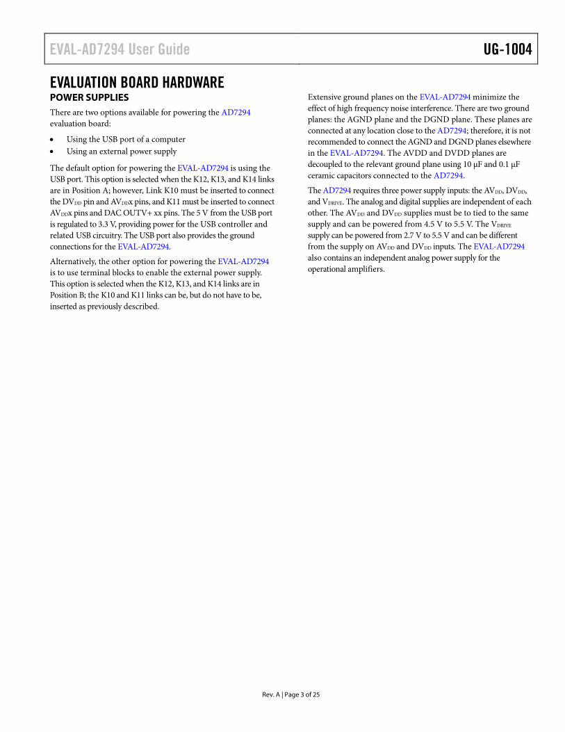
EVALUATION BOARD HARDWARE POWER SUPPLIES There are two options available for powering the AD7294 evaluation board:
• Using the USB port of a computer • Using an external power supply
The default option for powering the EVAL-AD7294 is using the USB port. This option is selected when the K12, K13, and K14 links are in Position A; however, Link K10 must be inserted to connect the DVDD pin and AVDDx pins, and K11 must be inserted to connect AVDDx pins and DAC OUTV+ xx pins. The 5 V from the USB port is regulated to 3.3 V, providing power for the USB controller and related USB circuitry. The USB port also provides the ground connections for the EVAL-AD7294.
Alternatively, the other option for powering the EVAL-AD7294 is to use terminal blocks to enable the external power supply. This option is selected when the K12, K13, and K14 links are in Position B; the K10 and K11 links can be, but do not have to be, inserted as previously described.
Extensive ground planes on the EVAL-AD7294 minimize the effect of high frequency noise interference. There are two ground planes: the AGND plane and the DGND plane. These planes are connected at any location close to the AD7294; therefore, it is not recommended to connect the AGND and DGND planes elsewhere in the EVAL-AD7294. The AVDD and DVDD planes are decoupled to the relevant ground plane using 10 µF and 0.1 µF ceramic capacitors connected to the AD7294.
The AD7294 requires three power supply inputs: the AVDD, DVDD, and VDRIVE. The analog and digital supplies are independent of each other. The AVDD and DVDD supplies must be to tied to the same supply and can be powered from 4.5 V to 5.5 V. The VDRIVE supply can be powered from 2.7 V to 5.5 V and can be different from the supply on AVDD and DVDD inputs. The EVAL-AD7294 also contains an independent analog power supply for the operational amplifiers.
UG-1004 EVAL-AD7294 User Guide
Rev. A | Page 4 of 25
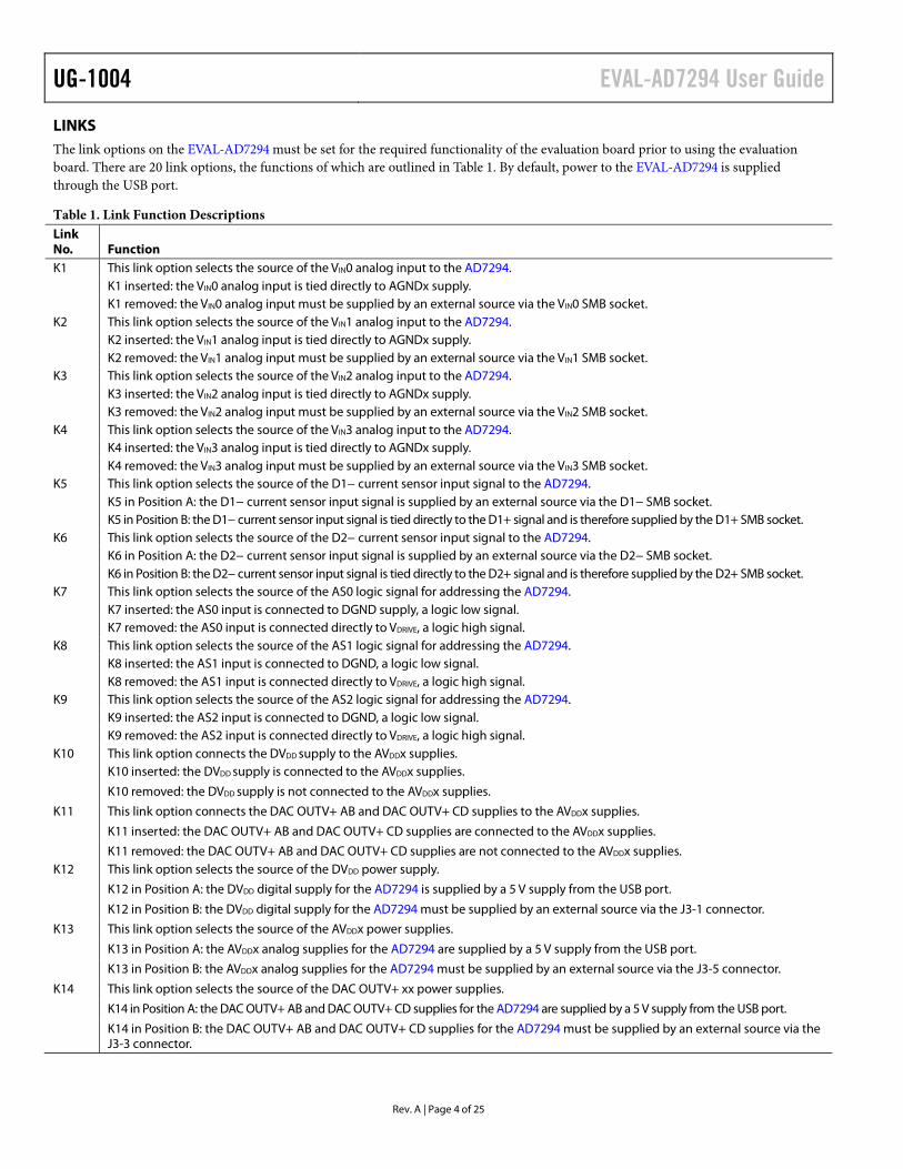
LINKS The link options on the EVAL-AD7294 must be set for the required functionality of the evaluation board prior to using the evaluation board. There are 20 link options, the functions of which are outlined in Table 1. By default, power to the EVAL-AD7294 is supplied through the USB port.
Table 1. Link Function Descriptions Link No. Function K1 This link option selects the source of the VIN0 analog input to the AD7294. K1 inserted: the VIN0 analog input is tied directly to AGNDx supply. K1 removed: the VIN0 analog input must be supplied by an external source via the VIN0 SMB socket. K2 This link option selects the source of the VIN1 analog input to the AD7294. K2 inserted: the VIN1 analog input is tied directly to AGNDx supply. K2 removed: the VIN1 analog input must be supplied by an external source via the VIN1 SMB socket. K3 This link option selects the source of the VIN2 analog input to the AD7294. K3 inserted: the VIN2 analog input is tied directly to AGNDx supply. K3 removed: the VIN2 analog input must be supplied by an external source via the VIN2 SMB socket. K4 This link option selects the source of the VIN3 analog input to the AD7294. K4 inserted: the VIN3 analog input is tied directly to AGNDx supply. K4 removed: the VIN3 analog input must be supplied by an external source via the VIN3 SMB socket. K5 This link option selects the source of the D1− current sensor input signal to the AD7294. K5 in Position A: the D1− current sensor input signal is supplied by an external source via the D1− SMB socket. K5 in Position B: the D1− current sensor input signal is tied directly to the D1+ signal and is therefore supplied by the D1+ SMB socket. K6 This link option selects the source of the D2− current sensor input signal to the AD7294. K6 in Position A: the D2− current sensor input signal is supplied by an external source via the D2− SMB socket. K6 in Position B: the D2− current sensor input signal is tied directly to the D2+ signal and is therefore supplied by the D2+ SMB socket. K7 This link option selects the source of the AS0 logic signal for addressing the AD7294. K7 inserted: the AS0 input is connected to DGND supply, a logic low signal. K7 removed: the AS0 input is connected directly to VDRIVE, a logic high signal. K8 This link option selects the source of the AS1 logic signal for addressing the AD7294. K8 inserted: the AS1 input is connected to DGND, a logic low signal. K8 removed: the AS1 input is connected directly to VDRIVE, a logic high signal. K9 This link option selects the source of the AS2 logic signal for addressing the AD7294. K9 inserted: the AS2 input is connected to DGND, a logic low signal. K9 removed: the AS2 input is connected directly to VDRIVE, a logic high signal. K10 This link option connects the DVDD supply to the AVDDx supplies. K10 inserted: the DVDD supply is connected to the AVDDx supplies.
K10 removed: the DVDD supply is not connected to the AVDDx supplies.
K11 This link option connects the DAC OUTV+ AB and DAC OUTV+ CD supplies to the AVDDx supplies.
K11 inserted: the DAC OUTV+ AB and DAC OUTV+ CD supplies are connected to the AVDDx supplies.
K11 removed: the DAC OUTV+ AB and DAC OUTV+ CD supplies are not connected to the AVDDx supplies. K12 This link option selects the source of the DVDD power supply.
K12 in Position A: the DVDD digital supply for the AD7294 is supplied by a 5 V supply from the USB port.
K12 in Position B: the DVDD digital supply for the AD7294 must be supplied by an external source via the J3-1 connector.
K13 This link option selects the source of the AVDDx power supplies.
K13 in Position A: the AVDDx analog supplies for the AD7294 are supplied by a 5 V supply from the USB port.
K13 in Position B: the AVDDx analog supplies for the AD7294 must be supplied by an external source via the J3-5 connector.
K14 This link option selects the source of the DAC OUTV+ xx power supplies.
K14 in Position A: the DAC OUTV+ AB and DAC OUTV+ CD supplies for the AD7294 are supplied by a 5 V supply from the USB port.
K14 in Position B: the DAC OUTV+ AB and DAC OUTV+ CD supplies for the AD7294 must be supplied by an external source via the J3-3 connector.

EVAL-AD7294 User Guide UG-1004
Rev. A | Page 5 of 25
Link No. Function K15 This link option selects whether the VOUT A signal is filtered prior to being supplied to the VOUT A SMB.
K15 in Position A: the VOUT A signal is filtered by a 100 kΩ resistor and a capacitor. This link option must be used in conjunction with K16 in Position A to provide the output signal to the VOUT A SMB.
K15 in Position B: the VOUT A signal from the AD7294 is connected directly to K16. This link option must be used in conjunction with K16 in Position B to provide the output signal to the VOUT A SMB.
K16 This link option connects the VOUT A signal to the VOUT A SMB. This link must be used in conjunction with K15.
K16 in Position A: the VOUT A signal is filtered by a 100 kΩ resistor and a capacitor. This link option must be used in conjunction with K15 in Position A to provide the output signal to the VOUT A SMB.
K16 in Position B: the VOUT A signal is connected directly from the AD7294 to the VOUT A SMB. This link option must be used in conjunction with K15 in Position B to provide the output signal directly to the VOUT A SMB.
K17 This link option selects whether the VOUT B signal is filtered prior to being supplied to the VOUT B SMB.
K17 in Position A: the VOUT B signal is filtered by a 100 kΩ resistor and a capacitor. This link option must be used in conjunction with K18 in Position A to provide the output signal to the VOUT B SMB.
K17 in Position B: the VOUT B signal is connected directly to K18. This link option must be used in conjunction with K18 in Position B to provide the output signal to the VOUT B SMB.
K18 This link option connects the VOUT B signal to the VOUT B SMB. This link must be used in conjunction with K17.
K18 in Position A: the VOUT B signal is filtered by a 100 kΩ resistor and a capacitor. This link option must must be used in conjunction with K17 in Position A to provide the output signal to the VOUT B SMB.
K18 in Position B: the VOUT B signal is connected directly from the AD7294 to the VOUT B SMB. This link option must be used in conjunction with K17 in Position B to provide the output signal directly to the VOUT B SMB.
K19 This link option must be kept in Position B.
K19 in Position B: Pin 48 is connected directly to the DGND supplies.
K22 This link option selects the source of the VDRIVE supply.
K22 in Position A: the VDRIVE supply of the AD7294 is tied directly to the DVDD supply.
K22 in Position B: the VDRIVE supply of the AD7294 is tied directly to the 3.3 V supply.
Table 2. Default Link Positions Link No. Position Description K1 Removed The analog input signal of the AD7294 is connected directly to the VIN0 SMB. K2 Removed The analog input signal of the AD7294 is connected directly to the VIN1 SMB. K3 Removed The analog input signal of the AD7294 is connected directly to the VIN2 SMB. K4 Removed The analog input signal of the AD7294 is connected directly to the VIN3 SMB. K5 A The D1− current sensor input signal is supplied by an external source via the D1− SMB socket. K6 A The D2− current sensor input signal is supplied by an external source via the D2− SMB socket. K7 Inserted The AS0 input is connected to DGND, a logic low signal. K8 Inserted The AS1 input is connected to DGND, a logic low signal.
K9 Inserted The AS2 input is connected to DGND supply, a logic low signal. K10 Removed The DVDD supply is not connected to the AVDDx supplies. K11 Removed The DAC OUTV+ AB and DAC OUTV+ CD supplies are not connected to the AVDDx supplies. K12 A The DVDD digital supply for the AD7294 is supplied by a 5 V supply from the USB port. K13 A The AVDDx analog supplies for the AD7294 are supplied by a 5 V supply from the USB port. K14 A The DAC OUTV+ AB and DAC OUTV+ CD supplies for the AD7294 are supplied by a 5 V supply from the
USB port. K15 B The VOUT A signal is connected directly to K16. K16 B The VOUT A signal is connected directly from the AD7294 to the VOUT A SMB. K17 B The VOUT B signal is connected directly to K18. K18 B The VOUT B signal is connected directly from the AD7294 to the VOUT B SMB. K19 B Pin 48 is connected directly to DGND supplies. K22 A The VDRIVE supply of the AD7294 is tied directly to the DVDD supply.

UG-1004 EVAL-AD7294 User Guide
Rev. A | Page 6 of 25
SOCKETS There are 24 SMB input/output sockets relevant to the operation of the AD7294 on this evaluation board. All of the sockets apply an externally generated signal to the EVAL-AD7294 evaluation board or access an output signal from the AD7294. When operating the EVAL-AD7294 with a USB power source, the only external sockets necessary are the sockets that supply the input signals to the analog inputs of the ADC (VIN0, VIN1, VIN2, and VIN3), the current sensor input signals (RS1(+) and RS2(+)), and the temperature sensor input signals (D1+, D1−, D2+, and D2−).
The DAC outputs can be accessed via the VOUT A, VOUT B, VOUT C, and VOUT D SMBs, and the current senor overrange outputs can be accessed via the ISENSE1 and ISENSE2 SMBs. The functions of all the SMB sockets on the AD7294 evaluation board are outlined in Table 3.
CONNECTORS There are two connectors (J2 and J3) on the EVAL-AD7294, as outlined in Table 4.
Table 3. Socket Functions Socket Function RS1(+), RS2(+), RS1(−), RS2(−)
Subminiature bayonet nut connector (BNC) sockets for the input signals that are applied directly to the RSx(+) and RSx(−) inputs in the absence of a sense resistor.
VIN0, VIN1, VIN2, VIN3 Subminiature BNC sockets for the analog input signals that are applied directly to the VIN0, VIN1, VIN2, and VIN3 pins, respectively
D1+, D2+ Subminiature BNC sockets for the input signals that are applied directly to the D1+, and D2+ pins, respectively D1−, D2− Subminiature BNC sockets for the input signals that are applied directly to the D1−, and D2− pins, respectively ISENSE1, ISENSE2 Subminiature BNC sockets for the ISENSEx output signals that are generated by the AD7294 VOUT A, VOUT B, VOUT C, VOUT D Subminiature BNC sockets for the VOUT x output signals that are generated by the AD7294 OFFSET IN A, OFFSET IN B, OFFSET IN C, OFFSET IN D
Subminiature BNC sockets for the OFFSET IN x input signals that are applied to the AD7294
REFIN DAC Subminiature BNC sockets that enable an external reference source to be supplied to the DACs on the AD7294 REFIN ADC Subminiature BNC sockets that enable an external reference source to be supplied to the ADC on the AD7294
Table 4. Connector Functions Connector Function J2-1 External RS2(+) power connector J2-2 External RS1(+) power connector J3-1 External DVDD power connector J3-2 DGND power connector J3-3 External DAC OUTV+ AB and DAC OUTV+ CD power connector J3-4 AGNDx power connector J3-5 External AVDDx power connector J3-6 AGNDx power connector
EVAL-AD7294 User Guide UG-1004
Rev. A | Page 7 of 25
GETTING STARTED SUMMARY OF THE SETUP SEQUENCE This installation uses the Windows XP® operating system. The installation consists of the following steps, described in detail in the sections that follow.
1. Install the AD7294 GUI software. Do not connect the USB cable from the AD7294 evaluation board to the computer USB port at this stage. See the Installing the Software section for more information.
2. Connect the USB port from the computer to the EVAL-AD7294, and run the USB installation wizard. See the Connecting the USB Cable section for more information.
3. Ensure the appropriate links are made throughout the evaluation board, and then power up the evaluation board. See the Verifying the Links and Powering Up the Evaluation Board section for more information.
4. Use the evaluation board software to operate the various functions on the AD7294.
INSTALLING THE SOFTWARE 1. Place the evaluation board software installation CD into
the CD drive of the computer and open My Computer. 2. Double-click Disc Drive (D:). 3. In the AD7294 Installation folder, double-click Setup.exe
(see Figure 2) and install the software onto the hard drive of the computer by using the installation wizard (see Figure 3). It is recommended to install the software in the default destination folder path, C:\Program Files\Analog Devices Inc\AD7294.
0792
2-00
2
Figure 2. Select Setup.exe File
0792
2-00
3
Figure 3. AD7294 Choose Destination Location Window
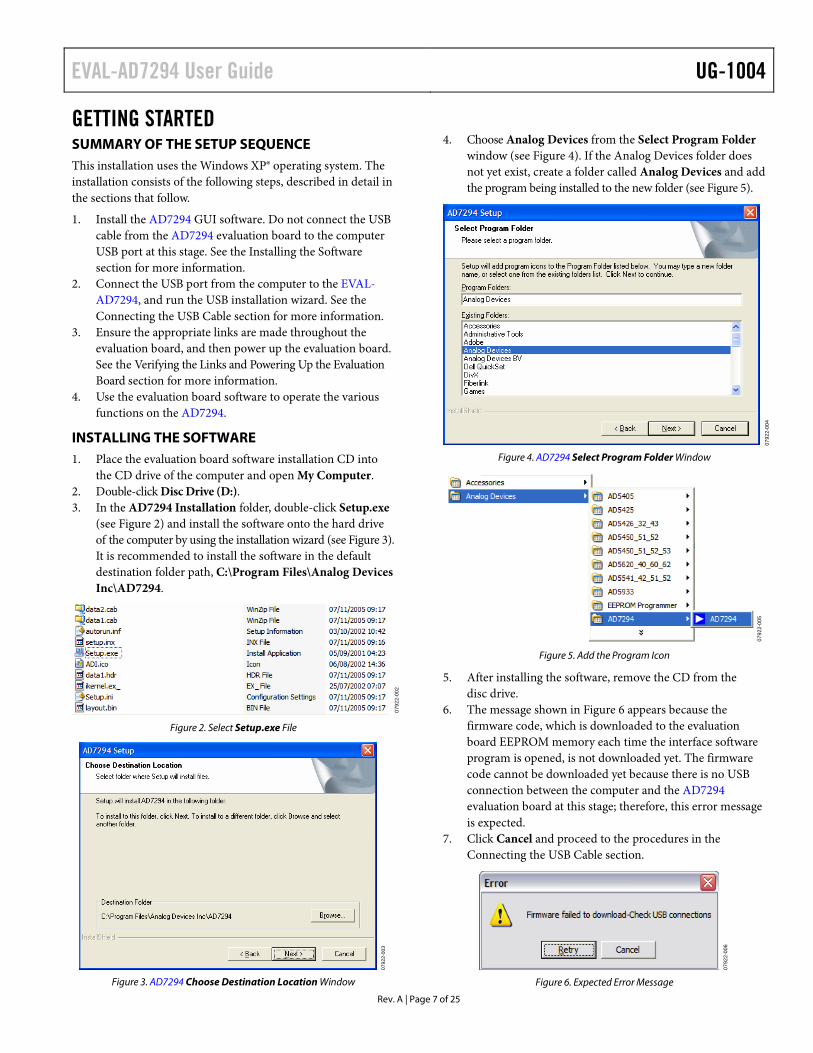
4. Choose Analog Devices from the Select Program Folder window (see Figure 4). If the Analog Devices folder does not yet exist, create a folder called Analog Devices and add the program being installed to the new folder (see Figure 5).
0792
2-00
4
Figure 4. AD7294 Select Program Folder Window
0792
2-00
5
Figure 5. Add the Program Icon
5. After installing the software, remove the CD from the disc drive.
6. The message shown in Figure 6 appears because the firmware code, which is downloaded to the evaluation board EEPROM memory each time the interface software program is opened, is not downloaded yet. The firmware code cannot be downloaded yet because there is no USB connection between the computer and the AD7294 evaluation board at this stage; therefore, this error message is expected.
7. Click Cancel and proceed to the procedures in the Connecting the USB Cable section.
0792
2-00
6
Figure 6. Expected Error Message

UG-1004 EVAL-AD7294 User Guide
Rev. A | Page 8 of 25
CONNECTING THE USB CABLE 1. Plug the USB cable into the computer USB port and into
the AD7294 evaluation board. 2. A message indicates a USB device has been detected and
that new hardware has been found (see Figure 7).
0792
2-00
7
Figure 7. Found New Hardware Message
3. The Found New Hardware Wizard window appears (see Figure 8). This wizard installs software for the EVAL-AD7294 evaluation kit.
4. Select Install the software automatically (Recommended) (see Figure 8), and then click Next to continue.
0792
2-00
8
Figure 8. Found New Hardware Wizard Window
5. A warning message appears (see Figure 9), indicating the EVAL-AD7294 hardware that is installing does not pass the Windows® logo testing to verify compatibility with Windows XP. This error appears because this is an evaluation setup installation and is not meant to be used in a production environment.
6. Click Continue Anyway and click Finish.
0792
2-00
9
Figure 9. Expected Warning Message
7. The Found New Hardware message appears, alerting the user that the hardware is installed and ready to use (see Figure 10).
0792
2-01
0
Figure 10. New Hardware Is Ready to Use Message
To learn more about verifying and troubleshooting the install-lation, refer to the Frequently Asked Questions section.
VERIFYING THE LINKS AND POWERING UP THE EVALUATION BOARD Take care before applying power and signals to the evaluation board. It is necessary to ensure all links are positioned correctly for the chosen operating mode.
Table 2 shows the default positions the links are set to when the evaluation board is packaged. There are two different modes in which to operate the evaluation board. The user can either operate the EVAL-AD7294 with an external supply or use the supply provided by the USB port. However, when the EVAL-AD7294 is shipped, it is assumed that the user operates with the power provided by the USB port.
EVAL-AD7294 User Guide UG-1004
Rev. A | Page 9 of 25
When using the power supply from the USB port,
1. Ensure all links are positioned correctly for the chosen operating mode. It is important to note the USB cable cannot act as a supply source to the AD7294 if the K10, K11, K12, K13, and K14 links are not inserted.
2. Connect the USB cable to the computer and to the evaluation board. Power is supplied automatically from the USB port to the AD7294 if the links are correctly positioned.
When using an external power supply, 1. Ensure all links are positioned correctly for the chosen
operating mode. 2. Make all relevant external power connections before using
the evaluation board software. Supply these signals from an external supply via the power supply connector (J3) on the EVAL-AD7294 or use the on-board ADP3303 precision voltage reference.
3. Plug in the USB cable. If the user does not use the software provided in the evaluation kit and all external supplies are used, the USB cable is not required.
4. Turn on the external power supply.
After powering up the evaluation board, start using the software to evaluate the AD7294. The EVAL-AD7294 must be repowered when the software window is closed; that is, the USB must be disconnected and reinserted.
EVALUATING THE EVAL-AD7294 The evaluation board software allows user to load values to the four DACs in the AD7294, read values from the 9-channel multiplexed ADC and depict these values in a plot, monitor a signal between two limited values, and change the configuration of the device. See the Using the Software section for more detailed information about these functions.

UG-1004 EVAL-AD7294 User Guide
Rev. A | Page 10 of 25
USING THE SOFTWARE MAIN WINDOW After following the procedures in the Getting Started section, the main window, shown in Figure 11, appears upon starting the evaluation software program. Use the drop-down menus in the AD7294 Evaluation Software main window to navigate through the various operational functions of the EVAL-AD7294 evaluation board.
0792
2-01
1
Figure 11. AD7294 Evaluation Software Main Window
Device Menu
The Device menu (see Figure 12) offers three options: Config-uration, Register Map, and Device Address. Select Configuration to change the configuration address, that selects various modes and configurations of the device. Each of these options is examined in more detail in the Configuration Window section. Selecting Register Map provides a user friendly tool to easily check the value of each bit in every readable register address. Selecting Device Address allows the user to choose the I2C slave address upon power-up.
0792
2-01
2
Figure 12. Device Menu of the Main Window
ADC Menu
As shown in Figure 13, the ADC menu accesses three functions: Read Channel, Alert Manager, and External Sensor Calibration. Selecting Read Channel shows some of the functionality options of the ADC. The Alert Manager option analyzes the alert register to check for out-of-limit alerts and the External Sense Calibration option enables calibrating the external temperature sensors.
0792
2-01
3
Figure 13. ADC Menu of the Main Window
DAC Menu
The DAC menu allows the user to load values to any of the four DAC channels.
CONFIGURATION WINDOW The configuration of the various modes and functionalities of the device is carried out in the Configuration window. Two tabs are available in this window. The first tab, Power Down, offers various power-down mode options. Click the appropriate check box to select the desired option (see Figure 14), and the equivalent bit automatically sets in the configuration register in the AD7294. Check the bit is set using the register map.
0792
2-01
4
Figure 14. Power-Down Modes Available in the Configuration Window
The second tab, Settings, allows the selection of various operating modes available for the AD7294 (see Figure 15).
0792
2-01
5
Figure 15. Modes Available in the Settings Tab of the Configuration Window

EVAL-AD7294 User Guide UG-1004
Rev. A | Page 11 of 25
REGISTER MAP WINDOW The Register Map window reads any register that can be accessed by the address pointer register. For more information about the address pointer register, see the AD7294 data sheet. Each data register, whether 8 bits or 16 bits, is accessed by the software, and displays the contents in the Register Map window. The window provides details about the function or mode represented by each bit, shown in Figure 16. The Register Details box of this window allows the user to see the decimal value of a register and the position in the address pointer register.
DEVICE ADDRESS INFORMATION WINDOW The serial bus address byte is the first byte that the user writes to the device. The five LSBs of this byte are user-programmable on the evaluation board, with the I2C address determined by the logic state of the AS1, AS2, and AS3 pins (that is, by connecting jumpers to the AS1, AS2, and AS3 pins). For more information about the I2C interface, see the AD7294 data sheet. With any jumper inserted, the signal is grounded; therefore, the K7 jumper reads 0 with a jumper inserted (see Figure 17).
0792
2-01
6
Figure 16. Register Map Window
0792
2-01
7
This is the I2C Slave Address of the AD7294. The Address can bechanged by inserting or removing the jumpers K9, K8 and K7 priorto power up.Once the part is powered up, the I2CAddress cannot be changed.
Figure 17. Device Address Information Window

UG-1004 EVAL-AD7294 User Guide
Rev. A | Page 12 of 25
READ CHANNEL WINDOW To read the converted analog signals from the 9-channel ADC, select Read Channel in the ADC menu of the main window. The Read Channel window appears, allowing the user to select which channel to access by clicking one of the nine tabs at the top of the window. There are two methods of reading the converted data. Clicking Read Single Value adds one value at a time to a list, whereas clicking Start Scope stores the values in an array to draw the scope plot. Various user options are also available in the Read Channel window (see Figure 18).
The differential mode can be selected for Channel 1 to Channel 4 (VIN0 to VIN3) by clicking the Differential Mode button. This mode allows analog input signals on Channel 1 and Channel 2 to become a differential input pair and input signals on Channel 3 and Channel 4 to form another differential pair. In addition, in differential mode it is possible to use the input channels in pseudo-differential mode when an offset from ground is provided on one of the differential inputs, thus enabling the advantage of canceling common-mode voltages.
To zoom in on a signal in the plot, use the arrows in the corners of the graphing tool (circled in Figure 18). To activate the DATAHIGH and DATALOW functions and the hysteresis functions, click the arrow in the top left of the window (circled in red in Figure 18). Two tab options appear on the right side of the window: the Limits tab and the Vref tab. With the Limits tab selected, the user can set up predetermined limits for the converted input signals. The alert bit is flagged and the relative bit in the alert status register is triggered when the input signal becomes greater than the DATAHIGH limit or less than the DATALOW limit. Note that the alert bit does not turn off until the signal is within the specified hysteresis limits (see the circled signal in Figure 19). To benefit from this option, the user must click Alert Manager at the lower right of the window or select the Alert Manager from the ADC menu in the main window of the evaluation software.
0792
2-01
8
Figure 18. Read Channel Window
0792
2-01
9
Figure 19. Data Limit Function

UG-1004 EVAL-AD7294 User Guide
Rev. A | Page 13 of 25
If the hysteresis register is filled with all 1s, the device operates in minimum/maximum mode. The DATAHIGH register stores the maximum conversion result and the DATALOW register stores the minimum conversion result.
The minimum/maximum mode is enabled by clicking the Min/Max Mode button or by dragging the slider in the Hysteresis Value box up to 4095 in the Limits tab (see Figure 19).
The Vref tab (see Figure 21) allows the user to select an external reference for the ADC with two decimals of accuracy.
The current sense tabs (ISENSE1 and ISENSE2) in the Read Channel window allow the user to enter a desired RSENSE value—from 10 mΩ up to 999 mΩ—to use on the evaluation board (see Figure 22), or, if a larger RSENSE resistor is required, scale the y-axis results in proportion to the RSENSE on the EVAL-AD7294. For example, if an RSENSE of 1.1 Ω is required with a 10 mΩ RSENSE on the EVAL-AD7294, divide the y-axis result by 110 or divide the y-axis scale by 20.
0792
2-02
0
Figure 20. Minimum/Maximum Mode of Operation for the Read Channel Window
0792
2-02
1
Figure 21. Vref Tab of the Read Channel Window
0792
2-02
2
Figure 22. ISENSE1 Tab of the Read Channel Window

UG-1004 EVAL-AD7294 User Guide
Rev. A | Page 14 of 25
ALERT MANAGER WINDOW The Alert Manager window analyzes the alert register to check for any alert events. An alert is signaled on a specific channel when the input analog signal becomes greater than or less than the specified limits. The software changes the marker from the color gray to the color red to convey an alert (see Figure 23). Due to timing constraints inherent in the software and Windows, an alert can be checked every 100 ms to 2000 ms. The period of time can be controlled using the scroll bar at the bottom of the window. The entire contents of the alert register can be cleared by writing all 1s to the alert status register.
The Alert Manager window also allows the autocycle mode to be selected for the four uncommitted analog input channels as well as the two ISENSE channels. The desired channels can be selected by clicking the Autocycle Mode button in the Alert Manager window and then selecting the appropriate check boxes in the Channels box (see Figure 24). Consult the Register Map window for the assignment of each alert bit into the three alert registers.
0792
2-02
3
Figure 23. Alert Manager Window
0792
2-02
4
Figure 24. Autocycle Mode Checking in the Alert Manager Window

EVAL-AD7294 User Guide UG-1004
Rev. A | Page 15 of 25
EXTERNAL TEMPERATURE SENSOR OFFSET CALIBRATION WINDOW The External Temperature Sensor Offset Calibration window calibrates the temperature, correcting errors attributable to noise that may be coupled onto the Dx+ and Dx− pins of the remote temperature sensors. Both TSENSE1 and TSENSE2 can be offset using the gauges shown in Figure 25. The sliders can be adjusted from between −32°C and +31.75°C, and the resulting value is automatically subtracted as a twos complement 8-bit reading from every temperature measurement before the value is stored in the relative result register.
0792
2-02
5
Figure 25. External Temperature Sensor Offset Calibration Window
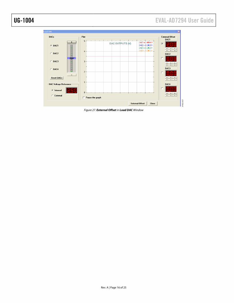
LOAD DAC WINDOW The DAC tab in the main window contains only the Load DAC Channel window. The Load DAC window allows the user to select any of the four DAC outputs and load a value to them, using the slider on the left side of the window (see Figure 26). All four DACs can be loaded simultaneously. Note that the DAC output is twice the reference voltage when no offset is applied.
An external offset can be applied to the selected DAC by clicking the External Offset button at the bottom of the Load DAC window. The External Offset box opens on the right side of the Load DAC window.
The user can select an offset of greater than or equal to the minimum offset input, 1.67 V. The resulting DAC output shown in the Plot box is given by
VOUT = 3VOFFSET − 5 + VDAC
Figure 27 shows an external voltage of 2.0 V being applied to DAC1. As a result, the DAC1 output is approximately 3.5 V, as determined by the previous formula and shown in the Plot box of Figure 27. Select the appropriate check box in the External Offset box in the Load DAC window to load the offset. Additionally, if an offset voltage is applied to the OFFSET IN x pin to achieve DAC output voltages in excess of 5 V, an external DAC_OUTPUT_V+ supply of up to 16.5 V is required via Terminal J3.3. For more details, refer to the AD7294 data sheet.
0792
2-02
6
Figure 26. Load DAC Window
UG-1004 EVAL-AD7294 User Guide
Rev. A | Page 16 of 25
0792
2-02
7
Figure 27. External Offset in Load DAC Window
EVAL-AD7294 User Guide UG-1004
Rev. A | Page 17 of 25
FREQUENTLY ASKED QUESTIONS HOW CAN A USER CONFIRM THE HARDWARE HAS BEEN CORRECTLY INSTALLED ON THE COMPUTER? Right-click My Computer and left-click Properties. On the Hardware tab, click Device Manager (see Figure 28).
0792
2-02
8
Figure 28. Accessing the Device Manager
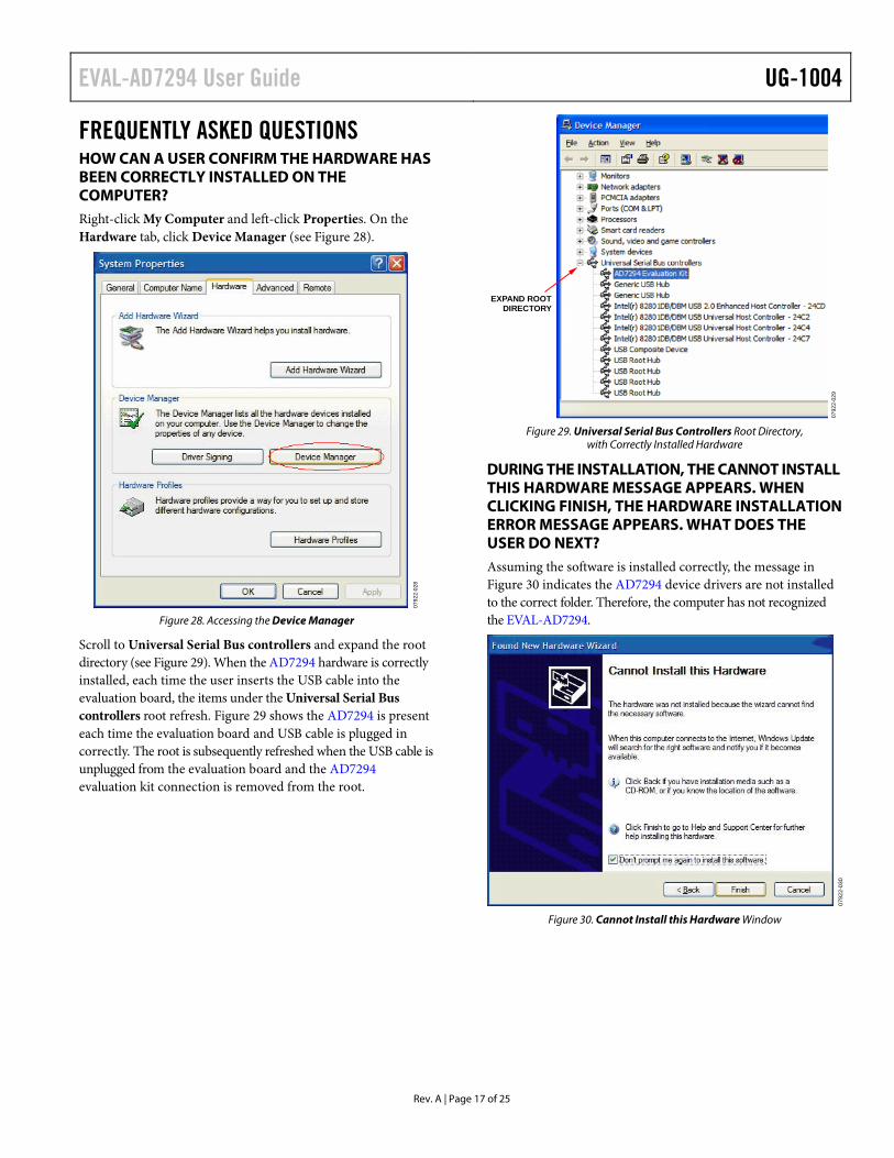
Scroll to Universal Serial Bus controllers and expand the root directory (see Figure 29). When the AD7294 hardware is correctly installed, each time the user inserts the USB cable into the evaluation board, the items under the Universal Serial Bus controllers root refresh. Figure 29 shows the AD7294 is present each time the evaluation board and USB cable is plugged in correctly. The root is subsequently refreshed when the USB cable is unplugged from the evaluation board and the AD7294 evaluation kit connection is removed from the root.
0792
2-02
9
EXPAND ROOTDIRECTORY
Figure 29. Universal Serial Bus Controllers Root Directory,
with Correctly Installed Hardware
DURING THE INSTALLATION, THE CANNOT INSTALL THIS HARDWARE MESSAGE APPEARS. WHEN CLICKING FINISH, THE HARDWARE INSTALLATION ERROR MESSAGE APPEARS. WHAT DOES THE USER DO NEXT? Assuming the software is installed correctly, the message in Figure 30 indicates the AD7294 device drivers are not installed to the correct folder. Therefore, the computer has not recognized the EVAL-AD7294.
0792
2-03
0
Figure 30. Cannot Install this Hardware Window
UG-1004 EVAL-AD7294 User Guide
Rev. A | Page 18 of 25
0792
2-03
1
Figure 31. Hardware Installation Error Message
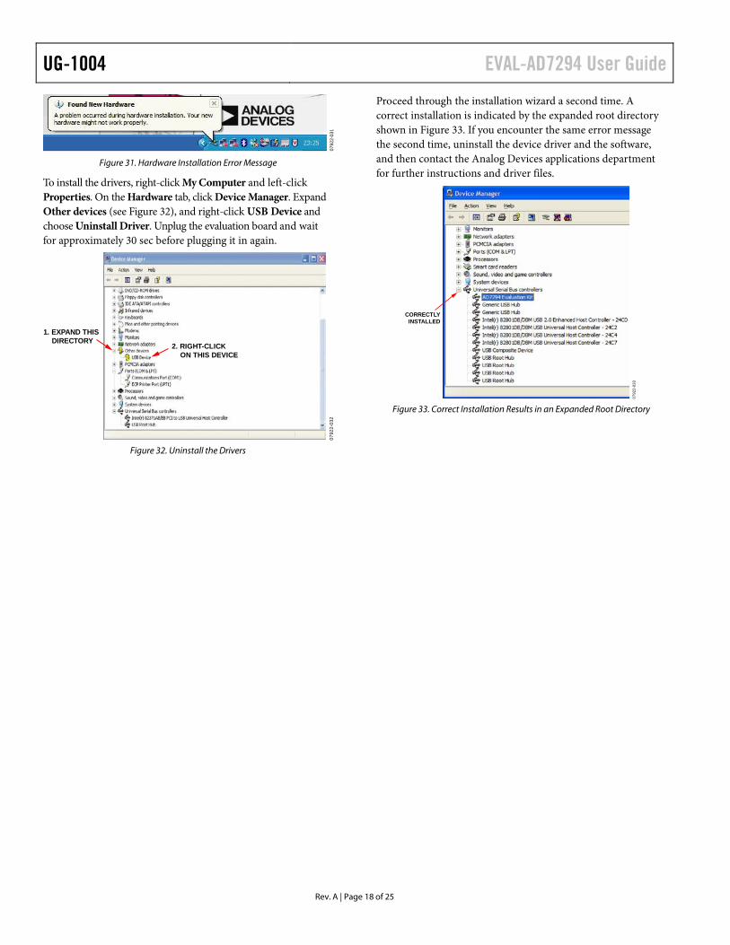
To install the drivers, right-click My Computer and left-click Properties. On the Hardware tab, click Device Manager. Expand Other devices (see Figure 32), and right-click USB Device and choose Uninstall Driver. Unplug the evaluation board and wait for approximately 30 sec before plugging it in again.
0792
2-03
21. EXPAND THIS DIRECTORY
2. RIGHT-CLICK ON THIS DEVICE
Figure 32. Uninstall the Drivers
Proceed through the installation wizard a second time. A correct installation is indicated by the expanded root directory shown in Figure 33. If you encounter the same error message the second time, uninstall the device driver and the software, and then contact the Analog Devices applications department for further instructions and driver files.
0792
2-03
3
CORRECTLYINSTALLED
Figure 33. Correct Installation Results in an Expanded Root Directory
EVAL-AD7294 User Guide UG-1004
Rev. A | Page 19 of 25
LAYOUT AND CONFIGURATION GUIDELINES POWER SUPPLY DECOUPLING AND GROUNDING When accuracy is important in a circuit, carefully consider the power supply and ground return layout on the EVAL-AD7294. The printed circuit board containing the AD7294 must have separate analog and digital sections, each having an area of the EVAL-AD7294. If the AD7294 is in a system where other devices require an AGND to DGND connection, the connection must be made at only one point. This ground point must be as close as possible to the AD7294.
The power supply to the AD7294 must be decoupled with 10 µF tantalum capacitor and 0.1 µF ceramic capacitor. The capacitors must be placed as close as possible to the device, with the 0.1 µF ceramic capacitor closer to the device than the tantalum capacitor. In addition, it is important that the 0.1 µF capacitor has low effective series resistance (ESR) and low effective series inductance (ESI).
The 0.1 µF capacitor provides a low impedance path to ground for high frequencies caused by transient currents due to internal logic switching.
The power supply line must have as large a trace as possible to provide a low impedance path and to reduce glitch effects on the supply line. Clocks and other components with fast-switching digital signals must be shielded from other parts of the EVAL-AD7294 by a digital ground. Avoid crossover of digital and analog signals if possible. When traces cross on opposite sides of the EVAL-AD7294, ensure that they run at right angles to each other to reduce feedthrough effects on the EVAL-AD7294. The most efficient board layout technique is the microstrip technique, where the component side of the EVAL-AD7294 is dedicated to the ground plane only and the signal traces are placed on the solder side; however, this is not always possible with a 2-layer board.

UG-1004 EVAL-AD7294 User Guide
Rev. A | Page 20 of 25
EVALUATION BOARD SCHEMATICS AND ARTWORK
07922-034
Figure 34. Evaluation Board Schematic

EVAL-AD7294 User Guide UG-1004
Rev. A | Page 21 of 25
0792
2-03
5
Figure 35. Evaluation Board Schematic, Auxiliary Blocks
UG-1004 EVAL-AD7294 User Guide
Rev. A | Page 22 of 25
3100mil
4950mil
0792
2-03
6
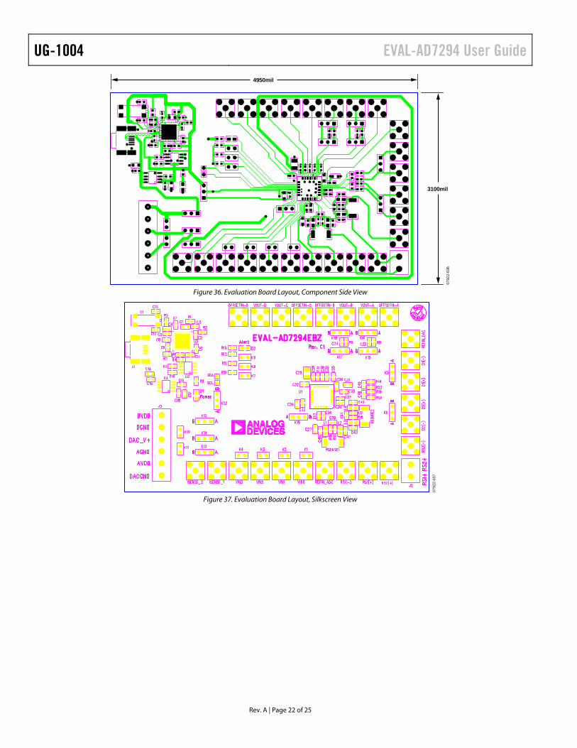
Figure 36. Evaluation Board Layout, Component Side View
0792
2-03
7
Figure 37. Evaluation Board Layout, Silkscreen View
EVAL-AD7294 User Guide UG-1004
Rev. A | Page 23 of 25
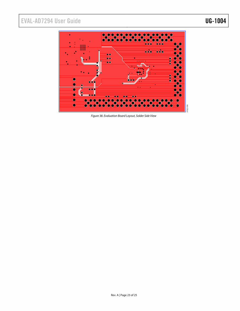
0792
2-03
8
Figure 38. Evaluation Board Layout, Solder Side View

UG-1004 EVAL-AD7294 User Guide
Rev. A | Page 24 of 25
ORDERING INFORMATION BILL OF MATERIALS
Table 5. Qty Reference Designator Description Supplier/Part Number1 24 C2, C3, C5, C6, C7, C8, C9, C10, C11, C15,
C16, C18, C19, C20, C22, C25, C28, C30, C31, C32, C33, C35, C36, C37, C38
0.1 µF capacitor FEC 136-2556
1 C47 10 nF capacitor FEC 141-4026 3 C40, C45, C46 1 nF capacitor FEC 141-4605 2 C39, C41 1 µF capacitor FEC 128-8202 1 C4 2.2 µF capacitor Digi-Key 490-1552-1-ND 2 C12, C13 22 pF capacitor FEC 722-005 4 C23, C24, C42, C48 Not inserted Not inserted 8 C1, C14, C17, C21, C26, C27, C29, C34 10 µF capacitor FEC 197-130 5 R3, R13, R14, R16, R17 0 Ω resistor FEC 933-1662 4 R1, R2, R8, R9 100 kΩ resistor FEC 933-0402 4 R18, R19, R20, R22 100 Ω resistor FEC 146-9862 1 R7 10 kΩ resistor FEC 933-0399 2 R6, R15 1 kΩ resistor FEC 933-0380 5 R4, R5, R10, R11, R12 2.2 kΩ resistor FEC 933-0810 2 RSENSE1, RSENSE2 200 mΩ resistor FEC 110-0068 2 D1, D2 LED FEC 579-0852 1 U1 12-bit, multichannel, ADC, DACs, temperature sensors,
and current sensors Analog Devices AD7294BSUZ
1 Y1 24 MHz SMD quartz crystal FEC 950-9658 1 U4 High accuracy, anyCAP®, 200 mA, low dropout linear
regulator Analog Devices ADP3303ARZ-3.3
1 U2 64k I2C serial EEPROM FEC 975-8070 1 U3 USB microcontroller high speed USB peripheral
controller Digi-Key 428-1669-ND
24 D1+, D1−, D2+, D2−, ISENSE1, ISENSE2, OFFSET IN A, OFFSET IN B, OFFSET IN C, OFFSET IN D, REFIN ADC, REFIN DAC, RS1(+), RS1(−), RS2(+), RS2(−), VIN0, VIN1, VIN2, VIN3, VOUT A, VOUT B, VOUT C, VOUT D
SMB connector FEC 120-6013
1 J2 Power terminal block, connector, two pins FEC 151-789 1 J3 Power terminal block, connector, six pins FEC 117-7890 9 K1, K2, K3, K4, K7, K8, K9, K10, K11 Jumper 1 FEC 102-2247 11 K5, K6, K12, K13, K14, K15, K16, K17,
K18, K19, K22 Jumper 2 FEC 102-2244
1 J1 USB connector FEC 978-6490
1 FEC = Farnell Electronics, Inc.
UG-1004 EVAL-AD7294 User Guide
Rev. A | Page 25 of 25
NOTES
I2C refers to a communications protocol originally developed by Philips Semiconductors (now NXP Semiconductors).
ESD Caution ESD (electrostatic discharge) sensitive device. Charged devices and circuit boards can discharge without detection. Although this product features patented or proprietary protection circuitry, damage may occur on devices subjected to high energy ESD. Therefore, proper ESD precautions should be taken to avoid performance degradation or loss of functionality.
Legal Terms and Conditions By using the evaluation board discussed herein (together with any tools, components documentation or support materials, the “Evaluation Board”), you are agreeing to be bound by the terms and conditions set forth below (“Agreement”) unless you have purchased the Evaluation Board, in which case the Analog Devices Standard Terms and Conditions of Sale shall govern. Do not use the Evaluation Board until you have read and agreed to the Agreement. Your use of the Evaluation Board shall signify your acceptance of the Agreement. This Agreement is made by and between you (“Customer”) and Analog Devices, Inc. (“ADI”), with its principal place of business at One Technology Way, Norwood, MA 02062, USA. Subject to the terms and conditions of the Agreement, ADI hereby grants to Customer a free, limited, personal, temporary, non-exclusive, non-sublicensable, non-transferable license to use the Evaluation Board FOR EVALUATION PURPOSES ONLY. Customer understands and agrees that the Evaluation Board is provided for the sole and exclusive purpose referenced above, and agrees not to use the Evaluation Board for any other purpose. Furthermore, the license granted is expressly made subject to the following additional limitations: Customer shall not (i) rent, lease, display, sell, transfer, assign, sublicense, or distribute the Evaluation Board; and (ii) permit any Third Party to access the Evaluation Board. As used herein, the term “Third Party” includes any entity other than ADI, Customer, their employees, affiliates and in-house consultants. The Evaluation Board is NOT sold to Customer; all rights not expressly granted herein, including ownership of the Evaluation Board, are reserved by ADI. CONFIDENTIALITY. This Agreement and the Evaluation Board shall all be considered the confidential and proprietary information of ADI. Customer may not disclose or transfer any portion of the Evaluation Board to any other party for any reason. Upon discontinuation of use of the Evaluation Board or termination of this Agreement, Customer agrees to promptly return the Evaluation Board to ADI. ADDITIONAL RESTRICTIONS. Customer may not disassemble, decompile or reverse engineer chips on the Evaluation Board. Customer shall inform ADI of any occurred damages or any modifications or alterations it makes to the Evaluation Board, including but not limited to soldering or any other activity that affects the material content of the Evaluation Board. Modifications to the Evaluation Board must comply with applicable law, including but not limited to the RoHS Directive. TERMINATION. ADI may terminate this Agreement at any time upon giving written notice to Customer. Customer agrees to return to ADI the Evaluation Board at that time. LIMITATION OF LIABILITY. THE EVALUATION BOARD PROVIDED HEREUNDER IS PROVIDED “AS IS” AND ADI MAKES NO WARRANTIES OR REPRESENTATIONS OF ANY KIND WITH RESPECT TO IT. ADI SPECIFICALLY DISCLAIMS ANY REPRESENTATIONS, ENDORSEMENTS, GUARANTEES, OR WARRANTIES, EXPRESS OR IMPLIED, RELATED TO THE EVALUATION BOARD INCLUDING, BUT NOT LIMITED TO, THE IMPLIED WARRANTY OF MERCHANTABILITY, TITLE, FITNESS FOR A PARTICULAR PURPOSE OR NONINFRINGEMENT OF INTELLECTUAL PROPERTY RIGHTS. IN NO EVENT WILL ADI AND ITS LICENSORS BE LIABLE FOR ANY INCIDENTAL, SPECIAL, INDIRECT, OR CONSEQUENTIAL DAMAGES RESULTING FROM CUSTOMER’S POSSESSION OR USE OF THE EVALUATION BOARD, INCLUDING BUT NOT LIMITED TO LOST PROFITS, DELAY COSTS, LABOR COSTS OR LOSS OF GOODWILL. ADI’S TOTAL LIABILITY FROM ANY AND ALL CAUSES SHALL BE LIMITED TO THE AMOUNT OF ONE HUNDRED US DOLLARS ($100.00). EXPORT. Customer agrees that it will not directly or indirectly export the Evaluation Board to another country, and that it will comply with all applicable United States federal laws and regulations relating to exports. GOVERNING LAW. This Agreement shall be governed by and construed in accordance with the substantive laws of the Commonwealth of Massachusetts (excluding conflict of law rules). Any legal action regarding this Agreement will be heard in the state or federal courts having jurisdiction in Suffolk County, Massachusetts, and Customer hereby submits to the personal jurisdiction and venue of such courts. The United Nations Convention on Contracts for the International Sale of Goods shall not apply to this Agreement and is expressly disclaimed.
©2009–2016 Analog Devices, Inc. All rights reserved. Trademarks and registered trademarks are the property of their respective owners. UG07922-0-8/16(A)