EMC Guidelines
17
EMC Improvement Guidelines Introduction High-speed digital Integrated Circuits operate in frequency bands where passive com- ponents (PCB, decoupling capacitors, PCB connections, packages, ... ) cannot be considered as ideal – and to the contrary contain, parasitic elements (inductance, resistance, ..). Because their impedances depend on the frequency, the emission lev- els generated by voltage and current drops may not be compliant to the different EMC standards. It is impossible to predict the compliance of a system. However, it is possi- ble to reduce the risk by implementing rules and design techniques in most applications. This application note gives a brief checklist of major points which can degrade EMC and demonstrates how some basic techniques can help to reduce emission levels and harden the electronic system. EMC Definitions Some basic terms are used in this application note and are explained hereafter: • EMC: Electromagnetic Compatibility , the ability of a product to coexist in its intended electromagnetic environment without causing or suffering functional degradation or damage. • EMI: Electromagnetic Interference , a process by which disruptive electromagnetic energy is transmitted from one electronic device to another via radiated or conducted paths (or both). • Radiated: Energy transmitted by the air via antenna or loops. • Conducted: Energy transmitted via solid medium like cables, PCB connections, packages,.... There are three elements in the EMC model to analyze and understand an EMC problem: • A Noise source, a source that generates an electromagnetic perturbation, • A victim, an electronic device that receives a perturbation which causes dysfunctionalities, • A coupling path, a medium that transmits energy from the noise source to the victim. 8051 Microcontrollers Application Note Rev. 4279B– 8051– 08/03
-
Upload
hemantgirdhar -
Category
Documents
-
view
229 -
download
0
Transcript of EMC Guidelines

872019 EMC Guidelines
httpslidepdfcomreaderfullemc-guidelines 117
EMC Improvement Guidelines
Introduction
High-speed digital Integrated Circuits operate in frequency bands where passive com-ponents (PCB decoupling capacitors PCB connections packages ) cannot beconsidered as ideal ndash and to the contrary contain parasitic elements (inductanceresistance ) Because their impedances depend on the frequency the emission lev-els generated by voltage and current drops may not be compliant to the different EMCstandards It is impossible to predict the compliance of a system However it is possi-ble to reduce the risk by implementing rules and design techniques in most
applications This application note gives a brief checklist of major points which candegrade EMC and demonstrates how some basic techniques can help to reduceemission levels and harden the electronic system
EMC Definitions
Some basic terms are used in this application note and are explained hereafterbull EMC Electromagnetic Compatibility the ability of a product to coexist in its intended
electromagnetic environment without causing or suffering functional degradation or damage
bull EMI Electromagnetic Interference a process by which disruptive electromagnetic energy is
transmitted from one electronic device to another via radiated or conducted paths (or both)
bull Radiated Energy transmitted by the air via antenna or loops
bull Conducted Energy transmitted via solid medium like cables PCB connections
packagesThere are three elements in the EMC model to analyze and understand an EMCproblembull A Noise source a source that generates an electromagnetic perturbation
bull A victim an electronic device that receives a perturbation which causes dysfunctionalities
bull A coupling path a medium that transmits energy from the noise source to the victim
8051
Microcontrollers
Application Note
Rev 4279Bndash 8051ndash 0803
872019 EMC Guidelines
httpslidepdfcomreaderfullemc-guidelines 217
2 EMC Guidelines 4279Bndash 8051ndash 0803
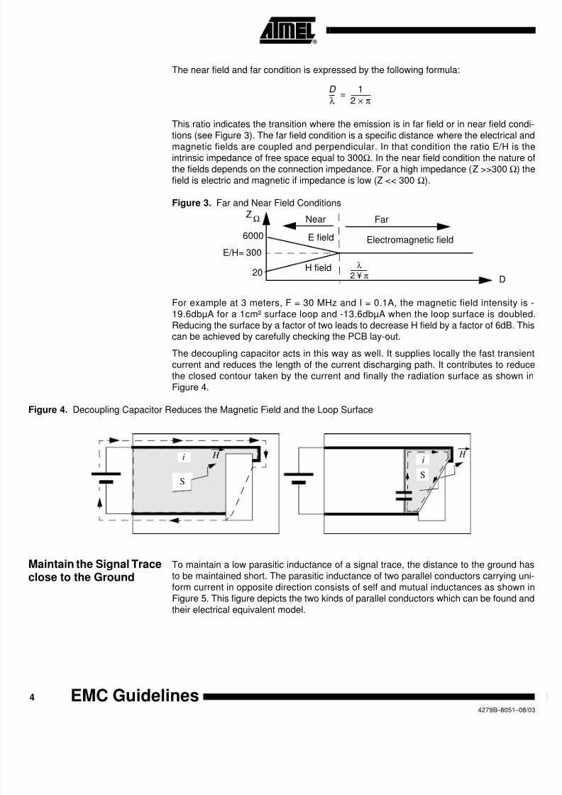
Figure 1 shows the topology of an EMC environment A noise source drives a currenti(t) This current flows through the left coupling path (PCB connection for example) andcauses voltage drops This voltage perturbation is transmitted to the victim through theright coupling path and can cause a dysfunctionnality if the level is high enough
Figure 1 Elements of EMC Environment
To significantly improve the EMC quality of the design the EMC environment throughthese elements have to be analyzed
Basic Checklist to be
Compliant with EMC
The basic rules to decrease the conducted and radiated emissions through the power-supply are to
bull Reduce the speed of the system
ndash Choose the lowest system clock frequency
ndash Adapt the technology to the system constraints
bull Reduce all the magnetic loops of the Printed Circuit Board
ndash Decrease the surface of the magnetic loops
ndash Maintain the signal trace closed to the ground
ndash Shorten the loops around the oscillator and crystal
bull Cancel H field
ndash Opposite magnetic loops
ndash Choose a package with a VCC and VSS pins close together
ndash Choose a package with several VSS and VCC pins connected in oppositeside
bull Reduce the parasitic inductance of all devices (PCB traces package capacitors)
ndash Increase the PCB connection widths
ndash Use ground and power planes
ndash Adapt the decoupling capacitors to the working frequency of ICrsquos
ndash Shorten the capacitor connection length
ndash Select the smaller package
bull Reduce the Equivalent Series Resistance (ESR)
ndash Put identical capacitors in parallel to reduce the ESR
ndash Choose COG and NPO dielectric types
All theses rules are detailed in the following sections
i(t)
Coupling paths
Noise Source Victim
v(t)
+5V
872019 EMC Guidelines
httpslidepdfcomreaderfullemc-guidelines 317
872019 EMC Guidelines
httpslidepdfcomreaderfullemc-guidelines 417
872019 EMC Guidelines
httpslidepdfcomreaderfullemc-guidelines 517
5
EMC Guidelines
4279Bndash 8051ndash 0803
Figure 5 Structure of a Parasitic Inductance
The total inductance for such topology is equal to
where L1 and L2 are the self-inductance of the individual conductors and Mk is themutual inductance between them If the VCC and VSS are identical then LT is reducedto
If the coefficient of magnetic coupling k between the two conductors is unity the mutualinductance would be equal to the self-inductance of one conductor since
and the total inductance of the closed loop would be zero So to minimize the totalinductance of the complete current path the mutual inductance between the conductorsmust be maximized Therefore the two conductors should be placed as close astogether as possible to minimize the area between them Figure 6 and Figure 7 give themutual inductance for different spacings
Figure 6 Mutual Inductance for l = 10 cm and h = 16 mm
Ground
i
d h
i
d h
a) b)
MkL1
L1-Mk
L1-MkL1 Self inductance
Mk Mutual inductance
L1
LT L1 L2 2 Mk timesndash+=
Mk k L1 L2timestimes=
LT 2 L1 Mk ndash( )times=
Mk L1=
Mk(nH) l=10 cm h=16mm
Mk nH ( ) 200 l 12xh
d ----------
2+ lntimestimes=
i
d h
d(mm)
872019 EMC Guidelines
httpslidepdfcomreaderfullemc-guidelines 617
6 EMC Guidelines 4279Bndash 8051ndash 0803
For this configuration the formula is applicable only if the direct and return currents areflowing through these two traces Figure 7 plots different Mk values for some PCB tracedimensions
Figure 7 Mutual Inductance Versus the Length and the Height of PCB Traces
If there is no dedicated plane for the power it is recommended to maintain as close aspossible the tracks to reduce the surface of loop and the parasitic inductance as shownin Figure 8
Figure 8 The Surface of the VCC and VSS Network has to be Reduced
Shorten the Loops aroundOscillator and Crystal
Figure 9 shows the electrical model of a common oscillator implemented in a microcon-troller At the resonance the fundamental currents i1 and i2 have the same amplitude Inthe closed loop mode the oscillator is stabilized in the saturation region of the amplifierthat generates some harmonics in HF So the output loop (X2 C2 and VSS) has to beoptimized first and then the input loop (X1 C1 and VSS) In both cases they have to beas small as possible
Figure 9 Oscillator Lay-out
Mk(nH) = f(LH)
Thickness and width
Mk(nH) 200 LL L
2H
2++
H ---------------------------------
lntimes L2
H 2
+ H + +
times=
i
d h
are neglected
h(mm)
VCC
VSS
VCC
VSS
i1i2
i0
C2 C1
X1 X2X2
X1
VssC2
C1C
rystal
872019 EMC Guidelines
httpslidepdfcomreaderfullemc-guidelines 717
7
EMC Guidelines
4279Bndash 8051ndash 0803
Cancel the H Field
Opposite MagneticLoops
Identical circuits have to be implemented as in Figure 10 In this type of implementationthe magnetic loop surface is the same and the H field are generated in opposite sidewhich tends to cancel them Other implementations can be used but this one needs onlyone decoupling capacitor for two chips
Figure 10 H Field Cancellation
Choose a Package with aVCC and VSS CloseTogether
When a VSS and VCC pins are close together the magnetic coupling can be close to 08and the mutual inductance can reach the self inductance of one pin and cancel mag-netic field of the total inductance of the VSS and VCC pins This true when ivss and ivcc have the same magnitude and the same phase which is the case for the current flowingthrough a digital core of an IC but not completely true for an output buffer
Figure 11 VSS and VCC Pins Close Together Can Cancel the Hfield
Choose a Package withSeveral VSS and VCCPins Connected inOpposite Side
Double the number of VCC and VSS pins reduce by half the equivalent pin inductanceand decrease down to 6dB the H field If the second pin is mounted in the opposite sidethe H field can be further reduced by 3 to 4 dB because a part of the H field is cancelledas shown in Figure 12 and reported in Figure 13
Figure 12 Double and Opposite VSS Pins Reduce 3 to 4dB the H Field
vcc vcc
vssvss
i1 i2
A1 A2
+ = 0A1 x i1 A2 x i2
VSS
ivss ivcc
VCC
MkL2
L1 Self inductance Mk Mutuel inductance
ivcc
ivss LT L1 L2 2 Mk timesndash+=
Mk k L1 L2timestimes=
VSS
ivss2
ivss2
H
H
872019 EMC Guidelines
httpslidepdfcomreaderfullemc-guidelines 817
8 EMC Guidelines 4279Bndash 8051ndash 0803
Figure 13 Double and Opposite VSS Pins Reduce the Radiated Emissions Down to 10dB
Reduce the Inductance of all Devices (PCB traces package capacitors)
Increase the Width of thePCB Connections
Because the real world is not an ideal a power-supply connection is not a pure short-cir-cuit but a trace with parasitic elements such as resistors and inductors
Figure 14 PCB Trace Modelization
L
d
L PCB length in m
d PCB trace width mm
e PCB trace thickness in mm
e=36microm for typical PCB
d=01mm
d=1mm
d=1cm
PCB Tracewidth L=10cm
01mm 1mm 1cm
Resistance(ohm)
Inductance(nH)
0944 0094 0009
340 258 168
LT
RT
LT microH ( ) 0 2 L Ln 2 Ltimesd e +-------------
0 5 0 22d e +
L-------------times++
timestimes=
RT m Ω( ) 17L
d e times------------times=
Z(f)Ω
F
872019 EMC Guidelines
httpslidepdfcomreaderfullemc-guidelines 917
872019 EMC Guidelines
httpslidepdfcomreaderfullemc-guidelines 1017
10 EMC Guidelines 4279Bndash 8051ndash 0803
load is less than 1 tenth of the minimum wave length Otherwise the PCB acts as a lineor an antenna
Figure 16 VCC and VSS Planes are Equivalent to an LC Model
The PCB capacitor consists in two copper planes with a dielectric inserted between thetwo planes The equivalent capacitor (CPcb ) is evaluated using the formula in Figure 16For example a 10 cm by 10 cm plane with 35microm thickness and separated by 16 mmhas a total inductance of 005 nH and a capacitor equal to 271 pF The frequency reso-nance of the plane is 14 GHz So the power-plane technique is efficient for high
frequencies if the distance between the source and the load is short These plans arenot so efficient in low frequency because the equivalent capacitor is not so high and theimpedance across the circuit increases and the emission levels too In low and mediumfrequency ranges additional decoupling capacitors help to maintain this impedance low
Figure 17 Power-supply Planes Characteristics
The next table shows the value of the PCB inductance for the three configurations seenabove The Vcc and Vss Power plane configuration gives the best result and a largedecoupling capacitor
Table 1 Comparison of PCB inductance for w = 1mm wt = 10cm l = 10cm h = 16mm
l
w
h
er=48
CPcb pF ( ) 8middot
85 er S
h ----timestimes=
LPcb
CPcb
LVcc=LVss=L
L(nH) 5 πtimes l h
w ----timestimes=
w h
l
l=10 cm w=10 cmLVcc(nHcm)
LVss(nHcm)
VCC plane
VSS plane
h(mm)
LPCB=LVcc+LVss
Vcc PCB trace
Vss PCB trace
Vcc PCB trace
Vss plane
Vcc Plane
Vss Plane
Inductance(nH) 115 + 115=230 51 + 08=518 0025 + 0025=005
Capacitance(pF) 5 pF 20 pF 271 pF
872019 EMC Guidelines
httpslidepdfcomreaderfullemc-guidelines 1117
11
EMC Guidelines
4279Bndash 8051ndash 0803
Adapt DecouplingCapacitors to theWorking Frequency
A capacitor is not pure and can be modelized like an RLC circuit The surface mountdevices (SMD) have the smallest internal and external inductances and have to beselected to get the best results Figure 18 shows the equivalent electrical model andplots the frequency response for a SMD 100 nF capacitor The capacitor acts like acapacitor a resistor or an inductor but depends on the frequency bands
bull Medium frequency band 0 Hz to 6 MHz the capacitor is a pure capacitor
bull Resonance frequency 6-7 MHz the capacitor is a pure resistance
bull High frequency gt 7 MHz the capacitor acts as a pure inductance
Figure 18 Self-Resonance Frequency of True Capacitor
The frequency behavior depends on the type of capacitor Table 2 gives the electricalcharacteristics for different capacitors
Table 2 Capacitor Characteristics Comparison
Figure 19 plots the frequency response for different types of capacitors
ESL
C
ESR
Capacitor
Resistance
Inductor
ESL=10nH
C=100nH
ESR=02oHm
1 microF Tantale 100 nF Ceramic 10 nF Ceramic
R 08 008 02
L(nH) 6 3 3
Fr(MHz) 2 71 29
872019 EMC Guidelines
httpslidepdfcomreaderfullemc-guidelines 1217
12 EMC Guidelines 4279Bndash 8051ndash 0803
Figure 19 Plots Versus Frequency of Several Types of Capacitors
Assuming the frequency band of the noise is in the range 10MHz to 100MHz and to be
compliant the network impedance has to be less than -10dBohms Figure 20 plots thepower network impedance versus the frequency and the impact of the decouplingcapacitors on the impedance of the network Five decoupling capacitors have to beadded to be in the -10dBohms specification Each capacitors is calculated to damp thepic of each frequency resonances
Figure 20 Decoupling Effects on the Network
1microF tantale
100nF Ceramic
10nF Ceramic
Z(f)Ω
C=33nF C=33nF + 56nF
F F
872019 EMC Guidelines
httpslidepdfcomreaderfullemc-guidelines 1317
13
EMC Guidelines
4279Bndash 8051ndash 0803
C = 33nF + 56nF + 10nF C = 18nF + 33nF + 56nF + 10nF
C = 1nF + 18nF + 33nF + 56nF + 10nF
872019 EMC Guidelines
httpslidepdfcomreaderfullemc-guidelines 1417
14 EMC Guidelines 4279Bndash 8051ndash 0803
Shorten the CapacitorConnection Length
When the capacitor value is assumed to be constant the resonance frequency dependson the inductance The total inductance of the circuit consists of the intrinsic capacitorinductance and the inductance of the connections The higher the inductance the lowerthe resonance frequency It is recommended to maintain as short as possible the lengthof the connections
Figure 21 Connection Increase the Impedance in HF
Figure 21 plots the capacitor impedance versus three different connection lengths Theresonance varies from 7 MHz to 30 MHz when the connection length varies from 0 to 5cm
Select the SmallestPackage
The package is used to connect the die to the pins but this connection consists of aninductance and a resistance The die has an internal capacitance and the package inseries with the die can be modeled like an RLC circuit which has a resonance fre-quency It is recommend to use the smallest package in order to reduce the Q factorFigure 22 shows the effect on the Q factor for a DIL and PLCC package and the diewithout the package (COB)
Figure 22 Impedance for a DIL PLCC and a COB
No connection
1 cm
5 cm
ΩZ(f)
LP
LP
LP
LP
LP 6nH 20nH
PLCC DILPackage
DIL PLCC
COB
2nH
DIL
PLCC COB
Z(f)
Ω
872019 EMC Guidelines
httpslidepdfcomreaderfullemc-guidelines 1517
15
EMC Guidelines
4279Bndash 8051ndash 0803
Figure 23 compares the radiated emissions between a DIL and PLCC package Emis-sions can be reduced down to 7dB in the range 015 MHz to 400 MHz using a PLCCpackage instead of a DIL package
Figure 23 Package Effect on Radiated Emissions
Reduce the
Equivalent Series
Resistance
Identical Capacitors inParallel to Reduce theESR
If the impedance of the power network is out of specification in some frequency bandsseveral identical capacitors can be connected in parallel to reduce the equivalent ESRThis impedance is reduced by a factor of two each time the number of capacitors is dou-bled (see Figure 24)
872019 EMC Guidelines
httpslidepdfcomreaderfullemc-guidelines 1617
16 EMC Guidelines 4279Bndash 8051ndash 0803
Figure 24 ESR is Reduced by Connected Several Identical Capacitors in Parallel
Choose COG NPO andX7R dielectric types
Capacitors that have these dielectrics have the lowest ESR and a good stability in tem-perature and the value can cover from few pF to several tens of nF
Conclusion Most of the EMC improvements detailed in this application note are already known butthey are not always applied There is not a unique solution to improve the EMC of a sys-tem but most yield to a cumulative improvement Designers must keep in mind thesemechanisms and apply them early in the conception phase of a system to ensure EMCcompliance
References bull Controlling Radiated Emissions by design Michel Mardiguian ChapmanampHall
bull Printed Circuit Board Design Techniques for EMC Compliance MarkI Montrose
IEEE Press
bull Introduction to Electromagnetic Compatibility Clayton RPaul Wiley Interscience
bull Noise Reduction Techniques In Electronic Systems Henry WOtt WileyInterscience
bull Computing Inductive noise of Chip Packages AJ RAinal ATampT Bell LaboratoriesTechnical Journal
bull Power Distribution System Design Methodology and Capacitor Selection for ModernCMOS technology IEEE TRANSACTIONS ON ADVANCED PACKAGING VOL22 NO 3 AUGUST 1999 Larry DSmith Raymond E Anderson Douglas WForehand Thomas J Pelc and Tanmoy Roy Member IEEE
bull High-Speed Digital Design Howard Jonson amp Martin Graham PTR PH
1 x 10nF
2 x 10nF
4 x 10nF
872019 EMC Guidelines
httpslidepdfcomreaderfullemc-guidelines 1717
Printed on recycled paper
Disclaimer Atmel Corporation makes no warranty for the use of its products other than those expressly contained in the Company rsquos standard
warranty which is detailed in Atmel rsquos Terms and Conditions located on the Companyrsquos web site The Company assumes no responsibility for anyerrors which may appear in this document reserves the right to change devices or specifications detailed herein at any time without notice anddoes not make any commitment to update the information contained herein No licenses to patents or other intellectual property of Atmel aregranted by the Company in connection with the sale of Atmel products expressly or by implication Atmel rsquos products are not authorized for useas critical components in life support devices or systems
Atmel Corporation Atmel Operations
2325 Orchard Parkway
San Jose CA 95131 USATel 1(408) 441-0311
Fax 1(408) 487-2600
Regional Headquarters
EuropeAtmel Sarl
Route des Arsenaux 41
Case Postale 80CH-1705 Fribourg
Switzerland
Tel (41) 26-426-5555
Fax (41) 26-426-5500
AsiaRoom 1219
Chinachem Golden Plaza
77 Mody Road Tsimshatsui
East Kowloon
Hong Kong
Tel (852) 2721-9778
Fax (852) 2722-1369
Japan
9F Tonetsu Shinkawa Bldg
1-24-8 Shinkawa
Chuo-ku Tokyo 104-0033Japan
Tel (81) 3-3523-3551
Fax (81) 3-3523-7581
Memory
2325 Orchard ParkwaySan Jose CA 95131 USA
Tel 1(408) 441-0311
Fax 1(408) 436-4314
Microcontrollers2325 Orchard Parkway
San Jose CA 95131 USA
Tel 1(408) 441-0311
Fax 1(408) 436-4314
La Chantrerie
BP 70602
44306 Nantes Cedex 3 France
Tel (33) 2-40-18-18-18Fax (33) 2-40-18-19-60
ASICASSPSmart CardsZone Industrielle
13106 Rousset Cedex FranceTel (33) 4-42-53-60-00
Fax (33) 4-42-53-60-01
1150 East Cheyenne Mtn Blvd
Colorado Springs CO 80906 USA
Tel 1(719) 576-3300
Fax 1(719) 540-1759
Scottish Enterprise Technology Park
Maxwell BuildingEast Kilbride G75 0QR Scotland
Tel (44) 1355-803-000
Fax (44) 1355-242-743
RFAutomotive
Theresienstrasse 2Postfach 3535
74025 Heilbronn Germany
Tel (49) 71-31-67-0Fax (49) 71-31-67-2340
1150 East Cheyenne Mtn Blvd
Colorado Springs CO 80906 USA
Tel 1(719) 576-3300
Fax 1(719) 540-1759
BiometricsImagingHi-Rel MPU
High Speed ConvertersRF Dat acomAvenue de Rochepleine
BP 123
38521 Saint-Egreve Cedex France
Tel (33) 4-76-58-30-00
Fax (33) 4-76-58-34-80
Literature Requests
wwwatmelcomliterature
4279Bndash 8051ndash 0803
copy Atmel Corporation 2003 All rights reserved Atmelreg is a registered trademark of Atmel Corporation or its subsidiaries Other terms andproduct names may be the trademarks of others

872019 EMC Guidelines
httpslidepdfcomreaderfullemc-guidelines 217
2 EMC Guidelines 4279Bndash 8051ndash 0803
Figure 1 shows the topology of an EMC environment A noise source drives a currenti(t) This current flows through the left coupling path (PCB connection for example) andcauses voltage drops This voltage perturbation is transmitted to the victim through theright coupling path and can cause a dysfunctionnality if the level is high enough
Figure 1 Elements of EMC Environment
To significantly improve the EMC quality of the design the EMC environment throughthese elements have to be analyzed
Basic Checklist to be
Compliant with EMC
The basic rules to decrease the conducted and radiated emissions through the power-supply are to
bull Reduce the speed of the system
ndash Choose the lowest system clock frequency
ndash Adapt the technology to the system constraints
bull Reduce all the magnetic loops of the Printed Circuit Board
ndash Decrease the surface of the magnetic loops
ndash Maintain the signal trace closed to the ground
ndash Shorten the loops around the oscillator and crystal
bull Cancel H field
ndash Opposite magnetic loops
ndash Choose a package with a VCC and VSS pins close together
ndash Choose a package with several VSS and VCC pins connected in oppositeside
bull Reduce the parasitic inductance of all devices (PCB traces package capacitors)
ndash Increase the PCB connection widths
ndash Use ground and power planes
ndash Adapt the decoupling capacitors to the working frequency of ICrsquos
ndash Shorten the capacitor connection length
ndash Select the smaller package
bull Reduce the Equivalent Series Resistance (ESR)
ndash Put identical capacitors in parallel to reduce the ESR
ndash Choose COG and NPO dielectric types
All theses rules are detailed in the following sections
i(t)
Coupling paths
Noise Source Victim
v(t)
+5V
872019 EMC Guidelines
httpslidepdfcomreaderfullemc-guidelines 317
872019 EMC Guidelines
httpslidepdfcomreaderfullemc-guidelines 417
872019 EMC Guidelines
httpslidepdfcomreaderfullemc-guidelines 517
5
EMC Guidelines
4279Bndash 8051ndash 0803
Figure 5 Structure of a Parasitic Inductance
The total inductance for such topology is equal to
where L1 and L2 are the self-inductance of the individual conductors and Mk is themutual inductance between them If the VCC and VSS are identical then LT is reducedto
If the coefficient of magnetic coupling k between the two conductors is unity the mutualinductance would be equal to the self-inductance of one conductor since
and the total inductance of the closed loop would be zero So to minimize the totalinductance of the complete current path the mutual inductance between the conductorsmust be maximized Therefore the two conductors should be placed as close astogether as possible to minimize the area between them Figure 6 and Figure 7 give themutual inductance for different spacings
Figure 6 Mutual Inductance for l = 10 cm and h = 16 mm
Ground
i
d h
i
d h
a) b)
MkL1
L1-Mk
L1-MkL1 Self inductance
Mk Mutual inductance
L1
LT L1 L2 2 Mk timesndash+=
Mk k L1 L2timestimes=
LT 2 L1 Mk ndash( )times=
Mk L1=
Mk(nH) l=10 cm h=16mm
Mk nH ( ) 200 l 12xh
d ----------
2+ lntimestimes=
i
d h
d(mm)
872019 EMC Guidelines
httpslidepdfcomreaderfullemc-guidelines 617
6 EMC Guidelines 4279Bndash 8051ndash 0803
For this configuration the formula is applicable only if the direct and return currents areflowing through these two traces Figure 7 plots different Mk values for some PCB tracedimensions
Figure 7 Mutual Inductance Versus the Length and the Height of PCB Traces
If there is no dedicated plane for the power it is recommended to maintain as close aspossible the tracks to reduce the surface of loop and the parasitic inductance as shownin Figure 8
Figure 8 The Surface of the VCC and VSS Network has to be Reduced
Shorten the Loops aroundOscillator and Crystal
Figure 9 shows the electrical model of a common oscillator implemented in a microcon-troller At the resonance the fundamental currents i1 and i2 have the same amplitude Inthe closed loop mode the oscillator is stabilized in the saturation region of the amplifierthat generates some harmonics in HF So the output loop (X2 C2 and VSS) has to beoptimized first and then the input loop (X1 C1 and VSS) In both cases they have to beas small as possible
Figure 9 Oscillator Lay-out
Mk(nH) = f(LH)
Thickness and width
Mk(nH) 200 LL L
2H
2++
H ---------------------------------
lntimes L2
H 2
+ H + +
times=
i
d h
are neglected
h(mm)
VCC
VSS
VCC
VSS
i1i2
i0
C2 C1
X1 X2X2
X1
VssC2
C1C
rystal
872019 EMC Guidelines
httpslidepdfcomreaderfullemc-guidelines 717
7
EMC Guidelines
4279Bndash 8051ndash 0803
Cancel the H Field
Opposite MagneticLoops
Identical circuits have to be implemented as in Figure 10 In this type of implementationthe magnetic loop surface is the same and the H field are generated in opposite sidewhich tends to cancel them Other implementations can be used but this one needs onlyone decoupling capacitor for two chips
Figure 10 H Field Cancellation
Choose a Package with aVCC and VSS CloseTogether
When a VSS and VCC pins are close together the magnetic coupling can be close to 08and the mutual inductance can reach the self inductance of one pin and cancel mag-netic field of the total inductance of the VSS and VCC pins This true when ivss and ivcc have the same magnitude and the same phase which is the case for the current flowingthrough a digital core of an IC but not completely true for an output buffer
Figure 11 VSS and VCC Pins Close Together Can Cancel the Hfield
Choose a Package withSeveral VSS and VCCPins Connected inOpposite Side
Double the number of VCC and VSS pins reduce by half the equivalent pin inductanceand decrease down to 6dB the H field If the second pin is mounted in the opposite sidethe H field can be further reduced by 3 to 4 dB because a part of the H field is cancelledas shown in Figure 12 and reported in Figure 13
Figure 12 Double and Opposite VSS Pins Reduce 3 to 4dB the H Field
vcc vcc
vssvss
i1 i2
A1 A2
+ = 0A1 x i1 A2 x i2
VSS
ivss ivcc
VCC
MkL2
L1 Self inductance Mk Mutuel inductance
ivcc
ivss LT L1 L2 2 Mk timesndash+=
Mk k L1 L2timestimes=
VSS
ivss2
ivss2
H
H
872019 EMC Guidelines
httpslidepdfcomreaderfullemc-guidelines 817
8 EMC Guidelines 4279Bndash 8051ndash 0803
Figure 13 Double and Opposite VSS Pins Reduce the Radiated Emissions Down to 10dB
Reduce the Inductance of all Devices (PCB traces package capacitors)
Increase the Width of thePCB Connections
Because the real world is not an ideal a power-supply connection is not a pure short-cir-cuit but a trace with parasitic elements such as resistors and inductors
Figure 14 PCB Trace Modelization
L
d
L PCB length in m
d PCB trace width mm
e PCB trace thickness in mm
e=36microm for typical PCB
d=01mm
d=1mm
d=1cm
PCB Tracewidth L=10cm
01mm 1mm 1cm
Resistance(ohm)
Inductance(nH)
0944 0094 0009
340 258 168
LT
RT
LT microH ( ) 0 2 L Ln 2 Ltimesd e +-------------
0 5 0 22d e +
L-------------times++
timestimes=
RT m Ω( ) 17L
d e times------------times=
Z(f)Ω
F
872019 EMC Guidelines
httpslidepdfcomreaderfullemc-guidelines 917
872019 EMC Guidelines
httpslidepdfcomreaderfullemc-guidelines 1017
10 EMC Guidelines 4279Bndash 8051ndash 0803
load is less than 1 tenth of the minimum wave length Otherwise the PCB acts as a lineor an antenna
Figure 16 VCC and VSS Planes are Equivalent to an LC Model
The PCB capacitor consists in two copper planes with a dielectric inserted between thetwo planes The equivalent capacitor (CPcb ) is evaluated using the formula in Figure 16For example a 10 cm by 10 cm plane with 35microm thickness and separated by 16 mmhas a total inductance of 005 nH and a capacitor equal to 271 pF The frequency reso-nance of the plane is 14 GHz So the power-plane technique is efficient for high
frequencies if the distance between the source and the load is short These plans arenot so efficient in low frequency because the equivalent capacitor is not so high and theimpedance across the circuit increases and the emission levels too In low and mediumfrequency ranges additional decoupling capacitors help to maintain this impedance low
Figure 17 Power-supply Planes Characteristics
The next table shows the value of the PCB inductance for the three configurations seenabove The Vcc and Vss Power plane configuration gives the best result and a largedecoupling capacitor
Table 1 Comparison of PCB inductance for w = 1mm wt = 10cm l = 10cm h = 16mm
l
w
h
er=48
CPcb pF ( ) 8middot
85 er S
h ----timestimes=
LPcb
CPcb
LVcc=LVss=L
L(nH) 5 πtimes l h
w ----timestimes=
w h
l
l=10 cm w=10 cmLVcc(nHcm)
LVss(nHcm)
VCC plane
VSS plane
h(mm)
LPCB=LVcc+LVss
Vcc PCB trace
Vss PCB trace
Vcc PCB trace
Vss plane
Vcc Plane
Vss Plane
Inductance(nH) 115 + 115=230 51 + 08=518 0025 + 0025=005
Capacitance(pF) 5 pF 20 pF 271 pF
872019 EMC Guidelines
httpslidepdfcomreaderfullemc-guidelines 1117
11
EMC Guidelines
4279Bndash 8051ndash 0803
Adapt DecouplingCapacitors to theWorking Frequency
A capacitor is not pure and can be modelized like an RLC circuit The surface mountdevices (SMD) have the smallest internal and external inductances and have to beselected to get the best results Figure 18 shows the equivalent electrical model andplots the frequency response for a SMD 100 nF capacitor The capacitor acts like acapacitor a resistor or an inductor but depends on the frequency bands
bull Medium frequency band 0 Hz to 6 MHz the capacitor is a pure capacitor
bull Resonance frequency 6-7 MHz the capacitor is a pure resistance
bull High frequency gt 7 MHz the capacitor acts as a pure inductance
Figure 18 Self-Resonance Frequency of True Capacitor
The frequency behavior depends on the type of capacitor Table 2 gives the electricalcharacteristics for different capacitors
Table 2 Capacitor Characteristics Comparison
Figure 19 plots the frequency response for different types of capacitors
ESL
C
ESR
Capacitor
Resistance
Inductor
ESL=10nH
C=100nH
ESR=02oHm
1 microF Tantale 100 nF Ceramic 10 nF Ceramic
R 08 008 02
L(nH) 6 3 3
Fr(MHz) 2 71 29
872019 EMC Guidelines
httpslidepdfcomreaderfullemc-guidelines 1217
12 EMC Guidelines 4279Bndash 8051ndash 0803
Figure 19 Plots Versus Frequency of Several Types of Capacitors
Assuming the frequency band of the noise is in the range 10MHz to 100MHz and to be
compliant the network impedance has to be less than -10dBohms Figure 20 plots thepower network impedance versus the frequency and the impact of the decouplingcapacitors on the impedance of the network Five decoupling capacitors have to beadded to be in the -10dBohms specification Each capacitors is calculated to damp thepic of each frequency resonances
Figure 20 Decoupling Effects on the Network
1microF tantale
100nF Ceramic
10nF Ceramic
Z(f)Ω
C=33nF C=33nF + 56nF
F F
872019 EMC Guidelines
httpslidepdfcomreaderfullemc-guidelines 1317
13
EMC Guidelines
4279Bndash 8051ndash 0803
C = 33nF + 56nF + 10nF C = 18nF + 33nF + 56nF + 10nF
C = 1nF + 18nF + 33nF + 56nF + 10nF
872019 EMC Guidelines
httpslidepdfcomreaderfullemc-guidelines 1417
14 EMC Guidelines 4279Bndash 8051ndash 0803
Shorten the CapacitorConnection Length
When the capacitor value is assumed to be constant the resonance frequency dependson the inductance The total inductance of the circuit consists of the intrinsic capacitorinductance and the inductance of the connections The higher the inductance the lowerthe resonance frequency It is recommended to maintain as short as possible the lengthof the connections
Figure 21 Connection Increase the Impedance in HF
Figure 21 plots the capacitor impedance versus three different connection lengths Theresonance varies from 7 MHz to 30 MHz when the connection length varies from 0 to 5cm
Select the SmallestPackage
The package is used to connect the die to the pins but this connection consists of aninductance and a resistance The die has an internal capacitance and the package inseries with the die can be modeled like an RLC circuit which has a resonance fre-quency It is recommend to use the smallest package in order to reduce the Q factorFigure 22 shows the effect on the Q factor for a DIL and PLCC package and the diewithout the package (COB)
Figure 22 Impedance for a DIL PLCC and a COB
No connection
1 cm
5 cm
ΩZ(f)
LP
LP
LP
LP
LP 6nH 20nH
PLCC DILPackage
DIL PLCC
COB
2nH
DIL
PLCC COB
Z(f)
Ω
872019 EMC Guidelines
httpslidepdfcomreaderfullemc-guidelines 1517
15
EMC Guidelines
4279Bndash 8051ndash 0803
Figure 23 compares the radiated emissions between a DIL and PLCC package Emis-sions can be reduced down to 7dB in the range 015 MHz to 400 MHz using a PLCCpackage instead of a DIL package
Figure 23 Package Effect on Radiated Emissions
Reduce the
Equivalent Series
Resistance
Identical Capacitors inParallel to Reduce theESR
If the impedance of the power network is out of specification in some frequency bandsseveral identical capacitors can be connected in parallel to reduce the equivalent ESRThis impedance is reduced by a factor of two each time the number of capacitors is dou-bled (see Figure 24)
872019 EMC Guidelines
httpslidepdfcomreaderfullemc-guidelines 1617
16 EMC Guidelines 4279Bndash 8051ndash 0803
Figure 24 ESR is Reduced by Connected Several Identical Capacitors in Parallel
Choose COG NPO andX7R dielectric types
Capacitors that have these dielectrics have the lowest ESR and a good stability in tem-perature and the value can cover from few pF to several tens of nF
Conclusion Most of the EMC improvements detailed in this application note are already known butthey are not always applied There is not a unique solution to improve the EMC of a sys-tem but most yield to a cumulative improvement Designers must keep in mind thesemechanisms and apply them early in the conception phase of a system to ensure EMCcompliance
References bull Controlling Radiated Emissions by design Michel Mardiguian ChapmanampHall
bull Printed Circuit Board Design Techniques for EMC Compliance MarkI Montrose
IEEE Press
bull Introduction to Electromagnetic Compatibility Clayton RPaul Wiley Interscience
bull Noise Reduction Techniques In Electronic Systems Henry WOtt WileyInterscience
bull Computing Inductive noise of Chip Packages AJ RAinal ATampT Bell LaboratoriesTechnical Journal
bull Power Distribution System Design Methodology and Capacitor Selection for ModernCMOS technology IEEE TRANSACTIONS ON ADVANCED PACKAGING VOL22 NO 3 AUGUST 1999 Larry DSmith Raymond E Anderson Douglas WForehand Thomas J Pelc and Tanmoy Roy Member IEEE
bull High-Speed Digital Design Howard Jonson amp Martin Graham PTR PH
1 x 10nF
2 x 10nF
4 x 10nF
872019 EMC Guidelines
httpslidepdfcomreaderfullemc-guidelines 1717
Printed on recycled paper
Disclaimer Atmel Corporation makes no warranty for the use of its products other than those expressly contained in the Company rsquos standard
warranty which is detailed in Atmel rsquos Terms and Conditions located on the Companyrsquos web site The Company assumes no responsibility for anyerrors which may appear in this document reserves the right to change devices or specifications detailed herein at any time without notice anddoes not make any commitment to update the information contained herein No licenses to patents or other intellectual property of Atmel aregranted by the Company in connection with the sale of Atmel products expressly or by implication Atmel rsquos products are not authorized for useas critical components in life support devices or systems
Atmel Corporation Atmel Operations
2325 Orchard Parkway
San Jose CA 95131 USATel 1(408) 441-0311
Fax 1(408) 487-2600
Regional Headquarters
EuropeAtmel Sarl
Route des Arsenaux 41
Case Postale 80CH-1705 Fribourg
Switzerland
Tel (41) 26-426-5555
Fax (41) 26-426-5500
AsiaRoom 1219
Chinachem Golden Plaza
77 Mody Road Tsimshatsui
East Kowloon
Hong Kong
Tel (852) 2721-9778
Fax (852) 2722-1369
Japan
9F Tonetsu Shinkawa Bldg
1-24-8 Shinkawa
Chuo-ku Tokyo 104-0033Japan
Tel (81) 3-3523-3551
Fax (81) 3-3523-7581
Memory
2325 Orchard ParkwaySan Jose CA 95131 USA
Tel 1(408) 441-0311
Fax 1(408) 436-4314
Microcontrollers2325 Orchard Parkway
San Jose CA 95131 USA
Tel 1(408) 441-0311
Fax 1(408) 436-4314
La Chantrerie
BP 70602
44306 Nantes Cedex 3 France
Tel (33) 2-40-18-18-18Fax (33) 2-40-18-19-60
ASICASSPSmart CardsZone Industrielle
13106 Rousset Cedex FranceTel (33) 4-42-53-60-00
Fax (33) 4-42-53-60-01
1150 East Cheyenne Mtn Blvd
Colorado Springs CO 80906 USA
Tel 1(719) 576-3300
Fax 1(719) 540-1759
Scottish Enterprise Technology Park
Maxwell BuildingEast Kilbride G75 0QR Scotland
Tel (44) 1355-803-000
Fax (44) 1355-242-743
RFAutomotive
Theresienstrasse 2Postfach 3535
74025 Heilbronn Germany
Tel (49) 71-31-67-0Fax (49) 71-31-67-2340
1150 East Cheyenne Mtn Blvd
Colorado Springs CO 80906 USA
Tel 1(719) 576-3300
Fax 1(719) 540-1759
BiometricsImagingHi-Rel MPU
High Speed ConvertersRF Dat acomAvenue de Rochepleine
BP 123
38521 Saint-Egreve Cedex France
Tel (33) 4-76-58-30-00
Fax (33) 4-76-58-34-80
Literature Requests
wwwatmelcomliterature
4279Bndash 8051ndash 0803
copy Atmel Corporation 2003 All rights reserved Atmelreg is a registered trademark of Atmel Corporation or its subsidiaries Other terms andproduct names may be the trademarks of others

872019 EMC Guidelines
httpslidepdfcomreaderfullemc-guidelines 317
872019 EMC Guidelines
httpslidepdfcomreaderfullemc-guidelines 417
872019 EMC Guidelines
httpslidepdfcomreaderfullemc-guidelines 517
5
EMC Guidelines
4279Bndash 8051ndash 0803
Figure 5 Structure of a Parasitic Inductance
The total inductance for such topology is equal to
where L1 and L2 are the self-inductance of the individual conductors and Mk is themutual inductance between them If the VCC and VSS are identical then LT is reducedto
If the coefficient of magnetic coupling k between the two conductors is unity the mutualinductance would be equal to the self-inductance of one conductor since
and the total inductance of the closed loop would be zero So to minimize the totalinductance of the complete current path the mutual inductance between the conductorsmust be maximized Therefore the two conductors should be placed as close astogether as possible to minimize the area between them Figure 6 and Figure 7 give themutual inductance for different spacings
Figure 6 Mutual Inductance for l = 10 cm and h = 16 mm
Ground
i
d h
i
d h
a) b)
MkL1
L1-Mk
L1-MkL1 Self inductance
Mk Mutual inductance
L1
LT L1 L2 2 Mk timesndash+=
Mk k L1 L2timestimes=
LT 2 L1 Mk ndash( )times=
Mk L1=
Mk(nH) l=10 cm h=16mm
Mk nH ( ) 200 l 12xh
d ----------
2+ lntimestimes=
i
d h
d(mm)
872019 EMC Guidelines
httpslidepdfcomreaderfullemc-guidelines 617
6 EMC Guidelines 4279Bndash 8051ndash 0803
For this configuration the formula is applicable only if the direct and return currents areflowing through these two traces Figure 7 plots different Mk values for some PCB tracedimensions
Figure 7 Mutual Inductance Versus the Length and the Height of PCB Traces
If there is no dedicated plane for the power it is recommended to maintain as close aspossible the tracks to reduce the surface of loop and the parasitic inductance as shownin Figure 8
Figure 8 The Surface of the VCC and VSS Network has to be Reduced
Shorten the Loops aroundOscillator and Crystal
Figure 9 shows the electrical model of a common oscillator implemented in a microcon-troller At the resonance the fundamental currents i1 and i2 have the same amplitude Inthe closed loop mode the oscillator is stabilized in the saturation region of the amplifierthat generates some harmonics in HF So the output loop (X2 C2 and VSS) has to beoptimized first and then the input loop (X1 C1 and VSS) In both cases they have to beas small as possible
Figure 9 Oscillator Lay-out
Mk(nH) = f(LH)
Thickness and width
Mk(nH) 200 LL L
2H
2++
H ---------------------------------
lntimes L2
H 2
+ H + +
times=
i
d h
are neglected
h(mm)
VCC
VSS
VCC
VSS
i1i2
i0
C2 C1
X1 X2X2
X1
VssC2
C1C
rystal
872019 EMC Guidelines
httpslidepdfcomreaderfullemc-guidelines 717
7
EMC Guidelines
4279Bndash 8051ndash 0803
Cancel the H Field
Opposite MagneticLoops
Identical circuits have to be implemented as in Figure 10 In this type of implementationthe magnetic loop surface is the same and the H field are generated in opposite sidewhich tends to cancel them Other implementations can be used but this one needs onlyone decoupling capacitor for two chips
Figure 10 H Field Cancellation
Choose a Package with aVCC and VSS CloseTogether
When a VSS and VCC pins are close together the magnetic coupling can be close to 08and the mutual inductance can reach the self inductance of one pin and cancel mag-netic field of the total inductance of the VSS and VCC pins This true when ivss and ivcc have the same magnitude and the same phase which is the case for the current flowingthrough a digital core of an IC but not completely true for an output buffer
Figure 11 VSS and VCC Pins Close Together Can Cancel the Hfield
Choose a Package withSeveral VSS and VCCPins Connected inOpposite Side
Double the number of VCC and VSS pins reduce by half the equivalent pin inductanceand decrease down to 6dB the H field If the second pin is mounted in the opposite sidethe H field can be further reduced by 3 to 4 dB because a part of the H field is cancelledas shown in Figure 12 and reported in Figure 13
Figure 12 Double and Opposite VSS Pins Reduce 3 to 4dB the H Field
vcc vcc
vssvss
i1 i2
A1 A2
+ = 0A1 x i1 A2 x i2
VSS
ivss ivcc
VCC
MkL2
L1 Self inductance Mk Mutuel inductance
ivcc
ivss LT L1 L2 2 Mk timesndash+=
Mk k L1 L2timestimes=
VSS
ivss2
ivss2
H
H
872019 EMC Guidelines
httpslidepdfcomreaderfullemc-guidelines 817
8 EMC Guidelines 4279Bndash 8051ndash 0803
Figure 13 Double and Opposite VSS Pins Reduce the Radiated Emissions Down to 10dB
Reduce the Inductance of all Devices (PCB traces package capacitors)
Increase the Width of thePCB Connections
Because the real world is not an ideal a power-supply connection is not a pure short-cir-cuit but a trace with parasitic elements such as resistors and inductors
Figure 14 PCB Trace Modelization
L
d
L PCB length in m
d PCB trace width mm
e PCB trace thickness in mm
e=36microm for typical PCB
d=01mm
d=1mm
d=1cm
PCB Tracewidth L=10cm
01mm 1mm 1cm
Resistance(ohm)
Inductance(nH)
0944 0094 0009
340 258 168
LT
RT
LT microH ( ) 0 2 L Ln 2 Ltimesd e +-------------
0 5 0 22d e +
L-------------times++
timestimes=
RT m Ω( ) 17L
d e times------------times=
Z(f)Ω
F
872019 EMC Guidelines
httpslidepdfcomreaderfullemc-guidelines 917
872019 EMC Guidelines
httpslidepdfcomreaderfullemc-guidelines 1017
10 EMC Guidelines 4279Bndash 8051ndash 0803
load is less than 1 tenth of the minimum wave length Otherwise the PCB acts as a lineor an antenna
Figure 16 VCC and VSS Planes are Equivalent to an LC Model
The PCB capacitor consists in two copper planes with a dielectric inserted between thetwo planes The equivalent capacitor (CPcb ) is evaluated using the formula in Figure 16For example a 10 cm by 10 cm plane with 35microm thickness and separated by 16 mmhas a total inductance of 005 nH and a capacitor equal to 271 pF The frequency reso-nance of the plane is 14 GHz So the power-plane technique is efficient for high
frequencies if the distance between the source and the load is short These plans arenot so efficient in low frequency because the equivalent capacitor is not so high and theimpedance across the circuit increases and the emission levels too In low and mediumfrequency ranges additional decoupling capacitors help to maintain this impedance low
Figure 17 Power-supply Planes Characteristics
The next table shows the value of the PCB inductance for the three configurations seenabove The Vcc and Vss Power plane configuration gives the best result and a largedecoupling capacitor
Table 1 Comparison of PCB inductance for w = 1mm wt = 10cm l = 10cm h = 16mm
l
w
h
er=48
CPcb pF ( ) 8middot
85 er S
h ----timestimes=
LPcb
CPcb
LVcc=LVss=L
L(nH) 5 πtimes l h
w ----timestimes=
w h
l
l=10 cm w=10 cmLVcc(nHcm)
LVss(nHcm)
VCC plane
VSS plane
h(mm)
LPCB=LVcc+LVss
Vcc PCB trace
Vss PCB trace
Vcc PCB trace
Vss plane
Vcc Plane
Vss Plane
Inductance(nH) 115 + 115=230 51 + 08=518 0025 + 0025=005
Capacitance(pF) 5 pF 20 pF 271 pF
872019 EMC Guidelines
httpslidepdfcomreaderfullemc-guidelines 1117
11
EMC Guidelines
4279Bndash 8051ndash 0803
Adapt DecouplingCapacitors to theWorking Frequency
A capacitor is not pure and can be modelized like an RLC circuit The surface mountdevices (SMD) have the smallest internal and external inductances and have to beselected to get the best results Figure 18 shows the equivalent electrical model andplots the frequency response for a SMD 100 nF capacitor The capacitor acts like acapacitor a resistor or an inductor but depends on the frequency bands
bull Medium frequency band 0 Hz to 6 MHz the capacitor is a pure capacitor
bull Resonance frequency 6-7 MHz the capacitor is a pure resistance
bull High frequency gt 7 MHz the capacitor acts as a pure inductance
Figure 18 Self-Resonance Frequency of True Capacitor
The frequency behavior depends on the type of capacitor Table 2 gives the electricalcharacteristics for different capacitors
Table 2 Capacitor Characteristics Comparison
Figure 19 plots the frequency response for different types of capacitors
ESL
C
ESR
Capacitor
Resistance
Inductor
ESL=10nH
C=100nH
ESR=02oHm
1 microF Tantale 100 nF Ceramic 10 nF Ceramic
R 08 008 02
L(nH) 6 3 3
Fr(MHz) 2 71 29
872019 EMC Guidelines
httpslidepdfcomreaderfullemc-guidelines 1217
12 EMC Guidelines 4279Bndash 8051ndash 0803
Figure 19 Plots Versus Frequency of Several Types of Capacitors
Assuming the frequency band of the noise is in the range 10MHz to 100MHz and to be
compliant the network impedance has to be less than -10dBohms Figure 20 plots thepower network impedance versus the frequency and the impact of the decouplingcapacitors on the impedance of the network Five decoupling capacitors have to beadded to be in the -10dBohms specification Each capacitors is calculated to damp thepic of each frequency resonances
Figure 20 Decoupling Effects on the Network
1microF tantale
100nF Ceramic
10nF Ceramic
Z(f)Ω
C=33nF C=33nF + 56nF
F F
872019 EMC Guidelines
httpslidepdfcomreaderfullemc-guidelines 1317
13
EMC Guidelines
4279Bndash 8051ndash 0803
C = 33nF + 56nF + 10nF C = 18nF + 33nF + 56nF + 10nF
C = 1nF + 18nF + 33nF + 56nF + 10nF
872019 EMC Guidelines
httpslidepdfcomreaderfullemc-guidelines 1417
14 EMC Guidelines 4279Bndash 8051ndash 0803
Shorten the CapacitorConnection Length
When the capacitor value is assumed to be constant the resonance frequency dependson the inductance The total inductance of the circuit consists of the intrinsic capacitorinductance and the inductance of the connections The higher the inductance the lowerthe resonance frequency It is recommended to maintain as short as possible the lengthof the connections
Figure 21 Connection Increase the Impedance in HF
Figure 21 plots the capacitor impedance versus three different connection lengths Theresonance varies from 7 MHz to 30 MHz when the connection length varies from 0 to 5cm
Select the SmallestPackage
The package is used to connect the die to the pins but this connection consists of aninductance and a resistance The die has an internal capacitance and the package inseries with the die can be modeled like an RLC circuit which has a resonance fre-quency It is recommend to use the smallest package in order to reduce the Q factorFigure 22 shows the effect on the Q factor for a DIL and PLCC package and the diewithout the package (COB)
Figure 22 Impedance for a DIL PLCC and a COB
No connection
1 cm
5 cm
ΩZ(f)
LP
LP
LP
LP
LP 6nH 20nH
PLCC DILPackage
DIL PLCC
COB
2nH
DIL
PLCC COB
Z(f)
Ω
872019 EMC Guidelines
httpslidepdfcomreaderfullemc-guidelines 1517
15
EMC Guidelines
4279Bndash 8051ndash 0803
Figure 23 compares the radiated emissions between a DIL and PLCC package Emis-sions can be reduced down to 7dB in the range 015 MHz to 400 MHz using a PLCCpackage instead of a DIL package
Figure 23 Package Effect on Radiated Emissions
Reduce the
Equivalent Series
Resistance
Identical Capacitors inParallel to Reduce theESR
If the impedance of the power network is out of specification in some frequency bandsseveral identical capacitors can be connected in parallel to reduce the equivalent ESRThis impedance is reduced by a factor of two each time the number of capacitors is dou-bled (see Figure 24)
872019 EMC Guidelines
httpslidepdfcomreaderfullemc-guidelines 1617
16 EMC Guidelines 4279Bndash 8051ndash 0803
Figure 24 ESR is Reduced by Connected Several Identical Capacitors in Parallel
Choose COG NPO andX7R dielectric types
Capacitors that have these dielectrics have the lowest ESR and a good stability in tem-perature and the value can cover from few pF to several tens of nF
Conclusion Most of the EMC improvements detailed in this application note are already known butthey are not always applied There is not a unique solution to improve the EMC of a sys-tem but most yield to a cumulative improvement Designers must keep in mind thesemechanisms and apply them early in the conception phase of a system to ensure EMCcompliance
References bull Controlling Radiated Emissions by design Michel Mardiguian ChapmanampHall
bull Printed Circuit Board Design Techniques for EMC Compliance MarkI Montrose
IEEE Press
bull Introduction to Electromagnetic Compatibility Clayton RPaul Wiley Interscience
bull Noise Reduction Techniques In Electronic Systems Henry WOtt WileyInterscience
bull Computing Inductive noise of Chip Packages AJ RAinal ATampT Bell LaboratoriesTechnical Journal
bull Power Distribution System Design Methodology and Capacitor Selection for ModernCMOS technology IEEE TRANSACTIONS ON ADVANCED PACKAGING VOL22 NO 3 AUGUST 1999 Larry DSmith Raymond E Anderson Douglas WForehand Thomas J Pelc and Tanmoy Roy Member IEEE
bull High-Speed Digital Design Howard Jonson amp Martin Graham PTR PH
1 x 10nF
2 x 10nF
4 x 10nF
872019 EMC Guidelines
httpslidepdfcomreaderfullemc-guidelines 1717
Printed on recycled paper
Disclaimer Atmel Corporation makes no warranty for the use of its products other than those expressly contained in the Company rsquos standard
warranty which is detailed in Atmel rsquos Terms and Conditions located on the Companyrsquos web site The Company assumes no responsibility for anyerrors which may appear in this document reserves the right to change devices or specifications detailed herein at any time without notice anddoes not make any commitment to update the information contained herein No licenses to patents or other intellectual property of Atmel aregranted by the Company in connection with the sale of Atmel products expressly or by implication Atmel rsquos products are not authorized for useas critical components in life support devices or systems
Atmel Corporation Atmel Operations
2325 Orchard Parkway
San Jose CA 95131 USATel 1(408) 441-0311
Fax 1(408) 487-2600
Regional Headquarters
EuropeAtmel Sarl
Route des Arsenaux 41
Case Postale 80CH-1705 Fribourg
Switzerland
Tel (41) 26-426-5555
Fax (41) 26-426-5500
AsiaRoom 1219
Chinachem Golden Plaza
77 Mody Road Tsimshatsui
East Kowloon
Hong Kong
Tel (852) 2721-9778
Fax (852) 2722-1369
Japan
9F Tonetsu Shinkawa Bldg
1-24-8 Shinkawa
Chuo-ku Tokyo 104-0033Japan
Tel (81) 3-3523-3551
Fax (81) 3-3523-7581
Memory
2325 Orchard ParkwaySan Jose CA 95131 USA
Tel 1(408) 441-0311
Fax 1(408) 436-4314
Microcontrollers2325 Orchard Parkway
San Jose CA 95131 USA
Tel 1(408) 441-0311
Fax 1(408) 436-4314
La Chantrerie
BP 70602
44306 Nantes Cedex 3 France
Tel (33) 2-40-18-18-18Fax (33) 2-40-18-19-60
ASICASSPSmart CardsZone Industrielle
13106 Rousset Cedex FranceTel (33) 4-42-53-60-00
Fax (33) 4-42-53-60-01
1150 East Cheyenne Mtn Blvd
Colorado Springs CO 80906 USA
Tel 1(719) 576-3300
Fax 1(719) 540-1759
Scottish Enterprise Technology Park
Maxwell BuildingEast Kilbride G75 0QR Scotland
Tel (44) 1355-803-000
Fax (44) 1355-242-743
RFAutomotive
Theresienstrasse 2Postfach 3535
74025 Heilbronn Germany
Tel (49) 71-31-67-0Fax (49) 71-31-67-2340
1150 East Cheyenne Mtn Blvd
Colorado Springs CO 80906 USA
Tel 1(719) 576-3300
Fax 1(719) 540-1759
BiometricsImagingHi-Rel MPU
High Speed ConvertersRF Dat acomAvenue de Rochepleine
BP 123
38521 Saint-Egreve Cedex France
Tel (33) 4-76-58-30-00
Fax (33) 4-76-58-34-80
Literature Requests
wwwatmelcomliterature
4279Bndash 8051ndash 0803
copy Atmel Corporation 2003 All rights reserved Atmelreg is a registered trademark of Atmel Corporation or its subsidiaries Other terms andproduct names may be the trademarks of others
872019 EMC Guidelines
httpslidepdfcomreaderfullemc-guidelines 417
872019 EMC Guidelines
httpslidepdfcomreaderfullemc-guidelines 517
5
EMC Guidelines
4279Bndash 8051ndash 0803
Figure 5 Structure of a Parasitic Inductance
The total inductance for such topology is equal to
where L1 and L2 are the self-inductance of the individual conductors and Mk is themutual inductance between them If the VCC and VSS are identical then LT is reducedto
If the coefficient of magnetic coupling k between the two conductors is unity the mutualinductance would be equal to the self-inductance of one conductor since
and the total inductance of the closed loop would be zero So to minimize the totalinductance of the complete current path the mutual inductance between the conductorsmust be maximized Therefore the two conductors should be placed as close astogether as possible to minimize the area between them Figure 6 and Figure 7 give themutual inductance for different spacings
Figure 6 Mutual Inductance for l = 10 cm and h = 16 mm
Ground
i
d h
i
d h
a) b)
MkL1
L1-Mk
L1-MkL1 Self inductance
Mk Mutual inductance
L1
LT L1 L2 2 Mk timesndash+=
Mk k L1 L2timestimes=
LT 2 L1 Mk ndash( )times=
Mk L1=
Mk(nH) l=10 cm h=16mm
Mk nH ( ) 200 l 12xh
d ----------
2+ lntimestimes=
i
d h
d(mm)
872019 EMC Guidelines
httpslidepdfcomreaderfullemc-guidelines 617
6 EMC Guidelines 4279Bndash 8051ndash 0803
For this configuration the formula is applicable only if the direct and return currents areflowing through these two traces Figure 7 plots different Mk values for some PCB tracedimensions
Figure 7 Mutual Inductance Versus the Length and the Height of PCB Traces
If there is no dedicated plane for the power it is recommended to maintain as close aspossible the tracks to reduce the surface of loop and the parasitic inductance as shownin Figure 8
Figure 8 The Surface of the VCC and VSS Network has to be Reduced
Shorten the Loops aroundOscillator and Crystal
Figure 9 shows the electrical model of a common oscillator implemented in a microcon-troller At the resonance the fundamental currents i1 and i2 have the same amplitude Inthe closed loop mode the oscillator is stabilized in the saturation region of the amplifierthat generates some harmonics in HF So the output loop (X2 C2 and VSS) has to beoptimized first and then the input loop (X1 C1 and VSS) In both cases they have to beas small as possible
Figure 9 Oscillator Lay-out
Mk(nH) = f(LH)
Thickness and width
Mk(nH) 200 LL L
2H
2++
H ---------------------------------
lntimes L2
H 2
+ H + +
times=
i
d h
are neglected
h(mm)
VCC
VSS
VCC
VSS
i1i2
i0
C2 C1
X1 X2X2
X1
VssC2
C1C
rystal
872019 EMC Guidelines
httpslidepdfcomreaderfullemc-guidelines 717
7
EMC Guidelines
4279Bndash 8051ndash 0803
Cancel the H Field
Opposite MagneticLoops
Identical circuits have to be implemented as in Figure 10 In this type of implementationthe magnetic loop surface is the same and the H field are generated in opposite sidewhich tends to cancel them Other implementations can be used but this one needs onlyone decoupling capacitor for two chips
Figure 10 H Field Cancellation
Choose a Package with aVCC and VSS CloseTogether
When a VSS and VCC pins are close together the magnetic coupling can be close to 08and the mutual inductance can reach the self inductance of one pin and cancel mag-netic field of the total inductance of the VSS and VCC pins This true when ivss and ivcc have the same magnitude and the same phase which is the case for the current flowingthrough a digital core of an IC but not completely true for an output buffer
Figure 11 VSS and VCC Pins Close Together Can Cancel the Hfield
Choose a Package withSeveral VSS and VCCPins Connected inOpposite Side
Double the number of VCC and VSS pins reduce by half the equivalent pin inductanceand decrease down to 6dB the H field If the second pin is mounted in the opposite sidethe H field can be further reduced by 3 to 4 dB because a part of the H field is cancelledas shown in Figure 12 and reported in Figure 13
Figure 12 Double and Opposite VSS Pins Reduce 3 to 4dB the H Field
vcc vcc
vssvss
i1 i2
A1 A2
+ = 0A1 x i1 A2 x i2
VSS
ivss ivcc
VCC
MkL2
L1 Self inductance Mk Mutuel inductance
ivcc
ivss LT L1 L2 2 Mk timesndash+=
Mk k L1 L2timestimes=
VSS
ivss2
ivss2
H
H
872019 EMC Guidelines
httpslidepdfcomreaderfullemc-guidelines 817
8 EMC Guidelines 4279Bndash 8051ndash 0803
Figure 13 Double and Opposite VSS Pins Reduce the Radiated Emissions Down to 10dB
Reduce the Inductance of all Devices (PCB traces package capacitors)
Increase the Width of thePCB Connections
Because the real world is not an ideal a power-supply connection is not a pure short-cir-cuit but a trace with parasitic elements such as resistors and inductors
Figure 14 PCB Trace Modelization
L
d
L PCB length in m
d PCB trace width mm
e PCB trace thickness in mm
e=36microm for typical PCB
d=01mm
d=1mm
d=1cm
PCB Tracewidth L=10cm
01mm 1mm 1cm
Resistance(ohm)
Inductance(nH)
0944 0094 0009
340 258 168
LT
RT
LT microH ( ) 0 2 L Ln 2 Ltimesd e +-------------
0 5 0 22d e +
L-------------times++
timestimes=
RT m Ω( ) 17L
d e times------------times=
Z(f)Ω
F
872019 EMC Guidelines
httpslidepdfcomreaderfullemc-guidelines 917
872019 EMC Guidelines
httpslidepdfcomreaderfullemc-guidelines 1017
10 EMC Guidelines 4279Bndash 8051ndash 0803
load is less than 1 tenth of the minimum wave length Otherwise the PCB acts as a lineor an antenna
Figure 16 VCC and VSS Planes are Equivalent to an LC Model
The PCB capacitor consists in two copper planes with a dielectric inserted between thetwo planes The equivalent capacitor (CPcb ) is evaluated using the formula in Figure 16For example a 10 cm by 10 cm plane with 35microm thickness and separated by 16 mmhas a total inductance of 005 nH and a capacitor equal to 271 pF The frequency reso-nance of the plane is 14 GHz So the power-plane technique is efficient for high
frequencies if the distance between the source and the load is short These plans arenot so efficient in low frequency because the equivalent capacitor is not so high and theimpedance across the circuit increases and the emission levels too In low and mediumfrequency ranges additional decoupling capacitors help to maintain this impedance low
Figure 17 Power-supply Planes Characteristics
The next table shows the value of the PCB inductance for the three configurations seenabove The Vcc and Vss Power plane configuration gives the best result and a largedecoupling capacitor
Table 1 Comparison of PCB inductance for w = 1mm wt = 10cm l = 10cm h = 16mm
l
w
h
er=48
CPcb pF ( ) 8middot
85 er S
h ----timestimes=
LPcb
CPcb
LVcc=LVss=L
L(nH) 5 πtimes l h
w ----timestimes=
w h
l
l=10 cm w=10 cmLVcc(nHcm)
LVss(nHcm)
VCC plane
VSS plane
h(mm)
LPCB=LVcc+LVss
Vcc PCB trace
Vss PCB trace
Vcc PCB trace
Vss plane
Vcc Plane
Vss Plane
Inductance(nH) 115 + 115=230 51 + 08=518 0025 + 0025=005
Capacitance(pF) 5 pF 20 pF 271 pF
872019 EMC Guidelines
httpslidepdfcomreaderfullemc-guidelines 1117
11
EMC Guidelines
4279Bndash 8051ndash 0803
Adapt DecouplingCapacitors to theWorking Frequency
A capacitor is not pure and can be modelized like an RLC circuit The surface mountdevices (SMD) have the smallest internal and external inductances and have to beselected to get the best results Figure 18 shows the equivalent electrical model andplots the frequency response for a SMD 100 nF capacitor The capacitor acts like acapacitor a resistor or an inductor but depends on the frequency bands
bull Medium frequency band 0 Hz to 6 MHz the capacitor is a pure capacitor
bull Resonance frequency 6-7 MHz the capacitor is a pure resistance
bull High frequency gt 7 MHz the capacitor acts as a pure inductance
Figure 18 Self-Resonance Frequency of True Capacitor
The frequency behavior depends on the type of capacitor Table 2 gives the electricalcharacteristics for different capacitors
Table 2 Capacitor Characteristics Comparison
Figure 19 plots the frequency response for different types of capacitors
ESL
C
ESR
Capacitor
Resistance
Inductor
ESL=10nH
C=100nH
ESR=02oHm
1 microF Tantale 100 nF Ceramic 10 nF Ceramic
R 08 008 02
L(nH) 6 3 3
Fr(MHz) 2 71 29
872019 EMC Guidelines
httpslidepdfcomreaderfullemc-guidelines 1217
12 EMC Guidelines 4279Bndash 8051ndash 0803
Figure 19 Plots Versus Frequency of Several Types of Capacitors
Assuming the frequency band of the noise is in the range 10MHz to 100MHz and to be
compliant the network impedance has to be less than -10dBohms Figure 20 plots thepower network impedance versus the frequency and the impact of the decouplingcapacitors on the impedance of the network Five decoupling capacitors have to beadded to be in the -10dBohms specification Each capacitors is calculated to damp thepic of each frequency resonances
Figure 20 Decoupling Effects on the Network
1microF tantale
100nF Ceramic
10nF Ceramic
Z(f)Ω
C=33nF C=33nF + 56nF
F F
872019 EMC Guidelines
httpslidepdfcomreaderfullemc-guidelines 1317
13
EMC Guidelines
4279Bndash 8051ndash 0803
C = 33nF + 56nF + 10nF C = 18nF + 33nF + 56nF + 10nF
C = 1nF + 18nF + 33nF + 56nF + 10nF
872019 EMC Guidelines
httpslidepdfcomreaderfullemc-guidelines 1417
14 EMC Guidelines 4279Bndash 8051ndash 0803
Shorten the CapacitorConnection Length
When the capacitor value is assumed to be constant the resonance frequency dependson the inductance The total inductance of the circuit consists of the intrinsic capacitorinductance and the inductance of the connections The higher the inductance the lowerthe resonance frequency It is recommended to maintain as short as possible the lengthof the connections
Figure 21 Connection Increase the Impedance in HF
Figure 21 plots the capacitor impedance versus three different connection lengths Theresonance varies from 7 MHz to 30 MHz when the connection length varies from 0 to 5cm
Select the SmallestPackage
The package is used to connect the die to the pins but this connection consists of aninductance and a resistance The die has an internal capacitance and the package inseries with the die can be modeled like an RLC circuit which has a resonance fre-quency It is recommend to use the smallest package in order to reduce the Q factorFigure 22 shows the effect on the Q factor for a DIL and PLCC package and the diewithout the package (COB)
Figure 22 Impedance for a DIL PLCC and a COB
No connection
1 cm
5 cm
ΩZ(f)
LP
LP
LP
LP
LP 6nH 20nH
PLCC DILPackage
DIL PLCC
COB
2nH
DIL
PLCC COB
Z(f)
Ω
872019 EMC Guidelines
httpslidepdfcomreaderfullemc-guidelines 1517
15
EMC Guidelines
4279Bndash 8051ndash 0803
Figure 23 compares the radiated emissions between a DIL and PLCC package Emis-sions can be reduced down to 7dB in the range 015 MHz to 400 MHz using a PLCCpackage instead of a DIL package
Figure 23 Package Effect on Radiated Emissions
Reduce the
Equivalent Series
Resistance
Identical Capacitors inParallel to Reduce theESR
If the impedance of the power network is out of specification in some frequency bandsseveral identical capacitors can be connected in parallel to reduce the equivalent ESRThis impedance is reduced by a factor of two each time the number of capacitors is dou-bled (see Figure 24)
872019 EMC Guidelines
httpslidepdfcomreaderfullemc-guidelines 1617
16 EMC Guidelines 4279Bndash 8051ndash 0803
Figure 24 ESR is Reduced by Connected Several Identical Capacitors in Parallel
Choose COG NPO andX7R dielectric types
Capacitors that have these dielectrics have the lowest ESR and a good stability in tem-perature and the value can cover from few pF to several tens of nF
Conclusion Most of the EMC improvements detailed in this application note are already known butthey are not always applied There is not a unique solution to improve the EMC of a sys-tem but most yield to a cumulative improvement Designers must keep in mind thesemechanisms and apply them early in the conception phase of a system to ensure EMCcompliance
References bull Controlling Radiated Emissions by design Michel Mardiguian ChapmanampHall
bull Printed Circuit Board Design Techniques for EMC Compliance MarkI Montrose
IEEE Press
bull Introduction to Electromagnetic Compatibility Clayton RPaul Wiley Interscience
bull Noise Reduction Techniques In Electronic Systems Henry WOtt WileyInterscience
bull Computing Inductive noise of Chip Packages AJ RAinal ATampT Bell LaboratoriesTechnical Journal
bull Power Distribution System Design Methodology and Capacitor Selection for ModernCMOS technology IEEE TRANSACTIONS ON ADVANCED PACKAGING VOL22 NO 3 AUGUST 1999 Larry DSmith Raymond E Anderson Douglas WForehand Thomas J Pelc and Tanmoy Roy Member IEEE
bull High-Speed Digital Design Howard Jonson amp Martin Graham PTR PH
1 x 10nF
2 x 10nF
4 x 10nF
872019 EMC Guidelines
httpslidepdfcomreaderfullemc-guidelines 1717
Printed on recycled paper
Disclaimer Atmel Corporation makes no warranty for the use of its products other than those expressly contained in the Company rsquos standard
warranty which is detailed in Atmel rsquos Terms and Conditions located on the Companyrsquos web site The Company assumes no responsibility for anyerrors which may appear in this document reserves the right to change devices or specifications detailed herein at any time without notice anddoes not make any commitment to update the information contained herein No licenses to patents or other intellectual property of Atmel aregranted by the Company in connection with the sale of Atmel products expressly or by implication Atmel rsquos products are not authorized for useas critical components in life support devices or systems
Atmel Corporation Atmel Operations
2325 Orchard Parkway
San Jose CA 95131 USATel 1(408) 441-0311
Fax 1(408) 487-2600
Regional Headquarters
EuropeAtmel Sarl
Route des Arsenaux 41
Case Postale 80CH-1705 Fribourg
Switzerland
Tel (41) 26-426-5555
Fax (41) 26-426-5500
AsiaRoom 1219
Chinachem Golden Plaza
77 Mody Road Tsimshatsui
East Kowloon
Hong Kong
Tel (852) 2721-9778
Fax (852) 2722-1369
Japan
9F Tonetsu Shinkawa Bldg
1-24-8 Shinkawa
Chuo-ku Tokyo 104-0033Japan
Tel (81) 3-3523-3551
Fax (81) 3-3523-7581
Memory
2325 Orchard ParkwaySan Jose CA 95131 USA
Tel 1(408) 441-0311
Fax 1(408) 436-4314
Microcontrollers2325 Orchard Parkway
San Jose CA 95131 USA
Tel 1(408) 441-0311
Fax 1(408) 436-4314
La Chantrerie
BP 70602
44306 Nantes Cedex 3 France
Tel (33) 2-40-18-18-18Fax (33) 2-40-18-19-60
ASICASSPSmart CardsZone Industrielle
13106 Rousset Cedex FranceTel (33) 4-42-53-60-00
Fax (33) 4-42-53-60-01
1150 East Cheyenne Mtn Blvd
Colorado Springs CO 80906 USA
Tel 1(719) 576-3300
Fax 1(719) 540-1759
Scottish Enterprise Technology Park
Maxwell BuildingEast Kilbride G75 0QR Scotland
Tel (44) 1355-803-000
Fax (44) 1355-242-743
RFAutomotive
Theresienstrasse 2Postfach 3535
74025 Heilbronn Germany
Tel (49) 71-31-67-0Fax (49) 71-31-67-2340
1150 East Cheyenne Mtn Blvd
Colorado Springs CO 80906 USA
Tel 1(719) 576-3300
Fax 1(719) 540-1759
BiometricsImagingHi-Rel MPU
High Speed ConvertersRF Dat acomAvenue de Rochepleine
BP 123
38521 Saint-Egreve Cedex France
Tel (33) 4-76-58-30-00
Fax (33) 4-76-58-34-80
Literature Requests
wwwatmelcomliterature
4279Bndash 8051ndash 0803
copy Atmel Corporation 2003 All rights reserved Atmelreg is a registered trademark of Atmel Corporation or its subsidiaries Other terms andproduct names may be the trademarks of others

872019 EMC Guidelines
httpslidepdfcomreaderfullemc-guidelines 817
8 EMC Guidelines 4279Bndash 8051ndash 0803
Figure 13 Double and Opposite VSS Pins Reduce the Radiated Emissions Down to 10dB
Reduce the Inductance of all Devices (PCB traces package capacitors)
Increase the Width of thePCB Connections
Because the real world is not an ideal a power-supply connection is not a pure short-cir-cuit but a trace with parasitic elements such as resistors and inductors
Figure 14 PCB Trace Modelization
L
d
L PCB length in m
d PCB trace width mm
e PCB trace thickness in mm
e=36microm for typical PCB
d=01mm
d=1mm
d=1cm
PCB Tracewidth L=10cm
01mm 1mm 1cm
Resistance(ohm)
Inductance(nH)
0944 0094 0009
340 258 168
LT
RT
LT microH ( ) 0 2 L Ln 2 Ltimesd e +-------------
0 5 0 22d e +
L-------------times++
timestimes=
RT m Ω( ) 17L
d e times------------times=
Z(f)Ω
F
872019 EMC Guidelines
httpslidepdfcomreaderfullemc-guidelines 917
872019 EMC Guidelines
httpslidepdfcomreaderfullemc-guidelines 1017
10 EMC Guidelines 4279Bndash 8051ndash 0803
load is less than 1 tenth of the minimum wave length Otherwise the PCB acts as a lineor an antenna
Figure 16 VCC and VSS Planes are Equivalent to an LC Model
The PCB capacitor consists in two copper planes with a dielectric inserted between thetwo planes The equivalent capacitor (CPcb ) is evaluated using the formula in Figure 16For example a 10 cm by 10 cm plane with 35microm thickness and separated by 16 mmhas a total inductance of 005 nH and a capacitor equal to 271 pF The frequency reso-nance of the plane is 14 GHz So the power-plane technique is efficient for high
frequencies if the distance between the source and the load is short These plans arenot so efficient in low frequency because the equivalent capacitor is not so high and theimpedance across the circuit increases and the emission levels too In low and mediumfrequency ranges additional decoupling capacitors help to maintain this impedance low
Figure 17 Power-supply Planes Characteristics
The next table shows the value of the PCB inductance for the three configurations seenabove The Vcc and Vss Power plane configuration gives the best result and a largedecoupling capacitor
Table 1 Comparison of PCB inductance for w = 1mm wt = 10cm l = 10cm h = 16mm
l
w
h
er=48
CPcb pF ( ) 8middot
85 er S
h ----timestimes=
LPcb
CPcb
LVcc=LVss=L
L(nH) 5 πtimes l h
w ----timestimes=
w h
l
l=10 cm w=10 cmLVcc(nHcm)
LVss(nHcm)
VCC plane
VSS plane
h(mm)
LPCB=LVcc+LVss
Vcc PCB trace
Vss PCB trace
Vcc PCB trace
Vss plane
Vcc Plane
Vss Plane
Inductance(nH) 115 + 115=230 51 + 08=518 0025 + 0025=005
Capacitance(pF) 5 pF 20 pF 271 pF
872019 EMC Guidelines
httpslidepdfcomreaderfullemc-guidelines 1117
11
EMC Guidelines
4279Bndash 8051ndash 0803
Adapt DecouplingCapacitors to theWorking Frequency
A capacitor is not pure and can be modelized like an RLC circuit The surface mountdevices (SMD) have the smallest internal and external inductances and have to beselected to get the best results Figure 18 shows the equivalent electrical model andplots the frequency response for a SMD 100 nF capacitor The capacitor acts like acapacitor a resistor or an inductor but depends on the frequency bands
bull Medium frequency band 0 Hz to 6 MHz the capacitor is a pure capacitor
bull Resonance frequency 6-7 MHz the capacitor is a pure resistance
bull High frequency gt 7 MHz the capacitor acts as a pure inductance
Figure 18 Self-Resonance Frequency of True Capacitor
The frequency behavior depends on the type of capacitor Table 2 gives the electricalcharacteristics for different capacitors
Table 2 Capacitor Characteristics Comparison
Figure 19 plots the frequency response for different types of capacitors
ESL
C
ESR
Capacitor
Resistance
Inductor
ESL=10nH
C=100nH
ESR=02oHm
1 microF Tantale 100 nF Ceramic 10 nF Ceramic
R 08 008 02
L(nH) 6 3 3
Fr(MHz) 2 71 29
872019 EMC Guidelines
httpslidepdfcomreaderfullemc-guidelines 1217
12 EMC Guidelines 4279Bndash 8051ndash 0803
Figure 19 Plots Versus Frequency of Several Types of Capacitors
Assuming the frequency band of the noise is in the range 10MHz to 100MHz and to be
compliant the network impedance has to be less than -10dBohms Figure 20 plots thepower network impedance versus the frequency and the impact of the decouplingcapacitors on the impedance of the network Five decoupling capacitors have to beadded to be in the -10dBohms specification Each capacitors is calculated to damp thepic of each frequency resonances
Figure 20 Decoupling Effects on the Network
1microF tantale
100nF Ceramic
10nF Ceramic
Z(f)Ω
C=33nF C=33nF + 56nF
F F
872019 EMC Guidelines
httpslidepdfcomreaderfullemc-guidelines 1317
13
EMC Guidelines
4279Bndash 8051ndash 0803
C = 33nF + 56nF + 10nF C = 18nF + 33nF + 56nF + 10nF
C = 1nF + 18nF + 33nF + 56nF + 10nF
872019 EMC Guidelines
httpslidepdfcomreaderfullemc-guidelines 1417
14 EMC Guidelines 4279Bndash 8051ndash 0803
Shorten the CapacitorConnection Length
When the capacitor value is assumed to be constant the resonance frequency dependson the inductance The total inductance of the circuit consists of the intrinsic capacitorinductance and the inductance of the connections The higher the inductance the lowerthe resonance frequency It is recommended to maintain as short as possible the lengthof the connections
Figure 21 Connection Increase the Impedance in HF
Figure 21 plots the capacitor impedance versus three different connection lengths Theresonance varies from 7 MHz to 30 MHz when the connection length varies from 0 to 5cm
Select the SmallestPackage
The package is used to connect the die to the pins but this connection consists of aninductance and a resistance The die has an internal capacitance and the package inseries with the die can be modeled like an RLC circuit which has a resonance fre-quency It is recommend to use the smallest package in order to reduce the Q factorFigure 22 shows the effect on the Q factor for a DIL and PLCC package and the diewithout the package (COB)
Figure 22 Impedance for a DIL PLCC and a COB
No connection
1 cm
5 cm
ΩZ(f)
LP
LP
LP
LP
LP 6nH 20nH
PLCC DILPackage
DIL PLCC
COB
2nH
DIL
PLCC COB
Z(f)
Ω
872019 EMC Guidelines
httpslidepdfcomreaderfullemc-guidelines 1517
15
EMC Guidelines
4279Bndash 8051ndash 0803
Figure 23 compares the radiated emissions between a DIL and PLCC package Emis-sions can be reduced down to 7dB in the range 015 MHz to 400 MHz using a PLCCpackage instead of a DIL package
Figure 23 Package Effect on Radiated Emissions
Reduce the
Equivalent Series
Resistance
Identical Capacitors inParallel to Reduce theESR
If the impedance of the power network is out of specification in some frequency bandsseveral identical capacitors can be connected in parallel to reduce the equivalent ESRThis impedance is reduced by a factor of two each time the number of capacitors is dou-bled (see Figure 24)
872019 EMC Guidelines
httpslidepdfcomreaderfullemc-guidelines 1617
16 EMC Guidelines 4279Bndash 8051ndash 0803
Figure 24 ESR is Reduced by Connected Several Identical Capacitors in Parallel
Choose COG NPO andX7R dielectric types
Capacitors that have these dielectrics have the lowest ESR and a good stability in tem-perature and the value can cover from few pF to several tens of nF
Conclusion Most of the EMC improvements detailed in this application note are already known butthey are not always applied There is not a unique solution to improve the EMC of a sys-tem but most yield to a cumulative improvement Designers must keep in mind thesemechanisms and apply them early in the conception phase of a system to ensure EMCcompliance
References bull Controlling Radiated Emissions by design Michel Mardiguian ChapmanampHall
bull Printed Circuit Board Design Techniques for EMC Compliance MarkI Montrose
IEEE Press
bull Introduction to Electromagnetic Compatibility Clayton RPaul Wiley Interscience
bull Noise Reduction Techniques In Electronic Systems Henry WOtt WileyInterscience
bull Computing Inductive noise of Chip Packages AJ RAinal ATampT Bell LaboratoriesTechnical Journal
bull Power Distribution System Design Methodology and Capacitor Selection for ModernCMOS technology IEEE TRANSACTIONS ON ADVANCED PACKAGING VOL22 NO 3 AUGUST 1999 Larry DSmith Raymond E Anderson Douglas WForehand Thomas J Pelc and Tanmoy Roy Member IEEE
bull High-Speed Digital Design Howard Jonson amp Martin Graham PTR PH
1 x 10nF
2 x 10nF
4 x 10nF
872019 EMC Guidelines
httpslidepdfcomreaderfullemc-guidelines 1717
Printed on recycled paper
Disclaimer Atmel Corporation makes no warranty for the use of its products other than those expressly contained in the Company rsquos standard
warranty which is detailed in Atmel rsquos Terms and Conditions located on the Companyrsquos web site The Company assumes no responsibility for anyerrors which may appear in this document reserves the right to change devices or specifications detailed herein at any time without notice anddoes not make any commitment to update the information contained herein No licenses to patents or other intellectual property of Atmel aregranted by the Company in connection with the sale of Atmel products expressly or by implication Atmel rsquos products are not authorized for useas critical components in life support devices or systems
Atmel Corporation Atmel Operations
2325 Orchard Parkway
San Jose CA 95131 USATel 1(408) 441-0311
Fax 1(408) 487-2600
Regional Headquarters
EuropeAtmel Sarl
Route des Arsenaux 41
Case Postale 80CH-1705 Fribourg
Switzerland
Tel (41) 26-426-5555
Fax (41) 26-426-5500
AsiaRoom 1219
Chinachem Golden Plaza
77 Mody Road Tsimshatsui
East Kowloon
Hong Kong
Tel (852) 2721-9778
Fax (852) 2722-1369
Japan
9F Tonetsu Shinkawa Bldg
1-24-8 Shinkawa
Chuo-ku Tokyo 104-0033Japan
Tel (81) 3-3523-3551
Fax (81) 3-3523-7581
Memory
2325 Orchard ParkwaySan Jose CA 95131 USA
Tel 1(408) 441-0311
Fax 1(408) 436-4314
Microcontrollers2325 Orchard Parkway
San Jose CA 95131 USA
Tel 1(408) 441-0311
Fax 1(408) 436-4314
La Chantrerie
BP 70602
44306 Nantes Cedex 3 France
Tel (33) 2-40-18-18-18Fax (33) 2-40-18-19-60
ASICASSPSmart CardsZone Industrielle
13106 Rousset Cedex FranceTel (33) 4-42-53-60-00
Fax (33) 4-42-53-60-01
1150 East Cheyenne Mtn Blvd
Colorado Springs CO 80906 USA
Tel 1(719) 576-3300
Fax 1(719) 540-1759
Scottish Enterprise Technology Park
Maxwell BuildingEast Kilbride G75 0QR Scotland
Tel (44) 1355-803-000
Fax (44) 1355-242-743
RFAutomotive
Theresienstrasse 2Postfach 3535
74025 Heilbronn Germany
Tel (49) 71-31-67-0Fax (49) 71-31-67-2340
1150 East Cheyenne Mtn Blvd
Colorado Springs CO 80906 USA
Tel 1(719) 576-3300
Fax 1(719) 540-1759
BiometricsImagingHi-Rel MPU
High Speed ConvertersRF Dat acomAvenue de Rochepleine
BP 123
38521 Saint-Egreve Cedex France
Tel (33) 4-76-58-30-00
Fax (33) 4-76-58-34-80
Literature Requests
wwwatmelcomliterature
4279Bndash 8051ndash 0803
copy Atmel Corporation 2003 All rights reserved Atmelreg is a registered trademark of Atmel Corporation or its subsidiaries Other terms andproduct names may be the trademarks of others
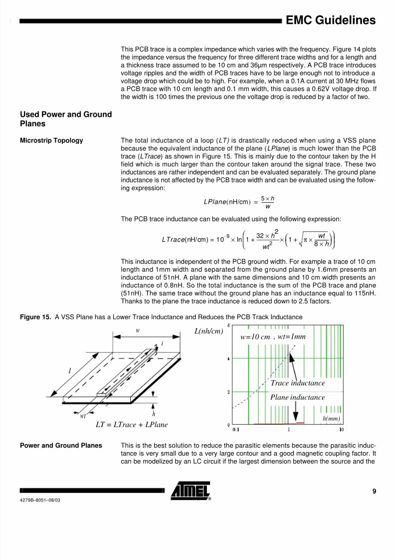
872019 EMC Guidelines
httpslidepdfcomreaderfullemc-guidelines 1617
16 EMC Guidelines 4279Bndash 8051ndash 0803
Figure 24 ESR is Reduced by Connected Several Identical Capacitors in Parallel
Choose COG NPO andX7R dielectric types
Capacitors that have these dielectrics have the lowest ESR and a good stability in tem-perature and the value can cover from few pF to several tens of nF
Conclusion Most of the EMC improvements detailed in this application note are already known butthey are not always applied There is not a unique solution to improve the EMC of a sys-tem but most yield to a cumulative improvement Designers must keep in mind thesemechanisms and apply them early in the conception phase of a system to ensure EMCcompliance
References bull Controlling Radiated Emissions by design Michel Mardiguian ChapmanampHall
bull Printed Circuit Board Design Techniques for EMC Compliance MarkI Montrose
IEEE Press
bull Introduction to Electromagnetic Compatibility Clayton RPaul Wiley Interscience
bull Noise Reduction Techniques In Electronic Systems Henry WOtt WileyInterscience
bull Computing Inductive noise of Chip Packages AJ RAinal ATampT Bell LaboratoriesTechnical Journal
bull Power Distribution System Design Methodology and Capacitor Selection for ModernCMOS technology IEEE TRANSACTIONS ON ADVANCED PACKAGING VOL22 NO 3 AUGUST 1999 Larry DSmith Raymond E Anderson Douglas WForehand Thomas J Pelc and Tanmoy Roy Member IEEE
bull High-Speed Digital Design Howard Jonson amp Martin Graham PTR PH
1 x 10nF
2 x 10nF
4 x 10nF
872019 EMC Guidelines
httpslidepdfcomreaderfullemc-guidelines 1717
Printed on recycled paper
Disclaimer Atmel Corporation makes no warranty for the use of its products other than those expressly contained in the Company rsquos standard
warranty which is detailed in Atmel rsquos Terms and Conditions located on the Companyrsquos web site The Company assumes no responsibility for anyerrors which may appear in this document reserves the right to change devices or specifications detailed herein at any time without notice anddoes not make any commitment to update the information contained herein No licenses to patents or other intellectual property of Atmel aregranted by the Company in connection with the sale of Atmel products expressly or by implication Atmel rsquos products are not authorized for useas critical components in life support devices or systems
Atmel Corporation Atmel Operations
2325 Orchard Parkway
San Jose CA 95131 USATel 1(408) 441-0311
Fax 1(408) 487-2600
Regional Headquarters
EuropeAtmel Sarl
Route des Arsenaux 41
Case Postale 80CH-1705 Fribourg
Switzerland
Tel (41) 26-426-5555
Fax (41) 26-426-5500
AsiaRoom 1219
Chinachem Golden Plaza
77 Mody Road Tsimshatsui
East Kowloon
Hong Kong
Tel (852) 2721-9778
Fax (852) 2722-1369
Japan
9F Tonetsu Shinkawa Bldg
1-24-8 Shinkawa
Chuo-ku Tokyo 104-0033Japan
Tel (81) 3-3523-3551
Fax (81) 3-3523-7581
Memory
2325 Orchard ParkwaySan Jose CA 95131 USA
Tel 1(408) 441-0311
Fax 1(408) 436-4314
Microcontrollers2325 Orchard Parkway
San Jose CA 95131 USA
Tel 1(408) 441-0311
Fax 1(408) 436-4314
La Chantrerie
BP 70602
44306 Nantes Cedex 3 France
Tel (33) 2-40-18-18-18Fax (33) 2-40-18-19-60
ASICASSPSmart CardsZone Industrielle
13106 Rousset Cedex FranceTel (33) 4-42-53-60-00
Fax (33) 4-42-53-60-01
1150 East Cheyenne Mtn Blvd
Colorado Springs CO 80906 USA
Tel 1(719) 576-3300
Fax 1(719) 540-1759
Scottish Enterprise Technology Park
Maxwell BuildingEast Kilbride G75 0QR Scotland
Tel (44) 1355-803-000
Fax (44) 1355-242-743
RFAutomotive
Theresienstrasse 2Postfach 3535
74025 Heilbronn Germany
Tel (49) 71-31-67-0Fax (49) 71-31-67-2340
1150 East Cheyenne Mtn Blvd
Colorado Springs CO 80906 USA
Tel 1(719) 576-3300
Fax 1(719) 540-1759
BiometricsImagingHi-Rel MPU
High Speed ConvertersRF Dat acomAvenue de Rochepleine
BP 123
38521 Saint-Egreve Cedex France
Tel (33) 4-76-58-30-00
Fax (33) 4-76-58-34-80
Literature Requests
wwwatmelcomliterature
4279Bndash 8051ndash 0803
copy Atmel Corporation 2003 All rights reserved Atmelreg is a registered trademark of Atmel Corporation or its subsidiaries Other terms andproduct names may be the trademarks of others