Electrostatic Discharge (ESD) and Failure Analysis: Models - JSTS
14
JOURNAL OF SEMICONDUCTOR TECHNOLOGY AND SCIENCE, VOL.3, NO. 3, SEPTEMBER, 2003 153 Manuscript received August 27, 2003; revised September 17, 2003. IBM Semiconductor Research and Development Center (SRDC) Essex Junction, Vermont 05452 Tel : 802-769-8368, Fax: 802-769-9659, E-mail: [email protected] Electrostatic Discharge (ESD) and Failure Analysis: Models, Methodologies and Mechanisms for CMOS, Silicon On Insulator and Silicon Germanium Technologies Steven H. Voldman Abstract− Failure analysis is fundamental to the design and development methodology of electrostatic discharge (ESD) devices and ESD robust circuits. The role of failure analysis (FA) in the models, methodology, band mechanisms evaluation for improving ESD robustness of semiconductor products in CMOS, silicon-on-insulator (SOI) and silicon germanium (SiGe) technologies will be reviewed. Index Terms− Reliability, Electrostatic, Discharge, CMOS, SOI, SiGe I. INTRODUCTION Failure analysis is invaluable in the learning process of ESD protection design and development. Today, there is still no design tool which will predict ESD protection levels in a semiconductor chip for human body model (HBM), machine model (MM) and charged device model (CDM) simulation tests. ESD prediction is a difficult task because ESD phenomena spans both on microscopic and macroscopic physical scale. ESD phenomena involves semiconductor device, circuit, and package effects and their interactions. Although significant resources have been placed on semiconductor design tools, ESD analysis and prediction remains significantly behind other circuit tool development. As a result, failure analysis assist the design and development process by providing visualization of the mechanisms leading to ESD failure. In this paper, we will focus on models, methodologies and mechanisms associated with ESD failures and failure analysis by use of examples from semiconductor technologies. The scope of the paper will show examples of failure analysis and characterization of CMOS, silicon-on-insulator (SOI) and silicon germanium (SiGe) technologies. In our discussion, we will present how failure analysis can assist in providing insight into achieving ESD robust implementations. 2. FAILURE MODELS ESD failure analytical models were established to provide predictive capability for semiconductor devices. ESD failure models typically are based on the relationship of the thermal physics and pulse parameters [1-5] or statistical analysis [6-9]. ESD physical models of devices explored the relationship between the ESD pulse and the thermal transport and its role in prediction in the power-to-failure. Wunsch focused on the time scale where the thermal diffusion time is on the order of the pulse width demonstrating a 1/t f 1/2 dependence [1]. Tasca analyzed the power-to-failure, P f , in a spherical source. Tasca explored the dependence on the power-to- failure when the pulse is significantly smaller than the
Transcript of Electrostatic Discharge (ESD) and Failure Analysis: Models - JSTS

JOURNAL OF SEMICONDUCTOR TECHNOLOGY AND SCIENCE, VOL.3, NO. 3, SEPTEMBER, 2003
153
Manuscript received August 27, 2003; revised September 17, 2003. IBM Semiconductor Research and Development Center (SRDC)
Essex Junction, Vermont 05452 Tel : 802-769-8368, Fax: 802-769-9659, E-mail: [email protected]
Electrostatic Discharge (ESD) and Failure Analysis: Models, Methodologies and Mechanisms for CMOS,
Silicon On Insulator and Silicon Germanium Technologies
Steven H. Voldman
Abstract−Failure analysis is fundamental to the
design and development methodology of electrostatic discharge (ESD) devices and ESD robust circuits. The role of failure analysis (FA) in the models, methodology, band mechanisms evaluation for improving ESD robustness of semiconductor products in CMOS, silicon-on-insulator (SOI) and silicon germanium (SiGe) technologies will be reviewed.
Index Terms−Reliability, Electrostatic, Discharge,
CMOS, SOI, SiGe
I. INTRODUCTION
Failure analysis is invaluable in the learning process
of ESD protection design and development. Today, there
is still no design tool which will predict ESD protection
levels in a semiconductor chip for human body model
(HBM), machine model (MM) and charged device
model (CDM) simulation tests. ESD prediction is a
difficult task because ESD phenomena spans both on
microscopic and macroscopic physical scale. ESD
phenomena involves semiconductor device, circuit, and
package effects and their interactions. Although
significant resources have been placed on semiconductor
design tools, ESD analysis and prediction remains
significantly behind other circuit tool development. As a
result, failure analysis assist the design and development
process by providing visualization of the mechanisms
leading to ESD failure. In this paper, we will focus on
models, methodologies and mechanisms associated with
ESD failures and failure analysis by use of examples
from semiconductor technologies. The scope of the
paper will show examples of failure analysis and
characterization of CMOS, silicon-on-insulator (SOI)
and silicon germanium (SiGe) technologies. In our
discussion, we will present how failure analysis can
assist in providing insight into achieving ESD robust
implementations.
2. FAILURE MODELS
ESD failure analytical models were established to
provide predictive capability for semiconductor devices.
ESD failure models typically are based on the
relationship of the thermal physics and pulse parameters
[1-5] or statistical analysis [6-9]. ESD physical models
of devices explored the relationship between the ESD
pulse and the thermal transport and its role in prediction
in the power-to-failure. Wunsch focused on the time
scale where the thermal diffusion time is on the order of
the pulse width demonstrating a 1/tf1/2 dependence [1].
Tasca analyzed the power-to-failure, Pf, in a spherical
source. Tasca explored the dependence on the power-to-
failure when the pulse is significantly smaller than the
STEVEN H. VOLDMAN : ELECTROSTATIC DISCHARGE (ESD) AND FAILURE ANALYSIS: MODELS, METHODOLOGIES… 154
pulse width, demonstrating an adiabatic dependence with
a 1/tf form [2]. Tasca also showed that as the pulse width
is much greater than the thermal diffusion time, the
power-to-failure is time independent. Today, the work of
Tasca and Wunsch-Bell together are integrated into a
single model to analyze the power-to-failure over all
time regimes. Arkhipov, Astvaturyan, Godovsyn, and
Rudenko developed a model assuming the discharge
follows a cylindrical discharge phenomenon [4].
( )[ ]
+
−=
ππ
π4
ln42ln
4
Dbft
ToTcKafP
Dwyer also extended the Wunsch-Bell model by
addressing the three dimensional nature of the thermal
transport as three different thermal diffusion time scales
ta, tb, and tc [5]. The work of Arkhipov et al influenced
the direction of the Dwyer model by the introduction of
the logarithm term.
( )ft
oTcTpMCfP
−=
( ) ( )2ctft
oTcTpCKabPf
−−
=ρπ
( )( ) ( )b
cbtft
oTcTKafP
−+−=
2ln
4π
( )
ftat
b
c
b
aoTcTKa
Pf
−−+
−=
22ln
2π
Another method of prediction is from a statistical
approach. For ESD field failure prediction, the power-to-
failure distribution can be compared to the actual pulse
power distribution [9]. Assuming a Gaussian distribution
of the design parameters, a probability distribution
function can be defined for the power-to-failure.
−−=
221exp
2
1)(
pSfPfP
pSfPfPf π
where the power-to-failure, Pf, is the random variable
and mean power-to-failure <Pf>, and standard deviation,
Sp. The standard deviation can be expressed as
{ }212
1
1
1
−
−= ∑
=
N
ifP
ifP
NpS
The net field failure is the cumulative distribution
function of the probability of the pulse power is greater
than the power-to-failure of the device. Models have
been developed by Alexander [7], Enlow [8], and Pierce-
Mason [9] to provide predictive ESD results in
semiconductor chips. Pierce and Mason applied this
concept by assuming a Wunsch-Bell time dependence as
the probability distribution and addressed dimensional
variation as cause of the statistical variation .
Although these analytical and statistical models exist
in the industry, a significant amount of ESD analysis
today relies on failure analysis. The existence of the
models, both analytical and statistical, has not assisted in
the prediction and assurance needed to achieve ESD
results. As a result, failure analysis plays a fundamental
role in achieving successful ESD results. Failure analysis
combined with other methodologies and techniques is
key to the ESD verification and learning process.
3. FAILURE ANALYSIS AND HEURISTIC DESIGN METHODOLOGY USING DESIGN
SYMMETRY
A goal of designing ESD protection networks and
ESD-robust circuits is to provide uniform current
distribution throughout a device. This can be achieved
using three dimensional (3-D) electro-thermal device
simulation [10]. Although 2-D and 3-D electro-thermal
semiconductor device simulators exist, today, most ESD
networks are still developed experimentally. The primary
reason is the availability, development time, calibration
effort and accuracy of simulation tools. As a result,
experimental design and failure analysis plays a key role
in the ESD design process today. As a methodology of
developing ESD protection networks, it is superior to use
intuition, design symmetry, and failure analysis as a
means of development of a good ESD protection
network. Our intuition teaches us, as a first step, that
JOURNAL OF SEMICONDUCTOR TECHNOLOGY AND SCIENCE, VOL.3, NO. 3, SEPTEMBER, 2003
155
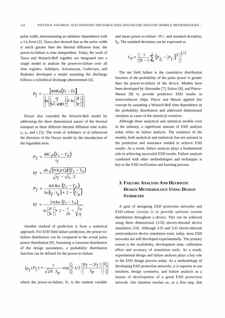
Fig. 1. Probability distribution functions of the ESD pulse
power and the power-to-failure of a component. Integration
over the cross-hatched area provides the total failure rate.
current uniformity will exist when design symmetry is
self-evident in a design. Hence by providing a design
whose physical layout embodies design symmetry on all
design levels, it would makes sense that current
uniformity will occur. Failure analysis plays a key role in
verifying the intuition of the ESD engineer in this first-
cut assumption. In reality, there are many reasons this
heuristic method is flawed. First, the actual processed
on-wafer does not always represent the design level
dimensions and process-induced asymmetry can be
established that influence the ESD results. Second, it is
hard to anticipate three-dimensional electro-thermal
effects. Third, while intuition helps us with visualizing
the physical layout symmetry, the “physical layout
symmetry” may not be equivalent to the “electrical
symmetry” or “electro-thermal symmetry”. Failure
analysis plays a key role in correcting intuition and
provides bridging from the layout to the understanding
of the electrical and thermal response of a device or
circuit network.
The FA damage pattern itself and its distribution
throughout the ESD network can be used as a “efficiency
factor” or ESD metric. In actuality, a device which has a
significant percentage of the area as damaged,
demonstrates the ability to utilize the maximum
percentage of the silicon area for providing ESD
protection. The damage pattern symmetry also is an
indicator of the ability to achieve current uniformity and
a measure of good ESD design practices.
4. FAILURE ANALYSIS METHODOLOGY AND
ELECTROTHERMAL SIMULATION
Using a heuristic understanding of the design layout,
failure analysis followed by electro-thermal simulation
can provide a higher intuition allowing the ESD designer
bridge from the physical to the electro-thermal results.
Failure patterns can teach the regions of peak thermal
heating and failure [10, 11]. Electro-thermal device
simulation can help understand the location and the root
cause of the ESD failure. As an example, the corner of
an shallow trench isolation (STI) bound p+ diffusion/n-
well diode was failing on the diffusion-to-STI corner.
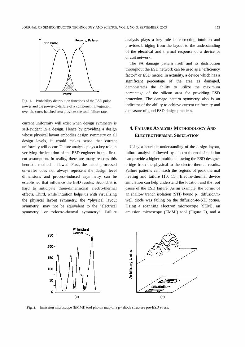
Using a scanning electron microscope (SEM), an
emission microscope (EMMI) tool (Figure 2), and a
(a) (b)
Fig. 2. Emission microscope (EMMI) tool photon map of a p+ diode structure pre-ESD stress.

STEVEN H. VOLDMAN : ELECTROSTATIC DISCHARGE (ESD) AND FAILURE ANALYSIS: MODELS, METHODOLOGIES… 156
Fig. 3. Kelvin probe force microscope (KPFM) topography
image of p+ diode post-ESD stress.
Fig. 4. Electrothermal Simulation Results.
Kelvin force probe microscope (KPFM) atomic force
tool (Figure 3), the ESD damage was imaged. The SEM
provided a bird’s eye view of the ESD device after
removal of the metal films. The EMMI tool provides a
photon-mapping of the ESD structure during direct
current (d.c.) measurement. The KPFM atomic force tool
provided both a topographic as well as electrical
potential mapping. Using a 3-D semiconductor electro-
thermal tool FIELDAY III, our analysis demonstrated
and verified that the peak lattice temperatures was at the
end of the p+ diode implant [10].
Although 3-D electro-thermal device simulation is
possible, it is extremely sensitive to the electrical and
thermal Von Neumann and Dirichlet boundary
conditions, mesh quality and mesh densification
techniques. Even with good refinements, heat capacity
and thermal conductivity models are not well
characterized or calibrated in the high temperature
regimes. Independent of the calibration and model fitting,
FA combined with the electro-thermal simulation
establishes good intuition and a good methodology for
the design of ESD protection networks and circuits.
5. FAILURE ANALYSIS METHODS AS A MEANS OF ESD DEVICE OPERATION VERIFICATION
Failure analysis can be used as a means of verifying
ESD device operation. At times, it is not clear to all ESD
engineers how an ESD device is operating or the current
paths. Failure analysis is a key means of verification of
the current transfer based on the location of the damage
on given shapes, or between shapes. The FA damage is a
verification of current transfer and clearly can show
device operation and the path of current transfer. For
example, in integrated cascode MOSFET, the electrical
schematics would not explain the nature of the failure
mechanism. Early measurements of cascode MOSFETs
anticipated that the MOSFET snapback voltage would
serve as the sum of the two MOSFETs. Experimental
results verified that integrated series cascode MOSFET
was significantly less than the sum of the two MOSFETs.
It is clear from the failure analysis that the interaction for
cascaded MOSFET second breakdown occurs in the
same local region, providing a response which behaved
as a single MOSFET. From the AFM failure analysis, it
is clear that the parasitic bipolar transistor is interactive
locally as one device. The AFM failure analysis results
then shows that treating the series cascode MOSFET
structure can not be modeled as two independent
components. Since this early work, the issue of analysis
of series cascode MOSFETs has had increased interest in
mixed-voltage interface networks in microprocessors
and peripheral circuits.
6. FAILURE ANALYSIS AND ESD TESTING METHODOLOGY
For failure analysis to be effective for ESD learning, a
good ESD testing methodology and strategy is needed to

JOURNAL OF SEMICONDUCTOR TECHNOLOGY AND SCIENCE, VOL.3, NO. 3, SEPTEMBER, 2003
157
maximize the ESD learning on ESD networks, circuits
and products. The ESD testing methodology is key in
providing valuable correlation between the ESD failure
and the failure mechanism. In IBM, the testing and
failure analysis strategy, developed by Gross and
Voldman [12], all pins are tested to a given power rail.
Second, each pin is tested from zero volts on the source,
and step stressed in small increments. It is also key that
all pins are tested to failure. The failure distribution
function of all the pins are plotted and evaluated to
determine the “mean failure distribution”, standard
deviation, and other statistics of the whole chip. In many
corporations, the FA focus is primarily on the worst case
pins. In this methodology, the failure analysis of the
“good” pins are as important to evaluate as well. This
allows documentation and classification of the pin types,
the failure mechanism and ESD results. This
methodology allows to verify at what level different
failure mechanisms are evident as well as quantify what
mechanisms are occurring in what circuit function. This
testing methodology highly incorporates failure analysis
as a key source to drive ESD learning in chip
development.
7. FAILURE ANALYSIS AND SEMICONDUCTOR PROCESS INDUCED ESD DESIGN ASSYMETRY
Failure analysis is a means to verify semiconductor
process or design asymmetry which can have an
influence on ESD robustness of circuits. Process induced
design asymmetries can occur on all design levels. For
example, photo and etch processing can have both
macroscopic and microscopic effects [13]. In the
processing of polysilicon gate structures, “across chip
line-width variation,” known as ACLV, can vary the
MOSFET polysilicon gate line-width. The placement of
the circuit in the chip globally leads to ACLV effects
because of macroscopic photo-tool source-intensity
effects, and within a multi-finger MOSFET because of
microscopic photo and etch effects. It is found that
depending on the type of photo-resist, “nested” line-
widths and “isolated” line-widths can be different. With
positive tone resist, nested lines are smaller than isolated
lines, and with negative tone resist, this reverses. The
implication of this effect is that MOSFET second
breakdown is a non-random phenomenon and will be
evident on the MOSFET fingers with smaller line-widths
because of the lower MOSFET snapback. Using a two-
dimensional “boot tip” atomic force microscope (AFM),
two-dimensional mappings of topography provided
significant accuracy of both the lateral and vertical
dimensions. Boot-tip AFM devices allows for the ability
to address sidewall slopes of polysilicon gate structures
and vertical trench profiles. Failure analysis verified that
the MOSFET second breakdown in the multi-finger
MOSFET structure was non-random in a positive tone
photo-resist system. Failure analysis results showed that
the “nested” lines with the smaller MOSFET line-widths
had damage between the source and drain. This ACLV
nested-to-isolated effect was eliminated as the
technology switched from positive to negative tone
photo-resist [13]. Combining the 2-D AFM tool with the
SEM analysis of the ESD-damaged MOSFETs,
verification of the reason for the non-random component
associated with line width as quantified and explain the
ESD results.
8. FAILURE ANALYSIS METHODOLOGY TO EVALUATE INTER-POWER RAIL ELECTRICAL CONNECTIVITY
Failure analysis can be used to verify and evaluate the
electrical connectivity between two power busses and
how they interact with a peripheral circuit. The ESD
robustness level, response and failure analysis of a multi-
finger MOSFET circuit is significantly dependent on the
relationship between the chip substrate and the other
ground rails. In CMOS chip, typical the off-chip driver
(OCD) bus or peripheral circuits bus is separated from
the core or chip substrate bus [14]. In mixed signal
designs, the digital and analog grounds are also
separated. In RF applications, different RF functional
blocks also have separated grounds. In the case that there
is strong bi-directional coupling between the grounds,
the failure damage pattern in a multi-finger shows
damage in many of the MOSFET fingers. When the
circuit is tested referenced to a substrate-decoupled
STEVEN H. VOLDMAN : ELECTROSTATIC DISCHARGE (ESD) AND FAILURE ANALYSIS: MODELS, METHODOLOGIES… 158
peripheral ground, the ESD results are significantly
lower and only one damage spot in a single finger is
evident. Hence from the failure analysis pattern in the
MOSFET, it can be determined whether is strong or
weak coupling between the rails.
9. FAILURE ANALYSIS METHODOLOGY FOR EVALUATION OF ESD PARASITICS
Failure analysis provides significant insight into the
current flow of parasitic elements and how they interact
with an ESD element. Three situations can exist 1) the
parasitic element draws the current, becomes damaged
and leads to low failure levels, 2) the ESD network
draws the current flow, becomes the limiting value and
fails at a high current, and 3) the parasitic and the ESD
element are working in conjunction where both are
damaged at the same failure voltage. The first case is
sometimes referred to as “ ESD current robbing”. For
example, a parasitic npn is formed between a n diffusion
resistor and a guard ring structure. Additionally, an ESD
n-well diode is also in parallel with the n-well diode
element which is also adjacent to the same guard ring
structure. In our experimental results, the parasitic npn
reduced the failure level to –3 kV whereas the ESD
element n-well diode would have produced – 7 kV. At –
3 kV, no damage is evident in the n-well diode but in the
parasitic npn damage is evident between the guard ring
and the resistor element. Failure analysis is able to
determine that “ ESD current robbing” was occurring
leading to the low failure level.
10. FAILURE ANALYSIS METHODS AND ESD GROUND RULES
Failure analysis is also used to develop ESD ground
rules. ESD ground rules are design rules which are
specifically used to minimize the effect of parasitic
elements or ESD failure. Using the failure damage
patterns, and ESD robustness levels, these spacings can
be decided. With the example in the prior section, it was
found by adjusting the spacing between the n-diffusion
and the guard ring, the “ESD current robbing” could be
eliminated. It is found that an optimum ESD result is
possible when the spacing of n-resistor to the n-well
guard ring was tuned to the spacing between the n-well
ESD diode and its adjacent guard ring. Hence an ESD
ground rule was established so that the spacings
provided the highest ESD level. Hence, using failure
analysis damage patterns, the spacing of guard rings and
ESD ground rules can be defined.
Interactions between floating-gate tie downs and the
pull-down MOSFET of a mixed-voltage off-chip driver
circuit also was evident using failure analysis of the
peripheral circuit. The drain of the MOSFET and the n+
diffusion tie down formed a parasitic bipolar transistor
when designed local to each other in the substrate. In this
work, it was found that in negative VDD test modes, the
lateral npn was active in LOCOS isolation, but not in
STI-bound MOSFETs. Ground rules were established to
avoid interaction between the floating gate tie down
elements and the peripheral circuit pull-down network.
11. ESD FAILURE MECHANISMS, AND TECHNOLOGY EVOLUTION AND REVOLUTION
With the evolution and revolution of CMOS
technology, at times some types of ESD failure
mechanisms are eliminated while others are omnipresent.
With technology transitions, the importance of some
ESD failure mechanisms were important years ago, were
resolved and again rise as a key technology concern [15-
22].
In early NMOS technology, there was considerable
focus on interconnects and oxides. Turner, in 1980,
stated “Today’s 2 and 3 micro metal widths have reduced
current carrying capacity to the point where it has
become a real concern from an ESD standpoint.” In this
time frame, devices were un-passivated leading to
vaporization of the aluminum (Al) wires and polysilicon
resistors. Aluminum and alloy spiking occurred both
vertically and laterally. ESD-induced gate oxide pin
holes were observed in NMOS technology as the most
dominant field failure mechanism [23]. With the
introduction of resistors and thick oxide MOSFETs to
lower the voltage at the receiver gate oxide, these issues

JOURNAL OF SEMICONDUCTOR TECHNOLOGY AND SCIENCE, VOL.3, NO. 3, SEPTEMBER, 2003
159
were resolved.
With the introduction of silicide films, the focus
shifted to MOSFET second breakdown and MOSFET
ESD robustness for technologies whose ground rules are
less than 2 �m. With the introduction of silicides, the
low resistance of the silicide eliminated the natural
resistor ballasting in the MOSFET source and drain.
With the introduction of low doped drain structures,
continuous junction scaling, and silicide, the product of
the current density and peak electric field lead to higher
temperatures in the MOSFET drain structure. MOSFET
second breakdown remained a dominant failure
mechanism in technology.
For 0.5 to 0.35 �m Leff technology, with the scaling
of ground rules, significant activity was present in
parasitic npn and pnp type devices. With the introduction
of shallow trench isolation, ESD learning, ESD ground
rules and ESD checking systems, many of the ESD
concerns with these parasitics were eliminated.
With smaller design rules and increased circuit density,
interconnects were scaled in width and film thickness for
density and performance objectives. Interconnect scaling
is driven by the MOSFET scaling dimensions.
According to Rent’s rule, the number of I/O increases
proportional to the number of gates on the chip. As the
interconnects, vias and contacts are scaled, the ESD
robustness of a given interconnect decreases. For 0.25
�m and below CMOS technologies, interconnects
became the dominant failure mechanism [16,17,19]. In
aluminum interconnects, the Ti/Al/Ti structure failure
was typically observed as a lateral cracking of the
insulator and Al filling this damaged region. Direct
current (d.c.) resistance shifts occurred at 90% of the
critical current. This resistance shift can lead to latent
mechanisms in circuits [20]. With new structures,
Banerjee constructed a model for the current-to-failure
for a Ti/Al/Ti interconnect incorporating the three film
structure and isolation region [18].
With the migration from Al to Copper (Cu)
interconnects, the ESD robustness of interconnects
improved because of Cu has a higher melting
temperature compared to aluminum [19-21]. HBM, MM
and TLP measurements verified the improvement in both
test sites and product implementations. In a damascene
process, the high refractory metal liner serves as a barrier
to Cu diffusion. The failure mechanism in liner-cladded
Cu interconnects typically show cracking above the
trough as opposed to lateral cracking. For interconnects
below 2 um, lateral extrusion was observed. For dual
damascene Cu interconnects, Voldman extended this
model to address the three-sided trough lining of the
damascene interconnect and Cu filling materials as well
as the surrounding insulation [19,20,21]. For low-K
materials, experimental measurements were also taken to
compare SiO2 and low-K material impacts on the current
to failure of a damascene interconnect highlighting the
ESD robustness degradation due to the low-K insulation
material [21].
For CMOS technology to follow the Moore’s law
relationship, it has been proposed that this is achievable
by having CMOS technology migrate to silicon-on-
insulator (SOI) technology [24,25].
With SOI technology, the failure mechanisms are
significantly different from bulk CMOS. This is a result
of new ESD networks and the lack of contact to the chip
substrate. With the introduction of the SOI lateral gated
diode ESD element, the ESD failure was observed from
the anode to the cathode under the SOI MOSFET gate
dielectric. In SOI, circuit elements which normally
discharged to the substrate in bulk CMOS, typically
failed in the reversed mode or took alternative current
paths. Unlike the bulk CMOS, no failures were observed
in the inverter gate structures for the CDM mechanism.
The CDM failure mechanism occurred in the gate to
input node of the SOI MOSFET pass transistor.
Evidence from the failure analysis showed the current
path occurred through the VDD to the gate of a SOI
MOSFET pass transistor as opposed to the traditional
CDM failure mechanism of the MOSFET inverter gate
and the pass transistor source-to-drain. New failure
mechanisms similar to the pass transistor also occurred
in the buried resistor (BR) structure. The BR resistor is
consists of a MOSFET gate structure, where dopants
exist in the channel region to form a resistor. The
MOSFET gate structure serves the purpose of blocking
the silicide film, isolating the resistor input and output.
BR resistors which normally discharge into the substrate,
can not in SOI. In SOI, these structures can fail in a
negative pulse device ESD stress. CDM failure
mechanisms also occur in the gate structure of the lateral
Lubistor structure when the gate was connected to the

STEVEN H. VOLDMAN : ELECTROSTATIC DISCHARGE (ESD) AND FAILURE ANALYSIS: MODELS, METHODOLOGIES… 160
Fig. 5. MOSFET Second Breakdown in a Series Cascode
MOSFET structure.
Fig. 6. Cross section of an lateral gated diode ESD structure.
cathode. Hence, isolation of the Lubistor gate structure
prevents CDM failure mechanisms in these SOI
structures. To resolve this issue, new SOI ESD circuit
solutions were developed to eliminate the failure
mechanism in the lateral gated Lubistor circuit and the
BR resistor elements by electrically de-coupling these
gates from the anode, cathode or power supply nodes.
An alternative path, chosen by Ker, extended the ESD
reliability of the lateral gated diode by removal of the
gate with an additional mask [26]. Two key points to
address on ESD in SOI technology. First, excellent ESD
results as good as or better than bulk CMOS products is
achievable in SOI semiconductor products. Second, to
achieve good ESD protection in SOI, a significant
amount of ESD learning is required to address the new
ESD-induced failure mechanisms. These mechanisms
need to be solved by either device structural, design
layout or circuit modifications.
Fig. 7 . Crosssection of the ESD structure after ESD failure.
ESD failure is on second finger of first diode structure.
Fig. 8. Cross section of a SiGe HBT device.
12. RADIO FREQUENCY (RF) DEVICES AND ESD
With the growth of high speed data-rate wired
communication, wireless market, high speed test
equipment, and magnetic recording industry, advanced
semiconductors are playing a more significant role in
this millennium. RF CMOS, Gallium Arsenide (GaAs),
Indium Phosphide (InP), Silicon Germanium (SiGe) and
Silicon Germanium Carbon (SiGeC) technologies will
dominate these application spaces of 1 to 300 GHz.
Early work on ESD sensitivity of RF devices was
performed by Whalen and Domingos [27,28]. ESD

JOURNAL OF SEMICONDUCTOR TECHNOLOGY AND SCIENCE, VOL.3, NO. 3, SEPTEMBER, 2003
161
sensitivity of these devices will be a larger concern as
the device sizes decrease and the application frequencies
increase. Although GaAs devices and GaAs technology
has matured, very little improvement in the ESD
protection levels have been demonstrated above 1000 V
HBM.
SiGe and SiGeC BiCMOS technology has the
advantage of natural integration with advanced CMOS
foundry technology as well as a myriad of additional
design levels, implants and devices. As a result,
excellent ESD robustness levels have been demonstrated
in BiCMOS SiGe technology by utilizing both CMOS
and bipolar ESD elements [29-34]. CMOS ESD
solutions can be incorporated in the digital, analog or RF
sectors of a mixed signal RF CMOS or RF BiCMOS
semiconductor chip. The CMOS ESD elements can
include p+/n-well diodes, n-well-to-substrate diodes, n+
diodes, grounded gate NFET elements. BiCMOS
features, such as buried layers, sub-collector and reach
through implants, and trench isolation can be added to
provide improved ESD and latchup robustness to these
CMOS elements. Additionally, CMOS-based ESD
power clamps, such as RC-triggered MOSFET circuits,
can be used for ESD protection of the MS chips. To
utilize these for RF CMOS or RF BiCMOS, RF models
must be established for the RF and analog sectors of a
SOC application.
In an RF BiCMOS product, many circuit designers
prefer to use bipolar-based active and passive ESD
elements because of the low noise, high Q, low
capacitance, and voltage power rail considerations.
Although SiGe technology research and development
was started in 1980’s, only recently with the increased
volume of SiGe products has the interest in ESD
protection has increased. Figure 9 shows the first
transmission line pulse (TLP) I-V plots of a SiGe
heterojunction bipolar transistor (HBT) device in a
common-emitter configuration as a function of the pulse
width. In the TLP measurement, the pulse magnitude
was increased until SiGe HBT device failure. A set of
TLP I-V characteristics were measured as a function of
different pulse widths. As the pulse width is varied, it
can be observed that the trigger conditions, resistances
and failure current is varied. Figure 10 shows a Wunsch-
Bell plot of power-to-failure versus the pulse width of an
epitaxial base Si BJT and epitaxial base SiGe HBT
Fig. 9. TLP I-V characteristic of SiGe HBT device (τ = 40ns
to τ = 1000ns).
Fig. 10. Wunsch-Bell Power-to-failure plot of SiGe HBT and
Si BJT devices.
device. Experimental results show that as a result of the
higher current gain, the SiGe HBT device results exceed
those of the Si BJT device.
The emitter-base junction of the bipolar transistor has
been historically a limiting failure mechanism.
Heterojunction bipolar transistors allows for an increase
in the base doping concentration for a given unity
current gain cutoff frequency. Figure 11 shows a TLP I-
V plot and leakage history of a SiGe HBT npn in a
reverse biased emitter-base operational mode. Experi-
mental results show that as the stress exceeds the safe
operating area (SOA) of a SiGe HBT device, leakage
current increases and then saturates. When the
breakdown voltage is reached, a rapid increase in
leakage current and device failure is evident.

STEVEN H. VOLDMAN : ELECTROSTATIC DISCHARGE (ESD) AND FAILURE ANALYSIS: MODELS, METHODOLOGIES… 162
Fig. 11. TLP Measurement of NSA SiGe HBT emitter-base
for large emitter diffusion-to-extrinsic base implant spacing.
Fig. 12. Unity current gain vs collector current degradation
plots with increased ESD stress in a SiGeC HBT device.
Evaluation of the RF characteristics during ESD stress is
important to evaluate the onset of performance
degradation. The demarcation point where RF
characteristics are below semiconductor device or
product specification is important in determining the
failure point. In an RF product, there are a multitude of
RF specifications which may be needed to determine the
failure point. A study was completed where unity current
gain cutoff frequency as a function of collector current
(fT vs Ic) was evaluated prior to ESD stress on a SiGeC
HBT device (Figure 12). A post-RF stress was
completed to evaluate the change in the device
characteristics. Experimental results infer that the
transconductance is impacted by the ESD stress as well
as the peak cutoff frequency. In this study, the d.c.
Fig. 13. Plot of the percent change in the cutoff frequency as
a function percent change in the forward bias voltage.
Fig. 14. Voltage to Failure of SiGe transistor with and
without Carbon implant in the SiGe base region.
parameter shifted also showed degradation in the
emitter-base configuration. Figure 13 demonstrates a
correlation exists between the normalized shift in the dc
characteristics and the cutoff frequency degradation for
both positive and negative stress. A key point is that the
RF degradation can be identified by the change in the dc
characteristic once the correlation is established.
Secondly, the failure occurs for both the positive and
negative stress conditions. In RF products, there are a
significant number of RF parameters and RF functional
tests which will be needed to be evaluated in order to
insure ESD reliability. These parameters are dependent
on the product application. Power gain, gain com-

JOURNAL OF SEMICONDUCTOR TECHNOLOGY AND SCIENCE, VOL.3, NO. 3, SEPTEMBER, 2003
163
pression, output-intercept 3rd order haramonic (OIP3),
linearity, quality factor and other design parameters may
be needed to evaluate to guarantee ESD robustness
additional to the standard d.c. shift or leakage test
requirements.
In the scaling of SiGe HBT devices, base width
scaling is important to achieve higher device
performance. The objective is to decrease the base width
and yet still provide a low base series resistance. With
the incorporation of Carbon into the SiGe epitaxial film,
the base doping concentration can be increased,
providing improved current distribution in SiGe HBT
devices and improved unity power gain cutoff frequency,
fMAX. Experimental results in SiGeC HBT devices and
ESD power clamps have already demonstrated ESD
levels above 2 kV HBM [34]. The placement of Carbon
in the base region of a SiGe HBT constrains the transient
enhanced diffusion (TED) of the Boron atom. As a result,
resistance parameters, breakdown parameters and ESD
results demonstrated tighter statistical control (Figure 14
and Figure 15).
13. MASKS AND ESD
ESD damage was observed in production masks due
to static induction charging as early as 1983. Chemelli,
Unger and Bossard noted damage patterns to production
masks failure analysis pattern could be replicated by a
laboratory controlled induced ESD [35]. High current at
the corners lead to field emission as well as arcing across
the narrow spaces.
Significant research in air ionization and installation
of ionizers in mask production lines have lowered the
concern for ESD-induced damage to masks in the last 17
years. With the continued scaling of mask dimensions,
both permanent damage and latent mechanisms have
again become a concern. A key result of recent work of
Montoya et al [36] showed that when the spacing
between lines are larger, the damage threshold is higher
and the energy transfer is greater leading to an
observable damage pattern. As the spacing decreases, the
energy in the discharge decreases leading to a less
observable damage pattern which may escape mask
inspection -- this concern will address itself as a
potential latent mask defect. New research in masks and
Fig. 15. Histogram of Current-to-Failure of SiGe and SiGeC
HBT device.
the discharge process is addressing these concerns for
future technology generations.
14. MAGNETIC RECORDING AND ESD
Electrostatic concerns in the magnetic recording
industry has increased with the introduction and scaling
of the magneto-resistive (MR) heads. In prior technology
generations, a thin film inductive read/write recording
head was used. With the transition to an inductive write
and magneto-resistive (MR) read head, ESD concerns
were evident. The publication of Wallash, Hughbanks
and Voldman [37], showed several ESD failure
mechanisms were evident in the MR head . A first
mechanism occurs between the MR shield and the MR
head element which occurs via an arc discharge across
the MR-shield gap. A second mechanism occurs from
the current that flows through the MR positive and
negative leads. The results in this study showed the
failure level decreases linearly with MR thin film stripe
width. MR head failure mechanisms manifest themselves
through electrical resistance increases. Additionally, in
the inductive write head, failure mechanisms also show
that ESD failure can occur between the pole tips and the
substrate as well as internal coil and dielectric damage.
With the introduction of the Giant Magneto-resistor
(GMR) head, continued scaling of the thin film stripe
lowered the ESD failure voltage by 5X. The introduction
of the spin valve (SV), which provides a means of
programming the GMR, can also lead to a new failure

STEVEN H. VOLDMAN : ELECTROSTATIC DISCHARGE (ESD) AND FAILURE ANALYSIS: MODELS, METHODOLOGIES… 164
mechanism. Spin-valve reversal occurs when the ESD
pulse itself influences the initial program state of the
GMR head.
In future generations, new inventions, such as the
Tunneling Magneto-resistive (TMR) devices also show a
reduced HBM ESD failure voltage below 10 V HBM
levels [38]. New challenges will be evident in the
production, manufacturing and handling of these new
magnetic recording devices as the ESD sensitivity
decreases below the 50 V HBM levels.
15. CONCLUSIONS
Although technology evolution and revolution has
changed, three basic mechanisms of ESD failures still
exist; junction damage, dielectric damage and
metallization damage. With the migration from NMOS
to CMOS, from single well to twin well, from diffused
wells to retrograde wells, from thick to thin oxides, from
Aluminum to Copper interconnects, from high K ILD to
low K ILD, from tapered Al vias to Cu dual damascene
vias, from AMR to GMR to TMR - - the failure
mechanisms are still similar. What does change is the
relative importance of one mechanism to another; this is
dependent on how devices scale, and whether the
technology migration leads to an ESD improvement or
ESD degradation. With the introduction of new
technologies, such as silicon-on-insulator (SOI), and
silicon germanium (SiGe), new failure mechanisms will
occur as a result of new physical structures and new
physics. With the rapid increase of interest in RF GaAs ,
InP, and SiGe technologies, new failure criteria for ESD
failure will be to address RF functional degradation
effects. With the continued scaling of semiconductors,
magnetic devices, and photomasks, the new ESD issues
and their failure analysis will continue to be important
for device design, reliability and manufacturing of these
components.
REFERENCES
[1] D.C. Wunsch, and R.R. Bell, “Determination Of
Threshold Voltage Levels Of Semiconductor Diodes And
Transistors Due To Pulsed Voltages,” IEEE Trans. on
Nuclear Science, Vol. NS-15, No. 6, pp. 244-259, Dec.
1968.
[2] D. M. Tasca, “Pulse Power Failure Modes in
Semiconductors,” IEEE Trans. on Nuclear Science, NS-
17, No. 6, pp. 346-372, Dec 1970.
[3] Ash, “Semiconductor Junction Non-linear Failure Power
Thresholds: Wunsch-Bell Revisited,” Proceedings of the
EOS/ESD Symposium, pp.122-127, 1983.
[4] V.I. Arkihpov, E. R. Astvatsaturyan, V.I. Godovosyn, and
A.I. Rudenko, International Journal of Electronics, 55, p.
395, 1983.
[5] V. M. Dwyer, A. J. Franklin, and D.S. Campbell,
“Thermal Failure in Semiconductor Devices,” pp. 553-
560, Solid State Electronics, 1989.
[6] W.D. Brown, “Semiconductor Device Degradation by
High Amplitude Current Pulses,” IEEE Trans. On
Nuclear Science, Vol. NS-19, December 1972.
[7] D.R. Alexander, and E.W. Enlow, “Predicting Lower
Bounds on Failure Power Distributions of Silicon NPN
Transistors,” IEEE Trans. On Nuclear Science, Vol. NS-
28, No.6, Dec. 1981.
[8] E.N. Enlow, “Determining an Emitter-Base Failure
Threshold Density of NPN Transistors,” Proceedings of
the EOS/ESD Symposium, pp.145-151, 1981.
[9] D. Pierce and R. Mason, “A Probabilistic Estimator for
Bounding Transistor Emitter-Base Junction Transient-
Induced Failures,” Proceedings of the EOS/ESD Sym-
posium, pp.82-90, 1982.
[10] S. Voldman, S. Furkay, and J. Slinkman, “Three
Dimensional Transient Electrothermal Simulation of
Electrostatic Discharge Protection Networks,”
Proceedings of the EOS/ESD Symposium, pp. 246-257,
1994.
[11] J. Never, and S. Voldman, “Failure Analysis of Shallow
Trench Isolated ESD Structures,” Proceedings of the
EOS/ESD Symposium, pp. 273-288, 1995.
[12] V. Gross and S. Voldman, “ESD Testing and
Qualification of Semiconductor Components,” Procee-
dings of the Electronic Component and Test Conference
(ECTC) Symposium, 1996.
[13] S. Voldman, J. Adkisson, “ Linewidth Control Effects on
MOSFET ESD Robustness,” Proceedings of the
EOS/ESD Symposium, pp.101-110, 1996.
[14] S. Voldman, “ESD Protection in a Mixed Voltage
Interface and Multi-Rail Disconnected Power Grid
Environment in 0.5 and 0.25 um Channel Length CMOS
Technologies,” Proceedings of the EOS/ESD Symposium,

JOURNAL OF SEMICONDUCTOR TECHNOLOGY AND SCIENCE, VOL.3, NO. 3, SEPTEMBER, 2003
165
pp.125-134, 1994.
[15] S. Voldman, and V. Gross, “Scaling, Optimization, and
Design Considerations of Electrostatic Discharge
Protection Circuits in CMOS Technology,” Proceedings
of the EOS/ESD Symposium, 1993; and Journal of
Electrostatics, Vol. 33, No. 3, pp.327-357, October 1994.
[16] S. Voldman, “The Impact of MOSFET Technology
Evolution and Scaling on Electrostatic Discharge
Protection,” Microelectronics Reliability, 38, pp.1649-
1668, 1998.
[17] S. Voldman, “The Impact of Technology Evolution and
Scaling on Electrostatic Discharge (ESD) Protection in
High Pin Count High Performance Microprocessors,”
Invited Talk, International Solid State Circuits
Conference, Session 21, WA 21.4, pp. 366-367, Feb.
1999.
[18] K. Banerjee, “Characterization of VLSI Circuit
Interconnect Heating and Failure under ESD Conditions,”
Proceedings of the International Reliability Physics
Symposium, pp.237-245, 1996.
[19] S. Voldman, “ESD Robustness and Scaling Implications
of Aluminum and Copper Interconnects in Advanced
Semiconductor Technology,” Proceedings of the
EOS/ESD Symposium, pp. 317-327, 1997.
[20] S. Voldman et al, “High Current Transmission Line Pulse
Characterization of Aluminum and Copper Interconnects
for Advanced CMOS Semiconductor Technologies,”
Proceedings of the International Reliability Physics
Symposium, pp.293-302, 1998.
[21] S. Voldman et al, “High Current Characterization of Dual
Damascene Copper/Si02 and Low-K Interlevel
Dielectrics for Advanced CMOS Semiconductor
Technologies,” Proceedings of the International
Reliability Physics Symposium, pp.144-153, 1999.
[22] S. Voldman, “Semiconductor Process and Structural
Optimization of Shallow Trench Isolated-Defined and
Polysilicon-Bound Source/Drain Diodes for ESD
Networks,” Proceedings of the EOS/ESD Symposium,
pp.151-160, 1998.
[23] T. Turner, and S. Morris, “Electrostatic Sensitivity of
Various Input Protection Networks,” Proceedings of the
EOS/ESD Symposium, pp.95-103, 1980.
[24] S. Voldman, R. Schulz, J. Howard, V. Gross, S. Wu, A.
Yapsir, D. Sadana, H. Hovel, J. Walker, F. Assaderaghi,
B. Chen, J.Y.C. Sun, G. Shahidi, “CMOS-on-SOI ESD
Protection Networks,” Proceedings of the EOS/ESD
Symposium, pp.291-302, 1996.
[25] S. Voldman, J. Howard, M. Sherony, F. Assaderaghi, D.
Hui, D. Young, D. Dreps, G.Shahidi, “Silicon-On-
Insulator Dynamic Threshold ESD Networks and Active
Clamp Circuitry,” Proceedings of the EOS/ESD
Symposium, pp.29-40, 2000.
[26] M. Ker et al, “Novel Diode Structures and ESD
Protection Circuits in a 1.8 V 0.15 um Partially Depleted
SOI Salicided CMOS Process,” Proceedings of the 9th
International Physical and Failure Analysis (IPFA)
Symposium, pp.91-96, Singapore, 2001.
[27] J. Whalen, “The RF pulse susceptibility of UHF
transistors,” IEEE Transaction of Electromagnetic
Compatibility, Vol. EMC-17, pp.220-225, November
1975.
[28] J. Whalen and H. Domingos, “Square Pulse and RF Pulse
Overstressing of UHF Transistors,” Proceedings of the
EOS/ESD Symposium, pp.140-146, 1979.
[29] S. Voldman et al., “Electrostatic Discharge and High
Current Pulse Characterization of Epitaxial Base Silicon
Germanium Heterojunction Bipolar Transistors,”
Proceedings of the International Reliability Physics
Symposium, pp.310-317, March 2000.
[30] S. Voldman, N. Schmidt, R. Johnson., L. Lanzerotti, A.
Joseph, C. Brennan, J. Dunn, D. Harame, P. Juliano, E.
Rosenbaum, and B. Meyerson, “Electrostatic Discharge
Characterization of Epitaxial Base Silicon Germanium
Heterojunction Bipolar Transistors,” Proceedings of the
EOS/ESD Symposium, pp. 239-251, Sept. 2000.
[31] S. Voldman et al., “ESD Robustness of a Silicon
Germanium BiCMOS Technology,” Proceedings of the
Bipolar/BiCMOS Circuits and Technology Meeting
Symposium, pp. 19-31, September, 2000.
[32] S. Voldman, L.D. Lanzerotti, and R. Johnson, “Emitter
Base Junction ESD Reliability of an Epitaxial Base
Silicon Germanium Heterojunction Transistor,”
Proceedings of the International Physical and Failure
Analysis of Integrated Circuits, pp.79-84, July 2001.
[33] S. Voldman, A. Botula, D. Hui, and P. Juliano, “Silicon
Germanium Heterojunction Bipolar Transistor ESD
Power Clamps and the Johnson Limit,” Proceedings of
the EOS/ESD Symposium, pp. 326-336, Sept. 13, 2001.
[34] B. Ronan, S.Voldman, L. Lanzerotti, J. Rascoe, D.
Sheridan, and K. Rajendran, “High Current Transmission
Line Pulse (TLP) and ESD Characterization of a Silicon
Germanium Heterojunction Bipolar Transistor with
Carbon Incorporation,” Proceedings of the International
Reliability Physics Symposium, 2002.

STEVEN H. VOLDMAN : ELECTROSTATIC DISCHARGE (ESD) AND FAILURE ANALYSIS: MODELS, METHODOLOGIES… 166
[35] R. G. Chemilli, B.A. Unger, and P.R. Bossard, “ESD By
Static Induction,” Proceedings of the EOS/ESD
Symposium, pp. 29-37, 1983.
[36] J. Montoya, L. Levit, A. Englisch, “A Study of
Mechanisms for ESD Damage to Reticles,” Proceedings
of the EOS/ESD Symposium, pp.394-405, 2000.
[37] A. Wallash, T. Hughbanks, and S. Voldman, “ESD
Failure Mechanisms in Inductive and Magnetoresistive
Recording Heads,” Proceedings of the EOS/ESD
Symposium, pp. 322-330, 1995.
[38] A. Wallash , J. Hillman, “ESD Evaluation of Tunneling
Magnetoresistive (TMR) Devices,” Proceedings of the
EOS/ESD Symposium, pp. 470-474, 2000.
Steven Voldman received his MS in electrical engineering from MIT in 1982 and Ph.D. from University of Vermont in 1991. He is a senior scientist at IBM Essex Junction Vermont. Voldman is a pioneer in the ESD studies and he is a ESDA standards committee member and associated with EOS/ESD symposium
for many years and was Chairman in 2001. He has over 100 publications and more than 50 US patents to his credit. Steve Voldman is an IEEE Fellow.