ElectronTran 32.ElectronTransportWithinIII-VNitride...
24
Electron Tran 829 Part D | 32 32. Electron Transport Within III-V Nitride Semiconductors Stephen K. O’Leary, Poppy Siddiqua, Walid A. Hadi, Brian E. Foutz, Michael S. Shur, Lester F. Eastman † The III-V nitride semiconductors, gallium nitride, aluminum nitride, and indium nitride, have been recognized as promising materials for novel elec- tronic and optoelectronic device applications for some time now. Since informed device design re- quires a firm grasp of the material properties of the underlying electronic materials, the electron transport that occurs within these III–V nitride semiconductors has been the focus of consider- able study over the years. In an effort to provide some perspective on this rapidly evolving field, in this paper we review analyses of the electron transport within these III–V nitride semiconduc- tors. In particular, we discuss the evolution of the field, compare and contrast results obtained by different researchers, and survey the more re- cent literature. In order to narrow the scope of this chapter, we will primarily focus on the elec- tron transport within bulk wurtzite gallium nitride, aluminum nitride, and indium nitride for the pur- poses of this review. Most of our discussion will focus on results obtained from our ensemble semi- classical three-valley Monte Carlo simulations of the electron transport within these materials, our results conforming with state-of-the-art III–V ni- tride semiconductor orthodoxy. Steady-state and transient electron transport results are presented. We conclude our discussion by presenting some recent developments on the electron transport within these materials. 32.1 Electron Transport Within Semiconductors and the Monte Carlo Simulation Approach ...... 830 32.1.1 The Boltzmann Transport Equation...... 831 32.1.2 Our Ensemble Semi-Classical Monte Carlo Simulation Approach ....... 832 32.1.3 Parameter Selections for Bulk Wurtzite GaN, AlN, and InN ............................. 832 32.2 Steady-State and Transient Electron Transport Within Bulk Wurtzite GaN, AlN, and InN ..................................... 834 32.2.1 Steady-State Electron Transport Within Bulk Wurtzite GaN ................... 835 32.2.2 Steady-State Electron Transport: A Comparison of the III–V Nitride Semiconductors with GaAs ................. 836 32.2.3 Influence of Temperature on the Electron Driſt Velocities Within GaN and GaAs ......................... 836 32.2.4 Influence of Doping on the Electron Driſt Velocities Within GaN and GaAs ......................... 839 32.2.5 Electron Transport in AlN .................... 841 32.2.6 Electron Transport in InN .................... 842 32.2.7 Transient Electron Transport................ 843 32.2.8 Electron Transport: Conclusions ........... 845 32.3 Electron Transport Within III–V Nitride Semiconductors: A Review ................. 845 32.3.1 Evolution of the Field ........................ 846 32.3.2 Developments in the 21st Century ........ 848 32.3.3 Future Perspectives ............................ 849 32.4 Conclusions ...................................... 850 References ................................................... 850 The III–V nitride semiconductors, gallium nitride (GaN), aluminum nitride (AlN), and indium nitride (InN), have been known as promising materials for novel electronic and optoelectronic device applications for some time now [32.1–4]. In terms of electronics, their wide energy gaps, large breakdown fields, high thermal conductivities, and favorable electron transport characteristics, make GaN, AlN, and InN, and alloys of these materials, ideally suited for novel high-power and high-frequency electron device applications. On the optoelectronics front, the direct nature of the en- ergy gaps associated with GaN, AlN, and InN, make this family of materials, and its alloys, well suited for novel optoelectronic device applications in the visible and ultraviolet frequency range. While initial efforts to study these materials were hindered by growth diffi- © Springer International Publishing AG 2017 S. Kasap, P. Capper (Eds.), Springer Handbook of Electronic and Photonic Materials, DOI 10.1007/978-3-319-48933-9_32
Transcript of ElectronTran 32.ElectronTransportWithinIII-VNitride...

Electron Tran829
PartD|32
32. Electron Transport Within III-V NitrideSemiconductors
Stephen K. O’Leary, Poppy Siddiqua, Walid A. Hadi, Brian E. Foutz, Michael S. Shur, Lester F. Eastman†
The III-V nitride semiconductors, gallium nitride,aluminum nitride, and indium nitride, have beenrecognized as promising materials for novel elec-tronic and optoelectronic device applications forsome time now. Since informed device design re-quires a firm grasp of the material properties ofthe underlying electronic materials, the electrontransport that occurs within these III–V nitridesemiconductors has been the focus of consider-able study over the years. In an effort to providesome perspective on this rapidly evolving field,in this paper we review analyses of the electrontransport within these III–V nitride semiconduc-tors. In particular, we discuss the evolution ofthe field, compare and contrast results obtainedby different researchers, and survey the more re-cent literature. In order to narrow the scope ofthis chapter, we will primarily focus on the elec-tron transport within bulk wurtzite gallium nitride,aluminum nitride, and indium nitride for the pur-poses of this review. Most of our discussion willfocus on results obtained from our ensemble semi-classical three-valley Monte Carlo simulations ofthe electron transport within these materials, ourresults conforming with state-of-the-art III–V ni-tride semiconductor orthodoxy. Steady-state andtransient electron transport results are presented.We conclude our discussion by presenting somerecent developments on the electron transportwithin these materials.
32.1 Electron TransportWithin Semiconductors and theMonte Carlo Simulation Approach ...... 830
32.1.1 The Boltzmann Transport Equation...... 83132.1.2 Our Ensemble Semi-Classical
Monte Carlo Simulation Approach ....... 83232.1.3 Parameter Selections for Bulk Wurtzite
GaN, AlN, and InN ............................. 832
32.2 Steady-State and Transient ElectronTransport Within Bulk Wurtzite GaN,AlN, and InN ..................................... 834
32.2.1 Steady-State Electron TransportWithin Bulk Wurtzite GaN ................... 835
32.2.2 Steady-State Electron Transport:A Comparison of the III–V NitrideSemiconductors with GaAs ................. 836
32.2.3 Influence of Temperatureon the Electron Drift VelocitiesWithin GaN and GaAs . ........................ 836
32.2.4 Influence of Dopingon the Electron Drift VelocitiesWithin GaN and GaAs . ........................ 839
32.2.5 Electron Transport in AlN .................... 84132.2.6 Electron Transport in InN .................... 84232.2.7 Transient Electron Transport................ 84332.2.8 Electron Transport: Conclusions........... 845
32.3 Electron Transport Within III–V NitrideSemiconductors: A Review ................. 845
32.3.1 Evolution of the Field ........................ 84632.3.2 Developments in the 21st Century........ 84832.3.3 Future Perspectives ............................ 849
32.4 Conclusions ...................................... 850
References ................................................... 850
The III–V nitride semiconductors, gallium nitride(GaN), aluminum nitride (AlN), and indium nitride(InN), have been known as promising materials fornovel electronic and optoelectronic device applicationsfor some time now [32.1–4]. In terms of electronics,their wide energy gaps, large breakdown fields, highthermal conductivities, and favorable electron transportcharacteristics, make GaN, AlN, and InN, and alloys
of these materials, ideally suited for novel high-powerand high-frequency electron device applications. Onthe optoelectronics front, the direct nature of the en-ergy gaps associated with GaN, AlN, and InN, makethis family of materials, and its alloys, well suited fornovel optoelectronic device applications in the visibleand ultraviolet frequency range. While initial efforts tostudy these materials were hindered by growth diffi-
© Springer International Publishing AG 2017S. Kasap, P. Capper (Eds.), Springer Handbook of Electronic and Photonic Materials, DOI 10.1007/978-3-319-48933-9_32

PartD|32.1
830 Part D Materials for Optoelectronics and Photonics
culties, recent improvements in material quality havemade the realization of a number of III–V nitridesemiconductor-based electronic [32.5–9] and optoelec-tronic [32.9–12] devices possible. These developmentshave fuelled considerable interest in these III–V nitridesemiconductors.
In order to analyze and improve the design of III–Vnitride semiconductor-based devices, an understandingof the electron transport that occurs within these mate-rials is necessary. Electron transport within bulk GaN,AlN, and InN has been examined extensively over theyears [32.13–32]. Unfortunately, uncertainty in the ma-terial parameters associated with GaN, AlN, and InNremains a key source of ambiguity in the analysis ofthe electron transport within these materials [32.32].In addition, some experimental [32.33] and theoret-ical [32.34] developments have cast doubt upon thevalidity of widely accepted notions upon which ourunderstanding of the electron transport mechanismswithin the III–V nitride semiconductors, GaN, AlN, andInN, has evolved. Another confounding matter is thesheer volume of research activity being performed onthe electron transport within these materials, present-ing the researcher with a dizzying array of seeminglydisparate approaches and results. Clearly, at this criti-cal juncture at least, our understanding of the electrontransport within the III–V nitride semiconductors, GaN,AlN, and InN, remains in a state of flux.
In order to provide some perspective on this rapidlyevolving field, we aim to review analyses of the electrontransport within the III–V nitride semiconductors, GaN,AlN, and InN, within this chapter. In particular, we willdiscuss the evolution of the field and survey the morerecent literature. In order to narrow the scope of this re-view, we will primarily focus on the electron transportwithin bulk wurtzite GaN, AlN, and InN for the pur-poses of this chapter. Most of our discussion will focusupon results obtained from our ensemble semi-classicalthree-valley Monte Carlo simulations of the electron
transport within these materials, our results conformingwith state-of-the-art III–V nitride semiconductor ortho-doxy. We hope that researchers in the field will find thisreview useful and informative.
We begin our review with the Boltzmann transportequation, which underlies most analyses of the electrontransport within semiconductors. The ensemble semi-classical three-valley Monte Carlo simulation approachthat we employ in order to solve this Boltzmann trans-port equation is then discussed. The material parameterscorresponding to bulk wurtzite GaN, AlN, and InN arethen presented. We then use these material parameterselections and our ensemble semi-classical three-valleyMonte Carlo simulation approach to determine the na-ture of the steady-state and transient electron transportwithin the III–V nitride semiconductors. Finally, wepresent some developments on the electron transportwithin these materials.
This chapter is organized in the following man-ner. In Sect. 32.1, we present the Boltzmann transportequation and our ensemble semi-classical three-valleyMonte Carlo simulation approach that we employ inorder to solve this equation for the III–V nitride semi-conductors, GaN, AlN, and InN. The material param-eters, corresponding to bulk wurtzite GaN, AlN, andInN, are also presented in Sect. 32.1, these material pa-rameters being updated for the specific case of wurtziteInN. Then, in Sect. 32.2, using results obtained fromour ensemble semi-classical three-valley Monte Carlosimulations of the electron transport within these III–V nitride semiconductors, we study the nature of thesteady-state electron transport that occurs within thesematerials. Transient electron transport within the III–Vnitride semiconductors is also discussed in Sect. 32.2.A review of the III–V nitride semiconductor electrontransport literature, in which the evolution of the fieldis discussed and a survey of the more recent literatureis presented, is then featured in Sect. 32.3. Finally, con-clusions are provided in Sect. 32.4.
32.1 Electron Transport Within Semiconductorsand the Monte Carlo Simulation Approach
The electrons within a semiconductor are in a perpet-ual state of motion. In the absence of an applied electricfield, this motion arises as a result of the thermal en-ergy that is present, and is referred to as thermal motion.From the perspective of an individual electron, ther-mal motion may be viewed as a series of trajectories,interrupted by a series of random scattering events.Scattering may arise as a result of interactions with thelattice atoms, impurities, other electrons, and defects.
As these interactions lead to electron trajectories in allpossible directions, i. e., there is no preferred direction,while individual electrons will move from one locationto another, when taken as an ensemble, and assumingthat the electrons are in thermal equilibrium, the overallelectron distribution will remain static. Accordingly, nonet current flow occurs.
With the application of an applied electric field Eeach electron in the ensemble will experience a force,

Electron Transport Within III-V Nitride Semiconductors 32.1 Electron Transport and Monte Carlo Simulation 831Part
D|32.1
�qE, where q denotes the magnitude of the electroncharge. While this force may have a negligible impactupon the motion of any given individual electron, takenas an ensemble, the application of such a force willlead to a net aggregate motion of the electron distribu-tion. Accordingly, a net current flow will occur, and theoverall electron ensemble will no longer be in thermalequilibrium. This movement of the electron ensemblein response to an applied electric field, in essence, rep-resents the fundamental issue at stake when we studythe electron transport within a semiconductor.
In this section, we provide a brief tutorial on theissues at stake in our analysis of the electron transportwithin the III–V nitride semiconductors, GaN, AlN, andInN. We begin our analysis with an introduction to theBoltzmann transport equation. This equation describeshow the electron distribution function evolves under theaction of an applied electric field, and underlies theelectron transport within bulk semiconductors. We thenintroduce the Monte Carlo simulation approach to solv-ing this Boltzmann transport equation, focusing on theensemble semi-classical three-valley Monte Carlo sim-ulation approach used in our simulations of the electrontransport within the III–V nitride semiconductors. Fi-nally, we present the material parameters correspondingto bulk wurtzite GaN, AlN, and InN.
This section is organized in the following manner.In Sect. 32.1.1, the Boltzmann transport equation isintroduced. Then, in Sect. 32.1.2, our ensemble semi-classical three-valley Monte Carlo simulation approachto solving this Boltzmann transport equation is pre-sented. Finally, in Sect. 32.1.3, our material parameterselections, corresponding to bulk wurtzite GaN, AlN,and InN, are presented.
32.1.1 The Boltzmann Transport Equation
An electron ensemblemay be characterized by its distri-bution function f .r; p; t/, where r denotes the position, prepresents the momentum, and t indicates time. The re-sponse of this distribution function to an applied electricfield E is the issue at stake when one investigates theelectron transport within a semiconductor. When thedimensions of the semiconductor are large, and quan-tum effects are negligible, the ensemble of electronsmay be treated as a continuum, so the corpuscular na-ture of the individual electrons within the ensemble,and the attendant complications which arise, may beneglected. In such a circumstance, the evolution of thedistribution function f .r; p; t/ may be determined usingthe Boltzmann transport equation. In contrast, when thedimensions of the semiconductor are small, and quan-tum effects are significant, then the Boltzmann transportequation, and its continuum description of the electron
ensemble, is no longer valid. In such a case, it is nec-essary to adopt quantum transport methods in orderto study the electron transport within the semiconduc-tor [32.35].
For the purposes of this analysis, we will focuson the electron transport within bulk semiconductors,i. e., semiconductors of sufficient dimensions so thatthe Boltzmann transport equation is valid. Ashcroft andMermin [32.36] demonstrated that this equation can beexpressed as
@f
@tD �Pp � rpf � Pr � rrf C @f
@t
ˇˇscat
: (32.1)
The first term on the right-hand side of (32.1) representsthe change in the distribution function due to externalforces applied to the system. The second term on theright-hand side of (32.1) accounts for the electron dif-fusion which occurs. The final term on the right-handside of (32.1) describes the effects of scattering.
Owing to its fundamental importance in the anal-ysis of the electron transport within semiconductors,a number of techniques have been developed over theyears in order to solve the Boltzmann transport equa-tion. Approximate solutions to the Boltzmann transportequation, such as the displaced Maxwellian distribu-tion function approach of Ferry [32.14] and Das andFerry [32.15] and the nonstationary charge transportanalysis of Sandborn et al. [32.37], have proven use-ful. Low-field approximate solutions have also provenelementary and insightful [32.17, 20, 38]. A number ofthese techniques have been applied to the analysis ofthe electron transport within the III–V nitride semi-conductors, GaN, AlN, and InN [32.14, 15, 17, 20, 38,39]. Alternatively, more sophisticated techniques havebeen developed which solve the Boltzmann transportequation directly. These techniques, while allowing fora rigorous solution of the Boltzmann transport equation,are rather involved, and require intense numerical anal-ysis. They are further discussed by Nag [32.40].
For studies of the electron transport within the III–V nitride semiconductors, GaN, AlN, and InN, by farthe most common approach to solving the Boltzmanntransport equation has been the ensemble semi-classicalMonte Carlo simulation approach. Of the III–V ni-tride semiconductors, the electron transport within GaNhas been studied the most extensively using this en-semble Monte Carlo simulation approach [32.13, 16,18, 19, 21, 22, 27, 29, 32], with AlN [32.24, 25, 29] andInN [32.23, 28, 29, 31] less so. The Monte Carlo simu-lation approach has also been used to study the electrontransport within the two-dimensional electron gas of theAlGaN=GaN interface which occurs in high electron

PartD|32.1
832 Part D Materials for Optoelectronics and Photonics
mobility AlGaN=GaN field-effect transistors [32.41,42].
At this point, it should be noted that the completesolution of the Boltzmann transport equation requiresthe resolution of both steady-state and transient re-sponses. Steady-state electron transport refers to theelectron transport that occurs long after the applicationof an applied electric field, i. e., once the electron en-semble has settled to a new equilibrium state (we are notnecessarily referring to thermal equilibrium here, sincethermal equilibrium is only achieved in the absence ofan applied electric field). As the distribution functionis difficult to visualize quantitatively, researchers typi-cally study the dependence of the electron drift velocity(the average electron velocity determined by statisti-cally averaging over the entire electron ensemble) onthe applied electric field in the analysis of steady-stateelectron transport; in other words, they determine thevelocity–field characteristic. Transient electron trans-port, by way of contrast, refers to the transport thatoccurs while the electron ensemble is evolving into itsnew equilibrium state. Typically, it is characterized bystudying the dependence of the electron drift velocityon the time elapsed, or the distance displaced, sincethe electric field was initially applied. Both steady-stateand transient electron transport within the III–V ni-tride semiconductors, GaN, AlN, and InN, are reviewedwithin this chapter.
32.1.2 Our Ensemble Semi-ClassicalMonte Carlo Simulation Approach
For the purposes of our analysis of the electron transportwithin the III–V nitride semiconductors, GaN, AlN,and InN, we employ ensemble semi-classical MonteCarlo simulations. A three-valley model for the conduc-tion band is employed. Nonparabolicity is consideredin the lowest conduction band valley, this nonparabol-icity being treated through the application of the Kanemodel [32.43].
In the Kane model, the energy band of the � val-ley is assumed to be nonparabolic, spherical, and of theform
„2k2
2m�D E .1C ˛E/ ; (32.2)
where „k denotes the magnitude of the crystal momen-tum, E represents the energy above the minimum,m� isthe effective mass, and the nonparabolicity coefficient˛ is given by
˛ D 1
Eg
�1� m�
me
�2
; (32.3)
where me and Eg denote the free electron mass and theenergy gap, respectively [32.43].
The scattering mechanisms considered in our anal-ysis are:
1. Ionized impurity2. Polar optical phonon3. Piezoelectric [32.44, 45]4. Acoustic deformation potential.
Intervalley scattering is also considered. Piezoelec-tric scattering is treated using the well established zincblende scattering rates, and so a suitably transformedpiezoelectric constant, e14, must be selected. This maybe achieved through the transformation suggested byBykhovski et al. [32.44, 45]. We also assume that alldonors are ionized and that the free electron concen-tration is equal to the dopant concentration. The motionof three thousand electrons is examined in our steady-state electron transport simulations, while the motionof ten thousand electrons is considered in our transientelectron transport simulations. The crystal temperatureis set to 300K and the doping concentration is set to1017 cm�3 in all cases, unless otherwise specified. Elec-tron degeneracy effects are accounted for by meansof the rejection technique of Lugli and Ferry [32.46].Electron screening is also accounted for following theBrooks–Herring method [32.47]. Further details of ourapproach are discussed in the literature [32.16, 21–24,29, 32, 48].
32.1.3 Parameter Selections for BulkWurtzite GaN, AlN, and InN
The material parameter selections, used for our simula-tions of the electron transport within the III–V nitridesemiconductors, GaN, AlN, and InN, are tabulated inTable 32.1. These parameter selections are the sameas those employed by Foutz et al. [32.29], with the ex-ception of the case of InN, whose material parametershave been updated [32.49, 50]; following the lead ofPolyakov et al. [32.50], the parameters corresponding toInN are as set by Hadi et al. [32.49]. While the bandstructures corresponding to bulk wurtzite GaN, AlN,and InN are still not agreed upon, the band structuresof Lambrecht and Segall [32.51] are adopted for thepurposes of this analysis except for the case of InN;for the case of InN, following the lead of Polyakovet al. [32.50], the band structure is as set by Hadiet al. [32.49]. For the case of bulk wurtzite GaN, theanalysis of Lambrecht and Segall [32.51] suggests thatthe lowest point in the conduction band is located atthe center of the Brillouin zone, at the � point, thefirst upper conduction band valley minimum also oc-curring at the � point, 1:9 eV above the lowest point
Electron Transport Within III-V Nitride Semiconductors 32.1 Electron Transport and Monte Carlo Simulation 833Part
D|32.1
Table 32.1 The material parameter selections corresponding to bulk wurtzite GaN, AlN, and InN. (These parameterselections are from Foutz et al. [32.29] and Hadi et al. [32.49])
Parameter GaN AlN InNMass density (g=cm3) 6:15 3:23 6:81Longitudinal sound velocity (cm=s) 6:56�105 9:06�105 6:24�105
Transverse sound velocity (cm=s) 2:68�105 3:70�105 2:55�105
Acoustic deformation potential (eV) 8:3 9:5 7:1Static dielectric constant 8:9 8:5 15:3High-frequency dielectric constant 5:35 4:77 8:4Effective mass (�1 valley) 0:20me 0:48me 0:04me
Piezoelectric constant, e14 (C=cm2) 3:75�10�5 9:2�10�5 3:75�10�5
Direct energy gap (eV) 3:39 6:2 0:7Optical phonon energy (meV) 91:2 99:2 73:0Intervalley deformation potentials (eV=cm) 109 109 109
Intervalley phonon energies (meV) 91:2 99:2 73:0
Table 32.2 The band structure parameter selections corresponding to bulk wurtzite GaN, AlN, and InN. (These param-eter selections are from Foutz et al. [32.29] and Hadi et al. [32.49]. These parameters were originally determined fromthe band structural calculations of Polyakov et al. [32.50] and Lambrecht and Segall [32.51])
Valley number1 2 3
GaN Valley location �1 �2 L–MValley degeneracy 1 1 6Effective mass 0:2me me me
Intervalley energy separation (eV) – 1:9 2:1Energy gap (eV) 3:39 5:29 5:49Nonparabolicity (eV�1) 0:189 0:0 0:0
AlN Valley location �1 L-M KValley degeneracy 1 6 2Effective mass 0:48me me me
Intervalley energy separation (eV) – 0:7 1:0Energy gap (eV) 6:2 6:9 7:2Nonparabolicity (eV�1) 0:044 0:0 0:0
InN Valley location �1 �2 L–MValley degeneracy 1 1 6Effective mass 0:04me 0:25me me
Intervalley energy separation (eV) – 1:775 2:709Energy gap (eV) 0:7 2:475 3:409Nonparabolicity (eV�1) 1:43 0:0 0:0
in the conduction band, the second upper conductionband valley minima occurring along the symmetry linesbetween the L and M points, 2:1 eV above the lowestpoint in the conduction band; see Table 32.2. The othermaterials considered in this analysis have suitably mod-ified band structures, as described in Table 32.2. Weascribe an effective mass equal to the free electron massme to all of the upper conduction band valleys, withthe exception of the case of InN, the values suggestedby Polyakov et al. [32.50] and Hadi et al. [32.49] be-ing employed for the specific case of this material. Thenonparabolicity coefficient ˛ corresponding to each up-per conduction band valley is set to zero, so the upperconduction band valleys are assumed to be completelyparabolic. For our simulations of the electron transport
within gallium arsenide (GaAs), the material parame-ters employed are mostly from Littlejohn et al. [32.52],although it should be noted that the mass density, theenergy gap, and the sound velocities are from Blake-more [32.53].
It should be noted that the energy gap associatedwith InN has been the subject of some controversy since2002. The pioneering experimental results of Tansleyand Foley [32.54], reported in 1986, suggested thatInN has an energy gap of 1:89 eV. This value hasbeen used extensively in Monte Carlo simulations ofthe electron transport within this material since thattime [32.23, 28, 29, 31]; typically, the influence of theenergy gap on the electron transport occurs through itsimpact on the nonparabolicity coefficient ˛. In 2002,

PartD|32.2
834 Part D Materials for Optoelectronics and Photonics
Davydov et al. [32.55],Wu et al. [32.56], andMatsuokaet al. [32.57], presented experimental evidence whichinstead suggests a considerably smaller energy gap forInN, around 0:7 eV. For the purposes of this analysis,the revised value for the InN energy gap is employed;the sensitivity of the velocity–field characteristic as-sociated with bulk wurtzite GaN to variations in thenonparabolicity coefficient ˛ has been explored, in de-tail, by O’Leary et al. [32.32].
The band structure associated with bulk wurtziteGaN has also been the focus of some controversy. Inparticular, Brazel et al. [32.58] employed ballistic elec-tron emission microscopy measurements in order todemonstrate that the first upper conduction band val-ley occurs only 340meV above the lowest point in theconduction band for this material. This contrasts rather
dramatically with more traditional results, such as thecalculation of Lambrecht and Segall [32.51], which in-stead suggest that the first upper conduction band valleyminimum within wurtzite GaN occurs about 2 eV abovethe lowest point in the conduction band. Clearly, thiswill have a significant impact upon the results. Whilethe results of Brazel et al. [32.58] were reported in1997, electron transport simulations adopted the moretraditional intervalley energy separation of about 2 eVuntil relatively recently. Accordingly, we have adoptedthe more traditional intervalley energy separation forthe purposes of our present analysis. The sensitivityof the velocity–field characteristic associated with bulkwurtzite GaN to variations in the intervalley energyseparation has been explored, in detail, by O’Learyet al. [32.32].
32.2 Steady-State and Transient Electron TransportWithin Bulk Wurtzite GaN, AlN, and InN
The current interest in the III–V nitride semiconductors,GaN, AlN, and InN, is primarily being fuelled by thetremendous potential of these materials for novel elec-tronic and optoelectronic device applications. With therecognition that informed electronic and optoelectronicdevice design requires a firm understanding of the na-ture of the electron transport within these materials,electron transport within the III–V nitride semicon-ductors has been the focus of intensive investigationover the years. The literature abounds with studieson steady-state and transient electron transport withinthese materials [32.13–34, 38, 39, 41, 42, 48]. As a re-sult of this intense flurry of research activity, novelIII–V nitride semiconductor-based devices are startingto be deployed in today’s commercial products. Futuredevelopments in the III–V nitride semiconductor fieldwill undoubtedly require an even deeper understandingof the electron transport mechanisms within these ma-terials.
In the previous section, we presented details ofthe Monte Carlo simulation approach that we employfor the analysis of the electron transport within theIII–V nitride semiconductors, GaN, AlN, and InN. Inthis section, an overview of the steady-state and tran-sient electron transport results we obtained from theseMonte Carlo simulations is provided. In the first partof this section, we focus upon bulk wurtzite GaN. Inparticular, the velocity–field characteristic associatedwith this material will be examined in detail. Then, anoverview of our steady-state electron transport results,corresponding to the three III–V nitride semiconduc-
tors under consideration in this analysis, i. e., GaN,AlN, and InN, will be given, and a comparison withthe more conventional III–V compound semiconduc-tor, GaAs, will be presented. A comparison betweenthe temperature dependence of the velocity–field char-acteristics associated with GaN and GaAs will then beprovided, and our Monte Carlo results will be used toaccount for the differences in behavior. A similar anal-ysis will be presented for the doping dependence. Next,detailed simulation results for AlN and InN will bepresented. Finally, the transient electron transport thatoccurs within the III–V nitride semiconductors, GaN,AlN, and InN, is determined and compared with that inGaAs.
This section is organized in the following manner.In Sect. 32.2.1, the velocity–field characteristic associ-ated with bulk wurtzite GaN is presented and analyzed.Then, in Sect. 32.2.2, the velocity-field characteristicsassociated with the III–V nitride semiconductors un-der consideration in this analysis will be comparedand contrasted with that of GaAs. The sensitivity ofthe velocity–field characteristic associated with bulkwurtzite GaN to variations in the crystal temperaturewill then be examined in Sect. 32.2.3, and a com-parison with that corresponding to GaAs presented.In Sect. 32.2.4, the sensitivity of the velocity–fieldcharacteristic associated with bulk wurtzite GaN tovariations in the doping concentration level will be ex-plored, and a comparison with that corresponding toGaAs presented. The velocity–field characteristics as-sociated with AlN and InN will then be examined in
Electron Transport Within III-V Nitride Semiconductors 32.2 Steady-State and Transient Electron Transport 835Part
D|32.2
Electron velocity (107 cm/s)
0Electric field (kV/cm)
3.0
2.0
1.0
0.0200 400 600
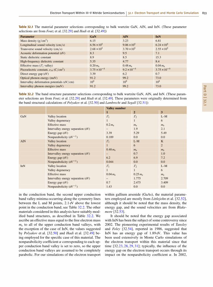
Fig. 32.1 The velocity–field characteristic associated withbulk wurtzite GaN. Like many other compound semi-conductors, the electron drift velocity reaches a peak,and at higher applied electric fields it decreases until itsaturates
Sect. 32.2.5 and Sect. 32.2.6, respectively. Our transientelectron transport analysis results are then presented inSect. 32.2.7. Finally, the conclusions of this electrontransport analysis are summarized in Sect. 32.2.8.
32.2.1 Steady-State Electron TransportWithin Bulk Wurtzite GaN
Our examination of results begins with GaN, the mostcommonly studied III–V nitride semiconductor. Thevelocity–field characteristic associated with this mate-rial is presented in Fig. 32.1. This result was obtainedthrough our Monte Carlo simulations of the electrontransport within this material for the bulk wurtzite GaNparameter selections specified in Table 32.1 and Ta-ble 32.2; the crystal temperature was set to 300K andthe doping concentration to 1017 cm�3. We see thatfor applied electric fields in excess of 140 kV=cm,the electron drift velocity decreases, eventually satu-rating at 1:4�107 cm=s for high applied electric fields.By examining the results of our Monte Carlo simula-tion further, an understanding of this result becomesclear.
First, we discuss the results at low applied electricfields, i. e., applied electric fields of less than 30 kV=cm.This is referred to as the linear regime of electrontransport as the electron drift velocity is well charac-terized by the low-field electron drift mobility � in thisregime, i. e., a linear low-field electron drift velocity de-pendence on the applied electric field, i. e., vd D �E,applies in this regime. Examining the distribution func-tion for this regime, we find that it is very similar to thezero-field distribution function with a slight shift in the
Electron energy (eV)
0Electric field (kV/cm)
2.0
1.0
0.0200 400 600
GaN
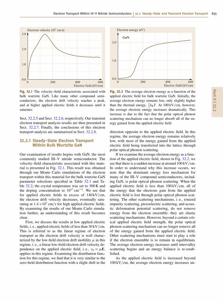
Fig. 32.2 The average electron energy as a function of theapplied electric field for bulk wurtzite GaN. Initially, theaverage electron energy remains low, only slightly higherthan the thermal energy, 3
2kBT . At 100 kV=cm, however,the average electron energy increases dramatically. Thisincrease is due to the fact that the polar optical phononscattering mechanism can no longer absorb all of the en-ergy gained from the applied electric field
direction opposite to the applied electric field. In thisregime, the average electron energy remains relativelylow, with most of the energy gained from the appliedelectric field being transferred into the lattice throughpolar optical phonon scattering.
If we examine the average electron energy as a func-tion of the applied electric field, shown in Fig. 32.2, wesee that there is a sudden increase at around 100 kV=cm.In order to understand why this increase occurs, wenote that the dominant energy loss mechanism formany of the III–V compound semiconductors, includ-ing GaN, is polar optical phonon scattering. When theapplied electric field is less than 100 kV=cm, all ofthe energy that the electrons gain from the appliedelectric field is lost through polar optical phonon scat-tering. The other scattering mechanisms, i. e., ionizedimpurity scattering, piezoelectric scattering, and acous-tic deformation potential scattering, do not removeenergy from the electron ensemble: they are elasticscattering mechanisms. However, beyond a certain crit-ical applied electric field strength, the polar opticalphonon scattering mechanism can no longer remove allof the energy gained from the applied electric field.Other scattering mechanisms must start to play a roleif the electron ensemble is to remain in equilibrium.The average electron energy increases until intervalleyscattering begins and an energy balance is re-estab-lished.
As the applied electric field is increased beyond100 kV=cm, the average electron energy increases un-
PartD|32.2
836 Part D Materials for Optoelectronics and Photonics
Number of particles
0Electric field (kV/cm)
3000
2000
1000
0200 400 600
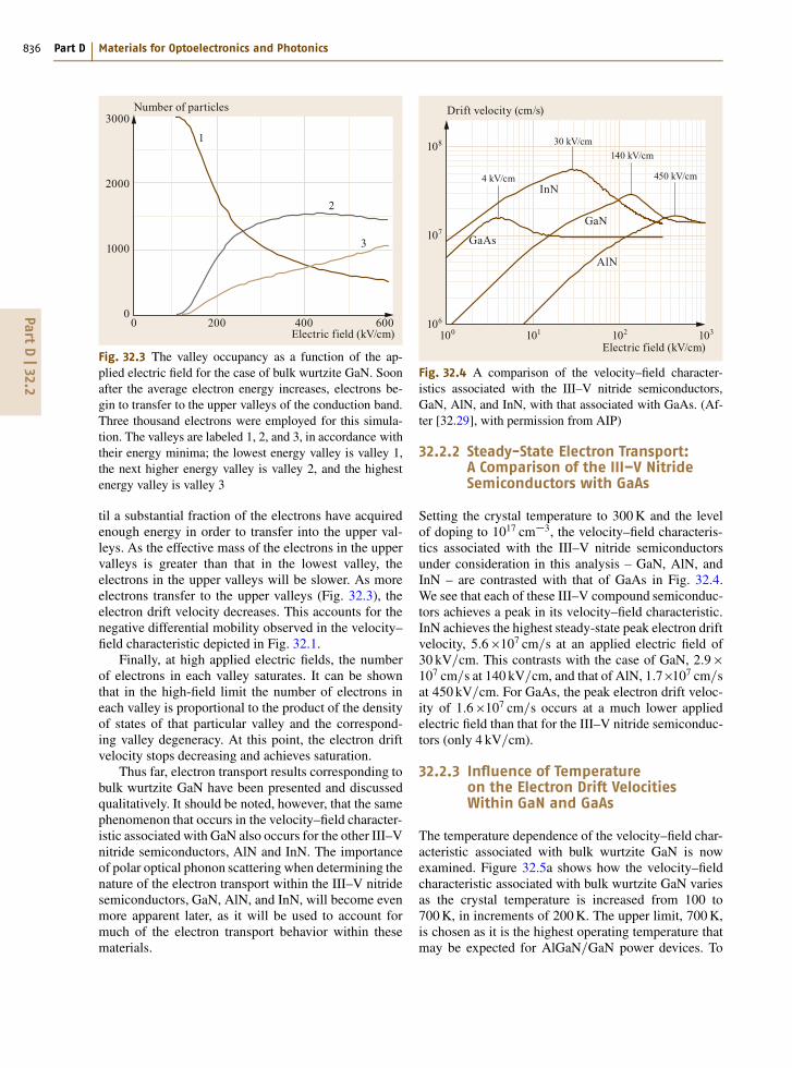
1
2
3
Fig. 32.3 The valley occupancy as a function of the ap-plied electric field for the case of bulk wurtzite GaN. Soonafter the average electron energy increases, electrons be-gin to transfer to the upper valleys of the conduction band.Three thousand electrons were employed for this simula-tion. The valleys are labeled 1, 2, and 3, in accordance withtheir energy minima; the lowest energy valley is valley 1,the next higher energy valley is valley 2, and the highestenergy valley is valley 3
til a substantial fraction of the electrons have acquiredenough energy in order to transfer into the upper val-leys. As the effective mass of the electrons in the uppervalleys is greater than that in the lowest valley, theelectrons in the upper valleys will be slower. As moreelectrons transfer to the upper valleys (Fig. 32.3), theelectron drift velocity decreases. This accounts for thenegative differential mobility observed in the velocity–field characteristic depicted in Fig. 32.1.
Finally, at high applied electric fields, the numberof electrons in each valley saturates. It can be shownthat in the high-field limit the number of electrons ineach valley is proportional to the product of the densityof states of that particular valley and the correspond-ing valley degeneracy. At this point, the electron driftvelocity stops decreasing and achieves saturation.
Thus far, electron transport results corresponding tobulk wurtzite GaN have been presented and discussedqualitatively. It should be noted, however, that the samephenomenon that occurs in the velocity–field character-istic associated with GaN also occurs for the other III–Vnitride semiconductors, AlN and InN. The importanceof polar optical phonon scattering when determining thenature of the electron transport within the III–V nitridesemiconductors, GaN, AlN, and InN, will become evenmore apparent later, as it will be used to account formuch of the electron transport behavior within thesematerials.
100 101 102 103106
107
108
Electric field (kV/cm)
Drift velocity (cm/s)
4 kV/cm
GaAs
140 kV/cm
GaN
450 kV/cm
AlN
30 kV/cm
InN
Fig. 32.4 A comparison of the velocity–field character-istics associated with the III–V nitride semiconductors,GaN, AlN, and InN, with that associated with GaAs. (Af-ter [32.29], with permission from AIP)
32.2.2 Steady-State Electron Transport:A Comparison of the III–V NitrideSemiconductors with GaAs
Setting the crystal temperature to 300K and the levelof doping to 1017 cm�3, the velocity–field characteris-tics associated with the III–V nitride semiconductorsunder consideration in this analysis – GaN, AlN, andInN – are contrasted with that of GaAs in Fig. 32.4.We see that each of these III–V compound semiconduc-tors achieves a peak in its velocity–field characteristic.InN achieves the highest steady-state peak electron driftvelocity, 5:6�107 cm=s at an applied electric field of30 kV=cm. This contrasts with the case of GaN, 2:9�107 cm=s at 140 kV=cm, and that of AlN, 1:7�107 cm=sat 450 kV=cm. For GaAs, the peak electron drift veloc-ity of 1:6�107 cm=s occurs at a much lower appliedelectric field than that for the III–V nitride semiconduc-tors (only 4 kV=cm).
32.2.3 Influence of Temperatureon the Electron Drift VelocitiesWithin GaN and GaAs
The temperature dependence of the velocity–field char-acteristic associated with bulk wurtzite GaN is nowexamined. Figure 32.5a shows how the velocity–fieldcharacteristic associated with bulk wurtzite GaN variesas the crystal temperature is increased from 100 to700K, in increments of 200K. The upper limit, 700K,is chosen as it is the highest operating temperature thatmay be expected for AlGaN=GaN power devices. To

Electron Transport Within III-V Nitride Semiconductors 32.2 Steady-State and Transient Electron Transport 837Part
D|32.2
0Electric field (kV/cm)
3.0
2.5
2.0
1.5
1.0
0.5
0200100 300
100 K
400 500 600
Drift velocity (107 cm/s)Drift velocity (107 cm/s)
0Electric field (kV/cm)
2.5
2.0
1.5
1.0
0.5
0
300 K
700 K500 K
GaAs
300 K
100 K
500 K
700 K
a) b)
20155 10
GaN
Fig. 32.5a,b A comparison of the temperature dependence of the velocity–field characteristics associated with (a) GaNand (b) GaAs. GaN maintains a higher electron drift velocity with increased temperatures than GaAs does
Drift velocity (107 cm/s)
100Temperature (K)
Mobility (cm2/Vs)
200 300 400 500 600 700
2500
2000
1500
1000
500
0
3.5
3.0
2.5
2.0
1.5
1.0
0.5
0.0
Drift velocity (107 cm/s)
100Temperature (K)
Mobility (cm2/Vs)
200 300 400 500 600 700
12000
10 000
8000
6000
4000
2000
0
2.5
2.0
1.5
1.0
0.5
0.0
a) b)
Ga aAsN G
Fig. 32.6a,b A comparison of the temperature dependence of the low-field electron drift mobility (solid lines), the peakelectron drift velocity (diamonds), and the saturation electron drift velocity (solid points) for (a) GaN and (b) GaAs. Thelow-field electron drift mobility of GaN drops quickly with increasing temperature, but its peak and saturation electrondrift velocities are less sensitive to increases in temperature than GaAs
highlight the difference between the III–V nitride semi-conductors with more conventional III–V compoundsemiconductors, such as GaAs, Monte Carlo simula-tions of the electron transport within GaAs have alsobeen performed under the same conditions as GaN. Fig-ure 32.5b shows the results of these simulations. Notethat the electron drift velocity for the case of GaN ismuch less sensitive to changes in temperature than thatassociated with GaAs.
To quantify this dependence further, the low-fieldelectron drift mobility, the peak electron drift veloc-ity, and the saturation electron drift velocity are plotted
as a function of the crystal temperature in Fig. 32.6,these results being determined from our Monte Carlosimulations of the electron transport within these ma-terials. For both GaN and GaAs, it is found that all ofthese electron transport metrics diminish as the crystaltemperature is increased. As may be seen through aninspection of Fig. 32.5, the peak and saturation elec-tron drift velocities do not drop as much in GaN asthey do in GaAs in response to increases in the crys-tal temperature. The low-field electron drift mobilityin GaN, however, is seen to fall quite rapidly withtemperature, this drop being particularly severe for tem-

PartD|32.2
838 Part D Materials for Optoelectronics and Photonics
Scattering rate (1013 s–1)
0Electric field (kV/cm)
10
8
6
4
2
0200 400 600
Scattering rate (1012 s–1)
0Electric field (kV/cm)
10
8
6
4
2
05
GaAs
20
a) b)
500 K
GaN 700 K
300 K
100 K
700 K
500 K
300 K
100 K
5 10 1
Fig. 32.7a,b A comparison of the polar optical phonon scattering rates as a function of the applied electric field strengthfor various crystal temperatures for (a) GaN and (b) GaAs. Polar optical phonon scattering is seen to increase much morequickly with temperature in GaAs
100 K
Number of particles
0Electric field (kV/cm)
3000
2500
2000
1500
1000
500
0200 400 600
Number of particles
0Electric field (kV/cm)
0 1 0100 300 500
3000
2500
2000
1500
1000
500
0
a) b)
GaN
700 K
700 K
100 K GaAs
5 25 1
Fig. 32.8a,b A comparison of the number of particles in the lowest energy valley of the conduction band, the � valley,as a function of the applied electric field for various crystal temperatures, for the cases of (a) GaN and (b) GaAs. InGaAs, the electrons begin to occupy the upper valleys much more quickly, causing the electron drift velocity to drop asthe crystal temperature is increased. Three thousand electrons were employed for these steady-state electron transportsimulations
peratures at and below room temperature. This propertywill likely have an impact on high-power device perfor-mance.
Delving deeper into our Monte Carlo results yieldsclues into the reason for this variation in temperaturedependence. First, we examine the polar optical phononscattering rate as a function of the applied electricfield strength. Figure 32.7 shows that the scattering rateonly increases slightly with temperature for the case ofGaN, from 6:7�1013 s�1 at 100K to 8:6�1013 s�1 at700K, for high applied electric field strengths. Contrast
this with the case of GaAs, where the rate increasesfrom 4:0�1012 s�1 at 100K to more than twice thatamount at 700K, 9:2�1012 s�1, at high applied electricfield strengths. This large increase in the polar opticalphonon scattering rate for the case of GaAs is one rea-son for the large drop in the electron drift velocity withincreasing temperature for the case of GaAs.
A second reason for the variation in temperature de-pendence of the two materials is the occupancy of theupper valleys, shown in Fig. 32.8. In the case of GaN,the upper valleys begin to become occupied at roughly

Electron Transport Within III-V Nitride Semiconductors 32.2 Steady-State and Transient Electron Transport 839Part
D|32.2
Drift velocity (107 cm/s)
0Electric field (kV/cm)
3.0
2.0
1.0
0.0200 400 600
Drift velocity (107 cm/s)
0Electric field (kV/cm)
0100 300 500
2.0
1.5
1.0
0.5
0
a) b)
Ga aAs1016 cm–3
1017 cm–3
1018 cm–3
1019 cm–3
1017 cm–3
1018 cm–3
1019 cm–3
5 20 1
N G
5 1
Fig. 32.9a,b A comparison of the dependence of the velocity–field characteristics associated with (a) GaN and (b)GaAson the doping concentration. GaN maintains a higher electron drift velocity with increased doping levels than GaAs does
1016 1017 1018 1019
1600
1200
800
400
0
3
2
1
0
Drift velocity (107 cm/s)
Doping concentration (cm–3)
Mobility (cm2/Vs)Drift velocity (107 cm/s) Mobility (cm2/Vs)
8000
6000
4000
2000
0
2.0
1.5
1.0
0.5
0.010191017 10181016
Doping concentration (cm–3)
a) b)
Ga aAsN G
Fig. 32.10a,b A comparison of the low-field electron drift mobility (solid lines), the peak electron drift velocity (dia-monds), and the saturation electron drift velocity (solid points) for (a) GaN and (b) GaAs as a function of the dopingconcentration. These parameters are more insensitive to increases in doping in GaN than in GaAs
the same applied electric field strength, 100 kV=cm,independent of temperature. For the case of GaAs, how-ever, the upper valleys are at a much lower energythan those in GaN. In particular, while the first upperconduction band valley minimum is 1:9 eV above thelowest point in the conduction band in GaN, the firstupper conduction band valley is only 290meV abovethe bottom of the conduction band in GaAs [32.53]. Asthe upper conduction band valleys are so close to thebottom of the conduction band for the case of GaAs,the thermal energy (at 700K, kBT Š 60meV) is enoughin order to allow for a small fraction of the electrons totransfer into the upper valleys even before an electricfield is applied. When electrons occupy the upper val-
leys, intervalley scattering and the upper valleys’ largereffective masses reduce the overall electron drift ve-locity. This is another reason why the velocity–fieldcharacteristic associated with GaAs is more sensitiveto variations in crystal temperature than that associatedwith GaN.
32.2.4 Influence of Doping on the ElectronDrift Velocities Within GaN and GaAs
One parameter that can be readily controlled duringthe fabrication of semiconductor devices is the dop-ing concentration. Understanding the effect of dopingon the resultant electron transport is also important.

PartD|32.2
840 Part D Materials for Optoelectronics and Photonics
Scattering rate (1013 s–1)
0Electric field (kV/cm)
10
8
6
4
2
0200 400 600
Scattering rate (1012 s–1)
0Electric field (kV/cm)
10
8
6
4
2
0
a) b)
Ga aAs
1016 cm–3
1019 cm–3
1018 cm–3
1017 cm–3
1017 cm–3
1018 cm–3
1019 cm–3
N G
205 10 15
Fig. 32.11a,b A comparison of the polar optical phonon scattering rates as a function of the applied electric field, forboth (a) GaN and (b) GaAs, for various doping concentrations
Number of particles
0Electric field (kV/cm)
3000
2000
1000
0200 400 600
Number of particles
0Electric field (kV/cm)
3000
2500
2000
1500
1000
500
0
a) b)
Ga aAs
1019 cm–3
1017 cm–3
1017 cm–3
1018 cm–3
1019 cm–3
N G
20155 10
Fig. 32.12a,b A comparison of the number of particles in the lowest valley of the conduction band, the � valley, asa function of the applied electric field, for both (a) GaN and (b) GaAs, for various doping concentration levels. Threethousand electrons were employed for these steady-state electron transport simulations
In Fig. 32.9, the velocity–field characteristic associatedwith GaN is presented for a number of different dop-ing concentration levels. Once again, three importantelectron transport metrics are influenced by the dopingconcentration level: the low-field electron drift mobil-ity, the peak electron drift velocity, and the saturationelectron drift velocity; see Fig. 32.10. Our simula-tion results suggest that for doping concentrations ofless than 1017 cm�3, there is very little effect on thevelocity–field characteristic for the case of GaN. How-ever, for doping concentrations above 1017 cm�3, thepeak electron drift velocity diminishes considerably,from 2:9�107 cm=s for the case of 1017 cm�3 dopingto 2:0�107 cm=s for the case of 1019 cm�3 doping. Thesaturation electron drift velocity within GaN is found
to only decrease slightly in response to increases in thedoping concentration. The effect of doping on the low-field electron drift mobility is also shown. It is seen thatthis mobility drops significantly in response to increasesin the doping concentration level, from 1200 cm2=.Vs/at 1016 cm�3 doping to 400 cm2=.Vs/ at 1019 cm�3
doping.As we did for temperature, we compare the sen-
sitivity of the velocity-field characteristic associatedwith GaN to doping with that associated with GaAs.Figure 32.10 shows this comparison. For the case ofGaAs, it is seen that the electron drift velocities de-crease much more with increased doping than thoseassociated with GaN. In particular, for the case ofGaAs, the peak electron drift velocity decreases from

Electron Transport Within III-V Nitride Semiconductors 32.2 Steady-State and Transient Electron Transport 841Part
D|32.2
0
2.0
1.5
1.0
0.5
0200 400 600
Drift velocity (107 cm/s)Drift velocity (107 cm/s)
100Temperature (K)
200 300 400 500
2.0
1.5
1.0
0.5
0.0800 1000
400
300
200
100
0
Mobility (cm2/Vs)
600 700
a) b)
Al lN100 K
300 K
500 K
700 K
N A
Electric field (kV/cm)
Fig. 32.13 The velocity–field characteristic associated with AlN (a) for various crystal temperatures. The trends in thelow-field mobility (solid line), the peak electron drift velocity (diamonds), and the saturation electron drift velocity(solid points), are also shown. AlN exhibits its peak electron drift velocity at very high applied electric fields. AlN hasthe lowest peak electron drift velocity and the lowest low-field electron drift mobility of the III–V nitride semiconductorsconsidered in this analysis (b)
1:8�107 cm=s at 1016 cm�3 doping to 0:6�107 cm=sat 1019 cm�3 doping. For GaAs, at the higher dop-ing levels, the peak in the velocity-field characteris-tic disappears completely for sufficiently high dopingconcentrations. The saturation electron drift velocitydecreases from 1:0�107 cm=s at 1016 cm�3 doping to0:6�107 cm=s at 1019 cm�3 doping. The low-field elec-tron drift mobility also diminishes dramatically withincreased doping, dropping from 7800 cm2=.Vs/ at1016 cm�3 doping to 2200 cm2=.Vs/ at 1019 cm�3 dop-ing; see Fig. 32.10.
Once again, it is interesting to determine why thedoping dependence in GaAs is so much more pro-nounced than it is in GaN. Again, we examine the polaroptical phonon scattering rate and the occupancy ofthe upper valleys. Figure 32.11 shows the polar opti-cal phonon scattering rates as a function of the appliedelectric field, for both GaN and GaAs. In this case, how-ever, due to screening effects, the rate drops when thedoping concentration is increased. The decrease, how-ever, is much more pronounced for the case of GaAsthan for GaN. It is believed that this drop in the polaroptical phonon scattering rate allows for upper valleyoccupancy to occur more quickly in GaAs rather thanin GaN (Fig. 32.12). For GaN, electrons begin to oc-cupy the upper valleys at roughly the same appliedelectric field strength, independent of the doping level.However, for the case of GaAs, the upper valleys areoccupied more quickly with greater doping. When theupper valleys are occupied, the electron drift velocitydecreases due to intervalley scattering and the larger ef-fective mass of the electrons within the upper valleys.
32.2.5 Electron Transport in AlN
AlN has the largest effective mass of the III–V nitridesemiconductors considered in this analysis. Accord-ingly, it is not surprising that this material exhibits thelowest electron drift velocity and the lowest low-fieldelectron drift mobility. The sensitivity of the velocity–field characteristic associated with AlN to variationsin the crystal temperature may be examined by con-sidering Fig. 32.13. As with the case of GaN, thevelocity–field characteristic associated with AlN is ex-tremely robust to variations in the crystal temperature.In particular, its peak electron drift velocity, which is1:8�107 cm=s at 100K, only decreases to 1:2�107 cm=sat 700K. Similarly, its saturation electron drift veloc-ity, which is 1:5�107 cm=s at 100K, only decreasesto 1:0�107 cm=s at 700K. The low-field electron driftmobility associated with AlN also diminishes in re-sponse to increases in the crystal temperature, from375 cm2=.Vs/ at 100K to 40 cm2=.Vs/ at 700K.
The sensitivity of the velocity–field characteristicassociated with AlN to variations in the doping concen-tration may be examined by considering Fig. 32.14. Itis noted that the variations in the velocity–field char-acteristic associated with AlN in response to variationsin the doping concentration are not as pronounced asthose which occur in response to variations in thecrystal temperature. Quantitatively, the peak electrondrift velocity drops from 1:7�107 cm=s at 1017 cm�3
doping to 1:3�107 cm=s at 1019 cm�3 doping. Simi-larly, its saturation electron drift velocity drops from1:4�107 cm=s at 1017 cm�3 doping to 1:2�107 cm=s

PartD|32.2
842 Part D Materials for Optoelectronics and Photonics
0Electric field (kV/cm)
2.0
1.5
1.0
0.5
0200 400 600
Drift velocity (107 cm/s)Drift velocity (107 cm/s)
1016
Doping concentration (cm–3)
2.0
1.5
1.0
0.5
0.0800 1000
250
200
150
100
50
0
Mobility (cm2/Vs)
1017 1018 1019
a) b)
Al lN1017cm–3 1018cm–3
1019cm–3
N A
Fig. 32.14 The velocity–field characteristic associated with AlN for various doping concentrations (a). The trends in thelow-field electron drift mobility (solid line), the peak electron drift velocity (diamonds), and the saturation electron driftvelocity (solid points), are also shown (b)
100 200 300 400 500 600 700Temperature (K)
InN
Drift velocity (107 cm/s) Mobility (cm2/Vs)
0
1
2
3
4
5
6
0
5000
10 000
15000
20 000
25000a) b)
0 50 100 150 200 250 3000
1
2
3
4
5
6
Electric field (kV/cm)
Drift velocity (107 cm/s)
100 K300 K
500 K700 K
InN
Fig. 32.15 The velocity–field characteristic associated with InN for various crystal temperatures (a). The trends in thelow-field electron drift mobility (solid line), the peak electron drift velocity (diamonds), and the saturation electron driftvelocity (solid points), are also shown (b). InN has the highest peak electron drift velocity and the highest low-fieldelectron drift mobility of the III–V nitride semiconductors considered in this analysis
at 1019 cm�3 doping. The influence of doping on thelow-field electron drift mobility associated with AlN isalso observed to be not as pronounced as for the caseof crystal temperature. Figure 32.14b shows that thelow-field electron drift mobility associated with AlNdecreases from 140 cm2=.Vs/ at 1016 cm�3 doping to100 cm2=.Vs/ at 1019 cm�3 doping.
32.2.6 Electron Transport in InN
InN has the smallest effective mass of the three III–Vnitride semiconductors considered in this analysis. Ac-
cordingly, it is not surprising that it exhibits the highestelectron drift velocity and the highest low-field elec-tron drift mobility. The sensitivity of the velocity-fieldcharacteristic associated with InN to variations in thecrystal temperature may be examined by consideringFig. 32.15. As with the cases of GaN and AlN, thevelocity–field characteristic associated with InN is ex-tremely robust to increases in the crystal temperature.In particular, its peak electron drift velocity, which is6:0�107 cm=s at 100K, only decreases to 4:2�107 cm=sat 700K. Similarly, its saturation electron drift veloc-ity, which is 1:5�107 cm=s at 100K, only decreases to

Electron Transport Within III-V Nitride Semiconductors 32.2 Steady-State and Transient Electron Transport 843Part
D|32.2
1016 1017 1018 1019
Doping concentration (cm−3)
InN
Drift velocity (107 cm/s) Mobility (cm2/Vs)
0
1
2
3
4
5
6
0
2000
4000
6000
8000
10 000
12000a) b)
0 50 100 150 200 250 3000
1
2
3
4
5
6
5 × 1018 cm−3
InN
1018 cm−3
1017 cm−3
Electric field (kV/cm)
Drift velocity (107 cm/s)
Fig. 32.16 The velocity–field characteristic associated with InN for various doping concentrations (a). The trends in thelow-field electron drift mobility (solid line), the peak electron drift velocity (diamonds), and the saturation electron driftvelocity (solid points), are also shown (b)
1:0�107 cm=s at 700K. The low-field electron drift mo-bility associated with InN also diminishes in responseto increases in the crystal temperature, from about22 000 cm2=.Vs/ at 100K to below 2300 cm2=.Vs/at 700K.
The sensitivity of the velocity–field characteristicassociated with InN to variations in the doping con-centration may be examined by considering Fig. 32.16.These results suggest a similar robustness to the dop-ing concentration for the case of InN. In particular, it isnoted that for doping concentrations below 1017 cm�3,the velocity–field characteristic associated with InNexhibits very little dependence on the doping concen-tration. When the doping concentration is increasedabove 1017 cm�3, however, the peak electron drift ve-locity diminishes. Quantitatively, the peak electron driftvelocity decreases from 5:6�107 cm=s at 1017 cm�3
doping to 4:2�107 cm=s at 5�1018 cm�3 doping; a nu-merical instability occurs for the case of InN at largedoping concentrations, owing to its small electron ef-fective mass, and this prevented the determination ofa 1019 cm�3 doping concentration result. The satura-tion electron drift velocity only drops slightly, how-ever, from 1:4�107 cm=s at 1017 cm�3 doping to 1:3�107 cm=s at 5�1018 cm�3 doping. The low-field elec-tron drift mobility, however, drops significantly withdoping, from 12 000 cm2=.Vs/ at 1016 cm�3 doping to4900 cm2=.Vs/ at 5�1018 cm�3 doping.
32.2.7 Transient Electron Transport
Steady-state electron transport is the dominant electrontransport mechanism in devices with larger dimensions.
For devices with smaller dimensions, however, transientelectron transport must also be considered when evalu-ating device performance. Ruch [32.59] demonstrated,for both silicon and GaAs, that the transient electrondrift velocity may exceed the corresponding steady-state electron drift velocity by a considerable marginfor appropriate selections of the applied electric field.Shur and Eastman [32.60] explored the device implica-tions of transient electron transport, and demonstratedthat substantial improvements in the device perfor-mance can be achieved as a consequence. Heiblumet al. [32.61] made the first direct experimental observa-tion of transient electron transport within GaAs. Sincethen there have been a number of experimental inves-tigations into the transient electron transport within theIII–V compound semiconductors [32.62–64].
Thus far, very little research has been investedinto the study of transient electron transport withinthe III–V nitride semiconductors, GaN, AlN, and InN.Foutz et al. [32.21] examined transient electron trans-port within both the wurtzite and zinc blende phasesof GaN. In particular, they examined how electrons,initially in thermal equilibrium, respond to the suddenapplication of a constant electric field. In devices withdimensions greater than 0:2�m, they found that steady-state electron transport is expected to dominate deviceperformance. For devices with smaller dimensions,however, upon the application of a sufficiently highelectric field, they found that the transient electron driftvelocity can considerably overshoot the correspondingsteady-state electron drift velocity. This velocity over-shoot was found to be comparable with that whichoccurs within GaAs.

PartD|32.2
844 Part D Materials for Optoelectronics and Photonics
0.0Distance (νm)
10.0
8.0
6.0
4.0
2.0
0.00.1 0.2 0. .4 0.00
Distance (νm)
5.0
4.0
3.0
2.0
1.0
0.00.01 0.02 0.03 0.04 0.05
Distance (μm)
Drift velocity (107 cm/s)Drift velocity (107 cm/s)
Drift velocity (107 cm/s)Drift velocity (107 cm/s)
0.0Distance (νm)
6.0
5.0
4.0
3.0
2.0
1.0
0.00. .4 0.6 0.8 1.0
a)
GaN
b)
AlN
c) d)
GaAs
560 kV/cm
280 kV/cm
210 kV/cm
140 kV/cm
70 kV/cm
1800 kV/cm
900 kV/cm
675 kV/cm450 kV/cm
225 kV/cm
16 kV/cm
8 kV/cm
6 kV/cm4 kV/cm
2 kV/cm
0 0.1 0.2 0.3 0.4 0.5 0.6 0.7 0.80
2
4
6
8
10 60 kV/cm
15 kV/cm
45 kV/cm30 kV/cm
InN120 kV/cm
3 0
2 0
Fig. 32.17a–d The electron drift velocity as a function of the distance displaced since the application of the electric fieldfor various applied electric field strengths, for the cases of (a) GaN, (b) AlN, (c) InN, and (d) GaAs. In all cases, wehave assumed an initial zero field electron distribution, a crystal temperature of 300K, and a doping concentration of1017 cm�3. (After [32.29] with permission, copyright AIP)
Foutz et al. [32.29] performed a subsequent analy-sis in which the transient electron transport within allof the III–V nitride semiconductors under considerationin this analysis were compared with that which occurswithin GaAs. In particular, following the approach ofFoutz et al. [32.21], they examined how electrons, ini-tially in thermal equilibrium, respond to the suddenapplication of a constant electric field. A key result ofthis study, presented in Fig. 32.17, plots the transientelectron drift velocity as a function of the distance dis-placed since the electric field was initially applied fora number of applied electric field strengths and for eachof the materials considered in this analysis. The InN re-sults have been updated owing to the revisions in thematerial parameter selections corresponding to this par-ticular material; see Figure 32.17c.
Focusing initially on the case of GaN (Fig. 32.17a),we note that the electron drift velocity for the ap-plied electric field strengths 70 kV=cm and 140 kV=cmreaches steady-state very quickly, with little or novelocity overshoot. In contrast, for applied electricfield strengths above 140 kV=cm, significant velocityovershoot occurs. This result suggests that in GaN,140 kV=cm is a critical field for the onset of veloc-ity overshoot effects. As mentioned in Sect. 32.2.2,140 kV=cm also corresponds to the peak in thevelocity-field characteristic associated with GaN; recallFig. 32.4. Steady-stateMonte Carlo simulations suggestthat this is the point at which significant upper valleyoccupation begins to occur; recall Fig. 32.3. This sug-gests that velocity overshoot is related to the transferof electrons to the upper valleys. Similar results are

Electron Transport Within III-V Nitride Semiconductors 32.3 Electron Transport Within III–V Nitride Semiconductors 845Part
D|32.3
0 0.05 0.1 0.15 0.2 0.25 0.3 0.35 0.40
1
2
3
4
5
6
7
8
9
10
Distance (μm)
Drift velocity (107 cm/s)
InN
GaN
AlN
GaAs
Fig. 32.18 A comparison of the velocity overshootamongst the III–V nitride semiconductors and GaAs. Theapplied electric field strength chosen corresponds to twicethe critical applied electric field strength at which thepeak in the steady-state velocity–field characteristic oc-curs (Fig. 32.4), i. e., 280 kV=cm for the case of GaN,900 kV=cm for the case of AlN, 60 kV=cm for the caseof InN, and 8 kV=cm for the case of GaAs. (After [32.29]with permission, copyright AIP)
found for the other III–V nitride semiconductors, AlNand InN, and GaAs; see Figs. 32.17b–d.
We now compare the transient electron transportcharacteristics for the materials. From Fig. 32.17, it isclear that certain materials exhibit higher peak over-shoot velocities and longer overshoot relaxation times.It is not possible to fairly compare these different semi-conductors by applying the same applied electric fieldstrength to each of the materials, as the transient effectsoccur over such a disparate range of applied electricfield strengths in each material. In order to facilitatesuch a comparison, we choose a field strength equal
to twice the critical applied electric field strength foreach material. Figure 32.18 shows a comparison ofthe velocity overshoot effects amongst the four mate-rials considered in this analysis, i. e., GaN, AlN, InN,and GaAs. It is clear that among the three III–V ni-tride semiconductors considered, InN exhibits superiortransient electron transport characteristics. In particular,InN has the largest overshoot velocity and the distanceover which this overshoot occurs, 0:6�m, is longer thanin either GaN or AlN. GaAs exhibits a longer overshootrelaxation distance, approximately 0:7�m, but the elec-tron drift velocity exhibited by InN is greater than thatof GaAs for all distances.
32.2.8 Electron Transport: Conclusions
In this section, steady-state and transient electron trans-port results, corresponding to the III–V nitride semi-conductors, GaN, AlN, and InN, were presented, theseresults being obtained from our Monte Carlo simula-tions of the electron transport within these materials.Steady-state electron transport was the dominant themeof our analysis. In order to aid in the understandingof these electron transport characteristics, a compar-ison was made between GaN and GaAs. Our simu-lations showed that GaN is more robust to variationsin crystal temperature and doping concentration thanGaAs, and an analysis of our Monte Carlo simula-tion results showed that polar optical phonon scatteringplays the dominant role in accounting for these differ-ences in behavior. This analysis was also performedfor the other III–V nitride semiconductors consideredin this analysis – AlN and InN – and similar resultswere obtained. Finally, we presented some key tran-sient electron transport results. These results indicatedthat the transient electron transport that occurs withinInN is the most pronounced of all of the materials un-der consideration in this review (GaN, AlN, InN, andGaAs).
32.3 Electron Transport Within III–V Nitride Semiconductors: A Review
Pioneering investigations into the material propertiesof the III–V nitride semiconductors, GaN, AlN, andInN, were performed during the earlier half of the20th Century [32.65–67]. The III–V nitride semicon-ductor materials available at the time, small crystalsand powders, were of poor quality, and completely un-suitable for device applications. Thus, it was not untilthe late 1960s, when Maruska and Tietjen [32.68] em-ployed chemical vapor deposition to fabricate GaN,that interest in the III–V nitride semiconductors expe-
rienced a renaissance. Since that time, interest in theIII–V nitride semiconductors has been growing, thematerial properties of these semiconductors improv-ing considerably over the years. As a result of thisresearch effort, there are currently a number of com-mercial devices available that employ the III–V nitridesemiconductors. More III–V nitride semiconductor-based device applications are currently under develop-ment, and these should become available in the nearfuture.

PartD|32.3
846 Part D Materials for Optoelectronics and Photonics
In this section, we present a brief overview of theIII–V nitride semiconductor electron transport field. Westart with a survey describing the evolution of the field.In particular, the sequence of critical developments thathave occurred that contribute to our current understand-ing of the electron transport mechanisms within theIII–V nitride semiconductors, GaN, AlN, and InN, ischronicled. Then, some of the more recent literaturerelated to the electron transport within the III–V ni-tride semiconductors, GaN, AlN, and InN, is presented,with particular emphasis being placed on the most re-cent developments in the field that have occurred in the21st Century, and how such developments have shapedour understanding of the electron transport mechanismswithin these materials. Finally, frontiers for further re-search and investigation are presented.
This section is organized in the following manner.In Sect. 32.3.1, we present a brief survey describingthe evolution of the field. Then, in Sect. 32.3.2, the de-velopments that have occurred in the 21st Century arediscussed. Finally, frontiers for further research and in-vestigation are presented in Sect. 32.3.3.
32.3.1 Evolution of the Field
The favorable electron transport characteristics of theIII–V nitride semiconductors, GaN, AlN, and InN, havelong been recognized. As early as the 1970s, Littlejohnet al. [32.13] pointed out that the large polar opticalphonon energy characteristic of GaN, in conjunctionwith its large intervalley energy separation, suggestsa high saturation electron drift velocity for this mate-rial. As high-frequency electron device performance is,to a large degree, determined by this saturation elec-tron drift velocity [32.14], the recognition of this factignited enhanced interest in this material and its III–Vnitride semiconductor compatriots, AlN and InN. Thisenhanced interest, and the developments which havetranspired as a result of it, are responsible for the III–V nitride semiconductor industry of today.
In 1975, Littlejohn et al. [32.13] were the first to re-port results obtained from semi-classical Monte Carlosimulations of the steady-state electron transport withinbulk wurtzite GaN. A one-valley model for the conduc-tion band was adopted in their analysis. Steady-stateelectron transport, for both parabolic and nonparabolicband structures, was considered in their analysis, non-parabolicity being treated through the application of theKane model [32.43]. The primary focus of their in-vestigation was the determination of the velocity-fieldcharacteristic associated with GaN. All donors were as-sumed to be ionized, and the free electron concentrationwas taken to be equal to the dopant concentration. Thescattering mechanisms considered were:
1. Ionized impurity2. Polar optical phonon3. Piezoelectric4. Acoustic deformation potential.
For the case of the parabolic band, in the ab-sence of ionized impurities, they found that the electrondrift velocity monotonically increases with the appliedelectric field strength, saturating at a value of about2:5�107 cm=s for the case of high applied electricfields. In contrast, for the case of the nonparabolicband, and in the absence of ionized impurities, a re-gion of negative differential mobility was found, theelectron drift velocity achieving a maximum of about2�107 cm=s at an applied electric field strength ofabout 100 kV=cm, with further increases in the appliedelectric field strength resulting in a slight decrease inthe corresponding electron drift velocity. The role ofionized impurity scattering was also investigated by Lit-tlejohn et al. [32.13].
In 1993, Gelmont et al. [32.16] reported on ensem-ble semi-classical two-valley Monte Carlo simulationsof the electron transport within bulk wurtzite GaN,this analysis improving upon the analysis of Littlejohnet al. [32.13] by incorporating intervalley scattering intothe simulations. They found that the negative differen-tial mobility found in bulk wurtzite GaN is much morepronounced than that found by Littlejohn et al. [32.13],and that intervalley transitions are responsible for this.For a doping concentration of 1017 cm�3, Gelmontet al. [32.16] demonstrated that the electron drift ve-locity achieves a peak value of about 2:8�107 cm=sat an applied electric field of about 140 kV=cm. Theimpact of intervalley transitions on the electron dis-tribution function was also determined and shown tobe significant. The impact of doping and compensationon the velocity-field characteristic associated with bulkwurtzite GaN was also examined.
Since these pioneering investigations, ensembleMonte Carlo simulations of the electron transportwithin GaN have been performed numerous times.In particular, in 1995 Mansour et al. [32.18] reportedthe use of such an approach in order to determinehow the crystal temperature influences the velocity-field characteristic associated with bulk wurtzite GaN.Later that year, Kolník et al. [32.19] reported on em-ploying full-band Monte Carlo simulations of the elec-tron transport within bulk wurtzite GaN and bulk zincblende GaN, finding that bulk zinc blende GaN ex-hibits a much higher low-field electron drift mobilitythan bulk wurtzite GaN. The peak electron drift veloc-ity corresponding to bulk zinc blende GaN was foundto be only marginally greater than that exhibited bybulk wurtzite GaN, however. In 1997, Bhapkar and

Electron Transport Within III-V Nitride Semiconductors 32.3 Electron Transport Within III–V Nitride Semiconductors 847Part
D|32.3
Shur [32.22] reported on employing ensemble semi-classical three-valley Monte Carlo simulations of theelectron transport within bulk and confined wurtziteGaN. Their simulations demonstrated that the two-dimensional electron gas within a confined wurtziteGaN structure will exhibit a higher low-field electrondrift mobility than bulk wurtzite GaN, by almost anorder of magnitude, this being in agreement with ex-periment. In 1998, Albrecht et al. [32.27] reported onemploying ensemble semi-classical five-valley MonteCarlo simulations of the electron transport within bulkwurtzite GaN, with the aim of determining elementaryanalytical expressions for a number of electron trans-port metrics corresponding to bulk wurtzite GaN, forthe purposes of device modeling.
Electron transport within the other III–V nitridesemiconductors, AlN and InN, has also been studied us-ing ensemble semi-classical Monte Carlo simulationsof the electron transport. In particular, by employ-ing ensemble semi-classical three-valley Monte Carlosimulations, the velocity–field characteristic associatedwith bulk wurtzite AlN was studied and reported byO’Leary et al. [32.24] in 1998. They found that AlNexhibits the lowest peak and saturation electron driftvelocities of the III–V nitride semiconductors con-sidered in this analysis. Similar simulations of theelectron transport within bulk wurtzite AlN were alsoreported by Albrecht et al. [32.25] in 1998. The resultsof O’Leary et al. [32.24] and Albrecht et al. [32.25]were found to be quite similar. The first known sim-ulation of the electron transport within bulk wurtziteInN was the semi-classical three-valley Monte Carlosimulation of O’Leary et al. [32.23], reported in 1998.InN was demonstrated to have the highest peak andsaturation electron drift velocities of the III–V nitridesemiconductors. The subsequent ensemble full-bandMonte Carlo simulations of Bellotti et al. [32.28], re-ported in 1999, produced results similar to those ofO’Leary et al. [32.23].
The first known study of transient electron trans-port within the III–V nitride semiconductors was thatperformed by Foutz et al. [32.21], reported in 1997. Inthis study, ensemble semi-classical three-valley MonteCarlo simulations were employed in order to determinehow the electrons within wurtzite and zinc blende GaN,initially in thermal equilibrium, respond to the suddenapplication of a constant electric field. The velocityovershoot that occurs within these materials was exam-ined. It was found that the electron drift velocities thatoccur within the zinc blende phase of GaN are slightlygreater than those exhibited by the wurtzite phase ow-ing to the slightly the smaller effective mass of theelectrons within the zinc blende phase of this material.A comparison with the transient electron transport that
occurs within GaAs was made. Using the results fromthis analysis, a determination of the minimum transittime as a function of the distance displaced since theapplication of the applied electric field was performedfor all three materials considered in this study: wurtziteGaN, zinc blende GaN, and GaAs. For distances inexcess of 0:1�m, both phases of GaN were shownto exhibit superior performance (reduced transit time)when contrasted with that associated with GaAs.
A more general analysis, in which transient electrontransport within GaN, AlN, and InN was studied, wasperformed by Foutz et al. [32.29], and reported in 1999.As with their previous study, Foutz et al. [32.29] deter-mined how electrons, initially in thermal equilibrium,respond to the sudden application of a constant electricfield. For GaN, AlN, InN, and GaAs, it was found thatthe electron drift velocity overshoot only occurs whenthe applied electric field exceeds a certain critical ap-plied electric field strength unique to each material. Thecritical applied electric field strengths, 140 kV=cm forthe case of wurtzite GaN, 450 kV=cm for the case ofAlN, 65 kV=cm for the case of InN (this was the criticalapplied electric field strength corresponding to our pre-vious InN parameter selections [32.29]), and 4 kV=cmfor the case of GaAs, were shown to correspond to thepeak electron drift velocity in the velocity-field charac-teristic associated with each of these materials; recallFig. 32.4. It was found that InN exhibits the highestpeak overshoot velocity, and that this overshoot lastsover prolonged distances compared with AlN, InN, andGaAs. A comparison with the results of experiment wasperformed.
In addition to Monte Carlo simulations of the elec-tron transport within these materials, a number ofother types of electron transport studies have been per-formed. In 1975, for example, Ferry [32.14] reportedon the determination of the velocity-field character-istic associated with wurtzite GaN using a displacedMaxwellian distribution function approach. For highapplied electric fields, Ferry [32.14] found that the elec-tron drift velocity associated with GaN monotonicallyincreases with the applied electric field strength (it doesnot saturate), reaching a value of about 2:5�107 cm=sat an applied electric field strength of 300 kV=cm.The device implications of this result were furtherexplored by Das and Ferry [32.15]. In 1994, Chinet al. [32.17] reported on a detailed study of the de-pendence of the low-field electron drift mobilities as-sociated with the III–V nitride semiconductors, GaN,AlN, and InN, on crystal temperature and doping con-centration. An analytical expression for the low-fieldelectron drift mobility � determined using a variationalprinciple, was used for the purposes of this analy-sis. The results obtained were contrasted with those

PartD|32.3
848 Part D Materials for Optoelectronics and Photonics
from experiment. A subsequent mobility study was re-ported in 1997 by Look et al. [32.38]. Then, in 1998,Weimann et al. [32.26] reported on a model for deter-mining how the scattering of electrons by the threadingdislocations within bulk wurtzite GaN influence thelow-field electron drift mobility. They demonstratedwhy the experimentally measured low-field electrondrift mobility associated with this material is muchlower than that predicted from Monte Carlo analyses:threading dislocations were not taken into account inthe Monte Carlo simulations of the electron transportwithin the III–V nitride semiconductors, GaN, AlN, andInN.
While the negative differential mobility exhibitedby the velocity-field characteristics associated with theIII–V nitride semiconductors, GaN, AlN, and InN, iswidely attributed to intervalley transitions, and whiledirect experimental evidence confirming this has beenpresented [32.69], Krishnamurthy et al. [32.34] sug-gest that the inflection points in the bands located inthe vicinity of the � valley are primarily responsi-ble for the negative differential mobility exhibited bywurtzite GaN instead. The relative importance of thesetwo mechanisms (intervalley transitions and inflectionpoint considerations) were evaluated by Krishnamurthyet al. [32.34], for both bulk wurtzite GaN and an AlGaNalloy.
32.3.2 Developments in the 21st Century
Thus far, the electron transport results that have beenpresented have focused on developments in our under-standing of the nature of the electron transport withinthe III–V nitride semiconductors, GaN, AlN, and InNthat were acquired in the latter part of the 20th Century.There have been a number of interesting more recentdevelopments in the study of the electron transportwithin the III–V nitride semiconductors which have in-fluenced the direction of thought in this field. On theexperimental front, in 2000 Wraback et al. [32.33] re-ported on the use of a femtosecond optically detectedtime-of-flight experimental technique in order to ex-perimentally determine the velocity–field characteristicassociated with bulk wurtzite GaN. They found that thepeak electron drift velocity, 1:9�107 cm=s, is achievedat an applied electric field strength of 225 kV=cm. Nodiscernible negative differential mobility was observed.Wraback et al. [32.33] suggested that the large defectdensity characteristic of the GaN samples they em-ployed, which were not taken into account in MonteCarlo simulations of the electron transport within thismaterial, accounts for the difference between this exper-imental result and that obtained using simulation. Theyalso suggested that decreasing the intervalley energy
separation from about 2 eV to 340meV, as suggestedby the experimental results of Brazel et al. [32.58], mayalso account for these observations.
The determination of the electron drift velocityfrom experimental measurements of the unity gain cut-off frequency ft has been pursued by a number ofresearchers. The key challenge in these analyses isthe de-embedding of the parasitics from the experi-mental measurements so that the true intrinsic satura-tion electron drift velocity may be obtained. Eastmanet al. [32.70] present experimental evidence which sug-gests that the saturation electron drift velocity withinbulk wurtzite GaN is about 1:2�107�1:3�107 cm=s.A more recent report, by Oxley and Uren [32.71], sug-gests a value of 1:1�107 cm=s. The role of self-heatingwas also probed by Oxley and Uren [32.71] and shownto be relatively insignificant. A completely satisfactoryexplanation for the discrepancy between these resultsand those from the Monte Carlo simulations has yet tobe provided.
Wraback et al. [32.72] performed a subsequentstudy on the transient electron transport within wurtziteGaN. In particular, using their femtosecond opticallydetected time-of-flight experimental technique in or-der to experimentally determine the velocity overshootthat occurs within bulk wurtzite GaN, they observedsubstantial velocity overshoot within this material. Inparticular, a peak transient electron drift velocity of7:25�107cm/s was observed within the first 200 fs afterphotoexcitation for an applied electric field strength of320 kV=cm. These experimental results were shown tobe consistent with the theoretical predictions of Foutzet al. [32.29].
On the theoretical front, there have been a numberof recent developments. In 2001, O’Leary et al. [32.30]presented an elementary, one-dimensional analyticalmodel for the electron transport within the III–V com-pound semiconductors, and applied it to the cases ofwurtzite GaN and GaAs. The predictions of this an-alytical model were compared with those of MonteCarlo simulations and were found to be in satisfac-tory agreement. Hot-electron energy relaxation timeswithin the III–V nitride semiconductors were studiedby Matulionis et al. [32.73] and reported in 2002. Bu-lutay et al. [32.74] studied the electron momentum andenergy relaxation times within the III–V nitride semi-conductors and reported the results of this study in2003. It is particularly interesting to note that theirarguments add considerable credence to the earlier in-flection point argument of Krishnamurthy et al. [32.34].In 2004, Brazis and Raguotis [32.75] reported on theresults of a Monte Carlo study involving additionalphonon modes and a smaller intervalley energy separa-tion for bulk wurtzite GaN. Their results were found to
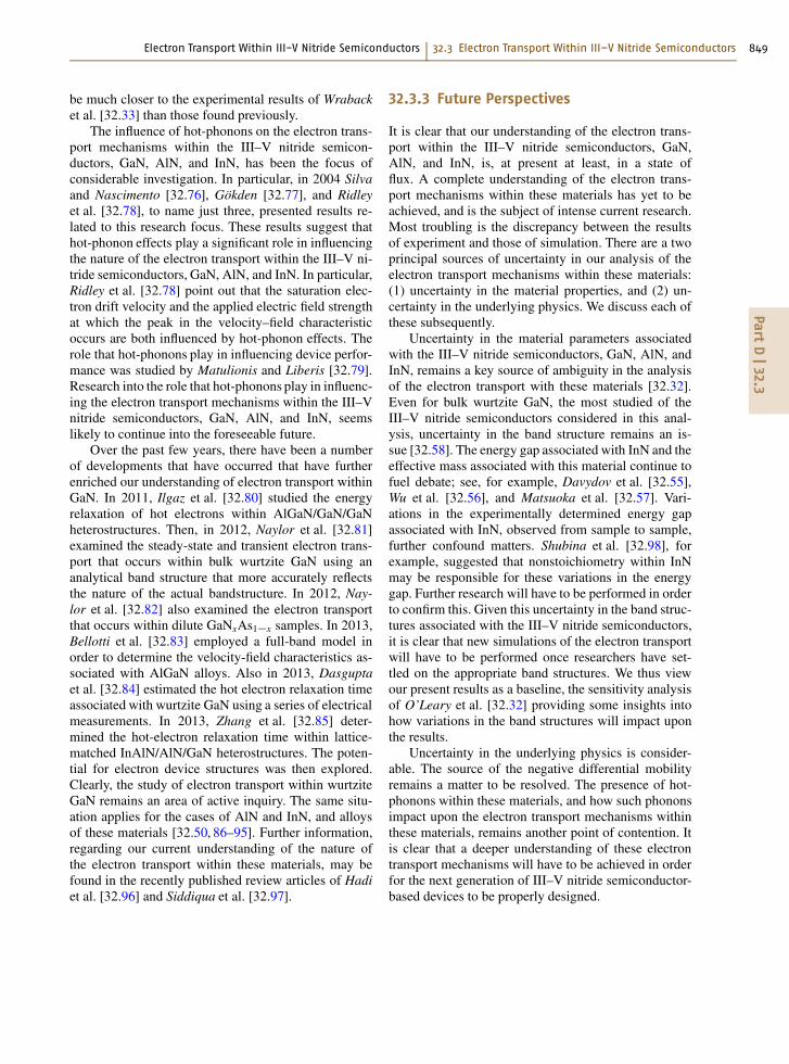
Electron Transport Within III-V Nitride Semiconductors 32.3 Electron Transport Within III–V Nitride Semiconductors 849Part
D|32.3
be much closer to the experimental results of Wrabacket al. [32.33] than those found previously.
The influence of hot-phonons on the electron trans-port mechanisms within the III–V nitride semicon-ductors, GaN, AlN, and InN, has been the focus ofconsiderable investigation. In particular, in 2004 Silvaand Nascimento [32.76], Gökden [32.77], and Ridleyet al. [32.78], to name just three, presented results re-lated to this research focus. These results suggest thathot-phonon effects play a significant role in influencingthe nature of the electron transport within the III–V ni-tride semiconductors, GaN, AlN, and InN. In particular,Ridley et al. [32.78] point out that the saturation elec-tron drift velocity and the applied electric field strengthat which the peak in the velocity–field characteristicoccurs are both influenced by hot-phonon effects. Therole that hot-phonons play in influencing device perfor-mance was studied by Matulionis and Liberis [32.79].Research into the role that hot-phonons play in influenc-ing the electron transport mechanisms within the III–Vnitride semiconductors, GaN, AlN, and InN, seemslikely to continue into the foreseeable future.
Over the past few years, there have been a numberof developments that have occurred that have furtherenriched our understanding of electron transport withinGaN. In 2011, Ilgaz et al. [32.80] studied the energyrelaxation of hot electrons within AlGaN/GaN/GaNheterostructures. Then, in 2012, Naylor et al. [32.81]examined the steady-state and transient electron trans-port that occurs within bulk wurtzite GaN using ananalytical band structure that more accurately reflectsthe nature of the actual bandstructure. In 2012, Nay-lor et al. [32.82] also examined the electron transportthat occurs within dilute GaNxAs1�x samples. In 2013,Bellotti et al. [32.83] employed a full-band model inorder to determine the velocity-field characteristics as-sociated with AlGaN alloys. Also in 2013, Dasguptaet al. [32.84] estimated the hot electron relaxation timeassociated with wurtzite GaN using a series of electricalmeasurements. In 2013, Zhang et al. [32.85] deter-mined the hot-electron relaxation time within lattice-matched InAlN/AlN/GaN heterostructures. The poten-tial for electron device structures was then explored.Clearly, the study of electron transport within wurtziteGaN remains an area of active inquiry. The same situ-ation applies for the cases of AlN and InN, and alloysof these materials [32.50, 86–95]. Further information,regarding our current understanding of the nature ofthe electron transport within these materials, may befound in the recently published review articles of Hadiet al. [32.96] and Siddiqua et al. [32.97].
32.3.3 Future Perspectives
It is clear that our understanding of the electron trans-port within the III–V nitride semiconductors, GaN,AlN, and InN, is, at present at least, in a state offlux. A complete understanding of the electron trans-port mechanisms within these materials has yet to beachieved, and is the subject of intense current research.Most troubling is the discrepancy between the resultsof experiment and those of simulation. There are a twoprincipal sources of uncertainty in our analysis of theelectron transport mechanisms within these materials:(1) uncertainty in the material properties, and (2) un-certainty in the underlying physics. We discuss each ofthese subsequently.
Uncertainty in the material parameters associatedwith the III–V nitride semiconductors, GaN, AlN, andInN, remains a key source of ambiguity in the analysisof the electron transport with these materials [32.32].Even for bulk wurtzite GaN, the most studied of theIII–V nitride semiconductors considered in this anal-ysis, uncertainty in the band structure remains an is-sue [32.58]. The energy gap associated with InN and theeffective mass associated with this material continue tofuel debate; see, for example, Davydov et al. [32.55],Wu et al. [32.56], and Matsuoka et al. [32.57]. Vari-ations in the experimentally determined energy gapassociated with InN, observed from sample to sample,further confound matters. Shubina et al. [32.98], forexample, suggested that nonstoichiometry within InNmay be responsible for these variations in the energygap. Further research will have to be performed in orderto confirm this. Given this uncertainty in the band struc-tures associated with the III–V nitride semiconductors,it is clear that new simulations of the electron transportwill have to be performed once researchers have set-tled on the appropriate band structures. We thus viewour present results as a baseline, the sensitivity analysisof O’Leary et al. [32.32] providing some insights intohow variations in the band structures will impact uponthe results.
Uncertainty in the underlying physics is consider-able. The source of the negative differential mobilityremains a matter to be resolved. The presence of hot-phonons within these materials, and how such phononsimpact upon the electron transport mechanisms withinthese materials, remains another point of contention. Itis clear that a deeper understanding of these electrontransport mechanisms will have to be achieved in orderfor the next generation of III–V nitride semiconductor-based devices to be properly designed.

PartD|32
850 Part D Materials for Optoelectronics and Photonics
32.4 ConclusionsIn this chapter, we reviewed analyses of the electrontransport within the III–V nitride semiconductors GaN,AlN, and InN. In particular, we have discussed the evo-lution of the field, surveyed the more recent literature,and presented frontiers for further investigation andanalysis. In order to narrow the scope of this review, wefocused on the electron transport within bulk wurtziteGaN, AlN, and InN for the purposes of this paper. Mostof our discussion focused upon results obtained fromour ensemble semi-classical three-valley Monte Carlosimulations of the electron transport within these mate-rials, our results conforming with state-of-the-art III–Vnitride semiconductor orthodoxy.
We began our review with the Boltzmann transportequation, since this equation underlies most analyses ofthe electron transport within semiconductors. A briefdescription of our ensemble semi-classical three-valleyMonte Carlo simulation approach to solving the Boltz-
mann transport equation was then provided. The ma-terial parameters, corresponding to bulk wurtzite GaN,AlN, and InN, were then presented. We then used thesematerial parameter selections, and our ensemble semi-classical three-valley Monte Carlo simulation approach,to determine the nature of the steady-state and transientelectron transport within the III–V nitride semiconduc-tors. Finally, we presented some recent developmentson the electron transport within these materials, andpointed to fertile frontiers for further research and in-vestigation.
Acknowledgments. The authors gratefully acknowl-edge financial support from the Natural Sciences andEngineering Research Council of Canada. The work atRensselaer Polytechnic Institute (M. S. Shur) was sup-ported by the US Army Cooperative Research Agree-ment (Project Monitor Dr. Meredith Reed).
References
32.1 S. Strite, H. Morkoç: J. Vac. Sci. Technol. B 10, 1237(1992)
32.2 H. Morkoç, S. Strite, G.B. Gao, M.E. Lin, B. Sverdlov,M. Burns: J. Appl. Phys. 76, 1363 (1994)
32.3 S.N. Mohammad, H. Morkoç: Prog. Quantum Elec-tron. 20, 361 (1996)
32.4 S.J. Pearton, J.C. Zolper, R.J. Shul, F. Ren: J. Appl.Phys. 86, 1 (1999)
32.5 M.A. Khan, J.W. Yang, W. Knap, E. Frayssinet, X. Hu,G. Simin, P. Prystawko, M. Leszczynski, I. Grzegory,S. Porowski, R. Gaska, M.S. Shur, B. Beaumont,M. Teisseire, G. Neu: Appl. Phys. Lett. 76, 3807(2000)
32.6 X. Hu, J. Deng, N. Pala, R. Gaska, M.S. Shur,C.Q. Chen, J. Yang, G. Simin, M.A. Khan, J.C. Rojo,L.J. Schowalter: Appl. Phys. Lett. 82, 1299 (2003)
32.7 W. Lu, V. Kumar, E.L. Piner, I. Adesida: IEEE Trans.Electron Devices 50, 1069 (2003)
32.8 A. Jiménez, Z. Bougrioua, J.M. Tirado, A.F. Braña,E. Calleja, E. Muñoz, I. Moerman: Appl. Phys. Lett.82, 4827 (2003)
32.9 A.A. Burk Jr., M.J. O’Loughlin, R.R. Siergiej,A.K. Agarwal, S. Sriram, R.C. Clarke, M.F. MacMillan,V. Balakrishna, C.D. Brandt: Solid-State Electron.43, 1459 (1999)
32.10 M. Umeno, T. Egawa, H. Ishikawa: Mater. Sci. Semi-cond. Process. 4, 459 (2001)
32.11 A. Krost, A. Dadgar: Phys. Status Solidi A 194, 361(2002)
32.12 C.L. Tseng, M.J. Youh, G.P. Moore, M.A. Hopkins,R. Stevens, W.N. Wang: Appl. Phys. Lett. 83, 3677(2003)
32.13 M.A. Littlejohn, J.R. Hauser, T.H. Glisson: Appl.Phys. Lett. 26, 625 (1975)
32.14 D.K. Ferry: Phys. Rev. B 12, 2361 (1975)32.15 P. Das, D.K. Ferry: Solid-State Electron. 19, 851 (1976)32.16 B. Gelmont, K. Kim, M. Shur: J. Appl. Phys. 74, 1818
(1993)32.17 V.W.L. Chin, T.L. Tansley, T. Osotchan: J. Appl. Phys.
75, 7365 (1994)32.18 N.S. Mansour, K.W. Kim, M.A. Littlejohn: J. Appl.
Phys. 77, 2834 (1995)32.19 J. Kolník, I.H. Oğuzman, K.F. Brennan, R. Wang,
P.P. Ruden, Y. Wang: J. Appl. Phys. 78, 1033 (1995)32.20 M. Shur, B. Gelmont, M.A. Khan: J. Electron. Mater.
25, 777 (1996)32.21 B.E. Foutz, L.F. Eastman, U.V. Bhapkar, M.S. Shur:
Appl. Phys. Lett. 70, 2849 (1997)32.22 U.V. Bhapkar, M.S. Shur: J. Appl. Phys. 82, 1649
(1997)32.23 S.K. O’Leary, B.E. Foutz, M.S. Shur, U.V. Bhapkar,
L.F. Eastman: J. Appl. Phys. 83, 826 (1998)32.24 S.K. O’Leary, B.E. Foutz, M.S. Shur, U.V. Bhapkar,
L.F. Eastman: Solid State Commun. 105, 621 (1998)32.25 J.D. Albrecht, R.P. Wang, P.P. Ruden, M. Farahmand,
K.F. Brennan: J. Appl. Phys. 83, 1446 (1998)32.26 N.G. Weimann, L.F. Eastman, D. Doppalapudi,
H.M. Ng, T.D. Moustakas: J. Appl. Phys. 83, 3656(1998)
32.27 J.D. Albrecht, R.P. Wang, P.P. Ruden, M. Farahmand,K.F. Brennan: J. Appl. Phys. 83, 4777 (1998)
32.28 E. Bellotti, B.K. Doshi, K.F. Brennan, J.D. Albrecht,P.P. Ruden: J. Appl. Phys. 85, 916 (1999)
32.29 B.E. Foutz, S.K. O’Leary, M.S. Shur, L.F. Eastman:J. Appl. Phys. 85, 7727 (1999)
32.30 S.K. O’Leary, B.E. Foutz, M.S. Shur, L.F. Eastman:Solid State Commun. 118, 79 (2001)

Electron Transport Within III-V Nitride Semiconductors References 851Part
D|32
32.31 T.F. de Vasconcelos, F.F. Maia Jr., E.W.S. Caetano,V.N. Freire, J.A.P. da Costa, E.F. da Silva Jr.: J. Cryst.Growth 246, 320 (2002)
32.32 S.K. O’Leary, B.E. Foutz, M.S. Shur, L.F. Eastman:J. Electron. Mater. 32, 327 (2003)
32.33 M. Wraback, H. Shen, J.C. Carrano, T. Li, J.C. Camp-bell, M.J. Schurman, I.T. Ferguson: Appl. Phys. Lett.76, 1155 (2000)
32.34 S. Krishnamurthy, M. van Schilfgaarde, A. Sher,A.-B. Chen: Appl. Phys. Lett. 71, 1999 (1997)
32.35 D.K. Ferry, C. Jacoboni (Eds.): Quantum Transport inSemiconductors (Plenum, New York 1992)
32.36 N.W. Ashcroft, N.D. Mermin: Solid State Physics(Saunders College, Philadelphia 1976)
32.37 P.A. Sandborn, A. Rao, P.A. Blakey: IEEE Trans. Elec-tron Devices 36, 1244 (1989)
32.38 D.C. Look, J.R. Sizelove, S. Keller, Y.F. Wu,U.K. Mishra, S.P. DenBaars: Solid State Commun.102, 297 (1997)
32.39 N.A. Zakhleniuk, C.R. Bennett, B.K. Ridley,M. Babiker: Appl. Phys. Lett. 73, 2485 (1998)
32.40 B.R. Nag: Electron Transport in Compound Semi-conductors (Springer, Berlin, Heidelberg 1980)
32.41 M.S. Krishnan, N. Goldsman, A. Christou: J. Appl.Phys. 83, 5896 (1998)
32.42 R. Oberhuber, G. Zandler, P. Vogl: Appl. Phys. Lett.73, 818 (1998)
32.43 W. Fawcett, A.D. Boardman, S. Swain: J. Phys.Chem. Solids 31, 1963 (1970)
32.44 A. Bykhovski, B. Gelmont, M. Shur, A. Khan: J. Appl.Phys. 77, 1616 (1995)
32.45 A.D. Bykhovski, V.V. Kaminski, M.S. Shur, Q.C. Chen,M.A. Khan: Appl. Phys. Lett. 68, 818 (1996)
32.46 P. Lugli, D.K. Ferry: IEEE Trans. Electron Devices 32,2431 (1985)
32.47 K. Seeger: Semiconductor Physics: An Introduction,9th edn. (Springer, Berlin, Heidelberg 2004)
32.48 S.K. O’Leary, B.E. Foutz, M.S. Shur, L.F. Eastman:J. Mater. Sci. Mater. Electron. 17, 87 (2006)
32.49 W.A. Hadi, P.K. Guram, M.S. Shur, S.K. O’Leary:J. Appl. Phys. 113, 113709 (2013)
32.50 V.M. Polyakov, F. Schwierz, F. Fuchs, J. Furthmüller,F. Bechstedt: Appl. Phys. Lett. 94, 022102 (2009)
32.51 W.R.L. Lambrecht, B. Segall: Band structure of puregroup III nitrides. In: Properties of Group III Ni-trides, EMIS Datareviews, ed. by J.H. Edgar (Inspec,London 1994) p. 125
32.52 M.A. Littlejohn, J.R. Hauser, T.H. Glisson: J. Appl.Phys. 48, 4587 (1977)
32.53 J.S. Blakemore: J. Appl. Phys. 53, R123 (1982)32.54 T.L. Tansley, C.P. Foley: J. Appl. Phys. 59, 3241 (1986)32.55 V.Y. Davydov, A.A. Klochikhin, V.V. Emtsev,
S.V. Ivanov, V.V. Vekshin, F. Bechstedt, J. Furth-müller, H. Harima, A.V. Mudryi, A. Hashimoto,A. Yamamoto, J. Aderhold, J. Graul, E.E. Haller:Phys. Status Solidi B 230, R4 (2002)
32.56 J. Wu, W. Walukiewicz, K.M. Yu, J.W. Ager III,E.E. Haller, H. Lu, W.J. Schaff, Y. Saito, Y. Nanishi:Appl. Phys. Lett. 80, 3967 (2002)
32.57 T. Matsuoka, H. Okamoto, M. Nakao, H. Harima,E. Kurimoto: Appl. Phys. Lett. 81, 1246 (2002)
32.58 E.G. Brazel, M.A. Chin, V. Narayanamurti, D. Kapol-nek, E.J. Tarsa, S.P. DenBaars: Appl. Phys. Lett. 70,330 (1997)
32.59 J.G. Ruch: IEEE Trans. Electron Devices 19, 652 (1972)32.60 M.S. Shur, L.F. Eastman: IEEE Trans. Electron Devices
26, 1677 (1979)32.61 M. Heiblum, M.I. Nathan, D.C. Thomas,
C.M. Knoedler: Phys. Rev. Lett. 55, 2200 (1985)32.62 A. Palevski, M. Heiblum, C.P. Umbach,
C.M. Knoedler, A.N. Broers, R.H. Koch: Phys.Rev. Lett. 62, 1776 (1989)
32.63 A. Palevski, C.P. Umbach, M. Heiblum: Appl. Phys.Lett. 55, 1421 (1989)
32.64 A. Yacoby, U. Sivan, C.P. Umbach, J.M. Hong: Phys.Rev. Lett. 66, 1938 (1991)
32.65 E. Tiede, M. Thimann, K. Sensse: Chem. Ber. 61, 1568(1928)
32.66 W.C. Johnson, J.B. Parsons, M.C. Crew: J. Phys.Chem. 36, 2651 (1932)
32.67 R. Juza, H. Hahn: Z. Anorg. Allg. Chem. 239, 282(1938)
32.68 H.P. Maruska, J.J. Tietjen: Appl. Phys. Lett. 15, 327(1969)
32.69 Z.C. Huang, R. Goldberg, J.C. Chen, Y. Zheng,D.B. Mott, P. Shu: Appl. Phys. Lett. 67, 2825 (1995)
32.70 L.F. Eastman, V. Tilak, J. Smart, B.M. Green,E.M. Chumbes, R. Dimitrov, H. Kim, O.S. Ambacher,N. Weimann, T. Prunty, M. Murphy, W.J. Schaff,J.R. Shealy: IEEE Trans. Electron Devices 48, 479(2001)
32.71 C.H. Oxley, M.J. Uren: IEEE Trans. Electron Devices52, 165 (2005)
32.72 M. Wraback, H. Shen, J.C. Carrano, C.J. Collins,J.C. Campbell, R.D. Dupuis, M.J. Schurman, I.T. Fer-guson: Appl. Phys. Lett. 79, 1303 (2001)
32.73 A. Matulionis, J. Liberis, L. Ardaravičius, M. Ra-monas, I. Matulioniene, J. Smart: Semicond. Sci.Technol. 17, L9 (2002)
32.74 C. Bulutay, B.K. Ridley, N.A. Zakhleniuk: Phys. Rev. B68, 115205 (2003)
32.75 R. Brazis, R. Raguotis: Appl. Phys. Lett. 85, 609(2004)
32.76 A.A.P. Silva, V.A. Nascimento: J. Lumin. 106, 253(2004)
32.77 S. Gökden: Physica E 23, 198 (2004)32.78 B.K. Ridley, W.J. Schaff, L.F. Eastman: J. Appl. Phys.
96, 1499 (2004)32.79 A. Matulionis, J. Liberis: IEE Proc. Circuits Devices
Syst. 151, 148 (2004)32.80 A. Ilgaz, S. Gőkden, R. Tűlek, A. Teke, S. Őzçelik,
E. Özbay: Eur. Phys. J. Appl. Phys. 55, 30102 (2011)32.81 D.R. Naylor, A. Dyson, B.K. Ridley: Solid State Com-
mun. 152, 549 (2012)32.82 D.R. Naylor, A. Dyson, B.K. Ridley: J. Appl. Phys. 111,
053703 (2012)32.83 E. Bellotti, F. Bertazzi, S. Shishehchi, M. Matsub-
ara, M. Goano: IEEE Trans. Electron Devices 60, 3204(2013)
32.84 S. Dasgupta, J. Lu, Nidhi, A. Raman, C. Hurni,G. Gupta, J.S. Speck, U.K. Mishra: Appl. Phys. Ex-press 6, 034002 (2013)
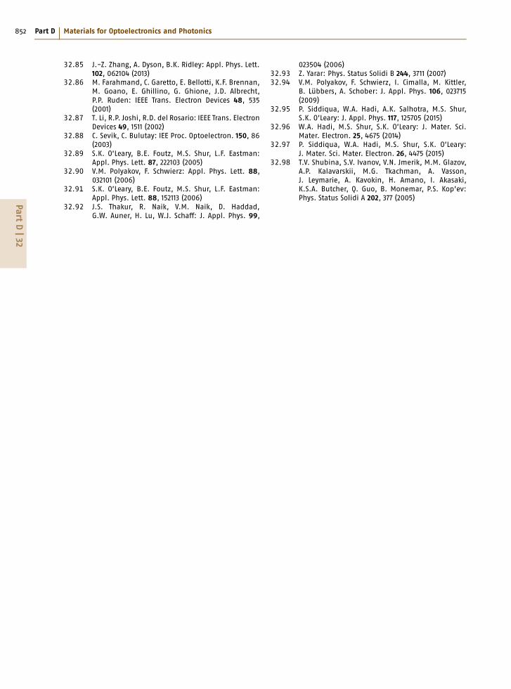
PartD|32
852 Part D Materials for Optoelectronics and Photonics
32.85 J.-Z. Zhang, A. Dyson, B.K. Ridley: Appl. Phys. Lett.102, 062104 (2013)
32.86 M. Farahmand, C. Garetto, E. Bellotti, K.F. Brennan,M. Goano, E. Ghillino, G. Ghione, J.D. Albrecht,P.P. Ruden: IEEE Trans. Electron Devices 48, 535(2001)
32.87 T. Li, R.P. Joshi, R.D. del Rosario: IEEE Trans. ElectronDevices 49, 1511 (2002)
32.88 C. Sevik, C. Bulutay: IEE Proc. Optoelectron. 150, 86(2003)
32.89 S.K. O’Leary, B.E. Foutz, M.S. Shur, L.F. Eastman:Appl. Phys. Lett. 87, 222103 (2005)
32.90 V.M. Polyakov, F. Schwierz: Appl. Phys. Lett. 88,032101 (2006)
32.91 S.K. O’Leary, B.E. Foutz, M.S. Shur, L.F. Eastman:Appl. Phys. Lett. 88, 152113 (2006)
32.92 J.S. Thakur, R. Naik, V.M. Naik, D. Haddad,G.W. Auner, H. Lu, W.J. Schaff: J. Appl. Phys. 99,
023504 (2006)32.93 Z. Yarar: Phys. Status Solidi B 244, 3711 (2007)32.94 V.M. Polyakov, F. Schwierz, I. Cimalla, M. Kittler,
B. Lübbers, A. Schober: J. Appl. Phys. 106, 023715(2009)
32.95 P. Siddiqua, W.A. Hadi, A.K. Salhotra, M.S. Shur,S.K. O’Leary: J. Appl. Phys. 117, 125705 (2015)
32.96 W.A. Hadi, M.S. Shur, S.K. O’Leary: J. Mater. Sci.Mater. Electron. 25, 4675 (2014)
32.97 P. Siddiqua, W.A. Hadi, M.S. Shur, S.K. O’Leary:J. Mater. Sci. Mater. Electron. 26, 4475 (2015)
32.98 T.V. Shubina, S.V. Ivanov, V.N. Jmerik, M.M. Glazov,A.P. Kalavarskii, M.G. Tkachman, A. Vasson,J. Leymarie, A. Kavokin, H. Amano, I. Akasaki,K.S.A. Butcher, Q. Guo, B. Monemar, P.S. Kop’ev:Phys. Status Solidi A 202, 377 (2005)