Electrons and holes in pure Silicon - Auburn...
103
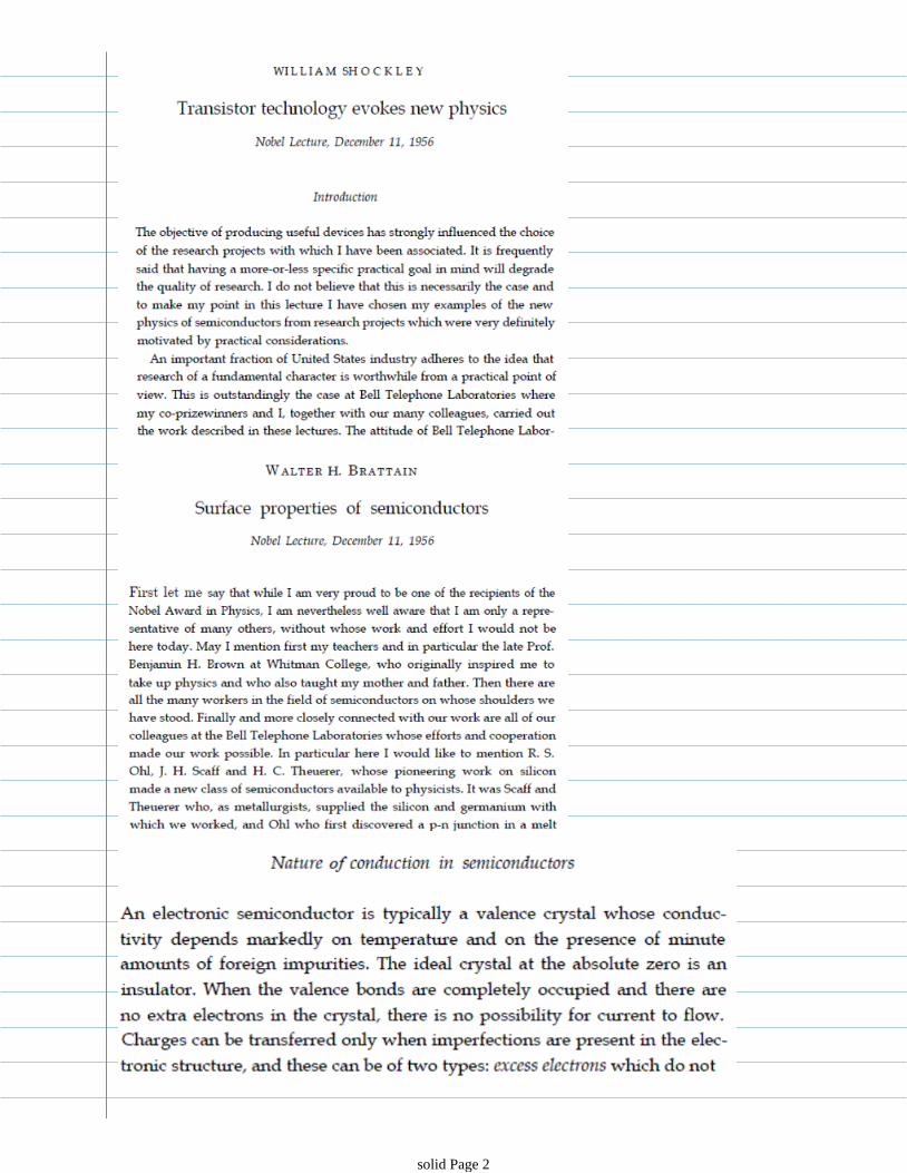
Develop bond and band models for semiconductors. 1. Develop the concept of bonds, freed electron and hole 2. Develop the concept of intrinsic carrier concentration 3. Understand how holes move to carry current (to be a carrier) 4. Understand how doping affects both N and P 5. Chapter goals: Electrons and holes in pure Silicon Sunday, April 22, 2012 12:45 PM solid Page 1
Transcript of Electrons and holes in pure Silicon - Auburn...

Develop bond and band models for semiconductors.
1.
Develop the concept of bonds, freed electron and hole
2.
Develop the concept of intrinsic carrier concentration
3.
Understand how holes move to carry current (to be a carrier)
4.
Understand how doping affects both N and P5.
Chapter goals:
Electrons and holes in pure SiliconSunday, April 22, 201212:45 PM
solid Page 1
solid Page 2
Solid-State Electronic Materials
Insulators Resistivity () > 105 -cm•
Semiconductors 10-3 < < 105 -cm•
Conductors < 10-3 -cm•
Electronic materials fall into three categories:•
Elemental semiconductors are formed from a single type of atom, typically Silicon or Germanium (Si or Ge).
•
Compound semiconductors are formed from combinations of column III and V elements or columns II and VI, e.g. GaAs.
•
Germanium was used in many early devices.•
Silicon quickly replaced germanium due to its higher band gap energy, lower cost, and is easily oxidized to form silicon-dioxide insulating layers.
•
GaAs has excellent optical properties solid Page 3

GaAs has excellent optical properties•
Increase of temperature, light or addition of impurities can greatly increase conductivity of semiconductors through increase of electrons and holes
•
Let us start with pure Silicon:
Pure (Intrinsic) Silicon
solid Page 4

solid Page 5

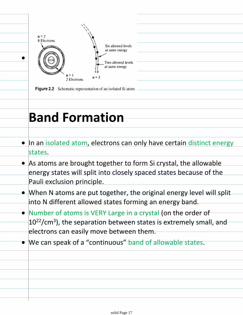
Valence electrons in isolated Si
Atom The energy of electrons in atomic systems is restricted to a limited set of values – the wonder of quantum mechanics.Electrons fill allowed energy levels, starting from lowest one
Ten of the 14 Si-atom electrons occupy very deep lying energy levels and are tightly bound to the nucleus
•
The remaining 4 electrons, called valence electrons are not very strongly bound and
occupy 4 of the 8 allowed slots.
•
Isolated Si atomsTuesday, May 22, 201210:26 PM
solid Page 6

•
solid Page 7
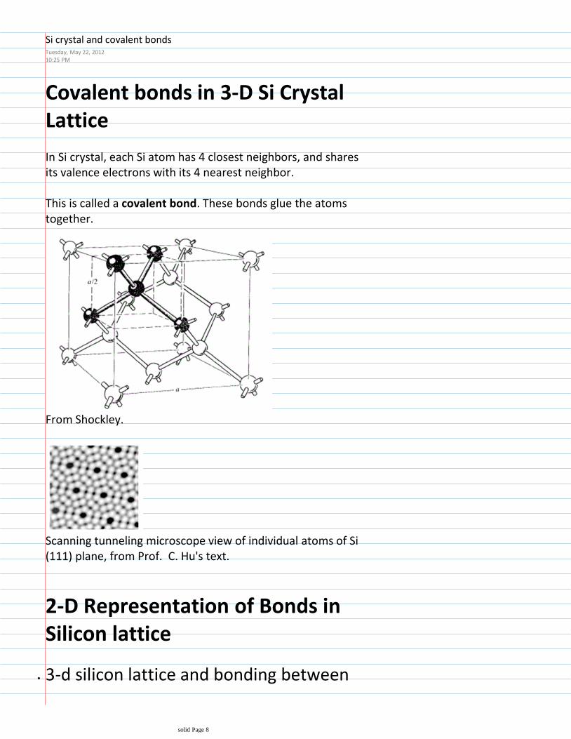
Covalent bonds in 3-D Si Crystal Lattice
In Si crystal, each Si atom has 4 closest neighbors, and shares its valence electrons with its 4 nearest neighbor.
This is called a covalent bond. These bonds glue the atoms together.
From Shockley.
Scanning tunneling microscope view of individual atoms of Si (111) plane, from Prof. C. Hu's text.
2-D Representation of Bonds in Silicon lattice
3-d silicon lattice and bonding between atoms are very hard to visualize
•
Si crystal and covalent bondsTuesday, May 22, 201210:25 PM
solid Page 8

atoms are very hard to visualizeIt can also be visually described as 2-D square lattice, with "two lines" representing a covalent bond
•
Like in 3d, each atom forms covalent bond with 4 closest neighbors
•
Each bond contains two valence electrons
•
each Si atom has four nearest neighbors, -
each isolated Si atom has 4 electrons in outer shell-
Each atom shares its electrons with its nearest neighbor in a Si crystal. This is called a covalent bonding
-
At 0 K , no electrons are available for conduction in this covalent structure, so the material is and should be an insulator at 0 K
-
Perfect Bonds at 0K
At 0K, all bonds are perfect, Si crystal is an insulator.
Bonds Break Above 0K due solid Page 9

Bonds Break Above 0K due to lattice vibrationAbove 0K, atoms are vibrating around their lattice positions due to thermal energy.
•
Atoms are closely packed and interact with one another, some atoms oscillate more violently than others.
•
"excess electrons" that do not fit into valence bonds and can move around crystal. These "electrons" are mobile, and have the normal -q charge
•
holes, places from which electrons are missing in the bonds, which also behave as mobile carriers. These holes have a "+q" charge.
•
At any given instant of time, oscillations are large in some locations, causing some bonds to break, and producing
•
The atomic agitation increases with absolute temperature – this is why it is also called thermal agitation
•
Mobile Electron and HoleWe now have broken bond due to thermal energy
“free” electrons (mobile negative charge –q) solid Page 10
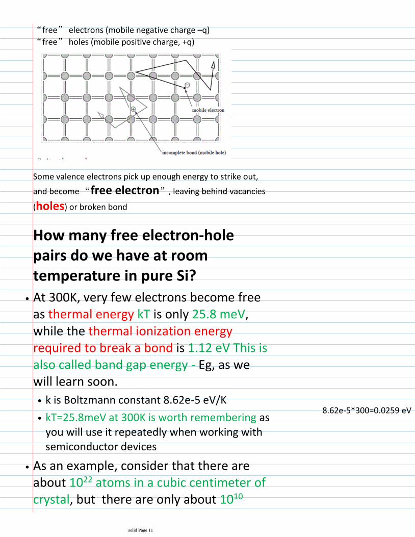
“free” electrons (mobile negative charge –q)
“free” holes (mobile positive charge, +q)
Some valence electrons pick up enough energy to strike out,
and become “free electron”, leaving behind vacancies
(holes) or broken bond
How many free electron-hole pairs do we have at room temperature in pure Si?
k is Boltzmann constant 8.62e-5 eV/K•
kT=25.8meV at 300K is worth remembering as you will use it repeatedly when working with semiconductor devices
•
At 300K, very few electrons become free as thermal energy kT is only 25.8 meV, while the thermal ionization energy required to break a bond is 1.12 eV This is also called band gap energy - Eg, as we will learn soon.
•
As an example, consider that there are about 1022 atoms in a cubic centimeter of crystal, but there are only about 1010
/cm3 free electrons in silicon – only 1 in
•
8.62e-5*300=0.0259 eV
solid Page 11

/cm3 free electrons in silicon – only 1 in one trillion atoms.
solid Page 12

Energy Unit for Electronics: eV
We often use eV as energy unit in electronics.
1 eV is the amount of energy a 1V battery provides when moving an electron across it.
So 1 eV = 1 * 1.6e-19 C * V = 1.6e-19 J.
Example: thermal energy and thermal voltage
"k" being Boltzmann constant, -
"T" being absolute temperature in K,-
Thermal energy is written as kT:
kT is 25.8 meV at 300K (our text uses 25 meV, an approximation).
Thermal voltage is kT/q, with q being elementary charge
kT/q is 25.8 mV at 300K.
Energy Unit for Electronics: eVTuesday, May 22, 201210:39 PM
solid Page 13

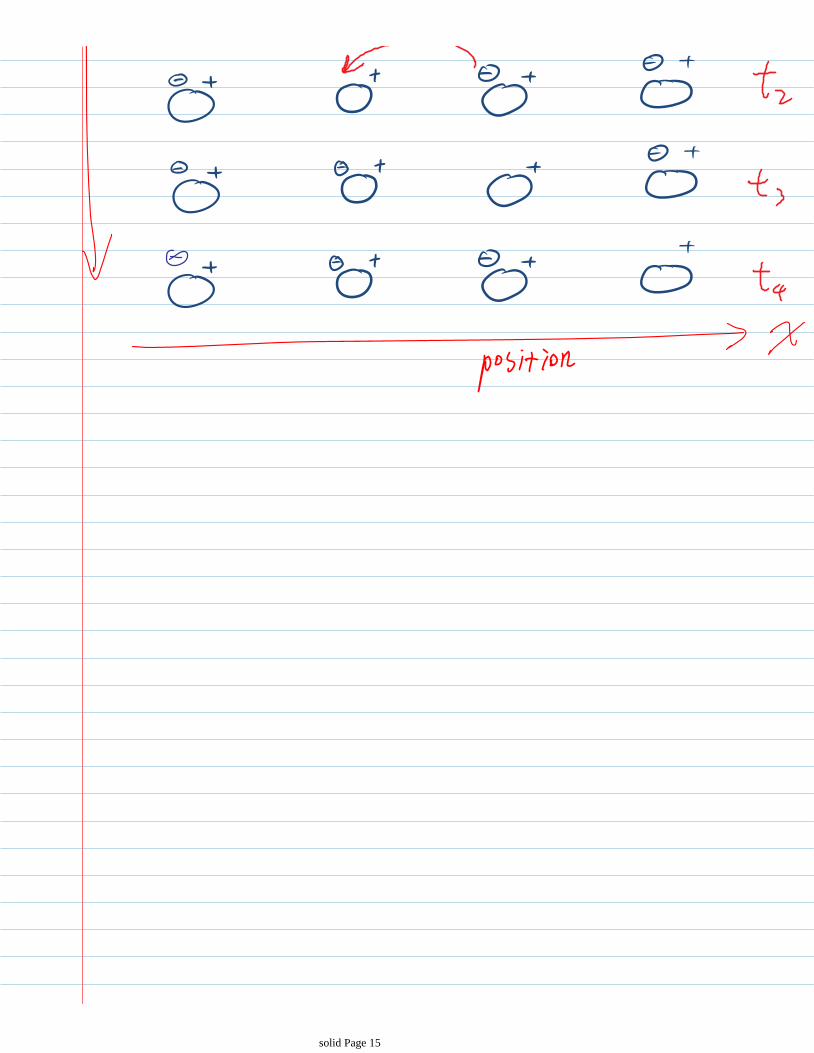
“Hole” movement movie
Freed electrons have left positively ionized Si atoms behind.•
The silicon ions do not move; however, their charges can.•
Valence electrons are traded among atoms, •
a positive ion will neutralize itself by capturing another valence electron, then some other atom is left ionized.
•
While the ion did not move, the +q charge has moved. •
We could just call this +q charge a mobile hole. •
The motion of holes becomes directed when an electric field is applied, producing a current.
•
Free electrons and holes will move in opposite directions in an electric field, but the resulting currents will add
•
How do holes carry current?Sunday, May 20, 20128:57 AM
solid Page 14
solid Page 15

Valence electrons in isolated Si Atom
The energy of electrons in atomic systems is restricted to a limited set of values – the wonder of quantum mechanics.Electrons fill allowed energy levels, starting from lowest one
Ten of the 14 Si-atom electrons occupy very deep lying energy levels and are tightly bound to the nucleus
The remaining 4 electrons, called valence electrons are not very strongly bound and
occupy 4 of the 8 allowed slots.
Energy bandsSunday, April 22, 201212:54 PM
solid Page 16
Band Formation
In an isolated atom, electrons can only have certain distinct energy states.
As atoms are brought together to form Si crystal, the allowable energy states will split into closely spaced states because of the Pauli exclusion principle.
When N atoms are put together, the original energy level will split into N different allowed states forming an energy band.
Number of atoms is VERY Large in a crystal (on the order of 1022/cm3), the separation between states is extremely small, and electrons can easily move between them.
We can speak of a “continuous” band of allowable states.
solid Page 17
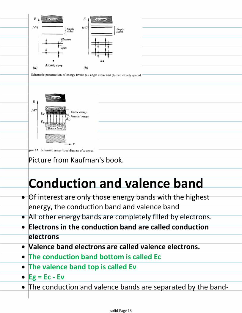
Picture from Kaufman's book.
Conduction and valence bandOf interest are only those energy bands with the highest energy, the conduction band and valence band
All other energy bands are completely filled by electrons.
Electrons in the conduction band are called conduction electrons
Valence band electrons are called valence electrons.
The conduction band bottom is called Ec
The valence band top is called Ev
Eg = Ec - Ev
The conduction and valence bands are separated by the band-gap Eg, where no energy state exists – forbidden gap.
solid Page 18
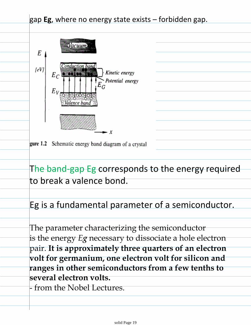
gap Eg, where no energy state exists – forbidden gap.
The band-gap Eg corresponds to the energy required to break a valence bond.
Eg is a fundamental parameter of a semiconductor.
The parameter characterizing the semiconductoris the energy Eg necessary to dissociate a hole electron pair. It is approximately three quarters of an electron volt for germanium, one electron volt for silicon and ranges in other semiconductors from a few tenths to several electron volts.- from the Nobel Lectures.
Band model description - Valence electrons pick up enough
solid Page 19

Band model description - Valence electrons pick up enough energy to overcome the band-gap and jump into the conduction band, leaving behind empty states (holes) in the valence band. Bond model - some valence electrons pick up enough energy
to strike out, and become “free”, leaving behind vacancies (holes) or broken bond
k is Boltzmann constant 8.62e-5 eV/K
kT=25.8meV at 300K is worth remembering as you will use it repeatedly when working with semiconductor devices
At 300K, very few electrons become free as thermal energy kT is only 25.8 meV, while the thermal ionization energy is 1.12 eV Eg.
As an example, consider that there are about 1022 atoms in a cubic centimeter of
solid Page 20

about 1022 atoms in a cubic centimeter of crystal, but there are only about 1010
/cm3 free electrons in silicon – only 1 in one trillion atoms.
CarriersElectrons and holes are called carriers – because they can carry current, i.e. when they move around the crystal, a current is producedThe number of carriers per volume is called carrier concentration
solid Page 21

Light as Energy Sources to Produce Electron-Hole Pairs
Light has wave-particle duality.
Light is a stream of "particles" called "photons", which carry energy
On a clear day, 4.4x10⁷ photons hit 1 square meter of Earth's surface every second.
Photon energy E = h * f = h*c/wave_length
Light as energy source for electron hole pairFriday, August 24, 20129:46 AM
solid Page 22

h*c/wave_length
h: Planck's constant, 6.625e-34 J-sf: frequency of light
c (light speed) = wave_length / T = wave_length * f, c = 3e8 cm/s
solar cells, -
photo conductors (light sensitive resistors), -
photo-transistors-
example:
Photon energy has to be higher than the bandgap Eg for optical e-h pair generation to occur
Visible light wavelengths are usually expressed in nanometers (nm), and give photon energies that are solid Page 23

nanometers (nm), and give photon energies that are given in electron volts (eV).
solid Page 24
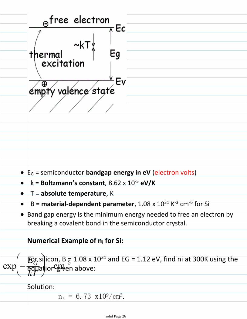
Intrinsic Carrier Concentration (ni)
The process of freeing electrons in pure silicon is an ionization of the silicon atoms,
free-electron concentration is equal to hole concentration (whole pure Si crystal is charge neutral), and either one is represented by the symbol ni, which is called the intrinsic carrier concentration.
ni is produced by a dynamic process; free electron hole pairs are continually being generated, while other electron hole pairs are recombining
Intrinsic concentration niSunday, May 20, 20129:01 AM
solid Page 25
ni2 BT 3 exp
EG
kT
cm-6
EG = semiconductor bandgap energy in eV (electron volts)
k = Boltzmann’s constant, 8.62 x 10⁻⁵ eV/K
T = absolute temperature, K
B = material-dependent parameter, 1.08 x 1031 K-3 cm-6 for Si
Band gap energy is the minimum energy needed to free an electron by breaking a covalent bond in the semiconductor crystal.
Numerical Example of ni for Si:
For silicon, B = 1.08 x 1031 and EG = 1.12 eV, find ni at 300K using the equation given above:
Solution:
ni = 6.73 x10⁹/cm3.
solid Page 26

Python code for step by step calculation:
from __future__ import print_function
from math import exp, sqrt
b = 1.08e31 # K^{-3} cm^{-6}
k = 8.62e-5 # eV/K
T = 300
eg = 1.12
kt = k * T
ni2 = b * T**3 * exp(-eg / kt)
ni = sqrt(ni2)
print('Si: Eg = {eg} eV, T = {T} K, B = {b}, ni = {ni:6.2e} /cm^3'.format(**locals()))
Python Output:
Si: Eg = 1.12 eV, T = 300 K, B = 1.08e+31, ni =
6.73e+09 /cm^3
Numerical Example Ge:
For germanium, B = 2.31 x 1030 and EG = 0.66 eV, at 300K:
ni = 2.27 x10¹³/cm3 .
ni of popular semiconductors
One expects that the intrinsic concentration is a function of temperature T and of the amount of energy required to break crystal bonds (ionization energy), which is also called Eg as we will introduce soon.
solid Page 27

As expected, the largest Intrinsic density results at higher temperature and in materials with a small band-gap.
I generated a graph for ni - T for three most popular semiconductors.
The main difference between materials is from Eg.
Eg = 1.12 eV for Si, 0.66 eV for Ge and 1.4 eV for GaAs.
solid Page 28
Donors
Acceptors
Charge Neutrality
Mass Action Law (pn product)
Carrier Concentration Engineering at
Equilibrium
Majority vs Minority Carrier
The discussion of semiconductor properties has so far been restricted to pure crystals. In semiconductor terminology an absolutely pure crystal is called an intrinsic semiconductor.
Intrinsic semiconductor is not very useful as we will learn later.
To make useful devices, we need to add small amounts of other elements having a different atomic structure, e.g. group III element Boron, or group V elements arsenic, phosphorous or antimony – also known as “impurities” – these are called extrinsic
Doping engineeringSunday, April 22, 20121:17 PM
solid Page 29

“impurities” – these are called extrinsic semiconductors
solid Page 30

Quiz:
1) what is the pH of pure water? What is the molar concentration of positive hydrogen ions and negative hydroxide ions in deionized (pure) water?
2) What can we add to water to increase hydrogen ion concentration?
3) if we increase hydrogen ion concentration by 1000 times, what will the concentration of hydroxide ions be?
Acceptors and donors (of electrons)Sunday, April 22, 20121:18 PM
solid Page 31

solid Page 32

In semiconductors, we add acceptors to increase "p" -concentration of positive charged holes
atoms which become negatively ionized when placed at Si lattice locations are called acceptors. We denote acceptor concentration Na. Ionized concentration Na-. Often we can assume Na- = Na, or complete ionization.
Acceptor in Si (Boron) solid Page 33
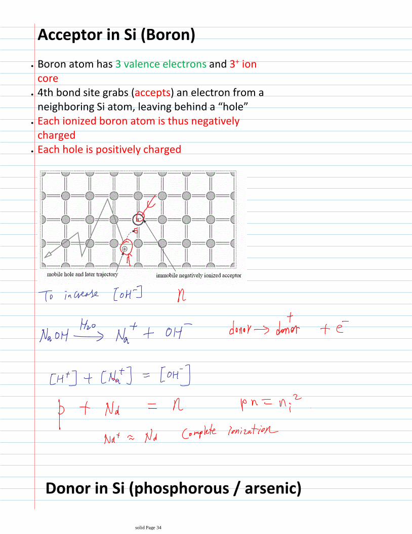
Acceptor in Si (Boron)
Boron atom has 3 valence electrons and 3+ ion core
4th bond site grabs (accepts) an electron from a neighboring Si atom, leaving behind a “hole”
Each ionized boron atom is thus negatively charged
Each hole is positively charged
Donor in Si (phosphorous / arsenic)
solid Page 34

P atom: 5 valence electrons and a 5+ ion core
The 5th valence electron has no available bond – so there is an extra electron
Each extra free electron, -q, has one +q ion
# P atoms = # free elect, so material is charge neutral at RT (300K), approximately
solid Page 35

How many electrons and holes are there in a cubic cm pure silicon at 300K? (assuming ni=1010/cm3)N=?
P=?
What if we add Phosphorous, at a concentration of 1016/cm3
N=?
P=?
Mass action law:
In thermal equilibrium and for a given semiconductor, np product is a constant
n0 * p0 = ni2
Popular misunderstanding of doping impactSunday, April 22, 20121:24 PM
solid Page 36

Typical doping level ranges from 1014/cm3
to 1021/cm3
solid Page 37
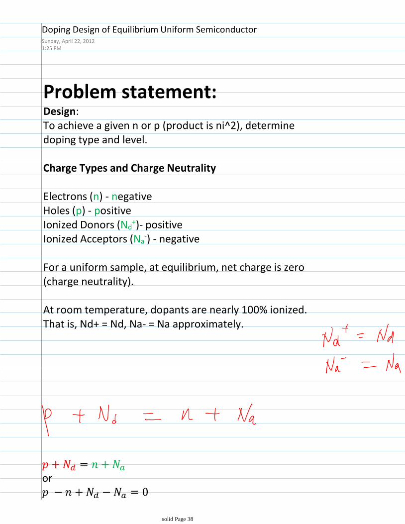
Problem statement: Design:To achieve a given n or p (product is ni^2), determine doping type and level.
Charge Types and Charge Neutrality
Electrons (n) - negativeHoles (p) - positiveIonized Donors (Nd
+)- positiveIonized Acceptors (Na
-) - negative
For a uniform sample, at equilibrium, net charge is zero (charge neutrality).
At room temperature, dopants are nearly 100% ionized. That is, Nd+ = Nd, Na- = Na approximately.
or This is the first weapon we have in solving equilibrium
Doping Design of Equilibrium Uniform Semiconductor Sunday, April 22, 20121:25 PM
solid Page 38

This is the first weapon we have in solving equilibrium uniform semiconductor problem.
The second weapon we have is the
law, also known as mass action law.
Mass Action Law at Equilibrium:
at equilibrium
We have therefore two equations, charge neutrality and pn product, which can be solved for p and n.
Before we mathematically solve these equations, let us make some simple observations in cases of donor and acceptor doping only.
solid Page 39

Q: is n > p or p > n?
Is n > ni?
Is p > ni?
Consider donor doping only, that is,
becomes:
which means as
consequence of donor doping. The semiconductor is said to be n-type.
The difference is set by donor concentration
In the mean time,
Therefore
N-type Doping Design Example:
Donor only case: n-typeMonday, August 27, 20121:27 PM
solid Page 40

N-type Doping Design Example:
Consider Si, 300K, ni = 1e10cm-3. Determine the doping type and level required to achieve n=1e15cm-3.
Solution:
n=1e15 > ni, therefore we need n-type doping.1.
p=ni^2/na.Nd = n-pb.
The level of n-type doping, Nd, can be found from pn product and charge neutrality
2.
>>> ni=1e10
>>> n=1e15
>>> p=ni**2/n
>>> p
100000.0
>>> nd = n-p
>>> nd
999999999900000.0
>>> print "%5.2e" % nd
1.00e+15
>>> print "%5.2e" % n
solid Page 41

>>> print "%5.2e" % n
1.00e+15
>>> print "%5.2e" % p
1.00e+05
Nd is smaller than n, by p. However, value wise, Nd is practically the same as "n" in our computer.
As shown above, Nd = 999999999900000.0 while n = 1e15.
Graphing n - Nd curve:
An easy way to visualize how Nd affects n is to assume an array of n values, use p=ni^2/n to calculate p, then find out the corresponding Nd. We can then plot out n as a function of Nd:
solid Page 42

only when Nd is much greater than ni, n increases with Nd considerably. For Nd > 10ni (1e11), practically n = Nd.
1.
When Nd << ni (1e10), n is approximately ni.2.Thus for doping to be effective in controlling n, Nd needs to be much greater than ni
3.
We will prove this analytically soon4.
Observe from the above graph that
Python codes:def n_vs_nd():
ni = 1e10
n = ni + logspace(-5, 10, 50)*ni
ni2 = ni**2
p = ni2/n
nd = n-p
myplot(x=nd, y=n, xlog=True, ylog=True, xlabel='$N_d(/cm^3)$',
ylabel='$n(/cm^3)$')
The other effect of Doping - recall what happens to p when we add more and more donors?
solid Page 43

Again, the key is that the pn product stays at ni^2.
solid Page 44

Q:
is n > p or p > n?
Is n > ni?
Is p > ni?
Therefore as consequence of acceptor doping We therefore also call acceptor doping p-type doping. The semiconductor is said to be p-type.The difference is set by acceptor doping level or acceptor concentration .
As , .
p-type doping design example:
Consider Si, 300K, ni = 1e10cm-3. Determine the doping type and level required to achieve p=1e15cm-3.
Solution:
p=1e15 > ni, therefore we need p-type doping.1.
Acceptor Only: p-typeSunday, April 22, 20121:28 PM
solid Page 45

Solution:
p=1e15 > ni, therefore we need p-type doping.1.
n=ni^2/pa.Na = p-nb.
The level of p-type doping, Na, can be found from pn product and charge neutrality
2.
>>> ni=1e10
>>> p=1e15
>>> n=ni**2/p
>>> na=p-n
>>> print "n=%g p=%g na=%g" % (n, p, na)
n=100000 p=1e+15 na=1e+15
You may wonder why na and p are the same, they are not, they look the same just because of the way they are printed, to show the difference:
>>> print na
9.999999999e+14
>>> print p
1e+15
>>> print p-na
100000.0
solid Page 46

Graph of p versus Na:
See if you can make observations similar to those in the n versus Nd graph.
Python codes:def p_vs_na():
ni = 1e10
p = ni + logspace(-5, 10, 50)*ni
ni2 = ni**2
n = ni2/p
na = p-n
myplot(x=na, y=p, xlog=True, ylog=True, xlabel='$N_a(/cm^3)$',
ylabel='$p(/cm^3)$')
solid Page 47
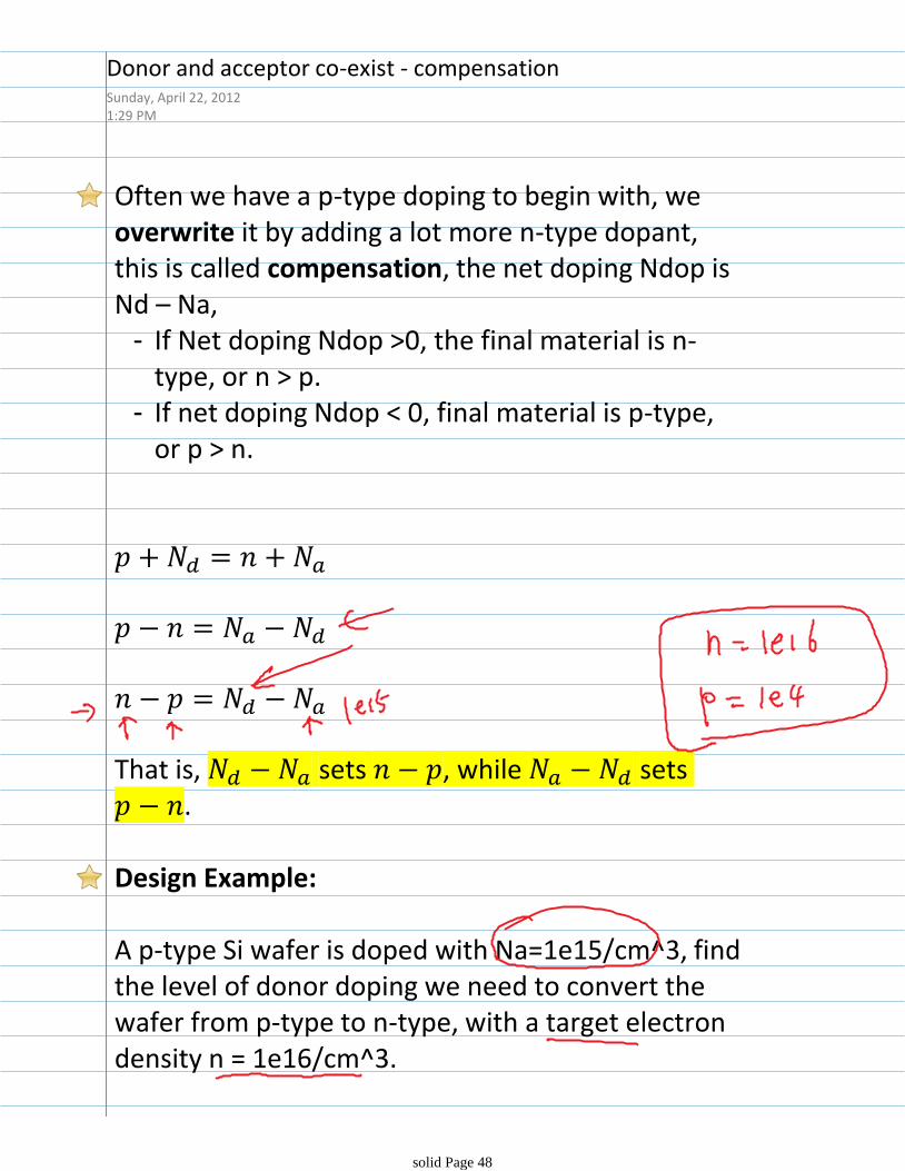
If Net doping Ndop >0, the final material is n-type, or n > p.
-
If net doping Ndop < 0, final material is p-type, or p > n.
-
Often we have a p-type doping to begin with, we overwrite it by adding a lot more n-type dopant, this is called compensation, the net doping Ndop is Nd – Na,
That is, sets , while sets .
Design Example:
A p-type Si wafer is doped with Na=1e15/cm^3, find the level of donor doping we need to convert the wafer from p-type to n-type, with a target electron density n = 1e16/cm^3.
In fact, this is how real devices are made, we start
Donor and acceptor co-exist - compensationSunday, April 22, 20121:29 PM
solid Page 48

In fact, this is how real devices are made, we start from a substrate, and then use compensation to create regions of different type and doping level to make integrated circuits.
Solution:
We know n, so p=ni^2/n.
Thus
>>> na=1e15
>>> n=1e16
>>> p=ni**2/n
>>> nd=(n-p)+na
>>> nd
1.099999999999e+16
Design Example 2:
solid Page 49

A n-type Si wafer is doped with Nd=5e16/cm^3, find the type and level of doping we need to add to the surface region to convert the surface region to p-type, with a target p = 5e16/cm^3.
solid Page 50

We have used the water analogy to show that the pn product at equilibrium is constant, and therefore, is equal to ni^2.
We will directly derive the pn product here.
The key is to understand that at
any point of time, e-h pairs are
generated, and in the same time,
e-h pairs recombine. In
equilibrium, the number of e-h
pairs generated exactly equals
the number of e-h pairs
recombined.
Pn product - direct derivationSunday, April 22, 20122:02 PM
solid Page 51

Generation rate ( the number of e-h pairs per volume generated per second):
Generation of e-h pairs requires energy from thermal or optical sources (orother external sources)
solid Page 52

G is independent of the density of bonds -which are virtually infinite. So supply of breakable bonds is inexhustible. In band model, the density of valence electrons is practically infinite.
So the generation rate depends on temperature (thermal energy), but to first order, is independent of the number of existing electrons or holes.
It makes intuitive sense, as most of CB states are empty. All of them can take an excited electron.
Recombination,
Recombination rate R:
solid Page 53
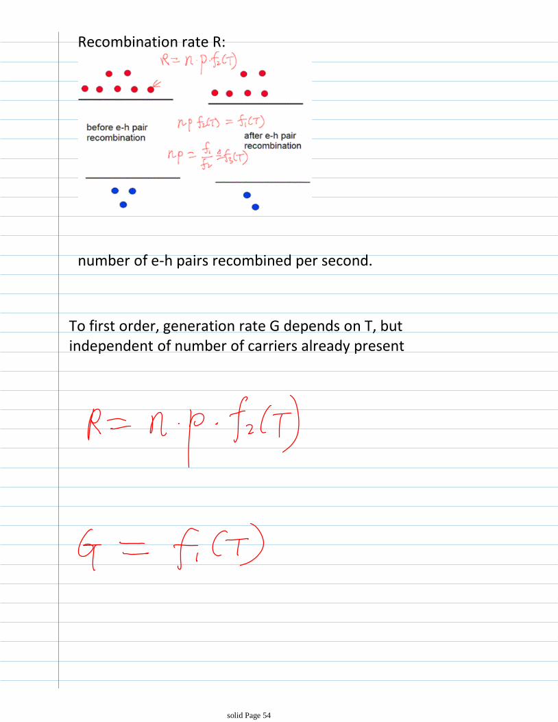
Recombination rate R:
number of e-h pairs recombined per second.
To first order, generation rate G depends on T, but independent of number of carriers already present
solid Page 54

a dynamic equilibrium exists
some valence electrons are constantly being excited from VB to CB - a process called generation of e-h pairs
some CB electrons are losing energy and falling back to VB - called recombination of e-h pairs, annilating both carriers
To first order, generation rate G depends on T, but independent of number of carriers already present
Recombination rate R, depends on n and p, because both species must interact for recombination to occur
Important consequence:
In thermal equilibrium and for a given semiconductor, np
solid Page 55

In thermal equilibrium and for a given semiconductor, np product is a constant that depends only on temperature!
What if this is intrinsic semiconductor?
Summary of PN Product
At equilibrium, the generation rate must equal the recombination rate, that is G=R
solid Page 56

n0 * p0 * f2(T) = f1(T) or
n0 * p0 = f1(T) / f2(T) = f3(T)
equal the recombination rate, that is G=R
The equilibrium np product is a function of only temperature and the bandgap Eg
In an intrinsic semiconductor (undoped), all n and p are from thermal ionization or excitation across the bandgap. Consequently n0 = p0 = ni, “i” indicates intrinsic
n0 * p0 = ni2
solid Page 57

Analysis Problem Statement:At manufacturing, Nd and Na are established, we need to find the resulting carrier concentrations, i.e. n and p values.
Let us solve the neutrality and pn product equations for p and n.
We will start with a n-type example, then look at a p-type example where a numerical issue is revealed.
We can then develop a generic solution that applies to any doping level.
Analysis of Equilibrium Uniform SemiconductorThursday, May 24, 20126:22 PM
solid Page 58
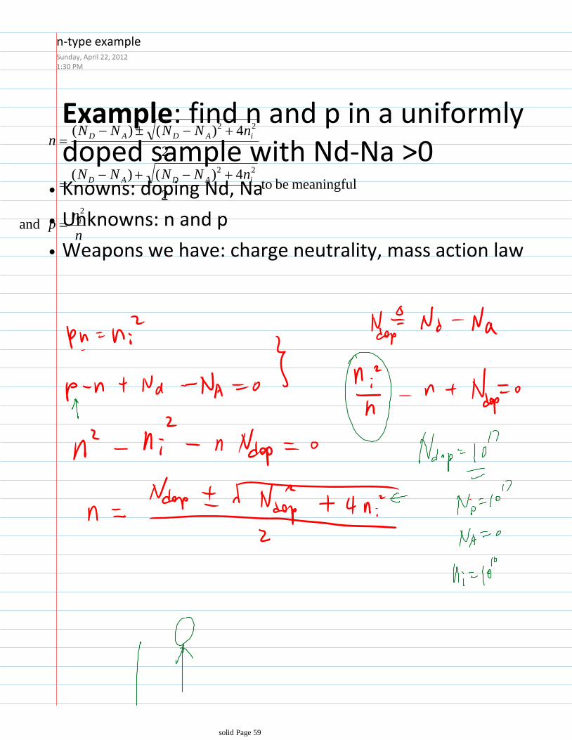
Example: find n and p in a uniformly doped sample with Nd-Na >0Knowns: doping Nd, Na•
Unknowns: n and p•
Weapons we have: charge neutrality, mass action law•n
np
nNNNN
nNNNNn
i
iADAD
iADAD
2
22
22
and
meaningful be to2
4)()(
2
4)()(
n-type exampleSunday, April 22, 20121:30 PM
solid Page 59

n
np
nNNNN
nNNNNn
i
iADAD
iADAD
2
22
22
and
meaningful be to2
4)()(
2
4)()(
solid Page 60

How many electrons and holes are there in a cubic cm pure silicon at 300K? (assuming ni=1e10/cm3)N=?
P=?
What if we add Phosphorous, at a concentration of 1016/cm3
N=?
P=?
solid Page 61

P-type material example (Nd – Na <0)
What is n and p if Nd = 0, Na=1e17?
We now need to take difference of two very large numbers, that difference gets lost easily in computers due to truncation errors! Try to do this calculation yourself with calculator and see what you get.
Solution: solve for the larger number "p" first or try to do something to your equation to avoid taking such difference, can you think of how?
p-type exampleSunday, April 22, 20121:34 PM
solid Page 62

A better way is to always solve for the larger number of "n" and "p" first, as shown below, to avoid the numerical issue above. We already know from previous analysis that if the net doping is p-type, p > n, so we can solve for "p" first as shown below, and then use pn = ni^2 to solve for "n"
solid Page 63

solid Page 64

General solution strategySunday, April 22, 20121:36 PM
solid Page 65

solid Page 66
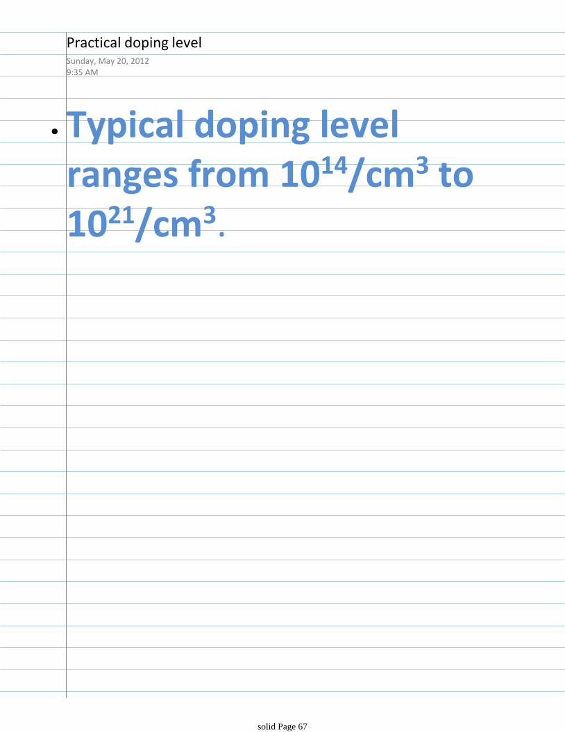
Typical doping level ranges from 1014/cm3 to 1021/cm3.
•
Practical doping levelSunday, May 20, 20129:35 AM
solid Page 67
The other effect of Doping -
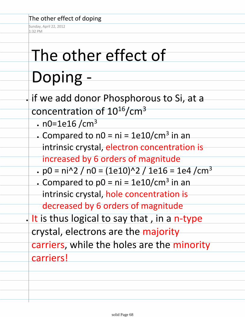
n0=1e16 /cm3
Compared to n0 = ni = 1e10/cm3 in an intrinsic crystal, electron concentration is increased by 6 orders of magnitude
p0 = ni^2 / n0 = (1e10)^2 / 1e16 = 1e4 /cm3
Compared to p0 = ni = 1e10/cm3 in an intrinsic crystal, hole concentration is decreased by 6 orders of magnitude
if we add donor Phosphorous to Si, at a concentration of 1016/cm3
It is thus logical to say that , in a n-typecrystal, electrons are the majority carriers, while the holes are the minority carriers!
The other effect of dopingSunday, April 22, 20121:32 PM
solid Page 68

If n > p, the material is n-type.If p > n, the material is p-type.
Nd = donor impurity concentration /cm3 –Na = acceptor impurity concentration /cm3
Ionized donors are positvely charged
Ionized acceptors are negatively charged
Ndop = Nd - Na is called Net Doping
,
The essence of doping is that it changes the difference between p and n
typically both ND and NA exist, this is called "compensation“
there is no net charge anywhere in sample – charge neutrality,
Charge neutrality requires q(Nd - Na + p -n) = 0
Mass action law requires pn = ni2
Doped Silicon Carrier Concentrations SummarySunday, April 22, 20121:37 PM
solid Page 69

Drift – movement of charged particle in electric fieldIn presence of electric field, electrons experience a force –qE, and thus drift against electric field
•
In ELEC5700, we will show that such velocity is linearly proportional to electric field
•
The proportionality constant is called mobility•
If we use cm/s for velocity, V/cm for e-field, what is the unit of mobility?
•
DriftSunday, April 22, 20121:44 PM
solid Page 70

In thermal equilibrium, mobile electrons in the conduction band or holes in the valence band will be in random thermal motion, through scattering from lattice vibrations, impurities, other electrons, or defects. From statistical mechanics, thermal energy = kT/2 per degree of freedomwhere k = Boltzmann's constant
At 300K, in Si, thermal velocity is on the order of 107cm/s.
This is pretty fast! About 223693 miles per hour (mph).
Random thermal motionThursday, May 24, 20127:49 PM
solid Page 71

Drift by definition means the motion of charged particles driven by electric field.
From our earlier discussion on carrier motion, the force acting on -q charged electron tends to accelerate electron in the direction of the force - opposite to direction of field.
The acceleration, however, is frequently interrupted by collisions with vibrating atoms (or phonons in quantum terms), ionized dopants (Columb scattering), other electrons or holes etc.
It is important to realize that the drift velocity is often much less than the thermal velocity - the random Brownian motion, at least at relatively low electric field.
The average thermal motion at a macroscopic level, however, is zero, due to the random nature of thermal motion.
Drift, however, is directional!
For current, we are interested in the directional "net" velocity.
Directed motion on top of random thermal motionThursday, May 24, 20127:53 PM
solid Page 72

Drift – motion of charged particle in electric fieldIn presence of electric field, electrons experience a force –qE, and thus drift against electric field, similarly holes drift along electric field
•
Unlike in vacuum, electron or hole velocity keeps on increasing over time in presence of electric field. Instead, acceleration occurs over a short time period only, as directed motions are frequently interrupted by vibrating Si atoms or charged dopants.
•
Drift-current and In-class questionsSunday, April 22, 20121:44 PM
solid Page 73
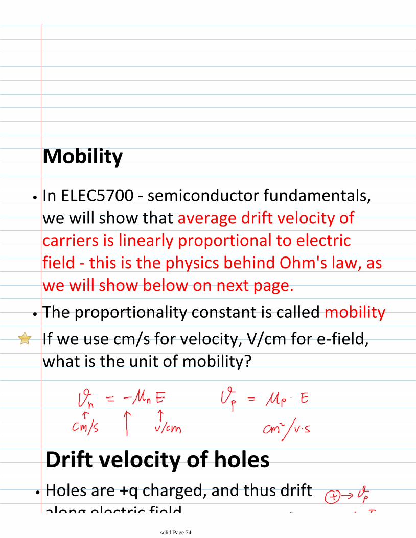
Mobility
In ELEC5700 - semiconductor fundamentals, we will show that average drift velocity of carriers is linearly proportional to electric field - this is the physics behind Ohm's law, as we will show below on next page.
•
The proportionality constant is called mobility•
If we use cm/s for velocity, V/cm for e-field, what is the unit of mobility?
Drift velocity of holesHoles are +q charged, and thus drift along electric field
•
solid Page 74

Holes are +q charged, and thus drift along electric field
•
Thus hole drift velocity is given by
•
Consider a uniform bar, hole density is p, a voltage is applied as shown. Holes move at velocity v. Cross sectional area is A, length is L in the electric field direction.
What is the total amount of hole charge in this bar? hole concentration is p.How long does it take a hole to travel across the length of L?If you stand at the end of the bar, how much current do you observe?What is the current per cross sectional area (current density)?
Drift Current and Drift Current Density DerivationCurrent = charge flowing through per unit time•
Current = The amount of charge / the amount of time taken for all the charges to move out
•
solid Page 75

time taken for all the charges to move out
•
Current density = current / cross section area•
Drift Current Densities and Conductivity
solid Page 76

Deriving Ohm’s LawNow we have established the relation between current density J and electric field E
•
Derivation of Ohm's lawSunday, April 22, 20121:49 PM
solid Page 77

Velocity SaturationAt high fields, carrier velocity saturates and places upper limits on the speed of solid-state devices.
Mobility and Resistivity in Doped Semiconductors
solid Page 78

Note that the total doping means Nd + Na, very different from net doping, which is Nd-Na.
Reason is simple, both ionized donors and acceptors can scatter the motion of electrons / holes through Columb force
solid Page 79

Example of electron drift current density calculation.
In a uniform Si sample doped with arsenic at 1017/cm3, find vn(drift) and Jn(drift) in an electric field of 2500V/cm. Assume electron mobility is 700cm2/(V s).
examplesWednesday, May 23, 201212:13 AM
solid Page 80

Example of hole drift current density calculation.
In a uniform Si sample doped with arsenic at 1017/cm3, find vp(drift) and Jp(drift) in an electric field of 2500V/cm. Assume hole mobility is 200cm2/(V s).
solid Page 81

vp = 5 x 105 cm/s. Jp = 8 x 10-11 A/cm2
solid Page 82

solid Page 83

Diffusion concept1.Diffusion current density expressions for electrons and holes
2.
Electron diffusion illustration3.Hole diffusion illustration4.Einstein's relation5.Numerical example6.
DiffusionSunday, April 22, 20121:54 PM
solid Page 84

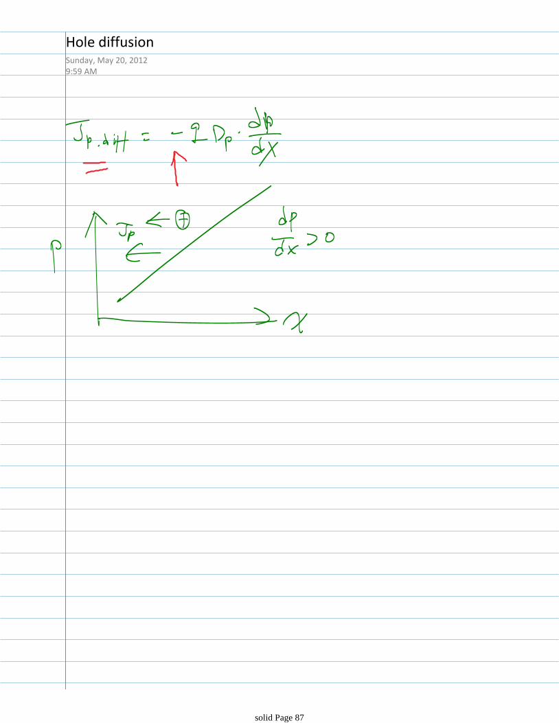
Diffusion Current DensityCarriers diffuse from high concentration to low concentration due to random thermal motion
•
diffusion current densities are proportional to the negative of the hole density gradient for holes and proportional to electron density gradient as follows:
•
Dp and Dn are the hole and electron diffusivities with units cm2/s.
Minority carriers can produce large diffusion current even if their concentration is low!!! – this is the foundation of diodes and bipolar transistors!
•
The gradient is what matters for diffusion current!!•
Diffusion Current DensitySunday, May 20, 20129:55 AM
solid Page 85

Electron diffusionSunday, May 20, 20129:59 AM
solid Page 86
Hole diffusionSunday, May 20, 20129:59 AM
solid Page 87

Einstein’s RelationDiffusivity and mobility are related by Einsteins’s relationship:
•
The thermal voltage,
, is
approximately 25 mV at room temperature. This is worth remembering.
•
Example: Diffusion Constant Using Einstein's Relation
Find D for mu = 410cm^2/(V*s)
Einstein's RelationSunday, May 20, 201210:00 AM
solid Page 88
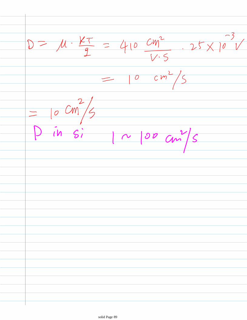
solid Page 89

exampleSunday, April 22, 20121:57 PM
solid Page 90

solid Page 91
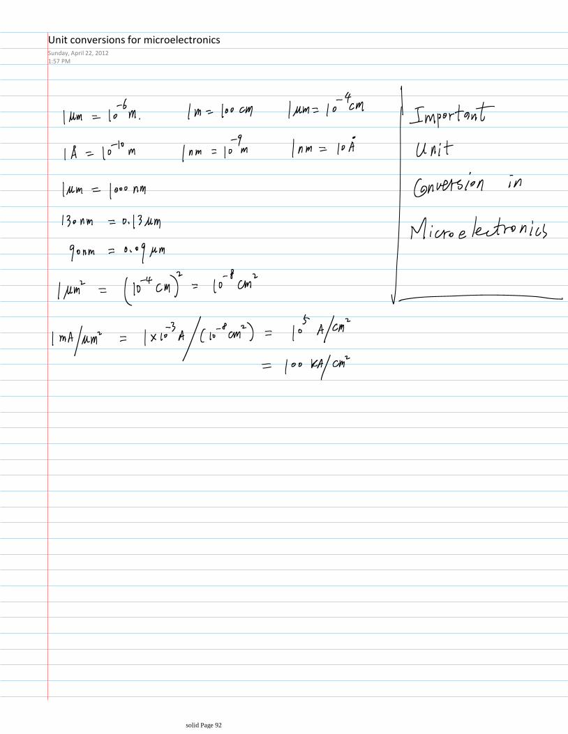
Unit conversions for microelectronicsSunday, April 22, 20121:57 PM
solid Page 92

Consider this non-uniform semiconductor system:
Quiz:
indicate directions of1) electron diffusion motion2) electron drift motion
3) electron diffusion current 4) electron drift current5) hole diffusion motion6) hole drift motion7) hole diffusion current8) hole drift current
Total current densitySunday, April 22, 20121:59 PM
solid Page 93

6) hole drift motion7) hole diffusion current8) hole drift current
solid Page 94
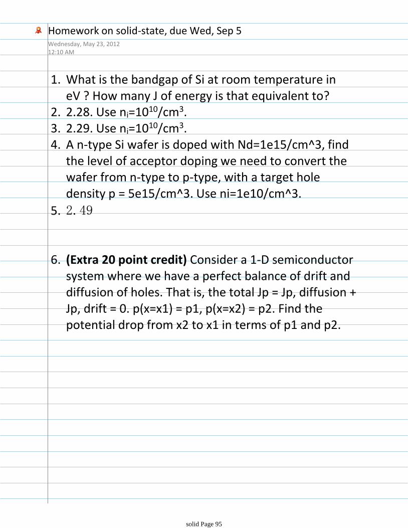
What is the bandgap of Si at room temperature in eV ? How many J of energy is that equivalent to?
1.
2.28. Use ni=1010/cm3.2.2.29. Use ni=1010/cm3.3.A n-type Si wafer is doped with Nd=1e15/cm^3, find the level of acceptor doping we need to convert the wafer from n-type to p-type, with a target hole density p = 5e15/cm^3. Use ni=1e10/cm^3.
4.
2.495.
(Extra 20 point credit) Consider a 1-D semiconductor system where we have a perfect balance of drift and diffusion of holes. That is, the total Jp = Jp, diffusion + Jp, drift = 0. p(x=x1) = p1, p(x=x2) = p2. Find the potential drop from x2 to x1 in terms of p1 and p2.
6.
Homework on solid-state, due Wed, Sep 5Wednesday, May 23, 201212:10 AM
solid Page 95

solutionsMonday, June 04, 201211:39 AM
solid Page 96

Eg=1.12eV1.12*1.6e-19=1.8e-19J
EgThursday, September 20, 20121:07 PM
solid Page 97

2.28(a) Arsenic is a donor, and boron is an acceptor. ND = 2 x 10¹⁸/cm3, and NA = 8 x 10¹⁸/cm3. Since NA > ND, the material is p-type.
2.28Monday, June 04, 201211:41 AM
solid Page 98

2.29Monday, June 04, 201211:44 AM
solid Page 99

We need to put in acceptors at a level of Na = Nd + p - nP = 5e15/cm^3, n = 1e20/p = 2e4/cm^3Na = 1e15 + 5e15 - 2e4 = 5E15 /cm^3
Doping design (problem 5))Monday, June 04, 201211:47 AM
solid Page 100
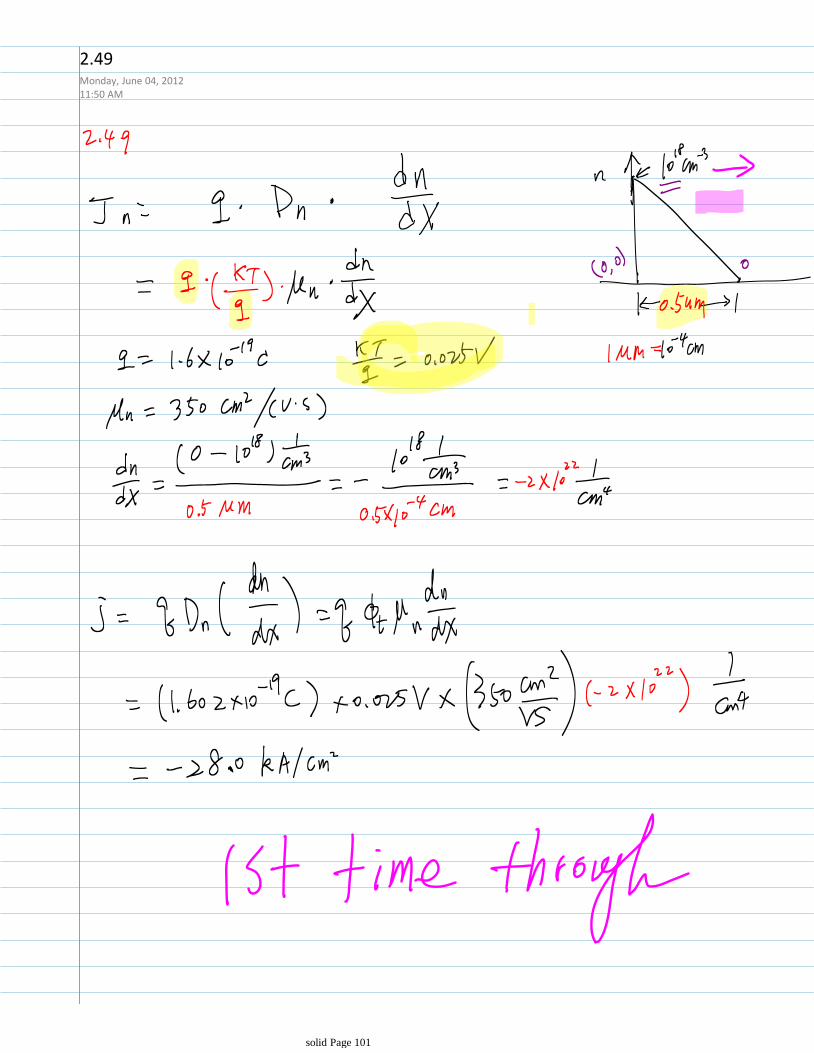
2.49Monday, June 04, 201211:50 AM
solid Page 101

solid Page 102

solid Page 103