ELECTRONICS DEVICES & CIRCUITS Lab Manual · of two stage RC coupled amplifier and calculate...
46
GOVERNMENT POLYTECHNIC HISAR Lab Manual ELECTRONICS DEVICES & CIRCUITS Er. Rajesh Kumar Gautam Lecturer ECE Govt. Polytechnic, Hisar
Transcript of ELECTRONICS DEVICES & CIRCUITS Lab Manual · of two stage RC coupled amplifier and calculate...
GOVERNMENT POLYTECHNIC HISARLab Manual
ELECTRONICS DEVICES & CIRCUITS
Er. Rajesh Kumar GautamLecturer ECE
Govt. Polytechnic, Hisar
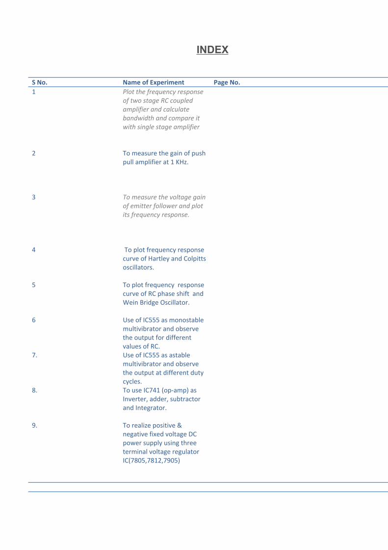
INDEX
S No. Name of Experiment Page No.1 Plot the frequency response
of two stage RC coupled amplifier and calculate bandwidth and compare it with single stage amplifier
2 To measure the gain of push pull amplifier at 1 KHz.
3 To measure the voltage gain of emitter follower and plot its frequency response.
4 To plot frequency response curve of Hartley and Colpitts oscillators.
5 To plot frequency response curve of RC phase shift and Wein Bridge Oscillator.
6
7.
8.
9.
Use of IC555 as monostable multivibrator and observe the output for different values of RC.Use of IC555 as astable multivibrator and observe the output at different duty cycles.To use IC741 (op-amp) as Inverter, adder, subtractor and Integrator.
To realize positive & negative fixed voltage DC power supply using three terminal voltage regulator IC(7805,7812,7905)

Aim: To calculate the voltage gain and to observe frequency response of RC Coupled amplifier.
Apparatus:
Transistors BC 107 2 No's
Resistors 3.3K 2 No's
33K 2 No's
330Ω 2 No's
1K 2 No's
Capacitors 100uF 3 No's
10uF 2 No's
Bread Board
Regulated power supply
Cathode ray oscilloscope
Theory:
This is most popular type of coupling as it provides excellent audio fidelity.
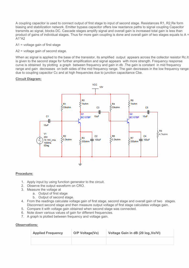
A coupling capacitor is used to connect output of first stage to input of second stage. Resistances R1, R2,Re form biasing and stabilization network. Emitter bypass capacitor offers low reactance paths to signal coupling Capacitor transmits ac signal, blocks DC. Cascade stages amplify signal and overall gain is increased total gain is less than product of gains of individual stages. Thus for more gain coupling is done and overall gain of two stages equals to A =A1*A2
A1 = voltage gain of first stage
A2 = voltage gain of second stage.
When ac signal is applied to the base of the transistor, its amplified output appears across the collector resistor Rc.It is given to the second stage for further amplification and signal appears with more strength. Frequency response curve is obtained by plotting a graph between frequency and gain in db .The gain is constant in mid frequency range and gain decreases on both sides of the mid frequency range. The gain decreases in the low frequency range due to coupling capacitor Cc and at high frequencies due to junction capacitance Cbe.
Circuit Diagram:
Procedure:
1. Apply input by using function generator to the circuit.2. Observe the output waveform on CRO.3. Measure the voltage at
a. Output of first stageb. Output of second stage.
4. From the readings calculate voltage gain of first stage, second stage and overall gain of two stages. Disconnect second stage and then measure output voltage of first stage calculates voltage gain.
5. Compare it with voltage gain obtained when second stage was connected.6. Note down various values of gain for different frequencies.7. A graph is plotted between frequency and voltage gain.
Observations:
Applied Frequency O/P Voltage(Vo) Voltage Gain in dB (20 log10Vo/Vi)
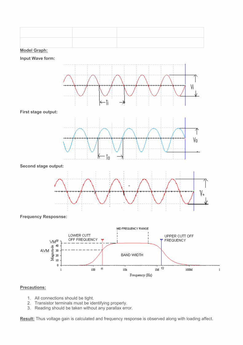
Model Graph:
Input Wave form:
First stage output:
Second stage output:
Frequency Resposnse:
Precautions:
1. All connections should be tight.2. Transistor terminals must be identifying properly.3. Reading should be taken without any parallax error.
Result: Thus voltage gain is calculated and frequency response is observed along with loading affect.
Viva Questions:
1. What is the necessity of cascading?2. What is 3dB bandwidth?3. Why RC coupling is preferred in audio range?4. Which type of coupling is preferred and why?5. Explain various types of Capacitors?6. What is loading effect?7. Why it is known as RC coupling?8. What is the purpose of emitter bypass capacitor?9. Which type of biasing is used in RC coupled amplifier?
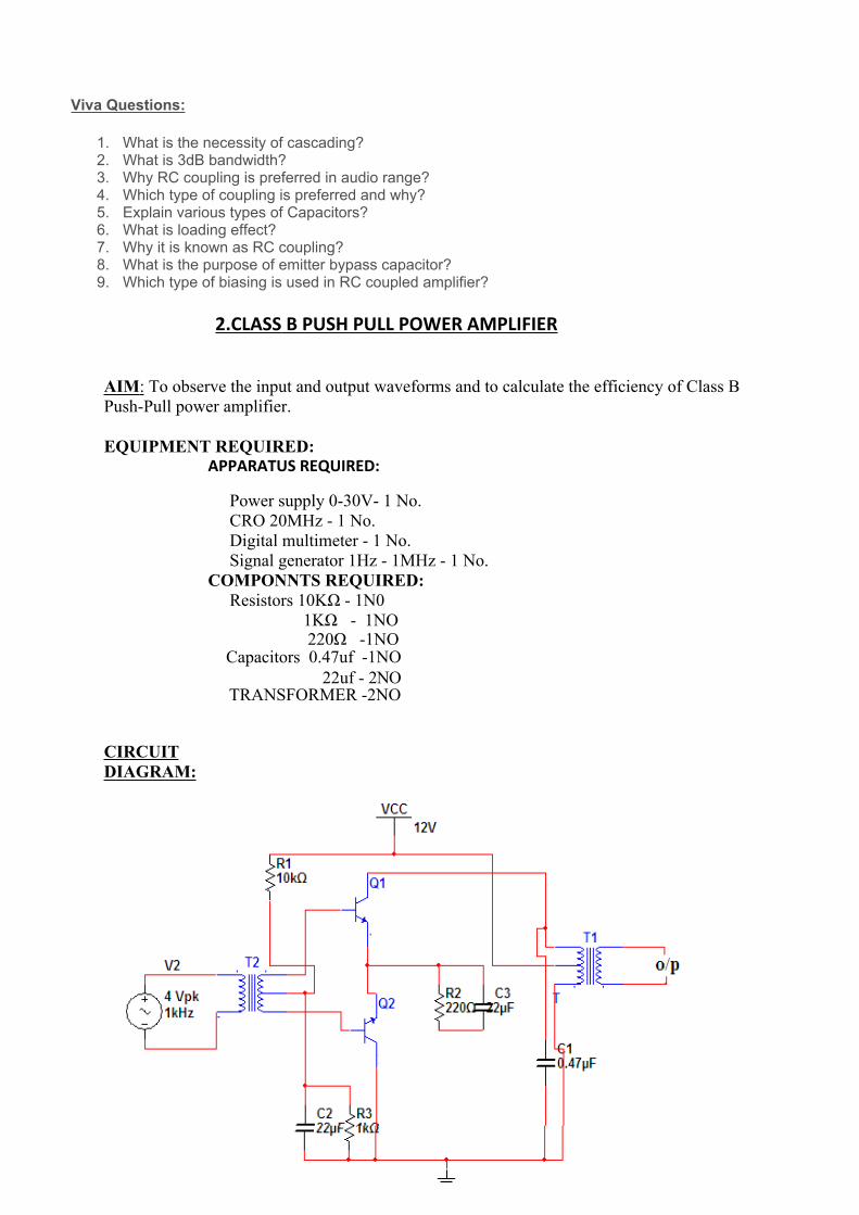
2.CLASS B PUSH PULL POWER AMPLIFIER
AIM: To observe the input and output waveforms and to calculate the efficiency of Class B Push-Pull power amplifier.
EQUIPMENT REQUIRED:APPARATUS REQUIRED:
Power supply 0-30V- 1 No. CRO 20MHz - 1 No.Digital multimeter - 1 No.Signal generator 1Hz - 1MHz - 1 No.
COMPONNTS REQUIRED:Resistors 10KΩ - 1N0
1KΩ - 1NO220Ω -1NO
Capacitors 0.47uf -1NO22uf - 2NO
TRANSFORMER -2NO
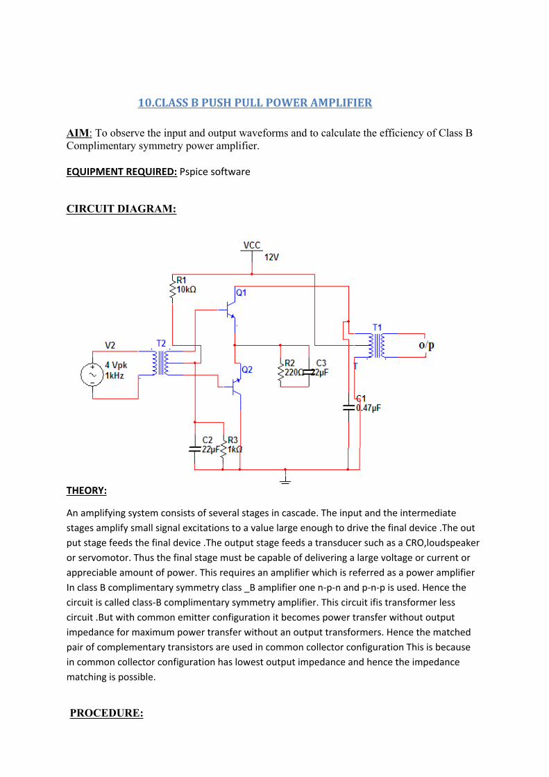
CIRCUIT DIAGRAM:

THEORY:
An amplifying system consists of several stages in cascade. The input and the intermediate stages amplify small signal excitations to a value large enough to drive the final device .The out put stage feeds the final device .The output stage feeds a transducer such as a CRO,loudspeaker or servomotor. Thus the final stage must be capable of delivering a large voltage or current or appreciable amount of power. This requires an amplifier which is referred as a power amplifier
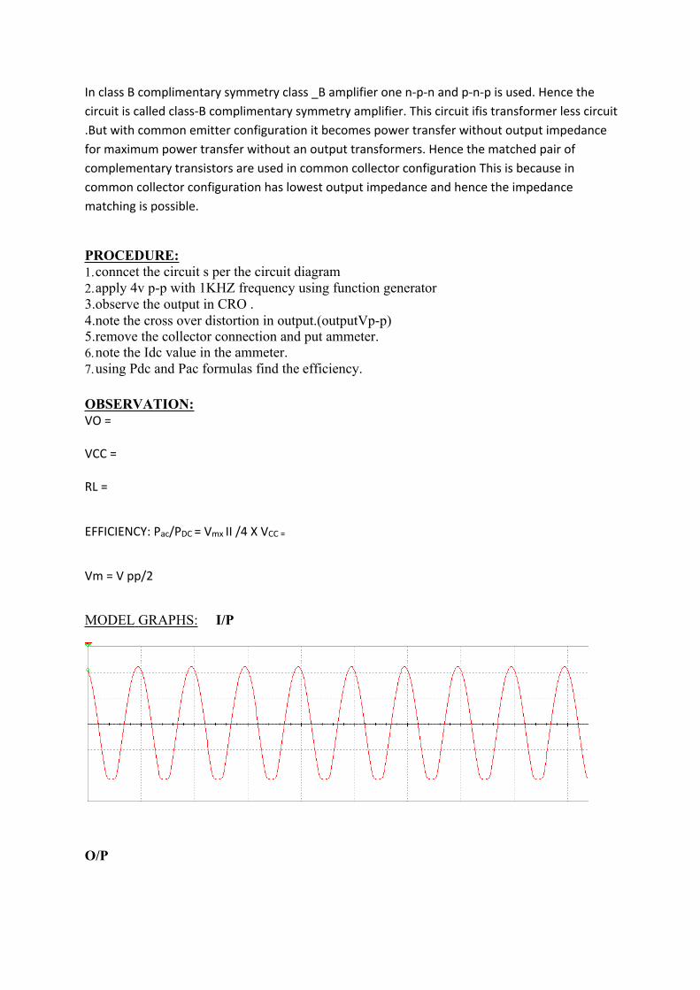
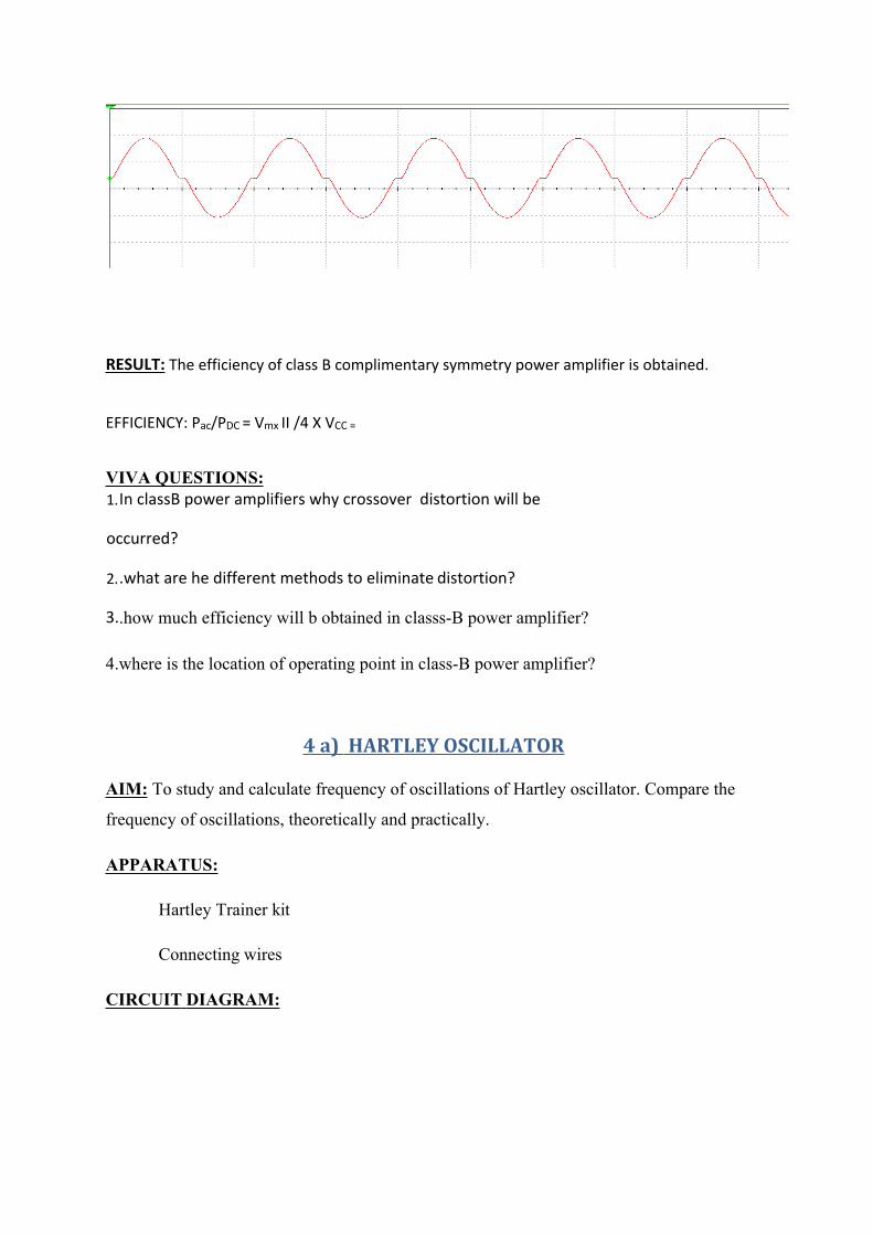
In class B complimentary symmetry class _B amplifier one n-p-n and p-n-p is used. Hence the circuit is called class-B complimentary symmetry amplifier. This circuit ifis transformer less circuit .But with common emitter configuration it becomes power transfer without output impedance for maximum power transfer without an output transformers. Hence the matched pair of complementary transistors are used in common collector configuration This is because in common collector configuration has lowest output impedance and hence the impedance matching is possible.
PROCEDURE:1.conncet the circuit s per the circuit diagram2.apply 4v p-p with 1KHZ frequency using function generator 3.observe the output in CRO .4.note the cross over distortion in output.(outputVp-p) 5.remove the collector connection and put ammeter.6.note the Idc value in the ammeter.7.using Pdc and Pac formulas find the efficiency.
OBSERVATION:VO =
VCC =
RL =
EFFICIENCY: Pac/PDC = Vmx II /4 X VCC =
Vm = V pp/2
MODEL GRAPHS: I/P
O/P
RESULT: The efficiency of class B complimentary symmetry power amplifier is obtained.
EFFICIENCY: Pac/PDC = Vmx II /4 X VCC =
VIVA QUESTIONS:1.In classB power amplifiers why crossover distortion will be
occurred?
2..what are he different methods to eliminate distortion?
3..how much efficiency will b obtained in classs-B power amplifier?
4.where is the location of operating point in class-B power amplifier?
4 a) HARTLEY OSCILLATOR
AIM: To study and calculate frequency of oscillations of Hartley oscillator. Compare the
frequency of oscillations, theoretically and practically.
APPARATUS:
Hartley Trainer kit
Connecting wires
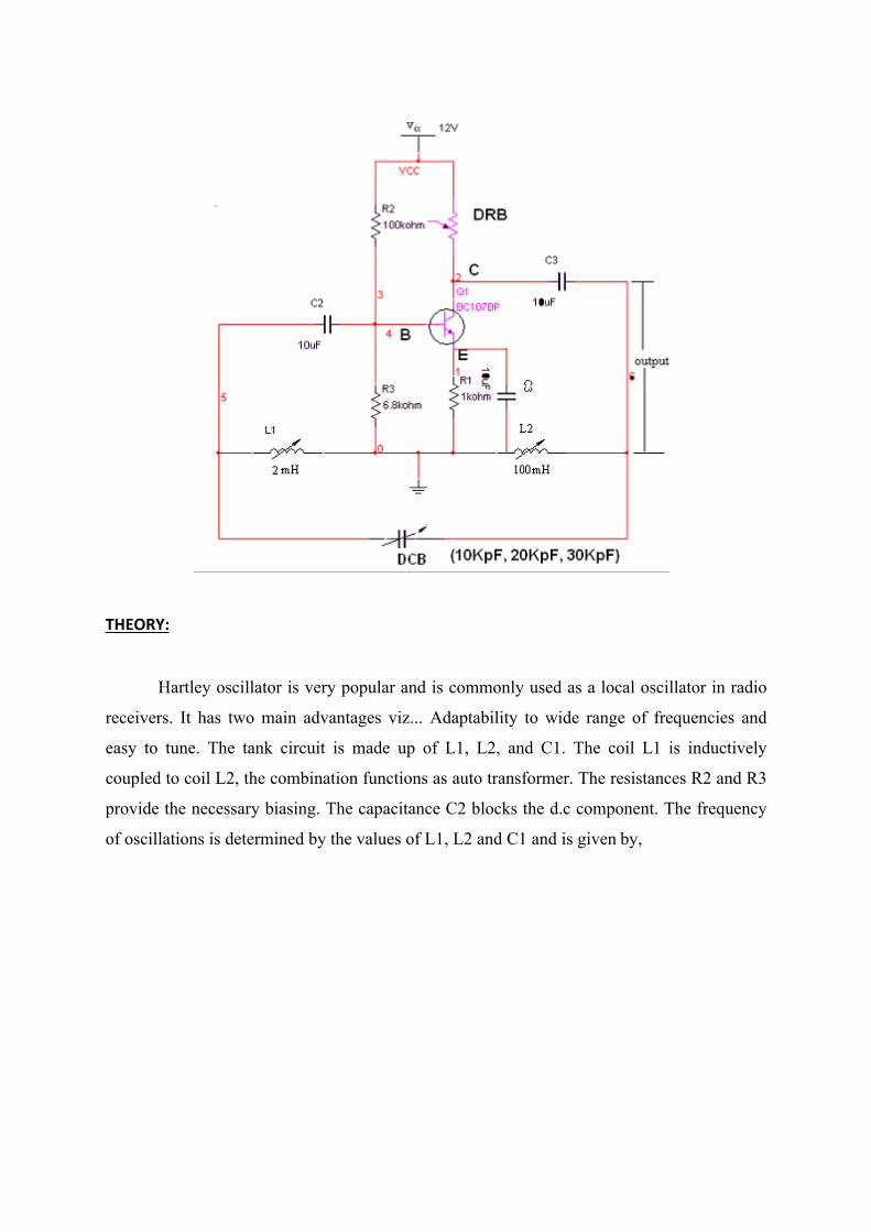
CIRCUIT DIAGRAM:
THEORY:
Hartley oscillator is very popular and is commonly used as a local oscillator in radio
receivers. It has two main advantages viz... Adaptability to wide range of frequencies and
easy to tune. The tank circuit is made up of L1, L2, and C1. The coil L1 is inductively
coupled to coil L2, the combination functions as auto transformer. The resistances R2 and R3
provide the necessary biasing. The capacitance C2 blocks the d.c component. The frequency
of oscillations is determined by the values of L1, L2 and C1 and is given by,
F=1/(2(C1(√L1+L2)))
The energy supplied to the tank circuit is of correct phase. The auto transformer provides
180˚ out of phase. Also another 180˚ is produced By the transistor. In this way, energy
feedback to the tank circuit is in phase with the generated oscillations.
PROCEDURE:
1. Connections are made as per the circuit diagram.
2. Connect CRO at output terminals and observe wave form.
3. Calculate practically the frequency of oscillations by using the Expression.
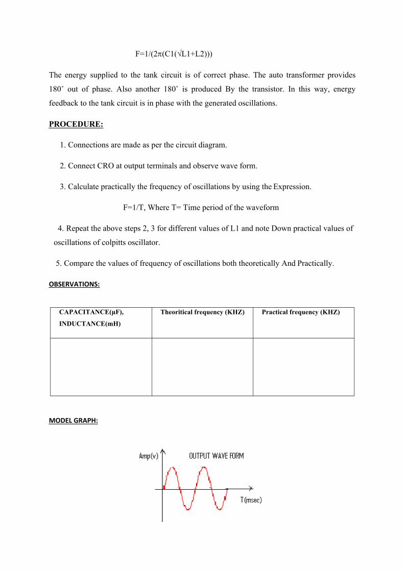
F=1/T, Where T= Time period of the waveform
4. Repeat the above steps 2, 3 for different values of L1 and note Down practical values of
oscillations of colpitts oscillator.
5. Compare the values of frequency of oscillations both theoretically And Practically.
OBSERVATIONS:
CAPACITANCE(μF),
INDUCTANCE(mH)
Theoritical frequency (KHZ) Practical frequency (KHZ)
MODEL GRAPH:
RESULT: Frequency of oscillations is calculated and compared with theoretical values.
F(theoretical) = 1/2 ГLC=
F(practicl) =
VIVA QUESTIONS:
1. What are the applications of LC oscillations?
2. What type of feedback is used in oscillators?
3. What the expression for frequency of oscillations?
4. Whether an oscillator is dc to ac converter?
5. What is the loop gain of an oscillator?
6. What is the difference between amplifier and oscillator?
7. What is the condition for oscillations?
8. How many inductors and capacitors are used in Hartley Oscillator?
9. How the oscillations are produced in Hartley oscillator?
10. What is the difference between damped oscillations undamped oscillations?
1. TWO STAGE RC COUPLED AMPLIFIER
AIM: To obtain the Voltage gain for two stage RC coupled Amplifier and also to observe the frequencyResponse..
EQUIPMENT REQUIRED:
1. cathode ray oscilloscope 1No
2.Regulated power supply 1No
3. function generator 1No
4.bread board 1No
5.connecting wiresCOMPONENTS REQUIRED:
1. Resistors:15k-2no 10k-2no 1k-2no 3.3k-2no 220Ω-2no
2.Transistor :BC107-2no
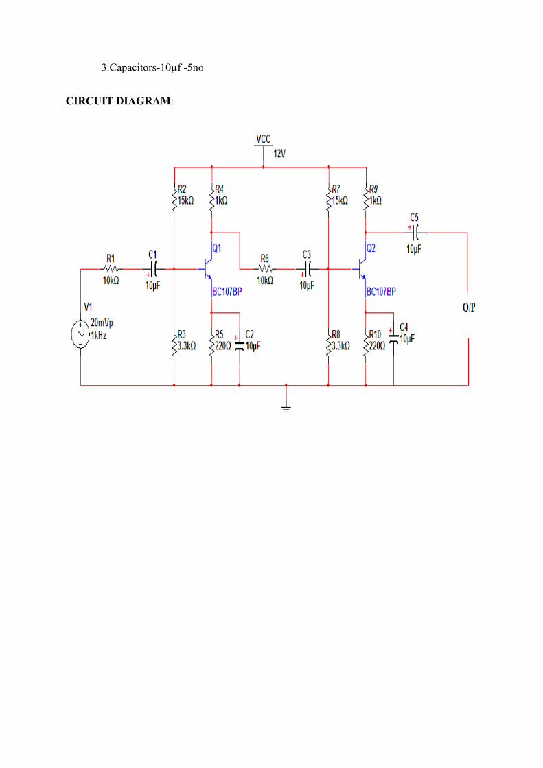
3.Capacitors-10µf -5no
CIRCUIT DIAGRAM:
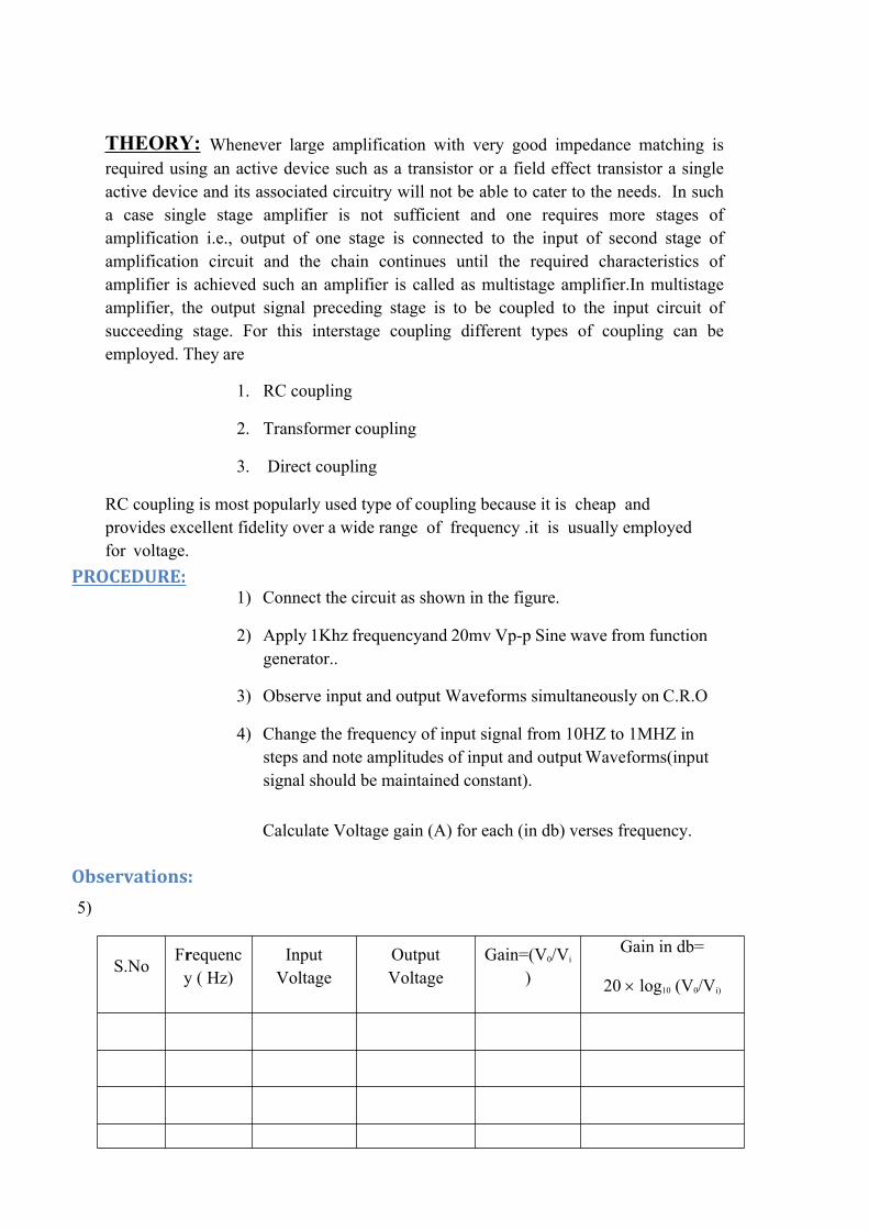
THEORY: Whenever large amplification with very good impedance matching is required using an active device such as a transistor or a field effect transistor a single active device and its associated circuitry will not be able to cater to the needs. In such a case single stage amplifier is not sufficient and one requires more stages of amplification i.e., output of one stage is connected to the input of second stage of amplification circuit and the chain continues until the required characteristics of amplifier is achieved such an amplifier is called as multistage amplifier.In multistage amplifier, the output signal preceding stage is to be coupled to the input circuit of succeeding stage. For this interstage coupling different types of coupling can be employed. They are
1. RC coupling
2. Transformer coupling
3. Direct coupling
RC coupling is most popularly used type of coupling because it is cheap and provides excellent fidelity over a wide range of frequency .it is usually employed for voltage.
PROCEDURE:1) Connect the circuit as shown in the figure.
2) Apply 1Khz frequencyand 20mv Vp-p Sine wave from function generator..
3) Observe input and output Waveforms simultaneously on C.R.O
4) Change the frequency of input signal from 10HZ to 1MHZ in steps and note amplitudes of input and output Waveforms(input signal should be maintained constant).
Observations:
5)
Calculate Voltage gain (A) for each (in db) verses frequency.
S.NoFrequenc y ( Hz)
Input Voltage
Output Voltage
Gain=(V0/Vi
)
Gain in db=
20 log10 (V0/Vi)

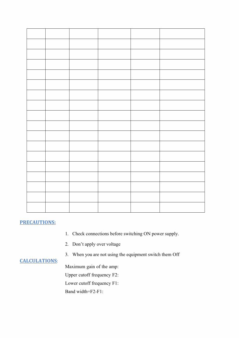
PRECAUTIONS:
1. Check connections before switching ON power supply.
2. Don’t apply over voltage
3. When you are not using the equipment switch them OffCALCULATIONS:
Maximum gain of the amp:
Upper cutoff frequency F2:
Lower cutoff frequency F1:
Band width=F2-F1:
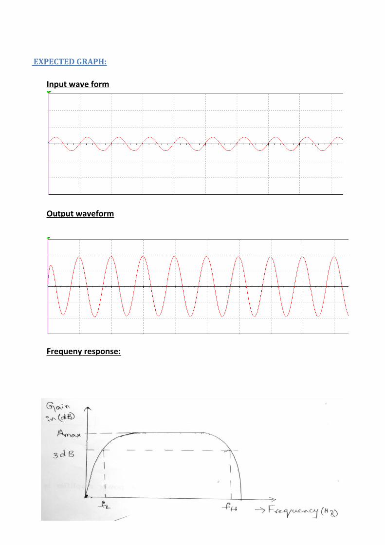
EXPECTED GRAPH:
Input wave form
Output waveform
Frequeny response:
RESULT: -
1. Frequency response of Two stage RC coupled amplifier is plotted.2. Gain = dB (maximum).3. Bandwidth= fH--fL = Hz. At stage 2
VIVA QUESTIONS:
1.What is an amplifier?2.what are the coupling elements of n this amplifier? 3.what are the applications of this amplifier?4.why this type of amplifier will be used in AF mplifiers? 5.which type of biasing isused in this amplifier?
6.whatis the range of bandwidth in this amplifier?
Redraw the circuit diagram
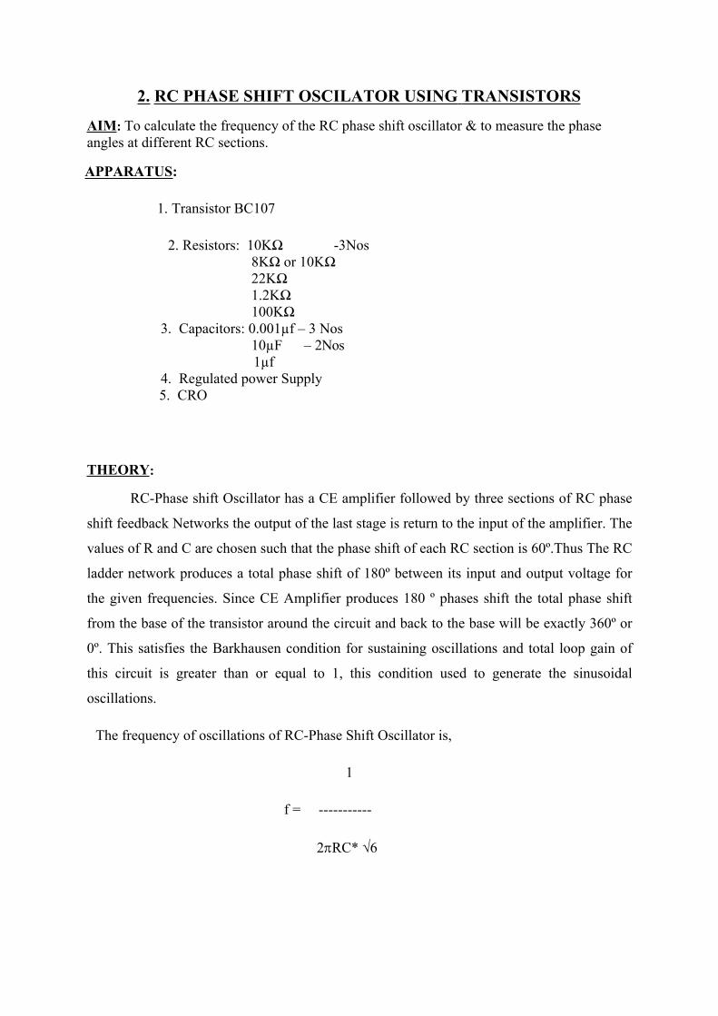
2. RC PHASE SHIFT OSCILATOR USING TRANSISTORS
AIM: To calculate the frequency of the RC phase shift oscillator & to measure the phase angles at different RC sections.
APPARATUS:
1. Transistor BC107
2. Resistors: 10KΩ -3Nos8KΩ or 10KΩ22KΩ1.2KΩ100KΩ
3. Capacitors: 0.001µf – 3 Nos10µF – 2Nos 1µf
4. Regulated power Supply5. CRO
THEORY:
RC-Phase shift Oscillator has a CE amplifier followed by three sections of RC phase
shift feedback Networks the output of the last stage is return to the input of the amplifier. The
values of R and C are chosen such that the phase shift of each RC section is 60º.Thus The RC
ladder network produces a total phase shift of 180º between its input and output voltage for
the given frequencies. Since CE Amplifier produces 180 º phases shift the total phase shift
from the base of the transistor around the circuit and back to the base will be exactly 360º or
0º. This satisfies the Barkhausen condition for sustaining oscillations and total loop gain of
this circuit is greater than or equal to 1, this condition used to generate the sinusoidal
oscillations.
The frequency of oscillations of RC-Phase Shift Oscillator is,
1
f = -----------
2RC* √6

CIRCUIT DIAGRAM:
PROCEDURE:
1. Make the connection as per the circuit diagram as shown above.
2. Observe the output signal and note down the output amplitude and time period (Td).
3. Calculate the frequency of oscillations theoretically and verify it practically (f=1/Td).
4. Calculate the phase shift at each RC section by measuring the time shifts (Tp) between
the final waveform and the waveform at that section by using the below formula.
OBSERVATIONS:
THEORITICAL CALCULATIONS: R = 10KΩ, C = 0.001 μf
1
f = =
2RC* √6
PRACTICAL CALCULATIONS:
Td =
1
f = -----
Td
Tp1
(1). θ 1= --------*3600 =

Td
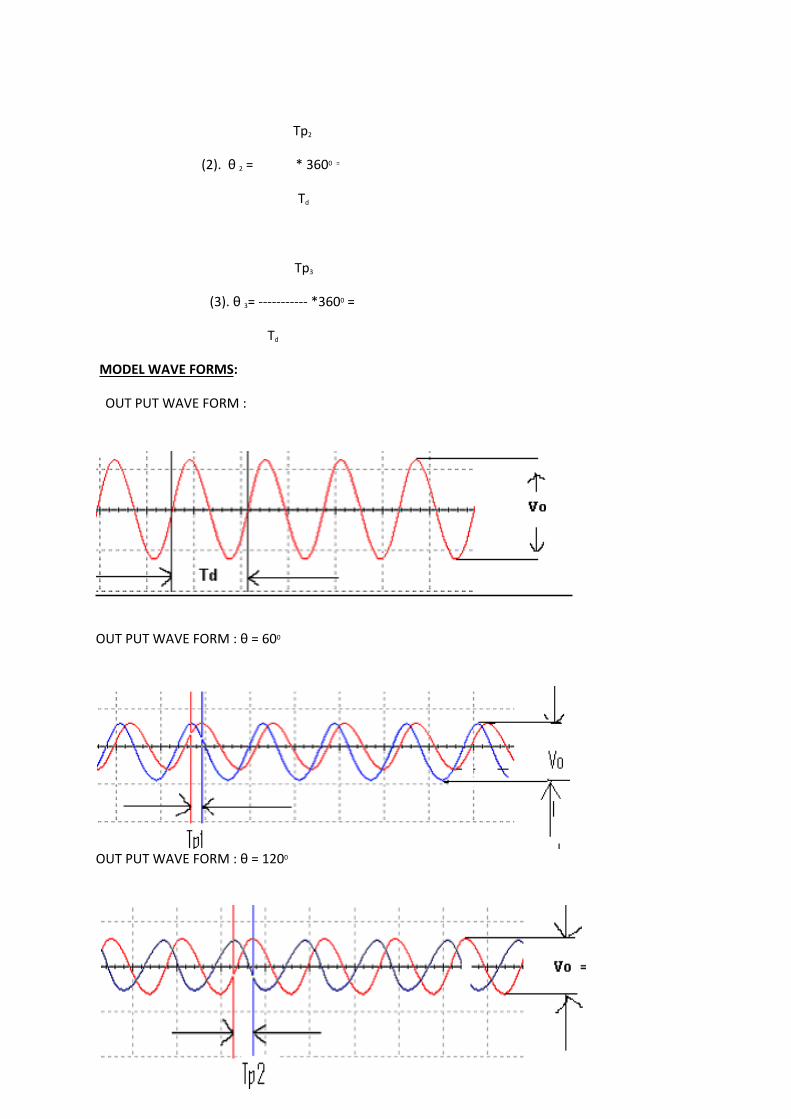
Tp2
(2). θ 2 = * 3600 =
Td
Tp3
(3). θ 3= ----------- *3600 =
Td
MODEL WAVE FORMS:
OUT PUT WAVE FORM :
OUT PUT WAVE FORM : θ = 600
OUT PUT WAVE FORM : θ = 1200

OUT PUT WAVE FORM : θ = 180

RESULT: The frequency of RC phase shift oscillator is calculated and the phase shift at
different RC sections is noted.
FT = FP =
VIVA QUESTIONS:
1. What are the conditions of oscillations?
2. Give the formula for frequency of oscillations?
3. What is the total phase shift produce by the RC ladder network?
4. Whether the oscillator is positive feedback or negative feedback?
5. What are the types of oscillators?
6. What is the gain of RC phase shift oscillator?
7. What is the difference between damped oscillations undamped oscillations?
8. What are the applications of RC oscillations?
9. How many resistors and capacitors are used in RC phase shift network
10. How the Barkhausen criterion is satisfied in RC phase shift oscillator
REDRAW THE CIRCUIT DIAGRAM:

1.SINGLE TUNED VOLTAGE AMPLIFIER
AIM: To study single tuned voltage Amplifier and to calculate
1. Resonant Frequency.2. Q factor.3. Bandwidth and4. Impedance
APPARATUS: 1. Tuned RF Amplifier trainer Kit.2. Function Generator.3. CRO.4. BNC probes and connecting wires
CIRCUIT DIAGRAM:
THEORY:
It is usually required to use a number of tuned amplifier stages in cascade in order to obtain large overall gain. These cascade tuned amplifiers may be put into the following three categories:
1. Single tuned amplifiers.2. Double tuned amplifiers.3. Stagger-tuned amplifiers.
Single tuned amplifiers use one parallel tuned circuit as the load impedance in each stage and all these tuned circuits in different stages are tuned to the same frequency.Double tuned amplifier uses two inductively coupled tuned circuits per stage, both the tuned circuits being tuned to the same frequency.Staggered tuned amplifier uses a number of single tuned stages in cascade, the successive tuned circuits being tuned to slightly different frequencies.

Single tuned amplifiers may again be put into following two categories:a) Capacitance coupled single tuned amplifiers and
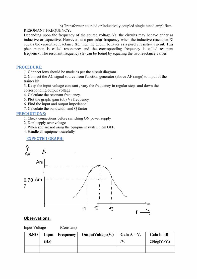
b) Transformer coupled or inductively coupled single tuned amplifiers RESONANT FREQUENCY:Depending upon the frequency of the source voltage Vs, the circuits may behave either as inductive or capacitive. However, at a particular frequency when the inductive reactance Xl equals the capacitive reactance Xc, then the circuit behaves as a purely resistive circuit. This phenomenon is called resonance: and the corresponding frequency is called resonant frequency. The resonant frequency (fr) can be found by equating the two reactance values.
PROCEDURE:1. Connect ions should be made as per the circuit diagram.2. Connect the AC signal source from function generator (above AF range) to input of the trainer kit.3. Keep the input voltage constant , vary the frequency in regular steps and down the corresponding output voltage4. Calculate the resonant frequency.5. Plot the graph: gain (db) Vs frequency6. Find the input and output impedance7. Calculate the bandwidth and Q factor
PRECAUTIONS:1. Check connections before switching ON power supply2. Don’t apply over voltage3. When you are not using the equipment switch them OFF.4. Handle all equipment carefully
EXPECTED GRAPH:
Observations:
Input Voltage= (Constant)
S.NO Input Frequency
(Hz)
OutputVoltage(Vo) Gain A = Vo-
/Vi
Gain in dB
20log(Vo/Vi)
RESULT: Gain and frequency as observed of single tuned voltage amplifier.
FT = FP=
VIVA QUESTIONS:
1. What are tuned amplifiers?2. What is tuning?3. Explain how the tuned amplifiers work?
REDRAW THE CIRCUIT DIAGRAM:
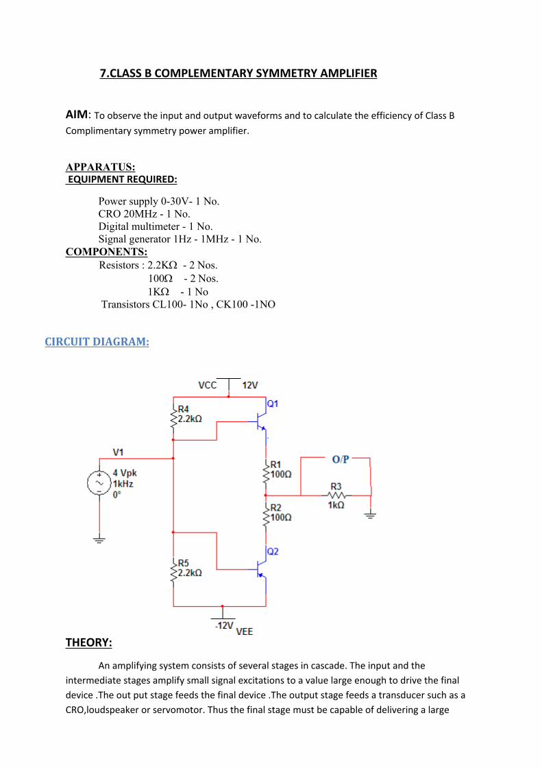
7.CLASS B COMPLEMENTARY SYMMETRY AMPLIFIER
AIM: To observe the input and output waveforms and to calculate the efficiency of Class B Complimentary symmetry power amplifier.
APPARATUS: EQUIPMENT REQUIRED:
Power supply 0-30V- 1 No. CRO 20MHz - 1 No.Digital multimeter - 1 No.Signal generator 1Hz - 1MHz - 1 No.
COMPONENTS:Resistors : 2.2K - 2 Nos.
100 - 2 Nos.1K - 1 No
Transistors CL100- 1No , CK100 -1NO
CIRCUIT DIAGRAM:
THEORY:
An amplifying system consists of several stages in cascade. The input and the intermediate stages amplify small signal excitations to a value large enough to drive the final device .The out put stage feeds the final device .The output stage feeds a transducer such as a CRO,loudspeaker or servomotor. Thus the final stage must be capable of delivering a large

voltage or current or appreciable amount of power. This requires an amplifier which is referred as a power amplifier
In class B complimentary symmetry class _B amplifier one n-p-n and p-n-p is used. Hence the circuit is called class-B complimentary symmetry amplifier. This circuit ifis transformer less circuit .But with common emitter configuration it becomes power transfer without output impedance for maximum power transfer without an output transformers. Hence the matched pair of complementary transistors are used in common collector configuration This is because in common collector configuration has lowest output impedance and hence the impedance matching is possible.
PROCEDURE:1.conncet the circuit s per the circuit diagram2.apply 4v p-p with 1KHZ frequency using function generator 3.observe the output in CRO .4.note the cross over distortion in output.(outputVp-p) 5.remove the collector connection and put ammeter.
6.note the Idc value in the ammeter.7.using Pdc and Pac formulas find the efficiency.
OBSERVATION:
Pac=Vm2/2RL =
Pdc=Vcc*Idc = VO
=
VCC =
RL =
EFFICIENCY: η =Pac/Pdc*100=
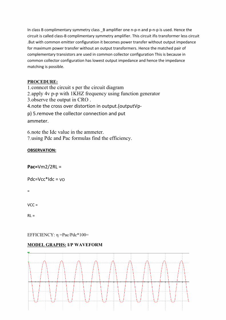
MODEL GRAPHS: I/P WAVEFORM
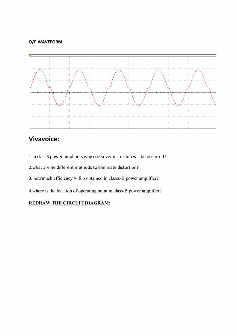
O/P WAVEFORM
Vivavoice:
1. In classB power amplifiers why crossover distortion will be occurred?
2.what are he different methods to eliminate distortion?
3..howmuch efficiency will b obtained in classs-B power amplifier?
4.where is the location of operating point in class-B power amplifier?
REDRAW THE CIRCUIT DIAGRAM:
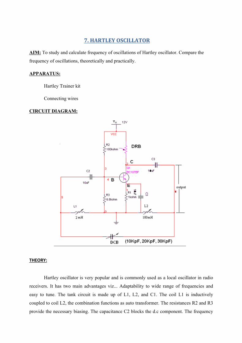
7. HARTLEY OSCILLATOR
AIM: To study and calculate frequency of oscillations of Hartley oscillator. Compare the
frequency of oscillations, theoretically and practically.
APPARATUS:
Hartley Trainer kit
Connecting wires
CIRCUIT DIAGRAM:
THEORY:
Hartley oscillator is very popular and is commonly used as a local oscillator in radio
receivers. It has two main advantages viz... Adaptability to wide range of frequencies and
easy to tune. The tank circuit is made up of L1, L2, and C1. The coil L1 is inductively
coupled to coil L2, the combination functions as auto transformer. The resistances R2 and R3
provide the necessary biasing. The capacitance C2 blocks the d.c component. The frequency

of oscillations is determined by the values of L1, L2 and C1 and is given by,

F=1/(2(C1(√L1+L2)))
The energy supplied to the tank circuit is of correct phase. The auto transformer provides
180˚ out of phase. Also another 180˚ is produced By the transistor. In this way, energy
feedback to the tank circuit is in phase with the generated oscillations.
PROCEDURE:
1. Connections are made as per the circuit diagram.
2. Connect CRO at output terminals and observe wave form.
3. Calculate practically the frequency of oscillations by using the Expression.
F=1/T, Where T= Time period of the waveform
4. Repeat the above steps 2, 3 for different values of L1 and note Down practical values of
oscillations of colpitts oscillator.
5. Compare the values of frequency of oscillations both theoretically And Practically.
OBSERVATIONS:
CAPACITANCE(μF),
INDUCTANCE(mH)
Theoritical frequency (KHZ) Practical frequency (KHZ)
MODEL GRAPH:

RESULT: Frequency of oscillations is calculated and compared with theoretical values.
F(theoretical) = 1/2 ГLC=
F(practicl) =
VIVA QUESTIONS:
1. What are the applications of LC oscillations?
2. What type of feedback is used in oscillators?
3. What the expression for frequency of oscillations?
4. Whether an oscillator is dc to ac converter?
5. What is the loop gain of an oscillator?
6. What is the difference between amplifier and oscillator?
7. What is the condition for oscillations?
8. How many inductors and capacitors are used in Hartley Oscillator?
9. How the oscillations are produced in Hartley oscillator?
10. What is the difference between damped oscillations undamped oscillations?
REDRAW THE CIRCUIT DIAGRAM:
10.CLASS B PUSH PULL POWER AMPLIFIER
AIM: To observe the input and output waveforms and to calculate the efficiency of Class B Complimentary symmetry power amplifier.
EQUIPMENT REQUIRED:APPARATUS REQUIRED:
Power supply 0-30V- 1 No. CRO 20MHz - 1 No.Digital multimeter - 1 No.Signal generator 1Hz - 1MHz - 1 No.
COMPONNTS REQUIRED:Resistors 10KΩ - 1N0
1KΩ - 1NO220Ω -1NO
Capacitors 0.47uf -1NO22uf - 2NO
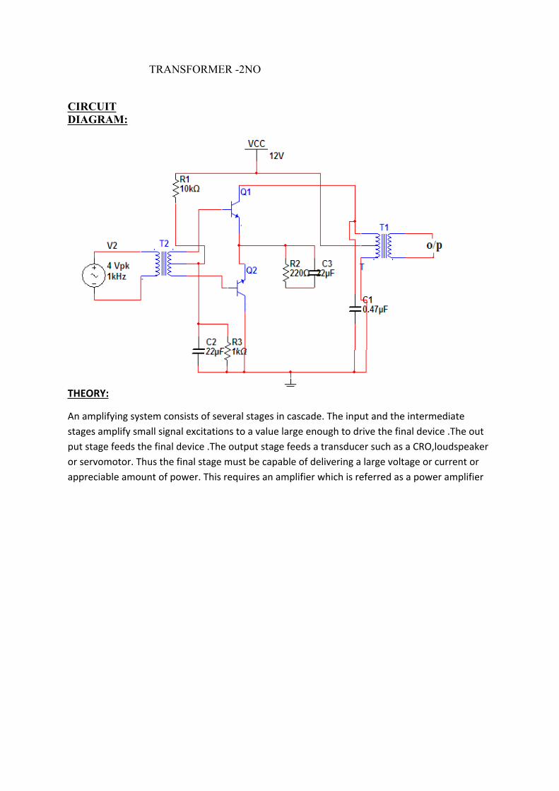
TRANSFORMER -2NO
CIRCUIT DIAGRAM:
THEORY:
An amplifying system consists of several stages in cascade. The input and the intermediate stages amplify small signal excitations to a value large enough to drive the final device .The out put stage feeds the final device .The output stage feeds a transducer such as a CRO,loudspeaker or servomotor. Thus the final stage must be capable of delivering a large voltage or current or appreciable amount of power. This requires an amplifier which is referred as a power amplifier
In class B complimentary symmetry class _B amplifier one n-p-n and p-n-p is used. Hence the circuit is called class-B complimentary symmetry amplifier. This circuit ifis transformer less circuit .But with common emitter configuration it becomes power transfer without output impedance for maximum power transfer without an output transformers. Hence the matched pair of complementary transistors are used in common collector configuration This is because in common collector configuration has lowest output impedance and hence the impedance matching is possible.
PROCEDURE:1.conncet the circuit s per the circuit diagram2.apply 4v p-p with 1KHZ frequency using function generator 3.observe the output in CRO .4.note the cross over distortion in output.(outputVp-p) 5.remove the collector connection and put ammeter.6.note the Idc value in the ammeter.7.using Pdc and Pac formulas find the efficiency.
OBSERVATION:VO =
VCC =
RL =
EFFICIENCY: Pac/PDC = Vmx II /4 X VCC =
Vm = V pp/2
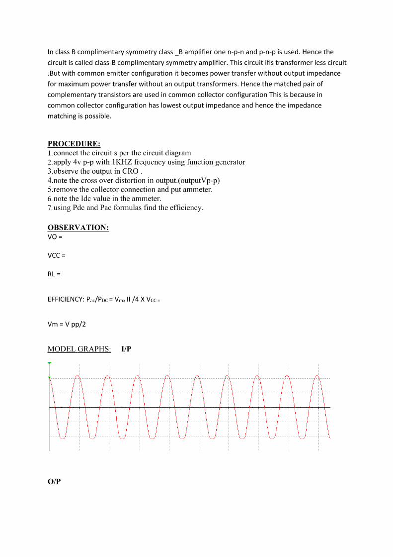
MODEL GRAPHS: I/P
O/P

RESULT: The efficiency of class B complimentary symmetry power amplifier is obtained.
EFFICIENCY: Pac/PDC = Vmx II /4 X VCC =
VIVA QUESTIONS:1. In classB power amplifiers why crossover distortion will be occurred?
2.what are he different methods to eliminate distortion?
3..howmuch efficiency will b obtained in classs-B power amplifier?
4.where is the location of operating point in class-B power amplifier?
REDRAW THE CIRCUIT DIAGRAM:
3. CLASS B COMPLEMENTARY SYMMETRY
AMPLIFIER
AIM: To observe the input and output waveforms and to calculate the efficiency of Class B Complimentary symmetry power amplifier.
EQUIPMENT REQUIRED: PSPICE Simulation Software
CIRCUIT DIAGRAM:

THEORY:
An amplifying system consists of several stages in cascade. The input and the intermediate stages amplify small signal excitations to a value large enough to drive the final device .The out put stage feeds the final device .The output stage feeds a transducer such as a CRO,loudspeaker or servomotor. Thus the final stage must be capable of delivering a large voltage or current or appreciable amount of power. This requires an amplifier which is referred as a power amplifierIn class B complimentary symmetry class _B amplifier one n-p-n and p-n-p is used. Hence the circuit is called class-B complimentary symmetry amplifier. This circuit ifis transformer less circuit .But with common emitter configuration it becomes power transfer without output impedance for maximum power transfer without an output transformers. Hence the matched pair of complementary transistors are used in common collector configuration This is because in common collector configuration has lowest output impedance and hence the impedance matching is possible.

PROCEDURE:1. Enter in to the Pspice software.2. Customize the screen and then draw the circuit on the screen .3. Start the simulation and observe the input and output waveforms.
MODEL GRAPHS:
RESULT:.
VIVA QUESTIONS
1. What is the efficiency of Class B complimentary symmetry power amplifier?2. What are the advantages of Class B complimentary symmetry power amplifier?3. What are the disadvantages in Class B push pull power amplifier?

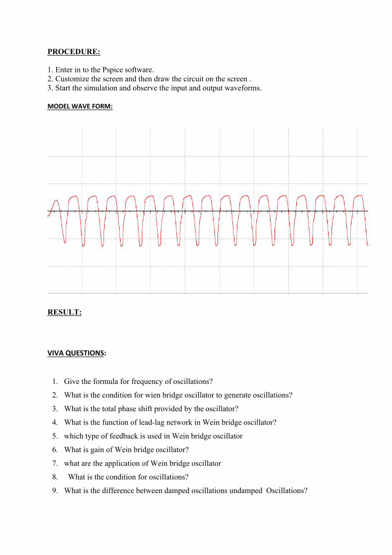
4. WEIN BRIDGE OSCILLATOR
AIM: To study and calculate frequency of Wein Bridge Oscillator.
APPARATUS:
Pspice software
CIRCUITDIAGRAM:
THEORY:
The wein bridge oscillator is a standard circuit for generating low frequencies in the
range of 10 Hz to about 1MHz.The method used for getting +ve feedback in wein bridge
oscillator is to use two stages of an RC-coupled amplifier. Since one stage of the RC-
coupled amplifier introduces a phase shift of 180 deg, two stages will introduces a phase shift
of 360 deg. At the frequency of oscillations f the +ve feedback network shown in fig makes
the input & output in the phase. The frequency of oscillations is given as
f =1/2π√R1C1R2C2
In addition to the positive feedback
PROCEDURE:
1. Enter in to the Pspice software.2. Customize the screen and then draw the circuit on the screen .3. Start the simulation and observe the input and output waveforms.
MODEL WAVE FORM:
RESULT:
VIVA QUESTIONS:
1. Give the formula for frequency of oscillations?
2. What is the condition for wien bridge oscillator to generate oscillations?
3. What is the total phase shift provided by the oscillator?
4. What is the function of lead-lag network in Wein bridge oscillator?
5. which type of feedback is used in Wein bridge oscillator
6. What is gain of Wein bridge oscillator?
7. what are the application of Wein bridge oscillator
8. What is the condition for oscillations?
9. What is the difference between damped oscillations undamped Oscillations?
10.CLASS B PUSH PULL POWER AMPLIFIER
AIM: To observe the input and output waveforms and to calculate the efficiency of Class B Complimentary symmetry power amplifier.
EQUIPMENT REQUIRED: Pspice software
CIRCUIT DIAGRAM:
THEORY:
An amplifying system consists of several stages in cascade. The input and the intermediate stages amplify small signal excitations to a value large enough to drive the final device .The out put stage feeds the final device .The output stage feeds a transducer such as a CRO,loudspeaker or servomotor. Thus the final stage must be capable of delivering a large voltage or current or appreciable amount of power. This requires an amplifier which is referred as a power amplifier In class B complimentary symmetry class _B amplifier one n-p-n and p-n-p is used. Hence the circuit is called class-B complimentary symmetry amplifier. This circuit ifis transformer less circuit .But with common emitter configuration it becomes power transfer without output impedance for maximum power transfer without an output transformers. Hence the matched pair of complementary transistors are used in common collector configuration This is because in common collector configuration has lowest output impedance and hence the impedance matching is possible.
PROCEDURE:

1.conncet the circuit s per the circuit diagram2.apply 4v p-p with 1KHZ frequency using function generator 3.observe the output in CRO .4.note the cross over distortion in output.(outputVp-p)

5.remove the collector connection and put ammeter. 6.note the Idc value in the ammeter.7.using Pdc and Pac formulas find the efficiency.
GRAPHS:
RESULT:
VIVA QUESTIONS:
1.In classB power amplifiers why crossover
distortion will be occurred? 2.what are he different
methods to eliminate distortion?
3..howmuch efficiency will b obtained in classs-
B power amplifier? 4.where is the location of
operating point in class-B power amplifier?