Fresh thinking flexible film solutions from LINPAC Packaging

1
Electronic Grade and Flexible Semiconductor Film Employing
Oriented Attachment of Colloidal Ligand-Free PbS and PbSe
Nanocrystals at Room Temperature
G. Shiva Shanker,a Abhishek Swarnkar, a Arindom Chatterjee,b S. Chakraborty,c
Manabjyoti Phukan,a Naziya Parveen,a Kanishka Biswas,b Angshuman Naga,*
aDepartment of Chemistry, Indian Institute of Science Education and Research (IISER), Pune,
411008, India.
b New Chemistry Unit and Sheikh Saqr Laboratory, Jawaharlal Nehru Centre for Advanced
Scientific Research (JNCASR), Jakkur P.O., Bangalore 560 064, India
c Centre for Advanced Materials, Indian Association for the Cultivation of Science, Kolkata-
700032, India
*Corresponding author’s e-mail: [email protected]
Electronic Supplementary Information (ESI)
Electronic Supplementary Material (ESI) for Nanoscale.This journal is © The Royal Society of Chemistry 2015
2
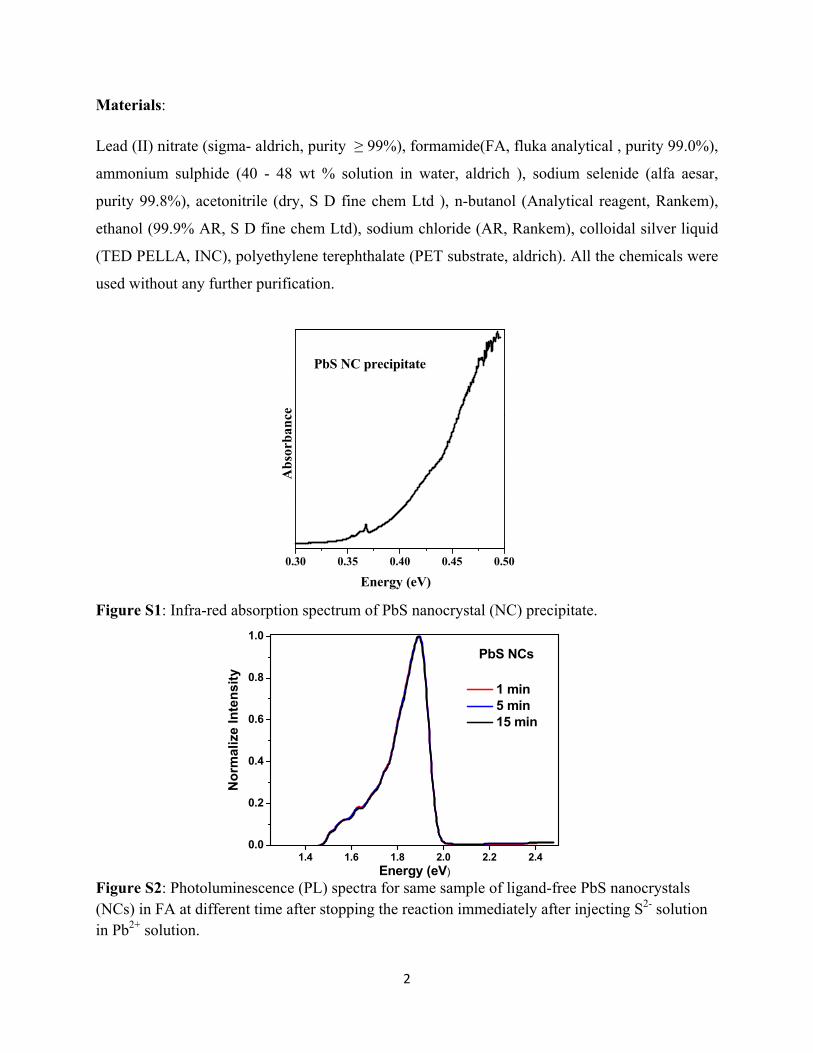
Materials:
Lead (II) nitrate (sigma- aldrich, purity ≥ 99%), formamide(FA, fluka analytical , purity 99.0%),
ammonium sulphide (40 - 48 wt % solution in water, aldrich ), sodium selenide (alfa aesar,
purity 99.8%), acetonitrile (dry, S D fine chem Ltd ), n-butanol (Analytical reagent, Rankem),
ethanol (99.9% AR, S D fine chem Ltd), sodium chloride (AR, Rankem), colloidal silver liquid
(TED PELLA, INC), polyethylene terephthalate (PET substrate, aldrich). All the chemicals were
used without any further purification.
Figure S1: Infra-red absorption spectrum of PbS nanocrystal (NC) precipitate.
Figure S2: Photoluminescence (PL) spectra for same sample of ligand-free PbS nanocrystals (NCs) in FA at different time after stopping the reaction immediately after injecting S2- solution in Pb2+ solution.
1.4 1.6 1.8 2.0 2.2 2.40.0
0.2
0.4
0.6
0.8
1.0
No
rmal
ize
Inte
nsi
ty
Energy (eV)
1 min 5 min 15 min
PbS NCs
0.30 0.35 0.40 0.45 0.50
PbS NC precipitate
Energy (eV)
Ab
sorb
ance
3
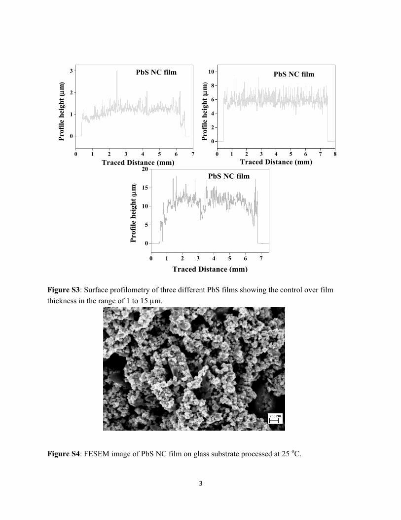
Figure S3: Surface profilometry of three different PbS films showing the control over film
thickness in the range of 1 to 15 m.
Figure S4: FESEM image of PbS NC film on glass substrate processed at 25 oC.
0 1 2 3 4 5 6 7
0
1
2
3
Pro
file
hei
ght
(m
)
Traced Distance (mm)
PbS NC film
0 1 2 3 4 5 6 7 8
0
2
4
6
8
10
Pro
file
hei
ght
(m
)
Traced Distance (mm)
PbS NC film
0 1 2 3 4 5 6 7
0
5
10
15
20
Pro
file
hei
ght
(m
)
Traced Distance (mm)
PbS NC film
4
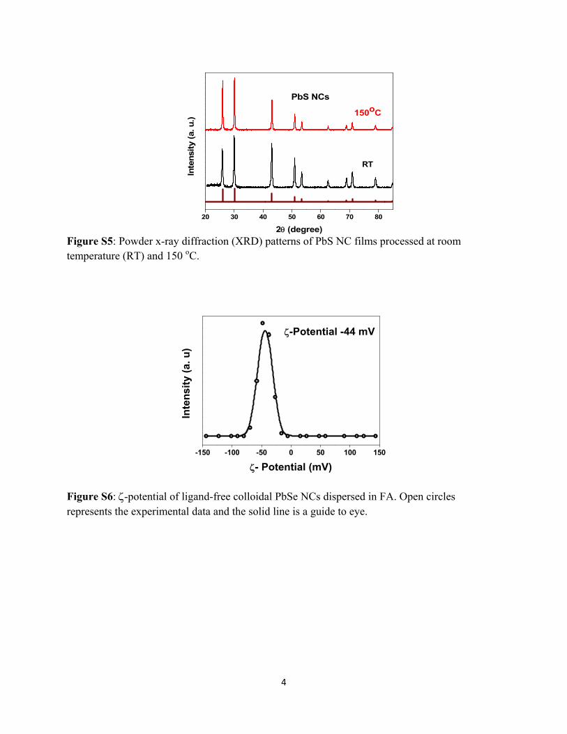
Figure S5: Powder x-ray diffraction (XRD) patterns of PbS NC films processed at room temperature (RT) and 150 oC.
Figure S6: -potential of ligand-free colloidal PbSe NCs dispersed in FA. Open circles represents the experimental data and the solid line is a guide to eye.
20 30 40 50 60 70 80
Inte
nsi
ty (
a. u
.)
2(degree)
RT
150oC
PbS NCs
-150 -100 -50 0 50 100 150
Inte
nsi
ty (
a. u
)
- Potential (mV)
-Potential -44 mV

5
Figure S7: HRTEM image of ligand-free PbSe NC precipitate.
Figure S8: Infra-red absorption spectrum of PbSe nanocrystal (NC) precipitate.
0.25 0.30 0.35 0.40
PbSe NC precipitate
Energy (eV)
Ab
sorb
ance

6
Figure S9: FESEM image of PbSe NC film on glass substrate processed at 25 oC.
Figure S10: Four-probe Current (I) vs voltage (V) plot for PbSe NC film on glass substrate after annealing at 150 oC. Electrical measurement was done at room temperature.
-10 -5 0 5 10-0.04
-0.02
0.00
0.02
0.04
Current ()
Vo
ltag
e (v
)

7
Figure S11: Powder XRD pattern of PbSe NC film after annealing at 150 oC.
-1-11
1-11
200
11-1
-11-1
-200
20 30 40 50 60 70 80
Inte
nsi
ty (
a. u
)
2 (degree)
PbSe NCs
PbSe bluk reference