
FUNCTIONAL FLEXIBLE THIN FILM ELECTRONICS
125
The Pennsylvania State University The Graduate School College of Engineering FUNCTIONAL FLEXIBLE THIN FILM ELECTRONICS A Dissertation in Electrical Engineering by Haoyu Li © 2015 Haoyu Li Submitted in Partial Fulfillment of the Requirements for the Degree of Doctor of Philosophy December 2015
Transcript of FUNCTIONAL FLEXIBLE THIN FILM ELECTRONICS

The Pennsylvania State University
The Graduate School
College of Engineering
FUNCTIONAL FLEXIBLE THIN FILM ELECTRONICS
A Dissertation in
Electrical Engineering
by
Haoyu Li
© 2015 Haoyu Li
Submitted in Partial Fulfillment
of the Requirements
for the Degree of
Doctor of Philosophy
December 2015
ii
The dissertation of Haoyu Li was reviewed and approved* by the following:
Thomas N. Jackson
Robert E. Kirby Chair Professor of Electrical Engineering
Dissertation Advisor
Chair of Committee
Srinivas A. Tadigadapa
Professor of Electrical Engineering
Noel C. Giebink
Assistant Professor of Electrical Engineering
Enrique D. Gomez
Associate Professor of Chemical Engineering
Kultegin Aydin
Professor of Electrical Engineering
Head of the Department of Electrical Engineering
*Signatures are on file in the Graduate School

iii
ABSTRACT
The field of flexible electronics has advanced rapidly in recent years. This dissertation
reports progress on a few components for flexible electronics with a special focus on process
development, system integration, flexibility testing, and improvements in flexibility. In this
dissertation, a rigid-substrate-compatible, lamination- and transfer-free process is developed to
fabricate ZnO thin film transistors (TFTs) on very thin (~5 μm) solution-cast polyimide substrates.
The flexible ZnO TFTs have very similar electrical characteristics to ZnO TFTs fabricated on rigid
glass substrates. Typical TFT mobility is > 12 cm2/V∙s for a gate electric field of 2 MV/cm.
Inverters and 51-stage ring oscillators have been demonstrated using ZnO TFTs on thin flexible
substrates. After a simple mechanical release, most TFTs show unchanged electrical characteristics
on the freestanding flexible substrates. The performance of the flexible TFTs also remains the same
when bent to radii between 7 mm concavely and 5 mm convexly.
Vanadium oxide (VOX) films have been studied as a temperature sensing material.
Motivated by its potential of high-rate and uniform deposition, we investigated using RF diode
sputtering to deposit VOX films as an alternative to the currently most commonly used ion-beam
deposition. We found that process control for bolometer-grade VOX is very difficult. Small changes
in oxygen-to-argon inlet ratio result in dramatic changes in the resistivity of the deposited VOX
films, and a positive feedback mechanism drives depositions performed without active control to
become either metallic or high resistivity films. We found that the local oxygen partial pressure
near the reactively sputtered target varies with the oxidation of the target and is thus a strong
candidate for an active control mechanism for reproducible reactive RF diode sputtering of VOX
thin films.
As efforts have taken place towards integrating more functions into flexible electronic
systems, flexible organic light emitting diodes (OLEDs) have been demonstrated on the same thin
iv
flexible substrate as for the aforementioned flexible ZnO TFTs. The OLEDs use sputtered ITO
anodes, evaporated organic layers, and evaporated Al top cathodes. Green light emission is
confirmed for both on-rigid-carrier and freestanding flexible OLEDs. A direct patterning technique
based on substrate surface energy contrast for parylene films as an encapsulation layer for
electronic devices, including OLEDs, is also reported.
The mechanical flexibility of flexible electronics is investigated in the context of testing
strategies and the experimental results of different types of measurements. Besides the commonly
reported static bending test, the strategies and apparatuses for repeated bending tests by push-to-
flex and roller-flex are developed with the capability of in-situ electrical measurement while
bending or flexing. Our flexible ZnO TFTs survive more than 50,000 repeated bending cycles with
a bending radius of 3.5 mm with very little change in electrical characteristics. With a smaller
bending radius of 1.6 mm, the modified TFTs with Ti gate survived more than 10,000 bending
cycles. For a better understanding of device failure mechanisms, numerical simulations for strain
and stress distributions in flexible structures under various stretching and bending conditions are
carried out using COMSOL Multiphysics. Means to improve device flexibility have also been
proposed based on the experimental and simulation results.
The work reported in this dissertation represents developments in multiple aspects for
flexible electronics and helps to pave the pathway to ubiquitous flexible electronics. This
dissertation also provides a foundation for further study and development of the fabrication process
and flexibility improvements for flexible electronic devices and systems.

v
TABLE OF CONTENTS
List of Figures .......................................................................................................................... vii
List of Tables ........................................................................................................................... xiii
Acknowledgements .................................................................................................................. xiv
Chapter 1 Introduction ............................................................................................................. 1
1.1 Background and overview.......................................................................................... 1 1.2 Design Considerations for Flexible Electronics ......................................................... 3
1.2.1 Application Orientated Considerations ........................................................... 3 1.2.2 Substrates ........................................................................................................ 5 1.2.3 Fabrication Oriented Considerations ............................................................... 7
1.3 Research Objectives and Thesis Organization ........................................................... 8
Chapter 2 ZnO Thin Film Transistors and Circuits on Flexible Substrates ............................. 11
2.1 Introduction to ZnO Thin Film Transistors ................................................................ 11 2.2 Fabrication of ZnO TFTs on Thin Solution-Cast Polymer Substrates ....................... 13 2.3 Process Control for Device Fabrication on Thin Flexible Substrate .......................... 15
2.3.1 Substrate Dimensional Stability ...................................................................... 15 2.3.2 Dielectric Integrity .......................................................................................... 18
2.4 Characteristics of Flexible ZnO Thin Film Transistors ............................................. 20 2.4.1 Basic Transistor Characteristics ...................................................................... 20 2.4.2 Bias Stability, Yield, and Uniformity .............................................................. 21
2.5 Flexible ZnO TFT Circuits......................................................................................... 24
Chapter 3 Functional Thin Film Materials and Devices for Flexible Electronics ................... 27
3.1 Vanadium Oxide Film for Temperature Sensing Applications .................................. 27 3.1.1 Temperature Sensing Using Thin Film Materials and Devices ....................... 27 3.1.2 Vanadium Oxide Thin Film Deposition .......................................................... 29 3.1.3 RF Diode Reactive Sputtering and Characterization of VOX Films ................ 29
3.2 Control of Reactive RF Diode Sputtered VOX Thin Films ........................................ 34 3.2.1 Control Issue for Reactive RF Diode Sputtered VOX Thin Films ................... 34 3.2.2 Process Control Attempt 1: Target Potential ................................................... 36 3.2.3 Process Control Attempt 2: Plasma Optical Emission Spectroscopy .............. 39 3.2.4 Process Control Attempt 3: Oxygen Partial Pressure ...................................... 42 3.2.5 Discussion and Summary ................................................................................ 45
3.3 Flexible Organic Light Emitting Diodes (OLEDs) .................................................... 46 3.3.1 Fabrication Process and Preparation for Flexible OLEDs .............................. 47 3.3.2 Characterization of Flexible OLEDs ............................................................... 49

vi
Chapter 4 Encapsulation Layer Patterning for Flexible Electronics ........................................ 53
4.1 Introduction ................................................................................................................ 53 4.2 Parylene Deposition Kinetics ..................................................................................... 55 4.3 Parylene Film Differential Growth on Si/SiO2 Surface ............................................. 56 4.4 Parylene Direct Patterning by Surface Treatment and Non-Relief Pattern
Lithography .............................................................................................................. 57 4.5 Mechanisms for Parylene Differential Growth .......................................................... 59 4.6 Discussion .................................................................................................................. 63
Chapter 5 Mechanical Flexibility of Flexible Electronics ....................................................... 65
5.1 Flexibility ................................................................................................................... 65 5.2 Strategy for Flexiblility Testing ................................................................................. 66
5.2.1 Electrical Connections and Testing Method ................................................... 66 5.2.2 Flexibility Testing Apparatuses....................................................................... 70
5.2.2.1 Static Bending ...................................................................................... 70 5.2.2.2 Push-to-Flex ......................................................................................... 71 5.2.2.3 Roller-Flex Test ................................................................................... 73
5.3 Flexibility Test for ZnO TFTs on Thin Polyimide Substrates ................................... 76 5.3.1 Static Bending ................................................................................................. 76 5.3.2 Repeated Bending by Push-to-Flex ................................................................. 77 5.3.3 Repeated Bending by Roller-Flex ................................................................... 80 5.3.5 Discussion and Improvement for Device Flexibility....................................... 81
5.4 Numerical Simulation ................................................................................................ 84 5.4.1 Model Construction ......................................................................................... 84 5.4.2 Strain by Lateral Displacement ....................................................................... 86 5.4.3 Strain by Bending Displacement ..................................................................... 89 5.4.4 Discussion ....................................................................................................... 93
5.5 Summary .................................................................................................................... 95
Chapter 6 Summary and Future Work ..................................................................................... 96
6.1 Summary .................................................................................................................... 96 6.2 Future work ................................................................................................................ 97
References ................................................................................................................................ 103

vii
LIST OF FIGURES
Figure 1-1: Number of publications each year on the topic of “flexible electronics” from a
search on ISI Web of Science .......................................................................................... 2
Figure 2-1: AFM image of cured PI-2611 on Si/SiNX substrate. The rms surface roughness
of the cured polyimide film is measured to be ~0.8 nm. .................................................. 13
Figure 2-2: Process flow for flexible ZnO TFT fabrication. Inset shows an optical
micrograph of a fabricated ZnO TFT on polyimide substrate.......................................... 15
Figure 2-3: (a) One set of vernier structures by design; (b) optical micrograph of one set of
vernier structures fabricated on a thin polyimide substrate .............................................. 16
Figure 2-4: Alignment errors between the gate (1st) and the source and drain (4th) layer at
different positions of a 2” ⤬ 2” flexible sample with PI-2611 substrates measured by
vernier structure readings. First number of each data point indicates the alignment
error in the horizontal (x) direction; second number of each data point indicates the
alignment error in the vertical (y) direction. Question marks indicate that the particular
vernier was hard to read due to process issues. ................................................................ 17
Figure 2-5: (a) Crossover mask design. Blue lines and red lines are bottom and top metal
layers respectively. (b) Optical micrograph and SEM image of a portion of a crossover
test structure. Each crossover overlap area is 10 μm ⤬ 10 μm......................................... 19
Figure 2-6: Leakage current (current density) as a function of bias voltage (electric field)
for a crossover test structure with 7650 10 μm ⤬ 10 μm overlaps. .................................. 20
Figure 2-7: Device characteristics for ZnO TFTs fabricated on thin flexible polyimide and
glass substrates (TFT W/L = 200/20 μm/μm, 32 nm Al2O
3 gate oxide, 10 nm ZnO
active layer, 30 nm Al2O3 passivation); (a) log(IDS) and differential mobility versus
VGS characteristics for VDS = 0.5 V; (b) IDS versus VDS characteristics for several
values of VGS. ................................................................................................................... 21
Figure 2-8: ZnO TFT bias stability. (a) Normalized drain current as a function of time under
bias stress at VDS = 3 V and VGS = 4 V for polyimide and glass samples. (b) IDS-VGS
characteristics of a ZnO TFT on thin polyimide substrate before and after bias stress
(at IDS = 3.7 µA/µm) for 60,000 sec. (TFT W/L = 200/20 μm/μm, 32 nm Al2O
3 gate
oxide, 10 nm ZnO active layer, 30 nm Al2O3 passivation) .............................................. 22
Figure 2-9: (a) IDS-VGS characteristics of 80 ZnO TFTs fabricated on 4.8 µm thick
polyimide substrate. (TFT channel width = 200 µm, channel length = 5 µm, 10 µm,
20 µm, and 50 µm, 32 nm Al2O
3 gate oxide, 10 nm ZnO active layer, 30 nm Al2O3
passivation), VDS = 6 V. (b) Extracted TFT mobility at VGS = 6 V. Average mobility
of all 80 TFTs was 9.3 cm2/V∙s; standard deviation was 0.9 cm2/V∙s.............................. 23
Figure 2-10: (a) Peeling off flexible polyimide substrate from rigid Si wafer carrier using
a pair of tweezers. (b) Concavely curled substrate after releasing. (c) Released 4.8 μm

viii
thick flexible polyimide substrate wrapped around a finger. (d) IDS-VGS curve for a
ZnO TFT fabricated on 4.8 μm thick flexible polyimide substrate before and after
release from rigid carrier. Device performance was essentially unchanged after
releasing. .......................................................................................................................... 24
Figure 2-11: (a) Circuit schematic of the saturated enhancement load inverter; (b) optical
micrograph of an inverter fabricated on polyimide substrate; (c) transfer curve for an
inverter at various supply voltages (1 – 9 V with 1 V step). ............................................ 25
Figure 2-12: (a) Optical micrograph of a 51-stage ZnO TFT ring oscillator fabricated on
thin polyimide substrate; (b) Frequency and delay of a 15-stage ring oscillator on thin
polyimide substrate (beta ratio = 5, source and drain to gate overlap 2 μm). .................. 26
Figure 3-1: Typical pixel structure of uncooled microbolometers [73] ................................... 28
Figure 3-2: (a) Schematic of the RF diode sputtering chamber, (b) photograph of CVC-611
load-locked RF sputtering system, (c) photograph of the inside of the deposition
chamber. ........................................................................................................................... 30
Figure 3-3: Transmission line structure (TLM) of VOX film on Si/SiO2 substrate.................. 31
Figure 3-4: TCR as a function of resistivity for VOX films deposited by different techniques
.......................................................................................................................................... 32
Figure 3-5: Resistivity of VOX films as a function of O2 supply ratio deposited by RF diode
reactive sputtering. ........................................................................................................... 33
Figure 3-6: Resistivity of deposited VOX films as a function of oxygen supply ratio from a
DC magnetron reactive sputtering system [15]. ............................................................... 34
Figure 3-7: Target DC self-bias and RF peak voltage monitoring circuit for the RF diode
reactive sputtering system ................................................................................................ 37
Figure 3-8: (a) Target average DC self-bias for 0% and 8% oxygen inlet ratio. (b) Positive
and negative RF peak voltages on target for two deposition runs both with 8% oxygen
inlet and the same process parameters. ............................................................................ 38
Figure 3-9: Target DC self-bias and RF peak voltages with stepped oxygen inlet ratio. ........ 39
Figure 3-10: Plasma emission spectra with different oxygen inlet ratios ................................ 40
Figure 3-11: Intensity ratios of plasma emission peaks as a function of oxygen inlet ratio.
Data from two experiments are shown. ............................................................................ 41
Figure 3-12: RF diode sputtering system schematic with gas sampling tube. The top part
of the chamber was drawn separately to show the inside. The gas sampling tube was
placed near the sample surface and roughly under the center of the vanadium target. .... 42
ix
Figure 3-13: (a) Oxygen partial pressure ratio (calculated as Poxygen/(Poxygen +Pargon), where
Poxygen and Pargon were oxygen and argon partial pressure readings taken by the RGA)
as a function of time with stepped oxygen inlet ratio; (b) oxygen partial pressure ratio
as a function of oxygen inlet ratio. Note that point A and point B have the same oxygen
inlet ratio, and the oxygen partial pressure change corresponded to the increase in the
curve shown in (a) between 27 and 28 minutes where the oxygen supply ratio was not
changed. ........................................................................................................................... 44
Figure 3-14: (a) Cross-sectional schematic of the OLED fabricated on solution-casted thin
polyimide substrate. (b) Photograph of a 1" × 1" sample that contains four 8 𝑚𝑚 ×2𝑚𝑚 OLEDs on it. .......................................................................................................... 48
Figure 3-15: Photograph of working OLED samples emitting green light (looking from the
back side). The OLED active area in the left picture was 2.5 𝑚𝑚 × 4 𝑚𝑚 (2 OLEDs
were lighting) and was 8 𝑚𝑚 × 2 𝑚𝑚 in the right picture. ............................................ 49
Figure 3-16: Current and current density as a function of bias voltage for an as-fabricated
flexible OLED with an active area of 8 𝑚𝑚 × 2 𝑚𝑚. .................................................... 50
Figure 3-17: (a) Released flexible OLED with 8 𝑚𝑚 × 2 𝑚𝑚 active area. Bending marks
on the metal contact from the releasing process can be seen. (b) Freestanding flexible
OLED with Cu strips attached for electrical contacts. (c) Freestanding flexible OLED
emitting green light. ......................................................................................................... 50
Figure 3-18: Emission spectrum for OLEDs fabricated on glass and thin polyimide
substrates. ......................................................................................................................... 51
Figure 3-19: (a) Current and current density as a function of bias voltage for a freestanding
flexible OLED with active area of 8 𝑚𝑚 × 2 𝑚𝑚 . (b) Calculated EQE for a
freestanding flexible OLED with active area of 8 𝑚𝑚 × 2 𝑚𝑚. .................................... 52
Figure 4-1: The polymerization route for parylene-N ............................................................. 54
Figure 4-2: Schematic (top) and photograph (bottom) of a typical parylene deposition
system .............................................................................................................................. 54
Figure 4-3: Photograph of SiO2 and Si substrates after parylene deposition. ~100 nm
parylene film was deposited on the SiO2 surface while no film was deposited on the
Si surface. ......................................................................................................................... 56
Figure 4-4: Optical micrograph of directly pattered parylene film (100 nm thickness) on
Si/native oxide.................................................................................................................. 57
Figure 4-5: Water droplet on OTS-treated SiO2 surface before and after DUV exposure.
OTS-treated SiO2 surface has low surface energy and the water contact angle is ~ 95°;
OTS-treated surface after DUV exposure has high surface energy with water contact
angle ~ 20°. ...................................................................................................................... 58

x
Figure 4-6: Parylene direct patterning achieved by non-relief-pattern lithograph on OTS-
treated SiO2 substrate. The white to yellow area has parylene film deposition, and the
bluish dark area has no parylene film deposition. ............................................................ 59
Figure 4-7: Deposited parylene thickness and water contact angle for four substrates with
different surface energies ................................................................................................. 60
Figure 4-8: Parylene deposited on both Si and SiO2 surfaces ................................................. 61
Figure 4-9: Deposited parylene film thickness after first- and second-deposition runs........... 61
Figure 4-10: Parylene initial polymerization process on (a) high-energy surface and (b)
low-energy surface ........................................................................................................... 62
Figure 4-11: (a) SEM image of parylene film deposited on a hydrophilic SiO2 surface, (b)
SEM image of parylene film deposited on a hydrophobic OTS-treated SiO2 surface,
(c) cartoon illustration of parylene deposition process on a hydrophilic surface, (d)
cartoon illustration of parylene deposition process on hydrophobic surfaces. ................. 63
Figure 5-1: Mask design for devices with ~ 1 cm long leads to the edge of the sample. The
left two pictures each show 12 single TFTs with different channel lengths positioned
with vertical and horizontal directions. The right figure shows the design of a die
containing ring oscillators with long leads connections. .................................................. 67
Figure 5-2: Flexible sample connected to PCB board through “homemade” flexible cable
(Inset: close up for ACF bond between flexible sample connection area and flexible
cable) ................................................................................................................................ 68
Figure 5-3: Flexible sample on a push-to-flex testing apparatus connected to the
measurement instruments through a flexible cable, PCB board, and flat cable. (See
section 5.2.2.2 for a detailed description of the push-to-flex testing apparatus) .............. 69
Figure 5-4: Photograph of a flexible ZnO TFT sample attached to the outer surface of a
glass rod with a 5 mm radius ........................................................................................... 70
Figure 5-5: Front panel of the LabView program used to control the flexibility testing
apparatus .......................................................................................................................... 72
Figure 5-6: Push-to-flex testing apparatus. (a) schematic, (b) a flexible sample bent on the
push-to-flex testing apparatus, (c) a flexible sample on the push-to-flex apparatus
while the gap was at its maximum (sample flat), (d) a flexible sample on the push-to-
flex apparatus while the gap was at its minimum (sample bent to the smallest bending
radius)............................................................................................................................... 73
Figure 5-7: Roller-flex testing apparatus. (a) Schematic, (b) photograph of the complete
roller-flex testing apparatus without a sample, (c) flexible sample tested on roller-flex
testing apparatus. .............................................................................................................. 75
xi
Figure 5-8: Flexible ZnO TFT IDS versus VGS curves before and after being released from
the rigid wafer carrier and for several different bending radii of the substrate (TFT
with patterned Cr gate, W/L = 200/20 µm/µm, 32 nm Al2O3 gate oxide, 10 nm ZnO
active layer, 30 nm Al2O3 passivation, VDS = 0.5 V). ...................................................... 76
Figure 5-9: Flexible ZnO TFT sample on push-to-flex apparatus with sample flat (left) and
bent convexly (right). The bending radius of the flexible sample was estimated to be
3.5 mm. ............................................................................................................................ 78
Figure 5-10: ZnO TFT IDS versus VGS characteristics after repeated convex bending cycles
with bending directions (a) parallel to current flow direction, and (b) perpendicular to
current flow direction. (TFTs with patterned Cr gate, W/L = 200/20 μm/μm, 32 nm
Al2O3 gate oxide, 10 nm ZnO active layer, 30nm Al2O3 passivation, VDS = 0.5 V). The
smallest bending radius was 3.5 mm (0.07% tensile strain). ........................................... 78
Figure 5-11: (a) Flexible ZnO TFT sample on push-to-flex apparatus with sample bent
concavely along the direction parallel to the current flow, (b) ZnO TFT IDS versus VGS
characteristics after repeated concave bending cycles (TFT with patterned Cr gate,
W/L = 200/20 μm/μm, 32 nm Al2O3 gate oxide, 10 nm ZnO active layer, 30nm Al2O3
passivation, VDS = 0.5 V). The smallest flexing radius was 1.75 mm (0.14%
compressive strain). ......................................................................................................... 79
Figure 5-12: (a) A flexible ZnO TFT sample on roller-flex testing apparatus with the
sample bent convexly with 1.6mm bending radius along the direction parallel to the
current flow, (b) ZnO TFT IDS versus VGS characteristics after repeated convex
bending cycles (1.6 mm bending radius, TFT with patterned Cr gate, W/L = 200/20
μm/μm, 32 nm Al2O3 gate oxide, 10 nm ZnO active layer, 30nm Al2O3 passivation,
VDS = 0.5 V). .................................................................................................................... 80
Figure 5-13: Optical micrograph of a flexible ZnO TFT with cracks generated after 15,000
cycles of bending to 1.6 mm radius. ................................................................................ 82
Figure 5-14: (a) SEM image of the channel area of a flexible ZnO TFT fabricated on
solution-cast polyimide substrate. Red box in the inset indicates the area shown in the
SEM image. (b) Cross-sectional TEM image of the flexible ZnO TFT channel area
(position indicated by the green box in figure (a). Image for figure (b) was taken on a
different sample than the one shown in figure (a)). The dark circles on the upper part
of the TEM image were an artifact possibly caused by carbon deposition during the
imaging process. ............................................................................................................... 83
Figure 5-15: IDS as a function of VGS for flexible ZnO TFTs with a Ti gate layer after
repeated bending cycles flexed by roller-flex testing apparatus with a 1.6 mm bending
radius. (a) Bending direction parallel to the current flow; (b) bending direction
perpendicular to the current flow. .................................................................................... 84
Figure 5-16: (a) schematic diagram of the TFT cross-section model for COMSOL
Multiphysics simulation (not drawn to scale), (b) 2-D model for ZnO TFT on flexible
substrate constructed in COMSOL Structural Mechanics module (aspect ratio
changed to better show layer structure) ........................................................................... 85

xii
Figure 5-17: Simulated von Mises stress in the flexible ZnO TFT model due to 0.156%
tensile direct displacement at the right edge. Inset shows enlarged area in the dashed-
line box. (Aspect ratio not reserved.) ............................................................................... 88
Figure 5-18: 1-D cuts of simulated von Mises stresses in the flexible ZnO TFT model due
to 0.071% and 0.156% tensile displacement at the right edge. (a) x-cut through the
middle of the source and drain to gate overlap area at the right-side contact (cut A-A’
in Figure 5-17). Inset shows enlarged device area (part of the curves in the dashed-
line box) stress distribution; (b) y-cut through the middle of the gate oxide layer (cut
B-B’ in Figure 5-17). ....................................................................................................... 89
Figure 5-19: Curved model with a prescribed displacement of an arc with a 1.6 mm radius
applied to the bottom. The blue solid strip is the curved sample, and the long empty
black rectangle is the original shape of the model. .......................................................... 90
Figure 5-20: Simulated von Mises stress distribution in the TFT device area (aspect ratio
not reserved). .................................................................................................................... 91
Figure 5-21: 1-D cuts of simulated von Mises stress in the flexible ZnO TFT model due to
convex bending of 1.6 mm and 3.5 mm radius. (a) X-cut through the middle of the
source and drain to the gate overlap area at the right-side contact (cut A-A’ in Figure
5-17), plotted in semi log scale. (b) Enlarged part of the von Mises stress curves in the
dashed-line box of (a), plotted in linear scale; (c) y-cut through the middle of gate
oxide layer (cut B-B’ in Figure 5-17). A laterally aligned schematic of the model was
overlaid on top of the stress curves. ................................................................................. 92
Figure 5-22: 1-D x cuts (through the middle of the source and drain to gate overlap area at
the right-side contact (cut A-A’ in Figure 5-17) of the simulated strain tensor x
component in the flexible ZnO TFT model due to tensile stress from (a) stretching and
(b) bending situations. The device areas are marked with dash-line boxes in both plots;
the rest of the curves represent the substrate area. ........................................................... 94
Figure 6-1: (a) Schematic of a belt-type bending apparatus for flexible electronic samples;
(b) photograph of a prototype of the belt-type bending apparatus using a pneumatic
rotary actuator and a Kapton film belt. ............................................................................ 100
Figure 6-2: Simulated von Mises stress in flexible TFT because of bending to a 1.6 mm
radius. (a) ZnO TFT on 5 μm thick polyimide substrate. (b) ZnO TFT on 5 μm thick
polyimide substrate with 5 μm thick polyimide layer on top. The color legends for (a)
and (b) are the same. ........................................................................................................ 102

xiii
LIST OF TABLES
Table 1-1. Characteristics for a few representative flexible substrates .................................... 6
Table 5-1. Extracted TFT mobility, turn-on voltage, and drain current at VGS = 6 V and VDS
= 0.5 V for different bending curvatures .......................................................................... 77
Table 5-2. Model dimension-related parameter definitions ..................................................... 86
Table 5-3. Key parameters of the materials used in COMSOL structural mechanics
simulation ......................................................................................................................... 86
Table 5-4. Tensile stress and strength for each layer in the simulation ................................... 93

xiv
ACKNOWLEDGEMENTS
This dissertation is made possible by a lot of help, guidance, encouragement, and support
in both professional and personal capacity from numerous people I would like to thank. First of all,
I would like to express my deepest gratitude to my advisor, Prof. Thomas N. Jackson, for teaching,
guiding, and supporting me throughout my Ph.D. process and making the Ph.D. something I
become, not just something I put on. I would also like to thank my other committee members: Dr.
Srinivas Tadigadapa, Dr. N. Chris Giebink, and Dr. Enrique Gomez.
This work has been made possible by a large group of collaborators, colleagues, and
friends. First, I would like to thank all the members of my research group at Penn State (JERG),
especially Dr. Yuanyuan Li, Dr. Dalong Zhao, and Dr. Devin Mourey for their mentoring and help
in my early years in the Ph.D. program, and Dr. Raymond H. Fok for many insightful discussions
throughout the years. Second, I would like to extend my appreciation to my colleagues from Dr.
Gomez’s group in the Department of Chemical Engineering and Dr. Giebink’s group in the
Department of Electrical Engineering. I would also like to thank Dr. Allison Beese in the
Department of Materials Science and Engineering for sharing her expertise in the mechanical
properties of materials with me. Additionally, I would like to thank my collaborators in the industry:
Dr. Weijun Niu from Corning and Dr. Elissei Iagodkine, Dr. Anatoliy Sokolov, and Dr. Luke Bu
from The DOW Chemical Company for useful discussions and fruitful collaborations. Lastly, I
would like to thank Corning Inc., The DOW Chemical Company, and the Army Research Lab for
their funding support.
I am also indebted to the people whose personal love, understanding, and support made
this dissertation possible. I would like to thank my parents for their unconditional love and care. I
would also like to thank my extended family for their care and hospitality. Without all these
people’s support, I would probably never have been able to make it through the completion of my
graduate work.

1
Chapter 1
Introduction
1.1 Background and overview
The history of flexible thin film electronics dates back to the 1960s when CdS thin film
solar cells were made and studied as an alternative to single-crystalline silicon solar cells for space
mission applications [1]. Nowadays, flexible electronics covers a vast variety of aspects in not only
state-of-the-art technologies but also our daily lives. In the past ten to fifteen years, flexible
electronic devices, circuits, and systems have seen extraordinarily rapid growth. Bendable,
foldable, and stretchable electronic devices have drawn a lot of attention, and a number of products
that take advantage of flexible electronics have hit the market. Samsung released the first “curved”
smartphone, featuring a 5.7-inch 1920x1080 Super AMOLED curved display, the Galaxy Round,
in October 2013. A few days later, LG released their competing model, the LG G Flex with a curved
screen. In January 2014, Samsung revealed its 85-inch bendable TV at the Consumer Electronics
Show (CES) held in Las Vegas. Besides displays, wearable devices and personalized health
monitoring systems have become a big trend for next-generation electronics. Various flexible
devices and systems for such applications have been demonstrated, including sensors, energy
harvesting and storage devices, environmental monitoring equipment, health care devices,
wearable or skin attachable devices, implanted electronics, and so forth [2, 3].
Flexible electronics differs from conventional microelectronics in that they are fabricated
on flexible substrates and can exhibit properties that conventional rigid electronics do not have,
such as that they are bendable, elastic, conformal, lightweight, large-area, and non-breakable [1].
They also enable applications that are not available when using conventional rigid electronic

2
systems, such as clothing- or skin-attachable health monitoring systems, non-invasive biosensors,
artificial skins, and smart textiles, in addition to the aforementioned curved displays.
Scientists and engineers have been working hard to push the boundaries for tomorrow’s
flexible electronics technology. Prof. John Rogers’ group at the University of Illinois, Urbana-
Champaign, Prof. Sigurd Wagner’s group at Princeton University, Prof. Takao Someya’s group at
the University of Tokyo, and Prof. Gerhard Troster’s group at ETH are among the very active
research groups in the area of flexible electronics. Prof. Zhigang Suo’s group at Harvard University
also did a very interesting theoretical study of the mechanical properties of some components for
flexible electronic systems. A simple search on ISI Web of Science on the topic of “flexible
electronics” returned 5625 results by mid-September 2015, and the number of publications has
increased rapidly, especially in the past decade. Figure 1-1 shows the number of publications each
year on the topic of “flexible electronics” from a search on ISI Web of Science.
Figure 1-1: Number of publications each year on the topic of “flexible electronics” from a search
on ISI Web of Science (as of mid-September 2015)

3
A useful flexible electronic system often should contain active electronic components,
functional components such as sensors or actuators of various kinds, and peripheral supporting
components such as power and communication systems. Protection mechanisms such as protective
coatings or passivation layers are usually also necessary for a complete flexible electronic system.
This dissertation attempts to view flexible electronics from the system level and will first describe
the considerations and challenges for the design and fabrication of flexible electronics, then touch
on a few of the components in a functional flexible electronic system, aiming to develop enabling
technologies for next-generation flexible electronics.
1.2 Design Considerations for Flexible Electronics
1.2.1 Application Orientated Considerations
Similar to their rigid counterparts, flexible electronics benefit from high-performance
devices and circuits (high transistor mobility and circuit frequency), low power consumption (high
efficiency), high reliability, low cost, long life-time, and so on. Being environmentally friendly is
another pursuit of today’s electronic products, and this is also desirable in flexible electronic
systems. Depending on their functionality and working environment, some design requirements are
either unnecessary for or can be automatically fulfilled by conventional rigid electronic systems
but produce challenges for flexible systems.
Taking a flexible display as an example, a large area is very much desired. For display
applications, a colorless and transparent substrate is needed to transmit the light emitted by the
pixels. Preferably, flexible displays can be incorporated with touch sensors and made into touch
panels. To meet the needs of this application, the flexible display has to be able to sustain not only
the force from touching but also the dirt and grease transferred from users’ fingers, which will
4
require proper design of the display panel structure as well as reliable passivation/encapsulation
layers to protect the active electronics. If foldable displays are considered, the smallest bending
radii of the display panels need to be in the sub-millimeter range, and the display panels need to be
able to sustain repeated bending cycles.
The Internet-of-Things (IoT) was first documented by a British visionary, Kevin Ashton,
in 1999 [4]. It refers to the network of physical objects or “things” embedded with electronics,
software, and sensors to enable them to achieve greater value and service by exchanging data with
the manufacturer, operator, and/or other connected devices. This concept has become popular, and
the vision has evolved in recent years. Sensor and communication tags are key components for the
IoT. They monitor the status of “things” and communicate with the “internet” to exchange the
information about or among the “things.” This is one key application of flexible electronics in
which environmental reliability is a vital requirement. Transportation industries could use
temperature sensor tags to monitor goods in cryogenic containers; oil companies may use pressure
sensors in oil wells, which are a high-pressure, high-temperature environment; or the agriculture
industry may be interested in using flexible sensors to monitor meteorological data across fields for
the season. These non-ideal working conditions may require electronics to function under extreme
high/low temperatures, high pressure, high humidity, and in dusty or other harsh environments.
In addition to these applications, small flexible memory card or ID tags can be very useful
for product validation and warehouse inventory. While a flexible form factor allows for attaching
the tag to any surface, an appropriate and convenient connector port is usually necessary for
information exchange with the reader. Thus, the readout connectors have to maintain their
flexibility and meanwhile support reliable electrical connections.
The bio-medical and health care fields are other popular application areas the flexible
electronics industry is aiming at. For these applications, the flexible electronic system needs to be

5
non-toxic, bio-compatible, and preferably non-breakable so that users will not risk leaving a piece
of their health monitor in their body.
In short, on one hand, just like conventional rigid electronic systems, flexible electronics
need to have good and robust performance with low energy consumption and good reliability. On
the other hand, bearing a different form factor, flexible electronics enable applications not easily
achievable by their rigid counterparts, but they also have to fulfill more requirements, depending
on their applications and working environments. These requirements may include an ability to
function under cold, hot, humid, dusty, or sensitive conditions as well as being non-toxic and bio-
compatible. Additionally, optical, thermal, thermomechanical, and chemical properties can also be
design considerations for a flexible electronic system.
1.2.2 Substrates
The substrate is an essential component for flexible electronics. Popular materials used as
flexible substrates include glass, stainless steel, and plastic. Paper has also been reported recently
as a low-cost, lightweight, and disposable flexible substrate [5, 6]. Glass is widely used as a
substrate for rigid-substrate electronics. It is usually colorless and transparent, which is beneficial
for optics-related applications. But glass is relatively brittle and thick and thus is not very suitable
for flexible applications where small bending radii are desired. In 2013, Corning Incorporated
developed WillowTM Glass, which can be as thin as 100 μm and is suitable for roll-to-roll processes.
The development of such ultrathin glass opens up some opportunities for glass to be used as a
flexible substrate. Unlike glass, stainless steel foil is much more ductile and less brittle, with high
tolerance to temperature. However, stainless steel is not very widely adopted as a flexible substrate
material because of a number of serious drawbacks, including its rough surface, requiring a buffer
layer (for insulating), and that it is not transparent and is relatively thick (a few hundred micro
6
meters, which makes it hard to bend, especially to small radius). Plastic films, although they have
a relatively low processing temperature, have been the most popular type of substrate for today’s
flexible electronics. Polyimide (Kapton) [7-10], polyethylene naphthalate (PEN) [11, 12],
polyethylene terephthalate (PET) [13-16], polyetherimide (PEI) [17], parylene [18, 19], and
polyethersulphone (PES) [20, 21] are several examples of plastic substrate materials for flexible
electronics.
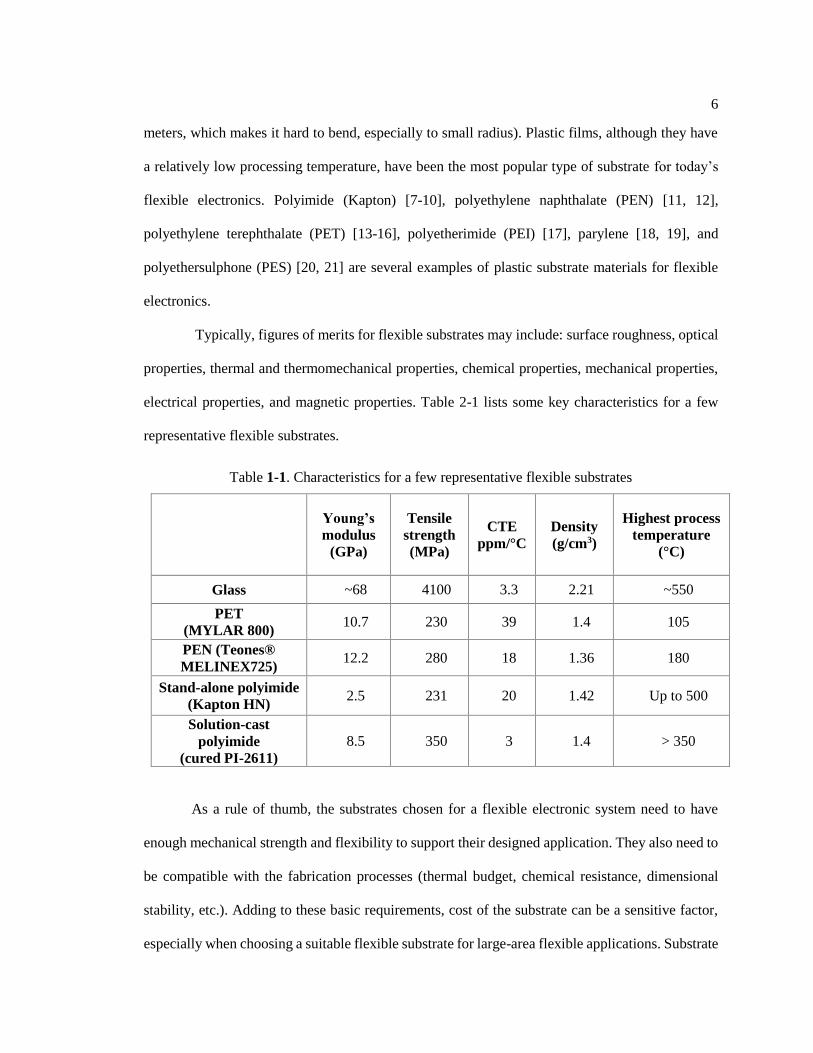
Typically, figures of merits for flexible substrates may include: surface roughness, optical
properties, thermal and thermomechanical properties, chemical properties, mechanical properties,
electrical properties, and magnetic properties. Table 2-1 lists some key characteristics for a few
representative flexible substrates.
Table 1-1. Characteristics for a few representative flexible substrates
Young’s
modulus
(GPa)
Tensile
strength
(MPa)
CTE
ppm/°C Density
(g/cm3)
Highest process
temperature
(°C)
Glass ~68 4100 3.3 2.21 ~550
PET
(MYLAR 800) 10.7 230 39 1.4 105
PEN (Teones®
MELINEX725) 12.2 280 18 1.36 180
Stand-alone polyimide
(Kapton HN) 2.5 231 20 1.42 Up to 500
Solution-cast
polyimide
(cured PI-2611) 8.5 350 3 1.4 > 350
As a rule of thumb, the substrates chosen for a flexible electronic system need to have
enough mechanical strength and flexibility to support their designed application. They also need to
be compatible with the fabrication processes (thermal budget, chemical resistance, dimensional
stability, etc.). Adding to these basic requirements, cost of the substrate can be a sensitive factor,
especially when choosing a suitable flexible substrate for large-area flexible applications. Substrate

7
thickness also plays an important role in device flexibility and is often an important factor for
substrate choice as well.
1.2.3 Fabrication Oriented Considerations
In the past, single crystalline silicon solar cell arrays were thinned down to ~ 100 μm and
assembled on a plastic substrate to provide flexibility [1]. Currently, various process approaches
have been taken to fabricate flexible electronics. Simply speaking, there are two main routes for
the fabrication processes. On one hand, the roll-to-roll (R2R) process has drawn interest because
of its potential for high-throughput and low-cost manufacturing. Figure 2-1 shows a picture of a
roll-to-roll printing line (partial) from Holst Center in the Netherlands. However, roll-to-roll
processing has limitations, such as difficulties in vacuum deposition, photolithography, and
alignment between layers. Moreover, roll-to-roll is not very suitable for customized small-volume
production, as it would be hard to justify the cost. On the other hand, sheet-fed processes, or
processes on planar substrates, are also of interest due to their better compatibility with current fab.
Two basic approaches have been employed for sheet-fed fabrication processes: (1) to fabricate
electronics on conventional rigid wafers and then transfer the fabricated circuits onto flexible
substrates; (2) to directly fabricate electronic circuits on flexible substrates. The former technique
is usually referred to as transfer printing [13, 22-25]. It allows the use of rigid-substrate-compatible
material and fabrication techniques for flexible electronics and can produce high-performance
devices on flexible substrates. However, the transfer step is often a major challenge. For direct
fabrication of electronic circuits on flexible substrates with a sheet-fed process, flexible substrates
laminated onto rigid carriers are usually utilized [26, 27]. This approach also allows the use of
standard equipment and processes for flexible electronics.

8
Recent interest in wearable, skin-attachable, and implantable electronics, and other non-
display flexible applications, emphasizes the importance of substrates for flexible electronics. Very
thin substrates provide advantages in forming or conforming to complicated textures and shapes
and would provide a friendlier vehicle for bio implantations. Recently, solution-cast flexible
substrates have been used for micro-electro-mechanical systems (MEMS) [10, 28-30] and thin film
transistors (TFTs) [7, 31-33]. Solution-cast flexible substrates do not require a lamination step and
may have better dimensional stability during fabrication processes. This will be further discussed
in the following chapters of this dissertation.
Figure 1-2: Roll-to-roll printing line (partial) from Holst Center in the Netherlands [34]
1.3 Research Objectives and Thesis Organization
This work attempts to look at the challenges and opportunities that exist in flexible
electronics from a system level. A transfer- and lamination-free fabrication process for flexible
ZnO TFTs on a very thin, solution-cast polyimide substrate is demonstrated, which could be used
to construct the active components for a functional flexible electronic system. Studies of functional
elements, namely temperature sensing, light emitting, and passive protection components for
flexible applications are also discussed. Device flexibility will be addressed in the context of testing

9
strategies and measurement results of various types of measurements. This dissertation will also
cover some finite element modeling towards an understanding of the mechanical properties and
failure mechanisms of thin film devices under flexed working conditions.
Chapter 2 will introduce a transfer- and lamination-free process for ZnO TFT fabrication
on solution-cast, thin, flexible substrates. The electrical characteristics of the TFTs on polyimide
substrates will be measured and compared to those of devices fabricated on glass substrates. The
results demonstrate decent TFT performance on flexible substrates, which is very similar to device
performance on glass substrates. In addition, simple circuits built from ZnO TFTs on thin flexible
substrates will be demonstrated using inverters and ring-oscillators as examples. These
demonstrations pave a pathway for using ZnO TFT-based active components and circuits on thin
flexible substrates for next-generation functional flexible electronic systems.
Chapter 3 will extend the research on active flexible electronics and talk about components
that provide additional functionalities to the system, namely temperature sensing and light emitting.
This chapter will first discuss the process control of using RF diode reactive sputtering to deposit
vanadium oxide (VOX) thin films for temperature sensing applications. Challenges and approaches
toward process control of RF sputtering deposition of VOX films will be addressed. In Chapter 3,
flexible OLEDs fabricated on thin solution-cast polyimide film will also been demonstrated as
another functional component for flexible applications.
Chapter 4 will talk about a passive component for a flexible electronic system, the
encapsulation layer. A direct patterning technique for parylene films based on the differential
growth of parylene on substrates with different surface energies will be described. This technique
provides a possible method to directly pattern parylene films without using any subtractive micro-
processing steps.
Chapter 5 will focus on mechanical flexibility of flexible electronics. Based on the
requirements of real flexible applications, testing strategies and apparatus have been developed.
10
ZnO TFTs fabricated on thin polyimide substrates are used in this chapter as the objects for testing.
Devices will be tested under different working conditions, aiming to provide useful guidance for
flexible electronics used in real-life situations. Highlight will be given to device stabilities against
mechanical manipulations of various kinds. This chapter will be concluded by the discussion of
failure mechanism study, including finite element modeling using COMSOL Multiphysics. The
simulation results hopefully provide insights into the stress/strain distributions in the device layers
and offer guidance on device optimization.
Chapter 6 will conclude the discussion about flexible electronic systems, comment on
current challenges and opportunities, and provide suggestions for future work.

11
Chapter 2
ZnO Thin Film Transistors and Circuits on Flexible
Substrates
2.1 Introduction to ZnO Thin Film Transistors
Emerging advances in thin film materials and devices have led to blooming progress and
opened up doors to numerous possibilities in the field of flexible electronics. The thin film transistor
(TFT) is one of the most common active components found in a wide range of digital and analog
circuits [3] and is meanwhile the key element in today’s backplane driving circuits for flat panel
displays (FPDs). The history of TFTs goes back more than 80 years. The thin film transistor was
first invented in 1925 and patented in 1930 by J.E. Lilienfeld and O. Heil [35-37]. Today, both
inorganic and organic materials have been used as TFT channel materials. Amorphous Si (a-Si)
and poly Si have been the most widely used inorganic channel materials, especially for the
backplanes of FPDs such as TFT-LCDs (liquid crystal displays) and AMOLEDs (active matrix
organic light emitting diodes), due to the maturity of mass production technology for silicon.
However, the performance (with mobility usually in the neighborhood of 0.5-1 cm2/V•s) and
stability of a-Si TFTs do not fully satisfy the requirements for high-resolution large panel displays.
Polysilicon TFTs usually are fabricated using LTPS (low temperature polycrystalline silicon)
technology, which requires a relatively low temperature of ~650 °C. LTPS TFTs usually have
higher mobility (in the 100 cm2/V•s range), but the temperature required for fabrication is too high
for most flexible substrates. As for organic semiconductor materials, both small molecules such as
pentacene, rubrene, dinaphtho[2,3-b:2',3'-f]thieno[3,2-b]thiophene (DNTT), and polymers such as
the family of polythiophene derivatives (for example P3HT) have been used as active materials for

12
TFTs. Organic semiconductor materials are of interest because they are potentially low cost and
solution processable or printable. However, due to their overall low mobility (usually < 2 cm2/V∙s),
large device-to-device variation, and poor environmental stability with exposure to oxygen and
moisture, organic TFTs have not been massively used in today’s commercial products. More
recently, emerging material systems such as nanotubes [32, 38] and 2-D materials [39, 40] have
been reported for flexible applications.
Oxide semiconductor materials, because of their relatively low processing temperature,
high mobility, and decent air stability, have been proved to be a strong candidate for high-
performance thin film transistors, including flexible electronics applications. Indium-gallium-zinc-
oxide (IGZO) [9, 41-47] and IGZO-based binary or ternary oxide compounds, including ZnO and
Al doped ZnO (AZO) [48-52], IZO [53-55], and IGO [56, 57], are the most representative oxide
semiconductor materials. At the current stage of development, IGZO-based oxide semiconductor
materials are mostly deposited by sputtering. However, atomic layer deposition (ALD) [25], plasma
enhanced atomic layer deposition (PEALD) [26, 58-61], pulsed laser deposition (PLD) [62-65],
ink-jet printing [44, 66, 67], and solution pyrolysis [52, 68] have also been reported for depositions
for IGZO family materials. ZnO TFTs typically exhibit field effect mobility in the 10-50 cm2/V∙s
range, according to most reports. They have a wide bandgap (~3.4 eV) and therefore are transparent
in the visible range and are thus of interest for display and imaging applications where transparent
electronics are desired.
For the past few decades, back planes for flat panel displays have been the main driving
force for the development of thin film transistor technology. A significant advantage of using metal
oxide semiconductor TFTs in flat panel displays is their large-area scalability and relatively simple
fabrication processes. In this work, PEALD deposited ZnO will be used as the active material for
the flexible TFTs. The PEALD process used for ZnO deposition is a scalable and low temperature
process and thus is very suitable for large-area and flexible applications.

13
2.2 Fabrication of ZnO TFTs on Thin Solution-Cast Polymer
Substrates
As stated in the last section, ZnO deposited by PEALD is used in this work as the active
material for the TFTs fabricated on thin, flexible substrates. The substrate temperature for PEALD
deposition is relatively low (200 °C), and polyimide films can easily withstand such a thermal
budget. The flexible substrate used in this work is solution-cast thin polyimide film. To prepare the
polymeric substrate, Hitachi DuPont Microsystems PI-2611 non-photodefineable polyimide
precursor was spin-casted on a rigid carrier (typically a Si wafer with a 50 nm silicon nitride layer)
at a final speed of 3000 rpm for 30 seconds. Because of the high viscosity of the PI-2611 precursor,
a slow ramping to the final spin speed was necessary. For the polyimide substrate used in this work,
the spin speed and ramp rate used were: 60 rpm/sec ramp to 300 rpm and spin for 20 sec; then 100
rpm/sec ramp to 1000 rpm and spin for 30 sec; then 200 rpm/sec ramp to 3000 rpm and spin for 40
sec. The film was then cured at 300 °C on a hot plate in air for 8-15 hours. When fully cured, the
PI-2611 films were 4.8 μm thick and had an rms surface roughness of ~0.8 nm. Figure 2-1 shows
an AFM image of a cured PI-2611 film on Si/SiNX substrate.
Figure 2-1: AFM image of cured PI-2611 on Si/SiNX substrate. The rms surface roughness of the
cured polyimide film is measured to be ~0.8 nm.

14
The fully cured PI-2611 film exhibits low stress, low CTE, low moisture uptake, and high
modulus. It is not attacked by most solvents found in semiconductor fab or by weak acids or bases.
Such characteristics allow direct processing of the ZnO TFTs on cured PI-2611 film substrates.
Normal deposition and patterning techniques for conventional rigid electronic devices were directly
used for the fabrication here. First, a 100 nm thick Cr layer was deposited by thermal evaporation
and patterned by wet etching as the gate metal. Next, plasma enhanced atomic layer deposition
(PEALD) was used to deposit a 32 nm thick Al2O3 layer and a 10 nm thick ZnO layer as gate
dielectric and semiconductor layers respectively. The Al2O3 and ZnO were deposited at 200 °C
from trimethylaluminum (TMA) and CO2, and diethylzinc (DEZ) and N2O, respectively [59]. The
Al2O3 and ZnO layers were then patterned by wet etching. A 100 nm thick Al layer was then
deposited by thermal evaporation and patterned by lift-off as source and drain contacts. Finally, a
30 nm Al2O3 layer was deposited by atomic layer deposition (ALD) from TMA and H2O at 200 °C
as a passivation layer. Figure 2-2 shows the process flow to fabricate ZnO TFTs on a solution-cast
thin polyimide substrate; the inset shows an optical micrograph of a fabricated ZnO TFT on
polyimide substrate.

15
Figure 2-2: Process flow for flexible ZnO TFT fabrication. Inset shows an optical micrograph of a
fabricated ZnO TFT on polyimide substrate.
2.3 Process Control for Device Fabrication on Thin Flexible
Substrate
2.3.1 Substrate Dimensional Stability
Fabrication on flexible substrates can be challenging. One factor is that the flexible
substrates usually do not maintain their shape and dimension very well during the process. Such
dimensional instability can increase alignment error and create challenges for registration between
layers. According to the datasheet, the polyimide (PI-2611) chosen for our flexible substrate has a
small coefficient of thermal expansion, 3 ppm/°C [69], which should be beneficial for dimensional
stability of the substrate.
For fabrication on rigid substrates such as glass or silicon wafers, the shape change of the
substrates is negligible and the alignment error at different positions of the sample should be

16
identical (taking rotational error into considerations). When fabricating on plastic substrates, the
dimension change of the substrates can cause discrepancies in alignment errors at different
positions of the sample. And these discrepancies can be used as an indicator of the substrate’s
dimensional instability. To quantitatively study the shape change of the polyimide substrate during
the fabrication process, vernier structures were designed and fabricated on the flexible substrate.
Figure 2-3 (a) shows the design of one set of verniers, and Figure 2-3 (b) is an optical micrograph
of such a structure fabricated on a thin polyimide substrate. Each of the vernier structures has two
groups of lines on two different layers; one group was positioned horizontally, and the other was
positioned vertically. Each group has 11 lines on each layer, and the spacing between the lines was
designed to be different by 1 μm for the two layers (blue layer and red layer in Figure 2-3 (a)).
After fabrication, if the layers were aligned perfectly, the middle line pair (middle red line and
middle blue line) in both the vertical and the horizontal groups would overlap, indicating 0
alignment error in both directions. However, for a lab-fabricated sample, alignment errors always
exist. As a result, another line pair instead of the middle one would overlap on the fabricated
sample. For example, in Figure 2-3 (b), the 6th (middle) line pair in the vertical line group and the
5th line pair in the horizontal line group overlapped, which indicated 0 μm alignment error in the
vertical direction and -1 μm alignment error in the horizontal direction.
Figure 2-3: (a) One set of vernier structures by design; (b) optical micrograph of one set of vernier
structures fabricated on a thin polyimide substrate

17
Figure 2-4 shows alignment errors (measured using the vernier structures) between the gate
(1st) and the source and drain (4th) layer at different positions of a 2-inch by 2-inch flexible sample
using PI-2611 as the substrate. The first number of each data set indicates the alignment error in
the horizontal (x) direction, and the second number indicates the alignment error in the vertical (y)
direction. A negative value means the alignment was too much to the left or bottom, and a positive
value means the alignment was too much to the right or top. Question marks indicate that the
particular vernier structure was hard to read due to process issues.
Figure 2-4: Alignment errors between the gate (1st) and the source and drain (4th) layer at different
positions of a 2” ⤬ 2” flexible sample with PI-2611 substrates measured by vernier structure
readings. First number of each data point indicates the alignment error in the horizontal (x)
direction; second number of each data point indicates the alignment error in the vertical (y)
direction. Question marks indicate that the particular vernier was hard to read due to process issues.
The alignment errors across the sample were apparently all different, and there was no clear
trend for the discrepancies. The discrepancies across the 2-inch sample suggest that the substrate
changed its shape between the processes of the gate layer and the source and drain layer. The
differences of the alignment error also suggest that the shape change was “random” and

18
complicated rather than simple uniform shrinking or swelling. However, regardless of the
complexity of the substrate shape change, if the differences of the alignment errors at different
positions were taken and divided by the distance between the vernier structures from which the
alignment errors were read, the shape change of the PI-2611 substrates between the process steps
of the first and the fourth layer can be calculated to be less than 60 ppm. This number is much
smaller than the shape change for typical freestanding plastic (polyimide) substrates, which is
usually in the hundreds of ppm range.
2.3.2 Dielectric Integrity
Another challenge for flexible electronics is dielectric integrity. Dielectric layers play an
important role for electronic devices. In our thin film transistors, the Al2O3 dielectric layer is only
32 nm thick. It is useful and important to examine the dielectric layer and evaluate its integrity over
a large area and on a flexible surface. An array of crossover test structures was fabricated on the
flexible substrate to characterize the dielectric layer. Figure 2-5 shows the design and optical
micrograph of such crossover structures. The structure has bottom metal electrodes and top metal
electrodes laid out perpendicular to each other with a 32 nm PEALD deposited Al2O3 dielectric
layer sandwiched in between. Between the top and bottom electrodes, the structure is basically a
number of small capacitors connected in parallel. The area of each small capacitor (crossover area)
was 10 μm ⤬ 10 μm.
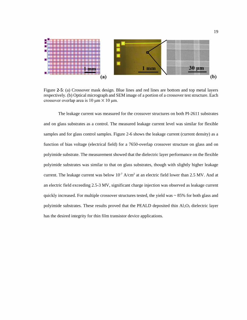
19
Figure 2-5: (a) Crossover mask design. Blue lines and red lines are bottom and top metal layers
respectively. (b) Optical micrograph and SEM image of a portion of a crossover test structure. Each
crossover overlap area is 10 μm ⤬ 10 μm.
The leakage current was measured for the crossover structures on both PI-2611 substrates
and on glass substrates as a control. The measured leakage current level was similar for flexible
samples and for glass control samples. Figure 2-6 shows the leakage current (current density) as a
function of bias voltage (electrical field) for a 7650-overlap crossover structure on glass and on
polyimide substrate. The measurement showed that the dielectric layer performance on the flexible
polyimide substrates was similar to that on glass substrates, though with slightly higher leakage
current. The leakage current was below 10-7 A/cm2 at an electric field lower than 2.5 MV. And at
an electric field exceeding 2.5-3 MV, significant charge injection was observed as leakage current
quickly increased. For multiple crossover structures tested, the yield was ~ 85% for both glass and
polyimide substrates. These results proved that the PEALD deposited thin Al2O3 dielectric layer
has the desired integrity for thin film transistor device applications.

20
0 2 4 6 8 10 12 14
1E-10
1E-9
1E-8
1E-7
Cu
rre
nt
de
nsity (
A/c
m2)
Electric field (MV/cm)
Cu
rre
nt
(A)
voltage (V)
on glass 7650 crossovers
on PI-2611 7650 crossovers
0.0 0.5 1.0 1.5 2.0 2.5 3.0 3.5 4.0 4.5
10-8
10-7
10-6
10-5
Figure 2-6: Leakage current (current density) as a function of bias voltage (electric field) for a
crossover test structure with 7650 10 μm ⤬ 10 μm overlaps.
2.4 Characteristics of Flexible ZnO Thin Film Transistors
2.4.1 Basic Transistor Characteristics
The ZnO TFTs on solution-cast polyimide substrates were characterized and compared
with control devices fabricated using the same process on borosilicate glass substrates. The devices
were measured using an HP4156B semiconductor parameter analyzer. Figure 2-3 (a) shows typical
linear region drain current and mobility versus gate voltage characteristics for PEALD ZnO TFTs
on thin polyimide (on a rigid Si wafer carrier) and on glass substrate. The TFTs had channel width
and length of 200 µm and 20 µm, a 32 nm thick PEALD Al2O3 gate dielectric, a 10 nm thick
PEALD ZnO active layer, and a 30 nm thick ALD Al2O3 passivation layer. Typical linear region
(VDS = 0.5 V) characteristics include a turn-on voltage (here defined as the gate-to-source voltage,
VGS, at which the drain current IDS exceeds 1×10-12 A/m) of ~-1.2 V, a linear region field effect
mobility greater than 12 cm2/V∙s (at VGS = 8 V), a sub-threshold slope less than 300 mV/decade,
and a current on/off ratio of greater than 108. Fig. 2-3 (b) shows PEALD ZnO TFT IDS versus VDS
characteristics for several gate voltages from 0 V to 8 V on the two substrates. TFTs fabricated on

21
thin solution-cast polyimide have characteristics very similar to those fabricated on glass; the
differences shown in Fig. 2-3 are typical for run-to-run variations for our PEALD TFT process.
Figure 2-7: Device characteristics for ZnO TFTs fabricated on thin flexible polyimide and glass
substrates (TFT W/L = 200/20 μm/μm, 32 nm Al2O
3 gate oxide, 10 nm ZnO active layer, 30 nm
Al2O3 passivation); (a) log(IDS) and differential mobility versus VGS characteristics for VDS = 0.5
V; (b) IDS versus VDS characteristics for several values of VGS.
2.4.2 Bias Stability, Yield, and Uniformity
Bias stability of the TFTs was measured by applying a constant gate-to-source voltage
(VGS) of 3 V and drain-to-source voltage (VDS) of 4 V to the passivated ZnO TFTs and monitoring
the drain current (IDS) as a function of time. Bias stability of ZnO TFTs on thin polyimide substrates
was measured and compared with the stability of glass substrate samples. Figure 2-4 (a) shows the
normalized drain current as a function of time for the TFTs under bias stress. ZnO TFTs on thin
polyimide and glass substrates showed similar bias stability characteristics, with the glass sample
exhibiting a 7.9% decrease in drain current and the polyimide sample exhibiting a 9.4% decrease
in drain current after 30,000 seconds of bias stress. Figure 2-5 (b) shows the IDS-VGS characteristic
of a ZnO TFT on thin polyimide substrate before and after the bias stress at VDS = 3 V and VGS = 4
V for 60,000 sec (IDS = 3.7 µA/µm). The IDS-VGS curve shifted to the positive direction by ~ 200
mV after stress.
-4 -2 0 2 4 6 8
10-13
10-12
10-11
10-10
10-9
10-8
10-7
10-6
10-5
10-4
I DS
(A
)
VGS (V)
0
4
8
12
16
Dif
fen
tia
l m
ob
ilit
y (
cm
2/V
-s) Glass sample
Flexible sample
VDS
= 0.5 V
0 2 4 6 80
50
100
150
200
250
300
350
400
450 Glass
Flexible
VGS = 4 V
VGS = 2 V
VGS = 6 V
VGS = 8 V
I DS
(A
)
VDS (V)

22
10 100 1000 10000
0.86
0.88
0.90
0.92
0.94
0.96
0.98
1.00
polyimide
glass
No
rmalized
dra
in c
urr
en
t
Time (seconds)
VDS
= 3 V
VGS
= 4 V
W/L = 200/20 m/m
32 nm Al2O
3 gate oxide
-4 -2 0 2 4 6 810
-14
10-13
10-12
10-11
10-10
10-9
10-8
10-7
10-6
10-5
10-4
10-3
~ 200 mV
I DS
(A
)
VGS (V)
Initial
After 60 ks bias
VDS
= 8 V
Figure 2-8: ZnO TFT bias stability. (a) Normalized drain current as a function of time under bias
stress at VDS = 3 V and VGS = 4 V for polyimide and glass samples. (b) IDS-VGS characteristics of a
ZnO TFT on thin polyimide substrate before and after bias stress (at IDS = 3.7 µA/µm) for 60,000
sec. (TFT W/L = 200/20 μm/μm, 32 nm Al2O
3 gate oxide, 10 nm ZnO active layer, 30 nm Al2O3
passivation)
The yield and uniformity of ZnO TFTs fabricated on thin polyimide substrates were tested
by measuring groups of multiple TFTs fabricated on the same sample. Figure 2-5 (a) shows the IDS-
VGS characteristics of a group of 80 TFTs on polyimide substrates with channel width of 200 µm
and four different channel lengths of 5 µm, 10 µm, 20 µm, and 50 µm. All of the 80 devices
measured performed properly as field effect transistors, which demonstrated a > 99% device yield
of PEALD ZnO TFTs on thin solution-cast polyimide flexible substrate. The extracted mobilities
of the 80 TFTs are plotted in Figure 2-5 (b). The average mobility for all devices was 9.3 cm2/V∙s
(at VGS = 6 V), and the standard deviation was 0.9 cm2/V∙s. With the transfer- and lamination-free
process used in this work, we successfully fabricated ZnO TFTs on ~5 µm thick flexible polyimide
substrate with a decent mobility of 10 cm2/V∙s and a very good yield of > 99%.

23
Figure 2-9: (a) IDS-VGS characteristics of 80 ZnO TFTs fabricated on 4.8 µm thick polyimide
substrate. (TFT channel width = 200 µm, channel length = 5 µm, 10 µm, 20 µm, and 50 µm, 32 nm
Al2O
3 gate oxide, 10 nm ZnO active layer, 30 nm Al2O3 passivation), VDS = 6 V. (b) Extracted TFT
mobility at VGS = 6 V. Average mobility of all 80 TFTs was 9.3 cm2/V∙s; standard deviation was
0.9 cm2/V∙s.
The solution-cast polyimide substrate needs to be detached from the rigid wafer carrier to
become truly flexible. The adhesion of PI-2611 films to Si3N4 surfaces is strong enough to endure
the TFT fabrication process but weak enough to allow the flexible substrates to be peeled from the
rigid wafer carrier [28, 70]. Figure 2-10 (a) shows a photograph of the peeling off process. After
this simple mechanical release, the polyimide substrates have a slight tendency to curl concavely
(TFTs on the inside curve, shown in Figure 2-10 (b)), likely due to tensile stress in the TFT layers,
but require little force to flatten. The released substrate is flexible enough that it can be easily
wrapped around a finger (Figure 2-10 (c)). We found that the characteristics of most TFTs on the
released substrates were essentially unchanged from the characteristics before release.
Approximately 25-30% of the TFTs could be degraded after releasing, which suggested that this
not-well-optimized releasing process was not an ideal method to release the flexible substrates.
Figure 2-10 (d) shows device IDS-VGS curves for a typical ZnO TFT on thin polyimide substrate
before and after release from its rigid wafer carrier.
Device number
Mo
bil
ity
(a
t V
GS =
6V
)
0 8 16 24 32 40 48 56 64 72 800
1
2
3
4
5
6
7
8
9
10
11

24
-4 -2 0 2 4 6
10-13
10-12
10-11
10-10
10-9
10-8
10-7
10-6
10-5
10-4
(d)
TFT On wafer carrier
TFT free standing flat
VGS (V)
I DS
(A
)
VDS = 0.5 V
0
5
10
15
Dif
fern
tia
l m
ob
ilit
y (
cm
2/v
-s)
Figure 2-10: (a) Peeling off flexible polyimide substrate from rigid Si wafer carrier using a pair of
tweezers. (b) Concavely curled substrate after releasing. (c) Released 4.8 μm thick flexible
polyimide substrate wrapped around a finger. (d) IDS-VGS curve for a ZnO TFT fabricated on 4.8
μm thick flexible polyimide substrate before and after release from rigid carrier. Device
performance was essentially unchanged after releasing.
2.5 Flexible ZnO TFT Circuits
To demonstrate the circuit capability of the PEALD ZnO TFTs on thin polyimide flexible
substrates, inverters and ring-oscillators have been fabricated. The inverters used a saturated
enhancement load. Figure 2-11 (a) shows the circuit diagram, and Figure 2-11 (b) shows the optical
micrograph of an inverter fabricated on polyimide substrate. The inverters had a beta ratio =
((
𝑊
𝐿)𝑑𝑟𝑖𝑣𝑒
(𝑊
𝐿)𝑙𝑜𝑎𝑑
⁄ ) = (200/5
40/5) = 5 , and the source/drain-to-gate overlap was 1 µm. With a

25
supply voltage of 9 V, the extracted voltage gain was ~ 1.6. Ideally, the gain should be equal to
the square root of the beta ratio, around 2.2, since the drive and load TFTs must have the same
current during the operation. However, this theory is based on the constant mobility model, in
which devices have a constant mobility under different bias conditions. As shown in previous
sections, the field effect mobility of ZnO TFTs typically increases when the gate field is
increased. Therefore, the estimated gain based on the beta ratio may not be very accurate.
Figure 2-11: (a) Circuit schematic of the saturated enhancement load inverter; (b) optical
micrograph of an inverter fabricated on polyimide substrate; (c) transfer curve for an inverter at
various supply voltages (1 – 9 V with 1 V step).
ZnO TFT Ring oscillators have also been fabricated on thin polyimide substrates. The
circuits had a beta ratio of 5 with (𝑊
𝐿)𝑑𝑟𝑖𝑣𝑒 =
50 𝜇𝑚
5 𝜇𝑚 and (
𝑊
𝐿)𝑙𝑜𝑎𝑑 =
10 𝜇𝑚
5 𝜇𝑚 and a source and drain to
gate overlap of 2 μm and 5 μm. Figure 2-12 (a) shows an optical micrograph of a 51-stage ring
oscillator (with 2 output buffer stages, 106 transistors in total) fabricated on polyimide substrate;
figure 2-7 (b) shows a 15-stage ring-oscillator (2 μm source and drain to gate overlap) frequency

26
and delay as a function of supply voltage. At its highest supply voltage of 14 V, the maximum
working frequency was 1.1 MHz and the delay time was 60 ns/stage. 51-stage ring oscillators with
the same device dimension that we fabricated showed a similar working voltage range and per-
stage delay.
Figure 2-12: (a) Optical micrograph of a 51-stage ZnO TFT ring oscillator fabricated on thin
polyimide substrate; (b) Frequency and delay of a 15-stage ring oscillator on thin polyimide
substrate (beta ratio = 5, source and drain to gate overlap 2 μm).
0.5 mm
27
Chapter 3
Functional Thin Film Materials and Devices for
Flexible Electronics
Large area electronics are usually composed of backplane electronics and a front plane. In
the previous chapter, ZnO TFTs were discussed as an active component for flexible electronics,
one that can be used to form circuits and realize logic on a flexible platform – or, in other words,
to form backplane electronics in flexible systems. For a useful flexible electronic system, various
front-plane functionalities may be desired. Materials and structures that realize functions such as
sensing, heating, cooling, imaging, and light emitting are of particular interest. Examples of the
applications for flexible electronics may include thermal, pressure, gesture, or gas sensors, artificial
skins, wearable health monitors, imaging and display panels, and electronics.
In this chapter, we will discuss work related to temperature sensing and light emitting
applications in order to incorporate additional functionalities into a flexible electronic system.
3.1 Vanadium Oxide Film for Temperature Sensing Applications
3.1.1 Temperature Sensing Using Thin Film Materials and Devices
Temperature sensing can be realized using multiple methods and various device
architectures. Most common temperature sensors include mechanical sensors, such as mercury-in-
glass thermometers, and electrical sensors, such as thermo couples, resistance thermometers, and
silicon bandgap temperature sensors. To realize temperature sensing in flexible electronics, sensors
in a thin-film geometry would be desirable. PyroFET temperature sensors have been demonstrated
using ZnO TFTs by monitoring changes in the turn-on voltage shift with changing temperature [48].

28
Another (and maybe simpler) approach to realize temperature sensing with thin film devices is to
utilize materials known to possess a large temperature coefficient of resistance (TCR) where the
film resistivity changes as a function of temperature. The change in resistance can then be captured
by a prepheral circuit and processed to indicate the change in temperature. A microbolometer is a
device that finds use as a detector in thermal cameras. It uses materials with large TCR values for
temperature sensing and constructs thermal images using the temperature signals.
Vanadium oxide (VOX) thin films have a large negative TCR (~ -2% K-1 at around 1 Ω∙cm)
and have been widely used as the thermal detection material in uncooled resistive microbolometers
[71-73]. Figure 3-1 shows a typical pixel structure of an uncooled bolometer [73]. The desired
resistivity for VOX thin films used for uncooled microbolometers is usually 0.01-1 Ω∙cm, and the
microstructure of the film is a mixed phase of face centered cubic (FCC) vanadium monoxide
nanocrystallites and an amorphous component present between the crystallites [74, 75].
Figure 3-1: Typical pixel structure of uncooled microbolometers [73]

29
3.1.2 Vanadium Oxide Thin Film Deposition
Vanadium oxide thin films are usually deposited by reactive deposition methods. They
typically employ one or more metallic vanadium or stoichiometric vanadium oxide targets in a
deposition environment with a controlled oxygen supply. Various VOX deposition methods have
been studied and reported, such as ion-beam deposition [76-79], pulsed laser sputtering [80], and
electron beam evaporation [81]. Despite its current popularity in VOX manufacturing, ion-beam
deposition suffers from a relatively low deposition rate. Pulsed DC magnetron sputtering of VOX
films for use in microbolometers has also been reported [82-85]. Pulsed DC magnetron sputtering
avoids target charging, a common problem for DC sputtering of insulators or targets with insulating
surface layers, by using a short positive potential pulse to attract electrons from the plasma to
maintain charge neutrality. DC magnetron sputtering can provide a faster deposition rate than ion
beam deposition; however, for reactive sputtering, it is often an inherently non-uniform process,
which may require a large target-to-substrate separation for better uniformity and bring other
challenges for implementation in the manufacturing environment [85].
RF diode sputtering is a simple technique for depositing from insulating or insulating
surface layer targets. It uses an RF power source but does not use a magnetic field to increase the
sputtering plasma density. Because of its relatively uniform plasma density, RF diode sputtering
has the potential to provide advantages in deposition uniformity. In this work, we will investigate
the feasibility of using RF diode reactive sputtering to deposit VOX films for use in uncooled
bolometers.
3.1.3 RF Diode Reactive Sputtering and Characterization of VOX Films
In this work, a CVC-611 load-locked RF diode sputtering system was used to deposit VOX
films. The deposition chamber is ~60 cm in diameter; a rotating stage that holds six 20-cm diameter

30
sample holders is located at the bottom of the chamber; a 20-cm diameter vanadium target is
mounted on top of the deposition chamber, facing downward. An Advanced Energy RFPP RF10S
plasma generator with a frequency of 13.6 MHz was used as the power supply. Figure 3-2 shows a
schematic and photographs of the RF diode sputtering system used.
Figure 3-2: (a) Schematic of the RF diode sputtering chamber, (b) photograph of CVC-611 load-
locked RF sputtering system, (c) photograph of the inside of the deposition chamber.
The deposition chamber was typically pumped down to a base pressure of low 10-7 torr
before film deposition. Ultra high purity Ar and O2 were introduced into the deposition chamber
through two mass flow controllers. The gas inlets are located at the bottom of the deposition
chamber. The process pressure and total flow rate were typically kept at 5 mTorr and 62 sccm. The
ratio of Ar and O2 was controlled by adjusting the flow rates for individual depositions to vary the
properties of the resultant films. An RF power of 1000 watts (~3 watt/cm2 on target) was used for
sputtering, and thermally oxidized Si wafers were usually used as the substrates. The target was
typically presputtered with the target shutter closed before film depositions, which typically used

31
15 minutes of sputtering with pure Ar followed by 15 minutes of sputtering with the Ar and O2 set
at the desired flow rates for film deposition. The sample was placed directly underneath the target
with a target-to-substrate distance of ~5 cm, and no substrate rotation was applied. There was no
substrate heater, but the substrate was heated by ion bombardment throughout the sputtering
process. The estimated maximum substrate temperature was about 70 ˚C.
Ellipsometry was used to measure the thickness of deposited VOX films. The sheet
resistance of the deposited films was first measured by a 4-point probe. Films with resistivity in the
desired range were patterned by photolithography and wet etching, and Ti was then deposited and
patterened using lift-off to form metal contacts for transmission line structures (TLM) used to
characterize the resistivity and TCR of the VOX films. Figure 3-3 shows a microscope image of the
fabricated TLM structure on a VOX film. Current-voltage (I-V) characterization was performed
with a two-probe configuration over the temperature range of 20 - 60 ˚C. TCR values of the films
were extracted using
0
0
0
)(ln1
1%
TT
TT
TT TTTTCR
where ρ is the film resistivity and T is the temperature.
Figure 3-3: Transmission line structure (TLM) of VOX film on Si/SiO2 substrate

32
The deposition rate for VOX films using RF diode reactive sputtering in this work was
about 8.5 – 30 nm/min, as calculated from the deposited film thickness and the deposition time.
VOX films with 0.01 – 1 Ω∙cm resistivity were deposited at a deposition rate of about 10 nm/min.
Using the RF diode reactive sputtering method, we have deposited several films within the
resistivity range of 0.1 – 1 Ω∙cm. Figure 3-4 shows a plot of extracted TCR value as a function of
film resistivity for selected VOX films. Comparing the extracted TCR values of these films to VOX
films deposited by other deposition techniques, VOX films deposited by RF diode sputtering with
resistivity in the 0.1 – 1 Ω∙cm range can have TCR values comparable to or even larger than films
deposited by other techniques [86, 87].
0.01 0.1 1 10 100 1000 100000
1
2
3
4
Resistivity [ohm.cm]
This work
PSU Magnetron VOx
PSU Biased Magnetron VOx
PSU VOx - Si alloy
Company J IBD VOx
Company Z IBD VOx
Company V IBD VOx
Company X IBD VOx
TC
R [-%
/K]
Figure 3-4: TCR as a function of resistivity for VOX films deposited by different techniques
Despite these encouraging results, we found film resistivity and composition control was
difficult and film reproducibility was poor when using RF diode reactive sputtering. From a total
of more than 150 RF reactive sputter runs, only a few (less than 10) VOX films were obtained with
resistivity in the desired range. Figure 3-5 shows the resistivity of VOX films as a function of O2
supply ratio for 52 consecutive RF diode sputter depositions. Of these films, only 5 exhibited

33
resistivity in the 0.01 – 1 Ω∙cm range. Each of the rest showed resistivity either in the 10-3 to 10-4
Ω∙cm range or too high to measure by 4-point-probe.
1.2 1.4 1.6 1.8 2.0 2.2 2.410
-5
10-4
10-3
10-2
10-1
100
101
102
105
desired resistivity range
Resis
tivity (
Ohm
-cm
)
O2 inlet ratio (%)
resistivity too high to measure
Figure 3-5: Resistivity of VOX films as a function of O2 supply ratio deposited by RF diode reactive
sputtering.
Hysteresis is widely observed in reactive sputtering [84, 88-90]. For ion-beam [78] or
magnetron sputtered [85] VOX, there is usually a range of oxygen input ratio within which the
deposited VOX film changes gradually from metallic and low resistivity to strongly oxidized and
high resistivity. Figure 3-6 shows an example of hysteresis curves from pulsed DC magnetron
sputtering for VOX films cited from reference [15]. However, as shown in Figure 3-5 for RF diode
reactive sputtering, the resistivity of deposited VOX could change dramatically with very little
change in oxygen inlet ratio. The resistivity obtained for a given oxygen input ratio depends
sensitively on the target and chamber history, and even consecutive deposition runs in our load-
locked sputtering system do not dependably result in reproducible films.

34
Figure 3-6: Resistivity of deposited VOX films as a function of oxygen supply ratio from a DC
magnetron reactive sputtering system [15].
3.2 Control of Reactive RF Diode Sputtered VOX Thin Films
3.2.1 Control Issue for Reactive RF Diode Sputtered VOX Thin Films
As stated in the last section, a specific range of oxygen input was absent in reactive RF
diode sputtering where VOX films gradually changed from metallic to highly oxidized with a
controllable transition. The extremes of the sputter range are clear. Having a target with a metallic
surface and using a small input oxygen ratio results in low-resistivity, metallic films. In this range
of oxygen input, the sputtered vanadium easily reacts with oxygen that reaches the sputter area, but
the available oxygen is insufficient to change the overall film character from metallic. On the other
hand, having a target with an oxidized surface and using a large input oxygen ratio results in high-
resistivity, oxidized films. In this range of oxygen input, there is excess oxygen available and the
sputtered vanadium is fully oxidized, either at the target, in the plasma, or at the substrate.
The intermediate oxygen input ratio range is more complicated. In this range of film
deposition, the target surface is neither fully metallic nor fully oxidized. We have observed that the
sputter deposition rate depends strongly on the target surface condition, with the deposition rate for

35
the metallic target surface about three times larger than for the oxidized target surface. If the target
surface is metallic, the sputter deposition rate is high, and sputtered vanadium can react with a
relatively large amount of oxygen. On the other hand, if the target surface is oxidized, the sputter
deposition rate will be low, much of the sputtered vanadium may already be oxidized, and little
additional oxygen can be consumed. This leads to the basic hysteretic behavior with a metallic
target surface tending to remain metallic and an oxidized surface tending to remain oxidized.
In the case of sputtering with a metallic target surface, suppose the oxygen input ratio is
increased until the film resistivity begins to move out of the metallic range. As the target surface
oxidation increases, the deposition rate will decrease and so will the sputtered vanadium metal
atoms. There will then be less vanadium available to react with oxygen, which causes the oxygen
partial pressure to further increase, and the sputtered film will tend to become strongly oxidized
with high resistivity. A similar but reversed effect will happen if sputtering begins with a large
oxygen partial pressure. For this case, the target surface will be oxidized and the sputter deposition
rate will be low. If the oxygen input ratio is decreased, at some point there will be insufficient
oxygen to retain the target surface in its fully oxidized state. As the target surface becomes less
oxidized, the sputtering rate will increase, and so will the sputtered vanadium metal atoms. The
sputtered vanadium will then react with more oxygen, which causes the oxygen partial pressure to
decrease further, and the sputtered film will tend to come metallic with low resistivity.
These effects lead to a positive feedback mechanism, thus the overlap in ranges of oxygen
inlet ratio for low and high resistivity films. The experiments suggest that the transitions from low
to high and high to low resistivity with oxygen inlet ratio may have a negative slope (or are at least
very steep and possibly time varying), and thus there is no “correct” oxygen inlet ratio for
depositing films with the desired resistivity for bolometer use. In principal, this problem can be
solved if an appropriate control signal can be found that allows dynamic control of the deposited

36
film characteristics. Target potential, plasma optical emission, and local oxygen partial pressure
will be examined in this work as possible control signals.
3.2.2 Process Control Attempt 1: Target Potential
During RF sputtering, a negative self-bias is generated on the target as a consequence of
the relatively high mobility of electrons compared to ions in the plasma; the self-bias provides the
driving force for charge neutrality [91]. When oxygen is introduced into the process chamber,
oxidation occurs on and near the substrate surface, in the plasma between the target and the
substrate, and at the target surface [92]. For sputtering with a partial pressure of oxygen, the
vanadium target will have a thin layer of its oxide, and intuitively one might expect the DC self-
bias to change in response to changes in the degree of oxidation and the thickness of the oxide layer
on the target surface. Conversely, the target potential could potentially provide a feedback or
control signal for the oxidation reaction and thus the reactive sputtering process.
An RF choke and capacitor network was originally connected to the vanadium target on
the deposition system, which monitors the average DC self-bias on the target during deposition
with an accuracy of 10 volts. To better monitor the variation in self-bias potential on the target, a
voltage divider consisting of a 5 MΩ and a 15 kΩ resistor was connected to the target to drop the
kilovolt-range target self-bias down to a few tens of volts. An envelope detector circuit (a forward
connected diode with a capacitor and a backward connected diode with a capacitor) was connected
to the output of the voltage divider to monitor the positive and negative peak voltages on the target.
Figure 3-7 shows a schematic of the monitoring circuit on the system.

37
Figure 3-7: Target DC self-bias and RF peak voltage monitoring circuit for the RF diode reactive
sputtering system
Target average DC self-bias and RF peak voltage were measured and recorded at different
oxygen levels. Two extreme sputtering conditions, no oxygen and a high oxygen level (8% O2 inlet
ratio), which yield metallic and fully oxidized films respectively, were studied here as examples.
The RF power was kept at 1 kW for both cases. The target was pre-sputtered at the deposition
conditions for 30 minutes, and the DC self-bias and RF peak voltages were recorded for one hour.
The average DC self-bias for no oxygen and high oxygen levels are plotted in Figure 3-8 (a). For
0% oxygen and 8% oxygen, the average DC self-bias was 1.528 kV and 1.506 kV respectively.
The difference for these two extreme conditions was less than 1.5%, and the small observed
differences in DC self-bias for varying oxygen input ratio were not repeatable from run to run. RF
peak voltages did not provide a useful control signal either. For two sequential depositions, both
with 8% O2 and the same process parameters, after averaging, the recorded RF peak voltages
differed by ~4% (positive peak) and 1% (negative peak). The recorded RF peak voltages for the
two depositions with the exact same parameters are plotted in Figure 3-8(b). Such run-to-run
variations were comparable to or even larger than the differences between extreme deposition

38
conditions, which made it difficult to use the absolute values of the target voltages as control signals
for the RF diode reactive sputtering process.
0 10 20 30 40 50 608
10
12
14
16
2nd run negative peak voltage (-V) [real]
2nd run positive peak voltage (V) [real]
1st run negative peak voltage (-V) real on target
1st run positive peak voltage (V) real on target
RF
pe
ak v
olta
ge
(kV
)
Time (min)
8% oxygen inlet ratio with oxidized target
Figure 3-8: (a) Target average DC self-bias for 0% and 8% oxygen inlet ratio. (b) Positive and
negative RF peak voltages on target for two deposition runs both with 8% oxygen inlet and the
same process parameters.
The changes in target potential have also been measured by monitoring the DC self-bias
and RF peak voltages for depositions that started with a metallic target and pure Ar. The input
oxygen ratio was increased to 1.87% after 15 minutes of sputtering, to 2.06% after 30 minutes of
sputtering, and to 2.19% after 45 minutes of sputtering. The RF power was maintained at 1 kW.
This process sequence results in films that vary from metallic (for pure Ar) to strongly oxidized,
high resistivity (for 2.19 % O2). Figure 3-9 shows the recorded target DC self-bias and RF peak
voltage as a function of deposition time. No clear change in either average DC self-bias or the RF
peak voltage was observed. Thus, the changes in DC self-bias and RF peak voltage were neither
large enough nor sufficiently repeatable to provide a useful control signal for our RF diode reactive
sputtering of VOX films.

39
0 10 20 30 40 50 601.52
1.54
1.56
5
10
15
20
25
2.19% O2
2.06% O2
1.87% O2
DC self-bias (-kV)
Negative RF peak voltage (-kV)
Positive RF peak voltage (kV)
DC
Se
lf-b
ias
/
RF
peak
vo
lta
ge (
± k
V)
Time (min)
0% O2
(pure Ar)
Figure 3-9: Target DC self-bias and RF peak voltages with stepped oxygen inlet ratio.
3.2.3 Process Control Attempt 2: Plasma Optical Emission Spectroscopy
As atoms are excited in the plasma, they emit light at wavelengths characteristic of
particular elements. The spectrum of this emission can be indicative of the relative concentration
of the elements present in the plasma mixture [93]. Plasma optical emission spectroscopy was
therefore investigated as a control signal for RF diode reactive sputtering of VOX films.
An optical fiber connected to a spectrometer (Acton Research Corporation, SpectraPro-
275) was brought to the vicinity of an observing window on the deposition chamber to measure the
spectrum of the plasma optical emission during the deposition. A series of spectra were taken with
different oxygen inlet ratios (spanning the 1.5 – 2.2% “control window”). Each spectrum was
recorded after the presputtering of 30 minutes in pure Ar followed by 30 minutes at the O2 inlet
ratio being tested. Figure 3-10 shows the plasma emission spectra for several different O2 inlet
ratios.

40
740 760 780 800 8200
1
2
3
4
5
6
7
Lig
ht
inte
nsit
y (
arb
itra
ry u
nit)
Wavelength (nm)
pure Ar
1.87% O2
2.06% O2
2.10% O2
2.14% O2
2.18% O2
Figure 3-10: Plasma emission spectra with different oxygen inlet ratios
No additional emission peak from the plasma was observed as oxygen was added into the
deposition chamber. Changes in plasma emission for depositions with 0% to 2.18% oxygen inlet
ratio were quite small, and almost all emission peaks at different oxygen ratios overlapped with
each other. To further investigate the use of plasma optical emission spectroscopy as a control
signal for RF diode reactive sputtering of VOX, quantitative study of the plasma emission spectrum
was done by analyzing the peak intensity ratios at different oxygen partial pressures and comparing
the changes. The intensity ratio of the highest optical emission peak (at 808 nm wavelength) to
other peaks as a function of oxygen inlet ratio is plotted in Figure 3-11. In the experiments, the
change of intensity ratios with respect to the change of oxygen inlet ratio was not monotonic. For
example, in experiment #1, the intensity ratio of 808 nm peak to 792 nm peak first decreased with
oxygen ratio increasing from 1.87% to 2.06% and then increased with oxygen ratio further
increasing from 2.06% to 2.18%. In addition, the changes of peak intensity ratios were not
consistent for different sputter deposition runs (Figure 3-11, see the difference between experiment
#1 and #2).

41
1.85 1.90 1.95 2.00 2.05 2.10 2.15 2.20
2
4
6
8
808 nm / 769.5 nm peak ratio
808 nm / 792 nm peak ratio
808 nm / 798.5 nm peak ratio
808 nm / 792 nm peak ratio
Pe
ak
in
ten
sit
y r
ati
o
O2 inlet ratio (%)
Experiment #1
Experiment #2
Figure 3-11: Intensity ratios of plasma emission peaks as a function of oxygen inlet ratio. Data from
two experiments are shown.
With no additional peaks in the plasma emission and very small changes in the emission
intensity as oxygen was introduced into the sputtering process, the plasma optical emission
provided little useful information for process feedback and control. One reason for the lack of utility
of the plasma emission may be the configuration employed for light collection. The light was
collected through an optical fiber that was placed outside an observation window, which means we
were attempting to look through the edge region of the plasma into the region under the target. It is
possible that plasma emission spectrum monitoring can provide a useful signal if the light is
collected under the target area. But because film deposition in the region makes light collection
more complicated, and no reproducible changes were found even for large changes in the oxygen
inlet ratio, the use of plasma emission spectroscopy as a control mechanism was not further
pursued.

42
3.2.4 Process Control Attempt 3: Oxygen Partial Pressure
Because the attempts to use the target potential or plasma optical emission spectroscopy
were not successful, we decided to look at feedback signals more closely connected to the reactive
sputtering process. To deposit VOX thin films for bolometer use, the vanadium needs to be only
partially oxidized. This requires the sputtering process to run under oxygen-deficient conditions.
That is, there is sufficient oxygen present to partially oxidize the sputtered vanadium, but
insufficient oxygen for full oxidation. With this view of the sputtering process, the oxygen partial
pressure in the target region may provide a useful control signal. To obtain this feedback signal, a
Teflon tube was used to sample the sputtering ambient near the sample surface and roughly under
the center of the vanadium target. A diagram of the sputtering system chamber and the gas sampling
tube is shown in Figure 3-12.
Figure 3-12: RF diode sputtering system schematic with gas sampling tube. The top part of the
chamber was drawn separately to show the inside. The gas sampling tube was placed near the
sample surface and roughly under the center of the vanadium target.
The sampled gas was differentially pumped and analyzed with a Stanford Research
Systems RGA100 residual gas analyzer (RGA). Because the sampled gas was differentially
pumped, the measured gas partial pressure did not represent the absolute partial pressure near the
43
sample surface. Also, in the case of low oxygen input or no oxygen input, the background oxygen
signal is not negligible. Oxygen partial pressure ratio (calculated as Poxygen/(Poxygen +Pargon), where
Poxygen and Pargon were oxygen and argon partial pressure readings taken by the RGA) was thus
analyzed instead of the absolute partial pressure values. Figure 3-13(a) shows the oxygen partial
pressure ratio as a function of time. For this test, the sputtering began with pure Ar pre-sputtering.
During the pre-sputtering, the measured oxygen partial pressure ratio decreased slowly, likely as
the sputtered vanadium reacted with background oxygen and water. After more than one hour of
pre-sputtering with pure Ar, O2 was introduced with an input concentration of 2.32% (at t = 0 in
figure 3-13(a)). Little change was seen in the measured O2 partial pressure as O2 was introduced;
in fact, the measured oxygen partial pressure continued to decrease. This was because all free
oxygen atoms reacted with the vanadium atoms, and the sputtering process was in oxygen deficient
condition at this time. After 24 minutes, the oxygen input concentration was increased to 2.45%.
No increase in the oxygen partial pressure was initially observed upon the change in oxygen
concentration. However, as the vanadium target became more oxidized, the oxygen partial pressure
in the deposition chamber began to increase even without increasing the oxygen supply. At 27-28
min, as shown in Figure 3-13(a), the oxygen partial pressure increased dramatically. During this
period of time, the vanadium target was further oxidized, and the deposition rate dropped. The
reactive sputtering transitioned from oxygen deficient to having excess oxygen. This transition can
be also observed in Figure 3-13(b). Note that in Figure 3-13(b), at an oxygen supply ratio of 0.0245
the oxygen partial pressure ratio was at first 0.0025 (point A) and then increased to 0.0054 (point
B) without any change in the oxygen supply. When sufficient oxygen was present to fully oxidize
the target surface and any sputtered vanadium atoms, O2 partial pressure finally reached some
saturated value if the oxygen supply was not further increased. After this transition, no more oxygen
could be consumed and the addition of oxygen would lead to a linear increase in the oxygen partial
pressure ratio, as shown in Figure 3-13(b) beyond point B.

44
Figure 3-13: (a) Oxygen partial pressure ratio (calculated as Poxygen/(Poxygen +Pargon), where Poxygen
and Pargon were oxygen and argon partial pressure readings taken by the RGA) as a function of time
with stepped oxygen inlet ratio; (b) oxygen partial pressure ratio as a function of oxygen inlet ratio.
Note that point A and point B have the same oxygen inlet ratio, and the oxygen partial pressure
change corresponded to the increase in the curve shown in (a) between 27 and 28 minutes where
the oxygen supply ratio was not changed.
Figure 3-13 shows that, as expected, the local oxygen partial pressure provides information
about the reactive sputtering; the change of oxygen partial pressure before and after the oxidation
reaches saturation was more than twofold. To control the VOX film resistivity in the desired range,
maintaining the oxygen partial pressure within the low-to-high transition region (between point A
and B in Figure 3-13(b)) is necessary. To do that, the oxygen supply needs to be adjusted according
to the real-time oxygen partial pressure reading, so the oxygen partial pressure during the deposition
can be set at some certain value in the transition region.
Note that if deposition starts with a metallic film, the very low-resistivity layers deposited
at the beginning will cause the resulting resistivity for the completed film to be below the useful
range even if successful control is implemented later throughout the deposition. As a result, for
practical deposition control, it is necessary to start the film deposition with highly resistive oxidized
0.000 0.005 0.010 0.015 0.020 0.025 0.030
0.002
0.004
0.006
B
O2 p
art
ial
pre
ssu
re r
atio
O2 inlet ratio
A
120 125 130 135 140 145 150 155 1600.002
0.004
0.006
0 5 10 15 20 25 30 35
2.45% O2
2.32% O2
no O2O
2 p
art
ial
pre
ssure
ratio
Time (min)-60

45
film (near point B in Figure 3-13(b)), then actively control the oxygen inlet ratio according to the
real-time oxygen partial pressure. Different resistivities can be obtained by choosing different
oxygen partial pressures for the sputtering process (between point A and point B in Figure 3-13(b)).
3.2.5 Discussion and Summary
RF diode reactive sputtering for VOX films, although bearing the potential for simple and
uniform deposition, is proved to be a process that is difficult to control. Neither target potential nor
plasma emission spectroscopy provided a useful control signal for the deposition process. On the
other hand, real-time monitoring of oxygen partial pressure did provide a signal that can be used
for process control. Additionally, the sputter deposition rate was found to vary with metallic
deposition at a rate about three times faster than the rate of deposition for a fully oxidized target.
In-situ monitoring of the sputtering deposition rate for VOX can also provide feedback for dynamic
oxygen partial pressure control to deposit films in the desired resistivity range. As a matter of fact,
the oxygen partial pressure and the deposition rate both indicate the degree of oxidation. A high
deposition rate indicates metallic film deposition as well as a low oxygen partial pressure; a low
deposition rate indicates oxidized film deposition as well as a high oxygen partial pressure.
Note, however, that while Figure 3-13 showed great potential for using oxygen partial
pressure as a control signal for RF diode reactive sputtering of VOX thin films, it also shows a
complication for control because there is a time delay between changes in process parameters and
the response of the sputtering ambient as the target surface adjusts to the varying sputtering
conditions (about three minutes for the process parameters used). In addition to a lag in response
when the sputter conditions are changed, the use of a shutter or other changes in the details of the
deposition configuration can also cause complications. For example, pre-sputtering is typically
done with a shutter closed. Depending somewhat on the location of the oxygen inlet, the close

46
spacing of the shutter to the target will typically lead to reduced oxygen consumption and a metallic
target surface. When the shutter is opened after pre-sputtering, film deposition will begin with low-
resistivity VOX even if the oxygen input ratio is sufficient to move the deposition to the desired
resistivity range with the shutter open. A strategy to control this is to do any needed pre-sputtering
with sufficient oxygen present to develop an oxidized target surface. When the shutter is opened,
the oxygen input ratio can be reduced, with an appropriate phase lag, to move the film resistivity
into the desired range.
With experimental results, it has been shown that RF diode reactive sputtering has the
potential to deposit VOX films for uncooled microbolometer applications. However, the control for
film resistivity was not trivial. A control strategy using real-time oxygen partial pressure or
deposition-rate monitoring as a feedback for dynamic oxygen input control to keep oxygen partial
pressure in the metal-to-oxide transition range has been proposed. Further process optimization
needs to be performed to actually implement this control mechanism, overcome the complications,
and create a practical deposition process procedure.
3.3 Flexible Organic Light Emitting Diodes (OLEDs)
Organic light emitting diodes (OLEDs) are electroluminescent devices based on organic
molecules. They were first made and reported by Tang et al. in 1987 [94]. Nowadays, OLED
lighting and displays are believed to be leading a paradigm shift in the lighting industry, together
with inorganic LED lighting [95]. OLED matrix display is a counterpart of liquid crystal display
(LCD) that has the advantages of low power consumption, better contrast ratio, a wide viewing
angle, less complexity, and a thinner structure. Because of their thin-film structure, OLED devices
have great potential for flexible applications.

47
In the micro-world, to help the study of biology and fight certain diseases, biologists are
interested in using optogenetic technology to achieve targeted, fast control of precisely defined
events in biological systems. Optogenetics works by delivering optical control at the speed
(millisecond scale) and with the precision (cell type-specific) required for biological processing
[96]. The most used tool currently for optogenetics is a fiber optic neural interface [97]. However,
such a technique can only provide a limited number of output channels and is too invasive as an
implant for live organisms. Novel devices and systems are required for biologists to advance
optogenetics technology. Flexible OLED arrays can be a promising tool as optogenetic actuators
due to their superior flexibility and controllability.
With the goal of enabling large-area flexible lighting and display systems as well as less-
invasive, more capable actuators for optogenetics, flexible OLEDs on very thin substrates were
studied and demonstrated. The demonstrated OLEDs used the same thin polyimide substrates as
the flexible ZnO TFTs described in Chapter 2, and they may be readily integrated together to form
more sophisticated systems.
3.3.1 Fabrication Process and Preparation for Flexible OLEDs
In this work, the flexible OLEDs were fabricated on solution-coated ~5 μm thick polyimide
films. To allow bottom light emitting, borosilicate glass was used as a transparent rigid carrier for
the thin polyimide substrates. PI-2611 polyimide precursor was spin-coated and cured on 1” by 1”
borosilicate glass pieces using the procedure described in Section 2.4. ITO was sputter deposited
through shadow masks to form patterned anodes for the OLEDs on the polyimide substrates using
an Edwards E306A DC sputtering system. The deposited ITO layers typically have thickness of
100 nm and sheet resistance of 100-150 Ω/square. The organic layers were deposited by thermal
evaporation at a base pressure of low- to mid- 10-7 torr. From the bottom to the top, 13 nm CuPc
48
(copper phthalocyanine), 50 nm NPB (N,N′-Di(1-naphthyl)-N,N′-diphenyl-(1,1′-biphenyl)-4,4′-
diamine), and 60 nm Alq3 (tris(8-hydroxyquinoline) aluminum (III)) were deposited. Finally, 30
nm of Al was deposited by thermal evaporation through another shadow mask to form the top
cathode contact. Depending on the design, the active area for fabricated OLEDs ranges from
2.5 𝑚𝑚 × 4 𝑚𝑚 to 8 𝑚𝑚 × 2 𝑚𝑚 . Figure 3-14 (a) shows a cross-sectional schematic of the
OLED fabricated, and Figure 3-14 (b) shows a photograph of a 1-inch by 1-inch sample that
contains 4 OLEDs.
Figure 3-14: (a) Cross-sectional schematic of the OLED fabricated on solution-casted thin
polyimide substrate. (b) Photograph of a 1" × 1" sample that contains four 8 𝑚𝑚 × 2𝑚𝑚 OLEDs
on it.
The fabricated OLEDs were first tested on a probe station for L-I-V measurement. After
the OLEDs were tested “as fabricated” on the rigid carrier, they were cut into individual devices
and released from the glass carrier for further characterization. Copper strips with conductive
adhesive were then attached to the ITO and Al pads to make electrical connections to the flexible
OLEDs. Figure 3-15 shows photographs of two operating OLED samples as seen from the back
side with polyimide substrates still on the glass carrier (as fabricated).

49
Figure 3-15: Photograph of working OLED samples emitting green light (looking from the back
side). The OLED active area in the left picture was 2.5 𝑚𝑚 × 4 𝑚𝑚 (2 OLEDs were lighting) and
was 8 𝑚𝑚 × 2 𝑚𝑚 in the right picture.
3.3.2 Characterization of Flexible OLEDs
The current-voltage (I-V) characteristic of the OLED was measured by a Keithley 2401
source meter with light emission measured by a Thorlabs FDS1010 photodiode connected to a
Keithley 6485 picoammeter, and light spectra were measured by a Horiba 320 spectrometer. The
light collection was performed through the bottom of the OLEDs (light passes through the glass
carrier and polyimide substrate). As mentioned in the last section, the OLED was first measured
while the polyimide substrate was still on the glass carrier (as fabricated) and connected by directly
probing the ITO (silver paste was used to improve contact) and Al electrodes. Figure 3-16 shows
the I-V characteristics of an as-fabricated OLED with an active area of 8 𝑚𝑚 × 2 𝑚𝑚. The rough
curves are likely due to probing contact issues. The OLED began to emit green light at a bias
voltage of approximately 3 V.

50
-2 0 2 4 6 8 10 12 14 16
0.0
0.2
0.4
0.6
0.8
Bias (V)
Curr
ent -
linear
(mA
)
10-8
10-7
10-6
10-5
10-4
10-3
10-2
Curr
ent density -
log (
A/c
m2)
Figure 3-16: Current and current density as a function of bias voltage for an as-fabricated flexible
OLED with an active area of 8 𝑚𝑚 × 2 𝑚𝑚.
After the OLED was tested on its glass carrier and its working conditions were confirmed,
it was cut out using a razor blade and released from the rigid glass carrier by mechanical peeling.
Copper strips with conductive adhesive were attached to the anode and cathode of the OLED to
form electrical connections. Figure 3-17 (a) and (b) shows a released, freestanding flexible OLED
on a thin polyimide substrate; Figure 3-17 (c) shows a freestanding flexible OLED emitting green
light.
Figure 3-17: (a) Released flexible OLED with 8 𝑚𝑚 × 2 𝑚𝑚 active area. Bending marks on the
metal contact from the releasing process can be seen. (b) Freestanding flexible OLED with Cu
strips attached for electrical contacts. (c) Freestanding flexible OLED emitting green light.
The emission spectrum of the OLEDs was measured and plotted in Figure 3-18. As can be
seen from Figure 3-18, the center of the emission spectrum of the flexible OLED was very close to

51
that of the OLED made on glass substrate, which was approximately 527 nm. However, the
emission spectrum of the flexible OLED was slightly red-shifted when compared to the glass-
sample, along with some small variations superimposed on its main peak. We think the small red
shift is mainly due to the yellow color of the polyimide substrates, and the superimposed small
variations might come from light interference because of the thin, smooth polyimide substrate used.
400 450 500 550 600 6500
50
100
150
200
250
L
igh
t in
ten
sit
y (
arb
. u
nit
)
Wavelength (nm)
Glass sample
Free standing
polyimide sample
Figure 3-18: Emission spectrum for OLEDs fabricated on glass and thin polyimide substrates.
External quantum efficiency (EQE) was calculated from the L-I-V measurement. Figure 3-
19 (a) shows the I-V characteristics of a freestanding flexible OLED with an active area of 8 𝑚𝑚 ×
2 𝑚𝑚; Figure 3-19 (b) shows the EQE curve as a function of bias voltage calculated from the L-I-
V measurement.

52
2 4 6 8 10 12 14 160.00
0.05
0.10
0.15
0.20
0.25
0.30
0.35
0.40
Bias (V)
Cu
rre
nt -
line
ar
(mA
)
1E-7
1E-6
1E-5
1E-4
1E-3
Cu
rre
nt d
en
sity -
lo
g (
A/c
m2)
(a)
2 4 6 8 10 12 14 160.00
0.05
0.10
0.15
0.20
0.25
0.30
Bias (V)
EQ
E (
%)
(b)
Figure 3-19: (a) Current and current density as a function of bias voltage for a freestanding flexible
OLED with active area of 8 𝑚𝑚 × 2 𝑚𝑚. (b) Calculated EQE for a freestanding flexible OLED
with active area of 8 𝑚𝑚 × 2 𝑚𝑚.
In a short summary, flexible OLEDs made on thin, solution-cast, flexible polyimide
substrate were demonstrated. Such flexible OLEDs can be readily integrated with the ZnO TFT
circuits described in Chapter 2 to form more sophisticated lighting or display systems or actuators
for optogenetics applications.

53
Chapter 4
Encapsulation Layer Patterning for Flexible Electronics
4.1 Introduction
Parylene is a transparent polymer material that finds use in various applications. Parylene
films have characteristics of being conformal, pinhole and stress free, and chemically resistant. In
microelectronics, parylene can serve as a coating layer to protect delicate features or electronic
devices from moisture or chemicals; it has also been used as dielectric layers for microelectronic
and MEMS devices. Also, because of their bio-compatibility, parylene films find widespread use
for medical devices. As for flexible electronics, parylene can be a good dielectric material to use
either for encapsulation and protection or for interlayer dielectric purposes.
The deposition of parylene onto a surface using a gaseous precursor was first observed by
Szwarc in 1947, and the vapor deposition method was later improved by Gorham, using a much
more efficient route through the vacuum pyrolysis of di-para-xylylene [98-100]. The monomer for
poly-para-xylylene (also termed parylene-N) is composed of an aromatic group with methylene
groups attached at the para position, as shown in Figure 4-1. Besides parylene-N, the most-used
types of parylene are parylene-C, parylene-D, and parylene-F [98].
The formation of parylene film is a chemical vapor deposition (CVD) process. To deposit
parylene films, one typically starts with the dimer material (di-para-xylylene). The dimer is cleaved
into two pary-xylylene monomers at temperatures above 550 °C and at pressures less than 1 Torr;
this process is usually done in the pyrolysis furnace. The monomers then diffuse into the deposition
chamber, which is usually at room temperature, where they adsorb onto a surface and
spontaneously polymerize, yielding high molecular weight parylene thin films. Figure 4-1 shows
the polymerization route for parylene-N as an example.
54
Figure 4-1: The polymerization route for parylene-N
A parylene deposition system typically includes a vaporizer, a pyrolysis furnace with a
long, tube-shaped configuration, and a deposition chamber that contains the sample holder. A
mechanical pump (sometimes a cryogenic or a turbo pump if a high vacuum is desired) is used to
provide the necessary vacuum for the deposition process. A cold trap is often installed between the
pump and the deposition chamber to prevent non-reacted parylene dimer from going into the pump.
Figure 4-2 shows a schematic and a photograph of a typical parylene deposition system.
Figure 4-2: Schematic (top) and photograph (bottom) of a typical parylene deposition system
The nature of conformal coating for parylene is a big advantage for applications such as
encapsulation and protection. However, for applications where parylene needs to be patterned,
photolithographic lift-off is difficult because of that same quality. Because of its chemical
resistance, parylene wet etching is also difficult. Currently, the most commonly used patterning
technique for parylene is reactive ion etching (RIE). But considering the similar etching rates for

55
parylene and photoresist and the problem of material re-deposition onto substrate, it is favorable to
have a direct patterning technique for parylene films. For flexible electronic applications, a
passivation layer is often necessary. A parylene direct patterning technique could potentially benefit
the passivation process for flexible electronics where selective areas (for example, electrical
connection ports) need to be left off from passivation. In this chapter, we will investigate a parylene
direct patterning process based on substrate surface energy contrast.
4.2 Parylene Deposition Kinetics
As stated above, the formation of parylene films is a unique chemical vapor deposition
(CVD) process. It comprises two steps: an initiation reaction and a propagation reaction. In the
initiation state, a minimum of three monomers are needed to be adsorbed on the substrate surface
and join together to form the initial oligomer[98], according to the equation:
3𝑀(𝑔) → 𝑃𝑚=3∗ (𝑠)
where M is the monomer, P is the polymer (or oligomer in this case), m is the number of monomer
units in the chain, and the * refers to a di-radical. The propagation reactions can happen after the
initiation by adding monomers to both ends of the oligomer to elongate the polymer chain,
according to the chemical reaction equation:
𝑀(𝑔) + 𝑃𝑚∗ (𝑠) → 𝑃𝑚+1
∗ (𝑠)
Parylene thin film growth has been previously reported to be a kinetically controlled
chemical reaction [98]. This means one or more of the following four steps can be the rate-limiting
step(s): 1, surface adsorption of reactants; 2, surface chemical reaction; 3, surface migration; 4,
desorption of reaction product. Such possible rate-limiting steps suggest that substrate surface
characteristics have a strong effect on parylene deposition. As a result, substrate surface
modification might provide a viable path for parylene film direct patterning.

56
4.3 Parylene Film Differential Growth on Si/SiO2 Surface
In this study, a PARA TECH model 4000V and a LabTop 3000 parylene deposition system
were used to deposit parylene films. Substrates with different surfaces were used for film
deposition. Si and SiO2 are the most common surfaces seen in microelectronics and therefore were
chosen for the preliminary parylene growth test. Two substrates were prepared for parylene
deposition: 1, an oxidized Si wafer rinsed by acetone and isopropanol alcohol followed by
UV/ozone cleaning; 2, a bare Si wafer dipped in HF acid right before film deposition to remove
any native oxide layer. The two substrates were put into the parylene deposition chamber at the
same time for parylene C deposition. After deposition, approximately 100 nm thick parylene film
was deposited on the hydrophilic SiO2 substrate while no film was deposited on the hydrophobic
Si substrate, as shown in Figure 4-3.
Figure 4-3: Photograph of SiO2 and Si substrates after parylene deposition. ~100 nm parylene film
was deposited on the SiO2 surface while no film was deposited on the Si surface.
Inspired by the feature of parylene differential growth on Si/SiO2 surfaces, we tried to
directly pattern parylene film on a Si wafer. A silicon wafer with a native oxide layer was used as
the substrate. Simple photolithography was performed to define the desired pattern on the native
oxide. HF was used to etch and pattern the native oxide layer. After photoresist cleaning, parylene
was deposited. On the patterned Si wafer, about 100 nm parylene C was deposited on the area

57
where native oxide existed, while no parylene was coated on the area with native oxide removed
before deposition. With this process, a spatial resolution of < 5 μm can be easily achieved. Figure
4-4 shows a micrograph of directly patterned parylene film on a Si/native oxide surface with a
minimum line width of 4 μm. The darker area in the micrograph was covered by 100 nm parylene,
and the white shiny area was the bare Si surface, which remained unchanged after parylene
deposition.
Figure 4-4: Optical micrograph of directly pattered parylene film (100 nm thickness) on Si/native
oxide
4.4 Parylene Direct Patterning by Surface Treatment and Non-
Relief Pattern Lithography
The experimental results in the last section clearly showed that parylene grows differently
on Si and SiO2 surfaces. However, the parylene direct patterning technique would not be very useful
if it has to rely on Si/SiO2 surfaces. The most apparent difference between Si and SiO2 surfaces is
the surface energy. A clean and UV/ozone-treated SiO2 surface provided a high-energy surface
with ~11° water contact angle (hydrophilic), and an HF-dipped bare Si surface provided an H-
terminated, low-energy Si surface with ~63° water contact angle (hydrophobic). This leads to the
hypothesis that parylene grows differently on surfaces with different surface energies.

58
Various surface treatments can be used to modify the substrate’s surface energy.
Octadecyltrichlorosilane (OTS) has been previously reported to chemically modify the surface of
silicon dioxide to make it hydrophobic [101]. An OTS monolayer formed by vacuum vapor
treatment was used to modify the surface energy of the SiO2 surface for our experiments. An
oxidized Si wafer was first soaked in piranha solution (H2SO4:H2O, 4:1) to remove any organic
contamination. The wafer was then rinsed with water, acetone, and isopropyl alcohol and blown
dry with compressed air. The wafer was then placed in a vacuum oven at 100 °C where liquid OTS
was heated to introduce OTS vapor to the sample surface. A monolayer of OTS was formed on the
SiO2 surface after this treatment. The OTS-treated SiO2 surface has a low surface energy with a
water contact angle of ~ 95°. In order to deposit directly patterned parylene films, spatial patterning
of the OTS layer was needed, and this could be achieved by non-relief-pattern lithography [102].
The OTS-treated substrate was exposed to deep UV (DUV) for 400 seconds through a quartz mask.
The DUV radiation was obtained from a low-pressure mercury lamp with primary output
wavelengths of 254 nm (90%) and 185 nm (10%). After exposure, OTS in the DUV-exposed area
was removed and the exposed surface returned to a hydrophilic state (water contact angle ~20°).
Figure 4-5 (a) and (b) shows a water droplet on the OTS-treated SiO2 surface before and after DUV
exposure.
Figure 4-5: Water droplet on OTS-treated SiO2 surface before and after DUV exposure. OTS-
treated SiO2 surface has low surface energy and the water contact angle is ~ 95°; OTS-treated
surface after DUV exposure has high surface energy with water contact angle ~ 20°.

59
Using the DUV-patterned, OTS-treated SiO2 substrates, parylene direct patterning was
successfully achieved as well. Figure 4-5 shows the directly patterned parylene film using OTS
surface treatment and non-relief-pattern lithography. Parylene deposition was observed on the
substrate areas exposed to DUV after OTS treatment (hydrophilic) but not on the remaining
hydrophobic areas.
Figure 4-6: Parylene direct patterning achieved by non-relief-pattern lithograph on OTS-treated
SiO2 substrate. The white to yellow area has parylene film deposition, and the bluish dark area has
no parylene film deposition.
4.5 Mechanisms for Parylene Differential Growth
As stated in previous sections, the hypothesis for the mechanism of parylene differential
growth and direct patterning was the surface energy contrast of the substrates. To test this
hypothesis, four substrates with different surface energies were prepared for test: clean SiO2,
HMDS (hexamethyldisilazane)-treated SiO2, bare Si, and OTS (octadecyltrichlorosilane)-treated
SiO2. These substrate surfaces range from high-energy hydrophilic to low-energy hydrophobic.
After the same parylene deposition, a reserve correlation between the deposited parylene film
thickness and the water contact angle to the surface was found. Figure 4-6 shows the deposited
parylene thickness and substrate surface water contact angle for the four substrates.

60
300
350
400
450
500
OTSSiHMDS
parylene-C thickness (nm)
contact angle (degree)
.
Pary
len
e f
ilm
th
ickn
ess (
nm
)
SiO2
0
20
40
60
80
100 Wate
r co
nta
ct a
ng
le (d
eg
ree)
Figure 4-7: Deposited parylene thickness and water contact angle for four substrates with different
surface energies
The results shown in Figure 4-4 supported the hypothesis that parylene deposition was
affected by the substrate surface energy and that the lower the substrate surface energy was, the
thinner the deposited parylene film thickness would be (under the same deposition conditions).
However, note that different from the first Si/SiO2 experiment shown in Figure 4-3, where no film
was deposited on the Si surface, parylene started to deposit on even a very low-energy
(hydrophobic) surface as the amount of starting parylene dimer and deposition time were increased.
Figure 4-7 shows the pattern of deposited parylene on an oxidized silicon wafer with half of the
wafer dipped in HF before parylene deposition to remove the oxide layer. This picture clearly shows
that parylene deposited on both the hydrophilic SiO2 and the hydrophobic Si surfaces (though the
deposition was thicker on the SiO2 surface).

61
Figure 4-8: Parylene deposited on both Si and SiO2 surfaces
The fact that the parylene films can eventually deposit on very low-energy surfaces but
with a smaller thickness than on high-energy surfaces suggested that parylene deposition starts later
on low-energy surfaces. To study the deposition after film started to form on the substrate surface,
we did another deposition on the already-deposited substrates shown in Figure 4-6. The results are
shown in Figure 4-8. Figure 4-8 (a) shows the deposited parylene film thickness on the four
substrates with different surface energies after the first deposition, where the deposited parylene
film thickness has a positive correlation with the substrate surface energy. Figure 4-8 (b) shows the
added thickness after another deposition run onto the already deposited substrates. The added
parylene film thickness for the four different substrates is essentially the same. In other words, once
parylene film started to form on a substrate, the following deposition would have no substrate
preference; that is to say, the deposition selectivity is lost after film started to grow on a
hydrophobic surface.
Figure 4-9: Deposited parylene film thickness after first- and second-deposition runs
Recall that parylene film formation includes an initial reaction, when three gaseous
monomers are required to adsorb on the substrate surface and join together to form the oligomer,
and a subsequent propagation reaction at which time monomers attach to the chain ends of the
oligomer and elongate the polymer chain. The experimental results discussed above suggest that

62
different surface energy influences only the initial stage of parylene deposition. On a high-energy,
or hydrophilic surface, the parylene film initiation happens faster than on a low-energy, less
preferred hydrophobic surface. A possible explanation for the delayed initiation reaction for
parylene film on a low energy surface is that parylene monomers have a lower sticking coefficient
to the surfaces and a higher tendency to detach from the surface before three monomers can join
and initial nucleation can happen. Figure 4-9 (a) shows a cartoon of the parylene initial
polymerization process on a preferred high-energy surface; Figure 4-9 (b) illustrates the situation
in which, on low-energy surfaces, parylene monomers have lower sticking coefficient to the surface
and higher tendency to detach from the surface before the initial nucleation can happen. Thus,
parylene film nucleation on low-energy surfaces is comparably slower.
Figure 4-10: Parylene initial polymerization process on (a) high-energy surface and (b) low-energy
surface
Topology of deposited parylene film on high- and low-energy surfaces also suggests a
slower nucleation on lower energy surfaces. In case of parylene deposition on high-energy
(hydrophilic) surfaces, the initial polymerization process is easier, and more initial islands or
nucleation sites would be available for the propagation reaction. On the other hand, on low-energy

63
(hydrophobic) surfaces, the film nucleation is much slower and the propagation reaction thus has
fewer nucleation sites to start with so that larger islands are more likely to form. Figure 4-10 (a)
and (b) shows SEM images of deposited parylene film on a hydrophilic SiO2 surface and an OTS-
treated hydrophobic surface. On the hydrophilic SiO2 surface, the deposited parylene film exhibits
a smoother surface than on the OTS-treated hydrophobic surface. Also, irregularly shaped islands
are observed on parylene films deposited on the OTS-treated hydrophobic surface. Figure 4-10 (c)
and (d) illustrate the parylene film growth mechanism on high-energy and low-energy surfaces,
respectively.
Figure 4-11: (a) SEM image of parylene film deposited on a hydrophilic SiO2 surface, (b) SEM
image of parylene film deposited on a hydrophobic OTS-treated SiO2 surface, (c) cartoon
illustration of parylene deposition process on a hydrophilic surface, (d) cartoon illustration of
parylene deposition process on hydrophobic surfaces.
4.6 Discussion
In this chapter, parylene differential growth and direct patterning based on substrate surface
energy contrast have been demonstrated. The spatial resolution of the direct patterning for parylene

64
thin films is < 5 μm. Currently, parylene films with about or less than 100 nm thickness can be
successfully deposited and directly patterned using the aforementioned mechanism. However,
patterning of parylene films thicker than 100 nm is still challenging.
It should be noted that the substrate surface energy is not the only influencing factor for
parylene film deposition. In order to increase the growth selectivity to facilitate direct parylene
patterning for thicker films, other influencing factors should be taken into consideration. As
discussed above, parylene differential growth relies on the difference of sticking coefficient for the
monomers. Having the deposition reaction happening under a “feed-limited” regime helps to
minimize the parylene initiation reaction on low-energy surfaces and therefore is desired for
parylene direct patterning. In other words, less monomer flux tends to yield better selectivity.
Previous research suggested that substrate surface chemistry also plays an important role for
parylene deposition [103]. Besides, higher substrate temperature slows down deposition rate on
both hydrophilic and hydrophobic surfaces. It is beneficial to optimize the substrate temperature
considering the other deposition parameters used in order to achieve better selectivity for parylene
film differential growth.

65
Chapter 5
Mechanical Flexibility of Flexible Electronics
Severval essential components of a functional flexible electronic system have been
discussed in the previous chapters, including active ZnO TFTs and circuits, temperature sensing
and light emitting devices, and encapsulation layers. A key requirement for flexible electronics is
mechanical flexibility. Regardless of material systems or fabrication approaches, a flexible
electronic system needs to sustain mechanical deformation without jeopardizing its functionality.
In this chapter, using ZnO TFTs on thin polyimide substrates as an example, testing stretegies for
device flexibility have been developed and excuted. Testing results will be discussed. Additionally,
numerical simulations have been performed to assist the understanding of the mechanical properties
of thin film flexible electronics. Directions and strategies for device modification and optimization
in order to improve device flexiblity will also be discussed based on experimental and simulation
results.
5.1 Flexibility
Flexibility can mean many different properties to manufacturers and users. As a mechanical
characteristic, it can be classifed into three categories: (1) conformally shaped, (2) bendable or
rollable, (3) elastically stretchable[1]. Conformally (permanently) shaped means continuous,
unbroken covereage over a non-planar surface. Such applications require the substrates for the
flexible electronic devices to be permenently bent to different curvatures in order to follow the
contour of the covering shape. Devices on the curved substrates need to retain their functionality
under tensile or compressive stress. Bendablity or rollablity are requirements towards rollable or
foldable applications. For these applications, electronic devices need to sustain repeated bending

66
or rolling cycles while still functioning. Stretchable electronics are usually made on elastomeric
substrates such as rubber, PDMS, or recently reported polyurethane [24, 104-108]. The flexible
substrate used in this work, polyimide, was not an elastomer, and therefore we will focus the
discussion about device flexibility on the first two categories mentioned above.
5.2 Strategy for Flexiblility Testing
5.2.1 Electrical Connections and Testing Method
Usually for device testing, the fabricated TFTs or simple circuits were probed using micro-
manipulaters and measured with a semiconductor parameter analyzer. However, it would be very
difficult or nearly impossible to make contact to the devices using micromanipulators and probe
tips when the devices are on a curved flexible substrate. Specially desgined electrical connection
mechanisms are needed for flexibility tests of the flexible devices. Because the cabling between
the flexible sample and the measurement instruments can interfere with the mechanical properties
of the sample, it is necessary to physically separate the connection area from the active device area
to minimize mechanical interference. Devices with long connection leads are designed for such a
purpose.

67
Figure 5-1: Mask design for devices with ~ 1 cm long leads to the edge of the sample. The left two
pictures each show 12 single TFTs with different channel lengths positioned with vertical and
horizontal directions. The right figure shows the design of a die containing ring oscillators with
long leads connections.
Figure 5-1 shows mask designs for flexible TFTs and ring oscillators with ~ 1 cm long
leads for connection. The long leads brought the connection area of the devices to the edge of the
sample to allow electrical connections without mechanically interferring with the active devices. A
homemade flexible cable was used to connect the devices under test (DUTs) to a PCB board, which
was connected to the electrical measurement instruments through headers and jumper wires or flat
cables. Figure 5-2 illustrates the connection between a flexible sample and the electrical testing
instruments. The flexible cable was made of a piece of Sheldahl G2300 (PN: 146331-002) copper-
coated polyimide film (3 μm thick plated copper on 50 μm thick polyimide). The pattern of the
flexible cable was designed to match the long leads connectors for the DUTs and was defined by
photolithography and etching. The copper coating was etched first in ferric chloride and then in
0.5% potassium permanganate + 0.5% potassium hydroxide DI water solution to remove the Cr
adhesion layer to ensure > 100 MΩ insulation resistance between the Cu lines. After processing,

68
the measured line resistance for the flexible cable with 250 μm line width and 10 cm line length
was 3.5 Ω.
Figure 5-2: Flexible sample connected to PCB board through “homemade” flexible cable (Inset:
close up for ACF bond between flexible sample connection area and flexible cable)
The flexible cable was bonded to the flexible sample and the PCB board using Hitachi AC-
7206NU-18 Anisotropic Conductive Film (ACF). Because of the high thermal conductivity of the
Si wafer carrier the flexible sample resided on, a higher ACF bonder head temperature of 280 °C
(instead of 170-180 °C, as suggested by the datasheet) was used to cure the ACF between the
flexible cable and the thin flexible sample. The long leads on the sample, the flexible cable, the
PCB board, and the two ACF bondings between the sample and the PCB board would add
resistance between the DUT and the measurement instruments. To estimate the added resistance,
test structures with two ~1 cm long leads with one end connected were fabricated on the flexible
sample. The other end of each lead was ACF bonded through the flexible cable to the PCB board,
as they would be for a flexible DUT. The resistance from the PCB board through the flexible cable
to the one-end-connected long leads (120 nm thick Al long leads) on flexible substrate and back to
the PCB board (round trip) was measured to be 52 Ω, which would be the added resistance to the
DUTs because of the connections added. This added resistance was more than two orders of

69
magnitude smaller than the effective resistance of our typical ZnO TFTs when turned on (calculated
as 𝑅𝑒𝑓𝑓_𝑂𝑁 =𝑉𝐷𝑆
𝐼𝐷𝑆|
𝑉𝐺𝑆≫𝑉𝑇
≈0.5 𝑉
7⤬10−5 𝐴 ≈ 7 𝑘𝛺, refer to Figure 2-3). Therefore, the added resistance
was small enough to be neglected for our electrical measurement.
Figure 5-3 shows a flexible sample on a push-to-flex testing apparatus (more details will
be discussed in Section 5.2.2.2), which was connected to the measurement instruments through
flexible cable, PCB board, and flat cable. The measurement instruments included an HP4141B
parameter analyer and a Keithley 708A switching matrix. These two pieces of equipment were
controlled by a Visual Studio program to consecutively measure multiple devices on a flexible
sample.
Figure 5-3: Flexible sample on a push-to-flex testing apparatus connected to the measurement
instruments through a flexible cable, PCB board, and flat cable. (See section 5.2.2.2 for a detailed
description of the push-to-flex testing apparatus)

70
5.2.2 Flexibility Testing Apparatuses
5.2.2.1 Static Bending
Conformally shaped electronics require devices on flexible substrates to remain functional
under tensile or compressive stresses created by bending. To mimic such working conditions, the
flexible sample was attached to the outer surface of rods or the inner surface of tubes. When
attached to the outer surface of rods, the active devices bend convexly, which induces tensile stress
in the device layers; when attached to the inner surface of tubes, the devices bend concavely, which
induces compressive stress in the device layers. The flexible substrates were assumed to have the
same radii as the rods or tubes to which they were attached. The value of the strain depended on
the radius of the the rod or tube. Figure 5-4 shows a photograph of a flexible ZnO TFT sample
attached to the outer surface of a glass rod with a 5 mm radius.
Figure 5-4: Photograph of a flexible ZnO TFT sample attached to the outer surface of a glass rod
with a 5 mm radius
When a mechcanically homogeneous sheet of thickness d is bent to a cylindrical radius r,
perpendicularly to the axis of bending, its outside surface is expanded and its inside surface is
compressed by the bending strain ε = d/2r. When the sheet is not homogeneous, as is the case for
electronic devices fabricated on a flexible substrate, the strain at the surface is modified from this

71
simple expression, which however remains a useful approximation [1]. In this work, the bending
strain the active devices experienced is estimated as [25]
𝑠𝑡𝑟𝑎𝑖𝑛 = 𝑠𝑢𝑏𝑠𝑡𝑟𝑎𝑡𝑒 𝑡ℎ𝑖𝑐𝑘𝑛𝑒𝑠𝑠+𝑇𝐹𝑇 𝑠𝑡𝑎𝑐𝑘 𝑡ℎ𝑖𝑐𝑘𝑛𝑒𝑠𝑠
2×𝑏𝑒𝑛𝑑𝑖𝑛𝑔 𝑟𝑎𝑑𝑖𝑢𝑠 (5-1)
Positive values represent convex bending and tensile strain; negative values represent concave
bending and compressive strain.
5.2.2.2 Push-to-Flex
To mimic working conditions for bendable or foldable electronic devices, the samples need
to be tested through repeated bending and flattening cycles. The previously described testing
method of attaching the samples to rod or tube surfaces was apparently not suitable for this kind of
test. A bending test apparatus was designed for the repeated flexing test. The actuator used for this
apparatus was an SMC MXS16-30 pneumatic slide table driven by compressed air. Figure 5-3
shows the push-to-flex testing apparatus setup. In the middle of the wood board was the pneumatic
slide table. Compressed air was connected to each of the air inlets of the slide table through a needle
valve. The moving direction of the slide table was controlled by selecting which air inlet the
compressed air went into. This selection was realized by controlling an SMC SYJ5143-6LOZ-01T
pneumatic valve using a LabView program-controlled Measurement Computing I/O interface
module (model#: USB-1208LS) and a simple power transistor 12 V on/off switch circuit. Cycle
time and number of cycles were controlled using the LabView program. Moving speed of the slide
table could be adjusted by adjusting the needle valves connected before the compressed air inlets.
Figure 5-5 shows the front panel of the LabView program used to control the testing apparatus.

72
Figure 5-5: Front panel of the LabView program used to control the flexibility testing apparatus
The flexible sample was placed across the gap between the moving part and the stationary
part of the pneumatic slide table. By pushing the moving part of the slide table towards the
stationary part, the flexible sample bends as the gap width reduces. By pulling the moving part
away from the stationary part, the flexible sample flattens as the width of the gap increases to
approximately the length of the sample. Bending curvature of the sample could be adjusted by
adjusting the minimum gap width when the moving part of the slide table was pushing towards the
stationary part. Figure 5-6 (a) shows a schematic of the push-to-flex testing apparatus, (b) shows a
flexible sample bent on the apparatus. Figure 5-6 (b) and (c) shows the flexible sample while the
gap was at its maximum (sample flat) and minimum (sample bent to the smallest bending radius).

73
Figure 5-6: Push-to-flex testing apparatus. (a) schematic, (b) a flexible sample bent on the push-to-
flex testing apparatus, (c) a flexible sample on the push-to-flex apparatus while the gap was at its
maximum (sample flat), (d) a flexible sample on the push-to-flex apparatus while the gap was at its
minimum (sample bent to the smallest bending radius).
5.2.2.3 Roller-Flex Test
The push-to-flex testing is easy to do; however, the flexible sample taped on the push-to-
flex testing apparatus bends freely, which makes it difficult to precisely control the bending radius.
Also, because of the nature of free bending, it is problematic to achieve a small bending radius and

74
get uniform bending across the sample. To overcome these problems, a roller-flex testing apparatus
was designed and built. Using such an apparatus, the flexible sample was wrapped around a rod
with a certain radius to form the desired curvature. The wrapping rod rested in a pair of slots cut
into thin aluminum plates, which served as rails, and it was loaded by two springs with a small
spring constant (0.88 g/mm or 0.0086 N/mm) so that the flexible sample was always under a small
tension and forced to the surface of the wrapping rod. After wrapping around the rod, one end of
the flexible sample was held stationary, and the other end was pulled (and relaxed) using a guided
air cylinder (SMC MGQM16-25-XC18). The penumatic air cylinder was driven by the same set of
electronics and valves as the penumatic slide table described in 5.2.2.2. As the moving end of the
sample moved back and forth with the air cylinder, the DUTs could be bent and flattened
periodically. The portion of the sample that was forced onto the rod would have the same bending
radius as the the rod (plus the thickness of the sample, which could be neglected compared to the
radius of the rod). Figure 5-7 shows the schematic and pictures of the roller-flex setup and a flexible
sample being tested on the roller-flex apparatus.

75
Figure 5-7: Roller-flex testing apparatus. (a) Schematic, (b) photograph of the complete roller-flex
testing apparatus without a sample, (c) flexible sample tested on roller-flex testing apparatus.

76
5.3 Flexibility Test for ZnO TFTs on Thin Polyimide Substrates
5.3.1 Static Bending
To study device performance with static mechanical deformation, the flexible ZnO TFT
samples were first measured on the original wafer carrier as a control. The samples were then
measured after being released from the wafer carrier and attached to the rods or tubes of various
radii. IDS-VGS sweeps were taken with flexible ZnO TFTs bent to various curvatures. Figure 5-8
shows linear region IDS-VGS curves for a TFT with W/L = 200/20 µm/µm before and after being
released from the wafer carrier and for a few different bending radii after release. The bending
direction was parallel to the direction of the current flow (as shown in Figure 5-8 inset).
Figure 5-8: Flexible ZnO TFT IDS versus VGS curves before and after being released from the rigid
wafer carrier and for several different bending radii of the substrate (TFT with patterned Cr gate,
W/L = 200/20 µm/µm, 32 nm Al2O3 gate oxide, 10 nm ZnO active layer, 30 nm Al2O3 passivation,
VDS = 0.5 V).
The bending radii used in this test were from 5 mm convex (+5 mm) to 7 mm concave (-7
mm), which corresponded to 0.05% tensile strain and 0.035% compressive strain respectively. The
strain was estimated according to Equation 5-1 (neglecting the effects from the TFT layers, because

77
the TFT stack thickness was much smaller than the substrate thickness and the bending radius).
The mobility µ, turn-on voltage VON (here defined as the gate-to-source voltage, VGS, at which the
drain current IDS exceeds 1×10-12 A/m), and drain current IDS at VGS = 6 V of the flexible ZnO
TFT for different bending curvatures were extracted from the measured IDS-VGS curves and listed
in Table 5-1. A 1.6% variation in extracted mobility and 2.7% variation in drain current (for VGS =
6 V and VDS = 0.5 V) were observed among all the data points measured. No clear trend related to
bending curvature was observed.
Table 5-1. Extracted TFT mobility, turn-on voltage, and drain current at VGS = 6 V and VDS = 0.5
V for different bending curvatures
bending radius (mm) -7 -19 -41 flat +45 +20 +5
Mobility (cm2/V∙s) 12.4 12.5 12.5 12.3 12.4 12.4 12.4
VON (IDS>1x10⁻¹⁰ A) (V) -2.13 -2.19 -2.11 -2.02 -2.09 -2.04 -1.96
IDS (μA) @ VGS = 6 V 47.7 47.8 47.6 46.5 46.9 47.5 47.3
5.3.2 Repeated Bending by Push-to-Flex
Push-to-flex bending testing was performed using the homemade bending test apparatus
described in Section 5.2.2.1. The flexible sample was held across the gap between the moving part
and the stationary part of the pneumatic slide table. As the width of the gap reduces, the flexible
sample under test bends freely. Simple mechanical fatigue testing was performed by putting the
flexible PEALD ZnO TFTs through repeated bending and flattening cycles. Each flex/flat cycle
took 7 seconds (3.5 seconds bending and 3.5 seconds flattening). Figure 5-9 shows the flexible
sample taped to the push-to-flex apparatus while it was flat (left) and while it was bent (right). The
smallest bending radius was estimated to be 3.5 mm, and that corresponded to 0.071% tensile strain
for the DUT.

78
Figure 5-9: Flexible ZnO TFT sample on push-to-flex apparatus with sample flat (left) and bent
convexly (right). The bending radius of the flexible sample was estimated to be 3.5 mm.
The TFTs were bent to two directions for this test: parallel and perpendicular to the current
flow direction. The IDS-VGS curves for the TFTs were measured periodically after certain numbers
of bending cycles while the sample was held flat without removal from the test apparatus. Figure
5-10 shows linear region IDS-VGS curves of two ZnO TFTs (bent parallel and perpendicular to the
current flow direction) after repeated bending cycles. The TFTs survived more than 50,000 flex/flat
cycles with little change in the above-threshold region characteristics, but showed an increase in
the TFT off current and a negative shift in the turn-on voltage of about 0.3 V. No apparent change
under optical microscope was observed for the flexible sample that had undergone 50,000 bending
cycles.
Figure 5-10: ZnO TFT IDS versus VGS characteristics after repeated convex bending cycles with
bending directions (a) parallel to current flow direction, and (b) perpendicular to current flow
direction. (TFTs with patterned Cr gate, W/L = 200/20 μm/μm, 32 nm Al2O3 gate oxide, 10 nm

79
ZnO active layer, 30nm Al2O3 passivation, VDS = 0.5 V). The smallest bending radius was 3.5 mm
(0.07% tensile strain).
The above test was for flexible ZnO TFTs undergoing tensile stress. The ZnO TFTs have
also been tested for repeated bending cycles, which introduced compressive stress. For this test, the
same bending apparatus was used, but instead of being bent convexly, the sample was bent
concavely with the TFTs on the inner surface of the curve. Figure 5-11 (a) shows the flexible sample
bent concavely on the bending apparatus with the estimated bending radius of 1.75 mm
(corresponding to ~ 0.14% compressive strain). Figure 5-11 (b) shows TFT IDS-VGS curves after
repeated bending cycles with the bending direction parallel to the current flow direction. The
difference in TFT turn-on voltage between Figure 5-10 and Figure 5-11 was due to run-to-run
sample variation and was unrelated to the device flexing. The TFT under test was damaged between
90,000 and 100,000 bending cycles. About 2 V negative shift of the device threshold voltage was
observed after 90,000 bending cycles.
Figure 5-11: (a) Flexible ZnO TFT sample on push-to-flex apparatus with sample bent concavely
along the direction parallel to the current flow, (b) ZnO TFT IDS versus VGS characteristics after
repeated concave bending cycles (TFT with patterned Cr gate, W/L = 200/20 μm/μm, 32 nm Al2O3
gate oxide, 10 nm ZnO active layer, 30nm Al2O3 passivation, VDS = 0.5 V). The smallest flexing
radius was 1.75 mm (0.14% compressive strain).
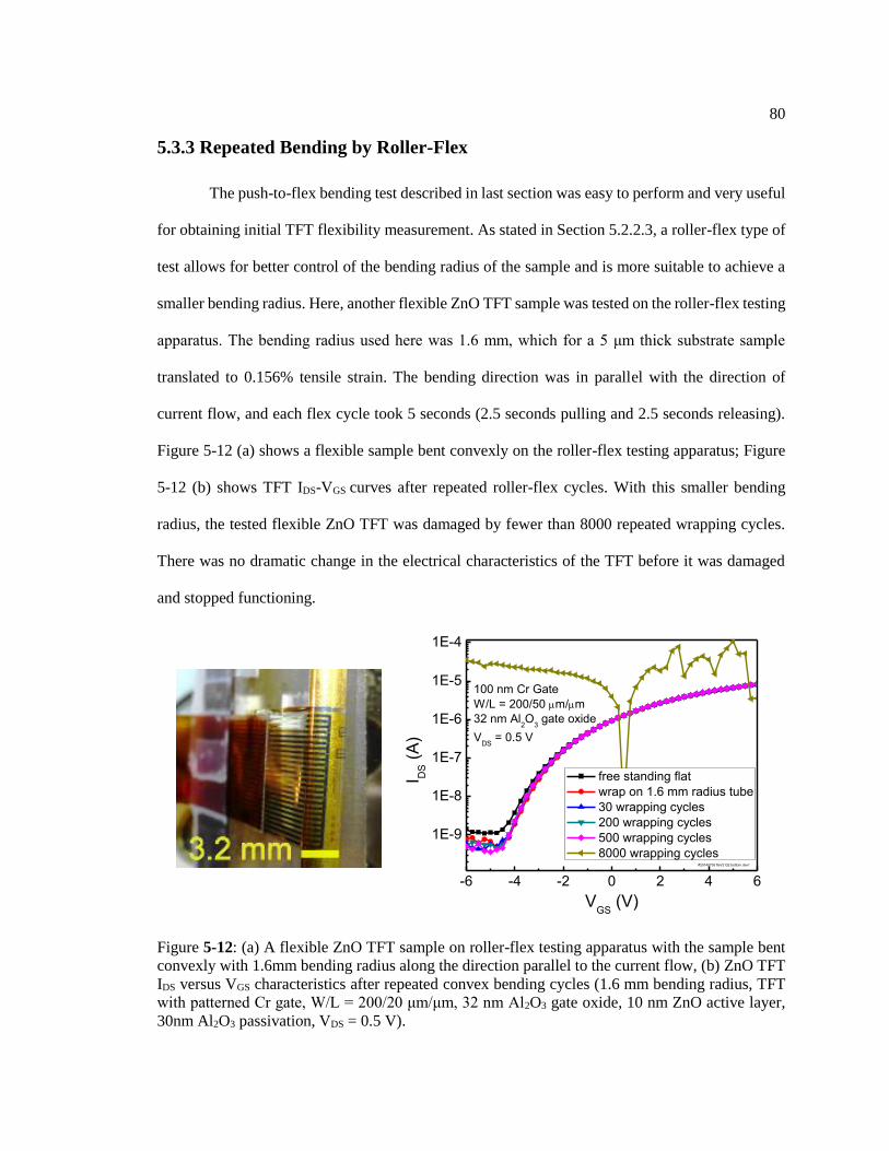
80
5.3.3 Repeated Bending by Roller-Flex
The push-to-flex bending test described in last section was easy to perform and very useful
for obtaining initial TFT flexibility measurement. As stated in Section 5.2.2.3, a roller-flex type of
test allows for better control of the bending radius of the sample and is more suitable to achieve a
smaller bending radius. Here, another flexible ZnO TFT sample was tested on the roller-flex testing
apparatus. The bending radius used here was 1.6 mm, which for a 5 μm thick substrate sample
translated to 0.156% tensile strain. The bending direction was in parallel with the direction of
current flow, and each flex cycle took 5 seconds (2.5 seconds pulling and 2.5 seconds releasing).
Figure 5-12 (a) shows a flexible sample bent convexly on the roller-flex testing apparatus; Figure
5-12 (b) shows TFT IDS-VGS curves after repeated roller-flex cycles. With this smaller bending
radius, the tested flexible ZnO TFT was damaged by fewer than 8000 repeated wrapping cycles.
There was no dramatic change in the electrical characteristics of the TFT before it was damaged
and stopped functioning.
-6 -4 -2 0 2 4 6
1E-9
1E-8
1E-7
1E-6
1E-5
1E-4
I DS (
A)
VGS
(V)
free standing flat
wrap on 1.6 mm radius tube
30 wrapping cycles
200 wrapping cycles
500 wrapping cycles
8000 wrapping cycles
100 nm Cr Gate
W/L = 200/50 m/m
32 nm Al2O
3 gate oxide
VDS
= 0.5 V
#20140705 fleV2 Q2 bottom dev1
Figure 5-12: (a) A flexible ZnO TFT sample on roller-flex testing apparatus with the sample bent
convexly with 1.6mm bending radius along the direction parallel to the current flow, (b) ZnO TFT
IDS versus VGS characteristics after repeated convex bending cycles (1.6 mm bending radius, TFT
with patterned Cr gate, W/L = 200/20 μm/μm, 32 nm Al2O3 gate oxide, 10 nm ZnO active layer,
30nm Al2O3 passivation, VDS = 0.5 V).

81
5.3.5 Discussion and Improvement for Device Flexibility
The bending and flexibility tests described above showed decent flexibility of the ZnO
TFTs that we fabricated on thin solution-cast polyimide substrates. The bending radii used in the
bending tests were smaller than the radii at which other workers saw significant device damage.
For example, Eun et al. reported flexible ZnO TFTs prepared by transfer printing method [13]
where 188 μm thick PET was used as the substrate. They observed cracks generated in the SiO2
bridge and ITO electrode with a bending radius of 11 mm, and devices failed after being bent to
such a radius. Munzenrieder et al. reported flexible double gate a-IGZO TFTs fabricated on 50 μm
freestanding Kapton E substrate [9], and those TFTs failed with a 3.5 mm bending radius. For our
thin-substrate flexible ZnO TFTs, even with the smallest bending radius tested, 1.6 mm, the devices
survived at least a few hundred flex-flattening cycles. The main reason for the superior flexibility
of our flexible TFTs was attributed to the very thin substrate. For 4.8 μm substrates and the bending
radii we used in the tests, the strains that the device layers experienced were much less than 0.2%,
and the devices can easily survive such strains. However, some of the TFTs showed an increase in
the off current and/or negative threshold voltage shift (200 mV to 2 V) after repeated flex cycles.
The increase of TFT off current could be because of minor damage to the dielectric layers. The
mechanism for the negative threshold shift is unclear at this point in time.
To better study the effects of repeated bending on the flexible TFTs, the flexed samples
were inspected under the microscope. For the push-to-flex tested samples (with 3.5 mm the smallest
bending radius), no clear change could be observed under optical microscope; for the samples
flexed on the roller-flex setup with a smaller bending radius of 1.6 mm, a considerable number of
cracks were generated after testing. Figure 5-13 shows an optical micrograph of a flexible ZnO
TFT with cracks on it after being bent to a 1.6 mm radius for 15,000 cycles. However, we found
that the generation of cracks on the TFTs during the flex testing did not correlate well with the
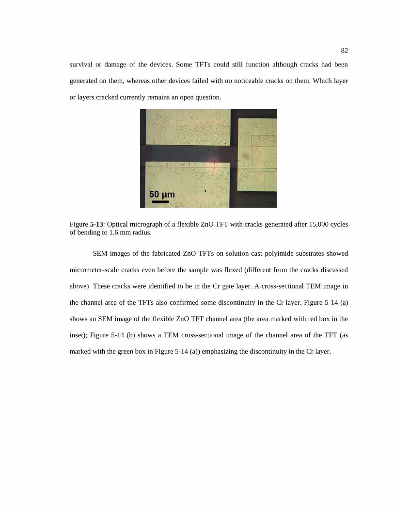
82
survival or damage of the devices. Some TFTs could still function although cracks had been
generated on them, whereas other devices failed with no noticeable cracks on them. Which layer
or layers cracked currently remains an open question.
Figure 5-13: Optical micrograph of a flexible ZnO TFT with cracks generated after 15,000 cycles
of bending to 1.6 mm radius.
SEM images of the fabricated ZnO TFTs on solution-cast polyimide substrates showed
micrometer-scale cracks even before the sample was flexed (different from the cracks discussed
above). These cracks were identified to be in the Cr gate layer. A cross-sectional TEM image in
the channel area of the TFTs also confirmed some discontinuity in the Cr layer. Figure 5-14 (a)
shows an SEM image of the flexible ZnO TFT channel area (the area marked with red box in the
inset); Figure 5-14 (b) shows a TEM cross-sectional image of the channel area of the TFT (as
marked with the green box in Figure 5-14 (a)) emphasizing the discontinuity in the Cr layer.
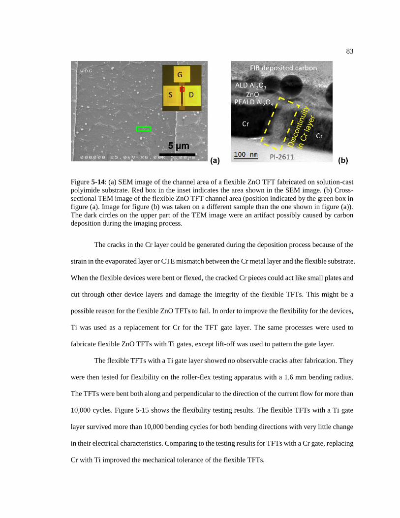
83
Figure 5-14: (a) SEM image of the channel area of a flexible ZnO TFT fabricated on solution-cast
polyimide substrate. Red box in the inset indicates the area shown in the SEM image. (b) Cross-
sectional TEM image of the flexible ZnO TFT channel area (position indicated by the green box in
figure (a). Image for figure (b) was taken on a different sample than the one shown in figure (a)).
The dark circles on the upper part of the TEM image were an artifact possibly caused by carbon
deposition during the imaging process.
The cracks in the Cr layer could be generated during the deposition process because of the
strain in the evaporated layer or CTE mismatch between the Cr metal layer and the flexible substrate.
When the flexible devices were bent or flexed, the cracked Cr pieces could act like small plates and
cut through other device layers and damage the integrity of the flexible TFTs. This might be a
possible reason for the flexible ZnO TFTs to fail. In order to improve the flexibility for the devices,
Ti was used as a replacement for Cr for the TFT gate layer. The same processes were used to
fabricate flexible ZnO TFTs with Ti gates, except lift-off was used to pattern the gate layer.
The flexible TFTs with a Ti gate layer showed no observable cracks after fabrication. They
were then tested for flexibility on the roller-flex testing apparatus with a 1.6 mm bending radius.
The TFTs were bent both along and perpendicular to the direction of the current flow for more than
10,000 cycles. Figure 5-15 shows the flexibility testing results. The flexible TFTs with a Ti gate
layer survived more than 10,000 bending cycles for both bending directions with very little change
in their electrical characteristics. Comparing to the testing results for TFTs with a Cr gate, replacing
Cr with Ti improved the mechanical tolerance of the flexible TFTs.

84
-8 -6 -4 -2 0 2 4 6
1E-11
1E-10
1E-9
1E-8
1E-7
1E-6
1E-5
1E-4100 nm Ti Gate
W/L = 200/50 m/m
32 nm Al2O
3 gate oxide
VDS
= 0.5 V
I DS (
A)
VGS
(V)
free standing
wrap on 1.6 mm tube
100 wrapping cycles
500 wrapping cycles
5,000 wrapping cycles
7,500 wrapping cycles
10,000 wrapping cycles
20140917 Ti gate FleV2 Q2 top device1
(a)
-8 -6 -4 -2 0 2 4 6
1E-11
1E-10
1E-9
1E-8
1E-7
1E-6
1E-5
1E-4
20140917 Ti gate fleV2 Q2 bottom dev9
100 nm Ti Gate
W/L = 200/5 m/m
32 nm Al2O
3 gate oxide
VDS
= 0.5 V
I DS (
A)
VGS
(V)
free standing
wrap on 1.6 mm tube
10 wrapping cycles
500 wrapping cycles
2500 wrapping cycles
7,500 wrapping cycles
12,500 wrapping cycles
(b)
Figure 5-15: IDS as a function of VGS for flexible ZnO TFTs with a Ti gate layer after repeated
bending cycles flexed by roller-flex testing apparatus with a 1.6 mm bending radius. (a) Bending
direction parallel to the current flow; (b) bending direction perpendicular to the current flow.
5.4 Numerical Simulation
5.4.1 Model Construction
The flexibility test experiments evaluated device flexibility and stability against
mechanical stresses. But they did not provide much information on the failure mechanism of the
flexible devices. In order to better study the failure mechanism from a theoretical standpoint,
numerical simulations were carried out for the strain and stress distribution in the layers of the
flexible TFTs. COMSOL Multiphysics 4.3 was used to simulate different stretching and bending
conditions for the electronic devices on thin flexible substrates. The structural mechanics module
with solid mechanics interface and stationary study type were used for the simulation. A 2-D model
was constructed for the simulation. The model replicated the cross-section of the channel area of
the flexible ZnO TFTs on thin flexible substrate. Figure 5-16 shows the schematic diagram of the
model and the 2-D model constructed in COMSOL Multiphysics.

85
Figure 5-16: (a) schematic diagram of the TFT cross-section model for COMSOL Multiphysics
simulation (not drawn to scale), (b) 2-D model for ZnO TFT on flexible substrate constructed in
COMSOL Structural Mechanics module (aspect ratio changed to better show layer structure)
A 5 μm polyimide layer was used as the substrate; a 100 nm Cr gate layer, 30 nm Al2O3
dielectric layer, 10 nm ZnO layer, 120 nm Al contact layer, and 30 nm Al2O3 passivation layer were
stacked on top of the substrate to form the TFT structure. The channel length of the simulated model
was 20 µm. Model dimension-related parameters are summarized in Table 5-2. Key parameters of
the materials used in the simulation are listed in Table 5-3.

86
Table 5-2. Model dimension-related parameter definitions
Name Value Description PI_length 220 [μm] Total TFT width
PI_thick 5 [μm] Polyimide substrate thickness
Metal1_length 50 [μm] Gate metal width
Metal1_thick 100 [nm] Gate metal thickness
Al2O3_thick 30 [nm] Al2O3 gate oxide layer thickness
ZnO_thick 10 [nm] ZnO channel layer thickness
Topmetal_thick 120 [nm] Source and drain metal contact thickness
Topmetal_length 100 [um] Source and drain contact pad width
sidePI_length 100 [um] Length of polyimide substrate outside the device area
(exceeding source and drain contact) on each side
Pass_thick 30 [nm] Al2O3 passivation layer thickness
Table 5-3. Key parameters of the materials used in COMSOL structural mechanics simulation
Density (g/cm3)
Young’s modulus
(GPa) Poisson’s ratio
Polyimide (substrate) 1.4 8.5 0.34
Cr (gate) 7.15 279 0.21
Al2O3 (gate & passivation) 3.96 400 0.22
ZnO (semiconductor channel) 5.676 210 0.33
Al (S & D contact) 2.7 70 0.35
Coarse meshes were used in the relatively thick polyimide substrate layer to reduce
calculation complicity, and finer meshes were used in the device channel area, especially in the
ZnO and Al2O3 layers. Using such a meshing strategy, the total number of elements for the model
was about 180k, and typical calculation time for one condition ranged from a few minutes to less
than an hour, depending on the situation.
5.4.2 Strain by Lateral Displacement
The simplest and most direct way to apply a certain strain to a thin film stack structure is
to elongate (stretch) the original structure by the desired percentage. Simulations that mimic this
condition were carried out using the above-described model with the modifications and boundary
conditions listed below:

87
1. To better represent the strain in the device area and to reduce computation complexity, the
sidePI_length parameter (the length of the part of the polyimide film that was extended beyond
the edge of the source and drain contact on either side of the TFT) was set to 1 μm.
2. “Fixed constraint” boundary condition was assigned to the left edges of the polyimide substrate
and Al2O3 layers (including both gate dielectric and passivation layers).
3. “Prescribed displacement” boundary condition with the lateral displacement of 𝑠𝑡𝑟𝑎𝑖𝑛 ×
(𝑃𝐼_𝑙𝑒𝑛𝑔𝑡ℎ + 2 × 𝑠𝑖𝑑𝑒𝑃𝐼_𝑙𝑒𝑛𝑔𝑡ℎ) in the + x direction was assigned to the right edge of the
simulated structure. The simulated strains here were 0.071% and 0.156%, which corresponded
to a 3.5 mm and 1.6 mm bending radius for 5 μm thick samples as experimentally tested and
described in Section 5.3.2 and 5.3.3 according to Equation 5-1.
4. “Roller” boundary condition was assigned to the bottom edge of the polyimide substrate so that
it could move freely in the lateral (x) direction but was restrained in the vertical (y) direction.
Figure 5-17 shows the von Mises stress in the simulated flexible TFT model due to 0.156%
tensile direct displacement. The von Mises stress in the polyimide substrate layer was
approximately a few MPa, which was more than 100 times smaller than the ultimate strength of the
PI-2611 film (350 MPa) used as our flexible substrate [69]. Therefore, we will focus the discussion
on the device stack layers in which the stresses were closer to the ultimate strengths of the materials.
Apparently from Figure 5-17, the stress was different in different layers of the materials and was a
function of position even in the same layer of a material. It can be also seen in Figure 5-17 that the
parts of the Al2O3 layer that were not overlapping with the gate metal had the largest stress (reddish
colored area in Figure 5-17). However, these areas were outside the active device channel area and
to the first order did not have a big impact on the function of the transistors. So we will not focus
our attention on these areas.

88
Figure 5-17: Simulated von Mises stress in the flexible ZnO TFT model due to 0.156% tensile
direct displacement at the right edge. Inset shows enlarged area in the dashed-line box. (Aspect
ratio not reserved.)
To better illustrate the stress distribution in the “important” layers (the device stack), a cut
line parallel to the y-axis (x-cut) through the middle of the source and drain to gate overlap area at
the right-side contact (shown as cut A-A’ in Figure 5-17) and another cut line parallel to the x-axis
(y-cut) through the middle of the gate oxide layer (shown as cut B-B’ in Figure 5-17) were drawn.
The von Mises stresses along these two cut lines with 0.071% and 0.156% tensile stresses are
plotted in Figure 5-18 (a) and 5-18 (b).

89
0.000 0.005 0.010 0.015 0.0200
100
200
300
400
500
600
Al Al
Al2O3
vo
n M
ises s
tress (
MP
a)
x-coordinate (m)
0.071%
0.156%
Simulated tensile strain
(b)
Figure 5-18: 1-D cuts of simulated von Mises stresses in the flexible ZnO TFT model due to 0.071%
and 0.156% tensile displacement at the right edge. (a) x-cut through the middle of the source and
drain to gate overlap area at the right-side contact (cut A-A’ in Figure 5-17). Inset shows enlarged
device area (part of the curves in the dashed-line box) stress distribution; (b) y-cut through the
middle of the gate oxide layer (cut B-B’ in Figure 5-17).
Figure 5-18 (a) confirms that the stress in the polyimide substrate layer was very small
compared to that in the device stack. Because of the difference in the materials’ Young’s modulus
and Poisson’s ratio, the layers in the device stack experienced different tensile stress under the same
strain. From Figure 5-18 (b), it is clear that the stress distribution within the Al2O3 layer was a
strong function of position and was affected greatly by what other layers it overlapped with. This
position-related stress distribution will be discussed in more detail in Section 5.4.4.
5.4.3 Strain by Bending Displacement
In order to better represent the flexibility tests the flexible ZnO TFTs went through
experimentally, simulations that mimic the bending of the flexible devices have been carried out.
The simulation for bending used the same model structure as the previously discussed simulation
for stretching (as shown in Figure 5-17). To apply a certain bending radius to the model, a
prescribed displacement was applied to the bottom of the polyimide substrate, which described an
arc with the desired bending radius. Figure 5-19 shows the curved model with a prescribed
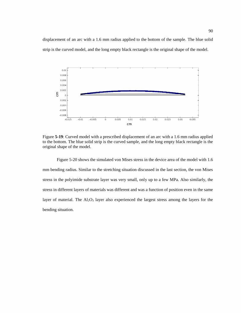
90
displacement of an arc with a 1.6 mm radius applied to the bottom of the sample. The blue solid
strip is the curved model, and the long empty black rectangle is the original shape of the model.
Figure 5-19: Curved model with a prescribed displacement of an arc with a 1.6 mm radius applied
to the bottom. The blue solid strip is the curved sample, and the long empty black rectangle is the
original shape of the model.
Figure 5-20 shows the simulated von Mises stress in the device area of the model with 1.6
mm bending radius. Similar to the stretching situation discussed in the last section, the von Mises
stress in the polyimide substrate layer was very small, only up to a few MPa. Also similarly, the
stress in different layers of materials was different and was a function of position even in the same
layer of material. The Al2O3 layer also experienced the largest stress among the layers for the
bending situation.

91
Figure 5-20: Simulated von Mises stress distribution in the TFT device area (aspect ratio not
reserved).
X-cut and y-cut lines, the same as those described in section 5.4.2 (also shown in Figure 5-
17 as A-A’ and B-B’), have also been drawn here to better illustrate the stress distribution for the
bending simulation. The von Mises stress along these cut lines with 3.5 mm and 1.6 mm bending
radii are plotted in Figure 5-21. Because the stress in the polyimide substrate layer was much
smaller than that in the device stack, Figure 5-21 (a) was plotted in a semi-log scale to better show
the stress in the substrate.
A difference between the bending situation and the stretching situation is that for bending,
the von Mises stress was a function of location in the y direction (parallel to the bending radius
direction), whereas for stretching, the von Mises stress was constant along the y direction within
the same material layer. In Figure 5-21 (a), the von Mises stress in the polyimide layer approaches
0 at ~4 μm. This position (or plane in the 2-D model) was actually the neutral plane position of the
structure where there was no stress while the structure was bent. Along the vertical direction, the
stress in a layer increases as the distance between the layer and the neutral plane increases.
Comparing Figure 5-21 (b) for bending to Figure 5-18 (a) for stretching, one can see the same trend

92
of stress distribution in different material layers. The Al2O3 layers experienced the largest stress,
and the Al contact experienced the smallest stress (not considering the substrate). Along the lateral
direction, a position-related stress distribution was also seen in the same layer of material, as shown
in Figure 5-21 (c).
0 1 2 3 4 50.1
1
10
100
Substrate
Simulated bending radius
vo
n M
ise
s s
tre
ss (
MP
a)
y-coordinate
1.6 mm
3.5 mm
(a)
de
vic
e a
rea
0 1 4.9 5.0 5.1 5.2 5.3
0
50
100
150
200
250
300
Al
ZnO
Al2O
3
Cr
Al2O
3
Simulated bending radius
vo
n M
ise
s s
tre
ss (
MP
a)
y-coordinate (m)
1.6 mm
3.5 mm
(b)
Polyimide
Figure 5-21: 1-D cuts of simulated von Mises stress in the flexible ZnO TFT model due to convex
bending of 1.6 mm and 3.5 mm radius. (a) X-cut through the middle of the source and drain to the
gate overlap area at the right-side contact (cut A-A’ in Figure 5-17), plotted in semi log scale. (b)
Enlarged part of the von Mises stress curves in the dashed-line box of (a), plotted in linear scale;
(c) y-cut through the middle of gate oxide layer (cut B-B’ in Figure 5-17). A laterally aligned
schematic of the model was overlaid on top of the stress curves.

93
5.4.4 Discussion
Comparing Figure 5-18 to Figure 5-15, it can be seen that the stress distribution in the
layers of the devices showed the same trend for both stretching and (convex) bending situations.
Comparing between the stretching situation and the bending situation, which presumably create the
same strain in the device layers, the device layers experience less stress in the bending situation
than in the stretching situation. Table 5-4 summarizes the tensile stress each layer experienced (at
the center of the source and drain to gate overlap area, or along the A-A’ cut in Figure 5-17) under
both stretching and bending situations, along with the ultimate strength of each material.
Table 5-4. Tensile stress and strength for each layer in the simulation
Layer
Stress at
0.071%
elongation
(MPa)
Stress under
3.5 mm radius
convex bending
Stress at
0.156%
elongation
(MPa)
Stress under
1.6
mm radius
convex
bending
Ultimate
strength
(MPa)
Polyimide 4.54 2.21-9.45 10.0 4.83-20.6 350 [69]
Gate (Cr) 142 72.5-78.1 312 158-170 83[109] -
282 [110]
Gate oxide
(Al2O3) 204 115-118 449 251-259
255[111] -
400 [112]
ZnO 111 64.5-64.9 244 141-142 412 [113]
Source and
drain
contact (Al)
37.4 22.1-24.4 82.4 48.2-53.2 90 [114]
Passivation
(Al2O3) 204 133-136 450 291-297
255[111] -
400 [112]
Comparing the numbers between column 2 and 3 and between column 4 and 5, bending
only caused ~ 60% of the tensile stress in the device layers compared to what was caused by
stretching to the same tensile strain (estimated using Equation 5-1). To better understand the
difference, x-cuts for x component of strain tensor are plotted in Figure 5-22 (a) and (b) for
stretching and bending situations (for the deformation situations simulated, most shape change was
along the lateral (x) direction, and the y component of the strain tensor was very small for both

94
stretching and bending cases and is thus not plotted here). Interestingly, the strain tensor x
component in the device stack for the bending situation was about 60% of that for the stretching
situation as well. These results show that although the estimation of strain-stress correlation given
by Equation 5-1 was simple and straightforward, it was not very precise. Even so, for any particular
layer of material, the amount of stress caused by some certain strain (actual strain in the layers) was
the same, regardless of the origin of the strain (stretching or bending), and the stress to strain ratios
match the Young’s modulus of the particular material the layer is made of, as expected.
0 1 2 3 4 5
0.04
0.08
0.12
Str
ain
ten
so
r x c
om
po
nen
t (%
)
y-coordinate (m)
0.071%
0.156%
Simulated tensile strain
devic
e a
rea
(a)
0 1 2 3 4 5
-0.25
-0.20
-0.15
-0.10
-0.05
0.00
0.05
0.10
Simulated bending radius
Str
ain
ten
so
r x c
om
po
nen
t (%
)
y-coordinate (m)
3.5 mm
1.6 mm devic
e a
rea
(b)
Figure 5-22: 1-D x cuts (through the middle of the source and drain to gate overlap area at the right-
side contact (cut A-A’ in Figure 5-17) of the simulated strain tensor x component in the flexible
ZnO TFT model due to tensile stress from (a) stretching and (b) bending situations. The device
areas are marked with dash-line boxes in both plots; the rest of the curves represent the substrate
area.
If we compare the numbers in the last two columns of Table 5-3, under 1.6 mm radius
convex bending, the simulated tensile stresses in the Cr gate and Al2O3 dielectric layers were
approaching or larger than the ultimate strength of the corresponding materials. Recall the repeated-
bending test described in Section 5.4.3, in which the flexible TFTs survived at least 500 cycles of
repeated bending to 1.6 mm radius. Such results suggest that the flexible device will not necessarily
be damaged electrically by experiencing stress close to or even above the ultimate strength of the

95
corresponding material. However, fatigue effect exists. Flexible devices can be damaged by
exposure to repeated stress; the larger the stress, the more profound the fatigue effect may be.
Both Figure 5-18 (b) and Figure 5-21 (c) showed a position-related stress distribution
within the same material layer. The stress in a particular layer was a strong function of the lateral
position and the layers it overlaps with. For the gate oxide Al2O3 layer, the portion within the
channel area experienced larger stress than the portion that was sandwiched in between the gate
electrode and the contact pads. Additionally, the stress in the Al2O3 layers peaked at the vertical
walls, which suggests these areas are the most likely places for the layers to fail because of
mechanical stresses.
5.5 Summary
In this chapter, testing strategies for flexible electronics have been discussed and developed.
A few different kinds of flexibility testing apparatus with the capability of in-situ electrical
measurement have been constructed and used for testing. Flexible ZnO TFTs fabricated on ~5 μm
thick solution-cast polyimide film have been tested under conditions of static bending, repeated
free bending, and repeated bending over a roller with sub-millimeter radius. The flexible ZnO TFTs
survived more than 50,000 cycles of repeated bending with a 3.5 mm radius and more than 10,000
cycles with a 1.6 mm radius. These results showed superior tolerance to mechanical manipulation
for our flexible ZnO TFTs.
Numerical simulations have been performed using COMSOL Multiphysics. Strain and
stress for the flexible devices under different bending and stretching situations were simulated and
discussed. The simulation results hopefully provided some guidance on the device failure
mechanisms and ways to improve device flexibility.

96
Chapter 6
Summary and Future Work
6.1 Summary
This dissertation has described progress in several aspects of flexible electronics including
active flexible electronic devices and circuits, functional thin film materials, and devices for
flexible applications, as well as studies towards mechanical flexibility of flexible electronic
devices. Design considerations from the application, substrate, and fabrication standpoints were
first discussed. A lamination- and transfer-free process was developed to fabricate ZnO TFTs on
solution-cast thin polyimide substrate. The process uses rigid-substrate-compatible fabrication
techniques and instruments to fabricate high-performance oxide semiconductor thin film transistors
on very thin (< 5 μm) flexible substrates. The fabricated flexible ZnO TFTs were characterized and
compared with ZnO TFTs fabricated on rigid glass substrate. The TFTs on both substrates show
very similar characteristics with mobility greater than 12 cm2/V∙s at VGS = 8 V and current on/off
ratio greater than 108. The yield of ZnO TFTs on thin polyimide substrate is greater than 99%. Ring
oscillators consisting of more than 100 transistors have been demonstrated with 60 ns/stage delay.
In order to incorporate more functions into the flexible electronic system, vanadium oxide
thin films for temperature sensing and flexible OLED devices have been studied. Effort has been
made in evaluating the feasibility of using reactive RF diode sputtering to deposit bolometer-grade
vanadium oxide films as an alternative to the currently widely used but expensive ion-beam
deposition technique. RF diode sputtering has been proved to be able to produce bolometer-grade
VOX thin films, but process control was very difficult. Attempts have been made to find control
mechanisms for RF diode sputtering of VOX films. In-situ oxygen partial pressure monitoring near
the sputtering area showed promising potential as a useful control signal. A strategy to deposit VOX

97
films for microbolometer applications by RF reactive sputtering using real-time oxygen partial
pressure readings as a control signal has been proposed. Additionally, flexible OLEDs on thin
polyimide substrates have been demonstrated. The flexible OLEDs can be readily integrated with
the flexible TFTs and form more complicated flexible electronic systems.
A passive component – a parylene encapsulation layer for electronic systems – has also
been studied with an emphasis on its differential growth according to the surface energies of
substrates. A direct patterning technique of parylene films using substrate surface energy as the
control mechanism has been developed.
Lastly, from the flexible electronic system point of view, device flexibility was discussed.
Strategies for three different types of flexibility tests – static bending, repeated bending by push-
to-flex, and repeated bending by roller-flex – have been developed. Special apparatuses have been
built for the push-to-flex and roller-flex tests. Our flexible ZnO TFTs survived more than 50,000
repeated bending cycles with the smallest bending radius of 3.5 mm. The modified TFTs with a Ti
gate layer survived more than 10,000 repeated bending cycles with the smallest bending radius of
1.6 mm. We have attributed such superior stability against mechanical bending to the very thin
substrates that we used. In order to better understand the failure mechanism of the flexible devices,
numerical simulations of strain and stress distributions under different stretching and bending
situations have been carried out using COMSOL Multiphysics. The simulation results provided
useful information and created foundation for further study of failure mechanisms and
improvement of device flexibility.
6.2 Future work
The first area of future work is a more thorough investigation of the ZnO TFTs fabricated
on thin flexible polyimide substrate. Major device characteristics have been discussed in Chapter

98
2 of this dissertation, but it would be beneficial to further characterize these TFTs. Polyimide
substrate is different from glass substrate in various ways: hardness, flatness, water and oxygen
permeability, thermal conductivity, coefficient of thermal expansion, and so forth. It can be very
helpful and even essential to understand device characteristics on such flexible substrates before
more complicated circuits and systems can be built using these TFTs as building blocks. Once a
better understanding of the single devices is achieved, the next logical steps can be to build more
complicated functional blocks, such as simple analog and/or digital circuits. Complimentary MOS
circuits using ZnO TFTs and organic TFTs as NMOS and PMOS respectively can be designed and
built on thin flexible substrates as well.
Another very important issue that needs to be addressed for the described flexible TFTs is
the currently not-well-optimized releasing process. The current mechanical peeling process can put
a large stress on devices when releasing them from the rigid carrier, and it can harm the yield. A
gentler releasing process is desired for flexible TFTs. Using a sacrificial layer between the rigid
carrier and the polyimide substrate can be a promising route to pursue. ZnO can be etched in diluted
acid; VOX can be etched in diluted H2O2; Au can be etched in an aqueous solution of potassium
iodide/iodine. These materials can be potential candidates for the releasing layer.
The second area of future work is to integrate the proposed functional components into
actual flexible systems. Some more work is needed to actually implement the control mechanism
proposed in Chapter 3 to deposit VOX thin films for bolometer applications. The time delay between
changes in process parameters and the response of the sputtering ambient needs to be investigated
in order to find an optimized delay time for oxygen input adjustment according to the real-time
oxygen partial pressure monitoring. Integrating the flexible OLEDs and ZnO TFTs is another very
interesting area for further development. Flexible light indicators and optogenetics actuators can be
potential applications for the integrated active OLED systems.
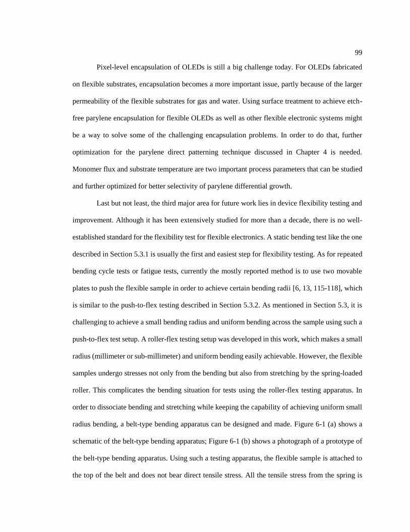
99
Pixel-level encapsulation of OLEDs is still a big challenge today. For OLEDs fabricated
on flexible substrates, encapsulation becomes a more important issue, partly because of the larger
permeability of the flexible substrates for gas and water. Using surface treatment to achieve etch-
free parylene encapsulation for flexible OLEDs as well as other flexible electronic systems might
be a way to solve some of the challenging encapsulation problems. In order to do that, further
optimization for the parylene direct patterning technique discussed in Chapter 4 is needed.
Monomer flux and substrate temperature are two important process parameters that can be studied
and further optimized for better selectivity of parylene differential growth.
Last but not least, the third major area for future work lies in device flexibility testing and
improvement. Although it has been extensively studied for more than a decade, there is no well-
established standard for the flexibility test for flexible electronics. A static bending test like the one
described in Section 5.3.1 is usually the first and easiest step for flexibility testing. As for repeated
bending cycle tests or fatigue tests, currently the mostly reported method is to use two movable
plates to push the flexible sample in order to achieve certain bending radii [6, 13, 115-118], which
is similar to the push-to-flex testing described in Section 5.3.2. As mentioned in Section 5.3, it is
challenging to achieve a small bending radius and uniform bending across the sample using such a
push-to-flex test setup. A roller-flex testing setup was developed in this work, which makes a small
radius (millimeter or sub-millimeter) and uniform bending easily achievable. However, the flexible
samples undergo stresses not only from the bending but also from stretching by the spring-loaded
roller. This complicates the bending situation for tests using the roller-flex testing apparatus. In
order to dissociate bending and stretching while keeping the capability of achieving uniform small
radius bending, a belt-type bending apparatus can be designed and made. Figure 6-1 (a) shows a
schematic of the belt-type bending apparatus; Figure 6-1 (b) shows a photograph of a prototype of
the belt-type bending apparatus. Using such a testing apparatus, the flexible sample is attached to
the top of the belt and does not bear direct tensile stress. All the tensile stress from the spring is
100
taken by the belt. To follow up, flexible TFTs and other flexible devices can be tested on this setup,
and the testing results from all the different testing methods should be compared to get a better
understanding about device mechanical flexibility and failure mechanisms.
Figure 6-1: (a) Schematic of a belt-type bending apparatus for flexible electronic samples; (b)
photograph of a prototype of the belt-type bending apparatus using a pneumatic rotary actuator and
a Kapton film belt.
The goal to design various flexibility testing strategies and apparatuses and understand the
device performances under different mechanical stresses is to eventually help improve the
mechanical flexibility for the devices. Based on the current experimental and simulation results, a

101
few ways to improve device flexibility can be pursued. Putting devices on the neutral plane has
been reported to increase the tolerance of flexible devices against mechanical deformation [24, 116,
119]. A simple COMSOL simulation showed that by adding a layer of polyimide with the same
thickness as the substrate on top of the fabricated flexible devices, the stress in the device layers
caused by bending could be dramatically reduced. Figure 6-2 shows the simulated von Mises stress
in a flexible ZnO TFT on 5 μm polyimide substrate from 1.6 mm radius bending. Figure 6-2 (a)
shows the flexible TFT with the regular structure; Figure 6-2 (b) shows the flexible TFT with an
extra layer of 5 μm polyimide on top. In the configuration shown by Figure 6-2 (b), the TFT was
roughly positioned at the neutral plane of the bending structure, and the stress in the TFT layers
was dramatically reduced as a result. Therefore, spin coating a top polyimide layer on the fabricated
flexible TFT sample can be a way to effectively reduce the bending stress in the device layers.
Follow-up experimental work needs to be carried out to confirm this. Besides coating a full layer
of polyimide on top of the flexible sample, small rigid islands can be selectively put on top of
device areas to locally modify the mechanical properties for better bending protection. Both
simulation and experimental work should be performed to study the effect of rigid islands and to
optimize the material, structure, and process for the islands to achieve better device flexibility.

102
Figure 6-2: Simulated von Mises stress in flexible TFT because of bending to a 1.6 mm radius. (a)
ZnO TFT on 5 μm thick polyimide substrate. (b) ZnO TFT on 5 μm thick polyimide substrate with
5 μm thick polyimide layer on top. The color legends for (a) and (b) are the same.
In conclusion, thin solution-cast substrate readily provides thin, smooth polymeric
substrates for flexible electronic applications and has been demonstrated as a simple yet promising
pathway for flexible electronics. Viewing flexible electronics as a system, there are a variety of
directions in which this work may continue forward, including efforts both toward understanding
and optimizing individual elements and toward system integration for different functionalities.
103
References
[1] Flexible Electronics: Materials and Applications: Springer, 2009.
[2] M. J. Deen, "Flexible Electronics - Opportunities and Challenges," in Electron Devices and
Solid-State Circuits (EDSSC), 2013 IEEE International Conference of, 2013, pp. 1-2.
[3] A. Nathan, A. Ahnood, M. T. Cole, S. Lee, Y. Suzuki, P. Hiralal, et al., "Flexible
Electronics: The Next Ubiquitous Platform," Proceedings of the IEEE, vol. 100, pp. 1486-
1517, May 2012.
[4] K. Ashton. (2009). That "Internet of Things" Thing.
Available: http://www.rfidjournal.com/articles/view?4986
[5] A. Manekkathodi, M. Y. Lu, C. W. Wang, and L. J. Chen, "Direct Growth of Aligned Zinc
Oxide Nanorods on Paper Substrates for Low-Cost Flexible Electronics," Advanced
Materials, vol. 22, pp. 4059-4063, Nov 2010.
[6] A. Russo, B. Y. Ahn, J. J. Adams, E. B. Duoss, J. T. Bernhard, and J. A. Lewis, "Pen-on-
Paper Flexible Electronics," Advanced Materials, vol. 23, pp. 3426-3430, Aug 2011.
[7] D. Y. Ji, L. Jiang, X. Z. Cai, H. L. Dong, Q. Meng, G. F. Tian, et al., "Large Scale, Flexible
Organic Transistor Arrays and Circuits Based On Polyimide Materials," Organic
Electronics, vol. 14, pp. 2528-2533, Oct 2013.
[8] D. A. Mourey, D. A. Zhao, and T. N. Jackson, "ZnO Thin Film Transistors and Circuits on
Glass and Polyimide by Low-Temperature PEALD," in IEEE Electron Device Meeting,
Dec. 2009.
[9] N. Munzenrieder, C. Zysset, L. Petti, T. Kinkeldei, G. A. Salvatore, and G. Troster,
"Flexible Double Gate a-IGZO TFT Fabricated on Free Standing Polyimide Foil," Solid-
State Electronics, vol. 84, pp. 198-204, Jun 2013.
[10] S. Y. Xiao, L. F. Che, X. X. Li, and Y. L. Wang, "A Novel Fabrication Process of MEMS
Devices on Polyimide Flexible Substrates," Microelectronic Engineering, vol. 85, pp. 452-
457, Feb 2008.
[11] S. Gowrisanker, M. A. Quevedo-Lopez, H. N. Alshareef, B. E. Gnade, S. Venugopal, R.
Krishna, et al., "A Novel Low Temperature Integration of Hybrid CMOS Devices on
Flexible Substrates," Organic Electronics, vol. 10, pp. 1217-1222, Nov 2009.
[12] H. P. Jen, M. H. Lin, L. L. Li, H. P. Wu, W. K. Huang, P. J. Cheng, et al., "High-
Performance Large-Scale Flexible Dye-Sensitized Solar Cells Based on Anodic TiO2
Nanotube Arrays," ACS Applied Materials & Interfaces, vol. 5, pp. 10098-10104, Oct
2013.
[13] K. T. Eun, W. J. Hwang, B. K. Sharma, J. H. Ahn, Y. K. Lee, and S. H. Choa, "Mechanica
Flexibility of Znic Oxide Thin-Film Transistors Prepared by Transfer Printing Method,"
Modern Physics Letters B, vol. 26, p. 10, May 2012.
[14] J. A. Jeong, H. S. Shin, K. H. Choi, and H. K. Kim, "Flexible Al-doped ZnO Films Grown
on PET Substrates Using Linear Facing Target Sputtering for Flexible OLEDs," Journal
of Physics D-Applied Physics, vol. 43, p. 6, Nov 2010.
[15] H. B. Zhao, H. L. Tu, F. Wei, Z. T. Shi, Y. H. Xiong, Y. Zhang, et al., "High Mechanical
Endurance RRAM Based On Amorphous Aadolinium Oxide for Flexible Nonvolatile
Memory Application," Journal of Physics D-Applied Physics, vol. 48, p. 7, May 2015.
[16] L. S. Zhou, A. Wanga, S. C. Wu, J. Sun, S. Y. Park, S. Nelson, et al., "All-Organic Active
Matrix OLED Flexible Display," in Conference on Defense, Security, Cockpit, and Future
Displays II, Kissimmee, FL, 2006, pp. E2250-E2250.
104
[17] J. C. Yang, Y. C. Liao, and J. W. Shiu, "Fabrication Methods for Liquid Crystal Display
Devices," US Patent, 2009.
[18] C. Y. Hsieh, C. S. Chen, W. A. Tsou, Y. T. Yeh, K. A. Wen, and L. S. Fan, "A Flexible
Mixed-Signal/RF CMOS Technology for Implantable Electronics Applications," Journal
of Micromechanics and Microengineering, vol. 20, p. 8, Apr 2010.
[19] N. Munzenrieder, G. A. Salvatore, T. Kinkeldei, L. Petti, C. Zysset, L. Buthe, et al.,
"InGaZno TFTs on a Flexible Membrane Transferred to a Curved Surface with a Radius
of 2 mm," in Device Research Conference (DRC), 2013 71st Annual, 2013, pp. 165-166.
[20] D. P. Gosain, T. Noguchi, and S. Usui, "High Mobility Thin Film Transistors Fabricated
on a Plastic Substrate at a Processing Temperature of 110 Degrees C," Japanese Journal
of Applied Physics Part 2-Letters & Express Letters, vol. 39, pp. L179-L181, Mar 2000.
[21] S. I. Shin, J. H. Kwon, H. Kang, and B. K. Ju, "Solution-Processed 6,13-
bis(triisopropylsilylethynyl) (TIPS) Pentacene Thin-Film Transistors with a Polymer
Dielectric on a Flexible Substrate," Semiconductor Science and Technology, vol. 23, p. 4,
Aug 2008.
[22] S. H. Kim, J. Yoon, S. O. Yun, Y. Hwang, H. S. Jang, and H. C. Ko, "Ultrathin Sticker-
Type ZnO Thin Film Transistors Formed by Transfer Printing via Topological
Confinement of Water-Soluble Sacrificial Polymer in Dimple Structure," Advanced
Functional Materials, vol. 23, pp. 1375-1382, Mar 2013.
[23] K. Park, D. K. Lee, B. S. Kim, H. Jeon, N. E. Lee, D. Whang, et al., "Stretchable,
Transparent Zinc Oxide Thin Film Transistors," Advanced Functional Materials, vol. 20,
pp. 3577-3582, Oct 2010.
[24] D. H. Kim, J. H. Ahn, W. M. Choi, H. S. Kim, T. H. Kim, J. Z. Song, et al., "Stretchable
and Foldable Silicon Integrated Circuits," Science, vol. 320, pp. 507-511, Apr 2008.
[25] J. M. Kim, T. Nam, S. J. Lim, Y. G. Seol, N. E. Lee, D. Kim, et al., "Atomic Layer
Deposition ZnO:N Flexible Thin Film Transistors and the Effects of Bending on Device
Properties," Applied Physics Letters, vol. 98, p. 3, Apr 2011.
[26] D. L. Zhao, D. A. Mourey, and T. N. Jackson, "Fast Flexible Plastic Substrate ZnO
Circuits," IEEE Electron Device Letters, vol. 31, pp. 323-325, Apr 2010.
[27] Y. H. Qin, D. H. Turkenburg, I. Barbu, W. T. T. Smaal, K. Myny, W. Y. Lin, et al.,
"Organic Thin-Film Transistors with Anodized Gate Dielectric Patterned by Self-Aligned
Embossing on Flexible Substrates," Advanced Functional Materials, vol. 22, pp. 1209-
1214, Mar 2012.
[28] M. Ahmed and D. P. Butler, "Flexible Substrate and Release Layer for Flexible MEMS
Devices," Journal of Vacuum Science & Technology B, vol. 31, p. 4, Sep 2013.
[29] M. S. K. Mutyala, J. Z. Zhou, and X. C. Li, "Transferable and Flexible Thin Film Devices
for Engineering Applications," Journal of Micromechanics and Microengineering, vol. 24,
p. 8, May 2014.
[30] C. J. Robin, A. Vishnoi, and K. N. Jonnalagadda, "Mechanical Behavior and Anisotropy
of Spin-Coated SU-8 Thin Films for MEMS," Journal of Microelectromechanical Systems,
vol. 23, pp. 168-180, Feb 2014.
[31] C.-Y. Lin, C.-W. Chien, C.-H. Wu, H.-H. Hsieh, C.-C. Wu, Y. Yung-Hui, et al., "Oxide-
Semiconductor-Based TFTs for Displays and Flexible Electronics," in ECS Transactions,
2012, pp. 293-309.
[32] P. Q. Gao and Q. Zhang, "Encapsulate-and-Peel: Fabricating Carbon Nanotube CMOS
Integrated Circuits in a Flexible Ultra-Thin Plastic Film," Nanotechnology, vol. 25, p. 7,
Feb 2014.

105
[33] K. C. Ok, S. H. K. Park, C. S. Hwang, H. Kim, H. S. Shin, J. Bae, et al., "The Effects of
Buffer Layers on the Performance and Stability of Flexible InGaZnO Thin Film Transistors
on Polyimide Substrates," Applied Physics Letters, vol. 104, p. 4, Feb 2014.
[34] Holst Centre - R2R Printing and Photonic Sintering.
Available: https://www.youtube.com/watch?v=7SpZPIVtryM
[35] E. Fortunato, P. Barquinha, and R. Martins, "Oxide Semiconductor Thin-Film Transistors:
A Review of Recent Advances," Advanced Materials, vol. 24, pp. 2945-2986, Jun 2012.
[36] O. Heil, "Improvements in or Relating to electrical amplifiers and Other Control
Arrangements and Devices," UK Patent, 1935.
[37] J. E. Lilienfield, "Method and Apparatus for Controlling Electric Currents," USA Patent,
1930.
[38] F. Y. Chang, R. H. Wang, H. Yang, Y. H. Lin, T. M. Chen, and S. J. Huang, "Flexible
Strain Sensors Fabricated with Carbon Nano-Tube and Carbon Nano-Fiber Composite
Thin Films," Thin Solid Films, vol. 518, pp. 7343-7347, Oct 2010.
[39] M.-Y. Tsai, A. Tarasov, Z. Razavi Hesabi, H. Taghinejad, P. M. Campbell, C. Joiner, et
al., "Flexible MoS2 Field-Effect Transistors for Gate-Tunable Piezoresistive Strain
Sensors," ACS Applied Materials & Interfaces, 2015/05/26 2015.
[40] G. A. Salvatore, N. Munzenrieder, C. Barraud, L. Petti, C. Zysset, L. Buthe, et al.,
"Fabrication and Transfer of Flexible Few-Layers MoS2 Thin Film Transistors to Any
Arbitrary Substrate," Acs Nano, vol. 7, pp. 8809-8815, Oct 2013.
[41] J. K. Jeong, J. H. Jeong, H. W. Yang, J. S. Park, Y. G. Mo, and H. D. Kim, "High
Performance Thin Film Transistors with Cosputtered Amorphous Indium Gallium Zinc
Oxide Channel," Applied Physics Letters, vol. 91, p. 3, Sep 2007.
[42] M. Kim, J. H. Jeong, H. J. Lee, T. K. Ahn, H. S. Shin, J. S. Park, et al., "High Mobility
Bottom Gate InGaZnO Thin Film Transistors with SiOx Etch Stopper," Applied Physics
Letters, vol. 90, p. 3, May 2007.
[43] T. Kamiya, K. Nomura, and H. Hosono, "Present Status of Amorphous In-Ga-Zn-O Thin-
Film Transistors," Science and Technology of Advanced Materials, vol. 11, p. 23, Aug
2010.
[44] G. H. Kim, H. S. Kim, H. S. Shin, B. D. Ahn, K. H. Kim, and H. J. Kim, "Inkjet-Printed
InGaZnO Thin Film Transistor," Thin Solid Films, vol. 517, pp. 4007-4010, May 2009.
[45] K. Nomura, H. Ohta, A. Takagi, T. Kamiya, M. Hirano, and H. Hosono, "Room-
Temperature Fabrication of Transparent Flexible Thin-Film Transistors Using Amorphous
Oxide Semiconductors," Nature, vol. 432, pp. 488-492, Nov 2004.
[46] A. Sato, K. Abe, R. Hayashi, H. Kumomi, K. Nomura, T. Kamiya, et al., "Amorphous In-
Ga-Zn-O Coplanar Homojunction Thin-Film Transistor," Applied Physics Letters, vol. 94,
p. 3, Mar 2009.
[47] H. Yabuta, M. Sano, K. Abe, T. Aiba, T. Den, H. Kumomi, et al., "High-Mobility Thin-
Film Transistor with Amorphous InGaZnO4 Channel Fabricated by Room Temperature
RF-Magnetron Sputtering," Applied Physics Letters, vol. 89, p. 3, Sep 2006.
[48] D. Zhao, "Plasma-Enhanced Atomic Layer Deposition Zinc Oixde Flexible Thin Film
Electronics," 3442972 Ph.D., The Pennsylvania State University, Ann Arbor, 2010.
[49] D. C. Look, "Recent Advances in ZnO Materials and Devices," Materials Science and
Engineering B-Solid State Materials for Advanced Technology, vol. 80, pp. 383-387, Mar
2001.
[50] H. U. Li and T. N. Jackson, "Oxide Semiconductor Thin Film Transistors on Thin Solution-
Cast Flexible Substrates," IEEE Electron Device Letters, vol. 36, pp. 35-37, JAN 2015
2015.

106
[51] J. Lee and Y. S. Park, "Characteristics of Al-Doped ZnO Films Annealed at Various
Temperatures for InGaZnO-Based Thin-Film Transistors," Thin Solid Films, vol. 587, pp.
94-99, Jul 2015.
[52] D. Afouxenidis, R. Mazzocco, G. Vourlias, P. J. Livesley, A. Krier, W. I. Milne, et al.,
"ZnO-based Thin Film Transistors Employing Aluminum Titanate Gate Dielectrics
Deposited by Spray Pyrolysis at Ambient Air," Acs Applied Materials & Interfaces, vol. 7,
pp. 7334-7341, Apr 2015.
[53] C. G. Choi, S. J. Seo, and B. S. Bae, "Solution-Processed Indium-Zinc Oxide Transparent
Thin-Film Transistors," Electrochemical and Solid State Letters, vol. 11, pp. H7-H9, 2008.
[54] D. C. Paine, B. Yaglioglu, Z. Beiley, and S. Lee, "Amorphous IZO-Based Transparent Thin
Film Transistors," Thin Solid Films, vol. 516, pp. 5894-5898, Jul 2008.
[55] H. Ji, A. Y. Hwang, C. K. Lee, P. S. Yun, J. U. Bae, K. S. Park, et al., "Improvement in
Field-Effect Mobility of Indium Zinc Oxide Transistor by Titanium Metal Reaction
Method," IEEE Transactions on Electron Devices, vol. 62, pp. 1195-1199, Apr 2015.
[56] K. Ebata, S. Tomai, Y. Tsuruma, T. Iitsuka, S. Matsuzaki, and K. Yano, "High-Mobility
Thin-Film Transistors with Polycrystalline In-Ga-O Channel Fabricated by DC Magnetron
Sputtering," Applied Physics Express, vol. 5, p. 3, Jan 2012.
[57] G. Goncalves, P. Barquinha, L. Pereira, N. Franco, E. Alves, R. Martins, et al., "High
Mobility a-IGO Films Produced at Room Temperature and Their Application in TFTs,"
Electrochemical and Solid State Letters, vol. 13, pp. II20-II22, 2010.
[58] H. U. Li and T. N. Jackson, "Oxide Semiconductor Thin Film Transistors on Thin Solution-
Cast Flexible Substrates," Electron Device Letters, IEEE, vol. 36, pp. 35-37, 2015.
[59] D. A. Mourey, D. A. Zhao, J. Sun, and T. N. Jackson, "Fast PEALD ZnO Thin-Film
Transistor Circuits," IEEE Transactions on Electron Devices, vol. 57, pp. 530-534, Feb
2010.
[60] Y. V. Li, K. G. Sun, J. I. Ramirez and T. N. Jackson, "Tri-layer PEALD ZnO Thin Film
Transistors and Circuits," in 71st Device Research Conference (DRC), Notre Dame, IN,
2013, pp. 167-168.
[61] J. Zhang, H. Yang, Q. L. Zhang, S. R. Dong, and J. K. Luo, "Bipolar Resistive Switching
Characteristics of Low Temperature Grown ZnO Thin Films by Plasma-Enhanced Atomic
Layer Deposition," Applied Physics Letters, vol. 102, p. 4, Jan 2013.
[62] R. S. Ajimsha, A. K. Das, P. Misra, M. P. Joshi, L. M. Kukreja, R. Kumar, et al.,
"Observation of Low Resistivity And High Mobility in Ga Doped ZnO Thin Films Grown
by Buffer Assisted Pulsed Laser Deposition," Journal of Alloys and Compounds, vol. 638,
pp. 55-58, Jul 2015.
[63] S. Saini, P. Mele, H. Honda, K. Matsumoto, K. Miyazaki, L. M. Luna, et al., "Influence of
Postdeposition Cooling Atmosphere on Thermoelectric Properties of 2% Al-Doped ZnO
Thin Films Grown by Pulsed Laser Deposition," Journal of Electronic Materials, vol. 44,
pp. 1547-1553, Jun 2015.
[64] E. M. Kaidashev, M. Lorenz, H. von Wenckstern, A. Rahm, H. C. Semmelhack, K. H. Han,
et al., "High Electron Mobility of Epitaxial ZnO Thin Films on c-Plane Sapphire Grown
by Multistep Pulsed-Laser Deposition," Applied Physics Letters, vol. 82, pp. 3901-3903,
Jun 2003.
[65] B. Bayraktaroglu, K. Leedy, and R. Neidhard, "High-Frequency ZnO Thin-Film
Transistors on Si Substrates," IEEE Electron Device Letters, vol. 30, pp. 946-948, Sep
2009.
[66] K. Everaerts, L. Zeng, J. W. Hennek, D. I. Camacho, D. Jariwala, M. J. Bedzyk, et al.,
"Printed Indium Gallium Zinc Oxide Transistors. Self-Assembled Nanodielectric Effects

107
on Low-Temperature Combustion Growth and Carrier Mobility," Acs Applied Materials
& Interfaces, vol. 5, pp. 11884-11893, Nov 2013.
[67] Y. Wang, X. W. Sun, S. W. Liu, A. K. K. Kyaw, and J. L. Zhao, "Oxide Thin Film
Transistors with Ink-Jet Printed In-Ga-Zn Oxide Channel Layer and ITO/IZO
Source/Drain Contacts," in Proceedings of the 2013 IEEE 5th International
Nanoelectronics Conference, New York, 2013, pp. 168-171.
[68] Y. Hou and A. H. Jayatissa, "Low resistive gallium doped nanocrystalline zinc oxide for
Gas Sensor Application via Sol-Gel Process," Sensors and Actuators B-Chemical, vol. 204,
pp. 310-318, Dec 2014.
[69] H. MicroSystems. PI-2600_ProcessGuide. Available:
http://hdmicrosystems.com/HDMicroSystems/en_US/pdf/PI-2600_ProcessGuide.pdf
[70] D. Suryanarayana and K. L. Mittal, "Effect of Polyimide Thickness on Its Adhesion to
Silicon-Nitride Substrate with and without Adhesion Promoter," Journal of Applied
Polymer Science, vol. 30, pp. 3107-3111, 1985.
[71] H. Jerominek, F. Picard, and D. Vincent, "Vanadium-Oxide Films for Optical Switching
and Detection," Optical Engineering, vol. 32, pp. 2092-2099, Sep 1993.
[72] R. J. Herring and P. E. Howard, "Design and Performance of the ULTRA 320x240
Uncooled Focal Plane Array And Sensor," in Infrared Detectors and Focal Plane Arrays
IV Conference, Orlando, FL, 1996, pp. 2-12.
[73] R. A. Wood, "Uncooled Infrared Imaging Arrays and Systems," in Semiconductors and
Semimetals. vol. 47, P. W. Kruse and D. D. Skatrud, Eds., ed: Academic Press, 1997, p.
45.
[74] N. J. Podraza, B. D. Gauntt, M. A. Motyka, E. C. Dickey, and M. W. Horn, "Electrical and
Optical Properties of Sputtered Amorphous Vanadium Oxide Thin Films," Journal of
Applied Physics, vol. 111, p. 9, Apr 2012.
[75] O. M. Cabarcos, J. Li, B. D. Gauntt, S. Antrazi, E. C. Dickey, D. L. Allara, et al.,
"Comparison of Ion Beam and Magnetron Sputtered Vanadium Oxide Thin Films for
Uncooled IR Imaging," in Conference on Infrared Technology and Applications XXXVII,
Orlando, FL, 2011.
[76] F. C. Case, "Influence of Ion-Beam Parameters on the Electrical and Optical-Properties of
Ion-Assisted Reactively Evaporated Vanadium Dioxide Thin-Films," Journal of Vacuum
Science & Technology a-Vacuum Surfaces and Films, vol. 5, pp. 1762-1766, Jul-Aug 1987.
[77] H. C. Wang, X. J. Yi, S. H. Chen, and X. C. Fu, "Fabrication of vanadium oxide micro-
optical switches," Sensors and Actuators a-Physical, vol. 122, pp. 108-112, Jul 2005.
[78] K. G. West, J. W. Lu, J. Yu, D. Kirkwood, W. Chen, Y. H. Pei, et al., "Growth and
Characterization of Vanadium Dioxide Thin Films Prepared by Reactive-Biased Target Ion
Beam Deposition," Journal of Vacuum Science & Technology A, vol. 26, pp. 133-139, Jan-
Feb 2008.
[79] X. J. Yi, C. H. Chen, L. Q. Liu, Y. R. Wang, B. F. Xiong, H. C. Wang, et al., "A New
Fabrication Method for Vanadium Dioxide Thin Films Deposited by Ion Beam Sputtering,"
Infrared Physics & Technology, vol. 44, pp. 137-141, Apr 2003.
[80] R. T. R. Kumar, B. Karunagaran, D. Mangalaraj, S. K. Narayandass, P. Manoravi, M.
Joseph, et al., "Study of a Pulsed Laser Deposited Vanadium Oxide Based Microbolometer
Array," Smart Materials & Structures, vol. 12, pp. 188-192, Apr 2003.
[81] A. Subrahmanyam, Y. B. K. Reddy, and C. L. Nagendra, "Nano-Vanadium Oxide Thin
Films in Mixed Phase for Microbolometer Applications," Journal of Physics D-Applied
Physics, vol. 41, p. 6, Oct 2008.

108
[82] N. Fieldhouse, S. M. Pursel, R. Carey, M. W. Horn, and S. S. N. Bharadwaja, "Vanadium
Oxide Thin Films for Bolometric Applications Deposited by Reactive Pulsed DC
Sputtering," Journal of Vacuum Science & Technology A, vol. 27, pp. 951-955, Jul 2009.
[83] N. Fieldhouse, S. M. Pursel, M. W. Horn, and S. S. N. Bharadwaja, "Electrical Properties
of Vanadium Oxide Thin Films for Bolometer Applications: Processed by Pulse DC
Sputtering," Journal of Physics D-Applied Physics, vol. 42, p. 6, Mar 2009.
[84] C. Venkatasubramanian, O. M. Cabarcos, W. R. Drawl, D. L. Allara, S. Ashok, M. W.
Horn, et al., "Process-Structure-Property Correlations in Pulsed DC Reactive Magnetron
Sputtered Vanadium Oxide Thin Films," Journal of Vacuum Science & Technology A, vol.
29, p. 7, Nov 2011.
[85] Y. O. Jin, A. Ozcelik, M. W. Horn, and T. N. Jackson, "Potential for Reactive Pulsed-DC
Magnetron Sputtering of Nanocomposite VOx Microbolometer Thin Films," Journal of
Vacuum Science & Technology A, vol. 32, p. 061501, 2014.
[86] H. A. Basantani, S. Kozlowski, M. Y. Lee, J. Li, E. C. Dickey, T. N. Jackson, et al.,
"Enhanced Electrical and Noise Properties of Nanocomposite Vanadium Oxide Thin Films
by Reactive Pulsed-DC Magnetron Sputtering," Applied Physics Letters, vol. 100, p. 4, Jun
2012.
[87] W. A. Radford, D. F. Murphy, M. Ray, S. H. Propst, A. Kennedy, J. K. Kojiro, et al., "320
x 240 Silicon Microbolometer Uncooled IR FPAs with On-Chip Offset Correction," 1996,
pp. 82-92.
[88] S. Kadlec, J. Musil, and H. Vyskocil, "Hysteresis Effect in Reactive Sputtering - A Problem
of System Stability," Journal of Physics D-Applied Physics, vol. 19, pp. L187-L190, Sep
1986.
[89] H. Seifarth, "Hysteresis Effect in Reactive RF Sputtering and the Adjustment of the Set
Point for Stoichiometric Film Deposition," Thin Solid Films, vol. 172, pp. 61-69, May
1989.
[90] T. Wang, Y. D. Jiang, H. Yu, and Z. M. Wu, "Analysis of Titanium and Vanadium Oxide
Thin Film by Method of Reactive Co-Sputtering," in 5th International Symposium on
Advanced Optical Manufacturing and Testing Technologies - Optoelectronic Materials
and Devices for Detector, Imager, Display, and Energy Conversion Technology, Dalian,
PEOPLES R CHINA, 2010.
[91] D. Smith, Thin-Film Deposition: Principles and Practice: McGraw-Hill Education, 1995.
[92] I. Safi, "Recent aspects concerning DC reactive magnetron sputtering of thin films: A
review," Surface & Coatings Technology, vol. 127, pp. 203-219, May 2000.
[93] J. E. Greene, "Optical Spectroscopy for Diagnostics and Process-Control During Glow-
Discharge Etching and Sputter Deposition," Journal of Vacuum Science & Technology,
vol. 15, pp. 1718-1729, 1978.
[94] C. W. Tang and S. A. Vanslyke, "Organic Electroluminescent Diodes," Applied Physics
Letters, vol. 51, pp. 913-915, Sep 1987.
[95] J. W. Park, D. C. Shin, and S. H. Park, "Large-Area OLED Lightings and Their
Applications," Semiconductor Science and Technology, vol. 26, p. 9, Mar 2011.
[96] K. Deisseroth, "Optogenetics," Nature Methods, vol. 8, pp. 26-29, Jan 2011.
[97] J. T. Smith, B. O'Brien, Y. K. Lee, E. J. Bawolek, and J. B. Christen, "Application of
Flexible OLED Display Technology for Electro-Optical Stimulation and/or Silencing of
Neural Activity," Journal of Display Technology, vol. 10, pp. 514-520, Jun 2014.
[98] J. B. Fortin and T.-M. Lu, Chemical Vapor Deposition Polymerization-The Growth and
Properties of Parylene Thin Films Kluwer Academic Publishers, 2004.
109
[99] W. F. Gorham, "A New, General Synthetic Method for the Preparation of Linear Poly-p-
xylylenes," Journal of Polymer Science Part A-1: Polymer Chemistry, vol. 4, pp. 3027--
3039, 1966.
[100] M. Szwarc, "The C-H Bond Energy in Toluene And Xylenes," Journal of Chemical
Physics, vol. 16, pp. 128-136, 1948.
[101] D. J. Gundlach, C. C. S. Kuo, C. D. Sheraw, J. A. Nichols, and T. N. Jackson, "Improved
Organic Thin Film Transistor Performance Using Chemically-Modified Gate Dielectrics,"
in Conference on Organic Field Effect Transistors, San Diego, CA, 2001, pp. 54-64.
[102] S. K. Park, D. A. Mourey, S. Subramanian, J. E. Anthony, and T. N. Jackson, "Non-Relief-
Pattern Lithography Patterning of Solution Processed Organic Semiconductors," Advanced
Materials, vol. 20, p. 4145, Nov 2008.
[103] K. M. Vaeth and K. F. Jensen, "Transition metals for Selective Chemical Vapor Deposition
of Parylene-Based Polymers," Chemistry of Materials, vol. 12, pp. 1305-1313, May 2000.
[104] J. A. Rogers, T. Someya, and Y. G. Huang, "Materials and Mechanics for Stretchable
Electronics," Science, vol. 327, pp. 1603-1607, Mar 2010.
[105] T. Sekitani and T. Someya, "Stretchable Organic Integrated Circuits for Large-Area
Electronic Skin Surfaces," MRS Bulletin, vol. 37, pp. 236-245, 2012.
[106] S. P. Lacour, J. Jones, S. Wagner, T. Li, and Z. G. Suo, "Stretchable Interconnects for
Elastic Electronic Surfaces," Proceedings of the IEEE, vol. 93, pp. 1459-1467, Aug 2005.
[107] J. H. Kim, M. J. Han, and S. Seo, "Flexible, Stretchable, and Patchable Organic Devices
Integrated on Freestanding Polymeric Substrates," Journal of Polymer Science Part B-
Polymer Physics, vol. 53, pp. 453-460, Mar 2015.
[108] S. Kharroub, S. Laflamme, S. Madbouly, and F. Ubertini, "Bio-Based Soft Elastomeric
Capacitor for Structural Health Monitoring Applications," Structural Health Monitoring,
vol. 14, pp. 158-167, Mar 2015.
[109] E. Metals. Technical data: chromium.
Available: http://www.espimetals.com/index.php/technical-data/63-chromium
[110] MatWeb, Material Property Data. Available:
http://www.matweb.com/search/DataSheet.aspx?MatGUID=e15e12ccafc949078b2e19e3
942e0200
[111] J. S. Park, W. Alexander, and J. F. Shackelford, CRC Materials Science And Engineering
Handbook. Boca Raton: CRC Press, 1994.
[112] F. Thümmler and R. Oberacker, "Introduction to Powder Metallurgy," ed: Maney
Publishing for IOM3, the Institute of Materials, Minerals and Mining, p. 311.
[113] C. W. Ong, D. G. Zong, M. Aravind, C. L. Choy, and D. R. Lu, "Tensile strength of Zinc
Oxide Films Measured by a Microbridge Method," Journal of Materials Research, vol. 18,
pp. 2464-2472, Oct 2003.
[114] A. Materials. Aluminium - Specifications, Properties, Classifications and Classes, Supplier
Data by Aalco. Available: http://www.azom.com/article.aspx?ArticleID=2863#8
[115] K. Song, J. Noh, T. Jun, Y. Jung, H. Y. Kang, and J. Moon, "Fully Flexible Solution-
Deposited ZnO Thin-Film Transistors," Advanced Materials, vol. 22, pp. 4308-+, Oct
2010.
[116] T. Sekitani, U. Zschieschang, H. Klauk, and T. Someya, "Flexible Organic Transistors and
Circuits with Extreme Bending Stability," Nature Materials, vol. 9, pp. 1015-1022, Dec
2010.
[117] N. Munzenrieder, L. Petti, C. Zysset, D. Gork, L. Buthe, G. A. Salvatore, et al.,
"Investigation of gate material ductility enables flexible a-IGZO TFTs bendable to a Radius
of 1.7 mm," in 43rd Conference on European Solid-State Device Research, Bucharest,
ROMANIA, 2013, pp. 362-365.

110
[118] N. Munzenrieder, K. H. Cherenack, and G. Troster, "The Effects of Mechanical Bending
and Illumination on the Performance of Flexible IGZO TFTs," IEEE Transactions on
Electron Devices, vol. 58, pp. 2041-2048, Jul 2011.
[119] A. L. des Etangs-Levallois, Z. K. Chen, M. Lesecq, S. Lepilliet, Y. Tagro, F. Danneville,
et al., "A Converging Route Towards Very High Frequency, Mechanically Flexible, and
Performance Stable Integrated Electronics," Journal of Applied Physics, vol. 113, p. 9, Apr
2013.

111
VITA
Haoyu Li
Haoyu Li was born and grew up in Sichuan, China. He obtained his bachelor’s degree in
Electronic Science and Technology from Xi’an Jiaotong University, China in 2007. He then went
to Polytechnic University (currently Polytechnic School of Engineering of NYU) to further his
study and he obtained a master’s degree of Electrical Engineering there. He joined the Ph.D.
program in Electrical Engineering at The Pennsylvania State University in 2009 under the
supervision of Prof. Thomas N. Jackson.
Haoyu Li’s research interests include semiconductor device design and fabrication, thin
film deposition and processing as well as flexible electronics. He has been a student member of the
Institute of Electrical and Electronic Engineers (IEEE) since 2010.


