
Electronic Components for High-g Hardened … Components for High-g Hardened Packaging ......
29
Electronic Components for High-g Hardened Packaging by Morris S. Berman ARL-TR-3705 January 2006 Approved for public release; distribution is unlimited.
Transcript of Electronic Components for High-g Hardened … Components for High-g Hardened Packaging ......

Electronic Components for High-g Hardened Packaging
by Morris S. Berman
ARL-TR-3705 January 2006 Approved for public release; distribution is unlimited.

NOTICES
Disclaimers The findings in this report are not to be construed as an official Department of the Army position unless so designated by other authorized documents. Citation of manufacturer’s or trade names does not constitute an official endorsement or approval of the use thereof. DESTRUCTION NOTICE⎯Destroy this report when it is no longer needed. Do not return it to the originator.
Army Research Laboratory Aberdeen Proving Ground, MD 21005-5069
ARL-TR-3705 January 2006
Electronic Components for High-g Hardened Packaging
by Morris S. Berman Weapons and Materials Research Directorate, ARL
Approved for public release; distribution is unlimited.

ii
REPORT DOCUMENTATION PAGE Form Approved OMB No. 0704-0188
Public reporting burden for this collection of information is estimated to average 1 hour per response, including the time for reviewing instructions, searching existing data sources, gathering and maintaining the data needed, and completing and reviewing the collection information. Send comments regarding this burden estimate or any other aspect of this collection of information, including suggestions for reducing the burden, to Department of Defense, Washington Headquarters Services, Directorate for Information Operations and Reports (0704-0188), 1215 Jefferson Davis Highway, Suite 1204, Arlington, VA 22202-4302. Respondents should be aware that notwithstanding any other provision of law, no person shall be subject to any penalty for failing to comply with a collection of information if it does not display a currently valid OMB control number. PLEASE DO NOT RETURN YOUR FORM TO THE ABOVE ADDRESS.
1. REPORT DATE (DD-MM-YYYY)
January 2006 2. REPORT TYPE Final
3. DATES COVERED (From - To) May 2004 to December 2004
5a. CONTRACT NUMBER 5b. GRANT NUMBER
4. TITLE AND SUBTITLE Electronic Components for High-g Hardened Packaging
5c. PROGRAM ELEMENT NUMBER
5d. PROJECT NUMBER 622105.AH84
5e. TASK NUMBER
6. AUTHOR(S) Morris S. Berman (ARL)
5f. WORK UNIT NUMBER
7. PERFORMING ORGANIZATION NAME(S) AND ADDRESS(ES) U.S. Army Research Laboratory Weapons and Materials Research Directorate Aberdeen Proving Ground, MD 21005-5069
8. PERFORMING ORGANIZATION REPORT NUMBER
ARL-TR-3705
10. SPONSOR/MONITOR'S ACRONYM(S) 9. SPONSORING/MONITORING AGENCY NAME(S) AND ADDRESS(ES)
11. SPONSOR/MONITOR'S REPORT NUMBER(S)
12. DISTRIBUTION/AVAILABILITY STATEMENT
Approved for public release; distribution is unlimited.
13. SUPPLEMENTARY NOTES 14. ABSTRACT A survey of packaging technology applicable to high-g environments is presented. Specifics of the artillery gun launch environment are discussed. The advantages and disadvantages of various external techniques including underfill and potting are also discussed. Discussion of the impact of the manufacturing process and resulting defects is included. Some key failure mechanisms are also identified.
15. SUBJECT TERMS electronic; gun launch; high g; packaging
16. SECURITY CLASSIFICATION OF: 19a. NAME OF RESPONSIBLE PERSON Morris S. Berman
a. REPORT Unclassified
b. ABSTRACT Unclassified
c. THIS PAGE Unclassified
17. LIMITATIONOF ABSTRACT
SAR
18. NUMBER OF PAGES
30 19b. TELEPHONE NUMBER (Include area code)
301-394-4188 Standard Form 298 (Rev. 8/98)
Prescribed by ANSI Std. Z39.18

iii
Contents
List of Figures v
1. Description of Technology 1 1.1 Encapsulation ..................................................................................................................2 1.2 Underfill ..........................................................................................................................2 1.3 Load Path Management...................................................................................................3 1.4 Component Selection ......................................................................................................3
2. Advantages of Technology 3 2.1 Encapsulation ..................................................................................................................3 2.2 Underfill ..........................................................................................................................4 2.3 Load Path Management...................................................................................................5 2.4 Component Selection ......................................................................................................5
3. Market Size and Opportunities 5
4. Critical Hurdles to Development of Acceptance 6 4.1 Encapsulation ..................................................................................................................6 4.2 Underfill ..........................................................................................................................7 4.3 Load Path Management...................................................................................................7 4.4 Component Selection ......................................................................................................8
5. Manufacturing Process and Material Selection 8 5.1 Encapsulation ..................................................................................................................8 5.2 Underfill ..........................................................................................................................9 5.3 Load Path Management...................................................................................................9
6. Manufacturing Defects 10 6.1 Encapsulation ................................................................................................................10 6.2 Underfill ........................................................................................................................11 6.3 Load Path Management.................................................................................................11 6.4 Component Selection ....................................................................................................11

iv
7. Key Failure Mechanisms 11
8. Failure Models for Key Mechanisms 12
9. Screening Tests 13 9.1 Potting and Underfill .....................................................................................................13 9.2 Component Selection ....................................................................................................13
10. References 14
Distribution List 17

v
List of Figures
Figure 1. Tank cannon launch acceleration. .................................................................................. 1 Figure 2. Typical drop test acceleration profile (3). ...................................................................... 2 Figure 3. Underfill effectiveness for drop tests (8)........................................................................ 4

vi
INTENTIONALLY LEFT BLANK
1
1. Description of Technology
This report discusses the issues surrounding electronics exposed to a high acceleration or “high-g” environment. Two of these environments are discussed in depth: consumer electronics and artillery munitions subjected to the gun launch environment. Several Army programs require complex electronics to survive the gun launch environment. The other environment comprises mainly dropped and mishandled consumer electronics devices.
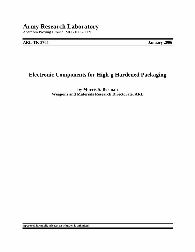
Although these environments appear to be very different, they subject the internal electronics to high accelerations and high frequencies. A gun-launched projectile can be subjected to acceleration magnitudes of 30,000 g’s (from a tank cannon) quasi-static, followed by high frequency excitation as great as 5,000 g’s (12, 1). A typical waveform for a tank cannon launch is shown in figure 1. Artillery projectiles are subjected to a similar acceleration profile, with a duration of approximately 10 ms and a peak of 15,000 g’s. Dropped consumer electronic devices can be subjected to accelerations from 400 g’s to 4,000 g’s (2, 3). A typical drop acceleration profile appears in figure 2.
Figure 1. Tank cannon launch acceleration.
In order for these devices to continue operating after being subjected to these high accelerations, a variety of techniques can be employed. These techniques include encapsulation, underfill, load path management, and careful component selection. The first three techniques seek to control the loads to which the components are subjected. The last technique seeks to identify specific components or classes of packages most likely to survive a given load.

2
Figure 2. Typical drop test acceleration profile (3).
1.1 Encapsulation
The circuitry is placed into a cavity and then filled with a “potting” material. These materials can take a variety of forms (5, 6). They can be filled or unfilled thermosetting epoxy resins. The encapsulation material can also be a foaming material (such as Stycast1). Its principal purpose is to provide structural support to the components embedded within it.
A secondary function served by encapsulation is to provide a damping mechanism. The potting materials currently employed have a significantly higher damping property than the traditional materials in which they reside. As a result, these materials tend to absorb and dissipate the mechanical energy imparted to them.
1.2 Underfill
Underfill materials are usually filled epoxy composites that are placed beneath flip chip or ball grid array (BGA) packages to fill the area surrounding the solder joints (7). Underfill has also been successfully used on chip scale packages (CSPs) to increase their reliability (8).
CSPs primarily employ two types of underfill. Capillary underfill is applied after the solder reflow process has been completed. These underfills have a low viscosity which allows them to flow under the CSP via capillary action. A heat process is then used to cure the material.
Fluxing underfill combines the solder flux functionality with the underfill functionality. The underfill is placed in the center of the CSP’s destination on the printed wiring board (PWB). The “pick-and-place” machine then places the component. The fluxing underfill is then drawn to the CSP’s perimeter upon placement by pressure exerted by the pick-and-place machine. During solder reflow, the fluxing underfill provides flux to the soldering process. The reflow provides the initial cure to the underfill which often undergoes a subsequent post-cure heat cycle.
1Stycast is a registered trademark of Emerson and Cumings, Inc.

3
1.3 Load Path Management
This is a broad category of techniques ranging from isolation to design of the outer casing of the electronic package. PWB flexure is a primary cause of electronic product failures (9). Therefore, the product should be designed so that impacts or shocks to the exposed portions of the product result in minimal deformation of the internal PWBs. Careful material choice and design of the connection between external surfaces and the internal PWB supports are used for this failure mitigation technique.
If certain components of a particular design are susceptible to shock and vibration damage, a shock and vibration isolator may be used to minimize the probability of damage. Isolators may use active, passive, or semi-active techniques as well as a variety of materials. They mitigate the propagation of shock and vibration from one boundary to another.
1.4 Component Selection
The electrical function of major classes of electronic components results in an interchangeability for a component with a given function and set of electrical characteristics. However, the different materials comprising the components as well as the factory and lot of manufacture can have a significant impact on the component’s reliability in the shock environment. Supply chain management is critical to ensure that components continue to meet the required specifications, whether those specifications are guaranteed by the manufacturer or measured by the user.
As a result, careful consideration of the mechanical characteristics for a given component must be included in its choice. An electronic component vendor is often providing a component that meets or exceeds its electrical specification. Rarely does an electronic component vendor guarantee the component’s mechanical performance. It is incumbent upon the system integrator to test critical components to ensure that they meet required performance levels at the design phase as well as throughout the device’s lifetime. Previous gun launched munitions programs have suffered reliability losses when a vendor’s processes change and mechanical performance is negatively impacted.
2. Advantages of Technology
2.1 Encapsulation
The U.S. Army has been using potting compounds in gun-launched munitions to ensure the survival of critical fuze components (10) since 1950. More recently, potting compounds have been employed extensively in the development electronic module assembly (EMA) of the sense and destroy armor (SADARM) submunition (11) as well as an in-house-developed launch environment characterization data acquisition unit (6).

4
Encapsulation materials can be added to almost any electronic design. In most cases, the addition of potting material increases the robustness of the design. There is a wide variety of potting materials to choose from, ranging from room temperature vulcanizing rubber to urethanes to lightweight structural foams. Potting materials come in a wide range of strengths and coefficients of thermal expansion (CTEs), thus enabling them to be matched to most applications. A side benefit of potting for shock reliability is that these assemblies are also environmentally protected by the encapsulation. Several potting materials are designed to break down when a particular solvent is applied. This reaction enables the removal of the potting material and subsequent re-working of the assembly.
2.2 Underfill
Underfill has been used extensively with the flip chip attachment method. As a result, manufacturers have significant experience with the required process steps. In a flip chip application the primary purpose of the underfill is to enable load sharing with the solder. The loads result from different CTEs between the die and the substrate. The underfill provides a physical constraint to the solder which further increases the reliability of the component attach. As the underfill cures, it also shrinks, resulting in the solder being compressed between the die and the substrate.
Liu et al. (8) investigated the effectiveness of several different underfills for the purpose of increasing the robustness of CSPs in a drop test environment. Their results are shown in figure 3. Regardless of the specific underfill technology employed, a significant increase in the number of drops that a CSP survives was noted. The significant decrease in failure frequency of the subject component under shock testing is the main advantage of this technology.
Figure 3. Underfill effectiveness for drop tests (8).

5
2.3 Load Path Management
Careful design of the load path from the external shell of an electronic product to the internal electronic packages is a critical element of any product’s design. However, it requires consideration from the earliest inception of the product’s design. Incorporation of design features that mitigate the adverse effects of high-g shocks to the critical components of a product can be a low cost option when done early in the design process. However, modifying basic elements of a mature device design that did not consider high-g loading can be expensive and can significantly reduce the effectiveness of any mitigation technique.
2.4 Component Selection
A basic understanding of the shock response of any particular packaging technology plays a critical role in the selection of a packaging technology to be used for a particular function. Careful choice of the proper package increases the reliability of the product and decreases the cost of future modifications resulting from a poor initial choice.
3. Market Size and Opportunities
The market size and opportunities for the design of high-g electronic devices are increasing. The military’s continued reliance on electronics and consumers’ expectations that their PDAs and cellular phones will continue to work after being dropped are driving designers to consider high-g environments in a variety of products.
The Army awarded the engineering and manufacturing development (EMD) phase for SADARM to Aerojet Corporation in 1986. A program reaches this phase of development when the Army is convinced that the technologies that it comprises are deemed mature. Five years later in 1991, a qualification test indicated that the overall reliability of SADARM was 16%, and 39 root causes of failure were identified. In 1993, the Army initiated another series of test flights after having resolved all 39 known root failure causes. This test series was discontinued before its scheduled conclusion because of significant reliability issues (20).
After another study, a combined Army-contractor team concluded that SADARM could succeed technically but that significant program changes would be necessary. They also concluded that the root causes of failure were still unknown in many cases. Of critical importance was the failure of 17% of the munitions to self-destruct upon impact. This poor performance poses a significant hazard in the tactical environment (20).
The military’s increasing reliance on smart munitions mandates that larger quantities of more complex electronics will be expected to survive the gun launch environment. The unacceptable performance resulting from poor design decisions ultimately led to the cancellation of the

6
SADARM program. Over the life of the program, the estimated total cost of development went from $365 million to $1.1 billion dollars and the unit cost of a submunition increased from $11,000 to $36,000 (20).
The SADARM program is indicative of a gun launched munitions program that did not give proper consideration to the design details necessary to survive the high-g environment. The Army and Navy are continuing to develop “smart” gun-launched projectiles. Each of these development efforts represents a potential multi-billion dollar market for technologies that enable reliability in a high-g environment.
Consumer electronic devices represent a more subtle market. As technology has become more ubiquitous, consumers have also expected it to become less fragile. In order to meet that expectation, manufacturers are becoming more adept at “hardening” their products to survive rough handling by the consumer. Product hardening is often a post-design exercise and does not receive due consideration in a product’s initial design.
Competition in the consumer product sector of industry is fierce. As the technical capabilities of a given product at a particular price point coalesce, the consumers begin to evaluate product reliability as a critical issue in their purchase decision. Therefore, the ability of a company to incorporate high-g hardening into their designs at minimal costs in time and money can provide them with a significant advantage in the marketplace. This marketplace advantage is not secured with a single product. It is the culmination of a company’s commitment to design goals and priorities that results in a reputation for producing highly reliable products. A reputation for quality, reliable products also increases their market share.
4. Critical Hurdles to Development of Acceptance
4.1 Encapsulation
The gun launched munitions community clearly understands that specialized technologies and procedures are necessary to ensure the reliability of components. The fuzing community has been using potting materials since 1950 to ensure the survival of electronic and electro-mechanical components. Given the state of the technology and the mass of the components, potting was the only viable means to ensure survival through the gun launch process in 1950. As fuze technology progressed, the use of potting to harden fuze components continued.
When the Army began considering smart projectiles, the electronic assemblies required to survive gun launch became significantly more complex and expensive. Although potting is still an effective means to harden components, it has several drawbacks. The CTE of the components in a potted assembly is a critical issue that requires careful attention. If the thermo-mechanical properties of the potting are poorly chosen, temperature changes will result in failure of the

7
electronic assembly. Military components are expected to have a shelf life of 20 years and operate in environments from -45 °F to 145 °F. It is very difficult to formulate potting compounds that retain their mechanical properties for that duration over that range of temperature.
The cost of the components incorporated into a smart projectile is a significant portion of its cost. As a result, rework of a failed or marginal part is preferred over disposal of the entire projectile or electronic assembly. Unfortunately, it is extremely difficult to remove a component from a potted assembly. Soluble potting compounds ease the removal process but significantly limit the choice of potting materials. The inability to rework components eliminates encapsulation as a preferred hardening solution. However, it is still employed as an option of last resort.
4.2 Underfill
Underfill of components has been used extensively to increase the reliability of flip chip and BGA devices. Research has shown that underfill greatly decreases a component’s susceptibility to failure under bending loads. Until recently, underfilling components also precluded their rework. Recently, Loctite2 developed a reworkable underfill (8). When heated in a reflow oven, this underfill breaks down, allowing the component to be removed and replaced.
In the gun hardening community, g-hardening is more important than cost. The consumer products community is less likely to use underfilling as a hardening technique because of the increased labor and inability to rework those components. Cost, not g-hardening, is a more critical consideration in the consumer products industry. Consumers are more apt to choose a cellular based on a $20.00 cost difference than on its ability to survive 12 drops instead of 3. As reworkable underfill technology matures, it can be employed with minimal cost impact. This development will remove a significant barrier to more extensive use of underfill in the commercial sector.
4.3 Load Path Management
Similar differences separate the commercial and munitions sectors when we consider the use of load path management techniques. Essentially, the user of this technique requires a heavy investment in modeling and understanding of how shock loads are transmitted through a product. The munitions community has made extensive use of modeling for the design of the primary load-bearing structures. With the introduction of smart projectiles, modeling is being used to design the electronic components and their support structures. Experiences, such as the SADARM’s cancellation because of unreliability, are providing impetus to the projectile community to more carefully consider the structural dynamic aspects of projectile-borne electronics. Advances in computational structural dynamics are enabling more complex and realistic models which can be used to drive design decisions.
2Loctite is a registered trademark of Henkel Technologies.

8
The consumer electronics industry is driven more by cost and time to market than by reliability. The goal is to design new products and produce them cheaply while keeping them “reliable enough.” As a result, external structural designs have focused more on ergonomics and style issues rather than on decreasing the shock loads experienced by their internal electronic components. Recent projects at Computer-Aided Life Cycle Engineering (CALCE), University of Maryland at College Park, by Vargehese et al. (21) and Barker et al. (22) as well as Ong, Shim, Chai, and Lim (2), have begun to look at the shock transmission from an electronic product’s outer shell to its printed wiring assemblies and components. The funding of this work is indicative of the industry beginning to accept these design aspects as important elements of their designs.
4.4 Component Selection
Experiences in the SADARM program indicated that component survival is sensitive to subtle design differences that may not be a part of their specification. The gun hardening community has realized the importance of these design differences and carefully chooses its components on the basis of mechanical design as well as electronic function. In some cases, components with identical functionality are provided from a specific supplier to ensure their survival. In one instance of hardening a commercial off-the-shelf (COTS) device to the gun environment, an oscillator from one vendor was substituted for an electrically equivalent oscillator from another vendor. In another case, a COTS supplier was requested to provide a specially modified component that enabled its survival in the gun launch environment.
Cost considerations preclude the consumer electronics industry from specifying process changes in commodity parts. Helmhold, Blattau, and Hillman (23) have begun a project at CALCE to qualify commodity capacitors for given design and application environments. The impetus for this work comes from increasing reliance on discrete capacitors and the realization that they are a significant contributor to electronic product failures. In addition, three of the major capacitor vendors are relocating their manufacturing facilities to China and there is a concern that subtle process changes will probably occur. The funding of this project at CALCE is indicative of industry realizing that although the electronic function of commodity components may be identical, subtlties in their construction can result in critical structural dynamic differences.
5. Manufacturing Process and Material Selection
5.1 Encapsulation
As previously stated, potting materials can be obtained in a wide variety of configurations and a wide range of physical parameters. When selecting which potting material to use for a specific application, one needs to consider a variety of factors.

9
The CTE of the potting material must be compatible with the items being encapsulated as well as the structure containing the assembly. The strength of the chosen material must be capable of providing the desired level of support. However, the potting must not excessively mass load the components that are being protected (6).
Most potting materials undergo some form of manufacturing processing to be cured. The curing process is usually a heat process. Other components must be compatible with the required cure temperature. In addition to the curing process, the components in contact with the potting material must be chemically compatible.
5.2 Underfill
The performance of capillary and fluxing underfills was examined (8). Most production processes currently use capillary underfill. With this type of underfilling technique, the material is applied after the components have been placed onto the PWB and soldered into place. The area to be underfilled must be clear of excess solder flux as well as moisture to maximize the effectiveness of the underfill. These two requirements add more processing steps to the manufacturing process before underfill placement. After these additional steps are complete, the underfill can be placed around the perimeter of the package where it is drawn underneath the component and cured.
Fluxing underfill is placed before chip placement and eliminates the need for solder paste and flux. Solder balls provide an obstacle around which voids can form as the underfill is squeezed out to the edges of the CSP. The placement parameters and reflow profile must be adjusted to minimize the formation of flaws.
Different choices of underfill material exist for each class. Both flux-only and solder-paste assembly processes are used for the capillary type underfill. The results (8) indicate that any underfill material choice improves the probability of the CSP surviving a high acceleration event.
A thermally reworkable underfill is also available. This underfill falls into the capillary action class of underfills. The advantage of this underfill is that rework of the component is enabled. Upon heating of the component to solder reflow temperatures, the underfill breaks down and loses its adhesive properties (8). The component can then be lifted from the board and cleaned.
5.3 Load Path Management
Extensive modeling of the SADARM projectile at various levels was initiated in an attempt to understand the interaction of various structures in the transmission of loads into electronic components. The entire SADARM projectile and gun system was modeled by Wilkerson et al. (24). This model characterized the load path from the gun tube to the major structural elements of the SADARM projectile. Results from this model were used by Berman et al. (11) in the development of a detailed model of the EMA. These structural models enabled a detailed understanding of how launch loads impact the critical electronic components. These models

10
were executed in various configurations to help us understand the detailed interactions between potting material, underfill, and encapsulation. This understanding led to material and processing changes which improved the reliability of the EMA. Detailed structural dynamic modeling continues to be a critical tool in the selection of materials and assessing the impact of processing techniques on Excalibur, the Army’s current smart projectile.
Although the use of potting compounds is diminishing, Quesenberry (5) has charactacterized potting compounds using mixtures of hollow and solid glass bead filler material. Relationships were developed for determining the material’s CTE and density as a function of the ratio of hollow to solid fill material. An intended use for this material is to minimize the weight of necessary potting material while maintaining a compatible CTE and strength for designs that require encapsulation.
The consumer products industry has yet to embrace modeling as a critical technology in an overall load path management methodology. Ong, Shim, Chai, and Lim have performed experimental investigations to understand the difference in PCB mechanical response to drop tests when mounted in a device or on a fixture outside a device (2). They determined that the mechanical response of the PCB differs significantly, depending on whether it was bare or installed. The differences were the result of interactions with other components and the boundary conditions imparted by the PCB support mechanism.
Varghese et al. have a research program at CALCE to examine the dynamic behavior of plastics under impact loading (21). This research program enables the development of a material model that can be used for the exterior case of electronic devices. Once this methodology is developed, it can be used to quantify the effect of processing variables on the plastic’s properties as well as to quantify the difference between various plastics.
Shi, Wang, Pang, and Zhang have developed a methodology to characterize underfill materials as a function of temperature and strain rate in support of finite element modeling (7). The variation of material properties as a function of strain rate is an important parameter in modeling components subjected to impact events. These two material characterization efforts enable designers to quantify the impact of different material choices on the load path to a component.
6. Manufacturing Defects
6.1 Encapsulation
The manufacturing defects associated with encapsulation fall into two categories. Voids can form in the potting material and the potting can fail to adhere to the cavity walls or components. Void formation can be controlled if we carefully monitor the curing process and minimize the

11
probability of contamination. Careful cleaning of components and cavity surfaces is the key to ensuring adherence of the potting.
6.2 Underfill
The basis for manufacturing defects for both types of underfill primarily lies in contamination of the area to be underfilled. Flux residue is a significant concern for the capillary type underfill. Excess flux can preclude the underfill from touching all areas beneath the component by interfering with the capillary action and thus the underfill flow. Before the underfill is applied, the component and PWB must be free of moisture. Moisture that seeps in from the board or adheres to the solder ball is another contaminant that will interfere with the underfill flow. Both of these defects result in voids in the underfill that decrease its efficiency. In some cases, fill is added to the epoxies to obtain a CTE match with other components. In this case, the fill material can interfere with the flow of the underfill beneath the component.
The fluxing underfill is not subject to contamination by flux or voids resulting from flow time. However, the placing parameters of the component become critical. As the component is placed on the board, void can be trapped by the solder ball array. As the size of the balls increases, the probability for trapped voids also increases (8).
6.3 Load Path Management
Once a validated model of the structure of interest has been developed, it can be exercised for a variety of conditions. Various structural elements can be “damaged” to simulate manufacturing defects. The result of these defects on the structural response of the electronic components can then easily be quantified.
6.4 Component Selection
One element of selecting components is the consistency of their response to shock loads. Lower quality components with significant manufacturing defects should manifest this property in their characterization tests. The designer is then able to choose components from a manufacturer that is capable of consistently delivering high quality components.
7. Key Failure Mechanisms
Reliability of electronic packages has traditionally focused on thermal and thermo-mechanical issues. Although the consideration of high acceleration loads touches upon some of the same basic physics, the causes of the loads resulting from high-g loads are different. Thermo-mechanical loads and shock loads induce strain differentials between the PWB and the

12
component. The strain difference is one of the key mechanisms for electronics subjected to high accelerations.
Bending of the PWB is the primary mechanism through which a high-g environment imparts strain into an electronic device (8, 13 through 17). As package-to-PWB interconnections have moved from leaded to solder ball attaches, the compliance between the board and component has decreased. Shetty et al. (13) investigating the bending loads necessary to impart failure in CSP packages, and Barker (15) is investigating the bending loads necessary to impart failure to plastic ball grid array (PBGA), capacitors, and other common packages. Varghese and Dasgupta (9) identify cracking at the intermetallic layer of solder balls as a result of bending stress.
The second key failure mechanism for high-g devices is simply a result of the acceleration to which they are subjected. In a high-g environment, all materials and parts in a device are subjected to a body force equal to the product of mass and acceleration. For commercial applications, the inertia is relatively small. However, as a device is subjected to accelerations of 5,000 to 30,000 times the acceleration of gravity, the force that the internal and external support structures must support becomes significant. D’Amico (12) notes that a key to survival of the gun launch process is to minimize component mass. In one gun launched munitions program, a particular component had to be specially procured with aluminum wire bonds since gold wire bonds were too weak to survive gun launch. The reduction of mass also results in the reduction of bending moments, thus minimizing one of the primary failure mechanisms.
8. Failure Models for Key Mechanisms
Tropea, Mellal, and Botsis (18) have examined in detail the failure properties of solder balls at the intermetallic layer. The actual solder ball failure results from complex interactions between the intermetallics. In some cases, the tin-lead interfaces break up and become surrounded by microcracks. Long cracks can form along the copper-tin interface. Cracks also tend to form along boundaries between different grain structures (18). Understanding the micromechanical damage is crucial in developing a physics-based failure model.
Underfill is a critical component for low-compliance packaging attachment schemes. Shi, Wang, and Pickering (19) have developed a characterization method for understanding failures in filled epoxy films. Linear elastic fracture mechanics were used to describe and predict grown crack tips in the epoxy material (19).
Barker has taken a macroscopic approach to developing a failure model. A failure model for capacitors has been developed which depends on knowledge of the strain values of the PWB at the base of the capacitor solder fillets. A failure model applicable to PBGAs is in the

13
development process. Recent experimentation has indicated that low cycle fatigue may be a critical factor in the development of a failure model (15).
9. Screening Tests
9.1 Encapsulation and Underfill
In order to ensure the highest consistency and thus reliability in the high-g environment, steps must be taken to ensure that batch processed chemicals, such as underfill and potting, are properly mixed. Hoang, Murphy, and Desai (26) suggest a two-phase test when one is screening underfill materials for high performance applications. Both tests should use components of the same configuration as used in the actual application. The components can be non-functioning dummies or electrically rejected actual components.
The first test determines the flow rate of the underfill. Underfill should be dispensed along one side of the component. The time for the underfill to flow to the other side should be monitored. The preheat temperature of the substrate could be varied to determine the impact of process variability. After curing, the components should be inspected with an acoustic microscope for void formation.
After a full cure, the flow rate specimens can be used for an adhesion test. A shear test appears to provide the best measure of adhesive strength. The shear test tends to concentrate failures at the underfill boundaries as opposed to cracking the die or delaminating the substrate. A similar series of tests could also apply to potting properties. Although Hoang et al. envisioned these tests for chosing appropriate underfill, they are also appropriate to be used as a screening process (26).
An adhesion test of the potting compounds would provide a good screen to ensure that the potting is consistent. A tensile test of a homogeneous material specimen would be a good augmentation of the adhesion test to ensure that the constitutive properties of the potting remain constant.
9.2 Component Selection
This technique for hardening is predicated on the fact that different components with the same specifications may exhibit dissimilar mechanical response. A critical facet of this hardening technique is to ensure that a component manufacturer has not changed processes, thus resulting in a change in mechanical properties. Screening tests that verify the mechanical properties of incoming parts are an extremely important part of the supply chain management process to ensure high-g survivability.

14
10. References
1. Wilkerson, S.; Hopkins, D.; Gazonas, G.; Berman, M. Developing a Transient Finite Element Model to Simulate the Launch Environment of the 155-mm SADARM Projectile. Shock and Vibration Information Analysis Center. Proceedings of the 71st Shock and Vibration Symposium, November 2000.
2. Ong, Y. C.; Shim, V.P.W.; Chai, T. C.; Lim, C. T. Comparison of mechanical response of PCBs subjected to product-level and board-level drop impact tests. Electronics Packaging Technology, 2003 5th Conference (EPTC 2003) Dec. 2003, Vol., Iss., 10-12, 223-227
3. Tee, T. Y.; Ng, H. S.; Lim, C. T.; Pek, E.; Zhong, Z. Impact life prediction modeling of TFBGA packages under board level drop test. Microelectronics Reliability 2004, 44 (7), 1131-1142.
4. Davis, B.; Hamilton, M.; Hepner, D. Shock Experiment Results of the DFuze 8-Channel Inertial Sensor Suite that Contains Commercial Magnetometers and Accelerometers; ARL-MR-532; U.S. Army Research Laboratory: Aberdeen Proving Ground, MD, April 2002.
5. Quesenberry, M. Characterization of Low Density Glass Filled Epoxies; ARL-TR-2938; U.S. Army Research Laboratory: Aberdeen Proving Ground, MD, March 2003.
6. University of Maryland. Virtual Qualification of Electronic Components Under High G Loads: End of Year Presentation; CALCE C02-15; College Park, MD, 2002.
7. Shi, X.Q.; Wang, Z. P.; Pang, H.L.J.; Zhang, . Investigation of effect of temperature and strain rate on mechanical properties of underfill material by use of microtensile specimens. Polymer Testing September 2002, 21 (6), 725-733.
8. Liu, J.; Johnson, R. W.; Yaeger, E.; Konarski, M.; Crane, L. Processing and reliability of CSPs with underfill. IEEE Transactions On Electronics Packaging Manufacturing 2003, 26 (4), 313-319.
9. Varghese, J.; Dasgupta, A. Test Tailoring Methodology for Impact Testing of Portable Electronic Products. IMAC-XXI Conference on Structural Dynamics, Kissimmee, Florida, February 3-6, 2003
10. U.S. Army Materiel Command Historical Office. Photolithography: A Breakthrough in Semiconductor Technology. http://www.amc.army.mil/amc/ho/studies/ photolithography.html.

15
11. Berman, M.; Wilkerson, S.; Hopkins, D.; Gazonas, G.; Frydman, A.; Carlucci, D. Methodology for Hardening Electronic Components for Gun Launch Survival. 19th International Ballistics Symposium, 2001.
12. D’Amico, W. Telemetry Systems and Electric Gun Projectiles; ARL-MR-499; U.S. Army Research Laboratory: Aberdeen Proving Ground, MD, October 2000.
13. Shetty, S.; Lehtinen, V.; Dasgupta, A.; Halkola, V.; Reinikainen, T. Effect of bending on Chip Scale Package Interconnects. CALCE C99-31 Annual Report, University of Maryland, 1999.
14. Yu, Q.; Kikuchi, H.; Ikeda, S.; Shiratori, M.; Kakino, M.; Fujiwara, N. Dynamic behavior of electronics package and impact reliability of BGA solder joints. Thermal and Thermomechanical Phenomena in Electronic Systems, 2002. ITHERM 2002. The Eighth Intersociety Conference on, Vol., Iss., 2002, 953-960
15. Barker, D. Electronic Component Failure; CALCE C04-30. Final Report, University of Maryland, 2004.
16. Quantitative Damage Characterization of Portable Electronics Under Impact Loading, CALCE C01-30. Final Report, University of Maryland, 2001.
17. Katchmar, R. Overload fracture of package solder joints. Microelectronics Reliability 2000, 40 (1), 123-129.
18. Tropea, P.; Mellal, A.; Botsis, J. Deformation and damage of a solder-copper joint. Microelectronics Reliability 2003, 43 (9-11), 1791-1796.
19. Shi, X. Q.; Wang, Z. P.; Pickering, J. P. A new methodology for the characterization of fracture toughness of filled epoxy films involved in microelectronics packages. Microelectronics Reliability 2003, 43 (7), 1105-1115.
20. Government Accountability Office. Army Acquisiton: Problems with the Sense and Destroy Armor Munition; GAO/NSIAD 94-59, Washington, DC, November 1993.
21. Vargehese; et al. Dynamic Behavior of Plastics under Impact Loading; CALCE C04-29. Mid-year report, University of Maryland,
22. Barker; et al. Drop Tower Testing of Portable Consumer Electronic Devices; CALCE C01-28. Final Report, University of Maryland,
23 Helmhold; Blatteu; Hillman, C. Qualification and Reliability Assessment of New Capacitor Technology, C04-10. Mid-year Presentation, University of Maryland,
24. Wilkerson, S.; Hopkins, D.; Gazonas, G.; Berman, M. Developing a Transient Finite Element Model to Simulate the Launch Environment of the 155-mm SADARM Projectile;

16
ARL-TR-2341; U.S. Army Research Laboratory: Aberdeen Proving Ground, MD, September 2000.
25. Cooper, G.; Wilkerson, S.; Carlucci, D. Analysis of Bending a Square Ceramic Plate Under Strong Rotation; ARL-TN-167; U.S. Army Research Laboratory: Aberdeen Proving Ground, MD, September 2000.
26. Hoang, L.; Murphy, A.; Desai, K. Methodology for screening high performance underfill materials. Electronic Components and Technology Conference, 1998. 48th IEEE, Vol., Iss., 25-28 May 1998, 111-116.

17
NO. OF COPIES ORGANIZATION 1 DEFENSE TECHNICAL (PDF INFORMATION CTR ONLY) DTIC OCA 8725 JOHN J KINGMAN RD STE 0944 FORT BELVOIR VA 22060-6218 1 US ARMY RSRCH DEV & ENGRG CMD SYSTEMS OF SYSTEMS INTEGRATION AMSRD SS T 6000 6TH ST STE 100 FORT BELVOIR VA 22060-5608 1 INST FOR ADVNCD TCHNLGY THE UNIV OF TEXAS AT AUSTIN 3925 W BRAKER LN STE 400 AUSTIN TX 78759-5316 1 DIRECTOR US ARMY RESEARCH LAB IMNE ALC IMS 2800 POWDER MILL RD ADELPHI MD 20783-1197 1 DIRECTOR US ARMY RESEARCH LAB AMSRD ARL CI OK TL 2800 POWDER MILL RD ADELPHI MD 20783-1197 2 DIRECTOR US ARMY RESEARCH LAB AMSRD ARL CS OK T 2800 POWDER MILL RD ADELPHI MD 20783-1197 1 DIRECTOR US ARMY RESEARCH LAB ATTN AMSRD ARL SE DE R ATKINSON 2800 POWDER MILL RD ADELPHI MD 20783-1197 6 DIR US ARMY RESEARCH LAB ATTN AMSRD ARL WM MB T LI A ABRAHAMIAN M BERMAN M CHOWDHURY A FRYDMAN E SZYMANSKI 2800 POWDER MILL RD ADELPHI MD 20783-1197
NO. OF COPIES ORGANIZATION 1 COMMANDER US ARMY MATERIEL CMD ATTN AMXMI INT 9301 CHAPEK RD FT BELVOIR VA 22060-5527 3 PM MAS ATTN SFAE AMO MAS SFAE AMO MAS MC CHIEF ENGINEER PICATINNY ARSENAL NJ 07806-5000 2 PM MAS ATTN SFAE AMO MAS PS SFAE AMO MAS LC PICATINNY ARSENAL NJ 07806-5000 1 CDR US ARMY ARDEC ATTN AMSTA AR CC COL JENKER PICATINNY ARSENAL NJ 07806-5000 1 CDR US ARMY ARDEC ATTN AMSTA AR FSE PICATINNY ARSENAL NJ 07806-5000 1 CDR US ARMY ARDEC ATTN AMSTA AR TD PICATINNY ARSENAL NJ 07806-5000 5 CDR US ARMY ARDEC ATTN AMSTA AR CCH A F ALTAMURA M NICOLICH R HOWELL A VELLA M YOUNG PICATINNY ARSENAL NJ 07806-5000 2 CDR US ARMY ARDEC ATTN AMSRD AAR AEM D VO M PALATHINGUL PICATINNY ARSENAL NJ 07806-5000 4 CDR US ARMY ARDEC ATTN AMSTA AR CCH A L MANOLE S MUSALLI E LOGSDEN T LOUZEIRO PICATINNY ARSENAL NJ 07806-5000 1 CDR US ARMY ARDEC ATTN AMSRD AAR AEM L R CARR PICATINNY ARSENAL NJ 07806-5000

18
NO. OF COPIES ORGANIZATION 1 CDR US ARMY ARDEC ATTN AMSRD AAR AEM M LUCIANO PICATINNY ARSENAL NJ 07806-5000 1 CDR US ARMY ARDEC ATTN AMSTA AR CCH P J LUTZ PICATINNY ARSENAL NJ 07806-5000 1 CDR US ARMY ARDEC ATTN AMSTA AR FSF T C LIVECCHIA PICATINNY ARSENAL NJ 07806-5000 1 CDR US ARMY ARDEC ATTN AMSTA ASF PICATINNY ARSENAL NJ 07806-5000 1 CDR US ARMY ARDEC ATTN AMSTA AR QAC T C J PAGE PICATINNY ARSENAL NJ 07806-5000 1 CDR US ARMY ARDEC ATTN AMSTA AR M D DEMELLA PICATINNY ARSENAL NJ 07806-5000 3 CDR US ARMY ARDEC ATTN AMSTA AR FSA A WARNASH B MACHAK M CHIEFA PICATINNY ARSENAL NJ 07806-5000 2 CDR US ARMY ARDEC ATTN AMSTA AR FSP G M SCHIKSNIS D CARLUCCI PICATINNY ARSENAL NJ 07806-5000 2 CDR US ARMY ARDEC ATTN AMSTA AR CCH C H CHANIN S CHICO PICATINNY ARSENAL NJ 07806-5000 1 CDR US ARMY ARDEC ATTN AMSTA AR QAC T D RIGOGLIOSO PICATINNY ARSENAL NJ 07806-5000 1 CDR US ARMY ARDEC ATTN AMSTA AR WEL F M GUERRIERE PICATINNY ARSENAL NJ 07806-5000 9 CDR US ARMY ARDEC ATTN AMSTA AR CCH B P DONADIA F DONLON P VALENTI C KNUTSON G EUSTICE K HENRY J MCNABOC R SAYER F CHANG PICATINNY ARSENAL NJ 07806-5000
NO. OF COPIES ORGANIZATION 1 PM ARMS ATTN SFAE GCSS ARMS BLDG 171 PICATINNY ARSENAL NJ 07806-5000 1 CDR US ARMY ARDEC ATTN AMSTA AR WEA J BRESCIA PICATINNY ARSENAL NJ 07806-5000 1 CDR US ARMY TACOM PM COMBAT SYSTEMS ATTN SFAE GCS CS 6501 ELEVEN MILE RD WARREN MI 48397-5000 1 CDR US ARMY TACOM PM SURVIVABLE SYSTEMS ATTN SFAE GCSS W GSI H M RYZYI 6501 ELEVEN MILE RD WARREN MI 48397-5000 1 COMMANDER US ARMY TACOM ATTN AMSTA SF WARREN MI 48397-5000 1 DIR AIR FORCE RSCH LAB ATTN MLLMD D MIRACLE 2230 TENTH ST WRIGHT PATTERSON AFB OH 45433-7817 1 OFC OF NAVAL RESEARCH ATTN J CHRISTODOULOU ONR CODE 332 800 N QUINCY ST ARLINGTON VA 22217-5600 1 CDR WATERVLIET ARSENAL ATTN SMCWV QAE Q B VANINA BLDG 44 WATERVLIET NY 12189-4050 2 COMMANDER US ARMY AMCOM AVIATION APPLIED TECH DIR ATTN J SCHUCK FORT EUSTIS VA 23604-5577 1 NSWC DAHLGREN DIV CODE G06 DAHLGREN VA 22448

19
NO. OF COPIES ORGANIZATION 1 US ARMY COLD REGIONS RSCH & ENGRNG LAB ATTN P DUTTA 72 LYME RD HANOVER NH 03755 4 CDR US ARMY TACOM ATTN AMSTA TR R R MCCLELLAND D THOMAS J BENNETT D HANSEN WARREN MI 48397-5000 4 CDR US ARMY TACOM ATTN AMSTA JSK S GOODMAN D TEMPLETON J FLORENCE A SCHUMACHER WARREN MI 48397-5000 5 CDR US ARMY TACOM ATTN AMSTA TR D D OSTBERG L HINOJOSA B RAJU AMSTA CS SF H HUTCHINSON F SCHWARZ WARREN MI 48397-5000 6 BENET LABS ATTN AMSTA AR CCB R FISCELLA M SOJA E KATHE G FRIAR M SCAVULO G SPENCER WATERVLIET NY 12189-4050 4 BENET LABS ATTN AMSTA AR CCB P WHEELER S KRUPSKI J VASILAKIS R HASENBEIN WATERVLIET NY 12189-4050 4 BENET LABS ATTN AMSTA CCB R S SOPOK E HYLAND D CRAYON R DILLON WATERVLIET NY 12189-4050 1 USA SBCCOM PM SOLDIER SPT ATTN AMSSB PM RSS A J CONNORS KANSAS ST NATICK MA 01760-5057 2 OFC OF NAVAL RESEARCH ATTN D SIEGEL CODE 315 J KELLY 800 N QUINCY ST ARLINGTON VA 22217-5660
NO. OF COPIES ORGANIZATION 1 NSWC CRANE DIVISION M JOHNSON CODE 20H4 LOUISVILLE KY 40214-5245 4 US ARMY SBCCOM SOLDIER SYSTEMS CTR BALLISTICS TEAM ATTN J WARD W ZUKAS P CUNNIFF J SONG KANSAS ST NATICK MA 01760-5019 3 US ARMY SBCCOM SOLDIER SYSTEMS CTR MARINE CORPS TEAM J MACKIEWICZ ATTN AMSSB RCP SS W NYKVIST S BEAUDOIN KANSAS ST NATICK MA 01760-5019 7 US ARMY RESEARCH OFC ATTN A CROWSON H EVERITT J PRATER G ANDERSON D STEPP D KISEROW J CHANG PO BOX 12211 RSCH TRIANGLE PARK NC 27709-2211 1 AFRL MLBC 2941 P ST RM 136 WRIGHT PATTERSON AFB OH 45433-7750 1 DIRECTOR LOS ALAMOS NATL LAB ATTN F L ADDESSIO T 3 MS 5000 PO BOX 1633 LOS ALAMOS NM 87545 1 AFRL MLSS ATTN R THOMSON 2179 12TH ST RM 122 WRIGHT PATTERSON AFB OH 45433-7718 1 AFRL MLS OL ATTN L COULTER 7278 4TH STREET BLDG 100 BAY D HILL AFB UT 84056-5713 3 DIR SANDIA NATL LABS APPLIED MECHS DEPT ATTN MS 9042 J HANDROCK Y R KAN J LAUFFER PO BOX 969 LIVERMORE CA 94551-0969

20
NO. OF COPIES ORGANIZATION 2 OAK RIDGE NATL LAB ATTN C D WARREN MS 8039 PO BOX 2008 OAK RIDGE TN 37831-6195 1 DIR US ARMY NGIC ATTN IANG TMT 2055 BOULDERS RD CHARLOTTESVILLE VA 22911-8318 1 DIR DIA ATTN K CRELLING TA 5 WASHINGTON DC 20310 ABERDEEN PROVING GROUND 1 DIRECTOR US ARMY RSCH LABORATORY ATTN AMSRD ARL CI OK (TECH LIB) BLDG 4600 1 US ARMY ATC ATTN CSTE DTC AT AC I W C FRAZER BLDG 400 1 DIR USARL ATTN AMSRD ARL CI BLDG 1 DIR USARL ATTN AMSRD ARL O AP EG M ADAMSON BLDG 1 DIR USARL ATTN AMSRD ARL SL BB D BELY BLDG 328 1 DIR USARL ATTN AMSRD ARL SL BE W BRUCHEY BLDG 390A 2 DIR USARL ATTN AMSRD ARL WM J SMITH D LYON BLDG 4600 2 DIR USARL ATTN AMSRD ARL WM B CHIEF T KOGLER BLDG 4600 2 DIR USARL ATTN AMSRD ARL WM BC P PLOSTINS J NEWILL BLDG 390
NO. OF COPIES ORGANIZATION 3 DIR USARL ATTN AMSRD ARL WM BD B FORCH R PESCE-RODRIGUEZ B RICE BLDG 4600 3 DIR USARL ATTN AMSRD ARL WM BD P CONROY C LEVERITT A ZIELINSKI BLDG 390 2 DIR USARL ATTN AMSRD ARL WM BE R LIEB M LEADORE BLDG 4600 1 DIR USARL ATTN AMSRD ARL WM BF S WILKERSON BLDG 390 2 DIR USARL ATTN AMSRD ARL WM M J MCCAULEY S MCKNIGHT BLDG 4600 2 DIR USARL ATTN AMSRD ARL WM MA L GHIORSE E WETZEL BLDG 4600 27 DIR USARL ATTN AMSRD ARL WM MB J BENDER M BERMAN (5 CYS) T BOGETTI J BROWN L BURTON R CARTER K CHO W DE ROSSET G DEWING R DOWDING W DRYSDALE R EMERSON D GRAY D HOPKINS R KASTE L KECSKES M MINNICINO B POWERS D SNOHA J SOUTH M STAKER J SWAB J TZENG BLDG 4600 11 DIR USARL ATTN AMSRD ARL WM MC J BEATTY R BOSSOLI E CHIN S CORNELISON D GRANVILLE B HART J LASALVIA J MONTGOMERY F PIERCE E RIGAS W SPURGEON BLDG 4600

21
NO. OF COPIES ORGANIZATION 11 DIR USARL ATTN AMSRD ARL WM MD P DEHMER B CHEESEMAN R DOOLEY G GAZONAS S GHIORSE M KLUSEWITZ W ROY J SANDS S WALSH D SPAGNUOLO S WOLF BLDG 4600 2 DIR USARL ATTN AMSRD ARL WM RP J BORNSTEIN C SHOEMAKER BLDG 1121 1 DIR USARL ATTN AMSRD ARL WM T B BURNS BLDG 309 1 DIR USARL ATTN AMSRD ARL WM TA W GILLICH BLDG 309 7 DIR USARL ATTN AMSRD ARL WM TA M BURKINS B GOOCH T HAVEL C HOPPEL E HORWATH J RUNYEON M ZOLTOSKI BLDG 393 1 DIR USARL ATTN AMSRD ARL WM TB P BAKER BLDG 309 1 DIR USARL ATTN AMSRD ARL WM TC R COATES BLDG 309 4 DIR USARL ATTN AMSRD ARL WM TD D DANDEKAR M RAFTENBERG S SCHOENFELD T WEERASOORIYA BLDG 4600 2 DIR USARL ATTN AMSRD ARL WM TE CHIEF J POWELL BLDG 120