Electrochemical Study of Under-Potential Deposition Processes on
131
APPROVED: Oliver M.R. Chyan, Major Professor Teresa D. Golden, Committee Member Ruthanne D. Thomas, Chair of the Department of Chemistry Sandra L. Terrell, Dean of the Robert B. Toulouse School of Graduate Studies ELECTROCHEMICAL STUDY OF UNDER-POTENTIAL DEPOSITION PROCESSES ON TRANSITION METAL SURFACES Sarah Cecilia Flores Araujo, B.S. Thesis Prepared for the Degree of MASTER OF SCIENCE UNIVERSITY OF NORTH TEXAS August 2006
Transcript of Electrochemical Study of Under-Potential Deposition Processes on
APPROVED: Oliver M.R. Chyan, Major Professor Teresa D. Golden, Committee Member Ruthanne D. Thomas, Chair of the
Department of Chemistry Sandra L. Terrell, Dean of the Robert B.
Toulouse School of Graduate Studies
ELECTROCHEMICAL STUDY OF UNDER-POTENTIAL DEPOSITION PROCESSES
ON TRANSITION METAL SURFACES
Sarah Cecilia Flores Araujo, B.S.
Thesis Prepared for the Degree of
MASTER OF SCIENCE
UNIVERSITY OF NORTH TEXAS
August 2006
Flores Araujo, Sarah Cecilia, Electrochemical Study of Under-Potential
Deposition Processes on Transition Metal Surfaces, Master of Science
(Chemistry), August 2006, 121 pp., 4 tables, 41 figures, reference list, 115
references.
Copper under-potential deposition (UPD) on iridium was studied due to
important implications it presents to the semiconductor industry. Copper UPD
allows controlled superfilling on sub-micrometer trenches; iridium has
characteristics to prevent copper interconnect penetration into the surrounding
dielectric. Copper UPD is not favored on iridium oxides but data shows copper
over-potential deposition when lower oxidation state Ir oxide is formed.
Effect of anions in solution on silver UPD at platinum (Pt) electrodes was
studied with the electrochemical quartz crystal microbalance. Silver UPD forms
about one monolayer in the three different electrolytes employed. When
phosphoric acid is used, silver oxide growth is identified due to presence of low
coverage hydrous oxide species at potentials prior to the monolayer oxide region
oxide region.

Copyright 2006
by
Sarah Cecilia Flores Araujo
ii
ACKNOWLEDGEMENTS
My profound appreciation and acknowledgements are to all the people
who helped me in accomplishing this very important goal. Thanks to Dr. Oliver
M.R. Chyan whose support was essential in the continuation of my studies, and
whose advice and knowledge was fundamental for my academic development.
My unique acknowledgements are for Dr. Teresa Golden, from whom I obtained
invaluable knowledge, support and understanding. The financial support from the
UNT Faculty Research Grant and the Welch Foundation is to a great extent
appreciated, as well as the help from the UNT Chemistry Department staff.
Special thanks to the members of my group, Praveen Nalla, Yibin Zhang, Shyam
Venkataraman, Kai-Hung Yu, and Karthikeyan Pillai, whose enthusiasm and
discussions helped in the accomplishment of the work presented here.
I would like to extend my acknowledgements to Dr. Oscar Mendoza,
whose guide and help was essential for the arrival to UNT. To Dr. Rosa Amelia
Orozco, Dr. Manuel Quevedo, and Dr. Alejandro Hernández, whose
unconditional friendship I truly appreciate. Exceptional acknowledgements to my
family and my in-laws whose confident love, values, support and friendship is
invaluable, making me withstand the most difficult situations; and to Oscar Ojeda,
whose love, support and confidence made it possible.
iii

TABLE OF CONTENTS
Page
ACKNOWLEDGEMENTS..................................................................................... iii
LIST OF TABLES .................................................................................................vi
LIST OF FIGURES..............................................................................................vii
Chapters
1 INTRODUCTION ....................................................................................... 1
1.1 Under-Potential Deposition of Metals ............................................. 1
1.2 Fundamental Concepts of Electrochemistry................................... 2
1.3 Electrode Preparation..................................................................... 7
1.4 Electrochemical Quartz Crystal Microbalance.............................. 11
1.4.1 Fundamentals of Operation................................................ 13
1.4.2 Electrochemical Apparatus................................................. 16
1.4.3 Frequency-Mass Correlations ............................................ 17
1.5 X-Ray Photoelectron Spectroscopy.............................................. 21
1.6 Conclusions.................................................................................. 23
1.7 References................................................................................... 24
2 COPPER UNDER-POTENTIAL DEPOSITION ON IRIDIUM................... 27
2.1 Introduction .................................................................................. 27
2.2 Experimental ................................................................................ 30
2.3 Copper Under-potential Deposition on Iridium ............................. 33
2.3.1 Results ............................................................................... 33
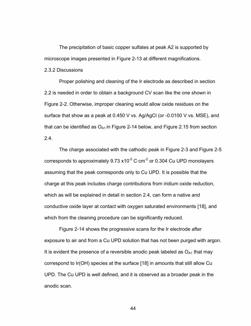
2.3.2 Discussions ........................................................................ 44
2.4 Copper Deposition on Electrochemically Formed Iridium Oxide .. 52
2.4.1 Results ............................................................................... 52
iv
2.4.2 Discussions ........................................................................ 55
2.5 Conclusions.................................................................................. 62
2.6 References................................................................................... 63
3 EFFECT OF DIFFERENT ELECTROLYTES ON SILVER UNDER-
POTENTIAL DEPOSITION AT PLATINUM EQCM ................................. 67
3.1 Introduction .................................................................................. 67
3.2 Experimental ................................................................................ 70
3.3 Effect of H SO , HClO and H PO2 4 4 3 4 Electrolytes on the Electro-
oxidation of Pt EQCM........................................................................... 73
3.3.1 Results ............................................................................... 73
3.3.2 Discussions ........................................................................ 80
on Ag UPD at Pt EQCM ...... 87 3.4 Effect of H SO , HClO , and H PO2 4 4 3 4
3.4.1 Results ............................................................................... 87
3.4.2 Discussions ........................................................................ 95
3.4.2.1 Thermodynamic parameters of Ag UPD on Pt
EQCM…………………………………………………………...96
3.4.2.2 Estimated Ag UPD Amounts from Sulfuric and
Perchloric Acid Electrolytes from EQCM Mass-responses..98
3.4.2.3 Estimated Ag UPD Amounts from Phosphoric Acid
Electrolyte and the Effect of the Platinum Premonolayer
Oxidation .......................................................................... 103
3.5 Conclusions................................................................................ 107
3.6 References................................................................................. 108
REFERENCE LIST........................................................................................... 112
v
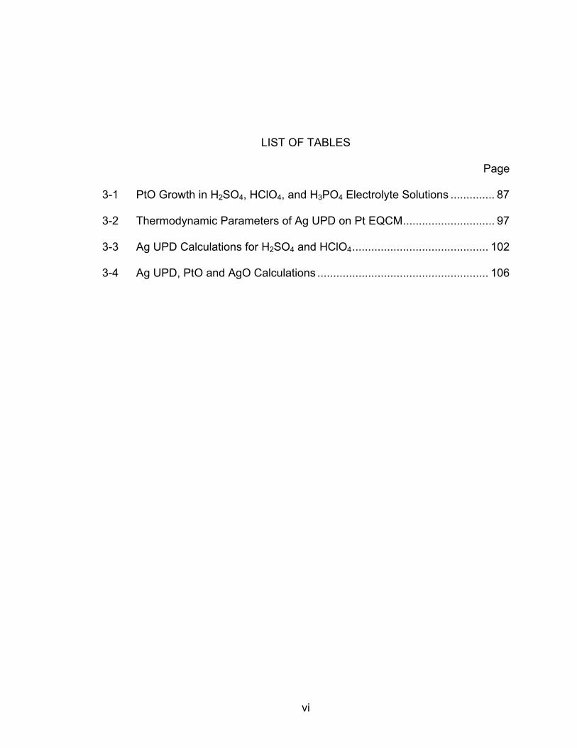
LIST OF TABLES
Page
3-1 PtO Growth in H Electrolyte Solutions .............. 87 SO , HClO , and H PO2 4 4 3 4
3-2 Thermodynamic Parameters of Ag UPD on Pt EQCM............................. 97
3-3 Ag UPD Calculations for H ........................................... 102 SO and HClO2 4 4
3-4 Ag UPD, PtO and AgO Calculations ...................................................... 106
vi
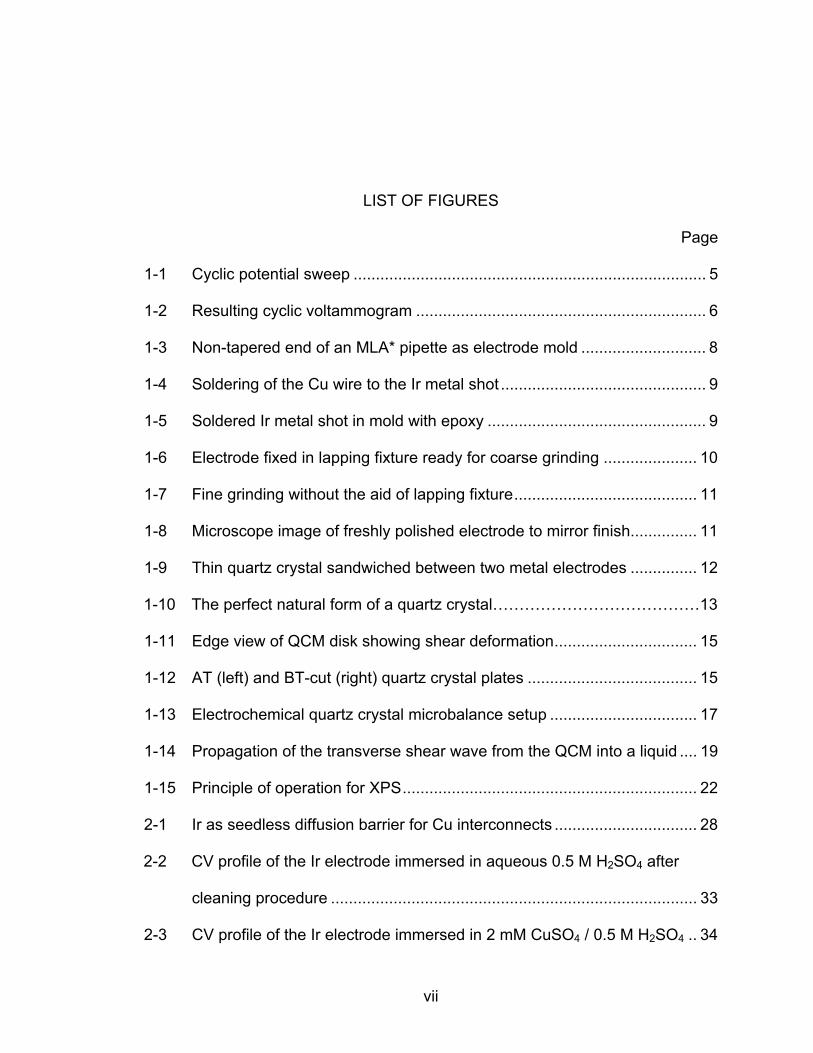
LIST OF FIGURES
Page
1-1 Cyclic potential sweep ............................................................................... 5
1-2 Resulting cyclic voltammogram ................................................................. 6
1-3 Non-tapered end of an MLA* pipette as electrode mold ............................ 8
1-4 Soldering of the Cu wire to the Ir metal shot .............................................. 9
1-5 Soldered Ir metal shot in mold with epoxy ................................................. 9
1-6 Electrode fixed in lapping fixture ready for coarse grinding ..................... 10
1-7 Fine grinding without the aid of lapping fixture......................................... 11
1-8 Microscope image of freshly polished electrode to mirror finish............... 11
1-9 Thin quartz crystal sandwiched between two metal electrodes ............... 12
1-10 The perfect natural form of a quartz crystal…………………………………13
1-11 Edge view of QCM disk showing shear deformation................................ 15
1-12 AT (left) and BT-cut (right) quartz crystal plates ...................................... 15
1-13 Electrochemical quartz crystal microbalance setup ................................. 17
1-14 Propagation of the transverse shear wave from the QCM into a liquid .... 19
1-15 Principle of operation for XPS.................................................................. 22
2-1 Ir as seedless diffusion barrier for Cu interconnects ................................ 28
2-2 CV profile of the Ir electrode immersed in aqueous 0.5 M H SO after 2 4
cleaning procedure .................................................................................. 33
2-3 CV profile of the Ir electrode immersed in 2 mM CuSO / 0.5 M H SO .. 344 2 4
vii
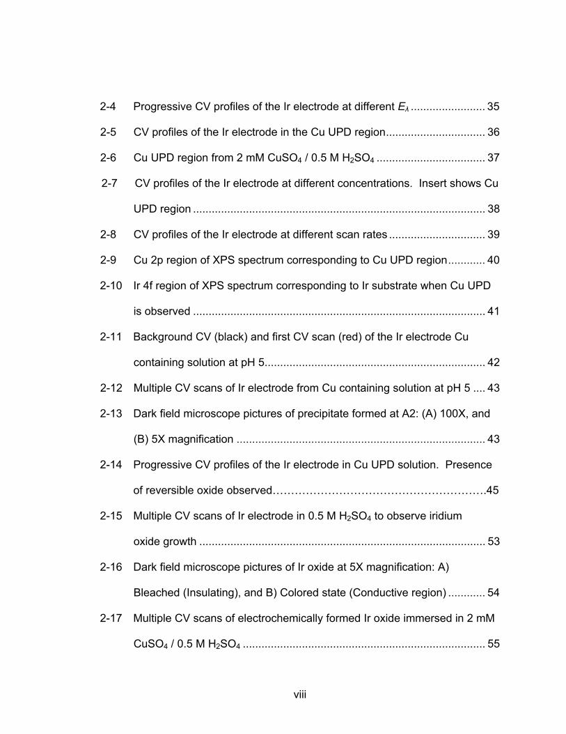
2-4 Progressive CV profiles of the Ir electrode at different E ........................ 35 λ
2-5 CV profiles of the Ir electrode in the Cu UPD region................................ 36
2-6 Cu UPD region from 2 mM CuSO ................................... 37 / 0.5 M H SO4 2 4
2-7 CV profiles of the Ir electrode at different concentrations. Insert shows Cu
UPD region .............................................................................................. 38
2-8 CV profiles of the Ir electrode at different scan rates ............................... 39
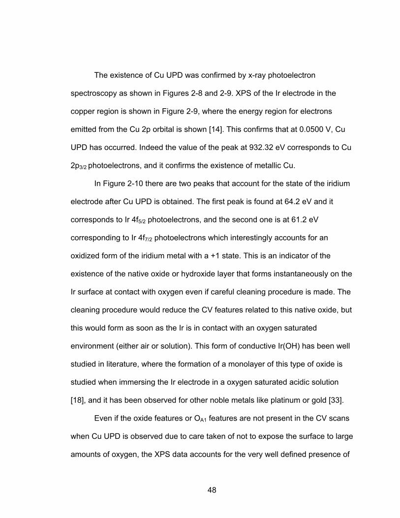
2-9 Cu 2p region of XPS spectrum corresponding to Cu UPD region............ 40
2-10 Ir 4f region of XPS spectrum corresponding to Ir substrate when Cu UPD
is observed .............................................................................................. 41
2-11 Background CV (black) and first CV scan (red) of the Ir electrode Cu
containing solution at pH 5....................................................................... 42
2-12 Multiple CV scans of Ir electrode from Cu containing solution at pH 5 .... 43
2-13 Dark field microscope pictures of precipitate formed at A2: (A) 100X, and
(B) 5X magnification ................................................................................ 43
2-14 Progressive CV profiles of the Ir electrode in Cu UPD solution. Presence
of reversible oxide observed………………………………………………….45
2-15 Multiple CV scans of Ir electrode in 0.5 M H SO to observe iridium 2 4
oxide growth ............................................................................................ 53
2-16 Dark field microscope pictures of Ir oxide at 5X magnification: A)
Bleached (Insulating), and B) Colored state (Conductive region) ............ 54
2-17 Multiple CV scans of electrochemically formed Ir oxide immersed in 2 mM
.............................................................................. 55 CuSO / 0.5 M H SO4 2 4
viii
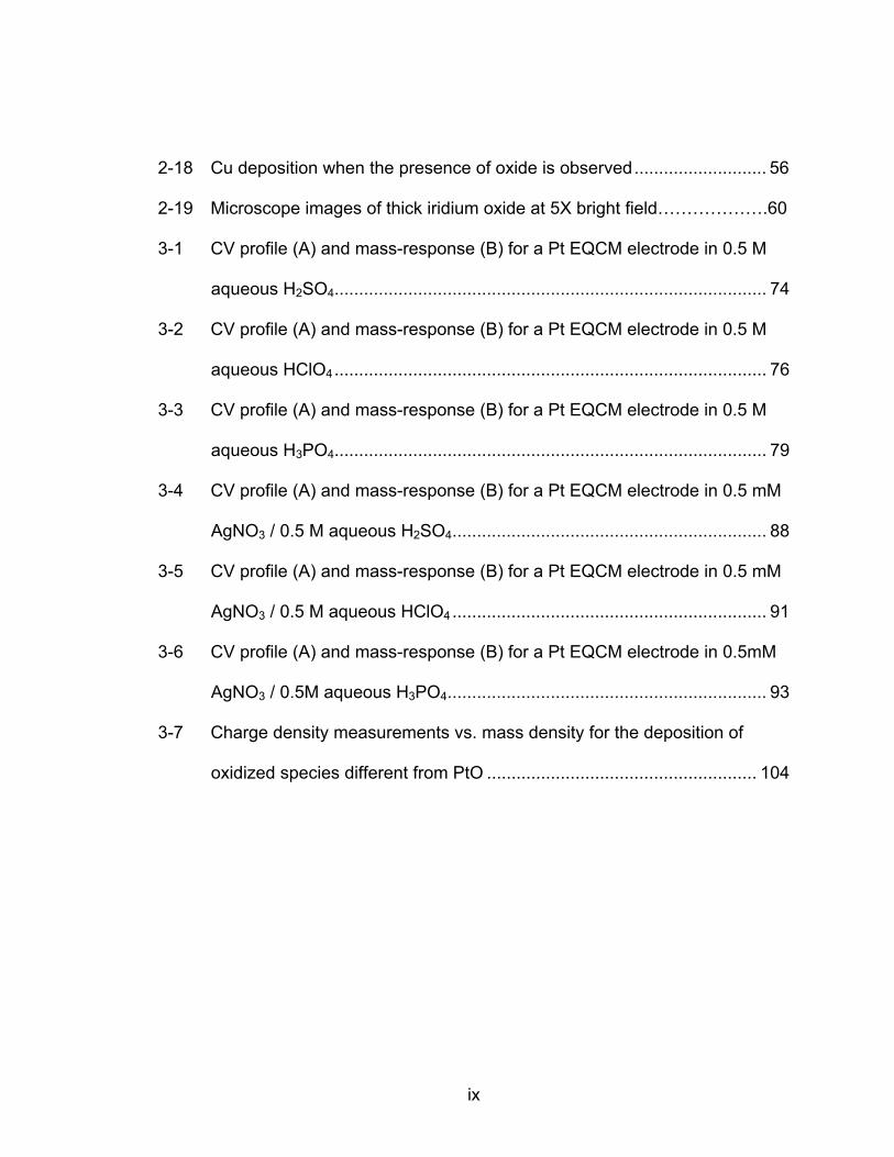
2-18 Cu deposition when the presence of oxide is observed........................... 56
2-19 Microscope images of thick iridium oxide at 5X bright field……………….60
3-1 CV profile (A) and mass-response (B) for a Pt EQCM electrode in 0.5 M
........................................................................................ 74 aqueous H SO2 4
3-2 CV profile (A) and mass-response (B) for a Pt EQCM electrode in 0.5 M
........................................................................................ 76 aqueous HClO4
3-3 CV profile (A) and mass-response (B) for a Pt EQCM electrode in 0.5 M
........................................................................................ 79 aqueous H PO3 4
3-4 CV profile (A) and mass-response (B) for a Pt EQCM electrode in 0.5 mM
................................................................ 88 AgNO / 0.5 M aqueous H SO3 2 4
3-5 CV profile (A) and mass-response (B) for a Pt EQCM electrode in 0.5 mM
................................................................ 91 AgNO / 0.5 M aqueous HClO3 4
3-6 CV profile (A) and mass-response (B) for a Pt EQCM electrode in 0.5mM
................................................................. 93 AgNO / 0.5M aqueous H PO3 3 4
3-7 Charge density measurements vs. mass density for the deposition of
oxidized species different from PtO ....................................................... 104
ix
CHAPTER 1
INTRODUCTION
1.1 Under-Potential Deposition of Metals
The under-potential deposition of metals is a phenomenon that has been
subject of study in the past decades since 1970s, and it refers to the deposition
of metals on a foreign metal substrate at potentials more positive than the
predicted by the Nernst equation for the bulk deposition of metals [1-3].
In 1974, Kolb studied the chemisorption of metal atoms on metal surfaces
in correlation to work function differences [2]. It was explained that the binding
energy for the adsorbed atoms on the substrate exceeds the binding energy of
the atoms in the respective bulk crystal, and later in the same year, electrolytic
deposition of metal atoms onto foreign metal substrates at under-potential were
studied in aqueous and non-aqueous solutions with the intention to express the
fact that under-potential deposition is a general phenomenon under certain
conditions that is even found at the solid-vacuum interface [3]. Studies that make
use of electrochemical techniques confirm the generality of this phenomenon,
since it has been observed that it is independent of concentration or scan rate,
and that it depends on plane orientation of the foreign metal.
Bruckenstein and Swathirajan studied in 1983 the equilibrium dynamic
properties of under-potential deposition on polycrystalline substrates with
1
special emphasis on information obtained from the rotating disk electrode
technique [4], and from there, extensive studies involving under-potential
deposition of different metals on polycrystalline [5] and single crystal surfaces [6]
have been made while using different electrochemical techniques.
For this study, the under-potential deposition of Cu and Ag are studied
with the use of potential sweep methods (e.g. cyclic voltammetry, linear sweep
voltammetry). These systems show a Nernstian behavior and results can be
analyzed by making use of the concepts that will be described in the following
sections.
1.2 Fundamental Concepts of Electrochemistry
In order to obtain the data that would allow the analysis of the under-
potential deposition of Cu and Ag, a conventional three-way electrode cell was
employed. In this arrangement the current is passed between the electrode of
interest or working electrode (WE) and a counter electrode (CE), and the
potential of the WE is monitored relative to a separate reference electrode (RE)
that has the characteristic of approaching ideal nonpolarizability [7].
For a chemical process in solution, the free energy (ΔG) associated with
the transfer of an electron to an oxidized species in solution is seen to be
composed of the free energy associated with transfer of the oxidized species
from solution to vacuum, the free energy associated with the transfer of an
electron to the oxidized species in vacuum, and the free energy associated with
the transfer of the reduced species from vacuum to solution [8]. If the oxidized
2
and reduced species are at unit activity then the free energy of the reduction is a
standard free energy and has the usual relationship to the standard reduction
potential:
oo nFEΔG −= (1)
The standard potential E° is an empirical constant expressing the redox-active
energy levels on the oxidized and reduced species in the general process:
(2) RneO ⇔+
For this process in equilibrium condition [7], thermodynamic arguments show that
the Nernst Equation corresponds to:
R
O0
aaln
nFRTEE += (3)
Where aO and aR are the activities of the oxidized and reduced species. It is
usually more convenient to work with concentrations instead of activities and
hence the Nernst equation can be rewritten as follows:
*R
*O0
*R
*O
R
O0
CCln
nFRTE
CCln
nFRTln
nFRTE E +=++= '
γγ (4)
3
Where the E°’ is the formal potential that includes the activity coefficients for the
specific medium, and generally the difference between standard and formal
potential is not expected to be great.
The Nernst equation provides a correlation between electrode potential E
and the concentration of participants in the electrode process. If a system follows
the Nernst equation or an equation derived from it, the electrode reaction is often
said to be thermodynamically or electrochemically reversible (or Nernstian). It is
important to emphasize that the Nernst equation is valid only at the equilibrium
condition [13]. Electrochemical techniques like cyclic voltammetry involve non-
equilibrium conditions, and therefore cannot be expected to exhibit a Nernstian
response unless rates are very fast and equilibrium is quickly reestablished in the
surface.
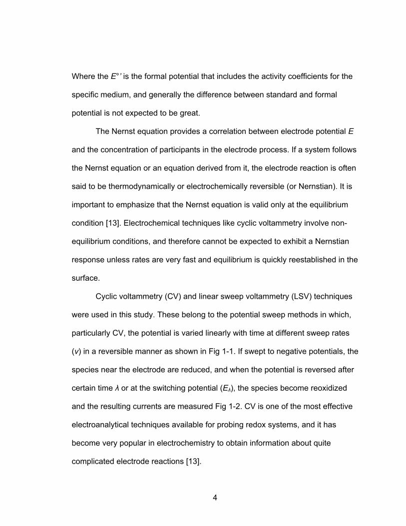
Cyclic voltammetry (CV) and linear sweep voltammetry (LSV) techniques
were used in this study. These belong to the potential sweep methods in which,
particularly CV, the potential is varied linearly with time at different sweep rates
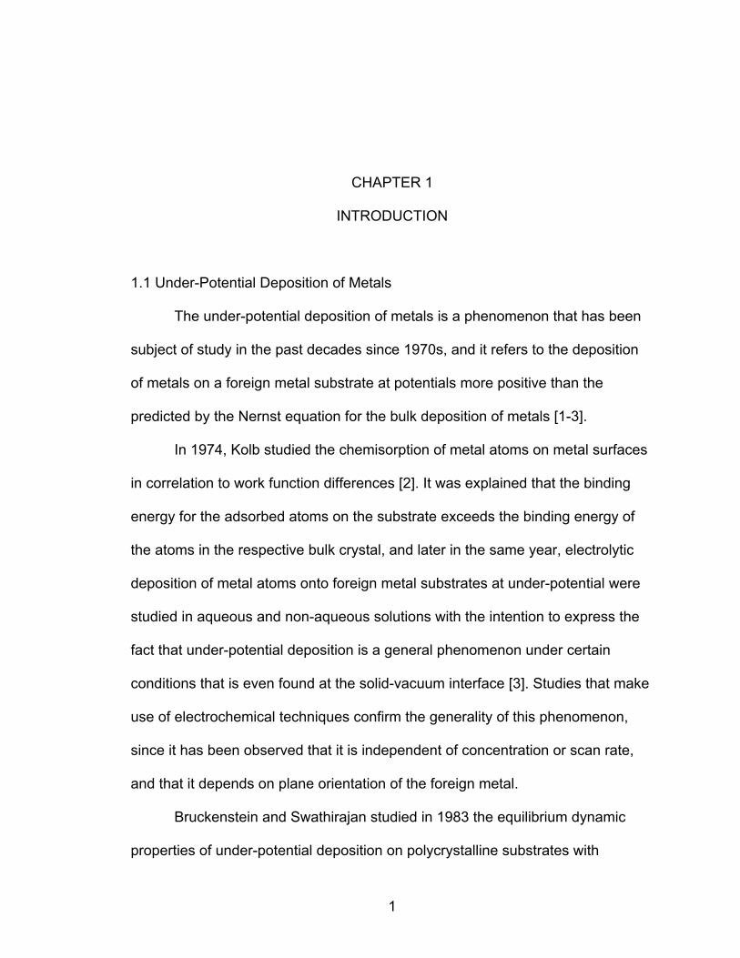
(v) in a reversible manner as shown in Fig 1-1. If swept to negative potentials, the
species near the electrode are reduced, and when the potential is reversed after
certain time λ or at the switching potential (Eλ), the species become reoxidized
and the resulting currents are measured Fig 1-2. CV is one of the most effective
electroanalytical techniques available for probing redox systems, and it has
become very popular in electrochemistry to obtain information about quite
complicated electrode reactions [13].
4
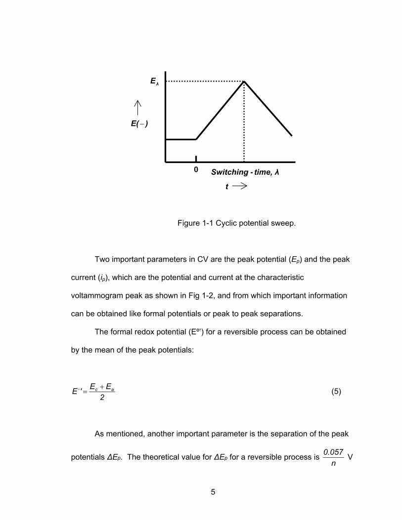
λE
λtime,
Figure 1-1 Cyclic potential sweep.
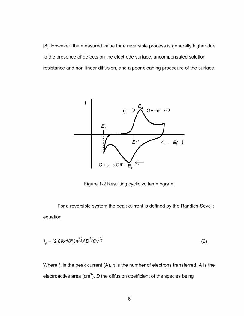
Two important parameters in CV are the peak potential (Ep) and the peak
current (ip), which are the potential and current at the characteristic
voltammogram peak as shown in Fig 1-2, and from which important information
can be obtained like formal potentials or peak to peak separations.
The formal redox potential (Eº’) for a reversible process can be obtained
by the mean of the peak potentials:
2EE'E ac +=o (5)
As mentioned, another important parameter is the separation of the peak
potentials ΔEp. The theoretical value for ΔEp for a reversible process is n
0.057 V
-Switchin0
t
)E −(
g
5
[8]. However, the measured value for a reversible process is generally higher due
to the presence of defects on the electrode surface, uncompensated solution
resistance and non-linear diffusion, and a poor cleaning procedure of the surface.
Figure 1-2 Resulting cyclic voltammogram.
For a reversible system the peak current is defined by the Randles-Sevcik
equation,
21
21
235
p CvAD)n(2.69x10i = (6)
Where ip is the peak current (A), n is the number of electrons transferred, A is the
electroactive area (cm2), D the diffusion coefficient of the species being
λE
•→+ OeO
)E( −'0E
OeO →−•i
cE
aEpi
6
2oxidized/reduced (cm ·s-1), C is the concentration of this same species in the bulk
solution (mol·cm-3), and v is the scan rate (V·s-1). For this study, equation (6) can
be used in order to determine the electroactive area of the electrode after the CV
data has been obtained. The linear sweep voltammetry technique differs from CV
in that it involves only one scan without a reverse one.
The potential sweep methods are controlled potential techniques where a
potentiostat is essential to direct the electrical potential between the working and
reference electrodes in a three-electrode cell at a preset value. The potentiostat
forces whatever current is necessary to flow between the working and counter
electrodes to keep the desired potential, as long as the needed cell voltage and
current do not exceed the compliance limits of the potentiostat. In this study, the
electrochemical experiments were performed using a CH Instruments © * 400 or a
440 model time-resolved EQCM potentiostat, and controlled by a personal
computer. The instrument’s software was used to record all data from
electrochemical experiments.
1.3 Electrode Preparation
The electrodes used for the electrochemical experiments corresponding to
Chapter 2 were made with Ir ESPI† shots. Following is the step by step
procedure on how to prepare an electrode, but for a more detailed description on
* CH Instruments, Inc. http://www.chinstruments.com† Electronic Space Products Incorporated, http://www.espi-metals.com
7
the materials and polishing procedure, the reader can refer to the laboratory
manual [38].
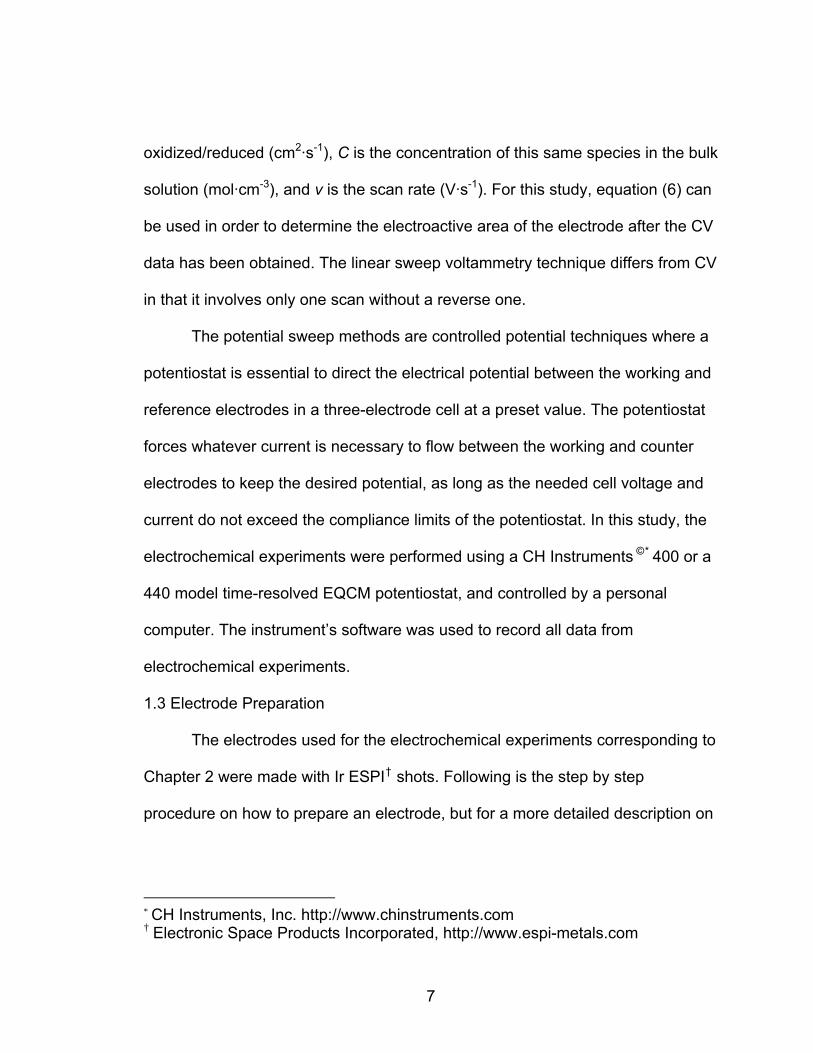
The mold where the metal shot is supported consists of the non-tapered
end of an MLA pipette, which was cut off as shown in Figure 1-3.
Figure 1-3 Non-tapered end of an MLA pipette as electrode mold.
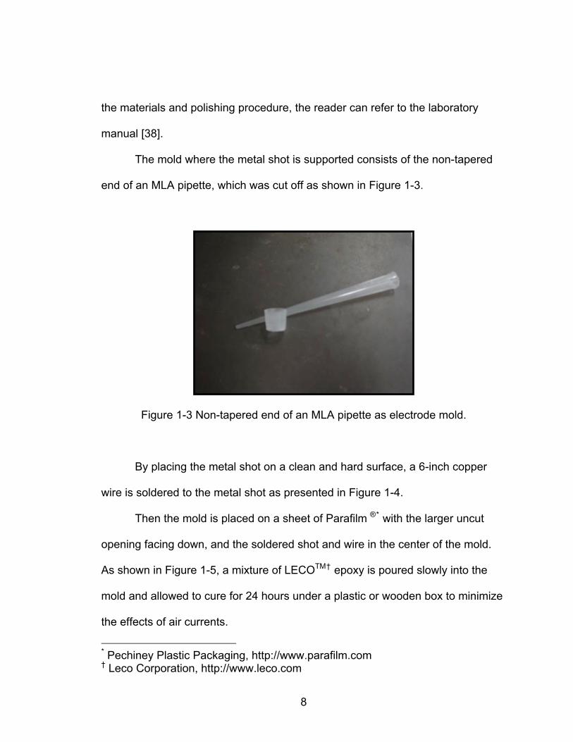
By placing the metal shot on a clean and hard surface, a 6-inch copper
wire is soldered to the metal shot as presented in Figure 1-4.
Then the mold is placed on a sheet of Parafilm ®* with the larger uncut
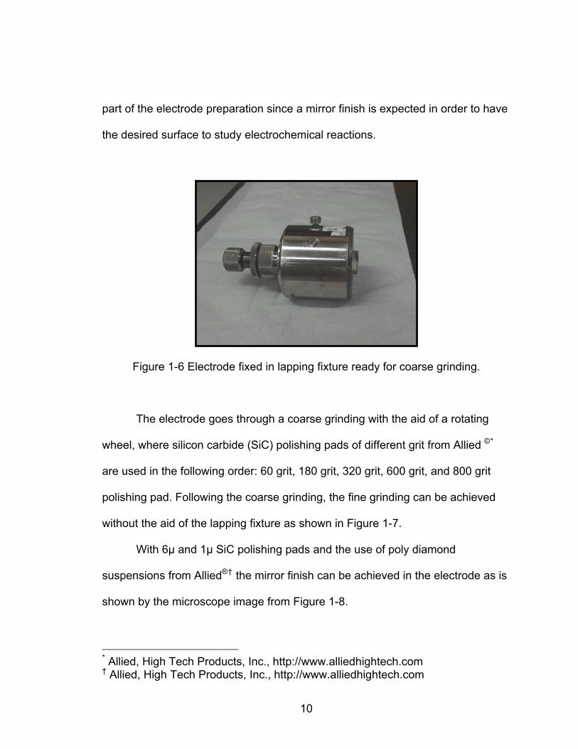
opening facing down, and the soldered shot and wire in the center of the mold.
As shown in Figure 1-5, a mixture of LECOTM† epoxy is poured slowly into the
mold and allowed to cure for 24 hours under a plastic or wooden box to minimize
the effects of air currents.
* Pechiney Plastic Packaging, http://www.parafilm.com † Leco Corporation, http://www.leco.com
8
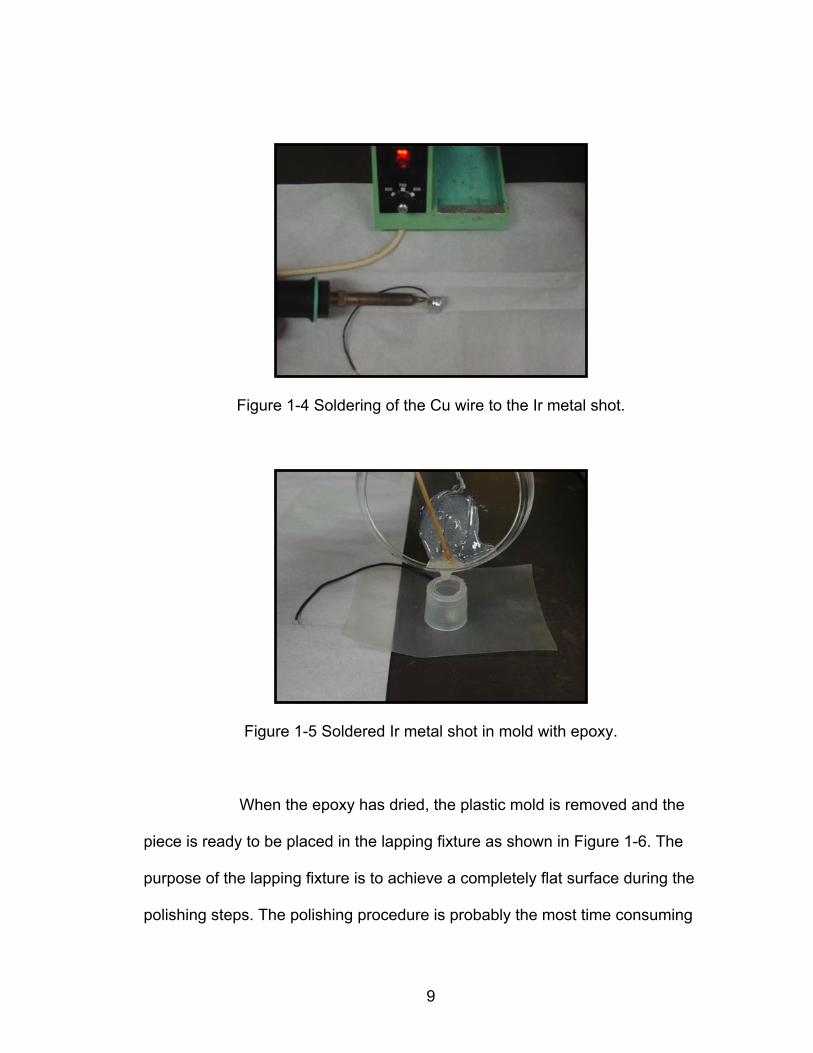
Figure 1-4 Soldering of the Cu wire to the Ir metal shot.
Figure 1-5 Soldered Ir metal shot in mold with epoxy.
When the epoxy has dried, the plastic mold is removed and the
piece is ready to be placed in the lapping fixture as shown in Figure 1-6. The
purpose of the lapping fixture is to achieve a completely flat surface during the
polishing steps. The polishing procedure is probably the most time consuming
9
part of the electrode preparation since a mirror finish is expected in order to have
the desired surface to study electrochemical reactions.
Figure 1-6 Electrode fixed in lapping fixture ready for coarse grinding.
The electrode goes through a coarse grinding with the aid of a rotating
wheel, where silicon carbide (SiC) polishing pads of different grit from Allied ©*
are used in the following order: 60 grit, 180 grit, 320 grit, 600 grit, and 800 grit
polishing pad. Following the coarse grinding, the fine grinding can be achieved
without the aid of the lapping fixture as shown in Figure 1-7.
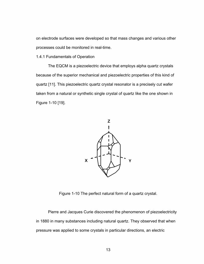
With 6µ and 1µ SiC polishing pads and the use of poly diamond
suspensions from Allied®† the mirror finish can be achieved in the electrode as is
shown by the microscope image from Figure 1-8.
* Allied, High Tech Products, Inc., http://www.alliedhightech.com † Allied, High Tech Products, Inc., http://www.alliedhightech.com
10
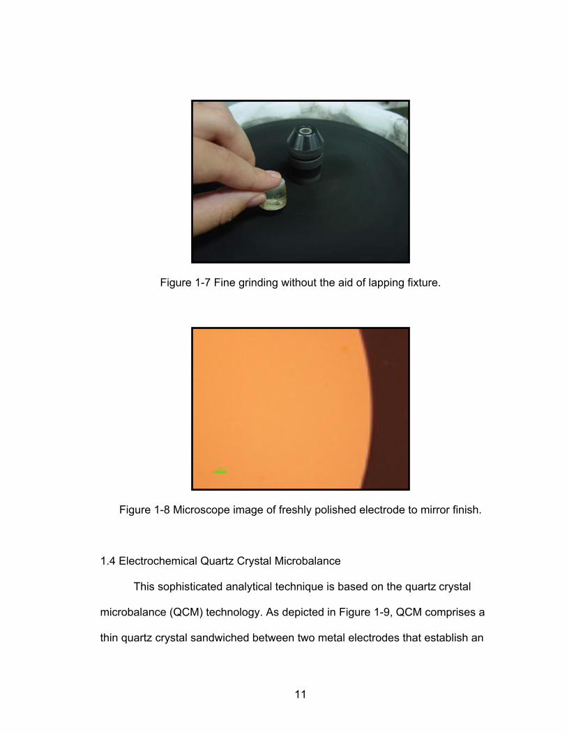
Figure 1-7 Fine grinding without the aid of lapping fixture.
Figure 1-8 Microscope image of freshly polished electrode to mirror finish.
1.4 Electrochemical Quartz Crystal Microbalance
This sophisticated analytical technique is based on the quartz crystal
microbalance (QCM) technology. As depicted in Figure 1-9, QCM comprises a
thin quartz crystal sandwiched between two metal electrodes that establish an
11

alternating electric field across the crystal, causing vibrational motion of the
crystal at its resonant frequency [9-12]. This resonant frequency is sensitive to
mass changes and other factors of the crystal and its electrodes.
Figure 1-9 Thin quartz crystal sandwiched between two metal electrodes.
The electrochemical quartz crystal microbalance (EQCM), which is the
electrochemical application of the QCM, has provided a powerful approach to
examining electrochemical processes involving thin films, including monolayer
and submonolayer films [16-18]. These studies have revealed detailed
mechanistic information about film deposition and dissolution, surface
morphology changes, and mass changes in thin films caused by redox or other
chemical processes [14, 15].
In its earliest form, the EQCM was used in ex situ experiments to measure
mass changes at electrode surfaces after electrodeposition of metals. Later, the
experimental methods required for its use as an in situ mass sensor for thin films
12
on electrode surfaces were developed so that mass changes and various other
processes could be monitored in real-time.
1.4.1 Fundamentals of Operation
The EQCM is a piezoelectric device that employs alpha quartz crystals
because of the superior mechanical and piezoelectric properties of this kind of
quartz [11]. This piezoelectric quartz crystal resonator is a precisely cut wafer
taken from a natural or synthetic single crystal of quartz like the one shown in
Figure 1-10 [19].
Z
X Y
Figure 1-10 The perfect natural form of a quartz crystal.
Pierre and Jacques Curie discovered the phenomenon of piezoelectricity
in 1880 in many substances including natural quartz. They observed that when
pressure was applied to some crystals in particular directions, an electric
13
potential was produced between the deformed surfaces of the crystal, with the
potential being proportional to the applied pressure. This behavior is referred to
as the piezoelectric effect, which is derived from the Greek word “piezein”,
meaning to press. Only crystals without a center of symmetry possess this
property [10].
The converse piezoelectric effect in which application of a voltage across
these crystals resulted in a corresponding shear strain is the basis of the QCM. If
an alternating potential is applied, vibrational motion occurs within the quartz
crystal lattice. Stable oscillation can be attained only at the natural resonant
frequency of the crystal, and at that frequency the crystal presents low
impedance to the exciting voltage. This crystal is thus called a quartz resonator
[10].
The useful mode of vibration in the QCM is the high frequency thickness-
shear mode that indicates that the motion of the disk surface is precisely parallel
to the disk face, and has been shown to be sensitive to the addition or removal of
mass at the electrode surface.
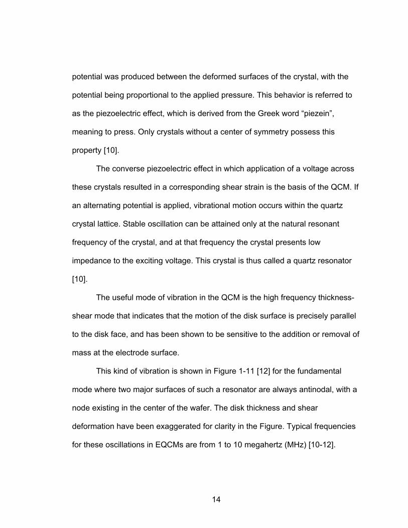
This kind of vibration is shown in Figure 1-11 [12] for the fundamental
mode where two major surfaces of such a resonator are always antinodal, with a
node existing in the center of the wafer. The disk thickness and shear
deformation have been exaggerated for clarity in the Figure. Typical frequencies
for these oscillations in EQCMs are from 1 to 10 megahertz (MHz) [10-12].
14
DISTORTIONSHEARNODE
Figure 1-11 Edge view of QCM disk showing shear deformation.
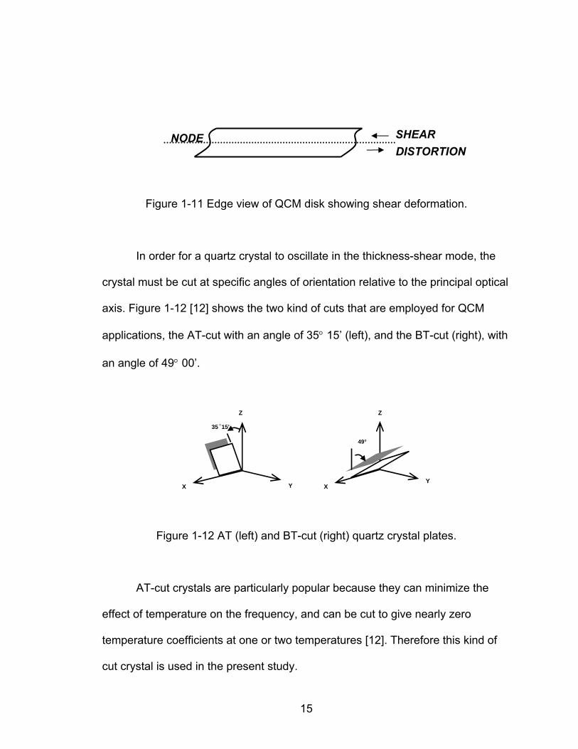
In order for a quartz crystal to oscillate in the thickness-shear mode, the
crystal must be cut at specific angles of orientation relative to the principal optical
axis. Figure 1-12 [12] shows the two kind of cuts that are employed for QCM
applications, the AT-cut with an angle of 35° 15’ (left), and the BT-cut (right), with
an angle of 49° 00’.
15'35 o
ZZ
YY XX
49°
Figure 1-12 AT (left) and BT-cut (right) quartz crystal plates.
AT-cut crystals are particularly popular because they can minimize the
effect of temperature on the frequency, and can be cut to give nearly zero
temperature coefficients at one or two temperatures [12]. Therefore this kind of
cut crystal is used in the present study.
15
1.4.2 Electrochemical Apparatus
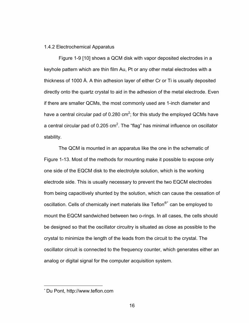
Figure 1-9 [10] shows a QCM disk with vapor deposited electrodes in a
keyhole pattern which are thin film Au, Pt or any other metal electrodes with a
thickness of 1000 Å. A thin adhesion layer of either Cr or Ti is usually deposited
directly onto the quartz crystal to aid in the adhesion of the metal electrode. Even
if there are smaller QCMs, the most commonly used are 1-inch diameter and
have a central circular pad of 0.280 cm2; for this study the employed QCMs have
a central circular pad of 0.205 cm2. The “flag” has minimal influence on oscillator
stability.
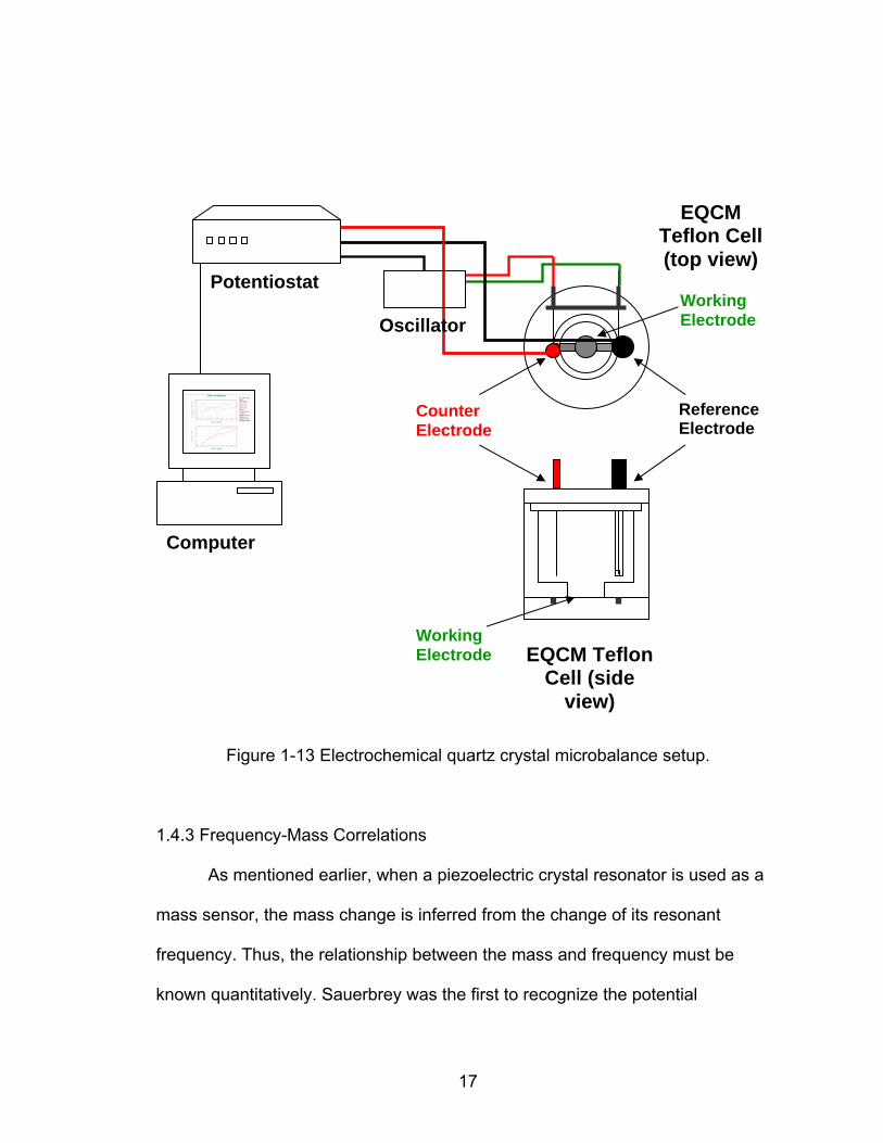
The QCM is mounted in an apparatus like the one in the schematic of
Figure 1-13. Most of the methods for mounting make it possible to expose only
one side of the EQCM disk to the electrolyte solution, which is the working
electrode side. This is usually necessary to prevent the two EQCM electrodes
from being capacitively shunted by the solution, which can cause the cessation of
oscillation. Cells of chemically inert materials like Teflon®* can be employed to
mount the EQCM sandwiched between two o-rings. In all cases, the cells should
be designed so that the oscillator circuitry is situated as close as possible to the
crystal to minimize the length of the leads from the circuit to the crystal. The
oscillator circuit is connected to the frequency counter, which generates either an
analog or digital signal for the computer acquisition system.
* Du Pont, http://www.teflon.com
16
Computer
Potentiostat
EQCM Teflon Cell (side
view)
EQCM Teflon Cell (top view)
Figure 1-13 Electrochemical quartz crystal microbalance setup.
1.4.3 Frequency-Mass Correlations
As mentioned earlier, when a piezoelectric crystal resonator is used as a
mass sensor, the mass change is inferred from the change of its resonant
frequency. Thus, the relationship between the mass and frequency must be
known quantitatively. Sauerbrey was the first to recognize the potential
Counter Electrode
Reference Electrode
Working Electrode
Working Electrode Oscillator
17
usefulness of AT and BT crystals as mass sensors. He demonstrated the
extremely sensitive nature of these piezoelectric devices towards mass changes
at the surface of the QCM electrodes. He also described their differential radial
mass sensitivity and correlated this with the radial distribution of the vibrational
amplitude. The results of his pioneering work in this area are embodied in the
Sauerbrey equation, which relates the mass change per unit area at the QCM
electrode surface to the observed change in oscillation frequency of the crystal:
( ) Δmμρ
2nfΔf 21
20
⎟⎟⎠
⎞⎜⎜⎝
⎛−= (7)
Where Δf is the frequency change caused by addition of a mass per unit area,
m, to the crystal surface, n is the harmonic number of the oscillation (e.g., n = 1
for 5 MHz with a 5 MHz crystal), μ is the shear modulus of quartz (2.95 x 10¹¹
g·cm-1 ·s-2), and is the density of quartz (2.65 g·cm-3ρ ). The constants are
usually lumped together to yield a single constant, the sensitivity factor, fC
(8) ΔmCΔf f−=
Which has the value of 1.42 x10⁻⁹ Hz·ng-1 for a 7.995 MHz crystal like the one
employed in this study. As seen from Equation (7), the mass sensitivity is
18
dependent of the square of resonant frequency (f 0). Higher frequency operation
of the quartz crystal thus offers the advantage of grater mass sensitivity.
Although the Sauerbrey relationship was derived for QCM operation in gas
phase, it is still applicable to the operation in liquids under appropriate conditions.
Therefore the behavior of the QCM depends on the medium in which it is
operating, because the medium couples to the crystal surface and affects the
shear mode.
z
x
Liquid
Figure 1-14 Propagation of the transverse shear wave from the QCM into a
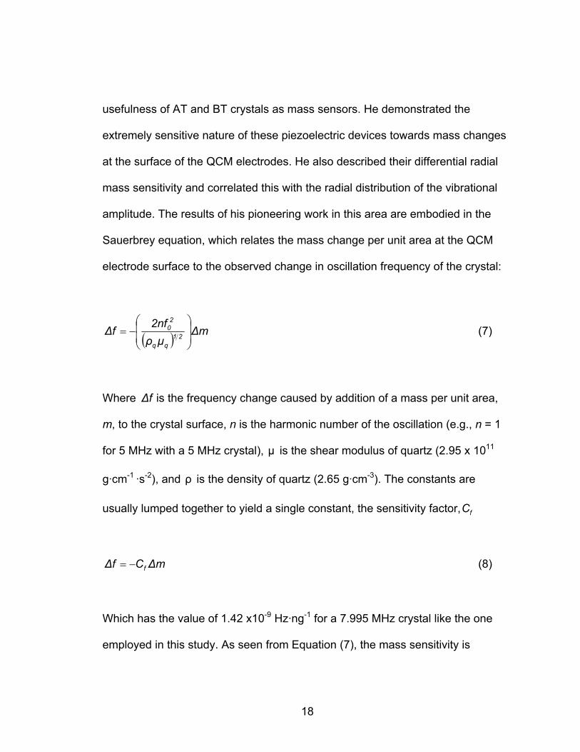
liquid.
When a planar surface that is oscillating in a shear mode is immersed into
any medium, a shear wave propagates normally away from the surface into the
medium in the form of acoustic waves as represented in Figure 1-14 [20]. This
19
behavior was first treated by Glassford, and later by Kanazawa and Gordon.
Kanazawa’s treatment of the influence of the solution properties on the crystal
permits the prediction of the change in resonant frequency that accompanies
immersion of the crystal into a viscous medium:
21
1123o μπρ
ηρfΔf ⎟⎟⎠
⎞⎜⎜⎝
⎛−= (9)
1/2Where the decrease in resonant frequency is seen to be proportional to ( )11ηρ ,
the square root of the density times the viscosity of the medium. This equation
predicts the decrease in frequency (f0) of ca. 700 Hz on transfer from vacuum to
pure water at 20°C [10, 12].
If the crystal is being used as the frequency determining element in a
circuit, frequency’s changes may be observed that are not derived from mass
changes but rather result from some other factors, and a non-ideal behavior is
suspected. Some of these factors are temperature, viscoelastic properties,
surface roughness and porosity, and surface stress, which are fully described in
the references [10, 12]. Detailed publications can be found that describe the
possible and future applications of the EQCM as well as the main concerns
regarding its use [21-30], and several attempts have been made to integrate it
with a rotating device to obtain rotating EQCM data [34], or even incorporate it to
20
scanning electrochemical microscopy to monitor film mass and surrounding
electrolyte composition during potential cycling [35].
For some, the question that if the quartz crystal microbalance is really a
mass sensor has been answered in a recent publication by Mecea [36] based on
its description as an actuator that generates a mega-gravity, time-dependent
inertial field on the surface of the quartz. The very high mass sensitivity of the
quartz crystal microbalance is explained by the very high intensity of the field
acting on the deposited film, and based on these ideas, three fundamental
principles for mass measurements are formulated and demonstrated: the field
principle, the mass sensitivity principle and the general equivalence principle.
1.5 X-Ray Photoelectron Spectroscopy
X-ray photoelectron spectroscopy (XPS), also known as electron
spectroscopy for chemical analysis (ESCA), is an electron spectroscopy method
commonly used to elucidate chemical and structural components of surfaces. It
was developed in the mid 1960s by K. Siegban and his research group, and its
principle of operation is based on the Photoelectric Effect where the concept of
photon is used to describe the ejection of electrons from the atom’s core energy
levels when a monochromatic electromagnetic wave impinge upon it, and
overcomes its binding energy as shown in Figure 1-15.
The XPS employs soft rays like Al and Mg Kα (1486.6 eV and 1253.6 eV
respectively) as photon energies of choice, and sometimes Ti Kα with energy of
2040 eV is used.
21
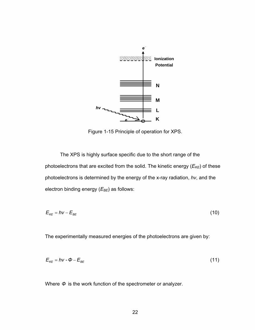
−e
−e
h L
M
N
PotentialIonization
v
K
Figure 1-15 Principle of operation for XPS.
The XPS is highly surface specific due to the short range of the
photoelectrons that are excited from the solid. The kinetic energy (EKE) of these
photoelectrons is determined by the energy of the x-ray radiation, hv, and the
electron binding energy (EBE) as follows:
(10) BEKE EhvE −=
The experimentally measured energies of the photoelectrons are given by:
(11) BEKE EΦ-hvE −=
Where Φ is the work function of the spectrometer or analyzer.
22
The detected kinetic energy is related to the binding energy of the
analyzed species by the used of the work function of the analyzer, and the
energy of the monochromatic beam. The energy of the photoelectrons leaving
the sample give a spectrum with a series of photoelectron peaks, and the binding
energy of the peaks are characteristic of each element. The peak areas can be
used to determine the composition of the material’s surface, and the shape of
each peak and the binding energy can be slightly altered by the chemical
oxidation state of the emitting atom as well as by the electron affinity of the
chemical environment where the photoelectron was emitted [37].
In the present study, the results from XPS analysis were obtained in a
VG®* ESCALAB MK II spectrometer, with an Al Kα emission ray as source of
excitation.
1.6 Conclusions
In this first chapter some of the fundamental concepts of electrochemistry
that are relevant to this work were described together with the methodology used
for the preparation of the working Ir electrode.
A detailed description of the electrochemical quartz crystal microbalance
is included, as well as an explanation of its principle of operation based on
frequency measurements that can be correlated to mass changes on the surface
of the balance by the Sauerbrey equation. References can be found that explain
in further detail the future applications of this powerful electrochemical
* Thermo Electron Corporation, http://www.thermo.com
23
instrument, as well as new literature that reveals exciting theory behind the
quartz crystal technology.
Finally a concise explanation of the XPS technique is presented, which is
one of the surface analysis techniques that provided surface characterization and
confirmed some of the results in Chapter 2 of this study.
1.7 References
1. Gerisher, H.; Kolb, D.M.; Przasnyski, M.; Surface Science 1974, 43, 662-
666.
2. Kolb, D.M., Advances in Electrochemistry and Electrochemical
Engineering, 1978. John Wiley Interscience: New York. vol. 11. p. 125.
3. Kolb, D.M.; Przasnyski, M.; Gerisher, H.; Electroanal. Chem. Interfac.
Electrochem. 1974, 54, 25-38.
4. Swathirajan, S.; Bruckenstein, S.; Electrochim. Acta 1983, 28(7), 865-877.
5. Van Huong C.N.; Gonzalez-Tejera, M.J.; J. Electroanal. Chem. 1988 244,
249-259.
6. Herrero, E.; Buller, L.J.; Abruña, H.D.; Chem. Rev. 2001, 101, 1897-1930.
7. Faulkner, L.R. Electrochemical Characterization of Chemical Systems.
1983. Academic Press, Inc.: vol. 3. p. 137.
8. Grosser, D.K., Cyclic Voltammetry: Simulation and Analysis of Reaction
Mechanism. 1993, New York: Wiley-VCH.
9. Buttry D. A.; Ward, M. D. Chem. Review, 1992, 92, 1355-1379.
10. Zhang, M., Ph. D. Thesis, University of Ottawa: Ottawa, Canada, 1995.
24
11. Salt, D. Hy-Q Handbook of Quartz Crystal Devices, Van Nostrand
Reinhold: UK, 1987, pp 5-36, 160-162.
12. Buttry, D.A. Applications of the Quartz Crystal Microbalance to
Electrochemistry, in Electroanalytical Chemistry: A series of Advances;
Bard, A. J. Marcel Dekker: New York, 1996, pp 1-85.
13. Bard, A. J.; Faulkner, L. R. Electrochemical Methods: Fundamentals and
Applications. Second Edition, John Wiley and Sons Inc.: New York, 2001,
pp 725.
14. Aurbach, D.; Moshkovich, M. J. Electrochem. Soc. 1998, 145(8), 2629-
2639.
15. Il-Hwan, K.; Kwang-Bum, K. J. Electrochem. Soc. 2004, 151(1), E7-E13.
16. Ostrom, G. S.; Buttry, D. A. J. Phys. Chem. 1995, 99(41), 15236-40.
17. Ariizumi, N.; Kamijo, M. Yamanashi-ken Kogyo Gijutsu Senta Kenkyu
Hokoku 2000, 14, 12-17.
18. Sadik, O. A.; Cheung, M-C. Talanta 2001, 55(5), 929-941.
19. O’Sullivan, C.K.; Guilbault, G. G. Biosensors & Bioelectronics 1999, 14,
663-670.
20. Lee, W.; White, H. S.; Ward, M. D. Anal. Chem. 1993, 65, 3232-3237.
21. Deakin, M.R.; Buttry, D. A. Anal. Chem. 1989, 61(20), 1147A-1154A.
22. Wunsche, M. Electrochim. Acta 1995, 5(40), 629-635.
23. Kraznaric, G. Langmuir 2001, 17, 43-4351.
24. Lay et al. J. Electroanal. Chem. 2003, 1, 1-11.
25
25. Herrero, E.; Buller, L. J.; Abruña, H. D. Chem. Rev. 2001, 101(7), 1897-
1930.
26. Nicic, L. et al. J. Phys. Chem. B 2002, 106, 12247-12252.
27. Uchida, H.; Hiei, M.; Watanabe, M. J. Electroanal. Chem. 1998, 452(1),
97-106.
28. Marx, K.A., et al. Biosensors and Bioelectronics 2001, 16, 773-782.
29. Tenreiro, A.; Cordas, C. M.; Abrantes, L. M. Portugaliae Electrochim. Acta
2003, 21(4), 361-370.
30. Jiang, M.; Ray, W. W.; Mukherjee, B.; Wang, J. Electrochem. Comm.
2004, 6, 576-582.
31. Ward, M.D.; Buttry, D.A.; Science, 1990, 249(4972), 1000-1007.
32. Deakin, M.R.; Buttry, D.A.; Anal. Chem. 1989, 61(20), 1147A-1154A.
33. Jeffrey, M.I.; Zheng, J.; Ritchie, I.M.; Meas. Sci. Technol. 2002, 11, 560-
567.
34. Vergé, M.-G.; Mettraux, P.; Olsson, C.-O.A.; Landolt, D.; J. Electroanal.
Chem. 2004, 566, 361-370.
35. Cliffel, D.E.; Bard, A.J.; Anal. Chem. 1998, 70, 1993-1998.
36. Mecea, V.M.; Sensors and Actuators A, 2006, 128, 270-277.
37. Nascente, P.A.P., Journal of Molecular Catalysis A: Chemical, 2005. 228:
p. 145-150.
38. Flores, S. Making an Electrode, 2003.
26
CHAPTER 2
COPPER UNDER-POTENTIAL DEPOSITION ON IRIDIUM
2.1 Introduction
Copper under-potential deposition has been a subject of study in the past
decades especially on platinum and gold substrates, and extensive studies with
different analytical techniques have been made in order to understand this
process [1-6 and references therein].
The competitive semiconductor industry is in constant technological
development and search of new materials that can meet the nano scale
conditions favorable for the miniaturization of on-chip interconnects. Therefore,
copper under-potential deposition has been recently studied in substrates like
ruthenium and its conductive ruthenium oxide due to the strong binding
interaction that exists between copper and these two kinds of substrates [7]. Ultra
thin films composed of ruthenium and its conductive oxides are promising
candidates as a directly copper plateable diffusion barrier for future metal
interconnects application, and copper under-potential deposition has important
implications since it allows the controlled superfilling on sub-micrometer trenches
[8].
Encouraged by these kinds of studies, copper deposition has been
recently studied on iridium metal surfaces due to the characteristics iridium has
27
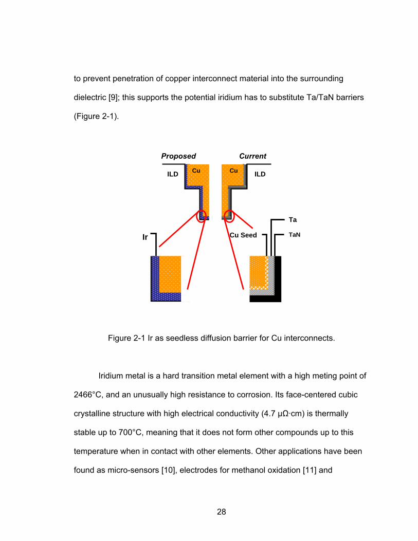
to prevent penetration of copper interconnect material into the surrounding
dielectric [9]; this supports the potential iridium has to substitute Ta/TaN barriers
(Figure 2-1).
Cu
Proposed
ILD
Current
ILD Cu
TaN Ir Cu Seed
Ta
Figure 2-1 Ir as seedless diffusion barrier for Cu interconnects.
Iridium metal is a hard transition metal element with a high meting point of
2466°C, and an unusually high resistance to corrosion. Its face-centered cubic
crystalline structure with high electrical conductivity (4.7 μΩ·cm) is thermally
stable up to 700°C, meaning that it does not form other compounds up to this
temperature when in contact with other elements. Other applications have been
found as micro-sensors [10], electrodes for methanol oxidation [11] and
28
ferroelectric non-volatile random access memories. The deposition of copper on
iridium has been characterized through electrochemical techniques, x-ray
photoelectron spectroscopy, x-ray diffraction, and scanning electron microscopy
[9]. It could be concluded that iridium is amenable to direct copper electroplating
with no seed layer needed and allows for precise potential control, important for
efficient bottom-up copper electrofill of dual-damascene features when
processing interconnect devices. Furthermore copper showed a strong adhesion
to iridium surfaces when annealed to 600°C, and overall stability. Additionally,
this kind of studies where made with iridium barrier layers deposited by atomic
layer deposition and scanning electron microscopy, and the results demonstrated
that these permit copper wetting and superfill during electrodeposition without the
need for a copper seed layer [12]. Therefore the importance of the study of
copper under-potential deposition on iridium is evident since it would allow
controlled superfilling on sub-micrometer trenches with a stronger binding of the
copper to the iridium metal.
In this chapter the copper under-potential deposition on iridium is studied
by means of cyclic voltammetry, linear sweep voltammetry, and x-ray
photoelectron spectroscopy. The presence of copper under-potential deposition
is observed on iridium but not on its thick electrochromic iridium oxide as
previously observed on ruthenium oxide; although results show that lower
oxidation state iridium oxide (or native oxide) is a good conductor that allows
copper deposition. The particular behavior of iridium and iridium oxide towards
29
copper deposition is examined, and the effect of copper concentration, scan rate,
and pH is considered. Results account for the limiting nature of copper under-
potential deposition process, and increased hydrogen concentration in solution
results in copper nucleation at the under-potential region. Interestingly, at pH
different than acidic, a particular phenomenon is observed that is associated with
the formation of basic copper sulfates or artificial patinas, which has been
previously observed when copper is deposited at pH 5 on platinum and
ruthenium substrates.
Thermodynamic information shows how copper under-potential deposition
is indeed favored on the iridium substrate to a greater extent than substrates like
platinum or even ruthenium and its oxides. The strong binding of the copper
under-potential deposition to the iridium substrate, and the small amounts at
which this occurs, are qualities that make iridium meet the nano scale conditions
favorable for the miniaturization of on-chip interconnects.
2.2 Experimental
*Ir ESPI shots were made into disks electrodes as previously described in
Chapter 1. The shots were polished to mirror finish by different grit silicon carbide
(SiC) pads (Allied®†), followed by soaking for seven minutes in aqua regia, and
electrochemical cleaning in sulfuric acid. A platinum sheet counter electrode, a
mercury/mercurous sulfate (Hg/Hg SO2 4 or MSE) or silver/silver chloride
(Ag/AgCl) with a potential shift of 0.660 V and 0.197 V respectively vs. the * Electronic Space Products Incorporated, http://www.espi-metals.com † Allied High Tech Products Incorporated, http://www.alliedhightech.com
30
standard hydrogen electrode (SHE) were employed. All potentials here in
referred, including the potentials presented in the cyclic voltammetry curves, are
reported versus the Ag/AgCl reference electrode, except for the experiments
related to basic copper sulfates formation and iridium oxide growth where MSE
reference electrode was employed.
High purity copper sulfate (99.9 %) and potassium sulfate (99.0 %
minimum) from Aldrich®*, 96.2 weight % sulfuric acid and sodium hydroxide (both
from Mallinckrodt Baker, Inc. ©†) were used to make all electrolyte solutions in
ultrapure water (18.2 MΩ, Millipore©‡). All solutions were purged with argon for
10 minutes. Electrochemical investigation was performed using a 440 and 400
series model electrochemical analyzer from CH Instruments, Inc. ©§. Cu plating
on Ir electrodes was carried out under argon atmosphere in order to avoid
presence of native oxides on the surface.
Hydrous Ir oxide was prepared electrochemically by potential cycling of a
freshly prepared Ir electrode between -0.200 V and 1.300 V vs. Ag/AgCl for 250
complete cycles in aqueous sulfuric acid solution. This is different from how the
oxide is formed for Pt or Ru, given that the oxide does not grow at constant
potential since an electrical field across the oxide is needed to support ionic
transport necessary for growth to occur [31, 32].
* Sigma Aldrich Corporation, http://www.sigmaaldrich.com † Mallinckrodt Baker, Inc. http://www.mallchem.com‡ Millipore Corporation, http://www.millipore.com§ CH Instruments, Inc. http://www.chinstruments.com
31
The potential limits used to obtain the cyclic voltammograms for the
iridium electrode from both the background electrolyte and the copper containing
solutions, are -0.100 V and 0.450 V where the copper under-potential deposition
and the initial growth of copper bulk overlayers (not complete, since it is not the
subject of study) are observed.
The open circuit potential for the iridium electrodes is between 0.430 V
and 0.520 V vs. Ag/AgCl for both background electrolyte and copper containing
solutions; these values were employed as the initial potentials in the cyclic
voltammograms. All experiments were performed at a scan rate of 20.0 m·Vs-1
and room temperature, except for the cyclic voltammograms where the objective
is to observe the influence of scan rate on the under-potential deposition of
copper. Additionally, the scan rate was varied to 50.0 m·Vs-1 when growing the
thick iridium oxide film.
The geometric area of the iridium electrode is 0.340 cm2 and the
electroactive area corresponds to 0.430 cm2, which is obtained by means of
Randles-Sevcik equation (6) from data obtained from cyclic voltammetry profiles
of the iridium electrode in potassium ferro-cyanide solution. With this information
the cyclic voltammograms could be plotted as potential versus current density.
®*XPS data were collected using a VG ESCALAB MKII spectrometer (VG
Scientific Ltd) with an Al Kα x-ray as the excitation source as explained in
* Thermo Electron Corporation, http://www.thermo.com
32
Chapter 1. The images were recorded in dark field at different magnifications
using a microscope (Nikon® ME600L*).
2.3 Copper Under-Potential Deposition on Iridium
2.3.1 Results
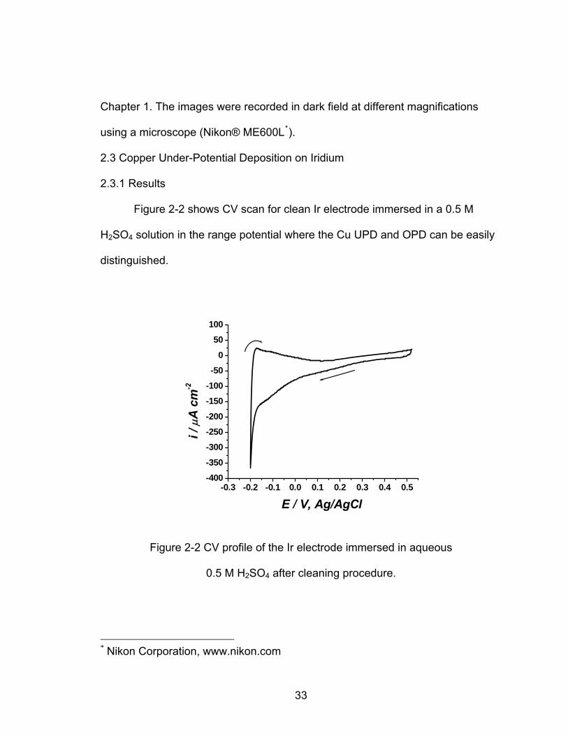
Figure 2-2 shows CV scan for clean Ir electrode immersed in a 0.5 M
H SO2 4 solution in the range potential where the Cu UPD and OPD can be easily
distinguished.
-0.3 -0.2 -0.1 0.0 0.1 0.2 0.3 0.4 0.5-400-350
-300-250-200
-150-100-50
0
50100
i / μ
A c
m-2
E / V, Ag/AgCl
Figure 2-2 CV profile of the Ir electrode immersed in aqueous
SO after cleaning procedure. 0.5 M H2 4
* Nikon Corporation, www.nikon.com
33
The CV scans started at the open circuit potential of the Ir electrode in this
solution, 0.520 V vs. Ag/AgCl, and continuous cycling was made in order to
obtain reproducible CV scans that would ensure proper electrochemical cleaning
of the Ir surface. Additionally, at each cathodic scan the potential was held at -
0.100 V to reduce the surface since the presence of native iridium oxides has
been observed at 0.450 V [13] that would interfere with the Cu UPD. The final
potential of the CV was that of 0.520 V in the anodic scan.
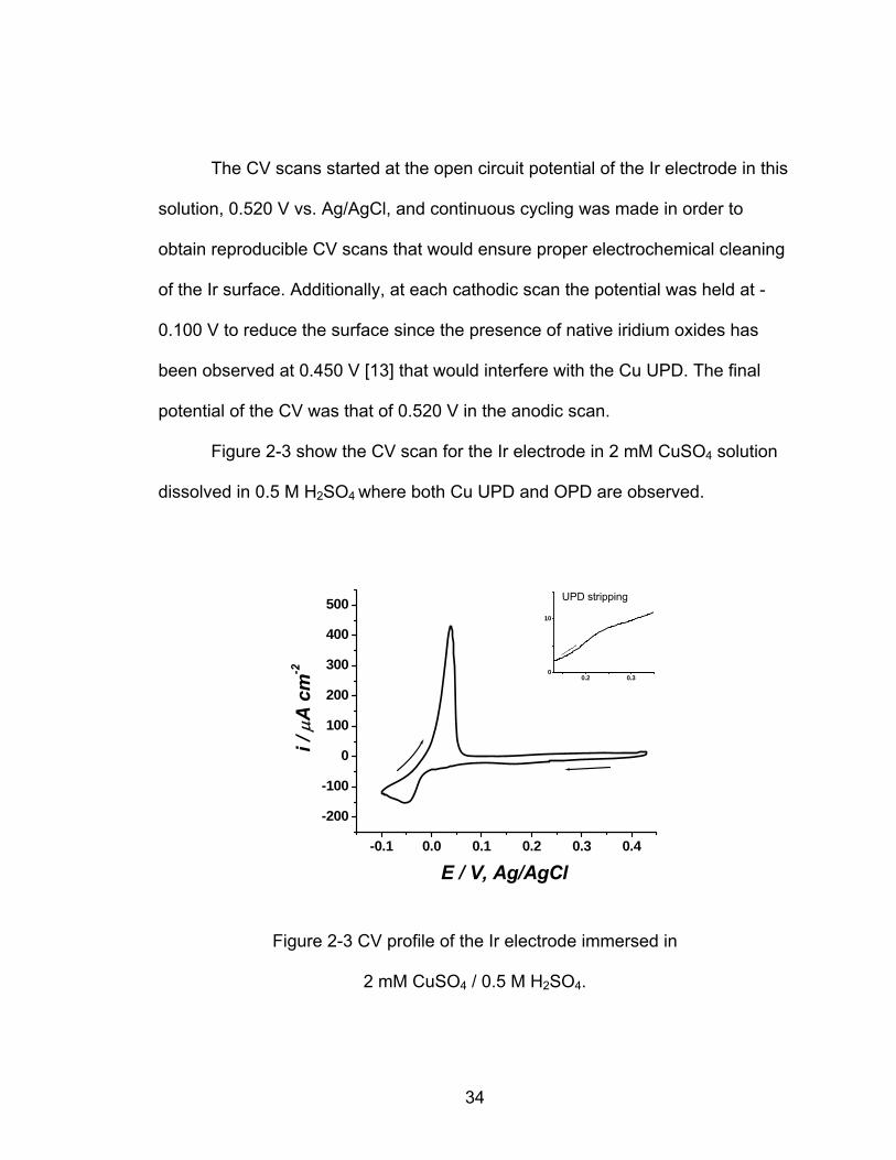
Figure 2-3 show the CV scan for the Ir electrode in 2 mM CuSO4 solution
dissolved in 0.5 M H SO where both Cu UPD and OPD are observed. 2 4
-0.1 0.0 0.1 0.2 0.3 0.4
-200
-100
0
100
200
300
400
500 UPD stripping
0.2 0.30
10
i / μ
A c
m-2
E / V, Ag/AgCl
Figure 2-3 CV profile of the Ir electrode immersed in
2 mM CuSO / 0.5 M H SO . 4 2 4
34
The CV scan starts at OCP of 0.430 V and moved towards negative
potentials where the UPD region is found between 0.250 V and 0.0500 V, with a
peak potential of Ep = 0.160 V. The Cu OPD overlayers start to deposit at 0 V,
and would deposit in larger amounts if the scan is allowed to go to more negative
potentials. In the reverse scan the Cu OPD stripping peak has Ep = 0.0400 V,
and is completely removed at 0.0700 V. The insert shows the anodic portion of
the Cu UPD stripping peak which is not is not a very well defined peak in the
anodic scan that has a Ep = 0.240 V. The final potential of the CV was that of
0.430 V in the anodic scan.
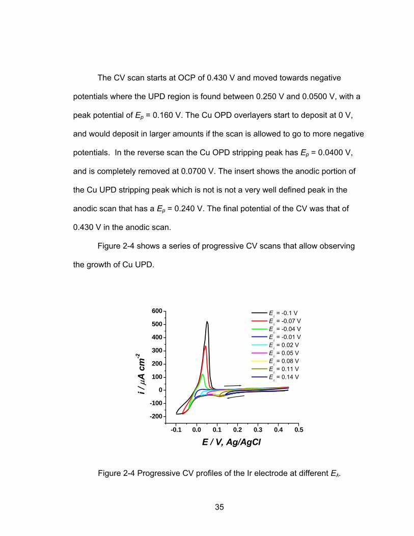
Figure 2-4 shows a series of progressive CV scans that allow observing
the growth of Cu UPD.
-0.1 0.0 0.1 0.2 0.3 0.4 0.5
-200
-100
0
100
200
300
400
500
600 Eλ = -0.1 V
Eλ = -0.07 V
Eλ = -0.04 V
Eλ = -0.01 V
Eλ = 0.02 V
Eλ = 0.05 V
Eλ = 0.08 V
Eλ = 0.11 V
Eλ = 0.14 V
i / μ
A c
m-2
E / V, Ag/AgCl
Figure 2-4 Progressive CV profiles of the Ir electrode at different Eλ.
35
The initial potential was that of the OCP, 0.450 V vs. Ag/AgCl, and moved
progressively negative to different Eλ every 30.0 mV starting at 0.140 V and
going cathodic to -0.100 V. The Cu UPD peak was observed in the potential
range of 0.250 V to 0.0500 V, and the peak potential is found at Ep = 0.120 V. Cu
OPD is obvious at -0.0400 V, and the Cu OPD stripping is found in the anodic
scan at 0.0500 V. With a very light peak the Cu UPD stripping region is observed
between 0.370 V to 0.180 V.
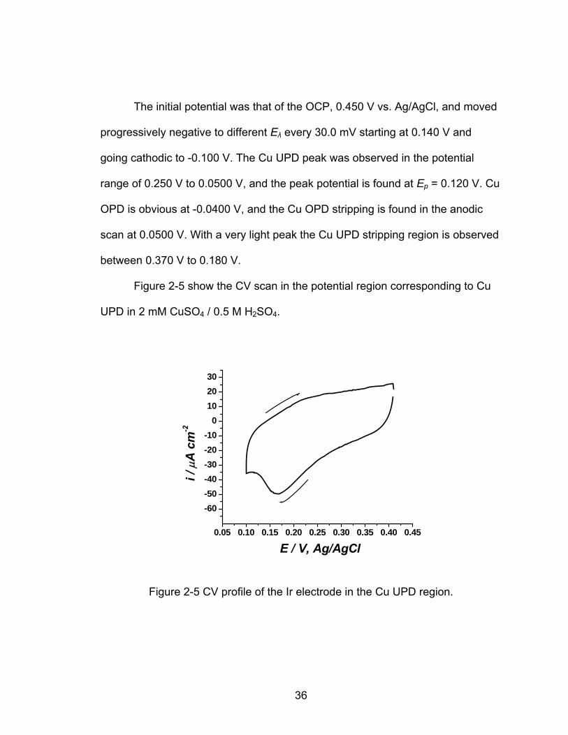
Figure 2-5 show the CV scan in the potential region corresponding to Cu
UPD in 2 mM CuSO / 0.5 M H SO . 4 2 4
0.05 0.10 0.15 0.20 0.25 0.30 0.35 0.40 0.45
-60-50-40-30-20-10
0102030
i / μ
A c
m-2
E / V, Ag/AgCl
Figure 2-5 CV profile of the Ir electrode in the Cu UPD region.
36

The cathodic Ep = is found at 0.170 V, and the current associated with this
peak corresponds to 9.73 x10⁻⁵ -2 C·cm ; it may be possible that this peak found in
the potential range of 0.275 V to 0.100 V corresponds to a combination of oxide
reduction and Cu UPD which will be discussed in further detail in section 2.3.2.
Additional CV scan was obtained from the Ir electrode in a 2 mM CuSO4 /
0.5 M H SO2 4 that was previously purged by hydrogen gas for 15 minutes to
reduce the presence of oxygen, and to observe the effect on Cu UPD. The
results are shown in Figure 2-6.
0.1 0.2 0.3 0.4-200
-100
0
100
200
300
i / μ
A c
m-2
E / V, Ag/AgCl
/ Figure 2-6 CV profile of Cu UPD region from 2 mM CuSO4
0.5 M H SO after 15 minutes of H purge. 2 4 2
37
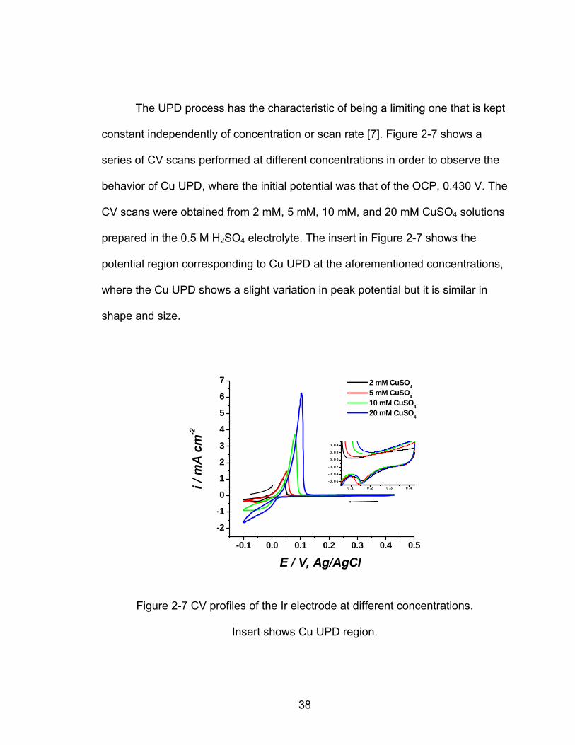
The UPD process has the characteristic of being a limiting one that is kept
constant independently of concentration or scan rate [7]. Figure 2-7 shows a
series of CV scans performed at different concentrations in order to observe the
behavior of Cu UPD, where the initial potential was that of the OCP, 0.430 V. The
CV scans were obtained from 2 mM, 5 mM, 10 mM, and 20 mM CuSO4 solutions
prepared in the 0.5 M H SO2 4 electrolyte. The insert in Figure 2-7 shows the
potential region corresponding to Cu UPD at the aforementioned concentrations,
where the Cu UPD shows a slight variation in peak potential but it is similar in
shape and size.
-0.1 0.0 0.1 0.2 0.3 0.4 0.5
-2
-1
0
1
2
3
4
5
6
7
0 .1 0 .2 0 .3 0 .4
-0 .0 6
-0 .0 4
-0 .0 2
0 .0 0
0 .0 2
0 .0 4
2 mM CuSO4 5 mM CuSO4 10 mM CuSO4 20 mM CuSO4
i / m
A c
m-2
E / V, Ag/AgCl
Figure 2-7 CV profiles of the Ir electrode at different concentrations.
Insert shows Cu UPD region.
38

Figure 2-8 shows CV scans at different scan rates in the 2 mM CuSO4 /
0.5 M H SO2 4 solution or UPD solution. The CV scans were obtained every 20.0
mV·sec-1 starting at 20.0 mV·sec-1 and moving to higher scan rates up to 140
mV·sec-1; the feature corresponding to Cu UPD is still visible at higher scan
rates.
-0.1 0.0 0.1 0.2 0.3 0.4 0.5-400
-300
-200
-100
0
100
200
300
400
500
Cu UPD
v = 0.02 Vsec-1
v = 0.04 Vsec-1
v = 0.06 Vsec-1
v = 0.08 Vsec-1
v = 0.1 Vsec-1
v = 0.12 Vsec-1
v = 0.14 Vsec-1
i / μ
A c
m-2
E / V, Ag/AgCl
Figure 2-8 CV profiles of the Ir electrode at different scan rates.
In order to confirm the existence of Cu UPD on Ir in the potential region of
0.250 V to 0.0500 V, linear sweep voltammetry (LSV) technique was used in
order to obtain a single cathodic scan starting at OCP of 0.450 V, and going to
negative potential of 0.0500 V to allow only Cu UPD, and avoiding Cu OPD
39
region. X-ray photoelectron spectroscopy data was obtained from the Cu UPD on
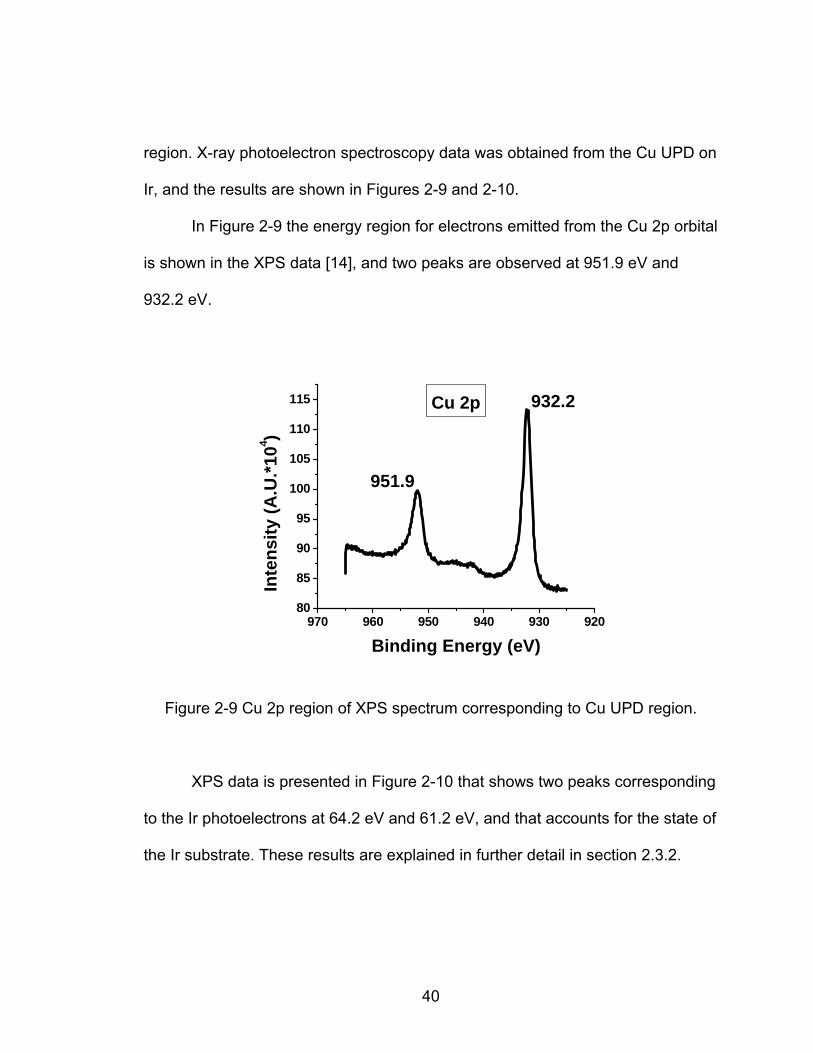
Ir, and the results are shown in Figures 2-9 and 2-10.
In Figure 2-9 the energy region for electrons emitted from the Cu 2p orbital
is shown in the XPS data [14], and two peaks are observed at 951.9 eV and
932.2 eV.
970 960 950 940 930 92080
85
90
95
100
105
110
115
951.9
932.2
Inte
nsity
(A.U
.*104 )
Binding Energy (eV)
Cu 2p
Figure 2-9 Cu 2p region of XPS spectrum corresponding to Cu UPD region.
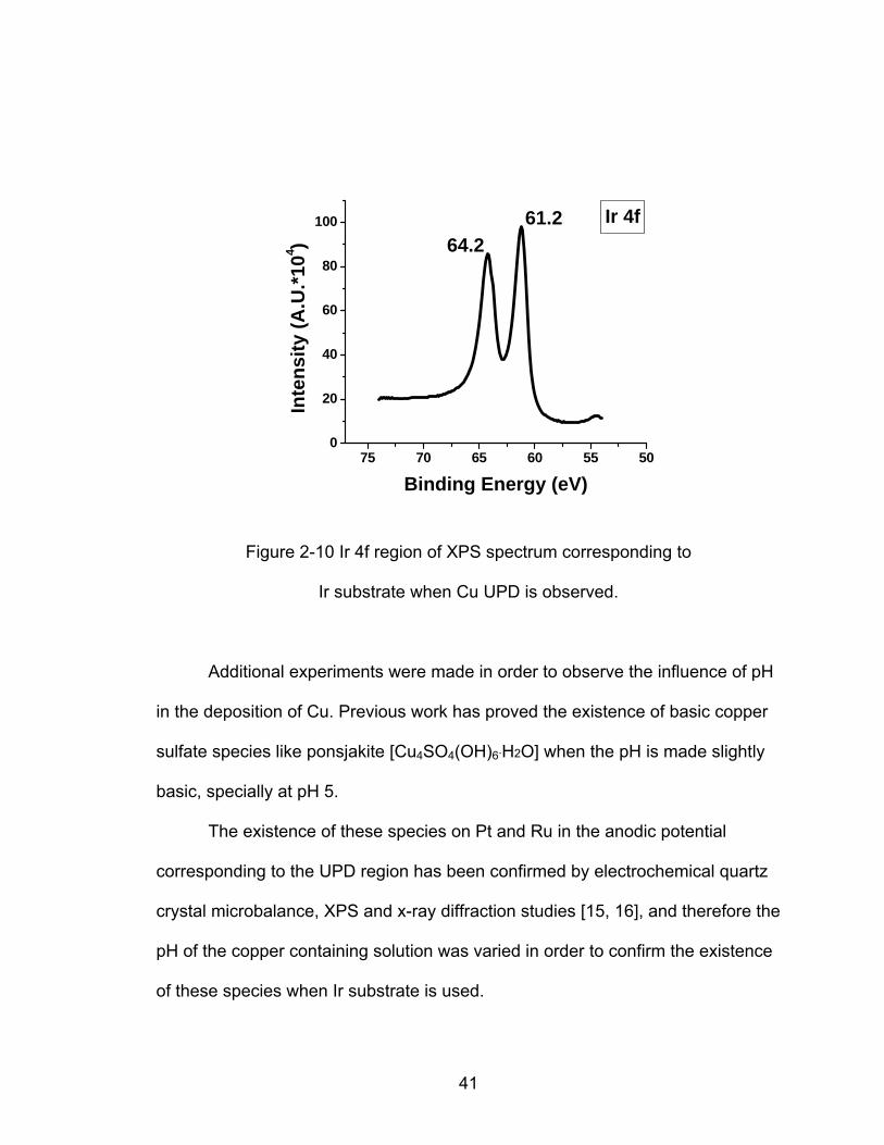
XPS data is presented in Figure 2-10 that shows two peaks corresponding
to the Ir photoelectrons at 64.2 eV and 61.2 eV, and that accounts for the state of
the Ir substrate. These results are explained in further detail in section 2.3.2.
40
75 70 65 60 55 500
20
40
60
80
100
64.261.2
Inte
nsity
(A.U
.*104 )
Binding Energy (eV)
Ir 4f
Figure 2-10 Ir 4f region of XPS spectrum corresponding to
Ir substrate when Cu UPD is observed.
Additional experiments were made in order to observe the influence of pH
in the deposition of Cu. Previous work has proved the existence of basic copper
sulfate species like ponsjakite [Cu SO (OH)4 4 6·H2O] when the pH is made slightly
basic, specially at pH 5.
The existence of these species on Pt and Ru in the anodic potential
corresponding to the UPD region has been confirmed by electrochemical quartz
crystal microbalance, XPS and x-ray diffraction studies [15, 16], and therefore the
pH of the copper containing solution was varied in order to confirm the existence
of these species when Ir substrate is used.
41
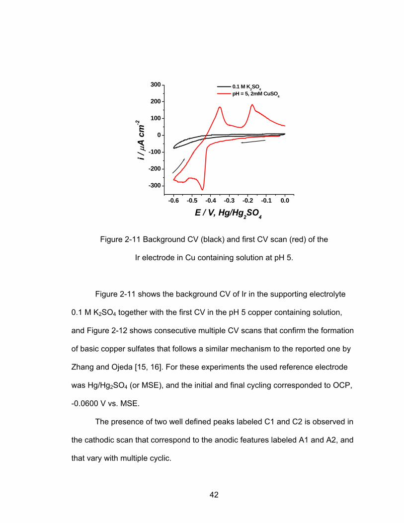
-0.6 -0.5 -0.4 -0.3 -0.2 -0.1 0.0
-300
-200
-100
0
100
200
300 0.1 M K2SO4 pH = 5, 2mM CuSO4
i / μ
A c
m-2
E / V, Hg/Hg2SO4
Figure 2-11 Background CV (black) and first CV scan (red) of the
Ir electrode in Cu containing solution at pH 5.
Figure 2-11 shows the background CV of Ir in the supporting electrolyte
0.1 M K SO2 4 together with the first CV in the pH 5 copper containing solution,
and Figure 2-12 shows consecutive multiple CV scans that confirm the formation
of basic copper sulfates that follows a similar mechanism to the reported one by
Zhang and Ojeda [15, 16]. For these experiments the used reference electrode
was Hg/Hg SO2 4 (or MSE), and the initial and final cycling corresponded to OCP,
-0.0600 V vs. MSE.
The presence of two well defined peaks labeled C1 and C2 is observed in
the cathodic scan that correspond to the anodic features labeled A1 and A2, and
that vary with multiple cyclic.
42
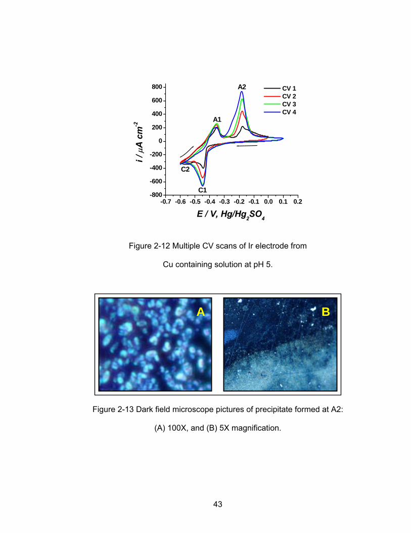
-0.7 -0.6 -0.5 -0.4 -0.3 -0.2 -0.1 0.0 0.1 0.2-800
-600
-400
-200
0
200
400
600
800 A2
A1
C2
C1
CV 1 CV 2 CV 3 CV 4
i / μ
A c
m-2
E / V, Hg/Hg2SO4
Figure 2-12 Multiple CV scans of Ir electrode from
Cu containing solution at pH 5.
A B
Figure 2-13 Dark field microscope pictures of precipitate formed at A2:
(A) 100X, and (B) 5X magnification.
43
The precipitation of basic copper sulfates at peak A2 is supported by
microscope images presented in Figure 2-13 at different magnifications.
2.3.2 Discussions
Proper polishing and cleaning of the Ir electrode as described in section
2.2 is needed in order to obtain a background CV scan like the one shown in
Figure 2-2. Otherwise, improper cleaning would allow oxide residues on the
surface that show as a peak at 0.450 V vs. Ag/AgCl (or -0.0100 V vs. MSE), and
that can be identified as OA1 in Figure 2-14 below, and Figure 2.15 from section
2.4.
The charge associated with the cathodic peak in Figure 2-3 and Figure 2-5
corresponds to approximately 9.73 x10⁻⁵ -2 C·cm or 0.304 Cu UPD monolayers
assuming that the peak corresponds only to Cu UPD. It is possible that the
charge at this peak includes charge contributions from iridium oxide reduction,
which as will be explained in detail in section 2.4, can form a native and
conductive oxide layer at contact with oxygen saturated environments [18], and
which from the cleaning procedure can be significantly reduced.
Figure 2-14 shows the progressive scans for the Ir electrode after
exposure to air and from a Cu UPD solution that has not been purged with argon.
It is evident the presence of a reversible anodic peak labeled as OA1 that may
correspond to Ir(OH) species at the surface [18] in amounts that still allow Cu
UPD. The Cu UPD is well defined, and it is observed as a broader peak in the
anodic scan.
44
-0.1 0.0 0.1 0.2 0.3 0.4 0.5-120-100-80-60-40-20
020406080
100120140
Cu UPD stripping
Cu UPD
OA1
OC1
Eλ = -0.02 V
Eλ = 0 V
Eλ = 0.02 V
Eλ = 0.05 V
Eλ = 0.15 V
i / μ
A c
m-2
E / V, Ag/AgCl
Figure 2-14 Progressive CV profiles of the Ir electrode in 2 mM CuSO4 / 0.5 M
H SO at different E2 4 λ. The presence of reversible oxide is observed.
From figure 2-14, charge measurements of the anodic peak corresponding
to Cu UPD stripping correspond to 1.76 x10⁻⁴ -2 C·cm which corresponds to 0.550
Cu UPD monolayers, and is slightly greater value than the one measured for the
pre-cleaned Ir surface. Therefore it can be observed that the polishing procedure
together with electrochemical cleaning, do reduce the CV features related with
the Ir(OH) species at 0.450 V (Figure 2-5) but does not affect in a great extent
the amount of Cu UPD peak. From Figure 2-14 the individual features are
observed for Cu UPD and Ir(OH) that account for two different reversible
processes; the observed broadness of the Cu UPD stripping as compared to the
OA1 peak in the anodic scan can explain why the Cu UPD stripping is so minute
45
in Figures 2-3 and 2-5. The Cu UPD is stripped off the surface in the broad
potential range of 0.150 V to 0.400 V, appearing to be smaller than the cathodic
peak. The somewhat grater Cu UPD amount for the CV in Figure 2-14 suggests
a favored Cu UPD on slightly oxidized Ir surface, and from the XPS results that
are discussed below it can be conclude that Cu UPD does deposit on the thin
native oxide layer of the Ir.
The potential difference between OPD and UPD anodic peaks can be
calculated as ΔEp = 210 mV, and the change in free energy associated with the
binding of the Cu UPD monolayer to the Ir substrate can be obtained from:
(1) pEnFΔG Δ=
Where F is Faraday’s constant (section 1.2), and n is the number of electrons
transferred in the reduction-oxidation of Cu:
(2) 02 Cu2eCu →+ −+
Therefore the change in free energy corresponds to ΔG° = 40.5 kJ·mol-1. This
value is larger if compared to published results [7] where the change in free
energy associated with the Cu UPD on ruthenium and ruthenium oxide is 21.0
kJ·mol-1 -1and 33.0 kJ·mol respectively; the binding of the first monolayer of Cu on
Ir would therefore be stronger than on ruthenium and ruthenium oxide.
46
The progressive CV scans in Figure 2-4 allow observing the Cu UPD
growth which occurs completely and free of Cu bulk overlayers if the switching
potential is E = 0.0200 V or 0.0500 V. The same kind of CV obtained from Hλ 2
purged solution is shown in Figure 2-6 and the CV scan presents a crossover that
occurs between the cathodic and anodic current traces at crossover potential Eχ
≈ 0.300 V. This is an indicator that Cu nucleation occurs due to the difference in
deposition and dissolution potentials [17] in that region. From [17] it has been
shown that Cu bulk nucleation depends on pH and concentration, and further
experimentation is needed to confirm if this is true for Cu UPD too; so far it is
evident that an increase in H concentration changes the way Cu deposits at
under-potential, favoring the nucleation mechanism.
Figure 2-7 shows the CV scans at different Cu2+ ion concentrations, which
does not cause significant change of Cu UPD coverage on the Ir electrode.
These observations are consistent with the surface-limiting nature of UPD
process. The peak potentials of Cu bulk did shift 50.0 mV positive as expected
when [Cu2+] is increased from 2 mM to 20 mM, and for the Cu UPD just a slight
shift was observed. Figure 2-8 shows the effect of scan rate on the Cu UPD, and
the observed peaks are clearly visible up to 400 mV·sec-1 as expected for UPD
process. This is in agreement with the idea that Cu UPD is constant and
sometimes favored with higher scan rates, since it is not a diffusion controlled
process.
47
The existence of Cu UPD was confirmed by x-ray photoelectron
spectroscopy as shown in Figures 2-8 and 2-9. XPS of the Ir electrode in the
copper region is shown in Figure 2-9, where the energy region for electrons
emitted from the Cu 2p orbital is shown [14]. This confirms that at 0.0500 V, Cu
UPD has occurred. Indeed the value of the peak at 932.32 eV corresponds to Cu
2p photoelectrons, and it confirms the existence of metallic Cu. 3/2
In Figure 2-10 there are two peaks that account for the state of the iridium
electrode after Cu UPD is obtained. The first peak is found at 64.2 eV and it
corresponds to Ir 4f5/2 photoelectrons, and the second one is at 61.2 eV
corresponding to Ir 4f7/2 photoelectrons which interestingly accounts for an
oxidized form of the iridium metal with a +1 state. This is an indicator of the
existence of the native oxide or hydroxide layer that forms instantaneously on the
Ir surface at contact with oxygen even if careful cleaning procedure is made. The
cleaning procedure would reduce the CV features related to this native oxide, but
this would form as soon as the Ir is in contact with an oxygen saturated
environment (either air or solution). This form of conductive Ir(OH) has been well
studied in literature, where the formation of a monolayer of this type of oxide is
studied when immersing the Ir electrode in a oxygen saturated acidic solution
[18], and it has been observed for other noble metals like platinum or gold [33].
Even if the oxide features or OA1 features are not present in the CV scans
when Cu UPD is observed due to care taken of not to expose the surface to large
amounts of oxygen, the XPS data accounts for the very well defined presence of
48
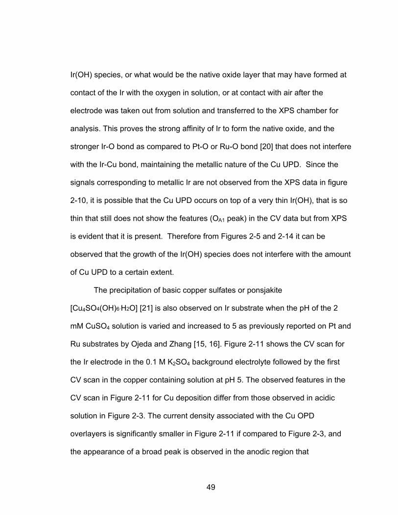
Ir(OH) species, or what would be the native oxide layer that may have formed at
contact of the Ir with the oxygen in solution, or at contact with air after the
electrode was taken out from solution and transferred to the XPS chamber for
analysis. This proves the strong affinity of Ir to form the native oxide, and the
stronger Ir-O bond as compared to Pt-O or Ru-O bond [20] that does not interfere
with the Ir-Cu bond, maintaining the metallic nature of the Cu UPD. Since the
signals corresponding to metallic Ir are not observed from the XPS data in figure
2-10, it is possible that the Cu UPD occurs on top of a very thin Ir(OH), that is so
thin that still does not show the features (OA1 peak) in the CV data but from XPS
is evident that it is present. Therefore from Figures 2-5 and 2-14 it can be
observed that the growth of the Ir(OH) species does not interfere with the amount
of Cu UPD to a certain extent.
The precipitation of basic copper sulfates or ponsjakite
[Cu4SO4(OH)6·H2O] [21] is also observed on Ir substrate when the pH of the 2
mM CuSO4 solution is varied and increased to 5 as previously reported on Pt and
Ru substrates by Ojeda and Zhang [15, 16]. Figure 2-11 shows the CV scan for
the Ir electrode in the 0.1 M K SO2 4 background electrolyte followed by the first
CV scan in the copper containing solution at pH 5. The observed features in the
CV scan in Figure 2-11 for Cu deposition differ from those observed in acidic
solution in Figure 2-3. The current density associated with the Cu OPD
overlayers is significantly smaller in Figure 2-11 if compared to Figure 2-3, and
the appearance of a broad peak is observed in the anodic region that
49
corresponds to a reaction different from Cu UPD stripping since the observed
current density is very large. In Figure 2-12 these features are observed more
clearly after obtaining multiple CV scans of the Ir electrode in the pH 5 copper
containing solution. As previously described in references [15, 16], the cathodic
peak C1 is associated with a pre-peak to Cu OPD peak C2. Peaks A1 and A2
correspond to Cu OPD stripping and precipitation of basic copper sulfates
respectively.
It is interesting to note that multiple scanning in this solution at the same
potential limits favor the increase in current density or charge accumulation at the
end of each cycle, caused by the appearance of A2; this is not observed at other
pH values. This increase in current density at the end of each cycle is related to
the precipitation of a blue-white compound that is visible to the eye on top of the
Ir electrode, and that is shown to more detail in the microscope images
presented in Figure 2-13. XRD has been previously used for characterization of
the precipitate [15] and it has shown the pattern characteristic of ponsjakite [22-
24] [Cu SO (OH)4 4 6·H2O], a form of basic copper sulfate (PDF#43-0670, 83-1410)
that it is considered a hydrated form of brochantite [25] which is product of
copper corrosion at statues and roofs, better known as patinas. XPS data at
different points of the CV scan allowed the identification of metallic Cu, Cu2O,
CuO, and sulfates, assisting in the development of the following mechanism for
ponsjakite precipitation:
50

OH(OH)SOCuOHSOCu3Cu(OH) 2644224
22 ⋅→+++ −+ (3)
This accumulation of ponsjakite eliminates the presence of active centers
in the Pt surface for under-potential deposition of copper, like it has been
observed at lower pH values by Danilov [26]. It has been studied by EQCM that
on the reverse cathodic scan, a proportional mass desorption or “dumping”
appears at potentials close to -0.420 V that corresponds to the dissolution of the
basic copper sulfates. The area of the peak C1 increases with the number of
cycles, and eventually peak C2 is obscured, meaning that the Cu OPD
deposition is also inhibited by the reaction that produces the ponsjakite or
artificial patina.
In summary, the following consecutive conditions were met that led to the
formation of ponsjakite or artificial patinas: first, cuprite was formed at C1 (-0.400
V) [22] in the cathodic range:
OHOCu2OH2e2Cu 222 +→++ −−+ (4)
Then, Cu2+ ion species were made available through the Cu stripping process
present at “A1” potential:
-2 2eCuCu +→ +0 (5)
51
Oxygen reduction reaction, occurring on the electrode’s surface causing an
increase in the available OH⎯ ions leads to the formation of copper hydroxide
Cu(OH) , on top of the Cu O layer [27,28]: 2 2
2-2 Cu(OH)2OHCu →++ (6)
The already mentioned affinity of Ir metal for the adsorption of OH⎯ ions and the
oxygen reduction reaction [20] suggest the Ir substrate is more favorable towards
the production of artificial patinas than other substrates.
The precipitate observed at the end of the cycle consisted of ponsjakite formed
by the chemical reaction between Cu(OH) 2+ 2- and Cu /SO2 4 shown in equation (3)
[29, 15, 16].
2.4 Copper Deposition on Electrochemically Formed Iridium Oxide
2.4.1 Results
Figure 2-15 shows the CV scans that correspond to electrochemically
formed iridium oxide. The potential cycling started at OCP value, and continued
to observe the features corresponding to iridium oxide formation. For this
purpose the reference electrode was changed to Hg/Hg SO2 4 since it has been
reported that the Cl⎯ ions will stop continuing oxide growth at Ir since it becomes
adsorbed at the metal/oxide interface where it obstructs.
52
-0.8 -0.6 -0.4 -0.2 0.0 0.2 0.4 0.6 0.8
-1000
-500
0
500
1000
1500
HydrogenEvolution
OxygenReduction
OA3
OC2
OC3
OC1
OA2
OA1
CV 1 CV 250
i / μ
A c
m-2
E / V, Hg/Hg2SO4
Figure 2-15 Multiple CV scans of Ir electrode in
0.5 M H SO to observe iridium oxide growth. 2 4
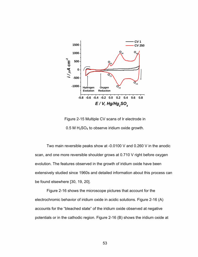
Two main reversible peaks show at -0.0100 V and 0.260 V in the anodic
scan, and one more reversible shoulder grows at 0.710 V right before oxygen
evolution. The features observed in the growth of iridium oxide have been
extensively studied since 1960s and detailed information about this process can
be found elsewhere [30, 19, 20].
Figure 2-16 shows the microscope pictures that account for the
electrochromic behavior of iridium oxide in acidic solutions. Figure 2-16 (A)
accounts for the “bleached state” of the iridium oxide observed at negative
potentials or in the cathodic region. Figure 2-16 (B) shows the iridium oxide at
53
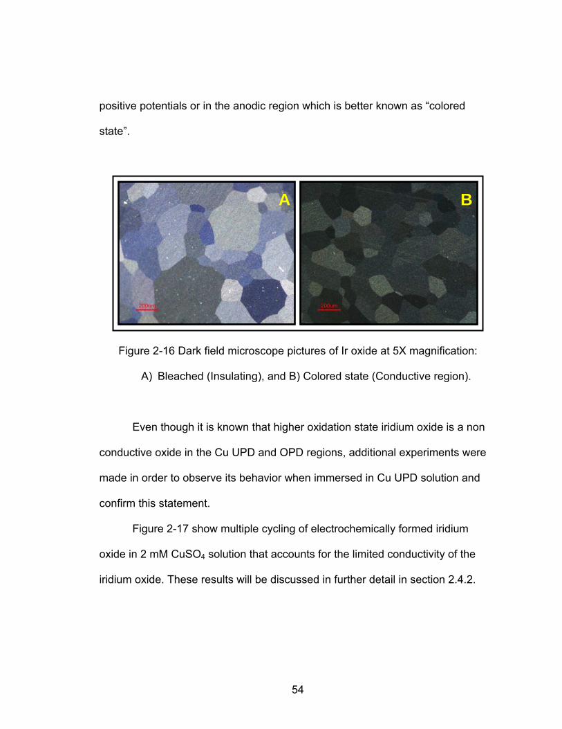
positive potentials or in the anodic region which is better known as “colored
state”.
A B
Figure 2-16 Dark field microscope pictures of Ir oxide at 5X magnification:
A) Bleached (Insulating), and B) Colored state (Conductive region).
Even though it is known that higher oxidation state iridium oxide is a non
conductive oxide in the Cu UPD and OPD regions, additional experiments were
made in order to observe its behavior when immersed in Cu UPD solution and
confirm this statement.
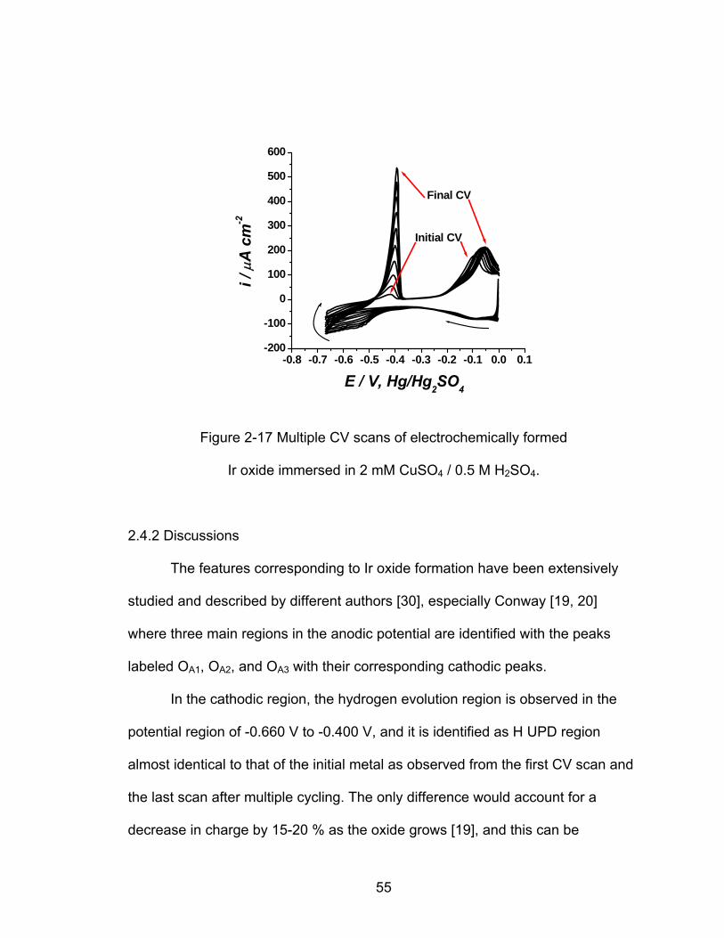
Figure 2-17 show multiple cycling of electrochemically formed iridium
oxide in 2 mM CuSO4 solution that accounts for the limited conductivity of the
iridium oxide. These results will be discussed in further detail in section 2.4.2.
54
-0.8 -0.7 -0.6 -0.5 -0.4 -0.3 -0.2 -0.1 0.0 0.1-200
-100
0
100
200
300
400
500
600
Final CV
Initial CVi /
μA
cm
-2
E / V, Hg/Hg2SO4
Figure 2-17 Multiple CV scans of electrochemically formed
Ir oxide immersed in 2 mM CuSO / 0.5 M H SO . 4 2 4
2.4.2 Discussions
The features corresponding to Ir oxide formation have been extensively
studied and described by different authors [30], especially Conway [19, 20]
where three main regions in the anodic potential are identified with the peaks
labeled OA1, OA2, and OA3 with their corresponding cathodic peaks.
In the cathodic region, the hydrogen evolution region is observed in the
potential region of -0.660 V to -0.400 V, and it is identified as H UPD region
almost identical to that of the initial metal as observed from the first CV scan and
the last scan after multiple cycling. The only difference would account for a
decrease in charge by 15-20 % as the oxide grows [19], and this can be
55
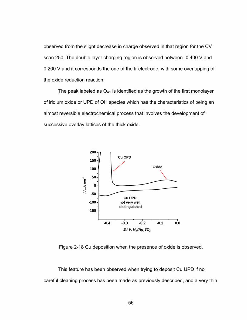
observed from the slight decrease in charge observed in that region for the CV
scan 250. The double layer charging region is observed between -0.400 V and
0.200 V and it corresponds the one of the Ir electrode, with some overlapping of
the oxide reduction reaction.
The peak labeled as OA1 is identified as the growth of the first monolayer
of iridium oxide or UPD of OH species which has the characteristics of being an
almost reversible electrochemical process that involves the development of
successive overlay lattices of the thick oxide.
-0.4 -0.3 -0.2 -0.1 0.0
-150
-100
-50
0
50
100
150
200
Cu UPD not very well distinguished
Cu OPD
Oxide
i / μ
A c
m-2
E / V, Hg/Hg2SO4
Figure 2-18 Cu deposition when the presence of oxide is observed.
This feature has been observed when trying to deposit Cu UPD if no
careful cleaning process has been made as previously described, and a very thin
56
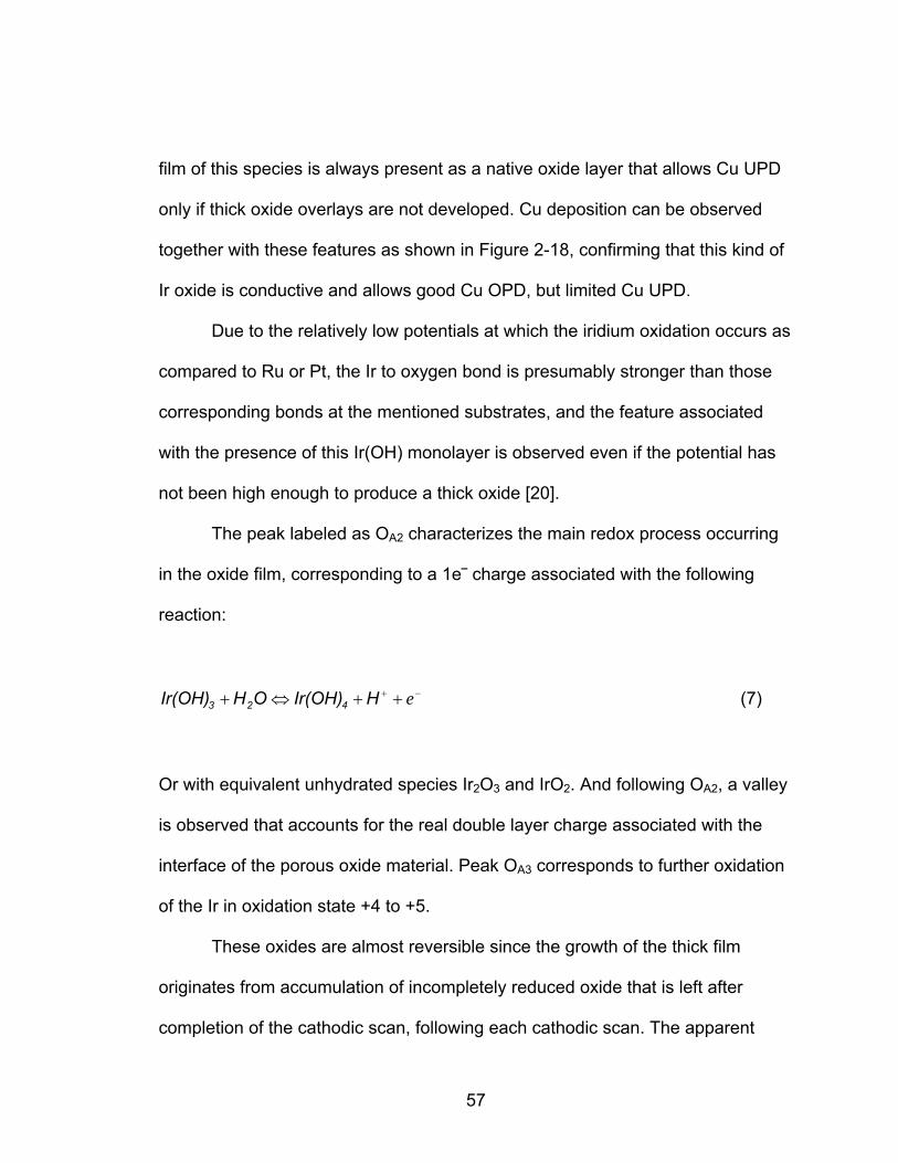
film of this species is always present as a native oxide layer that allows Cu UPD
only if thick oxide overlays are not developed. Cu deposition can be observed
together with these features as shown in Figure 2-18, confirming that this kind of
Ir oxide is conductive and allows good Cu OPD, but limited Cu UPD.
Due to the relatively low potentials at which the iridium oxidation occurs as
compared to Ru or Pt, the Ir to oxygen bond is presumably stronger than those
corresponding bonds at the mentioned substrates, and the feature associated
with the presence of this Ir(OH) monolayer is observed even if the potential has
not been high enough to produce a thick oxide [20].
The peak labeled as OA2 characterizes the main redox process occurring
in the oxide film, corresponding to a 1e⎯ charge associated with the following
reaction:
−+ ++⇔+ eHIr(OH)OHIr(OH) 423 (7)
O and IrO . And following OOr with equivalent unhydrated species Ir2 3 2 A2, a valley
is observed that accounts for the real double layer charge associated with the
interface of the porous oxide material. Peak OA3 corresponds to further oxidation
of the Ir in oxidation state +4 to +5.
These oxides are almost reversible since the growth of the thick film
originates from accumulation of incompletely reduced oxide that is left after
completion of the cathodic scan, following each cathodic scan. The apparent
57
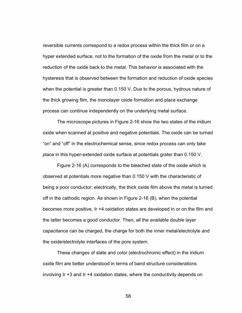
reversible currents correspond to a redox process within the thick film or on a
hyper extended surface, not to the formation of the oxide from the metal or to the
reduction of the oxide back to the metal. This behavior is associated with the
hysteresis that is observed between the formation and reduction of oxide species
when the potential is greater than 0.150 V. Due to the porous, hydrous nature of
the thick growing film, the monolayer oxide formation and place exchange
process can continue independently on the underlying metal surface.
The microscope pictures in Figure 2-16 show the two states of the iridium
oxide when scanned at positive and negative potentials. The oxide can be turned
“on” and “off” in the electrochemical sense, since redox process can only take
place in this hyper-extended oxide surface at potentials grater than 0.150 V.
Figure 2-16 (A) corresponds to the bleached state of the oxide which is
observed at potentials more negative than 0.150 V with the characteristic of
being a poor conductor; electrically, the thick oxide film above the metal is turned
off in the cathodic region. As shown in Figure 2-16 (B), when the potential
becomes more positive, Ir +4 oxidation states are developed in or on the film and
the latter becomes a good conductor. Then, all the available double layer
capacitance can be charged, the charge for both the inner metal/electrolyte and
the oxide/electrolyte interfaces of the pore system.
These changes of state and color (electrochromic effect) in the iridium
oxide film are better understood in terms of band structure considerations
involving Ir +3 and Ir +4 oxidation states, where the conductivity depends on
58
whether the Fermi level arises in an allowed band (conducting state) or is placed
in the middle of a band gap (insulating state).
These features account for the observed results corresponding to Figure
2-17 where it is evident the Cu deposition is not favored on the activated or
conductive oxide film due to the different potentials at which each feature is
observed. In the multiple CV scans from Figure 2-17 the feature associated with
the presence of Ir(OH) and the development thick oxide film is observed in the
same potential region, and there is a slight increase in the size of the peak with
cycling. This is an indicator that the use of 0.5 M H SOs 4 background electrolyte
makes the oxide grow even if Cu2+ species are present in solution.
The gradual increase of the peak associated with Cu deposition is
observed at -0.400 V in the anodic scan, and the current density corresponding
to this process increases with cycling, meaning that more Cu species are
deposited or stripped off the surface with each CV scan.
2+ In the cathodic end of the scan the large amount of electrolyte and Cu
species available through the pores system at the metal/oxide interface make the
metal-electrolyte interface to undergo a charging process that in the absence of
Cu2+ would be associated with the H and double layer capacitance
corresponding to the area of the underlying metal. The applied potential
difference falls mainly across the metal/oxide interface, and probably affects the
first few layers of oxide close to the metal (OA1 peak). For these conditions, Cu is
gradually deposited as the Cu2+ species permeate through the porous oxide and
59
reaches the possible effective bare metal sites, which have lost 20-30 % of the
active sites that have been geometrically blocked by the oxide. Only the Cu2+
species being available in the pores of the overlying hydrous oxide film are the
ones that interact with the metal for Cu deposition. It is therefore expected to
have a constant Cu bulk peak after several multiple scans that would account for
the real electroactive area of the Ir metal at those potentials. The large area
oxide film that has been developed on the surface or above the metal is turned
off under these potential conditions.
Upon further cycling of the oxidized electrode in Cu UPD solution, the Cu
OPD peak grows to reach a constant current density, and eventually the film of
thick iridium oxide conformed of the mixture of the aforementioned oxides is
detached or peeled off the surface.
A B C
Figure 2-19 Microscope images of thick iridium oxide at 5X bright field:
A) before cycling in 2 mM CuSO ; B) after 12 complete cycles in 4
; C) after further cycling. 2 mM CuSO4
60
This behavior is shown in Figure 2-19 (B), where it is possible to observe
the detaching of certain planes of the thick oxide. Further cycling will make most
of the thick iridium oxide to be removed from the surface as shown in Figure 2-19
(C).
The amount of Cu OPD observed on iridium oxide reaches a maximum
that is very similar in current density to the one observed for Cu OPD on Ir metal
or better said on native Ir oxide (compare Figures 2-3 and 2-17). The detaching
of the thick oxide does not eliminate some of the features of oxide growth in the
CV scan, specifically OA1, since this is observed even when the film is visually off
the surface and the Ir metal substrate is clearly observed. This confirms that the
peak corresponding to OA1 corresponds to the type of native hydroxide layer that
in some references mention as very good conductor [18] and the Cu OPD occurs
on the native Ir(OH) layer that is thicker than the native Ir(OH) layer that allows
Cu UPD.
It is therefore possible to deposit Cu OPD on thicker Ir(OH) film, but it is
not the case for Cu UPD, which grows to a limited extent only when the presence
of a very thin Ir(OH) film is present. The double layer charging region between -
0.400 V and 0.200 V that overlaps with the oxide reduction reaction is
approximately the same region that corresponds to Cu UPD; therefore it is
possible that the former is dominant over Cu UPD when the thick oxide is grown
even if the film has peeled off the surface since the Cu UPD feature is not
observed in Figure 2-17.
61
2.5 Conclusions
In this chapter, the under-potential deposition of copper was studied on
iridium substrate by means of cyclic voltammetry, linear sweep voltammetry, and
x-ray photoelectron spectroscopy.
The limiting nature of under-potential deposition process was observed for
copper on iridium through electrochemical experiments, and results of
thermodynamic calculations show a favorable strong binding of the Cu under-
potential deposition on the iridium hydroxide substrate. Cu under-potential
deposition corresponds to approximately 0.304 to 0.550 Cu monolayers
assuming that the cleaning procedure has reduced significantly (but not
completely) the presence of the native Ir(OH) species. Further confirmation of
results was made by obtaining XPS data.
The influence of hydrogen saturation was observed on the Cu under-
potential deposition region where the features of the cyclic voltammetry data
correspond to those of a nucleation mechanism for growth. Further
experimentation is needed to observe these features in detail. The influence of
slightly basic pH in solution was studied, and the growth of ponsjakite was
observed on top of the iridium surface; this reaction is favored due to the affinity
of iridium metal for OH⎯ ions and oxygen evolution reaction.
The deposition of copper was studied on iridium oxide, and it is observed
that the under-potential deposition is not favored due to the nature of the thick
oxide film. Cu over-potential deposition is observed in a particular manner that
62
depends on the porous nature of the iridium oxide film, but does not deposit
directly into the thick oxide due to difference in potentials at which Cu deposition
occurs and at which the thick iridium oxide film is conductive.
These results are important for the competitive semiconductor industry
that is in constant technological development, and search of new materials that
can meet the nano scale conditions favorable for the miniaturization of on-chip
interconnects. With the presence of a very thin native oxide layer, iridium
possesses the characteristics to prevent penetration of Cu interconnect material
into the surrounding dielectric; additionally allows electrodeposition of Cu without
the use the Cu seed needed due to poor nucleation on some conventionally used
barriers.
2.6 References
1. Gerisher, H.; Kolb, D.M.; Przasnyski, M.; Surface Science 1974, 43, 662-
666.
2. Kolb, D.M., Advances in Electrochemistry and Electrochemical
Engineering, 1978. John Wiley Interscience: New York. vol. 11. p. 125.
3. Kolb, D.M.; Przasnyski, M.; Gerisher, H.; Electroanal. Chem. Interfac.
Electrochem. 1974, 54, 25-38.
4. Swathirajan, S.; Bruckenstein, S.; Electrochim. Acta 1983, 28(7), 865-877.
5. Van Huong C.N.; Gonzalez-Tejera, M.J.; J. Electroanal. Chem. 1988 244,
249-259.
6. Herrero, E.; Buller, L.J.; Abruña, H.D.; Chem. Rev. 2001, 101, 1897-1930.
63
7. Zhang, Y.; Huang, L.; Arunagiri, T. N.; Ojeda, O.; Flores, S.; Chyan, O.,
Electrochem. Solid-State Letters, 2004. 7(9): p. C107-C110.
8. Chyan, O.; Arunagiri, T.N.; Ponnuswamy, T., J. Electrochem. Soc. 2003.
150: p. C347.
9. Chan, R., Interfacial Electrochemistry and Surface Characterization:
Hydrogen Terminated Silicon, Electrolessly Deposited Palladium &
Platinum on Pyrolyzed Photoresist Films and Electrodeposited Copper on
Iridium. 2003.
10. Jingying, S.; Xuifeng, Xiao; Zeshan, Z.; Xi, Z., Dianhuaxue, 1998. 4(2): p.
159-163.
11. Ureta-Zanartu, S.M..; Bravo, P.; Zagal, J.H., J. Electroanal. Chem. 1992.
337(1-2): p. 241-51.
12. Josell, D.; Bonevich, J.E.; Moffat, T.P.; Aaltonen, T.; Ritala, M.; Leskelä,
M., Electrochem. Solid-State Letters, 2006. 9(2): p. C48-C50.
13. Pickup, P.G.; Birss, V.I., J. Electroanal. Chem. 1987. 220: p. 83-100.
14. Wagner, C.D., Handbook of X-Ray Spectroscopy.
15. Ojeda Mota, O.U., Interfacial Study of Copper Electrodeposition with the
Electrochemical Quartz Crystal Microbalance (EQCM). 2005.
16. Zhang, Y., Dissertation. 2005.
17. Grujicic, D. and Pesic, B., Electrochemica Acta, 2002. 47(18): p. 2901-
2912.
18. Hoare, J.P., J. Electroanal. Chem. 1968. 18: p. 251-259.
64
19. Conway, B.E.; Mozota, J., Electrochim. Acta, 1983. 28(1): p. 9-16.
20. Conway, B.E.; Mozota, J., Electrochim. Acta, 1983. 28(1): p. 1-8.
21. Fitzgerald, K.P.; Nairn, J.; Atrens, A., Corr. Sci. 1998. 40(12): p. 2029-
2050.
22. Jouen, S.J.,and Hannoyer,B ., Surface and Interface Analysis, 2000. 30:
p. 145-148.
23. Watanabe, M.; Tomita, M.; Ichino, T., J. Electrochem. Soc. 2001. 148(12):
p. B522-B-528.
24. Barthelmy, D., http://webmineral.com/data/Posnjakite.html. 2004.
25. Helliwell, M. and Smith, J.V., Acta Crystallographica, Section C., 1997.
C53: p. 1369-1371.
26. Danilov, A.I.; Polukarov, Yu.M.; Climent, J. M.; Feliu, J. M., Electrochim.
Acta, 2001. 46: p. 3137-3145.
27. Zerbino, J.O, Journal of Applied Electrochemistry, 1997. 27: p. 335-344.
28. Cascalheira, A.C. and Abrantes, M.L., Electrochimica Acta, 2004. 49: p.
5023-5028.
29. Christy, A.G., et al., Journal of Applied Electrochemistry, 2004. 34: p. 225-
233.
30. Rand, D.A.J.; Woods, R., J. Electroanal. Chem. 1974. 55: p. 375-381.
31. Stonehart, P.; Angerstein-Kozlowska, H.; Conway, B.E., Proc. R. Soc.
Lond. 1969. 541: p. A310.
32. Woods, R., J. Electroanal. Chem. 1974. 49: p. 217.
65

33. Sherwood, P.M.A., Surface Science. 1980. 101: p. 619-623.
66

CHAPTER 3
EFFECT OF DIFFERENT ELECTROLYTES ON SILVER UNDER-POTENTIAL
DEPOSITION AT PLATINUM EQCM
3.1 Introduction
After electrochemists started using the electrochemical quartz crystal
microbalance (EQCM) in solution [1, 2], one of the most important applications
for this instrument has been the investigation of electro-deposition of metals [3,
4]. Of special interest has been the study of under-potential deposition processes
on transition metal surfaces [5-7], due to the sensitivity of the EQCM to detect
and measure trace mass amounts in the nanograms regime that correspond to
these processes.
Silver under-potential deposition on platinum is an interesting and
challenging redox process that has been extensively studied with different
electrochemical techniques, as well as other more complicated surface analysis
instrumentation. Since 1971, Tindall and Bruckenstein [8] studied the silver
under-potential deposition from sulfuric acid solutions by voltammetry rotating
disk electrodes, and they reported the effect of the platinum surface oxidation on
the deposition of silver; it was reported that 2 monolayers of silver would only
deposit after the platinum surface had been reduced, and that this under-
potential deposition was governed by the potential dependence for the reduction
67

of platinum. After this, a series of publications from different authors studying
under-potential deposition of silver on polycrystalline platinum electrodes
appeared in attempt to describe the process [9, 10], and to obtain accurate
charge calculations corresponding to the silver under-potential deposition and the
platinum oxide formation, which is somehow complex due to the occurrence of
both reactions in the same potential region [11].
Calculation methods based still on charge measurements [12], as well as
x-ray photoelectron spectroscopy and angle-resolved x-ray photoelectron
spectroscopy studies [13] were made to identify the potential range at which
silver could be deposited at under-potential without any influence from the
platinum electro-oxidation reaction. Silver under-potential deposition calculations
varied from 1 to 2 monolayers for the different authors working with
polycrystalline platinum, and as low as 0.77 monolayers were detected on
platinum single crystal electrodes [14].
Although if the EQCM is an extremely helpful technique to study silver
under-potential deposition on platinum from electrolytes that promote the electro-
oxidation of this transition metal, it has not been widely used for that purpose.
The EQCM allows monitoring the silver under-potential deposition and striping
from frequency measurements, and could be useful in differentiating from the
platinum oxide stripping and formation, even if these two reactions overlap in the
same potential region.
68
Iwata and Sasaki have studied silver deposition by means of the EQCM in
combination with Atomic Force Microscopy, and results regarding under-potential
deposition were not reported [15]. Jeffrey and Harrington have provided with a
more detailed report where they use the EQCM to study silver and copper under-
potential deposition from perchloric acid solutions [16]; they provide with a
detailed analysis of mass-responses for copper and silver deposition with and
without iodine, and propose the silver under-potential deposition on iodine
covered platinum electrodes as an ideal calibration system for the EQCM.
The effect of different anions in solution on the under-potential deposition
of silver and the platinum oxide formation is a topic that has not been extensively
studied by means of the EQCM. Uchida and Watanabe have studied the halide
adsorption from salts on gold single crystal EQCM [17], and Bruckenstein and
Jusys have also used this technique to study adsorption of perchlorate and
perrhenate ions on polycrystalline gold [18]. For platinum, only Santos and
Machado [19] have studied the anion adsorption on polycrystalline platinum by
EQCM from perchloric, sulfuric, phosphoric, and hydrochloric acids; they
identified the ions deposited on the surface and calculated the amount of each,
but they did not analyze the effect of the electrolytes on the amount of platinum
oxide produced since it is not the purpose of the publication.
In this chapter, the under-potential deposition of silver on platinum EQCM
is studied due to the complexity of this system especially in the platinum oxide
formation region. The effect of different anions present in solution are studied in
69
order to observe their influence in the potential region corresponding to silver
under-potential deposition and platinum oxide formation and on the amount of
silver deposited at underpotential. This study includes experimentation with
perchloric, sulfuric, and phosphoric acid since these electrolytes favor the
electro-oxidation of platinum [19]. The platinum electro-oxidation has been
additionally explored in hydrochloric acid, but this electrolyte would not be used
for this study due to the favored precipitation of silver chloride into solution, which
interferes with the oscillation of the quartz crystal. Experimental results in this
work indicate that silver under-potential deposition is close the one monolayer in
the three different electrolytes, and when phosphoric acid is used, the growth of
silver (II) oxide is observed due to the growth and reaction of low coverage
hydrous oxide species at potentials prior to the start of the monolayer oxide
region, which can be of interest to the fabrication of micro-sensing devices for the
detection of contaminants, and to the production of silver oxide for its use as
bactericidal.
3.2 Experimental
Electrochemical investigation was performed using a 440 and 400 series
model electrochemical analyzer from CH Instruments, Inc. ©*. With their
corresponding reference oscillators (CH Instruments, Inc.©*) vibrating at 7.99
MHz, the time resolved instrument can simultaneously read the frequency
* CH Instruments, Inc. http://www.chinstruments.com
70
change of the quartz crystal along with the electrochemical current change on the
electrode surface.
AT-cut quartz crystals with a fundamental frequency oscillation of 7.99
MHz where purchased from International Crystal Manufacturing ©*, with 1.00 x10³
Ǻ thick polycrystalline platinum electrodes deposited on a 100 Ǻ thick titanium
adhesion layer. The oscillating frequency of the crystal is subtracted from that of
the aforementioned reference oscillator during EQCM operation.
The crystal itself, bonded to a metallic mount is seated on the bottom of a
Teflon®† cell, with its surface facing the body of the solution as previously shown
in Figure 1-13. The abovementioned platinum EQCM was used as the working
electrode in a conventional three way electrode cell. A platinum coil counter
electrode and a saturated mercury/mercurous sulfate (Hg/Hg SO2 4 or MSE) with a
potential switch of 0.647 V vs. the standard hydrogen electrode (SHE) were
employed. All potentials here in referred, including the potentials presented in the
cyclic voltammetry curves, are reported versus the MSE reference electrode.
By means of the Sauerbrey’s equation [37], the change in frequency is
related to the change in mass:
(1) ΔmCΔf f=
* International Crystal Manufacturing Co., Inc. http://www.icmfg.com† Du Pont, http://www.teflon.com
71

The sensitivity factor is determined by various properties of the crystal [29, 30]
like its thickness, fundamental frequency, and density as mentioned in section
1.3.3. In the case where crystals have a fundamental frequency oscillation of
7.99 MHz the value of the sensitivity factor is 1.42 x10
fC
-9 Hz·ng-1.
96.2 weight % sulfuric acid, 69.7 weight % perchloric acid, and 85.0
weight % phosphoric acids (Mallinckrodt Baker, Inc. ©*) were used to make all
background electrolyte solutions in ultrapure water (18.2 MΩ, Millipore©†). High
purity silver nitrate (99.9 % pure) from Mallinckrodt Baker, Inc. ©* was used to
prepare the solutions corresponding to the silver under-potential deposition
studies. All solutions were purged with nitrogen gas for 10 minutes.
The potential limits used to obtain the cyclic voltammograms for the
platinum EQCM from both the background electrolytes and the silver containing
solutions, are -0.640 V and 0.80 V, where the complete hydrogen evolution
reaction is observed together with the anion adsorption and desorption reactions
[19], and the platinum electro-oxidation and reduction [20] together with the silver
under-potential deposition[11]. The abovementioned features are observed at
approximately the same potentials independently of the electrolyte employed.
The open circuit potential for the platinum EQCM electrodes is
approximately the same value when immersed in the three different electrolytes:
0.280 V, 0.290 V and 0.260 V for 0.5 M sulfuric, 0.5 M perchloric and 0.5 M
phosphoric acids respectively, and these values were employed as the initial * Mallinckrodt Baker, Inc. http://www.mallchem.com† Millipore Corporation, http://www.millipore.com
72
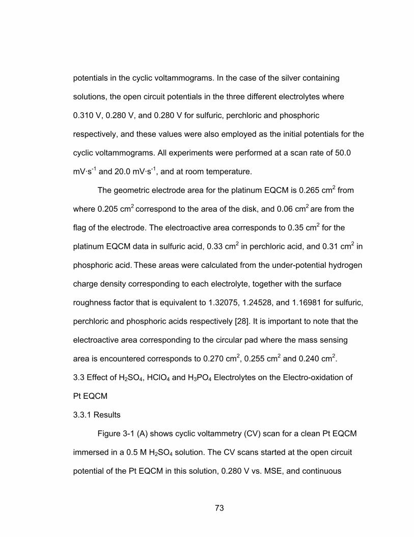
potentials in the cyclic voltammograms. In the case of the silver containing
solutions, the open circuit potentials in the three different electrolytes where
0.310 V, 0.280 V, and 0.280 V for sulfuric, perchloric and phosphoric
respectively, and these values were also employed as the initial potentials for the
cyclic voltammograms. All experiments were performed at a scan rate of 50.0
mV·s-1 and 20.0 mV·s-1 , and at room temperature.
The geometric electrode area for the platinum EQCM is 0.265 cm2 from
where 0.205 cm2 correspond to the area of the disk, and 0.06 cm2 are from the
flag of the electrode. The electroactive area corresponds to 0.35 cm2 for the
platinum EQCM data in sulfuric acid, 0.33 cm2 in perchloric acid, and 0.31 cm2 in
phosphoric acid. These areas were calculated from the under-potential hydrogen
charge density corresponding to each electrolyte, together with the surface
roughness factor that is equivalent to 1.32075, 1.24528, and 1.16981 for sulfuric,
perchloric and phosphoric acids respectively [28]. It is important to note that the
electroactive area corresponding to the circular pad where the mass sensing
area is encountered corresponds to 0.270 cm2 2 2, 0.255 cm and 0.240 cm .
3.3 Effect of H SO , HClO and H PO2 4 4 3 4 Electrolytes on the Electro-oxidation of
Pt EQCM
3.3.1 Results
Figure 3-1 (A) shows cyclic voltammetry (CV) scan for a clean Pt EQCM
immersed in a 0.5 M H SO2 4 solution. The CV scans started at the open circuit
potential of the Pt EQCM in this solution, 0.280 V vs. MSE, and continuous
73
cycling was made in order to obtain reproducible CV scans that would ensure
proper electrochemical cleaning of the platinum surface. The final potential of the
scans was that of -0.400 V in the anodic scan, right after the completion of the
hydrogen evolution reaction in order to avoid the presence of oxide or anions for
the silver experiments.
-0 .8 -0.6 -0.4 -0.2 0.0 0.2 0.4 0.6 0.8 1.0-200
-150
-100
-50
0
50
100
(A)
i / μ
A c
m-2
E / V , H g/H g 2S O 4
-0.8 -0.6 -0.4 -0.2 0.0 0.2 0.4 0.6 0.8 1.0
-35
-30
-25
-20
-15
-10
-5
(B )
E / V , H g/H g 2SO 4
Δm /
ng c
m-2
Figure 3-1 CV profile (A) and mass-response (B) for a
SO . Pt EQCM electrode in 0.5 M aqueous H2 4
74
In the anodic scan the double layer region is visually identified in the
potential range of -0.400 V to 0.200 V, and it is associated with the adsorption of
according to calculation made by Santos et al [19]. The onset of
platinum electro-oxidation appears to be at 0.200 V and continues to the anodic
switch potential of 0.800 V. In the cathodic scan, the potential region of 0.200 V
to -0.100 V associated with the platinum oxide electro-reduction region is
observed, where the peak potential for the platinum electro-reduction region
reaches a maximum peak current at 0.054 V. A switch potential of -0.640 V is
reached in the cathodic scan in order to allow monitoring the complete hydrogen
evolution reaction from where the electroactive area of the Pt EQCM was
obtained.
O2HHSO 24 ⋅−
Figure 3-1 (B) shows the corresponding mass-response for the CV scans
in Figure 3-1 (A), where it is possible to confirm the aforementioned regions by
identifying the corresponding mass changes. In the anodic scan, a light mass
increase between -0.420 V to 0.200 V is related to the double layer region. This
is followed by a more defined mass increase at 0.300 V that is associated with
the onset of platinum electro-oxidation (observed as 0.200 V from CV scans),
which continues to the switch potential of 0.800 V. In the reverse scan, the onset
of oxide reduction is observed at 0.200 V as a decrease in the mass that
prolongs with a steep slope to -0.100 V; half way of this region, the potential
corresponds to 0.0500 V which accounts for the peak potential of the platinum
electro-reduction observed in the CV scans. A continuous and less pronounced
75
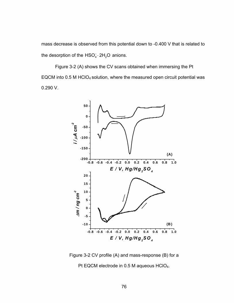
mass decrease is observed from this potential down to -0.400 V that is related to
the desorption of the anions. O2HHSO 24 ⋅−
Figure 3-2 (A) shows the CV scans obtained when immersing the Pt
EQCM into 0.5 M HClO4 solution, where the measured open circuit potential was
0.290 V.
-0.8 -0.6 -0.4 -0.2 0.0 0.2 0.4 0.6 0.8 1.0-200
-150
-100
-50
0
50
(A)
i / μ
A c
m-2
E / V , Hg/Hg2SO 4
-0.8 -0.6 -0.4 -0.2 0.0 0.2 0.4 0.6 0.8 1.0
-10
-5
0
5
10
15
20
(B )
Δm /
ng c
m-2
E / V , H g /H g 2S O 4
Figure 3-2 CV profile (A) and mass-response (B) for a
Pt EQCM electrode in 0.5 M aqueous HClO . 4
76
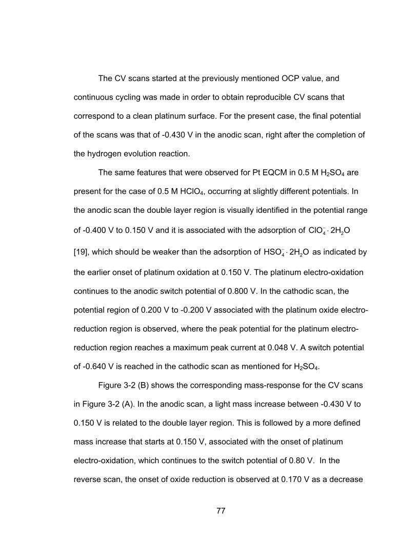
The CV scans started at the previously mentioned OCP value, and
continuous cycling was made in order to obtain reproducible CV scans that
correspond to a clean platinum surface. For the present case, the final potential
of the scans was that of -0.430 V in the anodic scan, right after the completion of
the hydrogen evolution reaction.
The same features that were observed for Pt EQCM in 0.5 M H SO2 4 are
present for the case of 0.5 M HClO4, occurring at slightly different potentials. In
the anodic scan the double layer region is visually identified in the potential range
of -0.400 V to 0.150 V and it is associated with the adsorption of
[19], which should be weaker than the adsorption of as indicated by
the earlier onset of platinum oxidation at 0.150 V. The platinum electro-oxidation
continues to the anodic switch potential of 0.800 V. In the cathodic scan, the
potential region of 0.200 V to -0.200 V associated with the platinum oxide electro-
reduction region is observed, where the peak potential for the platinum electro-
reduction region reaches a maximum peak current at 0.048 V. A switch potential
of -0.640 V is reached in the cathodic scan as mentioned for H
O2HClO 24 ⋅−
O2HHSO 24 ⋅−
SO . 2 4
Figure 3-2 (B) shows the corresponding mass-response for the CV scans
in Figure 3-2 (A). In the anodic scan, a light mass increase between -0.430 V to
0.150 V is related to the double layer region. This is followed by a more defined
mass increase that starts at 0.150 V, associated with the onset of platinum
electro-oxidation, which continues to the switch potential of 0.80 V. In the
reverse scan, the onset of oxide reduction is observed at 0.170 V as a decrease
77
in the mass that prolongs with a steep slope to -0.120 V; half way of this region,
the potential corresponds to 0.0250 V which accounts for the peak potential of
the platinum electro-reduction observed in the CV scans (observed as 0.0480 V).
A continuous and less pronounced mass decrease is observed from this potential
down to -0.400 V that is related to the desorption of the anions. O2HClO 24 ⋅−
The CV scan obtained for the Pt EQCM in 0.5 M H PO3 4 is shown in Figure
3-3 (A), where repetitive cycles where made starting at the open circuit potential
of 0.260 V. In this case the final potential was 0.440 V, at the completion of the
hydrogen evolution region.
For Pt EQCM in 0.5 M H PO ,3 4 in the anodic scan the double layer region is
visually identified in the potential range of -0.400 V to 0.200 V, and it is
associated with the adsorption of [19]; observing the insert in Figure 3-3
(A) it is possible to detect a very small protuberance at -0.150 V, which has been
reported as premonolayer oxidation that occurs for platinum immersed in this
electrolyte [23]. The onset of platinum electro-oxidation is found at 0.200 V and
continues to the anodic switch potential of 0.800 V. In the cathodic scan, the
potential region of 0.200 V to -0.150 V associated with the platinum electro-
reduction region is observed, where the peak potential for the platinum electro-
reduction region reaches a maximum peak current at 0.0270 V. A switch
potential of -0.640 V is reached in the cathodic scan as previously done.
−24HPO
78
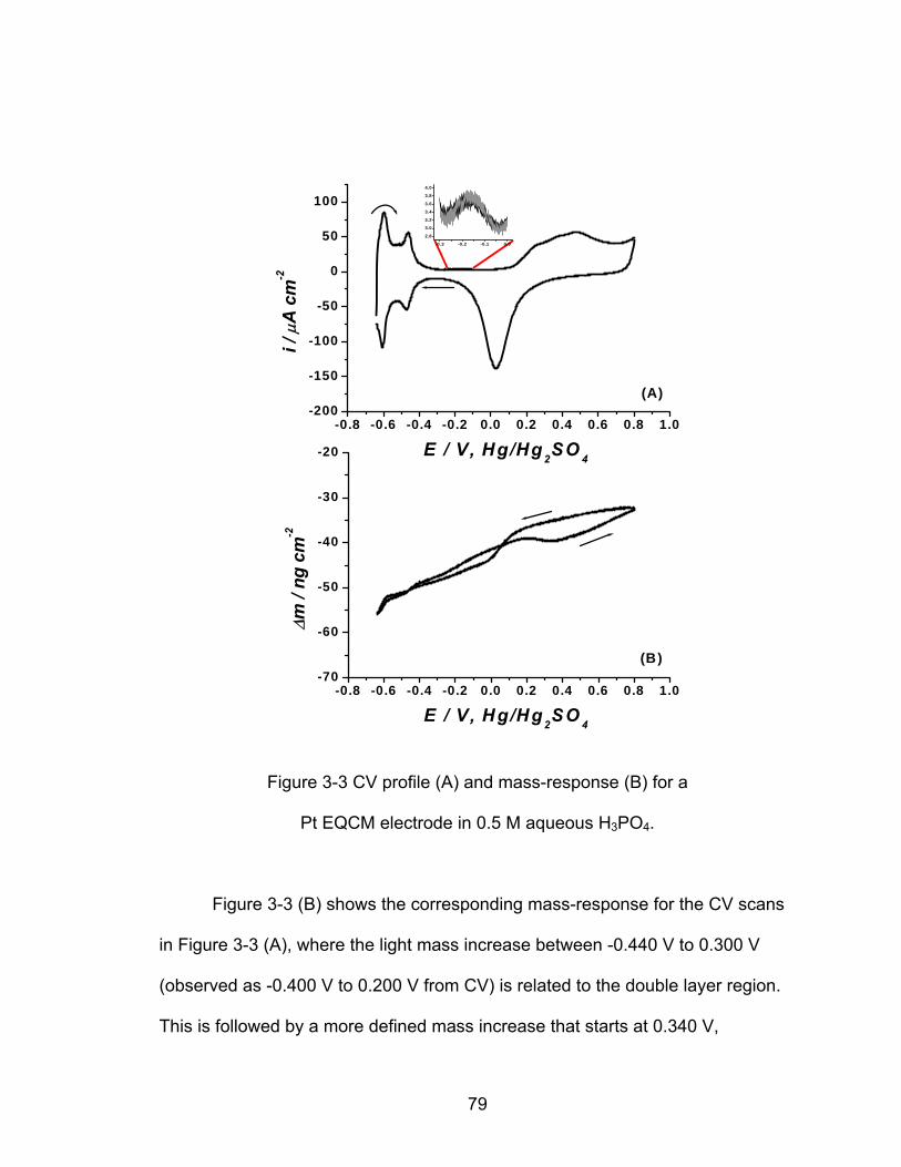
Figure 3-3 CV profile (A) and mass-response (B) for a
Pt EQCM electrode in 0.5 M aqueous H3PO4.
Figure 3-3 (B) shows the corresponding mass-response for the CV scans
in Figure 3-3 (A), where the light mass increase between -0.440 V to 0.300 V
(observed as -0.400 V to 0.200 V from CV) is related to the double layer region.
This is followed by a more defined mass increase that starts at 0.340 V,
-0.8 -0.6 -0.4 -0.2 0.0 0.2 0.4 0.6 0.8 1.0-70
-60
-50
-40
-30
-20
(B)
Δm /
ng c
m-2
E / V , Hg/Hg2SO 4
-0.8 -0.6 -0.4 -0.2 0.0 0.2 0.4 0.6 0.8 1.0-200
-150
-100
-50
0
50
100
-0.3 -0.2 -0.1 0.0
2.8
3.0
3.2
3.4
3.6
3.8
4.0
(A)
i / μ
A c
m-2
E / V, Hg/Hg2SO 4
79
associated with the onset of platinum electro-oxidation, which continues to the
switch potential of 0.800 V. In the reverse scan, the onset of oxide reduction is
observed at 0.150 V, as a decrease in the mass that prolongs to 0 V; in this
region, the potential corresponding to 0.0300 V accounts for the peak potential of
the platinum electro-reduction observed in the CV scans (observed as 0.0270 V).
A continuous and less pronounced mass decrease is observed from this potential
down to -0.440 V that is related to anions’ desorption. −24HPO
3.3.2 Discussions
The features for the CV scans shown in Figures 3-2 (A), 3-3 (A), and 3-4
(A) are in close agreement with results published by Jerkiewicz and Soriaga,
where they reexamine the mechanism of oxide growth at platinum electrodes
combining cyclic voltammetry and EQCM [20].
Supported with Auger electron spectroscopy data, the following
mechanism was proposed by these authors for the platinum electro-oxidation
where they exclude the idea that the mechanism involves OHads as an
intermediate. Instead strong water physisorption occurs for a later discharge of
2H+ - and 2e that is followed by formation of PtO by an additional reaction with
H O molecules: 2
2δδionphysisorpt
42 HOPtSOHPt −+⎯⎯⎯⎯ →⎯+ (2)
−+−+ ++−⎯⎯⎯ →⎯−− 2e2HOPt)(PtOHPt)(Pt δdchemisorbe
δdischarge2 (3)
80
⎯⎯⎯⎯⎯⎯⎯⎯⎯⎯⎯⎯⎯ →⎯+− letionnsfer_compcharge_traexchange,discharge,2dchemisorbe OHOPt
−+
−−+ ++− 2e2H)O(Pt 3_Dlatticequasi
22 (4)
This kind of mechanism is one of the two general paths proposed for the
surface oxide growth of noble metals by Jerkiewicz in 1999 [25]. In order to
identify the species that are adsorbed on the surface of the Pt EQCM, the
approximate molecular weights of the species deposited on the double layer and
platinum electro-oxidation regions were calculated using the equation proposed
in reference [20]:
ΔqδΔmnFM = (5)
Where is the interfacial mass change between two potential limits, δΔm
(6) 12 ΔmΔmδΔm −=
Determined from the EQCM measurements; is the charge density associated
with the platinum surface oxidation, n is the number of electrons exchanged in
the process, and F the Faraday’s constant (9.65 x10
Δq
4 C).
The growth of PtO is influenced by the co-adsorbed anions, which to some
extent affect the interfacial mass change in the double-layer region. Using a
81

rearrangement of equation (5) that provides with a linear relationship of vs.
with a single slope equal to
Δm
nFMΔq , Santos et al concluded that the mass
increase in this region has been associated with the adsorption of
for sulfuric acid solution, and for perchloric acid; in the case of
phosphoric acid the species deposited in the double-layer region correspond to
[19]. Equation (5) had previously been used by Uchida et al [36] to
analyze anion adsorption on gold from H
O2HHSO 24 ⋅−
O2HClO 24 ⋅−
−24HPO
SO and HClO2 4 4 electrolyte; therefore it
is a commonly used equation for identification of adsorbed species.
Wieckowski and co-workers have showed that these anions desorb at the
onset of the surface-oxide growth [21, 27], which is accounted by the different
potentials at which platinum oxide starts forming in either sulfuric, perchloric or
phosphoric acid. Their results indicate that the anion adsorption on the
polycrystalline electrode is a result of adsorption at single crystal micro and
macro facets of the polycrystalline surface. These results have also been
observed by Campbell and Corn, through more sophisticated techniques like
Second Harmonic Generation [31], and You et al. concluded that the process is
surface specific and that is different for each crystal platinum surface orientation
[22].
Equation (5) can be used directly to calculate the molar mass (M) of the
species deposited in the electro-oxidation region. Using the data corresponding
to the platinum electro-oxidation region in the CV scan from Figure 3-1 (A), the
82
molecular weight for the deposited species on the Pt EQCM corresponds
approximately to that of the addition of one monolayer of oxygen to the interface,
16.2 g·mol-1. This is an indicator that the type of oxide formed is composed of Pt
and O in the 2+ and 2- oxidation states respectively. The result is in close
agreement with the theoretical value of a monolayer of oxygen deposited on top
of the surface. In the case of the perchloric acid electrolyte the calculated value
of M is 16.3 g·mol-1, which would also correspond to the oxygen species that start
to deposit on the surface at a potential of 0.150 V.
Once it is known that for sulfuric and perchloric acids the kind of platinum
oxide species corresponds to PtO, it is possible to measure the mass changes in
the platinum electro-oxidation region that are associated with this reaction, and
therefore calculate the exact amount of monolayers of PtO that have been
formed on the Pt EQCM.
From the mass-response corresponding to Figure 3-1 (B) a change in
mass or an increase in mass is observed for the platinum electro-oxidation that
corresponds to 8.00 ng of PtO produced in the Pt EQCM. Therefore this amount
is associated to approximately 1.14 monolayers of PtO, since it is possible to
know that a monolayer of deposited oxygen corresponds to 7.0 ng by the
following relationship: the electroactive are that comprises the mass sensing area
corresponds to 0.270 cm2, and per each cm2 there are 1 x10¹⁵ atoms, meaning
that there are 2.70 x10¹⁴ atoms in the mentioned area. Then, if there are 6.02
83
23 -10x10 atoms per mol, then there are 4.48 x10 mol in total that according to the
molar mass of oxygen, correspond to 7.00 ng per monolayer of oxygen.
In the case of HClO4, the mass change associated with the platinum
oxidation reaction observed from Figure 3-2 (B) is larger than for sulfuric acid
since this starts at a more positive potential and continues forming in the cathodic
region up to the onset of reduction. The mass increase up to the switch potential
is 12.0 ng that corresponds in this case to approximately 1.70 monolayers of PtO
taking into account only the mass sensing area of the Pt EQCM corresponding to
0.255 cm2 in this solution. This is in agreement with the accepted idea that the
platinum surface oxidation resulting in PtO species, grows to a limiting thickness
of 2 monolayers [26]. Further oxide growth would have developed PtO2 species
with an unknown degree of hydration. Therefore, based on mass-responses and
comparing the calculated amounts of PtO formed in perchloric acid solution and
sulfuric acid solutions, it is evident that the growth of PtO is favored by perchloric
acid solution.
The platinum electro-oxidation in HClO4 solution is somehow different to
what has been discussed for sulfuric and perchloric acids. This system has been
previously studied by Burke and Morrissey [23], and even if this system is rather
similar to the reported for platinum in sulfuric acid, they have noted that platinum
oxide could be produced under quite severe conditions like high concentrations
(95% H PO2 4) and high temperatures (160°C), which are relevant to the operation
of the oxygen cathode of phosphoric acid fuel cells [24].
84
In the case of phosphoric acid, the molar mass of the oxygen species that
start to form at 0.340 V in Figure 3-3 (A) cannot be calculated as previously done
with sulfuric acid and perchloric acid by means of equation (5). It is possible to
obtain from the mass-response that the amount of deposited species correspond
to 7.00 ng in an electroactive area of 0.240 cm2, but there are some differences
in the way the oxide grows when compared with the aforementioned electrolytes
that does not allow to obtain the amount of PtO monolayers as previously done.
It is possible that species different than PtO, or a mixture of PtO and other kind of
oxides grow on the surface. In reference [23] it is mentioned that the platinum
oxide species formed in aqueous phosphoric acid solutions are similar to those
reported for gold [34, 35], in the sense that active surface metal atoms oxidize to
form low coverage hydrous oxide species at potentials prior to the start of the
monolayer oxide (or OH and Oads ads) region; this is the reason why when using
formula (5) to obtain the formula weight of the electrodeposited species, the
result is something different than the expected 15.9 g·mol-1 for oxygen
adsorption.
From reference [23] the feature associated with these premonolayer
oxidation observations, corresponds to a quite small peak present in the double
layer region which can be also be observed in the anodic scan at -0.170 V from
the insert in Figure 3-3 (A) when magnifying that region. This feature cannot be
distinguished in the cyclic voltammetry profiles obtained from sulfuric and
85
perchloric acid solutions, and therefore accounts for a light difference in the way
oxide is produced.
This assumption for premonolayer oxidation in gold has been supported
by Desilvestro and Weaver [32], with their surface enhanced Raman
spectroscopy studies, where the OH species produced in the premonolayer
reaction gave rise to signals that differed from those at the onset of monolayer
oxide formation; it is clear from their observations that two hydroxyl species must
be involved.
Premonolayer oxidation of platinum can be seen from work reported by
Vielstich and coworkers [33], but it will be discussed in more detail in section 3.4
from this study. In general the main problems faced in this area are: 1) the
premonolayer oxidation seems to be influenced largely by the defect structure of
the surface which is not easily controlled, and where the major factor seems to
be the history of the electrode; and 2) the extent of this reaction is usually quite
small, and the techniques currently available for the detection of submonolayer
coverage OH species are rather limited. Usually the features attributed to this
phenomenon may be mistaken as presence of impurities.
Table 3-1 summarizes the observations for the cyclic voltammetry profiles
obtained for Pt EQCM in the three different electrolytes.
86

Table 3-1 PtO Growth in H SO , HClO , and H PO Electrolyte Solutions 2 4 4 3 4
Electrolyte 0.5 M ation (V)
M Oxide (ML)
2SO4 0.270 0.300 16.2 8.00 1.14
ClO4 0.255 0.150 16.3 12.0 1.70
3PO4 0.240 0.340 7.00
3.4 Effect of H2SO4, HClO4, and H3PO4 on Ag UPD at Pt EQCM
3.4.1 Results
Figure 3-4 (A) shows the CV scan for a Pt EQCM obtained in a solution of
0.5 mM AgNO3 dissolved in 0.5 M aqueous H2SO4 electrolyte. The CV scans
started at 0.310 V vs. MSE, which is the open circuit potential of the Pt EQCM in
this silver containing solution, and only two complete CV scans where collected
in order to observe the anodic features of interest and due to the structural
changes occurring at the interface with further cycling in this solution that are
beyond the scope of this study. The final potential of the scans was the same as
the initial potential (OCP).
In the first cathodic scan the silver-under-potential deposition (UPD) is
visually identified in the potential range of 0.300 V to 0 V and it is assumed that
the peak corresponds only to the Ag UPD reaction since the Pt EQCM has been
Amount of Oxide (ng)
Electroactive Area (cm
M of Oxide Species (gmol-2 * -1 † ‡) Onset of ) onolayers of
Oxid H H H
* Electroactive area corresponding to mass sensing area only.
ΔqδΔmnFM =† From equation (5)
‡ From individual mass-responses.
87

electrochemically cleaned, and the scan started at OCP where little or no PtO
has been produced. The scan continues to reach a switch potential of -0.640 V in
order to allow monitoring the complete Ag over-potential deposition (OPD).
-0.8 -0.6 -0.4 -0.2 0.0 0.2 0.4 0.6 0.8 1.0-100
0
100
200
300
400 1st. Cycle 2nd. Cycle
(A)
i / μ
A c
m-2
E / V , H g/H g 2SO 4
-0 .8 -0 .6 -0 .4 -0 .2 0 .0 0 .2 0 .4 0 .6 0 .8 1 .0
0
50
100
150
200
250
300
350
400
0.4 0.5 0.6 0.7 0.8-22-20-18-16-14-12-10
-8-6-4-20
(B )
Δm /
ng c
m-2
E / V , H g /H g 2S O 4
Figure 3-4 CV profile (A) and mass-response (B) for a Pt EQCM in
0.5 mM AgNO / 0.5 M aqueous H SO . 3 2 4
88
In the reverse scan the Ag OPD stripping peak is observed between -
0.150 V and 0 V with a peak potential (EBulk) at -0.0540 V. The Ag UPD stripping
peak is observed between 0.200 V and 0.700 V, with a EUPD at 0.300 V, and it is
expected that the peak includes the charge contributions from the PtO formation,
since both reactions are occurring in the same potential range. In a subsequent
cathodic scan, the peaks corresponding to Ag UPD and PtO reduction are
merged in the potential range of 0.300 V to -0.0500 V; in this scan, the resulting
reduction peak is broader and expands to more negative potentials. Due to both
reactions, the expected switching of potentials is observed. In the reverse scan
the Ag OPD stripping is observed at EBulk = -0.0490 V, which is a little more
positive than the EBulk of the first CV scan. The Ag UPD stripping and PtO
deposition peak is found at EUPD = 0.280 V, which switched a little towards
negative potentials if compared to EUPD from the first CV scan.
Figure 3-4 (B) shows the corresponding mass-response for the CV scans
in Figure 3-4 (A), where it is possible to confirm the aforementioned regions by
identifying the corresponding mass changes. In the initial cathodic scan, a light
mass increase accompanies the potential region of 0.300 V to 0 V that has been
identified as Ag UPD. Following towards more negative potentials, a dramatic
mass increase is observed that corresponds to the Ag OPD, and that continues
to the anodic scan until reaching the onset of Ag OPD stripping at -0.150 V,
where a dramatic mass decrease is observed that corresponds to Ag OPD
stripping. A less pronounced mass decrease is observed in the potential region
89
corresponding to the Ag UPD stripping and the platinum oxidation reactions, and
from the insert in Figure 3-4 (B) it is observed that there is indeed a light mass
increase between 0.600 V and 0.800 V that can be exactly associated with PtO
formation. In a similar manner the mass changes are observed for the second
CV scan with some variations that will be discussed in further detail in section
3.4.2.
Figure 3-5 (A) shows the CV scan for a Pt EQCM obtained in a solution of
0.5 mM AgNO dissolved in 0.5 M aqueous HClO3 4 electrolyte. The CV scans
started at 0.280 V vs. MSE, which is the open circuit potential of the Pt EQCM in
the aforementioned solution, and only two complete CV scans where collected in
order to observe the features of interest. The final potential of the scans was the
same as the initial potential (OCP).
In the first cathodic scan the Ag UPD is identified in the potential region of
0.280 V to 0 V, and the onset of the Ag OPD bulk over-layers is found at -0.0500
V; the scan continues to reach a switch potential of -0.640 V in order to allow
monitoring the complete Ag OPD.
In the reverse scan the Ag OPD stripping peak is observed between -
0.150 V and 0.0500 V with EBulk = -0.0400 V. The Ag UPD stripping peak is
observed between 0.200 V and 0.700 V, with a EUPD = 0.300 V, and it is
expected that the peak includes the charge contributions from the PtO formation,
just like in H SO2 4 solution. In the second CV scan, the cathodic peak
corresponding to Ag UPD and PtO reduction is visually identified in the potential
90
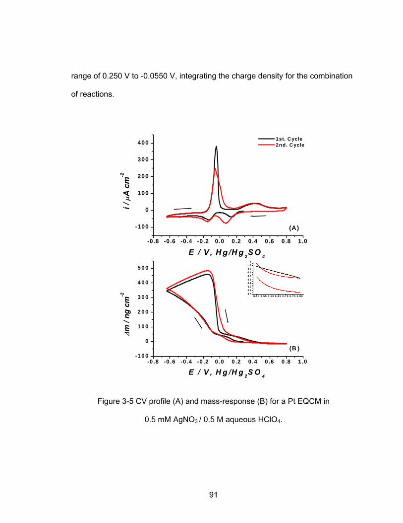
range of 0.250 V to -0.0550 V, integrating the charge density for the combination
of reactions.
-0 .8 -0.6 -0.4 -0.2 0.0 0.2 0.4 0.6 0.8 1.0
-100
0
100
200
300
400 1st. C ycle
(A)
2nd. Cycle
i / μ
A c
m-2
E / V , H g /H g 2S O 4
-0 .8 -0 .6 -0 .4 -0 .2 0 .0 0 .2 0 .4 0 .6 0 .8 1 .0-1 0 0
0
1 0 0
2 0 0
3 0 0
4 0 0
5 0 0
0 .5 0 0 .5 5 0 .6 0 0 .6 5 0 .7 0 0 .7 5 0 .8 0-1 7-1 6-1 5-1 4-1 3-1 2-1 1-1 0
-9-8
(B )
Δm /
ng c
m-2
E / V , H g /H g 2S O 4
Figure 3-5 CV profile (A) and mass-response (B) for a Pt EQCM in
/ 0.5 M aqueous HClO . 0.5 mM AgNO3 4
91
In the reverse scan the Ag OPD stripping is observed at EBulk = -0.0580 V,
which is a little more negative than the EBulk of the first CV scan. The Ag UPD
stripping and PtO deposition peak is found at EUPD = 0.270 V, which switched a
little towards negative potentials if compared to EUPD from the first CV scan.
Figure 3-5 (B) shows the corresponding mass-response for the CV scans
in Figure 3-5 (A), where the mass changes corresponding to the aforementioned
regions are identified. In the initial cathodic scan, a light mass increase
accompanies the potential region of 0.280 V to 0 V that is identified as Ag UPD.
Following towards more negative potentials, a dramatic mass increase is
observed that corresponds to the Ag OPD, and that continues to the anodic scan
until reaching the onset of Ag OPD stripping at -0.150 V, where a dramatic mass
decrease is observed that corresponds to Ag OPD stripping. A less pronounced
mass decrease is observed in the potential region for the Ag UPD stripping and
the platinum oxidation reactions, and from the insert in Figure 3-5 (B) it is
observed that there is no mass increase associated for PtO formation in this
electrolyte as observed in H SO2 4. In a similar manner the mass changes are
observed for the second CV scan and these will be discussed in further detail in
section 3.4.2.
Figure 3-6 (A) shows the CV scan for a Pt EQCM obtained in a solution of
0.5 mM AgNO dissolved in 0.5 M aqueous H PO3 3 4 electrolyte. The CV scans
started at the OCP value of 0.280 V for the phosphoric acid electrolyte and two
92
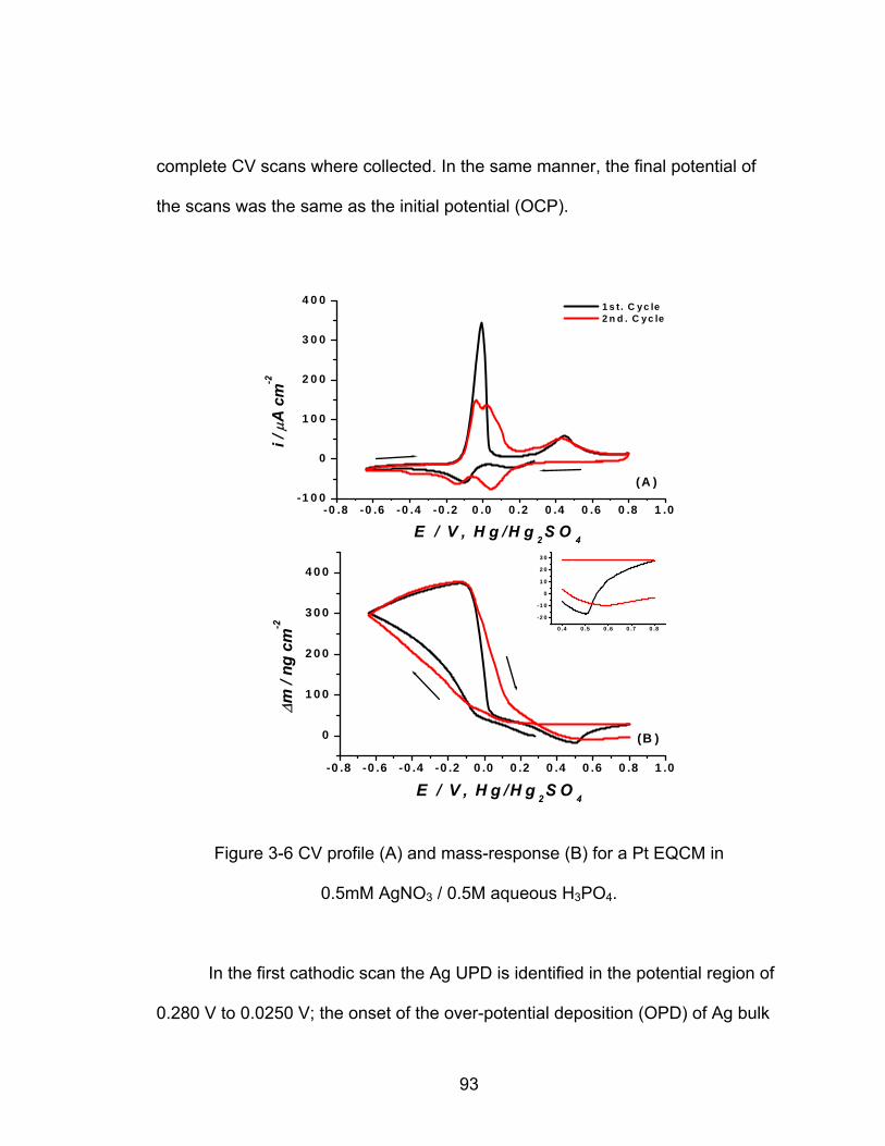
complete CV scans where collected. In the same manner, the final potential of
the scans was the same as the initial potential (OCP).
-0 .8 -0 .6 -0 .4 -0 .2 0 .0 0 .2 0 .4 0 .6 0 .8 1 .0-1 0 0
0
1 0 0
2 0 0
3 0 0
4 0 0 1 s t . C yc le
(A )
2 n d . C yc le
i / μ
A c
m-2
E / V , H g /H g 2 S O 4
-0 .8 -0 .6 -0 .4 -0 .2 0 .0 0 .2 0 .4 0 .6 0 .8 1 .0
0
1 0 0
2 0 0
3 0 0
4 0 0
0 .4 0 .5 0 .6 0 .7 0 .8
-2 0
-1 0
0
1 0
2 0
3 0
(B )
Δm /
ng c
m-2
E / V , H g /H g 2S O 4
Figure 3-6 CV profile (A) and mass-response (B) for a Pt EQCM in
0.5mM AgNO / 0.5M aqueous H PO . 3 3 4
In the first cathodic scan the Ag UPD is identified in the potential region of
0.280 V to 0.0250 V; the onset of the over-potential deposition (OPD) of Ag bulk
93
over-layers is found at 0.0200 V, and the scan continues to reach a switch
potential of -0.640 V to allow monitoring the complete Ag OPD. In the reverse
scan the Ag OPD stripping peak is observed between -0.120 V and 0.0500 V
with EBulk = -0.008 V. The Ag UPD stripping peak is observed between 0.200 V
and 0.700 V, with a EUPD = 0.270 V, and it is expected that the peak includes the
charge contributions from the PtO formation, just like in the previous cases.
In the second CV scan, the cathodic peak corresponding to Ag UPD and
PtO reduction is found in the potential range of 0.280 V to -0.060 V, integrating
the charge density for the combination of reactions. The onset of Ag OPD is
switched to more negative potentials as compared with the first cathodic scan,
and in the reverse scan the Ag OPD stripping is observed at EBulk = -0.0360 V,
which is more negative than the EBulk of the first CV scan. The Ag UPD stripping
and PtO deposition peak is found at EUPD = 0.270 V, which is lightly switched
towards negative potentials if compared to EUPD from the first CV scan.
Figure 3-6 (B) shows the corresponding mass-response for the CV scans
in Figure 3-6 (A), and in the initial cathodic scan a mass increase accompanies
the potential region of 0.280 V to 0.0250 V that could be identified as Ag UPD,
and that will be discussed in more detail in the following sections. Towards more
negative potentials, a dramatic mass increase is observed that corresponds to
the Ag OPD, and that continues to the anodic scan until reaching the onset of Ag
OPD stripping at -0.120 V, where a dramatic mass decrease is observed that
corresponds to Ag OPD stripping. A less pronounced mass decrease is observed
94

in the potential region for the Ag UPD stripping, and from the insert in Figure 3-7
(B) it is observed that there is a mass increase at 0.500 V that is identified as
AgO produced by a reaction of the premonolayer oxidation or “active oxide”
species, as will be described in the following section. In a similar manner the
mass changes are observed for the second CV scan where changes on the kind
of species adsorbed on the surface of the Pt EQCM modify the mass change
related to the potential region shown in the insert of Figure 3-7 (B); these will be
discussed in further detail in section 3.4.2.
3.4.2 Discussions
The cyclic voltammograms shown in Figures 3-5 (A), 3-6 (A) and 3-7 (A)
are in close agreement with results previously published by Salvarezza et al [9],
Martins et al [11], and Jeffrey et al [16]. The features in the voltammograms are
observed by these authors at 1 mM and 0.5 mM silver concentrations in either 1
mM or 0.5 mM electrolyte concentrations, and the reversible reaction associated
with the Ag UPD corresponds to:
(ads)PtAgeAgPt ⇔++ + (7)
It is well known that this reaction occurs in the same potential region
corresponding to the electro-reduction and oxidation of platinum, for which the
reaction is:
95
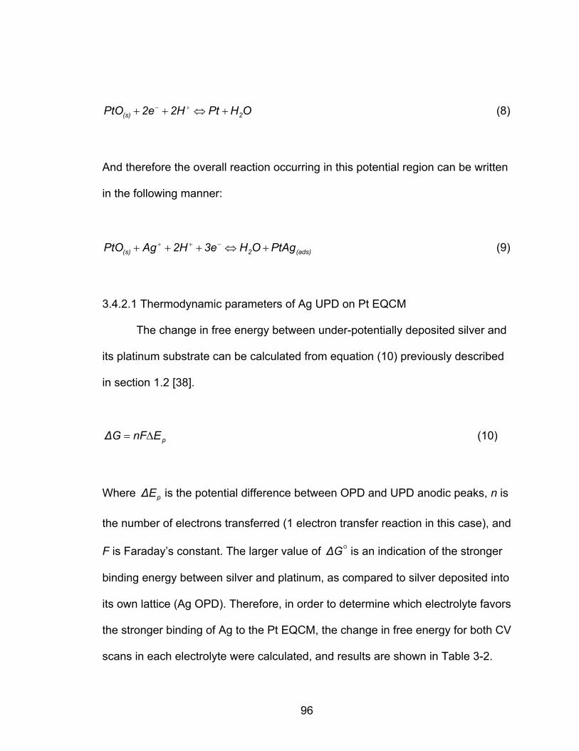
OHPt2H2ePtO 2(s) +⇔++ +− (8)
And therefore the overall reaction occurring in this potential region can be written
in the following manner:
(ads)2(s) PtAgOH3e2HAgPtO +⇔+++ −++ (9)
3.4.2.1 Thermodynamic parameters of Ag UPD on Pt EQCM
The change in free energy between under-potentially deposited silver and
its platinum substrate can be calculated from equation (10) previously described
in section 1.2 [38].
(10) pEnFΔG Δ=
Where is the potential difference between OPD and UPD anodic peaks, n is
the number of electrons transferred (1 electron transfer reaction in this case), and
F is Faraday’s constant. The larger value of
pΔE
oΔG is an indication of the stronger
binding energy between silver and platinum, as compared to silver deposited into
its own lattice (Ag OPD). Therefore, in order to determine which electrolyte favors
the stronger binding of Ag to the Pt EQCM, the change in free energy for both CV
scans in each electrolyte were calculated, and results are shown in Table 3-2.
96
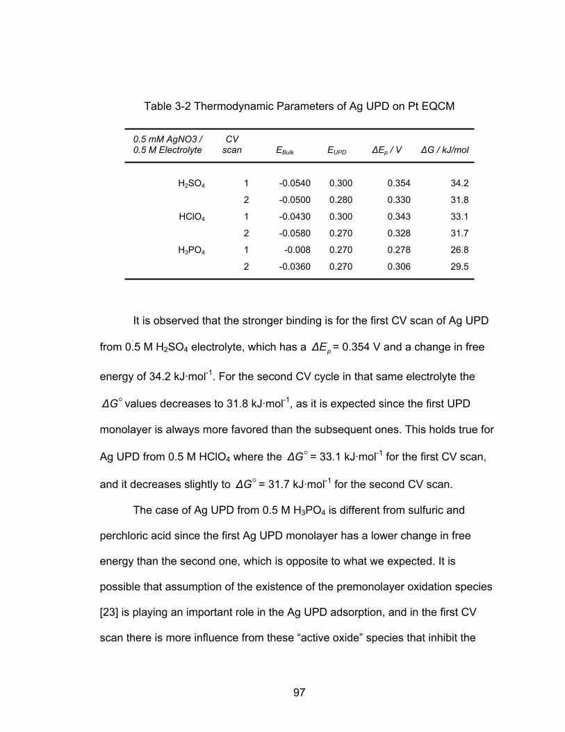
Table 3-2 Thermodynamic Parameters of Ag UPD on Pt EQCM
0.5 mM AgNO3 / CV scan 0.5 M Electrolyte E E ΔE
It is observed that the stronger binding is for the first CV scan of Ag UPD
from 0.5 M H2SO4 electrolyte, which has a = 0.354 V and a change in free
energy of 34.2 kJ·mol
pΔE
-1. For the second CV cycle in that same electrolyte the
values decreases to 31.8 kJ·moloΔG -1, as it is expected since the first UPD
monolayer is always more favored than the subsequent ones. This holds true for
Ag UPD from 0.5 M HClO4 where the = 33.1 kJ·moloΔG -1 for the first CV scan,
and it decreases slightly to = 31.7 kJ·moloΔG -1 for the second CV scan.
The case of Ag UPD from 0.5 M H3PO4 is different from sulfuric and
perchloric acid since the first Ag UPD monolayer has a lower change in free
energy than the second one, which is opposite to what we expected. It is
possible that assumption of the existence of the premonolayer oxidation species
[23] is playing an important role in the Ag UPD adsorption, and in the first CV
scan there is more influence from these “active oxide” species that inhibit the
Bulk UPD p / V ΔG / kJ/mol
H2SO 1 -0.0540 0.300 0.354 34.24
2 -0.0500 0.280 0.330 31.8
1 -0.0430 0.300 0.343 33.1HClO4
2 -0.0580 0.270 0.328 31.7
H3PO 1 -0.008 0.270 0.278 26.84
2 -0.0360 0.270 0.306 29.5
97
reduction of Ag or the Ag UPD [39]. From literature it is know that these species
form at potentials more negative than the platinum electro-oxidation (reason is
why is called a premonolayer oxidation process) and is possible that these
“active oxide” species can be formed at the open circuit potential (0.280 V) that
was used as initial potential in the presented CV scan therefore inhibiting the
strong binding of the first Ag UPD monolayer to the Pt surface. A change in the
species present on the surface of the Pt EQCM may occur after completion of the
first CV scan in H PO3 4 that allow for the second Ag UPD monolayer to have a
stronger binding energy to the Pt substrate.
Since it is known from literature that these premonolayer oxidation
species are very active and promote oxidation of reactive species and organics
like methanol and COads [34, 40], there must be some reaction involved with the
Ag in solution that produces silver oxide, therefore reducing the amount of “active
species” in the second CV scan that allows a better binding of the second Ag
UPD to the Pt substrate. These assumptions are supported by discussions in
section 3.4.2.3.
3.4.2.2 Estimated Ag UPD Amounts from Sulfuric and Perchloric Acid
Electrolytes from EQCM Mass-responses
The EQCM is a very powerful analytical instrument to elucidate chemical
mechanisms and reactions occurring at the electroactive surface that could not
be easily explained only by means of cyclic voltammetry, chronoamperometry, or
any other electrochemical technique by itself. In combination with these
98
techniques the EQCM’s mass-responses acquired, allow for a better
understanding of electrochemical systems where more than one well known
electrochemical process is occurring at the electrode’s surface.
The silver under-potential deposition on platinum from electrolyte solutions
that favor the oxidation of platinum is a complex system to analyze, and with the
EQCM’s mass-responses the approximate nanograms corresponding to Ag UPD,
Pt electro-oxidation, and any other reaction happening at the same time, can be
obtained from the changes in mass occurring at the corresponding potential
regions. These mass values can then be converted to monolayers and charge
densities by very simple mathematical correlations.
For Ag UPD on Pt EQCM from sulfuric and perchloric acid solutions, it is
more straight forward to identify the kinds of species that are present on top of
the Pt surface, since it is well known that the two main reactions occurring at the
selected potential region are that of Ag UPD and Pt oxidation. The system
becomes somehow more complex to analyze when the electrolyte is changed for
phosphoric acid due to interaction of “active oxide” species, the inability to
identify the monolayer oxide species through equation (5), and the observation of
relatively large changes in mass occurring at the anodic region that may account
for oxidation of any of the species in solution, mainly Ag.
From Figure 3-4 (B), the change in mass associated with the Ag UPD
stripping from H SO2 4 solution in the potential region of 0.2 V to 0.7V is measured
as = 55.5 ng. In order to obtain the Ag UPD as monolayers of Ag from this AgΔm
99

mass-measurement, it is necessary to know the mass per Ag monolayer for the
specified electroactive area. The following equation can be used to calculate the
nanograms per monolayer corresponding to Ag or any other element or
compound:
MAcmmol1.66x10m 2
9iML ⋅⋅= − (11)
29
cmmol1.66x10 −Where are the nanograms per monolayer of element i, iMLm is a
constant resulting from Avogadro’s number and the number of atoms per cm2 for
this system ⎥⎦
⎤⎢⎣
⎡⎟⎠⎞
⎜⎝⎛
×⎟⎟⎠
⎞⎜⎜⎝
⎛ ×atoms106.02
molcm
atoms101232
15
, A is the electroactive area, and
M is the molar mass of the element or compound adsorbed on the surface. It is
then calculated that one Ag monolayer corresponds to = 48.0 and =
46.0 nanograms for the sulfuric and perchloric acid environments respectively,
and one O monolayer is = 7.00 ng for both electrolytes (knowing from
section 3.2.2 that the oxide species correspond to PtO in these cases). Therefore
the monolayers corresponding to Ag UPD are calculated from the mass-
response by:
AgMLm AgMLm
OMLm
AgML
AgAg m
ΔmML = (12)
100
And for sulfuric acid a mass decrease of = 55.5 ng corresponds to 1.16
ML
AgΔm
Ag that are stripped off the surface. In a similar manner the number of
monolayers for Ag UPD in perchloric acid are calculated by measuring a mass
decrease of = 50.5 ng observed in the potential region of 0.200 V and
0.700 V in the first anodic scan from Figure 3-5 (B), and the Ag UPD monolayers
correspond to 1.10 ML
AgΔm
Ag taking into account that one silver monolayer is
equivalent to mAg = 46.0 ng in perchloric acid.
Since Ag UPD stripping is occurring while PtO is formed on the surface,
there exists a change in mass that has not been taken into account when
calculating MLAg for these two systems. The ignored change in mass comes from
the active sites that are immediately occupied by oxygen species after silver has
left any site vacant, and even if the replacing oxygen species are much smaller
than the laving silver atoms, it is possible to assume from the corresponding
molar masses that close to 14% ⎟⎟⎠
⎞⎜⎜⎝
⎛108g/mol15.9g/mol of the total amount of MLAg is
ignored in the calculated results. In order to avoid this error, the values for Ag
UPD were recalculated taking into account the change in mass of the sites that
are immediately occupied by oxygen. Then, if it is known for H SO2 4 that 1.16
MLAg corresponds to the 86.0 % of Ag UPD stripped off, then the total Ag UPD
would correspond to approximately 1.34 MLAg. For HClO4 is known that 1.10
MLAg correspond to the 86.0 % of Ag UPD stripped off, and then the total Ag
UPD corresponds to approximately 1.27 MLAg.
101
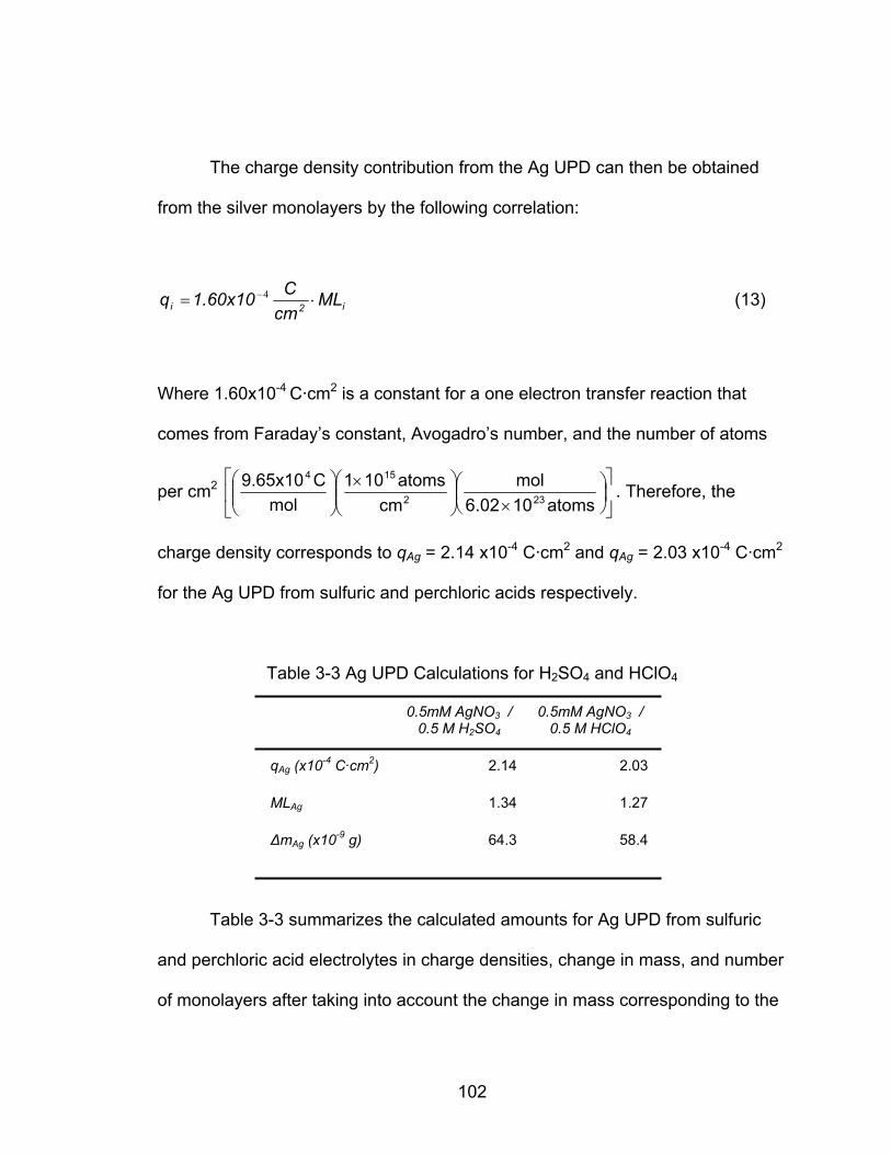
The charge density contribution from the Ag UPD can then be obtained
from the silver monolayers by the following correlation:
i2i MLcmC1.60x10q ⋅= −4 (13)
Where 1.60x10⁻⁴ 2C·cm is a constant for a one electron transfer reaction that
comes from Faraday’s constant, Avogadro’s number, and the number of atoms
per cm ⎥⎦
⎤⎢⎣
⎡⎟⎠⎞
⎜⎝⎛
×⎟⎟⎠
⎞⎜⎜⎝
⎛ ×⎟⎟⎠
⎞⎜⎜⎝
⎛atoms106.02
molcm
atoms101mol
C9.65x10232
1542 . Therefore, the
charge density corresponds to qAg = 2.14 x10⁻⁴ C·cm2 -4 and qAg = 2.03 x10 C·cm2
for the Ag UPD from sulfuric and perchloric acids respectively.
SO and HClOTable 3-3 Ag UPD Calculations for H2 4 4
0.5mM AgNO3 /
0.5 M H0.5mM AgNO3 /
0.5 M HClO2SO4 4
qAg (x10-4 C·cm2 2.14 2.03 )
1.34 1.27 MLAg
-9 64.3 58.4 ΔmAg (x10 g)
Table 3-3 summarizes the calculated amounts for Ag UPD from sulfuric
and perchloric acid electrolytes in charge densities, change in mass, and number
of monolayers after taking into account the change in mass corresponding to the
102
Ag UPD sites that are immediately occupied by oxygen atoms after they are left
vacant
3.4.2.3 Estimated Ag UPD Amounts from Phosphoric Acid Electrolyte and the
Effect of the Pt Premonolayer Oxidation
Figure 3-6 (B) shows a light mass decrease in the potential region of
0.200 V to 0.500 V that corresponds to = 51.1 ng of Ag UPD desorption,
and that is followed by a relatively large increase in mass from 0.500 V to 0.800
V that corresponds to an unknown kind of oxidized species which may include
some contributions from PtO formation. By means of equation (11) is known that
one silver monolayer in this case corresponds to = 43.0 ng, and with
equation (12) is calculated that the measured = 51.1 ng of Ag UPD
corresponds to 1.20 ML
AgΔm
AgMLm
AgΔm
Ag; with equation (13) the charge associated with this
calculated value is 1.90 x10⁻⁴ C·cm-2.
From section 3.4.2 and reference [23] is known that the platinum oxide
species that grow on Pt EQCM when immersed in phosphoric acid cannot be
elucidated by means of equation (5) due to the presence of “active oxide”
species that differ of those on the anodic monolayer region. Since these “active
oxide” species promote oxidation, it is possible that the mass increase observed
in the insert of Figure 3-6 (B) corresponds to oxidized species that differ from PtO
and that are a product of a reaction of the “active oxide” species with other ions
in solution like Ag ions or perchlorate ions.
103
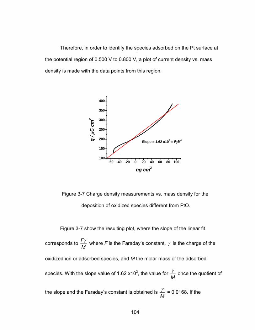
Therefore, in order to identify the species adsorbed on the Pt surface at
the potential region of 0.500 V to 0.800 V, a plot of current density vs. mass
density is made with the data points from this region.
-60 -40 -20 0 20 40 60 80 100100
150
200
250
300
350
400
Slope = 1.62 x103 = FγM-1q / μ
C c
m2
ng cm2
Figure 3-7 Charge density measurements vs. mass density for the
deposition of oxidized species different from PtO.
Figure 3-7 show the resulting plot, where the slope of the linear fit
corresponds to MFγ γ where F is the Faraday’s constant, is the charge of the
oxidized ion or adsorbed species, and M the molar mass of the adsorbed
species. With the slope value of 1.62 x10Mγ3, the value for once the quotient of
the slope and the Faraday’s constant is obtained is Mγ = 0.0168. If the
104
Mγassumption is made that the species correspond to PtO, the value of = 0.125;
assuming that the “active oxide” species reacted with Ag ions in solution to
produce AgO (M=124 g·mol-1) with an oxidation state of +2 for Ag, then the value
for Mγ = 0.0162 which is close to the product of the slope and Faraday’s constant
(0.0168 0.0162). ≈
Small deviation from the predicted value can be associated to a mixture of
Ag2O (where Ag ion is +1) and AgO, since it is known from literature that silver
oxide films tend to grow in combination with Ag2O as precursor of AgO when
anodizing silver electrodes in concentrated sodium hydroxide solutions [41], and
silver acetate and sodium acetate solutions [42]; but is evident the dominant or
favored specie is AgO in the present work.
The production of silver oxides observed at Pt EQCM on phosphoric acid
solutions is a direct evidence of existence of “active oxide” species or
premonolayer oxidation species which are different to the expected PtO, and that
are very reactive towards oxidation of surrounding species to an obvious extent.
From the insert in Figure 3-6 (B) the change in mass for the potential
region of 0.500 V to 0.800 V corresponds to an increase of ΔmAgO = 44.4 ng that
is equivalent to 0.750 MLAgO or 2.04 x10⁻⁴ -2 C·cm . The total integrated charge
density for the anodic peak that corresponds to Ag UPD stripping, AgO
adsorption, and possible PtO formation corresponds to 4.28 x10⁻⁴ C·cm-2;
subtracting the charge density associated to Ag UPD stripping and AgO
105
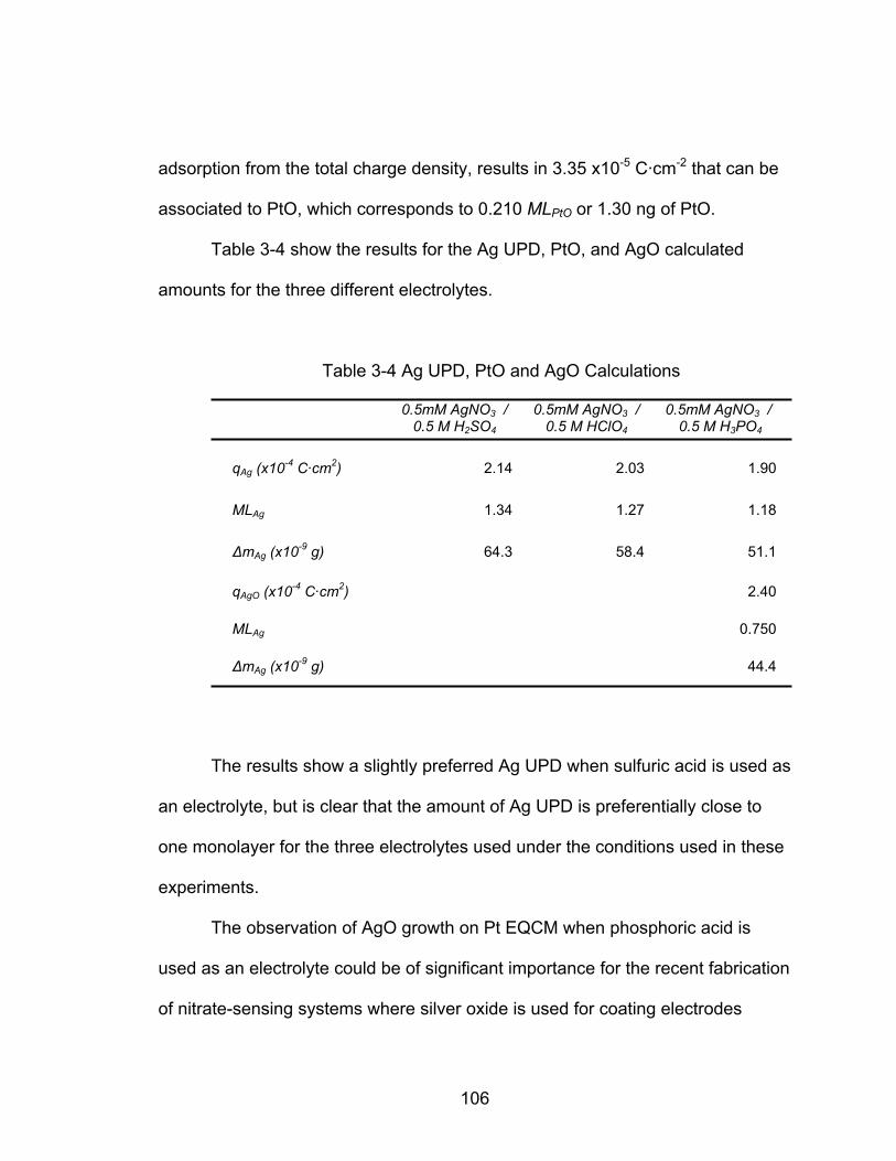
adsorption from the total charge density, results in 3.35 x10⁻⁵ C·cm-2 that can be
associated to PtO, which corresponds to 0.210 MLPtO or 1.30 ng of PtO.
Table 3-4 show the results for the Ag UPD, PtO, and AgO calculated
amounts for the three different electrolytes.
Table 3-4 Ag UPD, PtO and AgO Calculations
0.5mM AgNO3 / 0.5mM AgNO
0.5 M H2SO4
3 / 0.5 M HClO
0.5mM AgNO3 / 0.5 M H4 3PO4
qAg (x10-4 C·cm2 2.14 2.03 1.90)
1.34 1.27 1.18MLAg
-9 64.3 58.4 51.1ΔmAg (x10 g)
qAgO (x10-4 C·cm2 2.40)
0.750MLAg
-9 44.4 g) ΔmAg (x10
The results show a slightly preferred Ag UPD when sulfuric acid is used as
an electrolyte, but is clear that the amount of Ag UPD is preferentially close to
one monolayer for the three electrolytes used under the conditions used in these
experiments.
The observation of AgO growth on Pt EQCM when phosphoric acid is
used as an electrolyte could be of significant importance for the recent fabrication
of nitrate-sensing systems where silver oxide is used for coating electrodes
106
inside the sensing device, and which require controlled amounts of AgO [43].
This is important because of the significant risk that nitrate represents to human
health as a major contaminant in ground-water and surface-water systems.
Additional uses for AgO are found as bactericides due to its activity for
bactericidal treatment of water in medicine, or as device to reduce CO contents
due to its reactivity towards this compound [44].
3.5 Conclusions
In this chapter, the EQCM was used to study the effect of sulfuric,
perchloric and phosphoric acids on Ag UPD when used as electrolyte solutions.
The results account for values close to one monolayer of Ag UPD deposited on
Pt EQCM independently of the used electrolyte, being slightly larger when
sulfuric acid is used. The PtO growth is favored by perchloric acid solution as
observed from the mass-responses acquired for the background CV scans.
The EQCM proved to be such a powerful tool for analysis of CV data that
involves several reactions in the same potential region, and that would have not
been possible by pure cyclic voltammetry in this very straight forward manner. In
presence of silver atoms and phosphoric acid, the EQCM allowed monitoring the
reaction of low coverage “active oxide” species, and the identification of AgO as
product of this reaction which has not been reported previously by literature. This
can be of interest for fabrication of micro-sensing devices for the detection of
contaminants, and for the production of AgO for its use as bactericidal.
107
3.6 References
1. Bruckenstein, S.; Shay, M., Electrochim. Acta, 1985. 30(10): p. 1295-
1300.
2. Martin, B.A.; Hager, H.E., J. App. Phys. 1989. 65(7): p. 2627-2629.
3. Bund, A.; Schwitzgebel, G., Electrochim. Acta, 2000. 45: p. 3703-3710.
4. Gileadi, E.; Tsionsky, V., J. Electrochem. Soc. 2000. 147(2): p. 567-574.
5. Tang, Y.; Furtak, T.E.; Electrochim. Acta, 1991. 36(11/12): p. 1873-1877.
6. Palomar-Pardavé, M.; González, I.; Batina, N., J. Phys. Chem. 2000. 104:
p. 3545-3555.
7. Girija, T.C.; Sangaranarayanan, M.V., J. Solid State Electrochem. 2005. 9:
p. 621-626.
8. Tindall, G.W.; Bruckenstein, S., Electrochim. Acta, 1971. 16: p. 245-253.
9. Salvarezza, R.C.; Vásquez Moll, D.V.; Giordano, M.C.; Arvia, A.J., J.
Electroanal. Chem. 1986. 213: p. 301-312.
10. Parajón Costa, B.; Canullo, J.; Vásquez Moll, D.; Salvarezza, R.C.;
Giordano, M.C.; Arvia, A.J., J. Electroanal. Chem. 1988. 244: p. 261-272.
11. Martins, M. E.; Salvarezza, R. C.; Arvia, A. J., Electrochim. Acta, 1991.
36(10): p. 1617-1622.
12. Mascaro, L. H.; Santon, M. C.; Machado, S. A. S.; Avaca, L. A.; J. Chem.
Soc. Faraday Transactions, 1997. 93(22): p. 3999-4003.
13. Palacio, C.; Ocón, P.; Herrasti, P.; Díaz, D.; Arranz, A., J. Electroanal.
Chem. 2003. 545: p. 53-58.
108
14. Attard, G.A.; Al-Akl, A.; J. Electroanal. Chem. 2003. 554-555: p. 439-448.
15. Iwata, F.; Saruta, K.; Sasaki, A.; Appl. Phys. A, 1998. 66: p. S463-S466.
16. Jeffrey, C.A.; Storr, W. M.; Harrington, D.A., J. Electroanal. Chem. 2004.
569: p. 61-70.
17. Watanabe, M.; Uchida, H.; Ikeda, N., J. Electroanal. Chem. 1995. 380: p.
255-260.
18. Jusys, Z.; Bruckenstein, S., Electrochem. Communications, 2000. 2: p.
412-416.
19. Santos, M.C.; Miwa, D.W.; Machado, S.A.S., Electrochem.
Communications, 2000. 2: p. 692-296.
20. Jerkiewicz, G.; Vatankhah, G.; Lessard, J.; Soriaga, M.P.; Park, Y.-S.,
Electrochim. Acta, 2004. 49: p. 1451-1459.
21. Wieckowski, A.; Kolics, A., J. Phys. Chem. B. 2001. 105: p. 2588-2595.
22. You, H.; Zurawski, D. J.; Nagy, Z.; Yoncoa, R. M., J. Chem. Phys. 1994.
100 (6): p. 4699-4702.
23. Burke, L.D.; Morrissey, J.A., J. Electrochem. Soc., 1994. 141(9): p. 2361-
2368.
24. Conway, B.E., Modern Aspects of Electrochemistry No.38, 2005. New
York: Kluwer Academic/Plenum Publishers. p. 375.
25. Wieckowski, A.; Interfacial Electrochemistry: Theory, Experiment, and
Applications, 1999. New York: Marcel Dekker, Inc. p. 559.
109
26. Tremiliosi-Filho, G.; Jerkiewicz, G.; Conway, B.E., Langmuir, 1992. 8: p.
658-667.
27. Gamboa-Aldeco, M.E.; Herrero, E.; Zelenay, P.S.; Wieckovwski, A., J.
Electroanal. Chem. 1993. 348: p. 451-457.
28. Biegler, T.; Woods, R., Electroanal. Chem. Interfac. Electrochem. 1968.
20: p. 73-78.
29. Hepel, M., Electrode-Solution Interface Studied with Electrochemical
Quartz Crystal Nanobalance, in Interfacial Electrochemistry, ed,
Wieckowski, A., 1999, Marcel Dekker: Potsdam. p. 599-629.
30. Lu, C., Applications of Piezoelectric Quartz Crystal Microbalances, in
Methods and Phenomena: Their application in Science and Technology,
Ed. Lu, C., 1984, Elsevier Science: Amsterdam. p. 393.
31. Campbell, D.J.; Corn, R.M., J. Phys. Chem. 1988. 92: p. 5796-5800.
32. Desilvestro, J.; Weaver, M.J., J. Electroanal. Chem. 1986. 209: p. 377.
33. Kuver, A.; Vielstich, W.; Kitzelmann, D., J. Electroanal. Chem. 1993. 353:
p. 255.
34. Burke, L.D.; Healy, J.F.; O’Dwyer, K.J.; O’Learly, W.A., J. Electrochem.
Soc., 1989. 136: p. 1015.
35. Burke, L.D.; Cunnane, V.J., J. Electrochem. Soc. 1986. 133: p. 1657.
36. Uchida, H.; Hiei, M.; Watanabe, M., J. Electroanal. Chem. 1998. 452:
p.97.
37. Sauerbrey, G., Zeitschrift fuer Physik, 1959. 155: p. 206-222.
110
38. Zhang, Y.; Huang, L.; Arunagiri, T. N.; Ojeda, O.; Flores, S.; Chyan, O.,
Electrochem. Solid-State Letters, 2004. 7(9): p. C107-C110.
39. Burke, L.D.; O’Sullivan; O’Dwyer, K.J.; Scannell, R.A.; Ahern, M.J.G.;
McCarthy, M.M., ibid., 1990. 137: p. 2476.
40. Kunimatsu, K.; Seki, H.; Golden, W.G.; Gordon, J.G.; Philopott, M.R.,
Langmuir, 1986. 2: p. 464.
Uk Hur, T.; Sub Chung, W., J. Electrochem. Soc., 2005. 152(5): p. A996-
A1000.
41.
Breyfogle, B.E.; Hung, C.J.; Shumsky, M.G.; Switzer, J.A., J. Electrochem.
Soc. 1996. 143(9): p. 2741-2746.
42.
43. Kim, D.; Goldberg, I.B.; Judy, J.W. 2004.
44. Wokaun, A.; Kötz, R.; Scherer, G.G.; Raimondi, F., Angew. Chem. Int.
Ed., 2005. 44: p. 2190-2209.
111
REFERENCE LIST
1. Gerisher, H.; Kolb, D.M.; Przasnyski, M.; Surface Science 1974, 43, 662-
666.
2. Kolb, D.M., Advances in Electrochemistry and Electrochemical
Engineering, 1978. John Wiley Interscience: New York. vol. 11. p. 125.
3. Kolb, D.M.; Przasnyski, M.; Gerisher, H.; Electroanal. Chem. Interfac.
Electrochem. 1974, 54, 25-38.
4. Swathirajan, S.; Bruckenstein, S.; Electrochim. Acta 1983, 28(7), 865-877.
5. Van Huong C.N.; Gonzalez-Tejera, M.J.; J. Electroanal. Chem. 1988 244,
249-259.
6. Herrero, E.; Buller, L.J.; Abruña, H.D.; Chem. Rev. 2001, 101, 1897-1930.
7. Faulkner, L.R. Electrochemical Characterization of Chemical Systems.
1983. Academic Press, Inc.: vol. 3. p. 137.
8. Grosser, D.K., Cyclic Voltammetry: Simulation and Analysis of Reaction
Mechanism. 1993, New York: Wiley-VCH.
9. Buttry D. A.; Ward, M. D. Chem. Review, 1992, 92, 1355-1379.
10. Zhang, M., Ph. D. Thesis, University of Ottawa: Ottawa, Canada, 1995.
11. Salt, D. Hy-Q Handbook of Quartz Crystal Devices, Van Nostrand
Reinhold: UK, 1987, pp 5-36, 160-162.
112
12. Buttry, D.A. Applications of the Quartz Crystal Microbalance to
Electrochemistry, in Electroanalytical Chemistry: A series of Advances;
Bard, A. J. Marcel Dekker: New York, 1996, pp 1-85.
13. Bard, A. J.; Faulkner, L. R. Electrochemical Methods: Fundamentals and
Applications. Second Edition, John Wiley and Sons Inc.: New York, 2001,
pp 725.
14. Aurbach, D.; Moshkovich, M. J. Electrochem. Soc. 1998, 145(8), 2629-
2639.
15. Il-Hwan, K.; Kwang-Bum, K. J. Electrochem. Soc. 2004, 151(1), E7-E13.
16. Ostrom, G. S.; Buttry, D. A. J. Phys. Chem. 1995, 99(41), 15236-40.
17. Ariizumi, N.; Kamijo, M. Yamanashi-ken Kogyo Gijutsu Senta Kenkyu
Hokoku 2000, 14, 12-17.
18. Sadik, O. A.; Cheung, M-C. Talanta 2001, 55(5), 929-941.
19. O’Sullivan, C.K.; Guilbault, G. G. Biosensors & Bioelectronics 1999, 14,
663-670.
20. Lee, W.; White, H. S.; Ward, M. D. Anal. Chem. 1993, 65, 3232-3237.
21. Deakin, M.R.; Buttry, D. A. Anal. Chem. 1989, 61(20), 1147A-1154A.
22. Wunsche, M. Electrochim. Acta 1995, 5(40), 629-635.
23. Kraznaric, G. Langmuir 2001, 17, 43-4351.
24. Lay et al. J. Electroanal. Chem. 2003, 1, 1-11.
113

25. Herrero, E.; Buller, L. J.; Abruña, H. D. Chem. Rev. 2001, 101(7), 1897-
1930.
26. Nicic, L. et al. J. Phys. Chem. B 2002, 106, 12247-12252.
27. Uchida, H.; Hiei, M.; Watanabe, M. J. Electroanal. Chem. 1998, 452(1),
97-106.
28. Marx, K.A., et al. Biosensors and Bioelectronics 2001, 16, 773-782.
29. Tenreiro, A.; Cordas, C. M.; Abrantes, L. M. Portugaliae Electrochim. Acta
2003, 21(4), 361-370.
30. Jiang, M.; Ray, W. W.; Mukherjee, B.; Wang, J. Electrochem. Comm.
2004, 6, 576-582.
31. Ward, M.D.; Buttry, D.A.; Science, 1990, 249(4972), 1000-1007.
32. Deakin, M.R.; Buttry, D.A.; Anal. Chem. 1989, 61(20), 1147A-1154A.
33. Jeffrey, M.I.; Zheng, J.; Ritchie, I.M.; Meas. Sci. Technol. 2002, 11, 560-
567.
34. Vergé, M.-G.; Mettraux, P.; C.-O.A.Olsson,; Landolt, D.; J. Electroanal.
Chem. 2004, 566, 361-370.
35. Cliffel, D.E.; Bard, A.J.; Anal. Chem. 1998, 70, 1993-1998.
36. Mecea, V.M.; Sensors and Actuators A, 2006, 128, 270-277.
37. Nascente, P.A.P., Journal of Molecular Catalysis A: Chemical, 2005. 228:
p. 145-150.
38. Flores, S. Making an Electrode, 2003.
114
39. Gerisher, H.; Kolb, D.M.; Przasnyski, M.; Surface Science 1974, 43, 662-
666.
40. Kolb, D.M., Advances in Electrochemistry and Electrochemical
Engineering, 1978. John Wiley Interscience: New York. vol. 11. p. 125.
41. Kolb, D.M.; Przasnyski, M.; Gerisher, H.; Electroanal. Chem. Interfac.
Electrochem. 1974, 54, 25-38.
42. Swathirajan, S.; Bruckenstein, S.; Electrochim. Acta 1983, 28(7), 865-877.
43. Van Huong C.N.; Gonzalez-Tejera, M.J.; J. Electroanal. Chem. 1988 244,
249-259.
44. Herrero, E.; Buller, L.J.; Abruña, H.D.; Chem. Rev. 2001, 101, 1897-1930.
45. Zhang, Y.; Huang, L.; Arunagiri, T. N.; Ojeda, O.; Flores, S.; Chyan, O.,
Electrochem. Solid-State Letters, 2004. 7(9): p. C107-C110.
46. Chyan, O.; Arunagiri, T.N.; Ponnuswamy, T., J. Electrochem. Soc. 2003.
150: p. C347.
47. Chan, R., Interfacial Electrochemistry and Surface Characterization:
Hydrogen Terminated Silicon, Electrolessly Deposited Palladium &
Platinum on Pyrolyzed Photoresist Films and Electrodeposited Copper on
Iridium. 2003.
48. Jingying, S.; Xuifeng, Xiao; Zeshan, Z.; Xi, Z., Dianhuaxue, 1998. 4(2): p.
159-163.
49. Ureta-Zanartu, S.M..; Bravo, P.; Zagal, J.H., J. Electroanal. Chem. 1992.
337(1-2): p. 241-51.
115
50. Josell, D.; Bonevich, J.E.; Moffat, T.P.; Aaltonen, T.; Ritala, M.; Leskelä,
M., Electrochem. Solid-State Letters, 2006. 9(2): p. C48-C50.
51. Pickup, P.G.; Birss, V.I., J. Electroanal. Chem. 1987. 220: p. 83-100.
52. Wagner, C.D., Handbook of X-Ray Spectroscopy.
53. Ojeda Mota, O.U., Interfacial Study of Copper Electrodeposition with the
Electrochemical Quartz Crystal Microbalance (EQCM). 2005.
54. Zhang, Y., Dissertation. 2005.
55. Grujicic, D. and Pesic, B., Electrochemica Acta, 2002. 47(18): p. 2901-
2912.
56. Hoare, J.P., J. Electroanal. Chem. 1968. 18: p. 251-259.
57. Conway, B.E.; Mozota, J., Electrochim. Acta, 1983. 28(1): p. 9-16.
58. Conway, B.E.; Mozota, J., Electrochim. Acta, 1983. 28(1): p. 1-8.
59. Fitzgerald, K.P.; Nairn, J.; Atrens, A., Corr. Sci. 1998. 40(12): p. 2029-
2050.
60. Jouen, S.J.,and Hannoyer,B ., Surface and Interface Analysis, 2000. 30:
p. 145-148.
61. Watanabe, M.; Tomita, M.; Ichino, T., J. Electrochem. Soc. 2001. 148(12):
p. B522-B-528.
62. Barthelmy, D., http://webmineral.com/data/Posnjakite.html. 2004.
63. Helliwell, M. and Smith, J.V., Acta Crystallographica, Section C., 1997.
C53: p. 1369-1371.
116
64. Danilov, A.I.; Polukarov, Yu.M.; Climent, J. M.; Feliu, J. M., Electrochim.
Acta, 2001. 46: p. 3137-3145.
65. Zerbino, J.O, Journal of Applied Electrochemistry, 1997. 27: p. 335-344.
66. Cascalheira, A.C. and Abrantes, M.L., Electrochimica Acta, 2004. 49: p.
5023-5028.
67. Christy, A.G., et al., Journal of Applied Electrochemistry, 2004. 34: p. 225-
233.
68. Rand, D.A.J.; Woods, R., J. Electroanal. Chem. 1974. 55: p. 375-381.
69. Stonehart, P.; Angerstein-Kozlowska, H.; Conway, B.E., Proc. R. Soc.
Lond. 1969. 541: p. A310.
70. Woods, R., J. Electroanal. Chem. 1974. 49: p. 217.
71. Sherwood, P.M.A., Surface Science. 1980. 101: p. 619-623.
72. Bruckenstein, S.; Shay, M., Electrochim. Acta, 1985. 30(10): p. 1295-
1300.
73. Martin, B.A.; Hager, H.E., J. App. Phys. 1989. 65(7): p. 2627-2629.
74. Bund, A.; Schwitzgebel, G., Electrochim. Acta, 2000. 45: p. 3703-3710.
75. Gileadi, E.; Tsionsky, V., J. Electrochem. Soc. 2000. 147(2): p. 567-574.
76. Tang, Y.; Furtak, T.E.; Electrochim. Acta, 1991. 36(11/12): p. 1873-1877.
77. Palomar-Pardavé, M.; González, I.; Batina, N., J. Phys. Chem. 2000. 104:
p. 3545-3555.
78. Girija, T.C.; Sangaranarayanan, M.V., J. Solid State Electrochem. 2005. 9:
p. 621-626.
117
79. Tindall, G.W.; Bruckenstein, S., Electrochim. Acta, 1971. 16: p. 245-253.
80. Salvarezza, R.C.; Vásquez Moll, D.V.; Giordano, M.C.; Arvia, A.J., J.
Electroanal. Chem. 1986. 213: p. 301-312.
81. Parajón Costa, B.; Canullo, J.; Vásquez Moll, D.; Salvarezza, R.C.;
Giordano, M.C.; Arvia, A.J., J. Electroanal. Chem. 1988. 244: p. 261-272.
82. Martins, M. E.; Salvarezza, R. C.; Arvia, A. J., Electrochim. Acta, 1991.
36(10): p. 1617-1622.
83. Mascaro, L. H.; Santon, M. C.; Machado, S. A. S.; Avaca, L. A.; J. Chem.
Soc. Faraday Transactions, 1997. 93(22): p. 3999-4003.
84. Palacio, C.; Ocón, P.; Herrasti, P.; Díaz, D.; Arranz, A., J. Electroanal.
Chem. 2003. 545: p. 53-58.
85. Attard, G.A.; Al-Akl, A.; J. Electroanal. Chem. 2003. 554-555: p. 439-448.
86. Iwata, F.; Saruta, K.; Sasaki, A.; Appl. Phys. A, 1998. 66: p. S463-S466.
87. Jeffrey, C.A.; Storr, W. M.; Harrington, D.A., J. Electroanal. Chem. 2004.
569: p. 61-70.
88. Watanabe, M.; Uchida, H.; Ikeda, N., J. Electroanal. Chem. 1995. 380: p.
255-260.
89. Jusys, Z.; Bruckenstein, S., Electrochem. Communications, 2000. 2: p.
412-416.
90. Santos, M.C.; Miwa, D.W.; Machado, S.A.S., Electrochem.
Communications, 2000. 2: p. 692-296.
118
91. Jerkiewicz, G.; Vatankhah, G.; Lessard, J.; Soriaga, M.P.; Park, Y.-S.,
Electrochim. Acta, 2004. 49: p. 1451-1459.
92. Wieckowski, A.; Kolics, A., J. Phys. Chem. B. 2001. 105: p. 2588-2595.
93. You, H.; Zurawski, D. J.; Nagy, Z.; Yoncoa, R. M., J. Chem. Phys. 1994.
100 (6): p. 4699-4702.
94. Burke, L.D.; Morrissey, J.A., J. Electrochem. Soc., 1994. 141(9): p. 2361-
2368.
95. Conway, B.E., Modern Aspects of Electrochemistry No.38, 2005. New
York: Kluwer Academic/Plenum Publishers. p. 375.
96. Wieckowski, A.; Interfacial Electrochemistry: Theory, Experiment, and
Applications, 1999. New York: Marcel Dekker, Inc. p. 559.
97. Tremiliosi-Filho, G.; Jerkiewicz, G.; Conway, B.E., Langmuir, 1992. 8: p.
658-667.
98. Gamboa-Aldeco, M.E.; Herrero, E.; Zelenay, P.S.; Wieckovwski, A., J.
Electroanal. Chem. 1993. 348: p. 451-457.
99. Biegler, T.; Woods, R., Electroanal. Chem. Interfac. Electrochem. 1968.
20: p. 73-78.
100. Hepel, M., Electrode-Solution Interface Studied with Electrochemical
Quartz Crystal Nanobalance, in Interfacial Electrochemistry, ed,
Wieckowski, A., 1999, Marcel Dekker: Potsdam. p. 599-629.
119
101. Lu, C., Applications of Piezoelectric Quartz Crystal Microbalances, in
Methods and Phenomena: Their application in Science and Technology,
Ed. Lu, C., 1984, Elsevier Science: Amsterdam. p. 393.
102. Campbell, D.J.; Corn, R.M., J. Phys. Chem. 1988. 92: p. 5796-5800.
103. Desilvestro, J.; Weaver, M.J., J. Electroanal. Chem. 1986. 209: p. 377.
104. Kuver, A.; Vielstich, W.; Kitzelmann, D., J. Electroanal. Chem. 1993. 353:
p. 255.
105. Burke, L.D.; Healy, J.F.; O’Dwyer, K.J.; O’Learly, W.A., J. Electrochem.
Soc., 1989. 136: p. 1015.
106. Burke, L.D.; Cunnane, V.J., J. Electrochem. Soc. 1986. 133: p. 1657.
107. Uchida, H.; Hiei, M.; Watanabe, M., J. Electroanal. Chem. 1998. 452:
p.97.
108. Sauerbrey, G., Zeitschrift fuer Physik, 1959. 155: p. 206-222.
109. Zhang, Y.; Huang, L.; Arunagiri, T. N.; Ojeda, O.; Flores, S.; Chyan, O.,
Electrochem. Solid-State Letters, 2004. 7(9): p. C107-C110.
110. Burke, L.D.; O’Sullivan; O’Dwyer, K.J.; Scannell, R.A.; Ahern, M.J.G.;
McCarthy, M.M., ibid., 1990. 137: p. 2476.
111. Kunimatsu, K.; Seki, H.; Golden, W.G.; Gordon, J.G.; Philopott, M.R.,
Langmuir, 1986. 2: p. 464.
Uk Hur, T.; Sub Chung, W., J. Electrochem. Soc., 2005. 152(5): p. A996-
A1000.
112.
120
113. Breyfogle, B.E.; Hung, C.J.; Shumsky, M.G.; Switzer, J.A., J. Electrochem.
Soc. 1996. 143(9): p. 2741-2746.
114. Kim, D.; Goldberg, I.B.; Judy, J.W. 2004.
115. Wokaun, A.; Kötz, R.; Scherer, G.G.; Raimondi, F., Angew. Chem. Int.
Ed., 2005. 44: p. 2190-2209.
121