Elaboration of a laser doped selective emitter for ...
101
Elaboration of a laser doped selective emitter for crystalline silicon solar cells. Fabian Felipe Suarez Peinado Thesis submitted in partial fullfiment of the requirements for the degree of Master in Physics. Department of physics Faculty of Mathematics and Natural Sciences University of Oslo 2013
Transcript of Elaboration of a laser doped selective emitter for ...

Elaboration of a laser dopedselective emitter for crystalline
silicon solar cells.
Fabian Felipe Suarez Peinado
Thesis submitted in partial fullfiment of the requirementsfor the degree of
Master in Physics.
Department of physicsFaculty of Mathematics and Natural Sciences
University of Oslo
2013

Abstract
A study of the laser doping technique from a phosohorus glass layer as adopant source was carried out. This was done with the purpose of implement-ing a selective emitter in a crystal silicon solar cell. The main laser parametersstudied were the average power output and the pulse repetition frequency. Thisled us to conclusions regarding the influence of the laser pulse shape on theproduced doping concentration profiles, as well as quality of the recrystallizedirradiated area. With this, optimal laser parameters are chosen for the elabo-ration of the selective emitter solar cell.Regarding the implementation of the selective emitter solar cell the whole pro-cess was carried out. The laser parameters developed from the laser dopingstudy were used and it was found out that the selective emitter does improvethe blue response of the solar cell. Based on the results obtained various opti-mization steps are sugested for the improvement of the selective emitter solarcell. It is shown that the elaboration of a selective emitter by a laser dopingtechnique, is a very adaptable process which if correctly implented can lead toa considerable increase in the performace of the cells.

Acknowledgement
First of all I would like to thank my direct supervisor doctor Junjie Zhu, because hisvast knowledge on silicon solar cells made my work possible. Also I would like tothank doctors Erik Marstein and Sean Erik Foss for their support and contributions.
I also really want to thank all the rest of the IFE solar department not only becausetheir priceless technical help, but because of the warm relation they had with me.
Finally I want to thank all the friends that I made in Norway, the ones in Colombiaand my family because their spiritual suport allowed me to always keep on.Oslo, june 2013

Contents
1 Introduction 11.1 Thesis Outline. . . . . . . . . . . . . . . . . . . . . . . . . . . . . . . 2
2 Solar cell operation review and selective emitter principles. 42.1 Basic solar cell operation principles. . . . . . . . . . . . . . . . . . . . 42.2 Solar cells’ efficiency limiting factors . . . . . . . . . . . . . . . . . . 62.3 Typical solar cell design . . . . . . . . . . . . . . . . . . . . . . . . . 82.4 Selective emitter solar cell . . . . . . . . . . . . . . . . . . . . . . . . 9
3 Solar cell manufacturing processes and characterization. 123.1 Solar cell manufacturing. . . . . . . . . . . . . . . . . . . . . . . . . . 12
3.1.1 Czochralski silicon wafers . . . . . . . . . . . . . . . . . . . . 123.1.2 Wafer cleaning, saw damage etch and wafer texturing . . . . . 133.1.3 POCl3 diffusion . . . . . . . . . . . . . . . . . . . . . . . . . . 133.1.4 Surface passivation and antireflection coating. . . . . . . . . . 143.1.5 Front and back surface metallization . . . . . . . . . . . . . . 14
3.2 Solar cells characterization. . . . . . . . . . . . . . . . . . . . . . . . 153.2.1 Sheet resistance and four point probe method. . . . . . . . . . 153.2.2 Surface roughness . . . . . . . . . . . . . . . . . . . . . . . . . 163.2.3 Lifetime measurements . . . . . . . . . . . . . . . . . . . . . . 173.2.4 Emitter saturation current . . . . . . . . . . . . . . . . . . . . 193.2.5 SIMS profiles . . . . . . . . . . . . . . . . . . . . . . . . . . . 203.2.6 IV measurements . . . . . . . . . . . . . . . . . . . . . . . . . 203.2.7 Internal quantum efficiency . . . . . . . . . . . . . . . . . . . 20
4 Laser doping theory and experiments 224.1 Laser doping review. . . . . . . . . . . . . . . . . . . . . . . . . . . . 224.2 Qswitch Laser . . . . . . . . . . . . . . . . . . . . . . . . . . . . . . . 264.3 Experimental results . . . . . . . . . . . . . . . . . . . . . . . . . . . 28
4.3.1 Laser power stability and preliminary sheet resistance measure-ments. . . . . . . . . . . . . . . . . . . . . . . . . . . . . . . . 29
4.3.2 Second Doping experiment: Sheet resistance on laser dopedwafers using POCl3 diffusion as dopant source method. . . . . 30
4.3.3 Emitter sheet resistance simulation and Elaboration . . . . . . 334.3.4 Sheet resistance on textured wafers. . . . . . . . . . . . . . . . 35
4.4 Laser induced damage quantification by means of surface roughness. . 374.4.1 Secondary ion mass spectrometry analysis . . . . . . . . . . . 39
4.5 Lifetime Measurements. . . . . . . . . . . . . . . . . . . . . . . . . . 444.6 Saturated emitter current. . . . . . . . . . . . . . . . . . . . . . . . . 51
4.6.1 Laser doping conclusions and results analysis. . . . . . . . . . 53
5 Selective emitter solar cell results. 59
6 Conclusions 67
4

Appendices 69
A Laser doping parameter Tables. 69
B Lifetimes and metal-semiconductor interface 75B.1 Carrier Generation-Recombination Lifetimes . . . . . . . . . . . . . . 75
B.1.1 Optical Generation . . . . . . . . . . . . . . . . . . . . . . . . 76B.1.2 Radiative Recombination . . . . . . . . . . . . . . . . . . . . . 78B.1.3 Thermal generation . . . . . . . . . . . . . . . . . . . . . . . . 80B.1.4 Shockley-Read-Hall Recombination . . . . . . . . . . . . . . . 80B.1.5 SHR Surface recombination . . . . . . . . . . . . . . . . . . . 82B.1.6 Auger Recombination . . . . . . . . . . . . . . . . . . . . . . . 83B.1.7 Effective lifetime . . . . . . . . . . . . . . . . . . . . . . . . . 83
B.2 Shockley Read Hall recombination rate . . . . . . . . . . . . . . . . . 84B.3 Metal-N type semiconductor interface. . . . . . . . . . . . . . . . . . 86

1 Introduction
Solar cells is a very fast growing and active field of research, both because it constitutesone of the most promising solutions to many of the world’s energy and environmentalproblems, and because it is a direct application of some of the major achievementsin physics and technology during the twentieth century. During the first decade ofthe 21st century an increasing awareness on the problems related to the disponibilityand use of fossil energy resources led to a considerable expansion of renewable energyusage. In particular the photovoltaic (PV) sector experienced an amazing increasein energy production that went from a total world capacity of less than 4 GW in2002, to more than 100 Gw at the end of 2012 [1] (Figure 1 ). This increase in PVcapacity went hand in hand with a decrease in solar modules prices and an increase incommercial solar cells’ efficiency, which led to a decrease in the PV produced kilowatthour price.
Figure 1: Taken from [1]
Nevertheless, in spite of great technological advances, in many countries PV en-ergy production still relies on economical goverment incentives , this is because PVhas not yet been able to reach the point where obtaining energy from it will cost lessor equal than buying it from the electricity grid, which is called grid parity. Thusin order for PV to reach this point it is necessary to develop it’s technology so thatfurther increase in efficiency at low cost is attained. Being silicon the second mostabundant element on the surface of the earth and a semiconductor with suitablephysical and electronic properties for the conversion of light into electricity, it is very
1

natural that nowadays production and research of solar cells is mainly based on thismaterial. For this reason the objective of the present thesis work is the study andimplementation of an improving efficiency technique for silicon solar cells, which isthe elaboration of a selective emitter by means of a laser doping process.In a selective emitter solar cell the front thin N type zone which conforms one of thetwo main zones of the PN structure of the solar cell, is not homogenously doped butinstead has a higher doping concentration in the region underneath the metal con-tacts. This eliminates the trade off that appears when choosing the optimal emitterconcentration, between high minority carrier lifetimes in the bulk of the emitter andgood charge transportation through the metal contacts, this allows to further increasethe efficiency of the solar cell.Laser doping from a phosphorus glass source is a functional technique whose applica-tions extend over a wide range of semiconductor technologies. It is a very interestingfield of research whose studies emcompass knowledge of photonics, semiconductorphysics and thermodynamics. It was chosen for the development of the present thesisproject because of its versatility and easyness of implementation over most of thesolar cells baseline production processes. Therefore one of the main objectives of thisthesis is to develop through experimentation an understanding of the laser dopingprocess, that will allow us to establish methods to find optimal laser parameters forthe elaboration of the selective emitter solar cells. The conclusions obtained on thistopic will not only be useful for the development of the selective emitter solar cell butwill rather extent to any field that require the implementation of this useful technique.
1.1 Thesis Outline.
The following is the summary of the chapters of the present thesis.
Chapter 2 is a review of the basic working principles of solar cells necessary to un-derstand the central issued problem in the present thesis. A small review ofvarious of the limiting factors of solar cells will be presented as well as an expla-nation on why selective emitters are a good choice for improving the efficiencyof solar cells. Though an explanation on the problem of the optimization ofthe emitter doping concentration will be given in this chapter, a full physicaldescription on the issues of lifetimes in semiconductors and transport in metalsemiconductor interfaces will not be given until appendix B.
Chapter 3 is a brief presentation of the main manufacturing steps in the elabora-tion of the selective emitter solar cell, as well as the techniques used for it’scharacterization.
Chapter 4 is one of the main chapters. It begins with a review on the laser dopingtechnique, based on previous studies from different authors. The experimentsand results are presented. Finally and interpretation of the results is given
Chapter 5 is the one concerning the elaboration and characterization of the selectiveemitter solar cells. A small comparison with homogeneous emitter cells is given.Some possible improvements for the selective emitter cell are presented.
2

Chapter 6 is finally a summary of the main conclusions arrived in this thesis.
Apendix B is a short review of the theoretical background necessary to understandthe underlying physical process giving rise to the recombination and genera-tion mechanisms as well as the nature of the metal-semiconductor interface.Concepts which are central in the understanding of the concept of the selectiveemitter solar cell.
3
2 Solar cell operation review and selective emitter
principles.
2.1 Basic solar cell operation principles.
Most of the commonly used solar cells are semiconductor electronic devices whosefunction is to convert solar light into electric energy. This is done by means of threebasic steps: light trapping, charge separation and charge transport.
The common mechanism by which light is trapped in semiconductor solar cells isthe photoelectric effect. This is a phenomena first described by Albert Einstein inwhich incoming light photons incident on a material’s surface excite some electronsto a higher energy level. In the case of metal materials the electrons acquire enoughenergy to be removed from the metal’s surface while in semiconductor materials theexcited electrons jump from the static valence band to the conduction band. Sincephotons come in quantized amounts of energy when they get absorbed by the ma-terial they transfer all of its energy to the electrons, therefore the main requirementfor an absorption event to take place is that the photon is energetic enough so thatit can induce the electrons’ energy transition. This means that photons with energyless than the semiconductors badgap will not be absorbed and will just go throughthe material. The main reason why semiconductors are such a good choice for pho-tovoltaic converters, is that by having an energy band gap they are able to maintainthe electrochemical energy potential produced by the light photons. Generally theamount of electric energy that can be trapped and stored for use in semiconductors isdescribed by the Gibbs free energy given by N4µ, where N is the number of electronsand µ the chemical potential difference between electrons across the band gap.
Once the absorption process has taken place in the semiconductor two conductingcharges are produced; an electron in the conduction band and a hole in the valenceband. In order to take advantage of the energy arising from the absorbed photons, theconducting charges should quickly be spatially separated to avoid their recombination.This charge separation is usually accomplished by having a PN diode structure, whichprovides an electrostatic potential difference driving away the charges to two differencezones of the solar cell. The current passing through the junction of a diode underexternal Bias voltage and no illumination is given by the ideal diode equation [6]:
Jd = J0(eqV/kbT−1). (1)
where V is the external Bias voltage and J0 is a material dependent constant thatdepends on the diffusion length of holes and electrons in the junction. The built involtage across the junction is given by
Vbi =KbT
qlnNdNa
ni. (2)
Where Na and Nd are the acceptor and donnor concentration of the P and N regionrespectively. The width of the depletion region is given by :
4

w =
[Na +Nd
NaNd
2ε(Vbi)
e
], (3)
thus it is seen in equation 3 and 2 that the width of the depletion region decreaseswith doping concentration while Vbi increases.Under equilibrium conditions the drift and diffusion current that control the behaviorof the PN junctions cancel out and no net current is present. In a solar cell underillumination electron hole pairs are generated, this breaks the equilibrium concen-tration, thus the electron and hole Quasi Fermi levels separate. This creates a driftcurrent composed of minority carriers across the band gap which accomplishes thecharge separation in a semiconductor solar cell.Then when the electric charges are in different zones of the cell, they are carried outfrom the semiconductor through some metal contacts, usually present in the frontand back surface of the cell. Later it will be seen that this contacts are formed bymetal-semiconductor junctions that can be made from different materials, dependingon the optimization of the cell.The transport of electric charge carriers in semiconductors is in general described bythe following set of equations:
d2φ
dx2=
q
ε(p− n+Nd −Na)
Je = qµendφ
dx+ qDe
dn
dx(4)
Jh = qµhpdφ
dx− qDh
dp
dx1
q
dJedx
= U −G
1
q
dJhdx
= −(U −G)
where φ is the electrical potential, p and n the conducting holes and electrons con-centration, and G and U the generation and recombination rates. The first equationis the classical Poisson equation used in electromagnetic theory [2]. The second andthird equations tell us that the motion of the charge carriers is determined by theelectromagnetic fields and chemical potentials, arising from gradients in the relativeelectromagnetic energies of the energy bands and the gradients in charge concen-tration. The last two equations account for charge conservation and come from anspecific form of the continuity equations. The specific nature of the generation andrecombination mechanisms present in these equations will be studied on section B.1Globally the effect of light absorption is to produce current as well as voltage, whichcauses the generation of electric power. Under illumination and at short circuit thecell produces a photocurrent described by the current short circuit density given by:
Jsc = q
∫bs(E)QE(E)dE, (5)
5

where q is the electric charge, bs is the photon flux density at a certain wavelengthand QE is the quantum efficiency, i.e the probability that one striking photon on thecell generate one electron that gets transported out of the cell. Since solar cells arecomposed of a diode structure, when the contacts are connected to an external load,the voltage will generate a dark drift current Jdark which opposes the illuminationcurrent and is approximately equal to the ideal diode given in equation (1). Thereforein an ideal solar cell the total current density is given by:
J = Jsc − J0(eqV/kbT−1). (6)
When the contacts of the cell are isolated there is no net current flowing, and thevoltage drop across the terminals of the cell is maximum and this is called the opencircuit voltage. From equation 6 it can be seen that it is given by :
Voc =kbT
qln
(JscJ0
+ 1
)(7)
The power density delivered by the solar cell is given by the product of the voltageacross its terminals with the total current density produced . P = JV . The solar cellproduces power only for a range of voltages from 0 to Voc and for some especial voltageVm in this range it will produce its maximum power Pm, with a certain current Jm.The efficiency the solar cell is the ratio between the maximum delivered power andthe incoming light power, thus it is given by :
η =PoutPin
=PmPsun
=JmVmPsun
=FFJscVocPsun
(8)
where FF is called the fill factor, which is a quantity that describes how square isthe J − V curve.
2.2 Solar cells’ efficiency limiting factors
Altough the light coming from the sun is a very powerful source of energy, not all ofit can be extracted to use as electricity . Even for a perfect semiconductor solar cell,there are fundamental efficiency limits that cannot be overcomed. In 1961 Shockleyand Queisser published a paper in which they calculated the ultimate maximum effi-ciency for a perfect single bandgap solar cell [3].The first fundamental factor that limits the cells’ efficiency is the second law of ther-modynamics and the blackbody radiation. A perfect cell that could absorb all theincoming energy from sun would eventually heat up and emit back some radiation,this reduces already the maximum efficiency to around 86%.The next fundamental solar cells’ limiting factor are the spectral losses. This comesfrom the fact that light photons with lower energy than the band gap will not be ab-sorbed, while the ones with higher energy will be absorbed but the energy exceedingthe band gap will be lost mainly as heat. In general solar cells made of semiconduc-tor materials with smaller bandgap, will produce higher short circuit current because
6

more photons can be absorbed, but at the same a bigger diode saturation currentwill lead to a lower open circuit voltage Voc .Taking into account the solar spectrumirradiation of the sun it is calculated that the ideal solar cell should have a bandgap ofaround 1.34eV , which would give a maximum efficiency of 33.7%, while for a siliconsolar cell which has a band gap of around 1.1eV the maximum efficiency is 29%.Solar cells’ efficiency is also affected by temperature. At higher temperature the bandgap is reduced, this causes Voc as well as the fill factor to decrease , but Jsc increases.Nevertheless the effect is a net decrease in efficiency. For silicon solar cell the deliv-ered power decreases around 0.5% per oC [4]. Appart from these intrinsic losses thereare some other factors caused by the non perfect nature of the solar cell that furtherreduce the efficiency of the cell.Perhaps the most important effect that effectively affects solar cells efficiency is re-combination in the different regions of the cell, the most important recombinationmechanisms are reviewed in appendix B.1.1. In general recombination affects nega-tively both Jsc and Voc because less electric charges get to reach the cell’s contacts.Recombination happening in the depletion zone causes an increase in the dark sat-uration current by adding an additional term which causes an increase in Voc. Thiseffect is usually characterized by modifying the ideal diode equation taking the form:
Jd = J ′0(eqV/mkbT−1). (9)
where m is an ideality factor varying from 1 to 2. Recombination in the front andback surface of the cells is also an issue when bulk recombination is low as it affectsJsc and FF.Another source of efficiency losses in solar cells is light absorption, as some of thelight that hits the front surface of the cell is reflected back. For instance bare siliconis a very reflecting material and unless some texturing is made on the silicon wafera great portion of the light will not be absorbed. In addition to this, since both thefront and back sides of the cell need to be contacted to extract the charge carriers,the regions in the front part of the cell below the metal contacts will be shadowedand no light will ever reach it. The absorption coefficient of the cell depends on thewavelength of the incoming photons, having as general rule that the more energeticones are easily absorbed than the less energetic ones. So if the cell is not thick enoughsome high wavelength photons may not be absorbed even though they have enoughenergy to excite the electrons over the band gap.Another problem that arises from the front contacts of the solar cells, is the recom-bination in the metal semiconductor interface. In appendix B.3 it is explained thatbecause of the difference in work functions of metals and semiconductors an energeticbarrier that avoids conduction is formed in this interface. This has as consequence tocreate some series resistance Rs in the cell, which in turn diminish the FF of the celland lower its performance. If the series resistance value is not excessively high it’seffect on the fill factor might be easily calculated. This is done by assuming that themaximum power produced by solar cell is the power produced in the absence of seriesresistances minus the power lost by the series resistance, thus giving the following
7

expression for the FF :
FF = FF0
(1−Rs
JscVoc
)= FF0
(1− Rseries
Rch
)(10)
where FF0 is the fill factor when there is no series resistance and where we definedthe characteristic resistance Rch = Voc/Jsc. Reduction of this series resistance is animportant topic in the present thesis work, because as we will shortly see one of thepurposes of having an selective emitter solar cell is to reduce recombination in themetal semiconductor interface.Finally the last factor that I want to mention that affects the performance of solarcells, is leakage currents between the contacts and junction of the cell, as well on itssides . This problem arises because in this zones the currents find alternate pathsto flow which results in a power loss. The shunt resistance is the quantity thatcharacterizes the opposition to the flow through these alternate current paths, thushaving a higher shunt resistance will provide better cell performance. The effect thatthe series and shunt resistances have on the output density current of the cell issummarized in the following expresion:
J = Jsc − J0(e(qV+JARseries)/kbT−1)− V + JARseries
Rshunt
(11)
2.3 Typical solar cell design
As we have seen, for a solar cell to have an adequate performance it has to have somebasic design features that comply with the requirements necessary to overcome themayor practical efficiency losses. A typical solar cell is primarily formed by a thick Pdoped region called the base and a thin N doped region called the emitter. Usuallythe thickness of the base is around 200µm, whereas the one of the emitter is around0.3µm. Usually the emitter is heavily doped because this improves charge transportthrough the contacts, as it is explained in appendix B.3. But this has the drawbackthat surface and bulk recombination is so high that almost all charges generated inthis zone are lost, for this reason it is build as thin as possible. Usually the thicknessof the base should be optimized so that it is bigger than the absorption length of lightfor energies greater than the bandgap, so as to absorb as much light as possible, itshould be thinner than the minority carriers diffusion length so to avoid a dead layer.Over the emitter lays a antireflection coating that enhances light trapping, this can beenhanced by texturing the surfaces with an etching chemical. Over the emitter surfacealso lays the front metallic contacts, whose distance and width should be optimizedso as to minimize shadowing of the underlying region and at the same time maximizecharge transportation through the metal semiconductor interface. Regarding the backsurface contacts the whole area is metalized, again in order to avoid recombinationlosses by increasing the contact area and creating a back field that avoid charges torecombine in the back surface.
8

2.4 Selective emitter solar cell
As mentioned in the preceding section, in conventional solar cells the emitter dopantconcentration should be carefully selected, to account for a trade off between highminority carriers lifetimes and good charge transport through the front surface metalcontacts. In section (B.1) it will be seen that for various of the different recombinationmechanisms the recombination rate is proportional to the doping atoms concentrationand this in general affects all of the solar cells performance characteristics.Recombination affects Voc because it decreases the amount of minority photogener-ated charge carriers that reach the junction, thus it increases the dark saturationcurrent, which from equation (7) is inversely proportional to Voc. Jsc is affected byrecombination because it reduces the amount of charge carriers that reach the con-tacts, thus less current is transported out of the cell. Therefore for an emitter to havean acceptable performance the dopants concentration should be below 1020 cm−3[15].
On the other hand, as we will see in section B.3 , in order to have a good chargetransport across the metal-semiconductor interface in the contacts, the emitter’s dop-ing concentration should be high. Several author coincide in that the optimal sheetresistance for the semiconductor underneath the contact region is between 40-45 Ω/,for which doping concentrations of at least 1019-1020 cm−3 must be reached [16], [15].Not complying with this requirement has as consequence a high recombination rate inthe metal semiconductor interface, which considerably increases the series resistanceand may reduce the fill factor below 70% for screen printed contacts. Optimizationof the non selective emitter solar cell points that the sheet resistance in the emittershould be around 60Ω/ [14], but this is at the cost of having low blue light response,because charges generated near the front surface will quickly recombinate.
Having seen the problems that are encountered when optimizing the doping con-centration of the emitter in a solar cell, it appears that the natural solution is to havea selective emitter. In this approach the area underneath the front metal contacts hasa higher doping concentration than the rest of the emitter, thus providing good con-tact transportation as well as low bulk and surface emitter recombination. Howeverthere are some requirements that should be fullfilled by a solar cell for the selectiveemitter to improve its performance, some of these are:
• The front surface recombination velocity should be low, otherwise the extralifetime gained by the charge carriers by lowly doping the emitter will be lost insurface recombination. Therefore a selective emitter solar cell requires a goodfront surface passivation. It is estimated that for front surface recombinationvelocities under 10000 cm/s, the selective emitter can improve the efficiency inaround 0,60%,[17] .
• The resistivity of the base should be low. This is important because the to-tal leakage current of the cell has a contribution from both the base and theemitter, but when the base resistivity is very high the leakage current is almostdominated by the base contribution. Therefore, in this case, any reduction in
9

the emitter leakage current will not affect the total leakage current, as it isalmost equal to the base leakage current [16]
• The reflectivity of high energy photons should be low, otherwise very few chargeswill be generated in the emitter, thus making any improvement in the lifetimespurposeless.
In general a selective emitter can improve the efficiency of a solar cell up to 0.7% [17]. However the reason why few comercial solar cells have a selective emitteris that it’s fabrication requires incorporating some extra steps that in some casesmay be costly and lenghty. The following are some of the most popular fabricationtechniques:
Ion implantation. In this technique the selective emitter is made by performingan ion implantation over the wafers, which are covered by a mask that onlyexposes the desired areas that are going to be highly doped. After ion implan-tation, an annealing step is carried out in oxidizing environment, in order toactivate the dopant atoms as well as to reduce the damage caused by the ionbombardment [19]. Altough this is a simple and straightforward process it hasthe disadvantages that ion implantation if not done properly may cause damageto the crystal structure and that Ion implantation is a expensive technique, thusnot proper for mass production.
Oxide mask Process In this technique introduced by Centrotherm, the substratewafer is covered by a SiO2 layer over the regions of the emitter that are desiredto be lowly doped. The thin SiO2 layer will decrease the diffusion rate of thedopant phosphorus atoms during the diffusion doping process [20]. Then thehighly doped region pattern is made by means of laser ablation over the desiredarea. After the diffusion the masking layer is removed by a wet etching processthus having form the selective emitter. The mayor drawback that this processpresents is the laser induced damage produced by the high energy photonsrequired to form the oxide mask pattern [18].
Doped Si inks In this technology developed by Innovalight Inc, silicon nanoparti-cles which are highly doped are deposited onto the wafer by means of screenprinting in the areas where the contacts are going to be placed. Then the sampleundergoes a phosphorus diffusion that accounts for the formation of the lowlydoped emitter. This technology is clean, efficient and only adds an extra stepto the manufacturing process [21]. Nevertheless it has the disadvantage thatthe silicon inc is a pattented costly material, thus it would considerably raisethe cost of the solar cells.
Etch back techniques It is widely known that superficial doping concentration insilicon wafers is reduced when it is exposed to acid baths such as HF or HNO3
during long times. Thus Etch back is a technique for the formation of selectiveemitters in which the wafer is highly doped and then exposed to acid baths inorder to reduce the emitter sheet resistance to the needed value. The desired
10

high doping areas are properly shielded by means of a screen printing technique.Although this technique is cheap its reproducibility is low, having as majorproblem the setting of the acid bath.
Laser Doping In the laser doping technique, a phosphosilicate glass layer is de-posited on top of the wafer surface to serve as a dopant source. Then the waferis selectively irradiated by laser energy, this melts the material and incorporatesthe dopant atoms in the areas where metallization will take place. This is thetechnique that will be employed in the development of the present thesis be-cause it presents various advantages; it requires no extra diffusion steps or useof additional chemicals, it is cheap and has a very high reproducibility. Sincethe only additional equipment necessary to perform this technique is a shortwavelength laser, it is a process that can be easily incorporated in the baselineproduction of any manufacturer. The two major challenges that the elabora-tion of the selective emitter by means of this technique presents are reducingthe laser damage and achieving a proper alignment. In the subsequent sectionsmore details about the laser doping technique will be given
Thus having reviewed the basic characteristics of solar cells as well as the basicfeatures of the selective emitter, we will describe in the next section the differentmanufacturing processes as well as the main characterization techniques used in theelaboration of the present thesis.
11

3 Solar cell manufacturing processes and charac-
terization.
Solar cells’ manufacturing and characterization is a very active and interesting fieldof research because its background knowledge relies on deep theoretical chemist andphysics while is practical application methods make use of many state of the artsemiconductor technology techniques. Therefore the purpose of the present chapteris to present an overview of the techniques, materials and equipment that were usedin the elaboration and characterization of the laser doped samples and the selectiveemitter solar cells.
3.1 Solar cell manufacturing.
In figure 2 it is shown a diagram of the basic manufacturing steps used in the elab-oration of the selective emitter solar cell made in the present thesis. This processis similar to the standard baseline industrial production process, the main differencebeing the inclusion of the laser doping step. In order to understand better how theefficiency of the solar cells is affected by the manufacturing process, in this section itwill be explained how these process are carried out and what is their specific purpose.
Figure 2: Process flow for the elaboration of SE solar cell based on the baselineprocess at IFE laboratory.
3.1.1 Czochralski silicon wafers
In the present thesis most of the wafers used were Czochralski silicon wafers, becausethey are one the best high quality, low price options in the market. The Czochralskiprocess is one of the most popular techniques for growing single crystal high puritysilicon wafers. It starts by filling a crucible with high purity polycrystalline siliconmaterial, which has been refined from SiO2 quartzite, usually by a process calledSiemens . The crucible is made of hyper pure material and should be embedded in aclean room environment. Then the crucible is heated to temperatures slightly abovethe silicon melting point 1500oC. In order to maintain the temperature constant andoppose the effect of heat convexion across the crucible, magnetic fields are applied.Then, the most crucial step is to dip a silicon seed crystal into the melt over whichthe bigger crystal structure will grow maintaining the crystal seed properties. Carefulorientation ,controlled rotation and slow pulling of the seed crystal are required tocreate the pure crystal structure. The amount of defects formed in the generated
12

crystal structure will depend on many factors such as the environment oxygen levels,growing temperature and rotation speeds. In general the slower a wafer is grown theless defects its structure will have. Also bigger wafers tend have more impurities.Therefore the challenge is always to optimize the throughput against the crystalquality [23].
3.1.2 Wafer cleaning, saw damage etch and wafer texturing
In order to maintain the surface of the silicon wafers free of external impurities, allwafers should undergo through standard cleaning processes, between each manufac-turing step. A common procedure to clean the wafer is to dip it in 5% HF solution,which removes any growing oxide and external impurities. In certain cases it is nec-essary to perform a piranha cleaning (4:1:H2SO4:H2O2) which helps to remove anyorganic residue present in the wafer [24].Saw damage etch is a process whose purpose is to eliminate possible defects andcracks present in the surface of the wafer. The saw damage etch was done by dippingthe wafers in 30% KOH solution at 78 0C during 2 minutes. This process in generalreduces the thickness of the wafer and should be carefully controlled to not cause anysurface damage. Usually after saw damage etch the wafers should be cleaned withHCl solution and DI water so to remove al KOH particles.
One of the methods use to enhance light trapping in semiconductor solar cellsis to perform a surface texturing. One of the popular procedures to do this is byKOH baths which result in pyramidal structures which are formed because of thealkaline etching properties of the KOH solution. In our case the texturing was doneby dipping the samples in 1% KOH bath with IPA (isopropyl alcohol) for about 40min with subsequent appropriate cleaning, which included dipping in HF and DIwater.
3.1.3 POCl3 diffusion
The introduction of dopant atoms in a semiconductor is one of the processes that ismore important in the fabrication of semiconductor devices. In the case of solar cellsthis is an important step, because it produces the PN structure which provides theessential working mechanisms for the conversion of light into electricity. In most of thecommon baseline solar cells procedures the front emitter is formmed by performinga POCl3 diffusion in the wafer. This is a process which depends on many variablesand which should be optimized to obtained the desired dopant depth concentrationprofiles. Altough a great amount of research has been done in order to understandthe basic diffusion mechanisms of dopant particles into semiconductors [25], due tothe complicated nature of the processes most of the standard used recipes have beendeveloped empirically.
The first step in the diffusion process after the wafers have been inserted in thechamber is to heat it to the required diffusion temperature, between 800oC and1150oC. In order to maintain the recipes reproducibility the temperature should becontrolled with accuracy of about 1oC. Then a carrier gas is introduced. Usually this
13

are nitrogen, oxygen or argon. Then the dopant source gas is introduced an depositedin the surface of the wafers. This stage is called deposition. In normal p type solarcells the most popular phosphorus precursor is POCl3. The following are some of thepossible reactions that take place in the diffusion chamber:
Si+O2 → SiO2
4POCl3 + 4O2 → 2P2O5 + 6Cl2
were the formed P2O5 and SiO2 during the deposition will combine to form aphosphorus silicate glass which will subsequently deposit in the wafer’s surface. Thenthe second stage is to produce a drive in of the phosphorus dopants. This is doneby increasing the temperature of the furnace, which enhances phosphorus diffusioninto the material. In general the concentration profiles are very sensitive to all thedifferent conditions and parameters that can be set for the diffusion furnace. Therecipe used for the elaboration of our selective emitter solar cell will be discussed insection 4.3.3.
3.1.4 Surface passivation and antireflection coating.
In the front part of the solar cell two processes that reduce the maximum efficiencyof the solar cell take place, i.e surface recombination and reflection losses. These twoproblems are solved by depositing and antireflection coating and a passivation layer.Fortunately there are materials like SiNx that take care of both at the same time. Ingeneral SiNx posses good antireflection qualities and passivation properties, of whichboth can be controlled by modifying the Si content of the deposited SiNx layer [26].In addition, due to a high internal positive fixed charge densities, the SiNx coatinglayer creates an electrostatic field that avoids minority charge carriers to approachthe surface, which furthers reduce recombination. For depositing the SiNx layer themost common technique is plasma enhanced chemical vapor deposition. This is a lowtemperature technique which uses high electromagnetic fields to ionize the gases ofthe materials that will be deposited in the substrate. Usually the precursor gasses isa combination of NH3 and SiH4, which due to the plasma process creates additionalhydrogen atoms which help to reduce the amount of dangled bonds [27].
3.1.5 Front and back surface metallization
In order to extract the photogenerated charge carriers, metal contacts should bedeposited in the front and back surfaces of the solar cell, being screen printing one ofthe cheapest and most used solution in commercial silicon solar cells.An screen printing system is mainly composed by a screen, a squeegee and the metalpaste. The screen contains the pattern that will be printed in the solar cell, whichis composed by a few busbars and several metal fingers connecting them. The metalpaste is composed of an active powder metal plus some organic binders which keepthe mix in a suspension . After the metal paste has been deposited in the screen
14

the squeegee pushes it through the openings thus forming the desired metal patternon the wafer surface. In the present thesis Ag paste was used for the front contactsformation while for the back Al was used. Ag is known for having good conductivityand low diffusion coefficient.Then, in order to make the contact, the metal paste should penetrate through the frontsurface passivation layer and go deep into the emitter. This is done by performinga contact firing at temperatures between 700oC and 900oC in a belt furnace. Thisresults in the diffusion of Ag into the silicon substrate with formation of an alloythat provides a low resistivity metal semiconductor interface [27]. In general thefiring process highly determines the depth and quality of the contacts, therefore fordifferent emitter profiles should be optimized.
3.2 Solar cells characterization.
In solar cells development characterization techniques are as important as the man-ufacturing it self, because they allow to evaluate the performance of the elaboratedproduct and thus trace the future paths to follow. Therefore in the present chapterit will be presented an overview of some of the different characterization techniquesused in evaluating the properties of the different samples made.
3.2.1 Sheet resistance and four point probe method.
Probably the most important characterization method employed in the present thesiswas sheet resistance measurement, because it allowed us to quickly obtain informationon the emitter dopant concentration without causing damage to the analyzed sample.The reason for this is that the conductivity in a semiconductor material depends onthe amount of available conducting charge carriers, which in turn depends on thedopant atom concentration in the crystal lattice.Sheet resistance is formally defined as:
Rs = [q
∫µ(C)Ce(z)dz]−1 (12)
where Ce(z) is the carrier concentration depth profile and µ(C) is the mobilitywhich depends on the carrier concentration. Sheet resistance is the preferred usedquantity, when characterizing the resistance to current flows in thin homogeneouslayers of semiconductors. This quantity is related to the usual resistivity measure by:
Rs = ρ/t (13)
where ρ is the resistivity of the measured sample and t the thickness of the layerbeing analyzed. Sheet resistance has the same units as the usual resistance but isonly applicable over two dimensional homogeneous systems, therefore its units arewritten like Ω/ to specify the quantity measured.The usual method used to evaluate sheet resistance is the four point probe method.In this method four conducting probes in a linear configuration are placed over thestudied sample, then a known current is passed between the two external probes and
15

the voltage drop is measured between the two internal ones. The sheet resistance isthe value of the ratio between the voltage drop and the forced current [23]. Thesevalues have to be corrected by a geometrical factor which depends on the ratio of theprobe spacing to the thickness of the studied layer. If the spacing of the probes ismuch bigger than the layer and they are symmetrical between each other the factoris 4.5325. In figure 3 a schematical diagram of the 4 point probe system is displayed.
Figure 3: Four point probe method to measure sheet resistance.
The reason why a four point configuration is preferred over a two points one isthat it avoids problems arising from contact resistance, which sometimes can be asbig as the one in the measured sample it self.Thus even though it is hard to extract the doping concentration from sheet resistancealone, comparative measurements allowed us to study the amounts of doping atomsconcentration after the different doping processes.
3.2.2 Surface roughness
In order to measure the roughness of a wafer surface, some depth measurements weremade by means of an optical microscope. The microscope is controlled by a computersoftware, which by making a variation on the focus depth makes a 3d model of thepictured area. Using this it is possible to know with great accuracy the depth of eachpoint in the studied surface. Then in order to measure the surface roughness themicroscope’s software is used. This has an incorporated function in which the depthat each point in a line traced by the user is measured. This is illustrated in figure4. Then the software calculates quantities such as the average depth, the standarddeviation, root mean square standard deviation and the maximum peak to valleydistance.
16

Figure 4: Measuring the surface depths after laser irradiation. In the bottom part ofthe figure the surface depths at each point over the traced line are displayed
Therefore in order to calculate the surface roughness we used the root mean squaredeviation of the depths at all the measured points rq. For each sample various lineswere traced in different directions and the the quantity rq was averaged and this wastaken as the surface roughness.
3.2.3 Lifetime measurements
Carrier lifetimes is one of the parameters that is more critical when studying anddesigning semiconductor devices, because it determines most of the electronic trans-port properties of the crystal and its measurement gives important information aboutthe quality of the material . A complete explanation on the meaning of this quan-tity and the factors that affect it is given on appendix B.1.1. When one is studyinglifetimes one is not measuring a property of the semiconductor it self but a prop-erty of its carriers, whose states are greatly influenced by the measurement technique[30], therefore different measurement techniques may provide different results which
17

may in principle be correct, thus when characterizing lifetimes it is usually neces-sary to use more than one calibration method. Therefore the equipment used in thedevelopment of this thesis uses photoluminescesnce decay (PLD) and Quasi-steadyPhotoconductance QSSPC as lifetime measurement methods.
QSSPC method: In this method, the minority carriers lifetimes are obtained byfirst illuminating the sample with a flash lamp during periods of time longenough that the sample is considered to be in a quasi steady state during thetime of the measurement. Usually the requirement for the quasi steady statecondition is that the effective carrier lifetime is smaller than the lamp timeconstant [30]. The measurement consist on detecting the photoconductancesignal coming from the sample during the illumination time, which is done bymeans of an inductive coil placed below the sample. Then from the decaymenttime of this signal the minority carriers lifetimes τeff is obtained. But in orderfor this information to be useful the amount of excess minority carriers producedby the the illuminating photons should be known. This is easily accomplishedif the light intensity incident on the sample is measured, because then thegeneration rate G can be obtained by:
G(t) =fΦ(t)
d= G0e
−t/τflash (14)
where f is the absorbed fraction of photons, Φ the incident flux and d the samplethickness. The last equality of the equation is the generation rate, assumingthe pulse intensity decays exponentially with time constant τflash. From thisthe excess minority carriers density is calculated to be [30]:
∆n =τeff
1− τeff/τflashG0
(e−t/τflash − e−t/τeff
)(15)
Thus from this relation curves relating the effective minority carrier lifetime vsinjection level can be obtained.
Photoluminescence Decay method: In PL measurements the excess minority car-riers are generated by a short pulse of photons with energies greater than theband gap, then the lifetimes are measured by detecting the light emitted fromthe recombination process and its dependence on time. In general the PL signalis proportional to the rate of recombination, thus to the excess carrier density.The relation between the radiated photon flux Φpl(t) and the excess minoritycarriers is given by:
Φpl(t) = K
∫ d
0
∆n(x, t)dx (16)
where K is a constant accounting for solid angle emission variations and thereflectivity of the radiation emitted. The effective lifetime τeff is calculatedfrom the generation rate (equation 14) and ∆n by:
18

τeff =∆n
G(17)
In general PL is used for obtaining spatial mappings of the carriers lifetimes fora given injection level, while QSSPC is used for obtaining τeff vs ∆n curves.
3.2.4 Emitter saturation current
As was mentioned earlier lifetimes measurements is a powerful tool to study the qual-ity of a semiconductor sample, but it has the flaw that it does not distinguish betweendifferent recombination mechanisms, nor where in the sample does the recombinationtakes place. Since in the present thesis we are interested in studying the qualityof the crystal in the emitter which were formed by laser doping, it is necessary tohave a technique that separates recombination in the emitter from the rest of thesample. The more appropriate technique is saturation current measurements. Theemitter saturation current is a measure of the amount of current that is loss becauseof recombination in the emitter and the front surface region. It is formally definedas:
J0e =qn2
i
Na
Sem (18)
where Sem is the recombination velocity of charge in the region mentioned. Inappendix B.1.7 it will be seen that recombination lifetimes can be separated by termswhose contribution comes from the bulk of the sample and those whose contributioncomes from the regions near the surface. From equation 47 of appendix B.1.7 andequation 18 the effective lifetime can be expressed as [28]:
1
τeff− 1
τAu=
1
τSRH+(J0e(front) + J0e(back)
) (ND + ∆n)
qn2iW
(19)
where τAu and τSRH are the terms coming from the Auger and SHR recombinationmechanisms. Thus, from this equation it can be seen that the minority carrier effectivelifetime is inversely proportional to the saturation current. Thus the technique formeasuring saturation currents consist in elaborating symmetrical samples, so that thecontributions inside the first parenthesis of the right hand side of equation 19 is just2J0e. Then the idea is that at high injection levels the SHR recombination lifetimes isindependent of the injection level ∆n w, so that in this case 1/τeff increases linearlywith the injection level, and thus by finding the slope of the 1/τeff vs ∆n curve oneis able to find J0e.In the present thesis a Sinton instrument was used to find J0e. This is an equipmentthat uses a QSSPC coil together with a flash lamp to obtain 1/τeff vs ∆n curves. Theadvantage that this instrument has over the PL equipment, which also does QSSPC,is that it easily produces the high light intensity necessary for obtaining the requiredhigh injection levels . The software controlling the equipment calculates automaticallythe 1/τeff vs ∆n slope and thus gives the value for J0e, but it it necessary to visuallycheck that the curve are approximately linear, otherwise the flash intensity should beincreased.
19

3.2.5 SIMS profiles
One of the most accurate technique to characterize doping concentration profiles issecondary ion mass spectroscopy. In this method the tested sample is placed in an ul-tra high vacuum chamber and then impinged by a beam of high energy ions (between1-5 keV). This causes some sputtering of the sample’s atoms[30]. Then some of thisejected atoms are electrically charged, thus they can be subject to electromagneticfields that drives them towards an spectrometer which measures the mass/charge ra-tio. This ratio is characteristic of each element, thus it allows to calculate the amountof the element in the sample. By increasing the sputtering rate it is possible to obtainthe concentration of the impurities as a function of depth. In silicon this techniqueallows to measure phosphorus concentrations as low as 1× 1015 cm−3 by using Cs asbombardment ions source [23].
3.2.6 IV measurements
Perhaps the ultimate test performed on solar cells to evaluate its performance is theIV curve measurements. This is done by connecting the front and back terminalsof the solar cell to a variable voltage source that in addition measures current. Themeasurement consist in applying a voltage between the cells terminals while exposingthe cell to illumination from a source lamp with known intensity and then measuringthe output current density produced by the cell. Initially the voltage is 0 and then isincreased until the Voc value where the cell does not produce current anymore. Theoutput current is constantly measured in this process, thus a J vs V curve is obtained.From this curve the values of Jsc,Voc, FF and efficiency are obtained. To obtain theefficiency the values of the incident flux power should be known.Since the values of the output current are also dependent on many different externalfactors, in order to characterize solar cells in a comparable way certain standardconditions have been established. These are:
1. Light intensity of 100mW/cm2. This is called one sun illumination.
2. Cell temperature of 25 oC.
3. Four point probe to remove the effect of the probe-cell contacts resistance.
Besides the already mentioned quantities other cell parameters like series resis-tance and shunt resistances can be obtained by making appropriate fittings to the IVcurve [29].
3.2.7 Internal quantum efficiency
In a solar cell the quantum efficiency is the ratio between the amount of carriers col-lected in the cell’s terminals to the number of photons of a given wavelength. Sincethe reason why a photon was not converted to electricity might be either that it wasnot absorbed or that it recombined before reaching the cell’s terminal two kinds of
20

quantum efficiencies are defined: internal and external. In external quantum effi-ciency the ratio of all photons hitting the cell against the amount of collected chargesis measured. In internal quantum efficiency the ratio of absorbed photons is measuredagainst the amount of collected charges. This measurement then requires measuringthe reflectance of the cell for the wavelength range studied.In a quantum efficiency measurement an applied voltage is applied to the cell terminalsand then the output current is measured while the cell is illuminated by monochro-matic light from a lamp source. The light wavelength is varied from high energy valuesto the semiconductor bandgap energy where the cell does not produce any current.Then the reflectance for the same wavelength range is measured an by extracting theamount of reflected photons the internal quantum efficiency is measured.
21

4 Laser doping theory and experiments
Laser doping (LD) is a technique in which a thin layer of dopant source is depositedover a semiconductor surface to subsequently be irradiated by a laser energy sourcein order to incorporate the dopant atoms into the substrate. This technique was in-troduced in the early 60’s by Fairfield and Schwutke [38], and since then it has beenwidely used in the semiconductor industry for the elaboration of different devices suchas CMOS or bipolar structures.The advantages that laser doping offers over other traditional doping techniques suchas ion implantation and oven annealing are: quick and cheap processing times, se-lective area doping and novel doping profiles that allow to elaborate ultra shallowhighly doped junctions [37]. The mayor drawback that the laser doping techniquepresents is the introduction of defects into the crystal material caused by laser irradi-ation damage [41]. This topic has been widely researched and it has been found thatthe damage inflicted on the semiconductor greatly dependent on the laser parameterssettings.Regarding the fabrication of a selective emitters solar cell LD presents the advantageof localized doping, which allows to elaborate the required highly doped areas whileat the same time creating the metallization patterns.The great challenge presented when performing this technique is to acquire the desiredoping level while maintaining the materials laser damage as low as possible, thus inorder to do so it is necessary to understand well the laser doping mechanism and thenature of the created silicon defects. Therefore in the present chapter some theoreti-cal considerations as well as a brief review of some works already made on this topicwill be presented.
4.1 Laser doping review.
When a silicon surface is irradiated with laser photons, those with energy abovethe bandgap will excite the electrons to the conduction band, with the rate of lightabsorption being described by the material absorption coefficient λ ( equations 26and 27). If the energy absorption rate is faster than the heat dissipation rate byconduction, the material heats up due to electron collisions with the latice ions, untilit reaches the silicon melting point (1414oC) [39]. At this point, the present dopantswill diffuse into the silicon material, with characteristic diffusion depths dependendon the diffusion coefficient of the particular dopant source .
When the material starts to lose more energy by conduction than it gains by pho-ton absorption the temperature begins to decrease and then when the melt has lostenough energy to account for the latent heat, the molten silicon will recrystallize.Recrystallization of a molten volume that is deposited over a Si crystal structure willoccur epitaxially at ultra high speeds, which is believed to be one of the most impor-tant factors affecting the crystal’s quality [41].
Laser doping has been extensively studied by means of computer simulations whichuse the classical heat diffusion equation to analyze different probable doping profiles.
22

In one dimension the heat diffusion equation with an additional light absorption termgives [40]:
∂T (x, t)
∂t=
∂
∂x
[D(T )
∂T (x, t)
∂x
]+ S(x, t), (20)
where D is the thermal diffusivity and S(x, t) is the rate of laser light absorption(equation 31 ). Laser pulses only provide a finite amount of energy given by itsGaussian profile, thus S(x, t) is given by:
S(x, t) =
√4 ln 2
π
(1−R)Fpα
τpexp(−αx− 4 ln 2(t− tpeak)2/τ 2
p ) (21)
where Fp is the maximum pulse fluence ,tpeak is the time at which it occurs andτp is the half width pulse length.What the heat equation without the radiation term tells us, is that the temperatureat certain moment t at a certain point x will go up or down depending on if its warmerneighbor is warmer than its coldest is colder, so that the speed of the heat diffusion isin general controlled by the thermal diffusivity D of the material, and the temperaturevs depth position curve curvature. This is expressed in the second derivative of theright hand side of equation (20) . This will later be important in the interpretation ofthe obtained results. Usually, in order to include the possibility of phase transitions,equation (20) is transformed to an enthalpy version instead of a temperature one [39].
The other important equation used in computer simulations is the dopant atomsdiffusion equation, which describes the rate at which the dopants diffuses into thecrystal . This equation is,
∂C(x, t)
∂t= DD(T, x, t)
∂2C(x, t)
∂2x+Q(x, t) (22)
where C is the dopant atom concentration, DD is the dopant diffusion constant inthe material and Q is the source term at the surface. For phosphorus diffusing intoliquid silicon it is found out that DD = 3.4 ∗ 10−4cm2/s [42], which is five orders ofmagnitude higher than in solid silicon. For this reason it is assumed that diffusiononly takes place when the substrate is in liquid state.
As mentioned before computer simulations have allowed researches to obtain adetailed description of the laser doping process which along with some experimentalresults have led them to some very interesting conclusions, some of these are:
1. Incorporation of the dopant atoms into the crystal take place during epitaxialregrowth by means of latice silicon atoms substitution [47]. This implies thatafter laser doping the dopant is electrically active and no further annealing isneeded.
2. The amount of structural defects formed in the recrystallized area is propor-tional to the recrystallization velocity, which means that longer melting timeswill give higher quality material. [41]. This is so because by having longer
23

molten times, epitaxially regrown atoms will have more time to accommodatethem selves into the crystal latice. Usually the melting and recrystallizationvelocity is described by the front melt velocity, which is the rate at which theinterface between the liquid and solid state in the material penetrate in or outof the material. This is another point that will be crucial when analyzing ourobtained data.
3. Increasing laser pulse energy increases the materials molten time and depth, butthe time it takes to reach the maximum melting depth is almost constant [42].Therefore the recrystallization velocity and thus the quality of the material ismostly controlled by the pulse laser energy. Figure (5) illustrates the front meltposition as function of time (taken from [45]). Later on we will find out thatthis is true only when laser pulse duration are equal as is the case in figure (5)
Figure 5: Melt front position as a function of time. taken from [45].
4. Recrystallization velocities in silicon are very fast, in the order of µm/s[41].Thisimplies that the material will go through a whole cycle of melting and recrystal-lization during one laser pulse. For instance in the present thesis we used laserdoping frequencies of about 45 − 75kHz, which means that the time betweentwo pulses is of the order of 1x10⁻⁵s, while the time that it takes for a 200 nmzone to recrystallize is of the order of 1x10⁻⁷s. This means that the maximummelting depth is in each pulse almost the same.
5. The amount of doping atoms incorporated into the silicon depends both on
24

the diffusion velocity of the dopants and the front melt penetration velocity .Figure (6) displays the maximum melt and junction depths for various incidentlaser energies . At low energies the diffusion process is limited by the positionof the front melt while at high laser energies the front melt penetrates muchfaster than the doping atoms thus the process is limited by the atoms diffusionvelocities.
Figure 6: Simulated maximum melt depth and junction depth as function of laserenergy density. Taken from [45]
6. The depth of the molten region is strongly dependent on the absorption depthat the laser’s wavelength. In general the melting depth is proportional to theabsorption depth. High wavelength laser will produce deeper profiles, whilelow wavelength lasers produce shallower ones,[41], [44]. For this reason whenperforming very high and shallow doping profiles lasers with more energeticphotons are preferred. In general the absorption coefficient in silicon is tem-perature dependent, an empirical approximation that has been found for thisis:
α(T ) = 5.02eT (K)/430 (23)
This means that as the material gets hotter it absorbs more light, this can leadto runaway solutions when making computer simulations.
Besides computer simulations many other techniques have been used to un-derstand the nature and effect of laser doping on silicon materials. Regardingdefect formation due to laser damage some of the conclusions that have beenfound are:
25

7. Up to 90 % of the extra defects formed in the crystal due to Laser doping arefound in the nearby region of maximum light absorption. This was found byMooney et al by using deep level transient spectroscopy [50].
8. The most prominent type of defect found after LD on silicon substrates areelectrically active point defects. This is mainly due to the substitutional natureof the incorporated dopant atoms [49]. In general higher dimensions defectshave not been observed when using (100) silicon substrate, whereas in (111)silicon stacking faults were observed, this was studied by means of transmissionelectron microscope images by Young et al [47]. This comfirms that meltedsilicon recrystallizes epitaxially. Young et al suggested that heating up the waferwhile recrystallization takes place would reduce the number of point defectsformed in the solidification process, because the incorporated dopant atomswill have more time to find their place in the lattice.
9. Large concentrations of oxygen atoms have been found near the surface of thelaser doped areas. These impurity atoms could act as traps thus reducing theelectrical performance of the material.
The above considerations will help us to interpret the results obtained and thuschoose the best laser parameters to make our selective emitter solar cell.
4.2 Qswitch Laser
A laser is a semiconductor device which generates coherent light rays by means ofstimulated emission of radiation. Literature reviewing the basic principles of laser areeasily found, for instance one of the early classical articles reviewing this subject isthe one presented by one of the laser pioneers, Gould, R. Gordon [52].For the elaboration of the present thesis a Q switched diode pumped laser was used.Q-switching is a laser mode which allows pulsed operation by storing optically pumpedenergy in the laser crystal while preventing feedback into the gain medium. Whenthe maximum stored energy is reached the feedback is allowed into the gain mediumthus generating the stimulated emission process. This permits the generation ofshort pulses with high peak fluence. Usually this pulses have a Gaussian form whichare mostly characterized by the following parameters: the fluence (J/cm2), lightwavelength (nm), pulse duration width (ns) and in focus spot 1/e2 diameter(µm).The parameters of the laser over which we have control are the diode current, thepulse repetition and the scanning velocity. The current and repetition frequency ofthe laser will determine the output power and thus the pulse fluence, which is theaverage energy per unit area. This quantity is obtained by dividing the laser outputpower by the frequency and the pulse area.
The Rofin Sinar laser used for this thesis does not have an incorporated powermeter, and since in particular the one we were using suffers from stability problemsthe power had to be measured before and after each doping process by an externallaser power meter.
26

In general higher diode current gives higher output power, while higher pulse repeti-tion, results in lower laser power. This is illustrated in figure (7), where we measuredthe laser power output in function of the repetition frequency.
Figure 7: Measured laser power vs laser repetition frequency for different laser diodecurrents.
The wavelength of the laser depends on the diode’s crystal characteristics, thusfor a given laser it is determined. In our case the laser light wavelength is 532 nmwhich is very suitable for laser doping purposes because it produces a rather shallowdoping.In general the laser pulse duration is a very variable parameter that depends bothon the laser diode current and in the laser repetition frequency. For higher laserdiode current, the pulse duration tends to decrease, while the peak fluence of thepulses increase. For higher laser repetition frequencies the pulse duration increaseswhile the peak fluence decreases. This will be a very important point later in ourthesis because we will see that the doping profiles are highly influenced by the laserpulse shapes. In figure 8 we display the measured pulse duration for various laserdiode currents as well as laser energies. The measurement was made by means of anoscilloscope and it was at laser frequencies of 65 and 75 kHz because this are of themost used in this thesis.
In figure 8b it can be observed that in general the pulse width is higher for thehigh repetition frequency pulses. This implies that the low frequency pulses will havehigher peak fluences. Note that it is not always a rule that for pulses with sameenergy density, the ones at higher laser frequency have longer pulse duration, because
27

for two pulses to have same energy density but different laser frequency the powershould be adjusted with the one at higher frequency having higher laser power, butin general the pulse duration decreases with increasing laser power.
(a) Pulse duration vs laser diode currentfor laser repetition frequencies of 65 kHzand 75kHz.
(b) Pulse duration vs Pulse energy den-sity for laser repetition frequencies of 65kHz and 75kHz.
Figure 8: Laser pulse characteristics for two of the most used laser repetition frequen-cies in the present thesis.
The laser in focus spot diameter(µm) is a quantity that varies with the laser power.The manufacturer of the laser claims that it is 20 µm we measured it for various laserpowers and it gave and approximately constant values.
4.3 Experimental results
In the following section a report and analysis on the experiments done on laser dopingwill be given. The Laser doping experiments done in the present thesis were performedby using a diode pumped laser of wavelength , 532 nm with reference Nd:YVO4 RSM20E from Rofin-Sinar.
The wafers over which the doping was performed had different preparations andinitial doping depending on the experiment as explained later. In general, exceptfor the wafers used for the SIMS measurements, all experiments were performed onmonocrystalline boron doped unpolished wafers of dimension 125+/- 0.5 mm , re-sistivity 0.5-3 ohm·cm and thickness 200 micrometers. In general it was a commonprocedure to clean the wafer with 5% HF solution before depositing the dopant glasslayer whatever the deposition method was, so to remove any growing oxide.
The general Laser doping procedure was to first deposit in the surface of the sub-strate a phosphorus glass layer (two different methods were used for this), and thenirradiate it with the laser energy to perform the diffusion of the dopant into the wafer.
28

The purpose of the experiments was to characterize the laser parameters which wouldgive the best doping results causing fewer damage to the crystal structure of the wafer.
One of the factors that limits the range of values that can be chosen for makingthe laser doping is the stability of the Laser. Unfortunately the power output of theRofin-Sinar laser available at the IFE laboratory is not stable for a great range ofvalues for which the manufacturer claims the laser is operational. Therefore one ofthe necessary tasks was to choose parameters that would give laser power outputsreasonably stable for periods long enough to make the laser irradiation of the neededareas. For doing so the power output of the laser was measured before and after eachlaser doping process . The power meter used was manufactured by Coherent INC.Several experiments were performed in which current and frequency were varied butthe power was not measured, but since from day to day the output power of the lasermay notably vary they would not give accurate information, therefore they will notbe reported.
4.3.1 Laser power stability and preliminary sheet resistance measure-ments.
Since the parameters that can be adjusted in the laser have a wide range of possiblevalues the first experiments that were made during the present thesis were aimed toobtain a first approach and overview of the range of sheet resistances that could beobtained, as well as the range of parameters that would give decently stable poweroutputs. The wafers used in this experiment were saw damage etched in KOH byusual procedures but not textured.In this experiment the doping process was made by first using a spray on systemwhich used phosphorus pentoxide (P2O5) dissolved in alcohol in a 1:4 proportion as adoping source. The wafers where sprayed two times and then transported to a heatingoven at 150 o C for 15 min. Next the wafers where transported to the laser chamberthe laser doping process was performed. Afterthe laser doping the wafers were dippedin 5% HF bath during two minutes to remove the phosphorus glass. Finally the sheetresistance was measured by using a four point probe system.
The study of the parameters was carried out as follows: For a fixed value of thelaser current the frequency was varied from values from 30kHz to 80 kHz in steps often. This was done for current values of 30, 32, 34, 35 and 36 Amps . The overlap-ping was set to 75%. In order to keep this value fixed for the different frequenciesthe scanning speed should be adjusted. This experiment was not very well designedbecause by varying the laser frequency while leaving the current fixed one is varyingthe rate at which the laser pulses hits the wafer and also at the same time the powerof the laser, therefore two laser doping parameters are being varied. Also since thelaser power is not stable and same values for current and frequency may give differ-ent power values at different times the power is not studied systematically with thismethod.
It is to note that not all the samples processed in this experiment presented good
29

readable sheet resistace values. This would happen in two different circumstances.One would be that the laser power and energy density is so high that silicon ablationwould take place. This could easily be observed by eye inspection because the irradi-ated zone looked brilliant. The result of this would be that when trying to measure thesheet resistance Rsh the values given by the four point probe were not stable, givingenormously varying values for two different measurements. The second circumstancethat would lead to non readable Rsh values, was that the laser power output was tounstable during the laser doping process. This could be in many cases easily observedby eye because a strong color gradient could be noticed in the irradiated area. Thiscould also be observed if the power before and after the measurements would greatlydiffer, though that they don’t differ would not always mean that the power duringthe process was stable, because during the measuring process the laser could stabilizeit self again. In many cases both situations could be presented.
The results and parameters used in this experiment are shown in table 9 in ap-pendix A.
Even though this experiment had some flaws it allowed us to draw some con-clusions regarding the frequency and power of the laser, which helped us to designthe future doping experiment’s. First of all it was observed that the laser was veryunstable for laser frequencies higher than 90 kHz, therefore this was established asthe higher laser frequency limit to be used. Second it was observed that for laserconfiguration with energy densities higher than 10 J/cm2 ablation would take place,however physical change in appearance would take place for much lower energy densi-ties. Down to 4 J/cm2 the wafer surface would become brilliant, indicating that laserdamage was inflicted. In table 9 it can be seen that the lower sheet resistance thatcould be achieved was 14.1Ω/ . Further increasing the laser energy density wouldincrease dramatically the sheet resistance, thus showing that a severe damage in thecrystal structure had taken place.
Regarding the laser frequency it was decided that a good range for looking forthe frequency was between 45 kHz and 80 kHz, because for values below this range itcould be easily seen that the wafer was ablated and for values above the laser outputpower was to unstable.
4.3.2 Second Doping experiment: Sheet resistance on laser doped wafersusing POCl3 diffusion as dopant source method.
In the second doping experiment the doping source was not deposited by means ofan Spray on dopant system as in the first one, but instead a POCl3 furnace diffusionsystem was used. The general method was to make a POCl3 diffusion on the wafers,which would already incorporate some amount of dopant in the wafer and at the sametime deposit a superficial phosphorus glass layer which could subsequently used as adopant source. The heavily doped regions were formed by irradiating the wafers withthe still present phosphorus glass layer with the Laser.
The experiments where done for two different recipes of the POCl3 diffusion. Onewhich gave the wafers an initial sheet resistances of around 60 Ω/ and another 200
30

Ω/ respectively. We will refer to them as the Rsh200Ω/ and Rsh60Ω/ samplesrespectively . For each one of these wafers we varied the frequency and power. Thefrequencies studied were 45, 50 and 55 kHz. For each one of these frequencies thelaser power was varied from 1.5 W to 4.5 W in steps of around 0,5 W by varying thelaser current. The values of the power cannot be set exactly to a desire value becausethe same current does not always give the same power. Therefore the power had tobe varied manually by constantly measuring and doing a trial and error method. Foreach set of values the doping was performed on areas of squares with dimension 2.5cmX 2.5cm.After performing the doping the sheet resistance was measured , the results are dis-played in figure 9 and the laser parameters can be found in table 11 of appendixA.
Figure 9: Sheet resistance vs Laser doping power for the various samples. The sub-script R200 and R60 refers to the sheet resistance of the wafer after the POCL3diffusion. The joining lines are only guides to the eye, the measured points are onlywhere the error bars are.
In figure (9) it can be observed that the laser doping process indeed decreasesconsiderably the sheet resistance of the irradiated wafer. In the Rsh200Ω/ samples
31

it can be observed that first the sheet resistance decreases rapidly but at around2.5W it does not decrease appreciably any more, at some points it does even increase.There are two possible explanations of why this could have happened.
The First one is the availability of dopant source. It could be that above 2.5Wall the available doping phosphorus atoms diffused in the wafer thus no further lowersheet resistance could be attained.
The second explanation is that above certain energy density the front melt diffusesinto the crystal much faster than the dopants do. This means that the doping processis limited by the atoms diffusion velocities. This was illustrated in Figure (6).
In table (11) it can be seen in the rows corresponding to the Rsh200Ω/ samplesthat the samples made at 55 kHz and 50kHz laser frequency attain a first minimumsheet resistance at around 31Ω/ at a laser energy density of 7.34 J/cm2 and 7.48J/cm2 respectively. The 45 kHz sample reaches this sheet resistance value at around7.9 J/cm2. Thus for a given overlapping percentage there is a laser energy densitythreshold, in which further increase in the laser energy density does not decrease con-siderably the sheet resistance but instead will inflict damage to the wafer. Probablythe reason why this energy density limit differs between the different laser frequencysamples is that the laser pulse duration varies with frequency as seen in subsection(4.2).Thus since for higher frequency the laser pulse duration is longer, the laser dopedsamples done at higher laser frequency reach the maximum energy limit at lower en-ergy. More on this will be explained later. In the simulations done by Toshiyuki andSetsuo [43] (figure 6 ) the energy density threshold is at around 0.6 J/cm2 which ismuch lower than our case, but this is because this simulation is for a single pulse,whereas in our case we had a pulse overlapping of 75%.
Thus what happens, is that at certain point in the wafer when the first pulse hitsthe wafer some amount of dopant atoms diffuses into a certain depth limited by thediffusion velocity of the phosphorus atoms, then the next nearby pulse diffuses thisatoms further more and so on with the following pulses. But since the pulse overlap-ping is not 100%, eventually the pulse is too far away to cause any melting and nomore diffusion occurs. Obviously if the pulse overlapping was 100% the dopant atomscould reach the maximum melting depth of the pulse, but since it is not, the dopantatoms do not reach the maximum melting depth. This can be deduced by lookingat figure (5), there we can see that the maximum melting depths are about 0.5 µmwhereas as will later see in the SIMS experiments the doping depth don’t exceed 250nm. For this reason increasing the energy density beyond the mentioned thresholddoes not increase the doping level.Therefore if one wants to increase the doping level in this case, what should be doneis to increase the pulse overlapping percentage and maybe the dopant source. Thefact that increasing the energy density increases also the melting to the sides of theirradiated regions was not mentioned because again as can be seen in figure (5), thechanges in energy produce increase in the melting depth in amounts of the order of
32

0.1µm while the laser diameter is around 20µm, thus all doping is assumed to happenonly under the irradiated areas.In figure (9) it can be seen that the 60 RshΩ/ samples attained a lower sheetresistance after laser doping than the Rsh200Ω/. This probably means that theminimum sheet resistance in this experiment was limited by the atoms diffusion ve-locity rather than the amount of dopant source available, otherwise the 60Ω/ and200Ω/ samples would have reached similar minimum sheet resistances.
4.3.3 Emitter sheet resistance simulation and Elaboration
The central idea of the selective emitter solar cell is to have a lowly doped frontsurface with highly doped regions underneath the metal contacts. This decreases theemitter recombination and enhances transport through the metal contacts. Never-theless since the solar cell is composed of a PN structure it is clear that some level ofdoping should be maintained in the emitter in order to maintain a reasonable opencircuit voltage. Therefore in order to determine an optimal doping concentration ofthe emitter a quick PC1D simulation was performed.The idea of the simulation was to determine the variation of the efficiency of the cellas function of the emitter sheet resistance, while leaving the front surface contactresistance constant. For doing so we varied the junction depth and by this we con-trolled the sheet resistance.. We used as ground cell parameters the ones used for thebaseline manufacturing of the IFE institute. The parameters are shown in table 13of appendix A.
In figure 10 the resulting cell efficiencies is plotted as function of the emitter’s sheetresistance. It can be observed that after 100Ω/ the efficiency gained by increasingthe sheet resistance does not increase considerably. This means that the increase inthe efficiency due to the increase in blue response has some kind of asymptotic value.Therefore it was considered that an optimal sheet resistance for the emitter of ourselective emitter solar cell would be between 115Ω/ and 120Ω/.
33

Figure 10: Simulated total cell efficiency vs emitter sheet resistance.
Having decided the optimal sheet resistance for the emitter it was necessary todevelop a recipe for the POCl3 diffusion process that would give us this value, thusvarious recipes were tried in the POCl3 furnace. Before every POCl3 diffusion wasmade, usual 2 minuted 5% HF cleaning and spin drying procedures were carried out.The main parameters that were varied are the deposition time, drive in time, drivein temperature and nitrogen flow. After the POCl3 diffusion the sheet resistance ofthe wafers was measured using the four point probe method over 13 different pointsalong the wafer. In table 1 the average sheet resistance toked over t 13 points of thewafer and its standard deviation are shown for each one of the diffusion experiments.It is observed that recipe number 7, which is low temperature, has a sheet resistancevalue in the desired range with a low standard deviation, which means a good homo-geneity. It was decided that this recipe was going to be used in the elaboration of theselective emitter. Therefore the following laser doping experiments were performedusing wafers that were POCl3 diffused using this recipe.
34

Table 1: POCl3 diffusion experiment parameters.Recipe number 7 was decided to bethe appropriate one to elaborate the selective emitter.
Recipe Deposition(min)
Drive in(min)
Nitrogenflow(SLM)
Drivein Tem-peratureoC
emptyslotsbe-tweenwafers
Rsh
average(Ω/)
Rsh
STD(Ω/)
1 15 42 10 837 1 81 8,12 12 35 10 837 1 138,9 20,483 13 34 10 837 2 74,7 5,244 10 37 10 837 2 122,9 9,055 13 34 13 837 2 152 8,376 12 28 10 815 2 98 1,577 12 28 10 806 2 116,6 0,47
4.3.4 Sheet resistance on textured wafers.
Having developed a recipe for the POCl3 diffusion, we used it to elaborate the follow-ing doping experiment in which we measured the sheet resistance for samples madeat different laser doping parameters .It was made on textured wafers because whenelaborating the selective emitter solar cells it will be done on this kind of wafers. Thistime the pulse overlapping percentage was set to 80%, whereas the laser frequencywas set to 65, 75 and 85 kHz. For each one of these frequencies the laser poweroutput was also varied from about 2W to 0.5W . In table 14 of appendix A the exactparameter values are presented. The laser doping was performed on textured samplesthat were POCl3 diffused with the previously developed formula. In figures 11a and11b the resulting sheet resistance values are plotted in function of the laser outputpower and laser energy density respectively.
35

(a) Sheet resistance Vs Laser output power for various laser frequencies. Mea-sured points only where error bars are present
(b) Sheet resistance Vs Laser energy density for various laser frequencies. Mea-sured points only where error bars are present
It is observed in figure 11a that with the new POCl3 recipe sheet resistances below35 Ω/ are easily attainable. Visually the samples with sheet resistances above 40Ω/ look quite acceptable, not burned at all. As it was expected increasing the laserpower decreased the sheet resistance. In figure 11a it can also be seen that samplesmade at similar laser power but lower laser repetition frequency present lower sheetresistance. This is because at same power output but lower repetition frequency eachlaser pulse has higher energy.
36

What was not completely expected is what is observed in figure 11b, that is thatsamples that were made at similar laser energy densities but higher laser frequencypresented higher sheet resistances. This has to do with the fact that two pulses thathave the same energy density but were made at different repetition frequencies havedifferent pulse shapes.
As we saw in section 4.2 when the laser is set at a lower repetition frequencythe output light pulse has a longer duration but a smaller peak fluence. This hasas consequence that for lower repetition frequencies the substrate melting time islonger but the melting depth is shallower. Later on after the results for the SIMSmeasurements are presented we will give a deeper explanation on this.In addition to this experiment on textured wafers also some similar experiments werecarried out on flat surface ones. The results were quite similar only that the laserpower outputs had to be sligthly higher, because of the increased reflectivity.
4.4 Laser induced damage quantification by means of surfaceroughness.
The idea of the following experiment was to obtain a more quantitative idea of thedamage done by the laser on the irradiated crystal area, this was done by measuringthe surface roughness after the laser doping.
Two experiments were made which involved surface roughness measurements. Onein which we investigated the effect of varying the laser repetition frequency on thesurface roughness and other in which we investigated the effect of varying the laserpower. Both experiments were done on untextured wafers which had been POCl3diffused using the chosen recipe 7 developed in the last section. In both experimentsthe samples were dipped in HF bath after the laser doping in order to remove thePOCl3 glass layer.In our first experiment we wanted to study the damage caused by the laser irradiationover the wafer for various laser repetition frequencies . In order to do so we preparedsamples with Rsh values on the range of 43-45 (Ω/). The parameter varied to obtainthe desired samples was the laser diode current which in turn controls the laser poweroutput. Elaborating this samples required at some extent some trial and error tests,but since we had already accumulated some knowledge in the laser doping techniqueit was not difficult to obtain the desired Rsh values. The reason why we choose thisrange of Rsh values was that this was the determined desired value for the substrateregion below the front metal contacts in our selective emitter solar cell (see section 5).
The doping parameters can be observed in table 15 of appendix A. In figure11 the resulting average roughness was plotted for each of the different laser dopingfrequency samples. In this graph it can be clearly observed that the surface roughnessdecreases with the laser repetition frequency.
37

Figure 11: Wafer roughens measured by the root mean squared depth variationmethod, for 45 Ω/ samples prepared at 45, 55, 65 ,75 and 85 kHz laser repeti-tion frequency. Measured points only where the error bars are.
In table 15 it can be seen that not all the samples were prepared using the sameenergy density, but the ones done at higher laser frequency required higher energydensity. The reason why higher energy density and laser repetition frequency im-plies less surface roughness is that this conditions produce a higher melting time andsmaller recrystallization velocities, thus giving the atoms more time to epitaxiallyrecrystallize. Later on after the results for the SIMS experiment are present an hy-pothesis of why this happens will be presented.In the second experiment the laser output power was varied while keeping the laserrepetition frequency fixed at 65 kHz and the overlapping percentage at 80%. Thelaser power output was varied in steps of about 0.25W . The laser parameters as wellas the experiment results are resumed in table 17.
In figure 12 the average surface roughness is plot in function of the laser outputpower. In this figure it can be observed that the surface roughness increases with thelaser power and since the laser frequency is fixed it also increases with the laser energydensity. This may seem contradictory with the last experiment were we concludedthat higher energy density gave better surface uniformity. But the reason why thishappens is that in the last experiment the energy was varied by varying both laserrepetition frequency and laser output power whereas in this experiment we were onlyvarying the laser output power.
38

Figure 12: Wafer roughness measured by the root mean squared depth variationmethod vs Laser power output. Measured points only where the error bars are.
As it was mentioned on section 4.2, the effect that varying the laser output powerwith fixed repetition frequency has on the pulse shape, is that higher power giveshigher peak fluences and decreasing laser pulse duration. The net effect that increas-ing the energy on the second experiment had on the irradiated area was to increasethe melted volume while in the first experiment the effect was to increase the meltingtime. Thus in the second experiment with increased energy recrystallization velocitiesshould have been higher therefore giving more rough areas. In figure 12 it can also beobserved that for laser powers higher than 2W the roughness increases dramaticallywhich means that probably ablation is taking place.
4.4.1 Secondary ion mass spectrometry analysis
In the next experiment laser doped samples were prepared for SIMS analysis. Thistime we used 4 inch polished wafers, which were initially boron doped with resistivityin the range 0.5 − 3Ω · cm. The wafers were first POCl3 diffused using initiallyboron doped the 115Ω/ recipe developed in section 4.3.3 . In this experiment wewanted to compare the doping concentration profiles for samples made at differentlaser repetition frequencies and different powers. In table 2 the parameters used inthe laser doping process are displayed.
39

Table 2: Laser doping parameters used in SIMS experiment.
Overlapping =80%
Sample I(A) P(W)average
LaserFrequency(kHz)
Energydensity(J/cm2)
Rsh(Ω/)
t0 0 0 0 0 105t1 29,8 1,19 65 2.27 37,0t2 29,2 0,93 65 1.77 44,4t3 28,6 0,70 65 1.34 60,5t4 26,6 1,65 75 2.73 35,3t5 30,2 1,39 75 2.30 38,8t6 29,8 1,19 75 1.98 51,4t7 30 0,90 75 1.49 59,6t8 31,6 1,40 85 2.04 68,8t9 32,2 1,22 85 1.78 44,4
Figure 13: SIMS profiles for laser doped samples prepared at laser frequency of 65kHz. The black curve represents the non laser doped sample.
40

Figure 14: SIMS profiles for laser doped samples prepared at laser frequency of 75kHz.The black curve represents the non laser doped sample.
Figure 15: SIMS profiles for laser doped samples prepared at laser frequency of 85kHz. The black curve represents the non laser doped sample.
In figure 13, 14 and 15 the profiles for samples made at same frequency butdifferent powers are displayed in each graph. It can be observed that initially thesample that was POCl3 diffused but not irradiated with laser energy had a veryhigh but also very shallow phosphorus atom concentration. Then as was expected
41

increasing the laser Power increases the amount of dopant atoms that diffuses intothe silicon substrate. This is so because increasing laser power increases laser energydensity which means that more volume of the substrate will be melted.
Figure 16: SIMS profiles for laser doped samples prepared at laser power around0.9W . See table 2 , samples t2 and t9 for exact data
Figure 17: SIMS profiles for laser doped samples prepared at laser power around1.2W . See table 2 , samples t1 and t6,for exact data
In order to study the effect of the laser repetition frequency on the doping profileswe plot in figures 16 and 17 the SIMS profiles of different samples prepared at differ-
42

ent laser frequencies but with similar laser output power. In figure 16 for Pl = 0.9Wand in figure 17 for Pl=1.2 W. It can be seen in both of this figures that the samplesprepared at lower laser frequency have deeper diffusion profiles. This was also ex-pected because by having the same laser power output and decreasing the frequencyby 10 kHz one is considerably increasing the irradiation laser energy density.
Figure 18: SIMS profiles for laser doped samples prepared at different laser frequenciesbut which gave similar Rsh of about 38Ω/. See table 2 for exact data
Figure 19: SIMS profiles for laser doped samples prepared at different laser frequenciesbut which gave similar Rsh of about 60Ω/
43

Also we wanted to compare samples which had similar sheet resistance but whichwere made at different laser frequency repetitions. Therefore in figures 18 and 19 weplot the SIMS profiles for samples prepared at different frequencies of 65 kHz and75kHz but which presented similar sheet resistance values. It can be observed thatin the samples made at 65 kHz the dopant atoms diffused deeper than in the samplemade at 75 kHz. If you look at table 2 you can notice that sample t5 has slighterbigger energy than sample t1 , but the dopants in t5 diffused less depth. Similarsituation happens with samples t7 and t3. Therefore it is clear that samples madeat higher laser frequency present more shallow dopant concentration profiles. Againthis has to do with the fact that the high frequency laser pulses have longer durationbut smaller peak fluence.
4.5 Lifetime Measurements.
In the following experiment we wanted to study the degradation of the crystal’s qual-ity due to laser irradiation by means of lifetimes measurements. As we have alreadyseen, lifetimes measurement is a technique that provides accurate information aboutthe quality of a semiconductor material, because the minority carriers lifetime is in-versely proportional to the amount of defects present in the material. Therefore thepurpose of the following experiment is to compare the reduction of the minority car-riers lifetimes in laser irradiated samples.
For this experiment various nontextured wafers were POCl3 diffused using the usual115Ω/ recipe. Some of these wafers were laser doped using different laser param-eters. The laser doping was performed on 3cm × 3cm squares on both sides of thewafer to form a symmetrical structure. Two wafers were not laser doped but wereleft as references . After the laser doping all wafers were passivated in the PECVDmachine with amorphous silicon, at a deposition temperature of 230 oC during 5 min-utes. After the passivation, the lifetimes were measured for different injection ratesby means of the PL imaging machine.
In table 3 the parameters for each one of the samples used in the Passivationexperiment are shown. In the first Column the name of each sample is displayed.s1, s2 and s4 are the three different wafers which were laser doped, s1 and s2 weredoped using a laser frequency of 65 kHz and s4 laser frequency of 75 kHz. They inturned had 4 different squares which were irradiated by different laser powers goingfrom about 1.25 W to 0.5 W. The laser power was measured before and after thelaser doping , column 2 displays the average power. The samples called POCl3-1,2are the ones that were POCL3 diffused but were not laser doped. The samples calledClear-1,2 were clear samples that were not diffused only passivated.Column 4 displays the average laser energy density.Column 5 displays the sheet re-sistance of each sample measured by the four point probe method. In column 6 thelifetime at an injection level of ∆n = 2 ·1015cm−3 are displayed. In column 7 we com-pared the decrease in lifetime of the laser doped samples with the average lifetimeof the two POCl3 samples. Column 8 shows the measured inverse saturation currentvalues of which will talk again later.
44

Table 3: Laser parameters for lifetimes measurement experiment.
Sample P(W)average
LaserFre-quency(kHz)
LaserEnergydensity(J/cm2)
R(Ω/) τ (s) at∆n =2 · 1015cm−3
lifetime% de-crease(com-pared toPOCL3wafers)
J0e
(mA/cm2)
s1-t1 1.26 65 2,42 31.4 9.34E-05 46.8 4.03E-13s1-t2 1.09 65 2,09 35.4 8.58E-05 51.1 3.43E-13s1-t3 0.76 65 1,46 48.06 1.01E-04 42.4 3.11E-13s1-t4 0.57 65 1,08 60.64 1.30E-04 25.9 2.80E-13s2-t1 1.23 65 2,35 31,45 1.12E-04 36.2 4.04E-13s2-t2 1.01 65 1,93 38.2 8.55E-05 51.3 3.83E-13s2-t3 0.71 65 1,36 49.73 1.22E-04 30.5 3.10E-13s2-t4 0.53 65 1,02 70.26 1.54E-04 12.3 2.87E-13s4-t1 1.61 75 2,67 34.85 1.00E-04 43.0 3.08E-13s4-t2 1.17 75 1,94 47.13 1.15E-04 34.5 2.70E-13s4-t3 1.00 75 1,66 59.1 1.45E-04 17.4 2.22E-13s4-t4 0.77 75 1,28 101.2 1.67E-04 4.8 2,03E-13POCl3-1 0 0 0,00 114 1.75E-04 0.3 1.79E-13POCl3-2 0 0 0,00 115 1.76E-04 -0.3 1.95E-13Clear-1 0 0,00 260 2.34E-04 -33.3Clear-2 0 0,00 260 2.01E-04 -14.5
45

Figure 20: Lifetimes % decrease compared to non LD samples vs sheet resistance.s1,s2 and s4 samples plotted see 3 for parameters.
In figure 20 the lifetimes percentage reduction for each sample is plotted vs itssheet resistance value. It can be observed that in general the lifetimes decreased lessfor the samples prepared at laser frequencies of 75 kHz than for the ones at 65 kHz.It can also be seen that increasing the laser power decreases the minority carrierlifetimes, except for the samples at around 30Ω/ where we can see that there is anunexpected increase in lifetime compared to the ones at around 40Ω/, but in brieflywe will see that this anomality was because an specific irregularity on the wafer.
46

Figure 21: Lifetimes vs injection level for samples prepared at laser frequency of65kHz and different laser powers. See table 3 for laser parameters
Figure 22: Lifetimes vs injection level for samples prepared at laser frequency of65kHz and different laser powers. See table 3 for laser parameters
47

Figure 23: Lifetimes vs injection level for samples prepared at laser frequency of75kHz and different laser powers. See table 3 for laser parameters
In figures 21 and 22 and 23 the τ(s) vs ∆n curves are plotted for each wafer. Fig-ures 21 and 22 correspond to the samples doped at 65 kHz laser frequency. There itcan be observed that the samples made at laser power around 1.25 W present betterlifetimes than the ones made at 1.0 W. This could have happen for two reasons:The first is that indeed the damage caused by the laser at 1.25 W was smaller thanthe one caused at 1.0 W.The second is that the wafers on which the experiment was performed had a nonuni-formity in the passivation quality thus giving better lifetimes for a certain region. Inorder to investigate this in figures 24a and 24b we plot a lifetime mapping of the waferfor both the samples that were POCL3 diffused . In figure 24a it can be seen that inthe left upper corner there is a unusual high lifetime spot, which is not present in 24b.This explains why we had such high lifetime values in the s1t1 and s2t1 samples oftable 3. This nonuniformity in lifetimes probably was caused by some unknown factorduring the passivation process. Since in the second POCl3 sample this nonuniformityis not observed we can conclude that this was not present in all samples and that iswhy in the samples made at 75kHz not unexpected behavior was present. Comparingthe two samples it can also be seen that besides the anomaly, spot the rest of thewafer of figure 24a is quite uniform, so the results are still valid.
48

(a) POCL3-1.Sample. (b) POCL3-2.Sample .
Figure 24: Lifetime mapping for POCl3 diffused wafers without Laser doping atinjection level of around 1.9×1015cm−3
Table 4: Laser parameters for second lifetime measurement experiment.
Sample P(W)average
LaserFre-quency(kHz)
LaserEnergydensity(J/cm2)
R(Ω/) τ (s) at∆n =2 · 1015cm−3
lifetime %decrease(com-pared toPOCL3wafers)
J0e
(mA/cm2)
s5t1 1.22 65 2.34 32.35 7.07E-05 59.9 4.11E-13s5t2 1.04 65 1.98 38.3 8.41E-05 52.4 3.56E-13s5t3 0.75 65 1.43 49.1 9.77E-05 44.7 3.02E-13s5t4 0.53 65 1.01 61.4 1.21E-04 31.5 1.93E-13s5nl1 0.00 0 0.00 114 1.71E-04 2.9 1.76E-13s5nl2 0.00 0 0.00 115 1.82E-04 -3.1 1.56E-13
Nevertheless we decided to repeat the laser doping experiment for the samplemade at 65kHz.The procedure was the same as before, the doping parameters areshown in table 4. The samples referred as s5nl1 and s5nl2 are the reference samplesthat were POCl3 diffused and passivated but with no laser doping process . Theresulting lifetimes vs injection level curves are show in 25. In this figure it can beobserved that the lifetime decreases with increasing laser power and the phenomenonobserved before is not present.
49

Figure 25: Lifetimes vs injection level for samples prepared at laser frequency of65kHz and different laser powers. See table 3 for laser parameters.
In figure 26 we plot again the lifetime % decrease compared to non LD samples.It can again be observed that the samples made at 65 kHz laser frequency were moredamaged by the laser doping process than the ones made at 75 kHz. In order tovisualize the effect that laser frequency has on the minority carriers lifetimes, we plotin figures and the lifetime vs injection level curves for samples that have similar sheetresistance but which were laser doped at different laser frequencies.
Figure 27a correspond to samples with Rsh = 35± 0.5Ω/ whereas Figure 27b corre-spond to samples with Rsh = 60± 1Ω/. It is clear in both figures that the samplesmade at 65 kHz present lower lifetimes for all injection levels, even though they weremade at lower laser pulse energy density (see table 3 ). Therefore the results obtainedin section 4.4 are confirmed: Laser doped samples made at higher laser frequenciespresent less crystal degradation than the ones made at lower laser frequency. In theelaboration of our selective emitter solar cell we are interested in having a Rsh valueof around Rsh = 43Ω/ for the highly lased doped regions.
In figure 26 it can be seen that for the samples made at 65 kHz we would get alifetime degradation compared to the non laser doped samples of around 55% at Rsh
values near the desire one whereas for the sample made at 75 kHz we get a 45% lifetimedegradation. Taking into account that the non laser doped sample has Rsh = 115Ω/and that the recombination lifetime is inversely proportional to the concentration ofdopant atoms we conclude that the lifetime degradation obtained is quite acceptablefor the choosen laser parameters, thus they should be suitable for the elaboration of
50

the selective emitter solar cell.
Figure 26: Lifetimes % decrease compared to non LD samples vs sheet resistance forsamples at laser frequencies 65 kHz and 75 kHz. See table 4 for laser parameters.
(a) Samples with Rsh = 35± 0.5Ω/. (b) Samples with Rsh = 60± 1Ω/.
Figure 27: τ (s) vs ∆n for samples with similar Rsh but irradiated at different laserfrequencies of 65KHZ and 75KHZ .
4.6 Saturated emitter current.
Another quantity that can be measured using the elaborated double sided laser dopedsymmetrical structure is the saturation current. As we saw in section 3.2.4 the satu-ration current J0e is a very appropriate quantity to study the crystal quality in highlydoped samples, because it measures the amount of recombination that is taking placein the regions close to the wafer surfaces .In the last columns of tables 3 and 4 the
51

measured J0e values for each of the samples is displayed.
The first thing to note in tables 3 and 4 is that eventhough samples s1t1 and s2t1present unusual high lifetimes, their J0e value is similar to the s5t1 one. This confirmsthat the damage done on the surface by laser irradiation is similar and that the highlifetimes values observed for the s1t1 and s2t1 samples were caused by some anomalyin the wafer or in the passivation process.
Figure 28: Saturated current vs Laser Power. The values for the 65 kHz curve arethe average of samples s1,s2 and s5.
In figure 28 we plot the saturated current in function of the doping laser power.For the 65 kHz samples we plot the average of the measured values of samples s1,s2 and s5. As it was expected the saturation current increases with the laser power,indicating that indeed the defect density increases considerably after the laser dopingprocess. Some authors like M. Muller report decreasing J0e values for increasing laserpower after certain threshold[55]. However, in the present experiment such behaviorwas not observed . They do not report the exact laser parameters that they used so itis not easy to compare. It could be that if we try higher laser powers such decreasingbehavior would be observed. Comparing again the performance of the 65 kHz sampleswith the 75 kHz ones, it is again clear that more laser damage was produced in thelow laser frequency samples.
52

4.6.1 Laser doping conclusions and results analysis.
In section 4.3.2 it was observed that the sheet resistance of laser doped samples de-creases with increasing laser power. However it was observed that for a fixed pulseoverlapping percentage, there is a a Rsh minimum that cannot be trespassed by in-creasing laser power. When this threshold is reached, in order to decrease the sheetresistance and have deeper and more highly doped profiles an increase in the pulseoverlapping percentage should be made. It was concluded that this is because thedopants diffusion is limited by the dopant atoms diffusion velocity and not the frontmelt penetration velocity.
In section 4.3.3 it was observed that samples irradiated by similar laser energy densi-ties, but with lower laser frequency repetition, present lower sheet resistance. For thisreason when in section 4.4 we prepared samples with similar sheet resistances, the onesmade at higher laser frequency had to be made at higher laser pulse energy densities.Also in section 4.4 it was observed that for samples which had similar sheet resis-tances, the ones made at lower laser frequency presented higher surface roughness. Itwas observed that for a fixed laser frequency the roughness increases with laser power.
In section 4.4.1 the SIMS analysis showed that higher laser output power increasedthe dopants diffusion depths, as it was expected. Also it was found that for samplesmade at similar laser pulse energy densities, but different laser frequency, the ones atlower frequency present deeper dopant concentration profiles.
In section 4.5 where lifetimes and saturation current was studied, it was found outthat increasing laser power decreases the minority carriers lifetime and increases thesaturation current. This indicates that recombination in the emitter region is in-creased by the laser doping process, thus some damage in the crystal structure wasmade. For the desired 43 Ω/ high doped region we would have a lifetime decrease ofabout 45-55 % with respect to the 115Ω/ region. Regarding laser frequency it wasfound out that for samples that have similar sheet resistances the ones elaborated athigher laser frequency present better minority carriers lifetimes. Similarly saturatedcurrent values gave the same result that is that higher laser frequency decreases crys-tal degradation.So in conclusion two laser parameters were studied. Laser output power and laserrepetition frequency. The results obtained for the laser output power studies wereexpected and are easily explain. But the results regarding the laser frequency arenot very obvious. The following is my interpretation and hypothesis of the resultsobtained.First of all as already seen for two pulses carrying similar total energy the pulse du-ration is longer for the one for which the laser is set to a higher repetition frequency, but at the same time it has a smaller peak fluence. Lets called the high frequencypulse HFP and the low frequency one LFP.At the beginning of the irradiation process the sample is acquiring energy by lightabsorption and since the absorption rate is higher than the diffusion rate, the sample
53

is heating up. Thus the maximum temperature is reached some time after the pulsepeak fluence is reached. Afterwards it losses more energy by conduction than whatit gains by irradiation and it starts to cool down. The LFP sample will locally reacha higher temperature because it received a similar amount of energy in less time, sothis energy had no time to diffuse. In order to get a clearer view of what is happeninglet’s take a look at Figure 29, which is a computer simulated temperature vs sampledepth plot made by Young and Wood [46].
Figure 29: Computer simulated temperature vs crystal depth. Taken from [46]. Thedifferent curves correspond to different times after the laser pulse hitted the wafer.Pulse length is taken to be 25ns.
The different curves correspond to different times. We observe that the maximumtemperature is reached at about 37.5 ns after the laser pulse started . The meltingtemperature is about 1450 oC and it can be seen that at this point there is a brakein the curves, which is due to the phase transition. If you compare the curves at 37.5ns, 50 ns and 200 ns you can see that the concavity of the curves in the melted regiondecreases with time, which by equation 20 means that the rate of heat transferringdecreases with time.It can also be seen in the 25ns curve and in smaller extent in the 37.5 ns one, thatjust after the phase break the shape of the curve is also concave which means thatthis region is getting warmer, therefore it will get melted, whereas in the 50 ns thereis no concavity after the phase break, it is even a little convex which means that thetemperature is starting to go down.
54

When the maximum front melt position is reached the concavity just after the breakpoint will be zero, a bit later it will become convex thus cooling down. Now theLFP will reach higher temperature in less amount of time, therefore the curvatureof its melted region curve just after the maximum temperature is reached, is higherthan the curvature for the melted region curve of the HFP. This means that the frontmelt penetrates into the material faster in the LFP sample than in the HFP one.My hypothesis is that since it penetrates faster it also penetrates deeper. The reasonwhy I think this is that in figure29, in the curves in which the material has alreadyreached its maximum temperature and the front melt is still penetrating (like in theone at 37.5 ns ) the curvature in the melted zone is higher than the curvature inthe crystallized zone, which means that the energy is transmitted faster witthin themelted zone than in the crystallized one. For illustrating this I made the drawingshown in figure 30, showing what would be the difference in the temperature vs depthprofiles for the HFP and LFP samples just after the maximum temperature has beenreached (note that this does not have to be simultaneous in both samples).
In the LFP sample the curvature in the molten region is higher than in the HFPsample. In the HFP sample in general the temperature in the solid region after thefront melt position is higher than in the LFP sample.
Figure 30: Illustrative drawing for showing the difference in temperature vs depthprofiles. Just after the sample has reached its maximum temperature but the frontmelt is still penetrating. Two curves are displayed, one for samples made at highlaser frequency and one at low one.
55

Thus since compared to the HFP sample, in the LFP sample the energy is goingfaster from the hot parts of the melted zone to its colder parts where the front meltis, in the LFP sample more energy is being used in heating up the front melt zone ,whereas in the HFP sample more energy is being used heating up the regions beyondthe front melt zone. This implies that the front melt will reach a deeper distance inthe LFP sample than in the HFP sample, whereas the HFP sample will stay moltenfor a longer period of time and its recrystallization velocity will be smaller.
That the recrystallization velocity is smaller in the HFP sample follows from thefact that since the front melt was penetrating at a smaller rate, the rate at which theenergy was being transmitted from the molten to the solid zone was smaller, so theenergy in the solid zone had more time to distribute thus giving less abrupt profilethan in the LFP case. I illustrate this with the drawing showed in figure , where howa temperature vs depth profiles would look like for a time just after the front melthas reached its maximum depth is displayed.
Figure 31: Illustrative drawing for showing the difference in temperature vs depthprofiles just after the front melt has reached its maximum depth. Two curves aredisplayed, one for samples made at high laser frequency and one at low one.
So since the temperature vs depth profile in the solid region is less abrupt in theHFP case the energy flows at lower rate. When the front melt is penetrating thevelocity at which this is done is mostly dependent on the rate at which the energyflows inside the molten zone from its hotter regions to the front melt, but when thefront melt is retreating its velocity is more dependent on how the energy in the solid
56

zone near the front melt flows, so since in the HFP case in this region the energyflows at a slower rate the recrystallization velocity is smaller.
All this does not mean that doping atoms get to reach the front melt depth, becauseas we already saw the front melt might penetrate up to 0.5µm while our sampleswhere less than 0, 1µm. So the reason why in the LFP samples the doping atomspenetrate deeper than in the HFP ones is that since in the LFP sample the frontmelt reached a deeper depth when the sample is recrystallizing the front melt has togo through a longer distance to meet up with the deepest diffused atoms than in theHFP case. In figure I illustrate this with a drawing.
Figure 32: Illustrative drawing for showing why when the sample is recrystallizingit might in some cases take longer for the deepest diffused front melt to reach thedopant atoms.
Thus for some cases it might happen that since the recrystallization velocity forthe LFP case is higher than for the HFP case it takes shorter time for the front meltto encounter the dopant atoms. If the doping was done by a single pulse probablythis would happen . But since we have a 80% pulse overlapping, with each incomingpulse the atoms are diffusing deeper and deeper, so at some point the dopant atomsare closed enough to the front melt that the extra distance that the front melt hasin the LFP case compared to the HFP case, does make some diference regarding theamount of time that the front melt will take to meet up the diffusing dopant atoms.
Thus from the former analysis one concludes that for laser pulses with similar en-ergy density but different shapes, the one with shorter pulse duration but higherpeak fluence will produce a higher melting depth but shorter molten times, the dop-ing profiles will be deeper and the recrystallization velocity will be higher thus givinga poorer crystal quality.
57

This explains why the samples that were made at 65 kHz laser frequency had ingeneral lower sheet resistances, deeper doping profiles and worst lifetimes than theones made at 75kHz even though they were irradiated with pulses with similar laserenergy densities.
Based on the results obtained in this section I recommend the following proce-dure to optimize the laser parameters when making a laser doping: In general forachieving a desired sheet resistance with low crystal damage it is recommendable tofirst establish the maximum laser repetition frequency available for the laser. Thendepending on the throughput desired one should establish the pulse overlapping per-centage, higher overlapping will give better crystal quality because less energy in eachpulse will be needed, but this will produce lower throughput. With these two param-eters vary the laser power output until the required sheet resistance is achieved. Ifthe crystal quality is not high enough and the pulse frequency cannot be increasedthen a further increase in the overlapping percentage should be made.
58

5 Selective emitter solar cell results.
Having chosed suitable laser parameters to perform the laser doping process, weproceed to elaborate the selective emitter solar cells. These were 5cm×5cm area cells,which were cutted from 15,6cm×15,6 cm wafers Cz silicon wafers which went througha KOH texturing process. The manufacturing steps were carried out following thebaseline procedure of the IFE laboratory as described in section 3. For the elaborationof the selective emitter we used the developed formula number 7 of table 1 for thePOCl3 diffusion. By this method we elaborated double side P doped wafers withsheet resistances around 115 Ω/. As said before the desired sheet resistance forthe highly doped areas is around 43 Ω/. The laser doping was made at repetitionfrequencies of 65, 75 and 85 kHz. The laser parameters were chosen using the resultsof the experiment exposed in section 4.3.4 which were also made on textured wafers.Nevertheless in order to make sure that the desired sheet resistance would be obtainedsome testing experiments were made on wafers from the same batch. In table 5we resume the laser parameters that gave the best approach to the desired sheetresistances.
Table 5: Laser parameters for 43 Ω/ doping on textured POCl3 diffused wafer.
frequency (kHz) Diode current (A) Power (W) Scan velocity (mm/s) Rsh (Ω/)
65 27.9 0.66 260 43.175 29.8 0.85 300 43.785 32 1.53 340 42.8
After the laser doping the samples were passivated with SiNx by PECVD. Thenthe metallization of the cells was carried out by means of an screen printing process.As already mentioned the cells had a size of 5×5 cm2. The laser doped patternconsisted of 21 fingers equally spaced of 180 µm wide. These were connected to acentral perpendicular busbar of 1600 µm wide . The rear part of the cell had anhomogeneous contact with no busbar. For the rear part metallization, aluminum wasused and was deposited by means of screen printing and dried out at 250 oC. For thefront part metallization, silver contacts were used. In order to have a good alignmentwith the laser doped pattern some fiducial marks had to be made in the corners ofwafer.After the deposition and drying of the front contacts, a firing in the LA-309 furnacewas made. In the firing process the depth that the contacts reach depend on thetemperature of the four chambers of the furnace and the time the wafer spends oneach one, which is determined by the belt velocity. Samples with three different firingconditions were elaborated. The following are the recipes used, they are defined bythe temperature of each chamber and the belt velocity.
1. 780oC,835oC,890oC,945oC at 520 cm/min
2. 780oC,830oC,880oC,930oC at 520 cm/min
59

3. 780oC,825oC,870oC,915oC at 520 cm/min
For each firing condition various samples were elaborated. In table 16 the laserfrequency and firing recipe conditions for each cell are displayed, along with theirrespective IV performance characteristic values. In order to visualize better the resultsobtained an average of the quantities obtained by the IV characteristics measurementwas made for the samples with equal manufacturing conditions, with the results beingshowed in table 6.
Table 6: Averaged IV measurement results for each manufacturing condition.
LF(kHz)
Firingrecipe
Efficiency Voc(mV) Jsc(mA/cm2)
FF % Rs (Ω) Rshunt (Ω)
65 1 17.41 616.30 36.94 76.49 1.21E-02 6.62E+0165 2 17.19 615.29 36.87 75.79 1.39E-02 4.57E+0165 3 17.11 610.89 36.80 76.10 1.40E-02 3.94E+0175 1 17.26 615.39 36.81 76.21 1.30E-02 4.92E+0175 2 17.12 611.41 36.94 75.82 1.47E-02 4.24E+0175 3 17.22 615.21 36.78 76.11 1.41E-02 5.27E+0185 1 17.36 614.94 36.83 76.66 1.20E-02 7.36E+0185 2 17.31 614.28 36.88 76.39 1.33E-02 8.41E+0185 3 17.09 612.89 36.78 75.84 1.63E-02 6.54E+01
The first thing to note in table 6 is that for each laser frequency the best efficien-cies were obtained by the samples that were fired with recipe number 1, which is therecipe that presented higher firing temperatures. Among this samples the best resultswere obtained by the samples that were laser doped at 65 kHz, which is the lowestlaser frequency. For firing condition 1 and 2 the samples at 85 kHz Laser frequencyhad a higher efficiency than the ones at 75 kHz, but looking at the shunt resistanceswe observed that 75 kHz samples have lower shunt resistances, therefore the lowerefficiencies might be due to manufacturing mistakes, specially the ones using recipe2.
It is seen that the Voc is higher for the samples that were fired at higher temperature.The first possible reason for this is that because of the higher firing temperaturemore H atoms from the SiNx coating diffused into the silicon which resulted in a bet-ter passivation . Thus the samples fired at higher temperature have deeper profileswhich results in bigger junction depths and this produces higher Voc. The secondreason could be that higher firing temperature produces deeper front contacts, whichas we saw in section B.3 reduces the contact recombination because it increases theinterface area. For the samples fired at the highest firing temperature we see that theones that produce higher Voc are the ones that were laser doped at lower frequency.This is similar to what we mentioned before. As we saw in section 4.4.1 the samplesmade at lower frequency produce deeper doping profiles and this results in greater
60

Voc.Regarding Jsc the situation is less clear and should be analyzed looking at the otherquantities. For the samples done at 65 kHz Jsc increases with firing temperature. Thismight have to do with the increase in contact area. If we look at the series resistancefor the same samples we observe that this quantity decreases with increasing firingtemperature.This means that having deeper contacts reduces the series resistance,because by increasing the contact area one reduces the contact recombination. Butin the cases for samples made at 75 kHz and 85 kHz the situation is different. In bothof this cases the maximum Joc is reached in using recipe 2.
One possible explanation for this can be given by looking at the SIMS measure-ment results. For instance the one at 85 kHz which is labeled as sample t9 and hasRsh = 44Ω/ (figure 15). There it is observed that the doping profile that this samplehas, is neither Gaussian or ERFC but something in between. This profile has a peakconcentration of around 1.75 cm−3 and is almost constant until a depth of around80 nm. After this it starts to abruptly decrease. Therefore the possible reason whythe Jsc in the samples made at 85 kHz LF is better for recipe 2 than for recipe 1is the following: Since in recipe 1 the contact is deeper, its bottom part could bein the zone were the doping concentration started to decrease, and lower Si dopingas we saw implies higher interface recombination, therefore less current crossing thecontacts. M.Hilaly reports contacts penetration depths of 55 nm for the PV168 Agpaste fired at 900 C/80 ipm [54], it is seen the SIMS profile of the t9 sample that themaximum doping concentration is constant until about 50nm. This does not meanthat the deeper contact are shunted, because they still in a N doped zone. This issupported by the fact that the shunt resistance is higher for recipe 2 than for recipe1. This did not happen in the case were the highly doped zone was irradiated by 65kHz laser frequency because in this case, as we have seen, the doping profile is deeper(figure 13). This leads us to think that the contacts penetration is about 50-90 nmin our samples.It is observed that the best fill factors of the samples are obtained by the cells made at85 kHz. This is for two reasons. The first posible explanation for this is that for the85 kHz sample the maximum doping concentration is 1.75×1020 cm−3 while for the 65kHz sample it is 1.05×1020 cm−3. In general to up to 90 nm the doping concentrationof the 85 kHz sample is higher than for the 65 kHz. This means that in general inthe bottom region of the contact the semiconductor doping concentration is higherfor the 85 kHz than for the 65 kHz. The second reason is that the laser doped zonesof the 85 kHz samples presented higher lifetimes and smaller saturation current. Itis seen that indeed the maximum efficiencies obtained by a sample made at 65kHzand a 85 kHz don’t differ greatly. The best 65 kHz cell has an efficiency of 17.45%and the best 85 kHz has 17.41%. The difference is mainly because the deeper dopingprofiles provide higher Voc, but also since the doping concentration near the surface islower for the 65 kHz samples, the passivation is better so it presents a smaller surfacerecombination.In order to further study the performance of the cells in figure 33 we plotted the IVcharacteristics of the best cells of each laser frequency and those for a cell that haswas elaborated by a similar process, but with homogeneous emitter of 115 Ω/ sheet
61

resistance.
Figure 33: IV characteristics of best elaborated selective emitter solar cells and solarcell without SE.
It is observed in this figure that the main effect that the selective emitter hasis to increase the fill factor,this is due to the decrease in the metal semiconductorresistance due to the high doping level.
In order to characterize better the selective emitter solar cells, internal quantumefficiency (IQE) measurements were made. The improvement in the blue responsewas analyzed by comparing the IQE of the selective emitter cells with that of somecells with homogeneous of emitter 73 Ω/ sheet resistance . This value is closedto the optimal for non selective emitters. The cells that we used for this purposesare those of the baseline of the IFE laboratory. These cells were made by similarprocess than the ones with selective emitter, except that they had a homogeneousemitter (HE) and that they had been through an edge isolation process. The restof the fabrication steps were the same. The wafer quality was very similar becausethey were fabricated from same batches. In figure 34 the resulting quantum efficiencyvs wavelength curves are plotted for some selective emitter samples. For each of thestudied frequencies we plotted the samples that presented best efficiency. Also theIQE of the reference homogeneous emitter sample is plotted
62

Figure 34: Internal Quantum Efficiency for selective emitter cells and reference sam-ple.
In figure 34 it can clearly be observed that the blue response of the selective emit-ter cells improved with respect to the homogeneous emitter one. It is also seen thatthe samples that were made at higher laser frequency presented higher IQE. Onething that was not expected is that in the low energy photons region there is alsoan improvement in the IQE with respect to the sample with homogeneous emitter.This is probably because in the selective emitter sample the emitter is more shallowso there is a stronger back surface field compared to the baseline sample.
Besides the IQE the spectral response measurement also gives information on howmuch recombination occurs in the emitter and how much in the base, which is quiteappropriate to evaluate the selective emitter cell. In table 7 we display the recombi-nation velocities in the different regions of the cells for the samples plotted in figure34.
63

Table 7: Recombination velocities in different parts of the cell, for selective emitters(SE) and homogeneous emitter.
Sample SE.LF=65kHz
SE.LF=75kHz
SE.LF=85kHz
HomogeneousemitterRs = 73(Ω/)
Emitter recombination [mA/cm2] 0.8892 0.7655 0.7322 1.182Volume recombination [mA/cm2] 0.0309 0.0528 0.0585 0.1293Rear recombination [mA/cm2] 0.4044 0.5256 0.5629 0.5708Decrease % in emitter recombination 24.8 35.2 38.0 0
In this table it is confirmed again that the samples made at higher laser frequencypresent less recombination in the emitter, which again proves that higher laser fre-quency imflict less laser damage.It is also seen that compared to the HE cell the SE cell has less emitter recombina-tion. This was expected because except for the regions underneath the contacts theSE cells have a higher sheet resistance than the HE cells.Eventhough the decrease in the emitters recombination velocities in the SE cells gofrom 24% to 38%, it is seen in figure 34 that the increase in the blue response isonly increased in around 10%. This made us suspect that probably some current wasbeing loss in the contacts, meaning that the metallization pattern did not exactlymatch the laser doped one. To find this out some microscope pictures were taken .The results were that indeed there was a misalingment between the contacts and thelaser doped region. This can be seen in figure 35.
(a) Left side (b) Right side
Figure 35: .Microscope picture of the contacts in the area were the fingers (horizontal)meet the busbar (vertical). The laser doped area can be noticed by a different color.
In this figure it can be noticed that there is a portion of the contacts that is outsidethe laser doped area. Indeed it can be seen that above the fingers there is a region ofabout 80 µm of uncovered laser doped area. Since the fingers are about 130 µm width
64

whereas the laser doped region was 180 µm width. This means that about 24% of thecontact is outside the laser doped area, this leads to high recombination rates in thispart of the metal semiconductor interface, even more than in the baseline sample,because the low doped area of the emitter has higher sheet resistance. In the busbarregion the situation is not as bad because of the busbar dimensions. The metal isabout 1500 µm width while the laser doped region is 1600 µm width. In the pictureit can be seen that around 112 µm of laser doped region is not covered by metalcontacts. This means that less than 1% of the busbar has a high metal semicondutorrecombination interface. We took pictures of the contact region for various of thecells made, it was found out that all of them had a misalignment with some smallvariations between them. The main consequence that the misalignment produce isto decrease the FF of the cells, for this reason the fill factors of our cell were not asgood as expected.In order to make a final comparison of the elaborated selective emitter solar cells, intable 8 it is displayed the electrical characteristics of three cells with different typesof emitter. The first is the selective emitter one (SEc16) . The one displayed issample c16 of table 16, which presented one of the best performances. The secondone is a homogeneous emitter cell with Rs = 73(Ω/) (HE R73), which was takenfrom the IFE baseline reference cells. It is to mention that because this cells hadnot SE, and they had higher sheet resistance under the metal contacts, the spacebetween the fingers was bigger. The third cell is the homogeneous emitter cell withRs = 115(Ω/) (HE R115) whose features are similar to the SE one.
Table 8: Comparison of cells with three different types of emitter. One with selectiveemitter (SE c16), one with homogeneous emitter with Rs = 73(Ω/) and other withhomogeneous emitter with Rs = 115(Ω/)
Sample Efficiency Voc (mV) Jsc(mA/cm2)
FF % Rseries
(Ω/cm2)Rshunt
(Ω/cm2)
SE c16 17.3 614.2 36.7 76.7 2.88E-1 1.74E+3HE R73 17.3 617.7 36.2 77.18 5.57E-1 2.93E+4HE R115 16.1 604.5 37.0 71.66 7.00E-2 2.10E+3
In this table it is seen that the efficiency of the SE cell is not really higher thanthe HE R73 cell. The reasons for this are: First the missalignment mentioned beforein the SE cells. Second that the HE R73 cells had gone through an additional edgeisolation process which has as purpose to avoid leakage currents. This can be noticedin the fact that the shunt resistance of the HE R73 cell is almost an order of mag-nitude higher than the SE cell. Both of this factors have the effect of enhancing thefill factor of cell HE R73 over that of the SE one. Nevertheless the fill factors of theSE cells are not much lower than the ones HE R73 ones. Indeed looking at variouscells from the IFE baseline their fill factors range from 75%-78% which is kind of thesame fill factors obtained for the SE cells.
Comparing the SE cell with the HE R115 cell it can be seen that the fill factor
65

of the first is much higher than the second, meaning that in spite of the misalign-ment the effect of the high doping underneath the contacts is quite valuable. Also ifcomparing the series resistances of the three cells, it is seen that the SE cell has thelowest value, meaning again that the quality of the contacts was not bad.
The HE R73 cell presents the highest Voc value. The SE cell has the second highestand the HE R115 has the lowest. This has to do with the amount of doping con-centration in the emitters. Regarding Jsc, the effect of the lightly doped emitter canbe easily appreciated, because the more lightly doped HE R115 cell has the highestvalue, then the SE emitter is second and then HE R73 cell has the lowest.In general eventhough there was some problems in the elaboration of the selectiveemitter solar cell, it was seen that it’s effect is appreciable and that with some smallimprovements it can really present a much better performance than the homogeneousemitter cells. Based on the above results we present the following list of improvementsand optimizations that can be made to obtain a SE cell with higher efficiency:
Better metallization alignment : This can possibly be solved by increasing thevisibility of the alignment marks made on the wafer, in this way the screenprinting machine would recognize them better and more accuracy would beobtained. As already said a good contact-high doped pattern alignment wouldconsiderably increase the fill factor. This would further allow to better optimizethe fingers width and distance.
Perform and edge isolation : This would reduce the edge leakage currents arisingfrom the manufacturing problems.
Optimize SiNx surface passivation coating for the 115 (Ω/) emitter : Thiswas not mentioned before, but the surface passivation recipe used is optimizedfor a emitter with sheet resistance around 73(Ω/). This increases the surfacerecombination in the SE cells, which as mentioned in section 2.4 can substan-tially diminish the positive effects of the selective emitter.
More optimization on the laser parameters: Even though the laser parametersused presented satisfactory results, there still room for more optimization here.It was seen that higher laser frequency presented better Jsc but lower Voc ,because this creates less crystal damage but shallower doping profiles. Thus Ithink that one method to improve both of this parameters would be to increasethe pulse overlapping for a high frequency mode ( probably the most suitablefor our laser would be 75 kHz because of estability issues).Trying to obtain a high doping area of around 43 (Ω/) with higher pulseoverlapping and high frequency has two positive consequences: first that sincethe number of melting cycles for each spot is higher the dopant atoms wouldreach deeper into the crystal, which would increase Voc. Second that for ob-taining the same sheet resistance with higher pulse overlapping, the energy ofeach pulse should be decreased, this would decrease the amount of laser induceddefects and would further improve Jsc. The reasons for this is that to produce a
66

lower energy pulse at the same frequency one needs to decrease the laser outputpower, which would decrease the peak fluence of the pulses and at the sametime increase the pulse duration. Both of these effects were seen in section 4.6.1to improve the recrystallized area quality.
More optimization of the firing parameters . In order to do this some SEMpictures could be taken to measure exactly the contact depth for various firingconditions. It was mentioned that possibly the contact depth peneration arebetween 50 and 90nm.
For limited time reasons we were not able to implement the above mentioned im-provements in the selective emitter solar cells, but we hope to do it in a very closefuture. This concludes our analysis of the selective emitter solar cells made by laserdoping.
6 Conclusions
In the present thesis a study of the laser doping technique on crystalline silicon wascarried out. This was done with the purpose of implementing a selective emittersolar cell. The main laser parameters that were studied were the laser power, laserrepetition frequency and in some extent pulse overlapping. With these we arrived atconclusions regarding the effect that the laser pulse duration and peak fluence hason the doping profiles as well as in the quality of the recrystallized areas. This hadnot been previously studied experimentally, for most of the studies focus only on theeffect of the total energy density but not the particular shape of the pulses. A smalltheoretical explanation hypothesis based on computer simulations of other authorswas given. The conclusions were:
• Laser doping experiments made at same laser energy densities but producedat different pulse repetition frequencies and power will not produce the samedoping profiles. The sheet resistances produced by laser doping experiments atlower repetition frequencies are in general higher. There is no single laser pa-rameter that can exactly predict the outcome sheet resistance of the laser dopedsample, even for very similar dopant precursors. Therefore for any particularlaser doping application the laser parameters should be optimized.
• For two laser pulses carrying similar energies but with different shapes, the onewith higher peak fluence but smaller pulse duration will produce deeper dop-ing profiles but because of higher recrystallization velocity the amount of laserinduced crystal defects will be bigger. Therefore, since higher laser repetitionfrequencies produce pulses with longer durations but smaller peak fluences thisresults in better quality laser doped areas.
• Higher laser power output produce deeper doping profiles. Nevertheless fora fixed pulse overlapping there is a threshold on which increasing the laser
67

power output will not increase the dopants concentration but instead will createmore laser damage. To further increase the dopant concentration the pulseoverlapping should be increased.
• In general for a given required sheet resistance it is desirable to work with thehighest pulse repetition frequency available. And depending of the throughputrequirements with high pulse overlapping percentage.
In general the laser doping technique is a very versatile technique that if appro-priately optimized can provide very useful results. Some further works regarding thistopic could be a computer simulation study of the effect that the laser pulse shapehas on the recrystallized area quality.Regarding the selective emitter elaboration the following are the conclusions:
• A suitable POCl3 diffusion recipe was developed for the formation of the 115Ω/emitter with phosphorus glass layer appropriate for the laser doping
• Suitable laser parameters for the laser doping of the contacts area were found. Itwas confirmed that samples elaborated with high laser frequency can ultimatelypresent better performance because this reduces laser induced crystal defectsthus increasing the Jsc
• It was confirmed that the selective emitter solar cells present a better blueresponse than the homogeneous one. We did not achieve higher efficienciesfor the selective emitter cells than for the baseline ones, but this was mostlybecause of the missalignment in the metallization. Nevertheless various possibleimprovement steps for the selective emitter cell were presented, some of theseare hoped to be soon implemented.
• It was found out that in general the elaboration for elaboration the selectiveemitter by the laser doping technique it is preferable to do it at high laser pulserepetition frequencies, because this reduces the damage inflict on the crystalstructure.
• It was shown that in spite of the alignment problems, highly doping the areaunderneath the contacts increases the fill factors of the cells. This was done bycomparing the selective emitter cell with a homogeneous high resistance emitterone.
Finally in was shown that that despite the elaboration of a selective emitter solarcell by a laser doping technique present some optimization challenges, is a processthat is compatible with most of the standard solar cell baselines, and if correctlyimplemented it can lead to a considerable improvement on the net efficiency of thesilicon solar cells.
68

Appendices
A Laser doping parameter Tables.
Table 9: Laser doping results for experiment 1 of section 4.1.
I=30A Overlaping=75%
F (kHz) Power(W) Power STD (W) SR (Ω/)30 3,6 0,13 burned40 2,7 0,02 654 Burned50 2,0 0,03 1960 1,4 0,02 5070 1,0 0,01 17580 0,9 0,01 51290 0,8 0,04 Unstable
I=32A Overlaping=75%F (kHz) Power(W) Power STD (W) SR (Ω/)30 6,1 0,39 707 (burned)40 4,9 0,37 183,650 3,8 0,34 17,060 3,2 0,62 131,470 2,3 0,40 186,380 1,9 0,38 332,290 1,7 0,36 unstable
I=35A Overlaping=75%F (kHz) Power(W) Power STD (W) SR (Ω/)40 5,6 0,1 burned50 4,5 0,05 2160 3,2 0,02 16070 2,3 0,03 20080 1,7 0,01 48190 1,4 0,12 unstable
I=34A Overlaping=75%F (kHz) Power(W) Power STD (W) SR (Ω/)40 5,3 0,15 burned50 4,1 0,01 14,160 3,0 0,04 127,870 2,3 0,03 156,880 1,8 0,01 321,390 1,7 0,02 unstable90 1,7 0,36 unstable69

Table 10: Laser doping parameter for experiment in section 4.3.2
The following samples had initial Rsh of 65 Ω/
Frequency=45 kHz , vscan=225I (amps) P(W)av P STD(W) E ( J/cm2) R(Ω/)28.30 1.50 0.00 4.14 18.7828.90 2.03 0.06 5.60 25.3729.70 2.40 0.09 6.62 29.9930.70 2.96 0.06 8.18 37.0831.30 3.39 0.10 9.38 42.5132.50 4.00 0.07 11.05 50.0733.70 4.58 0.06 12.64 57.30
Frequency=50 kHz , vscan=250I (amps) P(W)av P STD(W) E ( J/cm2) R(Ω/)28.30 1.47 0.03 9.33 42.2729.50 2.25 0.26 14.30 64.7930.40 2.50 0.05 15.88 71.9931.30 2.98 0.05 18.96 85.9132.20 3.49 0.02 22.24 100.8033.00 3.95 0.06 25.13 113.9234.50 4.59 0.07 29.22 132.42
Frequency=55 kHz , vscan=275I (amps) P(W)av P STD(W) E ( J/cm2) R(Ω/)29.50 1.47 0.05 8.50 38.5530.80 2.09 0.01 12.12 54.9331.50 2.52 0.01 14.56 66.0032.40 3.05 0.03 17.67 80.1033.40 3.52 0.02 20.36 92.2736.00 3.99 0.00 23.12 104.77
70

Table 11: Laser doping parameter for experiment in section 4.3.2
The following samples had initial Rsh of 200 Ω/
Frequency=45 kHz , vscan=225I (amps) P(W)av P STD(W) E ( J/cm2) R(Ω/)28.50 1.66 0.02 4.59 20.7829.00 1.99 0.02 5.50 24.9230.00 2.66 0.03 7.34 33.2730.50 3.04 0.01 8.39 38.0131.30 3.54 0.01 9.77 44.2832.00 4.05 0.00 11.18 50.68
Frequency=50 kHz , vscan=225I (amps) P(W)av P STD(W) E ( J/cm2) R(Ω/)28.50 1.50 0.01 3.74 16.9429.50 1.96 0.05 4.87 22.0530.40 2.50 0.00 6.22 28.1831.20 3.01 0.01 7.48 33.9231.90 3.53 0.02 8.77 39.7332.80 3.99 0.07 9.92 44.9434.30 4.62 0.02 11.49 52.06
Frequency=55 kHz , vscan=250I (amps) P(W)av P STD(W) E ( J/cm2) R(Ω/)± 0.129.60 1.53 0.02 3.45 15.6430.30 1.98 0.01 4.47 20.2831.20 2.52 0.01 5.69 25.7832.00 3.03 0.07 6.84 31.0232.80 3.50 0.00 7.90 35.8334.00 4.05 0.07 9.16 41.50
71

Table 12: Laser parameters for doping experiment of section 4.3.4.
P (average) P STD(W)
Frequency(kHz)
Energydensity(J/cm2)
R(Ω/)± 0.1
1.52 0.00 65 2.90 23.81.29 0.01 65 2.47 27.30.98 0.07 65 1.87 32.10.79 0.03 65 1.50 37.10.51 0.03 65 0.98 47.60.27 0.01 65 0.52 100.51.53 0.01 75 2.54 31.21.27 0.02 75 2.10 34.11.03 0.03 75 1.70 40.70.77 0.01 75 1.28 48.10.50 0.01 75 0.82 66.10.28 0.01 75 0.46 99.11.46 0.05 85 2.14 38.21.27 0.02 85 1.85 44.01.03 0.01 85 1.50 49.90.77 0.01 85 1.12 54.60.53 0.01 85 0.77 97.90.28 0.00 85 0.41 109.3
Table 13: PC1D simulation parameters
Material Silicon
device area 1cm2
Thickness 180 µmDielectric constant 11,9Band gap 1,124 eVIntrinsic conc 1e10 cm−3
P type background doping 3,633e 15 cm−3
Front surface doping 1 e 19 cm−3
recombination lifetime 100 µsLight intensity 0,1 W/cm−2
72

Table 14: Laser parameters for sheet resistance experiment in textured wafers, section4.3.4
P (average) Frequency (KHz) Energy density(Jul/cm) R(Ohm/sq)
1,5195 65 2,9067 23,8741,2925 65 2,4724 27,290,9825 65 1,8794 32,07370,785 65 1,5016 37,1360,514 65 0,9832 47,6260,2745 65 0,5251 100,511,532 75 2,5398 31,171,2705 75 2,1063 34,091,0305 75 1,7084 40,740,7695 75 1,2757 48,1460,499 75 0,8273 66,170,277 75 0,4592 99,131,464 85 2,1416 38,111,2675 85 1,8541 44,031,0265 85 1,5016 49,950,7655 85 1,1198 54,640,5315 85 0,7775 97,960,2805 85 0,4103 109,31
Table 15: Laser parameters for roughness experiment 1, section 4.4
Power (W) Frequency (kHz) surface Roughness (µm) Energy density (J/cm2)
1,85 85 0,549 2,7061,31 75 0,63 2,1720,88 65 0,654 1,6830,501 55 0,727 1,1330,41 45 0,728 1,133
73

Table 16: Selective emitter cells manufacturing conditions and performance charac-teristics.
Sample LF(kHz)
Firingrecipe
Efficiency Voc(V) Jsc(mA/cm2)
FF % Rs (Ω) Rshunt (Ω)
c1 65 1 17.4 616.1 37.0 76.5 1.21E+04 6.69E+01c2 65 2 17.2 615.5 37.0 75.6 1.24E-02 2.81E+01c3 65 3 17.1 610.9 36.8 76.1 1.40E-02 3.94E+01c4c5c6 75 1 17.3 615.8 36.9 76.2 1.30E-02 5.85E+01c7 75 2 17.1 611.4 36.9 75.8 1.47E-02 4.24E+01c8 75 3 17.2 615.6 36.8 76.1 1.39E-02 4.25E+01c9 75c10 75c11 85 1 17.4 615.6 36.9 76.6 1.24E-02 7.77E+01c12 85 2 17.4 615.4 37.0 76.3 1.34E-02 6.67E+01c13 85 3 17.1 611.9 36.7 75.9 1.64E-02 5.20E+01c14 85c15 85c16 85 1 17.3 614.2 36.7 76.7 1.15E-02 6.96E+01c17 85 2 16.5 618.5 33.9 78.8 5.04E-02 2.29E+08c18 85 3 17.1 613.8 36.8 75.8 1.62E-02 7.87E+01c19 85 2 17.2 613.0 36.8 76.5 1.26E-02 1.20E+08c20 85 2 17.3 614.4 36.8 76.4 1.40E-02 6.60E+01c21 75 1 17.2 615.0 36.7 76.2 1.30E-02 3.99E+01c22 75 2 17.0 614.1 36.9 74.9 1.34E-02 1.91E+01c23 75 3 17.2 614.8 36.8 76.1 1.42E-02 6.28E+01c24 75 2 17.0 615.1 36.2 76.0 1.46E-02 4.34E+01c25 75c26 65 1 17.4 616.6 36.9 76.4 1.20E-02 6.55E+01c27 65 2 17.2 615.1 36.7 76.0 1.53E-02 6.33E+01c28 65 3c29 65 2 16.9 617.1 35.6 76.8 1.22E-02 6.91E+01c30 65 2 16.9 614.5 36.1 76.1 1.29E-02 3.20E+01
74

Table 17: Laser parameters for roughness experiment 2, section 4.4
Paverage (W) PSTD (W) Energydensity(J/cm2)
R(Ohm/sq) Roughness (µm)
0.63 0.006 1.20 52.1 0.600.80 0.005 1.53 45.8 0.571.07 0.059 2.05 35.8 0.681.27 0.070 2.43 31.8 0.901.48 0.009 2.84 30.5 0.951.74 0.025 3.33 28.7 0.921.95 0.100 3.73 27.8 0.992.20 0.027 4.21 27.2 1.082.38 0.105 4.55 24.1 1.452.53 0.151 4.84 22.7 3.29
B Lifetimes and metal-semiconductor interface
In section 2.4 it was seen that the purpose of the selective emitter is to optimizethe emitter doping level without having to account for the trade of between descentlifetimes in the bulk of the emitter and good charge transportation through the frontsurface contacts. In order to understand why this problems arise in the first place it isnecessary to understand the nature of the recombination and transport mechanismsboth in the bulk of the material as well as in the metal semiconductor interfaces.Therefore the purpose of the present section will be to understand with some level ofdetail the nature of the recombination processes.
B.1 Carrier Generation-Recombination Lifetimes
In solar cells the first step in the conversion of solar into electrical energy is the gener-ation of conducting charge carriers out of light photons. Generation are processes inwhich some electric charges present in a material absorb enough energy to pass froma statical bind state to a mobile conducting state. Usually in semiconductors, thegeneration is carried out by the creation of an electron hole pair (ehp) , by promotingan electron from the valence band to the conduction band, leaving a hole behind inthe valence band. Since conducting charge carriers are in a excited state with respectto the nonconducting ones, all generation processes require an input of energy to thesystem.
On the other hand in recombination processes conducting charge carriers release someenergy by decaying to less energetic non conducting states as a consequence of thesystem trying to attain equilibrium. These processes are contrary to the generationones, for in general every recombination mechanism has a generation counterpart.The main generation-recombination mechanisms are: Optical and radiative, thermal,
75

Auger and Shockley-Read-Hall recombination-generation.Radiative and Auger recombination are intrinsic processes which happen when anexcited charge carrier decays into a less energetic level by realeasing some energy inform of heat, light or both, depending on the specific mechanism. Shockley-Read-Hallis a recombination-generation mechanism in which electron-hole pairs are trapped orrealeased by a impurities or defects of the crystal which have discrete energy levelspresent in the band gap. This process requires that the charges absorb or releasesome energy, which is transferred to the lattice molecules in form of phonons. Thisis an extrinsic recombination mechanism which is highly dependent on the quality ofthe crystal.In general, even under equilibrium conditions conducting electron hole pairs (ehp) arealways being created and destroyed in any semiconductor with nonzero temperature,at generation and recombination rates G and U characteristic for each specific mech-anism. The average time that the excess minority carriers takes to recombine anddecay to a non conducting state is called the recombination lifetime τr . Contraryto this, the generation lifetime is the average time intervals at which ehp’s are beingcreated by processes usually opposite to the recombination ones. The carrier lifetimesare related to the recombination and generation rates by
G ≡ 4n/τG (24)
U ≡ 4n/τR(25)
where 4n are the excess carrier densities [30] .These generation recombination processes occur both in the bulk and at the sur-
face of the semiconductor, but since the surface is an abrupt interruption of thecrystal structure the nature of the generation-recombination mechanisms are in prin-ciple different from the ones in the bulk, therefore they should be studied separatelyand characterized by its own surface recombination-generation lifetimes.Carrier lifetimes is one of the parameters that is more critical when studying and de-signing semiconductor devices, because they determine most of the electronic trans-port properties of the crystal and its measurement gives important information aboutthe quality of the material . But in order to understand the information obtained bythe different measurement techniques it is important to understand how this is beingdone. When measuring the carrier lifetimes one is not measuring a property of thesemiconductor it self but a property of its carriers, whose states are greatly influencedby the measurement technique [30]. Therefore different measurement techniques mayprovide different results which may in principle be correct.
Therefore in the following section the nature of each of the main generation re-combination mechanisms will be explained with more detail.
B.1.1 Optical Generation
Optical generation is a processes in which conducting charge carriers are generatedin a semiconductor by absorbing incoming light photons. Usually when photons
76

are absorbed by a semiconductor, the electrons in the valence band get excited andjump to the conduction band and are able to transport electric charge. Thereforethe probability that a photon gets absorbed by the material depends on both thephoton’s energy and the material’s band gap. In general the main requirement for anabsorption event to take place is that the energy of the photon be greater than thebandgap of the semiconductor. In direct band gap semiconductors the absorption canbe directly made by converting the energy of the photon into the electrons kineticenergy. In indirect bandgap semiconductors the creation or destruction of a phononis sometimes required in order to conserve energy and momentum. Macroscopicallythe most used quantity used to describe how much light is absorbed as it passes amaterial is the absorption coefficient α(E). This quantity is an energy dependentproportionality factor which comes from a form of the Beer-Lambert law. This statesthat at a depth x in a material under the effect of an incident beam of light of intensityI(x), the amount of light absorbed by the material is proportional to the intensity ofthe beam at that point [33]. Therefore:
dI
dx= −αI. (26)
This is a easy first order differential equation whose solution is easy to find if weknow the α coefficient, it takes the form:
I(x) = I(0)e−R x0 α(E,x′)dx′ . (27)
So from this it is seen that for incident photons of suitable energy E, which we canassume that when absorbed generate free carriers, the generation rate at a materialdepth x due to an incoming flux of photons F (E) at an energy E is:
g(E, x) = (1−R(E))α(E)F (E)e−R x0 α(E,x′)dx′ . (28)
where R(E) is the reflectivity of the surface. For obtaining the total generationrate due to the incoming photons of all wavelengths we should integrate equation (27)over all photon energies.
So α(E) is a coefficient which is in general dependent on the material, and whichin order to characterize it the best way to proceed is to measure it. But as mentionedbefore, the most important process that occurs in the material during light absorptionis the transition of electrons from the valence band to the conduction band, whichmeans that the absorption is mostly dependent on the electron transition probabilities.This transition rate can be calculated using the so called Fermi golden rule, whichis a quantum mechanical analysis of the coupling between the electrons in the atomand the electromagnetic field composed of the incoming light photons. This rulegives the transition rate between and initial and final state of a system composed ofan electron and a photon. Usually the initial state is constituted by the electron in abase state and the photon whereas the final state is composed by the excited electronand no photon. These two states are coupled by an interaction Hamiltonian withwhich we obtain the interaction matrix elements |Tif | [34]. In order to apply this ruleto the case of absorption of photons by electrons in a semiconductor we multiply the
77

transition rate given by the Fermi golden rule by the density of conduction band statesgc, the density of valence band states gv and the difference in the probabilities thatvalence and conduction band states are occupied given by the Fermi Dirac statistics.Then we integrate over all the possible crystal’s wavevectors kv and kc and we obtainthat the net rate of absorption of photons energy E is given by
rabs(E) =2π
~
∫ ∫|Tcv|2δ(Ec−Ev−E)fi(1− ff )(fv(kv)− fc(kc))gv(kv)gc(kc)dkvdkc
(29)Therefore the rate at which the material is absorbing energy from the light photons
∂Ue
∂t= −E ∗ r(E). Since equation (26) tells us how the electromagnetic field losses
intensity as it passes the material, rabs(E) can be related to α by making someelectromagnetic considerations [33]. It is found that:
α =nsc
E
Uerabs(E) (30)
where c is the speed of light an ns is the materials index of refraction. It can beseen from equation (29) that calculating α from this method is not straightforwardprocedure because it requires a exact knowledge of the bands structure and densitiesof states for the material being analyzed. Nevertheless some general approximationscan be made for instance by using the parabolic band approximation it can be shownthat for direct gap semiconductors near the band minimum:
α = α0(E − Eg)1/2 (31)
where α0 is a constant dependent of the material and Eg is the materials band gap[5]. For indirect band gap semiconductors the situation is more complicated, becausethe absorption depends on the creation or destruction of a phonon. Sometimes theparabolic band approximation can be again used and if the incoming photon is veryenergetic, such that E − Eg >> Ep where Ep is the a energy of a created phonon,then
α ∝ (E − Eg)2 (32)
So in general this means that high energy photons are absorbed before than lowenergy ones, therefore they tend to be trapped towards the front part of the cell. Soas we already saw this is one of the important issues for the current thesis becauseby decreasing recombination in the emitter of the cell one improves the blue lightresponse of the cell which is the one responsible for the generation of charge carriersin this region of the cell.
B.1.2 Radiative Recombination
Radiative recombination is an unavoidable process in which an excited electron in theconduction band decays to an empty state in the valence band by emitting a photonwhich carries away the excess electron energy. In direct band gap semiconductors
78

the decayment of the electron can directly be made by the destruction of an ehp,whereas in indirect bandgap semiconductors the creation of a phonon is sometimesrequired. For this reason radiative recombination is not a very important limitingfactor in indirect materials, as is the case for Si, while for direct ones it is the mainrecombination mechanism, thus one of the most important efficiency limiting factors.Since radiative recombination is a process contrary to photon absorption, the sponta-neous photon emission rate rsp can be calculated by equilibrium considerations withthe absorption mechanism. From this it is found that the rsp in one direction is [33] :
rsp =2πn2
s
h3c2α(E)E2
e(E−4µ)/kbT − 1(33)
where 4µ is the chemical potential arising from the splitting of the quasi Fermilevels under a external disturbance such as light exposure or voltage bias. In orderto find the total radiative recombination rate is necessary to integrate equation (33)over all photons energies.
Uradt =
∫rspdE (34)
Radiative recombination is a process that is necessary in order to maintain thermalequilibrium, therefore it is always occurring even in equilibrium conditions and inorder to obtain the net radiative recombination rate the value at thermal equilibriummust be subtracted. When disturbances happen the population of holes an electronsincrease and their densities follow the relation np = e4µ/kbTn2
i , and from this relationand equations (33),(34) it is found that the net recombination rate follows a relationof the form:
Urad = Brad(np− n2i ). (35)
So it is seen that the radiative recombination rate is a quantity that is mostly depen-dend on population of carrier densities out of equilibrium. Furthermore it is foundthat if the semiconductor is doped Urad takes the forms:
Urad =n− n0
τn,rad, for p doped materials,
Urad =p− p0
τp,rad, for n doped materials,
where are n0 and p0 are the electron and holes equilibrium densities, τp,rad andτn,rad are the minority carriers lifetimes given by
τp,rad =1
BradNa
, with Na the acceptors doping density (36)
and
τd,rad =1
BradNd
, with Nd the donors doping density. (37)
79

In general radiative recombination is an important recombination mechanism be-cause it is the ultimate efficiency determining factor in solar cell, but as mentionedbefore for practical real semiconductor solar cells as the Si ones there are other re-combination mechanisms that affect more the operation of the cells.
B.1.3 Thermal generation
When a semiconductor is at a temperature above the absolute zero the lattice ionshave some thermal vibratory energy. Some of this energy is in turn transferred to theelectrons, which then get excited to an energetic conducting level, no longer occupyingall the available energy states up to the Fermi level and thus giving rise to the bandgapthat characterizes semiconductors. This process is called thermal generation.Thereverse process can also occur, that is an energetic conducting electron can collidewith the latice ions, thus losing its extra energy and decaying to a lower vacancylevel. This process is called thermal recombination. In general for solar cells underequilibrium thermal recombination and generation is not an affecting recombinationmechanism because usually the generation rate is equal to the recombination rategiving a net zero rate. Nevertheless this rates are taken into account when calculatingthe net generation-recombination rates given by the other mechanisms.
B.1.4 Shockley-Read-Hall Recombination
One of the most dramatic effects that impurities and defects have on crystals is theformation of intermediate energy levels on the band gap. These energy levels makethe defects act as recombination centers to where conducting ehp decay and possiblyrecombine through a process called Shockley-Read-Hall recombination, for they werethe first ones to develop the theory that allows to understand this mechanism.
When an electron decays from the conduction band into an energy level createdby a defect (denoted by Et ), two situations may happen: 1) The electron stays fora period of time in the Et energy level and then it is emitted back to the conductionband. In this case the impurity is called a trap. 2) A hole is also captured into Etand the electron-hole pair recombines. Then the impurity is called a recombinationcenter. Similar processes can also happen for a hole. Besides this two events, itcan also happen in an impurity that a generation process takes place . For this tohappen it is necessary that a hole decays from Et to the valence band and that thenan electron be emitted from Et to the conduction band . In this case the defect iscalled a generation center. In most cases, defects that act as recombination centersalso act as generation centers, so they are called generation-recombination centers(G-R centers).
In the famous 1952 paper Shockley and Read developed a formula for the netrate of recombination in the traps present in a semiconductor, [31]. They found thefollowing relation for it:
USRH =CnCp(pn− p1n1)
Cn(n+ n1) + Cp(p+ p1). (38)
80

where Cn and Cp are recombination constants dependent on the defects, theyrepresent the probability per unit time that electrons/holes decay in a defect statein case they have available empty states . p and n are the density of conductingholes and electrons and the product p1n1 is equal to the square of the intrinsic chargedensity n2
i . In appendix (1) it is presented a brief outlook to the derivation of formula(43) as well as a better explanation of the meaning of the constants Cn and Cp.
In order to have a nonzero net recombination rate it is necessary that the electronand holes densities have deviations above their thermal equilibrium values n0 andp0, that is that some external source generates electron hole pairs. So if there is adeviation of electrons and holes 4n and 4p respectively, then the carrier densitiesare:
n = n0 +4n, p = p0 +4p. (39)
In many cases, when the badgap is narrow as in Si, there is very little trappingin the defect states and they act mostly as generation-recombination centers, in thiscases 4n ≈ 4p. Using equation (43) it is found that the SHR lifetime is given by:
τSRH ≡=4nUSRH
=τp(n0 + n1 +4n) + τn(p0 + p1 +4p)
n0 + p0 +4n(40)
where τn = 1/Cn represents the decaying lifetime for electrons in case all trapshave available holes, which would be the case for highly P doped semiconductor [31].So it is seen in formula (45) that besides the nature and density of the defects, the SHRlifetime depends in general also on the injected density charge carriers 4n. This is aquantity that can be varied depending on the particular measurement technique used,therefore in order to interpret correctly the information gained from a measurement itis necessary to understand well the particular measurement technique. Neverthelessthere are two injection regimes in which the SHR lifetimes are independent of 4n,this are the low and high injection regimes. In the low injection regime the injectedminority carrier density is small compared to the majority carrier density. So if it isa P type semiconductor 4n = 4p p0 and p0 no, then it is seen that equation(45) approximates as:
τSRH ≈ τp(n1/p0) + τn(1 + p1/p0) (41)
Furthermore if the defects energy levels are not too near the conduction or valenceband the lifetime takes the simple form τSRH ≈ τn.
Now in the high level injection regime 4p p0, n0, p1, n1 in this case (45) ap-proximates as:
τSRH ≈ τp + τn (42)
In general when measuring lifetimes there are no standard values used for theinjection levels, rather this depend on the requirements of the different measurementtechniques.
81

B.1.5 SHR Surface recombination
In general recombination through defects is a phenomenon present over all the lengthof the semiconductor, but the nature of the defects present in the interfaces is differentfrom the ones in the bulk of the material. Therefore there is no reason to think thatthe cross sections and energy levels of the defects present in one of these two regionsof a semiconductor are equal. Since the surface is assumed to be a very thin layerof material we think of its defects as being distributed over a 2 dimensional andnot in a 3 Dimensional array. For this reason the recombination at the surface isbest characterized by a recombination flux which tells us the number off carriersthat are recombining at the surface per unit time per unit area. So if we assumethat the surface has a very small thickness δx the recombination flux in terms ofthe surface recombination rate (Us) would be Usδx . With this we define the surfacerecombination velocity (sr) by Usδx = sr4n, so that it would represent the velocityat which charges are being driven to the surface to recombine. In other words is aswe had a leakage current of minority carriers escaping at the surface [33]. Using asimilar analysis as the one used for deriving these quantities in the bulk in equation43), it is found that the net SHR surface recombination velocity is given by [30], [33]:
sr =snsp(pos + nos +4ns)
sn(n0s + n1s +4ns) + sp(p0s + p1s +4ps). (43)
where the quantities sn and sp are quantities analogous to Cn and Cp, thus theyrepresent the average probability that an electron or hole at the surface respectivelydecays into some defect state in case they all have available empty states (see appendixB.2 ). In general when considering surface recombination between two regions withdifferent dopings or materials , care must be taken with respect to the position ofthe surface, for not always do the surfaces between the two regions coincide with theedge of the depletion region, as it is sometimes assumed. As a matter of fact surfacerecombination is a more complicated phenomenon than bulk recombination becausebesides the density and energy of the interface defect states it also depends on theparticular state of the surface ( [32]). In general measuring the surface lifetime isnot an easy task for most of the measuring techniques don’t differentiate betweensurface and bulk recombination. Nevertheless there are some special techniques thatcould help to separate the recombination in these two places, for instance in reference[30] it is pointed out that in reference [35] the surface recombination lifetime can beobtained from the following relation
τs =1
β2Dn
. (44)
where Dn is the electron diffusion constant and β can be obtained by somehowsolving the following equation:
tan(βt
2=
srβDn
(45)
82

where t is the sample thickness.
B.1.6 Auger Recombination
Auger recombination is an intrinsic process that occurs in semiconductors when aconducting electron collides with another one, giving up some of its extra energy andthen decaying to a lower energetic level by recombining with an available hole. Thenow highly energetic electron will in turn transfer some of its energy to the lattice,thus converting it into heat. Since Auger recombination involves three different chargecarriers, its recombination rate is proportional to the square of the carrier density.Therefore the general expression for the Auger recombination lifetime is [30]:
τAug =1
Cp,Aug(p20 + 2p04n+4n2) + Cn,Aug(n2
0 + 2n04n+4n2)(46)
where Cp,Aug and Cn,Aug are the Auger holes and electrons recombination coef-ficients respectively. As it can be seen from equation 46 Auger recombination is adoping concentration dependent process whose effect on the efficiency of the semi-conductors is more important on highly doped ones. Unlike radiative recombinationwhere the emission of a photon conserves energy but not momentum, the collision oftwo electrons conserves both energy and momentum therefore Auger recombinationis a process that is frequent in indirect bandgap semiconductors, thus being one ofthe most important recombination mechanism in very pure materails such as Si andGe.
B.1.7 Effective lifetime
As we have seen, recombination is a process that is present in every semiconductormaterial and is carried out by more than one mechanism. For this reason the totalrecombination rate is the sum of the contributions of each one of the mechanismsexposed in the former sections. As we saw which mechanism is more dominant ineach region depends mainly on the nature and purity of the semiconductor. Since theminority carriers lifetimes is in general inversely proportional to the recombinationrates ( equation 24) we can define an effective recombination lifetime (τeff ) whichgives the average time that a conducting charge would take to decay be means of anyof the recombination mechanisms.
1
τeff=
(1
τrad+
1
τAuger+
1
τSHR
)+
1
τsurface(47)
So as we saw the first three terms inside the parenthesis are due to the recombi-nation in the bulk of the material, so it is common to associate this terms as bulkrecombination lifetime τ−1
bulk while the last term is the recombination in the surface,this might be measured using certains techniques like saturation current measure-ments (section 3.2.4 ) [36].
Most of the commonly used lifetime measurement techniques don’t differentiatethe actual recombination mechanism but actually give as result the effective lifetime.
83

Nevertheless there are special techniques that allow to obtain measurements of sepa-rate recombination mechanisms.
B.2 Shockley Read Hall recombination rate
In the following appendix it will be presented a rough sketch of the original derivationof the Shockley-Read-Hall recombination rate formula made by Shockley and Read[31]. For doing this they first calculated the average probability that electrons withenergy E and average random velocity ve falls into a empty trap with cross-sectionσn. This probability denoted cn(E) would be
cn(E) = σnve (48)
Then by assuming thermal equilibrium Fermi Dirac statistics can be used in orderto find the occupation probabilities . So if a certain state has energy E and Fermilevel F the probability that it is occupied is:
f =1
1 + e(E−F )/kT(49)
with k the Boltzmann constant and T the average temperature.The probability that an electron decays into a trap is proportional to the probabilitythat there is a hole in the trap times the number of traps present. Thus if we denoteby fpt the probability that a trap be occupied by a hole, Nt the densities of traps andN(E)dE the density of electrons states in the range dE, it is found that the capturerate of electrons into the trap is:
dUcn = fptNtcn(E)f(E)N(E)dE. (50)
By the other hand for electrons to be emitted the traps should have occupiedelectronic states and the conduction band should have empty ones, that is, thereshould be holes in the conduction band. Thus if ft is the occupation probability ofelectrons in the traps and fp the holes occupation probability in the conduction band(with f = 1− fp) the emission rate can be expressed as:
dUen = ftNten(E)fp(E)N(E)dE (51)
where en is a emission rate constant and the occupation probability Ft is describedby its own quasi Fermi level Ft. Under thermal equilibrium the quasi Fermi levels ofthe electrons and traps should be equal and the net rate of capturing and emission intothe traps must be zero. Therefore by equating equations (48) and (51) the followingrelation is found:
en/cn = e(Et−E)/kT (52)
Thus using this result and again equations (48) and (51), it is found after a smallmathematical manipulation that the net rate of electron capturing into the trap Unn( absorption minus emission) can be expressed as:
84

Unn = [1− e(Ft−Fn)/kT ]fptNt ×∫ ∞Ec
f(E)N(E)cn(E)dE, (53)
where the integrated quantity represents a non normalized average over cn. Butwhen a semiconductor is moderately doped the electron Fermi level is not too high,thus it follows that for most of the electrons in the conduction band E − F kTThis implies that:
1
1 + e(E−F )/kT≈ e(F−E)/kT
so the Boltzmann statistics can be used instead of the Fermi Dirac. This justreflects the fact that the electronic states in the conduction band is continuous ratherthan discrete.
〈cn〉 =
∫∞Ece(Ec−E)/kTN(E)cn(E)dE∫∞Ece(Ec−E)/kTN(E)dE
≡∫∞Ece(Ec−E)/kTN(E)cn(E)dE
Nc
(54)
where we have defined Nc, the effective density of states. Using this we can defineCn = Nt〈cn〉, which represents the probability per unit time that an electron in theconduction band gets trapped in any of the empty traps given in the density Nt. Alsowe write the density of electrons in the conduction band as n = Nce
(Fn−Ec)/kT andwith this we rewrite the net rate of absorption equations (53) as:
Unn = [1− e(Ft−Fn)/kT ]fptnCn = [fptn− fptNce(Fn−Ec)/kT e(Ft−Fn)/kT ]Cn (55)
= [fptn− fptNce(Ft−Ec)/kT ]Cn = [fptn− ftNce
(Et−Ec)/kT ]Cn
(56)
where in the last step we used fpt = 1−ft = fte(Et−Ft)/kT . Now we define from the
last term in the last equality n1 = Nce(Et−Ec)/kT which is just the number of electrons
in the conduction band for a Fermi level at Et.So with this we have that the net rate of electron absorption in the traps is :
Unn = CN [fptn− ftn1] (57)
Similarly the net rate of holes capture in the traps is found to be:
Unp = Cp[ftn− fptp1] (58)
Now let’s find the net rate of recombination in the traps for the case of steady rateof generation of electron-hole pairs U , which is the common case for semiconductorsunder constant illumination. Since electrons and holes are being generated at thesame rate, their rate of decayment into the traps should be equal. Thus equatingequations (57) and (58) we find that:
CN [(1− ft)n− ftn1] = Cp[ftn− (1− ft)p1], (59)
85

Both fpt and ft can be found from this equation by replacing and solving. Then af-ter replacing their values into equations (57) or (58) it is found that the recombinationrate in the traps is:
U =CnCp(pn− p1n1)
Cn(n+ n1) + Cp(p+ p1). (60)
In in this equation we have the term p1n1 which is equal to the square of theintrinsic charge carrier concentration:
p1n1 = NcNpeEv − Ec/kT = NcNve−EG/kT = n2i . (61)
B.3 Metal-N type semiconductor interface.
Similarly to what happens in a PN junction, when a metal-semiconductor interfaceis formed, the Fermi Levels of the two materials equate by exchanging some electriccharges until the chemical potentials difference is zero. If we have a N doped semi-conductor joined together with a metallic material such that the work function ofthe metal Φm is bigger than the work function of the semiconductor Φn, electronswill flow to the metal until enough charge is accumulated so to create a field thatcontrarest the flux. This creates a potential barrier as illustrated in figure 36a
(a) Lowly doped semiconduc-tor
(b) Medium doped semicon-ductor
(c) Heavily doped semicon-ductor
Figure 36: The different conducting regimes in a metal semiconductor interface
Just as in a PN diode the conduction through the junction depends on the heightof this barrier, thus in order to have a good conducting contact (called Ohmic contact)a very low barrier is desirable. In the early days when Schottky proposed his metal-semiconductor interface theory, it was thought that the height of the barrier dependedonly on the metal’s work function and therefore by choosing a metal with appropriatework function it could be easy to create a very low resistance interface. But soon itwas found out that for most of the popular semiconductor materials the barrier heightis independent of the metals work function because of a Fermi level pinning effect,which even today is not completely understood [7].Given this it was realized that the only possible way to control the junction conductionwas through the semiconductor doping level. In general the barrier height ΦB isindependent of the semiconductor’s doping concentration, but as we saw on equation
86

3 the depletion width decrease with increasing doping concentration. If the barrierheight and the depletion width are large the only way that electrons have to go fromthe semiconductor to the metal is by thermal excitation (formerly called thermionicemission), figure 36a . Nevertheless when the depletion zone is narrow enough theelectrons can overcome the barrier by tunneling thus being able to create a fair amountof current. Therefore by increasing the doping concentration in the semiconductorconduction will be enhanced by means of both tunnel effect and thermionic emission,this in turns decreases the voltage drop across the junction, giving as result a current-voltage characteristics propper of an Ohmic contact. In figure 36 it can be seen threeconducting regimes that happen in the metal semiconductor interface according tothe doping level. In figure 36a the semiconductor is lightly doped, thus the depletionwidth is large so all the electrons that go from the semiconductor to the metal do it bythermionic emission. In figure 36b the semiconductor is intermediately doped, so thedepletion width is not so large, thus some electrons can tunnel through the junctionwhile others still jump to the metal by thermionic emission. In 36c the semiconductoris heavily, so the depletion width is very narrow allowing all the electrons passing fromthe semiconductor to the metal to tunnel through the junction. Next we will see whatis the necessary condition for each one of this regimes to happen and what are therespective J-V characteristicsThe current density in a metal-semiconductor interface in which the depletion widthis wide enough so that no Quantum tunneling happens and only Thermionic emissionis possible is given by:
J = AT 2eqφb/KBT (eqVa/KBT − 1) (62)
where A = 4πm∗ q(kBT )2/h3 is the Richardson constant for thermionic emission andVa is the applied voltage.This equation is derived by using the classical Richardsonslaw of emission taking into account that since electrons have also a wave behaviorsome of them can be reflected at the boundary even though they have enough energyto surpassed it [12].Now the Quantum tunneling current. Suppose we have an electron coming from thesemiconductor to the metal, the probability that it crosses the junction interface isgiven by the square of the transmission coefficient T(E). The rate at which the elec-trons hit such interface per unit area would be given by fn(k)vv(k)d3k/(2π)3, wherefn is the Fermi distribution function for the electrons in the N-type semiconductor(see equation 51 ) and vv is the average speed perpendicular to the surface [9] . Sowe have that the current density from the metal to the semiconductor is given by:
2e
∫z+fn(k) [1− fm(k)] |T(k)|2 d3k
(2π)3(63)
where the term [1− fm(k)] accounts for the availability of holes in the metal and wehave set the interface at z = 0 with the semiconductor in the + side . Similarly thereis a current from the metal to the semiconductor which would be:
−2e
∫z−fm(k) [1− fn(k)] |T(k)|2 d3k
(2π)3(64)
87

So adding both currents the net total current would be:
J = −2e
∫z−
[fn(k)− fm(k)] |T(k)|2 d3k
(2π)3(65)
Thus in order to find these tunneling current it is necessary to find an expressionfor the transmission coefficient. This in principle can be done by finding the wavefunction Ψ(z) from solving Scrodinger′s equation with the appropriate Hamiltonianand boundary conditions. Then the square of the transmission coefficient wouldbe given by the square of the square function in the region z < 0 divided by anormalization constant I2
0 :
|T(k)|2 =Ψ(z)2
I20
z < 0 (66)
Suppose that the depletion region has a width d, then potential in this zone isobtained by simply solving the Poisson’s equation with Nd as the total charge (justas it is usually done for the PN diode). So if the contact is under an applied bias Vbthe resulting energy potential is:
ϕ(z) =e2Nd
2ε(x− ds)2 + e(Va − EfN
) 0 ≤ z ≤ d (67)
Where EfNis the electrons Fermi level in the semiconductor. With this this the
Hamiltonian of the system is :
H = − ~2
2mn∗d2
dz2, z ≥ d (68)
H = − ~2
2mn∗d2
dz2+ ϕ(z), 0 < z < d
H = − ~2
2mm∗d2
dz2+ e(Va − EfN
), z ≤ 0
where mm∗ and mn∗ are the electron’s effective masses in the metal and semicon-ductor respectively. One way to solve the Scrodinger′s equation for this Hamiltonianis to use the WKB approximation in which the wave function phi(z) is expressed as aexponential function. For example in this case the wave function in the region z < dwould have the form [8]:
ψ = I0Teikmz(z−d), z ≤ 0
One of the usual procedures for solving Scrodinger′s equation is postulating asolution for the wave function and plug it in the equation with the correct boundaryconditions so to find the eigenfunctions and the energy eigenvalues. But as in every-thing in semiconductor physics there is no exact analytical solution for the eigenvec-tors in this case.F.A Padovani and R.Stratton expanded the transmission coefficient
88

in Taylor series for the energy around the electron’s Fermi level of the semiconductor[10]. They only picked out the first two terms and from this they arrived at thefollowing expression for the current density
J = − Ae−b1
(c1kBT )2
πc1kBT
sin(πc1kBT )
[1− e−c1Va
](69)
where b1 and c1 are the parameters of the first two terms of the Taylor expantionwhich after evaluation for junctions such that eφb >> Efn are found to be:
b1 =(eφb − E)
E00
z ≥ d (70)
c1 =log[4φb−EEfn
]2E00
, 0 < z < d
(71)
where E00 is given by :
E00 = q~(ND
2m∗ε
)1/2
In this expression the doping concentration ND appears because it was present inthe junction potential and width (equations 3 and 67).The third coefficient in the Taylor expantion is g1 = 1/4E00Efn. This term wasnot taken into account when arriving at equation 69. This means that this equationis only valid when the two first terms in the Taylor expansion of the transmissioncoefficient are bigger than the third and subsequent ones.In reference [10] and [11]they show that this is equivalent to the following condition on the temperature T ofthe sample:
KbT <[2(E00Efn)−1/2 + 2(E00) log(4eφB/Efn)
]−1(72)
So since phiB and Efn and are constants of the metal-semiconductor interface atthe end what matters in inequality 72 is the relation KBT/E00. In reality what hap-pens is that when 72 is not satisfied the current from the semiconductor to the metaldue to Quantum tunneling is negligible, thus in general the quantity KBT/E00 tellsus how important is the thermionic emission current with respect to the Quantumtunneling. Since it is difficult to control the temperature of the system the rela-tion KBT/E00 can only be modified by means of the semiconductor doping level ,which means that ND will determine the conducting characteristics of the contact.As already said this is illustrated in figure 36 where three doping situations are il-lustrated. The case that kBT/E00 1 is called the Thermionic Emission regime(TE), which correspond to lightly doped semiconductor. When kBT/E00 sin 1 it iscalled the thermionic-field emission regime (TFE) and this corresponds to mediumdoped semiconductors. In this case electrons to the metal by both jumping over thepotential barrier and through tunneling. In the case that kBT/E00 1 the E00 term
89
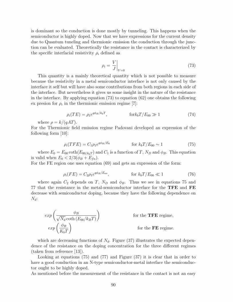
is dominant so the conduction is done mostly by tunneling. This happens when thesemiconductor is highly doped. Now that we have expressions for the current densitydue to Quantum tuneling and thermionic emission the conduction through the junc-tion can be evaluated. Theoretically the resistance in the contact is characterized bythe specific interfacial resistivity ρi defined as
ρi =V
J
∣∣∣∣V=0
(73)
This quantity is a mainly theoretical quantity which is not possible to measurebecause the resistivity in a metal semiconductor interface is not only caused by theinterface it self but will have also some contributions from both regions in each side ofthe interface. But nevertheless it gives us some insight in the nature of the resistancein the interface. By applying equation (73) to equation (62) one obtains the followingex presion for ρi in the thermionic emission regime [7]:
ρi(TE) = ρ1eqφB/kbT , forkbT/E00 1 (74)
where ρ = k/(qAT ).For the Thermionic field emission regime Padovani developed an expression of thefollowing form [10]:
ρi(TFE) = C1ρ1eqφB/E0 for kbT/E00 ∼ 1 (75)
where E0 = E00 coth(E00/kbT ) and C1 is a function of T , ND and φB. This equationis valid when E0 < 2/3(φB + Efn).For the FE region one uses equation (69) and gets an expression of the form:
ρi(FE) = C2ρ1eqφB/Eoo , for kbT/E00 1 (76)
where again C2 depends on T , ND and φB. Thus we see in equations 75 and77 that the resistance in the metal-semiconductor interface for the TFE and FEdecrease with semiconductor doping, because they have the following dependence onNd:
exp
(φB√
Nd coth (E00/kBT )
)for the TFE regime,
exp
(φBKbT
)for the FE regime.
which are decreasing functions of Nd. Figure (37) illustrates the expected depen-dence of the resistance on the doping concentration for the three different regimes(taken from reference [13]).
Looking at equations (75) and (77) and Figure (37) it is clear that in order tohave a good conduction in an N-type semiconductor-metal interface the semiconduc-tor ought to be highly doped.As mentioned before the measurement of the resistance in the contact is not an easy
90

Figure 37: Expected theoretical dependence of ρi on Nd. Taken from [13]
task because when doing it is not always clear which part of the current was lostdue to the resistance in the metal-semiconductor interface and which was lost dueto recombination and leakage currents in the semiconductor. Nevertheless severalmethods for doing so have been developed, they can vary in complexity dependingon the level of accuracy desired. The most basic one is the two terminals methods inwhich a current is forced to pass betweentwo metal terminals which have a semicon-ductor in between. Then the total resistance of the structure is measured and thenthe contact resistance is found by subtracting the semiconductor spreading resistancefrom the total measured resistance. This method fails in that determination of thesemiconductors spreading resistance comes out with a great uncertainty that usuallygives place to a great error to the contact resistance[7]. Some other more accuratemethods include multiple terminals methods which by playing with the geometry ofthe configuration of the terminals the innaccuracies due to the measuring of comple-mentary resistances in the system are possible to reduce.In addition to the doping level of the semiconductor the other factor that affectsconduction through the metal contacts is the contact area. This is so because insemiconductors we have current densities flowing around, so that the total currentthat passes through a metal contact of area A is J ×A. The maximum power outputthat can pass through a contact is given by AJmpVmp =, where Jmp and Vmp are thecurrent density and Voltage at the maximum power point [4]. Therefore in general
91

the higher the metal contacts area is, the better the charge transport will be. But asmentioned before this might be a problem when designing the solar cell, because ingeneral the wafer regions lying under contacts will be shadowed and no light absorp-tion will occur there. Therefore the dimensions and the geometry of the contacts isone of the parameters that is important to optimize.One method to optimize the width of the metal busbar is to calculate the power lossdue to the resistive losses in the busbar and also the power loss due to the shadowingcause by it. These two quantities depend on the area and thus its thickness. Then byadding them up and differentiating with respect to the thickness one finds the valuethat gives the minimum power loss. This happens when both power loss mechanismsare equal and is given by:
WB = A
√Rmsb
3
JmpVmp
(77)
where WB is the optimal busbar width and Rmsb is metal semiconductor sheet resis-tance in the bussbar [4] .
References
[1] Global Market outlook for photovoltaics 2013-2017. European photovoltaics in-dustry association.
[2] John David Jackson, Classical Electrodynamics Third Edition
[3] William Shockley and Hans J. Queisser, ”Detailed Balance Limit of Efficiency ofp-n Junction Solar Cells”, Journal of Applied Physics, Volume 32 (March 1961),pp. 510-519;
[4] Martin A . Green. Solar Cells, operating principles technology and system appli-cations, Prentice Hall 1982.
[5] Solid state physics, Guiseppe Grosso, Guisepe Pastori Parravacini, AcademicPress 2001
[6] Solid state physics, Guiseppe Grosso, Guisepe Pastori Parravacini, AcademicPress 2001 grosso cap 13.
[7] Semiconductor Material and Devices Characterization. Third Edition, by DieterK. Schroder. Cap 3
[8] J. W. Conley, C. B. Duke, G. D. Mahan, and J. J. Tiemann, Electron Tunnelingin Metal-Semiconductor Barriers, Phys. Rev. 150, 466 (1966).
[9] Theory of Electron Tunneling in Semiconductor Junctions Fredkin, D. R.; Wan-nier, G. H. Physical Review, vol. 128, Issue 5, pp. 2054-2061
92

[10] F.A Padovani and R.Stratton, FIELD AND THERMIONIC-FIELD EMISSIONIN SCHOTTKY BARRIERS Solid-State Electronics Pergamon Press 1966. Vol.9, pp. 695-701.
[11] E. L. MURPHY and R. H. GOOD, JR., Phys. Rev. 3. M. M. ATALLA and R.W. SOSHEA, Scientific Report 102, 1464 (1956).
[12] 14. E.H. Rhoderick and R.H. Williams, Metal-Semiconductor Contacts, 2nd ed.,Clarendon, Oxford, 1988.
[13] A. Y. C. YU, ELECTRON TUNNELING AND CONTACT RESISTANCE OFMETAL-SILICON CONTACT BARRIERS*, Solid-State Electronics PergamonPress 1970. Vol. 13, pp. 239-247.
[14] EDVRD BLINT KUTHI, Crystalline silicon solar cells with selective emitter andthe self-doping contact
[15] Crystalline silicon solar cells with selective emitter and the self-doping contactEDVRD BLINT KUTHI
[16] Simple integral screenprinting process for selective emitter polycrystalline siliconsolar cells, J. Szlufcik, H. E. Elgamel, M. Ghannam, J. Nijs, and R. MertensCitation: Appl. Phys. Lett. 59, 1583 (1991);
[17] A. Rohatgi1 , M. Hilali1, D. L. Meier2, A. Ebong1, C. Honsberg1 , A. F. Carrol3,and P. Hacke2, SELF-ALGINED SELF-DOPING SELECTIVE EMITTER FORSCREEN-PRINTED SILICON SOLAR CELLS.
[18] G. Hahn , STATUS OF SELECTIVE EMITTER TECHNOLOGY ,Preprint25th EU PVSEC / WCPEC-5 Valencia 2010
[19] HIGH EFFICIENCY SELECTIVE EMITTER ENABLED THROUGH PAT-TERNED ION IMPLANTATION, Russell Low1, Atul Gupta1, Nicholas Bate-man1, Deepak Ramappa1, Paul Sullivan1, Wesley Skinner1, James Mullin1.
[20] J.M. Serra, R. Gamboa and A.M. Vallra, A study on selective emitter formationthrough an oxide mask for silicon solar cells.
[21] H. Antoniadis, F. Jiang, W. Shan, Y. Liu, All screen printed mass producedsilicon ink selective emitter solar cells, Proc. 35th IEEE PVSC, Honolulu 2010
[22] Helg Haverkamp, Amir Dastgheib-Shirazi , Bernd Raabe , Felix Book , GisoHahn 1,2,MINIMIZING THE ELECTRICAL LOSSES ON THE FRONT SIDE:DEVELOPMENT OF A SELECTIVE EMITTER PROCESS FROM A SINGLEDIFFUSION
[23] Fabrication engineering at the micro and nanoscale / Stephen A. Campbell, NewYork : Oxford University Press ISBN: 9781613441151, 161344115x
93

[24] M. H. Rein. Wet chemical wafer cleaning of muliticrystalline silicon. Master?sthesis. Department of Mathematical Science and Technology, University of Life-sciences, 2001.
[25] R.B. Fair, ”Concentration profiles of diffused dopants in silicon, in F.F.Y. Wang,Ed. Impurity Doping Process in Silicon, North Holland, New York, 1981
[26] Optimiisation of SINx:H anti-reflection coatings for silicon solar cells J. Hofstet-ter, C. del Cafiizo, S. Ponce-Alcantara, A. Luque Instituto de Energia Solar -Universidad Politecnica de Madrid
[27] Chetan Singh Solanki, Solar Photovoltaics : Fundamentals, Technologies andApplications
[28] M. Mller, P.P. Altermattb, K. Schlegela, G. Fischera Evaluating The Quality OfSelective Emitter Structures By Imaging The Emitter Saturation Current Density,SiliconPV: April 03-05, 2012, Leuven, Belgium
[29] pveducation.org
[30] D.K. Schroder, ”Semiconductor Material and Device Characterization”,Chapter7 ,Wiley-IEEE Press; 3 edition ISBN-13: 978-0471739067 —
[31] D.K. Schroder, Carrier Lifetimes in Silicon, IEEE TRANSACTIONS ON ELEC-TRON DEVICES, VOL. 44, NO. 1, JANUARY 1997
[32] T. Otaredian, ?The influence of the surface and oxide charge on the surfacerecombination process,? Solid-State Electron., vol. 36, pp. 905915, June 1993.
[33] The Physics of Solar Cell, Jenny Nelson, Imperial college Press 2003
[34] Claude Cohen-Tannoudji, Bernard Diu, Franck Lalo, Quantum Mechanics Vol2. Wiley, 1977
[35] Analysis of the interaction of a laser pulse with a silicon wafer: Determinationof bulk lifetime and surface recombination velocity Keung L. Luke1 and Li JenCheng, J. Appl. Phys. 61, 2282 (1987);
[36] Chih Hsin Wang,Minority-Carrier Lifetime and Surface Recombination VelocityMeasurement by Frequency-Domain Photoluminescence IEEE TRANSACTIONSON ELECTRON DEVICES. VOL. 38. NO. 9, SEPTEMBER 1991
[37] Laser doping for microelectronics and microtechnology ,Original Research Arti-cle Applied Surface Science, Volume 247, Issue 14, 15 July 2005, Pages 537-544Thierry Sarnet, Gurwan Kerrien, Nourdin Yaakoubi, Alain Bosseboeuf,
[38] J.M. Fairfield,G.H. Schwuttke, Silicon diodes made by laser irradiation,Solid-State Electronics
Volume 11, Issue 12, December 1968, Pages 1175-1176
94

[39] R. F. Wood,Modeling of nonequilibrium melting and solidification in laser-irradiated materials Physical Review B, VOLUME 34, NUMBER 4.
[40] Back-contacted back-junction silicon solar cells Krister Mangersnes THESIS Uni-versity of Oslo. 2010
[41] Laser induced defects in laser doped solar cells Z. Hameiri et al., Progress inPhotovoltaics Research and Applications 19, 391 (2011) dd
[42] Properties of Silicon, EMIS Datareview Series No. 4 (INSPEC, London, 1988).
[43] Toshiyuki Sameshima and Setsuo Usui Analysis of Dopant Diffusion in MoltenSilicon Induced by a Pulsed Excimer Laser Jpn. J. Appl. Phys. 26 (1987) pp.L1208-L1210
[44] R. F. Wood, Modeling of nonequilibrium melting and solidification in laser-irradiated materials PHYSICAL REVIEW B 8 VOLUME 34, NUMBER 4 15AUGUST 1986
[45] R. F. Wood, Macroscopic theory of pulsed-laser annealing. I.Thermal transportand melting PHYSICAL REVIEW B VOLUME 23, NUMBER 6 15 MARCH1981
[46] R. F. Wood, LASER PROCESSING OF SEMICONDUCTOR MATERIALS 1,Ann. Rev. Mater. Sci. 1982. 12: 323-50
[47] R. T. Young and R. F. Wood,LASER PROCESSING OF SEMICONDUCTORMATERIALS Ann. Rev. Mater. Sci. 1982. 12: 323-50
[48] Jellison GE, Modine FA. Optical absorption of silicon between 1.6 and 4.7 eV atelevated temperatures. Applied Physics Letters 1982; 41: 180-182.
[49] Young RT, Narayan J, Wood RF. Electrical and structural characteristics oflaser-induced epitaxial layers in silicon. Applied Physics Letters 1979; 35: 447-449.
[50] P.M. MOONEY 4) ( a ) , R.T. YOUNG (b), J. KARINS (a), Y.H. LEE . Defectsin Laser Damaged Silicon Observed by DLTS. phys. stat. sol. (a) 48, K31 (1978)
[51] Characterization of a diode double-end pumped Nd:YVO4 laser for high-bit-ratefree-space and intersatellite communications
[52] Gould, R. Gordon (1959). ”The LASER, Light Amplification by StimulatedEmission of Radiation”. In Franken, P.A. and Sands, R.H. (Eds.). The Ann ArborConference on Optical Pumping, the University of Michigan, 15 June through 18June 1959. p. 128.
[53] 3. A. Safiei, H. Windgassen, K. Wolter, H. Kurz. Emitter Profile Tailoring toContact Homogeneous High Sheet Resistance Emitter. Energy Procedia, Volume27, 2012, Pages 432-437.
95

[54] UNDERSTANDING AND DEVELOPMENT OF MANUFACTURABLESCREENPRINTED CONTACTS ON HIGH SHEET-RESISTANCE EMITTERSFOR LOW-COST SILICON SOLAR CELLS, page 119. Mohamed M. Hilali. PHDthesis Georgia Institute of Technology August 2005
[55] M. Mllera*, P.P. Altermattb, K. Schlegela, G. Fischera, Evaluating The Qual-ity Of Selective Emitter Structures By Imaging The Emitter Saturation CurrentDensity, Energy Procedia 27 ( 2012 ) 293 299
[56] http://www.pvlighthouse.com
96