Effect of Nucleation Parameters of Ge Quantum Dots … of Nucleation Parameters of Ge Quantum Dots...
4
81 Journal Integrated Circuits and Systems 2007; v.2 / n.2:81-84 Effect of Nucleation Parameters of Ge Quantum Dots Grown over Silicon Oxide by LPCVD ABSTRACT Germanium quantum dots (Ge-QD) were grown by Low Pressure Chemical Vapor Deposition (LPCVD) on Si nucleus previously grown on 3 nm thick SiO 2 ultra thin film. Samples were analyzed by atomic force microscopy (AFM) and high resolution transmission electron microscopy (HRTEM). We report the analysis of the influence of the nucleation parameters on size and spatial distribution of Ge-QD. AFM images show a Ge-QD density of around 3.6x10 10 cm -2 , with an 11 nm mean size and 2.9 nm height. Finally, HRTEM investigation shows that the Ge-QD have a crystalline structure, i.e., they are nanocrystals. Index Terms: Nanocrystals, nanostructures, quantum dots, germanium, LPCVD. S. N. M. Mestanza 1 , I. Doi 1, 2 and N. C. Frateschi 1, 3 1 Center for Semiconductor Components, State University of Campinas, Brazil 2 School of Electrical and Computer Engineering, State University of Campinas, Brazil 3 Gleb-Wataghin Physics Institute, State University of Campinas, Brazil. E-mail: [email protected] 1. INTRODUCTION In the last years, silicon, germanium or sili- con–germanium quantum dots embedded in an insu- lator have been studied extensively for their meso- scopic behavior. They have potential applications not only for silicon-based optoelectronic devices, but also for room temperature operation of single electron memories [1]. Specifically, Ge nanocrystals embedded in a dielectric matrix (such as SiO 2 ) are now being extensively studied as the charge storage elements in flash memory devices [2], [3], [4]. It is known that due to quantum confinement effects these nanocrys- tals exhibit nonlinear optical properties that usually do not appear in the bulk materials. Ge-QD can be obtained by various techniques, such as pyrolysis [5], co-sputtering [6], pulsed-laser ablation [7], ion implantation [8] and Low Pressure Chemical Vapor Deposition (LPCVD) [9]. All these techniques, besides the last one, require a high tem- perature annealing to produce the nanostructures. The synthesis of Ge-ns reported herein is based on a con- ventional CVD method [10] using a low base pressure (LPCVD). In the case of Si-QD, chemical vapor dep- osition (CVD) addresses these issues quite well [10], [11]. CVD is a robust, efficient, and industry-compat- ible method to deposit semiconductor films and nanocrystals. The successful CVD of Si-QD on oxide substrate is well known in the literature. However, CVD of Ge onto SiO 2 surfaces involves first creating Si nuclei for the subsequent growth of the Ge-QD [12]. The primary aim of this work is to understand the influence of nucleation parameters, namely, total pres- sure, temperature and precursor gas flow rate on the density and size of the obtained Ge-QD. Moreover, we also studied further the formation of Ge-QD on the obtained Si nuclei by alternately controlling the selec- tive growth conditions in LPCVD using SiH 4 and GeH 4 , both diluted in H 2 . It is important to observe that in our study we demonstrate that crystalline quan- tum dots can be obtained by a technique that does not require high temperature annealing. 2. EXPERIMENT The substrates used in this study are p-type Si (100) wafers covered by a 3 nm thick thermally grown SiO 2 layer. Si nuclei and Ge-QD were grown in a ver- tical LPCVD reactor (PMC 200), using SiH 4 and GeH 4 as precursors and H 2 as carrier gas. The hydrox- ylation of the thermal SiO 2 was performed using a 0.1% HF solution. Ge-QD was grown in two-step process [13]. First, the SiO 2 surface was functionalized by deposition of Si nuclei using SiH 4 as gaseous precursor at tempera- tures of 550° C and 600° C; pressures of 2 and 5 Torr; nucleation time of 10, 20 and 30 sec.; and SiH 4 gas flow of 10, 20 and 40 sccm. Second, Ge-QD was grown selectively on the Si nuclei using GeH 4 gas. Before this
-
Upload
nguyentram -
Category
Documents
-
view
218 -
download
4
Transcript of Effect of Nucleation Parameters of Ge Quantum Dots … of Nucleation Parameters of Ge Quantum Dots...
81Journal Integrated Circuits and Systems 2007; v.2 / n.2:81-84
Effect of Nucleation Parameters of Ge Quantum DotsGrown over Silicon Oxide by LPCVD
ABSTRACT
Germanium quantum dots (Ge-QD) were grown by Low Pressure Chemical Vapor Deposition(LPCVD) on Si nucleus previously grown on 3 nm thick SiO2 ultra thin film. Samples were analyzedby atomic force microscopy (AFM) and high resolution transmission electron microscopy (HRTEM).We report the analysis of the influence of the nucleation parameters on size and spatial distributionof Ge-QD. AFM images show a Ge-QD density of around 3.6x1010 cm-2, with an 11 nm mean sizeand 2.9 nm height. Finally, HRTEM investigation shows that the Ge-QD have a crystalline structure,i.e., they are nanocrystals.
Index Terms: Nanocrystals, nanostructures, quantum dots, germanium, LPCVD.
S. N. M. Mestanza1 , I. Doi 1, 2 and N. C. Frateschi 1, 3
1 Center for Semiconductor Components, State University of Campinas, Brazil2 School of Electrical and Computer Engineering, State University of Campinas, Brazil
3 Gleb-Wataghin Physics Institute, State University of Campinas, Brazil.E-mail: [email protected]
1. INTRODUCTION
In the last years, silicon, germanium or sili-con–germanium quantum dots embedded in an insu-lator have been studied extensively for their meso-scopic behavior. They have potential applications notonly for silicon-based optoelectronic devices, but alsofor room temperature operation of single electronmemories [1]. Specifically, Ge nanocrystals embeddedin a dielectric matrix (such as SiO2) are now beingextensively studied as the charge storage elements inflash memory devices [2], [3], [4]. It is known thatdue to quantum confinement effects these nanocrys-tals exhibit nonlinear optical properties that usually donot appear in the bulk materials.
Ge-QD can be obtained by various techniques,such as pyrolysis [5], co-sputtering [6], pulsed-laserablation [7], ion implantation [8] and Low PressureChemical Vapor Deposition (LPCVD) [9]. All thesetechniques, besides the last one, require a high tem-perature annealing to produce the nanostructures. Thesynthesis of Ge-ns reported herein is based on a con-ventional CVD method [10] using a low base pressure(LPCVD). In the case of Si-QD, chemical vapor dep-osition (CVD) addresses these issues quite well [10],[11]. CVD is a robust, efficient, and industry-compat-ible method to deposit semiconductor films andnanocrystals. The successful CVD of Si-QD on oxidesubstrate is well known in the literature. However,CVD of Ge onto SiO2 surfaces involves first creating Si
nuclei for the subsequent growth of the Ge-QD [12].The primary aim of this work is to understand theinfluence of nucleation parameters, namely, total pres-sure, temperature and precursor gas flow rate on thedensity and size of the obtained Ge-QD. Moreover, wealso studied further the formation of Ge-QD on theobtained Si nuclei by alternately controlling the selec-tive growth conditions in LPCVD using SiH4 andGeH4, both diluted in H2. It is important to observethat in our study we demonstrate that crystalline quan-tum dots can be obtained by a technique that does notrequire high temperature annealing.
2. EXPERIMENT
The substrates used in this study are p-type Si(100) wafers covered by a 3 nm thick thermally grownSiO2 layer. Si nuclei and Ge-QD were grown in a ver-tical LPCVD reactor (PMC 200), using SiH4 andGeH4 as precursors and H2 as carrier gas. The hydrox-ylation of the thermal SiO2 was performed using a0.1% HF solution.
Ge-QD was grown in two-step process [13].First, the SiO2 surface was functionalized by depositionof Si nuclei using SiH4 as gaseous precursor at tempera-tures of 550° C and 600° C; pressures of 2 and 5 Torr;nucleation time of 10, 20 and 30 sec.; and SiH4 gas flowof 10, 20 and 40 sccm. Second, Ge-QD was grownselectively on the Si nuclei using GeH4 gas. Before this
Effect of Nucleation Parameters of Ge Quantum Dots Grown over Silicon Oxide by LPCVDMestanza, Doi & Frateschi
82 Journal Integrated Circuits and Systems 2007; v.2 / n.2:81-84
step, the CVD chamber is purged to eliminate the resid-ual SiH4 gas, and the sample maintained under pure H2atmosphere, without oxidizing Si nuclei. The conditionsfor the selective Ge deposition on Si nuclei were kept as550° C, 2 Torr, 30 sec. and 5 sccm GeH4 gas flow.
The morphological characteristics, such as sizesand density of the Ge-QD were characterized by atom-ic force microscopy (AFM) using a DI Nanoscope IIIamicroscope, as well as the high-resolution transmissionelectron microscopy (HRTEM), JEM-3010 ARPmicroscope, were used to verify the Ge-QD structure.
3. RESULTS AND DISCUSSION
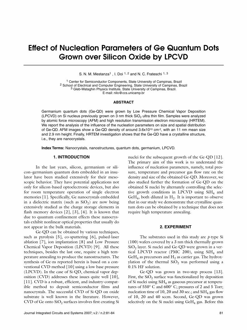
Figure 1 (a) and (b) show AFM images of thesurfaces of the Ge-QD deposited at nucleation tem-
peratures of 550° C and 600° C, respectively. Theother nucleation parameters were kept constant,namely, 5 Torr/40 sccm SiH4/20 sec. We observedthat on the sample prepared at 600° C, the Ge-QDdensity (6.4x109 cm-2) is increased by about 21X,and their mean size (26 nm) is decreased by approx-imately 4X, compared to the sample deposited at550° C. This increase in Ge-QD density can beattributed to the increase in the nucleation rate as aconsequence of the larger surface energy. A possibleexplanation for size decrease could be the Ge-QDdensity increase, since in both cases GeH4 flow isequal.
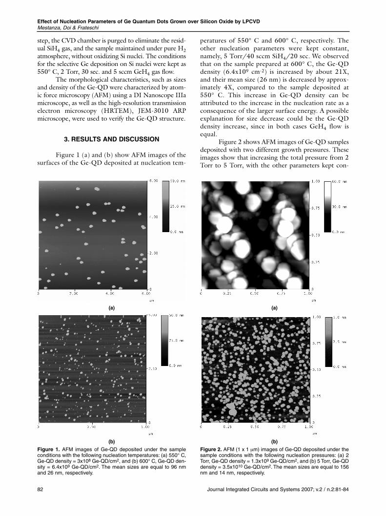
Figure 2 shows AFM images of Ge-QD samplesdeposited with two different growth pressures. Theseimages show that increasing the total pressure from 2Torr to 5 Torr, with the other parameters kept con-
Figure 1. AFM images of Ge-QD deposited under the sampleconditions with the following nucleation temperatures: (a) 550° C,Ge-QD density = 3x10⁸ Ge-QD/cm2, and (b) 600° C, Ge-QD den-sity = 6.4x10⁹ Ge-QD/cm2. The mean sizes are equal to 96 nmand 26 nm, respectively.
(b)
(a)
Figure 2. AFM (1 x 1 µm) images of Ge-QD deposited under thesample conditions with the following nucleation pressures: (a) 2Torr, Ge-QD density = 1.3x10⁹ Ge-QD/cm2, and (b) 5 Torr, Ge-QDdensity = 3.5x10¹⁰ Ge-QD/cm2. The mean sizes are equal to 156nm and 14 nm, respectively.
(b)
(a)

Effect of Nucleation Parameters of Ge Quantum Dots Grown over Silicon Oxide by LPCVDMestanza, Doi & Frateschi
83Journal Integrated Circuits and Systems 2007; v.2 / n.2:81-84
stant (600º C/20 sccm SiH4/20 sec.) the Ge-QDdensity increases 27X compared to the sample ana-lyzed in Figure 2(a), and that the mean size is of 14 nm, thus 11X smaller. It is known that at high totalpressures, the SiH4 concentration on silicon oxide sur-face is too high, therefore, this phenomenon is likelyto be the cause of the promotion of the larger numberof Si nuclei.
Figure 3 shows AFM images of Ge-QD samplesgrown at different SiH4 gas flow. These images showthat decreasing SiH4 flow from 20 sccm to 10 sccm,the Ge-QD density is increased by 28X and the meansize reduced by 14X compared to the samplesobtained at 20 sccm of SiH4 flow. This set of parame-ters (600° C/2 Torr/10 sccm SiH4/20 sec.) leads tothe highest Ge-QD density of 3.6x1010cm-2 and thesmallest mean sizes of approximately 11 nm.
Figure 4 shows statistical results of the Ge-QDdensity and sizes of the samples analyzed in Figure 3.In this graphic one can observe that decreasing SiH4flow below 20 sccm, the density of Ge-QD grown onSi nuclei increases abruptly and their sizes are alsoabruptly reduced. This change on Ge-QD growthbehavior can be due to the second step of our process,deposition of Ge, since nuclei may have formed alsoon SiO2 [14] from GeH4 decomposition, due to thesmaller density of Si nuclei observed for low SiH4flow, however, the combination of theses two effectsleads to the increasing of the Ge-QD grown on Sinuclei.
Figure 5 shows an HRTEM image of a Ge-QDprepared with 550° C/5 Torr/40 sccm SiH4 nucle-ation conditions. This result evidences the growth ofthe Ge-QD by LPCVD, and exhibit a typical hemi-
Figure 3. AFM (5 x 5 µm) images of Ge-QD deposited under thesample conditions with the following nucleation flows: (a) 10sccm, Ge-QD density = 3.6x10¹⁰ Ge-QD/cm2, and (b) 20 sccm,Ge-QD density = 1.3x10⁹ Ge-QD/cm2. The mean sizes are equalto 11 nm and 156 nm, respectively.
(b)
(a)
Figure 4. Variation of the density and size of Ge-QD grown onSiO2 with the SiH4 flow, for the samples analyzed in Figure 3.
Figure 5. Cross-sectional of HRTEM image of Ge-QD grows onSiO2. Ge-QD were formed at 550° C/5 Torr/40 sccm SiH4.
Effect of Nucleation Parameters of Ge Quantum Dots Grown over Silicon Oxide by LPCVDMestanza, Doi & Frateschi
84 Journal Integrated Circuits and Systems 2007; v.2 / n.2:81-84
spherical geometry. From this figure one can alsoclearly observe that the QD present a crystalline order.
Results of Raman spectroscopy characteriza-tions of these samples (not presented in this paper),have shown a well defined characteristic peak around300 cm-1 [15], which is a typical frequency that char-acterize the Ge crystalline formation. We are confi-dent therefore, that the obtained dots on our samplesare of Ge and crystalline.
4. CONCLUSIONS
Define We have studied the influence of nucle-ation parameters (temperature, total pressure andsilane flow) on the density and sizes of Ge-QD onSiO2. At particular processes conditions, an abruptincrease of Ge-QD density was found to occur as theSiH4 gas flow is reduced below 20 sccm. The highestGe-QD density obtained was 3.6x1010 cm-2 withmedium size of 11 nm. HRTEM characterizationconfirmed the formation of quantum dots with crys-talline structure which are obtained with no need forhigh temperature annealing.
ACKNOWLEDGEMENTS
The authors would like to acknowledge E. S.Marins for his help with the preparation of thesamples, and to Synchrotron Light NationalLaboratory, in Campinas, for the measurements ofHRTEM and AFM. This work was financiallysupported by the Conselho Nacional deDesenvolvimento Científico e Tecnológico (CNPq).
REFERENCES
[1] Y. M. Niquet, G. Allan, C. Delerue, and M. Lannoo, “Quantumconfinement in germanium nanocrystals”, Appl. Phys. Lett.77, 8, Aug., 2000, 1182-1184.
[2] S. Tiwari, F. Rana, K. Chan, H. Hanafi, W. Chan and D.Buchanan, “Volatile and Non-Volatile Memories in Siliconwith Nano-Crystal Storage,” Technical Digest of InternationalElectron Device Meeting, December 1995, IEEE No 0-7803-2700-4, pp. 521-524.
[3] K. Yano, T. Ishii, T. Hashimoto, T. Kobayashi, F. Murai, and K.Seki, “Room-Temperature Single-Electron Memory”, IEEETrans. Electron Devices 41, 9, Sep., 1994, pp. 1628-1638.
[4] M. L. Ostraat, J. W. De Blauwe, M. L. Green, L. D. Bell, M. L.Brongersma, J. Caperson, R. C. Flagan, and H. A. Atwater, “Synthesis and characterization of aerosol silicon nanocrys-tal nonvolatile floating-gate memory devices”, Appl. Phys.Lett. 79, 3, Jul., 2001, pp. 433-435.
[5] K. A. Littau, P. J. Szajowski, A. J. Muller, A. R. Kortan and L.E. Brus, “A Luminescent Silicon Nanocrystal Colloid Via AHigh-Temperature Aerosol Reaction”, J. Phys. Chem. 97, 6,Feb., 1993, pp. 1224-1230.
[6] Y. Maeda, N. Tsukamoto, Y. Yazawa, Y. Kanemitsu and Y.Masumoto, “Visible Photoluminescence of Ge MicrocrystalsEmbedded in SiO2 Glassy Matrices”, Appl. Phys. Lett. 59, 24,Dec., 1991, pp. 3168-3170.
[7] E. Werwa, A. A. Seraphin, L. A. Chiu, C. X. Zhou and K. D.Kolenbrander, “Synthesis and Processing of SiliconNanocrystallites Using a Pulsed-Laser Ablation SupersonicExpansion Method”, Appl. Phys. Lett. 64, 14, Apr., 1994, pp.1821-1823.
[8] T. Shimizu-Iwayama, K. Fujita, S. Nakao, K. Saitoh, T. Fugitaand N. Itoh, “Visible Photoluminescence in Si+-Implated SilicaGlass”, J. Appl. Phys. 75, 12, Jun., 1994, pp. 7779-7783.
[9] S. Miyazaki, Y. Hamamoto, E. Yoshida, M. Ikeda and M.Hirose, “Control of self-assembling formation of nanometersilicon dots by low pressure chemical vapor deposition”, ThinSolid Films, 369, 1-2, Jul., 2000, pp. 55-59.
[10]T. Baron, F. Martin, P. Mur, C. Wyon, and M. Dupuy, “Siliconquantum dot nucleation on Si3N4, SiO2 and SiOxNy sub-strates for nanoelectronic devices”, J. Cryst. Growth 209, 4,Feb., 2000, pp. 1004-1008.
[11]T. Baron, P. Gentile, N. Magnea, and P. Mur, “Single-electroncharging effect in individual Si nanocrystals”, Appl. Phys. Lett.79, 8, Aug., 2001, pp. 1175-1177.
[12]Y. Darma, R. Takaoka, H. Murakami and S. Miyazaki, “Self-assembling formation of silicon quantum dots with a germa-nium core by low-pressure chemical vapour deposition”,Nanotchnology 14, 4, Apr., 2003, pp. 413-415.
[13]T. Baron, B. Pelissier, L. Perniola, F. Mazen, J. M. Hartmannand G. Rolland, “Chemical vapor deposition of Genanocrystals on SiO2”, Appl. Phys. Lett. 83, 7, Aug., 2003,pp. 1444-1446.
[14]A. A. Shklyaev and M. Ichikawa, “Effect of interfaces onquantum confinement in Ge dots grown on Si surfaces witha SiO2 coverage”, Surface Science 514, 1-3, Aug., 2002,pp. 19-26.
[15]S. N. M. Mestanza, E. Rodriguez, I. Doi, A. R. Vaz, and N. C.Frateschi, “The Effect of Si-Substrate on the OpticalCharacterization of Ge Nanostructures Obtained by LPCVD”,Proc.2007 Electrochemical Society Workshop onMicroelectronics and Devices, 2007, (In Press.).