EEE310 MICROPROCESSORS CHAPTER 4compe.hku.edu.tr/Dosyalar/EEE310--Mikroislemciler... · MVI C, 15H...
42
EEE310 MICROPROCESSORS CHAPTER 4 M. Fatih Tüysüz
Transcript of EEE310 MICROPROCESSORS CHAPTER 4compe.hku.edu.tr/Dosyalar/EEE310--Mikroislemciler... · MVI C, 15H...

EEE310 MICROPROCESSORS
CHAPTER 4M. Fatih Tüysüz

CHAPTER 4
Contents
� Counters
� Time Delays
� Instruction Cycle
� Timing Diagram

Counters
• A loop counter is set up by loading a register witha certain value
• Then using the DCR (to decrement) and INR (toincrement) the contents of the register are updated.
• A loop is set up with a conditional jumpinstruction that loops back or not depending onwhether the count has reached the terminationcount.

Counters• The operation of a loop counter can be
described using the following flowchart.
Initialize
Update the count
Is thisFinal
Count?
Body of loop
No
Yes

MVI C, 15H
LOOP DCR C
JNZ LOOP
Sample ALP for implementing a loopUsing DCR instruction

Using a Register Pair as a Loop Counter
• Using a single register, one can repeat a loop for amaximum count of 255 times.
• It is possible to increase this count by using aregister pair for the loop counter instead of thesingle register.– A minor problem arises in how to test for the final
count since DCX and INX do not modify the flags.– However, if the loop is looking for when the count
becomes zero, we can use a small trick by ORing thetwo registers in the pair and then checking the zero flag.

Using a Register Pair as a Loop Counter
• The following is an example of a loop setup with a register pair as the loop counter.
LXI B, 1000HLOOP DCX B
MOV A, CORA BJNZ LOOP

Delays
• It was shown in Chapter 2 that each instructionpasses through different combinations of Fetch,Memory Read, and Memory Write cycles.
• Knowing the combinations of cycles, one cancalculate how long such an instruction wouldrequire to complete.
• The table in Appendix F of the book contains acolumn with the title B/M/T.– B for Number of Bytes– M for Number of Machine Cycles– T for Number of T-State.

Delays
• Knowing how many T-States an instructionrequires, and keeping in mind that a T-State is oneclock cycle long, we can calculate the time usingthe following formula:
Delay = No. of T-States / Frequency
• For example a “MVI” instruction uses 7 T-States.Therefore, if the Microprocessor is running at 2MHz, the instruction would require 3.5 µSecondsto complete.

Delay loops• We can use a loop to produce a certain
amount of time delay in a program.
• The following is an example of a delayloop:
MVI C, FFH 7 T-StatesLOOP DCR C 4 T-States
JNZ LOOP 10 T-States
• The first instruction initializes the loop counter and isexecuted only once requiring only 7 T-States.
• The following two instructions form a loop thatrequires 14 T-States to execute and is repeated 255times until C becomes 0.

Delay Loops (Contd.)
• We need to keep in mind though that in the lastiteration of the loop, the JNZ instruction will fail andrequire only 7 T-States rather than the 10.
• Therefore, we must deduct 3 T-States from the totaldelay to get an accurate delay calculation.
• To calculate the delay, we use the following formula:Tdelay = TO + TL
– Tdelay = total delay– TO = delay outside the loop– TL = delay of the loop
• TO is the sum of all delays outside the loop.

Delay Loops (Contd.)
• Using these formulas, we can calculate thetime delay for the previous example:
• TO = 7 T-States– Delay of the MVI instruction
• TL = (14 X 255) - 3 = 3567 T-States– 14 T-States for the 2 instructions repeated 255 times
(FF16 = 25510) reduced by the 3 T-States for the finalJNZ.
( )

Using a Register Pair as a Loop Counter
• Using a single register, one can repeat a loop for amaximum count of 255 times.
• It is possible to increase this count by using aregister pair for the loop counter instead of thesingle register.– A minor problem arises in how to test for the final
count since DCX and INX do not modify the flags.– However, if the loop is looking for when the count
becomes zero, we can use a small trick by ORing thetwo registers in the pair and then checking the zero flag.

Using a Register Pair as a Loop Counter
• The following is an example of a delay loopset up with a register pair as the loopcounter.
LXI B, 1000H 10 T-StatesLOOP DCX B 6 T-States
MOV A, C 4 T-StatesORA B 4 T-StatesJNZ LOOP 10 T-States

Using a Register Pair as a Loop Counter
• Using the same formula from before, we cancalculate:
• TO = 10 T-States– The delay for the LXI instruction
• TL = (24 X 4096) - 3 = 98301 T- States– 24 T-States for the 4 instructions in the loop repeated
4096 times (100016 = 409610) reduced by the 3 T-States for the JNZ in the last iteration.

Nested Loops
• Nested loops can beeasily setup inAssembly language byusing two registers forthe two loop countersand updating the rightregister in the rightloop.– In the figure, the body of
loop2 can be before orafter loop1.
Initialize loop 1
Update the count1
Is thisFinal
Count?
Body of loop 1
No
Yes
Initialize loop 2
Body of loop 2
Update the count 2
Is thisFinal
Count?
No
Yes

Nested Loops for Delay
• Instead (or in conjunction with) Register Pairs, anested loop structure can be used to increase thetotal delay produced.
MVI B, 10H 7 T-StatesLOOP2 MVI C, FFH 7 T-StatesLOOP1 DCR C 4 T-States
JNZ LOOP1 10 T-StatesDCR B 4 T-StatesJNZ LOOP2 10 T-States

Delay Calculation of Nested Loops
• The calculation remains the same exceptthat it the formula must be appliedrecursively to each loop.– Start with the inner loop, then plug that delay in
the calculation of the outer loop.
• Delay of inner loop– TO1 = 7 T-States
• MVI C, FFH instruction– TL1 = (255 X 14) - 3 = 3567 T-States
• 14 T-States for the DCR C and JNZ instructions repeated 255times (FF16 = 25510) minus 3 for the final JNZ

Delay Calculation of Nested Loops
• Delay of outer loop– TO2 = 7 T-States
• MVI B, 10H instruction– TL1 = (16 X (14 + 3574)) - 3 = 57405 T-States
• 14 T-States for the DCR B and JNZ instructions and 3574T-States for loop1 repeated 16 times (1016 = 1610) minus 3 for thefinal JNZ.
– TDelay = 7 + 57405 = 57412 T-States
• Total Delay– TDelay = 57412 X 0.5 µSec = 28.706 mSec

Increasing the delay
• The delay can be further increased by usingregister pairs for each of the loop countersin the nested loops setup.
• It can also be increased by adding dummyinstructions (like NOP) in the body of theloop.

Instruction CycleEach instruction in 8085 microprocessor consists of two part- operation code (opcode) and operand. The opcode is a command such as ADD and the operand is an object to be operated on, such as a byte or the content of a register.
Instruction Cycle: The time taken by the processor to complete the execution of an instruction. An instruction cycle consists of one to six machine cycles.
Machine Cycle: The time required to complete one operation; accessing either the memory or I/O device. A machine cycle consists of three to six T-states.
T-State: Time corresponding to one clock period. It is the basic unit to calculate execution of instructions orprograms in a processor.
To execute a program, 8085 performs various operations as:• Opcode fetch (4 T-State)• Operand fetch (3 T-State)• Memory read/write (3 T-State)• I/O read/write (3 T-State)
External communication functions are:• Memory read/write• I/O read/write• Interrupt request acknowledge

Opcode Fetch Machine Cycle:
It is the first step in the execution of any instruction. The timing diagram of this cycle is given in next Figure. The following points explain the various operations that take place and the signals that are changed during the execution of opcode fetch machine cycle:
T1 clock cycle
i. The content of PC is placed in the address bus; AD0 - AD7 lines contains lower bit addressand A8 – A15 contains higher bit address.
ii. IO/Msignal is low indicating that a memory location is being accessed. S1 and S0 alsochanged to the levels as indicated in Table 1.
iii. ALE is high, indicates that multiplexed AD0 – AD7 act as lower order bus.
T2 clock cycle
i. Multiplexed address bus is now changed to data bus.
ii. The RD signal is made low by the processor. This signal makes the memory device loadthe data bus with the contents of the location addressed by the processor.

T3 clock cycle
i. The opcode available on the data bus isread by the processor and moved to theinstruction register.
ii. The RD signal is deactivated bymaking it logic 1.
T4 clock cycle
i. The processor decode the instructionin the instruction register and generatethe necessary control signals to executethe instruction. Based on the instructionfurther operations such as fetching,writing into memory etc takes place.
Fig. Opcode fetch machine cycle

Memory Read Machine Cycle:
The memory read cycle is executed by the processor to read a data byte from memory. The machine cycle is exactly same to opcode fetch except: a) It has three T-states b) The S0 signal is set to 0. The timing diagram of this cycle is given in the following Figure.

Memory Write Machine Cycle:
The memory write cycle is executed by the processor to write a data byte in a memory location. The processor takes three T-states and WR signal is made low. The timing diagram of this cycle is given in the following Figure.

Summary: Instruction Cycle
A processor have to execute the program. A program is just a set of instructions written in a sequence. Multiple machine cycles are required to execute an instruction. The processor fetches an instruction from memory, Decodes it and then executes it. This fetching, decoding and executing an instruction makes an instructiion cycle. Basically we have an equation for instruction cycle....
IC = FC + EC
where IC is instruction cycle, FC is fetch cycle and EC is the execution cycle. Every instruction will have a fetch machine cycle. Mainly a processor have three machine cycles: (i) Fetch, (ii) Read, (iii) Write.
Fetch Machine cycle: Fetch machine cycle is made up of two parts, First read an instruction from memory, Second Decode the instruction code. It requires 4 t-states in case of Intel 8085 MP.
T1: Address to memory with contents of PC register.T2: Initiate the memory read process.T3: Complete the memory read.T4: Decode the instruction.
Some of the instruction that dont require any memory or I/O operation will be over in the same machine cycle, others may require some read or write machine cycles.
Read Machine cycle: This requires 3 T-states. In this microprocessor will read the contents of memory or I/O device.
T1: Address to memory.T2: Initiate the memory read process.T3: Complete the memory read.
Write Machine Cycle: In this the microprocessor will write the contents on memory or I/O devce. It again requires 3 T-States.
T1: Address to memory.T2: Initiate the memory write process.T3: Complete the memory write.

Representation of Various Control signals generated during Execution of an Instruction Following Buses and Control Signals must be shown in a Timing Diagram:
•Higher Order Address Bus.
•Lower Address/Data bus
•ALE
•RD
•WR
•IO/M
Timing Diagram
It is one of the best way to understand to process of micro-processor/controller. With the help of timing diagram we can understand the working of any system, step by step working of each instruction and its execution, etc.
It is the graphical representation of process in steps with respect to time. The timing diagram represents the clock cycle and duration, delay, content of address bus and data bus, type of operation ie. Read/write/status signals.

Instruction:
A000h MOV A,B
Corresponding Coding:
A000h 78
Timing Diagram

Instruction:
A000h MOV A,B
Corresponding Coding:
A000h 78
8085 Memory
OFC
Timing Diagram

78h00h
A15- A8 (Higher Order Address bus)
ALE
RD
WR
IO/M
T1 T2 T3 T4Instruction:
A000h MOV A,B
Corresponding Coding:
A000h 78
8085 Memory
OFC
Op-code fetch Cycle
A0h
Timing Diagram

Instruction:
A000h MVI A,45h
Corresponding Coding:
A000h 3E
A001h 45
Timing Diagram

Instruction:
A000h MVI A,45h
Corresponding Coding:
A000h 3E
A001h 45
8085 Memory
OFC
MEMR
Timing Diagram
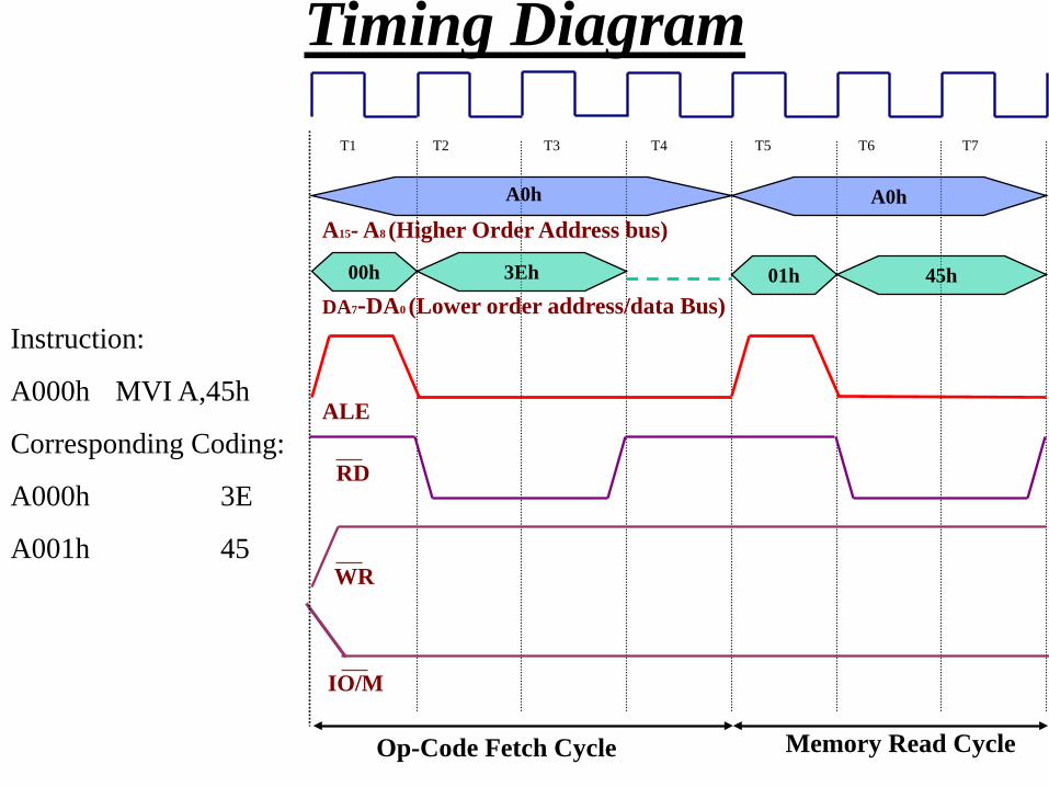
3Eh00h 01h 45h
A0h
A15- A8 (Higher Order Address bus)
DA7-DA0 (Lower order address/data Bus)
ALE
RD
WR
IO/M
Op-Code Fetch Cycle Memory Read Cycle
T1 T2 T3 T4 T5 T6 T7
A0h
Instruction:
A000h MVI A,45h
Corresponding Coding:
A000h 3E
A001h 45
Timing Diagram

Instruction:
A000h LXI A,FO45h
Corresponding Coding:
A000h 21
A001h 45
A002h F0
Timing Diagram

Instruction:
A000h LXI A,FO45h
Corresponding Coding:
A000h 21
A001h 45
A002h F0
Timing Diagram
8085 Memory
OFC
MEMR
MEMR

Timing Diagram
T1 T2 T3 T4 T5 T6 T7 T8 T9 T10
21h 01h 45h 02h F0h
A0h A0h A0h
A15- A8 (Higher Order Address bus)
DA7-DA0 (Lower order address/data Bus)
ALE
RD
WR
IO/M
00h
Op-Code Fetch Cycle Memory Read Cycle Memory Read Cycle

Instruction:
A000h MOV A,M
Corresponding Coding:
A000h 7E
Timing Diagram

8085 Memory
OFC
MEMR
Instruction:
A000h MOV A,M
Corresponding Coding:
A000h 7E
Timing Diagram

7Eh00h L Reg Content Of M
Content Of Reg H
A15- A8 (Higher Order Address bus)
DA7-DA0 (Lower order address/data Bus)
ALE
RD
WR
IO/M
Op-Code Fetch Cycle Memory Read Cycle
T1 T2 T3 T4 T5 T6 T7
A0h
Timing Diagram
Instruction:
A000h MOV A,M
Corresponding Coding:
A000h 7E

Instruction:
A000h MOV M,A
Corresponding Coding:
A000h 77
Timing Diagram

Instruction:
A000h MOV M,A
Corresponding Coding:
A000h 77
Timing Diagram
8085 Memory
OFC
MEMW

7Eh00h L Reg Content of Reg A
Content Of Reg H
A15- A8 (Higher Order Address bus)
DA7-DA0 (Lower order address/data Bus)
ALE
RD
WR
IO/M
Op-Code Fetch Cycle Memory Write Cycle
T1 T2 T3 T4 T5 T6 T7
A0h
Timing Diagram
Instruction:
A000h MOV M,A
Corresponding Coding:
A000h 77


![Single-head pumps...Wilo-Multivert MVI 50 Hz MVI 100 MVI 200 MVI 400 MVI 800 MVI 1600-6 S e r i es x p a n - s i o n ! H[m] 0 Q[m³/h] 0 20 40 60 80 100 120 140 160 180 200 220 20](https://static.fdocuments.net/doc/165x107/6090630f4b5f1b328e2b0736/single-head-wilo-multivert-mvi-50-hz-mvi-100-mvi-200-mvi-400-mvi-800-mvi-1600-6.jpg)