EEC 116 Lecture #2: MOSFET Basics Layout Introduction CMOS ...ramirtha/EEC116/F11/lecture2.pdf ·...
65
EEC 116 Lecture #2: MOSFET Basics Layout Introduction CMOS Inverters Rajeevan Amirtharajah Bevan Baas University of California, Davis Jeff Parkhurst Intel Corporation
-
Upload
truongminh -
Category
Documents
-
view
237 -
download
0
Transcript of EEC 116 Lecture #2: MOSFET Basics Layout Introduction CMOS ...ramirtha/EEC116/F11/lecture2.pdf ·...
EEC 116 Lecture #2:MOSFET Basics
Layout IntroductionCMOS Inverters
Rajeevan Amirtharajah Bevan BaasUniversity of California, Davis
Jeff ParkhurstIntel Corporation

Amirtharajah, EEC 116 Fall 2011 3
Outline
• Finish Lecture 1 Slides
• Switch Example
• MOSFET Structure
• MOSFET Regimes of Operation
• Scaling
• Parasitic Capacitances

Amirtharajah, EEC 116 Fall 2011 4
3D Perspective
Polysilicon Aluminum
Source: Digital Integrated Circuits, 2nd ©
Amirtharajah, EEC 116 Fall 2011 5
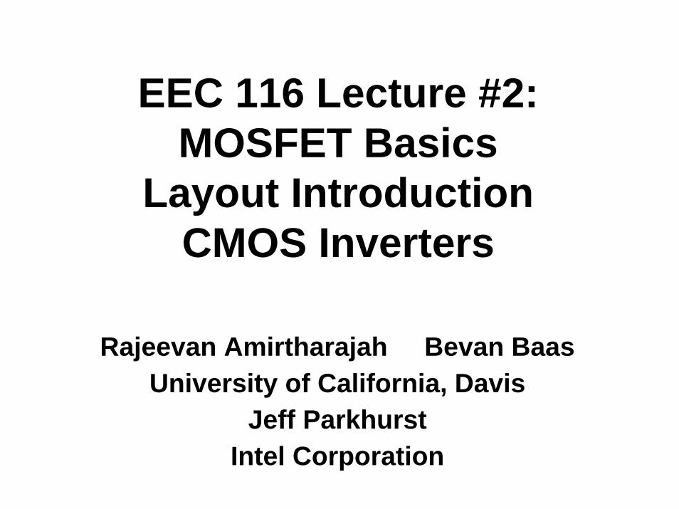
CMOS Process
Source: Digital Integrated Circuits, 2nd ©
Amirtharajah, EEC 116 Fall 2011 6
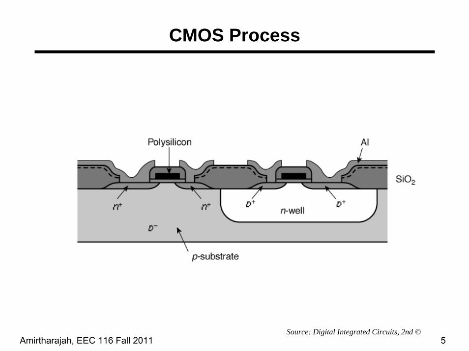
A Modern CMOS Process
p-well n-well
p+
p-epi
SiO2
AlCu
poly
n+
SiO2
p+
gate-oxide
Tungsten
TiSi2
DualDual--Well TrenchWell Trench--Isolated CMOS ProcessIsolated CMOS Process
Source: Digital Integrated Circuits, 2nd ©

Amirtharajah, EEC 116 Fall 2011 7
nwell and pwell
• The “bodies” of the transistors
Source: Omar Sattari
Amirtharajah, EEC 116 Fall 2011 8
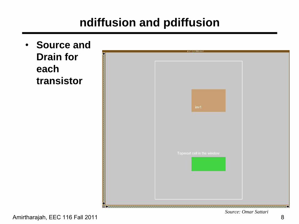
ndiffusion and pdiffusion
• Source and Drain for each transistor
Source: Omar Sattari
Amirtharajah, EEC 116 Fall 2011 9
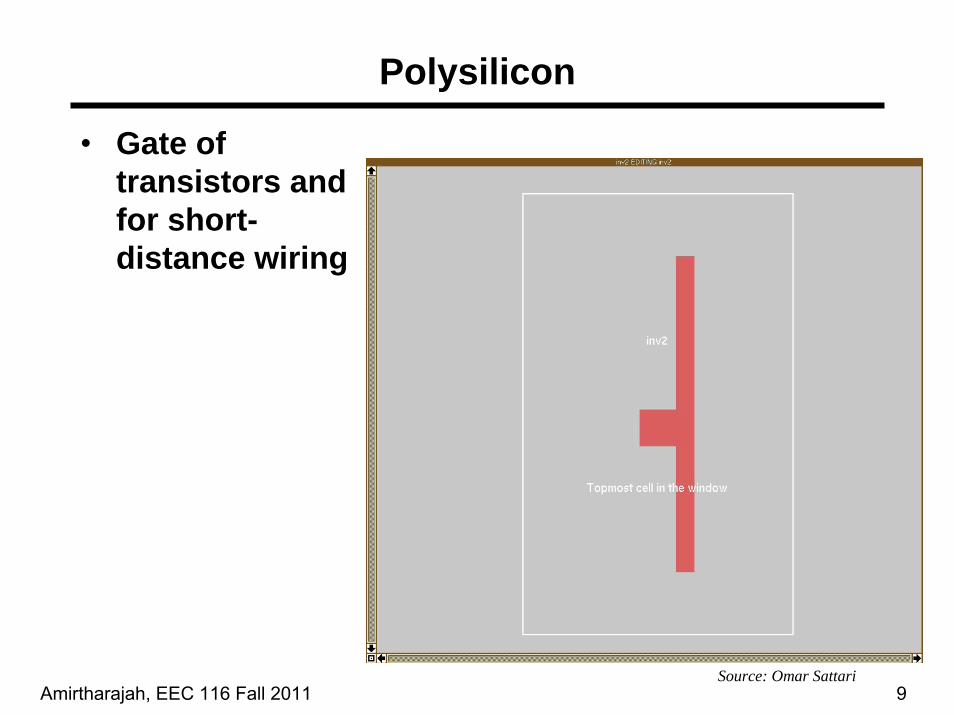
Polysilicon
• Gate of transistors and for short-distance wiring
Source: Omar Sattari

Amirtharajah, EEC 116 Fall 2011 10
Metal1
• First level of interconnect
Source: Omar Sattari
Amirtharajah, EEC 116 Fall 2011 11
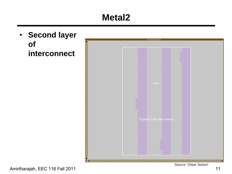
Metal2
• Second layer of interconnect
Source: Omar Sattari
Amirtharajah, EEC 116 Fall 2011 12
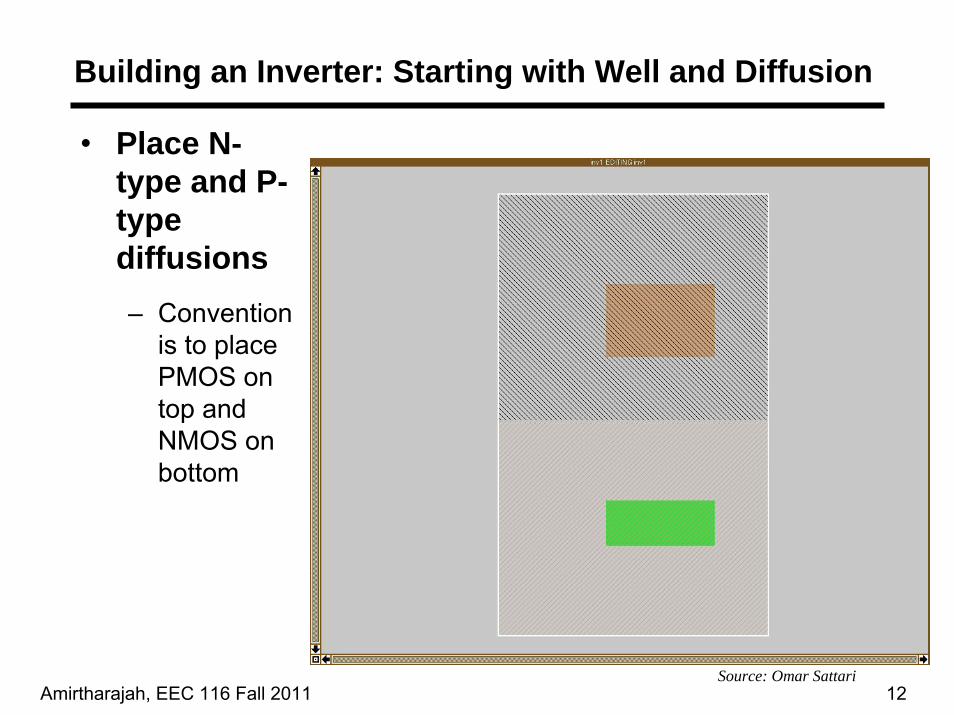
Building an Inverter: Starting with Well and Diffusion
• Place N-type and P-type diffusions– Convention
is to place PMOS on top and NMOS on bottom
Source: Omar Sattari
Amirtharajah, EEC 116 Fall 2011 13
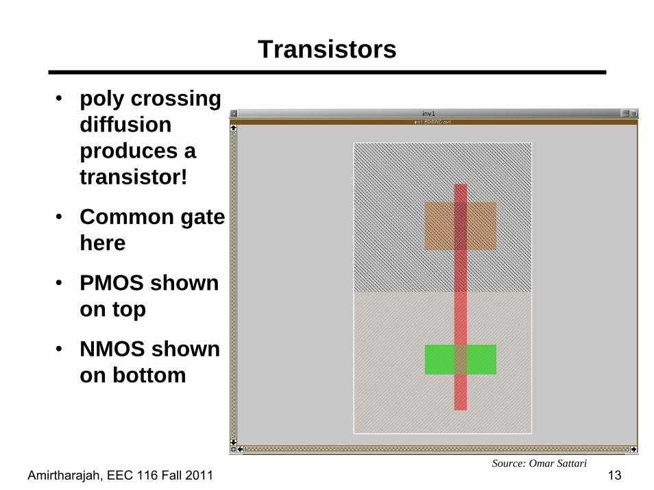
Transistors
• poly crossing diffusion produces a transistor!
• Common gate here
• PMOS shown on top
• NMOS shown on bottom
Source: Omar Sattari
Amirtharajah, EEC 116 Fall 2011 14
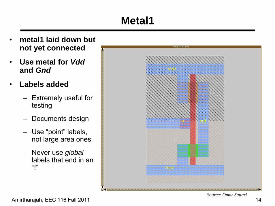
Metal1• metal1 laid down but
not yet connected
• Use metal for Vddand Gnd
• Labels added
– Extremely useful for testing
– Documents design
– Use “point” labels, not large area ones
– Never use globallabels that end in an “!”
Source: Omar Sattari
Amirtharajah, EEC 116 Fall 2011 15
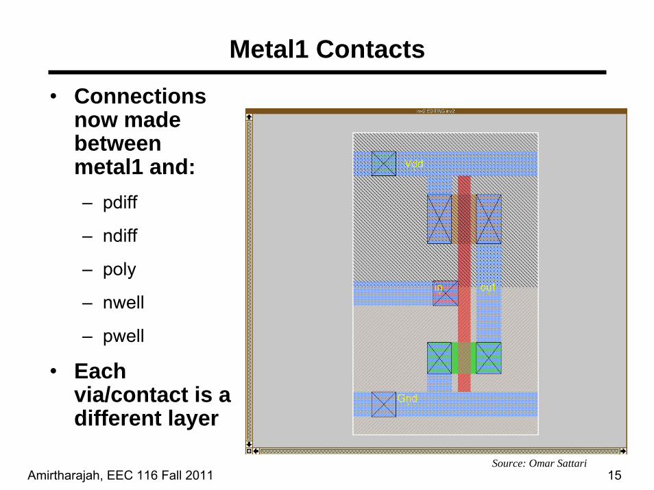
Metal1 Contacts
• Connections now made between metal1 and:– pdiff
– ndiff
– poly
– nwell
– pwell
• Each via/contact is a different layer
Source: Omar Sattari
Amirtharajah, EEC 116 Fall 2011 16
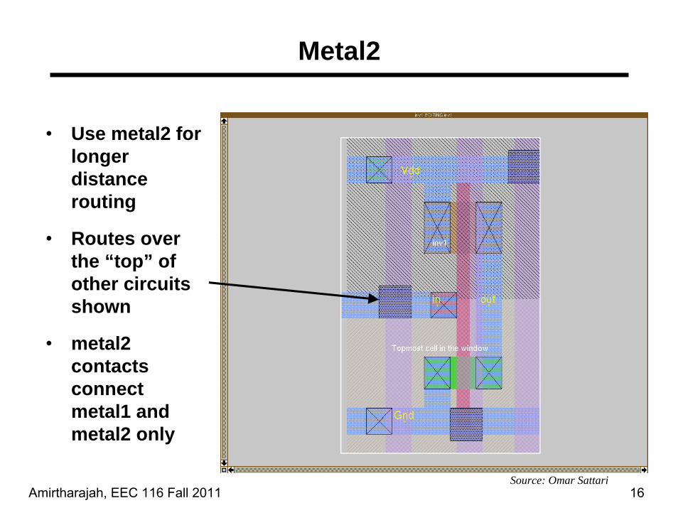
Metal2
• Use metal2 for longer distance routing
• Routes over the “top” of other circuits shown
• metal2 contacts connect metal1 and metal2 only
Source: Omar Sattari

Amirtharajah, EEC 116 Fall 2011 17
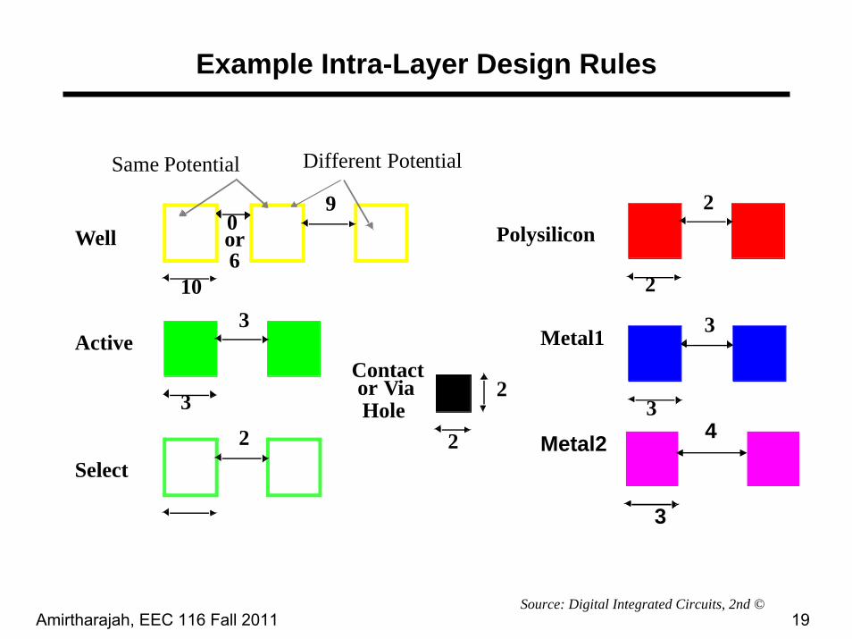
Design Rules• Interface between designer and process (CMOS
fabrication) engineer• Guidelines for constructing fabrication masks• Units commonly used
– Scalable design rules: lambda (λ) parameter (used in magic), or
– Absolute dimensions (micron rules)
• Common rule examples:– Minimum width
– Minimum separation same material
– Minimum separation different material
• Look for flashing markers in Cadence that show errors
Amirtharajah, EEC 116 Fall 2011 18
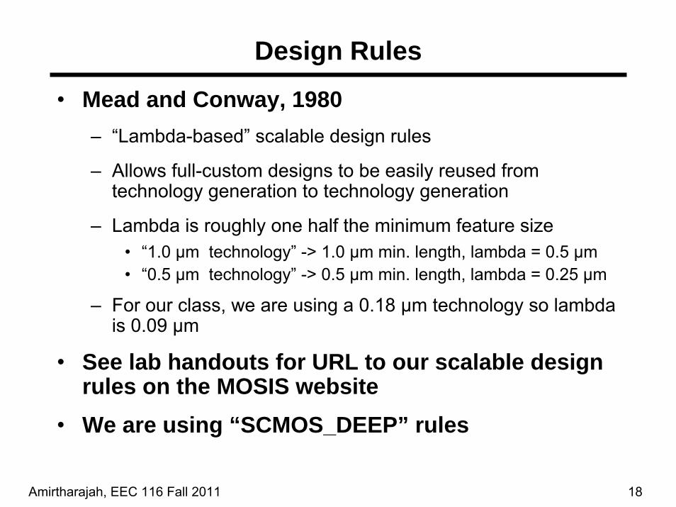
Design Rules
• Mead and Conway, 1980– “Lambda-based” scalable design rules
– Allows full-custom designs to be easily reused from technology generation to technology generation
– Lambda is roughly one half the minimum feature size• “1.0 µm technology” -> 1.0 µm min. length, lambda = 0.5 µm • “0.5 µm technology” -> 0.5 µm min. length, lambda = 0.25 µm
– For our class, we are using a 0.18 µm technology so lambda is 0.09 µm
• See lab handouts for URL to our scalable design rules on the MOSIS website
• We are using “SCMOS_DEEP” rules
Amirtharajah, EEC 116 Fall 2011 19
Example Intra-Layer Design Rules
Metal2 4
3
10
90
Well
Active3
3
Polysilicon2
2
Different PotentialSame Potential
Metal1 3
32
Contactor Via
Select2
or6
2Hole
Source: Digital Integrated Circuits, 2nd ©

Amirtharajah, EEC 116 Fall 2011 20
Example Design Rules: Transistor Layout
1
2
5
3
Tran
sist
or
Source: Digital Integrated Circuits, 2nd ©
Amirtharajah, EEC 116 Fall 2011 21
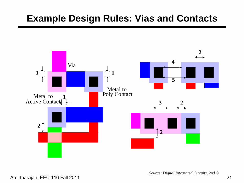
Example Design Rules: Vias and Contacts
1
2
1
Via
Metal toPoly ContactMetal to
Active Contact
1
2
5
4
3 2
2
Source: Digital Integrated Circuits, 2nd ©
Amirtharajah, EEC 116 Fall 2011 22
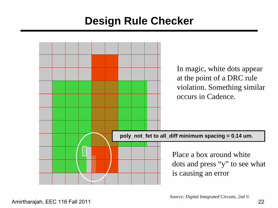
Design Rule Checker
poly_not_fet to all_diff minimum spacing = 0.14 um.
In magic, white dots appearat the point of a DRC ruleviolation. Something similaroccurs in Cadence.
Source: Digital Integrated Circuits, 2nd ©
Place a box around whitedots and press “y” to see what is causing an error
Amirtharajah, EEC 116 Fall 2011 23
Accounting for VDSM Effects
• VDSM = Very Deep Sub Micron
– Effects significant below 0.25 μm (0.18 μm, 130 nm, 90 nm, 65 nm, 45 nm)
• Compensation made at the mask level
– OPC – Optical Proximity Correction
– Occurs when different mask layers don’t align properly
– Test structures are used to characterize the process
– Ability to adapt depends on the consistency of the error from process run to process run

Amirtharajah, EEC 116 Fall 2011 24
Accounting for VDSM Effects: OPC
Amirtharajah, EEC 116 Fall 2011 25
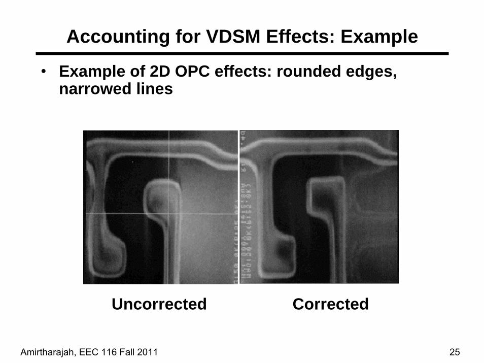
Accounting for VDSM Effects: Example
• Example of 2D OPC effects: rounded edges, narrowed lines
Uncorrected Corrected

Amirtharajah, EEC 116 Fall 2011 26
Compensating for VDSM Effects: Masks
Layout Mask Silicon
Amirtharajah, EEC 116 Fall 2011 27
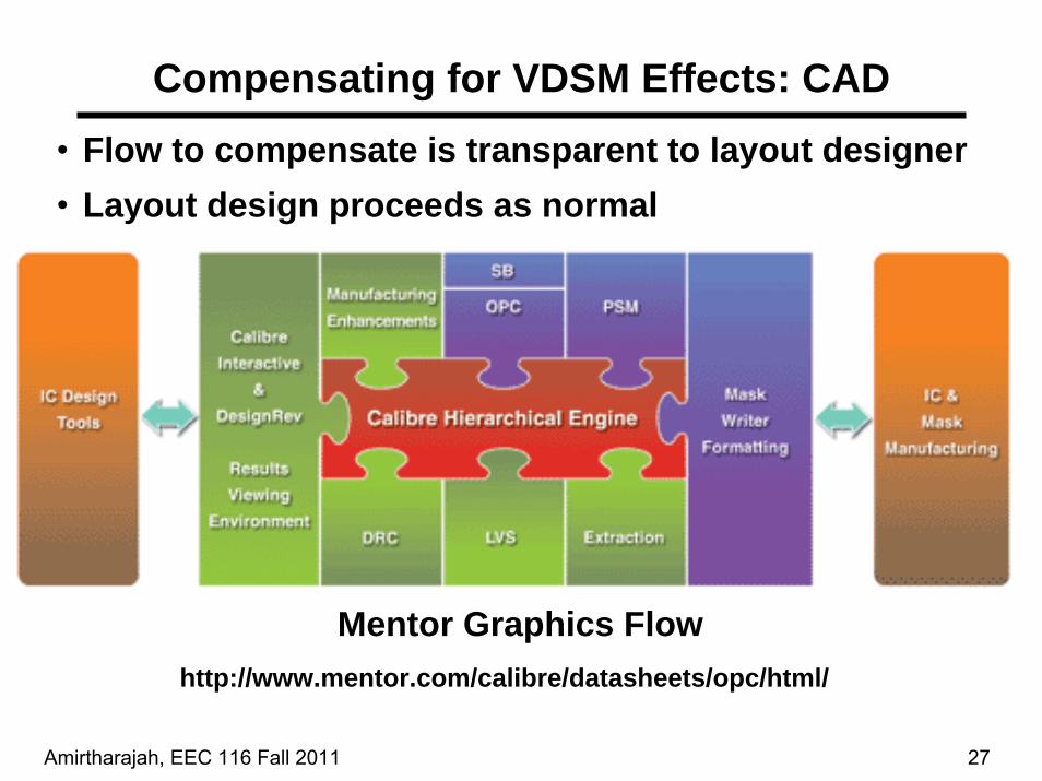
Compensating for VDSM Effects: CAD• Flow to compensate is transparent to layout designer• Layout design proceeds as normal
Mentor Graphics Flowhttp://www.mentor.com/calibre/datasheets/opc/html/

Amirtharajah, EEC 116 Fall 2011 28
References
• “Design of VLSI Systems”. A web based course located at: http://turquoise.wpi.edu/webcourse/
• “Simplified Rule Generation for Automated Rules-Based Optical Enhancement”, Otto et. al. On web at: http://www.jetlink.net/~ootto/bacus95/BACUS95Index.html
• Mark Anders and Jim Schantz of Intel Corporation
• Jan Rabaey, Lecture notes from his book “Digital Integrated Circuits, A Design Perspective”
Amirtharajah, EEC 116 Fall 2011 29
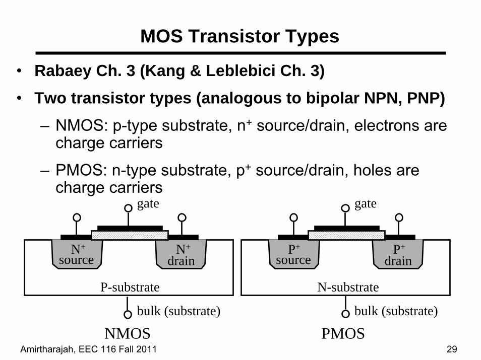
• Rabaey Ch. 3 (Kang & Leblebici Ch. 3)• Two transistor types (analogous to bipolar NPN, PNP)
– NMOS: p-type substrate, n+ source/drain, electrons are charge carriers
– PMOS: n-type substrate, p+ source/drain, holes are charge carriers
MOS Transistor Types
source drain
P-substrate
N+ N+
NMOS
source drain
N-substrate
P+ P+
PMOS
gate gate
bulk (substrate)bulk (substrate)
Amirtharajah, EEC 116 Fall 2011 30
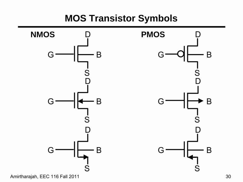
MOS Transistor SymbolsNMOS PMOSD
S
BG
D
S
BG
D
S
BG
D
S
BG
D
B
S
G
D
B
S
G
Amirtharajah, EEC 116 Fall 2011 31
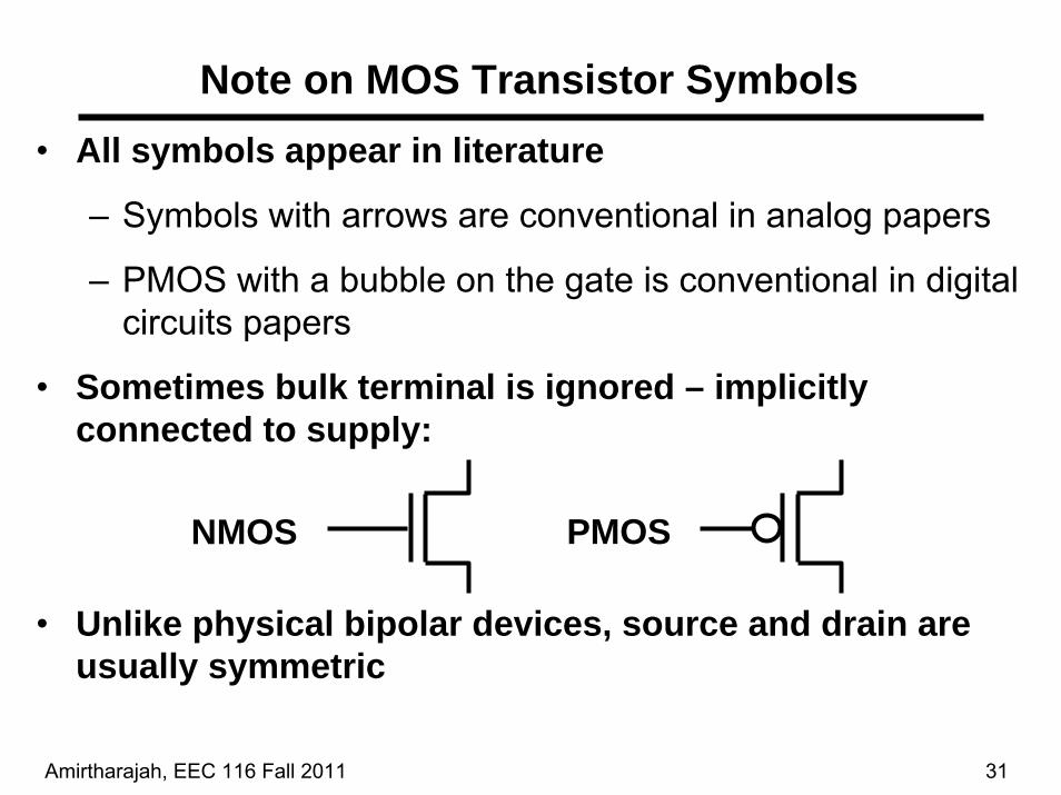
• All symbols appear in literature
– Symbols with arrows are conventional in analog papers
– PMOS with a bubble on the gate is conventional in digital circuits papers
• Sometimes bulk terminal is ignored – implicitly connected to supply:
• Unlike physical bipolar devices, source and drain are usually symmetric
Note on MOS Transistor Symbols
NMOS PMOS
Amirtharajah, EEC 116 Fall 2011 32
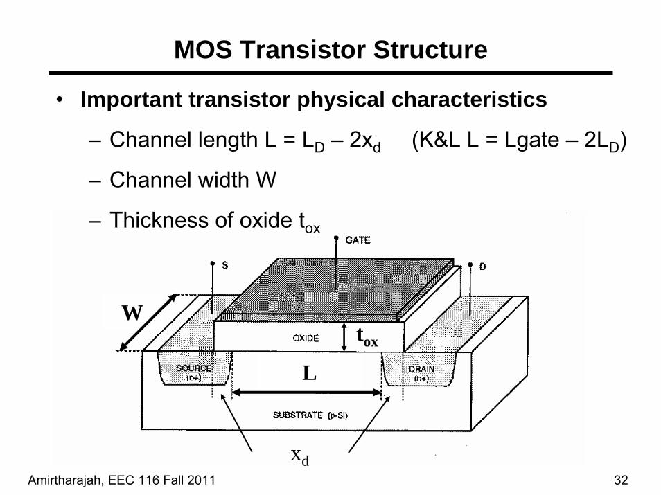
MOS Transistor Structure
L
Wtox
xd
• Important transistor physical characteristics
– Channel length L = LD – 2xd (K&L L = Lgate – 2LD)
– Channel width W
– Thickness of oxide tox
Amirtharajah, EEC 116 Fall 2011 33
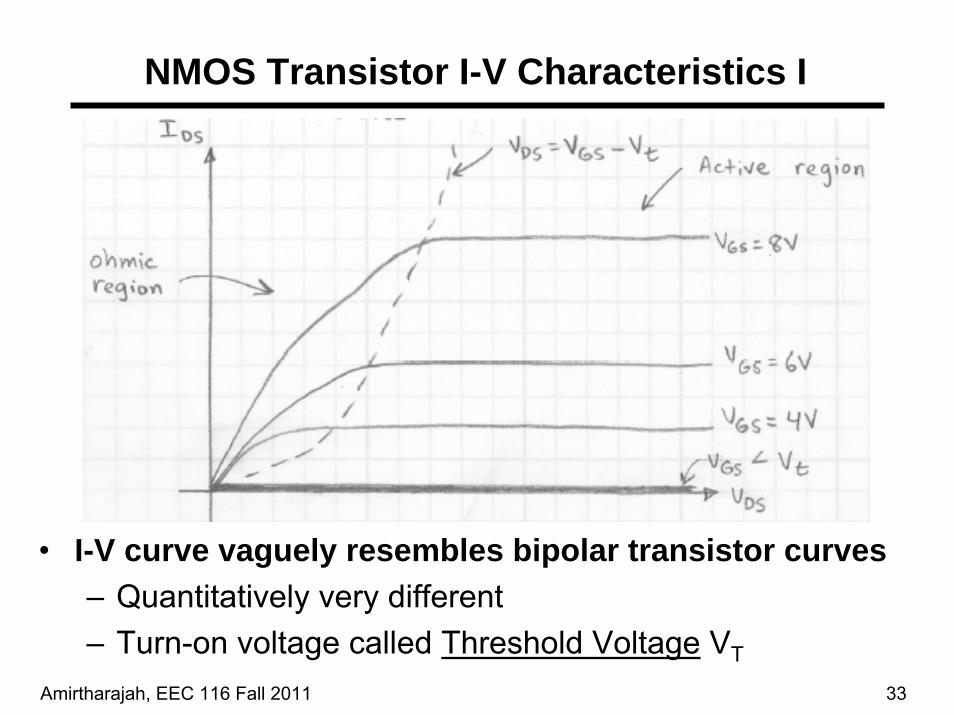
NMOS Transistor I-V Characteristics I
• I-V curve vaguely resembles bipolar transistor curves– Quantitatively very different– Turn-on voltage called Threshold Voltage VT
Amirtharajah, EEC 116 Fall 2011 34
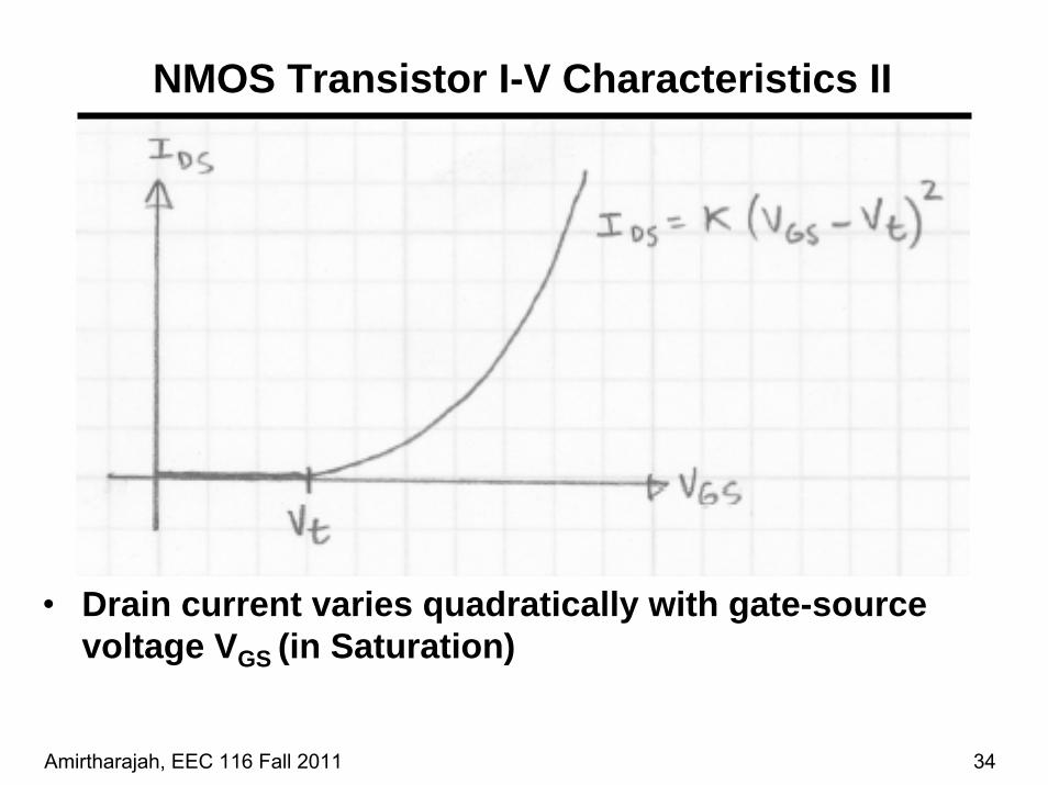
NMOS Transistor I-V Characteristics II
• Drain current varies quadratically with gate-source voltage VGS (in Saturation)

Amirtharajah, EEC 116 Fall 2011 35
MOS Transistor Operation: Cutoff• Simple case: VD = VS = VB = 0
– Operates as MOS capacitor (Cg = gate to channel)
– Transistor in cutoff region
• When VGS < VT0, depletion region forms
– No carriers in channel to connect S and D (Cutoff)Vg < VT0
source drain
P-substrate
VB = 0
Vd = 0Vs = 0depletion
region
Amirtharajah, EEC 116 Fall 2011 36
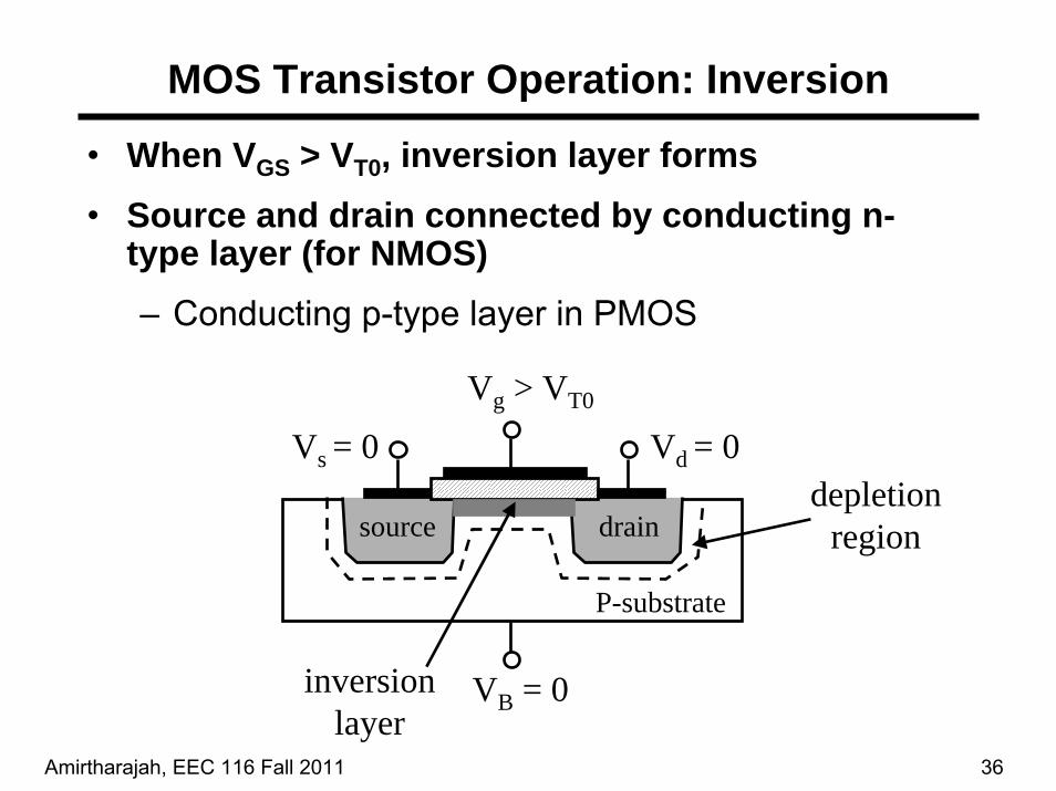
MOS Transistor Operation: Inversion
• When VGS > VT0, inversion layer forms• Source and drain connected by conducting n-
type layer (for NMOS)– Conducting p-type layer in PMOS
source drain
P-substrate
VB = 0
Vg > VT0
Vd = 0Vs = 0depletion
region
inversionlayer
Amirtharajah, EEC 116 Fall 2011 37
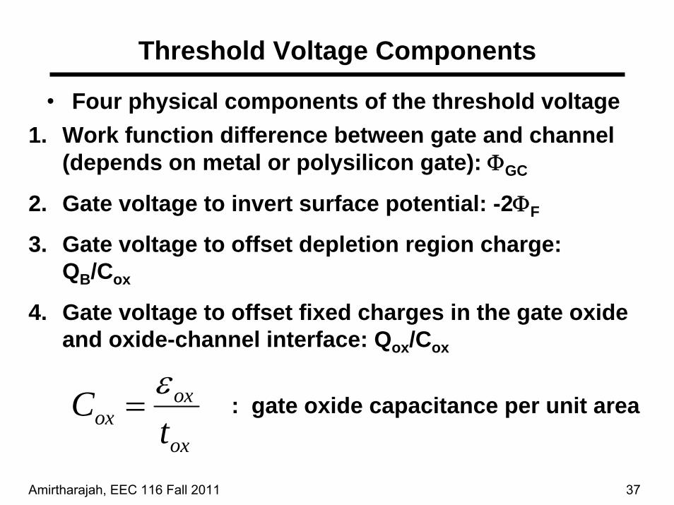
1. Work function difference between gate and channel (depends on metal or polysilicon gate): ΦGC
2. Gate voltage to invert surface potential: -2ΦF
3. Gate voltage to offset depletion region charge: QB/Cox
4. Gate voltage to offset fixed charges in the gate oxide and oxide-channel interface: Qox/Cox
Threshold Voltage Components
• Four physical components of the threshold voltage
ox
oxox t
C ε= : gate oxide capacitance per unit area
Amirtharajah, EEC 116 Fall 2011 38
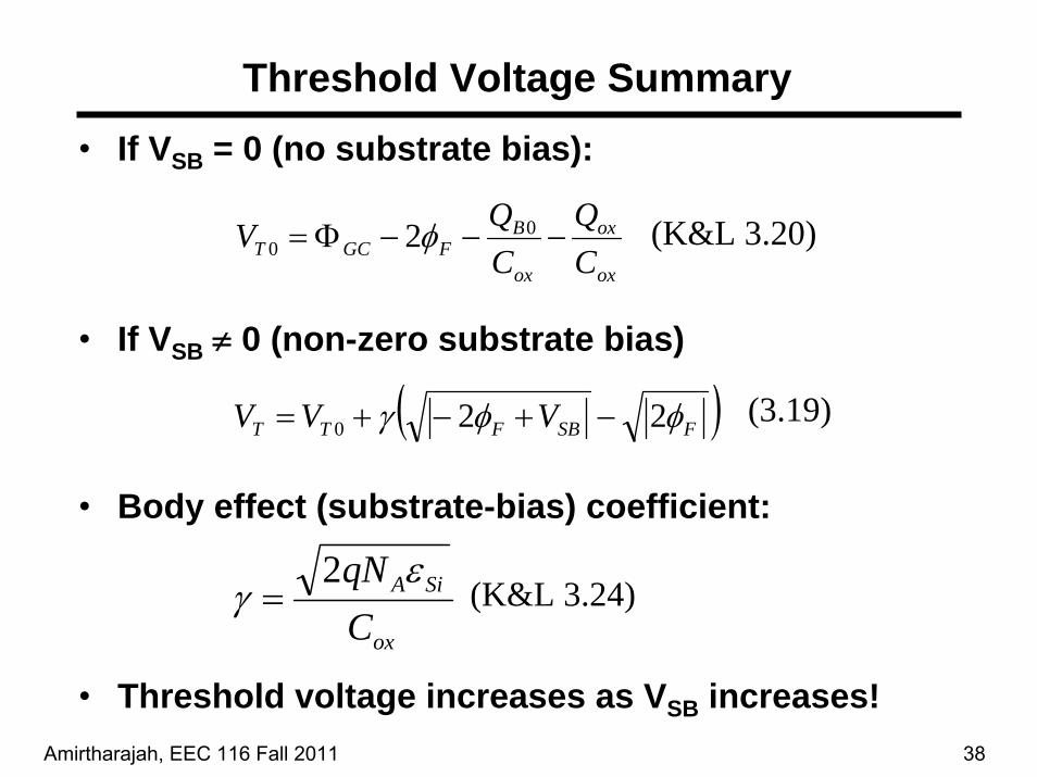
Threshold Voltage Summary• If VSB = 0 (no substrate bias):
• If VSB ≠ 0 (non-zero substrate bias)
• Body effect (substrate-bias) coefficient:
• Threshold voltage increases as VSB increases!
ox
ox
ox
BFGCT C
QCQV −−−Φ= 0
0 2φ
( )FSBFTT VVV φφγ 220 −+−+=
ox
SiA
CqN ε
γ2
=
(K&L 3.20)
(3.19)
(K&L 3.24)
Amirtharajah, EEC 116 Fall 2011 39
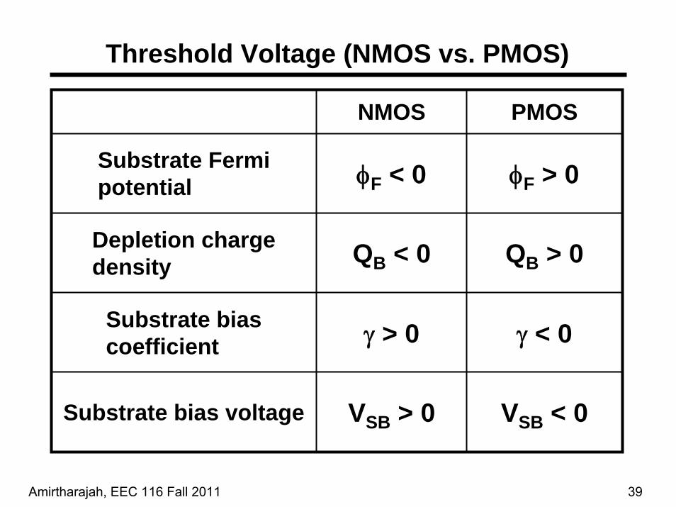
Threshold Voltage (NMOS vs. PMOS)
NMOS PMOS
Substrate Fermi potential φF < 0 φF > 0
Depletion charge density QB < 0 QB > 0
Substrate bias coefficient γ > 0 γ < 0
Substrate bias voltage VSB > 0 VSB < 0
Amirtharajah, EEC 116 Fall 2011 40
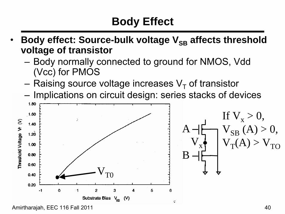
Vx
Body Effect• Body effect: Source-bulk voltage VSB affects threshold
voltage of transistor– Body normally connected to ground for NMOS, Vdd
(Vcc) for PMOS– Raising source voltage increases VT of transistor– Implications on circuit design: series stacks of devices
VT0
A
B
If Vx > 0, VSB (A) > 0,VT(A) > VTO

Amirtharajah, EEC 116 Fall 2011 41
MOS Transistor Regions of Operation
• Three main regions of operation
• Cutoff: VGS < VTNo inversion layer formed, drain and source are isolated by depleted channel. IDS ≈ 0
• Linear (Triode, Ohmic): VGS > VT, VDS < VGS-VTInversion layer connects drain and source.Current is almost linear with VDS (like a resistor)
• Saturation: VGS > VT, VDS ≥ VGS-VTChannel is “pinched-off”. Current saturates (becomes independent of VDS, to first order).
Amirtharajah, EEC 116 Fall 2011 42
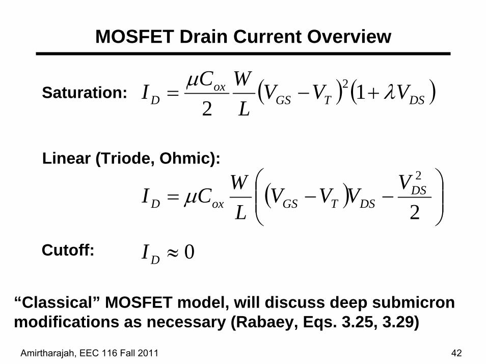
MOSFET Drain Current Overview
Linear (Triode, Ohmic):
“Classical” MOSFET model, will discuss deep submicron modifications as necessary (Rabaey, Eqs. 3.25, 3.29)
( ) ( )DSTGSox
D VVVL
WCI λμ+−= 1
22Saturation:
( ) ⎟⎟⎠
⎞⎜⎜⎝
⎛−−=
2
2DS
DSTGSoxDVVVV
LWCI μ
Cutoff: 0≈DI

Amirtharajah, EEC 116 Fall 2011 43
Cutoff Region
• For NMOS: VGS < VTN
• For PMOS: VGS > VTP
• Depletion region – no inversion• Current between drain and source is 0
– Actually there is always some leakage (subthreshold) current
source drain
substrate
VB
VG VDVS
depletionregion
Amirtharajah, EEC 116 Fall 2011 44
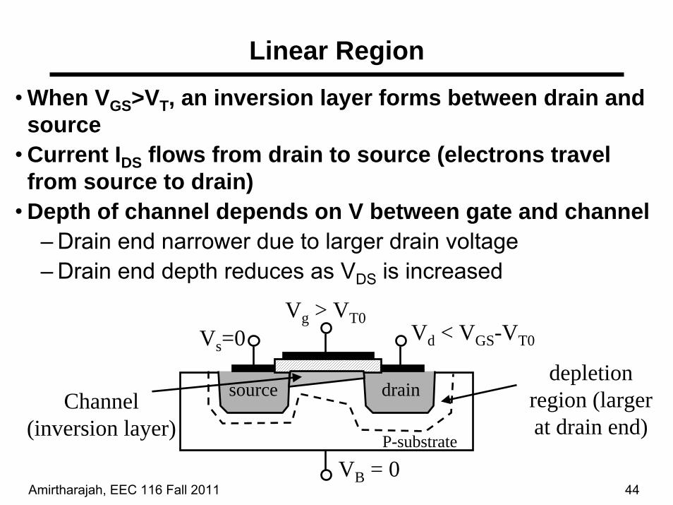
Linear Region
• When VGS>VT, an inversion layer forms between drain and source
• Current IDS flows from drain to source (electrons travel from source to drain)
• Depth of channel depends on V between gate and channel– Drain end narrower due to larger drain voltage– Drain end depth reduces as VDS is increased
source drain
P-substrate
VB = 0
Vg > VT0Vd < VGS-VT0Vs=0
depletionregion (larger at drain end)
Channel (inversion layer)

Amirtharajah, EEC 116 Fall 2011 45
Linear Region I/V Equation Derivation
• Gradual Channel Approximation:– Assume dominant electric field in y-direction– Current is constant along channel
• Integrate differential voltage drop dVc = IDdR along y
Amirtharajah, EEC 116 Fall 2011 46
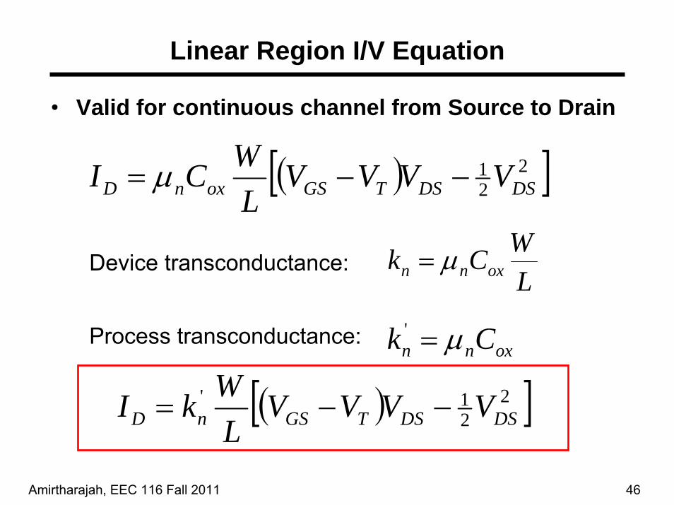
Linear Region I/V Equation
• Valid for continuous channel from Source to Drain
( )[ ]221
DSDSTGSoxnD VVVVL
WCI −−= μ
LWCk oxnn μ=Device transconductance:
oxnn Ck μ='Process transconductance:
( )[ ]221'
DSDSTGSnD VVVVL
WkI −−=

Amirtharajah, EEC 116 Fall 2011 47
Saturation Region• When VDS = VGS - VT:
– No longer voltage drop of VT from gate to substrate at drain– Channel is “pinched off”
• If VDS is further increased, no increase in current IDS– As VDS increased, pinch-off point moves closer to source– Channel between that point and drain is depleted– High electric field in depleted region accelerates electrons
towards drain
source drain
VB = 0
Vg > VT0Vd > VGS-VT0Vs=0
depletionregion
pinch-off point

Amirtharajah, EEC 116 Fall 2011 48
Saturation I/V Equation
• As drain voltage increases, channel remains pinched off
– Channel voltage remains constant
– Current saturates (no increase with increasing VDS)
• To get saturation current, use linear equation with VDS = VGS - VT
( )221
TNGSoxnD VVL
WCI −= μ
Amirtharajah, EEC 116 Fall 2011 49
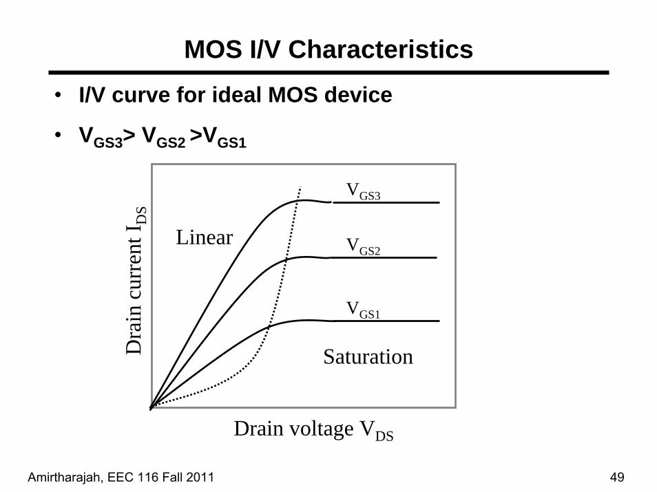
MOS I/V Characteristics• I/V curve for ideal MOS device
• VGS3> VGS2 >VGS1
Drain voltage VDS
Dra
in c
urre
nt I D
S
VGS1
VGS2
VGS3
Linear
Saturation
Amirtharajah, EEC 116 Fall 2011 50
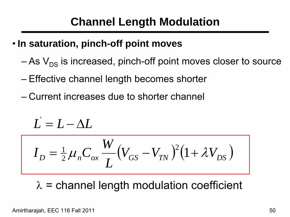
Channel Length Modulation
• In saturation, pinch-off point moves
– As VDS is increased, pinch-off point moves closer to source
– Effective channel length becomes shorter
– Current increases due to shorter channel
( ) ( )DSTNGSoxnD VVVL
WCI
LLL
λμ +−=
Δ−=
1221
'
λ = channel length modulation coefficient
Amirtharajah, EEC 116 Fall 2011 51
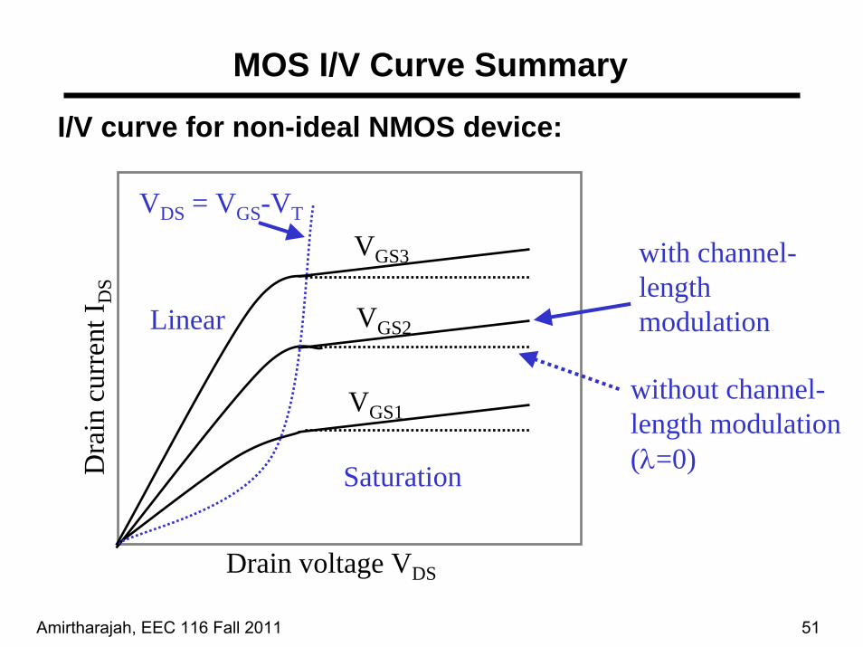
MOS I/V Curve Summary
I/V curve for non-ideal NMOS device:
Drain voltage VDS
Dra
in c
urre
nt I D
S
VGS1
VGS2
VGS3
Linear
Saturation
without channel-length modulation (λ=0)
with channel-length modulation
VDS = VGS-VT

Amirtharajah, EEC 116 Fall 2011 52
MOS I/V Equations SummaryCutoff
0=⇒><
DTPGS
TNGS IVVVV
Linear
( )[ ]221
,,
DSDSTGSoxDTPGSDSTPGS
TNGSDSTNGS VVVVLWCI
VVVVVVVVVV
−−=⇒−>≤−<≥
μ
Saturation
( ) ( )DSTGSoxDTPGSDSTPGS
TNGSDSTNGS VVVLWCI
VVVVVVVVVV
λμ +−=⇒−≤≤−≥≥
1,, 2
21
Note: if VSB ≠ 0, need to recalculate VT from VT0
Amirtharajah, EEC 116 Fall 2011 53
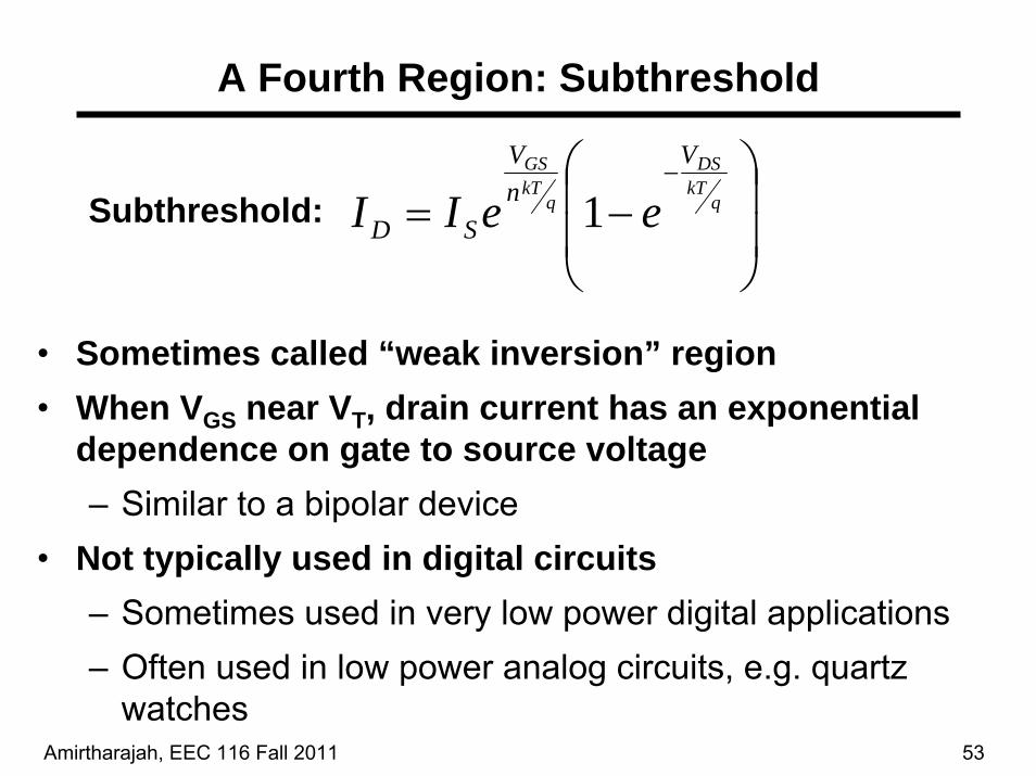
A Fourth Region: Subthreshold
Subthreshold:⎟⎟
⎠
⎞
⎜⎜
⎝
⎛−=
−q
kTDS
qkTGS V
nV
SD eeII 1
• Sometimes called “weak inversion” region• When VGS near VT, drain current has an exponential
dependence on gate to source voltage– Similar to a bipolar device
• Not typically used in digital circuits– Sometimes used in very low power digital applications– Often used in low power analog circuits, e.g. quartz
watches
Amirtharajah, EEC 116 Fall 2011 54
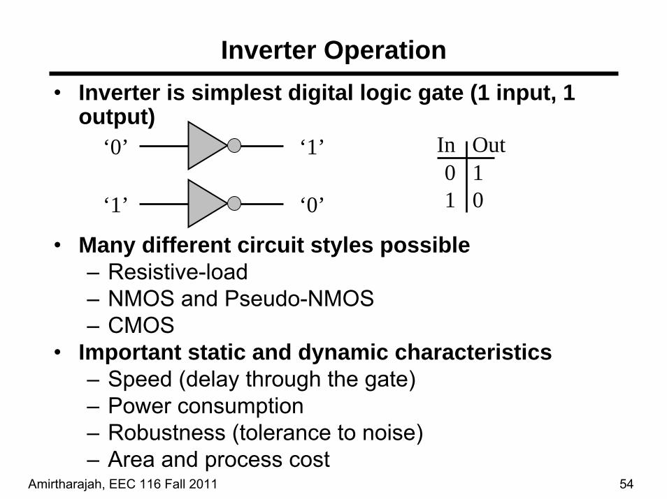
• Inverter is simplest digital logic gate (1 input, 1 output)
• Many different circuit styles possible– Resistive-load– NMOS and Pseudo-NMOS– CMOS
• Important static and dynamic characteristics– Speed (delay through the gate)– Power consumption– Robustness (tolerance to noise)– Area and process cost
Inverter Operation
‘0’ ‘1’
‘1’ ‘0’
In Out0 11 0
Amirtharajah, EEC 116 Fall 2011 55
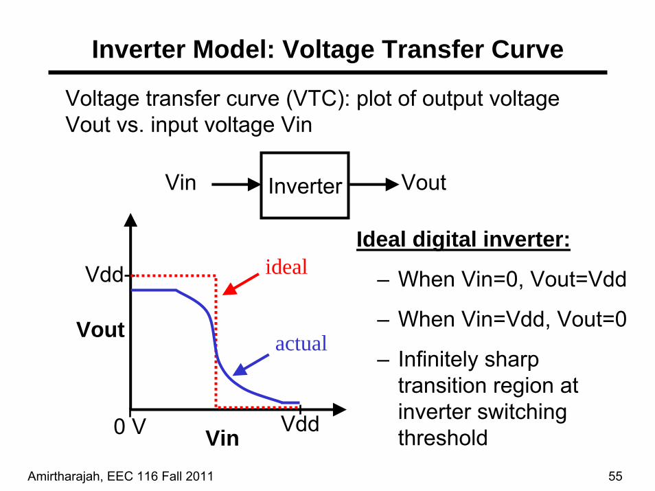
InverterVin Vout
Vdd
VddVin
Vout
ideal
actual
Ideal digital inverter:
Inverter Model: Voltage Transfer Curve
– When Vin=0, Vout=Vdd
– When Vin=Vdd, Vout=0
– Infinitely sharp transition region at inverter switching threshold
Voltage transfer curve (VTC): plot of output voltage Vout vs. input voltage Vin
0 V
Amirtharajah, EEC 116 Fall 2011 56
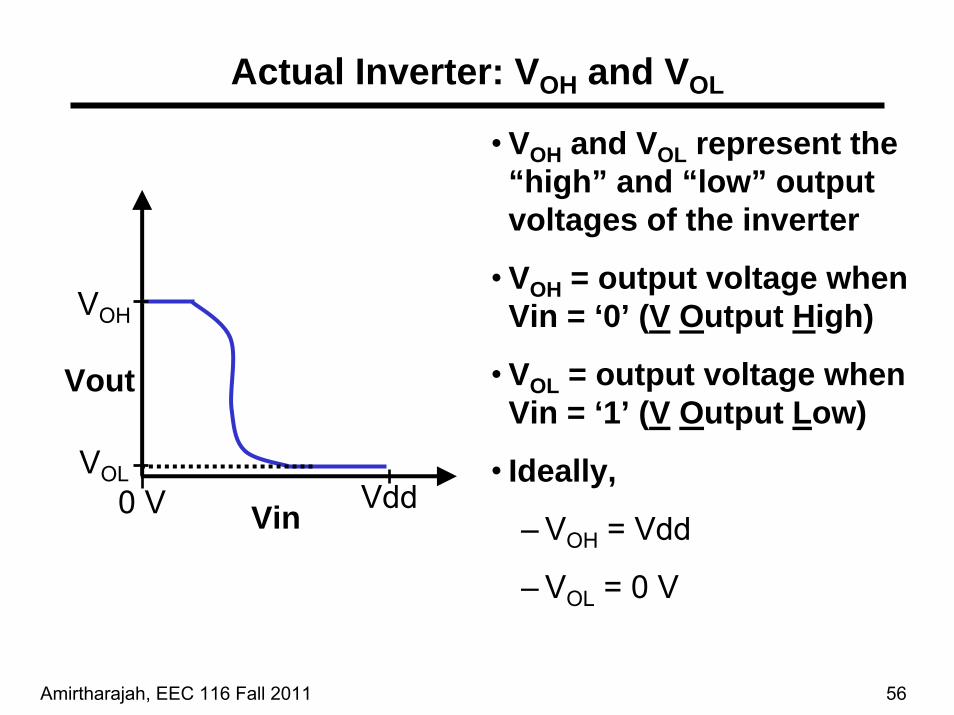
Actual Inverter: VOH and VOL
• VOH and VOL represent the “high” and “low” output voltages of the inverter
• VOH = output voltage when Vin = ‘0’ (V Output High)
• VOL = output voltage when Vin = ‘1’ (V Output Low)
• Ideally,
– VOH = Vdd
– VOL = 0 V
VddVin
Vout
VOH
VOL0 V
Amirtharajah, EEC 116 Fall 2011 57
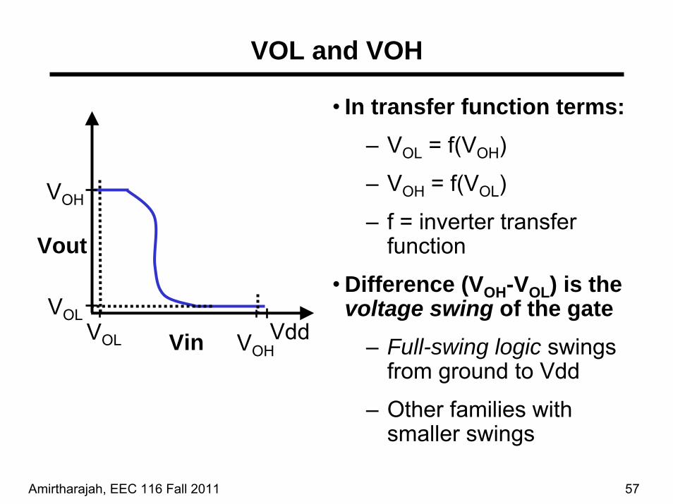
VOL and VOH
• In transfer function terms:– VOL = f(VOH)
– VOH = f(VOL)
– f = inverter transfer function
• Difference (VOH-VOL) is the voltage swing of the gate
– Full-swing logic swings from ground to Vdd
– Other families with smaller swings
VddVin
Vout
VOH
VOLVOL VOH

Amirtharajah, EEC 116 Fall 2011 58
Inverter Switching Threshold
Inverter switching threshold:
– Point where voltage transfer curve intersects line Vout=Vin
– Represents the point at which the inverter switches state
– Normally, VM ≈ Vdd/2
– Sometimes other thresholds desirable
VddVin
Vout
VOH
VOL
Vout=Vin
VM
(K&L VTH = VM)
Amirtharajah, EEC 116 Fall 2011 59
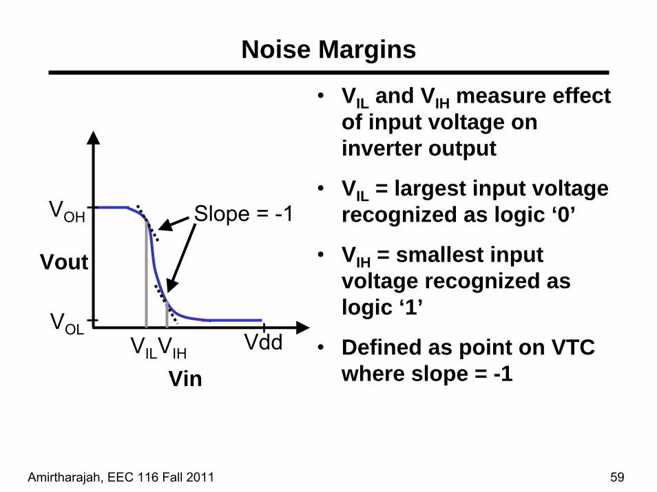
Noise Margins
• VIL and VIH measure effect of input voltage on inverter output
• VIL = largest input voltage recognized as logic ‘0’
• VIH = smallest input voltage recognized as logic ‘1’
• Defined as point on VTC where slope = -1
Vdd
Vin
Vout
VOH
VOLVILVIH
Slope = -1

Amirtharajah, EEC 116 Fall 2011 60
Noise Margins and Robustness
VOH
VOL
VIH
VIL
“1”NMH
NML
• Noise margin is a measure of the robustness of an inverter
– NML = VIL - VOL
– NMH = VOH - VIH
• Models a chain of inverters. Example:
– First inverter output is VOH
– Second inverter recognizes input > VIH as logic ‘1’
– Difference VOH-VIH is “safety zone” for noise
Ideally, noise margin should be as large as
possible
“0”
Noisy interconnect
Amirtharajah, EEC 116 Fall 2011 61
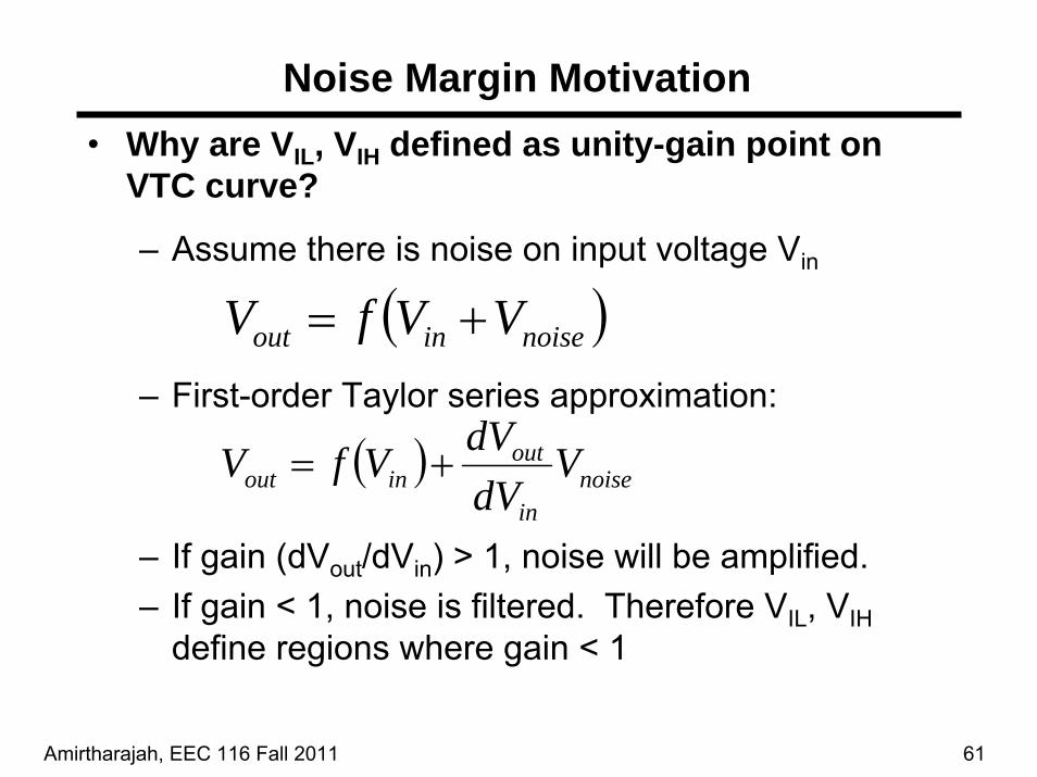
Noise Margin Motivation• Why are VIL, VIH defined as unity-gain point on
VTC curve?
– Assume there is noise on input voltage Vin
( )noiseinout VVfV +=
( ) noisein
outinout V
dVdVVfV +=
– First-order Taylor series approximation:
– If gain (dVout/dVin) > 1, noise will be amplified.– If gain < 1, noise is filtered. Therefore VIL, VIH
define regions where gain < 1
Amirtharajah, EEC 116 Fall 2011 62
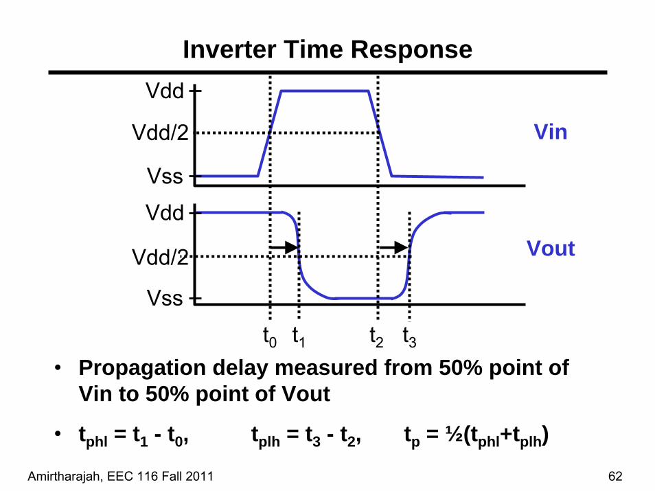
Inverter Time Response
• Propagation delay measured from 50% point of Vin to 50% point of Vout
• tphl = t1 - t0, tplh = t3 - t2, tp = ½(tphl+tplh)
Vdd
Vss
Vdd/2
Vdd
Vss
Vdd/2 Vout
t0 t1 t2 t3
Vin

Amirtharajah, EEC 116 Fall 2011 63
tR
Rise and Fall Time
• Fall time: measured from 90% point to 10% point– tF = t1 - t0
• Rise time: measured from 10% point to 90% point– tR = t3 - t2
• Alternately, can define 20%-80% rise/fall time
V90%
V10%
t2 t3t0 t1
tF
Amirtharajah, EEC 116 Fall 2011 64
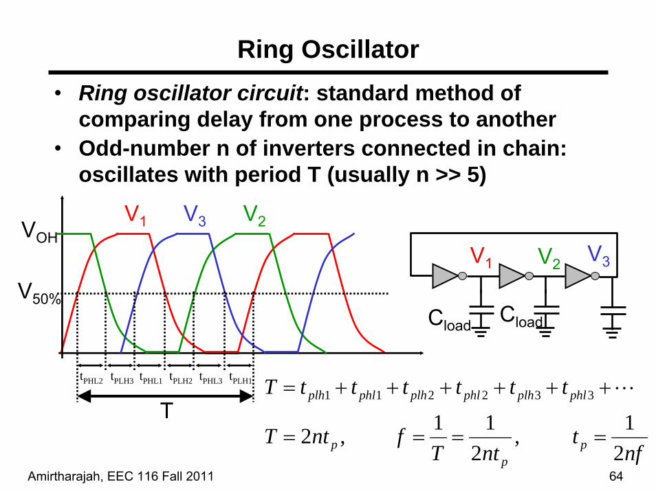
Ring Oscillator• Ring oscillator circuit: standard method of
comparing delay from one process to another• Odd-number n of inverters connected in chain:
oscillates with period T (usually n >> 5)
V1 V3 V2VOH
T
V50%
tPHL2 tPLH3 tPHL1 tPLH2 tPHL3 tPLH1
Cload Cload
V1 V2 V3
nft
ntTfntT
ttttttT
pp
p
phlplhphlplhphlplh
21 ,
211 ,2
332211
====
++++++= L
Amirtharajah, EEC 116 Fall 2011 65
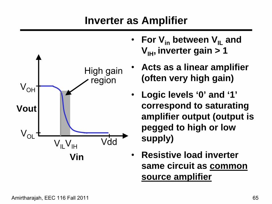
Inverter as Amplifier
• For Vin between VIL and VIH, inverter gain > 1
• Acts as a linear amplifier (often very high gain)
• Logic levels ‘0’ and ‘1’correspond to saturating amplifier output (output is pegged to high or low supply)
• Resistive load inverter same circuit as common source amplifier
Vdd
Vin
Vout
VOH
VOLVILVIH
High gainregion

Amirtharajah, EEC 116 Fall 2011 66
Next Topic: Inverters
• Inverter Characteristics
– Transfer functions, noise margins, resistive and nonlinear loads
• CMOS Inverters
• MOSFET Scaling
• MOSFET Capacitances