EE2730 Set 3 - LSU Set 3.pdfShift Registers Shift register counter – a circuit formed by a shift...
29
Counters Clocked sequential circuit whose state diagram contains a single cycle. Modulus – number of states in the cycle. Counters with non- power of 2 modulus has unused states S1 Sm S5 S4 S3 S2 Copyright © 2000 by Prentice Hall, Inc. Digital Design Principles and Practices, 3/e
Transcript of EE2730 Set 3 - LSU Set 3.pdfShift Registers Shift register counter – a circuit formed by a shift...

CountersClocked sequential circuit whose state diagram contains a single cycle.Modulus – number of states in the cycle.Counters with non-power of 2 modulus has unused states
S1
Sm
S5
S4
S3
S2
Copyright © 2000 by Prentice Hall, Inc.Digital Design Principles and Practices, 3/e

Ripple CountersRipple counter.
Requires fewer components than other counters.Slowest one.
Q
QTCLK
T
T
T
Q0
Q1
Q2
Q3
Q
Q
Q
Q
Q
Q
Copyright © 2000 by Prentice Hall, Inc.Digital Design Principles and Practices, 3/e

Synchronous Counters
Synchronous counters.
The clock inputs of all flip-flops in the counter circuit are connected to a common clock signal.
Synchronous serial counter.
Q
T
EN
CLK
CNTEN
Q
T
Q
T
Q
T
Q0
Q1
Q2
Q3
EN
EN
EN
Copyright © 2000 by Prentice Hall, Inc.Digital Design Principles and Practices, 3/e

CountersSynchronous parallel counter.
Q
T
EN
CLK
CNTEN
Q
T
Q
T
Q
T
Q0
Q1
Q2
Q3
EN
EN
EN
Copyright © 2000 by Prentice Hall, Inc.Digital Design Principles and Practices, 3/e
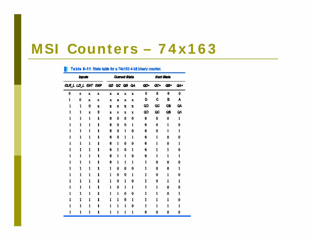
MSI Counters – 74x163

MSI Counters – 74x163
Q
Q
CLK
CK
D QA(14)
Q
QCK
D QB(13)
Q
QCK
D QC(12)
Q
QCK
D QD(11)
RCO(15)
(6)D
(7)ENP
(10)ENT
(5)C
(4)B
(3)A
(1)CLR_L
(9)
(2)
LD_L
Copyright © 2000 by Prentice Hall, Inc.Digital Design Principles and Practices, 3/e

74x163 – Free Running Mode
CLK
QA
QB
QC
QD
COUNT 0 1 2 8 9 10 11 12 13 14 15 03 4 5 6 7
RCO
Copyright © 2000 by Prentice Hall, Inc.Digital Design Principles and Practices, 3/e
74x163
CLR
CLK
LD
QA
QB
2
14
11
1
9
ENP
ENT
7
10
A QA
QB
QC
QD
RCO
B
3
4
C
D
5
6QC
QD15
RCO
U1
13
12
CLOCK
RPU+5 V
R
Copyright © 2000 by Prentice Hall, Inc.Digital Design Principles and Practices, 3/e

74x163 – Modulo 11 Counters
74x163
74x00
CLR
CLK
LD
QA
QB
2
14
11
1
1
2
9
ENP
ENT
7
10
A Q0
Q1
Q2
Q3
B
3
4
C
D
5
6QC
QD15
3
RCO
13
12
CNT10_L
U1
U2
CLOCK
RPU+5 V
R
Copyright © 2000 by Prentice Hall, Inc.Digital Design Principles and Practices, 3/e
74x163
74x04
CLR
CLK
LD
QA
QB
2
14
11
1
1
9
ENP
ENT
7
10
A Q0
Q1
Q2
Q3
B
3
4
C
D
5
6QC
QD15
2RCO
13
12
CNT15
CNT15_LU1 U2
CLOCKRPU
+5 V
R
Copyright © 2000 by Prentice Hall, Inc.Digital Design Principles and Practices, 3/e

74x163 – Excess-3 Counter
74x163
74x00
CLR
CLK
LD
QA
QB
2
14
11
1
1
2
9
ENP
ENT
7
10
A Q0
Q1
Q2
Q3
B
C
D
QC
QD15
3
RCO
13
12
S11XX_L
U1
U2
+5 V
CLOCK
RPUR
3
4
5
6
Copyright © 2000 by Prentice Hall, Inc.Digital Design Principles and Practices, 3/e

74x163 – Cascading Counters
74x163
CLR
CLK
LD
QA
QB
2
14
11
1
9
ENP
ENT
7
10
A Q0
Q1
Q2
Q3
B
3
4
C
D
5
6
Q4
Q5
Q6
Q7
RCO8
QC
QD15
RCO
13
12
U1
74x163
CLR
CLK
LD
QA
QB
2
1
9
14
11
ENP
ENT
7
10
A
B
3
4
C
D
5
6QC
QD15
RCO
13
12
U2
CLOCK
RESET_L
D0
D1
D2
D3
D4
D5
D6
D7
LOAD_L
CNTEN
RCO4
Copyright © 2000 by Prentice Hall, Inc.Digital Design Principles and Practices, 3/e
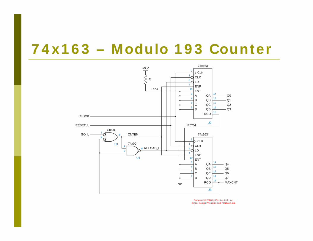
74x163 – Modulo 193 Counter74x163
CLR
CLK
LD
QA
QB
2
14
11
1
9
1
9
ENP
ENT
7
10
A Q0
Q1
Q2
Q3
B
3
4
6
C
D
5
4
5
31
2
6
Q4
Q5
Q6
Q7
MAXCNT
QC
QD15
RCO
13
12
U2
U1
U1
74x163
CLR
CLK
LD
QA
QB
2
14
11
ENP
ENT
7
10
A
B
3
4
C
D
5
6QC
QD15
RCO
13
12
U3
CLOCK
RESET_L
GO_L
RELOAD_L
CNTEN
RPU
74x00
74x00
+5 V
R
RCO4
Copyright © 2000 by Prentice Hall, Inc.Digital Design Principles and Practices, 3/e

74x163 – Modulo 8 Counter With Decoder
CLOCK_L
S0_L
S1_L
S2_L
S3_L
S4_L
S5_L
S6_L
S7_L
COUNT 0 21 0 1 23 4 5 6 7
Copyright © 2000 by Prentice Hall, Inc.Digital Design Principles and Practices, 3/e
74x163
CLR
CLK
LD
QA
QB
2
14
11
1
9
ENP
ENT
7
10
AQ1
Q2
Q3B
3
4
C
D
5
6QC
QD15
RCOU1
13
12
CLOCK
RPU+5 V
R
S0_L
S1_L
S2_L
S3_L
S4_L
S5_L
S6_L
S7_L
74x138
G2A
G1
G2B
Y0
Y1
Y2
Y3
615
14
13
7
4
5
B
A
C
Y4
Y5
Y6
Y7
1
12
11
10
92
3
U2
Copyright © 2000 by Prentice Hall, Inc.Digital Design Principles and Practices, 3/e

74x163 – Modulo 8 Counter With Decoder
Modulo 8 counter with decoder and glitch-free outputs.
74x163
CLR
CLK
LD
QA
QB
2
14
11
1
9
ENP
ENT
7
10
AQ1
Q2
Q3B
3
4
C
D
5
6QC
QD15
RCOU1
13
12
CLOCK
RPU +5 V
R
S0_L
S1_L
S2_L
S3_L
S4_L
S5_L
S6_L
S7_LRS0_L
RS1_L
RS2_L
RS3_L
RS4_L
RS5_L
RS6_L
RS7_L
74x138
G2A
G1
G2B
Y0
Y1
Y2
Y3
615
14
13
7
4
5
B
A
C
Y4
Y5
Y6
Y7
1
12
11
10
92
3
U2 U3
74x374
OE
CLK
1D 1Q
11
1
2
2Q5
3
2D4
3D7
4D8
5D13
6D14
3Q6
9
5Q12
15
4Q
6Q
7D17 16
7Q
8D18 19
8Q
Copyright © 2000 by Prentice Hall, Inc.Digital Design Principles and Practices, 3/e

Shift RegistersN-bit register with the provision for shifting its stored data by a bit position each tick of the clock.Serial input – specifies a new bit to shifted into the register.Serial output – specifies the bits being shifted out of the register
Q
CLOCK
SERIN
CK
CK
D
D
SEROUT
Q
QD
CK
Copyright © 2000 by Prentice Hall, Inc.Digital Design Principles and Practices, 3/e

Shift Registers
Q
CLOCK
LOAD/SHIFT
SERIN
CK
D
NQ
1Q
2Q
1D
Q
CK
D
2D
Q
CK
D
ND
Copyright © 2000 by Prentice Hall, Inc.Digital Design Principles and Practices, 3/e
Parallel input –specifies a new set of bits to be entered into the register, all at once during a single clock tick.Parallel output –specifies the bits at the output of every flip-flop in the register.

Shift RegistersSerial-in, parallel-out shift register. 1Q
2Q
NQ
Q
CLOCK
SERIN
CK
CK
D
D Q
QD
CK
Copyright © 2000 by Prentice Hall, Inc.Digital Design Principles and Practices, 3/e

Shift Registers
Q
CLOCK
LOAD/SHIFT
SERIN
CK
D
SEROUT
1D
Q
CK
D
2D
Q
CK
D
ND
Copyright © 2000 by Prentice Hall, Inc.Digital Design Principles and Practices, 3/e
Parallel-in, serial-out shift register.

Shift RegistersMSI Shift Registers.
74x164 – serial-in, parallel-out with asynchronous clear input.74x166 – parallel-in, serial-out with asynchronous clear input.74x194 – universal shift register.
al
Inputs Next state
Function S1 S0 QA∗ QB∗ QC∗ QD∗Hold 0 0 QA QB QC QDShift right 0 1 RIN QA QB QCShift left 1 0 QB QC QD LINLoad 1 1 A B C D

Shift Registers(11)
CLK
(1)
(12)
CLR_L
(7)LIN
(6)D
QDD Q
CLK
CLR
(13)
(5)C
QCD Q
CLK
CLR
(14)
(4)B
QBD Q
CLK
CLR
(15)
(3)A
(2)RIN
(10)S1
(9)S0
QAD Q
CLK
CLR
10
00
11
01
10
00
11
01
10
00
11
01
10
00
11
01
LEFT
RIGHT
S1 S0
Copyright © 2000 by Prentice Hall, Inc.Digital Design Principles and Practices, 3/e

Shift RegistersShift register counter – a circuit formed by a shift registers and combinational logic. The state diagram for this state machine is cyclic. This circuit does not necessarily count in ascending or descending order.Ring Counter – the simplest shift register counter. This circuit uses a n-bit shift register to obtain a counter with n states.
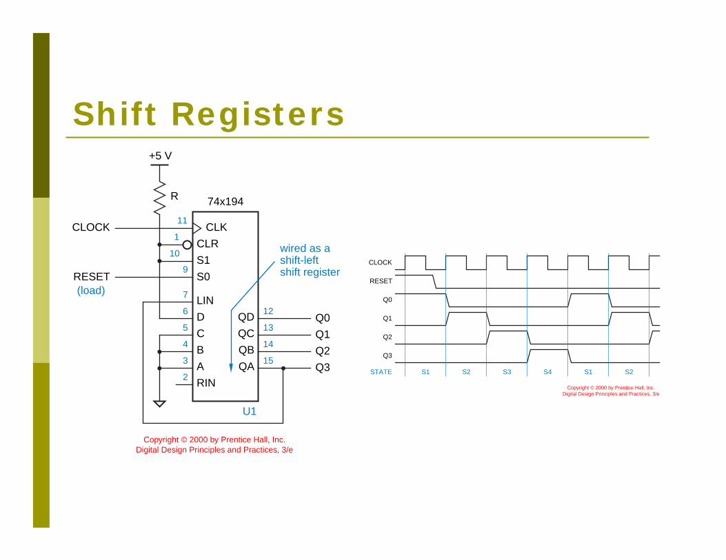
Shift Registers
CLOCK
RESET
Q0
Q1
Q2
Q3
STATE S1 S2 S3 S4 S1 S2
Copyright © 2000 by Prentice Hall, Inc.Digital Design Principles and Practices, 3/e
CLOCK
RESET
Q0
Q1
Q2
Q3
U1
74x194
CLR
CLK11
1
S110
RIN2
S09
B4
QB14
A3 15
QA
C5 13
QC
D6 12
QD
LIN7
wired as ashift-leftshift register
(load)
+5 V
R
Copyright © 2000 by Prentice Hall, Inc.Digital Design Principles and Practices, 3/e

Shift Registers
0100
0001
0000
1111
0101
1010
10000010
1100
0011
10010110
0111
10111110
1101
Copyright © 2000 by Prentice Hall, Inc.Digital Design Principles and Practices, 3/e

Shift RegistersA self correcting counter is designed so that all abnormal states have transitions leading to normal states.
CLOCK
1
2 12
13
Q0
Q1
Q2
Q3
+5 V
R
ABC0
U1
U2
74x27
wired as ashift-leftshift register
74x194
CLR
CLK11
1
S110
RIN2
S09
B4
QB14
A3 15
QA
C5 13
QC
D6 12
QD
LIN7
Copyright © 2000 by Prentice Hall, Inc.Digital Design Principles and Practices, 3/e
0100
0001
10000010
0000
1001 1100
1110
1111
0110
011110110011
1010
11010101
Copyright © 2000 by Prentice Hall, Inc.Digital Design Principles and Practices, 3/e
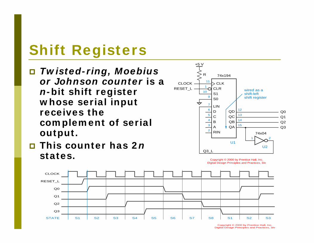
Shift RegistersTwisted-ring, Moebiusor Johnson counter is a n-bit shift register whose serial input receives the complement of serial output.This counter has 2nstates.
1 2
CLOCK
RESET_L
Q0
Q1
Q2
Q3
+5 V
R
Q3_L
U1U2
74x04
74x194
CLR
CLK11
1
S110
RIN2
S09
B4
QB14
A3 15
QA
C5 13
QC
D6 12
QD
LIN7
wired as ashift-leftshift register
Copyright © 2000 by Prentice Hall, Inc.Digital Design Principles and Practices, 3/e
CLOCK
RESET_L
Q0
Q1
Q2
Q3
STATE S1 S2 S3 S1 S2 S3S4 S5 S6 S7 S8
Copyright © 2000 by Prentice Hall, Inc.Digital Design Principles and Practices, 3/e

Shift Registers
Digital telephony.Central offices samples analog voice 8000 times/sec (once every 125μs).Then the COs transmit them digitally over a 64kbps serial channel.64kbps is much less than can be achieved by a single digital line, therefore several 64kbps signals are multiplexed onto a single wire.

Shift Registers74x163
CLR
CLK
LD
QA
QB
2
14
11
1
9
ENP
ENT
7
10
A
B
3
4
C
D
5
6QC
QD15
RCO
13
12
U1
74x163
CLR
CLK
LD
QA
QB
2
1
9
14
11
ENP
ENT
7
10
A
B
3
4
C
D
5
6QC
QD15
RCO
13
12
U2
CLOCK
RESET_L
74x166
CLR
CLK
SH/LD
7
6
15
SERIN1
9
A
B3
2
4C
D
E
F
G
H
5
10
11
12
14 13QH
CLKINH
U3
74x101
2
13
12
U4
BIT7_L
SYNC
D7
D6
D5
D4
D3
D2
D1
D0
paralleldata
+5 V
SYNC
CLOCK
timeslot number
todestination
bit number
SDATA
R
BC0
BC1
BC2
BC3
BC4
BC5
BC6
BC7
RCO4

Shift Registers
CLOCK
SYNC
BIT7_L
SDATA
D0–D7
bit 0 1 2 0 1 23 4 5 6 77
0 1 2 0 1 23 4 5 6 77
timeslot 0
(b)
timeslot 31 timeslot 1
Copyright © 2000 by Prentice Hall, Inc.Digital Design Principles and Practices, 3/e
74x163
CLR
CLK
LD
QA
QB
2
14
11
1
9
ENP
ENT
7
10
A
B
3
4
C
D
5
6QC
QD15
RCO
13
12
U1
74x163
CLR
CLK
LD
QA
QB
2
1
9
14
11
ENP
ENT
7
10
A
B
3
4
C
D
5
6QC
QD15
RCO
13
12
U2
CLOCK
RESET_L
74x166
CLR
CLK
SH/LD
7
6
15
SERIN1
9
A
B3
2
4C
D
E
F
G
H
5
10
11
12
14 13QH
CLKINH
U3
74x101
2
13
12
U4
BIT7_L
SYNC
D7
D6
D5
D4
D3
D2
D1
D0
paralleldata
+5 V
SYNC
CLOCK
timeslot number
todestination
bit number
SDATA
R
BC0
BC1
BC2
BC3
BC4
BC5
BC6
BC7
RCO4
timeslot 0 timeslot 1 timeslot 31 timeslot 0timeslot 31
(a)
(b)
CLOCK(2.048 MHz)
SYNC
SDATA
256 clock ticks per 125 μsec frame
32 timeslots per frame
488 nsec
Shift Registers
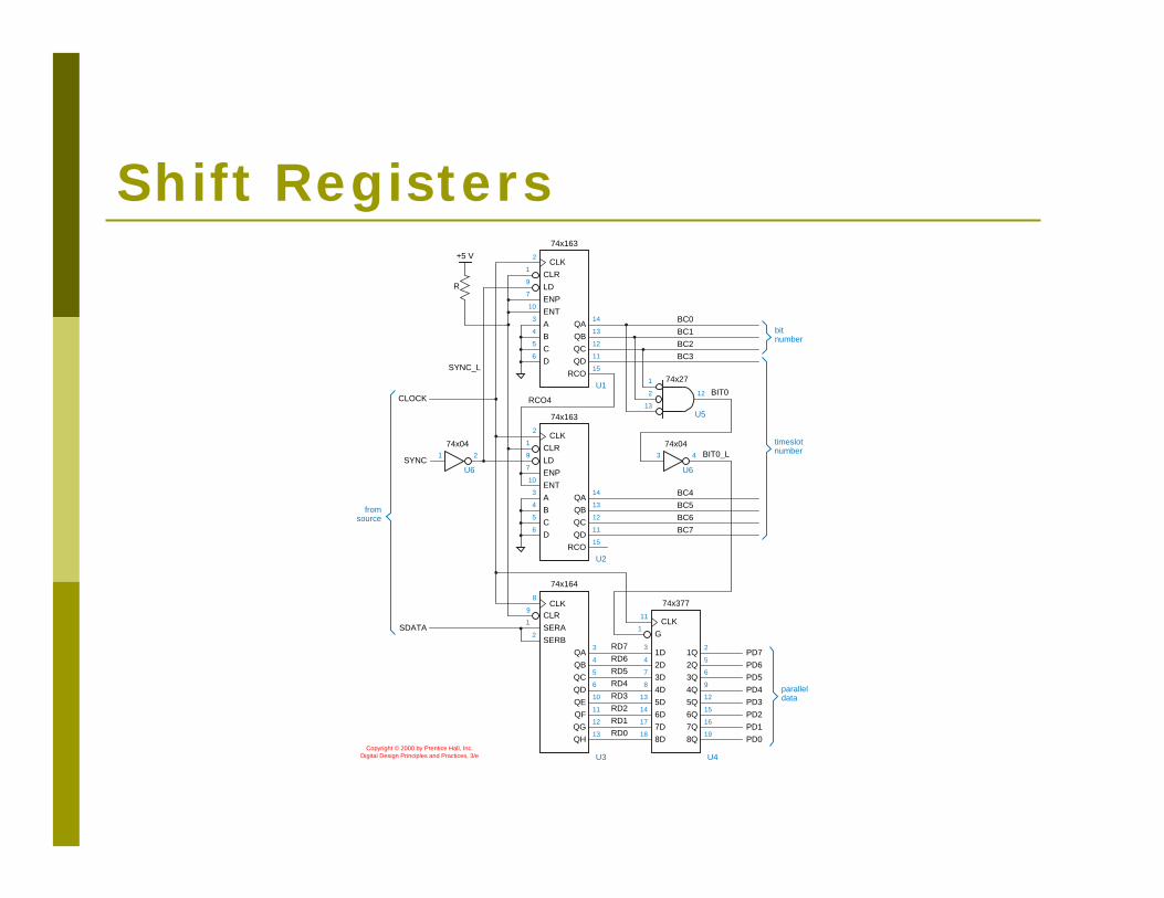
U4
74x164
CLRCLK
SERA
QA
8
9
3
QB4
1
SERB2
QC5
6
QE10
11
QD
QF12
QG13
QH
U3
U2
74x163
CLR
CLK
LD
QA
QB
14
11
ENP
ENT
A
B
C
D
QC
QD15
RCO
13
12
74x377
G
CLK
1D 1Q
11
1
2
2Q5
3
2D4
3D7
4D8
5D13
6D14
3Q6
9
5Q12
15
4Q
6Q
7D17 16
7Q
8D18 19
8Q
PD7
PD6
PD5
PD4
PD3
PD2
PD1
PD0
RD7
RD6
RD5
RD4
RD3
RD2
RD1
RD0
CLOCK
SDATA
SYNC_L
2
1
9
7
10
3
4
5
6
fromsource
paralleldata
1
2 12
3 4
13
U1
U5
U6
74x163
74x27
74x04
CLR
CLK
LD
QA
QB
14
11
ENP
ENT
A
B
C
D
QC
QD15
RCO
13
12
BC0
BC1
BC2
BC3
BC4
BC5
BC6
BC7
BIT0
BIT0_L
2
1
9
7
10
3
4
5
6
+5 V
R
timeslotnumber
bitnumber
RCO4
1 2
U6
74x04
SYNC
Copyright © 2000 by Prentice Hall, Inc.Digital Design Principles and Practices, 3/e
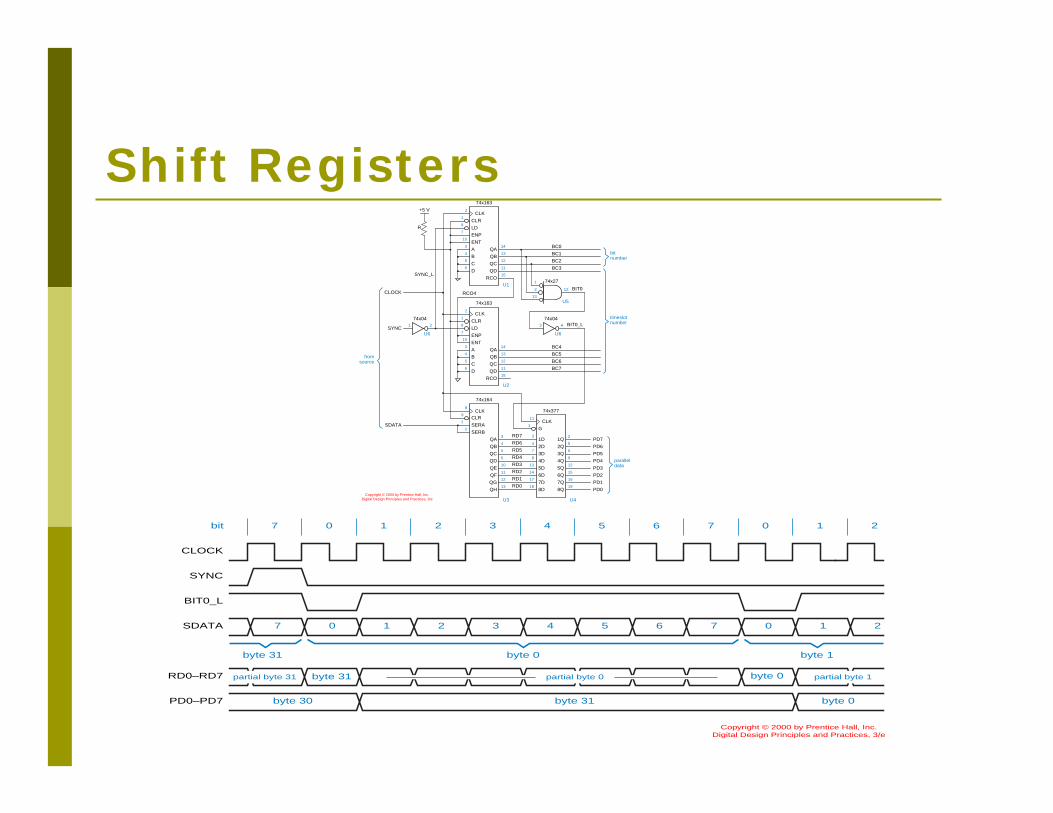
Shift Registers
CLOCK
SYNC
BIT0_L
SDATA
RD0–RD7
bit 0 1 2 0 1 23 4 5 6 77
0 1 2 0 1 23 4 5 6 77
byte 0
byte 0byte 31 byte 1
byte 31
PD0–PD7 byte 0byte 31byte 30
partial byte 31 partial byte 1partial byte 0
Copyright © 2000 by Prentice Hall, Inc.Digital Design Principles and Practices, 3/e
U4
74x164
CLRCLK
SERA
QA
8
9
3
QB4
1
SERB2
QC5
6
QE10
11
QD
QF12
QG13
QH
U3
U2
74x163
CLR
CLK
LD
QA
QB
14
11
ENP
ENT
A
B
C
D
QC
QD15
RCO
13
12
74x377
G
CLK
1D 1Q
11
1
2
2Q5
3
2D4
3D7
4D8
5D13
6D14
3Q6
9
5Q12
15
4Q
6Q
7D17 16
7Q
8D18 19
8Q
PD7
PD6
PD5
PD4
PD3
PD2
PD1
PD0
RD7
RD6
RD5
RD4
RD3
RD2
RD1
RD0
CLOCK
SDATA
SYNC_L
2
1
9
7
10
3
4
5
6
fromsource
paralleldata
1
2 12
3 4
13
U1
U5
U6
74x163
74x27
74x04
CLR
CLK
LD
QA
QB
14
11
ENP
ENT
A
B
C
D
QC
QD15
RCO
13
12
BC0
BC1
BC2
BC3
BC4
BC5
BC6
BC7
BIT0
BIT0_L
2
1
9
7
10
3
4
5
6
+5 V
R
timeslotnumber
bitnumber
RCO4
1 2
U6
74x04
SYNC
Copyright © 2000 by Prentice Hall, Inc.Digital Design Principles and Practices, 3/e