EB93 - Platform Manager 2 Evaluation Board User Guide
75
Platform Manager 2 Evaluation Board User Guide EB93 Version 1.0, June 2015
Transcript of EB93 - Platform Manager 2 Evaluation Board User Guide

Platform Manager 2 Evaluation Board User Guide
EB93 Version 1.0, June 2015

2
Platform Manager 2 Evaluation Board
IntroductionThank you for choosing the Lattice Semiconductor Platform Manager 2 Evaluation Board!
The Platform Manager 2 evaluation board is used to demonstrate, evaluate and design using the Platform Manager 2 (LPTM21) device and the Hardware Management Expander (L-ASC10) device. The board is pre-programmed with a demo design that highlights the features and flexibility of the LPTM21 and L-ASC10 devices. This demo operates on the board without any other software or hardware as described in the QuickSTART Guide that is included with the board. However, a more complete evaluation can be accomplished using the I2C demo / debugging software which is available from the Lattice website. This software and the demo design can be used to evaluate the following features provided by the Platform Manager 2 devices: Power Management (Power Sequencing, Voltage Monitoring, Trimming, Margining), Thermal Management (Temperature Monitoring, Fan Control, Power Control) and Control Plane (Reset Control, Fault Logging). The use of the software with the demo design is fully described in the user guide which is included with the software zip file: UG59, Platform Manager 2 I2C Demo Design and GUI User’s Guide.
The QuickSTART Guide Please use the Platform Manager 2 Board QuickSTART Guide to get started. The QuickSTART Guide provides a “fast path” for working with the Platform Manager 2 evaluation board and the pre-programmed demo. This user’s guide augments the QuickSTART Guide by providing detailed descriptions of the on board circuits that support both the demo and customer evaluation designs.
FeaturesThe Platform Manager 2 evaluation board has been designed to demonstrate and evaluate the following applica-tions:
• Supply Voltage monitoring, sequencing, trimming, VID, and control.
• Current sensing, monitoring and control.
• Temperature sensing, monitoring and control.
• 3-Wire, 4 Wire Fan Control.
• Fault logging to internal UFM or external SPI Flash.
• Scalable monitoring and control of voltages, currents, temperatures.
• Field upgrades via background programming and dual boot.
• GPIO control and expansion.
The Platform Manager 2 evaluation board also allows the user to quickly learn, evaluate, develop and test their own designs using the LPTM21, L-ASC10 and surrounding circuits and components.
The Platform Manager 2 evaluation board contains the following on-board components and circuits to support the demo design and customer developed designs:
• Integrated Circuits— LPTM21 – FTBGA-237 – Platform Manager 2 [U1]— L-ASC10 – QFN-48 – Hardware Expander [U4] — AT25DF041AMH -SPI Flash Memory [U3]— FT2232HL- USB Driver [U6]— 93C46-WMN6TP –EEPROM Memory [U7]— NCP1117-LDO [U8]— LD6836-LDO [U9]— FSA4157 Analog Switch-SPDT [U10, U11]

3
Platform Manager 2 Evaluation Board
• Power Supplies, Connections and Switches— External 12 V Supply Connector –Coaxial Power Jack [J28]— External 12 V Supply Connector – Two position Terminal [J25]— External 5 V Supply Connector – Two position Terminal [J12]— External 3 V Supply Connector – Two position Terminal [J13]— +5 V to 2.5 V Trim-able DCDC Converter [DCDC3, DCDC7]— +5 V to 1.2 V Trim-able DCDC Converter [DCDC4, DCDC8]
• LEDs and LCD Display— Blue USB Power LED [D42]— Green +3.3 V Power LED [D44]— Red LPTM21 (U1 ASC) Output LEDs [D3-D12]— Red LPTM21 (U1 FPGA) Output LEDs[D22-D36]— Red L-ASC10 (U4) Output LEDs [D13-D21]— 3-Digit LCD Display [U5]— Red ASC # 2 Interface Power LED [D39]— Red ASC # 3 Interface Power LED [D40]— Green DC-DC # 3 Power LED [D51]— Green DC-DC # 4 Power LED [D52]— Green DC-DC # 7 Power LED [D55]— Green DC-DC # 8 Power LED [D56]
• Switches, Sliders, Buttons, Sensors and Jumpers— VID_A 8-position DIP Switch [SW6]— Restart Push Button Switch [SW4]— Demo control Push Button Switch [SW1-SW3, SW5]— Slide Potentiometer [R34, R36, R39, R41]— Temperature Sensor [Q4, Q6, Q7]— Temperature Sensor [Q5-with artificial load power resistor]— 3.3 V supply select Jumper [J1, J3, J4]— Reset select Jumper [J5]— Fan Supply Select [J6, J8]— Enable ASC program Jumper [J31, J32]— MOSFET Drive Select [J30]— 5 V supply select jumper [J29]
• Connectors and Interfaces— JTAG connector [J2]— I2C/SPI connector [J26]— External FAN connectors [J7, J9, J10, J11]— Two Position Screw connector for off board load for DCDC3 and DCDC7 [J19, J23]— Four position screw connector for off board load for DCDC4 and DCDC8 [J20, J24]— USB B-mini Connector [J16]— DSUB 25 Expandable Architecture Connectors for ASC Breakout Board [J14, J15]— Probe and Test Points
• User Prototyping Area— 12 x 10 through-Hole array with +12 V, +5 V, +3.3 V, and GND buses— 24 SMD 0805 footprints— 8 SMD SOT-23 footprints— 4 SMD 2512 footprints— 4 SMD SOIC-8 footprints— 2 SMD SOT-223 footprints

4
Platform Manager 2 Evaluation Board
Mechanical SpecificationsDimensions: 7 in. [L] x 6 in. [W] x 1 in. [H]
Environmental SpecificationsThe evaluation board must be stored between –40 °C and 100 °C. The recommended operating temperature is between 0 °C and 55 °C.
Electrical Specifications• 12 V Input +/– 15% @ 50 mA typical.
• 5 V Input +/– 10% @ 110 mA typical.
• 3.3 V Input +/– 5% @ 150 mA typical.
• 12 V Maximum Current 10 A when using an off board supply and load.
• 5 V Maximum Current 10 A when using an off board supply and load.
• 3.3 V Maximum Current 5 A when using an off board supply and load.
Software RequirementsThe pre-loaded demo design on the Platform Manager 2 evaluation board can operate without the need to install any special software and can be powered using any standard USB port. All control and status information is avail-able on the board using switches, push-buttons, potentiometers, LEDs and the LCD display, as described in the QuickSTART Guide that was mentioned in the introduction. In order to create and program custom designs or pro-gram reference or demo designs, Lattice Diamond 3.4 or later software is required along with a corresponding license. Within Lattice Diamond®, Platform Designer is a custom tool that is used to create, edit, and build Platform Manager 2 designs.
Platform Designer Tool-Software The Platform Designer tool provides an integrated design environment that simplifies building and editing Platform Manager 2 designs. It supports all of the following and more: implement the hardware management algorithm, check design rules, compile the design, generate stimulus files, simulate the design, assign pins, and finally gener-ate the JEDEC files used to program and configure the device on the circuit board. Platform Designer also sup-ports the importing of an HDL file to integrate other desired functions.
Figure 1. Platform Designer Software

5
Platform Manager 2 Evaluation Board
As shown in Figure 1, the Platform Designer tool contains five main sections: Global, Analog, Components, Con-trol, and Build. Each of the five sections is briefly described below.
• Global – ASC Options and Device Options views are used for configuring global settings for the ASC and the device.
• Analog – Current, Temperature, and Voltage views are used for configuring the built-in monitoring circuits for these signals.
• Components – Fan Controller, Fault Logger, Hot Swap, and PMBus Adapter views are used to configure and instantiate built-in IPs for these functions.
• Control – Ports and Nodes and Logic views are used to name and assign I/O for the design; and to develop and/or import the control logic.
• Build – DRC, Compile, Pin Assignment, Generate Jedec, Generate Stimulus, and Export Configuration Report buttons are used for checking design rules, and building the design. A summary view shows the usage and con-sumption of the design resources available.
Platform Manager 2 I2C GUI - SoftwareThe Platform Manager 2 I2C GUI software and User’s Guide can be downloaded from the Lattice website. This soft-ware is provided license free and is used to enhance the demo experience and as a hardware debugging tool; the main interface is shown in Figure 2. The Demonstration buttons are used in conjunction with the default demo. The Power Management, Thermal Management, and Control Plane Management buttons can be used independently of the demo and can also be used with customer board designs (provided an FTDI based USB to I2C interface is used).
Figure 2. Platform Manager 2 I2C GUI Software
Platform Manager 2 Evaluation BoardLPTM21-Platform Manager 2-DeviceAs shown in Figure 3, the Lattice Platform Manager 2 device is a fast-reacting, programmable logic based hard-ware management controller. Platform Manager 2 is an integrated solution combining analog sense and control elements with scalable programmable logic resources. This unique approach allows Platform Manager 2 to inte-grate Power Management (Power Sequencing, Voltage Monitoring, Trimming and Margining), Thermal Manage-ment (Temperature Monitoring, Fan Control, Power Control), and Control Plane functions (System Configuration, I/O Expansion, etc.) as a single device.
Architecturally, the Platform Manager 2 device can be divided into two sections – Analog Sense and Control and FPGA. The Analog Sense and Control (ASC) section provides three types of analog sense channels: voltage (nine

6
Platform Manager 2 Evaluation Board
standard channels and one high voltage channel), current (one standard voltage and one high voltage) and tem-perature (two external and one internal).
Each of the analog sense channels is monitored through two independently programmable comparators to support both high/low and in-bounds/out-of-bounds (window-compare) monitor functions. In addition, each of the current sense channels provides a fast fault detect (one µs response time) for detecting short circuit events. The tempera-ture sense channels can be configured to work with different external transistor or diode configurations.
The Analog Sense and Control section also provides ten general purpose 5 V tolerant open-drain digital input/out-put pins that can be used for controlling DC-DC converters, low-drop-out regulators (LDOs) and opto-couplers, as well as for general purpose logic interface functions. In addition, four high-voltage charge pumped outputs (HVOUT1-HVOUT4) may be configured as high-voltage MOSFET drivers to control high-side MOSFET switches. These HVOUT outputs can also be programmed as static output signals or as switched outputs (to support exter-nal charge pump implementation) operating at a dedicated duty cycle and frequency.
The ASC section incorporates four TRIM outputs for controlling the output voltages of DC-DC converters. Each power supply output voltage can be maintained typically within 0.5% tolerance across various load conditions using the Digital Closed Loop Control mode of the trimming block.
The internal 10-bit A/D converter can be used to measure the voltage and current through the I2C bus. The ADC is also used in the digital closed loop control mode of the trimming block.
The ASC section also provides the capability of logging up to 16 status records into its nonvolatile EEPROM mem-ory. Each record includes voltage, current and temperature monitor signals along with digital input and output lev-els.
The ASC section includes an output control block (OCB) which allows certain inputs and control signals a direct connection to the digital outputs or HVOUTs, bypassing the ASC-I/F for a faster response. The OCB is used to con-nect the fast current fault detect signal to an FPGA input directly. It also supports functions such as Hot Swap with a programmable hysteretic controller.
The FPGA section contains non-volatile low cost programmable logic of 1280 Look-Up Tables (LUTs). In addition to the LUT-based logic, the FPGA section features Embedded Block RAM (EBR), Distributed RAM, User Flash Mem-ory (UFM), flexible I/Os, and hardened versions of commonly used functions such as SPI controller, I2C controller and Timer/counter. The FPGA I/Os offer enhanced features such as drive strength control, slew rate control, bus-keeper latches, internal pull-up or pull-down resistors, and open-drain outputs. These features are controllable on a “per-pin” basis.
The power management, thermal management and control plane logic functions are implemented in the FPGA section of Platform Manager 2. The FPGA receives the analog comparator values and inputs from the ASC section and sends output commands to the ASC section through the dedicated ASC-interface (ASC-I/F) high-speed, reli-able serial channel. The FPGA hardware management functions are implemented using the Platform Designer tool inside Lattice Diamond software. The Platform Designer tool includes an easy to use sequence and monitor logic builder tool and a set of pre-engineered components for functions like time-stamped fault logging, voltage by identi-fication (VID), and fan control.
The Platform Manager 2 is designed to enable seamless scaling of the number of voltage, current and temperature sense channels in the system by adding external Analog Sense and Control (ASC) Hardware Management Expanders. The algorithm implemented within the FPGA can access and control these external ASCs through the dedicated ASC-I/F. Larger systems with up to eight ASC devices can be created by using a MachXO2 FPGA in place of the Platform Manager 2 device. The companion devices are connected in a scalable, star topology to Plat-form Manager 2 or MachXO2.

7
Platform Manager 2 Evaluation Board
The Platform Manager 2 has an I2C interface which is used by the FPGA section for ASC interface configuration. The I2C interface also provides the mechanism for parameter measurement or I/O control or status. For example, voltage trim targets can be set over the I2C bus and measured voltage, current, or temperature values can be read over the I2C bus.
The Platform Manager 2 device can be programmed in-system through JTAG or I2C interfaces. The configuration is stored in on-chip non-volatile memory. Upon power-on, the FPGA section configuration is transferred to the on-chip SRAM and the device operates from SRAM. It is possible to update the non-volatile memory content in the back-ground without interrupting the system operation. For additional details please see DS1043, Platform Manager 2 Data Sheet.
Figure 3. Platform Manager 2 Block Diagram
L-ASC10-Hardware Expander-DeviceAs shown in Figure 4, The L-ASC10 (Analog Sense and Control - 10 rail) is a Hardware Management (Power, Thermal, and Control Plane Management) Expander designed to be used with Platform Manager 2 or MachXO2 FPGAs to imple-ment the Hardware Management Control function in a circuit board. The L-ASC10 (referred to as ASC) enables seamless scaling of power supply voltage and current monitoring, temperature monitoring, sequence and margin control channels. The ASC includes dedicated interfaces supporting the exchange of monitor signal status and output control signals with these centralized hardware management controllers. Up to eight ASC devices can be used to implement a hardware man-agement system.
The ASC provides three types of analog sense channels: voltage (nine standard channels and one high voltage channel), current (one standard voltage and one high voltage), and temperature (two external and one internal) as shown in Figure 2.
Output ControlBlock
ASC Interface
(ASC-I/F)
Non- Volatile
Fault Log
Trim & MarginControl
ADC
ADC
MOSFET & Digital I/O Drive(HVOUTs & GPIO)
Cur
rent
Sen
seV
olta
geS
ense
Tem
pera
ture
Sen
se
I2C Interface
ADC
ADC
FPGA LUTs1280
(HardwareManagement
Logic)
FPGAI/O - Ports
I2C
SPI
JTAG
Analog Sense and Control Section FPGA Section
DC-DCConverter

8
Platform Manager 2 Evaluation Board
Each of the analog sense channels is monitored through two independently programmable comparators to support both high/low and in-bounds/out-of-bounds (window-compare) monitor functions. The current sense channels feature a pro-grammable gain amplifier and a fast fault detect (<1 µs response time) for detecting short circuit events. The temperature sense channels can be configured to work with different external transistor or diode configurations.
Nine general purpose 5 V tolerant open-drain digital input/output pins are provided that can be used in a system for control-ling DC-DC converters, low-drop-out regulators (LDOs) and optocouplers, as well as for supervisory and general purpose logic interface functions. Four high-voltage charge pumped outputs (HVOUT1-HVOUT4) may be configured as high-volt-age MOSFET drivers to control high-side MOSFET switches. These HVOUT outputs can also be programmed as static output signals or as switched outputs (to support external charge pump implementation) operating at a dedicated duty cycle and frequency.
The ASC device incorporates four TRIM outputs for controlling the output voltages of DC-DC converters. Each power sup-ply output voltage can be maintained typically within 0.5% tolerance across various load conditions using the Digital Closed Loop Control mode.
The internal 10-bit A/D converter can be used to monitor the voltage and current through the I2C bus. The ADC is also used in the digital closed loop control mode of the trimming block.
The ASC also provides the capability of logging up to 16 status records into the on-chip nonvolatile EEPROM memory. Each record includes voltage, current and temperature monitor signals along with digital input and output levels.
The dedicated ASC Interface (ASC-I/F) is a reliable serial channel used to communicate with a Platform Manager 2 or a MachXO2 FPGA in a scalable star topology. The centralized control algorithm in the FPGA monitors signal status and con-trols output behavior via this ASC-I/F. The ASC I2C interface is used by the FPGA or an external microcontroller for ASC background programming, interface configuration, and additional data transfer such as parameter measurement or I/O con-trol or status. For example, voltage trim targets can be set over the I2C bus and measured voltage, current, or temperature values can be read over the I2C bus.
The ASC also includes an on-chip output control block (OCB) which allows certain alarms and control signals a direct con-nection to the GPIOs or HVOUTs, bypassing the ASC-I/F for a faster response. The OCB is used to connect the fast cur-rent fault detect signal to an FPGA input directly. It also supports functions like Hot Swap with a programmable hysteretic controller. For additional details please see DS1042, L-ASC10 Data Sheet.

9
Platform Manager 2 Evaluation Board
Figure 4. Hardware Management Expander L-ASC10 Block Diagram
Output ControlBlock
ASC Interface (ASC-I/F)
Non - Volatile
Fault Log
Trim & Margin Control
ADC
ADC
MOSFET & Digital I/O Drive
Cur
rent
Sen
seV
olta
geS
ense
Tem
pera
ture
Sen
se
I2C Interface
ADC
ADC

10
Platform Manager 2 Evaluation Board
Platform Manager 2 Board PhotosPhotographs of the top and bottom of Platform Manager 2 Board are shown in Figure 5 and Figure 6 below. Com-ponent location references are relative to the top of the board with the silk screen text in the readable orientation (as shown in the photo).
Figure 5. Platform Manager 2 Evaluation Board – Top View

11
Platform Manager 2 Evaluation Board
Figure 6. Platform Manager 2 Evaluation Board – Bottom View

12
Platform Manager 2 Evaluation Board
Platform Manager 2 Board – Architecture OverviewIn this section, the Platform Manager 2 evaluation board is described at the top level. It identifies the main hard-ware components on the board and briefly describes their functions. Because many of these elements are described in much more detail in the various Operational Description sections that follow, this section is just a short overview. Refer to the appropriate Operational Description Section for more details on each block. A block diagram of the overall system architecture of the Platform Manager 2 evaluation board is shown in Figure 7. Not all blocks are used by the demo but are provided to evaluate other features of the Platform Manager devices.
Figure 7. Platform Manager 2 Evaluation Board – Block Diagram
As discussed earlier the LPTM21 (U1) and L-ASC10 (U4) are the Platform Manager 2 devices that are highlighted on this board. Both are connected to a variety of input and output circuits that can be used in demos and customer evaluations.
LPTM21 (U1) is the primary Platform Manager 2 device. It is referred to as ASC0 in this document when discuss-ing the analog features and as LPTM21 or FPGA when the focus is on the programmable logic.
L-ASC10 (U4) is the secondary Platform Manager 2 device that expands the hardware control and monitoring of LPTM21 (U1).
SPI Memory (U3) is used for Dual Boot and fault logging.
FTDI USB Interface (U6) is used for programming the Platform Manager devices and to access the I2C bus from USB.
DC Buck Converter is used to power the board from an optional +12 V supply.
U6 – FTDI
USB toJTAG and I2C
SMD and Thru HolePrototyping
Area
2 – ASCInterface
ConnectorsASC2 and ASC3
4 – DCDCSupplies
3-Digit LCD and15 + 10 LEDs
4 – DCDCSupplies
4 – FanConnectors
U3 – SPIMemory
9LEDs
4 – Push ButtonSwitches
8 – PositionDIP Switch
2 – TemperatureSensors
2 – SlidePotentiometers
1 – Push ButtonSwitch
2 – TemperatureSensors
2 – SlidePotentiometers
Supply Options:USB, +3.3 V, +5 V, +12 V
DC Buck Converter
UI
LPTM21
FPGA
and
ASC0
U4
L-ASC10
ASC1

13
Platform Manager 2 Evaluation Board
Slide Potentiometers are used to demonstrate voltage monitoring; they simulate power supplies and can be used to generate either over or under voltage faults.
Temperature Sensors are used to demonstrate temperature monitoring.
8-Position DIP Switch interfaces with the FPGA and can be used for a variety of uses.
Push Button Switches are connected to ASC GPIO and FPGA pins for a variety of uses.
Fan Connectors are used with off board fans.
LCD Display is a three digit seven segment display that is connected to the FPGA for a variety of uses.
LED Indicators are distributed to the ASC GPIO pins and some FPGA pins for user defined functions.
DC-DC Supplies can be enabled, monitored, trimmed, and controlled be VID.
ASC Interface Connectors are provided to connect additional ASC Evaluation boards to expand the level of hard-ware control and monitoring.
Operational DescriptionPlatform Manager 2 evaluation board supports the demonstration of multiple features, the details of which are described in this part of user guide. Each of the following sections covers a specific Platform Manager 2 feature with a focus on the associated circuitry and signals. Some sections are independent while others are combined to implement the complete Platform Manager 2 solution. The operational sections are organized as follows:
• Voltage Monitor
• Temperature Sense
• Current Monitor
• Hot Swap
• Fan Control
• Fault Logging
• Closed Loop Trim
• VID
• Programming and Configuration
• Dual Boot
• 12 V Buck Converter
• Power Supplies
• ASC Interface
• I2C Bus
• Miscellaneous

14
Platform Manager 2 Evaluation Board
Voltage Monitor OperationOne of the key features of the Platform Manager 2 device is the ability to accurately monitor Voltages. The evalua-tion board has four slide potentiometers connected to Voltage Monitor inputs (VMONs). These potentiometers function as pseudo power supplies for the demo design and for evaluation of Voltage Monitoring. Most of the VMONs on the evaluation board have a low value series resistors connected to the on board source such as the DC-DC outputs, on-board supplies, and the potentiometers. These series resistors are only needed for the evalua-tion board so that the VMON test points can be driven from off-board sources without damage to either the on-board circuits or the off-board source and without the need to modify the board. Table 1 lists the components and signals associated with Voltage Monitoring.
Table 1. Components and Signals for Voltage Monitoring
Component / Signals Ref. Des.Schematic
Sheet Description
Components
Slider Potentiometers1 (POT1 and POT2)
R33, R35 6 1 kOhm slider potentiometer: provides a variable Volt-age from zero to 3.3 V. Connected to VMON7 and VMON8 of U1 with a 1 kOhm series resistor.
Series Resistors2 R34, R36 6 1 kOhm resistor.
Slider Potentiometers1 (POT3 and POT4)
R39, R41 6 1 kOhm slider potentiometer: provides a variable Volt-age from zero to 3.3 V. Connected to VMON7 and VMON8 of U4 with a 1 kOhm series resistor.
Series Resistors2 R39, R41 6 1 kOhm resistor.
Series Resistors2 R1, R2, R3, R4, R6, R7, R8
2 270 Ohm resistor.
Series Resistor2 R9 2 680 Ohm resistor.
Ground Sense Resistors2 R10, R11, R12 2 100 Ohm resistor.
Ground Sense Resistor2 R13 9 100 Ohm resistor.
Series Resistors2 R23, R24, R25, R26, R28, R29
5 270 Ohm resistor.
Ground Sense Resistors2 R29, R30, R31 5 100 Ohm resistor.
Ground Sense Resistor2 R32 9 100 Ohm resistor.
Signals
A0_VMON1 – A0_VMON9 2 ASC0 VMON inputs (9)
A0_GS_VMON1 – A0_GS_VMON4
2 ASC0 VMON Ground Sense inputs (4) pulled to ground with 100 Ohm resistors. Can be connected to low side of a differential source.
A0_HVMON 2 ASC0 High Voltage VMON input.
A1_VMON1 – A1_VMON9 5 ASC1 VMON inputs (9)
A1_GS_VMON1 – A1_GS_VMON4
5 ASC1 VMON Ground Sense inputs (4) pulled to ground with 100 Ohm resistors. Can be connected to low side of a differential source.
A1_HVMON 5 ASC1 High Voltage VMON input.
1. Not required for customer designs; this is only needed to support demonstrations on the evaluation board.2. Not required for customer designs; allows driving test points with an off-board Voltage source without adding or removing components or
damaging on board circuitry.

15
Platform Manager 2 Evaluation Board
Figure 8. Voltage Monitor POT Circuits
The four slide potentiometers shown in Figure 8 provide a variable Voltage source from zero to +3.3 V. POT1 and POT2 are connected to LPTM21 (U1) while POT3 and POT4 are connected to L-ASC10 (U4).
Temperature Monitor OperationAnother key feature of the Platform Manager 2 device is the ability to sense and monitor temperatures. Each device can support up to two external temperature sensors and one internal. The external sensors are diode configured bipolar transistors that are connected to the TMON (temperature monitor) inputs of LPTM21 and L-ASC10 (U1 and U4). Table 2 lists the components and signals on the Platform Manager 2 evaluation board to demonstrate temper-ature sensing and monitoring operation.
Table 2. Components and Signals for Temperature Sense and Monitor
Component / Signals Ref. Des.Schematic
Sheet Description
Components
Temperature Sensor 1 Q4 9 2N3906 PNP Transistor, Diode-configured (Beta Compensated) differential temperature sensor. Con-nected to TMON1 inputs of LPTM21 U1.
Temperature Sensor 2 Q5 9 2N3904 NPN Transistor, Diode- configured (Differen-tial NPN) temperature sensor. Connected to TMON2 inputs of LPTM21 U1.
Temperature Sensor 3 Q6 9 2N3906 PNP Transistor Diode- configured (Beta Compensated) differential temperature sensor. Con-nected to TMON1 inputs of L-ASC10 U4.
Temperature Sensor 4 Q7 9 2N3904 NPN Transistor Diode- configured (Differen-tial NPN) temperature sensor. Connected to TMON2 inputs of L-ASC10 U4.
Heater (Pseudo IC)1 R203 9 2.7 Ohm 1 W power resistor is mounted over Q5 for demo purposes. The amount of heat generated depends on the output of DCDC4 and the state of Q43.
Heater Power Switch1 Q43 9 Connects the output of DCDC4 to the heater (R203) when A0_HVOUT is active.
Sensor Filter Capacitors C1, C2, C24, C25
2 and 5 150 pF Input filter capacitors for temperature monitor-ing signals to reject external noise. Located near U1 and U4.
VMON7
VMON8
POT1
POT2
+3.3V
+3.3V
POT1(2)
POT2(2)
R331k
1
3
2
R351k
1
3
2
R341k
R361k
VMON7
VMON8
POT3
POT4
+3.3V
+3.3V
POT3(5)
POT4(5)
R391k
R411k
R381k
1
3
2
R401k
1
3
2
ASC0 ASC1

16
Platform Manager 2 Evaluation Board
Figure 9. Temperature Monitor Circuits
On the Platform Manager 2 evaluation board there are four external temperature sensors as shown in Figure 9. Two sensors (Q4 and Q5) are connected to LPTM21 (U1) and two sensors (Q6 and Q7) are connected to L-ASC10 (U4). The evaluation board demonstrates two different configurations for the temperature sensors. Q5 and Q7 are configured as Differential NPN diodes while; Q4 and Q6 are configured as Beta Compensated PNP diodes. The Beta Compensated PNP configuration is similar to a substrate diode connection and is able to take advantage of the Platform Manager 2 built-in beta compensation for more accurate temperature monitoring. All of the tempera-ture sensors have filter capacitors connected across the differential signals to improve noise-immunity and they are located close to the Platform Manager 2 devices (U1 and U4). All of the temperature sensors have test points nearby to support off-board sensors after the on-board sensor has been removed.
The circuit in Figure 9 shows a power resistor (R203) mounted thermally close to sensor 2 (Q5). This 1-watt power resistor is a pseudo IC load to demonstrate thermal management in the demo design. The resistor is powered when both the MOSFET switch (Q43) is biased ON and DCDC4 is enabled. Q43 is turned on when HVOUT4 of LPTM21 (U1) is turned ON; HVOUT4 needs to be in Charge Pump mode with the following settings: 8 V, 100 uA source, 3000 uA sink, and static mode. Using the Platform Manager 2 I2C GUI with the demo, the output of DCDC4
Signals
TEMP_SENSE1P / TEMP_SENSE1N
2 and 6 Differential temperature sensor inputs to TMON1 of LPTM21 U1.
TEMP_SENSE2P / TEMP_SENSE2N
2 and 6 Differential temperature sensor inputs to TMON2 of LPTM21 U1.
TEMP_SENSE3P / TEMP_SENSE3N
5 and 6 Differential temperature sensor inputs to TMON1 of L-ASC10 U4.
TEMP_SENSE4P / TEMP_SENSE4N
5 and 6 Differential temperature sensor inputs to TMON2 of L-ASC10 U4.
A0_HVOUT4 2 and 6 HVOUT output from LPTM21 to turn on/off transistor (Q43) in order to control the current flowing into resis-tor (R203) which provides temperature for demo pur-pose.
1. Not required for customer designs; this is only needed to support demonstrations on the evaluation board.
Component / Signals Ref. Des.Schematic
Sheet Description
Temperature Sensor 1
Temperature Sensor 2
TEMP_DEMO
TEMP_SENSE1P (2)
TEMP_SENSE1N (2)
TEMP_SENSE2P (2)
TEMP_SENSE2N (2)
OUT_DCDC4(2,9,12)
A0_HVOUT4(2)
R249100
Q43NDT3055LCT
Q52N3904
Q42N3906
R2032.71W
ASC0
ASC1
Temperature Sensor 3
Temperature Sensor 4
TEMP_SENSE3P (5)
TEMP_SENSE3N (5)
TEMP_SENSE4P (5)
TEMP_SENSE4N (5)
Q62N3906
Q72N3904

17
Platform Manager 2 Evaluation Board
can be adjusted or fan #2 can be controlled (or both) in order to reduce the power and lower the temperature of the sensor. For details on using the demo and GUI please refer to the Platform Manager 2 I2C Demo Design and GUI User’s Guide. For additional information regarding temperature monitoring please refer to TN1278, Temperature Monitoring and Fan Control with Platform Manager 2.
Current Monitoring OperationAnother key feature of the Platform Manager 2 device is the ability to monitor current. Each device has two current monitoring (IMON) inputs and each input has two pins that connect to an external current sensing resistor. One current sensing input is designed to monitor current at high voltage (12 V typical) and shares a pin with the high voltage VMON (HIMONN_HVMON). The second current sensing input is designed to monitor lower voltage (5 V typical or lower) currents. Table 3 lists the components and signals associated with current monitoring operation on the Platform Manager 2 board.
Table 3. Components and Signals for Current Monitoring Operation
Figure 10. ASC0 IMON1 Monitors ASC2 Current and Supports Hot Swap Circuits
Component / Signals Ref. Des.Schematic
Sheet Description
Components
Current sense resistor R54 10 20 milli-Ohm ¼ W Resistor for load side current mon-itoring with IMON1 inputs of LPTM21 (U1).
Current sense resistor R57 10 20 milli-Ohm ¼ W Resistor for supply side current monitoring with IMON1 inputs of L-ASC10 (U4).
Isolation Resistor R261 10 Zero Ohm Resistor isolates the ASC3_IMONP net from the +3.3 V supply net to support Kelvin layout.
Test Connector1 J31, J32 10 Connect an external load resistor between pin 2 and ground to provide a measurable current.
Power Switch MOSFET1 Q13, Q14 10 N-Channel Power MOSFET, used to enable power to loads either on/off or Hot Swap mode.
Signals
ASC2_IMONPASC2_IMONN
2, 10 The current monitoring signals to LPTM21 (U1) con-nected across the current sense resistor R54.
ASC3_IMONPASC3_IMONN
5, 10 The current monitoring signals to L-ASC10 (U4) con-nected across the current sense resistor R57.
1. Not required for customer designs; this is only needed to support demonstrations on the evaluation board.
+5V
+12V
8MHz
ASC2_+3.3V
A2_5V_OVERCURRENT_SENSE
A2_5V_OVERCURRENT_SHUTDOWN
A2_12V_OVERCURRENT_SHUTDOWN
A2_12V_OVERCURRENT_SENSE
+3.3V
+3.3V
ENABLE_ASC2_3.3V(2)
ASC2_IMONP(2)
ASC2_IMONN(2) +5V(8,9,12,14,16)
+12V(2,8,9,11,13,16)
LED_13(4,7)
LED_14(4,7)
LED_7(4,7)
ASC2_BOARD_SENSE(3)
LED_12(4,7)
ASC2_RESET(3)
I2C_SDA(2,3,4,5)
I2C_SCL(2,3,4,5)
+11.3V (2,9)
I2C_WRITE_PROTECT (2,3,5)
ASC2_WRCLK (3)
ASC2_WDAT (3)
ASC2_RDAT (3)
LPTM2_RESETb (2,3,5)
ASC2_3V_SOFTS(2)
+3.3V(2,3,4,5,6,7,8,9,11,12,13,14,16)
R173 0
R172 0
R55470
R175 0
R258 22
C29330uF10V
TP9
ASC2_+3.3V
1
J31Program J14 1
2
D39Green
SM_LED_0603
R257 22
R53100
R540.020
R174 0
J14
CONN DSUB 25-R
1325
1224
1123
1022
921
820
719
618
517
416
315
214
1
R561k
Q13
NDT3055LCT

18
Platform Manager 2 Evaluation Board
The current sense resistor (R54) shown in Figure 10 is used to monitor the current through power switch MOSFET (Q13). When Q13 is turned on, +3.3 V is supplied to loads both on and off board and R54 is used to monitor the combined load current. The signals ASC2_IMONP and ASC2_IMONN are connected to R54 using Kelvin connec-tions and differential signaling layout techniques to maximize the current sensing accuracy at the IMON1 inputs of U1 (sheet 2). The signals are named because they can be used to monitor off board current drawn by the ASC2 interface connector J14.
The N-channel MOSFET (Q13) is controlled by the HVOUT2 of U1 (sheet 2) either on/off control or Hot Swap based on the design. The gate resistor (R53) is mounted physically close to Q13 to minimize parasitic oscillations. The programming jumper (J31) by-passes Q13 when installed to support programming ASC2 via J14; the jumper should be removed for Hot Swap operation.
The on-board loads consist of the following components: C29, D39, R55, and R56. While they provide a path to ground for Q13 and R54, they are not designed to provide a significant load. Alternatively, an external load resistor can be attached between pin 2 of J31 and ground to provide a more significant load to be measured. The external load resistor should draw less than 200 mA when the board is powered by USB and less than 3 A when the board is powered from a bench supply connected to J12 (sheet 9). The function of LED D39 and bias resistor R55 is to indicate that +3.3 V is available for the ASC2 interface connector. R56 is designed to discharge the Hot Swap load capacitor C29 when power is removed. The Hot Swap load capacitor C29 only draws current when it is charging up which is discussed in the Hot Swap Operation section.
Figure 11. ASC1 IMON1 Monitors ASC3 Current and Supports Hot Swap Circuits
The current sense resistor (R57) shown in Figure 11 is used to monitor the current through the power switch MOS-FET (Q14). When Q14 is turned on, +3.3 V is supplied to loads both on and off board and R57 is used to monitor the combined load current. The signals ASC3_IMONP and ASC3_IMONN are connected to R57 using Kelvin con-nections and differential signaling layout techniques to maximize the current sensing accuracy at the IMON1 inputs of U4 (sheet 5). The signals ASC3_IMONP and ASC3_IMONN are named because they can be used to monitor off board current drawn by the ASC3 interface connector J15. Since R57 is used to monitor the current on the high (or supply side), a zero Ohm jumper (R261) is used to generate a sensing net that is isolated from the power net. This separate net supports differential signal layout from the sensing resistor to the IMON inputs.
ASC1
ASC0
+5V
+12V
+11.3V
8MHz
ASC3_+3.3V
ASC3_+3.3V
LPTM2_RESETb
+12V
I2C_SCL
I2C_SDAI2C_WRITE_PROTECT
A3_5V_OVERCURRENT_SENSE
A3_5V_OVERCURRENT_SHUTDOWN
A3_12V_OVERCURRENT_SHUTDOWN
A3_12V_OVERCURRENT_SENSE
+5V
+3.3V
ENABLE_ASC3_3.3V(2)
ASC3_IMONN(5)
ASC3_WRCLK (3)
ASC3_WDAT (3)
ASC3_RDAT (3)
LED_9(4,7)
LED_10(4,7)
LED_11(4,7)
ASC3_BOARD_SENSE(3)
LED_8(4,7)
ASC3_RESET(3)
HOTSWAP_ASC3_3.3V(5)
ASC3_3V_SOFTS(2,5)
ASC3_IMONP(5)
J32Program J15
12
R177 0
J30Mosfet Drive Select
1 2 3
R259 22
TP8
ASC3_+3.3V
1
R261 0
R179 0
D40Green
SM_LED_0603
R611k
R176 0
R260 22
R58100
J15
CONN DSUB 25-R
1325
1224
1123
1022
921
820
719
618
517
416
315
214
1
C30330uF10V
R178 0
R60470
Q14
NDT3055LCT
R570.020

19
Platform Manager 2 Evaluation Board
The N-channel MOSFET (Q14) can be controlled by either HVOUT3 of U1 (sheet 2) for simple on/off control or HVOUT3 of U4 (sheet 5) for Hot Swap control, based on the position of a jumper (J30). Hot Swap is only supported when the current sense and MOSFET control are connected to the same ASC; in this case ASC1 (U4). The gate resistor (R58) is mounted physically close to Q14 to minimize parasitic oscillations. The programming jumper (J32) by-passes Q14 when installed to support programming ASC3 via J15; the jumper should be removed for Hot Swap operation.
The on-board loads consist of the following components: C30, D40, R60, and R61. While they provide a path to ground for Q14 and R57, they are not designed to provide a significant load. Alternatively, one can attach a load resistor between pin 2 of J32 and ground to provide a load to be measured. The resistor should draw less than 200 mA when the board is powered by USB and less than 3 A when the board is powered from a bench supply con-nected to J12 (sheet 9). The function of LED D40 and bias resistor R60 is to indicate that +3.3 V is available for the ASC3 interface connector. R61 is designed to discharge the Hot Swap load capacitor C30 when power is removed. The Hot Swap load capacitor C30 only draws current when it is charging up which is discussed in the Hot Swap Operation section.
Hot Swap OperationThe Hot Swap operation can be demonstrated on the Platform Manager 2 evaluation board using the IMON1 cur-rent sense inputs and the HVOUT MOSFET driver outputs. The default demo does not include Hot Swap opera-tion. However, this section is provided for future demos and customer evaluations. Table 4 lists the components and signals associated with the Hot Swap operation on the Platform Manager 2 evaluation board
Table 4. Components and Signals for Hot Swap Operation
Component / Signals Ref. Des.Schematic
Sheet Description
Components
Current sense resistor R54 10 20 milli-Ohm ¼ W Resistor for load side current mon-itoring with IMON1 inputs of LPTM21 (U1).
Current sense resistor R57 10 20 milli-Ohm ¼ W Resistor for supply side current monitoring with IMON1 inputs of L-ASC10 (U4).
Isolation Resistor R261 10 Zero Ohm Resistor isolates the ASC3_IMONP net from the +3.3V supply net to support Kelvin layout.
Gate Resistors R53, R58 10 100 Ohm Resistor to reduce parasitic MOSFET oscil-lations on Q13 and Q14.
LED Bias Resistors R55, R60 10 470 Ohm Resistors to limit the current in LEDs D39 and D40.
MOSFET Switch Q13 10 N-Channel MOSFET Supply-side hot-swap switch supplies power to load capacitor C29 and ASC2 inter-face connector (J14).
MOSFET Switch Q14 10 N-Channel MOSFET Load-side hot-swap switch sup-plies power to load capacitor C30 and ASC3 interface connector (J15).
LEDs D39, D40 10 LEDs Green, indicate when hot-swap power is on or programming jumpers are in place.
Load Capacitors1 C29, C30 10 330 uF 10 V Bulk capacitance emulates a hot-swap load.
Discharge Resistors1 R56, R61 10 1 kOhm Resistor discharges load capacitor between hot-swaps.
Three-Pin Header1 J30 10
2-Pin Header1 J31, J32 10 Install jumper to bypass hot-swap circuits and provide power during programming of ASC2 and/or ASC3.

20
Platform Manager 2 Evaluation Board
There are two Hot Swap circuits provided on the Platform Manager 2 evaluation board; one is controlled LPTM21 U1 and the other is controlled by L-ASC10 U4. The supporting Hot Swap circuitry for U1 is shown in Figure 10 and for U4 in Figure 11. Neither Hot Swap circuit is used in the default demo but, they are described for future demos and customer evaluations.
The circuit in Figure 10 illustrates a Supply based Hot Swap with the MOSFET Q13 connected between the supply and the current sensing resistor R54. The N type MOSFET Q13 is controlled by HVOUT2 of LPTM21 (sheet 2) and the gate resistor R53 is located physically close to Q13 to reduce turn on oscillations. The signals ASC2_IMONP and ASC2_IMONN are connected to R54 using Kelvin connections and differential signaling layout techniques to maximize the current sensing accuracy at the IMON1 inputs of LPTM21 (sheet 2). The signal ASC2_3V_SOFTS can be used by the Hot Swap function to monitor the load capacitor C29 voltage and is connected to VMON6 of LPTM21 using R7 (sheet 2). The Hot Swap function monitors the load capacitor C29 voltage for the following rea-sons: 1) to see that C29 is charging up and there is not a short or open in the circuit, 2) see that C29 has reached a voltage where a higher current limit can be used, 3) to know when C29 is close to the supply value – Hot Swap is complete. When Hot Swap is disabled R56 provides a discharge path for C29 to prepare the circuit for a subse-quent Hot Swaps. LED D39 and bias resistor R55 gives a visual indication that the Hot Swap process is complete.
The circuit In Figure 11 illustrates a Load based Hot Swap with the MOSFET Q13 connected between the current sensing resistor R74 and the load. The N type MOSFET Q14 is controlled by HVOUT3 of L-ASC10 (sheet 5) and the gate resistor R58 is located physically close to Q14 to reduce turn on oscillations. The signals ASC3_IMONP and ASC3_IMONN are connected to R57 using Kelvin connections and differential signaling layout techniques to maximize the current sensing accuracy at the IMON1 inputs of L-ASC10 (sheet 5). The signal ASC3_3V_SOFTS is used by the Hot Swap function to monitor the load capacitor C30 voltage and is connected to VMON9 of L-ASC10 using R28 (sheet 5). The Hot Swap function monitors the load capacitor C30 voltage for the following reasons: 1) to see that C30 is charging up and there is not a short or open in the circuit, 2) see that C30 has reached a voltage
Signals
ENABLE_ASC2_3.3V 2, 10 HVOUT2 signal from LPTM21 (U1) to control Q13. Can be used in hot-swap or simply as on/off control.
ENABLE_ASC3_3.3V 2, 10 HVOUT3 signal from LPTM21 (U1) to control Q13. For use as on/off control when L-ASC10 (U4) is pow-ered down.
HOTSWAP_ASC3_3.3V 5, 10 HVOUT3 signal from L-ASC10 (U4) to control Q14. Can be used in hot-swap or simply as on/off control.
ASC2_IMONP
ASC2_IMONN 2, 10 The current monitoring signals to LPTM21 (U1) con-nected across the current sense resistor R54.
ASC3_IMONP
ASC3_IMONN 5, 10 The current monitoring signals to L-ASC10 (U4) con-nected across the current sense resistor R57.
ASC2_3V_SOFTS 2, 10 Voltage monitoring signal for Hot Swap or sequencing connected to VMON6 of LPTM21 (U1).
ASC3_3V_SOFTS 5, 10 Voltage monitoring signal connected to VMON9 of LPTM21 (U1) for sequencing and VMON9 of L-ASC10 (U4) for Hot Swap.
ASC2_+3.3V TP9 10 Hot-swap power bus for ASC2 interface connector (J14) and loads. Test point on board is labeled with the signal name.
ASC3_+3.3V TP8 10 Hot-swap power bus for ASC3 interface connector (J15) and loads. Test point on board is labeled with the signal name.
1. Not required for customer designs; this is only needed to support demonstrations on the evaluation board.
Component / Signals Ref. Des.Schematic
Sheet Description

21
Platform Manager 2 Evaluation Board
where a higher current limit can be used, 3) to know when C30 is close to the supply value – Hot Swap is complete. When Hot Swap is disabled R61 provides a discharge path for C30 to prepare the circuit for a subsequent Hot Swaps. LED D40 and bias resistor R60 gives a visual indication that the Hot Swap process is complete.
Note the series resistors R7 (sheet 2) and R28 (sheet 5) are not required for Hot Swap or VMON operation; in a typical design the VMON input is connected directly to the Voltage source being monitored. The value of the series resistor (270 Ohms) is a compromise; it is low enough that the voltage sensing accuracy during Hot Swap is not affected but, it is also high enough that another supply can be connected directly to VMON test point without signif-icant current flowing between the supplies. The function of R7 and R28 is to support prototype circuits that may be built using the Platform Manager 2 evaluation board without having to remove components or cut traces.
For Hot Swap operation the Platform Designer tool must be used to configure ASC0 and ASC1 (U1 and U4) so that the HVOUT output is controlled by the status of the IMON1 inputs. This internal connection provides hysteretic con-trol such that the MOSFET is modulated to restrict the current below the IMON1 trip point. If the sensed current is below the trip point then the MOSFET bias is increased; and if the sensed current exceeds the trip point then the MOSFET bias is reduced. For additional information please see the Hot Swap Application Note.
Note that for the Hot Swap operation to work properly, no significant off board load should be enabled or attached to J31 or J32 or the ASC interface connectors J14 and J15. A significant load would draw more than 20% of the Hot Swap current. Also J30 should be in the ASC1 position.
Fan Control OperationThe Platform Manager 2 evaluation board provides four channels of fan control for a variety of thermal manage-ment demos and the kit includes a loose un-mounted 5 V 3-wire fan. Table 5 lists the components and signals associated with fan control operation of the Platform Manager 2 board.
Table 5. Components and Signals for Fan Control Operation
Component / Signals Ref. Des.Schematic
Sheet Description
Components
5V 3-Wire Fan Not mounted on the board but, included with the kit for various demos. Has a 3x1 connector for use with FAN1 or FAN2.
3x1 Header J7, J9 8 Headers to connect external 3 Wire fans. (FAN1 and FAN2). Supports both +5 V and +12 V fans.
6x1 Header J10, J11 8 Headers to connect external fans (FAN3 and FAN4). Supports both +5 V and +12 V also 3-wire and 4-wire fans.
3x1 Header1 J6, J8 8 Headers to select from either +5 V or +12 V supply for FAN1 and FAN2.
3x1 Header1 J27 8 Provides options to connect various filter capacitors to the supply pin of FAN1.
High-Side Drive Filter Capacitor2 C69 8 0.22 uF capacitor – Default filter for PWM frequencies 40 kHz or more. No jumper on J27.
High-Side Drive Filter Capacitor2 C74 8 2.0 uF capacitor – Optional filter for PWM frequencies between 10 kHz and 26 kHz. Jumper pins 2-3 on J27.
High-Side Drive Filter Capacitor2 C75 8 10 uF capacitor – Optional filter for PWM frequencies below 10 kHz. Jumper pins 1-2 on J27.
NPN Transistor – SOT-23 Q8 8 2N3904 NPN Transistor inverts the FAN1_PWM sig-nal from LPTM21 U1 and shifts the drive level up to +12 V.
P-Channel MOSFET – SOT-23 Q3 8 IRLML6402 P-Channel MOSFET provides high-side switching for FAN1 based on the inverted (by Q8) FAN1_PWM signal.

22
Platform Manager 2 Evaluation Board
The control circuit shown in Figure 12 for Fan 1 is the most complex fan drive circuit on the board. This is to support a wide variety of design evaluations. High-side drive is implemented for Fan 1 using Q3 to modulate the supply to the fan. The FAN1_PWM signal from LPTM21 (U1) is inverted and level shifted by Q8. The low impedance (1 kOhm) of R44 is needed to turn Q3 off quickly and because of operation at +12 V the ¼ watt package is required. The high-side drive benefits from having a filter capacitor in the circuit and J27 provides the means to change the filter value based on the PWM frequency. The PWM frequency is selected in Platform Designer Fan Component view. A jumper needs to be installed on J6 to select the fan supply voltage. +5 V can be provided by the USB cable to power the included fan. Alternatively +5 V can be supplied from J12, J14, or J15 (sheets 9 and 10) based on type of evaluation being done. If a +12 V fan is used the voltage must be supplied from an off-board supply via J28, J25, J14, or J15 (sheets 9 and 10) because +12 V is not generated from the USB +5 V. The 10k pull-up resistor (R45) is connected to +3.3 V to provide bias for fans that have an open-drain tachometer or fault output and to interface with the LPTM21 (U1) FPGA inputs.
N-Channel MOSFET – SOT-235 Q10, Q11, Q12 8 NDT3055LCT – N-Channel MOSFET provides low-side drive based on PWM signal from LPTM21 U1.
Gate Resistor R212, R214,R228
8 470 Ohm resistor to isolate the MOSFET input capac-itance from the LPTM21 I/O bank to minimize ground and supply bounce. Also suppresses MOSFET turn-on oscillations.
Gate Pull Down Resistor R47, R49, R51 8 10k Ohm resistor to keep MOSFETs turned off by default.
Gate Pull Up Resistor R44 8 1 kOhm ¼ W Resistor to provide a fast turn-off of Q3. The power rating is required for operation at +12 V.
Tach Pull Up Resistor R45, R46, R48,R50
8 10 kOhm resistor to bias the open-drain tachometer feedback signal from the fans.
Base Pull Down Resistor R43 8 10 kOhm resistor to keep Q8 turned off by default.
Base Bias Resistor R42 8 1 kOhm resistor to limit the current from the LPTM21 U1 output when turning on Q8.
Signals
FAN1_PWM,
FAN2_PWM,
FAN3_PWM,
FAN4_PWM 4, 8 The PWM signals to control the fan speed, FPGA out-put from LPTM21 U1.
FAN1_TACH,
FAN2_TACH,
FAN3_TACH,
FAN4_TACH 4, 8 The Tachometer or fault signal from fan to FPGA input of LPTM21 U1.
1. Not required for customer designs; this is only needed to support demonstrations on the evaluation board.2. Actual values may vary for customer designs; several values are provided to support demonstrations on the evaluation board.
Component / Signals Ref. Des.Schematic
Sheet Description

23
Platform Manager 2 Evaluation Board
Figure 12. Fan 1 PWM Control Circuit
The control circuit shown in Figure 13 for Fan 2 provides a low-side drive circuit where Q10 modulates the ground connection to the fan. The signal FAN2_PWM comes from the FPGA output of LPTM21 (U1) through a series resistor (R212). The series resistor minimizes both the capacitive loading on the LPTM21 outputs and the tendency for Q10 to oscillate during turn-on; it is located physically close to Q10 on the board. The pull-down resistor R17 keeps the MOSFET Q10 turned off by default. A jumper needs to be installed on J8 to select the fan supply voltage. +5 V can be provided by the USB cable to power the included fan. Alternatively +5 V can be supplied from J12, J14, or J15 (sheets 9 and 10) based on type of evaluation being done. If a +12 V fan is used the voltage must be supplied from an off-board supply via J28, J25, J14, or J15 (sheets 9 and 10) because +12 V is not generated from the USB +5 V. The 10 kOhm pull-up resistor (R47) is connected to +3.3 V to provide bias for fans that have an open-drain tachometer or fault output and to interface with the LPTM21 (U1) FPGA inputs.
FAN 1 - 3 WIRE HIGH SIDE DRIVE
+12V
+5V
FAN1_PWM(4)
FAN1_TACH(4)
+3.3V(2,3,4,5,6,7,9,10,11,12,13,14,16)
R441k
0.25W
C7510uF
Q3IRLML6402
Q82N3904
R421k
J6
FAN 1 Voltage Select
123
C742uF
J27Fan1_Capacitor
1 2 3 J7
FAN 1
123
C690.22uF
R4310k
R4510k

24
Platform Manager 2 Evaluation Board
Figure 13. Fan 2 PWM Control Circuit
Figure 14. Fans 3 and 4 PWM Control Circuits
FAN 2 - 3 WIRE LOW SIDE DRIVE
+3.3V
+12V
+5V
FAN2_PWM(4)
FAN2_TACH(4)
J8
FAN 2 Voltage Select
123
Q10NDT3055LCT
R4610k
R4710k
J9
Fan 2
123
R212470
FAN 3 - 4 WIRE or 3 WIRE LOW SIDE DRIVE
FAN 4 - 4 WIRE or 3 WIRE LOW SIDE DRIVE
+3.3V
+12V+5V
+3.3V +12V+5V
FAN4_PWM(4)
FAN4_TACH(4)
+12V(2,9,10,11,13,16)
+5V(9,10,12,14,16)
FAN3_PWM(4)
FAN3_TACH(4)
Q12NDT3055LCT
J11
FAN 4
123456
R228470R51
10k
J10
FAN 3
123456
R4910k
R214470
Q11NDT3055LCT
R4810k
R5010k

25
Platform Manager 2 Evaluation Board
The control circuits shown in Figure 14 for Fan 3 and 4 provide low-side drive for both fans; Q11 modulates the ground connection for Fan 3 based on the FAN3_PWM signal and Q12 modulates the ground connection for Fan 4 based on the FAN4_PWM signal. Both signals come from LPTM21 (U1) FPGA outputs and use series resistors of 470 Ohms (R214 and R228) to minimize the capacitive loading. The series resistors are also mounted physically close to the MOSFETs (Q11 and Q12) to minimize parasitic oscillations. Both circuits have 10 kOhm pull-down resistors to keep the MOSFETs turned off by default. Unlike Fans 1 and 2 there is not a separate jumper to select the fan supply voltage; both the +5 V and +12 V supplies are available on the six-pin headers (J10 and J11) so that the fan connector can be wired to select the supply voltage. The six-pin headers also provide the PWM signals directly on pin three to support 4-wire fans. Both fan circuits have 10 kOhm pull-up resistors to +3.3 V on the TACH signals to support fans with open-drain tachometer outputs and to interface with the LPTM21 (U1) FPGA inputs.
The Platform Designer tool has a configurable Fan Controller component which can be implemented within the LPTM21 (U1). The fan controller can be configured to work with 2-wire, 3-wire, or 4-wire fans, and a maximum of sixteen fans can be controlled. The fan controller IP generates a pulse width modulated (PWM) signal, which is used to control the speed of the fan. It also monitors the tachometer input from the fan to detect a faulty condition. For additional information regarding fan control please refer to TN1278, Temperature Monitoring and Fan Control with Platform Manager 2.
Fault Logging OperationOne of the main features of any Platform Manager is the ability to log faults in non-volatile memory for later retrieval and analysis. The Platform Manager 2 evaluation board supports three methods of fault logging: 1) internal L-ASC10 storage only, 2) internal LPTM21 storage, and 3) external storage in SPI flash memory. The board also pro-vides hold-up circuits so the Platform Manager 2 has time to log faults in the event of a primary supply failure. Table 6 lists the components and signals associated with Fault Logging operation of the Platform Manager 2 evalu-ation board.
Table 6. Components and Signals for Fault Logging OperationComponents and Signals for Fan Control Operation
Component / Signals Ref. Des.Schematic
Sheet Description
Components
4 MB Flash Memory U3 3 SPI Flash memory to store Fault log data from LPTM21. LPTM21 has built-in SPI master which enables data transfer. This is the same memory that is used for Dual Boot.
5 V Blocking Diode D41 15 Schottky Diode. Prevents external loads or supply from draining the hold-up capacitor.
5 V Passing Diode D43 15 Schottky Diode. Allows the hold-up capacitor to pro-vide full current to down-stream supply.
5 V Hold-up Capacitor C59 15 47uF Capacitor. Keeps U1, U3, and U4 alive after +5 V power outage to store faults.
5 V Charging Resistor R120 15 100 Ohm Resistor. Prevents large in-rush current charging the hold-up capacitor at power up.
12 V Blocking Diode D37 9 Schottky Diode. Prevents external loads or supply from draining the hold-up capacitor.
12 V Passing Diode D38 9 Schottky Diode. Allows the hold-up capacitor to pro-vide full current to down-stream supply.
12 V Hold-up Capacitor C27, C28 9 47 uF and 220 uF Capacitors. Keeps U1, U3, and U4 alive after +12 V power outage to store faults.
12 V Charging Resistor R52 9 100 Ohm Resistor. Prevents large in-rush current charging the hold-up capacitor at power up.
26
Platform Manager 2 Evaluation Board
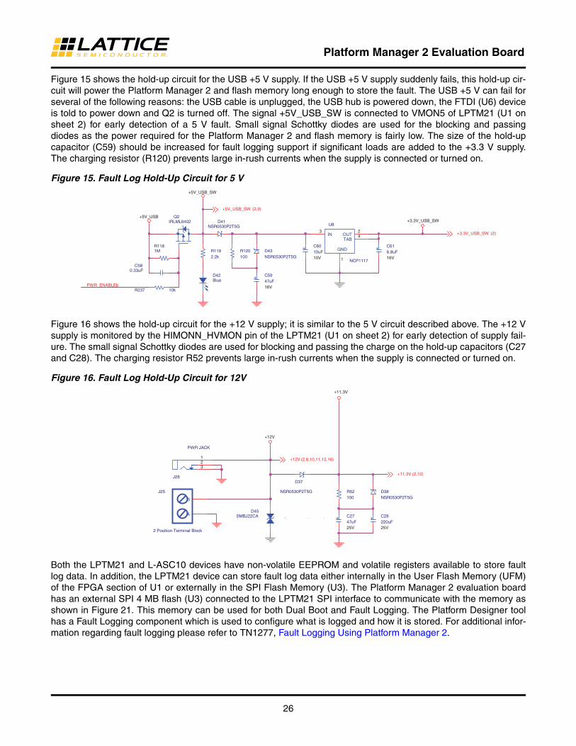
Figure 15 shows the hold-up circuit for the USB +5 V supply. If the USB +5 V supply suddenly fails, this hold-up cir-cuit will power the Platform Manager 2 and flash memory long enough to store the fault. The USB +5 V can fail for several of the following reasons: the USB cable is unplugged, the USB hub is powered down, the FTDI (U6) device is told to power down and Q2 is turned off. The signal +5V_USB_SW is connected to VMON5 of LPTM21 (U1 on sheet 2) for early detection of a 5 V fault. Small signal Schottky diodes are used for the blocking and passing diodes as the power required for the Platform Manager 2 and flash memory is fairly low. The size of the hold-up capacitor (C59) should be increased for fault logging support if significant loads are added to the +3.3 V supply. The charging resistor (R120) prevents large in-rush currents when the supply is connected or turned on.
Figure 15. Fault Log Hold-Up Circuit for 5 V
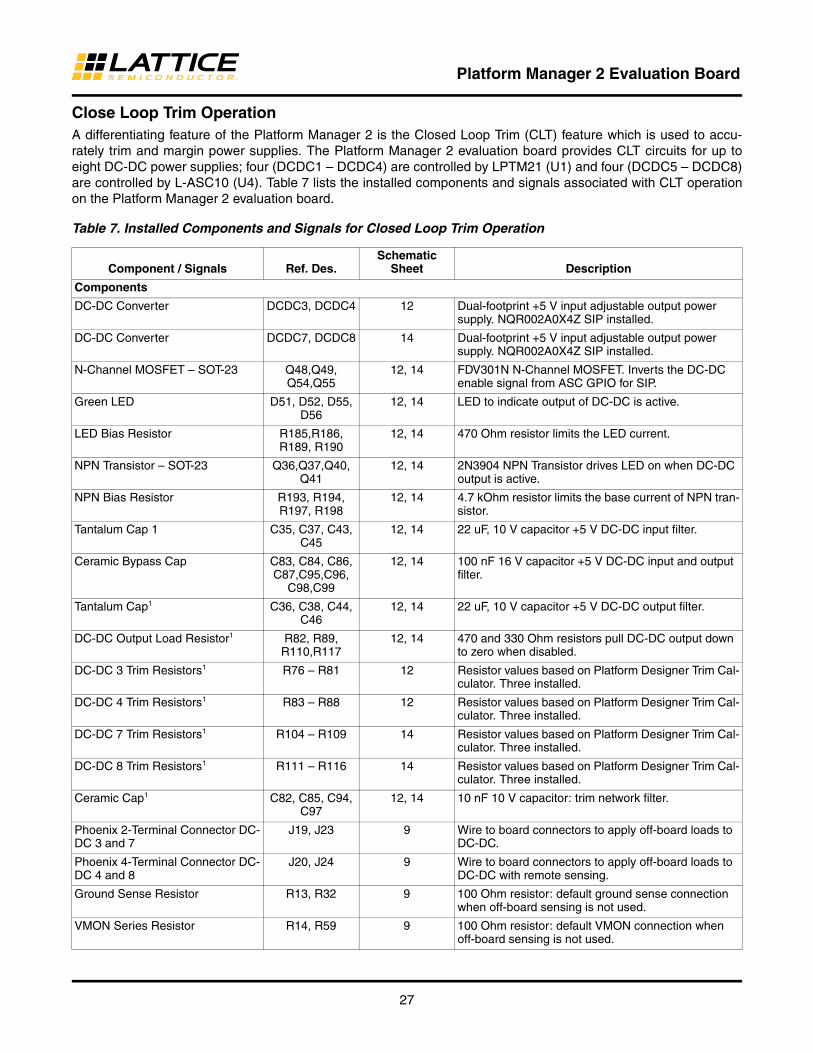
Figure 16 shows the hold-up circuit for the +12 V supply; it is similar to the 5 V circuit described above. The +12 V supply is monitored by the HIMONN_HVMON pin of the LPTM21 (U1 on sheet 2) for early detection of supply fail-ure. The small signal Schottky diodes are used for blocking and passing the charge on the hold-up capacitors (C27 and C28). The charging resistor R52 prevents large in-rush currents when the supply is connected or turned on.
Figure 16. Fault Log Hold-Up Circuit for 12V
Both the LPTM21 and L-ASC10 devices have non-volatile EEPROM and volatile registers available to store fault log data. In addition, the LPTM21 device can store fault log data either internally in the User Flash Memory (UFM) of the FPGA section of U1 or externally in the SPI Flash Memory (U3). The Platform Manager 2 evaluation board has an external SPI 4 MB flash (U3) connected to the LPTM21 SPI interface to communicate with the memory as shown in Figure 21. This memory can be used for both Dual Boot and Fault Logging. The Platform Designer tool has a Fault Logging component which is used to configure what is logged and how it is stored. For additional infor-mation regarding fault logging please refer to TN1277, Fault Logging Using Platform Manager 2.
PWR_ENABLEb
+5V_USB
+5V_USB_SW
+3.3V_USB_SW
+3.3V_USB_SW (2)
+5V_USB_SW (2,9)
R1192.2k
D42Blue
D41NSR0530P2T5G
R237 10k
U8
NCP1117
GND
1
IN3
OUT2
TAB4
C5947uF16V
R120100
C6010uF10V
C616.8uF16V
D43NSR0530P2T5G
C580.33uF
Q2IRLML6402
R1181M
+11.3V
+12V
+12V (2,8,10,11,13,16)
+11.3V (2,10)
D38NSR0530P2T5G
D45SMBJ22CA
J25
2 Position Terminal Block
A
B
C28220uF25V
J28
PWR JACK
321
C2747uF25V
D37
NSR0530P2T5G R52100
27
Platform Manager 2 Evaluation Board
Close Loop Trim OperationA differentiating feature of the Platform Manager 2 is the Closed Loop Trim (CLT) feature which is used to accu-rately trim and margin power supplies. The Platform Manager 2 evaluation board provides CLT circuits for up to eight DC-DC power supplies; four (DCDC1 – DCDC4) are controlled by LPTM21 (U1) and four (DCDC5 – DCDC8) are controlled by L-ASC10 (U4). Table 7 lists the installed components and signals associated with CLT operation on the Platform Manager 2 evaluation board.
Table 7. Installed Components and Signals for Closed Loop Trim Operation
Component / Signals Ref. Des.Schematic
Sheet Description
Components
DC-DC Converter DCDC3, DCDC4 12 Dual-footprint +5 V input adjustable output power supply. NQR002A0X4Z SIP installed.
DC-DC Converter DCDC7, DCDC8 14 Dual-footprint +5 V input adjustable output power supply. NQR002A0X4Z SIP installed.
N-Channel MOSFET – SOT-23 Q48,Q49, Q54,Q55
12, 14 FDV301N N-Channel MOSFET. Inverts the DC-DC enable signal from ASC GPIO for SIP.
Green LED D51, D52, D55, D56
12, 14 LED to indicate output of DC-DC is active.
LED Bias Resistor R185,R186, R189, R190
12, 14 470 Ohm resistor limits the LED current.
NPN Transistor – SOT-23 Q36,Q37,Q40, Q41
12, 14 2N3904 NPN Transistor drives LED on when DC-DC output is active.
NPN Bias Resistor R193, R194, R197, R198
12, 14 4.7 kOhm resistor limits the base current of NPN tran-sistor.
Tantalum Cap 1 C35, C37, C43, C45
12, 14 22 uF, 10 V capacitor +5 V DC-DC input filter.
Ceramic Bypass Cap C83, C84, C86, C87,C95,C96,
C98,C99
12, 14 100 nF 16 V capacitor +5 V DC-DC input and output filter.
Tantalum Cap1 C36, C38, C44, C46
12, 14 22 uF, 10 V capacitor +5 V DC-DC output filter.
DC-DC Output Load Resistor1 R82, R89, R110,R117
12, 14 470 and 330 Ohm resistors pull DC-DC output down to zero when disabled.
DC-DC 3 Trim Resistors1 R76 – R81 12 Resistor values based on Platform Designer Trim Cal-culator. Three installed.
DC-DC 4 Trim Resistors1 R83 – R88 12 Resistor values based on Platform Designer Trim Cal-culator. Three installed.
DC-DC 7 Trim Resistors1 R104 – R109 14 Resistor values based on Platform Designer Trim Cal-culator. Three installed.
DC-DC 8 Trim Resistors1 R111 – R116 14 Resistor values based on Platform Designer Trim Cal-culator. Three installed.
Ceramic Cap1 C82, C85, C94, C97
12, 14 10 nF 10 V capacitor: trim network filter.
Phoenix 2-Terminal Connector DC-DC 3 and 7
J19, J23 9 Wire to board connectors to apply off-board loads to DC-DC.
Phoenix 4-Terminal Connector DC-DC 4 and 8
J20, J24 9 Wire to board connectors to apply off-board loads to DC-DC with remote sensing.
Ground Sense Resistor R13, R32 9 100 Ohm resistor: default ground sense connection when off-board sensing is not used.
VMON Series Resistor R14, R59 9 100 Ohm resistor: default VMON connection when off-board sensing is not used.

28
Platform Manager 2 Evaluation Board
2x5 Header J35 12 Header to connect PM bus controller for DC-DC con-vertors (DOSA supplies).
1x2 Header J29 9 Jumper to provide +5 V to the DC-DCs from USB.
Signals
A0_LED5 2, 11 DCDC1 enable signal from ASC0_GPIO5. Safe state is low.
A0_LED6 2, 11 DCDC2 enable signal from ASC0_GPIO6. Safe state is low.
A0_LED3 2, 12 DCDC3 enable signal from ASC0_GPIO3. Safe state is low.
A0_LED4 2, 12 DCDC4 enable signal from ASC0_GPIO4. Safe state is low.
A1_LED5 2, 13 DCDC5 enable signal from ASC1_GPIO5. Safe state is low.
A1_LED6 2, 13 DCDC6 enable signal from ASC1_GPIO6. Safe state is low.
A1_LED8 2, 14 DCDC7 enable signal from ASC1_GPIO8. Safe state is high.
A1_LED9 2, 14 DCDC8 enable signal from ASC1_GPIO9. Safe state is high.
TRIM_DCDC1 2, 11 DCDC1 Trim signal from ASC0_TRIM1.
TRIM_DCDC2 2, 11 DCDC2 Trim signal from ASC0_TRIM2.
TRIM_DCDC3 2, 12 DCDC3 Trim signal from ASC0_TRIM3.
TRIM_DCDC4 2, 12 DCDC4 Trim signal from ASC0_TRIM4.
TRIM_DCDC5 5, 13 DCDC5 Trim signal from ASC1_TRIM1.
TRIM_DCDC6 5, 13 DCDC6 Trim signal from ASC1_TRIM2.
TRIM_DCDC7 5, 14 DCDC7 Trim signal from ASC1_TRIM3.
TRIM_DCDC8 5, 14 DCDC8 Trim signal from ASC1_TRIM4.
OUT_DCDC1 2, 11 DCDC1 Output connected to ASC0_VMON1 via R1.
OUT_DCDC2 2, 11 DCDC2 Output connected to ASC0_VMON2 via R2.
OUT_DCDC3 2, 12 DCDC3 Output connected to ASC0_VMON3 via R3.
OUT_DCDC4 2, 9, 12 DCDC4 Output connected to ASC0_VMON4 via R4.
OUT_DCDC5 5, 13 DCDC5 Output connected to ASC1_VMON1 via R23.
OUT_DCDC6 5, 13 DCDC6 Output connected to ASC1_VMON2 via R24.
OUT_DCDC7 5, 14 DCDC7 Output connected to ASC1_VMON3 via R25.
OUT_DCDC8 5, 9, 14 DCDC8 Output connected to ASC1_VMON4 via R26.
DCDC4_SENSE 9, 12 DCDC4 Sense input connected to DCDC4 output via R14.
DCDC8_SENSE 9, 14 DCDC8 Sense input connected to DCDC8 output via R59.
DCDC1_SYNC – DCDC8_SYNC 4, 11 - 14 DOSA DC-DC Synchronization signals: support for operating the supplies at different phases to minimize switching noise from the primary supply.
PMBUS_SDA, PMBUS_SCL, SMB_ALERT
11 - 14 PM Bus control signals for DOSA DC-DC convertors.
1. Value is subject to change and/or may not be required based on customer design.
Component / Signals Ref. Des.Schematic
Sheet Description

29
Platform Manager 2 Evaluation Board
Generic Overview of Trim and Margin Operation
The Platform Manager 2 evaluation board can support up to eight DC-DC modules. All eight are similarly designed and laid out so we will detail the generic similarities rather than provide a separate section for each DC-DC. The Platform Manager 2 evaluation board provides two footprints for each DC-DC: one is for a Single Inline Package (SIP) and the other is for the Distributed Open Source Alliance (DOSA) compliant package. The SIP footprint is populated for DCDC3, DCDC4, DCDC7, and DCDC8. The other DCDC locations are unpopulated to support user evaluation of other DC-DC supplies of either footprint. In addition, all of the surrounding components are also unpopulated for DCDC1, DCDC2, DCDC5, and DCDC6 to support the design and evaluation of different devices and values with Platform Manager 2.
ASC0 (U1) is used to enable, monitor, and trim DCDC1 – DCDC4 which are located on the left side of the board and ASC1 (U4) is used to enable, monitor, and trim DCDC5 – DCDC8 which are located on the right side of the board. The top four DC-DC supplies are powered by +12 V (DCDC1, DCDC2, DCDC5, and DCDC6) while the bot-tom four DC-DC supplies are powered by +5 V (DCDC3, DCDC4, DCDC7, and DCDC8). The installed DC-DC sup-plies can only be powered and demonstrated using an off board +5 V source. For light loads the +5 V from the USB cable can be used by installing a jumper on J29, while heavier loads may require a bench supply connected to J12.
The Platform Manager 2 evaluation board provides footprints and circuit connections for six trimming resistors for each DCDC. These six resistors are shared by both the SIP and DOSA footprints because only one supply can be populated at a time. The resistors are organized in an “H” pattern both in the schematic and on the board layout. The resistors are named in the schematic to match the names used in the Platform Designer Trim-view calculator. The names are listed and described in Table 8 below. Typically only three resistors are suggested by the calculator; a pull up, a pull down, and a series resistor. The exact population of the “H” pattern depends on many factors that the calcu-lator takes into account such as type of DC-DC, output voltage, and range of trim. The Platform Manager 2 evaluation board provides pads and connections to support any result from the Trim Calculator. However, with certain supplies and by adjusting the options, the calculator can produce a result that only uses two resistors: a pull down and a series resistor. The DC-DCs on the Platform Manager 2 Evaluation board are populated with the two resistor solution. A key requirement for the calculator to produce a two resistor solution is the Bi-Polar Zero (BPZ) voltage of the Trim Cell has to match the DC-DC’s internal reference voltage. Otherwise the calculator will add a pull up or pull down resistor in attempt to offset the imbalance and still keep the Trim DAC code near 80h (the BPZ value, halfway between –127 and +128). For more information on the Trim interface and Calculator please see AN6074 Interfacing the Trim Output of Power Manager II Devices to DC-DC Converters and the Platform Designer User Guide.
The Platform Manager 2 evaluation board uses two resistors for Rseries, Rs1 and Rs2, and places a 10nF capaci-tor in between them to form a low pass filter. The sum of Rs1 and Rs2 should equal the Rseries value calculated by Platform Designer. This filter network is recommended by some DOSA supply data sheets however, other supplies can also benefit from the additional filtering.
Table 8. Trim Resistor "H-Network" Names.
In order for the CLT circuits within the ASC to operate properly the output of the supply needs to be monitored by the correct VMON input. The Platform Manager 2 evaluation board illustrates the correct trimming connections by using TRIM1 with VMON1, TRIM2 with VMON2, all the way to TRIM4 with VMON4. As discussed in the Voltage Monitor Operation section, the DCDC outputs are connected to the VMON inputs using a series resistor with a value of 270 Ohms (see sheets 2 and 5). The series resistor is not required in customer designs; the only function on the evaluation board is to isolate the DCDC outputs from the VMON test points. The VMON series resistor
Schematic Name Calculator Name Description
RpupS RpupSupply Pull up resistor at DC-DC Trim input
RpdnS RpdnSupply Pull down resistor at DC-DC Trim input
Rs1 Rseries Series resistor (½ between Trim DAC output and filter)
Rs2 Rseries Series resistor (½ between filter and DC-DC Trim input)
RpupD RpupDAC Pull up resistor at Trim DAC output
RpdnD RpupDAC Pull down resistor at Trim DAC output

30
Platform Manager 2 Evaluation Board
allows another voltage source to be applied to the VMON test point directly. If the voltage source has a high output impedance, the VMON series resistor should be removed for accurate operation.
Each of the DCDC supplies has a dummy load resistor connected to the output. The dummy load resistor is not required in customer designs as the supply is connected to a real load. The dummy load resistor is only used on the evaluation board to prevent the output of the supply from “creeping up” when the supply is disabled. Without the dummy load resistor, an output of around 1 V can appear at the output of disabled supplies. The dummy load resis-tors are sized based on the target DCDC supply output voltage; lower values for lower voltages and higher values for higher voltages. In all circuits they are 1/10 watt packages because there is minimal heat generated.
DCDC1 – Enable and Trim Operation
In this section we will analyze the specific circuits that support DCDC1. The circuits for DCDC2, DCDC5, and DCDC6 are similar to DCDC1 and therefore will not be discussed in detail. In Figure 17 the control signal A0_LED5, which comes from ASC0’s GPIO5 output, is inverted and level shifted by a small signal N-channel MOS-FET (Q15 FDV301N). For +12 V supplies a buffer or inverter is needed because the ASC GPIOs can only be pulled up to +5.5 V. All the GPIOs of the ASC have a “safe state” which defines the behavior independent of configuration during Power-On-Reset (POR) or during programming; the safe state of GPIO5 is low. The DOSA supply is enabled when the On-Off pin is low (negative enable logic), so the inverter Q15 prevents the supply from turning on during POR or programming. Similarly, the SIP supply is enabled when the On-Off pin is high (positive enable logic) so, the second MOSFET inverter Q45 prevents the SIP from turning on during POR or programming. Both MOS-FETs use a 20k pull-up resistor to +12 V to insure a full logic swing at the enable inputs of the supplies.
Figure 17. Power On Indication, Enable, and Trim Circuits for DCDC1
DOSA5V @ 3A
ASC0 GPIO5
ASC0 TRIM1
ASC0 VMON1
SIP5V @ 2A
PMBUS_SCL
SMB_ALERTPMBUS_SDA
A0_LED5(2,7)
TRIM_DCDC1(2)
OUT_DCDC1 (2,9)
+12V(2,8,9,10,13,16)
+3.3V(2,3,4,5,6,7,8,9,10,12,13,14,16)
DCDC1_SYNC(4)
R183470
R21320K
Q45FDV301N
R681K
TP10_SYNC
R16220K
D49Green
SM_LED_0603
C3222uF10V
R1914.7k
R67openRpdnD
DCDC1PDT003A0X3
ON_OFF1 VIN2
GND
3
VOUT4
VS+5
GND
7
CLK8
SEQ9
PGOOD10
SYNC11
VS-12
SIG_GND
13
DATA15
ADDR016
ADDR117
TRIM6
SMBALERT14
C78100nF
R632.74kRpdnS
Q15FDV301N
R655.6kRs1
NQR002A0X4ZDCDC1_A
GND
3
Vin2
On-Off Control1
Trim5
Vout4
R66openRpupD
C77100nF
R645.6kRs2
R62openRpupS
C3122uF
16V
R20523.7k
Q342N3904
C7610nF
R204130k

31
Platform Manager 2 Evaluation Board
The control signal A0_LED5 is also used to turn on a red LED (D7) when it is low and is pulled up to +3.3 V by a 2.2k Ohm resistor (RN11B see sheet 7). Because the installed supply could use either positive or negative enable logic, the illumination of LED D7 may not correspond to the supply being enabled. A separate green LED (D49) is used to indicate when the supply is enabled. An NPN transistor (Q34) is used to turn the green LED on when the supply has enough voltage to bias the emitter-base junction (slightly more than 0.7 V).
Supply filtering is provided by a 22 uF and 100 nF pair of capacitors, both at the input and output, that are located close to both DC-DC footprints to be effective for either. For DCDC1 the input capacitors are C31 and C77 while the output capacitors are C32 and C78. A load resistor (R68) is used to pull the DCDC output low when it is disabled. Note, these values may not be optimal for all supplies and loading conditions; specific filtering requirements should be followed from the supply data sheet.
All the DOSA supply footprints on the Platform Manager 2 evaluation board have provision to set the PMBus address with pull-down resistors; for DCDC1 these are R204 and R205. The PMBus signals (PMBUS_SDA, PMBUS_SCL, SMB_ALERT) are bussed to all the DCDCs and are brought out on connector J35. Each DOSA supply footprint also has a SYNC connection to demonstrate the PMBus feature of DC-DC phasing; where the switching circuits of different DC-DCs is synchronized out-of-phase to minimize the peak power requirements of the power source.
DCDC4 – Enable and Trim Operation
In this section we discuss the circuits for the +5 V input supplies with a focus on DCDC4. The circuitry for all the DCDCs is very similar, so this discussion will be limited to the key differences from the +12 V input supplies described in the previous section (DCDC1). The support circuits with DCDC4 are shown in Figure 18.
Figure 18. Power On Indication, Enable, and Trim Circuits for DCDC4
ASC0 VMON4
ASC0 TRIM4
DOSA1.2V @ 3A
SIP1.2V @ 2A
ASC0 GPIO4
+5V
+3.3V
OUT_DCDC4 (2,6,9)
TRIM_DCDC4(2)
DCDC4_SYNC(4)
A0_LED4(2,7)
DCDC4_SENSE (2,9)
PMBUS_SCL(11,13,14)
SMB_ALERT(11,13,14)PMBUS_SDA(11,13,14)
A0_GS_VMON4 (2,9)
R21184.5k
C3822uF10V
R186470
R89330
C87100nF
C86100nF
R8420.0kRpdnS
Q49FDV301N
DCDC4PDT003A0X3
ON_OFF1 VIN2
GND
3
VOUT4
VS+5
GND
7
CLK8
SEQ9
PGOOD10
SYNC11
VS-12
SIG_GND
13
DATA15
ADDR016
ADDR117
TRIM6
SMBALERT14
R83openRpupS
TP13_SYNC
NQR002A0X4ZDCDC4_A
GND
3
Vin2
On-Off Control1
Trim5
Vout4
R8519.6kRs2
R210130k
R1944.7k
D52Green
SM_LED_0603
R88openRpdnD
C3722uF
10V
C8510nF
R87openRpupD
Q372N3904
R16510K
R8619.6kRs1

32
Platform Manager 2 Evaluation Board
The circuits for DCDC3, DCDC7, and DCDC8 are similar to DCDC4 and therefore will not be discussed in detail. The significant difference from the circuit for DCDC1 shown in Figure 17 is the +5 V input supply power for DCDC4 instead of +12 V. At this voltage level the On-Off pin of the SIP can be connected directly to the GPIO4 output of ASC0 without the need for a buffer. The inverter (Q49) is still used to keep the DOSA supply turned off during POR and programming.
One other unique feature of DCDC4 (and DCDC8) is the support for remote sensing when the DOSA supply is installed after removing the SIP. The V+ and V- pins of the DOSA are routed to a four pin screw connecter (J20 and J24 on sheet 9) instead of directly to the output and ground. Resistors with the value of 100 Ohms (R13, R14 and R32, R59 on sheet 9) are used to connect the sense pins to the output and ground when off-board connections are not used. When a four-wire off board load is used, the 100 Ohms is bypassed by a direct short and the V+ and V- pins sense the voltage at the load.
One difference from Figure 18 for DCDC7 and DCDC8 is the connections for the enable inverter. Since the safe state for GPIO8 and GPIO9 is high-impedance, the inverter transistors are used on the SIPs for DCDC7 and DCDC8 instead of the DOSAs (see sheet 14).
Table 9 provides a summary of the installed DCDCs, the connections, logic levels, and voltages for a quick refer-ence for designers.
Table 9. Summary of DCDC Trim Circuits.
The Platform Manager 2 evaluation board has four DC-DC trim circuits that are unpopulated to allow customization and evaluation of different circuits and devices, Table 10 lists the un-installed components to support custom designs.
DCDC Package Vin VoutControl Signal ASC GPIO
On Logic Level VMON RpdnS Rseries
11 n/a 12 V n/a A0_LED5 ASC0 GPIO5 n/a 1 n/a n/a
21 n/a 12 V n/a A0_LED6 ASC0 GPIO6 n/a 2 n/a n/a
3 SIP 5 V 2.5 V A0_LED3 ASC0 GPIO3 1 3 6.34k 22k
4 SIP 5 V 1.2 V A0_LED4 ASC0 GPIO4 1 4 20k 39.2k
51 n/a 12 V n/a A1_LED5 ASC1 GPIO5 n/a 1 n/a n/a
61 n/a 12 V n/a A1_LED6 ASC1 GPIO6 n/a 2 n/a n/a
7 SIP 5 V 2.5 V A1_LED8 ASC1 GPIO8 0 3 6.34k 22k
8 SIP 5 V 1.2 V A1_LED9 ASC1 GPIO9 0 4 20k 39.2k
1. Values shown in the schematic for these DC-DC converters is for example only – they are not installed.

33
Platform Manager 2 Evaluation Board
Table 10. Un-Installed Components for Closed Loop Trim Operation1
Components Ref. Des.Schematic
Sheet Description
DC-DC Converter DCDC1, DCDC2 11 Dual-footprint +12 V input adjustable output power supply.
DC-DC Converter DCDC5, DCDC6 13 Dual-footprint +12 V input adjustable output power supply.
N-Channel MOSFET – SOT-23 Q15 – Q18 11, 13 FDV301N N-Channel MOSFET. Inverts the DC-DC enable signal from ASC GPIO and shifts the level up to +12 V.
N-Channel MOSFET – SOT-23 Q45,Q47,Q51,Q53
11, 13 FDV301N N-Channel MOSFET. Inverts the DC-DC enable signal from DOSA to SIP.
Green LED D49,D50,D53,D54
11, 13 LED to indicate output of DC-DC is active.
LED Bias Resistor R183,R184,R187,R188
11, 13 470 Ohm resistor limits the LED current.
NPN Transistor – SOT-23 Q34,Q35,Q38,Q39
11, 13 2N3904 NPN Transistor drives LED on when DC-DC output is active.
NPN Bias Resistor R191,R192,R195,R196
11, 13 4.7k Ohm resistor limits the base current of NPN tran-sistor.
Tantalum Cap2 C31,C33,C39,C41
11, 13 22 uF, 16 V capacitor +12 V DC-DC input filter.
Ceramic Bypass Cap C77,C78,C80,C81,C89,
C90,C92,C93
11, 13 100 nF 16 V capacitor +12 V DC-DC input and output filter.
Tantalum Cap2 C32,C34,C40,C42
11, 13 22 uF, 10 V capacitor +12 V DC-DC output filter.
DC-DC Output Load Resistor2 R68,R75,R96,R103
11, 13 1k and 680 Ohm resistors pull DC-DC output down to zero when disabled.
DC-DC PMBus Address Setting Resistor2
R204 – R211,R218 – R225
11, 12,13, 14 Various resistor values to set PMBus address based on DOSA DC-DC data sheet.
DC-DC 1 Trim Resistors2 R62 – R67 11 Resistor values based on Platform Designer Trim Cal-culator. None installed.
DC-DC 2 Trim Resistors2 R69 – R74 11 Resistor values based on Platform Designer Trim Cal-culator.
DC-DC 5 Trim Resistors2 R90 – R95 13 Resistor values based on Platform Designer Trim Cal-culator.
DC-DC 6 Trim Resistors2 R97 – R102 13 Resistor values based on Platform Designer Trim Cal-culator.
Ceramic Cap2 C76, C79, C88, C91
11, 13 10 nF 10 V capacitor: trim network filter.
Phoenix 2-Terminal Connector DCDC 1, 2, 5, and 6
J17,J18,J21,J22 9 Wire to board connectors to apply off-board loads to DC-DC.
1. Not installed to allow customer development on the evaluation board.2. Value is subject to change and/or may not be required based on customer design.

34
Platform Manager 2 Evaluation Board
VID OperationVoltage Identification (VID) is supported by Platform Designer and the Platform Manager 2 evaluation board. In the Platform Designer Voltage view, VID can be configured and added to any Trim output. The Platform Manager 2 evaluation board has DC-DC supplies, switches, and connections to support VID operation. Table 11 lists the com-ponents and signals associated with VID operation on the Platform Manager 2 board.
Table 11. Components and Signals for VID Operation
When VID is added to a Trim channel in Platform Designer the software adds the VID IP to the design. The function of the VID IP is to read the Select Bus when the strobe signal is active and then send the target voltage to the cor-responding ASC via I2C. The VID IP translates the Select Bus value to the target voltage using a look-up table that is defined in the Platform Designer software. The Closed Loop Trim (CLT) circuits within the ASC then drive the Trim DAC output pin which adjusts the DC-DC output to the target voltage as read by the VMON input pin. For a more complete explanation of VID operation please see AN6092, Implementing VID Function with Platform Man-ager 2.
Figure 19. Switches for VID
Components / Signals Ref. Des.Schematic
Sheet Description
Components
DC-DC Convertor DCDC3, DCDC4 12 Dual-footprint +5V input adjustable output power sup-ply. NQR002A0X4Z SIP installed.
DC-DC Convertor DCDC7, DCDC8 14 Dual-footprint +5V input adjustable output power sup-ply. NQR002A0X4Z SIP installed.
DC-DC Trim Resistors 2 R76 – R81, R83 – R88
12 Resistor values based on Platform Designer Trim Cal-culator. Three installed.
DC-DC Trim Resistors 2 R104-R109, R111-R116
14 Resistor values based on Platform Designer Trim Cal-culator. Three installed.
8- position DIP switch1 SW6 6 Switch is used to change the VID Select Bus.
Push Button Switch1 SW2 6 Switch is used to create a VID strobe signal.
Signals
VIDA_1 to VIDA_8 4, 6 Signals used as the VID Select Bus.
VIDA_SW 4, 6 Signal used to strobe the VID Select Bus into the VID IP.
1. Installed to allow demos and development on the evaluation board customer designs can use other methods.2. Value is subject to change and/or may not be required based on customer design.
VID A
VIDA_1
VIDA_2
VIDA_3
VIDA_4
VIDA_5
VIDA_6
VIDA_7
VIDA_8
+3.3V
VIDA_[1:8] (4)
SW6E5 12
RN1D10k4
RN1E10k56
SW6D4 13
SW6H8 9
RN1B10k2
RN1A10k101
RN1F10k7
RN1G10k8
RN1H10k9
RN1C10k3
SW6B2 15
SW6C3 14
SW6G7 10
SW6A1 16
SW6F6 11
+3.3V
VIDA_SW (4)
R24210k
SW2VID_A
1 4
2 3

35
Platform Manager 2 Evaluation Board
Two switches are provided on the Platform Manager 2 evaluation board as shown in Figure 19; one is an eight posi-tion piano-style DIP switch (SW6) and the other is a momentary push button switch (SW2). As seen in Figure 5, SW6 is located in the lower right of the board. When the switch lever is up the signal is high (1) and when the switch lever is down the signal is low (0). It is up to the design as to the number and order of the switch positions used to generate the VID Select Bus. The eight position switch can easily support two VID channels of four bits each or a slightly more complex design could use three bits to multiplex the strobe signal to eight VID channels and use the other five bits as a common VID Select Bus. The push button switch SW2 can be used to generate a falling edge “VID Strobe” signal which triggers the VID IP to sample the VID Select Bus and update the target voltage. For design support the VID signals are defined in the preference file listing in Appendix B.
Programming and ConfigurationThe two featured devices on the Platform Manager 2 evaluation board are the LPTM21 and L-ASC10 (U1 and U4). Both devices have non-volatile memory that can be erased and reprogrammed numerous times to support demos, development, and testing. They can also be configured from the SPI memory (U3). The primary method of repro-gramming U1, U3, and U4 is with Diamond Programmer using a USB cable. Table 12 lists the components and sig-nals associated with programming and configuring the LPTM21, L-ASC10, and SPI devices on the Platform Manager 2 evaluation board.
Table 12. Components and Signals for Programming.
Components / Signals Ref. Des.Schematic
Sheet Description
Components
USB connector J16 15 USB Mini connector for connecting with USB cable (included).
FT2232H U6 15 FTDI chip converts USB to JTAG signal for program-ming U1 directly and U4 via the JTAG to I2C bridge within U1; also ASC2 and ASC3 if connected. The FTDI device also converts USB to I2C for software utilities.
JTAG Enable Pull-up Resistor R158 3 4.7k Ohm Resistor. Connected between +3.3 V and JTAGENAB pin of LPTM21.
Zero Ohm Jumper1 R122 – R125 15 Zero Ohm Resistor. Connects FTDI to JTAG signals. Remove to disconnect U6 from JTAG.
Zero Ohm Jumper1 R126 – R127 15 Zero Ohm Resistor. Connects FTDI to I2C bus. Remove to disconnect U6 from I2C bus.
Zero Ohm Jumper1 R248 15 Zero Ohm Resistor. Connects I2C-Enable signal to FTDI. Remove to use J33 in manual mode.
Red LED D57 15 Red LED indicates when FTDI U6 is the I2C master.
LED Bias Resistor R264 15 470 Ohm Resistor. Limits the current in D57 when Q42 is on.
LED Drive Transistor Q42 15 2N3904 NPN Transistor. Drives LED D57 on when USB_I2C_EN signal is active.
Transistor Bias Resistor R263 15 4.7k Ohm Resistor. Sets the base current of Q42.
I2C MUX1 U10, U11 3 FSA4157 Analog Switch. Used to disconnect the FTDI I2C ports from the bus when FTDI is not the master.
I2C Address Resistor R27 5 A pull down resistor of 2.2K connected to I2C_ADDR pin of L-ASC10. This sets the LSBs for I2C slave (L-ASC10) address to ”001”.
Atmel 4MB Flash Memory1 U3 3 SPI Flash memory to store “Golden Bitstream” for Dual Boot Programming operation.
2 x 1 Header J33 3 Unpopulated header provides manual control of USB_I2C_EN.

36
Platform Manager 2 Evaluation Board
The Platform Manager 2 evaluation board provides both a JTAG and I2C programming interface for LPTM21 and L-ASC10. A portion of the schematic which supports programming is shown in Figure 20 below.
Figure 20. USB Programming Interface
The mini-USB connector (J28) provides the USB connection to a computer running Lattice Diamond Programmer software. The FTDI device (U6) provides the interface between USB and JTAG signals (on AD BUS) and I2C sig-nals (on BD BUS). The FPGA within the LPTM21 device is programmed directly from the JTAG signals. All the ASC devices are programmed over the I2C bus using the LPTM21 built in JTAG to I2C bridge. When the LPTM21 device is the I2C master the MUX is needed to disconnect the I2C pins of the FTDI device (U6) from the bus. This is because the FTDI pins do not support multi-master mode and will load down the bus and prevent proper operation. The MUX can be controlled either by the FTDI device (U6 - bit 0 on the AC BUS) or the jumper J33 setting the level of USB_I2C_EN. The Platform Manager I2C Software Utility controls the MUX automatically. When other software is used that does not drive the USB_I2C_EN signal, the user must control the MUX manually with J33. When the signal USB_I2C_EN is high the I2C pins of the FTDI device (U6) are connected to the I2C bus and the red LED (D57) is illuminated.
8 x 1 Header J2 3 Unpopulated header provides JTAG access for optional programming with JTAG cable (not included).
8 x 1 Header J26 3 Unpopulated header provides access to I2C and SPI signals.
Signals
USB_TCK, USB_TMS, USB_TDO, USB_TDI
3, 15 The 4 JTAG signals for programming LPTM21 and ASC devices via the JTAG to I2C bridge within U1.
USB_I2C_EN 3, 15 Controls the I2C MUX. When this signal is high the I2C pins of the FTDI device U6 are connected to the I2C bus.
FTDI_SDA, FTDI_SCL
3, 15 Branch off the main I2C bus connected using a MUX.
SPI_CS0, SPI_CLK, SPI_IN, SPI_OUT
3 Bus between memory and SPI port of LPTM21 for Dual boot programming operation.
1. Not required for customer designs; this is only needed to support demonstrations on the evaluation board.
Components / Signals Ref. Des.Schematic
Sheet Description
USB Connection
EESKEEDATA
SHLD
PWR_ENABLEb
EECS
+3.3V_USB
+3.3V_USB
+3.3V_USB
+3.3V
FTDI_SCL (3)
USB_TCK (3)USB_TDI (3)USB_TDO (3)USB_TMS (3)
FTDI_SDA (3)
USB_I2C_EN (3)
C47
10nF R231 12k
R122
0
U7
M93C46-WMN6TP
SOIC-8
CS1
SK2
DIN3
DOUT4
VCC8
NC7
ORG6
GND5
D57Red
SM_LED_0603
R234 2.2k
1 2
R230 2.2k
L2Ferrite_bead
R2634.7k
C5518pF
FTDI High-Speed USB
FT2232H
FT2232HLU6
VREGIN50
VREGOUT49
DM7
DP8
REF6
RESET#14
EECS63
EECLK62
EEDATA61
OSCI2
OSCO3
TEST13
ADBUS016
ADBUS117
ADBUS218
ADBUS319
VP
HY
4
VP
LL9
VC
OR
E12
VC
OR
E37
VC
OR
E64
VC
CIO
20
VC
CIO
31
VC
CIO
42
VC
CIO
56
AG
ND
10
GN
D1
GN
D5
GN
D11
GN
D15
GN
D25
GN
D35
GN
D47
GN
D51
PWREN#60
SUSPEND#36
ADBUS421
ADBUS522
ADBUS623
ADBUS724
ACBUS026
ACBUS127
ACBUS228
ACBUS329
ACBUS430
ACBUS532
ACBUS633
ACBUS734
BDBUS038
BDBUS139
BDBUS240
BDBUS341
BDBUS443
BDBUS544
BDBUS645
BDBUS746
BCBUS048
BCBUS152
BCBUS253
BCBUS354
BCBUS455
BCBUS557
BCBUS658
BCBUS759
X1
12MHZ
1 3
2 4
R126
0R235 100k
R124
0
R125
0
R127
0
Q422N3904
C57100nF
R264470
R23610k
J16 USB_MINI_B
TYPE_B
VCC1
D-2
D+3
GND5NC4
CASE7
CASE8
CASE9
CASE6
MH110
MH211
R123
0
C5618pF
R2170
R2480

37
Platform Manager 2 Evaluation Board
The zero Ohm resistors (R122 – R127) connected to the FTDI device (U6) pins are installed to support the on board connections. If off-board JTAG or I2C sources are used the zero Ohm resistors should be removed to prevent the I/O pins of the FTDI device (U6) from loading down the signals.
To support dual boot the 4Mbit SPI Flash Memory device (U3) is connected to the SPI pins of the LPTM21 device (U1). The memory is programmed using Diamond Programmer and the JTAG to SPI interface built into the FPGA of U1. The SPI signals are also brought out to the unpopulated header J26 to support alternate programming sources.
On sheet 5 the LSBs of the I2C slave address for the L-ASC10 device (U4) are determined by the value of resistor R27 connected between the I2C_ADDR pin and ground. The 2.2k Ohm resistor value corresponds to ASC1 and LSBs of “001”.
For additional information regarding programming the LPTM21 and L-ASC10 please refer to AN6091, Powering Up and Programming Platform Manager 2 and L-ASC10.
Dual Boot OperationThe Platform Manager 2 devices are designed to support field updates. In the event that an update is terminated prematurely either by power outage or communication interruption, a back-up boot image can be recalled from the SPI flash memory. This back-up boot image is called the default or “Golden” bit-stream and is used to boot the LPTM21 and L-ASC10 devices. Thus the system can operate from this default design at a basic support level until another field update can be completed. Table 13 lists the components and signals associated with the dual boot operation.
Table 13. Components and Signals for Dual Boot Operation.
Dual boot support requires two key circuits which are shown in Figure 21; 1) a memory device to store the “Golden” bit-stream and 2) a delay circuit to prevent reading data from the SPI memory at power-on when the supply is still ramping up. A simple RC delay circuit is all that is needed to prevent the LPTM21 from reading the “Golden” bit-stream from the SPI memory until the supply is stable. The Platform Manager 2 evaluation board is built with the RC delay circuit attached to the INITN pin. However, either the INITN pin or the PROGRAMN pin can be used to delay the configuration. Without the delay the LPTM21 and SPI memory may come out of power-on-reset (POR) at different voltage levels and the data transfer between them can be corrupted causing the configuration to fail. The
Components / Signals Ref. Des.Schematic
Sheet Description
Components
Atmel 4MB Flash Memory U3 3 SPI Flash memory to store “Golden” bit-stream for Dual Boot Programming operation. This is the same memory that is used for Fault Logging.
Pull-up Resistor R159 3 1k Ohm Resistor. Strong pull-up is required for SPI Clock.
Pull-up Resistor R19 3 10k Ohm Resistor. Weak pull-up is required for SPI Chip Select.
RC Delay Resistor R265 3 100k Ohm Resistor. Used to delay INITN pin of LPTM21 during power up.
RC Delay Capacitor C102 3 10 uF Capacitor. Used to delay INITN pin of LPTM21 during power up.
Signals
SPI_CS0,SPI_CLK,SPI_IN,SPI_OUT
3 SPI signals to read the “Golden” bit-stream from the external memory into the LPTM21 and L-ASC10 devices.
Proto_INITN 3 Signal used to delay the external boot process of the LPTM21.

38
Platform Manager 2 Evaluation Board
SPI memory (U3) should be connected to the SPI pins of the LPTM21 (U1) with short and similar length traces as the clock frequency is around 25 MHz. Because the drive strength of the clock and chip select pins on the LPTM21 are similar, the SPI_CLK signal has a more substantial pull-up (R159) than the SPI_CS0 signal (R19) in order to improve the reliability of the interface with the SPI memory. For more information on the dual boot operation please see TN1284, Dual Boot and Background Programming with Platform Manager 2.
Figure 21. Dual Boot Circuitry
12 V Buck Converter OperationA key feature of the LPTM21 (U1) device is the built-in control circuitry to implement a DC-DC Buck converter. It only takes a few external components connected to the LPTM21 to implement a regulated step-down DC-DC Buck converter with an output of +3.3 V. The Buck converter can operate with an input voltage ranging from 13.2 V down to 4.5 V. The components used on the Platform Manager 2 evaluation board are designed for a typical load of 200 mA; this is more than enough power for the on-board devices and one L-ASC10 evaluation board. The components and signals associated with a Buck converter operation on the Platform Manager 2 evaluation board are listed in Table 14 below.

39
Platform Manager 2 Evaluation Board
Table 14. Components and Signals for 12 V Buck Converter.
Components / Signals Ref. Des.Schematic
Sheet Description
Components
Fast MOSFET Switch Q1 2 TP0202K-T1-E3 P-Channel MOSFET power switch for Buck converter operation.
Q1 Driver MOSFET Q19 2 IRLML2803TRPBF N-Channel MOSFET signal switch that drives Q1.
Schottky Diode D2 2 Schottky Diode for Buck converter operation.
Power Inductor L1 2 270 uH Inductor for Buck converter operation.
Q1 Drive Resistor R129 2 10 Ohms Resistor, Limits peak drain current for Q19 and sets bias voltage for Q1.
Q1 Drive Resistor R128 2 100 Ohms Resistor, Sets bias voltage and turns Q1 off quickly.
Filter Capacitor C6 2 47 uF Capacitor, output low-pass filter.
Filter Capacitor C7 2 100 nF Capacitor, output low-pass filter.
RC Filter Resistor R250 2 2 Ohms Resistor, output low-pass filter.
RC Filter Resistor R216 2 1 Ohm Resistor, output low-pass filter.
Capacitor C5 2 35 uF Capacitor, input filter.
Filter Capacitor C8 2 1 uF Capacitor, input filter.
Q19 Gate Resistor R226 2 220 Ohms Resistor, limits drive current for PWM sig-nal and reduces Q19 parasitic oscillations.
Fuse F1 250mA Fast-blow Fuse, Protects Buck converter from short and +3.3 V loads from over-voltage.
Zener Diode D48 2 3.9V Zener Diode, protects all 3.3V devices in the event of short across Q1 or other malfunction where too high a voltage is applied to the +3.3V bus.
3 x1 Header J1 2 Jumper to select the board’s +3.3 V source; The Buck converter output (2-3), The USB regulator (1-2), off board supply (open).
2 x 1 Header J3 4 Jumper to connect the +3.3 V Buck converter output to the LPTM21 supply pins for feedback control of the PWM. This jumper can also be replaced with an Ammeter to measure the U1 current during operation.
Signals
PWM 2 215 kHz Buck converter PWM drive signal output from the HDRV pin of LPTM21 U1
+11.3 V 2, 9, 10 Diode OR’d supply from various +12 V sources. Pro-vides power for Buck converter operation and VDC pin of LPTM21 U1.
+3.3 V 2, 4,(All)
The output of the Buck converter is monitored by the supply pins of U1 to close the feedback loop and adjust the PWM duty cycle.

40
Platform Manager 2 Evaluation Board
Figure 22. +12V Buck Converter Circuit
The Buck converter circuit shown in Figure 22 shows how a 12V source can be used to provide the 3.3 V required for the LPTM21 and supporting circuits (external ASC and SPI memory). The circuit is designed to provide approx-imately 200mA which is more than enough for most Platform Manager 2 demonstrations using this board.
Because this is an evaluation board, and it is likely that component values may be changed, the +3.3 V bus is pro-tected using a 250 mA fast-blow fuse (F1) and 3.9V Zener diode (D48). If the wrong device is installed for Q1 or a short from drain to source occurs then 11 V or more would be applied to the +3.3 V bus. In such a case, the Zener diode will limit the voltage and cause the current to exceed the rating of the fuse and the devices on the +3.3 V sup-ply bus will be protected. It is recommended that customer designs include these protection devices (F1 and D48) at least for prototypes; then in production the fuse could be replaced with a zero Ohm jumper (a resistor in parallel with the fuse) and the Zener could be left off the board, if cost is an issue. Note that a 3.6V Zener has significant leakage at 3.3 V which is why the 3.9 V Zener diode is used.
The Buck converter in Figure 22 is powered by +11.3 V because there are numerous +12 V sources on the board which may or may-not be used as part of a demo design. Thus, all the +12 V sources connect to the +11.3 V bus with a small diode so the Buck converter can be active no matter where the +12 V is supplied from. The VDC pin of LPTM21 U1 is powered by the +11.3 V and enables the Buck converter control circuits to drive the external power-switch (Q1) and monitor the +3.3 V supply pins.
As in most DC-DC converters one design goal is to minimize turn-on and turn-off times of the N-channel power MOSFET (Q1). This is accomplished in a cost effective manner using low impedance resistors and a P-channel driver MOSFET (Q19). The 100 Ohms of R128 rapidly drains the charge from the gate of Q1 when Q19 is turned off which will quickly turn Q1 off. Similarly the 10 Ohms of R129 quickly charges the gate of Q1 for a fast turn on time. The divider ratio of the two resistors is 1:10. This provides ample bias voltage for Q1 to reach saturation, which is also a desirable goal in DC-DC converters. By minimizing the turn-on and turn-off times and by driving Q1 into sat-uration the power loss is low enough that a SOT-23 device can be used as the Buck converter power-switch.
The rest of the Buck converter components (L1, D2, C6, and C7) perform their standard functions. The inductor L1 stores energy when Q1 is on. The ‘catch diode’ D2 provides a low-loss path for the inductor L1 to dump the energy when Q1 is off. The output filter C6 and C7 hold the energy for the load to use. The unique feature of this output fil-ter is the integration of a two pole low-pass filter. R250 with C6 form a low-pass filter with a corner frequency

41
Platform Manager 2 Evaluation Board
around 1.7 kHz and R216 with C7 form a low pass filter with a corner frequency around 1.6 MHz. The net effect of the combined filters is a very low ripple (typically less than 30 mV-pp) on the output which is most desirable when powering the analog circuits within LPTM21 and L-ASC10.
When J1 has the shorting jumper installed on pins 2-3 then the green LED (D44) will indicate that the Buck con-verter is operational.
Power SuppliesThe Platform Manager 2 evaluation board has multiple options to power the board. The power provided over the USB cable is sufficient for most demos, programming, and evaluation. However, USB is typically only able to supply 5 V at 500 mA. To support evaluations that require more current or higher voltage a variety of connections are avail-able around the board for other power sources and loads. Table 15 lists the components and signals associated with the power supplies and connections on the Platform Manager 2 evaluation board.
Table 15. Components and Signals for the Power Supplies
Components / Signals Ref. Des.Schematic
Sheet Description
Components
USB mini interface J16 15 USB connecter to provide +5 V for the board opera-tion. Board is functional with this interface.
Low Drop Out (LDO) Linear Regu-lator
U8 15 Generates +3.3 V supply for the board from the USB +5 V power.
12 V Buck Regulator n/a 2 Circuit and components described in DC-DC Con-verter section.
3 x 1 Header J1 2 Jumper to select either Buck converter output or LDO output for +3.3 V supply or neither when using J13.
Phoenix 2-Terminal Screw Con-nector 1
J13 9 Wire to board connector. For use with a bench supply for +3.3 V.
2 x 1 Header1 J3 4 Jumper to provide +3.3 V to LPTM21 (U1). Can also be used as test points to measure current drawn by U1.
2 x 1 Header1 J4 5 Jumper to provide +3.3 V supply for L-ASC10 (U4). Can also be used as test points to measure current drawn by U4.
Coaxial PWR Jack 1 J28 9 External +12 V supply from wall adapter.
Phoenix 2-Terminal Screw Con-nector 1
J25 9 Dual function. For off-board +12 V hot-swap load or to provide +12 V from a bench supply to power the board.
Phoenix 2-Terminal Screw Con-nector 1
J12 9 Dual function. For off-board +5 V hot-swap load or to provide +5 V from a bench supply to power the board.
Phoenix 2-Terminal Screw Con-nector 1
J13 9 To provide +3.3 V from a bench supply to power the board.
Transient Suppressor D45 9 Transient Voltage suppressor to protect the board from inductive spikes.
Schottky Diodes D37,D46 9 To implement Power Supply OR-ing between +12 V and +5 V supplies with a minimal voltage drop (typi-cally 0.4 V).
2 x 1 Header 1 J29 9 Jumper to connect USB +5 V to DCDC3, DCDC4, DCDC7, DCDC8, ASC Interface, and Fan connec-tors.
Signals
+3.3 V 2 - 16 3.3 V supply to the whole board
+3.3V_UB_SW 2, 15 3.3 V generated by LDO from USB power.

42
Platform Manager 2 Evaluation Board
For most applications the Platform Manager 2 board can simply be powered by the +5 V supply from the USB con-nection. J29 can be installed to provide power to the DC-DCs for low power loads. D47 is a protection diode for the USB interface in the event that +5 V is supplied to the board from another source. The Buck Regulator (described in the previous section) should not be powered from the USB through the series of diodes (D47 and D46). The combined diode drops with a marginal USB supply may provide too low a Voltage for proper Buck Regulator oper-ation. The Buck Regulator can operate with single Schottky diode drop (D46) when the +5 V bus is powered by J12 or the ASC Interface connectors (discussed in the next section).
When additional power or operation from a bench power supply is required several connectors and jumpers are available on the Platform Manager 2 board. A variety of options are available for operation from +12 V. Power can be supplied from J28, J25, or the ASC interface connectors. J25 can also be used to attach an off board load when +12 V is supplied from the ASC Interface connectors. As shown in Figure 23 a Transient Voltage suppressor [D45] is mounted on the board to absorb high voltage spikes from either the +12 V supply itself or from inductive spikes produced from an over-current shut-down by the hot swap circuits on the ASC evaluation board connected to the ASC Interface connector.
+5 V 8,10,12,14,16
Supply for DCDC3, DCDC4, DCDC7, DCDC8, ASC Interface and Fan connectors. Can be the supply for built in Buck Converter. Also the load side of the ASC evaluation board +5 V in a hot swap demo.
+11.3 V 2, 10 Supply to VDC pin of LPTM21 for Buck Converter operation.
+12 V 2,8,10,11,13, 16
Supply for DCDC1, DCDC2, DCDC5, and DCDC6. Also supply for built in Buck Converter. Also the load side of ASC evaluation board +12 V hot swap demo.
1. Not required for customer designs; this is only needed to support demonstrations on the evaluation board.
Components / Signals Ref. Des.Schematic
Sheet Description

43
Platform Manager 2 Evaluation Board
Figure 23. Platform Manager 2 Evaluation Board Power Supply Connections
To ensure reliable operation of the board, power supply ORing is implemented using diodes D37 and D46 between +5 V and +12 V supply. The +11.3 V after diode drop from +12 V is connected to VDC input of LPTM21 for Buck Regulator operation. The Hot swap demonstration might require high current therefore external +5 V should be used, the +5 V from USB should be disconnected by removing jumper J29.

44
Platform Manager 2 Evaluation Board
ASC Interface ConnectorsThe Platform Manager 2 evaluation Board has two DB25 connectors that are designed to interface with L-ASC10 evaluation Boards. Table 16 lists the components and signals associated with the interface connectors.
Table 16. Components and Signals for ASC Interface Connectors
The ASC2 interface connector J14 and associated circuitry are shown in Figure 10. The ASC3 interface connector J15 and associated circuitry are shown in Figure 11. Both circuits include a two pin jumper (J31 and J32) that must be installed to provide +3.3 V to the interface ASC boards for programming. During programming the HVOUT pins of U1 and U4 will be in safe state (weak pull down) so Q13 and Q14 will be turned off. Also the jumper must be in place if the +3.3 V power is provided from an ASC evaluation board; such as in a +12 V hot swap demo. The ASC Breakout Boards are programmed via the I2C signals on the DB25 connector. The ASC devices are integrated into the system using the ASC-I/F signals that connect to the FPGA of U1, also on the DB25 connector. The +12 V and +5 V signals use multiple pins for handling higher currents. Further details of the interface connector pins and sig-nals are provided in Table 17. The ASC interface connectors help demonstrate the concept of scalable architecture using In-System Programmable Hardware Management Expanders (L-ASC10 devices).
Components / Signals Ref. Des.Schematic
Sheet Description
Components
DB 25 Pin Connector J14 10 DSUB 25 pin connector to plug-in ASC2 evaluation board.
DB 25 Pin Connector J15 10 DSUB 25 pin connector to plug-in ASC3 evaluation board.
2 x 1 Header J31 10 Jumper to bypass the hot swap / soft start circuits and provide +3.3 V supply for programming ASC2 evalua-tion board.
2 x 1 Header J32 10 Jumper to bypass the hot swap / soft start circuits and provide +3.3 V supply for programming ASC3 evalua-tion board.
Zero Ohm Jumper R172 – R179 10 Zero Ohm Resistor. Allows the LED drive signals to support the ASC evaluation board hot swap signals.
I2C Series Resistor R257 – R260 10 22 Ohm Resistor. Passive buffer to isolate the ASC evaluation board and connector from the I2C bus.
Signals
(See Table 18 for the signal names and descriptions)

45
Platform Manager 2 Evaluation Board
Table 17. ASC Interface Connector Pin Descriptions
Pin # Name Description
1 GND Common ground for all boards.
2 ASC_WDAT ASC-I/F Signal – is connected to FPGA PIO and must be assigned in Diamond
3 ASC_RDAT ASC-I/F Signal – is connected to FPGA PIO and must be assigned in Diamond
4 ASC_WRCLK ASC-I/F Signal – is connected to FPGA PIO and must be assigned in Diamond
5 MANDATORY_RESET RESETb signal from ASC evaluation board. Wire-ORed with ASC0 and other mandatory ASC’s RESETb pins and is connected to FPGA PIO pin and must be assigned Diamond.
6 GND Common ground for all boards.
7 I2C_WRITE_EN Connected to GPIO1 on ASC evaluation board for optional ASC Write Protect feature. It is connected to FPGA PIO and must be assigned in Diamond if this feature is used.
8 ASC_CLK 8 MHz Clock Output from ASC0. Not used on Platform Manager 2 evaluation board; LPTM21 uses the 8 MHz clock from internal ASC0.
9 +3.3V Common +3.3 V supply rail. Can be provided by either ASC evaluation board or Platform Manager 2 evaluation board.
10 +11.3V Common +11.3 V supply. It is the pre hot swap supply from ASC evaluation board and is used by LPTM21 Buck converter. It is generated from multiple diode ORing supplies both on ASC evaluation board and Platform Manager 2 evalua-tion board.
11 +12V_HS Common +12 V supply rail. Output from 12 V hot swap circuit or input for DCDC1 and DCDC2 on ASC evaluation board.
12 +5V_HS Common +5 V supply rail. Output from 5 V hot swap circuit or input for DCDC3 and DCDC4 on ASC evaluation board.
13 GND Common ground for all boards.
14 ASC_12V_OC_SHUTDOWN Connected to fast shutoff transistor of 12 V hot swap circuit on ASC evaluation board. Driven from an output of the FPGA.
15 12V_OC_SENSE Output from ASC HIMONN_HVMON on ASC evaluation board. Used as fast shutdown alarm for 12 Volt hot swap demo. Connected to an input of the FPGA.
16 GND Common ground for all boards.
17 OPTIONAL_RESET RESETb signal from ASC evaluation board. Is connected to individual FPGA PIO and must be assigned in Diamond.
18 I2C_SCL I2C Clock Signal.
19 I2C_SDA I2C Data Signal.
20 ASC_5V_OC_SHUTDOWN Connected to fast shutoff transistor of 5V hot swap circuit on ASC evaluation board. Driven from an output of the FPGA.
21 5V_OC_SENSE Output from ASC IMON1 on ASC evaluation board. Used as fast shutdown alarm for 5 Volt hot swap demo. Connected to an input of the FPGA.
22 ASC_BOARD_PRESENT Grounded on ASC evaluation board and connected to an input of the FPGA to sense when the board is attached or removed.
23 +12V_HS Common +12 V supply rail. Output from 12V hot swap circuit or input for DCDC1 and DCDC2 on ASC evaluation board.
24 +5V_HS Common +5 V supply rail. Output from 5V hot swap circuit or input for DCDC3 and DCDC4 on ASC evaluation board.
25 +5V_HS Common +5 V supply rail. Output from 5V hot swap circuit or input for DCDC3 and DCDC4 on ASC evaluation board.

46
Platform Manager 2 Evaluation Board
I2C BusThe Platform Manager 2 evaluation board supports an I2C bus with multiple masters, slaves, and connectors. This bus is used to program the ASC devices, dynamically reconfigure the ASC devices, customize the sequence, and monitor status and signals. Table 18 lists the components and signals associated with I2C bus on the Platform Man-ager 2 evaluation board.
Table 18. Components and Signals of I2C Bus.
Components / Signals Ref. Des.Schematic
Sheet Description
Components
LPTM21 U1 2, 3, 4 Master: JTAG to I2C bridge is used to program the ASC devices; also the FPGA logic can read and con-trol the ASC devices from here.Analog Slave: Programming connection for ASC0.Logic Slave: Soft I2C interface to the FPGA control logic.
FT2232H U6 15 FTDI chip converts USB to either JTAG or I2C based on the software being used. The ACBUS0 pin can be used to automatically connect the FTDI pins to the I2C bus.
Pull Up Resistors R15, R16 3 2k Ohm Resistors. Slightly stronger than typical pull-up to match the series and filter resistors used by U1.
Filter Resistors R180,R181 3 150 Ohm Resistors. Provide an RC low-pass glitch fil-ter with C73 and C72.
Filter Capacitor C72 3 120 pF Capacitor. About 18 ns delay with R181 for primary SDA of U1. Slightly shorter delay on Data than Clock to prevent false re-starts.
Filter Capacitor C73 3 150 pF Capacitor. About 22.5 ns delay with R180 for primary SCL of U1. Slightly longer on Clock than Data to prevent false re-starts.
Series Resistor R253,R254 3 50 Ohm Resistors. Isolates the filter capacitor from the I2C pins when U1 is driving the bus, and provides secondary noise filter when U1 receiving from the bus.
Filter Resistors R240,R241 4 150 Ohm Resistors. Provide an RC low-pass glitch filter with C100 and C101.
Filter Capacitor C100 4 120 pF Capacitor. About 18 ns delay with R241 for secondary SDA of U1. Slightly shorter delay on Data than Clock to prevent false re-starts.
Filter Capacitor C101 4 150 pF Capacitor. About 22.5 ns delay with R240 for secondary SCL of U1. Slightly longer on Clock than Data to prevent false re-starts.
Series Resistor R251, R252 4 50 Ohm Resistors. Isolates the filter capacitor from the I2C pins when U1 is driving the bus, and provides secondary noise filter when U1 receiving from the bus.
Series Resistors R20, R21, R232, R233, R255,
R256,R257, R258,R259, R260
2, 3, 5, 6 22 Ohm Resistor. Isolates the bus capacitance from the I2C pins, provides minor noise filtering, and can be removed to disconnect selected devices from the bus; either for development or debugging.
Analog Mux U10, U11 3 Used to disconnect the FTDI I2C pins from the bus during programming.
2- pin header J33 3 When installed enables FTDI I2C interface.

47
Platform Manager 2 Evaluation Board
Programming the ASC Devices
The primary function of the I2C bus on the Platform Manager 2 evaluation board is to program the on-board and off-board ASC devices. Diamond Programmer will send the programming data over the USB connection (J16) to the FTDI (U6) device which drives the JTAG signals into the LPTM21 (U1). The LPTM21 device has a JTAG to I2C bridge that translates the data from the JTAG connections to the I2C Master in Bank 0 (note JTAG signals are not shown in Figure 22 to place focus on the I2C Bus route). The following ASC devices can be programmed Via I2C: ASC0 within U1, ASC1 (U4), ASC2 via J14, and ASC3 via J15. The I2C pins of the FTDI (U6) device are not fully I2C compliant. Specifically they do not support multi-master mode and must be disconnected from the bus when not in use. That is the function of two solid state switches U10 and U11; they only connect the FTDI I2C pins to the bus when U6 is the master.
Demo and Debugging Software
The I2C Demo and Debugging Software for the Platform Manager 2 evaluation board is available for download from the Lattice website. This software automatically drives the USB_I2C_EN signal to connect the FTDI I2C pins to the bus. The software configures the FTDI (U6) device to translate USB to I2C. The LED (D57) illuminates when the software is actively driving the I2C bus. Using the FTDI (U6) as the I2C master the software can read and write the ASC registers and communicate with the slave port in Bank 1 of the LPTM21 (U6) device as shown in Figure 24. Customer based software that does not automatically drive the USB_I2C_EN can still be supported by installing J33 to force the MUX to connect the I2C pins to the bus. Alternatively, an off board I2C master can be connected to the bus using J26. Note that neither J33 nor an off board I2C master should be active when programming the board via USB / JTAG.
NPN Transistor – SOT-23 Q42 15 2N3904 NPN Transistor drives LED (D57) on when FTDI pins are connected to the I2C bus.
Red LED D57 15 Illuminates to indicate the FTDI pins are connected to the I2C bus.
LED Bias Resistor R264 15 470 Ohm Resistor. Limits the current in D57.
NPN Bias Resistor R263 15 4.7k Ohm Resistor. Limits the base current of Q42.
Signals
USB_I2C_EN 3, 15 FTDI I2C MUX control signal. High to connect the FTDI I2C pins to the bus; Low to isolate the FTDI I2C pins from the bus. Controlled by U6 and software or
J33.
FTDI_SDA,
FTDI_SCL 3, 15 FTDI I2C bus signals.
I2C_SCL,
I2C_SDA 2, 3, 5, 10 I2C bus signals.
Components / Signals Ref. Des.Schematic
Sheet Description

48
Platform Manager 2 Evaluation Board
Figure 24. I2C Bus Route
VID Control
Another function of the I2C bus is to support the VID feature of the Platform Manager 2 system. The VID feature (described in the VID Section above) uses the I2C port in Bank 0 of U1 as the master to send target voltage data to the respective ASC devices. Note that when using the VID feature J33 should not be installed and the I2C Demo Debugging software should not be used as bus contentions may occur.
Dual Boot Control
The I2C bus can also be used to support the Dual Boot feature of the Platform Manager 2 system. The Dual Boot feature uses the I2C port in Bank 0 of U1 as the master to send configuration information to all the ASC devices in the system. Note that when using the Dual Boot feature J33 should not be installed and the I2C Demo Debugging software should not be used as bus contentions may occur.
Bank 0(Master) U4
ASC1
J15ASC3
J14ASC2
Bank Analog(ASC0 Slave)
Bank 1(Slave)
U1
U6FTDI
J26I2C / SPI Header
R126R127
0
R259R260
22
R257R258
22 R20R21 22
R240, R241
R255R256
22
R180, R181
+3.3V
R15R16 2k
R232, R23322
150
150
U10, U11
+3.3V
J33(2-Pin Header)
R262 1k
USB_I2C_EN
R202 10k

49
Platform Manager 2 Evaluation Board
Figure 25. I2C Noise Filter Circuit
Filters and Series Terminations
Throughout the I2C bus route shown in Figure 24 most of the devices are connected to the I2C bus either by a filter or series termination resistor. The noise filter is shown in Figure 25 and is an effective compromise to the 50 ns glitch filter called for in the I2C specification. This is because a full 50 ns low-pass filter results in too slow a rise time for the signals at the inputs of the FPGA. The 150 Ohm resistors with the capacitors values correspond to 18 ns to 22.5 ns which is enough filtering to block most of the high frequency noise. The data (I2C_SDA) has a shorter delay than the clock (I2C_SCL) by design to prevent false re-starts. False re-starts can occur when the rising edge of the data and clock happen at the same time with certain data patterns. The I2C pins of the FTDI (U6) device and external software based interfaces tend to drive the clock and data transitions at the same time, so the offset in delays prevents false re-starts. The 50 Ohm series resistors provide a second low-pass filter of about 0.8 ns using the input capacitance of the FPGA pins. More importantly the 50 Ohm resistor isolates the filter capacitor and limits the current when the FPGA is driving the bus. All of the slave devices and connectors also have a 22 Ohm series resistor on both the data and clock lines. These series resistors have multiple benefits. First, they isolate the slave device from having to drive the capacitance of the bus and they also minimize the effect of adding more pin capac-itance to the bus; so it works both ways. Furthermore, series resistors are easier to remove than a slave device when debugging an I2C issue.

50
Platform Manager 2 Evaluation Board
Miscellaneous The Platform Manager 2 evaluation board has other significant components used for indication, status information, and control in various designs by the user. These components and signals are listed in Table 19 below.
Table 19. Components and Signals for Miscellaneous Operation.
Ordering Information
Technical Support AssistanceSubmit a technical support case via www.latticesemi.com/techsupport.
Revision History
© 2015 Lattice Semiconductor Corp. All Lattice trademarks, registered trademarks, patents, and disclaimers are as listed at www.latticesemi.com/legal. All other brand or product names are trademarks or registered trademarks of their respective holders. The specifications and information herein are subject to change without notice.
Components / Signals Ref. Des.Schematic
Sheet Description
Components
LCD U5 7 LCD 3-Digit display driven by LPTM21 (U1) for dem-onstration purpose. See Appendix D and E for con-nections.
LED_1 to LED_15 D22 – D36 7 LEDs Red (15) for demonstration purpose connected to LPTM21 (U1 BANK1 and BANK3) on the board. See Appendix D and E for connections.
A0_LED1 to A0_LED10 D3 – D12 7 LEDs Red (10) for demonstration purpose connected to LPTM21 (U1 ASC section) on the board.
A1_LED1 to A1_LED10 D13 – D21 7 LEDs Red (9) for demonstration purpose connected to L-ASC10 (U4) on the board. Note A1_LED7 and GPIO7 do not exist.
Push Button Switches SW4, SW3 6 Switches push button (2) connected to LPTM21 on BANK2. The nets have pull-up resistors. See Appen-dix D and E for connections.
Push Button Switch SW1 6 Switch push button connected to GPIO10 of ASC0 (ASC section of LPTM21 U1). The net is shared by A0_LED10 and has a pull-up resistor.
Push Button Switch SW5 6 Switch push button connected to GPIO10 of ASC1 (U4). The net is shared by A1_LED10 and has a pull-up resistor.
Signals
Description Ordering Part Number China RoHS Environment-Friendly Use Period (EFUP)
Platform Manager 2 Evaluation Board LPTM-BPM-EVN
Date Version Change Summary
June 2015 1.0 Initial release.

51
Platform Manager 2 Evaluation Board
Appendix A. Bill of Materials (Installed)Table 20. Bill of Materials - Populated on Evaluation Board
QuantityReference Designator Description Package Manufacturer Part Number
ICs
1 U1 Platform Manager 2 Device FTBGA-237 Lattice Semiconductor
LPTM21-1AFTG237C
1 U3 4 Mbit Flash Device UDFN-8 Adesto Technologies AT25DF041A-MH-T
1 U4 ASC Device TQFN-48 Lattice Semiconductor
L-ASC10-1SG48I
1 U5 LCD 3 Digit LCD_301 Lumex Opto LCD-S301C31TR
1 U6 High Speed USB Interface
TQFP-64 FTDI FT2232HL-REEL
1 U7 1 Kbit EEPROM SOIC-8 ST Microelectronics M93C46-WMN6TP
1 U8 3.3 V LDO Regulator 1 A SOT223 On Semi NCP1117ST33T3G
1 U9 3.3 V LDO Regulator 0.3 A 5STOP NXP LD6836TD/33P
2 U10,U11 Dual Analog Switch 6-TSSOP Fairchild FSA4157P6X
Capacitors
2 C55,C56 18 pF 50 V 5% NP0 SM_C_0603 Kemet C0603C180J5GACTU
2 C73,C101 120 pF 50 V 5% NP0 SM_C_0603 Samsung CL10C121JB8NNNC
6 C1,C2,C24,C25,C72,C100
150 pF 50 V 5% NP0 SM_C_0603 Murata GRM1885C1H151JA01D
9 C26,C47,C48,C82,C85,C94,C97,C103,C104
10 nF 50 V 10% X7R SM_C_0603 Kemet C0603C103K5RACTU
36 C4,C9,C10,C11,C12,C13,C14,C15,C16,C17,C18,C19,C20,C21,C22,C23,C50,C52,C53,C54,C57,C62,C63,C64,C65,C66,C67,C68,C83,C84,C86,C87,C95,C96,C98,C99
100 nF 16 V 10% X7R SM_C_0603 Murata GRM188R71C104KA01D
1 C69 220 nF 16 V 10% X7R SM_C_0603 Murata GRM188R71C224KA01D
1 C58 330 nF 16 V 10% X7R SM_C_0603 Murata GRM188R71C334KA01D
3 C8,C70,C71 1 uF 16 V 10% X5R SM_C_0603 Murata GRM188R61C105KA93D
1 C74 2.2 uF 16 V 10% X7R SM_C_1206 Kemet C1206C225K4RACTU
1 C51 3.3 uF 10 V 10% Tantalum SM_C_1206 Kemet T491A335K010AT
1 C49 4.7 uF 10 V 10% Tantalum SM_C_1206 Kemet T491A475K010AT
1 C61 6.8 uF 16 V 10% Tantalum SM_C_1206 Kemet T491A685K016AT
1 C102 10 uF 10 V 10% X7R SM_C_0603 Kemet C0603C104K8RACTU
1 C75 10 uF 16 V 10% X5R SM_C_1206 Kemet C1206C106K4PACTU
1 C60 10 uF 10 V 10% Tantalum SM_C_1206 Kemet T491A106K010AT
8 C35,C36,C37,C38,C43,C44,C45,C46
22 uF 10 V 20% Tantalum SM_C_1206 Kemet T491A226M010AT
1 C5 33 uF 25 V 20% Aluminum SM_C_Can Panasonic EEE-FP1E330AP
2 C6,C59 47 uF 16 V 20% Aluminum Thru Hole Panasonic ECE-A1CKS470
1 C27 47 uF 25 V 20% Aluminum SM_C_Can Panasonic EEE-FP1E470AP
1 C28 220 uF 25 V 20% Aluminum SM_C_Can Rubycon 25YXG220MEFC6.3X11
2 C29,C30 330 uF 10 V 20% Aluminum SM_C_Can Rubycon 10ZLH330MEFC6.3X11

52
Platform Manager 2 Evaluation Board
Diodes
1 D2 Schottky 30 V 1 A MicroSMP Vishay MSS1P3L-M3/89A
35 D3,D4,D5,D6,D7,D8,D9,D10,D11,D12,D13,D14,D15,D16,D17,D18,D19,D20,D21,D22,D23,D24,D25,D26,D27,D28,D29,D30,D31,D32,D33,D34,D35,D36,D57
Red LED Clear SM_LED_0603 Lite-On LTST-C190KRKT
7 D39,D40,D44,D51,D52,D55,D56
Green LED Clear SM_LED_0603 Lite-On LTST-C190GKT
1 D42 Blue LED Clear SM_LED_0603 Lite-on LTST-C191TBKT
1 D45 22 V 600 W 5% TVS DO-214AA Bourns SMBJ22CA
6 D37,D38,D41,D43,D46,D47
Schottky 30 V 0.5 A SOD_923 On Semiconductor NSR0530P2T5G
1 D48 3.9 V 5W Zener Thru Hole ON Semiconductor 1N5335BRLG
Jumpers
6 J1,J5,J6,J8,J27,J30 3 Pin Header Header_3X1 Molex 22-28-4364
4 J3,J4,J29,J31,J32
2 Pin Header Header_2X1 Molex 22-28-4364
2 J7,J9 3 Pin Connector Header_3X1 Molex 22272031
2 J10,J11 6 Pin Connector Header_6X1 Molex 22272061
2 J14,J15 25 Pin D-SUB PLUG R/A Thru Hole TE Connectivity 5747842-3
1 J16 Mini USB RCPT RA Type B
SMD TE Connectivity 1734035-2
5 J12,J13,J19,J23,J25 2 Pin Terminal Block Thru Hole Phoenix Contact 1727010
2 J20,J24 4 Pin Terminal Block Thru Hole Phoenix Contact 1727036
1 J28 Power Jack 2.1 mm X 5.5 mm High Cur.
Thru Hole CUI Inc PJ-102AH
11 J1,J3,J4,J5,J6,J8,J27,J29,J30,J31,J32
Shorting Jumper N/A 3M 929957-08
Transistors
1 Q1 MOSFET P-CH 30 V 385 mA
SOT-23 Vishay Siliconix TP0202K-T1-E3
2 Q2,Q3 MOSFET P-CH 20 V 3.7 A SOT-23 IR IRLML6402TRPBF
2 Q4,Q6 PNP SOT-23 Fairchild MMBT3906
8 Q5,Q7,Q8,Q36,Q37,Q40,Q41,Q42
NPN SOT-23 Fairchild MMBT3904
6 Q10,Q11,Q12,Q13,Q14,Q43
MOSFET N-CH 60 V 4 A SOT-23 Fairchild NDT3055L
4 Q48,Q49,Q54,Q55 MOSFET N-CH 25 V 220 mA
SOT-23 Fairchild FDV301N
Resistors
20 R122,R123,R124,R125,R126,R127,R172,R173,R174,R175,R176,R177,R178,R179,R199,R200,R201,R217,R248,R261
Zero Ohm jumper SM_R_0603 Panasonic ERJ-3GEY0R00V
2 R54,R57 0.02 Ohm 1/4 W 1% SM_R_1206 Yageo PF1206FRF070R02L
1 R216 1.0 Ohm 1/10 W 1% SM_R_0603 Panasonic ERJ-3RQF1R0V
3 R182,R239,R250 2.0 Ohm 1/10 W 1% SM_R_0603 Panasonic ERJ-3RQF2R0V
1 R203 2.7 Ohm 1 W 5% Thru Hole Panasonic ERX-1SJ2R7A
1 R129 10 Ohm 1/10 W 5% SM_R_0603 Panasonic ERJ-3GEYJ100V
10 R20,R21,R232,R233,R255,R256,R257,R258,R259,R260
22 Ohm 1/10 W 5% SM_R_0603 Panasonic ERJ-3GEYJ220V
4 R251,R252,R253,R254,
50 Ohm 1/10 W 5% SM_R_0603 Panasonic ERJ-3GEYJ500V
QuantityReference Designator Description Package Manufacturer Part Number

53
Platform Manager 2 Evaluation Board
19 R10,R11,R12,R13,R14,R29,30,R31,R59,R120,R128,R245,R246,R247,R249
100 Ohm 1/10 W 5% SM_R_0603 Panasonic ERJ-3GEYJ101V
4 R180,R181,R240,R241
150 Ohm 1/10 W 5% SM_R_0603 Panasonic ERJ-3GEYJ151V
1 R226 220 Ohm 1/10 W 5% SM_R_0603 Panasonic ERJ-3GEYJ221V
12 R1,R2,R3,R4,R6,R7,R8,R23,R24,R25,R26,R28
270 Ohm 1/10 W 5% SM_R_0603 Panasonic ERJ-3GEYJ271V
2 R89,R117 330 Ohm 1/10 W 5% SM_R_0603 Panasonic ERJ-3GEYJ331V
13 R55,R60,R82,R110,R121,R185,R186,R189,R190,R212,R214,R228,R264
470 Ohm 1/10 W 5% SM_R_0603 Panasonic ERJ-3GEYJ471V
1 R9 680 Ohm 0.5 W 1% SM_R_1206 Vishay Dale CRCW1206680RFKEAHP
12 R34,R36,R39,R41,R42,R56,R61,R68,R96,R159,R244,R262
1 kOhm 1/10 W 5% SM_R_0603 Panasonic ERJ-3GEYJ102V
1 R44 1 kOhm 1/4 W 5% SM_R_0603 Rohm ESR03EZPJ102
4 R33,R35,R38,R40 1 kOhm Slide Pot Thru Hole Taiwan Alpha Elect. RA2043F-20-10EB1-B1K
2 R15,R16 2 kOhm 1/10 W 5% SM_R_0603 Panasonic ERJ-3GEYJ202V
4 R27,R34,R119,R230 2.2 kOhm 1/10 W 5% SM_R_0603 Panasonic ERJ-3GEYJ222V
9 RN3,RN4,RN5,RN6,RN7,RN8,RN9,RN10,RN11
2.2 kOhm Array SM_ 2512 CTS 745C101222JP
10 R17,R18,R158,R160,R161,R193,R194,R197,R198,R263
4.7 kOhm 1/10 W 5% SM_R_0603 Panasonic ERJ-3GEYJ472V
2 R77,R105 6.34 kOhm 1/8 W 1% SM_R_0805 Panasonic ERJ-6ENF6341V
22 R5,R19,R22,R37,R43,R45,R46,R47,R48,R49,R50,R51,R164,R165,R168,R169,R171,R202,R236,R237,R242,R243
10 kOhm 1/10 W 5% SM_R_0603 Panasonic ERJ-3GEYJ103V
1 RN1 10 kOhm Array SM_ 2512 CTS 745C101103JP
4 R78,R79,R106,R107 11.0 kOhm 1/8 W 1% SM_R_0805 Panasonic ERJ-6ENF1102V
1 R231 12 kOhm 1/10 W 5% SM_R_0603 Panasonic ERJ-3GEYJ123V
4 R85,R86,R113,R114 19.6 kOhm 1/8 W 1% SM_R_0805 Panasonic ERJ-6ENF1962V
2 R84,R112 20.0 kOhm 1/8 W 1% SM_R_0805 Panasonic ERJ-6ENF2002V
2 R235,R265 100 kOhm 1/10 W 5% SM_R_0603 Panasonic ERJ-3GEYJ104V
1 R118 1M Ohm 1/10 W 5% SM_R_0603 Panasonic ERJ-3GEYJ105V
DC-DC Converters
4 DCDC3,DCDC4,DCDC7,DCDC8
5V In, 0.6 V-5.5 V Out 2 A Thru Hole GE Critical Power NQR002A0X4Z
Fuse
1 F1 FAST ACT 125 V 0.25 A Thru Hole Littelfuse Inc. F5533CT
Inductors
1 L1 270 uH 0.4 A 10% SM 10 mm x 10 mm Bourns Inc. PM105SB-271K-RC
2 L2,L3 Ferrite Bead 600 Ohm SM_FB_0603 TDK Corp. MPZ1608S601A
Switches
5 SW1,SW2,SW3,SW4,SW5
Tactile SPST-NO 0.02 A 15 V SMT_SW Panasonic EVQ-Q2K03W
1 SW6 8 Pos Dip Sw Thru Hole CTS 195-8MST
Crystal
1 X1 12 MHz SM_XTAL TXC 7M-12.000MAAJ-T
QuantityReference Designator Description Package Manufacturer Part Number

54
Platform Manager 2 Evaluation Board
Appendix B: Bill of Materials (Not installed)Table 21. Bill of Materials – Not Populated on Evaluation Board
Quantity ReferenceDesignator Description Package Manufacturer Part Number
Capacitors
4 C76,C79,C88,C91 10 nF 50 V 10% X7R SM_C_0603 Kemet C0603C103K5RACTU
8 C77,C78,C80,C81,C89,C90,C92,C93
100 nF 16 V 10% X7R SM_C_0603 Murata GRM188R71C104KA01D
4 C31,C33,C39,C41 22 uF 16 V 20% Tantalum SM_C_2413 Kemet T491C226M016ZT
4 C32,C34,C40,C42 22 uF 10 V 20% Aluminum SM_C_1206 Kemet T491A226M010AT
Diodes
4 D49,D50,D53,D54 Green LED Clear SM_LED_0603 Lite-On LTST-C190GKT
Jumpers
1 J33 2 Pin Header Header_2X1 Molex 22-28-4364
2 J2,J26 8 Pin Header Header_8X1 Molex 22-28-4364
1 J35 10 Pin Header Header_5X2 Molex 22-28-4364
Transistors
4 Q34,Q35,Q38,Q39 NPN SOT-23 Fairchild MMBT3904
9 Q15,Q16,Q17,Q18,Q19,Q45,Q47,Q51,Q53
MOSFET N-CH 25 V 220 mA SOT-23 Fairchild FDV301N
8 Q20,Q21,Q22,Q23,Q24,Q25,Q26,Q27
Prototype1 SOT-23
2 Q32,Q33 Prototype1 SOT-223
4 Q28,Q29,Q30,Q31 Prototype1 SOIC-8
Resistors
2 R170,R238 Zero Ohm jumper SM_R_0603 Panasonic ERJ-3GEY0R00V
4 R183,R184,R187,R188
470 Ohm 1/10 W 5% SM_R_0603 Panasonic ERJ-3GEYJ471V
2 R75,R103 680 Ohm 1/10 W 1% SM_R_0603 Panasonic ERJ-3GEYJ681V
24 R132,R133,R134,R135,R136,R137,R138,R139,R140,R141,R142,R143,R144,R145,R146,R147,R150,R151,R152,R153,R154,R155,R156,R157
Prototype1 SM_R_0805
4 R130,R131,R148,R149
Prototype1 SM_R_2512
4 R191,R192,R195,R196
4.7 kOhm 1/10W 5% SM_R_0603 Panasonic ERJ-3GEYJ472V
8 R162,R163,R166,R167,R213,R215,R227,R229
20 kOhm 1/10W 5% SM_R_0603 Panasonic ERJ-3GEYJ203V
24 R62,R66,R67,R69, R73,R74,R76,R80,R81,R83,R87,R88,R90,R94,R95,R97,R101,R102,R104,R108,R109,R111,R115,R116
Open2 SM_R_0805
2 R63,R91 2.74 kOhm 1/8 W 1%2 SM_R_0805 Panasonic ERJ-6ENF2741V
2 R70,R98 4.42 kOhm 1/8 W 1%2 SM_R_0805 Panasonic ERJ-6ENF4421V
4 R64,R65,R92,R93 5.60 kOhm 1/8 W 1%2 SM_R_0805 Panasonic ERJ-6ENF5601V
4 R71,R72,R99,R100 8.02 kOhm 1/8 W 1%2 SM_R_0805 Panasonic ERJ-6ENF8061V
2 R205,R219 23.7 kOhm 1/8 W 1%2 SM_R_0805 Panasonic ERJ-6ENF2372V
2 R207,R221 36.5 kOhm 1/8 W 1%2 SM_R_0805 Panasonic ERJ-6ENF3652V
2 R209,R223 54.9 kOhm 1/8 W 1%2 SM_R_0805 Panasonic ERJ-6ENF5492V
2 R211,R225 84.5 kOhm 1/8 W 1%2 SM_R_0805 Panasonic ERJ-6ENF8452V
4 R204,R206,R208,R210
130 kOhm 1/8 W 1%2 SM_R_0805 Panasonic ERJ-6ENF1303V

55
Platform Manager 2 Evaluation Board
4 R218,R220,R222,R224
200 kOhm 1/8 W 1% 2 SM_R_0805 Panasonic ERJ-6ENF2003V
DC-DC Converters
4 DCDC1,DCDC2,DCDC5,DCDC6
12 V In – User selected 5 Pin SIP
1. Prototype mounting pads for “blue wire” connections to user defined transistors, resistors, inductors, capacitors, and diodes.2. Values subject to user selected DC-DC type and output; use Platform Designer to calculate values based on output voltage.

56
Platform Manager 2 Evaluation Board
Appendix C: Predefined Preference File Listing// These names are generated by the software and can be copied into the// preference file
// ASC0 ConnectionsLOCATE COMP "ASC0_RSTN" SITE "M8" ;
// ASC1 ConnectionsLOCATE COMP "ASC1_RSTN_I" SITE "C8" ;LOCATE COMP "rdat_1" SITE "B7" ;LOCATE COMP "wdat_1" SITE "C7" ;LOCATE COMP "wrclk_1" SITE "A7" ;
// ASC2 ConnectionsLOCATE COMP "ASC2_RSTN_I" SITE "C5" ;LOCATE COMP "rdat_2" SITE "B6" ;LOCATE COMP "wdat_2" SITE "B5" ;LOCATE COMP "wrclk_2" SITE "A4" ;
// ASC3 ConnectionsLOCATE COMP "ASC3_RSTN_I" SITE "N5" ;LOCATE COMP "rdat_3" SITE "T2" ;LOCATE COMP "wdat_3" SITE "P3" ;LOCATE COMP "wrclk_3" SITE "R4" ;

57
Platform Manager 2 Evaluation Board
Appendix D: User Defined Preference File Listing// These names follow the Platform Manager 2 Evaluation Board schematic but,// they may be defined by the user. Thus, they can be copied into the preference// file and edited to match a different naming convention if needed.
// LED ConnectionsLOCATE COMP "LED1" SITE "B10" ;LOCATE COMP "LED2" SITE "N9" ;LOCATE COMP "LED3" SITE "E9" ;LOCATE COMP "LED4" SITE "E10" ;LOCATE COMP "LED5" SITE "D11" ;LOCATE COMP "LED6" SITE "C11" ;LOCATE COMP "LED7" SITE "C10" ;LOCATE COMP "LED8" SITE "D10" ;LOCATE COMP "LED9" SITE "M2" ;LOCATE COMP "LED10" SITE "N2" ;LOCATE COMP "LED11" SITE "N1" ;LOCATE COMP "LED12" SITE "M1" ;LOCATE COMP "LED13" SITE "L2" ;LOCATE COMP "LED14" SITE "L3" ;LOCATE COMP "LED15" SITE "L1" ;
// LCD ConnectionsLOCATE COMP "LCD_COM" SITE "D3" ;LOCATE COMP "LCD_1E" SITE "B2" ;LOCATE COMP "LCD_1D" SITE "C2" ;LOCATE COMP "LCD_1C" SITE "C1" ;LOCATE COMP "LCD_DP1" SITE "P4" ;LOCATE COMP "LCD_2E" SITE "R5" ;LOCATE COMP "LCD_2D" SITE "P5" ;LOCATE COMP "LCD_2C" SITE "T4" ;LOCATE COMP "LCD_DP2" SITE "M7" ;LOCATE COMP "LCD_3E" SITE "P7" ;LOCATE COMP "LCD_3D" SITE "P8" ;LOCATE COMP "LCD_3C" SITE "N8" ;LOCATE COMP "LCD_3B" SITE "E8" ;LOCATE COMP "LCD_3A" SITE "D8" ;LOCATE COMP "LCD_3F" SITE "R7" ;LOCATE COMP "LCD_3G" SITE "T7" ;LOCATE COMP "LCD_2B" SITE "P6" ;LOCATE COMP "LCD_2A" SITE "N6" ;LOCATE COMP "LCD_2F" SITE "R6" ;LOCATE COMP "LCD_2G" SITE "N7" ;LOCATE COMP "LCD_1B" SITE "B1" ;LOCATE COMP "LCD_1A" SITE "E4" ;LOCATE COMP "LCD_1F" SITE "R1" ;LOCATE COMP "LCD_1G" SITE "P1" ;
// VID ConnectionsLOCATE COMP "VIDA_1" SITE "K2" ;LOCATE COMP "VIDA_2" SITE "K3" ;LOCATE COMP "VIDA_3" SITE "J3" ;LOCATE COMP "VIDA_4" SITE "J2" ;

58
Platform Manager 2 Evaluation Board
LOCATE COMP "VIDA_5" SITE "H2" ;LOCATE COMP "VIDA_6" SITE "H3" ;LOCATE COMP "VIDA_7" SITE "G3" ;LOCATE COMP "VIDA_8" SITE "G2" ;LOCATE COMP "VIDA_SW" SITE "K1" ;
// FAN ConnectionsLOCATE COMP "FAN1_TACH" SITE "E2" ;LOCATE COMP "FAN1_PWM" SITE "D2" ;LOCATE COMP "FAN2_TACH" SITE "D1" ;LOCATE COMP "FAN2_PWM" SITE "E1" ;LOCATE COMP "FAN3_TACH" SITE "F2" ;LOCATE COMP "FAN3_PWM" SITE "F3" ;LOCATE COMP "FAN4_TACH" SITE "F1" ;LOCATE COMP "FAN4_PWM" SITE "G1" ;
// DCDC ConnectionsLOCATE COMP "DCDC1_SYNC” SITE “N10” ;LOCATE COMP "DCDC2_SYNC” SITE “P10” ;LOCATE COMP "DCDC3_SYNC” SITE “P9” ;LOCATE COMP "DCDC4_SYNC” SITE “R10” ;LOCATE COMP "DCDC5_SYNC” SITE “L10” ;LOCATE COMP "DCDC6_SYNC” SITE “T10” ;LOCATE COMP "DCDC7_SYNC” SITE “M9” ;LOCATE COMP "DCDC8_SYNC” SITE “M10” ;
// ASC2 Hot-Swap ConnectionsLOCATE COMP “ASC2_BOARD_SENSE” SITE “D5” ;// Note: Overcurrent signals share the LED I/O.LOCATE COMP “A2_5V_OVERCURRENT_SENSE” SITE “C10” ; // LED_7LOCATE COMP “A2_5V_OVERCURRENT_SHUTDOWN” SITE “L3” ; // LED_14LOCATE COMP “A2_12V_OVERCURRENT_SENSE” SITE “M1” ; // LED_12LOCATE COMP “A2_12V_OVERCURRENT_SHUTDOWN” SITE “L2” ; // LED_13
// ASC3 Hot-Swap ConnectionsLOCATE COMP “ASC3_BOARD_SENSE” SITE “E6” ;// Note: Overcurrent signals share the LED I/O.LOCATE COMP “A3_5V_OVERCURRENT_SENSE” SITE “N1” ; // LED_11LOCATE COMP “A3_5V_OVERCURRENT_SHUTDOWN” SITE “N2” ; // LED_10LOCATE COMP “A3_12V_OVERCURRENT_SENSE” SITE “D10” ; // LED_8LOCATE COMP “A3_12V_OVERCURRENT_SHUTDOWN” SITE “M2” ; // LED_9
// Misc ConnectionsLOCATE COMP "PIO3_PB_SW3" SITE "T9" ;LOCATE COMP "MANUAL_RESTART_SW4" SITE "M6" ;LOCATE COMP “I2C_WRITE_PROTECT” SITE “M5” ;

59
Platform Manager 2 Evaluation Board
Appendix E: SchematicsFigure 26. System Block Diagram and Table of Contents
5 5
4 4
3 3
2 2
1 1
DD
CC
BB
AA
Co
nte
nts
Dat
e:
Siz
eS
chem
atic
Rev
ofS
heet
Titl
e
Latti
ce S
emic
ondu
ctor
App
licat
ions
ww
w.la
ttice
sem
i.com
/tech
supp
ort
Boa
rd R
ev
Pro
ject
May
13,
201
4
BC
161
Sys
tem
Blo
ck D
iagr
am a
nd T
able
of C
onte
nts
Pla
tform
Man
ager
2 E
valu
atio
n B
oard
CD
ate:
Siz
eS
chem
atic
Rev
ofS
heet
Titl
e
Latti
ce S
emic
ondu
ctor
App
licat
ions
ww
w.la
ttice
sem
i.com
/tech
supp
ort
Boa
rd R
ev
Pro
ject
May
13,
201
4
BC
161
Sys
tem
Blo
ck D
iagr
am a
nd T
able
of C
onte
nts
Pla
tform
Man
ager
2 E
valu
atio
n B
oard
CD
ate:
Siz
eS
chem
atic
Rev
ofS
heet
Titl
e
Latti
ce S
emic
ondu
ctor
App
licat
ions
ww
w.la
ttice
sem
i.com
/tech
supp
ort
Boa
rd R
ev
Pro
ject
May
13,
201
4
BC
161
Sys
tem
Blo
ck D
iagr
am a
nd T
able
of C
onte
nts
Pla
tform
Man
ager
2 E
valu
atio
n B
oard
C

60
Platform Manager 2 Evaluation Board
Figure 27. LPTM21 Analog Connections
5 5
4 4
3 3
2 2
1 1
DD
CC
BB
AA
Con
nect
with
thic
k tr
aces
(30
mils
min
imum
)C
lose
to e
ach
othe
rO
n to
p si
de o
f th
e bo
ard.
A0_
GS
_VM
ON
2
A0_
GS
_VM
ON
3
A0_
GS
_VM
ON
4
A0_
VM
ON
9
A0_
VM
ON
1
A0_
VM
ON
2
A0_
VM
ON
3
A0_
VM
ON
4
AS
C0_
WD
AT
AS
C0_
RD
AT
AS
C0_
WR
CLK P
WM
A0_
LED
5A
0_LE
D4
A0_
LED
3A
0_LE
D2
A0_
LED
1
A0_
LED
6
A0_
LED
9A
0_LE
D10
A0_
HIM
ON
A0_
HV
MO
N
A0_
VM
ON
6
A0_
VM
ON
1
A0_
VM
ON
2
A0_
VM
ON
3
A0_
VM
ON
4
A0_
VM
ON
5A
0_V
MO
N6
PO
T1
PO
T2
A0_
VM
ON
9
TR
IM_D
CD
C1
TR
IM_D
CD
C2
TR
IM_D
CD
C3
TR
IM_D
CD
C4
A0_
VM
ON
5
A0_
LED
7A
0_LE
D8
A0_
GS
_VM
ON
1
A0_
HV
OU
T1
A0_
HV
OU
T1
EN
AB
LE_A
SC
2_3.
3VE
NA
BLE
_AS
C3_
3.3V
A0_
HV
OU
T4
A0_
LED
1A
0_LE
D2
A0_
LED
3A
0_LE
D4
A0_
LED
5A
0_LE
D6
A0_
LED
7A
0_LE
D8
A0_
LED
9A
0_LE
D10
A0_
GS
_VM
ON
1
AS
C0_
WD
AT
AS
C0_
RD
AT
AS
C0_
WR
CLK
LPT
M2_
RE
SE
Tb
A0_
GS
_VM
ON
2
A0_
GS
_VM
ON
3
A0_
GS
_VM
ON
4
A0_
HIM
ON
A0_
HV
MO
NA
SC
2_IM
ON
PA
SC
2_IM
ON
N
TE
MP
_SE
NS
E1P
TE
MP
_SE
NS
E1N
TE
MP
_SE
NS
E2P
TE
MP
_SE
NS
E2N
A0_
VM
ON
6
A0_
VM
ON
9
A0_
GS
_VM
ON
1
A0_
GS
_VM
ON
2
A0_
GS
_VM
ON
3
A0_
VM
ON
5
A0_
HV
MO
N
A0_
LED
1
LDR
VP
WM
PW
M
AS
C0_
CLK
AS
C0_
CLK
+3.
3V
+11
.3V
PO
T1
(6)
TR
IM_D
CD
C1
(11)
TR
IM_D
CD
C2
(11)
TR
IM_D
CD
C3
(12)
TR
IM_D
CD
C4
(12)
PO
T2
(6)
OU
T_D
CD
C1
(9,1
1)
OU
T_D
CD
C2
(9,1
1)
OU
T_D
CD
C3
(9,1
2)
OU
T_D
CD
C4
(6,9
,12)
EN
AB
LE_A
SC
2_3.
3V(1
0)
LPT
M2_
RE
SE
Tb
(3,5
,10)
TE
MP
_SE
NS
E1P
(6) T
EM
P_S
EN
SE
1N(6
) TE
MP
_SE
NS
E2P
(6) T
EM
P_S
EN
SE
2N(6
)
AS
C2_
IMO
NP
(10)
AS
C2_
IMO
NN
(10)
AS
C3_
3V_S
OF
TS
(5,1
0)
+11
.3V
(9,1
0)
+3.
3V(3
,4,5
,6,7
,8,9
,10,
11,1
2,13
,14,
16)
I2C
_SC
L(3
,4,5
,10)
I2C
_SD
A(3
,4,5
,10)
+3.
3V_U
SB
_SW
(15)
EN
AB
LE_A
SC
3_3.
3V(1
0)
AS
C2_
3V_S
OF
TS
(10)
+5V
_US
B_S
W(9
,15)
+12
V(8
,9,1
0,11
,13,
16)
A0_
VM
ON
4(9
,12)
A0_
LED
[1:1
0](6
,7,1
1,12
)
I2C
_WR
ITE
_PR
OT
EC
T(3
,5,1
0)
A0_
GS
_VM
ON
4(9
)
A0_
HV
OU
T4
(6)
Dat
e:
Siz
eS
chem
atic
Rev
ofS
heet
Titl
e
Latti
ce S
emic
ondu
ctor
App
licat
ions
ww
w.la
ttice
sem
i.com
/tech
supp
ort
Boa
rd R
ev
Pro
ject
May
13,
201
4
BC
162
LPT
M21
Ana
log
Con
nect
ions
Pla
tform
Man
ager
2 E
valu
atio
n B
oard
CD
ate:
Siz
eS
chem
atic
Rev
ofS
heet
Titl
e
Latti
ce S
emic
ondu
ctor
App
licat
ions
ww
w.la
ttice
sem
i.com
/tech
supp
ort
Boa
rd R
ev
Pro
ject
May
13,
201
4
BC
162
LPT
M21
Ana
log
Con
nect
ions
Pla
tform
Man
ager
2 E
valu
atio
n B
oard
CD
ate:
Siz
eS
chem
atic
Rev
ofS
heet
Titl
e
Latti
ce S
emic
ondu
ctor
App
licat
ions
ww
w.la
ttice
sem
i.com
/tech
supp
ort
Boa
rd R
ev
Pro
ject
May
13,
201
4
BC
162
LPT
M21
Ana
log
Con
nect
ions
Pla
tform
Man
ager
2 E
valu
atio
n B
oard
C
A0_
GP
IO8
C1
150p
F
R11
100
A0_
TM
ON
2N
A0_
VM
ON
2_G
S
BANK
_ANA
LOG
LPT
M21
-FT
G23
7
U1A
SC
LP
12
SD
AN
12
AS
CC
LKP
11
NC
_FT
1B
11
NC
_FT
2F
11
NC
_FT
3G
11
VM
ON
1P
16
VM
ON
1GS
R16
VM
ON
2L1
5
VM
ON
2GS
M15
VM
ON
3K
16
VM
ON
3GS
L16
VM
ON
4H
16
VM
ON
4GS
J16
VM
ON
5G
15
VM
ON
6E
15
VM
ON
7E
16
VM
ON
8C
16
VM
ON
9B
16
HIM
ON
PT
13
HIM
ON
N_H
VM
ON
T14
IMO
N1P
R14
IMO
N1N
P14
TM
ON
1PT
15
TM
ON
1NR
15
TM
ON
2PP
15
TM
ON
2NN
15
VD
CD
13
HD
RV
A11
RE
SE
Tb
F13
HV
OU
T1
D12
HV
OU
T2
C13
HV
OU
T3
K11
HV
OU
T4
L11
GP
IO1
A14
GP
IO2
F12
GP
IO3
E13
GP
IO4
G12
GP
IO5
B13
GP
IO6
C12
GP
IO7
B12
GP
IO8
R11
GP
IO9
M11
GP
IO10
N11
TR
IM1
B15
TR
IM2
A15
TR
IM3
F14
TR
IM4
G14
R23
222
A0_
IMO
N1P
A0_
VM
ON
8
R5
10k
R7
270
R22
622
0
A0_
GP
IO5
R2
270
A0_
VM
ON
6
Q1
TP
0202
K-T
1-E
3
R10
100
A0_
CLK
LDR
V
A0_
HIM
ON
N_H
VM
ON
A0_
VM
ON
3
PW
M
D48
1N53
35B
RLG
3.9V
R12
810
0
F1
F55
33C
T25
0 m
AR
216
1
D2
MS
S1P
3L-M
3/89
AC
647
uF
J1 HE
AD
ER
3 123
L127
0uH
A0_
GP
IO6
R12
147
0
A0_
RE
SE
T
A0_
TR
IM4
R1
270
A0_
HV
OU
T2
A0_
TM
ON
1P
A0_
TR
IM1
A0_
RD
AT
A0_
HV
OU
T1
A0_
VM
ON
1_G
S
A0_
GP
IO9
A0_
TR
IM3
A0_
VM
ON
9
A0_
TR
IM2
C7
100n
F
R6
270
A0_
TM
ON
2P
R23
322
A0_
IMO
N1N
A0_
VM
ON
4
A0_
HV
OU
T3
A0_
VM
ON
4_G
SR
427
0
A0_
GP
IO7
R25
02
A0_
HIM
ON
P
R12
910
R9
680
A0_
VM
ON
7
A0_
GP
IO2
R12
100
C8
1uF
A0_
GP
IO1
A0_
VM
ON
3_G
S
A0_
VM
ON
1
A0_
VM
ON
5
D44
Gre
enS
M_L
ED
_060
3
C5
33uF
25V
A0_
HV
OU
T4
A0_
GP
IO3
A0_
VM
ON
2
R8
270
A0_
WR
CLK
C2
150p
F
R3
270
A0_
GP
IO10
A0_
TM
ON
1N
A0_
GP
IO4
A0_
WD
AT
R17
00
Q19
FD
V30
1N

61
Platform Manager 2 Evaluation Board
Figure 28. LPTM21 Top and Bottom Bank Digital Connections and SPI Memory
5 5
4 4
3 3
2 2
1 1
DD
CC
BB
AA
Dua
l Boo
t &F
ault
Log
Mem
Pro
to_D
ON
EP
roto
_PR
OG
RA
MN
SP
I_IN
SP
I_C
LK
SP
I_O
UT
SP
I_IN
Pro
to_I
NIT
NP
roto
_PR
OG
RA
MN
US
B_T
CK SP
I_C
LKLC
D_3
D
LCD
_3C
LCD
_2A
LCD
_2B
LCD
_2C
LCD
_2D
LCD
_2E
LCD
_2F
LCD
_2G
LCD
_DP
2
US
B_T
MS
US
B_T
DI
US
B_T
DO
Pro
to_D
ON
E
SP
I_O
UT
SP
I_C
S0LC
D_1
A
LCD
_1B
LCD
_1D
LCD
_1E
LCD
_3A
LCD
_3E
LCD
_3F
LCD
_3G
LCD
_DP
1
LCD
_3B
LCD
_1G
LCD
_1F
AS
C3_
WD
AT
AS
C3_
RD
AT
AS
C3_
WR
CLK
AS
C3_
RE
SE
T
AS
C2_
WD
AT
AS
C2_
RD
AT
AS
C2_
WR
CLK
AS
C2_
RE
SE
T
AS
C1_
RE
SE
TA
SC
1_W
DA
TA
SC
1_R
DA
TA
SC
1_W
RC
LK
LCD
_CO
M
LCD
_1C
I2C
_SD
AI2
C_S
CL
LPT
M2_
RE
SE
Tb
SP
I_C
S0
SP
I_C
S0
I2C
_SD
A
I2C
_SC
L
PB
_SW
3
SP
I_IN
SP
I_O
UT
SP
I_C
LK
Pro
to_I
NIT
N
+3.
3V
+3.
3V+
3.3V
+3.
3V
+3.
3V
+3.
3V
+3.
3V
+3.
3V+
3.3V
+3.
3V
+3.
3V
US
B_T
DI
(15)
US
B_T
CK
(15)
US
B_T
MS
(15)
AS
C2_
BO
AR
D_S
EN
SE
(10)
AS
C3_
BO
AR
D_S
EN
SE
(10)
I2C
_WR
ITE
_PR
OT
EC
T(2
,5,1
0)
MA
NU
AL_
RE
ST
AR
T(6
)
+3.
3V(2
,4,5
,6,7
,8,9
,10,
11,1
2,13
,14,
16)
US
B_T
DO
(15)
LCD
_CO
M(7
)LC
D_1
A(7
)LC
D_1
B(7
)LC
D_1
C(7
)LC
D_1
D(7
)LC
D_1
E(7
)LC
D_1
F(7
)LC
D_1
G(7
)LC
D_D
P1
(7)
LCD
_2A
(7)
LCD
_2B
(7)
LCD
_2C
(7)
LCD
_2D
(7)
LCD
_2E
(7)
LCD
_2F
(7)
LCD
_2G
(7)
LCD
_DP
2(7
)LC
D_3
A(7
)LC
D_3
B(7
)LC
D_3
C(7
)LC
D_3
D(7
)LC
D_3
E(7
)LC
D_3
F(7
)LC
D_3
G(7
)
AS
C3_
WD
AT
(10)
AS
C3_
RD
AT
(10) A
SC
3_W
RC
LK(1
0)A
SC
3_R
ES
ET
(10)
AS
C2_
WD
AT
(10)
AS
C2_
RD
AT
(10) A
SC
2_W
RC
LK(1
0)A
SC
2_R
ES
ET
(10)LP
TM
2_R
ES
ET
b(2
,5,1
0)
AS
C1_
WD
AT
(5)
AS
C1_
RD
AT
(5) AS
C1_
WR
CLK
(5)
AS
C1_
RE
SE
T(5
)
FT
DI_
SC
L(1
5)
FT
DI_
SD
A(1
5)
I2C
_SC
L(2
,4,5
,10)
I2C
_SD
A(2
,4,5
,10)
US
B_I
2C_E
N(1
5)
PB
_SW
3(6
)
Dat
e:
Siz
eS
chem
atic
Rev
ofS
heet
Titl
e
Latti
ce S
emic
ondu
ctor
App
licat
ions
ww
w.la
ttice
sem
i.com
/tech
supp
ort
Boa
rd R
ev
Pro
ject
May
13,
201
4
BC
163
LPT
M21
Top
& B
otto
m B
ank
Dig
ital C
onne
ctio
ns a
nd S
PI M
emor
y
Pla
tform
Man
ager
2 E
valu
atio
n B
oard
CD
ate:
Siz
eS
chem
atic
Rev
ofS
heet
Titl
e
Latti
ce S
emic
ondu
ctor
App
licat
ions
ww
w.la
ttice
sem
i.com
/tech
supp
ort
Boa
rd R
ev
Pro
ject
May
13,
201
4
BC
163
LPT
M21
Top
& B
otto
m B
ank
Dig
ital C
onne
ctio
ns a
nd S
PI M
emor
y
Pla
tform
Man
ager
2 E
valu
atio
n B
oard
CD
ate:
Siz
eS
chem
atic
Rev
ofS
heet
Titl
e
Latti
ce S
emic
ondu
ctor
App
licat
ions
ww
w.la
ttice
sem
i.com
/tech
supp
ort
Boa
rd R
ev
Pro
ject
May
13,
201
4
BC
163
LPT
M21
Top
& B
otto
m B
ank
Dig
ital C
onne
ctio
ns a
nd S
PI M
emor
y
Pla
tform
Man
ager
2 E
valu
atio
n B
oard
C
R15
84.
7kR
160
4.7k
J2
JTA
G
1 2 3 4 5 6 7 8
R24
510
0J2
6
I2C
_SP
I
1 2 3 4 5 6 7 8
R15 2k
U3
AT
25D
F04
1A-M
H
S1
Q2
W3
Vss
4
Vcc
8
D5
C6
Res
et7
EPAD9
R26
21k
U10
FS
A41
57_A
nalo
g_S
w
B1_
NO
1
B0_
NC
3
GN
D2
A_I
N4
VC
C5
S_C
TR
L6
C72
120p
F
J33
Ena
ble_
I2C
DN
I12
U11
FS
A41
57_A
nalo
g_S
w
B1_
NO
1
B0_
NC
3
GN
D2
A_I
N4
VC
C5
S_C
TR
L6
R19
10k
R17
110
k
C9
100n
F
R25
350
BANK
_2
PRI
Func
tion
||
SEC
Func
tion
(s)
LPT
M21
-FT
G23
7
U1B
PB
4AR
1
PB
4BP
1
PB
4C ||
CS
SP
INP
2
PB
4DM
5
PB
6AP
3
PB
6BT
2
PB
6C ||
MC
LK/C
CLK
R3
PB
6D ||
SO
/SP
ISO
T3
PB
9A ||
PC
LKT
2_0
P4
PB
9B ||
PC
LKC
2_0
R4
PB
9CN
5
PB
9DM
6
PB
11A
|| P
CLK
T2_
1N
6
PB
11B
|| P
CLK
C2_
1P
6
PB
11C
T4
PB
11D
P5
PB
15A
R5
PB
15B
R6
PB
15C
N7
PB
15D
M7
PB
18A
T7
PB
18B
R7
PB
18C
P7
PB
18D
P8
PB
20A
N8
PB
20B
M8
PB
20C
|| S
NT
9
PB
20D
|| S
I/SIP
IR
9
R20
210
k
DO
NE
C10
310
nF
R18
015
0
R26
510
0k
R16
2k
R25
622
C10
410
nF
INIT
N
R24
710
0
C73
150p
F
R16
14.
7k
BANK
_0
PRI
Func
tion
||
SEC
Func
tion
(s)
LPT
M21
-FT
G23
7
U1D
PT
15C
|| J
TA
GE
NB
D7
PT
15D
|| P
RO
GR
AM
NE
7
PT
12A
|| P
CLK
T0_
1A
4
PT
12B
|| P
CLK
C0_
1C
5
PT
12C
|| S
CL/
PC
LKT
0_0
D6
PT
12D
|| S
DA
/PC
LKC
0_0
C6
PT
11A
D5
PT
11B
E6
PT
11C
|| T
CK
C4
PT
11D
|| T
MS
B4
PT
10A
D3
PT
10B
E4
PT
10C
|| T
DO
B3
PT
10D
|| T
DI
A3
PT
9AB
1
PT
9BC
1
PT
9CC
2
PT
9DB
2
PT
15A
B5
PT
16C
C7
PT
16D
C8
PT
17B
E8
PT
17C
|| IN
ITN
C9
PT
17D
|| D
ON
ED
9
PT
16A
A7
PT
16B
B7
PT
17A
D8
PT
15B
B6
R17 4.
7k
R25
522
R25
450
R15
91k
R24
610
0
R18
4.7k
C10
210
uF
R18
115
0
PR
OG
RA
MN

62
Platform Manager 2 Evaluation Board
Figure 29. LPTM21 Left and Right Bank Digital and Power Connections
5 5
4 4
3 3
2 2
1 1
DD
CC
BB
AA
Dec
oupl
ing
Cap
s
LED
_5
LED
_8
LED
_6LE
D_7
LED
_3
LED
_13
LED
_14
LED
_15
LED
_4
LED
_9LE
D_1
0LE
D_1
1LE
D_1
2
LED
_15
LED
_1LE
D_2
LED
_3LE
D_4
LED
_5LE
D_6
LED
_7LE
D_8
LED
_9LE
D_1
0LE
D_1
1LE
D_1
2LE
D_1
3LE
D_1
4
VID
A_8
VID
A_7
VID
A_6
VID
A_5
VID
A_4
VID
A_3
VID
A_2
VID
A_1
LED
_2LE
D_1
US
ER
_I2C
_SC
LU
SE
R_I
2C_S
DA
+3.
3V_A
SC
0
+3.
3V_A
SC
0F
AN
1_P
WM
(8) F
AN
2_P
WM
(8)
FA
N1_
TA
CH
(8) F
AN
2_T
AC
H(8
) FA
N3_
PW
M(8
)F
AN
3_T
AC
H(8
) FA
N4_
PW
M(8
)F
AN
4_T
AC
H(8
)
VID
A_S
W(6
)
+3.
3V(2
,3,5
,6,7
,8,9
,10,
11,1
2,13
,14,
16)
LED
_[1:
15]
(7,1
0)
VID
A_[
1:8]
(6)
DC
DC
1_S
YN
C(1
1)D
CD
C2_
SY
NC
(11)
DC
DC
3_S
YN
C(1
2)D
CD
C4_
SY
NC
(12)
DC
DC
5_S
YN
C(1
3)D
CD
C6_
SY
NC
(13)
DC
DC
7_S
YN
C(1
4)D
CD
C8_
SY
NC
(14)
I2C
_SC
L(2
,3,5
,10)
I2C
_SD
A(2
,3,5
,10)
Dat
e:
Siz
eS
chem
atic
Rev
ofS
heet
Titl
e
Latti
ce S
emic
ondu
ctor
App
licat
ions
ww
w.la
ttice
sem
i.com
/tech
supp
ort
Boa
rd R
ev
Pro
ject
May
13,
201
4
BC
164
LPT
M21
Lef
t & R
ight
Ban
k D
igita
l and
Pow
er C
onne
ctio
ns
Pla
tform
Man
ager
2 E
valu
atio
n B
oard
CD
ate:
Siz
eS
chem
atic
Rev
ofS
heet
Titl
e
Latti
ce S
emic
ondu
ctor
App
licat
ions
ww
w.la
ttice
sem
i.com
/tech
supp
ort
Boa
rd R
ev
Pro
ject
May
13,
201
4
BC
164
LPT
M21
Lef
t & R
ight
Ban
k D
igita
l and
Pow
er C
onne
ctio
ns
Pla
tform
Man
ager
2 E
valu
atio
n B
oard
CD
ate:
Siz
eS
chem
atic
Rev
ofS
heet
Titl
e
Latti
ce S
emic
ondu
ctor
App
licat
ions
ww
w.la
ttice
sem
i.com
/tech
supp
ort
Boa
rd R
ev
Pro
ject
May
13,
201
4
BC
164
LPT
M21
Lef
t & R
ight
Ban
k D
igita
l and
Pow
er C
onne
ctio
ns
Pla
tform
Man
ager
2 E
valu
atio
n B
oard
C
R25
150
C15
100n
F
R25
250
R20
00
BANK_3
PRI
Func
tion
||
SEC
Func
tion
(s)
LPT
M21
-FT
G23
7
U1E
PL2
A ||
L_G
PLL
T_F
BE
2
PL2
B ||
L_G
PLL
C_F
BD
2
PL2
C ||
L_G
PLL
T_I
ND
1
PL2
D ||
L_G
PLL
C_I
NE
1
PL3
A ||
PC
LKT
3_2
F2
PL3
B ||
PC
LKC
3_2
F3
PL3
CF
1
PL3
DG
1
PL4
AG
2
PL4
BG
3
PL4
CH
3
PL4
DH
2
PL5
A ||
PC
LKT
3_1
J2
PL5
B ||
PC
LKC
3_1
J3
PL8
AK
3
PL8
BK
2
PL8
CK
1
PL8
DL1
PL9
A ||
PC
LKT
3_0
L3P
L9B
|| P
CLK
C3_
0L2
PL1
0AM
1P
L10B
N1
PL1
0CN
2P
L10D
M2
C10
115
0pF
C19
100n
F
TP
_VC
CIO
0
BANK_NC
LPT
M21
-FT
G23
7
U1G
NC
_1A
2
NC
_2A
8
NC
_3A
9
NC
_4A
10
NC
_5B
8
NC
_6B
9
NC
_7B
14
NC
_8C
3
NC
_9C
14
NC
_10
C15
NC
_11
D4
NC
_12
D14
NC
_13
D15
NC
_14
D16
NC
_15
E5
NC
_16
E12
NC
_17
E14
NC
_18
F15
NC
_19
F16
NC
_20
H15
NC
_21
J15
NC
_22
K12
NC
_23
K14
NC
_24
K15
NC
_25
L12
NC
_26
L14
NC
_27
M4
NC
_28
M12
NC
_29
M14
NC
_30
M16
NC
_31
N3
NC
_32
N4
NC
_33
N14
NC
_34
N16
NC
_35
R2
NC
_36
R8
NC
_37
R12
NC
_38
T8
NC
_39
T11
NC
_40
H1
NC
_41
G4
NC
_42
H4
NC
_43
A12
R24
015
0
C21
100n
FC
1610
0nF
TP
_VC
CIO
3
C12
100n
F
R20
10
C10
100n
F
C10
012
0pF
R19
90
C18
100n
FC
1410
0nF
J3 HE
AD
ER
2
1 2
C20
100n
FC
1710
0nF
R24
115
0
BANK
_1
PRI
Func
tion
||
SEC
Func
tion
(s)
LPT
M21
-FT
G23
7
U1C
PR
10A
N10
PR
10B
P10
PR
10C
P9
PR
10D
R10
PR
9AL1
0
PR
9BT
10
PR
9CM
9
PR
9DM
10
PR
8DN
9
PR
5DB
10
PR
4BF
10
PR
3AE
10P
R3B
E9
PR
2AD
10P
R2B
C10
PR
2CC
11P
R2D
D11
PR
4AE
11
TP
_VC
CIO
1
C13
100n
F
BANK
_POW
ER
LPT
M21
-FT
G23
7U1F
VC
CA
G16
GN
DA
16
GN
DH
14
GN
DJ1
4
GN
DT
16
VC
CA
H12
VC
CA
J12
GN
DA
13
GN
DH
11
GN
DJ1
1
GN
DT
12
VC
CG
5
VC
CG
7V
CC
G6
VC
CK
5
VC
CK
6
VC
CK
7G
ND
A1
GN
DA
6
GN
DE
3
GN
DF
6
GN
DH
5
GN
DH
6
GN
DH
7
GN
DJ1
GN
DJ5
GN
DJ6
GN
DJ7
GN
DL6
GN
DM
3
GN
DT
1
GN
DT
6
VC
CIO
0A
5V
CC
IO0
F4
VC
CIO
0F
5V
CC
IO0
F7
VC
CIO
0F
8
VC
CIO
1G
8V
CC
IO1
H8
VC
CIO
1J8
VC
CIO
1K
8
VC
CIO
2L4
VC
CIO
2L5
VC
CIO
2L7
VC
CIO
2L8
VC
CIO
2T
5
VC
CIO
3J4
VC
CIO
3K
4
C11
100n
F

63
Platform Manager 2 Evaluation Board
Figure 30. L-ASC10 Connections and Test Points
5 5
4 4
3 3
2 2
1 1
DD
CC
BB
AA
I2C
LSB
bits
set
to
001
ASC1
TES
T PO
INTS
Opti
onal
ASC
Jum
per
1 to
2
Mand
ator
y AS
C Ju
mper
2 t
o 3
A1_
GS
_VM
ON
2
A1_
GS
_VM
ON
3
A1_
GS
_VM
ON
4
A1_
VM
ON
9
A1_
VM
ON
1
A1_
VM
ON
2
A1_
VM
ON
3
A1_
VM
ON
4
A1_
HV
OU
T1
A1_
HV
OU
T2
A1_
HIM
ON
A1_
HV
MO
N
AS
C1_
RE
SE
Tb
AS
C1_
RE
SE
Tb
A1_
VM
ON
6A
1_V
MO
N5
A1_
VM
ON
1
A1_
VM
ON
2
A1_
VM
ON
3
A1_
VM
ON
4
A1_
VM
ON
5A
1_V
MO
N6
PO
T3
PO
T4
A1_
VM
ON
9
TR
IM_D
CD
C5
TR
IM_D
CD
C6
TR
IM_D
CD
C7
TR
IM_D
CD
C8
A1_
HV
OU
T1
A1_
HV
OU
T2
HO
TS
WA
P_A
SC
3_3.
3VA
1_H
VO
UT
4
A1_
LED
1A
1_LE
D2
A1_
LED
3A
1_LE
D4
A1_
LED
5
A1_
LED
6A
1_LE
D8
A1_
LED
9A
1_LE
D10
A1_
GS
_VM
ON
1
AS
C1_
WD
AT
AS
C1_
RD
AT
AS
C1_
WR
CLK
AS
C1_
RE
SE
Tb
A1_
GS
_VM
ON
2
A1_
GS
_VM
ON
3
A1_
GS
_VM
ON
4
A1_
HIM
ON
A1_
HV
MO
NA
SC
3_IM
ON
PA
SC
3_IM
ON
N
TE
MP
_SE
NS
E3P
TE
MP
_SE
NS
E3N
TE
MP
_SE
NS
E4P
TE
MP
_SE
NS
E4N
A1_
HV
OU
T4
A1_
GS
_VM
ON
1
A1_
VM
ON
9
A1_
GS
_VM
ON
1
A1_
GS
_VM
ON
2
A1_
GS
_VM
ON
3
AS
CC
LK
AS
CC
LK
A1_
LED
1
A1_
LED
3A
1_LE
D4
A1_
LED
5A
1_LE
D6
A1_
LED
1A
1_LE
D2
A1_
LED
10A
1_LE
D9
A1_
LED
8
+3.
3V_A
SC
1
+3.
3V_A
SC
1
AS
C3_
IMO
NP
(10)
AS
C3_
IMO
NN
(10)
OU
T_D
CD
C5
(9,1
3)
AS
C1_
WD
AT
(3)
OU
T_D
CD
C6
(9,1
3)
OU
T_D
CD
C7
(9,1
4)
OU
T_D
CD
C8
(9,1
4)
AS
C1_
RD
AT
(3)
AS
C1_
WR
CLK
(3)
TR
IM_D
CD
C5
(13)
TR
IM_D
CD
C6
(13)
TR
IM_D
CD
C7
(14)
TR
IM_D
CD
C8
(14)
PO
T4
(6)I2C
_SD
A(2
,3,4
,10)
I2C
_SC
L(2
,3,4
,10)
PO
T3
(6)
TE
MP
_SE
NS
E3P
(6) T
EM
P_S
EN
SE
3N(6
) TE
MP
_SE
NS
E4P
(6) T
EM
P_S
EN
SE
4N(6
)
AS
C1_
RE
SE
T(3
) LPT
M2_
RE
SE
Tb
(2,3
,10)
+3.
3V(2
,3,4
,6,7
,8,9
,10,
11,1
2,13
,14,
16)
HO
TS
WA
P_A
SC
3_3.
3V(1
0)
AS
C3_
3V_S
OF
TS
(2,1
0)
A1_
VM
ON
4(9
,14)I2
C_W
RIT
E_P
RO
TE
CT
(2,3
,10) A
1_G
S_V
MO
N4
(9)
A1_
LED
[8:1
0](6
,7,1
4)
A1_
LED
[1:6
](7
,13)
Dat
e:
Siz
eS
chem
atic
Rev
ofS
heet
Titl
e
Latti
ce S
emic
ondu
ctor
App
licat
ions
ww
w.la
ttice
sem
i.com
/tech
supp
ort
Boa
rd R
ev
Pro
ject
May
13,
201
4
BC
165
L-A
SC
10 C
onne
ctio
ns a
nd T
est P
oint
s
Pla
tform
Man
ager
2 E
valu
atio
n B
oard
CD
ate:
Siz
eS
chem
atic
Rev
ofS
heet
Titl
e
Latti
ce S
emic
ondu
ctor
App
licat
ions
ww
w.la
ttice
sem
i.com
/tech
supp
ort
Boa
rd R
ev
Pro
ject
May
13,
201
4
BC
165
L-A
SC
10 C
onne
ctio
ns a
nd T
est P
oint
s
Pla
tform
Man
ager
2 E
valu
atio
n B
oard
CD
ate:
Siz
eS
chem
atic
Rev
ofS
heet
Titl
e
Latti
ce S
emic
ondu
ctor
App
licat
ions
ww
w.la
ttice
sem
i.com
/tech
supp
ort
Boa
rd R
ev
Pro
ject
May
13,
201
4
BC
165
L-A
SC
10 C
onne
ctio
ns a
nd T
est P
oint
s
Pla
tform
Man
ager
2 E
valu
atio
n B
oard
C
A1_
VM
ON
6
A1_
VM
ON
1_G
SA
1_V
MO
N2
A1_
VM
ON
4_G
S
R29
100
A1_
VM
ON
4
A1_
HV
OU
T2
A1_
TM
ON
1N
A1_
IMO
N1P
J5HE
AD
ER
3
1 2 3
C22
100n
F
A1_
HV
OU
T4
A1_
AS
CC
LK
R27 2.2K
A1_
RE
SE
T
A1_
VM
ON
7
A1_
GP
IO2
R25
270
A1_
TR
IM1
A1_
GP
IO4
A1_
TR
IM3
A1_
GP
IO6
R31
100
A1_
VM
ON
5
A1_
VM
ON
2_G
S
R23
270
J4 HE
AD
ER
2
1 2
A1_
GP
IO9
C25
150p
F
A1_
TM
ON
1P
A1_
TM
ON
2N
A1_
HIM
ON
P
C24
150p
F
R21
22
R22
10k
A1_
HV
OU
T1
A1_
RD
AT
A1_
WD
AT
U4
AS
C10
-SG
48
GND49
GP
IO6
1
HV
OU
T1
2
HV
OU
T2
3W
DA
T4
RD
AT
5
WR
CLK
6
AS
CC
LK7
VCC8
HV
OU
T3
9
HV
OU
T4
10
GP
IO8
11
GP
IO9
12
SD
A14
SC
L15
I2C
_AD
DR
16
HIM
ON
P17
HIM
ON
N_H
VM
ON
18
IMO
N1P
19
IMO
N1N
20
TM
ON
1P21
TM
ON
1N22
TM
ON
2P23
TM
ON
2N24
VM
ON
1GS
25V
MO
N1
26
VM
ON
2GS
27V
MO
N2
28
VM
ON
3GS
29V
MO
N3
30
VM
ON
4GS
31V
MO
N4
32
VCC33
VM
ON
534
VM
ON
635
VM
ON
736
VM
ON
837
VM
ON
938
TR
IM1
39
TR
IM2
40
TR
IM3
41
TR
IM4
42
RE
SE
Tb
43
GP
IO1
44
GP
IO2
45
GP
IO3
46
GP
IO4
47
GP
IO5
48
GP
IO10
13
A1_
VM
ON
1
C23
100n
F
A1_
GP
IO1
A1_
VM
ON
3_G
S
R20
22
A1_
VM
ON
3
R28
270
A1_
VM
ON
9
A1_
GP
IO3
A1_
TM
ON
2P
R26
270
A1_
TR
IM2
A1_
GP
IO5
A1_
IMO
N1N
R23
80
A1_
HV
OU
T3
R24
270
R30
100
A1_
TR
IM4
A1_
GP
IO8
A1_
HIM
ON
N_H
VM
ON
A1_
VM
ON
8
A1_
GP
IO10
A1_
WR
CLK

64
Platform Manager 2 Evaluation Board
Figure 31. Inputs: Temperature Sensors, Slide Pots, and Switches
5 5
4 4
3 3
2 2
1 1
DD
CC
BB
AA
Temp
erat
ure
Sens
or 1
Temp
erat
ure
Sens
or 2
Temp
erat
ure
Sens
or 3
Temp
erat
ure
Sens
or 4
Man
ual
Res
tart
AS
C0
AS
C1
VID
A
VM
ON
7
VM
ON
8
VM
ON
7
VM
ON
8P
OT
1
PO
T2
PO
T3
PO
T4
VID
A_1
VID
A_2
VID
A_3
VID
A_4
VID
A_5
VID
A_6
VID
A_7
VID
A_8
TE
MP
_DE
MO
+3.
3V
+3.
3V
+3.
3V
+3.
3V
+3.
3V
+3.
3V
+3.
3V
+3.
3V
PO
T1
(2)
PO
T2
(2)
TE
MP
_SE
NS
E1P
(2)
TE
MP
_SE
NS
E1N
(2)
TE
MP
_SE
NS
E2P
(2)
TE
MP
_SE
NS
E2N
(2)
TE
MP
_SE
NS
E3P
(5)
TE
MP
_SE
NS
E3N
(5)
TE
MP
_SE
NS
E4P
(5)
TE
MP
_SE
NS
E4N
(5)
A0_
LED
10(2
,7)
A1_
LED
10(5
,7)
PO
T3
(5)
PO
T4
(5)
MA
NU
AL_
RE
ST
AR
T(3
)
+3.
3V(2
,3,4
,5,7
,8,9
,10,
11,1
2,13
,14,
16)
VID
A_[
1:8]
(4)
PB
_SW
3(3
)
VID
A_S
W(4
)
OU
T_D
CD
C4
(2,9
,12)
A0_
HV
OU
T4
(2)
Dat
e:
Siz
eS
chem
atic
Rev
ofS
heet
Titl
e
Latti
ce S
emic
ondu
ctor
App
licat
ions
ww
w.la
ttice
sem
i.com
/tech
supp
ort
Boa
rd R
ev
Pro
ject
May
13,
201
4
BC
166
Inpu
ts: T
empe
ratu
re S
enso
rs, S
lide
Pot
s, a
nd S
witc
hes
Pla
tform
Man
ager
2 E
valu
atio
n B
oard
CD
ate:
Siz
eS
chem
atic
Rev
ofS
heet
Titl
e
Latti
ce S
emic
ondu
ctor
App
licat
ions
ww
w.la
ttice
sem
i.com
/tech
supp
ort
Boa
rd R
ev
Pro
ject
May
13,
201
4
BC
166
Inpu
ts: T
empe
ratu
re S
enso
rs, S
lide
Pot
s, a
nd S
witc
hes
Pla
tform
Man
ager
2 E
valu
atio
n B
oard
CD
ate:
Siz
eS
chem
atic
Rev
ofS
heet
Titl
e
Latti
ce S
emic
ondu
ctor
App
licat
ions
ww
w.la
ttice
sem
i.com
/tech
supp
ort
Boa
rd R
ev
Pro
ject
May
13,
201
4
BC
166
Inpu
ts: T
empe
ratu
re S
enso
rs, S
lide
Pot
s, a
nd S
witc
hes
Pla
tform
Man
ager
2 E
valu
atio
n B
oard
C
C26
10nF D
I
R39
1k
SW
4
Res
tart
14
23
SW
6E5
12
R41
1k
RN
1E10
k5
6
RN
1D10
k4
R33
1k
1 3
2
R24
910
0
SW
6D4
13
SW
3P
B_S
W3
14
23
RN
1A10
k10
1
RN
1B10
k2
SW
6H8
9
PB
_SW
3
R38
1k
1 3
2
R24
310
k
RN
1H10
k9
RN
1G10
k8
Q43
ND
T30
55LC
T
RN
1F10
k7
R35
1k
1 3
2
R37
10k
DI
SW
6B2
15
Q5
2N39
04
RN
1C10
k3S
W6C
314
R24
210
k
R24
41k
SW
6G7
10
R34
1k
Q4
2N39
06
Q6
2N39
06
SW
2V
ID_A
14
23
SW
5A
1_G
PIO
10
14
23
SW
6A1
16
R20
32.
71W
SW
1A
0_G
PIO
_10
14
23
SW
6F6
11
R40
1k
1 3
2
R36
1k
Q7
2N39
04

65
Platform Manager 2 Evaluation Board
Figure 32. Outputs: LCD and LEDs
5 5
4 4
3 3
2 2
1 1
DD
CC
BB
AA
A1_
LED
8A
1_LE
D10
A1_
LED
9A
1_LE
D2
A1_
LED
1A
1_LE
D5
A1_
LED
4A
1_LE
D6
A1_
LED
3
A0_
LED
1A
0_LE
D10
A0_
LED
5A
0_LE
D6
A0_
LED
7A
0_LE
D8
A0_
LED
9A
0_LE
D4
A0_
LED
3A
0_LE
D2
LED
_11
LED
_12
LED
_13
LED
_14
LED
_15
LED
_5LE
D_6
LED
_7LE
D_8
LED
_9LE
D_1
0LE
D_4
LED
_3LE
D_2
LED
_1
+3.
3V
+3.
3V
+3.
3V
LCD
_1G
(3)
LCD
_1F
(3)
LCD
_1A
(3)
LCD
_1B
(3)
LCD
_2G
(3)
LCD
_2F
(3)
LCD
_2A
(3)
LCD
_2B
(3)
LCD
_3G
(3)
LCD
_3F
(3)
LCD
_3A
(3)
LCD
_3B
(3)
LCD
_CO
M(3
) LCD
_1E
(3) LC
D_1
D(3
) LCD
_1C
(3) LC
D_D
P1
(3) LC
D_2
E(3
) LCD
_2D
(3) LC
D_2
C(3
) LCD
_DP
2(3
) LCD
_3E
(3) LC
D_3
D(3
) LCD
_3C
(3)
A1_
LED
[8:1
0](5
,6,1
4)
A1_
LED
[1:6
](5
,13)
+3.
3V(2
,3,4
,5,6
,8,9
,10,
11,1
2,13
,14,
16)
A0_
LED
[1:1
0](2
,6,1
1,12
)
LED
_[1:
15]
(4,1
0)
Dat
e:
Siz
eS
chem
atic
Rev
ofS
heet
Titl
e
Latti
ce S
emic
ondu
ctor
App
licat
ions
ww
w.la
ttice
sem
i.com
/tech
supp
ort
Boa
rd R
ev
Pro
ject
May
13,
201
4
BC
167
Out
puts
: LC
D a
nd L
ED
s
Pla
tform
Man
ager
2 E
valu
atio
n B
oard
CD
ate:
Siz
eS
chem
atic
Rev
ofS
heet
Titl
e
Latti
ce S
emic
ondu
ctor
App
licat
ions
ww
w.la
ttice
sem
i.com
/tech
supp
ort
Boa
rd R
ev
Pro
ject
May
13,
201
4
BC
167
Out
puts
: LC
D a
nd L
ED
s
Pla
tform
Man
ager
2 E
valu
atio
n B
oard
CD
ate:
Siz
eS
chem
atic
Rev
ofS
heet
Titl
e
Latti
ce S
emic
ondu
ctor
App
licat
ions
ww
w.la
ttice
sem
i.com
/tech
supp
ort
Boa
rd R
ev
Pro
ject
May
13,
201
4
BC
167
Out
puts
: LC
D a
nd L
ED
s
Pla
tform
Man
ager
2 E
valu
atio
n B
oard
C
RN
7F2.
2k
7D
6 Red
RN
3H 2.2k
9
RN
10A
2.2k
10 1
RN
11E
2.2k
5 6
D24 Red
D33 Red
D18 Red
D14 Red
RN
8F2.
2k
7
D13 Red
D15 Red
RN
6B 2.2k
2D
30 Red
RN
6D 2.2k
4
RN
4G2.
2k
8
D21 Red
RN
3D 2.2k
4
RN
3B2.
2k
2
RN
10D
2.2k
4
RN
9E2.
2k
5 6
D12 Red
RN
11C
2.2k
3
RN
4A2.
2k
10 1
D35 Red
RN
8D2.
2k
4
RN
8E2.
2k
5 6
D9 Red
RN
7E2.
2k
5 6
RN
3G2.
2k
8
D22 Red
RN
3F 2.2k
7
RN
5B 2.2k
2D
26 Red
D23 Red
RN
6G2.
2k
8
RN
7C2.
2k
3
RN
4E2.
2k
5 6
D4 Red
D28 Red
RN
11B
2.2k
2
RN
10F
2.2k
7
D36 Red
D5 Red
RN
5E2.
2k
5 6
RN
7B2.
2k
2
RN
5H 2.2k
9
D3 Red
RN
8H2.
2k
9
RN
4F 2.2k
7D
34 Red
RN
9F2.
2k
7D
10 Red
D20 Red
RN
5C2.
2k
3
RN
10E
2.2k
5 6
RN
9B2.
2k
2
RN
11A
2.2k
10 1
RN
8B2.
2k
2
RN
4D 2.2k
4
D16 Red
D19 Red
RN
6H2.
2k
9
RN
10C
2.2k
3
D31 Red
RN
11F
2.2k
7
RN
4B 2.2k
2
RN
7D2.
2k
4
RN
10H
2.2k
9
RN
6C2.
2k
3
RN
9D2.
2k
4
D25 Red
RN
6F 2.2k
7
RN
7H2.
2k
9
RN
3E2.
2k
5 6
RN
6A2.
2k
10 1
RN
5G2.
2k
8
RN
4C2.
2k
3
RN
7G2.
2k
8
RN
3C2.
2k
3
1 2 3
A
BC
D
EF
G U5
LUM
EX
-LC
D2
PC
B F
ootp
rint
= L
CD
_301
F2
19
A2
18
G2
20
B2
17
G3
16
B3
13
F3
15
A3
14
D2
7
E2
6
DP
15
CO
M1
C2
8
DP
29
B1
21
E1
2
E3
10
D3
11
D1
3
C1
4
C3
12
G1
24
A1
22
F1
23
RN
11G
2.2k
8
RN
7A2.
2k
10 1 RN
3A2.
2k
10 1
RN
6E2.
2k
5 6
RN
8C2.
2k
3
D8 Red
RN
5A2.
2k
10 1R
N5F 2.2k
7
RN
9H2.
2k
9
RN
4H 2.2k
9D
29 Red
RN
11H
2.2k
9
RN
5D 2.2k
4
D11 Red
RN
9C2.
2k
3
RN
9G2.
2k
8
RN
11D
2.2k
4
RN
8A2.
2k
10 1
D27 Red
RN
10B
2.2k
2
RN
8G2.
2k
8
D7 Red
D17 Red
D32 Red
RN
9A2.
2k
10 1
RN
10G
2.2k
8

66
Platform Manager 2 Evaluation Board
Figure 33. Fan Connectors
5 5
4 4
3 3
2 2
1 1
DD
CC
BB
AA
FA
N 1
- 3
WIR
E H
IGH
SID
E D
RIV
E
FA
N 2
- 3
WIR
E L
OW
SID
E D
RIV
E
FA
N 3
- 4
WIR
E o
r 3
WIR
E L
OW
SID
E D
RIV
E
FA
N 4
- 4
WIR
E o
r 3
WIR
E L
OW
SID
E D
RIV
E
+3.
3V
+12
V+
5V
+3.
3V+
12V
+5V
+3.
3V
+12
V
+5V
+12
V
+5V
FA
N4_
PW
M(4
)FA
N4_
TA
CH
(4)
+12
V(2
,9,1
0,11
,13,
16)
+5V
(9,1
0,12
,14,
16)
FA
N3_
PW
M(4
)FA
N3_
TA
CH
(4)
FA
N2_
PW
M(4
)FA
N2_
TA
CH
(4)
FA
N1_
PW
M(4
)
FA
N1_
TA
CH
(4)
+3.
3V(2
,3,4
,5,6
,7,9
,10,
11,1
2,13
,14,
16)
Dat
e:
Siz
eS
chem
atic
Rev
ofS
heet
Titl
e
Latti
ce S
emic
ondu
ctor
App
licat
ions
ww
w.la
ttice
sem
i.com
/tech
supp
ort
Boa
rd R
ev
Pro
ject
May
13,
201
4
BC
168
Fan
Con
nect
ors
Pla
tform
Man
ager
2 E
valu
atio
n B
oard
CD
ate:
Siz
eS
chem
atic
Rev
ofS
heet
Titl
e
Latti
ce S
emic
ondu
ctor
App
licat
ions
ww
w.la
ttice
sem
i.com
/tech
supp
ort
Boa
rd R
ev
Pro
ject
May
13,
201
4
BC
168
Fan
Con
nect
ors
Pla
tform
Man
ager
2 E
valu
atio
n B
oard
CD
ate:
Siz
eS
chem
atic
Rev
ofS
heet
Titl
e
Latti
ce S
emic
ondu
ctor
App
licat
ions
ww
w.la
ttice
sem
i.com
/tech
supp
ort
Boa
rd R
ev
Pro
ject
May
13,
201
4
BC
168
Fan
Con
nect
ors
Pla
tform
Man
ager
2 E
valu
atio
n B
oard
C
J8 FA
N 2
Vol
tage
Sel
ect
123
Q12
ND
T30
55LC
T
R44 1k
0.25
W
C75
10uF
J11
FA
N 4
123456
Q10
ND
T30
55LC
T
R42
1k
Q8
2N39
04
Q3
IRLM
L640
2
R22
847
0
R46 10
k
R51 10
k
R47 10
k
R49 10
k
J10
FA
N 3
123456
J9 Fan
2
123
J6 FA
N 1
Vol
tage
Sel
ect
123
R21
247
0
C74
2uF
J7
FA
N 1
123
J27
Fan
1_C
apac
itor
123
R43
10k
C69
0.22
uF
R21
447
0
R45
10k
R48 10
k
Q11
ND
T30
55LC
T
R50 10
k

67
Platform Manager 2 Evaluation Board
Figure 34. Board Power Connections
5 5
4 4
3 3
2 2
1 1
DD
CC
BB
AA
+11
.3V
+5V
+12
V
+3.
3V
+12
V(2
,8,1
0,11
,13,
16)
+5V
(8,1
0,12
,14,
16)
+11
.3V
(2,1
0)
+3.
3V(2
,3,4
,5,6
,7,8
,10,
11,1
2,13
,14,
16)
OU
T_D
CD
C1
(2,1
1)
OU
T_D
CD
C2
(2,1
1)
OU
T_D
CD
C3
(2,1
2)
OU
T_D
CD
C5
(5,1
3)
OU
T_D
CD
C6
(5,1
3)
OU
T_D
CD
C7
(5,1
4)
+5V
_US
B_S
W(2
,15)
OU
T_D
CD
C4
(2,6
,12)
OU
T_D
CD
C8
(5,1
4)
A0_
VM
ON
4(2
,12)
A0_
GS
_VM
ON
4(2
) A1_
VM
ON
4(5
,14)
A1_
GS
_VM
ON
4(5
)
DC
DC
4_S
EN
SE
(2,1
2)
DC
DC
8_S
EN
SE
(5,1
4)
Dat
e:
Siz
eS
chem
atic
Rev
ofS
heet
Titl
e
Latti
ce S
emic
ondu
ctor
App
licat
ions
ww
w.la
ttice
sem
i.com
/tech
supp
ort
Boa
rd R
ev
Pro
ject
May
13,
201
4
BC
169
Boa
rd P
ower
Con
nect
ions
Pla
tform
Man
ager
2 E
valu
atio
n B
oard
CD
ate:
Siz
eS
chem
atic
Rev
ofS
heet
Titl
e
Latti
ce S
emic
ondu
ctor
App
licat
ions
ww
w.la
ttice
sem
i.com
/tech
supp
ort
Boa
rd R
ev
Pro
ject
May
13,
201
4
BC
169
Boa
rd P
ower
Con
nect
ions
Pla
tform
Man
ager
2 E
valu
atio
n B
oard
CD
ate:
Siz
eS
chem
atic
Rev
ofS
heet
Titl
e
Latti
ce S
emic
ondu
ctor
App
licat
ions
ww
w.la
ttice
sem
i.com
/tech
supp
ort
Boa
rd R
ev
Pro
ject
May
13,
201
4
BC
169
Boa
rd P
ower
Con
nect
ions
Pla
tform
Man
ager
2 E
valu
atio
n B
oard
C
J25
2 P
ositi
on T
erm
inal
Blo
ck
AB
R32 10
0
J18
DC
DC
2AB
J20
DC
DC
4
ABCD
D45
SM
BJ2
2CA
D38
NS
R05
30P
2T5G
R13 10
0
D47
NS
R05
30P
2T5G
J12
2 P
ositi
on T
erm
inal
Blo
ck
AB
J22
DC
DC
6A B
C28
220u
F25
V
R14 10
0
J17
DC
DC
1AB
J28
PW
R J
AC
K
321
J21
DC
DC
5A B
C27
47uF
25V
J24
DC
DC
8
A B C D
R59 10
0
D46
NS
R05
30P
2T5G
J19
DC
DC
3AB
J29
5V_U
SB
_PW
R
12
J23
DC
DC
7A B
R52
100
D37
NS
R05
30P
2T5G
J13
2 P
ositi
on T
erm
inal
Blo
ck
AB

68
Platform Manager 2 Evaluation Board
Figure 35. L-ASC10 #2 and #3 Expansion Connectors and 3.3 V Soft Start
5 5
4 4
3 3
2 2
1 1
DD
CC
BB
AA
AS
C1
AS
C0
+5V
+12
V
8MH
z
+5V
+12
V
+11
.3V
8MH
z
AS
C3_
+3.
3V
AS
C2_
+3.
3V
AS
C3_
+3.
3V
LPT
M2_
RE
SE
Tb
+12
V
I2C
_SC
L
I2C
_SD
AI2
C_W
RIT
E_P
RO
TE
CT
A2_
5V_O
VE
RC
UR
RE
NT
_SE
NS
E
A2_
5V_O
VE
RC
UR
RE
NT
_SH
UT
DO
WN
A2_
12V
_OV
ER
CU
RR
EN
T_S
HU
TD
OW
N
A2_
12V
_OV
ER
CU
RR
EN
T_S
EN
SE
A3_
5V_O
VE
RC
UR
RE
NT
_SE
NS
E
A3_
5V_O
VE
RC
UR
RE
NT
_SH
UT
DO
WN
A3_
12V
_OV
ER
CU
RR
EN
T_S
HU
TD
OW
N
A3_
12V
_OV
ER
CU
RR
EN
T_S
EN
SE
+5V
+3.
3V
+3.
3V
EN
AB
LE_A
SC
2_3.
3V(2
)
EN
AB
LE_A
SC
3_3.
3V(2
)
AS
C2_
IMO
NP
(2) A
SC
2_IM
ON
N(2
)+
5V(8
,9,1
2,14
,16)
+12
V(2
,8,9
,11,
13,1
6)
LED
_13
(4,7
)LED
_14
(4,7
)LED
_7(4
,7)
AS
C2_
BO
AR
D_S
EN
SE
(3)
LED
_12
(4,7
)
AS
C2_
RE
SE
T(3
)
I2C
_SD
A(2
,3,4
,5)
I2C
_SC
L(2
,3,4
,5)
+11
.3V
(2,9
)
I2C
_WR
ITE
_PR
OT
EC
T(2
,3,5
)
AS
C2_
WR
CLK
(3)
AS
C2_
WD
AT
(3)
AS
C2_
RD
AT
(3)
LPT
M2_
RE
SE
Tb
(2,3
,5)
AS
C3_
IMO
NN
(5)
AS
C3_
WR
CLK
(3)
AS
C3_
WD
AT
(3)
AS
C3_
RD
AT
(3)
LED
_9(4
,7)LE
D_1
0(4
,7)LE
D_1
1(4
,7)
AS
C3_
BO
AR
D_S
EN
SE
(3)
LED
_8(4
,7)
AS
C3_
RE
SE
T(3
)
HO
TS
WA
P_A
SC
3_3.
3V(5
)
AS
C3_
3V_S
OF
TS
(2,5
)
AS
C2_
3V_S
OF
TS
(2)
+3.
3V(2
,3,4
,5,6
,7,8
,9,1
1,12
,13,
14,1
6)
AS
C3_
IMO
NP
(5)
Dat
e:
Siz
eS
chem
atic
Rev
ofS
heet
Titl
e
Latti
ce S
emic
ondu
ctor
App
licat
ions
ww
w.la
ttice
sem
i.com
/tech
supp
ort
Boa
rd R
ev
Pro
ject
May
13,
201
4
BC
1610
L-A
SC
10 #
2 &
#3
Inte
rfac
e C
onne
ctor
s an
d 3.
3 V
Sof
t Sta
rt
Pla
tform
Man
ager
2 E
valu
atio
n B
oard
CD
ate:
Siz
eS
chem
atic
Rev
ofS
heet
Titl
e
Latti
ce S
emic
ondu
ctor
App
licat
ions
ww
w.la
ttice
sem
i.com
/tech
supp
ort
Boa
rd R
ev
Pro
ject
May
13,
201
4
BC
1610
L-A
SC
10 #
2 &
#3
Inte
rfac
e C
onne
ctor
s an
d 3.
3 V
Sof
t Sta
rt
Pla
tform
Man
ager
2 E
valu
atio
n B
oard
CD
ate:
Siz
eS
chem
atic
Rev
ofS
heet
Titl
e
Latti
ce S
emic
ondu
ctor
App
licat
ions
ww
w.la
ttice
sem
i.com
/tech
supp
ort
Boa
rd R
ev
Pro
ject
May
13,
201
4
BC
1610
L-A
SC
10 #
2 &
#3
Inte
rfac
e C
onne
ctor
s an
d 3.
3 V
Sof
t Sta
rt
Pla
tform
Man
ager
2 E
valu
atio
n B
oard
C
J32
Pro
gram
J15
1 2
R17
70R
173
0
R17
20
J30
Mos
fet D
rive
Sel
ect
123
R25
922
R55
470
R17
50
TP
8
AS
C3_
+3.
3V
1
R26
10
R17
90
D40
Gre
en
SM
_LE
D_0
603
R61
1k
R25
822
C29
330u
F10
V
TP
9
AS
C2_
+3.
3V
1
J31
Pro
gram
J14
12
R17
60
R26
022
D39
Gre
en
SM
_LE
D_0
603
R58
100
R25
722
J15
CO
NN
DS
UB
25-
R
1325
1224
1123
1022
921
820
719
618
517
416
315
214
1
R53
100
R54
0.02
0
R17
40
J14
CO
NN
DS
UB
25-
R
1325
1224
1123
1022
921
820
719
618
517
416
315
214
1
C30
330u
F10
V
R17
80
R56
1k
R60
470
Q14
ND
T30
55LC
T
Q13
ND
T30
55LC
T
R57
0.02
0

69
Platform Manager 2 Evaluation Board
Figure 36. LPTM21 Trims: DCDC1 and DCDC2
5 5
4 4
3 3
2 2
1 1
DD
CC
BB
AA
AS
C0
GP
IO6
DO
SA
3.3V
@ 3
AD
OS
A5V
@ 3
A
AS
C0
GP
IO5
AS
C0
TR
IM1
AS
C0
TR
IM2
AS
C0
VM
ON
2A
SC
0 V
MO
N1
SIP
5V @
2A
SIP
3.3V
@ 2
A
R62
R63
R64
R65
R66
R6
7op
en
1.3
6k
2.
8k
2
.8K
ope
n
ope
nop
en
2.7
4k
5.
6k
5
.6k
o
pen
o
pen
Res
isto
r nu
mbe
r5V
DC
DC
inst
alle
d
AP
XS
002A
0XN
QR
002A
0X4Z
or
PD
T00
3A0X
3
Res
isto
r nu
mbe
r
R69
R70
R71
R72
R73
R7
4op
en
2.2
2k
4.
12k
4.
12k
op
en
ope
nop
en
4.4
2k
8.
02k
8.
02k
op
en
ope
n
3.3V
DC
DC
inst
alle
d
AP
XS
002A
0XN
QR
002A
0X4Z
or
PD
T00
3A0X
3
The
NQ
R00
2A0X
4Z s
uppl
y is
Pos
itive
ON
logi
c an
d re
quire
s th
is c
ircui
t. T
he A
PX
S00
2A0X
and
PD
T00
3A0X
3 su
pplie
s ar
e N
egat
ive
ON
logi
c so
they
do
not n
eed
it.
The
Saf
e-st
ate
of G
PIO
5 an
d G
PIO
6 is
Low
.T
he tw
o M
OS
FE
T c
ircu
its a
re u
sed
to p
reve
nttu
rnin
g O
N a
DC
DC
x_A
sup
ply,
whi
ch u
ses
Pos
itive
ON
logi
c, d
urin
g S
afe-
stat
e.
Q15
is u
sed
to in
terf
ace
from
the
AS
C
to th
e +
12V
sup
ply.
How
ever
Q
15 in
vert
s th
e ou
tput
fro
m th
e G
PIO
so Q
45 is
use
d to
inve
rt it
bac
k ag
ain.
PM
BU
S_S
CL
SM
B_A
LER
TP
MB
US
_SD
A
+12
V
+3.
3V
A0_
LED
6(2
,7)
OU
T_D
CD
C2
(2,9
)
A0_
LED
5(2
,7)
TR
IM_D
CD
C1
(2)
OU
T_D
CD
C1
(2,9
)
+12
V(2
,8,9
,10,
13,1
6)
TR
IM_D
CD
C2
(2)
+3.
3V(2
,3,4
,5,6
,7,8
,9,1
0,12
,13,
14,1
6)
DC
DC
1_S
YN
C(4
)D
CD
C2_
SY
NC
(4)P
MB
US
_SC
L(1
2,13
,14)
SM
B_A
LER
T(1
2,13
,14)
PM
BU
S_S
DA
(12,
13,1
4)
Dat
e:
Siz
eS
chem
atic
Rev
ofS
heet
Titl
e
Latti
ce S
emic
ondu
ctor
App
licat
ions
ww
w.la
ttice
sem
i.com
/tech
supp
ort
Boa
rd R
ev
Pro
ject
May
13,
201
4
BC
1611
LPT
M21
Tri
ms:
DC
DC
1 an
d D
CD
C2
Pla
tform
Man
ager
2 E
valu
atio
n B
oard
CD
ate:
Siz
eS
chem
atic
Rev
ofS
heet
Titl
e
Latti
ce S
emic
ondu
ctor
App
licat
ions
ww
w.la
ttice
sem
i.com
/tech
supp
ort
Boa
rd R
ev
Pro
ject
May
13,
201
4
BC
1611
LPT
M21
Tri
ms:
DC
DC
1 an
d D
CD
C2
Pla
tform
Man
ager
2 E
valu
atio
n B
oard
CD
ate:
Siz
eS
chem
atic
Rev
ofS
heet
Titl
e
Latti
ce S
emic
ondu
ctor
App
licat
ions
ww
w.la
ttice
sem
i.com
/tech
supp
ort
Boa
rd R
ev
Pro
ject
May
13,
201
4
BC
1611
LPT
M21
Tri
ms:
DC
DC
1 an
d D
CD
C2
Pla
tform
Man
ager
2 E
valu
atio
n B
oard
C
C80
100n
F
R21
520
K
Q16
FD
V30
1N
R69
open
Rpu
pS
R18
347
0
R72
8.02
kR
s1
D50
Gre
enS
M_L
ED
_060
3
R21
320
K Q45
FD
V30
1N
NQ
R00
2A0X
4ZD
CD
C2_
A
GN
D
3
Vin
2
On-
Off
Con
trol
1T
rim5
Vou
t4
R68 1K
R16
320
K
R74
open
Rpd
nD
Q35
2N39
04
TP
10_S
YN
C
R75 68
0
R71
8.02
kR
s2
R16
220
K
R20
613
0k
D49
Gre
enS
M_L
ED
_060
3
C33
22uF 16
V
R73
open
Rpu
pD
C32
22uF
10V
C34
22uF
10V
R19
14.
7k
R67
open
Rpd
nD
DC
DC
1P
DT
003A
0X3
ON
_OF
F1
VIN
2
GN
D
3
VO
UT
4
VS
+5
GN
D
7
CLK
8
SE
Q9
PG
OO
D10
SY
NC
11
VS
-12
SIG
_GN
D
13
DA
TA
15
AD
DR
016
AD
DR
117
TR
IM6
SM
BA
LER
T14
C78
100n
F
R63
2.74
kR
pdnS
Q15
FD
V30
1N
R65
5.6k
Rs1
NQ
R00
2A0X
4ZD
CD
C1_
A
GN
D
3
Vin
2
On-
Off
Con
trol
1T
rim5
Vou
t4
R66
open
Rpu
pD
C77
100n
F
TP
11_S
YN
C
R18
447
0
DC
DC
2P
DT
003A
0X3
ON
_OF
F1
VIN
2
GN
D
3
VO
UT
4
VS
+5
GN
D
7
CLK
8
SE
Q9
PG
OO
D10
SY
NC
11
VS
-12
SIG
_GN
D
13
DA
TA
15
AD
DR
016
AD
DR
117
TR
IM6
SM
BA
LER
T14
R19
24.
7k
R64
5.6k
Rs2R62
open
Rpu
pS
C31
22uF 16
V
Q47
FD
V30
1N
R20
523
.7k
Q34
2N39
04
C79
10nF
R20
736
.5k
C81
100n
F
C76
10nF
R20
413
0k
R70
4.42
kR
pdnS

70
Platform Manager 2 Evaluation Board
Figure 37. LPTM21 Trims: DCDC3 and DCDC4
5 5
4 4
3 3
2 2
1 1
DD
CC
BB
AA
AS
C0
TR
IM3
AS
C0
VM
ON
3A
SC
0 V
MO
N4
AS
C0
TR
IM4
Res
isto
r nu
mbe
r
R76
R77
R78
R79
R80
R8
1op
en
3.1
6k
5
.6k
5
.6k
o
pen
o
pen
open
6
.34k
11.0
k 1
1.0k
open
o
pen
2.5V
DC
DC
inst
alle
d
AP
XS
002A
0XN
QR
002A
0X4Z
or
PD
T00
3A0X
3
Res
isto
r nu
mbe
r
R83
R84
R85
R86
R87
R8
8op
en
10.
0k
11
.0k
1
1.0k
open
o
pen
open
2
0.0k
19.6
k
19.
6k
op
en
ope
n
1.2V
DC
DC
inst
alle
d
AP
XS
002A
0XN
QR
002A
0X4Z
or
PD
T00
3A0X
3
DO
SA
2.5V
@ 3
A
SIP
2.5V
@ 2
A
DO
SA
1.2V
@ 3
A
SIP
1.2V
@ 2
A
AS
C0
GP
IO3
AS
C0
GP
IO4
The
Saf
e-st
ate
of G
PIO
3 an
d G
PIO
4 is
Low
.T
here
fore
thi
s G
PIO
can
be
dire
ctly
use
d fo
r tu
rnin
gO
N a
DC
-DC
sup
ply
whi
ch u
ses
Pos
itive
ON
logi
csu
ch a
s th
e N
QR
002A
0X4Z
sup
ply.
Q48
is u
sed
to in
vert
the
sign
al f
or tu
rnin
g O
Na
DC
-DC
sup
ply
whi
ch u
ses
Neg
ativ
e O
N lo
gic
such
as
the
AP
XS
002A
0X a
nd P
DT
003A
0X3
supp
lies.
Thi
s pr
even
ts th
e D
C-D
C s
uppl
y fr
om b
eing
turn
ed O
N d
urin
g S
afe-
stat
e of
the
GP
IO o
utpu
t.
PM
BU
S_S
CL
PM
BU
S_S
DA
SM
B_A
LER
T
PM
BU
S_S
CL
PM
BU
S_S
DA
SM
B_A
LER
T
+5V
+3.
3V
OU
T_D
CD
C3
(2,9
)
+5V
(8,9
,10,
14,1
6)
TR
IM_D
CD
C3
(2)
OU
T_D
CD
C4
(2,6
,9)
TR
IM_D
CD
C4
(2)
+3.
3V(2
,3,4
,5,6
,7,8
,9,1
0,11
,13,
14,1
6)
DC
DC
3_S
YN
C(4
)D
CD
C4_
SY
NC
(4)
A0_
LED
3(2
,7)
A0_
LED
4(2
,7)
DC
DC
4_S
EN
SE
(2,9
)
PM
BU
S_S
CL
(11,
13,1
4)
SM
B_A
LER
T(1
1,13
,14)
PM
BU
S_S
DA
(11,
13,1
4)
A0_
GS
_VM
ON
4(2
,9)
Dat
e:
Siz
eS
chem
atic
Rev
ofS
heet
Titl
e
Latti
ce S
emic
ondu
ctor
App
licat
ions
ww
w.la
ttice
sem
i.com
/tech
supp
ort
Boa
rd R
ev
Pro
ject
May
13,
201
4
BC
1612
LPT
M21
Tri
ms:
DC
DC
3 an
d D
CD
C4
Pla
tform
Man
ager
2 E
valu
atio
n B
oard
CD
ate:
Siz
eS
chem
atic
Rev
ofS
heet
Titl
e
Latti
ce S
emic
ondu
ctor
App
licat
ions
ww
w.la
ttice
sem
i.com
/tech
supp
ort
Boa
rd R
ev
Pro
ject
May
13,
201
4
BC
1612
LPT
M21
Tri
ms:
DC
DC
3 an
d D
CD
C4
Pla
tform
Man
ager
2 E
valu
atio
n B
oard
CD
ate:
Siz
eS
chem
atic
Rev
ofS
heet
Titl
e
Latti
ce S
emic
ondu
ctor
App
licat
ions
ww
w.la
ttice
sem
i.com
/tech
supp
ort
Boa
rd R
ev
Pro
ject
May
13,
201
4
BC
1612
LPT
M21
Tri
ms:
DC
DC
3 an
d D
CD
C4
Pla
tform
Man
ager
2 E
valu
atio
n B
oard
C
R20
954
.9k
R79
11.0
kR
s1
R21
184
.5k
C38
22uF
10V
R81
open
Rpd
nD
R18
647
0
C35
22uF 10
V
R18
547
0
R89 33
0
C87
100n
F
DC
DC
3P
DT
003A
0X3
ON
_OF
F1
VIN
2
GN
D
3
VO
UT
4
VS
+5
GN
D
7
CLK
8
SE
Q9
PG
OO
D10
SY
NC
11
VS
-12
SIG
_GN
D
13
DA
TA
15
AD
DR
016
AD
DR
117
TR
IM6
SM
BA
LER
T14
C86
100n
F
R84
20.0
kR
pdnS
C82
10nF
Q36
2N39
04
Q49
FD
V30
1N
DC
DC
4P
DT
003A
0X3
ON
_OF
F1
VIN
2
GN
D
3
VO
UT
4
VS
+5
GN
D
7
CLK
8
SE
Q9
PG
OO
D10
SY
NC
11
VS
-12
SIG
_GN
D
13
DA
TA
15
AD
DR
016
AD
DR
117
TR
IM6
SM
BA
LER
T14
R83
open
Rpu
pS
TP
13_S
YN
C
NQ
R00
2A0X
4ZD
CD
C4_
A
GN
D
3
Vin
2
On-
Off
Con
trol
1T
rim5
Vou
t4
R20
813
0kQ
48F
DV
301N
R85
19.6
kR
s2
J35
HE
AD
ER
_2X
5
12
34
56
78
910
R21
013
0k
R19
44.
7k
TP
12_S
YN
C
R80
open
Rpu
pD
D52
Gre
enS
M_L
ED
_060
3
R88
open
Rpd
nD
C83
100n
F
D51
Gre
enS
M_L
ED
_060
3
NQ
R00
2A0X
4ZD
CD
C3_
A
GN
D
3
Vin
2
On-
Off
Con
trol
1T
rim5
Vou
t4
R78
11.0
kR
s2
C37
22uF 10
V
C85
10nF
R82 47
0
R19
34.
7k
R16
410
K
R77
6.34
kR
pdnS
R76
open
Rpu
pS
R87
open
Rpu
pD
C36
22uF
10V
C84
100n
F
Q37
2N39
04
R16
510
K
R86
19.6
kR
s1

71
Platform Manager 2 Evaluation Board
Figure 38. L-ASC10 #1 Trims: DCDC5 and DCDC6
5 5
4 4
3 3
2 2
1 1
DD
CC
BB
AA
AS
C1
GP
IO6
DO
SA
3.3V
@ 3
AD
OS
A5V
@ 3
A
AS
C1
GP
IO5
AS
C1
TR
IM1
AS
C1
TR
IM2
R90
R91
R92
R93
R94
R9
5op
en
1.3
6k
2.
8k
2
.8K
ope
n
ope
nop
en
2.7
4k
5.
6k
5
.6k
o
pen
o
pen
Res
isto
r nu
mbe
r5V
DC
DC
inst
alle
d
AP
XS
002A
0XN
QR
002A
0X4Z
or
PD
T00
3A0X
3
Res
isto
r nu
mbe
r
R97
R98
R99
R10
0
R10
1
R10
2op
en
2.2
2k
4.
12k
4.
12k
op
en
ope
nop
en
4.4
2k
8.
02k
8.
02k
op
en
ope
n
3.3V
DC
DC
inst
alle
d
AP
XS
002A
0XN
QR
002A
0X4Z
or
PD
T00
3A0X
3
AS
C1
VM
ON
2A
SC
1 V
MO
N1
SIP
5V @
2A
SIP
3.3V
@ 2
A
The
Saf
e-st
ate
of G
PIO
5 an
d G
PIO
6 is
Low
.T
he tw
o M
OS
FE
T c
ircu
its a
re u
sed
to p
reve
nttu
rnin
g O
N D
CD
Cx_
A s
uppl
y, w
hich
use
sP
ositi
ve O
N lo
gic,
dur
ing
Saf
e-st
ate.
Q
17 is
use
d to
inte
rfac
e th
e A
SC
to th
e +
12V
su
pply
. How
ever
Q17
inve
rts
the
outp
u t f
rom
the
GP
IOso
Q51
is u
sed
to in
vert
it b
ack
agai
n.
The
NQ
R00
2A0X
4Z s
uppl
y is
Pos
itive
ON
logi
c an
d re
quire
s th
is c
ircui
t. T
he A
PX
S00
2A0X
and
PD
T00
3A0X
3 su
pplie
s ar
e N
egat
ive
ON
logi
c so
they
do
not n
eed
it.
PM
BU
S_S
CL
SM
B_A
LER
TP
MB
US
_SD
A
+12
V
+3.
3V
A1_
LED
6(5
,7)
OU
T_D
CD
C6
(5,9
)
DC
DC
5_S
YN
C(4
)D
CD
C6_
SY
NC
(4)
A1_
LED
5(5
,7)
TR
IM_D
CD
C5
(5)
OU
T_D
CD
C5
(5,9
)
PM
BU
S_S
CL
(11,
12,1
4)
SM
B_A
LER
T(1
1,12
,14)
PM
BU
S_S
DA
(11,
12,1
4)
+12
V(2
,8,9
,10,
11,1
6)
TR
IM_D
CD
C6
(5)
+3.
3V(2
,3,4
,5,6
,7,8
,9,1
0,11
,12,
14,1
6)
Dat
e:
Siz
eS
chem
atic
Rev
ofS
heet
Titl
e
Latti
ce S
emic
ondu
ctor
App
licat
ions
ww
w.la
ttice
sem
i.com
/tech
supp
ort
Boa
rd R
ev
Pro
ject
May
13,
201
4
BC
1613
L-A
SC
10 #
1 T
rim
s: D
CD
C5
and
DC
DC
6
Pla
tform
Man
ager
2 E
valu
atio
n B
oard
CD
ate:
Siz
eS
chem
atic
Rev
ofS
heet
Titl
e
Latti
ce S
emic
ondu
ctor
App
licat
ions
ww
w.la
ttice
sem
i.com
/tech
supp
ort
Boa
rd R
ev
Pro
ject
May
13,
201
4
BC
1613
L-A
SC
10 #
1 T
rim
s: D
CD
C5
and
DC
DC
6
Pla
tform
Man
ager
2 E
valu
atio
n B
oard
CD
ate:
Siz
eS
chem
atic
Rev
ofS
heet
Titl
e
Latti
ce S
emic
ondu
ctor
App
licat
ions
ww
w.la
ttice
sem
i.com
/tech
supp
ort
Boa
rd R
ev
Pro
ject
May
13,
201
4
BC
1613
L-A
SC
10 #
1 T
rim
s: D
CD
C5
and
DC
DC
6
Pla
tform
Man
ager
2 E
valu
atio
n B
oard
C
R10
2op
enR
pdnD
C40
22uF
10V
D54
Gre
enS
M_L
ED
_060
3
R16
720
K
TP
14_S
YN
C
Q39
2N39
04
NQ
R00
2A0X
4ZD
CD
C5_
A
GN
D
3
Vin
2
On-
Off
Con
trol
1T
rim5
Vou
t4
R97
open
Rpu
pS
C93
100n
F
R19
54.
7k
C88
10nF
R99
8.02
kR
s2
DC
DC
5P
DT
003A
0X3
ON
_OF
F1
VIN
2
GN
D
3
VO
UT
4
VS
+5
GN
D
7
CLK
8
SE
Q9
PG
OO
D10
SY
NC
11
VS
-12
SIG
_GN
D
13
DA
TA
15
AD
DR
016
AD
DR
117
TR
IM6
SM
BA
LER
T14
R95
open
Rpd
nD
R90
open
Rpu
pS
NQ
R00
2A0X
4ZD
CD
C6_
A
GN
D
3
Vin
2
On-
Off
Con
trol
1T
rim5
Vou
t4
C89
100n
F
R22
920
K
R93
5.6k
Rs1
C91
10nF
Q18
FD
V30
1N
R22
136
.5k
R10
08.
02k
Rs1
R21
923
.7k
C92
100n
F
C42
22uF
10V
C39
22uF 16
V
Q51
FD
V30
1N
R10
368
0
Q17
FD
V30
1N
C41
22uF 16
V
R19
64.
7k
R18
847
0
Q38
2N39
04
DC
DC
6P
DT
003A
0X3
ON
_OF
F1
VIN
2
GN
D
3
VO
UT
4
VS
+5
GN
D
7
CLK
8
SE
Q9
PG
OO
D10
SY
NC
11
VS
-12
SIG
_GN
D
13
DA
TA
15
AD
DR
016
AD
DR
117
TR
IM6
SM
BA
LER
T14
R91
2.74
kR
pdnS
R10
1op
enR
pupD
R94
open
Rpu
pD
R96 1K
R22
720
K
R21
820
0k
R16
620
K
Q53
FD
V30
1N
C90
100n
F
R18
747
0
R22
020
0k
TP
15_S
YN
C
D53
Gre
enS
M_L
ED
_060
3
R98
4.42
kR
pdnS
R92
5.6k
Rs2

72
Platform Manager 2 Evaluation Board
Figure 39. L-ASC10 #1 Trims: DCDC7 and DCDC8
5 5
4 4
3 3
2 2
1 1
DD
CC
BB
AA
AS
C1
GP
IO8
Res
isto
r nu
mbe
r
R10
4
R10
5
R10
6
R10
7
R10
8
R10
9op
en
3.1
6k
5
.6k
5
.6k
o
pen
o
pen
open
6
.34k
11.0
k 1
1.0k
open
o
pen
2.5V
DC
DC
inst
alle
d
AP
XS
002A
0XN
QR
002A
0X4Z
or
PD
T00
3A0X
3
Res
isto
r nu
mbe
r
R11
1
R11
2
R11
3
R11
4
R11
5
R11
6op
en
10.
0k
11
.0k
1
1.0k
open
o
pen
open
2
0.0k
19.6
k
19.
6k
op
en
ope
n
1.2V
DC
DC
inst
alle
d
AP
XS
002A
0XN
QR
002A
0X4Z
or
PD
T00
3A0X
3
DO
SA
2.5V
@ 3
A
SIP
2.5V
@ 2
A
AS
C1
GP
IO9
AS
C1
TR
IM3
AS
C1
VM
ON
3
AS
C1
VM
ON
4
AS
C1
TR
IM4
DO
SA
1.2V
@ 3
A
SIP
1.2V
@ 2
A
The
Saf
e-st
ate
of G
PIO
8 an
d G
PIO
9 is
HiZ
.T
here
fore
thi
s G
PIO
can
be
dire
ctly
use
d fo
r tu
rnin
gO
N a
DC
-DC
sup
ply
whi
ch u
ses
Neg
ativ
e O
N lo
gic
such
as
the
AP
XS
002A
0X a
nd P
DT
003A
0X3
supp
lies.
Q54
is u
sed
to in
vert
the
sign
al f
or tu
rnin
g O
Na
DC
-DC
sup
ply
whi
ch u
ses
Pos
itive
ON
logi
csu
ch a
s th
e N
QR
002A
0X4Z
sup
ply.
Thi
s pr
even
ts th
e D
C-D
C s
uppl
y fr
om b
eing
turn
ed O
N d
urin
g S
afe-
stat
e of
the
GP
IO o
utpu
t.
PM
BU
S_S
DA
SM
B_A
LER
T
PM
BU
S_S
CL
+3.
3V
+5V
A1_
LED
8(5
,7)
A1_
LED
9(5
,7)
DC
DC
7_S
YN
C(4
)
OU
T_D
CD
C7
(5,9
)
+5V
(8,9
,10,
12,1
6)
TR
IM_D
CD
C7
(5)
OU
T_D
CD
C8
(5,9
)
DC
DC
8_S
EN
SE
(5,9
)
TR
IM_D
CD
C8
(5)
DC
DC
8_S
YN
C(4
)
+3.
3V(2
,3,4
,5,6
,7,8
,9,1
0,11
,12,
13,1
6)
PM
BU
S_S
CL
(11,
12,1
3)
SM
B_A
LER
T(1
1,12
,13)
PM
BU
S_S
DA
(11,
12,1
3)
A1_
GS
_VM
ON
4(2
,9)
Dat
e:
Siz
eS
chem
atic
Rev
ofS
heet
Titl
e
Latti
ce S
emic
ondu
ctor
App
licat
ions
ww
w.la
ttice
sem
i.com
/tech
supp
ort
Boa
rd R
ev
Pro
ject
May
13,
201
4
BC
1614
L-A
SC
10 #
1 T
rim
s: D
CD
C7
and
DC
DC
8
Pla
tform
Man
ager
2 E
valu
atio
n B
oard
CD
ate:
Siz
eS
chem
atic
Rev
ofS
heet
Titl
e
Latti
ce S
emic
ondu
ctor
App
licat
ions
ww
w.la
ttice
sem
i.com
/tech
supp
ort
Boa
rd R
ev
Pro
ject
May
13,
201
4
BC
1614
L-A
SC
10 #
1 T
rim
s: D
CD
C7
and
DC
DC
8
Pla
tform
Man
ager
2 E
valu
atio
n B
oard
CD
ate:
Siz
eS
chem
atic
Rev
ofS
heet
Titl
e
Latti
ce S
emic
ondu
ctor
App
licat
ions
ww
w.la
ttice
sem
i.com
/tech
supp
ort
Boa
rd R
ev
Pro
ject
May
13,
201
4
BC
1614
L-A
SC
10 #
1 T
rim
s: D
CD
C7
and
DC
DC
8
Pla
tform
Man
ager
2 E
valu
atio
n B
oard
C
R11
419
.6k
Rs1
R11
319
.6k
Rs2
Q55
FD
V30
1N
R10
611
.0k
Rs2
NQ
R00
2A0X
4ZD
CD
C7_
A
GN
D
3
Vin
2
On-
Off
Con
trol
1T
rim5
Vou
t4 R
222
200k
R22
420
0k
R10
711
.0k
Rs1
R11
220
.0k
Rpd
nS
Q41
2N39
04
C96
100n
F
R22
354
.9k
R19
047
0
C94
10nF
R11
1op
enR
pupS
DC
DC
7P
DT
003A
0X3
ON
_OF
F1
VIN
2
GN
D
3
VO
UT
4
VS
+5
GN
D
7
CLK
8
SE
Q9
PG
OO
D10
SY
NC
11
VS
-12
SIG
_GN
D
13
DA
TA
15
AD
DR
016
AD
DR
117
TR
IM6
SM
BA
LER
T14
R11
6op
enR
pdnD
C95
100n
F
R19
84.
7k
R11
733
0
NQ
R00
2A0X
4ZD
CD
C8_
A
GN
D
3
Vin
2
On-
Off
Con
trol
1T
rim5
Vou
t4
C43
22uF
10V
R16
9
10K
Q40
2N39
04
DC
DC
8P
DT
003A
0X3
ON
_OF
F1
VIN
2
GN
D
3
VO
UT
4
VS
+5
GN
D
7
CLK
8
SE
Q9
PG
OO
D10
SY
NC
11
VS
-12
SIG
_GN
D
13
DA
TA
15
AD
DR
016
AD
DR
117
TR
IM6
SM
BA
LER
T14
R18
947
0
R10
8op
enR
pupD
R22
584
.5k
TP
17_S
YN
C
D56
Gre
enS
M_L
ED
_060
3
C99
100n
FR
168
10K
TP
16_S
YN
C
R19
74.
7k
R11
047
0
C45
22uF
10V
R10
56.
34k
Rpd
nS
C97
10nF
R11
5op
enR
pupD
C44
22uF
10V
R10
9op
enR
pdnD
C98
100n
F
C46
22uF
10V
Q54
FD
V30
1N
D55
Gre
enS
M_L
ED
_060
3
R10
4op
enR
pupS

73
Platform Manager 2 Evaluation Board
Figure 40. USB Programming Interface
5 5
4 4
3 3
2 2
1 1
DD
CC
BB
AA
US
B C
on
nec
tio
n
EE
SK
EE
DA
TA
SH
LD
PW
R_E
NA
BLE
b
EE
CS
PW
R_E
NA
BLE
b
+3.
3V_U
SB
+3.
3V_U
SB
VC
C18
FT +3.
3V_U
SB
+3.
3V_U
SB
+3.
3V_U
SB
+5V
_US
B
+5V
_US
B_S
W
VC
C18
FT
+3.
3V_U
SB
_SW
+3.
3V_U
SB
+5V
_US
B
+3.
3V
FT
DI_
SC
L(3
)
US
B_T
CK
(3)
US
B_T
DI
(3)
US
B_T
DO
(3)
US
B_T
MS
(3)
FT
DI_
SD
A(3
)
+3.
3V_U
SB
_SW
(2)
+5V
_US
B_S
W(2
,9)
US
B_I
2C_E
N(3
)
Dat
e:
Siz
eS
chem
atic
Rev
ofS
heet
Titl
e
Latti
ce S
emic
ondu
ctor
App
licat
ions
ww
w.la
ttice
sem
i.com
/tech
supp
ort
Boa
rd R
ev
Pro
ject
May
13,
201
4
BC
1615
US
B P
rogr
amm
ing
Inte
rfac
e
Pla
tform
Man
ager
2 E
valu
atio
n B
oard
CD
ate:
Siz
eS
chem
atic
Rev
ofS
heet
Titl
e
Latti
ce S
emic
ondu
ctor
App
licat
ions
ww
w.la
ttice
sem
i.com
/tech
supp
ort
Boa
rd R
ev
Pro
ject
May
13,
201
4
BC
1615
US
B P
rogr
amm
ing
Inte
rfac
e
Pla
tform
Man
ager
2 E
valu
atio
n B
oard
CD
ate:
Siz
eS
chem
atic
Rev
ofS
heet
Titl
e
Latti
ce S
emic
ondu
ctor
App
licat
ions
ww
w.la
ttice
sem
i.com
/tech
supp
ort
Boa
rd R
ev
Pro
ject
May
13,
201
4
BC
1615
US
B P
rogr
amm
ing
Inte
rfac
e
Pla
tform
Man
ager
2 E
valu
atio
n B
oard
C
R23
112
kC
47
10nF
C51
3.3u
F
U7
M93
C46
-WM
N6T
P
SO
IC-8
CS
1
SK
2
DIN
3
DO
UT
4
VC
C8
NC
7
OR
G6
GN
D5
R12
2
0
C70
1uF
D57
Red
SM
_LE
D_0
603
C53
100n
F
R11
92.
2k
R23
02.
2k
R23
42.
2k
12
C52
100n
F
L3 Fer
rite_
bead
D42
Blu
e
C55
18pF
R26
34.
7k
L2 Fer
rite_
bead
X1
12M
HZ
13
24
D41
NS
R05
30P
2T5G
C64
100n
F
FTD
I Hig
h-S
peed
US
B
F
T223
2H
FT
2232
HL
U6
VR
EG
IN50
VR
EG
OU
T49
DM
7
DP
8
RE
F6
RE
SE
T#
14
EE
CS
63
EE
CLK
62
EE
DA
TA
61
OS
CI
2
OS
CO
3
TE
ST
13
AD
BU
S0
16
AD
BU
S1
17
AD
BU
S2
18
AD
BU
S3
19
VPHY4
VPLL9
VCORE12
VCORE37
VCORE64
VCCIO20
VCCIO31
VCCIO42
VCCIO56
AGND10
GND1
GND5
GND11
GND15
GND25
GND35
GND47
GND51P
WR
EN
#60
SU
SP
EN
D#
36
AD
BU
S4
21
AD
BU
S5
22
AD
BU
S6
23
AD
BU
S7
24
AC
BU
S0
26
AC
BU
S1
27
AC
BU
S2
28
AC
BU
S3
29
AC
BU
S4
30
AC
BU
S5
32
AC
BU
S6
33
AC
BU
S7
34
BD
BU
S0
38
BD
BU
S1
39
BD
BU
S2
40
BD
BU
S3
41
BD
BU
S4
43
BD
BU
S5
44
BD
BU
S6
45
BD
BU
S7
46
BC
BU
S0
48
BC
BU
S1
52
BC
BU
S2
53
BC
BU
S3
54
BC
BU
S4
55
BC
BU
S5
57
BC
BU
S6
58
BC
BU
S7
59
C59
47uF
16V
U8
NC
P11
17
GN
D
1
IN3
OU
T2
TA
B4
R23
710
k
R12
6
0
C63
100n
F
R23
510
0k
C48
10nF
R12
4
0
C65
100n
F
R12
7
0
R12
5
0
C54
100n
FC
711u
F
C68
100n
F
Q42
2N39
04
C67
100n
F
C57
100n
F
R26
447
0
C49
4.7u
F
C66
100n
F
D43
NS
R05
30P
2T5G
C61
6.8u
F16
V
C62
100n
F
C60
10uF
10V
R12
010
0
U9
LD68
36
Vin
1
EN
3
GN
D
2
NC
4
Vou
t5
C50
100n
F
R11
81M
R23
610
k
Q2
IRLM
L640
2
C58
0.33
uF
R12
3
0J1
6U
SB
_MIN
I_B
TY
PE
_B
VC
C1
D-
2
D+
3
GN
D5
NC
4
CA
SE
7
CA
SE
8
CA
SE
9
CA
SE
6
MH
110
MH
211
R24
80
R21
70
C56
18pF

74
Platform Manager 2 Evaluation Board
Figure 41. Prototype, Mechanical, and Mounting Holes
5 5
4 4
3 3
2 2
1 1
DD
CC
BB
AA
Boa
rd L
ogos
Boa
rd M
ount
ing
Hol
es
Thr
ough
Hol
e P
roto
type
Are
a
SO
T-2
3 P
acka
ge
Pro
toty
pe
Are
aS
MD
SO
T-2
23 P
roto
typ
e A
rea
SM
D 2
512
Res
isto
rP
acka
ge
Pro
toty
pe
Are
a
SO
IC-8
Pac
kag
e P
roto
typ
e A
rea
SM
D 0
805
Cs,
Ds,
or
Rs
Pro
toty
pe
Are
a
Bo
ard
Sta
ck-U
p
+3.
3V(2
,3,4
,5,6
,7,8
,9,1
0,11
,12,
13,1
4)
+5V
(8,9
,10,
12,1
4)
+12
V(2
,8,9
,10,
11,1
3)
Dat
e:
Siz
eS
chem
atic
Rev
ofS
heet
Titl
e
Latti
ce S
emic
ondu
ctor
App
licat
ions
ww
w.la
ttice
sem
i.com
/tech
supp
ort
Boa
rd R
ev
Pro
ject
May
13,
201
4
BC
1616
Pro
toty
pe, M
echa
nica
l, an
d M
ount
ing
Hol
es
Pla
tform
Man
ager
2 E
valu
atio
n B
oard
CD
ate:
Siz
eS
chem
atic
Rev
ofS
heet
Titl
e
Latti
ce S
emic
ondu
ctor
App
licat
ions
ww
w.la
ttice
sem
i.com
/tech
supp
ort
Boa
rd R
ev
Pro
ject
May
13,
201
4
BC
1616
Pro
toty
pe, M
echa
nica
l, an
d M
ount
ing
Hol
es
Pla
tform
Man
ager
2 E
valu
atio
n B
oard
CD
ate:
Siz
eS
chem
atic
Rev
ofS
heet
Titl
e
Latti
ce S
emic
ondu
ctor
App
licat
ions
ww
w.la
ttice
sem
i.com
/tech
supp
ort
Boa
rd R
ev
Pro
ject
May
13,
201
4
BC
1616
Pro
toty
pe, M
echa
nica
l, an
d M
ount
ing
Hol
es
Pla
tform
Man
ager
2 E
valu
atio
n B
oard
C
MH
9
M_H
OLE
1D
IIW
_MN
T0
11
AJ2
0A
D15
AB
18
R14
31k D
NI
R13
91k D
NIA
H11
AE
18
AF
12
AA
22
MH
11
M_H
OLE
1D
IIW
_MN
T0
11
AK
14A
H18
AC
11
R14
51k D
NI
AA
21
AH
13
AF
20
AE
13
AE
22
AC
14
R14
81k D
NI
R14
71k D
NI
R13
21k D
NI
AC
21
AH
16
AA
14
AF
14
AF
22
AK
17A
J11
R15
61k D
NI
R13
41k D
NI
AE
21
AA
17
AE
16
AD
18
AK
22
Q33
FD
V30
1ND
NI
R15
31k D
NI
AJ1
3
AC
17
AJ1
6A
C20
AB
13
R13
61k D
NI
AG
21
AA
20A
F16
AG
11
Q25
FD
V30
1ND
NI
AJ1
9
AD
13
AB
16
G2
WE
EE
1
R13
81k D
NI
AJ2
1
AG
18
AF
18A
E11
G1
Latti
ce L
ogo
1
AK
12
AD
16
AB
19
Q21
FD
V30
1ND
NI
R13
01k D
NI
AG
20
AA
11
AF
13
AB
22
Q30
FD
V30
1N
DN
I
S1
1
S2
2
S3
3
G4
D1
5D
26
D3
7D
48
AK
15
AH
19A
C12
R15
41k D
NI
AH
14
AA
12A
E14
AD
22
R15
11k D
NI
R14
01k D
NI
AH
17
AA
15
AG
15
AJ2
2
R14
21k D
NI
Q27
FD
V30
1ND
NI
AK
18
AH
20A
C15
AA
18
AE
17
AD
19
MH
10
M_H
OLE
1D
IIW
_MN
T0
11
Q23
FD
V30
1ND
NI
R14
41k D
NI
Q28
FD
V30
1N
DN
I
S1
1
S2
2
S3
3
G4
D1
5D
26
D3
7D
48
AJ1
4
AC
18
AB
11
R14
61k D
NI
AB
21
Q32
FD
V30
1ND
NI
AJ1
7
AD
11
AB
14
AK
20
AG
17A
F17
AF
11
MH
12
M_H
OLE
1D
IIW
_MN
T0
11
R14
91k D
NI
R13
31k D
NI
AD
21
AK
11
AD
14
AB
17
R15
21k D
NI
AG
19A
F19
AE
12
AF
21
Q24
FD
V30
1ND
NI
AK
13
AD
17
AB
20
AH
12A
E19
AG
13
AC
22
R15
71k D
NI
R13
51k D
NI
Q29
FD
V30
1N
DN
I
S1
1
S2
2
S3
3
G4
D1
5D
26
D3
7D
48
AK
16
AC
13
AH
15
AA
13
AG
14
Q20
FD
V30
1ND
NI
AG
22
R13
71k D
NI
AH
21
AA
16
AE
15
AH
22
AK
21 AK
19A
J12
AC
16A
A19
AF
15
AD
20
R13
11k D
NI
AJ1
5
AC
19
AB
12
G3
E-F
rien
dly
1
R15
01k D
NI
Q26
FD
V30
1ND
NI
R15
51k D
NI
Q22
FD
V30
1ND
NI
Q31
FD
V30
1N
DN
I
S1
1
S2
2
S3
3
G4
D1
5D
26
D3
7D
48
AJ1
8A
D12
AB
15
R14
11k D
NI
AE
20
AG
16
AG
12

75
Platform Manager 2 Evaluation Board
Appendix F. Known IssuesR264 is not connected to the +3.3 V plane on the board. A blue wire jumper is added to the bottom of the board to make the required connection for LED D57 to operate as shown in Figure 42.
Figure 42. Connecting R264 to the +3.3 V Plane
For the +12 V DC Buck Converter the package for Q1 was changed from the SOT-223 to the SOT23. The device is soldered down to pins 2 and 3 of the SOT-223 footprint and jumper wires are attached to the SOT-23 source and gate pins as shown in Figure 43.
Figure 43. Q1 Package Change and Connections