Dynamic&p t-logic
45
Dynamic and Pass- Transistor Logic Prof. Vojin G. Oklobdzija References (used for creation of the presentation material): 1. Masaki, “Deep-Submicron CMOS Warms Up to High-Speed Logic”, IEEE Circuits and Devices Magazine, November 1992. 2. Krambeck, C.M. Lee, H.S. Law, “High-Speed Compact Circuits with CMOS”, IEEE Journal of Solid-State Circuits, Vol. SC-13, No 3, June 1982. 3. V.G. Oklobdzija, R.K. Montoye, “Design-Performance Trade-Offs in CMOS- Domino Logic”, IEEE Journal of Solid-State Circuits, Vol. SC-21, No 2, April 1986.
-
Upload
sowmya-balu -
Category
Documents
-
view
332 -
download
0
Transcript of Dynamic&p t-logic
Dynamic and Pass-Transistor Logic
Prof. Vojin G. Oklobdzija
References (used for creation of the presentation material):1. Masaki, “Deep-Submicron CMOS Warms Up to High-Speed Logic”, IEEE
Circuits and Devices Magazine, November 1992.
2. Krambeck, C.M. Lee, H.S. Law, “High-Speed Compact Circuits with CMOS”, IEEE Journal of Solid-State Circuits, Vol. SC-13, No 3, June 1982.
3. V.G. Oklobdzija, R.K. Montoye, “Design-Performance Trade-Offs in CMOS-Domino Logic”, IEEE Journal of Solid-State Circuits, Vol. SC-21, No 2, April 1986.
Prof. V.G. Oklobdzija Advanced Digital Integrated Circuits 2
References:
4. Goncalves, H.J. DeMan, “NORA: A Racefree Dynamic CMOS Technique for Pipelined Logic Structures”, IEEE Journal of Solid-State Circuits, Vol. SC-18, No 3, June 1983.
5. L.G. Heller, et al, “Cascode Voltage Switch Logic: A Differential CMOS Logic Family”, in 1984 Digest of Technical Papers, IEEE International Solid-State Circuits Conference, February 1984.
6. L.C.M.G. Pfennings, et al, “Differential Split-Level CMOS Logic for Subnanosecond Speeds”, IEEE Journal of Solid-State Circuits, Vol. SC-20, No 5, October 1985.
7. K.M. Chu, D.L. Pulfrey, "A Comparison of CMOS Circuit Techniques: Differential Cascode Voltage Switch Logic Versus Conventional Logic", IEEE Jouirnal of Solid-State Circuits, Vol. SC-22, No.4, August 1987.

Prof. V.G. Oklobdzija Advanced Digital Integrated Circuits 3
References:
Pass-Transistor Logic:8. S. Whitaker, “Pass-transistor networks optimize n-MOS logic”,
Electronics, September 1983. 9. K. Yano, et al, “A 3.8-ns CMOS 16x16-b Multiplier Using
Complementary Pass-Transistor Logic”, IEEE Journal of Solid-State Circuits, Vol. 25, No 2, April 1990.
10. K. Yano, et al, “Lean Integration: Achieving a Quantum Leap in Performance and Cost of Logic LSIs", Proceedings of the Custom Integrated Circuits Conference, San Diego, California, May 1-4, 1994.
11. M. Suzuki, et al, “A 1.5ns 32b CMOS ALU in Double Pass-Transistor Logic”, Journal of Solid-State Circuits, Vol. 28. No 11, November 1993.
12. N. Ohkubo, et al, “A 4.4-ns CMOS 54x54-b Multiplier Using Pass-transistor Multiplexer”, Proceedings of the Custom Integrated Circuits Conference, San Diego, California, May 1-4, 1994.
Prof. V.G. Oklobdzija Advanced Digital Integrated Circuits 4
References:
13. V. G. Oklobdzija and B. Duchêne, “Pass-Transistor Dual Value Logic For Low-Power CMOS,” Proceedings of the 1995 International Symposium on VLSI Technology, Taipei, Taiwan, May 31-June 2nd, 1995.
14. F.S. Lai, W. Hwang, “Differential Cascode Voltage Switch with the Pass-Gate (DCVSPG) Logic Tree for High Performance CMOS Digital Systems”, Proceedings of the 1993 International Symposium on VLSI Technology, Taipei, Taiwan, June 2-4, 1995
15. A. Parameswar, H. Hara, T. Sakurai, “A Swing Restored Pass-Transistor Logic Based Multiply and Accumulate Circuit for Multimedia Applications”, Proceedings of the Custom Integrated Circuits Conference, San Diego, California, May 1-4, 1994.
16. T. Fuse, et al, “0.5V SOI CMOS Pass-Gate Logic”, Digest of Technical Papers, 1996 IEEE International Solid-State Circuits Conference, San Francisco February 8, 1996.
Prof. V.G. Oklobdzija Advanced Digital Integrated Circuits 5
Dynamic CMOS Logic

Prof. V.G. Oklobdzija Advanced Digital Integrated Circuits 6
(a) Dynamic CMOS Latch (a), Dynamic CMOS Master-Slave Latch (b)

Prof. V.G. Oklobdzija Advanced Digital Integrated Circuits 7
Dynamic Manchester Carry Chain

Prof. V.G. Oklobdzija Advanced Digital Integrated Circuits 8
Radiation induced charge

Prof. V.G. Oklobdzija Advanced Digital Integrated Circuits 9
Accidental charge caused by capacitive or inductive coupling between the signal lines Y and Z. (a) Prevention by inserting and inverter between the affected line and the pass-transistor switch (b)

Prof. V.G. Oklobdzija Advanced Digital Integrated Circuits 10
CMOS Domino Logic
CMOS logic block (a), Domino Logic (b)

Prof. V.G. Oklobdzija Advanced Digital Integrated Circuits 11
CMOS Domino Logic
Prof. V.G. Oklobdzija Advanced Digital Integrated Circuits 12
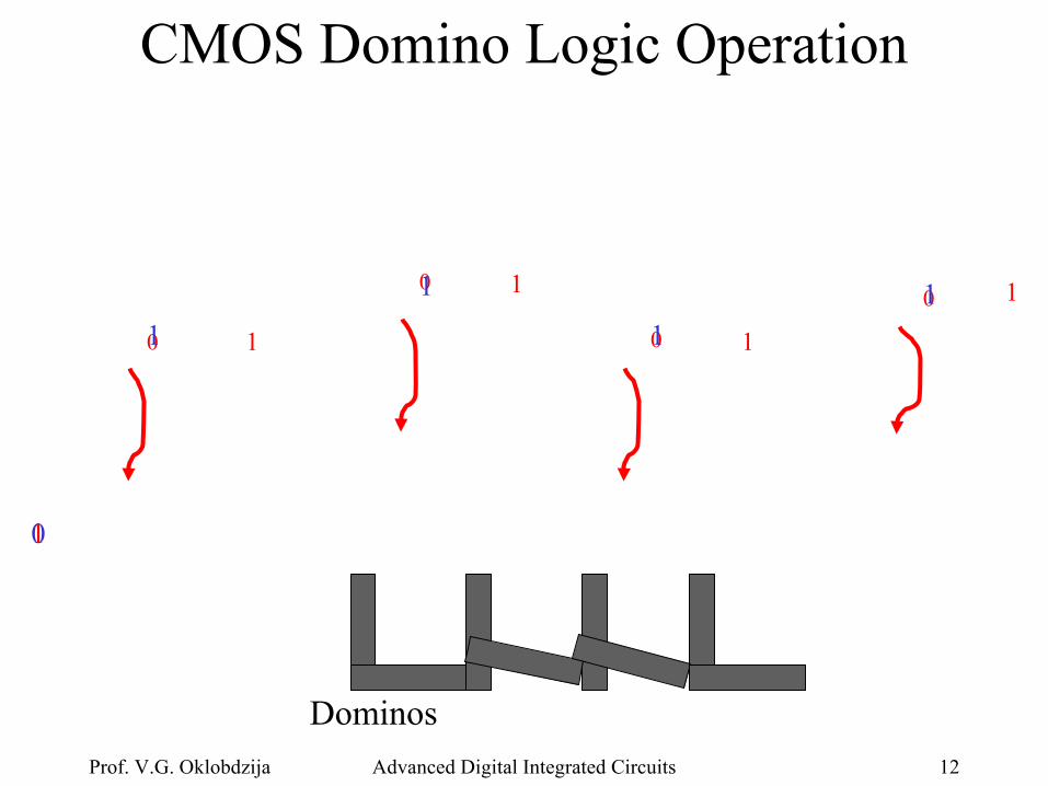
CMOS Domino Logic Operation
0 1
0 1
0 1
0 1
1
1
1
1
01
Dominos
Prof. V.G. Oklobdzija Advanced Digital Integrated Circuits 13
CMOS Domino Logic: Charge Re-Distribution
Prof. V.G. Oklobdzija Advanced Digital Integrated Circuits 14
Variations of CMOS Domino Logic:NORA Logic
Prof. V.G. Oklobdzija Advanced Digital Integrated Circuits 15
CVS and DCVS LogicIBM
(Heller et al. 1984)
Prof. V.G. Oklobdzija Advanced Digital Integrated Circuits 16
Cascode Voltage Switch Logic CVSIBM

Prof. V.G. Oklobdzija Advanced Digital Integrated Circuits 17
DCVS Logic (IBM)
Prof. V.G. Oklobdzija Advanced Digital Integrated Circuits 18
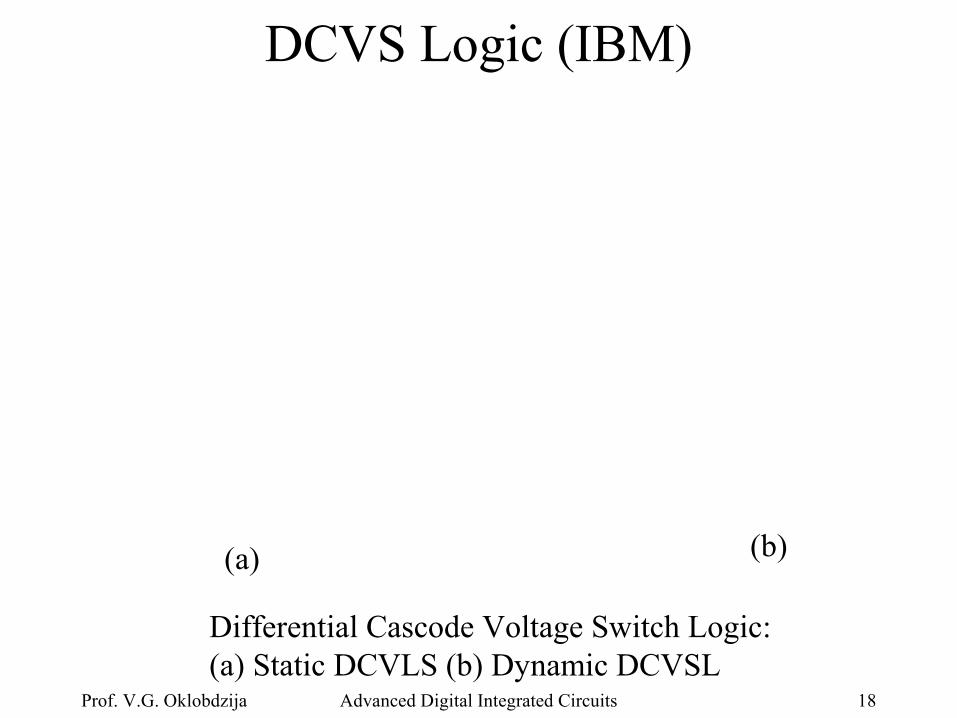
DCVS Logic (IBM)
Differential Cascode Voltage Switch Logic: (a) Static DCVLS (b) Dynamic DCVSL
(a) (b)
Prof. V.G. Oklobdzija Advanced Digital Integrated Circuits 19
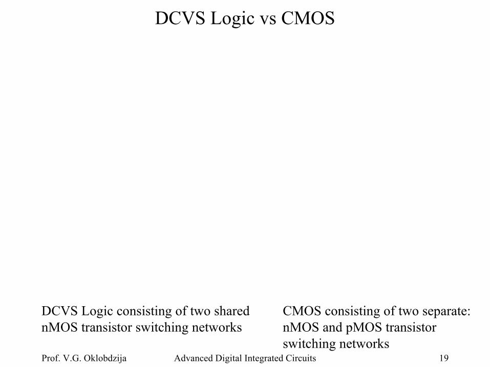
DCVS Logic vs CMOS
DCVS Logic consisting of two shared nMOS transistor switching networks
CMOS consisting of two separate: nMOS and pMOS transistor switching networks
Prof. V.G. Oklobdzija Advanced Digital Integrated Circuits 20
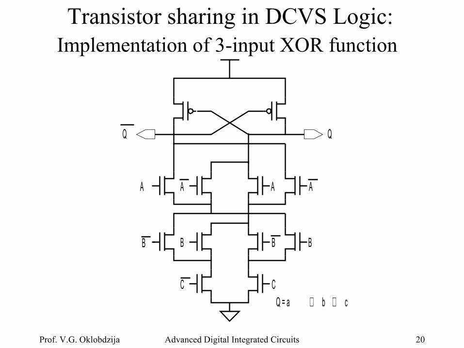
Transistor sharing in DCVS Logic: Implementation of 3-input XOR function
A A A A
B BB B
C C
Q Q
Q = a ⊕ b ⊕ c
Prof. V.G. Oklobdzija Advanced Digital Integrated Circuits 21
Switching Asymmetry in DCVSL
This asymmetry causes current spikes and increased power consumption !
Prof. V.G. Oklobdzija Advanced Digital Integrated Circuits 22
Pass-Transistor Logic
Prof. V.G. Oklobdzija Advanced Digital Integrated Circuits 23
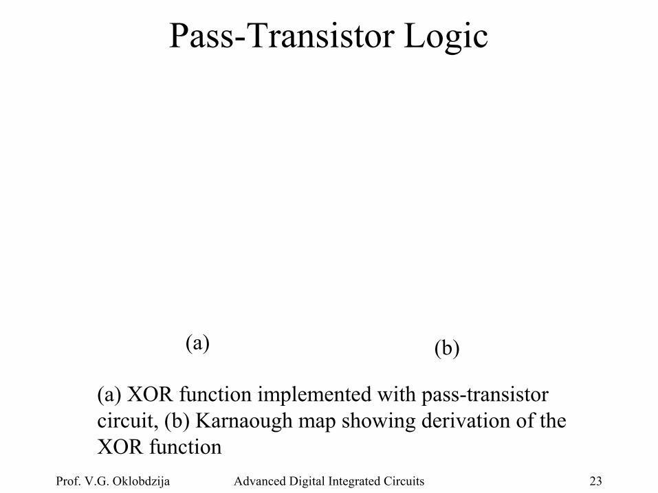
Pass-Transistor Logic
(a) XOR function implemented with pass-transistor circuit, (b) Karnaough map showing derivation of the XOR function
(a) (b)
Prof. V.G. Oklobdzija Advanced Digital Integrated Circuits 24
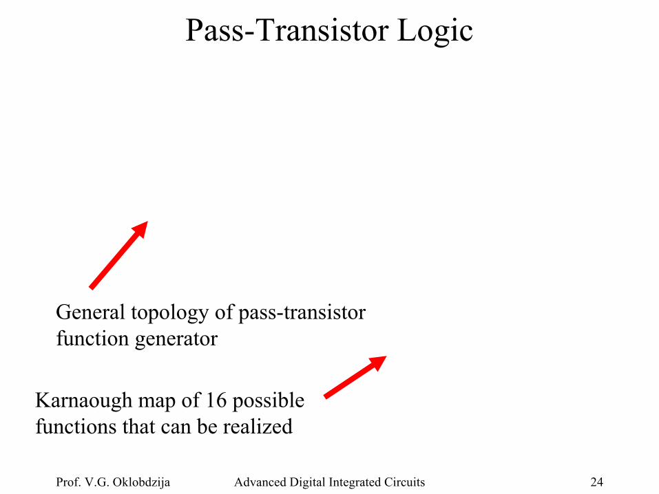
Pass-Transistor Logic
General topology of pass-transistor function generator
Karnaough map of 16 possible functions that can be realized
Prof. V.G. Oklobdzija Advanced Digital Integrated Circuits 25
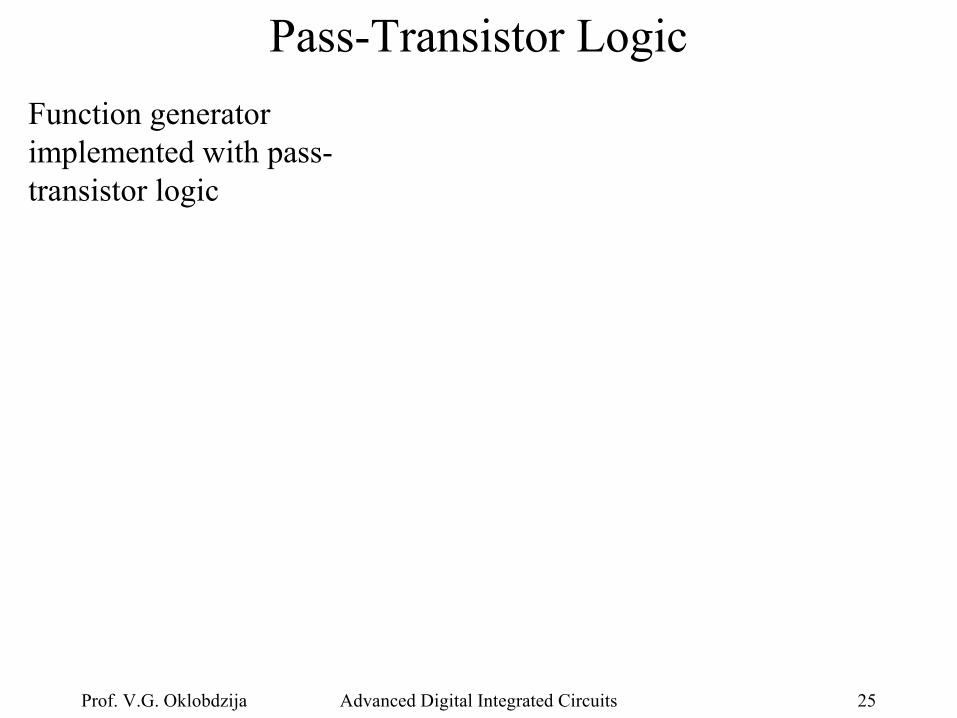
Pass-Transistor Logic
Function generator implemented with pass-transistor logic
Prof. V.G. Oklobdzija Advanced Digital Integrated Circuits 26
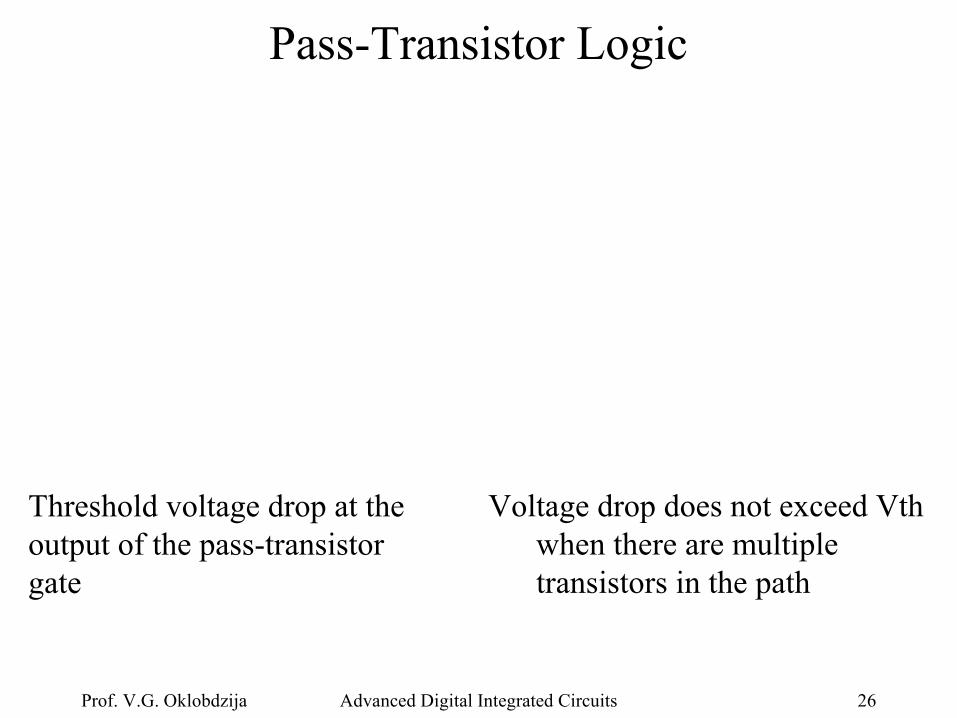
Pass-Transistor Logic
Voltage drop does not exceed Vth when there are multiple transistors in the path
Threshold voltage drop at the output of the pass-transistor gate

Prof. V.G. Oklobdzija Advanced Digital Integrated Circuits 27
Pass-Transistor Logic
Elimination of the threshold voltage drop by: (a) pairing nMOS transistor with a pMOS (b) using a swing-restoring inverter
Prof. V.G. Oklobdzija Advanced Digital Integrated Circuits 28
Complementary Pass-Transistor Logic (CPL)

Prof. V.G. Oklobdzija Advanced Digital Integrated Circuits 29
Basic logic functions in CPL A ABB
B
B
A ABB
B
B
A B
A B
A A
B
B
A A
A ABB
C
C
A B
A C B C
Prof. V.G. Oklobdzija Advanced Digital Integrated Circuits 30
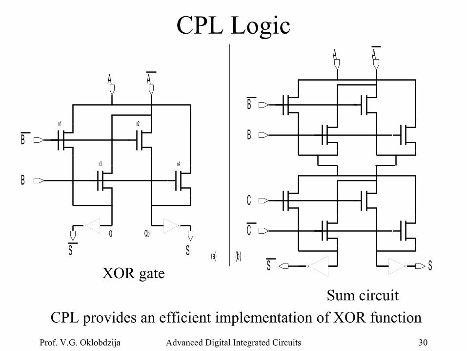
CPL Logic
AA
S S
A A
B
B
C
C
SS(a) (b)
B
B
Q Qb
n1 n2
n4n3
CPL provides an efficient implementation of XOR function
XOR gate
Sum circuit
Prof. V.G. Oklobdzija Advanced Digital Integrated Circuits 31
CPL Inverter
Prof. V.G. Oklobdzija Advanced Digital Integrated Circuits 32
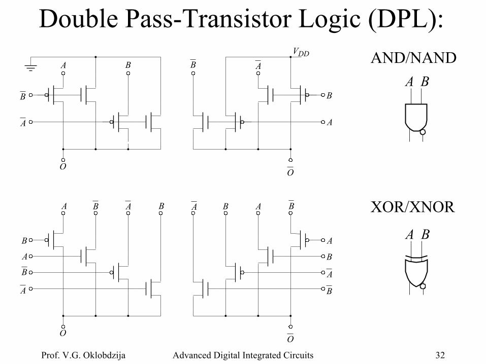
Double Pass-Transistor Logic (DPL):
A
B
A B B A
VDD
B
A
OO
A B
A
B
A B BA
B
A
OO
B
A
B A B A
B
A
A B
XOR/XNOR
AND/NAND
Prof. V.G. Oklobdzija Advanced Digital Integrated Circuits 33
Double Pass-Transistor Logic (DPL):
XOR
One bit full-adder: Sum circuit
Prof. V.G. Oklobdzija Advanced Digital Integrated Circuits 34
Double Pass-Transistor Logic (DPL):
The critical path traverses two transistors only (not counting the buffer)
DPL Full Adder

Prof. V.G. Oklobdzija Advanced Digital Integrated Circuits 35
Formal Method for CPL Logic DerivationMarkovic et al. 2000
(a) Cover the Karnaugh-map with largest possible cubes (overlapping allowed)
(b) Express the value of the function in each cube in terms of input signals
(c) Assign one branch of transistor(s) to each of the cubes and connect all the branches to one common node, which is the output of NMOS pass-transistor network
Prof. V.G. Oklobdzija Advanced Digital Integrated Circuits 36
Formal Method for P-T Logic Derivation
Complementary function can be implemented from the same circuit structure by applying complementarity principle:
Complementarity Principle: Using the same circuit topology, with pass signals inverted, complementary logic function is constructed in CPL.
By applying duality principle, a dual function is synthesized:
Duality Principle: Using the same circuit topology, with gate signals inverted, dual logic function is constructed.
Following pairs of basic functions are dual:AND-OR (and vice-versa)
NAND-NOR (and vice-versa)XOR and XNOR are self-dual (dual to itself)
Prof. V.G. Oklobdzija Advanced Digital Integrated Circuits 37
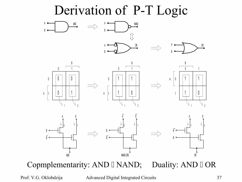
Derivation of P-T Logic
0 0
0 1
0 1
0
1A
B
L 1 L 2
B
B
AND
A B
L 2 L 1
1 1
1 0
0 1
0
1A
B
L 1 L 2
1 1
1 0
0 1
0
1
A
B
L 1 L 2
B
B
NAND (OR)
A B
L 2 L 1
B
B
OR
A B
L 1 L 2
B
A A
B
A
B
A
B
AND NAND
OR OR
Copmplementarity: AND NAND; Duality: AND OR
Prof. V.G. Oklobdzija Advanced Digital Integrated Circuits 38
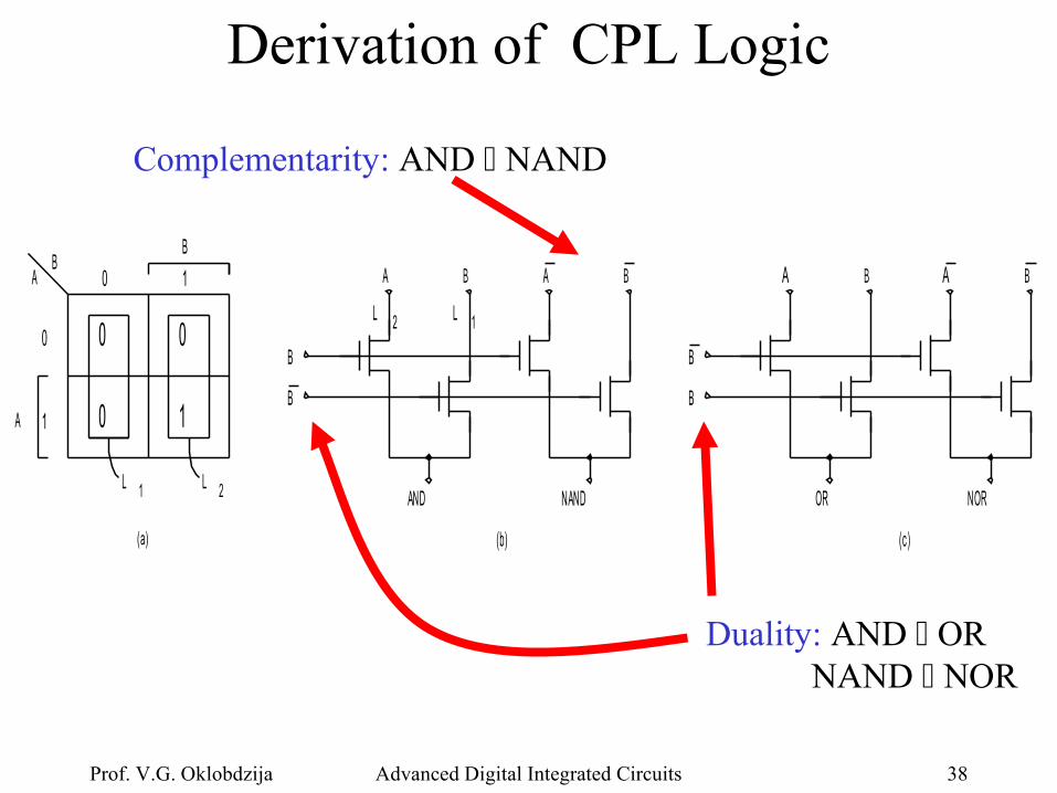
Derivation of CPL Logic
Duality: AND ORNAND NOR
0 0
0 1
BA 0 1
0
1A
B
L 1 L 2
(a)
B
B
AND
A A
B
B
OR NOR
A A
(c)
NAND
(b)
B B BB
L 2 L 1
Complementarity: AND NAND
Prof. V.G. Oklobdzija Advanced Digital Integrated Circuits 39
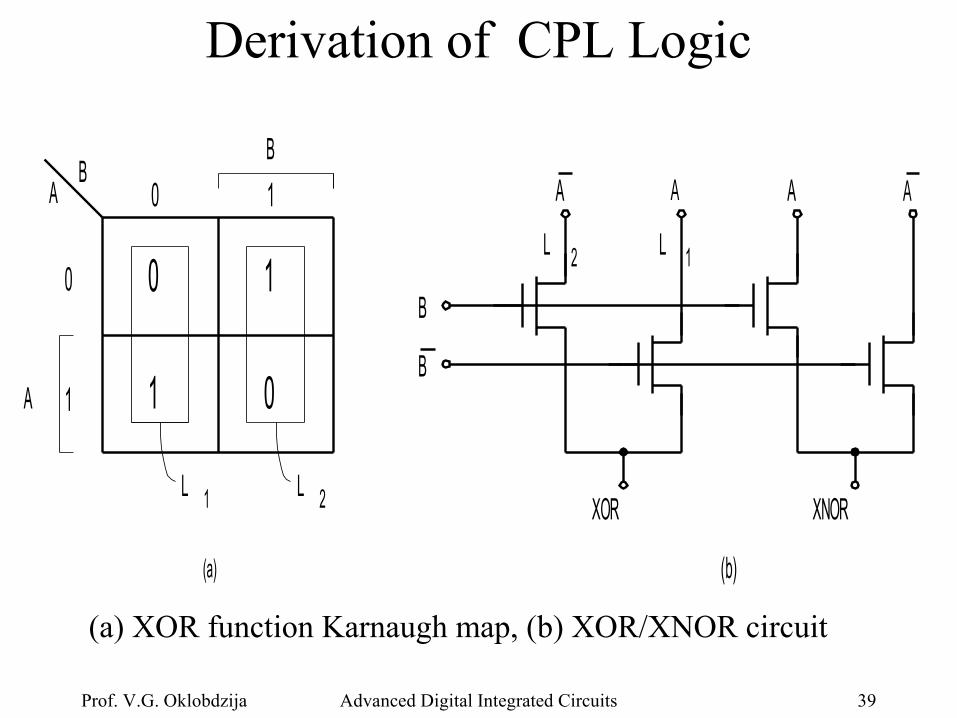
Derivation of CPL Logic
(a) XOR function Karnaugh map, (b) XOR/XNOR circuit
0 1
1 0
BA 0 1
0
1A
B
L 1 L 2
(a)
B
B
XOR
A A
XNOR
(b)
A A
L 2 L 1
Prof. V.G. Oklobdzija Advanced Digital Integrated Circuits 40
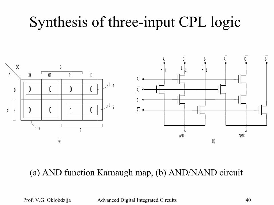
Synthesis of three-input CPL logic
0 0
0 0
BC
A 00 01
0
1A
C
L 3
L 2
(a)
A
B
AND
C
(b)
11 10
0 0
1 0
L 1
NAND
C
A
B
B
A B A B
L 3L 2L 1
(a) AND function Karnaugh map, (b) AND/NAND circuit
Prof. V.G. Oklobdzija Advanced Digital Integrated Circuits 41
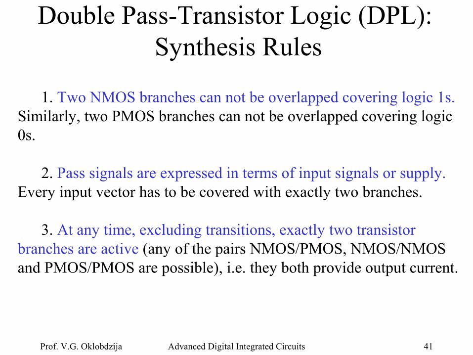
Double Pass-Transistor Logic (DPL): Synthesis Rules
1. Two NMOS branches can not be overlapped covering logic 1s. Similarly, two PMOS branches can not be overlapped covering logic 0s.
2. Pass signals are expressed in terms of input signals or supply. Every input vector has to be covered with exactly two branches.
3. At any time, excluding transitions, exactly two transistor branches are active (any of the pairs NMOS/PMOS, NMOS/NMOS and PMOS/PMOS are possible), i.e. they both provide output current.

Prof. V.G. Oklobdzija Advanced Digital Integrated Circuits 42
Double Pass-Transistor Logic (DPL): Synthesis Rules
Complementarity Principle: Complementary logic function in DPL is generated after the following modifications:
• Exchange PMOS and NMOS devices. Invert all pass and gate signals
Duality Principle: Dual logic function in DPL is generated
when:
• PMOS and NMOS devices are exchanged, and VDD and GND signals are exchanged.
Prof. V.G. Oklobdzija Advanced Digital Integrated Circuits 43
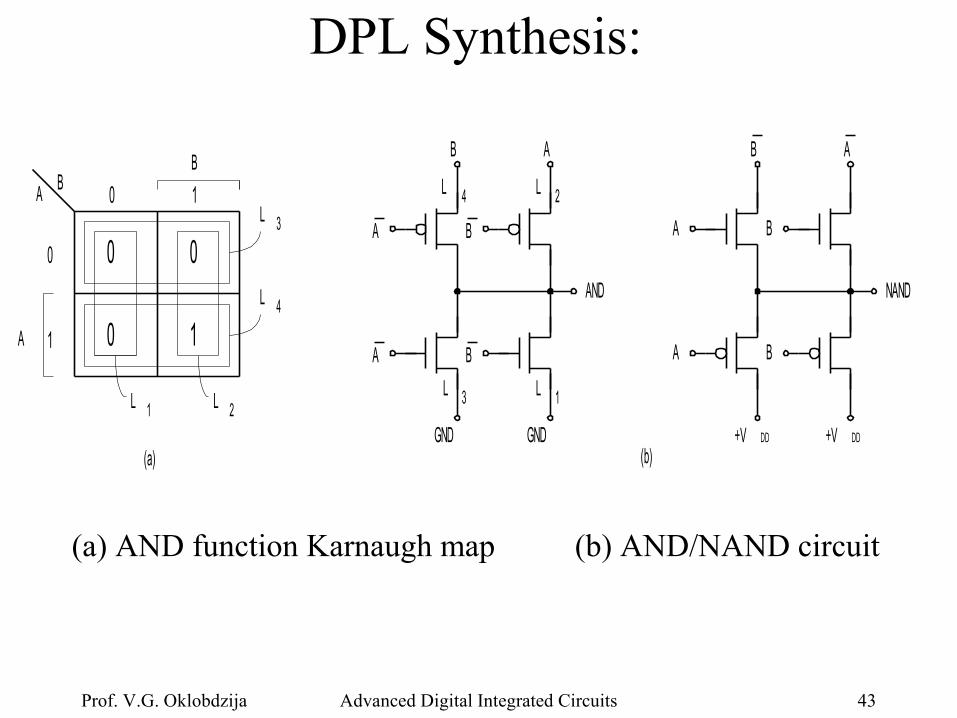
DPL Synthesis:
0 0
0 1
BA 0 1
0
1A
B
L 1 L 2
(a)
A B
B A
(b)
L
L
3
4
BA
GND GND
AND
A B
B A
BA
NAND
+V DD +V DD
L 2L 4
L 1L 3
(a) AND function Karnaugh map (b) AND/NAND circuit

Prof. V.G. Oklobdzija Advanced Digital Integrated Circuits 44
DPL Synthesis: OR/NOR circuit
A B
BA
B A
OR
A B
B A
BA
GND GND
NOR
+V DD +V DD

Prof. V.G. Oklobdzija Advanced Digital Integrated Circuits 45
DPL Synthesis:
0 0
0 1
BA 0 1
0
1A
B
L 1 L 2
(a)
A B
B A
(b)
L
L
3
4
BA
GND GND
AND
A B
B A
BA
NAND
+V DD +V DD
L 2L 4
L 1L 3
AND function Karnaugh map AND/NAND circuit
A B
BA
B A
OR
A B
B A
BA
GND GND
NOR
+V DD +V DD Duality Principle: PMOS and NMOS devices are exchanged, and VDD and GND signals are exchanged:AND ORNAND NOR
Complementarity Principle: Exchange PMOS and NMOS devices. Invert all pass and gate signalsAND NAND