Lecture 6: Combinational Logic Design: Dynamic Logic · Dynamic CMOS In static ... the logic levels...
26
ECE553 ECE553 1 Reading: CH 6.3 & 6.4 Lecture 6: Combinational Logic Design: Dynamic Logic
Transcript of Lecture 6: Combinational Logic Design: Dynamic Logic · Dynamic CMOS In static ... the logic levels...

ECE553 ECE553 1
Reading: CH 6.3 & 6.4
Lecture 6: Combinational Logic Design: Dynamic Logic

ECE553 ECE553
Dynamic CMOS In static circuits at every point in time (except
when switching) the output is connected to either GND or VDD via a low resistance path. l fan-in of n requires 2n (n N-type + n P-type) devices
Dynamic circuits rely on the temporary storage of signal values on the capacitance of high impedance nodes. l requires on n + 2 (n+1 N-type + 1 P-type) transistors l caps are left floating at times; noise sensitive
2

ECE553 ECE553
Dynamic Gate
3
In1
In2 PDN
In3
Me
Mp
Clk
Clk
Out CL
Out
Clk
Clk
A
B
C
Mp
Me
Two phase operation Precharge (CLK = 0) Evaluate (CLK = 1)
Clock +

ECE553 ECE553
Dynamic Gate
4
In1
In2 PDN
In3
Me
Mp
Clk
Clk
Out CL
Out
Clk
Clk
A
B
C
Mp
Me
Two phase operation Precharge (CLK = 0) Evaluate (CLK = 1)
on
off
1
off
on
((AB)+C)

ECE553 ECE553
Conditions on Output Once the output of a dynamic gate is
discharged, it cannot be charged again until the next precharge operation. Inputs to the gate can make at most one
transition during evaluation. Output can be in the high impedance state
during and after evaluation (PDN off), state is stored on CL
5

ECE553 ECE553
Properties of Dynamic Gates Logic function is implemented by the PDN only
l number of transistors is N + 2 (versus 2N for static complementary CMOS)
Full swing outputs (VOL = GND and VOH = VDD) Non-ratioed sizing of the devices does not affect
the logic levels Faster switching speeds (1.5-2X vs. static CMOS)
l reduced load capacitance due to lower input capacitance (Cin) l reduced load capacitance due to smaller output loading (Cout) l NMOS only, faster devices (optimize for one transition direction) l no Isc, so all the current provided by PDN goes into discharging CL
6

ECE553 ECE553
Properties of Dynamic Gates Overall power dissipation usually higher than static
CMOS dynamic power !!! l no static current path ever exists between VDD and GND
(including Psc) l no glitching l higher transition probabilities l extra load on Clk l Smaller devices (caps) helps reduce impact
PDN starts to work as soon as the input signals exceed VTn, so VM, VIH and VIL equal to VTn l Small low noise margin (NML) VTn
Needs a precharge/evaluate clock 7

ECE553 ECE553
Issues in Dynamic Design 1: Charge Leakage
8
CL
Clk
Clk
Out
A
Mp
Me
Leakage sources
CLK
VOut
Precharge
Evaluate
Dominant component is subthreshold current of M1
M1
Require a minimal clock rate ~ a few kHz (not good for low-performance circuit)

ECE553 ECE553
Solution to Charge Leakage
9
CL
Clk
Clk
Me
Mp
A
B
Out
Mkp
• Same approach as level restorer for pass-transistor logic • Psc during swithing when PDN and keeper are both on
Keeper Need to be small
Fight between the keeper and PDN

ECE553 ECE553
Issues in Dynamic Design 2: Charge Sharing
10
CL
Clk
Clk
CA
CB
B=0
A
Out Mp
Me
Charge stored originally on CL is redistributed (shared) over CL and CA leading to reduced robustness
To avoid: 1) Precharge internal nodes
adds delay 2) Add a feedback (keeper)
device
Ma

ECE553 ECE553
Charge Sharing
11
B = 0
Clk
X
C L
C a
C b
A
Out M p
M a
V DD
M b
Clk M e
on
off
case 1) if ΔVout <VTn : VX =VDD −VTn (VX )CLVDD = CLVout (final) + Ca[VDD −VTn (VX )]or
ΔVout =Vout (final)+ (−VDD ) = − Ca
CL
[VDD −VTn (VX )]
case 2) if ΔVout >VTn :Vout = VX
ΔVout = −VDDCa
Ca +CL
⎛⎝⎜
⎞⎠⎟

ECE553 ECE553
Solution to Charge Redistribution (sharing)
12
Clk
Clk
Me
Mp
A
B
Out Mkp
Clk
Precharge internal nodes using a clock-driven transistor (at the cost of increased area and power)

ECE553 ECE553
Issues in Dynamic Design 3: Backgate Coupling (output-to-input coupling)
13
CL1
Clk
Clk
B=0
A=0
Out1 Mp
Me
Out2
CL2 In
Dynamic NAND Static NAND
=1 = H à L
Out1 decrease

ECE553 ECE553
Issues in Dynamic Design 4: Clock Feedthrough
14
CL
Clk
Clk
B
A
Out Mp
Me
Coupling between Out and Clk input of the precharge device due to the gate to drain capacitance. So voltage of Out can rise above VDD (or below GND). The fast rising (and falling edges) of the clock couple to Out.

ECE553 ECE553
Backgate Coupling & Clock feedthrough
-1
0
1
2
3
0 2 4 6
15
Volta
ge
Time, ns
Clk
In
Out1
Out2
Backgate coupling Clock feedthrough
(Out2 does not drop to GND)

ECE553 ECE553
Clock Feedthrough
16
-0.5
0.5
1.5
2.5
0 0.5 1
Clk
Clk
In1
In2
In3
In4
Out
In & Clk
Out
Time, ns
Volta
ge
Clock feedthrough (L H)
Clock feedthrough (HL)

ECE553 ECE553
Other Effects
Capacitive coupling
Substrate coupling
Minority charge injection
Supply noise (ground bounce)
17

ECE553 ECE553
Cascading Dynamic Gates
18
Clk
Clk
Out1
In
Mp
Me
Mp
Me
Clk
Clk
Out2
V
t
Clk
In
Out1
Out2 ΔV
VTn
Setting all inputs of the 2nd gate to ‘0’ during precharge will fix it è Only 0 à 1 transitions allowed at inputs!
1 0 transition
Straightforward cascading of dynamic gates does not work!
1 0 1 1
Race b/w clk and out1
ECE553 ECE553
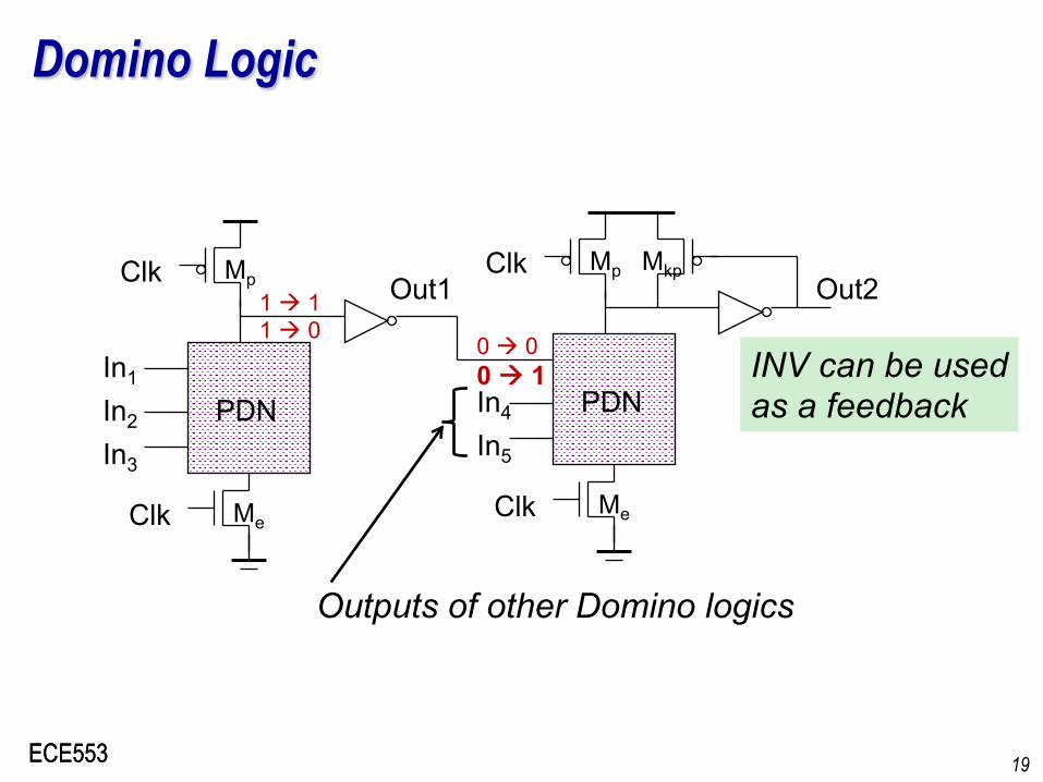
Domino Logic
19
In1
In2 PDN
In3
Me
Mp
Clk
Clk Out1
In4 PDN
In5
Me
Mp
Clk
Clk Out2
Mkp
1 à 1 1 à 0
0 à 0 0 1
Outputs of other Domino logics
INV can be used as a feedback

ECE553 ECE553
Why Domino? and Properties
20
Clk
Clk
Ini PDN Inj
Ini Inj
PDN Ini PDN Inj
Ini PDN Inj
Like falling dominos!
Only non-inverting logic can be implemented Very high speed (tpHL 0)
l static inverter can be skewed, only L-H transition l Input capacitance reduced – smaller logical effort
0 à 0 0 à 1 0 or 1 0 or 1
0 or 1

ECE553 ECE553
Designing with Domino Logic
21
M p
M e
V DD
PDN
Clk
In 1 In 2 In 3
Out1
Clk
M p
M e
V DD
PDN
Clk
In 4
Clk
Out2
M r
V DD
Inputs = 0 during precharge
Can be eliminated!

ECE553 ECE553
Footless Domino
22
• The first gate in the chain needs a foot switch • Precharge is rippling (critical path)
à both PDN, PUN are on (fighting)à short-circuit current • A solution is to delay the clock for each stage or put
evaluation NMOS always.
VDD
Clk MpOut1
In1
1 0
VDD
Clk MpOut2
In2
VDD
Clk MpOutn
InnIn3
1 0
0 1 0 1 0 1
1 0 1 0
Precharge device is fighting the PDN
0

ECE553 ECE553
Differential (Dual Rail) Domino
23
A
B
Me
Mp
Clk
Clk Out = AB
!A !B
Mkp Clk
Out = AB
Mkp Mp
Solves the problem of non-inverting logic But, expensive: double the # of transistors
1 0 1 0
on off

ECE553 ECE553
np-CMOS (aka Zipper logic)
24
In1
In2 PDN
In3
Me
Mp
Clk
Clk Out1
In4 PUN
In5
Me
Mp Clk
Clk
Out2 (to PDN)
1 à 1 1 à 0
0 à 0 0 à 1
Only 0 à 1 transitions allowed at inputs of PDN Only 1 à 0 transitions allowed at inputs of PUN è Requires extra area to balance PDN and PUN delay
From PUN
NO conditional discharge

ECE553 ECE553
NORA (NO RAcing) Logic
25
In1
In2 PDN
In3
Me
Mp
Clk
Clk Out1
In4 PUN
In5
Me
Mp Clk
Clk
Out2 (to PDN)
1 à 1 1 à 0
0 à 0 0 à 1
to other PDN’s
to other PUN’s
WARNING: Very sensitive to noise!: à All inputs are dynamic (capacitance) during evaluation

ECE553 ECE553
Summary of Dynamic Gates
26
Require fewer #of transistors than Static (N+2 vs. 2N) Require clock and PDN (NMOS) network only Two phase operation:
l precharge evaluation
Dynamic gates provide speed benefits l Smaller area, smaller parasitic capacitance
BUT: l Add complexity l Worsen power (most dynamic power) l Worsen noise immunity (leakage, charge sharing, coupling, etc…)