dsPIC30F Data Sheet
350
2002 Microchip Technology Inc. Advance Information DS70032B dsPIC30F Data Sheet High Performance Digital Signal Controllers M
Transcript of dsPIC30F Data Sheet
2002 Microchip Technology Inc. Advance Information DS70032B
dsPIC30FData Sheet
High Performance
Digital Signal Controllers
M
Note the following details of the code protection feature on PICmicro® MCUs.
• The PICmicro family meets the specifications contained in the Microchip Data Sheet.• Microchip believes that its family of PICmicro microcontrollers is one of the most secure products of its kind on the market today,
when used in the intended manner and under normal conditions.• There are dishonest and possibly illegal methods used to breach the code protection feature. All of these methods, to our knowl-
edge, require using the PICmicro microcontroller in a manner outside the operating specifications contained in the data sheet. The person doing so may be engaged in theft of intellectual property.
• Microchip is willing to work with the customer who is concerned about the integrity of their code.• Neither Microchip nor any other semiconductor manufacturer can guarantee the security of their code. Code protection does not
mean that we are guaranteeing the product as “unbreakable”.• Code protection is constantly evolving. We at Microchip are committed to continuously improving the code protection features of
our product.
If you have any further questions about this matter, please contact the local sales office nearest to you.
Information contained in this publication regarding deviceapplications and the like is intended through suggestion onlyand may be superseded by updates. It is your responsibility toensure that your application meets with your specifications.No representation or warranty is given and no liability isassumed by Microchip Technology Incorporated with respectto the accuracy or use of such information, or infringement ofpatents or other intellectual property rights arising from suchuse or otherwise. Use of Microchip’s products as critical com-ponents in life support systems is not authorized except withexpress written approval by Microchip. No licenses are con-veyed, implicitly or otherwise, under any intellectual propertyrights.
DS70032B - page ii Advance Info
Trademarks
The Microchip name and logo, the Microchip logo, FilterLab,KEELOQ, MPLAB, PIC, PICmicro, PICMASTER, PICSTART,PRO MATE, SEEVAL and The Embedded Control SolutionsCompany are registered trademarks of Microchip TechnologyIncorporated in the U.S.A. and other countries.
dsPIC, ECONOMONITOR, FanSense, FlexROM, fuzzyLAB,In-Circuit Serial Programming, ICSP, ICEPIC, microID,microPort, Migratable Memory, MPASM, MPLIB, MPLINK,MPSIM, MXDEV, PICC, PICDEM, PICDEM.net, rfPIC, SelectMode and Total Endurance are trademarks of MicrochipTechnology Incorporated in the U.S.A.
Serialized Quick Term Programming (SQTP) is a service markof Microchip Technology Incorporated in the U.S.A.
All other trademarks mentioned herein are property of theirrespective companies.
© 2002, Microchip Technology Incorporated, Printed in theU.S.A., All Rights Reserved.
Printed on recycled paper.
rmation 2002 Microchip Technology Inc.
Microchip received QS-9000 quality system certification for its worldwide headquarters, design and wafer fabrication facilities in Chandler and Tempe, Arizona in July 1999. The Company’s quality system processes and procedures are QS-9000 compliant for its PICmicro® 8-bit MCUs, KEELOQ® code hopping devices, Serial EEPROMs and microperipheral products. In addition, Microchip’s quality system for the design and manufacture of development systems is ISO 9001 certified.
M dsPIC30FdsPIC30F Enhanced FLASH 16-bit Microcontrollers
High Performance Modified RISC CPU:
• Modified Harvard architecture• C compiler optimized instruction set architecture
• 89 base instructions• 24-bit wide instructions, 16-bit wide data path• Linear program memory addressing up to 4M
Instruction Words• Linear data memory addressing up to 64 Kbytes• Up to 144 Kbytes on-chip FLASH program space
- Up to 48K Instruction Words• Up to 8 Kbytes of on-chip data RAM• Up to 4 Kbytes of non-volatile data EEPROM
• 16 x 16-bit working register array• Three Address Generation Units that enable:
- Dual data fetch- Accumulator write back for DSP operations
• Flexible addressing modes supporting:- Indirect, Modulo and Bit-Reversed modes
• Two, 40-bit wide accumulators with optional saturation logic
• 16-bit x 16-bit single cycle hardware fractional/integer multiplier
• Single cycle Multiply-Accumulate (MAC) operation• 40-stage Barrel Shifter• Up to 30 MIPS operation:
- DC to 40 MHz external clock input- 4 MHz - 10 MHz oscillator input with PLL
active (4x, 8x, 16x)• Up to 45 interrupt sources
- 8 user selectable priority levels• Vector table with up to 62 vectors
- 54 interrupt vectors- 8 processor exceptions and software traps
Peripheral Features:
• High current sink/source I/O pins: 25 mA/25 mA• Up to 5 external interrupt sources• Timer module with programmable prescaler:
- Up to five 16-bit timers/counters; optionally pair up 16-bit timers into 32-bit timer modules
• 16-bit Capture Input functions• 16-bit Compare/PWM Output functions
- Dual Compare mode available• Data Converter Interface (DCI), supports common
audio CODEC protocols including I2S and AC’97
Peripheral Features (Continued):
• 3-wire SPITM modules (supports 4 frame modes)• I2CTM module supports Multi-Master/Slave mode
and 7-bit/10-bit addressing• Addressable UART modules supporting:
- Interrupt on address bit- Wake-up on START bit- 4 characters deep TX and RX FIFO buffers
• CAN bus modules
Motor Control PWM Module Features:
• Up to 8 PWM output channels- Complementary or Independent Output
modes- Edge and Center Aligned modes
• 4 duty cycle generators • Dedicated time-base with 4 modes• Programmable output polarity• Dead-time control for Complementary mode• Manual output control• Trigger for A/D conversions
Quadrature Encoder Interface Module Features:
• Phase A, Phase B and Index Pulse input• 16-bit up/down position counter • Count direction status• Position measurement (x2 and x4) mode
• Programmable digital noise filters on inputs• Alternate 16-bit Timer/Counter mode• Interrupt on position counter rollover/underflow
Input Capture Module Features:
• Captures 16-bit timer value
- Capture every 1st, 4th or 16th rising edge- Capture every falling edge- Capture every rising and falling edge
• Resolution of 33 ns at 30 MIPS • Timer2 or Timer3 time-base selection• Input Capture during IDLE
• Interrupt on input capture event
2002 Microchip Technology Inc. Advance Information DS70032B-page 1
dsPIC30F
Analog Features:
• 12-bit or 10-bit Analog-to-Digital Converter (A/D) with:
- 100 Ksps (for 12-bit A/D) or 500 Ksps (for 10-bit A/D) conversion rate
- Up to 16 input channels- Conversion available during SLEEP and IDLE
• Programmable Low Voltage Detection (PLVD)
• Programmable Brown-out Detection and RESET generation
Special Microcontroller Features:
• Enhanced FLASH program memory
- 100,000 erase/write cycle (typical) for industrial temperature range
• Data EEPROM memory - 1,000,000 erase/write cycle (typical)
industrial temperature range- Data EEPROM Retention > 20 years
• Self-reprogrammable under software control• Power-on Reset (POR), Power-up Timer (PWRT)
and Oscillator Start-up Timer (OST)• Flexible Watchdog Timer (WDT) with on-chip low
power RC Oscillator for reliable operation• Fail safe clock monitor operation
- Detects clock failure and switches to on-chip low power RC oscillator
• Programmable code protection• In-Circuit Serial Programming™ (ICSP™) via 3
pins and power/ground• Selectable Power Management modes
- SLEEP, IDLE and Alternate Clock modes
CMOS Technology:
• Low power, high speed FLASH technology• Wide operating voltage range (2.5V to 5.5V)• Industrial and Extended temperature ranges• Low power consumption
2002 Microchip Technology Inc. Advance Information DS70032B-page 2
dsPIC30F
dsPIC30F Sensor Processor Family
Pin Diagrams
Device PinsProgram Memory
SRAM Bytes
EEPROMBytes
Timer 16-bit
Input Cap
Output Comp/Std PWM
A/D 12-bit 100 Ksps U
AR
T
SP
ITM
I2 CT
M
Bytes Instructions
dsPIC30F2011 18 12K 4K 1024 0 3 2 2 8 ch 1 1 1
dsPIC30F3012 18 24K 8K 2048 1024 3 2 2 8 ch 1 1 1
dsPIC30F2012 28 12K 4K 1024 0 3 2 2 10 ch 1 1 1
dsPIC30F3013 28 24K 8K 2048 1024 3 2 2 10 ch 2 1 1
dsP
IC30F
XX
XX
AN7/IC2/OC2/RB7
MCLR
AVDD
AVSS
AN0/VREF+/CN2/RB0Vss
AN1/VREF-/CN3/RB1AN3/CN5/RB3
IC1/OC1/RD8
SOSC1/T1CK/U1ARX/CN0/RC14
VDD
AN6/SCK1/INT0/OCFA/RB6
SOSC2/T2CK/U1ATX/CN1/RC13
OSC2/CLKO/RC15OSC1/CLKIN
AN5/U1RX/SDI1/SDA/CN7/RB5AN4/U1TX/SDO1/SCL/CN6/RB4
123456789
181716151413121110 AN2/SS1/CN4/RB2
18-Pin SOIC and PDIP
Note: Pinout subject to change.
Part No.: 30F2011 / 30F3012
MCLR
VSS
VDD
AN0/VREF+/CN2/RB0AN1/VREF-/CN3/RB1
AVDDAVSS
AN2/SS1/CN4/RB2
IC2/INT2/RD9 IC1/INT1/RD8
SOSC1/T1CK/U1ARX/CN0/RC14SOSC2/T2CK/U1ATX/CN1/RC13
VSSOSC2/CLKO/RC15OSC1/CLKIN VDD
SCK1/INT0/RF6
U1RX/SDI1/SDA/RF2U1TX/SDO1/SCL/RF3
AN5/CN7/RB5AN4/CN6/RB4AN3/CN5/RB3
1234567891011121314
2827262524232221201918171615
AN6/OCFA/RB6AN7/RB7AN8/OC1/RB8AN9/OC2/RB9U2RX/RF4U2TX/RF5
28-Pin SDIP
Note: Pinout subject to change.
dsP
IC30F
XX
XX
Part No.: 30F2012 / 30F3013
2002 Microchip Technology Inc. Advance Information DS70032B-page 3
dsPIC30F
dsPIC30F Power Conversion and Motion Control Family
Pin Diagrams
Device PinsProgram
Mem. Bytes/Instructions
SRAMBytes
EEPROMBytes
Timer 16-bit
InputCap
Output Comp/Std
PWM
Motor Control
PWM
A/D 10-bit 500 Ksps
Quad Enc U
AR
T
SP
ITM
I2 CT
M
CA
N
dsPIC30F2010 28 12K/4K 512 1024 3 4 2 6 ch 6 ch Yes 1 1 1 -
dsPIC30F3010 28 24K/8K 1024 1024 5 4 2 6 ch 6 ch Yes 1 1 1 -
dsPIC30F4012 28 48K/16K 2048 1024 5 4 2 6 ch 6 ch Yes 1 1 1 1
dsPIC30F3011 40/44 24K/8K 1024 1024 5 4 4 6 ch 9 ch Yes 2 1 1 -
dsPIC30F4011 40/44 48K/16K 2048 1024 5 4 4 6 ch 9 ch Yes 2 1 1 1
dsPIC30F4010 64 36K/12K 2048 1024 5 8 8 8 ch 16 ch Yes 2 2 1 1
dsPIC30F5010 64 96K/32K 4096 2048 5 8 8 8 ch 16 ch Yes 2 2 1 2
dsPIC30F6010 80 144K/48K 8192 4096 5 8 8 8 ch 16 ch Yes 2 2 1 2
MCLR
PWM0/RE0PWM1/RE1PWM2/RE2PWM3/RE3PWM4/RE4PWM5/RE5VSS
VDD
AN0/VREF+/CN2/RB0AN1/VREF-/CN3/RB1
AVDDAVSS
AN2/SS1/CN4/RB2
OC2/IC2/INT2/RD1 OC1/IC1/INT1/RD0
SOSC1/T1CK/U1ARX/CN0/RC14SOSC2/T2CK/U1ATX/CN1/RC13
VSSOSC2/CLKO/RC15OSC1/CLKIN VDD
FLTA/INT0/SCK1/OCFA/RE8
U1RX/SDI1/SDA/C1RX/RF2U1TX/SDO1/SCL/C1TX/RF3
AN5/QEB/IC8/CN7/RB5AN4/QEA/IC7/CN6/RB4
AN3/INDX/CN5/RB3
1234567891011121314
2827262524232221201918171615
28-Pin SDIP
Note: Pinout subject to change.
dsP
IC30F
XX
XX
Part No.: 30F2010 / 30F3010 / 30F4012
AN7/RB7AN6/OCFA/RB6
C1RX/RF0C1TX/RF1
OC3/RD2OC1/IC1/ INT1/RD0
AN8/RB8
1234567891011121314151617181920
4039383736353433323130292827262524232221
dsP
IC30F
XX
XX
MCLR
VDDVSS
AN0/VREF+/CN2/RB0AN1/VREF-/CN3/RB1
AN2/SS1/CN4/RB2
OC2/IC2/ INT2/RD1
SOSC1/T1CK/U1ARX/CN0/RC14SOSC2/T2CK/U1ATX/CN1/RC13
OSC2/CLKO/RC15OSC1/CLKIN
AN5/QEB/IC8/CN7/RB5AN4/QEA/IC7/CN6/RB4
AN3/INDX/CN5/RB3
PWM0/RE0PWM1/RE1PWM2/RE2PWM3/RE3
PWM5/RE5
AVDDAVSS
OC4/RD3
VSSVDD
SCK1/RF6
U1RX/SDI1/SDA/RF2U1TX/SDO1/SCK/RF3
PWM4/RE4
VSS VDD
U2RX/RF4U2TX/RF5
FLTA/INT0/RE8
40-Pin PDIP
Note: Pinout subject to change.
Part No.: 30F3011 / 30F4011
2002 Microchip Technology Inc. Advance Information DS70032B-page 4
dsPIC30F
Pin Diagrams (Cont.)
1011
23456
1
18 19 20 21 2212 13 14 15
38
87
44 43 42 41 40 39
16 172930313233
232425262728
36 3435
9
37
U1T
X/S
DO
1/SC
L/RF
3S
CK
1/TC
1/RF
6O
C1/IC
1/INT
1/RD
0O
C3/R
D2
VD
D
SO
SC
1/T1C
K/U
1AR
X/C
N0/R
C14
NC
VS
S
OC
4/RD
3O
C2/IC
2/INT
2/RD
1F
LTA/IN
T0/R
E8
AN
3/IN
DX
/CN
5/R
B3
AN
2/S
S1/
CN
4/R
B2
AN
1/V
RE
F-/
CN
3/R
B1
AN
0/V
RE
F+
/CN
2/R
B0
MC
LRN
CA
VD
D
AV
SS
PW
M0/
RE
0P
WM
1/R
E1
PW
M2/
RE
2
PWM3/RE3PWM4/RE4PWM5/RE5VDD
VSS
NCC1RX/RF0C1TX/RF1U2RXRF4U2TX/RF5U1RX/SDI1/SDA/RF2
AN4/QEA/IC7/CN6/RB4AN5/QEB/IC8/CN7/RB5
AN6/OCFA/RB6AN7/RB7AN8/RB8
NCVDD
VSS
OSC1/CLKINOSC2/CLKO/RC15
SOSC2/T2CK/U1ATX/CN1/RC13
dsPIC30FXXXX
44-Pin TQFP
Note: Pinout subject to change.
Part No.: 30F3011 / 30F4011
2002 Microchip Technology Inc. Advance Information DS70032B-page 5
dsPIC30F
Pin Diagrams (Cont.)
12345678910111213 36
353433
32313029282726
64 63 62 61 60 59 58 57 56
141516
17 18 19 20 21 22 23 24 25
SOSC1/T1CK/CN0/RC14SOSC2/T4CK/CN1/RC13OC1/RD0IC4/INT4/RD11
IC2/FLTB/INT2/RD9IC1/FLTA/INT1/RD8VSS
OSC2/CLKO/RC15OSC1/CLKINVDD
SCL/RG2
SCK1/INT0/RF6U1RX/SDI1/RF2U1TX/SDO1/RF3
PWM5/RE5PWM6/RE6PWM7/RE7
SCK2/CN8/RG6SDI2/CN9/RG7
SDO2/CN10/RG8MCLR
VSS
VDD
AN3/INDX/CN5/RB3 AN2/SS1/CN4/RB2 AN1/VREF-/CN3/RB1AN0/VREF+/CN2/RB0
OC
8/C
N16
/UP
DN
/RD
7
PW
M4/
RE
4P
WM
3/R
E3
PW
M2/
RE
2
VS
S
PW
M0/
RE
0C
1TX
/RF
1
PW
M1/
RE
1
OC
2/R
D1
OC
3/R
D2
AN
6/O
CFA
/RB
6A
N7/
RB
7A
VD
D
AV
SS
AN
8/R
B8
AN
9/R
B9
AN
10/R
B10
AN
11/R
B11
VS
S
VD
D
AN
12/R
B12
AN
13/R
B13
AN
14/R
B14
AN
15/C
N12
/OC
FB
/RB
15
U2T
X/C
2TX
/CN
18/R
F5
U2R
X/C
2RX
/CN
17/R
F4
SDA/RG3
43424140393837
44
484746
50 495154 53 5255
45
SS2/CN11/RG9
AN5/QEB/IC8/CN7/RB5AN4/QEA/IC7/CN6/RB4
IC3/INT3/RD10
VD
D
C1R
X/R
F0
OC
4/R
D3
OC
7/C
N15
/RD
6O
C6/
IC6/
CN
14/R
D5
OC
5/IC
5/C
N13
/RD
4
64-Pin TQFP
Note: Pinout subject to change.
dsPIC30FXXXX
Part No.: 30F4010 / 30F5010
2002 Microchip Technology Inc. Advance Information DS70032B-page 6
dsPIC30F
Pin Diagrams (Cont.)
72
74
73
71
70
69
68
67
66
65
64
63
62
61
20
2
3
4
5
6
7
8
9
10
11
12
13
14
15
16
50
49
48
47
46
45
44
21
41
4039383736353423 24 25 26 27 28 29 30 31 32 33dsPIC30FXXXX
17
18
19
75
1
57
56
55
54
53
52
51
60
59
58
43
42
76
78
77
79
2280
IC5/
RD
12O
C4/
RD
3
OC
3/R
D2
OC
2/R
D1
PW
M2/
RE
2P
WM
1/R
E1
PW
M0/
RE
0
C2R
X/R
G0
C2T
X/R
G1
C1T
X/R
F1
C1R
X/R
F0
PW
M4/
RE
4
PW
M3/
RE
3
OC
8/C
N16
/UP
DN
/RD
7
OC
6/C
N14
/RD
5
OC1/RD0
IC4/RD11
IC2/RD9
IC1/RD8
INT4/RA15
IC3/RD10
INT3/RA14VSS
OSC1/CLKIN
VDD
SCL/RG2
U1RX/RF2
U1TX/RF3
SOSC1/T1CK/CN0/RC14
SOSC2/CN1/RC13V
RE
F+
/RA
10
VR
EF-/
RA
9
AV
DD
AV
SS
AN
8/R
B8
AN
9/R
B9
AN
10/R
B10
AN
11/R
B11
VD
D
U2R
X/C
N17
/RF
4
IC8/
CN
21/R
D15
U2T
X/C
N18
/RF
5
AN
6/O
CFA
/RB
6
AN
7/R
B7
PWM7/RE7
T2CK/RC1
T4CK/RC3
SCLK2/CN8/RG6
SDI2/CN9/RG7
SDO2/CN10/RG8
MCLR
SS2/CN11/RG9
AN4/QEA/CN6/RB4AN3/INDX/CN5/RB3
AN2/SS1/CN4/RB2
AN1/CN3/RB1
AN0/CN2/RB0
VSS
VDD
PWM5/RE5
PWM6/RE6
FLTB/INT2/RE9
FLTA/INT1/RE8
AN
12/R
B12
AN
13/R
B13
AN
14/R
B14
AN
15/O
CF
B/C
N12
/RB
15
VD
D
VS
S
OC
5/C
N13
/RD
4
IC6/
CN
19/R
D13
SDA/RG3
SDI1/RF7
SDO1/RF8
AN5/QEB/CN7/RB5
VS
S
OSC2/CLKO/RC15O
C7/
CN
15/R
D6
SCK1/INT0/RF6
IC7/
CN
20/R
D14
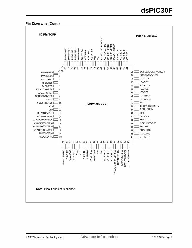
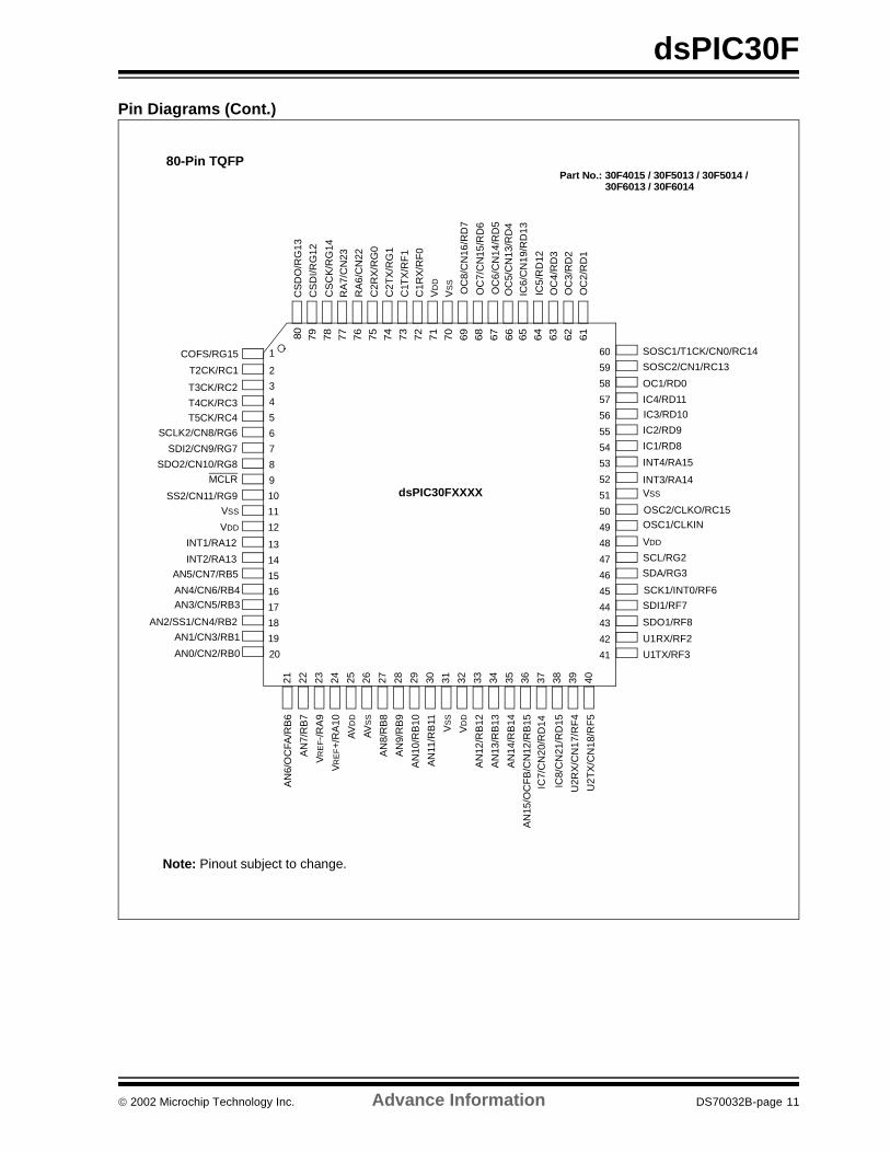
80-Pin TQFP
Note: Pinout subject to change.
Part No.: 30F6010
2002 Microchip Technology Inc. Advance Information DS70032B-page 7
dsPIC30F
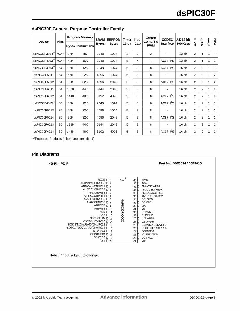
dsPIC30F General Purpose Controller Family
Pin Diagrams
Device PinsProgram Memory
SRAM Bytes
EEPROMBytes
Timer 16-bit
InputCap
Output Comp/Std
PWM
CODEC Interface
A/D 12-bit 100 Ksps U
AR
T
SP
ITM
I2 CT
M
CA
N
Bytes Instructions
dsPIC30F3014** 40/44 24K 8K 2048 1024 3 2 2 - 13 ch 2 1 1 -
dsPIC30F4013** 40/44 48K 16K 2048 1024 5 4 4 AC97, I2S 13 ch 2 1 1 1
dsPIC30F4014** 64 36K 12K 2048 1024 5 8 8 AC97, I2S 16 ch 2 2 1 1
dsPIC30F5011 64 66K 22K 4096 1024 5 8 8 - 16 ch 2 2 1 2
dsPIC30F5012 64 96K 32K 4096 2048 5 8 8 AC97, I2S 16 ch 2 2 1 2
dsPIC30F6011 64 132K 44K 6144 2048 5 8 8 - 16 ch 2 2 1 2
dsPIC30F6012 64 144K 48K 8192 4096 5 8 8 AC97, I2S 16 ch 2 2 1 2
dsPIC30F4015** 80 36K 12K 2048 1024 5 8 8 AC97, I2S 16 ch 2 2 1 1
dsPIC30F5013 80 66K 22K 4096 1024 5 8 8 - 16 ch 2 2 1 2
dsPIC30F5014 80 96K 32K 4096 2048 5 8 8 AC97, I2S 16 ch 2 2 1 2
dsPIC30F6013 80 132K 44K 6144 2048 5 8 8 - 16 ch 2 2 1 2
dsPIC30F6014 80 144K 48K 8192 4096 5 8 8 AC97, I2S 16 ch 2 2 1 2
**Proposed Products (others are committed)
AN7/RB7AN6/OCFA/RB6
C1RX/RF0C1TX/RF1
IC1/INT1/RD8OC3/RD2
AN8/RB8
1234567891011121314151617181920
4039383736353433323130292827262524232221
dsP
IC30F
XX
XX
MCLR
VDD
VSS
AN0/VREF+/CN2/RB0AN1/VREF-/CN3/RB1
AN2/SS1/CN4/RB2
OC4/RD3
SOSC1/T1CK/U1ARX/CN0/RC14SOSC2/T2CK/U1ATX/CN1/RC13
OSC2/CLKO/RC15OSC1/CLKIN
AN5/IC8/CN7/RB5AN4/IC7/CN6/RB4
AN3/CN5/RB3
AVDD
AVSS
IC2/INT2/RD9
VSS
VDD
SCK1/RF6
U1RX/SDI1/SDA/RF2U1TX/SDO1/SCL/RF3
VSS VDD
U2RX/RF4U2TX/RF5
AN12/COFS/RB12
AN10/CSDI/RB10AN11/CSDO/RB11
AN9/CSCK/RB9
OC1/RD0OC2/RD1
INT0/RA11
40-Pin PDIP
Note: Pinout subject to change.
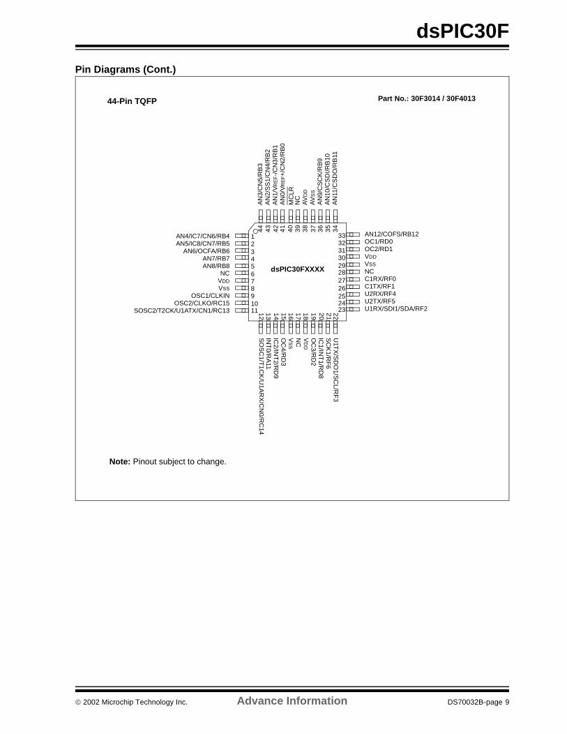
Part No.: 30F3014 / 30F4013
2002 Microchip Technology Inc. Advance Information DS70032B-page 8
dsPIC30F
Pin Diagrams (Cont.)
1011
23456
1
18 19 20 21 2212 13 14 15
38
87
44 43 42 41 40 39
16 172930313233
232425262728
36 3435
9
37
U1T
X/S
DO
1/SC
L/RF
3S
CK
1/RF
6IC
1/INT
1/RD
8O
C3/R
D2
VD
D
SO
SC
1/T1C
K/U
1AR
X/C
N0/R
C14
NC
VS
S
OC
4/RD
3IC
2/INT
2/RD
9IN
T0/R
A11
AN
3/C
N5/
RB
3A
N2/
SS
1/C
N4/
RB
2A
N1/
VR
EF-/
CN
3/R
B1
AN
0/V
RE
F+
/CN
2/R
B0
MC
LRN
CA
VD
D
AV
SS
AN
9/C
SC
K/R
B9
AN
10/C
SD
I/RB
10A
N11
/CS
DO
/RB
11
AN12/COFS/RB12OC1/RD0OC2/RD1VDD
VSS
NCC1RX/RF0C1TX/RF1U2RX/RF4U2TX/RF5U1RX/SDI1/SDA/RF2
AN4/IC7/CN6/RB4AN5/IC8/CN7/RB5
AN6/OCFA/RB6AN7/RB7AN8/RB8
NCVDD
VSS
OSC1/CLKINOSC2/CLKO/RC15
SOSC2/T2CK/U1ATX/CN1/RC13
dsPIC30FXXXX
44-Pin TQFP
Note: Pinout subject to change.
Part No.: 30F3014 / 30F4013
2002 Microchip Technology Inc. Advance Information DS70032B-page 9
dsPIC30F
Pin Diagrams (Cont.)
12345678910111213 36
353433
32313029282726
64 63 62 61 60 59 58 57 56
141516
17 18 19 20 21 22 23 24 25
SOSC1/T1CK/CN0/RC14SOSC2/T4CK/CN1/RC13OC1/RD0IC4/INT4/RD11
IC2/INT2/RD9IC1/INT1/RD8VSS
OSC2/CLKO/RC15OSC1/CLKINVDD
SCL/RG2
SCK1/INT0/RF6U1RX/SDI1/RF2U1TX/SDO1/RF3
COFS/RG15T2CK/RC1T3CK/RC2
SCK2/CN8/RG6SDI2/CN9/RG7
SDO2/CN10/RG8MCLR
VSS
VDD
AN3/CN5/RB3AN2/SS1/CN4/RB2
AN1/VREF-/CN3/RB1AN0/VREF+/CN2/RB0
OC
8/C
N16
/RD
7
CS
DO
/RG
13C
SD
I/RG
12C
SC
K/R
G14
VS
S
C2T
X/R
G1
C1T
X/R
F1
C2R
X/R
G0
OC
2/R
D1
OC
3/R
D2
AN
6/O
CFA
/RB
6A
N7/
RB
7A
VD
D
AV
SS
AN
8/R
B8
AN
9/R
B9
AN
10/R
B10
AN
11/R
B11
VS
S
VD
D
AN
12/R
B12
AN
13/R
B13
AN
14/R
B14
AN
15/O
CF
B/C
N12
/RB
15
U2T
X/C
N18
/RF
5U
2RX
/CN
17/R
F4
SDA/RG3
43424140393837
44
484746
50 495154 53 5255
45
SS2/CN11/RG9
AN5/IC8/CN7/RB5AN4/IC7/CN6/RB4
IC3/INT3/RD10
VD
D
C1R
X/R
F0
OC
4/R
D3
OC
7/C
N15
/RD
6O
C6/
IC6/
CN
14/R
D5
OC
5/IC
5/C
N13
/RD
4
Note: Pinout subject to change.
64-Pin TQFP
dsPIC30FXXXX
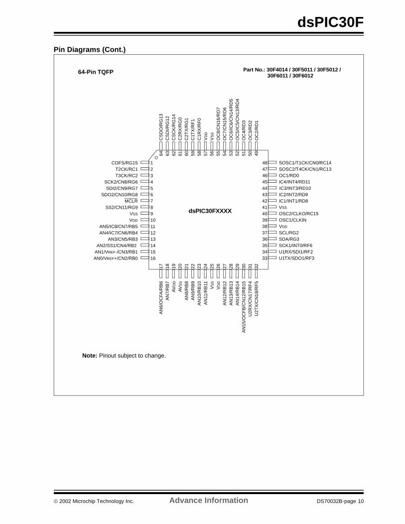
Part No.: 30F4014 / 30F5011 / 30F5012 /30F6011 / 30F6012
2002 Microchip Technology Inc. Advance Information DS70032B-page 10
dsPIC30F
Pin Diagrams (Cont.)
72
74
73
71
70
69
68
67
66
65
64
63
62
61
20
2
3
4
5
6
7
8
9
10
11
12
13
14
15
16
50
49
48
47
46
45
44
21
41
4039383736353423 24 25 26 27 28 29 30 31 32 33
dsPIC30FXXXX
17
18
19
75
1
57
56
55
54
53
52
51
60
59
58
43
42
76
78
77
79
2280
IC5/
RD
12O
C4/
RD
3
OC
3/R
D2
OC
2/R
D1
CS
CK
/RG
14R
A7/
CN
23
RA
6/C
N22
C2R
X/R
G0
C2T
X/R
G1
C1T
X/R
F1
C1R
X/R
F0
CS
DO
/RG
13
CS
DI/R
G12
OC
8/C
N16
/RD
7
OC
6/C
N14
/RD
5
OC1/RD0
IC4/RD11
IC2/RD9
IC1/RD8
INT4/RA15
IC3/RD10
INT3/RA14VSS
OSC1/CLKIN
VDD
SCL/RG2
U1RX/RF2
U1TX/RF3
SOSC1/T1CK/CN0/RC14
SOSC2/CN1/RC13
VR
EF+
/RA
10
VR
EF-/
RA
9
AV
DD
AV
SS
AN
8/R
B8
AN
9/R
B9
AN
10/R
B10
AN
11/R
B11
VD
D
U2R
X/C
N17
/RF
4
IC8/
CN
21/R
D15
U2T
X/C
N18
/RF
5
AN
6/O
CFA
/RB
6
AN
7/R
B7
T3CK/RC2
T4CK/RC3
T5CK/RC4
SCLK2/CN8/RG6
SDI2/CN9/RG7
SDO2/CN10/RG8
MCLR
SS2/CN11/RG9
AN4/CN6/RB4AN3/CN5/RB3
AN2/SS1/CN4/RB2
AN1/CN3/RB1
AN0/CN2/RB0
VSS
VDD
COFS/RG15
T2CK/RC1
INT2/RA13
INT1/RA12
AN
12/R
B12
AN
13/R
B13
AN
14/R
B14
AN
15/O
CF
B/C
N12
/RB
15
VD
D
VS
S
OC
5/C
N13
/RD
4
IC6/
CN
19/R
D13
SDA/RG3
SDI1/RF7
SDO1/RF8
AN5/CN7/RB5
VS
S
OSC2/CLKO/RC15
OC
7/C
N15
/RD
6
SCK1/INT0/RF6
IC7/
CN
20/R
D14
80-Pin TQFP
Note: Pinout subject to change.
Part No.: 30F4015 / 30F5013 / 30F5014 / 30F6013 / 30F6014
2002 Microchip Technology Inc. Advance Information DS70032B-page 11
dsPIC30F
Table of Contents
1.0 Device Overview .................................................................................................................................................................... 152.0 Core Architecture Overview ................................................................................................................................................... 193.0 Memory Organization............................................................................................................................................................. 334.0 FLASH Program Memory....................................................................................................................................................... 455.0 Data EEPROM Memory ......................................................................................................................................................... 556.0 DSP Engine............................................................................................................................................................................ 617.0 Address Generator Units........................................................................................................................................................ 698.0 Exception Processing............................................................................................................................................................. 839.0 I/O Ports ............................................................................................................................................................................... 11510.0 Timer1 Module ..................................................................................................................................................................... 13511.0 Timer2/3 Module .................................................................................................................................................................. 13912.0 Timer4/5 Module .................................................................................................................................................................. 14513.0 Input Capture Module........................................................................................................................................................... 15114.0 Output Compare Module...................................................................................................................................................... 15515.0 Quadrature Encoder Interface (QEI) Module ....................................................................................................................... 16316.0 Motor Control PWM Module................................................................................................................................................. 17317.0 SPI Module........................................................................................................................................................................... 19718.0 I2C Module........................................................................................................................................................................... 20919.0 Universal Asynchronous Receiver Transmitter (UART) Module .......................................................................................... 23320.0 CAN Module......................................................................................................................................................................... 24521.0 Data Converter Interface (DCI) Module ............................................................................................................................... 24722.0 12-bit Analog-to-Digital Converter (A/D) Module.................................................................................................................. 26523.0 10-bit High speed Analog-to-Digital Converter (A/D) Module .............................................................................................. 27724.0 System Integration ............................................................................................................................................................... 29325.0 Instruction Set Summary...................................................................................................................................................... 31126.0 Development Support .......................................................................................................................................................... 32127.0 Electrical Characteristics...................................................................................................................................................... 32328.0 DC and AC Characteristics Graphs and Tables................................................................................................................... 32529.0 Packaging Information ......................................................................................................................................................... 327Index .................................................................................................................................................................................................. 337On-Line Support................................................................................................................................................................................. 345Reader Response .............................................................................................................................................................................. 346Product Identification System ............................................................................................................................................................ 347
2002 Microchip Technology Inc. Advance Information DS70032B-page 12
dsPIC30F
TO OUR VALUED CUSTOMERS
It is our intention to provide our valued customers with the best documentation possible to ensure successful use of your Microchip products. To this end, we will continue to improve our publications to better suit your needs. Our publications will berefined and enhanced as new volumes and updates are introduced.
If you have any questions or comments regarding this publication, please contact the Marketing Communications Departmentvia E-mail at [email protected] or fax the Reader Response Form in the back of this data sheet to (480) 792-4150. We welcome your feedback.
Most Current Data SheetTo obtain the most up-to-date version of this data sheet, please register at our Worldwide Web site at:
http://www.microchip.com
You can determine the version of a data sheet by examining its literature number found on the bottom outside corner of any page.The last character of the literature number is the version number, (e.g., DS30000A is version A of document DS30000).
ErrataAn errata sheet, describing minor operational differences from the data sheet and recommended workarounds, may exist for currentdevices. As device/documentation issues become known to us, we will publish an errata sheet. The errata will specify the revisionof silicon and revision of document to which it applies.
To determine if an errata sheet exists for a particular device, please check with one of the following:
• Microchip’s Worldwide Web site; http://www.microchip.com• Your local Microchip sales office (see last page)• The Microchip Corporate Literature Center; U.S. FAX: (480) 792-7277When contacting a sales office or the literature center, please specify which device, revision of silicon and data sheet (include lit-erature number) you are using.
Customer Notification SystemRegister on our web site at www.microchip.com/cn to receive the most current information on all of our products.
2002 Microchip Technology Inc. Advance Information DS70032B-page 13

dsPIC30F
NOTES:
2002 Microchip Technology Inc. Advance Information DS70032B-page 14
dsPIC30F
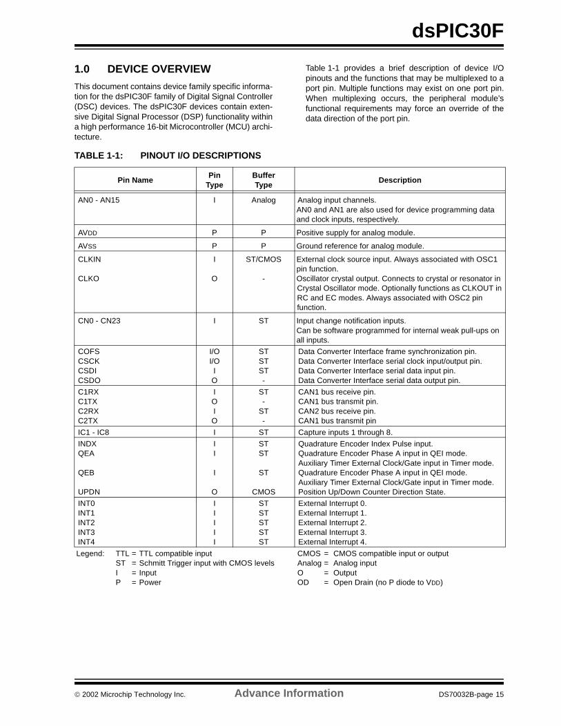
1.0 DEVICE OVERVIEW
This document contains device family specific informa-tion for the dsPIC30F family of Digital Signal Controller(DSC) devices. The dsPIC30F devices contain exten-sive Digital Signal Processor (DSP) functionality withina high performance 16-bit Microcontroller (MCU) archi-tecture.
Table 1-1 provides a brief description of device I/Opinouts and the functions that may be multiplexed to aport pin. Multiple functions may exist on one port pin.When multiplexing occurs, the peripheral module’sfunctional requirements may force an override of thedata direction of the port pin.
TABLE 1-1: PINOUT I/O DESCRIPTIONS
Pin NamePin
TypeBufferType
Description
AN0 - AN15 I Analog Analog input channels. AN0 and AN1 are also used for device programming data and clock inputs, respectively.
AVDD P P Positive supply for analog module.
AVSS P P Ground reference for analog module.
CLKIN
CLKO
I
O
ST/CMOS
-
External clock source input. Always associated with OSC1 pin function.Oscillator crystal output. Connects to crystal or resonator in Crystal Oscillator mode. Optionally functions as CLKOUT in RC and EC modes. Always associated with OSC2 pin function.
CN0 - CN23 I ST Input change notification inputs.Can be software programmed for internal weak pull-ups on all inputs.
COFSCSCKCSDICSDO
I/OI/OIO
STSTST-
Data Converter Interface frame synchronization pin.Data Converter Interface serial clock input/output pin.Data Converter Interface serial data input pin.Data Converter Interface serial data output pin.
C1RXC1TXC2RXC2TX
IOIO
ST-
ST-
CAN1 bus receive pin.CAN1 bus transmit pin.CAN2 bus receive pin.CAN1 bus transmit pin
IC1 - IC8 I ST Capture inputs 1 through 8.
INDXQEA
QEB
UPDN
II
I
O
STST
ST
CMOS
Quadrature Encoder Index Pulse input.Quadrature Encoder Phase A input in QEI mode. Auxiliary Timer External Clock/Gate input in Timer mode.Quadrature Encoder Phase A input in QEI mode. Auxiliary Timer External Clock/Gate input in Timer mode.Position Up/Down Counter Direction State.
INT0INT1INT2INT3INT4
IIIII
STSTSTSTST
External Interrupt 0.External Interrupt 1.External Interrupt 2.External Interrupt 3.External Interrupt 4.
Legend: TTL = TTL compatible input CMOS = CMOS compatible input or output ST = Schmitt Trigger input with CMOS levels Analog = Analog input I = Input O = Output P = Power OD = Open Drain (no P diode to VDD)
2002 Microchip Technology Inc. Advance Information DS70032B-page 15
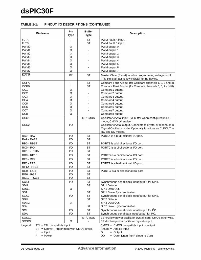
dsPIC30F
FLTAFLTBPWM0PWM1PWM2PWM3PWM4PWM5PWM6PWM7
IIOOOOOOOO
STST--------
PWM Fault A input.PWM Fault B input.PWM output 0. PWM output 1.PWM output 2.PWM output 3.PWM output 4.PWM output 5.PWM output 6.PWM output 7.
MCLR I/P ST Master Clear (Reset) input or programming voltage input. This pin is an active low RESET to the device.
OCFAOCFBOC1OC2OC3OC4OC5OC6OC7OC8
IIOOOOOOOO
STST--------
Compare Fault A input (for Compare channels 1, 2, 3 and 4).Compare Fault B input (for Compare channels 5, 6, 7 and 8).Compare1 output.Compare2 output.Compare3 output.Compare4 output.Compare5 output.Compare6 output.Compare7 output.Compare8 output.
OSC1
OSC2
I
I/O
ST/CMOS
-
Oscillator crystal input. ST buffer when configured in RC mode; CMOS otherwise.Oscillator crystal output. Connects to crystal or resonator in Crystal Oscillator mode. Optionally functions as CLKOUT in RC and EC modes.
RA0 - RA7RA9 - RA15
I/OI/O
STST
PORTA is a bi-directional I/O port.
RB0 - RB15 I/O ST PORTB is a bi-directional I/O port.
RC0 - RC4RC13 - RC15
I/OI/O
STST
PORTC is a bi-directional I/O port.
RD0 - RD15 I/O ST PORTD is a bi-directional I/O port.
RE0 - RE9 I/O ST PORTE is a bi-directional I/O port.
RF0 - RF8RF12 - RF13
I/OI/O
STST
PORTF is a bi-directional I/O port.
RG0 - RG3RG6 - RG9RG12 - RG15
I/OI/OI/O
STSTST
PORTG is a bi-directional I/O port.
SCK1SDI1SDO1SS1SCK2SDI2SDO2SS2
I/OIOI
I/OIOI
STST-
STSTST-
ST
Synchronous serial clock input/output for SPI1.SPI1 Data In.SPI1 Data Out.SPI1 Slave Synchronization.Synchronous serial clock input/output for SPI2.SPI2 Data In.SPI2 Data Out.SPI2 Slave Synchronization.
SCLSDA
I/OI/O
STST
Synchronous serial clock input/output for I2C.Synchronous serial data input/output for I2C.
SOSC1SOSC2
IO
ST/CMOS-
32 kHz low power oscillator crystal input; CMOS otherwise.32 kHz low power oscillator crystal output.
TABLE 1-1: PINOUT I/O DESCRIPTIONS (CONTINUED)
Pin NamePin
TypeBufferType
Description
Legend: TTL = TTL compatible input CMOS = CMOS compatible input or output ST = Schmitt Trigger input with CMOS levels Analog = Analog input I = Input O = Output P = Power OD = Open Drain (no P diode to VDD)
DS70032B-page 16 Advance Information 2002 Microchip Technology Inc.
dsPIC30F
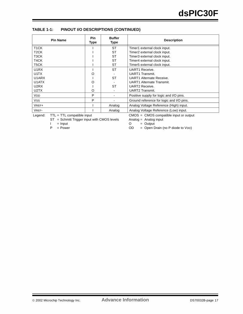
T1CKT2CKT3CKT4CKT5CK
IIIII
STSTSTSTST
Timer1 external clock input.Timer2 external clock input.Timer3 external clock input.Timer4 external clock input.Timer5 external clock input.
U1RXU1TXU1ARXU1ATXU2RXU2TX
IOIOIO
ST-
ST-
ST-
UART1 Receive.UART1 Transmit.UART1 Alternate Receive.UART1 Alternate Transmit.UART2 Receive.UART2 Transmit.
VDD P - Positive supply for logic and I/O pins.
VSS P - Ground reference for logic and I/O pins.
VREF+ I Analog Analog Voltage Reference (High) input.
VREF- I Analog Analog Voltage Reference (Low) input.
TABLE 1-1: PINOUT I/O DESCRIPTIONS (CONTINUED)
Pin NamePin
TypeBufferType
Description
Legend: TTL = TTL compatible input CMOS = CMOS compatible input or output ST = Schmitt Trigger input with CMOS levels Analog = Analog input I = Input O = Output P = Power OD = Open Drain (no P diode to VDD)
2002 Microchip Technology Inc. Advance Information DS70032B-page 17

dsPIC30F
NOTES:
DS70032B-page 18 Advance Information 2002 Microchip Technology Inc.
dsPIC30F
2.0 CORE ARCHITECTURE OVERVIEW
2.1 Core Overview
The core has a 24-bit instruction word. The ProgramCounter (PC) is 24-bits wide with the Least Significant(LS) bit always clear (see Section 3.1), and the MostSignificant (MS) bit is ignored during normal programexecution, except for certain specialized instructions.Thus, the PC can address up to 4M instruction wordsof user program space. An instruction pre-fetch mech-anism is used to help maintain throughput. Uncondi-tional overhead free program loop constructs aresupported using the DO and REPEAT instructions, bothof which are interruptible at any point.
The working register array consists of 16 x 16-bit regis-ters, each of which can act as data, address or offsetregisters. One working register (W15) operates as asoftware stack pointer for interrupts and calls.
The data space is 64 Kbytes (32K words), and is splitinto two blocks, referred to as X and Y data memory.Each block has its own independent Address Genera-tion Unit (AGU). Most instructions operate solelythrough the X memory AGU, which provides theappearance of a single unified data space. TheMultiply-Accumulate (MAC) class of dual source DSPinstructions operate through both the X and Y AGUs,splitting the data address space into two parts (seeSection 3.2). The X and Y data space boundary isdevice specific and cannot be altered by the user. Eachdata word consists of 2 bytes, and most instructionscan address data either as words or bytes.
There are two methods of accessing data stored in pro-gram memory:
• The upper 32 Kbytes of data space memory can optionally be mapped into the lower half (user space) of program space at any 16K program word boundary, defined by the 8-bit Program Space Visibility Page (PSVPAG) register. This lets any instruction access program space as if it were data space, with the sole limitation that the access requires an additional cycle. Moreover, only the lower 16 bits of each instruction word can be accessed using this method.
• Linear indirect access of 32K word pages within program space is also possible using any working register, via table read and write instructions. Table read and write instructions can be used to access all 24 bits of an instruction word.
Overhead-free circular buffers (modulo addressing) aresupported in both X and Y address spaces. This is pri-marily intended to remove the loop overhead for DSPalgorithms.
The X AGU also supports bit-reversed addressing ondestination effective addresses, to greatly simplify inputor output data reordering for radix-2 FFT algorithms.Refer to Section 7.0 for details on modulo and bit-reversed addressing.
The core supports Inherent (no operand), Relative, Lit-eral, Memory Direct, Register Direct, Register Indirectand Register Offset Addressing modes. Instructionsare associated with predefined addressing modes,depending upon their functional requirements.
For most instructions, the core is capable of executinga data (or program data) memory read, a working reg-ister (data) read, a data memory write and a program(instruction) memory read per instruction cycle. As aresult, 3-operand instructions are supported, allowingC = A+B operations to be executed in a single cycle.
A DSP engine has been included to significantlyenhance the core arithmetic capability and throughput.It features a high speed 16-bit by 16-bit multiplier, a40-bit ALU, two 40-bit saturating accumulators and a40-bit bi-directional barrel shifter. Data in the accumu-lator or any working register can be shifted up to 15 bitsright or 16 bits left in a single cycle. The DSP instruc-tions operate seamlessly with all other instructions andhave been designed for optimal real-time performance.The MAC class of instructions can concurrently fetchtwo data operands from memory, while multiplying twoW registers. To enable this concurrent fetching of dataoperands, the data space is split for these instructionsand linear for all others. This is achieved in a transpar-ent and flexible manner, through dedicating certainworking registers to each address space for the MACclass of instructions.
The core does not support a multi-stage instructionpipeline. However, a single stage instruction pre-fetchmechanism is used, which accesses and partially pre-decodes instructions a cycle ahead to maximize avail-able execution time. Most instructions execute in a sin-gle cycle, with certain exceptions as outlined inSection 2.3.2.
The core features a vectored exception processingstructure for traps and interrupts, with 62 independentvectors. The exceptions consist of up to 8 traps (ofwhich 3 are reserved) and 54 interrupts. Each interruptis prioritized based on a user assigned priority between0 and 7 (0 being the lowest priority and 7 being thehighest) in conjunction with a predetermined ‘naturalorder’.
A block diagram of the core is shown in Figure 2-1.
2002 Microchip Technology Inc. Advance Information DS70032B-page 19
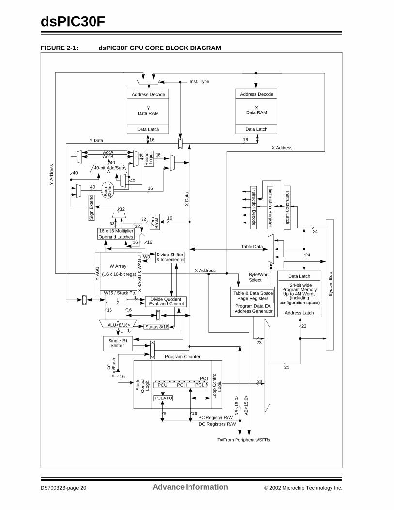
dsPIC30F
FIGURE 2-1: dsPIC30F CPU CORE BLOCK DIAGRAM
Sig
n E
xten
d
23
Address Decode
X
Data Latch
Sys
tem
BusData Latch
Up to 4M Words
Address Latch
24
24
23
Table & Data Space
23
Instruction Decode
ALU<8/16>
16
DB
<15
:0>PCLATU
PCU PCH PCL
Status 8/16
16 x 16 Multiplier
AccAAccB
Bar
rel
40-bit Add/Sub
Operand Latches
23
Address Decode
Y
Data Latch
16
Data RAM
Loop
Con
trol
Logi
c
W Array
(16 x 16-bit regs)
Y Data
Data RAM
X D
ata
16
Y A
ddre
ss
X Address
Program Data EAAddress Generator
Table Data
Byte/Word
Instruction Register
Instruction Latch
Program Memory24-bit wide
X R
AG
U &
WA
GU
Y A
GU X Address
Select
32
W15 / Stack Ptr.
Sta
ck
Logi
cC
ontr
ol
Program Counter
16Pop
/Pus
h
PC Register R/W168
PC
Shi
fter
Rou
ndLo
gic
32
Zer
o B
ackf
ill 16
16
40
40
40
40
40
16
32
16 16
To/From Peripherals/SFRs
Inst. Type
32
16
Page Registers
DO Registers R/W
(including
AB
<15
:0>
Divide Shifter& Incrementer
W0
Divide QuotientEval. and Control
11
Single BitShifter
PCT
1
configuration space)
DS70032B-page 20 Advance Information 2002 Microchip Technology Inc.
dsPIC30F
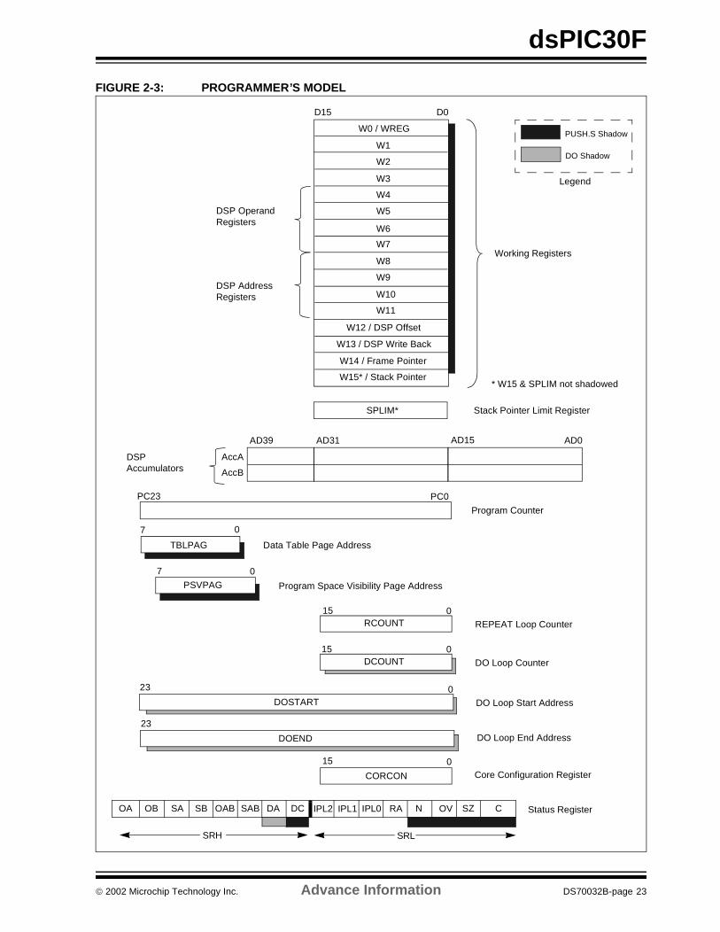
2.2 Programmer’s Model
The programmer’s model is shown in Figure 2-3 andconsists of 16 x 16-bit working registers (W0 throughW15), 2 x 40-bit accumulators (AccA and AccB),STATUS register (SR), Data Table Page register(TBLPAG), Program Space Visibility Page register(PSVPAG), DO and REPEAT registers (DOSTART,DOEND, DCOUNT and RCOUNT), and ProgramCounter (PC). The working registers can act as data,address or offset registers. All registers are memorymapped. W0 acts as the W register for file registeraddressing.
Most of these registers have a shadow register associ-ated with them, as shown in Figure 2-3. The shadowregister is used as a temporary holding register andcan transfer its contents to or from its host register uponsome event occurring. None of the shadow registersare accessible directly. The following rules apply fortransfer of registers into and out of shadows.
• PUSH.s and POP.s W0...W14, TBLPAG, PSVPAG, SR (DC, N, OV, SZ and C bits only) transferred
• DO instruction DA bit, DOSTART, DOEND, DCOUNT shadows pushed on loop start, popped on loop end
When a byte operation is performed on a working reg-ister, only the Least Significant Byte of the target regis-ter is affected. However, a benefit of memory mappedworking registers is that both the Least and Most Sig-nificant Bytes can be manipulated through byte widedata memory space accesses.
2.2.1 SOFTWARE STACK POINTER/ FRAME POINTER
W15 is the dedicated software stack pointer (SP), andwill be automatically modified by exception processingand subroutine calls and returns. However, W15 can bereferenced by any instruction in the same manner as allother W registers. This simplifies the reading, writingand manipulation of the stack pointer (e.g., creatingstack frames).
W15 is initialized to 0x0800 during a RESET. The usermay reprogram the SP during initialization to any loca-tion within data space.
W14 has been dedicated as a stack frame pointer asdefined by the LNK and ULNK instructions. However,W14 can be referenced by any instruction in the samemanner as all other W registers.
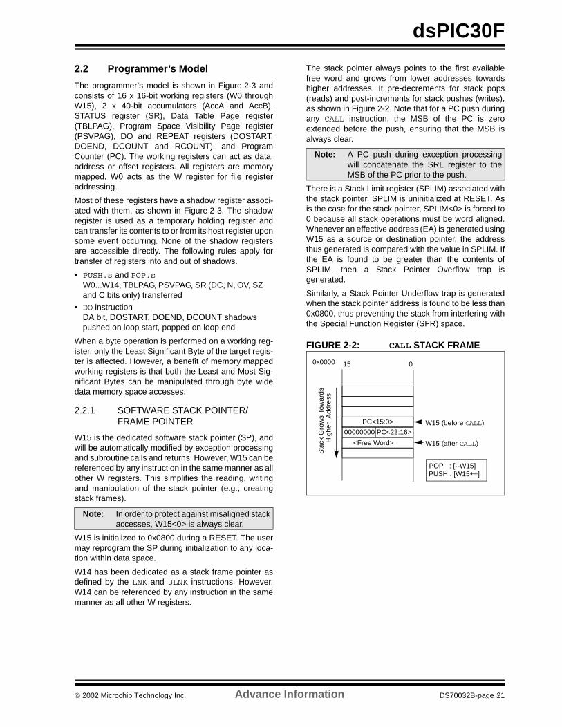
The stack pointer always points to the first availablefree word and grows from lower addresses towardshigher addresses. It pre-decrements for stack pops(reads) and post-increments for stack pushes (writes),as shown in Figure 2-2. Note that for a PC push duringany CALL instruction, the MSB of the PC is zeroextended before the push, ensuring that the MSB isalways clear.
There is a Stack Limit register (SPLIM) associated withthe stack pointer. SPLIM is uninitialized at RESET. Asis the case for the stack pointer, SPLIM<0> is forced to0 because all stack operations must be word aligned.Whenever an effective address (EA) is generated usingW15 as a source or destination pointer, the addressthus generated is compared with the value in SPLIM. Ifthe EA is found to be greater than the contents ofSPLIM, then a Stack Pointer Overflow trap isgenerated.
Similarly, a Stack Pointer Underflow trap is generatedwhen the stack pointer address is found to be less than0x0800, thus preventing the stack from interfering withthe Special Function Register (SFR) space.
FIGURE 2-2: CALL STACK FRAME
Note: In order to protect against misaligned stackaccesses, W15<0> is always clear.
Note: A PC push during exception processingwill concatenate the SRL register to theMSB of the PC prior to the push.
<Free Word>
PC<15:0>
00000000 PC<23:16>
015
W15 (before CALL)
W15 (after CALL)
Sta
ck G
row
s To
war
dsH
ighe
r A
ddre
ss
PUSH : [W15++]POP : [--W15]
0x0000
2002 Microchip Technology Inc. Advance Information DS70032B-page 21
dsPIC30F
2.2.2 STATUS REGISTER
The dsPIC™ core has a 16-bit status register (SR), theLS Byte of which is referred to as the STATUS registerlow byte (SRL). A detailed description is shown inRegister 2-1.
SRL contains all the MCU ALU operation status flags(including the ‘sticky Z’ bit, SZ), as well as the CPUInterrupt Priority status bits, IPL<2:0>, and theREPEAT active status bit, RA. During exception pro-cessing, SRL is concatenated with the MS Byte of thePC to form a complete word value which is thenstacked.
The upper byte of the STATUS register contains theDSP Adder/Subtractor status bits, the DO Loop Activebit (DA) and the Digit Carry (DC) status bit.
Most SR bits are read/write. Exceptions are:
1. The DA bit: DA is read and clear only, becauseaccidentally setting it could cause erroneousoperation.
2. The RA bit: RA is a read only bit, because acci-dentally setting it could cause erroneous opera-tion. RA is only set on entry into a repeat loop,and cannot be directly cleared by software.
3. The OV, OA, OB and OAB bits: These bits areread only and can only be set by the DSP engineoverflow logic.
4. The SA, SB and SAB bits: These are read andclear only and can only be set by the DSPengine saturation logic. They are ‘sticky’, i.e.,once set, they remain set until cleared by theuser, irrespective of the results from any subse-quent DSP operations.
2.2.2.1 Sticky Z (SZ) Status Bit
For most instructions, the SZ status bit is not sticky.Instructions that use a carry/borrow input will only beable to clear SZ (for a non-zero result) and can neverset it. A multi-precision sequence of instructions (start-ing with an instruction with no carry/borrow input) willthus, automatically logically AND the successiveresults of the zero test. All results must be zero for theSZ flag to remain set by the end of the sequence.
The following instructions feature sticky operation ofthe SZ flag: ADDC, CPB, SUBB and SUBBR.
2.2.3 PROGRAM COUNTER
The Program Counter is 24-bits wide. Bit 0 is alwaysclear. PC<23> may be used to access configurationfuse settings, using table read and table write instruc-tions. Bit 23 is also clear for normal user program mem-ory access. Therefore, the PC can address up to 4Minstruction words.
Note: When the memory mapped STATUS regis-ter is the destination address for an opera-tion which affects any of the SR bits, datawrites are disabled to all bits.
Note: Clearing the SAB bit will also clear both theSA and SB bits.
DS70032B-page 22 Advance Information 2002 Microchip Technology Inc.
dsPIC30F
FIGURE 2-3: PROGRAMMER’S MODEL
TABPAG
PC23 PC0
7 0
D0D15
Program Counter
Data Table Page Address
Status Register
Working Registers
DSP OperandRegisters
W1
W2
W3
W4
W5
W6
W7
W8
W9
W10
W11
W12 / DSP Offset
W13 / DSP Write Back
W14 / Frame Pointer
W15* / Stack Pointer
DSP AddressRegisters
AD39 AD0AD31
DSPAccumulators
AccA
AccB
PSVPAG7 0
Program Space Visibility Page Address
SZ OA OB SA SB
RCOUNT15 0
REPEAT Loop Counter
DCOUNT15 0
DO Loop Counter
DOSTART
23 0DO Loop Start Address
IPL2 IPL1
SPLIM* Stack Pointer Limit Register
AD15
SRL
* W15 & SPLIM not shadowed
PUSH.S Shadow
DO Shadow
OAB SAB
15 0 Core Configuration Register
Legend
CORCON
DA DC RA N
TBLPAG
PSVPAG
IPL0 OV
W0 / WREG
SRH
DO Loop End AddressDOEND
23
C
2002 Microchip Technology Inc. Advance Information DS70032B-page 23
dsPIC30F
REGISTER 2-1: STATUS REGISTER (SR)
Upper Half (SRH):R/W-0 R/W-0 R/W-0 R/W-0 R/W-0 R/W-0 R-0 R-0
OA OB SA SB OAB SAB DA DC
bit 15 bit 8
Lower Half (SRL):R/W-1 R/W-1 R/W-1 R-0 R/W-0 R/W-0 R/W-0 R/W-0IPL2 IPL1 IPL0 RA N OV SZ C
bit 7 bit 0
bit 15 OA: Accumulator A Overflow Status bit1 = Accumulator A overflowed0 = Accumulator A not overflowed
bit 14 OB: Accumulator B Overflow Status bit1 = Accumulator B overflowed0 = Accumulator B not overflowed
bit 13 SA: Accumulator A Saturation Status bit1 = Accumulator A is saturated or has been saturated at some time0 = Accumulator A is not saturated
Note: This bit may be read or cleared, but not set.
bit 12 SB: Accumulator B Saturation Status bit1 = Accumulator B is saturated or has been saturated at some time0 = Accumulator B is not saturated
Note: This bit may be read or cleared, but not set.
bit 11 OAB: OA || OB Combined Accumulator Overflow Status bit1 = Accumulators A or B have overflowed0 = Neither Accumulators A or B have overflowed
bit 10 SAB: SA || SB Combined Accumulator Status bit1 = Accumulators A or B are saturated or have been saturated at some time in the past0 = Neither Accumulator A or B are saturated
Note: This bit may be cleared or read, but not set. Clearing this bit will clear SA and SB.
bit 9 DA: DO Loop Active bit1 = DO loop in progress0 = DO loop not in progress
Note: This bit may be read or cleared, but not set.
bit 8 DC: MCU ALU Half-Carry bit1 = A carry-out from the 4th low order bit (for byte sized data) or 8th low order bit (for word sized data) of
the result occurred0 = No carry-out from the 4th low order bit (for byte sized data) or 8th low order bit (for word sized data) of
the result occurred
bit 7-5 IPL<2:0>: CPU Interrupt Priority Status bits111 = Level 7 interrupts enabled110 = Level 6 to 7 interrupts enabled101 = Level 5 to 7 interrupts enabled100 = Level 4 to 7 interrupts enabled011 = Level 3 to 7 interrupts enabled010 = Level 2 to 7 interrupts enabled001 = Level 1 to 7 interrupts enabled000 = Level 0 to 7 interrupts enabled
bit 4 RA: REPEAT Loop Active Status bit1 = REPEAT loop in progress0 = REPEAT loop not in progress
DS70032B-page 24 Advance Information 2002 Microchip Technology Inc.
dsPIC30F
REGISTER 2-1: STATUS REGISTER (SR) (Continued)
bit 3 N: MCU ALU Negative bitThis bit is used for signed arithmetic (2’s complement). It indicates whether the result of the ALU operationwas negative (ALU MSb = 1).1 = Result was negative0 = Result was non-negative (zero or positive)
bit 2 OV: MCU ALU Overflow bitThis bit is used for signed arithmetic (2’s complement). It indicates an overflow of the magnitude, whichcauses the sign bit to change state. 1 = Overflow occurred for signed arithmetic (in this arithmetic operation)0 = No overflow occurredExample 1: w1 before instruction = 0x7fff. OV = 0.
Instruction executed: ADD #1,w1w1 after instruction = 0x8000. OV = 1.
Example 2: w1 before instruction = 0xffff. OV = 0. Instruction executed: ADD #1,w1w1 after instruction = 0x0000. OV = 1.
bit 1 SZ: MCU ALU ‘sticky’ Zero bit1 = An ADDC, CPB, SUBB or SUBBR operation which affects the SZ bit has set it at some time in the past0 = The most recent operation which affects the SZ bit has cleared it (i.e., generated a non-zero result)For all other operations, this bit indicates whether the most recent operation has produced a zero result.
bit 0 C: MCU ALU Carry/Borrow bit1 = A carry-out from the Most Significant bit of the result occurred0 = No carry-out from the Most Significant bit of the result occurredFor Borrow, the polarity is reversed.
Legend:
R = Readable bit W = Writable bit U = Unimplemented bit, read as ‘0’
-n = Value at POR 1 = bit is set 0 = bit is cleared x = bit is unknown
2002 Microchip Technology Inc. Advance Information DS70032B-page 25
dsPIC30F
2.3 Instruction Flow
2.3.1 CLOCKING SCHEME
Each instruction cycle (TCY) is comprised of four Qcycles (Q1-Q4). The four-phase Q cycles provide thetiming/delineation for the phases of the instructioncycle, such as Decode, Read, Process Data, andWrite. Figure 2-4 shows the relationship of the Qcycles to the instruction cycle for both MCU and DSPinstructions. The four Q cycles that make up an execu-tion instruction cycle (TCY) can be generalized as:
Q1: Instruction decode or forced NOP (FNOP)Data space read startDestination EA calculation start
Q2: Instruction decode or FNOPData space read completeDestination EA calculation
Q3:Next instruction pre-decode startNext op read EA calculation startProcess the Data or FNOPData space write start
Q4: Next instruction pre-decodeNext op read EA calculationData space write complete or FNOP
The total time required for EA calculation and dataspace access is 4 Q clocks, for both read and writeaccesses. This device does not support any form ofdual ported data space, so read and write operationscannot occur simultaneously. As a result, at least aportion of these operations occur concurrently acrossinstruction boundaries. Data space accesses are par-tially pipelined.
There are separate AGUs for X reads and X writes soas to enable concurrent operation. The X RAGU(Read AGU) and X WAGU (Write AGU) serve this pur-pose and are functionally identical, with the exceptionthat bit-reversed addressing is only supported on the XWAGU. There is only a single Y AGU.
A consequence of this degree of pipelining is that datadependencies can now occur between completingdestination write EA operations and already startedsource read EA calculations. Data dependencies arediscussed in detail in Section 7.
FIGURE 2-4: BASIC CORE TIMING
2.3.2 INSTRUCTION FETCH AND PRE-DECODE MECHANISM
The core does not support an instruction pipeline. Apre-fetching mechanism accesses instructions a cycleahead to maximize available execution time and toallow for some pre-decode to occur. A conceptual tim-ing diagram, demonstrating the pre-fetch mechanism,is shown in Figure 2-5.
Note: From a Q cycle perspective, the DSPinstructions differ from the MCU instruc-tions in their ability to perform two simulta-neous source data reads during the Q1/Q2access from X and Y data space.
X and Y
Space Data
Read Space Data
Write Space Data
Read
X/Y
Space Data
Write
Program SpaceRead
MCU Ops MAC Class Ops
Q1
Q2
Q3
Q4
Program SpaceRead
TCY1 TCY2
Read Operation Read Operation
Write Operation Write Operation
Instruction Decode
Instruction Pre-Decode
DS70032B-page 26 Advance Information 2002 Microchip Technology Inc.
dsPIC30F
FIGURE 2-5: CLOCK/INSTRUCTION CYCLE
Most instructions execute in a single cycle. Exceptionsare:
1. Flow control instructions and interrupts wherethe IR (Instruction register) and pre-fetch buffermust be flushed and refilled.
2. Instructions where one operand is to be fetchedfrom program space (using any method). Theseoperations consume 2 cycles (with the notableexception of instructions executed within aREPEAT loop; in this case, it would execute in 1cycle).
3. Instructions where an effective address calcula-tion dependency has been detected and aninstruction stall must be inserted.
Most instructions access data as required duringinstruction execution. Instructions which utilize themultiplier array must have data available at the begin-ning of the instruction cycle. Consequently, this datamust be pre-fetched, usually by the preceding instruc-tion, resulting in a simple out of order data processingmodel.
During the instruction pre-decode, the core determinesif any address register data dependency is imminentacross an instruction boundary. It compares the work-ing register (if any) used for the destination EA (effec-tive address) of the instruction currently beingexecuted, with that about to be used by the source EA(if any) of the pre-fetched instruction. When itobserves a match between the destination and sourceregisters, a set of rules is applied to decide (by the fall-ing edge of Q3) whether or not to stall the instructionby one cycle. See Section 7.0 for more details on datadependencies.
Due to the instruction pre-fetch mechanism, eachinstruction effectively executes in one cycle. Thisremains true until a flow change occurs, which willrequire the pre-fetch register (ROMLATCH) to be dis-carded and refilled again from the new instructionthread.
Q1 Q2 Q3 Q4 Q1 Q2 Q3 Q4 Q1 Q2 Q3 Q4
OSC1
Q1
Q2
Q3
Q4
PC PC PC+2 PC+4
Fetch INST (PC)Execute INST (PC-2) Fetch INST (PC+2)
Execute INST (PC) Fetch INST (PC+4)Execute INST (PC+2)
InternalPhaseClock
2002 Microchip Technology Inc. Advance Information DS70032B-page 27
dsPIC30F
2.3.3 INSTRUCTION FLOW TYPES
There are 8 types of instruction flows:
1. Normal one-word, one-cycle pipelined instruc-tions. These instructions take one effective cycleto execute, as shown in Figure 2-6.
2. One-word, two-cycle pipeline flush instructions.These instructions include the relativebranches, relative call, skips and returns. Whenan instruction changes the PC (other than toincrement it), the pipelined fetch is discarded.This causes the instruction to take two effectivecycles to execute as shown in Figure 2-7.
3. One-word, two-cycle instructions that are notflow control instructions. The only instructions ofthis type are the MOV.D (load and store doubleword) instructions, as shown in Figure 2-8.
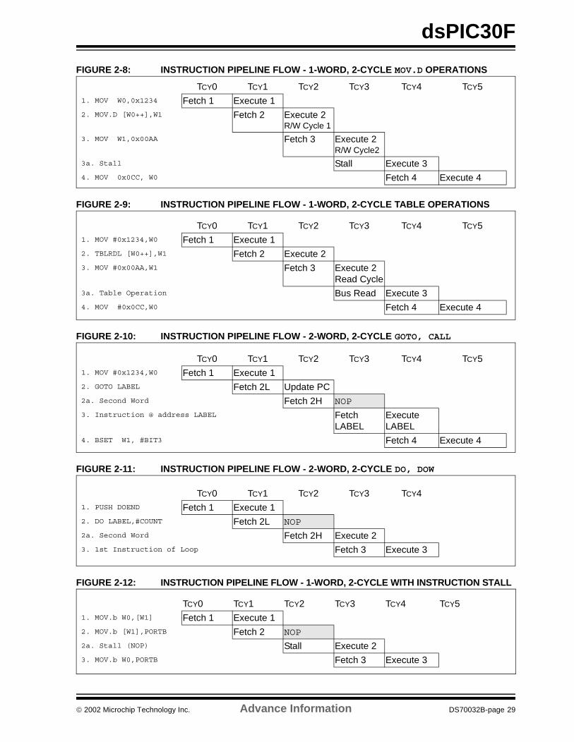
4. Table read/write instructions. These instructionswill suspend the fetching to insert a read or writecycle to the program memory. The instructionfetched while executing the table operation issaved for 1 cycle and executed in the cycleimmediately after the table operation, as shownin Figure 2-9.
5. Two-word instructions for CALL and GOTO. Inthese instructions, the fetch after the instructionprovides the remainder of the jump or call desti-nation address. These instructions require 2cycles to execute, 1 for fetching the 2 instructionwords (enabled by a high speed path on the sec-ond fetch), and 1 for the subsequent pipelineflush, as shown in Figure 2-10.
6. Two-word instructions for DO. In these instruc-tions, the fetch after the instruction contains anaddress offset. This address offset is added tothe first instruction address to generate the lastloop instruction address. Therefore, theseinstructions require two cycles, as shown inFigure 2-11.
7. Instructions that are subjected to a stall due to adata dependency between the X RAGU and XWAGU. An additional cycle is inserted to resolvethe resource conflict, as shown in Figure 2-11.Instruction stalls caused by data dependenciesare further discussed in Section 7.0.
8. Interrupt recognition execution. Refer toSection 8.0 for details on interrupts.
FIGURE 2-6: INSTRUCTION PIPELINE FLOW - 1-WORD, 1-CYCLE
FIGURE 2-7: INSTRUCTION PIPELINE FLOW - 1-WORD, 2-CYCLE
TCY0 TCY1 TCY2 TCY3 TCY4 TCY51. MOV.b #0x55,W0 Fetch 1 Execute 12. MOV.b #0x35,W1 Fetch 2 Execute 23. ADD.b W0,W1,W2 Fetch 3 Execute 3
TCY0 TCY1 TCY2 TCY3 TCY4 TCY51. MOV #0x55,W0 Fetch 1 Execute 12. BTSC W1,#3 Fetch 2 Execute 2
Skip Taken3. ADD W0,W1,W2 Fetch 3 Flush4. BRA SUB_1 Fetch 4 Execute 45. SUB W0,W1,W3 Fetch 5 Flush6. Instruction @ address SUB_1 Fetch SUB_1
DS70032B-page 28 Advance Information 2002 Microchip Technology Inc.
dsPIC30F
FIGURE 2-8: INSTRUCTION PIPELINE FLOW - 1-WORD, 2-CYCLE MOV.D OPERATIONS
FIGURE 2-9: INSTRUCTION PIPELINE FLOW - 1-WORD, 2-CYCLE TABLE OPERATIONS
FIGURE 2-10: INSTRUCTION PIPELINE FLOW - 2-WORD, 2-CYCLE GOTO, CALL
FIGURE 2-11: INSTRUCTION PIPELINE FLOW - 2-WORD, 2-CYCLE DO, DOW
FIGURE 2-12: INSTRUCTION PIPELINE FLOW - 1-WORD, 2-CYCLE WITH INSTRUCTION STALL
TCY0 TCY1 TCY2 TCY3 TCY4 TCY51. MOV W0,0x1234 Fetch 1 Execute 12. MOV.D [W0++],W1 Fetch 2 Execute 2
R/W Cycle 1
3. MOV W1,0x00AA Fetch 3 Execute 2R/W Cycle2
3a. Stall Stall Execute 34. MOV 0x0CC, W0 Fetch 4 Execute 4
TCY0 TCY1 TCY2 TCY3 TCY4 TCY51. MOV #0x1234,W0 Fetch 1 Execute 12. TBLRDL [W0++],W1 Fetch 2 Execute 23. MOV #0x00AA,W1 Fetch 3 Execute 2
Read Cycle3a. Table Operation Bus Read Execute 34. MOV #0x0CC,W0 Fetch 4 Execute 4
TCY0 TCY1 TCY2 TCY3 TCY4 TCY51. MOV #0x1234,W0 Fetch 1 Execute 12. GOTO LABEL Fetch 2L Update PC2a. Second Word Fetch 2H NOP
3. Instruction @ address LABEL FetchLABEL
ExecuteLABEL
4. BSET W1, #BIT3 Fetch 4 Execute 4
TCY0 TCY1 TCY2 TCY3 TCY41. PUSH DOEND Fetch 1 Execute 12. DO LABEL,#COUNT Fetch 2L NOP
2a. Second Word Fetch 2H Execute 23. 1st Instruction of Loop Fetch 3 Execute 3
TCY0 TCY1 TCY2 TCY3 TCY4 TCY51. MOV.b W0,[W1] Fetch 1 Execute 12. MOV.b [W1],PORTB Fetch 2 NOP
2a. Stall (NOP) Stall Execute 23. MOV.b W0,PORTB Fetch 3 Execute 3
2002 Microchip Technology Inc. Advance Information DS70032B-page 29
dsPIC30F
2.4 Program Loop Control
The dsPIC core supports both REPEAT and DO instruc-tion constructs to provide unconditional automatic pro-gram loop control.
2.4.1 REPEAT LOOP CONSTRUCT
The REPEAT instruction will cause the RA (RepeatActive) flag bit to be set if the REPEAT count is greaterthan 0. If RA = 1, PC increments and instructionfetches are inhibited until the REPEAT loop counter,RCOUNT, reaches 0 (at which point RA will also becleared by the loop count hardware).
The REPEAT instruction causes the instruction imme-diately following it to be repeated a fixed number oftimes as defined by either:
- a fixed, 14-bit literal encoded in the instruction, or
- the variable contents of bits <13:0> of a W register declared within the instruction
The loop count is held in the 16-bit RCOUNT register(which is memory mapped) and is thus, user accessi-ble. It is initialized by the REPEAT instruction during Q2.
The instruction to be repeated is pre-fetched duringthe REPEAT instruction and held in the ROMLATCH. Itis not fetched again for all subsequent iterations, andthe Instruction register is loaded from the lockedROMLATCH.
2.4.2 REPEAT LOOP INTERRUPT AND NESTING
A REPEAT instruction loop may be interrupted at anytime. As is the case for all instructions, the PC will notbe incremented during the instruction when an excep-tion is acknowledged. For a repeated instruction, thePC update is already inhibited (by the RA bit) whichensures that, upon return, the RETFIE instruction willcorrectly pre-fetch the instruction (i.e. the stacked PCwill point to the instruction to be repeated).
The RA state bit being present in SRL, is automaticallysaved on the stack during exception processing. Thisenables execution of further REPEAT loops fromwithin nested interrupts. After SRL is stacked, RA iscleared during exception processing to restore normalexecution within the ISR. Exception processing oper-ates as normal (i.e., with instruction pre-fetch) irre-spective of the state of RA.
2.4.3 REPEAT EARLY TERMINATION
Clearing the RA bit in the stacked SR from within anISR is a method to force an interrupted loop to termi-nate early (subject to one more iteration) after theinterrupt or trap returns. RA is not software modifiablewithin the SR, but will be updated with whatever valueis present in the stacked SRL during a return. Even ifthe RCOUNT ‘decrement then test’ does not indicate aloop end condition (RCOUNT = 0), RA will remainclear and will force the loop to exit. A subsequentREPEAT instruction will set RA, but will also updateRCOUNT with the new loop count.
2.4.4 DO LOOP CONSTRUCT
The DO instruction executes instructions following theDO until an end address is reached, at which timeinstruction execution will start again at the instructionimmediately following the DO. This will be repeated afinite number of times as defined by either:
- a fixed, 14-bit literal encoded in the first word of the instruction, or
- the variable contents of bits <13:0> of a W register declared within the instruction
The instructions within a loop (including the instructionimmediately preceding the last instruction in the loop)need not be executed in the same order in which theyappear in program memory, i.e., branches within a loopare allowed. Moreover, the loop end address may besmaller than the start address.
The instruction executed immediately before the lastinstruction in the loop does not have to be the oneimmediately preceding the last loop instruction in pro-gram memory.
The DO loop will always be executed at least once,since the loop count is examined only at the end ofeach iteration. For a DCOUNT loop count value of 0,DO will iterate the loop once.
Note: For a loop count value of 0, REPEAT will beexecuted like a NOP. The RA status bit isnot set, but RCOUNT is loaded with thevalue 0. However, the instruction within theREPEAT loop is executed once.
Note: The user must stack the RCOUNT (RepeatCount register), prior to executing aREPEAT within an ISR.
Note: The loop end comparison is an equalitytest only. The instruction at the loop endaddress must be pre-fetched, in order forthe end of the loop condition to be recog-nized. That is, exiting the loop to a PCvalue greater than the end address (or lessthan the start address) will not cause theloop count to change. An exact addressmatch must occur in order to change theloop count.
DS70032B-page 30 Advance Information 2002 Microchip Technology Inc.
dsPIC30F
2.4.5 DO LOOP NESTING
The DOSTART, DOEND and DCOUNT loop registershave a shadow register associated with each of them.This permits a single level of nesting. In addition, asthe DOSTART, DOEND and DCOUNT registers areuser accessible, they may be manually saved to per-mit additional nesting.
When a DO is executed, the DOSTART, DOEND andDCOUNT registers are transferred into the shadowregisters, prior to being updated with the new loop val-ues. The DA bit (SR<7>) is also shadowed prior tobeing set during DO execution. Similarly, during allloop exits, the shadow contents of the DOSTART,DOEND and DCOUNT registers and the DA bit aretransferred back into their respective host registers.
2.4.6 DO LOOPS AND INTERRUPTS
A DO loop may be interrupted at any time withoutpenalty.
If a DO loop is required within an exception handler,the DOSTART, DOEND, DCOUNT and MS Byte of theSR must be stacked before another DO loop may beexecuted. These registers must be restored prior toreturning from the ISR or trap handler.
2.4.7 DO EARLY TERMINATION
The DA bit in the MS Byte of the SR may be cleared(but not set) by the user. Clearing the DA bit is amethod to force a loop to terminate early at any time.The loop will complete the current iteration and thenterminate. If DA is cleared during one of the last twoinstructions of the loop, one more iteration of the loopwill occur.
A branch with a target instruction outside the loop maybe executed from within the loop. However, the lastinstruction in the DO loop cannot be a flow controlinstruction (see Section 2.4.8). It is recommended thatthe DA bit is cleared by software whenever a DO loopis terminated early.
2.4.8 DO AND REPEAT RESTRICTIONS
Any instruction can follow a REPEAT except for:
1. Flow control (any branch, compare and skip,GOTO, CALL, RCALL, RETURN, RETLW orRETFIE) instructions
2. DISI, ULNK, LNK, RESET and PWRSAVinstructions
3. Another REPEAT or DO
All DO loops must contain at least 2 instructions,because the loop termination tests are performed inthe second last instruction executed. REPEAT shouldbe used for single instruction loops. All other restric-tions with regard to the DO loop revolve around thelast two instructions. The last instruction in a DO loopshould not be:
1. Flow control (any branch, compare and skip,GOTO, CALL, RCALL, RETURN, RETLW orRETFIE) instructions, except the indirect CALL(CALL Wn)
2. Another REPEAT or DO3. Instruction within a REPEAT loop
4. Any 2-word instruction
The (one-word) CALL (CALL Wn) instruction willfunction correctly at the end of a DO loop because thestacked PC will address the first instruction in the loop(to fetch upon return).
The last instruction in a DO loop should not be either aREPEAT instruction, or the instruction repeated withina REPEAT loop. In such cases, the DO loop counterwill take priority, and the REPEAT instruction will notfunction correctly.
If the last instruction of a DO loop or the instructionwithin a REPEAT loop detects a data dependency thatindicates an instruction stall is necessary, the extracycle will be expended and the loop will continuenormally.
Note: The LS Byte of the SR (SRL), which isstacked during exception processing, doesnot include the DA bit.
2002 Microchip Technology Inc. Advance Information DS70032B-page 31
dsPIC30F
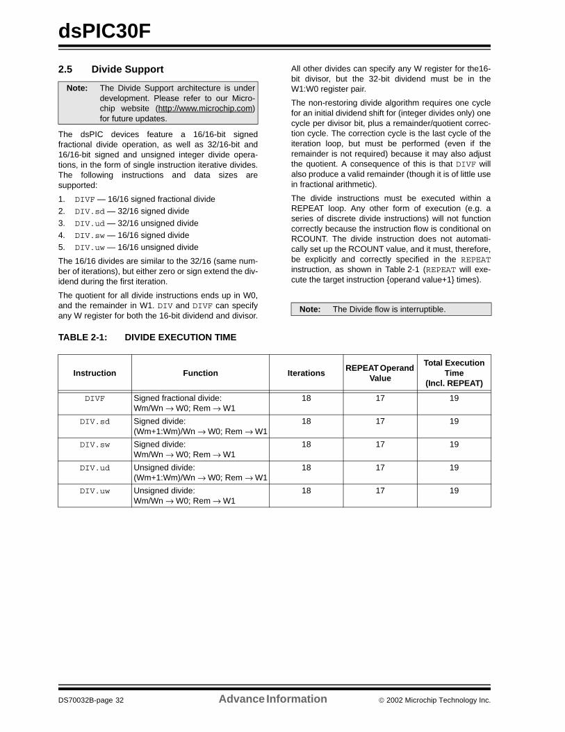
2.5 Divide Support
The dsPIC devices feature a 16/16-bit signedfractional divide operation, as well as 32/16-bit and16/16-bit signed and unsigned integer divide opera-tions, in the form of single instruction iterative divides.The following instructions and data sizes aresupported:
1. DIVF — 16/16 signed fractional divide2. DIV.sd — 32/16 signed divide
3. DIV.ud — 32/16 unsigned divide4. DIV.sw — 16/16 signed divide5. DIV.uw — 16/16 unsigned divide
The 16/16 divides are similar to the 32/16 (same num-ber of iterations), but either zero or sign extend the div-idend during the first iteration.
The quotient for all divide instructions ends up in W0,and the remainder in W1. DIV and DIVF can specifyany W register for both the 16-bit dividend and divisor.
All other divides can specify any W register for the16-bit divisor, but the 32-bit dividend must be in theW1:W0 register pair.
The non-restoring divide algorithm requires one cyclefor an initial dividend shift for (integer divides only) onecycle per divisor bit, plus a remainder/quotient correc-tion cycle. The correction cycle is the last cycle of theiteration loop, but must be performed (even if theremainder is not required) because it may also adjustthe quotient. A consequence of this is that DIVF willalso produce a valid remainder (though it is of little usein fractional arithmetic).
The divide instructions must be executed within aREPEAT loop. Any other form of execution (e.g. aseries of discrete divide instructions) will not functioncorrectly because the instruction flow is conditional onRCOUNT. The divide instruction does not automati-cally set up the RCOUNT value, and it must, therefore,be explicitly and correctly specified in the REPEATinstruction, as shown in Table 2-1 (REPEAT will exe-cute the target instruction operand value+1 times).
TABLE 2-1: DIVIDE EXECUTION TIME
Note: The Divide Support architecture is underdevelopment. Please refer to our Micro-chip website (http://www.microchip.com)for future updates.
Note: The Divide flow is interruptible.
Instruction Function IterationsREPEAT Operand
Value
Total Execution Time
(Incl. REPEAT)
DIVF Signed fractional divide: Wm/Wn → W0; Rem → W1
18 17 19
DIV.sd Signed divide:(Wm+1:Wm)/Wn → W0; Rem → W1
18 17 19
DIV.sw Signed divide:Wm/Wn → W0; Rem → W1
18 17 19
DIV.ud Unsigned divide:(Wm+1:Wm)/Wn → W0; Rem → W1
18 17 19
DIV.uw Unsigned divide:Wm/Wn → W0; Rem → W1
18 17 19
DS70032B-page 32 Advance Information 2002 Microchip Technology Inc.
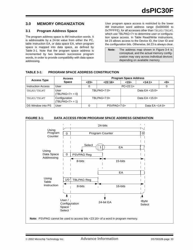
dsPIC30F
3.0 MEMORY ORGANIZATION
3.1 Program Address Space
The program address space is 4M instruction words. Itis addressable by a 24-bit value from either the PC,table instruction EA, or data space EA, when programspace is mapped into data space, as defined byTable 3-1. Note that the program space address isincremented by two between successive programwords, in order to provide compatibility with data spaceaddressing.
User program space access is restricted to the lower4M instruction word address range (0x000000 to0x7FFFFE), for all accesses other than TBLRD/TBLWT,which use TBLPAG<7> to determine user or configura-tion space access. In Table Read/Write instructions,bit 23 allows access to the Device ID, the User ID andthe configuration bits. Otherwise, bit 23 is always clear.
TABLE 3-1: PROGRAM SPACE ADDRESS CONSTRUCTION
FIGURE 3-1: DATA ACCESS FROM PROGRAM SPACE ADDRESS GENERATION
Note: The address map shown in Figure 3-4 isconceptual, and the actual memory config-uration may vary across individual devicesdepending on available memory.
Access TypeAccessSpace
Program Space Address<23> <22:16> <15> <14:1> <0>
Instruction Access User 0 PC<22:1> 0
TBLRD/TBLWT User (TBLPAG<7> = 0)
TBLPAG<7:0> Data EA <15:0>
TBLRD/TBLWT Configuration (TBLPAG<7> = 1)
TBLPAG<7:0> Data EA <15:0>
DS Window into PS User 0 PSVPAG<7:0> Data EA <14:0>
0Program Counter
24-bits
1
PSVPAG Reg
8-bits
EA
15-bits
Program
Using
Select
TBLPAG Reg
8-bits
EA
16-bits
Using
Byte24-bit EA
0
0
1/0
Select
User /Configuration
TableInstruction
Data SpaceAddressing
Counter
Using
Space Select
Note: PSVPAG cannot be used to access bits <23:16> of a word in program memory.
2002 Microchip Technology Inc. Advance Information DS70032B-page 33
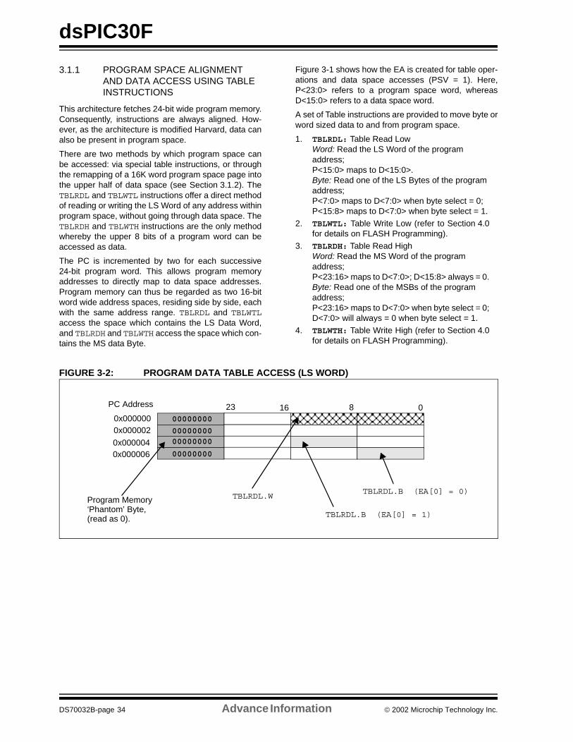
dsPIC30F
3.1.1 PROGRAM SPACE ALIGNMENT AND DATA ACCESS USING TABLE INSTRUCTIONS
This architecture fetches 24-bit wide program memory.Consequently, instructions are always aligned. How-ever, as the architecture is modified Harvard, data canalso be present in program space.
There are two methods by which program space canbe accessed: via special table instructions, or throughthe remapping of a 16K word program space page intothe upper half of data space (see Section 3.1.2). TheTBLRDL and TBLWTL instructions offer a direct methodof reading or writing the LS Word of any address withinprogram space, without going through data space. TheTBLRDH and TBLWTH instructions are the only methodwhereby the upper 8 bits of a program word can beaccessed as data.
The PC is incremented by two for each successive24-bit program word. This allows program memoryaddresses to directly map to data space addresses.Program memory can thus be regarded as two 16-bitword wide address spaces, residing side by side, eachwith the same address range. TBLRDL and TBLWTLaccess the space which contains the LS Data Word,and TBLRDH and TBLWTH access the space which con-tains the MS data Byte.
Figure 3-1 shows how the EA is created for table oper-ations and data space accesses (PSV = 1). Here,P<23:0> refers to a program space word, whereasD<15:0> refers to a data space word.
A set of Table instructions are provided to move byte orword sized data to and from program space.
1. TBLRDL: Table Read LowWord: Read the LS Word of the program address;P<15:0> maps to D<15:0>.Byte: Read one of the LS Bytes of the program address;P<7:0> maps to D<7:0> when byte select = 0;P<15:8> maps to D<7:0> when byte select = 1.
2. TBLWTL: Table Write Low (refer to Section 4.0for details on FLASH Programming).
3. TBLRDH: Table Read HighWord: Read the MS Word of the program address;P<23:16> maps to D<7:0>; D<15:8> always = 0.Byte: Read one of the MSBs of the program address;P<23:16> maps to D<7:0> when byte select = 0;D<7:0> will always = 0 when byte select = 1.
4. TBLWTH: Table Write High (refer to Section 4.0for details on FLASH Programming).
FIGURE 3-2: PROGRAM DATA TABLE ACCESS (LS WORD)
0816PC Address
0x0000000x000002
0x0000040x000006
2300000000
00000000
00000000
00000000
Program Memory‘Phantom’ Byte,(read as 0).
TBLRDL.W
TBLRDL.B (EA[0] = 1)
TBLRDL.B (EA[0] = 0)
DS70032B-page 34 Advance Information 2002 Microchip Technology Inc.
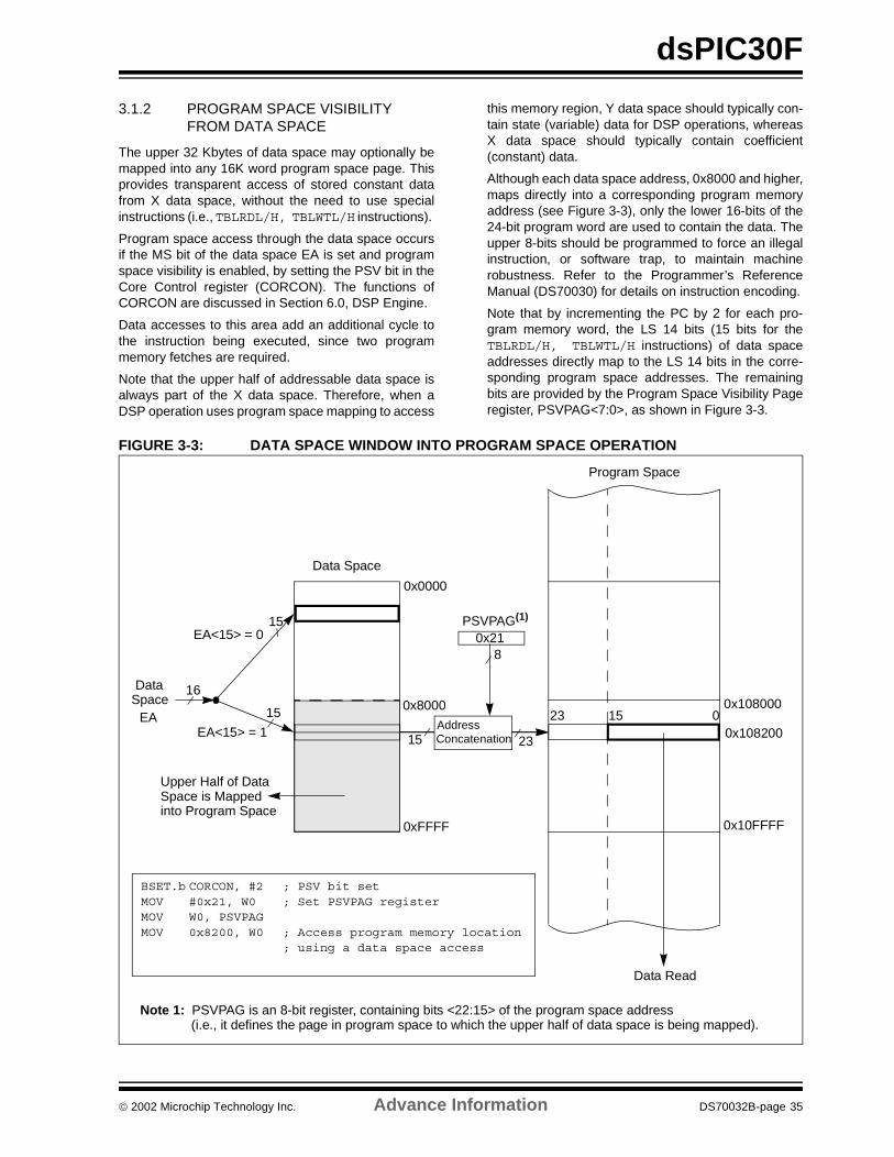
dsPIC30F
3.1.2 PROGRAM SPACE VISIBILITY FROM DATA SPACE
The upper 32 Kbytes of data space may optionally bemapped into any 16K word program space page. Thisprovides transparent access of stored constant datafrom X data space, without the need to use specialinstructions (i.e., TBLRDL/H, TBLWTL/H instructions).
Program space access through the data space occursif the MS bit of the data space EA is set and programspace visibility is enabled, by setting the PSV bit in theCore Control register (CORCON). The functions ofCORCON are discussed in Section 6.0, DSP Engine.
Data accesses to this area add an additional cycle tothe instruction being executed, since two programmemory fetches are required.
Note that the upper half of addressable data space isalways part of the X data space. Therefore, when aDSP operation uses program space mapping to access
this memory region, Y data space should typically con-tain state (variable) data for DSP operations, whereasX data space should typically contain coefficient(constant) data.
Although each data space address, 0x8000 and higher,maps directly into a corresponding program memoryaddress (see Figure 3-3), only the lower 16-bits of the24-bit program word are used to contain the data. Theupper 8-bits should be programmed to force an illegalinstruction, or software trap, to maintain machinerobustness. Refer to the Programmer’s ReferenceManual (DS70030) for details on instruction encoding.
Note that by incrementing the PC by 2 for each pro-gram memory word, the LS 14 bits (15 bits for theTBLRDL/H, TBLWTL/H instructions) of data spaceaddresses directly map to the LS 14 bits in the corre-sponding program space addresses. The remainingbits are provided by the Program Space Visibility Pageregister, PSVPAG<7:0>, as shown in Figure 3-3.
FIGURE 3-3: DATA SPACE WINDOW INTO PROGRAM SPACE OPERATION
23 15 0
PSVPAG(1)15
15
EA<15> = 0
EA<15> = 1
16DataSpace
EA
Data Space
Program Space
8
15 23
0x0000
0x8000
0xFFFF
0x21
0x108000
0x10FFFF
Data Read
Upper Half of Data Space is Mapped into Program Space
Note 1: PSVPAG is an 8-bit register, containing bits <22:15> of the program space address (i.e., it defines the page in program space to which the upper half of data space is being mapped).
0x108200AddressConcatenation
BSET.b CORCON, #2 ; PSV bit setMOV #0x21, W0 ; Set PSVPAG registerMOV W0, PSVPAGMOV 0x8200, W0 ; Access program memory location
; using a data space access
2002 Microchip Technology Inc. Advance Information DS70032B-page 35
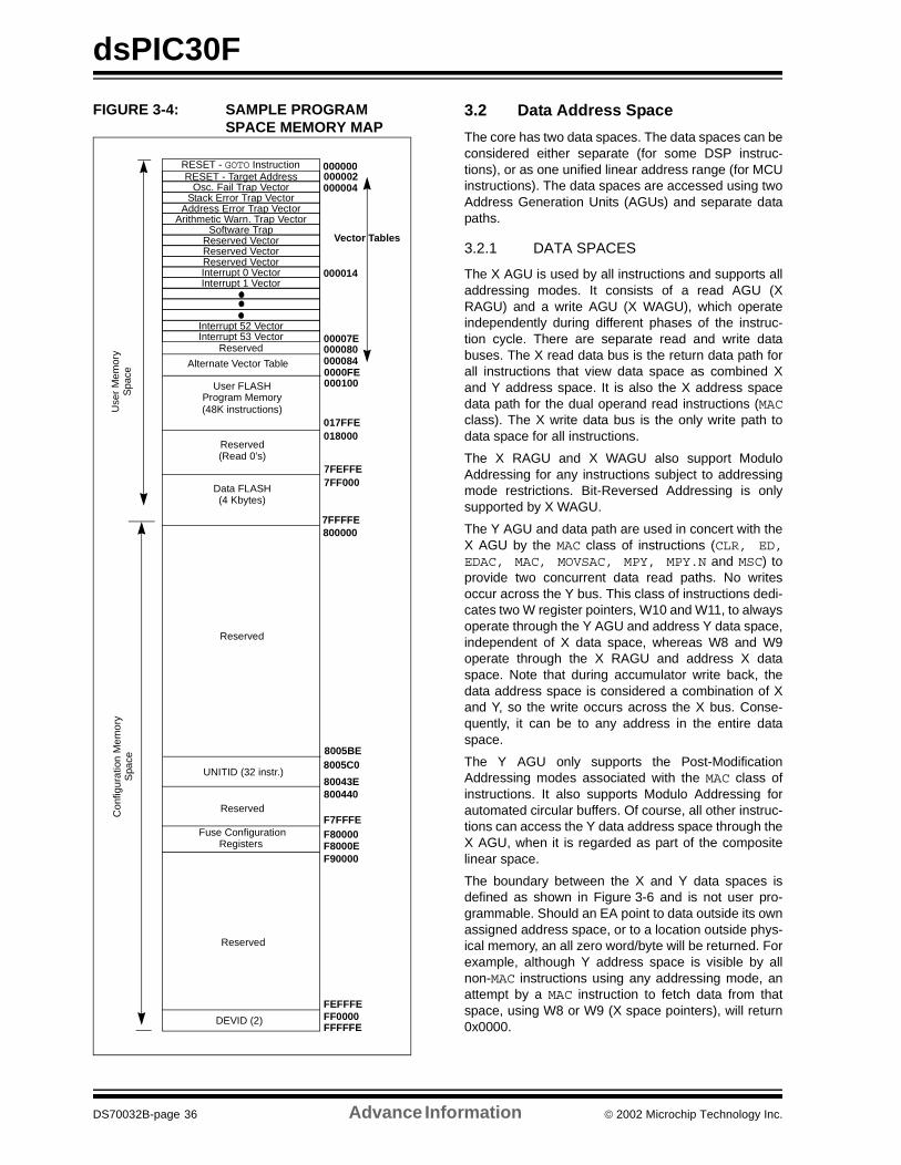
dsPIC30F
FIGURE 3-4: SAMPLE PROGRAM SPACE MEMORY MAP
3.2 Data Address Space
The core has two data spaces. The data spaces can beconsidered either separate (for some DSP instruc-tions), or as one unified linear address range (for MCUinstructions). The data spaces are accessed using twoAddress Generation Units (AGUs) and separate datapaths.
3.2.1 DATA SPACES
The X AGU is used by all instructions and supports alladdressing modes. It consists of a read AGU (XRAGU) and a write AGU (X WAGU), which operateindependently during different phases of the instruc-tion cycle. There are separate read and write databuses. The X read data bus is the return data path forall instructions that view data space as combined Xand Y address space. It is also the X address spacedata path for the dual operand read instructions (MACclass). The X write data bus is the only write path todata space for all instructions.
The X RAGU and X WAGU also support ModuloAddressing for any instructions subject to addressingmode restrictions. Bit-Reversed Addressing is onlysupported by X WAGU.
The Y AGU and data path are used in concert with theX AGU by the MAC class of instructions (CLR, ED,EDAC, MAC, MOVSAC, MPY, MPY.N and MSC) toprovide two concurrent data read paths. No writesoccur across the Y bus. This class of instructions dedi-cates two W register pointers, W10 and W11, to alwaysoperate through the Y AGU and address Y data space,independent of X data space, whereas W8 and W9operate through the X RAGU and address X dataspace. Note that during accumulator write back, thedata address space is considered a combination of Xand Y, so the write occurs across the X bus. Conse-quently, it can be to any address in the entire dataspace.
The Y AGU only supports the Post-ModificationAddressing modes associated with the MAC class ofinstructions. It also supports Modulo Addressing forautomated circular buffers. Of course, all other instruc-tions can access the Y data address space through theX AGU, when it is regarded as part of the compositelinear space.
The boundary between the X and Y data spaces isdefined as shown in Figure 3-6 and is not user pro-grammable. Should an EA point to data outside its ownassigned address space, or to a location outside phys-ical memory, an all zero word/byte will be returned. Forexample, although Y address space is visible by allnon-MAC instructions using any addressing mode, anattempt by a MAC instruction to fetch data from thatspace, using W8 or W9 (X space pointers), will return0x0000.
RESET - Target Address
Use
r M
emor
yS
pace
000000
00007E
Osc. Fail Trap Vector000002
000080
Fuse Configuration
User FLASHProgram Memory
018000017FFE
Con
figur
atio
n M
emor
yS
pace
Data FLASH
Stack Error Trap VectorAddress Error Trap Vector
Arithmetic Warn. Trap VectorSoftware Trap
Reserved VectorReserved VectorReserved VectorInterrupt 0 VectorInterrupt 1 Vector
Interrupt 52 VectorInterrupt 53 Vector
(48K instructions)
(4 Kbytes)
800000
F80000Registers F8000E
F90000
DEVID (2)
FEFFFEFF0000FFFFFE
ReservedF7FFFE
Reserved
7FF0007FEFFE
(Read 0’s)
80043E800440
UNITID (32 instr.)
000014
Vector Tables
8005BE8005C0
RESET - GOTO Instruction
000004
Reserved
7FFFFE
Reserved
0001000000FE000084Alternate Vector Table
Reserved
DS70032B-page 36 Advance Information 2002 Microchip Technology Inc.
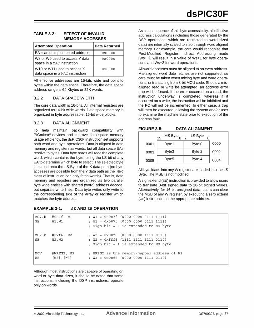
dsPIC30F
All effective addresses are 16-bits wide and point tobytes within the data space. Therefore, the data spaceaddress range is 64 Kbytes or 32K words.
3.2.2 DATA SPACE WIDTH
The core data width is 16-bits. All internal registers areorganized as 16-bit wide words. Data space memory isorganized in byte addressable, 16-bit wide blocks.
3.2.3 DATA ALIGNMENT
To help maintain backward compatibility withPICmicro® devices and improve data space memoryusage efficiency, the dsPIC30F instruction set supportsboth word and byte operations. Data is aligned in datamemory and registers as words, but all data space EAsresolve to bytes. Data byte reads will read the completeword, which contains the byte, using the LS bit of anyEA to determine which byte to select. The selected byteis placed onto the LS Byte of the X data path (no byteaccesses are possible from the Y data path as the MACclass of instruction can only fetch words). That is, datamemory and registers are organized as two parallelbyte wide entities with shared (word) address decode,but separate write lines. Data byte writes only write tothe corresponding side of the array or register whichmatches the byte address.
As a consequence of this byte accessibility, all effectiveaddress calculations (including those generated by theDSP operations, which are restricted to word sizeddata) are internally scaled to step through word alignedmemory. For example, the core would recognize thatPost-Modified Register Indirect Addressing mode[Ws++], will result in a value of Ws+1 for byte opera-tions and Ws+2 for word operations.
All word accesses must be aligned to an even address.Mis-aligned word data fetches are not supported, socare must be taken when mixing byte and word opera-tions, or translating from 8-bit MCU code. Should a mis-aligned read or write be attempted, an address errortrap will be forced. If the error occurred on a read, theinstruction underway is completed, whereas if itoccurred on a write, the instruction will be inhibited andthe PC will not be incremented. In either case, a trapwill then be executed, allowing the system and/or userto examine the machine state prior to execution of theaddress fault.
FIGURE 3-5: DATA ALIGNMENT
All byte loads into any W register are loaded into the LSByte. The MSB is not modified.
A sign extend (SE) instruction is provided to allow usersto translate 8-bit signed data to 16-bit signed values.Alternatively, for 16-bit unsigned data, users can clearthe MSB of any W register, by executing a zero extend(ZE) instruction on the appropriate address.
EXAMPLE 3-1: SE AND ZE OPERATION
Although most instructions are capable of operating onword or byte data sizes, it should be noted that someinstructions, including the DSP instructions, operateonly on words.
TABLE 3-2: EFFECT OF INVALID MEMORY ACCESSES
Attempted Operation Data Returned
EA = an unimplemented address 0x0000
W8 or W9 used to access Y data space in a MAC instruction
0x0000
W10 or W11 used to access X data space in a MAC instruction
0x0000
15 8 7 0
0001
0003
0005
0000
0002
0004
Byte1 Byte 0
Byte3 Byte 2
Byte5 Byte 4
LS ByteMS Byte
MOV.b #0x7f, W1 ; W1 = 0x007f (0000 0000 0111 1111)SE W1,W1 ; W1 = 0x007f (0000 0000 0111 1111)
; Sign bit = 0 is extended to MS byte
MOV.b #0xf6, W2 ; W2 = 0x00f6 (0000 0000 1111 0110)SE W2,W2 ; W2 = 0xfff6 (1111 1111 1111 0110)
; Sign bit = 1 is extended to MS byte
MOV #WREG2, W3 ; WREG2 is the memory-mapped address of W2ZE [W3],[W3] ; W3 = 0x00f6 (0000 0000 1111 0110)
2002 Microchip Technology Inc. Advance Information DS70032B-page 37
dsPIC30F
3.2.4 DATA SPACE MEMORY MAP
The data space memory is split into two blocks, X andY data space. A key element of this architecture is thatY space is a subset of X space, and is fully containedwithin X space. In order to provide an apparent linearaddressing space, X and Y spaces have contiguousaddresses.
When executing any instruction other than one of theMAC class of instructions, the X block consists of theentire 64 Kbyte data address space (including all Yaddresses). When executing a MAC class of instruction,the X block consists of the entire 64 Kbyte data addressspace, less the Y address block for data reads (only).In other words, all other instructions regard the entiredata memory as one composite address space. TheMAC class of instructions extracts the Y address spacefrom data space and addresses it using EAs sourcedfrom W10 and W11. The remaining X data space isaddressed using W8 and W9. Both address spaces areconcurrently accessed only by the MAC class ofinstruction.
An example data space memory map is shown inFigure 3-6.
3.2.5 ACCESS RAM SPACE
An 8 Kbyte access space is reserved in X addressmemory space between 0x0000 and 0x1FFF, which isdirectly addressable via a 13-bit absolute address fieldwithin all memory direct instructions. The remaining Xaddress space and all of the Y address space isaddressable indirectly. Additionally, the whole of X dataspace is addressable using MOV instructions, whichsupport memory direct addressing with a 16-bitaddress field.
DS70032B-page 38 Advance Information 2002 Microchip Technology Inc.
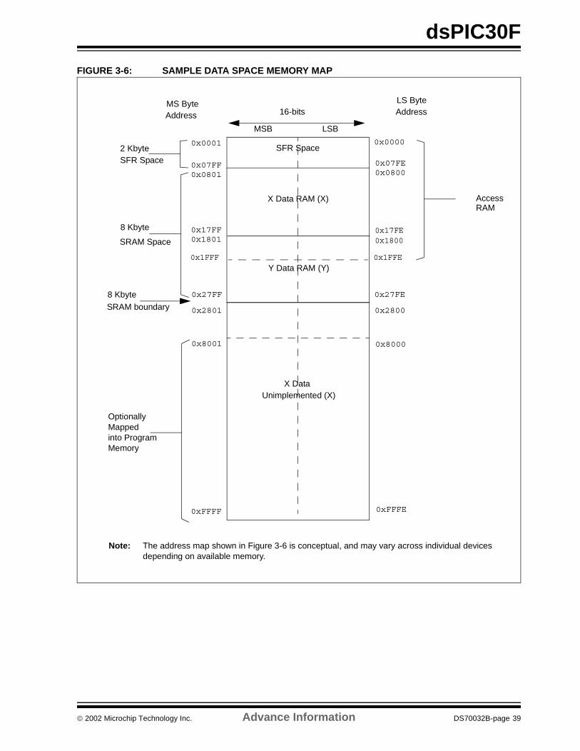
dsPIC30F
FIGURE 3-6: SAMPLE DATA SPACE MEMORY MAP
0x0000
0x07FE
SFR Space
0x17FE
0xFFFE
X Data RAM (X)
LS ByteAddress16-bits
LSBMSB
MS ByteAddress
0x0001
0x07FF
0x17FF
0xFFFF
X Data
0x8001 0x8000
OptionallyMappedinto ProgramMemory
Unimplemented (X)
0x27FF 0x27FE
0x28000x2801
0x0801 0x0800
0x1801 0x1800
AccessRAM
0x1FFE 0x1FFF Y Data RAM (Y)
2 KbyteSFR Space
8 Kbyte
SRAM Space
8 KbyteSRAM boundary
Note: The address map shown in Figure 3-6 is conceptual, and may vary across individual devicesdepending on available memory.
2002 Microchip Technology Inc. Advance Information DS70032B-page 39
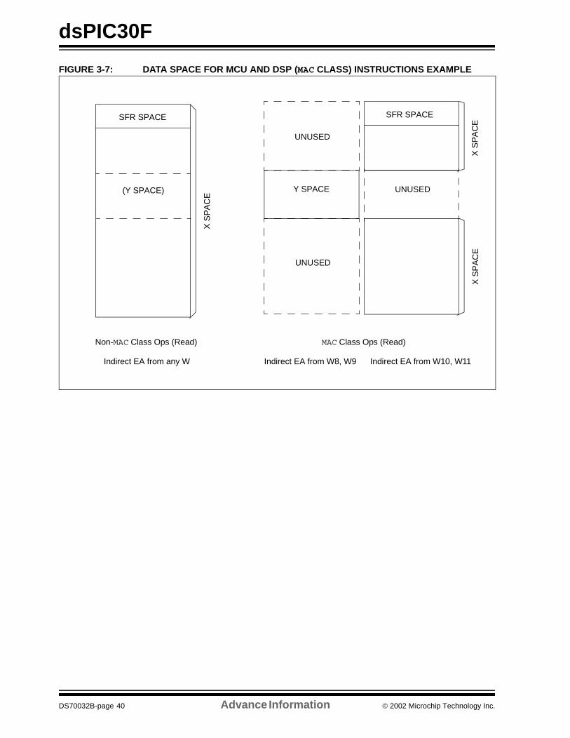
dsPIC30F
FIGURE 3-7: DATA SPACE FOR MCU AND DSP (MAC CLASS) INSTRUCTIONS EXAMPLE
SFR SPACE
(Y SPACE)
X S
PA
CE
SFR SPACE
UNUSED
X S
PA
CE
X S
PA
CE
Y SPACE
UNUSED
UNUSED
Non-MAC Class Ops (Read) MAC Class Ops (Read)
Indirect EA from any W Indirect EA from W8, W9 Indirect EA from W10, W11
DS70032B-page 40 Advance Information 2002 Microchip Technology Inc.
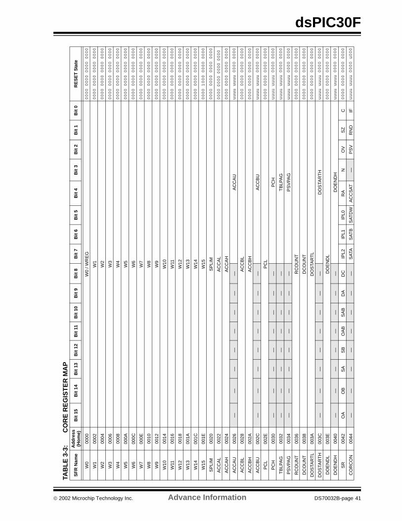
dsPIC30F
TAB
LE
3-3
:C
OR
E R
EG
IST
ER
MA
P
SF
R N
ame
Ad
dre
ss(H
om
e)B
it 1
5B
it 1
4B
it 1
3B
it 1
2B
it 1
1B
it 1
0B
it 9
Bit
8B
it 7
Bit
6B
it 5
Bit
4B
it 3
Bit
2B
it 1
Bit
0R
ES
ET
Sta
te
W0
0000
W0
/ WR
EG
0000 0000 0000 0000
W1
0002
W1
0000 0000 0000 0000
W2
0004
W2
0000 0000 0000 0000
W3
0006
W3
0000 0000 0000 0000
W4
0008
W4
0000 0000 0000 0000
W5
000A
W5
0000 0000 0000 0000
W6
000C
W6
0000 0000 0000 0000
W7
000E
W7
0000 0000 0000 0000
W8
0010
W8
0000 0000 0000 0000
W9
0012
W9
0000 0000 0000 0000
W10
0014
W10
0000 0000 0000 0000
W11
0016
W11
0000 0000 0000 0000
W12
0018
W12
0000 0000 0000 0000
W13
001A
W13
0000 0000 0000 0000
W14
001C
W14
0000 0000 0000 0000
W15
001E
W15
0000 1000 0000 0000
SP
LIM
0020
SP
LIM
0000 0000 0000 0000
AC
CA
L00
22A
CC
AL
0000 0000 0000 0000
AC
CA
H00
24A
CC
AH
0000 0000 0000 0000
AC
CA
U00
26—
——
——
——
—A
CC
AU
uuuu uuuu 0000 0000
AC
CB
L00
28A
CC
BL
0000 0000 0000 0000
AC
CB
H00
2AA
CC
BH
0000 0000 0000 0000
AC
CB
U00
2C—
——
——
——
—A
CC
BU
uuuu uuuu 0000 0000
PC
L00
2EP
CL
0000 0000 0000 0000
PC
H00
30—
——
——
——
—P
CH
uuuu uuuu 0000 0000
TB
LPA
G00
32—
——
——
——
—T
BLP
AG
uuuu uuuu 0000 0000
PS
VP
AG
0034
——
——
——
——
PS
VP
AG
uuuu uuuu 0000 0000
RC
OU
NT
0036
RC
OU
NT
0000 0000 0000 0000
DC
OU
NT
0038
DC
OU
NT
0000 0000 0000 0000
DO
STA
RT
L00
3AD
OS
TAR
TL
0000 0000 0000 0000
DO
STA
RT
H00
3C—
——
——
——
—D
OS
TAR
TH
uuuu uuuu 0000 0000
DO
EN
DL
003E
DO
EN
DL
0000 0000 0000 0000
DO
EN
DH
0040
——
——
——
——
DO
EN
DH
uuuu uuuu 0000 0000
SR
0042
OA
OB
SA
SB
OA
BS
AB
DA
DC
IPL2
IPL1
IPL0
RA
NO
VS
ZC
0000 0000 0000 0000
CO
RC
ON
0044
——
——
——
——
SA
TAS
AT
BS
AT
DW
AC
CS
AT
—P
SV
RN
DIF
uuuu uuuu 0000 u000
2002 Microchip Technology Inc. Advance Information DS70032B-page 41
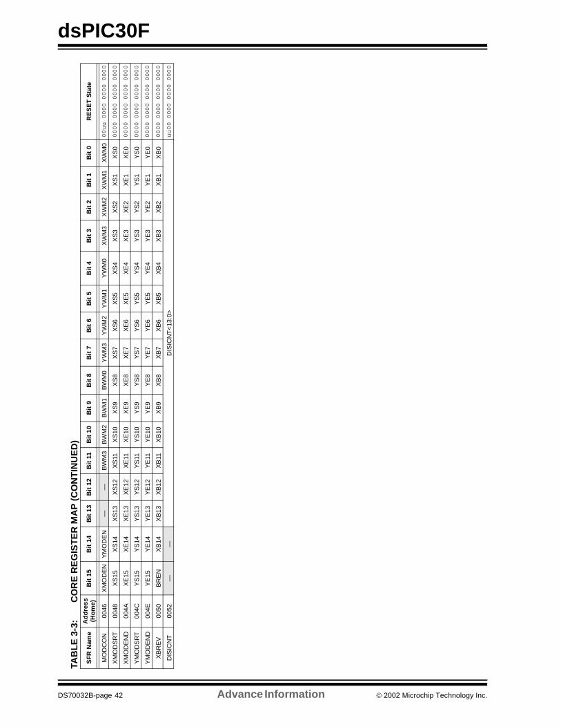
dsPIC30F
DS
MO
DC
ON
0046
XM
OD
EN
YM
OD
EN
——
BW
M3
BW
M2
BW
M1
BW
M0
YW
M3
YW
M2
YW
M1
YW
M0
XW
M3
XW
M2
XW
M1
XW
M0
00uu 0000 0000 0000
XM
OD
SR
T00
48X
S15
XS
14X
S13
XS
12X
S11
XS
10X
S9
XS
8X
S7
XS
6X
S5
XS
4X
S3
XS
2X
S1
XS
00000 0000 0000 0000
XM
OD
EN
D00
4AX
E15
XE
14X
E13
XE
12X
E11
XE
10X
E9
XE
8X
E7
XE
6X
E5
XE
4X
E3
XE
2X
E1
XE
00000 0000 0000 0000
YM
OD
SR
T00
4CY
S15
YS
14Y
S13
YS
12Y
S11
YS
10Y
S9
YS
8Y
S7
YS
6Y
S5
YS
4Y
S3
YS
2Y
S1
YS
00000 0000 0000 0000
YM
OD
EN
D00
4EY
E15
YE
14Y
E13
YE
12Y
E11
YE
10Y
E9
YE
8Y
E7
YE
6Y
E5
YE
4Y
E3
YE
2Y
E1
YE
00000 0000 0000 0000
XB
RE
V00
50B
RE
NX
B14
XB
13X
B12
XB
11X
B10
XB
9X
B8
XB
7X
B6
XB
5X
B4
XB
3X
B2
XB
1X
B0
0000 0000 0000 0000
DIS
ICN
T00
52—
—D
ISIC
NT
<13
:0>
uu00 0000 0000 0000
TAB
LE
3-3
:C
OR
E R
EG
IST
ER
MA
P (
CO
NT
INU
ED
)
SF
R N
ame
Ad
dre
ss(H
om
e)B
it 1
5B
it 1
4B
it 1
3B
it 1
2B
it 1
1B
it 1
0B
it 9
Bit
8B
it 7
Bit
6B
it 5
Bit
4B
it 3
Bit
2B
it 1
Bit
0R
ES
ET
Sta
te
70032B-page 42 Advance Information 2002 Microchip Technology Inc.
dsPIC30F
3.2.6 DATA PRE-FETCH FROM PROGRAM SPACE WITHIN A REPEAT LOOP
When pre-fetching data resident in program space, viathe data space window from within a REPEAT loop, alliterations of the repeated instruction will reload theinstruction from the Instruction Latch without re-fetching it, thereby releasing the program bus for a
data pre-fetch, as shown in Figure 3-8. In this exam-ple, the initial 2 data words for the first iteration of theinstruction to be repeated (MAC A) are fetched by aprior instruction (e.g., CLR A instruction). The subse-quent MAC instructions, therefore, only need to fetchtwo more data pairs to complete the loop. The initialfetch of the MAC A instruction is performed by theREPEAT instruction.
EXAMPLE 3-2: PROGRAM SPACE DATA READ THROUGH DATA SPACE WITHIN A REPEAT LOOP
FIGURE 3-8: PROGRAM SPACE DATA READ THROUGH DATA SPACE WITHIN A REPEAT LOOP
; In this example, data for MAC operations is stored in Program Space.
CLR A, [W8]+=2, W4, [W10]+=2, W5 ; Acc. A cleared, data prefetched (2 cycles)REPEAT #99 ; Repeat the MAC operation 100 times (1 cycle) MAC W4*W5, A, [W8]+=2, W4, [W10]+=2, W5 ; MAC operation within REPEAT loop (1 cycle)
Read [15:0] (X Data)(1)
TCY1 TCY2 TCY1 TCY1
Read [15:0] (X Data)(1)
CLR A
ProgramSpaceFetch
Read (REPEAT)
CLR A
Note 1: Program space window will always reside in X space.
Read (MAC A)
REPEAT 1ST MAC ATCY1
Read [15:0] (X Data)(1)
2ND MAC A
ReadData
Fetch (Y Data)(1)Read
(Y Data)(1)Space Write(Loop cnt.)
Read(Y Data)(1)
TCY13RD MAC A
InstructionExecuted
2002 Microchip Technology Inc. Advance Information DS70032B-page 43

dsPIC30F
NOTES:
DS70032B-page 44 Advance Information 2002 Microchip Technology Inc.
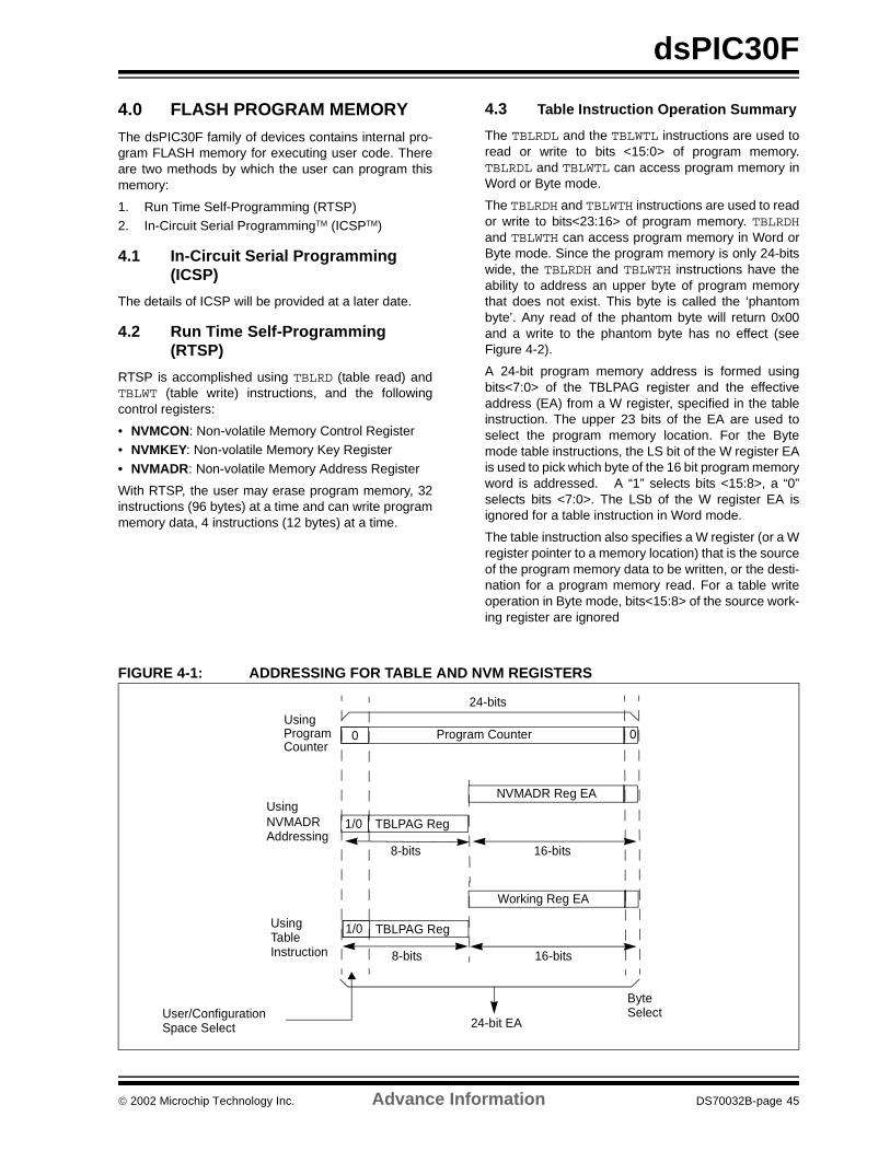
dsPIC30F
4.0 FLASH PROGRAM MEMORY
The dsPIC30F family of devices contains internal pro-gram FLASH memory for executing user code. Thereare two methods by which the user can program thismemory:
1. Run Time Self-Programming (RTSP)2. In-Circuit Serial ProgrammingTM (ICSPTM)
4.1 In-Circuit Serial Programming (ICSP)
The details of ICSP will be provided at a later date.
4.2 Run Time Self-Programming (RTSP)
RTSP is accomplished using TBLRD (table read) andTBLWT (table write) instructions, and the followingcontrol registers:
• NVMCON: Non-volatile Memory Control Register• NVMKEY: Non-volatile Memory Key Register
• NVMADR: Non-volatile Memory Address Register
With RTSP, the user may erase program memory, 32instructions (96 bytes) at a time and can write programmemory data, 4 instructions (12 bytes) at a time.
4.3 Table Instruction Operation Summary
The TBLRDL and the TBLWTL instructions are used toread or write to bits <15:0> of program memory.TBLRDL and TBLWTL can access program memory inWord or Byte mode.
The TBLRDH and TBLWTH instructions are used to reador write to bits<23:16> of program memory. TBLRDHand TBLWTH can access program memory in Word orByte mode. Since the program memory is only 24-bitswide, the TBLRDH and TBLWTH instructions have theability to address an upper byte of program memorythat does not exist. This byte is called the ‘phantombyte’. Any read of the phantom byte will return 0x00and a write to the phantom byte has no effect (seeFigure 4-2).
A 24-bit program memory address is formed usingbits<7:0> of the TBLPAG register and the effectiveaddress (EA) from a W register, specified in the tableinstruction. The upper 23 bits of the EA are used toselect the program memory location. For the Bytemode table instructions, the LS bit of the W register EAis used to pick which byte of the 16 bit program memoryword is addressed. A “1” selects bits <15:8>, a “0”selects bits <7:0>. The LSb of the W register EA isignored for a table instruction in Word mode.
The table instruction also specifies a W register (or a Wregister pointer to a memory location) that is the sourceof the program memory data to be written, or the desti-nation for a program memory read. For a table writeoperation in Byte mode, bits<15:8> of the source work-ing register are ignored
FIGURE 4-1: ADDRESSING FOR TABLE AND NVM REGISTERS
0Program Counter
24-bits
TBLPAG Reg
8-bits 16-bits
Program
Using
TBLPAG Reg
8-bits
Working Reg EA
16-bits
Using
Byte
24-bit EA
1/0
0
1/0
Select
TableInstruction
NVMADRAddressing
Counter
Using
NVMADR Reg EA
User/ConfigurationSpace Select
2002 Microchip Technology Inc. Advance Information DS70032B-page 45
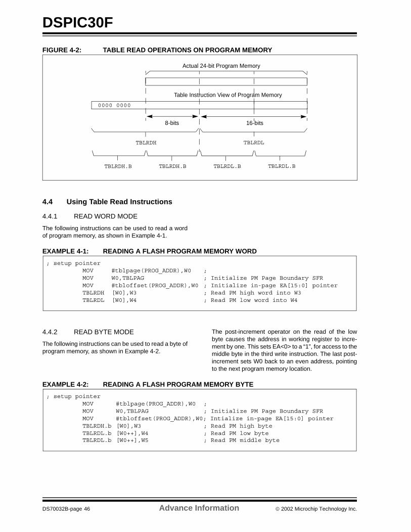
DSPIC30F
FIGURE 4-2: TABLE READ OPERATIONS ON PROGRAM MEMORY
4.4 Using Table Read Instructions
4.4.1 READ WORD MODE
The following instructions can be used to read a wordof program memory, as shown in Example 4-1.
EXAMPLE 4-1: READING A FLASH PROGRAM MEMORY WORD
4.4.2 READ BYTE MODE
The following instructions can be used to read a byte ofprogram memory, as shown in Example 4-2.
The post-increment operator on the read of the lowbyte causes the address in working register to incre-ment by one. This sets EA<0> to a “1”, for access to themiddle byte in the third write instruction. The last post-increment sets W0 back to an even address, pointingto the next program memory location.
EXAMPLE 4-2: READING A FLASH PROGRAM MEMORY BYTE
16-bits8-bits
TBLRDH TBLRDL
0000 0000
Actual 24-bit Program Memory
TBLRDH.B TBLRDH.B TBLRDL.B TBLRDL.B
Table Instruction View of Program Memory
; setup pointerMOV #tblpage(PROG_ADDR),W0 ; MOV W0,TBLPAG ; Initialize PM Page Boundary SFRMOV #tbloffset(PROG_ADDR),W0 ; Initialize in-page EA[15:0] pointerTBLRDH [W0],W3 ; Read PM high word into W3TBLRDL [W0],W4 ; Read PM low word into W4
; setup pointerMOV #tblpage(PROG_ADDR),W0 ;MOV W0,TBLPAG ; Initialize PM Page Boundary SFRMOV #tbloffset(PROG_ADDR),W0; Intialize in-page EA[15:0] pointerTBLRDH.b [W0],W3 ; Read PM high byteTBLRDL.b [W0++],W4 ; Read PM low byteTBLRDL.b [W0++],W5 ; Read PM middle byte
DS70032B-page 46 Advance Information 2002 Microchip Technology Inc.
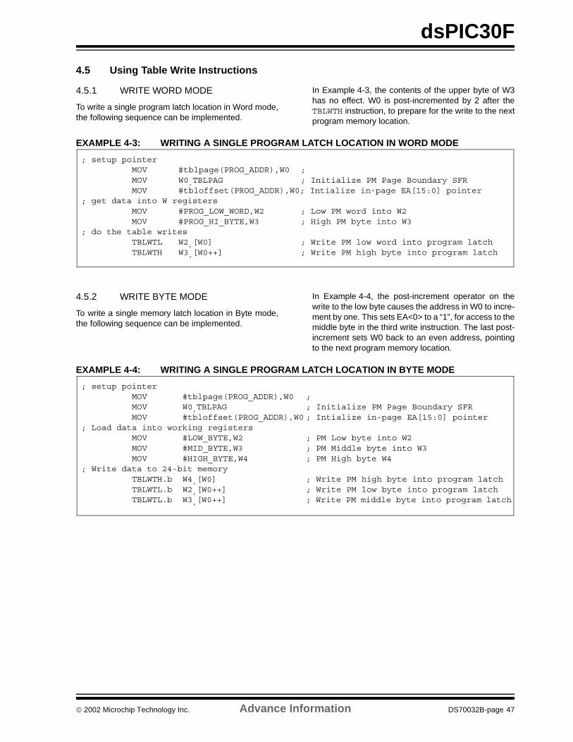
dsPIC30F
4.5 Using Table Write Instructions
4.5.1 WRITE WORD MODE
To write a single program latch location in Word mode,the following sequence can be implemented.
In Example 4-3, the contents of the upper byte of W3has no effect. W0 is post-incremented by 2 after theTBLWTH instruction, to prepare for the write to the nextprogram memory location.
EXAMPLE 4-3: WRITING A SINGLE PROGRAM LATCH LOCATION IN WORD MODE
4.5.2 WRITE BYTE MODE
To write a single memory latch location in Byte mode,the following sequence can be implemented.
In Example 4-4, the post-increment operator on thewrite to the low byte causes the address in W0 to incre-ment by one. This sets EA<0> to a “1”, for access to themiddle byte in the third write instruction. The last post-increment sets W0 back to an even address, pointingto the next program memory location.
EXAMPLE 4-4: WRITING A SINGLE PROGRAM LATCH LOCATION IN BYTE MODE
; setup pointerMOV #tblpage(PROG_ADDR),W0 ; MOV W0,TBLPAG ; Initialize PM Page Boundary SFRMOV #tbloffset(PROG_ADDR),W0; Intialize in-page EA[15:0] pointer
; get data into W registersMOV #PROG_LOW_WORD,W2 ; Low PM word into W2MOV #PROG_HI_BYTE,W3 ; High PM byte into W3
; do the table writesTBLWTL W2,[W0] ; Write PM low word into program latchTBLWTH W3,[W0++] ; Write PM high byte into program latch
; setup pointerMOV #tblpage(PROG_ADDR),W0 ;MOV W0,TBLPAG ; Initialize PM Page Boundary SFRMOV #tbloffset(PROG_ADDR),W0 ; Intialize in-page EA[15:0] pointer
; Load data into working registersMOV #LOW_BYTE,W2 ; PM Low byte into W2MOV #MID_BYTE,W3 ; PM Middle byte into W3MOV #HIGH_BYTE,W4 ; PM High byte W4
; Write data to 24-bit memoryTBLWTH.b W4,[W0] ; Write PM high byte into program latchTBLWTL.b W2,[W0++] ; Write PM low byte into program latchTBLWTL.b W3,[W0++] ; Write PM middle byte into program latch
2002 Microchip Technology Inc. Advance Information DS70032B-page 47
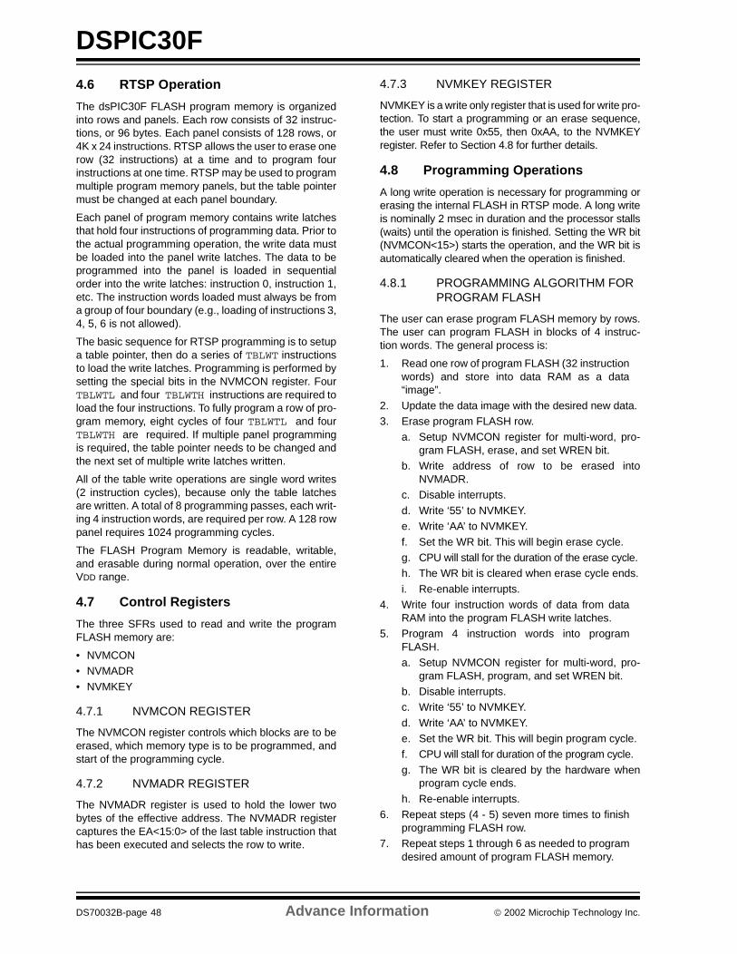
DSPIC30F
4.6 RTSP Operation
The dsPIC30F FLASH program memory is organizedinto rows and panels. Each row consists of 32 instruc-tions, or 96 bytes. Each panel consists of 128 rows, or4K x 24 instructions. RTSP allows the user to erase onerow (32 instructions) at a time and to program fourinstructions at one time. RTSP may be used to programmultiple program memory panels, but the table pointermust be changed at each panel boundary.
Each panel of program memory contains write latchesthat hold four instructions of programming data. Prior tothe actual programming operation, the write data mustbe loaded into the panel write latches. The data to beprogrammed into the panel is loaded in sequentialorder into the write latches: instruction 0, instruction 1,etc. The instruction words loaded must always be froma group of four boundary (e.g., loading of instructions 3,4, 5, 6 is not allowed).
The basic sequence for RTSP programming is to setupa table pointer, then do a series of TBLWT instructionsto load the write latches. Programming is performed bysetting the special bits in the NVMCON register. FourTBLWTL and four TBLWTH instructions are required toload the four instructions. To fully program a row of pro-gram memory, eight cycles of four TBLWTL and fourTBLWTH are required. If multiple panel programmingis required, the table pointer needs to be changed andthe next set of multiple write latches written.
All of the table write operations are single word writes(2 instruction cycles), because only the table latchesare written. A total of 8 programming passes, each writ-ing 4 instruction words, are required per row. A 128 rowpanel requires 1024 programming cycles.
The FLASH Program Memory is readable, writable,and erasable during normal operation, over the entireVDD range.
4.7 Control Registers
The three SFRs used to read and write the programFLASH memory are:
• NVMCON• NVMADR
• NVMKEY
4.7.1 NVMCON REGISTER
The NVMCON register controls which blocks are to beerased, which memory type is to be programmed, andstart of the programming cycle.
4.7.2 NVMADR REGISTER
The NVMADR register is used to hold the lower twobytes of the effective address. The NVMADR registercaptures the EA<15:0> of the last table instruction thathas been executed and selects the row to write.
4.7.3 NVMKEY REGISTER
NVMKEY is a write only register that is used for write pro-tection. To start a programming or an erase sequence,the user must write 0x55, then 0xAA, to the NVMKEYregister. Refer to Section 4.8 for further details.
4.8 Programming Operations
A long write operation is necessary for programming orerasing the internal FLASH in RTSP mode. A long writeis nominally 2 msec in duration and the processor stalls(waits) until the operation is finished. Setting the WR bit(NVMCON<15>) starts the operation, and the WR bit isautomatically cleared when the operation is finished.
4.8.1 PROGRAMMING ALGORITHM FOR PROGRAM FLASH
The user can erase program FLASH memory by rows.The user can program FLASH in blocks of 4 instruc-tion words. The general process is:
1. Read one row of program FLASH (32 instructionwords) and store into data RAM as a data“image”.
2. Update the data image with the desired new data.3. Erase program FLASH row.
a. Setup NVMCON register for multi-word, pro-gram FLASH, erase, and set WREN bit.
b. Write address of row to be erased intoNVMADR.
c. Disable interrupts.
d. Write ‘55’ to NVMKEY.e. Write ‘AA’ to NVMKEY.
f. Set the WR bit. This will begin erase cycle.g. CPU will stall for the duration of the erase cycle.h. The WR bit is cleared when erase cycle ends.
i. Re-enable interrupts.4. Write four instruction words of data from data
RAM into the program FLASH write latches.5. Program 4 instruction words into program
FLASH.a. Setup NVMCON register for multi-word, pro-
gram FLASH, program, and set WREN bit.b. Disable interrupts.c. Write ‘55’ to NVMKEY.
d. Write ‘AA’ to NVMKEY.e. Set the WR bit. This will begin program cycle.f. CPU will stall for duration of the program cycle.
g. The WR bit is cleared by the hardware whenprogram cycle ends.
h. Re-enable interrupts.6. Repeat steps (4 - 5) seven more times to finish
programming FLASH row. 7. Repeat steps 1 through 6 as needed to program
desired amount of program FLASH memory.
DS70032B-page 48 Advance Information 2002 Microchip Technology Inc.
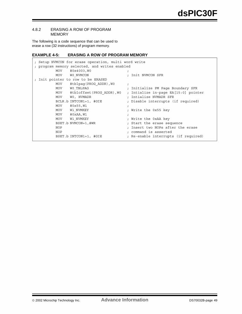
dsPIC30F
4.8.2 ERASING A ROW OF PROGRAM MEMORY
The following is a code sequence that can be used toerase a row (32 instructions) of program memory.
EXAMPLE 4-5: ERASING A ROW OF PROGRAM MEMORY
; Setup NVMCON for erase operation, multi word write; program memory selected, and writes enabled
MOV #0x4003,W0 ;MOV W0,NVMCON ; Init NVMCON SFR
; Init pointer to row to be ERASEDMOV #tblpag(PROG_ADDR),W0 ; MOV W0,TBLPAG ; Initialize PM Page Boundary SFRMOV #tbloffset(PROG_ADDR),W0 ; Intialize in-page EA[15:0] pointerMOV W0, NVMADR ; Intialize NVMADR SFRBCLR.b INTCON1+1, #GIE ; Disable interrupts (if required)MOV #0x55,W1 ; MOV W1,NVMKEY ; Write the 0x55 keyMOV #0xAA,W1 ; MOV W1,NVMKEY ; Write the 0xAA keyBSET.b NVMCON+1,#WR ; Start the erase sequence NOP ; Insert two NOPs after the eraseNOP ; command is assertedBSET.b INTCON1+1, #GIE ; Re-enable interrupts (if required)
2002 Microchip Technology Inc. Advance Information DS70032B-page 49
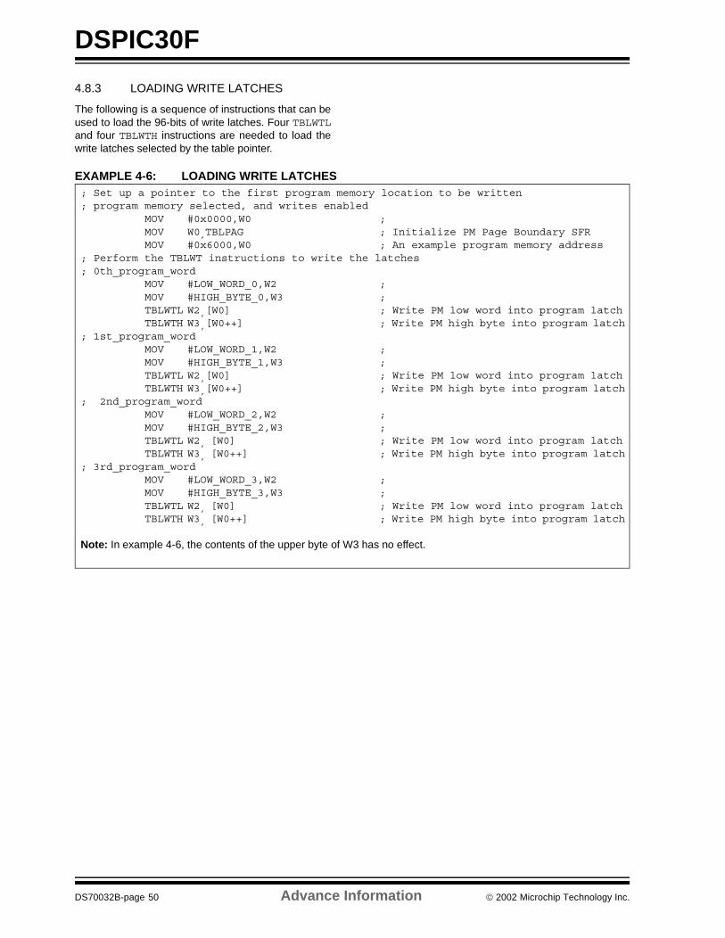
DSPIC30F
4.8.3 LOADING WRITE LATCHES
The following is a sequence of instructions that can beused to load the 96-bits of write latches. Four TBLWTLand four TBLWTH instructions are needed to load thewrite latches selected by the table pointer.
EXAMPLE 4-6: LOADING WRITE LATCHES ; Set up a pointer to the first program memory location to be written; program memory selected, and writes enabled
MOV #0x0000,W0 ; MOV W0,TBLPAG ; Initialize PM Page Boundary SFRMOV #0x6000,W0 ; An example program memory address
; Perform the TBLWT instructions to write the latches; 0th_program_word
MOV #LOW_WORD_0,W2 ; MOV #HIGH_BYTE_0,W3 ; TBLWTL W2,[W0] ; Write PM low word into program latchTBLWTH W3,[W0++] ; Write PM high byte into program latch
; 1st_program_wordMOV #LOW_WORD_1,W2 ; MOV #HIGH_BYTE_1,W3 ; TBLWTL W2,[W0] ; Write PM low word into program latchTBLWTH W3,[W0++] ; Write PM high byte into program latch
; 2nd_program_wordMOV #LOW_WORD_2,W2 ; MOV #HIGH_BYTE_2,W3 ; TBLWTL W2, [W0] ; Write PM low word into program latchTBLWTH W3, [W0++] ; Write PM high byte into program latch
; 3rd_program_wordMOV #LOW_WORD_3,W2 ; MOV #HIGH_BYTE_3,W3 ; TBLWTL W2, [W0] ; Write PM low word into program latchTBLWTH W3, [W0++] ; Write PM high byte into program latch
Note: In example 4-6, the contents of the upper byte of W3 has no effect.
DS70032B-page 50 Advance Information 2002 Microchip Technology Inc.
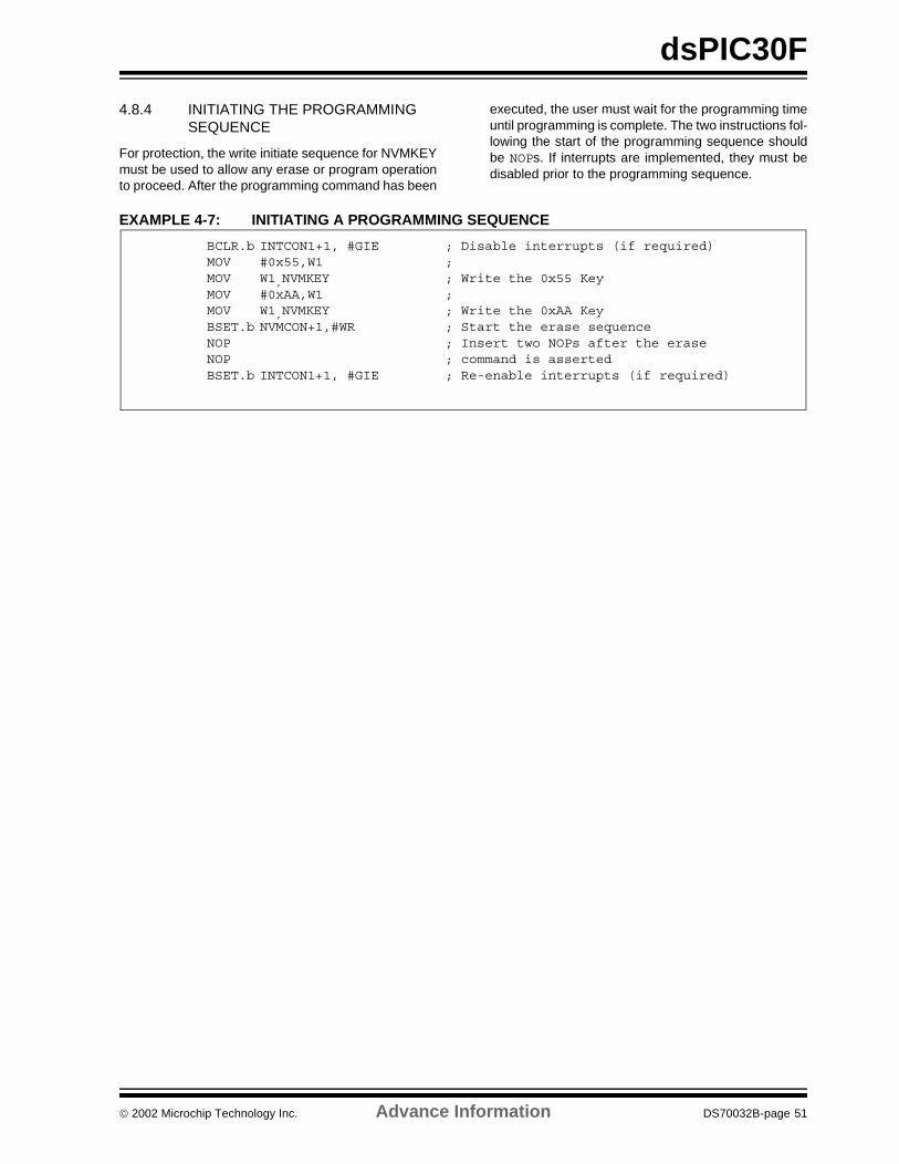
dsPIC30F
4.8.4 INITIATING THE PROGRAMMING SEQUENCE
For protection, the write initiate sequence for NVMKEYmust be used to allow any erase or program operationto proceed. After the programming command has been
executed, the user must wait for the programming timeuntil programming is complete. The two instructions fol-lowing the start of the programming sequence shouldbe NOPs. If interrupts are implemented, they must bedisabled prior to the programming sequence.
EXAMPLE 4-7: INITIATING A PROGRAMMING SEQUENCE
BCLR.b INTCON1+1, #GIE ; Disable interrupts (if required)MOV #0x55,W1 ; MOV W1,NVMKEY ; Write the 0x55 KeyMOV #0xAA,W1 ; MOV W1,NVMKEY ; Write the 0xAA KeyBSET.b NVMCON+1,#WR ; Start the erase sequence NOP ; Insert two NOPs after the eraseNOP ; command is assertedBSET.b INTCON1+1, #GIE ; Re-enable interrupts (if required)
2002 Microchip Technology Inc. Advance Information DS70032B-page 51
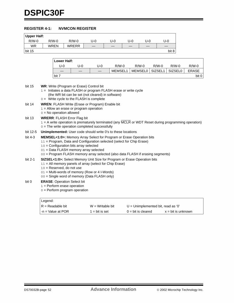
DSPIC30F
REGISTER 4-1: NVMCON REGISTER
Upper Half:R/W-0 R/W-0 R/W-0 U-0 U-0 U-0 U-0 U-0
WR WREN WRERR — — — — —
bit 15 bit 8
Lower Half:U-0 U-0 U-0 R/W-0 R/W-0 R/W-0 R/W-0 R/W-0— — — MEMSEL1 MEMSEL0 SIZSEL1 SIZSEL0 ERASE
bit 7 bit 0
bit 15 WR: Write (Program or Erase) Control bit 1 = Initiates a data FLASH or program FLASH erase or write cycle
(the WR bit can be set (not cleared) in software)0 = Write cycle to the FLASH is complete
bit 14 WREN: FLASH Write (Erase or Program) Enable bit1 = Allow an erase or program operation0 = No operation allowed
bit 13 WRERR: FLASH Error Flag bit1 = A write operation is prematurely terminated (any MCLR or WDT Reset during programming operation)0 = The write operation completed successfully
bit 12-5 Unimplemented: User code should write 0’s to these locations
bit 4-3 MEMSEL<1:0>: Memory Array Select for Program or Erase Operation bits11 = Program, Data and Configuration selected (select for Chip Erase)10 = Configuration bits array selected01 = Data FLASH memory array selected00 = Program FLASH memory array selected (also data FLASH if erasing segments)
bit 2-1 SIZSEL<1:0>: Select Memory Unit Size for Program or Erase Operation bits11 = All memory panels of array (select for Chip Erase)10 = Reserved, do not use01 = Multi-words of memory (Row or 4 I-Words)00 = Single word of memory (Data FLASH only)
bit 0 ERASE: Operation Select bit1 = Perform erase operation0 = Perform program operation
Legend:
R = Readable bit W = Writable bit U = Unimplemented bit, read as ‘0’
-n = Value at POR 1 = bit is set 0 = bit is cleared x = bit is unknown
DS70032B-page 52 Advance Information 2002 Microchip Technology Inc.
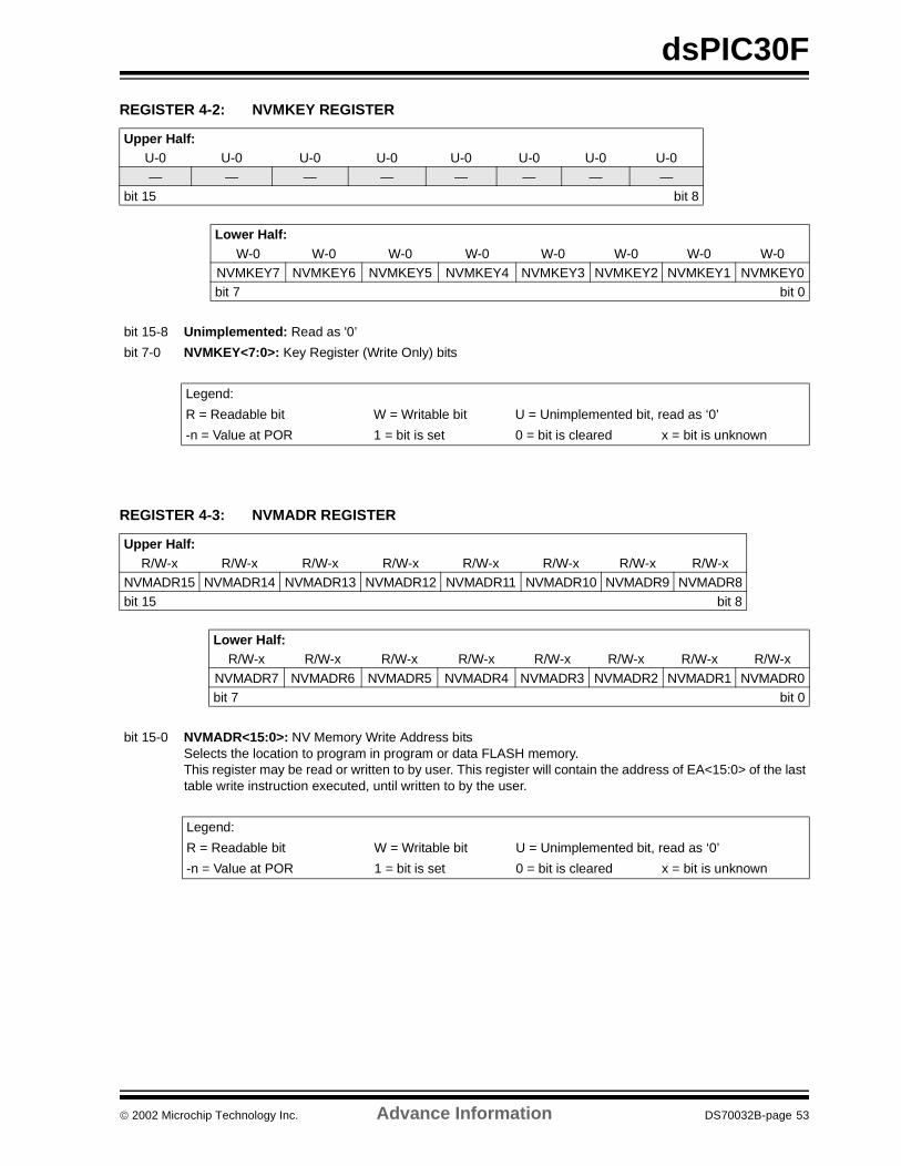
dsPIC30F
REGISTER 4-2: NVMKEY REGISTER
REGISTER 4-3: NVMADR REGISTER
Upper Half:U-0 U-0 U-0 U-0 U-0 U-0 U-0 U-0— — — — — — — —
bit 15 bit 8
Lower Half:W-0 W-0 W-0 W-0 W-0 W-0 W-0 W-0
NVMKEY7 NVMKEY6 NVMKEY5 NVMKEY4 NVMKEY3 NVMKEY2 NVMKEY1 NVMKEY0bit 7 bit 0
bit 15-8 Unimplemented: Read as '0’
bit 7-0 NVMKEY<7:0>: Key Register (Write Only) bits
Legend:
R = Readable bit W = Writable bit U = Unimplemented bit, read as ‘0’
-n = Value at POR 1 = bit is set 0 = bit is cleared x = bit is unknown
Upper Half:R/W-x R/W-x R/W-x R/W-x R/W-x R/W-x R/W-x R/W-x
NVMADR15 NVMADR14 NVMADR13 NVMADR12 NVMADR11 NVMADR10 NVMADR9 NVMADR8bit 15 bit 8
Lower Half:R/W-x R/W-x R/W-x R/W-x R/W-x R/W-x R/W-x R/W-x
NVMADR7 NVMADR6 NVMADR5 NVMADR4 NVMADR3 NVMADR2 NVMADR1 NVMADR0bit 7 bit 0
bit 15-0 NVMADR<15:0>: NV Memory Write Address bitsSelects the location to program in program or data FLASH memory.This register may be read or written to by user. This register will contain the address of EA<15:0> of the lasttable write instruction executed, until written to by the user.
Legend:
R = Readable bit W = Writable bit U = Unimplemented bit, read as ‘0’
-n = Value at POR 1 = bit is set 0 = bit is cleared x = bit is unknown
2002 Microchip Technology Inc. Advance Information DS70032B-page 53
DSPIC30F
NOTES:
DS70032B-page 54 Advance Information 2002 Microchip Technology Inc.
dsPIC30F
5.0 DATA EEPROM MEMORY
The Data EEPROM Memory is readable and writableduring normal operation over the entire VDD range. Thedata memory is directly mapped in the program mem-ory data space.
The three SFRs used to read and write the programFLASH memory are used to access data EEPROMmemory, as well. As described in Section 4.0, theseregisters are:
• NVMCON• NVMADR• NVMKEY
The EEPROM data memory allows read and write ofsingle words and 16-word blocks. When interfacing todata memory, NVMADR in conjunction with theTBLPAG register, are used to address the EEPROMlocation being accessed. TBLRDL and TBLWRL instruc-tions are used to read and write data EEPROM. ThedsPIC30F devices have up to 8 Kbytes (4K words) ofdata EEPROM, with an address range from0x7FF0000 to 0x7FFFFFE.
A word write operation should be preceded by an eraseof the location. The write time is controlled by an on-chip timer. The write time will vary with voltage andtemperature, and is typically 2 ms.
A program or erase operation on the data EEPROMdoes not stop the instruction flow. The user is respon-sible for waiting for the appropriate duration of timebefore initiating another data EEPROM write/eraseoperation. Attempting to read the data EEPROM whilea programming or erase operation is in progress resultsin unspecified data.
Control bit WR initiates write operations, similar to pro-gram FLASH writes. This bit cannot be cleared, onlyset, in software. They are cleared in hardware at thecompletion of the write operation. The inability to clearthe WR bit in software prevents the accidental or pre-mature termination of a write operation.
The WREN bit, when set, will allow a write operation.On power-up, the WREN bit is clear. The WRERR bit isset when a write operation is interrupted by a MCLRReset, or a WDT Time-out Reset, during normal oper-ation. In these situations, following RESET, the usercan check the WRERR bit and rewrite the location. Theaddress register NVMADR remains unchanged.
5.1 Reading the Data EEPROM
A TBLRD instruction reads a word at the current pro-gram word address. This example uses W0 as apointer to data EEPROM. The result is placed in regis-ter W4, as shown in Example 5-1.
EXAMPLE 5-1: DATA EEPROM READ
Note: Interrupt flag bit NVMIF in the IFS0 registeris set when write is complete. It must becleared in software.
MOV #LOW_ADDR_WORD,W0 ; Init Pointer
MOV #HIGH_ADDR_WORD,W1
MOV W1,TBLPAG
TBLRDL [ W0 ], W4 ; read data Flash
2002 Microchip Technology Inc. Advance Information DS70032B-page 55
dsPIC30F
5.2 Erasing Data EEPROM
5.2.1 ERASING ENTIRE DATA EEPROM
The following example shows a bulk erase of dataEEPROM.
EXAMPLE 5-2: DATA EEPROM BULK ERASE
5.2.2 ERASING A BLOCK OF DATA EEPROM
The TBLPAG and NVMADR registers must point to theblock. Select erase a block of data FLASH, and set theERASE and WREN bits in NVMCON register. Settingthe WR bit initiates the erase, as shown in Example 5-3.
EXAMPLE 5-3: DATA EEPROM BLOCK ERASE
; Select all data EEPROM, set ERASE, WREN bits MOV #0x400F,W0 ; MOV W0,NVMCON ; Initialize NVMCON SFR BCLR.b INTCON1+1, #GIE ; Disable Interrupts (if-required); Start erase cycle by setting WR after writing key sequence MOV #0x55,W1 MOV W1,NVMKEY ; Write the 0x55 key MOV #0xAA,W1 MOV W1, NVMKEY ; Write the 0xAA key BSET.b NVMCON+1,#WR ; Initiate erase sequence BSET.b INTCON1+1, #GIE ; Re-enable Interrupts (if-required); Erase cycle will complete in 2mS. CPU is not stalled for the Data Erase Cycle ; User can poll WR bit, use NVMIF or Timer IRQ to determine erasure complete
; Select data EEPROM block, ERASE, WREN bits MOV #400B,W0 MOV W0,NVMCON ; Initialize NVMCON SFR BCLR.b INTCON1+1, #GIE ; Disable Interrupts (if-required); Start erase cycle by setting WR after writing key sequence MOV #0x55,W1 MOV W1,NVMKEY ; Write the 0x55 key MOV #0xAA,W1 MOV W1,NVMKEY ; Write the 0xAA key BSET.b NVMCON+1,#WR ; Initiate erase sequence BSET.b INTCON1+1, #GIE ; Re-enable Interrupts (if-required); Erase cycle will complete in 2mS. CPU is not stalled for the Data Erase Cycle; User can poll WR bit, use NVMIF or Timer IRQ to determine erasure complete
DS70032B-page 56 Advance Information 2002 Microchip Technology Inc.
dsPIC30F
5.2.3 ERASING A WORD OF DATA EEPROM
The TBLPAG and NVMADR registers must point to theblock. Select erase a block of data FLASH, and set theERASE and WREN bits in NVMCON register. Settingthe WR bit initiates the erase, as shown in Example 5-4.
EXAMPLE 5-4: DATA EEPROM WORD ERASE
5.3 Writing to the Data EEPROM
To write an EEPROM data location, the followingsequence must be followed:
1. Erase data EEPROM word.a. Select word, data EEPROM, erase, and set
WREN bit in NVMCON register.b. Write address of word to be erased into
NVMADR.c. Optionally, enable NVM interrupt.
d. Write ‘55’ to NVMKEY.e. Write ‘AA’ to NVMKEY.f. Set the WR bit. This will begin erase cycle.
g. Either poll NVMIF bit or wait for NVMIF interrupt.h. The WR bit is cleared when the erase cycle
ends.2. Write data word into data EEPROM write
latches.3. Program 1 data word into data EEPROM.
a. Select word, data EEPROM, program, and setWREN bit in NVMCON register.
b. Optionally, enable NVM write done interrupt.
c. Write ‘55’ to NVMKEY.d. Write ‘AA’ to NVMKEY.e. Set The WR bit. This will begin program cycle.
f. Either poll NVMIF bit or wait for NVM interrupt.g. The WR bit is cleared when the write cycle
ends.
The write will not initiate if the above sequence is notexactly followed (write 0x55 to NVMKEY, write 0xAA toNVMCON, then set WR bit) for each word. It is stronglyrecommended that interrupts be disabled during thiscode segment.
Additionally, the WREN bit in NVMCON must be set toenable writes. This mechanism prevents accidentalwrites to data EEPROM, due to unexpected code exe-cution. The WREN bit should be kept clear at all times,except when updating the EEPROM. The WREN bit isnot cleared by hardware.
After a write sequence has been initiated, clearing theWREN bit will not affect the current write cycle. The WRbit will be inhibited from being set unless the WREN bitis set. The WREN bit must be set on a previous instruc-tion. Both WR and WREN cannot be set with the sameinstruction.
At the completion of the write cycle, the WR bit iscleared in hardware and the Non-Volatile MemoryWrite Complete Interrupt Flag bit (NVMIF) is set. Theuser may either enable this interrupt, or poll this bit.NVMIF must be cleared by software.
; Select data EEPROM word, ERASE, WREN bits
MOV #4009,W0
MOV W0,NVMCON
BCLR.b INTCON1+1, #GIE ; Disable Interrupts (if-required)
; Start erase cycle by setting WR after writing key sequence
MOV #0x55,W1
MOV W1,NVMKEY ; Write the 0x55 key
MOV #0xAA,W1
MOV W1,NVMKEY ; Write the 0xAA key
BSET.b NVMCON+1,#WR ; Initiate erase sequence
BSET.b INTCON1+1, #GIE ; Re-enable Interrupts (if-required)
; Erase cycle will complete in 2mS. CPU is not stalled for the Data Erase Cycle
; User can poll WR bit, use NVMIF or Timer IRQ to determine erasure complete
2002 Microchip Technology Inc. Advance Information DS70032B-page 57
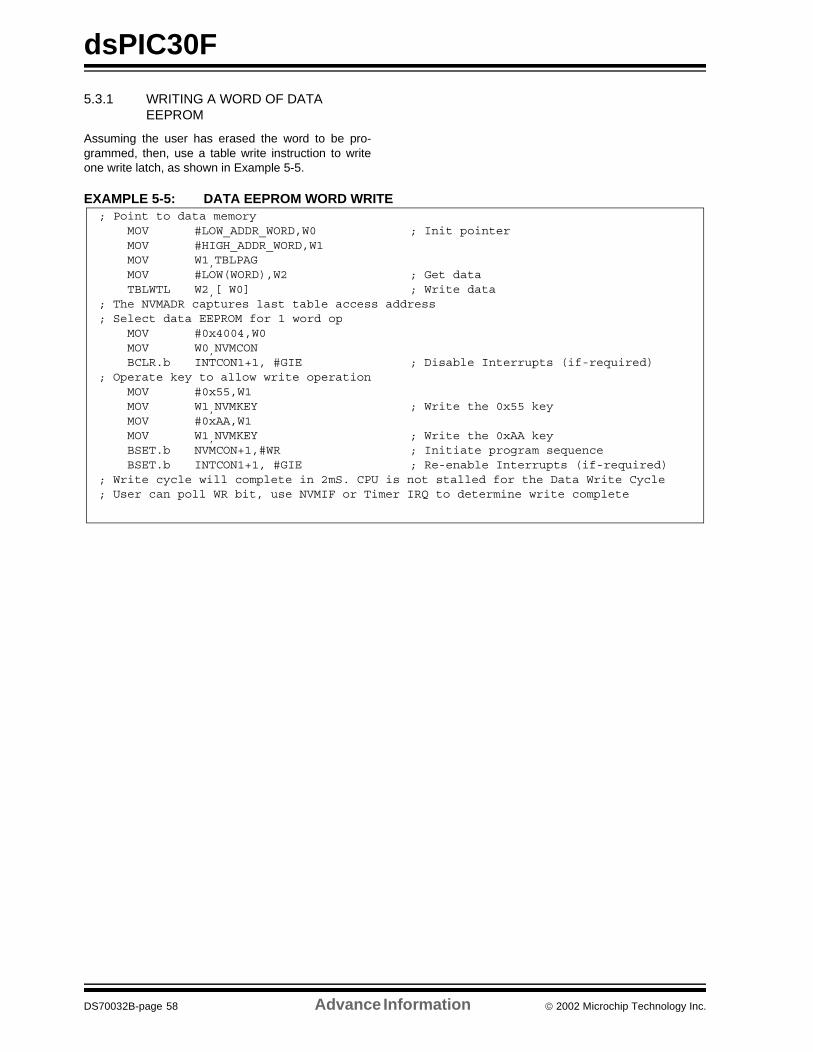
dsPIC30F
5.3.1 WRITING A WORD OF DATA EEPROM
Assuming the user has erased the word to be pro-grammed, then, use a table write instruction to writeone write latch, as shown in Example 5-5.
EXAMPLE 5-5: DATA EEPROM WORD WRITE; Point to data memory MOV #LOW_ADDR_WORD,W0 ; Init pointer MOV #HIGH_ADDR_WORD,W1 MOV W1,TBLPAG MOV #LOW(WORD),W2 ; Get data TBLWTL W2,[ W0] ; Write data; The NVMADR captures last table access address; Select data EEPROM for 1 word op MOV #0x4004,W0 MOV W0,NVMCON BCLR.b INTCON1+1, #GIE ; Disable Interrupts (if-required); Operate key to allow write operation MOV #0x55,W1 MOV W1,NVMKEY ; Write the 0x55 key MOV #0xAA,W1 MOV W1,NVMKEY ; Write the 0xAA key BSET.b NVMCON+1,#WR ; Initiate program sequence BSET.b INTCON1+1, #GIE ; Re-enable Interrupts (if-required); Write cycle will complete in 2mS. CPU is not stalled for the Data Write Cycle; User can poll WR bit, use NVMIF or Timer IRQ to determine write complete
DS70032B-page 58 Advance Information 2002 Microchip Technology Inc.
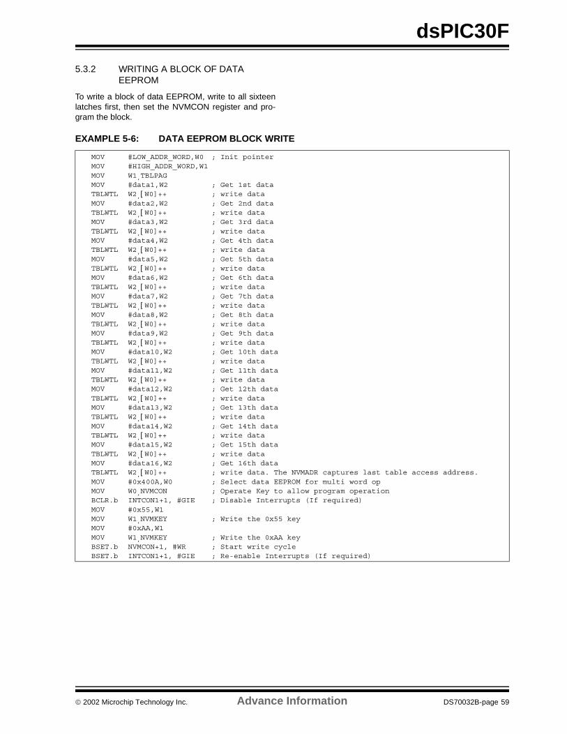
dsPIC30F
5.3.2 WRITING A BLOCK OF DATA EEPROM
To write a block of data EEPROM, write to all sixteenlatches first, then set the NVMCON register and pro-gram the block.
EXAMPLE 5-6: DATA EEPROM BLOCK WRITE
MOV #LOW_ADDR_WORD,W0 ; Init pointer MOV #HIGH_ADDR_WORD,W1 MOV W1,TBLPAG MOV #data1,W2 ; Get 1st data TBLWTL W2,[ W0]++ ; write data MOV #data2,W2 ; Get 2nd data TBLWTL W2,[ W0]++ ; write data MOV #data3,W2 ; Get 3rd data TBLWTL W2,[ W0]++ ; write data MOV #data4,W2 ; Get 4th data TBLWTL W2,[ W0]++ ; write data MOV #data5,W2 ; Get 5th data TBLWTL W2,[ W0]++ ; write data MOV #data6,W2 ; Get 6th data TBLWTL W2,[ W0]++ ; write data MOV #data7,W2 ; Get 7th data TBLWTL W2,[ W0]++ ; write data MOV #data8,W2 ; Get 8th data TBLWTL W2,[ W0]++ ; write data MOV #data9,W2 ; Get 9th data TBLWTL W2,[ W0]++ ; write data MOV #data10,W2 ; Get 10th data TBLWTL W2,[ W0]++ ; write data MOV #data11,W2 ; Get 11th data TBLWTL W2,[ W0]++ ; write data MOV #data12,W2 ; Get 12th data TBLWTL W2,[ W0]++ ; write data MOV #data13,W2 ; Get 13th data TBLWTL W2,[ W0]++ ; write data MOV #data14,W2 ; Get 14th data TBLWTL W2,[ W0]++ ; write data MOV #data15,W2 ; Get 15th data TBLWTL W2,[ W0]++ ; write data MOV #data16,W2 ; Get 16th data TBLWTL W2,[ W0]++ ; write data. The NVMADR captures last table access address. MOV #0x400A,W0 ; Select data EEPROM for multi word op MOV W0,NVMCON ; Operate Key to allow program operation BCLR.b INTCON1+1, #GIE ; Disable Interrupts (If required) MOV #0x55,W1 MOV W1,NVMKEY ; Write the 0x55 key MOV #0xAA,W1 MOV W1,NVMKEY ; Write the 0xAA key BSET.b NVMCON+1, #WR ; Start write cycle BSET.b INTCON1+1, #GIE ; Re-enable Interrupts (If required)
2002 Microchip Technology Inc. Advance Information DS70032B-page 59
dsPIC30F
5.4 Write Verify
Depending on the application, good programmingpractice may dictate that the value written to the mem-ory should be verified against the original value. Thisshould be used in applications where excessive writescan stress bits near the specification limit.
Generally, a write failure will be a bit which was writtenas a ’1’, but reads back as a ’0’ (due to leakage off thecell).
5.5 Protection Against Spurious Write
There are conditions when the device may not want towrite to the data EEPROM memory. To protect againstspurious EEPROM writes, various mechanisms havebeen built-in. On power-up, the WREN bit is cleared;also, the Power-up Timer prevents EEPROM write.
The write initiate sequence and the WREN bit together,help prevent an accidental write during brown-out,power glitch, or software malfunction.
DS70032B-page 60 Advance Information 2002 Microchip Technology Inc.
dsPIC30F
6.0 DSP ENGINE
Concurrent operation of the DSP engine with MCUinstruction flow is not possible, though both the MCUALU and DSP engine resources may be used concur-rently by the same instruction (e.g., ED and EDACinstructions).
The DSP engine consists of a high speed 16-bit x16-bit multiplier, a barrel shifter and a 40-bit adder/subtractor with two target accumulators, round andsaturation logic.
Data input to the DSP engine is derived from one of thefollowing:
1. Directly from the W array (registers W4, W5, W6or W7) via the X and Y data buses for the MACclass of instructions (MAC, MSC, MPY,MPY.N, ED, EDAC, CLR and MOVSAC).
2. From the X bus for all other DSP instructions.
3. From the X bus for all MCU instructions whichuse the barrel shifter.
Data output from the DSP engine is written to one of thefollowing:
1. The target accumulator, as defined by the DSPinstruction being executed.
2. The X bus for MAC, MSC, CLR and MOVSACaccumulator writes, where the EA is derivedfrom W13 only. (MPY, MPY.N, ED and EDACdo not offer an accumulator write option.)
3. The X bus for all MCU instructions which use thebarrel shifter.
The DSP engine also has the capability to performinherent accumulator-to-accumulator operations,which require no additional data. These instructions areADD, SUB and NEG.
A block diagram of the DSP engine is shown inFigure 6-1.
2002 Microchip Technology Inc. Advance Information DS70032B-page 61
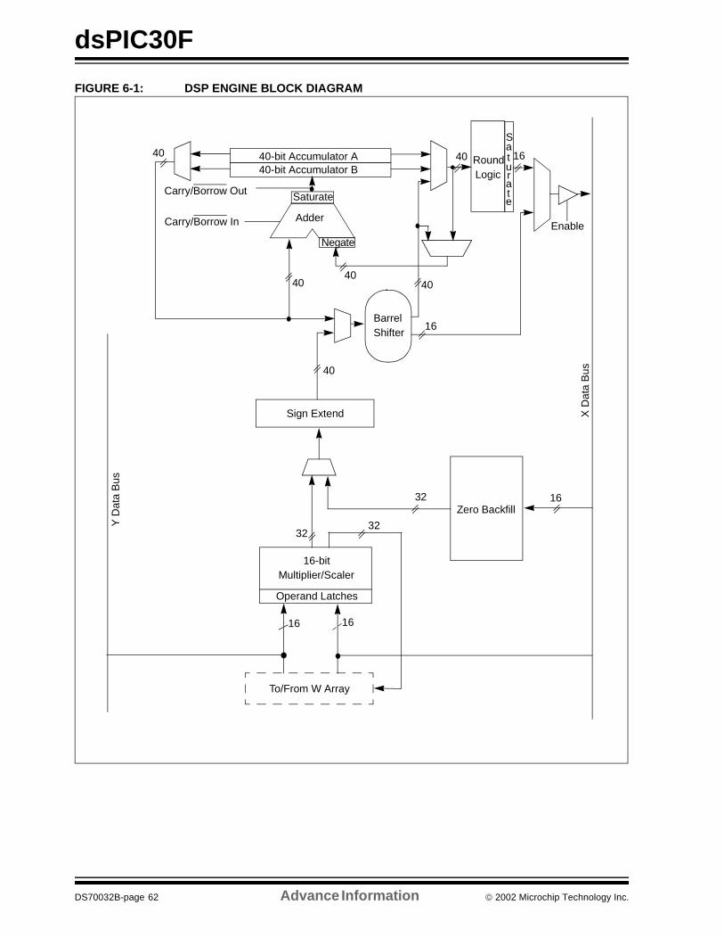
dsPIC30F
FIGURE 6-1: DSP ENGINE BLOCK DIAGRAM
Zero Backfill
Sign Extend
BarrelShifter
40-bit Accumulator A40-bit Accumulator B
RoundLogic
X D
ata
Bus
Multiplier/Scaler
To/From W Array
Adder
Saturate
Operand Latches
Enable
16-bit
Negate
32
3232
16
16 16
16
4040
40 40
Saturate
Y D
ata
Bus
40
Carry/Borrow Out
Carry/Borrow In
16
40
DS70032B-page 62 Advance Information 2002 Microchip Technology Inc.
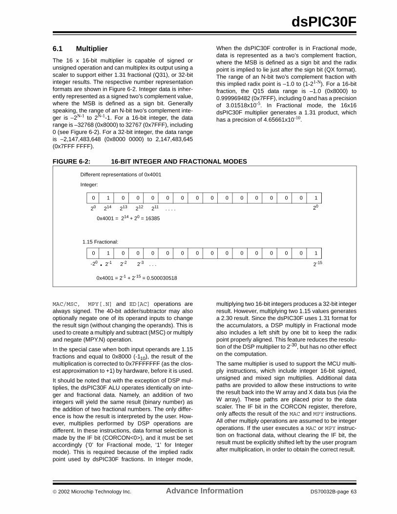
dsPIC30F
6.1 Multiplier
The 16 x 16-bit multiplier is capable of signed orunsigned operation and can multiplex its output using ascaler to support either 1.31 fractional (Q31), or 32-bitinteger results. The respective number representationformats are shown in Figure 6-2. Integer data is inher-ently represented as a signed two’s complement value,where the MSB is defined as a sign bit. Generallyspeaking, the range of an N-bit two’s complement inte-ger is –2N-1 to 2N-1-1. For a 16-bit integer, the datarange is –32768 (0x8000) to 32767 (0x7FFF), including0 (see Figure 6-2). For a 32-bit integer, the data rangeis –2,147,483,648 (0x8000 0000) to 2,147,483,645(0x7FFF FFFF).
When the dsPIC30F controller is in Fractional mode,data is represented as a two’s complement fraction,where the MSB is defined as a sign bit and the radixpoint is implied to lie just after the sign bit (QX format).The range of an N-bit two’s complement fraction withthis implied radix point is –1.0 to (1-21-N). For a 16-bitfraction, the Q15 data range is –1.0 (0x8000) to0.999969482 (0x7FFF), including 0 and has a precisionof 3.01518x10⁻⁵. In Fractional mode, the 16x16dsPIC30F multiplier generates a 1.31 product, whichhas a precision of 4.65661x10⁻¹⁰.
FIGURE 6-2: 16-BIT INTEGER AND FRACTIONAL MODES
MAC/MSC, MPY[.N] and ED[AC] operations arealways signed. The 40-bit adder/subtractor may alsooptionally negate one of its operand inputs to changethe result sign (without changing the operands). This isused to create a multiply and subtract (MSC) or multiplyand negate (MPY.N) operation.
In the special case when both input operands are 1.15fractions and equal to 0x8000 (-110), the result of themultiplication is corrected to 0x7FFFFFFF (as the clos-est approximation to +1) by hardware, before it is used.
It should be noted that with the exception of DSP mul-tiplies, the dsPIC30F ALU operates identically on inte-ger and fractional data. Namely, an addition of twointegers will yield the same result (binary number) asthe addition of two fractional numbers. The only differ-ence is how the result is interpreted by the user. How-ever, multiplies performed by DSP operations aredifferent. In these instructions, data format selection ismade by the IF bit (CORCON<0>), and it must be setaccordingly (‘0’ for Fractional mode, ‘1’ for Integermode). This is required because of the implied radixpoint used by dsPIC30F fractions. In Integer mode,
multiplying two 16-bit integers produces a 32-bit integerresult. However, multiplying two 1.15 values generatesa 2.30 result. Since the dsPIC30F uses 1.31 format forthe accumulators, a DSP multiply in Fractional modealso includes a left shift by one bit to keep the radixpoint properly aligned. This feature reduces the resolu-tion of the DSP multiplier to 2-30, but has no other effecton the computation.
The same multiplier is used to support the MCU multi-ply instructions, which include integer 16-bit signed,unsigned and mixed sign multiplies. Additional datapaths are provided to allow these instructions to writethe result back into the W array and X data bus (via theW array). These paths are placed prior to the datascaler. The IF bit in the CORCON register, therefore,only affects the result of the MAC and MPY instructions.All other multiply operations are assumed to be integeroperations. If the user executes a MAC or MPY instruc-tion on fractional data, without clearing the IF bit, theresult must be explicitly shifted left by the user programafter multiplication, in order to obtain the correct result.
Different representations of 0x4001
Integer:
214 213 212 211 . . . . 20
0x4001 = 214 + 20 = 16385
1.15 Fractional:
2-15
0x4001 = 2-1 + 2-15 = 0.500030518
0 1 0 0 0 0 0 0 0 0 0 0 0 0 0 1
. 2-1 2-2 2-3 . . . -20
0 1 0 0 0 0 0 0 0 0 0 0 0 0 0 1
20
2002 Microchip Technology Inc. Advance Information DS70032B-page 63
dsPIC30F
The MUL instruction may be directed to use byte orword sized operands. Byte operands will direct a 16-bitresult, and word operands will direct a 32-bit result tothe specified register(s) in the W array.
6.2 Data Accumulators and Adder/Subtractor
The data accumulator consists of a 40-bit adder/subractor with automatic sign extension logic. It canselect one of two accumulators (A or B) as its pre-accumulation source and post-accumulation destina-tion. For the ADD and LAC instructions, the data to beaccumulated or loaded can be optionally scaled via thebarrel shifter, prior to accumulation.
6.2.1 ADDER/SUBTRACTOR, OVERFLOW AND SATURATION
The adder/subtractor is a 40-bit adder with an optionalzero input into one side and either true, or complementdata into the other input. In the case of addition, thecarry/borrow input is active high and the other input istrue data (not complemented), whereas in the case ofsubtraction, the carry/borrow input is active low and theother input is complemented. The adder/subtractorgenerates overflow status bits SA/SB and OA/OB,which are latched and reflected in the STATUS register:
• Overflow from bit 39: this is a catastrophic over-flow in which the sign of the accumulator is destroyed.
• Overflow into guard bits 32 through 39: this is a recoverable overflow. This bit is set whenever all the guard bits bits are not identical to each other.
The adder has an additional saturation block whichcontrols accumulator data saturation, if selected. Ituses the result of the adder, the overflow status bitsdescribed above, and the SATA/B (CORCON<7:6>)and ACCSAT (CORCON<4>) mode control bits todetermine when to saturate and to what value tosaturate.
Six STATUS register bits have been provided to sup-port saturation and overflow; they are:
1. OA:AccA overflowed into guard bits
2. OB: AccB overflowed into guard bits
3. SA:AccA saturated (bit 31 overflow and saturation)orAccA overflowed into guard bits and saturated(bit 39 overflow and saturation)
4. SB:AccB saturated (bit 31 overflow and saturation)orAccB overflowed into guard bits and saturated(bit 39 overflow and saturation)
5. OAB:Logical OR of OA and OB
6. SAB:Logical OR of SA and SB
The OA and OB bits are modified each time datapasses through the adder/subtractor. When set, theyindicate that the most recent operation has overflowedinto the accumulator guard bits (bits 32 through 39).The OA and OB bits can also optionally generate anarithmetic warning trap when set and the correspond-ing overflow trap flag enable bit (OVATEN, OVBTEN) inthe INTCON1 register (see Section 8.0) is set. Thisallows the user to take immediate action, for example,to correct system gain.
The SA and SB bits can be set each time data passesthrough the adder/subtractor, but can only be clearedby the user. When set, they indicate that the accumula-tor has overflowed its maximum range (bit 31 for 32-bitsaturation, or bit 39 for 40-bit saturation) and will besaturated (if saturation is enabled). When saturation isnot enabled, the SA and SB default to bit 39 overflowand thus, indicate that a catastrophic overflow hasoccurred. If the COVTE bit in the INTCON1 register isset, SA and SB bits will generate an arithmetic warningtrap when saturation is disabled.
The overflow and saturation status bits can optionallybe viewed in the STATUS register as the logical OR ofOA and OB (in bit OAB) and the logical OR of SA andSB (in bit SAB). This allows programmers to check onebit in the STATUS register to determine if either accu-mulator has overflowed, or one bit to determine if eitheraccumulator has saturated. This would be useful forcomplex number arithmetic which typically uses boththe accumulators.
DS70032B-page 64 Advance Information 2002 Microchip Technology Inc.
dsPIC30F
The device supports three saturation and overflowmodes.
1. Bit 39 Overflow and Saturation:Using the bit 39 overflow status bit from theadder, and the bit 39 value after the addition, thecorrect sign of the 9.31 result can be determined.The saturate logic then loads the maximally pos-itive 9.31 (0x7FFFFFFFFF) or maximally nega-tive 9.31 value (0x8000000000) into the targetaccumulator. The SA or SB bit is set and remainsset until cleared by the user. This is referred to as‘super saturation’ and provides protection againsterroneous data, or unexpected algorithm prob-lems (e.g., gain calculations).
2. Bit 31 Overflow and Saturation:Using the bit 31 to 39 overflow status bit from theadder, and the bit 39 value after the addition, thecorrect sign of the required 1.31 result can bedetermined. The saturate logic then loads themaximally positive 1.31 value (0x007FFFFFFF)or maximally negative 1.31 value(0x0080000000) into the target accumulator.The SA or SB bit is set and remains set untilcleared by the user. When this Saturation modeis in effect, the guard bits are not used (so theOA, OB or OAB bits are never set).
3. Bit 39 Catastrophic OverflowThe bit 39 overflow status bit from the adder isused to set the SA or SB bit, which remain setuntil cleared by the user. No saturation operationis performed and the accumulator is allowed tooverflow (destroying its sign). If the COVTE bit inthe INTCON1 register is set, a catastrophicoverflow can initiate a trap exception.
6.2.2 ACCUMULATOR ‘WRITE BACK’
The MAC class of instructions (with the exception ofMPY, MPY.N, ED and EDAC) can optionally write arounded version of the high word (bits 31 through 16)of the accumulator, that is not targeted by the instruc-tion into data space memory. The write is performedacross the X bus into combined X and Y addressspace. The following addressing modes are supported.
1. W13, Register Direct:The rounded contents of the non-target accumu-lator are written into W13 as a 1.15 fraction.
2. [W13]+=2, Register Indirect with Post-Increment:The rounded contents of the non-target accumu-lator are written into the address pointed to byW13 as a 1.15 fraction. W13 is then incre-mented by 2 (for a word write).
6.2.3 ROUND LOGIC
The round logic is a combinational block, which per-forms a conventional (biased) or convergent (unbiased)round function during an accumulator write (store). TheRound mode is determined by the state of the RND bitin the CORCON register. It generates a 16-bit, 1.15 datavalue which is passed to the data space write saturationlogic (see Figure 6-3). If rounding is not indicated by theinstruction, a truncated 1.15 data value is stored and theLS Word is simply discarded.
The two Rounding modes are shown in Figure 7-7.Conventional rounding takes bit 15 of the accumulator,zero extends it and adds it to the ACCH word (bits 16through 31 of the accumulator). If the ACCL word (bits0 through 15 of the accumulator) is between 0x8000and 0xFFFF (0x8000 included), ACCH is incremented.If ACCL is between 0x0000 and 0x7FFF, ACCH is leftunchanged. A consequence of this algorithm is thatover a succession of random rounding operations, thevalue will tend to be biased slightly positive.
Convergent (or unbiased) rounding operates in thesame manner as conventional rounding, except whenACCL equals 0x8000. If this is the case, the LS bit (bit16 of the accumulator) of ACCH is examined. If it is 1,ACCH is incremented. If it is 0, ACCH is not modified.Assuming that bit 16 is effectively random in nature,this scheme will remove any rounding bias that mayaccumulate.
The SAC and SAC.R instructions store either a trun-cated (SAC) or rounded (SAC.R) version of the contentsof the target accumulator to data memory, via the X bus(subject to data saturation, see Section 6.2.4). Notethat for the MAC class of instructions, the accumulatorwrite back operation will function in the same manner,addressing combined MCU (X and Y) data spacethough the X bus. For this class of instructions, the datais always subject to rounding.
2002 Microchip Technology Inc. Advance Information DS70032B-page 65
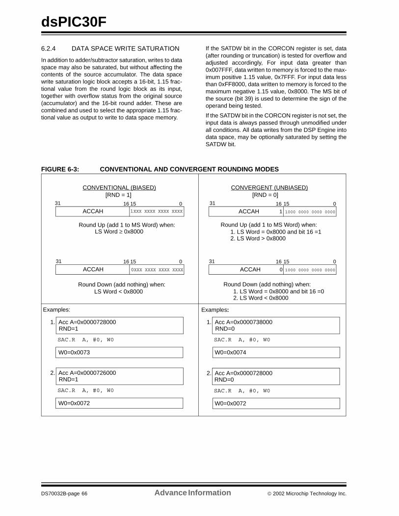
dsPIC30F
6.2.4 DATA SPACE WRITE SATURATION
In addition to adder/subtractor saturation, writes to dataspace may also be saturated, but without affecting thecontents of the source accumulator. The data spacewrite saturation logic block accepts a 16-bit, 1.15 frac-tional value from the round logic block as its input,together with overflow status from the original source(accumulator) and the 16-bit round adder. These arecombined and used to select the appropriate 1.15 frac-tional value as output to write to data space memory.
If the SATDW bit in the CORCON register is set, data(after rounding or truncation) is tested for overflow andadjusted accordingly, For input data greater than0x007FFF, data written to memory is forced to the max-imum positive 1.15 value, 0x7FFF. For input data lessthan 0xFF8000, data written to memory is forced to themaximum negative 1.15 value, 0x8000. The MS bit ofthe source (bit 39) is used to determine the sign of theoperand being tested.
If the SATDW bit in the CORCON register is not set, theinput data is always passed through unmodified underall conditions. All data writes from the DSP Engine intodata space, may be optionally saturated by setting theSATDW bit.
FIGURE 6-3: CONVENTIONAL AND CONVERGENT ROUNDING MODES
01516
01516
01516
01516
1000 0000 0000 00001XXX XXXX XXXX XXXX
0XXX XXXX XXXX XXXX 1000 0000 0000 0000
1
0
CONVENTIONAL (BIASED) CONVERGENT (UNBIASED)
Round Up (add 1 to MS Word) when:
Round Down (add nothing) when:
Round Up (add 1 to MS Word) when:1. LS Word = 0x8000 and bit 16 =12. LS Word > 0x8000
LS Word ≥ 0x8000
LS Word < 0x8000Round Down (add nothing) when:
1. LS Word = 0x8000 and bit 16 =02. LS Word < 0x8000
ACCAH
ACCAH
ACCAH
ACCAH
31
31
Examples: Examples:
1. Acc A=0x0000738000 RND=0
SAC.R A, #0, W0
W0=0x0074
2. Acc A=0x0000728000 RND=0
SAC.R A, #0, W0
W0=0x0072
1. Acc A=0x0000728000 RND=1
SAC.R A, #0, W0
W0=0x0073
2. Acc A=0x0000726000 RND=1
SAC.R A, #0, W0
W0=0x0072
31
31
[RND = 1] [RND = 0]
DS70032B-page 66 Advance Information 2002 Microchip Technology Inc.
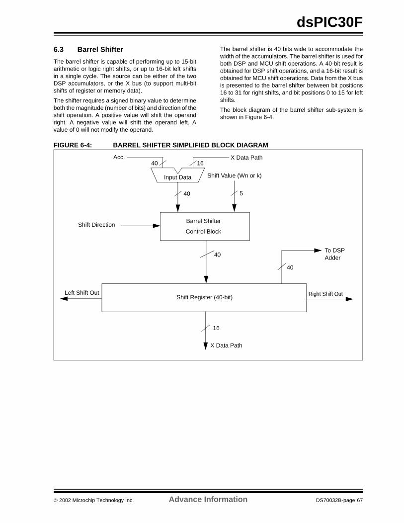
dsPIC30F
6.3 Barrel Shifter
The barrel shifter is capable of performing up to 15-bitarithmetic or logic right shifts, or up to 16-bit left shiftsin a single cycle. The source can be either of the twoDSP accumulators, or the X bus (to support multi-bitshifts of register or memory data).
The shifter requires a signed binary value to determineboth the magnitude (number of bits) and direction of theshift operation. A positive value will shift the operandright. A negative value will shift the operand left. Avalue of 0 will not modify the operand.
The barrel shifter is 40 bits wide to accommodate thewidth of the accumulators. The barrel shifter is used forboth DSP and MCU shift operations. A 40-bit result isobtained for DSP shift operations, and a 16-bit result isobtained for MCU shift operations. Data from the X busis presented to the barrel shifter between bit positions16 to 31 for right shifts, and bit positions 0 to 15 for leftshifts.
The block diagram of the barrel shifter sub-system isshown in Figure 6-4.
FIGURE 6-4: BARREL SHIFTER SIMPLIFIED BLOCK DIAGRAM
Shift Register (40-bit)
Barrel Shifter
Control Block
X Data Path
Input Data Shift Value (Wn or k)
To DSPAdder
Shift Direction
16
40
540
16 40Acc. X Data Path
Left Shift Out Right Shift Out
40
2002 Microchip Technology Inc. Advance Information DS70032B-page 67
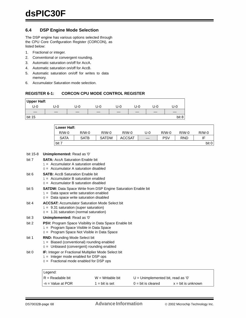
dsPIC30F
6.4 DSP Engine Mode Selection
The DSP engine has various options selected throughthe CPU Core Configuration Register (CORCON), aslisted below:
1. Fractional or integer.2. Conventional or convergent rounding.3. Automatic saturation on/off for AccA.
4. Automatic saturation on/off for AccB.5. Automatic saturation on/off for writes to data
memory.6. Accumulator Saturation mode selection.
REGISTER 6-1: CORCON CPU MODE CONTROL REGISTER
Upper Half:U-0 U-0 U-0 U-0 U-0 U-0 U-0 U-0— — — — — — — —
bit 15 bit 8
Lower Half:R/W-0 R/W-0 R/W-0 R/W-0 U-0 R/W-0 R/W-0 R/W-0
SATA SATB SATDW ACCSAT — PSV RND IFbit 7 bit 0
bit 15-8 Unimplemented: Read as '0’
bit 7 SATA: AccA Saturation Enable bit1 = Accumulator A saturation enabled0 = Accumulator A saturation disabled
bit 6 SATB: AccB Saturation Enable bit1 = Accumulator B saturation enabled0 = Accumulator B saturation disabled
bit 5 SATDW: Data Space Write from DSP Engine Saturation Enable bit1 = Data space write saturation enabled0 = Data space write saturation disabled
bit 4 ACCSAT: Accumulator Saturation Mode Select bit1 = 9.31 saturation (super saturation)0 = 1.31 saturation (normal saturation)
bit 3 Unimplemented: Read as ’0’
bit 2 PSV: Program Space Visibility in Data Space Enable bit1 = Program Space Visible in Data Space0 = Program Space Not Visible in Data Space
bit 1 RND: Rounding Mode Select bit1 = Biased (conventional) rounding enabled0 = Unbiased (convergent) rounding enabled
bit 0 IF: Integer or Fractional Multiplier Mode Select bit1 = Integer mode enabled for DSP ops0 = Fractional mode enabled for DSP ops
Legend:
R = Readable bit W = Writable bit U = Unimplemented bit, read as ‘0’
-n = Value at POR 1 = bit is set 0 = bit is cleared x = bit is unknown
DS70032B-page 68 Advance Information 2002 Microchip Technology Inc.
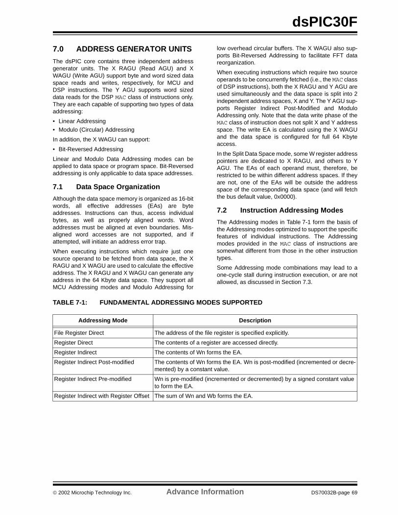
dsPIC30F
7.0 ADDRESS GENERATOR UNITS
The dsPIC core contains three independent addressgenerator units. The X RAGU (Read AGU) and XWAGU (Write AGU) support byte and word sized dataspace reads and writes, respectively, for MCU andDSP instructions. The Y AGU supports word sizeddata reads for the DSP MAC class of instructions only.They are each capable of supporting two types of dataaddressing:
• Linear Addressing
• Modulo (Circular) Addressing
In addition, the X WAGU can support:
• Bit-Reversed Addressing
Linear and Modulo Data Addressing modes can beapplied to data space or program space. Bit-Reversedaddressing is only applicable to data space addresses.
7.1 Data Space Organization
Although the data space memory is organized as 16-bitwords, all effective addresses (EAs) are byteaddresses. Instructions can thus, access individualbytes, as well as properly aligned words. Wordaddresses must be aligned at even boundaries. Mis-aligned word accesses are not supported, and ifattempted, will initiate an address error trap.
When executing instructions which require just onesource operand to be fetched from data space, the XRAGU and X WAGU are used to calculate the effectiveaddress. The X RAGU and X WAGU can generate anyaddress in the 64 Kbyte data space. They support allMCU Addressing modes and Modulo Addressing for
low overhead circular buffers. The X WAGU also sup-ports Bit-Reversed Addressing to facilitate FFT datareorganization.
When executing instructions which require two sourceoperands to be concurrently fetched (i.e., the MAC classof DSP instructions), both the X RAGU and Y AGU areused simultaneously and the data space is split into 2independent address spaces, X and Y. The Y AGU sup-ports Register Indirect Post-Modified and ModuloAddressing only. Note that the data write phase of theMAC class of instruction does not split X and Y addressspace. The write EA is calculated using the X WAGUand the data space is configured for full 64 Kbyteaccess.
In the Split Data Space mode, some W register addresspointers are dedicated to X RAGU, and others to YAGU. The EAs of each operand must, therefore, berestricted to be within different address spaces. If theyare not, one of the EAs will be outside the addressspace of the corresponding data space (and will fetchthe bus default value, 0x0000).
7.2 Instruction Addressing Modes
The Addressing modes in Table 7-1 form the basis ofthe Addressing modes optimized to support the specificfeatures of individual instructions. The Addressingmodes provided in the MAC class of instructions aresomewhat different from those in the other instructiontypes.
Some Addressing mode combinations may lead to aone-cycle stall during instruction execution, or are notallowed, as discussed in Section 7.3.
TABLE 7-1: FUNDAMENTAL ADDRESSING MODES SUPPORTED
Addressing Mode Description
File Register Direct The address of the file register is specified explicitly.
Register Direct The contents of a register are accessed directly.
Register Indirect The contents of Wn forms the EA.
Register Indirect Post-modified The contents of Wn forms the EA. Wn is post-modified (incremented or decre-mented) by a constant value.
Register Indirect Pre-modified Wn is pre-modified (incremented or decremented) by a signed constant value to form the EA.
Register Indirect with Register Offset The sum of Wn and Wb forms the EA.
2002 Microchip Technology Inc. Advance Information DS70032B-page 69
dsPIC30F
7.2.1 FILE REGISTER INSTRUCTIONS
Most file register instructions use a 13-bit address field(f) to directly address data present in the first 8192bytes of data memory. These memory locations areknown as File Registers. Most file register instructionsemploy a working register W0, which is denoted asWREG in these instructions. The destination is typicallyeither the same file register, or WREG (with the excep-tion of the MUL instruction), which writes the result to aregister or register pair.
7.2.2 MCU INSTRUCTIONS
The three-operand MCU instructions are of the form:
Operand 3 = Operand 1 <function> Operand 2
where Operand 1 is always a working register (i.e., theAddressing mode can only be register direct), which isreferred to as Wb. Operand 2 can be W register,fetched from data memory, or 5-bit literal. In two-operand instructions, the result location is the same asthat of one of the operands. Certain MCU instructionsare one-operand operations. The following addressingmodes are supported by MCU instructions:
• Register Direct• Register Indirect• Register Indirect Post-decremented
• Register Indirect Post-incremented• Register Indirect Pre-decremented• Register Indirect Pre-incremented
• 5-bit or 10-bit Literal
7.2.3 MOVE AND ACCUMULATOR INSTRUCTIONS
Move instructions and the DSP accumulator class ofinstructions provide a greater degree of addressingflexibility than other instructions. In addition to theAddressing modes supported by most MCU instruc-tions, Move and Accumulator instructions also supportRegister Indirect with Register Offset Addressingmode, also referred to as Register Indexed mode.
In summary, the following addressing modes supportedby Move and Accumulator instructions:
• Register Direct• Register Indirect• Register Indirect Post-decremented
• Register Indirect Post-incremented• Register Indirect Pre-decremented• Register Indirect Pre-incremented
• Register Indirect with Register Offset (Indexed)• 10-bit Literal• 16-bit Literal
7.2.4 MAC INSTRUCTIONS
The dual source operand DSP instructions (CLR, ED,EDAC, MAC, MPY, MPY.N, MOVSAC and MSC), alsoreferred to as MAC instructions, utilize a simplified set ofAddressing modes to allow the user to effectivelymanipulate the data pointers through register indirecttables.
The 2 source operand pre-fetch registers must be amember of the set W8, W9, W10, W11. For datareads, W8 and W9 will always be directed to the XRAGU and W10 and W11 will always be directed to theY AGU. The effective addresses generated (before andafter modification) must, therefore, be valid addresseswithin X data space for W8 and W9, and Y data spacefor W10 and W11.
In summary, the following addressing modes are sup-ported by the MAC class of instructions:
• Register Indirect• Register Indirect Post-incremented by 2
• Register Indirect Post-incremented by 4• Register Indirect Post-incremented by 6• Register Indirect with Register Offset (Indexed)
7.2.5 OTHER INSTRUCTIONS
Besides the various Addressing modes outlined above,some instructions use literal constants of various sizes.For example, BRA (branch) instructions use 16-bitsigned literals to specify the branch destination directly,whereas the DISI instruction uses a 14-bit unsignedliteral field. In some instructions, such as ADD Acc, thesource of an operand or result is implied by the opcodeitself. Certain operations, such as NOP, do not have anyoperands.
Note: Not all instructions support all the Address-ing modes given above. Individual instruc-tions may support different subsets ofthese Addressing modes.
Note: For the MOV instructions, the Addressingmode specified in the instruction can differfor the source and destination EA. How-ever, the 4-bit Wb (Register Offset) field isshared between both source and destina-tion (but typically only used by one).
Note: Not all instructions support all the Address-ing modes given above. Individual instruc-tions may support different subsets ofthese Addressing modes.
Note: Register Indirect with Register OffsetAddressing is only available for W9 (in Xspace) and W11 (in Y space).
DS70032B-page 70 Advance Information 2002 Microchip Technology Inc.
dsPIC30F
7.3 Instruction Stalls
7.3.1 INTRODUCTION
In order to maximize data space EA calculation andoperand fetch time, the X data space read and writeaccesses are partially pipelined. The latter half of theread phase overlaps the first half of the write phase ofan instruction, as shown in Section 2.
Address register data dependencies may arisebetween successive read and write operations, usingcommon registers.
There are two types of dependencies possible in thedsPIC30F architecture. ‘Read After Write’ (RAW)dependencies occur across instruction boundariesand are detected by the hardware. ‘Write After Read’(WAR) dependencies occur within instructions and aredetected by the assembler, enabling users to modifytheir program to avoid it.
An example of a RAW dependency is a write operationthat modifies W5 (on falling Q4), followed by a readoperation that uses W5 as an address pointer (startingin Q3). W5 will not be valid for the read operation untilthe earlier write completes. This problem is resolved
by stalling the instruction execution for one instructioncycle, thereby, allowing the write to complete beforethe next read is started.
7.3.2 RAW DEPENDENCY DETECTION
During the instruction pre-decode, the core determinesif any address register dependency is imminent acrossan instruction boundary. The stall detection logic com-pares the W register (if any) used for the destinationEA of the instruction currently being executed, with theW register to be used by the source EA (if any) of thepre-fetched instruction. As the W registers are alsomemory mapped, the stall detection logic also derivesan SFR address from the W register being used by thedestination EA (see Figure 7-1), and determineswhether this address is being issued during the writephase of the instruction currently being executed.
When it observes a match between the destinationand source registers, a set of rules are applied todecide whether or not to stall the instruction by onecycle. Table 7-2 lists out the various RAW conditionswhich cause an instruction execution stall.
FIGURE 7-1: W REGISTER SFR ADDRESS DERIVATION
0 0 0 0 0 0 0 0 0 0 0 0
WDST FROM IR
N3 N2 N1 N0
WDST SFR ADDRESS
2002 Microchip Technology Inc. Advance Information DS70032B-page 71
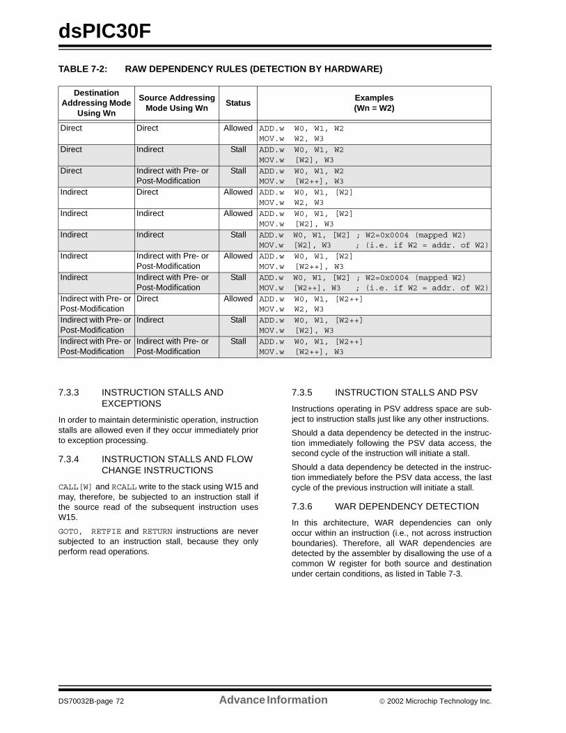
dsPIC30F
TABLE 7-2: RAW DEPENDENCY RULES (DETECTION BY HARDWARE)
7.3.3 INSTRUCTION STALLS AND EXCEPTIONS
In order to maintain deterministic operation, instructionstalls are allowed even if they occur immediately priorto exception processing.
7.3.4 INSTRUCTION STALLS AND FLOW CHANGE INSTRUCTIONS
CALL[W] and RCALL write to the stack using W15 andmay, therefore, be subjected to an instruction stall ifthe source read of the subsequent instruction usesW15.
GOTO, RETFIE and RETURN instructions are neversubjected to an instruction stall, because they onlyperform read operations.
7.3.5 INSTRUCTION STALLS AND PSV
Instructions operating in PSV address space are sub-ject to instruction stalls just like any other instructions.
Should a data dependency be detected in the instruc-tion immediately following the PSV data access, thesecond cycle of the instruction will initiate a stall.
Should a data dependency be detected in the instruc-tion immediately before the PSV data access, the lastcycle of the previous instruction will initiate a stall.
7.3.6 WAR DEPENDENCY DETECTION
In this architecture, WAR dependencies can onlyoccur within an instruction (i.e., not across instructionboundaries). Therefore, all WAR dependencies aredetected by the assembler by disallowing the use of acommon W register for both source and destinationunder certain conditions, as listed in Table 7-3.
DestinationAddressing Mode
Using Wn
Source Addressing Mode Using Wn
StatusExamples(Wn = W2)
Direct Direct Allowed ADD.w W0, W1, W2MOV.w W2, W3
Direct Indirect Stall ADD.w W0, W1, W2MOV.w [W2], W3
Direct Indirect with Pre- or Post-Modification
Stall ADD.w W0, W1, W2MOV.w [W2++], W3
Indirect Direct Allowed ADD.w W0, W1, [W2]MOV.w W2, W3
Indirect Indirect Allowed ADD.w W0, W1, [W2]MOV.w [W2], W3
Indirect Indirect Stall ADD.w W0, W1, [W2] ; W2=0x0004 (mapped W2)MOV.w [W2], W3 ; (i.e. if W2 = addr. of W2)
Indirect Indirect with Pre- or Post-Modification
Allowed ADD.w W0, W1, [W2]MOV.w [W2++], W3
Indirect Indirect with Pre- or Post-Modification
Stall ADD.w W0, W1, [W2] ; W2=0x0004 (mapped W2)MOV.w [W2++], W3 ; (i.e. if W2 = addr. of W2)
Indirect with Pre- or Post-Modification
Direct Allowed ADD.w W0, W1, [W2++]MOV.w W2, W3
Indirect with Pre- or Post-Modification
Indirect Stall ADD.w W0, W1, [W2++]MOV.w [W2], W3
Indirect with Pre- or Post-Modification
Indirect with Pre- or Post-Modification
Stall ADD.w W0, W1, [W2++]MOV.w [W2++], W3
DS70032B-page 72 Advance Information 2002 Microchip Technology Inc.
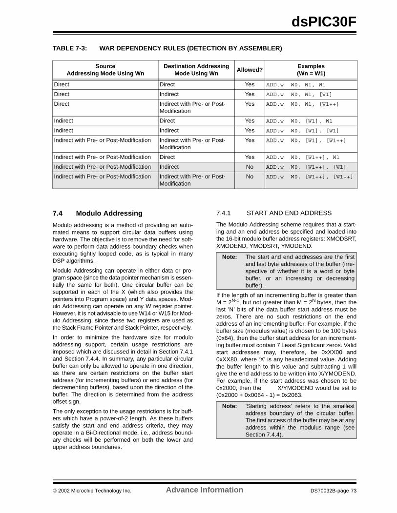
dsPIC30F
TABLE 7-3: WAR DEPENDENCY RULES (DETECTION BY ASSEMBLER)
7.4 Modulo Addressing
Modulo addressing is a method of providing an auto-mated means to support circular data buffers usinghardware. The objective is to remove the need for soft-ware to perform data address boundary checks whenexecuting tightly looped code, as is typical in manyDSP algorithms.
Modulo Addressing can operate in either data or pro-gram space (since the data pointer mechanism is essen-tially the same for both). One circular buffer can besupported in each of the X (which also provides thepointers into Program space) and Y data spaces. Mod-ulo Addressing can operate on any W register pointer.However, it is not advisable to use W14 or W15 for Mod-ulo Addressing, since these two registers are used asthe Stack Frame Pointer and Stack Pointer, respectively.
In order to minimize the hardware size for moduloaddressing support, certain usage restrictions areimposed which are discussed in detail in Section 7.4.1and Section 7.4.4. In summary, any particular circularbuffer can only be allowed to operate in one direction,as there are certain restrictions on the buffer startaddress (for incrementing buffers) or end address (fordecrementing buffers), based upon the direction of thebuffer. The direction is determined from the addressoffset sign.
The only exception to the usage restrictions is for buff-ers which have a power-of-2 length. As these bufferssatisfy the start and end address criteria, they mayoperate in a Bi-Directional mode, i.e., address bound-ary checks will be performed on both the lower andupper address boundaries.
7.4.1 START AND END ADDRESS
The Modulo Addressing scheme requires that a start-ing and an end address be specified and loaded intothe 16-bit modulo buffer address registers: XMODSRT,XMODEND, YMODSRT, YMODEND.
If the length of an incrementing buffer is greater thanM = 2N-1, but not greater than M = 2N bytes, then thelast ’N’ bits of the data buffer start address must bezeros. There are no such restrictions on the endaddress of an incrementing buffer. For example, if thebuffer size (modulus value) is chosen to be 100 bytes(0x64), then the buffer start address for an increment-ing buffer must contain 7 Least Significant zeros. Validstart addresses may, therefore, be 0xXX00 and0xXX80, where ‘X’ is any hexadecimal value. Addingthe buffer length to this value and subtracting 1 willgive the end address to be written into X/YMODEND.For example, if the start address was chosen to be0x2000, then the X/YMODEND would be set to(0x2000 + 0x0064 - 1) = 0x2063.
SourceAddressing Mode Using Wn
Destination Addressing Mode Using Wn
Allowed?Examples(Wn = W1)
Direct Direct Yes ADD.w W0, W1, W1
Direct Indirect Yes ADD.w W0, W1, [W1]
Direct Indirect with Pre- or Post-Modification
Yes ADD.w W0, W1, [W1++]
Indirect Direct Yes ADD.w W0, [W1], W1
Indirect Indirect Yes ADD.w W0, [W1], [W1]
Indirect with Pre- or Post-Modification Indirect with Pre- or Post-Modification
Yes ADD.w W0, [W1], [W1++]
Indirect with Pre- or Post-Modification Direct Yes ADD.w W0, [W1++], W1
Indirect with Pre- or Post-Modification Indirect No ADD.w W0, [W1++], [W1]
Indirect with Pre- or Post-Modification Indirect with Pre- or Post-Modification
No ADD.w W0, [W1++], [W1++]
Note: The start and end addresses are the firstand last byte addresses of the buffer (irre-spective of whether it is a word or bytebuffer, or an increasing or decreasingbuffer).
Note: ‘Starting address’ refers to the smallestaddress boundary of the circular buffer.The first access of the buffer may be at anyaddress within the modulus range (seeSection 7.4.4).
2002 Microchip Technology Inc. Advance Information DS70032B-page 73
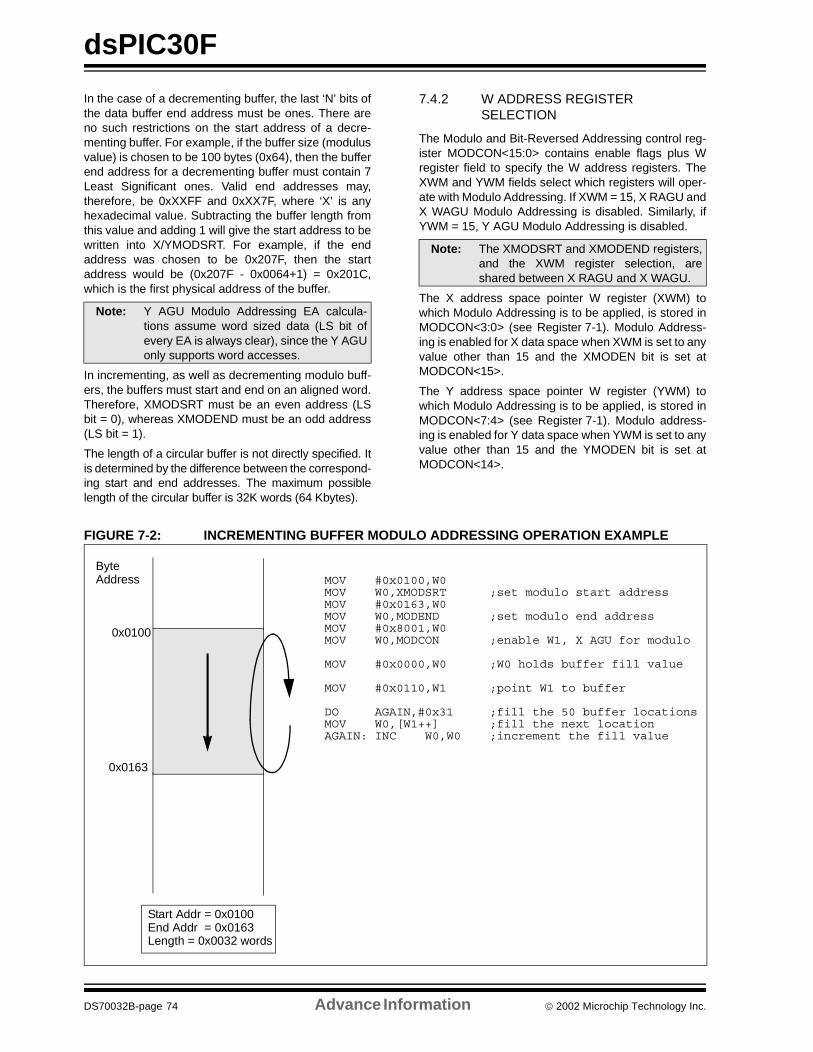
dsPIC30F
In the case of a decrementing buffer, the last ‘N’ bits ofthe data buffer end address must be ones. There areno such restrictions on the start address of a decre-menting buffer. For example, if the buffer size (modulusvalue) is chosen to be 100 bytes (0x64), then the bufferend address for a decrementing buffer must contain 7Least Significant ones. Valid end addresses may,therefore, be 0xXXFF and 0xXX7F, where ‘X’ is anyhexadecimal value. Subtracting the buffer length fromthis value and adding 1 will give the start address to bewritten into X/YMODSRT. For example, if the endaddress was chosen to be 0x207F, then the startaddress would be (0x207F - 0x0064+1) = 0x201C,which is the first physical address of the buffer.
In incrementing, as well as decrementing modulo buff-ers, the buffers must start and end on an aligned word.Therefore, XMODSRT must be an even address (LSbit = 0), whereas XMODEND must be an odd address(LS bit = 1).
The length of a circular buffer is not directly specified. Itis determined by the difference between the correspond-ing start and end addresses. The maximum possiblelength of the circular buffer is 32K words (64 Kbytes).
7.4.2 W ADDRESS REGISTER SELECTION
The Modulo and Bit-Reversed Addressing control reg-ister MODCON<15:0> contains enable flags plus Wregister field to specify the W address registers. TheXWM and YWM fields select which registers will oper-ate with Modulo Addressing. If XWM = 15, X RAGU andX WAGU Modulo Addressing is disabled. Similarly, ifYWM = 15, Y AGU Modulo Addressing is disabled.
The X address space pointer W register (XWM) towhich Modulo Addressing is to be applied, is stored inMODCON<3:0> (see Register 7-1). Modulo Address-ing is enabled for X data space when XWM is set to anyvalue other than 15 and the XMODEN bit is set atMODCON<15>.
The Y address space pointer W register (YWM) towhich Modulo Addressing is to be applied, is stored inMODCON<7:4> (see Register 7-1). Modulo address-ing is enabled for Y data space when YWM is set to anyvalue other than 15 and the YMODEN bit is set atMODCON<14>.
FIGURE 7-2: INCREMENTING BUFFER MODULO ADDRESSING OPERATION EXAMPLE
Note: Y AGU Modulo Addressing EA calcula-tions assume word sized data (LS bit ofevery EA is always clear), since the Y AGUonly supports word accesses.
Note: The XMODSRT and XMODEND registers,and the XWM register selection, areshared between X RAGU and X WAGU.
0x0100
0x0163
Start Addr = 0x0100End Addr = 0x0163Length = 0x0032 words
MOV #0x0100,W0 MOV W0,XMODSRT ;set modulo start addressMOV #0x0163,W0 MOV W0,MODEND ;set modulo end addressMOV #0x8001,W0 MOV W0,MODCON ;enable W1, X AGU for modulo
MOV #0x0000,W0 ;W0 holds buffer fill value
MOV #0x0110,W1 ;point W1 to buffer
DO AGAIN,#0x31 ;fill the 50 buffer locationsMOV W0,[W1++] ;fill the next locationAGAIN: INC W0,W0 ;increment the fill value
ByteAddress
DS70032B-page 74 Advance Information 2002 Microchip Technology Inc.
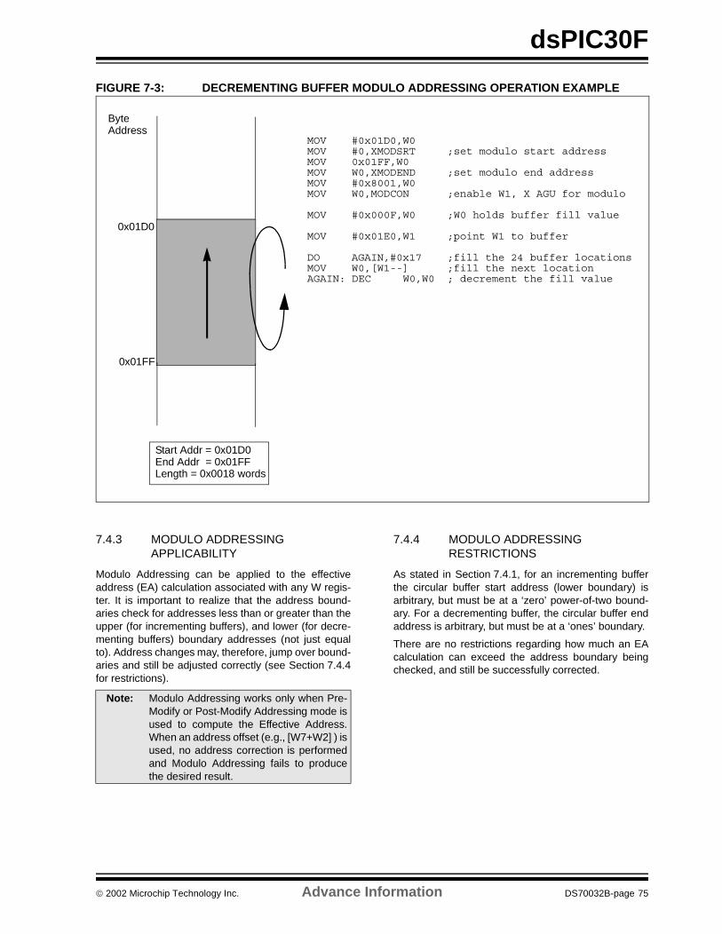
dsPIC30F
FIGURE 7-3: DECREMENTING BUFFER MODULO ADDRESSING OPERATION EXAMPLE
7.4.3 MODULO ADDRESSING APPLICABILITY
Modulo Addressing can be applied to the effectiveaddress (EA) calculation associated with any W regis-ter. It is important to realize that the address bound-aries check for addresses less than or greater than theupper (for incrementing buffers), and lower (for decre-menting buffers) boundary addresses (not just equalto). Address changes may, therefore, jump over bound-aries and still be adjusted correctly (see Section 7.4.4for restrictions).
7.4.4 MODULO ADDRESSING RESTRICTIONS
As stated in Section 7.4.1, for an incrementing bufferthe circular buffer start address (lower boundary) isarbitrary, but must be at a ‘zero’ power-of-two bound-ary. For a decrementing buffer, the circular buffer endaddress is arbitrary, but must be at a ‘ones’ boundary.
There are no restrictions regarding how much an EAcalculation can exceed the address boundary beingchecked, and still be successfully corrected.
0x01D0
0x01FF
Start Addr = 0x01D0End Addr = 0x01FFLength = 0x0018 words
MOV #0x01D0,W0 MOV #0,XMODSRT ;set modulo start addressMOV 0x01FF,W0 MOV W0,XMODEND ;set modulo end addressMOV #0x8001,W0 MOV W0,MODCON ;enable W1, X AGU for modulo
MOV #0x000F,W0 ;W0 holds buffer fill value
MOV #0x01E0,W1 ;point W1 to buffer
DO AGAIN,#0x17 ;fill the 24 buffer locationsMOV W0,[W1--] ;fill the next locationAGAIN: DEC W0,W0 ; decrement the fill value
ByteAddress
Note: Modulo Addressing works only when Pre-Modify or Post-Modify Addressing mode isused to compute the Effective Address.When an address offset (e.g., [W7+W2] ) isused, no address correction is performedand Modulo Addressing fails to producethe desired result.
2002 Microchip Technology Inc. Advance Information DS70032B-page 75
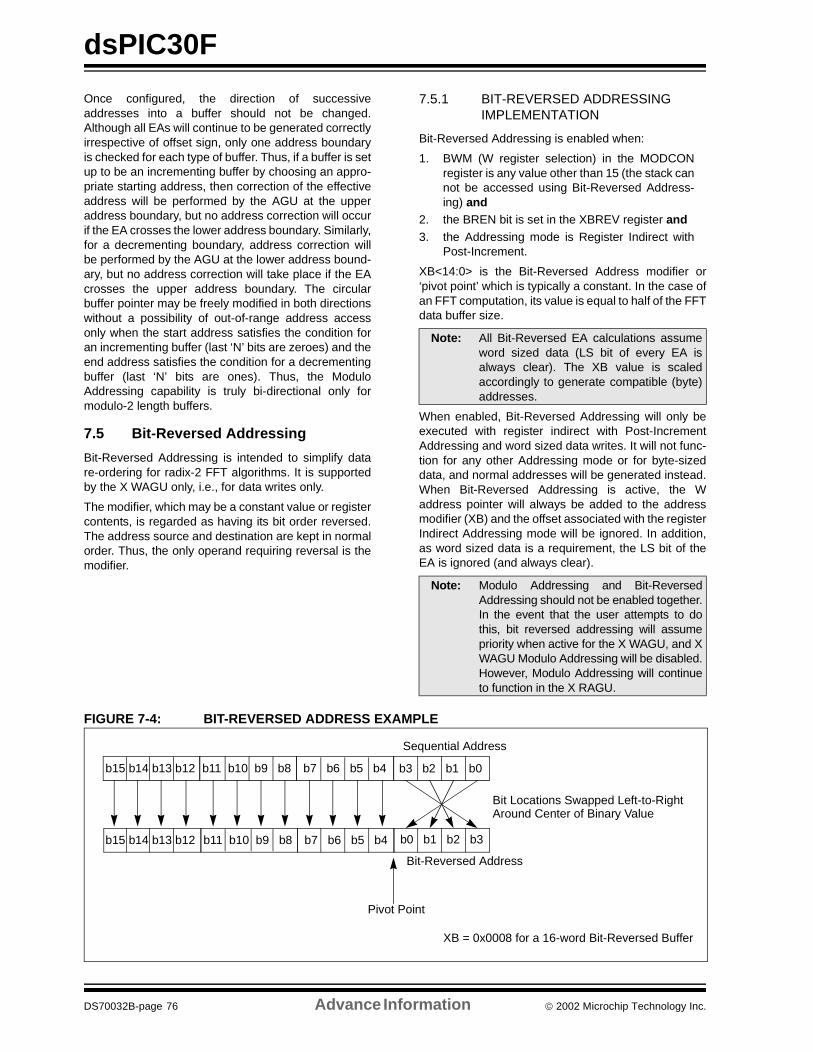
dsPIC30F
Once configured, the direction of successiveaddresses into a buffer should not be changed.Although all EAs will continue to be generated correctlyirrespective of offset sign, only one address boundaryis checked for each type of buffer. Thus, if a buffer is setup to be an incrementing buffer by choosing an appro-priate starting address, then correction of the effectiveaddress will be performed by the AGU at the upperaddress boundary, but no address correction will occurif the EA crosses the lower address boundary. Similarly,for a decrementing boundary, address correction willbe performed by the AGU at the lower address bound-ary, but no address correction will take place if the EAcrosses the upper address boundary. The circularbuffer pointer may be freely modified in both directionswithout a possibility of out-of-range address accessonly when the start address satisfies the condition foran incrementing buffer (last ‘N’ bits are zeroes) and theend address satisfies the condition for a decrementingbuffer (last ‘N’ bits are ones). Thus, the ModuloAddressing capability is truly bi-directional only formodulo-2 length buffers.
7.5 Bit-Reversed Addressing
Bit-Reversed Addressing is intended to simplify datare-ordering for radix-2 FFT algorithms. It is supportedby the X WAGU only, i.e., for data writes only.
The modifier, which may be a constant value or registercontents, is regarded as having its bit order reversed.The address source and destination are kept in normalorder. Thus, the only operand requiring reversal is themodifier.
7.5.1 BIT-REVERSED ADDRESSING IMPLEMENTATION
Bit-Reversed Addressing is enabled when:
1. BWM (W register selection) in the MODCONregister is any value other than 15 (the stack cannot be accessed using Bit-Reversed Address-ing) and
2. the BREN bit is set in the XBREV register and3. the Addressing mode is Register Indirect with
Post-Increment.
XB<14:0> is the Bit-Reversed Address modifier or‘pivot point’ which is typically a constant. In the case ofan FFT computation, its value is equal to half of the FFTdata buffer size.
When enabled, Bit-Reversed Addressing will only beexecuted with register indirect with Post-IncrementAddressing and word sized data writes. It will not func-tion for any other Addressing mode or for byte-sizeddata, and normal addresses will be generated instead.When Bit-Reversed Addressing is active, the Waddress pointer will always be added to the addressmodifier (XB) and the offset associated with the registerIndirect Addressing mode will be ignored. In addition,as word sized data is a requirement, the LS bit of theEA is ignored (and always clear).
FIGURE 7-4: BIT-REVERSED ADDRESS EXAMPLE
Note: All Bit-Reversed EA calculations assumeword sized data (LS bit of every EA isalways clear). The XB value is scaledaccordingly to generate compatible (byte)addresses.
Note: Modulo Addressing and Bit-ReversedAddressing should not be enabled together.In the event that the user attempts to dothis, bit reversed addressing will assumepriority when active for the X WAGU, and XWAGU Modulo Addressing will be disabled.However, Modulo Addressing will continueto function in the X RAGU.
b3 b2 b1 b0
b0 b1 b2 b3
Bit Locations Swapped Left-to-RightAround Center of Binary Value
Bit-Reversed Address
XB = 0x0008 for a 16-word Bit-Reversed Buffer
b7 b6 b5 b4
b7 b6 b5 b4b11 b10 b9 b8
b11 b10 b9 b8
b15 b14 b13 b12
b15 b14 b13 b12
Sequential Address
Pivot Point
DS70032B-page 76 Advance Information 2002 Microchip Technology Inc.
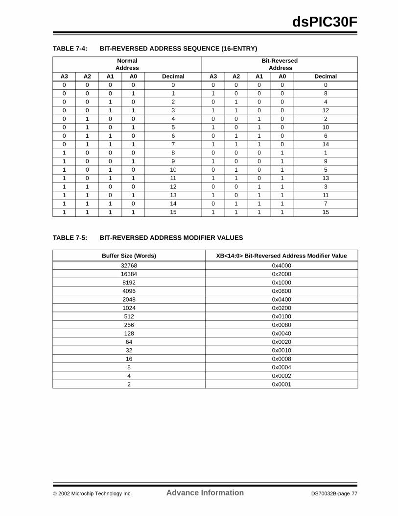
dsPIC30F
TABLE 7-4: BIT-REVERSED ADDRESS SEQUENCE (16-ENTRY)
TABLE 7-5: BIT-REVERSED ADDRESS MODIFIER VALUES
NormalAddress
Bit-Reversed Address
A3 A2 A1 A0 Decimal A3 A2 A1 A0 Decimal0 0 0 0 0 0 0 0 0 00 0 0 1 1 1 0 0 0 80 0 1 0 2 0 1 0 0 4
0 0 1 1 3 1 1 0 0 120 1 0 0 4 0 0 1 0 20 1 0 1 5 1 0 1 0 10
0 1 1 0 6 0 1 1 0 60 1 1 1 7 1 1 1 0 141 0 0 0 8 0 0 0 1 1
1 0 0 1 9 1 0 0 1 91 0 1 0 10 0 1 0 1 51 0 1 1 11 1 1 0 1 13
1 1 0 0 12 0 0 1 1 31 1 0 1 13 1 0 1 1 111 1 1 0 14 0 1 1 1 7
1 1 1 1 15 1 1 1 1 15
Buffer Size (Words) XB<14:0> Bit-Reversed Address Modifier Value
32768 0x400016384 0x2000
8192 0x10004096 0x08002048 0x0400
1024 0x0200512 0x0100256 0x0080
128 0x004064 0x002032 0x0010
16 0x00088 0x00044 0x0002
2 0x0001
2002 Microchip Technology Inc. Advance Information DS70032B-page 77
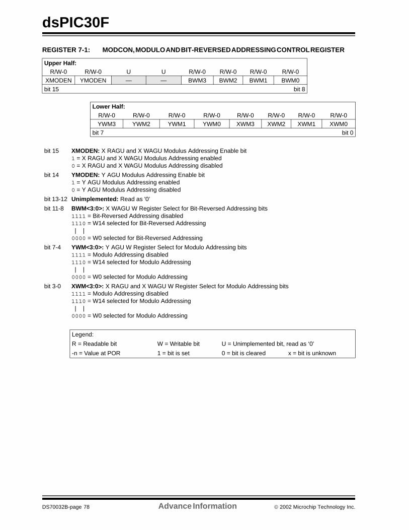
dsPIC30F
REGISTER 7-1: MODCON, MODULO AND BIT-REVERSED ADDRESSING CONTROL REGISTER
Upper Half:R/W-0 R/W-0 U U R/W-0 R/W-0 R/W-0 R/W-0
XMODEN YMODEN — — BWM3 BWM2 BWM1 BWM0
bit 15 bit 8
Lower Half:R/W-0 R/W-0 R/W-0 R/W-0 R/W-0 R/W-0 R/W-0 R/W-0YWM3 YWM2 YWM1 YWM0 XWM3 XWM2 XWM1 XWM0
bit 7 bit 0
bit 15 XMODEN: X RAGU and X WAGU Modulus Addressing Enable bit1 = X RAGU and X WAGU Modulus Addressing enabled0 = X RAGU and X WAGU Modulus Addressing disabled
bit 14 YMODEN: Y AGU Modulus Addressing Enable bit1 = Y AGU Modulus Addressing enabled0 = Y AGU Modulus Addressing disabled
bit 13-12 Unimplemented: Read as '0’
bit 11-8 BWM<3:0>: X WAGU W Register Select for Bit-Reversed Addressing bits1111 = Bit-Reversed Addressing disabled 1110 = W14 selected for Bit-Reversed Addressing | |0000 = W0 selected for Bit-Reversed Addressing
bit 7-4 YWM<3:0>: Y AGU W Register Select for Modulo Addressing bits1111 = Modulo Addressing disabled 1110 = W14 selected for Modulo Addressing | |0000 = W0 selected for Modulo Addressing
bit 3-0 XWM<3:0>: X RAGU and X WAGU W Register Select for Modulo Addressing bits1111 = Modulo Addressing disabled 1110 = W14 selected for Modulo Addressing | |0000 = W0 selected for Modulo Addressing
Legend:
R = Readable bit W = Writable bit U = Unimplemented bit, read as ‘0’
-n = Value at POR 1 = bit is set 0 = bit is cleared x = bit is unknown
DS70032B-page 78 Advance Information 2002 Microchip Technology Inc.
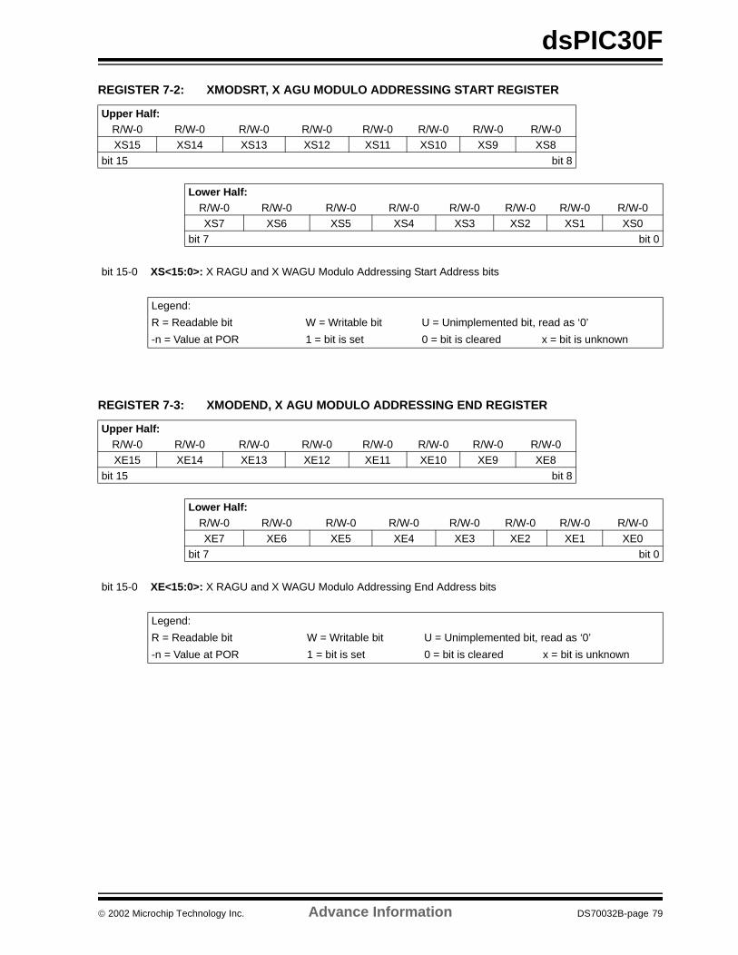
dsPIC30F
REGISTER 7-2: XMODSRT, X AGU MODULO ADDRESSING START REGISTER
REGISTER 7-3: XMODEND, X AGU MODULO ADDRESSING END REGISTER
Upper Half:R/W-0 R/W-0 R/W-0 R/W-0 R/W-0 R/W-0 R/W-0 R/W-0XS15 XS14 XS13 XS12 XS11 XS10 XS9 XS8
bit 15 bit 8
Lower Half:R/W-0 R/W-0 R/W-0 R/W-0 R/W-0 R/W-0 R/W-0 R/W-0XS7 XS6 XS5 XS4 XS3 XS2 XS1 XS0
bit 7 bit 0
bit 15-0 XS<15:0>: X RAGU and X WAGU Modulo Addressing Start Address bits
Legend:
R = Readable bit W = Writable bit U = Unimplemented bit, read as ‘0’
-n = Value at POR 1 = bit is set 0 = bit is cleared x = bit is unknown
Upper Half:R/W-0 R/W-0 R/W-0 R/W-0 R/W-0 R/W-0 R/W-0 R/W-0XE15 XE14 XE13 XE12 XE11 XE10 XE9 XE8
bit 15 bit 8
Lower Half:R/W-0 R/W-0 R/W-0 R/W-0 R/W-0 R/W-0 R/W-0 R/W-0XE7 XE6 XE5 XE4 XE3 XE2 XE1 XE0
bit 7 bit 0
bit 15-0 XE<15:0>: X RAGU and X WAGU Modulo Addressing End Address bits
Legend:
R = Readable bit W = Writable bit U = Unimplemented bit, read as ‘0’
-n = Value at POR 1 = bit is set 0 = bit is cleared x = bit is unknown
2002 Microchip Technology Inc. Advance Information DS70032B-page 79
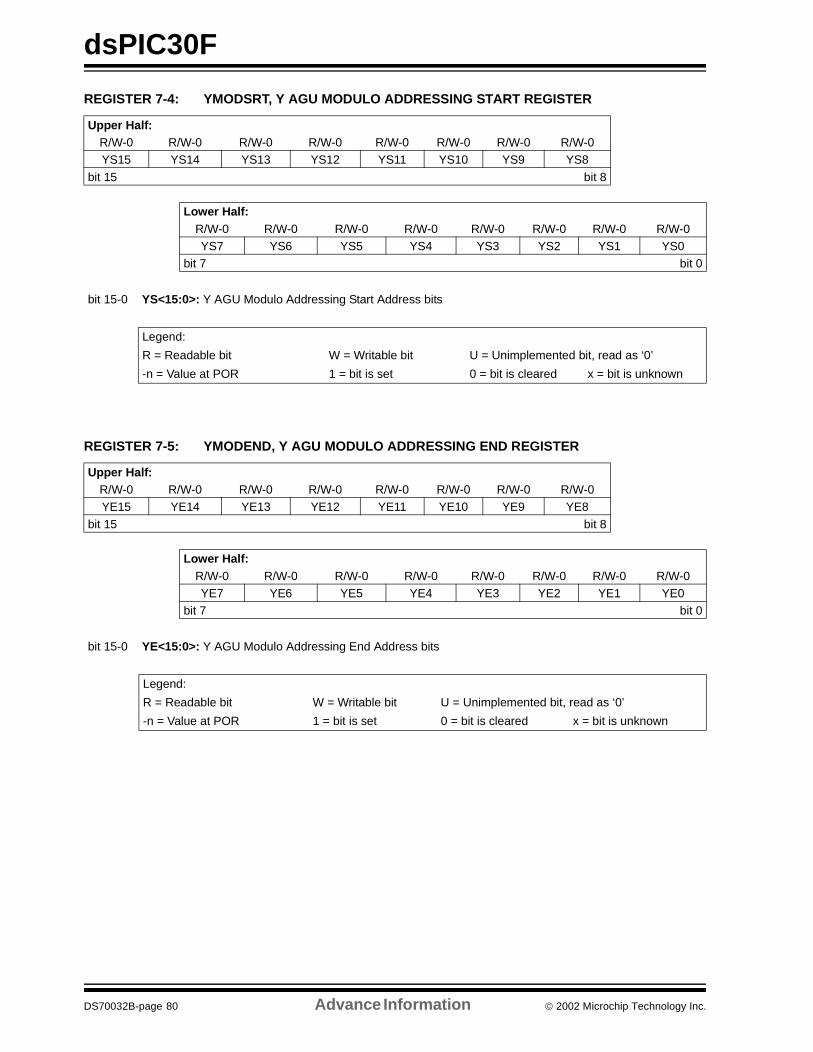
dsPIC30F
REGISTER 7-4: YMODSRT, Y AGU MODULO ADDRESSING START REGISTER
REGISTER 7-5: YMODEND, Y AGU MODULO ADDRESSING END REGISTER
Upper Half:R/W-0 R/W-0 R/W-0 R/W-0 R/W-0 R/W-0 R/W-0 R/W-0YS15 YS14 YS13 YS12 YS11 YS10 YS9 YS8
bit 15 bit 8
Lower Half:R/W-0 R/W-0 R/W-0 R/W-0 R/W-0 R/W-0 R/W-0 R/W-0YS7 YS6 YS5 YS4 YS3 YS2 YS1 YS0
bit 7 bit 0
bit 15-0 YS<15:0>: Y AGU Modulo Addressing Start Address bits
Legend:
R = Readable bit W = Writable bit U = Unimplemented bit, read as ‘0’
-n = Value at POR 1 = bit is set 0 = bit is cleared x = bit is unknown
Upper Half:R/W-0 R/W-0 R/W-0 R/W-0 R/W-0 R/W-0 R/W-0 R/W-0YE15 YE14 YE13 YE12 YE11 YE10 YE9 YE8
bit 15 bit 8
Lower Half:R/W-0 R/W-0 R/W-0 R/W-0 R/W-0 R/W-0 R/W-0 R/W-0YE7 YE6 YE5 YE4 YE3 YE2 YE1 YE0
bit 7 bit 0
bit 15-0 YE<15:0>: Y AGU Modulo Addressing End Address bits
Legend:
R = Readable bit W = Writable bit U = Unimplemented bit, read as ‘0’
-n = Value at POR 1 = bit is set 0 = bit is cleared x = bit is unknown
DS70032B-page 80 Advance Information 2002 Microchip Technology Inc.
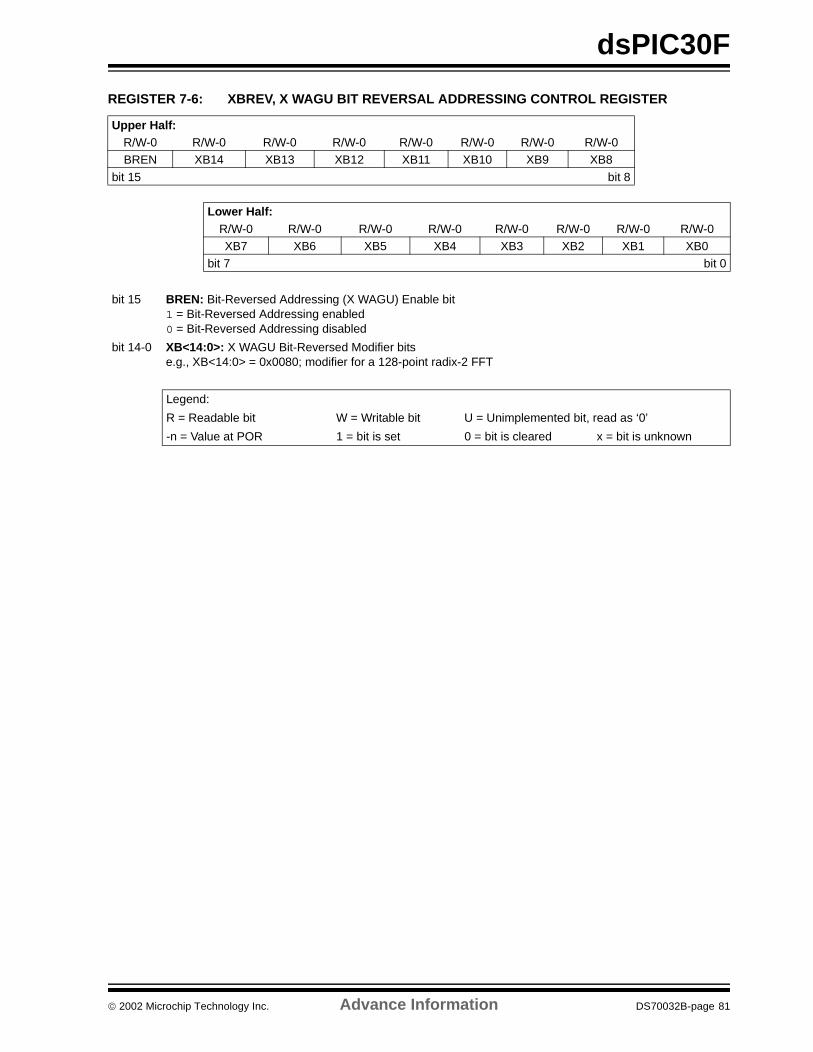
dsPIC30F
REGISTER 7-6: XBREV, X WAGU BIT REVERSAL ADDRESSING CONTROL REGISTER
Upper Half:R/W-0 R/W-0 R/W-0 R/W-0 R/W-0 R/W-0 R/W-0 R/W-0BREN XB14 XB13 XB12 XB11 XB10 XB9 XB8
bit 15 bit 8
Lower Half:R/W-0 R/W-0 R/W-0 R/W-0 R/W-0 R/W-0 R/W-0 R/W-0XB7 XB6 XB5 XB4 XB3 XB2 XB1 XB0
bit 7 bit 0
bit 15 BREN: Bit-Reversed Addressing (X WAGU) Enable bit1 = Bit-Reversed Addressing enabled0 = Bit-Reversed Addressing disabled
bit 14-0 XB<14:0>: X WAGU Bit-Reversed Modifier bitse.g., XB<14:0> = 0x0080; modifier for a 128-point radix-2 FFT
Legend:
R = Readable bit W = Writable bit U = Unimplemented bit, read as ‘0’
-n = Value at POR 1 = bit is set 0 = bit is cleared x = bit is unknown
2002 Microchip Technology Inc. Advance Information DS70032B-page 81

dsPIC30F
NOTES:
DS70032B-page 82 Advance Information 2002 Microchip Technology Inc.
dsPIC30F
8.0 EXCEPTION PROCESSING
The dsPIC30F has 45 interrupt sources and 8 proces-sor exceptions (traps), which must be arbitrated basedon a priority scheme.
The processor core is responsible for reading theInterrupt Vector Table (IVT) and transferring theaddress contained in the interrupt vector to the pro-gram counter. The interrupt vector is transferred fromthe program data bus into the program counter, via a24-bit wide multiplexer on the input of the programcounter.
The Interrupt Vector Table (IVT) and Alternate Inter-rupt Vector Table (AIVT) are placed near the beginningof program memory (0x000004). The IVT and AIVTare shown in Table 8-2.
The interrupt controller is responsible for pre-process-ing the interrupts, prior to them being presented to theprocessor core. The peripheral interrupts are enabled,prioritized, and controlled using centralized specialfunction registers:
• IFS0<15:0>, IFS1<15:0>, IFS2<15:0>All interrupt request flags are maintained in these three registers. The flags are set by their respec-tive peripherals or external signals, and they are cleared via software.
• IEC0<15:0>, IEC1<15:0>, IEC2<15:0>All interrupt enable control bits are maintained in these three registers. These control bits are used to individually enable interrupts from the peripher-als or external signals.
• IPC0<15:0> ... IPC11<7:0>The user assignable priority level associated with each of these 45 interrupts is held centrally in these twelve registers.
• IPL<2:0> The current CPU priority level is explic-itly stored in the 16-bit STATUS register that resides in the processor core.
• INTCON1<15:0>, INTCON2<15:0>Global interrupt control functions are derived from these two registers. INTCON1 contains the Global Interrupt Enable (GIE) bit, as well as the control and status flags for the processor exceptions. The INTCON2 register controls the external interrupt request signal behavior and the use of the alter-nate vector table.
All interrupt sources can be user assigned to one of 8priority levels, 0 through 7, via the IPCx registers.Each interrupt source is associated with an interruptvector, as shown in Table 8-2. Levels 6 and 0 repre-sent the highest and lowest maskable priorities,respectively. Level 7 interrupts are non-maskable.
Certain interrupts have specialized control bits for fea-tures like edge or level triggered interrupts, interrupt-on-change, etc. Control of these features remainswithin the peripheral module, which generates theinterrupt.
The DISI instruction can be used to disable the pro-cessing of interrupts of priorities 7 and lower for a cer-tain number of instructions, during which the DISI bit(INTCON2<14>) remains set.
When an interrupt is serviced, the PC is loaded with theaddress stored in the vector location in Program mem-ory that corresponds to the interrupt. There are 63 dif-ferent vectors within the IVT (refer to Table 8-2). Thesevectors are contained in locations 0x000004 through0x0000FE of program memory (refer to Table 8-2).These locations contain 24-bit addresses, and in orderto preserve robustness, an address error trap will takeplace should the PC attempt to fetch any of thesewords during normal execution. This prevents execu-tion of random data through accidentally decrementinga PC into vector space, accidentally mapping a dataspace address into vector space, or the PC rolling overto 0x000000 after reaching the end of implementedprogram memory space. Execution of a GOTO instruc-tion to this vector space will also generate an addresserror trap.
8.1 Interrupt Priority
The user assignable Interrupt Priority (IP<2:0>) bits foreach individual interrupt source are located in the LS3-bits of each nibble, within the IPCx register(s). Bit 3of each nibble is not used and is read as a 0. Thesebits define the priority level assigned to a particularinterrupt by the user.
Since more than one interrupt request source may beassigned to a specific user specified priority level, ameans is provided to assign priority within a givenlevel. This method is called “Natural Order Priority” Note: Interrupt flag bits get set when an interrupt
condition occurs, regardless of the state ofits corresponding enable bit or the GlobalInterrupt Enable bit. User software shouldensure the appropriate interrupt flag bitsare clear prior to enabling an interrupt.
Note: The user selectable priority levels start at 0as the lowest priority and level 7, as thehighest priority.
2002 Microchip Technology Inc. Advance Information DS70032B-page 83
dsPIC30F
Table 8-1 lists the interrupt numbers and interruptsources for the dsPIC device, and their associatedvector numbers. The Natural Order Priority of an inter-rupt is numerically identical to its Vector Number.The ability for the user to assign every interrupt to oneof eight priority levels implies that the user can assigna very high overall priority level to an interrupt with alow natural order priority. For example, the PLVD (LowVoltage Detect) can be given a priority of 7. The INT0(external interrupt 0) may be assigned to priority level0, thus giving it a very low effective priority.
TABLE 8-1: NATURAL ORDER PRIORITY
Note 1: The natural order priority scheme has 0as the highest priority and 53 as the low-est priority.
2: The natural order priority number is thesame as the vector number.
INT Number
Vector Number
Interrupt Source
Highest Natural Order Priority0 8 INT0 - External Interrupt 01 9 IC1 - Input Compare 1
2 10 OC1 - Output Compare 13 11 T1 - Timer 14 12 IC2 - Input Capture 2
5 13 OC2 - Output Compare 26 14 T2 - Timer 27 15 TMR3 - Timer 3
8 16 SPI1 9 17 U1RX - UART1 Receiver
10 18 U1TX - UART1 Transmitter
11 19 ADC - ADC Convert Done12 20 NVM - NVM Write Complete13 21 I2C - I2C Transfer Complete14 22 BCL - I2C Bus Collision
15 23 Input Change Interrupt16 24 INT1 - External Interrupt 117 25 IC7 - Input Capture 7
18 26 IC8 - Input Capture 819 27 OC3 - Output Compare 320 28 OC4 - Output Compare 4
21 29 T4 - Timer 422 30 T5 - Timer 523 31 INT2 - External Interrupt 2
24 32 U2RX - UART2 Receiver25 33 U2TX - UART2 Transmitter26 34 SPI2
27 35 C1 - Combined IRQ for CAN128 36 IC3 - Input Capture 329 37 IC4 - Input Capture 4
30 38 IC5 - Input Capture 531 39 IC6 - Input Capture 632 40 OC5 - Output Compare 5
33 41 OC6 - Output Compare 634 42 OC7 - Output Compare 735 43 OC8 - Output Compare 8
36 44 INT3 - External Interrupt 337 45 INT4 - External Interrupt 438 46 C2 - Combined IRQ for CAN2
39 47 PWM - PWM Period Match40 48 QEI - Position Counter Compare41 49 DCI - CODEC Transfer Done
42 50 LVD - Low Voltage Detect43 51 FLTA - Motor Control PWM Fault A44 52 FLTB - Motor Control PWM Fault B
45- 53 53 - 61 ReservedLowest Natural Order Priority
DS70032B-page 84 Advance Information 2002 Microchip Technology Inc.
dsPIC30F
8.2 RESET Sequence
A RESET is not a true exception, because the inter-rupt controller is not involved in the RESET process.The processor clears its registers in response to aRESET, which forces the PC to zero. The processorthen begins program execution at location 0x000000.A GOTO instruction is stored in the first program mem-ory location, immediately followed by the address tar-get for the GOTO instruction. The processor executesthe GOTO to the specified address and then beginsoperation at the specified target (start) address.
8.2.1 RESET SOURCES
In addition to external, Power-on Resets (POR) andsoftware RESETS, there are three sources of errorconditions which ‘trap’ to the RESET vector.
• Watchdog Time-out:The watchdog has timed out, indicating that the processor is no longer executing the correct flow of code.
• Illegal Instruction Trap:Attempted execution of any unused opcodes will result in an illegal instruction trap. Note that a fetch of an illegal instruction does not result in an illegal instruction trap if that instruction is flushed prior to execution due to a flow change.
• Brown-out Reset (BOR):A momentary dip in the power supply to the device has been detected, which may result in malfunction.
8.3 Traps
Traps can be considered as non-maskable, non-stableinterrupts, which adhere to a predefined priority asshown in Table 8-2. They are intended to provide theuser a means to correct erroneous operation duringdebug and when operating within the application.
Note that many of these trap conditions can only bedetected when they occur. Consequently, the ques-tionable instruction is allowed to complete prior to trapexception processing. If the user chooses to recoverfrom the error, the result of the erroneous action whichcaused the trap may, therefore, have to be corrected.
8.3.1 TRAP SOURCES
The following traps are provided with increasing prior-ity. However, as all traps are nestable, priority has littleeffect.
• Software Trap:Execution of the TRAP instruction causes an exception.
• Arithmetic Error Trap:The Arithmetic Error trap executes under the fol-lowing three circumstances.
1. Should an attempt be made to divide byzero, the divide operation will be aborted ona cycle boundary and the trap taken.
2. If enabled, an Arithmetic Error trap will betaken when an arithmetic operation oneither accumulator A or B, causes an over-flow from bit 31 and the accumulator guardbits are unutilized.
3. If enabled, an Arithmetic Error trap will betaken when an arithmetic operation oneither accumulator A or B causes a cata-strophic overflow from bit 39 and all satura-tion is disabled.
• Address Error Trap:This trap is initiated when any of the following cir-cumstances occurs:
1. A misaligned data word fetch is attempted.2. A data fetch from unused data address
space is attempted.3. A program fetch from unimplemented user
program address space is attempted.4. A program fetch from vector address space
is attempted.5. A read (for address) of an uninitialized W
register is attempted.• Stack Error Trap
This trap is initiated under the following conditions:
1. The stack pointer is loaded with a valuewhich is greater than the (user program-mable) limit value written into the SPLIMregister (stack overflow).
2. The stack pointer is loaded with a valuewhich is less than 0x0800 (simple stackunderflow).
• Oscillator Fail Trap:This trap is initiated if the external oscillator fails and operation becomes reliant on an internal RC backup.
It is possible that multiple traps can become activewithin the same cycle (e.g., a mis-aligned word stackwrite to an overflowed address). In such a case, thefixed priority shown in Figure 8-2 is implemented,which may require the user to check if other traps arepending, in order to completely correct the fault.
Note: If the user does not intend to take correc-tive action in the event of a trap error con-dition, these vectors must be loaded withthe RESET vector address. If, on the otherhand, one of the vectors containing aninvalid address is called, an address errortrap is generated.
2002 Microchip Technology Inc. Advance Information DS70032B-page 85
dsPIC30F
8.4 Interrupt Sequence
The GIE (Global Interrupt Enable) bit in the INTCON1register must be set to enable interrupts, but excep-tions can be processed, regardless of the state of theGIE bit.
All interrupt event flags are sampled in the beginningof each instruction cycle by the IFSx registers. A pend-ing interrupt request (IRQ) is indicated by the flag bitbeing equal to a ‘1’ in an IFSx register. The IRQ willcause the interrupt to occur if the corresponding bit inthe interrupt enable (IECx) registers is set. For theremainder of the instruction cycle, the priorities of allpending interrupt requests are evaluated.
If there is a pending IRQ with a priority level equal to orgreater than the current processor priority level in thestatus register, an interrupt will be presented to theprocessor.
The processor reacts to the interrupt request byasserting the IACK (Interrupt Acknowledge) signal.The GIE bit in the INTCON1 register is cleared. Thisdisables all interrupts until either a RETFIE instructionis executed, or the user sets the GIE bit.
The processor then stacks the current programcounter and the low byte of the processor STATUSregister, as shown in Figure 8-1. The low byte of theSTATUS register contains the processor priority levelat the time, prior to the beginning of the interrupt cycle.
FIGURE 8-1: INTERRUPT STACK FRAME
The processor then loads the priority level for thisinterrupt into the status register. This action will disableall lower priority interrupts until the completion of theInterrupt Service Routine.
Unless the GIE bit is re-enabled, NO further interruptswill occur. The Interrupt Service Routine must clear theinterrupt flag bits in the IFSx register before re-enabling interrupts, in order to avoid recursiveinterrupts.
The RETFIE (Return from Interrupt) instruction willunstack the program counter and STATUS registers toreturn the processor to its state prior to the interruptsequence. The RETFIE instruction will also set theGIE bit to re-enable interrupts.
TABLE 8-2: EXCEPTION VECTORS
8.5 Alternate Vector Table
In Program Memory, the Interrupt Vector Table (IVT) isfollowed by the Alternate Interrupt Vector Table (AIVT),as shown in Table 8-2. Access to the Alternate VectorTable is provided by the ALTIVT bit in the INTCON2register. If the ALTIVT bit is set, all interrupt andexception processes will use the alternate vectorsinstead of the default vectors. The alternate vectorsare organized in the same manner as the default vec-tors. The AIVT supports emulation and debuggingefforts by providing a means to switch between anapplication and a support environment, without requir-ing the interrupt vectors to be reprogrammed. This fea-ture also enables switching between applications forevaluation of different software algorithms at run time.
If the AIVT is not required, the program memory allo-cated to the AIVT may be used for other purposes.AIVT is not a protected section and may be freely pro-grammed by the user.
Note: The user can always lower the priority levelby writing a new value into the STATUSregister.
<Free Word>
PC<15:0>SR<7:0> PC<23:16>
015
W15 (before CALL)
W15 (after CALL)
Sta
ck G
row
s To
war
dsH
ighe
r A
ddre
ss
PUSH : [W15++]POP : [--W15]
0x0000
Reserved VectorReserved VectorInterrupt 0 VectorInterrupt 1 Vector
~~~
Interrupt 52 VectorInterrupt 53 Vector
Software Trap Vector
Software Trap Vector
Dec
reas
ing
Prio
rity
0x000000
0x000014
Oscillator Fail Trap Vector
Address Error Trap VectorArithmetic Warning Trap Vector
Reserved VectorReserved VectorInterrupt 0 VectorInterrupt 1 Vector
~~~
Interrupt 52 VectorInterrupt 53 Vector
Stack Error Trap Vector
IVT
AIVT
0x0000800x00007E
0x0000FE
reservedOscillator Fail Trap Vector
Address Error Trap VectorArithmetic Warning Trap Vector
Reserved Vector
Stack Error Trap Vector
0x000094
RESET - GOTO InstructionRESET - GOTO Address 0x000002
reserved0x0000820x000084
0x000004
Reserved Vector
DS70032B-page 86 Advance Information 2002 Microchip Technology Inc.
dsPIC30F
8.6 Fast Context Saving
A context saving option is available using shadow reg-isters. Shadow registers are provided for the DA, DC,N, OV, SZ and C bits in SR, the TBLPAG and PSVPAGregisters, and the registers W0 through W14. Theshadows are only one level deep. The shadow regis-ters are accessible using the PUSH.S and POP.Sinstructions only.
When the processor vectors to an interrupt, thePUSH.S instruction can be used to store the currentvalue of the aforementioned registers into their respec-tive shadow registers.
If an ISR of a certain priority uses the PUSH.S andPOP.S instructions for fast context saving, then ahigher priority ISR should not include the same instruc-tions. Users must save the key registers in softwareduring a lower priority interrupt, if the higher priority ISRuses fast context saving.
8.7 External Interrupt Requests
The interrupt controller supports up to five externalinterrupt request signals, INT0 - INT4. These inputsare edge sensitive, i.e., they require a low-to-high or ahigh-to-low transition to generate an interrupt request.The INTCON2 register has five bits, INT0EP - INT4EP,that select the polarity of the edge detection circuitry.
8.8 Wake-up from SLEEP and IDLE
The interrupt controller may be used to wake up theprocessor from either SLEEP or IDLE modes, ifSLEEP or IDLE mode is active when the interrupt isgenerated.
If the GIE in the INTCON1 register is set, and anenabled interrupt request of sufficient priority isreceived by the interrupt controller, then the standardinterrupt request is presented to the processor. At thesame time, the processor will wake-up from SLEEP orIDLE and begin execution of the Interrupt ServiceRoutine (ISR), needed to process the interruptrequest.
If the GIE control bit is cleared, the interrupt controllerwill not generate an interrupt request to the processor.The interrupt enable bit must be set for a peripheral towake the device from SLEEP. In this case, the proces-sor will resume normal execution without processingan ISR.
2002 Microchip Technology Inc. Advance Information DS70032B-page 87
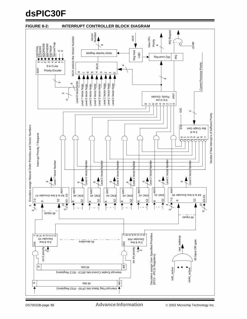
dsPIC30F
FIGURE 8-2: INTERRUPT CONTROLLER BLOCK DIAGRAM0 44
0 44
Interrupt Flag Status bits (IFS0 - IFS2 Registers)
Interrupt Enable Control bits (IEC0 - IEC2 Registers)
3 to 8 lineDecoder #44
EN
3In
t 0 p
riorit
y
3
Int 4
4 pr
iorit
y
07
3 to 8 lineDecoder #0
EN
45 bits
45 bits
45 decoders
64 to 6 line Encoder #7 64 to 6 line Encoder #06 5 4 3 2 1
7-0
7-0
63 -
53
63-5
3
AN
Y
AN
Y
45 inputs45 inputs
Inte
rrup
t Prio
rity
7 R
eque
st
017 6 5 4 23
6 6
MU
X
Vec
tor
6
Dec
oder
s as
sign
Use
r S
peci
fied
Prio
ritie
s
Enc
oder
s as
sign
Nat
ural
Ord
er P
riorit
ies
and
Vec
tor
Num
bers
MU
X s
elec
ts th
e V
ecto
r N
umbe
r
4
7 06 5 4 3 12
70 654321
AN
Y
AN
Y
AN
Y
AN
Y
AN
Y
AN
Y
6 6 6 6 6 6
ENC #6 ENC #5 ENC #4 ENC #3 ENC #2 ENC #1
888888 525252525252
7 06 5 4 3 2 1A
NY
3
Cur
rent
Pro
cess
or P
riorit
y
IRQ
Req
uest
9 to 4 Line Priority Encoder
Leve
l 7 V
ecto
r Num
ber
Leve
l 6 V
ecto
r Num
ber
Leve
l 5 V
ecto
r Num
ber
Leve
l 4 V
ecto
r Num
ber
Leve
l 3 V
ecto
r Num
ber
Leve
l 2 V
ecto
r Num
ber
Leve
l 1 V
ecto
r Num
ber
Leve
l 0 V
ecto
r Num
ber
Leve
l 7 V
ecto
r Nm
brLe
vel 6
Vec
tor N
mbr
Leve
l 5 V
ecto
r Nm
br
Leve
l 4 V
ecto
r Nm
br
Leve
l 3 V
ecto
r Nm
br
Leve
l 2 V
ecto
r Nm
br
Leve
l 1 V
ecto
r Nm
br
Leve
l 0 V
ecto
r Nm
br
4
3 to 8 Bar Graph Gen
4New
CP
U
Vector Number Register
Prio
rity
Num
ber
IRQ Level Reg
IRQ
IAC
KR
eg H
old
Logi
c
8 52 8 52
0
00 0
8Le
vel 8
Vec
tor N
mbr
0 71 2 3 4 5 6
AN
Y
8 to 3 Line
Priority Encoder
OS
CFA
ILS
TK
ER
RA
DD
RE
RR
MA
TH
ER
RS
WT
RA
P
0
Sec
ureT
rap
8
33
0
6
LEV
8F
0
EN
GIE
8 13813
Dec
ides
if N
ew In
terru
pt is
of S
uffic
ient
Prio
rity
(IP
C0
- IP
C11
Reg
iste
rs)
raw
_wak
eup
int0
_act
ive
int4
4_ac
tive
45 in
put O
R g
ate
DS70032B-page 88 Advance Information 2002 Microchip Technology Inc.
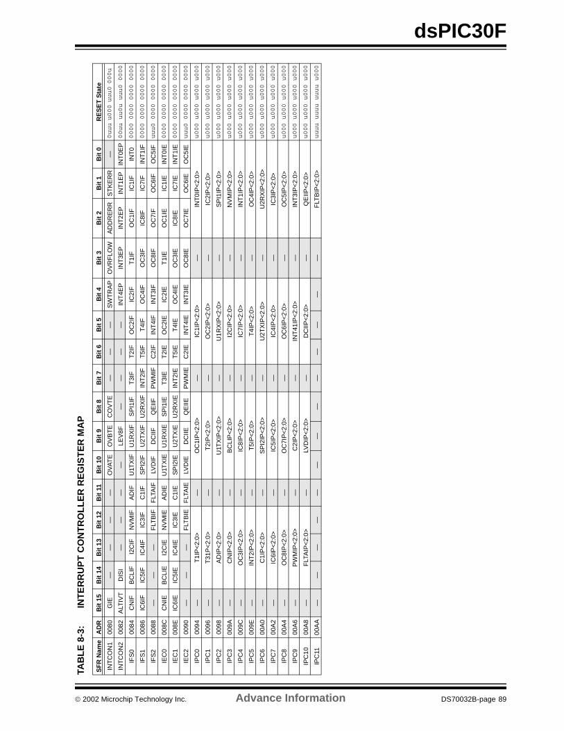
dsPIC30F
TAB
LE
8-3
:IN
TE
RR
UP
T C
ON
TR
OL
LE
R R
EG
IST
ER
MA
P
SF
R N
ame
AD
RB
it 1
5B
it 1
4B
it 1
3B
it 1
2B
it 1
1B
it 1
0B
it 9
Bit
8B
it 7
Bit
6B
it 5
Bit
4B
it 3
Bit
2B
it 1
Bit
0R
ES
ET
Sta
te
INT
CO
N1
0080
GIE
——
——
OV
AT
EO
VB
TE
CO
VT
E—
——
SW
TR
AP
OV
RF
LOW
AD
DR
ER
RS
TK
ER
R—
0uuu u000 uuu0 000u
INT
CO
N2
0082
ALT
IVT
DIS
I—
——
—LE
V8F
——
——
INT
4EP
INT
3EP
INT
2EP
INT
1EP
INT
0EP
00uu uu0u uuu0 0000
IFS
000
84C
NIF
BC
LIF
I2C
IFN
VM
IFA
DIF
U1T
XIF
U1R
XIF
SP
I1IF
T3I
FT
2IF
OC
2IF
IC2I
FT
1IF
OC
1IF
IC1I
FIN
T0
0000 0000 0000 0000
IFS
100
86IC
6IF
IC5I
FIC
4IF
IC3I
FC
1IF
SP
I2IF
U2T
XIF
U2R
XIF
INT
2IF
T5I
FT
4IF
OC
4IF
OC
3IF
IC8I
FIC
7IF
INT
1IF
0000 0000 0000 0000
IFS
200
88—
——
FLT
BIF
FLT
AIF
LVD
IFD
CIIF
QE
IIFP
WM
IFC
2IF
INT
4IF
INT
3IF
OC
8IF
OC
7IF
OC
6IF
OC
5IF
uuu0 0000 0000 0000
IEC
000
8CC
NIE
BC
LIE
I2C
IEN
VM
IEA
DIE
U1T
XIE
U1R
XIE
SP
I1IE
T3I
ET
2IE
OC
2IE
IC2I
ET
1IE
OC
1IE
IC1I
EIN
T0I
E0000 0000 0000 0000
IEC
100
8EIC
6IE
IC5I
EIC
4IE
IC3I
EC
1IE
SP
I2IE
U2T
XIE
U2R
XIE
INT
2IE
T5I
ET
4IE
OC
4IE
OC
3IE
IC8I
EIC
7IE
INT
1IE
0000 0000 0000 0000
IEC
200
90—
——
FLT
BIE
FLT
AIE
LVD
IED
CIIE
QE
IIEP
WM
IEC
2IE
INT
4IE
INT
3IE
OC
8IE
OC
7IE
OC
6IE
OC
5IE
uuu0 0000 0000 0000
IPC
000
94—
T1I
P<
2:0>
—O
C1I
P<
2:0>
—IC
1IP
<2:
0>—
INT
0IP
<2:
0>u000 u000 u000 u000
IPC
100
96—
T31
P<
2:0>
—T
2IP
<2:
0>—
OC
2IP
<2:
0>—
IC2I
P<
2:0>
u000 u000 u000 u000
IPC
200
98—
AD
IP<
2:0>
—U
1TX
IP<
2:0>
—U
1RX
IP<
2:0>
—S
PI1
IP<
2:0>
u000 u000 u000 u000
IPC
300
9A—
CN
IP<
2:0>
—B
CLI
P<
2:0>
—I2
CIP
<2:
0>—
NV
MIP
<2:
0>u000 u000 u000 u000
IPC
400
9C—
OC
3IP
<2:
0>—
IC8I
P<
2:0>
—IC
7IP
<2:
0>—
INT
1IP
<2:
0>u000 u000 u000 u000
IPC
500
9E—
INT
2IP
<2:
0>—
T5I
P<
2:0>
—T
4IP
<2:
0>—
OC
4IP
<2:
0>u000 u000 u000 u000
IPC
600
A0
—C
1IP
<2:
0>—
SP
I2IP
<2:
0>—
U2T
XIP
<2:
0>—
U2R
XIP
<2:
0>u000 u000 u000 u000
IPC
700
A2
—IC
6IP
<2:
0>—
IC5I
P<
2:0>
—IC
4IP
<2:
0>—
IC3I
P<
2:0>
u000 u000 u000 u000
IPC
800
A4
—O
C8I
P<
2:0>
—O
C7I
P<
2:0>
—O
C6I
P<
2:0>
—O
C5I
P<
2:0>
u000 u000 u000 u000
IPC
900
A6
—P
WM
IP<
2:0>
—C
2IP
<2:
0>—
INT
41IP
<2:
0>—
INT
3IP
<2:
0>u000 u000 u000 u000
IPC
1000
A8
—F
LTA
IP<
2:0>
—LV
DIP
<2:
0>—
DC
IIP<
2:0>
—Q
EIIP
<2:
0>u000 u000 u000 u000
IPC
1100
AA
——
——
——
——
——
——
—F
LTB
IP<
2:0>
uuuu uuuu uuuu u000
2002 Microchip Technology Inc. Advance Information DS70032B-page 89
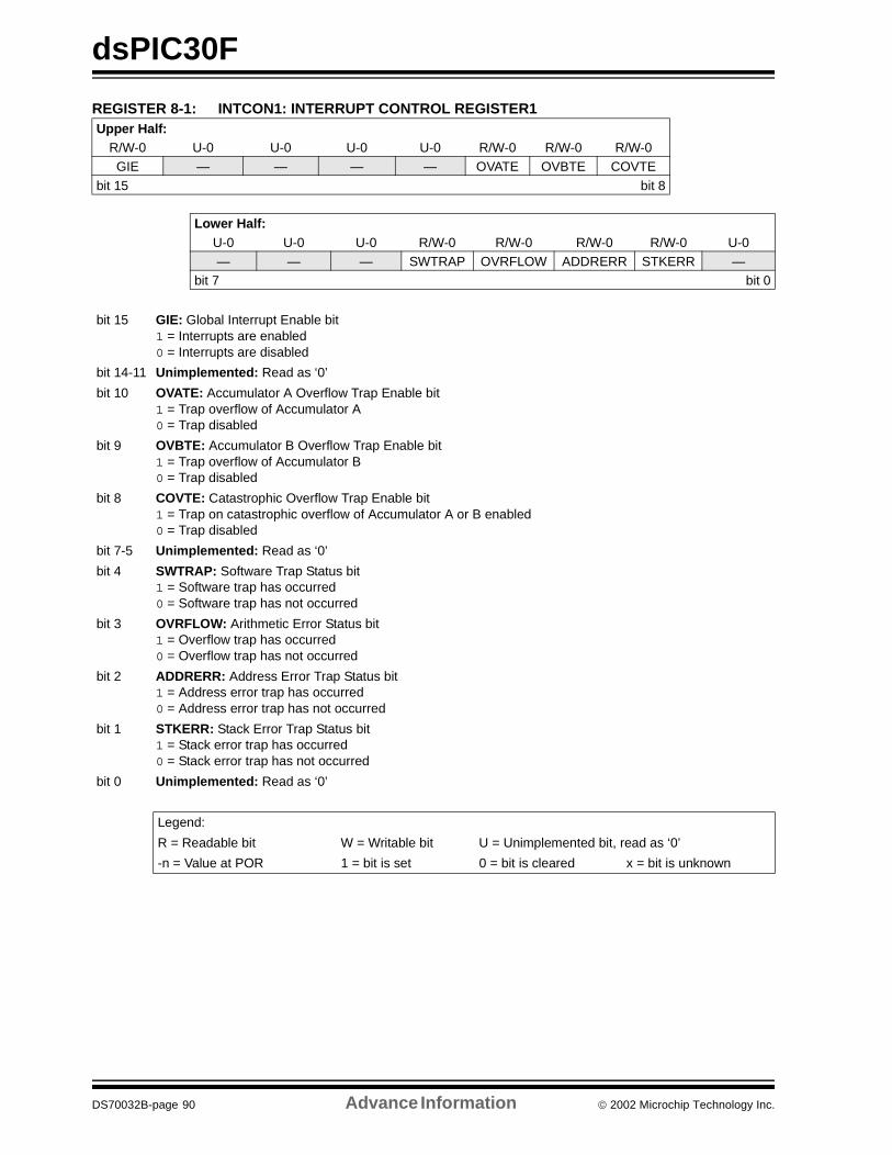
dsPIC30F
REGISTER 8-1: INTCON1: INTERRUPT CONTROL REGISTER1 Upper Half:
R/W-0 U-0 U-0 U-0 U-0 R/W-0 R/W-0 R/W-0GIE — — — — OVATE OVBTE COVTE
bit 15 bit 8
Lower Half:U-0 U-0 U-0 R/W-0 R/W-0 R/W-0 R/W-0 U-0— — — SWTRAP OVRFLOW ADDRERR STKERR —
bit 7 bit 0
bit 15 GIE: Global Interrupt Enable bit1 = Interrupts are enabled0 = Interrupts are disabled
bit 14-11 Unimplemented: Read as ‘0’
bit 10 OVATE: Accumulator A Overflow Trap Enable bit1 = Trap overflow of Accumulator A0 = Trap disabled
bit 9 OVBTE: Accumulator B Overflow Trap Enable bit1 = Trap overflow of Accumulator B0 = Trap disabled
bit 8 COVTE: Catastrophic Overflow Trap Enable bit1 = Trap on catastrophic overflow of Accumulator A or B enabled0 = Trap disabled
bit 7-5 Unimplemented: Read as ‘0’
bit 4 SWTRAP: Software Trap Status bit1 = Software trap has occurred0 = Software trap has not occurred
bit 3 OVRFLOW: Arithmetic Error Status bit1 = Overflow trap has occurred0 = Overflow trap has not occurred
bit 2 ADDRERR: Address Error Trap Status bit1 = Address error trap has occurred0 = Address error trap has not occurred
bit 1 STKERR: Stack Error Trap Status bit1 = Stack error trap has occurred0 = Stack error trap has not occurred
bit 0 Unimplemented: Read as ‘0’
Legend:
R = Readable bit W = Writable bit U = Unimplemented bit, read as ‘0’
-n = Value at POR 1 = bit is set 0 = bit is cleared x = bit is unknown
DS70032B-page 90 Advance Information 2002 Microchip Technology Inc.
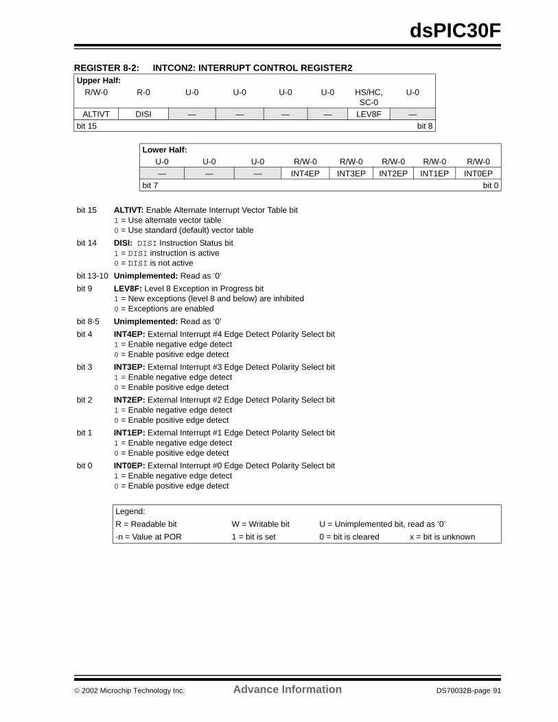
dsPIC30F
REGISTER 8-2: INTCON2: INTERRUPT CONTROL REGISTER2 Upper Half:
R/W-0 R-0 U-0 U-0 U-0 U-0 HS/HC,SC-0
U-0
ALTIVT DISI — — — — LEV8F —bit 15 bit 8
Lower Half:U-0 U-0 U-0 R/W-0 R/W-0 R/W-0 R/W-0 R/W-0
— — — INT4EP INT3EP INT2EP INT1EP INT0EPbit 7 bit 0
bit 15 ALTIVT: Enable Alternate Interrupt Vector Table bit1 = Use alternate vector table0 = Use standard (default) vector table
bit 14 DISI: DISI Instruction Status bit1 = DISI instruction is active0 = DISI is not active
bit 13-10 Unimplemented: Read as ‘0’
bit 9 LEV8F: Level 8 Exception in Progress bit1 = New exceptions (level 8 and below) are inhibited0 = Exceptions are enabled
bit 8-5 Unimplemented: Read as ‘0’
bit 4 INT4EP: External Interrupt #4 Edge Detect Polarity Select bit1 = Enable negative edge detect0 = Enable positive edge detect
bit 3 INT3EP: External Interrupt #3 Edge Detect Polarity Select bit1 = Enable negative edge detect0 = Enable positive edge detect
bit 2 INT2EP: External Interrupt #2 Edge Detect Polarity Select bit1 = Enable negative edge detect0 = Enable positive edge detect
bit 1 INT1EP: External Interrupt #1 Edge Detect Polarity Select bit1 = Enable negative edge detect0 = Enable positive edge detect
bit 0 INT0EP: External Interrupt #0 Edge Detect Polarity Select bit1 = Enable negative edge detect0 = Enable positive edge detect
Legend:
R = Readable bit W = Writable bit U = Unimplemented bit, read as ‘0’
-n = Value at POR 1 = bit is set 0 = bit is cleared x = bit is unknown
2002 Microchip Technology Inc. Advance Information DS70032B-page 91
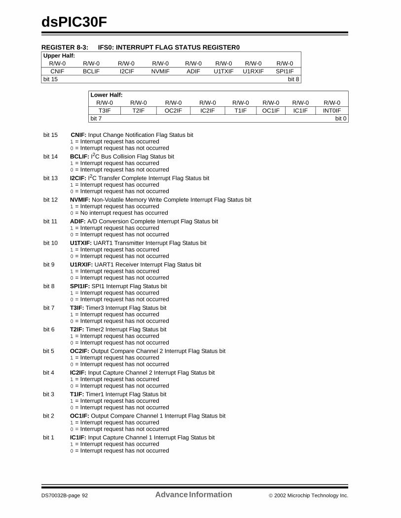
dsPIC30F
REGISTER 8-3: IFS0: INTERRUPT FLAG STATUS REGISTER0 Upper Half:
R/W-0 R/W-0 R/W-0 R/W-0 R/W-0 R/W-0 R/W-0 R/W-0CNIF BCLIF I2CIF NVMIF ADIF U1TXIF U1RXIF SPI1IF
bit 15 bit 8
Lower Half:R/W-0 R/W-0 R/W-0 R/W-0 R/W-0 R/W-0 R/W-0 R/W-0T3IF T2IF OC2IF IC2IF T1IF OC1IF IC1IF INT0IF
bit 7 bit 0
bit 15 CNIF: Input Change Notification Flag Status bit1 = Interrupt request has occurred0 = Interrupt request has not occurred
bit 14 BCLIF: I2C Bus Collision Flag Status bit1 = Interrupt request has occurred0 = Interrupt request has not occurred
bit 13 I2CIF: I2C Transfer Complete Interrupt Flag Status bit1 = Interrupt request has occurred0 = Interrupt request has not occurred
bit 12 NVMIF: Non-Volatile Memory Write Complete Interrupt Flag Status bit1 = Interrupt request has occurred0 = No interrupt request has occurred
bit 11 ADIF: A/D Conversion Complete Interrupt Flag Status bit1 = Interrupt request has occurred0 = Interrupt request has not occurred
bit 10 U1TXIF: UART1 Transmitter Interrupt Flag Status bit1 = Interrupt request has occurred0 = Interrupt request has not occurred
bit 9 U1RXIF: UART1 Receiver Interrupt Flag Status bit1 = Interrupt request has occurred0 = Interrupt request has not occurred
bit 8 SPI1IF: SPI1 Interrupt Flag Status bit1 = Interrupt request has occurred0 = Interrupt request has not occurred
bit 7 T3IF: Timer3 Interrupt Flag Status bit1 = Interrupt request has occurred0 = Interrupt request has not occurred
bit 6 T2IF: Timer2 Interrupt Flag Status bit1 = Interrupt request has occurred0 = Interrupt request has not occurred
bit 5 OC2IF: Output Compare Channel 2 Interrupt Flag Status bit1 = Interrupt request has occurred0 = Interrupt request has not occurred
bit 4 IC2IF: Input Capture Channel 2 Interrupt Flag Status bit1 = Interrupt request has occurred0 = Interrupt request has not occurred
bit 3 T1IF: Timer1 Interrupt Flag Status bit1 = Interrupt request has occurred0 = Interrupt request has not occurred
bit 2 OC1IF: Output Compare Channel 1 Interrupt Flag Status bit1 = Interrupt request has occurred0 = Interrupt request has not occurred
bit 1 IC1IF: Input Capture Channel 1 Interrupt Flag Status bit1 = Interrupt request has occurred0 = Interrupt request has not occurred
DS70032B-page 92 Advance Information 2002 Microchip Technology Inc.
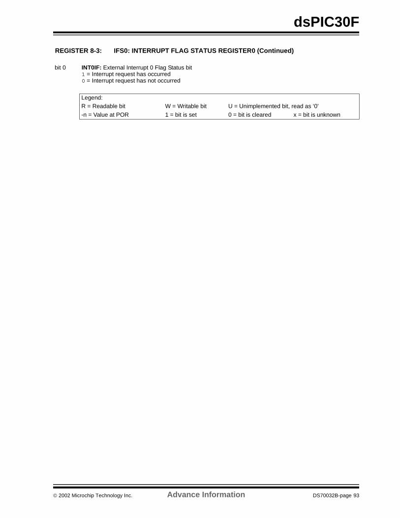
dsPIC30F
REGISTER 8-3: IFS0: INTERRUPT FLAG STATUS REGISTER0 (Continued)
bit 0 INT0IF: External Interrupt 0 Flag Status bit1 = Interrupt request has occurred0 = Interrupt request has not occurred
Legend:R = Readable bit W = Writable bit U = Unimplemented bit, read as ‘0’
-n = Value at POR 1 = bit is set 0 = bit is cleared x = bit is unknown
2002 Microchip Technology Inc. Advance Information DS70032B-page 93
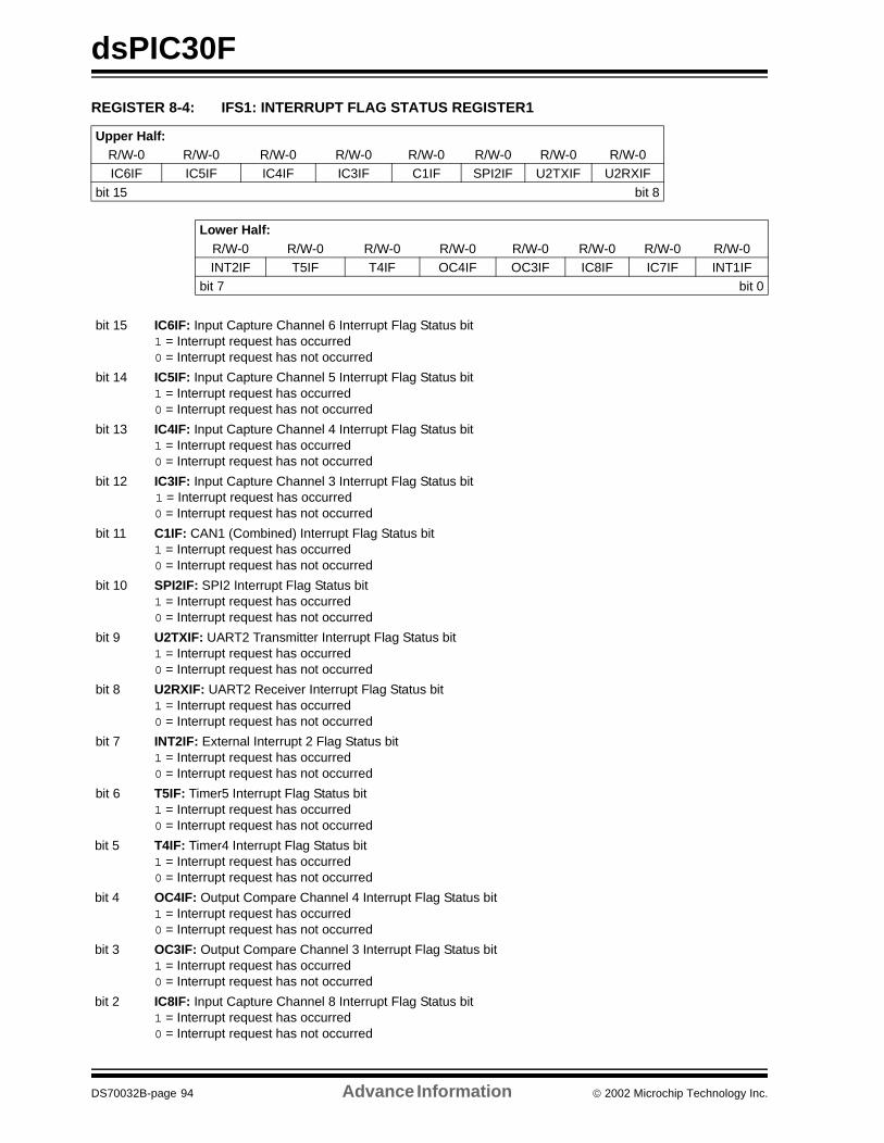
dsPIC30F
REGISTER 8-4: IFS1: INTERRUPT FLAG STATUS REGISTER1
Upper Half:R/W-0 R/W-0 R/W-0 R/W-0 R/W-0 R/W-0 R/W-0 R/W-0IC6IF IC5IF IC4IF IC3IF C1IF SPI2IF U2TXIF U2RXIF
bit 15 bit 8
Lower Half:R/W-0 R/W-0 R/W-0 R/W-0 R/W-0 R/W-0 R/W-0 R/W-0INT2IF T5IF T4IF OC4IF OC3IF IC8IF IC7IF INT1IF
bit 7 bit 0
bit 15 IC6IF: Input Capture Channel 6 Interrupt Flag Status bit1 = Interrupt request has occurred0 = Interrupt request has not occurred
bit 14 IC5IF: Input Capture Channel 5 Interrupt Flag Status bit1 = Interrupt request has occurred0 = Interrupt request has not occurred
bit 13 IC4IF: Input Capture Channel 4 Interrupt Flag Status bit1 = Interrupt request has occurred0 = Interrupt request has not occurred
bit 12 IC3IF: Input Capture Channel 3 Interrupt Flag Status bit1 = Interrupt request has occurred0 = Interrupt request has not occurred
bit 11 C1IF: CAN1 (Combined) Interrupt Flag Status bit1 = Interrupt request has occurred0 = Interrupt request has not occurred
bit 10 SPI2IF: SPI2 Interrupt Flag Status bit1 = Interrupt request has occurred0 = Interrupt request has not occurred
bit 9 U2TXIF: UART2 Transmitter Interrupt Flag Status bit1 = Interrupt request has occurred0 = Interrupt request has not occurred
bit 8 U2RXIF: UART2 Receiver Interrupt Flag Status bit1 = Interrupt request has occurred0 = Interrupt request has not occurred
bit 7 INT2IF: External Interrupt 2 Flag Status bit1 = Interrupt request has occurred0 = Interrupt request has not occurred
bit 6 T5IF: Timer5 Interrupt Flag Status bit1 = Interrupt request has occurred0 = Interrupt request has not occurred
bit 5 T4IF: Timer4 Interrupt Flag Status bit1 = Interrupt request has occurred0 = Interrupt request has not occurred
bit 4 OC4IF: Output Compare Channel 4 Interrupt Flag Status bit1 = Interrupt request has occurred0 = Interrupt request has not occurred
bit 3 OC3IF: Output Compare Channel 3 Interrupt Flag Status bit1 = Interrupt request has occurred0 = Interrupt request has not occurred
bit 2 IC8IF: Input Capture Channel 8 Interrupt Flag Status bit1 = Interrupt request has occurred0 = Interrupt request has not occurred
DS70032B-page 94 Advance Information 2002 Microchip Technology Inc.
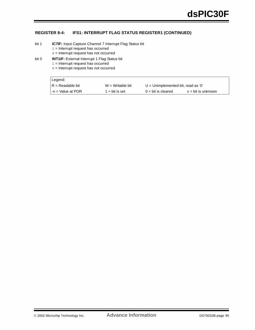
dsPIC30F
REGISTER 8-4: IFS1: INTERRUPT FLAG STATUS REGISTER1 (CONTINUED)
bit 1 IC7IF: Input Capture Channel 7 Interrupt Flag Status bit1 = Interrupt request has occurred0 = Interrupt request has not occurred
bit 0 INT1IF: External Interrupt 1 Flag Status bit1 = Interrupt request has occurred0 = Interrupt request has not occurred
Legend:
R = Readable bit W = Writable bit U = Unimplemented bit, read as ‘0’
-n = Value at POR 1 = bit is set 0 = bit is cleared x = bit is unknown
2002 Microchip Technology Inc. Advance Information DS70032B-page 95
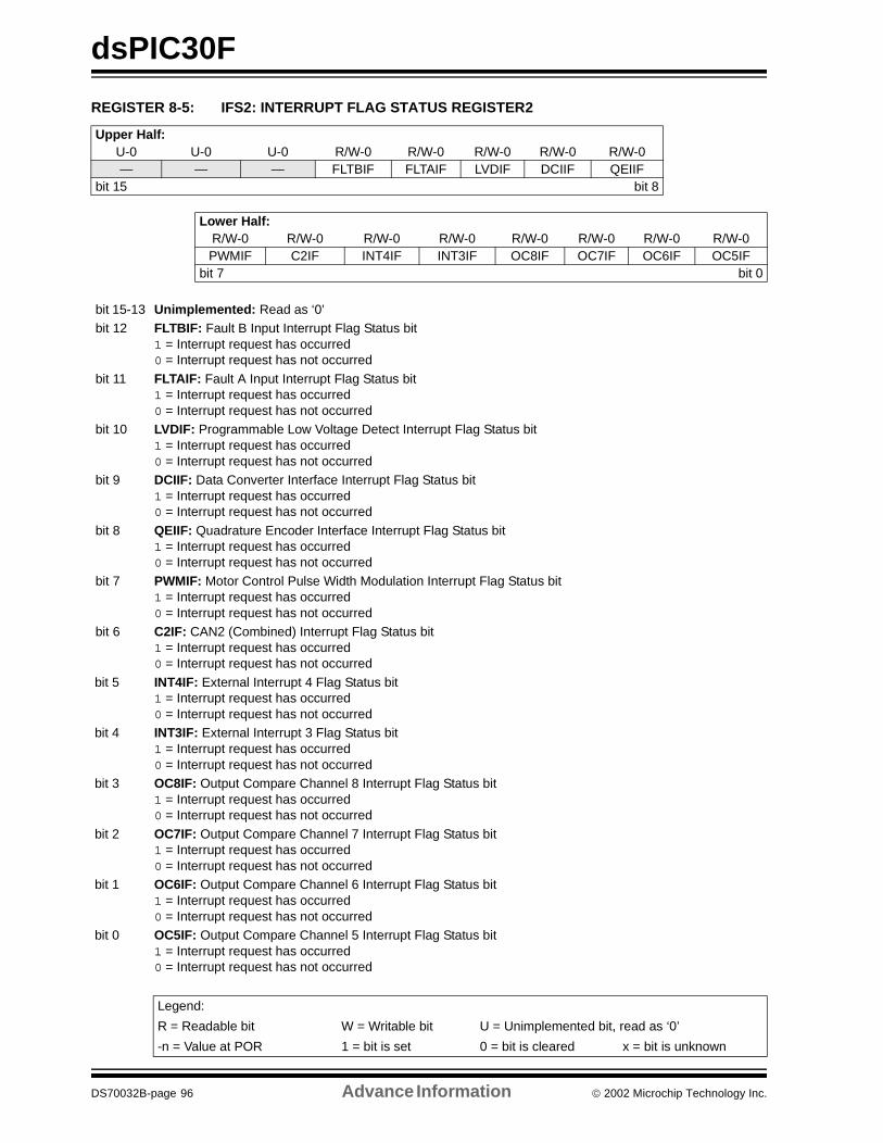
dsPIC30F
REGISTER 8-5: IFS2: INTERRUPT FLAG STATUS REGISTER2
Upper Half:U-0 U-0 U-0 R/W-0 R/W-0 R/W-0 R/W-0 R/W-0— — — FLTBIF FLTAIF LVDIF DCIIF QEIIF
bit 15 bit 8
Lower Half:R/W-0 R/W-0 R/W-0 R/W-0 R/W-0 R/W-0 R/W-0 R/W-0PWMIF C2IF INT4IF INT3IF OC8IF OC7IF OC6IF OC5IF
bit 7 bit 0
bit 15-13 Unimplemented: Read as ‘0’ bit 12 FLTBIF: Fault B Input Interrupt Flag Status bit
1 = Interrupt request has occurred0 = Interrupt request has not occurred
bit 11 FLTAIF: Fault A Input Interrupt Flag Status bit1 = Interrupt request has occurred0 = Interrupt request has not occurred
bit 10 LVDIF: Programmable Low Voltage Detect Interrupt Flag Status bit1 = Interrupt request has occurred0 = Interrupt request has not occurred
bit 9 DCIIF: Data Converter Interface Interrupt Flag Status bit1 = Interrupt request has occurred0 = Interrupt request has not occurred
bit 8 QEIIF: Quadrature Encoder Interface Interrupt Flag Status bit1 = Interrupt request has occurred0 = Interrupt request has not occurred
bit 7 PWMIF: Motor Control Pulse Width Modulation Interrupt Flag Status bit1 = Interrupt request has occurred0 = Interrupt request has not occurred
bit 6 C2IF: CAN2 (Combined) Interrupt Flag Status bit1 = Interrupt request has occurred0 = Interrupt request has not occurred
bit 5 INT4IF: External Interrupt 4 Flag Status bit1 = Interrupt request has occurred0 = Interrupt request has not occurred
bit 4 INT3IF: External Interrupt 3 Flag Status bit1 = Interrupt request has occurred0 = Interrupt request has not occurred
bit 3 OC8IF: Output Compare Channel 8 Interrupt Flag Status bit1 = Interrupt request has occurred0 = Interrupt request has not occurred
bit 2 OC7IF: Output Compare Channel 7 Interrupt Flag Status bit1 = Interrupt request has occurred0 = Interrupt request has not occurred
bit 1 OC6IF: Output Compare Channel 6 Interrupt Flag Status bit1 = Interrupt request has occurred0 = Interrupt request has not occurred
bit 0 OC5IF: Output Compare Channel 5 Interrupt Flag Status bit1 = Interrupt request has occurred0 = Interrupt request has not occurred
Legend:
R = Readable bit W = Writable bit U = Unimplemented bit, read as ‘0’
-n = Value at POR 1 = bit is set 0 = bit is cleared x = bit is unknown
DS70032B-page 96 Advance Information 2002 Microchip Technology Inc.
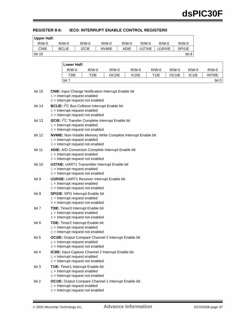
dsPIC30F
REGISTER 8-6: IEC0: INTERRUPT ENABLE CONTROL REGISTER0
Upper Half:R/W-0 R/W-0 R/W-0 R/W-0 R/W-0 R/W-0 R/W-0 R/W-0CNIE BCLIE I2CIE NVMIE ADIE U1TXIE U1RXIE SPI1IE
bit 15 bit 8
Lower Half:R/W-0 R/W-0 R/W-0 R/W-0 R/W-0 R/W-0 R/W-0 R/W-0T3IE T2IE OC2IE IC2IE T1IE OC1IE IC1IE INT0IE
bit 7 bit 0
bit 15 CNIE: Input Change Notification Interrupt Enable bit1 = Interrupt request enabled0 = Interrupt request not enabled
bit 14 BCLIE: I2C Bus Collision Interrupt Enable bit1 = Interrupt request enabled0 = Interrupt request not enabled
bit 13 I2CIE: I2C Transfer Complete Interrupt Enable bit1 = Interrupt request enabled0 = Interrupt request not enabled
bit 12 NVMIE: Non-Volatile Memory Write Complete Interrupt Enable bit1 = Interrupt request enabled0 = Interrupt request not enabled
bit 11 ADIE: A/D Conversion Complete Interrupt Enable bit1 = Interrupt request enabled0 = Interrupt request not enabled
bit 10 U1TXIE: UART1 Transmitter Interrupt Enable bit1 = Interrupt request enabled0 = Interrupt request not enabled
bit 9 U1RXIE: UART1 Receiver Interrupt Enable bit1 = Interrupt request enabled0 = Interrupt request not enabled
bit 8 SPI1IE: SPI1 Interrupt Enable bit1 = Interrupt request enabled0 = Interrupt request not enabled
bit 7 T3IE: Timer3 Interrupt Enable bit1 = Interrupt request enabled0 = Interrupt request not enabled
bit 6 T2IE: Timer2 Interrupt Enable bit1 = Interrupt request enabled0 = Interrupt request not enabled
bit 5 OC2IE: Output Compare Channel 2 Interrupt Enable bit1 = Interrupt request enabled0 = Interrupt request not enabled
bit 4 IC2IE: Input Capture Channel 2 Interrupt Enable bit1 = Interrupt request enabled0 = Interrupt request not enabled
bit 3 T1IE: Timer1 Interrupt Enable bit1 = Interrupt request enabled0 = Interrupt request not enabled
bit 2 OC1IE: Output Compare Channel 1 Interrupt Enable bit1 = Interrupt request enabled0 = Interrupt request not enabled
2002 Microchip Technology Inc. Advance Information DS70032B-page 97
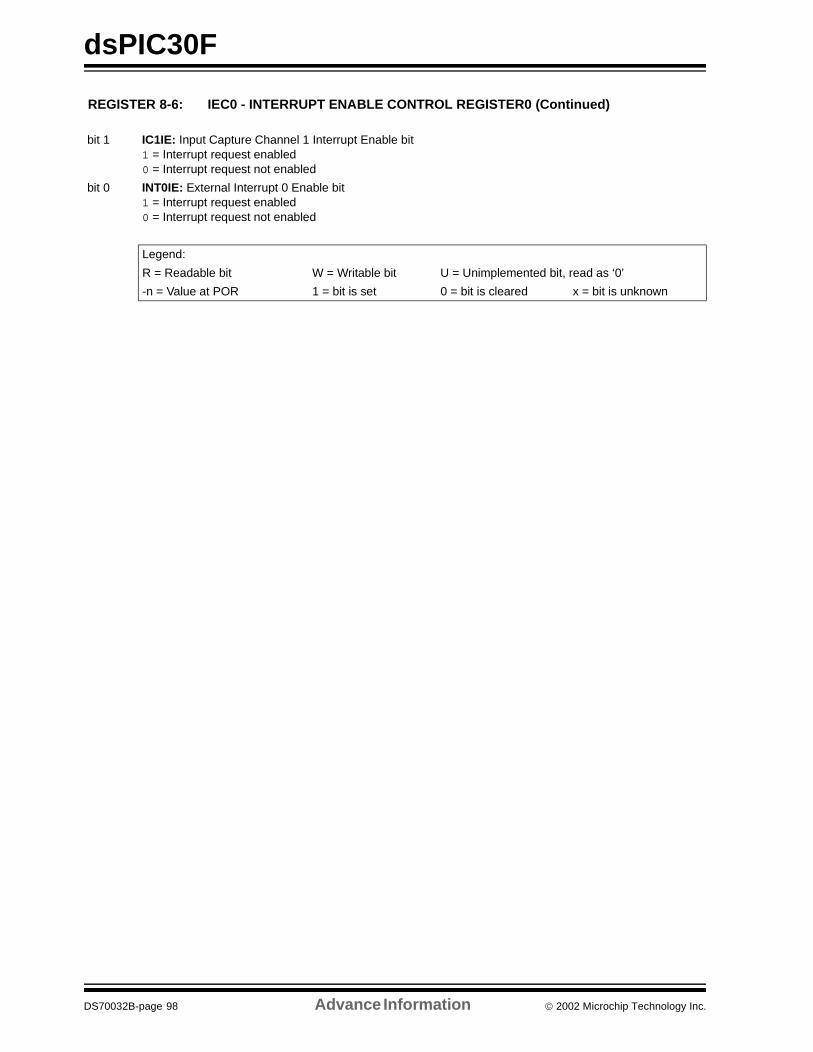
dsPIC30F
REGISTER 8-6: IEC0 - INTERRUPT ENABLE CONTROL REGISTER0 (Continued)
bit 1 IC1IE: Input Capture Channel 1 Interrupt Enable bit1 = Interrupt request enabled0 = Interrupt request not enabled
bit 0 INT0IE: External Interrupt 0 Enable bit1 = Interrupt request enabled0 = Interrupt request not enabled
Legend:
R = Readable bit W = Writable bit U = Unimplemented bit, read as ‘0’
-n = Value at POR 1 = bit is set 0 = bit is cleared x = bit is unknown
DS70032B-page 98 Advance Information 2002 Microchip Technology Inc.
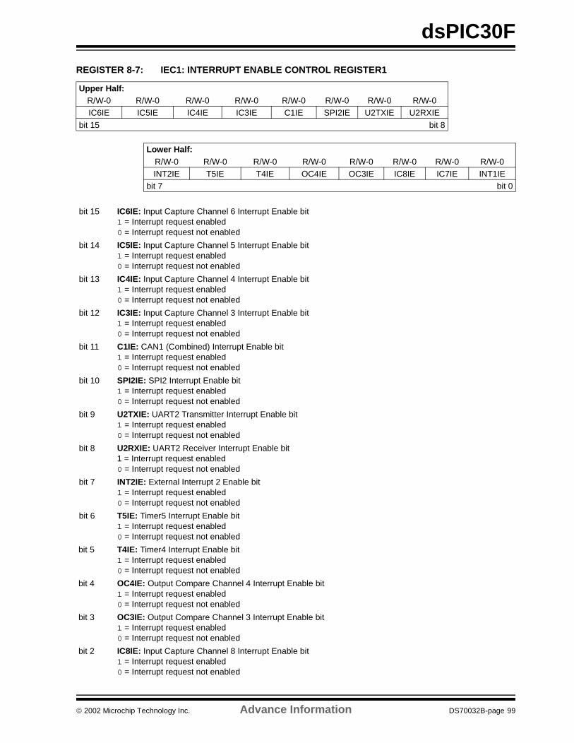
dsPIC30F
REGISTER 8-7: IEC1: INTERRUPT ENABLE CONTROL REGISTER1
Upper Half:R/W-0 R/W-0 R/W-0 R/W-0 R/W-0 R/W-0 R/W-0 R/W-0IC6IE IC5IE IC4IE IC3IE C1IE SPI2IE U2TXIE U2RXIE
bit 15 bit 8
Lower Half:R/W-0 R/W-0 R/W-0 R/W-0 R/W-0 R/W-0 R/W-0 R/W-0INT2IE T5IE T4IE OC4IE OC3IE IC8IE IC7IE INT1IE
bit 7 bit 0
bit 15 IC6IE: Input Capture Channel 6 Interrupt Enable bit1 = Interrupt request enabled0 = Interrupt request not enabled
bit 14 IC5IE: Input Capture Channel 5 Interrupt Enable bit1 = Interrupt request enabled0 = Interrupt request not enabled
bit 13 IC4IE: Input Capture Channel 4 Interrupt Enable bit1 = Interrupt request enabled0 = Interrupt request not enabled
bit 12 IC3IE: Input Capture Channel 3 Interrupt Enable bit1 = Interrupt request enabled0 = Interrupt request not enabled
bit 11 C1IE: CAN1 (Combined) Interrupt Enable bit1 = Interrupt request enabled0 = Interrupt request not enabled
bit 10 SPI2IE: SPI2 Interrupt Enable bit1 = Interrupt request enabled0 = Interrupt request not enabled
bit 9 U2TXIE: UART2 Transmitter Interrupt Enable bit1 = Interrupt request enabled0 = Interrupt request not enabled
bit 8 U2RXIE: UART2 Receiver Interrupt Enable bit1 = Interrupt request enabled0 = Interrupt request not enabled
bit 7 INT2IE: External Interrupt 2 Enable bit1 = Interrupt request enabled0 = Interrupt request not enabled
bit 6 T5IE: Timer5 Interrupt Enable bit1 = Interrupt request enabled0 = Interrupt request not enabled
bit 5 T4IE: Timer4 Interrupt Enable bit1 = Interrupt request enabled0 = Interrupt request not enabled
bit 4 OC4IE: Output Compare Channel 4 Interrupt Enable bit1 = Interrupt request enabled0 = Interrupt request not enabled
bit 3 OC3IE: Output Compare Channel 3 Interrupt Enable bit1 = Interrupt request enabled0 = Interrupt request not enabled
bit 2 IC8IE: Input Capture Channel 8 Interrupt Enable bit1 = Interrupt request enabled0 = Interrupt request not enabled
2002 Microchip Technology Inc. Advance Information DS70032B-page 99

dsPIC30F
REGISTER 8-7: IEC1 - INTERRUPT ENABLE CONTROL REGISTER1 (Continued)
bit 1 IC7IE: Input Capture Channel 7 Interrupt Enable bit1 = Interrupt request enabled0 = Interrupt request not enabled
bit 0 INT1IE: External Interrupt 1 Enable bit1 = Interrupt request enabled0 = Interrupt request not enabled
Legend:
R = Readable bit W = Writable bit U = Unimplemented bit, read as ‘0’
-n = Value at POR 1 = bit is set 0 = bit is cleared x = bit is unknown
DS70032B-page 100 Advance Information 2002 Microchip Technology Inc.
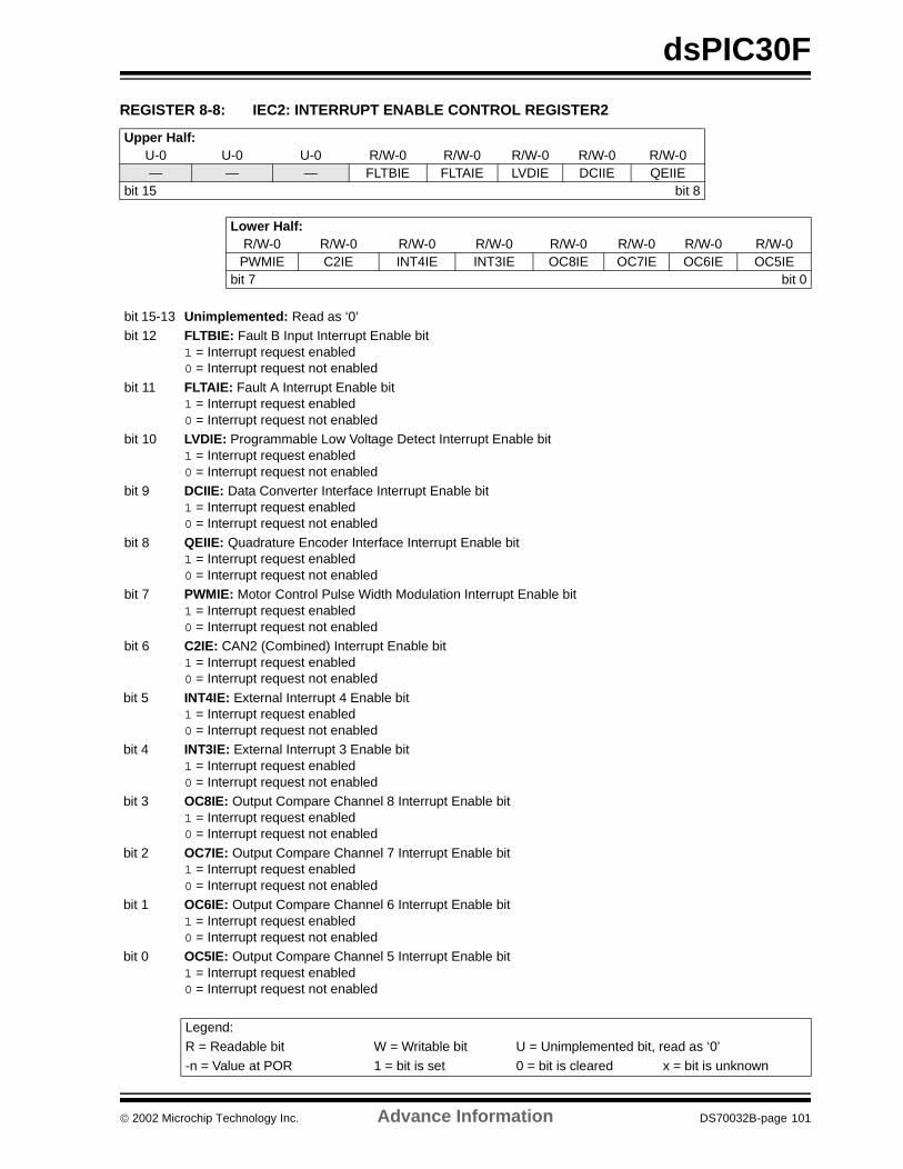
dsPIC30F
REGISTER 8-8: IEC2: INTERRUPT ENABLE CONTROL REGISTER2
Upper Half:U-0 U-0 U-0 R/W-0 R/W-0 R/W-0 R/W-0 R/W-0— — — FLTBIE FLTAIE LVDIE DCIIE QEIIE
bit 15 bit 8
Lower Half:R/W-0 R/W-0 R/W-0 R/W-0 R/W-0 R/W-0 R/W-0 R/W-0
PWMIE C2IE INT4IE INT3IE OC8IE OC7IE OC6IE OC5IEbit 7 bit 0
bit 15-13 Unimplemented: Read as ‘0’ bit 12 FLTBIE: Fault B Input Interrupt Enable bit
1 = Interrupt request enabled0 = Interrupt request not enabled
bit 11 FLTAIE: Fault A Interrupt Enable bit1 = Interrupt request enabled0 = Interrupt request not enabled
bit 10 LVDIE: Programmable Low Voltage Detect Interrupt Enable bit1 = Interrupt request enabled0 = Interrupt request not enabled
bit 9 DCIIE: Data Converter Interface Interrupt Enable bit1 = Interrupt request enabled0 = Interrupt request not enabled
bit 8 QEIIE: Quadrature Encoder Interface Interrupt Enable bit1 = Interrupt request enabled0 = Interrupt request not enabled
bit 7 PWMIE: Motor Control Pulse Width Modulation Interrupt Enable bit1 = Interrupt request enabled0 = Interrupt request not enabled
bit 6 C2IE: CAN2 (Combined) Interrupt Enable bit1 = Interrupt request enabled0 = Interrupt request not enabled
bit 5 INT4IE: External Interrupt 4 Enable bit1 = Interrupt request enabled0 = Interrupt request not enabled
bit 4 INT3IE: External Interrupt 3 Enable bit1 = Interrupt request enabled0 = Interrupt request not enabled
bit 3 OC8IE: Output Compare Channel 8 Interrupt Enable bit1 = Interrupt request enabled0 = Interrupt request not enabled
bit 2 OC7IE: Output Compare Channel 7 Interrupt Enable bit1 = Interrupt request enabled0 = Interrupt request not enabled
bit 1 OC6IE: Output Compare Channel 6 Interrupt Enable bit1 = Interrupt request enabled0 = Interrupt request not enabled
bit 0 OC5IE: Output Compare Channel 5 Interrupt Enable bit1 = Interrupt request enabled0 = Interrupt request not enabled
Legend:R = Readable bit W = Writable bit U = Unimplemented bit, read as ‘0’
-n = Value at POR 1 = bit is set 0 = bit is cleared x = bit is unknown
2002 Microchip Technology Inc. Advance Information DS70032B-page 101
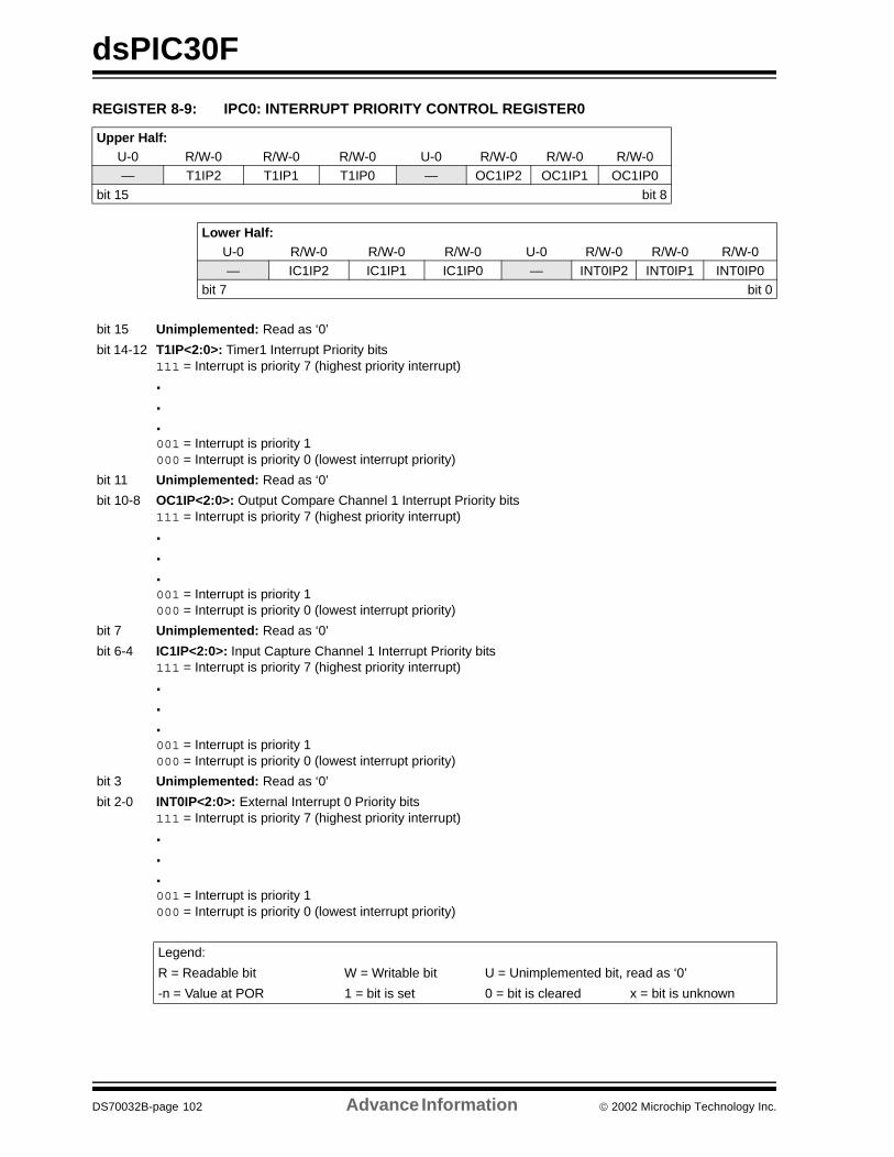
dsPIC30F
REGISTER 8-9: IPC0: INTERRUPT PRIORITY CONTROL REGISTER0
Upper Half:U-0 R/W-0 R/W-0 R/W-0 U-0 R/W-0 R/W-0 R/W-0— T1IP2 T1IP1 T1IP0 — OC1IP2 OC1IP1 OC1IP0
bit 15 bit 8
Lower Half:U-0 R/W-0 R/W-0 R/W-0 U-0 R/W-0 R/W-0 R/W-0— IC1IP2 IC1IP1 IC1IP0 — INT0IP2 INT0IP1 INT0IP0
bit 7 bit 0
bit 15 Unimplemented: Read as ‘0’
bit 14-12 T1IP<2:0>: Timer1 Interrupt Priority bits111 = Interrupt is priority 7 (highest priority interrupt)...001 = Interrupt is priority 1000 = Interrupt is priority 0 (lowest interrupt priority)
bit 11 Unimplemented: Read as ‘0’
bit 10-8 OC1IP<2:0>: Output Compare Channel 1 Interrupt Priority bits111 = Interrupt is priority 7 (highest priority interrupt)...001 = Interrupt is priority 1000 = Interrupt is priority 0 (lowest interrupt priority)
bit 7 Unimplemented: Read as ‘0’
bit 6-4 IC1IP<2:0>: Input Capture Channel 1 Interrupt Priority bits111 = Interrupt is priority 7 (highest priority interrupt)
.
.
.001 = Interrupt is priority 1000 = Interrupt is priority 0 (lowest interrupt priority)
bit 3 Unimplemented: Read as ‘0’
bit 2-0 INT0IP<2:0>: External Interrupt 0 Priority bits111 = Interrupt is priority 7 (highest priority interrupt)...001 = Interrupt is priority 1000 = Interrupt is priority 0 (lowest interrupt priority)
Legend:
R = Readable bit W = Writable bit U = Unimplemented bit, read as ‘0’
-n = Value at POR 1 = bit is set 0 = bit is cleared x = bit is unknown
DS70032B-page 102 Advance Information 2002 Microchip Technology Inc.
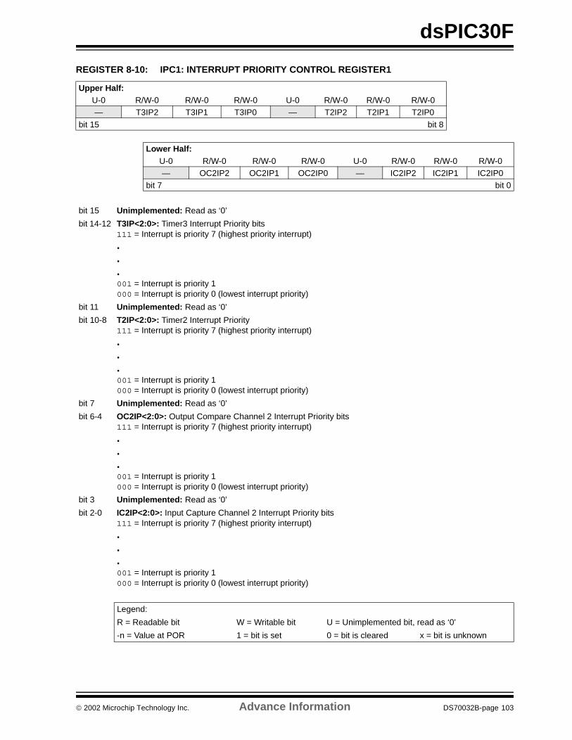
dsPIC30F
REGISTER 8-10: IPC1: INTERRUPT PRIORITY CONTROL REGISTER1
Upper Half:U-0 R/W-0 R/W-0 R/W-0 U-0 R/W-0 R/W-0 R/W-0— T3IP2 T3IP1 T3IP0 — T2IP2 T2IP1 T2IP0
bit 15 bit 8
Lower Half:U-0 R/W-0 R/W-0 R/W-0 U-0 R/W-0 R/W-0 R/W-0— OC2IP2 OC2IP1 OC2IP0 — IC2IP2 IC2IP1 IC2IP0
bit 7 bit 0
bit 15 Unimplemented: Read as ‘0’
bit 14-12 T3IP<2:0>: Timer3 Interrupt Priority bits111 = Interrupt is priority 7 (highest priority interrupt)...001 = Interrupt is priority 1000 = Interrupt is priority 0 (lowest interrupt priority)
bit 11 Unimplemented: Read as ‘0’
bit 10-8 T2IP<2:0>: Timer2 Interrupt Priority111 = Interrupt is priority 7 (highest priority interrupt)...001 = Interrupt is priority 1000 = Interrupt is priority 0 (lowest interrupt priority)
bit 7 Unimplemented: Read as ‘0’
bit 6-4 OC2IP<2:0>: Output Compare Channel 2 Interrupt Priority bits111 = Interrupt is priority 7 (highest priority interrupt)
.
.
.001 = Interrupt is priority 1000 = Interrupt is priority 0 (lowest interrupt priority)
bit 3 Unimplemented: Read as ‘0’
bit 2-0 IC2IP<2:0>: Input Capture Channel 2 Interrupt Priority bits111 = Interrupt is priority 7 (highest priority interrupt)...001 = Interrupt is priority 1000 = Interrupt is priority 0 (lowest interrupt priority)
Legend:
R = Readable bit W = Writable bit U = Unimplemented bit, read as ‘0’
-n = Value at POR 1 = bit is set 0 = bit is cleared x = bit is unknown
2002 Microchip Technology Inc. Advance Information DS70032B-page 103
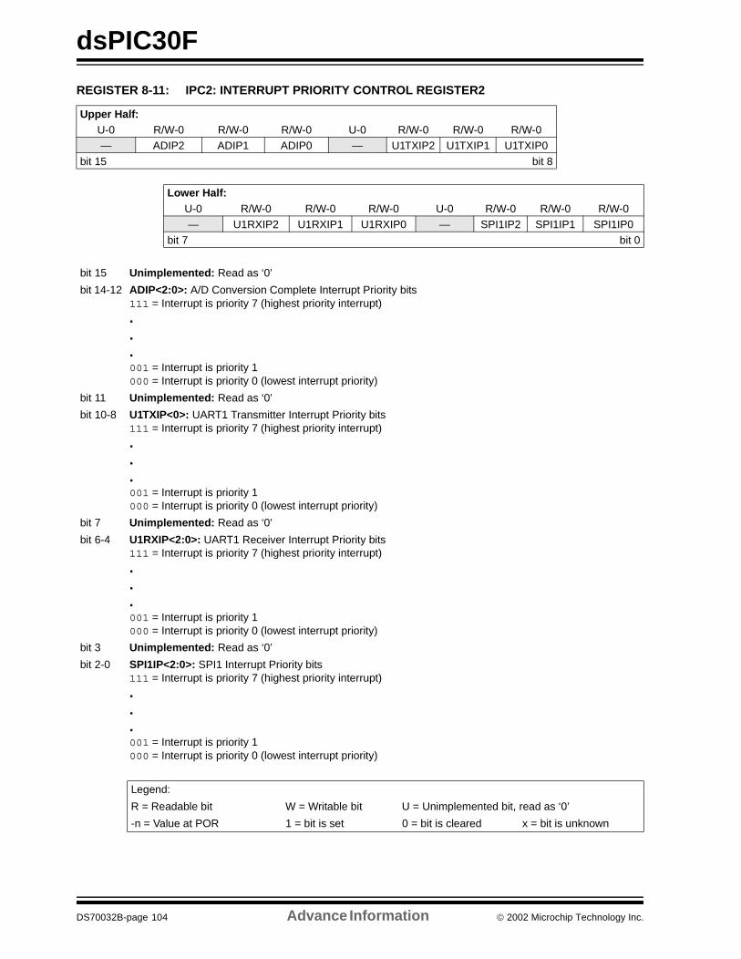
dsPIC30F
REGISTER 8-11: IPC2: INTERRUPT PRIORITY CONTROL REGISTER2
Upper Half:U-0 R/W-0 R/W-0 R/W-0 U-0 R/W-0 R/W-0 R/W-0— ADIP2 ADIP1 ADIP0 — U1TXIP2 U1TXIP1 U1TXIP0
bit 15 bit 8
Lower Half:U-0 R/W-0 R/W-0 R/W-0 U-0 R/W-0 R/W-0 R/W-0— U1RXIP2 U1RXIP1 U1RXIP0 — SPI1IP2 SPI1IP1 SPI1IP0
bit 7 bit 0
bit 15 Unimplemented: Read as ‘0’
bit 14-12 ADIP<2:0>: A/D Conversion Complete Interrupt Priority bits111 = Interrupt is priority 7 (highest priority interrupt)...001 = Interrupt is priority 1000 = Interrupt is priority 0 (lowest interrupt priority)
bit 11 Unimplemented: Read as ‘0’
bit 10-8 U1TXIP<0>: UART1 Transmitter Interrupt Priority bits111 = Interrupt is priority 7 (highest priority interrupt)...001 = Interrupt is priority 1000 = Interrupt is priority 0 (lowest interrupt priority)
bit 7 Unimplemented: Read as ‘0’
bit 6-4 U1RXIP<2:0>: UART1 Receiver Interrupt Priority bits111 = Interrupt is priority 7 (highest priority interrupt)
.
.
.001 = Interrupt is priority 1000 = Interrupt is priority 0 (lowest interrupt priority)
bit 3 Unimplemented: Read as ‘0’
bit 2-0 SPI1IP<2:0>: SPI1 Interrupt Priority bits111 = Interrupt is priority 7 (highest priority interrupt)...001 = Interrupt is priority 1000 = Interrupt is priority 0 (lowest interrupt priority)
Legend:
R = Readable bit W = Writable bit U = Unimplemented bit, read as ‘0’
-n = Value at POR 1 = bit is set 0 = bit is cleared x = bit is unknown
DS70032B-page 104 Advance Information 2002 Microchip Technology Inc.
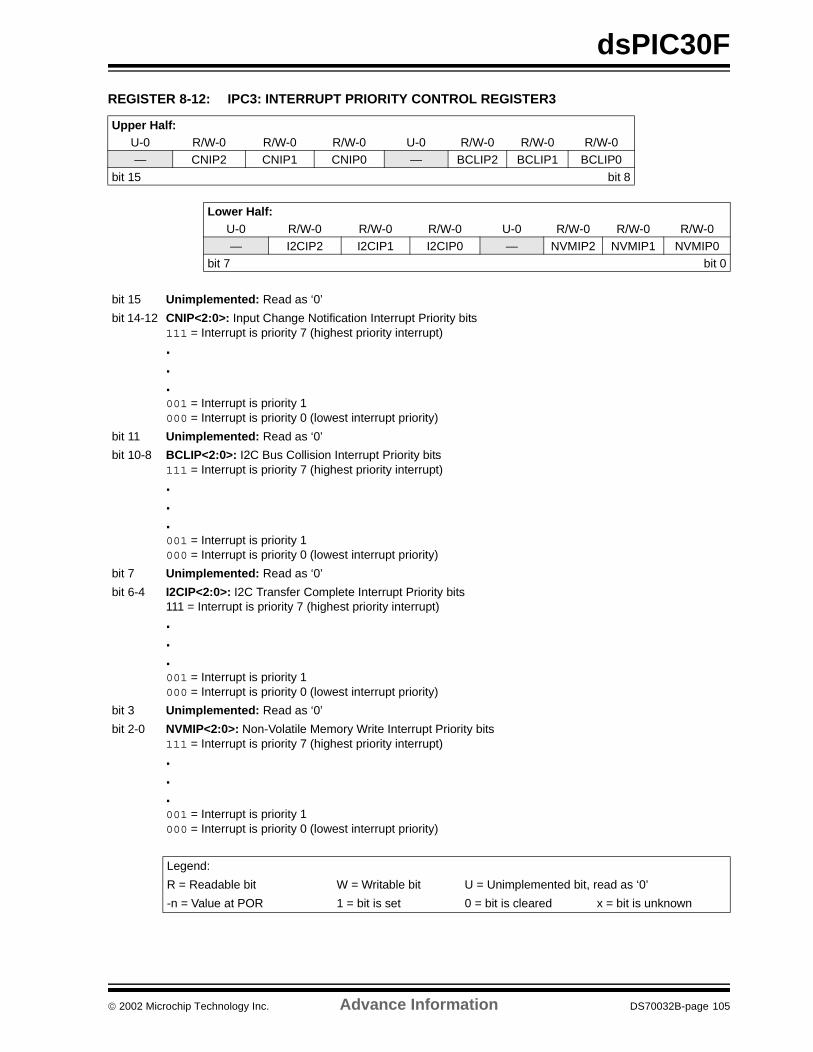
dsPIC30F
REGISTER 8-12: IPC3: INTERRUPT PRIORITY CONTROL REGISTER3
Upper Half:U-0 R/W-0 R/W-0 R/W-0 U-0 R/W-0 R/W-0 R/W-0— CNIP2 CNIP1 CNIP0 — BCLIP2 BCLIP1 BCLIP0
bit 15 bit 8
Lower Half:U-0 R/W-0 R/W-0 R/W-0 U-0 R/W-0 R/W-0 R/W-0— I2CIP2 I2CIP1 I2CIP0 — NVMIP2 NVMIP1 NVMIP0
bit 7 bit 0
bit 15 Unimplemented: Read as ‘0’
bit 14-12 CNIP<2:0>: Input Change Notification Interrupt Priority bits111 = Interrupt is priority 7 (highest priority interrupt)...001 = Interrupt is priority 1000 = Interrupt is priority 0 (lowest interrupt priority)
bit 11 Unimplemented: Read as ‘0’
bit 10-8 BCLIP<2:0>: I2C Bus Collision Interrupt Priority bits111 = Interrupt is priority 7 (highest priority interrupt)...001 = Interrupt is priority 1000 = Interrupt is priority 0 (lowest interrupt priority)
bit 7 Unimplemented: Read as ‘0’
bit 6-4 I2CIP<2:0>: I2C Transfer Complete Interrupt Priority bits111 = Interrupt is priority 7 (highest priority interrupt)
.
.
.001 = Interrupt is priority 1000 = Interrupt is priority 0 (lowest interrupt priority)
bit 3 Unimplemented: Read as ‘0’
bit 2-0 NVMIP<2:0>: Non-Volatile Memory Write Interrupt Priority bits111 = Interrupt is priority 7 (highest priority interrupt)...001 = Interrupt is priority 1000 = Interrupt is priority 0 (lowest interrupt priority)
Legend:
R = Readable bit W = Writable bit U = Unimplemented bit, read as ‘0’
-n = Value at POR 1 = bit is set 0 = bit is cleared x = bit is unknown
2002 Microchip Technology Inc. Advance Information DS70032B-page 105
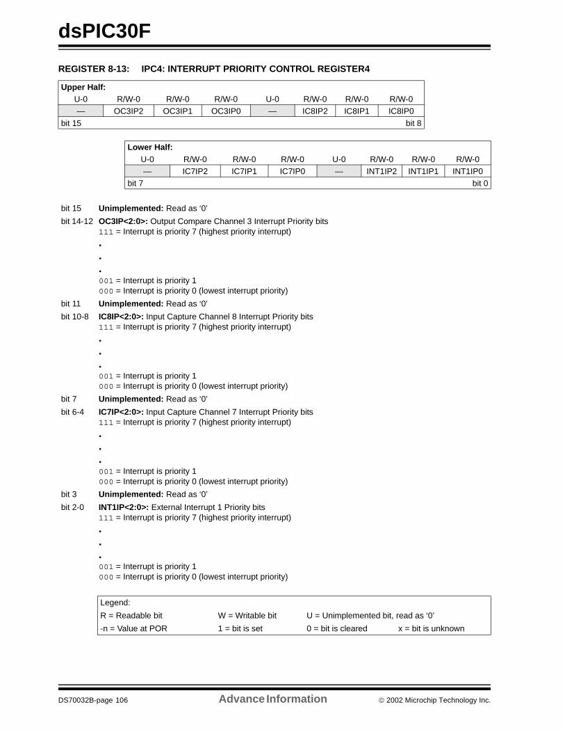
dsPIC30F
REGISTER 8-13: IPC4: INTERRUPT PRIORITY CONTROL REGISTER4
Upper Half:U-0 R/W-0 R/W-0 R/W-0 U-0 R/W-0 R/W-0 R/W-0— OC3IP2 OC3IP1 OC3IP0 — IC8IP2 IC8IP1 IC8IP0
bit 15 bit 8
Lower Half:U-0 R/W-0 R/W-0 R/W-0 U-0 R/W-0 R/W-0 R/W-0— IC7IP2 IC7IP1 IC7IP0 — INT1IP2 INT1IP1 INT1IP0
bit 7 bit 0
bit 15 Unimplemented: Read as ‘0’
bit 14-12 OC3IP<2:0>: Output Compare Channel 3 Interrupt Priority bits111 = Interrupt is priority 7 (highest priority interrupt)...001 = Interrupt is priority 1000 = Interrupt is priority 0 (lowest interrupt priority)
bit 11 Unimplemented: Read as ‘0’
bit 10-8 IC8IP<2:0>: Input Capture Channel 8 Interrupt Priority bits111 = Interrupt is priority 7 (highest priority interrupt)...001 = Interrupt is priority 1000 = Interrupt is priority 0 (lowest interrupt priority)
bit 7 Unimplemented: Read as ‘0’
bit 6-4 IC7IP<2:0>: Input Capture Channel 7 Interrupt Priority bits111 = Interrupt is priority 7 (highest priority interrupt)
.
.
.001 = Interrupt is priority 1000 = Interrupt is priority 0 (lowest interrupt priority)
bit 3 Unimplemented: Read as ‘0’
bit 2-0 INT1IP<2:0>: External Interrupt 1 Priority bits111 = Interrupt is priority 7 (highest priority interrupt)...001 = Interrupt is priority 1000 = Interrupt is priority 0 (lowest interrupt priority)
Legend:
R = Readable bit W = Writable bit U = Unimplemented bit, read as ‘0’
-n = Value at POR 1 = bit is set 0 = bit is cleared x = bit is unknown
DS70032B-page 106 Advance Information 2002 Microchip Technology Inc.
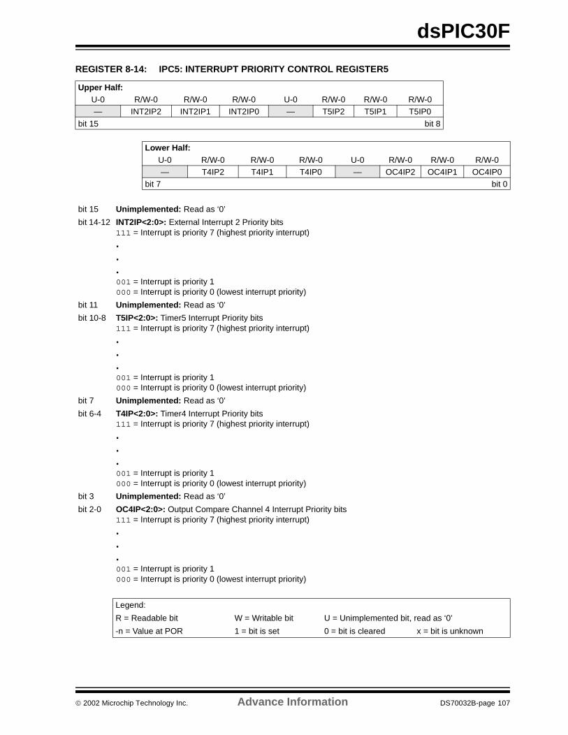
dsPIC30F
REGISTER 8-14: IPC5: INTERRUPT PRIORITY CONTROL REGISTER5
Upper Half:U-0 R/W-0 R/W-0 R/W-0 U-0 R/W-0 R/W-0 R/W-0— INT2IP2 INT2IP1 INT2IP0 — T5IP2 T5IP1 T5IP0
bit 15 bit 8
Lower Half:U-0 R/W-0 R/W-0 R/W-0 U-0 R/W-0 R/W-0 R/W-0— T4IP2 T4IP1 T4IP0 — OC4IP2 OC4IP1 OC4IP0
bit 7 bit 0
bit 15 Unimplemented: Read as ‘0’
bit 14-12 INT2IP<2:0>: External Interrupt 2 Priority bits111 = Interrupt is priority 7 (highest priority interrupt)...001 = Interrupt is priority 1000 = Interrupt is priority 0 (lowest interrupt priority)
bit 11 Unimplemented: Read as ‘0’
bit 10-8 T5IP<2:0>: Timer5 Interrupt Priority bits111 = Interrupt is priority 7 (highest priority interrupt)...001 = Interrupt is priority 1000 = Interrupt is priority 0 (lowest interrupt priority)
bit 7 Unimplemented: Read as ‘0’
bit 6-4 T4IP<2:0>: Timer4 Interrupt Priority bits111 = Interrupt is priority 7 (highest priority interrupt)
.
.
.001 = Interrupt is priority 1000 = Interrupt is priority 0 (lowest interrupt priority)
bit 3 Unimplemented: Read as ‘0’
bit 2-0 OC4IP<2:0>: Output Compare Channel 4 Interrupt Priority bits111 = Interrupt is priority 7 (highest priority interrupt)...001 = Interrupt is priority 1000 = Interrupt is priority 0 (lowest interrupt priority)
Legend:
R = Readable bit W = Writable bit U = Unimplemented bit, read as ‘0’
-n = Value at POR 1 = bit is set 0 = bit is cleared x = bit is unknown
2002 Microchip Technology Inc. Advance Information DS70032B-page 107
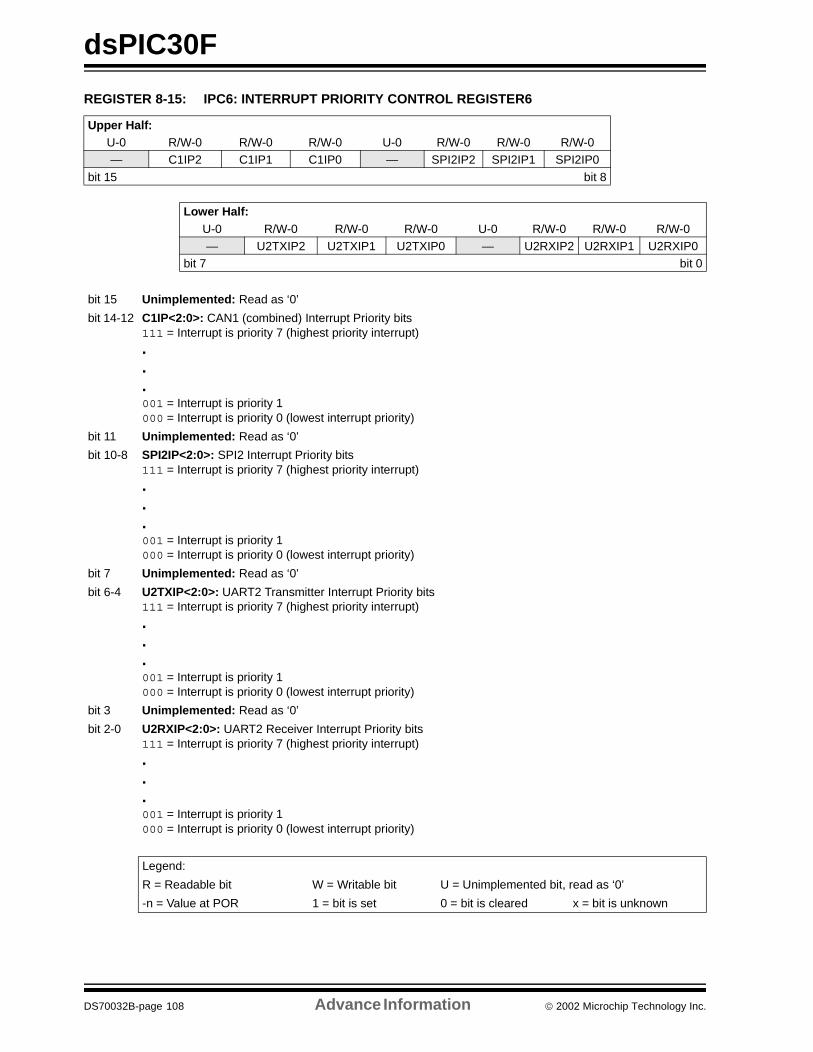
dsPIC30F
REGISTER 8-15: IPC6: INTERRUPT PRIORITY CONTROL REGISTER6
Upper Half:U-0 R/W-0 R/W-0 R/W-0 U-0 R/W-0 R/W-0 R/W-0— C1IP2 C1IP1 C1IP0 — SPI2IP2 SPI2IP1 SPI2IP0
bit 15 bit 8
Lower Half:U-0 R/W-0 R/W-0 R/W-0 U-0 R/W-0 R/W-0 R/W-0— U2TXIP2 U2TXIP1 U2TXIP0 — U2RXIP2 U2RXIP1 U2RXIP0
bit 7 bit 0
bit 15 Unimplemented: Read as ‘0’
bit 14-12 C1IP<2:0>: CAN1 (combined) Interrupt Priority bits111 = Interrupt is priority 7 (highest priority interrupt)...001 = Interrupt is priority 1000 = Interrupt is priority 0 (lowest interrupt priority)
bit 11 Unimplemented: Read as ‘0’
bit 10-8 SPI2IP<2:0>: SPI2 Interrupt Priority bits111 = Interrupt is priority 7 (highest priority interrupt)...001 = Interrupt is priority 1000 = Interrupt is priority 0 (lowest interrupt priority)
bit 7 Unimplemented: Read as ‘0’
bit 6-4 U2TXIP<2:0>: UART2 Transmitter Interrupt Priority bits111 = Interrupt is priority 7 (highest priority interrupt)
.
.
.001 = Interrupt is priority 1000 = Interrupt is priority 0 (lowest interrupt priority)
bit 3 Unimplemented: Read as ‘0’
bit 2-0 U2RXIP<2:0>: UART2 Receiver Interrupt Priority bits111 = Interrupt is priority 7 (highest priority interrupt)...001 = Interrupt is priority 1000 = Interrupt is priority 0 (lowest interrupt priority)
Legend:
R = Readable bit W = Writable bit U = Unimplemented bit, read as ‘0’
-n = Value at POR 1 = bit is set 0 = bit is cleared x = bit is unknown
DS70032B-page 108 Advance Information 2002 Microchip Technology Inc.
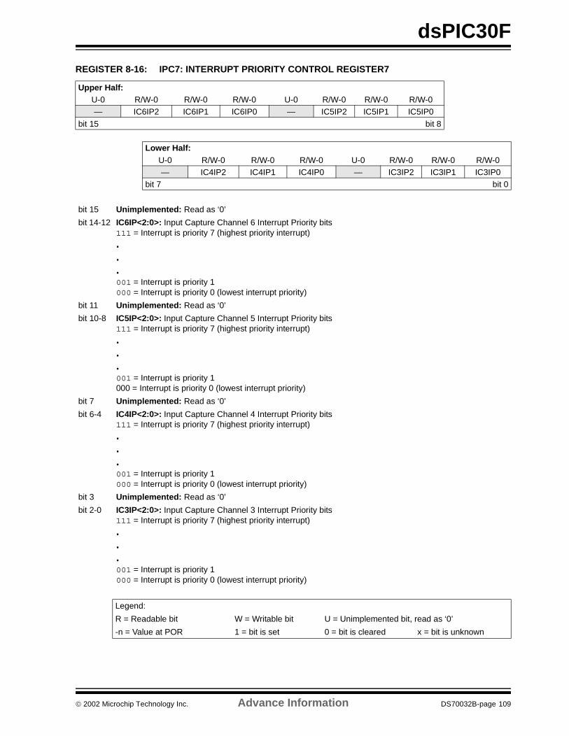
dsPIC30F
REGISTER 8-16: IPC7: INTERRUPT PRIORITY CONTROL REGISTER7
Upper Half:U-0 R/W-0 R/W-0 R/W-0 U-0 R/W-0 R/W-0 R/W-0— IC6IP2 IC6IP1 IC6IP0 — IC5IP2 IC5IP1 IC5IP0
bit 15 bit 8
Lower Half:U-0 R/W-0 R/W-0 R/W-0 U-0 R/W-0 R/W-0 R/W-0— IC4IP2 IC4IP1 IC4IP0 — IC3IP2 IC3IP1 IC3IP0
bit 7 bit 0
bit 15 Unimplemented: Read as ‘0’
bit 14-12 IC6IP<2:0>: Input Capture Channel 6 Interrupt Priority bits111 = Interrupt is priority 7 (highest priority interrupt)...001 = Interrupt is priority 1000 = Interrupt is priority 0 (lowest interrupt priority)
bit 11 Unimplemented: Read as ‘0’
bit 10-8 IC5IP<2:0>: Input Capture Channel 5 Interrupt Priority bits111 = Interrupt is priority 7 (highest priority interrupt)...001 = Interrupt is priority 1000 = Interrupt is priority 0 (lowest interrupt priority)
bit 7 Unimplemented: Read as ‘0’
bit 6-4 IC4IP<2:0>: Input Capture Channel 4 Interrupt Priority bits111 = Interrupt is priority 7 (highest priority interrupt)
.
.
.001 = Interrupt is priority 1000 = Interrupt is priority 0 (lowest interrupt priority)
bit 3 Unimplemented: Read as ‘0’
bit 2-0 IC3IP<2:0>: Input Capture Channel 3 Interrupt Priority bits111 = Interrupt is priority 7 (highest priority interrupt)...001 = Interrupt is priority 1000 = Interrupt is priority 0 (lowest interrupt priority)
Legend:
R = Readable bit W = Writable bit U = Unimplemented bit, read as ‘0’
-n = Value at POR 1 = bit is set 0 = bit is cleared x = bit is unknown
2002 Microchip Technology Inc. Advance Information DS70032B-page 109
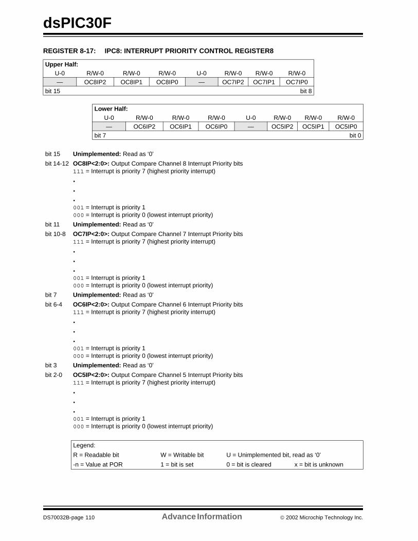
dsPIC30F
REGISTER 8-17: IPC8: INTERRUPT PRIORITY CONTROL REGISTER8
Upper Half:U-0 R/W-0 R/W-0 R/W-0 U-0 R/W-0 R/W-0 R/W-0— OC8IP2 OC8IP1 OC8IP0 — OC7IP2 OC7IP1 OC7IP0
bit 15 bit 8
Lower Half:U-0 R/W-0 R/W-0 R/W-0 U-0 R/W-0 R/W-0 R/W-0— OC6IP2 OC6IP1 OC6IP0 — OC5IP2 OC5IP1 OC5IP0
bit 7 bit 0
bit 15 Unimplemented: Read as ‘0’
bit 14-12 OC8IP<2:0>: Output Compare Channel 8 Interrupt Priority bits111 = Interrupt is priority 7 (highest priority interrupt)...001 = Interrupt is priority 1000 = Interrupt is priority 0 (lowest interrupt priority)
bit 11 Unimplemented: Read as ‘0’
bit 10-8 OC7IP<2:0>: Output Compare Channel 7 Interrupt Priority bits111 = Interrupt is priority 7 (highest priority interrupt)...001 = Interrupt is priority 1000 = Interrupt is priority 0 (lowest interrupt priority)
bit 7 Unimplemented: Read as ‘0’
bit 6-4 OC6IP<2:0>: Output Compare Channel 6 Interrupt Priority bits111 = Interrupt is priority 7 (highest priority interrupt)
.
.
.001 = Interrupt is priority 1000 = Interrupt is priority 0 (lowest interrupt priority)
bit 3 Unimplemented: Read as ‘0’
bit 2-0 OC5IP<2:0>: Output Compare Channel 5 Interrupt Priority bits111 = Interrupt is priority 7 (highest priority interrupt)...001 = Interrupt is priority 1000 = Interrupt is priority 0 (lowest interrupt priority)
Legend:
R = Readable bit W = Writable bit U = Unimplemented bit, read as ‘0’
-n = Value at POR 1 = bit is set 0 = bit is cleared x = bit is unknown
DS70032B-page 110 Advance Information 2002 Microchip Technology Inc.
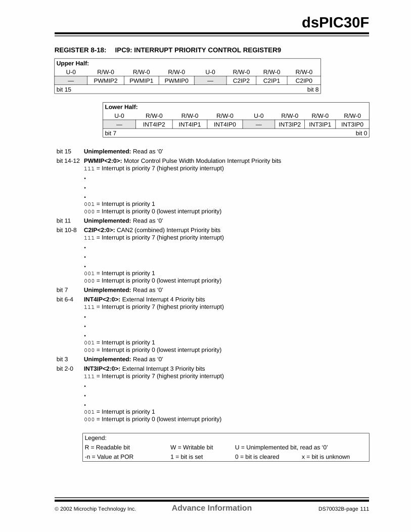
dsPIC30F
REGISTER 8-18: IPC9: INTERRUPT PRIORITY CONTROL REGISTER9
Upper Half:U-0 R/W-0 R/W-0 R/W-0 U-0 R/W-0 R/W-0 R/W-0— PWMIP2 PWMIP1 PWMIP0 — C2IP2 C2IP1 C2IP0
bit 15 bit 8
Lower Half:U-0 R/W-0 R/W-0 R/W-0 U-0 R/W-0 R/W-0 R/W-0— INT4IP2 INT4IP1 INT4IP0 — INT3IP2 INT3IP1 INT3IP0
bit 7 bit 0
bit 15 Unimplemented: Read as ‘0’
bit 14-12 PWMIP<2:0>: Motor Control Pulse Width Modulation Interrupt Priority bits111 = Interrupt is priority 7 (highest priority interrupt)...001 = Interrupt is priority 1000 = Interrupt is priority 0 (lowest interrupt priority)
bit 11 Unimplemented: Read as ‘0’
bit 10-8 C2IP<2:0>: CAN2 (combined) Interrupt Priority bits111 = Interrupt is priority 7 (highest priority interrupt)...001 = Interrupt is priority 1000 = Interrupt is priority 0 (lowest interrupt priority)
bit 7 Unimplemented: Read as ‘0’
bit 6-4 INT4IP<2:0>: External Interrupt 4 Priority bits111 = Interrupt is priority 7 (highest priority interrupt)
.
.
.001 = Interrupt is priority 1000 = Interrupt is priority 0 (lowest interrupt priority)
bit 3 Unimplemented: Read as ‘0’
bit 2-0 INT3IP<2:0>: External Interrupt 3 Priority bits111 = Interrupt is priority 7 (highest priority interrupt)...001 = Interrupt is priority 1000 = Interrupt is priority 0 (lowest interrupt priority)
Legend:
R = Readable bit W = Writable bit U = Unimplemented bit, read as ‘0’
-n = Value at POR 1 = bit is set 0 = bit is cleared x = bit is unknown
2002 Microchip Technology Inc. Advance Information DS70032B-page 111
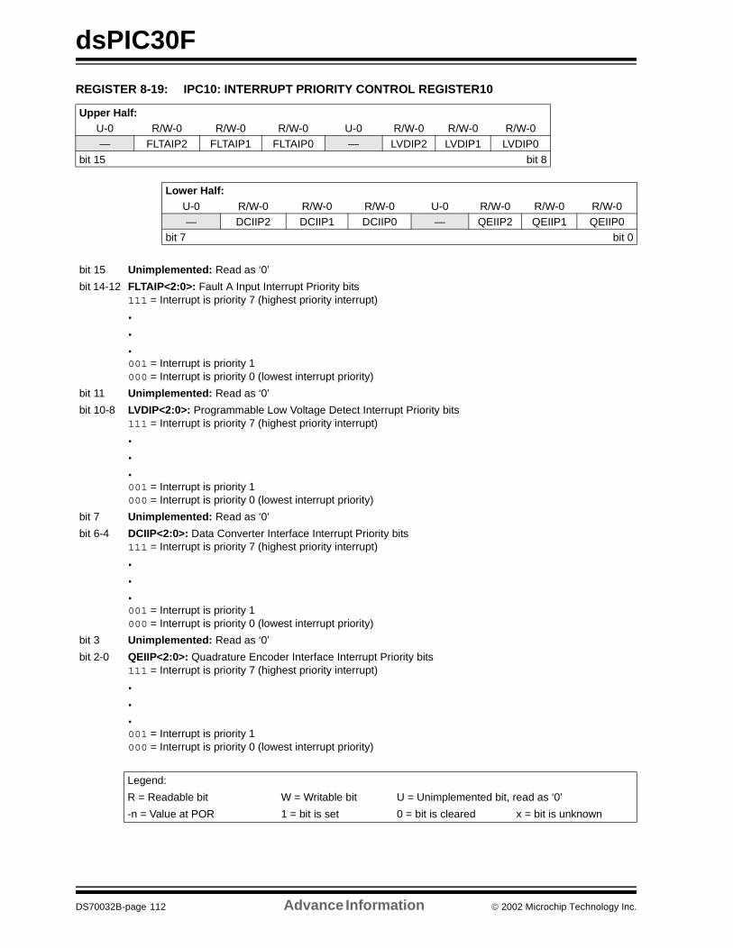
dsPIC30F
REGISTER 8-19: IPC10: INTERRUPT PRIORITY CONTROL REGISTER10
Upper Half:U-0 R/W-0 R/W-0 R/W-0 U-0 R/W-0 R/W-0 R/W-0— FLTAIP2 FLTAIP1 FLTAIP0 — LVDIP2 LVDIP1 LVDIP0
bit 15 bit 8
Lower Half:U-0 R/W-0 R/W-0 R/W-0 U-0 R/W-0 R/W-0 R/W-0— DCIIP2 DCIIP1 DCIIP0 — QEIIP2 QEIIP1 QEIIP0
bit 7 bit 0
bit 15 Unimplemented: Read as ‘0’
bit 14-12 FLTAIP<2:0>: Fault A Input Interrupt Priority bits111 = Interrupt is priority 7 (highest priority interrupt)...001 = Interrupt is priority 1000 = Interrupt is priority 0 (lowest interrupt priority)
bit 11 Unimplemented: Read as ‘0’
bit 10-8 LVDIP<2:0>: Programmable Low Voltage Detect Interrupt Priority bits111 = Interrupt is priority 7 (highest priority interrupt)...001 = Interrupt is priority 1000 = Interrupt is priority 0 (lowest interrupt priority)
bit 7 Unimplemented: Read as ‘0’
bit 6-4 DCIIP<2:0>: Data Converter Interface Interrupt Priority bits111 = Interrupt is priority 7 (highest priority interrupt)
.
.
.001 = Interrupt is priority 1000 = Interrupt is priority 0 (lowest interrupt priority)
bit 3 Unimplemented: Read as ‘0’
bit 2-0 QEIIP<2:0>: Quadrature Encoder Interface Interrupt Priority bits111 = Interrupt is priority 7 (highest priority interrupt)...001 = Interrupt is priority 1000 = Interrupt is priority 0 (lowest interrupt priority)
Legend:
R = Readable bit W = Writable bit U = Unimplemented bit, read as ‘0’
-n = Value at POR 1 = bit is set 0 = bit is cleared x = bit is unknown
DS70032B-page 112 Advance Information 2002 Microchip Technology Inc.
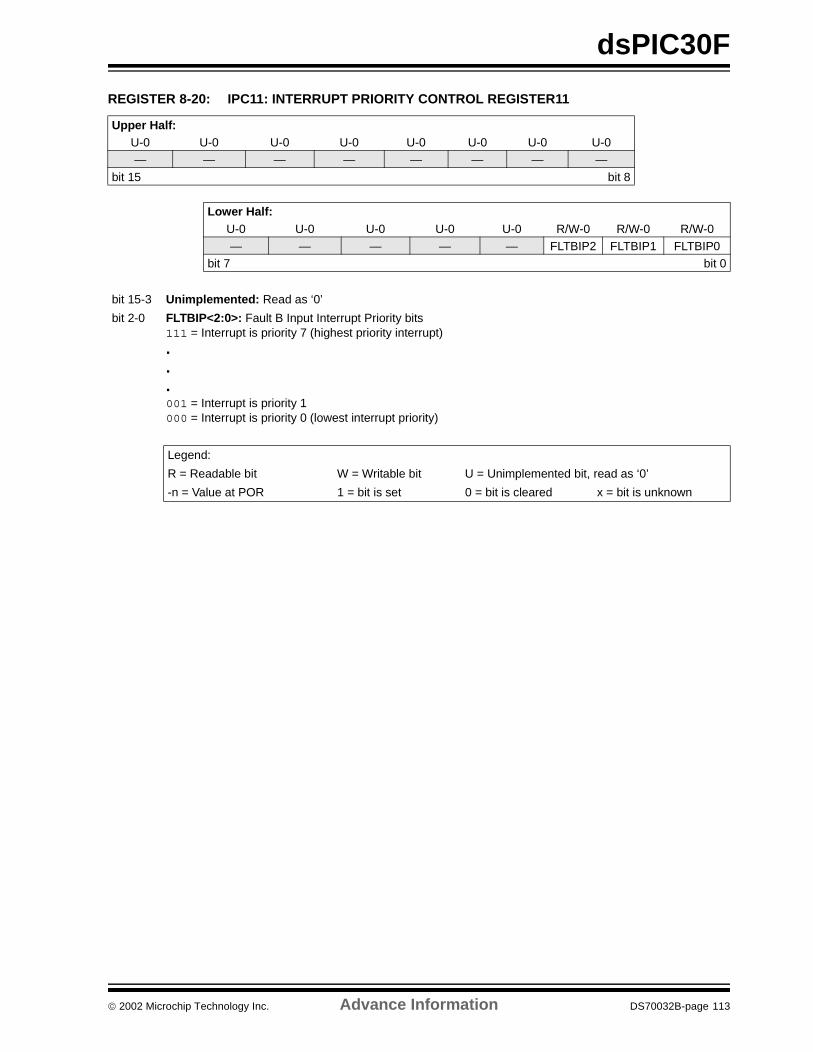
dsPIC30F
REGISTER 8-20: IPC11: INTERRUPT PRIORITY CONTROL REGISTER11
Upper Half:U-0 U-0 U-0 U-0 U-0 U-0 U-0 U-0— — — — — — — —
bit 15 bit 8
Lower Half:U-0 U-0 U-0 U-0 U-0 R/W-0 R/W-0 R/W-0— — — — — FLTBIP2 FLTBIP1 FLTBIP0
bit 7 bit 0
bit 15-3 Unimplemented: Read as ‘0’
bit 2-0 FLTBIP<2:0>: Fault B Input Interrupt Priority bits111 = Interrupt is priority 7 (highest priority interrupt)...001 = Interrupt is priority 1000 = Interrupt is priority 0 (lowest interrupt priority)
Legend:
R = Readable bit W = Writable bit U = Unimplemented bit, read as ‘0’
-n = Value at POR 1 = bit is set 0 = bit is cleared x = bit is unknown
2002 Microchip Technology Inc. Advance Information DS70032B-page 113

dsPIC30F
NOTES:
DS70032B-page 114 Advance Information 2002 Microchip Technology Inc.
dsPIC30F
9.0 I/O PORTS
All of the device pins (except VDD, VSS, MCLR, andOSC1/CLKIN) are shared between the peripheralsand the parallel I/O ports.
All I/O input ports feature Schmitt Trigger inputs forimproved noise immunity.
9.1 Parallel I/O (PIO) Ports
When a peripheral is enabled, the use of any associ-ated pin as a general purpose output pin is disabled.The I/O pin may be read, but the output driver for theparallel port bit will be disabled. If a peripheral isenabled, but the peripheral is not actively driving a pin,that pin may be driven by a port.
All port pins have three registers directly associatedwith the operation of the port pin. The data directionregister (TRISx) determines whether the pin is an inputor an output. If the Data Direction bit is a ‘1’, then thepin is an input. All port pins are defined as inputs aftera RESET. Reads from the latch (LATx), read the
latch. Writes to the latch, write the latch (LATx). Readsfrom the port (PORTx), read the port pins, and writesto the port pins, write the latch (LATx).
Any bit and its associated data and control registersthat is not valid for a particular device will be disabled.That means the corresponding LATx and TRISx regis-ters, and the port pin, will read as zeros.
When a pin is shared with another peripheral or func-tion that is defined as an input only, it is neverthelessregarded as a dedicated port because there is noother competing source of outputs. An example is theINT4 pin.
The format of the registers for PORTA is shown inTable 9-1.
The TRISA (Data Direction Control) register controlsthe direction of the RA<7:0> pins, as well as the INTxpins and the VREF pins. TRISA is a read/write register.The LATA register supplies data to the outputs, and isreadable/writable. Reading the PORTA register yieldsthe state of the input pins, while writing the PORTAregister yields the contents of the LATA register.
FIGURE 9-1: BLOCK DIAGRAM OF A DEDICATED PORT STRUCTURE
QD
CK
WR LAT +
TRIS Latch
I/O Pad
WR Port
Data Bus
QD
CK
Data Latch
Read LAT
Read Port
Read TRIS
WR TRIS
I/O Cell
Dedicated Port Module
2002 Microchip Technology Inc. Advance Information DS70032B-page 115
dsPIC30F
TAB
LE
9-1
:P
OR
TA R
EG
IST
ER
MA
P
SF
R
Nam
eA
dd
r.B
it 1
5B
it 1
4B
it 1
3B
it 1
2B
it 1
1B
it 1
0B
it 9
Bit
8B
it 7
Bit
6B
it 5
Bit
4B
it 3
Bit
2B
it 1
Bit
0R
ES
ET
Sta
te
TR
ISA
02C
0T
RIS
A15
TR
ISA
14T
RIS
A13
TR
ISA
12T
RIS
A11
TR
ISA
10T
RIS
A9
—T
RIS
A7
TR
ISA
6T
RIS
A5
TR
ISA
4T
RIS
A3
TR
ISA
2T
RIS
A1
TR
ISA
01111 111u 1111 1111
PO
RTA
02C
2R
A15
RA
14R
A13
RA
12R
A11
RA
10R
A9
—R
A7
RA
6R
A5
RA
4R
A3
RA
2R
A1
RA
00000 000u 0000 0000
LATA
02C
4LA
TA15
LATA
14LA
TA13
LATA
12LA
TA11
LATA
10LA
TA9
—LA
TA7
LATA
6LA
TA5
LATA
4LA
TA3
LATA
2LA
TA1
LATA
00000 000u 0000 0000
DS70032B-page 116 Advance Information 2002 Microchip Technology Inc.
dsPIC30F
A parallel I/O (PIO) port that shares a pin with anotherperipheral is always subservient to the other periph-eral. The peripheral’s output buffer data and controlsignals are provided to a pair of multiplexers. The mul-tiplexers select whether the peripheral or the associ-ated port has ownership of the output data and controlsignals of the I/O pad cell. Figure 9-2 shows how portsare shared with other peripherals, and the associated
I/O cell (pad) to which they are connected. Table 9-2through Table 9-7 show the formats of the registers forthe shared ports, PORTB through PORTG.
FIGURE 9-2: BLOCK DIAGRAM OF A SHARED PORT STRUCTURE
Note: The actual bits in use vary betweendevices.
QD
CK
WR LAT +
TRIS Latch
I/O Pad
WR Port
Data Bus
QD
CK
Data Latch
Read LAT
Read Port
Read TRIS
1
0
1
0
WR TRIS
Peripheral Output DataOutput Enable
Peripheral Input Data
I/O Cell
Peripheral Module
Peripheral Output Enable
PIO Module
Output Multiplexers
Output Data
Input Data
Peripheral Module Enable
2002 Microchip Technology Inc. Advance Information DS70032B-page 117
dsPIC30F
TABL
E 9
-2:
PO
RT
B R
EG
IST
ER
MA
P
TAB
LE
9-3
:P
OR
TC
RE
GIS
TE
R M
AP
TAB
LE
9-4
:P
OR
TD
RE
GIS
TE
R M
AP
TAB
LE
9-5
:P
OR
TE
RE
GIS
TE
R M
AP
TAB
LE
9-6
:P
OR
TF
RE
GIS
TE
R M
AP
SF
R
Nam
eA
dd
r.B
it 1
5B
it 1
4B
it 1
3B
it 1
2B
it 1
1B
it 1
0B
it 9
Bit
8B
it 7
Bit
6B
it 5
Bit
4B
it 3
Bit
2B
it 1
Bit
0R
ES
ET
Sta
te
TR
ISB
02C
6T
RIS
B15
TR
ISB
14T
RIS
B13
TR
ISB
12T
RIS
B11
TR
ISB
10T
RIS
B9
TR
ISB
8T
RIS
B7
TR
ISB
6T
RIS
B5
TR
ISB
4T
RIS
B3
TR
ISB
2T
RIS
B1
TR
ISB
01111 1111 1111 1111
PO
RT
B02
C8
RB
15R
B14
RB
13R
B12
RB
11R
B10
RB
9R
B8
RB
7R
B6
RB
5R
B4
RB
3R
B2
RB
1R
B0
0000 0000 0000 0000
LAT
B02
CB
LAT
B15
LAT
B14
LAT
B13
LAT
B12
LAT
B11
LAT
B10
LAT
B9
LAT
B8
LAT
B7
LAT
B6
LAT
B5
LAT
B4
LAT
B3
LAT
B2
LAT
B1
LAT
B0
0000 0000 0000 0000
SF
R
Nam
eA
dd
r.B
it 1
5B
it 1
4B
it 1
3B
it 1
2B
it 1
1B
it 1
0B
it 9
Bit
8B
it 7
Bit
6B
it 5
Bit
4B
it 3
Bit
2B
it 1
Bit
0R
ES
ET
Sta
te
TR
ISC
02C
CT
RIS
C15
TR
ISC
14T
RIS
C13
——
——
——
——
TR
ISC
4T
RIS
C3
TR
ISC
2T
RIS
C1
TR
ISC
0111u uuuu uuu1 1111
PO
RT
C02
CE
RC
15R
C14
RC
13—
——
——
——
—R
C4
RC
3R
C2
RC
1R
C0
000u uuuu uuu0 0000
LAT
C02
D0
LAT
C15
LAT
C14
LAT
C13
——
——
——
——
LAT
C4
LAT
C3
LAT
C2
LAT
C1
LAT
C0
000u uuuu uuu0 0000
SF
R
Nam
eA
dd
r.B
it 1
5B
it 1
4B
it 1
3B
it 1
2B
it 1
1B
it 1
0B
it 9
Bit
8B
it 7
Bit
6B
it 5
Bit
4B
it 3
Bit
2B
it 1
Bit
0R
ES
ET
Sta
te
TR
ISD
02D
2T
RIS
D15
TR
ISD
14T
RIS
D13
TR
ISD
12T
RIS
D11
TR
ISD
10T
RIS
D9
TR
ISD
8T
RIS
D7
TR
ISD
6T
RIS
D5
TR
ISD
4T
RIS
D3
TR
ISD
2T
RIS
D1
TR
ISD
01111 1111 1111 1111
PO
RT
D02
D4
RD
15R
D14
RD
13R
D12
RD
11R
D10
RD
9R
D8
RD
7R
D6
RD
5R
D4
RD
3R
D2
RD
1R
D0
0000 0000 0000 0000
LAT
D02
D6
LAT
D15
LAT
D14
LAT
D13
LAT
D12
LAT
D11
LAT
D10
LAT
D9
LAT
D8
LAT
D7
LAT
D6
LAT
D5
LAT
D4
LAT
D3
LAT
D2
LAT
D1
LAT
D0
0000 0000 0000 0000
SF
R
Nam
eA
dd
r.B
it 1
5B
it 1
4B
it 1
3B
it 1
2B
it 1
1B
it 1
0B
it 9
Bit
8B
it 7
Bit
6B
it 5
Bit
4B
it 3
Bit
2B
it 1
Bit
0R
ES
ET
Sta
te
TR
ISE
02D
8—
——
——
—T
RIS
E9
TR
ISE
8T
RIS
E7
TR
ISE
6T
RIS
E5
TR
ISE
4T
RIS
E3
TR
ISE
2T
RIS
E1
TR
ISE
0uuuu uu11 1111 1111
PO
RT
E02
DB
——
——
——
RE
9R
E8
RE
7R
E6
RE
5R
E4
RE
3R
E2
RE
1R
E0
uuuu uu00 0000 0000
LAT
E02
DC
——
——
——
LAT
E9
LAT
E8
LAT
E7
LAT
E6
LAT
E5
LAT
E4
LAT
E3
LAT
E2
LAT
E1
LAT
E0
uuuu uu00 0000 0000
SF
R
Nam
eA
dd
r.B
it 1
5B
it 1
4B
it 1
3B
it 1
2B
it 1
1B
it 1
0B
it 9
Bit
8B
it 7
Bit
6B
it 5
Bit
4B
it 3
Bit
2B
it 1
Bit
0R
ES
ET
Sta
te
TR
ISF
02E
E—
—T
RIS
F13
TR
ISF
12—
——
TR
ISF
8T
RIS
F7
TR
ISF
6T
RIS
F5
TR
ISF
4T
RIS
F3
TR
ISF
2T
RIS
F1
TR
ISF
0uu11 uuu1 1111 1111
PO
RT
F02
E0
——
RF
13R
F12
——
—R
F8
RF
7R
F6
RF
5R
F4
RF
3R
F2
RF
1R
F0
uu00 uuu0 0000 0000
LAT
F02
E2
——
LAT
F13
LAT
F12
——
—LA
TF
8LA
TF
7LA
TF
6LA
TF
5LA
TF
4LA
TF
3LA
TF
2LA
TF
1LA
TF
0uu00 uuu0 0000 0000
DS70032B-page 118 Advance Information 2002 Microchip Technology Inc.
dsPIC30F
TAB
LE
9-7
: P
OR
TG
RE
GIS
TE
R M
AP
SF
R
Nam
eA
dd
r.B
it 1
5B
it 1
4B
it 1
3B
it 1
2B
it 1
1B
it 1
0B
it 9
Bit
8B
it 7
Bit
6B
it 5
Bit
4B
it 3
Bit
2B
it 1
Bit
0R
ES
ET
Sta
te
TR
ISG
02E
4T
RIS
G15
TR
ISG
14T
RIS
G13
TR
ISG
12—
—T
RIS
G9
TR
ISG
8T
RIS
G7
TR
ISG
6—
—T
RIS
G3
TR
ISG
2T
RIS
G1
TR
ISG
01111 uu11 11uu 1111
PO
RT
G02
E6
RG
15R
G14
RG
13R
G12
——
RG
9R
G8
RG
7R
G6
——
RG
3R
G2
RG
1R
G0
0000 uu00 00uu 0000
LAT
G02
E8
LAT
G15
LAT
G14
LAT
G13
LAT
G12
——
LAT
G9
LAT
G8
LAT
G7
LAT
G6
——
LAT
G3
LAT
G2
LAT
G1
LAT
G0
0000 uu00 00uu 0000
2002 Microchip Technology Inc. Advance Information DS70032B-page 119
dsPIC30F
9.2 Input Change Notification Module
The Input Change Notification module provides thedsPIC30F devices the ability to generate interruptrequests to the processor in response to a change ofstate on selected input pins. This module is capable ofdetecting input change of states even in SLEEP mode,when the clocks are disabled. There are up to 24external signals (CN0 through CN23) that may beselected (enabled) for generating an interrupt requeston a change of state.
TABLE 9-8: INPUT CHANGE NOTIFICATION REGISTER MAP (BITS 15-8)
TABLE 9-9: INPUT CHANGE NOTIFICATION REGISTER MAP (BITS 7-0)
SFR Name Addr. Bit 15 Bit 14 Bit 13 Bit 12 Bit 11 Bit 10 Bit 9 Bit 8 RESET State
CNEN1 00C0 CN15IE CN14IE CN13IE CN12IE CN11IE CN10IE CN9IE CN8IE 0000 0000 0000 0000
CNEN2 00C2 — — — — — — — — 0000 0000 0000 0000
CNPU1 00C4 CN15PUE CN14PUE CN13PUE CN12PUE CN11PUE CN10PUE CN9PUE CN8PUE 0000 0000 0000 0000
CNPU2 00C6 — — — — — — — — 0000 0000 0000 0000
SFR Name Addr. Bit 7 Bit 6 Bit 5 Bit 4 Bit 3 Bit 2 Bit 1 Bit 0 RESET State
CNEN1 00C0 CN7IE CN6IE CN5IE CN4IE CN3IE CN2IE CN1IE CN0IE 0000 0000 0000 0000
CNEN2 00C2 CN23IE CN22IE CN21IE CN20IE CN19IE CN18IE CN17IE CN16IE 0000 0000 0000 0000
CNPU1 00C4 CN7PUE CN6PUE CN5PUE CN4PUE CN3PUE CN2PUE CN1PUE CN0PUE 0000 0000 0000 0000
CNPU2 00C6 CN23PUE CN22PUE CN21PUE CN20PUE CN19PUE CN18PUE CN17PUE CN16PUE 0000 0000 0000 0000
DS70032B-page 120 Advance Information 2002 Microchip Technology Inc.
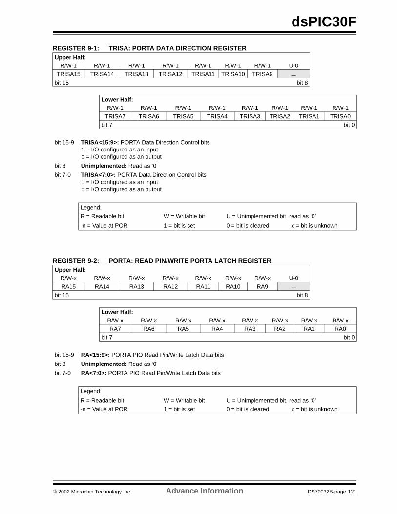
dsPIC30F
REGISTER 9-1: TRISA: PORTA DATA DIRECTION REGISTER
REGISTER 9-2: PORTA: READ PIN/WRITE PORTA LATCH REGISTER
Upper Half:R/W-1 R/W-1 R/W-1 R/W-1 R/W-1 R/W-1 R/W-1 U-0
TRISA15 TRISA14 TRISA13 TRISA12 TRISA11 TRISA10 TRISA9 —
bit 15 bit 8
Lower Half:R/W-1 R/W-1 R/W-1 R/W-1 R/W-1 R/W-1 R/W-1 R/W-1
TRISA7 TRISA6 TRISA5 TRISA4 TRISA3 TRISA2 TRISA1 TRISA0bit 7 bit 0
bit 15-9 TRISA<15:9>: PORTA Data Direction Control bits1 = I/O configured as an input0 = I/O configured as an output
bit 8 Unimplemented: Read as ‘0’
bit 7-0 TRISA<7:0>: PORTA Data Direction Control bits1 = I/O configured as an input0 = I/O configured as an output
Legend:
R = Readable bit W = Writable bit U = Unimplemented bit, read as ‘0’
-n = Value at POR 1 = bit is set 0 = bit is cleared x = bit is unknown
Upper Half:R/W-x R/W-x R/W-x R/W-x R/W-x R/W-x R/W-x U-0RA15 RA14 RA13 RA12 RA11 RA10 RA9 —
bit 15 bit 8
Lower Half:R/W-x R/W-x R/W-x R/W-x R/W-x R/W-x R/W-x R/W-xRA7 RA6 RA5 RA4 RA3 RA2 RA1 RA0
bit 7 bit 0
bit 15-9 RA<15:9>: PORTA PIO Read Pin/Write Latch Data bits
bit 8 Unimplemented: Read as ‘0’
bit 7-0 RA<7:0>: PORTA PIO Read Pin/Write Latch Data bits
Legend:
R = Readable bit W = Writable bit U = Unimplemented bit, read as ‘0’
-n = Value at POR 1 = bit is set 0 = bit is cleared x = bit is unknown
2002 Microchip Technology Inc. Advance Information DS70032B-page 121
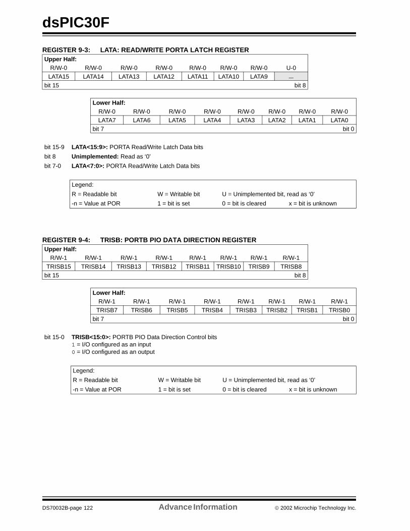
dsPIC30F
REGISTER 9-3: LATA: READ/WRITE PORTA LATCH REGISTER
REGISTER 9-4: TRISB: PORTB PIO DATA DIRECTION REGISTER
Upper Half:R/W-0 R/W-0 R/W-0 R/W-0 R/W-0 R/W-0 R/W-0 U-0
LATA15 LATA14 LATA13 LATA12 LATA11 LATA10 LATA9 —
bit 15 bit 8
Lower Half:R/W-0 R/W-0 R/W-0 R/W-0 R/W-0 R/W-0 R/W-0 R/W-0LATA7 LATA6 LATA5 LATA4 LATA3 LATA2 LATA1 LATA0
bit 7 bit 0
bit 15-9 LATA<15:9>: PORTA Read/Write Latch Data bits
bit 8 Unimplemented: Read as ‘0’
bit 7-0 LATA<7:0>: PORTA Read/Write Latch Data bits
Legend:
R = Readable bit W = Writable bit U = Unimplemented bit, read as ‘0’
-n = Value at POR 1 = bit is set 0 = bit is cleared x = bit is unknown
Upper Half:R/W-1 R/W-1 R/W-1 R/W-1 R/W-1 R/W-1 R/W-1 R/W-1
TRISB15 TRISB14 TRISB13 TRISB12 TRISB11 TRISB10 TRISB9 TRISB8bit 15 bit 8
Lower Half:R/W-1 R/W-1 R/W-1 R/W-1 R/W-1 R/W-1 R/W-1 R/W-1
TRISB7 TRISB6 TRISB5 TRISB4 TRISB3 TRISB2 TRISB1 TRISB0
bit 7 bit 0
bit 15-0 TRISB<15:0>: PORTB PIO Data Direction Control bits1 = I/O configured as an input0 = I/O configured as an output
Legend:
R = Readable bit W = Writable bit U = Unimplemented bit, read as ‘0’
-n = Value at POR 1 = bit is set 0 = bit is cleared x = bit is unknown
DS70032B-page 122 Advance Information 2002 Microchip Technology Inc.
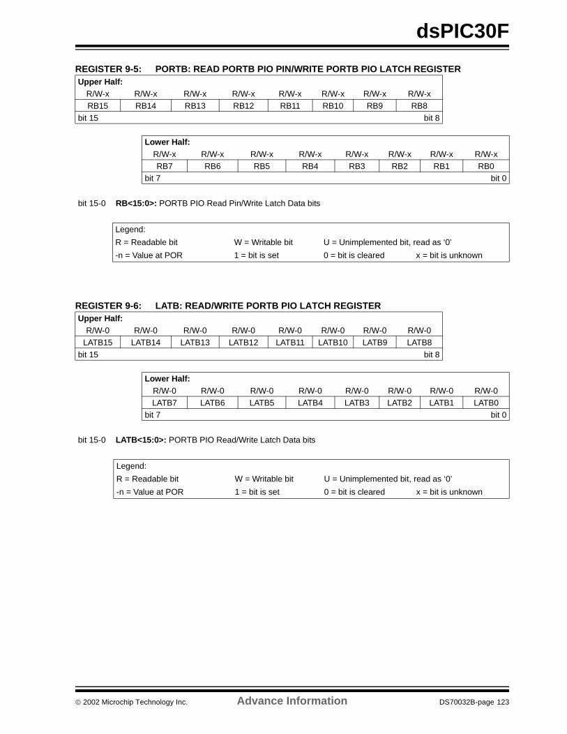
dsPIC30F
REGISTER 9-5: PORTB: READ PORTB PIO PIN/WRITE PORTB PIO LATCH REGISTER
REGISTER 9-6: LATB: READ/WRITE PORTB PIO LATCH REGISTER
Upper Half:R/W-x R/W-x R/W-x R/W-x R/W-x R/W-x R/W-x R/W-xRB15 RB14 RB13 RB12 RB11 RB10 RB9 RB8
bit 15 bit 8
Lower Half:R/W-x R/W-x R/W-x R/W-x R/W-x R/W-x R/W-x R/W-xRB7 RB6 RB5 RB4 RB3 RB2 RB1 RB0
bit 7 bit 0
bit 15-0 RB<15:0>: PORTB PIO Read Pin/Write Latch Data bits
Legend:
R = Readable bit W = Writable bit U = Unimplemented bit, read as ‘0’
-n = Value at POR 1 = bit is set 0 = bit is cleared x = bit is unknown
Upper Half:R/W-0 R/W-0 R/W-0 R/W-0 R/W-0 R/W-0 R/W-0 R/W-0
LATB15 LATB14 LATB13 LATB12 LATB11 LATB10 LATB9 LATB8
bit 15 bit 8
Lower Half:R/W-0 R/W-0 R/W-0 R/W-0 R/W-0 R/W-0 R/W-0 R/W-0LATB7 LATB6 LATB5 LATB4 LATB3 LATB2 LATB1 LATB0
bit 7 bit 0
bit 15-0 LATB<15:0>: PORTB PIO Read/Write Latch Data bits
Legend:
R = Readable bit W = Writable bit U = Unimplemented bit, read as ‘0’
-n = Value at POR 1 = bit is set 0 = bit is cleared x = bit is unknown
2002 Microchip Technology Inc. Advance Information DS70032B-page 123
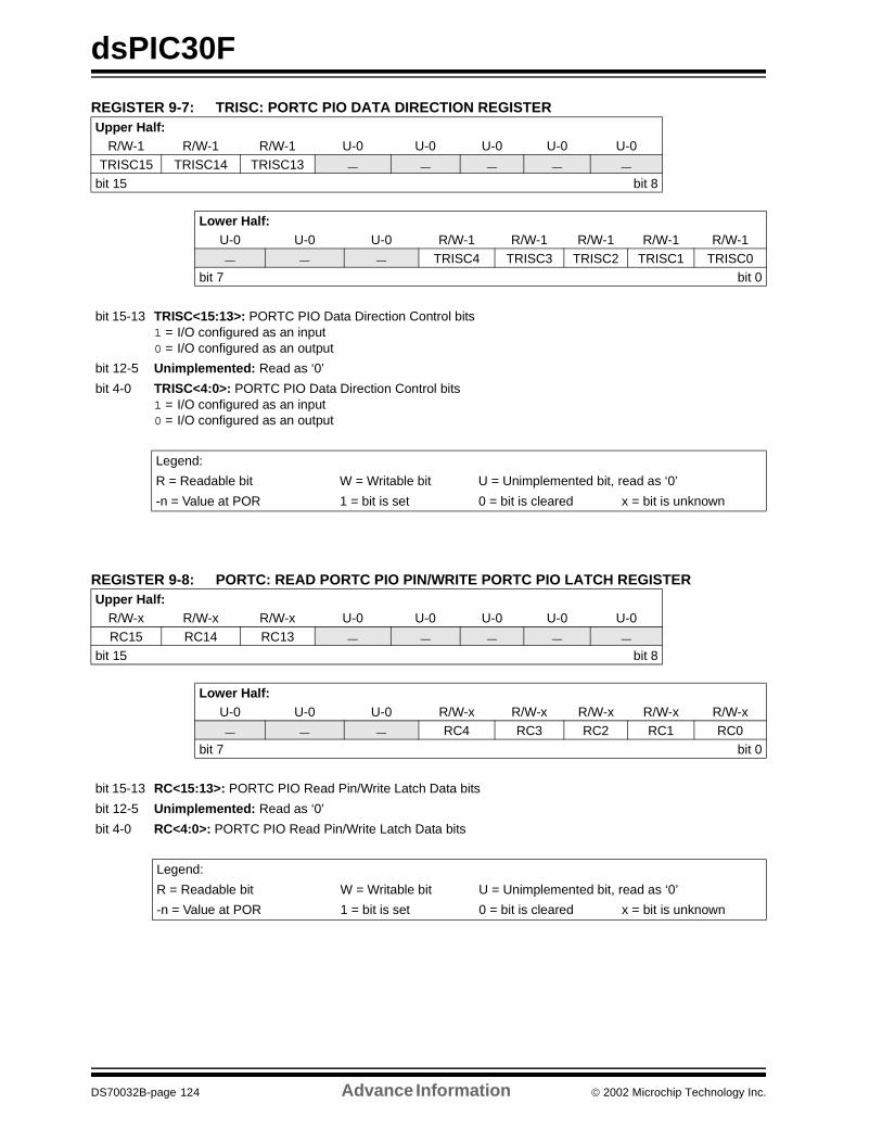
dsPIC30F
REGISTER 9-7: TRISC: PORTC PIO DATA DIRECTION REGISTER
REGISTER 9-8: PORTC: READ PORTC PIO PIN/WRITE PORTC PIO LATCH REGISTER
Upper Half:R/W-1 R/W-1 R/W-1 U-0 U-0 U-0 U-0 U-0
TRISC15 TRISC14 TRISC13 — — — — —
bit 15 bit 8
Lower Half:U-0 U-0 U-0 R/W-1 R/W-1 R/W-1 R/W-1 R/W-1
— — — TRISC4 TRISC3 TRISC2 TRISC1 TRISC0bit 7 bit 0
bit 15-13 TRISC<15:13>: PORTC PIO Data Direction Control bits1 = I/O configured as an input0 = I/O configured as an output
bit 12-5 Unimplemented: Read as ‘0’
bit 4-0 TRISC<4:0>: PORTC PIO Data Direction Control bits1 = I/O configured as an input0 = I/O configured as an output
Legend:
R = Readable bit W = Writable bit U = Unimplemented bit, read as ‘0’
-n = Value at POR 1 = bit is set 0 = bit is cleared x = bit is unknown
Upper Half:R/W-x R/W-x R/W-x U-0 U-0 U-0 U-0 U-0RC15 RC14 RC13 — — — — —
bit 15 bit 8
Lower Half:U-0 U-0 U-0 R/W-x R/W-x R/W-x R/W-x R/W-x
— — — RC4 RC3 RC2 RC1 RC0bit 7 bit 0
bit 15-13 RC<15:13>: PORTC PIO Read Pin/Write Latch Data bits
bit 12-5 Unimplemented: Read as ‘0’
bit 4-0 RC<4:0>: PORTC PIO Read Pin/Write Latch Data bits
Legend:
R = Readable bit W = Writable bit U = Unimplemented bit, read as ‘0’
-n = Value at POR 1 = bit is set 0 = bit is cleared x = bit is unknown
DS70032B-page 124 Advance Information 2002 Microchip Technology Inc.
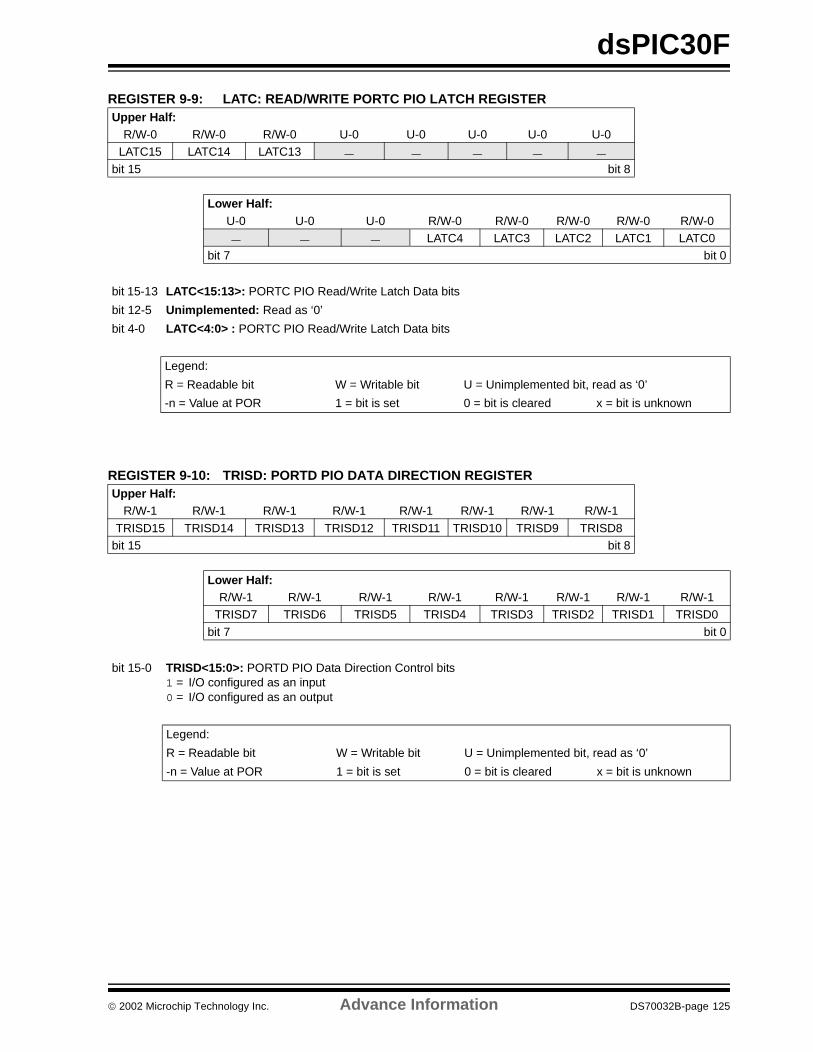
dsPIC30F
REGISTER 9-9: LATC: READ/WRITE PORTC PIO LATCH REGISTER
REGISTER 9-10: TRISD: PORTD PIO DATA DIRECTION REGISTER
Upper Half:R/W-0 R/W-0 R/W-0 U-0 U-0 U-0 U-0 U-0
LATC15 LATC14 LATC13 — — — — —
bit 15 bit 8
Lower Half:U-0 U-0 U-0 R/W-0 R/W-0 R/W-0 R/W-0 R/W-0
— — — LATC4 LATC3 LATC2 LATC1 LATC0bit 7 bit 0
bit 15-13 LATC<15:13>: PORTC PIO Read/Write Latch Data bits
bit 12-5 Unimplemented: Read as ‘0’
bit 4-0 LATC<4:0> : PORTC PIO Read/Write Latch Data bits
Legend:
R = Readable bit W = Writable bit U = Unimplemented bit, read as ‘0’
-n = Value at POR 1 = bit is set 0 = bit is cleared x = bit is unknown
Upper Half:R/W-1 R/W-1 R/W-1 R/W-1 R/W-1 R/W-1 R/W-1 R/W-1
TRISD15 TRISD14 TRISD13 TRISD12 TRISD11 TRISD10 TRISD9 TRISD8bit 15 bit 8
Lower Half:R/W-1 R/W-1 R/W-1 R/W-1 R/W-1 R/W-1 R/W-1 R/W-1
TRISD7 TRISD6 TRISD5 TRISD4 TRISD3 TRISD2 TRISD1 TRISD0
bit 7 bit 0
bit 15-0 TRISD<15:0>: PORTD PIO Data Direction Control bits1 = I/O configured as an input0 = I/O configured as an output
Legend:
R = Readable bit W = Writable bit U = Unimplemented bit, read as ‘0’
-n = Value at POR 1 = bit is set 0 = bit is cleared x = bit is unknown
2002 Microchip Technology Inc. Advance Information DS70032B-page 125
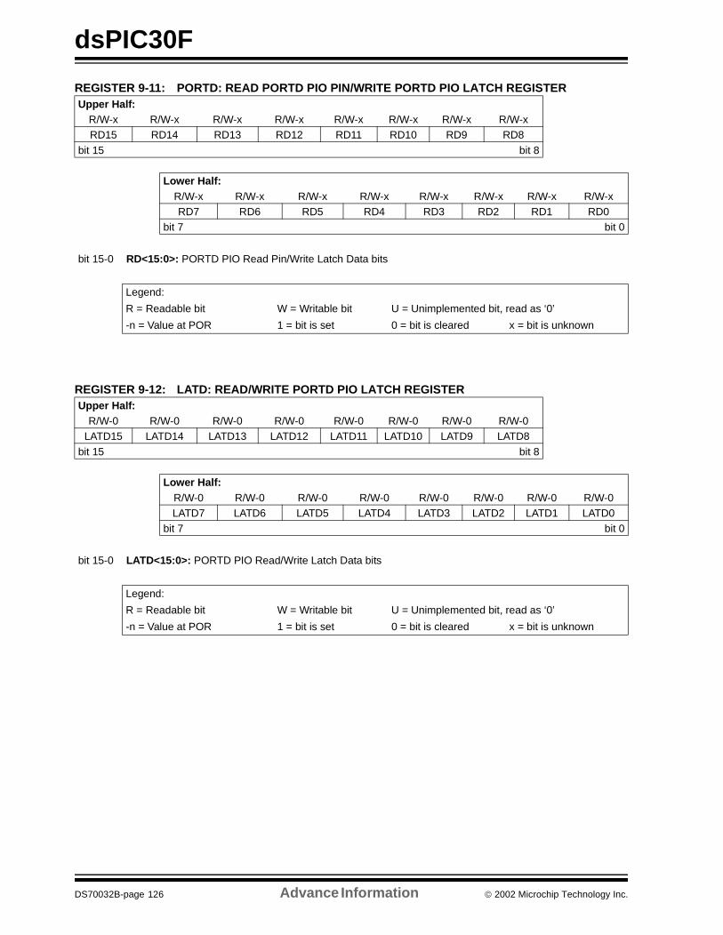
dsPIC30F
REGISTER 9-11: PORTD: READ PORTD PIO PIN/WRITE PORTD PIO LATCH REGISTER
REGISTER 9-12: LATD: READ/WRITE PORTD PIO LATCH REGISTER
Upper Half:R/W-x R/W-x R/W-x R/W-x R/W-x R/W-x R/W-x R/W-xRD15 RD14 RD13 RD12 RD11 RD10 RD9 RD8
bit 15 bit 8
Lower Half:R/W-x R/W-x R/W-x R/W-x R/W-x R/W-x R/W-x R/W-xRD7 RD6 RD5 RD4 RD3 RD2 RD1 RD0
bit 7 bit 0
bit 15-0 RD<15:0>: PORTD PIO Read Pin/Write Latch Data bits
Legend:
R = Readable bit W = Writable bit U = Unimplemented bit, read as ‘0’
-n = Value at POR 1 = bit is set 0 = bit is cleared x = bit is unknown
Upper Half:R/W-0 R/W-0 R/W-0 R/W-0 R/W-0 R/W-0 R/W-0 R/W-0
LATD15 LATD14 LATD13 LATD12 LATD11 LATD10 LATD9 LATD8
bit 15 bit 8
Lower Half:R/W-0 R/W-0 R/W-0 R/W-0 R/W-0 R/W-0 R/W-0 R/W-0LATD7 LATD6 LATD5 LATD4 LATD3 LATD2 LATD1 LATD0
bit 7 bit 0
bit 15-0 LATD<15:0>: PORTD PIO Read/Write Latch Data bits
Legend:
R = Readable bit W = Writable bit U = Unimplemented bit, read as ‘0’
-n = Value at POR 1 = bit is set 0 = bit is cleared x = bit is unknown
DS70032B-page 126 Advance Information 2002 Microchip Technology Inc.
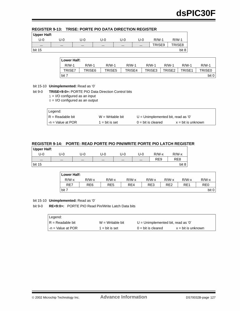
dsPIC30F
REGISTER 9-13: TRISE: PORTE PIO DATA DIRECTION REGISTER
REGISTER 9-14: PORTE: READ PORTE PIO PIN/WRITE PORTE PIO LATCH REGISTER
Upper Half:U-0 U-0 U-0 U-0 U-0 U-0 R/W-1 R/W-1
— — — — — — TRISE9 TRISE8
bit 15 bit 8
Lower Half:R/W-1 R/W-1 R/W-1 R/W-1 R/W-1 R/W-1 R/W-1 R/W-1
TRISE7 TRISE6 TRISE5 TRISE4 TRISE3 TRISE2 TRISE1 TRISE0bit 7 bit 0
bit 15-10 Unimplemented: Read as ‘0’
bit 9-0 TRISE<9:0>: PORTE PIO Data Direction Control bits1 = I/O configured as an input0 = I/O configured as an output
Legend:
R = Readable bit W = Writable bit U = Unimplemented bit, read as ‘0’
-n = Value at POR 1 = bit is set 0 = bit is cleared x = bit is unknown
Upper Half:U-0 U-0 U-0 U-0 U-0 U-0 R/W-x R/W-x
— — — — — — RE9 RE8
bit 15 bit 8
Lower Half:R/W-x R/W-x R/W-x R/W-x R/W-x R/W-x R/W-x R/W-xRE7 RE6 RE5 RE4 RE3 RE2 RE1 RE0
bit 7 bit 0
bit 15-10 Unimplemented: Read as ‘0’
bit 9-0 RE<9:0>: PORTE PIO Read Pin/Write Latch Data bits
Legend:
R = Readable bit W = Writable bit U = Unimplemented bit, read as ‘0’
-n = Value at POR 1 = bit is set 0 = bit is cleared x = bit is unknown
2002 Microchip Technology Inc. Advance Information DS70032B-page 127
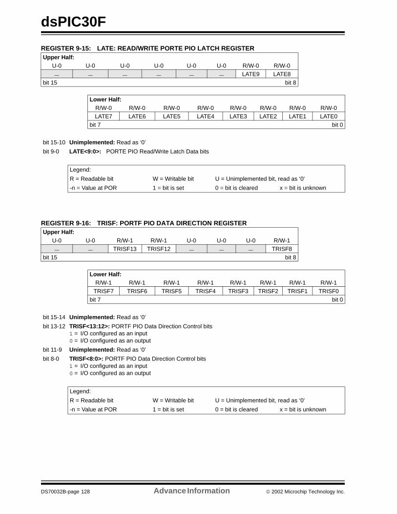
dsPIC30F
REGISTER 9-15: LATE: READ/WRITE PORTE PIO LATCH REGISTER
REGISTER 9-16: TRISF: PORTF PIO DATA DIRECTION REGISTER
Upper Half:U-0 U-0 U-0 U-0 U-0 U-0 R/W-0 R/W-0
— — — — — — LATE9 LATE8
bit 15 bit 8
Lower Half:R/W-0 R/W-0 R/W-0 R/W-0 R/W-0 R/W-0 R/W-0 R/W-0LATE7 LATE6 LATE5 LATE4 LATE3 LATE2 LATE1 LATE0
bit 7 bit 0
bit 15-10 Unimplemented: Read as ‘0’
bit 9-0 LATE<9:0>: PORTE PIO Read/Write Latch Data bits
Legend:
R = Readable bit W = Writable bit U = Unimplemented bit, read as ‘0’
-n = Value at POR 1 = bit is set 0 = bit is cleared x = bit is unknown
Upper Half:U-0 U-0 R/W-1 R/W-1 U-0 U-0 U-0 R/W-1
— — TRISF13 TRISF12 — — — TRISF8bit 15 bit 8
Lower Half:R/W-1 R/W-1 R/W-1 R/W-1 R/W-1 R/W-1 R/W-1 R/W-1
TRISF7 TRISF6 TRISF5 TRISF4 TRISF3 TRISF2 TRISF1 TRISF0bit 7 bit 0
bit 15-14 Unimplemented: Read as ‘0’
bit 13-12 TRISF<13:12>: PORTF PIO Data Direction Control bits1 = I/O configured as an input0 = I/O configured as an output
bit 11-9 Unimplemented: Read as ‘0’
bit 8-0 TRISF<8:0>: PORTF PIO Data Direction Control bits1 = I/O configured as an input0 = I/O configured as an output
Legend:
R = Readable bit W = Writable bit U = Unimplemented bit, read as ‘0’
-n = Value at POR 1 = bit is set 0 = bit is cleared x = bit is unknown
DS70032B-page 128 Advance Information 2002 Microchip Technology Inc.
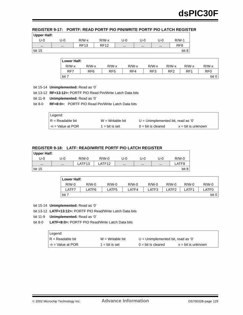
dsPIC30F
REGISTER 9-17: PORTF: READ PORTF PIO PIN/WRITE PORTF PIO LATCH REGISTER
REGISTER 9-18: LATF: READ/WRITE PORTF PIO LATCH REGISTER
Upper Half:U-0 U-0 R/W-x R/W-x U-0 U-0 U-0 R/W-1
— — RF13 RF12 — — — RF8
bit 15 bit 8
Lower Half:R/W-x R/W-x R/W-x R/W-x R/W-x R/W-x R/W-x R/W-xRF7 RF6 RF5 RF4 RF3 RF2 RF1 RF0
bit 7 bit 0
bit 15-14 Unimplemented: Read as ‘0’
bit 13-12 RF<13:12>: PORTF PIO Read Pin/Write Latch Data bits
bit 11-9 Unimplemented: Read as ‘0’
bit 8-0 RF<8:0>: PORTF PIO Read Pin/Write Latch Data bits
Legend:
R = Readable bit W = Writable bit U = Unimplemented bit, read as ‘0’
-n = Value at POR 1 = bit is set 0 = bit is cleared x = bit is unknown
Upper Half:U-0 U-0 R/W-0 R/W-0 U-0 U-0 U-0 R/W-0
— — LATF13 LATF12 — — — LATF8
bit 15 bit 8
Lower Half:R/W-0 R/W-0 R/W-0 R/W-0 R/W-0 R/W-0 R/W-0 R/W-0LATF7 LATF6 LATF5 LATF4 LATF3 LATF2 LATF1 LATF0
bit 7 bit 0
bit 15-14 Unimplemented: Read as ‘0’
bit 13-12 LATF<13:12>: PORTF PIO Read/Write Latch Data bits
bit 11-9 Unimplemented: Read as ‘0’
bit 8-0 LATF<8:0>: PORTF PIO Read/Write Latch Data bits
Legend:
R = Readable bit W = Writable bit U = Unimplemented bit, read as ‘0’
-n = Value at POR 1 = bit is set 0 = bit is cleared x = bit is unknown
2002 Microchip Technology Inc. Advance Information DS70032B-page 129
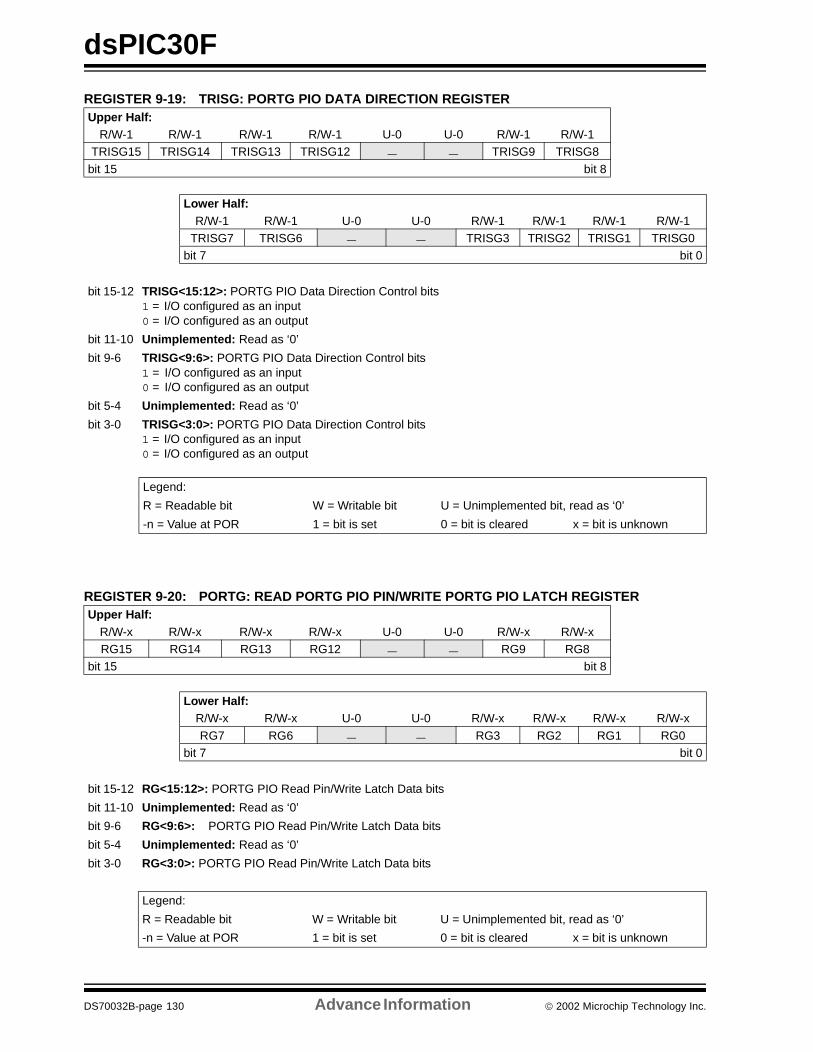
dsPIC30F
REGISTER 9-19: TRISG: PORTG PIO DATA DIRECTION REGISTER
REGISTER 9-20: PORTG: READ PORTG PIO PIN/WRITE PORTG PIO LATCH REGISTER
Upper Half:R/W-1 R/W-1 R/W-1 R/W-1 U-0 U-0 R/W-1 R/W-1
TRISG15 TRISG14 TRISG13 TRISG12 — — TRISG9 TRISG8
bit 15 bit 8
Lower Half:R/W-1 R/W-1 U-0 U-0 R/W-1 R/W-1 R/W-1 R/W-1
TRISG7 TRISG6 — — TRISG3 TRISG2 TRISG1 TRISG0bit 7 bit 0
bit 15-12 TRISG<15:12>: PORTG PIO Data Direction Control bits1 = I/O configured as an input0 = I/O configured as an output
bit 11-10 Unimplemented: Read as ‘0’
bit 9-6 TRISG<9:6>: PORTG PIO Data Direction Control bits1 = I/O configured as an input0 = I/O configured as an output
bit 5-4 Unimplemented: Read as ‘0’
bit 3-0 TRISG<3:0>: PORTG PIO Data Direction Control bits1 = I/O configured as an input0 = I/O configured as an output
Legend:
R = Readable bit W = Writable bit U = Unimplemented bit, read as ‘0’
-n = Value at POR 1 = bit is set 0 = bit is cleared x = bit is unknown
Upper Half:R/W-x R/W-x R/W-x R/W-x U-0 U-0 R/W-x R/W-xRG15 RG14 RG13 RG12 — — RG9 RG8
bit 15 bit 8
Lower Half:R/W-x R/W-x U-0 U-0 R/W-x R/W-x R/W-x R/W-x
RG7 RG6 — — RG3 RG2 RG1 RG0bit 7 bit 0
bit 15-12 RG<15:12>: PORTG PIO Read Pin/Write Latch Data bits
bit 11-10 Unimplemented: Read as ‘0’
bit 9-6 RG<9:6>: PORTG PIO Read Pin/Write Latch Data bits
bit 5-4 Unimplemented: Read as ‘0’
bit 3-0 RG<3:0>: PORTG PIO Read Pin/Write Latch Data bits
Legend:
R = Readable bit W = Writable bit U = Unimplemented bit, read as ‘0’
-n = Value at POR 1 = bit is set 0 = bit is cleared x = bit is unknown
DS70032B-page 130 Advance Information 2002 Microchip Technology Inc.
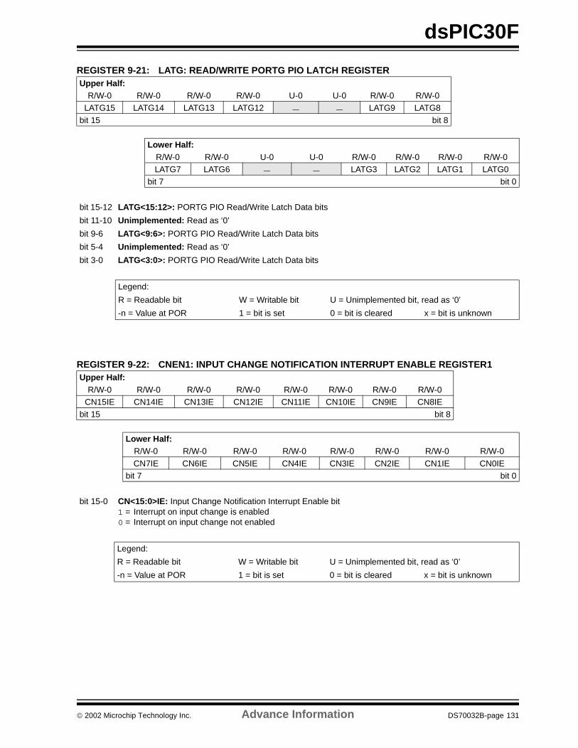
dsPIC30F
REGISTER 9-21: LATG: READ/WRITE PORTG PIO LATCH REGISTER
REGISTER 9-22: CNEN1: INPUT CHANGE NOTIFICATION INTERRUPT ENABLE REGISTER1
Upper Half:R/W-0 R/W-0 R/W-0 R/W-0 U-0 U-0 R/W-0 R/W-0
LATG15 LATG14 LATG13 LATG12 — — LATG9 LATG8
bit 15 bit 8
Lower Half:R/W-0 R/W-0 U-0 U-0 R/W-0 R/W-0 R/W-0 R/W-0LATG7 LATG6 — — LATG3 LATG2 LATG1 LATG0
bit 7 bit 0
bit 15-12 LATG<15:12>: PORTG PIO Read/Write Latch Data bits
bit 11-10 Unimplemented: Read as ‘0’
bit 9-6 LATG<9:6>: PORTG PIO Read/Write Latch Data bits
bit 5-4 Unimplemented: Read as ‘0’
bit 3-0 LATG<3:0>: PORTG PIO Read/Write Latch Data bits
Legend:
R = Readable bit W = Writable bit U = Unimplemented bit, read as ‘0’
-n = Value at POR 1 = bit is set 0 = bit is cleared x = bit is unknown
Upper Half:R/W-0 R/W-0 R/W-0 R/W-0 R/W-0 R/W-0 R/W-0 R/W-0
CN15IE CN14IE CN13IE CN12IE CN11IE CN10IE CN9IE CN8IEbit 15 bit 8
Lower Half:R/W-0 R/W-0 R/W-0 R/W-0 R/W-0 R/W-0 R/W-0 R/W-0
CN7IE CN6IE CN5IE CN4IE CN3IE CN2IE CN1IE CN0IEbit 7 bit 0
bit 15-0 CN<15:0>IE: Input Change Notification Interrupt Enable bit1 = Interrupt on input change is enabled0 = Interrupt on input change not enabled
Legend:
R = Readable bit W = Writable bit U = Unimplemented bit, read as ‘0’
-n = Value at POR 1 = bit is set 0 = bit is cleared x = bit is unknown
2002 Microchip Technology Inc. Advance Information DS70032B-page 131
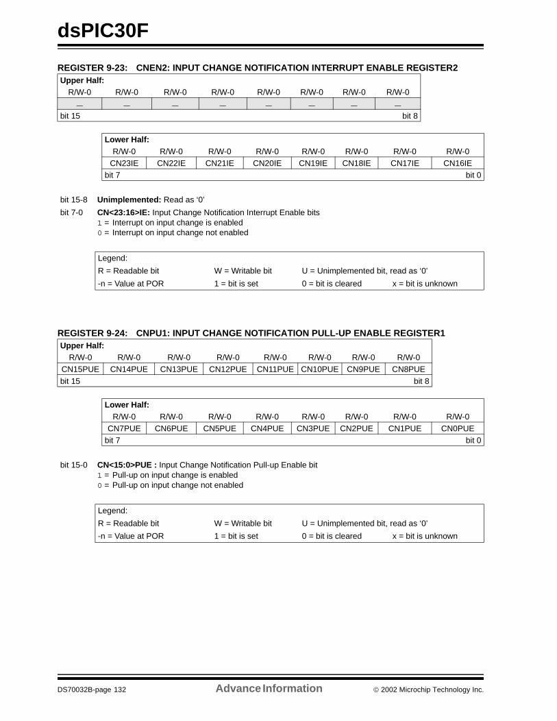
dsPIC30F
REGISTER 9-23: CNEN2: INPUT CHANGE NOTIFICATION INTERRUPT ENABLE REGISTER2
REGISTER 9-24: CNPU1: INPUT CHANGE NOTIFICATION PULL-UP ENABLE REGISTER1
Upper Half:R/W-0 R/W-0 R/W-0 R/W-0 R/W-0 R/W-0 R/W-0 R/W-0
— — — — — — — —
bit 15 bit 8
Lower Half:R/W-0 R/W-0 R/W-0 R/W-0 R/W-0 R/W-0 R/W-0 R/W-0
CN23IE CN22IE CN21IE CN20IE CN19IE CN18IE CN17IE CN16IEbit 7 bit 0
bit 15-8 Unimplemented: Read as ‘0’
bit 7-0 CN<23:16>IE: Input Change Notification Interrupt Enable bits1 = Interrupt on input change is enabled0 = Interrupt on input change not enabled
Legend:
R = Readable bit W = Writable bit U = Unimplemented bit, read as ‘0’
-n = Value at POR 1 = bit is set 0 = bit is cleared x = bit is unknown
Upper Half:R/W-0 R/W-0 R/W-0 R/W-0 R/W-0 R/W-0 R/W-0 R/W-0
CN15PUE CN14PUE CN13PUE CN12PUE CN11PUE CN10PUE CN9PUE CN8PUE
bit 15 bit 8
Lower Half:R/W-0 R/W-0 R/W-0 R/W-0 R/W-0 R/W-0 R/W-0 R/W-0
CN7PUE CN6PUE CN5PUE CN4PUE CN3PUE CN2PUE CN1PUE CN0PUEbit 7 bit 0
bit 15-0 CN<15:0>PUE : Input Change Notification Pull-up Enable bit1 = Pull-up on input change is enabled0 = Pull-up on input change not enabled
Legend:
R = Readable bit W = Writable bit U = Unimplemented bit, read as ‘0’
-n = Value at POR 1 = bit is set 0 = bit is cleared x = bit is unknown
DS70032B-page 132 Advance Information 2002 Microchip Technology Inc.
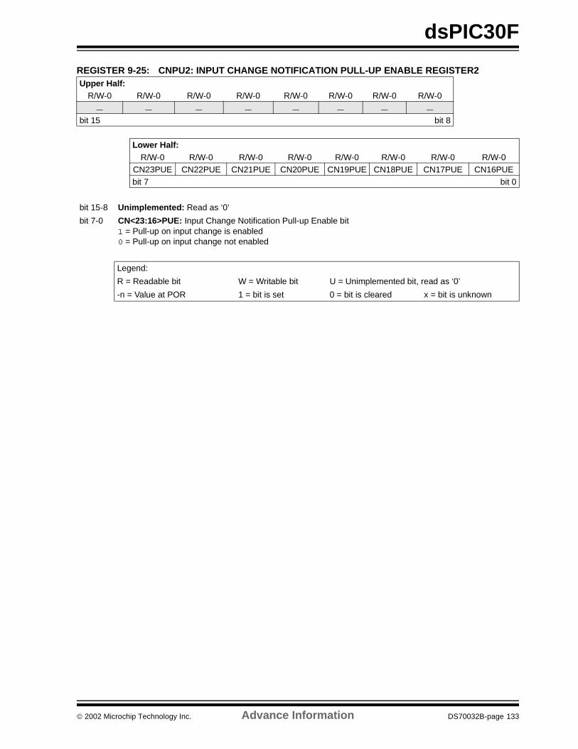
dsPIC30F
REGISTER 9-25: CNPU2: INPUT CHANGE NOTIFICATION PULL-UP ENABLE REGISTER2 Upper Half:
R/W-0 R/W-0 R/W-0 R/W-0 R/W-0 R/W-0 R/W-0 R/W-0
— — — — — — — —
bit 15 bit 8
Lower Half:R/W-0 R/W-0 R/W-0 R/W-0 R/W-0 R/W-0 R/W-0 R/W-0
CN23PUE CN22PUE CN21PUE CN20PUE CN19PUE CN18PUE CN17PUE CN16PUEbit 7 bit 0
bit 15-8 Unimplemented: Read as ‘0’
bit 7-0 CN<23:16>PUE: Input Change Notification Pull-up Enable bit1 = Pull-up on input change is enabled0 = Pull-up on input change not enabled
Legend:
R = Readable bit W = Writable bit U = Unimplemented bit, read as ‘0’
-n = Value at POR 1 = bit is set 0 = bit is cleared x = bit is unknown
2002 Microchip Technology Inc. Advance Information DS70032B-page 133

dsPIC30F
NOTES:
DS70032B-page 134 Advance Information 2002 Microchip Technology Inc.
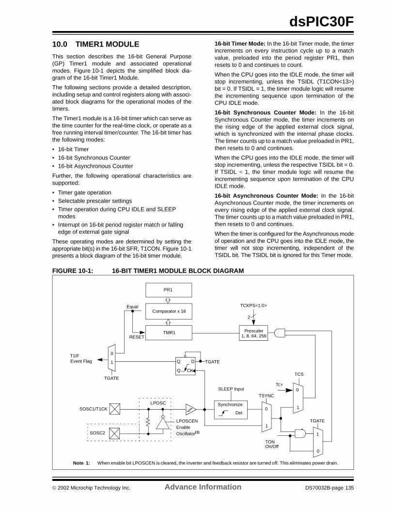
dsPIC30F
10.0 TIMER1 MODULEThis section describes the 16-bit General Purpose(GP) Timer1 module and associated operationalmodes. Figure 10-1 depicts the simplified block dia-gram of the 16-bit Timer1 Module.
The following sections provide a detailed description,including setup and control registers along with associ-ated block diagrams for the operational modes of thetimers.
The Timer1 module is a 16-bit timer which can serve asthe time counter for the real-time clock, or operate as afree running interval timer/counter. The 16-bit timer hasthe following modes:
• 16-bit Timer
• 16-bit Synchronous Counter• 16-bit Asynchronous Counter
Further, the following operational characteristics aresupported:
• Timer gate operation• Selectable prescaler settings• Timer operation during CPU IDLE and SLEEP
modes• Interrupt on 16-bit period register match or falling
edge of external gate signal
These operating modes are determined by setting theappropriate bit(s) in the 16-bit SFR, T1CON. Figure 10-1presents a block diagram of the 16-bit timer module.
16-bit Timer Mode: In the 16-bit Timer mode, the timerincrements on every instruction cycle up to a matchvalue, preloaded into the period register PR1, thenresets to 0 and continues to count.
When the CPU goes into the IDLE mode, the timer willstop incrementing, unless the TSIDL (T1CON<13>)bit = 0. If TSIDL = 1, the timer module logic will resumethe incrementing sequence upon termination of theCPU IDLE mode.
16-bit Synchronous Counter Mode: In the 16-bitSynchronous Counter mode, the timer increments onthe rising edge of the applied external clock signal,which is synchronized with the internal phase clocks.The timer counts up to a match value preloaded in PR1,then resets to 0 and continues.
When the CPU goes into the IDLE mode, the timer willstop incrementing, unless the respective TSIDL bit = 0.If TSIDL = 1, the timer module logic will resume theincrementing sequence upon termination of the CPUIDLE mode.
16-bit Asynchronous Counter Mode: In the 16-bitAsynchronous Counter mode, the timer increments onevery rising edge of the applied external clock signal.The timer counts up to a match value preloaded in PR1,then resets to 0 and continues.
When the timer is configured for the Asynchronous modeof operation and the CPU goes into the IDLE mode, thetimer will not stop incrementing, independent of theTSIDL bit. The TSIDL bit is ignored for this Timer mode.
FIGURE 10-1: 16-BIT TIMER1 MODULE BLOCK DIAGRAM
LPOSC
TSYNC
TCS
SLEEP InputTCY
TONOn/Off
Synchronize
Det
0
10
1
SOSC1/T1CK
SOSC2
PR1
T1IF
EqualComparator x 16
TMR1RESET
Note 1: When enable bit LPOSCEN is cleared, the inverter and feedback resistor are turned off. This eliminates power drain.
LPOSCENEnableOscillator(1)
Event Flag
1
0
TGATE
Q
Q D
CK
TGATE
TCKPS<1:0>
Prescaler1, 8, 64, 256
2
TGATE
1
0
2002 Microchip Technology Inc. Advance Information DS70032B-page 135
dsPIC30F
10.1 Timer Gate Operation
The 16-bit timer can be placed in the Gated Time Accu-mulation mode. This mode allows the internal TCY toincrement the respective timer when the gate input sig-nal (T1CK pin) is asserted high. Control bit TGATE(T1CON<6>) must be set to enable this mode. Thetimer must be enabled (TON = 1) and the timer clocksource set to internal (TCS = 0).
When the CPU goes into the IDLE mode, the timer willstop incrementing, unless TSIDL = 0. If TSIDL = 1, thetimer will resume the incrementing sequence upon ter-mination of the CPU IDLE mode.
10.2 Timer Prescaler
The input clock (FOSC/4 or external clock) to the 16-bitTimer, has a prescale option of 1:1, 1:8, 1:64, and1:256 selected by control bits TCKPS<1:0>(T1CON<5:4>). The prescaler counter is cleared whenany of the following occurs:
• a write to the TMR1 register• a write to the T1CON register
• device RESET such as POR and BOR
However, if the timer is disabled (TON = 0), then thetimer prescaler cannot be reset since the prescalerclock is halted.
TMR1 is not cleared when T1CON is written. It iscleared by writing to the TMR1 register.
10.3 Timer Operation During SLEEP Mode
During CPU SLEEP mode, the timer will operate if:
• The timer module is enabled (TON = 1) and • The timer clock source is selected as external
(TCS = 0) and• The TSYNC bit is asserted to a logic 0, which
defines the external clock source as asynchro-nous.
When all three conditions are true, the timer will con-tinue to count up to the period register and be reset to0x0000.
When a match between the timer and the period regis-ter occurs, an interrupt can be generated, if the respec-tive timer interrupt enable bit is asserted.
10.4 Timer Interrupt
The 16-bit timer has the ability to generate an interrupton period match. When the timer count matches theperiod register, the T1IF bit is asserted and an interruptwill be generated if enabled. The T1IF bit must becleared in software. The timer interrupt flag T1IF islocated in the IFS0 control register in the InterruptController.
When the Gated Time Accumulation mode is enabled,an interrupt will also be generated on the falling edge ofthe gate signal (at the end of the accumulation cycle).
Enabling an interrupt is accomplished via the respec-tive timer interrupt enable bit, T1IE. The timer interruptenable bit is located in the IEC0 control register in theInterrupt Controller.
10.5 Real-Time Clock
The Real-Time Clock (RTC) provides time-of-day andevent time stamping capabilities. Key operational fea-tures of the RTC are:
• RTC Oscillator operation• 8-bit prescaler• Low power
• Real-Time Clock Interrupts• These operating modes are determined by setting
the appropriate bit(s) in the T1CON Control register.
10.5.1 RTC OSCILLATOR OPERATION
When the TON = 1, TCS = 1 and TGATE = 0, the timerincrements on the rising edge of the 32 kHz LP oscilla-tor output signal, up to the value specified in the periodregister, and is then reset to 0.
The TSYNC bit must be asserted to a logic 0 (Asyn-chronous mode) for correct operation.
Enabling LPOSCEN (OSCCON<1>) will disable thenormal Timer and Counter modes and enable a timercarry-out wake-up event.
When the CPU enters SLEEP or IDLE mode, the timerwill continue to increment, provided the external clockis active and the control bits have not been changed.The TSIDL bit is excluded from the control of the timermodule for this mode.
10.5.2 REAL-TIME CLOCK INTERRUPTS
When an interrupt event occurs, the respective inter-rupt flag, T1IF, is asserted and an interrupt will be gen-erated, if enabled. The T1IF bit must be cleared insoftware. The respective Timer interrupt flag, T1IF, islocated in the IFS0 status register in the InterruptController.
Enabling an interrupt is accomplished via the respec-tive timer interrupt enable bit, T1IE. The Timer interruptenable bit is located in the IEC0 control register in theInterrupt Controller.
DS70032B-page 136 Advance Information 2002 Microchip Technology Inc.
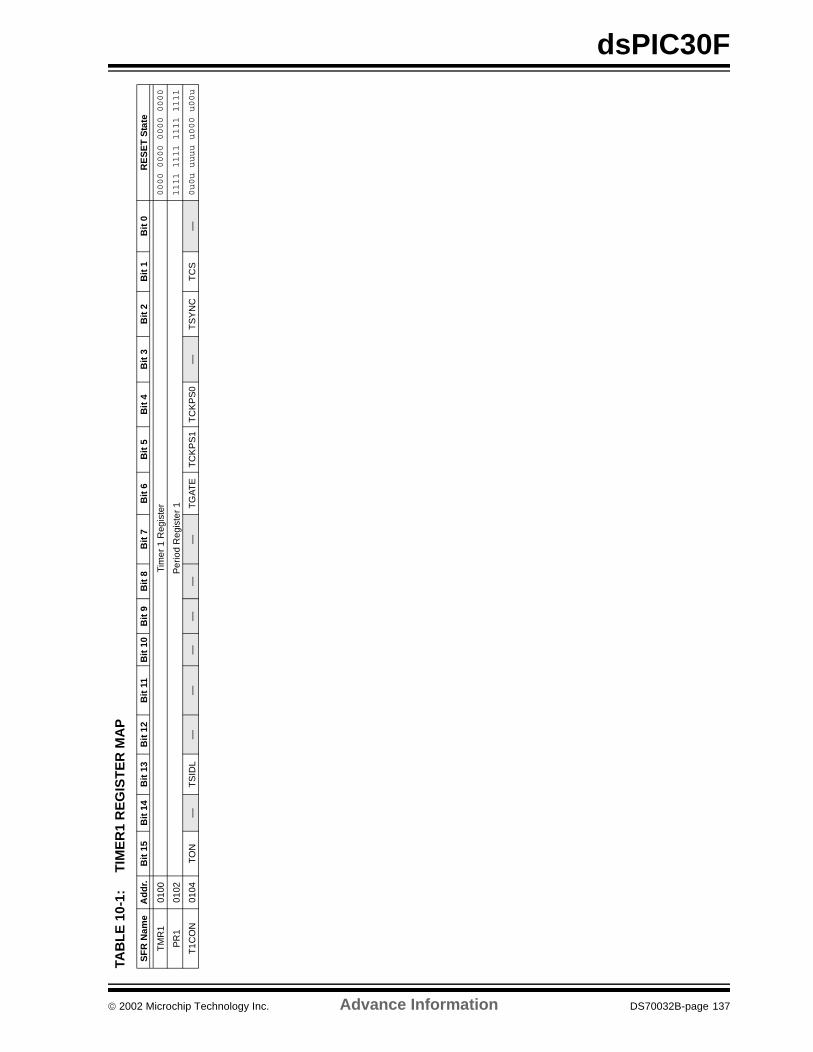
dsPIC30F
TAB
LE
10-
1:T
IME
R1
RE
GIS
TE
R M
AP
SF
R N
ame
Ad
dr.
Bit
15
Bit
14
Bit
13
Bit
12
Bit
11
Bit
10
Bit
9B
it 8
Bit
7B
it 6
Bit
5B
it 4
Bit
3B
it 2
Bit
1B
it 0
RE
SE
T S
tate
TM
R1
0100
Tim
er 1
Reg
iste
r0000 0000 0000 0000
PR
101
02P
erio
d R
egis
ter
11111 1111 1111 1111
T1C
ON
0104
TO
N—
TS
IDL
——
——
——
TG
AT
ET
CK
PS
1T
CK
PS
0—
TS
YN
CT
CS
—0u0u uuuu u000 u00u
2002 Microchip Technology Inc. Advance Information DS70032B-page 137
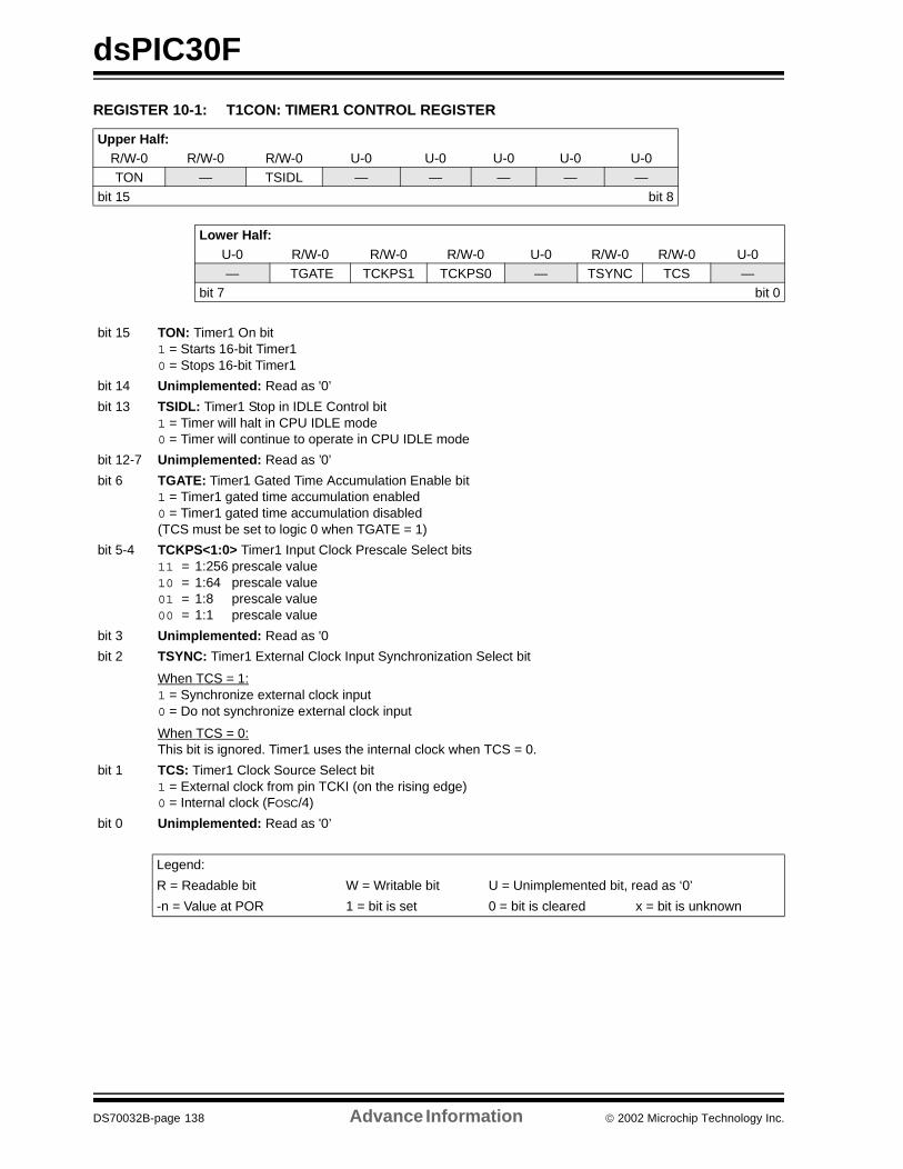
dsPIC30F
REGISTER 10-1: T1CON: TIMER1 CONTROL REGISTER
Upper Half:R/W-0 R/W-0 R/W-0 U-0 U-0 U-0 U-0 U-0TON — TSIDL — — — — —
bit 15 bit 8
Lower Half:U-0 R/W-0 R/W-0 R/W-0 U-0 R/W-0 R/W-0 U-0— TGATE TCKPS1 TCKPS0 — TSYNC TCS —
bit 7 bit 0
bit 15 TON: Timer1 On bit1 = Starts 16-bit Timer10 = Stops 16-bit Timer1
bit 14 Unimplemented: Read as '0’
bit 13 TSIDL: Timer1 Stop in IDLE Control bit 1 = Timer will halt in CPU IDLE mode0 = Timer will continue to operate in CPU IDLE mode
bit 12-7 Unimplemented: Read as ’0’
bit 6 TGATE: Timer1 Gated Time Accumulation Enable bit1 = Timer1 gated time accumulation enabled0 = Timer1 gated time accumulation disabled(TCS must be set to logic 0 when TGATE = 1)
bit 5-4 TCKPS<1:0> Timer1 Input Clock Prescale Select bits11 = 1:256 prescale value10 = 1:64 prescale value01 = 1:8 prescale value00 = 1:1 prescale value
bit 3 Unimplemented: Read as '0
bit 2 TSYNC: Timer1 External Clock Input Synchronization Select bit
When TCS = 1: 1 = Synchronize external clock input0 = Do not synchronize external clock input
When TCS = 0: This bit is ignored. Timer1 uses the internal clock when TCS = 0.
bit 1 TCS: Timer1 Clock Source Select bit1 = External clock from pin TCKI (on the rising edge) 0 = Internal clock (FOSC/4)
bit 0 Unimplemented: Read as '0’
Legend:
R = Readable bit W = Writable bit U = Unimplemented bit, read as ‘0’
-n = Value at POR 1 = bit is set 0 = bit is cleared x = bit is unknown
DS70032B-page 138 Advance Information 2002 Microchip Technology Inc.
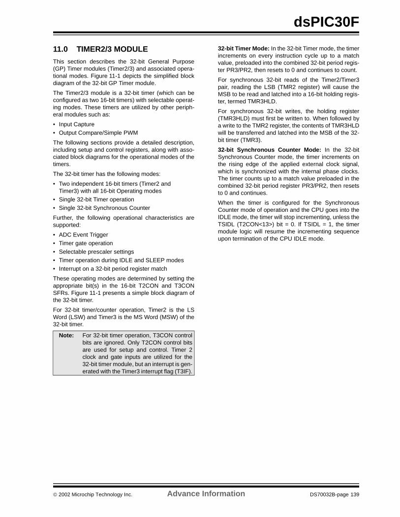
dsPIC30F
11.0 TIMER2/3 MODULE
This section describes the 32-bit General Purpose(GP) Timer modules (Timer2/3) and associated opera-tional modes. Figure 11-1 depicts the simplified blockdiagram of the 32-bit GP Timer module.
The Timer2/3 module is a 32-bit timer (which can beconfigured as two 16-bit timers) with selectable operat-ing modes. These timers are utilized by other periph-eral modules such as:
• Input Capture• Output Compare/Simple PWM
The following sections provide a detailed description,including setup and control registers, along with asso-ciated block diagrams for the operational modes of thetimers.
The 32-bit timer has the following modes:
• Two independent 16-bit timers (Timer2 and Timer3) with all 16-bit Operating modes
• Single 32-bit Timer operation• Single 32-bit Synchronous Counter
Further, the following operational characteristics aresupported:
• ADC Event Trigger• Timer gate operation
• Selectable prescaler settings• Timer operation during IDLE and SLEEP modes• Interrupt on a 32-bit period register match
These operating modes are determined by setting theappropriate bit(s) in the 16-bit T2CON and T3CONSFRs. Figure 11-1 presents a simple block diagram ofthe 32-bit timer.
For 32-bit timer/counter operation, Timer2 is the LSWord (LSW) and Timer3 is the MS Word (MSW) of the32-bit timer.
32-bit Timer Mode: In the 32-bit Timer mode, the timerincrements on every instruction cycle up to a matchvalue, preloaded into the combined 32-bit period regis-ter PR3/PR2, then resets to 0 and continues to count.
For synchronous 32-bit reads of the Timer2/Timer3pair, reading the LSB (TMR2 register) will cause theMSB to be read and latched into a 16-bit holding regis-ter, termed TMR3HLD.
For synchronous 32-bit writes, the holding register(TMR3HLD) must first be written to. When followed bya write to the TMR2 register, the contents of TMR3HLDwill be transferred and latched into the MSB of the 32-bit timer (TMR3).
32-bit Synchronous Counter Mode: In the 32-bitSynchronous Counter mode, the timer increments onthe rising edge of the applied external clock signal,which is synchronized with the internal phase clocks.The timer counts up to a match value preloaded in thecombined 32-bit period register PR3/PR2, then resetsto 0 and continues.
When the timer is configured for the SynchronousCounter mode of operation and the CPU goes into theIDLE mode, the timer will stop incrementing, unless theTSIDL (T2CON<13>) bit = 0. If TSIDL = 1, the timermodule logic will resume the incrementing sequenceupon termination of the CPU IDLE mode.
Note: For 32-bit timer operation, T3CON controlbits are ignored. Only T2CON control bitsare used for setup and control. Timer 2clock and gate inputs are utilized for the32-bit timer module, but an interrupt is gen-erated with the Timer3 interrupt flag (T3IF).
2002 Microchip Technology Inc. Advance Information DS70032B-page 139
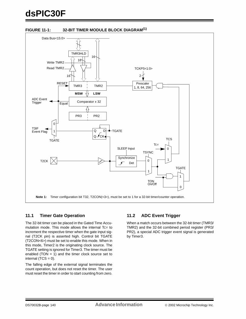
dsPIC30F
FIGURE 11-1: 32-BIT TIMER MODULE BLOCK DIAGRAM(1)
11.1 Timer Gate Operation
The 32-bit timer can be placed in the Gated Time Accu-mulation mode. This mode allows the internal TCY toincrement the respective timer when the gate input sig-nal (T2CK pin) is asserted high. Control bit TGATE(T2CON<6>) must be set to enable this mode. When inthis mode, Timer2 is the originating clock source. TheTGATE setting is ignored for Timer3. The timer must beenabled (TON = 1) and the timer clock source set tointernal (TCS = 0).
The falling edge of the external signal terminates thecount operation, but does not reset the timer. The usermust reset the timer in order to start counting from zero.
11.2 ADC Event Trigger
When a match occurs between the 32-bit timer (TMR3/TMR2) and the 32-bit combined period register (PR3/PR2), a special ADC trigger event signal is generatedby Timer3.
TMR3 TMR2
T3IF
Equal Comparator x 32
PR3 PR2
RESET
LSW MSW
Event Flag
Note 1: Timer configuration bit T32, T2CON(<3>), must be set to 1 for a 32-bit timer/counter operation.
Data Bus<15:0>
TMR3HLD
Read TMR2
Write TMR216
16
16
Q
Q D
CK
TGATE
ADC EventTrigger
TCKPS<1:0>
Prescaler 1, 8, 64, 256
2
TSYNC
TCS
SLEEP InputTCY
TONOn/Off
Synchronize
Det
0
10
1
T2CK
1
0
TGATE
TGATE
1
0
DS70032B-page 140 Advance Information 2002 Microchip Technology Inc.
dsPIC30F
11.3 Timer Prescaler
The input clock (FOSC/4 or external clock) to the timerhas a prescale option of 1:1, 1:8, 1:64, and 1:256selected by control bits TCKPS<1:0> (T2CON<5:4>and T3CON<5:4>). For the 32-bit timer operation, theoriginating clock source is Timer2. The prescaler oper-ation for Timer3 is not applicable in this mode. Theprescaler counter is cleared when any of the followingoccurs:
• a write to the TMR2/TMR3 register• a write to the T2CON/T3CON register
• device RESET such as POR and BOR
However, if the timer is disabled (TON = 0), then theTimer 2 prescaler cannot be reset, since the prescalerclock is halted.
TMR2/TMR3 is not cleared when T2CON/T3CON iswritten.
11.4 Timer Operation During SLEEP Mode
During CPU SLEEP mode, the timer will operate if:
• The timer module is enabled (TON = 1) and • The timer clock source is selected as external
(TCS = 0) and• The TSYNC bit is asserted to a logic 0, which
defines the external clock source as asynchro-nous.
When all three conditions are true, the timer will con-tinue to count up to the period register and be reset to0x00000000.
When a match between the timer and the period regis-ter occurs, an interrupt can be generated, if therespective timer interrupt enable bit is asserted.
11.5 Timer Interrupt
The 32-bit timer module can generate an interrupt onperiod match, or on the falling edge of the external gatesignal. When the 32-bit timer count matches therespective 32-bit period register, or the falling edge ofthe external “gate” signal is detected, the T3IF bit isasserted and an interrupt will be generated if enabled.In this mode, the T3IF interrupt flag is used as thesource of the interrupt. The T3IF bit must be cleared insoftware. The timer interrupt flag, T3IF, is located in theIFS0 status register in the Interrupt Controller.
Enabling an interrupt is accomplished via the respec-tive timer interrupt enable bit, T3IE. The timer interruptenable bit is located in the IEC0 control register.
2002 Microchip Technology Inc. Advance Information DS70032B-page 141
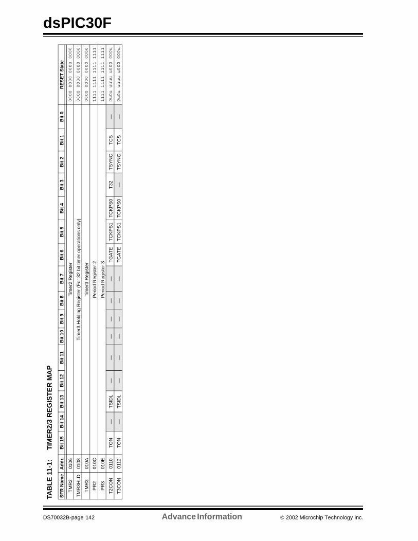
dsPIC30F
TAB
LE
11-
1:TI
ME
R2/
3 R
EG
IST
ER
MA
P
SF
R N
ame
Ad
dr.
Bit
15
Bit
14
Bit
13
Bit
12
Bit
11
Bit
10
Bit
9B
it 8
Bit
7B
it 6
Bit
5B
it 4
Bit
3B
it 2
Bit
1B
it 0
RE
SE
T S
tate
TM
R2
0106
Tim
er2
Reg
iste
r0000 0000 0000 0000
TM
R3H
LD01
08Ti
mer
3 H
oldi
ng R
egis
ter
(For
32
bit t
imer
ope
ratio
ns o
nly)
0000 0000 0000 0000
TM
R3
010A
Tim
er3
Reg
iste
r0000 0000 0000 0000
PR
201
0CP
erio
d R
egis
ter
21111 1111 1111 1111
PR
301
0EP
erio
d R
egis
ter
31111 1111 1111 1111
T2C
ON
0110
TO
N—
TS
IDL
——
——
——
TG
AT
ET
CK
PS
1T
CK
PS
0T
32T
SY
NC
TC
S—
0u0u uuuu u000 000u
T3C
ON
0112
TO
N—
TS
IDL
——
——
——
TG
AT
ET
CK
PS
1T
CK
PS
0—
TS
YN
CT
CS
—0u0u uuuu u000 000u
DS70032B-page 142 Advance Information 2002 Microchip Technology Inc.
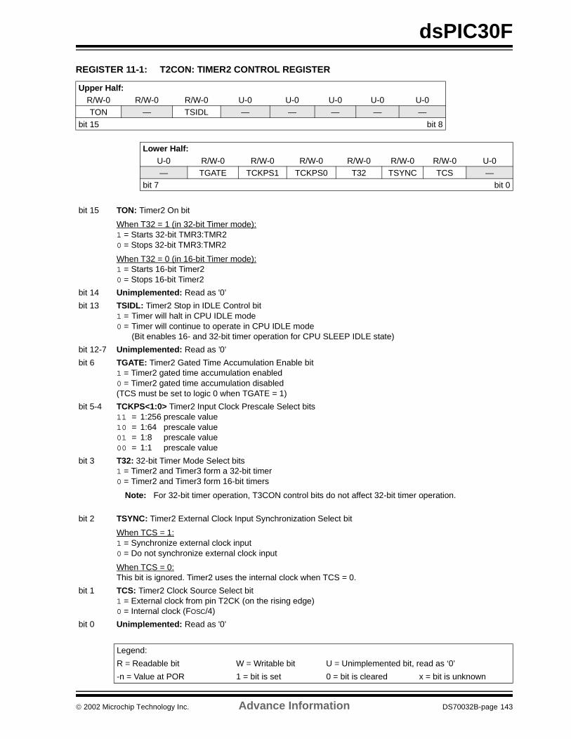
dsPIC30F
REGISTER 11-1: T2CON: TIMER2 CONTROL REGISTER
Upper Half:R/W-0 R/W-0 R/W-0 U-0 U-0 U-0 U-0 U-0TON — TSIDL — — — — —
bit 15 bit 8
Lower Half:U-0 R/W-0 R/W-0 R/W-0 R/W-0 R/W-0 R/W-0 U-0— TGATE TCKPS1 TCKPS0 T32 TSYNC TCS —
bit 7 bit 0
bit 15 TON: Timer2 On bit
When T32 = 1 (in 32-bit Timer mode):1 = Starts 32-bit TMR3:TMR20 = Stops 32-bit TMR3:TMR2
When T32 = 0 (in 16-bit Timer mode):1 = Starts 16-bit Timer20 = Stops 16-bit Timer2
bit 14 Unimplemented: Read as '0’
bit 13 TSIDL: Timer2 Stop in IDLE Control bit 1 = Timer will halt in CPU IDLE mode0 = Timer will continue to operate in CPU IDLE mode
(Bit enables 16- and 32-bit timer operation for CPU SLEEP IDLE state)
bit 12-7 Unimplemented: Read as ’0’
bit 6 TGATE: Timer2 Gated Time Accumulation Enable bit1 = Timer2 gated time accumulation enabled0 = Timer2 gated time accumulation disabled(TCS must be set to logic 0 when TGATE = 1)
bit 5-4 TCKPS<1:0> Timer2 Input Clock Prescale Select bits11 = 1:256 prescale value10 = 1:64 prescale value01 = 1:8 prescale value00 = 1:1 prescale value
bit 3 T32: 32-bit Timer Mode Select bits1 = Timer2 and Timer3 form a 32-bit timer0 = Timer2 and Timer3 form 16-bit timers
Note: For 32-bit timer operation, T3CON control bits do not affect 32-bit timer operation.
bit 2 TSYNC: Timer2 External Clock Input Synchronization Select bit
When TCS = 1: 1 = Synchronize external clock input0 = Do not synchronize external clock input
When TCS = 0: This bit is ignored. Timer2 uses the internal clock when TCS = 0.
bit 1 TCS: Timer2 Clock Source Select bit1 = External clock from pin T2CK (on the rising edge) 0 = Internal clock (FOSC/4)
bit 0 Unimplemented: Read as '0’
Legend:
R = Readable bit W = Writable bit U = Unimplemented bit, read as ‘0’
-n = Value at POR 1 = bit is set 0 = bit is cleared x = bit is unknown
2002 Microchip Technology Inc. Advance Information DS70032B-page 143
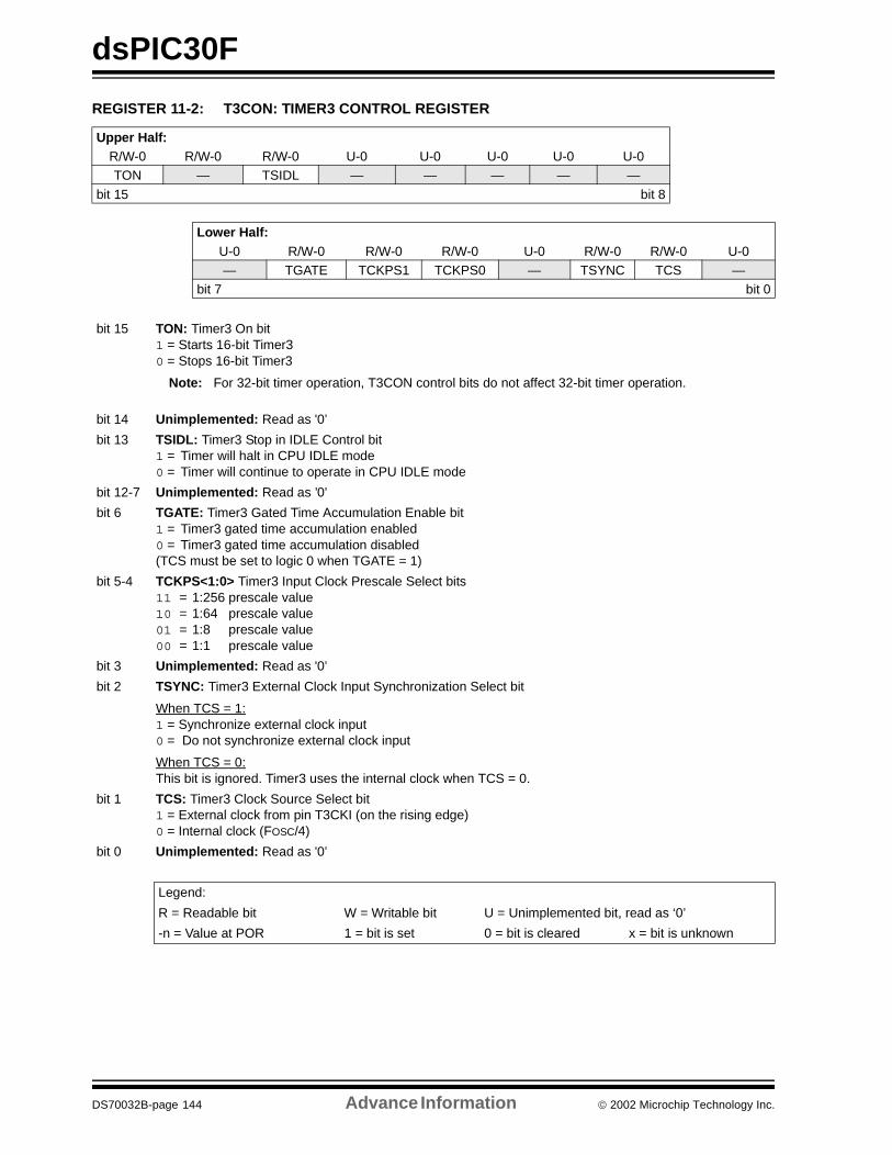
dsPIC30F
REGISTER 11-2: T3CON: TIMER3 CONTROL REGISTER
Upper Half:R/W-0 R/W-0 R/W-0 U-0 U-0 U-0 U-0 U-0TON — TSIDL — — — — —
bit 15 bit 8
Lower Half:U-0 R/W-0 R/W-0 R/W-0 U-0 R/W-0 R/W-0 U-0— TGATE TCKPS1 TCKPS0 — TSYNC TCS —
bit 7 bit 0
bit 15 TON: Timer3 On bit1 = Starts 16-bit Timer30 = Stops 16-bit Timer3
Note: For 32-bit timer operation, T3CON control bits do not affect 32-bit timer operation.
bit 14 Unimplemented: Read as '0’
bit 13 TSIDL: Timer3 Stop in IDLE Control bit 1 = Timer will halt in CPU IDLE mode0 = Timer will continue to operate in CPU IDLE mode
bit 12-7 Unimplemented: Read as ’0’
bit 6 TGATE: Timer3 Gated Time Accumulation Enable bit1 = Timer3 gated time accumulation enabled0 = Timer3 gated time accumulation disabled(TCS must be set to logic 0 when TGATE = 1)
bit 5-4 TCKPS<1:0> Timer3 Input Clock Prescale Select bits11 = 1:256 prescale value10 = 1:64 prescale value01 = 1:8 prescale value00 = 1:1 prescale value
bit 3 Unimplemented: Read as '0’
bit 2 TSYNC: Timer3 External Clock Input Synchronization Select bit
When TCS = 1: 1 = Synchronize external clock input0 = Do not synchronize external clock input
When TCS = 0: This bit is ignored. Timer3 uses the internal clock when TCS = 0.
bit 1 TCS: Timer3 Clock Source Select bit1 = External clock from pin T3CKI (on the rising edge) 0 = Internal clock (FOSC/4)
bit 0 Unimplemented: Read as '0’
Legend:
R = Readable bit W = Writable bit U = Unimplemented bit, read as ‘0’
-n = Value at POR 1 = bit is set 0 = bit is cleared x = bit is unknown
DS70032B-page 144 Advance Information 2002 Microchip Technology Inc.
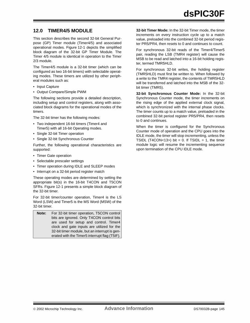
dsPIC30F
12.0 TIMER4/5 MODULE
This section describes the second 32-bit General Pur-pose (GP) Timer module (Timer4/5) and associatedoperational modes. Figure 12-1 depicts the simplifiedblock diagram of the 32-bit GP Timer Module. TheTimer 4/5 module is identical in operation to the Timer2/3 module.
The Timer4/5 module is a 32-bit timer (which can beconfigured as two 16-bit timers) with selectable operat-ing modes. These timers are utilized by other periph-eral modules such as:
• Input Capture• Output Compare/Simple PWM
The following sections provide a detailed description,including setup and control registers, along with asso-ciated block diagrams for the operational modes of thetimers.
The 32-bit timer has the following modes:
• Two independent 16-bit timers (Timer4 and Timer5) with all 16-bit Operating modes.
• Single 32-bit Timer operation
• Single 32-bit Synchronous Counter
Further, the following operational characteristics aresupported:
• Timer Gate operation
• Selectable prescaler settings• Timer operation during IDLE and SLEEP modes• Interrupt on a 32-bit period register match
These operating modes are determined by setting theappropriate bit(s) in the 16-bit T4CON and T5CONSFRs. Figure 12-1 presents a simple block diagram ofthe 32-bit timer.
For 32-bit timer/counter operation, Timer4 is the LSWord (LSW) and Timer5 is the MS Word (MSW) of the32-bit timer.
32-bit Timer Mode: In the 32-bit Timer mode, the timerincrements on every instruction cycle up to a matchvalue, preloaded into the combined 32-bit period regis-ter PR5/PR4, then resets to 0 and continues to count.
For synchronous 32-bit reads of the Timer4/Timer5pair, reading the LSB (TMR4 register) will cause theMSB to be read and latched into a 16-bit holding regis-ter, termed TMR5HLD.
For synchronous 32-bit writes, the holding register(TMR5HLD) must first be written to. When followed bya write to the TMR4 register, the contents of TMR5HLDwill be transferred and latched into the MSB of the 32-bit timer (TMR5).
32-bit Synchronous Counter Mode: In the 32-bitSynchronous Counter mode, the timer increments onthe rising edge of the applied external clock signal,which is synchronized with the internal phase clocks.The timer counts up to a match value, preloaded in thecombined 32-bit period register PR5/PR4, then resetsto 0 and continues.
When the timer is configured for the SynchronousCounter mode of operation and the CPU goes into theIDLE mode, the timer will stop incrementing, unless theTSIDL (T4CON<13>) bit = 0. If TSIDL = 1, the timermodule logic will resume the incrementing sequenceupon termination of the CPU IDLE mode.
Note: For 32-bit timer operation, T5CON controlbits are ignored. Only T4CON control bitsare used for setup and control. Timer4clock and gate inputs are utilized for the32-bit timer module, but an interrupt is gen-erated with the Timer5 interrupt flag (T5IF).
2002 Microchip Technology Inc. Advance Information DS70032B-page 145
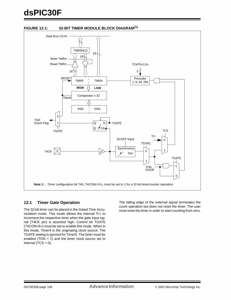
dsPIC30F
FIGURE 12-1: 32-BIT TIMER MODULE BLOCK DIAGRAM(1)
12.1 Timer Gate Operation
The 32-bit timer can be placed in the Gated Time Accu-mulation mode. This mode allows the internal TCY toincrement the respective timer when the gate input sig-nal (T4CK pin) is asserted high. Control bit TGATE(T4CON<6>) must be set to enable this mode. When inthis mode, Timer4 is the originating clock source. TheTGATE setting is ignored for Timer5. The timer must beenabled (TON = 1) and the timer clock source set tointernal (TCS = 0).
The falling edge of the external signal terminates thecount operation but does not reset the timer. The usermust reset the timer in order to start counting from zero.
TMR5 TMR4
T5IF
EqualComparator x 32
PR5 PR4
RESET
LSW MSW
Event Flag
Note 1: Timer configuration bit T45, T4CON(<3>), must be set to 1 for a 32-bit timer/counter operation.
Data Bus<15:0>
TMR5HLD
Read TMR4
Write TMR416
16
16
Q
Q D
CK
TGATE
TCKPS<1:0>
Prescaler 1, 8, 64, 256
2
TSYNC
TCS
SLEEP InputTCY
On/Off
Synchronize
Det
0
10
1
T4CK
1
0
TGATE
TGATE
1
0
TON
DS70032B-page 146 Advance Information 2002 Microchip Technology Inc.
dsPIC30F
12.2 Timer Prescaler
The input clock (FOSC/4 or external clock) to the timerhas a prescale option of 1:1, 1:8, 1:64, and 1:256,selected by control bits TCKPS<1:0> (T4CON<5:4>and T5CON<5:4>). For the 32-bit timer operation, theoriginating clock source is Timer4. The prescaler oper-ation for Timer5 is not applicable in this mode. Theprescaler counter is cleared when any of the followingoccurs:
• a write to the TMR4/TMR5 register• a write to the T4CON/T5CON register
• device RESET such as POR and BOR
However, if the timer is disabled (TON = 0), then theTimer 4 prescaler cannot be reset, since the prescalerclock is halted.
TMR4/TMR5 is not cleared when T4CON/T5CON iswritten.
12.3 Timer Operation During SLEEP Mode
During CPU SLEEP mode, the timer will operate if:
• The timer module is enabled (TON = 1) and • The timer clock source is selected as external
(TCS = 0) and• The TSYNC bit is asserted to a logic 0, which
defines the external clock source as asynchro-nous.
When all three conditions are true, the timer will con-tinue to count up to the period register and be reset to0x00000000.
When a match between the timer and the period regis-ter occurs, an interrupt can be generated if the respec-tive timer interrupt enable bit is asserted.
12.4 Timer Interrupt
The 32-bit timer module can generate an interrupt onperiod match or on the falling edge of the external gatesignal. When the 32-bit timer count matches therespective 32-bit period register, or the falling edge ofthe external “gate” signal is detected, the T5IF bit isasserted and an interrupt will be generated, if enabled.In this mode, the T5IF interrupt flag is used as thesource of the interrupt. The T5IF bit must be cleared insoftware. The timer interrupt flag, T5IF, is located in thecorresponding IFS1 Status register in the InterruptController.
Enabling an interrupt is accomplished via the respec-tive timer interrupt enable bit, T5IE. The timer interruptenable bit, is located in the corresponding IEC1 Controlregister.
2002 Microchip Technology Inc. Advance Information DS70032B-page 147
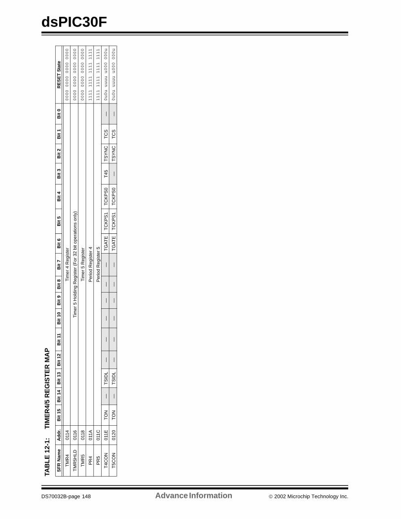
dsPIC30F
TAB
LE
12-
1:TI
ME
R4/
5 R
EG
IST
ER
MA
P
SF
R N
ame
Ad
dr.
Bit
15
Bit
14
Bit
13
Bit
12
Bit
11
Bit
10
Bit
9B
it 8
Bit
7B
it 6
Bit
5B
it 4
Bit
3B
it 2
Bit
1B
it 0
RE
SE
T S
tate
TM
R4
0114
Tim
er 4
Reg
iste
r0000 0000 0000 0000
TM
R5H
LD01
16Ti
mer
5 H
oldi
ng R
egis
ter
(For
32
bit o
pera
tions
onl
y)0000 0000 0000 0000
TM
R5
0118
Tim
er 5
Reg
iste
r0000 0000 0000 0000
PR
401
1AP
erio
d R
egis
ter
41111 1111 1111 1111
PR
501
1CP
erio
d R
egis
ter
51111 1111 1111 1111
T4C
ON
011E
TO
N—
TS
IDL
——
——
——
TG
AT
ET
CK
PS
1T
CK
PS
0T
45T
SY
NC
TC
S—
0u0u uuuu u000 000u
T5C
ON
0120
TO
N—
TS
IDL
——
——
——
TG
AT
ET
CK
PS
1T
CK
PS
0—
TS
YN
CT
CS
—0u0u uuuu u000 000u
DS70032B-page 148 Advance Information 2002 Microchip Technology Inc.
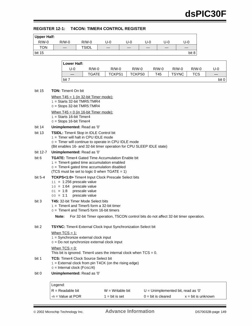
dsPIC30F
REGISTER 12-1: T4CON: TIMER4 CONTROL REGISTERUpper Half:R/W-0 R/W-0 R/W-0 U-0 U-0 U-0 U-0 U-0
TON — TSIDL — — — — —bit 15 bit 8
Lower Half:U-0 R/W-0 R/W-0 R/W-0 R/W-0 R/W-0 R/W-0 U-0— TGATE TCKPS1 TCKPS0 T45 TSYNC TCS —
bit 7 bit 0
bit 15 TON: Timer4 On bit
When T45 = 1 (in 32-bit Timer mode):1 = Starts 32-bit TMR5:TMR40 = Stops 32-bit TMR5:TMR4
When T45 = 0 (in 16-bit Timer mode):1 = Starts 16-bit Timer40 = Stops 16-bit Timer4
bit 14 Unimplemented: Read as '0’
bit 13 TSIDL: Timer4 Stop in IDLE Control bit 1 = Timer will halt in CPU IDLE mode0 = Timer will continue to operate in CPU IDLE mode(Bit enables 16- and 32-bit timer operation for CPU SLEEP IDLE state)
bit 12-7 Unimplemented: Read as ’0’
bit 6 TGATE: Timer4 Gated Time Accumulation Enable bit1 = Timer4 gated time accumulation enabled0 = Timer4 gated time accumulation disabled(TCS must be set to logic 0 when TGATE = 1)
bit 5-4 TCKPS<1:0> Timer4 Input Clock Prescale Select bits11 = 1:256 prescale value10 = 1:64 prescale value01 = 1:8 prescale value00 = 1:1 prescale value
bit 3 T45: 32-bit Timer Mode Select bits1 = Timer4 and Timer5 form a 32-bit timer0 = Timer4 and Timer5 form 16-bit timers
Note: For 32-bit Timer operation, T5CON control bits do not affect 32-bit timer operation.
bit 2 TSYNC: Timer4 External Clock Input Synchronization Select bit
When TCS = 1: 1 = Synchronize external clock input0 = Do not synchronize external clock input
When TCS = 0: This bit is ignored. Timer4 uses the internal clock when TCS = 0.
bit 1 TCS: Timer4 Clock Source Select bit1 = External clock from pin T4CK (on the rising edge) 0 = Internal clock (FOSC/4)
bit 0 Unimplemented: Read as '0’
Legend:
R = Readable bit W = Writable bit U = Unimplemented bit, read as ‘0’
-n = Value at POR 1 = bit is set 0 = bit is cleared x = bit is unknown
2002 Microchip Technology Inc. Advance Information DS70032B-page 149
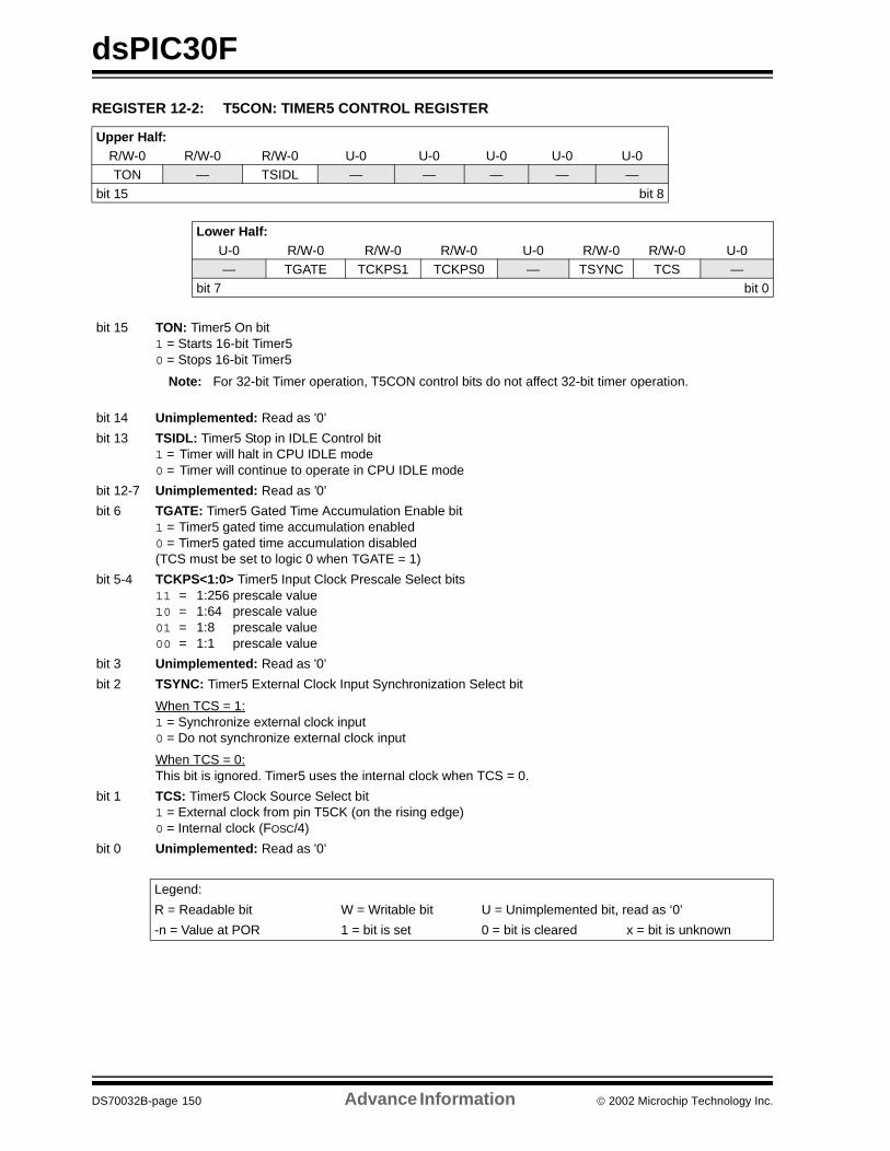
dsPIC30F
REGISTER 12-2: T5CON: TIMER5 CONTROL REGISTER
Upper Half:R/W-0 R/W-0 R/W-0 U-0 U-0 U-0 U-0 U-0TON — TSIDL — — — — —
bit 15 bit 8
Lower Half:U-0 R/W-0 R/W-0 R/W-0 U-0 R/W-0 R/W-0 U-0— TGATE TCKPS1 TCKPS0 — TSYNC TCS —
bit 7 bit 0
bit 15 TON: Timer5 On bit1 = Starts 16-bit Timer50 = Stops 16-bit Timer5
Note: For 32-bit Timer operation, T5CON control bits do not affect 32-bit timer operation.
bit 14 Unimplemented: Read as '0’
bit 13 TSIDL: Timer5 Stop in IDLE Control bit 1 = Timer will halt in CPU IDLE mode0 = Timer will continue to operate in CPU IDLE mode
bit 12-7 Unimplemented: Read as ’0’
bit 6 TGATE: Timer5 Gated Time Accumulation Enable bit1 = Timer5 gated time accumulation enabled0 = Timer5 gated time accumulation disabled(TCS must be set to logic 0 when TGATE = 1)
bit 5-4 TCKPS<1:0> Timer5 Input Clock Prescale Select bits11 = 1:256 prescale value10 = 1:64 prescale value01 = 1:8 prescale value00 = 1:1 prescale value
bit 3 Unimplemented: Read as '0’
bit 2 TSYNC: Timer5 External Clock Input Synchronization Select bit
When TCS = 1: 1 = Synchronize external clock input0 = Do not synchronize external clock input
When TCS = 0: This bit is ignored. Timer5 uses the internal clock when TCS = 0.
bit 1 TCS: Timer5 Clock Source Select bit1 = External clock from pin T5CK (on the rising edge) 0 = Internal clock (FOSC/4)
bit 0 Unimplemented: Read as '0’
Legend:
R = Readable bit W = Writable bit U = Unimplemented bit, read as ‘0’
-n = Value at POR 1 = bit is set 0 = bit is cleared x = bit is unknown
DS70032B-page 150 Advance Information 2002 Microchip Technology Inc.
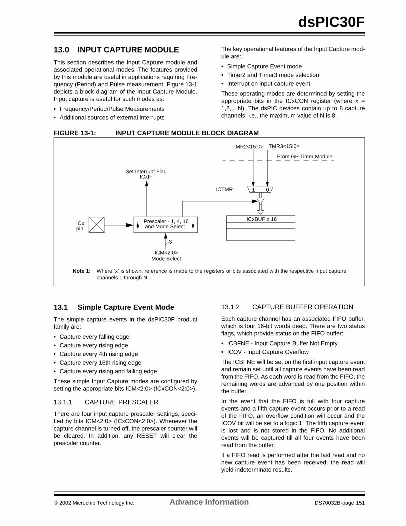
dsPIC30F
13.0 INPUT CAPTURE MODULE
This section describes the Input Capture module andassociated operational modes. The features providedby this module are useful in applications requiring Fre-quency (Period) and Pulse measurement. Figure 13-1depicts a block diagram of the Input Capture Module.Input capture is useful for such modes as:
• Frequency/Period/Pulse Measurements• Additional sources of external interrupts
The key operational features of the Input Capture mod-ule are:
• Simple Capture Event mode• Timer2 and Timer3 mode selection• Interrupt on input capture event
These operating modes are determined by setting theappropriate bits in the ICxCON register (where x =1,2,...,N). The dsPIC devices contain up to 8 capturechannels, i.e., the maximum value of N is 8.
FIGURE 13-1: INPUT CAPTURE MODULE BLOCK DIAGRAM
13.1 Simple Capture Event Mode
The simple capture events in the dsPIC30F productfamily are:
• Capture every falling edge• Capture every rising edge• Capture every 4th rising edge
• Capture every 16th rising edge• Capture every rising and falling edge
These simple Input Capture modes are configured bysetting the appropriate bits ICM<2:0> (ICxCON<2:0>).
13.1.1 CAPTURE PRESCALER
There are four input capture prescaler settings, speci-fied by bits ICM<2:0> (ICxCON<2:0>). Whenever thecapture channel is turned off, the prescaler counter willbe cleared. In addition, any RESET will clear theprescaler counter.
13.1.2 CAPTURE BUFFER OPERATION
Each capture channel has an associated FIFO buffer,which is four 16-bit words deep. There are two statusflags, which provide status on the FIFO buffer:
• ICBFNE - Input Capture Buffer Not Empty• ICOV - Input Capture Overflow
The ICBFNE will be set on the first input capture eventand remain set until all capture events have been readfrom the FIFO. As each word is read from the FIFO, theremaining words are advanced by one position withinthe buffer.
In the event that the FIFO is full with four captureevents and a fifth capture event occurs prior to a readof the FIFO, an overflow condition will occur and theICOV bit will be set to a logic 1. The fifth capture eventis lost and is not stored in the FIFO. No additionalevents will be captured till all four events have beenread from the buffer.
If a FIFO read is performed after the last read and nonew capture event has been received, the read willyield indeterminate results.
ICxBUF x 16 Prescaler - 1, 4, 16ICx
ICM<2:0>Mode Select
3
Note 1: Where ‘x’ is shown, reference is made to the registers or bits associated with the respective input capturechannels 1 through N.
1 0
Set Interrupt Flag
and Mode Selectpin
ICxIF
ICTMR
TMR2<15:0> TMR3<15:0>
From GP Timer Module
2002 Microchip Technology Inc. Advance Information DS70032B-page 151
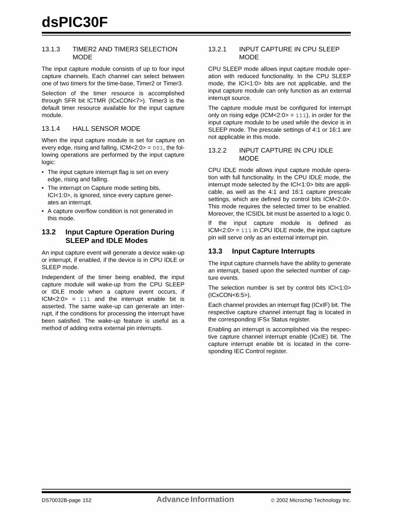
dsPIC30F
13.1.3 TIMER2 AND TIMER3 SELECTION MODE
The input capture module consists of up to four inputcapture channels. Each channel can select betweenone of two timers for the time-base, Timer2 or Timer3.
Selection of the timer resource is accomplishedthrough SFR bit ICTMR (ICxCON<7>). Timer3 is thedefault timer resource available for the input capturemodule.
13.1.4 HALL SENSOR MODE
When the input capture module is set for capture onevery edge, rising and falling, ICM<2:0> = 001, the fol-lowing operations are performed by the input capturelogic:
• The input capture interrupt flag is set on every edge, rising and falling.
• The interrupt on Capture mode setting bits, ICI<1:0>, is ignored, since every capture gener-ates an interrupt.
• A capture overflow condition is not generated in this mode.
13.2 Input Capture Operation During SLEEP and IDLE Modes
An input capture event will generate a device wake-upor interrupt, if enabled, if the device is in CPU IDLE orSLEEP mode.
Independent of the timer being enabled, the inputcapture module will wake-up from the CPU SLEEPor IDLE mode when a capture event occurs, ifICM<2:0> = 111 and the interrupt enable bit isasserted. The same wake-up can generate an inter-rupt, if the conditions for processing the interrupt havebeen satisfied. The wake-up feature is useful as amethod of adding extra external pin interrupts.
13.2.1 INPUT CAPTURE IN CPU SLEEP MODE
CPU SLEEP mode allows input capture module oper-ation with reduced functionality. In the CPU SLEEPmode, the ICI<1:0> bits are not applicable, and theinput capture module can only function as an externalinterrupt source.
The capture module must be configured for interruptonly on rising edge (ICM<2:0> = 111), in order for theinput capture module to be used while the device is inSLEEP mode. The prescale settings of 4:1 or 16:1 arenot applicable in this mode.
13.2.2 INPUT CAPTURE IN CPU IDLE MODE
CPU IDLE mode allows input capture module opera-tion with full functionality. In the CPU IDLE mode, theinterrupt mode selected by the ICI<1:0> bits are appli-cable, as well as the 4:1 and 16:1 capture prescalesettings, which are defined by control bits ICM<2:0>.This mode requires the selected timer to be enabled.Moreover, the ICSIDL bit must be asserted to a logic 0.
If the input capture module is defined asICM<2:0> = 111 in CPU IDLE mode, the input capturepin will serve only as an external interrupt pin.
13.3 Input Capture Interrupts
The input capture channels have the ability to generatean interrupt, based upon the selected number of cap-ture events.
The selection number is set by control bits ICI<1:0>(ICxCON<6:5>).
Each channel provides an interrupt flag (ICxIF) bit. Therespective capture channel interrupt flag is located inthe corresponding IFSx Status register.
Enabling an interrupt is accomplished via the respec-tive capture channel interrupt enable (ICxIE) bit. Thecapture interrupt enable bit is located in the corre-sponding IEC Control register.
DS70032B-page 152 Advance Information 2002 Microchip Technology Inc.
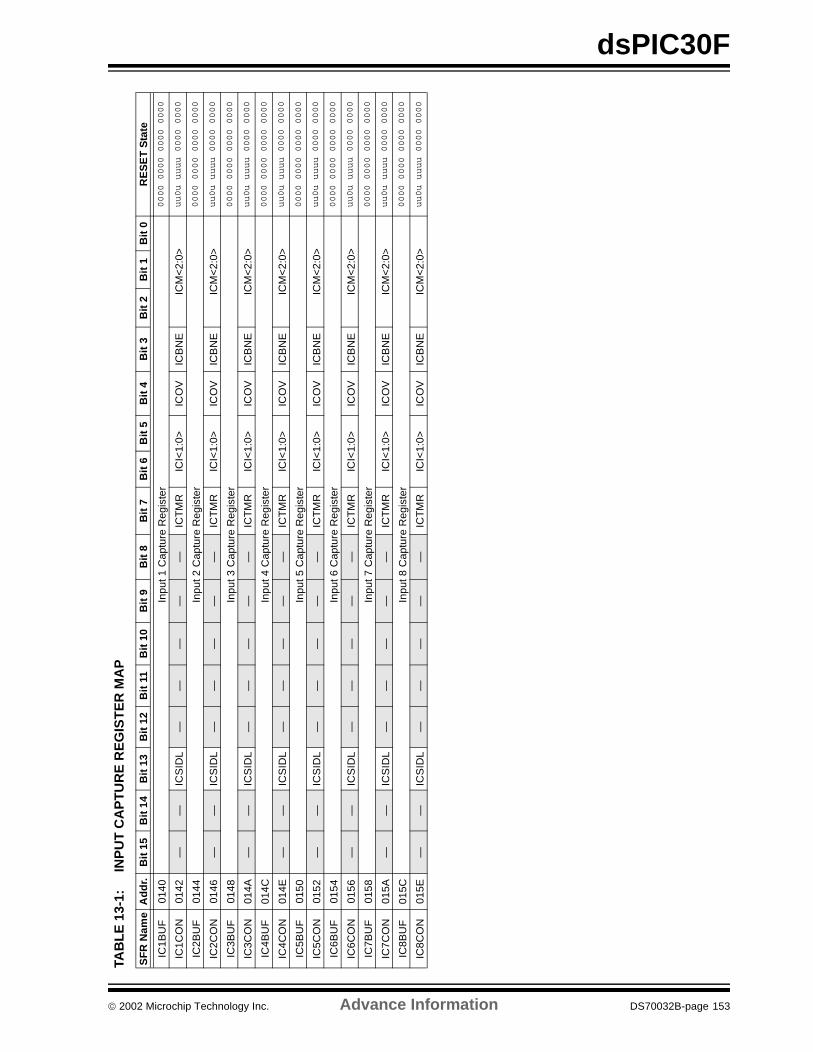
dsPIC30F
TAB
LE
13-
1:IN
PU
T C
AP
TU
RE
RE
GIS
TE
R M
AP
SF
R N
ame
Ad
dr.
Bit
15
Bit
14
Bit
13
Bit
12
Bit
11
Bit
10
Bit
9B
it 8
Bit
7B
it 6
Bit
5B
it 4
Bit
3B
it 2
Bit
1B
it 0
RE
SE
T S
tate
IC1B
UF
0140
Inpu
t 1 C
aptu
re R
egis
ter
0000 0000 0000 0000
IC1C
ON
0142
——
ICS
IDL
——
——
—IC
TM
RIC
I<1:
0>IC
OV
ICB
NE
ICM
<2:
0>uu0u uuuu 0000 0000
IC2B
UF
0144
Inpu
t 2 C
aptu
re R
egis
ter
0000 0000 0000 0000
IC2C
ON
0146
——
ICS
IDL
——
——
—IC
TM
RIC
I<1:
0>IC
OV
ICB
NE
ICM
<2:
0>uu0u uuuu 0000 0000
IC3B
UF
0148
Inpu
t 3 C
aptu
re R
egis
ter
0000 0000 0000 0000
IC3C
ON
014A
——
ICS
IDL
——
——
—IC
TM
RIC
I<1:
0>IC
OV
ICB
NE
ICM
<2:
0>uu0u uuuu 0000 0000
IC4B
UF
014C
Inpu
t 4 C
aptu
re R
egis
ter
0000 0000 0000 0000
IC4C
ON
014E
——
ICS
IDL
——
——
—IC
TM
RIC
I<1:
0>IC
OV
ICB
NE
ICM
<2:
0>uu0u uuuu 0000 0000
IC5B
UF
0150
Inpu
t 5 C
aptu
re R
egis
ter
0000 0000 0000 0000
IC5C
ON
0152
——
ICS
IDL
——
——
—IC
TM
RIC
I<1:
0>IC
OV
ICB
NE
ICM
<2:
0>uu0u uuuu 0000 0000
IC6B
UF
0154
Inpu
t 6 C
aptu
re R
egis
ter
0000 0000 0000 0000
IC6C
ON
0156
——
ICS
IDL
——
——
—IC
TM
RIC
I<1:
0>IC
OV
ICB
NE
ICM
<2:
0>uu0u uuuu 0000 0000
IC7B
UF
0158
Inpu
t 7 C
aptu
re R
egis
ter
0000 0000 0000 0000
IC7C
ON
015A
——
ICS
IDL
——
——
—IC
TM
RIC
I<1:
0>IC
OV
ICB
NE
ICM
<2:
0>uu0u uuuu 0000 0000
IC8B
UF
015C
Inpu
t 8 C
aptu
re R
egis
ter
0000 0000 0000 0000
IC8C
ON
015E
——
ICS
IDL
——
——
—IC
TM
RIC
I<1:
0>IC
OV
ICB
NE
ICM
<2:
0>uu0u uuuu 0000 0000
2002 Microchip Technology Inc. Advance Information DS70032B-page 153
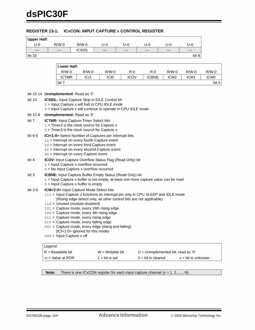
dsPIC30F
REGISTER 13-1: ICXCON: INPUT CAPTURE X CONTROL REGISTER
Upper Half:U-0 R/W-0 R/W-0 U-0 U-0 U-0 U-0 U-0— — ICSIDL — — — — —
bit 15 bit 8
Lower Half:R/W-0 R/W-0 R/W-0 R-0 R-0 R/W-0 R/W-0 R/W-0ICTMR ICI1 ICI0 ICOV ICBNE ICM2 ICM1 ICM0
bit 7 bit 0
bit 15-14 Unimplemented: Read as '0’
bit 13 ICSIDL: Input Capture Stop in IDLE Control bit 1 = Input Capture x will halt in CPU IDLE mode0 = Input Capture x will continue to operate in CPU IDLE mode
bit 12-8 Unimplemented: Read as '0’
bit 7 ICTMR: Input Capture Timer Select bits1 = Timer2 is the clock source for Capture x0 = Timer3 is the clock source for Capture x
bit 6-5 ICI<1:0> Select Number of Captures per Interrupt bits11 = Interrupt on every fourth Capture event10 = Interrupt on every third Capture event01 = Interrupt on every second Capture event00 = Interrupt on every Capture event
bit 4 ICOV: Input Capture Overflow Status Flag (Read Only) bit1 = Input Capture x overflow occurred0 = No Input Capture x overflow occurred
bit 3 ICBNE: Input Capture Buffer Empty Status (Read Only) bit1 = Input Capture x buffer is not empty, at least one more capture value can be read0 = Input Capture x buffer is empty
bit 2-0 ICM<2:0> Input Capture Mode Select bits111 = Input Capture x functions as interrupt pin only in CPU SLEEP and IDLE mode
(Rising edge detect only, all other control bits are not applicable)110 = Unused (module disabled)101 = Capture mode, every 16th rising edge100 = Capture mode, every 4th rising edge011 = Capture mode, every rising edge010 = Capture mode, every falling edge001 = Capture mode, every edge (rising and falling)
(ICI<1:0> ignored for this mode)000 = Input Capture x off
Legend:
R = Readable bit W = Writable bit U = Unimplemented bit, read as ‘0’
-n = Value at POR 1 = bit is set 0 = bit is cleared x = bit is unknown
Note: There is one ICxCON register for each input capture channel (x = 1, 2, ...., N).
DS70032B-page 154 Advance Information 2002 Microchip Technology Inc.
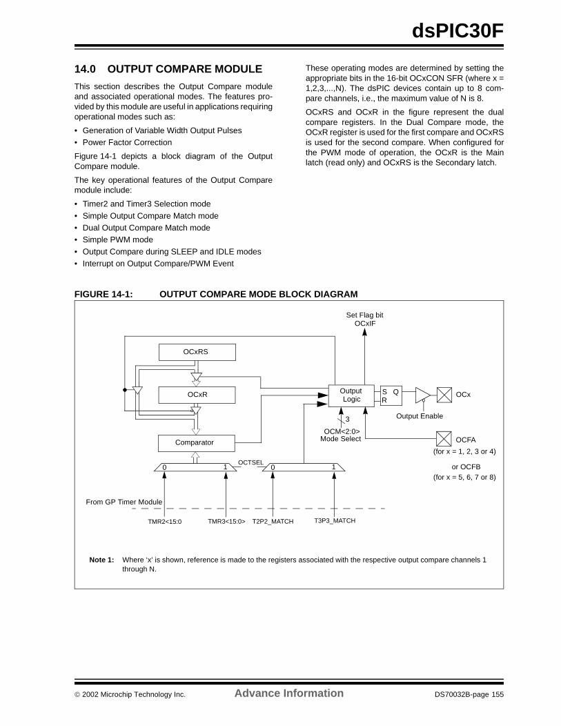
dsPIC30F
14.0 OUTPUT COMPARE MODULE
This section describes the Output Compare moduleand associated operational modes. The features pro-vided by this module are useful in applications requiringoperational modes such as:
• Generation of Variable Width Output Pulses• Power Factor Correction
Figure 14-1 depicts a block diagram of the OutputCompare module.
The key operational features of the Output Comparemodule include:
• Timer2 and Timer3 Selection mode
• Simple Output Compare Match mode• Dual Output Compare Match mode• Simple PWM mode
• Output Compare during SLEEP and IDLE modes• Interrupt on Output Compare/PWM Event
These operating modes are determined by setting theappropriate bits in the 16-bit OCxCON SFR (where x =1,2,3,...,N). The dsPIC devices contain up to 8 com-pare channels, i.e., the maximum value of N is 8.
OCxRS and OCxR in the figure represent the dualcompare registers. In the Dual Compare mode, theOCxR register is used for the first compare and OCxRSis used for the second compare. When configured forthe PWM mode of operation, the OCxR is the Mainlatch (read only) and OCxRS is the Secondary latch.
FIGURE 14-1: OUTPUT COMPARE MODE BLOCK DIAGRAM
OCxR
Comparator
OutputLogic
QSR
OCM<2:0>
Output Enable
OCx
Set Flag bitOCxIF
OCxRS
Mode Select
3
Note 1: Where ‘x’ is shown, reference is made to the registers associated with the respective output compare channels 1through N.
OCFA
OCTSEL0 1
T2P2_MATCHTMR2<15:0 TMR3<15:0> T3P3_MATCH
From GP Timer Module
(for x = 1, 2, 3 or 4)
or OCFB(for x = 5, 6, 7 or 8)
0 1
2002 Microchip Technology Inc. Advance Information DS70032B-page 155
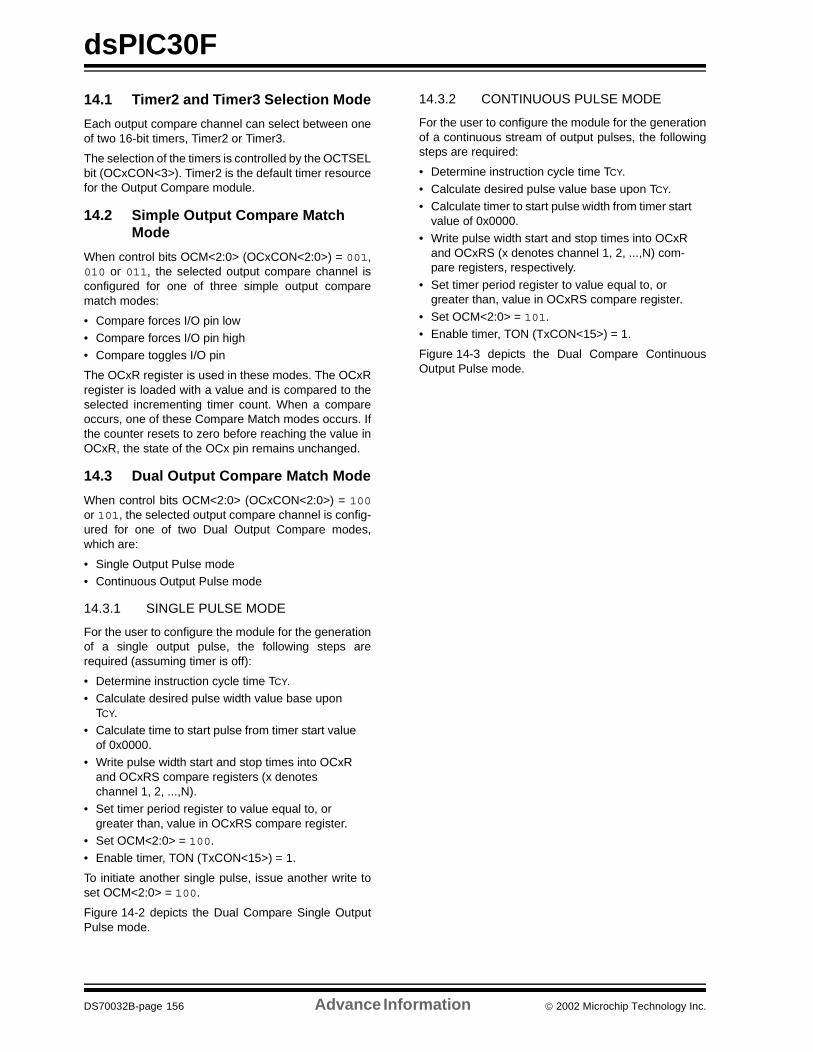
dsPIC30F
14.1 Timer2 and Timer3 Selection Mode
Each output compare channel can select between oneof two 16-bit timers, Timer2 or Timer3.
The selection of the timers is controlled by the OCTSELbit (OCxCON<3>). Timer2 is the default timer resourcefor the Output Compare module.
14.2 Simple Output Compare Match Mode
When control bits OCM<2:0> (OCxCON<2:0>) = 001,010 or 011, the selected output compare channel isconfigured for one of three simple output comparematch modes:
• Compare forces I/O pin low• Compare forces I/O pin high• Compare toggles I/O pin
The OCxR register is used in these modes. The OCxRregister is loaded with a value and is compared to theselected incrementing timer count. When a compareoccurs, one of these Compare Match modes occurs. Ifthe counter resets to zero before reaching the value inOCxR, the state of the OCx pin remains unchanged.
14.3 Dual Output Compare Match Mode
When control bits OCM<2:0> (OCxCON<2:0>) = 100or 101, the selected output compare channel is config-ured for one of two Dual Output Compare modes,which are:
• Single Output Pulse mode• Continuous Output Pulse mode
14.3.1 SINGLE PULSE MODE
For the user to configure the module for the generationof a single output pulse, the following steps arerequired (assuming timer is off):
• Determine instruction cycle time TCY.• Calculate desired pulse width value base upon
TCY.• Calculate time to start pulse from timer start value
of 0x0000.• Write pulse width start and stop times into OCxR
and OCxRS compare registers (x denotes channel 1, 2, ...,N).
• Set timer period register to value equal to, or greater than, value in OCxRS compare register.
• Set OCM<2:0> = 100.• Enable timer, TON (TxCON<15>) = 1.
To initiate another single pulse, issue another write toset OCM<2:0> = 100.
Figure 14-2 depicts the Dual Compare Single OutputPulse mode.
14.3.2 CONTINUOUS PULSE MODE
For the user to configure the module for the generationof a continuous stream of output pulses, the followingsteps are required:
• Determine instruction cycle time TCY.
• Calculate desired pulse value base upon TCY.• Calculate timer to start pulse width from timer start
value of 0x0000.• Write pulse width start and stop times into OCxR
and OCxRS (x denotes channel 1, 2, ...,N) com-pare registers, respectively.
• Set timer period register to value equal to, or greater than, value in OCxRS compare register.
• Set OCM<2:0> = 101.• Enable timer, TON (TxCON<15>) = 1.
Figure 14-3 depicts the Dual Compare ContinuousOutput Pulse mode.
DS70032B-page 156 Advance Information 2002 Microchip Technology Inc.
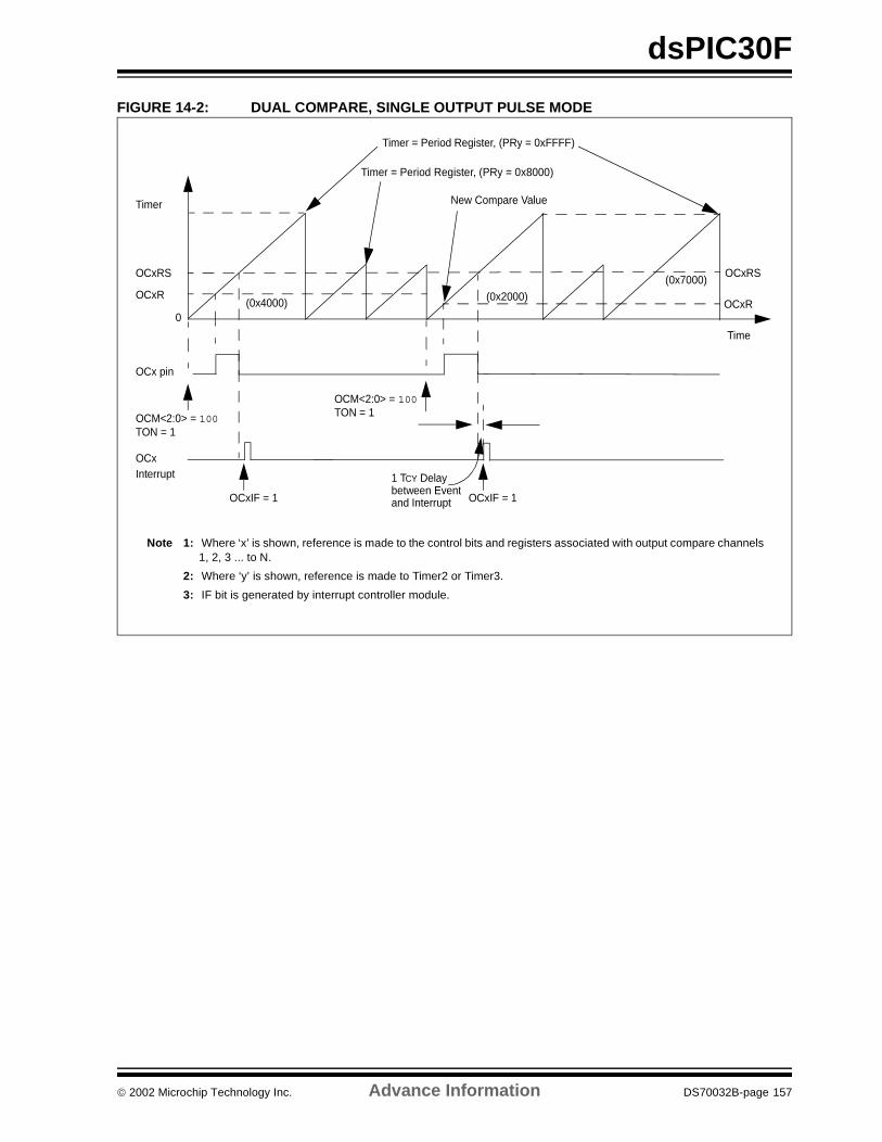
dsPIC30F
FIGURE 14-2: DUAL COMPARE, SINGLE OUTPUT PULSE MODE
0
OCxR
Time
Timer
OCxRS
Timer = Period Register, (PRy = 0xFFFF)
New Compare Value
OCxRS
OCxR
Timer = Period Register, (PRy = 0x8000)
(0x7000)
(0x2000)(0x4000)
OCM<2:0> = 100
Note 1: Where ‘x’ is shown, reference is made to the control bits and registers associated with output compare channels1, 2, 3 ... to N.
2: Where ‘y’ is shown, reference is made to Timer2 or Timer3.
3: IF bit is generated by interrupt controller module.
TON = 1
OCx pin
OCM<2:0> = 100TON = 1
OCxIF = 1 OCxIF = 1
OCx
1 TCY Delaybetween Eventand Interrupt
Interrupt
2002 Microchip Technology Inc. Advance Information DS70032B-page 157
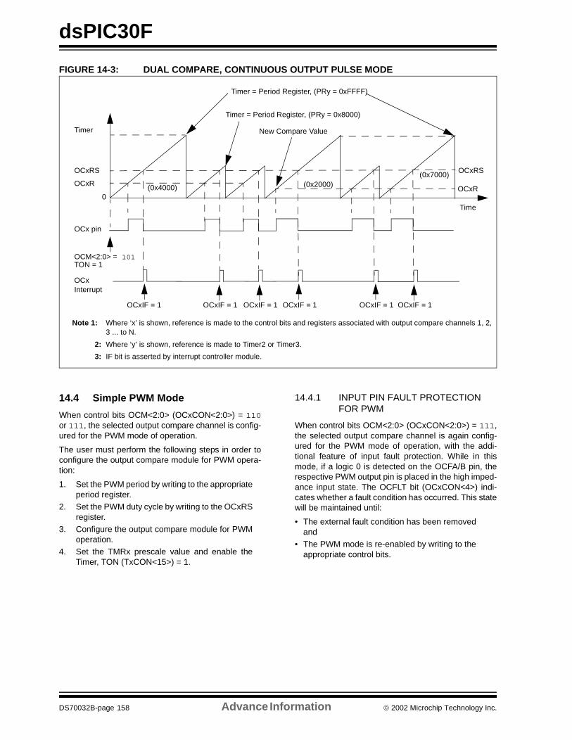
dsPIC30F
FIGURE 14-3: DUAL COMPARE, CONTINUOUS OUTPUT PULSE MODE
14.4 Simple PWM Mode
When control bits OCM<2:0> (OCxCON<2:0>) = 110or 111, the selected output compare channel is config-ured for the PWM mode of operation.
The user must perform the following steps in order toconfigure the output compare module for PWM opera-tion:
1. Set the PWM period by writing to the appropriateperiod register.
2. Set the PWM duty cycle by writing to the OCxRSregister.
3. Configure the output compare module for PWMoperation.
4. Set the TMRx prescale value and enable theTimer, TON (TxCON<15>) = 1.
14.4.1 INPUT PIN FAULT PROTECTION FOR PWM
When control bits OCM<2:0> (OCxCON<2:0>) = 111,the selected output compare channel is again config-ured for the PWM mode of operation, with the addi-tional feature of input fault protection. While in thismode, if a logic 0 is detected on the OCFA/B pin, therespective PWM output pin is placed in the high imped-ance input state. The OCFLT bit (OCxCON<4>) indi-cates whether a fault condition has occurred. This statewill be maintained until:
• The external fault condition has been removed and
• The PWM mode is re-enabled by writing to the appropriate control bits.
0
OCxR
Time
Timer
OCxRS
Timer = Period Register, (PRy = 0xFFFF)
New Compare Value
OCxRS
OCxR
Timer = Period Register, (PRy = 0x8000)
(0x7000)(0x2000)(0x4000)
OCM<2:0> = 101
Note 1: Where ‘x’ is shown, reference is made to the control bits and registers associated with output compare channels 1, 2,3 ... to N.
2: Where ‘y’ is shown, reference is made to Timer2 or Timer3.
3: IF bit is asserted by interrupt controller module.
TON = 1
OCx pin
OCxIF = 1
OCx
OCxIF = 1 OCxIF = 1 OCxIF = 1 OCxIF = 1 OCxIF = 1
Interrupt
DS70032B-page 158 Advance Information 2002 Microchip Technology Inc.
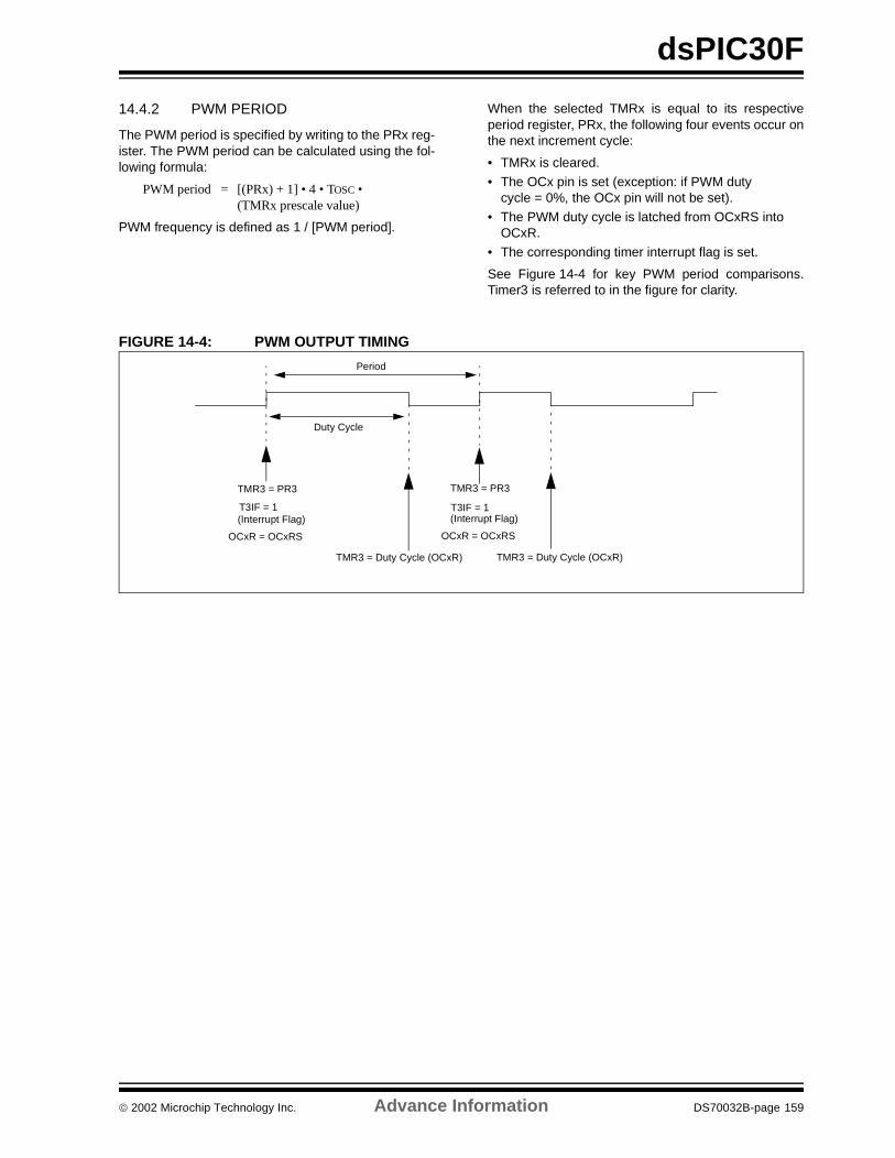
dsPIC30F
14.4.2 PWM PERIOD
The PWM period is specified by writing to the PRx reg-ister. The PWM period can be calculated using the fol-lowing formula:
PWM period = [(PRx) + 1] • 4 • TOSC •(TMRx prescale value)
PWM frequency is defined as 1 / [PWM period].
When the selected TMRx is equal to its respectiveperiod register, PRx, the following four events occur onthe next increment cycle:
• TMRx is cleared.
• The OCx pin is set (exception: if PWM duty cycle = 0%, the OCx pin will not be set).
• The PWM duty cycle is latched from OCxRS into OCxR.
• The corresponding timer interrupt flag is set.
See Figure 14-4 for key PWM period comparisons.Timer3 is referred to in the figure for clarity.
FIGURE 14-4: PWM OUTPUT TIMING
Period
Duty Cycle
TMR3 = Duty Cycle (OCxR) TMR3 = Duty Cycle (OCxR)
TMR3 = PR3
T3IF = 1(Interrupt Flag)
OCxR = OCxRS
TMR3 = PR3
(Interrupt Flag)
OCxR = OCxRS
T3IF = 1
2002 Microchip Technology Inc. Advance Information DS70032B-page 159
dsPIC30F
14.5 Output Compare Operation During CPU SLEEP Mode
When the CPU enters the SLEEP mode, limited func-tionality is provided for the output compare module.During SLEEP, all internal clocks are stopped. There-fore, the output compare module can operate if thetimer clock is configured for the External Asynchro-nous Clock mode. In addition, the module will gener-ate an interrupt signal when a match occurs betweenthe timer (TMRx) and period register (PRx).
If the output compare timer source is configured forinternal instruction cycle, or External SynchronizedClock mode when the CPU enters the SLEEP state,the output compare channel will drive the pin to theactive state that was observed prior to entering theCPU SLEEP state.
For example, if the pin was high when the CPUentered the SLEEP state, the pin will remain high.Likewise, if the pin was low when the CPU entered theSLEEP state, the pin will remain low. In either case,the output compare module will resume operationwhen the device wakes up.
14.6 Output Compare Operation During CPU IDLE Mode
When the CPU enters the IDLE mode, the output com-pare module operates with full functionality.
The output compare channel will operate during theCPU IDLE mode if the OCSIDL bit (OCxCON<13>) isat logic 0 and the selected time-base (Timer2 orTimer3) is enabled and the TSIDL bit of the selectedtimer is set to logic 0.
The selected time-base for the output compare can beconfigured for:
• Internal Instruction Cycle
• External Synchronous• External Asynchronous
14.7 Output Compare Interrupts
The output compare channels have the ability to gener-ate an interrupt on a compare match, for whicheverMatch mode has been selected.
For all modes except the PWM mode, when a compareevent occurs, the respective interrupt flag (OCxIF) bit isasserted and an interrupt will be generated, if enabled.The OCxIF bit is located in the corresponding IFSStatus register, and must be cleared in software. Theinterrupt is enabled via the respective compare inter-rupt enable (OCxIE) bit, located in the correspondingIEC Control register.
For the PWM mode, when an event occurs, the respec-tive timer interrupt flag (T2IF or T3IF) is asserted andan interrupt will be generated if enabled. The IF bit islocated in the IFS0 Status register, and must be clearedin software. The interrupt is enabled via the respectivetimer interrupt enable bit (T2IE or T3IE), located in theIEC0 Control register. The output compare interruptflag is never set during the PWM mode of operation.
DS70032B-page 160 Advance Information 2002 Microchip Technology Inc.
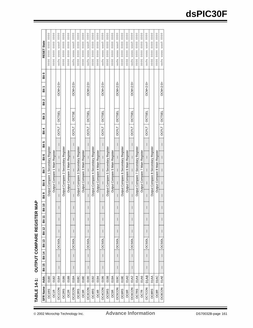
dsPIC30F
TAB
LE
14-
1:O
UT
PU
T C
OM
PA
RE
RE
GIS
TE
R M
AP
SF
R N
ame
Ad
dr.
Bit
15
Bit
14
Bit
13
Bit
12
Bit
11
Bit
10
Bit
9B
it 8
Bit
7B
it 6
Bit
5B
it 4
Bit
3B
it 2
Bit
1B
it 0
RE
SE
T S
tate
OC
1RS
0180
Out
put C
ompa
re 1
Sec
onda
ry R
egis
ter
0000 0000 0000 0000
OC
1R01
82O
utpu
t Com
pare
1 M
ain
Reg
iste
r0000 0000 0000 0000
OC
1CO
N01
84—
—O
CS
IDL
——
——
——
——
OC
FLT
OC
TS
EL
OC
M<
2:0>
uu0u uuuu uuu0 0000
OC
2RS
0186
Out
put C
ompa
re 2
Sec
onda
ry R
egis
ter
0000 0000 0000 0000
OC
2R01
88O
utpu
t Com
pare
2 M
ain
Reg
iste
r0000 0000 0000 0000
OC
2CO
N01
8A—
—O
CS
IDL
——
——
——
——
OC
FLT
OC
TS
EO
CM
<2:
0>uu0u uuuu uuu0 0000
OC
3RS
018C
Out
put C
ompa
re 3
Sec
onda
ry R
egis
ter
0000 0000 0000 0000
OC
3R01
8EO
utpu
t Com
pare
3 M
ain
Reg
iste
r0000 0000 0000 0000
OC
3CO
N01
90—
—O
CS
IDL
——
——
——
——
OC
FLT
OC
TS
EL
OC
M<
2:0>
uu0u uuuu uuu0 0000
OC
4RS
0192
Out
put C
ompa
re 4
Sec
onda
ry R
egis
ter
0000 0000 0000 0000
OC
4R01
94O
utpu
t Com
pare
4 M
ain
Reg
iste
r0000 0000 0000 0000
OC
4CO
N01
96—
—O
CS
IDL
——
——
——
——
OC
FLT
OC
TS
EL
OC
M<
2:0>
uu0u uuuu uuu0 0000
OC
5RS
0198
Out
put C
ompa
re 5
Sec
onda
ry R
egis
ter
0000 0000 0000 0000
OC
5R01
9AO
utpu
t Com
pare
5 M
ain
Reg
iste
r0000 0000 0000 0000
OC
5CO
N01
9C—
—O
CS
IDL
——
——
——
——
OC
FLT
OC
TS
EL
OC
M<
2:0>
uu0u uuuu uuu0 0000
OC
6RS
019E
Out
put C
ompa
re 6
Sec
onda
ry R
egis
ter
0000 0000 0000 0000
OC
6R01
A0
Out
put C
ompa
re 6
Mai
n R
egis
ter
0000 0000 0000 0000
OC
6CO
N01
A2
——
OC
SID
L—
——
——
——
—O
CF
LTO
CT
SE
LO
CM
<2:
0>uu0u uuuu uuu0 0000
OC
7RS
01A
4O
utpu
t Com
pare
7 S
econ
dary
Reg
iste
r0000 0000 0000 0000
OC
7R01
A6
Out
put C
ompa
re 7
Mai
n R
egis
ter
0000 0000 0000 0000
OC
7CO
N01
A8
——
OC
SID
L—
——
——
——
—O
CF
LTO
CT
SE
LO
CM
<2:
0>uu0u uuuu uuu0 0000
OC
8RS
01A
AO
utpu
t Com
pare
8 S
econ
dary
Reg
iste
r0000 0000 0000 0000
OC
8R01
AC
Out
put C
ompa
re 8
Mai
n R
egis
ter
0000 0000 0000 0000
OC
8CO
N01
AE
——
OC
SID
L—
——
——
——
—O
CF
LTO
CT
SE
LO
CM
<2:
0>uu0u uuuu uuu0 0000
2002 Microchip Technology Inc. Advance Information DS70032B-page 161
dsPIC30F
REGISTER 14-1: OCXCON: OUTPUT COMPARE CONTROL X REGISTER
Upper Half:U-0 R/W-0 R/W-0 U-0 U-0 U-0 U-0 U-0— — OCSIDL — — — — —
bit 15 bit 8
Lower Half:U-0 U-0 U-0 R-0 R/W-0 R/W-0 R/W-0 R/W-0— — — OCFLT OCTSEL OCM2 OCM1 OCM0
bit 7 bit 0
bit 15-14 Unimplemented: Read as '0’
bit 13 OCSIDL: Output Compare Stop in IDLE Control bit 1 = Output Compare x will halt in CPU IDLE mode0 = Output Compare x will continue to operate in CPU IDLE mode
bit 12-5 Unimplemented: Read as '0’
bit 4 OCFLT: PWM Fault Condition Status bit1 = PWM fault condition has occurred (cleared in HW only)0 = No PWM fault condition has occurred(Status bit is unimplemented in non-PWM mode)
bit 3 OCTSEL: Output Compare Timer Select bits1 = Timer3 is the clock source for Compare x0 = Timer2 is the clock source for Compare x
bit 2-0 OCM<2:0>: Output Compare Mode Select bits111 = PWM mode on OCx, fault pin enabled, (T2IF/T3IF bit is set for PWM, OCxIF is set for fault)110 = PWM mode on OCx, fault pin disabled, (T2IF/T3IF bit is set for PWM)101 = Initialize OCx pin Low, generate continuous output pulses on OCx pin, (OCxIF bit is set)100 = Initialize OCx pin Low, generate single output pulse on OCx pin, (OCxIF bit is set)011 = Initialize OCx pin Low, Compare x toggles OCx pin, (OCxIF bit is set)010 = Initialize OCx pin High, Compare x forces OCx pin Low, (OCxIF bit is set)001 = Initialize OCx pin Low, Compare x forces OCx pin High, (OCxIF bit is set)000 = Output Compare x off
Legend:
R = Readable bit W = Writable bit U = Unimplemented bit, read as ‘0’
-n = Value at POR 1 = bit is set 0 = bit is cleared x = bit is unknown
Note: There is one OCxCON register for each output compare channel (x = 1, 2, ...., N).
DS70032B-page 162 Advance Information 2002 Microchip Technology Inc.
dsPIC30F
15.0 QUADRATURE ENCODER INTERFACE (QEI) MODULE
This section describes the Quadrature Encoder Inter-face (QEI) module and associated operational modes.The QEI module provides the interface to incrementalencoders for obtaining motor positioning data. Incre-mental encoders are very useful in motor control appli-cations.
The Quadrature Encoder Interface (QEI) is a key fea-ture requirement for several motor control applications,such as Switched Reluctance (SR) and AC InductionMotor (ACIM). The operational features of the QEI are,but not limited to:
• Three input channels for two phase signals and index pulse
• 16-bit up/down position counter• Count direction status
• Position Measurement (x2 and x4) mode• Programmable digital noise filters on inputs• Alternate 16-bit Timer/Counter mode
• Quadrature Encoder Interface interrupts
These operating modes are determined by setting theappropriate bits QEIM<2:0> (QEICON<10:8>).Figure 15-1 depicts the Quadrature Encoder Interfaceblock diagram.
FIGURE 15-1: QUADRATURE ENCODER INTERFACE BLOCK DIAGRAM
16-bit Up/Down Counter
Comparator
Max Count Register
Quadrature
ProgrammableDigital Filter
QEA
ProgrammableDigital Filter
INDX
0
1Up/Down
Existing Pin Logic
UPDN
3
Encoder
ProgrammableDigital Filter
QEB
Interface Logic
QEIM<2:0> Mode Select
3
(POSCNT)
(MAXCNT)
PCDOUT
QEIIFEvent Flag
RESET
Equal
2
TCY
1
0
TQCS TQCKPS<1:0>
2
1, 8, 64, 256 Prescaler
Q
QD
CKTQGATE
QEIM<2:0>
TQSYNC
Synchronize
Det1
0 1
0
SLEEP Input
0
1
UPDN_CNT
QEICON<11>
2002 Microchip Technology Inc. Advance Information DS70032B-page 163
dsPIC30F
15.1 Quadrature Encoder Interface Logic
A typical incremental (a.k.a. optical) encoder has threeoutputs: Phase A, Phase B, and an index pulse. Thesesignals are useful and often required in position andspeed control of ACIM and SR motors.
The two channels, Phase A (QEA) and Phase B (QEB),have a unique relationship. If Phase A leads Phase B,then the direction (of the motor) is deemed positive orforward. If Phase A lags Phase B, then the direction (ofthe motor) is deemed negative or reverse.
A third channel, termed index pulse, occurs once perrevolution and is used as a reference to establish anabsolute position. The index pulse coincides withPhase A and Phase B, both low.
15.2 16-bit Up/Down Position Counter Mode
The 16-bit Up/Down Counter counts up or down onevery count pulse, which is generated by the differenceof the Phase A and Phase B input signals. The counteracts as an integrator, whose count value is proportionalto position. The direction of the count is determined bythe UPDN signal, which is generated by the Quadra-ture Encoder Interface Logic.
15.3 Count Direction Status
As mentioned in the previous section, the QEI logicgenerates an UPDN signal, based upon the relation-ship between Phase A and Phase B. In addition to theoutput pin, the state of this internal UPDN signal is sup-plied to a SFR bit UPDN (QEICON<11>) as a read onlybit. To place the state of this signal on an I/O pin, theSFR bit PCDOUT (QEICON<6>) must be 1.
15.4 Position Measurement Mode
There are two Measurement modes which are sup-ported and are termed x2 and x4. These modes areselected by the EIM<2:0> mode select bits located inSFR QEICON<10:8>.
When control bits QEIM<2:0> = 100 or 101, the x2Measurement mode is selected and the QEI logic onlylooks at the Phase A input for the position counterincrement rate. Every rising and falling edge of thePhase A signal causes the position counter to be incre-mented or decremented. The Phase B signal is still uti-lized for the determination of the counter direction, justas in the x4 mode.
Within the x2 Measurement mode, there are two varia-tions of how the position counter is RESET:
1. Position counter RESET by detection of indexpulse, QEIM<2:0> = 100.
2. Position counter RESET by match withMAXCNT, QEIM<2:0> = 101.
When control bits QEIM<2:0> = 110 or 111, the x4Measurement mode is selected and the QEI logic looksat both edges of the Phase A and Phase B input sig-nals. Every edge of both signals causes the positioncounter to increment or decrement.
Within the x4 Measurement mode, there are two varia-tions of how the position counter is reset:
1. Position counter reset by detection of indexpulse, QEIM<2:0> = 110.
2. Position counter reset by match with MAXCNT,QEIM<2:0> = 111.
The x4 Measurement mode provides for finer resolu-tion data (more position counts) for determining motorposition.
15.5 Programmable Digital Noise Filters
The digital noise filter section is responsible for reject-ing noise on the incoming capture or quadrature sig-nals. Schmitt Trigger inputs and a three-clock cycledelay filter combine to reject low level noise and large,short duration noise spikes that typically occur in noiseprone applications, such as a motor system.
The filter ensures that the filtered output signal is notpermitted to change until a stable value has been reg-istered for three consecutive clock cycles.
To enable the filter output for channels QEA and QEB,the QEOUT bit must be 1. To enable the filter output forthe index channel, the INDOUT bit must be 1. The filternetwork for all channels is disabled on POR and BORRESET.
Figure 15-2 demonstrates the effect of the digital noisefilter.
DS70032B-page 164 Advance Information 2002 Microchip Technology Inc.
dsPIC30F
FIGURE 15-2: SIGNAL RELATIONSHIP THROUGH FILTER, 1:1 CLOCK DIVIDE
15.6 Alternate 16-bit Timer/Counter
When the QEI module is not configured for the QEImode QEIM<2:0> = 001, the module can be configuredfor a simple 16-bit timer/counter. The setup and controlfor the auxiliary timer is accomplished through theQEICON SFR register. This timer functions identical toTimer1. The QEA pin is used as the timer clock input.
When configured as a timer, the POSCNT registerserves as the Timer Count Register and the MAXCNTregister serves as the Period Register. When a timer/period register match occur, the QEI interrupt flag willbe asserted.
The only exception between the general purpose tim-ers and this timer is the added feature of externalup_down input select. When the UPDN pin is assertedhigh, the timer will increment up. When the UPDN pinis asserted low, the timer will be decremented.
The UPDN control/status bit (QEICON<11>) can beused to select the count direction state of the Timer reg-ister. When QEICON<11> = 1, the timer will count up.When QEICON<11> = 0, the timer will count down.
In addition, control bit UPDN_CNT (QEICON<0>)determines whether the timer count direction state isbased on the logic state, written into control/status bitUPDN (QEICON<11>), or the QEB pin state. WhenQEICON<0> = 1, the timer count direction is controlledfrom the QEB pin. Likewise, when QEICON<0> = 0, thetimer count direction is controlled by QEICON<11>.
15.7 QEI Module Operation During CPU SLEEP Mode
15.7.1 QEI OPERATION DURING CPU SLEEP MODE
The QEI module will be halted during the CPU SLEEPmode.
15.7.2 TIMER OPERATION DURING CPU SLEEP MODE
During CPU SLEEP mode, the timer will operate if:
• The timer module is enabled (TQON = 1), and
• The timer clock source is selected as external (TQCS = 0), and
• The TQSYNC bit is asserted to a logic 0, which defines the external clock source as asynchronous.
When all three conditions are true, the timer will con-tinue to count up to the period register and be reset to0x0000.
When a match between the timer and the period regis-ter occurs, an interrupt can be generated if the respec-tive timer interrupt enable bit is asserted.
15.8 QEI Module Operation During CPU IDLE Mode
Since the QEI module can function as a quadratureencoder interface, or as a 16-bit timer, the followingsection describes operation of the module in bothmodes.
INPUT 1
INPUT 2
FILTERED OUT 1
FILTERED OUT 2
TCY
Note: Changing the operational mode, i.e., fromQEI to Timer or vice versa, will not affect theTimer/Position Count Register contents.
2002 Microchip Technology Inc. Advance Information DS70032B-page 165
dsPIC30F
15.8.1 QEI OPERATION DURING CPU IDLE MODE
When the CPU is placed in the IDLE mode, the QEImodule will operate if the QEISIDL bit (QEICON<13>)= 0. This bit defaults to a logic 0 upon executing PORand BOR. For halting the QEI module during the CPUIDLE mode, QEISIDL should be set to 1.
15.8.2 TIMER OPERATION DURING CPU IDLE MODE
When the CPU is placed in the IDLE mode and theQEI module is configured in the 16-bit Timer mode, the16-bit timer will operate if the QEISIDL bit(QEICON<13>) = 0. This bit defaults to a logic 0 uponexecuting POR and BOR. For halting the timer moduleduring the CPU IDLE mode, QEISIDL should be setto 1.
If the QEISIDL bit is cleared, the timer will function nor-mally, as if the CPU IDLE mode had not been entered.
15.9 Quadrature Encoder Interface Interrupts
The quadrature encoder interface has the ability togenerate an interrupt on occurrence of the followingevents:
• Interrupt on 16-bit up/down position counter rollover/underflow
• Timer period match event (overflow/underflow)• Gate accumulation event
The QEI interrupt flag bit, QEIIF, is asserted upon the16-bit up/down position counter rollover/underflow, ortimer period match (POSCNT = MAXCNT). The QEIIFbit must be cleared in software. QEIIF is located in theIFS2 Status register.
Enabling an interrupt is accomplished via the respec-tive enable bit, QEIIE. The QEIIE bit is located in theIEC2 Control register.
DS70032B-page 166 Advance Information 2002 Microchip Technology Inc.
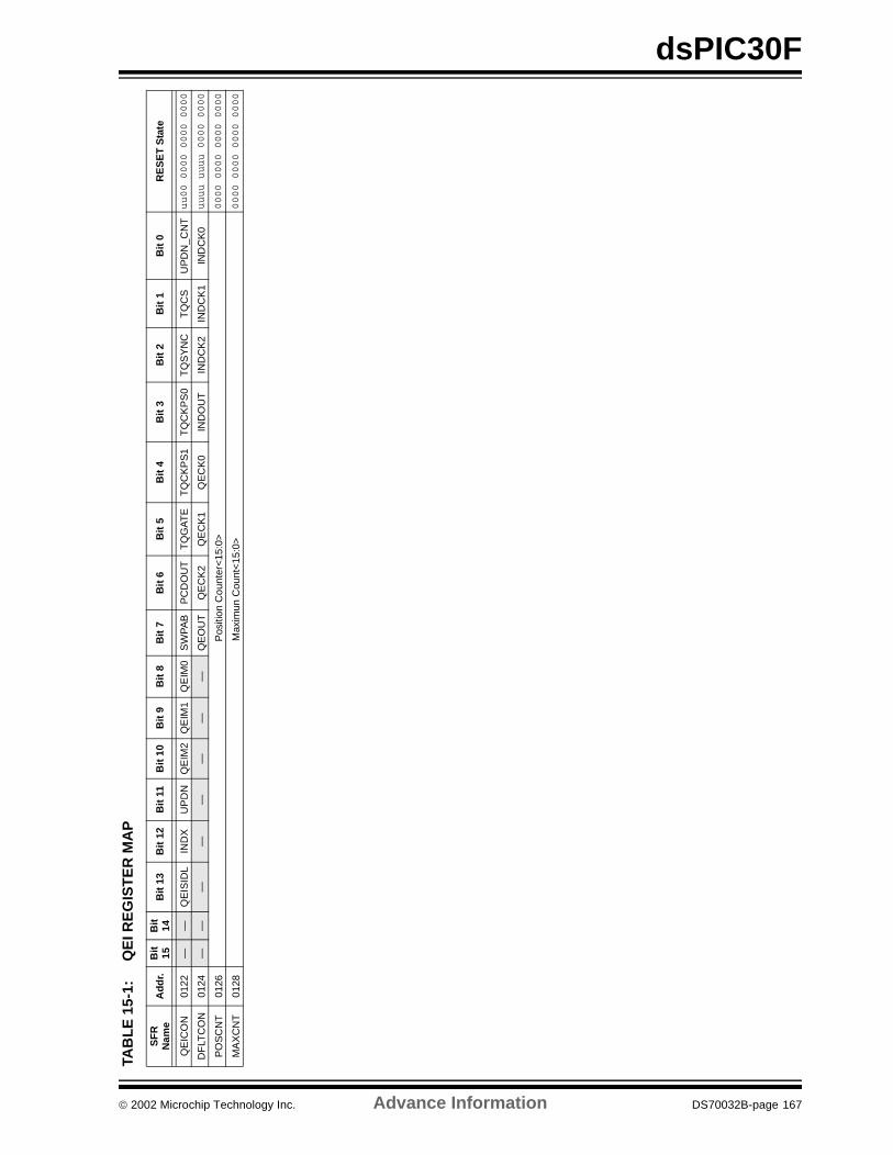
dsPIC30F
TAB
LE
15-
1:Q
EI R
EG
IST
ER
MA
P
SF
R
Nam
eA
dd
r.B
it
15B
it
14B
it 1
3B
it 1
2B
it 1
1B
it 1
0B
it 9
Bit
8B
it 7
Bit
6B
it 5
Bit
4B
it 3
Bit
2B
it 1
Bit
0R
ES
ET
Sta
te
QE
ICO
N01
22—
—Q
EIS
IDL
IND
XU
PD
NQ
EIM
2Q
EIM
1Q
EIM
0S
WP
AB
PC
DO
UT
TQ
GA
TE
TQ
CK
PS
1T
QC
KP
S0
TQ
SY
NC
TQ
CS
UP
DN
_CN
Tuu00 0000 0000 0000
DF
LTC
ON
0124
——
——
——
——
QE
OU
TQ
EC
K2
QE
CK
1Q
EC
K0
IND
OU
TIN
DC
K2
IND
CK
1IN
DC
K0
uuuu uuuu 0000 0000
PO
SC
NT
0126
Pos
ition
Cou
nter
<15
:0>
0000 0000 0000 0000
MA
XC
NT
0128
Max
imun
Cou
nt<
15:0
>0000 0000 0000 0000
2002 Microchip Technology Inc. Advance Information DS70032B-page 167
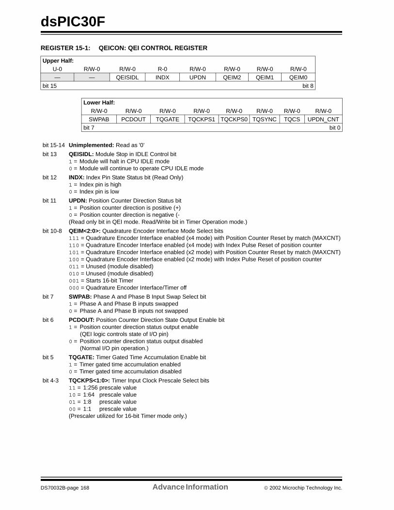
dsPIC30F
REGISTER 15-1: QEICON: QEI CONTROL REGISTER
Upper Half:U-0 R/W-0 R/W-0 R-0 R/W-0 R/W-0 R/W-0 R/W-0— — QEISIDL INDX UPDN QEIM2 QEIM1 QEIM0
bit 15 bit 8
Lower Half:R/W-0 R/W-0 R/W-0 R/W-0 R/W-0 R/W-0 R/W-0 R/W-0
SWPAB PCDOUT TQGATE TQCKPS1 TQCKPS0 TQSYNC TQCS UPDN_CNTbit 7 bit 0
bit 15-14 Unimplemented: Read as '0’
bit 13 QEISIDL: Module Stop in IDLE Control bit 1 = Module will halt in CPU IDLE mode0 = Module will continue to operate CPU IDLE mode
bit 12 INDX: Index Pin State Status bit (Read Only)1 = Index pin is high0 = Index pin is low
bit 11 UPDN: Position Counter Direction Status bit1 = Position counter direction is positive (+)0 = Position counter direction is negative (-(Read only bit in QEI mode. Read/Write bit in Timer Operation mode.)
bit 10-8 QEIM<2:0>: Quadrature Encoder Interface Mode Select bits111 = Quadrature Encoder Interface enabled (x4 mode) with Position Counter Reset by match (MAXCNT)110 = Quadrature Encoder Interface enabled (x4 mode) with Index Pulse Reset of position counter101 = Quadrature Encoder Interface enabled (x2 mode) with Position Counter Reset by match (MAXCNT)100 = Quadrature Encoder Interface enabled (x2 mode) with Index Pulse Reset of position counter011 = Unused (module disabled)010 = Unused (module disabled)001 = Starts 16-bit Timer000 = Quadrature Encoder Interface/Timer off
bit 7 SWPAB: Phase A and Phase B Input Swap Select bit1 = Phase A and Phase B inputs swapped0 = Phase A and Phase B inputs not swapped
bit 6 PCDOUT: Position Counter Direction State Output Enable bit1 = Position counter direction status output enable
(QEI logic controls state of I/O pin)0 = Position counter direction status output disabled
(Normal I/O pin operation.)
bit 5 TQGATE: Timer Gated Time Accumulation Enable bit1 = Timer gated time accumulation enabled0 = Timer gated time accumulation disabled
bit 4-3 TQCKPS<1:0>: Timer Input Clock Prescale Select bits11 = 1:256 prescale value10 = 1:64 prescale value01 = 1:8 prescale value00 = 1:1 prescale value(Prescaler utilized for 16-bit Timer mode only.)
DS70032B-page 168 Advance Information 2002 Microchip Technology Inc.
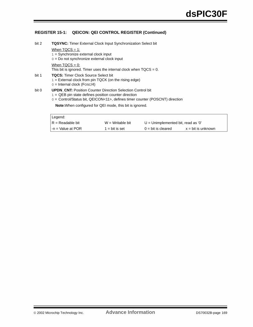
dsPIC30F
REGISTER 15-1: QEICON: QEI CONTROL REGISTER (Continued)
bit 2 TQSYNC: Timer External Clock Input Synchronization Select bit
When TQCS = 1: 1 = Synchronize external clock input0 = Do not synchronize external clock input
When TQCS = 0: This bit is ignored. Timer uses the internal clock when TQCS = 0.
bit 1 TQCS: Timer Clock Source Select bit1 = External clock from pin TQCK (on the rising edge) 0 = Internal clock (FOSC/4)
bit 0 UPDN_CNT: Position Counter Direction Selection Control bit1 = QEB pin state defines position counter direction0 = Control/Status bit, QEICON<11>, defines timer counter (POSCNT) direction
Note:When configured for QEI mode, this bit is ignored.
Legend:
R = Readable bit W = Writable bit U = Unimplemented bit, read as ‘0’
-n = Value at POR 1 = bit is set 0 = bit is cleared x = bit is unknown
2002 Microchip Technology Inc. Advance Information DS70032B-page 169
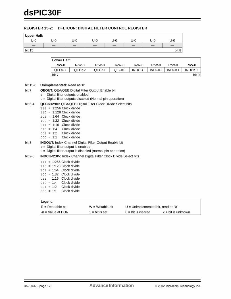
dsPIC30F
REGISTER 15-2: DFLTCON: DIGITAL FILTER CONTROL REGISTER
Upper Half:U-0 U-0 U-0 U-0 U-0 U-0 U-0 U-0— — — — — — — —
bit 15 bit 8
Lower Half:R/W-0 R/W-0 R/W-0 R/W-0 R/W-0 R/W-0 R/W-0 R/W-0
QEOUT QECK2 QECK1 QECK0 INDOUT INDCK2 INDCK1 INDCK0bit 7 bit 0
bit 15-8 Unimplemented: Read as '0’
bit 7 QEOUT: QEA/QEB Digital Filter Output Enable bit1 = Digital filter outputs enabled0 = Digital filter outputs disabled (Normal pin operation)
bit 6-4 QECK<2:0>: QEA/QEB Digital Filter Clock Divide Select bits111 = 1:256 Clock divide110 = 1:128 Clock divide101 = 1:64 Clock divide100 = 1:32 Clock divide011 = 1:16 Clock divide010 = 1:4 Clock divide001 = 1:2 Clock divide000 = 1:1 Clock divide
bit 3 INDOUT: Index Channel Digital Filter Output Enable bit1 = Digital filter output is enabled0 = Digital filter output is disabled (normal pin operation)
bit 2-0 INDCK<2:0>: Index Channel Digital Filter Clock Divide Select bits
111 = 1:256 Clock divide110 = 1:128 Clock divide101 = 1:64 Clock divide100 = 1:32 Clock divide011 = 1:16 Clock divide010 = 1:4 Clock divide001 = 1:2 Clock divide000 = 1:1 Clock divide
Legend:
R = Readable bit W = Writable bit U = Unimplemented bit, read as ‘0’
-n = Value at POR 1 = bit is set 0 = bit is cleared x = bit is unknown
DS70032B-page 170 Advance Information 2002 Microchip Technology Inc.
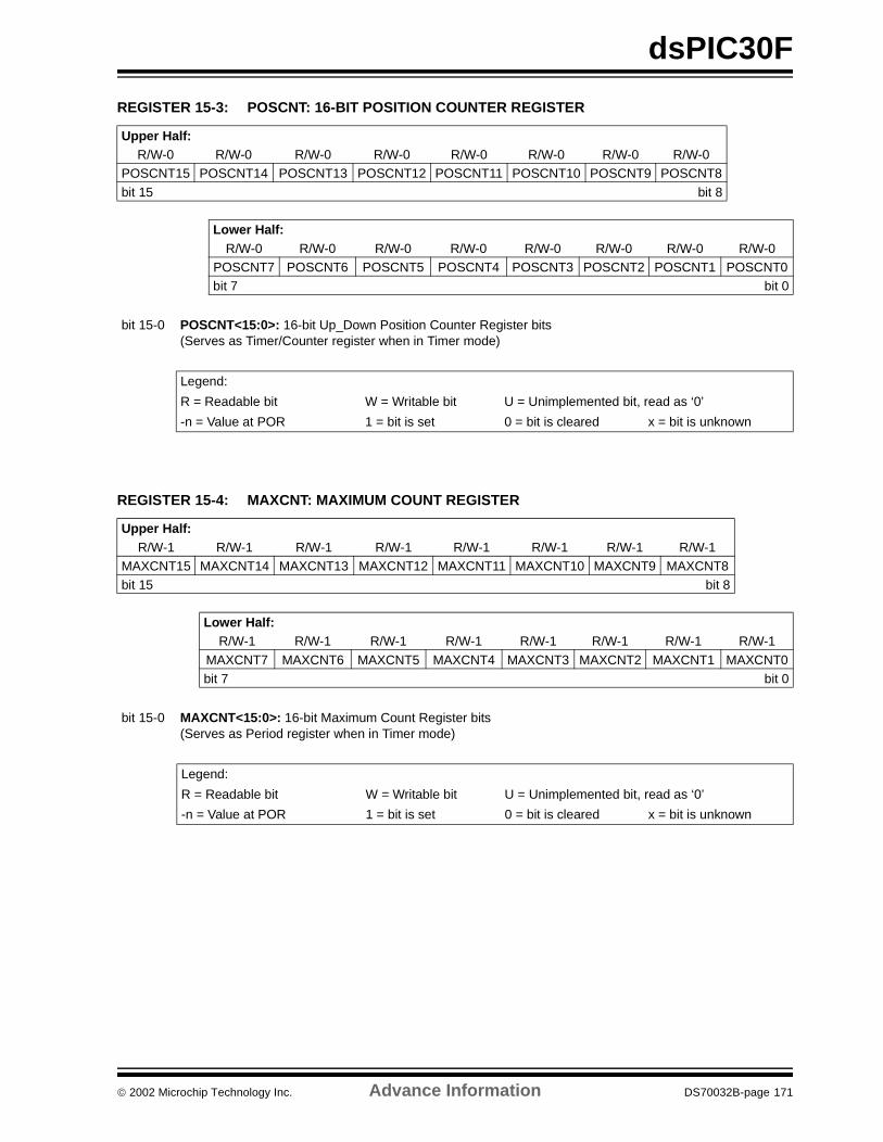
dsPIC30F
REGISTER 15-3: POSCNT: 16-BIT POSITION COUNTER REGISTER
REGISTER 15-4: MAXCNT: MAXIMUM COUNT REGISTER
Upper Half:R/W-0 R/W-0 R/W-0 R/W-0 R/W-0 R/W-0 R/W-0 R/W-0
POSCNT15 POSCNT14 POSCNT13 POSCNT12 POSCNT11 POSCNT10 POSCNT9 POSCNT8
bit 15 bit 8
Lower Half:R/W-0 R/W-0 R/W-0 R/W-0 R/W-0 R/W-0 R/W-0 R/W-0
POSCNT7 POSCNT6 POSCNT5 POSCNT4 POSCNT3 POSCNT2 POSCNT1 POSCNT0bit 7 bit 0
bit 15-0 POSCNT<15:0>: 16-bit Up_Down Position Counter Register bits(Serves as Timer/Counter register when in Timer mode)
Legend:
R = Readable bit W = Writable bit U = Unimplemented bit, read as ‘0’
-n = Value at POR 1 = bit is set 0 = bit is cleared x = bit is unknown
Upper Half:R/W-1 R/W-1 R/W-1 R/W-1 R/W-1 R/W-1 R/W-1 R/W-1
MAXCNT15 MAXCNT14 MAXCNT13 MAXCNT12 MAXCNT11 MAXCNT10 MAXCNT9 MAXCNT8bit 15 bit 8
Lower Half:R/W-1 R/W-1 R/W-1 R/W-1 R/W-1 R/W-1 R/W-1 R/W-1
MAXCNT7 MAXCNT6 MAXCNT5 MAXCNT4 MAXCNT3 MAXCNT2 MAXCNT1 MAXCNT0bit 7 bit 0
bit 15-0 MAXCNT<15:0>: 16-bit Maximum Count Register bits(Serves as Period register when in Timer mode)
Legend:
R = Readable bit W = Writable bit U = Unimplemented bit, read as ‘0’
-n = Value at POR 1 = bit is set 0 = bit is cleared x = bit is unknown
2002 Microchip Technology Inc. Advance Information DS70032B-page 171

dsPIC30F
NOTES:
DS70032B-page 172 Advance Information 2002 Microchip Technology Inc.
dsPIC30F
16.0 MOTOR CONTROL PWM MODULE
This module simplifies the task of generating multiple,synchronized Pulse Width Modulated (PWM) outputs.In particular, the following power and motion controlapplications are supported by the PWM module:
• Three Phase AC Induction Motor
• Switched Reluctance (SR) Motor• Brushless DC (BLDC) Motor• Uninterruptible Power Supply (UPS)
The PWM module has the following features:
• 8 PWM I/O pins with 4 duty cycle generators
• Up to 16-bit resolution• ‘On-the-Fly’ PWM frequency changes• Edge and Center Aligned Output modes
• Single Pulse Generation mode• Interrupt support for asymmetrical updates in
Center Aligned mode• Output override control for Electrically Commuta-
tive Motor (ECM) operation• ‘Special Event’ comparator for scheduling other
peripheral events • Fault pins to optionally drive each of the PWM I/O
pins to a defined state
A simplified block diagram of the PWM module isshown in Figure 16-1. Figure 16-5 and Figure 16-9show how the module hardware is partitioned for eachPWM output pair for the Complementary and Indepen-dent Output modes, respectively.
This module contains 4 duty cycle generators, num-bered 1 through 4. The module has 8 PWM output pins,numbered 0 through 7. The eight I/O pins are groupedinto odd numbered/even numbered pairs. For comple-mentary loads, the even PWM pins are always thecomplement of the corresponding odd I/O pin.
2002 Microchip Technology Inc. Advance Information DS70032B-page 173
dsPIC30F
FIGURE 16-1: PWM MODULE BLOCK DIAGRAM
PDC4
PDC4 Buffer
PWMCON1
PTPER Buffer
PWMCON2
PTPER
PTMR
Comparator
Comparator
Channel 4 Dead-TimeGenerator and
PTCON
SEVTCMP
ComparatorSpecial Event Trigger
FLTBCON
OVDCON
PWM Enable and Mode SFRs
PWM ManualControl SFR
Channel 3 Dead-TimeGenerator and
Channel 2 Dead-TimeGenerator and
PWM Generator#3
PWM Generator#2
PWM Generator #4
SEVTDIR
PTDIR
DTCON1 Dead-Time Control SFRs
Special EventPostscaler
PWM0
PWM1
PWM2
PWM3
PWM4
PWM5
PWM Generator#1 Channel 1 Dead-Time
Generator and
Note: Details of PWM Generator #1, #2, and #3 not shown for clarity.
16-b
it D
ata
Bus
PWM6
PWM7
DTCON2
FLTACON Fault Pin Control SFRs
PWM Time-Base
Output
Driver
Block
FLTB
FLTA
Override Logic
Override Logic
Override Logic
Override Logic
DS70032B-page 174 Advance Information 2002 Microchip Technology Inc.
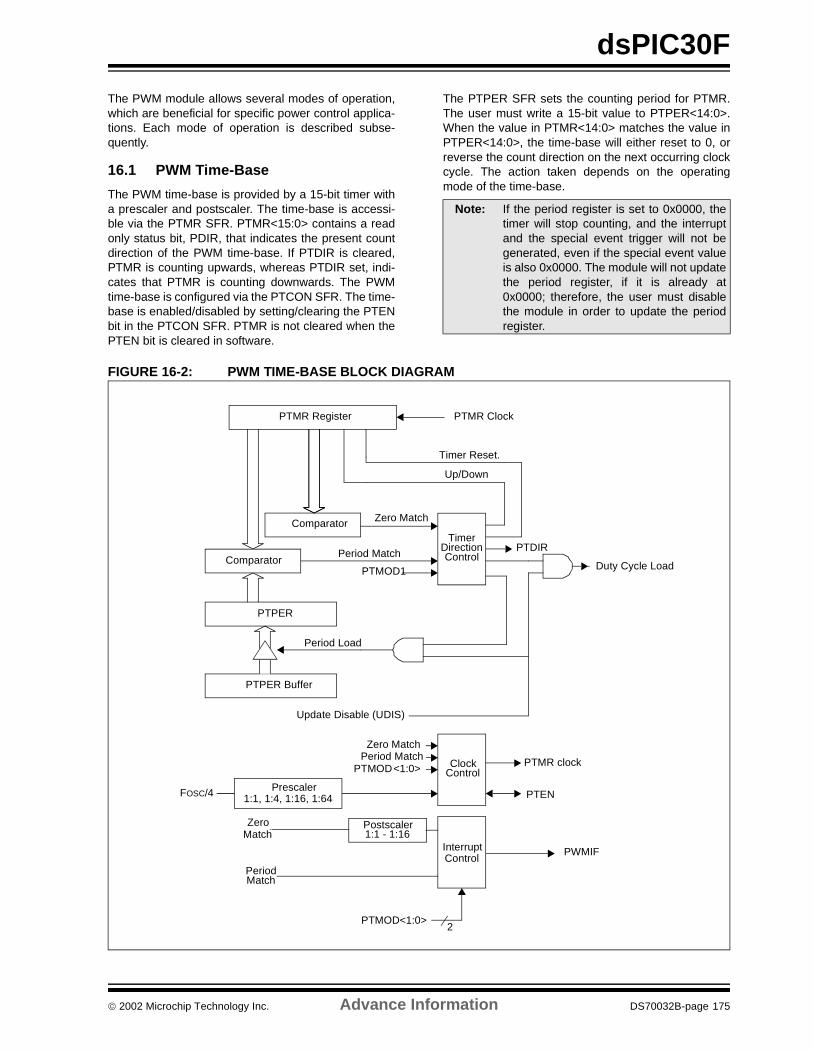
dsPIC30F
The PWM module allows several modes of operation,which are beneficial for specific power control applica-tions. Each mode of operation is described subse-quently.
16.1 PWM Time-Base
The PWM time-base is provided by a 15-bit timer witha prescaler and postscaler. The time-base is accessi-ble via the PTMR SFR. PTMR<15:0> contains a readonly status bit, PDIR, that indicates the present countdirection of the PWM time-base. If PTDIR is cleared,PTMR is counting upwards, whereas PTDIR set, indi-cates that PTMR is counting downwards. The PWMtime-base is configured via the PTCON SFR. The time-base is enabled/disabled by setting/clearing the PTENbit in the PTCON SFR. PTMR is not cleared when thePTEN bit is cleared in software.
The PTPER SFR sets the counting period for PTMR.The user must write a 15-bit value to PTPER<14:0>.When the value in PTMR<14:0> matches the value inPTPER<14:0>, the time-base will either reset to 0, orreverse the count direction on the next occurring clockcycle. The action taken depends on the operatingmode of the time-base.
FIGURE 16-2: PWM TIME-BASE BLOCK DIAGRAM
Note: If the period register is set to 0x0000, thetimer will stop counting, and the interruptand the special event trigger will not begenerated, even if the special event valueis also 0x0000. The module will not updatethe period register, if it is already at0x0000; therefore, the user must disablethe module in order to update the periodregister.
Comparator
PTPER Buffer
Comparator Zero Match
Period Match
PTMOD1
Up/Down
Timer Reset.
FOSC/4 Prescaler1:1, 1:4, 1:16, 1:64
TimerDirectionControl
ClockControl
Period Load
Duty Cycle Load
PTMODPeriod Match
Zero Match
PTMR clock
InterruptControl
PTMOD<1:0>
PeriodMatch
ZeroMatch
Postscaler1:1 - 1:16
PTEN
PWMIF
PTDIR
PTMR Clock
Update Disable (UDIS)
2
<1:0>
PTMR Register
PTPER
2002 Microchip Technology Inc. Advance Information DS70032B-page 175
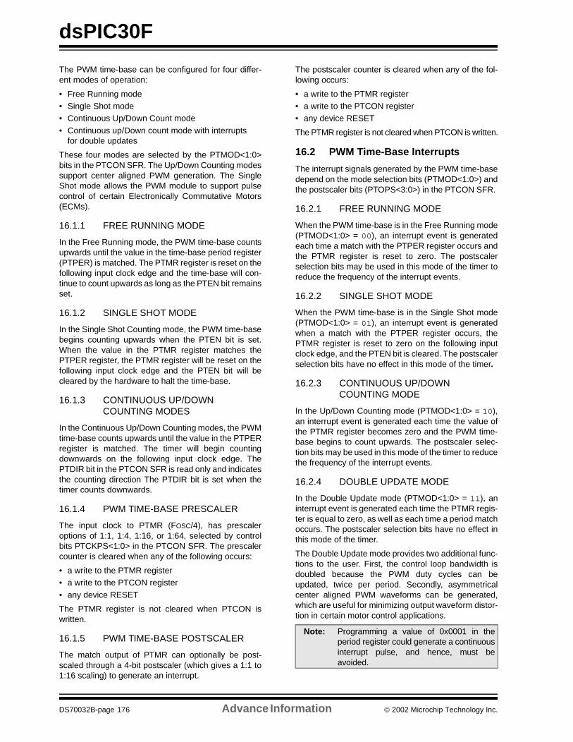
dsPIC30F
The PWM time-base can be configured for four differ-ent modes of operation:
• Free Running mode• Single Shot mode• Continuous Up/Down Count mode
• Continuous up/Down count mode with interrupts for double updates
These four modes are selected by the PTMOD<1:0>bits in the PTCON SFR. The Up/Down Counting modessupport center aligned PWM generation. The SingleShot mode allows the PWM module to support pulsecontrol of certain Electronically Commutative Motors(ECMs).
16.1.1 FREE RUNNING MODE
In the Free Running mode, the PWM time-base countsupwards until the value in the time-base period register(PTPER) is matched. The PTMR register is reset on thefollowing input clock edge and the time-base will con-tinue to count upwards as long as the PTEN bit remainsset.
16.1.2 SINGLE SHOT MODE
In the Single Shot Counting mode, the PWM time-basebegins counting upwards when the PTEN bit is set.When the value in the PTMR register matches thePTPER register, the PTMR register will be reset on thefollowing input clock edge and the PTEN bit will becleared by the hardware to halt the time-base.
16.1.3 CONTINUOUS UP/DOWN COUNTING MODES
In the Continuous Up/Down Counting modes, the PWMtime-base counts upwards until the value in the PTPERregister is matched. The timer will begin countingdownwards on the following input clock edge. ThePTDIR bit in the PTCON SFR is read only and indicatesthe counting direction The PTDIR bit is set when thetimer counts downwards.
16.1.4 PWM TIME-BASE PRESCALER
The input clock to PTMR (FOSC/4), has prescaleroptions of 1:1, 1:4, 1:16, or 1:64, selected by controlbits PTCKPS<1:0> in the PTCON SFR. The prescalercounter is cleared when any of the following occurs:
• a write to the PTMR register• a write to the PTCON register
• any device RESET
The PTMR register is not cleared when PTCON iswritten.
16.1.5 PWM TIME-BASE POSTSCALER
The match output of PTMR can optionally be post-scaled through a 4-bit postscaler (which gives a 1:1 to1:16 scaling) to generate an interrupt.
The postscaler counter is cleared when any of the fol-lowing occurs:
• a write to the PTMR register• a write to the PTCON register• any device RESET
The PTMR register is not cleared when PTCON is written.
16.2 PWM Time-Base Interrupts
The interrupt signals generated by the PWM time-basedepend on the mode selection bits (PTMOD<1:0>) andthe postscaler bits (PTOPS<3:0>) in the PTCON SFR.
16.2.1 FREE RUNNING MODE
When the PWM time-base is in the Free Running mode(PTMOD<1:0> = 00), an interrupt event is generatedeach time a match with the PTPER register occurs andthe PTMR register is reset to zero. The postscalerselection bits may be used in this mode of the timer toreduce the frequency of the interrupt events.
16.2.2 SINGLE SHOT MODE
When the PWM time-base is in the Single Shot mode(PTMOD<1:0> = 01), an interrupt event is generatedwhen a match with the PTPER register occurs, thePTMR register is reset to zero on the following inputclock edge, and the PTEN bit is cleared. The postscalerselection bits have no effect in this mode of the timer.
16.2.3 CONTINUOUS UP/DOWN COUNTING MODE
In the Up/Down Counting mode (PTMOD<1:0> = 10),an interrupt event is generated each time the value ofthe PTMR register becomes zero and the PWM time-base begins to count upwards. The postscaler selec-tion bits may be used in this mode of the timer to reducethe frequency of the interrupt events.
16.2.4 DOUBLE UPDATE MODE
In the Double Update mode (PTMOD<1:0> = 11), aninterrupt event is generated each time the PTMR regis-ter is equal to zero, as well as each time a period matchoccurs. The postscaler selection bits have no effect inthis mode of the timer.
The Double Update mode provides two additional func-tions to the user. First, the control loop bandwidth isdoubled because the PWM duty cycles can beupdated, twice per period. Secondly, asymmetricalcenter aligned PWM waveforms can be generated,which are useful for minimizing output waveform distor-tion in certain motor control applications.
Note: Programming a value of 0x0001 in theperiod register could generate a continuousinterrupt pulse, and hence, must beavoided.
DS70032B-page 176 Advance Information 2002 Microchip Technology Inc.
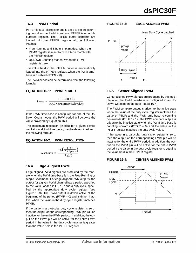
dsPIC30F
16.3 PWM Period
PTPER is a 15-bit register and is used to set the count-ing period for the PWM time-base. PTPER is a doublebuffered register. The PTPER buffer contents areloaded into the PTPER register at the followinginstants:
• Free Running and Single Shot modes: When the PTMR register is reset to zero after a match with the PTPER register.
• Up/Down Counting modes: When the PTMR register is zero.
The value held in the PTPER buffer is automaticallyloaded into the PTPER register, when the PWM time-base is disabled (PTEN = 0).
The PWM period can be determined from the followingformula:
EQUATION 16-1: PWM PERIOD
If the PWM time-base is configured for one of the Up/Down Count modes, the PWM period will be twice thevalue provided by Equation 16-1.
The maximum resolution (in bits) for a given deviceoscillator and PWM frequency can be determined fromthe following formula:
EQUATION 16-2: PWM RESOLUTION
16.4 Edge Aligned PWM
Edge aligned PWM signals are produced by the mod-ule when the PWM time-base is in the Free Running orSingle Shot mode. For edge aligned PWM outputs, theoutput for a given PWM channel has a period specifiedby the value loaded in PTPER and a duty cycle speci-fied by the appropriate duty cycle register (seeFigure 16-3). The PWM output is driven active at thebeginning of the period (PTMR = 0) and is driven inac-tive, when the value in the duty cycle register matchesPTMR.
If the value in a particular duty cycle register is zero,then the output on the corresponding PWM pin will beinactive for the entire PWM period. In addition, the out-put on the PWM pin will be active for the entire PWMperiod if the value in the duty cycle register is greaterthan the value held in the PTPER register.
FIGURE 16-3: EDGE ALIGNED PWM
16.5 Center Aligned PWM
Center aligned PWM signals are produced by the mod-ule when the PWM time-base is configured in an Up/Down Counting mode (see Figure 16-4).
The PWM compare output is driven to the active statewhen the value of the duty cycle register matches thevalue of PTMR and the PWM time-base is countingdownwards (PTDIR = 1). The PWM compare output isdriven to the inactive state when the PWM time-base iscounting upwards (PTDIR = 0) and the value in thePTMR register matches the duty cycle value.
If the value in a particular duty cycle register is zero,then the output on the corresponding PWM pin will beinactive for the entire PWM period. In addition, the out-put on the PWM pin will be active for the entire PWMperiod if the value in the duty cycle register is equal tothe value held in the PTPER register.
FIGURE 16-4: CENTER ALIGNED PWM
PPWM =4(PTPER + 1)
FOSC (PTMRprescalevalue)•
Resolution =log
log(2)
FOSC
2 Fpwm•( )
Period
Duty Cycle
0
PTPER
PTMRValue
New Duty Cycle Latched
0
PTPERPTMRValue
Period
Period/2
DutyCycle
2002 Microchip Technology Inc. Advance Information DS70032B-page 177
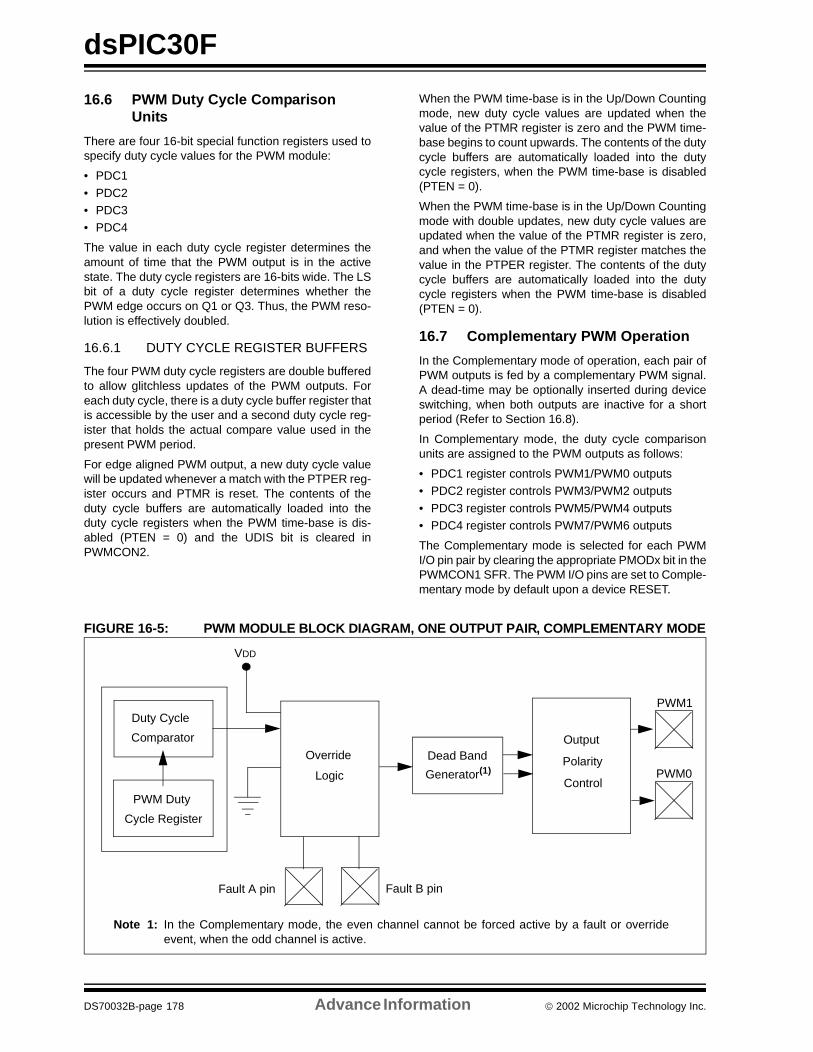
dsPIC30F
16.6 PWM Duty Cycle Comparison Units
There are four 16-bit special function registers used tospecify duty cycle values for the PWM module:
• PDC1
• PDC2• PDC3• PDC4
The value in each duty cycle register determines theamount of time that the PWM output is in the activestate. The duty cycle registers are 16-bits wide. The LSbit of a duty cycle register determines whether thePWM edge occurs on Q1 or Q3. Thus, the PWM reso-lution is effectively doubled.
16.6.1 DUTY CYCLE REGISTER BUFFERS
The four PWM duty cycle registers are double bufferedto allow glitchless updates of the PWM outputs. Foreach duty cycle, there is a duty cycle buffer register thatis accessible by the user and a second duty cycle reg-ister that holds the actual compare value used in thepresent PWM period.
For edge aligned PWM output, a new duty cycle valuewill be updated whenever a match with the PTPER reg-ister occurs and PTMR is reset. The contents of theduty cycle buffers are automatically loaded into theduty cycle registers when the PWM time-base is dis-abled (PTEN = 0) and the UDIS bit is cleared inPWMCON2.
When the PWM time-base is in the Up/Down Countingmode, new duty cycle values are updated when thevalue of the PTMR register is zero and the PWM time-base begins to count upwards. The contents of the dutycycle buffers are automatically loaded into the dutycycle registers, when the PWM time-base is disabled(PTEN = 0).
When the PWM time-base is in the Up/Down Countingmode with double updates, new duty cycle values areupdated when the value of the PTMR register is zero,and when the value of the PTMR register matches thevalue in the PTPER register. The contents of the dutycycle buffers are automatically loaded into the dutycycle registers when the PWM time-base is disabled(PTEN = 0).
16.7 Complementary PWM Operation
In the Complementary mode of operation, each pair ofPWM outputs is fed by a complementary PWM signal.A dead-time may be optionally inserted during deviceswitching, when both outputs are inactive for a shortperiod (Refer to Section 16.8).
In Complementary mode, the duty cycle comparisonunits are assigned to the PWM outputs as follows:
• PDC1 register controls PWM1/PWM0 outputs• PDC2 register controls PWM3/PWM2 outputs
• PDC3 register controls PWM5/PWM4 outputs• PDC4 register controls PWM7/PWM6 outputs
The Complementary mode is selected for each PWMI/O pin pair by clearing the appropriate PMODx bit in thePWMCON1 SFR. The PWM I/O pins are set to Comple-mentary mode by default upon a device RESET.
FIGURE 16-5: PWM MODULE BLOCK DIAGRAM, ONE OUTPUT PAIR, COMPLEMENTARY MODE
Fault A pin
Dead Band
PWM Duty
PWM1
Output
VDD
Override
Duty Cycle
Fault B pin
Comparator
Cycle Register
PWM0Logic Generator(1)Polarity
Control
Note 1: In the Complementary mode, the even channel cannot be forced active by a fault or overrideevent, when the odd channel is active.
DS70032B-page 178 Advance Information 2002 Microchip Technology Inc.
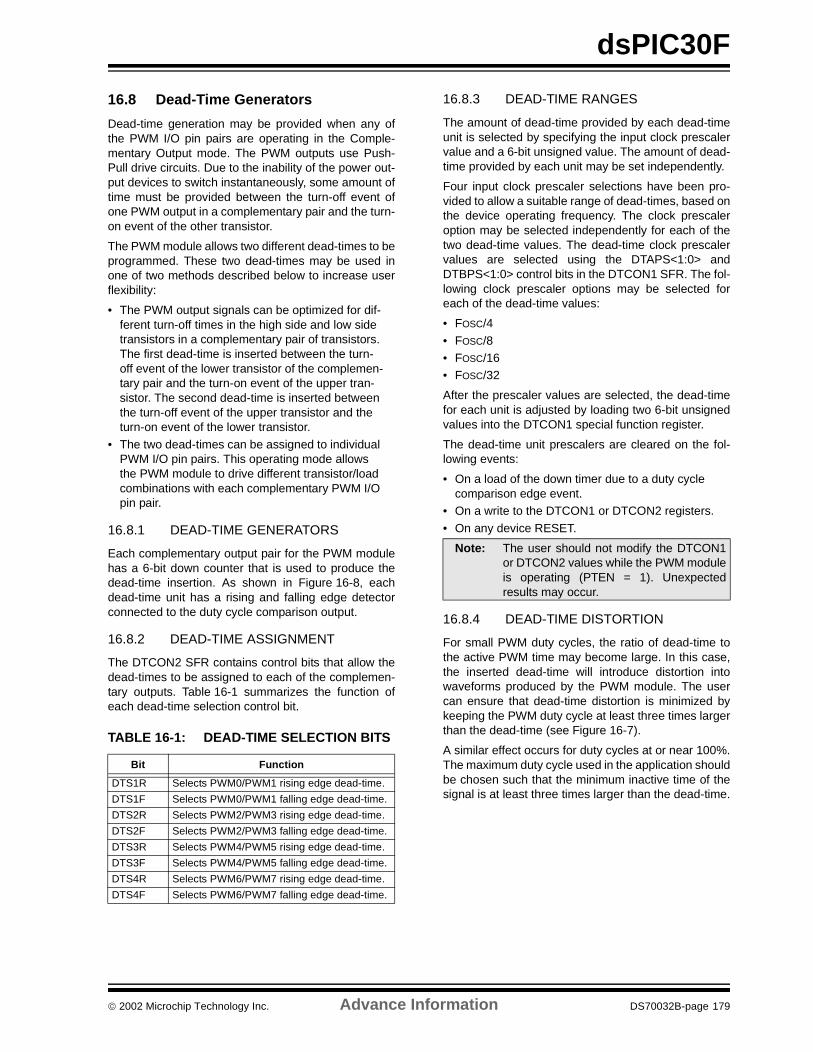
dsPIC30F
16.8 Dead-Time Generators
Dead-time generation may be provided when any ofthe PWM I/O pin pairs are operating in the Comple-mentary Output mode. The PWM outputs use Push-Pull drive circuits. Due to the inability of the power out-put devices to switch instantaneously, some amount oftime must be provided between the turn-off event ofone PWM output in a complementary pair and the turn-on event of the other transistor.
The PWM module allows two different dead-times to beprogrammed. These two dead-times may be used inone of two methods described below to increase userflexibility:
• The PWM output signals can be optimized for dif-ferent turn-off times in the high side and low side transistors in a complementary pair of transistors. The first dead-time is inserted between the turn-off event of the lower transistor of the complemen-tary pair and the turn-on event of the upper tran-sistor. The second dead-time is inserted between the turn-off event of the upper transistor and the turn-on event of the lower transistor.
• The two dead-times can be assigned to individual PWM I/O pin pairs. This operating mode allows the PWM module to drive different transistor/load combinations with each complementary PWM I/O pin pair.
16.8.1 DEAD-TIME GENERATORS
Each complementary output pair for the PWM modulehas a 6-bit down counter that is used to produce thedead-time insertion. As shown in Figure 16-8, eachdead-time unit has a rising and falling edge detectorconnected to the duty cycle comparison output.
16.8.2 DEAD-TIME ASSIGNMENT
The DTCON2 SFR contains control bits that allow thedead-times to be assigned to each of the complemen-tary outputs. Table 16-1 summarizes the function ofeach dead-time selection control bit.
TABLE 16-1: DEAD-TIME SELECTION BITS
16.8.3 DEAD-TIME RANGES
The amount of dead-time provided by each dead-timeunit is selected by specifying the input clock prescalervalue and a 6-bit unsigned value. The amount of dead-time provided by each unit may be set independently.
Four input clock prescaler selections have been pro-vided to allow a suitable range of dead-times, based onthe device operating frequency. The clock prescaleroption may be selected independently for each of thetwo dead-time values. The dead-time clock prescalervalues are selected using the DTAPS<1:0> andDTBPS<1:0> control bits in the DTCON1 SFR. The fol-lowing clock prescaler options may be selected foreach of the dead-time values:
• FOSC/4
• FOSC/8• FOSC/16• FOSC/32
After the prescaler values are selected, the dead-timefor each unit is adjusted by loading two 6-bit unsignedvalues into the DTCON1 special function register.
The dead-time unit prescalers are cleared on the fol-lowing events:
• On a load of the down timer due to a duty cycle comparison edge event.
• On a write to the DTCON1 or DTCON2 registers.
• On any device RESET.
16.8.4 DEAD-TIME DISTORTION
For small PWM duty cycles, the ratio of dead-time tothe active PWM time may become large. In this case,the inserted dead-time will introduce distortion intowaveforms produced by the PWM module. The usercan ensure that dead-time distortion is minimized bykeeping the PWM duty cycle at least three times largerthan the dead-time (see Figure 16-7).
A similar effect occurs for duty cycles at or near 100%.The maximum duty cycle used in the application shouldbe chosen such that the minimum inactive time of thesignal is at least three times larger than the dead-time.
Bit Function
DTS1R Selects PWM0/PWM1 rising edge dead-time.
DTS1F Selects PWM0/PWM1 falling edge dead-time.
DTS2R Selects PWM2/PWM3 rising edge dead-time.
DTS2F Selects PWM2/PWM3 falling edge dead-time.
DTS3R Selects PWM4/PWM5 rising edge dead-time.
DTS3F Selects PWM4/PWM5 falling edge dead-time.
DTS4R Selects PWM6/PWM7 rising edge dead-time.
DTS4F Selects PWM6/PWM7 falling edge dead-time.
Note: The user should not modify the DTCON1or DTCON2 values while the PWM moduleis operating (PTEN = 1). Unexpectedresults may occur.
2002 Microchip Technology Inc. Advance Information DS70032B-page 179
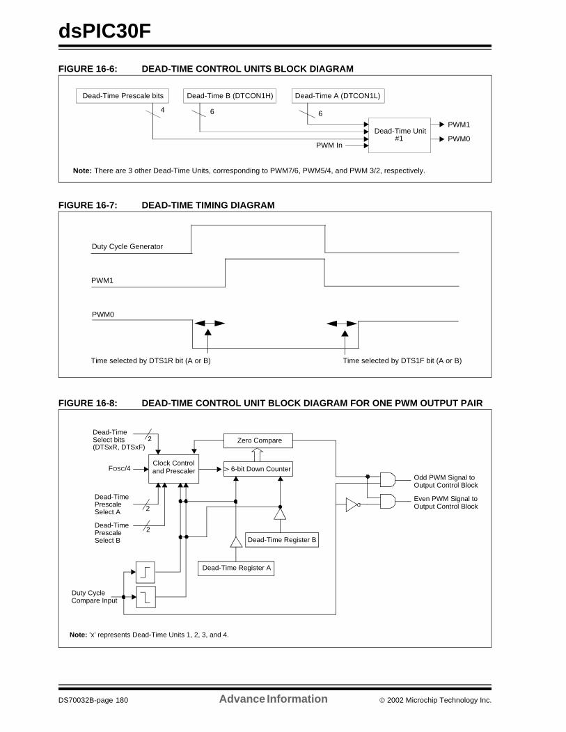
dsPIC30F
FIGURE 16-6: DEAD-TIME CONTROL UNITS BLOCK DIAGRAM
FIGURE 16-7: DEAD-TIME TIMING DIAGRAM
FIGURE 16-8: DEAD-TIME CONTROL UNIT BLOCK DIAGRAM FOR ONE PWM OUTPUT PAIR
Dead-Time Unit#1
Dead-Time A (DTCON1L)Dead-Time B (DTCON1H)Dead-Time Prescale bits
4 6 6
PWM In
PWM1
PWM0
Note: There are 3 other Dead-Time Units, corresponding to PWM7/6, PWM5/4, and PWM 3/2, respectively.
Duty Cycle Generator
PWM1
PWM0
Time selected by DTS1R bit (A or B) Time selected by DTS1F bit (A or B)
Even PWM Signal toOutput Control Block
Odd PWM Signal toOutput Control Block
Zero Compare
Clock Controland Prescaler 6-bit Down Counter
Duty CycleCompare Input
Dead-TimePrescaleSelect B
Dead-TimePrescaleSelect A
FOSC/4
Dead-TimeSelect bits
Dead-Time Register B
Dead-Time Register A
(DTSxR, DTSxF)
Note: ’x’ represents Dead-Time Units 1, 2, 3, and 4.
2
2
2
DS70032B-page 180 Advance Information 2002 Microchip Technology Inc.
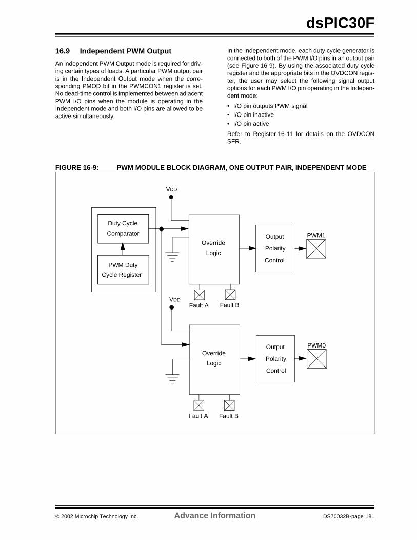
dsPIC30F
16.9 Independent PWM Output
An independent PWM Output mode is required for driv-ing certain types of loads. A particular PWM output pairis in the Independent Output mode when the corre-sponding PMOD bit in the PWMCON1 register is set.No dead-time control is implemented between adjacentPWM I/O pins when the module is operating in theIndependent mode and both I/O pins are allowed to beactive simultaneously.
In the Independent mode, each duty cycle generator isconnected to both of the PWM I/O pins in an output pair(see Figure 16-9). By using the associated duty cycleregister and the appropriate bits in the OVDCON regis-ter, the user may select the following signal outputoptions for each PWM I/O pin operating in the Indepen-dent mode:
• I/O pin outputs PWM signal• I/O pin inactive
• I/O pin active
Refer to Register 16-11 for details on the OVDCONSFR.
FIGURE 16-9: PWM MODULE BLOCK DIAGRAM, ONE OUTPUT PAIR, INDEPENDENT MODE
PWM Duty
PWM1Output
VDD
Override
Duty Cycle
Comparator
Cycle Register
LogicPolarity
Control
Output
VDD
Override
LogicPolarity
Control
Fault A Fault B
Fault A Fault B
PWM0
2002 Microchip Technology Inc. Advance Information DS70032B-page 181
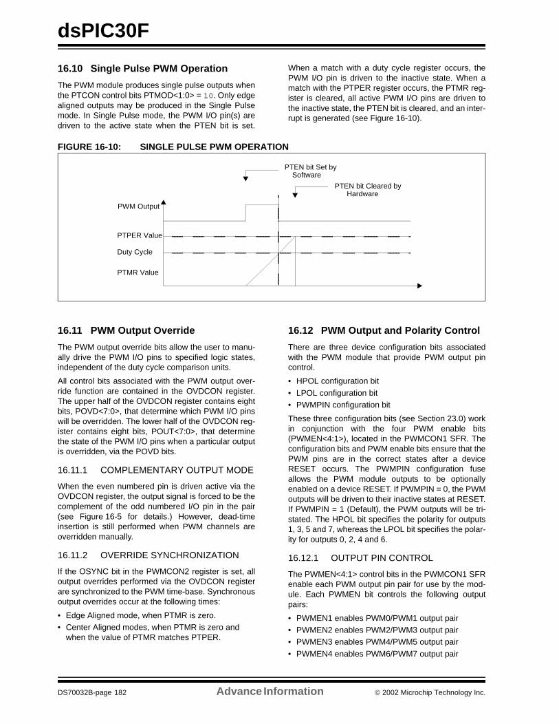
dsPIC30F
16.10 Single Pulse PWM Operation
The PWM module produces single pulse outputs whenthe PTCON control bits PTMOD<1:0> = 10. Only edgealigned outputs may be produced in the Single Pulsemode. In Single Pulse mode, the PWM I/O pin(s) aredriven to the active state when the PTEN bit is set.
When a match with a duty cycle register occurs, thePWM I/O pin is driven to the inactive state. When amatch with the PTPER register occurs, the PTMR reg-ister is cleared, all active PWM I/O pins are driven tothe inactive state, the PTEN bit is cleared, and an inter-rupt is generated (see Figure 16-10).
FIGURE 16-10: SINGLE PULSE PWM OPERATION
16.11 PWM Output Override
The PWM output override bits allow the user to manu-ally drive the PWM I/O pins to specified logic states,independent of the duty cycle comparison units.
All control bits associated with the PWM output over-ride function are contained in the OVDCON register.The upper half of the OVDCON register contains eightbits, POVD<7:0>, that determine which PWM I/O pinswill be overridden. The lower half of the OVDCON reg-ister contains eight bits, POUT<7:0>, that determinethe state of the PWM I/O pins when a particular outputis overridden, via the POVD bits.
16.11.1 COMPLEMENTARY OUTPUT MODE
When the even numbered pin is driven active via theOVDCON register, the output signal is forced to be thecomplement of the odd numbered I/O pin in the pair(see Figure 16-5 for details.) However, dead-timeinsertion is still performed when PWM channels areoverridden manually.
16.11.2 OVERRIDE SYNCHRONIZATION
If the OSYNC bit in the PWMCON2 register is set, alloutput overrides performed via the OVDCON registerare synchronized to the PWM time-base. Synchronousoutput overrides occur at the following times:
• Edge Aligned mode, when PTMR is zero.• Center Aligned modes, when PTMR is zero and
when the value of PTMR matches PTPER.
16.12 PWM Output and Polarity Control
There are three device configuration bits associatedwith the PWM module that provide PWM output pincontrol.
• HPOL configuration bit
• LPOL configuration bit• PWMPIN configuration bit
These three configuration bits (see Section 23.0) workin conjunction with the four PWM enable bits(PWMEN<4:1>), located in the PWMCON1 SFR. Theconfiguration bits and PWM enable bits ensure that thePWM pins are in the correct states after a deviceRESET occurs. The PWMPIN configuration fuseallows the PWM module outputs to be optionallyenabled on a device RESET. If PWMPIN = 0, the PWMoutputs will be driven to their inactive states at RESET.If PWMPIN = 1 (Default), the PWM outputs will be tri-stated. The HPOL bit specifies the polarity for outputs1, 3, 5 and 7, whereas the LPOL bit specifies the polar-ity for outputs 0, 2, 4 and 6.
16.12.1 OUTPUT PIN CONTROL
The PWMEN<4:1> control bits in the PWMCON1 SFRenable each PWM output pin pair for use by the mod-ule. Each PWMEN bit controls the following outputpairs:
• PWMEN1 enables PWM0/PWM1 output pair• PWMEN2 enables PWM2/PWM3 output pair• PWMEN3 enables PWM4/PWM5 output pair
• PWMEN4 enables PWM6/PWM7 output pair
PTMR Value
PWM Output
Duty Cycle
PTPER Value
PTEN bit Set bySoftware
PTEN bit Cleared byHardware
DS70032B-page 182 Advance Information 2002 Microchip Technology Inc.
dsPIC30F
16.13 PWM Fault Pins
There are two fault pins (FLTA and FLTB) associatedwith the PWM module. When asserted, these pins canoptionally drive each of the PWM I/O pins to a definedstate.
16.13.1 FAULT PIN ENABLE BITS
The FLTACON and FLTBCON Special Function Regis-ters each have 4 control bits that determine whether aparticular pair of PWM I/O pins is to be controlled by thefault input pin. To enable a specific PWM I/O pin pair forfault overrides, the corresponding bit should be set inthe FLTACON or FLTBCON register.
If all enable bits are cleared in the FLTACON orFLTBCON registers, then the corresponding fault inputpin has no effect on the PWM module and the pin maybe used as a general purpose interrupt pin or I/O.
16.13.2 FAULT STATES
The FLTACON and FLTBCON special function regis-ters have 8 bits each, that determine the state of eachPWM I/O pin when it is overridden by a fault input.When these bits are cleared, the PWM I/O pin is drivento the inactive state. If the bit is set, the PWM I/O pinwill be driven to the active state. The active and inactivestates are referenced to the polarity defined for eachPWM I/O pin (HPOL and LPOL polarity control bits).
A special case exists when a PWM module I/O pair isin the Complementary mode and both pins are pro-grammed to be active on a fault condition. The oddnumbered PWM I/O pin always has priority in the Com-plementary mode, so that both I/O pins cannot bedriven active simultaneously. Refer to Figure 16-5 fordetails.
16.13.3 FAULT PIN PRIORITY
If both fault input pins have been assigned to control aparticular PWM I/O pin, the fault state programmed forthe Fault A input pin will take priority over the Fault Binput pin.
16.13.4 FAULT INPUT MODES
Each of the fault input pins has two modes of operation:
• Latched Mode: When the fault pin is driven low, the PWM outputs will go to the states defined in the FLTACON/FLTBCON register. The PWM out-puts will remain in this state until the fault pin is driven high and the corresponding interrupt flag has been cleared in software. When both of these actions have occurred, the PWM outputs will return to normal operation at the beginning of the next PWM cycle or half-cycle boundary. If the interrupt flag is cleared before the fault condition ends, the PWM module will wait until the fault pin is no longer asserted, to restore the outputs.
• Cycle-by-Cycle Mode: When the fault input pin is driven low, the PWM outputs remain in the defined fault states for as long as the fault pin is held low. After the fault pin is driven high, the PWM outputs return to normal operation at the beginning of the following PWM cycle, or half-cycle boundary.
The operating mode for each fault input pin is selectedusing the FLTAM and FLTBM control bits in theFLTACON and FLTBCON Special Function Registers.
Each of the fault pins can be controlled manually insoftware.
16.14 PWM Update Lockout
For a complex PWM application, the user may need towrite up to four duty cycle registers and the time-baseperiod register, PTPER, at a given time. In some appli-cations, it is important that all buffer registers be writtenbefore the new duty cycle and period values are loadedfor use by the module.
The PWM update lockout feature may optionally beenabled so that the user may specify when new dutycycle buffer values are valid. The PWM update lockoutfeature is enabled by setting the UDIS control bit in thePWMCON2 SFR. The UDIS bit affects all duty cyclebuffer registers and the PWM time-base period buffer,PTPER.
Note: The fault pin logic can operate indepen-dent of the PWM logic. If all the enable bitsin the FLTACON/FLTBCON register arecleared, then the fault pin(s) could be usedas general purpose interrupt pin(s). Eachfault pin has an interrupt vector, interruptflag bit and interrupt priority bits associatedwith it.
2002 Microchip Technology Inc. Advance Information DS70032B-page 183
dsPIC30F
16.15 PWM Special Event Trigger
The PWM module has a special event trigger thatallows A/D conversions to be synchronized to the PWMtime-base. The A/D sampling and conversion time maybe programmed to occur at any point within the PWMperiod. The special event trigger allows the user to min-imize the delay between the time when A/D conversionresults are acquired and the time when the duty cyclevalue is updated.
The PWM special event trigger has an SFR namedSEVTCMP, and five control bits to control its operation.The PTMR value for which a special event triggershould occur is loaded into the SEVTCMP register.When the PWM time-base is in an Up/Down Countingmode, an additional control bit is required to specify thecounting phase for the special event trigger. The countphase is selected using the SEVTDIR control bit in theSEVTCMP SFR. If the SEVTDIR bit is cleared, the spe-cial event trigger will occur on the upward countingcycle of the PWM time-base. If the SEVTDIR bit is set,the special event trigger will occur on the downwardcount cycle of the PWM time-base. The SEVTDIRcontrol bit has no effect unless the PWM time-base isconfigured for an Up/Down Counting mode.
16.15.1 SPECIAL EVENT TRIGGER POSTSCALER
The PWM special event trigger has a postscaler thatallows a 1:1 to 1:16 postscale ratio. The postscaler isconfigured by writing the SEVOPS<3:0> control bits inthe PWMCON2 SFR.
The special event output postscaler is cleared on thefollowing events:
• Any write to the SEVTCMP register.• Any device RESET.
16.16 PWM Operation During CPU SLEEP Mode
The Fault A and Fault B input pins have the ability towake the CPU from SLEEP mode. The PWM modulegenerates an interrupt if either of the fault pins isdriven low while in SLEEP.
16.17 PWM Operation During CPU IDLE Mode
The PTCON SFR contains a PTSIDL control bit. Thisbit determines if the PWM module will continue tooperate or stop when the device enters IDLE mode. IfPTSIDL = 0, the module continues to operate. IfPTSIDL = 1, the module will stop operation as long asthe CPU remains in IDLE mode.
DS70032B-page 184 Advance Information 2002 Microchip Technology Inc.
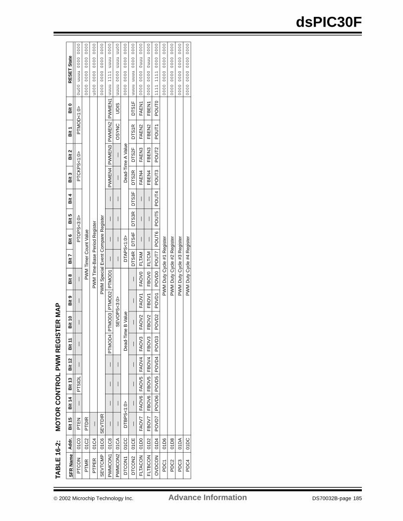
dsPIC30F
TAB
LE
16-
2:M
OT
OR
CO
NT
RO
L P
WM
RE
GIS
TE
R M
AP
SF
R N
ame
Ad
dr.
Bit
15
Bit
14
Bit
13
Bit
12
Bit
11
Bit
10
Bit
9B
it 8
Bit
7B
it 6
Bit
5B
it 4
Bit
3B
it 2
Bit
1B
it 0
RE
SE
T S
tate
PT
CO
N01
C0
PT
EN
—P
TS
IDL
——
——
—P
TO
PS
<3:
0>P
TC
KP
S<
1:0>
PT
MO
D<
1:0>
0u00 uuuu 0000 0000
PT
MR
01C
2P
TD
IRP
WM
Tim
er C
ount
Val
ue0000 0000 0000 0000
PT
PE
R01
C4
—P
WM
Tim
e-B
ase
Per
iod
Reg
iste
ru000 0000 0000 0000
SE
VT
CM
P01
C6
SE
VT
DIR
PW
M S
peci
al E
vent
Com
pare
Reg
iste
r0000 0000 0000 0000
PW
MC
ON
101
C8
——
——
PT
MO
D4
PT
MO
D3
PT
MO
D2
PT
MO
D1
——
——
PW
ME
N4
PW
ME
N3
PW
ME
N2
PW
ME
N1uuuu 1111 uuuu 0000
PW
MC
ON
201
CA
——
——
SE
VO
PS
<3:
0>—
——
——
—O
SY
NC
UD
ISuuuu 0000 uuuu uu00
DT
CO
N1
01C
CD
TB
PS
<1:
0>D
ead-
Tim
e B
Val
ueD
TAP
S<
1:0>
Dea
d-Ti
me
A V
alue
0000 0000 0000 0000
DT
CO
N2
01C
E—
——
——
——
—D
TS
4RD
TS
4FD
TS
3RD
TS
3FD
TS
2RD
TS
2FD
TS
1RD
TS
1Fuuuu uuuu 0000 0000
FLT
AC
ON
01D
0FA
OV
7FA
OV
6FA
OV
5FA
OV
4FA
OV
3FA
OV
2FA
OV
1FA
OV
0F
LTA
M—
——
FAE
N4
FAE
N3
FAE
N2
FAE
N1
0000 0000 0uuu 0000
FLT
BC
ON
01D
2F
BO
V7
FB
OV
6F
BO
V5
FB
OV
4F
BO
V3
FB
OV
2F
BO
V1
FB
OV
0F
LTC
M—
——
FB
EN
4F
BE
N3
FB
EN
2F
BE
N1
0000 0000 0uuu 0000
OV
DC
ON
01D
4P
OV
D7
PO
VD
6P
OV
D5
PO
VD
4P
OV
D3
PO
VD
2P
OV
D1
PO
VD
0P
OU
T7
PO
UT
6P
OU
T5
PO
UT
4P
OU
T3
PO
UT
2P
OU
T1
PO
UT
01111 1111 0000 0000
PD
C1
01D
6P
WM
Dut
y C
ycle
#1
Reg
iste
r0000 0000 0000 0000
PD
C2
01D
8P
WM
Dut
y C
ycle
#2
Reg
iste
r0000 0000 0000 0000
PD
C3
01D
AP
WM
Dut
y C
ycle
#3
Reg
iste
r0000 0000 0000 0000
PD
C4
01D
CP
WM
Dut
y C
ycle
#4
Reg
iste
r0000 0000 0000 0000
2002 Microchip Technology Inc. Advance Information DS70032B-page 185
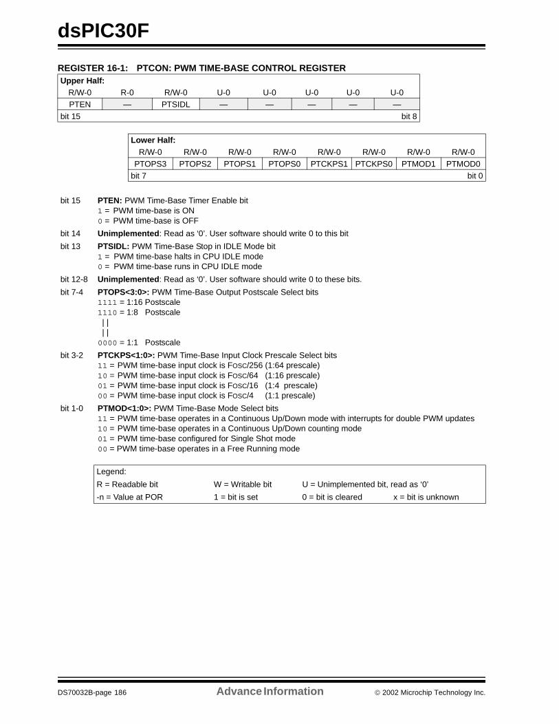
dsPIC30F
REGISTER 16-1: PTCON: PWM TIME-BASE CONTROL REGISTER Upper Half:
R/W-0 R-0 R/W-0 U-0 U-0 U-0 U-0 U-0PTEN — PTSIDL — — — — —
bit 15 bit 8
Lower Half:R/W-0 R/W-0 R/W-0 R/W-0 R/W-0 R/W-0 R/W-0 R/W-0
PTOPS3 PTOPS2 PTOPS1 PTOPS0 PTCKPS1 PTCKPS0 PTMOD1 PTMOD0bit 7 bit 0
bit 15 PTEN: PWM Time-Base Timer Enable bit1 = PWM time-base is ON0 = PWM time-base is OFF
bit 14 Unimplemented: Read as ‘0’. User software should write 0 to this bit
bit 13 PTSIDL: PWM Time-Base Stop in IDLE Mode bit1 = PWM time-base halts in CPU IDLE mode0 = PWM time-base runs in CPU IDLE mode
bit 12-8 Unimplemented: Read as ‘0’. User software should write 0 to these bits.
bit 7-4 PTOPS<3:0>: PWM Time-Base Output Postscale Select bits1111 = 1:16 Postscale1110 = 1:8 Postscale | | | |0000 = 1:1 Postscale
bit 3-2 PTCKPS<1:0>: PWM Time-Base Input Clock Prescale Select bits11 = PWM time-base input clock is FOSC/256 (1:64 prescale)10 = PWM time-base input clock is FOSC/64 (1:16 prescale)01 = PWM time-base input clock is FOSC/16 (1:4 prescale)00 = PWM time-base input clock is FOSC/4 (1:1 prescale)
bit 1-0 PTMOD<1:0>: PWM Time-Base Mode Select bits11 = PWM time-base operates in a Continuous Up/Down mode with interrupts for double PWM updates10 = PWM time-base operates in a Continuous Up/Down counting mode01 = PWM time-base configured for Single Shot mode00 = PWM time-base operates in a Free Running mode
Legend:
R = Readable bit W = Writable bit U = Unimplemented bit, read as ‘0’
-n = Value at POR 1 = bit is set 0 = bit is cleared x = bit is unknown
DS70032B-page 186 Advance Information 2002 Microchip Technology Inc.
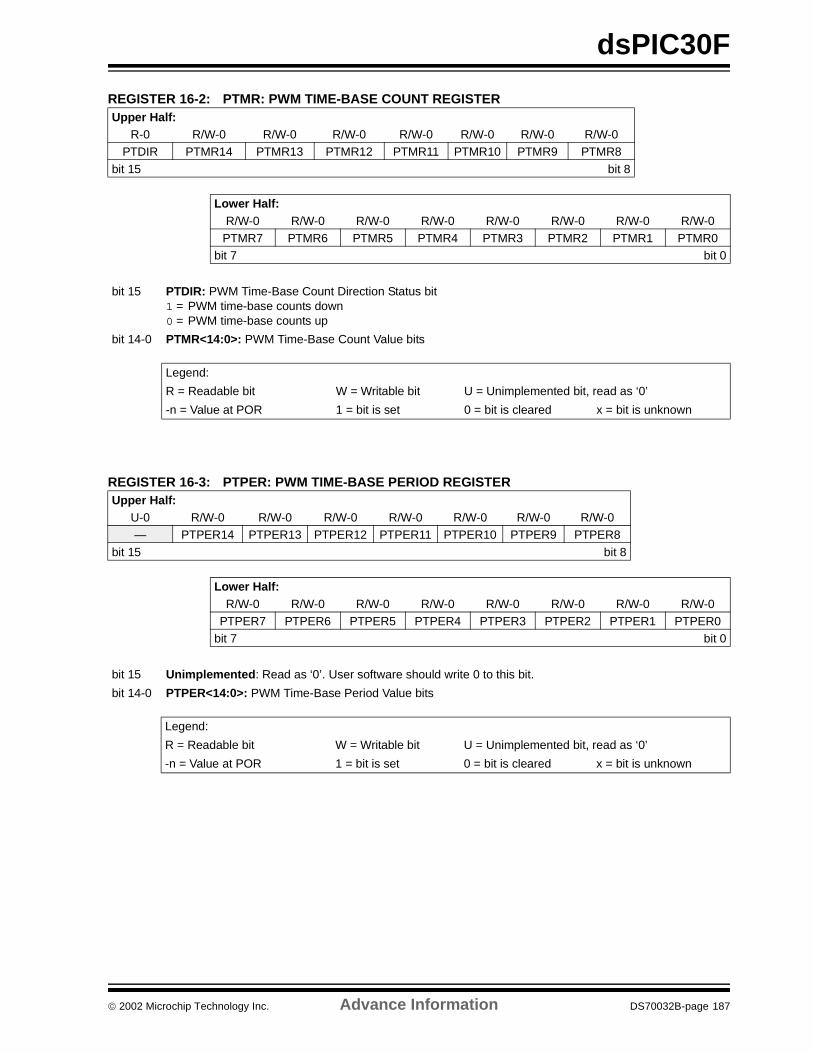
dsPIC30F
REGISTER 16-2: PTMR: PWM TIME-BASE COUNT REGISTER
REGISTER 16-3: PTPER: PWM TIME-BASE PERIOD REGISTER
Upper Half:R-0 R/W-0 R/W-0 R/W-0 R/W-0 R/W-0 R/W-0 R/W-0
PTDIR PTMR14 PTMR13 PTMR12 PTMR11 PTMR10 PTMR9 PTMR8
bit 15 bit 8
Lower Half:R/W-0 R/W-0 R/W-0 R/W-0 R/W-0 R/W-0 R/W-0 R/W-0
PTMR7 PTMR6 PTMR5 PTMR4 PTMR3 PTMR2 PTMR1 PTMR0bit 7 bit 0
bit 15 PTDIR: PWM Time-Base Count Direction Status bit1 = PWM time-base counts down0 = PWM time-base counts up
bit 14-0 PTMR<14:0>: PWM Time-Base Count Value bits
Legend:
R = Readable bit W = Writable bit U = Unimplemented bit, read as ‘0’
-n = Value at POR 1 = bit is set 0 = bit is cleared x = bit is unknown
Upper Half:U-0 R/W-0 R/W-0 R/W-0 R/W-0 R/W-0 R/W-0 R/W-0— PTPER14 PTPER13 PTPER12 PTPER11 PTPER10 PTPER9 PTPER8
bit 15 bit 8
Lower Half:R/W-0 R/W-0 R/W-0 R/W-0 R/W-0 R/W-0 R/W-0 R/W-0
PTPER7 PTPER6 PTPER5 PTPER4 PTPER3 PTPER2 PTPER1 PTPER0bit 7 bit 0
bit 15 Unimplemented: Read as ‘0’. User software should write 0 to this bit.
bit 14-0 PTPER<14:0>: PWM Time-Base Period Value bits
Legend:
R = Readable bit W = Writable bit U = Unimplemented bit, read as ‘0’
-n = Value at POR 1 = bit is set 0 = bit is cleared x = bit is unknown
2002 Microchip Technology Inc. Advance Information DS70032B-page 187
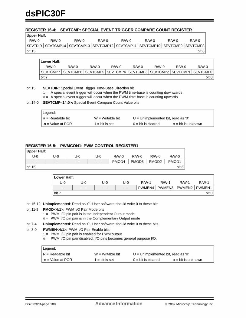
dsPIC30F
REGISTER 16-4: SEVTCMP: SPECIAL EVENT TRIGGER COMPARE COUNT REGISTER
REGISTER 16-5: PWMCON1: PWM CONTROL REGISTER1
Upper Half:R/W-0 R/W-0 R/W-0 R/W-0 R/W-0 R/W-0 R/W-0 R/W-0
SEVTDIR SEVTCMP14 SEVTCMP13 SEVTCMP12 SEVTCMP11 SEVTCMP10 SEVTCMP9 SEVTCMP8
bit 15 bit 8
Lower Half:R/W-0 R/W-0 R/W-0 R/W-0 R/W-0 R/W-0 R/W-0 R/W-0
SEVTCMP7 SEVTCMP6 SEVTCMP5 SEVTCMP4 SEVTCMP3 SEVTCMP2 SEVTCMP1 SEVTCMP0bit 7 bit 0
bit 15 SEVTDIR: Special Event Trigger Time-Base Direction bit1 = A special event trigger will occur when the PWM time-base is counting downwards0 = A special event trigger will occur when the PWM time-base is counting upwards
bit 14-0 SEVTCMP<14:0>: Special Event Compare Count Value bits
Legend:
R = Readable bit W = Writable bit U = Unimplemented bit, read as ‘0’
-n = Value at POR 1 = bit is set 0 = bit is cleared x = bit is unknown
Upper Half:U-0 U-0 U-0 U-0 R/W-0 R/W-0 R/W-0 R/W-0— — — — PMOD4 PMOD3 PMOD2 PMOD1
bit 15 bit 8
Lower Half:U-0 U-0 U-0 U-0 R/W-1 R/W-1 R/W-1 R/W-1— — — — PWMEN4 PWMEN3 PWMEN2 PWMEN1
bit 7 bit 0
bit 15-12 Unimplemented: Read as ‘0’. User software should write 0 to these bits.
bit 11-8 PMOD<4:1>: PWM I/O Pair Mode bits1 = PWM I/O pin pair is in the Independent Output mode0 = PWM I/O pin pair is in the Complementary Output mode
bit 7-4 Unimplemented: Read as ‘0’. User software should write 0 to these bits.
bit 3-0 PWMEN<4:1>: PWM I/O Pair Enable bits1 = PWM I/O pin pair is enabled for PWM output0 = PWM I/O pin pair disabled. I/O pins becomes general purpose I/O.
Legend:
R = Readable bit W = Writable bit U = Unimplemented bit, read as ‘0’
-n = Value at POR 1 = bit is set 0 = bit is cleared x = bit is unknown
DS70032B-page 188 Advance Information 2002 Microchip Technology Inc.
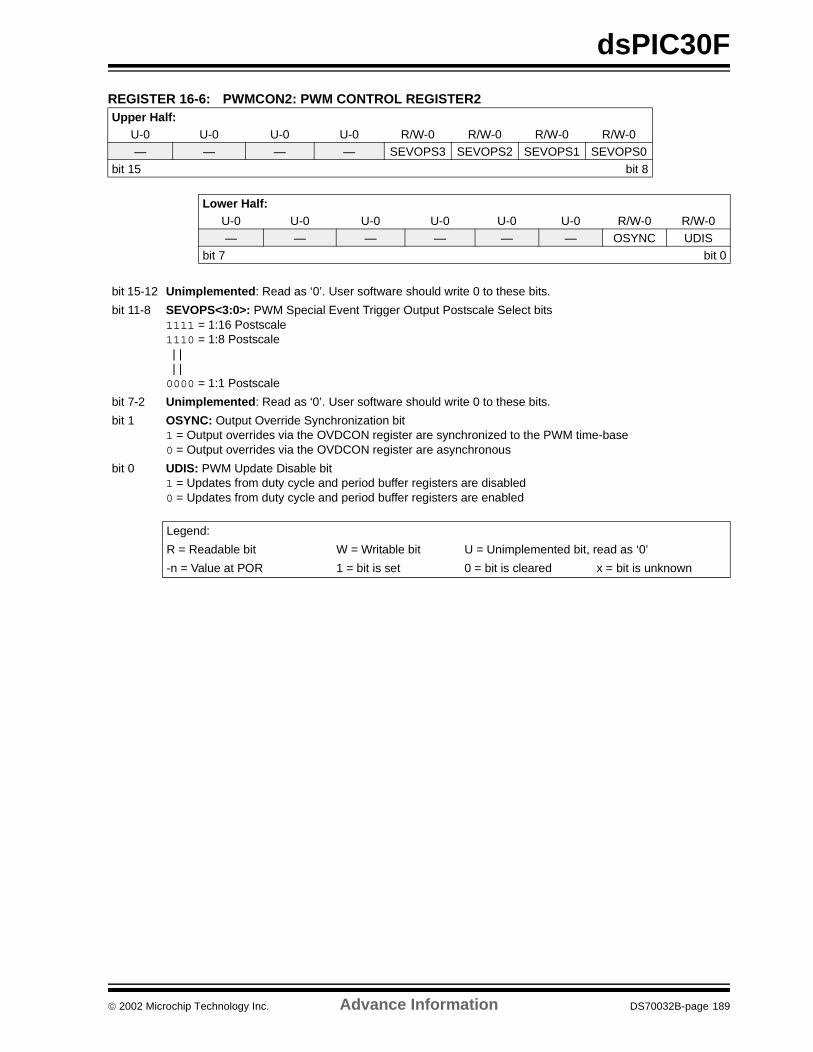
dsPIC30F
REGISTER 16-6: PWMCON2: PWM CONTROL REGISTER2 Upper Half:
U-0 U-0 U-0 U-0 R/W-0 R/W-0 R/W-0 R/W-0— — — — SEVOPS3 SEVOPS2 SEVOPS1 SEVOPS0
bit 15 bit 8
Lower Half:U-0 U-0 U-0 U-0 U-0 U-0 R/W-0 R/W-0— — — — — — OSYNC UDIS
bit 7 bit 0
bit 15-12 Unimplemented: Read as ‘0’. User software should write 0 to these bits.
bit 11-8 SEVOPS<3:0>: PWM Special Event Trigger Output Postscale Select bits1111 = 1:16 Postscale1110 = 1:8 Postscale | | | |0000 = 1:1 Postscale
bit 7-2 Unimplemented: Read as ‘0’. User software should write 0 to these bits.
bit 1 OSYNC: Output Override Synchronization bit1 = Output overrides via the OVDCON register are synchronized to the PWM time-base0 = Output overrides via the OVDCON register are asynchronous
bit 0 UDIS: PWM Update Disable bit1 = Updates from duty cycle and period buffer registers are disabled0 = Updates from duty cycle and period buffer registers are enabled
Legend:
R = Readable bit W = Writable bit U = Unimplemented bit, read as ‘0’
-n = Value at POR 1 = bit is set 0 = bit is cleared x = bit is unknown
2002 Microchip Technology Inc. Advance Information DS70032B-page 189
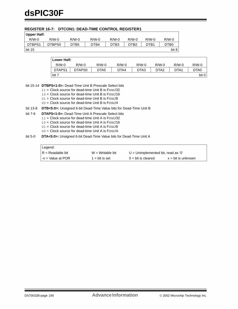
dsPIC30F
REGISTER 16-7: DTCON1: DEAD-TIME CONTROL REGISTER1 Upper Half:
R/W-0 R/W-0 R/W-0 R/W-0 R/W-0 R/W-0 R/W-0 R/W-0DTBPS1 DTBPS0 DTB5 DTB4 DTB3 DTB2 DTB1 DTB0
bit 15 bit 8
Lower Half:R/W-0 R/W-0 R/W-0 R/W-0 R/W-0 R/W-0 R/W-0 R/W-0
DTAPS1 DTAPS0 DTA5 DTA4 DTA3 DTA2 DTA1 DTA0bit 7 bit 0
bit 15-14 DTBPS<1:0>: Dead-Time Unit B Prescale Select bits11 = Clock source for dead-time Unit B is FOSC/3210 = Clock source for dead-time Unit B is FOSC/1601 = Clock source for dead-time Unit B is FOSC/800 = Clock source for dead-time Unit B is FOSC/4
bit 13-8 DTB<5:0>: Unsigned 6-bit Dead-Time Value bits for Dead-Time Unit B
bit 7-6 DTAPS<1:0>: Dead-Time Unit A Prescale Select bits11 = Clock source for dead-time Unit A is FOSC/3210 = Clock source for dead-time Unit A is FOSC/1601 = Clock source for dead-time Unit A is FOSC/800 = Clock source for dead-time Unit A is FOSC/4.
bit 5-0 DTA<5:0>: Unsigned 6-bit Dead-Time Value bits for Dead-Time Unit A
Legend:
R = Readable bit W = Writable bit U = Unimplemented bit, read as ‘0’
-n = Value at POR 1 = bit is set 0 = bit is cleared x = bit is unknown
DS70032B-page 190 Advance Information 2002 Microchip Technology Inc.
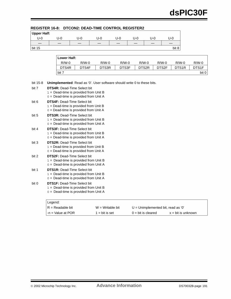
dsPIC30F
REGISTER 16-8: DTCON2: DEAD-TIME CONTROL REGISTER2 Upper Half:
U-0 U-0 U-0 U-0 U-0 U-0 U-0 U-0— — — — — — — —
bit 15 bit 8
Lower Half:R/W-0 R/W-0 R/W-0 R/W-0 R/W-0 R/W-0 R/W-0 R/W-0DTS4R DTS4F DTS3R DTS3F DTS2R DTS2F DTS1R DTS1F
bit 7 bit 0
bit 15-8 Unimplemented: Read as ‘0’. User software should write 0 to these bits.
bit 7 DTS4R: Dead-Time Select bit1 = Dead-time is provided from Unit B0 = Dead-time is provided from Unit A
bit 6 DTS4F: Dead-Time Select bit1 = Dead-time is provided from Unit B0 = Dead-time is provided from Unit A
bit 5 DTS3R: Dead-Time Select bit1 = Dead-time is provided from Unit B0 = Dead-time is provided from Unit A
bit 4 DTS3F: Dead-Time Select bit1 = Dead-time is provided from Unit B0 = Dead-time is provided from Unit A
bit 3 DTS2R: Dead-Time Select bit1 = Dead-time is provided from Unit B0 = Dead-time is provided from Unit A
bit 2 DTS2F: Dead-Time Select bit1 = Dead-time is provided from Unit B0 = Dead-time is provided from Unit A
bit 1 DTS1R: Dead-Time Select bit1 = Dead-time is provided from Unit B0 = Dead-time is provided from Unit A
bit 0 DTS1F: Dead-Time Select bit1 = Dead-time is provided from Unit B0 = Dead-time is provided from Unit A
Legend:
R = Readable bit W = Writable bit U = Unimplemented bit, read as ‘0’
-n = Value at POR 1 = bit is set 0 = bit is cleared x = bit is unknown
2002 Microchip Technology Inc. Advance Information DS70032B-page 191
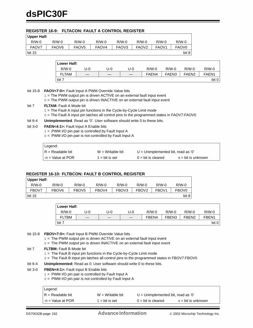
dsPIC30F
REGISTER 16-9: FLTACON: FAULT A CONTROL REGISTER
REGISTER 16-10: FLTBCON: FAULT B CONTROL REGISTER
Upper Half:R/W-0 R/W-0 R/W-0 R/W-0 R/W-0 R/W-0 R/W-0 R/W-0FAOV7 FAOV6 FAOV5 FAOV4 FAOV3 FAOV2 FAOV1 FAOV0
bit 15 bit 8
Lower Half:R/W-0 U-0 U-0 U-0 R/W-0 R/W-0 R/W-0 R/W-0FLTAM — — — FAEN4 FAEN3 FAEN2 FAEN1
bit 7 bit 0
bit 15-8 FAOV<7:0>: Fault Input A PWM Override Value bits1 = The PWM output pin is driven ACTIVE on an external fault input event0 = The PWM output pin is driven INACTIVE on an external fault input event
bit 7 FLTAM: Fault A Mode bit1 = The Fault A input pin functions in the Cycle-by-Cycle Limit mode0 = The Fault A input pin latches all control pins to the programmed states in FAOV7:FAOV0
bit 6-4 Unimplemented. Read as ‘0’. User software should write 0 to these bits.
bit 3-0 FAEN<4:1>: Fault Input A Enable bits1 = PWM I/O pin pair is controlled by Fault Input A0 = PWM I/O pin pair is not controlled by Fault Input A
Legend:
R = Readable bit W = Writable bit U = Unimplemented bit, read as ‘0’
-n = Value at POR 1 = bit is set 0 = bit is cleared x = bit is unknown
Upper Half:R/W-0 R/W-0 R/W-0 R/W-0 R/W-0 R/W-0 R/W-0 R/W-0FBOV7 FBOV6 FBOV5 FBOV4 FBOV3 FBOV2 FBOV1 FBOV0
bit 15 bit 8
Lower Half:R/W-0 U-0 U-0 U-0 R/W-0 R/W-0 R/W-0 R/W-0FLTBM — — — FBEN4 FBEN3 FBEN2 FBEN1
bit 7 bit 0
bit 15-8 FBOV<7:0>: Fault Input B PWM Override Value bits1 = The PWM output pin is driven ACTIVE on an external fault input event0 = The PWM output pin is driven INACTIVE on an external fault input event
bit 7 FLTBM: Fault B Mode bit1 = The Fault B input pin functions in the Cycle-by-Cycle Limit mode0 = The Fault B input pin latches all control pins to the programmed states in FBOV7:FBOV0
bit 6-4 Unimplemented: Read as 0. User software should write 0 to these bits.
bit 3-0 FBEN<4:1>: Fault Input B Enable bits1 = PWM I/O pin pair is controlled by Fault Input A0 = PWM I/O pin pair is not controlled by Fault Input A
Legend:
R = Readable bit W = Writable bit U = Unimplemented bit, read as ‘0’
-n = Value at POR 1 = bit is set 0 = bit is cleared x = bit is unknown
DS70032B-page 192 Advance Information 2002 Microchip Technology Inc.
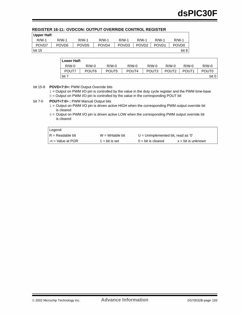
dsPIC30F
REGISTER 16-11: OVDCON: OUTPUT OVERRIDE CONTROL REGISTER Upper Half:
R/W-1 R/W-1 R/W-1 R/W-1 R/W-1 R/W-1 R/W-1 R/W-1POVD7 POVD6 POVD5 POVD4 POVD3 POVD2 POVD1 POVD0
bit 15 bit 8
Lower Half:R/W-0 R/W-0 R/W-0 R/W-0 R/W-0 R/W-0 R/W-0 R/W-0POUT7 POUT6 POUT5 POUT4 POUT3 POUT2 POUT1 POUT0
bit 7 bit 0
bit 15-8 POVD<7:0>: PWM Output Override bits1 = Output on PWM I/O pin is controlled by the value in the duty cycle register and the PWM time-base0 = Output on PWM I/O pin is controlled by the value in the corresponding POUT bit
bit 7-0 POUT<7:0> : PWM Manual Output bits1 = Output on PWM I/O pin is driven active HIGH when the corresponding PWM output override bit
is cleared0 = Output on PWM I/O pin is driven active LOW when the corresponding PWM output override bit
is cleared
Legend:
R = Readable bit W = Writable bit U = Unimplemented bit, read as ‘0’
-n = Value at POR 1 = bit is set 0 = bit is cleared x = bit is unknown
2002 Microchip Technology Inc. Advance Information DS70032B-page 193
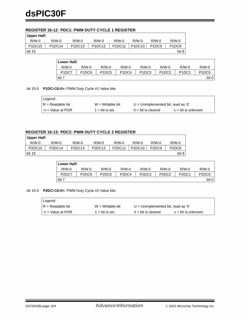
dsPIC30F
REGISTER 16-12: PDC1: PWM DUTY CYCLE 1 REGISTER
REGISTER 16-13: PDC2: PWM DUTY CYCLE 2 REGISTER
Upper Half:R/W-0 R/W-0 R/W-0 R/W-0 R/W-0 R/W-0 R/W-0 R/W-0
P1DC15 P1DC14 P1DC13 P1DC12 P1DC11 P1DC10 P1DC9 P1DC8
bit 15 bit 8
Lower Half:R/W-0 R/W-0 R/W-0 R/W-0 R/W-0 R/W-0 R/W-0 R/W-0P1DC7 P1DC6 P1DC5 P1DC4 P1DC3 P1DC2 P1DC1 P1DC0
bit 7 bit 0
bit 15-0 P1DC<15:0>: PWM Duty Cycle #1 Value bits
Legend:
R = Readable bit W = Writable bit U = Unimplemented bit, read as ‘0’
-n = Value at POR 1 = bit is set 0 = bit is cleared x = bit is unknown
Upper Half:R/W-0 R/W-0 R/W-0 R/W-0 R/W-0 R/W-0 R/W-0 R/W-0
P2DC15 P2DC14 P2DC13 P2DC12 P2DC11 P2DC10 P2DC9 P2DC8
bit 15 bit 8
Lower Half:R/W-0 R/W-0 R/W-0 R/W-0 R/W-0 R/W-0 R/W-0 R/W-0P2DC7 P2DC6 P2DC5 P2DC4 P2DC3 P2DC2 P2DC1 P2DC0
bit 7 bit 0
bit 15-0 P2DC<15:0>: PWM Duty Cycle #2 Value bits
Legend:
R = Readable bit W = Writable bit U = Unimplemented bit, read as ‘0’
-n = Value at POR 1 = bit is set 0 = bit is cleared x = bit is unknown
DS70032B-page 194 Advance Information 2002 Microchip Technology Inc.
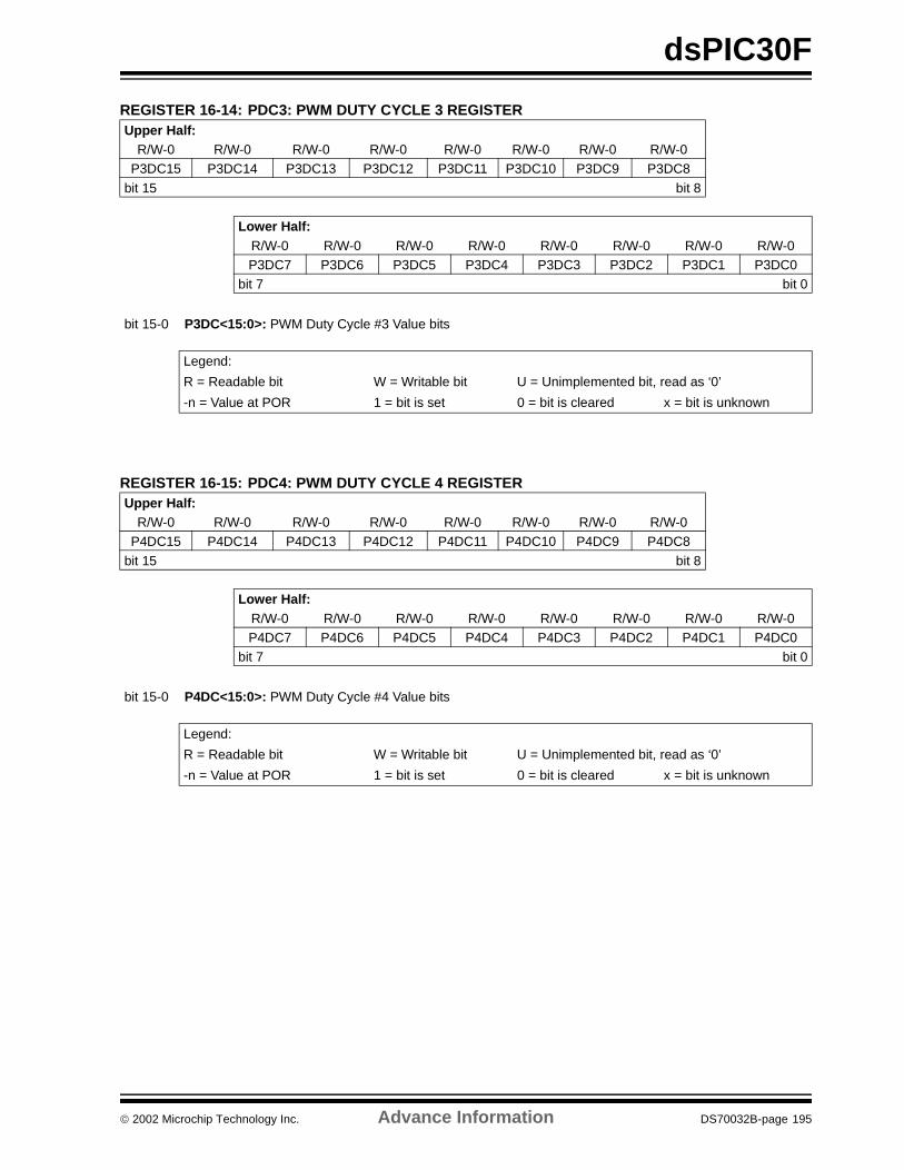
dsPIC30F
REGISTER 16-14: PDC3: PWM DUTY CYCLE 3 REGISTER
REGISTER 16-15: PDC4: PWM DUTY CYCLE 4 REGISTER
Upper Half:R/W-0 R/W-0 R/W-0 R/W-0 R/W-0 R/W-0 R/W-0 R/W-0
P3DC15 P3DC14 P3DC13 P3DC12 P3DC11 P3DC10 P3DC9 P3DC8
bit 15 bit 8
Lower Half:R/W-0 R/W-0 R/W-0 R/W-0 R/W-0 R/W-0 R/W-0 R/W-0P3DC7 P3DC6 P3DC5 P3DC4 P3DC3 P3DC2 P3DC1 P3DC0
bit 7 bit 0
bit 15-0 P3DC<15:0>: PWM Duty Cycle #3 Value bits
Legend:
R = Readable bit W = Writable bit U = Unimplemented bit, read as ‘0’
-n = Value at POR 1 = bit is set 0 = bit is cleared x = bit is unknown
Upper Half:R/W-0 R/W-0 R/W-0 R/W-0 R/W-0 R/W-0 R/W-0 R/W-0
P4DC15 P4DC14 P4DC13 P4DC12 P4DC11 P4DC10 P4DC9 P4DC8
bit 15 bit 8
Lower Half:R/W-0 R/W-0 R/W-0 R/W-0 R/W-0 R/W-0 R/W-0 R/W-0P4DC7 P4DC6 P4DC5 P4DC4 P4DC3 P4DC2 P4DC1 P4DC0
bit 7 bit 0
bit 15-0 P4DC<15:0>: PWM Duty Cycle #4 Value bits
Legend:
R = Readable bit W = Writable bit U = Unimplemented bit, read as ‘0’
-n = Value at POR 1 = bit is set 0 = bit is cleared x = bit is unknown
2002 Microchip Technology Inc. Advance Information DS70032B-page 195

dsPIC30F
NOTES:
DS70032B-page 196 Advance Information 2002 Microchip Technology Inc.
dsPIC30F
17.0 SPI MODULE
The Serial Peripheral Interface (SPI) module is a syn-chronous serial interface, useful for communicatingwith other peripheral or microcontroller devices, suchas EEPROMs, shift registers, display drivers and A/Dconverters. It is compatible with Motorola’s SPITM andSIOPTM interfaces.
17.1 Operating Function Description
Each SPI module consists of a 16-bit shift register,SPIxSR (where x = 1 or 2), used for shifting data inand out, and a buffer register, SPIxBUF. A control reg-ister, SPIxCON, configures the module. Additionally, astatus register, SPIxSTAT, indicates various statusconditions.
The serial interface consists of 4 pins: SDIx (serialdata input), SDOx (serial data output), SCKx (shiftclock input or output), and SSx (active low slaveselect).
In Master mode operation, SCK is a clock output, butin Slave mode, it is a clock input.
A series of eight (8) or sixteen (16) clock pulses shiftsout bits from the SPIxSR to SDOx pin and simulta-neously shifts in data from SDIx pin. An interrupt isgenerated when the transfer is complete and the cor-responding interrupt flag bit (SPI1IF or SPI2IF) is set.This interrupt can be disabled through an interruptenable bit (SPI1IE or SPI2IE).
The receive operation is double buffered. When acomplete byte is received, it is transferred fromSPIxSR to SPIxBUF.
If the receive buffer is full when new data is beingtransferred from SPIxSR to SPIxBUF, the module willset the SPIROV bit, indicating an overflow condition.The transfer of the data from SPIxSR to SPIxBUF willnot be completed and the new data will be lost. Themodule will not respond to SCL transitions whileSPIROV is 1, effectively disabling the module untilSPIxBUF is read by user software.
Transmit writes are also double buffered. The userwrites to SPIxBUF. When the master or slave transferis completed, the SPIxSR is swapped with SPIxBUF.The received data is thus placed in SPIxBUF and thetransmit data in SPIxSR is ready for the next transfer.
In Master mode, the clock is generated by prescalingthe system clock. Data is transmitted as soon asSPIBUF is written to. The interrupt is generated at themiddle of the transfer of the last bit.
In Slave mode, data is transmitted and received asexternal clock pulses appear on SCK. Again, the inter-rupt is generated when the last bit is latched in. If SSxcontrol is enabled, then transmission and reception areenabled only when SSx = low. The SDOx output will bedisabled in SSx mode with SSx high.
The clock provided to the module is (FOSC/4). Thisclock is then prescaled by the primary (PPRE<1:0>)and the secondary (SPRE<2:0>) prescale factors. TheCKE bit determines whether transmit occurs on transi-tion from active clock state to IDLE clock state, or viceversa. The CKP bit selects the IDLE state (high or low)for the clock.
17.1.1 WORD AND BYTE COMMUNICATION
A control bit, MODE16 (SPIxCON<10>), allows themodule to communicate in either 16-bit or 8-bit mode.Figure 17-5 through Figure 17-7 demonstrate the func-tionality of the module in 8-bit mode. 16-bit operation isidentical to 8-bit operation, except that the number ofbits transmitted is 16 instead of 8.
The SPI module always gets reset to start a new com-munication when the MODE16 bit is changed by theuser.
A basic difference between 8-bit and 16-bit operation isthat the data is transmitted out of bit 7 of the SPIxSR for8-bit operation, and data is transmitted out of bit15 ofthe SPIxSR for 16-bit operation. In both modes, data isshifted into bit 0 of the SPIxSR.
17.1.2 SDOx DISABLE
A control bit, DISSDO, is provided to the SPIxCON reg-ister to allow the SDOx output to be disabled. This willallow the SPI module to be connected in an input onlyconfiguration. SDO can also be used for generalpurpose I/O.
17.2 Framed SPI Support
The module supports a basic framed SPI protocol inMaster or Slave mode. The control bit FRMEN enablesframed SPI support and causes the SSx pin to performthe frame synchronization pulse (FSYNC) function.The control bit SPIFSD determines whether the SSxpin is an input or an output, i.e., whether the modulereceives or generates the frame synchronization pulse.The frame pulse is an active high pulse for a single SPIclock cycle. When frame synchronization is enabled,the data starts transmitting only on the subsequenttransmit edge of the SPI clock.
17.2.1 MODE: SPI MASTER, FRAME MASTER
With framed SPI enabled, the clock will be output con-tinuously, regardless of whether the module is transmit-ting. The FRMEN bit is high, and the SPIFSD bit is low.When the SPIxBUF is written, the SSx pin will be drivenhigh on the next transmit edge of the SPI clock. TheSSx pin will be high for one SPI clock cycle. Data willstart transmitting on the next transmit edge of the SPIclock, as shown in Figure 17-1.
2002 Microchip Technology Inc. Advance Information DS70032B-page 197
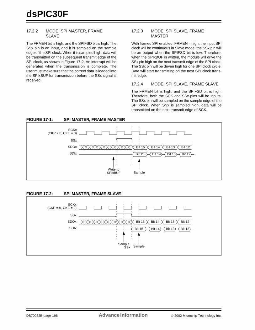
dsPIC30F
17.2.2 MODE: SPI MASTER, FRAME SLAVE
The FRMEN bit is high, and the SPIFSD bit is high. TheSSx pin is an input, and it is sampled on the sampleedge of the SPI clock. When it is sampled high, data willbe transmitted on the subsequent transmit edge of theSPI clock, as shown in Figure 17-2. An interrupt will begenerated when the transmission is complete. Theuser must make sure that the correct data is loaded intothe SPIxBUF for transmission before the SSx signal isreceived.
17.2.3 MODE: SPI SLAVE, FRAME MASTER
With framed SPI enabled, FRMEN = high, the input SPIclock will be continuous in Slave mode. the SSx pin willbe an output when the SPIFSD bit is low. Therefore,when the SPIxBUF is written, the module will drive theSSx pin high on the next transmit edge of the SPI clock.The SSx pin will be driven high for one SPI clock cycle.Data will start transmitting on the next SPI clock trans-mit edge.
17.2.4 MODE: SPI SLAVE, FRAME SLAVE
The FRMEN bit is high, and the SPIFSD bit is high.Therefore, both the SCK and SSx pins will be inputs.The SSx pin will be sampled on the sample edge of theSPI clock. When SSx is sampled high, data will betransmitted on the next transmit edge of SCK.
FIGURE 17-1: SPI MASTER, FRAME MASTER
FIGURE 17-2: SPI MASTER, FRAME SLAVE
SCKx
SSx
SDOx
(CKP = 0, CKE = 0)
Bit 15 Bit 14 Bit 13 Bit 12
SDIx
Write toSPIxBUF Sample
Bit 15 Bit 14 Bit 13 Bit 12
SCKx
SSx
SDOx
(CKP = 0, CKE = 0)
Bit 15 Bit 14 Bit 13 Bit 12
SDIx
SampleSSx Sample
Bit 15 Bit 14 Bit 13 Bit 12
DS70032B-page 198 Advance Information 2002 Microchip Technology Inc.
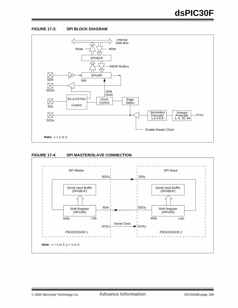
dsPIC30F
FIGURE 17-3: SPI BLOCK DIAGRAM
FIGURE 17-4: SPI MASTER/SLAVE CONNECTION
Read Write
InternalData Bus
SDIx
SDOx
SSx
SCKx
SPIxSR
SPIxBUF
bit0
ShiftClock
EdgeSelect
FOSCPrimary
1, 4, 16, 64
Enable Master Clock
PrescalerSecondaryPrescaler1,2,4,6,8
SS & FSYNC
Control
ClockControl
SWAP Buffers
Note: x = 1 or 2.
Serial Input Buffer(SPIxBUF)
Shift Register(SPIxSR)
MSb LSb
SDOx
SDIx
PROCESSOR 1
SCKx
SPI Master
Serial Input Buffer(SPIxBUF)
Shift Register(SPIxSR)
LSbMSb
SDIy
SDOy
PROCESSOR 2
SCKy
SPI Slave
Serial Clock
Note: x = 1 or 2, y = 1 or 2.
2002 Microchip Technology Inc. Advance Information DS70032B-page 199
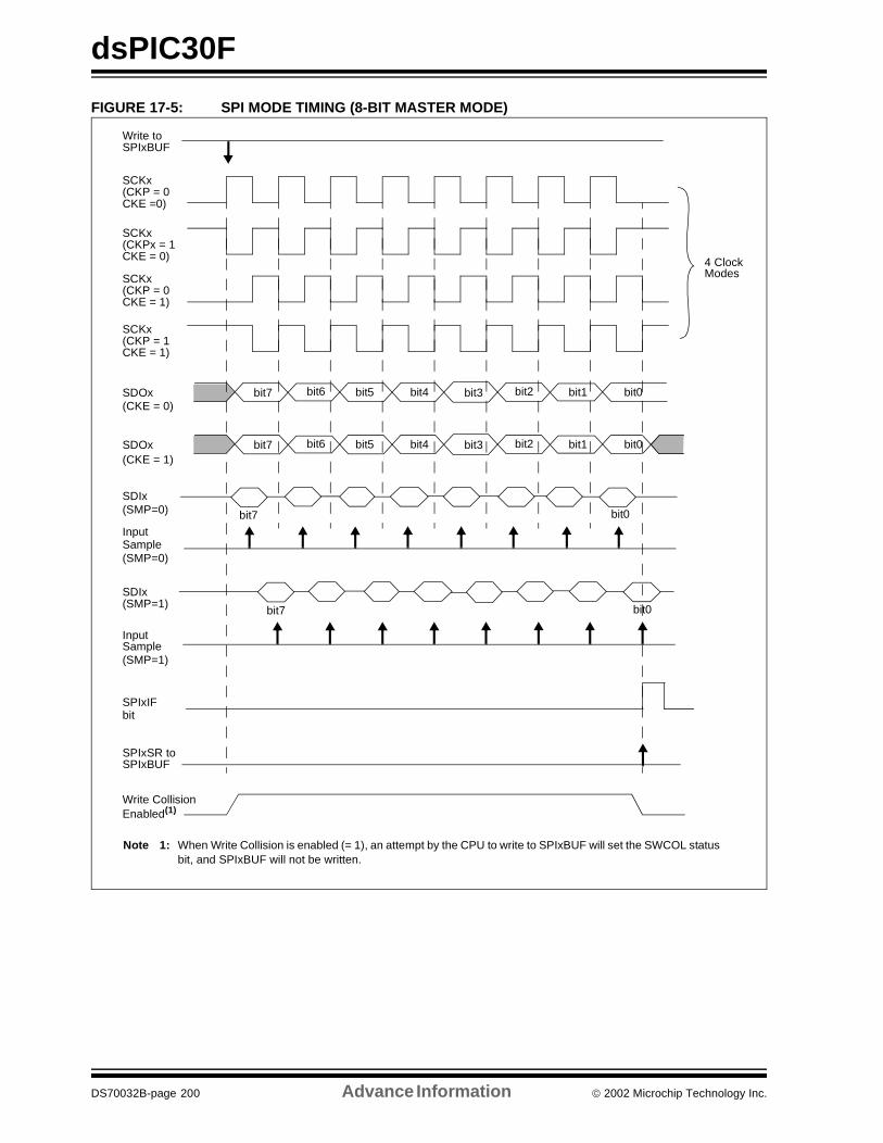
dsPIC30F
FIGURE 17-5: SPI MODE TIMING (8-BIT MASTER MODE)
SCKx(CKP = 0
SCKx(CKPx = 1
SCKx(CKP = 0
SCKx(CKP = 1
4 ClockModes
InputSample
InputSample
SDIx
bit7 bit0
SDOx bit7 bit6 bit5 bit4 bit3 bit2 bit1 bit0
bit7 bit0
SDIx
SPIxIF
(SMP=1)
(SMP=0)
(SMP=1)
CKE = 1)
CKE =0)
CKE = 1)
CKE = 0)
(SMP=0)
Write toSPIxBUF
SPIxSR toSPIxBUF
Write CollisionEnabled(1)
SDOx bit7 bit6 bit5 bit4 bit3 bit2 bit1 bit0
(CKE = 0)
(CKE = 1)
bit
Note 1: When Write Collision is enabled (= 1), an attempt by the CPU to write to SPIxBUF will set the SWCOL statusbit, and SPIxBUF will not be written.
DS70032B-page 200 Advance Information 2002 Microchip Technology Inc.
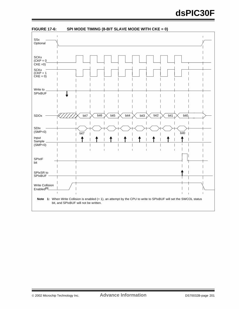
dsPIC30F
FIGURE 17-6: SPI MODE TIMING (8-BIT SLAVE MODE WITH CKE = 0)
SCKx(CKP = 1
SCKx(CKP = 0
InputSample
SDIx
bit7 bit0
SDOx bit7 bit6 bit5 bit4 bit3 bit2 bit1 bit0
SPIxIF
(SMP=0)
CKE =0)
CKE = 0)
(SMP=0)
Write toSPIxBUF
SPIxSR toSPIxBUF
Write CollisionEnabled(1)
Optional
bit
SSx
Note 1: When Write Collision is enabled (= 1), an attempt by the CPU to write to SPIxBUF will set the SWCOL statusbit, and SPIxBUF will not be written.
2002 Microchip Technology Inc. Advance Information DS70032B-page 201
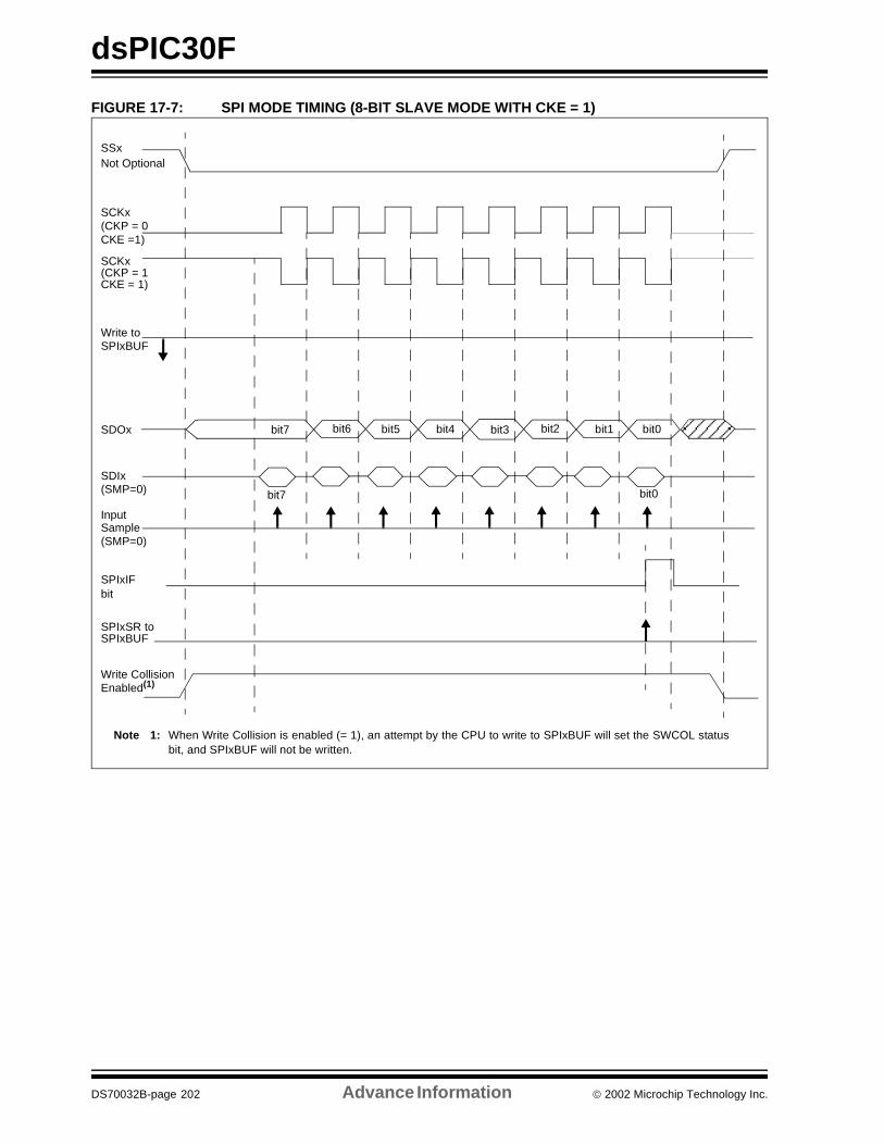
dsPIC30F
FIGURE 17-7: SPI MODE TIMING (8-BIT SLAVE MODE WITH CKE = 1)
SCKx(CKP = 1
SCKx(CKP = 0
InputSample
SDIx
bit7 bit0
SDOx bit7 bit6 bit5 bit4 bit3 bit2 bit1 bit0
SPIxIF
(SMP=0)
CKE =1)
CKE = 1)
(SMP=0)
Write toSPIxBUF
SPIxSR toSPIxBUF
Write CollisionEnabled(1)
Not Optional
bit
SSx
Note 1: When Write Collision is enabled (= 1), an attempt by the CPU to write to SPIxBUF will set the SWCOL statusbit, and SPIxBUF will not be written.
DS70032B-page 202 Advance Information 2002 Microchip Technology Inc.
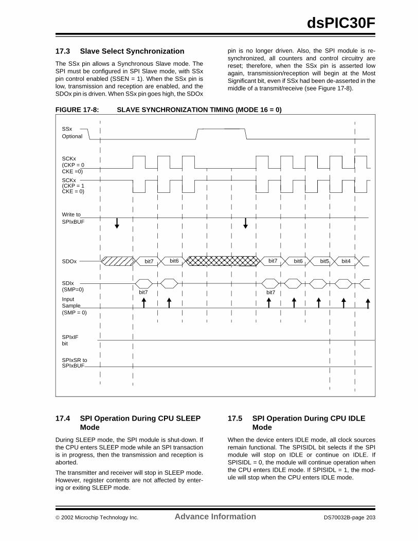
dsPIC30F
17.3 Slave Select Synchronization
The SSx pin allows a Synchronous Slave mode. TheSPI must be configured in SPI Slave mode, with SSxpin control enabled (SSEN = 1). When the SSx pin islow, transmission and reception are enabled, and theSDOx pin is driven. When SSx pin goes high, the SDOx
pin is no longer driven. Also, the SPI module is re-synchronized, all counters and control circuitry arereset; therefore, when the SSx pin is asserted lowagain, transmission/reception will begin at the MostSignificant bit, even if SSx had been de-asserted in themiddle of a transmit/receive (see Figure 17-8).
FIGURE 17-8: SLAVE SYNCHRONIZATION TIMING (MODE 16 = 0)
17.4 SPI Operation During CPU SLEEP Mode
During SLEEP mode, the SPI module is shut-down. Ifthe CPU enters SLEEP mode while an SPI transactionis in progress, then the transmission and reception isaborted.
The transmitter and receiver will stop in SLEEP mode.However, register contents are not affected by enter-ing or exiting SLEEP mode.
17.5 SPI Operation During CPU IDLE Mode
When the device enters IDLE mode, all clock sourcesremain functional. The SPISIDL bit selects if the SPImodule will stop on IDLE or continue on IDLE. IfSPISIDL = 0, the module will continue operation whenthe CPU enters IDLE mode. If SPISIDL = 1, the mod-ule will stop when the CPU enters IDLE mode.
SCKx(CKP = 1
SCKx(CKP = 0
InputSample
SDIx
bit7
SDOx bit7 bit6 bit7 bit6 bit5
SPIxIF
(SMP = 0)
CKE =0)
CKE = 0)
(SMP=0)
Write toSPIxBUF
SPIxSR toSPIxBUF
Optional
bit4
bit7
bit
SSx
2002 Microchip Technology Inc. Advance Information DS70032B-page 203
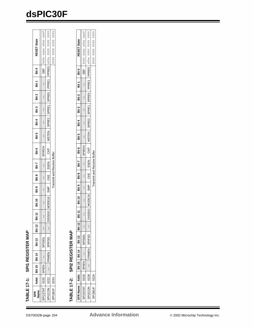
dsPIC30F
TABL
E 1
7-1:
SP
I1 R
EG
IST
ER
MA
P
TAB
LE
17-
2:S
PI2
RE
GIS
TE
R M
AP
SF
R
Nam
eA
dd
r.B
it 1
5B
it 1
4B
it 1
3B
it 1
2B
it 1
1B
it 1
0B
it 9
Bit
8B
it 7
Bit
6B
it 5
Bit
4B
it 3
Bit
2B
it 1
Bit
0R
ES
ET
Sta
te
SP
I1S
TAT
0220
SP
IEN
—S
PIS
IDL
——
——
——
SP
IRO
V—
——
——
SB
F0u0u uuuu u0uu uuu0
SP
I1C
ON
0222
—F
RM
EN
SP
IFS
D—
DIS
SD
OM
OD
E16
SM
PC
KE
SS
EN
CK
PM
ST
EN
SP
RE
2S
PR
E1
SP
RE
0P
PR
E1
PP
RE
0u00u 0000 0000 0000
SP
I1B
UF
0224
Tra
nsm
it an
d R
ecei
ve B
uffe
r0000 0000 0000 0000
SF
R N
ame
Ad
dr.
Bit
15
Bit
14
Bit
13
Bit
12
Bit
11
Bit
10
Bit
9B
it 8
Bit
7B
it 6
Bit
5B
it 4
Bit
3B
it 2
Bit
1B
it 0
RE
SE
T S
tate
SP
I2S
TAT
0226
SP
IEN
—S
PIS
IDL
——
——
——
SP
IRO
V—
——
——
SB
F0u0u uuuu u0uu uuu0
SP
I2C
ON
0228
—F
RM
EN
SP
IFS
D—
DIS
SD
OM
OD
E16
SM
PC
KE
SS
EN
CK
PM
ST
EN
SP
RE
2S
PR
E1
SP
RE
0P
PR
E1
PP
RE
0u00u 0000 0000 0000
SP
I2B
UF
022A
Tran
smit
and
Rec
eive
Buf
fer
0000 0000 0000 0000
DS70032B-page 204 Advance Information 2002 Microchip Technology Inc.
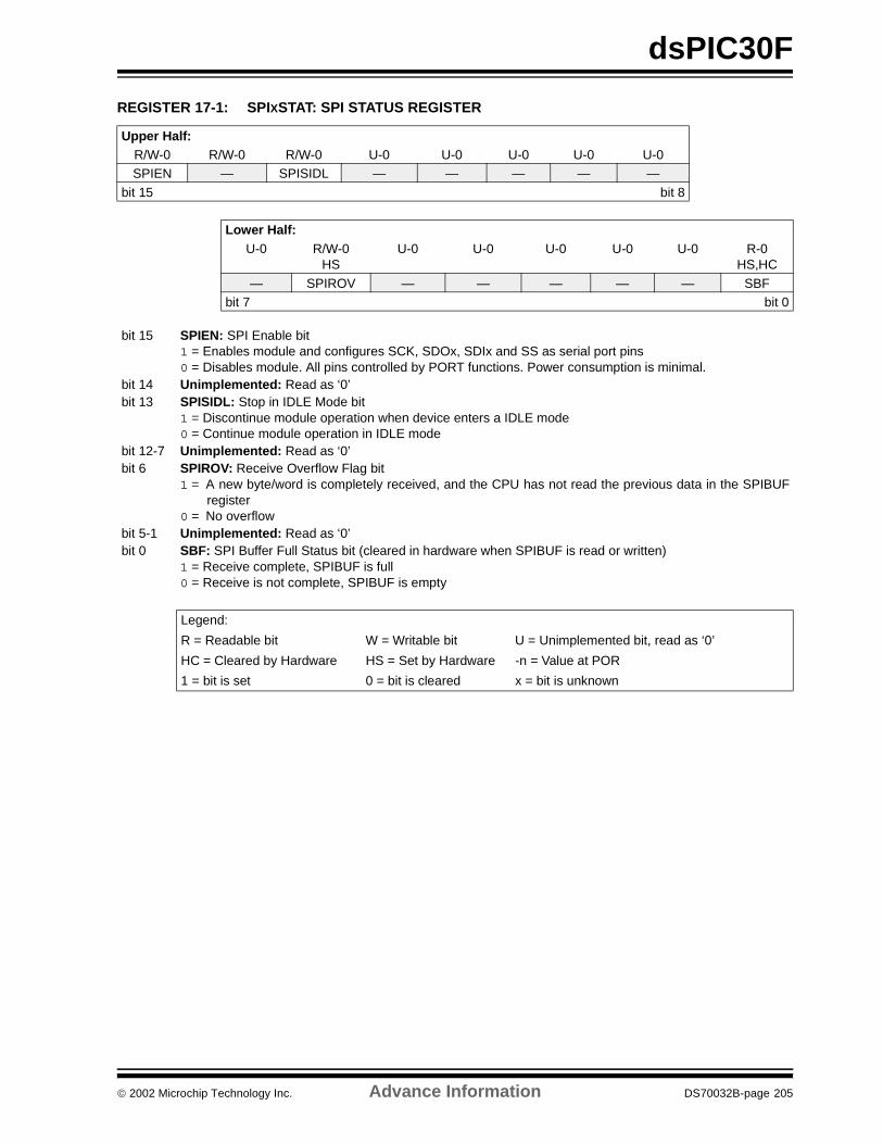
dsPIC30F
REGISTER 17-1: SPIXSTAT: SPI STATUS REGISTER
Upper Half:R/W-0 R/W-0 R/W-0 U-0 U-0 U-0 U-0 U-0SPIEN — SPISIDL — — — — —
bit 15 bit 8
Lower Half:U-0 R/W-0
HSU-0 U-0 U-0 U-0 U-0 R-0
HS,HC
— SPIROV — — — — — SBFbit 7 bit 0
bit 15 SPIEN: SPI Enable bit1 = Enables module and configures SCK, SDOx, SDIx and SS as serial port pins0 = Disables module. All pins controlled by PORT functions. Power consumption is minimal.
bit 14 Unimplemented: Read as ‘0’bit 13 SPISIDL: Stop in IDLE Mode bit
1 = Discontinue module operation when device enters a IDLE mode0 = Continue module operation in IDLE mode
bit 12-7 Unimplemented: Read as ‘0’bit 6 SPIROV: Receive Overflow Flag bit
1 = A new byte/word is completely received, and the CPU has not read the previous data in the SPIBUFregister
0 = No overflowbit 5-1 Unimplemented: Read as ‘0’bit 0 SBF: SPI Buffer Full Status bit (cleared in hardware when SPIBUF is read or written)
1 = Receive complete, SPIBUF is full0 = Receive is not complete, SPIBUF is empty
Legend:
R = Readable bit W = Writable bit U = Unimplemented bit, read as ‘0’
HC = Cleared by Hardware HS = Set by Hardware -n = Value at POR
1 = bit is set 0 = bit is cleared x = bit is unknown
2002 Microchip Technology Inc. Advance Information DS70032B-page 205
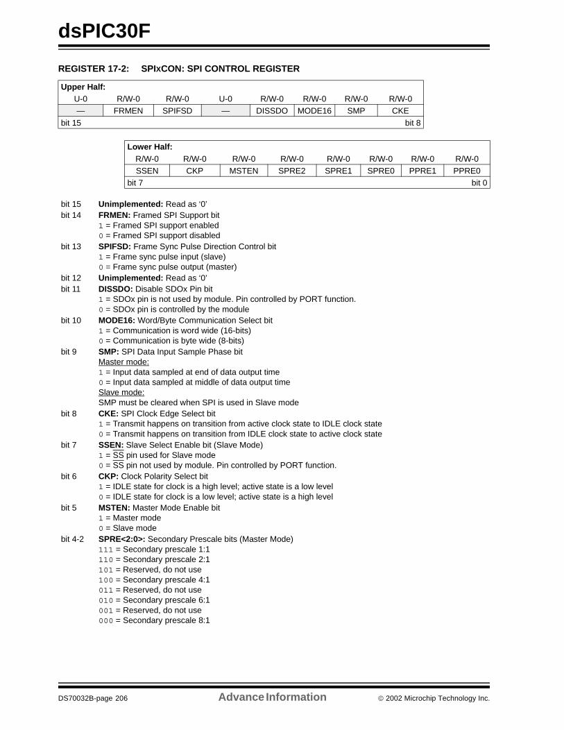
dsPIC30F
REGISTER 17-2: SPIXCON: SPI CONTROL REGISTER
Upper Half:U-0 R/W-0 R/W-0 U-0 R/W-0 R/W-0 R/W-0 R/W-0— FRMEN SPIFSD — DISSDO MODE16 SMP CKE
bit 15 bit 8
Lower Half:R/W-0 R/W-0 R/W-0 R/W-0 R/W-0 R/W-0 R/W-0 R/W-0SSEN CKP MSTEN SPRE2 SPRE1 SPRE0 PPRE1 PPRE0
bit 7 bit 0
bit 15 Unimplemented: Read as ‘0’bit 14 FRMEN: Framed SPI Support bit
1 = Framed SPI support enabled0 = Framed SPI support disabled
bit 13 SPIFSD: Frame Sync Pulse Direction Control bit1 = Frame sync pulse input (slave)0 = Frame sync pulse output (master)
bit 12 Unimplemented: Read as ‘0’bit 11 DISSDO: Disable SDOx Pin bit
1 = SDOx pin is not used by module. Pin controlled by PORT function.0 = SDOx pin is controlled by the module
bit 10 MODE16: Word/Byte Communication Select bit1 = Communication is word wide (16-bits)0 = Communication is byte wide (8-bits)
bit 9 SMP: SPI Data Input Sample Phase bitMaster mode:1 = Input data sampled at end of data output time0 = Input data sampled at middle of data output timeSlave mode:SMP must be cleared when SPI is used in Slave mode
bit 8 CKE: SPI Clock Edge Select bit1 = Transmit happens on transition from active clock state to IDLE clock state0 = Transmit happens on transition from IDLE clock state to active clock state
bit 7 SSEN: Slave Select Enable bit (Slave Mode)1 = SS pin used for Slave mode0 = SS pin not used by module. Pin controlled by PORT function.
bit 6 CKP: Clock Polarity Select bit1 = IDLE state for clock is a high level; active state is a low level0 = IDLE state for clock is a low level; active state is a high level
bit 5 MSTEN: Master Mode Enable bit1 = Master mode0 = Slave mode
bit 4-2 SPRE<2:0>: Secondary Prescale bits (Master Mode)111 = Secondary prescale 1:1110 = Secondary prescale 2:1101 = Reserved, do not use100 = Secondary prescale 4:1011 = Reserved, do not use010 = Secondary prescale 6:1001 = Reserved, do not use000 = Secondary prescale 8:1
DS70032B-page 206 Advance Information 2002 Microchip Technology Inc.
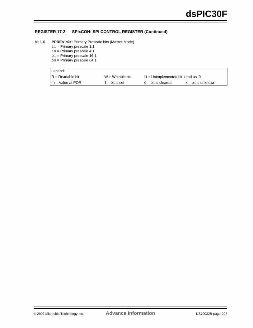
dsPIC30F
REGISTER 17-2: SPIXCON: SPI CONTROL REGISTER (Continued)
bit 1-0 PPRE<1:0>: Primary Prescale bits (Master Mode)11 = Primary prescale 1:110 = Primary prescale 4:101 = Primary prescale 16:100 = Primary prescale 64:1
Legend:
R = Readable bit W = Writable bit U = Unimplemented bit, read as ‘0’
-n = Value at POR 1 = bit is set 0 = bit is cleared x = bit is unknown
2002 Microchip Technology Inc. Advance Information DS70032B-page 207

dsPIC30F
NOTES:
DS70032B-page 208 Advance Information 2002 Microchip Technology Inc.
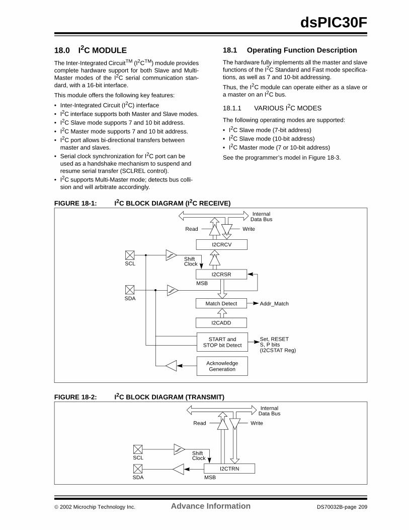
dsPIC30F
18.0 I2C MODULE
The Inter-Integrated CircuitTM (I2CTM) module providescomplete hardware support for both Slave and Multi-Master modes of the I2C serial communication stan-dard, with a 16-bit interface.
This module offers the following key features:
• Inter-Integrated Circuit (I2C) interface• I2C interface supports both Master and Slave modes.• I2C Slave mode supports 7 and 10 bit address.
• I2C Master mode supports 7 and 10 bit address.• I2C port allows bi-directional transfers between
master and slaves.• Serial clock synchronization for I2C port can be
used as a handshake mechanism to suspend and resume serial transfer (SCLREL control).
• I2C supports Multi-Master mode; detects bus colli-sion and will arbitrate accordingly.
18.1 Operating Function Description
The hardware fully implements all the master and slavefunctions of the I2C Standard and Fast mode specifica-tions, as well as 7 and 10-bit addressing.
Thus, the I2C module can operate either as a slave ora master on an I2C bus.
18.1.1 VARIOUS I2C MODES
The following operating modes are supported:
• I2C Slave mode (7-bit address)• I2C Slave mode (10-bit address)
• I2C Master mode (7 or 10-bit address)
See the programmer’s model in Figure 18-3.
FIGURE 18-1: I2C BLOCK DIAGRAM (I2C RECEIVE)
FIGURE 18-2: I2C BLOCK DIAGRAM (TRANSMIT)
Read Write
I2CRSR
I2CRCV
InternalData Bus
MSB
SCL
SDA
Shift
Match Detect
I2CADD
START andSTOP bit Detect
Clock
Set, RESETS, P bits
Addr_Match
(I2CSTAT Reg)
AcknowledgeGeneration
Read Write
I2CTRN
InternalData Bus
MSB
SCL
SDA
ShiftClock
2002 Microchip Technology Inc. Advance Information DS70032B-page 209
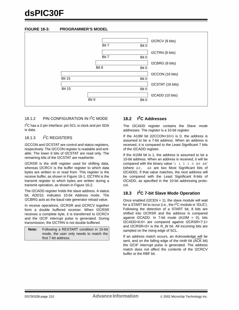
dsPIC30F
FIGURE 18-3: PROGRAMMER’S MODEL
18.1.2 PIN CONFIGURATION IN I2C MODE
I2C has a 2-pin interface: pin SCL is clock and pin SDAis data.
18.1.3 I2C REGISTERS
I2CCON and I2CSTAT are control and status registers,respectively. The I2CCON register is readable and writ-able. The lower 6 bits of I2CSTAT are read only. Theremaining bits of the I2CSTAT are read/write.
I2CRSR is the shift register used for shifting data,whereas I2CRCV is the buffer register to which databytes are written to or read from. This register is thereceive buffer, as shown in Figure 16-1. I2CTRN is thetransmit register to which bytes are written during atransmit operation, as shown in Figure 16-2.
The I2CADD register holds the slave address. A statusbit, ADD10, indicates 10-bit Address mode. TheI2CBRG acts as the baud rate generator reload value.
In receive operations, I2CRSR and I2CRCV togetherform a double buffered receiver. When I2CRSRreceives a complete byte, it is transferred to I2CRCVand the I2CIF interrupt pulse is generated. Duringtransmission, the I2CTRN is not double buffered.
18.2 I2C Addresses
The I2CADD register contains the Slave modeaddresses. The register is a 10-bit register.
If the A10M bit (I2CCON<10>) is 0, the address isassumed to be a 7-bit address. When an address isreceived, it is compared to the Least Significant 7 bitsof the I2CADD register.
If the A10M bit is 1, the address is assumed to be a10-bit address. When an address is received, it will becompared with the binary value ‘1 1 1 1 0 A9 A8’(where A9, A8 are two Most Significant bits ofI2CADD). If that value matches, the next address willbe compared with the Least Significant 8-bits ofI2CADD, as specified in the 10-bit addressing proto-col.
18.3 I2C 7-bit Slave Mode Operation
Once enabled (I2CEN = 1), the slave module will waitfor a START bit to occur (i.e., the I2C module is ‘IDLE’).Following the detection of a START bit, 8 bits areshifted into I2CRSR and the address is comparedagainst I2CADD. In 7-bit mode (A10M = 0), bitsI2CADD<6:0> are compared against I2CRSR<7:1>and I2CRSR<0> is the R_W bit. All incoming bits aresampled on the rising edge of SCL.
If an address match occurs, an Acknowledge will besent, and on the falling edge of the ninth bit (ACK bit)the I2CIF interrupt pulse is generated. The addressmatch does not affect the contents of the I2CRCVbuffer or the RBF bit.
Bit 7 Bit 0I2CRCV (8 bits)
Bit 7 Bit 0I2CTRN (8 bits)
Bit 8 Bit 0I2CBRG (9 bits)
Bit 15 Bit 0I2CCON (16 bits)
Bit 15 Bit 0I2CSTAT (16 bits)
Bit 9 Bit 0I2CADD (10 bits)
Note: Following a RESTART condition in 10-bitmode, the user only needs to match thefirst 7-bit address.
DS70032B-page 210 Advance Information 2002 Microchip Technology Inc.
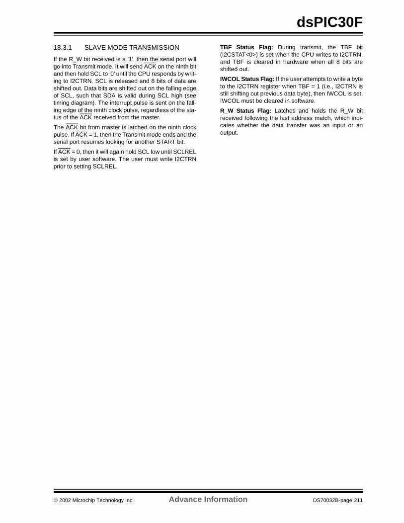
dsPIC30F
18.3.1 SLAVE MODE TRANSMISSION
If the R_W bit received is a ’1’, then the serial port willgo into Transmit mode. It will send ACK on the ninth bitand then hold SCL to ’0’ until the CPU responds by writ-ing to I2CTRN. SCL is released and 8 bits of data areshifted out. Data bits are shifted out on the falling edgeof SCL, such that SDA is valid during SCL high (seetiming diagram). The interrupt pulse is sent on the fall-ing edge of the ninth clock pulse, regardless of the sta-tus of the ACK received from the master.
The ACK bit from master is latched on the ninth clockpulse. If ACK = 1, then the Transmit mode ends and theserial port resumes looking for another START bit.
If ACK = 0, then it will again hold SCL low until SCLRELis set by user software. The user must write I2CTRNprior to setting SCLREL.
TBF Status Flag: During transmit, the TBF bit(I2CSTAT<0>) is set when the CPU writes to I2CTRN,and TBF is cleared in hardware when all 8 bits areshifted out.
IWCOL Status Flag: If the user attempts to write a byteto the I2CTRN register when TBF = 1 (i.e., I2CTRN isstill shifting out previous data byte), then IWCOL is set.IWCOL must be cleared in software.
R_W Status Flag: Latches and holds the R_W bitreceived following the last address match, which indi-cates whether the data transfer was an input or anoutput.
2002 Microchip Technology Inc. Advance Information DS70032B-page 211
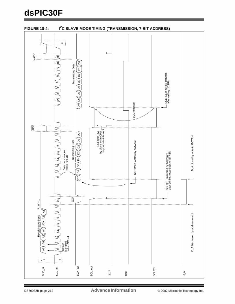
dsPIC30F
FIGURE 18-4: I2C SLAVE MODE TIMING (TRANSMISSION, 7-BIT ADDRESS)
SD
A_o
ut
SC
L_ou
t
I2C
IF
TB
F
D6
D5
D4
D3
D2
D1
D0
I2C
TR
N is
writ
ten
by s
oftw
are
SC
L he
ld lo
wby
sla
ve w
hile
CP
Ure
spon
ds to
inte
rrup
t
Tran
smitt
ing
Dat
a
D7
D6
D5
D4
D3
D2
D1
D0
Tran
smitt
ing
Dat
a
D7
SC
LRE
L
SC
LRE
L is
set
by
softw
are
SD
A_i
n
SC
L_in
A6
A5
A4
A3
A2
A1
12
34
56
78
23
45
67
89
Dat
a in
sa
mpl
ed
S
AC
K
R_W
= 1 AC
K
Rec
eivi
ng A
ddre
ss
A7
91
23
45
67
89
1
P
whe
n S
CL=
1D
ata
out c
hang
es
whe
n S
CL=
0
SC
L re
leas
ed
afte
r w
ritin
g I2
CT
RN
SC
LRE
L is
cle
ared
by
hard
war
eaf
ter
9th
bit,
rega
rdle
ss o
f ST
RE
N
D_A
D_A
bit
clea
red
by a
ddre
ss m
atch
D_A
bit
set b
y w
rite
to I2
CT
RN
NA
CK
DS70032B-page 212 Advance Information 2002 Microchip Technology Inc.
dsPIC30F
18.3.2 SLAVE MODE RECEPTION
If the R_W bit received is a ’0’ during an address match,then Receive mode is initiated. Incoming bits are sam-pled on the rising edge of SCL. After 8 bits arereceived, if I2CRCV is not full or I2COV is not set,I2CRSR is transferred to I2CRCV. ACK is sent on theninth clock.
If the RBF flag is set, indicating that I2CRCV is stillholding data from a previous operation (RBF = 1), thenACK is not sent; however, the interrupt pulse is gener-ated. In the case of an overflow, the contents of theI2CRSR are not loaded into the I2CRCV.
RBF Status Flag: RBF is set when an address or databyte is loaded into I2CRCV from I2CRSR. It is clearedwhen I2CRCV is read.
I2COV Status Flag: I2COV is set when 8 bits arereceived into the I2CRSR, and the RBF flag has notbeen cleared from a previous reception.
R_W Status Flag: Latches and holds the R_W bitreceived following the last address match, which indi-cates whether the data transfer was an input or anoutput.
D_A Status Flag: Indicates whether the last bytereceived was data or an address.
Note: The I2CRCV will be loaded if the I2COVbit = 1 and the RBF flag = 0. In this case, aread of the I2CRCV was performed, butthe user did not clear the state of theI2COV bit before the next receiveoccurred. The Acknowledge is not sent(ACK = 1) and the I2CRCV is updated.
2002 Microchip Technology Inc. Advance Information DS70032B-page 213
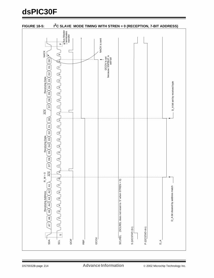
dsPIC30F
FIGURE 18-5: I2C SLAVE MODE TIMING WITH STREN = 0 (RECEPTION, 7-BIT ADDRESS)
SD
A
SC
L
I2C
IF
RB
F
I2C
OV
S1
23
45
67
89
12
34
56
78
91
23
45
78
9P
A7
A6
A5
A4
A3
A2
A1
D7
D6
D5
D4
D3
D2
D1
D0
D7
D6
D5
D4
D3
D1
D0
Rec
eivi
ng D
ata
AC
KR
ecei
ving
Dat
aR
_W =
0
AC
K
Rec
eivi
ng A
ddre
ss
Bus
Mas
ter
term
inat
estr
ansf
er
I2C
OV
is s
etbe
caus
e S
SP
BU
F is
still
full
D2 6
SC
LRE
L(S
CLR
EL
does
not
res
et to
‘0’ w
hen
ST
RE
N =
0)
S (
I2C
STA
T<
3>)
P (
I2C
STA
T<
4>)
NA
CK
is s
ent
D_A
D_A
bit
clea
red
by a
ddre
ss m
atch
D_A
bit
set b
y re
ceiv
ed b
yte
NA
CK
DS70032B-page 214 Advance Information 2002 Microchip Technology Inc.
dsPIC30F
18.4 I2C 10-bit Slave Mode Operation
In 10-bit mode, the basic receive and transmit opera-tions are the same as in the 7-bit mode. However, thecriteria for address match is more complex.
The I2C specification dictates that a slave must beaddressed for a write operation, with two address bytesfollowing a START bit.
The A10M bit is a control bit that signifies that theaddress in I2CADD is a 10-bit address rather than a7-bit address. The address detection protocol for thefirst byte of a message address is identical for 7-bitand 10-bit messages, but the bits being compared aredifferent.
I2CADD holds the entire 10-bit address. Upon receiv-ing an address following a START bit, I2CRSR <7:3> iscompared against a literal ‘11110’ (the default 10-bitaddress) and I2CRSR<2:1> are compared againstI2CADD<9:8>. If a match occurs and only if R_W = 0,the interrupt pulse is sent. The ADD10 bit will becleared to indicate a partial address match. If a matchfails or R_W = 1, the ADD10 bit is cleared and the mod-ule returns to the IDLE state.
Then, the low byte of the address is received and com-pared against I2CADD<7:0>. If an address matchoccurs, the interrupt pulse is generated and the ADD10bit is set, indicating a complete 10-bit address match. Ifan address match did not occur, the ADD10 bit iscleared and the module returns to the IDLE state.
18.4.1 10-BIT SLAVE TRANSMISSION
Once a slave is addressed in this fashion with the full10-bit address (we will refer to this state as"PRIOR_ADDR_MATCH"), the master can beginsending data bytes for a slave reception operation.
18.4.2 10-BIT SLAVE RECEPTION
Once addressed, the master can, without generating aSTOP bit, generate a Repeated START bit and resetthe high byte of the address and R_W = 1, thus initiat-ing a slave transmit operation.
2002 Microchip Technology Inc. Advance Information DS70032B-page 215
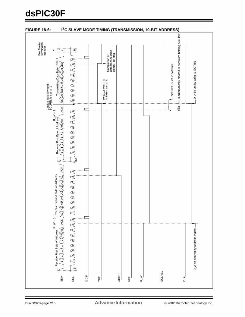
dsPIC30F
FIGURE 18-6: I2C SLAVE MODE TIMING (TRANSMISSION, 10-BIT ADDRESS)
SD
A
I2C
IF
RB
F
S1
23
45
67
89
12
34
56
78
91
23
45
78
9P
11
11
0A
9A
8A
7A
6A
5A
4A
3A
2A
1A
01
11
10
A8R
_W =
1 AC
KA
CK
R_W
= 0
AC
K
Rec
eive
Firs
t Byt
e of
Add
ress
Bus
Mas
ter
term
inat
estr
ansf
er
A9 6
Rec
eive
Sec
ond
Byt
e of
Add
ress
Rec
eive
Firs
t Byt
e of
Add
ress
12
34
57
89
D7
D6
D5
D4
D3
D1
D2 6
Tran
smitt
ing
Dat
a B
yte
D0
Sr
Writ
e of
I2C
TR
Nin
itiat
es tr
ansm
itC
ompl
etio
n of
clea
rs T
BF
flag
SC
LRE
L
SC
LRE
L is
set
in s
oftw
are
SC
LRE
L is
aut
omat
ical
ly c
lear
ed in
har
dwar
e ho
ldin
g S
CL
low
data
tran
smis
sion
Clo
ck is
hel
d lo
w u
ntil
SC
LRE
L is
set
to ‘1
’
TB
F
SC
L
D_A
D_A
bit
set b
y w
rite
to I2
CT
RN
D_A
bit
clea
red
by a
ddre
ss m
atch
AD
D10
R_W
NA
CK
DS70032B-page 216 Advance Information 2002 Microchip Technology Inc.
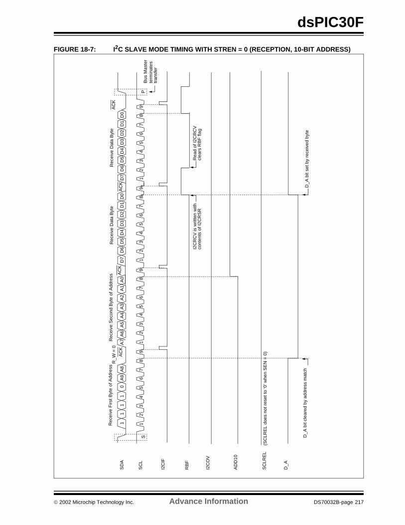
dsPIC30F
FIGURE 18-7: I2C SLAVE MODE TIMING WITH STREN = 0 (RECEPTION, 10-BIT ADDRESS)
SD
A
SC
L
I2C
IF
RB
F
S1
23
45
67
89
12
34
56
78
91
23
45
78
9P
11
11
0A
9A
8A
7A
6A
5A
4A
3A
2A
1A
0D
7D
6D
5D
4D
3D
1D
0
Rec
eive
Dat
a B
yte
AC
KR
_W =
0
AC
K
Rec
eive
Firs
t Byt
e of
Add
ress
D2 6
Rec
eive
Sec
ond
Byt
e of
Add
ress
AC
K
SC
LRE
L
12
34
57
89
D7
D6
D5
D4
D3
D1
D0
Rec
eive
Dat
a B
yte
Bus
Mas
ter
term
inat
estr
ansf
er
D2 6
AC
K
I2C
OV
(SC
LRE
L do
es n
ot r
eset
to ‘0
’ whe
n S
EN
= 0
)
Rea
d of
I2C
RC
Vcl
ears
RB
F fl
agI2
CR
CV
is w
ritte
n w
ithco
nten
ts o
f I2C
RS
R
AD
D10
D_A
D_A
bit
set b
y re
ceiv
ed b
yte
D_A
bit
clea
red
by a
ddre
ss m
atch
2002 Microchip Technology Inc. Advance Information DS70032B-page 217
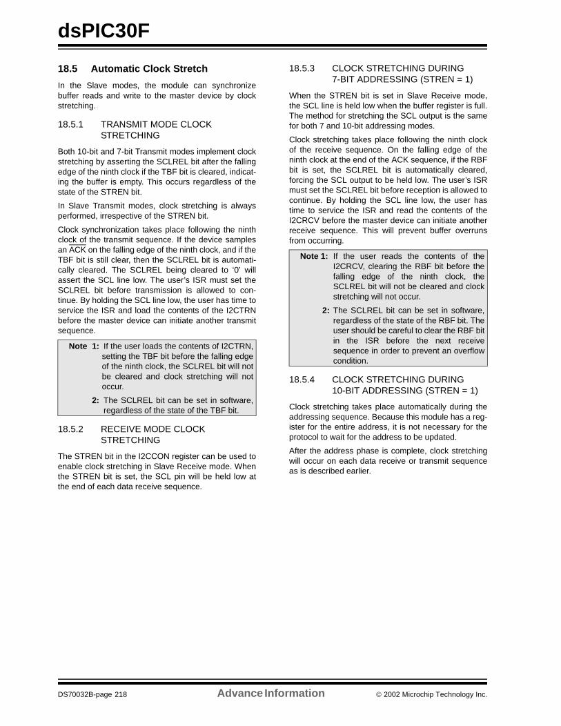
dsPIC30F
18.5 Automatic Clock Stretch
In the Slave modes, the module can synchronizebuffer reads and write to the master device by clockstretching.
18.5.1 TRANSMIT MODE CLOCK STRETCHING
Both 10-bit and 7-bit Transmit modes implement clockstretching by asserting the SCLREL bit after the fallingedge of the ninth clock if the TBF bit is cleared, indicat-ing the buffer is empty. This occurs regardless of thestate of the STREN bit.
In Slave Transmit modes, clock stretching is alwaysperformed, irrespective of the STREN bit.
Clock synchronization takes place following the ninthclock of the transmit sequence. If the device samplesan ACK on the falling edge of the ninth clock, and if theTBF bit is still clear, then the SCLREL bit is automati-cally cleared. The SCLREL being cleared to ‘0’ willassert the SCL line low. The user’s ISR must set theSCLREL bit before transmission is allowed to con-tinue. By holding the SCL line low, the user has time toservice the ISR and load the contents of the I2CTRNbefore the master device can initiate another transmitsequence.
18.5.2 RECEIVE MODE CLOCK STRETCHING
The STREN bit in the I2CCON register can be used toenable clock stretching in Slave Receive mode. Whenthe STREN bit is set, the SCL pin will be held low atthe end of each data receive sequence.
18.5.3 CLOCK STRETCHING DURING 7-BIT ADDRESSING (STREN = 1)
When the STREN bit is set in Slave Receive mode,the SCL line is held low when the buffer register is full.The method for stretching the SCL output is the samefor both 7 and 10-bit addressing modes.
Clock stretching takes place following the ninth clockof the receive sequence. On the falling edge of theninth clock at the end of the ACK sequence, if the RBFbit is set, the SCLREL bit is automatically cleared,forcing the SCL output to be held low. The user’s ISRmust set the SCLREL bit before reception is allowed tocontinue. By holding the SCL line low, the user hastime to service the ISR and read the contents of theI2CRCV before the master device can initiate anotherreceive sequence. This will prevent buffer overrunsfrom occurring.
18.5.4 CLOCK STRETCHING DURING 10-BIT ADDRESSING (STREN = 1)
Clock stretching takes place automatically during theaddressing sequence. Because this module has a reg-ister for the entire address, it is not necessary for theprotocol to wait for the address to be updated.
After the address phase is complete, clock stretchingwill occur on each data receive or transmit sequenceas is described earlier.
Note 1: If the user loads the contents of I2CTRN,setting the TBF bit before the falling edgeof the ninth clock, the SCLREL bit will notbe cleared and clock stretching will notoccur.
2: The SCLREL bit can be set in software,regardless of the state of the TBF bit.
Note 1: If the user reads the contents of theI2CRCV, clearing the RBF bit before thefalling edge of the ninth clock, theSCLREL bit will not be cleared and clockstretching will not occur.
2: The SCLREL bit can be set in software,regardless of the state of the RBF bit. Theuser should be careful to clear the RBF bitin the ISR before the next receivesequence in order to prevent an overflowcondition.
DS70032B-page 218 Advance Information 2002 Microchip Technology Inc.
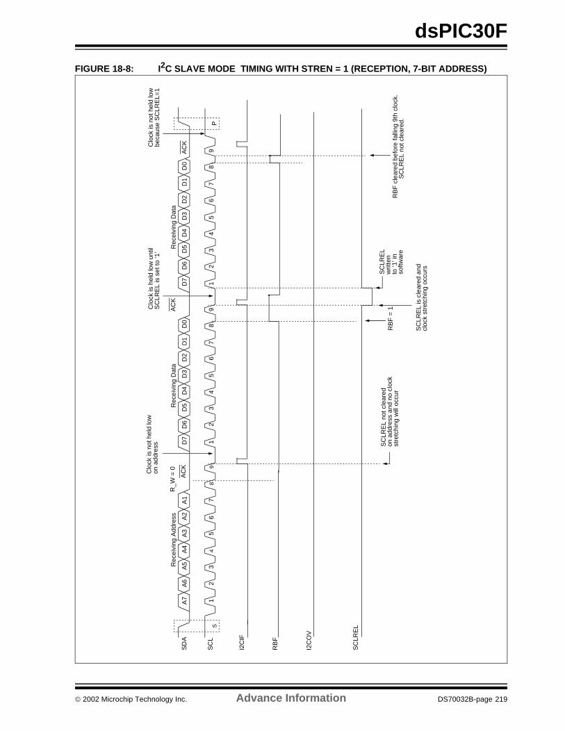
dsPIC30F
FIGURE 18-8: I2C SLAVE MODE TIMING WITH STREN = 1 (RECEPTION, 7-BIT ADDRESS)
SD
A
SC
L
I2C
IF
RB
F
I2C
OV
S1
23
45
67
89
12
34
56
78
91
23
45
78
9P
A7
A6
A5
A4
A3
A2
A1
D7
D6
D5
D4
D3
D2
D1
D0
D7
D6
D5
D4
D3
D1
D0
AC
K
Rec
eivi
ng D
ata
AC
KR
ecei
ving
Dat
aR
_W =
0
AC
K
Rec
eivi
ng A
ddre
ss
D2 6
SC
LRE
L
SC
LRE
Lw
ritte
nto
‘1’ i
n
SC
LRE
L no
t cle
ared
on a
ddre
ss a
nd n
o cl
ock
stre
tchi
ng w
ill o
ccur
softw
are
Clo
ck is
hel
d lo
w u
ntil
SC
LRE
L is
set
to ‘1
’C
lock
is n
ot h
eld
low
on a
ddre
ssC
lock
is n
ot h
eld
low
beca
use
SC
LRE
L=1
RB
F =
1
SC
LRE
L is
cle
ared
and
cloc
k st
retc
hing
occ
urs
RB
F c
lear
ed b
efor
e fa
lling
9th
clo
ck.
SC
LRE
L no
t cle
ared
.
2002 Microchip Technology Inc. Advance Information DS70032B-page 219
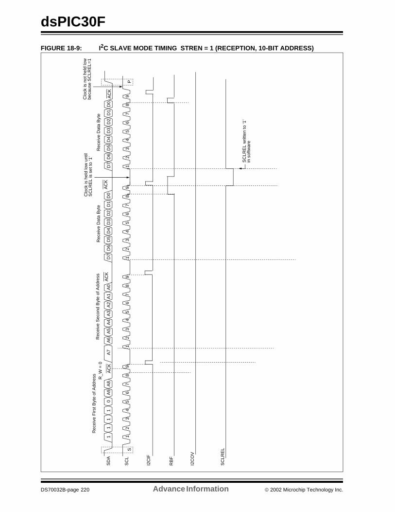
dsPIC30F
FIGURE 18-9: I2C SLAVE MODE TIMING STREN = 1 (RECEPTION, 10-BIT ADDRESS)
SD
A
SC
L
I2C
IF
RB
F
S1
23
45
67
89
12
34
56
78
91
23
45
78
9P
11
11
0A
9A
8A
7A
6A
5A
4A
3A
2A
1A
0D
7D
6D
5D
4D
3D
1D
0
Rec
eive
Dat
a B
yte
AC
KR
_W =
0
AC
K
Rec
eive
Firs
t Byt
e of
Add
ress
D2 6
Rec
eive
Sec
ond
Byt
e of
Add
ress
AC
K
SC
LRE
L
12
34
57
89
D7
D6
D5
D4
D3
D1
D0
Rec
eive
Dat
a B
yte
D2 6
AC
K
I2C
OV
SC
LRE
L w
ritte
n to
‘1’
in s
oftw
are
Clo
ck is
hel
d lo
w u
ntil
SC
LRE
L is
set
to ‘1
’C
lock
is n
ot h
eld
low
beca
use
SC
LRE
L=1
DS70032B-page 220 Advance Information 2002 Microchip Technology Inc.
dsPIC30F
18.6 Software Controlled Clock Stretching (STREN = 1)
When the STREN bit is ‘1’, the SCLREL bit may becleared by software to allow software to control theclock stretching. The logic will synchronize writes tothe SCLREL bit with the SCL clock. Clearing theSCLREL bit will not assert the SCL output until themodule detects a falling edge on the SCL output andSCL is sampled low. If the SCLREL bit is cleared bythe user while the SCL line is already sampled low, theSCL output will be asserted. The SCL output willremain low until the SCLREL bit is set, and all otherdevices on the I2C bus have de-asserted SCL. Thisensures that a write to the SCLREL bit will not violatethe minimum high time requirement for SCL.
If the STREN bit is ‘0’, a software write to the SCLRELbit will be disregarded and have no effect on theSCLREL bit.
18.7 Interrupts
The I2C module generates two interrupt flags, I2CIF(I2C Transfer Complete Interrupt Flag) and BCLIF (I2CBus Collision Interrupt Flag). The I2CIF interrupt flag ispulsed high for one TCY on the falling edge of the 9thclock pulse. The BCLIF interrupt flag is pulsed high forone TCY when a bus collision event is detected.
18.8 Slope Control
The I2C standard requires slope control on the SDAand SCL signals for Fast Mode (400 kHz). The controlbit, DISSLW, enables the user to disable slew rate con-trol, if desired. It is necessary to disable the slew ratecontrol for 1 MHz mode.
18.9 IPMI Support
The control bit IPMIEN enables the module to supportIntelligent Peripheral Management Interface (IPMI).When this bit is set, the module accepts and acts uponall addresses.
18.9.1 SLEEP OPERATION
The control bit, SLPEN, dictates the operation of theI2C module when a SLEEP event occurs. With SLPEN= 0 (RESET state), the module continues operation inSLEEP mode, assuming support signals are provided.Interrupts will be generated at the appropriate time.When SLPEN = 1, the module discontinues all func-tions when a SLEEP mode is entered. Interrupts arenot generated while SLEEP is active.
18.10 General Call Address Support
The general call address can address all devices.When this address is used, all devices should, in the-ory, respond with an Acknowledge.
The general call address is one of eight addressesreserved for specific purposes by the I2C protocol. Itconsists of all 0’s with R_W = 0.
The general call address is recognized when the Gen-eral Call Enable bit (GCEN) is set (I2CCON<15> = 1).Following a START bit detect, 8 bits are shifted intoI2CRSR and the address is compared againstI2CADD, and is also compared to the general calladdress, which is fixed in hardware.
If a general call address match occurs, the I2CRSR istransferred to the I2CRCV after the eighth clock, theRBF flag is set, and on the falling edge of the ninth bit(ACK bit), the I2CIF interrupt is set.
When the interrupt is serviced, the source for the inter-rupt can be checked by reading the contents of theI2CRCV to determine if the address was devicespecific, or a general call address.
18.11 I2C Master Mode Support
In Master mode, the user has six options.
• Assert a START condition on SDA and SCL.
• Assert a RESTART condition on SDA and SCL.• Write to the I2CTRN register initiating transmis-
sion of data/address.• Generate a STOP condition on SDA and SCL.• Configure the I2C port to receive data.
• Generate an Acknowledge condition at the end of a received byte of data.
18.12 I2C Master Mode Operation
The master device generates all the serial clock pulsesand the START and STOP conditions. A transfer isended with a STOP condition or with a RepeatedSTART condition. Since the Repeated START condi-tion is also the beginning of the next serial transfer, theI2C bus will not be released.
In Master Transmitter mode, serial data is outputthrough SDA, while SCL outputs the serial clock. Thefirst byte transmitted contains the slave address of thereceiving device (7 bits) and the data direction bit. Inthis case, the data direction bit (R_W) is logic 0. Serialdata is transmitted 8 bits at a time. After each byte istransmitted, an Acknowledge bit is received. STARTand STOP conditions are output to indicate the begin-ning and the end of a serial transfer.
2002 Microchip Technology Inc. Advance Information DS70032B-page 221
dsPIC30F
In Master Receive mode, the first byte transmitted con-tains the slave address of the transmitting device (7bits) and the data direction bit. In this case, the datadirection bit (R_W) is logic 1. Thus, the first byte trans-mitted is a 7-bit slave address, followed by a ‘1’ to indi-cate receive bit. Serial data is received via SDA whileSCL outputs the serial clock. Serial data is received 8bits at a time. After each byte is received, an Acknowl-edge bit is transmitted. START and STOP conditionsindicate the beginning and end of transmission.
The baud rate generator used for I2C mode operationis now used to set the SCL clock frequency for either100 kHz or 400 kHz I2C operation. 1 MHz operation isalso supported. The baud rate generator re-load valueis contained in the I2CBRG register. The baud rategenerator will automatically begin counting on a write tothe I2CTRN. Once the given operation is complete (i.e.,transmission of the last data bit is followed by ACK) theinternal clock will automatically stop counting and theSCL pin will remain in its last state.
18.12.1 I2C MASTER MODE TRANSMISSION
Transmission of a data byte, a 7 bit address, or the sec-ond half of a 10 bit address is accomplished by simplywriting a value to I2CTRN register. The user shouldonly write to I2CTRN when the module is in a WAITstate. This action will set the buffer full flag (TBF) andallow the baud rate generator to begin counting andstart the next transmission. Each bit of address/datawill be shifted out onto the SDA pin after the fallingedge of SCL is asserted. SCL is held low for 1 baudrate generator rollover count (TBRG). Data should bevalid before SCL is released high. When the SCL pin isreleased high, it is held high for TBRG. The data on theSDA pin must remain stable for that duration and somehold time after the next falling edge of SCL. After theeighth bit is shifted out (the falling edge of the eighthclock), the TBF flag is cleared and the master releasesSDA, allowing the slave device being addressed torespond with an ACK bit during the ninth bit time, if anaddress match occurs or if data was received properly.If the master receives an Acknowledge, the Acknowl-edge status bit (ACKSTAT) is cleared. If not, the bit isset. After the ninth clock the I2CIF is set, and the mas-ter clock (baud rate generator) is suspended until thenext event, thus leaving SCL low and SDA unchanged(see Figure 18-10).
The Transmit Status Flag, TRSTAT (I2CSTAT<14>),indicates that a master transmit is in progress.
TBF Status Flag:
In Transmit mode, the TBF bit (I2CSTAT<0>) is setwhen the CPU writes to I2CTRN and is cleared whenall 8 bits are shifted out.
IWCOL Status Flag:
If the user writes the I2CTRN when a transmit isalready in progress, then IWCOL is set and the con-tents of the buffer are unchanged (the write doesn’toccur). It must be cleared in software.
ACKSTAT Status Flag:
In Transmit mode, the ACKSTAT bit (I2CSTAT<15>) iscleared when the slave has sent an Acknowledge(ACK = 0), and is set when the slave does NotAcknowledge (ACK = 1). A slave sends an Acknowl-edge when it has recognized its address, or when theslave has properly received its data.
The D_A and R_W status bits are not applicable inMaster mode.
DS70032B-page 222 Advance Information 2002 Microchip Technology Inc.
dsPIC30F
FIGURE 18-10: I2C MASTER MODE TIMING (TRANSMISSION, 7- OR 10-BIT ADDRESS)
SD
A
SC
L
I2C
IF
TB
F (
I2C
STA
T<
0>)
SE
N
A6
A5
A4
A3
A2
A1
A0
AC
K =
0D
7D
6D
5D
4D
3D
2D
1D
0
Tran
smit
Dat
a or
Sec
ond
Hal
fR
_W =
0T
rans
mit
Add
ress
to S
lave
12
34
56
78
91
23
45
67
89
ST
OP
bit
I2C
TR
N is
writ
ten
in s
oftw
are
Afte
r S
TAR
T c
ondi
tion
SE
N c
lear
ed b
y ha
rdw
are
Sta
rt b
it
I2C
TR
N w
ritte
n w
ith 7
bit
addr
ess
and
R_W
star
t tra
nsm
it
SC
L he
ld lo
ww
hile
CP
Ure
spon
ds to
I2C
IF
of 1
0 B
it A
ddre
ss
Writ
e S
EN
= 1
STA
RT
con
ditio
n be
gins
Rec
eive
Ack
now
ledg
e -
AK
STA
T =
0A
KS
TAT
= 1
I2C
TR
N w
ritte
n
PE
N
NA
CK
2002 Microchip Technology Inc. Advance Information DS70032B-page 223
dsPIC30F
18.12.2 I2C MASTER MODE RECEPTION
Master mode reception is enabled by programming thereceive enable (RCEN) bit (I2CCON<11>). The I2Cmodule must be IDLE before the RCEN bit is set, oth-erwise the RCEN bit will be disregarded. The baud rategenerator begins counting, and on each rollover, thestate of the SCL pin changes (high to low/low to high),and data is shifted in to the I2CRSR on the rising edgeof each clock. After the falling edge of the eighth clock,the receive enable flag is automatically cleared, thecontents of the I2CRSR are loaded into the I2CRCV,the RBF and I2CIF bits are set, and the baud rate gen-erator is suspended from counting, holding SCL low.The I2C is now in IDLE state, awaiting the next com-mand. When the I2CRCV is read by the CPU, the RBFflag is automatically cleared. The user can then sendan Acknowledge bit at the end of reception, by settingthe Acknowledge sequence enable (ACKEN) bit(I2CCON<12>).
RBF Status Flag:
In receive operation, RBF is set when an address ordata byte is loaded into I2CRCV from I2CRSR. It iscleared when I2CRCV is read.
I2COV Status Flag:
In receive operation, I2COV is set when 8 bits arereceived into the I2CRSR, and the RBF flag is alreadyset from a previous reception.
IWCOL Status Flag:
If the user writes the I2CTRN when a receive is alreadyin progress, then IWCOL is set and the contents of thebuffer are unchanged (the write does not occur).
The D_A and R_W status bits are not applicable inMaster mode.
DS70032B-page 224 Advance Information 2002 Microchip Technology Inc.
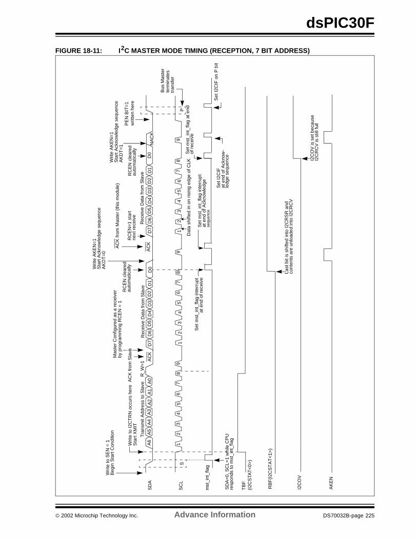
dsPIC30F
FIGURE 18-11: I2C MASTER MODE TIMING (RECEPTION, 7 BIT ADDRESS)
P9
87
65
D0
D1
D2
D3
D4
D5
D6
D7
S
A6
A5
A4
A3
A2
A1
A0
SD
A
SC
L1
23
45
67
89
12
34
56
78
91
23
4
Bus
Mas
ter
term
inat
estr
ansf
er
AC
KR
ecei
ve D
ata
from
Sla
veR
ecei
ve D
ata
from
Sla
ve
D0
D1
D2
D3
D4
D5
D6
D7
AC
K
R_W
=1
Tra
nsm
it A
ddre
ss to
Sla
ve
mst
_int
_fla
g
TB
F
Writ
e to
SE
N =
1B
egin
Sta
rt C
ondi
tion
Writ
e to
I2C
TR
N o
ccur
s he
reA
CK
from
Sla
ve
Mas
ter
Con
figur
ed a
s a
rece
iver
by p
rogr
amm
ing
RC
EN
= 1
PE
N B
IT=
1w
ritte
n he
re
Dat
a sh
ifted
in o
n ris
ing
edge
of C
LK
Sta
rt X
MIT
I2C
OV
SD
A=
0, S
CL=
1 w
hile
CP
U
(I2C
STA
T<
0>)
Set
mst
_int
_fla
g in
terr
upt
at e
nd o
f rec
eive
Set
I2C
IF o
n P
bit
AC
K fr
om M
aste
r (t
his
mod
ule)
Set
mst
_int
_fla
g at
end
Set
mst
_int
_fla
g in
terr
upt
at e
nd o
f Ack
now
ledg
ese
quen
ce
Set
I2C
IFat
end
of A
ckno
w-
ledg
e se
quen
ce
of r
ecei
ve
Writ
e A
KE
N=
1 S
tart
Ack
now
ledg
e se
quen
ce
I2C
OV
is s
et b
ecau
seI2
CR
CV
is s
till f
ull
AK
DT
=1
RC
EN
cle
ared
auto
mat
ical
lyR
CE
N=
1 st
art
next
rec
eive
Writ
e A
KE
N=
1S
tart
Ack
now
ledg
e se
quen
ceA
KD
T=
0
RC
EN
cle
ared
auto
mat
ical
ly
resp
onds
to m
st_i
nt_f
lag
AK
EN
RB
F(I
2CS
TA
T<
1>)
Last
bit
is s
hifte
d in
to I2
CR
SR
and
cont
ents
are
unl
oade
d in
to I2
CR
CV
NA
CK
2002 Microchip Technology Inc. Advance Information DS70032B-page 225
dsPIC30F
18.12.3 BAUD RATE GENERATORIn I2C Master mode, the reload value for the BRG islocated in the I2CBRG register. When the BRG isloaded with this value, the BRG counts down to 0 andstops until another reload has taken place. In I2C Mas-ter mode, the BRG is not reloaded automatically. Ifclock arbitration is taking place, for instance, the BRGis reloaded when the SCL pin is sampled high.
EQUATION 18-1: SERIAL CLOCK RATE
18.12.4 CLOCK ARBITRATION
Clock arbitration occurs when the master de-assertsthe SCL pin (SCL allowed to float high) during anyreceive, transmit, or RESTART/STOP condition. Whenthe SCL pin is allowed to float high, the baud rate gen-erator (BRG) is suspended from counting until the SCLpin is actually sampled high. When the SCL pin is sam-pled high, the baud rate generator is reloaded with thecontents of I2CBRG and begins counting. This guaran-tees that the SCL high time will always be at least oneBRG rollover count, in the event that the clock is heldlow by an external device.
18.12.5 MULTI-MASTER COMMUNICATION, BUS COLLISION, AND BUS ARBITRATION
Multi-Master mode support is achieved by bus arbitra-tion. When the master outputs address/data bits ontothe SDA pin, arbitration takes place when the masteroutputs a 1 on SDA, by letting SDA float high andanother master asserts a 0. When the SCL pin floatshigh, data should be stable. If the expected data onSDA is a 1 and the data sampled on the SDA pin = 0,then a bus collision has taken place. The master will setthe Bus Collision Interrupt (BCLIF) pulse and reset themaster portion of the I2C port to its IDLE state.
If a transmit was in progress when the bus collisionoccurred, the transmission is halted, the TBF flag iscleared, the SDA and SCL lines are de-asserted, andthe I2CTRN can now be written to. When the user ser-vices the bus collision Interrupt Service Routine, and ifthe I2C bus is free (i.e., the P bit is set), the user canresume communication by asserting a STARTcondition.
If a START, RESTART, STOP, or Acknowledge condi-tion was in progress when the bus collision occurred,the condition is aborted, the SDA and SCL lines are de-asserted, and the respective control bits in the I2CCONregister are cleared to 0. When the user services thebus collision Interrupt Service Routine, and if the I2Cbus is free, the user can resume communication byasserting a START condition.
The Master will continue to monitor the SDA and SCLpins, and if a STOP condition occurs, the I2CIF bit willbe set.
A write to the I2CTRN will start the transmission of dataat the first data bit, regardless of where the transmitterleft off when bus collision occurred.
In Multi-Master mode, the interrupt generation on thedetection of START and STOP conditions allows thedetermination of when the bus is free. Control of the I2Cbus can be taken when the P bit is set in the I2CSTAT reg-ister, or the bus is IDLE and the S and P bits are cleared.
18.12.5.1 Bus Collision During a START Condition
During a START condition, a bus collision occurs if:
1. SDA or SCL are sampled low at the beginning ofthe START condition.
2. SCL is sampled low before SDA is asserted low.
18.12.5.2 Bus Collision During a RESTART Condition
During a RESTART condition, bus collision occurs if:
1. A 0 is sampled on SDA, when SCL goes from 0to 1.
2. SCL goes low before SDA is asserted low, indi-cating that another master is attempting to trans-mit a data 1.
18.12.5.3 Bus Collision During a STOP Condition
Bus collision occurs during a STOP condition if:
1. After the SDA pin has been de-asserted andallowed to float high, SDA is sampled low afterthe BRG has timed out.
2. After the SCL pin is de-asserted, SCL is sam-pled low before SDA goes high.
18.13 I2C Module Operation During CPU SLEEP and IDLE Modes
18.13.1 I2C OPERATION DURING CPU SLEEP MODE
When the device enters SLEEP mode, all Q clocksources to the module are shut-down and stay at logic‘0’. If SLEEP occurs in the middle of a transmission,and the state machine is partially into a transmission asthe clocks stop, then the transmission is aborted. Sim-ilarly, if SLEEP occurs in the middle of a reception, thenthe reception is aborted.
18.13.2 I2C OPERATION DURING CPU IDLE MODE
For the I2C, the I2CSIDL bit selects if the module willstop on IDLE or continue on IDLE. If I2CSIDL = 0, themodule will continue operation on assertion of the IDLEmode. If I2CSIDL = 1, the module will stop on IDLE.
FSCK = (FOSC/2) / (I2CBRG * 2)
DS70032B-page 226 Advance Information 2002 Microchip Technology Inc.
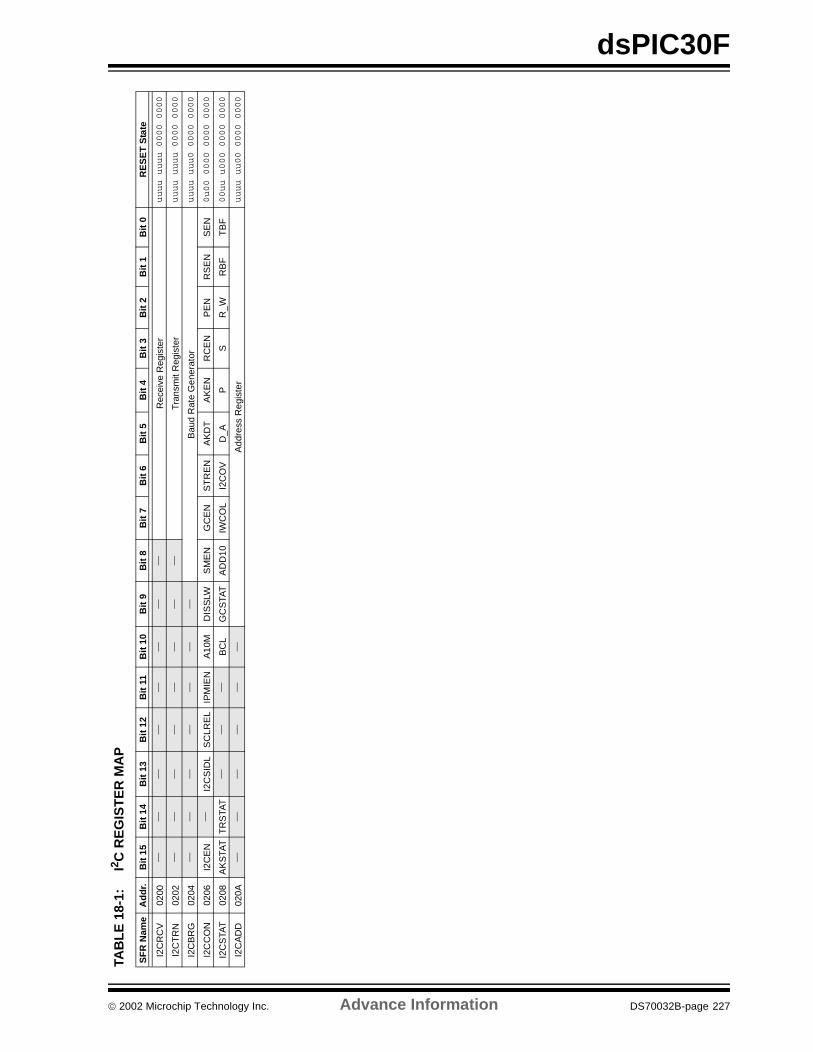
dsPIC30F
TAB
LE
18-
1:I2 C
RE
GIS
TE
R M
AP
SF
R N
ame
Ad
dr.
Bit
15
Bit
14
Bit
13
Bit
12
Bit
11
Bit
10
Bit
9B
it 8
Bit
7B
it 6
Bit
5B
it 4
Bit
3B
it 2
Bit
1B
it 0
RE
SE
T S
tate
I2C
RC
V02
00—
——
——
——
—R
ecei
ve R
egis
ter
uuuu uuuu 0000 0000
I2C
TR
N02
02—
——
——
——
—T
rans
mit
Reg
iste
ruuuu uuuu 0000 0000
I2C
BR
G02
04—
——
——
——
Bau
d R
ate
Gen
erat
oruuuu uuu0 0000 0000
I2C
CO
N02
06I2
CE
N—
I2C
SID
LS
CLR
EL
IPM
IEN
A10
MD
ISS
LWS
ME
NG
CE
NS
TR
EN
AK
DT
AK
EN
RC
EN
PE
NR
SE
NS
EN
0u00 0000 0000 0000
I2C
STA
T02
08A
KS
TAT
TR
STA
T—
——
BC
LG
CS
TAT
AD
D10
IWC
OL
I2C
OV
D_A
PS
R_W
RB
FT
BF
00uu u000 0000 0000
I2C
AD
D02
0A—
——
——
—A
ddre
ss R
egis
ter
uuuu uu00 0000 0000
2002 Microchip Technology Inc. Advance Information DS70032B-page 227
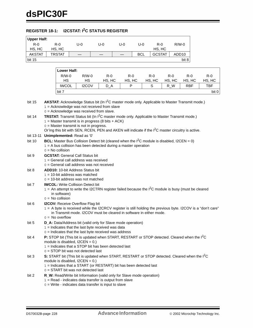
dsPIC30F
REGISTER 18-1: I2CSTAT: I2C STATUS REGISTER
Upper Half:R-0
HS, HCR-0
HS, HCU-0 U-0 U-0 U-0 R-0
HS, HCR/W-0
AKSTAT TRSTAT — — — BCL GCSTAT ADD10bit 15 bit 8
Lower Half:R/W-0
HSR/W-0
HSR-0
HS, HCR-0
HS, HCR-0
HS, HCR-0
HS, HCR-0
HS, HCR-0
HS, HCIWCOL I2COV D_A P S R_W RBF TBF
bit 7 bit 0
bit 15 AKSTAT: Acknowledge Status bit (In I2C master mode only. Applicable to Master Transmit mode.)1 = Acknowledge was not received from slave0 = Acknowledge was received from slave.
bit 14 TRSTAT: Transmit Status bit (In I2C master mode only. Applicable to Master Transmit mode.)1 = Master transmit is in progress (8 bits + ACK)0 = Master transmit is not in progress. Or’ing this bit with SEN, RCEN, PEN and AKEN will indicate if the I2C master circuitry is active.
bit 13-11 Unimplemented: Read as ‘0’
bit 10 BCL: Master Bus Collision Detect bit (cleared when the I2C module is disabled, I2CEN = 0)1 = A bus collision has been detected during a master operation0 = No collision
bit 9 GCSTAT: General Call Status bit1 = General call address was received0 = General call address was not received
bit 8 ADD10: 10-bit Address Status bit1 = 10-bit address was matched0 = 10-bit address was not matched
bit 7 IWCOL: Write Collision Detect bit1 = An attempt to write the I2CTRN register failed because the I2C module is busy (must be cleared
in software)0 = No collision
bit 6 I2COV: Receive Overflow Flag bit1 = A byte is received while the I2CRCV register is still holding the previous byte. I2COV is a “don’t care”
in Transmit mode. I2COV must be cleared in software in either mode.0 = No overflow
bit 5 D_A: Data/Address bit (valid only for Slave mode operation)1 = Indicates that the last byte received was data0 = Indicates that the last byte received was address
bit 4 P: STOP bit (This bit is updated when START, RESTART or STOP detected. Cleared when the I2C module is disabled, I2CEN = 0.)1 = Indicates that a STOP bit has been detected last0 = STOP bit was not detected last
bit 3 S: START bit (This bit is updated when START, RESTART or STOP detected. Cleared when the I2C module is disabled, I2CEN = 0.)1 = Indicates that a START (or RESTART) bit has been detected last0 = START bit was not detected last
bit 2 R_W: Read/Write bit Information (valid only for Slave mode operation)1 = Read - indicates data transfer is output from slave0 = Write - indicates data transfer is input to slave
DS70032B-page 228 Advance Information 2002 Microchip Technology Inc.
dsPIC30F
REGISTER 18-1: I2CSTAT: I2C STATUS REGISTER (Continued)
bit 1 RBF: Receive Buffer Full Status bit (cleared by reading I2CRCV)1 = Receive complete, I2CRCV is full0 = Receive not complete, I2CRCV is empty
bit 0 TBF: Transmit Buffer Full Status bit1 = Transmit in progress, I2CTRN is full (8 bits)0 = Transmit complete, I2CTRN is empty
Legend:R = Readable bit W = Writable bit U = Unimplemented bit, read as ‘0’HC = Cleared by Hardware HS = Set by Hardware -n = Value at POR1 = bit is set 0 = bit is cleared x = bit is unknown x = bit is unknown
2002 Microchip Technology Inc. Advance Information DS70032B-page 229
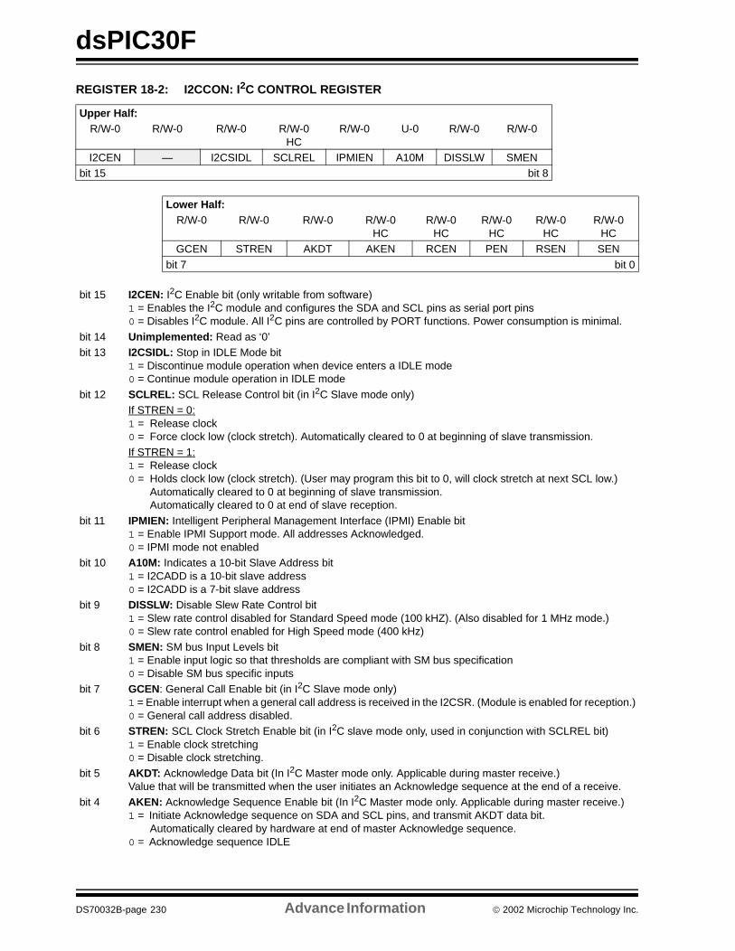
dsPIC30F
REGISTER 18-2: I2CCON: I2C CONTROL REGISTER
Upper Half:R/W-0 R/W-0 R/W-0 R/W-0
HCR/W-0 U-0 R/W-0 R/W-0
I2CEN — I2CSIDL SCLREL IPMIEN A10M DISSLW SMENbit 15 bit 8
Lower Half:R/W-0 R/W-0 R/W-0 R/W-0
HCR/W-0
HCR/W-0
HCR/W-0
HCR/W-0
HCGCEN STREN AKDT AKEN RCEN PEN RSEN SEN
bit 7 bit 0
bit 15 I2CEN: I2C Enable bit (only writable from software)1 = Enables the I2C module and configures the SDA and SCL pins as serial port pins0 = Disables I2C module. All I2C pins are controlled by PORT functions. Power consumption is minimal.
bit 14 Unimplemented: Read as ‘0’bit 13 I2CSIDL: Stop in IDLE Mode bit
1 = Discontinue module operation when device enters a IDLE mode0 = Continue module operation in IDLE mode
bit 12 SCLREL: SCL Release Control bit (in I2C Slave mode only)If STREN = 0:1 = Release clock0 = Force clock low (clock stretch). Automatically cleared to 0 at beginning of slave transmission.
If STREN = 1:1 = Release clock0 = Holds clock low (clock stretch). (User may program this bit to 0, will clock stretch at next SCL low.)
Automatically cleared to 0 at beginning of slave transmission.Automatically cleared to 0 at end of slave reception.
bit 11 IPMIEN: Intelligent Peripheral Management Interface (IPMI) Enable bit1 = Enable IPMI Support mode. All addresses Acknowledged.0 = IPMI mode not enabled
bit 10 A10M: Indicates a 10-bit Slave Address bit1 = I2CADD is a 10-bit slave address0 = I2CADD is a 7-bit slave address
bit 9 DISSLW: Disable Slew Rate Control bit1 = Slew rate control disabled for Standard Speed mode (100 kHZ). (Also disabled for 1 MHz mode.)0 = Slew rate control enabled for High Speed mode (400 kHz)
bit 8 SMEN: SM bus Input Levels bit1 = Enable input logic so that thresholds are compliant with SM bus specification0 = Disable SM bus specific inputs
bit 7 GCEN: General Call Enable bit (in I2C Slave mode only)1 = Enable interrupt when a general call address is received in the I2CSR. (Module is enabled for reception.)0 = General call address disabled.
bit 6 STREN: SCL Clock Stretch Enable bit (in I2C slave mode only, used in conjunction with SCLREL bit)1 = Enable clock stretching0 = Disable clock stretching.
bit 5 AKDT: Acknowledge Data bit (In I2C Master mode only. Applicable during master receive.)Value that will be transmitted when the user initiates an Acknowledge sequence at the end of a receive.
bit 4 AKEN: Acknowledge Sequence Enable bit (In I2C Master mode only. Applicable during master receive.)1 = Initiate Acknowledge sequence on SDA and SCL pins, and transmit AKDT data bit.
Automatically cleared by hardware at end of master Acknowledge sequence.0 = Acknowledge sequence IDLE
DS70032B-page 230 Advance Information 2002 Microchip Technology Inc.
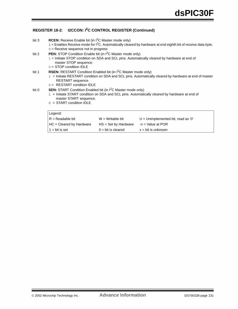
dsPIC30F
REGISTER 18-2: I2CCON: I2C CONTROL REGISTER (Continued)
bit 3 RCEN: Receive Enable bit (in I2C Master mode only)1 = Enables Receive mode for I2C. Automatically cleared by hardware at end eighth bit of receive data byte.0 = Receive sequence not in progress
bit 2 PEN: STOP Condition Enable bit (in I2C Master mode only)1 = Initiate STOP condition on SDA and SCL pins. Automatically cleared by hardware at end of
master STOP sequence.0 = STOP condition IDLE
bit 1 RSEN: RESTART Condition Enabled bit (in I2C Master mode only)1 = Initiate RESTART condition on SDA and SCL pins. Automatically cleared by hardware at end of master
RESTART sequence.0 = RESTART condition IDLE
bit 0 SEN: START Condition Enabled bit (in I2C Master mode only)1 = Initiate START condition on SDA and SCL pins. Automatically cleared by hardware at end of
master START sequence.0 = START condition IDLE
Legend:
R = Readable bit W = Writable bit U = Unimplemented bit, read as ‘0’
HC = Cleared by Hardware HS = Set by Hardware -n = Value at POR
1 = bit is set 0 = bit is cleared x = bit is unknown
2002 Microchip Technology Inc. Advance Information DS70032B-page 231

dsPIC30F
NOTES:
DS70032B-page 232 Advance Information 2002 Microchip Technology Inc.
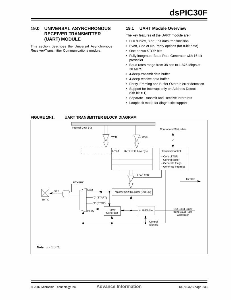
dsPIC30F
19.0 UNIVERSAL ASYNCHRONOUS RECEIVER TRANSMITTER (UART) MODULE
This section describes the Universal AsynchronousReceiver/Transmitter Communications module.
19.1 UART Module Overview
The key features of the UART module are:
• Full-duplex, 8 or 9-bit data transmission
• Even, Odd or No Parity options (for 8-bit data)• One or two STOP bits• Fully integrated Baud Rate Generator with 16-bit
prescaler• Baud rates range from 38 bps to 1.875 Mbps at
30 MIPS• 4-deep transmit data buffer
• 4-deep receive data buffer• Parity, Framing and Buffer Overrun error detection• Support for Interrupt only on Address Detect
(9th bit = 1)• Separate Transmit and Receive Interrupts
• Loopback mode for diagnostic support
FIGURE 19-1: UART TRANSMITTER BLOCK DIAGRAM
Write Write
UTX8 UxTXREG Low Byte
Load TSR
Transmit Control
– Control TSR– Control Buffer– Generate Flags– Generate Interrupt
Control and Status bits
UxTXIF
Data
‘0’ (START)
‘1’ (STOP)
Parity ParityGenerator
Transmit Shift Register (UxTSR)
16 Divider
ControlSignals
16X Baud Clockfrom Baud Rate
Generator
Internal Data Bus
UTXBRK
UxTX
Note: x = 1 or 2.
UxTX
2002 Microchip Technology Inc. Advance Information DS70032B-page 233
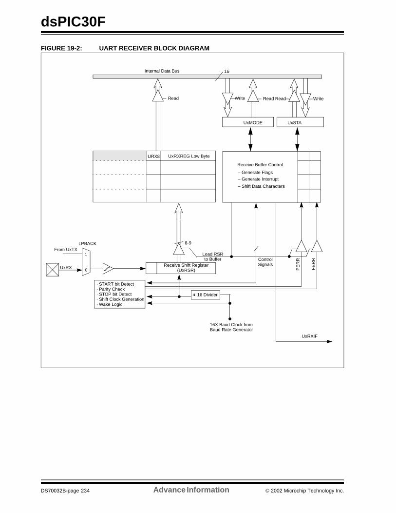
dsPIC30F
FIGURE 19-2: UART RECEIVER BLOCK DIAGRAM
Read
URX8 UxRXREG Low Byte
Load RSR
UxMODE
Receive Buffer Control
– Generate Flags
– Generate Interrupt
UxRXIF
UxRX
· START bit Detect
Receive Shift Register
16 Divider
ControlSignals
UxSTA
– Shift Data Characters
Read ReadWrite Write
to Buffer
8-9
(UxRSR) PE
RR
FE
RR
· Parity Check· STOP bit Detect· Shift Clock Generation· Wake Logic
16Internal Data Bus
1
0
LPBACKFrom UxTX
16X Baud Clock fromBaud Rate Generator
DS70032B-page 234 Advance Information 2002 Microchip Technology Inc.
dsPIC30F
19.2 Enabling and Setting Up UART
19.2.1 ENABLING THE UART
The UART module is enabled by setting the UARTENbit in the UxMODE register (where x = 1 or 2). Onceenabled, the UxTX and UxRX pins are configured as anoutput and an input respectively, overriding the TRISand LATCH register bit settings for the correspondingI/O port pin. The UxTX pin is at logic ‘1’ when no trans-mission is taking place.
19.2.2 DISABLING THE UART
The UART module is disabled by clearing theUARTEN bit in the UxMODE register. This is thedefault state after any RESET. If the UART is disabled,all I/O pins operate as port pins, under the control ofthe latch and TRIS bits of the corresponding port pins.
Disabling the UART module resets the buffers toempty states. Any data characters in the buffers arelost, and the baud rate counter is reset.
All error and status flags associated with the UARTmodule are reset when the module is disabled. TheURXDA, OERR, FERR, PERR, UTXEN, UTXBRK andUTXBF bits are cleared, whereas RIDLE and TRMTare set. Other control bits, including ADDEN,URXISEL<1:0>, UTXISEL, as well as the UxMODEand UxBRG registers, are not affected.
Clearing the UARTEN bit while the UART is active willabort all pending transmissions and receptions andreset the module as defined above. Re-enabling theUART will restart the UART in the same configuration.
19.2.3 ALTERNATE I/O
The alternate I/O function is enabled by setting theALTIO bit (UxMODE<10>). If ALTIO = 1, the UxATXand UxARX pins (alternate transmit and alternatereceive pins, respectively) are used by the UART mod-ule, instead of the UxTX and UxRX pins. If ALTIO = 0,the UxTX and UxRX pins are used by the UARTmodule.
19.2.4 SETTING UP DATA, PARITY AND STOP BIT SELECTIONS
Control bits PDSEL<1:0> in the UxSTA register areused to select the data length and parity used in thetransmission. The data length may either be 8-bits witheven, odd or no parity, or 9-bits with no parity.
The STSEL bit determines whether one or two STOPbits will be used during data transmission.
The default (Power-on) setting of the UART is 8 bits, noparity, 1 STOP bit (typically represented as 8, N, 1).
19.3 Transmitting Data
19.3.1 TRANSMITTING IN 8-BIT DATA MODE
The following steps must be performed in order totransmit 8-bit data:
1. Set up the UART:First, the data length, parity and number ofSTOP bits must be selected, and then, theTransmit and Receive Interrupt enable and pri-ority bits are setup in the UxMODE and UxSTAregisters. Also, the appropriate baud rate valuemust be written to the UxBRG register.
2. Enable the UART by setting the UARTEN bit(UxMODE<15>).
3. Set the UTXEN bit (UxSTA<10>), therebyenabling a transmission.
4. Write the data byte to be transmitted, to thelower byte of UxTXREG. The value will be trans-ferred to Transmit Shift register (UxTSR) imme-diately and the serial bit stream will start shiftingout during the next rising edge of the baud clock.
5. A Transmit interrupt will be generated depend-ing on the value of the interrupt control bitUTXISEL (UxSTA<15>).
Alternatively, the data byte may be written whileUTXEN = 0, following which, the user may set UTXEN.This will cause the serial bit stream to begin immedi-ately because the baud clock will start from a clearedstate.
19.3.2 TRANSMITTING IN 9-BIT DATA MODE
The sequence of steps involved in the transmission of9-bit data is similar to 8-bit transmission, except that a16-bit data word (of which the upper 7 bits are alwaysclear) must be written to the UxTXREG register.
19.3.3 TRANSMIT BUFFER (UXTXB)
The transmit buffer is 9-bits wide and 4 charactersdeep. Including the Transmit Shift Register (UxTSR),the user effectively has a 5-deep FIFO (First In FirstOut) buffer. The UTXBF status bit (UxSTA<9>) indi-cates whether the transmit buffer is full.
If a user attempts to write to a full buffer, the new datawill not be accepted into the FIFO, and no data shiftwill occur within the buffer. This enables recovery froma buffer overrun condition.
The FIFO is reset during any device RESET, but is notaffected when the device enters a Power Saving mode,or wakes up from a Power Saving mode.
2002 Microchip Technology Inc. Advance Information DS70032B-page 235
dsPIC30F
19.3.4 TRANSMIT INTERRUPT
The transmit interrupt flag (U1TXIF or U2TXIF) islocated in the corresponding interrupt flag register.
The transmitter generates an edge to set the UxTXIFbit. The condition of generating the interrupt dependson UTXISEL control bit.
a) If UTXISEL = 0, an interrupt is generated whena word is transferred from the Transmit buffer toTransmit Shift register (UxTSR). This impliesthat the transmit buffer has at least one emptyword.
b) If UTXISEL = 1, an interrupt is generated whena word is transferred from the Transmit buffer toTransmit Shift register (UxTSR) and the Trans-mit buffer is empty.
Switching between the two interrupt modes duringoperation is possible and sometimes offers moreflexibility.
19.3.5 TRANSMIT BREAK
Setting the UTXBRK bit (UxSTA<11>) will cause theUxTX line to be driven to logic ‘0’. The UTXBRK bitoverrides all transmission activity. Therefore, the usershould generally wait for the transmitter to be IDLEbefore setting UTXBRK.
To send a break character, the UTXBRK bit must beset by software and must remain set for a minimum of13 baud clock cycles. The UTXBRK bit is then clearedby software to generate STOP bits. The user must waitfor a duration of at least one or two baud clock cyclesin order to ensure a valid STOP bit(s), before reloadingthe UxTXB or starting other transmitter activity. Trans-mission of a break character does not generate atransmit interrupt.
19.4 Receiving Data
19.4.1 RECEIVING IN 8-BIT OR 9-BIT DATA MODE
The following steps must be performed while receiving8-bit or 9-bit data:
1. Set up the UART (see Section 19.3.1).2. Enable the UART (see Section 19.3.1).3. A receive interrupt will be generated when one
or more data bytes have been received,depending on the receive interrupt settingsspecified by the URXISEL bits (UxSTA<7:6>).
4. Read the OERR bit to determine if an overrunerror has occurred. The OERR bit must be resetin software.
5. Read the received data from UxRXREG. The actof reading UxRXREG will move the next word tothe top of the receive FIFO, and the PERR andFERR values will be updated.
19.4.2 RECEIVE BUFFER (UXRXB)
The receive buffer is 4-deep. Including the ReceiveShift register (UxRSR), the user effectively has a5-deep FIFO (First In First Out) buffer.
URXDA (UxSTA<0>) = 1 indicates that the receivebuffer has data available. URXDA = 0 implies that thebuffer is empty. If a user attempts to read an emptybuffer, the old values in the buffer will be read, and nodata shift will occur within the FIFO.
The FIFO is reset during any device RESET. It is notaffected when the device enters a power-saving modeor wakes up from a power-saving mode.
19.4.3 RECEIVE INTERRUPT
The receive interrupt flag (U1RXIF or U2RXIF) can beread from the corresponding interrupt flag register. Theinterrupt flag is set by an edge generated by thereceiver. The condition for setting the receive interruptflag depends on the settings specified by theURXISEL<1:0> (UxSTA<7:6>) control bits.
a) If URXISEL<1:0> = 00 or 01, an interrupt isgenerated every time a data word is transferredfrom the Receive Shift Register (UxRSR) to theReceive Buffer. There may be one or more char-acters in the receive buffer.
b) If URXISEL<1:0> = 10, an interrupt is generatedwhen a word is transferred from the ReceiveShift Register (UxRSR) to the Receive Bufferand as a result, the Receive Buffer contains 3 or4 characters.
c) If URXISEL<1:0> = 11, an interrupt is set whena word is transferred from the Receive ShiftRegister (UxRSR) to the Receive Buffer and asa result, the Receive Buffer contains 4 charac-ters (i.e., becomes full).
Switching between the interrupt modes during opera-tion is possible, though generally not advisable duringnormal operation.
19.5 Reception Error Handling
19.5.1 RECEIVE BUFFER OVERRUN ERROR (OERR BIT)
The OERR bit (UxSTA<1>) is set if all of the followingconditions occur:
a) The receive buffer is full.b) The receive shift register is full, but unable to
transfer the character to the receive buffer.c) The STOP bit of the character in the UxRSR is
detected, indicating that the UxRSR needs totransfer the character to the buffer.
Once OERR is set, no further data is shifted in UxRSR(until the OERR bit is cleared in software or a RESEToccurs). The data held in UxRSR and UxRXREGremain valid.
DS70032B-page 236 Advance Information 2002 Microchip Technology Inc.
dsPIC30F
19.5.2 FRAMING ERROR (FERR)
The FERR bit (UxSTA<2>) is set if a ‘0’ is detectedinstead of a STOP bit. If two STOP bits are selected,both STOP bits must be ‘1’, otherwise FERR will be set.The read only FERR bit is buffered along with thereceived data. It is cleared on any RESET.
19.5.3 PARITY ERROR (PERR)
The PERR bit (UxSTA<3>) is set if the parity of thereceived word is incorrect. This error bit is applicableonly if a Parity mode (odd or even) is selected. Theread only PERR bit is buffered along with the receiveddata bytes. It is cleared on any RESET.
19.5.4 IDLE STATUS
When the receiver is active, i.e., between the initialdetection of the START bit and the completion of theSTOP bit, the RIDLE bit (UxSTA<4>) is ‘0’. Betweenthe completion of the STOP bit and detection of thenext START bit, the RIDLE bit is ‘1’, indicating that theUART is IDLE.
19.5.5 RECEIVE BREAK
The receiver will count and expect a certain number ofbit times based on the values programmed in thePDSEL (UxMODE<2:1>) and STSEL (UxMODE<0>)bits.
If the break is much longer than 13 bit times, thereception is considered complete after the number ofbit times specified by PDSEL and STSEL. TheURXDA bit is set, FERR is set, zeros are loaded intothe receive FIFO, interrupts are generated if appropri-ate, and the RIDLE bit is set.
When the module receives a long break signal and thereceiver has detected the START bit, the data bits andthe invalid STOP bit (which sets the FERR), thereceiver must wait for a valid STOP bit before lookingfor the next START bit. It cannot assume that thebreak condition on the line is the next START bit.
Break is regarded as a character containing all 0’s,with the FERR bit set. The break character is loadedinto the buffer. No further reception can occur until aSTOP bit is received. Note that RIDLE goes high whenthe STOP bit has not been received yet.
19.6 Address Detect Mode
Setting the ADDEN bit (UxSTA<5>) enables this spe-cial mode, in which a 9th bit (URX8) value of ‘1’ identi-fies the received word as an address rather than data.This mode is only applicable for 9-bit data transmis-sion. The URXISEL control bit does not have anyimpact on interrupt generation in this mode, since aninterrupt (if enabled) will be generated if the receivedword has the 9th bit set.
19.7 Loopback Mode
Setting the LPBACK bit enables this special mode, inwhich the UxTX pin is internally connected to the UxRXpin. When configured for the loopback mode, the UxRXpin is disconnected from the internal UART receivelogic. However, the UxTX pin still functions as in a nor-mal operation.
To select this mode:
a) Configure UART for desired mode of operation.
a) Set LPBACK = 1 to enable Loopback mode.b) Enable transmission as defined in Section 19.3.
19.8 Baud Rate Generator
The UART has a 16-bit baud rate generator to allowmaximum flexibility in baud rate generation. The baudrate generator register (UxBRG) is readable and writ-able. The baud rate is computed as follows:
BRG = 16-bit value held in UxBRG register (0 through65535)
fCY = Instruction Clock Rate (1/TCY)
Then Baud Rate = fCY / (16* (BRG + 1) )
Therefore, maximum baud rate possible is = fCY /16 (If BRG = 0),
and minimum baud rate possible is = fCY / (16* 65536).
With a full 16-bit baud rate generator, at 30 MIPS oper-ation, the minimum baud rate achievable is 28.5 bps.
19.9 Auto Baud Support
To allow the system to determine baud rates ofreceived characters, the input can be optionally linkedto a selected capture input. To enable this mode, theuser must program the input capture module to detectthe falling and rising edges of the START bit.
2002 Microchip Technology Inc. Advance Information DS70032B-page 237
dsPIC30F
19.10 UART Operation During CPU SLEEP and IDLE Modes
19.10.1 UART OPERATION DURING CPU SLEEP MODE
When the device enters SLEEP mode, all clocksources to the module are shut-down and stay at logic‘0’. If entry into SLEEP mode occurs while a transmis-sion is in progress, then the transmission is aborted.The UxTX pin is driven to logic ‘1’. Similarly, if entryinto SLEEP mode occurs while a reception is inprogress, then the reception is aborted. The UxSTA,UxMODE, transmit and receive registers and buffers,and the UxBRG register are not affected by SLEEPmode.
If the WAKE bit (UxSTA<7>) is set before the deviceenters SLEEP mode, then a falling edge on the UxRXpin will generate a receive interrupt. The ReceiveInterrupt Select mode bit (URXISEL) has no effect forthis function. If the receive interrupt is enabled, thenthis will wake-up the device from SLEEP. The UAR-TEN bit must be set in order to generate a wake-upinterrupt.
19.10.2 UART OPERATION DURING CPU IDLE MODE
For the UART, the USIDL bit selects if the module willstop operation when the device enters IDLE mode, orwhether the module will continue on IDLE. IfUSIDL = 0, the module will continue operation duringIDLE mode. If USIDL = 1, the module will stop onIDLE.
DS70032B-page 238 Advance Information 2002 Microchip Technology Inc.
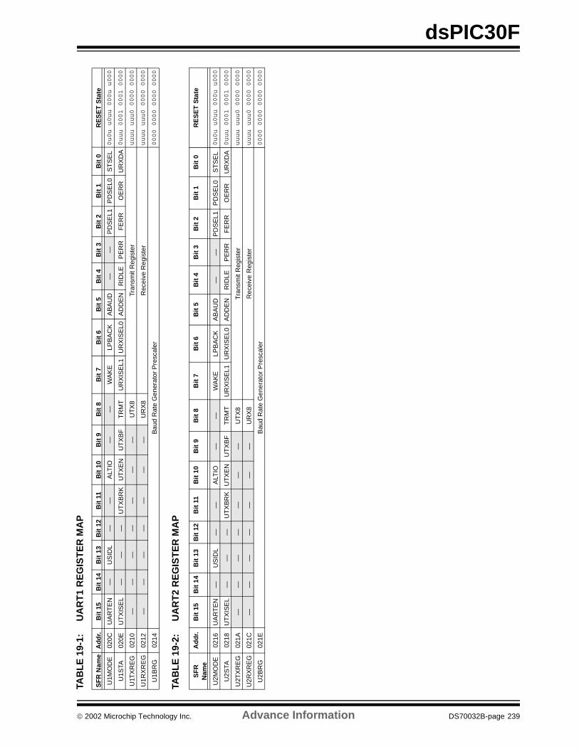
dsPIC30F
TAB
LE
19-
1:U
AR
T1
RE
GIS
TE
R M
AP
TAB
LE
19-
2:U
AR
T2
RE
GIS
TE
R M
AP
SF
R N
ame
Ad
dr.
Bit
15
Bit
14
Bit
13
Bit
12
Bit
11
Bit
10
Bit
9B
it 8
Bit
7B
it 6
Bit
5B
it 4
Bit
3B
it 2
Bit
1B
it 0
RE
SE
T S
tate
U1M
OD
E02
0CU
AR
TE
N—
US
IDL
——
ALT
IO—
—W
AK
ELP
BA
CK
AB
AU
D—
—P
DS
EL1
PD
SE
L0S
TS
EL
0u0u u0uu 000u u000
U1S
TA02
0EU
TX
ISE
L—
——
UT
XB
RK
UT
XE
NU
TX
BF
TR
MT
UR
XIS
EL1
UR
XIS
EL0
AD
DE
NR
IDLE
PE
RR
FE
RR
OE
RR
UR
XD
A0uuu 0001 0001 0000
U1T
XR
EG
0210
——
——
——
—U
TX
8Tr
ansm
it R
egis
ter
uuuu uuu0 0000 0000
U1R
XR
EG
0212
——
——
——
—U
RX
8R
ecei
ve R
egis
ter
uuuu uuu0 0000 0000
U1B
RG
0214
Bau
d R
ate
Gen
erat
or P
resc
aler
0000 0000 0000 0000
SF
R
Nam
eA
dd
r.B
it 1
5B
it 1
4B
it 1
3B
it 1
2B
it 1
1B
it 1
0B
it 9
Bit
8B
it 7
Bit
6B
it 5
Bit
4B
it 3
Bit
2B
it 1
Bit
0R
ES
ET
Sta
te
U2M
OD
E02
16U
AR
TE
N—
US
IDL
——
ALT
IO—
—W
AK
ELP
BA
CK
AB
AU
D—
—P
DS
EL1
PD
SE
L0S
TS
EL
0u0u u0uu 000u u000
U2S
TA02
18U
TX
ISE
L—
——
UT
XB
RK
UT
XE
NU
TX
BF
TR
MT
UR
XIS
EL1
UR
XIS
EL0
AD
DE
NR
IDLE
PE
RR
FE
RR
OE
RR
UR
XD
A0uuu 0001 0001 0000
U2T
XR
EG
021A
——
——
——
—U
TX
8T
rans
mit
Reg
iste
ruuuu uuu0 0000 0000
U2R
XR
EG
021C
——
——
——
—U
RX
8R
ecei
ve R
egis
ter
uuuu uuu0 0000 0000
U2B
RG
021E
Bau
d R
ate
Gen
erat
or P
resc
aler
0000 0000 0000 0000
2002 Microchip Technology Inc. Advance Information DS70032B-page 239
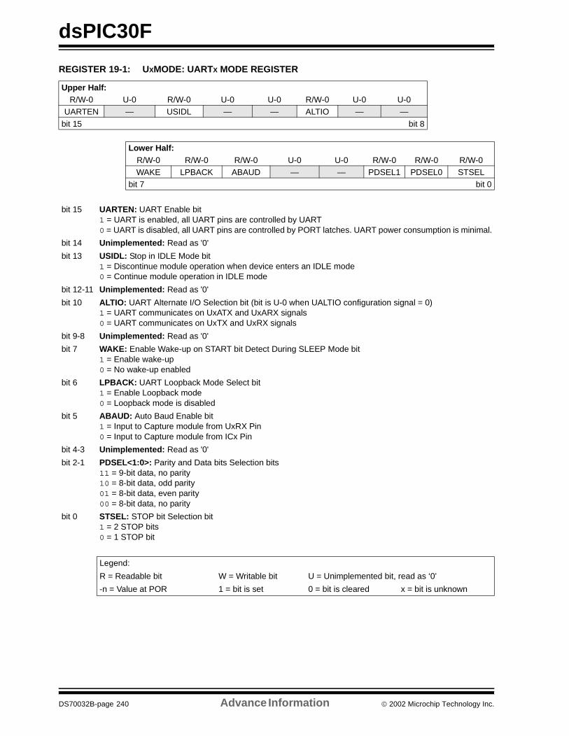
dsPIC30F
REGISTER 19-1: UXMODE: UARTX MODE REGISTER
Upper Half:R/W-0 U-0 R/W-0 U-0 U-0 R/W-0 U-0 U-0
UARTEN — USIDL — — ALTIO — —
bit 15 bit 8
Lower Half:R/W-0 R/W-0 R/W-0 U-0 U-0 R/W-0 R/W-0 R/W-0WAKE LPBACK ABAUD — — PDSEL1 PDSEL0 STSEL
bit 7 bit 0
bit 15 UARTEN: UART Enable bit1 = UART is enabled, all UART pins are controlled by UART0 = UART is disabled, all UART pins are controlled by PORT latches. UART power consumption is minimal.
bit 14 Unimplemented: Read as '0'
bit 13 USIDL: Stop in IDLE Mode bit1 = Discontinue module operation when device enters an IDLE mode0 = Continue module operation in IDLE mode
bit 12-11 Unimplemented: Read as '0'
bit 10 ALTIO: UART Alternate I/O Selection bit (bit is U-0 when UALTIO configuration signal = 0)1 = UART communicates on UxATX and UxARX signals0 = UART communicates on UxTX and UxRX signals
bit 9-8 Unimplemented: Read as '0'
bit 7 WAKE: Enable Wake-up on START bit Detect During SLEEP Mode bit1 = Enable wake-up0 = No wake-up enabled
bit 6 LPBACK: UART Loopback Mode Select bit1 = Enable Loopback mode0 = Loopback mode is disabled
bit 5 ABAUD: Auto Baud Enable bit1 = Input to Capture module from UxRX Pin0 = Input to Capture module from ICx Pin
bit 4-3 Unimplemented: Read as '0'
bit 2-1 PDSEL<1:0>: Parity and Data bits Selection bits11 = 9-bit data, no parity10 = 8-bit data, odd parity01 = 8-bit data, even parity00 = 8-bit data, no parity
bit 0 STSEL: STOP bit Selection bit1 = 2 STOP bits0 = 1 STOP bit
Legend:
R = Readable bit W = Writable bit U = Unimplemented bit, read as ‘0’
-n = Value at POR 1 = bit is set 0 = bit is cleared x = bit is unknown
DS70032B-page 240 Advance Information 2002 Microchip Technology Inc.
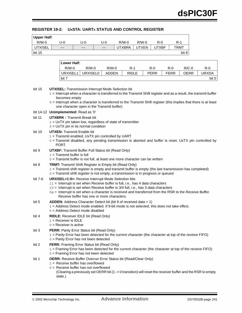
dsPIC30F
REGISTER 19-2: UXSTA: UARTX STATUS AND CONTROL REGISTER
Upper Half:R/W-0 U-0 U-0 U-0 R/W-0 R/W-0 R-0 R-1
UTXISEL — — — UTXBRK UTXEN UTXBF TRMT
bit 15 bit 8
Lower Half:R/W-0 R/W-0 R/W-0 R-1 R-0 R-0 R/C-0 R-0
URXISEL1 URXISEL0 ADDEN RIDLE PERR FERR OERR URXDAbit 7 bit 0
bit 15 UTXISEL: Transmission Interrupt Mode Selection bit1 = Interrupt when a character is transferred to the Transmit Shift register and as a result, the transmit buffer
becomes empty0 = Interrupt when a character is transferred to the Transmit Shift register (this implies that there is at least
one character open in the Transmit buffer)
bit 14-12 Unimplemented: Read as '0'
bit 11 UTXBRK : Transmit Break bit1 = UxTX pin taken low, regardless of state of transmitter0 = UxTX pin in its normal condition
bit 10 UTXEN: Transmit Enable bit1 = Transmit enabled, UxTX pin controlled by UART0 = Transmit disabled, any pending transmission is aborted and buffer is reset. UxTX pin controlled by
PORT.
bit 9 UTXBF: Transmit Buffer Full Status bit (Read Only)1 = Transmit buffer is full0 = Transmit buffer is not full, at least one more character can be written
bit 8 TRMT: Transmit Shift Register is Empty bit (Read Only)1 = Transmit shift register is empty and transmit buffer is empty (the last transmission has completed)0 = Transmit shift register is not empty, a transmission is in progress or queued
bit 7-6 URXISEL<1:0>: Receive Interrupt Mode Selection bits11 = Interrupt is set when Receive buffer is full, i.e., has 4 data characters10 = Interrupt is set when Receive buffer is 3/4 full, i.e., has 3 data characters0x = Interrupt is set when a character is received and transferred from the RSR to the Receive Buffer.
Receive buffer has one or more characters.
bit 5 ADDEN: Address Character Detect bit (bit 8 of received data = 1)1 = Address Detect mode enabled. If 9-bit mode is not selected, this does not take effect.0 = Address Detect mode disabled
bit 4 RIDLE: Receiver IDLE bit (Read Only)1 = Receiver is IDLE0 = Receiver is active
bit 3 PERR: Parity Error Status bit (Read Only)1 = Parity Error has been detected for the current character (the character at top of the receive FIFO)0 = Parity Error has not been detected
bit 2 FERR: Framing Error Status bit (Read Only)1 = Framing Error has been detected for the current character (the character at top of the receive FIFO)0 = Framing Error has not been detected
bit 1 OERR: Receive Buffer Overrun Error Status bit (Read/Clear Only)1 = Receive buffer has overflowed0 = Receive buffer has not overflowed
(Clearing a previously set OERR bit (1 -> 0 transition) will reset the receiver buffer and the RSR to empty state.)
2002 Microchip Technology Inc. Advance Information DS70032B-page 241
dsPIC30F
REGISTER 19-2: UXSTA: UARTX STATUS AND CONTROL REGISTER (Continued)
bit 0 URXDA: Receive Buffer Data Available bit (Read Only)1 = Receive buffer has data, at least one more character can be read0 = Receive buffer is empty
Legend:
R = Readable bit W = Writable bit U = Unimplemented bit, read as ‘0’
-n = Value at POR 1 = bit is set 0 = bit is cleared x = bit is unknown
DS70032B-page 242 Advance Information 2002 Microchip Technology Inc.
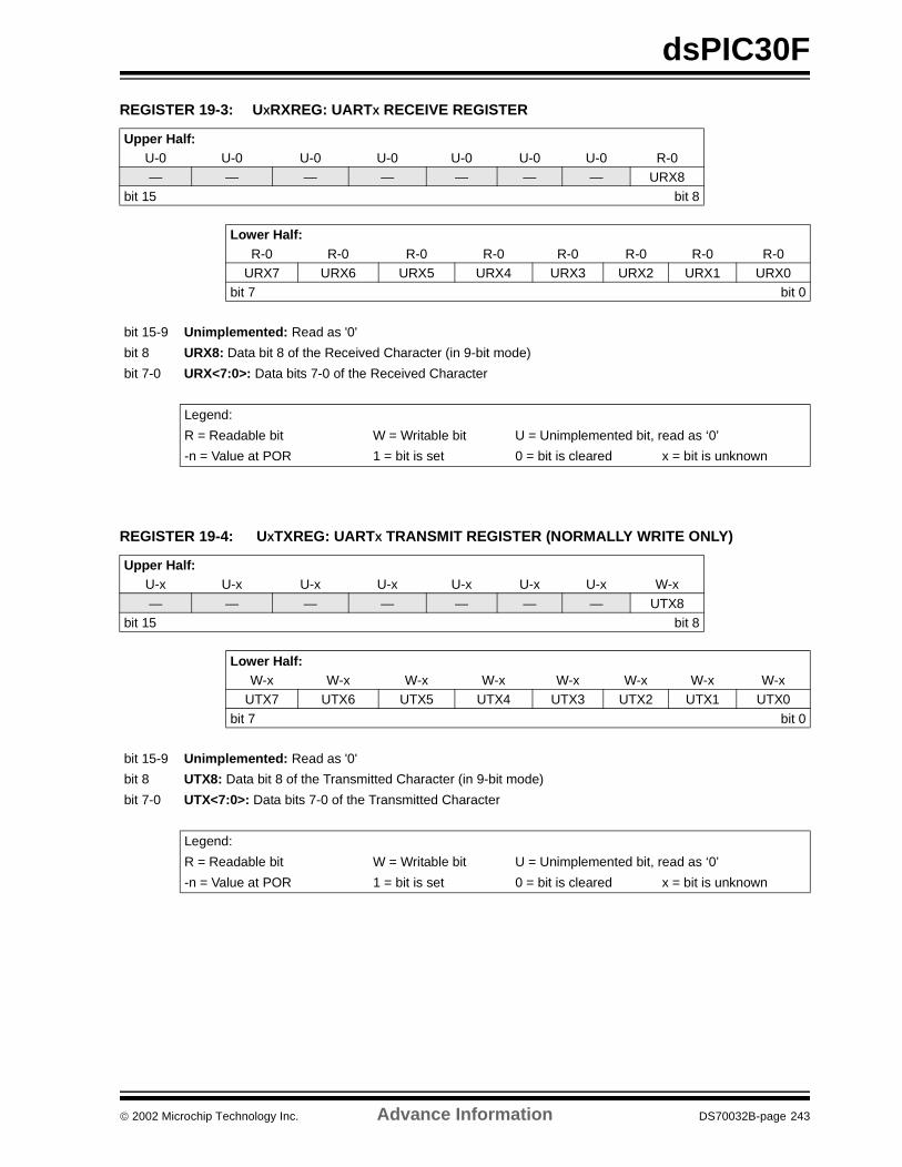
dsPIC30F
REGISTER 19-3: UXRXREG: UARTX RECEIVE REGISTER
REGISTER 19-4: UXTXREG: UARTX TRANSMIT REGISTER (NORMALLY WRITE ONLY)
Upper Half:U-0 U-0 U-0 U-0 U-0 U-0 U-0 R-0— — — — — — — URX8
bit 15 bit 8
Lower Half:R-0 R-0 R-0 R-0 R-0 R-0 R-0 R-0
URX7 URX6 URX5 URX4 URX3 URX2 URX1 URX0bit 7 bit 0
bit 15-9 Unimplemented: Read as '0'
bit 8 URX8: Data bit 8 of the Received Character (in 9-bit mode)
bit 7-0 URX<7:0>: Data bits 7-0 of the Received Character
Legend:
R = Readable bit W = Writable bit U = Unimplemented bit, read as ‘0’
-n = Value at POR 1 = bit is set 0 = bit is cleared x = bit is unknown
Upper Half:U-x U-x U-x U-x U-x U-x U-x W-x
— — — — — — — UTX8bit 15 bit 8
Lower Half:W-x W-x W-x W-x W-x W-x W-x W-x
UTX7 UTX6 UTX5 UTX4 UTX3 UTX2 UTX1 UTX0
bit 7 bit 0
bit 15-9 Unimplemented: Read as '0'
bit 8 UTX8: Data bit 8 of the Transmitted Character (in 9-bit mode)
bit 7-0 UTX<7:0>: Data bits 7-0 of the Transmitted Character
Legend:
R = Readable bit W = Writable bit U = Unimplemented bit, read as ‘0’
-n = Value at POR 1 = bit is set 0 = bit is cleared x = bit is unknown
2002 Microchip Technology Inc. Advance Information DS70032B-page 243
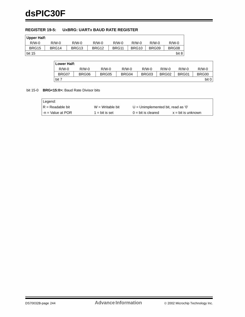
dsPIC30F
REGISTER 19-5: UXBRG: UARTX BAUD RATE REGISTER
Upper Half:R/W-0 R/W-0 R/W-0 R/W-0 R/W-0 R/W-0 R/W-0 R/W-0BRG15 BRG14 BRG13 BRG12 BRG11 BRG10 BRG09 BRG08
bit 15 bit 8
Lower Half:R/W-0 R/W-0 R/W-0 R/W-0 R/W-0 R/W-0 R/W-0 R/W-0BRG07 BRG06 BRG05 BRG04 BRG03 BRG02 BRG01 BRG00
bit 7 bit 0
bit 15-0 BRG<15:0>: Baud Rate Divisor bits
Legend:
R = Readable bit W = Writable bit U = Unimplemented bit, read as ‘0’
-n = Value at POR 1 = bit is set 0 = bit is cleared x = bit is unknown
DS70032B-page 244 Advance Information 2002 Microchip Technology Inc.
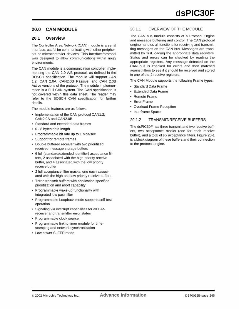
dsPIC30F
20.0 CAN MODULE
20.1 Overview
The Controller Area Network (CAN) module is a serialinterface, useful for communicating with other peripher-als or microcontroller devices. This interface/protocolwas designed to allow communications within noisyenvironments.
The CAN module is a communication controller imple-menting the CAN 2.0 A/B protocol, as defined in theBOSCH specification. The module will support CAN1.2, CAN 2.0A, CAN2.0B Passive, and CAN 2.0BActive versions of the protocol. The module implemen-tation is a Full CAN system. The CAN specification isnot covered within this data sheet. The reader mayrefer to the BOSCH CAN specification for furtherdetails.
The module features are as follows:
• Implementation of the CAN protocol CAN1.2, CAN2.0A and CAN2.0B
• Standard and extended data frames• 0 - 8 bytes data length
• Programmable bit rate up to 1 Mbit/sec• Support for remote frames• Double buffered receiver with two prioritized
received message storage buffers• 6 full (standard/extended identifier) acceptance fil-
ters, 2 associated with the high priority receive buffer, and 4 associated with the low priority receive buffer
• 2 full acceptance filter masks, one each associ-ated with the high and low priority receive buffers
• Three transmit buffers with application specified prioritization and abort capability
• Programmable wake-up functionality with integrated low pass filter
• Programmable Loopback mode supports self-test operation
• Signaling via interrupt capabilities for all CAN receiver and transmitter error states
• Programmable clock source• Programmable link to timer module for time-
stamping and network synchronization• Low power SLEEP mode
20.1.1 OVERVIEW OF THE MODULE
The CAN bus module consists of a Protocol Engineand message buffering and control. The CAN protocolengine handles all functions for receiving and transmit-ting messages on the CAN bus. Messages are trans-mitted by first loading the appropriate data registers.Status and errors can be checked by reading theappropriate registers. Any message detected on theCAN bus is checked for errors and then matchedagainst filters to see if it should be received and storedin one of the 2 receive registers.
The CAN Module supports the following Frame types:
• Standard Data Frame• Extended Data Frame
• Remote Frame• Error Frame• Overload Frame Reception
• Interframe Space
20.1.2 TRANSMIT/RECEIVE BUFFERS
The dsPIC30F has three transmit and two receive buff-ers, two acceptance masks (one for each receivebuffer), and a total of six acceptance filters. Figure 20-1is a block diagram of these buffers and their connectionto the protocol engine.
2002 Microchip Technology Inc. Advance Information DS70032B-page 245
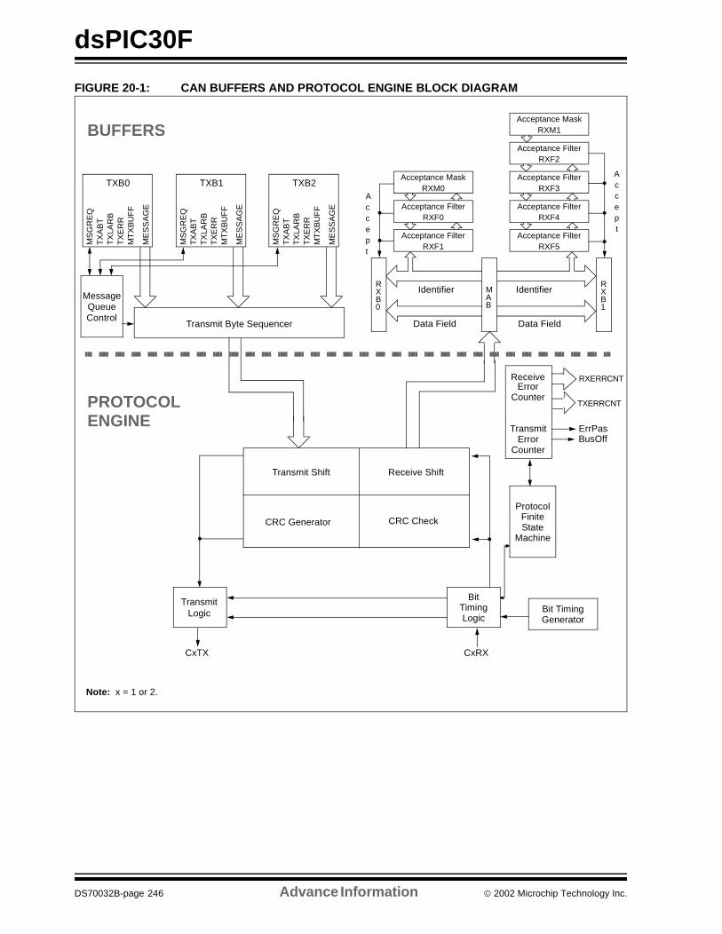
dsPIC30F
FIGURE 20-1: CAN BUFFERS AND PROTOCOL ENGINE BLOCK DIAGRAM
Acceptance FilterRXF2
RXB1
Accept
Accept
Identifier
Data Field Data Field
Identifier
Acceptance MaskRXM1
Acceptance FilterRXF3
Acceptance FilterRXF4
Acceptance FilterRXF5
MAB
Acceptance MaskRXM0
Acceptance FilterRXF0
Acceptance FilterRXF1
RXB0
MS
GR
EQ
TXB2
TX
AB
TT
XLA
RB
TX
ER
RM
TX
BU
FF
ME
SS
AG
E
MessageQueueControl
Transmit Byte Sequencer
MS
GR
EQ
TXB1T
XA
BT
TX
LAR
BT
XE
RR
MT
XB
UF
F
ME
SS
AG
E
MS
GR
EQ
TXB0
TX
AB
TT
XLA
RB
TX
ER
RM
TX
BU
FF
ME
SS
AG
E
Receive ShiftTransmit Shift
ReceiveError
TransmitError
Protocol
RXERRCNT
TXERRCNT
ErrPasBusOff
FiniteState
Machine
Counter
Counter
TransmitLogic
BitTimingLogic
CxTX CxRX
Bit TimingGenerator
PROTOCOLENGINE
BUFFERS
CRC CheckCRC Generator
Note: x = 1 or 2.
DS70032B-page 246 Advance Information 2002 Microchip Technology Inc.
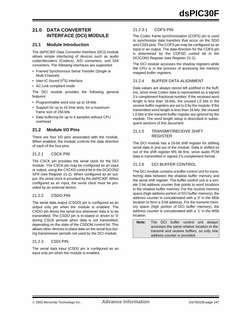
dsPIC30F
21.0 DATA CONVERTER INTERFACE (DCI) MODULE
21.1 Module Introduction
The dsPIC30F Data Converter Interface (DCI) moduleallows simple interfacing of devices such as audiocoder/decoders (Codecs), A/D converters, and D/Aconverters. The following interfaces are supported:
• Framed Synchronous Serial Transfer (Single or Multi-Channel)
• Inter-IC Sound (I2S) Interface• AC-Link compliant mode
The DCI module provides the following generalfeatures:
• Programmable word size up to 16-bits• Support for up to 16 time slots, for a maximum
frame size of 256 bits• Data buffering for up to 4 samples without CPU
overhead
21.2 Module I/O Pins
There are four I/O pins associated with the module.When enabled, the module controls the data directionof each of the four pins.
21.2.1 CSCK PIN
The CSCK pin provides the serial clock for the DCImodule. The CSCK pin may be configured as an inputor output, using the CSCKD control bit in the DCICON2SFR (see Register 21-2). When configured as an out-put, the serial clock is provided by the dsPIC30F. Whenconfigured as an input, the serial clock must be pro-vided by an external device.
21.2.2 CSDO PIN
The serial data output (CSDO) pin is configured as anoutput only pin when the module is enabled. TheCSDO pin drives the serial bus whenever data is to betransmitted. The CSDO pin is tri-stated or driven to ‘0’during CSCK periods when data is not transmitted,depending on the state of the CSDOM control bit. Thisallows other devices to place data on the serial bus dur-ing transmission periods not used by the DCI module.
21.2.3 CSDI PIN
The serial data input (CSDI) pin is configured as aninput only pin when the module is enabled.
21.2.3.1 COFS PIN
The Codec frame synchronization (COFS) pin is usedto synchronize data transfers that occur on the SDOand CSDI pins. The COFS pin may be configured as aninput or an output. The data direction for the COFS pinis determined by the COFSD control bit in theDCICON1 Register (see Register 21-1).
The DCI module accesses the shadow registers whilethe CPU is in the process of accessing the memorymapped buffer registers.
21.2.4 BUFFER DATA ALIGNMENT
Data values are always stored left justified in the buff-ers, since most Codec data is represented as a signed2’s complement fractional number. If the received wordlength is less than 16-bits, the unused LS bits in thereceive buffer registers are set to 0 by the module. If thetransmitted word length is less than 16 bits, the unusedLS bits in the transmit buffer register are ignored by themodule. The word length setup is described in subse-quent sections of this document.
21.2.5 TRANSMIT/RECEIVE SHIFT REGISTER
The DCI module has a 16-bit shift register for shiftingserial data in and out of the module. Data is shifted in/out of the shift register MS bit first, since audio PCMdata is transmitted in signed 2’s complement format.
21.2.6 DCI BUFFER CONTROL
The DCI module contains a buffer control unit for trans-ferring data between the shadow buffer memory andthe serial shift register. The buffer control unit is a sim-ple 2-bit address counter that points to word locationsin the shadow buffer memory. For the receive memoryspace (high address portion of DCI buffer memory), theaddress counter is concatenated with a ‘0’ in the MSblocation to form a 3-bit address. For the transmit mem-ory space (high portion of DCI buffer memory), theaddress counter is concatenated with a ‘1’ in the MSblocation.
Note: The DCI buffer control unit alwaysaccesses the same relative location in thetransmit and receive buffers, so only oneaddress counter is provided.
2002 Microchip Technology Inc. Advance Information DS70032B-page 247
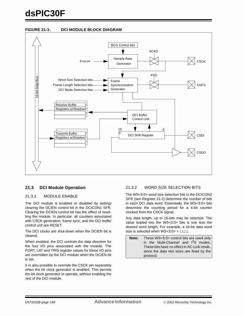
dsPIC30F
FIGURE 21-1: DCI MODULE BLOCK DIAGRAM
21.3 DCI Module Operation
21.3.1 MODULE ENABLE
The DCI module is enabled or disabled by setting/clearing the DCIEN control bit in the DCICON1 SFR.Clearing the DCIEN control bit has the effect of reset-ting the module. In particular, all counters associatedwith CSCK generation, frame sync, and the DCI buffercontrol unit are RESET.
The DCI clocks are shut-down when the DCIEN bit iscleared.
When enabled, the DCI controls the data direction forthe four I/O pins associated with the module. ThePORT, LAT and TRIS register values for these I/O pinsare overridden by the DCI module when the DCIEN bitis set.
It is also possible to override the CSCK pin separatelywhen the bit clock generator is enabled. This permitsthe bit clock generator to operate, without enabling therest of the DCI module.
21.3.2 WORD SIZE SELECTION BITS
The WS<3:0> word size selection bits in the DCICON2SFR (see Register 21-2) determine the number of bitsin each DCI data word. Essentially, the WS<3:0> bitsdetermine the counting period for a 4-bit counterclocked from the CSCK signal.
Any data length, up to 16-bits may be selected. Thevalue loaded into the WS<3:0> bits is one less thedesired word length. For example, a 16-bit data wordsize is selected when WS<3:0> = 1111.
BCG Control bits
16-b
it D
ata
Bus
Sample Rate
Generator
SCKD
FSD
DCI Buffer
Frame SynchronizationGenerator
Control Unit
DCI Shift Register
Receive Buffer Registers w/Shadow
FOSC/4
Word Size Selection bits
Frame Length Selection bits
DCI Mode Selection bits
CSCK
COFS
CSDI
CSDO
15 0Transmit Buffer Registers w/Shadow
Note: These WS<3:0> control bits are used onlyin the Multi-Channel and I2S modes.These bits have no effect in AC-Link mode,since the data slot sizes are fixed by theprotocol.
DS70032B-page 248 Advance Information 2002 Microchip Technology Inc.
dsPIC30F
21.3.3 FRAME SYNC GENERATOR
The frame sync generator (COFSG) is a 4-bit counterthat sets the frame length in data words. The framesync generator is incremented each time the word sizecounter is reset (refer to Section 21.3.2). The period forthe frame synchronization generator is set by writingthe COFSG<3:0> control bits in the DCICON2 SFR.The COFSG period in clock cycles is determined by thefollowing formula:
EQUATION 21-1: COFSG PERIOD
Frame lengths, up to 16 data words may be selected.The frame length in CSCK periods can vary up to amaximum of 256 depending on the word size that isselected.
21.3.4 FRAME SYNC MODE CONTROL BITS
The type of frame sync signal is selected using theFrame Synchronization mode control bits(COFSM<1:0>) in the DCICON1 SFR (seeRegister 21-1). The following operating modes can beselected:
• Multi-Channel mode
• I2S mode• AC-Link mode (16-bit)• AC-Link mode (20-bit)
The operation of the COFSM control bits depends onwhether the DCI module generates the frame sync sig-nal as a master device, or receives the frame sync sig-nal as a slave device.
The master device in a DSP/Codec pair is the devicethat generates the frame sync signal. The frame syncsignal initiates data transfers on the CSDI and CSDOpins and usually has the same frequency as the datasample rate (COFS).
The DCI module is a frame sync master, if the COFSDcontrol bit is cleared and is a frame sync slave, if theCOFSD control bit is set.
21.3.5 MASTER FRAME SYNC OPERATION
When the DCI module is operating as a frame syncmaster device (COFSD = 0), the COFSM mode bitsdetermine the type of frame sync pulse that is gener-ated by the frame sync generator logic.
A new COFS signal is generated when the frame syncgenerator resets to 0.
In the Multi-Channel mode, the frame sync pulse isdriven high for the CSCK period to initiate a data trans-fer. The number of CSCK cycles between successiveframe sync pulses will depend on the word size andframe sync generator control bits. A timing diagram forthe frame sync signal in Multi-Channel mode is shownin Figure 21-2.
In the AC-Link mode of operation, the frame sync sig-nal has a fixed period and duty cycle. The AC-Linkframe sync signal is high for 16 CSCK cycles and is lowfor 240 CSCK cycles. A timing diagram with the timingdetails at the start of an AC-Link frame is shown inFigure 21-3.
In the I2S mode, a frame sync signal having a 50% dutycycle is generated. The period of the I2S frame syncsignal in CSCK cycles is determined by the word sizeand frame sync generator control bits. A new I2S datatransfer boundary is marked by a high-to-low or a low-to-high transition edge on the COFS pin.
21.3.6 SLAVE FRAME SYNC OPERATION
When the DCI module is operating as a frame syncslave (COFSD = 1), data transfers are controlled by theCodec device attached to the DCI module. TheCOFSM control bits control how the DCI moduleresponds to incoming COFS signals.
In the Multi-Channel mode, a new data frame transferwill begin one CSCK cycle after the COFS pin is sam-pled high (see Figure 21-2). The pulse on the COFSpin resets the frame sync generator logic.
In the I2S mode, a new data word will be transferredone CSCK cycle after a low-to-high or a high-to-lowtransition is sampled on the COFS pin. A rising or fall-ing edge on the COFS pin resets the frame sync gen-erator logic.
In the AC-Link mode, the tag slot and subsequent dataslots for the next frame will be transferred one CSCKcycle after the COFS pin is sampled high.
The COFSG and WS bits must be configured to pro-vide the proper frame length when the module is oper-ating in the Slave mode. Once a valid frame syncpulse has been sampled by the module on the COFSpin, an entire data frame transfer will take place. Themodule will not respond to further frame sync pulsesuntil the data frame transfer has completed.
Note: The COFSG control bits will have no effectin AC-Link mode, since the frame length isset to 256 CSCK periods by the protocol.
FrameLength = WordLength (FSGvalue + 1)•
2002 Microchip Technology Inc. Advance Information DS70032B-page 249
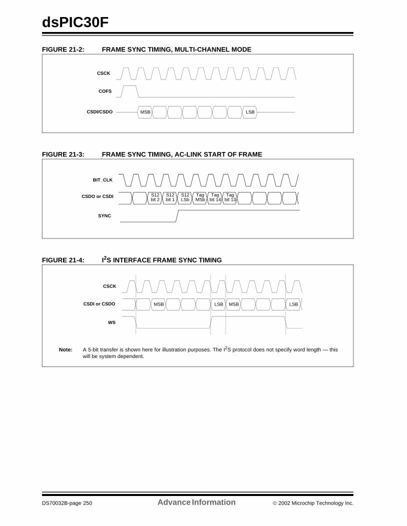
dsPIC30F
FIGURE 21-2: FRAME SYNC TIMING, MULTI-CHANNEL MODE
FIGURE 21-3: FRAME SYNC TIMING, AC-LINK START OF FRAME
FIGURE 21-4: I2S INTERFACE FRAME SYNC TIMING
CSCK
CSDI/CSDO
COFS
MSB LSB
TagMSb
BIT_CLK
CSDO or CSDI
SYNC
Tagbit 14
S12LSb
S12bit 1
S12bit 2
Tagbit 13
MSB LSB MSB LSB
CSCK
CSDI or CSDO
WS
Note: A 5-bit transfer is shown here for illustration purposes. The I2S protocol does not specify word length — thiswill be system dependent.
DS70032B-page 250 Advance Information 2002 Microchip Technology Inc.
dsPIC30F
21.3.7 BIT CLOCK GENERATOR
The DCI module has a dedicated 12-bit time-base thatproduces the bit clock. The bit clock rate (period) is setby writing a non-zero 12-bit value to the BCG<11:0>control bits in the DCICON1 SFR.
When the BCG<11:0> bits are set to zero, the bit clockwill be disabled. If the BCG<11:0> bits are set to a non-zero value, the bit clock generator is enabled. Thesebits should be set to ‘0’ and the CSCKD bit set to 1, ifthe serial clock for the DCI is received from an externaldevice.
The formula for the bit clock frequency is given inEquation 21-2.
EQUATION 21-2: BIT CLOCK FREQUENCY
The required bit clock frequency will be determined bythe system sampling rate and frame size. Typical bitclock frequencies range from 16x to 512x the convertersample rate, depending on the data converter and thecommunication protocol that is used.
To achieve bit clock frequencies associated with com-mon audio sampling rates, the user will need to selecta crystal frequency that has an ‘even’ binary value.Examples of such crystal frequencies are listed inTable 21-1.
TABLE 21-1: DEVICE FREQUENCIES FOR COMMON CODEC CSCK FREQUENCIES
21.3.8 SAMPLE CLOCK EDGE CONTROL BIT
The sample clock edge (CSCKE) control bit determinesthe sampling edge for the CSCK signal. If the CSCK bitis cleared (default), data will be sampled on the fallingedge of the CSCK signal. The AC-Link protocols andmost Multi-Channel formats require that data be sam-pled on the falling edge of the CSCK signal. If theCSCK bit is set, data will be sampled on the rising edgeof CSCK. The I2S protocol requires that data be sam-pled on the rising edge of the CSCK signal.
21.3.9 DATA JUSTIFICATION CONTROL BIT
In most applications, the data transfer begins oneCSCK cycle after the COFS signal is sampled active.This is the default configuration of the DCI module. Analternate data alignment can be selected by setting theDJST control bit in the DCICON2 SFR. When DJST = 1,data transfers will begin during the same CSCK cyclewhen the COFS signal is sampled active.
21.3.10 TRANSMIT SLOT ENABLE BITS
The TSCON SFR (see Register 21-5) has control bitsthat are used to enable up to 16 time-slots for transmis-sion. These control bits are the TSE<15:0> bits. Thesize of each time-slot is determined by the WS<3:0>word size selection bits and can vary up to 16-bits.
If a transmit time-slot is enabled via one of the TSE bits(TSEx = 1), the contents of the current transmit shadowbuffer location will be loaded into the CSDO shift regis-ter and the DCI buffer control unit is incremented topoint to the next location.
During an unused transmit time-slot, the CSDO pin willdrive 0’s or will be tri-stated during all disabled time-slots, depending on the state of the CSDOM bit in theDCICON1 SFR.
The data frame size in bits is determined by the chosendata word size and the number of data word elementsin the frame. If the chosen frame size has less than 16elements, the additional slot enable bits will have noeffect.
Each transmit data word is written to the 16-bit transmitbuffer as left justified data. If the selected word size isless than 16-bits, then the LS bits of the transmit buffermemory will have no effect on the transmitted data. Theuser should write 0’s to the unused LS bits of eachtransmit buffer location.
FOSC PLL FCYC
2.048 MHz 16x 32.768 MIPS4.096 MHz 8x 32.768 MIPS
4.800 MHz 8x 38.4 MIPS9.600 MHz 4x 38.4 MIPS
Note 1: When the CSCK signal is applied exter-nally (CSCKD = 1), the BCG<9:0> bitshave no effect on the operation of the DCImodule.
2: When the CSCK signal is applied exter-nally (CSCKD = 1), the external clockhigh and low times must meet the devicetiming requirements.
fBCK =fCYC
2 (BCG + 1)•
2002 Microchip Technology Inc. Advance Information DS70032B-page 251
dsPIC30F
21.3.11 RECEIVE SLOT ENABLE BITS
The RSCON SFR (see Register 21-6) contains controlbits that are used to enable up to 16 time-slots forreception. These control bits are the RSE<15:0> bits.The size of each receive time-slot is determined by theWS<3:0> word size selection bits and can vary from 1to 16 bits.
If a receive time-slot is enabled via one of the RSE bits(RSEx = 1), the shift register contents will be written tothe current DCI receive shadow buffer location and thebuffer control unit will be incremented to point to thenext buffer location.
Data is not packed in the receive memory buffer loca-tions if the selected word size is less than 16 bits. Eachreceived slot data word is stored in a separate 16-bitbuffer location. Data is always stored in a left justifiedformat in the receive memory buffer.
21.3.12 SLOT ENABLE BITS OPERATION WITH FRAME SYNC
The TSE and RSE control bits operate in concert withthe DCI frame sync generator. In the Master mode, aCOFS signal is generated whenever the frame syncgenerator is reset. In the Slave mode, the frame syncgenerator is reset whenever a COFS pulse is received.
The TSE and RSE control bits allow up to 16 consecu-tive time-slots to be enabled for transmit or receive.After the last enabled time-slot has been transmitted/received, the DCI will stop buffering data until the nextoccurring COFS pulse.
21.3.13 SYNCHRONOUS DATA TRANSFERS
The DCI buffer control unit will be incremented by oneword location, whenever a given time-slot has beenenabled for transmission or reception. In most cases,data input and output transfers will be synchronized,which means that a data sample is received for a givenchannel at the same time a data sample is transmitted.Therefore, the transmit and receive buffers will be filledwith equal amounts of data when a DCI interrupt is gen-erated.
In some cases, the amount of data transmitted andreceived during a data frame may not be equal. As anexample, assume a two-word data frame is used. Fur-thermore, assume that data is only received during slot#0, but is transmitted during slot #0 and slot #1. In thiscase, the buffer control unit counter would be incre-mented twice during a data frame, but only one receiveregister location would be filled with data.
21.3.14 BUFFER LENGTH CONTROL
The amount of data that is buffered between interruptsis determined by the buffer length (BLEN<1:0>) controlbits in the DCISTAT SFR (see Register 21-4). The sizeof the transmit and receive buffers may be varied from1 to 4 data words, using the BLEN control bits. TheBLEN control bits are compared to the current value ofthe DCI buffer control unit address counter. When the 2LS bits of the DCI address counter match theBLEN<1:0> value, the buffer control unit will be reset to0. In addition, the contents of the receive shadow reg-isters are transferred to the receive buffer registers andthe contents of the transmit buffer registers are trans-ferred to the transmit shadow registers.
21.3.15 BUFFER ALIGNMENT WITH DATA FRAMES
There is no direct coupling between the position of theAGU address pointer and the data frame boundaries.This means that there will be an implied assignment ofeach transmit and receive buffer that is a function ofthe BLEN control bits and the number of enabled dataslots via the TSE and RSE control bits.
As an example, assume that a 4-word data frame ischosen and that we want to transmit on all four time-slots in the frame. This configuration would be estab-lished by setting the TSE0, TSE1, TSE2, and TSE3control bits in the TSCON SFR. With this modulesetup, the TXBUF0 register would be naturallyassigned to slot #0, the TXBUF1 register would benaturally assigned to slot #1, and so on.
Note: When more than four time-slots are activewithin a data frame, the user code mustkeep track of which time-slots are to beread/written at each interrupt. In somecases, the alignment between transmit/receive buffers and their respective slotassignments could be lost. Examples ofsuch cases include an emulation break-point or a hardware trap. In these situa-tions, the user should poll the SLOT statusbits to determine what data should beloaded into the buffer registers to resyn-chronize the software with the DCI module.
DS70032B-page 252 Advance Information 2002 Microchip Technology Inc.
dsPIC30F
21.3.16 TRANSMIT STATUS BITS
There are two transmit status bits in the DCISTAT SFR.
The TMPTY bit is set when the contents of the trans-mit buffer registers are transferred to the transmitshadow registers. The TMPTY bit may be polled insoftware to determine when the transmit buffer regis-ters may be written. The TMPTY bit is cleared auto-matically by the hardware when a write to one of thefour transmit buffers occurs.
The TUNF bit is read only and indicates that a transmitunderflow has occurred for at least one of the transmitbuffer registers that is in use. The TUNF bit is set at thetime the transmit buffer registers are transferred to thetransmit shadow registers. The TUNF status bit iscleared automatically when the buffer register thatunderflowed is written by the CPU.
21.3.17 RECEIVE STATUS BITS
There are two receive status bits in the DCISTAT SFR.
The RFUL status bit is read only and indicates that newdata is available in the receive buffers. The RFUL bit iscleared automatically when all receive buffers in usehave been read by the CPU.
The ROV status bit is read only and indicates that areceive overflow has occurred for at least one of thereceive buffer locations. A receive overflow occurswhen the buffer location is not read by the CPU beforenew data is transferred from the shadow registers. TheROV status bit is cleared automatically when the bufferregister that caused the overflow is read by the CPU.
When a receive overflow occurs for a specific bufferlocation, the old contents of the buffer are overwritten.
21.3.18 SLOT STATUS BITS
The SLOT<3:0> status bits in the DCISTAT SFR indi-cate the current active time-slot. These bits will corre-spond to the value of the frame sync generatorcounter. The user may poll these status bits in soft-ware when a DCI interrupt occurs, to determine whattime-slot data was last received and which time-slotdata should be loaded into the TXBUF registers.
21.3.19 CSDO MODE BIT
The CSDOM control bit controls the behavior of theCSDO pin during unused transmit slots. A given trans-mit time-slot is unused if its corresponding TSEx bit inthe TSCON SFR is cleared.
If the CSDOM bit is cleared (default), the CSDO pinwill drive 0’s onto the CSDO pin during unused time-slot periods. This mode will be used when there areonly two devices attached to the serial bus.
If the CSDOM bit is set, the CSDO pin will be tri-statedduring unused time-slot periods. This mode allowsmultiple devices to share the same CSDO line in aMulti-Channel application. Each device on the CSDOline is configured so that it will only transmit data dur-ing specific time-slots. No two devices will transmitdata during the same time-slot.
21.3.20 DIGITAL LOOPBACK MODE
Digital Loopback mode is enabled by setting theDLOOP control bit in the DCISTAT SFR. When theDLOOP bit is set, the module internally connects theSDO signal to CSDI. The actual data input on the CSDII/O pin will be ignored in Digital Loopback mode.
21.3.21 UNDERFLOW MODE CONTROL BIT
When an underflow occurs, one of two actions mayoccur, depending on the state of the Underflow mode(UNFM) control bit in the DCICON2 SFR. If the UNFMbit is cleared (default), the module will transmit 0’s onthe SDO pin during the active time-slot for the bufferlocation. In this operating mode, the Codec deviceattached to the DCI module will simply be fed digital‘silence’. If the UNFM control bit is set, the module willtransmit the last data written to the buffer location. Thisoperating mode permits the user to send continuousdata to the Codec device without consuming CPUoverhead.
21.4 DCI Module interrupts
The frequency of DCI module interrupts is dependenton the BLEN<1:0> control bits in the DCICON2 SFR.An interrupt to the CPU is generated each time the setbuffer length has been reached and a shadow registertransfer takes place. A shadow register transfer isdefined as the time when the previously writtenTXBUF values are transferred to the transmit shadowregisters and new received values in the receiveshadow registers are transferred into the RXBUF reg-isters.
Note: The transmit status bits only indicate statusfor buffer locations that are used by themodule. If the buffer length is set to lessthan four words, for example, the unusedbuffer locations will not affect the transmitstatus bits.
Note: The receive status bits only indicate statusfor buffer locations that are used by themodule. If the buffer length is set to lessthan four-words, for example, the unusedbuffer locations will not affect the transmitstatus bits.
2002 Microchip Technology Inc. Advance Information DS70032B-page 253
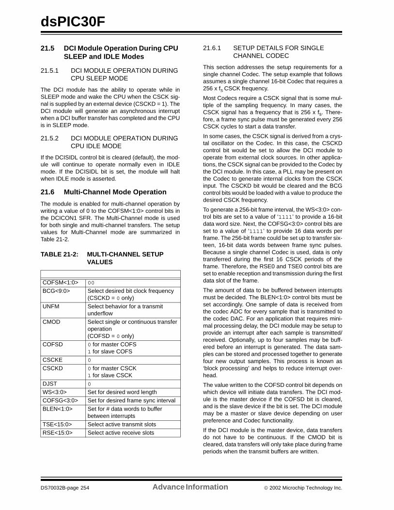
dsPIC30F
21.5 DCI Module Operation During CPU SLEEP and IDLE Modes
21.5.1 DCI MODULE OPERATION DURING CPU SLEEP MODE
The DCI module has the ability to operate while inSLEEP mode and wake the CPU when the CSCK sig-nal is supplied by an external device (CSCKD = 1). TheDCI module will generate an asynchronous interruptwhen a DCI buffer transfer has completed and the CPUis in SLEEP mode.
21.5.2 DCI MODULE OPERATION DURING CPU IDLE MODE
If the DCISIDL control bit is cleared (default), the mod-ule will continue to operate normally even in IDLEmode. If the DCISIDL bit is set, the module will haltwhen IDLE mode is asserted.
21.6 Multi-Channel Mode Operation
The module is enabled for multi-channel operation bywriting a value of 0 to the COFSM<1:0> control bits inthe DCICON1 SFR. The Multi-Channel mode is usedfor both single and multi-channel transfers. The setupvalues for Multi-Channel mode are summarized inTable 21-2.
TABLE 21-2: MULTI-CHANNEL SETUP VALUES
21.6.1 SETUP DETAILS FOR SINGLE CHANNEL CODEC
This section addresses the setup requirements for asingle channel Codec. The setup example that followsassumes a single channel 16-bit Codec that requires a256 x fS CSCK frequency.
Most Codecs require a CSCK signal that is some mul-tiple of the sampling frequency. In many cases, theCSCK signal has a frequency that is 256 x fs. There-fore, a frame sync pulse must be generated every 256CSCK cycles to start a data transfer.
In some cases, the CSCK signal is derived from a crys-tal oscillator on the Codec. In this case, the CSCKDcontrol bit would be set to allow the DCI module tooperate from external clock sources. In other applica-tions, the CSCK signal can be provided to the Codec bythe DCI module. In this case, a PLL may be present onthe Codec to generate internal clocks from the CSCKinput. The CSCKD bit would be cleared and the BCGcontrol bits would be loaded with a value to produce thedesired CSCK frequency.
To generate a 256-bit frame interval, the WS<3:0> con-trol bits are set to a value of ‘1111’ to provide a 16-bitdata word size. Next, the COFSG<3:0> control bits areset to a value of ‘1111’ to provide 16 data words perframe. The 256-bit frame could be set up to transfer six-teen, 16-bit data words between frame sync pulses.Because a single channel Codec is used, data is onlytransferred during the first 16 CSCK periods of theframe. Therefore, the RSE0 and TSE0 control bits areset to enable reception and transmission during the firstdata slot of the frame.
The amount of data to be buffered between interruptsmust be decided. The BLEN<1:0> control bits must beset accordingly. One sample of data is received fromthe codec ADC for every sample that is transmitted tothe codec DAC. For an application that requires mini-mal processing delay, the DCI module may be setup toprovide an interrupt after each sample is transmitted/received. Optionally, up to four samples may be buff-ered before an interrupt is generated. The data sam-ples can be stored and processed together to generatefour new output samples. This process is known as‘block processing’ and helps to reduce interrupt over-head.
The value written to the COFSD control bit depends onwhich device will initiate data transfers. The DCI mod-ule is the master device if the COFSD bit is cleared,and is the slave device if the bit is set. The DCI modulemay be a master or slave device depending on userpreference and Codec functionality.
If the DCI module is the master device, data transfersdo not have to be continuous. If the CMOD bit iscleared, data transfers will only take place during frameperiods when the transmit buffers are written.
COFSM<1:0> 00
BCG<9:0> Select desired bit clock frequency(CSCKD = 0 only)
UNFM Select behavior for a transmit underflow
CMOD Select single or continuous transfer operation (COFSD = 0 only)
COFSD 0 for master COFS1 for slave COFS
CSCKE 0
CSCKD 0 for master CSCK1 for slave CSCK
DJST 0
WS<3:0> Set for desired word lengthCOFSG<3:0> Set for desired frame sync interval
BLEN<1:0> Set for # data words to buffer between interrupts
TSE<15:0> Select active transmit slotsRSE<15:0> Select active receive slots
DS70032B-page 254 Advance Information 2002 Microchip Technology Inc.
dsPIC30F
21.6.2 MULTI-CHANNEL CODEC CONFIGURATION
The transfer of control data and multiple data channelsover the serial connection between the dsPIC deviceand the Codec is enabled by Time Division Multiplexing(TDM) of the data. The number of TDM time-slots willdepend on the actual Codec that is selected.
A hypothetical example of serial time-slot assignmentfor a Codec is given below:
Transmit Time-slots
• Slot #0: Control Register Address
• Slot #1: Control Register Write Data• Slot #2: DAC Channel 1 Data• Slot #3: DAC Channel 2 Data
Receive Time-slots
• Slot #0: Control Register Address Echo
• Slot #1: Control Register Read Data• Slot #2: ADC Channel 1 Data• Slot #3: ADC Channel 2 Data
The DCI module is configured similar to the singlechannel setup described in Section 21.6.1, except thatmultiple slots are enabled for transmission and recep-tion. In this example, TSE0, TSE1, TSE2, and TSE3are set to transmit data on the first four slots of theframe. Similarly, RSE0, RSE1, RSE2, and RSE3 areset to enable reception during the first four time-slots.
The WS<3:0> control bits should be set to the nativeword size of the Codec and the COFSG<3:0> controlbits should be set to provide the correct number ofCSCK cycles per frame.
21.7 AC-Link Mode Operation
21.7.1 AC-LINK WORD SIZE ISSUES
The AC-Link protocol is a 256-bit frame with one 16-bitdata slot, followed by twelve 20-bit data slots. The DCImodule has two operating modes for the AC-Link pro-tocol. These operating modes are selected by theCOFSM<1:0> control bits in the DCICON1 SFR. Thefirst AC-Link mode is called ‘16-bit AC-Link mode’ andis selected by setting COFSM<1:0> = 10. The secondAC-Link mode is called ‘20-bit AC-Link mode’ and isselected by setting COFSM<1:0> = 11.
21.7.2 16-BIT AC-LINK MODE
In the 16-bit AC-Link mode, data word lengths arerestricted to 16-bits. Note that this restriction only affectsthe 20-bit data time-slots of the AC-Link protocol. Forreceived time-slots, the incoming data is simply trun-cated to 16-bits. For outgoing time-slots, the 4 LS bits ofthe data word are set to 0 by the module. This trunca-tion of the time-slots limits the A/D and DAC data to 16-bits, but permits proper data alignment in the TXBUFand RXBUF registers. Each RXBUF and TXBUF regis-ter will contain one data time-slot value.
21.7.3 20-BIT AC-LINK MODE
The 20-bit AC-Link mode allows all bits in the datatime-slots to be transmitted and received, but does notmaintain data alignment in the TXBUF and RXBUFregisters.
The 20-bit AC-Link mode functions similar to the Multi-Channel mode of the DCI module, except for the dutycycle of the frame synchronization signal. The AC-Linkframe synchronization signal should remain high for16 CSCK cycles and should be low for the following240 cycles.
The 20-bit mode treats each 256-bit AC-Link frame assixteen, 16-bit time-slots. In the 20-bit AC-Link mode,the module operates as if COFSG<3:0> = 1111 andWS<3:0> = 1111. The data alignment for 20-bit dataslots is ignored. For example, an entire AC-link dataframe can be transmitted and received in a packedfashion by setting all bits in the TSCON and RSCONSFRs. Since the total available buffer length is 64-bits,it would take 4 consecutive interrupts to transfer theAC-Link frame. The application software must keeptrack of the current AC-Link frame segment.
21.7.4 AC-LINK SETUP
The module is enabled for AC-Link mode by writing 10or 11 to the COFSM<1:0> control bits in the DCICON1SFR. The word size selection bits (WS<3:0>) and theframe synchronization generator bits (COFS<4:0>)have no effect in the AC-Link modes, since the frameand word sizes are set by the protocol.
The CSCKD control bit is set in software. The COFSDcontrol bit is cleared because the DCI will generate theCOFS signal from the incoming CSCK signal. TheCSCKE bit is cleared so that data is sampled on therising edge.
The user must decide which time-slots in the AC-Linkdata frame are to be buffered, and set the TSE andRSE control bits accordingly. At a minimum, it will benecessary to buffer the transmit and receive Tag slots,which implies that the TSE0 and RSE0 bits should beset in software.
Note: Only the TSE<12:0> and RSE12:0> bits willhave an effect in the 16-bit AC-Link modesince an AC-Link frame has 13 time-slots.
2002 Microchip Technology Inc. Advance Information DS70032B-page 255
dsPIC30F
21.8 I2S Mode Operation
The DCI module is configured for I2S mode by writinga value of 01 to the COFSM<1:0> control bits in theDCICON1 SFR. When operating in the I2S mode, theDCI module will generate frame synchronization sig-nals with a 50% duty cycle. Each edge of the framesynchronization signal marks the boundary of a newdata word transfer.
The user must also select the frame length and dataword size using the COFSG and WS control bits in theDCICON2 SFR.
21.8.1 I2S FRAME AND DATA WORD LENGTH SELECTION
The WS and COFSG control bits are set to produce theperiod for one half of an I2S data frame. That is, theframe length is the total number of CSCK cyclesrequired for a left or a right data word transfer.
Although only one data word is transferred per I2S sub-frame, It may be necessary to set the COFSG value toa higher value to produce the appropriate number ofCSCK cycles per frame. For example, many I2SCodecs use a 64x serial clock. In other words, there are64 CSCK cycles per frame and 32 cycles per left/rightsubframe. Assuming that a 16-bit Codec is connectedto the DCI module, the user should configure theCOFSG bits for 2 words per frame (COFSG<3:0> =0001) and the WS bits are configured for a 16-bit dataword (WS<3:0> = 1111).
A 4 data word frame has been defined for this example,but only the first time-slot is of interest. Therefore, theTSE0 and RSE0 control bits are set to make the mod-ule actively transmit and receive data during thesetime-slots.
The BLEN bits must be set for the desired buffer length.Setting BLEN<1:0> = 01 will produce a CPU interrupt,once per I2S frame.
21.8.2 I2S DATA JUSTIFICATION
As per the I2S specification, a data word transfer will, bydefault, begin one CSCK cycle after a transition of theWS signal. A ‘MS bit left justified’ option can beselected using the DJST control bit in the DCICON2SFR.
If DJST = 1, the I2S data transfers will be MS bit left jus-tified. The MS bit of the data word will be presented onthe SDO pin during the same CSCK cycle as the risingor falling edge of the COFS signal. The SDO pin is tri-stated after the data word has been sent.
The left justified data option allows two stereo Codecsto be connected to the same serial bus. The word sizeselection bits are set to twice the Codec word lengthand data is read/written to the DCI memory in a packedformat.
Timing diagrams for I2S mode are shown in Figure 21-5.For reference, these diagrams assume an 8-bit wordsize (WS<3:0> = 0111). Two elements would berequired to achieve a 16-bit sub-frame (COFSG<3:0> =0001). The third timing diagram in Figure 21-5 usespacked data to read/write from two Codecs. For thisexample, the DCI module is configured for a 16-bit dataword (WS<3:0> = 1111). Two packed 8-bit words arewritten to each 16-bit location in the DCI memory buffer.
DS70032B-page 256 Advance Information 2002 Microchip Technology Inc.
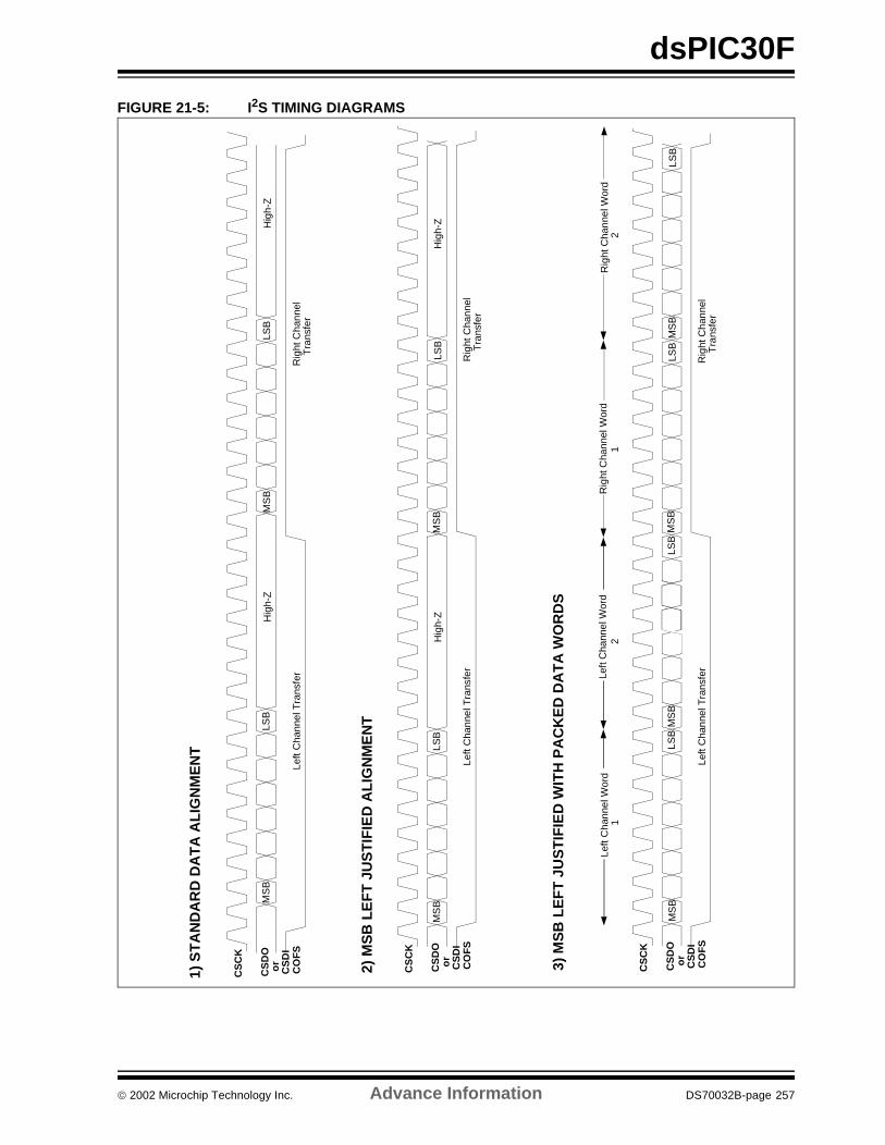
dsPIC30F
FIGURE 21-5: I2S TIMING DIAGRAMS
MS
BLS
BM
SB
CS
CK
CS
DO
or
CS
DI
CO
FS
Left
Cha
nnel
Tra
nsfe
rR
ight
Cha
nnel
Tra
nsfe
r
LSB
Hig
h-Z
Hig
h-Z
MS
BLS
BM
SB
CS
CK
CS
DO
or
CS
DI
CO
FS
Left
Cha
nnel
Tra
nsfe
rR
ight
Cha
nnel
Tra
nsfe
r
LSB
Hig
h-Z
Hig
h-Z
MS
BLS
BM
SB
MS
B
CS
CK
CS
DO
or
CS
DI
CO
FS
Left
Cha
nnel
Tra
nsfe
rR
ight
Cha
nnel
Tra
nsfe
r
LSB
LSB
MS
BLS
B
Rig
ht C
hann
el W
ord
2R
ight
Cha
nnel
Wor
d1
Left
Cha
nnel
Wor
d2
Left
Cha
nnel
Wor
d1
1) S
TA
ND
AR
D D
AT
A A
LIG
NM
EN
T
2) M
SB
LE
FT
JU
ST
IFIE
D A
LIG
NM
EN
T
3) M
SB
LE
FT
JU
ST
IFIE
D W
ITH
PA
CK
ED
DA
TA
WO
RD
S
2002 Microchip Technology Inc. Advance Information DS70032B-page 257
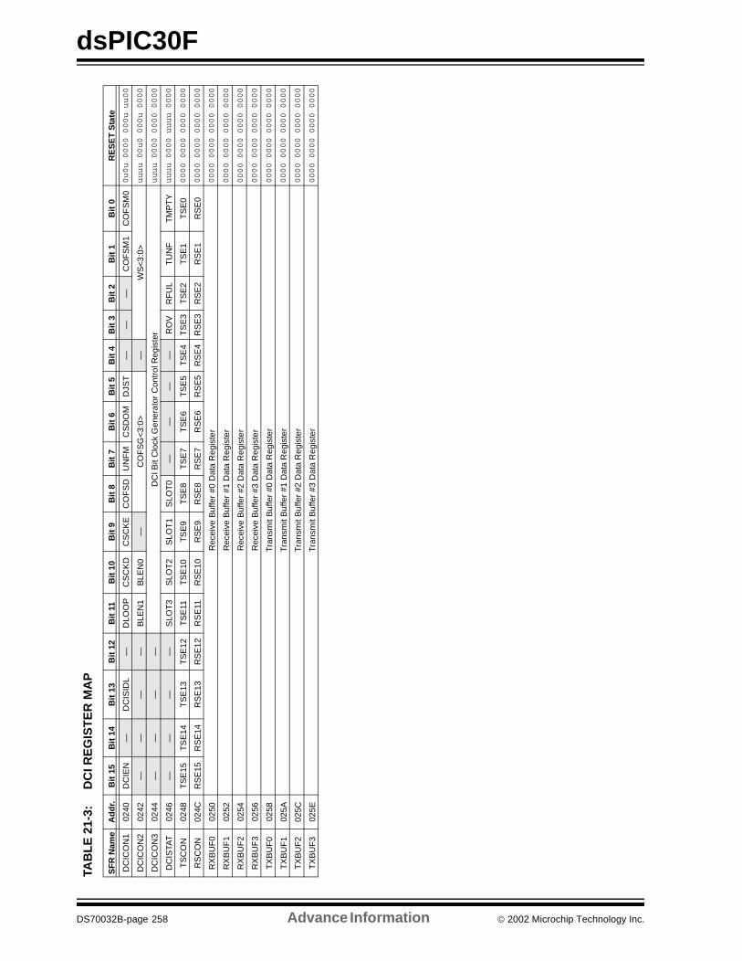
dsPIC30F
TAB
LE
21-
3:D
CI R
EG
IST
ER
MA
P
SF
R N
ame
Ad
dr.
Bit
15
Bit
14
Bit
13
Bit
12
Bit
11
Bit
10
Bit
9B
it 8
Bit
7B
it 6
Bit
5B
it 4
Bit
3B
it 2
Bit
1B
it 0
RE
SE
T S
tate
DC
ICO
N1
0240
DC
IEN
—D
CIS
IDL
—D
LOO
PC
SC
KD
CS
CK
EC
OF
SD
UN
FM
CS
DO
MD
JST
——
—C
OF
SM
1C
OF
SM
00u0u 0000 000u uu00
DC
ICO
N2
0242
——
——
BLE
N1
BLE
N0
—C
OF
SG
<3:
0>—
WS
<3:
0>uuuu 00u0 000u 0000
DC
ICO
N3
0244
——
——
DC
I Bit
Clo
ck G
ener
ator
Con
trol
Reg
iste
ruuuu 0000 0000 0000
DC
ISTA
T02
46—
——
—S
LOT
3S
LOT
2S
LOT
1S
LOT
0—
——
—R
OV
RF
UL
TU
NF
TM
PT
Yuuuu 0000 uuuu 0000
TS
CO
N02
48T
SE
15T
SE
14T
SE
13T
SE
12T
SE
11T
SE
10T
SE
9T
SE
8T
SE
7T
SE
6T
SE
5T
SE
4T
SE
3T
SE
2T
SE
1T
SE
00000 0000 0000 0000
RS
CO
N02
4CR
SE
15R
SE
14R
SE
13R
SE
12R
SE
11R
SE
10R
SE
9R
SE
8R
SE
7R
SE
6R
SE
5R
SE
4R
SE
3R
SE
2R
SE
1R
SE
00000 0000 0000 0000
RX
BU
F0
0250
Rec
eive
Buf
fer
#0 D
ata
Reg
iste
r0000 0000 0000 0000
RX
BU
F1
0252
Rec
eive
Buf
fer
#1 D
ata
Reg
iste
r0000 0000 0000 0000
RX
BU
F2
0254
Rec
eive
Buf
fer
#2 D
ata
Reg
iste
r0000 0000 0000 0000
RX
BU
F3
0256
Rec
eive
Buf
fer
#3 D
ata
Reg
iste
r0000 0000 0000 0000
TX
BU
F0
0258
Tran
smit
Buf
fer
#0 D
ata
Reg
iste
r0000 0000 0000 0000
TX
BU
F1
025A
Tran
smit
Buf
fer
#1 D
ata
Reg
iste
r0000 0000 0000 0000
TX
BU
F2
025C
Tran
smit
Buf
fer
#2 D
ata
Reg
iste
r0000 0000 0000 0000
TX
BU
F3
025E
Tran
smit
Buf
fer
#3 D
ata
Reg
iste
r0000 0000 0000 0000
DS70032B-page 258 Advance Information 2002 Microchip Technology Inc.
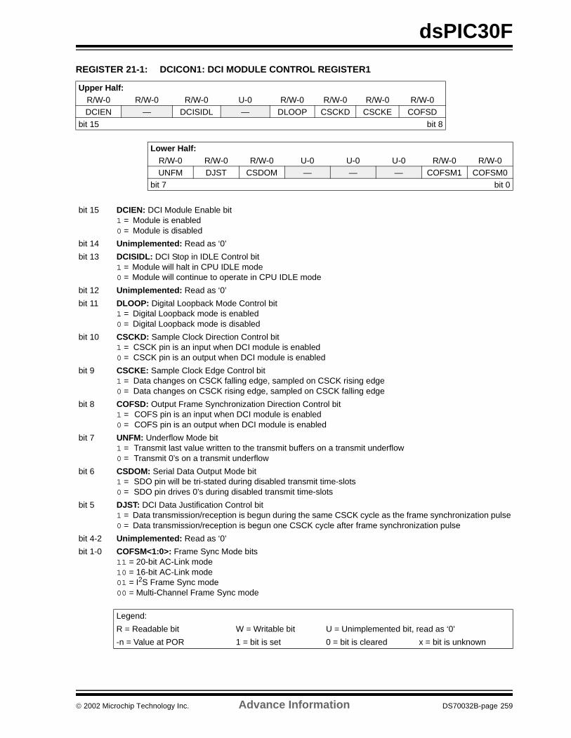
dsPIC30F
REGISTER 21-1: DCICON1: DCI MODULE CONTROL REGISTER1
Upper Half:R/W-0 R/W-0 R/W-0 U-0 R/W-0 R/W-0 R/W-0 R/W-0DCIEN — DCISIDL — DLOOP CSCKD CSCKE COFSD
bit 15 bit 8
Lower Half:R/W-0 R/W-0 R/W-0 U-0 U-0 U-0 R/W-0 R/W-0UNFM DJST CSDOM — — — COFSM1 COFSM0
bit 7 bit 0
bit 15 DCIEN: DCI Module Enable bit1 = Module is enabled0 = Module is disabled
bit 14 Unimplemented: Read as ‘0’
bit 13 DCISIDL: DCI Stop in IDLE Control bit1 = Module will halt in CPU IDLE mode0 = Module will continue to operate in CPU IDLE mode
bit 12 Unimplemented: Read as ‘0’
bit 11 DLOOP: Digital Loopback Mode Control bit1 = Digital Loopback mode is enabled0 = Digital Loopback mode is disabled
bit 10 CSCKD: Sample Clock Direction Control bit1 = CSCK pin is an input when DCI module is enabled0 = CSCK pin is an output when DCI module is enabled
bit 9 CSCKE: Sample Clock Edge Control bit1 = Data changes on CSCK falling edge, sampled on CSCK rising edge0 = Data changes on CSCK rising edge, sampled on CSCK falling edge
bit 8 COFSD: Output Frame Synchronization Direction Control bit1 = COFS pin is an input when DCI module is enabled0 = COFS pin is an output when DCI module is enabled
bit 7 UNFM: Underflow Mode bit1 = Transmit last value written to the transmit buffers on a transmit underflow0 = Transmit 0’s on a transmit underflow
bit 6 CSDOM: Serial Data Output Mode bit1 = SDO pin will be tri-stated during disabled transmit time-slots0 = SDO pin drives 0’s during disabled transmit time-slots
bit 5 DJST: DCI Data Justification Control bit1 = Data transmission/reception is begun during the same CSCK cycle as the frame synchronization pulse0 = Data transmission/reception is begun one CSCK cycle after frame synchronization pulse
bit 4-2 Unimplemented: Read as ‘0’
bit 1-0 COFSM<1:0>: Frame Sync Mode bits11 = 20-bit AC-Link mode10 = 16-bit AC-Link mode01 = I2S Frame Sync mode00 = Multi-Channel Frame Sync mode
Legend:
R = Readable bit W = Writable bit U = Unimplemented bit, read as ‘0’
-n = Value at POR 1 = bit is set 0 = bit is cleared x = bit is unknown
2002 Microchip Technology Inc. Advance Information DS70032B-page 259
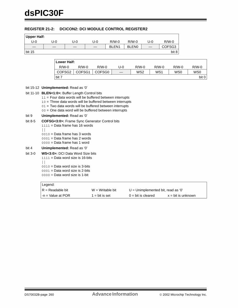
dsPIC30F
REGISTER 21-2: DCICON2: DCI MODULE CONTROL REGISTER2
Upper Half:U-0 U-0 U-0 U-0 R/W-0 R/W-0 U-0 R/W-0— — — — BLEN1 BLEN0 — COFSG3
bit 15 bit 8
Lower Half:R/W-0 R/W-0 R/W-0 U-0 R/W-0 R/W-0 R/W-0 R/W-0
COFSG2 COFSG1 COFSG0 — WS2 WS1 WS0 WS0bit 7 bit 0
bit 15-12 Unimplemented: Read as ‘0’
bit 11-10 BLEN<1:0>: Buffer Length Control bits11 = Four data words will be buffered between interrupts10 = Three data words will be buffered between interrupts01 = Two data words will be buffered between interrupts00 = One data word will be buffered between interrupts
bit 9 Unimplemented: Read as ‘0’
bit 8-5 COFSG<3:0>: Frame Sync Generator Control bits1111 = Data frame has 16 words||0010 = Data frame has 3 words0001 = Data frame has 2 words0000 = Data frame has 1 word
bit 4 Unimplemented: Read as ‘0’
bit 3-0 WS<3:0>: DCI Data Word Size bits1111 = Data word size is 16-bits||0010 = Data word size is 3-bits0001 = Data word size is 2-bits0000 = Data word size is 1-bit
Legend:
R = Readable bit W = Writable bit U = Unimplemented bit, read as ‘0’
-n = Value at POR 1 = bit is set 0 = bit is cleared x = bit is unknown
DS70032B-page 260 Advance Information 2002 Microchip Technology Inc.
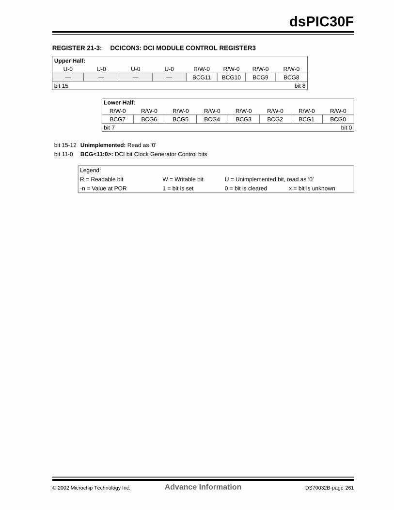
dsPIC30F
REGISTER 21-3: DCICON3: DCI MODULE CONTROL REGISTER3
Upper Half:U-0 U-0 U-0 U-0 R/W-0 R/W-0 R/W-0 R/W-0— — — — BCG11 BCG10 BCG9 BCG8
bit 15 bit 8
Lower Half:R/W-0 R/W-0 R/W-0 R/W-0 R/W-0 R/W-0 R/W-0 R/W-0BCG7 BCG6 BCG5 BCG4 BCG3 BCG2 BCG1 BCG0
bit 7 bit 0
bit 15-12 Unimplemented: Read as ‘0’
bit 11-0 BCG<11:0>: DCI bit Clock Generator Control bits
Legend:
R = Readable bit W = Writable bit U = Unimplemented bit, read as ‘0’
-n = Value at POR 1 = bit is set 0 = bit is cleared x = bit is unknown
2002 Microchip Technology Inc. Advance Information DS70032B-page 261
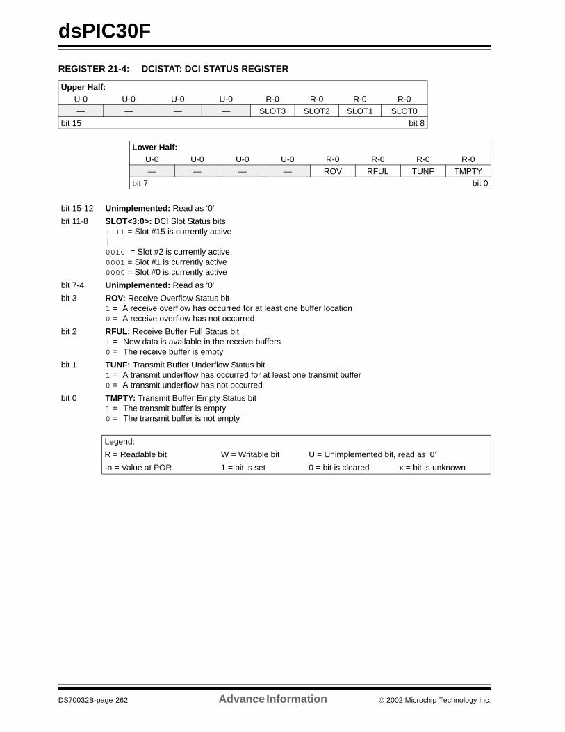
dsPIC30F
REGISTER 21-4: DCISTAT: DCI STATUS REGISTER
Upper Half:U-0 U-0 U-0 U-0 R-0 R-0 R-0 R-0— — — — SLOT3 SLOT2 SLOT1 SLOT0
bit 15 bit 8
Lower Half:U-0 U-0 U-0 U-0 R-0 R-0 R-0 R-0— — — — ROV RFUL TUNF TMPTY
bit 7 bit 0
bit 15-12 Unimplemented: Read as ‘0’
bit 11-8 SLOT<3:0>: DCI Slot Status bits1111 = Slot #15 is currently active||0010 = Slot #2 is currently active0001 = Slot #1 is currently active0000 = Slot #0 is currently active
bit 7-4 Unimplemented: Read as ‘0’
bit 3 ROV: Receive Overflow Status bit1 = A receive overflow has occurred for at least one buffer location0 = A receive overflow has not occurred
bit 2 RFUL: Receive Buffer Full Status bit1 = New data is available in the receive buffers0 = The receive buffer is empty
bit 1 TUNF: Transmit Buffer Underflow Status bit1 = A transmit underflow has occurred for at least one transmit buffer0 = A transmit underflow has not occurred
bit 0 TMPTY: Transmit Buffer Empty Status bit1 = The transmit buffer is empty0 = The transmit buffer is not empty
Legend:
R = Readable bit W = Writable bit U = Unimplemented bit, read as ‘0’
-n = Value at POR 1 = bit is set 0 = bit is cleared x = bit is unknown
DS70032B-page 262 Advance Information 2002 Microchip Technology Inc.
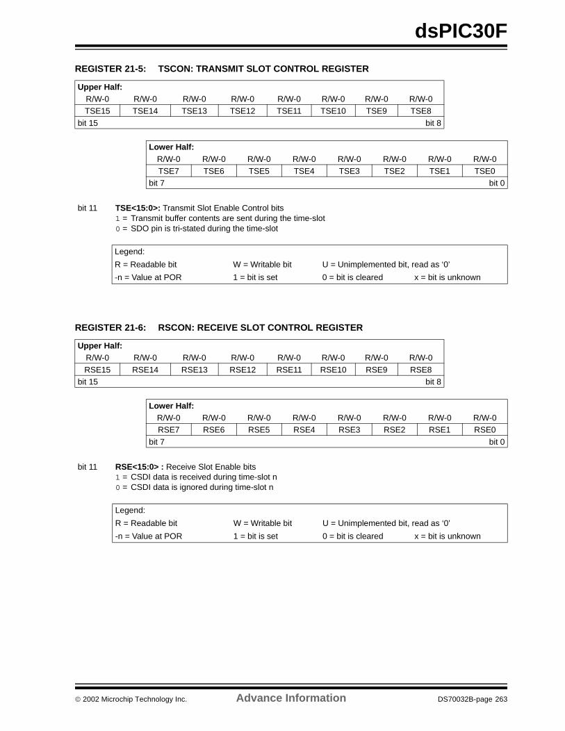
dsPIC30F
REGISTER 21-5: TSCON: TRANSMIT SLOT CONTROL REGISTER
REGISTER 21-6: RSCON: RECEIVE SLOT CONTROL REGISTER
Upper Half:R/W-0 R/W-0 R/W-0 R/W-0 R/W-0 R/W-0 R/W-0 R/W-0TSE15 TSE14 TSE13 TSE12 TSE11 TSE10 TSE9 TSE8
bit 15 bit 8
Lower Half:R/W-0 R/W-0 R/W-0 R/W-0 R/W-0 R/W-0 R/W-0 R/W-0TSE7 TSE6 TSE5 TSE4 TSE3 TSE2 TSE1 TSE0
bit 7 bit 0
bit 11 TSE<15:0>: Transmit Slot Enable Control bits1 = Transmit buffer contents are sent during the time-slot0 = SDO pin is tri-stated during the time-slot
Legend:
R = Readable bit W = Writable bit U = Unimplemented bit, read as ‘0’
-n = Value at POR 1 = bit is set 0 = bit is cleared x = bit is unknown
Upper Half:R/W-0 R/W-0 R/W-0 R/W-0 R/W-0 R/W-0 R/W-0 R/W-0
RSE15 RSE14 RSE13 RSE12 RSE11 RSE10 RSE9 RSE8bit 15 bit 8
Lower Half:R/W-0 R/W-0 R/W-0 R/W-0 R/W-0 R/W-0 R/W-0 R/W-0RSE7 RSE6 RSE5 RSE4 RSE3 RSE2 RSE1 RSE0
bit 7 bit 0
bit 11 RSE<15:0> : Receive Slot Enable bits1 = CSDI data is received during time-slot n0 = CSDI data is ignored during time-slot n
Legend:
R = Readable bit W = Writable bit U = Unimplemented bit, read as ‘0’
-n = Value at POR 1 = bit is set 0 = bit is cleared x = bit is unknown
2002 Microchip Technology Inc. Advance Information DS70032B-page 263

dsPIC30F
NOTES:
DS70032B-page 264 Advance Information 2002 Microchip Technology Inc.
dsPIC30F
22.0 12-BIT ANALOG-TO-DIGITAL CONVERTER (A/D) MODULE
The 12-bit Analog-to-Digital Converter (A/D) allowsconversion of an analog input signal to a corresponding12-bit digital number. This module is based on a Suc-cessive Approximation Register (SAR) architecture,and provides a maximum sampling rate of 500 ksps.The A/D module has up to 16 analog inputs, which aremultiplexed into a sample and hold amplifier. The out-put of the sample and hold is the input into the con-verter, which generates the result. The analogreference voltage is software selectable to either thedevice supply voltage (AVDD/AVSS), or the voltage levelon the (VREF+/VREF-) pin. The A/D converter has aunique feature of being able to operate while the deviceis in SLEEP mode, with RC oscillator selection.
The A/D module has six 16-bit registers.
• A/D Control Register1 (ADCON1)• A/D Control Register2 (ADCON2)
• A/D Control Register3 (ADCON3)• A/D Input Select Register (ADCHS)• A/D Port Configuration Register (ADPCFG)
• A/D Input Scan Selection Register (ADCSSL)
The ADCON1, ADCON2 and ADCON3 registers con-trol the operation of the A/D module. The ADCHS reg-ister selects the input channels to be converted. TheADPCFG register configures the port pins as analoginputs or as digital I/O. The ADCSSL register selectsinputs for scanning.
The block diagram of the 12-bit A/D module is shown inFigure 22-1.
FIGURE 22-1: 12-BIT A/D FUNCTIONAL BLOCK DIAGRAM
Note: The SSRC<2:0>, ASAM, SMPI<3:0>,BUFM and ALTS bits, as well as theADCON3 and ADCSSL registers, must notbe written to while ADON = 1. This wouldlead to indeterminate results.
Comparator
12-Bit SAR Conversion Logic
VREF+AVSSAVDD
DAC
Dat
a F
orm
at16-word, 12-bit
Dual PortRAM
Bus
Inte
rfac
e
AN12
0000
0101
0111
1001
1101
1110
1111
1100
0001
0010
0011
0100
0110
1000
1010
1011
AN13
AN14
AN15
AN8
AN9
AN10
AN11
AN4
AN5
AN6
AN7
AN0
AN1
AN2
AN3
CH0
CH0RCH0G
VREF-
Sample/SequenceControlSample
Input MuxControl
InputSwitches
S/H
2002 Microchip Technology Inc. Advance Information DS70032B-page 265
dsPIC30F
22.1 A/D Result Buffer
The module contains a 16-word dual port RAM, calledADRES<15:0>, to buffer the A/D results. The RAM is12-bits wide, but the data obtained is represented inone of four different 16-bit data formats.
Only word writes are allowed to the result buffer. If bytewrites are attempted, the results are indeterminate.
22.2 Conversion Operation
After the A/D module has been configured as desired,the sampling is started by setting the SAMP bit. Varioussources, such as a programmable bit, timer time-outsand external events, will terminate sampling and start aconversion. When the A/D conversion is completed,the result is loaded into ADRES<15:0>, the CONV bitis cleared, and the A/D interrupt flag, ADIF, is set. TheADC module can be configured for different interruptrates, as described in Section 22.3.
The following steps should be followed for doing anA/D conversion:
1. Configure the A/D module• Configure analog pins/voltage reference/
and digital I/O• Select A/D input channels
• Select A/D conversion clock• Select A/D conversion trigger• Turn on A/D module
2. Configure A/D interrupt (if required)• Clear ADIF bit • Select A/D interrupt priority
3. Start sampling4. Wait the required sampling time5. Trigger sample end, start conversion
• Module sets CONV bit6. Wait for A/D conversion to complete, by either:
• Polling for the CONV bit to be cleared
• Waiting for the A/D interrupt7. Read A/D result buffer, clear ADIF if required.
22.3 Selecting the Conversion Sequence
Several groups of control bits select the sequence thatthe A/D connects inputs to the sample/hold channel,converts a channel, writes the buffer memory and gen-erates interrupts.
The sequence is controlled by the sampling clocks.
The SMPI bits will select how many sample clocksoccur before an interrupt occurs. This can vary from 1sample per interrupt, to 16 samples per interrupt.
The BUFM bit will split the 16-word results buffer into(2) 8-word groups. Writing to the 8-word buffers will bealternated on each interrupt event.
Use of the BUFM bit will depend on how much time isavailable for the moving of the buffers after theinterrupt.
If the processor can quickly unload a full buffer withinthe time it takes to sample and convert one channel,the BUFM bit can be 0 and up to 16 conversions (cor-responding to the 16 input channels) may be done perinterrupt. The processor will have one sample and con-version time to move the sixteen conversions.
If the processor cannot unload the buffer within thesample and conversion time, the BUFM bit should be 1.For example, if SMPI<3:0> (ADCON2<5:2>) = 0111,then eight conversions will be loaded into 1/2 of thebuffer, following which, an interrupt occurs. The nexteight conversions will be loaded into the other 1/2 of thebuffer. The processor will have the entire time betweeninterrupts to move the eight conversions.
The ALTS bit can be used to alternate the inputsselected during the sampling sequence. If the ALTS bitis 0, only the SAMPLE A inputs are selected for sam-pling. If the ALTS bit is 1 and SMPI<3:0> = 0000, onthe first sample/convert sequence, the SAMPLE Ainputs are selected, and on the next sample/convertsequence, the SAMPLE B inputs are selected.
The CSCNA bit (ADCON2<10>) will allow the CH0channel inputs to be scanned across a selected num-ber of analog inputs during SAMPLE A samples. Theinputs are selected by the ADCSSL register. If a partic-ular bit in the ADCSSL register is ‘1’, the correspondinginput is selected. The inputs are always scanned fromlower to higher numbered inputs, starting after eachinterrupt occurs. If the number of inputs selected isgreater than the number of samples taken per interrupt,the higher numbered inputs are unused.
22.4 Programming the Sample Trigger
The sample trigger will terminate sampling and start therequested conversions.
The SSRC<2:0> bits select the source of the sampletrigger.
When SSRC<2:0> = 000, the sample trigger is undersoftware control. Clearing the SAMP bit will cause thesample trigger.
When SSRC<2:0> = 111, the sample trigger is underA/D clock control. The SAMC bits select the number ofA/D clocks between the start of sampling and the startof conversion. This provides the fastest conversionrates on multiple channels. SAMC must always be atleast 1 clock cycle.
Other trigger sources can come from timer modules orexternal interrupts.
The SSRC bits provide for up to 6 alternate sources ofsample trigger.
DS70032B-page 266 Advance Information 2002 Microchip Technology Inc.
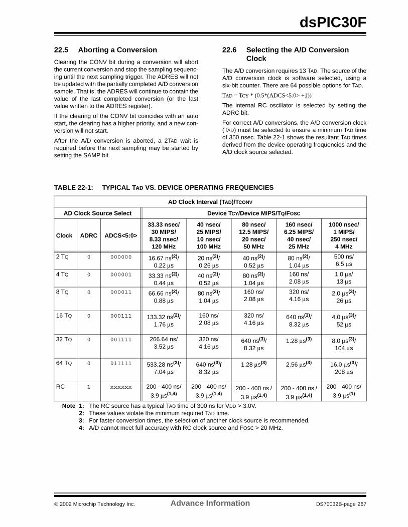
dsPIC30F
22.5 Aborting a Conversion
Clearing the CONV bit during a conversion will abortthe current conversion and stop the sampling sequenc-ing until the next sampling trigger. The ADRES will notbe updated with the partially completed A/D conversionsample. That is, the ADRES will continue to contain thevalue of the last completed conversion (or the lastvalue written to the ADRES register).
If the clearing of the CONV bit coincides with an autostart, the clearing has a higher priority, and a new con-version will not start.
After the A/D conversion is aborted, a 2TAD wait isrequired before the next sampling may be started bysetting the SAMP bit.
22.6 Selecting the A/D Conversion Clock
The A/D conversion requires 13 TAD. The source of theA/D conversion clock is software selected, using asix-bit counter. There are 64 possible options for TAD.
TAD = TCY * (0.5*(ADCS<5:0> +1))
The internal RC oscillator is selected by setting theADRC bit.
For correct A/D conversions, the A/D conversion clock(TAD) must be selected to ensure a minimum TAD timeof 350 nsec. Table 22-1 shows the resultant TAD timesderived from the device operating frequencies and theA/D clock source selected.
TABLE 22-1: TYPICAL TAD VS. DEVICE OPERATING FREQUENCIES
AD Clock Interval (TAD)/TCONV
AD Clock Source Select Device TCY/Device MIPS/TQ/FOSC
Clock ADRC ADCS<5:0>
33.33 nsec/ 30 MIPS/
8.33 nsec/120 MHz
40 nsec/ 25 MIPS/10 nsec/100 MHz
80 nsec/ 12.5 MIPS/20 nsec/50 MHz
160 nsec/ 6.25 MIPS/40 nsec/25 MHz
1000 nsec/ 1 MIPS/
250 nsec/4 MHz
2 TQ 0 000000 16.67 ns(2)/0.22 µs
20 ns(2)/0.26 µs
40 ns(2)/0.52 µs
80 ns(2)/1.04 µs
500 ns/6.5 µs
4 TQ 0 000001 33.33 ns(2)/0.44 µs
40 ns(2)/0.52 µs
80 ns(2)/1.04 µs
160 ns/2.08 µs
1.0 µs/13 µs
8 TQ 0 000011 66.66 ns(2)/0.88 µs
80 ns(2)/1.04 µs
160 ns/2.08 µs
320 ns/4.16 µs
2.0 µs(3)/26 µs
16 TQ 0 000111 133.32 ns(2)/1.76 µs
160 ns/2.08 µs
320 ns/4.16 µs
640 ns(3)/8.32 µs
4.0 µs(3)/52 µs
32 TQ 0 001111 266.64 ns/3.52 µs
320 ns/4.16 µs
640 ns(3)/8.32 µs
1.28 µs(3) 8.0 µs(3)/104 µs
64 TQ 0 011111 533.28 ns(3)/7.04 µs
640 ns(3)/8.32 µs
1.28 µs(3) 2.56 µs(3) 16.0 µs(3)/208 µs
RC 1 xxxxxx 200 - 400 ns/
3.9 µs(1,4)200 - 400 ns/
3.9 µs(1,4) 200 - 400 ns /
3.9 µs(1,4)
200 - 400 ns /
3.9 µs(1,4)
200 - 400 ns/
3.9 µs(1)
Note 1: The RC source has a typical TAD time of 300 ns for VDD > 3.0V.2: These values violate the minimum required TAD time.3: For faster conversion times, the selection of another clock source is recommended.4: A/D cannot meet full accuracy with RC clock source and FOSC > 20 MHz.
2002 Microchip Technology Inc. Advance Information DS70032B-page 267
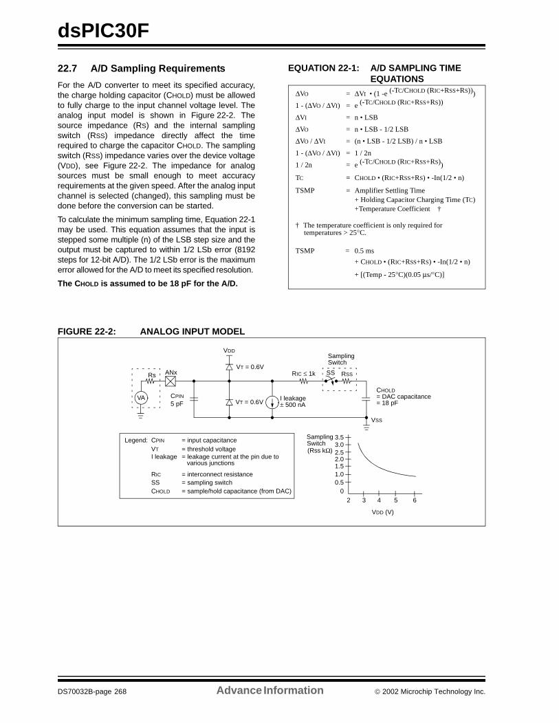
dsPIC30F
22.7 A/D Sampling Requirements
For the A/D converter to meet its specified accuracy,the charge holding capacitor (CHOLD) must be allowedto fully charge to the input channel voltage level. Theanalog input model is shown in Figure 22-2. Thesource impedance (RS) and the internal samplingswitch (RSS) impedance directly affect the timerequired to charge the capacitor CHOLD. The samplingswitch (RSS) impedance varies over the device voltage(VDD), see Figure 22-2. The impedance for analogsources must be small enough to meet accuracyrequirements at the given speed. After the analog inputchannel is selected (changed), this sampling must bedone before the conversion can be started.
To calculate the minimum sampling time, Equation 22-1may be used. This equation assumes that the input isstepped some multiple (n) of the LSB step size and theoutput must be captured to within 1/2 LSb error (8192steps for 12-bit A/D). The 1/2 LSb error is the maximumerror allowed for the A/D to meet its specified resolution.
The CHOLD is assumed to be 18 pF for the A/D.
EQUATION 22-1: A/D SAMPLING TIME EQUATIONS
FIGURE 22-2: ANALOG INPUT MODEL
∆VO = ∆VI • (1 -e (-TC/CHOLD (RIC+RSS+RS)))
1 - (∆VO / ∆VI) = e (-TC/CHOLD (RIC+RSS+RS))
∆VI = n • LSB
∆VO = n • LSB - 1/2 LSB
∆VO / ∆VI = (n • LSB - 1/2 LSB) / n • LSB
1 - (∆VO / ∆VI) = 1 / 2n
1 / 2n = e (-TC/CHOLD (RIC+RSS+RS))
TC = CHOLD • (RIC+RSS+RS) • -In(1/2 • n)
TSMP = Amplifier Settling Time+ Holding Capacitor Charging Time (TC)+Temperature Coefficient †
† The temperature coefficient is only required for temperatures > 25°C.
TSMP = 0.5 ms
+ CHOLD • (RIC+RSS+RS) • -In(1/2 • n)
+ [(Temp - 25°C)(0.05 µs/°C)]
CPINVA
Rs ANx
5 pF
VDD (V)
VT = 0.6V
VT = 0.6VI leakage
RIC ≤ 1k
SamplingSwitch
SS RSS
CHOLD= DAC capacitance
VSS
3.5
2.52.01.51.0
2 3 4 5
(Rss kΩ)
VDD
= 18 pF± 500 nA
Legend: CPIN
VT
I leakage
RIC
SSCHOLD
= input capacitance= threshold voltage= leakage current at the pin due to
= interconnect resistance= sampling switch= sample/hold capacitance (from DAC)
various junctions
Sampling 3.0
0.50
6
Switch
DS70032B-page 268 Advance Information 2002 Microchip Technology Inc.
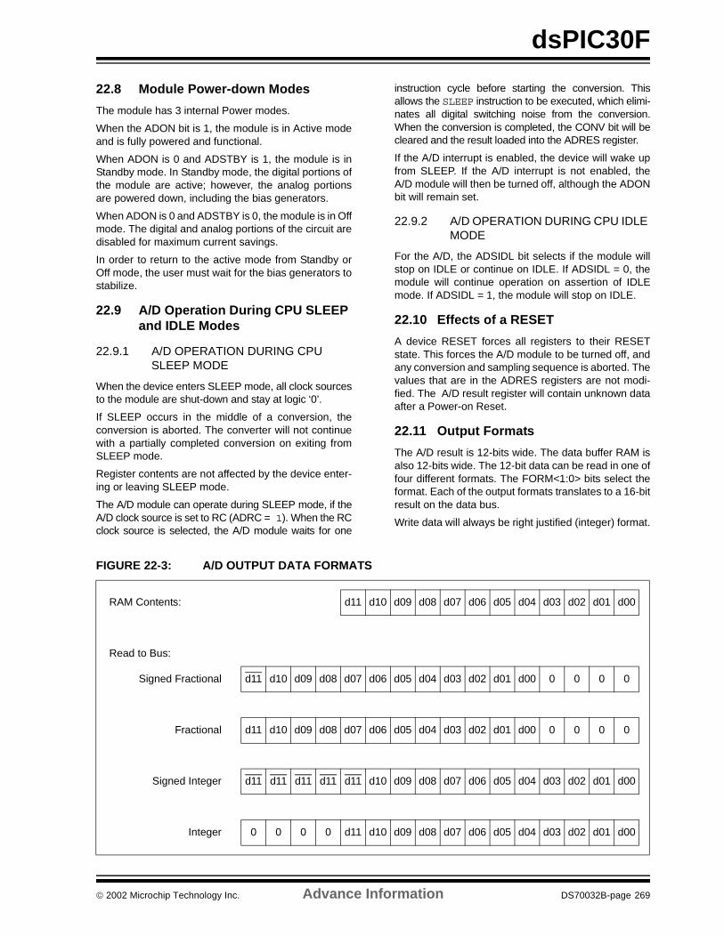
dsPIC30F
22.8 Module Power-down Modes
The module has 3 internal Power modes.
When the ADON bit is 1, the module is in Active modeand is fully powered and functional.
When ADON is 0 and ADSTBY is 1, the module is inStandby mode. In Standby mode, the digital portions ofthe module are active; however, the analog portionsare powered down, including the bias generators.
When ADON is 0 and ADSTBY is 0, the module is in Offmode. The digital and analog portions of the circuit aredisabled for maximum current savings.
In order to return to the active mode from Standby orOff mode, the user must wait for the bias generators tostabilize.
22.9 A/D Operation During CPU SLEEP and IDLE Modes
22.9.1 A/D OPERATION DURING CPU SLEEP MODE
When the device enters SLEEP mode, all clock sourcesto the module are shut-down and stay at logic ‘0’.
If SLEEP occurs in the middle of a conversion, theconversion is aborted. The converter will not continuewith a partially completed conversion on exiting fromSLEEP mode.
Register contents are not affected by the device enter-ing or leaving SLEEP mode.
The A/D module can operate during SLEEP mode, if theA/D clock source is set to RC (ADRC = 1). When the RCclock source is selected, the A/D module waits for one
instruction cycle before starting the conversion. Thisallows the SLEEP instruction to be executed, which elimi-nates all digital switching noise from the conversion.When the conversion is completed, the CONV bit will becleared and the result loaded into the ADRES register.
If the A/D interrupt is enabled, the device will wake upfrom SLEEP. If the A/D interrupt is not enabled, theA/D module will then be turned off, although the ADONbit will remain set.
22.9.2 A/D OPERATION DURING CPU IDLE MODE
For the A/D, the ADSIDL bit selects if the module willstop on IDLE or continue on IDLE. If ADSIDL = 0, themodule will continue operation on assertion of IDLEmode. If ADSIDL = 1, the module will stop on IDLE.
22.10 Effects of a RESET
A device RESET forces all registers to their RESETstate. This forces the A/D module to be turned off, andany conversion and sampling sequence is aborted. Thevalues that are in the ADRES registers are not modi-fied. The A/D result register will contain unknown dataafter a Power-on Reset.
22.11 Output Formats
The A/D result is 12-bits wide. The data buffer RAM isalso 12-bits wide. The 12-bit data can be read in one offour different formats. The FORM<1:0> bits select theformat. Each of the output formats translates to a 16-bitresult on the data bus.
Write data will always be right justified (integer) format.
FIGURE 22-3: A/D OUTPUT DATA FORMATS
RAM Contents: d11 d10 d09 d08 d07 d06 d05 d04 d03 d02 d01 d00
Read to Bus:
Signed Fractional d11 d10 d09 d08 d07 d06 d05 d04 d03 d02 d01 d00 0 0 0 0
Fractional d11 d10 d09 d08 d07 d06 d05 d04 d03 d02 d01 d00 0 0 0 0
Signed Integer d11 d11 d11 d11 d11 d10 d09 d08 d07 d06 d05 d04 d03 d02 d01 d00
Integer 0 0 0 0 d11 d10 d09 d08 d07 d06 d05 d04 d03 d02 d01 d00
2002 Microchip Technology Inc. Advance Information DS70032B-page 269
dsPIC30F
22.12 Configuring Analog Port Pins
The use of the ADPCFG and TRIS registers control theoperation of the A/D port pins. The port pins that aredesired as analog inputs must have their correspond-ing TRIS bit set (input). If the TRIS bit is cleared (out-put), the digital output level (VOH or VOL) will beconverted.
The A/D operation is independent of the state of theCHS<3:0> bits and the TRIS bits.
When reading the PORT register, all pins configured asanalog input channel will read as cleared (a low level).
Pins configured as digital inputs, will convert an analoginput. Analog levels on a digitally configured input willnot affect the conversion accuracy.
Analog levels on any pin that is defined as a digitalinput (including the AN pins), may cause the inputbuffer to consume current that exceeds the devicespecifications.
22.13 Connection Considerations
Since the analog inputs employ ESD protection, theyhave diodes to VDD and VSS. This requires that theanalog input must be between VDD and VSS. If the inputvoltage exceeds this range by greater than 0.3V (eitherdirection), one of the diodes becomes forward biasedand it may damage the device if the input current spec-ification is exceeded.
An external RC filter is sometimes added for anti-aliasing of the input signal. The R component should beselected to ensure that the sampling time requirementsare satisfied. Any external components connected (viahigh impedance) to an analog input pin (capacitor,zener diode, etc.) should have very little leakagecurrent at the pin.
DS70032B-page 270 Advance Information 2002 Microchip Technology Inc.
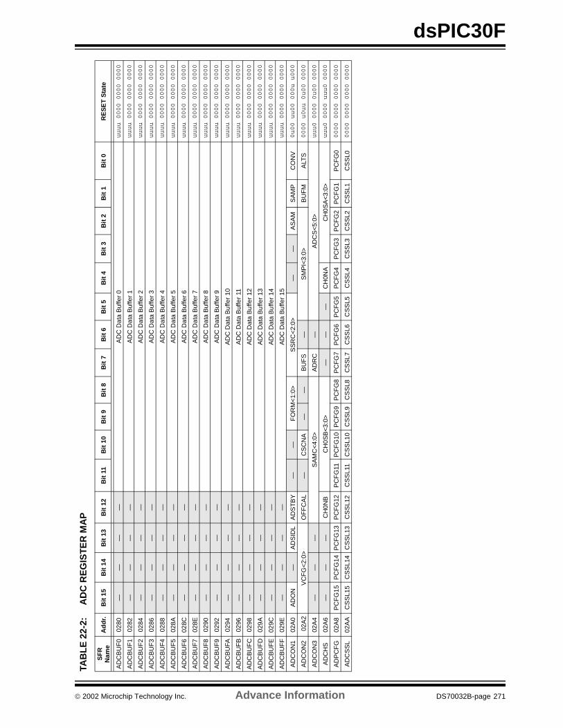
dsPIC30F
TAB
LE
22-
2:A
DC
RE
GIS
TE
R M
AP
SF
R
Nam
eA
dd
r.B
it 1
5B
it 1
4B
it 1
3B
it 1
2B
it 1
1B
it 1
0B
it 9
Bit
8B
it 7
Bit
6B
it 5
Bit
4B
it 3
Bit
2B
it 1
Bit
0R
ES
ET
Sta
te
AD
CB
UF
002
80—
——
—A
DC
Dat
a B
uffe
r 0
uuuu 0000 0000 0000
AD
CB
UF
102
82—
——
—A
DC
Dat
a B
uffe
r 1
uuuu 0000 0000 0000
AD
CB
UF
202
84—
——
—A
DC
Dat
a B
uffe
r 2
uuuu 0000 0000 0000
AD
CB
UF
302
86—
——
—A
DC
Dat
a B
uffe
r 3
uuuu 0000 0000 0000
AD
CB
UF
402
88—
——
—A
DC
Dat
a B
uffe
r 4
uuuu 0000 0000 0000
AD
CB
UF
502
8A—
——
—A
DC
Dat
a B
uffe
r 5
uuuu 0000 0000 0000
AD
CB
UF
602
8C—
——
—A
DC
Dat
a B
uffe
r 6
uuuu 0000 0000 0000
AD
CB
UF
702
8E—
——
—A
DC
Dat
a B
uffe
r 7
uuuu 0000 0000 0000
AD
CB
UF
802
90—
——
—A
DC
Dat
a B
uffe
r 8
uuuu 0000 0000 0000
AD
CB
UF
902
92—
——
—A
DC
Dat
a B
uffe
r 9
uuuu 0000 0000 0000
AD
CB
UFA
0294
——
——
AD
C D
ata
Buf
fer
10uuuu 0000 0000 0000
AD
CB
UF
B02
96—
——
—A
DC
Dat
a B
uffe
r 11
uuuu 0000 0000 0000
AD
CB
UF
C02
98—
——
—A
DC
Dat
a B
uffe
r 12
uuuu 0000 0000 0000
AD
CB
UF
D02
9A—
——
—A
DC
Dat
a B
uffe
r 13
uuuu 0000 0000 0000
AD
CB
UF
E02
9C—
——
—A
DC
Dat
a B
uffe
r 14
uuuu 0000 0000 0000
AD
CB
UF
F02
9E—
——
—A
DC
Dat
a B
uffe
r 15
uuuu 0000 0000 0000
AD
CO
N1
02A
0A
DO
N—
AD
SID
LA
DS
TB
Y—
—F
OR
M<
1:0>
SS
RC
<2:
0>—
—A
SA
MS
AM
PC
ON
V0u00 uu00 000u u000
AD
CO
N2
02A
2V
CF
G<
2:0>
OF
FC
AL
—C
SC
NA
——
BU
FS
—S
MP
I<3:
0>B
UF
MA
LTS
0000 u0uu 0u00 0000
AD
CO
N3
02A
4—
——
SA
MC
<4:
0>A
DR
C—
AD
CS
<5:
0>uuu0 0000 0u00 0000
AD
CH
S02
A6
——
—C
H0N
BC
H0S
B<
3:0>
——
—C
H0N
AC
H0S
A<
3:0>
uuu0 0000 uuu0 0000
AD
PC
FG
02A
8P
CF
G15
PC
FG
14P
CF
G13
PC
FG
12P
CF
G11
PC
FG
10P
CF
G9
PC
FG
8P
CF
G7
PC
FG
6P
CF
G5
PC
FG
4P
CF
G3
PC
FG
2P
CF
G1
PC
FG
00000 0000 0000 0000
AD
CS
SL
02A
AC
SS
L15
CS
SL1
4C
SS
L13
CS
SL1
2C
SS
L11
CS
SL1
0C
SS
L9C
SS
L8C
SS
L7C
SS
L6C
SS
L5C
SS
L4C
SS
L3C
SS
L2C
SS
L1C
SS
L00000 0000 0000 0000
2002 Microchip Technology Inc. Advance Information DS70032B-page 271
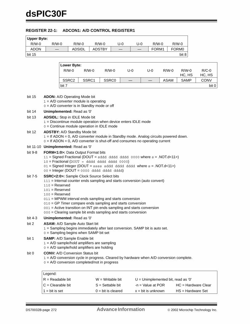
dsPIC30F
REGISTER 22-1: ADCON1: A/D CONTROL REGISTER1
Upper Byte:R/W-0 R/W-0 R/W-0 R/W-0 U-0 U-0 R/W-0 R/W-0ADON — ADSIDL ADSTBY — — FORM1 FORM0
bit 15 bit 8
Lower Byte:R/W-0 R/W-0 R/W-0 U-0 U-0 R/W-0 R/W-0
HC, HSR/C-0
HC, HS
SSRC2 SSRC1 SSRC0 — — ASAM SAMP CONVbit 7 bit 0
bit 15 ADON: A/D Operating Mode bit1 = A/D converter module is operating0 = A/D converter is in Standby mode or off
bit 14 Unimplemented: Read as '0'
bit 13 ADSIDL: Stop in IDLE Mode bit1 = Discontinue module operation when device enters IDLE mode0 = Continue module operation in IDLE mode
bit 12 ADSTBY: A/D Standby Mode bit1 = If ADON = 0, A/D converter module in Standby mode. Analog circuits powered down.0 = If ADON = 0, A/D converter is shut-off and consumes no operating current
bit 11-10 Unimplemented: Read as '0'
bit 9-8 FORM<1:0>: Data Output Format bits11 = Signed Fractional (DOUT = sddd dddd dddd 0000 where s = .NOT.d<11>)10 = Fractional (DOUT = dddd dddd dddd 0000)01 = Signed Integer (DOUT = ssss sddd dddd dddd where s = .NOT.d<11>)00 = Integer (DOUT = 0000 dddd dddd dddd)
bit 7-5 SSRC<2:0>: Sample Clock Source Select bits111 = Internal counter ends sampling and starts conversion (auto convert)110 = Reserved101 = Reserved100 = Reserved011 = MPWM interval ends sampling and starts conversion010 = GP Timer compare ends sampling and starts conversion001 = Active transition on INT pin ends sampling and starts conversion000 = Clearing sample bit ends sampling and starts conversion
bit 4-3 Unimplemented: Read as '0'
bit 2 ASAM: A/D Sample Auto Start bit1 = Sampling begins immediately after last conversion. SAMP bit is auto set.0 = Sampling begins when SAMP bit set
bit 1 SAMP: A/D Sample Enable bit1 = A/D sample/hold amplifiers are sampling0 = A/D sample/hold amplifiers are holding
bit 0 CONV: A/D Conversion Status bit1 = A/D conversion cycle in progress. Cleared by hardware when A/D conversion complete.0 = A/D conversion completed/not in progress
Legend:
R = Readable bit W = Writable bit U = Unimplemented bit, read as ‘0’
C = Clearable bit S = Settable bit -n = Value at POR HC = Hardware Clear
1 = bit is set 0 = bit is cleared x = bit is unknown HS = Hardware Set
DS70032B-page 272 Advance Information 2002 Microchip Technology Inc.
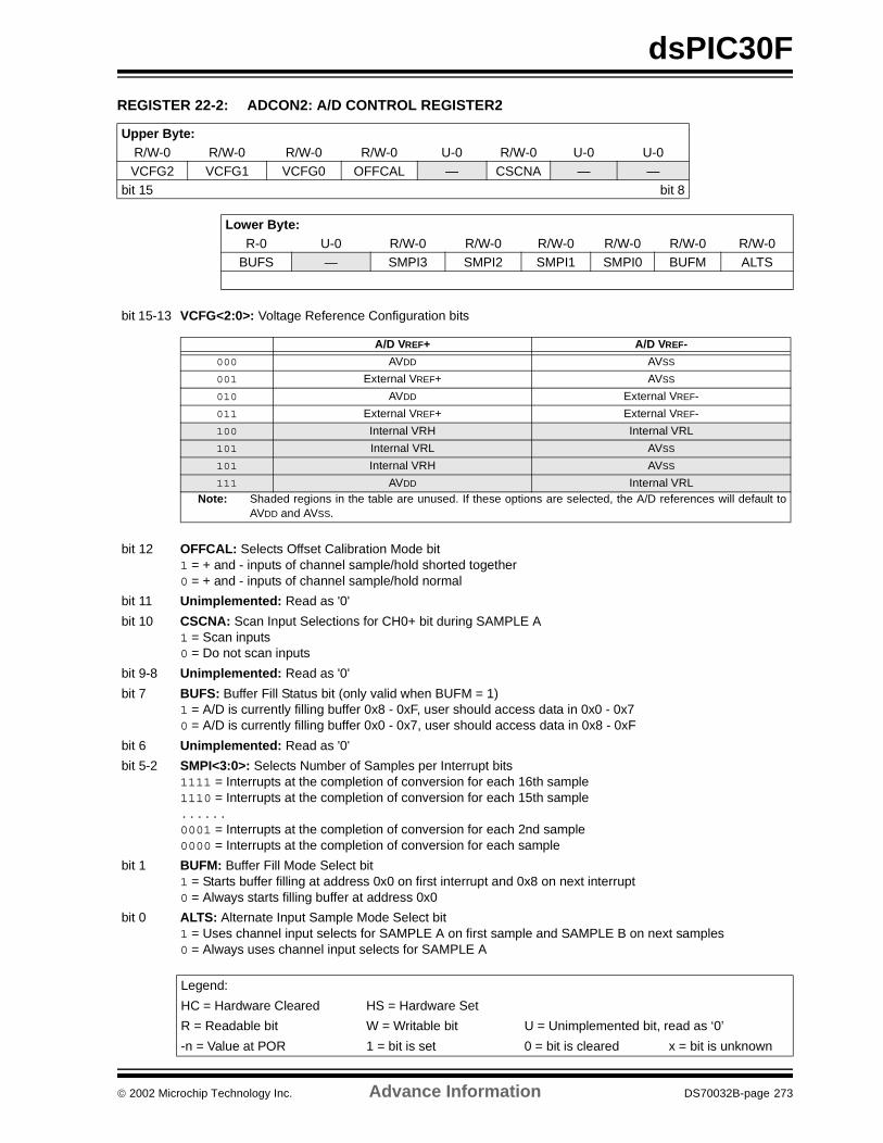
dsPIC30F
REGISTER 22-2: ADCON2: A/D CONTROL REGISTER2
Upper Byte:R/W-0 R/W-0 R/W-0 R/W-0 U-0 R/W-0 U-0 U-0VCFG2 VCFG1 VCFG0 OFFCAL — CSCNA — —
bit 15 bit 8
Lower Byte:R-0 U-0 R/W-0 R/W-0 R/W-0 R/W-0 R/W-0 R/W-0
BUFS — SMPI3 SMPI2 SMPI1 SMPI0 BUFM ALTS
bit 15-13 VCFG<2:0>: Voltage Reference Configuration bits
bit 12 OFFCAL: Selects Offset Calibration Mode bit1 = + and - inputs of channel sample/hold shorted together0 = + and - inputs of channel sample/hold normal
bit 11 Unimplemented: Read as '0'
bit 10 CSCNA: Scan Input Selections for CH0+ bit during SAMPLE A1 = Scan inputs0 = Do not scan inputs
bit 9-8 Unimplemented: Read as '0'
bit 7 BUFS: Buffer Fill Status bit (only valid when BUFM = 1)1 = A/D is currently filling buffer 0x8 - 0xF, user should access data in 0x0 - 0x70 = A/D is currently filling buffer 0x0 - 0x7, user should access data in 0x8 - 0xF
bit 6 Unimplemented: Read as '0'
bit 5-2 SMPI<3:0>: Selects Number of Samples per Interrupt bits1111 = Interrupts at the completion of conversion for each 16th sample1110 = Interrupts at the completion of conversion for each 15th sample......0001 = Interrupts at the completion of conversion for each 2nd sample0000 = Interrupts at the completion of conversion for each sample
bit 1 BUFM: Buffer Fill Mode Select bit1 = Starts buffer filling at address 0x0 on first interrupt and 0x8 on next interrupt0 = Always starts filling buffer at address 0x0
bit 0 ALTS: Alternate Input Sample Mode Select bit1 = Uses channel input selects for SAMPLE A on first sample and SAMPLE B on next samples0 = Always uses channel input selects for SAMPLE A
Legend:
HC = Hardware Cleared HS = Hardware Set
R = Readable bit W = Writable bit U = Unimplemented bit, read as ‘0’
-n = Value at POR 1 = bit is set 0 = bit is cleared x = bit is unknown
A/D VREF+ A/D VREF-
000 AVDD AVSS
001 External VREF+ AVSS
010 AVDD External VREF-
011 External VREF+ External VREF-
100 Internal VRH Internal VRL
101 Internal VRL AVSS
101 Internal VRH AVSS
111 AVDD Internal VRLNote: Shaded regions in the table are unused. If these options are selected, the A/D references will default to
AVDD and AVSS.
2002 Microchip Technology Inc. Advance Information DS70032B-page 273

dsPIC30F
REGISTER 22-3: ADCON3: A/D CONTROL REGISTER3
Upper Byte:U-0 U-0 U-0 R/W-0 R/W-0 R/W-0 R/W-0 R/W-0— — — SAMC4 SAMC3 SAMC2 SAMC1 SAMC0
bit 15 bit 8
Lower Byte:R/W-0 U-0 R/W-0 R/W-0 R/W-0 R/W-0 R/W-0 R/W-0ADRC — ADCS5 ADCS4 ADCS3 ADCS2 ADCS1 ADCS0
bit 7 bit 0
bit 15-13 Unimplemented: Read as '0'
bit 12-8 SAMC<4:0>: Auto Sample Time bits11111 = 31 TAD
·····00001 = 1 TAD
00000 = 0 TAD
bit 7 ADRC: A/D Conversion Clock Source bit1 = A/D internal RC clock0 = Clock derived from system clock
bit 6 Unimplemented: Read as ’0’
bit 5-0 ADCS<5:0>: A/D Conversion Clock Select bits111111 = TQ·2·(ADCS<5:0> +1) = 128·TQ
······000001 = TQ·2·(ADCS<5:0> +1) = 4·TQ
000000 = TQ·2·(ADCS<5:0> +1) = 2·TQ
Legend:
R = Readable bit W = Writable bit U = Unimplemented bit, read as ‘0’
-n = Value at POR 1 = bit is set 0 = bit is cleared x = bit is unknown
DS70032B-page 274 Advance Information 2002 Microchip Technology Inc.
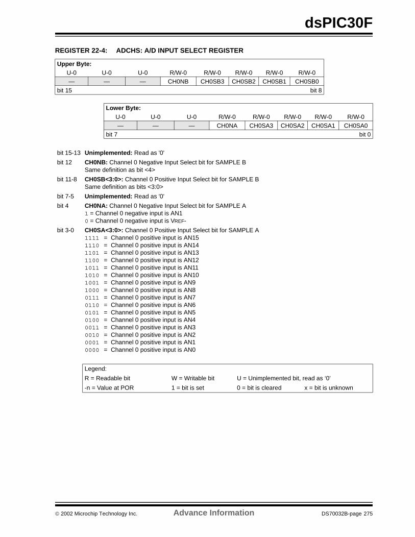
dsPIC30F
REGISTER 22-4: ADCHS: A/D INPUT SELECT REGISTER
Upper Byte:U-0 U-0 U-0 R/W-0 R/W-0 R/W-0 R/W-0 R/W-0— — — CH0NB CH0SB3 CH0SB2 CH0SB1 CH0SB0
bit 15 bit 8
Lower Byte:U-0 U-0 U-0 R/W-0 R/W-0 R/W-0 R/W-0 R/W-0— — — CH0NA CH0SA3 CH0SA2 CH0SA1 CH0SA0
bit 7 bit 0
bit 15-13 Unimplemented: Read as '0'
bit 12 CH0NB: Channel 0 Negative Input Select bit for SAMPLE BSame definition as bit <4>
bit 11-8 CH0SB<3:0>: Channel 0 Positive Input Select bit for SAMPLE BSame definition as bits <3:0>
bit 7-5 Unimplemented: Read as '0'
bit 4 CH0NA: Channel 0 Negative Input Select bit for SAMPLE A1 = Channel 0 negative input is AN10 = Channel 0 negative input is VREF-
bit 3-0 CH0SA<3:0>: Channel 0 Positive Input Select bit for SAMPLE A1111 = Channel 0 positive input is AN151110 = Channel 0 positive input is AN141101 = Channel 0 positive input is AN131100 = Channel 0 positive input is AN121011 = Channel 0 positive input is AN111010 = Channel 0 positive input is AN101001 = Channel 0 positive input is AN91000 = Channel 0 positive input is AN80111 = Channel 0 positive input is AN70110 = Channel 0 positive input is AN60101 = Channel 0 positive input is AN50100 = Channel 0 positive input is AN40011 = Channel 0 positive input is AN30010 = Channel 0 positive input is AN20001 = Channel 0 positive input is AN10000 = Channel 0 positive input is AN0
Legend:
R = Readable bit W = Writable bit U = Unimplemented bit, read as ‘0’
-n = Value at POR 1 = bit is set 0 = bit is cleared x = bit is unknown
2002 Microchip Technology Inc. Advance Information DS70032B-page 275
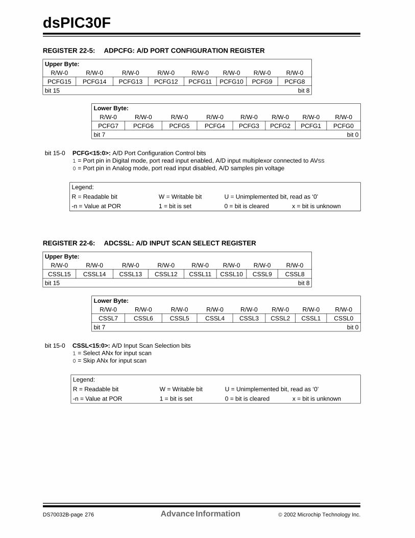
dsPIC30F
REGISTER 22-5: ADPCFG: A/D PORT CONFIGURATION REGISTER
REGISTER 22-6: ADCSSL: A/D INPUT SCAN SELECT REGISTER
Upper Byte:R/W-0 R/W-0 R/W-0 R/W-0 R/W-0 R/W-0 R/W-0 R/W-0
PCFG15 PCFG14 PCFG13 PCFG12 PCFG11 PCFG10 PCFG9 PCFG8
bit 15 bit 8
Lower Byte:R/W-0 R/W-0 R/W-0 R/W-0 R/W-0 R/W-0 R/W-0 R/W-0PCFG7 PCFG6 PCFG5 PCFG4 PCFG3 PCFG2 PCFG1 PCFG0
bit 7 bit 0
bit 15-0 PCFG<15:0>: A/D Port Configuration Control bits1 = Port pin in Digital mode, port read input enabled, A/D input multiplexor connected to AVSS
0 = Port pin in Analog mode, port read input disabled, A/D samples pin voltage
Legend:
R = Readable bit W = Writable bit U = Unimplemented bit, read as ‘0’
-n = Value at POR 1 = bit is set 0 = bit is cleared x = bit is unknown
Upper Byte:R/W-0 R/W-0 R/W-0 R/W-0 R/W-0 R/W-0 R/W-0 R/W-0
CSSL15 CSSL14 CSSL13 CSSL12 CSSL11 CSSL10 CSSL9 CSSL8bit 15 bit 8
Lower Byte:R/W-0 R/W-0 R/W-0 R/W-0 R/W-0 R/W-0 R/W-0 R/W-0CSSL7 CSSL6 CSSL5 CSSL4 CSSL3 CSSL2 CSSL1 CSSL0
bit 7 bit 0
bit 15-0 CSSL<15:0>: A/D Input Scan Selection bits1 = Select ANx for input scan0 = Skip ANx for input scan
Legend:
R = Readable bit W = Writable bit U = Unimplemented bit, read as ‘0’
-n = Value at POR 1 = bit is set 0 = bit is cleared x = bit is unknown
DS70032B-page 276 Advance Information 2002 Microchip Technology Inc.
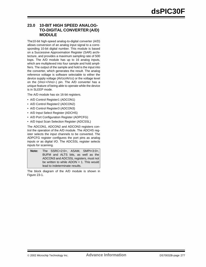
dsPIC30F
23.0 10-BIT HIGH SPEED ANALOG-TO-DIGITAL CONVERTER (A/D) MODULE
The10-bit high-speed analog-to-digital converter (A/D)allows conversion of an analog input signal to a corre-sponding 10-bit digital number. This module is basedon a Successive Approximation Register (SAR) archi-tecture, and provides a maximum sampling rate of 500ksps. The A/D module has up to 16 analog inputs,which are multiplexed into four sample and hold ampli-fiers. The output of the sample and hold is the input intothe converter, which generates the result. The analogreference voltage is software selectable to either thedevice supply voltage (AVDD/AVSS) or the voltage levelon the (VREF+/VREF-) pin. The A/D converter has aunique feature of being able to operate while the deviceis in SLEEP mode.
The A/D module has six 16-bit registers.
• A/D Control Register1 (ADCON1)• A/D Control Register2 (ADCON2)• A/D Control Register3 (ADCON3)
• A/D Input Select Register (ADCHS)• A/D Port Configuration Register (ADPCFG)• A/D Input Scan Selection Register (ADCSSL)
The ADCON1, ADCON2 and ADCON3 registers con-trol the operation of the A/D module. The ADCHS reg-ister selects the input channels to be converted. TheADPCFG register configures the port pins as analoginputs or as digital I/O. The ADCSSL register selectsinputs for scanning.
The block diagram of the A/D module is shown inFigure 23-1.
Note: The SSRC<2:0>, ASAM, SMPI<3:0>,BUFM and ALTS bits, as well as theADCON3 and ADCSSL registers, must notbe written to while ADON = 1. This wouldlead to indeterminate results.
2002 Microchip Technology Inc. Advance Information DS70032B-page 277
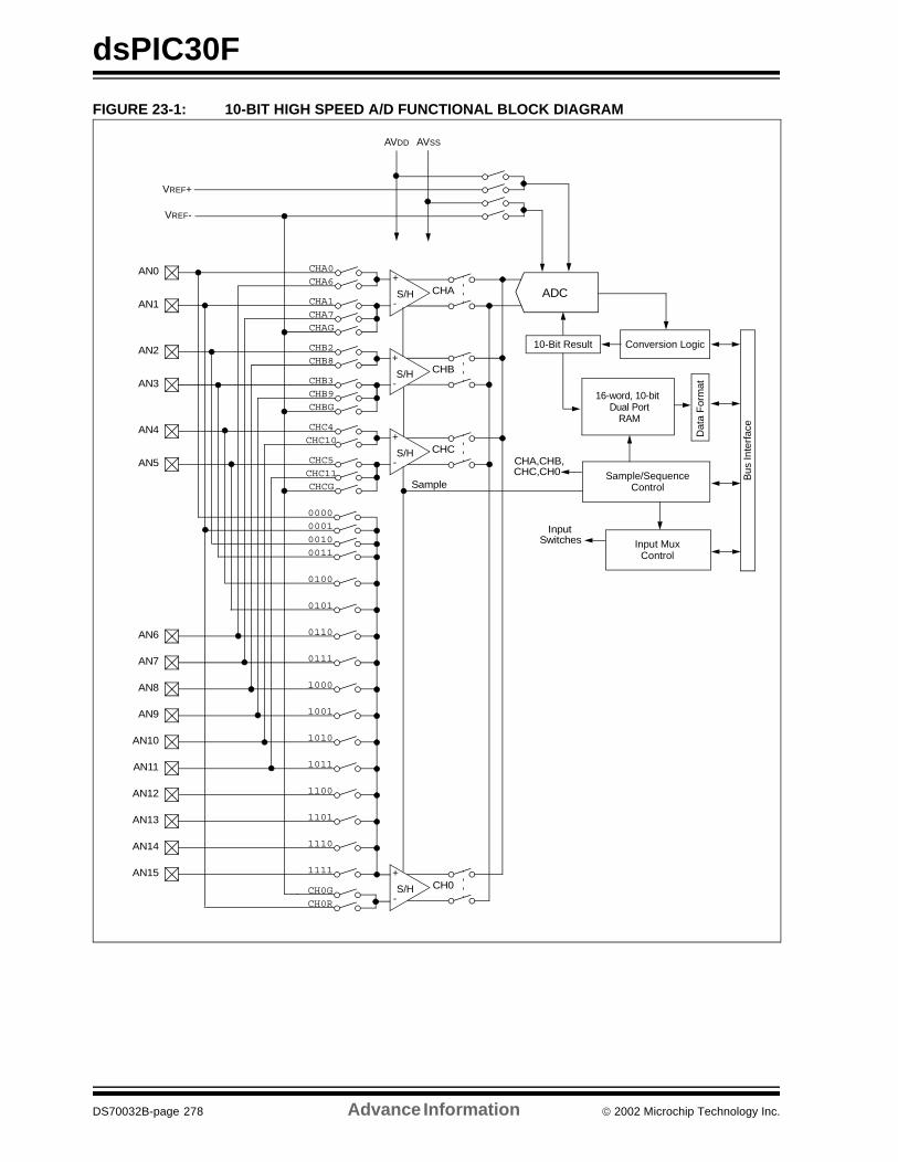
dsPIC30F
FIGURE 23-1: 10-BIT HIGH SPEED A/D FUNCTIONAL BLOCK DIAGRAM
S/H
+
-
10-Bit Result Conversion Logic
VREF+
AVSSAVDD
ADC
Dat
a F
orm
at
16-word, 10-bitDual Port
RAM
Bus
Inte
rfac
e
AN12
0000
0101
0111
1001
1101
1110
1111
1100
000100100011
0100
0110
1000
1010
1011
AN13
AN14
AN15
AN8
AN9
AN10
AN11
AN4
AN5
AN7
AN0
AN1
AN2
AN3
CHA
CHB
CHC
CH0
CHC10CHC4
CHC11CHC5
CHCG
CHB8CHB2
CHB9CHB3
CHBG
CHA6CHA0
CHA7CHA1
CHAG
CH0RCH0G
VREF-
Sample/SequenceControlSample
CHA,CHB,CHC,CH0
Input MuxControl
InputSwitches
S/H
+
-
S/H
+
-
S/H
+
-
AN6
DS70032B-page 278 Advance Information 2002 Microchip Technology Inc.
dsPIC30F
23.1 A/D Result Buffer
The module contains a 16-word dual port RAM, calledADRES<15:0>, to buffer the A/D results. The RAM is10-bits wide, but is read into different format 16-bit words.
Only word writes are allowed to the result buffer. If bytewrites are attempted, the results are indeterminate.
23.2 Conversion Operation
After the A/D module has been configured as desired, thesampling is started by setting the SAMP bit. Varioussources, such as a programmable bit, timer time-outsand external events, will terminate sampling and start aconversion. When the A/D conversion is completed, theresult is loaded into ADRES<15:0>, the CONV bit iscleared, and if, at the correct number of samples as spec-ified by the SMPI bit, the A/D interrupt flag ADIF is set.
The following steps should be followed for doing anA/D conversion:
1. Configure the A/D module:• Configure analog pins/voltage reference/and
digital I/O• Select A/D input channels• Select A/D conversion clock
• Select A/D conversion trigger• Turn on A/D module
2. Configure A/D interrupt (if required):
• Clear ADIF bit • Select A/D interrupt priority
3. Start sampling.
4. Wait the required sampling time.5. Trigger sample end, start conversion:
• Module sets CONV bit
6. Wait for A/D conversion to complete, by either:• Polling for the CONV bit to be cleared• Waiting for the A/D interrupt
7. Read A/D result buffer, clear ADIF if required.
23.3 Selecting the Conversion Sequence
Several groups of control bits select the sequence thatthe A/D connects inputs to the sample/hold channels,converts channels, writes the buffer memory, and gen-erates interrupts. The sequence is controlled by thesampling clocks.
The SIMSAM bit controls the sample/convert sequencefor multiple channels. If the SIMSAM bit is 0, the two orfour selected channels are sampled and convertedsequentially, with two or four sample clocks. If theSIMSAM bit is 1, two or four selected channels aresampled simultaneously, with one sample clock. Thechannels are then converted sequentially. Obviously, ifthere is only 1 channel selected, the SIMSAM bit is notapplicable.
The CHPS bits selects how many channels are sam-pled. This can vary from 1, 2 or 4 channels. If CHPSselects 1 channel, the CH0 channel will be sampledand at the sample clock, CH0 will be converted. Theresult is stored in the buffer. If CHPS selects 2 chan-nels, the CH0 and CHA channels will be sampled andconverted. If CHPS selects 4 channels, the CH0, CHA,CHB and CHC channels will be sampled andconverted.
The SMPI bits will select how many sample clocksoccur before an interrupt occurs. This can vary from 1sample per interrupt to 16 samples per interrupt.
The user cannot program a combination of CHPS andSMPI bits that specifies more than 16 conversions perinterrupt or 8 conversions per interrupt depending onthe BUFM bit. The BUFM bit, when set, will split the16-word results buffer (ADRES) into two 8-wordgroups. Writing to the 8-word buffers will be alternatedon each interrupt event. Use of the BUFM bit willdepend on how much time is available for moving dataout of the buffers after the interrupt, as determined bythe application.
If the processor can quickly unload a full buffer withinthe time it takes to sample and convert one channel,the BUFM bit can be 0 and up to 16 conversions maybe done per interrupt. The processor will have onesample and conversion time to move the sixteenconversions.
If the processor cannot unload the buffer within thesample and conversion time, the BUFM bit should be 1.For example, if SMPI<3:0> (ADCON2<5:2>) = 0111,then eight conversions will be loaded into 1/2 of thebuffer, following which, an interrupt occurs. The nexteight conversions will be loaded into the other 1/2 of thebuffer. The processor will have the entire time betweeninterrupts to move the eight conversions.
The ALTS bit can be used to alternate the inputsselected during the sampling sequence. If the ALTS bitis 0, only the SAMPLE A inputs are selected for sam-pling. If the ALTS bit is 1 and SMPI<3:0> = 0000, onthe first sample/convert sequence, the SAMPLE Ainputs are selected, and on the next sample/convertsequence, the SAMPLE B inputs are selected.
The CSCNA bit (ADCON2<10>) will allow the CH0channel inputs to be scanned across a selected num-ber of analog inputs during SAMPLE A samples. Theinputs are selected by the ADCSSL register. If a partic-ular bit in the ADCSSL register is ‘1’, the correspondinginput is selected. The inputs are always scanned fromlower to higher numbered inputs, starting after eachinterrupt occurs. If the number of inputs selected isgreater than the number of samples taken per interrupt,the higher numbered inputs are unused.
2002 Microchip Technology Inc. Advance Information DS70032B-page 279
dsPIC30F
23.4 Programming the Start-of-Conversion Trigger
The sample trigger will terminate sampling and start therequested conversions.
The SSRC<2:0> bits select the source of the sampletrigger.
When SSRC<2:0> = 000, the sample trigger is undersoftware control. Clearing the SAMP bit will cause thesample trigger.
When SSRC<2:0> = 111, the sample trigger is underA/D clock control. The SAMC bits select the number ofA/D clocks between the start of sampling and the startof conversion. This provides the fastest conversionrates on multiple channels. SAMC must always be atleast 1 clock cycle.
Other trigger sources can come from timer modules orexternal interrupts.
The SSRC bits provide for up to 6 alternate sources ofsample trigger.
23.5 Aborting a Conversion
Clearing the CONV bit during a conversion will abortthe current conversion and stop the sampling sequenc-ing until the next sampling trigger. The ADRES will notbe updated with the partially completed A/D conversionsample. That is, the ADRES will continue to contain thevalue of the last completed conversion (or the lastvalue written to the ADRES register).
If the clearing of the CONV bit coincides with an autostart, the clearing has a higher priority.
After the A/D conversion is aborted, a 2TAD wait isrequired before the next sampling may be started bysetting the SAMP bit.
If sequential sampling is specified, the A/D will continueat the next sample pulse which corresponds with thenext channel converted. If simultaneous sampling isspecified, the A/D will continue with the next multi-channel group conversion sequence.
23.6 Selecting the A/D Conversion Clock
The A/D conversion requires 11 TAD. The source of theA/D conversion clock is software selected using a sixbit counter. There are 64 possible options for TAD.
TAD = TCY * (0.5*(ADCS<5:0> +1))
The internal RC oscillator is selected by setting theADRC bit.
For correct A/D conversions, the A/D conversion clock(TAD) must be selected to ensure a minimum TAD timeof 150 nsec. Table 23-1 shows the resultant TAD timesderived from the device operating frequencies and theA/D clock source selected.
DS70032B-page 280 Advance Information 2002 Microchip Technology Inc.
dsPIC30F
TABLE 23-1: TYPICAL TAD VS. DEVICE OPERATING FREQUENCIES
AD Clock Interval (TAD /TCONV)AD Clock Source Select Device TCY/Device MIPS/TQ/FOSC
Clock ADRC ADCS<5:0>
33.33 nsec/30 MIPS/
8.33 nsec/120 MHz
40 nsec/25 MIPS/10 nsec/100 MHz
80 nsec/12.5 MIPS/20 nsec/50 MHz
160 nsec/6.25 MIPS/40 nsec/25 MHz
1000 nsec/1 MIPS/
250 nsec/4 MHz
2 TQ 0 000000 16.67 ns(2)/0.22 µs
20 ns(2)/0.26 µs
40 ns(2)/0.52 µs
80 ns(2)/1.04 µs
500 ns/6.5 µs
4 TQ 0 000001 33.33 ns(2)/0.44 µs
40 ns(2)/0.52 µs
80 ns(2)/1.04 µs
160 ns/2.08 µs
1.0 µs/13 µs
8 TQ 0 000011 66.66 ns(2)/0.88 µs
80 ns(2)/1.04 µs
160 ns/2.08 µs
320 ns/4.16 µs
2.0 µs(3)/26 µs
16 TQ 0 000111 133.32 ns(2)/1.76 µs
160 ns/2.08 µs
320 ns/4.16 µs
640 ns(3)/8.32 µs
4.0 µs(3)/52 µs
32 TQ 0 001111 266.64 ns/3.52 µs
320 ns/4.16 µs
640 ns(3)/8.32 µs
1.28 µs(3) 8.0 µs(3)/104 µs
64 TQ 0 011111 533.28 ns(3)/7.04 µs
640 ns(3)/8.32 µs
1.28 µs(3) 2.56 µs(3) 16.0 µs(3)/208 µs
128 TQ 0 111111 1066.56 ns(3)/14.08 µs
1280 ns(3)/16.64 µs
2.56 µs(3) 5.12 µs(3) 32.0 µs(3)/416 µs
RC 1 xxxxxx 200 - 400 ns/
3.9 µs(1,4) 200 - 400 ns/
3.9 µs(1,4) 200 - 400 ns/
3.9 µs(1,4) 200 - 400 ns/
3.9 µs(1,4) 200 - 400 ns/
3.9 µs(1) Note 1: The RC source has a typical TAD time of 300 ns for VDD > 3.0V.
2: These values violate the minimum required TAD time.3: For faster conversion times, the selection of another clock source is recommended.4: A/D cannot meet full accuracy with RC clock source and FOSC > 20 MHz
2002 Microchip Technology Inc. Advance Information DS70032B-page 281

dsPIC30F
23.7 A/D Sampling Requirements
For the A/D converter to meet its specified accuracy,the charge holding capacitor (CHOLD) must be allowedto fully charge to the input channel voltage level. Theanalog input model is shown in Figure 23-2. Thesource impedance (RS) and the internal samplingswitch (RSS) impedance directly affect the timerequired to charge the capacitor CHOLD. The samplingswitch (RSS) impedance varies over the device voltage(VDD), see Figure 23-2. The impedance for analogsources must be small enough to meet accuracyrequirements at the given speed. After the analog inputchannel is selected (changed), this sampling must bedone before the conversion can be started.
To calculate the minimum sampling time, Equation 23-1may be used. This equation assumes that the input isstepped some multiple (n) of the LSB step size and theoutput must be captured to within 1/2 LSb error (2096steps for 10-bit A/D). The 1/2 LSb error is the maximumerror allowed for the A/D to meet its specified resolution.
The CHOLD is assumed to be 5 pF for the A/D.
EQUATION 23-1: A/D SAMPLING TIME EQUATIONS
FIGURE 23-2: ANALOG INPUT MODEL
∆VO = ∆VI • (1 - e (-TC/CHOLD (RIC+RSS+RS)))
1 - (∆VO / ∆VI) = e (-TC/CHOLD (RIC+RSS+RS))
∆VI = n • LSB
∆VO = n • LSB - 1/2 LSB
∆VO / ∆VI = (n • LSB - 1/2 LSB) / n • LSB
1 - (∆VO / ∆VI) = 1 / 2n
1 / 2n = e (-TC/CHOLD (RIC+RSS+RS))
TC = CHOLD • (RIC+RSS+RS) • -In(1/2 • n)
TSMP = Amplifier Settling Time+ Holding Capacitor Charging Time (TC)+Temperature Coefficient †
† The temperature coefficient is only required for temperatures > 25°C.
TSMP = 0.5 ms
+ CHOLD • (RIC+RSS+RS) • -In(1/2 • n)
+ [(Temp - 25°C)(0.05 ms/°C)]
CPINVA
Rs ANx
5 pF
VT = 0.6V
VT = 0.6VI leakage
RIC ≤ 250Ω
SamplingSwitch
SS RSS
CHOLD= DAC capacitance
VSS
VDD
= 5 pF± 500 nA
Legend: CPIN
VT
I leakage
RIC
SSCHOLD
= input capacitance= threshold voltage= leakage current at the pin due to
= interconnect resistance= sampling switch= sample/hold capacitance (from DAC)
various junctions
VDD (V)
3.5
2.52.01.51.0
2 3 4 5
(Rss kΩ)
Sampling 3.0
0.50
6
Switch
DS70032B-page 282 Advance Information 2002 Microchip Technology Inc.
dsPIC30F
23.8 Module Power-down Modes
The module has 3 internal Power modes.
When the ADON bit is 1, the module is in Active modeand is fully powered and functional.
When ADON is 0 and ADSTBY is 1, the module is inStandby mode. In Standby mode, the digital portions ofthe module are active; however, the analog portionsare powered down, including the bias generators.
When ADON is 0 and ADSTBY is 0, the module is in Offmode. The digital and analog portions of the circuit aredisabled for maximum current savings.
In order to return to the Active mode from Standby orOff mode, the user must wait for the bias generators tostabilize.
23.9 A/D Operation During CPU SLEEP and IDLE Modes
23.9.1 A/D OPERATION DURING CPU SLEEP MODE
When the device enters SLEEP mode, all clocksources to the module are shut-down and stay at logic‘0’.
If SLEEP occurs in the middle of a conversion, theconversion is aborted. The converter will not continuewith a partially completed conversion on exiting fromSLEEP mode.
Register contents are not affected by the device enter-ing or leaving SLEEP mode.
The A/D module can operate during SLEEP mode, ifthe A/D clock source is set to RC (ADRC = 1). Whenthe RC clock source is selected, the A/D module waitsfor one instruction cycle before starting the conversion.This allows the SLEEP instruction to be executed,which eliminates all digital switching noise from theconversion. When the conversion is completed, theCONV bit will be cleared and the result loaded into theADRES register.
If the A/D interrupt is enabled, the device will wake-upfrom SLEEP. If the A/D interrupt is not enabled, theA/D module will then be turned off, although the ADONbit will remain set.
23.9.2 A/D OPERATION DURING CPU IDLE MODE
For the A/D, the ADSIDL bit selects if the module willstop on IDLE or continue on IDLE. If ADSIDL = 0, themodule will continue operation on assertion of IDLEmode. If ADSIDL = 1, the module will stop on IDLE.
23.10 Effects of a RESET
A device RESET forces all registers to their RESETstate. This forces the A/D module to be turned off, andany conversion and sampling sequence are aborted.The values that are in the ADRES registers are notmodified. The A/D result register will contain unknowndata after a Power-on Reset.
2002 Microchip Technology Inc. Advance Information DS70032B-page 283
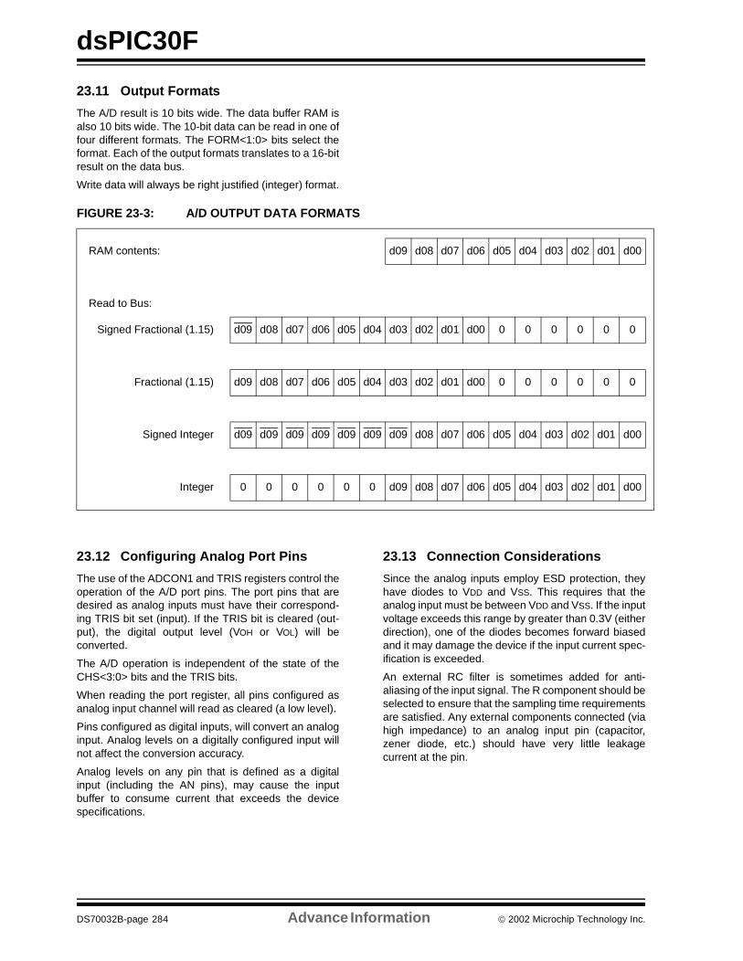
dsPIC30F
23.11 Output Formats
The A/D result is 10 bits wide. The data buffer RAM isalso 10 bits wide. The 10-bit data can be read in one offour different formats. The FORM<1:0> bits select theformat. Each of the output formats translates to a 16-bitresult on the data bus.
Write data will always be right justified (integer) format.
FIGURE 23-3: A/D OUTPUT DATA FORMATS
23.12 Configuring Analog Port Pins
The use of the ADCON1 and TRIS registers control theoperation of the A/D port pins. The port pins that aredesired as analog inputs must have their correspond-ing TRIS bit set (input). If the TRIS bit is cleared (out-put), the digital output level (VOH or VOL) will beconverted.
The A/D operation is independent of the state of theCHS<3:0> bits and the TRIS bits.
When reading the port register, all pins configured asanalog input channel will read as cleared (a low level).
Pins configured as digital inputs, will convert an analoginput. Analog levels on a digitally configured input willnot affect the conversion accuracy.
Analog levels on any pin that is defined as a digitalinput (including the AN pins), may cause the inputbuffer to consume current that exceeds the devicespecifications.
23.13 Connection Considerations
Since the analog inputs employ ESD protection, theyhave diodes to VDD and VSS. This requires that theanalog input must be between VDD and VSS. If the inputvoltage exceeds this range by greater than 0.3V (eitherdirection), one of the diodes becomes forward biasedand it may damage the device if the input current spec-ification is exceeded.
An external RC filter is sometimes added for anti-aliasing of the input signal. The R component should beselected to ensure that the sampling time requirementsare satisfied. Any external components connected (viahigh impedance) to an analog input pin (capacitor,zener diode, etc.) should have very little leakagecurrent at the pin.
RAM contents: d09 d08 d07 d06 d05 d04 d03 d02 d01 d00
Read to Bus:
Signed Fractional (1.15) d09 d08 d07 d06 d05 d04 d03 d02 d01 d00 0 0 0 0 0 0
Fractional (1.15) d09 d08 d07 d06 d05 d04 d03 d02 d01 d00 0 0 0 0 0 0
Signed Integer d09 d09 d09 d09 d09 d09 d09 d08 d07 d06 d05 d04 d03 d02 d01 d00
Integer 0 0 0 0 0 0 d09 d08 d07 d06 d05 d04 d03 d02 d01 d00
DS70032B-page 284 Advance Information 2002 Microchip Technology Inc.
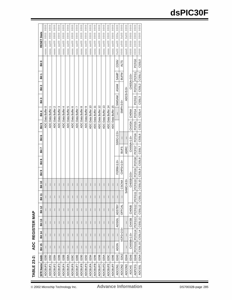
dsPIC30F
TAB
LE
23-
2:A
DC
RE
GIS
TE
R M
AP
SF
R N
ame
Ad
dr.
Bit
15
Bit
14
Bit
13
Bit
12
Bit
11
Bit
10
Bit
9B
it 8
Bit
7B
it 6
Bit
5B
it 4
Bit
3B
it 2
Bit
1B
it 0
RE
SE
T S
tate
AD
CB
UF
002
80—
——
——
—A
DC
Dat
a B
uffe
r 0
uuuu uu00 0000 0000
AD
CB
UF
102
82—
——
——
—A
DC
Dat
a B
uffe
r 1
uuuu uu00 0000 0000
AD
CB
UF
202
84—
——
——
—A
DC
Dat
a B
uffe
r 2
uuuu uu00 0000 0000
AD
CB
UF
302
86—
——
——
—A
DC
Dat
a B
uffe
r 3
uuuu uu00 0000 0000
AD
CB
UF
402
88—
——
——
—A
DC
Dat
a B
uffe
r 4
uuuu uu00 0000 0000
AD
CB
UF
502
8A—
——
——
—A
DC
Dat
a B
uffe
r 5
uuuu uu00 0000 0000
AD
CB
UF
602
8C—
——
——
—A
DC
Dat
a B
uffe
r 6
uuuu uu00 0000 0000
AD
CB
UF
702
8E—
——
——
—A
DC
Dat
a B
uffe
r 7
uuuu uu00 0000 0000
AD
CB
UF
802
90—
——
——
—A
DC
Dat
a B
uffe
r 8
uuuu uu00 0000 0000
AD
CB
UF
902
92—
——
——
—A
DC
Dat
a B
uffe
r 9
uuuu uu00 0000 0000
AD
CB
UFA
0294
——
——
——
AD
C D
ata
Buf
fer
10uuuu uu00 0000 0000
AD
CB
UF
B02
96—
——
——
—A
DC
Dat
a B
uffe
r 11
uuuu uu00 0000 0000
AD
CB
UF
C02
98—
——
——
—A
DC
Dat
a B
uffe
r 12
uuuu uu00 0000 0000
AD
CB
UF
D02
9A—
——
——
—A
DC
Dat
a B
uffe
r 13
uuuu uu00 0000 0000
AD
CB
UF
E02
9C—
——
——
—A
DC
Dat
a B
uffe
r 14
uuuu uu00 0000 0000
AD
CB
UF
F02
9E—
——
——
—A
DC
Dat
a B
uffe
r 15
uuuu uu00 0000 0000
AD
CO
N1
02A
0A
DO
N—
AD
SID
LA
DS
TB
Y—
—F
OR
M<
1:0>
SS
RC
<2:
0>—
SIM
SA
MA
SA
MS
AM
PC
ON
V0u00 uu00 000u 0000
AD
CO
N2
02A
2V
CF
G<
2:0>
OF
FC
AL
—C
SC
NA
CH
PS
<1:
0>B
UF
S—
SM
PI<
3:0>
BU
FM
ALT
S0000 u000 0u00 0000
AD
CO
N3
02A
4—
——
SA
MC
<4:
0>A
DR
C—
AD
CS
<5:
0>uuu0 0000 0u00 0000
AD
CH
S02
A6
CH
XN
B<
1:0>
CH
XS
BC
H0N
BC
H0S
B<
3:0>
CH
XN
A<
1:0>
CH
XS
AC
H0N
AC
H0S
A<
3:0>
0000 0000 0000 0000
AD
PC
FG
02A
8P
CF
G15
PC
FG
14P
CF
G13
PC
FG
12P
CF
G11
PC
FG
10P
CF
G9
PC
FG
8P
CF
G7
PC
FG
6P
CF
G5
PC
FG
4P
CF
G3
PC
FG
2P
CF
G1
PC
FG
00000 0000 0000 0000
AD
CS
SL
02A
AC
SS
L15
CS
SL1
4C
SS
L13
CS
SL1
2C
SS
L11
CS
SL1
0C
SS
L9C
SS
L8C
SS
L7C
SS
L6C
SS
L5C
SS
L4C
SS
L3C
SS
L2C
SS
L1C
SS
L00000 0000 0000 0000
2002 Microchip Technology Inc. Advance Information DS70032B-page 285
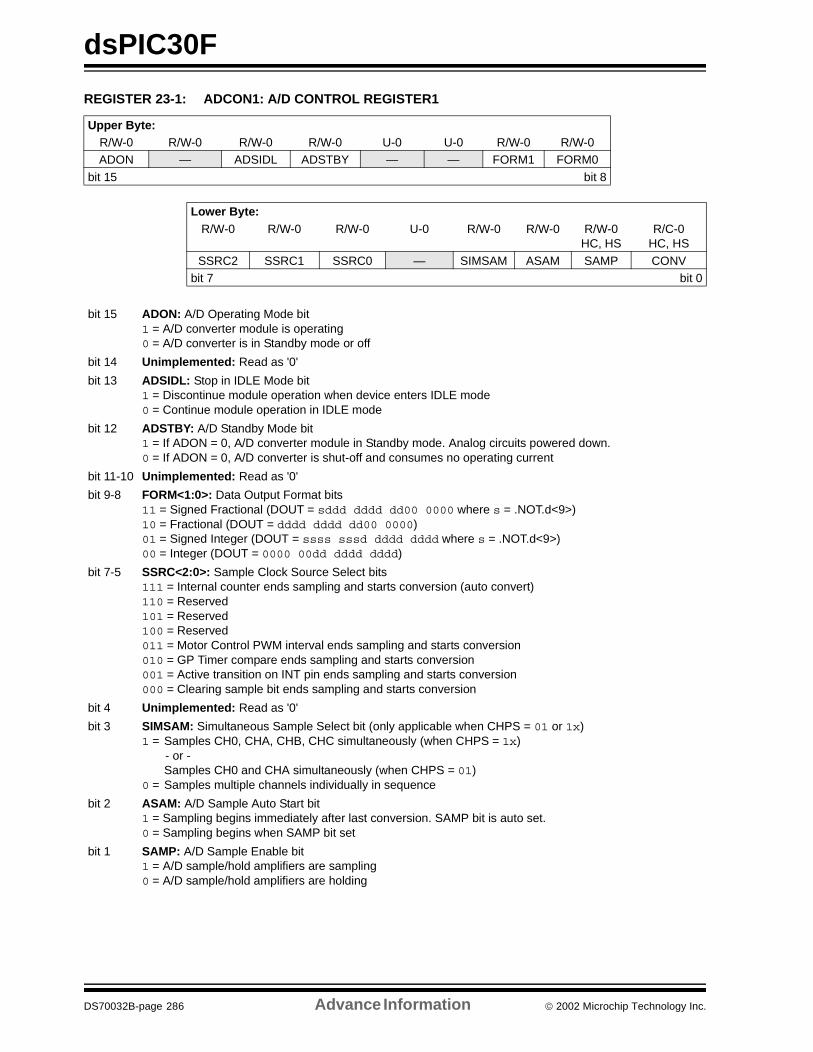
dsPIC30F
REGISTER 23-1: ADCON1: A/D CONTROL REGISTER1
Upper Byte:R/W-0 R/W-0 R/W-0 R/W-0 U-0 U-0 R/W-0 R/W-0ADON — ADSIDL ADSTBY — — FORM1 FORM0
bit 15 bit 8
Lower Byte:R/W-0 R/W-0 R/W-0 U-0 R/W-0 R/W-0 R/W-0
HC, HSR/C-0
HC, HS
SSRC2 SSRC1 SSRC0 — SIMSAM ASAM SAMP CONVbit 7 bit 0
bit 15 ADON: A/D Operating Mode bit1 = A/D converter module is operating0 = A/D converter is in Standby mode or off
bit 14 Unimplemented: Read as '0'
bit 13 ADSIDL: Stop in IDLE Mode bit1 = Discontinue module operation when device enters IDLE mode0 = Continue module operation in IDLE mode
bit 12 ADSTBY: A/D Standby Mode bit1 = If ADON = 0, A/D converter module in Standby mode. Analog circuits powered down.0 = If ADON = 0, A/D converter is shut-off and consumes no operating current
bit 11-10 Unimplemented: Read as '0'
bit 9-8 FORM<1:0>: Data Output Format bits11 = Signed Fractional (DOUT = sddd dddd dd00 0000 where s = .NOT.d<9>)10 = Fractional (DOUT = dddd dddd dd00 0000)01 = Signed Integer (DOUT = ssss sssd dddd dddd where s = .NOT.d<9>)00 = Integer (DOUT = 0000 00dd dddd dddd)
bit 7-5 SSRC<2:0>: Sample Clock Source Select bits111 = Internal counter ends sampling and starts conversion (auto convert)110 = Reserved101 = Reserved100 = Reserved011 = Motor Control PWM interval ends sampling and starts conversion010 = GP Timer compare ends sampling and starts conversion001 = Active transition on INT pin ends sampling and starts conversion000 = Clearing sample bit ends sampling and starts conversion
bit 4 Unimplemented: Read as '0'
bit 3 SIMSAM: Simultaneous Sample Select bit (only applicable when CHPS = 01 or 1x)1 = Samples CH0, CHA, CHB, CHC simultaneously (when CHPS = 1x) - or -
Samples CH0 and CHA simultaneously (when CHPS = 01)0 = Samples multiple channels individually in sequence
bit 2 ASAM: A/D Sample Auto Start bit1 = Sampling begins immediately after last conversion. SAMP bit is auto set.0 = Sampling begins when SAMP bit set
bit 1 SAMP: A/D Sample Enable bit1 = A/D sample/hold amplifiers are sampling0 = A/D sample/hold amplifiers are holding
DS70032B-page 286 Advance Information 2002 Microchip Technology Inc.
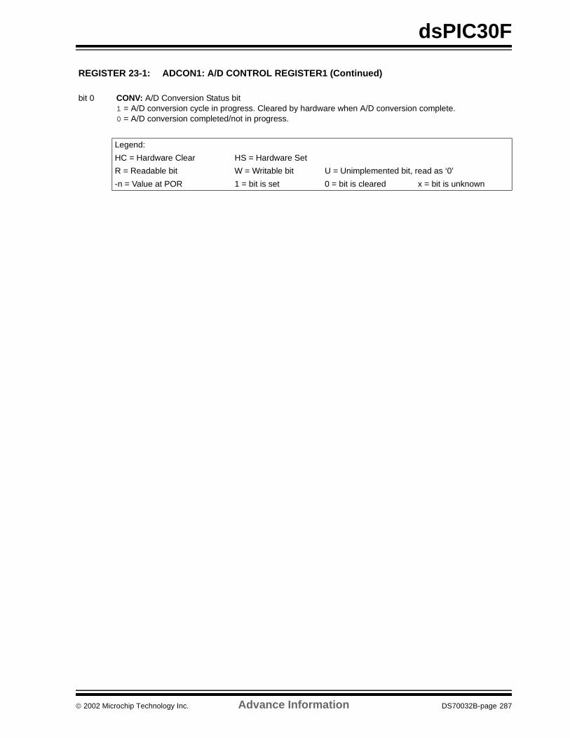
dsPIC30F
REGISTER 23-1: ADCON1: A/D CONTROL REGISTER1 (Continued)
bit 0 CONV: A/D Conversion Status bit1 = A/D conversion cycle in progress. Cleared by hardware when A/D conversion complete.0 = A/D conversion completed/not in progress.
Legend:
HC = Hardware Clear HS = Hardware Set
R = Readable bit W = Writable bit U = Unimplemented bit, read as ‘0’
-n = Value at POR 1 = bit is set 0 = bit is cleared x = bit is unknown
2002 Microchip Technology Inc. Advance Information DS70032B-page 287
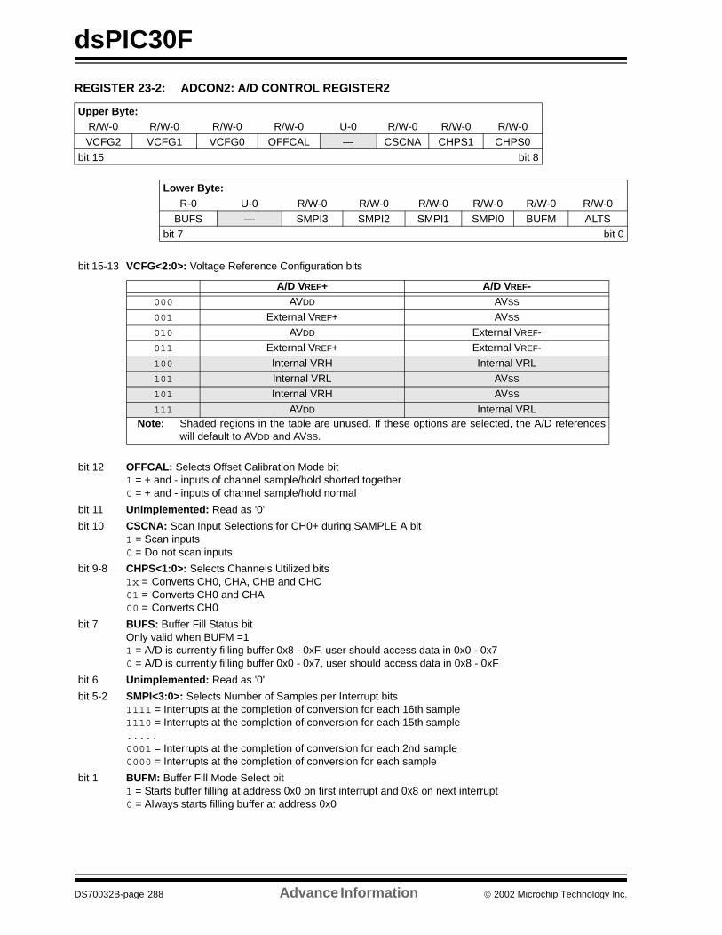
dsPIC30F
REGISTER 23-2: ADCON2: A/D CONTROL REGISTER2
Upper Byte:R/W-0 R/W-0 R/W-0 R/W-0 U-0 R/W-0 R/W-0 R/W-0VCFG2 VCFG1 VCFG0 OFFCAL — CSCNA CHPS1 CHPS0
bit 15 bit 8
Lower Byte:R-0 U-0 R/W-0 R/W-0 R/W-0 R/W-0 R/W-0 R/W-0
BUFS — SMPI3 SMPI2 SMPI1 SMPI0 BUFM ALTSbit 7 bit 0
bit 15-13 VCFG<2:0>: Voltage Reference Configuration bits
bit 12 OFFCAL: Selects Offset Calibration Mode bit1 = + and - inputs of channel sample/hold shorted together0 = + and - inputs of channel sample/hold normal
bit 11 Unimplemented: Read as '0'
bit 10 CSCNA: Scan Input Selections for CH0+ during SAMPLE A bit1 = Scan inputs0 = Do not scan inputs
bit 9-8 CHPS<1:0>: Selects Channels Utilized bits1x = Converts CH0, CHA, CHB and CHC01 = Converts CH0 and CHA00 = Converts CH0
bit 7 BUFS: Buffer Fill Status bitOnly valid when BUFM =1 1 = A/D is currently filling buffer 0x8 - 0xF, user should access data in 0x0 - 0x70 = A/D is currently filling buffer 0x0 - 0x7, user should access data in 0x8 - 0xF
bit 6 Unimplemented: Read as '0'
bit 5-2 SMPI<3:0>: Selects Number of Samples per Interrupt bits1111 = Interrupts at the completion of conversion for each 16th sample1110 = Interrupts at the completion of conversion for each 15th sample.....0001 = Interrupts at the completion of conversion for each 2nd sample0000 = Interrupts at the completion of conversion for each sample
bit 1 BUFM: Buffer Fill Mode Select bit1 = Starts buffer filling at address 0x0 on first interrupt and 0x8 on next interrupt0 = Always starts filling buffer at address 0x0
A/D VREF+ A/D VREF-000 AVDD AVSS
001 External VREF+ AVSS
010 AVDD External VREF-011 External VREF+ External VREF-
100 Internal VRH Internal VRL101 Internal VRL AVSS
101 Internal VRH AVSS
111 AVDD Internal VRLNote: Shaded regions in the table are unused. If these options are selected, the A/D references
will default to AVDD and AVSS.
DS70032B-page 288 Advance Information 2002 Microchip Technology Inc.
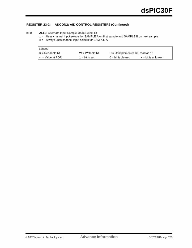
dsPIC30F
REGISTER 23-2: ADCON2: A/D CONTROL REGISTER2 (Continued)
bit 0 ALTS: Alternate Input Sample Mode Select bit1 = Uses channel input selects for SAMPLE A on first sample and SAMPLE B on next sample0 = Always uses channel input selects for SAMPLE A
Legend:
R = Readable bit W = Writable bit U = Unimplemented bit, read as ‘0’
-n = Value at POR 1 = bit is set 0 = bit is cleared x = bit is unknown
2002 Microchip Technology Inc. Advance Information DS70032B-page 289
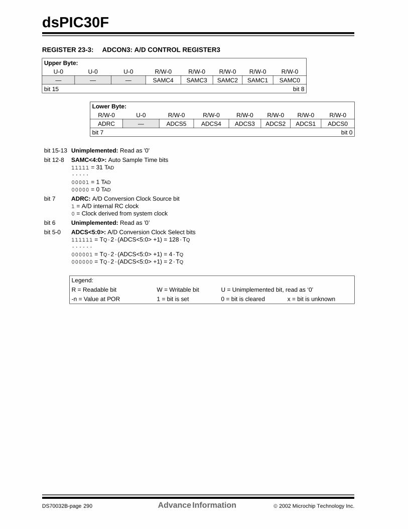
dsPIC30F
REGISTER 23-3: ADCON3: A/D CONTROL REGISTER3
Upper Byte:U-0 U-0 U-0 R/W-0 R/W-0 R/W-0 R/W-0 R/W-0— — — SAMC4 SAMC3 SAMC2 SAMC1 SAMC0
bit 15 bit 8
Lower Byte:R/W-0 U-0 R/W-0 R/W-0 R/W-0 R/W-0 R/W-0 R/W-0ADRC — ADCS5 ADCS4 ADCS3 ADCS2 ADCS1 ADCS0
bit 7 bit 0
bit 15-13 Unimplemented: Read as '0'
bit 12-8 SAMC<4:0>: Auto Sample Time bits11111 = 31 TAD
·····00001 = 1 TAD
00000 = 0 TAD
bit 7 ADRC: A/D Conversion Clock Source bit1 = A/D internal RC clock0 = Clock derived from system clock
bit 6 Unimplemented: Read as ’0’
bit 5-0 ADCS<5:0>: A/D Conversion Clock Select bits111111 = TQ·2·(ADCS<5:0> +1) = 128·TQ
······000001 = TQ·2·(ADCS<5:0> +1) = 4·TQ
000000 = TQ·2·(ADCS<5:0> +1) = 2·TQ
Legend:
R = Readable bit W = Writable bit U = Unimplemented bit, read as ‘0’
-n = Value at POR 1 = bit is set 0 = bit is cleared x = bit is unknown
DS70032B-page 290 Advance Information 2002 Microchip Technology Inc.
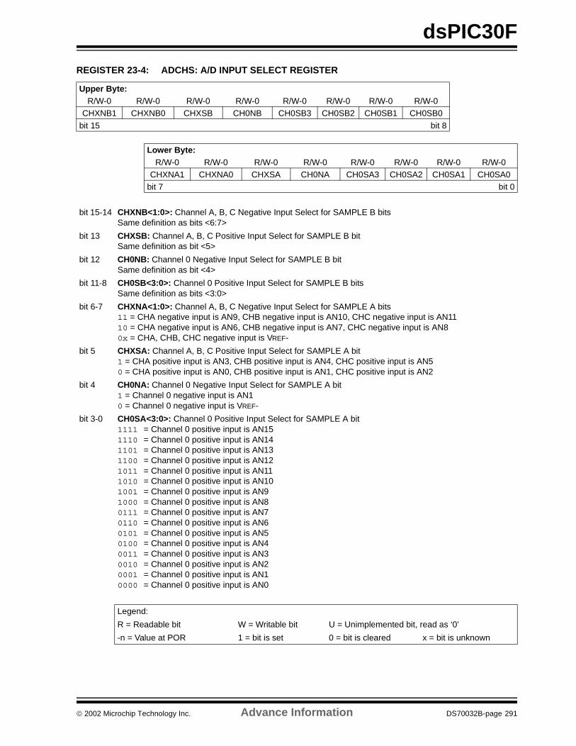
dsPIC30F
REGISTER 23-4: ADCHS: A/D INPUT SELECT REGISTER
Upper Byte:R/W-0 R/W-0 R/W-0 R/W-0 R/W-0 R/W-0 R/W-0 R/W-0
CHXNB1 CHXNB0 CHXSB CH0NB CH0SB3 CH0SB2 CH0SB1 CH0SB0
bit 15 bit 8
Lower Byte:R/W-0 R/W-0 R/W-0 R/W-0 R/W-0 R/W-0 R/W-0 R/W-0
CHXNA1 CHXNA0 CHXSA CH0NA CH0SA3 CH0SA2 CH0SA1 CH0SA0bit 7 bit 0
bit 15-14 CHXNB<1:0>: Channel A, B, C Negative Input Select for SAMPLE B bitsSame definition as bits <6:7>
bit 13 CHXSB: Channel A, B, C Positive Input Select for SAMPLE B bitSame definition as bit <5>
bit 12 CH0NB: Channel 0 Negative Input Select for SAMPLE B bitSame definition as bit <4>
bit 11-8 CH0SB<3:0>: Channel 0 Positive Input Select for SAMPLE B bitsSame definition as bits <3:0>
bit 6-7 CHXNA<1:0>: Channel A, B, C Negative Input Select for SAMPLE A bits11 = CHA negative input is AN9, CHB negative input is AN10, CHC negative input is AN1110 = CHA negative input is AN6, CHB negative input is AN7, CHC negative input is AN80x = CHA, CHB, CHC negative input is VREF-
bit 5 CHXSA: Channel A, B, C Positive Input Select for SAMPLE A bit1 = CHA positive input is AN3, CHB positive input is AN4, CHC positive input is AN50 = CHA positive input is AN0, CHB positive input is AN1, CHC positive input is AN2
bit 4 CH0NA: Channel 0 Negative Input Select for SAMPLE A bit1 = Channel 0 negative input is AN10 = Channel 0 negative input is VREF-
bit 3-0 CH0SA<3:0>: Channel 0 Positive Input Select for SAMPLE A bit1111 = Channel 0 positive input is AN151110 = Channel 0 positive input is AN141101 = Channel 0 positive input is AN131100 = Channel 0 positive input is AN121011 = Channel 0 positive input is AN111010 = Channel 0 positive input is AN101001 = Channel 0 positive input is AN91000 = Channel 0 positive input is AN80111 = Channel 0 positive input is AN70110 = Channel 0 positive input is AN60101 = Channel 0 positive input is AN50100 = Channel 0 positive input is AN40011 = Channel 0 positive input is AN30010 = Channel 0 positive input is AN20001 = Channel 0 positive input is AN10000 = Channel 0 positive input is AN0
Legend:
R = Readable bit W = Writable bit U = Unimplemented bit, read as ‘0’
-n = Value at POR 1 = bit is set 0 = bit is cleared x = bit is unknown
2002 Microchip Technology Inc. Advance Information DS70032B-page 291

dsPIC30F
REGISTER 23-5: ADPCFG: A/D PORT CONFIGURATION REGISTER
REGISTER 23-6: ADCSSL: A/D INPUT SCAN SELECT REGISTER
Upper Byte:R/W-0 R/W-0 R/W-0 R/W-0 R/W-0 R/W-0 R/W-0 R/W-0
PCFG15 PCFG14 PCFG13 PCFG12 PCFG11 PCFG10 PCFG9 PCFG8
bit 15 bit 8
Lower Byte:R/W-0 R/W-0 R/W-0 R/W-0 R/W-0 R/W-0 R/W-0 R/W-0PCFG7 PCFG6 PCFG5 PCFG4 PCFG3 PCFG2 PCFG1 PCFG0
bit 7 bit 0
bit 15-0 PCFG<15:0>: A/D Port Configuration Control bits1 = Port pin in Digital mode, port read input enabled, A/D input multiplexor connected to AVSS
0 = Port pin in Analog mode, port read input disabled, A/D samples pin voltage
Legend:
R = Readable bit W = Writable bit U = Unimplemented bit, read as ‘0’
-n = Value at POR 1 = bit is set 0 = bit is cleared x = bit is unknown
Upper Byte:R/W-0 R/W-0 R/W-0 R/W-0 R/W-0 R/W-0 R/W-0 R/W-0
CSSL15 CSSL14 CSSL13 CSSL12 CSSL11 CSSL10 CSSL9 CSSL8bit 15 bit 8
Lower Byte:R/W-0 R/W-0 R/W-0 R/W-0 R/W-0 R/W-0 R/W-0 R/W-0CSSL7 CSSL6 CSSL5 CSSL4 CSSL3 CSSL2 CSSL1 CSSL0
bit 7 bit 0
bit 15-0 CSSL<15:0>: A/D Input Scan Selection bits1 = Select ANx for input scan0 = Skip ANx for input scan
Legend:
R = Readable bit W = Writable bit U = Unimplemented bit, read as ‘0’
-n = Value at POR 1 = bit is set 0 = bit is cleared x = bit is unknown
DS70032B-page 292 Advance Information 2002 Microchip Technology Inc.
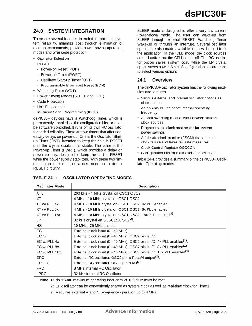
dsPIC30F
24.0 SYSTEM INTEGRATION
There are several features intended to maximize sys-tem reliability, minimize cost through elimination ofexternal components, provide power saving operatingmodes and offer code protection:
• Oscillator Selection• RESET
- Power-on Reset (POR)
- Power-up Timer (PWRT)- Oscillator Start-up Timer (OST)- Programmable Brown-out Reset (BOR)
• Watchdog Timer (WDT)• Power Saving Modes (SLEEP and IDLE)• Code Protection
• Unit ID Locations• In-Circuit Serial Programming (ICSP)
dsPIC30F devices have a Watchdog Timer, which ispermanently enabled via the configuration bits, or it canbe software controlled. It runs off its own RC oscillatorfor added reliability. There are two timers that offer nec-essary delays on power-up. One is the Oscillator Start-up Timer (OST), intended to keep the chip in RESETuntil the crystal oscillator is stable. The other is thePower-up Timer (PWRT), which provides a delay onpower-up only, designed to keep the part in RESETwhile the power supply stabilizes. With these two tim-ers on-chip, most applications need no externalRESET circuitry.
SLEEP mode is designed to offer a very low currentPower-down mode. The user can wake-up fromSLEEP through external RESET, Watchdog TimerWake-up or through an interrupt. Several oscillatoroptions are also made available to allow the part to fitthe application. In the IDLE mode, the clock sourcesare still active, but the CPU is shut-off. The RC oscilla-tor option saves system cost, while the LP crystaloption saves power. A set of configuration bits are usedto select various options
24.1 Overview
The dsPIC30F oscillator system has the following mod-ules and features:
• Various external and internal oscillator options as clock sources
• An on-chip PLL to boost internal operating frequency
• A clock switching mechanism between various clock sources
• Programmable clock post-scaler for system power savings
• A fail safe clock monitor (FSCM) that detects clock failure and takes fail safe measures
• Clock Control Register OSCCON• Configuration bits for main oscillator selection
Table 24-1 provides a summary of the dsPIC30F Oscil-lator Operating modes.
TABLE 24-1: OSCILLATOR OPERATING MODES
Oscillator Mode Description
XTL 200 kHz - 4 MHz crystal on OSC1:OSC2.XT 4 MHz - 10 MHz crystal on OSC1:OSC2. XT w/ PLL 4x 4 MHz - 10 MHz crystal on OSC1:OSC2. 4x PLL enabled.
XT w/ PLL 8x 4 MHz - 10 MHz crystal on OSC1:OSC2. 8x PLL enabled.XT w/ PLL 16x 4 MHz - 10 MHz crystal on OSC1:OSC2. 16x PLL enabled(1).LP 32 kHz crystal on SOSC1:SOSC2(2).
HS 10 MHz - 25 MHz crystal.EC External clock input (0 - 40 MHz).ECIO External clock input (0 - 40 MHz). OSC2 pin is I/O.
EC w/ PLL 4x External clock input (0 - 40 MHz). OSC2 pin is I/O. 4x PLL enabled(1).EC w/ PLL 8x External clock input (0 - 40 MHz). OSC2 pin is I/O. 8x PLL enabled(1).EC w/ PLL 16x External clock input (0 - 40 MHz). OSC2 pin is I/O. 16x PLL enabled(1).
ERC External RC oscillator. OSC2 pin is FOSC/4 output(3).ERCIO External RC oscillator. OSC2 pin is I/O(3).FRC 8 MHz internal RC Oscillator.
LPRC 32 kHz internal RC Oscillator.
Note 1: dsPIC30F maximum operating frequency of 120 MHz must be met.
2: LP oscillator can be conveniently shared as system clock as well as real-time clock for Timer1.
3: Requires external R and C. Frequency operation up to 4 MHz.
2002 Microchip Technology Inc. Advance Information DS70032B-page 293
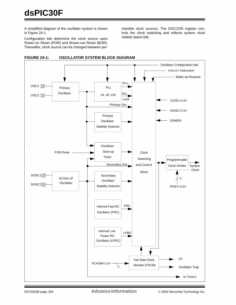
dsPIC30F
A simplified diagram of the oscillator system is shownin Figure 24-1.
Configuration bits determine the clock source uponPower-on Reset (POR) and Brown-out Reset (BOR).Thereafter, clock source can be changed between per-
missible clock sources. The OSCCON register con-trols the clock switching and reflects system clockrelated status bits.
FIGURE 24-1: OSCILLATOR SYSTEM BLOCK DIAGRAM
Primary OSC1
OSC2
SOSC1
SOSC2
Oscillator
32 kHz LP
Clock
and Control
Block
Switching
Oscillator
x4, x8, x16
PLL
Primary
Oscillator
Stability Detector
Stability Detector
Secondary
Oscillator
Programmable
Clock Divider
Oscillator
Start-up
Timer
Fail Safe Clock
Monitor (FSCM)
Internal Fast RC
Oscillator (FRC)
Internal Low
Power RC
Oscillator (LPRC)
PWRSAV Instruction
Wake-up Request
Oscillator Configuration bits
SystemClock
Oscillator Trap
to Timer1
LPRC
FRC
Secondary Osc
POR Done
Primary Osc
FPLL
POST<1:0>
2
FCKSM<1:0>2
PLL
Lock COSC<1:0>
NOSC<1:0>
OSWEN
CF
DS70032B-page 294 Advance Information 2002 Microchip Technology Inc.
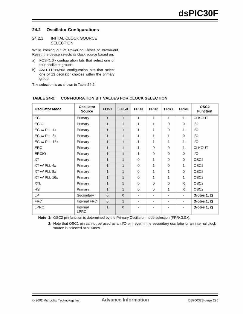
dsPIC30F
24.2 Oscillator Configurations
24.2.1 INITIAL CLOCK SOURCE SELECTION
While coming out of Power-on Reset or Brown-outReset, the device selects its clock source based on:
a) FOS<1:0> configuration bits that select one offour oscillator groups
b) AND FPR<3:0> configuration bits that selectone of 13 oscillator choices within the primarygroup.
The selection is as shown in Table 24-2.
TABLE 24-2: CONFIGURATION BIT VALUES FOR CLOCK SELECTION
Oscillator ModeOscillator
SourceFOS1 FOS0 FPR3 FPR2 FPR1 FPR0
OSC2 Function
EC Primary 1 1 1 1 1 1 CLKOUT
ECIO Primary 1 1 1 1 0 0 I/O
EC w/ PLL 4x Primary 1 1 1 1 0 1 I/O
EC w/ PLL 8x Primary 1 1 1 1 1 0 I/O
EC w/ PLL 16x Primary 1 1 1 1 1 1 I/O
ERC Primary 1 1 1 0 0 1 CLKOUT
ERCIO Primary 1 1 1 0 0 0 I/O
XT Primary 1 1 0 1 0 0 OSC2
XT w/ PLL 4x Primary 1 1 0 1 0 1 OSC2
XT w/ PLL 8x Primary 1 1 0 1 1 0 OSC2
XT w/ PLL 16x Primary 1 1 0 1 1 1 OSC2
XTL Primary 1 1 0 0 0 X OSC2
HS Primary 1 1 0 0 1 X OSC2
LP Secondary 0 0 - - - - (Notes 1, 2)
FRC Internal FRC 0 1 - - - - (Notes 1, 2)
LPRC Internal LPRC
1 0 - - - - (Notes 1, 2)
Note 1: OSC2 pin function is determined by the Primary Oscillator mode selection (FPR<3:0>).
2: Note that OSC1 pin cannot be used as an I/O pin, even if the secondary oscillator or an internal clocksource is selected at all times.
2002 Microchip Technology Inc. Advance Information DS70032B-page 295
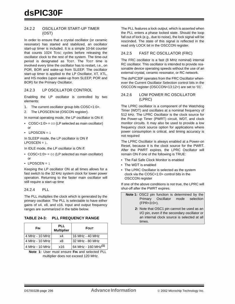
dsPIC30F
24.2.2 OSCILLATOR START-UP TIMER (OST)
In order to ensure that a crystal oscillator (or ceramicresonator) has started and stabilized, an oscillatorstart-up timer is included. It is a simple 10-bit counterthat counts 1024 TOSC cycles before releasing theoscillator clock to the rest of the system. The time-outperiod is designated as TOST. The TOST time isinvolved every time the oscillator has to restart, i.e., onPOR, BOR and wake-up from SLEEP. The oscillatorstart-up timer is applied to the LP Oscillator, XT, XTL,and HS modes (upon wake-up from SLEEP, POR andBOR) for the Primary Oscillator.
24.2.3 LP OSCILLATOR CONTROL
Enabling the LP oscillator is controlled by twoelements:
1. The current oscillator group bits COSC<1:0>.2. The LPOSCEN bit (OSCON register).
In normal operating mode, the LP oscillator is ON if:
• COSC<1:0> = 00 (LP selected as main oscillator) or
• LPOSCEN = 1
In SLEEP mode, the LP oscillator is ON if LPOSCEN = 1.
In IDLE mode, the LP oscillator is ON if:
• COSC<1:0> = 00 (LP selected as main oscillator) or
• LPOSCEN = 1
Keeping the LP oscillator ON at all times allows for afast switch to the 32 kHz system clock for lower poweroperation. Returning to the faster main oscillator willstill require a start-up time
24.2.4 PLL
The PLL multiplies the clock which is generated by theprimary oscillator. The PLL is selectable to have eithergains of x4, x8, and x16. Input and output frequencyranges are summarized in the table below.
TABLE 24-3: PLL FREQUENCY RANGE
The PLL features a lock output, which is asserted whenthe PLL enters a phase locked state. Should the loopfall out of lock (e.g., due to noise), the lock signal will berescinded. The state of this signal is reflected in theread only LOCK bit in the OSCCON register.
24.2.5 FAST RC OSCILLATOR (FRC)
The FRC oscillator is a fast (8 MHz nominal) internalRC oscillator. This oscillator is intended to provide rea-sonable device operating speeds without the use of anexternal crystal, ceramic resonator, or RC network.
The dsPIC30F operates from the FRC Oscillator when-ever the Current Oscillator Selection control bits in theOSCCON register (OSCCON<13:12>) are set to ‘01’.
24.2.6 LOW POWER RC OSCILLATOR (LPRC)
The LPRC oscillator is a component of the WatchdogTimer (WDT) and oscillates at a nominal frequency of512 kHz. The LPRC Oscillator is the clock source forthe Power-up Timer (PWRT) circuit, WDT, and clockmonitor circuits. It may also be used to provide a lowfrequency clock source option for applications wherepower consumption is critical, and timing accuracy isnot required
The LPRC Oscillator is always enabled at a Power-onReset, because it is the clock source for the PWRT.After the PWRT expires, the LPRC Oscillator willremain ON if one of the following is TRUE:
• The Fail Safe Clock Monitor is enabled• The WDT is enabled
• The LPRC Oscillator is selected as the system clock via the COSC<1:0> control bits in the OSCCON register
If one of the above conditions is not true, the LPRC willshut-off after the PWRT expires.
FINPLL
MultiplierFOUT
4 MHz - 10 MHz x4 16 MHz - 40 MHz4 MHz - 10 MHz x8 32 MHz - 80 MHz
4 MHz - 10 MHz x16 64 MHz - 160 MHz(1)
Note 1: User must ensure FIN and selected PLLmultiplier does not exceed 120 MHz.
Note 1: OSC2 pin function is determined by thePrimary Oscillator mode selection(FPR<3:0>).
2: Note that OSC1 pin cannot be used as anI/O pin, even if the secondary oscillator oran internal clock source is selected at alltimes.
DS70032B-page 296 Advance Information 2002 Microchip Technology Inc.
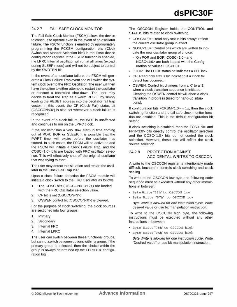
dsPIC30F
24.2.7 FAIL SAFE CLOCK MONITOR
The Fail Safe Clock Monitor (FSCM) allows the deviceto continue to operate even in the event of an oscillatorfailure. The FSCM function is enabled by appropriatelyprogramming the FCKSM configuration bits (ClockSwitch and Monitor Selection bits) in the FOSC deviceconfiguration register. If the FSCM function is enabled,the LPRC Internal oscillator will run at all times (exceptduring SLEEP mode) and will not be subject to controlby the SWDTEN bit.
In the event of an oscillator failure, the FSCM will gen-erate a Clock Failure Trap event and will switch the sys-tem clock over to the FRC Oscillator. The user will thenhave the option to either attempt to restart the oscillatoror execute a controlled shut-down. The user maydecide to treat the Trap as a warm RESET by simplyloading the RESET address into the oscillator fail trapvector. In this event, the CF (Clock Fail) status bit(OSCCON<3>) is also set whenever a clock failure isrecognized.
In the event of a clock failure, the WDT is unaffectedand continues to run on the LPRC clock.
If the oscillator has a very slow start-up time comingout of POR, BOR or SLEEP, it is possible that thePWRT timer will expire before the oscillator hasstarted. In such cases, the FSCM will be activated andthe FSCM will initiate a Clock Failure Trap, and theCOSC<1:0> bits are loaded with FRC oscillator selec-tion. This will effectively shut-off the original oscillatorthat was trying to start.
The user may detect this situation and restart the oscil-lator in the Clock Fail Trap ISR.
Upon a clock failure detection the FSCM module willinitiate a clock switch to the FRC Oscillator as follows:
1. The COSC bits (OSCCON<13:12>) are loadedwith the FRC Oscillator selection value.
2. CF bit is set (OSCCON<3>).3. OSWEN control bit (OSCCON<0>) is cleared.
For the purpose of clock switching, the clock sourcesare sectioned into four groups:
1. Primary2. Secondary
3. Internal FRC4. Internal LPRC
The user can switch between these functional groups,but cannot switch between options within a group. If theprimary group is selected, then the choice within thegroup is always determined by the FPR<3:0> configu-ration bits.
The OSCCON Register holds the CONTROL andSTATUS bits related to clock switching.
• COSC<1:0>: Read only status bits always reflect the current oscillator group in effect.
• NOSC<1:0>: Control bits which are written to indi-cate the new oscillator group of choice.
- On POR and BOR, COSC<1:0> and NOSC<1:0> are both loaded with the Config-uration bit values FOS<1:0>.
• LOCK: The LOCK status bit indicates a PLL lock.
• CF: Read only status bit indicating if a clock fail detect has occurred.
• OSWEN: Control bit changes from a ‘0’ to a ‘1’ when a clock transition sequence is initiated. Clearing the OSWEN control bit will abort a clock transition in progress (used for hang-up situa-tions).
If configuration bits FCKSM<1:0> = 1x, then the clockswitching function and the fail safe clock monitor func-tion are disabled. This is the default configuration bitsetting.
If clock switching is disabled, then the FOS<1:0> andFPR<3:0> bits directly control the oscillator selectionand the COSC<1:0> bits do not control the clockselection. However, these bits will reflect the clocksource selection.
24.2.8 PROTECTION AGAINST ACCIDENTAL WRITES TO OSCCON
A write to the OSCCON register is intentionally madedifficult, because it controls clock switching and clockscaling.
To write to the OSCCON low byte, the following codesequence must be executed without any other instruc-tions in between:
• Byte Write “46h” to OSCCON low
• Byte Write “57h” to OSCCON low
Byte Write is allowed for one instruction cycle. Writedesired value or use bit manipulation instruction.
To write to the OSCCON high byte, the followinginstructions must be executed without any otherinstructions in between:
• Byte Write “78h” to OSCCON high• Byte Write “9Ah” to OSCCON high
Byte Write is allowed for one instruction cycle. Write“Desired Value” or use bit manipulation instruction.
2002 Microchip Technology Inc. Advance Information DS70032B-page 297
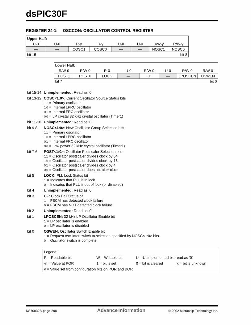
dsPIC30F
REGISTER 24-1: OSCCON: OSCILLATOR CONTROL REGISTER
Upper Half:U-0 U-0 R-y R-y U-0 U-0 R/W-y R/W-y— — COSC1 COSC0 — — NOSC1 NOSC0
bit 15 bit 8
Lower Half:R/W-0 R/W-0 R-0 U-0 R/W-0 U-0 R/W-0 R/W-0POST1 POST0 LOCK — CF — LPOSCEN OSWEN
bit 7 bit 0
bit 15-14 Unimplemented: Read as ‘0’
bit 13-12 COSC<1:0>: Current Oscillator Source Status bits11 = Primary oscillator10 = Internal LPRC oscillator01 = Internal FRC oscillator00 = LP crystal 32 kHz crystal oscillator (Timer1)
bit 11-10 Unimplemented: Read as ‘0’
bit 9-8 NOSC<1:0>: New Oscillator Group Selection bits11 = Primary oscillator10 = Internal LPRC oscillator01 = Internal FRC oscillator00 = Low power 32 kHz crystal oscillator (Timer1)
bit 7-6 POST<1:0>: Oscillator Postscaler Selection bits11 = Oscillator postscaler divides clock by 6410 = Oscillator postscaler divides clock by 1601 = Oscillator postscaler divides clock by 400 = Oscillator postscaler does not alter clock
bit 5 LOCK: PLL Lock Status bit1 = Indicates that PLL is in lock0 = Indicates that PLL is out of lock (or disabled)
bit 4 Unimplemented: Read as ‘0’
bit 3 CF: Clock Fail Status bit1 = FSCM has detected clock failure0 = FSCM has NOT detected clock failure
bit 2 Unimplemented: Read as ‘0’
bit 1 LPOSCEN: 32 kHz LP Oscillator Enable bit1 = LP oscillator is enabled0 = LP oscillator is disabled
bit 0 OSWEN: Oscillator Switch Enable bit1 = Request oscillator switch to selection specified by NOSC<1:0> bits0 = Oscillator switch is complete
Legend:
R = Readable bit W = Writable bit U = Unimplemented bit, read as ‘0’
-n = Value at POR 1 = bit is set 0 = bit is cleared x = bit is unknown
y = Value set from configuration bits on POR and BOR
DS70032B-page 298 Advance Information 2002 Microchip Technology Inc.
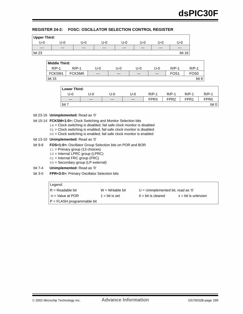
dsPIC30F
REGISTER 24-2: FOSC: OSCILLATOR SELECTION CONTROL REGISTER
Upper Third:U-0 U-0 U-0 U-0 U-0 U-0 U-0 U-0— — — — — — — —
bit 23 bit 16
Middle Third:R/P-1 R/P-1 U-0 U-0 U-0 U-0 R/P-1 R/P-1
FCKSM1 FCKSM0 — — — — FOS1 FOS0bit 15 bit 8
Lower Third:U-0 U-0 U-0 U-0 R/P-1 R/P-1 R/P-1 R/P-1
— — — — FPR3 FPR2 FPR1 FPR0bit 7 bit 0
bit 23-16 Unimplemented: Read as ‘0’
bit 15-14 FCKSM<1:0>: Clock Switching and Monitor Selection bits1x = Clock switching is disabled, fail safe clock monitor is disabled01 = Clock switching is enabled, fail safe clock monitor is disabled00 = Clock switching is enabled, fail safe clock monitor is enabled
bit 13-10 Unimplemented: Read as ‘0’
bit 9-8 FOS<1:0>: Oscillator Group Selection bits on POR and BOR11 = Primary group (13 choices)10 = Internal LPRC group (LPRC)01 = Internal FRC group (FRC)00 = Secondary group (LP external)
bit 7-4 Unimplemented: Read as ‘0’
bit 3-0 FPR<3:0>: Primary Oscillator Selection bits
Legend:
R = Readable bit W = Writable bit U = Unimplemented bit, read as ‘0’
-n = Value at POR 1 = bit is set 0 = bit is cleared x = bit is unknown
P = FLASH programmable bit
2002 Microchip Technology Inc. Advance Information DS70032B-page 299
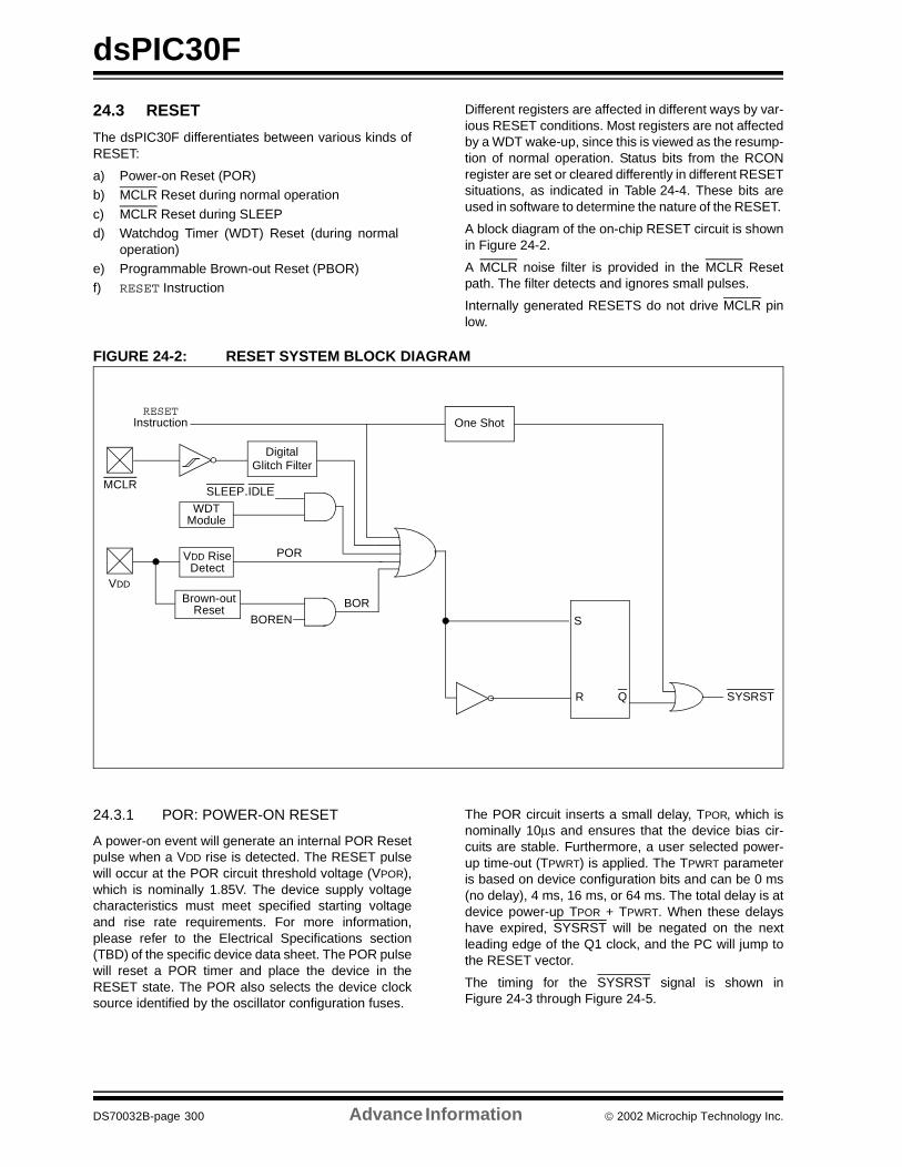
dsPIC30F
24.3 RESET
The dsPIC30F differentiates between various kinds ofRESET:
a) Power-on Reset (POR) b) MCLR Reset during normal operation
c) MCLR Reset during SLEEP d) Watchdog Timer (WDT) Reset (during normal
operation)e) Programmable Brown-out Reset (PBOR) f) RESET Instruction
Different registers are affected in different ways by var-ious RESET conditions. Most registers are not affectedby a WDT wake-up, since this is viewed as the resump-tion of normal operation. Status bits from the RCONregister are set or cleared differently in different RESETsituations, as indicated in Table 24-4. These bits areused in software to determine the nature of the RESET.
A block diagram of the on-chip RESET circuit is shownin Figure 24-2.
A MCLR noise filter is provided in the MCLR Resetpath. The filter detects and ignores small pulses.
Internally generated RESETS do not drive MCLR pinlow.
FIGURE 24-2: RESET SYSTEM BLOCK DIAGRAM
24.3.1 POR: POWER-ON RESET
A power-on event will generate an internal POR Resetpulse when a VDD rise is detected. The RESET pulsewill occur at the POR circuit threshold voltage (VPOR),which is nominally 1.85V. The device supply voltagecharacteristics must meet specified starting voltageand rise rate requirements. For more information,please refer to the Electrical Specifications section(TBD) of the specific device data sheet. The POR pulsewill reset a POR timer and place the device in theRESET state. The POR also selects the device clocksource identified by the oscillator configuration fuses.
The POR circuit inserts a small delay, TPOR, which isnominally 10µs and ensures that the device bias cir-cuits are stable. Furthermore, a user selected power-up time-out (TPWRT) is applied. The TPWRT parameteris based on device configuration bits and can be 0 ms(no delay), 4 ms, 16 ms, or 64 ms. The total delay is atdevice power-up TPOR + TPWRT. When these delayshave expired, SYSRST will be negated on the nextleading edge of the Q1 clock, and the PC will jump tothe RESET vector.
The timing for the SYSRST signal is shown inFigure 24-3 through Figure 24-5.
S
R Q
MCLR
VDD
VDD RiseDetect
POR
SYSRST
SLEEP.IDLE
Brown-outReset
BOREN
RESETInstruction
WDTModule
DigitalGlitch Filter
One Shot
BOR
DS70032B-page 300 Advance Information 2002 Microchip Technology Inc.
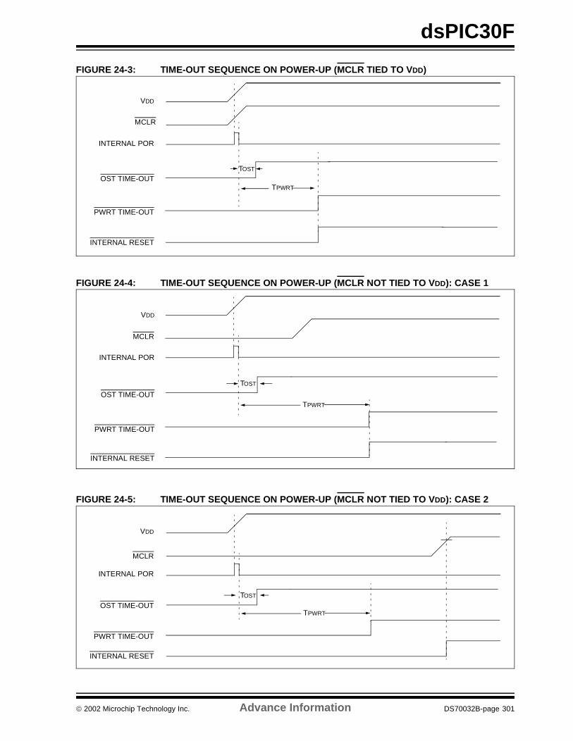
dsPIC30F
FIGURE 24-3: TIME-OUT SEQUENCE ON POWER-UP (MCLR TIED TO VDD)
FIGURE 24-4: TIME-OUT SEQUENCE ON POWER-UP (MCLR NOT TIED TO VDD): CASE 1
FIGURE 24-5: TIME-OUT SEQUENCE ON POWER-UP (MCLR NOT TIED TO VDD): CASE 2
TPWRT
TOST
VDD
INTERNAL POR
PWRT TIME-OUT
OST TIME-OUT
INTERNAL RESET
MCLR
TPWRT
TOST
VDD
INTERNAL POR
PWRT TIME-OUT
OST TIME-OUT
INTERNAL RESET
MCLR
VDD
MCLR
INTERNAL POR
PWRT TIME-OUT
OST TIME-OUT
INTERNAL RESET
TPWRT
TOST
2002 Microchip Technology Inc. Advance Information DS70032B-page 301
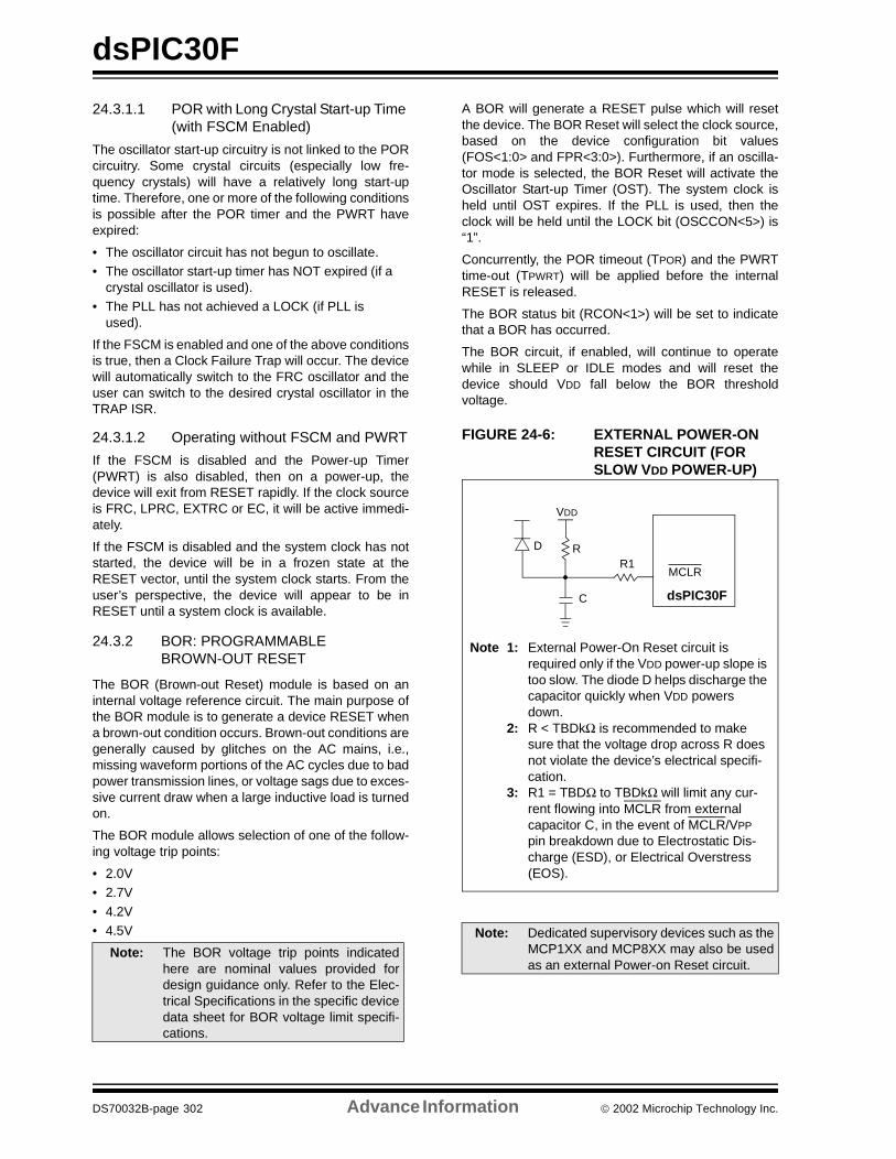
dsPIC30F
24.3.1.1 POR with Long Crystal Start-up Time (with FSCM Enabled)
The oscillator start-up circuitry is not linked to the PORcircuitry. Some crystal circuits (especially low fre-quency crystals) will have a relatively long start-uptime. Therefore, one or more of the following conditionsis possible after the POR timer and the PWRT haveexpired:
• The oscillator circuit has not begun to oscillate.• The oscillator start-up timer has NOT expired (if a
crystal oscillator is used).• The PLL has not achieved a LOCK (if PLL is
used).
If the FSCM is enabled and one of the above conditionsis true, then a Clock Failure Trap will occur. The devicewill automatically switch to the FRC oscillator and theuser can switch to the desired crystal oscillator in theTRAP ISR.
24.3.1.2 Operating without FSCM and PWRT
If the FSCM is disabled and the Power-up Timer(PWRT) is also disabled, then on a power-up, thedevice will exit from RESET rapidly. If the clock sourceis FRC, LPRC, EXTRC or EC, it will be active immedi-ately.
If the FSCM is disabled and the system clock has notstarted, the device will be in a frozen state at theRESET vector, until the system clock starts. From theuser’s perspective, the device will appear to be inRESET until a system clock is available.
24.3.2 BOR: PROGRAMMABLE BROWN-OUT RESET
The BOR (Brown-out Reset) module is based on aninternal voltage reference circuit. The main purpose ofthe BOR module is to generate a device RESET whena brown-out condition occurs. Brown-out conditions aregenerally caused by glitches on the AC mains, i.e.,missing waveform portions of the AC cycles due to badpower transmission lines, or voltage sags due to exces-sive current draw when a large inductive load is turnedon.
The BOR module allows selection of one of the follow-ing voltage trip points:
• 2.0V• 2.7V
• 4.2V• 4.5V
A BOR will generate a RESET pulse which will resetthe device. The BOR Reset will select the clock source,based on the device configuration bit values(FOS<1:0> and FPR<3:0>). Furthermore, if an oscilla-tor mode is selected, the BOR Reset will activate theOscillator Start-up Timer (OST). The system clock isheld until OST expires. If the PLL is used, then theclock will be held until the LOCK bit (OSCCON<5>) is“1”.
Concurrently, the POR timeout (TPOR) and the PWRTtime-out (TPWRT) will be applied before the internalRESET is released.
The BOR status bit (RCON<1>) will be set to indicatethat a BOR has occurred.
The BOR circuit, if enabled, will continue to operatewhile in SLEEP or IDLE modes and will reset thedevice should VDD fall below the BOR thresholdvoltage.
FIGURE 24-6: EXTERNAL POWER-ON RESET CIRCUIT (FOR SLOW VDD POWER-UP)
Note: The BOR voltage trip points indicatedhere are nominal values provided fordesign guidance only. Refer to the Elec-trical Specifications in the specific devicedata sheet for BOR voltage limit specifi-cations.
Note: Dedicated supervisory devices such as theMCP1XX and MCP8XX may also be usedas an external Power-on Reset circuit.
Note 1: External Power-On Reset circuit is required only if the VDD power-up slope is too slow. The diode D helps discharge the capacitor quickly when VDD powers down.
2: R < TBDkΩ is recommended to make sure that the voltage drop across R does not violate the device’s electrical specifi-cation.
3: R1 = TBDΩ to TBDkΩ will limit any cur-rent flowing into MCLR from external capacitor C, in the event of MCLR/VPP pin breakdown due to Electrostatic Dis-charge (ESD), or Electrical Overstress (EOS).
C
R1RD
VDD
dsPIC30F
MCLR
DS70032B-page 302 Advance Information 2002 Microchip Technology Inc.
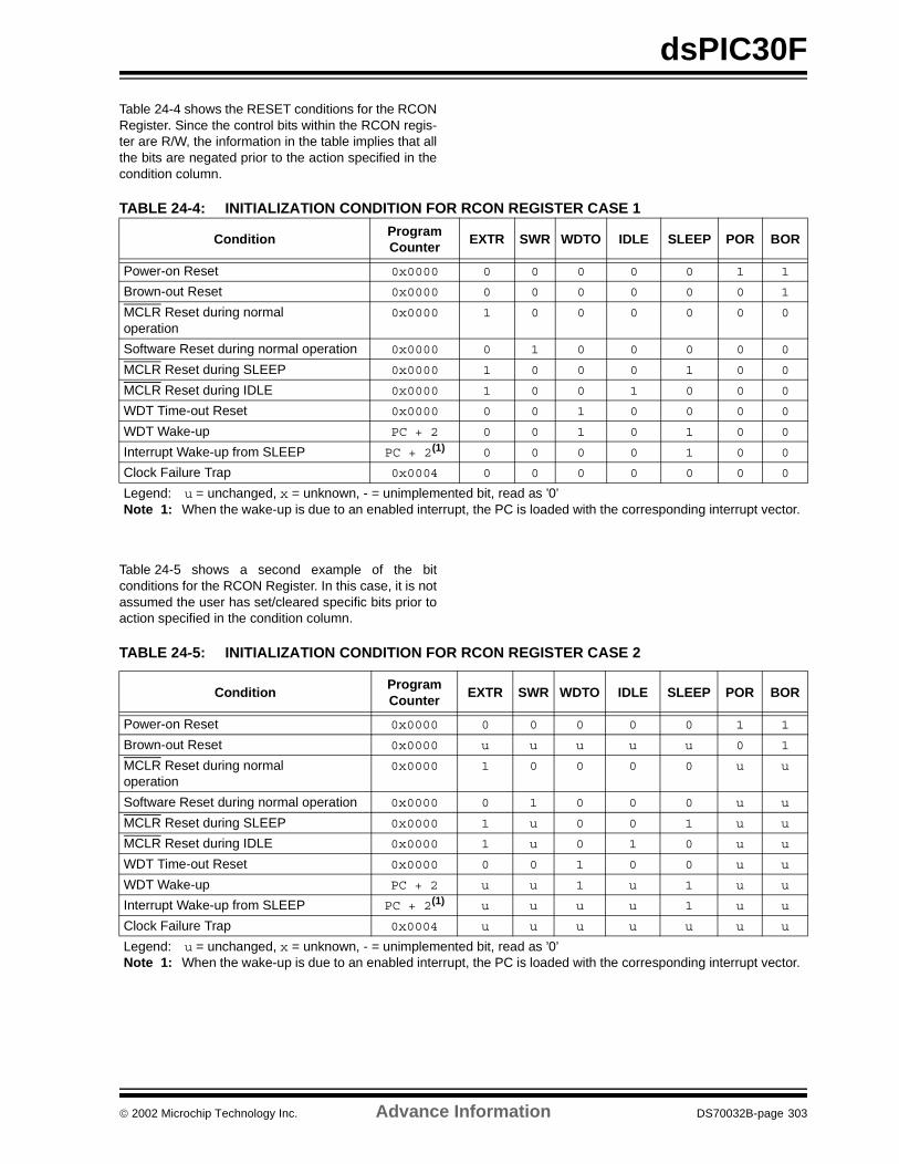
dsPIC30F
Table 24-4 shows the RESET conditions for the RCONRegister. Since the control bits within the RCON regis-ter are R/W, the information in the table implies that allthe bits are negated prior to the action specified in thecondition column.
TABLE 24-4: INITIALIZATION CONDITION FOR RCON REGISTER CASE 1
Table 24-5 shows a second example of the bitconditions for the RCON Register. In this case, it is notassumed the user has set/cleared specific bits prior toaction specified in the condition column.
TABLE 24-5: INITIALIZATION CONDITION FOR RCON REGISTER CASE 2
ConditionProgram Counter
EXTR SWR WDTO IDLE SLEEP POR BOR
Power-on Reset 0x0000 0 0 0 0 0 1 1
Brown-out Reset 0x0000 0 0 0 0 0 0 1
MCLR Reset during normal operation
0x0000 1 0 0 0 0 0 0
Software Reset during normal operation 0x0000 0 1 0 0 0 0 0
MCLR Reset during SLEEP 0x0000 1 0 0 0 1 0 0
MCLR Reset during IDLE 0x0000 1 0 0 1 0 0 0
WDT Time-out Reset 0x0000 0 0 1 0 0 0 0
WDT Wake-up PC + 2 0 0 1 0 1 0 0
Interrupt Wake-up from SLEEP PC + 2(1) 0 0 0 0 1 0 0
Clock Failure Trap 0x0004 0 0 0 0 0 0 0
Legend: u = unchanged, x = unknown, - = unimplemented bit, read as ’0’Note 1: When the wake-up is due to an enabled interrupt, the PC is loaded with the corresponding interrupt vector.
ConditionProgram Counter
EXTR SWR WDTO IDLE SLEEP POR BOR
Power-on Reset 0x0000 0 0 0 0 0 1 1
Brown-out Reset 0x0000 u u u u u 0 1
MCLR Reset during normal operation
0x0000 1 0 0 0 0 u u
Software Reset during normal operation 0x0000 0 1 0 0 0 u u
MCLR Reset during SLEEP 0x0000 1 u 0 0 1 u u
MCLR Reset during IDLE 0x0000 1 u 0 1 0 u u
WDT Time-out Reset 0x0000 0 0 1 0 0 u u
WDT Wake-up PC + 2 u u 1 u 1 u u
Interrupt Wake-up from SLEEP PC + 2(1) u u u u 1 u u
Clock Failure Trap 0x0004 u u u u u u u
Legend: u = unchanged, x = unknown, - = unimplemented bit, read as ’0’Note 1: When the wake-up is due to an enabled interrupt, the PC is loaded with the corresponding interrupt vector.
2002 Microchip Technology Inc. Advance Information DS70032B-page 303
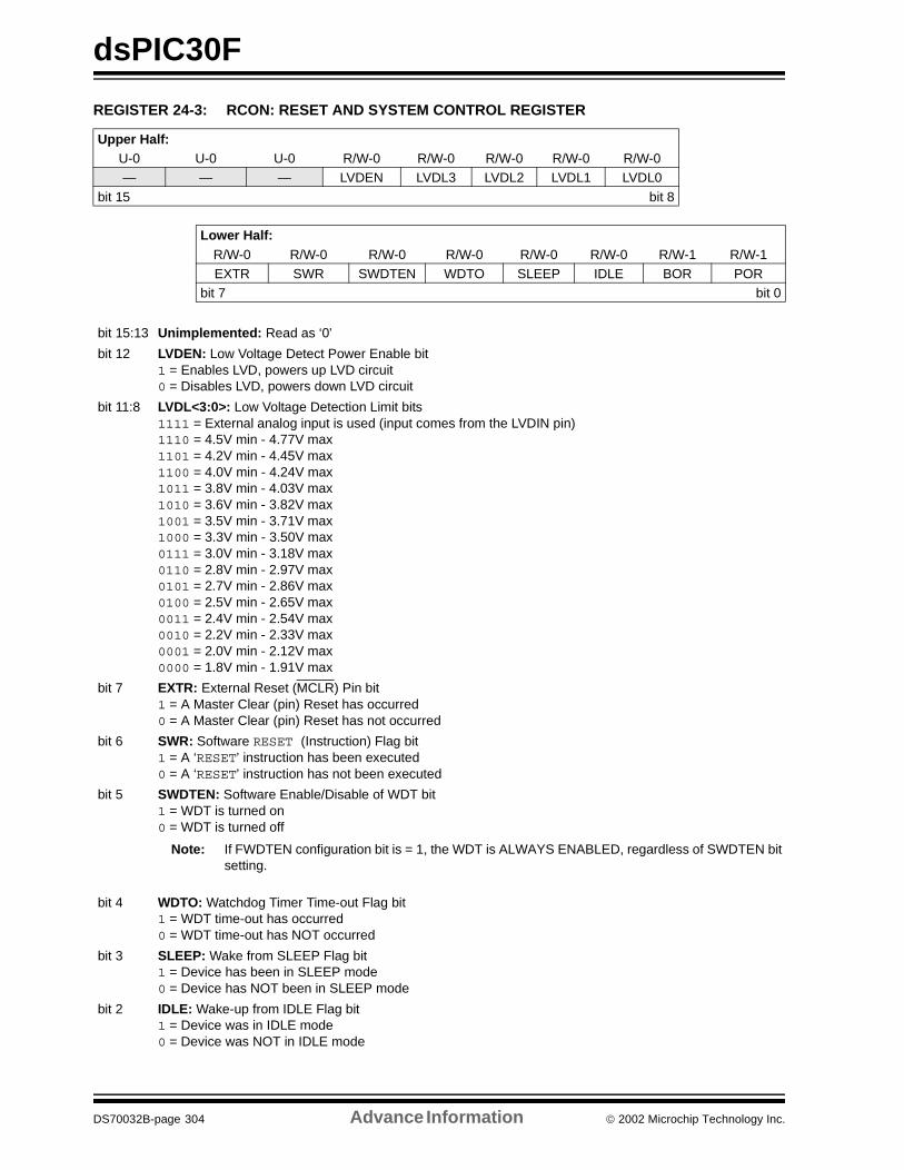
dsPIC30F
REGISTER 24-3: RCON: RESET AND SYSTEM CONTROL REGISTER
Upper Half:U-0 U-0 U-0 R/W-0 R/W-0 R/W-0 R/W-0 R/W-0— — — LVDEN LVDL3 LVDL2 LVDL1 LVDL0
bit 15 bit 8
Lower Half:R/W-0 R/W-0 R/W-0 R/W-0 R/W-0 R/W-0 R/W-1 R/W-1EXTR SWR SWDTEN WDTO SLEEP IDLE BOR POR
bit 7 bit 0
bit 15:13 Unimplemented: Read as ‘0’
bit 12 LVDEN: Low Voltage Detect Power Enable bit1 = Enables LVD, powers up LVD circuit0 = Disables LVD, powers down LVD circuit
bit 11:8 LVDL<3:0>: Low Voltage Detection Limit bits1111 = External analog input is used (input comes from the LVDIN pin)1110 = 4.5V min - 4.77V max1101 = 4.2V min - 4.45V max1100 = 4.0V min - 4.24V max1011 = 3.8V min - 4.03V max1010 = 3.6V min - 3.82V max1001 = 3.5V min - 3.71V max1000 = 3.3V min - 3.50V max0111 = 3.0V min - 3.18V max0110 = 2.8V min - 2.97V max0101 = 2.7V min - 2.86V max0100 = 2.5V min - 2.65V max0011 = 2.4V min - 2.54V max0010 = 2.2V min - 2.33V max0001 = 2.0V min - 2.12V max0000 = 1.8V min - 1.91V max
bit 7 EXTR: External Reset (MCLR) Pin bit1 = A Master Clear (pin) Reset has occurred0 = A Master Clear (pin) Reset has not occurred
bit 6 SWR: Software RESET (Instruction) Flag bit1 = A ‘RESET’ instruction has been executed0 = A ‘RESET’ instruction has not been executed
bit 5 SWDTEN: Software Enable/Disable of WDT bit1 = WDT is turned on0 = WDT is turned off
Note: If FWDTEN configuration bit is = 1, the WDT is ALWAYS ENABLED, regardless of SWDTEN bitsetting.
bit 4 WDTO: Watchdog Timer Time-out Flag bit1 = WDT time-out has occurred0 = WDT time-out has NOT occurred
bit 3 SLEEP: Wake from SLEEP Flag bit1 = Device has been in SLEEP mode0 = Device has NOT been in SLEEP mode
bit 2 IDLE: Wake-up from IDLE Flag bit1 = Device was in IDLE mode0 = Device was NOT in IDLE mode
DS70032B-page 304 Advance Information 2002 Microchip Technology Inc.
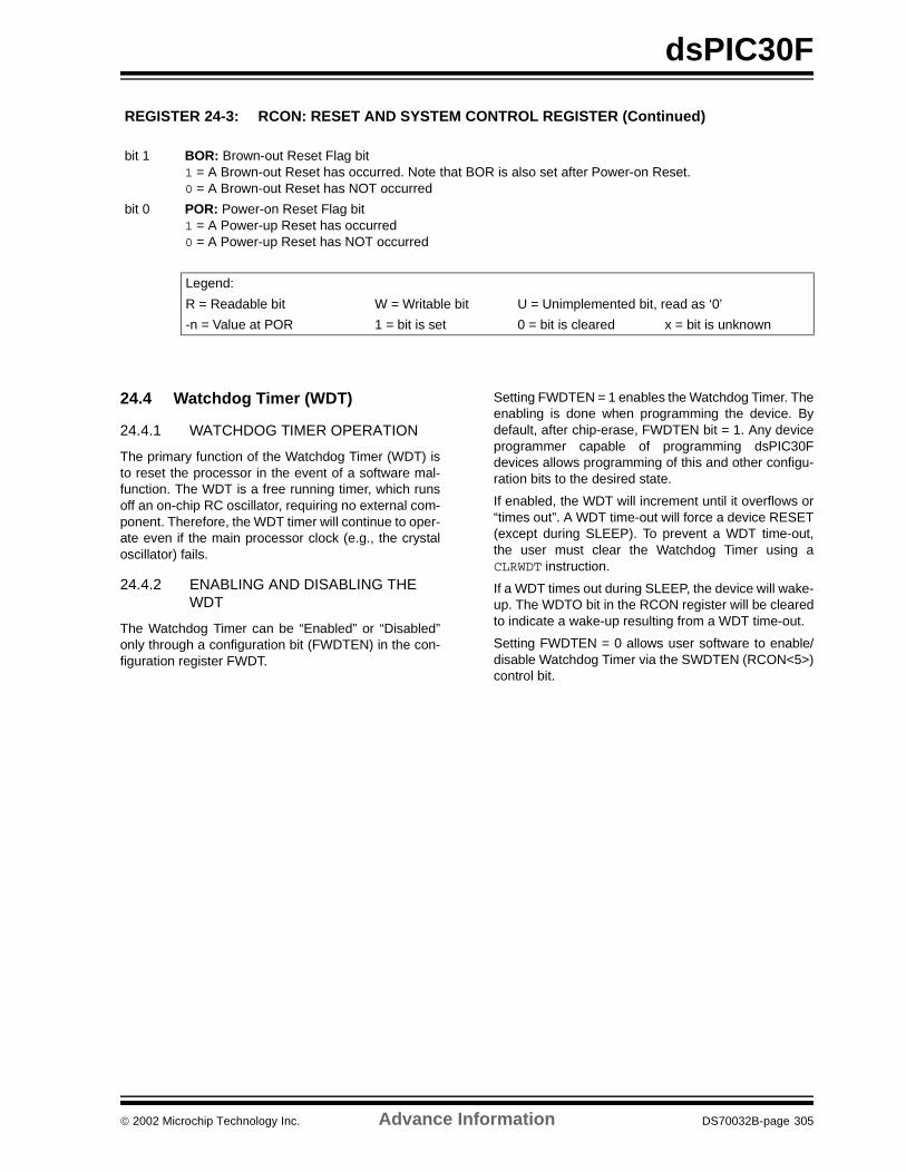
dsPIC30F
24.4 Watchdog Timer (WDT)
24.4.1 WATCHDOG TIMER OPERATION
The primary function of the Watchdog Timer (WDT) isto reset the processor in the event of a software mal-function. The WDT is a free running timer, which runsoff an on-chip RC oscillator, requiring no external com-ponent. Therefore, the WDT timer will continue to oper-ate even if the main processor clock (e.g., the crystaloscillator) fails.
24.4.2 ENABLING AND DISABLING THE WDT
The Watchdog Timer can be “Enabled” or “Disabled”only through a configuration bit (FWDTEN) in the con-figuration register FWDT.
Setting FWDTEN = 1 enables the Watchdog Timer. Theenabling is done when programming the device. Bydefault, after chip-erase, FWDTEN bit = 1. Any deviceprogrammer capable of programming dsPIC30Fdevices allows programming of this and other configu-ration bits to the desired state.
If enabled, the WDT will increment until it overflows or“times out”. A WDT time-out will force a device RESET(except during SLEEP). To prevent a WDT time-out,the user must clear the Watchdog Timer using aCLRWDT instruction.
If a WDT times out during SLEEP, the device will wake-up. The WDTO bit in the RCON register will be clearedto indicate a wake-up resulting from a WDT time-out.
Setting FWDTEN = 0 allows user software to enable/disable Watchdog Timer via the SWDTEN (RCON<5>)control bit.
REGISTER 24-3: RCON: RESET AND SYSTEM CONTROL REGISTER (Continued)
bit 1 BOR: Brown-out Reset Flag bit1 = A Brown-out Reset has occurred. Note that BOR is also set after Power-on Reset.0 = A Brown-out Reset has NOT occurred
bit 0 POR: Power-on Reset Flag bit1 = A Power-up Reset has occurred0 = A Power-up Reset has NOT occurred
Legend:
R = Readable bit W = Writable bit U = Unimplemented bit, read as ‘0’
-n = Value at POR 1 = bit is set 0 = bit is cleared x = bit is unknown
2002 Microchip Technology Inc. Advance Information DS70032B-page 305
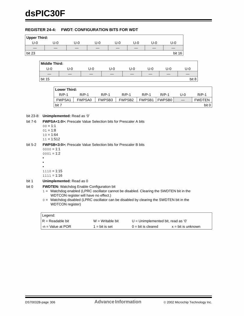
dsPIC30F
REGISTER 24-4: FWDT: CONFIGURATION BITS FOR WDT
Upper Third:U-0 U-0 U-0 U-0 U-0 U-0 U-0 U-0— — — — — — — —
bit 23 bit 16
Middle Third:U-0 U-0 U-0 U-0 U-0 U-0 U-0 U-0— — — — — — — —
bit 15 bit 8
Lower Third:R/P-1 R/P-1 R/P-1 R/P-1 R/P-1 R/P-1 U-0 R/P-1
FWPSA1 FWPSA0 FWPSB3 FWPSB2 FWPSB1 FWPSB0 — FWDTENbit 7 bit 0
bit 23-8: Unimplemented: Read as ‘0’
bit 7-6 FWPSA<1:0>: Prescale Value Selection bits for Prescaler A bits00 = 1:101 = 1:810 = 1:6411 = 1:512
bit 5-2 FWPSB<3:0>: Prescale Value Selection bits for Prescaler B bits0000 = 1:10001 = 1:2•••1110 = 1:151111 = 1:16
bit 1 Unimplemented: Read as 0
bit 0 FWDTEN: Watchdog Enable Configuration bit1 = Watchdog enabled (LPRC oscillator cannot be disabled. Clearing the SWDTEN bit in the
WDTCON register will have no effect.)0 = Watchdog disabled (LPRC oscillator can be disabled by clearing the SWDTEN bit in the
WDTCON register)
Legend:
R = Readable bit W = Writable bit U = Unimplemented bit, read as ‘0’
-n = Value at POR 1 = bit is set 0 = bit is cleared x = bit is unknown
DS70032B-page 306 Advance Information 2002 Microchip Technology Inc.
dsPIC30F
24.5 Power Saving Modes
There are two power saving states that can be enteredthrough the execution of a special instruction, PWRSAV.
These are: SLEEP and IDLE.
The format of the PWRSAV instruction is as follows:
PWRSAV <parameter>, where ‘parameter’ definesIDLE or SLEEP mode.
24.5.1 SLEEP MODE
In SLEEP mode, the clock to the CPU and the periph-erals is shut-down. If an on-chip oscillator is beingused, it is shut-down.
The fail safe clock monitor is not functional duringSLEEP, since there is no clock to monitor. However,LPRC clock remains active if WDT is operational dur-ing SLEEP.
The Brown-out protection circuit and the Low VoltageDetect circuit, if enabled, will remain functional duringSLEEP.
The processor wakes up from SLEEP if at least one ofthe following conditions is true:
• on occurrence of any interrupt that is individually enabled and meets the required priority level
• on any RESET (POR, BOR and MCLR) • on WDT time-out
On waking up from SLEEP mode, the processor willrestart the same clock that was active prior to entryinto SLEEP mode. When clock switching is enabled,bits COSC<1:0> will determine the oscillator sourcethat will be used on wake-up. If clock switch is dis-abled, then there is only one system clock.
If the clock source is an oscillator, the clock to thedevice will be held off until OST times out (indicating astable oscillator). If PLL is used, the system clock isheld off until LOCK = 1 (indicating that the PLL is sta-ble). In either case, TPOR, TLOCK and TPWRT delaysare applied.
If EC, FRC, LPRC or EXTRC oscillators are used,then the start-up delay will be a few cycles. A delay ofTPOR (~ 10 µs) is applied. This is the smallest delaypossible on wake-up from SLEEP.
Moreover, if LP oscillator was active during SLEEP,and LP is the oscillator used on wake-up, then thestart-up delay will be equal to TPOR. PWRT delay andOST timer delay are not applied. In order to have thesmallest possible start-up delay when waking up fromSLEEP, then one of these faster wake-up optionsshould be selected before entering SLEEP.
Any interrupt that is individually enabled (using thecorresponding IE bit) and meets the prevailing prioritylevel will be able to wake-up the processor. If controlbit GIE = 1, then the processor will process the inter-rupt and branch to the ISR. If GIE = 0, then the proces-sor will simply continue execution, starting with theinstruction immediately following the SLEEP instruc-tion. The SLEEP status bit in RCON register is setupon wake-up.
All RESETS will wake-up the processor from SLEEPmode. Any RESET, other than POR, will set theSLEEP status bit. In a POR Reset, the SLEEP bit iscleared.
If Watchdog Timer is enabled, then upon WDT time-out, the processor will wake-up from SLEEP mode.SLEEP and WDTO status bits are both set.
24.5.2 IDLE MODE
In IDLE mode, the clock to the CPU is shut-down whileperipherals keep running. Unlike SLEEP mode, theclock source remains active.
Several peripherals have a control bit in each module,that allows them to operate during IDLE.
LPRC fail safe clock remains active if clock failuredetect is enabled.
The processor wakes up from IDLE if at least one ofthe following conditions is true:
• on any interrupt that is individually enabled (IE bit is ‘1’) and meets the required priority level
• on any RESET (POR, BOR, MCLR)• on WDT time-out
Upon wake-up from IDLE mode, the clock is re-appliedto the CPU and instruction execution begins immedi-ately, starting with the instruction following the PWRSAVinstruction.
Note: If a POR or BOR Reset occurred, theselection of the oscillator is based on theFOS<1:0> and FPR<3:0> configurationbits.
Note: In spite of various delays applied (TPOR,TLOCK and TPWRT) the crystal oscillator(and PLL) may not be active at the end ofthe time-out, e.g., for low frequency crys-tals. In such cases, if FSCM is enabled,then the device will detect this as a clockfailure and process the Clock Failure Trap,the FRC oscillator will be enabled, and theuser will have to re-enable the crystal oscil-lator. If FSCM is not enabled, then thedevice will simply suspend execution ofcode until the clock is stable, and willremain in SLEEP until the oscillator clockhas started.
2002 Microchip Technology Inc. Advance Information DS70032B-page 307
dsPIC30F
Any interrupt that is individually enabled (using IE bit)and meets the prevailing priority level, will be able towake-up the processor. If control bit GIE = 1, then theprocessor will process the interrupt and branch to theISR. If GIE = 0, then the processor will continue exe-cution with the instruction immediately following thePWRSAV instruction. The IDLE status bit in RCON reg-ister is set upon wake-up.
Any RESET other than POR will set the IDLE statusbit. On a POR Reset, the IDLE bit is cleared.
If Watchdog Timer is enabled, then upon WDT time-out, the processor will wake-up from IDLE mode. IDLEand WDTO status bits are both set.
Unlike wake-up from SLEEP, there are no time delaysinvolved in wake-up from IDLE.
24.6 In-Circuit Serial Programming
(TBD)
DS70032B-page 308 Advance Information 2002 Microchip Technology Inc.
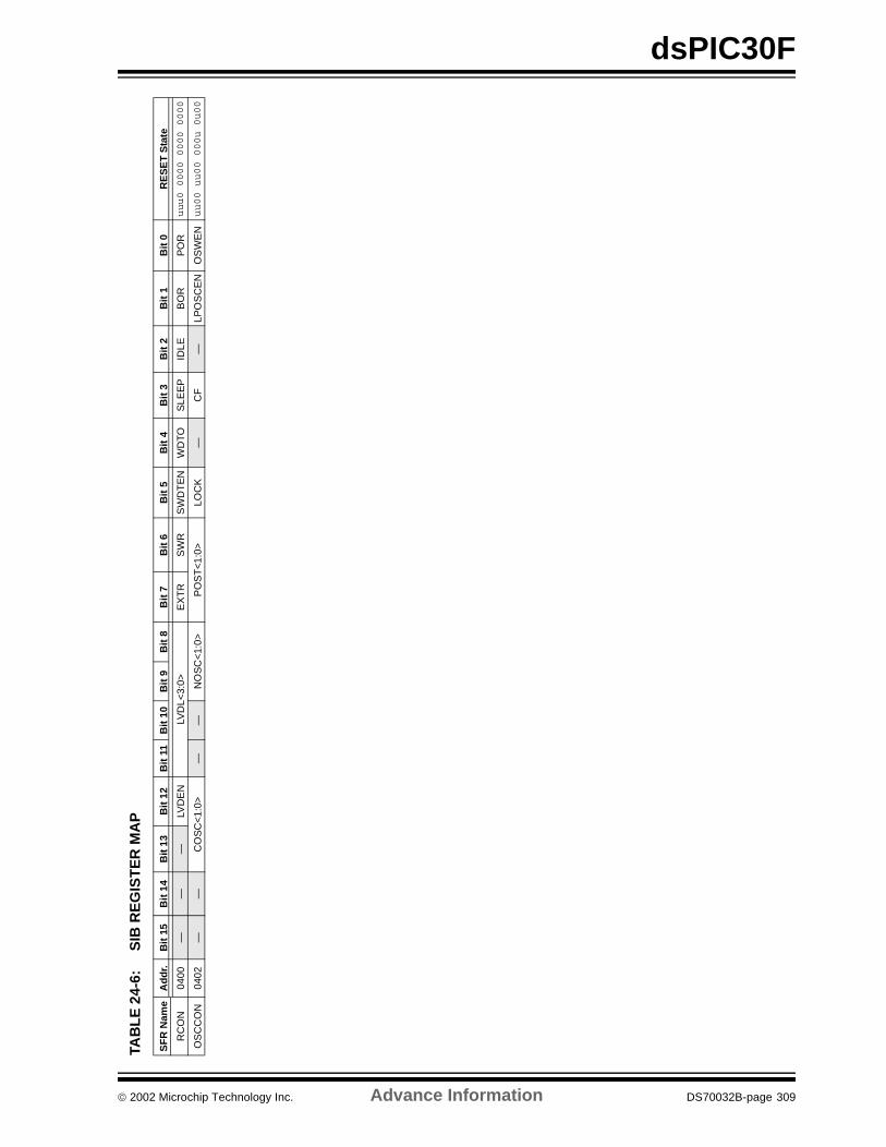
dsPIC30F
TAB
LE
24-
6:S
IB R
EG
IST
ER
MA
P
SF
R N
ame
Ad
dr.
Bit
15
Bit
14
Bit
13
Bit
12
Bit
11
Bit
10
Bit
9B
it 8
Bit
7B
it 6
Bit
5B
it 4
Bit
3B
it 2
Bit
1B
it 0
RE
SE
T S
tate
RC
ON
0400
——
—LV
DE
NLV
DL<
3:0>
EX
TR
SW
RS
WD
TE
NW
DT
OS
LEE
PID
LEB
OR
PO
Ruuu0 0000 0000 0000
OS
CC
ON
0402
——
CO
SC
<1:
0>—
—N
OS
C<
1:0>
PO
ST
<1:
0>LO
CK
—C
F—
LPO
SC
EN
OS
WE
Nuu00 uu00 000u 0u00
2002 Microchip Technology Inc. Advance Information DS70032B-page 309

dsPIC30F
NOTES:
DS70032B-page 310 Advance Information 2002 Microchip Technology Inc.
dsPIC30F
25.0 INSTRUCTION SET SUMMARY
The dsPIC30F instruction set adds manyenhancements to the previous PICmicro® instructionsets, while maintaining an easy migration fromPICmicro instruction sets.
Most instructions are a single program memory word(24-bits), but there are three instructions that requiretwo program memory locations.
Each single-word instruction is a 24-bit word dividedinto an 8-bit opcode, which specifies the instructiontype and one or more operands, which further specifythe operation of the instruction.
The instruction set is highly orthogonal and is groupedinto five basic categories:
• Word or byte-oriented operations• Bit-oriented operations• Literal operations
• DSP operations• Control operations
Table 25-1 shows the general symbols used in describ-ing the instructions.
The dsPIC30F instruction set summary in Table 25-2lists all the instructions along with the status flagsaffected by each instruction.
Most word or byte-oriented W register instructions(including barrel shift instructions) have three oper-ands:
• The first source operand, which is typically a reg-ister ’Wb’ without any address modifier
• The second source operand, which is typically a register ’Ws’ with or without an address modifier
• The destination of the result, which is typically a register ’Wd’ with or without an address modifier
However, word or byte-oriented file register instructionshave two operands:
• The file register specified by the value ’f’• The destination, which could either be the file reg-
ister ’f’ or the W0 register, which is denoted as ’WREG’
The destination designator ‘d’ specifies where theresult of the operation is to be placed. If 'd' is zero, theresult is placed in WREG. If 'd' is one, the result isplaced in the file register specified in the instruction.
Most bit-oriented instructions (including simple rotate/shift instructions) have two operands:
• The W register (with or without an address modi-fier) or file register (specified by the value of ’Ws’ or ’f’)
• The bit in the W register or file register (specified by a literal value, or indirectly by the contents of register ’Wb’)
The literal instructions that involve data movementmay use some of the following operands:
• A literal value to be loaded into a W register or file register (specified by the value of ’k’)
• The desired W register or file register to load the literal value into (specified by ’Wb’ or ’f’)
However, literal instructions that involve arithmetic orlogical operations use some of the following operands:
• The first source operand, which is a register ’Wb’ without any address modifier
• The second source operand, which is a literal value
• The destination of the result (only if not the same as the first source operand), which is typically a register ’Wd’ with or without an address modifier
The MAC class of DSP instructions may use some of thefollowing operands:
• The accumulator (A or B) to be used• The W registers to be used as the two operands
• The X and Y address space pre-fetch operations• The X and Y address space pre-fetch destinations• The accumulator write-back destination
The other DSP instructions do not involve any multipli-cation, and may include:
• The accumulator to be used• The source or destination operand (designated as
Wso or Wdo, respectively) with or without an address modifier
• The amount of shift (in the case of accumulator shift instructions), specified by a W register ’Wn’ or a literal value
The control instructions may use some of the followingoperands:
• A program memory address • The mode of the Table Read and Table Write
instructions • No operand required
All instructions are a single-word, except for certaindouble-word instructions, which were made double-word instructions so that all the required information isavailable in these 48-bits. In the second word, the8 MSb’s are 0’s. If this second word is executed as aninstruction (by itself), it will execute as a NOP.
2002 Microchip Technology Inc. Advance Information DS70032B-page 311
dsPIC30F
Most single-word instructions are executed in a singleinstruction cycle, unless a conditional test is true or theprogram counter is changed as a result of the instruc-tion. In these cases, the execution takes two instructioncycles with the additional instruction cycle(s) executedas a NOP. Notable exceptions are the BRA (uncondi-tional/computed branch), indirect CALL/GOTO, allTable Reads and Writes, TRAP, and RETURN/RETFIEinstructions, which are single-word instructions but taketwo cycles. Certain instructions that involve skippingover the subsequent instruction, require either two orthree cycles if the skip is performed, depending onwhether the instruction being skipped is a single-wordor two-word instruction. Moreover, double-word movesrequire two cycles.
The double-word instructions execute in two instructioncycles.
One instruction cycle consists of four oscillator periods.Thus, for an oscillator frequency of 120 MHz, the nor-mal instruction execution time is 0.033 µs. If a condi-tional test is true or the program counter is changed asa result of an instruction, the instruction execution timeis 0.066 µs.
Note: For more details on the instruction set, referto the Programmer’s Reference Manual.
TABLE 25-1: SYMBOLS USED IN ROADRUNNER OPCODE DESCRIPTIONS
Field Description
#text Means literal defined by “text“(text) Means “content of text“.b Byte mode selection
.d Double-word mode selection
.S Shadow register select
.w Word mode selection (default)
[text] Means “the location addressed by text” Optional field or operation<n:m> Register bit field
Acc One of two accumulators A, BAWB Accumulator write back destination address register ∈ W13, [W13]+=2bit3 3-bit bit selection field (used in byte addressed instructions) ∈ 0...7
bit4 4-bit bit selection field (used in word addressed instructions) ∈ 0...15C, DC, N, OV, SZ MCU status bits: Carry, Digit Carry, Negative, Overflow, Sticky-Zerod File register destination d ∈ WREG, none
Expr Absolute address, label or expression (resolved by the linker)f File register address ∈ 0x0000...0x1FFFlit1 1-bit unsigned literal ∈ 0,1
lit14 14-bit unsigned literal ∈ 0...16384lit16 16-bit unsigned literal ∈ 0...65535lit23 23-bit unsigned literal ∈ 0...8388608; LSB must be 0
lit4 4-bit unsigned literal ∈ 0...15lit5 5-bit unsigned literal ∈ 0...31lit8 8-bit unsigned literal ∈ 0...255
lit10 10-bit unsigned literal ∈ 0...255 for Byte mode, 0:1023 for Word modeNone field does not require an entry, may be blankOA, OB, SA, SB DSP status bits: AccA Overflow, AccB Overflow, AccA Saturate, AccB Saturate
PC Program CounterSlit10 10-bit signed literal ∈ -512...511Slit16 16-bit signed literal ∈ -32768...32767
Slit5 5-bit signed literal ∈ -16...15text1 Œ text2, text3, ...
text1 must be in the set of text2, text3, ...
Wb Base W register ∈ W0..W15
DS70032B-page 312 Advance Information 2002 Microchip Technology Inc.
dsPIC30F
Wd Destination W register ∈ Wd, [Wd], [Wd++], [Wd--], [++Wd], [--Wd]
Wdo Destination W register ∈ Wnd, [Wnd], [Wnd++], [Wnd--], [++Wnd], [--Wnd], [Wnd+Wb]
Wm,Wn Dividend, Divisor working register pair (direct addressing)Wm*Wm Multiplicand and Multiplier working register pair for Square instructions ∈
W4*W4,W5*W5,W6*W6,W7*W7 Wm*Wn Multiplicand and Multiplier working register pair for DSP instructions ∈
W4*W5,W4*W6,W4*W7,W5*W6,W5*W7,W6*W7Wn One of 16 working registers ∈ W0..W15Wnd One of 16 destination working registers ∈ W0..W15
Wns One of 16 source working registers ∈ W0..W15WREG W0 (working register used in file register instructions)Ws Source W register ∈ Ws, [Ws], [Ws++], [Ws--], [++Ws], [--Ws]
Wso Source W register ∈ Wns, [Wns], [Wns++], [Wns--], [++Wns], [--Wns], [Wns+Wb]
Wx X data space pre-fetch address register for DSP instructions ∈ [W8]+=6, [W8]+=4, [W8]+=2, [W8], [W8]-=6, [W8]-=4, [W8]-=2, [W9]+=6, [W9]+=4, [W9]+=2, [W9], [W9]-=6, [W9]-=4, [W9]-=2, [W9+W12],none
Wxd X data space pre-fetch destination register for DSP instructions ∈ W4..W7Wy Y data space pre-fetch address register for DSP instructions
∈ [W10]+=6, [W10]+=4, [W10]+=2, [W10], [W10]-=6, [W10]-=4, [W10]-=2, [W11]+=6, [W11]+=4, [W11]+=2, [W11], [W11]-=6, [W11]-=4, [W11]-=2, [W11+W12],none
Wyd Y data space pre-fetch destination register for DSP instructions ∈ W4..W7
TABLE 25-1: SYMBOLS USED IN ROADRUNNER OPCODE DESCRIPTIONS (CONTINUED)
Field Description
2002 Microchip Technology Inc. Advance Information DS70032B-page 313
dsPIC30F
TABLE 25-2: INSTRUCTION SET OVERVIEW
BaseInstr
#
AssemblyMnemonic Assembly Syntax Description # of
words# of
cyclesStatus Flags
Affected
1 ADD ADD Acc Add Accumulators 1 1 OA,OB,SA,SB
ADD f f = f + WREG 1 1 C,DC,N,OV,SZ
ADD f,WREG WREG = f + WREG 1 1 C,DC,N,OV,SZ
ADD #lit10,Wn Wd = lit10 + Wd 1 1 C,DC,N,OV,SZ
ADD Wb,Ws,Wd Wd = Wb + Ws 1 1 C,DC,N,OV,SZ
ADD Wb,#lit5,Wd Wd = Wb + lit5 1 1 C,DC,N,OV,SZ
ADD Wso,#Slit4,Acc 16-bit Signed Add to Accumulator 1 1 OA,OB,SA,SB
2 ADDC ADDC f f = f + WREG + (C) 1 1 C,DC,N,OV,SZ
ADDC f,WREG WREG = f + WREG + (C) 1 1 C,DC,N,OV,SZ
ADDC #lit10,Wn Wd = lit10 + Wd + (C) 1 1 C,DC,N,OV,SZ
ADDC Wb,Ws,Wd Wd = Wb + Ws + (C) 1 1 C,DC,N,OV,SZ
ADDC Wb,#lit5,Wd Wd = Wb + lit5 + (C) 1 1 C,DC,N,OV,SZ
3 AND AND f f = f .AND. WREG 1 1 N,SZ
AND f,WREG WREG = f .AND. WREG 1 1 N,SZ
AND #lit10,Wn Wd = lit10 .AND. Wd 1 1 N,SZ
AND Wb,Ws,Wd Wd = Wb .AND. Ws 1 1 N,SZ
AND Wb,#lit5,Wd Wd = Wb .AND. lit5 1 1 N,SZ
4 ASR ASR f f = Arithmetic Right Shift f 1 1 C,N,OV,SZ
ASR f,WREG WREG = Arithmetic Right Shift f 1 1 C,N,OV,SZ
ASR Ws,Wd Wd = Arithmetic Right Shift Ws 1 1 C,N,OV,SZ
ASR Wb,Wns,Wnd Wnd = Arithmetic Right Shift Wb by Wns 1 1 N,SZ
ASR Wb,#lit5,Wnd Wnd = Arithmetic Right Shift Wb by lit5 1 1 N,SZ
5 BCLR BCLR.b f,#bit3 Bit Clear f 1 1 None
BCLR Ws,#bit4 Bit Clear Ws 1 1 None
6 BRA BRA C,Expr Branch if Carry 1 1 (2) None
BRA GE,Expr Branch if greater than or equal 1 1 (2) None
BRA GEU,Expr Branch if unsigned greater than or equal 1 1 (2) None
BRA GT,Expr Branch if greater than 1 1 (2) None
BRA GTU,Expr Branch if unsigned greater than 1 1 (2) None
BRA LE,Expr Branch if less than or equal 1 1 (2) None
BRA LEU,Expr Branch if unsigned less than or equal 1 1 (2) None
BRA LT,Expr Branch if less than 1 1 (2) None
BRA LTU,Expr Branch if unsigned less than 1 1 (2) None
BRA N,Expr Branch if Negative 1 1 (2) None
BRA NC,Expr Branch if Not Carry 1 1 (2) None
BRA NN,Expr Branch if Not Negative 1 1 (2) None
BRA NOV,Expr Branch if Not Overflow 1 1 (2) None
BRA NZ,Expr Branch if Not Zero 1 1 (2) None
BRA OA,Expr Branch if accumulator A overflow 1 1 (2) None
BRA OB,Expr Branch if accumulator B overflow 1 1 (2) None
BRA OV,Expr Branch if Overflow 1 1 (2) None
BRA SA,Expr Branch if accumulator A saturated 1 1 (2) None
BRA SB,Expr Branch if accumulator B saturated 1 1 (2) None
BRA Expr Branch Unconditionally 1 2 None
BRA Z,Expr Branch if Zero 1 1 (2) None
BRA Wn Computed Branch 1 2 None
7 BSET BSET.b f,#bit3 Bit Set f 1 1 None
BSET Ws,#bit4 Bit Set Ws 1 1 None
8 BSW BSW.C Ws,Wb Write C bit to Ws<Wb> 1 1 None
BSW.Z Ws,Wb Write SZ bit to Ws<Wb> 1 1 None
9 BTG BTG.b f,#bit3 Bit Toggle f 1 1 None
BTG Ws,#bit4 Bit Toggle Ws 1 1 None
10 BTSC BTSC.b f,#bit3 Bit Test f, Skip if Clear 1 1 (2 or 3)
None
BTSC Ws,#bit4 Bit Test Ws, Skip if Clear 1 1 (2 or 3)
None
DS70032B-page 314 Advance Information 2002 Microchip Technology Inc.
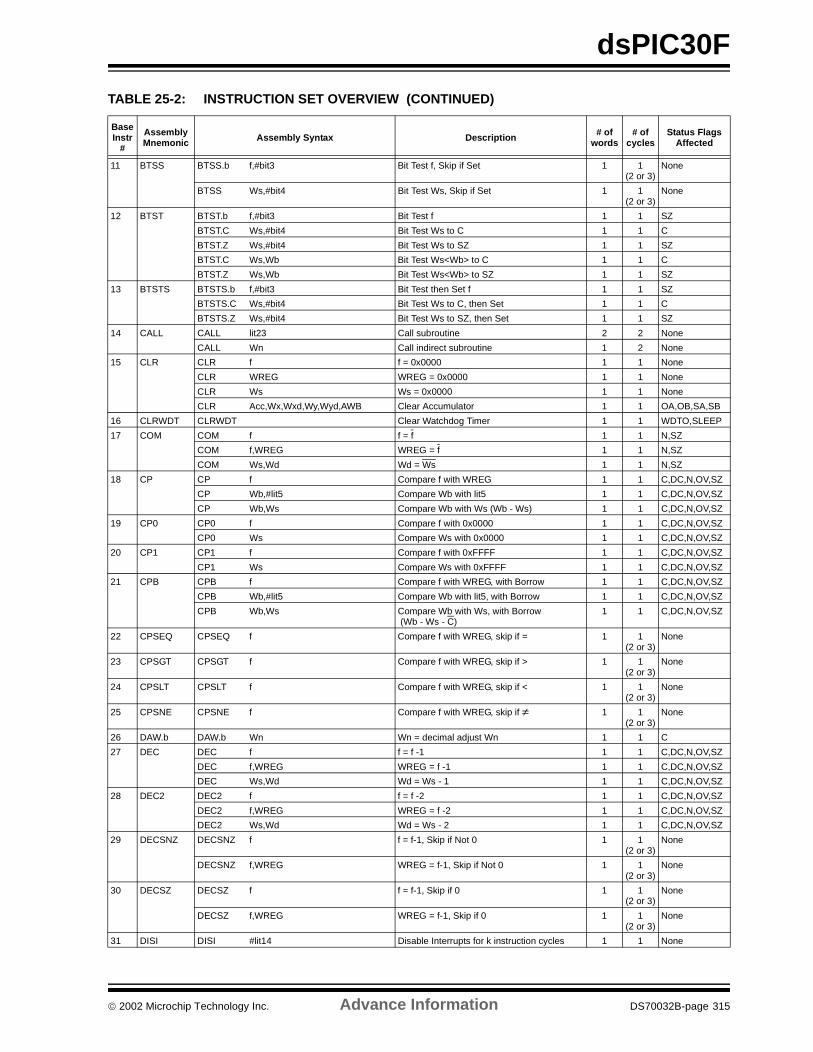
dsPIC30F
11 BTSS BTSS.b f,#bit3 Bit Test f, Skip if Set 1 1 (2 or 3)
None
BTSS Ws,#bit4 Bit Test Ws, Skip if Set 1 1 (2 or 3)
None
12 BTST BTST.b f,#bit3 Bit Test f 1 1 SZ
BTST.C Ws,#bit4 Bit Test Ws to C 1 1 C
BTST.Z Ws,#bit4 Bit Test Ws to SZ 1 1 SZ
BTST.C Ws,Wb Bit Test Ws<Wb> to C 1 1 C
BTST.Z Ws,Wb Bit Test Ws<Wb> to SZ 1 1 SZ
13 BTSTS BTSTS.b f,#bit3 Bit Test then Set f 1 1 SZ
BTSTS.C Ws,#bit4 Bit Test Ws to C, then Set 1 1 C
BTSTS.Z Ws,#bit4 Bit Test Ws to SZ, then Set 1 1 SZ
14 CALL CALL lit23 Call subroutine 2 2 None
CALL Wn Call indirect subroutine 1 2 None
15 CLR CLR f f = 0x0000 1 1 None
CLR WREG WREG = 0x0000 1 1 None
CLR Ws Ws = 0x0000 1 1 None
CLR Acc,Wx,Wxd,Wy,Wyd,AWB Clear Accumulator 1 1 OA,OB,SA,SB
16 CLRWDT CLRWDT Clear Watchdog Timer 1 1 WDTO,SLEEP
17 COM COM f f = f 1 1 N,SZ
COM f,WREG WREG = f 1 1 N,SZ
COM Ws,Wd Wd = Ws 1 1 N,SZ
18 CP CP f Compare f with WREG 1 1 C,DC,N,OV,SZ
CP Wb,#lit5 Compare Wb with lit5 1 1 C,DC,N,OV,SZ
CP Wb,Ws Compare Wb with Ws (Wb - Ws) 1 1 C,DC,N,OV,SZ
19 CP0 CP0 f Compare f with 0x0000 1 1 C,DC,N,OV,SZ
CP0 Ws Compare Ws with 0x0000 1 1 C,DC,N,OV,SZ
20 CP1 CP1 f Compare f with 0xFFFF 1 1 C,DC,N,OV,SZ
CP1 Ws Compare Ws with 0xFFFF 1 1 C,DC,N,OV,SZ
21 CPB CPB f Compare f with WREG, with Borrow 1 1 C,DC,N,OV,SZ
CPB Wb,#lit5 Compare Wb with lit5, with Borrow 1 1 C,DC,N,OV,SZ
CPB Wb,Ws Compare Wb with Ws, with Borrow (Wb - Ws - C)
1 1 C,DC,N,OV,SZ
22 CPSEQ CPSEQ f Compare f with WREG, skip if = 1 1 (2 or 3)
None
23 CPSGT CPSGT f Compare f with WREG, skip if > 1 1 (2 or 3)
None
24 CPSLT CPSLT f Compare f with WREG, skip if < 1 1 (2 or 3)
None
25 CPSNE CPSNE f Compare f with WREG, skip if ≠ 1 1 (2 or 3)
None
26 DAW.b DAW.b Wn Wn = decimal adjust Wn 1 1 C
27 DEC DEC f f = f -1 1 1 C,DC,N,OV,SZ
DEC f,WREG WREG = f -1 1 1 C,DC,N,OV,SZ
DEC Ws,Wd Wd = Ws - 1 1 1 C,DC,N,OV,SZ
28 DEC2 DEC2 f f = f -2 1 1 C,DC,N,OV,SZ
DEC2 f,WREG WREG = f -2 1 1 C,DC,N,OV,SZ
DEC2 Ws,Wd Wd = Ws - 2 1 1 C,DC,N,OV,SZ
29 DECSNZ DECSNZ f f = f-1, Skip if Not 0 1 1 (2 or 3)
None
DECSNZ f,WREG WREG = f-1, Skip if Not 0 1 1 (2 or 3)
None
30 DECSZ DECSZ f f = f-1, Skip if 0 1 1 (2 or 3)
None
DECSZ f,WREG WREG = f-1, Skip if 0 1 1 (2 or 3)
None
31 DISI DISI #lit14 Disable Interrupts for k instruction cycles 1 1 None
TABLE 25-2: INSTRUCTION SET OVERVIEW (CONTINUED)
BaseInstr
#
AssemblyMnemonic Assembly Syntax Description # of
words# of
cyclesStatus Flags
Affected
2002 Microchip Technology Inc. Advance Information DS70032B-page 315
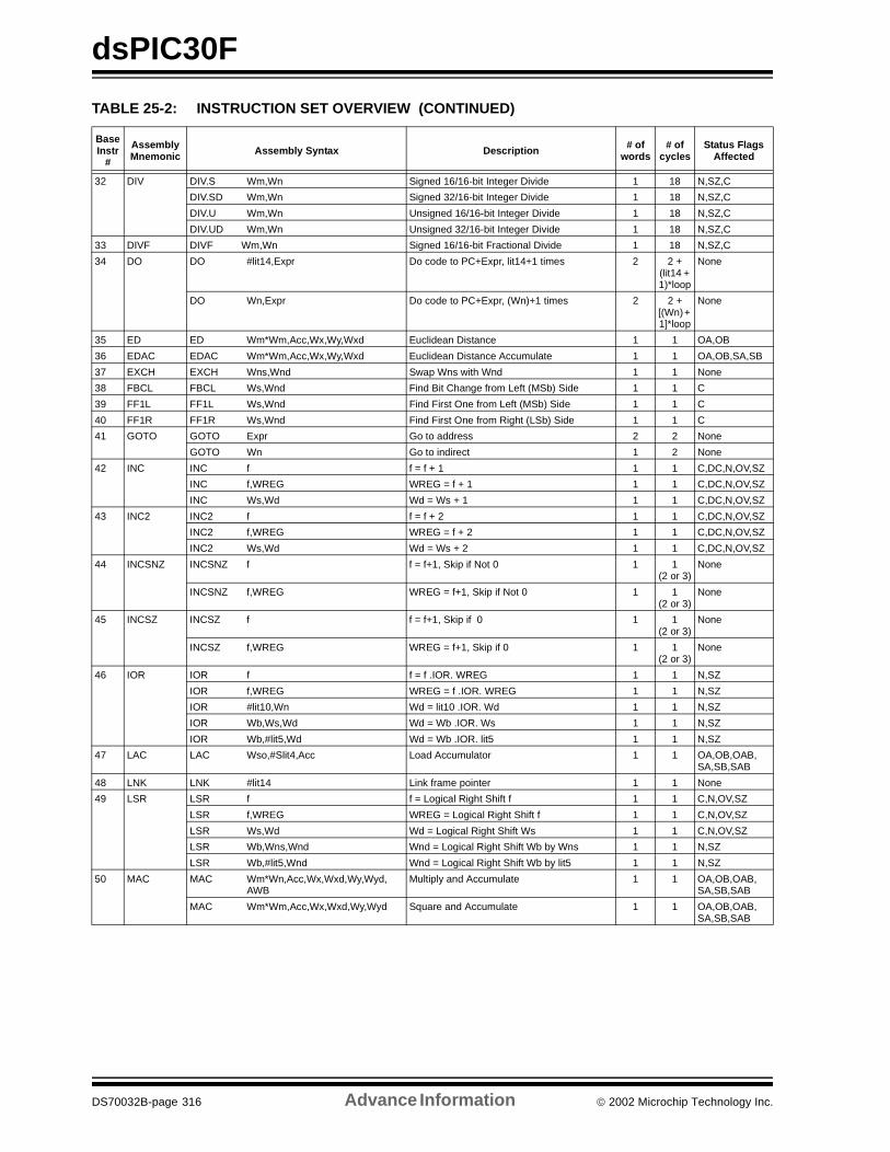
dsPIC30F
32 DIV DIV.S Wm,Wn Signed 16/16-bit Integer Divide 1 18 N,SZ,C
DIV.SD Wm,Wn Signed 32/16-bit Integer Divide 1 18 N,SZ,C
DIV.U Wm,Wn Unsigned 16/16-bit Integer Divide 1 18 N,SZ,C
DIV.UD Wm,Wn Unsigned 32/16-bit Integer Divide 1 18 N,SZ,C
33 DIVF DIVF Wm,Wn Signed 16/16-bit Fractional Divide 1 18 N,SZ,C
34 DO DO #lit14,Expr Do code to PC+Expr, lit14+1 times 2 2 + (lit14 + 1)*loop
None
DO Wn,Expr Do code to PC+Expr, (Wn)+1 times 2 2 + [(Wn) + 1]*loop
None
35 ED ED Wm*Wm,Acc,Wx,Wy,Wxd Euclidean Distance 1 1 OA,OB
36 EDAC EDAC Wm*Wm,Acc,Wx,Wy,Wxd Euclidean Distance Accumulate 1 1 OA,OB,SA,SB
37 EXCH EXCH Wns,Wnd Swap Wns with Wnd 1 1 None
38 FBCL FBCL Ws,Wnd Find Bit Change from Left (MSb) Side 1 1 C
39 FF1L FF1L Ws,Wnd Find First One from Left (MSb) Side 1 1 C
40 FF1R FF1R Ws,Wnd Find First One from Right (LSb) Side 1 1 C
41 GOTO GOTO Expr Go to address 2 2 None
GOTO Wn Go to indirect 1 2 None
42 INC INC f f = f + 1 1 1 C,DC,N,OV,SZ
INC f,WREG WREG = f + 1 1 1 C,DC,N,OV,SZ
INC Ws,Wd Wd = Ws + 1 1 1 C,DC,N,OV,SZ
43 INC2 INC2 f f = f + 2 1 1 C,DC,N,OV,SZ
INC2 f,WREG WREG = f + 2 1 1 C,DC,N,OV,SZ
INC2 Ws,Wd Wd = Ws + 2 1 1 C,DC,N,OV,SZ
44 INCSNZ INCSNZ f f = f+1, Skip if Not 0 1 1 (2 or 3)
None
INCSNZ f,WREG WREG = f+1, Skip if Not 0 1 1 (2 or 3)
None
45 INCSZ INCSZ f f = f+1, Skip if 0 1 1 (2 or 3)
None
INCSZ f,WREG WREG = f+1, Skip if 0 1 1 (2 or 3)
None
46 IOR IOR f f = f .IOR. WREG 1 1 N,SZ
IOR f,WREG WREG = f .IOR. WREG 1 1 N,SZ
IOR #lit10,Wn Wd = lit10 .IOR. Wd 1 1 N,SZ
IOR Wb,Ws,Wd Wd = Wb .IOR. Ws 1 1 N,SZ
IOR Wb,#lit5,Wd Wd = Wb .IOR. lit5 1 1 N,SZ
47 LAC LAC Wso,#Slit4,Acc Load Accumulator 1 1 OA,OB,OAB,SA,SB,SAB
48 LNK LNK #lit14 Link frame pointer 1 1 None
49 LSR LSR f f = Logical Right Shift f 1 1 C,N,OV,SZ
LSR f,WREG WREG = Logical Right Shift f 1 1 C,N,OV,SZ
LSR Ws,Wd Wd = Logical Right Shift Ws 1 1 C,N,OV,SZ
LSR Wb,Wns,Wnd Wnd = Logical Right Shift Wb by Wns 1 1 N,SZ
LSR Wb,#lit5,Wnd Wnd = Logical Right Shift Wb by lit5 1 1 N,SZ
50 MAC MAC Wm*Wn,Acc,Wx,Wxd,Wy,Wyd,AWB
Multiply and Accumulate 1 1 OA,OB,OAB,SA,SB,SAB
MAC Wm*Wm,Acc,Wx,Wxd,Wy,Wyd Square and Accumulate 1 1 OA,OB,OAB,SA,SB,SAB
TABLE 25-2: INSTRUCTION SET OVERVIEW (CONTINUED)
BaseInstr
#
AssemblyMnemonic Assembly Syntax Description # of
words# of
cyclesStatus Flags
Affected
DS70032B-page 316 Advance Information 2002 Microchip Technology Inc.
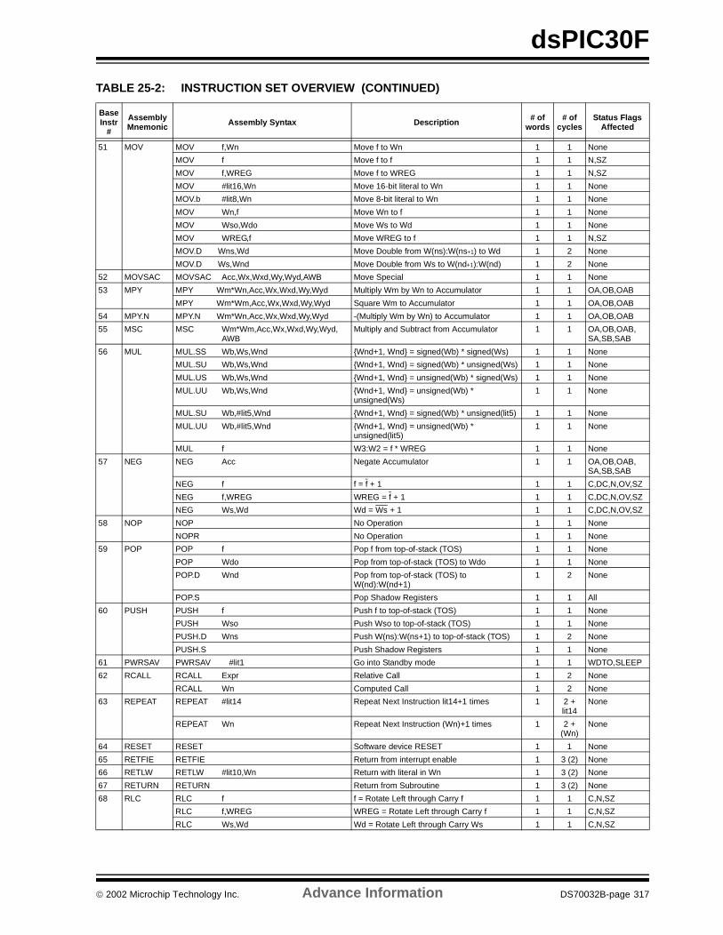
dsPIC30F
51 MOV MOV f,Wn Move f to Wn 1 1 None
MOV f Move f to f 1 1 N,SZ
MOV f,WREG Move f to WREG 1 1 N,SZ
MOV #lit16,Wn Move 16-bit literal to Wn 1 1 None
MOV.b #lit8,Wn Move 8-bit literal to Wn 1 1 None
MOV Wn,f Move Wn to f 1 1 None
MOV Wso,Wdo Move Ws to Wd 1 1 None
MOV WREG,f Move WREG to f 1 1 N,SZ
MOV.D Wns,Wd Move Double from W(ns):W(ns+1) to Wd 1 2 None
MOV.D Ws,Wnd Move Double from Ws to W(nd+1):W(nd) 1 2 None
52 MOVSAC MOVSAC Acc,Wx,Wxd,Wy,Wyd,AWB Move Special 1 1 None
53 MPY MPY Wm*Wn,Acc,Wx,Wxd,Wy,Wyd Multiply Wm by Wn to Accumulator 1 1 OA,OB,OAB
MPY Wm*Wm,Acc,Wx,Wxd,Wy,Wyd Square Wm to Accumulator 1 1 OA,OB,OAB
54 MPY.N MPY.N Wm*Wn,Acc,Wx,Wxd,Wy,Wyd -(Multiply Wm by Wn) to Accumulator 1 1 OA,OB,OAB
55 MSC MSC Wm*Wm,Acc,Wx,Wxd,Wy,Wyd,AWB
Multiply and Subtract from Accumulator 1 1 OA,OB,OAB,SA,SB,SAB
56 MUL MUL.SS Wb,Ws,Wnd Wnd+1, Wnd = signed(Wb) * signed(Ws) 1 1 None
MUL.SU Wb,Ws,Wnd Wnd+1, Wnd = signed(Wb) * unsigned(Ws) 1 1 None
MUL.US Wb,Ws,Wnd Wnd+1, Wnd = unsigned(Wb) * signed(Ws) 1 1 None
MUL.UU Wb,Ws,Wnd Wnd+1, Wnd = unsigned(Wb) * unsigned(Ws)
1 1 None
MUL.SU Wb,#lit5,Wnd Wnd+1, Wnd = signed(Wb) * unsigned(lit5) 1 1 None
MUL.UU Wb,#lit5,Wnd Wnd+1, Wnd = unsigned(Wb) * unsigned(lit5)
1 1 None
MUL f W3:W2 = f * WREG 1 1 None
57 NEG NEG Acc Negate Accumulator 1 1 OA,OB,OAB,SA,SB,SAB
NEG f f = f + 1 1 1 C,DC,N,OV,SZ
NEG f,WREG WREG = f + 1 1 1 C,DC,N,OV,SZ
NEG Ws,Wd Wd = Ws + 1 1 1 C,DC,N,OV,SZ
58 NOP NOP No Operation 1 1 None
NOPR No Operation 1 1 None
59 POP POP f Pop f from top-of-stack (TOS) 1 1 None
POP Wdo Pop from top-of-stack (TOS) to Wdo 1 1 None
POP.D Wnd Pop from top-of-stack (TOS) to W(nd):W(nd+1)
1 2 None
POP.S Pop Shadow Registers 1 1 All
60 PUSH PUSH f Push f to top-of-stack (TOS) 1 1 None
PUSH Wso Push Wso to top-of-stack (TOS) 1 1 None
PUSH.D Wns Push W(ns):W(ns+1) to top-of-stack (TOS) 1 2 None
PUSH.S Push Shadow Registers 1 1 None
61 PWRSAV PWRSAV #lit1 Go into Standby mode 1 1 WDTO,SLEEP
62 RCALL RCALL Expr Relative Call 1 2 None
RCALL Wn Computed Call 1 2 None
63 REPEAT REPEAT #lit14 Repeat Next Instruction lit14+1 times 1 2 + lit14
None
REPEAT Wn Repeat Next Instruction (Wn)+1 times 1 2 + (Wn)
None
64 RESET RESET Software device RESET 1 1 None
65 RETFIE RETFIE Return from interrupt enable 1 3 (2) None
66 RETLW RETLW #lit10,Wn Return with literal in Wn 1 3 (2) None
67 RETURN RETURN Return from Subroutine 1 3 (2) None
68 RLC RLC f f = Rotate Left through Carry f 1 1 C,N,SZ
RLC f,WREG WREG = Rotate Left through Carry f 1 1 C,N,SZ
RLC Ws,Wd Wd = Rotate Left through Carry Ws 1 1 C,N,SZ
TABLE 25-2: INSTRUCTION SET OVERVIEW (CONTINUED)
BaseInstr
#
AssemblyMnemonic Assembly Syntax Description # of
words# of
cyclesStatus Flags
Affected
2002 Microchip Technology Inc. Advance Information DS70032B-page 317
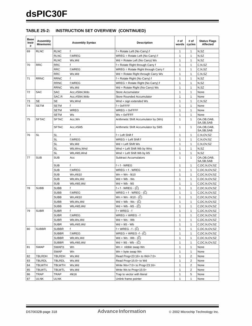
dsPIC30F
69 RLNC RLNC f f = Rotate Left (No Carry) f 1 1 N,SZ
RLNC f,WREG WREG = Rotate Left (No Carry) f 1 1 N,SZ
RLNC Ws,Wd Wd = Rotate Left (No Carry) Ws 1 1 N,SZ
70 RRC RRC f f = Rotate Right through Carry f 1 1 C,N,SZ
RRC f,WREG WREG = Rotate Right through Carry f 1 1 C,N,SZ
RRC Ws,Wd Wd = Rotate Right through Carry Ws 1 1 C,N,SZ
71 RRNC RRNC f f = Rotate Right (No Carry) f 1 1 N,SZ
RRNC f,WREG WREG = Rotate Right (No Carry) f 1 1 N,SZ
RRNC Ws,Wd Wd = Rotate Right (No Carry) Ws 1 1 N,SZ
72 SAC SAC Acc,#Slit4,Wdo Store Accumulator 1 1 None
SAC.R Acc,#Slit4,Wdo Store Rounded Accumulator 1 1 None
73 SE SE Ws,Wnd Wnd = sign extended Ws 1 1 C,N,SZ
74 SETM SETM f f = 0xFFFF 1 1 None
SETM WREG WREG = 0xFFFF 1 1 None
SETM Ws Ws = 0xFFFF 1 1 None
75 SFTAC SFTAC Acc,Wn Arithmetic Shift Accumulator by (Wn) 1 1 OA,OB,OAB,SA,SB,SAB
SFTAC Acc,#Slit5 Arithmetic Shift Accumulator by Slit5 1 1 OA,OB,OAB,SA,SB,SAB
76 SL SL f f = Left Shift f 1 1 C,N,OV,SZ
SL f,WREG WREG = Left Shift f 1 1 C,N,OV,SZ
SL Ws,Wd Wd = Left Shift Ws 1 1 C,N,OV,SZ
SL Wb,Wns,Wnd Wnd = Left Shift Wb by Wns 1 1 N,SZ
SL Wb,#lit5,Wnd Wnd = Left Shift Wb by lit5 1 1 N,SZ
77 SUB SUB Acc Subtract Accumulators 1 1 OA,OB,OAB,SA,SB,SAB
SUB f f = f - WREG 1 1 C,DC,N,OV,SZ
SUB f,WREG WREG = f - WREG 1 1 C,DC,N,OV,SZ
SUB Wn,#lit10 Wn = Wn - lit10 1 1 C,DC,N,OV,SZ
SUB Wb,Ws,Wd Wd = Wb - Ws 1 1 C,DC,N,OV,SZ
SUB Wb,#lit5,Wd Wd = Wb - lit5 1 1 C,DC,N,OV,SZ
78 SUBB SUBB f f = f - WREG - (C) 1 1 C,DC,N,OV,SZ
SUBB f,WREG WREG = f - WREG - (C) 1 1 C,DC,N,OV,SZ
SUBB Wn,#lit10 Wn = Wn - lit10 - (C) 1 1 C,DC,N,OV,SZ
SUBB Wb,Ws,Wd Wd = Wb - Ws - (C) 1 1 C,DC,N,OV,SZ
SUBB Wb,#lit5,Wd Wd = Wb - lit5 - (C) 1 1 C,DC,N,OV,SZ
79 SUBR SUBR f f = WREG - f 1 1 C,DC,N,OV,SZ
SUBR f,WREG WREG = WREG - f 1 1 C,DC,N,OV,SZ
SUBR Wb,Ws,Wd Wd = Ws - Wb 1 1 C,DC,N,OV,SZ
SUBR Wb,#lit5,Wd Wd = lit5 - Wb 1 1 C,DC,N,OV,SZ
80 SUBBR SUBBR f f = WREG - f - (C) 1 1 C,DC,N,OV,SZ
SUBBR f,WREG WREG = WREG -f - (C) 1 1 C,DC,N,OV,SZ
SUBBR Wb,Ws,Wd Wd = Ws - Wb - (C) 1 1 C,DC,N,OV,SZ
SUBBR Wb,#lit5,Wd Wd = lit5 - Wb - (C) 1 1 C,DC,N,OV,SZ
81 SWAP SWAP.b Wn Wn = nibble swap Wn 1 1 None
SWAP Wn Wn = byte swap Wn 1 1 None
82 TBLRDH TBLRDH Ws,Wd Read Prog<23:16> to Wd<7:0> 1 2 None
83 TBLRDL TBLRDL Ws,Wd Read Prog<15:0> to Wd 1 2 None
84 TBLWTH TBLWTH Ws,Wd Write Ws<7:0> to Prog<23:16> 1 2 None
85 TBLWTL TBLWTL Ws,Wd Write Ws to Prog<15:0> 1 2 None
86 TRAP TRAP #lit16 Trap to vector with literal 1 5 None
87 ULNK ULNK Unlink frame pointer 1 1 None
TABLE 25-2: INSTRUCTION SET OVERVIEW (CONTINUED)
BaseInstr
#
AssemblyMnemonic Assembly Syntax Description # of
words# of
cyclesStatus Flags
Affected
DS70032B-page 318 Advance Information 2002 Microchip Technology Inc.
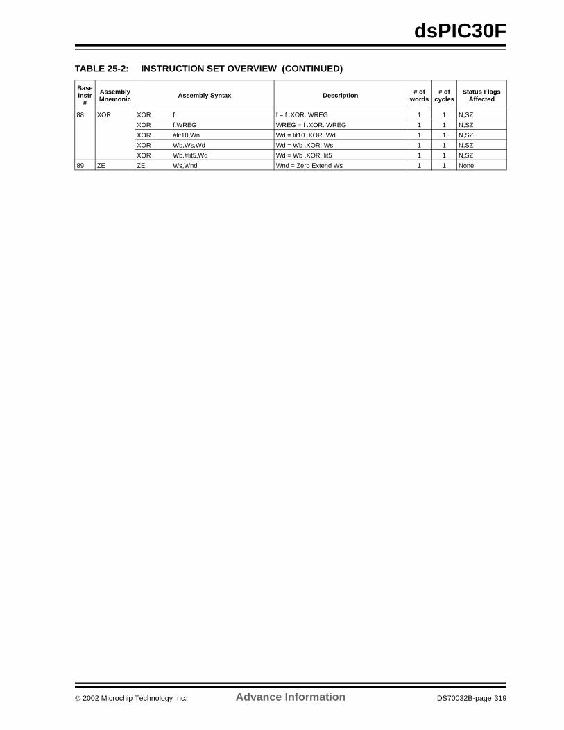
dsPIC30F
88 XOR XOR f f = f .XOR. WREG 1 1 N,SZ
XOR f,WREG WREG = f .XOR. WREG 1 1 N,SZ
XOR #lit10,Wn Wd = lit10 .XOR. Wd 1 1 N,SZ
XOR Wb,Ws,Wd Wd = Wb .XOR. Ws 1 1 N,SZ
XOR Wb,#lit5,Wd Wd = Wb .XOR. lit5 1 1 N,SZ
89 ZE ZE Ws,Wnd Wnd = Zero Extend Ws 1 1 None
TABLE 25-2: INSTRUCTION SET OVERVIEW (CONTINUED)
BaseInstr
#
AssemblyMnemonic Assembly Syntax Description # of
words# of
cyclesStatus Flags
Affected
2002 Microchip Technology Inc. Advance Information DS70032B-page 319

dsPIC30F
NOTES:
DS70032B-page 320 Advance Information 2002 Microchip Technology Inc.
dsPIC30F
26.0 DEVELOPMENT SUPPORT
Microchip is offering a comprehensive package ofdevelopment tools and libraries to support thedsPIC30F architecture. In addition, the company ispartnering with many third party tools manufacturers foradditional dsPIC30F support. The Microchip tools willinclude:
• MPLAB 6.00 Integrated Development Environ-ment (IDE)
• dsPIC30F Language Suite including MPLAB C30 C Compiler, Assembler, Linker and Librarian
• MPLAB SIM Software Simulator• MPLAB ICE 4000 In-Circuit Emulator
• MPLAB ICD 2 In-Circuit Debugger• PRO MATE II Universal Device Programmer• PICSTART Plus Development Programmer
26.1 MPLAB V6.00 Integrated Development Environment Software
The MPLAB Integrated Development Environment isavailable at no cost. The IDE gives users the flexibilityto edit, compile and emulate all from a single user inter-face. Engineers can design and develop code for thedsPIC30F in the same design environment that theyhave used for PICmicro microcontrollers.
The MPLAB IDE is a 32-bit Windows based applica-tion. It provides many advanced features for the criticalengineer in a modern, easy to use interface. MPLABIDE integrates:
• Full featured, color coded text editor
• Easy to use project manager with visual display• Source level debugging• Enhanced source level debugging for ‘C’
(Structures, automatic variables, and so on)• Customizable toolbar and key mapping
• Dynamic status bar displays processor condition at a glance
• Context sensitive, interactive on-line help• Integrated MPLAB SIM instruction simulator• User interface for PRO MATE II and PICSTART
Plus device programmers (sold separately)• User interface for MPLAB ICE 4000 In-Circuit
Emulator (sold separately)• User interface for MPLAB ICD 2 In-Circuit
Debugger
The MPLAB IDE allows the engineer to:
• Edit your source files in either assembly or ‘C’• One-touch compile and download to dsPIC30F
program memory on emulator or simulator. Updates all project information.
• Debug using:- Source files
- Machine code- Mixed mode source and machine code
The ability to use the MPLAB IDE with multipledevelopment and debugging targets, allows users toeasily switch from the cost effective simulator to a fullfeatured emulator with minimal retraining.
26.2 dsPIC30F Language Suite
The Microchip Technology MPLAB C30 C compiler is afully ANSI compliant product with standard libraries forthe dsPIC30F architecture. It is highly optimizing andtakes advantage of many dsPIC30F architecturespecific features to provide efficient software codegeneration.
MPLAB C30 also provides extensions that allow forexcellent support of the hardware, such as interruptsand peripherals. It is fully integrated with the MPLABIDE for high level, source debugging.
• 16-bit native data types
• Efficient use of register based, 3-operand instructions
• Complex Addressing modes• Efficient multi-bit shift operations• Efficient signed/unsigned comparisons
MPLAB C30 comes complete with its own assembler,linker and librarian. These allow the user to write Mixedmode C and assembly programs and link the resultingobject files into a single executable file. The compiler issold separately. The assembler, linker and librarian areavailable for free with MPLAB IDE.
26.3 MPLAB SIM Software Simulator
The MPLAB SIM software simulator allows code devel-opment in a PC-hosted environment by simulating thedsPIC30F on an instruction level. On any given instruc-tion, the data areas can be examined or modified andstimuli can be applied from a file, or user defined keypress, to any of the pins.
The execution can be performed in single step, executeuntil break, or Trace mode.
The MPLAB SIM simulator fully supports symbolicdebugging using the MPLAB C30 compiler and assem-bler. The software simulator offers the flexibility todevelop and debug code outside of the laboratory envi-ronment, making it an excellent multi-project softwaredevelopment tool.
2002 Microchip Technology Inc. Advance Information DS70032B-page 321
dsPIC30F
26.4 MPLAB ICE 4000 In-Circuit Emulator
The MPLAB ICE 4000 In-Circuit Emulator is intendedto provide the product development engineer with acomplete hardware design tool for the dsPIC30F. Soft-ware control of the emulator is provided by MPLAB,allowing editing, building, downloading and sourcedebugging from a single environment.
The MPLAB ICE 4000 is a full featured emulator sys-tem with enhanced trace, trigger and data monitoringfeatures. Interchangeable processor modules allow thesystem to be easily reconfigured for emulation of differ-ent processors. The MPLAB ICE 4000 supports theextended, high-end PICmicro microcontrollers, thePIC18CXXX and PIC18FXXX devices, as well as thedsPIC30F family of digital signal controllers. The mod-ular architecture of the MPLAB ICE in-circuit emulatorallows expansion to support new devices.
The MPLAB ICE in-circuit emulator system has beendesigned as a real-time emulation system, withadvanced features that are generally found on moreexpensive development tools.
• Full speed emulation, up to 50 MHz bus speed, or 200 MHz external clock speed
• Low voltage emulation down to 1.8 volts• Configured with 2 Mb program emulation memory,
additional modular memory up to 16 Mb• 64K x 248-bit wide Trace Memory
• Unlimited software breakpoints• Complex break, trace and trigger logic• Multi-level trigger up to 4 levels
• Filter trigger functions to trace specific event• 16-bit Pass counter for triggering on sequential
events• 16-bit Delay counter• 48-bit time stamp
• Stopwatch feature• Time between events• Statistical performance analysis
• Code coverage analysis• USB and parallel printer port PC connection
26.5 MPLAB ICD 2 In-Circuit Debugger
Microchip’s In-Circuit Debugger, MPLAB ICD, is a pow-erful, low cost, run-time development tool. This tool isbased on the PICmicro and dsPIC30F FLASH devices.The MPLAB ICD utilizes the in-circuit debugging capa-bility built into the various devices. This feature, alongwith Microchip’s In-Circuit Serial ProgrammingTM proto-col, offers cost effective, in-circuit debugging from thegraphical user interface of MPLAB ICD. This enables adesigner to develop and debug source code by watchingvariables, single-stepping and setting break points. Run-ning at full speed enables testing hardware in real-time.
• Full speed operation to the range of the device• Serial or USB PC connector
• Serial interface externally powered• USB powered from PC interface• Low noise power (VPP and VDD) for use with ana-
log and other noise sensitive applications• Operation down to 2.0V
• Can be used as an ICD or inexpensive serial programmer
• Modular application connector as MPLAB ICD• Limited number of breakpoints• “Smart watch” variable windows
• Some chip resources required (RAM, program memory and 2 pins)
26.6 PRO MATE II Universal Device Programmer
The PRO MATE II universal device programmer is a fullfeatured programmer, capable of operating in Stand-Alone mode, as well as PC-hosted mode. ThePRO MATE II device programmer is CE compliant.
The PRO MATE II device programmer has program-mable VDD and VPP supplies, which allow it to verifyprogrammed memory at VDDMIN and VDDMAX for max-imum reliability when programming, requiring thiscapability. It has an LCD display for instructions anderror messages, keys to enter commands, and inter-changeable socket modules for all package types.
In Stand-Alone mode, the PRO MATE II device pro-grammer can read, verify, or program PICmicrodevices. It can also set code protection in this mode.
• Runs under MPLAB IDE• Field upgradable firmware
• DOS Command Line interface for production• Host, Safe, and “Stand-Alone” operation• Automatic downloading of object file
• SQTPSM serialization adds unique serial number to each device programmed
• In-Circuit Serial Programming Kit (sold separately)
• Interchangeable socket modules supports all package options (sold separately)
DS70032B-page 322 Advance Information 2002 Microchip Technology Inc.
dsPIC30F
27.0 ELECTRICAL CHARACTERISTICS
Electrical characteristics are not available at this time.
2002 Microchip Technology Inc. Advance Information DS70032B-page 323

dsPIC30F
NOTES:
DS70032B-page 324 Advance Information 2002 Microchip Technology Inc.

dsPIC30F
28.0 DC AND AC CHARACTERISTICS GRAPHS AND TABLES
Graphs and tables are not available at this time.
2002 Microchip Technology Inc. Advance Information DS70032B-page 325

dsPIC30F
NOTES:
DS70032B-page 326 Advance Information 2002 Microchip Technology Inc.
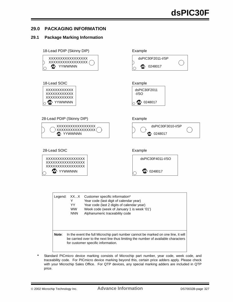
dsPIC30F
29.0 PACKAGING INFORMATION
29.1 Package Marking Information
18-Lead PDIP (Skinny DIP)
XXXXXXXXXXXXXXXXXXXXXXXXXXXXXXXXXX
YYWWNNN
Example
dsPIC30F2011-I/SP
0248017
YYWWNNNXXXXXXXXXXXXXXXXXXXXXXXX
18-Lead SOIC
XXXXXXXXXXXX
0248017
-I/SO
Example
dsPIC30F2011
XXXXXXXXXXXXXXXXXYYWWNNN
28-Lead PDIP (Skinny DIP) Example
XXXXXXXXXXXXXXXXX
0248017
dsPIC30F3010-I/SP
28-Lead SOIC
YYWWNNN
Example
XXXXXXXXXXXXXXXXXXXXXXXXXXXXXXXXXX
XXXXXXXXXXXXXXXXX
0248017
dsPIC30F4011-I/SO
Legend: XX...X Customer specific information*Y Year code (last digit of calendar year)YY Year code (last 2 digits of calendar year)WW Week code (week of January 1 is week ‘01’)NNN Alphanumeric traceability code
Note: In the event the full Microchip part number cannot be marked on one line, it willbe carried over to the next line thus limiting the number of available charactersfor customer specific information.
* Standard PICmicro device marking consists of Microchip part number, year code, week code, andtraceability code. For PICmicro device marking beyond this, certain price adders apply. Please checkwith your Microchip Sales Office. For QTP devices, any special marking adders are included in QTPprice.
2002 Microchip Technology Inc. Advance Information DS70032B-page 327
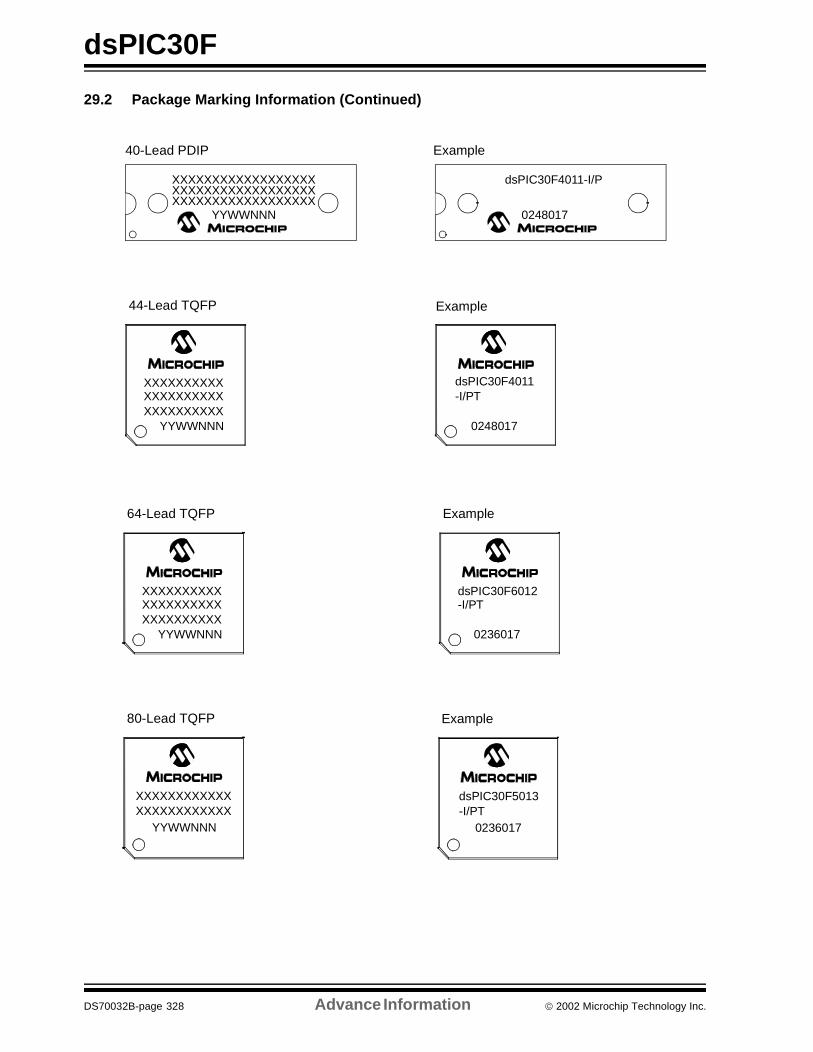
dsPIC30F
29.2 Package Marking Information (Continued)
XXXXXXXXXXXXXXXXXX
YYWWNNN
40-Lead PDIP Example
XXXXXXXXXXXXXXXXXXXXXXXXXXXXXXXXXXXX
dsPIC30F4011-I/P
0248017
44-Lead TQFP Example
XXXXXXXXXXXXXXXXXXXXXXXXXXXXXX
YYWWNNN
dsPIC30F4011-I/PT
0248017
64-Lead TQFP
XXXXXXXXXXXXXXXXXXXXXXXXXXXXXX
YYWWNNN
Example
dsPIC30F6012-I/PT
0236017
80-Lead TQFP
XXXXXXXXXXXX
YYWWNNNXXXXXXXXXXXX
Example
dsPIC30F5013
0236017-I/PT
DS70032B-page 328 Advance Information 2002 Microchip Technology Inc.
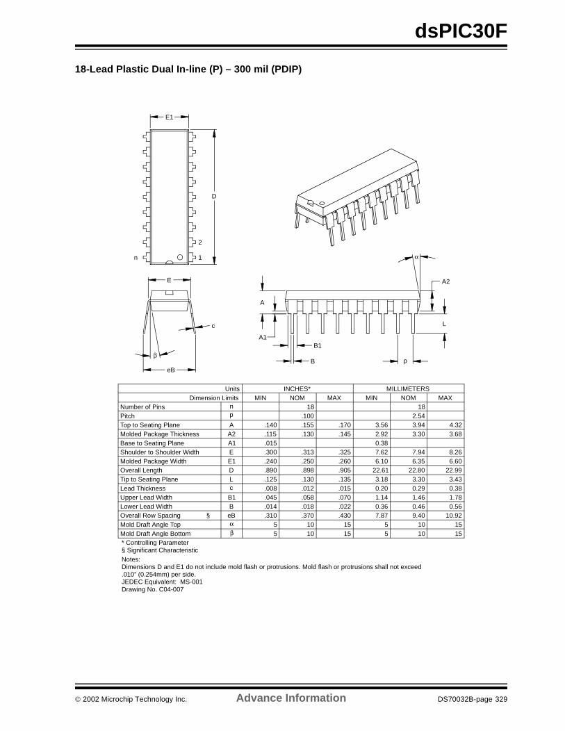
dsPIC30F
18-Lead Plastic Dual In-line (P) – 300 mil (PDIP)
1510515105βMold Draft Angle Bottom1510515105αMold Draft Angle Top
10.929.407.87.430.370.310eBOverall Row Spacing §0.560.460.36.022.018.014BLower Lead Width1.781.461.14.070.058.045B1Upper Lead Width0.380.290.20.015.012.008cLead Thickness3.433.303.18.135.130.125LTip to Seating Plane
22.9922.8022.61.905.898.890DOverall Length6.606.356.10.260.250.240E1Molded Package Width8.267.947.62.325.313.300EShoulder to Shoulder Width
0.38.015A1Base to Seating Plane3.683.302.92.145.130.115A2Molded Package Thickness4.323.943.56.170.155.140ATop to Seating Plane
2.54.100pPitch1818nNumber of Pins
MAXNOMMINMAXNOMMINDimension LimitsMILLIMETERSINCHES*Units
1
2
D
n
E1
c
eB
β
E
α
p
A2
L
B1
B
A
A1
* Controlling Parameter
Notes:Dimensions D and E1 do not include mold flash or protrusions. Mold flash or protrusions shall not exceed .010” (0.254mm) per side.JEDEC Equivalent: MS-001Drawing No. C04-007
§ Significant Characteristic
2002 Microchip Technology Inc. Advance Information DS70032B-page 329
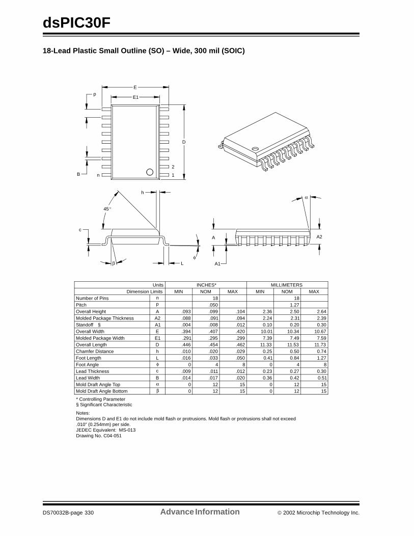
dsPIC30F
18-Lead Plastic Small Outline (SO) – Wide, 300 mil (SOIC)
Foot Angle φ 0 4 8 0 4 8
1512015120βMold Draft Angle Bottom1512015120αMold Draft Angle Top
0.510.420.36.020.017.014BLead Width0.300.270.23.012.011.009cLead Thickness
1.270.840.41.050.033.016LFoot Length0.740.500.25.029.020.010hChamfer Distance
11.7311.5311.33.462.454.446DOverall Length7.597.497.39.299.295.291E1Molded Package Width
10.6710.3410.01.420.407.394EOverall Width0.300.200.10.012.008.004A1Standoff §2.392.312.24.094.091.088A2Molded Package Thickness2.642.502.36.104.099.093AOverall Height
1.27.050pPitch1818nNumber of Pins
MAXNOMMINMAXNOMMINDimension LimitsMILLIMETERSINCHES*Units
Lβ
c
φ
h
45°
1
2
D
p
nB
E1
E
α
A2
A1
A
* Controlling Parameter
Notes:Dimensions D and E1 do not include mold flash or protrusions. Mold flash or protrusions shall not exceed .010” (0.254mm) per side.JEDEC Equivalent: MS-013Drawing No. C04-051
§ Significant Characteristic
DS70032B-page 330 Advance Information 2002 Microchip Technology Inc.
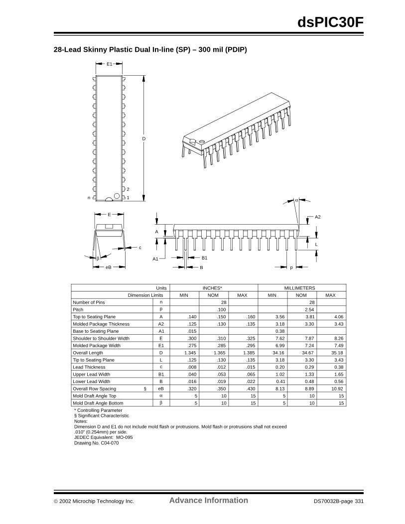
dsPIC30F
28-Lead Skinny Plastic Dual In-line (SP) – 300 mil (PDIP)
1510515105βMold Draft Angle Bottom
1510515105αMold Draft Angle Top
10.928.898.13.430.350.320eBOverall Row Spacing §
0.560.480.41.022.019.016BLower Lead Width
1.651.331.02.065.053.040B1Upper Lead Width
0.380.290.20.015.012.008cLead Thickness
3.433.303.18.135.130.125LTip to Seating Plane
35.1834.6734.161.3851.3651.345DOverall Length
7.497.246.99.295.285.275E1Molded Package Width
8.267.877.62.325.310.300EShoulder to Shoulder Width
0.38.015A1Base to Seating Plane
3.433.303.18.135.130.125A2Molded Package Thickness
4.063.813.56.160.150.140ATop to Seating Plane
2.54.100pPitch
2828nNumber of Pins
MAXNOMMINMAXNOMMINDimension Limits
MILLIMETERSINCHES*Units
2
1
D
n
E1
c
eB
β
E
α
p
L
A2
B
B1
A
A1
Notes:
JEDEC Equivalent: MO-095Drawing No. C04-070
* Controlling Parameter
Dimension D and E1 do not include mold flash or protrusions. Mold flash or protrusions shall not exceed .010” (0.254mm) per side.
§ Significant Characteristic
2002 Microchip Technology Inc. Advance Information DS70032B-page 331
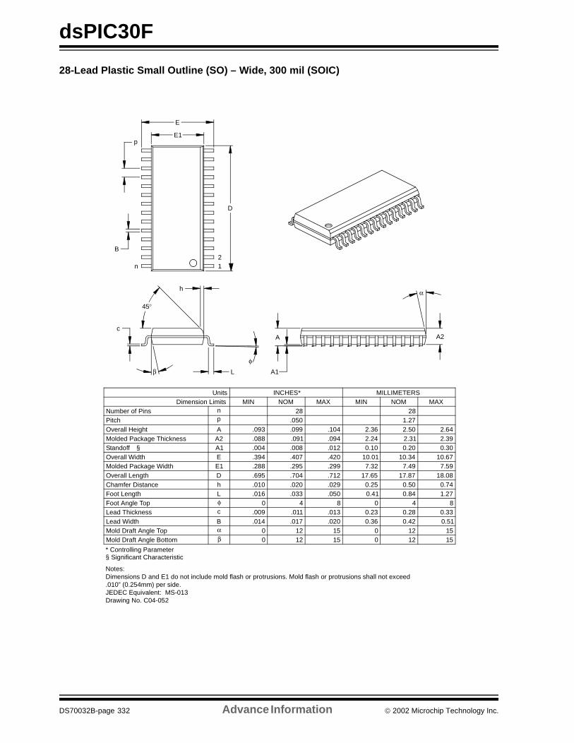
dsPIC30F
28-Lead Plastic Small Outline (SO) – Wide, 300 mil (SOIC)
Foot Angle Top φ 0 4 8 0 4 8
1512015120βMold Draft Angle Bottom1512015120αMold Draft Angle Top
0.510.420.36.020.017.014BLead Width0.330.280.23.013.011.009cLead Thickness
1.270.840.41.050.033.016LFoot Length0.740.500.25.029.020.010hChamfer Distance
18.0817.8717.65.712.704.695DOverall Length7.597.497.32.299.295.288E1Molded Package Width
10.6710.3410.01.420.407.394EOverall Width0.300.200.10.012.008.004A1Standoff §2.392.312.24.094.091.088A2Molded Package Thickness2.642.502.36.104.099.093AOverall Height
1.27.050pPitch2828nNumber of Pins
MAXNOMMINMAXNOMMINDimension LimitsMILLIMETERSINCHES*Units
21
D
p
n
B
E
E1
L
c
β
45°
h
φ
A2
α
A
A1
* Controlling Parameter
Notes:Dimensions D and E1 do not include mold flash or protrusions. Mold flash or protrusions shall not exceed .010” (0.254mm) per side.JEDEC Equivalent: MS-013Drawing No. C04-052
§ Significant Characteristic
DS70032B-page 332 Advance Information 2002 Microchip Technology Inc.
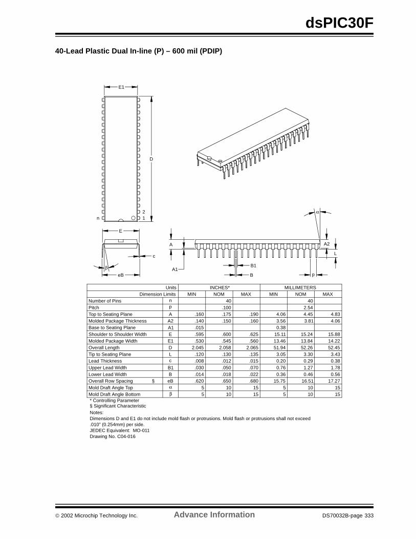
dsPIC30F
40-Lead Plastic Dual In-line (P) – 600 mil (PDIP)
1510515105βMold Draft Angle Bottom1510515105αMold Draft Angle Top
17.2716.5115.75.680.650.620eBOverall Row Spacing §0.560.460.36.022.018.014BLower Lead Width1.781.270.76.070.050.030B1Upper Lead Width0.380.290.20.015.012.008cLead Thickness3.433.303.05.135.130.120LTip to Seating Plane
52.4552.2651.942.0652.0582.045DOverall Length14.2213.8413.46.560.545.530E1Molded Package Width15.8815.2415.11.625.600.595EShoulder to Shoulder Width
0.38.015A1Base to Seating Plane4.063.813.56.160.150.140A2Molded Package Thickness4.834.454.06.190.175.160ATop to Seating Plane
2.54.100pPitch4040nNumber of Pins
MAXNOMMINMAXNOMMINDimension LimitsMILLIMETERSINCHES*Units
A2
12
D
n
E1
c
βeB
E
α
p
L
B
B1
A
A1
* Controlling Parameter
Notes:Dimensions D and E1 do not include mold flash or protrusions. Mold flash or protrusions shall not exceed .010” (0.254mm) per side.JEDEC Equivalent: MO-011Drawing No. C04-016
§ Significant Characteristic
2002 Microchip Technology Inc. Advance Information DS70032B-page 333
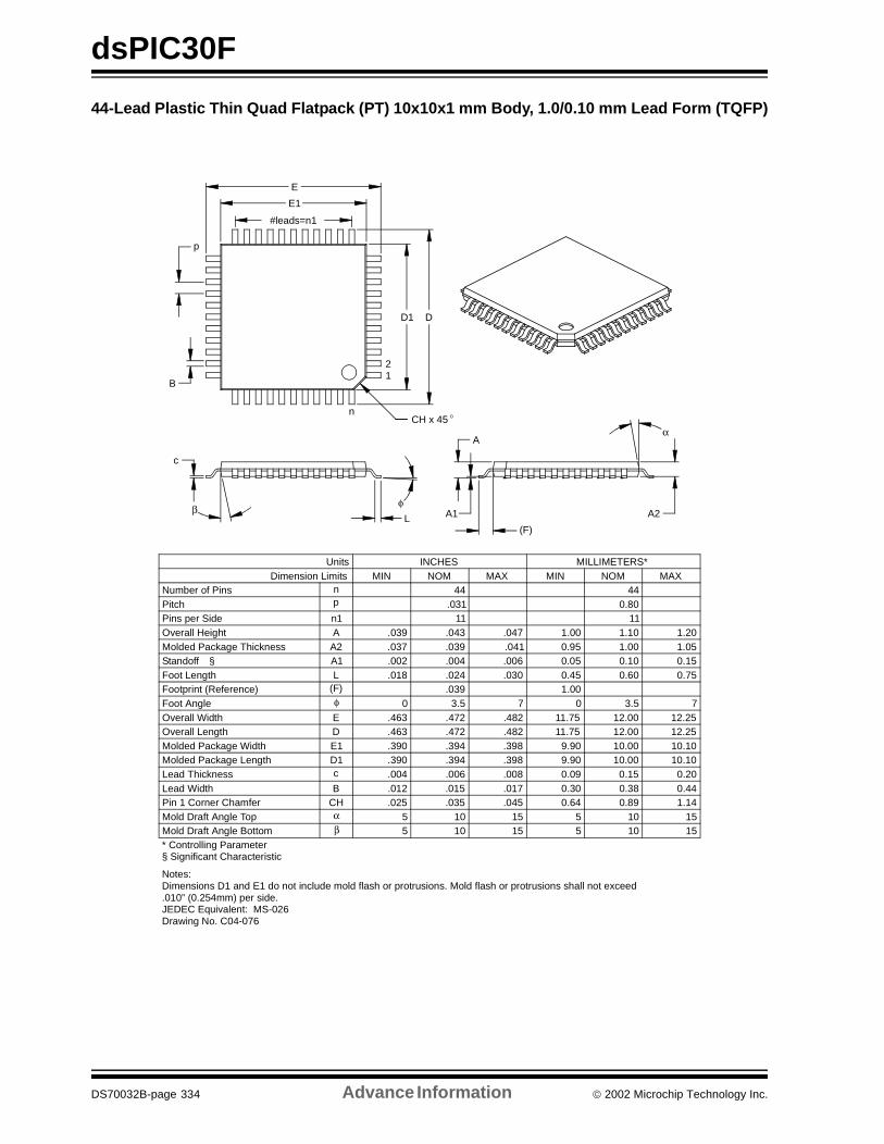
dsPIC30F
44-Lead Plastic Thin Quad Flatpack (PT) 10x10x1 mm Body, 1.0/0.10 mm Lead Form (TQFP)
* Controlling Parameter
Notes:Dimensions D1 and E1 do not include mold flash or protrusions. Mold flash or protrusions shall not exceed .010” (0.254mm) per side.JEDEC Equivalent: MS-026Drawing No. C04-076
1.140.890.64.045.035.025CHPin 1 Corner Chamfer
1.00.039(F)Footprint (Reference)
(F)
A
A1 A2
α
E
E1
#leads=n1
p
B
D1 D
n
12
φ
c
βL
Units INCHES MILLIMETERS*Dimension Limits MIN NOM MAX MIN NOM MAX
Number of Pins n 44 44Pitch p .031 0.80
Overall Height A .039 .043 .047 1.00 1.10 1.20Molded Package Thickness A2 .037 .039 .041 0.95 1.00 1.05Standoff § A1 .002 .004 .006 0.05 0.10 0.15Foot Length L .018 .024 .030 0.45 0.60 0.75
Foot Angle φ 0 3.5 7 0 3.5 7Overall Width E .463 .472 .482 11.75 12.00 12.25Overall Length D .463 .472 .482 11.75 12.00 12.25Molded Package Width E1 .390 .394 .398 9.90 10.00 10.10Molded Package Length D1 .390 .394 .398 9.90 10.00 10.10
Pins per Side n1 11 11
Lead Thickness c .004 .006 .008 0.09 0.15 0.20Lead Width B .012 .015 .017 0.30 0.38 0.44
Mold Draft Angle Top α 5 10 15 5 10 15Mold Draft Angle Bottom β 5 10 15 5 10 15
CH x 45 °
§ Significant Characteristic
DS70032B-page 334 Advance Information 2002 Microchip Technology Inc.
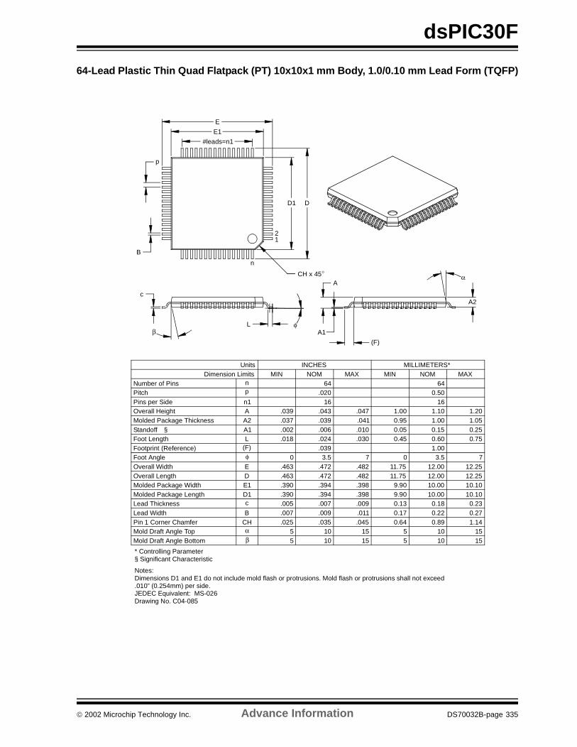
dsPIC30F
64-Lead Plastic Thin Quad Flatpack (PT) 10x10x1 mm Body, 1.0/0.10 mm Lead Form (TQFP)
* Controlling Parameter
Notes:Dimensions D1 and E1 do not include mold flash or protrusions. Mold flash or protrusions shall not exceed.010” (0.254mm) per side.JEDEC Equivalent: MS-026Drawing No. C04-085
1510515105βMold Draft Angle Bottom1510515105αMold Draft Angle Top
0.270.220.17.011.009.007BLead Width0.230.180.13.009.007.005cLead Thickness
1616n1Pins per Side
10.1010.009.90.398.394.390D1Molded Package Length10.1010.009.90.398.394.390E1Molded Package Width12.2512.0011.75.482.472.463DOverall Length12.2512.0011.75.482.472.463EOverall Width
73.5073.50φFoot Angle
0.750.600.45.030.024.018LFoot Length0.250.150.05.010.006.002A1Standoff §1.051.000.95.041.039.037A2Molded Package Thickness1.201.101.00.047.043.039AOverall Height
0.50.020pPitch6464nNumber of Pins
MAXNOMMINMAXNOMMINDimension LimitsMILLIMETERS*INCHESUnits
c
21
n
DD1
B
p
#leads=n1
E1
E
A2
A1
A
L
CH x 45°
βφ
α
(F)
Footprint (Reference) (F) .039 1.00
Pin 1 Corner Chamfer CH .025 .035 .045 0.64 0.89 1.14
§ Significant Characteristic
2002 Microchip Technology Inc. Advance Information DS70032B-page 335
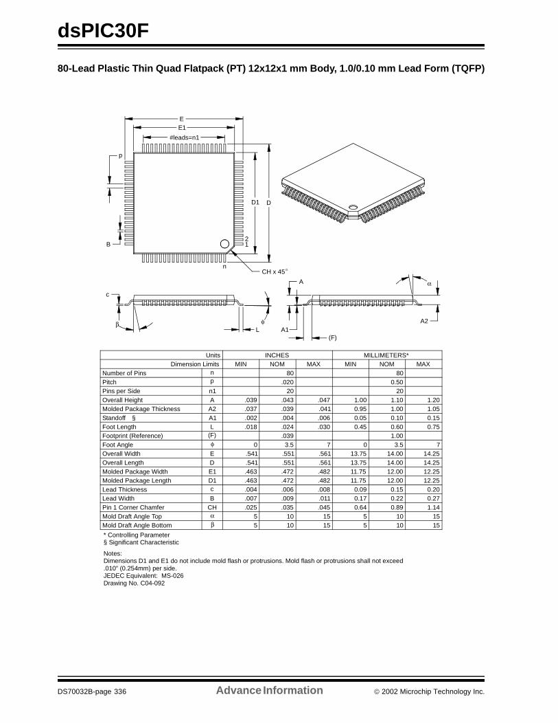
dsPIC30F
80-Lead Plastic Thin Quad Flatpack (PT) 12x12x1 mm Body, 1.0/0.10 mm Lead Form (TQFP)
* Controlling Parameter
Notes:Dimensions D1 and E1 do not include mold flash or protrusions. Mold flash or protrusions shall not exceed .010” (0.254mm) per side.JEDEC Equivalent: MS-026Drawing No. C04-092
1.101.00.043.039
1.140.890.64.045.035.025CHPin 1 Corner Chamfer
1.00.039(F)Footprint (Reference)
(F)
EE1
#leads=n1
p
B
D1 D
n
12
φ
c
βL
A
A1A2
α
Units INCHES MILLIMETERS*Dimension Limits MIN NOM MAX MIN NOM MAX
Number of Pins n 80 80Pitch p .020 0.50
Overall Height A .047 1.20Molded Package Thickness A2 .037 .039 .041 0.95 1.00 1.05Standoff § A1 .002 .004 .006 0.05 0.10 0.15Foot Length L .018 .024 .030 0.45 0.60 0.75
Foot Angle φ 0 3.5 7 0 3.5 7Overall Width E .541 .551 .561 13.75 14.00 14.25Overall Length D .541 .551 .561 13.75 14.00 14.25Molded Package Width E1 .463 .472 .482 11.75 12.00 12.25Molded Package Length D1 .463 .472 .482 11.75 12.00 12.25
Pins per Side n1 20 20
Lead Thickness c .004 .006 .008 0.09 0.15 0.20Lead Width B .007 .009 .011 0.17 0.22 0.27
Mold Draft Angle Top α 5 10 15 5 10 15Mold Draft Angle Bottom β 5 10 15 5 10 15
CH x 45°
§ Significant Characteristic
DS70032B-page 336 Advance Information 2002 Microchip Technology Inc.
dsPIC30F
INDEX
AAC-Link Mode Operation .................................................. 255
Setup ........................................................................ 255Word Size Issues ..................................................... 25516-bit Mode .............................................................. 25520-bit Mode .............................................................. 255
10-bit High Speed Analog-to-Digital Converter. See A/D10-bit High Speed A/D
Aborting a Conversion ............................................. 280ADCHS .................................................................... 277ADCON1 .................................................................. 277ADCON2 .................................................................. 277ADCON3 .................................................................. 277ADPCFG .................................................................. 277Analog Input Model .................................................. 282Configuring Analog Port Pins ................................... 284Connection Considerations ...................................... 284Conversion Operation .............................................. 279Effects of a RESET .................................................. 283Operation During CPU IDLE Mode .......................... 283Operation During CPU SLEEP Mode ...................... 283Output Formats ........................................................ 284Power-down Modes ................................................. 283Programming the Start-of-Conversion Trigger ......... 280Register Map ............................................................ 285Result Buffer ............................................................ 279Sampling Requirements ........................................... 282Selecting the Conversion Clock ............................... 280Selecting the Conversion Sequence ........................ 279Tad vs. Device Operating Frequencies Table .......... 281
12-Bit Analog-to-Digital Converter (A/D) Module ............. 26512-Bit A/D
ADCHS .................................................................... 265ADCON1 .................................................................. 265ADCON2 .................................................................. 265ADCON3 .................................................................. 265ADCSSL ................................................................... 265ADPCFG .................................................................. 265
12-bit A/DAborting a Conversion ............................................. 267Analog Input Model .................................................. 268Configuring Analog Port Pins ................................... 270Connection Considerations ...................................... 270Conversion Operation .............................................. 266Effects of a RESET .................................................. 269Operation During CPU IDLE Mode .......................... 269Operation During CPU SLEEP Mode ...................... 269Output Formats ........................................................ 269Power-down Modes ................................................. 269Programming the Start-of-Conversion Trigger ......... 266Register Map ............................................................ 271Result Buffer ............................................................ 266Sampling Requirements ........................................... 268Selecting the Conversion Clock ............................... 267Selecting the Conversion Sequence ........................ 266Tad vs. Device Operating Frequencies .................... 267
Address Generator Units .................................................... 69Alternate 16-bit Timer/Counter ......................................... 165
Quadrature Encoder Interface Interrupts ................. 166
Analog-to-Digital Converter. See A/DAutomatic Clock Stretch .................................................. 218
During 10-bit Addressing (STREN = 1) ................... 218During 7-bit Addressing (STREN = 1) ..................... 218Receive Mode .......................................................... 218Transmit Mode ......................................................... 218
A/D ............................................................................265, 277
BBarrel Shifter ...................................................................... 67Bit Reversed Addressing ................................................... 76
Example ..................................................................... 76Implementation .......................................................... 76Sequence Table (16-Entry) ........................................ 77
Block DiagramsBarrel Shifter Simplified ............................................. 67CAN Buffers and Protocol Engine ........................... 246CPU Core .................................................................. 20Dead-Time Control Unit for One PWM
Output Pair ...................................................... 180Dead-Time Control Units ......................................... 180DSP Engine ............................................................... 62External Power-on Reset Circuit .............................. 302Input Capture Module .............................................. 151Interrupt Controller ..................................................... 88I2C Receive .............................................................. 209I2C Transmit ............................................................. 209Oscillator System ..................................................... 294Output Compare Mode ............................................ 155PWM Module ........................................................... 174PWM Module, One Output Pair,
Complementary Mode ..................................... 178PWM Module, One Output Pair,
Independent Mode ........................................... 181PWM Time-Base ...................................................... 175Quadrature Encoder Interface ................................. 163RESET System ........................................................ 300Simplified DCI Module ............................................. 248SPI ........................................................................... 199SPI Master/Slave Connection .................................. 199UART Receiver ........................................................ 234UART Transmitter .................................................... 23310-bit High Speed A/D Functional ........................... 27812-Bit A/D Functional ............................................... 26516-bit Timer1 Module ............................................... 13532-bit Timer (Timer2/Timer3) Module ...................... 14032-bit Timer (Timer4/Timer5) Module ...................... 146
BOR. See Brown-out ResetBrown-out Reset (BOR) ................................................... 293
CCAN Module .................................................................... 245
Overview .................................................................. 245Overview of the Module ........................................... 245Transmit/Receive Buffers ........................................ 245
Center Aligned PWM ....................................................... 177
2002 Microchip Technology Inc. Advance Information DS70032B-page 337
DSPIC30F
Code ExamplesData EEPROM Block Erase ....................................... 56Data EEPROM Block Write ........................................ 59Data EEPROM Bulk Erase ......................................... 56Data EEPROM Read ................................................. 55Data EEPROM Word Erase ....................................... 57Data EEPROM Word Write ........................................ 58Erasing a Row of Program Memory ........................... 49Initiating a Programming Sequence ........................... 51Loading Write Latches ............................................... 50Program Space Data Read Through Data
Space Within a REPEAT Loop .......................... 43Reading a FLASH Program Memory Byte ................. 46Reading a FLASH Program Memory Word ................ 46SE and ZE Operation ................................................. 37Writing a Single Program Latch Location in
Byte Mode .......................................................... 47Writing a Single Program Latch Location in
Word Mode ........................................................ 47Code Protection ............................................................... 293Complementary PWM Operation ..................................... 178Control Registers ............................................................... 48
NVMADR .................................................................... 48NVMCON ................................................................... 48NVMKEY .................................................................... 48
Core ArchitectureOverview .................................................................... 19
Core Register Map ............................................................. 41Count Direction Status ..................................................... 164
DData Accumulators and Adder/ .............................. 64, 65, 66Data Address Space .......................................................... 36
Access RAM ............................................................... 38Alignment ................................................................... 37Alignment (Figure) ...................................................... 37Effect of Invalid Memory Accesses ............................ 37MCU and DSP (MAC Class) Instructions
Example ............................................................. 40Memory Map .............................................................. 38Memory Map Example ............................................... 39Spaces ....................................................................... 36Width .......................................................................... 37
Data Converter Interface (DCI) Module ........................... 247Data EEPROM Memory ..................................................... 55
Erasing ....................................................................... 56Erasing, Block ............................................................ 56Erasing, Entire Memory .............................................. 56Erasing, Word ............................................................ 57Protection Against Spurious Write ............................. 60Reading ...................................................................... 55Write Verify ................................................................. 60Writing ........................................................................ 57Writing, Block ............................................................. 59Writing, Word ............................................................. 58
Data Space Organization ................................................... 69DC and AC Characteristics Graphs and Tables ............... 325DCI Module
Bit Clock Generator .................................................. 251Buffer Alignment with Data Frames ......................... 252Buffer Control ........................................................... 247Buffer Data Alignment .............................................. 247Buffer Length Control ............................................... 252COFS Pin ................................................................. 247CSDI Pin .................................................................. 247CSDO Mode Bit ........................................................ 253
CSDO Pin ................................................................ 247Data Justification Control Bit .................................... 251Device Frequencies for Common Codec
CSCK Frequencies Table ................................ 251Digital Loopback Mode ............................................ 253Frame Sync Generator ............................................ 249Frame Sync Mode Control Bits ................................ 249Interrupts .................................................................. 253Introduction .............................................................. 247I/O Pins .................................................................... 247Master Frame Sync Operation ................................. 249Module Enable ......................................................... 248Operation ................................................................. 248Operation During CPU IDLE Mode .......................... 254Operation During CPU SLEEP Mode ...................... 254Receive Slot Enable Bits ......................................... 252Receive Status Bits .................................................. 253Register Map ........................................................... 258Sample Clock Edge Select Control Bit .................... 251SCK Pin ................................................................... 247Slave Frame Sync Operation ................................... 249Slot Enable Bits Operation with Frame Sync ........... 252Slot Status Bits ........................................................ 253Synchronous Data Transfers ................................... 252Transmit Slot Enable Bits ........................................ 251Transmit Status Bits ................................................. 253Transmit/Receive Shift Register .............................. 247Underflow Mode Control Bit ..................................... 253Word Size Selection Bits ......................................... 248
Dead-Time Generators .................................................... 179Assignment .............................................................. 179Distortion .................................................................. 179Ranges .................................................................... 179Selection Bits ........................................................... 179
Development Support ...................................................... 321Device Overview ................................................................ 15Disabling the UART ......................................................... 235Divide Support ................................................................... 32DSP Engine ....................................................................... 61
Multiplier .................................................................... 63DSP Engine Mode Selection .............................................. 68dsPIC30F Language Suite ............................................... 321Dual Output Compare Match Mode ................................. 156
Continuous Pulse Mode ........................................... 156Dual Compare, Continuous Output Pulse Mode
Diagram ........................................................... 158Dual Compare, Single Output Pulse Mode
Diagram ........................................................... 157Single Pulse Mode ................................................... 156
EEdge Aligned PWM .......................................................... 177Electrical Characteristics .................................................. 323Enabling and Setting Up UART ....................................... 235
Alternate I/O ............................................................. 235Setting Up Data, Parity and STOP Bit
Selections ........................................................ 235Enabling the UART .......................................................... 235Equations
A/D Sampling Time ...........................................268, 282Bit Clock Frequency ................................................. 251COFSG Period ......................................................... 249PWM Period ............................................................. 177PWM Resolution ...................................................... 177Serial Clock Rate ..................................................... 226
Errata ................................................................................. 13
DS70032B-page 338 Advance Information 2002 Microchip Technology Inc.
dsPIC30F
Exception Processing ......................................................... 83Exception Sequence .......................................................... 86
Interrupt Stack Frame ................................................ 86Interrupt/ ..................................................................... 86RESET Sources ......................................................... 85Trap Sources ............................................................. 85
External Interrupt Requests ............................................... 87
FFast Context Saving ........................................................... 87Firmware Instructions ....................................................... 311FLASH Program Memory ................................................... 45
In-Circuit Serial Programming (ICSP) ........................ 45Run Time Self-Programming (RTSP) ......................... 45Table Reads and Table Writes .................................. 45
IID Locations ..................................................................... 293In-Circuit Serial Programming .......................................... 308In-Circuit Serial Programming (ICSP) .............................. 293Independent PWM Output ................................................ 181Input Capture Module ....................................................... 151Input Change Notification Module .................................... 120
Register Map (bit 15-8) ............................................ 120Register Map (bit 7-0) .............................................. 120
Instruction SetOverview .................................................................. 314
Instruction Addressing Modes ............................................ 69File Register Instructions ........................................... 70Fundamental Modes Supported ................................. 69MAC Instructions ........................................................ 70MCU Instructions ....................................................... 70Move and Accumulator Instructions ........................... 70Other Instructions ....................................................... 70
Instruction Flow .................................................................. 26Clocking Scheme ....................................................... 26Fetch and Pre-Decode Mechanism ........................... 26Pipeline - 1-Word, 1-Cycle (Figure) ........................... 28Pipeline - 1-Word, 2-Cycle MOV.D
Operations (Figure) ............................................ 29Pipeline - 1-Word, 2-Cycle Table
Operations (Figure) ............................................ 29Pipeline - 1-Word, 2-Cycle with Instruction
Stall (Figure) ...................................................... 29Pipeline - 1-Word, 2-Cycle (Figure) ........................... 28Pipeline - 2-Word, 2-Cycle DO, DOW (Figure) .......... 29Pipeline - 2-Word, 2-Cycle GOTO,
CALL (Figure) .................................................... 29Types ......................................................................... 28
Instruction Set .................................................................. 311Instruction Stalls ................................................................. 71
and Exceptions .......................................................... 72and Flow Change Instructions ................................... 72and PSV ..................................................................... 72Introduction ................................................................ 71Raw Dependency Detection ...................................... 71WAR Dependency Detection ..................................... 72
16-bit Integer and Fractional Modes Example ................... 63Inter-Integrated Circuit. See I2CInterrupt Controller
Register Map .............................................................. 89Interrupt Priority .................................................................. 83
RESET Sequence ...................................................... 85Traps .......................................................................... 85
I2C .................................................................................... 209
I2C Master ModeBaud Rate Generator .............................................. 226Bus Collision During a RESTART Condition ........... 226Bus Collision During a START Condition ................ 226Bus Collision During a STOP Condition .................. 226Clock Arbitration ...................................................... 226Multi-Master Communication, Bus Collision,
and Bus Arbitration .......................................... 226Reception ................................................................ 224Transmission ........................................................... 222
I2C Master Mode Operation ............................................. 221I2C Master Mode Support ................................................ 221I2C Module ....................................................................... 209
General Call Address Support ................................. 221Interrupts ................................................................. 221IPMI Support ............................................................ 221Operating Function Description ............................... 209Pin Configuration ..................................................... 210Register Map ........................................................... 227Registers ................................................................. 210Slope Control ........................................................... 221Software Controlled Clock Stretching
(STREN = 1) .................................................... 221Various Modes ......................................................... 209
I2C ModuleAddresses ................................................................ 210
I2C Module Operation During CPU SLEEP and IDLE Modes ............................................................. 226
I2C 10-bit Slave Mode Operation ..................................... 215Reception ................................................................ 215Transmission ........................................................... 215
I2C 7-bit Slave Mode Operation ....................................... 210Programmer’s Model ............................................... 210Reception ................................................................ 213Transmission ........................................................... 211
I2S Mode Operation ......................................................... 256Data Justification ..................................................... 256Frame and Data Word Length Selection ................. 256
I/O Ports ........................................................................... 115Parallel ..................................................................... 115
MMemory Organization ........................................................ 333 Module .......................................................................... 139
ADC Event Trigger ................................................... 140Gate Operation ........................................................ 140Interrupt ................................................................... 141Operation During SLEEP Mode ............................... 141Register Map ........................................................... 142Timer Prescaler ....................................................... 14132-bit Synchronous Counter Mode .......................... 13932-bit Timer Mode .................................................... 139
5 Module Gate Operation ................................................ 146Interrupt ................................................................... 147Operation During SLEEP Mode ............................... 147Register Map ........................................................... 148Timer Prescaler ....................................................... 14732-bit Synchronous Counter Mode .......................... 14532-bit Timer Mode .................................................... 145
Modulo Addressing ............................................................ 73Applicability ................................................................ 75Decrementing Buffer Operation Example .................. 75Incrementing Buffer Operation Example .................... 74Restrictions ................................................................ 75Start and End Address .............................................. 73W Address Register Selection ................................... 74
2002 Microchip Technology Inc. Advance Information DS70032B-page 339
DSPIC30F
Motor Control PWM Module ............................................. 173MPLAB ICD 2 In-Circuit Debugger ................................... 322MPLAB ICE 4000 In-Circuit Emulator .............................. 322MPLAB SIM Software Simulator ...................................... 321MPLAB V6.00 Integrated Development
Environment Software .............................................. 321Multi-Channel Mode Operation ........................................ 254
Codec Configuration ................................................ 255Setup Details for Single Channel Codec .................. 254Setup Values Table .................................................. 254
OOscillator Configurations .................................................. 295
Fail Safe Clock Monitor ............................................ 297Fast RC (FRC) ......................................................... 296Initial Clock Source Selection ................................... 295Low Power RC (LPRC) ............................................ 296LP Osc Control ......................................................... 296PLL ........................................................................... 296Start-up Timer (OST) ............................................... 296
Oscillator Operating Modes Table .................................... 293Oscillator Selection .......................................................... 293Output Compare Interrupts .............................................. 160Output Compare Mode
Register Map ............................................................ 161Output Compare Module .................................................. 155Output Compare Operation During CPU IDLE Mode ....... 160Output Compare SLEEP Mode Operation ....................... 160
PPackaging
Marking Information ................................................. 327Packaging Information ..................................................... 327Pinout Descriptions ............................................................ 15PORTA
Register Map ............................................................ 116PORTB
Register Map ............................................................ 118PORTC
Register Map ............................................................ 118PORTD
Register Map ............................................................ 118PORTE
Register Map ............................................................ 118PORTF
Register Map ............................................................ 118PORTG
Register Map ............................................................ 119POR. See Power-on ResetPosition Measurement Mode ........................................... 164Power Saving Modes ....................................................... 307
IDLE ......................................................................... 307SLEEP ...................................................................... 307
Power-on Reset (POR) .................................................... 293Oscillator Start-up Timer (OST) ............................... 293Power-up Timer (PWRT) .......................................... 293
PRO MATE II Universal Device Programmer ................... 322Product Identification System ........................................... 347Program Address Space .................................................... 33
Alignment and Data Access Using Table Instructions ............................................... 34
Construction ............................................................... 33Data Access from, Address Generation ..................... 33Memory Map .............................................................. 36
Table InstructionsTBLRDH ............................................................ 34TBLRDL ............................................................. 34TBLWTH ............................................................ 34TBLWTL ............................................................ 34
Program Counter ............................................................... 22Program Loop Control ........................................................ 30
DO and REPEAT Restrictions ................................... 31DO Early Termination ................................................ 31DO Loop Construct .................................................... 30DO Loop Nesting ....................................................... 31DO Loops and Interrupts ........................................... 31REPEAT Early Termination ....................................... 30REPEAT Loop Construct ........................................... 30REPEAT Loop Interrupt and Nesting ......................... 30
Program Space Data Read Through Data Space Within a REPEAT Loop Diagram ............................... 43
Program Space VisibilityWindow into Program Space Operation .................... 35
Program Space Visibility from Data Space ........................ 35Data Pre-fetch from Program Space Within
a REPEAT Loop ................................................ 43Programmable ................................................................. 293Programmable Digital Noise Filters ................................. 164Programmer’s Model .......................................................... 21
Diagram ..................................................................... 23Programming Operations ................................................... 48
Algorithm for Program FLASH ................................... 48Erasing a Row of Program Memory ........................... 49Initiating the Programming Sequence ........................ 51Loading Write Latches ............................................... 50
Programming, Device Instructions ................................... 311Protection Against Accidental Writes to OSCCON .......... 297PWM
Motor Control PWM Register Map ........................... 185PWM Duty Cycle Comparison Units ................................ 178
Duty Cycle Register Buffers ..................................... 178PWM Fault Pins ............................................................... 183
Enable Bits ............................................................... 183Fault States .............................................................. 183Modes ...................................................................... 183
Cycle-by-Cycle ................................................. 183Latched ............................................................ 183
Priority ...................................................................... 183PWM Operation During CPU IDLE Mode ........................ 184PWM Operation During CPU SLEEP Mode ..................... 184PWM Output and Polarity Control .................................... 182
Output Pin Control ................................................... 182PWM Output Override ...................................................... 182
Complementary Output Mode .................................. 182Synchronization ....................................................... 182
PWM Period ..................................................................... 177PWM Special Event Trigger ............................................. 184
Postscaler ................................................................ 184PWM Time-Base .............................................................. 175
Continuous Up/Down Counting Modes .................... 176Free Running Mode ................................................. 176Postscaler ................................................................ 176Prescaler .................................................................. 176Single Shot Mode .................................................... 176
PWM Time-Base Interrupts .............................................. 176Continuous Up/Down Counting Mode ..................... 176Double Update Mode ............................................... 176Free Running Mode ................................................. 176Single Shot Mode .................................................... 176
PWM Update Lockout ...................................................... 183
DS70032B-page 340 Advance Information 2002 Microchip Technology Inc.
dsPIC30F
QQEI Module
Operation During CPU IDLE Mode .......................... 165Operation During CPU SLEEP Mode ...................... 165Register Map ............................................................ 167
Quadrature Encoder Interface Logic ................................ 164Quadrature Encoder Interface (QEI) Module ................... 163
RRegisters
ADCHS (A/D Input Select) Register ................. 275, 291ADCON1 (A/D Control) Register1 .................... 272, 286ADCON2 (A/D Control) Register2 .................... 273, 288ADCON3 (A/D Control) Register3 .................... 274, 290ADCSSL (A/D Input Scan Select) Register ...... 276, 292ADPCFG (A/D Port Configuration) Register .... 276, 292CNEN1 (Input Change Notification Interrupt
Enable) Register1 ............................................ 131CNEN2 (Input Change Notification Interrupt
Enable) Register2 ............................................ 132CNPU1 (Input Change Notification Pull-up
Enable) Register1 ............................................ 132CNPU2 (Input Change Notification Pull-up
Enable) Register2 ............................................ 133CORCON (CPU Mode Control) Register ................... 68DCICON1 (DCI Module Control) Register1 .............. 259DCICON2 (DCI Module Control) Register2 .............. 260DCICON3 (DCI Module Control) Register3 .............. 261DCISTAT (DCI Status) Register .............................. 262DFLTCON (Digital Dilter Control) Register .............. 170DTCON1 (Dead-Time Control) Register1 ................ 190DTCON2 (Dead-Time Control) Register2 ................ 191FLTACON (Fault A Control) Register ...................... 192FLTBCON (Fault B Control) Register ...................... 192FOSC (Oscillator Selection Control) Register .......... 299FWDT (Configuration bits for WDT) Register ........... 306ICxCON (Input Capture x Control) Register ............. 154IEC0 (Interrupt Enable Control) Register0 ................. 97IEC1 (Interrupt Enable Control) Register1 ................. 99IEC2 (Interrupt Enable Control) Register2 ............... 101IFS0 (Interrupt Flag Status) Register0 ....................... 92IFS1 (Interrupt Flag Status) Register1 ....................... 94IFS2 (Interrupt Flag Status) Register2 ....................... 96INTCON1 (Interrupt Control) Register1 ..................... 90INTCON2 (Interrupt Control) Register2 ..................... 91IPC0 (Interrupt Priority Control) Register0 ............... 102IPC1 (Interrupt Priority Control) Register1 ............... 103IPC10 (Interrupt Priority Control) Register10 ........... 112IPC11 (Interrupt Priority Control) Register11 ........... 113IPC2 (Interrupt Priority Control) Register2 ............... 104IPC3 (Interrupt Priority Control) Register3 ............... 105IPC4 (Interrupt Priority Control) Register4 ............... 106IPC5 (Interrupt Priority Control) Register5 ............... 107IPC6 (Interrupt Priority Control) Register6 ............... 108IPC7 (Interrupt Priority Control) Register7 ............... 109IPC8 (Interrupt Priority Control) Register8 ............... 110IPC9 (Interrupt Priority Control) Register9 ............... 111I2CCON (I2C Control) Register ................................ 230I2CSTAT (I2C Status) Register ................................ 228LATA (Read/Write PORTA Latch) Register ............. 122LATB (Read/Write PORTB PIO Latch) Register ...... 123LATC (Read/Write PORTC PIO Latch) Register ...... 125LATD (Read/Write PORTD PIO Latch) Register ...... 126LATE (Read/Write PORTE PIO Latch) Register ...... 128LATF (Read/Write PORTF PIO Latch) Register ...... 129
LATG (Read/Write PORTG PIO Latch) Register ..... 131MAXCNT (Maximum Count) Register ...................... 171MODCON (Modulo and Bit-Reversed
Addressing Control) Register ............................ 78NVMADR Register ..................................................... 53NVMCON Register .................................................... 52NVMKEY Register ..................................................... 53OCxCON (Output Compare Control x) Register ...... 162OSCCON (Oscillator Control) Register .................... 298OVDCON (Output Override Control) Register ......... 193PDC1 (PWM Duty Cycle 1) Register ....................... 194PDC2 (PWM Duty Cycle 2) Register ....................... 194PDC3 (PWM Duty Cycle 3) Register ....................... 195PDC4 (PWM Duty Cycle 4) Register ....................... 195PORTA (Read Pin/Write PORTA Latch) Register ... 121PORTB -(Read PORTB PIO Pin/Write
PORTB PIO Latch) Register ............................ 123PORTC (Read PORTC PIO Pin/Write
PORTC PIO Latch) Register ........................... 124PORTD (Read PORTD PIO Pin/Write
PORTD PIO Latch) Register ........................... 126PORTE (Read PORTE PIO Pin/Write
PORTE PIO Latch) Register ............................ 127PORTF (Read PORTF PIO Pin/Write
PORTF PIO Latch) Register ............................ 129PORTG (Read PORTG PIO Pin/Write
PORTG PIO Latch) Register ........................... 130POSCNT (16-bit Position Counter) Register ........... 171PTCON (PWM Time-Base Control) Register ........... 186PTMR (PWM Time-Base Count) Register ............... 187PWM Time-Base Period) Register ........................... 187PWMCON1 (PWM Control) Register1 ..................... 188PWMCON2 (PWM Control) Register2 ..................... 189QEICON (QEI Control) Register .............................. 168RCON (RESET and System Control) Register ........ 304RSCON (Receive Slot Control) Register ................. 263SEVTCMP (Special Event Trigger Compare
Count) Register ............................................... 188SPIxCON (SPI Control) Register ............................. 206SPIxSTAT (SPI Status) Register ............................. 205STATUS (SR) Register .............................................. 24TRISA (PORTA Data Direction) Register ................ 121TRISB (PORTB PIO Data Direction) Register ......... 122TRISC (PORTC PIO Data Direction) Register ......... 124TRISD (PORTD PIO Data Direction) Register ......... 125TRISE (PORTE PIO Data Direction) Register ......... 127TRISF (PORTF PIO Data Direction) Register ......... 128TRISG (PORTG PIO Data Direction) Register ........ 130TSCON (Transmit Slot Control) Register ................. 263T1CON (Timer1 Control) Register ........................... 138T2CON (Timer2 Control) Register ........................... 143T3CON (Timer3 Control) Register ........................... 144T4CON (Timer4 Control) Register ........................... 149T5CON (Timer5 Control) Register ........................... 150UxBRG (UARTx Baud Rate) Register ..................... 244UxMODE (UARTx Mode) Register .......................... 240UxRXREG (UARTx Receive) Register .................... 243UxSTA (UARTx Status and Control) Register ......... 241XBREV (X WAGU Bit Reversal Addressing
Control) Register ............................................... 81XMODEND (X AGU Modulo Addressing End)
Register ............................................................. 79XMODSRT (X AGU Modulo Addressing Start)
Register ............................................................. 79
2002 Microchip Technology Inc. Advance Information DS70032B-page 341
DSPIC30F
YMODEND (Y AGU Modulo Addressing End) Register .............................................................. 80
YMODSRT (Y AGU Modulo Addressing Start) Register .............................................................. 80
RESET ..................................................................... 293, 300RESET Vectors .................................................................. 86RESETS
BOR, Programmable ................................................ 302POR ......................................................................... 300
Operating without FSCM and PWRT ............... 302POR with Long Crystal Start-up Time ...................... 302
RTSP Operation ................................................................. 48
SSales and Support ............................................................ 347SCI. See UARTSerial Communication Interface. See UARTSerial Peripheral Interface. See SPISIB
Register Map ............................................................ 309Simple Capture Event Mode ............................................ 151
Capture Buffer Operation ......................................... 151Capture Prescaler .................................................... 151Hall Sensor Mode ..................................................... 152Input Capture in CPU IDLE Mode ............................ 152Input Capture in CPU SLEEP Mode ........................ 152Input Capture Interrupts ........................................... 152Input Capture Operation During SLEEP Mode ........ 152Register Map ............................................................ 153Timer2 and Timer3 Selection Mode ......................... 152
Simple Output Compare Match Mode .............................. 156Simple PWM Mode .......................................................... 158
Input Pin Fault Protection ......................................... 158Period ....................................................................... 159
Single Pulse PWM Operation ........................................... 182Software Stack Pointer, Frame Pointer .............................. 21
CALL Stack Frame ..................................................... 21SPI ................................................................................... 197SPI Mode
Slave Select Synchronization ................................... 203SPI Master, Frame Master ....................................... 197SPI Master, Frame Slave ......................................... 198SPI Slave, Frame Master ......................................... 198SPI Slave, Frame Slave ........................................... 198SPI1 Register Map ................................................... 204SPI2 Register Map ................................................... 204
SPI Module ....................................................................... 197Framed SPI Support ................................................ 197Operating Function Description ................................ 197SDOx Disable ........................................................... 197Word and Byte Communication ............................... 197
SPI Operation During CPU IDLE Mode ........................... 203SPI Operation During CPU SLEEP Mode ........................ 203SSP
SSPCON .......................................................... 205, 206STATUS Bits, Their Significance and the Initialization
Condition for RCON Register ................................... 303STATUS Register ............................................................... 22
Sticky Z (SZ) Status Bit .............................................. 22Subtractor ........................................................................... 64
Conventional and Convergent Rounding Modes Diagram .................................................. 66
Data Space Write Saturation ...................................... 66Overflow and Saturation ............................................. 64Round Logic ............................................................... 65Write Back .................................................................. 65
Symbols used in Roadrunner Opcode Descriptions ........ 312System Integration ........................................................... 293
Overview .................................................................. 293
TTable Read
Byte Modes ................................................................ 46Using Table Read Instructions ................................... 46Word Mode ................................................................ 46
Table WriteByte Mode .................................................................. 47Using Table Write Instructions ................................... 47Word Mode ................................................................ 47
Timer Operation During CPU Idle Mode .......................... 166Timer Operation During CPU SLEEP Mode .................... 165Timer1 Module ................................................................. 135
Gate Operation ........................................................ 136Interrupt ................................................................... 136Operation During SLEEP Mode ............................... 136Prescaler .................................................................. 136Real-Time Clock ...................................................... 136
Interrupts ......................................................... 136RTC Oscillator Operation ................................. 136
Register Map ........................................................... 13716-bit Asynchronous Counter Mode ........................ 13516-bit Synchronous Counter Mode .......................... 13516-bit Timer Mode .................................................... 135
Timer2 and Timer 3 Selection Mode ................................ 156Timer2/ ...................................................... 139, 140, 141, 142Timer4/ ...................................................... 145, 146, 147, 148Timer4/5 Module .............................................................. 145Timing Diagrams
Basic Core ................................................................. 26Center Aligned PWM ............................................... 177Clock/Instruction Cycle .............................................. 27Dead-Time ............................................................... 180Edge Aligned PWM .................................................. 177Frame Sync, AC-Link Start of Frame ....................... 250Frame Sync, Multi-Channel Mode ........................... 250I2C Master Mode (Reception, 7-bit Address) ........... 225I2C Master Mode (Transmission, 7- or
10-bit Address) ................................................ 223I2C Slave Mode with STREN = 0 (Reception,
10-bit Address) ................................................ 217I2C Slave Mode with STREN = 0 (Reception,
7-bit Address) .................................................. 214I2C Slave Mode with STREN = 1 (Reception,
10-bit Address) ................................................ 220I2C Slave Mode with STREN = 1 (Reception,
7-bit Address) .................................................. 219I2C Slave Mode (Transmission, 10-bit Address) ...... 216I2C Slave Mode (Transmission, 7-bit Address) ........ 212I2S ............................................................................ 257I2S Interface Frame Sync ........................................ 250PWM Output ............................................................ 159Signal Relationship Through Filter,
1/1 Clock Divide ............................................... 165Single Pulse PWM Operation .................................. 182Slave Synchronization (Mode 16 = 0) ...................... 203SPI Master, Frame Master ....................................... 198SPI Master, Frame Slave ......................................... 198SPI Mode Timing (8-bit Master Mode) ..................... 200SPI Mode Timing (8-bit Slave Mode w/CKE = 0) ..... 201SPI Mode Timing (8-bit Slave Mode w/CKE = 1) ..... 202Time-out Sequence on Power-up (MCLR
Not Tied to Vdd), Case 1 ................................. 301
DS70032B-page 342 Advance Information 2002 Microchip Technology Inc.
dsPIC30F
Time-out Sequence on Power-up (MCLR Not Tied to Vdd), Case 2 ................................. 301
Time-out Sequence on Power-up (MCLR Tied to Vdd) ..................................................... 301
Trap..................................................................................... 86
UUART
Address Detect Mode .............................................. 237Auto Baud Support ................................................... 237Baud Rate Generator ............................................... 237Framing Error (FERR) .............................................. 237Loopback Mode ....................................................... 237Parity Error (PERR) ................................................. 237Receive Break .......................................................... 237Receive Buffer Overrun Error (OERR Bit) ................ 236Receive Buffer (UxRCB) .......................................... 236Receive Interrupt ...................................................... 236Receiving Data ......................................................... 236Receiving in 8-bit or 9-bit Data Mode ....................... 236Reception Error Handling ......................................... 236Transmit Buffer (UxTXB) .......................................... 235Transmit Interrupt ..................................................... 236Transmitting Data ..................................................... 235Transmitting in 8-bit Data Mode ............................... 235Transmitting in 9-bit Data Mode ............................... 235
UART ModuleUART1 Register Map ............................................... 239UART2 Register Map ............................................... 239
UART Module Overview .................................................. 233UART Operation
IDLE Mode ............................................................... 238SLEEP Mode ........................................................... 238
UART Operation During CPU SLEEP and IDLE Modes ............................................................. 238
Universal Asynchronous Receiver Transmitter. See UART16-bit Up/Down Position Counter Mode .......................... 164UxTXREG
UARTx Transmit) Register ....................................... 243
WWake-up from SLEEP ...................................................... 293Wake-up from SLEEP and IDLE ........................................ 87Watchdog Timer (WDT) ............................................293, 305
Enabling and Disabling ............................................ 305Operation ................................................................. 305
WWW, On-Line Support .................................................... 13
2002 Microchip Technology Inc. Advance Information DS70032B-page 343

DSPIC30F
NOTES:
DS70032B-page 344 Advance Information 2002 Microchip Technology Inc.
dsPIC30F
ON-LINE SUPPORT
Microchip provides on-line support on the MicrochipWorld Wide Web (WWW) site.
The web site is used by Microchip as a means to makefiles and information easily available to customers. Toview the site, the user must have access to the Internetand a web browser, such as Netscape or MicrosoftExplorer. Files are also available for FTP downloadfrom our FTP site.
Connecting to the Microchip Internet Web Site
The Microchip web site is available by using yourfavorite Internet browser to attach to:
www.microchip.com
The file transfer site is available by using an FTP ser-vice to connect to:
ftp://ftp.microchip.com
The web site and file transfer site provide a variety ofservices. Users may download files for the latestDevelopment Tools, Data Sheets, Application Notes,User’s Guides, Articles and Sample Programs. A vari-ety of Microchip specific business information is alsoavailable, including listings of Microchip sales offices,distributors and factory representatives. Other dataavailable for consideration is:
• Latest Microchip Press Releases• Technical Support Section with Frequently Asked
Questions • Design Tips• Device Errata
• Job Postings• Microchip Consultant Program Member Listing• Links to other useful web sites related to
Microchip Products• Conferences for products, Development Sys-
tems, technical information and more• Listing of seminars and events
2002 Microchip Technology Inc. Advance Info
Systems Information and Upgrade Hot Line
The Systems Information and Upgrade Line providessystem users a listing of the latest versions of all ofMicrochip’s development systems software products.Plus, this line provides information on how customerscan receive any currently available upgrade kits.TheHot Line Numbers are:
1-800-755-2345 for U.S. and most of Canada, and
1-480-792-7302 for the rest of the world.
013001
rmation DS70032B-page345

dsPIC30F
READER RESPONSE
It is our intention to provide you with the best documentation possible to ensure successful use of your Microchip prod-uct. If you wish to provide your comments on organization, clarity, subject matter, and ways in which our documentationcan better serve you, please FAX your comments to the Technical Publications Manager at (480) 792-4150.
Please list the following information, and use this outline to provide us with your comments about this Data Sheet.
1. What are the best features of this document?
2. How does this document meet your hardware and software development needs?
3. Do you find the organization of this data sheet easy to follow? If not, why?
4. What additions to the data sheet do you think would enhance the structure and subject?
5. What deletions from the data sheet could be made without affecting the overall usefulness?
6. Is there any incorrect or misleading information (what and where)?
7. How would you improve this document?
8. How would you improve our software, systems, and silicon products?
To: Technical Publications Manager
RE: Reader Response
Total Pages Sent
From: Name
Company
Address
City / State / ZIP / Country
Telephone: (_______) _________ - _________
Application (optional):
Would you like a reply? Y N
Device: Literature Number:
Questions:
FAX: (______) _________ - _________
DS70032BdsPIC30F
DS70032B-page346 Advance Information 2002 Microchip Technology Inc.
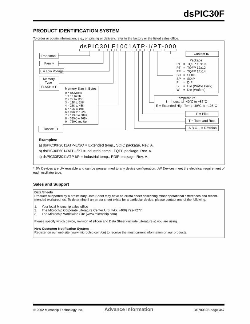
2002 Microchip Technology Inc. Advance Information DS70032B-page 347
dsPIC30F
PRODUCT IDENTIFICATION SYSTEMTo order or obtain information, e.g., on pricing or delivery, refer to the factory or the listed sales office.
* JW Devices are UV erasable and can be programmed to any device configuration. JW Devices meet the electrical requirement ofeach oscillator type.
Sales and Support
Examples:a) dsPIC30F2011ATP-E/SO = Extended temp., SOIC package, Rev. A.
b) dsPIC30F6014ATP-I/PT = Industrial temp., TQFP package, Rev. A.
c) dsPIC30F3011ATP-I/P = Industrial temp., PDIP package, Rev. A.
d s P I C 3 0 L F 1 0 0 1 AT P - I / PT- 0 0 0
Trademark
Family
MemoryType
FLASH = F
E = Extended High Temp -40°C to +125°CI = Industrial -40°C to +85°C
Temperature
Device ID
P = Pilot
PackagePT = TQFP 10x10PT = TQFP 12x12PF = TQFP 14x14SO = SOICSP = SDIPP = DIPS = Die (Waffle Pack)W = Die (Wafers)
L = Low Voltage
Memory Size in Bytes0 = ROMless1 = 1K to 6K2 = 7K to 12K3 = 13K to 24K4 = 25K to 48K5 = 49K to 96K6 = 97K to 192K7 = 193K to 384K8 = 385K to 768K9 = 769K and Up
Custom ID
T = Tape and Reel
A,B,C… = Revision
Data SheetsProducts supported by a preliminary Data Sheet may have an errata sheet describing minor operational differences and recom-mended workarounds. To determine if an errata sheet exists for a particular device, please contact one of the following:
1. Your local Microchip sales office2. The Microchip Corporate Literature Center U.S. FAX: (480) 792-72773. The Microchip Worldwide Site (www.microchip.com)
Please specify which device, revision of silicon and Data Sheet (include Literature #) you are using.
New Customer Notification SystemRegister on our web site (www.microchip.com/cn) to receive the most current information on our products.
DS70032B-page 348 Advance Information 2002 Microchip Technology Inc.
MAMERICASCorporate Office2355 West Chandler Blvd.Chandler, AZ 85224-6199Tel: 480-792-7200 Fax: 480-792-7277Technical Support: 480-792-7627Web Address: http://www.microchip.comRocky Mountain2355 West Chandler Blvd.Chandler, AZ 85224-6199Tel: 480-792-7966 Fax: 480-792-7456
Atlanta500 Sugar Mill Road, Suite 200BAtlanta, GA 30350Tel: 770-640-0034 Fax: 770-640-0307Boston2 Lan Drive, Suite 120Westford, MA 01886Tel: 978-692-3848 Fax: 978-692-3821Chicago333 Pierce Road, Suite 180Itasca, IL 60143Tel: 630-285-0071 Fax: 630-285-0075Dallas4570 Westgrove Drive, Suite 160Addison, TX 75001Tel: 972-818-7423 Fax: 972-818-2924DetroitTri-Atria Office Building 32255 Northwestern Highway, Suite 190Farmington Hills, MI 48334Tel: 248-538-2250 Fax: 248-538-2260Kokomo2767 S. Albright Road Kokomo, Indiana 46902Tel: 765-864-8360 Fax: 765-864-8387Los Angeles18201 Von Karman, Suite 1090Irvine, CA 92612Tel: 949-263-1888 Fax: 949-263-1338New York150 Motor Parkway, Suite 202Hauppauge, NY 11788Tel: 631-273-5305 Fax: 631-273-5335San JoseMicrochip Technology Inc.2107 North First Street, Suite 590San Jose, CA 95131Tel: 408-436-7950 Fax: 408-436-7955Toronto6285 Northam Drive, Suite 108Mississauga, Ontario L4V 1X5, CanadaTel: 905-673-0699 Fax: 905-673-6509
ASIA/PACIFICAustraliaMicrochip Technology Australia Pty LtdSuite 22, 41 Rawson StreetEpping 2121, NSWAustraliaTel: 61-2-9868-6733 Fax: 61-2-9868-6755China - BeijingMicrochip Technology Consulting (Shanghai)Co., Ltd., Beijing Liaison OfficeUnit 915Bei Hai Wan Tai Bldg.No. 6 Chaoyangmen Beidajie Beijing, 100027, No. ChinaTel: 86-10-85282100 Fax: 86-10-85282104China - ChengduMicrochip Technology Consulting (Shanghai)Co., Ltd., Chengdu Liaison OfficeRm. 2401, 24th Floor, Ming Xing Financial TowerNo. 88 TIDU StreetChengdu 610016, ChinaTel: 86-28-6766200 Fax: 86-28-6766599China - FuzhouMicrochip Technology Consulting (Shanghai)Co., Ltd., Fuzhou Liaison OfficeUnit 28F, World Trade PlazaNo. 71 Wusi RoadFuzhou 350001, ChinaTel: 86-591-7503506 Fax: 86-591-7503521China - ShanghaiMicrochip Technology Consulting (Shanghai)Co., Ltd.Room 701, Bldg. BFar East International PlazaNo. 317 Xian Xia RoadShanghai, 200051Tel: 86-21-6275-5700 Fax: 86-21-6275-5060China - ShenzhenMicrochip Technology Consulting (Shanghai)Co., Ltd., Shenzhen Liaison OfficeRm. 1315, 13/F, Shenzhen Kerry Centre,Renminnan LuShenzhen 518001, ChinaTel: 86-755-2350361 Fax: 86-755-2366086Hong KongMicrochip Technology Hongkong Ltd.Unit 901-6, Tower 2, Metroplaza223 Hing Fong RoadKwai Fong, N.T., Hong KongTel: 852-2401-1200 Fax: 852-2401-3431IndiaMicrochip Technology Inc.India Liaison OfficeDivyasree Chambers1 Floor, Wing A (A3/A4)No. 11, O’Shaugnessey RoadBangalore, 560 025, IndiaTel: 91-80-2290061 Fax: 91-80-2290062
JapanMicrochip Technology Japan K.K.Benex S-1 6F3-18-20, ShinyokohamaKohoku-Ku, Yokohama-shiKanagawa, 222-0033, JapanTel: 81-45-471- 6166 Fax: 81-45-471-6122KoreaMicrochip Technology Korea168-1, Youngbo Bldg. 3 FloorSamsung-Dong, Kangnam-KuSeoul, Korea 135-882Tel: 82-2-554-7200 Fax: 82-2-558-5934SingaporeMicrochip Technology Singapore Pte Ltd.200 Middle Road#07-02 Prime CentreSingapore, 188980Tel: 65-334-8870 Fax: 65-334-8850TaiwanMicrochip Technology Taiwan11F-3, No. 207Tung Hua North RoadTaipei, 105, TaiwanTel: 886-2-2717-7175 Fax: 886-2-2545-0139
EUROPEDenmarkMicrochip Technology Nordic ApSRegus Business CentreLautrup hoj 1-3Ballerup DK-2750 DenmarkTel: 45 4420 9895 Fax: 45 4420 9910FranceMicrochip Technology SARLParc d’Activite du Moulin de Massy43 Rue du Saule TrapuBatiment A - ler Etage91300 Massy, FranceTel: 33-1-69-53-63-20 Fax: 33-1-69-30-90-79GermanyMicrochip Technology GmbHGustav-Heinemann Ring 125D-81739 Munich, GermanyTel: 49-89-627-144 0 Fax: 49-89-627-144-44ItalyMicrochip Technology SRLCentro Direzionale Colleoni Palazzo Taurus 1 V. Le Colleoni 120041 Agrate BrianzaMilan, Italy Tel: 39-039-65791-1 Fax: 39-039-6899883United KingdomArizona Microchip Technology Ltd.505 Eskdale RoadWinnersh TriangleWokingham Berkshire, England RG41 5TUTel: 44 118 921 5869 Fax: 44-118 921-5820
01/18/02
WORLDWIDE SALES AND SERVICE