dsPIC30F Family Reference Manual - Mobile Devices
772
© 2006 Microchip Technology Inc. DS70046E dsPIC30F Family Reference Manual High-Performance Digital Signal Controllers
Transcript of dsPIC30F Family Reference Manual - Mobile Devices
© 2006 Microchip Technology Inc. DS70046E
dsPIC30FFamily Reference Manual
High-Performance
Digital Signal Controllers
Note the following details of the code protection feature on Microchip devices:
• Microchip products meet the specification contained in their particular Microchip Data Sheet.
• Microchip believes that its family of products is one of the most secure families of its kind on the market today, when used in the intended manner and under normal conditions.
• There are dishonest and possibly illegal methods used to breach the code protection feature. All of these methods, to our knowledge, require using the Microchip products in a manner outside the operating specifications contained in Microchip’s Data Sheets. Most likely, the person doing so is engaged in theft of intellectual property.
• Microchip is willing to work with the customer who is concerned about the integrity of their code.
• Neither Microchip nor any other semiconductor manufacturer can guarantee the security of their code. Code protection does not mean that we are guaranteeing the product as “unbreakable.”
Code protection is constantly evolving. We at Microchip are committed to continuously improving the code protection features of ourproducts. Attempts to break Microchip’s code protection feature may be a violation of the Digital Millennium Copyright Act. If such actsallow unauthorized access to your software or other copyrighted work, you may have a right to sue for relief under that Act.
Information contained in this publication regarding deviceapplications and the like is provided only for your convenienceand may be superseded by updates. It is your responsibility toensure that your application meets with your specifications.MICROCHIP MAKES NO REPRESENTATIONS OR WAR-RANTIES OF ANY KIND WHETHER EXPRESS OR IMPLIED,WRITTEN OR ORAL, STATUTORY OR OTHERWISE,RELATED TO THE INFORMATION, INCLUDING BUT NOTLIMITED TO ITS CONDITION, QUALITY, PERFORMANCE,MERCHANTABILITY OR FITNESS FOR PURPOSE.Microchip disclaims all liability arising from this information andits use. Use of Microchip devices in life support and/or safetyapplications is entirely at the buyer’s risk, and the buyer agreesto defend, indemnify and hold harmless Microchip from any andall damages, claims, suits, or expenses resulting from suchuse. No licenses are conveyed, implicitly or otherwise, underany Microchip intellectual property rights.
DS70046E-page ii
Trademarks
The Microchip name and logo, the Microchip logo, Accuron, dsPIC, KEELOQ, microID, MPLAB, PIC, PICmicro, PICSTART, PRO MATE, PowerSmart, rfPIC and SmartShunt are registered trademarks of Microchip Technology Incorporated in the U.S.A. and other countries.
AmpLab, FilterLab, Migratable Memory, MXDEV, MXLAB, SEEVAL, SmartSensor and The Embedded Control Solutions Company are registered trademarks of Microchip Technology Incorporated in the U.S.A.
Analog-for-the-Digital Age, Application Maestro, dsPICDEM, dsPICDEM.net, dsPICworks, ECAN, ECONOMONITOR, FanSense, FlexROM, fuzzyLAB, In-Circuit Serial Programming, ICSP, ICEPIC, Linear Active Thermistor, MPASM, MPLIB, MPLINK, MPSIM, PICkit, PICDEM, PICDEM.net, PICLAB, PICtail, PowerCal, PowerInfo, PowerMate, PowerTool, Real ICE, rfLAB, rfPICDEM, Select Mode, Smart Serial, SmartTel, Total Endurance, UNI/O, WiperLock and Zena are trademarks of Microchip Technology Incorporated in the U.S.A. and other countries.
SQTP is a service mark of Microchip Technology Incorporated in the U.S.A.
All other trademarks mentioned herein are property of their respective companies.
© 2006, Microchip Technology Incorporated, Printed in the U.S.A., All Rights Reserved.
Printed on recycled paper.
© 2006 Microchip Technology Inc.
Microchip received ISO/TS-16949:2002 quality system certification for its worldwide headquarters, design and wafer fabrication facilities in Chandler and Tempe, Arizona and Mountain View, California in October 2003. The Company’s quality system processes and procedures are for its PICmicro® 8-bit MCUs, KEELOQ® code hopping devices, Serial EEPROMs, microperipherals, nonvolatile memory and analog products. In addition, Microchip’s quality system for the design and manufacture of development systems is ISO 9001:2000 certified.
PAGE
MTable of Contents
SECTION 1. INTRODUCTION 1-1
Introduction ...................................................................................................................................................... 1-2Manual Objective ............................................................................................................................................. 1-2Device Structure ............................................................................................................................................... 1-3Development Support ...................................................................................................................................... 1-4Style and Symbol Conventions ........................................................................................................................ 1-4Related Documents .......................................................................................................................................... 1-6Revision History ............................................................................................................................................... 1-7
SECTION 2. CPU 2-1
Introduction ...................................................................................................................................................... 2-2Programmer’s Model ........................................................................................................................................ 2-4Software Stack Pointer ..................................................................................................................................... 2-8CPU Register Descriptions ............................................................................................................................. 2-11Arithmetic Logic Unit (ALU) ............................................................................................................................ 2-17DSP Engine .................................................................................................................................................... 2-18Divide Support ................................................................................................................................................ 2-27Instruction Flow Types ................................................................................................................................... 2-27Loop Constructs ............................................................................................................................................. 2-30Address Register Dependencies .................................................................................................................... 2-35Register Maps ................................................................................................................................................ 2-38Related Application Notes .............................................................................................................................. 2-40Revision History ............................................................................................................................................. 2-41
SECTION 3. DATA MEMORY 3-1
Introduction ...................................................................................................................................................... 3-2Data Space Address Generator Units (AGUs) ................................................................................................. 3-5Modulo Addressing .......................................................................................................................................... 3-7Bit-Reversed Addressing ............................................................................................................................... 3-14Control Register Descriptions ......................................................................................................................... 3-18Related Application Notes .............................................................................................................................. 3-23Revision History ............................................................................................................................................. 3-24
SECTION 4. PROGRAM MEMORY 4-1
Program Memory Address Map ....................................................................................................................... 4-2Program Counter .............................................................................................................................................. 4-4Data Access from Program Memory ................................................................................................................ 4-4Program Space Visibility from Data Space ...................................................................................................... 4-8Program Memory Writes ................................................................................................................................ 4-10PSV Code Examples ...................................................................................................................................... 4-11Related Application Notes .............................................................................................................................. 4-12Revision History ............................................................................................................................................. 4-13
© 2006 Microchip Technology Inc. 70046E-page iii

PAGE
MTable of Contents
SECTION 5. FLASH AND EEPROM PROGRAMMING 5-1
Introduction ...................................................................................................................................................... 5-2Table Instruction Operation .............................................................................................................................. 5-2Control Registers ............................................................................................................................................. 5-5Run-Time Self-Programming (RTSP) ............................................................................................................. 5-10 Data EEPROM Programming ........................................................................................................................ 5-15Design Tips .................................................................................................................................................... 5-21Related Application Notes .............................................................................................................................. 5-22Revision History ............................................................................................................................................. 5-23
SECTION 6. RESET INTERRUPTS 6-1
Introduction ...................................................................................................................................................... 6-2Non-Maskable Traps ........................................................................................................................................ 6-6Interrupt Processing Timing ........................................................................................................................... 6-11Interrupt Control and Status Registers ........................................................................................................... 6-14Interrupt Setup Procedures ............................................................................................................................ 6-42Design Tips .................................................................................................................................................... 6-44Related Application Notes .............................................................................................................................. 6-45Revision History ............................................................................................................................................. 6-46
SECTION 7. OSCILLATOR 7-1
Introduction ...................................................................................................................................................... 7-2Device Clocking and MIPS ............................................................................................................................... 7-5Oscillator Configuration .................................................................................................................................... 7-6Oscillator Control Registers – OSCCON and OSCTUN ................................................................................. 7-13Primary Oscillator ........................................................................................................................................... 7-20Crystal Oscillators/Ceramic Resonators ......................................................................................................... 7-22Determining Best Values for Crystals, Clock Mode, C1, C2 and Rs .............................................................. 7-24External Clock Input ....................................................................................................................................... 7-25External RC Oscillator .................................................................................................................................... 7-26Phase Locked Loop (PLL) .............................................................................................................................. 7-30Low-Power 32 kHz Crystal Oscillator ............................................................................................................. 7-31Oscillator Start-up Timer (OST) ...................................................................................................................... 7-31Internal Fast RC Oscillator (FRC) .................................................................................................................. 7-31Internal Low-Power RC (LPRC) Oscillator ..................................................................................................... 7-32Fail-Safe Clock Monitor (FSCM) .................................................................................................................... 7-32Programmable Oscillator Postscaler .............................................................................................................. 7-33Clock Switching Operation ............................................................................................................................. 7-34Design Tips .................................................................................................................................................... 7-38Related Application Notes .............................................................................................................................. 7-39Revision History ............................................................................................................................................. 7-40
70046E-page iv © 2006 Microchip Technology Inc.
PAGE
MTable of Contents
SECTION 8. RESET 8-1
Introduction ...................................................................................................................................................... 8-2Clock Source Selection at Reset ...................................................................................................................... 8-5POR: Power-on Reset ...................................................................................................................................... 8-5External Reset (EXTR) ..................................................................................................................................... 8-7Software RESET Instruction (SWR) ................................................................................................................. 8-7Watchdog Time-out Reset (WDTR) ................................................................................................................. 8-7Brown-out Reset (BOR) ................................................................................................................................... 8-8Using the RCON Status Bits .......................................................................................................................... 8-10Device Reset Times ....................................................................................................................................... 8-11Device Start-up Time Lines ............................................................................................................................ 8-13Special Function Register Reset States ......................................................................................................... 8-16Design Tips .................................................................................................................................................... 8-17Related Application Notes .............................................................................................................................. 8-18Revision History ............................................................................................................................................. 8-19
SECTION 9. LOW VOLTAGE DETECT (LVD) 9-1
Introduction ...................................................................................................................................................... 9-2LVD Operation ................................................................................................................................................. 9-5Design Tips ...................................................................................................................................................... 9-6Related Application Notes ................................................................................................................................ 9-7Revision History ............................................................................................................................................... 9-8
SECTION 10. WATCHDOG TIMER AND POWER SAVING MODES 10-1
Introduction .................................................................................................................................................... 10-2Power Saving Modes ..................................................................................................................................... 10-2Sleep Mode .................................................................................................................................................... 10-2Idle Mode ....................................................................................................................................................... 10-4Interrupts Coincident with Power Save Instructions ....................................................................................... 10-5Watchdog Timer ............................................................................................................................................. 10-6Peripheral Module Disable (PMD) Registers .................................................................................................. 10-9Design Tips .................................................................................................................................................. 10-10Related Application Notes ............................................................................................................................ 10-11Revision History ........................................................................................................................................... 10-12
SECTION 11. I/O PORTS 11-1
Introduction .................................................................................................................................................... 11-2I/O Port Control Registers .............................................................................................................................. 11-3Peripheral Multiplexing ................................................................................................................................... 11-4Port Descriptions ............................................................................................................................................ 11-6Change Notification (CN) Pins ....................................................................................................................... 11-7CN Operation in Sleep and Idle Modes .......................................................................................................... 11-8Related Application Notes ............................................................................................................................ 11-11Revision History ........................................................................................................................................... 11-12
© 2006 Microchip Technology Inc. 70046E-page v
PAGE
MTable of Contents
SECTION 12. TIMERS 12-1
Introduction .................................................................................................................................................... 12-2Timer Variants ................................................................................................................................................ 12-3Control Registers ........................................................................................................................................... 12-6Modes of Operation ........................................................................................................................................ 12-9Timer Prescalers .......................................................................................................................................... 12-14Timer Interrupts ............................................................................................................................................ 12-14Reading and Writing 16-bit Timer Module Registers .................................................................................... 12-15Low Power 32 kHz Crystal Oscillator Input .................................................................................................. 12-1532-bit Timer Configuration ............................................................................................................................ 12-1632-bit Timer Modes of Operation ................................................................................................................. 12-18Reading and Writing into 32-bit Timers ........................................................................................................ 12-21Timer Operation in Power Saving States ..................................................................................................... 12-21Peripherals Using Timer Modules ................................................................................................................ 12-22Design Tips .................................................................................................................................................. 12-24Related Application Notes ............................................................................................................................ 12-25Revision History ........................................................................................................................................... 12-26
SECTION 13. INPUT CAPTURE 13-1
Introduction .................................................................................................................................................... 13-2Input Capture Registers ................................................................................................................................. 13-3Timer Selection .............................................................................................................................................. 13-4Input Capture Event Modes ........................................................................................................................... 13-4Capture Buffer Operation ............................................................................................................................... 13-8Input Capture Interrupts ................................................................................................................................. 13-9UART Autobaud Support ............................................................................................................................... 13-9Input Capture Operation in Power Saving States ........................................................................................ 13-10I/O Pin Control .............................................................................................................................................. 13-10Special Function Registers Associated with the Input Capture Module ....................................................... 13-11Design Tips .................................................................................................................................................. 13-12Related Application Notes ............................................................................................................................ 13-13Revision History ........................................................................................................................................... 13-14
SECTION 14. OUTPUT COMPARE 14-1
Introduction .................................................................................................................................................... 14-2Output Compare Registers ............................................................................................................................ 14-3Modes of Operation ........................................................................................................................................ 14-4Output Compare Operation in Power Saving States .................................................................................... 14-23I/O Pin Control .............................................................................................................................................. 14-23Design Tips .................................................................................................................................................. 14-26Related Application Notes ............................................................................................................................ 14-27Revision History ........................................................................................................................................... 14-28
70046E-page vi © 2006 Microchip Technology Inc.
PAGE
MTable of Contents
SECTION 15. MOTOR CONTROL PWM 15-1
Introduction .................................................................................................................................................... 15-2Control Registers ........................................................................................................................................... 15-4PWM Time Base .......................................................................................................................................... 15-16PWM Duty Cycle Comparison Units ............................................................................................................. 15-20Complementary PWM Output Mode ............................................................................................................ 15-26Dead Time Control ....................................................................................................................................... 15-27Independent PWM Output Mode .................................................................................................................. 15-30PWM Output Override .................................................................................................................................. 15-31PWM Output and Polarity Control ................................................................................................................ 15-34PWM Fault Pins ........................................................................................................................................... 15-34PWM Update Lockout .................................................................................................................................. 15-37PWM Special Event Trigger ......................................................................................................................... 15-38Operation in Device Power Saving Modes ................................................................................................... 15-38Special Features for Device Emulation ........................................................................................................ 15-39Related Application Notes ............................................................................................................................ 15-42Revision History ........................................................................................................................................... 15-43
SECTION 16. QUADRATURE ENCODER INTERFACE (QEI) 16-1
Module Introduction ........................................................................................................................................ 16-2Control and Status Registers ......................................................................................................................... 16-4Programmable Digital Noise Filters ................................................................................................................ 16-9Quadrature Decoder .................................................................................................................................... 16-1016-bit Up/Down Position Counter ................................................................................................................. 16-12Using QEI as an Alternate 16-bit Timer/Counter .......................................................................................... 16-16Quadrature Encoder Interface Interrupts ..................................................................................................... 16-17I/O Pin Control .............................................................................................................................................. 16-18QEI Operation During Power Saving Modes ................................................................................................ 16-19Effects of a Reset ......................................................................................................................................... 16-19Design Tips .................................................................................................................................................. 16-21Related Application Notes ............................................................................................................................ 16-22Revision History ........................................................................................................................................... 16-23
© 2006 Microchip Technology Inc. 70046E-page vii
PAGE
MTable of Contents
SECTION 17. 10-BIT A/D CONVERTER 17-1
Introduction .................................................................................................................................................... 17-2Control Registers ........................................................................................................................................... 17-4A/D Result Buffer ........................................................................................................................................... 17-4A/D Terminology and Conversion Sequence ............................................................................................... 17-11A/D Module Configuration ............................................................................................................................ 17-13Selecting the Voltage Reference Source ..................................................................................................... 17-13Selecting the A/D Conversion Clock ............................................................................................................ 17-13Selecting Analog Inputs for Sampling .......................................................................................................... 17-14Enabling the Module .................................................................................................................................... 17-16Specifying the Sample/Conversion Sequence ............................................................................................. 17-16How to Start Sampling ................................................................................................................................. 17-17How to Stop Sampling and Start Conversions ............................................................................................. 17-18Controlling Sample/Conversion Operation ................................................................................................... 17-29Specifying How Conversion Results are Written Into the Buffer .................................................................. 17-30Conversion Sequence Examples ................................................................................................................. 17-31A/D Sampling Requirements ........................................................................................................................ 17-45Reading the A/D Result Buffer ..................................................................................................................... 17-46Transfer Function ......................................................................................................................................... 17-47A/D Accuracy/Error ...................................................................................................................................... 17-47Connection Considerations .......................................................................................................................... 17-47Initialization .................................................................................................................................................. 17-48A/D Conversion Speeds ............................................................................................................................... 17-49Operation During Sleep and Idle Modes ...................................................................................................... 17-55Effects of a Reset ......................................................................................................................................... 17-55Special Function Registers Associated with the 10-bit A/D Converter ......................................................... 17-56Design Tips .................................................................................................................................................. 17-57Related Application Notes ............................................................................................................................ 17-58Revision History ........................................................................................................................................... 17-59
70046E-page viii © 2006 Microchip Technology Inc.
PAGE
MTable of Contents
SECTION 18. 12-BIT A/D CONVERTER 18-1
Introduction .................................................................................................................................................... 18-2Control Registers ........................................................................................................................................... 18-4A/D Result Buffer ........................................................................................................................................... 18-4A/D Terminology and Conversion Sequence ............................................................................................... 18-10A/D Module Configuration ............................................................................................................................ 18-11Selecting the Voltage Reference Source ..................................................................................................... 18-11Selecting the A/D Conversion Clock ............................................................................................................ 18-12Selecting Analog Inputs for Sampling .......................................................................................................... 18-12Enabling the Module .................................................................................................................................... 18-14How to Start Sampling ................................................................................................................................. 18-14How to Stop Sampling and Start Conversions ............................................................................................. 18-14Controlling Sample/Conversion Operation ................................................................................................... 18-19Specifying How Conversion Results are Written into the Buffer .................................................................. 18-19Conversion Sequence Examples ................................................................................................................. 18-21A/D Sampling Requirements ........................................................................................................................ 18-26Reading the A/D Result Buffer ..................................................................................................................... 18-27Transfer Function ......................................................................................................................................... 18-28A/D Accuracy/Error ...................................................................................................................................... 18-28Connection Considerations .......................................................................................................................... 18-28Initialization .................................................................................................................................................. 18-29A/D Conversion Speeds ............................................................................................................................... 18-30Operation During Sleep and Idle Modes ...................................................................................................... 18-33Effects of a Reset ......................................................................................................................................... 18-33Special Function Registers Associated with the 12-bit A/D Converter ......................................................... 18-34Design Tips .................................................................................................................................................. 18-35Related Application Notes ............................................................................................................................ 18-36Revision History ........................................................................................................................................... 18-37
SECTION 19. UART 19-1
Introduction .................................................................................................................................................... 19-2Control Registers ........................................................................................................................................... 19-3UART Baud Rate Generator (BRG) ............................................................................................................... 19-8UART Configuration ..................................................................................................................................... 19-10UART Transmitter ........................................................................................................................................ 19-11UART Receiver ............................................................................................................................................ 19-14Using the UART for 9-bit Communication .................................................................................................... 19-18Receiving Break Characters ........................................................................................................................ 19-19Initialization .................................................................................................................................................. 19-20Other Features of the UART ........................................................................................................................ 19-21UART Operation During CPU Sleep and Idle Modes ................................................................................... 19-21Registers Associated with UART Module ..................................................................................................... 19-22Design Tips .................................................................................................................................................. 19-23Related Application Notes ............................................................................................................................ 19-24Revision History ........................................................................................................................................... 19-25
© 2006 Microchip Technology Inc. 70046E-page ix
PAGE
MTable of Contents
SECTION 20. SERIAL PERIPHERAL INTERFACE (SPI™) 20-1
Introduction .................................................................................................................................................... 20-2Status and Control Registers ......................................................................................................................... 20-4Modes of Operation ........................................................................................................................................ 20-7SPI Master Mode Clock Frequency .............................................................................................................. 20-19Operation in Power Save Modes ................................................................................................................. 20-20Special Function Registers Associated with SPI Modules ........................................................................... 20-22Related Application Notes ............................................................................................................................ 20-23Revision History ........................................................................................................................................... 20-24
SECTION 21. INTER-INTEGRATED CIRCUIT™ (I2C™) 21-1
Overview ........................................................................................................................................................ 21-2I2C Bus Characteristics .................................................................................................................................. 21-4Control and Status Registers ......................................................................................................................... 21-7Enabling I2C Operation ................................................................................................................................ 21-13Communicating as a Master in a Single Master Environment ...................................................................... 21-15Communicating as a Master in a Multi-Master Environment ........................................................................ 21-29Communicating as a Slave .......................................................................................................................... 21-32Connection Considerations for I2C Bus ....................................................................................................... 21-47Module Operation During PWRSAV Instruction ........................................................................................... 21-49Effects of a Reset ......................................................................................................................................... 21-49Design Tips .................................................................................................................................................. 21-50Related Application Notes ............................................................................................................................ 21-51Revision History ........................................................................................................................................... 21-52
SECTION 22. DATA CONVERTER INTERFACE (DCI) 22-1
Introduction .................................................................................................................................................... 22-2Control Register Descriptions ......................................................................................................................... 22-2Codec Interface Basics and Terminology ....................................................................................................... 22-8DCI Operation .............................................................................................................................................. 22-10Using the DCI Module .................................................................................................................................. 22-17Operation in Power Saving Modes ............................................................................................................... 22-28Registers Associated with DCI ..................................................................................................................... 22-28Design Tips .................................................................................................................................................. 22-30Related Application Notes ............................................................................................................................ 22-31Revision History ........................................................................................................................................... 22-32
70046E-page x © 2006 Microchip Technology Inc.
PAGE
MTable of Contents
SECTION 23. CAN MODULE 23-1
Introduction .................................................................................................................................................... 23-2Control Registers for the CAN Module ........................................................................................................... 23-2CAN Module Features .................................................................................................................................. 23-28CAN Module Implementation ....................................................................................................................... 23-29CAN Module Operation Modes .................................................................................................................... 23-36Message Reception ..................................................................................................................................... 23-39Transmission ................................................................................................................................................ 23-49Error Detection ............................................................................................................................................. 23-58CAN Baud Rate ............................................................................................................................................ 23-60Interrupts ...................................................................................................................................................... 23-64CAN Capture ................................................................................................................................................ 23-65CAN Module I/O ........................................................................................................................................... 23-65Operation in CPU Power Saving Modes ...................................................................................................... 23-66CAN Protocol Overview ............................................................................................................................... 23-68Related Application Notes ............................................................................................................................ 23-72Revision History ........................................................................................................................................... 23-73
SECTION 24. DEVICE CONFIGURATION 24-1
Introduction .................................................................................................................................................... 24-2Device Configuration Registers ...................................................................................................................... 24-2Configuration Bit Descriptions ........................................................................................................................ 24-6Device Identification Registers ....................................................................................................................... 24-7Related Application Notes .............................................................................................................................. 24-8Revision History ............................................................................................................................................. 24-9
SECTION 25. DEVELOPMENT TOOL SUPPORT 25-1
Introduction .................................................................................................................................................... 25-2Microchip Hardware and Language Tools ...................................................................................................... 25-2Third Party Hardware/Software Tools and Application Libraries ................................................................... 25-6dsPIC30F Hardware Development Boards .................................................................................................. 25-11Related Application Notes ............................................................................................................................ 25-15Revision History ........................................................................................................................................... 25-16
SECTION 26. APPENDIX 26-1
© 2006 Microchip Technology Inc. 70046E-page xi

PAGE
MTable of Contents
NOTES:
70046E-page xii © 2006 Microchip Technology Inc.

Intro
du
ction
1
Section 1. Introduction
HIGHLIGHTS
This section of the manual contains the following topics:
1.1 Introduction .................................................................................................................... 1-2
1.2 Manual Objective ........................................................................................................... 1-21.3 Device Structure............................................................................................................. 1-31.4 Development Support .................................................................................................... 1-4
1.5 Style and Symbol Conventions ...................................................................................... 1-41.6 Related Documents ....................................................................................................... 1-61.7 Revision History ............................................................................................................. 1-7
© 2004 Microchip Technology Inc. DS70048C-page 1-1
dsPIC30F Family Reference Manual
1.1 Introduction
Microchip is a leading provider of microcontrollers and analog semiconductors. The company’sfocus is on products that meet the needs of the embedded control market. We are a leadingsupplier of:
• 8-bit general purpose microcontrollers (PICmicro® MCUs)• dsPIC30F 16-bit microcontrollers• Speciality and standard non-volatile memory devices• Security devices (KEELOQ®)• Application specific standard products
Please request a Microchip Product Line Card for a listing of all the interesting products that wehave to offer. This literature can be obtained from your local sales office, or downloaded from theMicrochip web site (www.microchip.com).
1.2 Manual Objective
PICmicro and dsPIC30F devices are grouped by the size of their Instruction Word and Data Path.The current device families are:
1. Base-Line: 12-bit Instruction Word length, 8-bit Data Path2. Mid-Range: 14-bit Instruction Word length, 8-bit Data Path3. High-End: 16-bit Instruction Word length, 8-bit Data Path
4. Enhanced: 16-bit Instruction Word length, 8-bit Data Path5. dsPIC30F: 24-bit Instruction Word length, 16-bit Data Path
This manual describes the dsPIC30F 16-bit MCU family of devices.
This manual explains the operation of the dsPIC30F MCU family architecture and peripheralmodules, but does not cover the specifics of each device. The user should refer to the data sheetfor device specific information. The information that can be found in the data sheet includes:
• Device memory map
• Device pinout and packaging details• Device electrical specifications• List of peripherals included on the device
Code examples are given throughout this manual. These examples sometimes need to bewritten as device specific as opposed to family generic, though they are valid for most otherdevices. Some modifications may be required for devices with variations in register filemappings.
DS70048C-page 1-2 © 2004 Microchip Technology Inc.
Section 1. IntroductionIn
trod
uctio
n
1
1.3 Device StructureEach part of the dsPIC30F device can be placed into one of three groups:
1. CPU Core
2. System Integration3. Peripherals
1.3.1 CPU Core
The CPU core pertains to the basic features that are required to make the device operate. Thesections of the manual related to the CPU core include:
1. CPU2. Data Memory3. Program Memory
4. DSP Engine5. Interrupts
1.3.2 System Integration
System integration functions help to:
• Decrease system cost• Increase system reliability• Increase design flexibility
The following sections of the manual discuss dsPIC30F system integration functions:
1. Oscillator
2. Reset 3. Low Voltage Detect 4. Watchdog Timer and Power Saving Modes
5. Flash and EEPROM Programming6. Device Configuration
1.3.3 Peripherals
The dsPIC30F has many peripherals that allow the device to be interfaced to the external world.The peripherals discussed in this manual include:
1. I/O Ports2. Timers 3. Input Capture Module
4. Output Compare Module5. Quadrature Encoder Interface (QEI)6. 10-bit A/D Converter
7. 12-bit A/D Converter8. UART Module9. SPITM Module
10. I2CTM Module11. Data Converter Interface (DCI) Module12. CAN Module
1.3.4 Memory Technology
At the time of this writing, all dsPIC30F devices use Flash program memory technology. TheFlash program memory can be electrically erased or programmed.
© 2004 Microchip Technology Inc. DS70048C-page 1-3
dsPIC30F Family Reference Manual
1.4 Development Support
Microchip offers a wide range of development tools that allow users to efficiently develop anddebug application code. Microchip’s development tools can be broken down into four categories:
1. Code generation2. Hardware/Software debug
3. Device programmer4. Product evaluation boards
A full description of each of Microchip’s development tools is discussed in Section25. “Development Tool Support”. As new tools are developed, the latest product briefs anduser guides can be obtained from the Microchip web site (www.microchip.com) or from your localMicrochip Sales Office.
Microchip offers other reference tools to speed the development cycle. These include:
• Application Notes • Reference Designs • Microchip web site • Local Sales Offices with Field Application Support • Corporate Support Line
The Microchip web site lists other sites that may be useful references.
1.5 Style and Symbol Conventions
Throughout this document, certain style and font format conventions are used. Most formatconventions imply a distinction should be made for the emphasized text. The MCU industry hasmany symbols and non-conventional word definitions/abbreviations. Table 1-1 provides adescription for many of the conventions contained in this document. Located at the rear of thisdocument, a glossary provides additional word and abbreviation definitions used throughout thismanual.
DS70048C-page 1-4 © 2004 Microchip Technology Inc.
Section 1. IntroductionIn
trod
uctio
n
1
1.5.1 Document ConventionsTable 1-1 defines some of the symbols and terms used throughout this manual.
Table 1-1: Document Conventions
Symbol or Term Description
set To force a bit/register to a value of logic ‘1’.clear To force a bit/register to a value of logic ‘0’.Reset 1) To force a register/bit to its default state.
2) A condition in which the device places itself after a device Reset occurs. Some bits will be forced to ‘0’ (such as interrupt enable bits), while others will be forced to ‘1’ (such as the I/O data direction bits).
0xnn or nnh Designates the number ‘nn’ in the hexadecimal number system. These conventions are used in the code examples. For example, 0x13F or 13Fh.
B‘bbbbbbbb’ Designates the number ‘bbbbbbbb’ in the binary number system. This convention is used in the text and in figures and tables. For example, B‘10100000’.
R-M-W Read-Modify-Write. This is when a register or port is read, then the value is modified, and that value is then written back to the register or port. This action can occur from a single instruction (such as bit set, BSET), or a sequence of instructions.
: (colon) Used to specify a range or the concatenation of registers/bits/pins. One example is TMR3:TMR2, which is the concatenation of two 16-bit registers to form a 32-bit timer value. Concatenation order (left-right) usually specifies a positional relationship (MSb to LSb, higher to lower).
< > Specifies bit(s) locations in a particular register. One example is PTCON<PTMOD1:PTMOD0> (or PTMOD<1:0>), which specifies the register and associated bits or bit positions.
MSb, MSbit, LSb, LSbit
Indicates the Least Significant or Most Significant bit in a field.
MSByte, MSWord, LSByte, LSWord
Indicates the Least/Most Significant Byte or Word in a field of bits.
Courier Font Used for code examples, binary numbers and for instruction mnemonics in the text.
Times Font Used for equations and variables.Times, Bold Font, Italics
Used in explanatory text for items called out from a graphic/ equation/example.
Note A Note presents information that we wish to re-emphasize, either to help you avoid a common pitfall, or make you aware of operating differences between some device family members. A Note is always in a shaded box (as below), unless used in a table, where it is at the bottom of the table (as in this table).
Note: This is a Note in a shaded note box.
© 2004 Microchip Technology Inc. DS70048C-page 1-5
dsPIC30F Family Reference Manual
1.5.2 Electrical Specifications
Throughout this manual, there will be references to electrical specifications and their parameternumbers. Table 1-2 shows the parameter numbering convention for dsPIC30F devices. Aparameter number represents a unique set of characteristics and conditions that is consistentbetween every data sheet, though the actual parameter value may vary from device to device.This manual describes a family of devices and therefore, does not specify the parameter values.The user should refer to the “Electrical Specifications” section of the device data sheet for theactual parameter values for that device.
Table 1-2: Electrical Specification Parameter Numbering Convention
1.6 Related Documents
Microchip, as well as other sources, offers additional documentation which can aid in yourdevelopment with dsPIC30F MCUs. These lists contain the most common documentation,but other documents may also be available. Please check the Microchip web site(www.microchip.com) for the latest published technical documentation.
1.6.1 Microchip Documentation
The following dsPIC30F documentation is available from Microchip at the time of this writing.Many of these documents provide application specific information that gives actual examples ofusing, programming and designing with dsPIC30F MCUs.
1. dsPIC30F Programmer’s Reference Manual (DS70030)
The dsPIC30F Programmer’s Reference Manual provides information about the dsPIC30Fprogrammer’s model and instruction set. A description of each instruction and syntaxexamples are provided in this document.
2. dsPIC30F Family Overview (DS70043)
This document provides a summary of the available dsPIC30F family variants, includingdevice pinouts, memory sizes and available peripherals.
3. dsPIC30F Data Sheets (DS70082 and DS70083)
The data sheets contain device specific information, such as pinout and packaging details,electrical specifications and memory maps.
1.6.2 Third Party Documentation
There are several documents available from third party sources around the world. Microchipdoes not review these documents for technical accuracy. However, they may be a helpful sourcefor understanding the operation of Microchip dsPIC30F devices. Please refer to the Microchipweb site for third party documentation related to the dsPIC30F.
Parameter Number Format Comment
DXXX DC Specification
AXXX DC Specification for Analog Peripherals
XXX Timing (AC) Specification
PDXXX Device Programming DC Specification
PXXX Device Programming Timing (AC) Specification
Legend: XXX represents a number.
DS70048C-page 1-6 © 2004 Microchip Technology Inc.

Section 1. IntroductionIn
trod
uctio
n
1
1.7 Revision HistoryRevision A
This is the initial released revision of this document.
Revision B
There were no technical content or editorial revisions to this section of the manual, however, thissection was updated to reflect Revision B throughout the manual.
Revision C
There were no technical content revisions to this section of the manual, however, this section wasupdated to reflect Revision C throughout the manual.
© 2004 Microchip Technology Inc. DS70048C-page 1-7

dsPIC30F Family Reference Manual
NOTES:
DS70048C-page 1-8 © 2004 Microchip Technology Inc.

CP
U
2
Section 2. CPU
HIGHLIGHTS
This section of the manual contains the following topics:
2.1 Introduction .................................................................................................................... 2-2
2.2 Programmer’s Model...................................................................................................... 2-42.3 Software Stack Pointer................................................................................................... 2-82.4 CPU Register Descriptions .......................................................................................... 2-11
2.5 Arithmetic Logic Unit (ALU).......................................................................................... 2-172.6 DSP Engine ................................................................................................................. 2-182.7 Divide Support ............................................................................................................. 2-27
2.8 Instruction Flow Types ................................................................................................. 2-272.9 Loop Constructs........................................................................................................... 2-302.10 Address Register Dependencies ................................................................................. 2-35
2.11 Register Maps.............................................................................................................. 2-382.12 Related Application Notes............................................................................................ 2-402.13 Revision History ........................................................................................................... 2-41
© 2004 Microchip Technology Inc. DS70049C-page 2-1
dsPIC30F Family Reference Manual
2.1 Introduction
The dsPIC30F CPU module has a 16-bit (data) modified Harvard architecture with an enhancedinstruction set, including significant support for DSP. The CPU has a 24-bit instruction word, witha variable length opcode field. The program counter (PC) is 24-bits wide and addresses up to4M x 24 bits of user program memory space. A single cycle instruction pre-fetch mechanism isused to help maintain throughput and provides predictable execution. All instructions execute ina single cycle, with the exception of instructions that change the program flow, the double-wordmove (MOV.D) instruction and the table instructions. Overhead free program loop constructs aresupported using the DO and REPEAT instructions, both of which are interruptible at any point.
The dsPIC30F devices have sixteen 16-bit working registers in the programmer’s model. Eachof the working registers can act as a data, address, or address offset register. The 16th workingregister (W15) operates as a software stack pointer for interrupts and calls.
The dsPIC30F instruction set has two classes of instructions: the MCU class of instructions andthe DSP class of instructions. These two instruction classes are seamlessly integrated into thearchitecture and execute from a single execution unit. The instruction set includes manyAddressing modes and was designed for optimum C compiler efficiency.
The data space can be addressed as 32K words or 64 Kbytes and is split into two blocks,referred to as X and Y data memory. Each memory block has its own independent AddressGeneration Unit (AGU). The MCU class of instructions operate solely through the X memoryAGU, which accesses the entire memory map as one linear data space. Certain DSP instruc-tions operate through the X and Y AGUs to support dual operand reads, which splits the dataaddress space into two parts. The X and Y data space boundary is device specific.
The upper 32 Kbytes of the data space memory map can optionally be mapped into programspace at any 16K program word boundary defined by the 8-bit Program Space Visibility Page(PSVPAG) register. The program to data space mapping feature lets any instruction accessprogram space as if it were data space. Furthermore, RAM may be connected to the programmemory bus on devices with an external bus and used to extend the internal data RAM.
Overhead free circular buffers (modulo addressing) are supported in both X and Y addressspaces. The modulo addressing removes the software boundary checking overhead for DSPalgorithms. Furthermore, the X AGU circular addressing can be used with any of the MCU classof instructions. The X AGU also supports bit-reverse addressing to greatly simplify input oroutput data reordering for radix-2 FFT algorithms.
The CPU supports Inherent (no operand), Relative, Literal, Memory Direct, Register Directand Register Indirect Addressing modes. Each instruction is associated with a predefinedAddressing mode group depending upon its functional requirements. As many as 6 Addressingmodes are supported for each instruction.
For most instructions, the dsPIC30F is capable of executing a data (or program data) memoryread, a working register (data) read, a data memory write and a program (instruction) memoryread per instruction cycle. As a result, 3 operand instructions can be supported, allowingA+B=C operations to be executed in a single cycle.
The DSP engine features a high speed, 17-bit by 17-bit multiplier, a 40-bit ALU, two 40-bitsaturating accumulators and a 40-bit bi-directional barrel shifter. The barrel shifter is capable ofshifting a 40-bit value up to 15 bits right, or up to 16 bits left, in a single cycle. The DSP instruc-tions operate seamlessly with all other instructions and have been designed for optimalreal-time performance. The MAC instruction and other associated instructions can concurrentlyfetch two data operands from memory while multiplying two W registers. This requires that thedata space be split for these instructions and linear for all others. This is achieved in atransparent and flexible manner through dedicating certain working registers to each addressspace.
The dsPIC30F has a vectored exception scheme with up to 8 sources of non-maskable trapsand 54 interrupt sources. Each interrupt source can be assigned to one of seven priority levels.
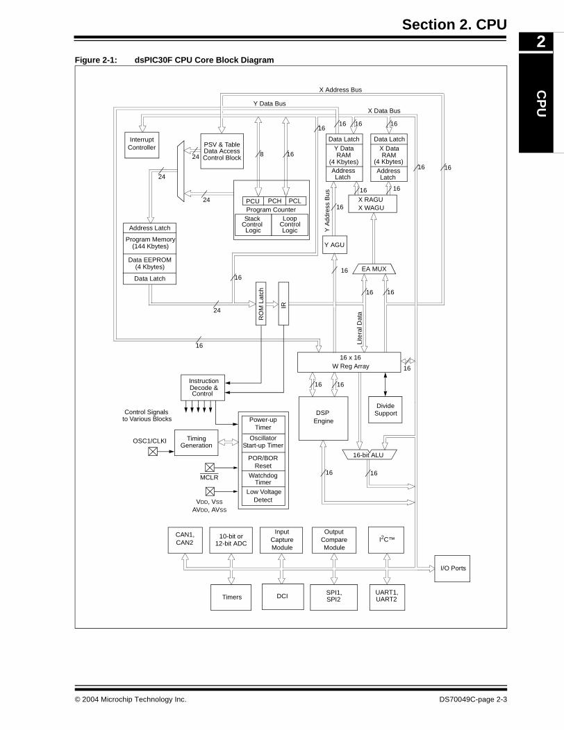
A block diagram of the CPU is shown in Figure 2-1.
DS70049C-page 2-2 © 2004 Microchip Technology Inc.
Section 2. CPUC
PU
2
Figure 2-1: dsPIC30F CPU Core Block DiagramPower-upTimer
OscillatorStart-up Timer
POR/BORReset
WatchdogTimer
InstructionDecode &Control
OSC1/CLKI
MCLR
VDD, VSS
Low VoltageDetect
UART1,
CAN2
TimingGeneration
CAN1,
16
PCH PCL
16
Program Counter
16-bit ALU
24
24
24
24
X Data Bus
IR
I2C™
DCI
PCU
10-bit or
Timers
InputCaptureModule
OutputCompareModule
16
16 16
16 x 16W Reg Array
DivideSupport
EngineDSP
RO
M L
atch
16
Y Data Bus
EA MUX
X RAGUX WAGU
Y AGU
AVDD, AVSS
UART2SPI2
16
16
16
16
16
16
16
16
16
8
InterruptController PSV & Table
Data AccessControl Block
StackControl
Logic
LoopControlLogic
Data LatchData LatchY Data
(4 Kbytes)RAM
X Data
(4 Kbytes)RAM
AddressLatch
AddressLatch
Control Signalsto Various Blocks
16
SPI1,
Address Latch
Program Memory(144 Kbytes)
Data Latch
Data EEPROM(4 Kbytes)
I/O Ports
16
16
16
X Address Bus
Y A
ddre
ss B
us
16
Lite
ral D
ata
12-bit ADC
© 2004 Microchip Technology Inc. DS70049C-page 2-3
dsPIC30F Family Reference Manual
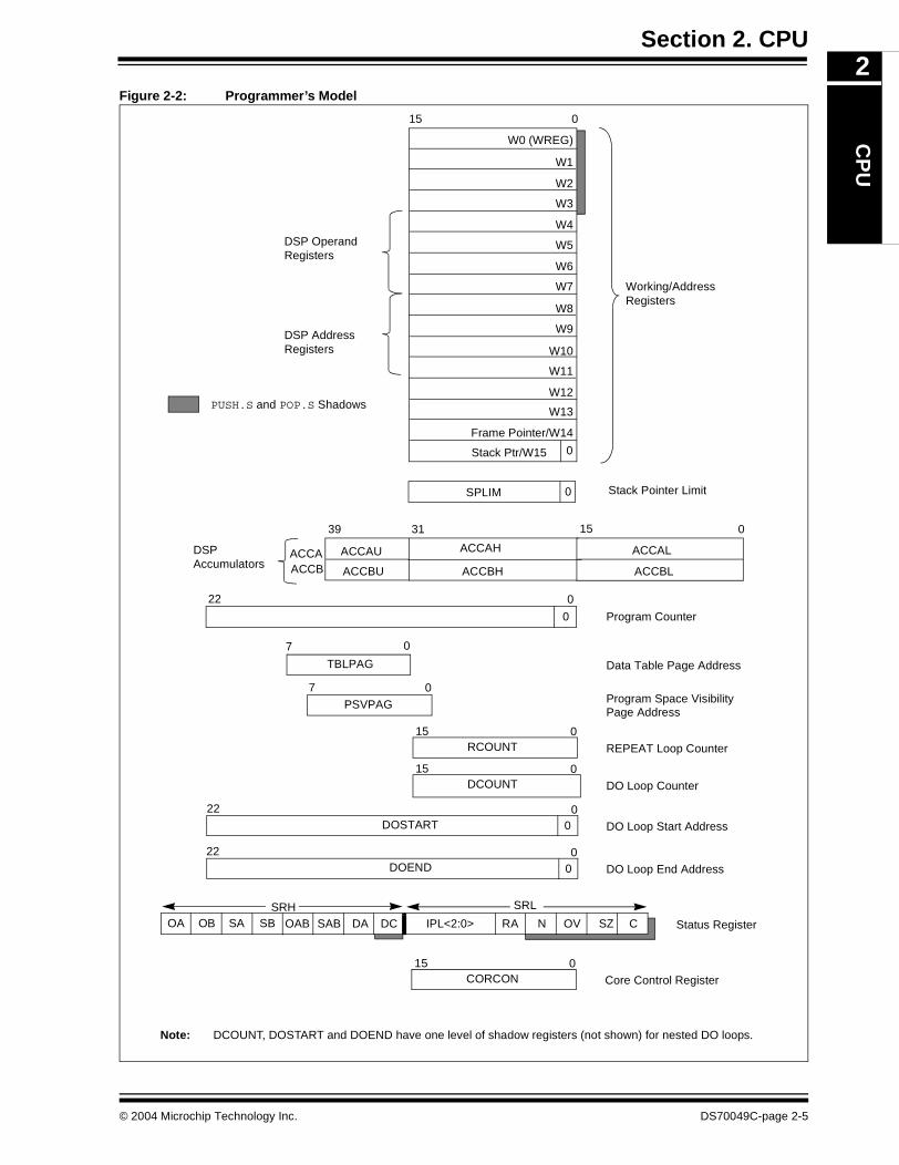
2.2 Programmer’s Model
The programmer’s model for the dsPIC30F is shown in Figure 2-2. All registers in the program-mer’s model are memory mapped and can be manipulated directly by instructions. A descriptionof each register is provided in Table 2-1.
In addition to the registers contained in the programmer’s model, the dsPIC30F contains controlregisters for modulo addressing, bit-reversed addressing and interrupts. These registers aredescribed in subsequent sections of this document.
All registers associated with the programmer’s model are memory mapped, as shown inTable 2-8 on page 2-38.
Table 2-1: Programmer’s Model Register Descriptions
Register(s) Name Description
W0 through W15 Working register array
ACCA, ACCB 40-bit DSP AccumulatorsPC 23-bit Program CounterSR ALU and DSP Engine Status register
SPLIM Stack Pointer Limit Value registerTBLPAG Table Memory Page Address registerPSVPAG Program Space Visibility Page Address register
RCOUNT REPEAT Loop Count registerDCOUNT DO Loop Count registerDOSTART DO Loop Start Address register
DOEND DO Loop End Address registerCORCON Contains DSP Engine and DO Loop control bits
DS70049C-page 2-4 © 2004 Microchip Technology Inc.
Section 2. CPUC
PU
2
Figure 2-2: Programmer’s ModelN OV SZ C
TBLPAG
22 0
7 0
015
Program Counter
Data Table Page Address
Status Register
Working/AddressRegisters
DSP OperandRegisters
W0 (WREG)
W1
W2
W3
W4
W5
W6
W7
W8
W9
W10
W11
W12
W13
Frame Pointer/W14
Stack Ptr/W15
DSP AddressRegisters
39 031
DSPAccumulators
PSVPAG
7 0Program Space Visibility
RA
0
OA OB SA SB
RCOUNT15 0
REPEAT Loop Counter
DCOUNT15 0
DO Loop Counter
DOSTART22 0
DO Loop Start Address
DOEND DO Loop End Address
IPL<2:0>
SPLIM Stack Pointer Limit
15
22 0
SRL
PUSH.S and POP.S Shadows
0
0
OAB SAB
Page Address
DA DC
CORCON15 0
Core Control Register
ACCAH ACCALACCAU
ACCBU ACCBH ACCBL
ACCAACCB
SRH
0
0
Note: DCOUNT, DOSTART and DOEND have one level of shadow registers (not shown) for nested DO loops.
© 2004 Microchip Technology Inc. DS70049C-page 2-5
dsPIC30F Family Reference Manual
2.2.1 Working Register Array
The 16 working (W) registers can function as data, address or address offset registers. Thefunction of a W register is determined by the Addressing mode of the instruction that accesses it.
The dsPIC30F instruction set can be divided into two instruction types: register and file registerinstructions. Register instructions can use each W register as a data value or an address offsetvalue. For example:
MOV W0,W1 ; move contents of W0 to W1MOV W0,[W1] ; move W0 to address contained in W1ADD W0,[W4],W5 ; add contents of W0 to contents pointed
; to by W4. Place result in W5.
2.2.1.1 W0 and File Register Instructions
W0 is a special working register because it is the only working register that can be used in fileregister instructions. File register instructions operate on a specific memory address containedin the instruction opcode and W0. W1-W15 cannot be specified as a target register in file registerinstructions.
The file register instructions provide backward compatibility with existing PICmicro® deviceswhich have only one W register. The label ‘WREG’ is used in the assembler syntax to denote W0in a file register instruction. For example:
MOV WREG,0x0100 ; move contents of W0 to address 0x0100ADD 0x0100,WREG ; add W0 to address 0x0100, store in W0
2.2.1.2 W Register Memory Mapping
Since the W registers are memory mapped, it is possible to access a W register in a file registerinstruction as shown below:
MOV 0x0004, W10 ; equivalent to MOV W2, W10
where 0x0004 is the address in memory of W2.
Further, it is also possible to execute an instruction that will attempt to use a W register as bothan address pointer and operand destination. For example:
MOV W1,[W2++]
where:
W1 = 0x1234W2 = 0x0004 ;[W2] addresses W2
In the example above, the contents of W2 are 0x0004. Since W2 is used as an address pointer,it points to location 0x0004 in memory. W2 is also mapped to this address in memory. Eventhough this is an unlikely event, it is impossible to detect until run-time. The dsPIC30F ensuresthat the data write will dominate, resulting in W2 = 0x1234 in the example above.
2.2.1.3 W Registers and Byte Mode Instructions
Byte instructions which target the W register array only affect the Least Significant Byte of thetarget register. Since the working registers are memory mapped, the Least and Most SignificantBytes can be manipulated through byte wide data memory space accesses.
2.2.2 Shadow Registers
Many of the registers in the programmer’s model have an associated shadow register as shownin Figure 2-2. None of the shadow registers are accessible directly. There are two types ofshadow registers: those utilized by the PUSH.S and POP.S instructions and those utilized by theDO instruction.
Note: For a complete description of Addressing modes and instruction syntax, pleaserefer to the dsPIC30F Programmer’s Reference Manual (DS70032).
DS70049C-page 2-6 © 2004 Microchip Technology Inc.
Section 2. CPUC
PU
2
2.2.2.1 PUSH.S and POP.S Shadow RegistersThe PUSH.S and POP.S instructions are useful for fast context save/restore during a function callor Interrupt Service Routine (ISR). The PUSH.S instruction will transfer the following registervalues into their respective shadow registers:
• W0...W3• SR (N, OV, Z , C, DC bits only)
The POP.S instruction will restore the values from the shadow registers into these registerlocations. A code example using the PUSH.S and POP.S instructions is shown below:
MyFunction:
PUSH.S ; Save W registers, MCU statusMOV #0x03,W0 ; load a literal value into W0ADD RAM100 ; add W0 to contents of RAM100BTSC SR,#Z ; is the result 0?BSET Flags,#IsZero ; Yes, set a flagPOP.S ; Restore W regs, MCU status RETURN
The PUSH.S instruction will overwrite the contents previously saved in the shadow registers. Theshadow registers are only one level in depth, so care must be taken if the shadow registers areto be used for multiple software tasks.
The user must ensure that any task using the shadow registers will not be interrupted by a higherpriority task that also uses the shadow registers. If the higher priority task is allowed to interruptthe lower priority task, the contents of the shadow registers saved in the lower priority task willbe overwritten by the higher priority task.
2.2.2.2 DO Loop Shadow Registers
The following registers are automatically saved in shadow registers when a DO instruction isexecuted:
• DOSTART
• DOEND• DCOUNT
The DO shadow registers are one level in depth, permitting two loops to be automatically nested.Refer to Section 2.9.2.2 “DO Loop Nesting” for further details.
2.2.3 Uninitialized W Register Reset
The W register array (with the exception of W15) is cleared during all Resets and is considereduninitialized until written to. An attempt to use an uninitialized register as an address pointer willreset the device.
A word write must be performed to initialize a W register. A byte write will not affect the initializationdetection logic.
© 2004 Microchip Technology Inc. DS70049C-page 2-7
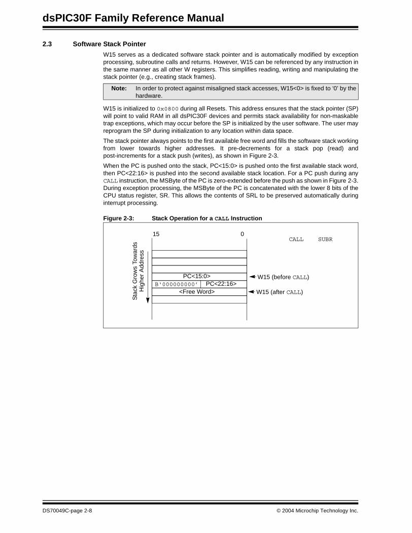
dsPIC30F Family Reference Manual
2.3 Software Stack Pointer
W15 serves as a dedicated software stack pointer and is automatically modified by exceptionprocessing, subroutine calls and returns. However, W15 can be referenced by any instruction inthe same manner as all other W registers. This simplifies reading, writing and manipulating thestack pointer (e.g., creating stack frames).
W15 is initialized to 0x0800 during all Resets. This address ensures that the stack pointer (SP)will point to valid RAM in all dsPIC30F devices and permits stack availability for non-maskabletrap exceptions, which may occur before the SP is initialized by the user software. The user mayreprogram the SP during initialization to any location within data space.
The stack pointer always points to the first available free word and fills the software stack workingfrom lower towards higher addresses. It pre-decrements for a stack pop (read) andpost-increments for a stack push (writes), as shown in Figure 2-3.
When the PC is pushed onto the stack, PC<15:0> is pushed onto the first available stack word,then PC<22:16> is pushed into the second available stack location. For a PC push during anyCALL instruction, the MSByte of the PC is zero-extended before the push as shown in Figure 2-3.During exception processing, the MSByte of the PC is concatenated with the lower 8 bits of theCPU status register, SR. This allows the contents of SRL to be preserved automatically duringinterrupt processing.
Figure 2-3: Stack Operation for a CALL Instruction
Note: In order to protect against misaligned stack accesses, W15<0> is fixed to ‘0’ by thehardware.
<Free Word>
PC<15:0>PC<22:16>
015
W15 (before CALL)
W15 (after CALL)
Sta
ck G
row
s To
war
dsH
ighe
r A
ddre
ss
B‘000000000’
CALL SUBR
DS70049C-page 2-8 © 2004 Microchip Technology Inc.
Section 2. CPUC
PU
2
2.3.1 Software Stack ExamplesThe software stack is manipulated using the PUSH and POP instructions. The PUSH and POPinstructions are the equivalent of a MOV instruction with W15 used as the destination pointer. Forexample, the contents of W0 can be pushed onto the stack by:
PUSH W0
This syntax is equivalent to:
MOV W0,[W15++]
The contents of the top-of-stack can be returned to W0 by:
POP W0
This syntax is equivalent to:
MOV [--W15],W0
Figure 2-4 through Figure 2-7 show examples of how the software stack is used. Figure 2-4shows the software stack at device initialization. W15 has been initialized to 0x0800. Further-more, this example assumes the values 0x5A5A and 0x3636 have been written to W0 and W1,respectively. The stack is pushed for the first time in Figure 2-5 and the value contained in W0 iscopied to the stack. W15 is automatically updated to point to the next available stack location(0x0802). In Figure 2-6, the contents of W1 are pushed onto the stack. In Figure 2-7, the stackis popped and the top-of-stack value (previously pushed from W1) is written to W3.
Figure 2-4: Stack Pointer at Device Reset
Figure 2-5: Stack Pointer After the First PUSH Instruction
Figure 2-6: Stack Pointer After the Second PUSH Instruction
0x0000
0xFFFE
0x0800W15
W15 = 0x0800W0 = 0x5A5AW1 = 0x3636
0x0000
0xFFFE
0x5A5A
W15 = 0x0802W0 = 0x5A5AW1 = 0x3636
0x0800 PUSH W00x0802W15
0x0000
0xFFFE
0x5A5A0x3636
W15 = 0x0804W0 = 0x5A5AW1 = 0x3636
0x0800PUSH W1
0x08020x0804W15
© 2004 Microchip Technology Inc. DS70049C-page 2-9
dsPIC30F Family Reference Manual
Figure 2-7: Stack Pointer After a POP Instruction
2.3.2 W14 Software Stack Frame Pointer
A frame is a user defined section of memory in the stack that is used by a single subroutine. W14is a special working register because it can be used as a stack frame pointer with the LNK (link)and ULNK (unlink) instructions. W14 can be used in a normal working register by instructionswhen it is not used as a frame pointer.
Refer to the “dsPIC30F Programmer’s Reference Manual” (DS70030) for software examples thatuse W14 as a stack frame pointer.
2.3.3 Stack Pointer Overflow
There is a stack limit register (SPLIM) associated with the stack pointer that is reset to 0x0000.SPLIM is a 16-bit register, but SPLIM<0> is fixed to ‘0’ because all stack operations must be wordaligned.
The stack overflow check will not be enabled until a word write to SPLIM occurs, after which timeit can only be disabled by a device Reset. All effective addresses generated using W15 as asource or destination are compared against the value in SPLIM. If the contents of the StackPointer (W15) are greater than the contents of the SPLIM register by 2 and a push operation isperformed, a Stack Error Trap will not occur. The Stack Error Trap will occur on a subsequentpush operation. Thus, for example, if it is desirable to cause a Stack Error Trap when the stackgrows beyond address 0x2000 in RAM, initialize the SPLIM with the value, 0x1FFE.
If stack overflow checking has been enabled, a stack error trap will also occur if the W15 effectiveaddress calculation wraps over the end of data space (0xFFFF).
Refer to Section 6. “Reset Interrupts” for more information on the stack error trap.
2.3.4 Stack Pointer Underflow
The stack is initialized to 0x0800 during Reset. A stack error trap will be initiated should the stackpointer address ever be less than 0x0800.
0x0000
0xFFFE
0x05A5A0x03636
0x3636 → W3W15 = 0x0802
POP W3
0x08020x0800
W15
Note: A Stack Error Trap may be caused by any instruction that uses the contents of theW15 register to generate an effective address (EA). Thus, if the contents of W15 aregreater than the contents of the SPLIM register by 2, and a CALL instruction isexecuted, or if an interrupt occurs, a Stack Error Trap will be generated.
Note: A write to the Stack Pointer Limit register, SPLIM, should not be followed by anindirect read operation using W15.
Note: Locations in data space between 0x0000 and 0x07FF are, in general, reserved forcore and peripheral special function registers.
DS70049C-page 2-10 © 2004 Microchip Technology Inc.

Section 2. CPUC
PU
2
2.4 CPU Register Descriptions2.4.1 SR: CPU Status Register
The dsPIC30F CPU has a 16-bit status register (SR), the LSByte of which is referred to as thelower status register (SRL). The upper byte of SR is referred to as SRH. A detailed descriptionof SR is shown in Register 2-1.
SRL contains all the MCU ALU operation status flags, plus the CPU interrupt priority status bits,IPL<2:0> and the REPEAT loop active status bit, RA (SR<4>). During exception processing, SRLis concatenated with the MSByte of the PC to form a complete word value, which is then stacked.
SRH contains the DSP Adder/Subtractor status bits, the DO loop active bit, DA (SR<9>) and theDigit Carry bit, DC (SR<8>).
The SR bits are readable/writable with the following exceptions:
1. The DA bit (SR<8>): DA is a read only bit.2. The RA bit (SR<4>): RA is a read only bit.3. The OA, OB (SR<15:14>) and OAB (SR<11>) bits: These bits are read only and can only
be modified by the DSP engine hardware.4. The SA, SB (SR<13:12>) and SAB (SR<10>) bits: These are read and clear only and can
only be set by the DSP engine hardware. Once set, they remain set until cleared by theuser, irrespective of the results from any subsequent DSP operations.
2.4.2 CORCON: Core Control Register
The CORCON register contains bits that control the operation of the DSP multiplier and DO loophardware. The CORCON register also contains the IPL3 status bit, which is concatenated withIPL<2:0> (SR<7:5>), to form the CPU Interrupt Priority Level.
Note: Clearing the SAB bit will also clear both the SA and SB bits.
Note: A description of the SR bits affected by each instruction is provided in the dsPIC30FProgrammer’s Reference Manual (DS70030).
© 2004 Microchip Technology Inc. DS70049C-page 2-11
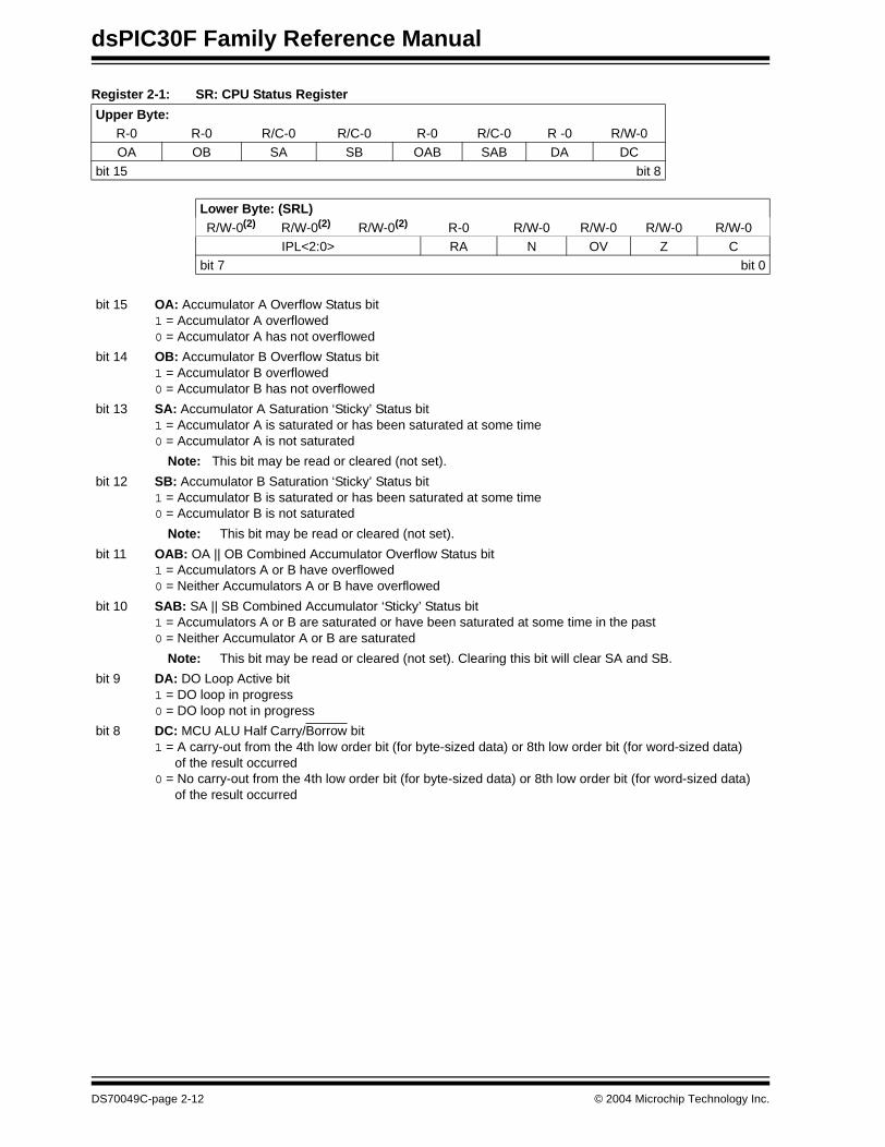
dsPIC30F Family Reference Manual
Register 2-1: SR: CPU Status Register
Upper Byte:R-0 R-0 R/C-0 R/C-0 R-0 R/C-0 R -0 R/W-0OA OB SA SB OAB SAB DA DC
bit 15 bit 8
Lower Byte: (SRL)R/W-0(2) R/W-0(2) R/W-0(2) R-0 R/W-0 R/W-0 R/W-0 R/W-0
IPL<2:0> RA N OV Z Cbit 7 bit 0
bit 15 OA: Accumulator A Overflow Status bit1 = Accumulator A overflowed0 = Accumulator A has not overflowed
bit 14 OB: Accumulator B Overflow Status bit1 = Accumulator B overflowed0 = Accumulator B has not overflowed
bit 13 SA: Accumulator A Saturation ‘Sticky’ Status bit1 = Accumulator A is saturated or has been saturated at some time0 = Accumulator A is not saturated
Note: This bit may be read or cleared (not set).
bit 12 SB: Accumulator B Saturation ‘Sticky’ Status bit1 = Accumulator B is saturated or has been saturated at some time0 = Accumulator B is not saturated
Note: This bit may be read or cleared (not set).
bit 11 OAB: OA || OB Combined Accumulator Overflow Status bit1 = Accumulators A or B have overflowed0 = Neither Accumulators A or B have overflowed
bit 10 SAB: SA || SB Combined Accumulator ‘Sticky’ Status bit1 = Accumulators A or B are saturated or have been saturated at some time in the past0 = Neither Accumulator A or B are saturated
Note: This bit may be read or cleared (not set). Clearing this bit will clear SA and SB.
bit 9 DA: DO Loop Active bit1 = DO loop in progress0 = DO loop not in progress
bit 8 DC: MCU ALU Half Carry/Borrow bit1 = A carry-out from the 4th low order bit (for byte-sized data) or 8th low order bit (for word-sized data)
of the result occurred0 = No carry-out from the 4th low order bit (for byte-sized data) or 8th low order bit (for word-sized data)
of the result occurred
DS70049C-page 2-12 © 2004 Microchip Technology Inc.
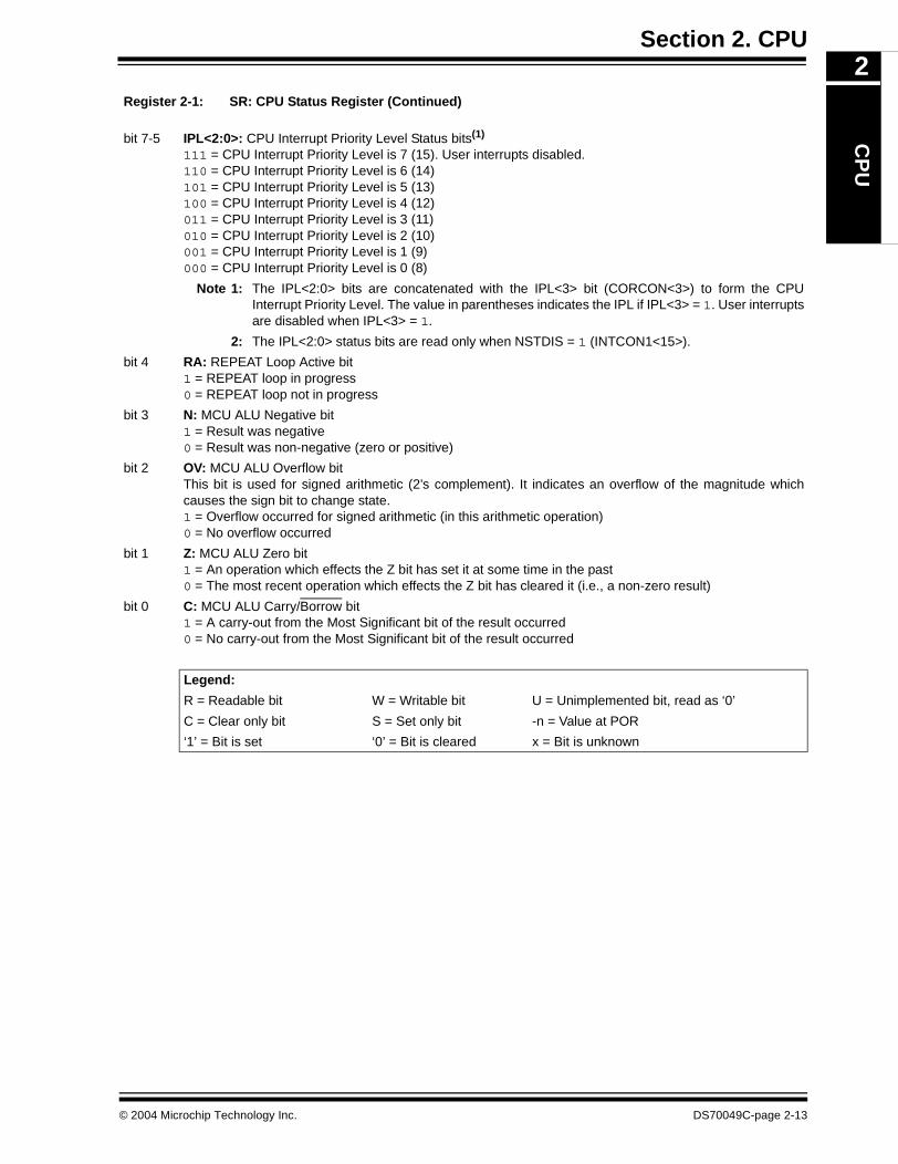
Section 2. CPUC
PU
2
Register 2-1: SR: CPU Status Register (Continued)bit 7-5 IPL<2:0>: CPU Interrupt Priority Level Status bits(1)
111 = CPU Interrupt Priority Level is 7 (15). User interrupts disabled.110 = CPU Interrupt Priority Level is 6 (14)101 = CPU Interrupt Priority Level is 5 (13)100 = CPU Interrupt Priority Level is 4 (12)011 = CPU Interrupt Priority Level is 3 (11)010 = CPU Interrupt Priority Level is 2 (10)001 = CPU Interrupt Priority Level is 1 (9)000 = CPU Interrupt Priority Level is 0 (8)
Note 1: The IPL<2:0> bits are concatenated with the IPL<3> bit (CORCON<3>) to form the CPUInterrupt Priority Level. The value in parentheses indicates the IPL if IPL<3> = 1. User interruptsare disabled when IPL<3> = 1.
2: The IPL<2:0> status bits are read only when NSTDIS = 1 (INTCON1<15>).
bit 4 RA: REPEAT Loop Active bit1 = REPEAT loop in progress0 = REPEAT loop not in progress
bit 3 N: MCU ALU Negative bit1 = Result was negative0 = Result was non-negative (zero or positive)
bit 2 OV: MCU ALU Overflow bitThis bit is used for signed arithmetic (2’s complement). It indicates an overflow of the magnitude whichcauses the sign bit to change state. 1 = Overflow occurred for signed arithmetic (in this arithmetic operation)0 = No overflow occurred
bit 1 Z: MCU ALU Zero bit1 = An operation which effects the Z bit has set it at some time in the past0 = The most recent operation which effects the Z bit has cleared it (i.e., a non-zero result)
bit 0 C: MCU ALU Carry/Borrow bit1 = A carry-out from the Most Significant bit of the result occurred0 = No carry-out from the Most Significant bit of the result occurred
Legend:
R = Readable bit W = Writable bit U = Unimplemented bit, read as ‘0’
C = Clear only bit S = Set only bit -n = Value at POR
‘1’ = Bit is set ‘0’ = Bit is cleared x = Bit is unknown
© 2004 Microchip Technology Inc. DS70049C-page 2-13
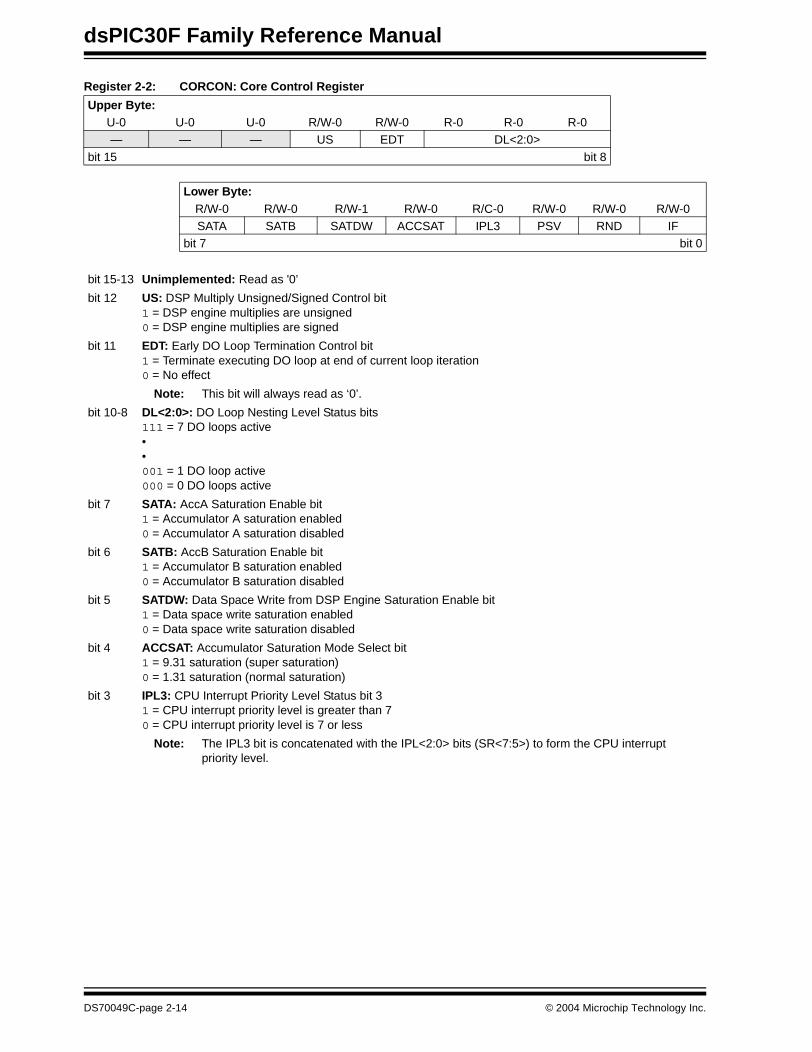
dsPIC30F Family Reference Manual
Register 2-2: CORCON: Core Control Register
Upper Byte:U-0 U-0 U-0 R/W-0 R/W-0 R-0 R-0 R-0— — — US EDT DL<2:0>
bit 15 bit 8
Lower Byte:R/W-0 R/W-0 R/W-1 R/W-0 R/C-0 R/W-0 R/W-0 R/W-0SATA SATB SATDW ACCSAT IPL3 PSV RND IF
bit 7 bit 0
bit 15-13 Unimplemented: Read as '0’
bit 12 US: DSP Multiply Unsigned/Signed Control bit1 = DSP engine multiplies are unsigned 0 = DSP engine multiplies are signed
bit 11 EDT: Early DO Loop Termination Control bit1 = Terminate executing DO loop at end of current loop iteration0 = No effect
Note: This bit will always read as ‘0’.
bit 10-8 DL<2:0>: DO Loop Nesting Level Status bits111 = 7 DO loops active••001 = 1 DO loop active000 = 0 DO loops active
bit 7 SATA: AccA Saturation Enable bit1 = Accumulator A saturation enabled0 = Accumulator A saturation disabled
bit 6 SATB: AccB Saturation Enable bit1 = Accumulator B saturation enabled0 = Accumulator B saturation disabled
bit 5 SATDW: Data Space Write from DSP Engine Saturation Enable bit1 = Data space write saturation enabled0 = Data space write saturation disabled
bit 4 ACCSAT: Accumulator Saturation Mode Select bit1 = 9.31 saturation (super saturation)0 = 1.31 saturation (normal saturation)
bit 3 IPL3: CPU Interrupt Priority Level Status bit 31 = CPU interrupt priority level is greater than 70 = CPU interrupt priority level is 7 or less
Note: The IPL3 bit is concatenated with the IPL<2:0> bits (SR<7:5>) to form the CPU interrupt priority level.
DS70049C-page 2-14 © 2004 Microchip Technology Inc.

Section 2. CPUC
PU
2
Register 2-2: CORCON: Core Control Register (Continued)bit 2 PSV: Program Space Visibility in Data Space Enable bit1 = Program space visible in data space0 = Program space not visible in data space
bit 1 RND: Rounding Mode Select bit1 = Biased (conventional) rounding enabled0 = Unbiased (convergent) rounding enabled
bit 0 IF: Integer or Fractional Multiplier Mode Select bit1 = Integer mode enabled for DSP multiply ops0 = Fractional mode enabled for DSP multiply ops
Legend:
R = Readable bit W = Writable bit U = Unimplemented bit, read as ‘0’ C = Bit can be cleared
-n = Value at POR ‘1’ = Bit is set ‘0’ = Bit is cleared x = Bit is unknown
© 2004 Microchip Technology Inc. DS70049C-page 2-15
dsPIC30F Family Reference Manual
2.4.3 Other dsPIC30F CPU Control Registers
The registers listed below are associated with the dsPIC30F CPU core, but are described infurther detail in other sections of this manual.
2.4.3.1 TBLPAG: Table Page Register
The TBLPAG register is used to hold the upper 8 bits of a program memory address during tableread and write operations. Table instructions are used to transfer data between program memoryspace and data memory space. Refer to Section 4. “Program Memory” for further details.
2.4.3.2 PSVPAG: Program Space Visibility Page Register
Program space visibility allows the user to map a 32-Kbyte section of the program memory spaceinto the upper 32 Kbytes of data address space. This feature allows transparent access ofconstant data through dsPIC30F instructions that operate on data memory. The PSVPAGregister selects the 32 Kbyte region of program memory space that is mapped to the dataaddress space. Refer to Section 4. “Program Memory” for more information on the PSVPAGregister.
2.4.3.3 MODCON: Modulo Control Register
The MODCON register is used to enable and configure modulo addressing (circular buffers).Refer to Section 3. “Data Memory” for further details on modulo addressing.
2.4.3.4 XMODSRT, XMODEND: X Modulo Start and End Address Registers
The XMODSRT and XMODEND registers hold the start and end addresses for modulo (circular)buffers implemented in the X data memory address space. Refer to Section 3. “Data Memory”for further details on modulo addressing.
2.4.3.5 YMODSRT, YMODEND: Y Modulo Start and End Address Registers
The YMODSRT and YMODEND registers hold the start and end addresses for modulo (circular)buffers implemented in the Y data memory address space. Refer to Section 3. “Data Memory”for further details on modulo addressing.
2.4.3.6 XBREV: X Modulo Bit-Reverse Register
The XBREV register is used to set the buffer size used for bit-reversed addressing. Refer toSection 3. “Data Memory” for further details on bit-reversed addressing.
2.4.3.7 DISICNT: Disable Interrupts Count Register
The DISICNT register is used by the DISI instruction to disable interrupts of priority 1-6 for aspecified number of cycles. See Section 6. “Reset Interrupts” for further information.
DS70049C-page 2-16 © 2004 Microchip Technology Inc.

Section 2. CPUC
PU
2
2.5 Arithmetic Logic Unit (ALU)The dsPIC30F ALU is 16-bits wide and is capable of addition, subtraction, single bit shifts andlogic operations. Unless otherwise mentioned, arithmetic operations are 2’s complement innature. Depending on the operation, the ALU may affect the values of the Carry (C), Zero (Z),Negative (N), Overflow (OV) and Digit Carry (DC) status bits in the SR register. The C and DCstatus bits operate as a Borrow and Digit Borrow bits, respectively, for subtraction operations.
The ALU can perform 8-bit or 16-bit operations, depending on the mode of the instruction that isused. Data for the ALU operation can come from the W register array or data memory dependingon the Addressing mode of the instruction. Likewise, output data from the ALU can be written tothe W register array or a data memory location.
Refer to the dsPIC30F Programmer’s Reference Manual (DS70030) for information on the SRbits affected by each instruction, Addressing modes and 8-bit/16-bit Instruction modes.
2.5.1 Byte to Word Conversion
The dsPIC30F has two instructions that are helpful when mixing 8-bit and 16-bit ALU operations.The sign-extend (SE) instruction takes a byte value in a W register or data memory and createsa sign-extended word value that is stored in a W register. The zero-extend (ZE) instruction clearsthe 8 MSbs of a word value in a W register or data memory and places the result in a destinationW register.
Note 1: Byte operations use the 16-bit ALU and can produce results in excess of 8 bits.However, to maintain backward compatibility with PICmicro devices, the ALU resultfrom all byte operations is written back as a byte (i.e., MSByte not modified), andthe SR register is updated based only upon the state of the LSByte of the result.
2: All register instructions performed in Byte mode only affect the LSByte of the Wregisters. The MSByte of any W register can be modified by using file registerinstructions that access the memory mapped contents of the W registers.
© 2004 Microchip Technology Inc. DS70049C-page 2-17
dsPIC30F Family Reference Manual
2.6 DSP Engine
The DSP engine is a block of hardware which is fed data from the W register array but containsits own specialized result registers. The DSP engine is driven from the same instruction decoderthat directs the MCU ALU. In addition, all operand effective addresses (EAs) are generated in theW register array. Concurrent operation with MCU instruction flow is not possible, though both theMCU ALU and DSP engine resources may be shared by all instructions in the instruction set.
The DSP engine consists of the following components:
• high speed 17-bit x 17-bit multiplier• barrel shifter
• 40-bit adder/subtractor• two target accumulator registers• rounding logic with Selectable modes
• saturation logic with Selectable modes
Data input to the DSP engine is derived from one of the following sources:
1. Directly from the W array (registers W4, W5, W6 or W7) for dual source operand DSPinstructions. Data values for the W4, W5, W6 and W7 registers are pre-fetched via the Xand Y memory data buses.
2. From the X memory data bus for all other DSP instructions.
Data output from the DSP engine is written to one of the following destinations:
1. The target accumulator, as defined by the DSP instruction being executed.2. The X memory data bus to any location in the data memory address space.
The DSP engine has the capability to perform inherent accumulator to accumulator operationswhich require no additional data.
The MCU shift and multiply instructions use the DSP engine hardware to obtain their results. TheX memory data bus is used for data reads and writes in these operations.
A block diagram of the DSP engine is shown in Figure 2-8.
Note: For detailed code examples and instruction syntax related to this section, refer tothe dsPIC30F Programmer’s Reference Manual (DS70030).
DS70049C-page 2-18 © 2004 Microchip Technology Inc.

Section 2. CPUC
PU
2
Figure 2-8: DSP Engine Block DiagramZero Backfill
Sign-Extend
BarrelShifter
40-bit Accumulator A40-bit Accumulator B
Rou
nd L
ogic
X D
ata
Bus
To/From W Array
Adder
Saturate
Negate
32
3232
16
16 16
16
40 40
40 40Y
Dat
a B
us
40
16
40
Multiplier/Scaler
17-bit x 17-bit
16-bit to 17-bitConversion
Sat
urat
ion
Logi
c
© 2004 Microchip Technology Inc. DS70049C-page 2-19
dsPIC30F Family Reference Manual
2.6.1 Data Accumulators
There are two 40-bit data accumulators, ACCA and ACCB, that are the result registers for theDSP instructions listed in Table 2-3. Each accumulator is memory mapped to three registers,where ‘x’ denotes the particular accumulator:
• ACCxL: ACCx<15:0>• ACCxH: ACCx<31:16>
• ACCxU: ACCx<39:32>For fractional operations that use the accumulators, the radix point is located to the right ofbit 31. The range of fractional values that be stored in each accumulator is -256.0 to(256.0 – 2-31). For integer operations that use the accumulators, the radix point is located to theright of bit 0. The range of integer values that can be stored in each accumulator is-549,755,813,888 to 549,755,813,887.
2.6.2 Multiplier
The dsPIC30F features a 17-bit x 17-bit multiplier which is shared by both the MCU ALU and theDSP engine. The multiplier is capable of signed or unsigned operation and can support either1.31 fractional (Q.31) or 32-bit integer results.
The multiplier takes in 16-bit input data and converts the data to 17-bits. Signed operands to themultiplier are sign-extended. Unsigned input operands are zero-extended. The 17-bit conversionlogic is transparent to the user and allows the multiplier to support mixed sign andunsigned/unsigned multiplication.
The IF control bit (CORCON<0>) determines integer/fractional operation for the instructionslisted in Table 2-3. The IF bit does not affect MCU multiply instructions listed in Table 2-4, whichare always integer operations. The multiplier scales the result one bit to the left for fractionaloperation. The LSbit of the result is always cleared. The multiplier defaults to Fractional mode forDSP operations at a device Reset.
The representation of data in hardware for each of these modes is as follows:
• Integer data is inherently represented as a signed two’s complement value, where the MSbit is defined as a sign bit. Generally speaking, the range of an N-bit two’s complement integer is -2N-1 to 2N-1 – 1.
• Fractional data is represented as a two’s complement fraction where the MSbit is defined as a sign bit and the radix point is implied to lie just after the sign bit (Q.X format). The range of an N-bit two’s complement fraction with this implied radix point is -1.0 to (1 – 21-N).
Figure 2-9 and Figure 2-10 illustrate how the multiplier hardware interprets data in Integer andFractional modes. The range of data in both Integer and Fractional modes is listed in Table 2-2.
DS70049C-page 2-20 © 2004 Microchip Technology Inc.

Section 2. CPUC
PU
2
Figure 2-9: Integer and Fractional Representation of 0x4001Figure 2-10: Integer and Fractional Representation of 0xC002
Different Representations of 0x4001
Integer:
-215 214 213 212 . . . .
0x4001 = 214 + 20 = 16385
1.15 Fractional:
2-15
0
2-1 2-2 2-3 . . . -20
20
0x4001 = 2-1 + 2-15 = 0.500030518
Implied Radix Point
.
1 10 0 0 0 0 0 0 0 0 0 0 0 0
0 1 10 0 0 0 0 0 0 0 0 0 0 0 0
Different Representations of 0xC002
Integer:
-215 214 213 212 . . . .
0xC002 = -215 + 214 + 20 = -32768 + 16384 + 2 = -16382
1.15 Fractional:
2-15 . 2-1 2-2 2-3 . . . -20
20
0xC002 = -20 + 2-1 + 2-14 = -1 + 0.5 + 0.000061035 = -0.499938965
Implied Radix Point
1 1 00 0 0 0 0 0 0 0 0 0 0 0 1
1 1 00 0 0 0 0 0 0 0 0 0 0 0 1
© 2004 Microchip Technology Inc. DS70049C-page 2-21
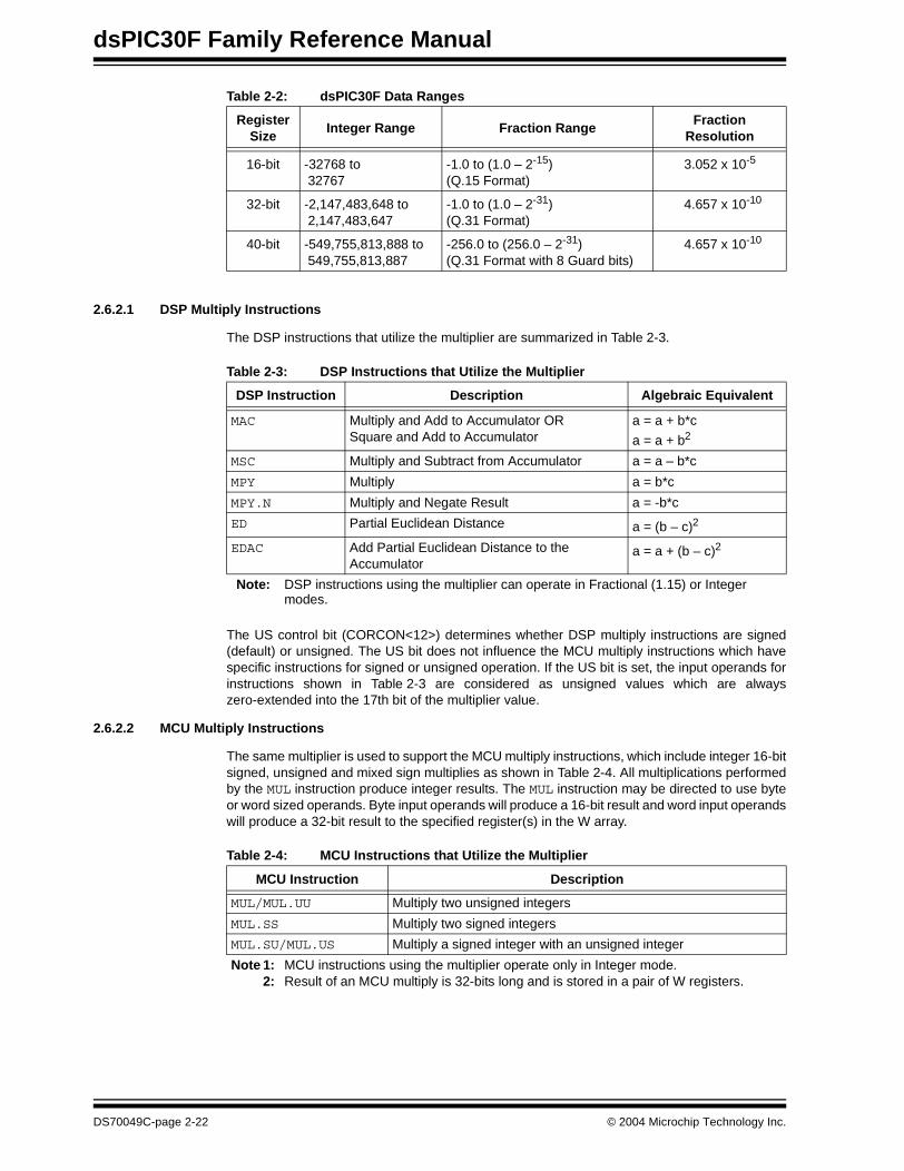
dsPIC30F Family Reference Manual
Table 2-2: dsPIC30F Data Ranges
2.6.2.1 DSP Multiply Instructions
The DSP instructions that utilize the multiplier are summarized in Table 2-3.
Table 2-3: DSP Instructions that Utilize the Multiplier
The US control bit (CORCON<12>) determines whether DSP multiply instructions are signed(default) or unsigned. The US bit does not influence the MCU multiply instructions which havespecific instructions for signed or unsigned operation. If the US bit is set, the input operands forinstructions shown in Table 2-3 are considered as unsigned values which are alwayszero-extended into the 17th bit of the multiplier value.
2.6.2.2 MCU Multiply Instructions
The same multiplier is used to support the MCU multiply instructions, which include integer 16-bitsigned, unsigned and mixed sign multiplies as shown in Table 2-4. All multiplications performedby the MUL instruction produce integer results. The MUL instruction may be directed to use byteor word sized operands. Byte input operands will produce a 16-bit result and word input operandswill produce a 32-bit result to the specified register(s) in the W array.
Table 2-4: MCU Instructions that Utilize the Multiplier
Register Size
Integer Range Fraction RangeFraction
Resolution
16-bit -32768 to 32767
-1.0 to (1.0 – 2-15)(Q.15 Format)
3.052 x 10⁻⁵
32-bit -2,147,483,648 to 2,147,483,647
-1.0 to (1.0 – 2-31)(Q.31 Format)
4.657 x 10⁻¹⁰
40-bit -549,755,813,888 to 549,755,813,887
-256.0 to (256.0 – 2-31)(Q.31 Format with 8 Guard bits)
4.657 x 10⁻¹⁰
DSP Instruction Description Algebraic Equivalent
MAC Multiply and Add to Accumulator ORSquare and Add to Accumulator
a = a + b*c
a = a + b2
MSC Multiply and Subtract from Accumulator a = a – b*c
MPY Multiply a = b*c
MPY.N Multiply and Negate Result a = -b*c
ED Partial Euclidean Distance a = (b – c)2
EDAC Add Partial Euclidean Distance to theAccumulator
a = a + (b – c)2
Note: DSP instructions using the multiplier can operate in Fractional (1.15) or Integermodes.
MCU Instruction Description
MUL/MUL.UU Multiply two unsigned integers
MUL.SS Multiply two signed integers
MUL.SU/MUL.US Multiply a signed integer with an unsigned integer
Note 1: MCU instructions using the multiplier operate only in Integer mode.2: Result of an MCU multiply is 32-bits long and is stored in a pair of W registers.
DS70049C-page 2-22 © 2004 Microchip Technology Inc.
Section 2. CPUC
PU
2
2.6.3 Data Accumulator Adder/SubtractorThe data accumulators have a 40-bit adder/subtractor with automatic sign extension logic for themultiplier result (if signed). It can select one of two accumulators (A or B) as its pre-accumulationsource and post-accumulation destination. For the ADD (accumulator) and LAC instructions, thedata to be accumulated or loaded can optionally be scaled via the barrel shifter prior toaccumulation.
The 40-bit adder/subtractor may optionally negate one of its operand inputs to change the signof the result (without changing the operands). The negate is used during multiply and subtract(MSC), or multiply and negate (MPY.N) operations.
The 40-bit adder/subtractor has an additional saturation block which controls accumulator datasaturation, if enabled.
2.6.3.1 Accumulator Status Bits
Six Status register bits have been provided to support saturation and overflow. They are locatedin the CPU Status register, SR, and are listed below:
Table 2-5: Accumulator Overflow and Saturation Status Bits
The OA and OB bits are read only and are modified each time data passes through the accumu-lator add/subtract logic. When set, they indicate that the most recent operation has overflowedinto the accumulator guard bits (bits 32 through 39). This type of overflow is not catastrophic; theguard bits preserve the accumulator data. The OAB status bit is the logically ORed value of OAand OB.
The OA and OB bits, when set, can optionally generate an arithmetic error trap. The trap isenabled by setting the corresponding overflow trap flag enable bit OVATE:OVBTE(INTCON1<10:9>). The trap event allows the user to take immediate corrective action, if desired.
The SA and SB bits can be set each time data passes through the accumulator saturation logic.Once set, these bits remain set until cleared by the user. The SAB status bit indicates the logicallyORed value of SA and SB. The SA and SB bits will be cleared when SAB is cleared. When set,these bits indicate that the accumulator has overflowed its maximum range (bit 31 for 32-bitsaturation or bit 39 for 40-bit saturation) and will be saturated (if saturation is enabled).
When saturation is not enabled, the SA and SB bits indicate that a catastrophic overflow hasoccurred (the sign of the accumulator has been destroyed). If the COVTE (INTCON1<8>) bit isset, SA and SB bits will generate an arithmetic error trap when saturation is disabled.
Status Bit Location Description
OA SR<15> Accumulator A overflowed into guard bits (ACCA<39:32>)
OB SR<14> Accumulator B overflowed into guard bits(ACCB<39:32>)
SA SR<13> ACCA saturated (bit 31 overflow and saturation)orACCA overflowed into guard bits and saturated(bit 39 overflow and saturation)
SB SR<12> ACCB saturated (bit 31 overflow and saturation)orACCB overflowed into guard bits and saturated(bit 39 overflow and saturation)
OAB SR<11> OA logically ORed with OB
SAB SR<10> SA logically ORed with SB.Clearing SAB will also clear SA and SB.
Note: See Section 6. “Reset Interrupts” for further information on arithmetic warningtraps.
Note: The user must remember that SA, SB and SAB status bits can have differentmeanings depending on whether accumulator saturation is enabled. TheAccumulator Saturation mode is controlled via the CORCON register.
© 2004 Microchip Technology Inc. DS70049C-page 2-23
dsPIC30F Family Reference Manual
2.6.3.2 Saturation and Overflow Modes
The device supports three Saturation and Overflow modes.
1. Accumulator 39-bit Saturation:In this mode, the saturation logic loads the maximally positive 9.31 value(0x7FFFFFFFFF), or maximally negative 9.31 value (0x8000000000), into the targetaccumulator. The SA or SB bit is set and remains set until cleared by the user. ThisSaturation mode is useful for extending the dynamic range of the accumulator.
To configure for this mode of saturation, the ACCSAT(CORCON<4>) bit must be set.Additionally, the SATA and/or SATB (CORCON<7 and/or 6>) bits must be set to enableaccumulator saturation.
2. Accumulator 31-bit Saturation:In this mode, the saturation logic loads the maximally positive 1.31 value(0x007FFFFFFF) or maximally negative 1.31 value (0xFF80000000) into the targetaccumulator. The SA or SB bit is set and remains set until cleared by the user. When thisSaturation mode is in effect, the guard bits 32 through 39 are not used, except forsign-extension of the accumulator value. Consequently, the OA, OB or OAB bits in SR willnever be set.
To configure for this mode of overflow and saturation, the ACCSAT (CORCON<4>) bitmust be cleared. Additionally, the SATA and/or SATB (CORCON<7 and/or 6>) bits mustbe set to enable accumulator saturation.
3. Accumulator Catastrophic Overflow:If the SATA and/or SATB (CORCON<7 and/or 6>) bits are not set, then no saturationoperation is performed on the accumulator and the accumulator is allowed to overflow allthe way up to bit 39 (destroying its sign). If the COVTE bit (INTCON1<8>) is set, acatastrophic overflow will initiate an arithmetic error trap.
Note that accumulator saturation and overflow detection can only result from the execution of aDSP instruction that modifies one of the two accumulators via the 40-bit DSP ALU. Saturationand overflow detection will not take place when the accumulators are accessed as memorymapped registers via MCU class instructions. Furthermore, the accumulator status bits shown inTable 2-5 will not be modified. However, the MCU status bits (Z, N, C, OV, DC) will be modifieddepending on the MCU instruction that accesses the accumulator.
2.6.3.3 Data Space Write Saturation
In addition to adder/subtractor saturation, writes to data space can be saturated without affectingthe contents of the source accumulator. This feature allows data to be limited while not sacrificingthe dynamic range of the accumulator during intermediate calculation stages. Data space writesaturation is enabled by setting the SATDW control bit (CORCON<5>). Data space writesaturation is enabled by default at a device Reset.
The data space write saturation feature works with the SAC and SAC.R instructions. The valueheld in the accumulator is never modified when these instructions are executed. The hardwaretakes the following steps to obtain the saturated write result:
1. The read data is scaled based upon the arithmetic shift value specified in the instruction.2. The scaled data is rounded (SAC.R only).
3. The scaled/rounded value is saturated to a 16-bit result based on the value of the guardbits. For data values greater than 0x007FFF, the data written to memory is saturated tothe maximum positive 1.15 value, 0x7FFF. For input data less than 0xFF8000, datawritten to memory is saturated to the maximum negative 1.15 value, 0x8000.
Note: See Section 6. “Reset Interrupts” for further information on arithmetic error traps.
DS70049C-page 2-24 © 2004 Microchip Technology Inc.
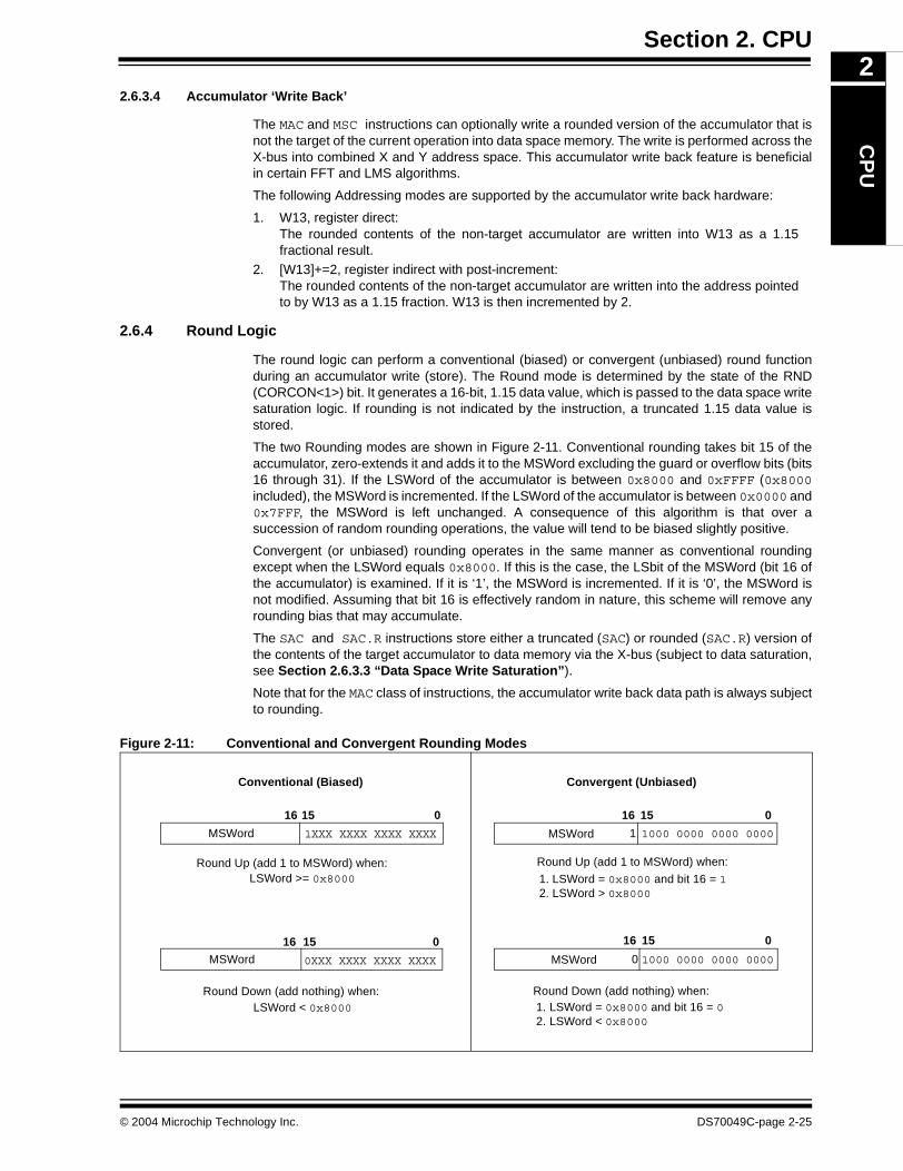
Section 2. CPUC
PU
2
2.6.3.4 Accumulator ‘Write Back’The MAC and MSC instructions can optionally write a rounded version of the accumulator that isnot the target of the current operation into data space memory. The write is performed across theX-bus into combined X and Y address space. This accumulator write back feature is beneficialin certain FFT and LMS algorithms.
The following Addressing modes are supported by the accumulator write back hardware:
1. W13, register direct:The rounded contents of the non-target accumulator are written into W13 as a 1.15fractional result.
2. [W13]+=2, register indirect with post-increment:The rounded contents of the non-target accumulator are written into the address pointedto by W13 as a 1.15 fraction. W13 is then incremented by 2.
2.6.4 Round Logic
The round logic can perform a conventional (biased) or convergent (unbiased) round functionduring an accumulator write (store). The Round mode is determined by the state of the RND(CORCON<1>) bit. It generates a 16-bit, 1.15 data value, which is passed to the data space writesaturation logic. If rounding is not indicated by the instruction, a truncated 1.15 data value isstored.
The two Rounding modes are shown in Figure 2-11. Conventional rounding takes bit 15 of theaccumulator, zero-extends it and adds it to the MSWord excluding the guard or overflow bits (bits16 through 31). If the LSWord of the accumulator is between 0x8000 and 0xFFFF (0x8000included), the MSWord is incremented. If the LSWord of the accumulator is between 0x0000 and0x7FFF, the MSWord is left unchanged. A consequence of this algorithm is that over asuccession of random rounding operations, the value will tend to be biased slightly positive.
Convergent (or unbiased) rounding operates in the same manner as conventional roundingexcept when the LSWord equals 0x8000. If this is the case, the LSbit of the MSWord (bit 16 ofthe accumulator) is examined. If it is ‘1’, the MSWord is incremented. If it is ‘0’, the MSWord isnot modified. Assuming that bit 16 is effectively random in nature, this scheme will remove anyrounding bias that may accumulate.
The SAC and SAC.R instructions store either a truncated (SAC) or rounded (SAC.R) version ofthe contents of the target accumulator to data memory via the X-bus (subject to data saturation,see Section 2.6.3.3 “Data Space Write Saturation”).
Note that for the MAC class of instructions, the accumulator write back data path is always subjectto rounding.
Figure 2-11: Conventional and Convergent Rounding Modes
01516
01516
01516
01516
1000 0000 0000 00001XXX XXXX XXXX XXXX
0XXX XXXX XXXX XXXX 1000 0000 0000 0000
1
0
Conventional (Biased) Convergent (Unbiased)
Round Up (add 1 to MSWord) when:
Round Down (add nothing) when:
Round Up (add 1 to MSWord) when:
1. LSWord = 0x8000 and bit 16 = 12. LSWord > 0x8000
LSWord >= 0x8000
LSWord < 0x8000Round Down (add nothing) when:1. LSWord = 0x8000 and bit 16 = 02. LSWord < 0x8000
MSWord
MSWord
MSWord
MSWord
© 2004 Microchip Technology Inc. DS70049C-page 2-25
dsPIC30F Family Reference Manual
2.6.5 Barrel Shifter
The barrel shifter is capable of performing up to a 16-bit arithmetic right shift, or up to a 16-bit leftshift, in a single cycle. The barrel shifter can be used by DSP instructions or MCU instructions formulti-bit shifts.
The shifter requires a signed binary value to determine both the magnitude (number of bits) anddirection of the shift operation:
• A positive value will shift the operand right • A negative value will shift the operand left • A value of ‘0’ will not modify the operand
The barrel shifter is 40-bits wide to accommodate the width of the accumulators. A 40-bit outputresult is provided for DSP shift operations, and a 16-bit result for MCU shift operations.
A summary of instructions that use the barrel shifter is provided below in Table 2-6.
Table 2-6: Instructions that Utilize the DSP Engine Barrel Shifter
2.6.6 DSP Engine Mode Selection
The various operational characteristics of the DSP engine discussed in previous sub-sectionscan be selected through the CPU Core Configuration register (CORCON). These are listedbelow:
• Fractional or integer multiply operation.• Conventional or convergent rounding.
• Automatic saturation on/off for ACCA.• Automatic saturation on/off for ACCB.• Automatic saturation on/off for writes to data memory.
• Accumulator Saturation mode selection.
2.6.7 DSP Engine Trap Events
The various arithmetic error traps that can be generated for handling exceptions in the DSPengine are selected through the Interrupt Control register (INTCON1). These are listed below:
• Trap on ACCA overflow enable, using OVATE (INTCON1<10>).
• Trap on ACCB overflow enable, using OVBTE (INTCON1<9>).• Trap on catastrophic ACCA and/or ACCB overflow enable, using COVTE (INTCON1<8>).
An arithmetic error trap will also be generated when the user attempts to shift a value beyond themaximum allowable range (+/- 16 bits) using the SFTAC instruction. This trap source cannot bedisabled. The execution of the instruction will complete, but the results of the shift will not bewritten to the target accumulator.
For further information on bits in the INTCON1 register and arithmetic error traps, please refer toSection 6. “Reset Interrupts”.
Instruction Description
ASR Arithmetic multi-bit right shift of data memory location
LSR Logical multi-bit right shift of data memory location
SL Multi-bit shift left of data memory location
SAC Store DSP accumulator with optional shift
SFTAC Shift DSP accumulator
DS70049C-page 2-26 © 2004 Microchip Technology Inc.
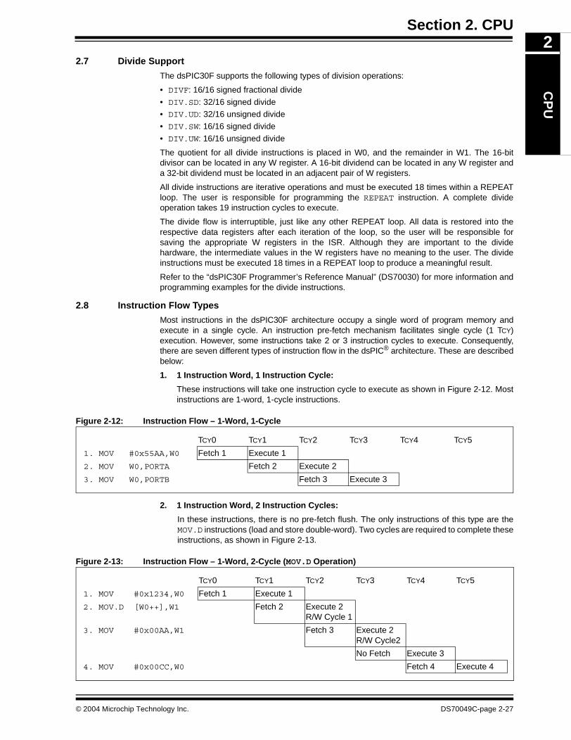
Section 2. CPUC
PU
2
2.7 Divide SupportThe dsPIC30F supports the following types of division operations:
• DIVF: 16/16 signed fractional divide
• DIV.SD: 32/16 signed divide• DIV.UD: 32/16 unsigned divide• DIV.SW: 16/16 signed divide
• DIV.UW: 16/16 unsigned divide
The quotient for all divide instructions is placed in W0, and the remainder in W1. The 16-bitdivisor can be located in any W register. A 16-bit dividend can be located in any W register anda 32-bit dividend must be located in an adjacent pair of W registers.
All divide instructions are iterative operations and must be executed 18 times within a REPEATloop. The user is responsible for programming the REPEAT instruction. A complete divideoperation takes 19 instruction cycles to execute.
The divide flow is interruptible, just like any other REPEAT loop. All data is restored into therespective data registers after each iteration of the loop, so the user will be responsible forsaving the appropriate W registers in the ISR. Although they are important to the dividehardware, the intermediate values in the W registers have no meaning to the user. The divideinstructions must be executed 18 times in a REPEAT loop to produce a meaningful result.
Refer to the “dsPIC30F Programmer’s Reference Manual” (DS70030) for more information andprogramming examples for the divide instructions.
2.8 Instruction Flow Types
Most instructions in the dsPIC30F architecture occupy a single word of program memory andexecute in a single cycle. An instruction pre-fetch mechanism facilitates single cycle (1 TCY)execution. However, some instructions take 2 or 3 instruction cycles to execute. Consequently,there are seven different types of instruction flow in the dsPIC® architecture. These are describedbelow:
1. 1 Instruction Word, 1 Instruction Cycle:
These instructions will take one instruction cycle to execute as shown in Figure 2-12. Mostinstructions are 1-word, 1-cycle instructions.
Figure 2-12: Instruction Flow – 1-Word, 1-Cycle
2. 1 Instruction Word, 2 Instruction Cycles:
In these instructions, there is no pre-fetch flush. The only instructions of this type are theMOV.D instructions (load and store double-word). Two cycles are required to complete theseinstructions, as shown in Figure 2-13.
Figure 2-13: Instruction Flow – 1-Word, 2-Cycle (MOV.D Operation)
TCY0 TCY1 TCY2 TCY3 TCY4 TCY5
1. MOV #0x55AA,W0 Fetch 1 Execute 1
2. MOV W0,PORTA Fetch 2 Execute 2
3. MOV W0,PORTB Fetch 3 Execute 3
TCY0 TCY1 TCY2 TCY3 TCY4 TCY5
1. MOV #0x1234,W0 Fetch 1 Execute 1
2. MOV.D [W0++],W1 Fetch 2 Execute 2R/W Cycle 1
3. MOV #0x00AA,W1 Fetch 3 Execute 2R/W Cycle2
No Fetch Execute 3
4. MOV #0x00CC,W0 Fetch 4 Execute 4
© 2004 Microchip Technology Inc. DS70049C-page 2-27
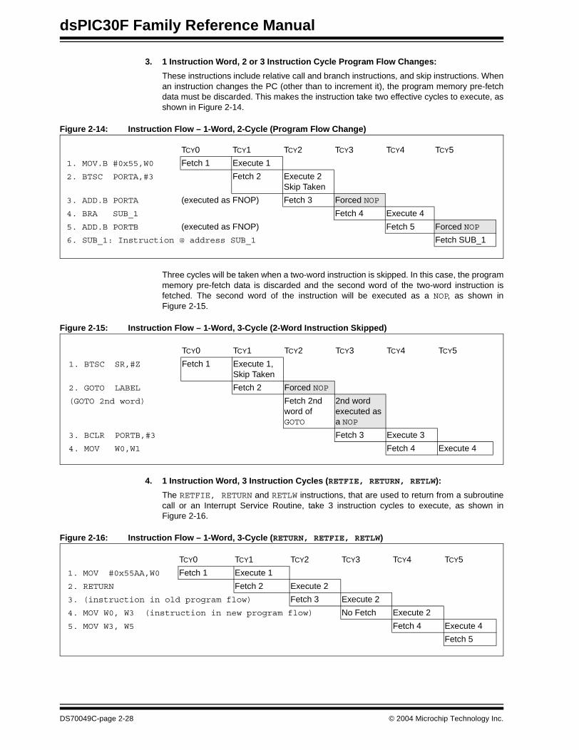
dsPIC30F Family Reference Manual
3. 1 Instruction Word, 2 or 3 Instruction Cycle Program Flow Changes:
These instructions include relative call and branch instructions, and skip instructions. Whenan instruction changes the PC (other than to increment it), the program memory pre-fetchdata must be discarded. This makes the instruction take two effective cycles to execute, asshown in Figure 2-14.
Figure 2-14: Instruction Flow – 1-Word, 2-Cycle (Program Flow Change)
Three cycles will be taken when a two-word instruction is skipped. In this case, the programmemory pre-fetch data is discarded and the second word of the two-word instruction isfetched. The second word of the instruction will be executed as a NOP, as shown inFigure 2-15.
Figure 2-15: Instruction Flow – 1-Word, 3-Cycle (2-Word Instruction Skipped)
4. 1 Instruction Word, 3 Instruction Cycles (RETFIE, RETURN, RETLW):
The RETFIE, RETURN and RETLW instructions, that are used to return from a subroutinecall or an Interrupt Service Routine, take 3 instruction cycles to execute, as shown inFigure 2-16.
Figure 2-16: Instruction Flow – 1-Word, 3-Cycle (RETURN, RETFIE, RETLW)
TCY0 TCY1 TCY2 TCY3 TCY4 TCY5
1. MOV.B #0x55,W0 Fetch 1 Execute 1
2. BTSC PORTA,#3 Fetch 2 Execute 2Skip Taken
3. ADD.B PORTA (executed as FNOP) Fetch 3 Forced NOP
4. BRA SUB_1 Fetch 4 Execute 4
5. ADD.B PORTB (executed as FNOP) Fetch 5 Forced NOP
6. SUB_1: Instruction @ address SUB_1 Fetch SUB_1
TCY0 TCY1 TCY2 TCY3 TCY4 TCY5
1. BTSC SR,#Z Fetch 1 Execute 1,Skip Taken
2. GOTO LABEL Fetch 2 Forced NOP
(GOTO 2nd word) Fetch 2nd word of GOTO
2nd wordexecuted asa NOP
3. BCLR PORTB,#3 Fetch 3 Execute 3
4. MOV W0,W1 Fetch 4 Execute 4
TCY0 TCY1 TCY2 TCY3 TCY4 TCY5
1. MOV #0x55AA,W0 Fetch 1 Execute 1
2. RETURN Fetch 2 Execute 2
3. (instruction in old program flow) Fetch 3 Execute 2
4. MOV W0, W3 (instruction in new program flow) No Fetch Execute 2
5. MOV W3, W5 Fetch 4 Execute 4
Fetch 5
DS70049C-page 2-28 © 2004 Microchip Technology Inc.
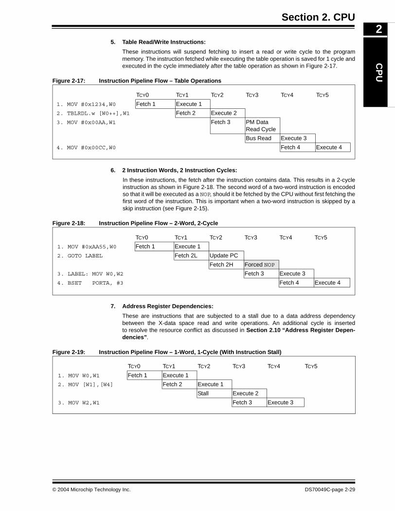
Section 2. CPUC
PU
2
5. Table Read/Write Instructions:These instructions will suspend fetching to insert a read or write cycle to the programmemory. The instruction fetched while executing the table operation is saved for 1 cycle andexecuted in the cycle immediately after the table operation as shown in Figure 2-17.
Figure 2-17: Instruction Pipeline Flow – Table Operations
6. 2 Instruction Words, 2 Instruction Cycles:
In these instructions, the fetch after the instruction contains data. This results in a 2-cycleinstruction as shown in Figure 2-18. The second word of a two-word instruction is encodedso that it will be executed as a NOP, should it be fetched by the CPU without first fetching thefirst word of the instruction. This is important when a two-word instruction is skipped by askip instruction (see Figure 2-15).
Figure 2-18: Instruction Pipeline Flow – 2-Word, 2-Cycle
7. Address Register Dependencies:
These are instructions that are subjected to a stall due to a data address dependencybetween the X-data space read and write operations. An additional cycle is insertedto resolve the resource conflict as discussed in Section 2.10 “Address Register Depen-dencies”.
Figure 2-19: Instruction Pipeline Flow – 1-Word, 1-Cycle (With Instruction Stall)
TCY0 TCY1 TCY2 TCY3 TCY4 TCY5
1. MOV #0x1234,W0 Fetch 1 Execute 1
2. TBLRDL.w [W0++],W1 Fetch 2 Execute 2
3. MOV #0x00AA,W1 Fetch 3 PM DataRead Cycle
Bus Read Execute 3
4. MOV #0x00CC,W0 Fetch 4 Execute 4
TCY0 TCY1 TCY2 TCY3 TCY4 TCY5
1. MOV #0xAA55,W0 Fetch 1 Execute 1
2. GOTO LABEL Fetch 2L Update PC
Fetch 2H Forced NOP
3. LABEL: MOV W0,W2 Fetch 3 Execute 3
4. BSET PORTA, #3 Fetch 4 Execute 4
TCY0 TCY1 TCY2 TCY3 TCY4 TCY5
1. MOV W0,W1 Fetch 1 Execute 1
2. MOV [W1],[W4] Fetch 2 Execute 1
Stall Execute 2
3. MOV W2,W1 Fetch 3 Execute 3
© 2004 Microchip Technology Inc. DS70049C-page 2-29
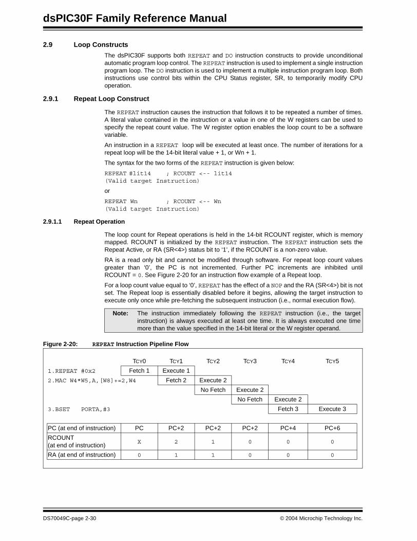
dsPIC30F Family Reference Manual
2.9 Loop Constructs
The dsPIC30F supports both REPEAT and DO instruction constructs to provide unconditionalautomatic program loop control. The REPEAT instruction is used to implement a single instructionprogram loop. The DO instruction is used to implement a multiple instruction program loop. Bothinstructions use control bits within the CPU Status register, SR, to temporarily modify CPUoperation.
2.9.1 Repeat Loop Construct
The REPEAT instruction causes the instruction that follows it to be repeated a number of times.A literal value contained in the instruction or a value in one of the W registers can be used tospecify the repeat count value. The W register option enables the loop count to be a softwarevariable.
An instruction in a REPEAT loop will be executed at least once. The number of iterations for arepeat loop will be the 14-bit literal value + 1, or Wn + 1.
The syntax for the two forms of the REPEAT instruction is given below:
REPEAT #lit14 ; RCOUNT <-- lit14(Valid target Instruction)
or
REPEAT Wn ; RCOUNT <-- Wn(Valid target Instruction)
2.9.1.1 Repeat Operation
The loop count for Repeat operations is held in the 14-bit RCOUNT register, which is memorymapped. RCOUNT is initialized by the REPEAT instruction. The REPEAT instruction sets theRepeat Active, or RA (SR<4>) status bit to ‘1’, if the RCOUNT is a non-zero value.
RA is a read only bit and cannot be modified through software. For repeat loop count valuesgreater than ‘0’, the PC is not incremented. Further PC increments are inhibited untilRCOUNT = 0. See Figure 2-20 for an instruction flow example of a Repeat loop.
For a loop count value equal to ‘0’, REPEAT has the effect of a NOP and the RA (SR<4>) bit is notset. The Repeat loop is essentially disabled before it begins, allowing the target instruction toexecute only once while pre-fetching the subsequent instruction (i.e., normal execution flow).
Figure 2-20: REPEAT Instruction Pipeline Flow
Note: The instruction immediately following the REPEAT instruction (i.e., the targetinstruction) is always executed at least one time. It is always executed one timemore than the value specified in the 14-bit literal or the W register operand.
TCY0 TCY1 TCY2 TCY3 TCY4 TCY5
1.REPEAT #0x2 Fetch 1 Execute 1
2.MAC W4*W5,A,[W8]+=2,W4 Fetch 2 Execute 2
No Fetch Execute 2
No Fetch Execute 2
3.BSET PORTA,#3 Fetch 3 Execute 3
PC (at end of instruction) PC PC+2 PC+2 PC+2 PC+4 PC+6
RCOUNT (at end of instruction)
X 2 1 0 0 0
RA (at end of instruction) 0 1 1 0 0 0
DS70049C-page 2-30 © 2004 Microchip Technology Inc.

Section 2. CPUC
PU
2
2.9.1.2 Interrupting a REPEAT LoopA REPEAT instruction loop may be interrupted at any time.
The RA state is preserved on the stack during exception processing to allow the user to executefurther REPEAT loops from within (any number) of nested interrupts. After SRL is stacked, theRA status bit is cleared to restore normal execution flow within the ISR.
Returning into a Repeat loop from an ISR using RETFIE requires no special handling. Interruptswill pre-fetch the repeated instruction during the third cycle of the RETFIE. The stacked RA bitwill be restored when the SRL register is popped and, if set, the interrupted Repeat loop will beresumed.
2.9.1.2.1 Early Termination of a Repeat Loop
An interrupted Repeat loop can be terminated earlier than normal in the ISR by clearing theRCOUNT register in software.
2.9.1.3 Restrictions on the REPEAT Instruction
Any instruction can immediately follow a REPEAT except for the following:
1. Program Flow Control instructions (any branch, compare and skip, subroutine calls,returns, etc.).
2. Another REPEAT or DO instruction.
3. DISI, ULNK, LNK, PWRSAV, RESET. 4. MOV.D instruction.
Note: If a Repeat loop has been interrupted and an ISR is being processed, the user muststack the RCOUNT (Repeat Count register) prior to executing another REPEATinstruction within an ISR.
Note: If Repeat was used within an ISR, the user must unstack RCOUNT prior to executingRETFIE.
Note: Should the repeated instruction (target instruction in the Repeat loop) be accessingdata from PS using PSV, the first time it is executed after a return from an exceptionwill require 2 instruction cycles. Similar to the first iteration of a loop, timing limita-tions will not allow the first instruction to access data residing in PS in a singleinstruction cycle.
Note: There are some instructions and/or Instruction Addressing modes that can beexecuted within a Repeat loop, but make little sense when repeated.
© 2004 Microchip Technology Inc. DS70049C-page 2-31
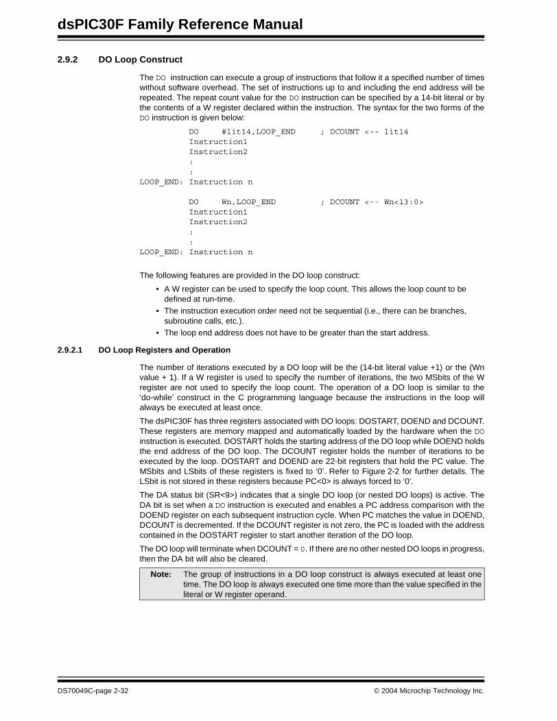
dsPIC30F Family Reference Manual
2.9.2 DO Loop Construct
The DO instruction can execute a group of instructions that follow it a specified number of timeswithout software overhead. The set of instructions up to and including the end address will berepeated. The repeat count value for the DO instruction can be specified by a 14-bit literal or bythe contents of a W register declared within the instruction. The syntax for the two forms of theDO instruction is given below:
DO #lit14,LOOP_END ; DCOUNT <-- lit14Instruction1Instruction2::
LOOP_END: Instruction n
DO Wn,LOOP_END ; DCOUNT <-- Wn<13:0>Instruction1
Instruction2::
LOOP_END: Instruction n
The following features are provided in the DO loop construct:
• A W register can be used to specify the loop count. This allows the loop count to be defined at run-time.
• The instruction execution order need not be sequential (i.e., there can be branches, subroutine calls, etc.).
• The loop end address does not have to be greater than the start address.
2.9.2.1 DO Loop Registers and Operation
The number of iterations executed by a DO loop will be the (14-bit literal value +1) or the (Wnvalue + 1). If a W register is used to specify the number of iterations, the two MSbits of the Wregister are not used to specify the loop count. The operation of a DO loop is similar to the‘do-while’ construct in the C programming language because the instructions in the loop willalways be executed at least once.
The dsPIC30F has three registers associated with DO loops: DOSTART, DOEND and DCOUNT.These registers are memory mapped and automatically loaded by the hardware when the DOinstruction is executed. DOSTART holds the starting address of the DO loop while DOEND holdsthe end address of the DO loop. The DCOUNT register holds the number of iterations to beexecuted by the loop. DOSTART and DOEND are 22-bit registers that hold the PC value. TheMSbits and LSbits of these registers is fixed to ‘0’. Refer to Figure 2-2 for further details. TheLSbit is not stored in these registers because PC<0> is always forced to ‘0’.
The DA status bit (SR<9>) indicates that a single DO loop (or nested DO loops) is active. TheDA bit is set when a DO instruction is executed and enables a PC address comparison with theDOEND register on each subsequent instruction cycle. When PC matches the value in DOEND,DCOUNT is decremented. If the DCOUNT register is not zero, the PC is loaded with the addresscontained in the DOSTART register to start another iteration of the DO loop.
The DO loop will terminate when DCOUNT = 0. If there are no other nested DO loops in progress,then the DA bit will also be cleared.
Note: The group of instructions in a DO loop construct is always executed at least onetime. The DO loop is always executed one time more than the value specified in theliteral or W register operand.
DS70049C-page 2-32 © 2004 Microchip Technology Inc.
Section 2. CPUC
PU
2
2.9.2.2 DO Loop NestingThe DOSTART, DOEND and DCOUNT registers each have a shadow register associated withthem, such that the DO loop hardware supports one level of automatic nesting. The DOSTART,DOEND and DCOUNT registers are user accessible and they may be manually saved to permitadditional nesting, where required.
The DO Level bits, DL<2:0> (CORCON<10:8>) indicate the nesting level of the DO loop currentlybeing executed. When the first DO instruction is executed, DL<2:0> is set to B‘001’ to indicatethat one level of DO loop is underway. The DA (SR<9>) is also set. When another DO instructionis executed within the first DO loop, the DOSTART, DOEND and DCOUNT registers aretransferred into the shadow registers, prior to being updated with the new loop values. TheDL<2:0> bits are set to B‘010’ indicating that a second, nested DO loop is in progress. The DA(SR<9>) bit also remains set.
If no more than one level of DO loop nesting is required in the application, no special attention isrequired. Should the user require more than one level of DO loop nesting, this may be achievedthrough manually saving the DOSTART, DOEND and DCOUNT registers prior to executing thenext DO instruction. These registers should be saved whenever DL<2:0> is B’010’ or greater.
The DOSTART, DOEND and DCOUNT registers will automatically be restored from their shadowregisters when a DO loop terminates and DL<2:0> = B’010’.
2.9.2.3 Interrupting a DO Loop
DO loops may be interrupted at any time. If another DO loop is to be executed during the ISR,the user must check the DL<2:0> status bits and save the DOSTART, DOEND and DCOUNTregisters as required.
No special handling is required if the user can ensure that only one level of DO loop will ever beexecuted in:
• both background and any one ISR handler (if interrupt nesting is enabled) or • both background and any ISR (if interrupt nesting is disabled)
Alternatively, up to two (nested) DO loops may be executed in either background or within any
• one ISR handler (if interrupt nesting is enabled) or • in any ISR (if interrupt nesting is disabled)
It is assumed that no DO loops are used within any trap handlers.
Returning to a DO loop from an ISR, using the RETFIE instruction, requires no special handling.
2.9.2.4 Early Termination of the DO loop
There are two ways to terminate a DO loop, earlier than normal:
1. The EDT (CORCON<11>) bit provides a means for the user to terminate a DO loop beforeit completes all loops. Writing a ‘1’ to the EDT bit will force the loop to complete theiteration underway and then terminate. If EDT is set during the penultimate or lastinstruction of the loop, one more iteration of the loop will occur. EDT will always read as a‘0’; clearing it has no effect. After the EDT bit is set, the user can optionally branch out ofthe DO loop.
2. Alternatively, the code may branch out of the loop at any point except from the last instruc-tion, which cannot be a flow control instruction. Although the DA bit enables the DO loophardware, it will have no effect unless the address of the penultimate instruction isencountered during an instruction pre-fetch. This is not a recommended method forterminating a DO loop.
Note: The DL<2:0> (CORCON<10:8>) bits are combined (logically OR-ed) to form the DA(SR<9>) bit. If nested DO loops are being executed, the DA bit is cleared only whenthe loop count associated with the outer most loop expires.
Note: Exiting a DO loop without using EDT is not recommended because the hardwarewill continue to check for DOEND addresses.
© 2004 Microchip Technology Inc. DS70049C-page 2-33
dsPIC30F Family Reference Manual
2.9.2.5 DO Loop Restrictions
DO loops have the following restrictions imposed:
• choice of last instruction in the loop
• the loop length (offset from the first instruction) • reading of the DOEND register
All DO loops must contain at least 2 instructions because the loop termination tests areperformed in the penultimate instruction. REPEAT should be used for single instruction loops.
The special function register, DOEND, cannot be read by user software in the instruction thatimmediately follows either a DO instruction, or a file register write operation to the DOEND SFR.
The instruction that is executed two instructions before the last instruction in a DO loop should notmodify any of the following:
• CPU priority level governed by the IPL (SR<7:5>) bits• Peripheral Interrupt Enable bits governed by the IEC0, IEC1 and IEC2 registers
• Peripheral Interrupt Priority bits governed by the IPC0 through IPC11 registers
If the restrictions above are not followed, the DO loop may execute incorrectly.
2.9.2.5.1 Last Instruction Restrictions
There are restrictions on the last instruction executed in a DO loop. The last instruction in a DOloop should not be:
1. Flow control instruction (for e.g., any branch, compare and skip, GOTO, CALL, RCALL,TRAP).
2. RETURN, RETFIE and RETLW will work correctly as the last instruction of a DO loop, butthe user must be responsible for returning into the loop to complete it.
3. Another REPEAT or DO instruction.4. Target instruction within a REPEAT loop. This restriction implies that the penultimate
instruction also cannot be a REPEAT.5. Any instruction that occupies two words in program space.
6. DISI instruction
2.9.2.5.2 Loop Length Restrictions
Loop length is defined as the signed offset of the last instruction from the first instruction in the DOloop. The loop length when added to the address of the first instruction in the loop forms theaddress of the last instruction of the loop.There are some loop length values that should beavoided.
1. Loop Length = -2Execution will start at the first instruction in the loop (i.e., at [PC]) and will continue until theloop end address (in this case [PC – 4]) is pre-fetched. As this is the first word of the DOinstruction, it will execute the DO instruction again, re-initializing the DCOUNT andpre-fetching [PC]. This will continue forever as long as the loop end address [PC – 4] ispre-fetched. This value of n has the potential of creating an infinite loop (subject to aWatchdog Timer Reset).end_loop: DO #33, end_loop ;DO is a two-word instruction
NOP ;2nd word of DO executes as a NOPADD W2,W3,W4 ;First instruction in DO loop([PC])
DS70049C-page 2-34 © 2004 Microchip Technology Inc.
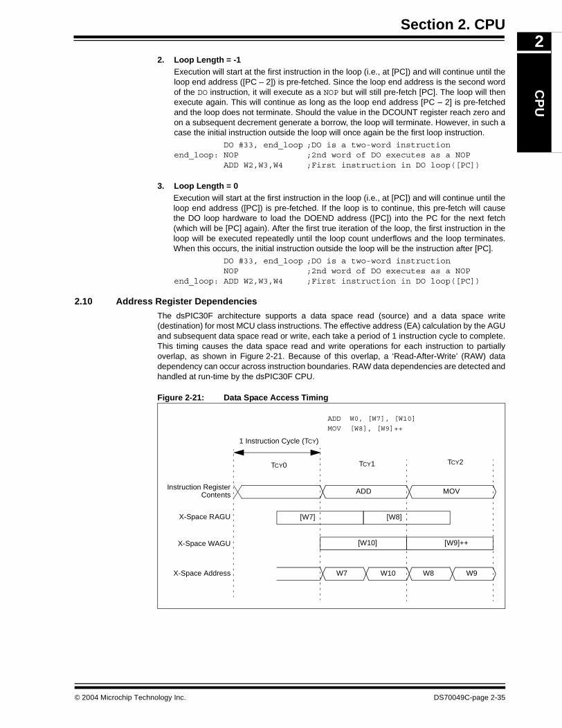
Section 2. CPUC
PU
2
2. Loop Length = -1Execution will start at the first instruction in the loop (i.e., at [PC]) and will continue until theloop end address ([PC – 2]) is pre-fetched. Since the loop end address is the second wordof the DO instruction, it will execute as a NOP but will still pre-fetch [PC]. The loop will thenexecute again. This will continue as long as the loop end address [PC – 2] is pre-fetchedand the loop does not terminate. Should the value in the DCOUNT register reach zero andon a subsequent decrement generate a borrow, the loop will terminate. However, in such acase the initial instruction outside the loop will once again be the first loop instruction.
DO #33, end_loop ;DO is a two-word instructionend_loop: NOP ;2nd word of DO executes as a NOP
ADD W2,W3,W4 ;First instruction in DO loop([PC])
3. Loop Length = 0Execution will start at the first instruction in the loop (i.e., at [PC]) and will continue until theloop end address ([PC]) is pre-fetched. If the loop is to continue, this pre-fetch will causethe DO loop hardware to load the DOEND address ([PC]) into the PC for the next fetch(which will be [PC] again). After the first true iteration of the loop, the first instruction in theloop will be executed repeatedly until the loop count underflows and the loop terminates.When this occurs, the initial instruction outside the loop will be the instruction after [PC].
DO #33, end_loop ;DO is a two-word instructionNOP ;2nd word of DO executes as a NOP
end_loop: ADD W2,W3,W4 ;First instruction in DO loop([PC])
2.10 Address Register Dependencies
The dsPIC30F architecture supports a data space read (source) and a data space write(destination) for most MCU class instructions. The effective address (EA) calculation by the AGUand subsequent data space read or write, each take a period of 1 instruction cycle to complete.This timing causes the data space read and write operations for each instruction to partiallyoverlap, as shown in Figure 2-21. Because of this overlap, a ‘Read-After-Write’ (RAW) datadependency can occur across instruction boundaries. RAW data dependencies are detected andhandled at run-time by the dsPIC30F CPU.
Figure 2-21: Data Space Access Timing
ADD MOV
[W7]
[W10] [W9]++
X-Space Address W7 W10 W8 W9
ADD W0, [W7], [W10]
MOV [W8], [W9]++
[W8] X-Space RAGU
Instruction Register Contents
X-Space WAGU
1 Instruction Cycle (TCY)
TCY0 TCY1 TCY2
© 2004 Microchip Technology Inc. DS70049C-page 2-35
dsPIC30F Family Reference Manual
2.10.1 Read-After-Write Dependency Rules
If the W register is used as a write operation destination in the current instruction and the Wregister being read in the pre-fetched instruction are the same, the following rules will apply:
1. If the destination write (current instruction) does not modify the contents of Wn, no stallswill occur.or
2. If the source read (pre-fetched instruction) does not calculate an EA using Wn, no stallswill occur.
During each instruction cycle, the dsPIC30F hardware automatically checks to see if a RAW datadependency is about to occur. If the conditions specified above are not satisfied, the CPU willautomatically add a one instruction cycle delay before executing the pre-fetched instruction. Theinstruction stall provides enough time for the destination W register write to take place before thenext (pre-fetched) instruction has to use the written data.
Table 2-7: Read-After-Write Dependency Summary
2.10.2 Instruction Stall Cycles
An instruction stall is essentially a one instruction cycle wait period appended in front of the readphase of an instruction, in order to allow the prior write to complete before the next read opera-tion. For the purposes of interrupt latency, it should be noted that the stall cycle is associated withthe instruction following the instruction where it was detected (i.e., stall cycles always precedeinstruction execution cycles).
Destination Addressing Mode
using Wn
SourceAddressing Mode
using WnStatus
Examples(Wn = W2)
Direct Direct Allowed ADD.w W0, W1, W2MOV.w W2, W3
Direct Indirect Stall ADD.w W0, W1, W2MOV.w [W2], W3
Direct Indirect withmodification
Stall ADD.w W0, W1, W2MOV.w [W2++], W3
Indirect Direct Allowed ADD.w W0, W1, [W2]MOV.w W2, W3
Indirect Indirect Allowed ADD.w W0, W1, [W2]MOV.w [W2], W3
Indirect Indirect withmodification
Allowed ADD.w W0, W1, [W2]MOV.w [W2++], W3
Indirect withmodification
Direct Allowed ADD.w W0, W1, [W2++]MOV.w W2, W3
Indirect Indirect Stall ADD.w W0, W1, [W2]MOV.w [W2], W3; W2=0x0004 (mapped W2)
Indirect Indirect with modification
Stall ADD.w W0, W1, [W2]MOV.w [W2++], W3; W2=0x0004 (mapped W2)
Indirect withmodification
Indirect Stall ADD.w W0, W1, [W2++]MOV.w [W2], W3
Indirect withmodification
Indirect withmodification
Stall ADD.w W0, W1, [W2++]MOV.w [W2++], W3
DS70049C-page 2-36 © 2004 Microchip Technology Inc.
Section 2. CPUC
PU
2
If a RAW data dependency is detected, the dsPIC30F will begin an instruction stall. During aninstruction stall, the following events occur:1. The write operation underway (for the previous instruction) is allowed to complete as normal.2. Data space is not addressed until after the instruction stall.3. PC increment is inhibited until after the instruction stall.
4. Further instruction fetches are inhibited until after the instruction stall.
2.10.2.1 Instruction Stall Cycles and Interrupts
When an interrupt event coincides with two adjacent instructions that will cause an instructionstall, one of two possible outcomes could occur:
1. The interrupt could be coincident with the first instruction. In this situation, the first instruc-tion will be allowed to complete and the second instruction will be executed after the ISRcompletes. In this case, the stall cycle is eliminated from the second instruction becausethe exception process provides time for the first instruction to complete the write phase.
2. The interrupt could be coincident with the second instruction. In this situation, the secondinstruction and the appended stall cycle will be allowed to execute prior to the ISR. In thiscase, the stall cycle associated with the second instruction executes normally. However,the stall cycle will be effectively absorbed into the exception process timing. The exceptionprocess proceeds as if an ordinary two-cycle instruction was interrupted.
2.10.2.2 Instruction Stall Cycles and Flow Change Instructions
The CALL and RCALL instructions write to the stack using W15 and may, therefore, force aninstruction stall prior to the next instruction, if the source read of the next instruction uses W15.
The RETFIE and RETURN instructions can never force an instruction stall prior to the nextinstruction because they only perform read operations. However, the user should note that theRETLW instruction could force a stall, because it writes to a W register during the last cycle.
The GOTO and branch instructions can never force an instruction stall because they do notperform write operations.
2.10.2.3 Instruction Stalls and DO and REPEAT Loops
Other than the addition of instruction stall cycles, RAW data dependencies will not affect theoperation of either DO or REPEAT loops.
The pre-fetched instruction within a REPEAT loop does not change until the loop is complete oran exception occurs. Although register dependency checks occur across instruction boundaries,the dsPIC30F effectively compares the source and destination of the same instruction during aREPEAT loop.
The last instruction of a DO loop either pre-fetches the instruction at the loop start address or thenext instruction (outside the loop). The instruction stall decision will be based on the lastinstruction in the loop and the contents of the pre-fetched instruction.
2.10.2.4 Instruction Stalls and Program Space Visibility (PSV)
When program space (PS) is mapped to data space by enabling the PSV (CORCON<2>) bit, andthe X space EA falls within the visible program space window, the read or write cycle is redirectedto the address in program space. Accessing data from program space takes up to 3 instructioncycles.
Instructions operating in PSV address space are subject to RAW data dependencies andconsequent instruction stalls, just like any other instruction.
Consider the following code segment:
ADD W0,[W1],[W2++] ; PSV = 1, W1=0x8000, PSVPAG=0xAAMOV [W2],[W3]
This sequence of instructions would take 5 instruction cycles to execute. 2 instruction cycles areadded to perform the PSV access via W1. Furthermore, an instruction stall cycle is inserted toresolve the RAW data dependency caused by W2.
© 2004 Microchip Technology Inc. DS70049C-page 2-37
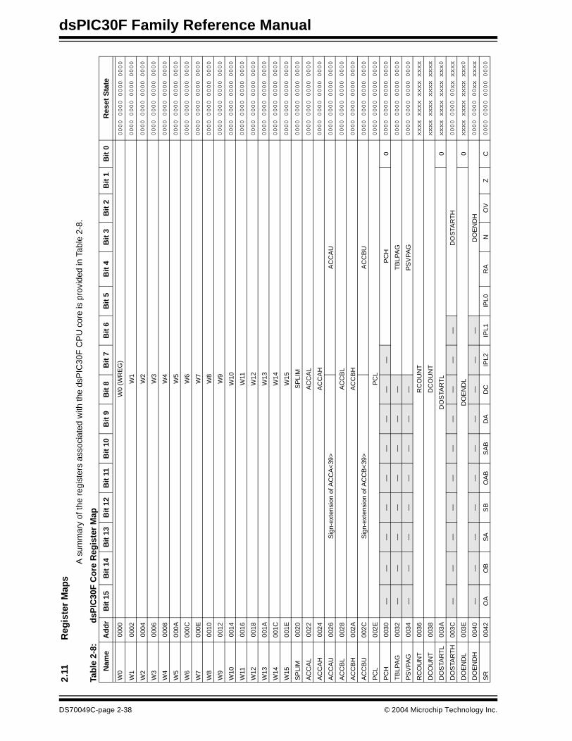
dsPIC30F Family Reference Manual
2.11
Reg
iste
r M
aps
A s
umm
ary
of th
e re
gist
ers
asso
ciat
ed w
ith th
e ds
PIC
30F
CP
U c
ore
is p
rovi
ded
in T
able
2-8.
Tab
le 2
-8:
dsP
IC30
F C
ore
Reg
iste
r M
ap N
ame
Ad
dr
Bit
15
Bit
14
Bit
13
Bit
12
Bit
11
Bit
10
Bit
9B
it 8
Bit
7B
it 6
Bit
5B
it 4
Bit
3B
it 2
Bit
1B
it 0
Res
et S
tate
W0
0000
W0
(WR
EG
)0000 0000 0000 0000
W1
0002
W1
0000 0000 0000 0000
W2
0004
W2
0000 0000 0000 0000
W3
0006
W3
0000 0000 0000 0000
W4
0008
W4
0000 0000 0000 0000
W5
000A
W5
0000 0000 0000 0000
W6
000C
W6
0000 0000 0000 0000
W7
000E
W7
0000 0000 0000 0000
W8
0010
W8
0000 0000 0000 0000
W9
0012
W9
0000 0000 0000 0000
W10
0014
W10
0000 0000 0000 0000
W11
0016
W11
0000 0000 0000 0000
W12
0018
W12
0000 0000 0000 0000
W13
001A
W13
0000 0000 0000 0000
W14
001C
W14
0000 0000 0000 0000
W15
001E
W15
0000 0000 0000 0000
SP
LIM
0020
SP
LIM
0000 0000 0000 0000
AC
CA
L00
22A
CC
AL
0000 0000 0000 0000
AC
CA
H00
24A
CC
AH
0000 0000 0000 0000
AC
CA
U00
26S
ign-
exte
nsio
n of
AC
CA
<39
>A
CC
AU
0000 0000 0000 0000
AC
CB
L00
28A
CC
BL
0000 0000 0000 0000
AC
CB
H00
2AA
CC
BH
0000 0000 0000 0000
AC
CB
U00
2CS
ign-
exte
nsio
n of
AC
CB
<39
>A
CC
BU
0000 0000 0000 0000
PC
L00
2EP
CL
0000 0000 0000 0000
PC
H00
30—
——
——
——
——
PC
H0
0000 0000 0000 0000
TB
LPA
G00
32—
——
——
——
—T
BLP
AG
0000 0000 0000 0000
PS
VP
AG
0034
——
——
——
——
PS
VP
AG
0000 0000 0000 0000
RC
OU
NT
0036
RC
OU
NT
xxxx xxxx xxxx xxxx
DC
OU
NT
0038
DC
OU
NT
xxxx xxxx xxxx xxxx
DO
STA
RT
L00
3AD
OS
TAR
TL
0xxxx xxxx xxxx xxx0
DO
STA
RT
H00
3C—
——
——
——
——
—D
OS
TAR
TH
0000 0000 00xx xxxx
DO
EN
DL
003E
DO
EN
DL
0xxxx xxxx xxxx xxx0
DO
EN
DH
0040
——
——
——
——
——
DO
EN
DH
0000 0000 00xx xxxx
SR
0042
OA
OB
SA
SB
OA
BS
AB
DA
DC
IPL2
IPL1
IPL0
RA
NO
VZ
C0000 0000 0000 0000
DS70049C-page 2-38 © 2004 Microchip Technology Inc.

Section 2. CPUC
PU
2
CO
RC
ON
0044
——
—U
SE
DT
DL2
DL<
1:0>
SA
TAS
AT
BS
AT
DW
AC
CS
AT
IPL3
PS
VR
ND
IF0000 0000 0010 0000
MO
DC
ON
0046
XM
OD
EN
YM
OD
EN
——
BW
M<
3:0>
YW
M<
3:0>
XW
M<
3:0>
0000 0000 0000 0000
XM
OD
SR
T00
48X
MO
DS
RT
<15
:0>
0xxxx xxxx xxxx xxx0
XM
OD
EN
D00
4AX
MO
DE
ND
<15
:0>
1xxxx xxxx xxxx xxx1
YM
OD
SR
T00
4CY
MO
DS
RT
<15
:0>
0xxxx xxxx xxxx xxx0
YM
OD
EN
D00
4EY
MO
DE
ND
<15
:0>
1xxxx xxxx xxxx xxx1
XB
RE
V00
50B
RE
NX
BR
EV
<14
:0>
xxxx xxxx xxxx xxxx
DIS
ICN
T00
52—
—D
ISIC
NT
<13
:0>
0000 0000 0000 0000
Res
erve
d00
54 -
007E
——
——
——
——
——
——
——
——
0000 0000 0000 0000
Lege
nd:
x =
uni
nitia
ted
No
te:
Ref
er to
the
devi
ce d
ata
shee
t for
spe
cific
Cor
e R
egis
ter
Map
det
ails
.
Tab
le 2
-8:
dsP
IC30
F C
ore
Reg
iste
r M
ap (
Co
nti
nu
ed)
Nam
eA
dd
rB
it 1
5B
it 1
4B
it 1
3B
it 1
2B
it 1
1B
it 1
0B
it 9
Bit
8B
it 7
Bit
6B
it 5
Bit
4B
it 3
Bit
2B
it 1
Bit
0R
eset
Sta
te
© 2004 Microchip Technology Inc. DS70049C-page 2-39

dsPIC30F Family Reference Manual
2.12 Related Application Notes
This section lists application notes that are related to this section of the manual. Theseapplication notes may not be written specifically for the dsPIC30F Product Family, but theconcepts are pertinent and could be used with modification and possible limitations. The currentapplication notes related to the dsPIC30F CPU module are:
Title Application Note #
No related application notes at this time.
Note: Please visit the Microchip web site (www.microchip.com) for additional ApplicationNotes and code examples for the dsPIC30F Family of devices.
DS70049C-page 2-40 © 2004 Microchip Technology Inc.

Section 2. CPUC
PU
2
2.13 Revision HistoryRevision A
This is the initial released revision of this document.
Revision B
This revision incorporates additional technical content for the dsPIC30F CPU module.
Revision C
This revision incorporates all known errata at the time of this document update.
© 2004 Microchip Technology Inc. DS70049C-page 2-41

dsPIC30F Family Reference Manual
NOTES:
DS70049C-page 2-42 © 2004 Microchip Technology Inc.
Section 3. Data Memory
Data M
emo
ry
3
HIGHLIGHTS
This section of the manual contains the following topics:
3.1 Introduction .................................................................................................................... 3-2
3.2 Data Space Address Generator Units (AGUs)............................................................... 3-53.3 Modulo Addressing ........................................................................................................ 3-73.4 Bit-Reversed Addressing ............................................................................................. 3-14
3.5 Control Register Descriptions ...................................................................................... 3-183.6 Related Application Notes............................................................................................ 3-233.7 Revision History ........................................................................................................... 3-24
© 2004 Microchip Technology Inc. DS70050C-page 3-1
dsPIC30F Family Reference Manual
3.1 Introduction
The dsPIC30F data width is 16-bits. All internal registers and data space memory are organizedas 16-bits wide. The dsPIC30F features two data spaces. The data spaces can be accessedseparately (for some DSP instructions) or together as one 64-Kbyte linear address range (forMCU instructions). The data spaces are accessed using two Address Generation Units (AGUs)and separate data paths.
An example data space memory map is shown in Figure 3-1.
Data memory addresses between 0x0000 and 0x07FF are reserved for the device specialfunction registers (SFRs). The SFRs include control and status bits for the CPU and peripheralson the device.
The RAM begins at address 0x0800 and is split into two blocks, X and Y data space. For datawrites, the X and Y data spaces are always accessed as a single, linear data space. For datareads, the X and Y memory spaces can be accessed independently or as a single, linear space.Data reads for MCU class instructions always access the the X and Y data spaces as a singlecombined data space. Dual source operand DSP instructions, such as the MAC instruction,access the X and Y data spaces separately to support simultaneous reads for the two sourceoperands.
MCU instructions can use any W register as an address pointer for a data read or write operation.
During data reads, the DSP class of instructions isolates the Y address space from the total dataspace. W10 and W11 are used as address pointers for reads from the Y data space. The remain-ing data space is referred to as X space, but could more accurately be described as “X minus Y”space. W8 and W9 are used as address pointers for data reads from the X data space in DSPclass instructions.
Figure 3-2 shows how the data memory map functions for both MCU class and DSP classinstructions. Note that it is the W register number and type of instruction that determines howaddress space is accessed for data reads. In particular, MCU instructions treat the X and Ymemory as a single combined data space. The MCU instructions can use any W register as anaddress pointer for reads and writes. The DSP instructions that can simultaneously pre-fetch twodata operands, split the data memory into two spaces. Specific W registers must be used for readaddress pointers in this case.
Some DSP instructions have the ability to store the accumulator that is not targeted by theinstruction to data memory. This function is called “accumulator write back”. W13 must be usedas an address pointer to the combined data memory space for accumulator write backoperations.
For DSP class instructions, W8 and W9 should point to implemented X memory space for allmemory reads. If W8 or W9 points to Y memory space, zeros will be returned. If W8 or W9 pointsto an unimplemented memory address, an address error trap will be generated.
For DSP class instructions, W10 and W11 should point to implemented Y memory space for allmemory reads. If W10 or W11 points to implemented X memory space, all zeros will be returned.If W10 or W11 points to an unimplemented memory address, an address error trap will begenerated. For additional information on address error traps, refer to Section 6. “Reset Inter-rupts”.
Note: The data memory map and the partition between the X and Y data spaces is devicespecific. Refer to the specific dsPIC30F device data sheet for further details.
DS70050C-page 3-2 © 2004 Microchip Technology Inc.
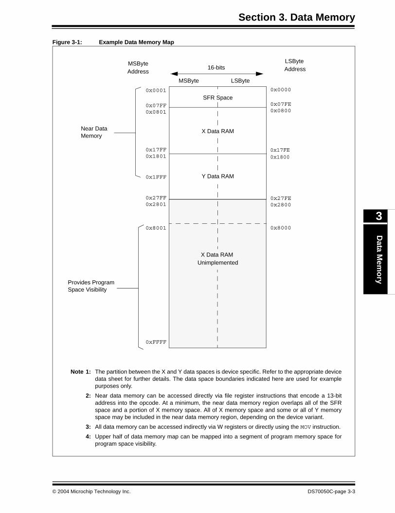
Section 3. Data MemoryD
ata Mem
ory
3
Figure 3-1: Example Data Memory Map
Note 1: The partition between the X and Y data spaces is device specific. Refer to the appropriate devicedata sheet for further details. The data space boundaries indicated here are used for examplepurposes only.
2: Near data memory can be accessed directly via file register instructions that encode a 13-bitaddress into the opcode. At a minimum, the near data memory region overlaps all of the SFRspace and a portion of X memory space. All of X memory space and some or all of Y memoryspace may be included in the near data memory region, depending on the device variant.
3: All data memory can be accessed indirectly via W registers or directly using the MOV instruction.
4: Upper half of data memory map can be mapped into a segment of program memory space forprogram space visibility.
0x0000
0x07FE
0x17FE
LSByteAddress16-bits
LSByteMSByte
MSByteAddress
0x0001
0x07FF
0x17FF
0xFFFF
X Data RAM
0x8001 0x8000
Provides ProgramSpace Visibility
Unimplemented
0x27FF 0x27FE0x28000x2801
0x0801 0x0800
0x1801 0x1800
Near DataMemory
0x1FFF
SFR Space
X Data RAM
Y Data RAM
© 2004 Microchip Technology Inc. DS70050C-page 3-3
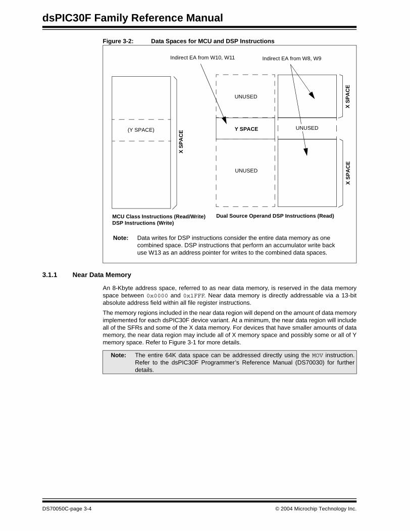
dsPIC30F Family Reference Manual
Figure 3-2: Data Spaces for MCU and DSP Instructions
3.1.1 Near Data Memory
An 8-Kbyte address space, referred to as near data memory, is reserved in the data memoryspace between 0x0000 and 0x1FFF. Near data memory is directly addressable via a 13-bitabsolute address field within all file register instructions.
The memory regions included in the near data region will depend on the amount of data memoryimplemented for each dsPIC30F device variant. At a minimum, the near data region will includeall of the SFRs and some of the X data memory. For devices that have smaller amounts of datamemory, the near data region may include all of X memory space and possibly some or all of Ymemory space. Refer to Figure 3-1 for more details.
(Y SPACE)
X S
PA
CE
UNUSED
X S
PA
CE
X S
PA
CE
UNUSED
UNUSED
MCU Class Instructions (Read/Write) Dual Source Operand DSP Instructions (Read)
Indirect EA from W10, W11 Indirect EA from W8, W9
Note: Data writes for DSP instructions consider the entire data memory as onecombined space. DSP instructions that perform an accumulator write backuse W13 as an address pointer for writes to the combined data spaces.
DSP Instructions (Write)
Y SPACE
Note: The entire 64K data space can be addressed directly using the MOV instruction.Refer to the dsPIC30F Programmer’s Reference Manual (DS70030) for furtherdetails.
DS70050C-page 3-4 © 2004 Microchip Technology Inc.
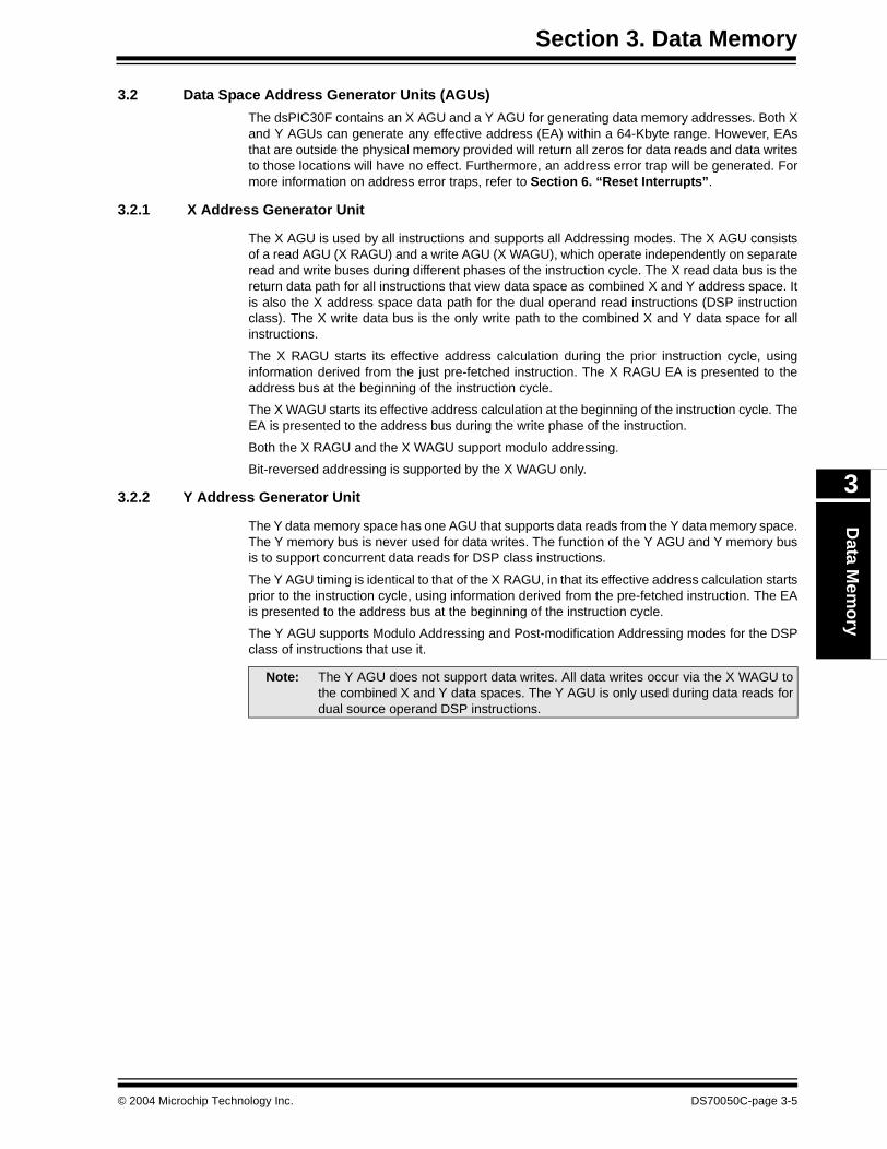
Section 3. Data MemoryD
ata Mem
ory
3
3.2 Data Space Address Generator Units (AGUs)
The dsPIC30F contains an X AGU and a Y AGU for generating data memory addresses. Both Xand Y AGUs can generate any effective address (EA) within a 64-Kbyte range. However, EAsthat are outside the physical memory provided will return all zeros for data reads and data writesto those locations will have no effect. Furthermore, an address error trap will be generated. Formore information on address error traps, refer to Section 6. “Reset Interrupts”.
3.2.1 X Address Generator Unit
The X AGU is used by all instructions and supports all Addressing modes. The X AGU consistsof a read AGU (X RAGU) and a write AGU (X WAGU), which operate independently on separateread and write buses during different phases of the instruction cycle. The X read data bus is thereturn data path for all instructions that view data space as combined X and Y address space. Itis also the X address space data path for the dual operand read instructions (DSP instructionclass). The X write data bus is the only write path to the combined X and Y data space for allinstructions.
The X RAGU starts its effective address calculation during the prior instruction cycle, usinginformation derived from the just pre-fetched instruction. The X RAGU EA is presented to theaddress bus at the beginning of the instruction cycle.
The X WAGU starts its effective address calculation at the beginning of the instruction cycle. TheEA is presented to the address bus during the write phase of the instruction.
Both the X RAGU and the X WAGU support modulo addressing.
Bit-reversed addressing is supported by the X WAGU only.
3.2.2 Y Address Generator Unit
The Y data memory space has one AGU that supports data reads from the Y data memory space.The Y memory bus is never used for data writes. The function of the Y AGU and Y memory busis to support concurrent data reads for DSP class instructions.
The Y AGU timing is identical to that of the X RAGU, in that its effective address calculation startsprior to the instruction cycle, using information derived from the pre-fetched instruction. The EAis presented to the address bus at the beginning of the instruction cycle.
The Y AGU supports Modulo Addressing and Post-modification Addressing modes for the DSPclass of instructions that use it.
Note: The Y AGU does not support data writes. All data writes occur via the X WAGU tothe combined X and Y data spaces. The Y AGU is only used during data reads fordual source operand DSP instructions.
© 2004 Microchip Technology Inc. DS70050C-page 3-5

dsPIC30F Family Reference Manual
Figure 3-3: Data Space Access Timing
3.2.3 Address Generator Units and DSP Class Instructions
The Y AGU and Y memory data path are used in concert with the X RAGU by the DSP class ofinstructions to provide two concurrent data read paths. For example, the MAC instruction cansimultaneously pre-fetch two operands to be used in the next multiplication.
The DSP class of instructions dedicates two W register pointers, W8 and W9, to always operatethrough the X RAGU and address X data space independently from Y data space, plus two Wregister pointers, W10 and W11, to always operate through the Y AGU and address Y data spaceindependently from X data space. Any data write performed by a DSP class instruction will takeplace in the combined X and Y data space and the write will occur across the X-bus.Consequently, the write can be to any address irrespective of where the EA is directed.
The Y AGU only supports Post-modification Addressing modes associated with the DSP class ofinstructions. For more information on Addressing modes, please refer to the dsPIC30F Program-mer’s Reference Manual. The Y AGU also supports modulo addressing for automated circularbuffers. All other (MCU) class instructions can access the Y data address space through the XAGU when it is regarded as part of the composite linear space.
IR
X RAGU
X WAGU
[W7]X Data Read
ADD MOV
Y Address
MAC SUB
[W7] [W8]+=2 [--W9]
ALU
OP
ALU
OP
[W10] [W9++] [W13] [W6++]
Stall Check
[W10]+=2Stall Check
X Address
Y AGU
[W7] W10 W9 W8 W13 W9-2 W6
[W8] [W9-2]
[W10]X Data Write [W9] [W13]
W10
[W10]Y Data (Read)
ADD.W W0, [W7], [W10]
MOV.W W10, [W9++]
MAC W4*W5, A, W4, [W8]+=2, W5, [W10]+=2, [W13]+=2
SUB.W W4, [--W9], [W6++]
Dur
ing
Stall Check
TCY
Q3
DS70050C-page 3-6 © 2004 Microchip Technology Inc.
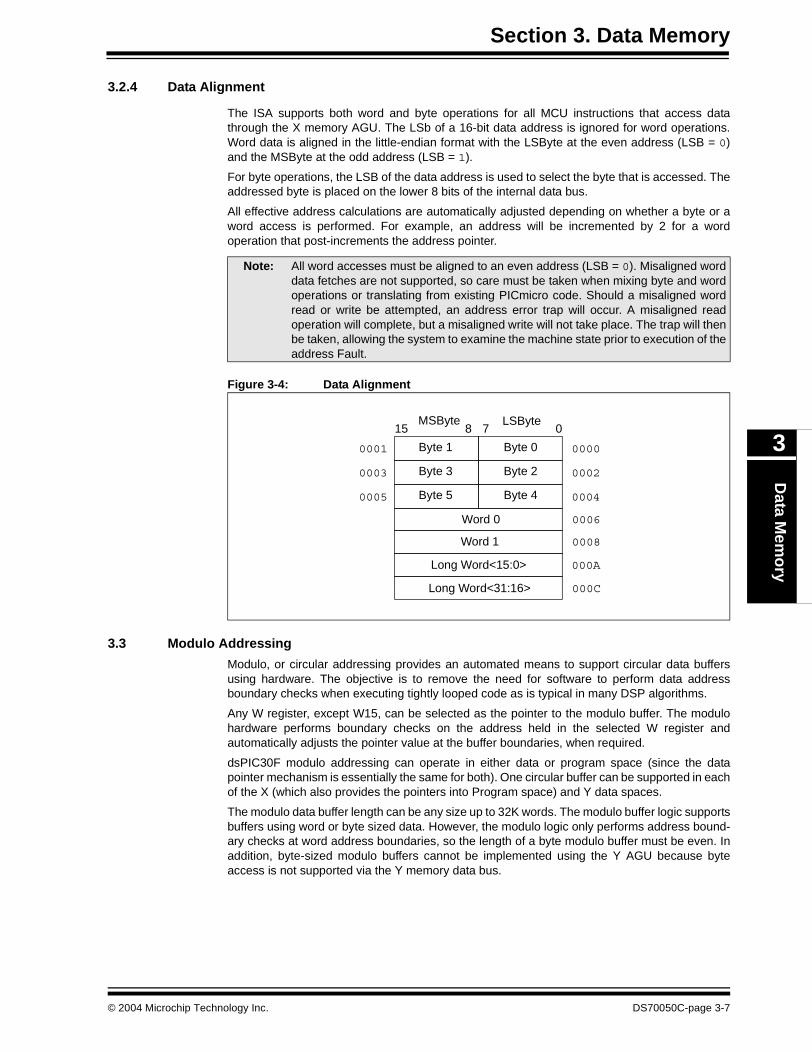
Section 3. Data MemoryD
ata Mem
ory
3
3.2.4 Data Alignment
The ISA supports both word and byte operations for all MCU instructions that access datathrough the X memory AGU. The LSb of a 16-bit data address is ignored for word operations.Word data is aligned in the little-endian format with the LSByte at the even address (LSB = 0)and the MSByte at the odd address (LSB = 1).
For byte operations, the LSB of the data address is used to select the byte that is accessed. Theaddressed byte is placed on the lower 8 bits of the internal data bus.
All effective address calculations are automatically adjusted depending on whether a byte or aword access is performed. For example, an address will be incremented by 2 for a wordoperation that post-increments the address pointer.
Figure 3-4: Data Alignment
3.3 Modulo Addressing
Modulo, or circular addressing provides an automated means to support circular data buffersusing hardware. The objective is to remove the need for software to perform data addressboundary checks when executing tightly looped code as is typical in many DSP algorithms.
Any W register, except W15, can be selected as the pointer to the modulo buffer. The modulohardware performs boundary checks on the address held in the selected W register andautomatically adjusts the pointer value at the buffer boundaries, when required.
dsPIC30F modulo addressing can operate in either data or program space (since the datapointer mechanism is essentially the same for both). One circular buffer can be supported in eachof the X (which also provides the pointers into Program space) and Y data spaces.
The modulo data buffer length can be any size up to 32K words. The modulo buffer logic supportsbuffers using word or byte sized data. However, the modulo logic only performs address bound-ary checks at word address boundaries, so the length of a byte modulo buffer must be even. Inaddition, byte-sized modulo buffers cannot be implemented using the Y AGU because byteaccess is not supported via the Y memory data bus.
Note: All word accesses must be aligned to an even address (LSB = 0). Misaligned worddata fetches are not supported, so care must be taken when mixing byte and wordoperations or translating from existing PICmicro code. Should a misaligned wordread or write be attempted, an address error trap will occur. A misaligned readoperation will complete, but a misaligned write will not take place. The trap will thenbe taken, allowing the system to examine the machine state prior to execution of theaddress Fault.
15 8 7 0
0001
0003
0005
0000
0002
0004
Byte 1
Byte 3
Byte 5
LSByteMSByte
Word 0
Word 1
0006
0008
Long Word<15:0> 000A
Long Word<31:16> 000C
Byte 0
Byte 2
Byte 4
© 2004 Microchip Technology Inc. DS70050C-page 3-7
dsPIC30F Family Reference Manual
3.3.1 Modulo Start and End Address Selection
Four address registers are available for specifying the modulo buffer start and end addresses:
• XMODSRT: X AGU Modulo Start Address Register• XMODEND: X AGU Modulo End Address Register• YMODSRT: Y AGU Modulo Start Address Register
• YMODEND: Y AGU Modulo End Address Register
The start address for a modulo buffer must be located at an even byte address boundary. TheLSB of the XMODSRT and YMODSRT registers is fixed at ‘0’ to ensure the correct modulo startaddress. The end address for a modulo buffer must be located at an odd byte address boundary.The LSB of the XMODEND and YMODEND registers is fixed to ‘1’ to ensure the correct moduloend address.
The start and end address selected for each modulo buffer have certain restrictions, dependingon whether an incrementing or decrementing buffer is to be implemented. For an incrementingbuffer, a W register pointer is incremented through the buffer address range. When the endaddress of the incrementing buffer is reached, the W register pointer is reset to point to the startof the buffer. For a decrementing buffer, a W register pointer is decremented through the bufferaddress range. When the start address of a decrementing buffer is reached, the W registerpointer is reset to point to the end of the buffer.
3.3.1.1 Modulo Start Address
The data buffer start address is arbitrary, but must be at a ‘zero’ power of two boundary forincrementing modulo buffers. The modulo start address can be any value for decrementingmodulo buffers and is calculated using the chosen buffer end address and buffer length.
For example, if the buffer length for an incrementing buffer is chosen to be 50 words (100 bytes),then the buffer start byte address must contain 7 Least Significant zeros. Valid start addressesmay, therefore, be 0xNN00 and 0xNN80, where ‘N’ is any hexadecimal value.
3.3.1.2 Modulo End Address
The data buffer end address is arbitrary but must be at a ‘ones’ boundary for decrementingbuffers. The modulo end address can be any value for an incrementing buffer and is calculatedusing the chosen buffer start address and buffer length.
For example, if the buffer size (modulus value) is chosen to be 50 words (100 bytes), then thebuffer end byte address for decrementing modulo buffer must contain 7 Least Significant ones.Valid end addresses may, therefore, be 0xNNFF and 0xNN7F, where ‘x’ is any hexadecimalvalue.
Note: The user must decide whether an incrementing or decrementing modulo buffer isrequired for the application. There are certain address restrictions that depend onwhether an incrementing or decrementing modulo buffer is to be implemented.
Note: If the required modulo buffer length is an even power of 2, modulo start and endaddresses can be chosen that satisfy the requirements for incrementing anddecrementing buffers.
DS70050C-page 3-8 © 2004 Microchip Technology Inc.
Section 3. Data MemoryD
ata Mem
ory
3
3.3.1.3 Modulo Address Calculation
The end address for an incrementing modulo buffer must be calculated from the chosen startaddress and the chosen buffer length in bytes. Equation 3-1 may be used to calculate the endaddress.
Equation 3-1: Modulo End Address for Incrementing Buffer
The start address for a decrementing modulo buffer is calculated from the chosen end addressand the buffer length, as shown in Equation 3-2.
Equation 3-2: Modulo Start Address for Decrementing Buffer
3.3.1.4 Data Dependencies Associated with Modulo Addressing SFRs
A write operation to the Modulo Addressing Control register, MODCON, should not beimmediately followed by an indirect read operation using any W register. The code segmentshown in Example 3-1 will thus lead to unexpected results.
Example 3-1: Incorrect MODCON Initialization
To work around this problem of initialization, use any Addressing mode other than indirect readsin the instruction that immediately follows the initialization of MODCON. A simple work around tothe problem is achieved by adding a NOP after initializing MODCON, as shown in Example 3-2.
Example 3-2: Correct MODCON Initialization
End Address = Start Address + Buffer Length – 1
Start Address = End Address – Buffer Length + 1
Note 1: Using a POP instruction to pop the contents of the top-of-stack (TOS) location intoMODCON, also constitutes a write to MODCON. The instruction immediatelyfollowing a write to MODCON cannot be any instruction performing an indirect readoperation.
2: The user should note that some instructions perform an indirect read operation,implicitly. These are: POP, RETURN, RETFIE, RETLW and ULNK.
MOV #0x8FF4, w0 ;Initialize MODCONMOV w0, MODCONMOV [w1], w2 ;Incorrect EA generated here
MOV #0x8FF4, w0 ;Initialize MODCONMOV w0, MODCONNOP ;See Note belowMOV [w1], w2 ;Correct EA generated here
© 2004 Microchip Technology Inc. DS70050C-page 3-9
dsPIC30F Family Reference Manual
An additional condition exists for indirect read operations performed immediately after writing tothe modulo address SFRs:
• XMODSRT• XMODEND• YMODSRT
• YMODEND
If modulo addressing has already been enabled in MODCON, then a write to the X (or Y) moduloaddress SFRs should not be immediately followed by an indirect read, using the W registerdesignated for modulo buffer access from X-data space (or Y-data space). The code segment inExample 3-3 shows how initializing the modulo SFRs associated with the X-data space, couldlead to unexpected results. A similar example can be made for initialization in Y-data space.
Example 3-3: Incorrect Modulo Addressing Setup
To work around this issue, insert a NOP, or perform any operation other than an indirect read thatuses the W register designated for modulo buffer access, after initializing the modulo addressSFRs. This is demonstrated in Example 3-4. Another alternative would be to enable moduloaddressing in MODCON after initializing the modulo start and end address SFRs.
Example 3-4: Correct Modulo Addressing Setup
MOV #0x8FF4, w0 ;Modulo addressing enabledMOV w0, MODCON ;in X-data space using w4
;for buffer accessMOV #0x1200, w4 ;XMODSRT is initializedMOV w4, XMODSRTMOV #0x12FF, w0 ;XMODEND is initializedMOV w0, XMODENDMOV [w4++], w5 ;Incorrect EA generated
MOV #0x8FF4, w0 ;Modulo addressing enabledMOV w0, MODCON ;in X-data space using w4
;for buffer accessMOV #0x1200, w4 ;XMODSRT is initializedMOV w4, XMODSRTMOV #0x12FF, w0 ;XMODEND is initializedMOV w0, XMODENDNOP ;See Note belowMOV [w4++], w5 ;Correct EA generated here
Note: Alternatively, execute other instructions that do not perform indirect read operations,using the W register designated for modulo buffer access.
DS70050C-page 3-10 © 2004 Microchip Technology Inc.
Section 3. Data MemoryD
ata Mem
ory
3
3.3.2 W Address Register Selection
The X address space pointer W register (XWM) to which modulo addressing is to be applied, isstored in MODCON<3:0> (see Register 3-1). The XMODSRT, XMODEND, and the XWMregister selection are shared between the X RAGU and X WAGU. Modulo addressing is enabledfor X data space when XWM is set to any value other than 15 and the XMODEN bit is set(MODCON<15>). W15 cannot be used as the pointer for modulo addressing because it is thededicated software stack pointer.
The Y address space pointer W register (YWM) to which modulo addressing is to be applied, isstored in MODCON<7:4> (see Register 3-2). Modulo addressing is enabled for Y data spacewhen YWM is set to any value other than 15 and the YMODEN bit is set (MODCON<14>).
3.3.3 Modulo Addressing Applicability
Modulo addressing can be applied to the effective address (EA) calculation associated with theselected W register. It is important to realize that the address boundary tests look for addressesequal to or greater than the upper address boundary for incrementing buffers and equal to or lessthan the lower address boundary for decrementing buffers. Address changes may, therefore,jump over boundaries and still be adjusted correctly. Remember that the automatic adjustmentof the W register pointer by the modulo hardware is uni-directional. That is, the W register pointermay not be adjusted correctly by the modulo hardware when the W register pointer for anincrementing buffer is decremented and vice versa. The exception to this rule is when the bufferlength is an even power of 2 and the start and end addresses can be chosen to meet the-boundary requirements for both incrementing and decrementing modulo buffers.
A new EA can exceed the modulo buffer boundary by up to the length of the buffer and still besuccessfully corrected. This is important to remember when the Register Indexed ([Wb + Wn])and Literal Offset ([Wn + lit10]) Addressing modes are used. The user should remember thatthe Register Indexed and Literal Offset Addressing modes do not change the value held in theW register. Only the indirect with Pre- and Post-modification Addressing modes ([Wn++],[Wn--], [++Wn], [--Wn]) will modify the W register address value.
Note: A write to the MODCON register should not be followed by an instruction thatperforms an indirect read operation using a W register. Unexpected results mayoccur. Some instructions perform an implicit indirect read. These are:POP,RETURN, RETFIE, RETLW and ULNK.
© 2004 Microchip Technology Inc. DS70050C-page 3-11
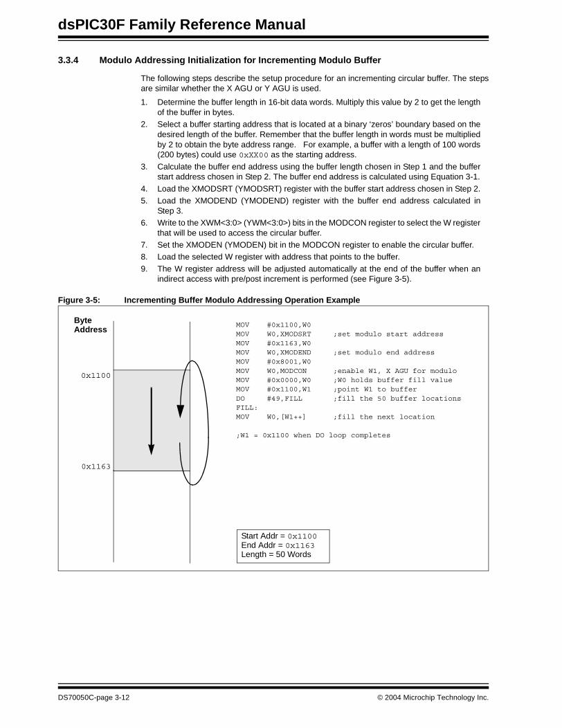
dsPIC30F Family Reference Manual
3.3.4 Modulo Addressing Initialization for Incrementing Modulo Buffer
The following steps describe the setup procedure for an incrementing circular buffer. The stepsare similar whether the X AGU or Y AGU is used.
1. Determine the buffer length in 16-bit data words. Multiply this value by 2 to get the lengthof the buffer in bytes.
2. Select a buffer starting address that is located at a binary ‘zeros’ boundary based on thedesired length of the buffer. Remember that the buffer length in words must be multipliedby 2 to obtain the byte address range. For example, a buffer with a length of 100 words(200 bytes) could use 0xXX00 as the starting address.
3. Calculate the buffer end address using the buffer length chosen in Step 1 and the bufferstart address chosen in Step 2. The buffer end address is calculated using Equation 3-1.
4. Load the XMODSRT (YMODSRT) register with the buffer start address chosen in Step 2.5. Load the XMODEND (YMODEND) register with the buffer end address calculated in
Step 3.6. Write to the XWM<3:0> (YWM<3:0>) bits in the MODCON register to select the W register
that will be used to access the circular buffer.7. Set the XMODEN (YMODEN) bit in the MODCON register to enable the circular buffer.8. Load the selected W register with address that points to the buffer.
9. The W register address will be adjusted automatically at the end of the buffer when anindirect access with pre/post increment is performed (see Figure 3-5).
Figure 3-5: Incrementing Buffer Modulo Addressing Operation Example
0x1100
0x1163
Start Addr = 0x1100End Addr = 0x1163Length = 50 Words
ByteAddress
MOV #0x1100,W0MOV W0,XMODSRT ;set modulo start addressMOV #0x1163,W0MOV W0,XMODEND ;set modulo end addressMOV #0x8001,W0MOV W0,MODCON ;enable W1, X AGU for moduloMOV #0x0000,W0 ;W0 holds buffer fill valueMOV #0x1100,W1 ;point W1 to bufferDO #49,FILL ;fill the 50 buffer locationsFILL:MOV W0,[W1++] ;fill the next location
;W1 = 0x1100 when DO loop completes
DS70050C-page 3-12 © 2004 Microchip Technology Inc.
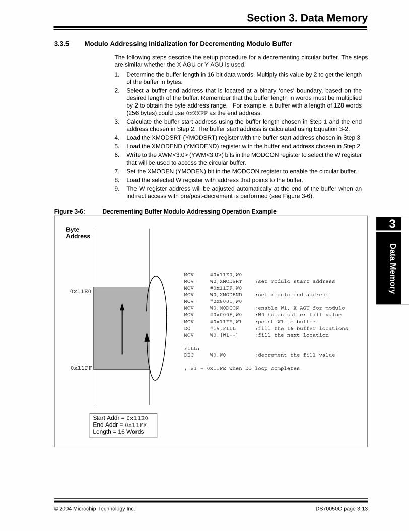
Section 3. Data MemoryD
ata Mem
ory
3
3.3.5 Modulo Addressing Initialization for Decrementing Modulo Buffer
The following steps describe the setup procedure for a decrementing circular buffer. The stepsare similar whether the X AGU or Y AGU is used.
1. Determine the buffer length in 16-bit data words. Multiply this value by 2 to get the lengthof the buffer in bytes.
2. Select a buffer end address that is located at a binary ‘ones’ boundary, based on thedesired length of the buffer. Remember that the buffer length in words must be multipliedby 2 to obtain the byte address range. For example, a buffer with a length of 128 words(256 bytes) could use 0xXXFF as the end address.
3. Calculate the buffer start address using the buffer length chosen in Step 1 and the endaddress chosen in Step 2. The buffer start address is calculated using Equation 3-2.
4. Load the XMODSRT (YMODSRT) register with the buffer start address chosen in Step 3.5. Load the XMODEND (YMODEND) register with the buffer end address chosen in Step 2.6. Write to the XWM<3:0> (YWM<3:0>) bits in the MODCON register to select the W register
that will be used to access the circular buffer.7. Set the XMODEN (YMODEN) bit in the MODCON register to enable the circular buffer.
8. Load the selected W register with address that points to the buffer.9. The W register address will be adjusted automatically at the end of the buffer when an
indirect access with pre/post-decrement is performed (see Figure 3-6).
Figure 3-6: Decrementing Buffer Modulo Addressing Operation Example
0x11E0
0x11FF
Start Addr = 0x11E0End Addr = 0x11FFLength = 16 Words
ByteAddress
MOV #0x11E0,W0MOV W0,XMODSRT ;set modulo start addressMOV #0x11FF,W0MOV W0,XMODEND ;set modulo end addressMOV #0x8001,W0MOV W0,MODCON ;enable W1, X AGU for moduloMOV #0x000F,W0 ;W0 holds buffer fill valueMOV #0x11FE,W1 ;point W1 to bufferDO #15,FILL ;fill the 16 buffer locationsMOV W0,[W1--] ;fill the next location
FILL:DEC W0,W0 ;decrement the fill value
; W1 = 0x11FE when DO loop completes
© 2004 Microchip Technology Inc. DS70050C-page 3-13
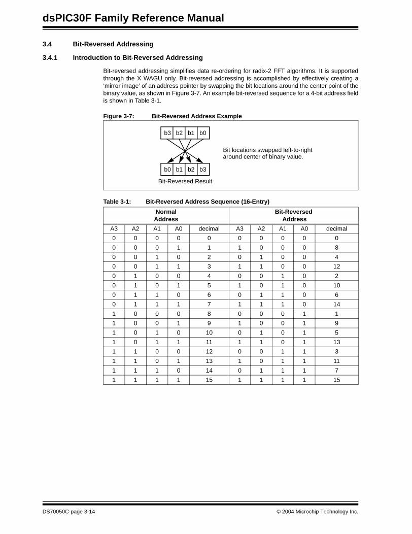
dsPIC30F Family Reference Manual
3.4 Bit-Reversed Addressing
3.4.1 Introduction to Bit-Reversed Addressing
Bit-reversed addressing simplifies data re-ordering for radix-2 FFT algorithms. It is supportedthrough the X WAGU only. Bit-reversed addressing is accomplished by effectively creating a‘mirror image’ of an address pointer by swapping the bit locations around the center point of thebinary value, as shown in Figure 3-7. An example bit-reversed sequence for a 4-bit address fieldis shown in Table 3-1.
Figure 3-7: Bit-Reversed Address Example
Table 3-1: Bit-Reversed Address Sequence (16-Entry)
b3 b2 b1 b0
b0 b1 b2 b3
Bit locations swapped left-to-rightaround center of binary value.
Bit-Reversed Result
NormalAddress
Bit-Reversed Address
A3 A2 A1 A0 decimal A3 A2 A1 A0 decimal
0 0 0 0 0 0 0 0 0 0
0 0 0 1 1 1 0 0 0 8
0 0 1 0 2 0 1 0 0 4
0 0 1 1 3 1 1 0 0 12
0 1 0 0 4 0 0 1 0 2
0 1 0 1 5 1 0 1 0 10
0 1 1 0 6 0 1 1 0 6
0 1 1 1 7 1 1 1 0 14
1 0 0 0 8 0 0 0 1 1
1 0 0 1 9 1 0 0 1 9
1 0 1 0 10 0 1 0 1 5
1 0 1 1 11 1 1 0 1 13
1 1 0 0 12 0 0 1 1 3
1 1 0 1 13 1 0 1 1 11
1 1 1 0 14 0 1 1 1 7
1 1 1 1 15 1 1 1 1 15
DS70050C-page 3-14 © 2004 Microchip Technology Inc.
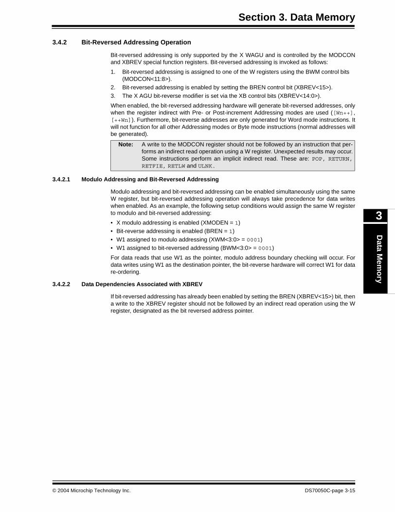
Section 3. Data MemoryD
ata Mem
ory
3
3.4.2 Bit-Reversed Addressing Operation
Bit-reversed addressing is only supported by the X WAGU and is controlled by the MODCONand XBREV special function registers. Bit-reversed addressing is invoked as follows:
1. Bit-reversed addressing is assigned to one of the W registers using the BWM control bits(MODCON<11:8>).
2. Bit-reversed addressing is enabled by setting the BREN control bit (XBREV<15>).
3. The X AGU bit-reverse modifier is set via the XB control bits (XBREV<14:0>).
When enabled, the bit-reversed addressing hardware will generate bit-reversed addresses, onlywhen the register indirect with Pre- or Post-increment Addressing modes are used ([Wn++],[++Wn]). Furthermore, bit-reverse addresses are only generated for Word mode instructions. Itwill not function for all other Addressing modes or Byte mode instructions (normal addresses willbe generated).
3.4.2.1 Modulo Addressing and Bit-Reversed Addressing
Modulo addressing and bit-reversed addressing can be enabled simultaneously using the sameW register, but bit-reversed addressing operation will always take precedence for data writeswhen enabled. As an example, the following setup conditions would assign the same W registerto modulo and bit-reversed addressing:
• X modulo addressing is enabled (XMODEN = 1)• Bit-reverse addressing is enabled (BREN = 1)
• W1 assigned to modulo addressing (XWM<3:0> = 0001)• W1 assigned to bit-reversed addressing (BWM<3:0> = 0001)
For data reads that use W1 as the pointer, modulo address boundary checking will occur. Fordata writes using W1 as the destination pointer, the bit-reverse hardware will correct W1 for datare-ordering.
3.4.2.2 Data Dependencies Associated with XBREV
If bit-reversed addressing has already been enabled by setting the BREN (XBREV<15>) bit, thena write to the XBREV register should not be followed by an indirect read operation using the Wregister, designated as the bit reversed address pointer.
Note: A write to the MODCON register should not be followed by an instruction that per-forms an indirect read operation using a W register. Unexpected results may occur.Some instructions perform an implicit indirect read. These are: POP, RETURN,RETFIE, RETLW and ULNK.
© 2004 Microchip Technology Inc. DS70050C-page 3-15
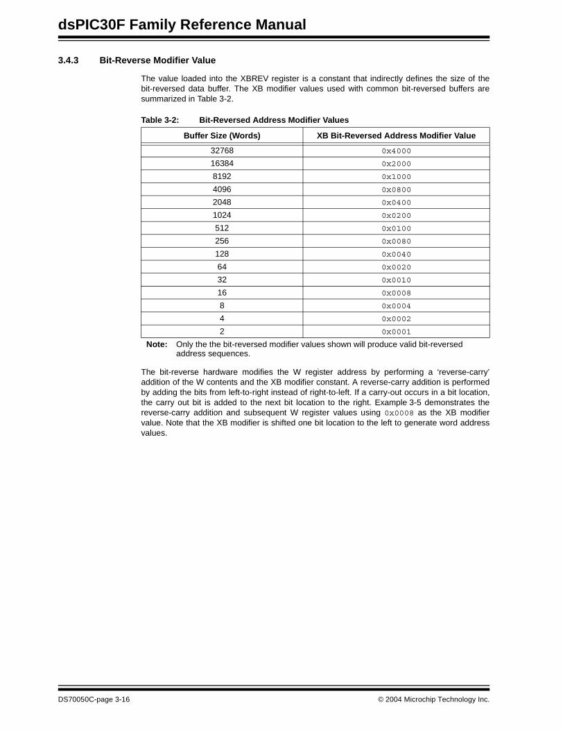
dsPIC30F Family Reference Manual
3.4.3 Bit-Reverse Modifier Value
The value loaded into the XBREV register is a constant that indirectly defines the size of thebit-reversed data buffer. The XB modifier values used with common bit-reversed buffers aresummarized in Table 3-2.
Table 3-2: Bit-Reversed Address Modifier Values
The bit-reverse hardware modifies the W register address by performing a ‘reverse-carry’addition of the W contents and the XB modifier constant. A reverse-carry addition is performedby adding the bits from left-to-right instead of right-to-left. If a carry-out occurs in a bit location,the carry out bit is added to the next bit location to the right. Example 3-5 demonstrates thereverse-carry addition and subsequent W register values using 0x0008 as the XB modifiervalue. Note that the XB modifier is shifted one bit location to the left to generate word addressvalues.
Buffer Size (Words) XB Bit-Reversed Address Modifier Value
32768 0x4000
16384 0x2000
8192 0x1000
4096 0x0800
2048 0x0400
1024 0x0200
512 0x0100
256 0x0080
128 0x0040
64 0x0020
32 0x0010
16 0x0008
8 0x0004
4 0x0002
2 0x0001
Note: Only the the bit-reversed modifier values shown will produce valid bit-reversedaddress sequences.
DS70050C-page 3-16 © 2004 Microchip Technology Inc.
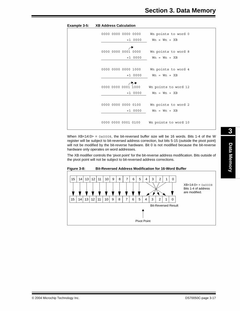
Section 3. Data MemoryD
ata Mem
ory
3
Example 3-5: XB Address Calculation
When XB<14:0> = 0x0008, the bit-reversed buffer size will be 16 words. Bits 1-4 of the Wregister will be subject to bit-reversed address correction, but bits 5-15 (outside the pivot point)will not be modified by the bit-reverse hardware. Bit 0 is not modified because the bit-reversehardware only operates on word addresses.
The XB modifier controls the ‘pivot point’ for the bit-reverse address modification. Bits outside ofthe pivot point will not be subject to bit-reversed address corrections.
Figure 3-8: Bit-Reversed Address Modification for 16-Word Buffer
0000 0000 0000 0000 Wn points to word 0
+1 0000 Wn = Wn + XB
0000 0000 0001 0000 Wn points to word 8
+1 0000 Wn = Wn + XB
0000 0000 0000 1000 Wn points to word 4
+1 0000 Wn = Wn + XB
0000 0000 0001 1000 Wn points to word 12
+1 0000 Wn = Wn + XB
0000 0000 0000 0100 Wn points to word 2
+1 0000 Wn = Wn + XB
0000 0000 0001 0100 Wn points to word 10
Bit-Reversed Result
15 14 13 12 11 10 9 8 7 6 5 4 3 2 1 0
15 14 13 12 11 10 9 8 7 6 5 4 3 2 1 0
XB<14:0> = 0x0008Bits 1-4 of address
Pivot Point
are modified.
© 2004 Microchip Technology Inc. DS70050C-page 3-17

dsPIC30F Family Reference Manual
3.4.4 Bit-Reversed Addressing Code Example
The following code example reads a series of 16 data words and writes the data to a new locationin bit-reversed order. W0 is the read address pointer and W1 is the write address pointer subjectto bit-reverse modification.
; Set XB for 16-word buffer, enable bit reverse addressingMOV #0x8008,W0MOV W0,XBREV
; Setup MODCON to use W1 for bit reverse addressingMOV #0x01FF,W0MOV W0,MODCON
; W0 points to input data bufferMOV #Input_Buf,W0
; W1 points to bit reversed dataMOV #Bit_Rev_Buf,W1
; Re-order the data from Input_Buf into Bit_Rev_BufREPEAT #15MOV [W0++],[W1++]
3.5 Control Register Descriptions
The following registers are used to control modulo and bit-reversed addressing:
• MODCON: Modulo Addressing Control Register• XMODSRT: X AGU Modulo Start Address Register• XMODEND: X AGU Modulo End Address Register
• YMODSRT: Y AGU Modulo Start Address Register• YMODEND: Y AGU Modulo End Address Register• XBREV: X AGU Bit-Reverse Addressing Control Register
A detailed description of each register is provided on subsequent pages.
DS70050C-page 3-18 © 2004 Microchip Technology Inc.
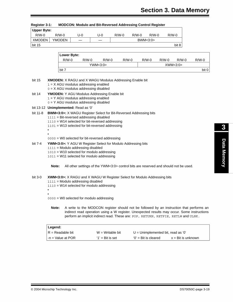
Section 3. Data MemoryD
ata Mem
ory
3
Register 3-1: MODCON: Modulo and Bit-Reversed Addressing Control Register
Upper Byte:R/W-0 R/W-0 U-0 U-0 R/W-0 R/W-0 R/W-0 R/W-0
XMODEN YMODEN — — BWM<3:0>
bit 15 bit 8
Lower Byte:R/W-0 R/W-0 R/W-0 R/W-0 R/W-0 R/W-0 R/W-0 R/W-0
YWM<3:0> XWM<3:0>bit 7 bit 0
bit 15 XMODEN: X RAGU and X WAGU Modulus Addressing Enable bit1 = X AGU modulus addressing enabled0 = X AGU modulus addressing disabled
bit 14 YMODEN: Y AGU Modulus Addressing Enable bit1 = Y AGU modulus addressing enabled0 = Y AGU modulus addressing disabled
bit 13-12 Unimplemented: Read as ‘0’
bit 11-8 BWM<3:0>: X WAGU Register Select for Bit-Reversed Addressing bits1111 = Bit-reversed addressing disabled1110 = W14 selected for bit-reversed addressing1101 = W13 selected for bit-reversed addressing••0000 = W0 selected for bit-reversed addressing
bit 7-4 YWM<3:0>: Y AGU W Register Select for Modulo Addressing bits1111 = Modulo addressing disabled1010 = W10 selected for modulo addressing1011 = W11 selected for modulo addressing
Note: All other settings of the YWM<3:0> control bits are reserved and should not be used.
bit 3-0 XWM<3:0>: X RAGU and X WAGU W Register Select for Modulo Addressing bits1111 = Modulo addressing disabled1110 = W14 selected for modulo addressing••0000 = W0 selected for modulo addressing
Note: A write to the MODCON register should not be followed by an instruction that performs anindirect read operation using a W register. Unexpected results may occur. Some instructionsperform an implicit indirect read. These are: POP, RETURN, RETFIE, RETLW and ULNK.
Legend:
R = Readable bit W = Writable bit U = Unimplemented bit, read as ‘0’
-n = Value at POR ‘1’ = Bit is set ‘0’ = Bit is cleared x = Bit is unknown
© 2004 Microchip Technology Inc. DS70050C-page 3-19
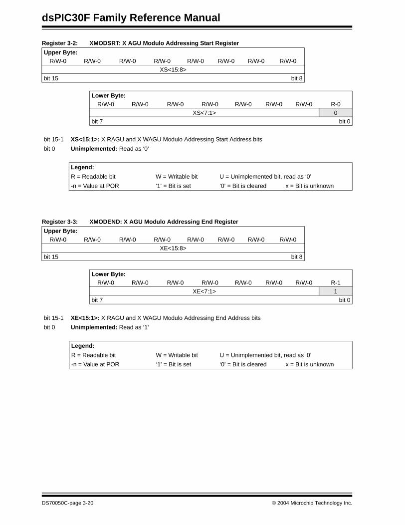
dsPIC30F Family Reference Manual
Register 3-2: XMODSRT: X AGU Modulo Addressing Start Register
Register 3-3: XMODEND: X AGU Modulo Addressing End Register
Upper Byte:R/W-0 R/W-0 R/W-0 R/W-0 R/W-0 R/W-0 R/W-0 R/W-0
XS<15:8>
bit 15 bit 8
Lower Byte:R/W-0 R/W-0 R/W-0 R/W-0 R/W-0 R/W-0 R/W-0 R-0
XS<7:1> 0bit 7 bit 0
bit 15-1 XS<15:1>: X RAGU and X WAGU Modulo Addressing Start Address bits
bit 0 Unimplemented: Read as ‘0’
Legend:
R = Readable bit W = Writable bit U = Unimplemented bit, read as ‘0’
-n = Value at POR ‘1’ = Bit is set ‘0’ = Bit is cleared x = Bit is unknown
Upper Byte:R/W-0 R/W-0 R/W-0 R/W-0 R/W-0 R/W-0 R/W-0 R/W-0
XE<15:8>bit 15 bit 8
Lower Byte:R/W-0 R/W-0 R/W-0 R/W-0 R/W-0 R/W-0 R/W-0 R-1
XE<7:1> 1bit 7 bit 0
bit 15-1 XE<15:1>: X RAGU and X WAGU Modulo Addressing End Address bits
bit 0 Unimplemented: Read as ‘1’
Legend:
R = Readable bit W = Writable bit U = Unimplemented bit, read as ‘0’
-n = Value at POR ‘1’ = Bit is set ‘0’ = Bit is cleared x = Bit is unknown
DS70050C-page 3-20 © 2004 Microchip Technology Inc.
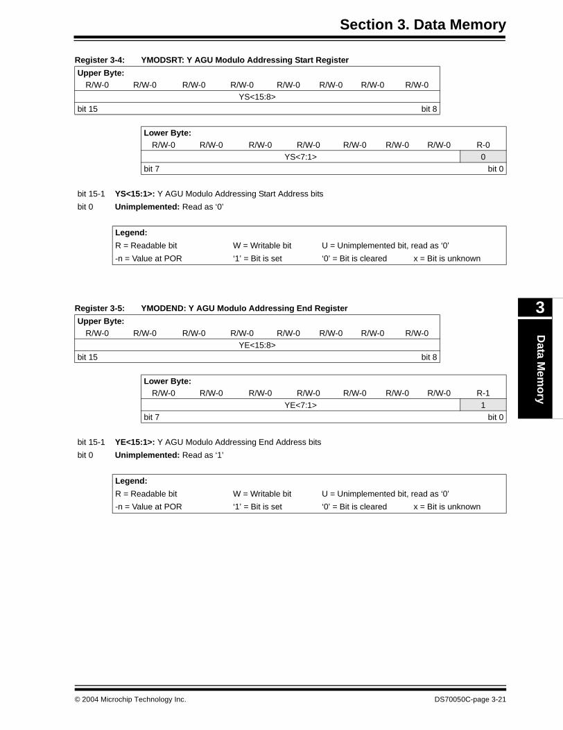
Section 3. Data MemoryD
ata Mem
ory
3
Register 3-4: YMODSRT: Y AGU Modulo Addressing Start Register
Register 3-5: YMODEND: Y AGU Modulo Addressing End Register
Upper Byte:R/W-0 R/W-0 R/W-0 R/W-0 R/W-0 R/W-0 R/W-0 R/W-0
YS<15:8>
bit 15 bit 8
Lower Byte:R/W-0 R/W-0 R/W-0 R/W-0 R/W-0 R/W-0 R/W-0 R-0
YS<7:1> 0bit 7 bit 0
bit 15-1 YS<15:1>: Y AGU Modulo Addressing Start Address bits
bit 0 Unimplemented: Read as ‘0’
Legend:
R = Readable bit W = Writable bit U = Unimplemented bit, read as ‘0’
-n = Value at POR ‘1’ = Bit is set ‘0’ = Bit is cleared x = Bit is unknown
Upper Byte:R/W-0 R/W-0 R/W-0 R/W-0 R/W-0 R/W-0 R/W-0 R/W-0
YE<15:8>bit 15 bit 8
Lower Byte:R/W-0 R/W-0 R/W-0 R/W-0 R/W-0 R/W-0 R/W-0 R-1
YE<7:1> 1bit 7 bit 0
bit 15-1 YE<15:1>: Y AGU Modulo Addressing End Address bits
bit 0 Unimplemented: Read as ‘1’
Legend:
R = Readable bit W = Writable bit U = Unimplemented bit, read as ‘0’
-n = Value at POR ‘1’ = Bit is set ‘0’ = Bit is cleared x = Bit is unknown
© 2004 Microchip Technology Inc. DS70050C-page 3-21
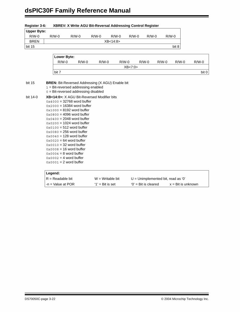
dsPIC30F Family Reference Manual
Register 3-6: XBREV: X Write AGU Bit-Reversal Addressing Control Register
Upper Byte:R/W-0 R/W-0 R/W-0 R/W-0 R/W-0 R/W-0 R/W-0 R/W-0BREN XB<14:8>
bit 15 bit 8
Lower Byte:R/W-0 R/W-0 R/W-0 R/W-0 R/W-0 R/W-0 R/W-0 R/W-0
XB<7:0>bit 7 bit 0
bit 15 BREN: Bit-Reversed Addressing (X AGU) Enable bit1 = Bit-reversed addressing enabled0 = Bit-reversed addressing disabled
bit 14-0 XB<14:0>: X AGU Bit-Reversed Modifier bits0x4000 = 32768 word buffer0x2000 = 16384 word buffer0x1000 = 8192 word buffer0x0800 = 4096 word buffer0x0400 = 2048 word buffer0x0200 = 1024 word buffer0x0100 = 512 word buffer0x0080 = 256 word buffer0x0040 = 128 word buffer0x0020 = 64 word buffer0x0010 = 32 word buffer0x0008 = 16 word buffer0x0004 = 8 word buffer0x0002 = 4 word buffer0x0001 = 2 word buffer
Legend:
R = Readable bit W = Writable bit U = Unimplemented bit, read as ‘0’
-n = Value at POR ‘1’ = Bit is set ‘0’ = Bit is cleared x = Bit is unknown
DS70050C-page 3-22 © 2004 Microchip Technology Inc.
Section 3. Data MemoryD
ata Mem
ory
3
3.6 Related Application Notes
This section lists application notes that are related to this section of the manual. Theseapplication notes may not be written specifically for the dsPIC30F Product Family, but theconcepts are pertinent and could be used with modification and possible limitations. The currentapplication notes related to the Data Memory module are:
Title Application Note #
No related application notes at this time.
Note: Please visit the Microchip web site (www.microchip.com) for additional ApplicationNotes and code examples for the dsPIC30F Family of devices.
© 2004 Microchip Technology Inc. DS70050C-page 3-23

dsPIC30F Family Reference Manual
3.7 Revision History
Revision A
This is the initial released revision of this document.
Revision B
This revision incorporates additional technical content for the dsPIC30F Data Memory module.
Revision C
This revision incorporates all known errata at the time of this document update.
DS70050C-page 3-24 © 2004 Microchip Technology Inc.

Section 4. Program Memory
Pro
gram
Mem
ory
4
HIGHLIGHTS
This section of the manual contains the following topics:
4.1 Program Memory Address Map ..................................................................................... 4-2
4.2 Program Counter ........................................................................................................... 4-44.3 Data Access from Program Memory.............................................................................. 4-44.4 Program Space Visibility from Data Space .................................................................... 4-8
4.5 Program Memory Writes .............................................................................................. 4-104.6 PSV Code Examples ................................................................................................... 4-114.7 Related Application Notes............................................................................................ 4-12
4.8 Revision History ........................................................................................................... 4-13
© 2005 Microchip Technology Inc. DS70051D-page 4-1
dsPIC30F Family Reference Manual
4.1 Program Memory Address Map
The dsPIC30F devices have a 4M x 24-bit program memory address space, shown in Figure 4-1.There are three available methods for accessing program space.
1. Via the 23-bit PC.2. Via table read (TBLRD) and table write (TBLWT) instructions.
3. By mapping a 32-Kbyte segment of program memory into the data memory addressspace.
The program memory map is divided into the user program space and the user configurationspace. The user program space contains the Reset vector, interrupt vector tables, programmemory and data EEPROM memory. The user configuration space contains non-volatileconfiguration bits for setting device options and the device ID locations.
DS70051D-page 4-2 © 2005 Microchip Technology Inc.
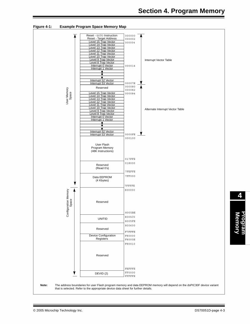
Section 4. Program MemoryP
rog
ramM
emo
ry
4
Figure 4-1: Example Program Space Memory Map
Note: The address boundaries for user Flash program memory and data EEPROM memory will depend on the dsPIC30F device variantthat is selected. Refer to the appropriate device data sheet for further details.
Reset - Target Address
Use
r M
emor
yS
pace
000000
00007E
Level 15 Trap Vector000002
000080
Device Configuration
User FlashProgram Memory
018000
017FFE
Con
figur
atio
n M
emor
yS
pace
Data EEPROM
Level 14 Trap VectorLevel 13 Trap VectorLevel 12 Trap VectorLevel 11 Trap VectorLevel 10 Trap VectorLevel 9 Trap VectorLevel 8 Trap VectorInterrupt 0 VectorInterrupt 1 Vector
Interrupt 52 VectorInterrupt 53 Vector
(48K Instructions)
(4 Kbytes)
800000
F80000Registers F8000E
F80010
DEVID (2)
FEFFFE
FF0000FFFFFE
ReservedF7FFFE
Reserved
7FF000
7FEFFE(Read 0’s)
8005FE
800600
UNITID
000014
Interrupt Vector Table
8005BE
8005C0
Reset - GOTO Instruction
000004
Reserved
7FFFFE
Reserved
000100
0000FE
000084
Reserved
Level 15 Trap VectorLevel 14 Trap VectorLevel 13 Trap VectorLevel 12 Trap VectorLevel 11 Trap VectorLevel 10 Trap VectorLevel 9 Trap VectorLevel 8 Trap VectorInterrupt 0 VectorInterrupt 1 Vector
Interrupt 52 VectorInterrupt 53 Vector
000082
Alternate Interrupt Vector Table
© 2005 Microchip Technology Inc. DS70051D-page 4-3
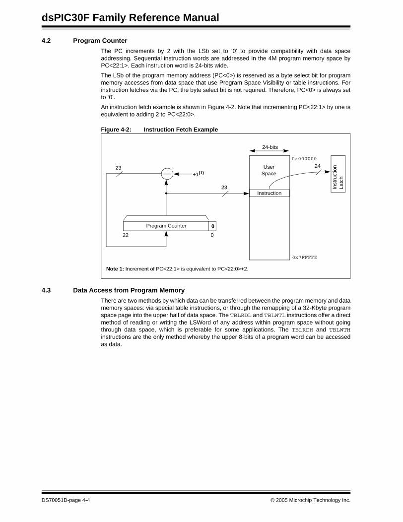
dsPIC30F Family Reference Manual
4.2 Program Counter
The PC increments by 2 with the LSb set to ‘0’ to provide compatibility with data spaceaddressing. Sequential instruction words are addressed in the 4M program memory space byPC<22:1>. Each instruction word is 24-bits wide.
The LSb of the program memory address (PC<0>) is reserved as a byte select bit for programmemory accesses from data space that use Program Space Visibility or table instructions. Forinstruction fetches via the PC, the byte select bit is not required. Therefore, PC<0> is always setto ‘0’.
An instruction fetch example is shown in Figure 4-2. Note that incrementing PC<22:1> by one isequivalent to adding 2 to PC<22:0>.
Figure 4-2: Instruction Fetch Example
4.3 Data Access from Program Memory
There are two methods by which data can be transferred between the program memory and datamemory spaces: via special table instructions, or through the remapping of a 32-Kbyte programspace page into the upper half of data space. The TBLRDL and TBLWTL instructions offer a directmethod of reading or writing the LSWord of any address within program space without goingthrough data space, which is preferable for some applications. The TBLRDH and TBLWTHinstructions are the only method whereby the upper 8-bits of a program word can be accessedas data.
22 0
Program Counter 0
0x000000
0x7FFFFE
24-bits
Inst
ruct
ion
Instruction23
+1(1)
Note 1: Increment of PC<22:1> is equivalent to PC<22:0>+2.
2423 UserSpace
Latc
h
DS70051D-page 4-4 © 2005 Microchip Technology Inc.

Section 4. Program MemoryP
rog
ramM
emo
ry
4
4.3.1 Table Instruction Summary
A set of table instructions is provided to move byte or word-sized data between program spaceand data space. The table read instructions are used to read from the program memory spaceinto data memory space. The table write instructions allow data memory to be written to theprogram memory space.
The four available table instructions are listed below:
• TBLRDL: Table Read Low
• TBLWTL: Table Write Low• TBLRDH: Table Read High• TBLWTH: Table Write High
For table instructions, program memory can be regarded as two 16-bit word wide address spacesresiding side by side, each with the same address range as shown in Figure 4-3. This allowsprogram space to be accessed as byte or aligned word addressable, 16-bit wide, 64-Kbyte pages(i.e., same as data space).
TBLRDL and TBLWTL access the LS Data Word of the program memory, and TBLRDH andTBLWTH access the upper word. As program memory is only 24-bits wide, the upper byte fromthis latter space does not exist, though it is addressable. It is, therefore, termed the ‘phantom’byte.
Figure 4-3: High and Low Address Regions for Table Operations
Note: Detailed code examples using table instructions can be found in Section 5. “Flashand EEPROM Programming”.
0816PC Address
0x000100
0x000102
0x000104
0x000106
23
00000000
00000000
00000000
00000000
Program Memory‘Phantom’ Byte(Read as ‘0’)
‘HIGH’ Table Address Range ‘LOW’ Table Address Range
© 2005 Microchip Technology Inc. DS70051D-page 4-5
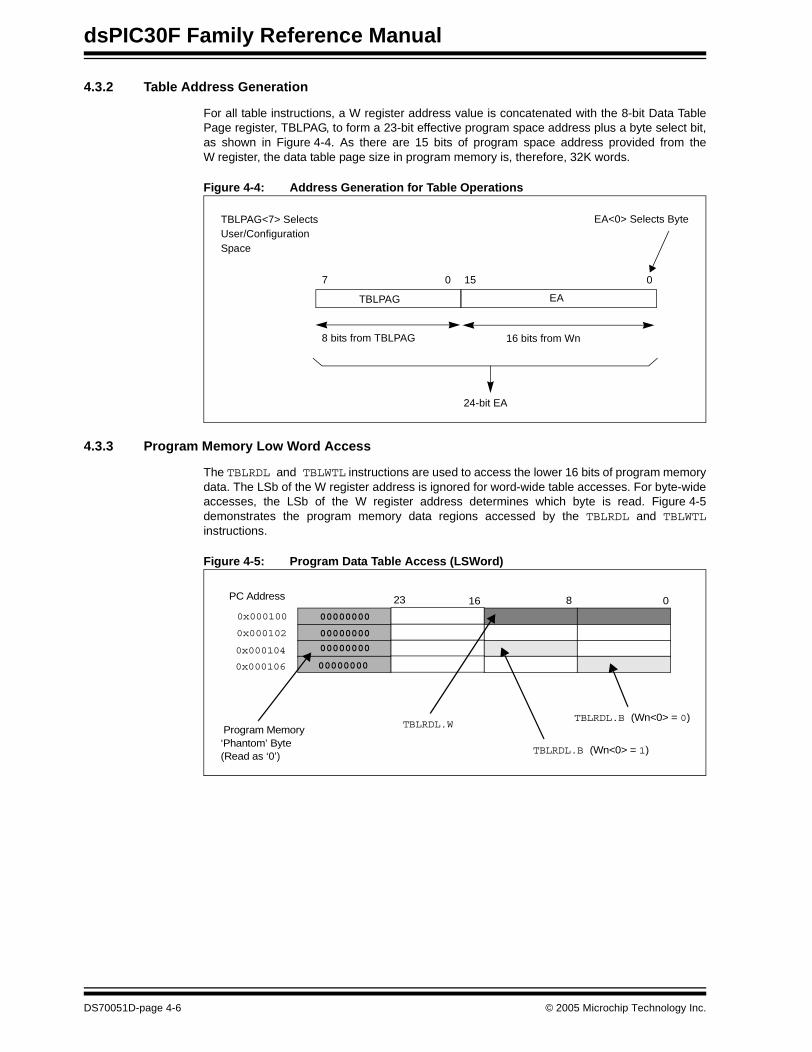
dsPIC30F Family Reference Manual
4.3.2 Table Address Generation
For all table instructions, a W register address value is concatenated with the 8-bit Data TablePage register, TBLPAG, to form a 23-bit effective program space address plus a byte select bit,as shown in Figure 4-4. As there are 15 bits of program space address provided from theW register, the data table page size in program memory is, therefore, 32K words.
Figure 4-4: Address Generation for Table Operations
4.3.3 Program Memory Low Word Access
The TBLRDL and TBLWTL instructions are used to access the lower 16 bits of program memorydata. The LSb of the W register address is ignored for word-wide table accesses. For byte-wideaccesses, the LSb of the W register address determines which byte is read. Figure 4-5demonstrates the program memory data regions accessed by the TBLRDL and TBLWTLinstructions.
Figure 4-5: Program Data Table Access (LSWord)
TBLPAG
8 bits from TBLPAG
EA
EA<0> Selects Byte
24-bit EA
TBLPAG<7> SelectsUser/ConfigurationSpace
01507
16 bits from Wn
0816PC Address
0x000100
0x000102
0x000104
0x000106
23
00000000
00000000
00000000
00000000
Program Memory‘Phantom’ Byte(Read as ‘0’)
TBLRDL.W
TBLRDL.B (Wn<0> = 1)
TBLRDL.B (Wn<0> = 0)
DS70051D-page 4-6 © 2005 Microchip Technology Inc.
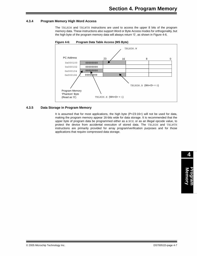
Section 4. Program MemoryP
rog
ramM
emo
ry
4
4.3.4 Program Memory High Word Access
The TBLRDH and TBLWTH instructions are used to access the upper 8 bits of the programmemory data. These instructions also support Word or Byte Access modes for orthogonality, butthe high byte of the program memory data will always return ‘0’, as shown in Figure 4-6.
Figure 4-6: Program Data Table Access (MS Byte)
4.3.5 Data Storage in Program Memory
It is assumed that for most applications, the high byte (P<23:16>) will not be used for data,making the program memory appear 16-bits wide for data storage. It is recommended that theupper byte of program data be programmed either as a NOP, or as an illegal opcode value, toprotect the device from accidental execution of stored data. The TBLRDH and TBLWTHinstructions are primarily provided for array program/verification purposes and for thoseapplications that require compressed data storage.
0816PC Address
0x000100
0x000102
0x000104
0x000106
23
00000000
00000000
00000000
00000000
Program Memory‘Phantom’ Byte(Read as ‘0’)
TBLRDH.W
TBLRDH.B (Wn<0> = 1)
TBLRDH.B (Wn<0> = 0)
© 2005 Microchip Technology Inc. DS70051D-page 4-7
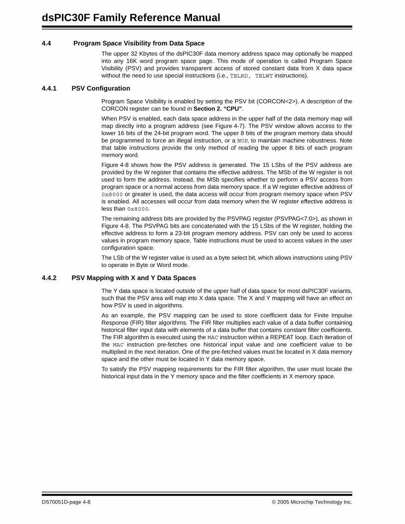
dsPIC30F Family Reference Manual
4.4 Program Space Visibility from Data Space
The upper 32 Kbytes of the dsPIC30F data memory address space may optionally be mappedinto any 16K word program space page. This mode of operation is called Program SpaceVisibility (PSV) and provides transparent access of stored constant data from X data spacewithout the need to use special instructions (i.e., TBLRD, TBLWT instructions).
4.4.1 PSV Configuration
Program Space Visibility is enabled by setting the PSV bit (CORCON<2>). A description of theCORCON register can be found in Section 2. “CPU”.
When PSV is enabled, each data space address in the upper half of the data memory map willmap directly into a program address (see Figure 4-7). The PSV window allows access to thelower 16 bits of the 24-bit program word. The upper 8 bits of the program memory data shouldbe programmed to force an illegal instruction, or a NOP, to maintain machine robustness. Notethat table instructions provide the only method of reading the upper 8 bits of each programmemory word.
Figure 4-8 shows how the PSV address is generated. The 15 LSbs of the PSV address areprovided by the W register that contains the effective address. The MSb of the W register is notused to form the address. Instead, the MSb specifies whether to perform a PSV access fromprogram space or a normal access from data memory space. If a W register effective address of0x8000 or greater is used, the data access will occur from program memory space when PSVis enabled. All accesses will occur from data memory when the W register effective address isless than 0x8000.
The remaining address bits are provided by the PSVPAG register (PSVPAG<7:0>), as shown inFigure 4-8. The PSVPAG bits are concatenated with the 15 LSbs of the W register, holding theeffective address to form a 23-bit program memory address. PSV can only be used to accessvalues in program memory space. Table instructions must be used to access values in the userconfiguration space.
The LSb of the W register value is used as a byte select bit, which allows instructions using PSVto operate in Byte or Word mode.
4.4.2 PSV Mapping with X and Y Data Spaces
The Y data space is located outside of the upper half of data space for most dsPIC30F variants,such that the PSV area will map into X data space. The X and Y mapping will have an effect onhow PSV is used in algorithms.
As an example, the PSV mapping can be used to store coefficient data for Finite ImpulseResponse (FIR) filter algorithms. The FIR filter multiplies each value of a data buffer containinghistorical filter input data with elements of a data buffer that contains constant filter coefficients.The FIR algorithm is executed using the MAC instruction within a REPEAT loop. Each iteration ofthe MAC instruction pre-fetches one historical input value and one coefficient value to bemultiplied in the next iteration. One of the pre-fetched values must be located in X data memoryspace and the other must be located in Y data memory space.
To satisfy the PSV mapping requirements for the FIR filter algorithm, the user must locate thehistorical input data in the Y memory space and the filter coefficients in X memory space.
DS70051D-page 4-8 © 2005 Microchip Technology Inc.
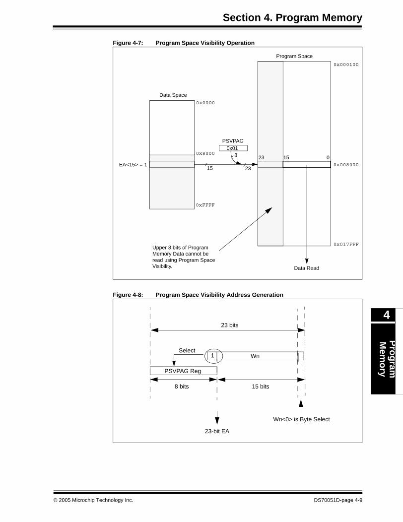
Section 4. Program MemoryP
rog
ramM
emo
ry
4
Figure 4-7: Program Space Visibility Operation
Figure 4-8: Program Space Visibility Address Generation
23 15 0
PSVPAG
EA<15> = 1
Data Space
Program Space
8
15 23
0x0000
0x8000
0xFFFF
0x01
0x008000
Data Read
Upper 8 bits of ProgramMemory Data cannot beread using Program SpaceVisibility.
0x000100
0x017FFF
23 bits
1
PSVPAG Reg
8 bits
Wn
15 bits
Select
23-bit EA
Wn<0> is Byte Select
© 2005 Microchip Technology Inc. DS70051D-page 4-9
dsPIC30F Family Reference Manual
4.4.3 PSV Timing
Instructions that use PSV will require two extra instruction cycles to complete execution, exceptthe following instructions that require only one extra cycle to complete execution:
- The MAC class of instructions with data pre-fetch operands
- All MOV instructions including the MOV.D instruction
The additional instruction cycles are used to fetch the PSV data on the program memory bus.
4.4.3.1 Using PSV in a Repeat Loop
Instructions that use PSV within a REPEAT loop eliminate the extra instruction cycle(s) requiredfor the data access from program memory, hence incurring no overhead in execution time.However, the following iterations of the REPEAT loop will incur an overhead of two instructioncycles to complete execution:
- The first iteration
- The last iteration- Instruction execution prior to exiting the loop due to an interrupt- Instruction execution upon re-entering the loop after an interrupt is serviced
4.4.3.2 PSV and Instruction Stalls
Refer to Section 2. “CPU” for more information about instruction stalls using PSV.
4.5 Program Memory Writes
The dsPIC30F family of devices contains internal program Flash memory for executing usercode. There are two methods by which the user can program this memory:
1. Run-Time Self Programming (RTSP)2. In-Circuit Serial Programming™ (ICSP™)
RTSP is accomplished using TBLWT instructions. ICSP is accomplished using the SPI interfaceand integral bootloader software. Refer to Section 5. “Flash and EEPROM Programming” forfurther details about RTSP. ICSP specifications can be downloaded from the MicrochipTechnology web site (www.microchip.com).
DS70051D-page 4-10 © 2005 Microchip Technology Inc.

Section 4. Program MemoryP
rog
ramM
emo
ry
4
4.6 PSV Code Examples
4.6.1 PSV Code Example in C:
// PSV code example in C// When defined as below the const string uses the PSV feature of dsPIC
const unsigned char hello[] = {"Hello World:\r\n"};unsigned char *TXPtr; // Transmit pointer
int main(void){// Initialize the UART1 U1MODE = 0x8000; U1STA = 0x0000; U1BRG = ((FCY/16)/BAUD) - 1; // set baud rate = BAUD TXPtr = &hello[0]; // point to first char in string U1STAbits.UTXEN = 1; // Initiate transmissionwhile (1)
{while (*TXPtr) // while valid char in string ...
if (!U1STAbits.UTXBF) // and buffer not full ...U1TXREG = *TXPtr++; // transmit string via UART
DelayNmSec(500); // delay for 500 mS
TXPtr = &hello[0]; // re-initialize pointer to first char}
} // end main
4.6.2 PSV code Example in Assembly:
.equ CORCONL, CORCON.section .const, "r"
hello:.ascii "Hello World:\n\r\0"
.global __reset ;Declare the label for the start of code
.text ;Start of Code section
__reset:
clr U1STAmov #0x8000,W0 ; enable UART modulemov W0,U1MODEmov #BR,W0 ; set baudrate using formula valuemov W0, U1BRG ; /bset U1STA,#UTXEN ; initiate transmission
Again:rcall Delay500mSec ; delay for 500 mSmov #psvpage(hello),w0mov w0, PSVPAGbset.b CORCONL,#PSVmov #psvoffset(hello),w0
TxSend:mov.b [w0++], w1 ; get char in stringcp w1,#0 ; if Nullbra Z,Again ; then re-initialize
BufferTest:btsc U1STA,#UTXBF ; see if buffer fullbra BufferTest ; wait till emptymov w1,U1TXREG ; load value in TX bufferbra TxSend ; repeat for next char.
© 2005 Microchip Technology Inc. DS70051D-page 4-11
dsPIC30F Family Reference Manual
4.7 Related Application Notes
This section lists application notes that are related to this section of the manual. Theseapplication notes may not be written specifically for the dsPIC30F Product Family, but theconcepts are pertinent and could be used with modification and possible limitations. The currentapplication notes related to the Program Memory module are:
Title Application Note #
No related application notes at this time.
Note: Please visit the Microchip web site (www.microchip.com) for additional ApplicationNotes and code examples for the dsPIC30F Family of devices.
DS70051D-page 4-12 © 2005 Microchip Technology Inc.

Section 4. Program MemoryP
rog
ramM
emo
ry
4
4.8 Revision History
Revision A
This is the initial released revision of this document.
Revision B
There were no technical content or editorial revisions to this section of the manual, however, thissection was updated to reflect Revision B throughout the manual.
Revision C
This revision incorporates all known errata at the time of this document update.
Revision D
Section 4.6 “PSV Code Examples”, has been added.
© 2005 Microchip Technology Inc. DS70051D-page 4-13

dsPIC30F Family Reference Manual
NOTES:
DS70051D-page 4-14 © 2005 Microchip Technology Inc.
Section 5. Flash and EEPROM Programming
Flash
and
EE
PR
OM
Pro
gram
min
g
5
HIGHLIGHTS
This section of the manual contains the following topics:
5.1 Introduction .................................................................................................................... 5-2
5.2 Table Instruction Operation ............................................................................................ 5-25.3 Control Registers ........................................................................................................... 5-55.4 Run-Time Self-Programming (RTSP) .......................................................................... 5-10
5.5 Data EEPROM Programming ...................................................................................... 5-155.6 Design Tips .................................................................................................................. 5-215.7 Related Application Notes............................................................................................ 5-22
5.8 Revision History ........................................................................................................... 5-23
© 2005 Microchip Technology Inc. DS70052D-page 5-1
dsPIC30F Family Reference Manual
5.1 Introduction
This section describes programming techniques for Flash program memory and data EEPROMmemory. The dsPIC30F family of devices contains internal program Flash memory for executinguser code. There are two methods by which the user can program this memory:
1. Run-Time Self Programming (RTSP)2. In-Circuit Serial Programming™ (ICSP™)
RTSP is performed by the user’s software. ICSP is performed using a serial data connection tothe device and allows much faster programming times than RTSP. RTSP techniques aredescribed in this chapter. The ICSP protocol is described in the dsPIC30F ProgrammingSpecification document, which may be downloaded from the Microchip web site.
The data EEPROM is mapped into the program memory space. The EEPROM is organized as16-bit wide memory and the memory size can be up to 2K words (4 Kbytes). The amount ofEEPROM is device dependent. Refer to the device data sheet for further information.
The programming techniques used for the data EEPROM are similar to those used for Flashprogram memory RTSP. The key difference between Flash and data EEPROM programmingoperations is the amount of data that can be programmed or erased during each program/erasecycle.
5.2 Table Instruction Operation
The table instructions provide one method of transferring data between the program memoryspace and the data memory space of dsPIC30F devices. A summary of the table instructions isprovided here since they are used during programming of the Flash program memory and dataEEPROM. There are four basic table instructions:
• TBLRDL: Table Read Low• TBLRDH: Table Read High• TBLWTL: Table Write Low
• TBLWTH: Table Write High
The TBLRDL and the TBLWTL instructions are used to read and write to bits <15:0> of programmemory space. TBLRDL and TBLWTL can access program memory in Word or Byte mode.
The TBLRDH and TBLWTH instructions are used to read or write to bits <23:16> of programmemory space. TBLRDH and TBLWTH can access program memory in Word or Byte mode. Sincethe program memory is only 24-bits wide, the TBLRDH and TBLWTH instructions have the abilityto address an upper byte of program memory that does not exist. This byte is called the ‘phantombyte’. Any read of the phantom byte will return 0x00 and a write to the phantom byte has noeffect.
Always remember that the 24-bit program memory can be regarded as two side-by-side 16-bitspaces, with each space sharing the same address range. Therefore, the TBLRDL and TBLWTLinstructions access the ‘low’ program memory space (PM<15:0>). The TBLRDH and TBLWTHinstructions access the ‘high’ program memory space (PM<31:16>). Any reads or writes toPM<31:24> will access the phantom (unimplemented) byte. When any of the table instructionsare used in Byte mode, the LSb of the table address will be used as the byte select bit. The LSbdetermines which byte in the high or low program memory space is accessed.
Figure 5-1 shows how the program memory is addressed using the table instructions. A 24-bitprogram memory address is formed using bits <7:0> of the TBLPAG register and the effectiveaddress (EA) from a W register, specified in the table instruction. The 24-bit program counter isshown in Figure 5-1 for reference. The upper 23 bits of the EA are used to select the programmemory location. For the Byte mode table instructions, the LSb of the W register EA is used topick which byte of the 16-bit program memory word is addressed. A ‘1’ selects bits <15:8>, a ‘0’selects bits <7:0>. The LSb of the W register EA is ignored for a table instruction in Word mode.
In addition to the program memory address, the table instruction also specifies a W register (ora W register pointer to a memory location) that is the source of the program memory data to bewritten, or the destination for a program memory read. For a table write operation in Byte mode,bits <15:8> of the source working register are ignored.
DS70052D-page 5-2 © 2005 Microchip Technology Inc.
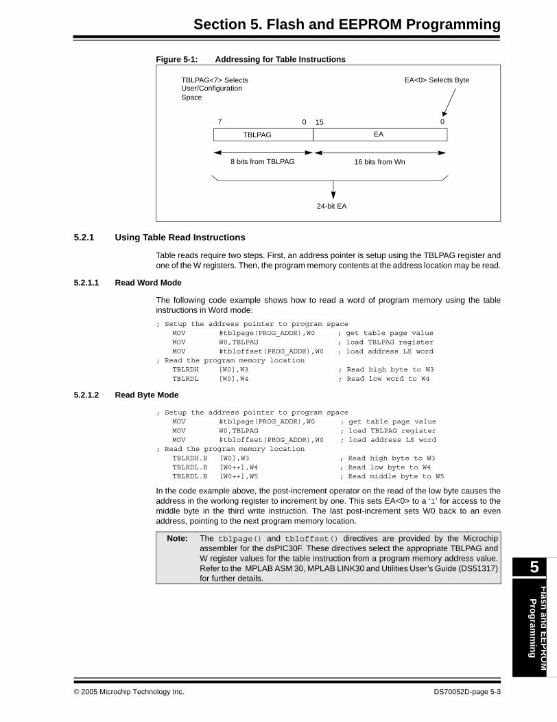
Section 5. Flash and EEPROM ProgrammingF
lash an
d E
EP
RO
MP
rog
ramm
ing
5
Figure 5-1: Addressing for Table Instructions
5.2.1 Using Table Read Instructions
Table reads require two steps. First, an address pointer is setup using the TBLPAG register andone of the W registers. Then, the program memory contents at the address location may be read.
5.2.1.1 Read Word Mode
The following code example shows how to read a word of program memory using the tableinstructions in Word mode:
; Setup the address pointer to program spaceMOV #tblpage(PROG_ADDR),W0 ; get table page valueMOV W0,TBLPAG ; load TBLPAG registerMOV #tbloffset(PROG_ADDR),W0 ; load address LS word
; Read the program memory locationTBLRDH [W0],W3 ; Read high byte to W3TBLRDL [W0],W4 ; Read low word to W4
5.2.1.2 Read Byte Mode
; Setup the address pointer to program spaceMOV #tblpage(PROG_ADDR),W0 ; get table page valueMOV W0,TBLPAG ; load TBLPAG registerMOV #tbloffset(PROG_ADDR),W0 ; load address LS word
; Read the program memory locationTBLRDH.B [W0],W3 ; Read high byte to W3TBLRDL.B [W0++],W4 ; Read low byte to W4TBLRDL.B [W0++],W5 ; Read middle byte to W5
In the code example above, the post-increment operator on the read of the low byte causes theaddress in the working register to increment by one. This sets EA<0> to a ‘1’ for access to themiddle byte in the third write instruction. The last post-increment sets W0 back to an evenaddress, pointing to the next program memory location.
TBLPAG
8 bits from TBLPAG
EA
EA<0> Selects Byte
24-bit EA
TBLPAG<7> SelectsUser/ConfigurationSpace
01507
16 bits from Wn
Note: The tblpage() and tbloffset() directives are provided by the Microchipassembler for the dsPIC30F. These directives select the appropriate TBLPAG andW register values for the table instruction from a program memory address value.Refer to the MPLAB ASM 30, MPLAB LINK30 and Utilities User’s Guide (DS51317)for further details.
© 2005 Microchip Technology Inc. DS70052D-page 5-3
dsPIC30F Family Reference Manual
5.2.2 Using Table Write Instructions
The effect of a table write instruction will depend on the type of memory technology that is presentin the device program memory address space. The program memory address space couldcontain volatile or non-volatile program memory, non-volatile data memory, and an External BusInterface (EBI). If a table write instruction occurs within the EBI address region, for example, thewrite data will be placed onto the EBI data lines.
5.2.2.1 Table Write Holding Latches
Table write instructions do not write directly to the non-volatile program and data memory.Instead, the table write instructions load holding latches that store the write data. The holdinglatches are not memory mapped and can only be accessed using table write instructions. Whenall of the holding latches have been loaded, the actual memory programming operation is startedby executing a special sequence of instructions.
The number of holding latches will determine the maximum memory block size that can beprogrammed and may vary depending on the type of non-volatile memory and the device variant.For example, the number of holding latches could be different for program memory, dataEEPROM memory and Device Configuration registers for a given device.
In general, the program memory is segmented into rows and panels. Each panel will have its ownset of table write holding latches. This allows multiple memory panels to be programmed at once,reducing the overall programming time for the device. For each memory panel, there aregenerally enough holding latches to program one row of memory at a time. The memory logicautomatically decides which set of write latches to load based on the address value used in thetable write instruction.
Please refer to the specific device data sheet for further details.
5.2.2.2 Write Word Mode
The following sequence can be used to write a single program memory latch location in Wordmode:
; Setup the address pointer to program spaceMOV #tblpage(PROG_ADDR),W0 ; get table page valueMOV W0,TBLPAG ; load TBLPAG registerMOV #tbloffset(PROG_ADDR),W0 ; load address LS word
; Load write data into W registersMOV #PROG_LOW_WORD,W2MOV #PROG_HI_BYTE,W3
; Perform the table writes to load the latchTBLWTL W2,[W0] TBLWTH W3,[W0++]
In this example, the contents of the upper byte of W3 does not matter because this data will bewritten to the phantom byte location. W0 is post-incremented by 2, after the second TBLWTHinstruction, to prepare for the write to the next program memory location.
DS70052D-page 5-4 © 2005 Microchip Technology Inc.
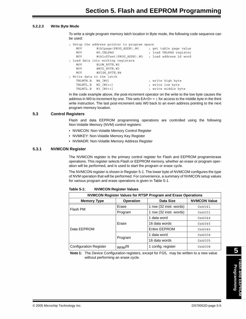
Section 5. Flash and EEPROM ProgrammingF
lash an
d E
EP
RO
MP
rog
ramm
ing
5
5.2.2.3 Write Byte Mode
To write a single program memory latch location in Byte mode, the following code sequence canbe used:
; Setup the address pointer to program spaceMOV #tblpage(PROG_ADDR),W0 ; get table page valueMOV W0,TBLPAG ; load TBLPAG registerMOV #tbloffset(PROG_ADDR),W0 ; load address LS word
; Load data into working registersMOV #LOW_BYTE,W2MOV #MID_BYTE,W3MOV #HIGH_BYTE,W4
; Write data to the latchTBLWTH.B W4,[W0] ; write high byteTBLWTL.B W2,[W0++] ; write low byteTBLWTL.B W3,[W0++] ; write middle byte
In the code example above, the post-increment operator on the write to the low byte causes theaddress in W0 to increment by one. This sets EA<0> = 1 for access to the middle byte in the thirdwrite instruction. The last post-increment sets W0 back to an even address pointing to the nextprogram memory location.
5.3 Control Registers
Flash and data EEPROM programming operations are controlled using the followingNon-Volatile Memory (NVM) control registers:
• NVMCON: Non-Volatile Memory Control Register
• NVMKEY: Non-Volatile Memory Key Register • NVMADR: Non-Volatile Memory Address Register
5.3.1 NVMCON Register
The NVMCON register is the primary control register for Flash and EEPROM program/eraseoperations. This register selects Flash or EEPROM memory, whether an erase or program oper-ation will be performed, and is used to start the program or erase cycle.
The NVMCON register is shown in Register 5-1. The lower byte of NVMCOM configures the typeof NVM operation that will be performed. For convenience, a summary of NVMCON setup valuesfor various program and erase operations is given in Table 5-1.
Table 5-1: NVMCON Register Values
NVMCON Register Values for RTSP Program and Erase Operations
Memory Type Operation Data Size NVMCON Value
Flash PMErase 1 row (32 instr. words) 0x4041
Program 1 row (32 instr. words) 0x4001
Data EEPROM
Erase
1 data word 0x4044
16 data words 0x4045
Entire EEPROM 0x4046
Program1 data word 0x4004
16 data words 0x4005
Configuration Register Write(1) 1 config. register 0x4008
Note 1: The Device Configuration registers, except for FG5, may be written to a new value without performing an erase cycle.
© 2005 Microchip Technology Inc. DS70052D-page 5-5
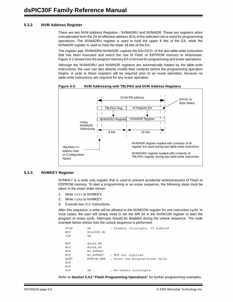
dsPIC30F Family Reference Manual
5.3.2 NVM Address Register
There are two NVM Address Registers - NVMADRU and NVMADR. These two registers whenconcatenated form the 24-bit effective address (EA) of the selected row or word for programmingoperations. The NVMADRU register is used to hold the upper 8 bits of the EA, while theNVMADR register is used to hold the lower 16 bits of the EA.
The register pair, NVMADRU:NVMADR, capture the EA<23:0> of the last table-write instructionthat has been executed and select the row of Flash or EEPROM memory to write/erase.Figure 5-2 shows how the program memory EA is formed for programming and erase operations.
Although the NVMADRU and NVMADR registers are automatically loaded by the table-writeinstructions, the user can also directly modify their contents before the programming operationbegins. A write to these registers will be required prior to an erase operation, because notable-write instructions are required for any erase operation.
Figure 5-2: NVM Addressing with TBLPAG and NVM Address Registers
5.3.3 NVMKEY Register
NVMKEY is a write only register that is used to prevent accidental writes/erasures of Flash orEEPROM memory. To start a programming or an erase sequence, the following steps must betaken in the exact order shown:
1. Write 0x55 to NVMKEY.2. Write 0xAA to NVMKEY.
3. Execute two NOP instructions.
After this sequence, a write will be allowed to the NVMCON register for one instruction cycle. Inmost cases, the user will simply need to set the WR bit in the NVMCON register to start theprogram or erase cycle. Interrupts should be disabled during the unlock sequence. The codeexample below shows how the unlock sequence is performed:
PUSH SR ; Disable interrupts, if enabledMOV #0x00E0,W0IOR SR
MOV #0x55,W0MOV #0xAA,W0MOV W0,NVMKEYMOV W0,NVMKEY ; NOP not requiredBSET NVMCON,#WR ; Start the program/erase cycleNOPNOPPOP SR ; Re-enable interrupts
Refer to Section 5.4.2 “Flash Programming Operations” for further programming examples.
24-bit PM address
TBLPAG Reg
8 bits 16 bits
UsingNVMADRAddressing
NVMADR Register
NVMADR register loaded with contents of Wregister EA used during last table-write instruction.
W Register EA
EA<0> isByte Select
TBLPAG<7>selects Useror ConfigurationSpace
NVMADRU Register
TBLPAG register during last table-write instructionNVMADRU register loaded with contents of
DS70052D-page 5-6 © 2005 Microchip Technology Inc.
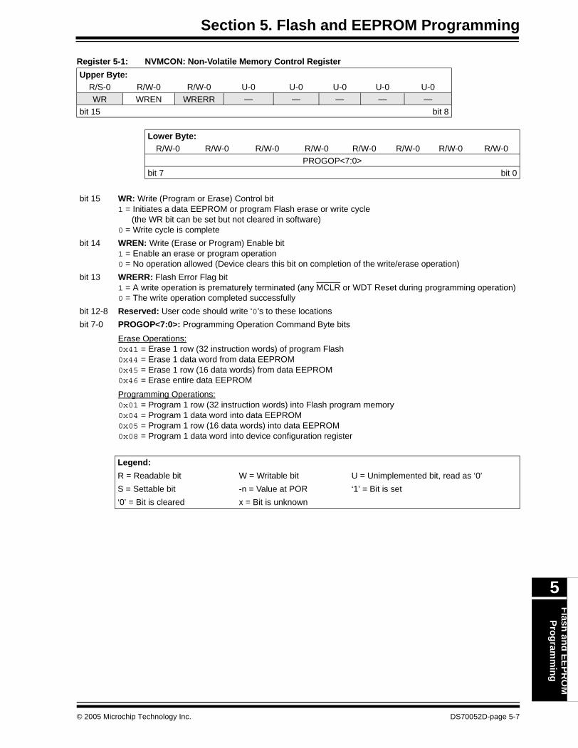
Section 5. Flash and EEPROM ProgrammingF
lash an
d E
EP
RO
MP
rog
ramm
ing
5
Register 5-1: NVMCON: Non-Volatile Memory Control Register
Upper Byte:R/S-0 R/W-0 R/W-0 U-0 U-0 U-0 U-0 U-0WR WREN WRERR — — — — —
bit 15 bit 8
Lower Byte:R/W-0 R/W-0 R/W-0 R/W-0 R/W-0 R/W-0 R/W-0 R/W-0
PROGOP<7:0>bit 7 bit 0
bit 15 WR: Write (Program or Erase) Control bit 1 = Initiates a data EEPROM or program Flash erase or write cycle
(the WR bit can be set but not cleared in software)0 = Write cycle is complete
bit 14 WREN: Write (Erase or Program) Enable bit1 = Enable an erase or program operation0 = No operation allowed (Device clears this bit on completion of the write/erase operation)
bit 13 WRERR: Flash Error Flag bit1 = A write operation is prematurely terminated (any MCLR or WDT Reset during programming operation)0 = The write operation completed successfully
bit 12-8 Reserved: User code should write ‘0’s to these locations
bit 7-0 PROGOP<7:0>: Programming Operation Command Byte bits
Erase Operations:0x41 = Erase 1 row (32 instruction words) of program Flash0x44 = Erase 1 data word from data EEPROM0x45 = Erase 1 row (16 data words) from data EEPROM0x46 = Erase entire data EEPROM
Programming Operations:0x01 = Program 1 row (32 instruction words) into Flash program memory0x04 = Program 1 data word into data EEPROM0x05 = Program 1 row (16 data words) into data EEPROM0x08 = Program 1 data word into device configuration register
Legend:
R = Readable bit W = Writable bit U = Unimplemented bit, read as ‘0’
S = Settable bit -n = Value at POR ‘1’ = Bit is set
‘0’ = Bit is cleared x = Bit is unknown
© 2005 Microchip Technology Inc. DS70052D-page 5-7
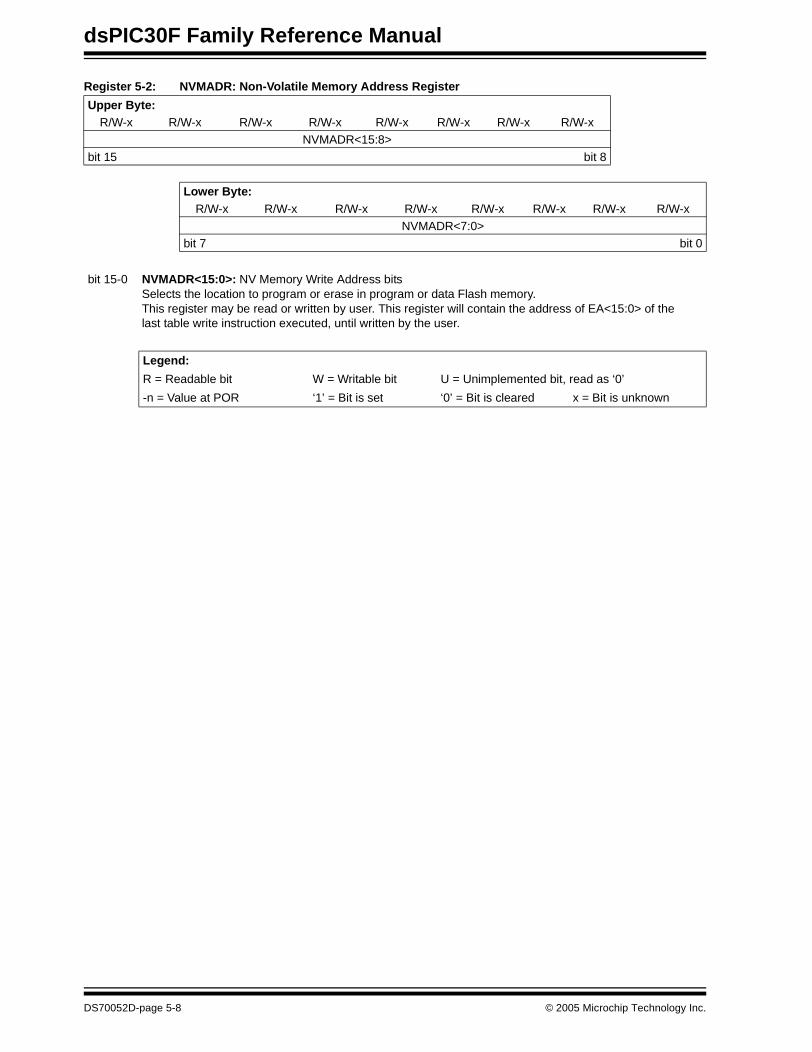
dsPIC30F Family Reference Manual
Register 5-2: NVMADR: Non-Volatile Memory Address Register
Upper Byte:R/W-x R/W-x R/W-x R/W-x R/W-x R/W-x R/W-x R/W-x
NVMADR<15:8>
bit 15 bit 8
Lower Byte:R/W-x R/W-x R/W-x R/W-x R/W-x R/W-x R/W-x R/W-x
NVMADR<7:0>bit 7 bit 0
bit 15-0 NVMADR<15:0>: NV Memory Write Address bitsSelects the location to program or erase in program or data Flash memory.This register may be read or written by user. This register will contain the address of EA<15:0> of the last table write instruction executed, until written by the user.
Legend:
R = Readable bit W = Writable bit U = Unimplemented bit, read as ‘0’
-n = Value at POR ‘1’ = Bit is set ‘0’ = Bit is cleared x = Bit is unknown
DS70052D-page 5-8 © 2005 Microchip Technology Inc.
Section 5. Flash and EEPROM ProgrammingF
lash an
d E
EP
RO
MP
rog
ramm
ing
5
Register 5-3: NVMADRU: Non-Volatile Memory Upper Address Register
Register 5-4: NVMKEY: Non-Volatile Memory Key Register
Upper Byte:U-0 U-0 U-0 U-0 U-0 U-0 U-0 U-0
— — — — — — — —bit 15 bit 8
Lower Byte:R/W-x R/W-x R/W-x R/W-x R/W-x R/W-x R/W-x R/W-x
NVMADRU<7:0>
bit 7 bit 0
bit 15-8 Unimplemented: Read as ‘0’
bit 7-0 NVMADRU<7:0>: NV Memory Upper Write Address bitsSelects the upper 8 bits of the location to program or erase in program or data Flash memory.This register may be read or written by the user. This register will contain the value of the TBLPAG registerwhen the last table write instruction executed, until written by the user.
Legend:
R = Readable bit W = Writable bit U = Unimplemented bit, read as ‘0’
-n = Value at POR ‘1’ = Bit is set ‘0’ = Bit is cleared x = Bit is unknown
Upper Byte:U-0 U-0 U-0 U-0 U-0 U-0 U-0 U-0— — — — — — — —
bit 15 bit 8
Lower Byte:W-0 W-0 W-0 W-0 W-0 W-0 W-0 W-0
NVMKEY<7:0>bit 7 bit 0
bit 15-8 Unimplemented: Read as ‘0’
bit 7-0 NVMKEY<7:0>: Key Register (Write Only) bits
Legend:
R = Readable bit W = Writable bit U = Unimplemented bit, read as ‘0’
-n = Value at POR ‘1’ = Bit is set ‘0’ = Bit is cleared x = Bit is unknown
© 2005 Microchip Technology Inc. DS70052D-page 5-9

dsPIC30F Family Reference Manual
5.4 Run-Time Self-Programming (RTSP)
RTSP allows the user code to modify Flash program memory contents. RTSP is accomplishedusing TBLRD (table read) and TBLWT (table write) instructions, and the NVM Control registers.With RTSP, the user may erase program memory, 32 instructions (96 bytes) at a time and canwrite program memory data, 32 instructions (96 bytes) at a time.
5.4.1 RTSP Operation
The dsPIC30F Flash program memory is organized into rows and panels. Each row consists of32 instructions or 96 bytes. The panel size may vary depending on the dsPIC30F device variant.Refer to the device data sheet for further information. Typically, each panel consists of 128 rows,or 4K x 24 instructions. RTSP allows the user to erase one row (32 instructions) at a time and toprogram 32 instructions at one time.
Each panel of program memory contains write latches that hold 32 instructions of programmingdata. These latches are not memory mapped. The only way for the user to access the writelatches is through the use of table write instructions. Prior to the actual programming operation,the write data must be loaded into the panel write latches with table write instructions. The datato be programmed into the panel is typically loaded in sequential order into the write latches:instruction 0, instruction 1, etc. The instruction words loaded must always be from an ‘even’group of four address boundaries (e.g., loading of instructions 3, 4, 5, 6 is not allowed). Anotherway of stating this requirement is that the starting program memory address of the four instruc-tions must have the 3 LSb’s equal to ‘0’. All 32 write latches must be written during aprogramming operation to ensure that any old data held in the latches is overwritten.
The basic sequence for RTSP programming is to setup a table pointer, then do a series of TBLWTinstructions to load the write latches. Programming is performed by setting special bits in theNVMCON register. 32 TBLWTL and 32 TBLWTH instructions are required to load the four instruc-tions. If multiple, discontinuous regions of program memory need to be programmed, the tablepointer should be changed for each region and the next set of write latches written.
All of the table write operations to the Flash program memory take 2 instruction cycles each,because only the table latches are written. The actual programming operation is initiated usingthe NVMCON register.
5.4.2 Flash Programming Operations
A program/erase operation is necessary for programming or erasing the internal Flash programmemory in RTSP mode. The program or erase operation is automatically timed by the deviceand is nominally 2 msec in duration. Setting the WR bit (NVMCON<15>) starts the operationand the WR bit is automatically cleared when the operation is finished.
The CPU stalls (waits) until the programming operation is finished. The CPU will not executeany instruction or respond to interrupts during this time. If any interrupts do occur during theprogramming cycle, then they will remain pending until the cycle completes.
DS70052D-page 5-10 © 2005 Microchip Technology Inc.
Section 5. Flash and EEPROM ProgrammingF
lash an
d E
EP
RO
MP
rog
ramm
ing
5
5.4.2.1 Flash Program Memory Programming Algorithm
The user can erase and program Flash Program Memory by rows (32 instruction words). Thegeneral process is as follows:
1. Read one row of program Flash (32 instruction words) and store into data RAM as a data“image”. The RAM image must be read from an even 32-word program memory addressboundary.
2. Update the RAM data image with the new program memory data.3. Erase program Flash row.
• Setup NVMCON register to erase 1 row of Flash program memory.
• Write address of row to be erased into NVMADRU and NVMADR registers.• Disable interrupts.• Write the key sequence to NVMKEY to enable the erase.
• Set the WR bit. This will begin erase cycle.• CPU will stall for the duration of the erase cycle.• The WR bit is cleared when erase cycle ends.
• Re-enable interrupts.4. Write 32 instruction words of data from RAM into the Flash program memory write latches.5. Program 32 instruction words into program Flash.
• Setup NVMCON to program one row of Flash program memory.• Disable interrupts.• Write the key sequence to NVMKEY to enable the program cycle.
• Set the WR bit. This will begin the program cycle.• CPU will stall for duration of the program cycle.• The WR bit is cleared by the hardware when program cycle ends.
• Re-enable interrupts.6. Repeat steps 1 through 6, as needed, to program the desired amount of Flash program
memory
Note: The user should remember that the minimum amount of program memory that canbe modified using RTSP is 32 instruction word locations. Therefore, it is importantthat an image of these locations be stored in general purpose RAM before an erasecycle is initiated. An erase cycle must be performed on any previously writtenlocations before any programming is done.
© 2005 Microchip Technology Inc. DS70052D-page 5-11
dsPIC30F Family Reference Manual
5.4.2.2 Erasing a Row of Program Memory
The following is a code sequence that can be used to erase a row (32 instructions) of programmemory. The NVMCON register is configured to erase one row of program memory. TheNVMADRU and NVMADR registers are loaded with the address of the row to be erased. Theprogram memory must be erased at ‘even’ row boundaries. Therefore, the 6 LSbits of the valuewritten to the NVMADR register have no effect when a row is erased.
The erase operation is initiated by writing a special unlock, or key sequence to the NVMKEYregister before setting the WR control bit (NVMCON<15>). The unlock sequence needs to beexecuted in the exact order shown without interruption. Therefore, interrupts should be disabledprior to writing the sequence.
Two NOP instructions should be inserted in the code at the point where the CPU will resumeoperation. Finally, interrupts can be enabled (if required).
; Setup NVMCON to erase one row of Flash program memoryMOV #0x4041,W0MOV W0,NVMCON
; Setup address pointer to row to be ERASEDMOV #tblpage(PROG_ADDR),W0MOV W0,NVMADRUMOV #tbloffset(PROG_ADDR),W0MOV W0,NVMADR
; Disable interrupts, if enabledPUSH SRMOV #0x00E0,W0IOR SR
; Write the KEY sequenceMOV #0x55,W0 MOV W0, NVMKEYMOV #0xAA, W0MOV W0, NVMKEY
; Start the erase operationBSET NVMCON,#WR
; Insert two NOPs after the erase cycle (required)NOP NOP
; Re-enable interrupts, if neededPOP SR
Note: When erasing a row of program memory, the user writes the upper 8 bits of theerase address directly to the NVMADRU and NVMADR registers. Together, thecontents of the NVMADRU and NVMADR registers form the complete address ofthe program memory row to be erased.
The NVMADRU and NVMADR registers specify the address for all Flash erase andprogram operations. However, these two registers do not have to be directly writtenby the user for Flash program operations. This is because the table write instruc-tions used to write the program memory data automatically transfers the TBLPAGregister contents and the table write address into the NVMADRU and NVMADRregisters.
The above code example could be modified to perform a ‘dummy’ table writeoperation to capture the program memory erase address.
DS70052D-page 5-12 © 2005 Microchip Technology Inc.
Section 5. Flash and EEPROM ProgrammingF
lash an
d E
EP
RO
MP
rog
ramm
ing
5
5.4.2.3 Loading Write Latches
The following is a sequence of instructions that can be used to load the 768-bits of write latches(32 instruction words). 32 TBLWTL and 32 TBLWTH instructions are needed to load the writelatches selected by the table pointer.
The TBLPAG register is loaded with the 8 MSbits of the program memory address. The userdoes not need to write the NVMADRU:NVMADR register-pair for a Flash programming opera-tion. The 24-bits of the program memory address are automatically captured into theNVMADRU:NVMADR register-pair when each table write instruction is executed. The programmemory must be programmed at an ‘even’ 32 instruction word address boundary. In effect, the6 LSbits of the value captured in the NVMADR register are not used during the programmingoperation.
The row of 32 instruction words do not necessarily have to be written in sequential order. The6 LSbits of the table write address determine which of the latches will be written. However, all 32instruction words should be written for each programming cycle to overwrite old data.
; Set up a pointer to the first program memory location to be written.MOV #tblpage(PROG_ADDR),W0MOV W0,TBLPAG MOV #tbloffset(PROG_ADDR),W0
; Perform the TBLWT instructions to write the latches; W0 is incremented in the TBLWTH instruction to point to the; next instruction location.
MOV #LOW_WORD_0,W2MOV #HIGH_BYTE_0,W3TBLWTL W2,[W0] TBLWTH W3,[W0++] ; 1st_program_wordMOV #LOW_WORD_1,W2MOV #HIGH_BYTE_1,W3TBLWTL W2,[W0] TBLWTH W3,[W0++] ; 2nd_program_wordMOV #LOW_WORD_2,W2MOV #HIGH_BYTE_2,W3TBLWTL W2, [W0] TBLWTH W3, [W0++] ; 3rd_program_wordMOV #LOW_WORD_3,W2MOV #HIGH_BYTE_3,W3TBLWTL W2,[W0] TBLWTH W3,[W0++] ; 4th_program_word................MOV #LOW_WORD_31,W2MOV #HIGH_BYTE_31,W3TBLWTL W2,[W0] TBLWTH W3,[W0++] ; 32nd_program_word
Note: The following code example is the ‘Load_Write_Latch’ code referred to insubsequent examples.
© 2005 Microchip Technology Inc. DS70052D-page 5-13
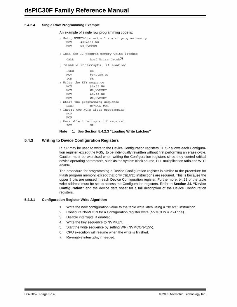
dsPIC30F Family Reference Manual
5.4.2.4 Single Row Programming Example
An example of single row programming code is:
; Setup NVMCON to write 1 row of program memoryMOV #0x4001,W0MOV W0,NVMCON
; Load the 32 program memory write latches
CALL Load_Write_Latch(1)
; Disable interrupts, if enabled
PUSH SRMOV #0x00E0,W0IOR SR
; Write the KEY sequence MOV #0x55,W0 MOV W0,NVMKEYMOV #0xAA,W0MOV W0,NVMKEY
; Start the programming sequenceBSET NVMCON,#WR
; Insert two NOPs after programmingNOP NOP
; Re-enable interrupts, if requiredPOP SR
Note 1: See Section 5.4.2.3 “Loading Write Latches”
5.4.3 Writing to Device Configuration Registers
RTSP may be used to write to the Device Configuration registers. RTSP allows each Configura-tion register, except the FG5, to be individually rewritten without first performing an erase cycle.Caution must be exercised when writing the Configuration registers since they control criticaldevice operating parameters, such as the system clock source, PLL multiplication ratio and WDTenable.
The procedure for programming a Device Configuration register is similar to the procedure forFlash program memory, except that only TBLWTL instructions are required. This is because theupper 8 bits are unused in each Device Configuration register. Furthermore, bit 23 of the tablewrite address must be set to access the Configuration registers. Refer to Section 24. “DeviceConfiguration” and the device data sheet for a full description of the Device Configurationregisters.
5.4.3.1 Configuration Register Write Algorithm
1. Write the new configuration value to the table write latch using a TBLWTL instruction.2. Configure NVMCON for a Configuration register write (NVMCON = 0x4008).
3. Disable interrupts, if enabled.4. Write the key sequence to NVMKEY.5. Start the write sequence by setting WR (NVMCON<15>).
6. CPU execution will resume when the write is finished.7. Re-enable interrupts, if needed.
DS70052D-page 5-14 © 2005 Microchip Technology Inc.
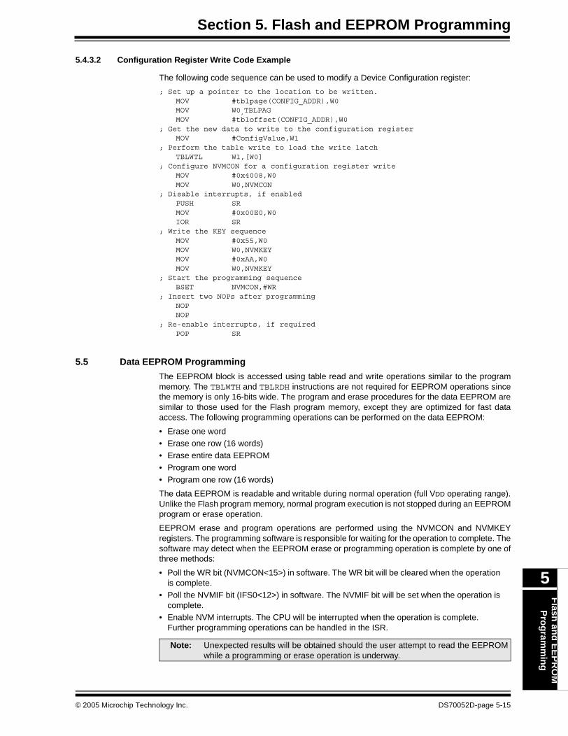
Section 5. Flash and EEPROM ProgrammingF
lash an
d E
EP
RO
MP
rog
ramm
ing
5
5.4.3.2 Configuration Register Write Code Example
The following code sequence can be used to modify a Device Configuration register:
; Set up a pointer to the location to be written.MOV #tblpage(CONFIG_ADDR),W0MOV W0,TBLPAG MOV #tbloffset(CONFIG_ADDR),W0
; Get the new data to write to the configuration registerMOV #ConfigValue,W1
; Perform the table write to load the write latchTBLWTL W1,[W0]
; Configure NVMCON for a configuration register writeMOV #0x4008,W0MOV W0,NVMCON
; Disable interrupts, if enabledPUSH SRMOV #0x00E0,W0IOR SR
; Write the KEY sequence MOV #0x55,W0 MOV W0,NVMKEYMOV #0xAA,W0MOV W0,NVMKEY
; Start the programming sequenceBSET NVMCON,#WR
; Insert two NOPs after programmingNOP NOP
; Re-enable interrupts, if requiredPOP SR
5.5 Data EEPROM Programming
The EEPROM block is accessed using table read and write operations similar to the programmemory. The TBLWTH and TBLRDH instructions are not required for EEPROM operations sincethe memory is only 16-bits wide. The program and erase procedures for the data EEPROM aresimilar to those used for the Flash program memory, except they are optimized for fast dataaccess. The following programming operations can be performed on the data EEPROM:
• Erase one word• Erase one row (16 words)• Erase entire data EEPROM
• Program one word• Program one row (16 words)
The data EEPROM is readable and writable during normal operation (full VDD operating range).Unlike the Flash program memory, normal program execution is not stopped during an EEPROMprogram or erase operation.
EEPROM erase and program operations are performed using the NVMCON and NVMKEYregisters. The programming software is responsible for waiting for the operation to complete. Thesoftware may detect when the EEPROM erase or programming operation is complete by one ofthree methods:
• Poll the WR bit (NVMCON<15>) in software. The WR bit will be cleared when the operation is complete.
• Poll the NVMIF bit (IFS0<12>) in software. The NVMIF bit will be set when the operation is complete.
• Enable NVM interrupts. The CPU will be interrupted when the operation is complete. Further programming operations can be handled in the ISR.
Note: Unexpected results will be obtained should the user attempt to read the EEPROMwhile a programming or erase operation is underway.
© 2005 Microchip Technology Inc. DS70052D-page 5-15
dsPIC30F Family Reference Manual
5.5.1 EEPROM Single Word Programming Algorithm
1. Erase one EEPROM word.• Setup NVMCON register to erase one EEPROM word.• Write address of word to be erased into NVMADRU, NVMADR registers.
• Clear NVMIF status bit and enable NVM interrupt (optional).• Write the key sequence to NVMKEY.• Set the WR bit. This will begin erase cycle.
• Either poll the WR bit or wait for the NVM interrupt.2. Write data word into data EEPROM write latch.3. Program the data word into the EEPROM.
• Setup the NVMCON register to program one EEPROM word.• Clear NVMIF status bit and enable NVM interrupt (optional).• Write the key sequence to NVMKEY.
• Set the WR bit. This will begin the program cycle.• Either poll the WR bit or wait for the NVM interrupt.
5.5.2 EEPROM Row Programming Algorithm
If multiple words need to be programmed into the EEPROM, it is quicker to erase and program16 words (1 row) at a time. The process to program 16 words of EEPROM is:
1. Read one row of data EEPROM (16 words) and store into data RAM as a data “image”.The section of EEPROM to be modified must fall on an even 16-word address boundary.
2. Update the data image with the new data.3. Erase the EEPROM row.
• Setup the NVMCON register to erase one row of EEPROM.
• Write starting address of row to be erased into NUMADRU and NVMADR registers.• Clear NVMIF status bit and enable NVM interrupt (optional).• Write the key sequence to NVMKEY.
• Set the WR bit. This will begin the erase cycle.• Either poll the WR bit or wait for the NVM interrupt.
4. Write the 16 data words into the data EEPROM write latches.
5. Program a row into data EEPROM.• Setup the NVMCON register to program one row of EEPROM.
• Clear NVMIF status bit and enable NVM interrupt (optional).• Write the key sequence to NVMKEY.• Set the WR bit. This will begin the program cycle.
• Either poll the WR bit or wait for the NVM interrupt.
DS70052D-page 5-16 © 2005 Microchip Technology Inc.

Section 5. Flash and EEPROM ProgrammingF
lash an
d E
EP
RO
MP
rog
ramm
ing
5
5.5.3 Erasing One Word of Data EEPROM Memory
The NVMADRU and NVMADR registers must be loaded with the data EEPROM address to beerased. Since one word of the EEPROM is accessed, the LSB of the NVMADR has no effect onthe erase operation. The NVMCON register must be configured to erase one word of EEPROMmemory.
Setting the WR control bit (NVMCON<15>) initiates the erase. A special unlock or key sequenceshould be written to the NVMKEY register before setting the WR control bit. The unlock sequenceneeds to be executed in the exact order shown without interruption. Therefore, interrupts shouldbe disabled prior to writing the sequence.
; Set up a pointer to the EEPROM location to be erased.MOV #tblpage(EE_ADDR),W0MOV W0,NVMADRU MOV #tbloffset(EE_ADDR),W0MOV W0,NVMADR
; Setup NVMCON to erase one word of data EEPROMMOV #0x4044,W0MOV W0,NVMCON
; Disable interrupts while the KEY sequence is writtenPUSH SRMOV #0x00E0,W0IOR SR
; Write the KEY sequenceMOV #0x55,W0MOV W0,NVMKEYMOV #0xAA,W0MOV W0,NVMKEY
; Start the erase cycleBSET NVMCON,#WR
; Re-enable interruptsPOP SR
© 2005 Microchip Technology Inc. DS70052D-page 5-17
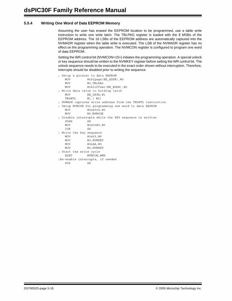
dsPIC30F Family Reference Manual
5.5.4 Writing One Word of Data EEPROM Memory
Assuming the user has erased the EEPROM location to be programmed, use a table writeinstruction to write one write latch. The TBLPAG register is loaded with the 8 MSBs of theEEPROM address. The 16 LSBs of the EEPROM address are automatically captured into theNVMADR register when the table write is executed. The LSB of the NVMADR register has noeffect on the programming operation. The NVMCON register is configured to program one wordof data EEPROM.
Setting the WR control bit (NVMCON<15>) initiates the programming operation. A special unlockor key sequence should be written to the NVMKEY register before setting the WR control bit. Theunlock sequence needs to be executed in the exact order shown without interruption. Therefore,interrupts should be disabled prior to writing the sequence.
; Setup a pointer to data EEPROMMOV #tblpage(EE_ADDR),W0MOV W0,TBLPAG MOV #tbloffset(EE_ADDR),W0
; Write data value to holding latch MOV EE_DATA,W1 TBLWTL W1,[ W0]
; NVMADR captures write address from the TBLWTL instruction.; Setup NVMCON for programming one word to data EEPROM
MOV #0x4004,W0MOV W0,NVMCON
; Disable interrupts while the KEY sequence is writtenPUSH SRMOV #0x00E0,W0IOR SR
; Write the key sequence MOV #0x55,W0MOV W0,NVMKEYMOV #0xAA,W0MOV W0,NVMKEY
; Start the write cycleBSET NVMCON,#WR
;Re-enable interrupts, if neededPOP SR
DS70052D-page 5-18 © 2005 Microchip Technology Inc.

Section 5. Flash and EEPROM ProgrammingF
lash an
d E
EP
RO
MP
rog
ramm
ing
5
5.5.5 Erasing One Row of Data EEPROM
The NVMCON register is configured to erase one row of EEPROM memory. The NVMADRUand NVMADR registers must point to the row to be erased. The data EEPROM must be erasedat even address boundaries. Therefore, the 5 LSBs of the NVMADR register will have no effecton the row that is erased.
Setting the WR control bit (NVMCON<15>) initiates the erase. A special unlock or key sequenceshould be written to the NVMKEY register before setting the WR control bit. The unlock sequenceneeds to be executed in the exact order shown without interruption. Therefore, interrupts shouldbe disabled prior to writing the sequence.
; Set up a pointer to the EEPROM row to be erased.MOV #tblpage(EE_ADDR),W0MOV W0,NVMADRU MOV #tbloffset(EE_ADDR),W0MOV W0,NVMADR
; Setup NVMCON to erase one row of EEPROMMOV #0x4045,W0MOV W0,NVMCON
; Disable interrupts while the KEY sequence is writtenPUSH SRMOV #0x00E0,W0IOR SR
; Write the KEY SequenceMOV #0x55,W0MOV W0,NVMKEYMOV #0xAA,W0MOV W0,NVMKEY
; Start the erase operationBSET NVMCON,#WR
;Re-enable interrupts, if neededPOP SR
© 2005 Microchip Technology Inc. DS70052D-page 5-19
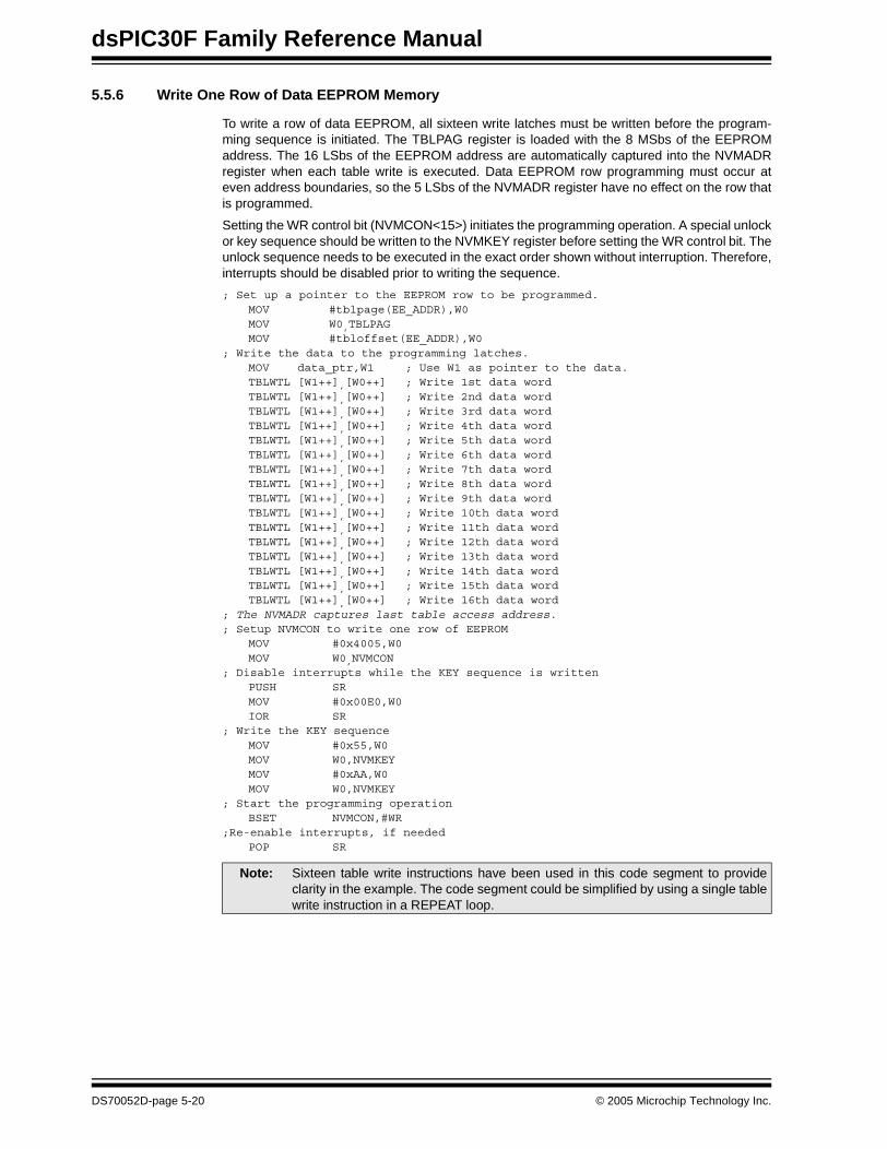
dsPIC30F Family Reference Manual
5.5.6 Write One Row of Data EEPROM Memory
To write a row of data EEPROM, all sixteen write latches must be written before the program-ming sequence is initiated. The TBLPAG register is loaded with the 8 MSbs of the EEPROMaddress. The 16 LSbs of the EEPROM address are automatically captured into the NVMADRregister when each table write is executed. Data EEPROM row programming must occur ateven address boundaries, so the 5 LSbs of the NVMADR register have no effect on the row thatis programmed.
Setting the WR control bit (NVMCON<15>) initiates the programming operation. A special unlockor key sequence should be written to the NVMKEY register before setting the WR control bit. Theunlock sequence needs to be executed in the exact order shown without interruption. Therefore,interrupts should be disabled prior to writing the sequence.
; Set up a pointer to the EEPROM row to be programmed.MOV #tblpage(EE_ADDR),W0MOV W0,TBLPAG MOV #tbloffset(EE_ADDR),W0
; Write the data to the programming latches.MOV data_ptr,W1 ; Use W1 as pointer to the data.TBLWTL [W1++],[W0++] ; Write 1st data wordTBLWTL [W1++],[W0++] ; Write 2nd data wordTBLWTL [W1++],[W0++] ; Write 3rd data wordTBLWTL [W1++],[W0++] ; Write 4th data wordTBLWTL [W1++],[W0++] ; Write 5th data wordTBLWTL [W1++],[W0++] ; Write 6th data wordTBLWTL [W1++],[W0++] ; Write 7th data wordTBLWTL [W1++],[W0++] ; Write 8th data wordTBLWTL [W1++],[W0++] ; Write 9th data wordTBLWTL [W1++],[W0++] ; Write 10th data wordTBLWTL [W1++],[W0++] ; Write 11th data wordTBLWTL [W1++],[W0++] ; Write 12th data wordTBLWTL [W1++],[W0++] ; Write 13th data wordTBLWTL [W1++],[W0++] ; Write 14th data wordTBLWTL [W1++],[W0++] ; Write 15th data wordTBLWTL [W1++],[W0++] ; Write 16th data word
; The NVMADR captures last table access address.; Setup NVMCON to write one row of EEPROM
MOV #0x4005,W0MOV W0,NVMCON
; Disable interrupts while the KEY sequence is writtenPUSH SRMOV #0x00E0,W0IOR SR
; Write the KEY sequenceMOV #0x55,W0 MOV W0,NVMKEYMOV #0xAA,W0MOV W0,NVMKEY
; Start the programming operationBSET NVMCON,#WR
;Re-enable interrupts, if neededPOP SR
Note: Sixteen table write instructions have been used in this code segment to provideclarity in the example. The code segment could be simplified by using a single tablewrite instruction in a REPEAT loop.
DS70052D-page 5-20 © 2005 Microchip Technology Inc.
Section 5. Flash and EEPROM ProgrammingF
lash an
d E
EP
RO
MP
rog
ramm
ing
5
5.5.7 Reading the Data EEPROM Memory
A TBLRD instruction reads a word at the current program word address. This example uses W0as a pointer to data Flash. The result is placed into register W4.
; Setup pointer to EEPROM memory MOV #tblpage(EE_ADDR),W0MOV W0,TBLPAG MOV #tbloffset(EE_ADDR),W0
; Read the EEPROM dataTBLRDL [W0],W4
5.6 Design Tips
Question 1: I cannot get the device to program or erase properly. My code appears tobe correct. What could be the cause?
Answer: Interrupts should be disabled when a program or erase cycle is initiated to ensure thatthe key sequence executes without interruption. Interrupts can be disabled by raising the currentCPU priority to level 7. The code examples in this chapter disable interrupts by saving the currentSR register value on the stack, then ORing the value 0x00E0 with SR to force IPL<2:0> = 111.If no priority level 7 interrupts are enabled, then the DISI instruction provides another method totemporarily disable interrupts, while the key sequence is executed.
Question 2: What is an easy way to read data EEPROM without using tableinstructions?
Answer: The data EEPROM is mapped into the program memory space. PSV can be used tomap the EEPROM region into data memory space. See Section 4. “Program Memory” forfurther information about PSV.
Note: Program Space Visibility (PSV) can also be used to read locations in the programmemory address space. See Section 4. “Program Memory” for further informationabout PSV.
© 2005 Microchip Technology Inc. DS70052D-page 5-21
dsPIC30F Family Reference Manual
5.7 Related Application Notes
This section lists application notes that are related to this section of the manual. Theseapplication notes may not be written specifically for the dsPIC30F Product Family, but theconcepts are pertinent and could be used with modification and possible limitations. The currentapplication notes related to the Flash and EEPROM Programming module are:
Title Application Note #
Using the dsPIC30F for Sensorless BLDC Control AN901
Note: Please visit the Microchip web site (www.microchip.com) for additional ApplicationNotes and code examples for the dsPIC30F Family of devices.
DS70052D-page 5-22 © 2005 Microchip Technology Inc.

Section 5. Flash and EEPROM ProgrammingF
lash an
d E
EP
RO
MP
rog
ramm
ing
5
5.8 Revision History
Revision A
This is the initial released revision of this document.
Revision B
This revision incorporates technical content changes for the dsPIC30F Flash and EEPROMProgramming module.
Revision C
This revision incorporates all known errata at the time of this document update.
Revision D
This revision incorporates technical content changes for the dsPIC30F Flash and EEPROMProgramming module.
© 2005 Microchip Technology Inc. DS70052D-page 5-23
dsPIC30F Family Reference Manual
NOTES:
DS70052D-page 5-24 © 2005 Microchip Technology Inc.
Interru
pts
6
Section 6. Reset Interrupts
HIGHLIGHTS
This section of the manual contains the following topics:
6.1 Introduction .................................................................................................................... 6-2
6.2 Non-Maskable Traps...................................................................................................... 6-66.3 Interrupt Processing Timing ......................................................................................... 6-116.4 Interrupt Control and Status Registers......................................................................... 6-14
6.5 Interrupt Setup Procedures.......................................................................................... 6-426.6 Design Tips .................................................................................................................. 6-446.7 Related Application Notes............................................................................................ 6-45
6.8 Revision History ........................................................................................................... 6-46
© 2004 Microchip Technology Inc. DS70053C-page 6-1
dsPIC30F Family Reference Manual
6.1 Introduction
The dsPIC30F interrupt controller module reduces the numerous peripheral interrupt requestsignals to a single interrupt request signal to the dsPIC30F CPU and has the following features:
• Up to 8 processor exceptions and software traps• 7 user selectable priority levels
• Interrupt Vector Table (IVT) with up to 62 vectors• A unique vector for each interrupt or exception source• Fixed priority within a specified user priority level
• Alternate Interrupt Vector Table (AIVT) for debug support• Fixed interrupt entry and return latencies
6.1.1 Interrupt Vector Table
The Interrupt Vector Table (IVT) is shown in Figure 6-1. The IVT resides in program memory,starting at location 0x000004. The IVT contains 62 vectors consisting of 8 non-maskable trapvectors plus up to 54 sources of interrupt. In general, each interrupt source has its own vector.Each interrupt vector contains a 24-bit wide address. The value programmed into each interruptvector location is the starting address of the associated Interrupt Service Routine (ISR).
6.1.2 Alternate Vector Table
The Alternate Interrupt Vector Table (AIVT) is located after the IVT as shown in Figure 6-1.Access to the AIVT is provided by the ALTIVT control bit (INTCON2<15>). If the ALTIVT bit isset, all interrupt and exception processes will use the alternate vectors instead of the defaultvectors. The alternate vectors are organized in the same manner as the default vectors.
The AIVT supports emulation and debugging efforts by providing a means to switch betweenan application and a support environment without requiring the interrupt vectors to bereprogrammed. This feature also enables switching between applications for evaluation ofdifferent software algorithms at run-time. If the AIVT is not needed, the AIVT should beprogrammed with the same addresses used in the IVT.
6.1.3 Reset Sequence
A device Reset is not a true exception because the interrupt controller is not involved in the Resetprocess. The dsPIC30F device clears its registers in response to a Reset which forces the PC tozero. The processor then begins program execution at location 0x000000. The user programsa GOTO instruction at the Reset address which redirects program execution to the appropriatestart-up routine.
Note: Any unimplemented or unused vector locations in the IVT and AIVT should beprogrammed with the address of a default interrupt handler routine that contains aRESET instruction.
DS70053C-page 6-2 © 2004 Microchip Technology Inc.
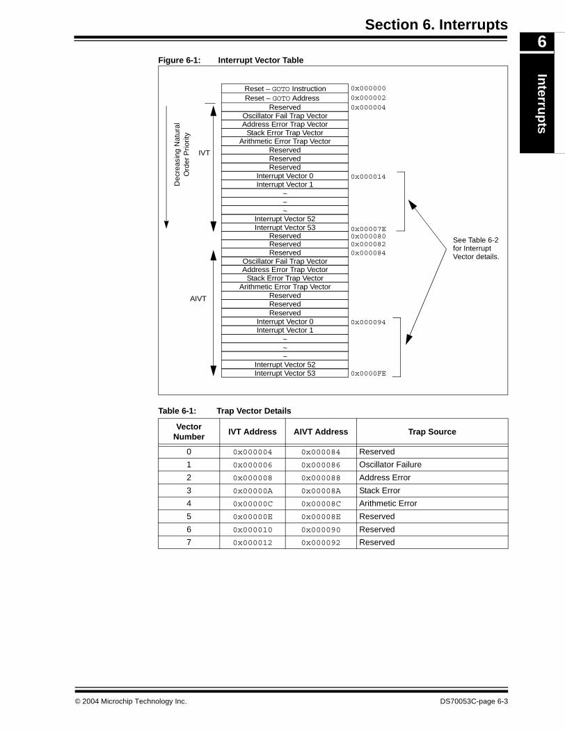
Section 6. InterruptsIn
terrup
ts
6
Figure 6-1: Interrupt Vector TableTable 6-1: Trap Vector Details
Dec
reas
ing
Nat
ural
Ord
er P
riorit
y
0x000000
0x000014
Reserved
Address Error Trap VectorStack Error Trap Vector
ReservedReservedReserved
Interrupt Vector 0Interrupt Vector 1
~~~
Interrupt Vector 52Interrupt Vector 53
Arithmetic Error Trap Vector
Oscillator Fail Trap Vector
ReservedInterrupt Vector 0Interrupt Vector 1
~~~
Interrupt Vector 52Interrupt Vector 53
IVT
AIVT
0x0000800x00007E
0x0000FE
ReservedReserved
Address Error Trap VectorStack Error Trap Vector
ReservedReserved
Arithmetic Error Trap Vector
Oscillator Fail Trap Vector
0x000094
Reset – GOTO InstructionReset – GOTO Address 0x000002
Reserved0x0000820x000084
0x000004
See Table 6-2
Vector details.for Interrupt
Vector Number
IVT Address AIVT Address Trap Source
0 0x000004 0x000084 Reserved
1 0x000006 0x000086 Oscillator Failure
2 0x000008 0x000088 Address Error
3 0x00000A 0x00008A Stack Error
4 0x00000C 0x00008C Arithmetic Error
5 0x00000E 0x00008E Reserved
6 0x000010 0x000090 Reserved
7 0x000012 0x000092 Reserved
© 2004 Microchip Technology Inc. DS70053C-page 6-3
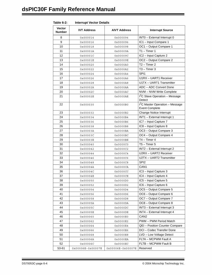
dsPIC30F Family Reference Manual
Table 6-2: Interrupt Vector Details
Vector Number
IVT Address AIVT Address Interrupt Source
8 0x000014 0x000094 INT0 – External Interrupt 0
9 0x000016 0x000096 IC1 – Input Compare 1
10 0x000018 0x000098 OC1 – Output Compare 1
11 0x00001A 0x00009A T1 – Timer 1
12 0x00001C 0x00009C IC2 – Input Capture 2
13 0x00001E 0x00009E OC2 – Output Compare 2
14 0x000020 0x0000A0 T2 – Timer 2
15 0x000022 0x0000A2 T3 – Timer 3
16 0x000024 0x0000A4 SPI1
17 0x000026 0x0000A6 U1RX – UART1 Receiver
18 0x000028 0x0000A8 U1TX – UART1 Transmitter
19 0x00002A 0x0000AA ADC – ADC Convert Done
20 0x00002C 0x0000AC NVM – NVM Write Complete
21 0x00002E 0x0000AE I2C Slave Operation – Message Detect
22 0x000030 0x0000B0 I2C Master Operation – Message Event Complete
23 0x000032 0x0000B2 Change Notice Interrupt
24 0x000034 0x0000B4 INT1 – External Interrupt 1
25 0x000036 0x0000B6 IC7 – Input Capture 7
26 0x000038 0x0000B8 IC8 – Input Capture 8
27 0x00003A 0x0000BA OC3 – Output Compare 3
28 0x00003C 0x0000BC OC4 – Output Compare 4
29 0x00003E 0x0000BE T4 – Timer 4
30 0x000040 0x0000C0 T5 – Timer 5
31 0x000042 0x0000C2 INT2 – External Interrupt 2
32 0x000044 0x0000C4 U2RX – UART2 Receiver
33 0x000046 0x0000C6 U2TX – UART2 Transmitter
34 0x000048 0x0000C8 SPI2
35 0x00004A 0x0000CA CAN1
36 0x00004C 0x0000CC IC3 – Input Capture 3
37 0x00004E 0x0000CE IC4 – Input Capture 4
38 0x000050 0x0000D0 IC5 – Input Capture 5
39 0x000052 0x0000D2 IC6 – Input Capture 6
40 0x000054 0x0000D4 OC5 – Output Compare 5
41 0x000056 0x0000D6 OC6 – Output Compare 6
42 0x000058 0x0000D8 OC7 – Output Compare 7
43 0x00005A 0x0000DA OC8 – Output Compare 8
44 0x00005C 0x0000DC INT3 – External Interrupt 3
45 0x00005E 0x0000DE INT4 – External Interrupt 4
46 0x000060 0x0000E0 CAN2
47 0x000062 0x0000E2 PWM – PWM Period Match
48 0x000064 0x0000E4 QEI – Position Counter Compare
49 0x000066 0x0000E6 DCI – Codec Transfer Done
50 0x000068 0x0000E8 LVD – Low Voltage Detect
51 0x00006A 0x0000EA FLTA – MCPWM Fault A
52 0x00006C 0x0000EC FLTB – MCPWM Fault B
53-61 0x00006E-0x00007E 0x00006E-0x00007E Reserved
DS70053C-page 6-4 © 2004 Microchip Technology Inc.
Section 6. InterruptsIn
terrup
ts
6
6.1.4 CPU Priority StatusThe CPU can operate at one of sixteen priority levels, 0-15. An interrupt or trap source must havea priority level greater than the current CPU priority in order to initiate an exception process.Peripheral and external interrupt sources can be programmed for level 0-7, while CPU prioritylevels 8-15 are reserved for trap sources. A trap is a non-maskable interrupt source intended todetect hardware and software problems (see Section 6.2 ”Non-Maskable Traps”). The prioritylevel for each trap source is fixed and only one trap is assigned to a priority level. Note that aninterrupt source programmed to priority level 0 is effectively disabled, since it can never begreater than the CPU priority.
The current CPU priority level is indicated by the following four status bits:
• IPL<2:0> status bits located in SR<7:5>
• IPL3 status bit located in CORCON<3>
The IPL<2:0> status bits are readable and writable, so the user may modify these bits to disableall sources of interrupts below a given priority level. If IPL<2:0> = 3, for example, the CPU wouldnot be interrupted by any source with a programmed priority level of 0, 1, 2 or 3.
Trap events have higher priority than any user interrupt source. When the IPL3 bit is set, a trapevent is in progress. The IPL3 bit can be cleared, but not set by the user. In some applications,it may be desirable to clear the IPL3 bit when a trap has occurred and branch to an instructionother than the instruction after the one that originally caused the trap to occur.
All user interrupt sources can be disabled by setting IPL<2:0> = 111.
6.1.5 Interrupt Priority
Each peripheral interrupt source can be assigned to one of seven priority levels. The userassignable interrupt priority control bits for each individual interrupt are located in the LeastSignificant 3 bits of each nibble within the IPCx register(s). Bit 3 of each nibble is not used andis read as a ‘0’. These bits define the priority level assigned to a particular interrupt. The usablepriority levels start at ‘1’ as the lowest priority and level 7 as the highest priority. If the IPC bitsassociated with an interrupt source are all cleared, then the interrupt source is effectivelydisabled.
Since more than one interrupt request source may be assigned to a specific priority level, ameans is provided to resolve priority conflicts within a given user assigned level. Each source ofinterrupt has a natural order priority based on its location in the IVT. Table 6-2 shows the locationof each interrupt source in the IVT. The lower numbered interrupt vectors have higher naturalpriority, while the higher numbered vectors have lower natural priority. The overall priority levelfor any pending source of interrupt is determined first by the user assigned priority of that sourcein the IPCx register, then by the natural order priority within the IVT.
Natural order priority is used only to resolve conflicts between simultaneous pending interruptswith the same user assigned priority level. Once the priority conflict is resolved and the exceptionprocess begins, the CPU can only be interrupted by a source with higher user assigned priority.Interrupts with the same user assigned priority but a higher natural order priority, that becomepending after the exception process begins, will remain pending until the current exceptionprocess completes.
The ability for the user to assign each interrupt source to one of seven priority levels means thatthe user can give an interrupt with a low natural order priority a very high overall priority level. Forexample: the PLVD (Programmable Low Voltage Detect) can be given a priority of 7 and the INT0(External Interrupt 0) may be assigned to priority level 1, thus giving it a very low effective priority.
Note: The IPL<2:0> bits become read only bits when interrupt nesting is disabled. SeeSection 6.2.4.2 ”Interrupt Nesting” for more information.
Note: The peripherals and sources of interrupt available in the IVT will vary depending onthe specific dsPIC30F device. The sources of interrupt shown in this documentrepresent a comprehensive listing of all interrupt sources found on dsPIC30Fdevices. Refer to the specific device data sheet for further details.
© 2004 Microchip Technology Inc. DS70053C-page 6-5
dsPIC30F Family Reference Manual
6.2 Non-Maskable Traps
Traps can be considered as non-maskable, nestable interrupts which adhere to a fixed prioritystructure. Traps are intended to provide the user a means to correct erroneous operation duringdebug and when operating within the application. If the user does not intend to take correctiveaction in the event of a trap error condition, these vectors must be loaded with the address of asoftware routine that will reset the device. Otherwise, the trap vector is programmed with theaddress of a service routine that will correct the trap condition.
The dsPIC30F has four implemented sources of non-maskable traps:
• Oscillator Failure Trap• Stack Error Trap• Address Error Trap
• Arithmetic Error Trap
Note that many of these trap conditions can only be detected when they happen. Consequently,the instruction that caused the trap is allowed to complete before exception processing begins.Therefore, the user may have to correct the action of the instruction that caused the trap.
Each trap source has a fixed priority as defined by its position in the IVT. An oscillator failure traphas the highest priority, while an arithmetic error trap has the lowest priority (see Figure 6-1). Inaddition, trap sources are classified into two distinct categories: ‘Hard’ traps and ‘Soft’ traps.
6.2.1 Soft Traps
The arithmetic error trap (priority level 11) and stack error trap (priority level 12) are categorizedas ‘soft’ trap sources. Soft traps can be treated like non-maskable sources of interrupt thatadhere to the priority assigned by their position in the IVT. Soft traps are processed like interruptsand require 2 cycles to be sampled and Acknowledged prior to exception processing. Therefore,additional instructions may be executed before a soft trap is Acknowledged.
6.2.1.1 Stack Error Trap (Soft Trap, Level 12)
The stack is initialized to 0x0800 during Reset. A stack error trap will be generated should thestack pointer address ever be less than 0x0800.
There is a Stack Limit register (SPLIM) associated with the stack pointer that is uninitialized atReset. The stack overflow check is not enabled until a word write to SPLIM occurs.
All Effective Addresses (EA) generated using W15 as a source or destination pointer arecompared against the value in SPLIM. Should the EA be greater than the contents of the SPLIMregister, then a stack error trap is generated. In addition, a stack error trap will be generatedshould the EA calculation wrap over the end of data space (0xFFFF).
A stack error can be detected in software by polling the STKERR status bit (INTCON1<2>). Toavoid re-entering the Trap Service Routine, the STKERR status flag must be cleared in softwareprior to returning from the trap with a RETFIE instruction.
DS70053C-page 6-6 © 2004 Microchip Technology Inc.
Section 6. InterruptsIn
terrup
ts
6
6.2.1.2 Arithmetic Error Trap (Soft Trap, Level 11)Any of the following events will cause an arithmetic error trap to be generated:
• Accumulator A Overflow
• Accumulator B Overflow• Catastrophic Accumulator Overflow• Divide by Zero
• Shift Accumulator (SFTAC) operation exceeding +/-16 bits
There are three enable bits in the INTCON1 register that enable the three types of accumulatoroverflow traps. The OVATE control bit (INTCON1<10>) is used to enable traps for an Accumula-tor A overflow event. The OVBTE control bit (INTCON1<9>) is used to enable traps for anAccumulator B overflow event. The COVTE control bit (INTCON1<8>) is used to enable traps fora catastrophic overflow of either accumulator.
An Accumulator A or Accumulator B overflow event is defined as a carry-out from bit 31. Notethat no accumulator overflow can occur if the 31-bit Saturation mode is enabled for the accumu-lator. A catastrophic accumulator overflow is defined as a carry-out from bit 39 of eitheraccumulator. No catastrophic overflow can occur if accumulator saturation (31-bit or 39-bit) isenabled.
Divide-by-zero traps cannot be disabled. The divide-by-zero check is performed during the firstiteration of the REPEAT loop that executes the divide instruction.
Accumulator shift traps cannot be disabled. The SFTAC instruction can be used to shift theaccumulator by a literal value or a value in one of the W registers. If the shift value exceeds+/-16 bits, an arithmetic trap will be generated. The SFTAC instruction will execute, but the resultsof the shift will not be written to the target accumulator.
An arithmetic error trap can be detected in software by polling the MATHERR status bit(INTCON1<4>). To avoid re-entering the Trap Service Routine, the MATHERR status flag mustbe cleared in software prior to returning from the trap with a RETFIE instruction. Before theMATHERR status bit can be cleared, all conditions that caused the trap to occur must also becleared. If the trap was due to an accumulator overflow, the OA and OB status bits (SR<15:14>)must be cleared. The OA and OB status bits are read only, so the user software must perform adummy operation on the overflowed accumulator (such as adding ‘0’) that will cause thehardware to clear the OA or OB status bit.
6.2.2 Hard Traps
Hard traps include exceptions of priority level 13 through level 15, inclusive. The address error(level 13) and oscillator error (level 14) traps fall into this category.
Like soft traps, hard traps can also be viewed as non-maskable sources of interrupt. Thedifference between hard traps and soft traps is that hard traps force the CPU to stop codeexecution after the instruction causing the trap has completed. Normal program execution flowwill not resume until after the trap has been Acknowledged and processed.
6.2.2.1 Trap Priority and Hard Trap Conflicts
If a higher priority trap occurs while any lower priority trap is in progress, processing of the lowerpriority trap will be suspended and the higher priority trap will be Acknowledged and processed.The lower priority trap will remain pending until processing of the higher priority trap completes.
Each hard trap that occurs must be Acknowledged before code execution of any type maycontinue. If a lower priority hard trap occurs while a higher priority trap is pending, Acknowledged,or is being processed, a hard trap conflict will occur. The conflict occurs because the lowerpriority trap cannot be Acknowledged until processing for the higher priority trap completes.
The device is automatically reset in a hard trap conflict condition. The TRAPR status bit(RCON<15> ) is set when the Reset occurs, so that the condition may be detected in software.
© 2004 Microchip Technology Inc. DS70053C-page 6-7

dsPIC30F Family Reference Manual
6.2.2.2 Oscillator Failure Trap (Hard Trap, Level 14)
An oscillator failure trap event will be generated for any of the following reasons:
• The Fail-Safe Clock Monitor (FSCM) is enabled and has detected a loss of the system clock source.
• A loss of PLL lock has been detected during normal operation using the PLL.
• The FSCM is enabled and the PLL fails to achieve lock at a Power-On Reset (POR).
An oscillator failure trap event can be detected in software by polling the OSCFAIL status bit(INTCON1<1>), or the CF status bit (OSCCON<3>). To avoid re-entering the Trap ServiceRoutine, the OSCFAIL status flag must be cleared in software prior to returning from the trap witha RETFIE instruction.
Refer to Section 7. “Oscillator” and Section 24. “Device Configuration” for more informationabout the FSCM.
6.2.2.3 Address Error Trap (Hard Trap, Level 13)
The following paragraphs describe operating scenarios that would cause an address error trapto be generated:
1. A misaligned data word fetch is attempted. This condition occurs when an instructionperforms a word access with the LSb of the effective address set to ‘1’. The dsPIC30FCPU requires all word accesses to be aligned to an even address boundary.
2. A bit manipulation instruction using the Indirect Addressing mode with the LSb of theeffective address set to ‘1’.
3. A data fetch from unimplemented data address space is attempted.
4. Execution of a “BRA #literal” instruction or a “GOTO #literal” instruction, whereliteral is an unimplemented program memory address.
5. Executing instructions after modifying the PC to point to unimplemented program memoryaddresses. The PC may be modified by loading a value into the stack and executing aRETURN instruction.
Data space writes will be inhibited whenever an address error trap occurs, so that data is notdestroyed.
An address error can be detected in software by polling the ADDRERR status bit (INTCON1<3>).To avoid re-entering the Trap Service Routine, the ADDRERR status flag must be cleared insoftware prior to returning from the trap with a RETFIE instruction.
6.2.3 Disable Interrupts Instruction
The DISI (disable interrupts) instruction has the ability to disable interrupts for up to 16384instruction cycles. This instruction is useful when time critical code segments must be executed.
The DISI instruction only disables interrupts with priority levels 1-6. Priority level 7 interrupts andall trap events still have the ability to interrupt the CPU when the DISI instruction is active.
The DISI instruction works in conjunction with the DISICNT register. When the DISICNT registeris non-zero, priority level 1-6 interrupts are disabled. The DISICNT register is decremented oneach subsequent instruction cycle. When the DISICNT register counts down to ‘0’, prioritylevel 1-6 interrupts will be re-enabled. The value specified in the DISI instruction includes allcycles due to PSV accesses, instruction stalls, etc.
The DISICNT register is readable and writable. The user can terminate the effect of a previousDISI instruction early by clearing the DISICNT register. The amount of time that interrupts aredisabled can also be increased by writing to or adding to DISICNT.
Note: In the MAC class of instructions, the data space is split into X and Y spaces. In theseinstructions, unimplemented X space includes all of Y space, and unimplemented Yspace includes all of X space.
DS70053C-page 6-8 © 2004 Microchip Technology Inc.
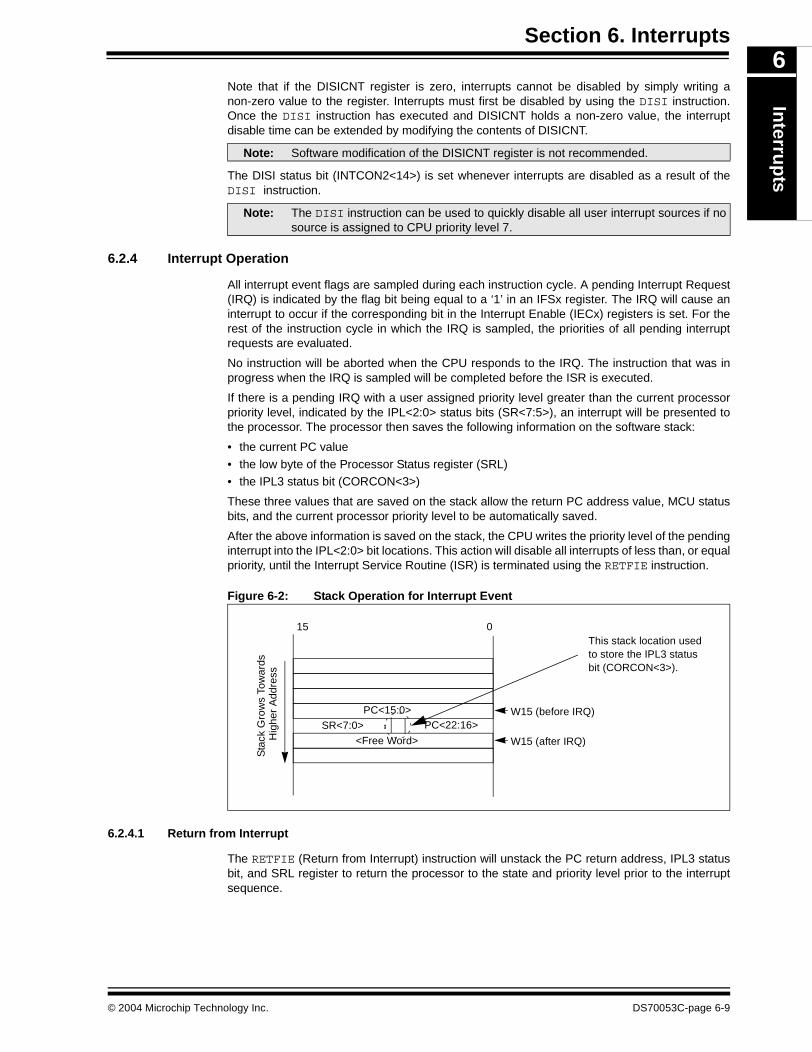
Section 6. InterruptsIn
terrup
ts
6
Note that if the DISICNT register is zero, interrupts cannot be disabled by simply writing anon-zero value to the register. Interrupts must first be disabled by using the DISI instruction.Once the DISI instruction has executed and DISICNT holds a non-zero value, the interruptdisable time can be extended by modifying the contents of DISICNT.The DISI status bit (INTCON2<14>) is set whenever interrupts are disabled as a result of theDISI instruction.
6.2.4 Interrupt Operation
All interrupt event flags are sampled during each instruction cycle. A pending Interrupt Request(IRQ) is indicated by the flag bit being equal to a ‘1’ in an IFSx register. The IRQ will cause aninterrupt to occur if the corresponding bit in the Interrupt Enable (IECx) registers is set. For therest of the instruction cycle in which the IRQ is sampled, the priorities of all pending interruptrequests are evaluated.
No instruction will be aborted when the CPU responds to the IRQ. The instruction that was inprogress when the IRQ is sampled will be completed before the ISR is executed.
If there is a pending IRQ with a user assigned priority level greater than the current processorpriority level, indicated by the IPL<2:0> status bits (SR<7:5>), an interrupt will be presented tothe processor. The processor then saves the following information on the software stack:
• the current PC value
• the low byte of the Processor Status register (SRL)• the IPL3 status bit (CORCON<3>)
These three values that are saved on the stack allow the return PC address value, MCU statusbits, and the current processor priority level to be automatically saved.
After the above information is saved on the stack, the CPU writes the priority level of the pendinginterrupt into the IPL<2:0> bit locations. This action will disable all interrupts of less than, or equalpriority, until the Interrupt Service Routine (ISR) is terminated using the RETFIE instruction.
Figure 6-2: Stack Operation for Interrupt Event
6.2.4.1 Return from Interrupt
The RETFIE (Return from Interrupt) instruction will unstack the PC return address, IPL3 statusbit, and SRL register to return the processor to the state and priority level prior to the interruptsequence.
Note: Software modification of the DISICNT register is not recommended.
Note: The DISI instruction can be used to quickly disable all user interrupt sources if nosource is assigned to CPU priority level 7.
<Free Word>
PC<15:0>PC<22:16>
015
W15 (before IRQ)
W15 (after IRQ)
Sta
ck G
row
s To
war
dsH
ighe
r A
ddre
ss
SR<7:0>
This stack location usedto store the IPL3 statusbit (CORCON<3>).
© 2004 Microchip Technology Inc. DS70053C-page 6-9
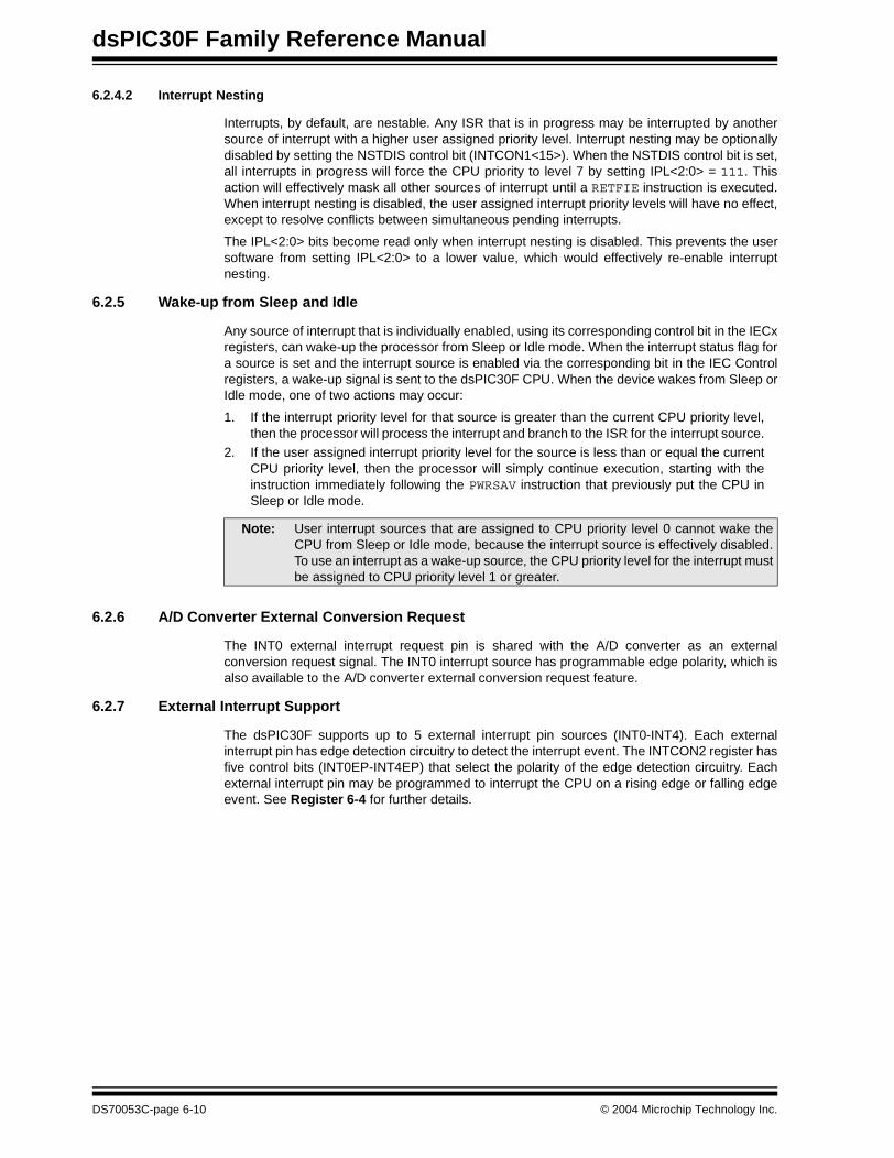
dsPIC30F Family Reference Manual
6.2.4.2 Interrupt Nesting
Interrupts, by default, are nestable. Any ISR that is in progress may be interrupted by anothersource of interrupt with a higher user assigned priority level. Interrupt nesting may be optionallydisabled by setting the NSTDIS control bit (INTCON1<15>). When the NSTDIS control bit is set,all interrupts in progress will force the CPU priority to level 7 by setting IPL<2:0> = 111. Thisaction will effectively mask all other sources of interrupt until a RETFIE instruction is executed.When interrupt nesting is disabled, the user assigned interrupt priority levels will have no effect,except to resolve conflicts between simultaneous pending interrupts.
The IPL<2:0> bits become read only when interrupt nesting is disabled. This prevents the usersoftware from setting IPL<2:0> to a lower value, which would effectively re-enable interruptnesting.
6.2.5 Wake-up from Sleep and Idle
Any source of interrupt that is individually enabled, using its corresponding control bit in the IECxregisters, can wake-up the processor from Sleep or Idle mode. When the interrupt status flag fora source is set and the interrupt source is enabled via the corresponding bit in the IEC Controlregisters, a wake-up signal is sent to the dsPIC30F CPU. When the device wakes from Sleep orIdle mode, one of two actions may occur:
1. If the interrupt priority level for that source is greater than the current CPU priority level,then the processor will process the interrupt and branch to the ISR for the interrupt source.
2. If the user assigned interrupt priority level for the source is less than or equal the currentCPU priority level, then the processor will simply continue execution, starting with theinstruction immediately following the PWRSAV instruction that previously put the CPU inSleep or Idle mode.
6.2.6 A/D Converter External Conversion Request
The INT0 external interrupt request pin is shared with the A/D converter as an externalconversion request signal. The INT0 interrupt source has programmable edge polarity, which isalso available to the A/D converter external conversion request feature.
6.2.7 External Interrupt Support
The dsPIC30F supports up to 5 external interrupt pin sources (INT0-INT4). Each externalinterrupt pin has edge detection circuitry to detect the interrupt event. The INTCON2 register hasfive control bits (INT0EP-INT4EP) that select the polarity of the edge detection circuitry. Eachexternal interrupt pin may be programmed to interrupt the CPU on a rising edge or falling edgeevent. See Register 6-4 for further details.
Note: User interrupt sources that are assigned to CPU priority level 0 cannot wake theCPU from Sleep or Idle mode, because the interrupt source is effectively disabled.To use an interrupt as a wake-up source, the CPU priority level for the interrupt mustbe assigned to CPU priority level 1 or greater.
DS70053C-page 6-10 © 2004 Microchip Technology Inc.
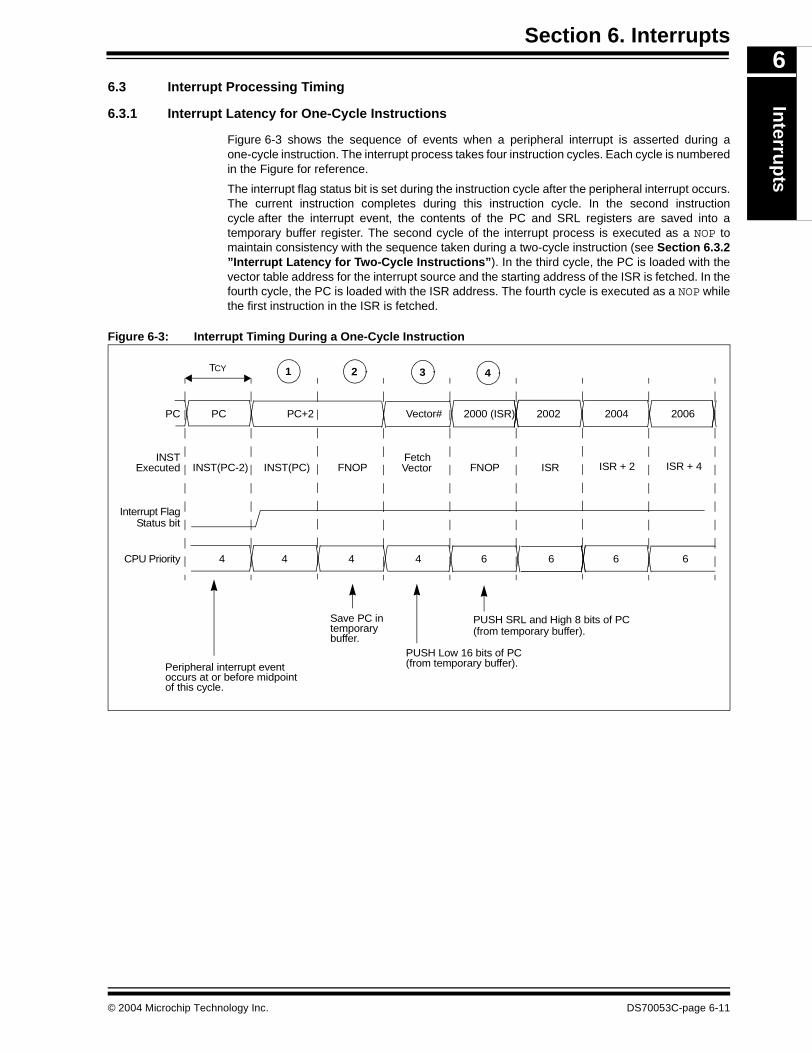
Section 6. InterruptsIn
terrup
ts
6
6.3 Interrupt Processing Timing6.3.1 Interrupt Latency for One-Cycle Instructions
Figure 6-3 shows the sequence of events when a peripheral interrupt is asserted during aone-cycle instruction. The interrupt process takes four instruction cycles. Each cycle is numberedin the Figure for reference.
The interrupt flag status bit is set during the instruction cycle after the peripheral interrupt occurs.The current instruction completes during this instruction cycle. In the second instructioncycle after the interrupt event, the contents of the PC and SRL registers are saved into atemporary buffer register. The second cycle of the interrupt process is executed as a NOP tomaintain consistency with the sequence taken during a two-cycle instruction (see Section 6.3.2”Interrupt Latency for Two-Cycle Instructions”). In the third cycle, the PC is loaded with thevector table address for the interrupt source and the starting address of the ISR is fetched. In thefourth cycle, the PC is loaded with the ISR address. The fourth cycle is executed as a NOP whilethe first instruction in the ISR is fetched.
Figure 6-3: Interrupt Timing During a One-Cycle Instruction
4 6 6 64 4
INST(PC-2) INST(PC) FNOP FNOP ISRINST
Executed
Interrupt Flag
PUSH Low 16 bits of PC
PUSH SRL and High 8 bits of PC
64
ISR + 2 ISR + 4
CPU Priority
Fetch
2000 (ISR) 2002 2004 2006PC PC+2PC
Vector
Save PC in
Status bit
Vector#
Peripheral interrupt eventoccurs at or before midpoint
TCY 1 2 3 4
temporarybuffer.
of this cycle.
(from temporary buffer).
(from temporary buffer).
© 2004 Microchip Technology Inc. DS70053C-page 6-11
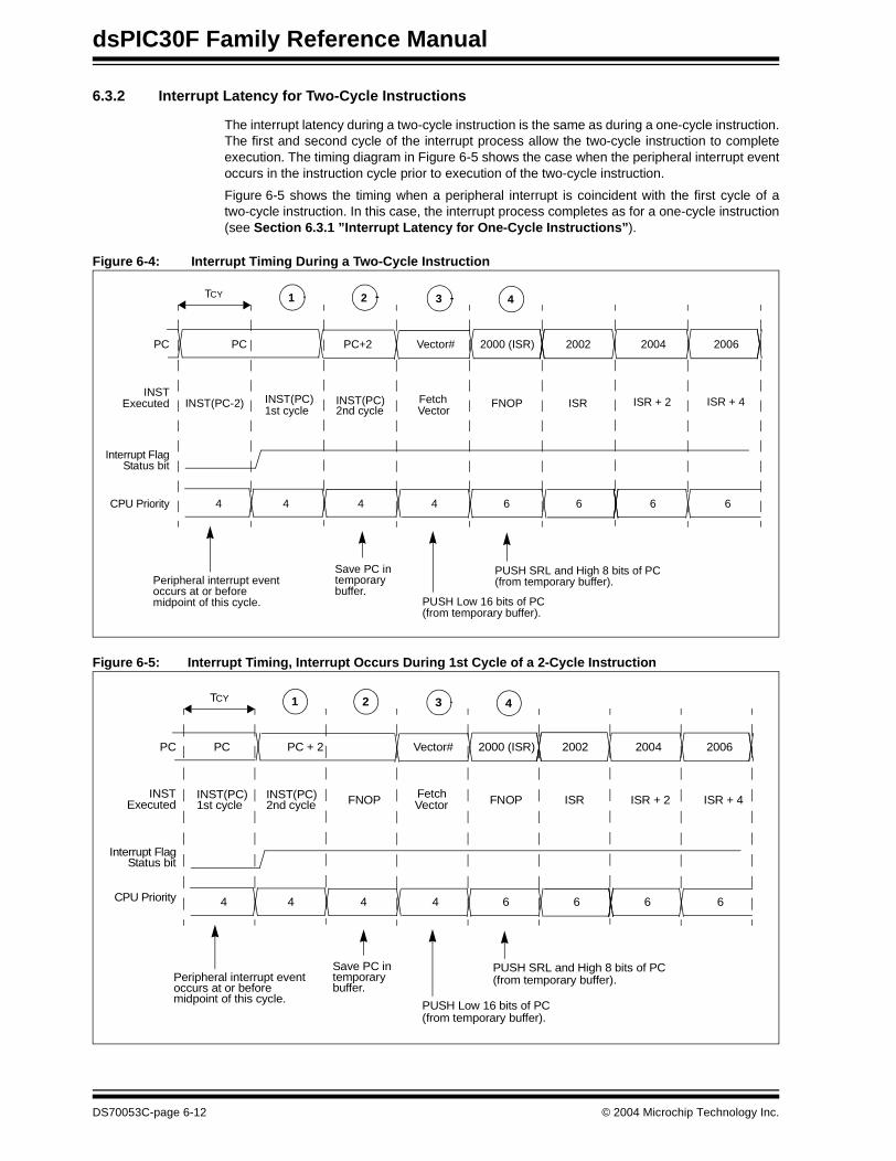
dsPIC30F Family Reference Manual
6.3.2 Interrupt Latency for Two-Cycle Instructions
The interrupt latency during a two-cycle instruction is the same as during a one-cycle instruction.The first and second cycle of the interrupt process allow the two-cycle instruction to completeexecution. The timing diagram in Figure 6-5 shows the case when the peripheral interrupt eventoccurs in the instruction cycle prior to execution of the two-cycle instruction.
Figure 6-5 shows the timing when a peripheral interrupt is coincident with the first cycle of atwo-cycle instruction. In this case, the interrupt process completes as for a one-cycle instruction(see Section 6.3.1 ”Interrupt Latency for One-Cycle Instructions”).
Figure 6-4: Interrupt Timing During a Two-Cycle Instruction
Figure 6-5: Interrupt Timing, Interrupt Occurs During 1st Cycle of a 2-Cycle Instruction
4 6 6 64 4
INST(PC-2) INST(PC) INST(PC) FNOP ISRINST
Executed
Interrupt Flag
PUSH Low 16 bits of PC
PUSH SRL and High 8 bits of PC
64
ISR + 2 ISR + 4
CPU Priority
Fetch
2000 (ISR) 2002 2004 2006PC PC+2PC
Vector
Save PC in
Status bit
Vector#
Peripheral interrupt eventoccurs at or before
TCY 1 2 3 4
2nd cycle1st cycle
temporarybuffer.
midpoint of this cycle.
(from temporary buffer).
(from temporary buffer).
4 6 6 64 4
INST(PC) INST(PC) FNOP ISRINSTExecuted
Interrupt Flag
PUSH Low 16 bits of PC
PUSH SRL and High 8 bits of PC
64
ISR + 2 ISR + 4
CPU Priority
Fetch
2000 (ISR) 2002 2004 2006PC PC + 2PC
Vector
Save PC in
Status bit
Vector#
Peripheral interrupt eventoccurs at or before
TCY 1 2 3 4
2nd cycle1st cycle
temporarybuffer.
FNOP
midpoint of this cycle.
(from temporary buffer).
(from temporary buffer).
DS70053C-page 6-12 © 2004 Microchip Technology Inc.
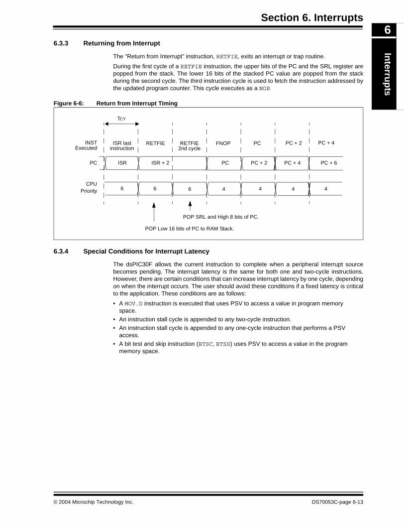
Section 6. InterruptsIn
terrup
ts
6
6.3.3 Returning from InterruptThe “Return from Interrupt” instruction, RETFIE, exits an interrupt or trap routine.
During the first cycle of a RETFIE instruction, the upper bits of the PC and the SRL register arepopped from the stack. The lower 16 bits of the stacked PC value are popped from the stackduring the second cycle. The third instruction cycle is used to fetch the instruction addressed bythe updated program counter. This cycle executes as a NOP.
Figure 6-6: Return from Interrupt Timing
6.3.4 Special Conditions for Interrupt Latency
The dsPIC30F allows the current instruction to complete when a peripheral interrupt sourcebecomes pending. The interrupt latency is the same for both one and two-cycle instructions.However, there are certain conditions that can increase interrupt latency by one cycle, dependingon when the interrupt occurs. The user should avoid these conditions if a fixed latency is criticalto the application. These conditions are as follows:
• A MOV.D instruction is executed that uses PSV to access a value in program memory space.
• An instruction stall cycle is appended to any two-cycle instruction.• An instruction stall cycle is appended to any one-cycle instruction that performs a PSV
access.• A bit test and skip instruction (BTSC, BTSS) uses PSV to access a value in the program
memory space.
4 4 4 46 6CPU
Priority
RETFIE RETFIE PCINSTExecuted
FNOPISR last
6
PC + 2 PC + 4
POP Low 16 bits of PC to RAM Stack.
POP SRL and High 8 bits of PC.
PC PC + 2 PC + 4 PC + 6ISR ISR + 2PC
2nd cycle
TCY
instruction
© 2004 Microchip Technology Inc. DS70053C-page 6-13
dsPIC30F Family Reference Manual
6.4 Interrupt Control and Status Registers
The following registers are associated with the interrupt controller:
• INTCON1, INTCON2 RegistersGlobal interrupt control functions are derived from these two registers. INTCON1 contains the Interrupt Nesting Disable (NSTDIS) bit, as well as the control and status flags for the processor trap sources. The INTCON2 register controls the external interrupt request signal behavior and the use of the alternate vector table.
• IFSx: Interrupt Flag Status RegistersAll interrupt request flags are maintained in the IFSx registers, where ‘x’ denotes the register number. Each source of interrupt has a Status bit, which is set by the respective peripherals or external signal and is cleared via software.
• IECx: Interrupt Enable Control RegistersAll Interrupt Enable Control bits are maintained in the IECx registers, where ‘x’ denotes the register number. These control bits are used to individually enable interrupts from the peripherals or external signals.
• IPCx: Interrupt Priority Control RegistersEach user interrupt source can be assigned to one of eight priority levels. The IPC registers are used to set the interrupt priority level for each source of interrupt.
• SR: CPU Status Register The SR is not specifically part of the interrupt controller hardware, but it contains the IPL<2:0> Status bits (SR<7:5>) that indicate the current CPU priority level. The user may change the current CPU priority level by writing to the IPL bits.
• CORCON: Core Control Register The CORCON is not specifically part of the interrupt controller hardware, but it contains the IPL3 Status bit which indicates the current CPU priority level. IPL3 is a Read Only bit so that trap events cannot be masked by the user software.
Each register is described in detail on the following pages.
6.4.1 Assignment of Interrupts to Control Registers
The interrupt sources are assigned to the IFSx, IECx and IPCx registers in the same sequencethat they are listed in Table 6-2. For example, the INT0 (External Interrupt 0) is shown as havingvector number and a natural order priority of ‘0’. Thus, the INT0IF Status bit is found in IFS0<0>.The INT0 interrupt uses bit 0 of the IEC0 register as its Enable bit and the IPC0<2:0> bits assignthe interrupt priority level for the INT0 interrupt.
Note: The total number and type of interrupt sources will depend on the device variant.Refer to the specific device data sheet for further details.
DS70053C-page 6-14 © 2004 Microchip Technology Inc.
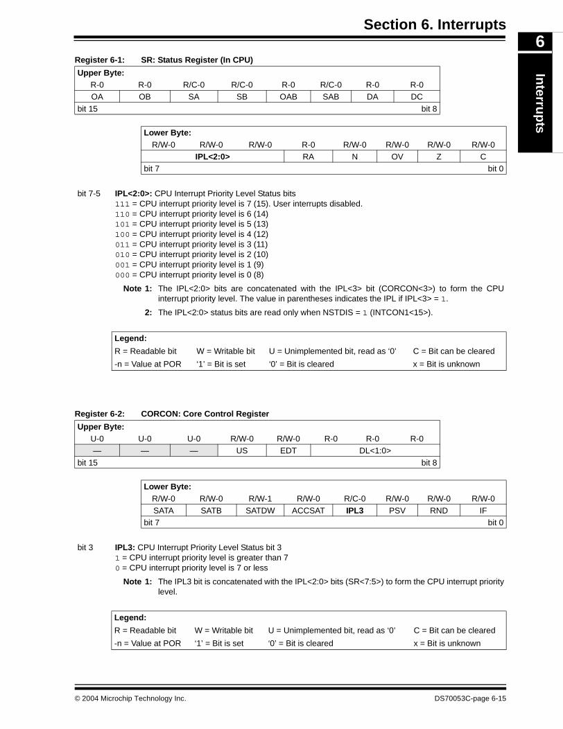
Section 6. InterruptsIn
terrup
ts
6
Register 6-1: SR: Status Register (In CPU)Register 6-2: CORCON: Core Control Register
Upper Byte:R-0 R-0 R/C-0 R/C-0 R-0 R/C-0 R-0 R-0OA OB SA SB OAB SAB DA DC
bit 15 bit 8
Lower Byte:R/W-0 R/W-0 R/W-0 R-0 R/W-0 R/W-0 R/W-0 R/W-0
IPL<2:0> RA N OV Z Cbit 7 bit 0
bit 7-5 IPL<2:0>: CPU Interrupt Priority Level Status bits111 = CPU interrupt priority level is 7 (15). User interrupts disabled.110 = CPU interrupt priority level is 6 (14)101 = CPU interrupt priority level is 5 (13)100 = CPU interrupt priority level is 4 (12)011 = CPU interrupt priority level is 3 (11)010 = CPU interrupt priority level is 2 (10)001 = CPU interrupt priority level is 1 (9)000 = CPU interrupt priority level is 0 (8)
Note 1: The IPL<2:0> bits are concatenated with the IPL<3> bit (CORCON<3>) to form the CPUinterrupt priority level. The value in parentheses indicates the IPL if IPL<3> = 1.
2: The IPL<2:0> status bits are read only when NSTDIS = 1 (INTCON1<15>).
Legend:
R = Readable bit W = Writable bit U = Unimplemented bit, read as ‘0’ C = Bit can be cleared
-n = Value at POR ‘1’ = Bit is set ‘0’ = Bit is cleared x = Bit is unknown
Upper Byte:U-0 U-0 U-0 R/W-0 R/W-0 R-0 R-0 R-0— — — US EDT DL<1:0>
bit 15 bit 8
Lower Byte:R/W-0 R/W-0 R/W-1 R/W-0 R/C-0 R/W-0 R/W-0 R/W-0SATA SATB SATDW ACCSAT IPL3 PSV RND IF
bit 7 bit 0
bit 3 IPL3: CPU Interrupt Priority Level Status bit 31 = CPU interrupt priority level is greater than 70 = CPU interrupt priority level is 7 or less
Note 1: The IPL3 bit is concatenated with the IPL<2:0> bits (SR<7:5>) to form the CPU interrupt prioritylevel.
Legend:
R = Readable bit W = Writable bit U = Unimplemented bit, read as ‘0’ C = Bit can be cleared
-n = Value at POR ‘1’ = Bit is set ‘0’ = Bit is cleared x = Bit is unknown
© 2004 Microchip Technology Inc. DS70053C-page 6-15
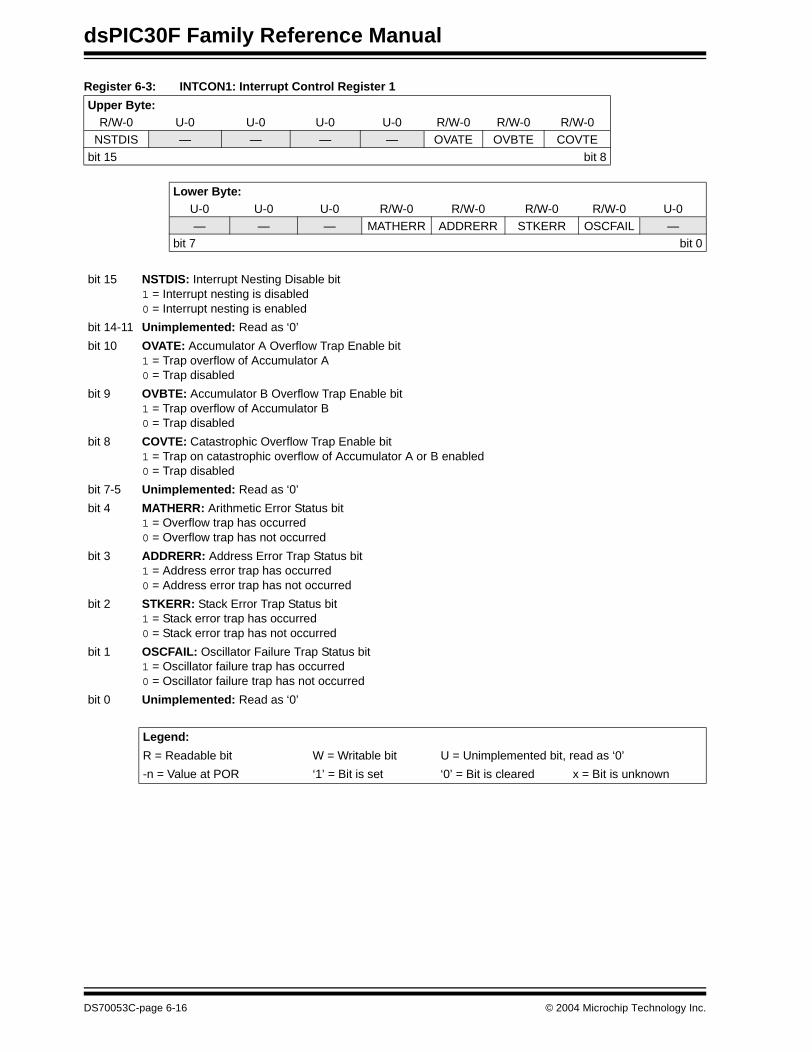
dsPIC30F Family Reference Manual
Register 6-3: INTCON1: Interrupt Control Register 1
Upper Byte:R/W-0 U-0 U-0 U-0 U-0 R/W-0 R/W-0 R/W-0
NSTDIS — — — — OVATE OVBTE COVTE
bit 15 bit 8
Lower Byte:U-0 U-0 U-0 R/W-0 R/W-0 R/W-0 R/W-0 U-0— — — MATHERR ADDRERR STKERR OSCFAIL —
bit 7 bit 0
bit 15 NSTDIS: Interrupt Nesting Disable bit1 = Interrupt nesting is disabled0 = Interrupt nesting is enabled
bit 14-11 Unimplemented: Read as ‘0’
bit 10 OVATE: Accumulator A Overflow Trap Enable bit1 = Trap overflow of Accumulator A0 = Trap disabled
bit 9 OVBTE: Accumulator B Overflow Trap Enable bit1 = Trap overflow of Accumulator B0 = Trap disabled
bit 8 COVTE: Catastrophic Overflow Trap Enable bit1 = Trap on catastrophic overflow of Accumulator A or B enabled0 = Trap disabled
bit 7-5 Unimplemented: Read as ‘0’
bit 4 MATHERR: Arithmetic Error Status bit1 = Overflow trap has occurred0 = Overflow trap has not occurred
bit 3 ADDRERR: Address Error Trap Status bit1 = Address error trap has occurred0 = Address error trap has not occurred
bit 2 STKERR: Stack Error Trap Status bit1 = Stack error trap has occurred0 = Stack error trap has not occurred
bit 1 OSCFAIL: Oscillator Failure Trap Status bit1 = Oscillator failure trap has occurred0 = Oscillator failure trap has not occurred
bit 0 Unimplemented: Read as ‘0’
Legend:
R = Readable bit W = Writable bit U = Unimplemented bit, read as ‘0’
-n = Value at POR ‘1’ = Bit is set ‘0’ = Bit is cleared x = Bit is unknown
DS70053C-page 6-16 © 2004 Microchip Technology Inc.
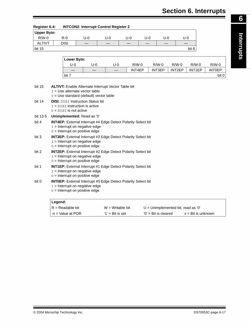
Section 6. InterruptsIn
terrup
ts
6
Register 6-4: INTCON2: Interrupt Control Register 2Upper Byte:R/W-0 R-0 U-0 U-0 U-0 U-0 U-0 U-0ALTIVT DISI — — — — — —
bit 15 bit 8
Lower Byte:U-0 U-0 U-0 R/W-0 R/W-0 R/W-0 R/W-0 R/W-0— — — INT4EP INT3EP INT2EP INT1EP INT0EP
bit 7 bit 0
bit 15 ALTIVT: Enable Alternate Interrupt Vector Table bit1 = Use alternate vector table0 = Use standard (default) vector table
bit 14 DISI: DISI Instruction Status bit1 = DISI instruction is active0 = DISI is not active
bit 13-5 Unimplemented: Read as ‘0’
bit 4 INT4EP: External Interrupt #4 Edge Detect Polarity Select bit1 = Interrupt on negative edge 0 = Interrupt on positive edge
bit 3 INT3EP: External Interrupt #3 Edge Detect Polarity Select bit1 = Interrupt on negative edge 0 = Interrupt on positive edge
bit 2 INT2EP: External Interrupt #2 Edge Detect Polarity Select bit1 = Interrupt on negative edge 0 = Interrupt on positive edge
bit 1 INT1EP: External Interrupt #1 Edge Detect Polarity Select bit1 = Interrupt on negative edge 0 = Interrupt on positive edge
bit 0 INT0EP: External Interrupt #0 Edge Detect Polarity Select bit1 = Interrupt on negative edge 0 = Interrupt on positive edge
Legend:
R = Readable bit W = Writable bit U = Unimplemented bit, read as ‘0’
-n = Value at POR ‘1’ = Bit is set ‘0’ = Bit is cleared x = Bit is unknown
© 2004 Microchip Technology Inc. DS70053C-page 6-17
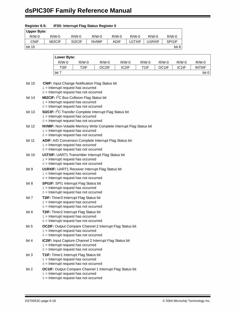
dsPIC30F Family Reference Manual
Register 6-5: IFS0: Interrupt Flag Status Register 0
Upper Byte:R/W-0 R/W-0 R/W-0 R/W-0 R/W-0 R/W-0 R/W-0 R/W-0CNIF MI2CIF SI2CIF NVMIF ADIF U1TXIF U1RXIF SPI1IF
bit 15 bit 8
Lower Byte:R/W-0 R/W-0 R/W-0 R/W-0 R/W-0 R/W-0 R/W-0 R/W-0T3IF T2IF OC2IF IC2IF T1IF OC1IF IC1IF INT0IF
bit 7 bit 0
bit 15 CNIF: Input Change Notification Flag Status bit1 = Interrupt request has occurred0 = Interrupt request has not occurred
bit 14 MI2CIF: I2C Bus Collision Flag Status bit1 = Interrupt request has occurred0 = Interrupt request has not occurred
bit 13 SI2CIF: I2C Transfer Complete Interrupt Flag Status bit1 = Interrupt request has occurred0 = Interrupt request has not occurred
bit 12 NVMIF: Non-Volatile Memory Write Complete Interrupt Flag Status bit1 = Interrupt request has occurred0 = Interrupt request has not occurred
bit 11 ADIF: A/D Conversion Complete Interrupt Flag Status bit1 = Interrupt request has occurred0 = Interrupt request has not occurred
bit 10 U1TXIF: UART1 Transmitter Interrupt Flag Status bit1 = Interrupt request has occurred0 = Interrupt request has not occurred
bit 9 U1RXIF: UART1 Receiver Interrupt Flag Status bit1 = Interrupt request has occurred0 = Interrupt request has not occurred
bit 8 SPI1IF: SPI1 Interrupt Flag Status bit1 = Interrupt request has occurred0 = Interrupt request has not occurred
bit 7 T3IF: Timer3 Interrupt Flag Status bit1 = Interrupt request has occurred0 = Interrupt request has not occurred
bit 6 T2IF: Timer2 Interrupt Flag Status bit1 = Interrupt request has occurred0 = Interrupt request has not occurred
bit 5 OC2IF: Output Compare Channel 2 Interrupt Flag Status bit1 = Interrupt request has occurred0 = Interrupt request has not occurred
bit 4 IC2IF: Input Capture Channel 2 Interrupt Flag Status bit1 = Interrupt request has occurred0 = Interrupt request has not occurred
bit 3 T1IF: Timer1 Interrupt Flag Status bit1 = Interrupt request has occurred0 = Interrupt request has not occurred
bit 2 OC1IF: Output Compare Channel 1 Interrupt Flag Status bit1 = Interrupt request has occurred0 = Interrupt request has not occurred
DS70053C-page 6-18 © 2004 Microchip Technology Inc.

Section 6. InterruptsIn
terrup
ts
6
Register 6-5: IFS0: Interrupt Flag Status Register 0 (Continued)bit 1 IC1IF: Input Capture Channel 1 Interrupt Flag Status bit1 = Interrupt request has occurred0 = Interrupt request has not occurred
bit 0 INT0IF: External Interrupt 0 Flag Status bit1 = Interrupt request has occurred0 = Interrupt request has not occurred
Legend:
R = Readable bit W = Writable bit U = Unimplemented bit, read as ‘0’
-n = Value at POR ‘1’ = Bit is set ‘0’ = Bit is cleared x = Bit is unknown
© 2004 Microchip Technology Inc. DS70053C-page 6-19
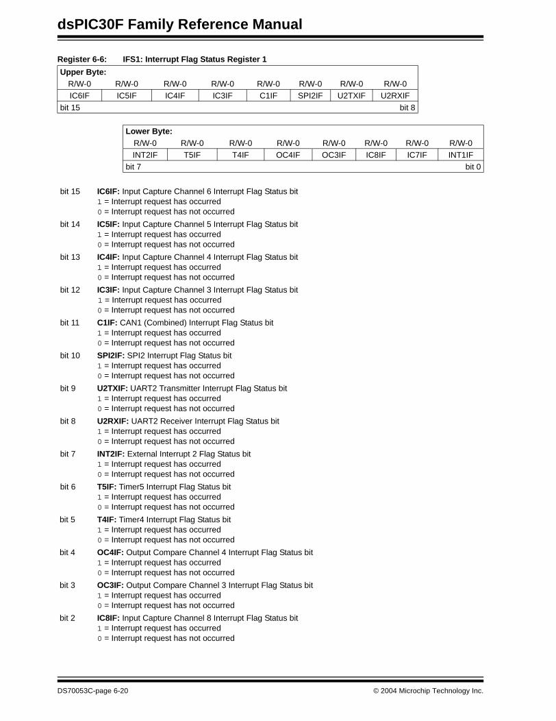
dsPIC30F Family Reference Manual
Register 6-6: IFS1: Interrupt Flag Status Register 1
Upper Byte:R/W-0 R/W-0 R/W-0 R/W-0 R/W-0 R/W-0 R/W-0 R/W-0IC6IF IC5IF IC4IF IC3IF C1IF SPI2IF U2TXIF U2RXIF
bit 15 bit 8
Lower Byte:R/W-0 R/W-0 R/W-0 R/W-0 R/W-0 R/W-0 R/W-0 R/W-0INT2IF T5IF T4IF OC4IF OC3IF IC8IF IC7IF INT1IF
bit 7 bit 0
bit 15 IC6IF: Input Capture Channel 6 Interrupt Flag Status bit1 = Interrupt request has occurred0 = Interrupt request has not occurred
bit 14 IC5IF: Input Capture Channel 5 Interrupt Flag Status bit1 = Interrupt request has occurred0 = Interrupt request has not occurred
bit 13 IC4IF: Input Capture Channel 4 Interrupt Flag Status bit1 = Interrupt request has occurred0 = Interrupt request has not occurred
bit 12 IC3IF: Input Capture Channel 3 Interrupt Flag Status bit1 = Interrupt request has occurred0 = Interrupt request has not occurred
bit 11 C1IF: CAN1 (Combined) Interrupt Flag Status bit1 = Interrupt request has occurred0 = Interrupt request has not occurred
bit 10 SPI2IF: SPI2 Interrupt Flag Status bit1 = Interrupt request has occurred0 = Interrupt request has not occurred
bit 9 U2TXIF: UART2 Transmitter Interrupt Flag Status bit1 = Interrupt request has occurred0 = Interrupt request has not occurred
bit 8 U2RXIF: UART2 Receiver Interrupt Flag Status bit1 = Interrupt request has occurred0 = Interrupt request has not occurred
bit 7 INT2IF: External Interrupt 2 Flag Status bit1 = Interrupt request has occurred0 = Interrupt request has not occurred
bit 6 T5IF: Timer5 Interrupt Flag Status bit1 = Interrupt request has occurred0 = Interrupt request has not occurred
bit 5 T4IF: Timer4 Interrupt Flag Status bit1 = Interrupt request has occurred0 = Interrupt request has not occurred
bit 4 OC4IF: Output Compare Channel 4 Interrupt Flag Status bit1 = Interrupt request has occurred0 = Interrupt request has not occurred
bit 3 OC3IF: Output Compare Channel 3 Interrupt Flag Status bit1 = Interrupt request has occurred0 = Interrupt request has not occurred
bit 2 IC8IF: Input Capture Channel 8 Interrupt Flag Status bit1 = Interrupt request has occurred0 = Interrupt request has not occurred
DS70053C-page 6-20 © 2004 Microchip Technology Inc.
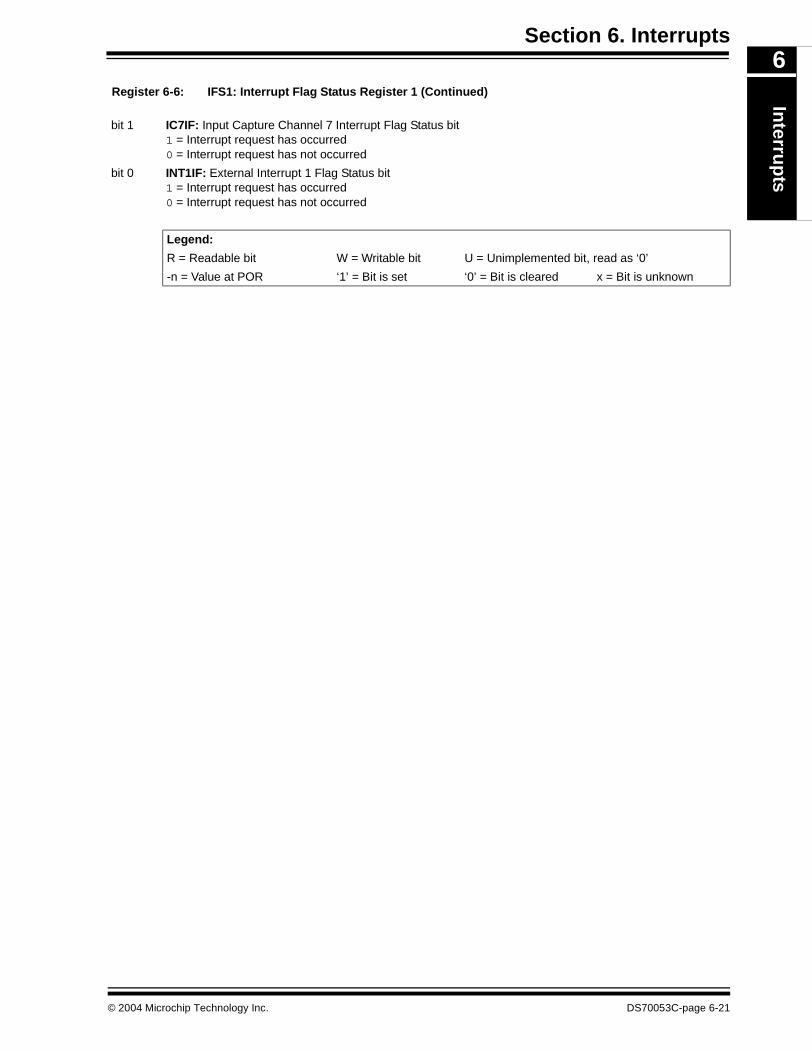
Section 6. InterruptsIn
terrup
ts
6
Register 6-6: IFS1: Interrupt Flag Status Register 1 (Continued)bit 1 IC7IF: Input Capture Channel 7 Interrupt Flag Status bit1 = Interrupt request has occurred0 = Interrupt request has not occurred
bit 0 INT1IF: External Interrupt 1 Flag Status bit1 = Interrupt request has occurred0 = Interrupt request has not occurred
Legend:
R = Readable bit W = Writable bit U = Unimplemented bit, read as ‘0’
-n = Value at POR ‘1’ = Bit is set ‘0’ = Bit is cleared x = Bit is unknown
© 2004 Microchip Technology Inc. DS70053C-page 6-21

dsPIC30F Family Reference Manual
Register 6-7: IFS2: Interrupt Flag Status Register 2
Upper Byte:U-0 U-0 U-0 R/W-0 R/W-0 R/W-0 R/W-0 R/W-0
— — — FLTBIF FLTAIF LVDIF DCIIF QEIIFbit 15 bit 8
Lower Byte:R/W-0 R/W-0 R/W-0 R/W-0 R/W-0 R/W-0 R/W-0 R/W-0PWMIF C2IF INT4IF INT3IF OC8IF OC7IF OC6IF OC5IF
bit 7 bit 0
bit 15-13 Unimplemented: Read as ‘0’
bit 12 FLTBIF: Fault B Input Interrupt Flag Status bit1 = Interrupt request has occurred0 = Interrupt request has not occurred
bit 11 FLTAIF: Fault A Input Interrupt Flag Status bit1 = Interrupt request has occurred0 = Interrupt request has not occurred
bit 10 LVDIF: Programmable Low Voltage Detect Interrupt Flag Status bit1 = Interrupt request has occurred0 = Interrupt request has not occurred
bit 9 DCIIF: Data Converter Interface Interrupt Flag Status bit1 = Interrupt request has occurred0 = Interrupt request has not occurred
bit 8 QEIIF: Quadrature Encoder Interface Interrupt Flag Status bit1 = Interrupt request has occurred0 = Interrupt request has not occurred
bit 7 PWMIF: Motor Control Pulse Width Modulation Interrupt Flag Status bit1 = Interrupt request has occurred0 = Interrupt request has not occurred
bit 6 C2IF: CAN2 (Combined) Interrupt Flag Status bit1 = Interrupt request has occurred0 = Interrupt request has not occurred
bit 5 INT4IF: External Interrupt 4 Flag Status bit1 = Interrupt request has occurred0 = Interrupt request has not occurred
bit 4 INT3IF: External Interrupt 3 Flag Status bit1 = Interrupt request has occurred0 = Interrupt request has not occurred
bit 3 OC8IF: Output Compare Channel 8 Interrupt Flag Status bit1 = Interrupt request has occurred0 = Interrupt request has not occurred
bit 2 OC7IF: Output Compare Channel 7 Interrupt Flag Status bit1 = Interrupt request has occurred0 = Interrupt request has not occurred
DS70053C-page 6-22 © 2004 Microchip Technology Inc.

Section 6. InterruptsIn
terrup
ts
6
Register 6-7: IFS2: Interrupt Flag Status Register 2 (Continued)bit 1 OC6IF: Output Compare Channel 6 Interrupt Flag Status bit1 = Interrupt request has occurred0 = Interrupt request has not occurred
bit 0 OC5IF: Output Compare Channel 5 Interrupt Flag Status bit1 = Interrupt request has occurred0 = Interrupt request has not occurred
Legend:
R = Readable bit W = Writable bit U = Unimplemented bit, read as ‘0’
-n = Value at POR ‘1’ = Bit is set ‘0’ = Bit is cleared x = Bit is unknown
© 2004 Microchip Technology Inc. DS70053C-page 6-23
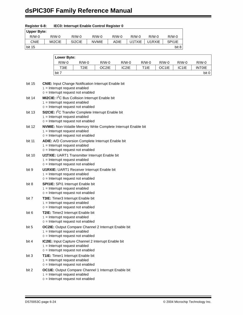
dsPIC30F Family Reference Manual
Register 6-8: IEC0: Interrupt Enable Control Register 0
Upper Byte:R/W-0 R/W-0 R/W-0 R/W-0 R/W-0 R/W-0 R/W-0 R/W-0CNIE MI2CIE SI2CIE NVMIE ADIE U1TXIE U1RXIE SPI1IE
bit 15 bit 8
Lower Byte:R/W-0 R/W-0 R/W-0 R/W-0 R/W-0 R/W-0 R/W-0 R/W-0T3IE T2IE OC2IE IC2IE T1IE OC1IE IC1IE INT0IE
bit 7 bit 0
bit 15 CNIE: Input Change Notification Interrupt Enable bit1 = Interrupt request enabled0 = Interrupt request not enabled
bit 14 MI2CIE: I2C Bus Collision Interrupt Enable bit1 = Interrupt request enabled0 = Interrupt request not enabled
bit 13 SI2CIE: I2C Transfer Complete Interrupt Enable bit1 = Interrupt request enabled0 = Interrupt request not enabled
bit 12 NVMIE: Non-Volatile Memory Write Complete Interrupt Enable bit1 = Interrupt request enabled0 = Interrupt request not enabled
bit 11 ADIE: A/D Conversion Complete Interrupt Enable bit1 = Interrupt request enabled0 = Interrupt request not enabled
bit 10 U1TXIE: UART1 Transmitter Interrupt Enable bit1 = Interrupt request enabled0 = Interrupt request not enabled
bit 9 U1RXIE: UART1 Receiver Interrupt Enable bit1 = Interrupt request enabled0 = Interrupt request not enabled
bit 8 SPI1IE: SPI1 Interrupt Enable bit1 = Interrupt request enabled0 = Interrupt request not enabled
bit 7 T3IE: Timer3 Interrupt Enable bit1 = Interrupt request enabled0 = Interrupt request not enabled
bit 6 T2IE: Timer2 Interrupt Enable bit1 = Interrupt request enabled0 = Interrupt request not enabled
bit 5 OC2IE: Output Compare Channel 2 Interrupt Enable bit1 = Interrupt request enabled0 = Interrupt request not enabled
bit 4 IC2IE: Input Capture Channel 2 Interrupt Enable bit1 = Interrupt request enabled0 = Interrupt request not enabled
bit 3 T1IE: Timer1 Interrupt Enable bit1 = Interrupt request enabled0 = Interrupt request not enabled
bit 2 OC1IE: Output Compare Channel 1 Interrupt Enable bit1 = Interrupt request enabled0 = Interrupt request not enabled
DS70053C-page 6-24 © 2004 Microchip Technology Inc.

Section 6. InterruptsIn
terrup
ts
6
Register 6-8: IEC0: Interrupt Enable Control Register 0 (Continued)bit 1 IC1IE: Input Capture Channel 1 Interrupt Enable bit1 = Interrupt request enabled0 = Interrupt request not enabled
bit 0 INT0IE: External Interrupt 0 Enable bit1 = Interrupt request enabled0 = Interrupt request not enabled
Legend:
R = Readable bit W = Writable bit U = Unimplemented bit, read as ‘0’
-n = Value at POR ‘1’ = Bit is set ‘0’ = Bit is cleared x = Bit is unknown
© 2004 Microchip Technology Inc. DS70053C-page 6-25
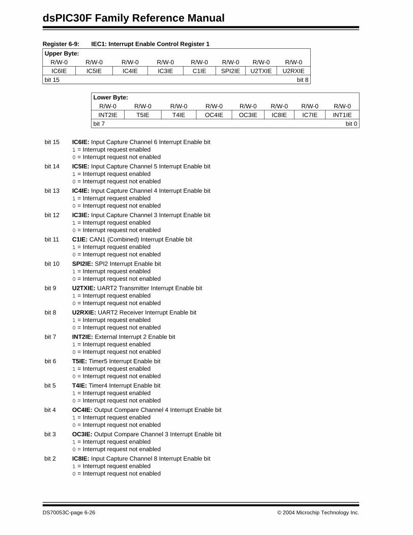
dsPIC30F Family Reference Manual
Register 6-9: IEC1: Interrupt Enable Control Register 1
Upper Byte:R/W-0 R/W-0 R/W-0 R/W-0 R/W-0 R/W-0 R/W-0 R/W-0IC6IE IC5IE IC4IE IC3IE C1IE SPI2IE U2TXIE U2RXIE
bit 15 bit 8
Lower Byte:R/W-0 R/W-0 R/W-0 R/W-0 R/W-0 R/W-0 R/W-0 R/W-0INT2IE T5IE T4IE OC4IE OC3IE IC8IE IC7IE INT1IE
bit 7 bit 0
bit 15 IC6IE: Input Capture Channel 6 Interrupt Enable bit1 = Interrupt request enabled0 = Interrupt request not enabled
bit 14 IC5IE: Input Capture Channel 5 Interrupt Enable bit1 = Interrupt request enabled0 = Interrupt request not enabled
bit 13 IC4IE: Input Capture Channel 4 Interrupt Enable bit1 = Interrupt request enabled0 = Interrupt request not enabled
bit 12 IC3IE: Input Capture Channel 3 Interrupt Enable bit1 = Interrupt request enabled0 = Interrupt request not enabled
bit 11 C1IE: CAN1 (Combined) Interrupt Enable bit1 = Interrupt request enabled0 = Interrupt request not enabled
bit 10 SPI2IE: SPI2 Interrupt Enable bit1 = Interrupt request enabled0 = Interrupt request not enabled
bit 9 U2TXIE: UART2 Transmitter Interrupt Enable bit1 = Interrupt request enabled0 = Interrupt request not enabled
bit 8 U2RXIE: UART2 Receiver Interrupt Enable bit1 = Interrupt request enabled0 = Interrupt request not enabled
bit 7 INT2IE: External Interrupt 2 Enable bit1 = Interrupt request enabled0 = Interrupt request not enabled
bit 6 T5IE: Timer5 Interrupt Enable bit1 = Interrupt request enabled0 = Interrupt request not enabled
bit 5 T4IE: Timer4 Interrupt Enable bit1 = Interrupt request enabled0 = Interrupt request not enabled
bit 4 OC4IE: Output Compare Channel 4 Interrupt Enable bit1 = Interrupt request enabled0 = Interrupt request not enabled
bit 3 OC3IE: Output Compare Channel 3 Interrupt Enable bit1 = Interrupt request enabled0 = Interrupt request not enabled
bit 2 IC8IE: Input Capture Channel 8 Interrupt Enable bit1 = Interrupt request enabled0 = Interrupt request not enabled
DS70053C-page 6-26 © 2004 Microchip Technology Inc.
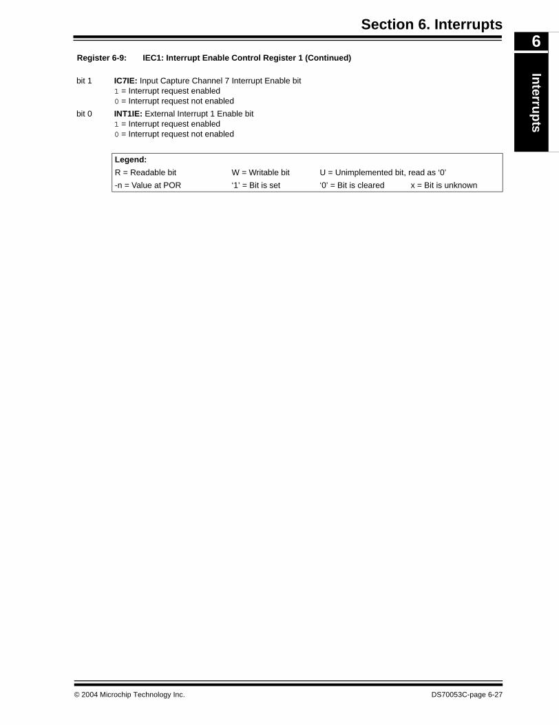
Section 6. InterruptsIn
terrup
ts
6
Register 6-9: IEC1: Interrupt Enable Control Register 1 (Continued)bit 1 IC7IE: Input Capture Channel 7 Interrupt Enable bit1 = Interrupt request enabled0 = Interrupt request not enabled
bit 0 INT1IE: External Interrupt 1 Enable bit1 = Interrupt request enabled0 = Interrupt request not enabled
Legend:
R = Readable bit W = Writable bit U = Unimplemented bit, read as ‘0’
-n = Value at POR ‘1’ = Bit is set ‘0’ = Bit is cleared x = Bit is unknown
© 2004 Microchip Technology Inc. DS70053C-page 6-27

dsPIC30F Family Reference Manual
Register 6-10: IEC2: Interrupt Enable Control Register 2
Upper Byte:U-0 U-0 U-0 R/W-0 R/W-0 R/W-0 R/W-0 R/W-0— — — FLTBIE FLTAIE LVDIE DCIIE QEIIE
bit 15 bit 8
Lower Byte:R/W-0 R/W-0 R/W-0 R/W-0 R/W-0 R/W-0 R/W-0 R/W-0
PWMIE C2IE INT4IE INT3IE OC8IE OC7IE OC6IE OC5IEbit 7 bit 0
bit 15-13 Unimplemented: Read as ‘0’
bit 12 FLTBIE: Fault B Input Interrupt Enable bit1 = Interrupt request enabled0 = Interrupt request not enabled
bit 11 FLTAIE: Fault A Interrupt Enable bit1 = Interrupt request enabled0 = Interrupt request not enabled
bit 10 LVDIE: Programmable Low Voltage Detect Interrupt Enable bit1 = Interrupt request enabled0 = Interrupt request not enabled
bit 9 DCIIE: Data Converter Interface Interrupt Enable bit1 = Interrupt request enabled0 = Interrupt request not enabled
bit 8 QEIIE: Quadrature Encoder Interface Interrupt Enable bit1 = Interrupt request enabled0 = Interrupt request not enabled
bit 7 PWMIE: Motor Control Pulse Width Modulation Interrupt Enable bit1 = Interrupt request enabled0 = Interrupt request not enabled
bit 6 C2IE: CAN2 (Combined) Interrupt Enable bit1 = Interrupt request enabled0 = Interrupt request not enabled
bit 5 INT4IE: External Interrupt 4 Enable bit1 = Interrupt request enabled0 = Interrupt request not enabled
bit 4 INT3IE: External Interrupt 3 Enable bit1 = Interrupt request enabled0 = Interrupt request not enabled
bit 3 OC8IE: Output Compare Channel 8 Interrupt Enable bit1 = Interrupt request enabled0 = Interrupt request not enabled
bit 2 OC7IE: Output Compare Channel 7 Interrupt Enable bit1 = Interrupt request enabled0 = Interrupt request not enabled
DS70053C-page 6-28 © 2004 Microchip Technology Inc.

Section 6. InterruptsIn
terrup
ts
6
Register 6-10: IEC2: Interrupt Enable Control Register 2 (Continued)bit 1 OC6IE: Output Compare Channel 6 Interrupt Enable bit1 = Interrupt request enabled0 = Interrupt request not enabled
bit 0 OC5IE: Output Compare Channel 5 Interrupt Enable bit1 = Interrupt request enabled0 = Interrupt request not enabled
Legend:
R = Readable bit W = Writable bit U = Unimplemented bit, read as ‘0’
-n = Value at POR ‘1’ = Bit is set ‘0’ = Bit is cleared x = Bit is unknown
© 2004 Microchip Technology Inc. DS70053C-page 6-29
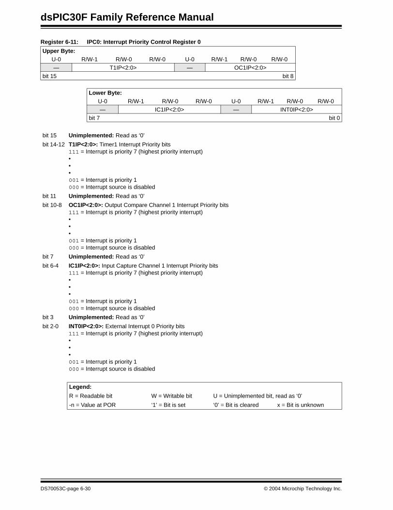
dsPIC30F Family Reference Manual
Register 6-11: IPC0: Interrupt Priority Control Register 0
Upper Byte:U-0 R/W-1 R/W-0 R/W-0 U-0 R/W-1 R/W-0 R/W-0— T1IP<2:0> — OC1IP<2:0>
bit 15 bit 8
Lower Byte:U-0 R/W-1 R/W-0 R/W-0 U-0 R/W-1 R/W-0 R/W-0— IC1IP<2:0> — INT0IP<2:0>
bit 7 bit 0
bit 15 Unimplemented: Read as ‘0’
bit 14-12 T1IP<2:0>: Timer1 Interrupt Priority bits111 = Interrupt is priority 7 (highest priority interrupt)•••001 = Interrupt is priority 1000 = Interrupt source is disabled
bit 11 Unimplemented: Read as ‘0’
bit 10-8 OC1IP<2:0>: Output Compare Channel 1 Interrupt Priority bits111 = Interrupt is priority 7 (highest priority interrupt)•••001 = Interrupt is priority 1000 = Interrupt source is disabled
bit 7 Unimplemented: Read as ‘0’
bit 6-4 IC1IP<2:0>: Input Capture Channel 1 Interrupt Priority bits111 = Interrupt is priority 7 (highest priority interrupt)•••001 = Interrupt is priority 1000 = Interrupt source is disabled
bit 3 Unimplemented: Read as ‘0’
bit 2-0 INT0IP<2:0>: External Interrupt 0 Priority bits111 = Interrupt is priority 7 (highest priority interrupt)•••001 = Interrupt is priority 1000 = Interrupt source is disabled
Legend:
R = Readable bit W = Writable bit U = Unimplemented bit, read as ‘0’
-n = Value at POR ‘1’ = Bit is set ‘0’ = Bit is cleared x = Bit is unknown
DS70053C-page 6-30 © 2004 Microchip Technology Inc.

Section 6. InterruptsIn
terrup
ts
6
Register 6-12: IPC1: Interrupt Priority Control Register 1Upper Byte:U-0 R/W-1 R/W-0 R/W-0 U-0 R/W-1 R/W-0 R/W-0— T3IP<2:0> — T2IP<2:0>
bit 15 bit 8
Lower Byte:U-0 R/W-1 R/W-0 R/W-0 U-0 R/W-1 R/W-0 R/W-0— OC2IP<2:0> — IC2IP<2:0>
bit 7 bit 0
bit 15 Unimplemented: Read as ‘0’
bit 14-12 T3IP<2:0>: Timer3 Interrupt Priority bits111 = Interrupt is priority 7 (highest priority interrupt)•••001 = Interrupt is priority 1000 = Interrupt source is disabled
bit 11 Unimplemented: Read as ‘0’
bit 10-8 T2IP<2:0>: Timer2 Interrupt Priority bits111 = Interrupt is priority 7 (highest priority interrupt)•••001 = Interrupt is priority 1000 = Interrupt source is disabled
bit 7 Unimplemented: Read as ‘0’
bit 6-4 OC2IP<2:0>: Output Compare Channel 2 Interrupt Priority bits111 = Interrupt is priority 7 (highest priority interrupt)•••001 = Interrupt is priority 1000 = Interrupt source is disabled
bit 3 Unimplemented: Read as ‘0’
bit 2-0 IC2IP<2:0>: Input Capture Channel 2 Interrupt Priority bits111 = Interrupt is priority 7 (highest priority interrupt)•••001 = Interrupt is priority 1000 = Interrupt source is disabled
Legend:
R = Readable bit W = Writable bit U = Unimplemented bit, read as ‘0’
-n = Value at POR ‘1’ = Bit is set ‘0’ = Bit is cleared x = Bit is unknown
© 2004 Microchip Technology Inc. DS70053C-page 6-31

dsPIC30F Family Reference Manual
Register 6-13: IPC2: Interrupt Priority Control Register 2
Upper Byte:U-0 R/W-1 R/W-0 R/W-0 U-0 R/W-1 R/W-0 R/W-0— ADIP<2:0> — U1TXIP<2:0>
bit 15 bit 8
Lower Byte:U-0 R/W-1 R/W-0 R/W-0 U-0 R/W-1 R/W-0 R/W-0— U1RXIP<2:0> — SPI1IP<2:0>
bit 7 bit 0
bit 15 Unimplemented: Read as ‘0’
bit 14-12 ADIP<2:0>: A/D Conversion Complete Interrupt Priority bits111 = Interrupt is priority 7 (highest priority interrupt)•••001 = Interrupt is priority 1000 = Interrupt source is disabled
bit 11 Unimplemented: Read as ‘0’
bit 10-8 U1TXIP<0>: UART1 Transmitter Interrupt Priority bits111 = Interrupt is priority 7 (highest priority interrupt)•••001 = Interrupt is priority 1000 = Interrupt source is disabled
bit 7 Unimplemented: Read as ‘0’
bit 6-4 U1RXIP<2:0>: UART1 Receiver Interrupt Priority bits111 = Interrupt is priority 7 (highest priority interrupt)•••001 = Interrupt is priority 1000 = Interrupt source is disabled
bit 3 Unimplemented: Read as ‘0’
bit 2-0 SPI1IP<2:0>: SPI1 Interrupt Priority bits111 = Interrupt is priority 7 (highest priority interrupt)•••001 = Interrupt is priority 1000 = Interrupt source is disabled
Legend:
R = Readable bit W = Writable bit U = Unimplemented bit, read as ‘0’
-n = Value at POR ‘1’ = Bit is set ‘0’ = Bit is cleared x = Bit is unknown
DS70053C-page 6-32 © 2004 Microchip Technology Inc.

Section 6. InterruptsIn
terrup
ts
6
Register 6-14: IPC3: Interrupt Priority Control Register 3Upper Byte:U-0 R/W-1 R/W-0 R/W-0 U-0 R/W-1 R/W-0 R/W-0— CNIP<2:0> — MI2CIP<2:0>
bit 15 bit 8
Lower Byte:U-0 R/W-1 R/W-0 R/W-0 U-0 R/W-1 R/W-0 R/W-0— SI2CIP<2:0> — NVMIP<2:0>
bit 7 bit 0
bit 15 Unimplemented: Read as ‘0’
bit 14-12 CNIP<2:0>: Input Change Notification Interrupt Priority bits111 = Interrupt is priority 7 (highest priority interrupt)•••001 = Interrupt is priority 1000 = Interrupt source is disabled
bit 11 Unimplemented: Read as ‘0’
bit 10-8 MI2CIP<2:0>: I2C Bus Collision Interrupt Priority bits111 = Interrupt is priority 7 (highest priority interrupt)•••001 = Interrupt is priority 1000 = Interrupt source is disabled
bit 7 Unimplemented: Read as ‘0’
bit 6-4 SI2CIP<2:0>: I2C Transfer Complete Interrupt Priority bits111 = Interrupt is priority 7 (highest priority interrupt)•••001 = Interrupt is priority 1000 = Interrupt source is disabled
bit 3 Unimplemented: Read as ‘0’
bit 2-0 NVMIP<2:0>: Non-Volatile Memory Write Interrupt Priority bits111 = Interrupt is priority 7 (highest priority interrupt)•••001 = Interrupt is priority 1000 = Interrupt source is disabled
Legend:
R = Readable bit W = Writable bit U = Unimplemented bit, read as ‘0’
-n = Value at POR ‘1’ = Bit is set ‘0’ = Bit is cleared x = Bit is unknown
© 2004 Microchip Technology Inc. DS70053C-page 6-33
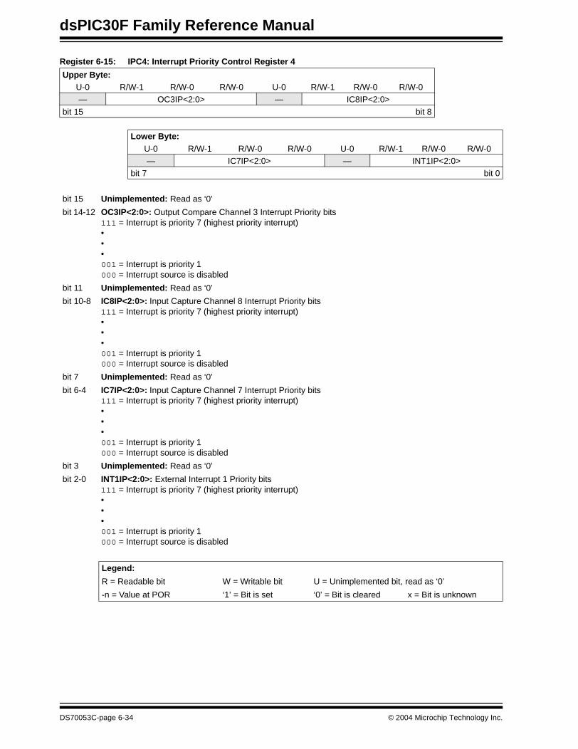
dsPIC30F Family Reference Manual
Register 6-15: IPC4: Interrupt Priority Control Register 4
Upper Byte:U-0 R/W-1 R/W-0 R/W-0 U-0 R/W-1 R/W-0 R/W-0— OC3IP<2:0> — IC8IP<2:0>
bit 15 bit 8
Lower Byte:U-0 R/W-1 R/W-0 R/W-0 U-0 R/W-1 R/W-0 R/W-0— IC7IP<2:0> — INT1IP<2:0>
bit 7 bit 0
bit 15 Unimplemented: Read as ‘0’
bit 14-12 OC3IP<2:0>: Output Compare Channel 3 Interrupt Priority bits111 = Interrupt is priority 7 (highest priority interrupt)•••001 = Interrupt is priority 1000 = Interrupt source is disabled
bit 11 Unimplemented: Read as ‘0’
bit 10-8 IC8IP<2:0>: Input Capture Channel 8 Interrupt Priority bits111 = Interrupt is priority 7 (highest priority interrupt)•••001 = Interrupt is priority 1000 = Interrupt source is disabled
bit 7 Unimplemented: Read as ‘0’
bit 6-4 IC7IP<2:0>: Input Capture Channel 7 Interrupt Priority bits111 = Interrupt is priority 7 (highest priority interrupt)•••001 = Interrupt is priority 1000 = Interrupt source is disabled
bit 3 Unimplemented: Read as ‘0’
bit 2-0 INT1IP<2:0>: External Interrupt 1 Priority bits111 = Interrupt is priority 7 (highest priority interrupt)•••001 = Interrupt is priority 1000 = Interrupt source is disabled
Legend:
R = Readable bit W = Writable bit U = Unimplemented bit, read as ‘0’
-n = Value at POR ‘1’ = Bit is set ‘0’ = Bit is cleared x = Bit is unknown
DS70053C-page 6-34 © 2004 Microchip Technology Inc.

Section 6. InterruptsIn
terrup
ts
6
Register 6-16: IPC5: Interrupt Priority Control Register 5Upper Byte:U-0 R/W-1 R/W-0 R/W-0 U-0 R/W-1 R/W-0 R/W-0— INT2IP<2:0> — T5IP<2:0>
bit 15 bit 8
Lower Byte:U-0 R/W-1 R/W-0 R/W-0 U-0 R/W-1 R/W-0 R/W-0— T4IP<2:0> — OC4IP<2:0>
bit 7 bit 0
bit 15 Unimplemented: Read as ‘0’
bit 14-12 INT2IP<2:0>: External Interrupt 2 Priority bits111 = Interrupt is priority 7 (highest priority interrupt)•••001 = Interrupt is priority 1000 = Interrupt source is disabled
bit 11 Unimplemented: Read as ‘0’
bit 10-8 T5IP<2:0>: Timer5 Interrupt Priority bits111 = Interrupt is priority 7 (highest priority interrupt)•••001 = Interrupt is priority 1000 = Interrupt source is disabled
bit 7 Unimplemented: Read as ‘0’
bit 6-4 T4IP<2:0>: Timer4 Interrupt Priority bits111 = Interrupt is priority 7 (highest priority interrupt)•••001 = Interrupt is priority 1000 = Interrupt source is disabled
bit 3 Unimplemented: Read as ‘0’
bit 2-0 OC4IP<2:0>: Output Compare Channel 4 Interrupt Priority bits111 = Interrupt is priority 7 (highest priority interrupt)•••001 = Interrupt is priority 1000 = Interrupt source is disabled
Legend:
R = Readable bit W = Writable bit U = Unimplemented bit, read as ‘0’
-n = Value at POR ‘1’ = Bit is set ‘0’ = Bit is cleared x = Bit is unknown
© 2004 Microchip Technology Inc. DS70053C-page 6-35

dsPIC30F Family Reference Manual
Register 6-17: IPC6: Interrupt Priority Control Register 6
Upper Byte:U-0 R/W-1 R/W-0 R/W-0 U-0 R/W-1 R/W-0 R/W-0— C1IP<2:0> — SPI2IP<2:0>
bit 15 bit 8
Lower Byte:U-0 R/W-1 R/W-0 R/W-0 U-0 R/W-1 R/W-0 R/W-0— U2TXIP<2:0> — U2RXIP<2:0>
bit 7 bit 0
bit 15 Unimplemented: Read as ‘0’
bit 14-12 C1IP<2:0>: CAN1 (Combined) Interrupt Priority bits111 = Interrupt is priority 7 (highest priority interrupt)•••001 = Interrupt is priority 1000 = Interrupt source is disabled
bit 11 Unimplemented: Read as ‘0’
bit 10-8 SPI2IP<2:0>: SPI2 Interrupt Priority bits111 = Interrupt is priority 7 (highest priority interrupt)•••001 = Interrupt is priority 1000 = Interrupt source is disabled
bit 7 Unimplemented: Read as ‘0’
bit 6-4 U2TXIP<2:0>: UART2 Transmitter Interrupt Priority bits111 = Interrupt is priority 7 (highest priority interrupt)•••001 = Interrupt is priority 1000 = Interrupt source is disabled
bit 3 Unimplemented: Read as ‘0’
bit 2-0 U2RXIP<2:0>: UART2 Receiver Interrupt Priority bits111 = Interrupt is priority 7 (highest priority interrupt)•••001 = Interrupt is priority 1000 = Interrupt source is disabled
Legend:
R = Readable bit W = Writable bit U = Unimplemented bit, read as ‘0’
-n = Value at POR ‘1’ = Bit is set ‘0’ = Bit is cleared x = Bit is unknown
DS70053C-page 6-36 © 2004 Microchip Technology Inc.
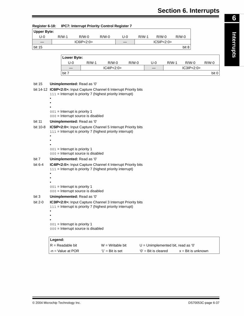
Section 6. InterruptsIn
terrup
ts
6
Register 6-18: IPC7: Interrupt Priority Control Register 7Upper Byte:U-0 R/W-1 R/W-0 R/W-0 U-0 R/W-1 R/W-0 R/W-0— IC6IP<2:0> — IC5IP<2:0>
bit 15 bit 8
Lower Byte:U-0 R/W-1 R/W-0 R/W-0 U-0 R/W-1 R/W-0 R/W-0— IC4IP<2:0> — IC3IP<2:0>
bit 7 bit 0
bit 15 Unimplemented: Read as ‘0’
bit 14-12 IC6IP<2:0>: Input Capture Channel 6 Interrupt Priority bits111 = Interrupt is priority 7 (highest priority interrupt)•••001 = Interrupt is priority 1000 = Interrupt source is disabled
bit 11 Unimplemented: Read as ‘0’
bit 10-8 IC5IP<2:0>: Input Capture Channel 5 Interrupt Priority bits111 = Interrupt is priority 7 (highest priority interrupt)•••001 = Interrupt is priority 1000 = Interrupt source is disabled
bit 7 Unimplemented: Read as ‘0’
bit 6-4 IC4IP<2:0>: Input Capture Channel 4 Interrupt Priority bits111 = Interrupt is priority 7 (highest priority interrupt)•••001 = Interrupt is priority 1000 = Interrupt source is disabled
bit 3 Unimplemented: Read as ‘0’
bit 2-0 IC3IP<2:0>: Input Capture Channel 3 Interrupt Priority bits111 = Interrupt is priority 7 (highest priority interrupt)•••001 = Interrupt is priority 1000 = Interrupt source is disabled
Legend:
R = Readable bit W = Writable bit U = Unimplemented bit, read as ‘0’
-n = Value at POR ‘1’ = Bit is set ‘0’ = Bit is cleared x = Bit is unknown
© 2004 Microchip Technology Inc. DS70053C-page 6-37
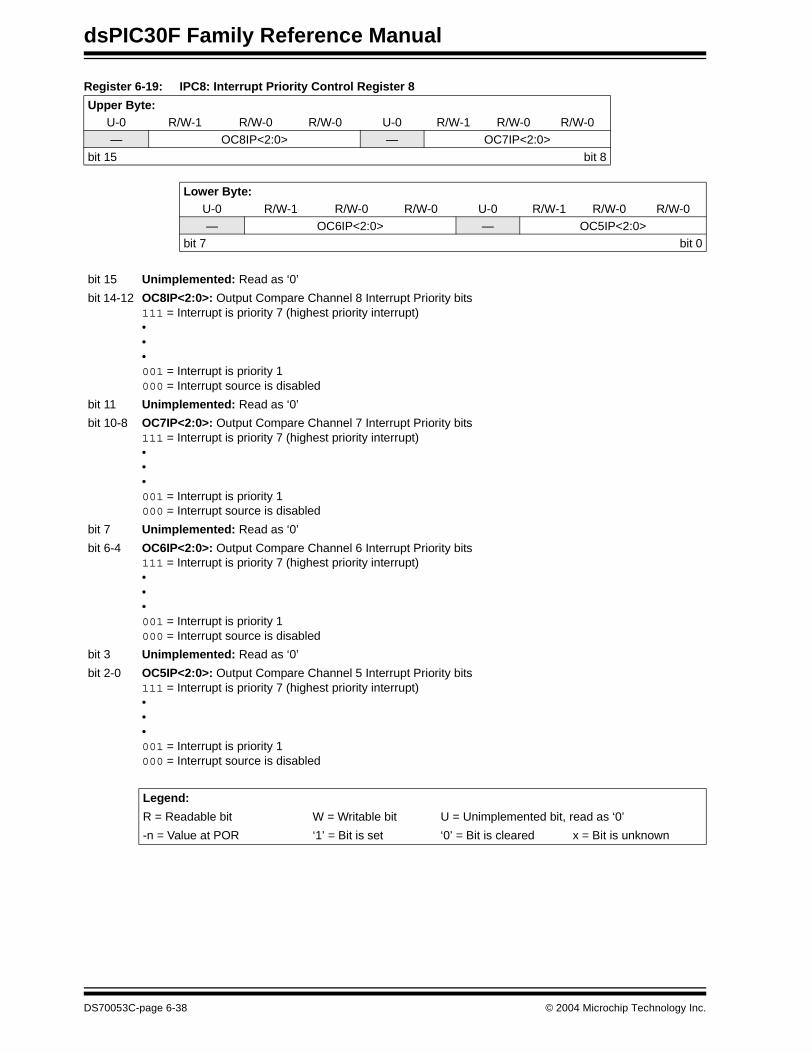
dsPIC30F Family Reference Manual
Register 6-19: IPC8: Interrupt Priority Control Register 8
Upper Byte:U-0 R/W-1 R/W-0 R/W-0 U-0 R/W-1 R/W-0 R/W-0— OC8IP<2:0> — OC7IP<2:0>
bit 15 bit 8
Lower Byte:U-0 R/W-1 R/W-0 R/W-0 U-0 R/W-1 R/W-0 R/W-0— OC6IP<2:0> — OC5IP<2:0>
bit 7 bit 0
bit 15 Unimplemented: Read as ‘0’
bit 14-12 OC8IP<2:0>: Output Compare Channel 8 Interrupt Priority bits111 = Interrupt is priority 7 (highest priority interrupt)•••001 = Interrupt is priority 1000 = Interrupt source is disabled
bit 11 Unimplemented: Read as ‘0’
bit 10-8 OC7IP<2:0>: Output Compare Channel 7 Interrupt Priority bits111 = Interrupt is priority 7 (highest priority interrupt)•••001 = Interrupt is priority 1000 = Interrupt source is disabled
bit 7 Unimplemented: Read as ‘0’
bit 6-4 OC6IP<2:0>: Output Compare Channel 6 Interrupt Priority bits111 = Interrupt is priority 7 (highest priority interrupt)•••001 = Interrupt is priority 1000 = Interrupt source is disabled
bit 3 Unimplemented: Read as ‘0’
bit 2-0 OC5IP<2:0>: Output Compare Channel 5 Interrupt Priority bits111 = Interrupt is priority 7 (highest priority interrupt)•••001 = Interrupt is priority 1000 = Interrupt source is disabled
Legend:
R = Readable bit W = Writable bit U = Unimplemented bit, read as ‘0’
-n = Value at POR ‘1’ = Bit is set ‘0’ = Bit is cleared x = Bit is unknown
DS70053C-page 6-38 © 2004 Microchip Technology Inc.

Section 6. InterruptsIn
terrup
ts
6
Register 6-20: IPC9: Interrupt Priority Control Register 9Upper Byte:U-0 R/W-1 R/W-0 R/W-0 U-0 R/W-1 R/W-0 R/W-0— PWMIP<2:0> — C2IP<2:0>
bit 15 bit 8
Lower Byte:U-0 R/W-1 R/W-0 R/W-0 U-0 R/W-1 R/W-0 R/W-0— INT4IP<2:0> — INT3IP<2:0>
bit 7 bit 0
bit 15 Unimplemented: Read as ‘0’
bit 14-12 PWMIP<2:0>: Motor Control Pulse Width Modulation Interrupt Priority bits111 = Interrupt is priority 7 (highest priority interrupt)•••001 = Interrupt is priority 1000 = Interrupt source is disabled
bit 11 Unimplemented: Read as ‘0’
bit 10-8 C2IP<2:0>: CAN2 (Combined) Interrupt Priority bits111 = Interrupt is priority 7 (highest priority interrupt)•••001 = Interrupt is priority 1000 = Interrupt source is disabled
bit 7 Unimplemented: Read as ‘0’
bit 6-4 INT4IP<2:0>: External Interrupt 4 Priority bits111 = Interrupt is priority 7 (highest priority interrupt)•••001 = Interrupt is priority 1000 = Interrupt source is disabled
bit 3 Unimplemented: Read as ‘0’
bit 2-0 INT3IP<2:0>: External Interrupt 3 Priority bits111 = Interrupt is priority 7 (highest priority interrupt)•••001 = Interrupt is priority 1000 = Interrupt source is disabled
Legend:
R = Readable bit W = Writable bit U = Unimplemented bit, read as ‘0’
-n = Value at POR ‘1’ = Bit is set ‘0’ = Bit is cleared x = Bit is unknown
© 2004 Microchip Technology Inc. DS70053C-page 6-39
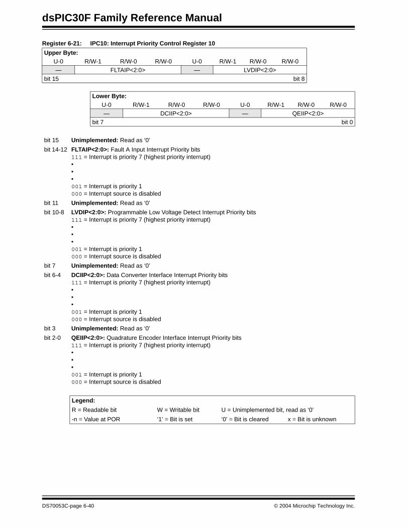
dsPIC30F Family Reference Manual
Register 6-21: IPC10: Interrupt Priority Control Register 10
Upper Byte:U-0 R/W-1 R/W-0 R/W-0 U-0 R/W-1 R/W-0 R/W-0— FLTAIP<2:0> — LVDIP<2:0>
bit 15 bit 8
Lower Byte:U-0 R/W-1 R/W-0 R/W-0 U-0 R/W-1 R/W-0 R/W-0— DCIIP<2:0> — QEIIP<2:0>
bit 7 bit 0
bit 15 Unimplemented: Read as ‘0’
bit 14-12 FLTAIP<2:0>: Fault A Input Interrupt Priority bits111 = Interrupt is priority 7 (highest priority interrupt)•••001 = Interrupt is priority 1000 = Interrupt source is disabled
bit 11 Unimplemented: Read as ‘0’
bit 10-8 LVDIP<2:0>: Programmable Low Voltage Detect Interrupt Priority bits111 = Interrupt is priority 7 (highest priority interrupt)•••001 = Interrupt is priority 1000 = Interrupt source is disabled
bit 7 Unimplemented: Read as ‘0’
bit 6-4 DCIIP<2:0>: Data Converter Interface Interrupt Priority bits111 = Interrupt is priority 7 (highest priority interrupt)•••001 = Interrupt is priority 1000 = Interrupt source is disabled
bit 3 Unimplemented: Read as ‘0’
bit 2-0 QEIIP<2:0>: Quadrature Encoder Interface Interrupt Priority bits111 = Interrupt is priority 7 (highest priority interrupt)•••001 = Interrupt is priority 1000 = Interrupt source is disabled
Legend:
R = Readable bit W = Writable bit U = Unimplemented bit, read as ‘0’
-n = Value at POR ‘1’ = Bit is set ‘0’ = Bit is cleared x = Bit is unknown
DS70053C-page 6-40 © 2004 Microchip Technology Inc.
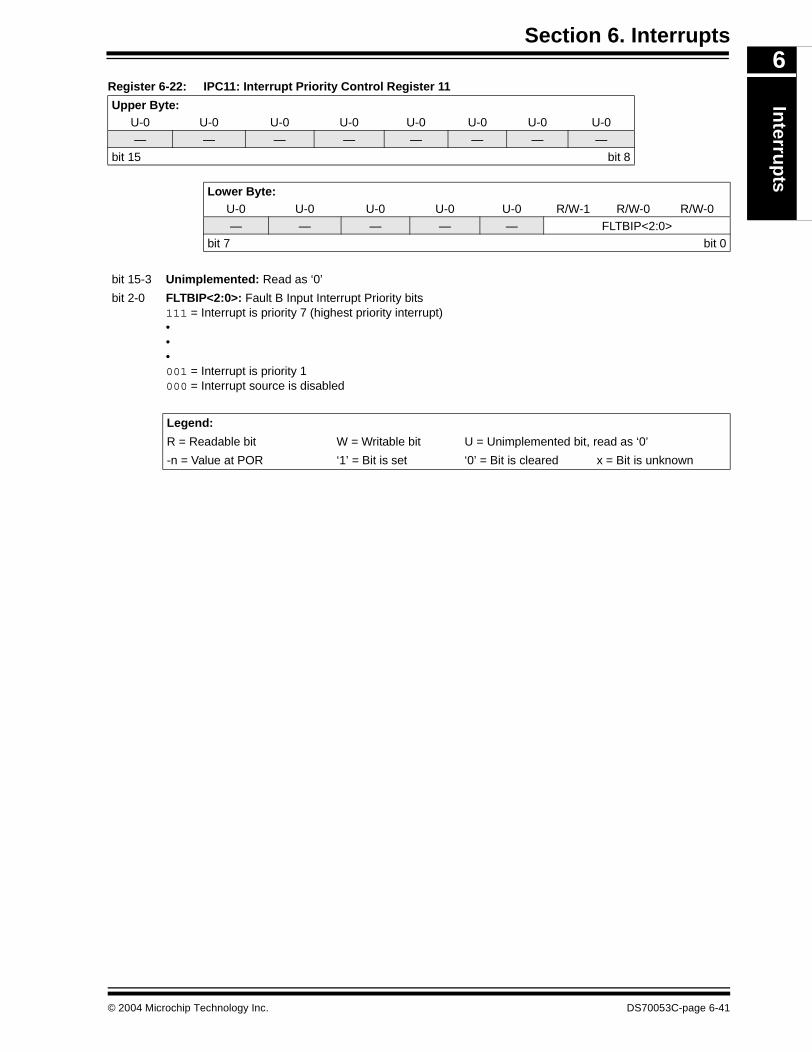
Section 6. InterruptsIn
terrup
ts
6
Register 6-22: IPC11: Interrupt Priority Control Register 11Upper Byte:U-0 U-0 U-0 U-0 U-0 U-0 U-0 U-0— — — — — — — —
bit 15 bit 8
Lower Byte:U-0 U-0 U-0 U-0 U-0 R/W-1 R/W-0 R/W-0— — — — — FLTBIP<2:0>
bit 7 bit 0
bit 15-3 Unimplemented: Read as ‘0’
bit 2-0 FLTBIP<2:0>: Fault B Input Interrupt Priority bits111 = Interrupt is priority 7 (highest priority interrupt)•••001 = Interrupt is priority 1000 = Interrupt source is disabled
Legend:
R = Readable bit W = Writable bit U = Unimplemented bit, read as ‘0’
-n = Value at POR ‘1’ = Bit is set ‘0’ = Bit is cleared x = Bit is unknown
© 2004 Microchip Technology Inc. DS70053C-page 6-41
dsPIC30F Family Reference Manual
6.5 Interrupt Setup Procedures
6.5.1 Initialization
The following steps describe how to configure a source of interrupt:
1. Set the NSTDIS Control bit (INTCON1<15>) if nested interrupts are not desired.
2. Select the user assigned priority level for the interrupt source by writing the control bits inthe appropriate IPCx Control register. The priority level will depend on the specificapplication and type of interrupt source. If multiple priority levels are not desired, the IPCxregister control bits for all enabled interrupt sources may be programmed to the samenon-zero value.
3. Clear the interrupt flag status bit associated with the peripheral in the associated IFSxStatus register.
4. Enable the interrupt source by setting the interrupt enable control bit associated with thesource in the appropriate IECx Control register.
6.5.2 Interrupt Service Routine
The method that is used to declare an ISR and initialize the IVT with the correct vector addresswill depend on the programming language (i.e., C or assembler) and the language developmenttool suite that is used to develop the application. In general, the user must clear the interrupt flagin the appropriate IFSx register for the source of interrupt that the ISR handles. Otherwise, theISR will be re-entered immediately after exiting the routine. If the ISR is coded in assemblylanguage, it must be terminated using a RETFIE instruction to unstack the saved PC value, SRLvalue, and old CPU priority level.
6.5.3 Trap Service Routine
A Trap Service Routine (TSR) is coded like an ISR, except that the appropriate trap status flagin the INTCON1 register must be cleared to avoid re-entry into the TSR.
6.5.4 Interrupt Disable
All user interrupts can be disabled using the following procedure:
1. Push the current SR value onto the software stack using the PUSH instruction.2. Force the CPU to priority level 7 by inclusive ORing the value 0xE0 with SRL.
To enable user interrupts, the POP instruction may be used to restore the previous SR value.
Note that only user interrupts with a priority level of 7 or less can be disabled. Trap sources(level 8-level 15) cannot be disabled.
The DISI instruction provides a convenient way to disable interrupts of priority levels 1-6, for afixed period of time. Level 7 interrupt sources are not disabled by the DISI instruction.
Note: At a device Reset, the IPC registers are initialized, such that all user interruptsources are assigned to priority level 4.
DS70053C-page 6-42 © 2004 Microchip Technology Inc.
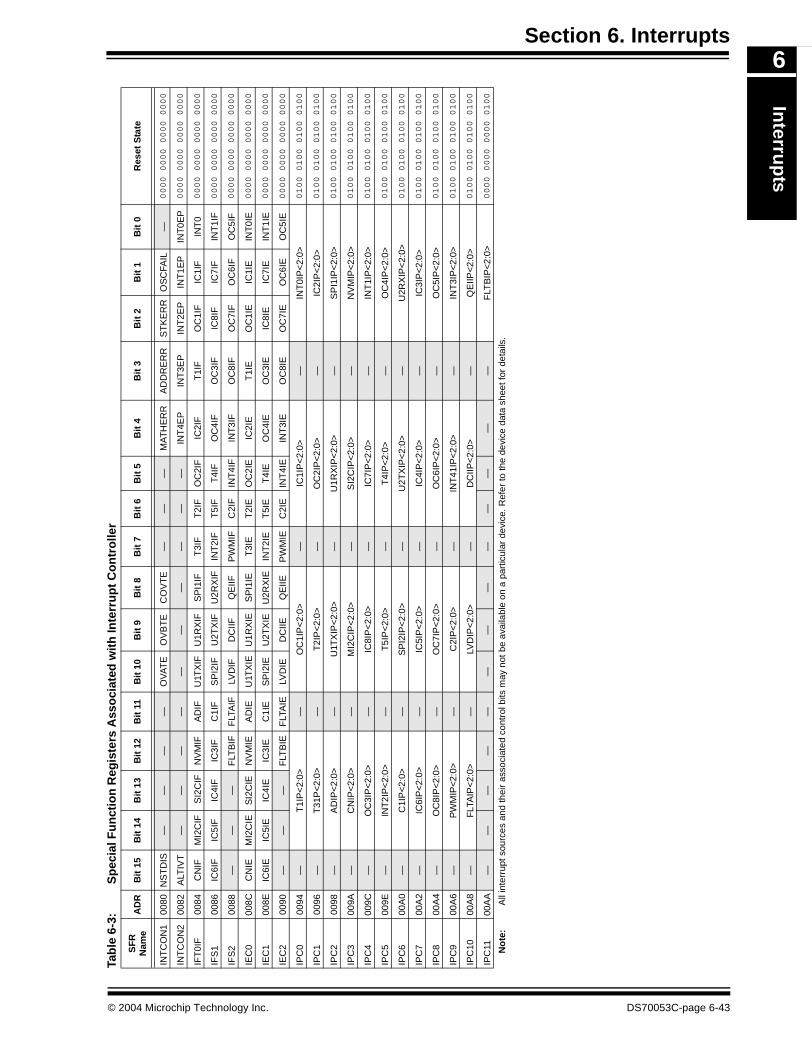
Section 6. InterruptsIn
terrup
ts
6
Tab
le 6
-3:
Sp
ecia
l Fu
nct
ion
Reg
iste
rs A
sso
ciat
ed w
ith
Inte
rru
pt
Co
ntr
olle
r
SF
R
Nam
eA
DR
Bit
15
Bit
14
Bit
13
Bit
12
Bit
11
Bit
10
Bit
9B
it 8
Bit
7B
it 6
Bit
5B
it 4
Bit
3B
it 2
Bit
1B
it 0
Res
et S
tate
INT
CO
N1
0080
NS
TD
IS—
——
—O
VA
TE
OV
BT
EC
OV
TE
——
—M
AT
HE
RR
AD
DR
ER
RS
TK
ER
RO
SC
FAIL
—0000 0000 0000 0000
INT
CO
N2
0082
ALT
IVT
——
——
——
——
——
INT
4EP
INT
3EP
INT
2EP
INT
1EP
INT
0EP
0000 0000 0000 0000
IFT
0IF
0084
CN
IFM
I2C
IF S
I2C
IFN
VM
IFA
DIF
U1T
XIF
U1R
XIF
SP
I1IF
T3I
FT
2IF
OC
2IF
IC2I
FT
1IF
OC
1IF
IC1I
FIN
T0
0000 0000 0000 0000
IFS
100
86IC
6IF
IC5I
FIC
4IF
IC3I
FC
1IF
SP
I2IF
U2T
XIF
U2R
XIF
INT
2IF
T5I
FT
4IF
OC
4IF
OC
3IF
IC8I
FIC
7IF
INT
1IF
0000 0000 0000 0000
IFS
200
88—
——
FLT
BIF
FLT
AIF
LVD
IFD
CIIF
QE
IIFP
WM
IFC
2IF
INT
4IF
INT
3IF
OC
8IF
OC
7IF
OC
6IF
OC
5IF
0000 0000 0000 0000
IEC
000
8CC
NIE
MI2
CIE
SI2
CIE
NV
MIE
AD
IEU
1TX
IEU
1RX
IES
PI1
IET
3IE
T2I
EO
C2I
EIC
2IE
T1I
EO
C1I
EIC
1IE
INT
0IE
0000 0000 0000 0000
IEC
100
8EIC
6IE
IC5I
EIC
4IE
IC3I
EC
1IE
SP
I2IE
U2T
XIE
U2R
XIE
INT
2IE
T5I
ET
4IE
OC
4IE
OC
3IE
IC8I
EIC
7IE
INT
1IE
0000 0000 0000 0000
IEC
200
90—
——
FLT
BIE
FLT
AIE
LVD
IED
CIIE
QE
IIEP
WM
IEC
2IE
INT
4IE
INT
3IE
OC
8IE
OC
7IE
OC
6IE
OC
5IE
0000 0000 0000 0000
IPC
000
94—
T1I
P<
2:0>
—O
C1I
P<
2:0>
—IC
1IP
<2:
0>—
INT
0IP
<2:
0>0100 0100 0100 0100
IPC
100
96—
T31
P<
2:0>
—T
2IP
<2:
0>—
OC
2IP
<2:
0>—
IC2I
P<
2:0>
0100 0100 0100 0100
IPC
200
98—
AD
IP<
2:0>
—U
1TX
IP<
2:0>
—U
1RX
IP<
2:0>
—S
PI1
IP<
2:0>
0100 0100 0100 0100
IPC
300
9A—
CN
IP<
2:0>
—M
I2C
IP<
2:0>
—S
I2C
IP<
2:0>
—N
VM
IP<
2:0>
0100 0100 0100 0100
IPC
400
9C—
OC
3IP
<2:
0>—
IC8I
P<
2:0>
—IC
7IP
<2:
0>—
INT
1IP
<2:
0>0100 0100 0100 0100
IPC
500
9E—
INT
2IP
<2:
0>—
T5I
P<
2:0>
—T
4IP
<2:
0>—
OC
4IP
<2:
0>0100 0100 0100 0100
IPC
600
A0
—C
1IP
<2:
0>—
SP
I2IP
<2:
0>—
U2T
XIP
<2:
0>—
U2R
XIP
<2:
0>0100 0100 0100 0100
IPC
700
A2
—IC
6IP
<2:
0>—
IC5I
P<
2:0>
—IC
4IP
<2:
0>—
IC3I
P<
2:0>
0100 0100 0100 0100
IPC
800
A4
—O
C8I
P<
2:0>
—O
C7I
P<
2:0>
—O
C6I
P<
2:0>
—O
C5I
P<
2:0>
0100 0100 0100 0100
IPC
900
A6
—P
WM
IP<
2:0>
—C
2IP
<2:
0>—
INT
41IP
<2:
0>—
INT
3IP
<2:
0>0100 0100 0100 0100
IPC
1000
A8
—F
LTA
IP<
2:0>
—LV
DIP
<2:
0>—
DC
IIP<
2:0>
—Q
EIIP
<2:
0>0100 0100 0100 0100
IPC
1100
AA
——
——
——
——
——
——
—F
LTB
IP<
2:0>
0000 0000 0000 0100
No
te:
All
inte
rrup
t sou
rces
and
thei
r as
soci
ated
con
trol
bits
may
not
be
avai
labl
e on
a p
artic
ular
dev
ice.
Ref
er to
the
devi
ce d
ata
shee
t for
det
ails
.
© 2004 Microchip Technology Inc. DS70053C-page 6-43
dsPIC30F Family Reference Manual
6.6 Design Tips
Question 1: What happens when two sources of interrupt become pending at the sametime and have the same user assigned priority level?
Answer: The interrupt source with the highest natural order priority will take precedence. Thenatural order priority is determined by the Interrupt Vector Table (IVT) address for that source.Interrupt sources with a smaller IVT address have a higher natural order priority.
Question 2: Can the DISI instruction be used to disable all sources of interrupt andtraps?
Answer: The DISI instruction does not disable traps or priority level 7 interrupt sources.However, the DISI instruction can be used as a convenient way to disable all interrupt sourcesif no priority level 7 interrupt sources are enabled in the user’s application.
DS70053C-page 6-44 © 2004 Microchip Technology Inc.

Section 6. InterruptsIn
terrup
ts
6
6.7 Related Application NotesThis section lists application notes that are related to this section of the manual. Theseapplication notes may not be written specifically for the dsPIC30F Product Family, but theconcepts are pertinent and could be used with modification and possible limitations. The currentapplication notes related to the Interrupts module are:
Title Application Note #
No related application notes at this time.
Note: Please visit the Microchip web site (www.microchip.com) for additional ApplicationNotes and code examples for the dsPIC30F Family of devices.
© 2004 Microchip Technology Inc. DS70053C-page 6-45
dsPIC30F Family Reference Manual
6.8 Revision History
Revision A
This is the initial released revision of this document.
Revision B
This revision incorporates additional technical content for the dsPIC30F Interrupts module.
Revision C
This revision incorporates all known errata at the time of this document update.
DS70053C-page 6-46 © 2004 Microchip Technology Inc.
Section 7. Oscillator
Oscillato
r
7
HIGHLIGHTSThis section of the manual contains the following topics:
7.1 Introduction .................................................................................................................... 7-2
7.2 Device Clocking and MIPS ............................................................................................ 7-57.3 Oscillator Configuration.................................................................................................. 7-67.4 Oscillator Control Registers – OSCCON and OSCTUN .............................................. 7-13
7.5 Primary Oscillator......................................................................................................... 7-207.6 Crystal Oscillators/Ceramic Resonators ...................................................................... 7-227.7 Determining Best Values for Crystals, Clock Mode, C1, C2 and Rs ............................ 7-24
7.8 External Clock Input..................................................................................................... 7-257.9 External RC Oscillator.................................................................................................. 7-267.10 Phase Locked Loop (PLL) ........................................................................................... 7-30
7.11 Low-Power 32 kHz Crystal Oscillator........................................................................... 7-317.12 Oscillator Start-up Timer (OST).................................................................................... 7-317.13 Internal Fast RC Oscillator (FRC) ................................................................................ 7-31
7.14 Internal Low-Power RC (LPRC) Oscillator................................................................... 7-327.15 Fail-Safe Clock Monitor (FSCM) .................................................................................. 7-327.16 Programmable Oscillator Postscaler............................................................................ 7-33
7.17 Clock Switching Operation........................................................................................... 7-347.18 Design Tips .................................................................................................................. 7-387.19 Related Application Notes............................................................................................ 7-39
7.20 Revision History ........................................................................................................... 7-40
© 2005 Microchip Technology Inc. DS70054D-page 7-1
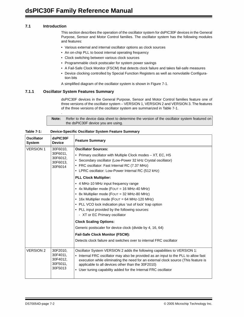
dsPIC30F Family Reference Manual
7.1 Introduction
This section describes the operation of the oscillator system for dsPIC30F devices in the GeneralPurpose, Sensor and Motor Control families. The oscillator system has the following modulesand features:
• Various external and internal oscillator options as clock sources• An on-chip PLL to boost internal operating frequency • Clock switching between various clock sources
• Programmable clock postscaler for system power savings • A Fail-Safe Clock Monitor (FSCM) that detects clock failure and takes fail-safe measures• Device clocking controlled by Special Function Registers as well as nonvolatile Configura-
tion bits
A simplified diagram of the oscillator system is shown in Figure 7-1.
7.1.1 Oscillator System Features Summary
dsPIC30F devices in the General Purpose, Sensor and Motor Control families feature one ofthree versions of the oscillator system – VERSION 1, VERSION 2 and VERSION 3. The featuresof the three versions of the oscillator system are summarized in Table 7-1..
Note: Refer to the device data sheet to determine the version of the oscillator system featured onthe dsPIC30F device you are using.
Table 7-1: Device-Specific Oscillator System Feature Summary
Oscillator System
dsPIC30F Device
Feature Summary
VERSION 1 30F6010,30F6011,30F6012,30F6013,30F6014
Oscillator Sources:
• Primary oscillator with Multiple Clock modes – XT, EC, HS
• Secondary oscillator (Low-Power 32 kHz Crystal oscillator) • FRC oscillator: Fast Internal RC (7.37 MHz)• LPRC oscillator: Low-Power Internal RC (512 kHz)
PLL Clock Multiplier:
• 4 MHz-10 MHz input frequency range• 4x Multiplier mode (FOUT = 16 MHz-40 MHz)
• 8x Multiplier mode (FOUT = 32 MHz-80 MHz)• 16x Multiplier mode (FOUT = 64 MHz-120 MHz)• PLL VCO lock indication plus ‘out of lock’ trap option
• PLL input provided by the following sources:- XT or EC Primary oscillator
Clock Scaling Options:
Generic postscaler for device clock (divide by 4, 16, 64)
Fail-Safe Clock Monitor (FSCM):
Detects clock failure and switches over to internal FRC oscillator
VERSION 2 30F2010, 30F4011, 30F4012, 30F5011, 30F5013
Oscillator System VERSION 2 adds the following capabilities to VERSION 1:• Internal FRC oscillator may also be provided as an input to the PLL to allow fast
execution while eliminating the need for an external clock source (This feature is applicable to all devices other than the 30F2010)
• User tuning capability added for the Internal FRC oscillator
DS70054D-page 7-2 © 2005 Microchip Technology Inc.

Section 7. OscillatorO
scillator
7
VERSION 3 30F2011, 30F2012, 30F3010, 30F3011, 30F3012, 30F3013, 30F3014, 30F4013, 30F5015, 30F5016, 30F6010A, 30F6011A, 30F6012A, 30F6013A, 30F6014A, 30F6015
Oscillator System VERSION 3 adds the following capabilities to VERSION 2:• HS oscillator may also be provided as an input to the PLL to allow greater
choices of crystal frequency
Table 7-1: Device-Specific Oscillator System Feature Summary
Oscillator System
dsPIC30F Device
Feature Summary
© 2005 Microchip Technology Inc. DS70054D-page 7-3
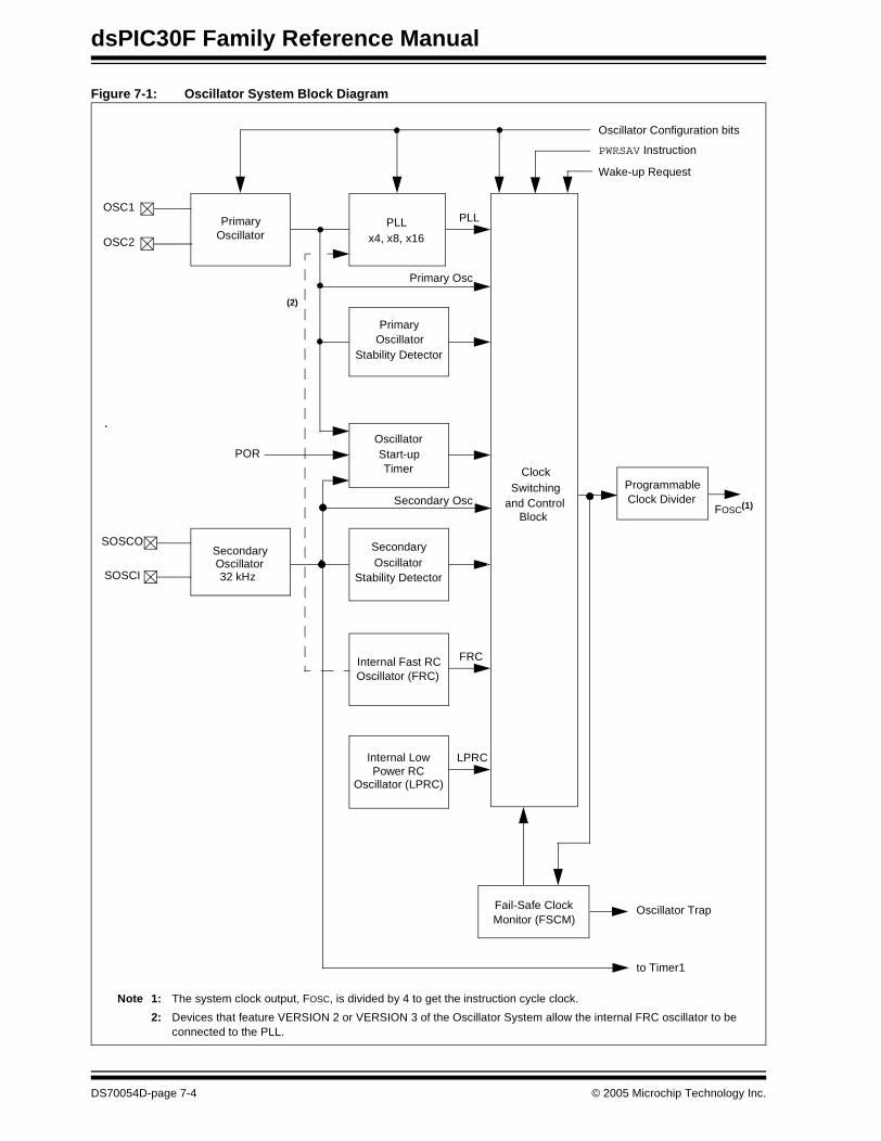
dsPIC30F Family Reference Manual
Figure 7-1: Oscillator System Block Diagram
PrimaryOSC1
OSC2
SOSCO
SOSCI
Oscillator
Secondary
Clock
and ControlBlock
Switching
x4, x8, x16 PLL
PrimaryOscillator
Stability Detector
Stability Detector
SecondaryOscillator
ProgrammableClock Divider
OscillatorStart-upTimer
Fail-Safe ClockMonitor (FSCM)
Internal Fast RCOscillator (FRC)
Internal LowPower RC
Oscillator (LPRC)
PWRSAV Instruction
Wake-up Request
Oscillator Configuration bits
Oscillator Trap
to Timer1
LPRC
FRC
Secondary Osc
POR
Primary Osc
PLL
Oscillator32 kHz
FOSC(1)
(2)
Note 1: The system clock output, FOSC, is divided by 4 to get the instruction cycle clock.
2: Devices that feature VERSION 2 or VERSION 3 of the Oscillator System allow the internal FRC oscillator to beconnected to the PLL.
DS70054D-page 7-4 © 2005 Microchip Technology Inc.

Section 7. OscillatorO
scillator
7
7.2 Device Clocking and MIPS
Referring to Figure 7-1, the system clock source can be provided by one of four sources. Thesesources are the Primary oscillator, Secondary oscillator, Internal Fast RC (FRC) oscillator or theLow-Power RC (LPRC) oscillator. The Primary oscillator source has the option of usingthe internal PLL. The frequency of the selected clock source can optionally be reduced by theprogrammable postscaler (clock divider). The output from the programmable postscalerbecomes the system clock source, FOSC.
The system clock source is divided by four to produce the internal instruction cycle clock, FCY. Inthis document, the instruction cycle clock is also denoted by FOSC/4. The timing diagram inFigure 7-2 shows the relationship between the system clock source and instruction execution.
The internal instruction cycle clock, FCY, can be provided on the OSC2 I/O pin for someOperating modes of the Primary oscillator (see Section 7.3 “Oscillator Configuration”).
Figure 7-2: Clock/Instruction Cycle Timing
Equation 7-1: MIPS and Source Oscillator Frequency Relationship
FOSC
PC
FCY
PC PC + 2 PC + 4
Fetch INST (PC)Execute INST (PC - 2) Fetch INST (PC + 2)
Execute INST (PC) Fetch INST (PC + 4)Execute INST (PC + 2)
TCY
FCY = SOURCE OSCILLATOR FREQUENCY * PLL MULTIPLIER PROGRAMMABLE POSTSCALER * 4 ( )FOSC
4=
© 2005 Microchip Technology Inc. DS70054D-page 7-5

dsPIC30F Family Reference Manual
7.3 Oscillator Configuration
The oscillator source (and Operating mode) that is used at a device Power-on Reset event isselected using nonvolatile Configuration bits. The oscillator Configuration bits are located in theFOSC Configuration register.
The FOS bits in the FOSC nonvolatile Configuration register select the oscillator source that isused at a Power-on Reset. The Primary oscillator is the default (unprogrammed) selection. TheSecondary oscillator, or one of the internal oscillators, may be chosen by programming these bitlocations.
The FPR bits in the FOSC nonvolatile Configuration register select the Operating mode of thePrimary oscillator.
dsPIC30F devices in the General Purpose, Sensor and Motor Control families may feature oneof three versions of the Oscillator system. The definition of the FOSC nonvolatile Configurationregister varies between these versions, as described in the sub-sections below.
7.3.1 Oscillator System VERSION 1 Configuration
For devices that feature the Oscillator system VERSION 1, the FOSC nonvolatile Configurationregister is shown in Register 7-1. The operating modes for the FPR bits may be selected asshown in Table 7-2.
7.3.2 Oscillator System VERSION 2 Configuration
For devices that feature the Oscillator system VERSION 2, the FOSC nonvolatile Configurationregister is shown in Register 7-2. The operating modes for the FPR bits may be selected asshown in Table 7-3.
7.3.3 Oscillator System VERSION 3 Configuration
For devices that feature the Oscillator system VERSION 3, the FOSC nonvolatile Configurationregister is shown in Register 7-3. The operating modes for the FPR bits may be selected asshown in Table 7-4.
7.3.4 Clock Switching Mode Configuration Bits
The FCKSM<1:0> Configuration bits (FOSC<15:14>) are used to enable/disable device clockswitching and the Fail-Safe Clock Monitor (FSCM). When these bits are unprogrammed (default),clock switching and the FSCM are disabled. These bits carry the same definition and functionalityacross all versions of the Oscillator system.
DS70054D-page 7-6 © 2005 Microchip Technology Inc.
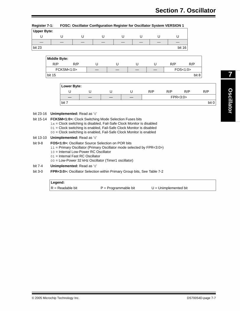
Section 7. OscillatorO
scillator
7
Register 7-1: FOSC: Oscillator Configuration Register for Oscillator System VERSION 1
Upper Byte:
U U U U U U U U
— — — — — — — —
bit 23 bit 16
Middle Byte:
R/P R/P U U U U R/P R/P
FCKSM<1:0> — — — — FOS<1:0>
bit 15 bit 8
Lower Byte:
U U U U R/P R/P R/P R/P
— — — — FPR<3:0>
bit 7 bit 0
bit 23-16 Unimplemented: Read as ‘0’
bit 15-14 FCKSM<1:0>: Clock Switching Mode Selection Fuses bits1x = Clock switching is disabled, Fail-Safe Clock Monitor is disabled01 = Clock switching is enabled, Fail-Safe Clock Monitor is disabled00 = Clock switching is enabled, Fail-Safe Clock Monitor is enabled
bit 13-10 Unimplemented: Read as ‘0’
bit 9-8 FOS<1:0>: Oscillator Source Selection on POR bits11 = Primary Oscillator (Primary Oscillator mode selected by FPR<3:0>)10 = Internal Low-Power RC Oscillator01 = Internal Fast RC Oscillator00 = Low-Power 32 kHz Oscillator (Timer1 oscillator)
bit 7-4 Unimplemented: Read as ‘0’
bit 3-0 FPR<3:0>: Oscillator Selection within Primary Group bits, See Table 7-2
Legend:
R = Readable bit P = Programmable bit U = Unimplemented bit
© 2005 Microchip Technology Inc. DS70054D-page 7-7
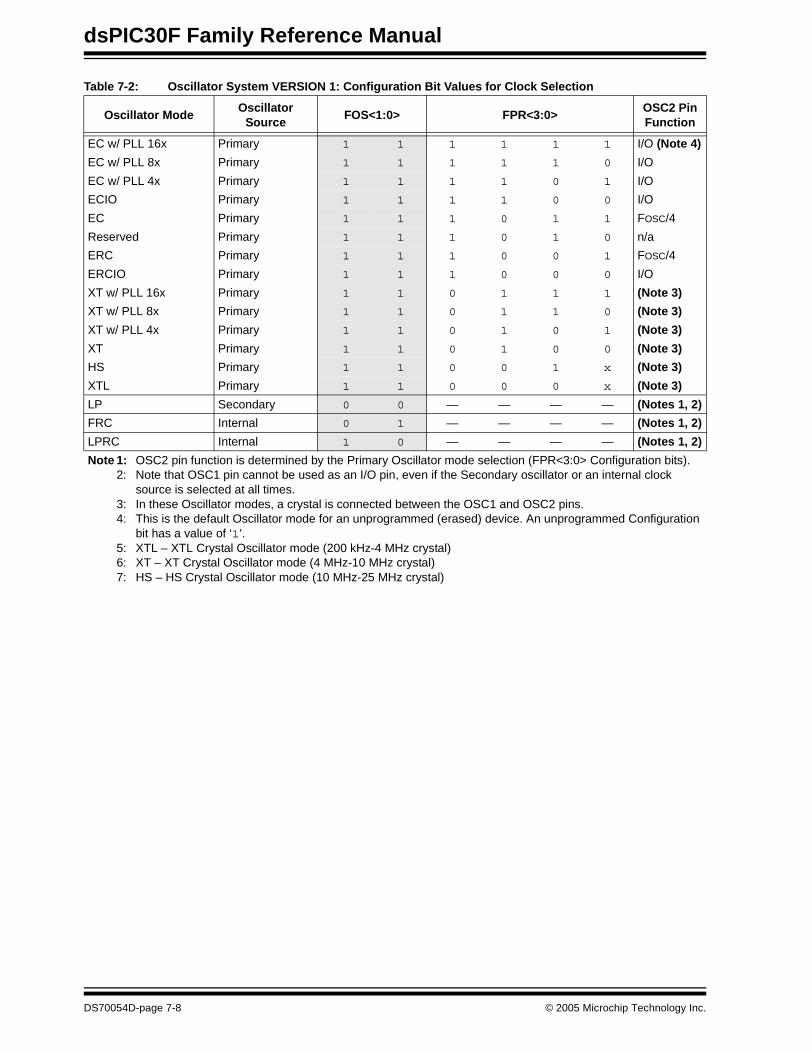
dsPIC30F Family Reference Manual
Table 7-2: Oscillator System VERSION 1: Configuration Bit Values for Clock Selection
Oscillator ModeOscillator
SourceFOS<1:0> FPR<3:0>
OSC2 PinFunction
EC w/ PLL 16x Primary 1 1 1 1 1 1 I/O (Note 4)
EC w/ PLL 8x Primary 1 1 1 1 1 0 I/O
EC w/ PLL 4x Primary 1 1 1 1 0 1 I/O
ECIO Primary 1 1 1 1 0 0 I/O
EC Primary 1 1 1 0 1 1 FOSC/4
Reserved Primary 1 1 1 0 1 0 n/a
ERC Primary 1 1 1 0 0 1 FOSC/4
ERCIO Primary 1 1 1 0 0 0 I/O
XT w/ PLL 16x Primary 1 1 0 1 1 1 (Note 3)
XT w/ PLL 8x Primary 1 1 0 1 1 0 (Note 3)
XT w/ PLL 4x Primary 1 1 0 1 0 1 (Note 3)
XT Primary 1 1 0 1 0 0 (Note 3)
HS Primary 1 1 0 0 1 x (Note 3)
XTL Primary 1 1 0 0 0 x (Note 3)
LP Secondary 0 0 — — — — (Notes 1, 2)
FRC Internal 0 1 — — — — (Notes 1, 2)
LPRC Internal 1 0 — — — — (Notes 1, 2)
Note 1: OSC2 pin function is determined by the Primary Oscillator mode selection (FPR<3:0> Configuration bits).2: Note that OSC1 pin cannot be used as an I/O pin, even if the Secondary oscillator or an internal clock
source is selected at all times.3: In these Oscillator modes, a crystal is connected between the OSC1 and OSC2 pins. 4: This is the default Oscillator mode for an unprogrammed (erased) device. An unprogrammed Configuration
bit has a value of ‘1’.5: XTL – XTL Crystal Oscillator mode (200 kHz-4 MHz crystal)6: XT – XT Crystal Oscillator mode (4 MHz-10 MHz crystal)7: HS – HS Crystal Oscillator mode (10 MHz-25 MHz crystal)
DS70054D-page 7-8 © 2005 Microchip Technology Inc.

Section 7. OscillatorO
scillator
7
Register 7-2: FOSC: Oscillator Configuration Register for Oscillator System VERSION 2
Upper Byte:
U U U U U U U U
— — — — — — — —
bit 23 bit 16
Middle Byte:
R/P R/P U U U U R/P R/P
FCKSM<1:0> — — — — FOS<1:0>
bit 15 bit 8
Lower Byte:
U U U U R/P R/P R/P R/P
— — — — FPR<3:0>
bit 7 bit 0
bit 23-16 Unimplemented: Read as ‘0’
bit 15-14 FCKSM<1:0>: Clock Switching Mode Selection Fuses bits1x = Clock switching is disabled, Fail-Safe Clock Monitor is disabled01 = Clock switching is enabled, Fail-Safe Clock Monitor is disabled00 = Clock switching is enabled, Fail-Safe Clock Monitor is enabled
bit 13-10 Unimplemented: Read as ‘0’
bit 9-8 FOS<1:0>: Oscillator Source Selection on POR bits11 = Primary Oscillator (Primary Oscillator mode selected by FPR<3:0>)10 = Internal Low-Power RC Oscillator01 = Internal Fast RC Oscillator00 = Low-Power 32 kHz Oscillator (Timer1 oscillator)
bit 7-4 Unimplemented: Read as ‘0’
bit 3-0 FPR<3:0>: Oscillator Mode Selection within Primary Group bits, See Table 7-3
Legend:
R = Readable bit P = Programmable bit U = Unimplemented bit
© 2005 Microchip Technology Inc. DS70054D-page 7-9
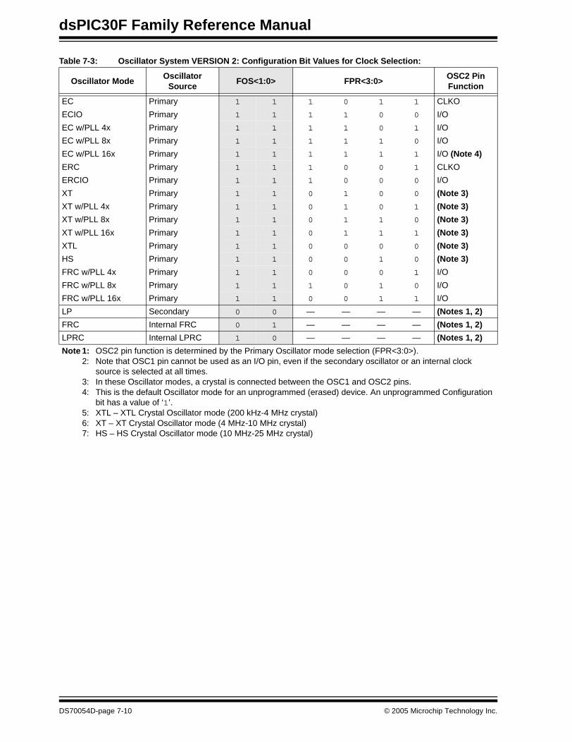
dsPIC30F Family Reference Manual
Table 7-3: Oscillator System VERSION 2: Configuration Bit Values for Clock Selection:
Oscillator ModeOscillator
SourceFOS<1:0> FPR<3:0>
OSC2 Pin Function
EC Primary 1 1 1 0 1 1 CLKO
ECIO Primary 1 1 1 1 0 0 I/O
EC w/PLL 4x Primary 1 1 1 1 0 1 I/O
EC w/PLL 8x Primary 1 1 1 1 1 0 I/O
EC w/PLL 16x Primary 1 1 1 1 1 1 I/O (Note 4)
ERC Primary 1 1 1 0 0 1 CLKO
ERCIO Primary 1 1 1 0 0 0 I/O
XT Primary 1 1 0 1 0 0 (Note 3)
XT w/PLL 4x Primary 1 1 0 1 0 1 (Note 3)
XT w/PLL 8x Primary 1 1 0 1 1 0 (Note 3)
XT w/PLL 16x Primary 1 1 0 1 1 1 (Note 3)
XTL Primary 1 1 0 0 0 0 (Note 3)
HS Primary 1 1 0 0 1 0 (Note 3)
FRC w/PLL 4x Primary 1 1 0 0 0 1 I/O
FRC w/PLL 8x Primary 1 1 1 0 1 0 I/O
FRC w/PLL 16x Primary 1 1 0 0 1 1 I/O
LP Secondary 0 0 — — — — (Notes 1, 2)
FRC Internal FRC 0 1 — — — — (Notes 1, 2)
LPRC Internal LPRC 1 0 — — — — (Notes 1, 2)
Note 1: OSC2 pin function is determined by the Primary Oscillator mode selection (FPR<3:0>).2: Note that OSC1 pin cannot be used as an I/O pin, even if the secondary oscillator or an internal clock
source is selected at all times.3: In these Oscillator modes, a crystal is connected between the OSC1 and OSC2 pins. 4: This is the default Oscillator mode for an unprogrammed (erased) device. An unprogrammed Configuration
bit has a value of ‘1’.5: XTL – XTL Crystal Oscillator mode (200 kHz-4 MHz crystal)6: XT – XT Crystal Oscillator mode (4 MHz-10 MHz crystal)7: HS – HS Crystal Oscillator mode (10 MHz-25 MHz crystal)
DS70054D-page 7-10 © 2005 Microchip Technology Inc.
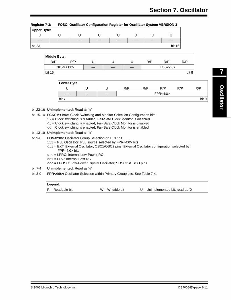
Section 7. OscillatorO
scillator
7
Register 7-3: FOSC: Oscillator Configuration Register for Oscillator System VERSION 3
Upper Byte:
U U U U U U U U
— — — — — — — —
bit 23 bit 16
Middle Byte:
R/P R/P U U U R/P R/P R/P
FCKSM<1:0> — — — FOS<2:0>
bit 15 bit 8
Lower Byte:
U U U R/P R/P R/P R/P R/P
— — — FPR<4:0>
bit 7 bit 0
bit 23-16 Unimplemented: Read as ‘0’
bit 15-14 FCKSM<1:0>: Clock Switching and Monitor Selection Configuration bits1x = Clock switching is disabled, Fail-Safe Clock Monitor is disabled01 = Clock switching is enabled, Fail-Safe Clock Monitor is disabled00 = Clock switching is enabled, Fail-Safe Clock Monitor is enabled
bit 13-10 Unimplemented: Read as ‘0’
bit 9-8 FOS<2:0>: Oscillator Group Selection on POR bit111 = PLL Oscillator; PLL source selected by FPR<4:0> bits011 = EXT: External Oscillator; OSC1/OSC2 pins; External Oscillator configuration selected by
FPR<4:0> bits010 = LPRC: Internal Low-Power RC001 = FRC: Internal Fast RC000 = LPOSC: Low-Power Crystal Oscillator; SOSCI/SOSCO pins
bit 7-4 Unimplemented: Read as ‘0’
bit 3-0 FPR<4:0>: Oscillator Selection within Primary Group bits, See Table 7-4.
Legend:
R = Readable bit W = Writable bit U = Unimplemented bit, read as ‘0’
© 2005 Microchip Technology Inc. DS70054D-page 7-11
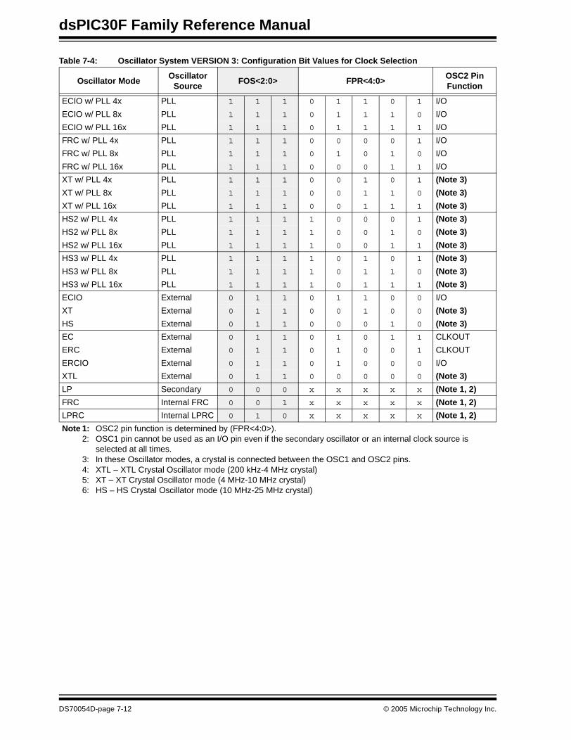
dsPIC30F Family Reference Manual
Table 7-4: Oscillator System VERSION 3: Configuration Bit Values for Clock Selection
Oscillator ModeOscillator
SourceFOS<2:0> FPR<4:0>
OSC2 Pin Function
ECIO w/ PLL 4x PLL 1 1 1 0 1 1 0 1 I/O
ECIO w/ PLL 8x PLL 1 1 1 0 1 1 1 0 I/O
ECIO w/ PLL 16x PLL 1 1 1 0 1 1 1 1 I/O
FRC w/ PLL 4x PLL 1 1 1 0 0 0 0 1 I/O
FRC w/ PLL 8x PLL 1 1 1 0 1 0 1 0 I/O
FRC w/ PLL 16x PLL 1 1 1 0 0 0 1 1 I/O
XT w/ PLL 4x PLL 1 1 1 0 0 1 0 1 (Note 3)
XT w/ PLL 8x PLL 1 1 1 0 0 1 1 0 (Note 3)
XT w/ PLL 16x PLL 1 1 1 0 0 1 1 1 (Note 3)
HS2 w/ PLL 4x PLL 1 1 1 1 0 0 0 1 (Note 3)
HS2 w/ PLL 8x PLL 1 1 1 1 0 0 1 0 (Note 3)
HS2 w/ PLL 16x PLL 1 1 1 1 0 0 1 1 (Note 3)
HS3 w/ PLL 4x PLL 1 1 1 1 0 1 0 1 (Note 3)
HS3 w/ PLL 8x PLL 1 1 1 1 0 1 1 0 (Note 3)
HS3 w/ PLL 16x PLL 1 1 1 1 0 1 1 1 (Note 3)
ECIO External 0 1 1 0 1 1 0 0 I/O
XT External 0 1 1 0 0 1 0 0 (Note 3)
HS External 0 1 1 0 0 0 1 0 (Note 3)
EC External 0 1 1 0 1 0 1 1 CLKOUT
ERC External 0 1 1 0 1 0 0 1 CLKOUT
ERCIO External 0 1 1 0 1 0 0 0 I/O
XTL External 0 1 1 0 0 0 0 0 (Note 3)
LP Secondary 0 0 0 x x x x x (Note 1, 2)
FRC Internal FRC 0 0 1 x x x x x (Note 1, 2)
LPRC Internal LPRC 0 1 0 x x x x x (Note 1, 2)
Note 1: OSC2 pin function is determined by (FPR<4:0>).2: OSC1 pin cannot be used as an I/O pin even if the secondary oscillator or an internal clock source is
selected at all times.3: In these Oscillator modes, a crystal is connected between the OSC1 and OSC2 pins.4: XTL – XTL Crystal Oscillator mode (200 kHz-4 MHz crystal)5: XT – XT Crystal Oscillator mode (4 MHz-10 MHz crystal)6: HS – HS Crystal Oscillator mode (10 MHz-25 MHz crystal)
DS70054D-page 7-12 © 2005 Microchip Technology Inc.
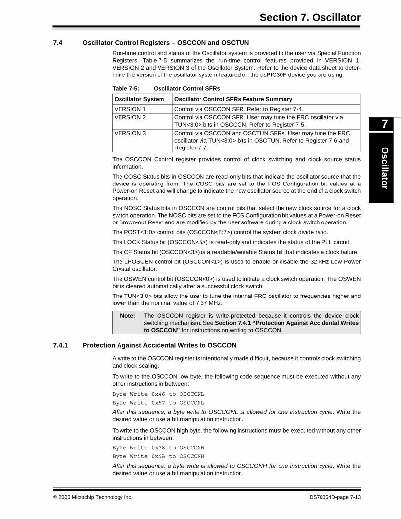
Section 7. OscillatorO
scillator
7
7.4 Oscillator Control Registers – OSCCON and OSCTUN
Run-time control and status of the Oscillator system is provided to the user via Special FunctionRegisters. Table 7-5 summarizes the run-time control features provided in VERSION 1,VERSION 2 and VERSION 3 of the Oscillator System. Refer to the device data sheet to deter-mine the version of the oscillator system featured on the dsPIC30F device you are using.
The OSCCON Control register provides control of clock switching and clock source statusinformation.
The COSC Status bits in OSCCON are read-only bits that indicate the oscillator source that thedevice is operating from. The COSC bits are set to the FOS Configuration bit values at aPower-on Reset and will change to indicate the new oscillator source at the end of a clock switchoperation.
The NOSC Status bits in OSCCON are control bits that select the new clock source for a clockswitch operation. The NOSC bits are set to the FOS Configuration bit values at a Power-on Resetor Brown-out Reset and are modified by the user software during a clock switch operation.
The POST<1:0> control bits (OSCCON<8:7>) control the system clock divide ratio.
The LOCK Status bit (OSCCON<5>) is read-only and indicates the status of the PLL circuit.
The CF Status bit (OSCCON<3>) is a readable/writable Status bit that indicates a clock failure.
The LPOSCEN control bit (OSCCON<1>) is used to enable or disable the 32 kHz Low-PowerCrystal oscillator.
The OSWEN control bit (OSCCON<0>) is used to initiate a clock switch operation. The OSWENbit is cleared automatically after a successful clock switch.
The TUN<3:0> bits allow the user to tune the internal FRC oscillator to frequencies higher andlower than the nominal value of 7.37 MHz.
7.4.1 Protection Against Accidental Writes to OSCCON
A write to the OSCCON register is intentionally made difficult, because it controls clock switchingand clock scaling.
To write to the OSCCON low byte, the following code sequence must be executed without anyother instructions in between:
Byte Write 0x46 to OSCCONL
Byte Write 0x57 to OSCCONL
After this sequence, a byte write to OSCCONL is allowed for one instruction cycle. Write thedesired value or use a bit manipulation instruction.
To write to the OSCCON high byte, the following instructions must be executed without any otherinstructions in between:
Byte Write 0x78 to OSCCONH
Byte Write 0x9A to OSCCONH
After this sequence, a byte write is allowed to OSCCONH for one instruction cycle. Write thedesired value or use a bit manipulation instruction.
Table 7-5: Oscillator Control SFRs
Oscillator System Oscillator Control SFRs Feature Summary
VERSION 1 Control via OSCCON SFR. Refer to Register 7-4.VERSION 2 Control via OSCCON SFR. User may tune the FRC oscillator via
TUN<3:0> bits in OSCCON. Refer to Register 7-5.VERSION 3 Control via OSCCON and OSCTUN SFRs. User may tune the FRC
oscillator via TUN<3:0> bits in OSCTUN. Refer to Register 7-6 and Register 7-7.
Note: The OSCCON register is write-protected because it controls the device clockswitching mechanism. See Section 7.4.1 “Protection Against Accidental Writesto OSCCON” for instructions on writing to OSCCON.
© 2005 Microchip Technology Inc. DS70054D-page 7-13
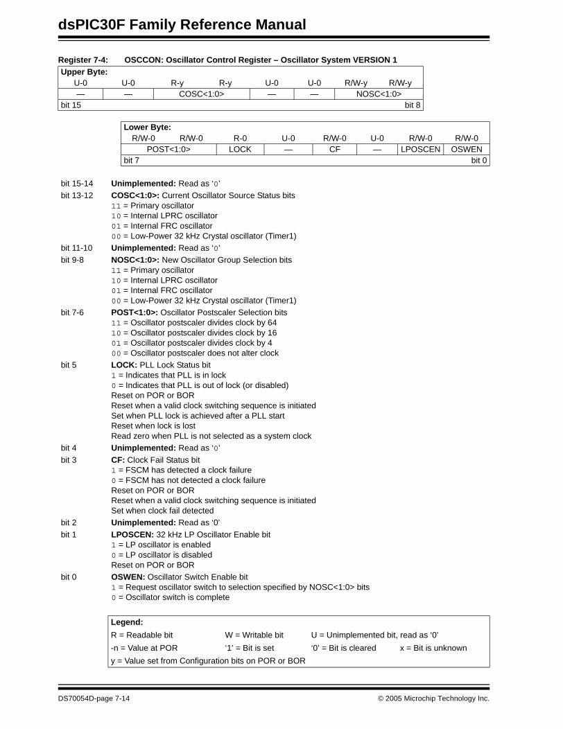
dsPIC30F Family Reference Manual
Register 7-4: OSCCON: Oscillator Control Register – Oscillator System VERSION 1 Upper Byte:
U-0 U-0 R-y R-y U-0 U-0 R/W-y R/W-y— — COSC<1:0> — — NOSC<1:0>
bit 15 bit 8
Lower Byte:R/W-0 R/W-0 R-0 U-0 R/W-0 U-0 R/W-0 R/W-0
POST<1:0> LOCK — CF — LPOSCEN OSWENbit 7 bit 0
bit 15-14 Unimplemented: Read as ‘0’bit 13-12 COSC<1:0>: Current Oscillator Source Status bits
11 = Primary oscillator10 = Internal LPRC oscillator01 = Internal FRC oscillator00 = Low-Power 32 kHz Crystal oscillator (Timer1)
bit 11-10 Unimplemented: Read as ‘0’bit 9-8 NOSC<1:0>: New Oscillator Group Selection bits
11 = Primary oscillator10 = Internal LPRC oscillator01 = Internal FRC oscillator00 = Low-Power 32 kHz Crystal oscillator (Timer1)
bit 7-6 POST<1:0>: Oscillator Postscaler Selection bits11 = Oscillator postscaler divides clock by 6410 = Oscillator postscaler divides clock by 1601 = Oscillator postscaler divides clock by 400 = Oscillator postscaler does not alter clock
bit 5 LOCK: PLL Lock Status bit1 = Indicates that PLL is in lock0 = Indicates that PLL is out of lock (or disabled)Reset on POR or BORReset when a valid clock switching sequence is initiatedSet when PLL lock is achieved after a PLL startReset when lock is lostRead zero when PLL is not selected as a system clock
bit 4 Unimplemented: Read as ‘0’
bit 3 CF: Clock Fail Status bit1 = FSCM has detected a clock failure0 = FSCM has not detected a clock failureReset on POR or BORReset when a valid clock switching sequence is initiatedSet when clock fail detected
bit 2 Unimplemented: Read as ‘0’
bit 1 LPOSCEN: 32 kHz LP Oscillator Enable bit1 = LP oscillator is enabled0 = LP oscillator is disabledReset on POR or BOR
bit 0 OSWEN: Oscillator Switch Enable bit1 = Request oscillator switch to selection specified by NOSC<1:0> bits0 = Oscillator switch is complete
Legend:
R = Readable bit W = Writable bit U = Unimplemented bit, read as ‘0’
-n = Value at POR ‘1’ = Bit is set ‘0’ = Bit is cleared x = Bit is unknown
y = Value set from Configuration bits on POR or BOR
DS70054D-page 7-14 © 2005 Microchip Technology Inc.
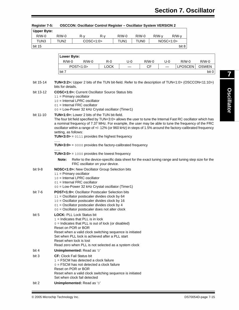
Section 7. OscillatorO
scillator
7
Register 7-5: OSCCON: Oscillator Control Register – Oscillator System VERSION 2
Upper Byte:R/W-0 R/W-0 R-y R-y R/W-0 R/W-0 R/W-y R/W-yTUN3 TUN2 COSC<1:0> TUN1 TUN0 NOSC<1:0>
bit 15 bit 8
Lower Byte:R/W-0 R/W-0 R-0 U-0 R/W-0 U-0 R/W-0 R/W-0
POST<1:0> LOCK — CF — LPOSCEN OSWENbit 7 bit 0
bit 15-14 TUN<3:2>: Upper 2 bits of the TUN bit-field. Refer to the description of TUN<1:0> (OSCCON<11:10>)bits for details.
bit 13-12 COSC<1:0>: Current Oscillator Source Status bits11 = Primary oscillator10 = Internal LPRC oscillator01 = Internal FRC oscillator00 = Low-Power 32 kHz Crystal oscillator (Timer1)
bit 11-10 TUN<1:0>: Lower 2 bits of the TUN bit-field. The four bit field specified by TUN<3:0> allows the user to tune the Internal Fast RC oscillator which hasa nominal frequency of 7.37 MHz. For example, the user may be able to tune the frequency of the FRCoscillator within a range of +/- 12% (or 960 kHz) in steps of 1.5% around the factory-calibrated frequencysetting, as follows:TUN<3:0> = 0111 provides the highest frequency......TUN<3:0> = 0000 provides the factory-calibrated frequency......TUN<3:0> = 1000 provides the lowest frequency
Note: Refer to the device-specific data sheet for the exact tuning range and tuning step size for theFRC oscillator on your device.
bit 9-8 NOSC<1:0>: New Oscillator Group Selection bits11 = Primary oscillator10 = Internal LPRC oscillator01 = Internal FRC oscillator00 = Low-Power 32 kHz Crystal oscillator (Timer1)
bit 7-6 POST<1:0>: Oscillator Postscaler Selection bits11 = Oscillator postscaler divides clock by 6410 = Oscillator postscaler divides clock by 1601 = Oscillator postscaler divides clock by 400 = Oscillator postscaler does not alter clock
bit 5 LOCK: PLL Lock Status bit1 = Indicates that PLL is in lock0 = Indicates that PLL is out of lock (or disabled)Reset on POR or BORReset when a valid clock switching sequence is initiatedSet when PLL lock is achieved after a PLL startReset when lock is lostRead zero when PLL is not selected as a system clock
bit 4 Unimplemented: Read as ‘0’
bit 3 CF: Clock Fail Status bit1 = FSCM has detected a clock failure0 = FSCM has not detected a clock failureReset on POR or BORReset when a valid clock switching sequence is initiatedSet when clock fail detected
bit 2 Unimplemented: Read as ‘0’
© 2005 Microchip Technology Inc. DS70054D-page 7-15
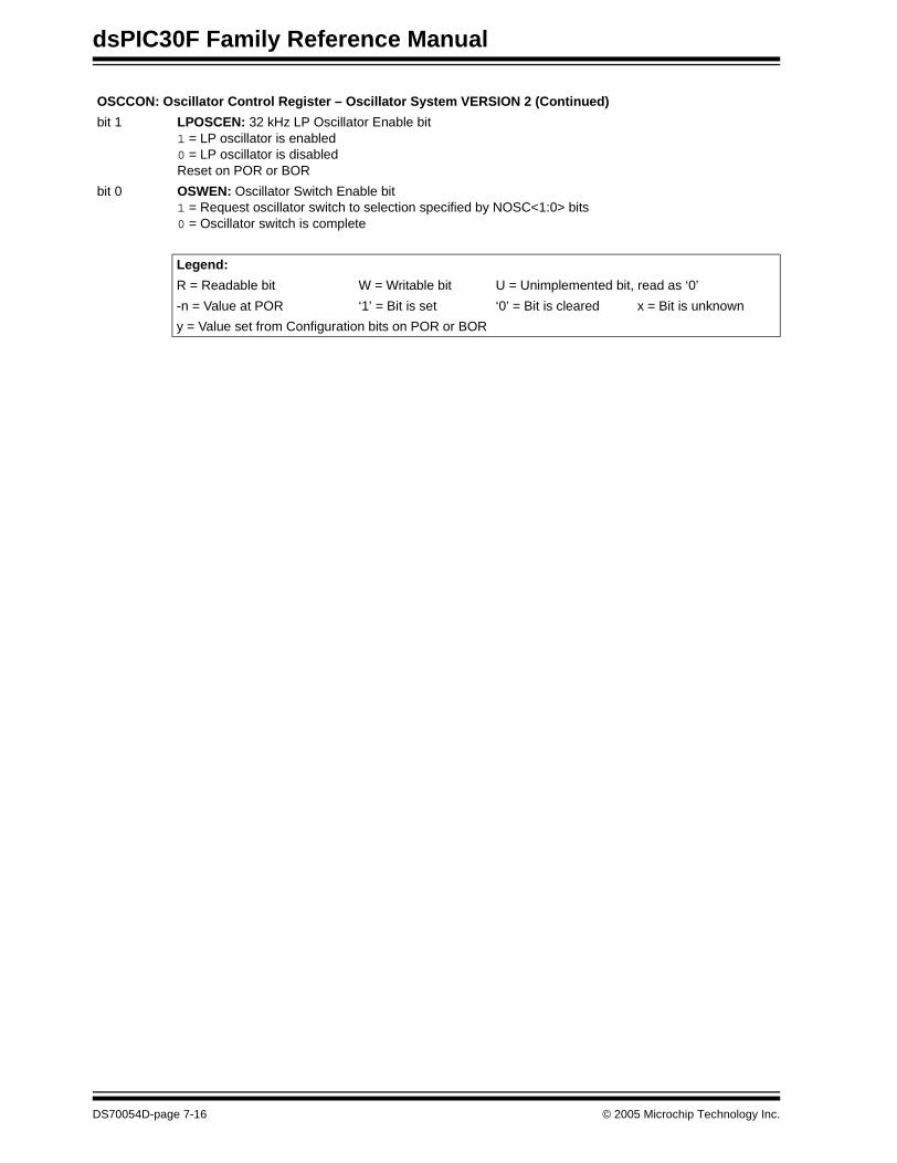
dsPIC30F Family Reference Manual
OSCCON: Oscillator Control Register – Oscillator System VERSION 2 (Continued)
bit 1 LPOSCEN: 32 kHz LP Oscillator Enable bit1 = LP oscillator is enabled0 = LP oscillator is disabledReset on POR or BOR
bit 0 OSWEN: Oscillator Switch Enable bit1 = Request oscillator switch to selection specified by NOSC<1:0> bits0 = Oscillator switch is complete
Legend:
R = Readable bit W = Writable bit U = Unimplemented bit, read as ‘0’
-n = Value at POR ‘1’ = Bit is set ‘0’ = Bit is cleared x = Bit is unknown
y = Value set from Configuration bits on POR or BOR
DS70054D-page 7-16 © 2005 Microchip Technology Inc.
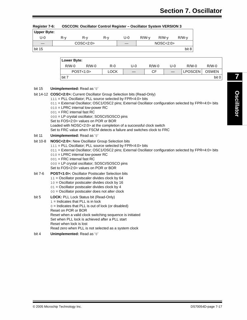
Section 7. OscillatorO
scillator
7
Register 7-6: OSCCON: Oscillator Control Register – Oscillator System VERSION 3
Upper Byte:
U-0 R-y R-y R-y U-0 R/W-y R/W-y R/W-y
— COSC<2:0> — NOSC<2:0>
bit 15 bit 8
Lower Byte:
R/W-0 R/W-0 R-0 U-0 R/W-0 U-0 R/W-0 R/W-0
POST<1:0> LOCK — CF — LPOSCEN OSWEN
bit 7 bit 0
bit 15 Unimplemented: Read as ‘0’
bit 14-12 COSC<2:0>: Current Oscillator Group Selection bits (Read-Only)111 = PLL Oscillator; PLL source selected by FPR<4:0> bits011 = External Oscillator; OSC1/OSC2 pins; External Oscillator configuration selected by FPR<4:0> bits010 = LPRC internal low-power RC001 = FRC internal fast RC000 = LP crystal oscillator; SOSCI/SOSCO pinsSet to FOS<2:0> values on POR or BORLoaded with NOSC<2:0> at the completion of a successful clock switchSet to FRC value when FSCM detects a failure and switches clock to FRC
bit 11 Unimplemented: Read as ‘0’
bit 10-8 NOSC<2:0>: New Oscillator Group Selection bits111 = PLL Oscillator; PLL source selected by FPR<4:0> bits011 = External Oscillator; OSC1/OSC2 pins; External Oscillator configuration selected by FPR<4:0> bits010 = LPRC internal low-power RC001 = FRC internal fast RC000 = LP crystal oscillator; SOSCI/SOSCO pinsSet to FOS<2:0> values on POR or BOR
bit 7-6 POST<1:0>: Oscillator Postscaler Selection bits11 = Oscillator postscaler divides clock by 6410 = Oscillator postscaler divides clock by 1601 = Oscillator postscaler divides clock by 400 = Oscillator postscaler does not alter clock
bit 5 LOCK: PLL Lock Status bit (Read-Only)1 = Indicates that PLL is in lock0 = Indicates that PLL is out of lock (or disabled)Reset on POR or BORReset when a valid clock switching sequence is initiatedSet when PLL lock is achieved after a PLL startReset when lock is lostRead zero when PLL is not selected as a system clock
bit 4 Unimplemented: Read as ‘0’
© 2005 Microchip Technology Inc. DS70054D-page 7-17
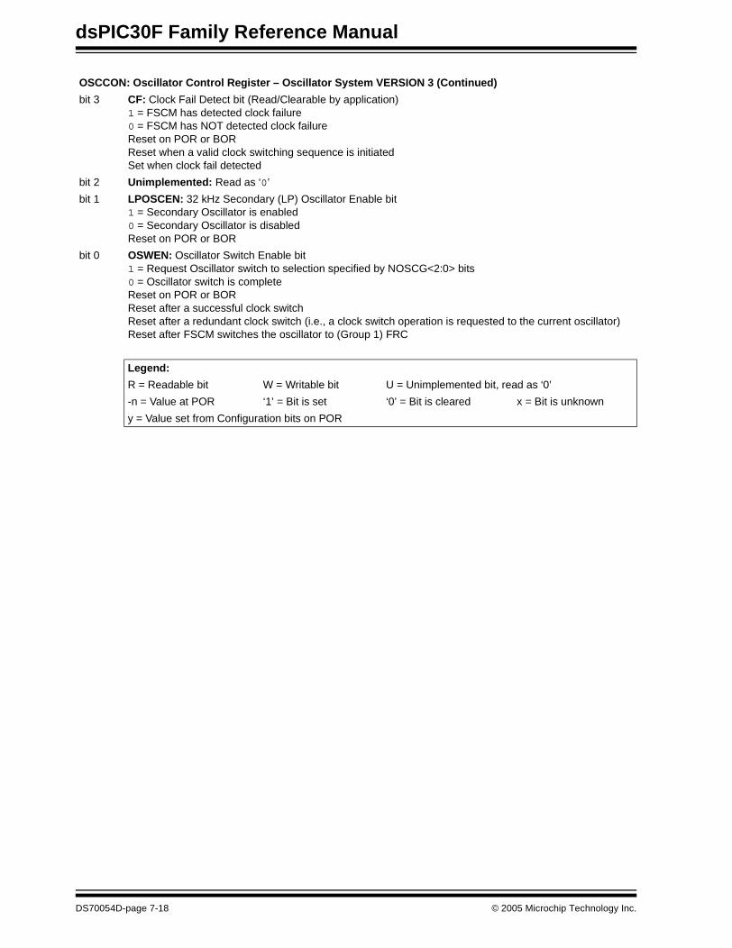
dsPIC30F Family Reference Manual
OSCCON: Oscillator Control Register – Oscillator System VERSION 3 (Continued)
bit 3 CF: Clock Fail Detect bit (Read/Clearable by application)1 = FSCM has detected clock failure0 = FSCM has NOT detected clock failureReset on POR or BORReset when a valid clock switching sequence is initiatedSet when clock fail detected
bit 2 Unimplemented: Read as ‘0’
bit 1 LPOSCEN: 32 kHz Secondary (LP) Oscillator Enable bit1 = Secondary Oscillator is enabled0 = Secondary Oscillator is disabledReset on POR or BOR
bit 0 OSWEN: Oscillator Switch Enable bit1 = Request Oscillator switch to selection specified by NOSCG<2:0> bits0 = Oscillator switch is completeReset on POR or BORReset after a successful clock switchReset after a redundant clock switch (i.e., a clock switch operation is requested to the current oscillator)Reset after FSCM switches the oscillator to (Group 1) FRC
Legend:
R = Readable bit W = Writable bit U = Unimplemented bit, read as ‘0’
-n = Value at POR ‘1’ = Bit is set ‘0’ = Bit is cleared x = Bit is unknown
y = Value set from Configuration bits on POR
DS70054D-page 7-18 © 2005 Microchip Technology Inc.
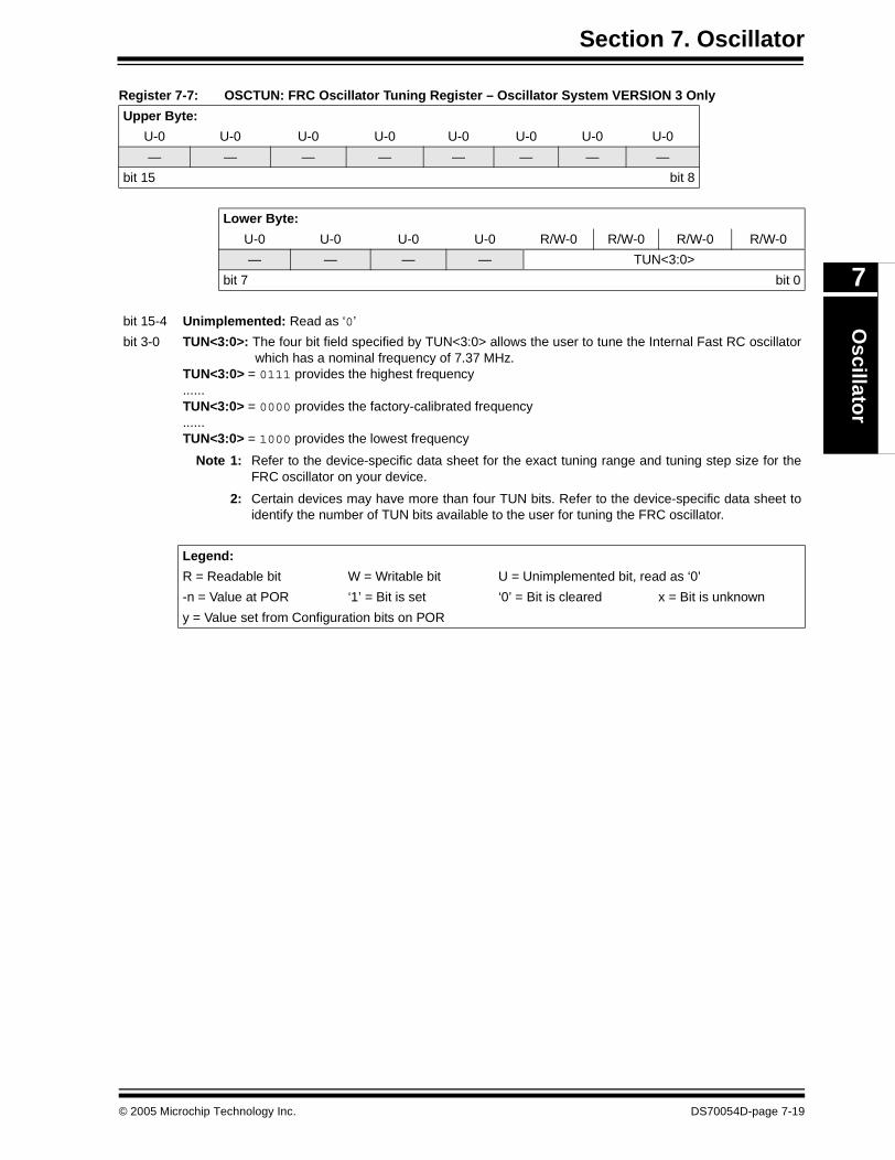
Section 7. OscillatorO
scillator
7
Register 7-7: OSCTUN: FRC Oscillator Tuning Register – Oscillator System VERSION 3 Only
Upper Byte:
U-0 U-0 U-0 U-0 U-0 U-0 U-0 U-0
— — — — — — — —
bit 15 bit 8
Lower Byte:
U-0 U-0 U-0 U-0 R/W-0 R/W-0 R/W-0 R/W-0
— — — — TUN<3:0>
bit 7 bit 0
bit 15-4 Unimplemented: Read as ‘0’
bit 3-0 TUN<3:0>: The four bit field specified by TUN<3:0> allows the user to tune the Internal Fast RC oscillatorwhich has a nominal frequency of 7.37 MHz.
TUN<3:0> = 0111 provides the highest frequency......TUN<3:0> = 0000 provides the factory-calibrated frequency......TUN<3:0> = 1000 provides the lowest frequency
Note 1: Refer to the device-specific data sheet for the exact tuning range and tuning step size for theFRC oscillator on your device.
2: Certain devices may have more than four TUN bits. Refer to the device-specific data sheet toidentify the number of TUN bits available to the user for tuning the FRC oscillator.
Legend:
R = Readable bit W = Writable bit U = Unimplemented bit, read as ‘0’
-n = Value at POR ‘1’ = Bit is set ‘0’ = Bit is cleared x = Bit is unknown
y = Value set from Configuration bits on POR
© 2005 Microchip Technology Inc. DS70054D-page 7-19
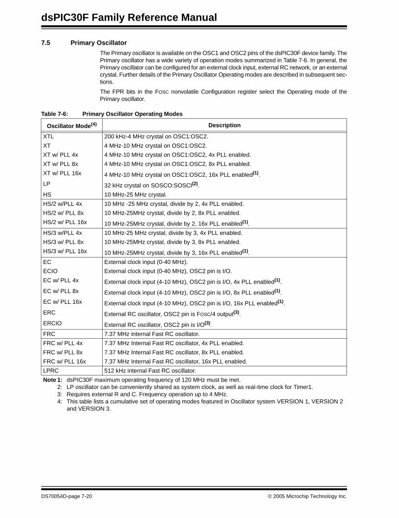
dsPIC30F Family Reference Manual
7.5 Primary Oscillator
The Primary oscillator is available on the OSC1 and OSC2 pins of the dsPIC30F device family. ThePrimary oscillator has a wide variety of operation modes summarized in Table 7-6. In general, thePrimary oscillator can be configured for an external clock input, external RC network, or an externalcrystal. Further details of the Primary Oscillator Operating modes are described in subsequent sec-tions.
The FPR bits in the FOSC nonvolatile Configuration register select the Operating mode of thePrimary oscillator.
Table 7-6: Primary Oscillator Operating Modes
Oscillator Mode(4) Description
XTL 200 kHz-4 MHz crystal on OSC1:OSC2.
XT 4 MHz-10 MHz crystal on OSC1:OSC2.
XT w/ PLL 4x 4 MHz-10 MHz crystal on OSC1:OSC2, 4x PLL enabled.
XT w/ PLL 8x 4 MHz-10 MHz crystal on OSC1:OSC2, 8x PLL enabled.
XT w/ PLL 16x 4 MHz-10 MHz crystal on OSC1:OSC2, 16x PLL enabled(1).
LP 32 kHz crystal on SOSCO:SOSCI(2).
HS 10 MHz-25 MHz crystal.
HS/2 w/PLL 4x 10 MHz -25 MHz crystal, divide by 2, 4x PLL enabled.
HS/2 w/ PLL 8x 10 MHz-25MHz crystal, divide by 2, 8x PLL enabled.
HS/2 w/ PLL 16x 10 MHz-25MHz crystal, divide by 2, 16x PLL enabled(1).
HS/3 w/PLL 4x 10 MHz-25 MHz crystal, divide by 3, 4x PLL enabled.
HS/3 w/ PLL 8x 10 MHz-25MHz crystal, divide by 3, 8x PLL enabled.
HS/3 w/ PLL 16x 10 MHz-25MHz crystal, divide by 3, 16x PLL enabled(1).
EC External clock input (0-40 MHz).
ECIO External clock input (0-40 MHz), OSC2 pin is I/O.
EC w/ PLL 4x External clock input (4-10 MHz), OSC2 pin is I/O, 4x PLL enabled(1).
EC w/ PLL 8x External clock input (4-10 MHz), OSC2 pin is I/O, 8x PLL enabled(1).
EC w/ PLL 16x External clock input (4-10 MHz), OSC2 pin is I/O, 16x PLL enabled(1).
ERC External RC oscillator, OSC2 pin is FOSC/4 output(3).
ERCIO External RC oscillator, OSC2 pin is I/O(3).
FRC 7.37 MHz internal Fast RC oscillator.
FRC w/ PLL 4x 7.37 MHz Internal Fast RC oscillator, 4x PLL enabled.
FRC w/ PLL 8x 7.37 MHz Internal Fast RC oscillator, 8x PLL enabled.
FRC w/ PLL 16x 7.37 MHz Internal Fast RC oscillator, 16x PLL enabled.
LPRC 512 kHz internal Fast RC oscillator.
Note 1: dsPIC30F maximum operating frequency of 120 MHz must be met.2: LP oscillator can be conveniently shared as system clock, as well as real-time clock for Timer1.3: Requires external R and C. Frequency operation up to 4 MHz.4: This table lists a cumulative set of operating modes featured in Oscillator system VERSION 1, VERSION 2
and VERSION 3.
DS70054D-page 7-20 © 2005 Microchip Technology Inc.
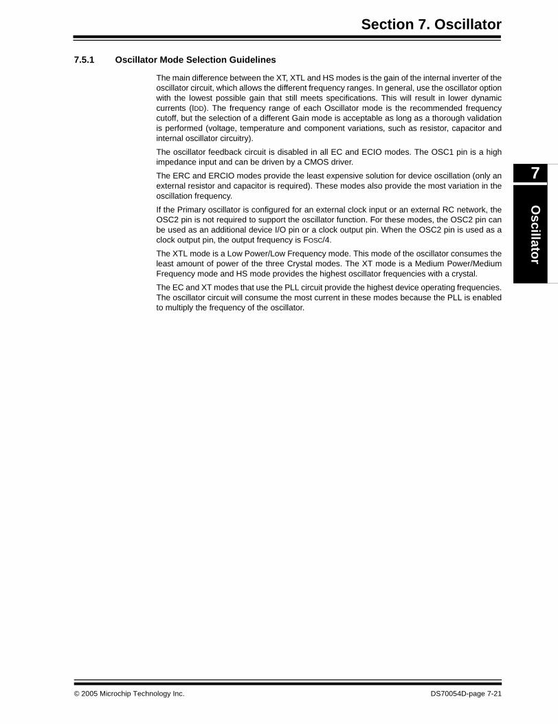
Section 7. OscillatorO
scillator
7
7.5.1 Oscillator Mode Selection Guidelines
The main difference between the XT, XTL and HS modes is the gain of the internal inverter of theoscillator circuit, which allows the different frequency ranges. In general, use the oscillator optionwith the lowest possible gain that still meets specifications. This will result in lower dynamiccurrents (IDD). The frequency range of each Oscillator mode is the recommended frequencycutoff, but the selection of a different Gain mode is acceptable as long as a thorough validationis performed (voltage, temperature and component variations, such as resistor, capacitor andinternal oscillator circuitry).
The oscillator feedback circuit is disabled in all EC and ECIO modes. The OSC1 pin is a highimpedance input and can be driven by a CMOS driver.
The ERC and ERCIO modes provide the least expensive solution for device oscillation (only anexternal resistor and capacitor is required). These modes also provide the most variation in theoscillation frequency.
If the Primary oscillator is configured for an external clock input or an external RC network, theOSC2 pin is not required to support the oscillator function. For these modes, the OSC2 pin canbe used as an additional device I/O pin or a clock output pin. When the OSC2 pin is used as aclock output pin, the output frequency is FOSC/4.
The XTL mode is a Low Power/Low Frequency mode. This mode of the oscillator consumes theleast amount of power of the three Crystal modes. The XT mode is a Medium Power/MediumFrequency mode and HS mode provides the highest oscillator frequencies with a crystal.
The EC and XT modes that use the PLL circuit provide the highest device operating frequencies.The oscillator circuit will consume the most current in these modes because the PLL is enabledto multiply the frequency of the oscillator.
© 2005 Microchip Technology Inc. DS70054D-page 7-21
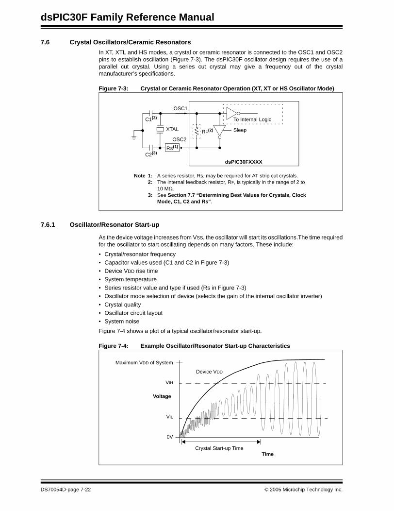
dsPIC30F Family Reference Manual
7.6 Crystal Oscillators/Ceramic Resonators
In XT, XTL and HS modes, a crystal or ceramic resonator is connected to the OSC1 and OSC2pins to establish oscillation (Figure 7-3). The dsPIC30F oscillator design requires the use of aparallel cut crystal. Using a series cut crystal may give a frequency out of the crystalmanufacturer’s specifications.
Figure 7-3: Crystal or Ceramic Resonator Operation (XT, XT or HS Oscillator Mode)
7.6.1 Oscillator/Resonator Start-up
As the device voltage increases from VSS, the oscillator will start its oscillations.The time requiredfor the oscillator to start oscillating depends on many factors. These include:
• Crystal/resonator frequency• Capacitor values used (C1 and C2 in Figure 7-3)• Device VDD rise time
• System temperature• Series resistor value and type if used (Rs in Figure 7-3)• Oscillator mode selection of device (selects the gain of the internal oscillator inverter)
• Crystal quality• Oscillator circuit layout• System noise
Figure 7-4 shows a plot of a typical oscillator/resonator start-up.
Figure 7-4: Example Oscillator/Resonator Start-up Characteristics
C1(3)
C2(3)
XTAL
OSC2
RS(1)
OSC1
RF(2) Sleep
To Internal Logic
dsPIC30FXXXX
Note 1: A series resistor, Rs, may be required for AT strip cut crystals.2: The internal feedback resistor, RF, is typically in the range of 2 to
10 MΩ.3: See Section 7.7 “Determining Best Values for Crystals, Clock
Mode, C1, C2 and Rs”.
Voltage
Crystal Start-up TimeTime
Device VDD
Maximum VDD of System
0V
VIL
VIH
DS70054D-page 7-22 © 2005 Microchip Technology Inc.

Section 7. OscillatorO
scillator
7
7.6.2 Tuning the Oscillator Circuit
Since Microchip devices have wide operating ranges (frequency, voltage and temperature;depending on the part and version ordered) and external components (crystals, capacitors,...) ofvarying quality and manufacture, validation of operation needs to be performed to ensure thatthe component selection will comply with the requirements of the application.
There are many factors that go into the selection and arrangement of these external components.These factors include:
• amplifier gain
• desired frequency • resonant frequency(s) of the crystal • temperature of operation
• supply voltage range • start-up time • stability
• crystal life • power consumption • simplification of the circuit
• use of standard components• component count
7.6.3 Oscillator Start-up from Sleep Mode
The most difficult time for the oscillator to start-up is when waking up from Sleep mode. This isbecause the load capacitors have both partially charged to some quiescent value, and phasedifferential at wake-up is minimal. Thus, more time is required to achieve stable oscillation.Remember also that low voltage, high temperatures and the Lower Frequency Clock modes alsoimpose limitations on loop gain, which in turn affects start-up. Each of the following factorsincreases the start-up time:
• a low frequency design (with a Low Gain Clock mode)
• a quiet environment (such as a battery operated device) • operating in a shielded box (away from the noisy RF area) • low voltage
• high temperature • wake-up from Sleep mode
Noise actually helps lower the oscillator start-up time since it provides a “kick start” to theoscillator.
Prior to entering Sleep mode, the application may switch to the Internal FRC(+PLL) oscillator inorder to reduce the time taken by the device to wake-up from Sleep.
© 2005 Microchip Technology Inc. DS70054D-page 7-23
dsPIC30F Family Reference Manual
7.7 Determining Best Values for Crystals, Clock Mode, C1, C2 and RS
The best method for selecting components is to apply a little knowledge and a lot of trial,measurement and testing.
Crystals are usually selected by their parallel resonant frequency only, however, other parame-ters may be important to your design, such as temperature or frequency tolerance. ApplicationNote AN588 “PICmicro® Microcontroller Oscillator Design Guide” is an excellent reference tolearn more about crystal operation and their ordering information.
The dsPIC30F internal oscillator circuit is a parallel oscillator circuit, which requires that a parallelresonant crystal be selected. The load capacitance is usually specified in the 22 pF to 33 pFrange. The crystal will oscillate closest to the desired frequency with a load capacitance in thisrange. It may be necessary to alter these values, as described later, in order to achieve otherbenefits.
The Clock mode is primarily chosen based on the desired frequency of the crystal oscillator. Themain difference between the XT, XTL and HS Oscillator modes is the gain of the internal inverterof the oscillator circuit, which allows the different frequency ranges. In general, use the oscillatoroption with the lowest possible gain that still meets specifications. This will result in lowerdynamic currents (IDD). The frequency range of each Oscillator mode is the recommendedfrequency cutoff, but the selection of a different Gain mode is acceptable, as long as a thoroughvalidation is performed (voltage, temperature and component variations, such as resistor,capacitor and internal oscillator circuitry).
C1 and C2 (see Figure 7-3) should also be initially selected based on the load capacitance assuggested by the crystal manufacturer and the tables supplied in the device data sheet. Thevalues given in the device data sheet can only be used as a starting point since the crystalmanufacturer, supply voltage, and other factors already mentioned may cause your circuit todiffer from the one used in the factory characterization process.
Ideally, the capacitance is chosen so that it will oscillate at the highest temperature and the lowestVDD that the circuit will be expected to perform under. High temperature and low VDD both havea limiting effect on the loop gain, such that if the circuit functions at these extremes, the designercan be more assured of proper operation at other temperatures and supply voltagecombinations. The output sine wave should not be clipped in the highest gain environment(highest VDD and lowest temperature) and the sine output amplitude should be large enough inthe lowest gain environment (lowest VDD and highest temperature) to cover the logic inputrequirements of the clock as listed in the device data sheet.
A method for improving start-up is to use a value of C2 greater than C1. This causes a greaterphase shift across the crystal at power-up, which speeds oscillator start-up.
Besides loading the crystal for proper frequency response, these capacitors can have the effectof lowering loop gain if their value is increased. C2 can be selected to affect the overall gain ofthe circuit. A higher C2 can lower the gain if the crystal is being over driven (also, see discussionon Rs). Capacitance values that are too high can store and dump too much current through thecrystal, so C1 and C2 should not become excessively large. Unfortunately, measuring thewattage through a crystal is difficult, but if you do not stray too far from the suggested values youshould not have to be concerned with this.
A series resistor, Rs, is added to the circuit if, after all other external components are selected tosatisfaction, the crystal is still being overdriven. This can be determined by looking at the OSC2pin, which is the driven pin, with an oscilloscope. Connecting the probe to the OSC1 pin will loadthe pin too much and negatively affect performance. Remember that a scope probe adds its owncapacitance to the circuit, so this may have to be accounted for in your design (i.e., if the circuitworked best with a C2 of 22 pF and scope probe was 10 pF, a 33 pF capacitor may actually becalled for). The output signal should not be clipping or flattened. Overdriving the crystal can alsolead to the circuit jumping to a higher harmonic level or even crystal damage.
DS70054D-page 7-24 © 2005 Microchip Technology Inc.

Section 7. OscillatorO
scillator
7
The OSC2 signal should be a clean sine wave that easily spans the input minimum and maximumof the clock input pin (4V to 5V peak-to-peak for a 5V VDD is usually good). An easy way to setthis is to again test the circuit at the minimum temperature and maximum VDD that the design willbe expected to perform in, then look at the output. This should be the maximum amplitude of theclock output. If there is clipping or the sine wave is distorted near VDD and VSS, increasing loadcapacitors may cause too much current to flow through the crystal or push the value too far fromthe manufacturer’s load specification. To adjust the crystal current, add a trimmer potentiometerbetween the crystal inverter output pin and C2 and adjust it until the sine wave is clean. Thecrystal will experience the highest drive currents at the low temperature and high VDD extremes.The trimmer potentiometer should be adjusted at these limits to prevent overdriving. A seriesresistor, Rs, of the closest standard value can now be inserted in place of the trimpot. If Rs is toohigh, perhaps more than 20 kOhms, the input will be too isolated from the output, making theclock more susceptible to noise. If you find a value this high is needed to prevent overdriving thecrystal, try increasing C2 to compensate or changing the Oscillator Operating mode. Try to get acombination where Rs is around 10k or less and load capacitance is not too far from themanufacturer specification.
7.8 External Clock Input
Two of the Primary Oscillator modes use an external clock. These modes are EC and ECIO.
In the EC mode (Figure 7-5), the OSC1 pin can be driven by CMOS drivers. In this mode, theOSC1 pin is high-impedance and the OSC2 pin is the clock output (FOSC/4). This output clock isuseful for testing or synchronization purposes.
Figure 7-5: External Clock Input Operation (EC Oscillator Configuration)
In the ECIO mode (Figure 7-6), the OSC1 pin can be driven by CMOS drivers. In this mode, theOSC1 pin is high-impedance and the OSC2 pin becomes a general purpose I/O pin. The feed-back device between OSC1 and OSC2 is turned off to save current.
Figure 7-6: External Clock Input Operation (ECIO Oscillator Configuration)
OSC1
OSC2FOSC/4
Clock fromExt. System dsPIC30F
OSC1
I/O (OSC2)I/O
Clock fromExt. System dsPIC30F
© 2005 Microchip Technology Inc. DS70054D-page 7-25

dsPIC30F Family Reference Manual
7.9 External RC Oscillator
For timing insensitive applications, the ERC and ERCIO modes of the Primary oscillator offeradditional cost savings. The RC oscillator frequency is a function of the:
• Supply voltage• External resistor (REXT) values
• External capacitor (CEXT) values• Operating temperature
In addition to this, the oscillator frequency will vary from unit-to-unit due to normal processparameter variation. Furthermore, the difference in lead frame capacitance between packagetypes will also affect the oscillation frequency, especially for low CEXT values. The user alsoneeds to take into account variation due to tolerance of external REXT and CEXT componentsused. Figure 7-7 shows how the RC combination is connected. For REXT values below 2.2 kΩ,oscillator operation may become unstable or stop completely. For very high REXT values (e.g.,1 MΩ), the oscillator becomes sensitive to noise, humidity and leakage. Thus, it is recommendedthat a REXT value between 3 kΩ and 100 kΩ is used.
Figure 7-7: ERC Oscillator Mode
Although the oscillator will operate with no external capacitor (CEXT = 0 pF), a value above 20 pFshould be used for noise and stability reasons. With no or a small external capacitance, theoscillation frequency can vary dramatically due to changes in external capacitances, such asPCB trace capacitance and package lead frame capacitance.
The oscillator frequency, divided by 4, is available on the OSC2/CLKO pin, and can be used fortest purposes or to synchronize other logic.
Note: An external clock source should not be connected to the OSC1 pin when theoscillator is configured for ERC or ERCIO modes.
OSC2
CEXT
VDD
REXT
VSS
dsPIC30F
OSC1
FOSC/4
InternalClock
DS70054D-page 7-26 © 2005 Microchip Technology Inc.
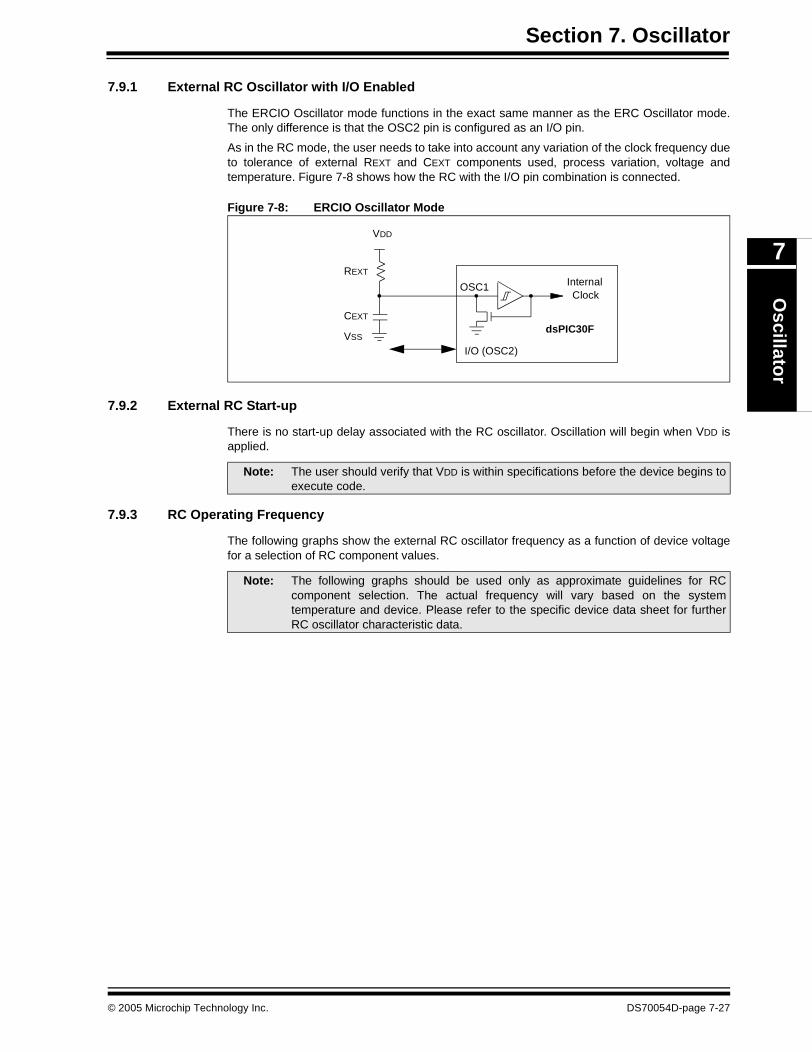
Section 7. OscillatorO
scillator
7
7.9.1 External RC Oscillator with I/O Enabled
The ERCIO Oscillator mode functions in the exact same manner as the ERC Oscillator mode.The only difference is that the OSC2 pin is configured as an I/O pin.
As in the RC mode, the user needs to take into account any variation of the clock frequency dueto tolerance of external REXT and CEXT components used, process variation, voltage andtemperature. Figure 7-8 shows how the RC with the I/O pin combination is connected.
Figure 7-8: ERCIO Oscillator Mode
7.9.2 External RC Start-up
There is no start-up delay associated with the RC oscillator. Oscillation will begin when VDD isapplied.
7.9.3 RC Operating Frequency
The following graphs show the external RC oscillator frequency as a function of device voltagefor a selection of RC component values.
I/O (OSC2)
CEXT
REXT
VSS
OSC1 InternalClock
VDD
dsPIC30F
Note: The user should verify that VDD is within specifications before the device begins toexecute code.
Note: The following graphs should be used only as approximate guidelines for RCcomponent selection. The actual frequency will vary based on the systemtemperature and device. Please refer to the specific device data sheet for furtherRC oscillator characteristic data.
© 2005 Microchip Technology Inc. DS70054D-page 7-27
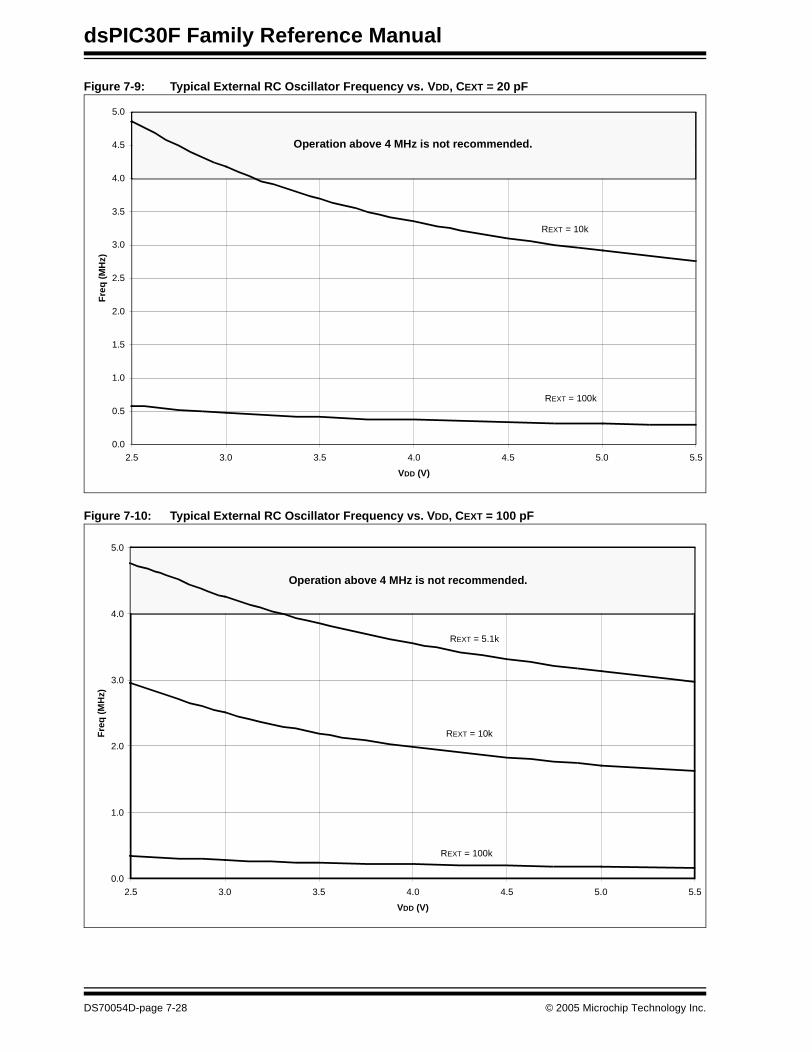
dsPIC30F Family Reference Manual
Figure 7-9: Typical External RC Oscillator Frequency vs. VDD, CEXT = 20 pF
Figure 7-10: Typical External RC Oscillator Frequency vs. VDD, CEXT = 100 pF
0.0
0.5
1.0
1.5
2.0
2.5
3.0
3.5
4.0
4.5
5.0
2.5 3.0 3.5 4.0 4.5 5.0 5.5
VDD (V)
Fre
q (
MH
z)
REXT = 10k
REXT = 100k
Operation above 4 MHz is not recommended.
0.0
1.0
2.0
3.0
4.0
5.0
2.5 3.0 3.5 4.0 4.5 5.0 5.5
VDD (V)
Fre
q (
MH
z)
REXT = 5.1k
REXT = 10k
REXT = 100k
Operation above 4 MHz is not recommended.
DS70054D-page 7-28 © 2005 Microchip Technology Inc.
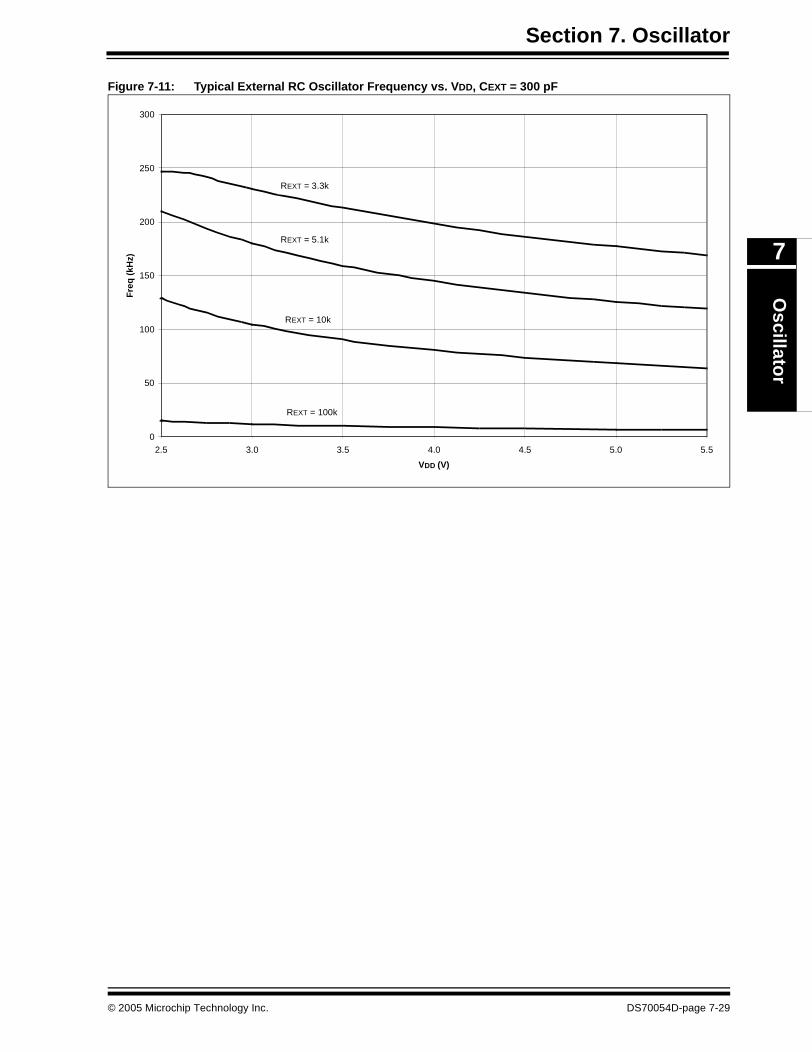
Section 7. OscillatorO
scillator
7
Figure 7-11: Typical External RC Oscillator Frequency vs. VDD, CEXT = 300 pF
0
50
100
150
200
250
300
2.5 3.0 3.5 4.0 4.5 5.0 5.5
VDD (V)
Fre
q (
kHz)
REXT = 3.3k
REXT = 5.1k
REXT = 10k
REXT = 100k
© 2005 Microchip Technology Inc. DS70054D-page 7-29
dsPIC30F Family Reference Manual
7.10 Phase Locked Loop (PLL)
The PLL can be enabled for x4, x8 or x16 Operation modes using the FPR<3:0> oscillatorConfiguration bits. The input and output frequency ranges for each Operating mode aresummarized in Table 7-7.
Table 7-7: PLL Frequency Range
7.10.1 PLL Lock Status
The PLL circuit is able to detect when the PLL enters a phase locked state. It can also detectwhen the PLL loses lock. The time delay for the PLL to achieve lock is designated as TLOCK. TheTLOCK value is nominally 20 μs. Refer to the “Electrical Specifications” in the specific device datasheet for further information.
The LOCK bit is a read-only Status bit (OSCCON<5>) that reflects the LOCK status of the PLL.The LOCK bit is cleared at a Power-on Reset.
7.10.1.1 Loss of PLL Lock During Clock Switching
When the PLL is selected as a destination clock source in a clock switch operation (including aPower-on Reset), the LOCK bit is cleared. The LOCK bit is set after phase lock has beenachieved. If the PLL fails to achieve lock, then the clock switching circuit will NOT switch to thePLL output for system clock; instead, it will continue to run with the old clock source.
7.10.1.2 Loss of PLL Lock During a Power-on Reset
If the PLL fails to achieve lock at a Power-on Reset (POR) and the Fail-Safe Clock Monitor(FSCM) is enabled, the FRC oscillator will become the device clock source and a clock failuretrap will occur.
7.10.1.3 Loss of PLL Lock During Normal Device Operation
If the PLL loses lock during normal operation for at least 4 input clock cycles, then the LOCK bitis cleared, indicating a loss of PLL lock. Furthermore, a clock failure trap will be generated. In thissituation, the processor continues to run using the PLL clock source. The user can switch toanother clock source in the Trap Service Routine, if desired.
Note: Some PLL output frequency ranges can be achieved that exceed the maximumoperating frequency of the dsPIC30F device. Refer to the “Electrical Specifications”in the specific device data sheet for further details.
FIN PLL Multiplier FOUT
4 MHz-10 MHz x4 16 MHz-40 MHz
4 MHz-10 MHz x8 32 MHz-80 MHz
4 MHz-7.5 MHz x16 64 MHz-120 MHz
Note: Refer to Section 6. “Reset Interrupts” for further details about oscillator failuretraps.
Note: A loss of PLL lock during normal device operation will generate a clock failure trap,but the system clock source will not be changed. The FSCM does not need to beenabled to detect the loss of lock.
DS70054D-page 7-30 © 2005 Microchip Technology Inc.
Section 7. OscillatorO
scillator
7
7.11 Low-Power 32 kHz Crystal Oscillator
The LP or Secondary oscillator is designed specifically for low power operation with a 32 kHzcrystal. The LP oscillator is located on the SOSCO and SOSCI device pins and serves as asecondary crystal clock source for low power operation. The LP oscillator can also drive Timer1for a real-time clock application.
7.11.1 LP Oscillator Enable
The following control bits affect the operation of the LP oscillator:
1. The COSC<1:0> bits in the OSCCON register (OSCCON<13:12>).
2. The LPOSCEN bit in the OSCCON register (OSCCON<1>).
When the LP Oscillator is enabled, the SOSCO and SOSCI I/O pins are controlled by theoscillator and cannot be used for other I/O functions.
7.11.1.1 LP Oscillator Continuous Operation
The LP oscillator will always be enabled if the LPOSCEN control bit (OSCCON<1>) is set. Thereare two reasons to leave the LP oscillator running. First, keeping the LP oscillator ON at all timesallows a fast switch to the 32 kHz system clock for lower power operation. Returning to the fastermain oscillator will still require an oscillator start-up time if it is a crystal type source (seeSection 7.12 “Oscillator Start-up Timer (OST)”). Second, the oscillator should remain ON atall times when using Timer1 as a real-time clock.
7.11.1.2 LP Oscillator Intermittent Operation
When the LPOSCEN control bit (OSCCON<1>) is cleared, the LP oscillator will only operatewhen it is selected as the current device clock source (COSC<1:0> = 00). The LP oscillator willbe disabled if it is the current device clock source and the device enters Sleep mode.
7.11.2 LP Oscillator Operation with Timer1
The LP oscillator can be used as a clock source for Timer1 in a real-time clock application. Referto Section 12. “Timers” for further details.
7.12 Oscillator Start-up Timer (OST)
In order to ensure that a crystal oscillator (or ceramic resonator) has started and stabilized, anOscillator Start-up Timer is provided. It is a simple 10-bit counter that counts 1024 TOSC cyclesbefore releasing the oscillator clock to the rest of the system. The time-out period is designatedas TOST. The amplitude of the oscillator signal must reach the VIL and VIH thresholds for theoscillator pins before the OST can begin to count cycles (see Figure 7-4).
The TOST time is involved every time the oscillator has to restart (i.e., on POR, BOR and wake-upfrom Sleep mode). The Oscillator Start-up Timer is applied to the LP oscillator and the XT, XTLand HS modes for the Primary oscillator.
7.13 Internal Fast RC Oscillator (FRC)
The FRC oscillator is a fast (7.37 MHz nominal) internal RC oscillator. This oscillator is intendedto provide a range of device operating speeds without the use of an external crystal, ceramicresonator or RC network. Devices featuring the Oscillator system VERSIONs 2 or 3 mayoptionally provide the FRC oscillator as an input frequency to the PLL.
© 2005 Microchip Technology Inc. DS70054D-page 7-31
dsPIC30F Family Reference Manual
7.14 Internal Low-Power RC (LPRC) Oscillator
The LPRC oscillator is a component of the Watchdog Timer (WDT) and oscillates at a nominalfrequency of 512 kHz. The LPRC oscillator is the clock source for the Power-up Timer (PWRT)circuit, WDT and clock monitor circuits. It may also be used to provide a low frequency clocksource option for applications where power consumption is critical, and timing accuracy is notrequired.
7.14.1 Enabling the LPRC Oscillator
The LPRC oscillator is always enabled at a Power-on Reset because it is the clock source forthe PWRT. After the PWRT expires, the LPRC oscillator will remain ON if one of the following isTRUE:
• The Fail-Safe Clock Monitor is enabled.
• The WDT is enabled.• The LPRC oscillator is selected as the system clock (COSC<1:0> = 10).
If none of the above conditions is true, the LPRC will shut-off after the PWRT expires.
7.15 Fail-Safe Clock Monitor (FSCM)
The Fail-Safe Clock Monitor (FSCM) allows the device to continue to operate even in the eventof an oscillator failure. The FSCM function is enabled by programming the FCKSM bits(Clock Switch and Monitor bits) in the FOSC Device Configuration register. Refer to7.3 “Oscillator Configuration” for further details. If the FSCM function is enabled, the LPRCinternal oscillator will run at all times (except during Sleep mode).
In the event of an oscillator failure, the FSCM will generate a clock failure trap and will switch thesystem clock to the FRC oscillator. The user will then have the option to either attempt to restartthe oscillator or execute a controlled shutdown.
The FSCM module will take the following actions when switching to the FRC oscillator:
1. The COSC<1:0> bits are loaded with ‘01’.2. The CF bit is set to indicate the clock failure.3. The OSWEN control bit is cleared to cancel any pending clock switches.
7.15.1 FSCM Delay
On a POR, BOR or wake-up event from Sleep mode, a nominal 100 μs delay (TFSCM) may beinserted before the FSCM begins to monitor the system clock source. The purpose of the FSCMdelay is to provide time for the oscillator and/or PLL to stabilize when the Power-up Timer(PWRT) is not utilized. The FSCM delay will be generated after the internal System Reset signal,SYSRST, has been released. Refer to Section 8. “Reset” for FSCM delay timing information.
The FSCM delay, TFSCM, is applied when the FSCM is enabled and any of the following deviceclock sources is selected as the system clock:
• EC+PLL
• XT+PLL• XT• HS
• HS/2 or HS/3 + PLL• XTL• LP
Note: The oscillation frequency of the LPRC oscillator will vary depending on the devicevoltage and operating temperature. Refer to the “Electrical Specifications” in thespecific device data sheet for further details.
Note: For more information about the oscillator failure trap, please refer toSection 6. “Reset Interrupts”.
Note: Please refer to the “Electrical Specifications” section of the device data sheet forTFSCM specification values.
DS70054D-page 7-32 © 2005 Microchip Technology Inc.
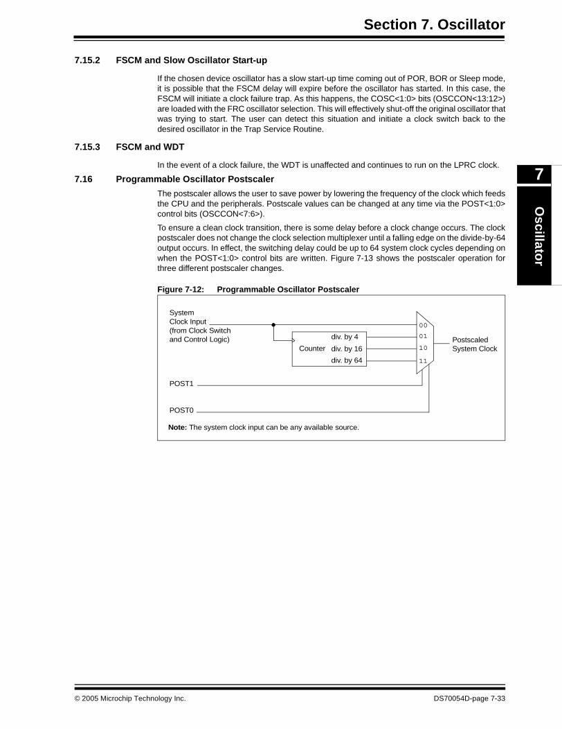
Section 7. OscillatorO
scillator
7
7.15.2 FSCM and Slow Oscillator Start-up
If the chosen device oscillator has a slow start-up time coming out of POR, BOR or Sleep mode,it is possible that the FSCM delay will expire before the oscillator has started. In this case, theFSCM will initiate a clock failure trap. As this happens, the COSC<1:0> bits (OSCCON<13:12>)are loaded with the FRC oscillator selection. This will effectively shut-off the original oscillator thatwas trying to start. The user can detect this situation and initiate a clock switch back to thedesired oscillator in the Trap Service Routine.
7.15.3 FSCM and WDT
In the event of a clock failure, the WDT is unaffected and continues to run on the LPRC clock.
7.16 Programmable Oscillator Postscaler
The postscaler allows the user to save power by lowering the frequency of the clock which feedsthe CPU and the peripherals. Postscale values can be changed at any time via the POST<1:0>control bits (OSCCON<7:6>).
To ensure a clean clock transition, there is some delay before a clock change occurs. The clockpostscaler does not change the clock selection multiplexer until a falling edge on the divide-by-64output occurs. In effect, the switching delay could be up to 64 system clock cycles depending onwhen the POST<1:0> control bits are written. Figure 7-13 shows the postscaler operation forthree different postscaler changes.
Figure 7-12: Programmable Oscillator Postscaler
Counter
div. by 4
div. by 16
div. by 64
System
POST1
POST0
00
01
10
11
Clock Input
PostscaledSystem Clock
(from Clock Switchand Control Logic)
Note: The system clock input can be any available source.
© 2005 Microchip Technology Inc. DS70054D-page 7-33

dsPIC30F Family Reference Manual
Figure 7-13: Postscaler Update Timing
7.17 Clock Switching Operation
The selection of clock sources available for clock switching during device operation are asfollows:
• Primary oscillator on OSC1/OSC2 pins• Low-Power 32 kHz Crystal (Secondary) oscillator on SOSCO/SOSCI pins• Internal Fast RC (FRC) oscillator
• Internal Low-Power RC (LPRC) oscillator
7.17.1 Clock Switching Enable
To enable clock switching, the FCKSM1 Configuration bit in the FOSC Configuration register mustbe programmed to a ‘0’. (Refer to 7.3 “Oscillator Configuration” for further details.)
If the FCKSM1 Configuration bit is a ‘1’ (unprogrammed), then the clock switching function isdisabled. The Fail-Safe Clock Monitor function is also disabled. This is the default setting. TheNOSC control bits in OSCCON do not control the clock selection when clock switching isdisabled. However, the COSC bits in OSCCON will reflect the clock source selected by the FPRand FOS Configuration bits in the FOSC Configuration register. The OSWEN control bit(OSCCON<0>) has no effect when clock switching is disabled. It is held at ‘0’ at all times.
Divideby 4
Divideby 16
Divideby 64
POST<1:0> 0001 10 11
Postscaled
SystemClock
System
1:4 1:16 1:1 1:64Clock
Note: This diagram demonstrates the clock postscaler function only. The divide ratios shown in the timing diagram are not correct.
Note: The Primary oscillator has multiple operating modes (EC, RC, XT, FRC etc.). TheOperating mode of the Primary oscillator is determined by the FPR Configurationbits in the FOSC device Configuration register. (Refer to 7.3 “Oscillator Configura-tion” for further details.)
DS70054D-page 7-34 © 2005 Microchip Technology Inc.
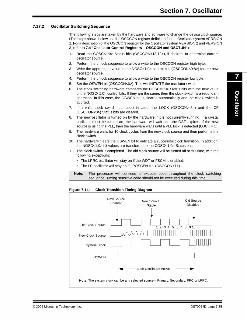
Section 7. OscillatorO
scillator
7
7.17.2 Oscillator Switching Sequence
The following steps are taken by the hardware and software to change the device clock source.(The steps shown below use the OSCCON register definition for the Oscillator system VERSION1. For a description of the OSCCON register for the Oscillator system VERSION 2 and VERSION3, refer to 7.4 “Oscillator Control Registers – OSCCON and OSCTUN”):
1. Read the COSC<1:0> Status bits (OSCCON<13:12>), if desired, to determine currentoscillator source.
2. Perform the unlock sequence to allow a write to the OSCCON register high byte.3. Write the appropriate value to the NOSC<1:0> control bits (OSCCON<9:8>) for the new
oscillator source.4. Perform the unlock sequence to allow a write to the OSCCON register low byte.5. Set the OSWEN bit (OSCCON<0>). This will INITIATE the oscillator switch.
6. The clock switching hardware compares the COSC<1:0> Status bits with the new valueof the NOSC<1:0> control bits. If they are the same, then the clock switch is a redundantoperation. In this case, the OSWEN bit is cleared automatically and the clock switch isaborted.
7. If a valid clock switch has been initiated, the LOCK (OSCCON<5>) and the CF(OSCCON<3>) Status bits are cleared.
8. The new oscillator is turned on by the hardware if it is not currently running. If a crystaloscillator must be turned on, the hardware will wait until the OST expires. If the newsource is using the PLL, then the hardware waits until a PLL lock is detected (LOCK = 1).
9. The hardware waits for 10 clock cycles from the new clock source and then performs theclock switch.
10. The hardware clears the OSWEN bit to indicate a successful clock transition. In addition,the NOSC<1:0> bit values are transferred to the COSC<1:0> Status bits.
11. The clock switch is completed. The old clock source will be turned off at this time, with thefollowing exceptions:
• The LPRC oscillator will stay on if the WDT or FSCM is enabled.• The LP oscillator will stay on if LPOSCEN = 1 (OSCCON<1>).
Figure 7-14: Clock Transition Timing Diagram
Note: The processor will continue to execute code throughout the clock switchingsequence. Timing sensitive code should not be executed during this time.
Old Clock Source
New Clock Source
System Clock
Both Oscillators Active
OSWEN
1 2 3 4 5 6 7 8 9 10
New SourceEnabled
New SourceStable
Old SourceDisabled
Note: The system clock can be any selected source – Primary, Secondary, FRC or LPRC.
© 2005 Microchip Technology Inc. DS70054D-page 7-35
dsPIC30F Family Reference Manual
7.17.3 Clock Switching Tips
• If the destination clock source is a crystal oscillator, the clock switch time will be dominated by the oscillator start-up time.
• If the new clock source does not start, or is not present, then the clock switching hardware will simply wait for the 10 synchronization cycles to occur. The user can detect this situation because the OSWEN bit (OSCCON<0>) remains set indefinitely.
• If the new clock source uses the PLL, a clock switch will not occur until lock has been achieved. The user can detect a loss of PLL lock because the LOCK bit will be cleared and the OSWEN bit is set.
• The user may wish to consider the settings of the POST<1:0> control bits (OSCCON<7:6>) when executing a clock switch. Switching to a low frequency clock source, such as the LP oscillator with a postscaler ratio greater than 1:1, will result in very slow device operation.
7.17.4 Aborting a Clock Switch
In the event the clock switch did not complete, the clock switch logic can be reset by clearing theOSWEN bit. Clearing the OSWEN bit (OSCCON<0>) will:
1. Abandon the clock switch2. Stop and reset the OST, if applicable
3. Stop the PLL, if applicable
A clock switch procedure can be aborted at any time.
7.17.5 Entering Sleep Mode During a Clock Switch
If the device enters Sleep mode during a clock switch operation, the clock switch operation isaborted. The processor keeps the old clock selection and the OSWEN bit is cleared. The PWRSAVinstruction is then executed normally.
7.17.6 Recommended Code Sequence for Clock Switching
The following steps should be taken to change the oscillator source:
• Disable interrupts during the OSCCON register unlock and write sequence.• Execute unlock sequence for OSCCON high byte.
• Write new oscillator source to NOSC control bits. • Execute unlock sequence for OSCCON low byte.• Set OSWEN bit.
• Continue to execute code that is not clock sensitive (optional).• Invoke an appropriate amount of software delay (cycle counting) to allow for oscillator
and/or PLL start-up.• Check to see if OSWEN is ‘0’. If it is, we are DONE SUCCESSFULLY.• If OSWEN is still set, then check LOCK bit to determine cause of failure.
Note: The application should not attempt to switch to a clock of frequency lower than100 kHz when the Fail-Safe Clock Monitor is enabled. If such clock switching isperformed, the device may generate an oscillator fail trap and switch to the Fast RCoscillator.
DS70054D-page 7-36 © 2005 Microchip Technology Inc.
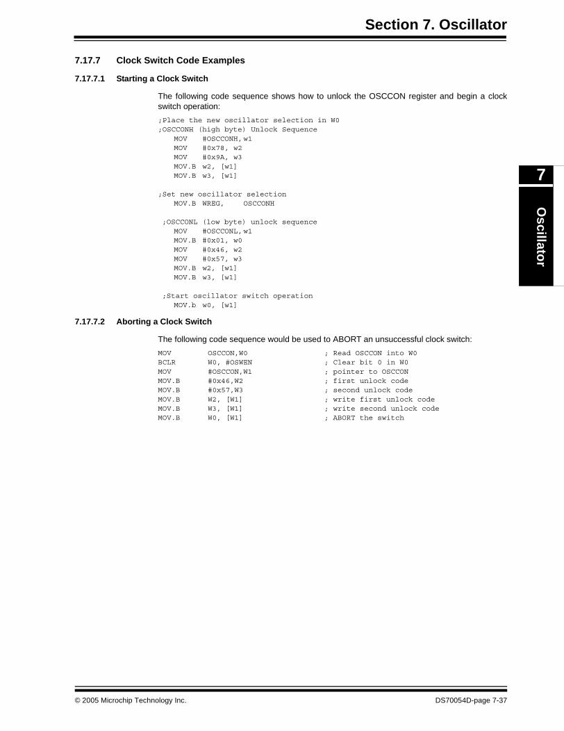
Section 7. OscillatorO
scillator
7
7.17.7 Clock Switch Code Examples
7.17.7.1 Starting a Clock Switch
The following code sequence shows how to unlock the OSCCON register and begin a clockswitch operation:
;Place the new oscillator selection in W0;OSCCONH (high byte) Unlock Sequence
MOV #OSCCONH,w1MOV #0x78, w2MOV #0x9A, w3MOV.B w2, [w1]MOV.B w3, [w1]
;Set new oscillator selectionMOV.B WREG, OSCCONH
;OSCCONL (low byte) unlock sequenceMOV #OSCCONL,w1MOV.B #0x01, w0MOV #0x46, w2MOV #0x57, w3MOV.B w2, [w1]MOV.B w3, [w1]
;Start oscillator switch operationMOV.b w0, [w1]
7.17.7.2 Aborting a Clock Switch
The following code sequence would be used to ABORT an unsuccessful clock switch:
MOV OSCCON,W0 ; Read OSCCON into W0BCLR W0, #OSWEN ; Clear bit 0 in W0MOV #OSCCON,W1 ; pointer to OSCCONMOV.B #0x46,W2 ; first unlock codeMOV.B #0x57,W3 ; second unlock codeMOV.B W2, [W1] ; write first unlock codeMOV.B W3, [W1] ; write second unlock codeMOV.B W0, [W1] ; ABORT the switch
© 2005 Microchip Technology Inc. DS70054D-page 7-37
dsPIC30F Family Reference Manual
7.18 Design Tips
Question 1: When looking at the OSC2 pin after power-up with an oscilloscope, there isno clock. What can cause this?
Answer:
1. Entering Sleep mode with no source for wake-up (such as, WDT, MCLR, or an interrupt).Verify that the code does not put the device to Sleep without providing for wake-up. If it ispossible, try waking it up with a low pulse on MCLR. Powering up with MCLR held low willalso give the crystal oscillator more time to start-up, but the Program Counter will notadvance until the MCLR pin is high.
2. The wrong Clock mode is selected for the desired frequency. For a blank device, thedefault oscillator is EC + 16x PLL. Most parts come with the clock selected in the Defaultmode, which will not start oscillation with a crystal or resonator. Verify that the Clock modehas been programmed correctly.
3. The proper power-up sequence has not been followed. If a CMOS part is powered throughan I/O pin prior to power-up, bad things can happen (latch-up, improper start-up, etc.). Itis also possible for brown-out conditions, noisy power lines at start-up, and slow VDD risetimes to cause problems. Try powering up the device with nothing connected to the I/O,and power-up with a known, good, fast rise, power supply. Refer to the power-upinformation in the device data sheet for considerations on brown-out and power-upsequences.
4. The C1 and C2 capacitors attached to the crystal have not been connected properly orare not the correct values. Make sure all connections are correct. The device data sheetvalues for these components will usually get the oscillator running; however, they justmight not be the optimal values for your design.
Question 2: The device starts, but runs at a frequency much higher than the resonantfrequency of the crystal.
Answer: The gain is too high for this oscillator circuit. Refer to Section 7.6 “Crystal Oscilla-tors/Ceramic Resonators” to aid in the selection of C2 (may need to be higher), Rs (may beneeded) and Clock mode (wrong mode may be selected). This is especially possible for lowfrequency crystals, like the common 32.768 kHz.
Question 3: The design runs fine, but the frequency is slightly off. What can be done toadjust this?
Answer: Changing the value of C1 has some effect on the oscillator frequency. If a SERIESresonant crystal is used, it will resonate at a different frequency than a PARALLEL resonantcrystal of the same frequency call-out. Ensure that you are using a PARALLEL resonant crystal.
Question 4: The board works fine, then suddenly quits or loses time.
Answer: Other than the obvious software checks that should be done to investigate losing time,it is possible that the amplitude of the oscillator output is not high enough to reliably trigger theoscillator input. Look at the C1 and C2 values and ensure that the device Configuration bits arecorrect for the desired oscillator mode.
Question 5: If I put an oscilloscope probe on an oscillator pin, I don’t see what I expect.Why?
Answer: Remember that an oscilloscope probe has capacitance. Connecting the probe to theoscillator circuitry will modify the oscillator characteristics. Consider using a low capacitance(active) probe.
DS70054D-page 7-38 © 2005 Microchip Technology Inc.
Section 7. OscillatorO
scillator
7
7.19 Related Application Notes
This section lists application notes that are related to this section of the manual. Theseapplication notes may not be written specifically for the dsPIC30F Product Family, but theconcepts are pertinent and could be used with modification and possible limitations. The currentapplication notes related to the Oscillator module are:
Title Application Note #
PICmicro® Microcontroller Oscillator Design Guide AN588Low Power Design using PICmicro® Microcontrollers AN606Crystal Oscillator Basics and Crystal Selection for rfPIC® and PICmicro® Devices AN826
Note: Please visit the Microchip web site (www.microchip.com) for additional ApplicationNotes and code examples for the dsPIC30F Family of devices.
© 2005 Microchip Technology Inc. DS70054D-page 7-39
dsPIC30F Family Reference Manual
7.20 Revision History
Revision A
This is the initial released revision of this document.
Revision B
This revision incorporates technical content changes for the dsPIC30F Oscillator module.
Revision C
This revision incorporates all known errata at the time of this document update.
Revision D
This revision incorporates details on the three versions (VERSION 1, VERSION 2 and VERSION3) of the Oscillator system implemented in dsPIC30F devices in the General Purpose, Sensorand Motor Control families.
DS70054D-page 7-40 © 2005 Microchip Technology Inc.
Section 8. Reset
Reset
8
HIGHLIGHTS
This section of the manual contains the following topics:
8.1 Introduction .................................................................................................................... 8-2
8.2 Clock Source Selection at Reset ................................................................................... 8-58.3 POR: Power-on Reset ................................................................................................... 8-58.4 External Reset (EXTR) .................................................................................................. 8-7
8.5 Software Reset Instruction (SWR) ................................................................................. 8-78.6 Watchdog Time-out Reset (WDTR) ............................................................................... 8-78.7 Brown-out Reset (BOR) ................................................................................................. 8-8
8.8 Using the RCON Status Bits ........................................................................................ 8-108.9 Device Reset Times..................................................................................................... 8-118.10 Device Start-up Time Lines .......................................................................................... 8-13
8.11 Special Function Register Reset States....................................................................... 8-168.12 Design Tips .................................................................................................................. 8-178.13 Related Application Notes............................................................................................ 8-18
8.14 Revision History ........................................................................................................... 8-19
© 2004 Microchip Technology Inc. DS70055C-page 8-1
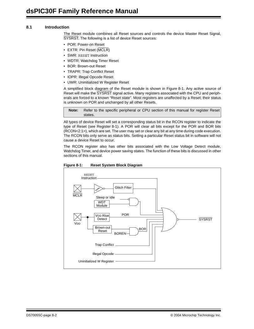
dsPIC30F Family Reference Manual
8.1 Introduction
The Reset module combines all Reset sources and controls the device Master Reset Signal,SYSRST. The following is a list of device Reset sources:
• POR: Power-on Reset • EXTR: Pin Reset (MCLR)
• SWR: RESET Instruction• WDTR: Watchdog Timer Reset• BOR: Brown-out Reset
• TRAPR: Trap Conflict Reset• IOPR: Illegal Opcode Reset• UWR: Uninitialized W Register Reset
A simplified block diagram of the Reset module is shown in Figure 8-1. Any active source ofReset will make the SYSRST signal active. Many registers associated with the CPU and periph-erals are forced to a known “Reset state”. Most registers are unaffected by a Reset; their statusis unknown on POR and unchanged by all other Resets.
All types of device Reset will set a corresponding status bit in the RCON register to indicate thetype of Reset (see Register 8-1). A POR will clear all bits except for the POR and BOR bits(RCON<2:1>), which are set. The user may set or clear any bit at any time during code execution.The RCON bits only serve as status bits. Setting a particular Reset status bit in software will notcause a device Reset to occur.
The RCON register also has other bits associated with the Low Voltage Detect module,Watchdog Timer, and device power saving states. The function of these bits is discussed in othersections of this manual.
Figure 8-1: Reset System Block Diagram
Note: Refer to the specific peripheral or CPU section of this manual for register Resetstates.
MCLR
VDD
VDD RiseDetect
POR
Sleep or Idle
Brown-outReset
BOREN
RESETInstruction
WDTModule
Glitch Filter
BOR
Trap Conflict
Illegal Opcode
Uninitialized W Register
SYSRST
DS70055C-page 8-2 © 2004 Microchip Technology Inc.
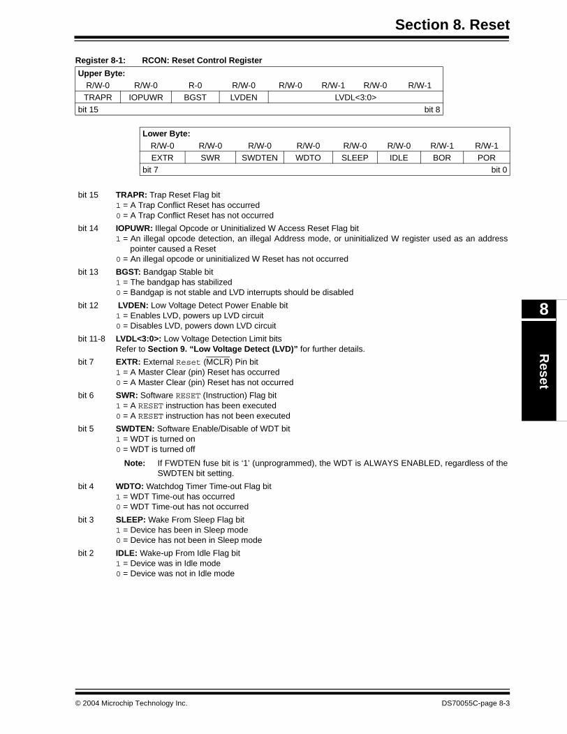
Section 8. ResetR
eset
8
Register 8-1: RCON: Reset Control Register
Upper Byte:R/W-0 R/W-0 R-0 R/W-0 R/W-0 R/W-1 R/W-0 R/W-1
TRAPR IOPUWR BGST LVDEN LVDL<3:0>
bit 15 bit 8
Lower Byte:R/W-0 R/W-0 R/W-0 R/W-0 R/W-0 R/W-0 R/W-1 R/W-1EXTR SWR SWDTEN WDTO SLEEP IDLE BOR POR
bit 7 bit 0
bit 15 TRAPR: Trap Reset Flag bit1 = A Trap Conflict Reset has occurred0 = A Trap Conflict Reset has not occurred
bit 14 IOPUWR: Illegal Opcode or Uninitialized W Access Reset Flag bit1 = An illegal opcode detection, an illegal Address mode, or uninitialized W register used as an address
pointer caused a Reset0 = An illegal opcode or uninitialized W Reset has not occurred
bit 13 BGST: Bandgap Stable bit1 = The bandgap has stabilized0 = Bandgap is not stable and LVD interrupts should be disabled
bit 12 LVDEN: Low Voltage Detect Power Enable bit1 = Enables LVD, powers up LVD circuit0 = Disables LVD, powers down LVD circuit
bit 11-8 LVDL<3:0>: Low Voltage Detection Limit bitsRefer to Section 9. “Low Voltage Detect (LVD)” for further details.
bit 7 EXTR: External Reset (MCLR) Pin bit1 = A Master Clear (pin) Reset has occurred0 = A Master Clear (pin) Reset has not occurred
bit 6 SWR: Software RESET (Instruction) Flag bit1 = A RESET instruction has been executed0 = A RESET instruction has not been executed
bit 5 SWDTEN: Software Enable/Disable of WDT bit1 = WDT is turned on0 = WDT is turned off
Note: If FWDTEN fuse bit is ‘1’ (unprogrammed), the WDT is ALWAYS ENABLED, regardless of theSWDTEN bit setting.
bit 4 WDTO: Watchdog Timer Time-out Flag bit1 = WDT Time-out has occurred0 = WDT Time-out has not occurred
bit 3 SLEEP: Wake From Sleep Flag bit1 = Device has been in Sleep mode0 = Device has not been in Sleep mode
bit 2 IDLE: Wake-up From Idle Flag bit1 = Device was in Idle mode0 = Device was not in Idle mode
© 2004 Microchip Technology Inc. DS70055C-page 8-3
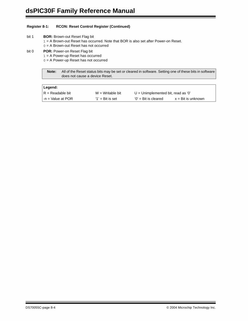
dsPIC30F Family Reference Manual
Register 8-1: RCON: Reset Control Register (Continued)
bit 1 BOR: Brown-out Reset Flag bit1 = A Brown-out Reset has occurred. Note that BOR is also set after Power-on Reset.0 = A Brown-out Reset has not occurred
bit 0 POR: Power-on Reset Flag bit1 = A Power-up Reset has occurred0 = A Power-up Reset has not occurred
Note: All of the Reset status bits may be set or cleared in software. Setting one of these bits in softwaredoes not cause a device Reset.
Legend:
R = Readable bit W = Writable bit U = Unimplemented bit, read as ‘0’
-n = Value at POR ‘1’ = Bit is set ‘0’ = Bit is cleared x = Bit is unknown
DS70055C-page 8-4 © 2004 Microchip Technology Inc.
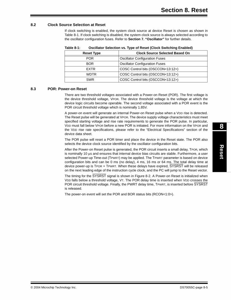
Section 8. ResetR
eset
8
8.2 Clock Source Selection at Reset
If clock switching is enabled, the system clock source at device Reset is chosen as shown inTable 8-1. If clock switching is disabled, the system clock source is always selected according tothe oscillator configuration fuses. Refer to Section 7. “Oscillator” for further details.
Table 8-1: Oscillator Selection vs. Type of Reset (Clock Switching Enabled)
8.3 POR: Power-on Reset
There are two threshold voltages associated with a Power-on Reset (POR). The first voltage isthe device threshold voltage, VPOR. The device threshold voltage is the voltage at which thedevice logic circuits become operable. The second voltage associated with a POR event is thePOR circuit threshold voltage which is nominally 1.85V.
A power-on event will generate an internal Power-on Reset pulse when a VDD rise is detected.The Reset pulse will be generated at VPOR. The device supply voltage characteristics must meetspecified starting voltage and rise rate requirements to generate the POR pulse. In particular,VDD must fall below VPOR before a new POR is initiated. For more information on the VPOR andthe VDD rise rate specifications, please refer to the “Electrical Specifications” section of thedevice data sheet.
The POR pulse will reset a POR timer and place the device in the Reset state. The POR alsoselects the device clock source identified by the oscillator configuration bits.
After the Power-on Reset pulse is generated, the POR circuit inserts a small delay, TPOR, whichis nominally 10 μs and ensures that internal device bias circuits are stable. Furthermore, a userselected Power-up Time-out (TPWRT) may be applied. The TPWRT parameter is based on deviceconfiguration bits and can be 0 ms (no delay), 4 ms, 16 ms or 64 ms. The total delay time atdevice power-up is TPOR + TPWRT. When these delays have expired, SYSRST will be releasedon the next leading edge of the instruction cycle clock, and the PC will jump to the Reset vector.
The timing for the SYSRST signal is shown in Figure 8-2. A Power-on Reset is initialized whenVDD falls below a threshold voltage, VT. The POR delay time is inserted when VDD crosses thePOR circuit threshold voltage. Finally, the PWRT delay time, TPWRT, is inserted before SYSRSTis released.
The power-on event will set the POR and BOR status bits (RCON<1:0>).
Reset Type Clock Source Selected Based On
POR Oscillator Configuration Fuses
BOR Oscillator Configuration Fuses
EXTR COSC Control bits (OSCCON<13:12>)
WDTR COSC Control bits (OSCCON<13:12>)
SWR COSC Control bits (OSCCON<13:12>)
© 2004 Microchip Technology Inc. DS70055C-page 8-5
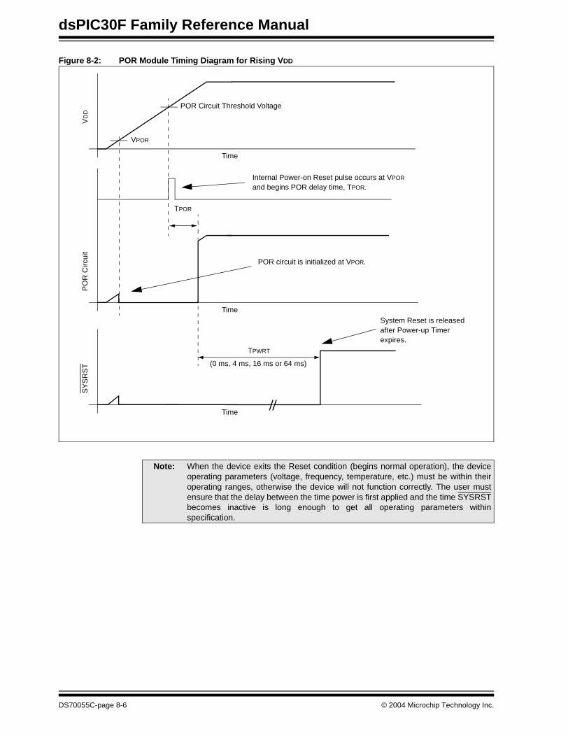
dsPIC30F Family Reference Manual
Figure 8-2: POR Module Timing Diagram for Rising VDD
TPOR
VD
DP
OR
Circ
uit
Time
Time
VPOR
POR Circuit Threshold Voltage
SY
SR
ST
Time
TPWRT
Internal Power-on Reset pulse occurs at VPOR
and begins POR delay time, TPOR.
POR circuit is initialized at VPOR.
System Reset is releasedafter Power-up Timerexpires.
(0 ms, 4 ms, 16 ms or 64 ms)
Note: When the device exits the Reset condition (begins normal operation), the deviceoperating parameters (voltage, frequency, temperature, etc.) must be within theiroperating ranges, otherwise the device will not function correctly. The user mustensure that the delay between the time power is first applied and the time SYSRSTbecomes inactive is long enough to get all operating parameters withinspecification.
DS70055C-page 8-6 © 2004 Microchip Technology Inc.
Section 8. ResetR
eset
8
8.3.1 Using the POR Circuit
To take advantage of the POR circuit, just tie the MCLR pin directly to VDD. This will eliminateexternal RC components usually needed to create a Power-on Reset delay. A minimum rise timefor VDD is required. Refer to the “Electrical Specifications” section in the specific device datasheet for further details.
Depending on the application, a resistor may be required between the MCLR pin and VDD. Thisresistor can be used to decouple the MCLR pin from a noisy power supply rail. The resistor willalso be necessary if the device programming voltage, VPP, needs to be placed on the MCLR pinwhile the device is installed in the application circuit. VPP is 13 volts for most devices.
Figure 8-3 shows a possible POR circuit for a slow power supply ramp up. The externalPower-on Reset circuit is only required if the device would exit Reset before the device VDD is inthe valid operating range. The diode, D, helps discharge the capacitor quickly when VDD powersdown.
Figure 8-3: External Power-on Reset Circuit (For Slow VDD Rise Time)
8.3.2 Power-up Timer (PWRT)
The PWRT provides an optional time delay (TPWRT) before SYSRST is released at a device PORor BOR (Brown-out Reset). The PWRT time delay is provided in addition to the POR delay time(TPOR). The PWRT time delay may be 0 ms, 4 ms, 16 ms or 64 ms nominal (see Figure 8-2).
The PWRT delay time is selected using the FPWRT<1:0> configuration fuses in the FBORPORDevice Configuration register. Refer to Section 24. “Device Configuration” for further details.
8.4 External Reset (EXTR)
Whenever the MCLR pin is driven low, the device will asynchronously assert SYSRST, providedthe input pulse on MCLR is longer than a certain minimum width. (Refer to the “ElectricalSpecifications” in the specific device data sheet for further details.) When the MCLR pin isreleased, SYSRST will be released on the next instruction clock cycle, and the Reset vector fetchwill commence. The processor will maintain the existing clock source that was in use before theEXTR occurred. The EXTR status bit (RCON<7>) will be set to indicate the MCLR Reset.
8.5 Software RESET Instruction (SWR)
Whenever the RESET instruction is executed, the device will assert SYSRST, placing the devicein a special Reset state. This Reset state will not re-initialize the clock. The clock source in effectprior to the RESET instruction will remain. SYSRST will be released at the next instruction cycle,and the Reset vector fetch will commence.
8.6 Watchdog Time-out Reset (WDTR)
Whenever a Watchdog time-out occurs, the device will asynchronously assert SYSRST. Theclock source will remain unchanged. Note that a WDT time-out during Sleep or Idle mode willwake-up the processor, but NOT reset the processor. For more information, refer to Section10. “Watchdog Timer and Power Saving Modes”.
Note 1: The value of R should be low enough so that the voltage drop across it does not violate the VIH specification of the MCLR pin.
2: R1 will limit any current flowing into MCLR from external capacitor C in the event of MCLR/VPP pin breakdown, due to Electrostatic Discharge (ESD) or Electrical Overstress (EOS).
R1MCLR
dsPIC30F
RD
C
VDD VDD
© 2004 Microchip Technology Inc. DS70055C-page 8-7
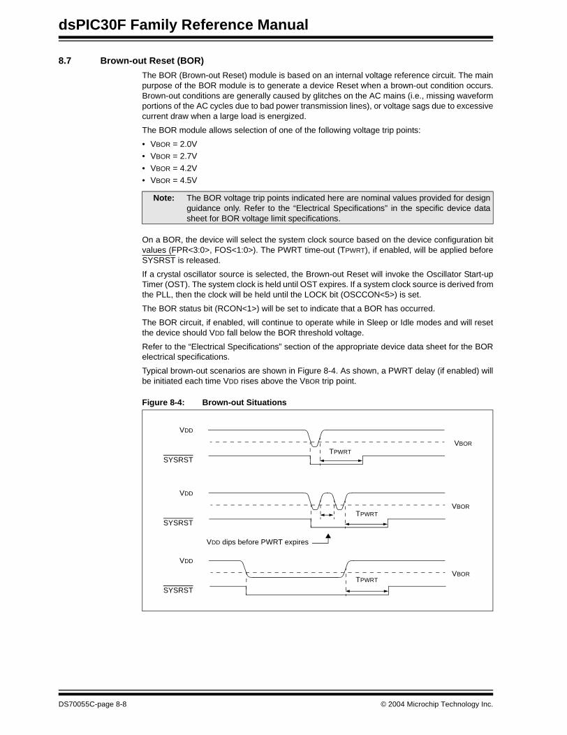
dsPIC30F Family Reference Manual
8.7 Brown-out Reset (BOR)
The BOR (Brown-out Reset) module is based on an internal voltage reference circuit. The mainpurpose of the BOR module is to generate a device Reset when a brown-out condition occurs.Brown-out conditions are generally caused by glitches on the AC mains (i.e., missing waveformportions of the AC cycles due to bad power transmission lines), or voltage sags due to excessivecurrent draw when a large load is energized.
The BOR module allows selection of one of the following voltage trip points:
• VBOR = 2.0V• VBOR = 2.7V
• VBOR = 4.2V• VBOR = 4.5V
On a BOR, the device will select the system clock source based on the device configuration bitvalues (FPR<3:0>, FOS<1:0>). The PWRT time-out (TPWRT), if enabled, will be applied beforeSYSRST is released.
If a crystal oscillator source is selected, the Brown-out Reset will invoke the Oscillator Start-upTimer (OST). The system clock is held until OST expires. If a system clock source is derived fromthe PLL, then the clock will be held until the LOCK bit (OSCCON<5>) is set.
The BOR status bit (RCON<1>) will be set to indicate that a BOR has occurred.
The BOR circuit, if enabled, will continue to operate while in Sleep or Idle modes and will resetthe device should VDD fall below the BOR threshold voltage.
Refer to the “Electrical Specifications” section of the appropriate device data sheet for the BORelectrical specifications.
Typical brown-out scenarios are shown in Figure 8-4. As shown, a PWRT delay (if enabled) willbe initiated each time VDD rises above the VBOR trip point.
Figure 8-4: Brown-out Situations
Note: The BOR voltage trip points indicated here are nominal values provided for designguidance only. Refer to the “Electrical Specifications” in the specific device datasheet for BOR voltage limit specifications.
VDD
SYSRST
VBOR
VDD
SYSRST
VBOR
VDD
SYSRST
VBOR TPWRT
TPWRT
TPWRT
VDD dips before PWRT expires
DS70055C-page 8-8 © 2004 Microchip Technology Inc.
Section 8. ResetR
eset
8
8.7.1 BOR Configuration
The BOR module is enabled/disabled and configured via device configuration fuses.
The BOR module is enabled by default and may be disabled (to reduce power consumption) byprogramming the BOREN device configuration fuse to a ‘0’ (FBORPOR<7>). The BORENconfiguration fuse is located in the FBORPOR Device Configuration register. The BOR voltagetrip point (VBOR) is selected using the BORV<1:0> configuration fuses (FBOR<5:4>). Refer toSection 24. “Device Configuration” for further details.
8.7.2 Current Consumption for BOR Operation
The BOR circuit relies on an internal voltage reference circuit that is shared with other peripheraldevices, such as the Low Voltage Detect module. The internal voltage reference will be activewhenever one of its associated peripherals is enabled. For this reason, the user may not observethe expected change in current consumption when the BOR is disabled.
8.7.3 Illegal Opcode Reset
A device Reset will be generated if the device attempts to execute an illegal opcode value thatwas fetched from program memory. The Illegal Opcode Reset function can prevent the devicefrom executing program memory sections that are used to store constant data. To takeadvantage of the Illegal Opcode Reset, use only the lower 16 bits of each program memorysection to store the data values. The upper 8 bits should be programmed with 0x3F, which is anillegal opcode value.
If a device Reset occurs as a result of an illegal opcode value, the IOPUWR status bit(RCON<14>) will be set.
8.7.4 Uninitialized W Register Reset
The W register array (with the exception of W15) is cleared during all Resets and is considereduninitialized until written to. An attempt to use an uninitialized register as an address pointer willreset the device. Furthermore, the IOPUWR status bit (RCON<14>) will be set.
8.7.5 Trap Conflict Reset
A device Reset will occur whenever multiple hard trap sources become pending at the sametime. The TRAPR status bit (RCON<15>) will be set. Refer to Section 6. “Reset Interrupts” formore information on Trap Conflict Resets.
© 2004 Microchip Technology Inc. DS70055C-page 8-9
dsPIC30F Family Reference Manual
8.8 Using the RCON Status Bits
The user can read the RCON register after any device Reset to determine the cause of theReset.
Table 8-2 provides a summary of the Reset flag bit operation.
Table 8-2: Reset Flag Bit Operation
Note: The status bits in the RCON register should be cleared after they are read so thatthe next RCON register value after a device Reset will be meaningful.
Flag Bit Set by: Cleared by:
TRAPR (RCON<15>) Trap conflict event POR
IOPWR (RCON<14>) Illegal opcode or uninitialized W register access
POR
EXTR (RCON<7>) MCLR Reset POR
SWR (RCON<6>) RESET instruction POR
WDTO (RCON<4>) WDT time-out PWRSAV instruction, POR
SLEEP (RCON<3>) PWRSAV #SLEEP instruction POR
IDLE (RCON<2>) PWRSAV #IDLE instruction POR
BOR (RCON<1>) POR, BOR
POR (RCON<0>) POR
Note: All RESET flag bits may be set or cleared by the user software.
DS70055C-page 8-10 © 2004 Microchip Technology Inc.
Section 8. ResetR
eset
8
8.9 Device Reset Times
The Reset times for various types of device Reset are summarized in Table 8-3. Note that thesystem Reset signal, SYSRST, is released after the POR delay time and PWRT delay timesexpire.
The time that the device actually begins to execute code will also depend on the system oscillatordelays, which include the Oscillator Start-up Timer (OST) and the PLL lock time. The OST andPLL lock times occur in parallel with the applicable SYSRST delay times.
The FSCM delay determines the time at which the FSCM begins to monitor the system clocksource after the SYSRST signal is released.
Table 8-3: Reset Delay Times for Various Device Resets
Reset Type Clock Source SYSRST DelaySystem Clock
DelayFSCMDelay
Notes
POR EC, EXTRC, FRC, LPRC
TPOR + TPWRT — — 1, 2
EC + PLL TPOR + TPWRT TLOCK TFSCM 1, 2, 4, 5
XT, HS, XTL, LP TPOR + TPWRT TOST TFSCM 1, 2, 3, 5
XT + PLL TPOR + TPWRT TOST + TLOCK TFSCM 1, 2, 3, 4, 5
BOR EC, EXTRC, FRC, LPRC
TPWRT — — 2
EC + PLL TPWRT TLOCK TFSCM 1, 2, 4, 5
XT, HS, XTL, LP TPWRT TOST TFSCM 1, 2, 3, 5
XT + PLL TPWRT TOST + TLOCK TFSCM 1, 2, 3, 4, 5
MCLR Any Clock — — —
WDT Any Clock — — —
Software Any clock — — —
Illegal Opcode Any Clock — — —
Uninitialized W Any Clock — — —
Trap Conflict Any Clock — — —
Note 1: TPOR = Power-on Reset delay (10 μs nominal).
2: TPWRT = Additional “power-up” delay as determined by the FPWRT<1:0>configuration bits. This delay is 0 ms, 4 ms, 16 ms or 64 ms nominal.
3: TOST = Oscillator Start-up Timer. A 10-bit counter counts 1024 oscillator periodsbefore releasing the oscillator clock to the system.
4: TLOCK = PLL lock time (20 μs nominal).5: TFSCM = Fail-Safe Clock Monitor delay (100 μs nominal).
© 2004 Microchip Technology Inc. DS70055C-page 8-11
dsPIC30F Family Reference Manual
8.9.1 POR and Long Oscillator Start-up Times
The oscillator start-up circuitry and its associated delay timers is not linked to the device Resetdelays that occur at power-up. Some crystal circuits (especially low frequency crystals) will havea relatively long start-up time. Therefore, one or more of the following conditions is possible afterSYSRST is released:
• The oscillator circuit has not begun to oscillate.• The oscillator start-up timer has NOT expired (if a crystal oscillator is used).• The PLL has not achieved a LOCK (if PLL is used).
The device will not begin to execute code until a valid clock source has been released to thesystem. Therefore, the oscillator and PLL start-up delays must be considered when the Resetdelay time must be known.
8.9.2 Fail-Safe Clock Monitor (FSCM) and Device Resets
If the FSCM is enabled, it will begin to monitor the system clock source when SYSRST isreleased. If a valid clock source is not available at this time, the device will automatically switchto the FRC oscillator and the user can switch to the desired crystal oscillator in the Trap ServiceRoutine.
8.9.2.1 FSCM Delay for Crystal and PLL Clock Sources
When the system clock source is provided by a crystal oscillator and/or the PLL, a small delay,TFSCM, will automatically be inserted after the POR and PWRT delay times. The FSCM will notbegin to monitor the system clock source until this delay expires. The FSCM delay time isnominally 100 μs and provides additional time for the oscillator and/or PLL to stabilize. In mostcases, the FSCM delay will prevent an oscillator failure trap at a device Reset when the PWRTis disabled.
DS70055C-page 8-12 © 2004 Microchip Technology Inc.
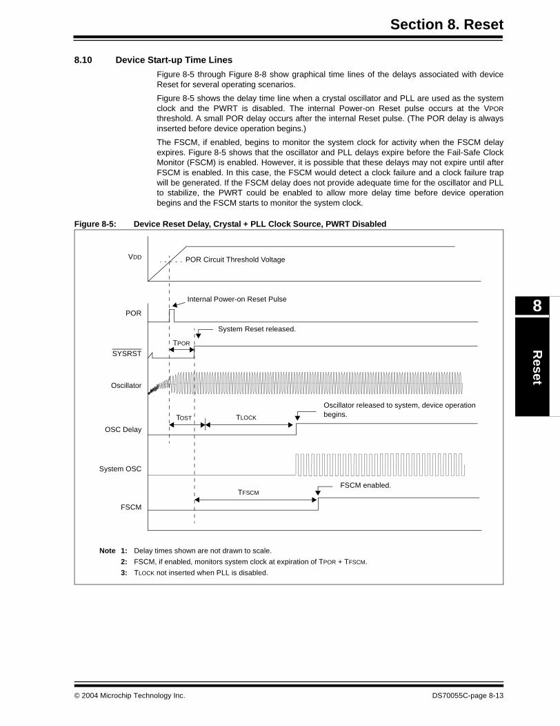
Section 8. ResetR
eset
8
8.10 Device Start-up Time Lines
Figure 8-5 through Figure 8-8 show graphical time lines of the delays associated with deviceReset for several operating scenarios.
Figure 8-5 shows the delay time line when a crystal oscillator and PLL are used as the systemclock and the PWRT is disabled. The internal Power-on Reset pulse occurs at the VPOR
threshold. A small POR delay occurs after the internal Reset pulse. (The POR delay is alwaysinserted before device operation begins.)
The FSCM, if enabled, begins to monitor the system clock for activity when the FSCM delayexpires. Figure 8-5 shows that the oscillator and PLL delays expire before the Fail-Safe ClockMonitor (FSCM) is enabled. However, it is possible that these delays may not expire until afterFSCM is enabled. In this case, the FSCM would detect a clock failure and a clock failure trapwill be generated. If the FSCM delay does not provide adequate time for the oscillator and PLLto stabilize, the PWRT could be enabled to allow more delay time before device operationbegins and the FSCM starts to monitor the system clock.
Figure 8-5: Device Reset Delay, Crystal + PLL Clock Source, PWRT Disabled
POR Circuit Threshold Voltage
SYSRST
Oscillator
Internal Power-on Reset Pulse
TPOR
TFSCM
TOST TLOCK
VDD
Oscillator released to system, device operation
POR
System Reset released.
Note 1: Delay times shown are not drawn to scale.
2: FSCM, if enabled, monitors system clock at expiration of TPOR + TFSCM.
3: TLOCK not inserted when PLL is disabled.
FSCM
FSCM enabled.
begins.
OSC Delay
System OSC
© 2004 Microchip Technology Inc. DS70055C-page 8-13
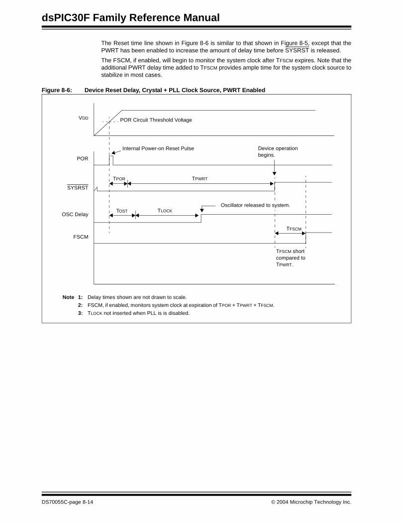
dsPIC30F Family Reference Manual
The Reset time line shown in Figure 8-6 is similar to that shown in Figure 8-5, except that thePWRT has been enabled to increase the amount of delay time before SYSRST is released.
The FSCM, if enabled, will begin to monitor the system clock after TFSCM expires. Note that theadditional PWRT delay time added to TFSCM provides ample time for the system clock source tostabilize in most cases.
Figure 8-6: Device Reset Delay, Crystal + PLL Clock Source, PWRT Enabled
POR Circuit Threshold Voltage
SYSRST
Internal Power-on Reset Pulse
TPOR TPWRT
TOST TLOCK
VDD
Oscillator released to system.
POR
Note 1: Delay times shown are not drawn to scale.
2: FSCM, if enabled, monitors system clock at expiration of TPOR + TPWRT + TFSCM.
3: TLOCK not inserted when PLL is is disabled.
TFSCM shortcompared toTPWRT.
FSCM
Device operationbegins.
OSC Delay
TFSCM
DS70055C-page 8-14 © 2004 Microchip Technology Inc.
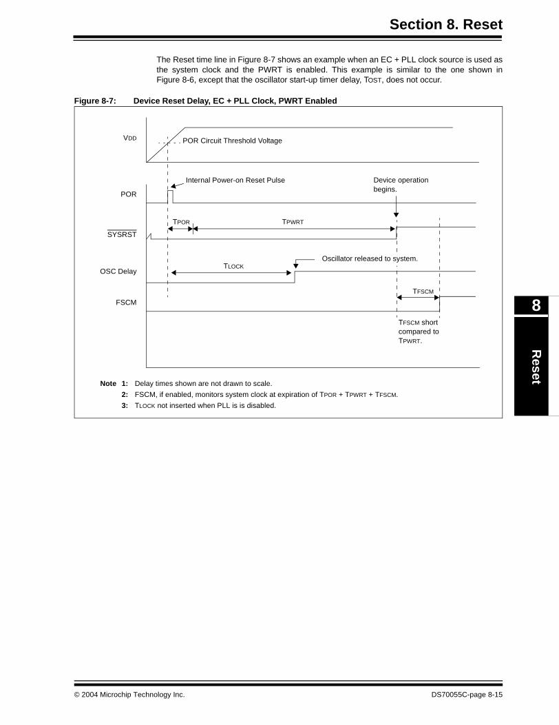
Section 8. ResetR
eset
8
The Reset time line in Figure 8-7 shows an example when an EC + PLL clock source is used asthe system clock and the PWRT is enabled. This example is similar to the one shown inFigure 8-6, except that the oscillator start-up timer delay, TOST, does not occur.
Figure 8-7: Device Reset Delay, EC + PLL Clock, PWRT Enabled
POR Circuit Threshold Voltage
SYSRST
Internal Power-on Reset Pulse
TPOR TPWRT
TLOCK
VDD
POR
Note 1: Delay times shown are not drawn to scale.
2: FSCM, if enabled, monitors system clock at expiration of TPOR + TPWRT + TFSCM.
3: TLOCK not inserted when PLL is is disabled.
TFSCM shortcompared toTPWRT.
FSCM
Device operationbegins.
OSC Delay
TFSCM
Oscillator released to system.
© 2004 Microchip Technology Inc. DS70055C-page 8-15
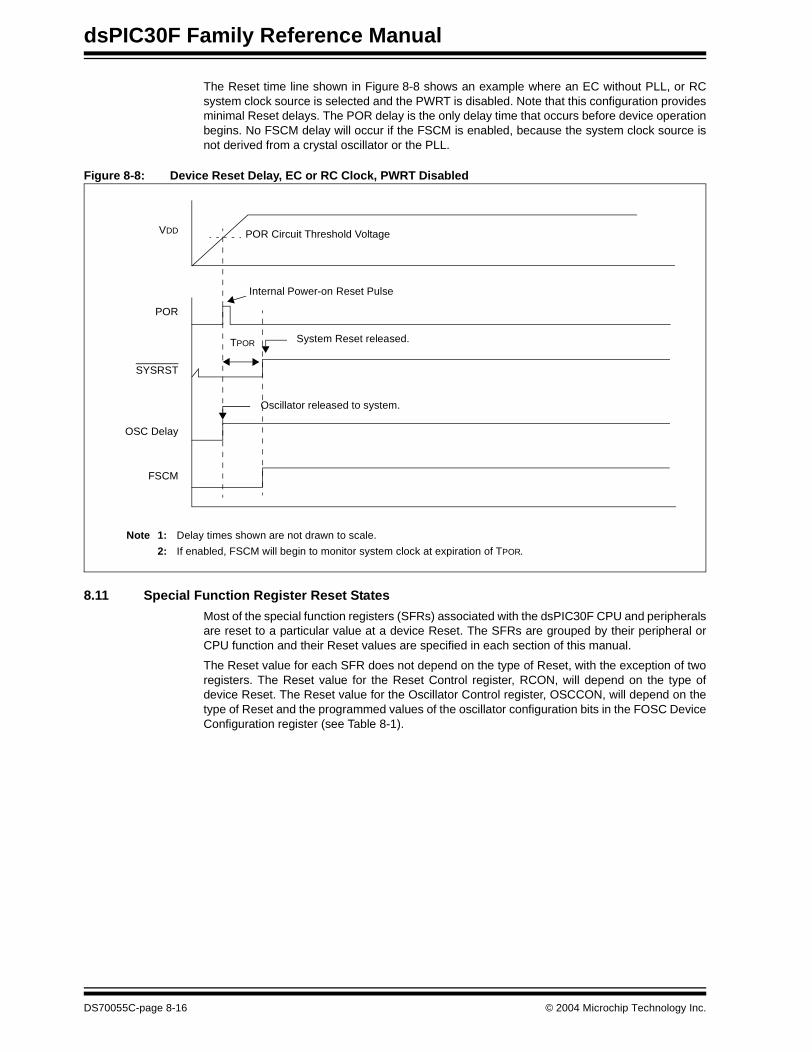
dsPIC30F Family Reference Manual
The Reset time line shown in Figure 8-8 shows an example where an EC without PLL, or RCsystem clock source is selected and the PWRT is disabled. Note that this configuration providesminimal Reset delays. The POR delay is the only delay time that occurs before device operationbegins. No FSCM delay will occur if the FSCM is enabled, because the system clock source isnot derived from a crystal oscillator or the PLL.
Figure 8-8: Device Reset Delay, EC or RC Clock, PWRT Disabled
8.11 Special Function Register Reset States
Most of the special function registers (SFRs) associated with the dsPIC30F CPU and peripheralsare reset to a particular value at a device Reset. The SFRs are grouped by their peripheral orCPU function and their Reset values are specified in each section of this manual.
The Reset value for each SFR does not depend on the type of Reset, with the exception of tworegisters. The Reset value for the Reset Control register, RCON, will depend on the type ofdevice Reset. The Reset value for the Oscillator Control register, OSCCON, will depend on thetype of Reset and the programmed values of the oscillator configuration bits in the FOSC DeviceConfiguration register (see Table 8-1).
POR Circuit Threshold Voltage
SYSRST
Internal Power-on Reset Pulse
TPOR
VDD
Oscillator released to system.
POR
System Reset released.
Note 1: Delay times shown are not drawn to scale.
2: If enabled, FSCM will begin to monitor system clock at expiration of TPOR.
FSCM
OSC Delay
DS70055C-page 8-16 © 2004 Microchip Technology Inc.
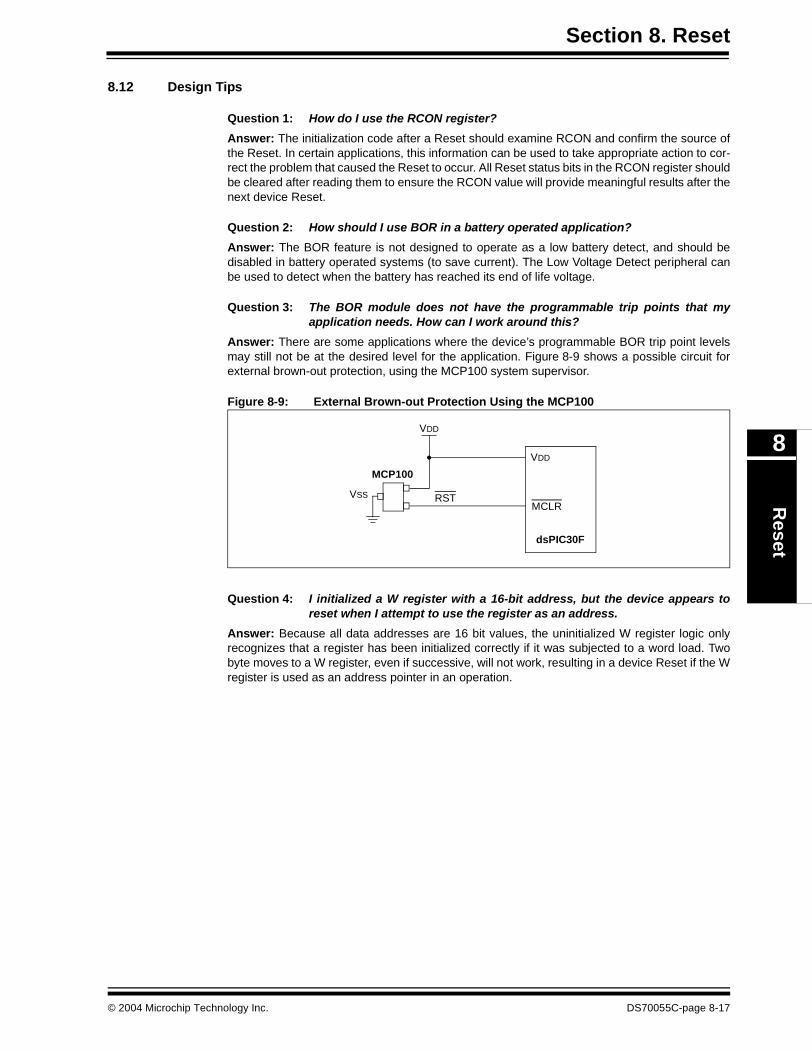
Section 8. ResetR
eset
8
8.12 Design Tips
Question 1: How do I use the RCON register?
Answer: The initialization code after a Reset should examine RCON and confirm the source ofthe Reset. In certain applications, this information can be used to take appropriate action to cor-rect the problem that caused the Reset to occur. All Reset status bits in the RCON register shouldbe cleared after reading them to ensure the RCON value will provide meaningful results after thenext device Reset.
Question 2: How should I use BOR in a battery operated application?
Answer: The BOR feature is not designed to operate as a low battery detect, and should bedisabled in battery operated systems (to save current). The Low Voltage Detect peripheral canbe used to detect when the battery has reached its end of life voltage.
Question 3: The BOR module does not have the programmable trip points that myapplication needs. How can I work around this?
Answer: There are some applications where the device’s programmable BOR trip point levelsmay still not be at the desired level for the application. Figure 8-9 shows a possible circuit forexternal brown-out protection, using the MCP100 system supervisor.
Figure 8-9: External Brown-out Protection Using the MCP100
Question 4: I initialized a W register with a 16-bit address, but the device appears toreset when I attempt to use the register as an address.
Answer: Because all data addresses are 16 bit values, the uninitialized W register logic onlyrecognizes that a register has been initialized correctly if it was subjected to a word load. Twobyte moves to a W register, even if successive, will not work, resulting in a device Reset if the Wregister is used as an address pointer in an operation.
VSS RST
MCP100
VDD
dsPIC30F
VDD
MCLR
© 2004 Microchip Technology Inc. DS70055C-page 8-17

dsPIC30F Family Reference Manual
8.13 Related Application Notes
This section lists application notes that are related to this section of the manual. Theseapplication notes may not be written specifically for the dsPIC30F Product Family, but theconcepts are pertinent and could be used with modification and possible limitations. The currentapplication notes related to the Reset module are:
Title Application Note #
Power-up Trouble Shooting AN607Power-up Considerations AN522
Note: Please visit the Microchip web site (www.microchip.com) for additional ApplicationNotes and code examples for the dsPIC30F Family of devices.
DS70055C-page 8-18 © 2004 Microchip Technology Inc.
Section 8. ResetR
eset
8
8.14 Revision History
Revision A
This is the initial released revision of this document.
Revision B
There were no technical content or editorial revisions to this section of the manual, however, thissection was updated to reflect Revision B throughout the manual.
Revision C
There were no technical content revisions to this section of the manual, however, this section wasupdated to reflect Revision C throughout the manual.
© 2004 Microchip Technology Inc. DS70055C-page 8-19

dsPIC30F Family Reference Manual
NOTES:
DS70055C-page 8-20 © 2004 Microchip Technology Inc.

Section 9. Low Voltage Detect (LVD)
Lo
w Vo
ltage
Detect (LV
D)
9
HIGHLIGHTS
This section of the manual contains the following topics:
9.1 Introduction .................................................................................................................... 9-2
9.2 LVD Operation ............................................................................................................... 9-59.3 Design Tips .................................................................................................................... 9-69.4 Related Application Notes.............................................................................................. 9-7
9.5 Revision History ............................................................................................................. 9-8
© 2004 Microchip Technology Inc. DS70056C-page 9-1
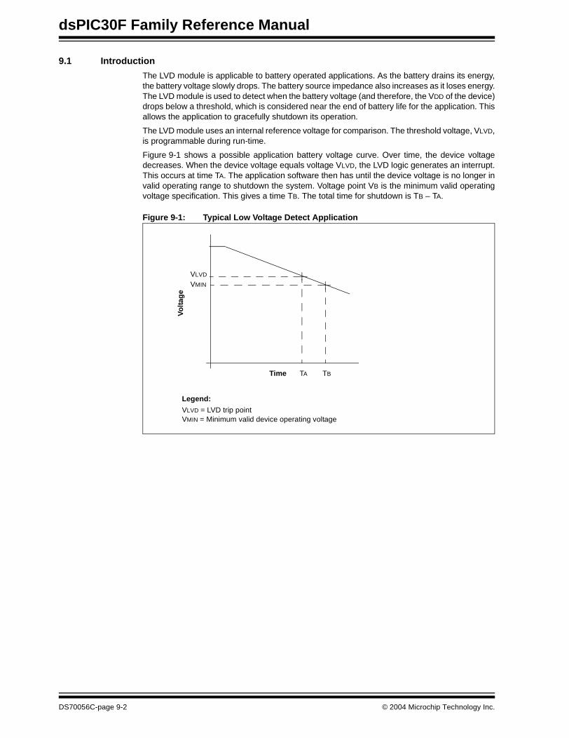
dsPIC30F Family Reference Manual
9.1 Introduction
The LVD module is applicable to battery operated applications. As the battery drains its energy,the battery voltage slowly drops. The battery source impedance also increases as it loses energy.The LVD module is used to detect when the battery voltage (and therefore, the VDD of the device)drops below a threshold, which is considered near the end of battery life for the application. Thisallows the application to gracefully shutdown its operation.
The LVD module uses an internal reference voltage for comparison. The threshold voltage, VLVD,is programmable during run-time.
Figure 9-1 shows a possible application battery voltage curve. Over time, the device voltagedecreases. When the device voltage equals voltage VLVD, the LVD logic generates an interrupt.This occurs at time TA. The application software then has until the device voltage is no longer invalid operating range to shutdown the system. Voltage point VB is the minimum valid operatingvoltage specification. This gives a time TB. The total time for shutdown is TB – TA.
Figure 9-1: Typical Low Voltage Detect Application
Time
Vo
ltag
e
VLVD
VMIN
TA
VLVD = LVD trip pointVMIN = Minimum valid device operating voltage
Legend:
TB
DS70056C-page 9-2 © 2004 Microchip Technology Inc.
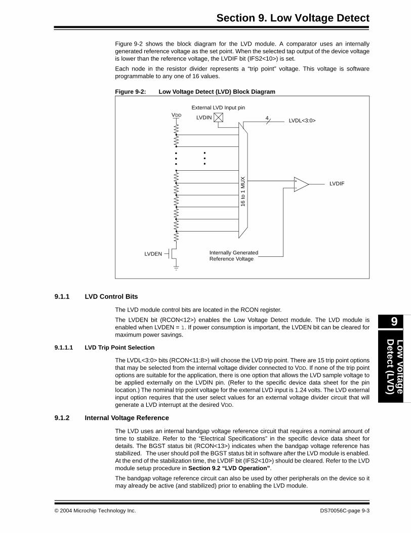
Section 9. Low Voltage DetectL
ow
Voltag
eD
etect (LVD
)
9
Figure 9-2 shows the block diagram for the LVD module. A comparator uses an internallygenerated reference voltage as the set point. When the selected tap output of the device voltageis lower than the reference voltage, the LVDIF bit (IFS2<10>) is set.
Each node in the resistor divider represents a “trip point” voltage. This voltage is softwareprogrammable to any one of 16 values.
Figure 9-2: Low Voltage Detect (LVD) Block Diagram
9.1.1 LVD Control Bits
The LVD module control bits are located in the RCON register.
The LVDEN bit (RCON<12>) enables the Low Voltage Detect module. The LVD module isenabled when LVDEN = 1. If power consumption is important, the LVDEN bit can be cleared formaximum power savings.
9.1.1.1 LVD Trip Point Selection
The LVDL<3:0> bits (RCON<11:8>) will choose the LVD trip point. There are 15 trip point optionsthat may be selected from the internal voltage divider connected to VDD. If none of the trip pointoptions are suitable for the application, there is one option that allows the LVD sample voltage tobe applied externally on the LVDIN pin. (Refer to the specific device data sheet for the pinlocation.) The nominal trip point voltage for the external LVD input is 1.24 volts. The LVD externalinput option requires that the user select values for an external voltage divider circuit that willgenerate a LVD interrupt at the desired VDD.
9.1.2 Internal Voltage Reference
The LVD uses an internal bandgap voltage reference circuit that requires a nominal amount oftime to stabilize. Refer to the “Electrical Specifications” in the specific device data sheet fordetails. The BGST status bit (RCON<13>) indicates when the bandgap voltage reference hasstabilized. The user should poll the BGST status bit in software after the LVD module is enabled.At the end of the stabilization time, the LVDIF bit (IFS2<10>) should be cleared. Refer to the LVDmodule setup procedure in Section 9.2 “LVD Operation”.
The bandgap voltage reference circuit can also be used by other peripherals on the device so itmay already be active (and stabilized) prior to enabling the LVD module.
VDD
LVDIF
16 to
1 M
UX
LVDEN Internally GeneratedReference Voltage
LVDIN LVDL<3:0>
External LVD Input pin
4
© 2004 Microchip Technology Inc. DS70056C-page 9-3
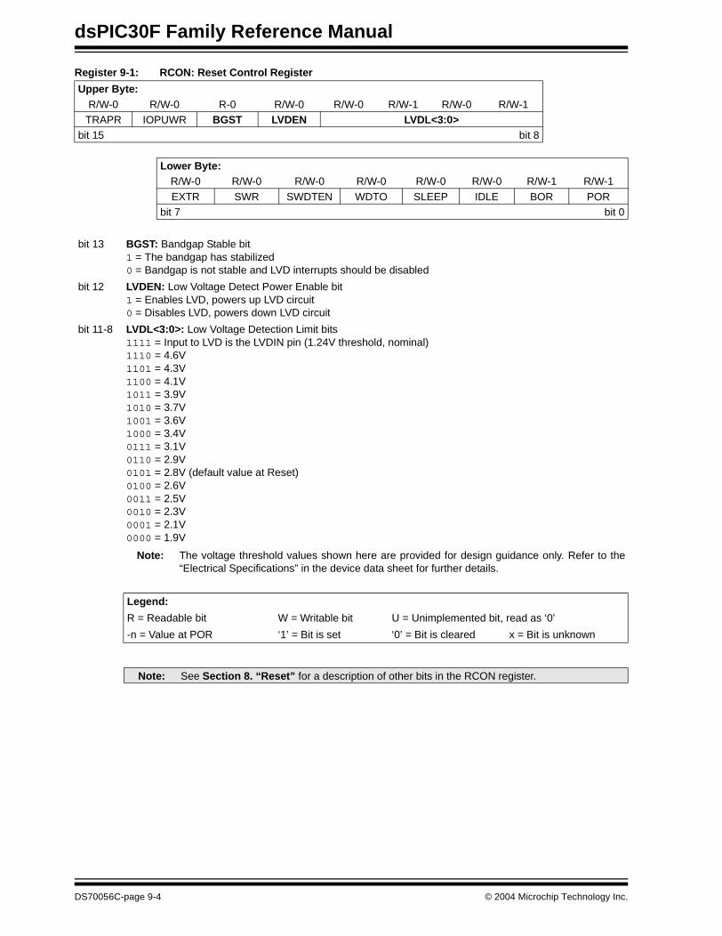
dsPIC30F Family Reference Manual
Register 9-1: RCON: Reset Control Register
Upper Byte:R/W-0 R/W-0 R-0 R/W-0 R/W-0 R/W-1 R/W-0 R/W-1
TRAPR IOPUWR BGST LVDEN LVDL<3:0>bit 15 bit 8
Lower Byte:R/W-0 R/W-0 R/W-0 R/W-0 R/W-0 R/W-0 R/W-1 R/W-1
EXTR SWR SWDTEN WDTO SLEEP IDLE BOR PORbit 7 bit 0
bit 13 BGST: Bandgap Stable bit1 = The bandgap has stabilized0 = Bandgap is not stable and LVD interrupts should be disabled
bit 12 LVDEN: Low Voltage Detect Power Enable bit1 = Enables LVD, powers up LVD circuit0 = Disables LVD, powers down LVD circuit
bit 11-8 LVDL<3:0>: Low Voltage Detection Limit bits1111 = Input to LVD is the LVDIN pin (1.24V threshold, nominal)1110 = 4.6V1101 = 4.3V1100 = 4.1V1011 = 3.9V1010 = 3.7V1001 = 3.6V1000 = 3.4V0111 = 3.1V0110 = 2.9V0101 = 2.8V (default value at Reset)0100 = 2.6V0011 = 2.5V0010 = 2.3V0001 = 2.1V0000 = 1.9V
Note: The voltage threshold values shown here are provided for design guidance only. Refer to the“Electrical Specifications” in the device data sheet for further details.
Legend:
R = Readable bit W = Writable bit U = Unimplemented bit, read as ‘0’
-n = Value at POR ‘1’ = Bit is set ‘0’ = Bit is cleared x = Bit is unknown
Note: See Section 8. “Reset” for a description of other bits in the RCON register.
DS70056C-page 9-4 © 2004 Microchip Technology Inc.
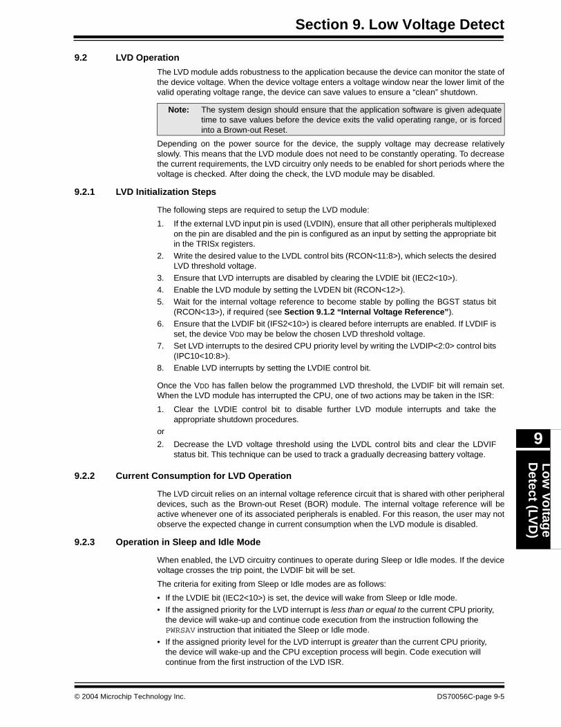
Section 9. Low Voltage DetectL
ow
Voltag
eD
etect (LVD
)
9
9.2 LVD Operation
The LVD module adds robustness to the application because the device can monitor the state ofthe device voltage. When the device voltage enters a voltage window near the lower limit of thevalid operating voltage range, the device can save values to ensure a “clean” shutdown.
Depending on the power source for the device, the supply voltage may decrease relativelyslowly. This means that the LVD module does not need to be constantly operating. To decreasethe current requirements, the LVD circuitry only needs to be enabled for short periods where thevoltage is checked. After doing the check, the LVD module may be disabled.
9.2.1 LVD Initialization Steps
The following steps are required to setup the LVD module:
1. If the external LVD input pin is used (LVDIN), ensure that all other peripherals multiplexedon the pin are disabled and the pin is configured as an input by setting the appropriate bitin the TRISx registers.
2. Write the desired value to the LVDL control bits (RCON<11:8>), which selects the desiredLVD threshold voltage.
3. Ensure that LVD interrupts are disabled by clearing the LVDIE bit (IEC2<10>).4. Enable the LVD module by setting the LVDEN bit (RCON<12>).5. Wait for the internal voltage reference to become stable by polling the BGST status bit
(RCON<13>), if required (see Section 9.1.2 “Internal Voltage Reference”).6. Ensure that the LVDIF bit (IFS2<10>) is cleared before interrupts are enabled. If LVDIF is
set, the device VDD may be below the chosen LVD threshold voltage.7. Set LVD interrupts to the desired CPU priority level by writing the LVDIP<2:0> control bits
(IPC10<10:8>).8. Enable LVD interrupts by setting the LVDIE control bit.
Once the VDD has fallen below the programmed LVD threshold, the LVDIF bit will remain set.When the LVD module has interrupted the CPU, one of two actions may be taken in the ISR:
1. Clear the LVDIE control bit to disable further LVD module interrupts and take theappropriate shutdown procedures.
or
2. Decrease the LVD voltage threshold using the LVDL control bits and clear the LDVIFstatus bit. This technique can be used to track a gradually decreasing battery voltage.
9.2.2 Current Consumption for LVD Operation
The LVD circuit relies on an internal voltage reference circuit that is shared with other peripheraldevices, such as the Brown-out Reset (BOR) module. The internal voltage reference will beactive whenever one of its associated peripherals is enabled. For this reason, the user may notobserve the expected change in current consumption when the LVD module is disabled.
9.2.3 Operation in Sleep and Idle Mode
When enabled, the LVD circuitry continues to operate during Sleep or Idle modes. If the devicevoltage crosses the trip point, the LVDIF bit will be set.
The criteria for exiting from Sleep or Idle modes are as follows:
• If the LVDIE bit (IEC2<10>) is set, the device will wake from Sleep or Idle mode.• If the assigned priority for the LVD interrupt is less than or equal to the current CPU priority,
the device will wake-up and continue code execution from the instruction following the PWRSAV instruction that initiated the Sleep or Idle mode.
• If the assigned priority level for the LVD interrupt is greater than the current CPU priority, the device will wake-up and the CPU exception process will begin. Code execution will continue from the first instruction of the LVD ISR.
Note: The system design should ensure that the application software is given adequatetime to save values before the device exits the valid operating range, or is forcedinto a Brown-out Reset.
© 2004 Microchip Technology Inc. DS70056C-page 9-5
dsPIC30F Family Reference Manual
9.3 Design Tips
Question 1: The LVD circuitry seems to be generating random interrupts?
Answer: Ensure that the internal voltage reference is stable before enabling the LVD interrupt.This is done by polling the BGST status bit (RCON<13>) after the LVD module is enabled. Afterthis time delay, the LVDIF bit should be cleared and then, the LVDIE bit may be set.
Question 2: How can I reduce the current consumption of the module?
Answer: Low Voltage Detect is used to monitor the device voltage. The power source is normallya battery that ramps down slowly. This means that the LVD circuity can be disabled for most ofthe time, and only enabled occasionally to do the device voltage check.
Question 3: Should I enable the BOR circuit for a battery powered application?
Answer: The BOR circuit is intended to protect the device from improper operation due to powersupply fluctuations caused by the AC line voltage. The BOR is typically not required for batteryapplications and can be disabled for lower current consumption.
DS70056C-page 9-6 © 2004 Microchip Technology Inc.

Section 9. Low Voltage DetectL
ow
Voltag
eD
etect (LVD
)
9
9.4 Related Application Notes
This section lists application notes that are related to this section of the manual. Theseapplication notes may not be written specifically for the dsPIC30F Product Family, but theconcepts are pertinent and could be used with modification and possible limitations. The currentapplication notes related to the Low Voltage Detect module are:
Title Application Note #
No related application notes at this time.
Note: Please visit the Microchip web site (www.microchip.com) for additional ApplicationNotes and code examples for the dsPIC30F Family of devices.
© 2004 Microchip Technology Inc. DS70056C-page 9-7

dsPIC30F Family Reference Manual
9.5 Revision History
Revision A
This is the initial released revision of this document.
Revision B
There were no technical content or editorial revisions to this section of the manual, however, thissection was updated to reflect Revision B throughout the manual.
Revision C
There were no technical content revisions to this section of the manual, however, this section wasupdated to reflect Revision C throughout the manual.
DS70056C-page 9-8 © 2004 Microchip Technology Inc.
Section 10. Watchdog Timer and Power Saving Modes
WD
T an
d P
ow
erS
aving
Mo
des
10
HIGHLIGHTS
This section of the manual contains the following topics:
10.1 Introduction .................................................................................................................. 10-2
10.2 Power Saving Modes ................................................................................................... 10-210.3 Sleep Mode.................................................................................................................. 10-210.4 Idle Mode ..................................................................................................................... 10-4
10.5 Interrupts Coincident with Power Save Instructions..................................................... 10-510.6 Watchdog Timer........................................................................................................... 10-610.7 Peripheral Module Disable (PMD) Registers ............................................................... 10-9
10.8 Design Tips ................................................................................................................ 10-1010.9 Related Application Notes.......................................................................................... 10-1110.10 Revision History ......................................................................................................... 10-12
© 2005 Microchip Technology Inc. DS70057D-page 10-1
dsPIC30F Family Reference Manual
10.1 Introduction
This section addresses the Watchdog Timer (WDT) and Power Saving modes of the dsPIC30Fdevice family. The dsPIC DSC devices have two reduced Power modes that can be enteredthrough execution of the PWRSAV instruction:
• Sleep Mode: The CPU, system clock source, and any peripherals that operate on the system clock source are disabled. This is the lowest Power mode for the device.
• Idle Mode: The CPU is disabled, but the system clock source continues to operate. Peripherals continue to operate, but can optionally be disabled.
The WDT, when enabled, operates from the internal LPRC clock source and can be used todetect system software malfunctions by resetting the device if the WDT has not been cleared insoftware. Various WDT time-out periods can be selected using the WDT postscaler. The WDTcan also be used to wake the device from Sleep or Idle mode.
10.2 Power Saving Modes
The dsPIC30F device family has two special Power Saving modes, Sleep mode and Idle mode,that can be entered through the execution of a special PWRSAV instruction.
The assembly syntax of the PWRSAV instruction is as follows:
PWRSAV #SLEEP_MODE ; Put the device into SLEEP modePWRSAV #IDLE_MODE ; Put the device into IDLE mode
The Power Saving modes can be exited as a result of an enabled interrupt, WDT time-out, or adevice Reset. When the device exits one of these two Operating modes, it is said to ‘wake-up’.The characteristics of the Power Saving modes are described in subsequent sections.
10.3 Sleep Mode
The characteristics of Sleep mode are as follows:
• The system clock source is shutdown. If an on-chip oscillator is used, it is turned off.• The device current consumption will be at a minimum provided that no I/O pin is sourcing
current.• The Fail-Safe Clock Monitor (FSCM) does not operate during Sleep mode since the system
clock source is disabled.• The LPRC clock will continue to run in Sleep mode if the WDT is enabled.• The Low Voltage Detect circuit, if enabled, remains operative during Sleep mode.
• The BOR circuit, if enabled, remains operative during Sleep mode.• The WDT, if enabled, is automatically cleared prior to entering Sleep mode. • Some peripherals may continue to operate in Sleep mode. These peripherals include I/O
pins that detect a change in the input signal, or peripherals that use an external clock input. Any peripheral that is operating on the system clock source will be disabled in Sleep mode.
The processor will exit, or ‘wake-up’, from Sleep on one of the following events:
• On any interrupt source that is individually enabled• On any form of device Reset
• On a WDT time-out
10.3.1 Clock Selection on Wake-up from Sleep
The processor will restart the same clock source that was active when Sleep mode was entered.
Note: SLEEP_MODE and IDLE_MODE are constants defined in the assembler includefile for the selected device.
DS70057D-page 10-2 © 2005 Microchip Technology Inc.
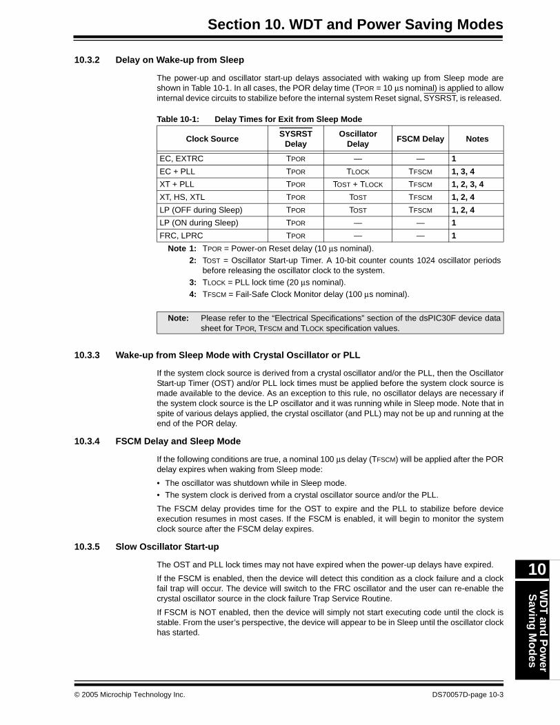
Section 10. WDT and Power Saving ModesW
DT
and
Po
wer
Savin
g M
od
es
10
10.3.2 Delay on Wake-up from Sleep
The power-up and oscillator start-up delays associated with waking up from Sleep mode areshown in Table 10-1. In all cases, the POR delay time (TPOR = 10 μs nominal) is applied to allowinternal device circuits to stabilize before the internal system Reset signal, SYSRST, is released.
Table 10-1: Delay Times for Exit from Sleep Mode
10.3.3 Wake-up from Sleep Mode with Crystal Oscillator or PLL
If the system clock source is derived from a crystal oscillator and/or the PLL, then the OscillatorStart-up Timer (OST) and/or PLL lock times must be applied before the system clock source ismade available to the device. As an exception to this rule, no oscillator delays are necessary ifthe system clock source is the LP oscillator and it was running while in Sleep mode. Note that inspite of various delays applied, the crystal oscillator (and PLL) may not be up and running at theend of the POR delay.
10.3.4 FSCM Delay and Sleep Mode
If the following conditions are true, a nominal 100 μs delay (TFSCM) will be applied after the PORdelay expires when waking from Sleep mode:
• The oscillator was shutdown while in Sleep mode.• The system clock is derived from a crystal oscillator source and/or the PLL.
The FSCM delay provides time for the OST to expire and the PLL to stabilize before deviceexecution resumes in most cases. If the FSCM is enabled, it will begin to monitor the systemclock source after the FSCM delay expires.
10.3.5 Slow Oscillator Start-up
The OST and PLL lock times may not have expired when the power-up delays have expired.
If the FSCM is enabled, then the device will detect this condition as a clock failure and a clockfail trap will occur. The device will switch to the FRC oscillator and the user can re-enable thecrystal oscillator source in the clock failure Trap Service Routine.
If FSCM is NOT enabled, then the device will simply not start executing code until the clock isstable. From the user’s perspective, the device will appear to be in Sleep until the oscillator clockhas started.
Clock SourceSYSRST
DelayOscillator
DelayFSCM Delay Notes
EC, EXTRC TPOR — — 1
EC + PLL TPOR TLOCK TFSCM 1, 3, 4
XT + PLL TPOR TOST + TLOCK TFSCM 1, 2, 3, 4
XT, HS, XTL TPOR TOST TFSCM 1, 2, 4
LP (OFF during Sleep) TPOR TOST TFSCM 1, 2, 4
LP (ON during Sleep) TPOR — — 1
FRC, LPRC TPOR — — 1
Note 1: TPOR = Power-on Reset delay (10 μs nominal).2: TOST = Oscillator Start-up Timer. A 10-bit counter counts 1024 oscillator periods
before releasing the oscillator clock to the system.3: TLOCK = PLL lock time (20 μs nominal).4: TFSCM = Fail-Safe Clock Monitor delay (100 μs nominal).
Note: Please refer to the “Electrical Specifications” section of the dsPIC30F device datasheet for TPOR, TFSCM and TLOCK specification values.
© 2005 Microchip Technology Inc. DS70057D-page 10-3
dsPIC30F Family Reference Manual
10.3.6 Wake-up from Sleep on Interrupt
User interrupt sources that are assigned to CPU priority level 0 cannot wake the CPU from Sleepmode, because the interrupt source is effectively disabled. To use an interrupt as a wake-upsource, the CPU priority level for the interrupt must be assigned to CPU priority level 1 or greater.
Any source of interrupt that is individually enabled, using its corresponding IE control bit in theIECx registers, can wake-up the processor from Sleep mode. When the device wakes from Sleepmode, one of two actions may occur:
• If the assigned priority for the interrupt is less than or equal to the current CPU priority, the device will wake-up and continue code execution from the instruction following the PWRSAV instruction that initiated Sleep mode.
• If the assigned priority level for the interrupt source is greater than the current CPU priority, the device will wake-up and the CPU exception process will begin. Code execution will continue from the first instruction of the ISR.
The Sleep status bit (RCON<3>) is set upon wake-up.
10.3.7 Wake-up from Sleep on Reset
All sources of device Reset will wake the processor from Sleep mode. Any source of Reset (otherthan a POR) that wakes the processor will set the Sleep status bit (RCON<3>) to indicate thatthe device was previously in Sleep mode.
On a Power-on Reset, the Sleep bit is cleared.
10.3.8 Wake-up from Sleep on Watchdog Time-out
If the Watchdog Timer (WDT) is enabled and expires while the device is in Sleep mode, theprocessor will wake-up. The Sleep and WDTO status bits (RCON<3>, RCON<4>) are both setto indicate that the device resumed operation due to the WDT expiration. Note that this eventdoes not reset the device. Operation continues from the instruction following the PWRSAVinstruction that initiated Sleep mode.
10.4 Idle Mode
User interrupt sources that are assigned to CPU priority level 0 cannot wake the CPU from Idlemode, because the interrupt source is effectively disabled. To use an interrupt as a wake-upsource, the CPU priority level for the interrupt must be assigned to CPU priority level 1 or greater.
When the device enters Idle mode, the following events occur:
• The CPU will stop executing instructions.• The WDT is automatically cleared.• The system clock source will remain active and peripheral modules, by default, will
continue to operate normally from the system clock source. Peripherals can optionally be shutdown in Idle mode using their ‘stop-in-idle’ control bit. (See peripheral descriptions for further details.)
• If the WDT or FSCM is enabled, the LPRC will also remain active.
The processor will wake from Idle mode on the following events:
• On any interrupt that is individually enabled. • On any source of device Reset.
• On a WDT time-out.
Upon wake-up from Idle, the clock is re-applied to the CPU and instruction execution beginsimmediately starting with the instruction following the PWRSAV instruction, or the first instructionin the ISR.
DS70057D-page 10-4 © 2005 Microchip Technology Inc.

Section 10. WDT and Power Saving ModesW
DT
and
Po
wer
Savin
g M
od
es
10
10.4.1 Wake-up from Idle on Interrupt
Any source of interrupt that is individually enabled using the corresponding IE control bit in theIECx register and exceeds the current CPU priority level, will be able to wake-up the processorfrom Idle mode. When the device wakes from Idle mode, one of two options may occur:
• If the assigned priority for the interrupt is less than or equal to the current CPU priority, the device will wake-up and continue code execution from the instruction following the PWRSAV instruction that initiated Idle mode.
• If the assigned priority level for the interrupt source is greater than the current CPU priority, the device will wake-up and the CPU exception process will begin. Code execution will continue from the first instruction of the ISR.
The Idle status bit (RCON<2>) is set upon wake-up.
10.4.2 Wake-up from Idle on Reset
Any Reset, other than a POR, will wake the CPU from Idle mode. On any device Reset, excepta POR, the Idle status bit is set (RCON<2>) to indicate that the device was previously in Idlemode. In a Power-on Reset, the Idle bit is cleared.
10.4.3 Wake-up from Idle on WDT Time-out
If the WDT is enabled, then the processor will wake from Idle mode on a WDT time-out andcontinue code execution with the instruction following the PWRSAV instruction that initiated Idlemode. Note that the WDT time-out does not reset the device in this case. The WDTO and Idlestatus bits (RCON<4>, RCON<2>) will both be set.
10.4.4 Time Delays on Wake from Idle Mode
Unlike a wake-up from Sleep mode, there are no time delays associated with wake-up from Idlemode. The system clock is running during Idle mode, therefore, no start-up times are required atwake-up.
10.5 Interrupts Coincident with Power Save Instructions
Any interrupt that coincides with the execution of a PWRSAV instruction will be held off until entryinto Sleep or Idle mode has completed. The device will then wake-up from Sleep or Idle mode.
© 2005 Microchip Technology Inc. DS70057D-page 10-5
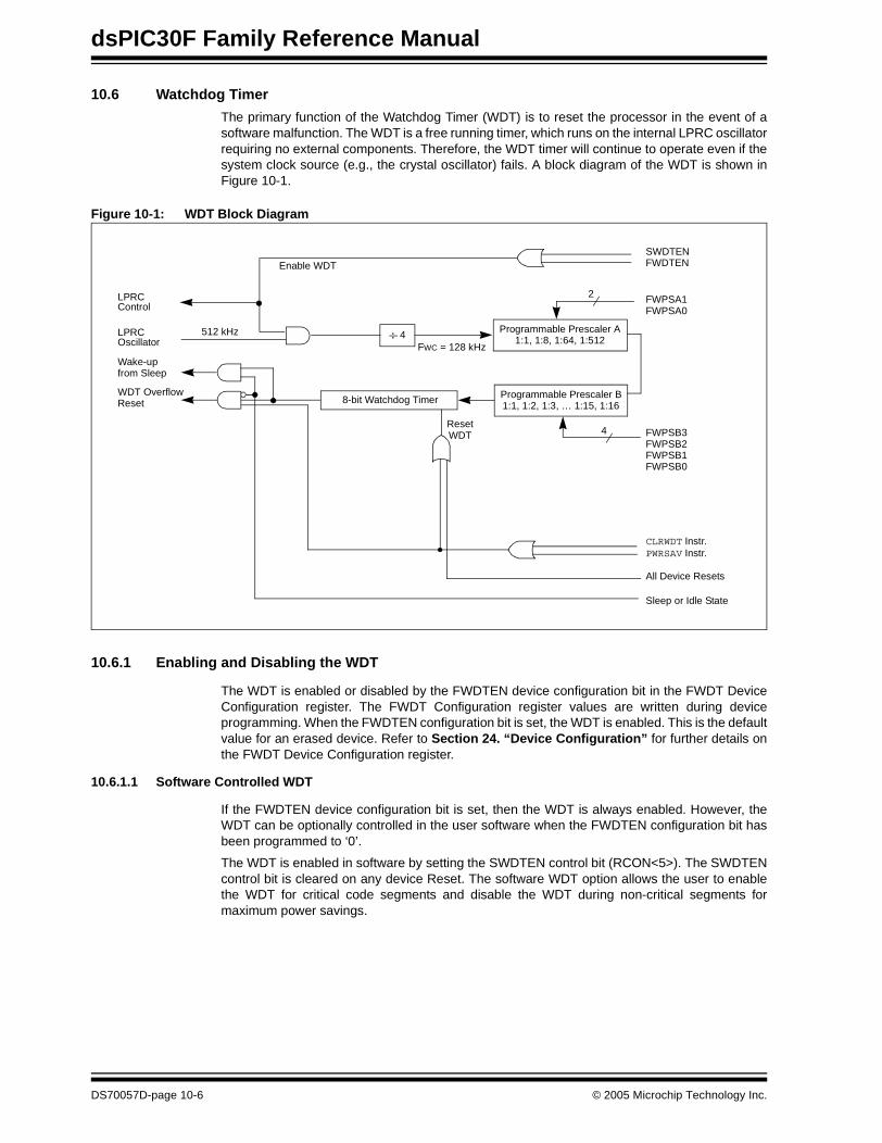
dsPIC30F Family Reference Manual
10.6 Watchdog Timer
The primary function of the Watchdog Timer (WDT) is to reset the processor in the event of asoftware malfunction. The WDT is a free running timer, which runs on the internal LPRC oscillatorrequiring no external components. Therefore, the WDT timer will continue to operate even if thesystem clock source (e.g., the crystal oscillator) fails. A block diagram of the WDT is shown inFigure 10-1.
Figure 10-1: WDT Block Diagram
10.6.1 Enabling and Disabling the WDT
The WDT is enabled or disabled by the FWDTEN device configuration bit in the FWDT DeviceConfiguration register. The FWDT Configuration register values are written during deviceprogramming. When the FWDTEN configuration bit is set, the WDT is enabled. This is the defaultvalue for an erased device. Refer to Section 24. “Device Configuration” for further details onthe FWDT Device Configuration register.
10.6.1.1 Software Controlled WDT
If the FWDTEN device configuration bit is set, then the WDT is always enabled. However, theWDT can be optionally controlled in the user software when the FWDTEN configuration bit hasbeen programmed to ‘0’.
The WDT is enabled in software by setting the SWDTEN control bit (RCON<5>). The SWDTENcontrol bit is cleared on any device Reset. The software WDT option allows the user to enablethe WDT for critical code segments and disable the WDT during non-critical segments formaximum power savings.
LPRC
WDT Overflow
Wake-up
ResetWDT
8-bit Watchdog Timer
512 kHz 4 Programmable Prescaler A1:1, 1:8, 1:64, 1:512
Programmable Prescaler B1:1, 1:2, 1:3, … 1:15, 1:16
FWC = 128 kHz
Enable WDT
FWPSB3FWPSB2FWPSB1FWPSB0
FWPSA1FWPSA0
SWDTENFWDTEN
2
4
from Sleep
Reset
All Device Resets
Sleep or Idle State
LPRC
CLRWDT Instr.PWRSAV Instr.
Control
Oscillator
DS70057D-page 10-6 © 2005 Microchip Technology Inc.
Section 10. WDT and Power Saving ModesW
DT
and
Po
wer
Savin
g M
od
es
10
10.6.2 WDT Operation
If enabled, the WDT will increment until it overflows or “times out”. A WDT time-out will force adevice Reset, except during Sleep or Idle modes. To prevent a WDT Time-out Reset, the usermust periodically clear the Watchdog Timer using the CLRWDT instruction. The CLRWDTinstruction also clears the WDT prescalers.
If the WDT times out during Sleep or Idle modes, the device will wake-up and continue codeexecution from where the PWRSAV instruction was executed.
In either case, the WDTO bit (RCON<4>) will be set to indicate that the device Reset or wake-upevent was due to a WDT time-out. If the WDT wakes the CPU from Sleep or Idle mode, the Sleepstatus bit (RCON<3>), or Idle status bit (RCON<2>) will also be set to indicate that the devicewas previously in a Power Saving mode.
10.6.3 WDT Timer Period Selection
The WDT clock source is the internal LPRC oscillator, which has a nominal frequency of 512 kHz.The LPRC clock is further divided by 4 to provide a 128 kHz clock to the WDT. The counter forthe WDT is 8-bits wide, so the nominal time-out period for the WDT (TWDT) is 2 milliseconds.
10.6.3.1 WDT Prescalers
The WDT has two clock prescalers, Prescaler A and Prescaler B, to allow a wide variety oftime-out periods. Prescaler A can be configured for 1:1, 1:8, 1:64 or 1:512 divide ratios. PrescalerB can be configured for any divide ratio from 1:1 through 1:16. Time-out periods that rangebetween 2 ms and 16 seconds (nominal) can be achieved using the prescalers.
The prescaler settings are selected using the FWPSA<1:0> (Prescaler A) and FWPSB<3:0>(Prescaler B) configuration bits in the FWDT Device Configuration register. The FWPSA<1:0>and FWPSB<3:0> values are written during device programming. For more information on theWDT prescaler configuration bits, please refer to Section 24. “Device Configuration”.
The time-out period of the WDT is calculated as follows:
Equation 10-1: WDT Time-out Period
Note: The WDT time-out period is directly related to the frequency of the LPRC oscillator.The frequency of the LPRC oscillator will vary as a function of device operatingvoltage and temperature. Please refer to the specific dsPIC30F device data sheetfor LPRC clock frequency specifications.
WDT Period = 2 ms • Prescale A • Prescale B
© 2005 Microchip Technology Inc. DS70057D-page 10-7
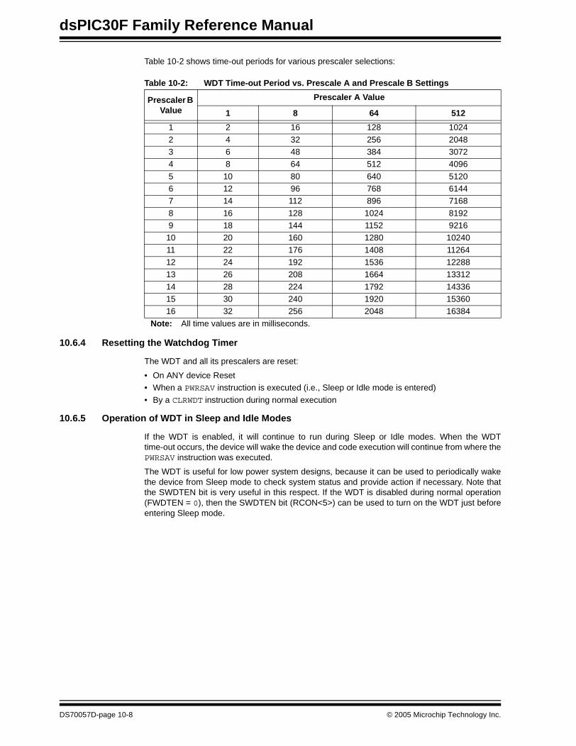
dsPIC30F Family Reference Manual
Table 10-2 shows time-out periods for various prescaler selections:
Table 10-2: WDT Time-out Period vs. Prescale A and Prescale B Settings
10.6.4 Resetting the Watchdog Timer
The WDT and all its prescalers are reset:
• On ANY device Reset• When a PWRSAV instruction is executed (i.e., Sleep or Idle mode is entered)
• By a CLRWDT instruction during normal execution
10.6.5 Operation of WDT in Sleep and Idle Modes
If the WDT is enabled, it will continue to run during Sleep or Idle modes. When the WDTtime-out occurs, the device will wake the device and code execution will continue from where thePWRSAV instruction was executed.
The WDT is useful for low power system designs, because it can be used to periodically wakethe device from Sleep mode to check system status and provide action if necessary. Note thatthe SWDTEN bit is very useful in this respect. If the WDT is disabled during normal operation(FWDTEN = 0), then the SWDTEN bit (RCON<5>) can be used to turn on the WDT just beforeentering Sleep mode.
Prescaler B Value
Prescaler A Value
1 8 64 512
1 2 16 128 1024
2 4 32 256 20483 6 48 384 30724 8 64 512 4096
5 10 80 640 51206 12 96 768 61447 14 112 896 7168
8 16 128 1024 81929 18 144 1152 9216
10 20 160 1280 10240
11 22 176 1408 1126412 24 192 1536 1228813 26 208 1664 13312
14 28 224 1792 1433615 30 240 1920 1536016 32 256 2048 16384
Note: All time values are in milliseconds.
DS70057D-page 10-8 © 2005 Microchip Technology Inc.
Section 10. WDT and Power Saving ModesW
DT
and
Po
wer
Savin
g M
od
es
10
10.7 Peripheral Module Disable (PMD) Registers
The Peripheral Module Disable (PMD) registers provide a method to disable a peripheral moduleby stopping all clock sources supplied to that module. When a peripheral is disabled via theappropriate PMD control bit, the peripheral is in a minimum power consumption state. The controland status registers associated with the peripheral will also be disabled so writes to those regis-ters will have no effect and read values will be invalid.
A peripheral module will only be enabled if both the associated bit in the the PMD register iscleared and the peripheral is supported by the specific dsPIC variant. If the peripheral is presentin the device, it is enabled in the PMD register by default.
Please check individual device data sheet for specific operational details of the PMD register.
Note: If a PMD bit is set, the corresponding module is disabled after a delay of 1 instructioncycle. Similarly, if a PMD bit is cleared, the corresponding module is enabled after adelay of 1 instruction cycle (assuming the module control registers are alreadyconfigured to enable module operation).
© 2005 Microchip Technology Inc. DS70057D-page 10-9
dsPIC30F Family Reference Manual
10.8 Design Tips
Question 1: The device resets even though I have inserted a CLRWDT instruction in mymain software loop.
Answer: Make sure that the software loop that contains the CLRWDT instruction meets theminimum specification of the WDT (not the typical value). Also, make sure that interruptprocessing time has been accounted for.
Question 2: What should my software do before entering Sleep or Idle mode?
Answer: Make sure that the sources intended to wake the device have their IE bits set. Inaddition, make sure that the particular source of interrupt has the ability to wake the device.Some sources do not function when the device is in Sleep mode.
If the device is to be placed in Idle mode, make sure that the ‘stop-in-idle’ control bit for eachdevice peripheral is properly set. These control bits determine whether the peripheral willcontinue operation in Idle mode. See the individual peripheral sections of this manual for furtherdetails.
Question 3: How do I tell which peripheral woke the device from Sleep or Idle mode?
Answer: You can poll the IF bits for each enabled interrupt source to determine the source ofwake-up.
DS70057D-page 10-10 © 2005 Microchip Technology Inc.

Section 10. WDT and Power Saving ModesW
DT
and
Po
wer
Savin
g M
od
es
10
10.9 Related Application Notes
This section lists application notes that are related to this section of the manual. Theseapplication notes may not be written specifically for the dsPIC30F Product Family, but theconcepts are pertinent and could be used with modification and possible limitations. The currentapplication notes related to the Watchdog Timer and Power Saving Modes are:
Title Application Note #
Low Power Design using PICmicro® Microcontrollers AN606
Note: Please visit the Microchip web site (www.microchip.com) for additional ApplicationNotes and code examples for the dsPIC30F Family of devices.
© 2005 Microchip Technology Inc. DS70057D-page 10-11
dsPIC30F Family Reference Manual
10.10 Revision History
Revision A
This is the initial released revision of this document.
Revision B
There were no technical content or editorial revisions to this section of the manual, however, thissection was updated to reflect Revision B throughout the manual.
Revision C
This revision incorporates all known errata at the time of this document update.
Revision D
Section 10.7, Peripheral Module Disable (PMD) Registers, has been added.
DS70057D-page 10-12 © 2005 Microchip Technology Inc.

Section 10. WDT and Power Saving ModesW
DT
and
Po
wer
Savin
g M
od
es
10
NOTES:
© 2005 Microchip Technology Inc. DS70057D-page 10-13

I/O P
orts
11
Section 11. I/O Ports
HIGHLIGHTS
This section of the manual contains the following topics:
11.1 Introduction .................................................................................................................. 11-2
11.2 I/O Port Control Registers............................................................................................ 11-311.3 Peripheral Multiplexing................................................................................................. 11-411.4 Port Descriptions.......................................................................................................... 11-6
11.5 Change Notification (CN) Pins ..................................................................................... 11-711.6 CN Operation in Sleep and Idle Modes ....................................................................... 11-811.7 Related Application Notes...........................................................................................11-11
11.8 Revision History ......................................................................................................... 11-12
© 2005 Microchip Technology Inc. DS70058D-page 11-1
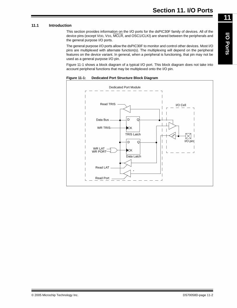
Section 11. I/O PortsI/O
Po
rts
11
11.1 IntroductionThis section provides information on the I/O ports for the dsPIC30F family of devices. All of thedevice pins (except VDD, VSS, MCLR, and OSC1/CLKI) are shared between the peripherals andthe general purpose I/O ports.
The general purpose I/O ports allow the dsPIC30F to monitor and control other devices. Most I/Opins are multiplexed with alternate function(s). The multiplexing will depend on the peripheralfeatures on the device variant. In general, when a peripheral is functioning, that pin may not beused as a general purpose I/O pin.
Figure 11-1 shows a block diagram of a typical I/O port. This block diagram does not take intoaccount peripheral functions that may be multiplexed onto the I/O pin.
Figure 11-1: Dedicated Port Structure Block Diagram
QD
CK
WR LAT
TRIS Latch
I/O pin
WR PORT
Data Bus
QD
CK
Data Latch
Read LAT
Read Port
Read TRIS
WR TRIS
I/O Cell
Dedicated Port Module
© 2005 Microchip Technology Inc. DS70058D-page 11-2
dsPIC30F Family Reference Manual
11.2 I/O Port Control Registers
All I/O ports have three registers directly associated with the operation of the port, where ‘x’ is aletter that denotes the particular I/O port:
• TRISx: Data Direction register• PORTx: I/O Port register
• LATx: I/O Latch register
Each I/O pin on the device has an associated bit in the TRIS, PORT and LAT registers.
11.2.1 TRIS Registers
The TRISx register control bits determine whether each pin associated with the I/O port is aninput or an output. If the TRIS bit for an I/O pin is a ‘1’, then the pin is an input. If the TRIS bit foran I/O pin is a ‘0’, then the pin is configured for an output. An easy way to remember is that a ‘1’looks like an I (input) and a ‘0’ looks like an O (output). All port pins are defined as inputs after aReset.
11.2.2 PORT Registers
Data on an I/O pin is accessed via a PORTx register. A read of the PORTx register reads thevalue of the I/O pin, while a write to the PORTx register writes the value to the port data latch.
Many instructions, such as BSET and BCLR instructions, are read-modify-write operations.Therefore, a write to a port implies that the port pins are read, this value is modified, and thenwritten to the port data latch. Care should be taken when read-modify-write commands are usedon the PORTx registers and when some I/O pins associated with the port are configured asinputs. If an I/O pin configured as an input is changed to an output at some later time, an unex-pected value may be output on the I/O pin. This effect occurs because the read-modify-writeinstruction reads the instantaneous value on the input pin and loads that value into the port datalatch.
11.2.3 LAT Registers
The LATx register associated with an I/O pin eliminates the problems that could occur withread-modify-write instructions. A read of the LATx register returns the values held in the portoutput latches, instead of the values on the I/O pins. A read-modify-write operation on the LATregister, associated with an I/O port, avoids the possibility of writing the input pin values into theport latches. A write to the LATx register has the same effect as a write to the PORTx register.
The differences between the PORT and LAT registers can be summarized as follows:
• A write to the PORTx register writes the data value to the port latch.• A write to the LATx register writes the data value to the port latch.• A read of the PORTx register reads the data value on the I/O pin.
• A read of the LATx register reads the data value held in the port latch.
Any bit and its associated data and control registers that are not valid for a particular device willbe disabled. That means the corresponding LATx and TRISx registers, and the port pin, will readas zeros.
Note: The total number of ports and available I/O pins will depend on the device variant.In a given device, all of the bits in a port control register may not be implemented.Refer to the specific device data sheet for further details.
DS70058D-page 11-3 © 2005 Microchip Technology Inc.
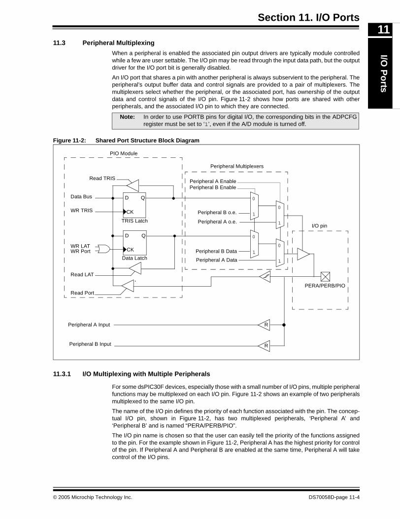
Section 11. I/O PortsI/O
Po
rts
11
11.3 Peripheral MultiplexingWhen a peripheral is enabled the associated pin output drivers are typically module controlledwhile a few are user settable. The I/O pin may be read through the input data path, but the outputdriver for the I/O port bit is generally disabled.
An I/O port that shares a pin with another peripheral is always subservient to the peripheral. Theperipheral’s output buffer data and control signals are provided to a pair of multiplexers. Themultiplexers select whether the peripheral, or the associated port, has ownership of the outputdata and control signals of the I/O pin. Figure 11-2 shows how ports are shared with otherperipherals, and the associated I/O pin to which they are connected.
Figure 11-2: Shared Port Structure Block Diagram
11.3.1 I/O Multiplexing with Multiple Peripherals
For some dsPIC30F devices, especially those with a small number of I/O pins, multiple peripheralfunctions may be multiplexed on each I/O pin. Figure 11-2 shows an example of two peripheralsmultiplexed to the same I/O pin.
The name of the I/O pin defines the priority of each function associated with the pin. The concep-tual I/O pin, shown in Figure 11-2, has two multiplexed peripherals, ‘Peripheral A’ and‘Peripheral B’ and is named “PERA/PERB/PIO”.
The I/O pin name is chosen so that the user can easily tell the priority of the functions assignedto the pin. For the example shown in Figure 11-2, Peripheral A has the highest priority for controlof the pin. If Peripheral A and Peripheral B are enabled at the same time, Peripheral A will takecontrol of the I/O pins.
Note: In order to use PORTB pins for digital I/O, the corresponding bits in the ADPCFGregister must be set to ‘1’, even if the A/D module is turned off.
QD
CK
TRIS Latch
Data Bus
QD
CK
Data Latch
Read LAT
Read Port
Read TRIS
WR TRIS
PIO Module
WR LATWR Port
0
1Peripheral A o.e.
0
1
Peripheral A EnablePeripheral B Enable
Peripheral B o.e.
0
1Peripheral A Data
0
1Peripheral B Data
RPeripheral A Input
RPeripheral B Input
PERA/PERB/PIO
Peripheral Multiplexers
I/O pin
© 2005 Microchip Technology Inc. DS70058D-page 11-4
dsPIC30F Family Reference Manual
DS
11.3.1.1 Software Input Pin Control
Some of the functions assigned to an I/O pin may be input functions that do not take control ofthe pin output driver. An example of one such peripheral is the Input Capture module. If the I/Opin associated with the Input Capture is configured as an output, using the appropriateTRIS control bit, the user can manually affect the state of the Input Capture pin through itscorresponding PORT register. This behavior can be useful in some situations, especially fortesting purposes, when no external signal is connected to the input pin.
Referring to Figure 11-2, the organization of the peripheral multiplexers will determine if the peripheralinput pin can be manipulated in software using the PORT register. The conceptual peripherals shownin this figure disconnect the PORT data from the I/O pin when the peripheral function is enabled.
In general, the following peripherals allow their input pins to be controlled manually through thePORT registers:
• External Interrupt pins• Timer Clock Input pins• Input Capture pins• PWM Fault pins
Most serial communication peripherals, when enabled, take full control of the I/O pin, so that theinput pins associated with the peripheral cannot be affected through the corresponding PORTregisters. These peripherals include the following:
• SPITM
• I2CTM
• DCI• UART• CAN
11.3.1.2 Pin Control Summary
When a peripheral is enabled the associated pin output drivers are typically module controlledwhile a few are user settable. The term "Module Control" means that the associated port pin out-put driver is disabled and the pin can only be controlled and accessed by the peripheral. The term"User Settable" means that the associated peripheral port pin output driver is user configurablevia the associated TRISx SFR. The TRISx register must be set properly for the peripheral to func-tion properly. For "User Settable" peripheral pins, the actual port pin state can always be readvia the PORTx SFR.
An Input Capture peripheral makes a good example of a User Settable peripheral. The user mustwrite the associated TRIS register to configure the Input Capture pin as an input. Since the I/Opin circuitry is still active when the Input Capture is enabled, a 'trick' can be used to manuallyproduce capture events using software. The Input Capture pin is configured as an output usingthe associated TRIS register. Then, the software can write values to the corresponding LAT reg-ister drive to internally control the Input Capture pin and force capture events.
As another example an INTx pin can be configured as an output and then by writing to the asso-ciated LATx bit an INTx interrupt, if enabled, can be generated.
The UART is an example of a Module Control peripheral. When the UART is enabled, the PORTand TRIS registers have no effect and cannot be used to read or write the RX and TX pins. Mostcommunication peripheral functions available on the dsPIC are Module Control peripherals.
For example, the SPI module can be configured for Master mode in which only the SDO pin isrequired. In this scenario the SDI pin can be configured as a general purpose output pin by clear-ing (setting to a logic "0") the associated TRISx bit. Table 11-1 presents a summary of the dsPICperipherals and associated Pin Output Control and Port pin read status.
70058D-page 11-5 © 2005 Microchip Technology Inc.
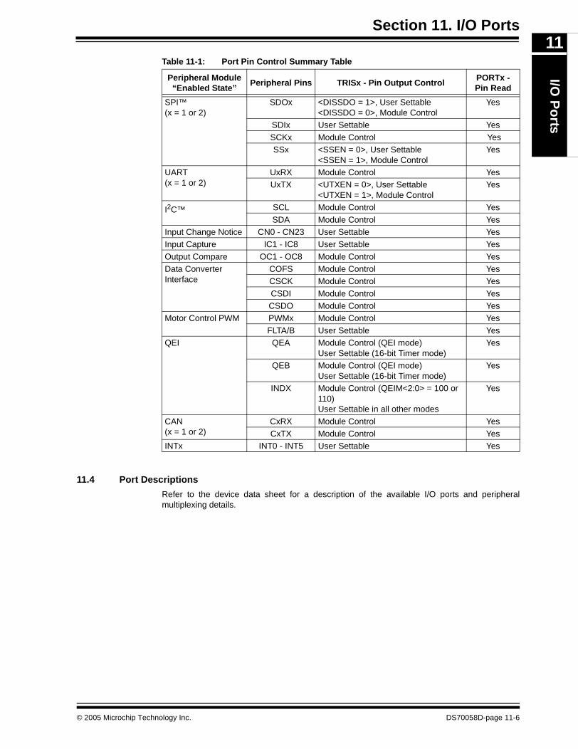
Section 11. I/O PortsI/O
Po
rts
11
11.4 Port Descriptions
Refer to the device data sheet for a description of the available I/O ports and peripheralmultiplexing details.
Table 11-1: Port Pin Control Summary Table
Peripheral Module “Enabled State”
Peripheral Pins TRISx - Pin Output ControlPORTx - Pin Read
SPI™(x = 1 or 2)
SDOx <DISSDO = 1>, User Settable<DISSDO = 0>, Module Control
Yes
SDIx User Settable Yes
SCKx Module Control YesSSx <SSEN = 0>, User Settable
<SSEN = 1>, Module ControlYes
UART(x = 1 or 2)
UxRX Module Control YesUxTX <UTXEN = 0>, User Settable
<UTXEN = 1>, Module ControlYes
I2C™ SCL Module Control Yes
SDA Module Control YesInput Change Notice CN0 - CN23 User Settable YesInput Capture IC1 - IC8 User Settable Yes
Output Compare OC1 - OC8 Module Control YesData Converter Interface
COFS Module Control YesCSCK Module Control Yes
CSDI Module Control YesCSDO Module Control Yes
Motor Control PWM PWMx Module Control Yes
FLTA/B User Settable YesQEI QEA Module Control (QEI mode)
User Settable (16-bit Timer mode)Yes
QEB Module Control (QEI mode)User Settable (16-bit Timer mode)
Yes
INDX Module Control (QEIM<2:0> = 100 or 110)User Settable in all other modes
Yes
CAN(x = 1 or 2)
CxRX Module Control YesCxTX Module Control Yes
INTx INT0 - INT5 User Settable Yes
© 2005 Microchip Technology Inc. DS70058D-page 11-6
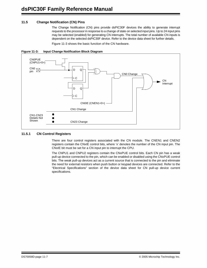
dsPIC30F Family Reference Manual
11.5 Change Notification (CN) Pins
The Change Notification (CN) pins provide dsPIC30F devices the ability to generate interruptrequests to the processor in response to a change of state on selected input pins. Up to 24 input pinsmay be selected (enabled) for generating CN interrupts. The total number of available CN inputs isdependent on the selected dsPIC30F device. Refer to the device data sheet for further details.
Figure 11-3 shows the basic function of the CN hardware.
Figure 11-3: Input Change Notification Block Diagram
11.5.1 CN Control Registers
There are four control registers associated with the CN module. The CNEN1 and CNEN2registers contain the CNxIE control bits, where ‘x’ denotes the number of the CN input pin. TheCNxIE bit must be set for a CN input pin to interrupt the CPU.
The CNPU1 and CNPU2 registers contain the CNxPUE control bits. Each CN pin has a weakpull-up device connected to the pin, which can be enabled or disabled using the CNxPUE controlbits. The weak pull-up devices act as a current source that is connected to the pin and eliminatethe need for external resistors when push button or keypad devices are connected. Refer to the“Electrical Specifications” section of the device data sheet for CN pull-up device currentspecifications.
CN
D Q
C
D Q
C
CN0IE (CNEN1<0>)
CN0pin
CN0PUE(CNPU1<0>)
CN0 Change
CN1 Change
CN23 Change
Interrupt
CN1-CN23Details NotShown
DS70058D-page 11-7 © 2005 Microchip Technology Inc.

Section 11. I/O PortsI/O
Po
rts
11
11.5.2 CN Configuration and OperationThe CN pins are configured as follows:
1. Ensure that the CN pin is configured as a digital input by setting the associated bit in theTRISx register.
2. Enable interrupts for the selected CN pins by setting the appropriate bits in the CNEN1and CNEN2 registers.
3. Turn on the weak pull-up devices (if desired) for the selected CN pins by setting theappropriate bits in the CNPU1 and CNPU2 registers.
4. Clear the CNIF (IFS0<15>) interrupt flag.5. Select the desired interrupt priority for CN interrupts using the CNIP<2:0> control bits
(IPC3<14:12>).6. Enable CN interrupts using the CNIE (IEC0<15>) control bit.
When a CN interrupt occurs, the user should read the PORT register associated with the CNpin(s). This will clear the mismatch condition and setup the CN logic to detect the next pinchange. The current PORT value can be compared to the PORT read value obtained at the lastCN interrupt to determine the pin that changed.
The CN pins have a minimum input pulse width specification. Refer to the “ElectricalSpecifications” section of the device data sheet for further details.
11.6 CN Operation in Sleep and Idle Modes
The CN module continues to operate during Sleep or Idle modes. If one of the enabled CN pinschanges states, the CNIF (IFS0<15>) status bit will be set. If the CNIE bit (IEC0<15>) is set, thedevice will wake from Sleep or Idle mode and resume operation.
If the assigned priority level of the CN interrupt is equal to or less than the current CPU prioritylevel, device execution will continue from the instruction immediately following the SLEEP orIDLE instruction.
If the assigned priority level of the CN interrupt is greater than the current CPU priority level,device execution will continue from the CN interrupt vector address.
© 2005 Microchip Technology Inc. DS70058D-page 11-8
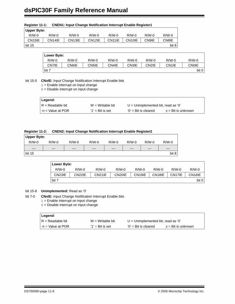
dsPIC30F Family Reference Manual
Register 11-1: CNEN1: Input Change Notification Interrupt Enable Register1
Register 11-2: CNEN2: Input Change Notification Interrupt Enable Register2
Upper Byte:R/W-0 R/W-0 R/W-0 R/W-0 R/W-0 R/W-0 R/W-0 R/W-0
CN15IE CN14IE CN13IE CN12IE CN11IE CN10IE CN9IE CN8IE
bit 15 bit 8
Lower Byte:R/W-0 R/W-0 R/W-0 R/W-0 R/W-0 R/W-0 R/W-0 R/W-0CN7IE CN6IE CN5IE CN4IE CN3IE CN2IE CN1IE CN0IE
bit 7 bit 0
bit 15-0 CNxIE: Input Change Notification Interrupt Enable bits1 = Enable interrupt on input change0 = Disable interrupt on input change
Legend:
R = Readable bit W = Writable bit U = Unimplemented bit, read as ‘0’
-n = Value at POR ‘1’ = Bit is set ‘0’ = Bit is cleared x = Bit is unknown
Upper Byte:
R/W-0 R/W-0 R/W-0 R/W-0 R/W-0 R/W-0 R/W-0 R/W-0
— — — — — — — —bit 15 bit 8
Lower Byte:
R/W-0 R/W-0 R/W-0 R/W-0 R/W-0 R/W-0 R/W-0 R/W-0
CN23IE CN22IE CN21IE CN20IE CN19IE CN18IE CN17IE CN16IE
bit 7 bit 0
bit 15-8 Unimplemented: Read as ‘0’
bit 7-0 CNxIE: Input Change Notification Interrupt Enable bits1 = Enable interrupt on input change0 = Disable interrupt on input change
Legend:
R = Readable bit W = Writable bit U = Unimplemented bit, read as ‘0’
-n = Value at POR ‘1’ = Bit is set ‘0’ = Bit is cleared x = Bit is unknown
DS70058D-page 11-9 © 2005 Microchip Technology Inc.
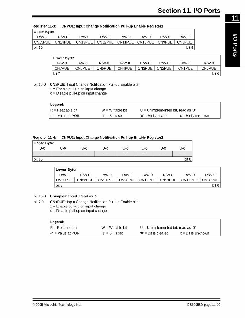
Section 11. I/O PortsI/O
Po
rts
11
Register 11-3: CNPU1: Input Change Notification Pull-up Enable Register1Register 11-4: CNPU2: Input Change Notification Pull-up Enable Register2
Upper Byte:R/W-0 R/W-0 R/W-0 R/W-0 R/W-0 R/W-0 R/W-0 R/W-0
CN15PUE CN14PUE CN13PUE CN12PUE CN11PUE CN10PUE CN9PUE CN8PUE
bit 15 bit 8
Lower Byte:R/W-0 R/W-0 R/W-0 R/W-0 R/W-0 R/W-0 R/W-0 R/W-0
CN7PUE CN6PUE CN5PUE CN4PUE CN3PUE CN2PUE CN1PUE CN0PUEbit 7 bit 0
bit 15-0 CNxPUE: Input Change Notification Pull-up Enable bits1 = Enable pull-up on input change0 = Disable pull-up on input change
Legend:
R = Readable bit W = Writable bit U = Unimplemented bit, read as ‘0’
-n = Value at POR ‘1’ = Bit is set ‘0’ = Bit is cleared x = Bit is unknown
Upper Byte:U-0 U-0 U-0 U-0 U-0 U-0 U-0 U-0
— — — — — — — —
bit 15 bit 8
Lower Byte:R/W-0 R/W-0 R/W-0 R/W-0 R/W-0 R/W-0 R/W-0 R/W-0
CN23PUE CN22PUE CN21PUE CN20PUE CN19PUE CN18PUE CN17PUE CN16PUEbit 7 bit 0
bit 15-8 Unimplemented: Read as ‘0’
bit 7-0 CNxPUE: Input Change Notification Pull-up Enable bits1 = Enable pull-up on input change0 = Disable pull-up on input change
Legend:
R = Readable bit W = Writable bit U = Unimplemented bit, read as ‘0’
-n = Value at POR ‘1’ = Bit is set ‘0’ = Bit is cleared x = Bit is unknown
© 2005 Microchip Technology Inc. DS70058D-page 11-10

dsPIC30F Family Reference Manual
11.7 Related Application Notes
This section lists application notes that are related to this section of the manual. Theseapplication notes may not be written specifically for the dsPIC30F Product Family, but theconcepts are pertinent and could be used with modification and possible limitations. The currentapplication notes related to the I/O Ports module are:
Title Application Note #
Implementing Wake-up on Key Stroke AN552
Note: Please visit the Microchip web site (www.microchip.com) for additional ApplicationNotes and code examples for the dsPIC30F Family of devices.
DS70058D-page 11-11 © 2005 Microchip Technology Inc.

Section 11. I/O PortsI/O
Po
rts
11
11.8 Revision HistoryRevision A
This is the initial released revision of this document.
Revision B
This revision incorporates additional technical content for the dsPIC30F I/O Ports module.
Revision C
There were no technical content revisions to this section of the manual, however, this section wasupdated to reflect Revision C throughout the manual.
Revision D
Section 11.3.1.2 “Pin Control Summary” was added to this revision.
© 2005 Microchip Technology Inc. DS70058D-page 11-12
Section 12. Timers
Timers
12
HIGHLIGHTSThis section of the manual contains the following major topics:
12.1 Introduction .................................................................................................................. 12-2
12.2 Timer Variants .............................................................................................................. 12-312.3 Control Registers ......................................................................................................... 12-612.4 Modes of Operation ..................................................................................................... 12-9
12.5 Timer Prescalers ........................................................................................................ 12-1412.6 Timer Interrupts.......................................................................................................... 12-1412.7 Reading and Writing 16-bit Timer Module Registers ................................................. 12-15
12.8 Low Power 32 kHz Crystal Oscillator Input ................................................................ 12-1512.9 32-bit Timer Configuration.......................................................................................... 12-1612.10 32-bit Timer Modes of Operation ............................................................................... 12-18
12.11 Reading and Writing into 32-bit Timers...................................................................... 12-2112.12 Timer Operation in Power Saving States ................................................................... 12-2112.13 Peripherals Using Timer Modules.............................................................................. 12-22
12.14 Design Tips ................................................................................................................ 12-2412.15 Related Application Notes.......................................................................................... 12-2512.16 Revision History ......................................................................................................... 12-26
© 2005 Microchip Technology Inc. DS70059D-page 12-1
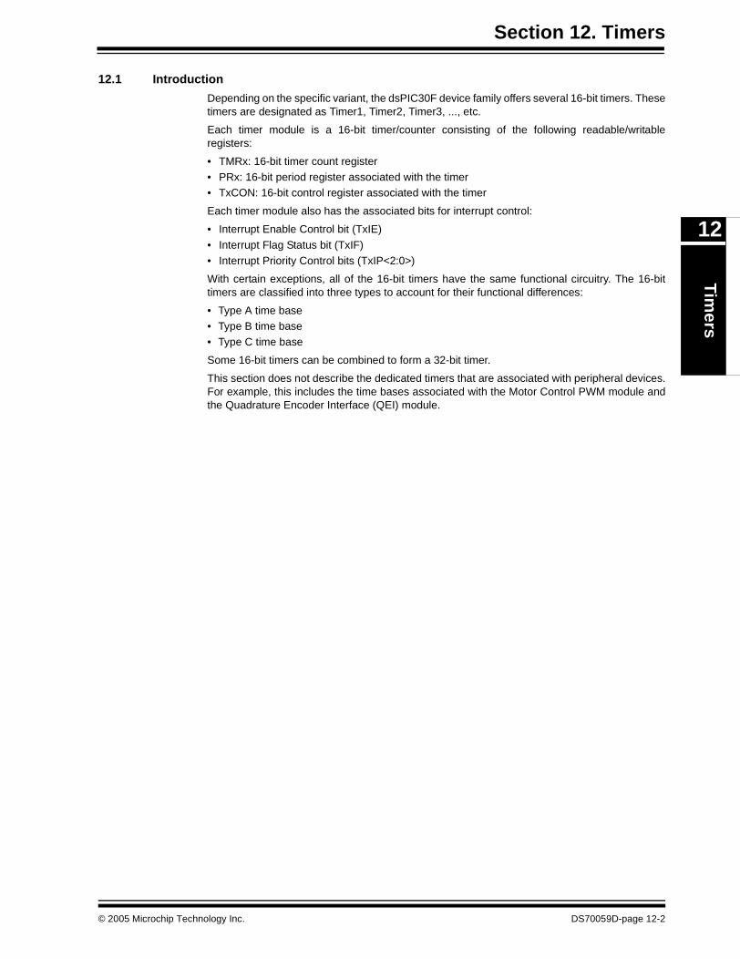
Section 12. TimersTim
ers
12
12.1 Introduction
Depending on the specific variant, the dsPIC30F device family offers several 16-bit timers. Thesetimers are designated as Timer1, Timer2, Timer3, ..., etc.
Each timer module is a 16-bit timer/counter consisting of the following readable/writableregisters:
• TMRx: 16-bit timer count register• PRx: 16-bit period register associated with the timer• TxCON: 16-bit control register associated with the timer
Each timer module also has the associated bits for interrupt control:
• Interrupt Enable Control bit (TxIE)
• Interrupt Flag Status bit (TxIF) • Interrupt Priority Control bits (TxIP<2:0>)
With certain exceptions, all of the 16-bit timers have the same functional circuitry. The 16-bittimers are classified into three types to account for their functional differences:
• Type A time base• Type B time base• Type C time base
Some 16-bit timers can be combined to form a 32-bit timer.
This section does not describe the dedicated timers that are associated with peripheral devices.For example, this includes the time bases associated with the Motor Control PWM module andthe Quadrature Encoder Interface (QEI) module.
© 2005 Microchip Technology Inc. DS70059D-page 12-2
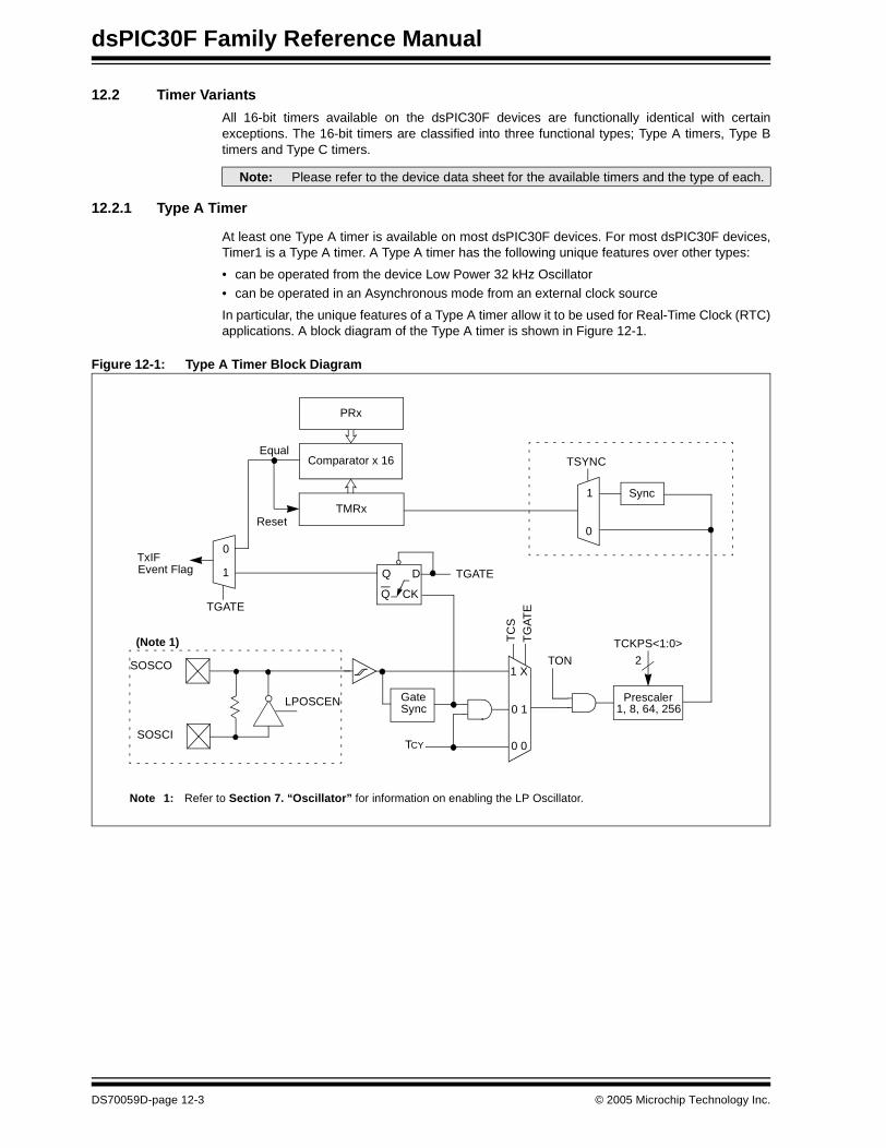
dsPIC30F Family Reference Manual
12.2 Timer Variants
All 16-bit timers available on the dsPIC30F devices are functionally identical with certainexceptions. The 16-bit timers are classified into three functional types; Type A timers, Type Btimers and Type C timers.
12.2.1 Type A Timer
At least one Type A timer is available on most dsPIC30F devices. For most dsPIC30F devices,Timer1 is a Type A timer. A Type A timer has the following unique features over other types:
• can be operated from the device Low Power 32 kHz Oscillator
• can be operated in an Asynchronous mode from an external clock source
In particular, the unique features of a Type A timer allow it to be used for Real-Time Clock (RTC)applications. A block diagram of the Type A timer is shown in Figure 12-1.
Figure 12-1: Type A Timer Block Diagram
Note: Please refer to the device data sheet for the available timers and the type of each.
TON
Sync
SOSCI
SOSCO
PRx
TxIF
EqualComparator x 16
TMRxReset
Note 1: Refer to Section 7. “Oscillator” for information on enabling the LP Oscillator.
LPOSCEN
Event Flag
(Note 1)
1
0
TSYNC
Q
Q D
CK
TGATE
TCKPS<1:0>
Prescaler1, 8, 64, 256
2
TGATE
TCY
1
0
TC
S
1 X
0 1
TG
AT
E
0 0
GateSync
DS70059D-page 12-3 © 2005 Microchip Technology Inc.

Section 12. TimersTim
ers
12
12.2.2 Type B Timer
Timer2 and Timer4, if present, are Type B timers on most dsPIC30F devices. A Type B timer hasthe following unique features over other types of timers:
• A Type B timer can be concatenated with a Type C timer to form a 32-bit timer. The TxCON register for a Type B timer has the T32 control bits to enable the 32-bit timer function.
• The clock synchronization for a Type B timer is performed after the prescale logic.
A block diagram of the Type B timer is shown in Figure 12-2.
Figure 12-2: Type B Timer Block Diagram
TON
Sync
PRx
TxIF
EqualComparator x 16
TMRxReset
Event Flag
Q
Q D
CK
TGATE
TCKPS<1:0>
Prescaler1, 8, 64, 256
2
TGATE
TCY
1
0
TC
S1 X
0 1
TG
AT
E
0 0
Gate
TxCKI
Sync
© 2005 Microchip Technology Inc. DS70059D-page 12-4
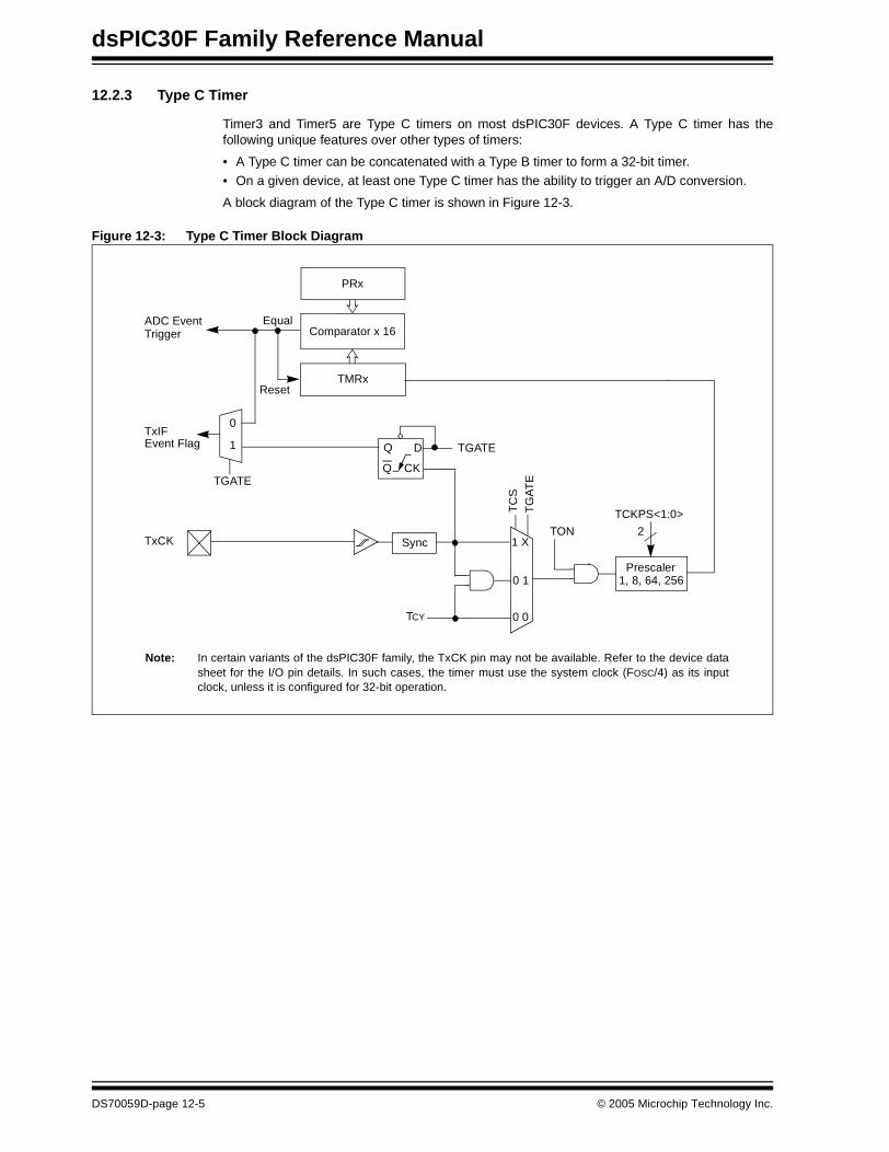
dsPIC30F Family Reference Manual
12.2.3 Type C Timer
Timer3 and Timer5 are Type C timers on most dsPIC30F devices. A Type C timer has thefollowing unique features over other types of timers:
• A Type C timer can be concatenated with a Type B timer to form a 32-bit timer.
• On a given device, at least one Type C timer has the ability to trigger an A/D conversion.
A block diagram of the Type C timer is shown in Figure 12-3.
Figure 12-3: Type C Timer Block Diagram
TON
PRx
TxIF
EqualComparator x 16
TMRxReset
Event Flag
Q
Q D
CK
TGATE
TCKPS<1:0>
Prescaler1, 8, 64, 256
2
TGATE
TCY
1
0
TC
S
1 X
0 1
TG
AT
E
0 0
TxCK
ADC Event
Note: In certain variants of the dsPIC30F family, the TxCK pin may not be available. Refer to the device datasheet for the I/O pin details. In such cases, the timer must use the system clock (FOSC/4) as its inputclock, unless it is configured for 32-bit operation.
Sync
Trigger
DS70059D-page 12-5 © 2005 Microchip Technology Inc.
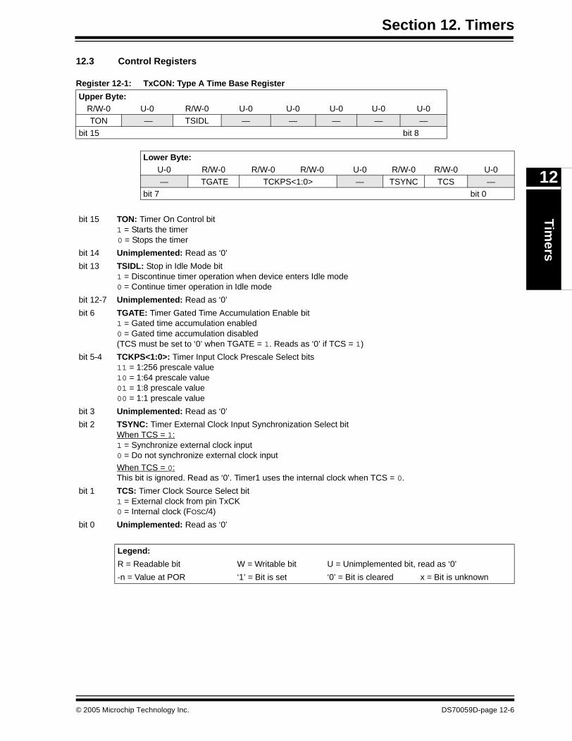
Section 12. TimersTim
ers
12
12.3 Control Registers
Register 12-1: TxCON: Type A Time Base Register
Upper Byte:R/W-0 U-0 R/W-0 U-0 U-0 U-0 U-0 U-0TON — TSIDL — — — — —
bit 15 bit 8
Lower Byte:U-0 R/W-0 R/W-0 R/W-0 U-0 R/W-0 R/W-0 U-0— TGATE TCKPS<1:0> — TSYNC TCS —
bit 7 bit 0
bit 15 TON: Timer On Control bit1 = Starts the timer0 = Stops the timer
bit 14 Unimplemented: Read as ‘0’
bit 13 TSIDL: Stop in Idle Mode bit1 = Discontinue timer operation when device enters Idle mode0 = Continue timer operation in Idle mode
bit 12-7 Unimplemented: Read as ‘0’
bit 6 TGATE: Timer Gated Time Accumulation Enable bit1 = Gated time accumulation enabled0 = Gated time accumulation disabled(TCS must be set to ‘0’ when TGATE = 1. Reads as ‘0’ if TCS = 1)
bit 5-4 TCKPS<1:0>: Timer Input Clock Prescale Select bits11 = 1:256 prescale value10 = 1:64 prescale value01 = 1:8 prescale value00 = 1:1 prescale value
bit 3 Unimplemented: Read as ‘0’
bit 2 TSYNC: Timer External Clock Input Synchronization Select bitWhen TCS = 1: 1 = Synchronize external clock input0 = Do not synchronize external clock input
When TCS = 0: This bit is ignored. Read as ‘0’. Timer1 uses the internal clock when TCS = 0.
bit 1 TCS: Timer Clock Source Select bit1 = External clock from pin TxCK 0 = Internal clock (FOSC/4)
bit 0 Unimplemented: Read as ‘0’
Legend:
R = Readable bit W = Writable bit U = Unimplemented bit, read as ‘0’
-n = Value at POR ‘1’ = Bit is set ‘0’ = Bit is cleared x = Bit is unknown
© 2005 Microchip Technology Inc. DS70059D-page 12-6
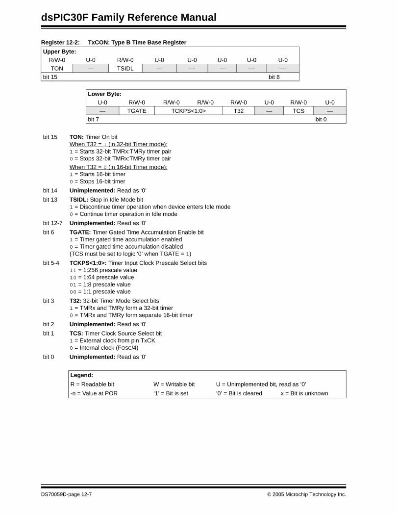
dsPIC30F Family Reference Manual
Register 12-2: TxCON: Type B Time Base Register Upper Byte:
R/W-0 U-0 R/W-0 U-0 U-0 U-0 U-0 U-0TON — TSIDL — — — — —
bit 15 bit 8
Lower Byte:U-0 R/W-0 R/W-0 R/W-0 R/W-0 U-0 R/W-0 U-0— TGATE TCKPS<1:0> T32 — TCS —
bit 7 bit 0
bit 15 TON: Timer On bitWhen T32 = 1 (in 32-bit Timer mode):1 = Starts 32-bit TMRx:TMRy timer pair0 = Stops 32-bit TMRx:TMRy timer pair
When T32 = 0 (in 16-bit Timer mode):1 = Starts 16-bit timer0 = Stops 16-bit timer
bit 14 Unimplemented: Read as ‘0’
bit 13 TSIDL: Stop in Idle Mode bit1 = Discontinue timer operation when device enters Idle mode0 = Continue timer operation in Idle mode
bit 12-7 Unimplemented: Read as ‘0’
bit 6 TGATE: Timer Gated Time Accumulation Enable bit1 = Timer gated time accumulation enabled0 = Timer gated time accumulation disabled(TCS must be set to logic ‘0’ when TGATE = 1)
bit 5-4 TCKPS<1:0>: Timer Input Clock Prescale Select bits11 = 1:256 prescale value10 = 1:64 prescale value01 = 1:8 prescale value00 = 1:1 prescale value
bit 3 T32: 32-bit Timer Mode Select bits1 = TMRx and TMRy form a 32-bit timer0 = TMRx and TMRy form separate 16-bit timer
bit 2 Unimplemented: Read as ‘0’
bit 1 TCS: Timer Clock Source Select bit1 = External clock from pin TxCK 0 = Internal clock (FOSC/4)
bit 0 Unimplemented: Read as ‘0’
Legend:
R = Readable bit W = Writable bit U = Unimplemented bit, read as ‘0’
-n = Value at POR ‘1’ = Bit is set ‘0’ = Bit is cleared x = Bit is unknown
DS70059D-page 12-7 © 2005 Microchip Technology Inc.
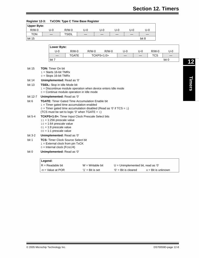
Section 12. TimersTim
ers
12
Register 12-3: TxCON: Type C Time Base Register Upper Byte:
R/W-0 U-0 R/W-0 U-0 U-0 U-0 U-0 U-0TON — TSIDL — — — — —
bit 15 bit 8
Lower Byte:U-0 R/W-0 R/W-0 R/W-0 U-0 U-0 R/W-0 U-0— TGATE TCKPS<1:0> — — TCS —
bit 7 bit 0
bit 15 TON: Timer On bit1 = Starts 16-bit TMRx0 = Stops 16-bit TMRx
bit 14 Unimplemented: Read as ‘0’
bit 13 TSIDL: Stop in Idle Mode bit1 = Discontinue module operation when device enters Idle mode0 = Continue module operation in Idle mode
bit 12-7 Unimplemented: Read as ‘0’
bit 6 TGATE: Timer Gated Time Accumulation Enable bit1 = Timer gated time accumulation enabled0 = Timer gated time accumulation disabled (Read as ‘0’ if TCS = 1)(TCS must be set to logic ‘0’ when TGATE = 1)
bit 5-4 TCKPS<1:0>: Timer Input Clock Prescale Select bits11 = 1:256 prescale value10 = 1:64 prescale value01 = 1:8 prescale value00 = 1:1 prescale value
bit 3-2 Unimplemented: Read as ‘0’
bit 1 TCS: Timer Clock Source Select bit1 = External clock from pin TxCK 0 = Internal clock (FOSC/4)
bit 0 Unimplemented: Read as ‘0’
Legend:
R = Readable bit W = Writable bit U = Unimplemented bit, read as ‘0’
-n = Value at POR ‘1’ = Bit is set ‘0’ = Bit is cleared x = Bit is unknown
© 2005 Microchip Technology Inc. DS70059D-page 12-8
dsPIC30F Family Reference Manual
12.4 Modes of Operation
Each timer module can operate in one of the following modes:
• As a synchronous timer
• As a synchronous counter• As a gated timer• As an asynchronous counter (Type A time base only)
The Timer modes are determined by the following bits:
• TCS (TxCON<1>): Timer Clock Source Control bit
• TSYNC (T1CON<2>): Timer Synchronization Control bit (Type A time base only)• TGATE (TxCON<6>): Timer Gate Control bit
Each timer module is enabled or disabled using the TON Control bit (TxCON <15>).
12.4.1 Timer Mode
All types of timers have the ability to operate in Timer mode. In Timer mode, the input clock tothe timer is provided from the internal system clock (FOSC/4). When enabled, the timerincrements once per instruction cycle for a 1:1 prescaler setting. The Timer mode is selected byclearing the TCS control bit (TxCON<1>). The Synchronous mode control bit, TSYNC(T1CON<2>), has no effect, since the system clock source is used to generate the timer clock.
Example 12-1: Initialization Code for 16-bit Timer Using System Clock
Note: Only Type A time bases support the External Asynchronous Clock mode.
; The following code example will enable Timer1 interrupts, ; load the Timer1 Period register and start Timer1.
; When a Timer1 period match interrupt occurs, the interrupt ; service routine must clear the Timer1 interrupt status flag ; in software.
CLR T1CON ; Stops the Timer1 and reset control reg. CLR TMR1 ; Clear contents of the timer register MOV #0xFFFF, w0 ; Load the Period register MOV w0, PR1 ; with the value 0xFFFF
BSET IPC0, #T1IP0 ; Setup Timer1 interrupt for BCLR IPC0, #T1IP1 ; desired priority levelBCLR IPC0, #T1IP2 ; (this example assigns level 1 priority)BCLR IFS0, #T1IF ; Clear the Timer1 interrupt status flag BSET IEC0, #T1IE ; Enable Timer1 interruptsBSET T1CON, #TON ; Start Timer1 with prescaler settings
; at 1:1 and clock source set to ; the internal instruction cycle
; Example code for Timer1 ISR
__T1Interrupt: BCLR IFS0, #T1IF ; Reset Timer1 interrupt flag
; User code goes here.RETFIE ; Return from ISR
DS70059D-page 12-9 © 2005 Microchip Technology Inc.
Section 12. TimersTim
ers
12
12.4.2 Synchronous Counter Mode Using External Clock Input
When the TCS control bit (TxCON<1>) is set, the clock source for the timer is provided externallyand the selected timer increments on every rising edge of clock input on the TxCK pin.
External clock synchronization must be enabled for a Type A time base. This is accomplished bysetting the TSYNC control bit (TxCON<2>). For Type B and Type C time bases, the externalclock input is always synchronized to the system instruction cycle clock, TCY.
When the timer is operated in the Synchronized Counter mode, there are minimum requirementsfor the external clock high time and low time. The synchronization of the external clock sourcewith the device instruction clock is accomplished by sampling the external clock signal at twodifferent times within an instruction cycle.
A timer operating from a synchronized external clock source will not operate in Sleep mode,since the synchronization circuit is shut-off during Sleep mode.
Example 12-2: Initialization Code for 16-bit Synchronous Counter Mode Using an External Clock Input
Note: The external input clock must meet certain minimum high time and low timerequirements when Timerx is used in the Synchronous Counter mode. Refer to thedevice data sheet “Electrical Specifications” section for further details.
; The following code example will enable Timer1 interrupts, load the ; Timer1 Period register and start Timer1 using an external clock ; and a 1:8 prescaler setting.
; When a Timer1 period match interrupt occurs, the interrupt service ; routine must clear the Timer1 interrupt status flag in software.
CLR T1CON ; Stops the Timer1 and reset control reg. CLR TMR1 ; Clear contents of the timer register MOV #0x8CFF, w0 ; Load the Period register MOV w0, PR1 ; with the value 0x8CFF
BSET IPC0, #T1IP0 ; Setup Timer1 interrupt for BCLR IPC0, #T1IP1 ; desired priority levelBCLR IPC0, #T1IP2 ; (this example assigns level 1 priority)BCLR IFS0, #T1IF ; Clear the Timer1 interrupt status flag BSET IEC0, #T1IE ; Enable Timer1 interruptsMOV #0x8016, W0 ; Start Timer1 with prescaler settings at
; 1:8 and clock source set to the external MOV w0, T1CON ; clock in the synchronous mode
; Example code for Timer1 ISR
__T1Interrupt: BCLR IFS0, #T1IF ; Reset Timer1 interrupt flag
; User code goes here.RETFIE ; Return from ISR
© 2005 Microchip Technology Inc. DS70059D-page 12-10
dsPIC30F Family Reference Manual
12.4.3 Type A Timer Asynchronous Counter Mode Using External Clock Input
A Type A time base has the ability to operate in an Asynchronous Counting mode, using anexternal clock source connected to the TxCK pin. When the TSYNC control bit (TxCON<2>) iscleared, the external clock input is not synchronized with the device system clock source. Thetime base continues to increment asynchronously to the internal device clock.
The asynchronous operation time base is beneficial for the following applications:
• The time base can operate during Sleep mode and can generate an interrupt on period register match that will wake-up the processor.
• The time base can be clocked from the low power 32 kHz oscillator for real-time clock applications
Please see Section 12.12.1 “Timer Operation in Sleep Mode” for more details..
Example 12-3: Initialization Code for 16-bit Asynchronous Counter Mode Using an External Clock Input
Note 1: Only Type A time bases support the Asynchronous Counter mode.2: The external input clock must meet certain minimum high time and low time
requirements when Timerx is used in the Asynchronous Counter mode. Refer to thedevice data sheet “Electrical Specifications” section for further details.
3: Unexpected results may occur when reading Timer1, in asynchronous mode.
; The following code example will enable Timer1 interrupts, load the ; Timer1 Period register and start Timer1 using an asynchronous ; external clock and a 1:8 prescaler setting.
; When a Timer1 period match interrupt occurs, the interrupt service ; routine must clear the Timer1 interrupt status flag in software.
CLR T1CON ; Stops the Timer1 and reset control reg. CLR TMR1 ; Clear contents of the timer register MOV #0x7FFF, w0 ; Load the Period register MOV w0, PR1 ; with the value 0x7FFF
BSET IPC0, #T1IP0 ; Setup Timer1 interrupt for BCLR IPC0, #T1IP1 ; desired priority levelBCLR IPC0, #T1IP2 ; (this example assigns level 1 priority)BCLR IFS0, #T1IF ; Clear the Timer1 interrupt status flag BSET IEC0, #T1IE ; Enable Timer1 interruptsMOV #0x8012, w0 ; Start Timer1 with prescaler settings at
; 1:8 and clock source set to the external MOV w0, T1CON ; clock in the asynchronous mode
; Example code for Timer1 ISR
__T1Interrupt: BCLR IFS0, #T1IF ; Reset Timer1 interrupt flag
; User code goes here.RETFIE ; Return from ISR
DS70059D-page 12-11 © 2005 Microchip Technology Inc.
Section 12. TimersTim
ers
12
12.4.4 Timer Operation with Fast External Clock Source
In some applications, it may be desirable to use one of the timers to count clock edges from arelatively high frequency external clock source. In these situations, Type A and Type B timebases are the most suitable choices for counting the external clock source, because the clocksynchronization logic for these timers is located after the timer prescaler (see Figure 12-1 andFigure 12-2). This allows a higher external clock frequency to be used that will not violate theminimum high and low times required by the prescaler. When a timer prescaler ratio other than1:1 is selected for a Type A or Type B time base, the minimum high and low times for the externalclock input are reduced by the chosen prescaler ratio.
A Type A time base is unique because it can be operated in an Asynchronous Clock mode,eliminating any prescaler timing requirements.
Note that in all cases, there are minimum high and low times for the external clock signal thatcannot be exceeded. These minimum times are required to satisfy the I/O pin timingrequirements.
Please refer to the device data sheet for the external clock timing specifications associated withthe time bases.
12.4.5 Gated Time Accumulation Mode
The Gated Time Accumulation mode allows the internal timer register to increment based uponthe duration of the high time applied to the TxCK pin. In the Gated Time Accumulation mode, thetimer clock source is derived from the internal system clock. When the TxCK pin state is high, thetimer register will count up until a period match has occurred, or the TxCK pin state is changedto a low state. A pin state transition from high to low will set the TxIF interrupt flag. Depending onwhen the edge occurs, the interrupt flag is asserted 1 or 2 instruction cycles after the falling edgeof the signal on the TxCK pin.
The TGATE control bit (TxCON<6>) must be set to enable the Gated Time Accumulation mode.The timer must be enabled, TON (TxCON<15>) = 1, and the timer clock source set to the internalclock, TCS (TxCON<1>) = 0.
The gate operation starts on a rising edge of the signal applied to the TxCK pin and terminateson the falling edge of the signal applied to the TxCK pin. The respective timer will increment whilethe external gate signal is high.
The falling edge of the gate signal terminates the count operation, but does not reset the timer.The user must reset the timer if it is desired to start from zero on the next rising edge gate input.The falling edge of the gate signal generates an interrupt.
The resolution of the timer count is directly related to the timer clock period. For a timer prescalerof 1:1, the timer clock period is one instruction cycle. For a timer prescaler of 1:256, the timerclock period is 256 times the instruction cycle. The timer clock resolution can be associated tothe pulse width of the gate signal. Refer to the “Electrical Specifications” section in the devicedata sheet for further details on the gate width pulse requirements.
Note: The timer will not interrupt the CPU when a timer period match occurs in Gate TimeAccumulation mode.
© 2005 Microchip Technology Inc. DS70059D-page 12-12
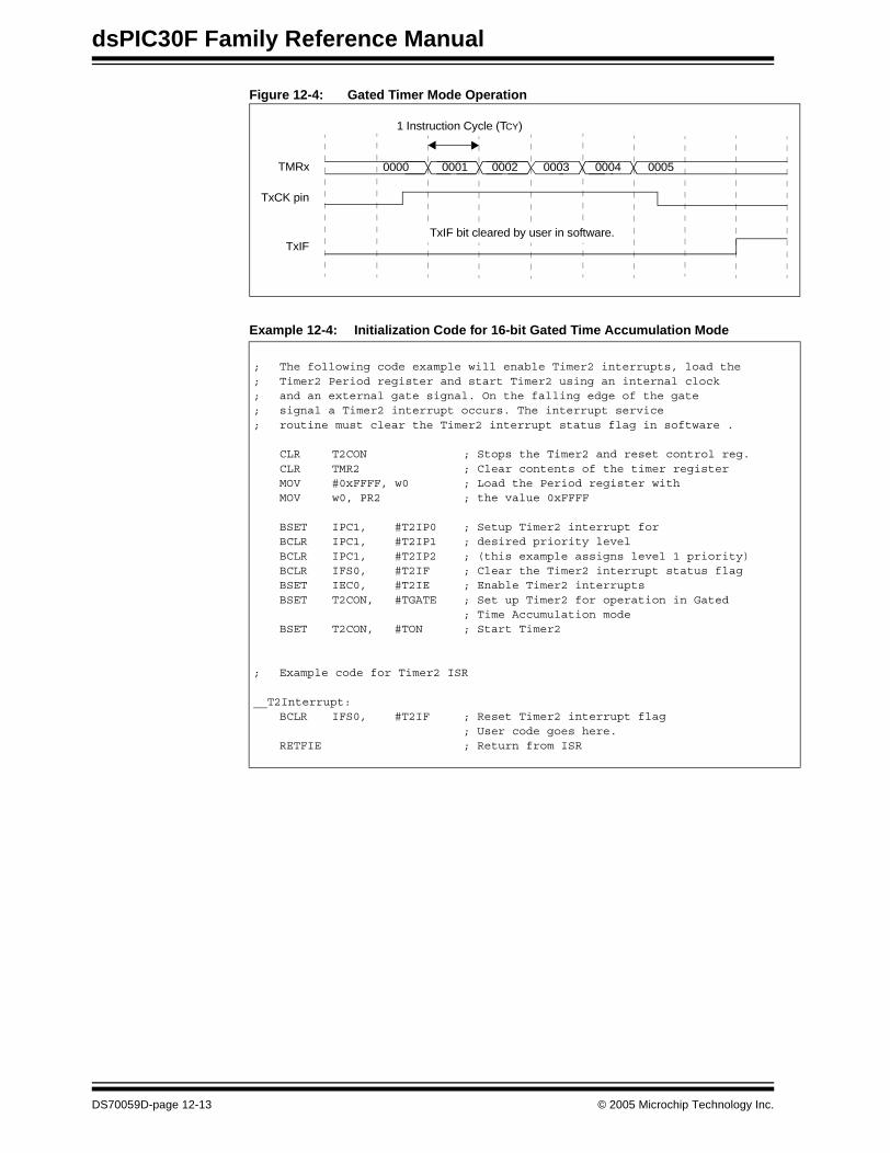
dsPIC30F Family Reference Manual
DS
Figure 12-4: Gated Timer Mode Operation
Example 12-4: Initialization Code for 16-bit Gated Time Accumulation Mode
TxIF
0001 0002TMRx
1 Instruction Cycle (TCY)
00040003
TxCK pin
00050000
TxIF bit cleared by user in software.
; The following code example will enable Timer2 interrupts, load the ; Timer2 Period register and start Timer2 using an internal clock ; and an external gate signal. On the falling edge of the gate ; signal a Timer2 interrupt occurs. The interrupt service ; routine must clear the Timer2 interrupt status flag in software .
CLR T2CON ; Stops the Timer2 and reset control reg.CLR TMR2 ; Clear contents of the timer register MOV #0xFFFF, w0 ; Load the Period register with MOV w0, PR2 ; the value 0xFFFF
BSET IPC1, #T2IP0 ; Setup Timer2 interrupt for BCLR IPC1, #T2IP1 ; desired priority levelBCLR IPC1, #T2IP2 ; (this example assigns level 1 priority)BCLR IFS0, #T2IF ; Clear the Timer2 interrupt status flag BSET IEC0, #T2IE ; Enable Timer2 interruptsBSET T2CON, #TGATE ; Set up Timer2 for operation in Gated
; Time Accumulation mode BSET T2CON, #TON ; Start Timer2
; Example code for Timer2 ISR
__T2Interrupt: BCLR IFS0, #T2IF ; Reset Timer2 interrupt flag
; User code goes here.RETFIE ; Return from ISR
70059D-page 12-13 © 2005 Microchip Technology Inc.
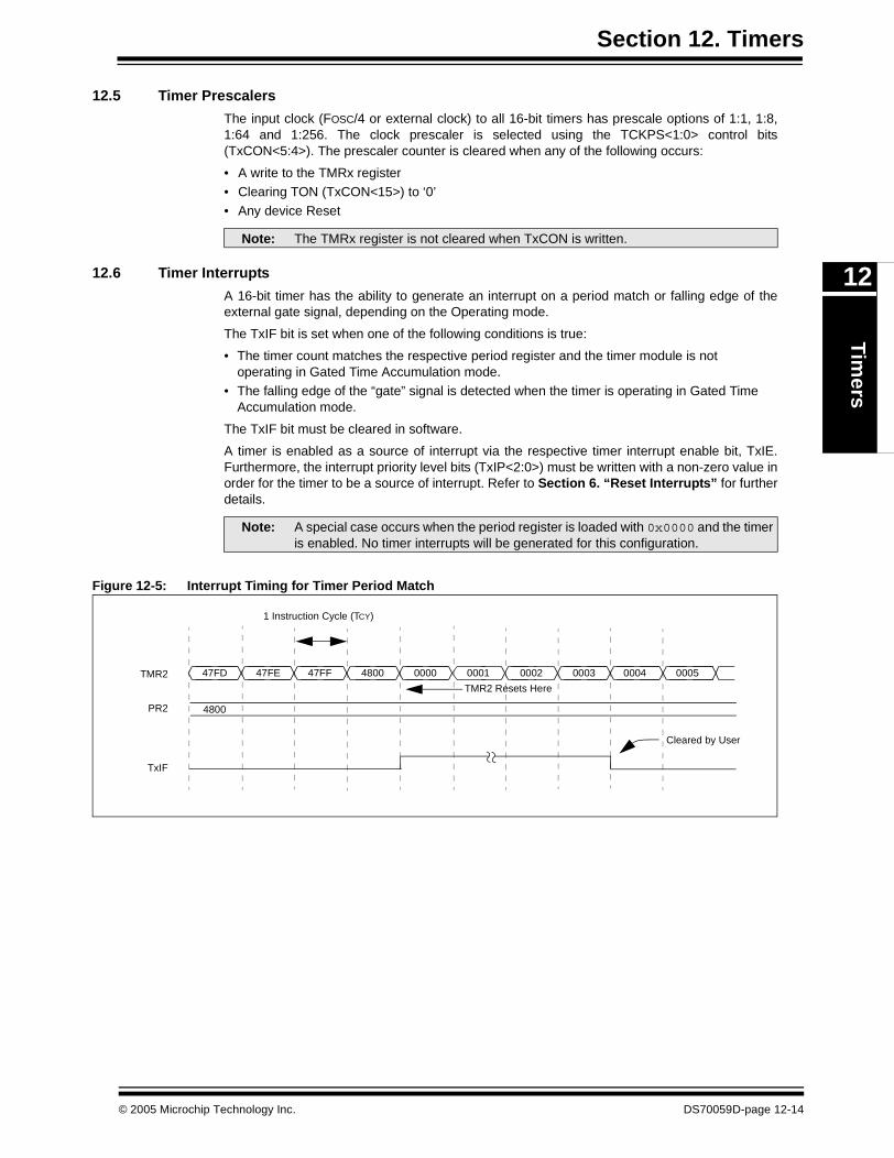
Section 12. TimersTim
ers
12
12.5 Timer Prescalers
The input clock (FOSC/4 or external clock) to all 16-bit timers has prescale options of 1:1, 1:8,1:64 and 1:256. The clock prescaler is selected using the TCKPS<1:0> control bits(TxCON<5:4>). The prescaler counter is cleared when any of the following occurs:
• A write to the TMRx register• Clearing TON (TxCON<15>) to ‘0’• Any device Reset
12.6 Timer Interrupts
A 16-bit timer has the ability to generate an interrupt on a period match or falling edge of theexternal gate signal, depending on the Operating mode.
The TxIF bit is set when one of the following conditions is true:
• The timer count matches the respective period register and the timer module is not operating in Gated Time Accumulation mode.
• The falling edge of the “gate” signal is detected when the timer is operating in Gated Time Accumulation mode.
The TxIF bit must be cleared in software.
A timer is enabled as a source of interrupt via the respective timer interrupt enable bit, TxIE.Furthermore, the interrupt priority level bits (TxIP<2:0>) must be written with a non-zero value inorder for the timer to be a source of interrupt. Refer to Section 6. “Reset Interrupts” for furtherdetails.
Figure 12-5: Interrupt Timing for Timer Period Match
Note: The TMRx register is not cleared when TxCON is written.
Note: A special case occurs when the period register is loaded with 0x0000 and the timeris enabled. No timer interrupts will be generated for this configuration.
TxIF
0003 000547FE 47FF 4800 000047FDTMR2 0004
1 Instruction Cycle (TCY)
4800PR2
0002
TMR2 Resets Here
0001
Cleared by User
© 2005 Microchip Technology Inc. DS70059D-page 12-14
dsPIC30F Family Reference Manual
12.7 Reading and Writing 16-bit Timer Module Registers• All timer module SFRs can be written to as a byte (8-bits) or as a word (16-bits).• All timer module SFRs can only be read as a word (16-bits).
12.7.1 Writing to the 16-bit Timers
The timer and its respective period register can be written to while the module is operating. Theuser should be aware of the following when byte writes are performed:
• If the timer is incrementing and the low byte of the timer is written to, the upper byte of the timer is not affected. If 0xFF is written into the low byte of the timer, the next timer count clock after this write will cause the low byte to rollover to 0x00 and generate a carry into the high byte of the timer.
• If the timer is incrementing and the high byte of the timer is written to, the low byte of the timer is not affected. If the low byte of the timer contains 0xFF when the write occurs, the next timer count clock will generate a carry from the timer low byte and this carry will cause the upper byte of the timer to increment.
When the TMRx register is written to (word or byte) via an instruction, the TMRx registerincrement is masked and does not occur during that instruction cycle.
Writes to a timer with an asynchronous clock source should be avoided in a real-timekeepingapplication. See Section 12.4.1 “Timer Mode” for more details.
12.7.2 Reading from the 16-bit Timers
All reads of the timers and their associated SFRs must be word reads (16-bits). A byte read willhave no effect (‘0’ will be returned).
The timer and respective period register can be read while the module is operating. A read of theTMRx register does not prevent the timer from incrementing during the same instruction cycle.
12.8 Low Power 32 kHz Crystal Oscillator Input
In each device variant, the Low Power 32 kHz Crystal Oscillator is available to a Type A timermodule for Real-Time Clock (RTC) applications.
• The LP Oscillator becomes the clock source for the timer when the LP Oscillator is enabled and the timer is configured to use the external clock source.
• The LP Oscillator is enabled by setting the LPOSCEN control bit in the OSCCON register.
• The 32 kHz crystal is connected to the SOSCO/SOSCI device pins.
Refer to Section 7. “Oscillator” for further details.
DS70059D-page 12-15 © 2005 Microchip Technology Inc.
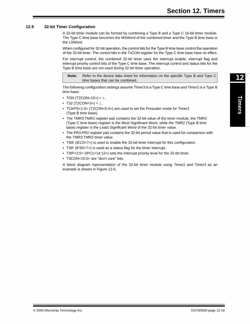
Section 12. TimersTim
ers
12
12.9 32-bit Timer Configuration
A 32-bit timer module can be formed by combining a Type B and a Type C 16-bit timer module.The Type C time base becomes the MSWord of the combined timer and the Type B time base isthe LSWord.
When configured for 32-bit operation, the control bits for the Type B time base control the operationof the 32-bit timer. The control bits in the TxCON register for the Type C time base have no effect.
For interrupt control, the combined 32-bit timer uses the interrupt enable, interrupt flag andinterrupt priority control bits of the Type C time base. The interrupt control and status bits for theType B time base are not used during 32-bit timer operation.
The following configuration settings assume Timer3 is a Type C time base and Timer2 is a Type Btime base:
• TON (T2CON<15>) = 1.• T32 (T2CON<3>) = 1.
• TCKPS<1:0> (T2CON<5:4>) are used to set the Prescaler mode for Timer2 (Type B time base).
• The TMR3:TMR2 register pair contains the 32-bit value of the timer module; the TMR3 (Type C time base) register is the Most Significant Word, while the TMR2 (Type B time base) register is the Least Significant Word of the 32-bit timer value.
• The PR3:PR2 register pair contains the 32-bit period value that is used for comparison with the TMR3:TMR2 timer value.
• T3IE (IEC0<7>) is used to enable the 32-bit timer interrupt for this configuration.
• T3IF (IFS0<7>) is used as a status flag for the timer interrupt.• T3IP<2:0> (IPC1<14:12>) sets the interrupt priority level for the 32-bit timer.• T3CON<15:0> are “don’t care” bits.
A block diagram representation of the 32-bit timer module using Timer2 and Timer3 as anexample is shown in Figure 12-6.
Note: Refer to the device data sheet for information on the specific Type B and Type Ctime bases that can be combined.
© 2005 Microchip Technology Inc. DS70059D-page 12-16
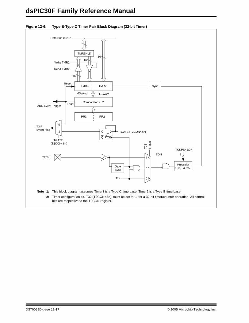
dsPIC30F Family Reference Manual
Figure 12-6: Type B-Type C Timer Pair Block Diagram (32-bit Timer)
TMR3 TMR2
T3IF
EqualComparator x 32
PR3 PR2
Reset
LSWord MSWord
Event Flag
Note 1: This block diagram assumes Timer3 is a Type C time base, Timer2 is a Type B time base.
2: Timer configuration bit, T32 (T2CON<3>), must be set to ‘1’ for a 32-bit timer/counter operation. All controlbits are respective to the T2CON register.
Data Bus<15:0>
TMR3HLD
Read TMR2
Write TMR216
16
16
Q
Q D
CK
TGATE (T2CON<6>)
(T2CON<6>)
TGATE
0
1
TON
TCKPS<1:0>
Prescaler1, 8, 64, 256
2
TCY
T
CS
1 X
0 1
TG
AT
E
0 0
Gate
T2CKI
Sync
ADC Event Trigger
Sync
DS70059D-page 12-17 © 2005 Microchip Technology Inc.
Section 12. TimersTim
ers
12
12.10 32-bit Timer Modes of Operation
12.10.1 Timer Mode
Example 12-5 shows how to configure a 32-bit timer in Timer mode. This example assumesTimer2 is a Type B time base and Timer3 is a Type C time base. For 32-bit timer operation, theT32 control bit must be set in the T2CON register (Type B time base). When Timer2 and Timer3are configured for a 32-bit timer, the T3CON control bits are ignored. Only the T2CON controlbits are required for setup and control. The Timer2 clock and gate input is utilized for the 32-bittimer module, but an interrupt is generated with the T3IF flag. Timer2 is the LSWord and Timer3is the MSWord of the 32-bit timer. TMR3 is incremented by an overflow (carry-out) from TMR2.The 32-bit timer increments up to a match value preloaded into the combined 32-bit periodregister formed by PR2 and PR3, then rolls over and continues. For a maximum 32-bit timercount, load PR3:PR2 with a value of 0xFFFFFFFF. An interrupt is generated on a period match,if enabled.
Example 12-5: Initialization Code for 32-bit Timer Using Instruction Cycle as Input Clock
; The following code example will enable Timer3 interrupts, load the ; Timer3:Timer2 Period Register and start the 32-bit timer module ; consisting of Timer3 and Timer2.
; When a 32-bit period match interrupt occurs, the user must clear ; the Timer3 interrupt status flag in software.
CLR T2CON ; Stops any 16/32-bit Timer2 operation CLR T3CON ; Stops any 16-bit Timer3 operation CLR TMR3 ; Clear contents of the Timer3 timer register CLR TMR2 ; Clear contents of the Timer2 timer register MOV #0xFFFF, w0 ; Load the Period Register 3 MOV w0, PR3 ; with the value 0xFFFF MOV w0, PR2 ; Load the Period Register2 with value 0xFFFF
BSET IPC1, #T3IP0 ; Setup Timer3 interrupt for BCLR IPC1, #T3IP1 ; desired priority levelBCLR IPC1, #T3IP2 ; (this example assigns level 1 priority)BCLR IFS0, #T3IF ; Clear the Timer3 interrupt status flag BSET IEC0, #T3IE ; Enable Timer3 interruptsBSET T2CON, #T32 ; Enable 32-bit Timer operation BSET T2CON, #TON ; Start 32-bit timer with prescaler
; settings at 1:1 and clock source set to ; the internal instruction cycle
; Example code for Timer3 ISR
__T3Interrupt: BCLR IFS0, #T3IF ; Reset Timer3 interrupt flag
; User code goes here.RETFIE ; Return from ISR
© 2005 Microchip Technology Inc. DS70059D-page 12-18
dsPIC30F Family Reference Manual
12.10.2 Synchronous Counter Mode
The 32-bit timer operates similarly to a 16-bit timer in Synchronous Counter mode. Example 12-6shows how to configure a 32-bit timer in Synchronous Counter mode. This example assumesTimer2 is a Type B time base and Timer3 is a Type C time base.
Example 12-6: Initialization Code for 32-bit Synchronous Counter Mode Using an External Clock Input
; The following code example will enable Timer2 interrupts, load ; the Timer3:Timer2 Period register and start the 32-bit timer ; module consisting of Timer3 and Timer2.
; When a 32-bit period match interrupt occurs, the user must clear ; the Timer3 interrupt status flag in the software.
CLR T2CON ; Stops any 16/32-bit Timer2 operation CLR T3CON ; Stops any 16-bit Timer3 operation CLR TMR3 ; Clear contents of the Timer3 timer register CLR TMR2 ; Clear contents of the Timer2 timer register MOV #0xFFFF, w0 ; Load the Period Register3 MOV w0, PR3 ; with the value 0xFFFF MOV w0, PR2 ; Load the Period Register2 with value 0xFFFF
BSET IPC1, #T3IP0 ; Setup Timer3 interrupt for BCLR IPC1, #T3IP1 ; desired priority levelBCLR IPC1, #T3IP2 ; (this example assigns level 1 priority)BCLR IFS0, #T3IF ; Clear the Timer3 interrupt status flag BSET IEC0, #T3IE ; Enable Timer3 interruptsMOV #0x801A, w0 ; Enable 32-bit Timer operation and start MOV w0, T2CON ; 32-bit timer with prescaler settings at
; 1:8 and clock source set to external clock
; Example code for Timer3 ISR
__T3Interrupt: BCLR IFS0, #T3IF ; Reset Timer3 interrupt flag
; User code goes here.RETFIE ; Return from ISR
DS70059D-page 12-19 © 2005 Microchip Technology Inc.

Section 12. TimersTim
ers
12
12.10.3 Asynchronous Counter Mode
Type B and Type C time bases do not support the Asynchronous External Clock mode.Therefore, no 32-bit Asynchronous Counter mode is supported.
12.10.4 Gated Time Accumulation Mode
The 32-bit timer operates similarly to a 16-bit timer in Gated Time Accumulation mode.Example 12-7 shows how to configure a 32-bit timer in Gated Time Accumulation mode. Thisexample assumes Timer2 is a Type B time base and Timer3 is a Type C time base.
Example 12-7: Initialization Code for 32-bit Gated Time Accumulation Mode
; The following code example will enable Timer2 interrupts, load the ; Timer3:Timer2 Period register and start the 32-bit timer module ; consisting of Timer3 and Timer2. When a 32-bit period match occurs ; the timer will simply roll over and continue counting.
; However, when at the falling edge of the Gate signal on T2CK ; an interrupt is generated, if enabled. The user must clear the ; Timer3 interrupt status flag in the software.
CLR T2CON ; Stops any 16/32-bit Timer2 operation CLR T3CON ; Stops any 16-bit Timer3 operation CLR TMR3 ; Clear contents of the Timer3 register CLR TMR2 ; Clear contents of the Timer2 register MOV #0xFFFF, w0 ; Load the Period Register3 MOV w0, PR3 ; with the value 0xFFFF MOV w0, PR2 ; Load the Period Register2 with value 0xFFFF
BSET IPC1, #T3IP0 ; Setup Timer3 interrupt for BCLR IPC1, #T3IP1 ; desired priority levelBCLR IPC1, #T3IP2 ; (this example assigns level 1 priority)BCLR IFS0, #T3IF ; Clear the Timer3 interrupt status flag BSET IEC0, #T3IE ; Enable Timer3 interruptsMOV #0x804C, w0 ; Enable 32-bit Timer operation and MOV w0, T2CON ; Start 32-bit timer in gated time
; accumulation mode.
; Example code for Timer3 ISR
__T3Interrupt: BCLR IFS0, #T3IF ; Reset Timer3 interrupt flag
; User code goes here.RETFIE ; Return from ISR
© 2005 Microchip Technology Inc. DS70059D-page 12-20

dsPIC30F Family Reference Manual
12.11 Reading and Writing into 32-bit Timers
In order for 32-bit read/write operations to be synchronized between the LSWord and MSWordof the 32-bit timer, additional control logic and holding registers are utilized (see Figure 12-6).Each Type C time base has a register called TMRxHLD, that is used when reading or writing thetimer register pair. The TMRxHLD registers are only used when their respective timers areconfigured for 32-bit operation.
Assuming TMR3:TMR2 form a 32-bit timer pair; the user should first read the LSWord of the timervalue from the TMR2 register. The read of the LSWord will automatically transfer the contents ofTMR3 into the TMR3HLD register. The user can then read TMR3HLD to get the MSWord of thetimer value. This is shown in the example below:
Example 12-8: Reading from a 32-bit Timer
To write a value to the TMR3:TMR2 register pair, the user should first write the MSWord to theTMR3HLD register. When the LSWord of the timer value is written to TMR2, the contents ofTMR3HLD will automatically be transferred to the TMR3 register.
12.12 Timer Operation in Power Saving States
12.12.1 Timer Operation in Sleep Mode
When the device enters Sleep mode, the system clock is disabled. If the timer module is runningfrom the internal clock source (FOSC/4), it will also be disabled.
A Type A timer is different from the other timer modules because it can operate asynchronouslyfrom an external clock source. Because of this distinction, the Type A time base module cancontinue to operate during Sleep mode. To operate in Sleep mode, Type A time base must beconfigured as follows:
• The Timer1 module is enabled, TON = 1 (T1CON<15>) and • The Timer1 clock source is selected as external, TCS = 1 (T1CON<1> = 1) and• The TSYNC bit (T1CON<2>) is set to logic ‘0’ (Asynchronous Counter mode enabled).
When all of the above conditions are met, Timer1 will continue to count and detect periodmatches when the device is in Sleep mode. When a match between the timer and the periodregister occurs, the TxIF bit will be set and an interrupt can be generated to optionally wake thedevice from Sleep. Refer to Section 10. “Watchdog Timer and Power Saving Modes” forfurther details.
When executing the SLEEP instruction in asynchronous mode using a 32.768 kHz real timeoscillator to keep track of real time in seconds, it is important to insure the crystal connected tothe inputs is operating. This can be done by checking for a non-zero value in TMR1 and thenexecuting the SLEEP instruction. Failure to do so may result in a normal sleep execution with nowake-up from sleep due to timer time out.
Example Code:
mov.b #0x46,w1 ; follow write sequence …mov.b #0x57,w2 ; for OSCCONL writes.mov #OSCCONL,w3mov.b w1,[w3]mov.b w2,[w3]bset OSCCONL,#LPOSCEN ;enable 32Khz external xtalclr TMR1 ; set up TMR1 for …mov #0x7FFF,W0 ;interrupts every 1.0 Secmov W0,PR1
; The following code segment reads the 32-bit timer formed by the ; Timer3-Timer2 pair into the registers W1(MS Word) and W0(LS Word).
MOV TMR2, W0 ;Transfer the LSW into W1 MOV TMR3HLD, W1 ;Transfer the MSW from the holding register to W0
Note: Asynchronous counter operation is only supported for the Timer1 module.
DS70059D-page 12-21 © 2005 Microchip Technology Inc.
Section 12. TimersTim
ers
12
bclr IFS0,#T1IF ; clr interrupt flagmov #0x8002,W0 ; External clock, 1:1; start TMR1 mov W0,T1CONbset IEC0,#T1IE ; enable interrupt
TestLPOperation:mov TMR1,W0 ; check for non-zero value in TMR1cp W0,#0bra Z,TestLPOperation ; if zero then recheckpwrsav #0 ; non-zero then execute sleep
12.12.2 Timer Operation in Idle Mode
When the device enters Idle mode, the system clock sources remain functional and the CPUstops executing code. The timer modules can optionally continue to operate in Idle mode.
The TSIDL bit (TxCON<13>) selects if the timer module will stop in Idle mode, or continue tooperate normally. If TSIDL = 0, the module will continue operation in Idle mode. If TSIDL = 1, themodule will stop in Idle mode.
12.13 Peripherals Using Timer Modules
12.13.1 Time Base for Input Capture/Output Compare
The Input Capture and Output Compare peripherals can select one of two timer modules as theirtime base. Refer to Section 13. “Input Capture”, Section 14. “Output Compare”, and thedevice data sheet for further details.
12.13.2 A/D Special Event Trigger
On each device variant, one Type C time base has the capability to generate a special A/Dconversion trigger signal on a period match, in both 16 and 32-bit modes. The timer moduleprovides a conversion start signal to the A/D sampling logic.
• If T32 = 0, when a match occurs between the 16-bit timer register (TMRx) and the respective 16-bit period register (PRx), the A/D special event trigger signal is generated.
• If T32 = 1, when a match occurs between the 32-bit timer (TMRx:TMRy) and the 32-bit respective combined period register (PRx:PRy), the A/D special event trigger signal is generated.
The special event trigger signal is always generated by the timer. The trigger source must beselected in the A/D converter control registers. Refer to Section 17. “10-bit A/D Converter”,Section 18. “12-bit A/D Converter”, and the device data sheet for additional information.
12.13.3 Timer as an External Interrupt Pin
The external clock input pin for each timer can be used as an additional interrupt pin. To providethe interrupt, the timer period register, PRx, is written with a non-zero value and the TMRxregister is initialized to a value of 1 less than the value written to the period register. The timermust be configured for a 1:1 clock prescaler. An interrupt will be generated when the next risingedge of the external clock signal is detected.
12.13.4 I/O Pin Control
When a timer module is enabled and configured for external clock or gate operation, the usermust ensure the I/O pin direction is configured for an input. Enabling the timer module does notconfigure the pin direction.
© 2005 Microchip Technology Inc. DS70059D-page 12-22
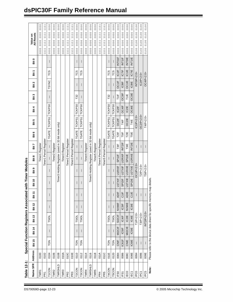
dsPIC30F Family Reference Manual
Tab
le 1
2-1:
Sp
ecia
l Fu
nct
ion
Reg
iste
rs A
sso
ciat
ed w
ith
Tim
er M
od
ule
s
Nam
e S
FR
Ad
dre
ssB
it 1
5B
it 1
4B
it 1
3B
it 1
2B
it 1
1B
it 1
0B
it 9
Bit
8B
it 7
Bit
6B
it 5
Bit
4B
it 3
Bit
2B
it 1
Bit
0V
alu
e o
nA
ll R
eset
s
TM
R1
0100
Tim
er1
Reg
iste
r0000 0000 0000 0000
PR
101
02Ti
mer
1 P
erio
d R
egis
ter
1111 1111 1111 1111
T1C
ON
0104
TO
N—
TS
IDL
——
——
——
TG
AT
ET
CK
PS
1T
CK
PS
0—
TS
YN
CT
CS
—0000 0000 0000 0000
TM
R2
0106
Tim
er2
Reg
iste
r0000 0000 0000 0000
TM
R3H
LD01
08Ti
mer
3 H
oldi
ng R
egis
ter
(use
d in
32-
bit m
ode
only
)0000 0000 0000 0000
TM
R3
010A
Tim
er3
Reg
iste
r0000 0000 0000 0000
PR
201
0CTi
mer
2 P
erio
d R
egis
ter
1111 1111 1111 1111
PR
301
0ETi
mer
3 P
erio
d R
egis
ter
1111 1111 1111 1111
T2C
ON
0110
TO
N—
TS
IDL
——
——
——
TG
AT
ET
CK
PS
1T
CK
PS
0T
32—
TC
S—
0000 0000 0000 0000
T3C
ON
0112
TO
N—
TS
IDL
——
——
——
TG
AT
ET
CK
PS
1T
CK
PS
0—
—T
CS
—0000 0000 0000 0000
TM
R4
0114
Tim
er4
Reg
iste
r0000 0000 0000 0000
TM
R5H
LD01
16Ti
mer
5 H
oldi
ng R
egis
ter
(use
d in
32-
bit m
ode
only
)0000 0000 0000 0000
TM
R5
0118
Tim
er5
Reg
iste
r0000 0000 0000 0000
PR
401
1ATi
mer
4 P
erio
d R
egis
ter
1111 1111 1111 1111
PR
501
1CTi
mer
5 P
erio
d R
egis
ter
1111 1111 1111 1111
T4C
ON
011E
TO
N—
TS
IDL
——
——
——
TG
AT
ET
CK
PS
1T
CK
PS
0T
32—
TC
S—
0000 0000 0000 0000
T5C
ON
0120
TO
N—
TS
IDL
——
——
——
TG
AT
ET
CK
PS
1T
CK
PS
0—
—T
CS
—0000 0000 0000 0000
IFS
000
84C
NIF
MI2
CIF
SI2
CIF
NV
MIF
AD
IFU
1TX
IFU
1RX
IFS
PI1
IFT
3IF
T2I
FO
C2I
FIC
2IF
T1I
FO
C1I
FIC
1IF
INT
01F
0000 0000 0000 0000
IFS
100
86IC
61F
IC5I
FIC
4IF
IC3I
FC
1IF
SP
I2IF
U2T
XIF
U2R
XIF
INT
2IF
T5I
FT
4IF
OC
4IF
OC
3IF
IC8I
FIC
7IF
INT
1IF
0000 0000 0000 0000
IEC
000
8CC
NIE
MI2
CIE
IC2I
EN
VM
IEA
DIE
U1T
XIE
U1R
XIE
SP
I1IE
T3I
ET
2IE
OC
2IE
IC2I
ET
1IE
OC
1IE
IC1I
EIN
T0I
E0000 0000 0000 0000
IEC
100
8EIC
6IE
IC5I
EIC
4IE
IC3I
EC
1IE
SP
I2IE
U2T
XIE
U2R
XIE
INT
2IE
T5I
ET
4IE
OC
4IE
OC
3IE
IC8I
EIC
7IE
INT
1IE
0000 0000 0000 0000
IPC
000
94—
T1I
P<
2:0>
—O
C1I
P<
2:0>
—IC
1IP
<2:
0>IN
T0I
P<
2:0>
0100 0100 0100 0100
IPC
100
96—
T3I
P<
2:0>
—T
2IP
<2:
0>—
OC
2IP
<2:
0>IC
2IP
<2:
0>0100 0100 0100 0100
IPC
500
9E—
INT
2IP
<2:
0>—
T5I
P<
2:0>
—T
4IP
<2:
0>O
C4I
P<
2:0>
0100 0100 0100 0100
No
te:
Ple
ase
refe
r to
the
devi
ce d
ata
shee
t for
spe
cific
mem
ory
map
det
ails
.
DS70059D-page 12-23 © 2005 Microchip Technology Inc.
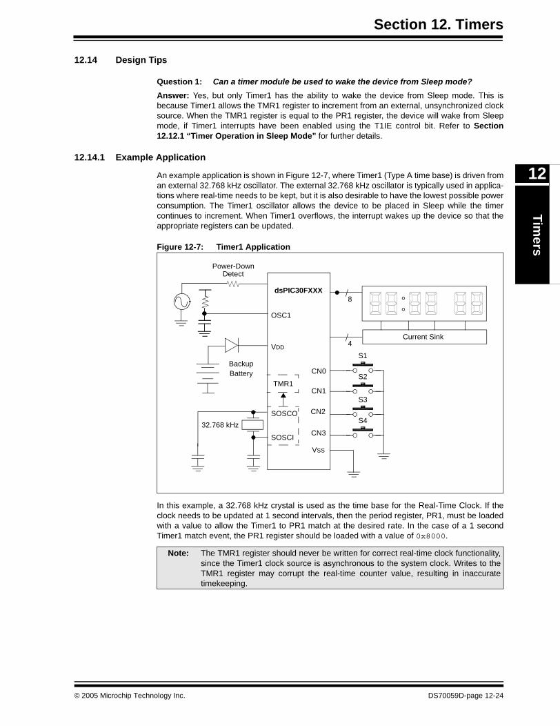
Section 12. TimersTim
ers
12
12.14 Design Tips
Question 1: Can a timer module be used to wake the device from Sleep mode?
Answer: Yes, but only Timer1 has the ability to wake the device from Sleep mode. This isbecause Timer1 allows the TMR1 register to increment from an external, unsynchronized clocksource. When the TMR1 register is equal to the PR1 register, the device will wake from Sleepmode, if Timer1 interrupts have been enabled using the T1IE control bit. Refer to Section12.12.1 “Timer Operation in Sleep Mode” for further details.
12.14.1 Example Application
An example application is shown in Figure 12-7, where Timer1 (Type A time base) is driven froman external 32.768 kHz oscillator. The external 32.768 kHz oscillator is typically used in applica-tions where real-time needs to be kept, but it is also desirable to have the lowest possible powerconsumption. The Timer1 oscillator allows the device to be placed in Sleep while the timercontinues to increment. When Timer1 overflows, the interrupt wakes up the device so that theappropriate registers can be updated.
Figure 12-7: Timer1 Application
In this example, a 32.768 kHz crystal is used as the time base for the Real-Time Clock. If theclock needs to be updated at 1 second intervals, then the period register, PR1, must be loadedwith a value to allow the Timer1 to PR1 match at the desired rate. In the case of a 1 secondTimer1 match event, the PR1 register should be loaded with a value of 0x8000.
Note: The TMR1 register should never be written for correct real-time clock functionality,since the Timer1 clock source is asynchronous to the system clock. Writes to theTMR1 register may corrupt the real-time counter value, resulting in inaccuratetimekeeping.
8
4Current Sink
TMR1
VSS
dsPIC30FXXX
VDD
32.768 kHz
BackupBattery
Power-DownDetect
SOSCO
SOSCI
OSC1
S1
S2
S3
S4
CN0
CN1
CN2
CN3
© 2005 Microchip Technology Inc. DS70059D-page 12-24
dsPIC30F Family Reference Manual
12.15 Related Application Notes
This section lists application notes that are related to this section of the manual. Theseapplication notes may not be written specifically for the dsPIC30F Product Family, but theconcepts are pertinent and could be used with modification and possible limitations. The currentapplication notes related to the Timers module are:
Title Application Note #
Using Timer1 in Asynchronous Clock Mode AN580
Yet Another Clock Featuring the PIC16C924 AN649
Note: Please visit the Microchip web site (www.microchip.com) for additional ApplicationNotes and code examples for the dsPIC30F Family of devices.
DS70059D-page 12-25 © 2005 Microchip Technology Inc.

Section 12. TimersTim
ers
12
12.16 Revision History
Revision A
This is the initial released revision of this document.
Revision B
This revision incorporates technical content changes for the dsPIC30F Timers module.
Revision C
There were no technical content revisions to this section of the manual, however, this section wasupdated to reflect Revision C throughout the manual.
Revision D
Added example code in Section 12.12.1 “Timer Operation in Sleep Mode”.
© 2005 Microchip Technology Inc. DS70059D-page 12-26
dsPIC30F Family Reference Manual
DS70059D-page 12-27 © 2005 Microchip Technology Inc.
Section 13. Input Capture
Inp
ut C
aptu
re
13
HIGHLIGHTS
This section of the manual contains the following major topics:
13.1 Introduction .................................................................................................................. 13-2
13.2 Input Capture Registers ............................................................................................... 13-313.3 Timer Selection ............................................................................................................ 13-413.4 Input Capture Event Modes ......................................................................................... 13-4
13.5 Capture Buffer Operation............................................................................................. 13-813.6 Input Capture Interrupts ............................................................................................... 13-913.7 UART Autobaud Support ............................................................................................. 13-9
13.8 Input Capture Operation in Power Saving States ...................................................... 13-1013.9 I/O Pin Control ........................................................................................................... 13-1013.10 Special Function Registers Associated with the Input Capture Module..................... 13-11
13.11 Design Tips ................................................................................................................ 13-1213.12 Related Application Notes.......................................................................................... 13-1313.13 Revision History ......................................................................................................... 13-14
© 2004 Microchip Technology Inc. DS70060C-page 13-1
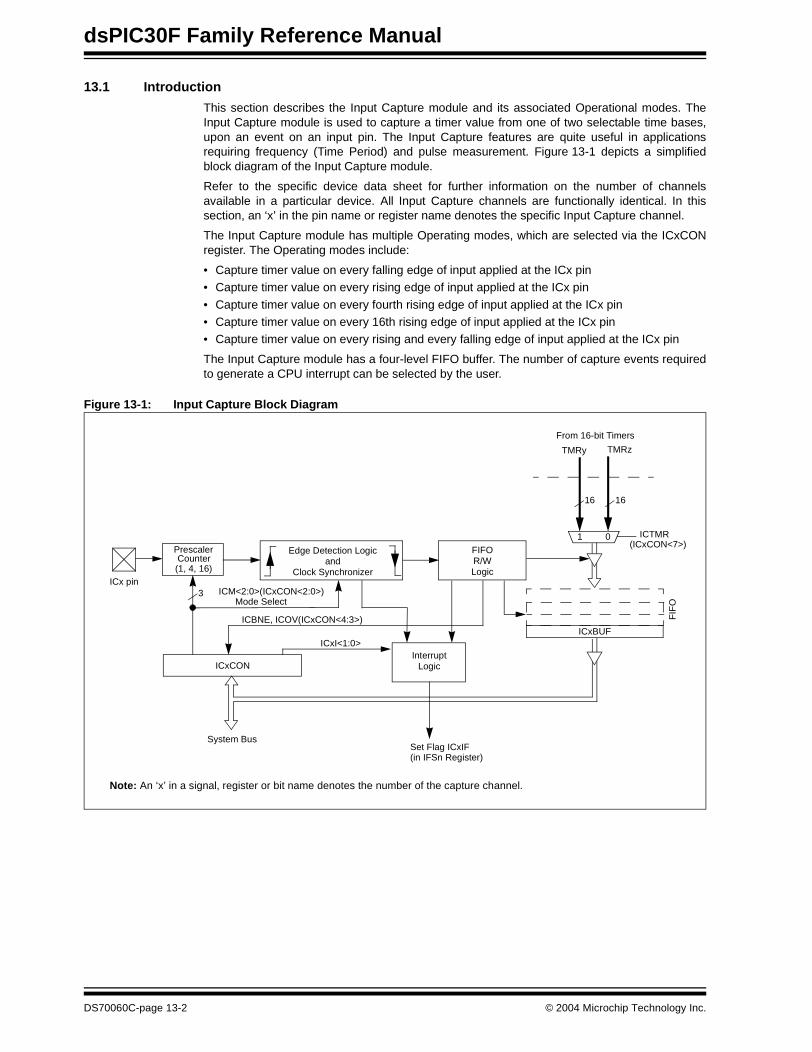
dsPIC30F Family Reference Manual
13.1 Introduction
This section describes the Input Capture module and its associated Operational modes. TheInput Capture module is used to capture a timer value from one of two selectable time bases,upon an event on an input pin. The Input Capture features are quite useful in applicationsrequiring frequency (Time Period) and pulse measurement. Figure 13-1 depicts a simplifiedblock diagram of the Input Capture module.
Refer to the specific device data sheet for further information on the number of channelsavailable in a particular device. All Input Capture channels are functionally identical. In thissection, an ‘x’ in the pin name or register name denotes the specific Input Capture channel.
The Input Capture module has multiple Operating modes, which are selected via the ICxCONregister. The Operating modes include:
• Capture timer value on every falling edge of input applied at the ICx pin • Capture timer value on every rising edge of input applied at the ICx pin
• Capture timer value on every fourth rising edge of input applied at the ICx pin• Capture timer value on every 16th rising edge of input applied at the ICx pin• Capture timer value on every rising and every falling edge of input applied at the ICx pin
The Input Capture module has a four-level FIFO buffer. The number of capture events requiredto generate a CPU interrupt can be selected by the user.
Figure 13-1: Input Capture Block Diagram
ICxBUF
ICx pinICM<2:0>(ICxCON<2:0>) Mode Select
3
1 0
Set Flag ICxIF (in IFSn Register)
TMRy TMRz
Edge Detection Logic
16 16
FIFOR/WLogic
ICxI<1:0>
ICBNE, ICOV(ICxCON<4:3>)
ICxCONInterrupt
Logic
System Bus
From 16-bit Timers
ICTMR(ICxCON<7>)
FIF
O
PrescalerCounter(1, 4, 16)
andClock Synchronizer
Note: An ‘x’ in a signal, register or bit name denotes the number of the capture channel.
DS70060C-page 13-2 © 2004 Microchip Technology Inc.
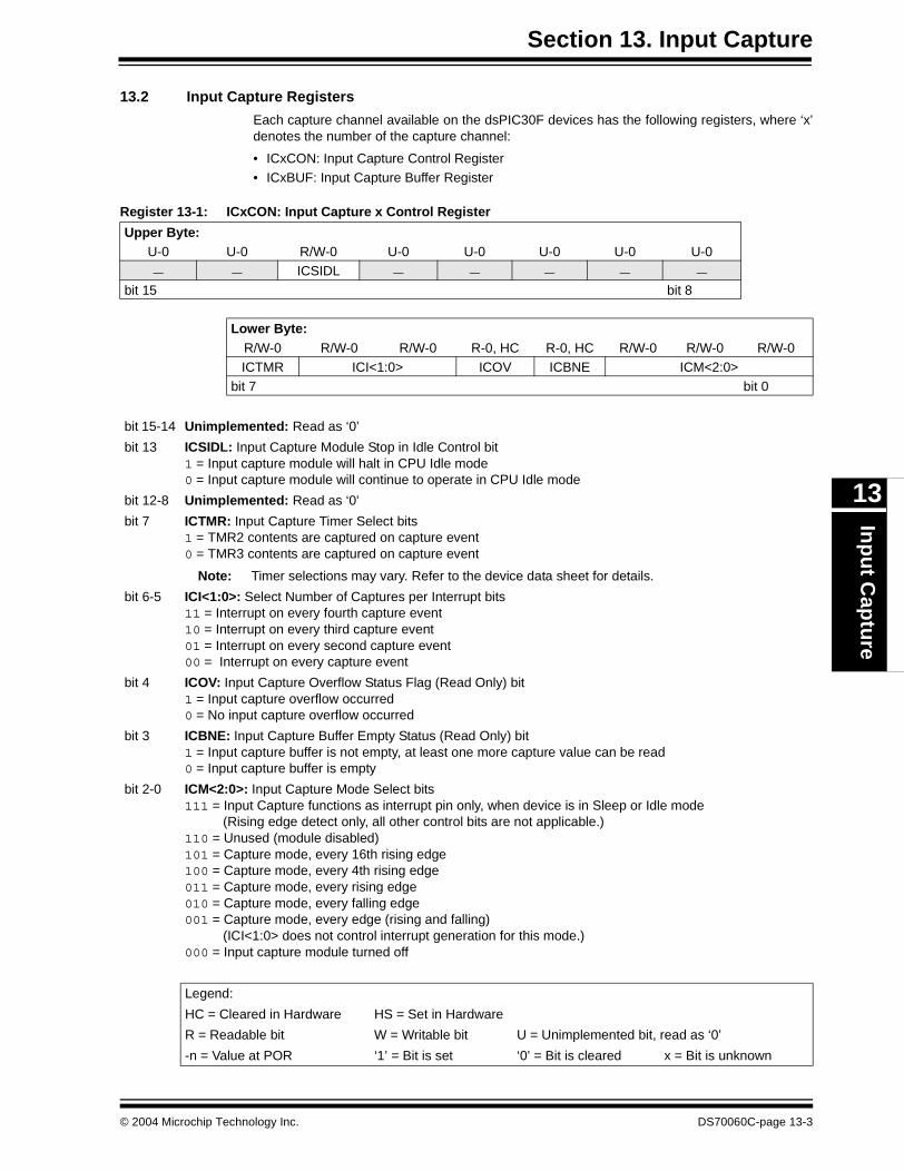
Section 13. Input CaptureIn
pu
t Cap
ture
13
13.2 Input Capture Registers
Each capture channel available on the dsPIC30F devices has the following registers, where ‘x’denotes the number of the capture channel:
• ICxCON: Input Capture Control Register• ICxBUF: Input Capture Buffer Register
Register 13-1: ICxCON: Input Capture x Control Register
Upper Byte:U-0 U-0 R/W-0 U-0 U-0 U-0 U-0 U-0
— — ICSIDL — — — — —
bit 15 bit 8
Lower Byte:R/W-0 R/W-0 R/W-0 R-0, HC R-0, HC R/W-0 R/W-0 R/W-0ICTMR ICI<1:0> ICOV ICBNE ICM<2:0>
bit 7 bit 0
bit 15-14 Unimplemented: Read as ‘0’
bit 13 ICSIDL: Input Capture Module Stop in Idle Control bit 1 = Input capture module will halt in CPU Idle mode0 = Input capture module will continue to operate in CPU Idle mode
bit 12-8 Unimplemented: Read as ‘0’
bit 7 ICTMR: Input Capture Timer Select bits1 = TMR2 contents are captured on capture event0 = TMR3 contents are captured on capture event
Note: Timer selections may vary. Refer to the device data sheet for details.
bit 6-5 ICI<1:0>: Select Number of Captures per Interrupt bits11 = Interrupt on every fourth capture event10 = Interrupt on every third capture event01 = Interrupt on every second capture event00 = Interrupt on every capture event
bit 4 ICOV: Input Capture Overflow Status Flag (Read Only) bit1 = Input capture overflow occurred0 = No input capture overflow occurred
bit 3 ICBNE: Input Capture Buffer Empty Status (Read Only) bit1 = Input capture buffer is not empty, at least one more capture value can be read0 = Input capture buffer is empty
bit 2-0 ICM<2:0>: Input Capture Mode Select bits111 = Input Capture functions as interrupt pin only, when device is in Sleep or Idle mode
(Rising edge detect only, all other control bits are not applicable.)110 = Unused (module disabled)101 = Capture mode, every 16th rising edge100 = Capture mode, every 4th rising edge011 = Capture mode, every rising edge010 = Capture mode, every falling edge001 = Capture mode, every edge (rising and falling)
(ICI<1:0> does not control interrupt generation for this mode.)000 = Input capture module turned off
Legend:
HC = Cleared in Hardware HS = Set in Hardware
R = Readable bit W = Writable bit U = Unimplemented bit, read as ‘0’
-n = Value at POR ‘1’ = Bit is set ‘0’ = Bit is cleared x = Bit is unknown
© 2004 Microchip Technology Inc. DS70060C-page 13-3
dsPIC30F Family Reference Manual
13.3 Timer Selection
Each dsPIC30F device may have one or more input capture channels. Each channel can selectbetween one of two 16-bit timers for the time base. Refer to the device data sheet for the specifictimers that can be selected.
Selection of the timer resource is accomplished through the ICTMR control bit (ICxCON<7>).The timers can be setup using the internal clock source (FOSC/4), or using a synchronizedexternal clock source applied at the TxCK pin.
13.4 Input Capture Event Modes
The input capture module captures the 16-bit value of the selected time base register when anevent occurs at the ICx pin. The events that can be captured are listed below in three categories:
1. Simple Capture Event modes
• Capture timer value on every falling edge of input at ICx pin• Capture timer value on every rising edge of input at ICx pin
2. Capture timer value on every edge (rising and falling)
3. Prescaler Capture Event modes• Capture timer value on every 4th rising edge of input at ICx pin• Capture timer value on every 16th rising edge of input at ICx pin
These Input Capture modes are configured by setting the appropriate Input Capture mode bits,ICM<2:0> (ICxCON<2:0>).
13.4.1 Simple Capture Events
The capture module can capture a timer count value (TMR2 or TMR3) based on the selectededge (rising or falling defined by mode) of the input applied to the ICx pin. These modes arespecified by setting the ICM<2:0> (ICxCON<2:0>) bits to ‘010’ or ‘011’, respectively. In thesemodes, the prescaler counter is not used. See Figure 13-3 and Figure 13-2 for simplified timingdiagrams of a simple capture event.
The input capture logic detects and synchronizes the rising or falling edge of the capture pinsignal on the internal phase clocks. If the rising/falling edge has occurred, the capture modulelogic will write the current time base value to the capture buffer and signal the interrupt generationlogic. When the number of elapsed capture events matches the number specified by the ICI<1:0>control bits, the respective capture channel interrupt status flag, ICxIF, is asserted 2 instructioncycles after the capture buffer write event.
If the capture time base increments every instruction cycle, the captured count value will be thevalue that was present 1 or 2 instruction cycles past the time of the event on the ICx pin. Thistime delay is a function of the actual ICx edge event related to the instruction cycle clock anddelay associated with the input capture logic. If the input clock to the capture time base isprescaled, then the delay in the captured value can be eliminated. See Figure 13-3 andFigure 13-2 for details.
The input capture pin has minimum high time and low time specifications. Refer to the “ElectricalSpecifications” section of the device data sheet for further details.
DS70060C-page 13-4 © 2004 Microchip Technology Inc.
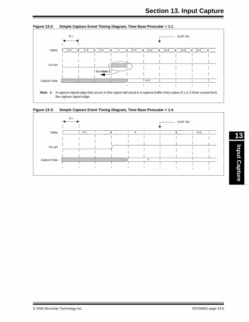
Section 13. Input CaptureIn
pu
t Cap
ture
13
Figure 13-2: Simple Capture Event Timing Diagram, Time Base Prescaler = 1:1
Figure 13-3: Simple Capture Event Timing Diagram, Time Base Prescaler = 1:4
Capture Data
n+2 n+3 n+4n-2 n-1 n n+1n-3TMR2
n+1
ICx pin
n+5
Note 1: A capture signal edge that occurs in this region will result in a capture buffer entry value of 1 or 2 timer counts fromthe capture signal edge.
See Note 1
TCY ICxIF Set
Capture Data
n+1n-1 nTMRy
n
ICx pin
ICxIF SetTCY
© 2004 Microchip Technology Inc. DS70060C-page 13-5
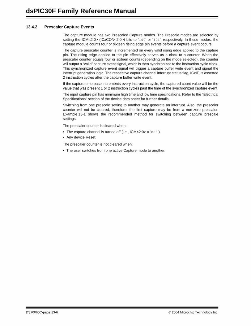
dsPIC30F Family Reference Manual
13.4.2 Prescaler Capture Events
The capture module has two Prescaled Capture modes. The Prescale modes are selected bysetting the ICM<2:0> (ICxCON<2:0>) bits to ‘100’ or ‘101’, respectively. In these modes, thecapture module counts four or sixteen rising edge pin events before a capture event occurs.
The capture prescaler counter is incremented on every valid rising edge applied to the capturepin. The rising edge applied to the pin effectively serves as a clock to a counter. When theprescaler counter equals four or sixteen counts (depending on the mode selected), the counterwill output a “valid” capture event signal, which is then synchronized to the instruction cycle clock.This synchronized capture event signal will trigger a capture buffer write event and signal theinterrupt generation logic. The respective capture channel interrupt status flag, ICxIF, is asserted2 instruction cycles after the capture buffer write event.
If the capture time base increments every instruction cycle, the captured count value will be thevalue that was present 1 or 2 instruction cycles past the time of the synchronized capture event.
The input capture pin has minimum high time and low time specifications. Refer to the “ElectricalSpecifications” section of the device data sheet for further details.
Switching from one prescale setting to another may generate an interrupt. Also, the prescalercounter will not be cleared, therefore, the first capture may be from a non-zero prescaler.Example 13-1 shows the recommended method for switching between capture prescalesettings.
The prescaler counter is cleared when:
• The capture channel is turned off (i.e., ICM<2:0> = ‘000’).• Any device Reset.
The prescaler counter is not cleared when:
• The user switches from one active Capture mode to another.
DS70060C-page 13-6 © 2004 Microchip Technology Inc.
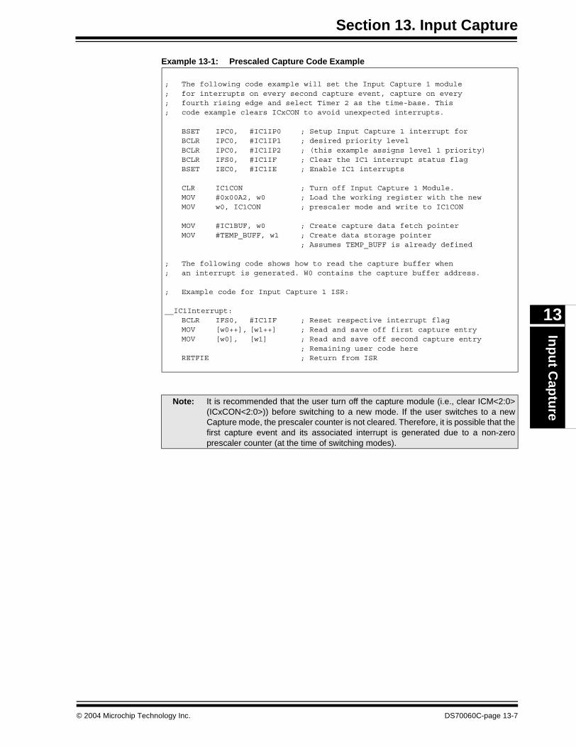
Section 13. Input CaptureIn
pu
t Cap
ture
13
Example 13-1: Prescaled Capture Code Example
; The following code example will set the Input Capture 1 module ; for interrupts on every second capture event, capture on every ; fourth rising edge and select Timer 2 as the time-base. This ; code example clears ICxCON to avoid unexpected interrupts.
BSET IPC0, #IC1IP0 ; Setup Input Capture 1 interrupt for BCLR IPC0, #IC1IP1 ; desired priority level BCLR IPC0, #IC1IP2 ; (this example assigns level 1 priority) BCLR IFS0, #IC1IF ; Clear the IC1 interrupt status flag BSET IEC0, #IC1IE ; Enable IC1 interrupts
CLR IC1CON ; Turn off Input Capture 1 Module. MOV #0x00A2, w0 ; Load the working register with the new MOV w0, IC1CON ; prescaler mode and write to IC1CON
MOV #IC1BUF, w0 ; Create capture data fetch pointer MOV #TEMP_BUFF, w1 ; Create data storage pointer
; Assumes TEMP_BUFF is already defined
; The following code shows how to read the capture buffer when; an interrupt is generated. W0 contains the capture buffer address.
; Example code for Input Capture 1 ISR:
__IC1Interrupt:BCLR IFS0, #IC1IF ; Reset respective interrupt flag MOV [w0++], [w1++] ; Read and save off first capture entry MOV [w0], [w1] ; Read and save off second capture entry
; Remaining user code hereRETFIE ; Return from ISR
Note: It is recommended that the user turn off the capture module (i.e., clear ICM<2:0>(ICxCON<2:0>)) before switching to a new mode. If the user switches to a newCapture mode, the prescaler counter is not cleared. Therefore, it is possible that thefirst capture event and its associated interrupt is generated due to a non-zeroprescaler counter (at the time of switching modes).
© 2004 Microchip Technology Inc. DS70060C-page 13-7
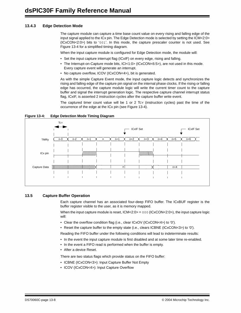
dsPIC30F Family Reference Manual
13.4.3 Edge Detection Mode
The capture module can capture a time base count value on every rising and falling edge of theinput signal applied to the ICx pin. The Edge Detection mode is selected by setting the ICM<2:0>(ICxCON<2:0>) bits to ‘001’. In this mode, the capture prescaler counter is not used. SeeFigure 13-4 for a simplified timing diagram.
When the input capture module is configured for Edge Detection mode, the module will:
• Set the input capture interrupt flag (ICxIF) on every edge, rising and falling.• The Interrupt-on-Capture mode bits, ICI<1:0> (ICxCON<6:5>), are not used in this mode.
Every capture event will generate an interrupt.• No capture overflow, ICOV (ICxCON<4>), bit is generated.
As with the simple Capture Event mode, the input capture logic detects and synchronizes therising and falling edge of the capture pin signal on the internal phase clocks. If the rising or fallingedge has occurred, the capture module logic will write the current timer count to the capturebuffer and signal the interrupt generation logic. The respective capture channel interrupt statusflag, ICxIF, is asserted 2 instruction cycles after the capture buffer write event.
The captured timer count value will be 1 or 2 TCY (instruction cycles) past the time of theoccurrence of the edge at the ICx pin (see Figure 13-4).
Figure 13-4: Edge Detection Mode Timing Diagram
13.5 Capture Buffer Operation
Each capture channel has an associated four-deep FIFO buffer. The ICxBUF register is thebuffer register visible to the user, as it is memory mapped.
When the input capture module is reset, ICM<2:0> = 000 (ICxCON<2:0>), the input capture logicwill:
• Clear the overflow condition flag (i.e., clear ICxOV (ICxCON<4>) to ‘0’).
• Reset the capture buffer to the empty state (i.e., clears ICBNE (ICxCON<3>) to ‘0’).
Reading the FIFO buffer under the following conditions will lead to indeterminate results:
• In the event the input capture module is first disabled and at some later time re-enabled.• In the event a FIFO read is performed when the buffer is empty.• After a device Reset.
There are two status flags which provide status on the FIFO buffer:
• ICBNE (ICxCON<3>): Input Capture Buffer Not Empty• ICOV (ICxCON<4>): Input Capture Overflow
Capture Data
n+2 n+3 n+4 n+6n-2 n-1 n n+1n-3TMRy
n
ICx pin
n+5
TCY
n+4
ICxIF Set ICxIF Set
DS70060C-page 13-8 © 2004 Microchip Technology Inc.
Section 13. Input CaptureIn
pu
t Cap
ture
13
13.5.1 Input Capture Buffer Not Empty (ICBNE)
The ICBNE read only Status bit (ICxCON<3>) will be set on the first input capture event andremain set until all capture events have been read from the capture buffer. For example, if threecapture events have occurred, then three reads of the capture buffer are required before theICBNE (ICxCON<3>) flag will be cleared. If four capture events, then four reads are required toclear the ICBNE (ICxCON<3>) flag. Each read of the capture buffer will allow the remainingword(s) to move to the next available top location. Since the ICBNE reflects the capture bufferstate, the ICBNE Status bit will be cleared in the event of any device Reset.
13.5.2 Input Capture Overflow (ICOV)
The ICOV read only Status bit (ICxCON<4>) will be set when the capture buffer overflows. In theevent that buffer is full with four capture events and a fifth capture event occurs prior to a read ofthe buffer, an overrun condition will occur, the ICOV (ICxCON<4>) bit will be set to a logic ‘1’ andthe respective capture event interrupt will not be generated. In addition, the fifth capture event isnot recorded and all subsequent capture events will not alter the current buffer contents.
To clear the overrun condition, the capture buffer must be read four times. Upon the fourth read,the ICOV (ICxCON<4>) status flag will be cleared and the capture channel will resume normaloperation.
Clearing of the overflow condition can be accomplished in the following ways:
• Set ICM<2:0> (ICxCON<2:0>) = 000• Read capture buffer until ICBNE (ICxCON<3>) = 0• Any device Reset
13.5.2.1 ICOV and Interrupt Only Mode
The input capture module can also be configured to function as an external interrupt pin. For thismode, the ICI<1:0> (ICxCON<6:5>) bits must be set to ‘00’. Interrupts will be generatedindependently of buffer reads.
13.6 Input Capture Interrupts
The input capture module has the ability to generate an interrupt based upon a selected numberof capture events. A capture event is defined as a write of a time base value into the capturebuffer. This setting is configured by the control bits ICI<1:0> (ICxCON<6:5>).
Except for the case when ICI<1:0> = ‘00’, no interrupts will be generated until a buffer overflowcondition is removed (see Section 13.5.2 “Input Capture Overflow (ICOV)”). When thecapture buffer has been emptied, either by a Reset condition or a read operation, the interruptcount is reset. This allows for the resynchronization of the interrupt count to the FIFO entrystatus.
13.6.1 Interrupt Control Bits
Each input capture channel has interrupt flag Status bits (ICxIF), interrupt enable bits (ICxIE) andinterrupt priority control bits (ICxIP<2:0>). Refer to Section 6. “Reset Interrupts” for furtherinformation on peripheral interrupts.
13.7 UART Autobaud Support
The input capture module can be used by the UART module when the UART is configured forthe Autobaud mode of operation, ABAUD = 1 (UxMODE<5>). When the ABAUD control bit is set,the UART RX pin will be internally connected to the assigned input capture module input. TheI/O pin associated with the capture module will be disconnected. The baud rate can be deter-mined by measuring the width of the Start bit when a NULL character is received. Note that thecapture module must be configured for the Edge Detection mode (capture on every rising andfalling edge) to take advantage of the autobaud feature. The input capture module assignmentfor each UART will depend on the dsPIC30F device variant that is selected. Refer to the devicedata sheet for further details on the autobaud support.
© 2004 Microchip Technology Inc. DS70060C-page 13-9
dsPIC30F Family Reference Manual
13.8 Input Capture Operation in Power Saving States
13.8.1 Input Capture Operation in Sleep Mode
When the device enters Sleep mode, the system clock is disabled. In Sleep mode, the input cap-ture module can only function as an external interrupt source. This mode is enabled by settingcontrol bits ICM<2:0> = ‘111’. In this mode, a rising edge on the capture pin will generate devicewake-up from Sleep condition. If the respective module interrupt bit is enabled and the modulepriority is of the required priority, an interrupt will be generated.
In the event the capture module has been configured for a mode other than ICM<2:0> = ‘111’and the dsPIC30F does enter the Sleep mode, no external pin stimulus, rising or falling, willgenerate a wake-up condition from Sleep.
13.8.2 Input Capture Operation in Idle Mode
When the device enters Idle mode, the system clock sources remain functional and the CPUstops executing code. The ICSIDL bit (ICxCON<13>) selects if the module will stop in Idle mode,or continue to operate in Idle mode.
If ICSIDL = 0 (ICxCON<13>), the module will continue operation in Idle mode. Full functionalityof the input capture module is provided for, including the 4:1 and 16:1 capture prescale settings,defined by control bits ICM<2:0> (ICxCON<2:0>). These modes require that the selected timeris enabled during Idle mode as well.
If the Input Capture mode is configured for ICM<2:0> = ‘111’, the input capture pin will serve onlyas an external interrupt pin. In this mode, a rising edge on the capture pin will generate devicewake-up from Idle mode. A capture time base does not have to be enabled. If the respectivemodule interrupt enable bit is set and the user assigned priority is greater than the current CPUpriority level, an interrupt will be generated.
If ICSIDL = 1 (ICxCON<13>), the module will stop in Idle mode. The module will perform the samefunctions when stopped in Idle mode as for Sleep mode (see Section 13.8.1 “Input CaptureOperation in Sleep Mode”).
13.8.3 Device Wake-up on Sleep/Idle
An input capture event can generate a device wake-up or interrupt, if enabled, if the device is inIdle or Sleep mode.
Independent of the timer being enabled, the input capture module will wake-up from Sleep or Idlemode when a capture event occurs, if the following are true:
• Input Capture mode bits, ICM<2:0> = ‘111’ (ICxCON<2:0>) and• The interrupt enable bit (ICxIE) is asserted.
This same wake-up feature will interrupt the CPU if:
• The respective interrupt is enabled (ICxIE = 1) and is of the required priority.
This wake-up feature is quite useful for adding extra external pin interrupts. The followingconditions are true when the input capture module is used in this mode:
• The capture prescaler counter is not utilized while in this mode.• The ICI<1:0>(ICxCON<6:5>) bits are not applicable.
13.9 I/O Pin Control
When the capture module is enabled, the user must ensure the I/O pin direction is configured foran input by setting the associated TRIS bit. The pin direction is not set when the capture moduleis enabled. Furthermore, all other peripherals multiplexed with the input pin must be disabled.
DS70060C-page 13-10 © 2004 Microchip Technology Inc.
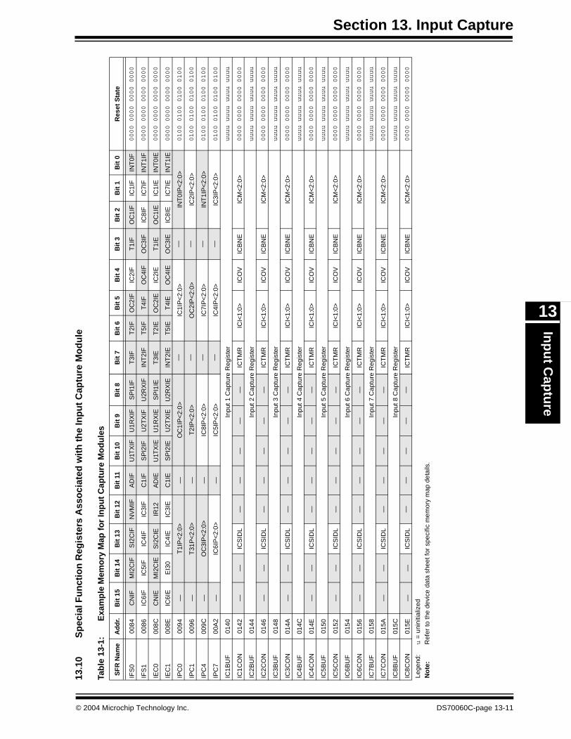
Section 13. Input CaptureIn
pu
t Cap
ture
13
13.1
0S
pec
ial F
un
ctio
n R
egis
ters
Ass
oci
ated
wit
h t
he
Inp
ut
Cap
ture
Mo
du
le
Tab
le 1
3-1:
Exa
mp
le M
emo
ry M
ap f
or
Inp
ut
Cap
ture
Mo
du
les
SF
R N
ame
Ad
dr.
Bit
15
Bit
14
Bit
13
Bit
12
Bit
11
Bit
10
Bit
9B
it 8
Bit
7B
it 6
Bit
5B
it 4
Bit
3B
it 2
Bit
1B
it 0
Res
et S
tate
IFS
000
84C
NIF
MI2
CIF
SI2
CIF
NV
MIF
AD
IFU
1TX
IFU
1RX
IFS
PI1
IFT
3IF
T2I
FO
C2I
FIC
2IF
T1I
FO
C1I
FIC
1IF
INT
0F0000 0000 0000 0000
IFS
100
86IC
6IF
IC5I
FIC
4IF
IC3I
FC
1IF
SP
I2IF
U2T
XIF
U2R
XIF
INT
2IF
T5I
FT
4IF
OC
4IF
OC
3IF
IC8I
FIC
7IF
INT
1IF
0000 0000 0000 0000
IEC
000
8CC
NIE
MI2
CIE
SI2
CIE
IR12
AD
IEU
1TX
IEU
1RX
IES
PI1
IET
3IE
T2I
EO
C2I
EIC
2IE
T1I
EO
C1I
EIC
1IE
INT
0IE
0000 0000 0000 0000
IEC
100
8EIC
6IE
EI3
0IC
4IE
IC3I
EC
1IE
SP
I2IE
U2T
XIE
U2R
XIE
INT
2IE
T5I
ET
4IE
OC
4IE
OC
3IE
IC8I
EIC
7IE
INT
1IE
0000 0000 0000 0000
IPC
000
94—
T1I
P<
2:0>
—O
C1I
P<
2:0>
—IC
1IP
<2:
0>—
INT
0IP
<2:
0>0100 0100 0100 0100
IPC
100
96—
T31
P<
2:0>
—T
2IP
<2:
0>—
OC
2IP
<2:
0>—
IC2I
P<
2:0>
0100 0100 0100 0100
IPC
400
9C—
OC
3IP
<2:
0>—
IC8I
P<
2:0>
—IC
7IP
<2:
0>—
INT
1IP
<2:
0>0100 0100 0100 0100
IPC
700
A2
—IC
6IP
<2:
0>—
IC5I
P<
2:0>
—IC
4IP
<2:
0>—
IC3I
P<
2:0>
0100 0100 0100 0100
IC1B
UF
0140
Inpu
t 1 C
aptu
re R
egis
ter
uuuu uuuu uuuu uuuu
IC1C
ON
0142
——
ICS
IDL
——
——
—IC
TM
RIC
I<1:
0>IC
OV
ICB
NE
ICM
<2:
0>0000 0000 0000 0000
IC2B
UF
0144
Inpu
t 2 C
aptu
re R
egis
ter
uuuu uuuu uuuu uuuu
IC2C
ON
0146
——
ICS
IDL
——
——
—IC
TM
RIC
I<1:
0>IC
OV
ICB
NE
ICM
<2:
0>0000 0000 0000 0000
IC3B
UF
0148
Inpu
t 3 C
aptu
re R
egis
ter
uuuu uuuu uuuu uuuu
IC3C
ON
014A
——
ICS
IDL
——
——
—IC
TM
RIC
I<1:
0>IC
OV
ICB
NE
ICM
<2:
0>0000 0000 0000 0000
IC4B
UF
014C
Inpu
t 4 C
aptu
re R
egis
ter
uuuu uuuu uuuu uuuu
IC4C
ON
014E
——
ICS
IDL
——
——
—IC
TM
RIC
I<1:
0>IC
OV
ICB
NE
ICM
<2:
0>0000 0000 0000 0000
IC5B
UF
0150
Inpu
t 5 C
aptu
re R
egis
ter
uuuu uuuu uuuu uuuu
IC5C
ON
0152
——
ICS
IDL
——
——
—IC
TM
RIC
I<1:
0>IC
OV
ICB
NE
ICM
<2:
0>0000 0000 0000 0000
IC6B
UF
0154
Inpu
t 6 C
aptu
re R
egis
ter
uuuu uuuu uuuu uuuu
IC6C
ON
0156
——
ICS
IDL
——
——
—IC
TM
RIC
I<1:
0>IC
OV
ICB
NE
ICM
<2:
0>0000 0000 0000 0000
IC7B
UF
0158
Inpu
t 7 C
aptu
re R
egis
ter
uuuu uuuu uuuu uuuu
IC7C
ON
015A
——
ICS
IDL
——
——
—IC
TM
RIC
I<1:
0>IC
OV
ICB
NE
ICM
<2:
0>0000 0000 0000 0000
IC8B
UF
015C
Inpu
t 8 C
aptu
re R
egis
ter
uuuu uuuu uuuu uuuu
IC8C
ON
015E
——
ICS
IDL
——
——
—IC
TM
RIC
I<1:
0>IC
OV
ICB
NE
ICM
<2:
0>0000 0000 0000 0000
Lege
nd:
u =
uni
nitia
lized
No
te:
Ref
er to
the
devi
ce d
ata
shee
t for
spe
cific
mem
ory
map
det
ails
.
© 2004 Microchip Technology Inc. DS70060C-page 13-11
dsPIC30F Family Reference Manual
13.11 Design Tips
Question 1: Can the Input Capture module be used to wake the device from Sleepmode?
Answer: Yes. When the Input Capture module is configured to ICM<2:0> = ‘111’ and therespective channel interrupt enable bit is asserted, ICxIE = 1, a rising edge on the capture pinwill wake-up the device from Sleep (see Section 13.8 “Input Capture Operation in PowerSaving States”).
DS70060C-page 13-12 © 2004 Microchip Technology Inc.
Section 13. Input CaptureIn
pu
t Cap
ture
13
13.12 Related Application Notes
This section lists application notes that are related to this section of the manual. Theseapplication notes may not be written specifically for the dsPIC30F Product Family, but theconcepts are pertinent and could be used with modification and possible limitations. The currentapplication notes related to the Input Capture module are:
Title Application Note #
Using the CCP Module(s) AN594Implementing Ultrasonic Ranging AN597
Note: Please visit the Microchip web site (www.microchip.com) for additional ApplicationNotes and code examples for the dsPIC30F Family of devices.
© 2004 Microchip Technology Inc. DS70060C-page 13-13
dsPIC30F Family Reference Manual
13.13 Revision History
Revision A
This is the initial released revision of this document.
Revision B
There were no technical content or editorial revisions to this section of the manual, however, thissection was updated to reflect Revision B throughout the manual.
Revision C
There were no technical content revisions to this section of the manual, however, this section wasupdated to reflect Revision C throughout the manual.
DS70060C-page 13-14 © 2004 Microchip Technology Inc.
Section 14. Output Compare
Ou
tpu
tC
om
pare
14
HIGHLIGHTS
This section of the manual contains the following major topics:
14.1 Introduction .................................................................................................................. 14-2
14.2 Output Compare Registers .......................................................................................... 14-314.3 Modes of Operation ..................................................................................................... 14-414.4 Output Compare Operation in Power Saving States.................................................. 14-23
14.5 I/O Pin Control ........................................................................................................... 14-2314.6 Design Tips ................................................................................................................ 14-2614.7 Related Application Notes.......................................................................................... 14-27
14.8 Revision History ......................................................................................................... 14-28
© 2004 Microchip Technology Inc. DS70061C-page 14-1
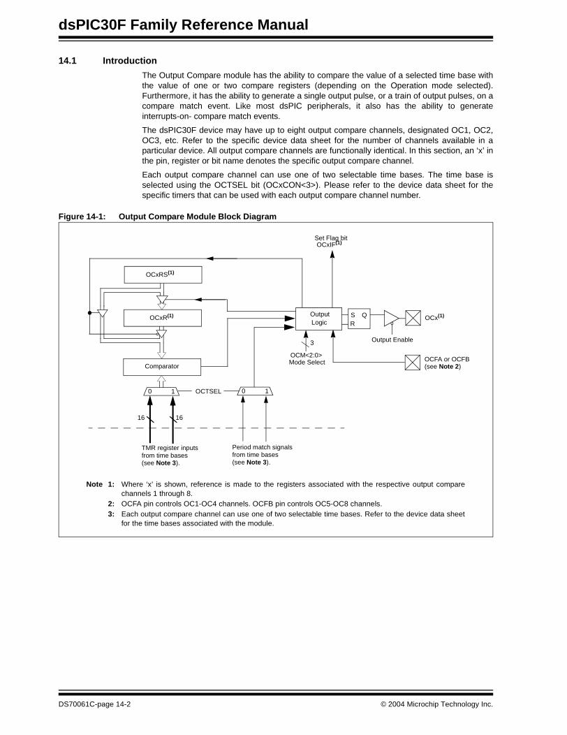
dsPIC30F Family Reference Manual
14.1 Introduction
The Output Compare module has the ability to compare the value of a selected time base withthe value of one or two compare registers (depending on the Operation mode selected).Furthermore, it has the ability to generate a single output pulse, or a train of output pulses, on acompare match event. Like most dsPIC peripherals, it also has the ability to generateinterrupts-on- compare match events.
The dsPIC30F device may have up to eight output compare channels, designated OC1, OC2,OC3, etc. Refer to the specific device data sheet for the number of channels available in aparticular device. All output compare channels are functionally identical. In this section, an ‘x’ inthe pin, register or bit name denotes the specific output compare channel.
Each output compare channel can use one of two selectable time bases. The time base isselected using the OCTSEL bit (OCxCON<3>). Please refer to the device data sheet for thespecific timers that can be used with each output compare channel number.
Figure 14-1: Output Compare Module Block Diagram
OCxR(1)
Comparator
OutputLogic
QSR
OCM<2:0>
Output Enable
OCx(1)
Set Flag bitOCxIF(1)
OCxRS(1)
Mode Select
3
Note 1: Where ‘x’ is shown, reference is made to the registers associated with the respective output comparechannels 1 through 8.
2: OCFA pin controls OC1-OC4 channels. OCFB pin controls OC5-OC8 channels.3: Each output compare channel can use one of two selectable time bases. Refer to the device data sheet
for the time bases associated with the module.
0 1 OCTSEL 0 1
16 16
OCFA or OCFB(see Note 2)
TMR register inputsfrom time bases(see Note 3).
Period match signalsfrom time bases(see Note 3).
DS70061C-page 14-2 © 2004 Microchip Technology Inc.
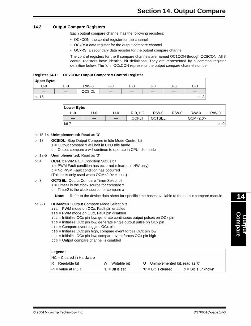
Section 14. Output CompareO
utp
ut
Co
mpare
14
14.2 Output Compare Registers
Each output compare channel has the following registers:
• OCxCON: the control register for the channel
• OCxR: a data register for the output compare channel• OCxRS: a secondary data register for the output compare channel
The control registers for the 8 compare channels are named OC1CON through OC8CON. All 8control registers have identical bit definitions. They are represented by a common registerdefinition below. The ‘x’ in OCxCON represents the output compare channel number.
Register 14-1: OCxCON: Output Compare x Control Register
Upper Byte:U-0 U-0 R/W-0 U-0 U-0 U-0 U-0 U-0— — OCSIDL — — — — —
bit 15 bit 8
Lower Byte:U-0 U-0 U-0 R-0, HC R/W-0 R/W-0 R/W-0 R/W-0— — — OCFLT OCTSEL OCM<2:0>
bit 7 bit 0
bit 15-14 Unimplemented: Read as ‘0’
bit 13 OCSIDL: Stop Output Compare in Idle Mode Control bit 1 = Output compare x will halt in CPU Idle mode0 = Output compare x will continue to operate in CPU Idle mode
bit 12-5 Unimplemented: Read as ‘0’
bit 4 OCFLT: PWM Fault Condition Status bit1 = PWM Fault condition has occurred (cleared in HW only)0 = No PWM Fault condition has occurred(This bit is only used when OCM<2:0> = 111.)
bit 3 OCTSEL: Output Compare Timer Select bit1 = Timer3 is the clock source for compare x0 = Timer2 is the clock source for compare x
Note: Refer to the device data sheet for specific time bases available to the output compare module.
bit 2-0 OCM<2:0>: Output Compare Mode Select bits111 = PWM mode on OCx, Fault pin enabled110 = PWM mode on OCx, Fault pin disabled101 = Initialize OCx pin low, generate continuous output pulses on OCx pin100 = Initialize OCx pin low, generate single output pulse on OCx pin011 = Compare event toggles OCx pin010 = Initialize OCx pin high, compare event forces OCx pin low001 = Initialize OCx pin low, compare event forces OCx pin high 000 = Output compare channel is disabled
Legend:
HC = Cleared in Hardware
R = Readable bit W = Writable bit U = Unimplemented bit, read as ‘0’
-n = Value at POR ‘1’ = Bit is set ‘0’ = Bit is cleared x = Bit is unknown
© 2004 Microchip Technology Inc. DS70061C-page 14-3
dsPIC30F Family Reference Manual
14.3 Modes of Operation
Each output compare module has the following modes of operation:
• Single Compare Match mode• Dual Compare Match mode generating
- Single Output Pulse- Continuous Output Pulses
• Simple Pulse Width Modulation mode
- with Fault Protection Input- without Fault Protection Input
14.3.1 Single Compare Match Mode
When control bits OCM<2:0> (OCxCON<2:0>) are set to ‘001’, ‘010’ or ‘011’, the selectedoutput compare channel is configured for one of three Single Output Compare Match modes.
In the Single Compare mode, the OCxR register is loaded with a value and is compared to theselected incrementing timer register, TMRy. On a compare match event, one of the followingevents will take place:
• Compare forces OCx pin high, initial state of pin is low. Interrupt is generated on the single compare match event.
• Compare forces OCx pin low, initial state of pin is high. Interrupt is generated on the single compare match event.
• Compare toggles OCx pin. Toggle event is continuous and an interrupt is generated for each toggle event.
Note 1: It is recommended that the user turn off the output compare module (i.e., clearOCM<2:0> (OCxCON<2:0>)) before switching to a new mode.
2: In this section, a reference to any SFRs associated with the selected timer sourceis indicated by a ‘y’ suffix. For example, PRy is the Period register for the selectedtimer source, while TyCON is the Timer Control register for the selected timersource.
DS70061C-page 14-4 © 2004 Microchip Technology Inc.
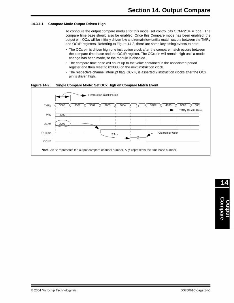
Section 14. Output CompareO
utp
ut
Co
mpare
14
14.3.1.1 Compare Mode Output Driven High
To configure the output compare module for this mode, set control bits OCM<2:0> = ‘001’. Thecompare time base should also be enabled. Once this Compare mode has been enabled, theoutput pin, OCx, will be initially driven low and remain low until a match occurs between the TMRyand OCxR registers. Referring to Figure 14-2, there are some key timing events to note:
• The OCx pin is driven high one instruction clock after the compare match occurs between the compare time base and the OCxR register. The OCx pin will remain high until a mode change has been made, or the module is disabled.
• The compare time base will count up to the value contained in the associated period register and then reset to 0x0000 on the next instruction clock.
• The respective channel interrupt flag, OCxIF, is asserted 2 instruction clocks after the OCx pin is driven high.
Figure 14-2: Single Compare Mode: Set OCx High on Compare Match Event
OCxIF
4000 00013001 3002 3003 30043000TMRy 0000
Cleared by User
1 Instruction Clock Period
2 TCY
4000
3002
PRy
OCxR
3FFF
OCx pin
TMRy Resets Here
Note: An ‘x’ represents the output compare channel number. A ‘y’ represents the time base number.
© 2004 Microchip Technology Inc. DS70061C-page 14-5
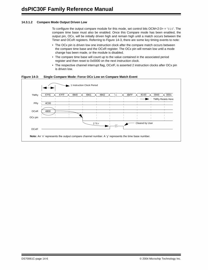
dsPIC30F Family Reference Manual
14.3.1.2 Compare Mode Output Driven Low
To configure the output compare module for this mode, set control bits OCM<2:0> = ‘010’. Thecompare time base must also be enabled. Once this Compare mode has been enabled, theoutput pin, OCx, will be initially driven high and remain high until a match occurs between theTimer and OCxR registers. Referring to Figure 14-3, there are some key timing events to note:
• The OCx pin is driven low one instruction clock after the compare match occurs between the compare time base and the OCxR register. The OCx pin will remain low until a mode change has been made, or the module is disabled.
• The compare time base will count up to the value contained in the associated period register and then reset to 0x0000 on the next instruction clock.
• The respective channel interrupt flag, OCxIF, is asserted 2 instruction clocks after OCx pin is driven low.
Figure 14-3: Single Compare Mode: Force OCx Low on Compare Match Event
OCxIF
4C00 000147FF 4800 4801 480247FETMRy 0000
Cleared by User
1 Instruction Clock Period
2 TCY
4C00
4800
PRy
OCxR
4BFF
OCx pin
TMRy Resets Here
Note: An ‘x’ represents the output compare channel number. A ‘y’ represents the time base number.
DS70061C-page 14-6 © 2004 Microchip Technology Inc.
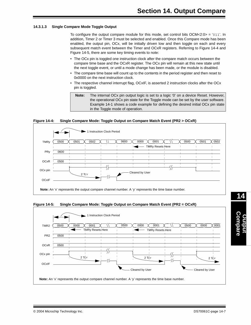
Section 14. Output CompareO
utp
ut
Co
mpare
14
14.3.1.3 Single Compare Mode Toggle Output
To configure the output compare module for this mode, set control bits OCM<2:0> = ‘011’. Inaddition, Timer 2 or Timer 3 must be selected and enabled. Once this Compare mode has beenenabled, the output pin, OCx, will be initially driven low and then toggle on each and everysubsequent match event between the Timer and OCxR registers. Referring to Figure 14-4 andFigure 14-5, there are some key timing events to note:
• The OCx pin is toggled one instruction clock after the compare match occurs between the compare time base and the OCxR register. The OCx pin will remain at this new state until the next toggle event, or until a mode change has been made, or the module is disabled.
• The compare time base will count up to the contents in the period register and then reset to 0x0000 on the next instruction clock.
• The respective channel interrupt flag, OCxIF, is asserted 2 instruction clocks after the OCx pin is toggled.
Figure 14-4: Single Compare Mode: Toggle Output on Compare Match Event (PR2 > OCxR)
Figure 14-5: Single Compare Mode: Toggle Output on Compare Match Event (PR2 = OCxR)
Note: The internal OCx pin output logic is set to a logic ‘0’ on a device Reset. However,the operational OCx pin state for the Toggle mode can be set by the user software.Example 14-1 shows a code example for defining the desired initial OCx pin statein the Toggle mode of operation.
OCxIF
05000501 0502 06000500TMRy
1 Instruction Clock Period
0600
0500
PRy
OCxR
0001
OCx pin
TMRy Resets Here
0000 0501 0502
Cleared by User2 TCY
Note: An ‘x’ represents the output compare channel number. A ‘y’ represents the time base number.
OCxIF
05000000 0001 05000500TMR2
Cleared by User
1 Instruction Clock Period
2 TCY
0500
0500
PR2
OCxR
0001
OCx pin
TMRy Resets Here
0000 0000 0001
Cleared by User
2 TCY 2 TCY
TMRy Resets Here
Note: An ‘x’ represents the output compare channel number. A ‘y’ represents the time base number.
© 2004 Microchip Technology Inc. DS70061C-page 14-7
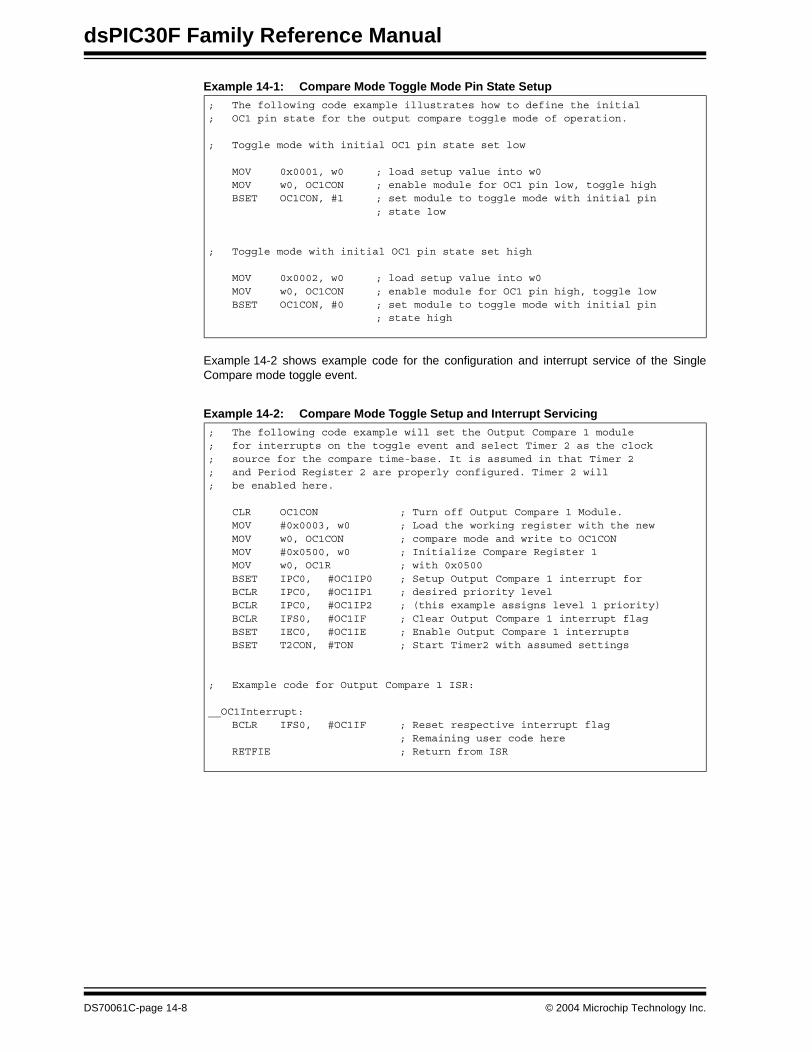
dsPIC30F Family Reference Manual
Example 14-1: Compare Mode Toggle Mode Pin State Setup
Example 14-2 shows example code for the configuration and interrupt service of the SingleCompare mode toggle event.
Example 14-2: Compare Mode Toggle Setup and Interrupt Servicing
; The following code example illustrates how to define the initial; OC1 pin state for the output compare toggle mode of operation.
; Toggle mode with initial OC1 pin state set low
MOV 0x0001, w0 ; load setup value into w0MOV w0, OC1CON ; enable module for OC1 pin low, toggle highBSET OC1CON, #1 ; set module to toggle mode with initial pin
; state low
; Toggle mode with initial OC1 pin state set high
MOV 0x0002, w0 ; load setup value into w0MOV w0, OC1CON ; enable module for OC1 pin high, toggle lowBSET OC1CON, #0 ; set module to toggle mode with initial pin
; state high
; The following code example will set the Output Compare 1 module ; for interrupts on the toggle event and select Timer 2 as the clock ; source for the compare time-base. It is assumed in that Timer 2 ; and Period Register 2 are properly configured. Timer 2 will ; be enabled here.
CLR OC1CON ; Turn off Output Compare 1 Module. MOV #0x0003, w0 ; Load the working register with the new MOV w0, OC1CON ; compare mode and write to OC1CON MOV #0x0500, w0 ; Initialize Compare Register 1 MOV w0, OC1R ; with 0x0500 BSET IPC0, #OC1IP0 ; Setup Output Compare 1 interrupt for BCLR IPC0, #OC1IP1 ; desired priority level BCLR IPC0, #OC1IP2 ; (this example assigns level 1 priority) BCLR IFS0, #OC1IF ; Clear Output Compare 1 interrupt flag BSET IEC0, #OC1IE ; Enable Output Compare 1 interrupts BSET T2CON, #TON ; Start Timer2 with assumed settings
; Example code for Output Compare 1 ISR:
__OC1Interrupt:BCLR IFS0, #OC1IF ; Reset respective interrupt flag
; Remaining user code hereRETFIE ; Return from ISR
DS70061C-page 14-8 © 2004 Microchip Technology Inc.
Section 14. Output CompareO
utp
ut
Co
mpare
14
14.3.2 Dual Compare Match Mode
When control bits OCM<2:0> = ‘100’ or ‘101’ (OCxCON<2:0>), the selected output comparechannel is configured for one of two Dual Compare Match modes which are:
• Single Output Pulse mode
• Continuous Output Pulse mode
In the Dual Compare mode, the module uses both the OCxR and OCxRS registers for thecompare match events. The OCxR register is compared against the incrementing timer count,TMRy, and the leading (rising) edge of the pulse is generated at the OCx pin, on a comparematch event. The OCxRS register is then compared to the same incrementing timer count,TMRy, and the trailing (falling) edge of the pulse is generated at the OCx pin, on a comparematch event.
14.3.2.1 Dual Compare Mode: Single Output Pulse
To configure the Output Compare module for the Single Output Pulse mode, set control bitsOCM<2:0> = ‘100’. In addition, the compare time base must be selected and enabled. Once thismode has been enabled, the output pin, OCx, will be driven low and remain low until a matchoccurs between the time base and OCxR registers. Referring to Figure 14-6 and Figure 14-7,there are some key timing events to note:
• The OCx pin is driven high one instruction clock after the compare match occurs between the compare time base and OCxR register. The OCx pin will remain high until the next match event occurs between the time base and the OCxRS register. At this time, the pin will be driven low. The OCx pin will remain low until a mode change has been made, or the module is disabled.
• The compare time base will count up to the value contained in the associated period register and then reset to 0x0000 on the next instruction clock.
• If the time base period register contents are less than the OCxRS register contents, then no falling edge of the pulse is generated. The OCx pin will remain high until OCxRS <= PRy, or a mode change or Reset condition has occurred.
• The respective channel interrupt flag, OCxIF, is asserted 2 instruction clocks after the OCx pin is driven low (falling edge of single pulse).
Figure 14-6 depicts the General Dual Compare mode generating a single output pulse.Figure 14-7 depicts another timing example where OCxRS > PRy. In this example, no fallingedge of the pulse is generated since the compare time base resets before counting up to0x4100.
© 2004 Microchip Technology Inc. DS70061C-page 14-9

dsPIC30F Family Reference Manual
Figure 14-6: Dual Compare Mode
Figure 14-7: Dual Compare Mode: Single Output Pulse (OCxRS > PR2)
OCxIF
00003001 3002 3003 30043000TMRy 4000
Cleared by User
Note 1: An ‘x’ represents the output compare channel number. A ‘y’ represents the time base number.
2: OCxR = Compare Register, OCxRS = Secondary Compare Register.
1 Instruction Clock Period
2 TCY
4000
3000
PRy
OCxR
3006
OCx pin
TMRy Resets Here
3003OCxRS
3005
OCxIF
00003001 3002 3003 30043000TMRy 4000
1 Instruction Clock Period
4000
3000
PRy
OCxR
3006
OCx pin
TMRy Resets Here
4100OCxRS
3005
Note 1: An ‘x’ represents the output compare channel number. A ‘y’ represents the time base number.
2: OCxR = Compare Register, OCxRS = Secondary Compare Register.
Compare Interrupt does not occur
DS70061C-page 14-10 © 2004 Microchip Technology Inc.
Section 14. Output CompareO
utp
ut
Co
mpare
14
14.3.2.2 Setup for Single Output Pulse Generation
When control bits OCM<2:0> (OCxCON<2:0>) are set to ‘100’, the selected output comparechannel initializes the OCx pin to the low state and generates a single output pulse.
To generate a single output pulse, the following steps are required (these steps assume timersource is initially turned off, but this is not a requirement for the module operation):
1. Determine the instruction clock cycle time. Take into account the frequency of the externalclock to the timer source (if one is used) and the timer prescaler settings.
2. Calculate time to the rising edge of the output pulse relative to the TMRy start value(0x0000).
3. Calculate the time to the falling edge of the pulse based on the desired pulse width andthe time to the rising edge of the pulse.
4. Write the values computed in steps 2 and 3 above into the compare register, OCxR, andthe secondary compare register, OCxRS, respectively.
5. Set timer period register, PRy, to value equal to or greater than value in OCxRS, thesecondary compare register.
6. Set OCM<2:0> = ‘100’ and the OCTSEL (OCxCON<3>) bit to the desired timer source.The OCx pin state will now be driven low.
7. Set the TON (TyCON<15>) bit to ‘1’, which enables the compare time base to count. 8. Upon the first match between TMRy and OCxR, the OCx pin will be driven high.9. When the incrementing timer, TMRy, matches the secondary compare register, OCxRS,
the second and trailing edge (high-to-low) of the pulse is driven onto the OCx pin. Noadditional pulses are driven onto the OCx pin and it remains at low. As a result of thesecond compare match event, the OCxIF interrupt flag bit set, which will result in aninterrupt if it is enabled, by setting the OCxIE bit. For further information on peripheralinterrupts, refer to Section 6. “Reset Interrupts”.
10. To initiate another single pulse output, change the timer and compare register settings, ifneeded, and then issue a write to set OCM<2:0> (OCxCON<2:0>) bits to ‘100’. Disablingand re-enabling of the timer and clearing the TMRy register are not required, but may beadvantageous for defining a pulse from a known event time boundary.
The output compare module does not have to be disabled after the falling edge of the outputpulse. Another pulse can be initiated by rewriting the value of the OCxCON register.
© 2004 Microchip Technology Inc. DS70061C-page 14-11
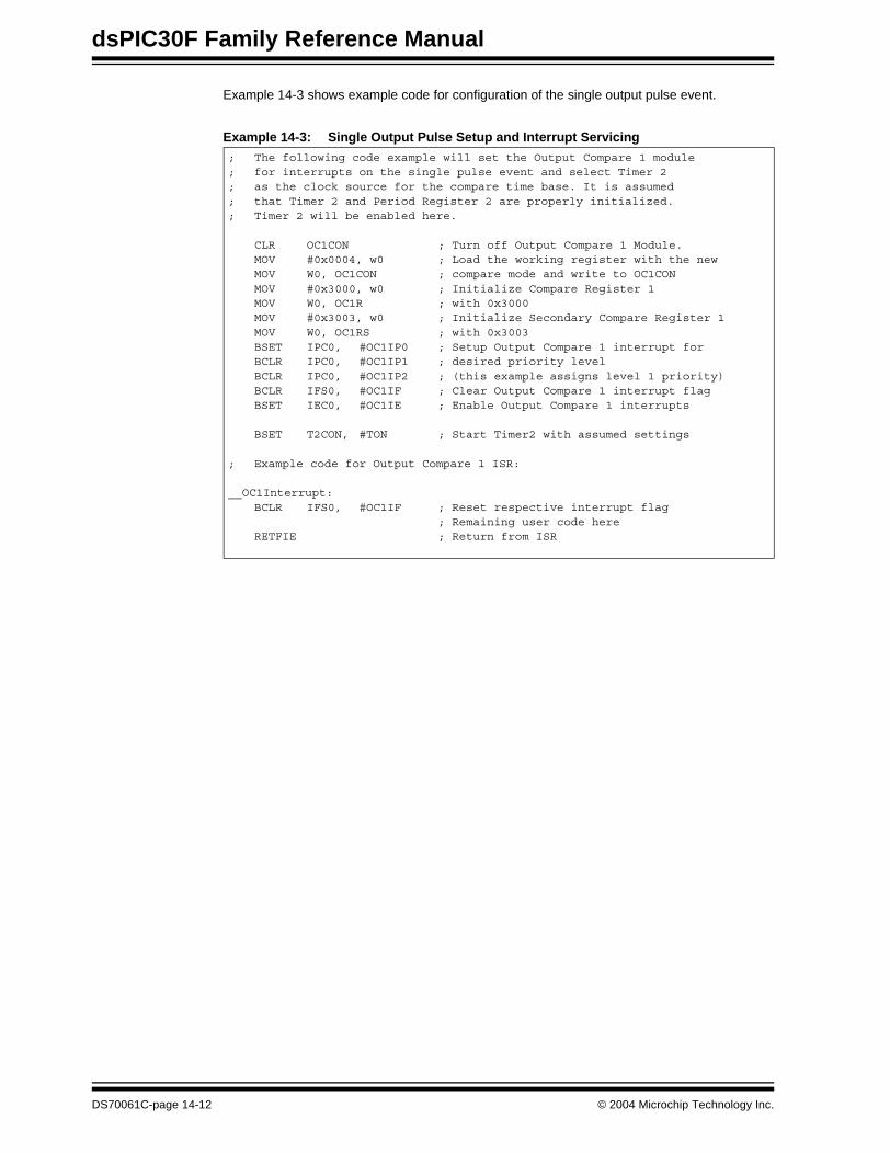
dsPIC30F Family Reference Manual
Example 14-3 shows example code for configuration of the single output pulse event.
Example 14-3: Single Output Pulse Setup and Interrupt Servicing ; The following code example will set the Output Compare 1 module ; for interrupts on the single pulse event and select Timer 2 ; as the clock source for the compare time base. It is assumed ; that Timer 2 and Period Register 2 are properly initialized. ; Timer 2 will be enabled here.
CLR OC1CON ; Turn off Output Compare 1 Module. MOV #0x0004, w0 ; Load the working register with the new MOV W0, OC1CON ; compare mode and write to OC1CON MOV #0x3000, w0 ; Initialize Compare Register 1 MOV W0, OC1R ; with 0x3000 MOV #0x3003, w0 ; Initialize Secondary Compare Register 1 MOV W0, OC1RS ; with 0x3003 BSET IPC0, #OC1IP0 ; Setup Output Compare 1 interrupt for BCLR IPC0, #OC1IP1 ; desired priority level BCLR IPC0, #OC1IP2 ; (this example assigns level 1 priority) BCLR IFS0, #OC1IF ; Clear Output Compare 1 interrupt flag BSET IEC0, #OC1IE ; Enable Output Compare 1 interrupts
BSET T2CON, #TON ; Start Timer2 with assumed settings
; Example code for Output Compare 1 ISR:
__OC1Interrupt:BCLR IFS0, #OC1IF ; Reset respective interrupt flag
; Remaining user code hereRETFIE ; Return from ISR
DS70061C-page 14-12 © 2004 Microchip Technology Inc.

Section 14. Output CompareO
utp
ut
Co
mpare
14
14.3.2.3 Special Cases for Dual Compare Mode Generating a Single Output Pulse
Depending on the relationship of the OCxR, OCxRS and PRy values, the output compare modulehas a few unique conditions which should be understood. These special conditions are specifiedin Table 14-1, along with the resulting behavior of the module.
Table 14-1: Special Cases for Dual Compare Mode Generating a Single Output Pulse
SFR LogicalRelationship
Special Conditions OperationOutputat OCx
PRy >= OCxRS andOCxRS > OCxR
OCxR = 0Initialize TMRy = 0
In the first iteration of the TMRy counting from 0x0000 up to PRy, the OCx pin remains low, no pulse is generated. After the TMRy resets to zero (on period match), the OCx pin goes high due to match with OCxR. Upon the next TMRy to OCxRS match, the OCx pin goes low and remains there. The OCxIF bit will be set as a result of the second compare.There are two alternative initial conditions to consider:a] Initialize TMRy = 0 and set OCxR >= 1b] Initialize TMRy = PRy (PRy > 0) and set OCxR = 0
Pulse will be delayed by the value in the PRy register depending on setup
PRy >= OCxR andOCxR >= OCxRS
OCxR >= 1 andPRy >= 1
TMRy counts up to OCxR and on a compare match event (i.e., TMRy = OCxR), the OCx pin is driven to a high state. TMRy then continues to count and eventually resets on period match (i.e., PRy =TMRy). The timer then restarts from 0x0000 and counts up to OCxRS, and on a compare match event (i.e., TMRy = OCxRS), the OCx pin is driven to a low state. The OCxIF bit will be set as a result of the second compare.
Pulse
OCxRS > PRy andPRy >= OCxR
None Only the rising edge will be generated at the OCx pin. The OCxIF will not be set.
Rising edge/transition to high
OCxR = OCxRS = PRy = 0x0000
None An output pulse delayed 2 instruction clock periods upon the match of the timer and period register is generated at the OCx pin. The OCxIF bit will be set as a result of the second compare.
Delayed pulse
OCxR > PRy None Unsupported mode, timer resets prior to match condition. Remains low
Note 1: In all the cases considered herein, the TMRy register is assumed to be initialized to 0x0000.
2: OCxR = Compare Register, OCxRS = Secondary Compare Register, TMRy = Timery Count,PRy = Timery Period Register.
© 2004 Microchip Technology Inc. DS70061C-page 14-13
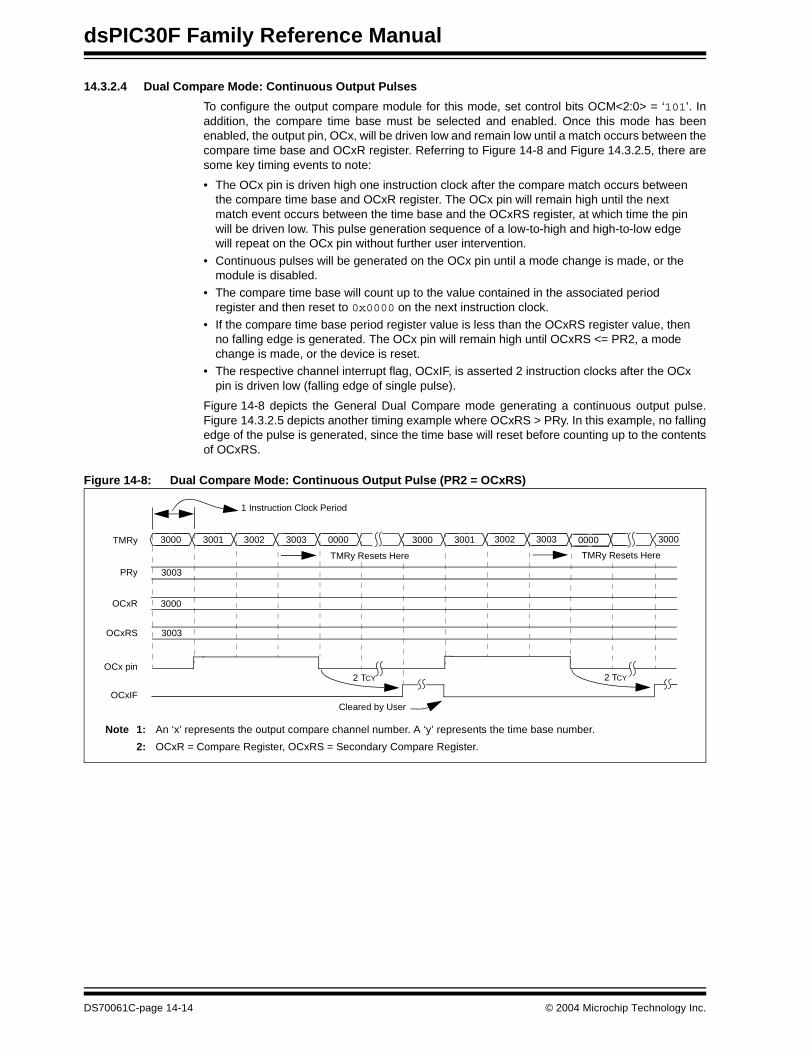
dsPIC30F Family Reference Manual
14.3.2.4 Dual Compare Mode: Continuous Output Pulses
To configure the output compare module for this mode, set control bits OCM<2:0> = ‘101’. Inaddition, the compare time base must be selected and enabled. Once this mode has beenenabled, the output pin, OCx, will be driven low and remain low until a match occurs between thecompare time base and OCxR register. Referring to Figure 14-8 and Figure 14.3.2.5, there aresome key timing events to note:
• The OCx pin is driven high one instruction clock after the compare match occurs between the compare time base and OCxR register. The OCx pin will remain high until the next match event occurs between the time base and the OCxRS register, at which time the pin will be driven low. This pulse generation sequence of a low-to-high and high-to-low edge will repeat on the OCx pin without further user intervention.
• Continuous pulses will be generated on the OCx pin until a mode change is made, or the module is disabled.
• The compare time base will count up to the value contained in the associated period register and then reset to 0x0000 on the next instruction clock.
• If the compare time base period register value is less than the OCxRS register value, then no falling edge is generated. The OCx pin will remain high until OCxRS <= PR2, a mode change is made, or the device is reset.
• The respective channel interrupt flag, OCxIF, is asserted 2 instruction clocks after the OCx pin is driven low (falling edge of single pulse).
Figure 14-8 depicts the General Dual Compare mode generating a continuous output pulse.Figure 14.3.2.5 depicts another timing example where OCxRS > PRy. In this example, no fallingedge of the pulse is generated, since the time base will reset before counting up to the contentsof OCxRS.
Figure 14-8: Dual Compare Mode: Continuous Output Pulse (PR2 = OCxRS)
OCxIF
30033001 3002 3003 00003000TMRy 3002
Cleared by User
1 Instruction Clock Period
2 TCY
3003
3000
PRy
OCxR
3000
OCx pin
3003OCxRS
3001 30000000
2 TCY
TMRy Resets Here TMRy Resets Here
Note 1: An ‘x’ represents the output compare channel number. A ‘y’ represents the time base number.
2: OCxR = Compare Register, OCxRS = Secondary Compare Register.
DS70061C-page 14-14 © 2004 Microchip Technology Inc.
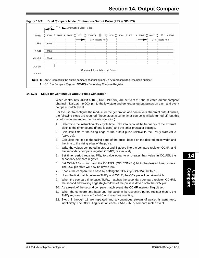
Section 14. Output CompareO
utp
ut
Co
mpare
14
Figure 14-9: Dual Compare Mode: Continuous Output Pulse (PR2 = OCxRS)
14.3.2.5 Setup for Continuous Output Pulse Generation
When control bits OCxM<2:0> (OCxCON<2:0>) are set to ‘101’, the selected output comparechannel initializes the OCx pin to the low state and generates output pulses on each and everycompare match event.
For the user to configure the module for the generation of a continuous stream of output pulses,the following steps are required (these steps assume timer source is initially turned off, but thisis not a requirement for the module operation):
1. Determine the instruction clock cycle time. Take into account the frequency of the externalclock to the timer source (if one is used) and the timer prescaler settings.
2. Calculate time to the rising edge of the output pulse relative to the TMRy start value(0x0000).
3. Calculate the time to the falling edge of the pulse, based on the desired pulse width andthe time to the rising edge of the pulse.
4. Write the values computed in step 2 and 3 above into the compare register, OCxR, andthe secondary compare register, OCxRS, respectively.
5. Set timer period register, PRy, to value equal to or greater than value in OCxRS, thesecondary compare register.
6. Set OCM<2:0> = ‘101’ and the OCTSEL (OCxCON<3>) bit to the desired timer source.The OCx pin state will now be driven low.
7. Enable the compare time base by setting the TON (TyCON<15>) bit to ‘1’. 8. Upon the first match between TMRy and OCxR, the OCx pin will be driven high.
9. When the compare time base, TMRy, matches the secondary compare register, OCxRS,the second and trailing edge (high-to-low) of the pulse is driven onto the OCx pin.
10. As a result of the second compare match event, the OCxIF interrupt flag bit set.11. When the compare time base and the value in its respective period register match, the
TMRy register resets to 0x0000 and resumes counting.12. Steps 8 through 11 are repeated and a continuous stream of pulses is generated,
indefinitely. The OCxIF flag is set on each OCxRS-TMRy compare match event.
OCxIF
30033001 3002 3003 00003000TMRy 3002
1 Instruction Clock Period
3003
3000
PRy
OCxR
3000
OCx pin
3003OCxRS
3001 30000000
TMRy Resets Here TMRy Resets Here
Note 1: An ‘x’ represents the output compare channel number. A ‘y’ represents the time base number.
2: OCxR = Compare Register, OCxRS = Secondary Compare Register.
Compare Interrupt does not Occur
© 2004 Microchip Technology Inc. DS70061C-page 14-15

dsPIC30F Family Reference Manual
Example 14-4 shows example code for configuration of the continuous output pulse event.
Example 14-4: Continuous Output Pulse Setup and Interrupt Servicing ; The following code example will set the Output Compare 1 module ; for interrupts on the continuous pulse event and select Timer 2 ; as the clock source for the compare time-base. It is assumed ; that Timer 2 and Period Register 2 are properly configured. ; Timer 2 will be enabled here.
CLR OC1CON ; Turn off Output Compare 1 Module. MOV #0x0005, W0 ; Load the working register with the new MOV W0, OC1CON ; compare mode and write to OC1CON MOV #0x3000, W0 ; Initialize Compare Register 1 MOV W0, OC1R ; with 0x3000 MOV #0x3003, W0 ; Initialize Secondary Compare Register 1 MOV W0, OC1RS ; with 0x3003 BSET IPC0, #OC1IP0 ; Setup Output Compare 1 interrupt for BCLR IPC0, #OC1IP1 ; desired priority level BCLR IPC0, #OC1IP2 ; (this example assigns level 1 priority) BCLR IFS0, #OC1IF ; Clear Output Compare 1 interrupt flag BSET IEC0, #OC1IE ; Enable Output Compare 1 interrupts
BSET T2CON, #TON ; Start Timer2 with assumed settings
; Example code for Output Compare 1 ISR:
__OC1Interrupt:BCLR IFS0, #OC1IF ; Reset respective interrupt flag
; Remaining user code hereRETFIE ; Return from ISR
DS70061C-page 14-16 © 2004 Microchip Technology Inc.

Section 14. Output CompareO
utp
ut
Co
mpare
14
14.3.2.6 Special Cases for Dual Compare Mode Generating Continuous Output Pulses
Depending on the relationship of the OCxR, OCxRS and PRy values, the output compare modulemay not provide the expected results. These special cases are specified in Table 14-2, along withthe resulting behavior of the module.
Table 14-2: Special Cases for Dual Compare Mode Generating Continuous Output Pulses
SFR LogicalRelationship
Special Conditions OperationOutputat OCx
PRy >= OCxRS andOCxRS > OCxR
OCxR = 0Initialize TMRy = 0
In the first iteration of the TMRy counting from 0x0000 up to PRy, the OCx pin remains low, no pulse is generated. After the TMRy resets to zero (on period match), the OCx pin goes high. Upon the next TMRy to OCxRS match, the OCx pin goes low. If OCxR = 0 and PRy = OCxRS, the pin will remain low for one clock cycle, then be driven high until the next TMRy to OCxRS match. The OCxIF bit will be set as a result of the second compare.There are two alternative initial conditions to consider:a] Initialize TMRy = 0 and set OCxR >= 1b] Initialize TMRy = PRy (PRy > 0) and set OCxR = 0
Continuous pulses with the first pulse delayed by the value in the PRy register, depending on setup.
PRy >= OCxR andOCxR >= OCxRS
OCxR >= 1 andPRy >= 1
TMRy counts up to OCxR and on a compare match event (i.e., TMRy = OCxR), the OCx pin is driven to a high state. TMRy then continues to count and eventually resets on period match (i.e., PRy =TMRy). The timer then restarts from 0x0000 and counts up to OCxRS, and on a compare match event (i.e., TMRy = OCxR), the OCx pin is driven to a low state. The OCxIF bit will be set as a result of the second compare.
Continuous pulses
OCxRS > PRy andPRy >= OCxR
None Only one transition will be generated at the OCx pin until the OCxRS register contents have been changed to a value less than or equal to the period register contents (PRy). OCxIF is not set until then.
Rising edge/ transition to high
OCxR = OCxRS =PRy = 0x0000
None Continuous output pulses are generated at the OCx pin. The first pulse is delayed 2 instruction clock periods upon the match of the timer and period register. The OCxIF bit will be set as a result of the second compare.
First pulse is delayed. Continuous pulsesare generated.
OCxR > PRy None Unsupported mode, Timer resets prior to match condition. Remains low
Note 1: In all the cases considered herein, the TMRy register is assumed to be initialized to 0x0000.
2: OCxR = Compare Register, OCxRS = Secondary Compare Register, TMRy = Timery Count,PRy = Timery Period Register.
© 2004 Microchip Technology Inc. DS70061C-page 14-17
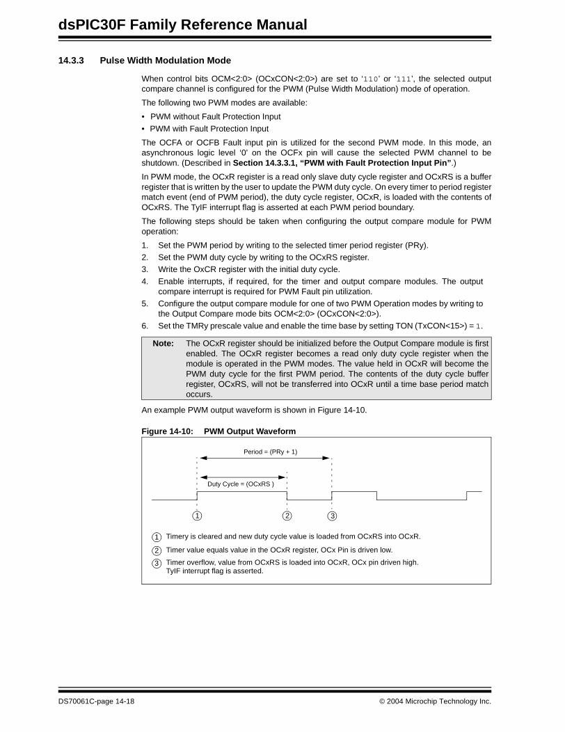
dsPIC30F Family Reference Manual
14.3.3 Pulse Width Modulation Mode
When control bits OCM<2:0> (OCxCON<2:0>) are set to ‘110’ or ‘111’, the selected outputcompare channel is configured for the PWM (Pulse Width Modulation) mode of operation.
The following two PWM modes are available:
• PWM without Fault Protection Input
• PWM with Fault Protection Input
The OCFA or OCFB Fault input pin is utilized for the second PWM mode. In this mode, anasynchronous logic level ‘0’ on the OCFx pin will cause the selected PWM channel to beshutdown. (Described in Section 14.3.3.1, “PWM with Fault Protection Input Pin”.)
In PWM mode, the OCxR register is a read only slave duty cycle register and OCxRS is a bufferregister that is written by the user to update the PWM duty cycle. On every timer to period registermatch event (end of PWM period), the duty cycle register, OCxR, is loaded with the contents ofOCxRS. The TyIF interrupt flag is asserted at each PWM period boundary.
The following steps should be taken when configuring the output compare module for PWMoperation:
1. Set the PWM period by writing to the selected timer period register (PRy).2. Set the PWM duty cycle by writing to the OCxRS register.3. Write the OxCR register with the initial duty cycle.
4. Enable interrupts, if required, for the timer and output compare modules. The outputcompare interrupt is required for PWM Fault pin utilization.
5. Configure the output compare module for one of two PWM Operation modes by writing tothe Output Compare mode bits OCM<2:0> (OCxCON<2:0>).
6. Set the TMRy prescale value and enable the time base by setting TON (TxCON<15>) = 1.
An example PWM output waveform is shown in Figure 14-10.
Figure 14-10: PWM Output Waveform
Note: The OCxR register should be initialized before the Output Compare module is firstenabled. The OCxR register becomes a read only duty cycle register when themodule is operated in the PWM modes. The value held in OCxR will become thePWM duty cycle for the first PWM period. The contents of the duty cycle bufferregister, OCxRS, will not be transferred into OCxR until a time base period matchoccurs.
Period = (PRy + 1)
Duty Cycle = (OCxRS )
Timery is cleared and new duty cycle value is loaded from OCxRS into OCxR.
Timer value equals value in the OCxR register, OCx Pin is driven low.
Timer overflow, value from OCxRS is loaded into OCxR, OCx pin driven high.
21 3
2
3
1
TyIF interrupt flag is asserted.
DS70061C-page 14-18 © 2004 Microchip Technology Inc.
Section 14. Output CompareO
utp
ut
Co
mpare
14
14.3.3.1 PWM with Fault Protection Input Pin
When the Output Compare mode bits, OCM<2:0> (OCxCON<2:0>), are set to ‘111’, the selectedoutput compare channel is configured for the PWM mode of operation. All functions described inSection 14.3.3, “Pulse Width Modulation Mode” apply, with the addition of input Faultprotection.
Fault protection is provided via the OCFA and OCFB pins. The OCFA pin is associated with theoutput compare channels 1 through 4, while the OCFB pin is associated with the output comparechannels 5 through 8.
If a logic ‘0’ is detected on the OCFA/OCFB pin, the selected PWM output pin(s) are placed inthe high impedance state. The user may elect to provide a pull-down or pull-up resistor on thePWM pin to provide for a desired state if a Fault condition occurs. The shutdown of the PWMoutput is immediate and is not tied to the device clock source. This state will remain until:
• The external Fault condition has been removed and• The PWM mode is re-enabled by writing to the appropriate mode bits, OCM<2:0>
(OCxCON<2:0>).
As a result of the Fault condition, the respective interrupt flag, OCxIF bit, is asserted and aninterrupt will be generated, if enabled. Upon detection of the Fault condition, the OCFLT bit(OCx-CON<4>) is asserted high (logic ‘1’). This bit is a read only bit and will only be cleared oncethe external Fault condition has been removed and the PWM mode is re-enabled, by writing tothe appropriate mode bits, OCM<2:0> (OCxCON<2:0>).
14.3.3.2 PWM Period
The PWM period is specified by writing to PRy, the Timery period register. The PWM period canbe calculated using the following formula:
Equation 14-1: Calculating the PWM Period
Note: The external Fault pins, if enabled for use, will continue to control the OCx outputpins, while the device is in Sleep or Idle mode.
PWM Period = [(PRy) + 1] • TCY • (TMRy Prescale Value)
PWM Frequency = 1/[PWM Period]
Note: A PRy value of N will produce a PWM period of N + 1 time base count cycles. Forexample: a value of 7 written into the PRy register will yield a period consisting of 8time base cycles.
© 2004 Microchip Technology Inc. DS70061C-page 14-19
dsPIC30F Family Reference Manual
14.3.3.3 PWM Duty Cycle
The PWM duty cycle is specified by writing to the OCxRS register. The OCxRS register can bewritten to at any time, but the duty cycle value is not latched into OCxR until a match betweenPRy and TMRy occurs (i.e., the period is complete). This provides a double buffer for the PWMduty cycle and is essential for glitchless PWM operation. In the PWM mode, OCxR is a read onlyregister.
Some important boundary parameters of the PWM duty cycle include:
• If the duty cycle register, OCxR, is loaded with 0x0000, the OCx pin will remain low(0% duty cycle).
• If OCxR is greater than PRy (timer period register), the pin will remain high (100% duty cycle).
• If OCxR is equal to PRy, the OCx pin will be low for one time base count value and high for all other count values.
See Figure 14-11 for PWM mode timing details. Table 14-3 and Table 14-4 show example PWMfrequencies and resolutions for a device operating at 10 and 30 MIPs, respectively.
Equation 14-2: Calculation for Maximum PWM Resolution
Example 14-5: PWM Period and Duty Cycle Calculation
( )Maximum PWM Resolution (bits) =
FOSC
FPWMlog10
log10(2)bits
Desired PWM frequency is 52.08 kHz, FOSC = 10 MHz with x4 PLL (40 MHz device clock rate) (TCY = 4/FOSC))Timer 2 prescale setting: 1:1
1/52.08 kHz = (PR2+1) • TCY • (Timer 2 prescale value) 19.20 μs = (PR2+1) • 0.1 μs • (1) PR2 = 191
Find the maximum resolution of the duty cycle that can be used with a 48 kHz frequency and a 40 MHz device clock rate.
1/52.08 kHz = 2PWM RESOLUTION • 1/40 MHz • 1
19.20 μs = 2PWM RESOLUTION • 25 ns • 1
768 = 2PWM RESOLUTION
log10(768) = (PWM Resolution) • log10(2)
PWM Resolution= 9.5 bits
DS70061C-page 14-20 © 2004 Microchip Technology Inc.
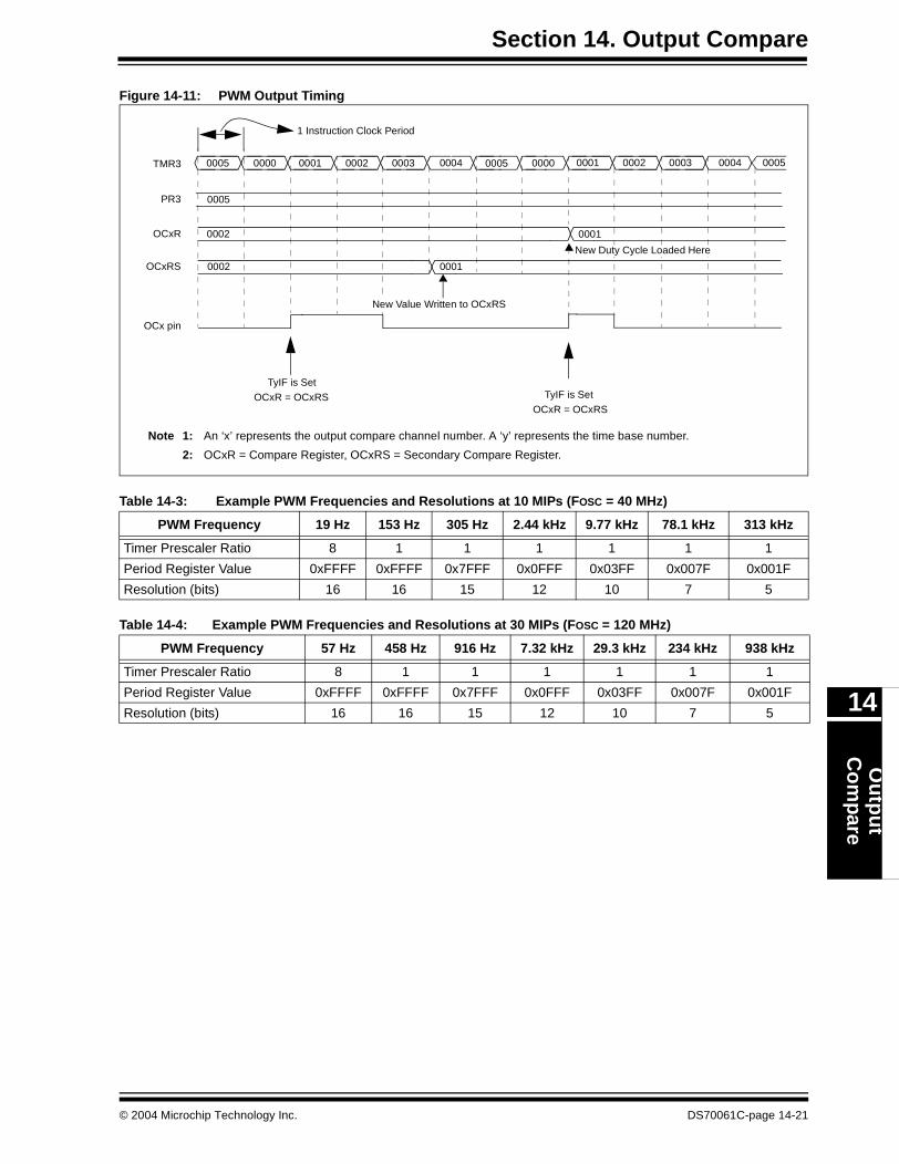
Section 14. Output CompareO
utp
ut
Co
mpare
14
Figure 14-11: PWM Output Timing
Table 14-3: Example PWM Frequencies and Resolutions at 10 MIPs (FOSC = 40 MHz)
Table 14-4: Example PWM Frequencies and Resolutions at 30 MIPs (FOSC = 120 MHz)
PWM Frequency 19 Hz 153 Hz 305 Hz 2.44 kHz 9.77 kHz 78.1 kHz 313 kHz
Timer Prescaler Ratio 8 1 1 1 1 1 1
Period Register Value 0xFFFF 0xFFFF 0x7FFF 0x0FFF 0x03FF 0x007F 0x001F
Resolution (bits) 16 16 15 12 10 7 5
PWM Frequency 57 Hz 458 Hz 916 Hz 7.32 kHz 29.3 kHz 234 kHz 938 kHz
Timer Prescaler Ratio 8 1 1 1 1 1 1
Period Register Value 0xFFFF 0xFFFF 0x7FFF 0x0FFF 0x03FF 0x007F 0x001F
Resolution (bits) 16 16 15 12 10 7 5
00020000 0001 0002 00030005TMR3 0001
1 Instruction Clock Period
0005
0002
PR3
OCxR
0005
OCx pin
0002OCxRS
0000 000500030004 0004
0001
New Value Written to OCxRS
0001
New Duty Cycle Loaded Here
Note 1: An ‘x’ represents the output compare channel number. A ‘y’ represents the time base number.
2: OCxR = Compare Register, OCxRS = Secondary Compare Register.
TyIF is Set
OCxR = OCxRS TyIF is Set
OCxR = OCxRS
© 2004 Microchip Technology Inc. DS70061C-page 14-21
dsPIC30F Family Reference Manual
Example 14-6 shows configuration and interrupt service code for the PWM mode of operation.
Example 14-6: PWM Mode Pulse Setup and Interrupt Servicing
; The following code example will set the Output Compare 1 module ; for PWM mode w/o FAULT pin enabled, a 50% duty cycle and a ; PWM frequency of 52.08 kHz at Fosc = 40 MHz. Timer2 is selected as ; the clock for the PWM time base and Timer2 interrupts ; are enabled.
CLR OC1CON ; Turn off Output Compare 1 Module.
MOV #0x0060, w0 ; Initialize Duty Cycle to 0x0060MOV w0, OC1RS ; Write duty cycle buffer registerMOV w0, OC1R ; Write OC1R to initial duty cycle value
MOV #0x0006, w0 ; Load the working register with the new MOV w0, OC1CON ; compare mode and write to OC1CON MOV #0x00BF w0 ; Initialize PR2 with 0x00BF MOV w0, PR2 ;
BSET IPC0, #T2IP0 ; Setup Timer 2 interrupt for BCLR IPC0, #T2IP1 ; desired priority level BCLR IPC0, #T2IP2 ; (this example assigns level 1 priority) BCLR IFS0, #T21IF ; Clear Timer 2 interrupt flag BSET IEC0, #T21IE ; Enable Timer 2 interrupts BSET T2CON, #TON ; Start Timer2 with assumed settings
; Example code for Timer 2 ISR:
__T2Interrupt:BCLR IFS0, #T21IF ; Reset respective interrupt flag
; Remaining user code hereRETFIE ; Return from ISR
DS70061C-page 14-22 © 2004 Microchip Technology Inc.
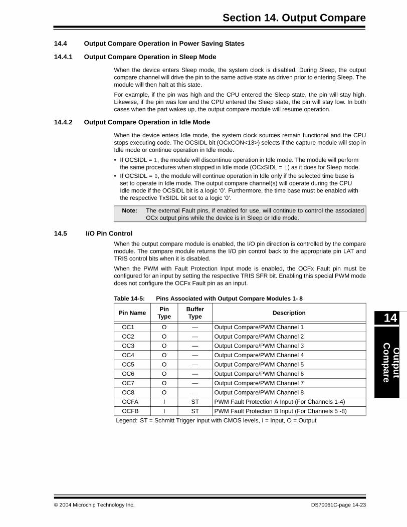
Section 14. Output CompareO
utp
ut
Co
mpare
14
14.4 Output Compare Operation in Power Saving States
14.4.1 Output Compare Operation in Sleep Mode
When the device enters Sleep mode, the system clock is disabled. During Sleep, the outputcompare channel will drive the pin to the same active state as driven prior to entering Sleep. Themodule will then halt at this state.
For example, if the pin was high and the CPU entered the Sleep state, the pin will stay high.Likewise, if the pin was low and the CPU entered the Sleep state, the pin will stay low. In bothcases when the part wakes up, the output compare module will resume operation.
14.4.2 Output Compare Operation in Idle Mode
When the device enters Idle mode, the system clock sources remain functional and the CPUstops executing code. The OCSIDL bit (OCxCON<13>) selects if the capture module will stop inIdle mode or continue operation in Idle mode.
• If OCSIDL = 1, the module will discontinue operation in Idle mode. The module will perform the same procedures when stopped in Idle mode (OCxSIDL = 1) as it does for Sleep mode.
• If OCSIDL = 0, the module will continue operation in Idle only if the selected time base is set to operate in Idle mode. The output compare channel(s) will operate during the CPU Idle mode if the OCSIDL bit is a logic ‘0’. Furthermore, the time base must be enabled with the respective TxSIDL bit set to a logic ‘0’.
14.5 I/O Pin Control
When the output compare module is enabled, the I/O pin direction is controlled by the comparemodule. The compare module returns the I/O pin control back to the appropriate pin LAT andTRIS control bits when it is disabled.
When the PWM with Fault Protection Input mode is enabled, the OCFx Fault pin must beconfigured for an input by setting the respective TRIS SFR bit. Enabling this special PWM modedoes not configure the OCFx Fault pin as an input.
Table 14-5: Pins Associated with Output Compare Modules 1- 8
Note: The external Fault pins, if enabled for use, will continue to control the associatedOCx output pins while the device is in Sleep or Idle mode.
Pin NamePin
TypeBufferType
Description
OC1 O — Output Compare/PWM Channel 1
OC2 O — Output Compare/PWM Channel 2
OC3 O — Output Compare/PWM Channel 3
OC4 O — Output Compare/PWM Channel 4
OC5 O — Output Compare/PWM Channel 5
OC6 O — Output Compare/PWM Channel 6
OC7 O — Output Compare/PWM Channel 7
OC8 O — Output Compare/PWM Channel 8
OCFA I ST PWM Fault Protection A Input (For Channels 1-4)
OCFB I ST PWM Fault Protection B Input (For Channels 5 -8)
Legend: ST = Schmitt Trigger input with CMOS levels, I = Input, O = Output
© 2004 Microchip Technology Inc. DS70061C-page 14-23
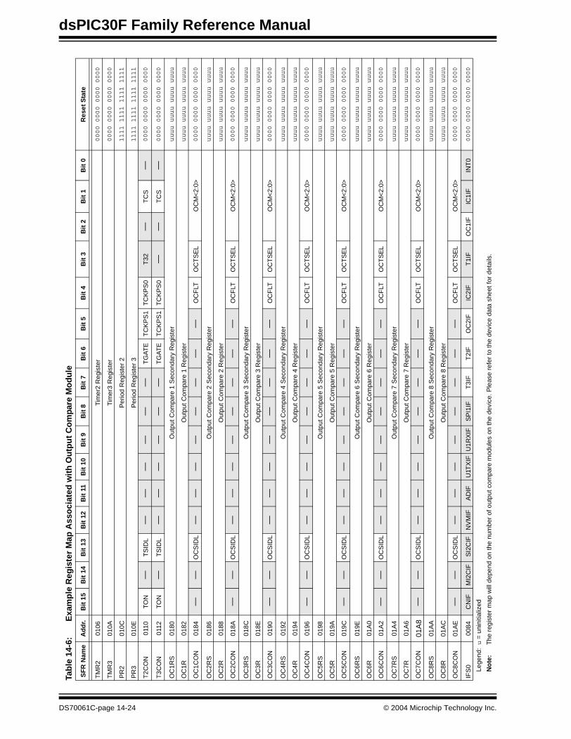
dsPIC30F Family Reference Manual
Tab
le 1
4-6:
Exa
mp
le R
egis
ter
Map
Ass
oci
ated
wit
h O
utp
ut
Co
mpa
re M
od
ule
SF
R N
ame
Ad
dr.
Bit
15
Bit
14
Bit
13
Bit
12
Bit
11
Bit
10
Bit
9B
it 8
Bit
7B
it 6
Bit
5B
it 4
Bit
3B
it 2
Bit
1B
it 0
Res
et S
tate
TM
R2
0106
Tim
er2
Reg
iste
r0000 0000 0000 0000
TM
R3
010A
Tim
er3
Reg
iste
r0000 0000 0000 0000
PR
201
0CP
erio
d R
egis
ter
21111 1111 1111 1111
PR
301
0EP
erio
d R
egis
ter
31111 1111 1111 1111
T2C
ON
0110
TO
N—
TS
IDL
——
——
——
TG
AT
ET
CK
PS
1T
CK
PS
0T
32—
TC
S—
0000 0000 0000 0000
T3C
ON
0112
TO
N—
TS
IDL
——
——
——
TG
AT
ET
CK
PS
1T
CK
PS
0—
—T
CS
—0000 0000 0000 0000
OC
1RS
0180
Out
put C
ompa
re 1
Sec
onda
ry R
egis
ter
uuuu uuuu uuuu uuuu
OC
1R01
82O
utpu
t Com
pare
1 R
egis
ter
uuuu uuuu uuuu uuuu
OC
1CO
N01
84—
—O
CS
IDL
——
——
——
——
OC
FLT
OC
TS
EL
OC
M<
2:0>
0000 0000 0000 0000
OC
2RS
0186
Out
put C
ompa
re 2
Sec
onda
ry R
egis
ter
uuuu uuuu uuuu uuuu
OC
2R01
88O
utpu
t Com
pare
2 R
egis
ter
uuuu uuuu uuuu uuuu
OC
2CO
N01
8A—
—O
CS
IDL
——
——
——
——
OC
FLT
OC
TS
EL
OC
M<
2:0>
0000 0000 0000 0000
OC
3RS
018C
Out
put C
ompa
re 3
Sec
onda
ry R
egis
ter
uuuu uuuu uuuu uuuu
OC
3R01
8EO
utpu
t Com
pare
3 R
egis
ter
uuuu uuuu uuuu uuuu
OC
3CO
N01
90—
—O
CS
IDL
——
——
——
——
OC
FLT
OC
TS
EL
OC
M<
2:0>
0000 0000 0000 0000
OC
4RS
0192
Out
put C
ompa
re 4
Sec
onda
ry R
egis
ter
uuuu uuuu uuuu uuuu
OC
4R01
94O
utpu
t Com
pare
4 R
egis
ter
uuuu uuuu uuuu uuuu
OC
4CO
N01
96—
—O
CS
IDL
——
——
——
——
OC
FLT
OC
TS
EL
OC
M<
2:0>
0000 0000 0000 0000
OC
5RS
0198
Out
put C
ompa
re 5
Sec
onda
ry R
egis
ter
uuuu uuuu uuuu uuuu
OC
5R01
9AO
utpu
t Com
pare
5 R
egis
ter
uuuu uuuu uuuu uuuu
OC
5CO
N01
9C—
—O
CS
IDL
——
——
——
——
OC
FLT
OC
TS
EL
OC
M<
2:0>
0000 0000 0000 0000
OC
6RS
019E
Out
put C
ompa
re 6
Sec
onda
ry R
egis
ter
uuuu uuuu uuuu uuuu
OC
6R01
A0
Out
put C
ompa
re 6
Reg
iste
ruuuu uuuu uuuu uuuu
OC
6CO
N01
A2
——
OC
SID
L—
——
——
——
—O
CF
LTO
CT
SE
LO
CM
<2:
0>0000 0000 0000 0000
OC
7RS
01A
4O
utpu
t Com
pare
7 S
econ
dary
Reg
iste
ruuuu uuuu uuuu uuuu
OC
7R01
A6
Out
put C
ompa
re 7
Reg
iste
ruuuu uuuu uuuu uuuu
OC
7CO
N01
A8
——
OC
SID
L—
——
——
——
—O
CF
LTO
CT
SE
LO
CM
<2:
0>0000 0000 0000 0000
OC
8RS
01A
AO
utpu
t Com
pare
8 S
econ
dary
Reg
iste
ruuuu uuuu uuuu uuuu
OC
8R01
AC
Out
put C
ompa
re 8
Reg
iste
ruuuu uuuu uuuu uuuu
OC
8CO
N01
AE
——
OC
SID
L—
——
——
——
—O
CF
LTO
CT
SE
LO
CM
<2:
0>0000 0000 0000 0000
IFS
000
84C
NIF
MI2
CIF
SI2
CIF
NV
MIF
AD
IFU
1TX
IFU
1RX
IFS
PI1
IFT
3IF
T2I
FO
C2I
FIC
2IF
T1I
FO
C1I
FIC
1IF
INT
00000 0000 0000 0000
Lege
nd:u
= u
nini
tializ
ed
No
te:
The
reg
iste
r m
ap w
ill d
epen
d on
the
num
ber
of o
utpu
t com
pare
mod
ules
on
the
devi
ce. P
leas
e re
fer
to th
e de
vice
dat
a sh
eet f
or d
etai
ls.
DS70061C-page 14-24 © 2004 Microchip Technology Inc.
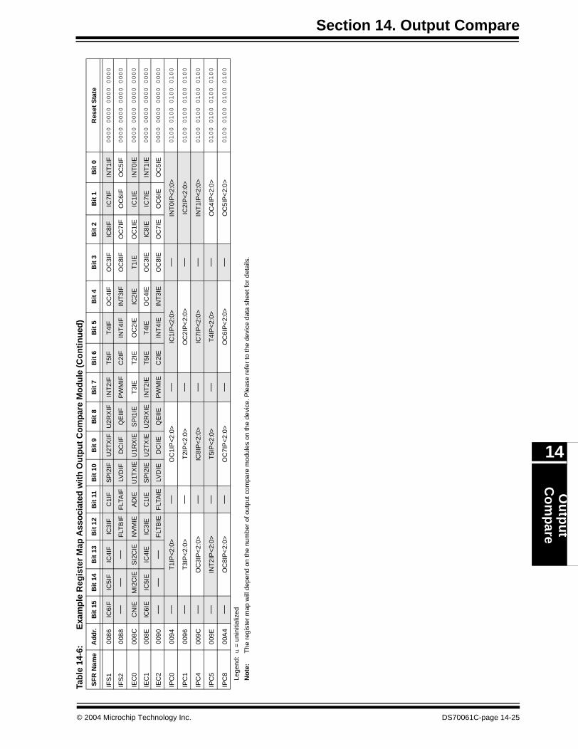
Section 14. Output CompareO
utp
ut
Co
mpare
14
IFS
100
86IC
6IF
IC5I
FIC
4IF
IC3I
FC
1IF
SP
I2IF
U2T
XIF
U2R
XIF
INT
2IF
T5I
FT
4IF
OC
4IF
OC
3IF
IC8I
FIC
7IF
INT
1IF
0000 0000 0000 0000
IFS
200
88—
——
FLT
BIF
FLT
AIF
LVD
IFD
CIIF
QE
IIFP
WM
IFC
2IF
INT
4IF
INT
3IF
OC
8IF
OC
7IF
OC
6IF
OC
5IF
0000 0000 0000 0000
IEC
000
8CC
NIE
MI2
CIE
SI2
CIE
NV
MIE
AD
IEU
1TX
IEU
1RX
IES
PI1
IET
3IE
T2I
EO
C2I
EIC
2IE
T1I
EO
C1I
EIC
1IE
INT
0IE
0000 0000 0000 0000
IEC
100
8EIC
6IE
IC5I
EIC
4IE
IC3I
EC
1IE
SP
I2IE
U2T
XIE
U2R
XIE
INT
2IE
T5I
ET
4IE
OC
4IE
OC
3IE
IC8I
EIC
7IE
INT
1IE
0000 0000 0000 0000
IEC
200
90—
——
FLT
BIE
FLT
AIE
LVD
IED
CIIE
QE
IIEP
WM
IEC
2IE
INT
4IE
INT
3IE
OC
8IE
OC
7IE
OC
6IE
OC
5IE
0000 0000 0000 0000
IPC
000
94—
T1I
P<
2:0>
—O
C1I
P<
2:0>
—IC
1IP
<2:
0>—
INT
0IP
<2:
0>0100 0100 0100 0100
IPC
100
96—
T3I
P<
2:0>
—T
2IP
<2:
0>—
OC
2IP
<2:
0>—
IC2I
P<
2:0>
0100 0100 0100 0100
IPC
400
9C—
OC
3IP
<2:
0>—
IC8I
P<
2:0>
—IC
7IP
<2:
0>—
INT
1IP
<2:
0>0100 0100 0100 0100
IPC
500
9E—
INT
2IP
<2:
0>—
T5I
P<
2:0>
—T
4IP
<2:
0>—
OC
4IP
<2:
0>0100 0100 0100 0100
IPC
800
A4
—O
C8I
P<
2:0>
—O
C7I
P<
2:0>
—O
C6I
P<
2:0>
—O
C5I
P<
2:0>
0100 0100 0100 0100
Tab
le 1
4-6:
Exa
mp
le R
egis
ter
Map
Ass
oci
ated
wit
h O
utp
ut
Co
mpa
re M
od
ule
(C
on
tin
ued
)
SF
R N
ame
Ad
dr.
Bit
15
Bit
14
Bit
13
Bit
12
Bit
11
Bit
10
Bit
9B
it 8
Bit
7B
it 6
Bit
5B
it 4
Bit
3B
it 2
Bit
1B
it 0
Res
et S
tate
Lege
nd:u
= u
nini
tializ
ed
No
te:
The
reg
iste
r m
ap w
ill d
epen
d on
the
num
ber
of o
utpu
t com
pare
mod
ules
on
the
devi
ce. P
leas
e re
fer
to th
e de
vice
dat
a sh
eet f
or d
etai
ls.
© 2004 Microchip Technology Inc. DS70061C-page 14-25
dsPIC30F Family Reference Manual
14.6 Design Tips
Question 1: The Output Compare pin stops functioning even when the OCSIDL bit is notset. Why?
Answer: This is most likely to occur when the TSIDL bit (TxCON<13>) of the associated timersource is set. Therefore, it is the timer that actually goes into Idle mode when the PWRSAVinstruction is executed.
Question 2: Can I use the Output Compare modules with the selected time baseconfigured for 32-bit mode?
Answer: No. The T32 bit (TxCON<3>) should be cleared when the timer is used with an outputcompare module.
DS70061C-page 14-26 © 2004 Microchip Technology Inc.
Section 14. Output CompareO
utp
ut
Co
mpare
14
14.7 Related Application Notes
This section lists application notes that are related to this section of the manual. Theseapplication notes may not be written specifically for the dsPIC30F Product Family, but theconcepts are pertinent and could be used with modification and possible limitations. The currentapplication notes related to the Output Compare module are:
Title Application Note #
No related application notes at this time.
Note: Please visit the Microchip web site (www.microchip.com) for additional ApplicationNotes and code examples for the dsPIC30F Family of devices.
© 2004 Microchip Technology Inc. DS70061C-page 14-27

dsPIC30F Family Reference Manual
14.8 Revision History
Revision A
This is the initial released revision of this document.
Revision B
There were no technical content or editorial revisions to this section of the manual, however, thissection was updated to reflect Revision B throughout the manual.
Revision C
There were no technical content revisions to this section of the manual, however, this section wasupdated to reflect Revision C throughout the manual.
DS70061C-page 14-28 © 2004 Microchip Technology Inc.
Section 15. Motor Control PWM
Moto
r Co
ntrolP
WM
15
HIGHLIGHTS
This section of the manual contains the following topics:
15.1 Introduction .................................................................................................................. 15-2
15.2 Control Registers ......................................................................................................... 15-415.3 PWM Time Base ........................................................................................................ 15-1615.4 PWM Duty Cycle Comparison Units .......................................................................... 15-20
15.5 Complementary PWM Output Mode .......................................................................... 15-2615.6 Dead Time Control ..................................................................................................... 15-2715.7 Independent PWM Output Mode ............................................................................... 15-30
15.8 PWM Output Override................................................................................................ 15-3115.9 PWM Output and Polarity Control.............................................................................. 15-3415.10 PWM Fault Pins ......................................................................................................... 15-34
15.11 PWM Update Lockout ................................................................................................ 15-3715.12 PWM Special Event Trigger ....................................................................................... 15-3815.13 Operation in Device Power Saving Modes ................................................................ 15-38
15.14 Special Features for Device Emulation...................................................................... 15-3915.15 Related Application Notes.......................................................................................... 15-4215.16 Revision History ......................................................................................................... 15-43
© 2005 Microchip Technology Inc. DS70062D-page 15-1
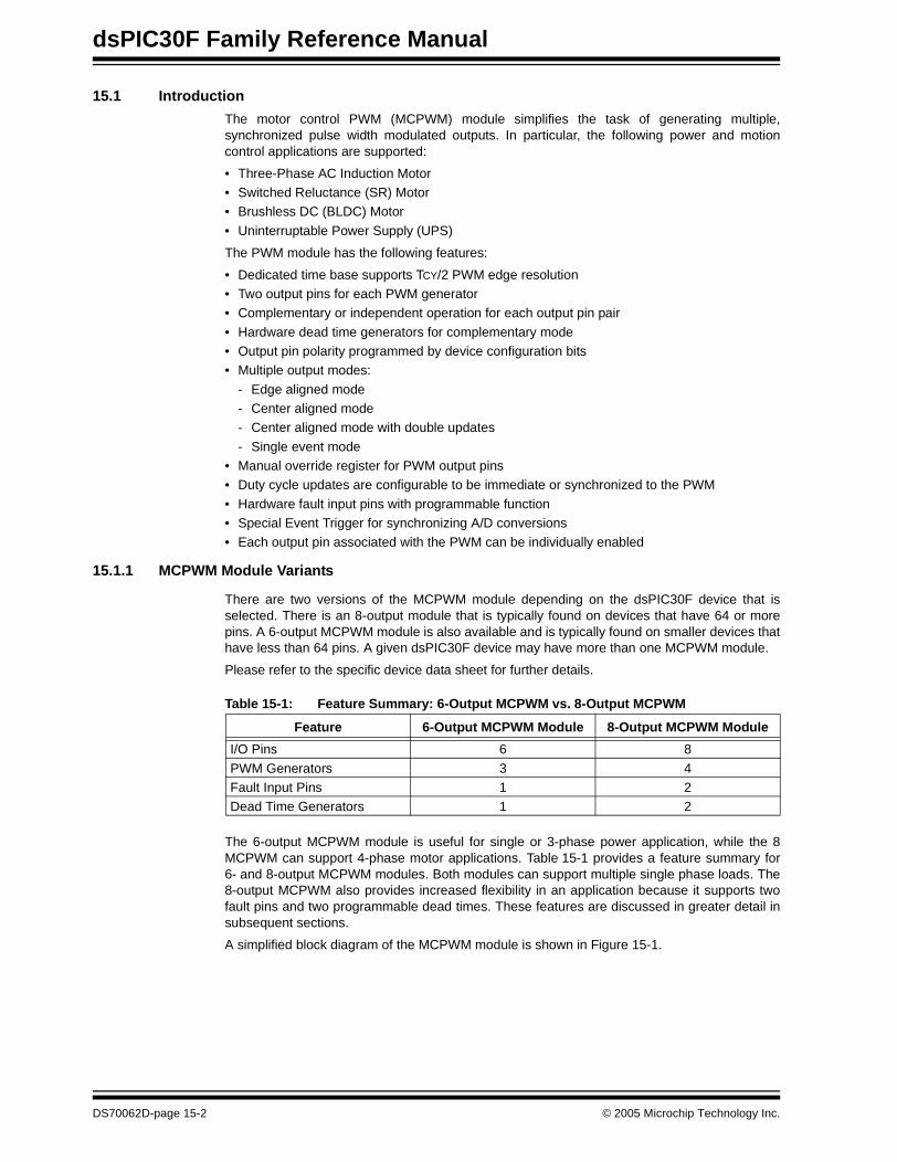
dsPIC30F Family Reference Manual
15.1 Introduction
The motor control PWM (MCPWM) module simplifies the task of generating multiple,synchronized pulse width modulated outputs. In particular, the following power and motioncontrol applications are supported:
• Three-Phase AC Induction Motor• Switched Reluctance (SR) Motor• Brushless DC (BLDC) Motor
• Uninterruptable Power Supply (UPS)
The PWM module has the following features:
• Dedicated time base supports TCY/2 PWM edge resolution• Two output pins for each PWM generator• Complementary or independent operation for each output pin pair
• Hardware dead time generators for complementary mode• Output pin polarity programmed by device configuration bits• Multiple output modes:
- Edge aligned mode- Center aligned mode- Center aligned mode with double updates
- Single event mode• Manual override register for PWM output pins• Duty cycle updates are configurable to be immediate or synchronized to the PWM
• Hardware fault input pins with programmable function• Special Event Trigger for synchronizing A/D conversions• Each output pin associated with the PWM can be individually enabled
15.1.1 MCPWM Module Variants
There are two versions of the MCPWM module depending on the dsPIC30F device that isselected. There is an 8-output module that is typically found on devices that have 64 or morepins. A 6-output MCPWM module is also available and is typically found on smaller devices thathave less than 64 pins. A given dsPIC30F device may have more than one MCPWM module.
Please refer to the specific device data sheet for further details.
Table 15-1: Feature Summary: 6-Output MCPWM vs. 8-Output MCPWM
The 6-output MCPWM module is useful for single or 3-phase power application, while the 8MCPWM can support 4-phase motor applications. Table 15-1 provides a feature summary for6- and 8-output MCPWM modules. Both modules can support multiple single phase loads. The8-output MCPWM also provides increased flexibility in an application because it supports twofault pins and two programmable dead times. These features are discussed in greater detail insubsequent sections.
A simplified block diagram of the MCPWM module is shown in Figure 15-1.
Feature 6-Output MCPWM Module 8-Output MCPWM Module
I/O Pins 6 8
PWM Generators 3 4Fault Input Pins 1 2Dead Time Generators 1 2
DS70062D-page 15-2 © 2005 Microchip Technology Inc.
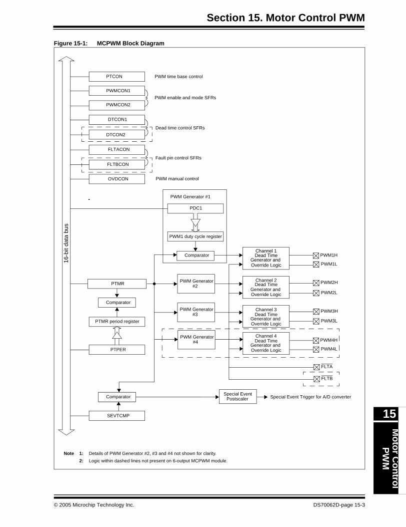
Section 15. Motor Control PWMM
otor C
ontrol
PW
M
15
Figure 15-1: MCPWM Block Diagram
PWM1 duty cycle register
PDC1
PWMCON1
PTPER
PWMCON2
PTMR period register
PTMR
Comparator
Comparator
Channel 1
Generator and
SEVTCMP
Comparator Special Event Trigger for A/D converter
FLTBCON
OVDCON
PWM enable and mode SFRs
PWM manual control
PWM Generator#2
PWM Generator#3
PWM Generator #1
DTCON1
Dead time control SFRs
Special EventPostscaler
FLTA
PWM4L
PWM4H
PWM3L
PWM3H
PWM2L
PWM2H
PWM Generator#4
FLTB
Note 1: Details of PWM Generator #2, #3 and #4 not shown for clarity.
2: Logic within dashed lines not present on 6-output MCPWM module.
16-b
it da
ta b
us
PWM1L
PWM1H
DTCON2
FLTACON
Fault pin control SFRs
Dead Time
Override Logic
Channel 2
Generator and Dead Time
Override Logic
Channel 3
Generator and Dead Time
Override Logic
Channel 4
Generator and Dead Time
Override Logic
PTCON PWM time base control
© 2005 Microchip Technology Inc. DS70062D-page 15-3
dsPIC30F Family Reference Manual
15.2 Control Registers
The following registers control the operation of the MCPWM module:
• PTCON: PWM Time Base Control register
• PTMR: PWM Time Base register• PTPER: PWM Time Base Period register• SEVTCMP: PWM Special Event Compare register
• PWMCON1: PWM Control register #1• PWMCON2: PWM Control register #2• DTCON1: Dead Time Control register #1
• DTCON2: Dead Time Control register #2• FLTACON: Fault A Control register• FLTBCON: Fault B Control register
• PDC1: PWM Duty Cycle register #1• PDC2: PWM Duty Cycle register #2• PDC3: PWM Duty Cycle register #3
• PDC4: PWM Duty Cycle register #4
In addition, there are three device configuration bits associated with the MCPWM module to setup the initial Reset states and polarity of the I/O pins. These configuration bits are located in theFBORPOR device configuration register. Please refer to Section 24. “Device Configuration”for further details.
DS70062D-page 15-4 © 2005 Microchip Technology Inc.
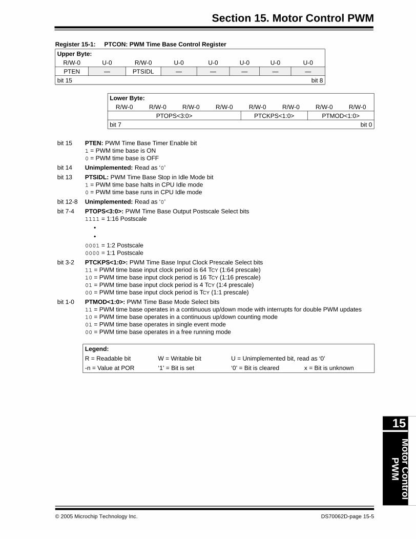
Section 15. Motor Control PWMM
otor C
ontrol
PW
M
15
Register 15-1: PTCON: PWM Time Base Control Register
Upper Byte:R/W-0 U-0 R/W-0 U-0 U-0 U-0 U-0 U-0PTEN — PTSIDL — — — — —
bit 15 bit 8
Lower Byte:R/W-0 R/W-0 R/W-0 R/W-0 R/W-0 R/W-0 R/W-0 R/W-0
PTOPS<3:0> PTCKPS<1:0> PTMOD<1:0>bit 7 bit 0
bit 15 PTEN: PWM Time Base Timer Enable bit1 = PWM time base is ON0 = PWM time base is OFF
bit 14 Unimplemented: Read as ‘0’
bit 13 PTSIDL: PWM Time Base Stop in Idle Mode bit1 = PWM time base halts in CPU Idle mode0 = PWM time base runs in CPU Idle mode
bit 12-8 Unimplemented: Read as ‘0’
bit 7-4 PTOPS<3:0>: PWM Time Base Output Postscale Select bits1111 = 1:16 Postscale
••
0001 = 1:2 Postscale0000 = 1:1 Postscale
bit 3-2 PTCKPS<1:0>: PWM Time Base Input Clock Prescale Select bits11 = PWM time base input clock period is 64 TCY (1:64 prescale)10 = PWM time base input clock period is 16 TCY (1:16 prescale)01 = PWM time base input clock period is 4 TCY (1:4 prescale)00 = PWM time base input clock period is TCY (1:1 prescale)
bit 1-0 PTMOD<1:0>: PWM Time Base Mode Select bits11 = PWM time base operates in a continuous up/down mode with interrupts for double PWM updates10 = PWM time base operates in a continuous up/down counting mode01 = PWM time base operates in single event mode00 = PWM time base operates in a free running mode
Legend:
R = Readable bit W = Writable bit U = Unimplemented bit, read as ‘0’
-n = Value at POR ‘1’ = Bit is set ‘0’ = Bit is cleared x = Bit is unknown
© 2005 Microchip Technology Inc. DS70062D-page 15-5
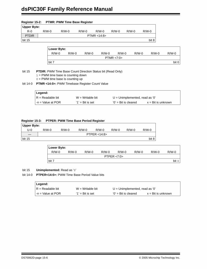
dsPIC30F Family Reference Manual
Register 15-2: PTMR: PWM Time Base Register
Register 15-3: PTPER: PWM Time Base Period Register
Upper Byte:R-0 R/W-0 R/W-0 R/W-0 R/W-0 R/W-0 R/W-0 R/W-0
PTDIR PTMR <14:8>
bit 15 bit 8
Lower Byte:R/W-0 R/W-0 R/W-0 R/W-0 R/W-0 R/W-0 R/W-0 R/W-0
PTMR <7:0>bit 7 bit 0
bit 15 PTDIR: PWM Time Base Count Direction Status bit (Read Only)1 = PWM time base is counting down0 = PWM time base is counting up
bit 14-0 PTMR <14:0>: PWM Timebase Register Count Value
Legend:
R = Readable bit W = Writable bit U = Unimplemented, read as ‘0’
-n = Value at POR ‘1’ = Bit is set ‘0’ = Bit is cleared x = Bit is unknown
Upper Byte:U-0 R/W-0 R/W-0 R/W-0 R/W-0 R/W-0 R/W-0 R/W-0— PTPER <14:8>
bit 15 bit 8
Lower Byte:R/W-0 R/W-0 R/W-0 R/W-0 R/W-0 R/W-0 R/W-0 R/W-0
PTPER <7:0>bit 7 bit 0
bit 15 Unimplemented: Read as ‘0’
bit 14-0 PTPER<14:0>: PWM Time Base Period Value bits
Legend:
R = Readable bit W = Writable bit U = Unimplemented, read as ‘0’
-n = Value at POR ‘1’ = Bit is set ‘0’ = Bit is cleared x = Bit is unknown
DS70062D-page 15-6 © 2005 Microchip Technology Inc.
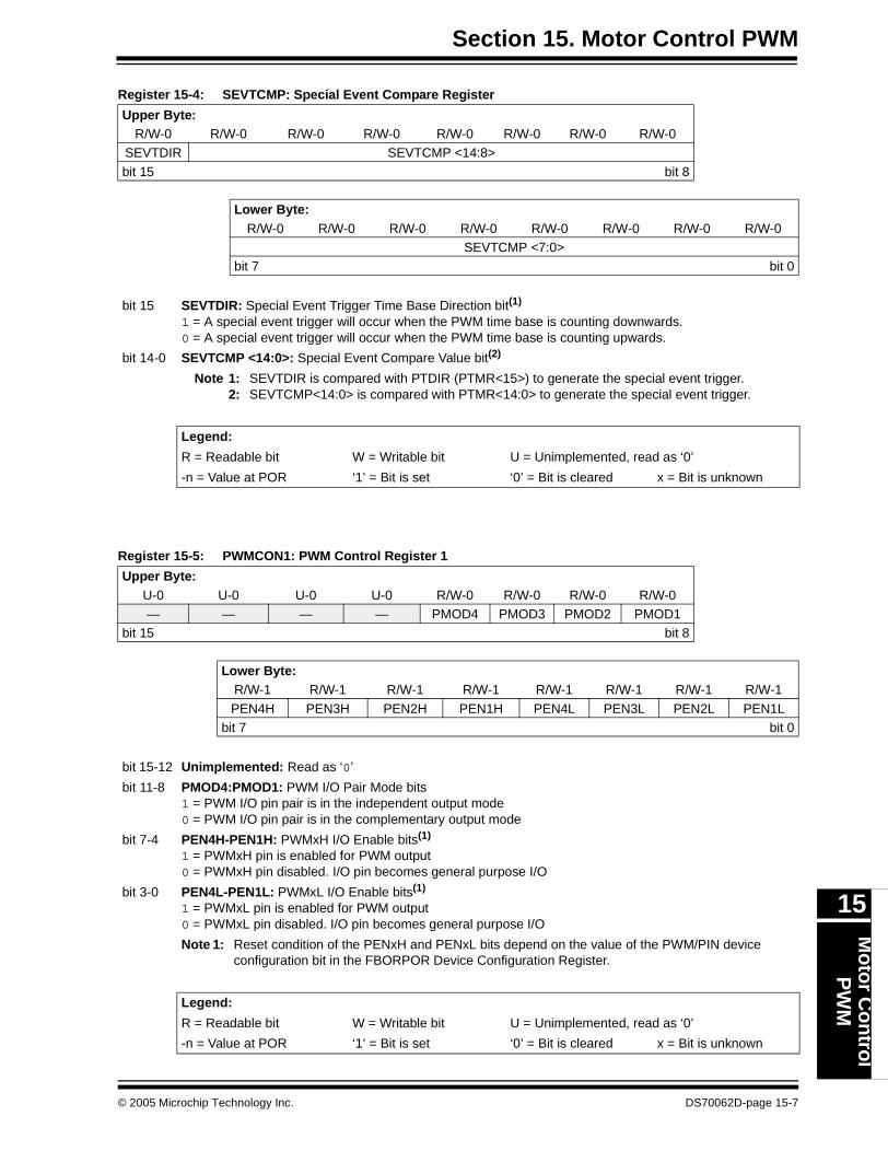
Section 15. Motor Control PWMM
otor C
ontrol
PW
M
15
Register 15-4: SEVTCMP: Special Event Compare Register
Register 15-5: PWMCON1: PWM Control Register 1
Upper Byte:R/W-0 R/W-0 R/W-0 R/W-0 R/W-0 R/W-0 R/W-0 R/W-0
SEVTDIR SEVTCMP <14:8>
bit 15 bit 8
Lower Byte:R/W-0 R/W-0 R/W-0 R/W-0 R/W-0 R/W-0 R/W-0 R/W-0
SEVTCMP <7:0>bit 7 bit 0
bit 15 SEVTDIR: Special Event Trigger Time Base Direction bit(1)
1 = A special event trigger will occur when the PWM time base is counting downwards.0 = A special event trigger will occur when the PWM time base is counting upwards.
bit 14-0 SEVTCMP <14:0>: Special Event Compare Value bit(2)
Note 1: SEVTDIR is compared with PTDIR (PTMR<15>) to generate the special event trigger.2: SEVTCMP<14:0> is compared with PTMR<14:0> to generate the special event trigger.
Legend:
R = Readable bit W = Writable bit U = Unimplemented, read as ‘0’
-n = Value at POR ‘1’ = Bit is set ‘0’ = Bit is cleared x = Bit is unknown
Upper Byte:U-0 U-0 U-0 U-0 R/W-0 R/W-0 R/W-0 R/W-0— — — — PMOD4 PMOD3 PMOD2 PMOD1
bit 15 bit 8
Lower Byte:R/W-1 R/W-1 R/W-1 R/W-1 R/W-1 R/W-1 R/W-1 R/W-1
PEN4H PEN3H PEN2H PEN1H PEN4L PEN3L PEN2L PEN1Lbit 7 bit 0
bit 15-12 Unimplemented: Read as ‘0’
bit 11-8 PMOD4:PMOD1: PWM I/O Pair Mode bits1 = PWM I/O pin pair is in the independent output mode0 = PWM I/O pin pair is in the complementary output mode
bit 7-4 PEN4H-PEN1H: PWMxH I/O Enable bits(1)
1 = PWMxH pin is enabled for PWM output0 = PWMxH pin disabled. I/O pin becomes general purpose I/O
bit 3-0 PEN4L-PEN1L: PWMxL I/O Enable bits(1)
1 = PWMxL pin is enabled for PWM output0 = PWMxL pin disabled. I/O pin becomes general purpose I/O
Note 1: Reset condition of the PENxH and PENxL bits depend on the value of the PWM/PIN deviceconfiguration bit in the FBORPOR Device Configuration Register.
Legend:
R = Readable bit W = Writable bit U = Unimplemented, read as ‘0’
-n = Value at POR ‘1’ = Bit is set ‘0’ = Bit is cleared x = Bit is unknown
© 2005 Microchip Technology Inc. DS70062D-page 15-7
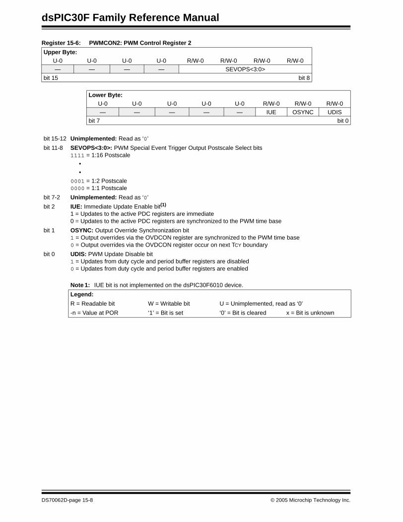
dsPIC30F Family Reference Manual
Register 15-6: PWMCON2: PWM Control Register 2
Upper Byte:U-0 U-0 U-0 U-0 R/W-0 R/W-0 R/W-0 R/W-0— — — — SEVOPS<3:0>
bit 15 bit 8
Lower Byte:U-0 U-0 U-0 U-0 U-0 R/W-0 R/W-0 R/W-0— — — — — IUE OSYNC UDIS
bit 7 bit 0
bit 15-12 Unimplemented: Read as ‘0’
bit 11-8 SEVOPS<3:0>: PWM Special Event Trigger Output Postscale Select bits1111 = 1:16 Postscale
••
0001 = 1:2 Postscale0000 = 1:1 Postscale
bit 7-2 Unimplemented: Read as ‘0’
bit 2 IUE: Immediate Update Enable bit(1)
1 = Updates to the active PDC registers are immediate0 = Updates to the active PDC registers are synchronized to the PWM time base
bit 1 OSYNC: Output Override Synchronization bit1 = Output overrides via the OVDCON register are synchronized to the PWM time base0 = Output overrides via the OVDCON register occur on next TCY boundary
bit 0 UDIS: PWM Update Disable bit1 = Updates from duty cycle and period buffer registers are disabled0 = Updates from duty cycle and period buffer registers are enabled
Note 1: IUE bit is not implemented on the dsPIC30F6010 device.
Legend:
R = Readable bit W = Writable bit U = Unimplemented, read as ‘0’
-n = Value at POR ‘1’ = Bit is set ‘0’ = Bit is cleared x = Bit is unknown
DS70062D-page 15-8 © 2005 Microchip Technology Inc.
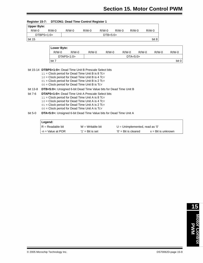
Section 15. Motor Control PWMM
otor C
ontrol
PW
M
15
Register 15-7: DTCON1: Dead Time Control Register 1
Upper Byte:R/W-0 R/W-0 R/W-0 R/W-0 R/W-0 R/W-0 R/W-0 R/W-0
DTBPS<1:0> DTB<5:0>
bit 15 bit 8
Lower Byte:R/W-0 R/W-0 R/W-0 R/W-0 R/W-0 R/W-0 R/W-0 R/W-0
DTAPS<1:0> DTA<5:0>bit 7 bit 0
bit 15-14 DTBPS<1:0>: Dead Time Unit B Prescale Select bits11 = Clock period for Dead Time Unit B is 8 TCY
10 = Clock period for Dead Time Unit B is 4 TCY
01 = Clock period for Dead Time Unit B is 2 TCY
00 = Clock period for Dead Time Unit B is TCY
bit 13-8 DTB<5:0>: Unsigned 6-bit Dead Time Value bits for Dead Time Unit B
bit 7-6 DTAPS<1:0>: Dead Time Unit A Prescale Select bits11 = Clock period for Dead Time Unit A is 8 TCY
10 = Clock period for Dead Time Unit A is 4 TCY
01 = Clock period for Dead Time Unit A is 2 TCY
00 = Clock period for Dead Time Unit A is TCY
bit 5-0 DTA<5:0>: Unsigned 6-bit Dead Time Value bits for Dead Time Unit A
Legend:
R = Readable bit W = Writable bit U = Unimplemented, read as ‘0’
-n = Value at POR ‘1’ = Bit is set ‘0’ = Bit is cleared x = Bit is unknown
© 2005 Microchip Technology Inc. DS70062D-page 15-9
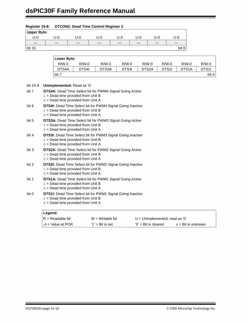
dsPIC30F Family Reference Manual
Register 15-8: DTCON2: Dead Time Control Register 2
Upper Byte:U-0 U-0 U-0 U-0 U-0 U-0 U-0 U-0— — — — — — — —
bit 15 bit 8
Lower Byte:R/W-0 R/W-0 R/W-0 R/W-0 R/W-0 R/W-0 R/W-0 R/W-0DTS4A DTS4I DTS3A DTS3I DTS2A DTS2I DTS1A DTS1I
bit 7 bit 0
bit 15-8 Unimplemented: Read as ‘0’
bit 7 DTS4A: Dead Time Select bit for PWM4 Signal Going Active1 = Dead time provided from Unit B0 = Dead time provided from Unit A
bit 6 DTS4I: Dead Time Select bit for PWM4 Signal Going Inactive1 = Dead time provided from Unit B0 = Dead time provided from Unit A
bit 5 DTS3A: Dead Time Select bit for PWM3 Signal Going Active1 = Dead time provided from Unit B0 = Dead time provided from Unit A
bit 4 DTS3I: Dead Time Select bit for PWM3 Signal Going Inactive1 = Dead time provided from Unit B0 = Dead time provided from Unit A
bit 3 DTS2A: Dead Time Select bit for PWM2 Signal Going Active1 = Dead time provided from Unit B0 = Dead time provided from Unit A
bit 2 DTS2I: Dead Time Select bit for PWM2 Signal Going Inactive1 = Dead time provided from Unit B0 = Dead time provided from Unit A
bit 1 DTS1A: Dead Time Select bit for PWM1 Signal Going Active1 = Dead time provided from Unit B0 = Dead time provided from Unit A
bit 0 DTS1I: Dead Time Select bit for PWM1 Signal Going Inactive1 = Dead time provided from Unit B0 = Dead time provided from Unit A
Legend:
R = Readable bit W = Writable bit U = Unimplemented, read as ‘0’
-n = Value at POR ‘1’ = Bit is set ‘0’ = Bit is cleared x = Bit is unknown
DS70062D-page 15-10 © 2005 Microchip Technology Inc.
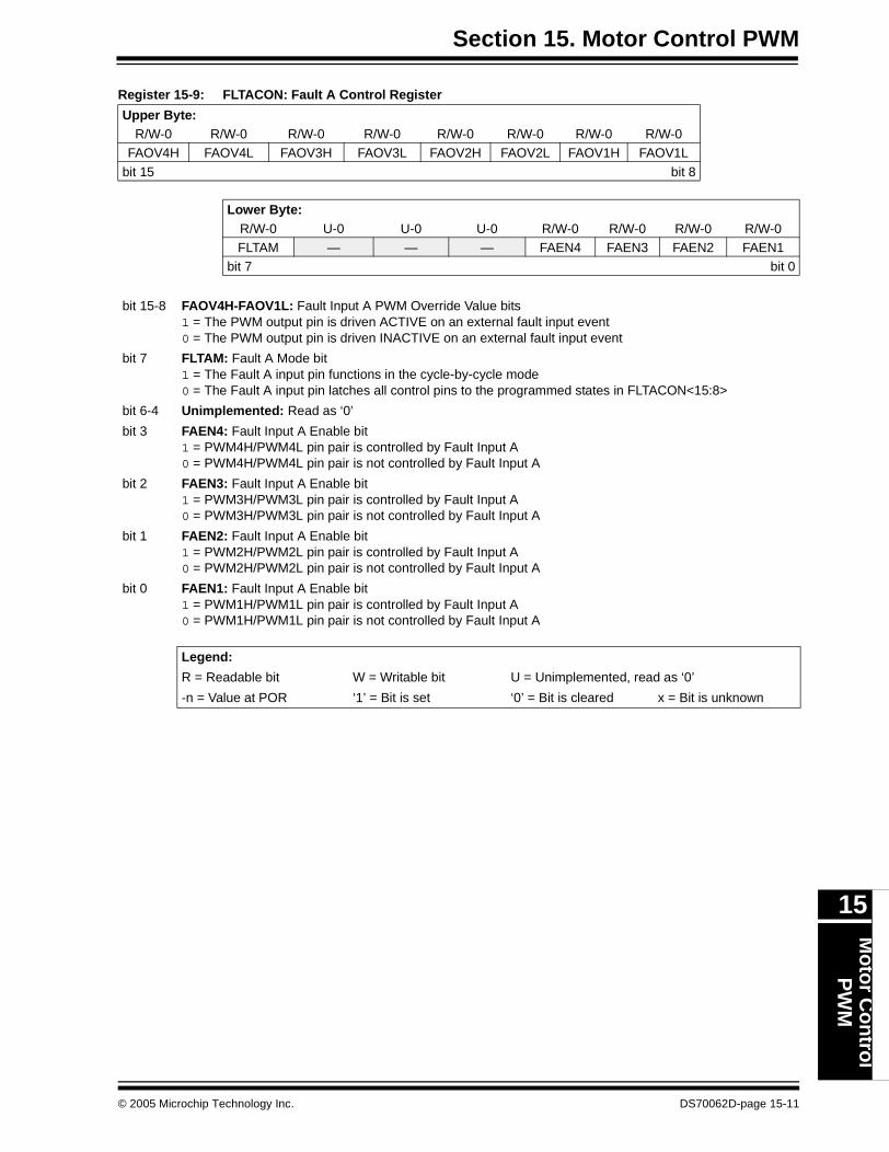
Section 15. Motor Control PWMM
otor C
ontrol
PW
M
15
Register 15-9: FLTACON: Fault A Control Register
Upper Byte:R/W-0 R/W-0 R/W-0 R/W-0 R/W-0 R/W-0 R/W-0 R/W-0
FAOV4H FAOV4L FAOV3H FAOV3L FAOV2H FAOV2L FAOV1H FAOV1L
bit 15 bit 8
Lower Byte:R/W-0 U-0 U-0 U-0 R/W-0 R/W-0 R/W-0 R/W-0FLTAM — — — FAEN4 FAEN3 FAEN2 FAEN1
bit 7 bit 0
bit 15-8 FAOV4H-FAOV1L: Fault Input A PWM Override Value bits1 = The PWM output pin is driven ACTIVE on an external fault input event0 = The PWM output pin is driven INACTIVE on an external fault input event
bit 7 FLTAM: Fault A Mode bit1 = The Fault A input pin functions in the cycle-by-cycle mode0 = The Fault A input pin latches all control pins to the programmed states in FLTACON<15:8>
bit 6-4 Unimplemented: Read as ‘0’
bit 3 FAEN4: Fault Input A Enable bit1 = PWM4H/PWM4L pin pair is controlled by Fault Input A0 = PWM4H/PWM4L pin pair is not controlled by Fault Input A
bit 2 FAEN3: Fault Input A Enable bit1 = PWM3H/PWM3L pin pair is controlled by Fault Input A0 = PWM3H/PWM3L pin pair is not controlled by Fault Input A
bit 1 FAEN2: Fault Input A Enable bit1 = PWM2H/PWM2L pin pair is controlled by Fault Input A0 = PWM2H/PWM2L pin pair is not controlled by Fault Input A
bit 0 FAEN1: Fault Input A Enable bit1 = PWM1H/PWM1L pin pair is controlled by Fault Input A0 = PWM1H/PWM1L pin pair is not controlled by Fault Input A
Legend:
R = Readable bit W = Writable bit U = Unimplemented, read as ‘0’
-n = Value at POR ‘1’ = Bit is set ‘0’ = Bit is cleared x = Bit is unknown
© 2005 Microchip Technology Inc. DS70062D-page 15-11
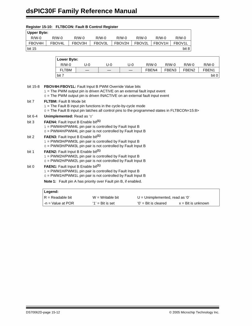
dsPIC30F Family Reference Manual
Register 15-10: FLTBCON: Fault B Control Register
Upper Byte:R/W-0 R/W-0 R/W-0 R/W-0 R/W-0 R/W-0 R/W-0 R/W-0
FBOV4H FBOV4L FBOV3H FBOV3L FBOV2H FBOV2L FBOV1H FBOV1L
bit 15 bit 8
Lower Byte:R/W-0 U-0 U-0 U-0 R/W-0 R/W-0 R/W-0 R/W-0FLTBM — — — FBEN4 FBEN3 FBEN2 FBEN1
bit 7 bit 0
bit 15-8 FBOV4H:FBOV1L: Fault Input B PWM Override Value bits1 = The PWM output pin is driven ACTIVE on an external fault input event0 = The PWM output pin is driven INACTIVE on an external fault input event
bit 7 FLTBM: Fault B Mode bit1 = The Fault B input pin functions in the cycle-by-cycle mode0 = The Fault B input pin latches all control pins to the programmed states in FLTBCON<15:8>
bit 6-4 Unimplemented: Read as ‘0’
bit 3 FAEN4: Fault Input B Enable bit(1)
1 = PWM4H/PWM4L pin pair is controlled by Fault Input B0 = PWM4H/PWM4L pin pair is not controlled by Fault Input B
bit 2 FAEN3: Fault Input B Enable bit(1)
1 = PWM3H/PWM3L pin pair is controlled by Fault Input B0 = PWM3H/PWM3L pin pair is not controlled by Fault Input B
bit 1 FAEN2: Fault Input B Enable bit(1)
1 = PWM2H/PWM2L pin pair is controlled by Fault Input B0 = PWM2H/PWM2L pin pair is not controlled by Fault Input B
bit 0 FAEN1: Fault Input B Enable bit(1)
1 = PWM1H/PWM1L pin pair is controlled by Fault Input B0 = PWM1H/PWM1L pin pair is not controlled by Fault Input B
Note 1: Fault pin A has priority over Fault pin B, if enabled.
Legend:
R = Readable bit W = Writable bit U = Unimplemented, read as ‘0’
-n = Value at POR ‘1’ = Bit is set ‘0’ = Bit is cleared x = Bit is unknown
DS70062D-page 15-12 © 2005 Microchip Technology Inc.
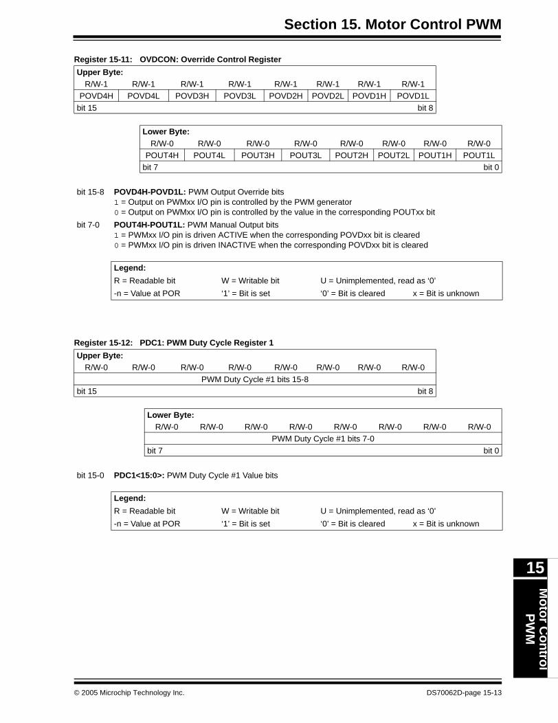
Section 15. Motor Control PWMM
otor C
ontrol
PW
M
15
Register 15-11: OVDCON: Override Control Register
Register 15-12: PDC1: PWM Duty Cycle Register 1
Upper Byte:R/W-1 R/W-1 R/W-1 R/W-1 R/W-1 R/W-1 R/W-1 R/W-1
POVD4H POVD4L POVD3H POVD3L POVD2H POVD2L POVD1H POVD1L
bit 15 bit 8
Lower Byte:R/W-0 R/W-0 R/W-0 R/W-0 R/W-0 R/W-0 R/W-0 R/W-0
POUT4H POUT4L POUT3H POUT3L POUT2H POUT2L POUT1H POUT1Lbit 7 bit 0
bit 15-8 POVD4H-POVD1L: PWM Output Override bits1 = Output on PWMxx I/O pin is controlled by the PWM generator0 = Output on PWMxx I/O pin is controlled by the value in the corresponding POUTxx bit
bit 7-0 POUT4H-POUT1L: PWM Manual Output bits1 = PWMxx I/O pin is driven ACTIVE when the corresponding POVDxx bit is cleared0 = PWMxx I/O pin is driven INACTIVE when the corresponding POVDxx bit is cleared
Legend:
R = Readable bit W = Writable bit U = Unimplemented, read as ‘0’
-n = Value at POR ‘1’ = Bit is set ‘0’ = Bit is cleared x = Bit is unknown
Upper Byte:R/W-0 R/W-0 R/W-0 R/W-0 R/W-0 R/W-0 R/W-0 R/W-0
PWM Duty Cycle #1 bits 15-8bit 15 bit 8
Lower Byte:R/W-0 R/W-0 R/W-0 R/W-0 R/W-0 R/W-0 R/W-0 R/W-0
PWM Duty Cycle #1 bits 7-0
bit 7 bit 0
bit 15-0 PDC1<15:0>: PWM Duty Cycle #1 Value bits
Legend:
R = Readable bit W = Writable bit U = Unimplemented, read as ‘0’
-n = Value at POR ‘1’ = Bit is set ‘0’ = Bit is cleared x = Bit is unknown
© 2005 Microchip Technology Inc. DS70062D-page 15-13
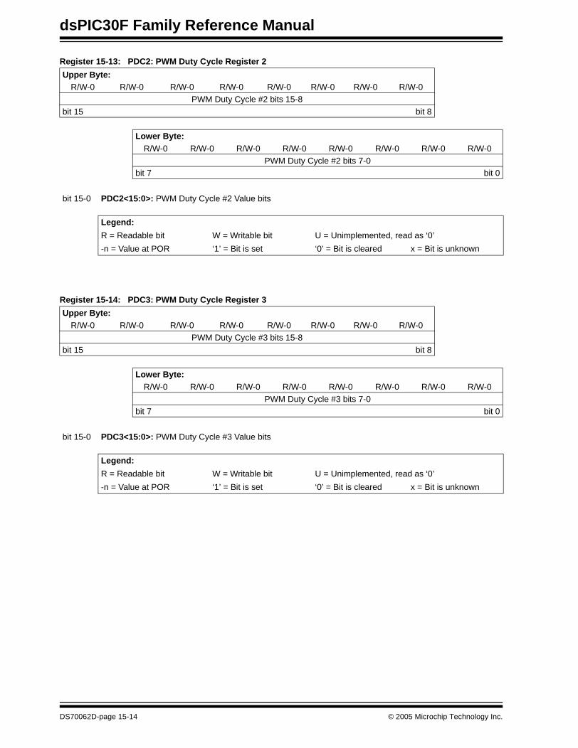
dsPIC30F Family Reference Manual
Register 15-13: PDC2: PWM Duty Cycle Register 2
Register 15-14: PDC3: PWM Duty Cycle Register 3
Upper Byte:R/W-0 R/W-0 R/W-0 R/W-0 R/W-0 R/W-0 R/W-0 R/W-0
PWM Duty Cycle #2 bits 15-8
bit 15 bit 8
Lower Byte:R/W-0 R/W-0 R/W-0 R/W-0 R/W-0 R/W-0 R/W-0 R/W-0
PWM Duty Cycle #2 bits 7-0bit 7 bit 0
bit 15-0 PDC2<15:0>: PWM Duty Cycle #2 Value bits
Legend:
R = Readable bit W = Writable bit U = Unimplemented, read as ‘0’
-n = Value at POR ‘1’ = Bit is set ‘0’ = Bit is cleared x = Bit is unknown
Upper Byte:R/W-0 R/W-0 R/W-0 R/W-0 R/W-0 R/W-0 R/W-0 R/W-0
PWM Duty Cycle #3 bits 15-8
bit 15 bit 8
Lower Byte:R/W-0 R/W-0 R/W-0 R/W-0 R/W-0 R/W-0 R/W-0 R/W-0
PWM Duty Cycle #3 bits 7-0bit 7 bit 0
bit 15-0 PDC3<15:0>: PWM Duty Cycle #3 Value bits
Legend:
R = Readable bit W = Writable bit U = Unimplemented, read as ‘0’
-n = Value at POR ‘1’ = Bit is set ‘0’ = Bit is cleared x = Bit is unknown
DS70062D-page 15-14 © 2005 Microchip Technology Inc.
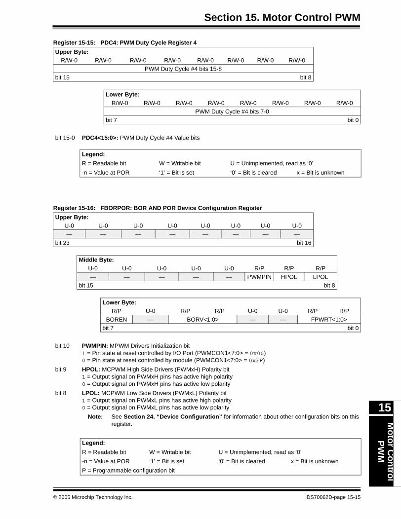
Section 15. Motor Control PWMM
otor C
ontrol
PW
M
15
Register 15-15: PDC4: PWM Duty Cycle Register 4
Register 15-16: FBORPOR: BOR AND POR Device Configuration Register
Upper Byte:R/W-0 R/W-0 R/W-0 R/W-0 R/W-0 R/W-0 R/W-0 R/W-0
PWM Duty Cycle #4 bits 15-8
bit 15 bit 8
Lower Byte:R/W-0 R/W-0 R/W-0 R/W-0 R/W-0 R/W-0 R/W-0 R/W-0
PWM Duty Cycle #4 bits 7-0bit 7 bit 0
bit 15-0 PDC4<15:0>: PWM Duty Cycle #4 Value bits
Legend:
R = Readable bit W = Writable bit U = Unimplemented, read as ‘0’
-n = Value at POR ‘1’ = Bit is set ‘0’ = Bit is cleared x = Bit is unknown
Upper Byte:U-0 U-0 U-0 U-0 U-0 U-0 U-0 U-0— — — — — — — —
bit 23 bit 16
Middle Byte:U-0 U-0 U-0 U-0 U-0 R/P R/P R/P— — — — — PWMPIN HPOL LPOL
bit 15 bit 8
Lower Byte:R/P U-0 R/P R/P U-0 U-0 R/P R/P
BOREN — BORV<1:0> — — FPWRT<1:0>bit 7 bit 0
bit 10 PWMPIN: MPWM Drivers Initialization bit1 = Pin state at reset controlled by I/O Port (PWMCON1<7:0> = 0x00)0 = Pin state at reset controlled by module (PWMCON1<7:0> = 0xFF)
bit 9 HPOL: MCPWM High Side Drivers (PWMxH) Polarity bit1 = Output signal on PWMxH pins has active high polarity0 = Output signal on PWMxH pins has active low polarity
bit 8 LPOL: MCPWM Low Side Drivers (PWMxL) Polarity bit1 = Output signal on PWMxL pins has active high polarity0 = Output signal on PWMxL pins has active low polarity
Note: See Section 24. “Device Configuration” for information about other configuration bits on thisregister.
Legend:
R = Readable bit W = Writable bit U = Unimplemented, read as ‘0’
-n = Value at POR ‘1’ = Bit is set ‘0’ = Bit is cleared x = Bit is unknown
P = Programmable configuration bit
© 2005 Microchip Technology Inc. DS70062D-page 15-15
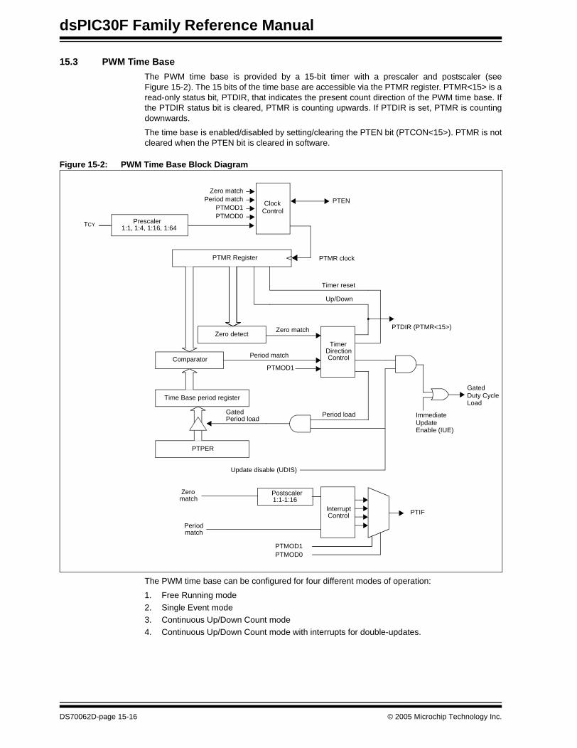
dsPIC30F Family Reference Manual
15.3 PWM Time Base
The PWM time base is provided by a 15-bit timer with a prescaler and postscaler (seeFigure 15-2). The 15 bits of the time base are accessible via the PTMR register. PTMR<15> is aread-only status bit, PTDIR, that indicates the present count direction of the PWM time base. Ifthe PTDIR status bit is cleared, PTMR is counting upwards. If PTDIR is set, PTMR is countingdownwards.
The time base is enabled/disabled by setting/clearing the PTEN bit (PTCON<15>). PTMR is notcleared when the PTEN bit is cleared in software.
Figure 15-2: PWM Time Base Block Diagram
The PWM time base can be configured for four different modes of operation:
1. Free Running mode
2. Single Event mode3. Continuous Up/Down Count mode4. Continuous Up/Down Count mode with interrupts for double-updates.
PTMR Register
Time Base period register
Comparator
PTPER
Zero detectZero match
Period match
PTMOD1
Up/Down
Timer reset
TCY Prescaler1:1, 1:4, 1:16, 1:64
TimerDirectionControl
ClockControl
Period load
Duty Cycle
PTMOD1Period match
Zero match
PTMR clock
InterruptControl
PTMOD1
Periodmatch
Zeromatch
PTMOD0
Postscaler1:1-1:16
PTMOD0
PTEN
PTIF
Update disable (UDIS)
PTDIR (PTMR<15>)
Gated
Gated Period load
Load
Update Immediate
Enable (IUE)
DS70062D-page 15-16 © 2005 Microchip Technology Inc.
Section 15. Motor Control PWMM
otor C
ontrol
PW
M
15
These four modes are selected by the PTMOD<1:0> control bits (PTCON<1:0>).
15.3.1 Free Running Mode
In the Free Running mode, the time base will count upwards until the value in the PTPERregister is matched. The PTMR register is reset on the following input clock edge and the timebase will continue counting upwards as long as the PTEN bit remains set.
15.3.2 Single-Event Mode
In the Single Event Counting mode, the PWM time base will begin counting upwards when thePTEN bit is set. When the PTMR value matches the PTPER register, the PTMR register will bereset on the following input clock edge and the PTEN bit will be cleared by the hardware to haltthe time base.
15.3.3 Up/Down Counting Modes
For the Continuous Up/Down Counting modes, the PWM time base will count upwards until thevalue in the PTPER register is matched. The timer will begin counting downwards on the follow-ing input clock edge and continue counting down until it reaches ‘0’. The PTDIR bit PTMR<15>is read-only and indicates the counting direction. The PTDIR bit is set when the timer countsdownwards.
15.3.4 PWM Time Base Prescaler
The input clock to PTMR, (TCY) has prescaler options of 1:1, 1:4, 1:16 or 1:64 selected bycontrol bits PTCKPS<1:0> (PTCON<3:2>). The prescaler counter is cleared when any of thefollowing occurs:
• A write to the PTMR register
• A write to the PTCON register• Any device reset
The PTMR register is not cleared when PTCON is written.
15.3.5 PWM Time Base Postscaler
The match output of PTMR can optionally be post-scaled through a 4-bit postscaler (whichgives a 1:1 to 1:16 scaling inclusive) to generate an interrupt. The postscaler is useful when thePWM duty cycle does not need to be updated every PWM cycle.
The postscaler counter is cleared when any of the following occurs:
• A write to the PTMR register
• A write to the PTCON register• Any device reset
The PTMR register is not cleared when PTCON is written.
Note: The mode of the PWM time base determines the type of PWM signal that isgenerated by the module. (See Section 15.4.2, Section 15.4.3 and Section 15.4.4for more details.)
© 2005 Microchip Technology Inc. DS70062D-page 15-17
dsPIC30F Family Reference Manual
15.3.6 PWM Time Base Interrupts
The interrupt signals generated by the PWM time base depend on the mode selection bits,PTMOD<1:0> (PTCON<1:0>), and the time base postscaler bits, PTOPS<3:0> (PTCON<7:4>).
• Free Running Mode
When the PWM time base is in the Free Running mode (PTMOD<1:0> = 00), an interrupt isgenerated when the PTMR register is reset to ‘0’, due to a match with the PTPER register. Thepostscaler selection bits may be used in this mode of the timer to reduce the frequency of theinterrupt events.
• Single Event Mode
When the PWM time base is in the Single Event mode (PTMOD<1:0> = 01), an interrupt isgenerated when the PTMR register is reset to ‘0’ due to a match with the PTPER register. ThePTEN bit (PTCON<15>) is also cleared at this time to inhibit further PTMR increments. Thepostscaler selection bits have no effect in this mode of the timer.
• Up/Down Counting Mode
In the Up/Down Counting mode (PTMOD<1:0> = 10), an interrupt event is generated each timethe value of the PTMR register becomes zero and the PWM time base begins to count upwards.The postscaler selection bits may be used in this mode of the timer to reduce the frequency ofthe interrupt events.
• Up/Down Counting Mode with Double Updates
In the Double Update mode (PTMOD<1:0> = 11), an interrupt event is generated each time thePTMR register is equal to zero and each time a period match occurs. The postscaler selectionbits have no effect in this mode of the timer.
The Double Update mode allows the control loop bandwidth to be doubled because the PWMduty cycles can be updated twice per period. Every rising and falling edge of the PWM signalcan be controlled using the double update mode.
15.3.7 PWM Period
The PTPER register sets the counting period for PTMR. The user must write a 15-bit value toPTPER<14:0>. When the value in PTMR<14:0> matches the value in PTPER<14:0>, the timebase will either reset to ‘0’ or reverse the count direction on the next clock input edge. The actiontaken depends on the operating mode of the time base.
The time base period is double buffered to allow on-the-fly period changes of the PWM signalwithout glitches. The PTPER register serves as a buffer register to the actual time base periodregister, which is not accessible by the user. The PTPER register contents are loaded into theactual time base period register at the following times:
• Free Running and Single Event modes: when the PTMR register is reset to zero after a match with the PTPER register.
• Up/Down Counting modes: When the PTMR register is zero.
The value held in the PTPER register is automatically loaded into the time base period registerwhen the PWM time base is disabled (PTEN = 0).
Figure 15-3 and Figure 15-4 indicate the times when the contents of the PTPER register areloaded into the time base period register.
DS70062D-page 15-18 © 2005 Microchip Technology Inc.

Section 15. Motor Control PWMM
otor C
ontrol
PW
M
15
Figure 15-3: PWM Period Buffer Updates in Free Running Count Mode
The PWM period can be determined from the following formula:
Equation 15-1: PWM Period Calculation for Free Running Count Mode (PTMOD = 10 or 11)
Figure 15-4: PWM Period Buffer Updates in Up/Down Counting Modes
Old PTPER value
New PTPER value
Period value loaded from PTPER buffer register
New value written to PTPER buffer
PTMR Value
PTPER = FPWM • (PTMR Prescaler)
FCY- 1
FCY = 20 MHz FPWM = 20,000 Hz
PTMR Prescaler = 1:1
PTPER = 20,000 • 1
20,000,000- 1
= 1000 -1= 999
Example:
Old PTPER value
New PTPER value
New value written to PTPER buffer
PTMR Value
Period value loaded from PTPER Buffer register
© 2005 Microchip Technology Inc. DS70062D-page 15-19
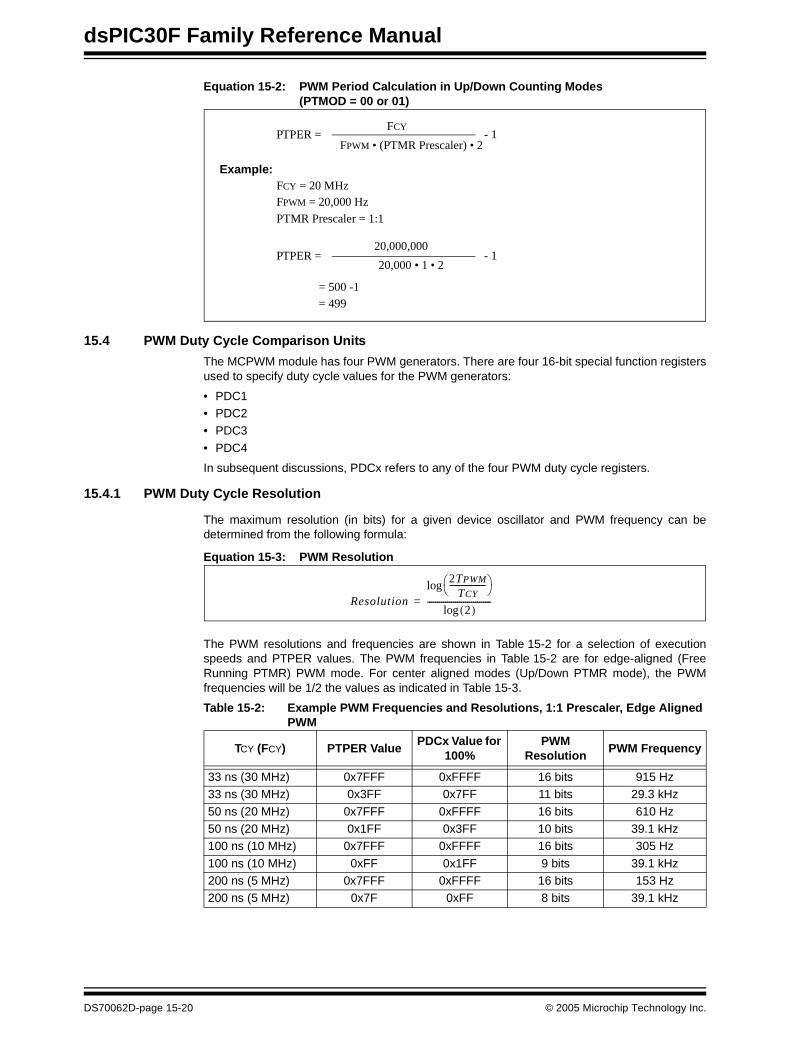
dsPIC30F Family Reference Manual
Equation 15-2: PWM Period Calculation in Up/Down Counting Modes(PTMOD = 00 or 01)
15.4 PWM Duty Cycle Comparison Units
The MCPWM module has four PWM generators. There are four 16-bit special function registersused to specify duty cycle values for the PWM generators:
• PDC1• PDC2• PDC3
• PDC4
In subsequent discussions, PDCx refers to any of the four PWM duty cycle registers.
15.4.1 PWM Duty Cycle Resolution
The maximum resolution (in bits) for a given device oscillator and PWM frequency can bedetermined from the following formula:
Equation 15-3: PWM Resolution
The PWM resolutions and frequencies are shown in Table 15-2 for a selection of executionspeeds and PTPER values. The PWM frequencies in Table 15-2 are for edge-aligned (FreeRunning PTMR) PWM mode. For center aligned modes (Up/Down PTMR mode), the PWMfrequencies will be 1/2 the values as indicated in Table 15-3.
PTPER = FPWM • (PTMR Prescaler) • 2
FCY- 1
FCY = 20 MHz FPWM = 20,000 Hz
PTMR Prescaler = 1:1
PTPER = 20,000 • 1 • 2
20,000,000- 1
= 500 -1= 499
Example:
Table 15-2: Example PWM Frequencies and Resolutions, 1:1 Prescaler, Edge Aligned PWM
TCY (FCY) PTPER ValuePDCx Value for
100%PWM
ResolutionPWM Frequency
33 ns (30 MHz) 0x7FFF 0xFFFF 16 bits 915 Hz33 ns (30 MHz) 0x3FF 0x7FF 11 bits 29.3 kHz
50 ns (20 MHz) 0x7FFF 0xFFFF 16 bits 610 Hz50 ns (20 MHz) 0x1FF 0x3FF 10 bits 39.1 kHz100 ns (10 MHz) 0x7FFF 0xFFFF 16 bits 305 Hz
100 ns (10 MHz) 0xFF 0x1FF 9 bits 39.1 kHz200 ns (5 MHz) 0x7FFF 0xFFFF 16 bits 153 Hz200 ns (5 MHz) 0x7F 0xFF 8 bits 39.1 kHz
Resolution
2TPWM
TCY------------------⎝ ⎠⎛ ⎞log
2( )log--------------------------------=
DS70062D-page 15-20 © 2005 Microchip Technology Inc.
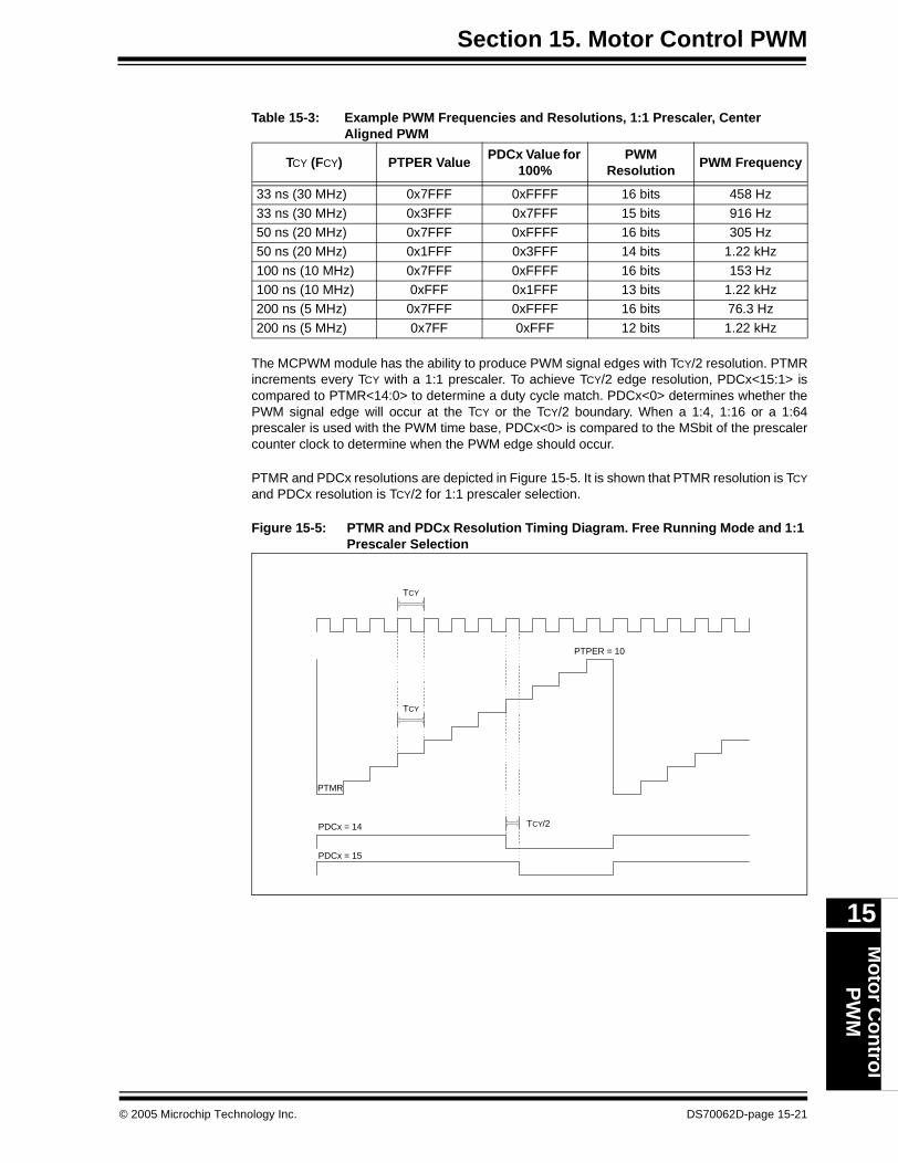
Section 15. Motor Control PWMM
otor C
ontrol
PW
M
15
The MCPWM module has the ability to produce PWM signal edges with TCY/2 resolution. PTMRincrements every TCY with a 1:1 prescaler. To achieve TCY/2 edge resolution, PDCx<15:1> iscompared to PTMR<14:0> to determine a duty cycle match. PDCx<0> determines whether thePWM signal edge will occur at the TCY or the TCY/2 boundary. When a 1:4, 1:16 or a 1:64prescaler is used with the PWM time base, PDCx<0> is compared to the MSbit of the prescalercounter clock to determine when the PWM edge should occur.
PTMR and PDCx resolutions are depicted in Figure 15-5. It is shown that PTMR resolution is TCY
and PDCx resolution is TCY/2 for 1:1 prescaler selection.
Figure 15-5: PTMR and PDCx Resolution Timing Diagram. Free Running Mode and 1:1 Prescaler Selection
Table 15-3: Example PWM Frequencies and Resolutions, 1:1 Prescaler, Center Aligned PWM
TCY (FCY) PTPER ValuePDCx Value for
100%PWM
ResolutionPWM Frequency
33 ns (30 MHz) 0x7FFF 0xFFFF 16 bits 458 Hz
33 ns (30 MHz) 0x3FFF 0x7FFF 15 bits 916 Hz50 ns (20 MHz) 0x7FFF 0xFFFF 16 bits 305 Hz50 ns (20 MHz) 0x1FFF 0x3FFF 14 bits 1.22 kHz
100 ns (10 MHz) 0x7FFF 0xFFFF 16 bits 153 Hz100 ns (10 MHz) 0xFFF 0x1FFF 13 bits 1.22 kHz200 ns (5 MHz) 0x7FFF 0xFFFF 16 bits 76.3 Hz
200 ns (5 MHz) 0x7FF 0xFFF 12 bits 1.22 kHz
PTMR
TCY
TCY
TCY/2PDCx = 14
PDCx = 15
PTPER = 10
© 2005 Microchip Technology Inc. DS70062D-page 15-21
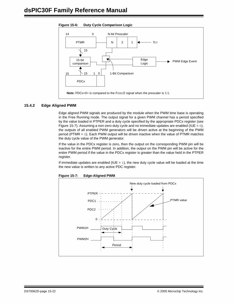
dsPIC30F Family Reference Manual
Figure 15-6: Duty Cycle Comparison Logic
15.4.2 Edge Aligned PWM
Edge aligned PWM signals are produced by the module when the PWM time base is operatingin the Free Running mode. The output signal for a given PWM channel has a period specifiedby the value loaded in PTPER and a duty cycle specified by the appropriate PDCx register (seeFigure 15-7). Assuming a non-zero duty cycle and no immediate updates are enabled (IUE = 0),the outputs of all enabled PWM generators will be driven active at the beginning of the PWMperiod (PTMR = 0). Each PWM output will be driven inactive when the value of PTMR matchesthe duty cycle value of the PWM generator.
If the value in the PDCx register is zero, then the output on the corresponding PWM pin will beinactive for the entire PWM period. In addition, the output on the PWM pin will be active for theentire PWM period if the value in the PDCx register is greater than the value held in the PTPERregister.
If immediate updates are enabled (IUE = 1), the new duty cycle value will be loaded at the timethe new value is written to any active PDC register.
Figure 15-7: Edge-Aligned PWM
PTMR N 2 1 TCY
15-bit comparison
PDCx
EdgeLogic
PWM Edge Event
14 0 N-bit Prescaler
15 15 1 0
15
1-Bit Comparison
Note: PDCx<0> is compared to the FOSC/2 signal when the prescaler is 1:1.
Period
Duty Cycle
0
PTPER
New duty cycle loaded from PDCx
PWM1H
PWM2H
PDC1
PDC2
PTMR value
DS70062D-page 15-22 © 2005 Microchip Technology Inc.
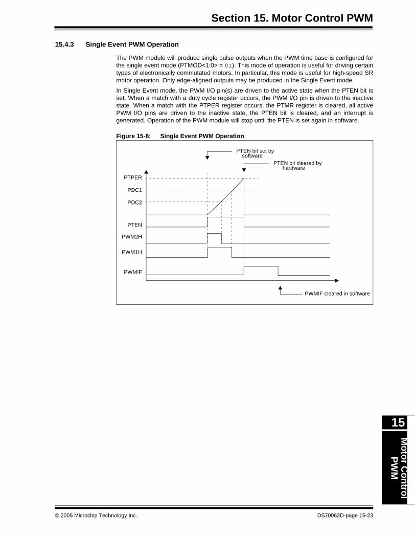
Section 15. Motor Control PWMM
otor C
ontrol
PW
M
15
15.4.3 Single Event PWM Operation
The PWM module will produce single pulse outputs when the PWM time base is configured forthe single event mode (PTMOD<1:0> = 01). This mode of operation is useful for driving certaintypes of electronically commutated motors. In particular, this mode is useful for high-speed SRmotor operation. Only edge-aligned outputs may be produced in the Single Event mode.
In Single Event mode, the PWM I/O pin(s) are driven to the active state when the PTEN bit isset. When a match with a duty cycle register occurs, the PWM I/O pin is driven to the inactivestate. When a match with the PTPER register occurs, the PTMR register is cleared, all activePWM I/O pins are driven to the inactive state, the PTEN bit is cleared, and an interrupt isgenerated. Operation of the PWM module will stop until the PTEN is set again in software.
Figure 15-8: Single Event PWM Operation
PDC1
PTPER
PTEN bit set bysoftware
PTEN bit cleared byhardware
PWMIF
PWMIF cleared in software
PDC2
PWM2H
PWM1H
PTEN
© 2005 Microchip Technology Inc. DS70062D-page 15-23
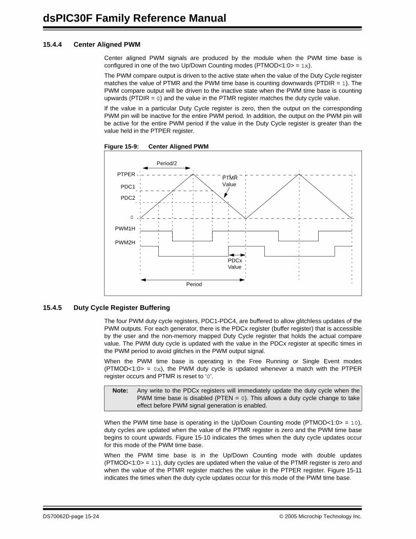
dsPIC30F Family Reference Manual
15.4.4 Center Aligned PWM
Center aligned PWM signals are produced by the module when the PWM time base isconfigured in one of the two Up/Down Counting modes (PTMOD<1:0> = 1x).
The PWM compare output is driven to the active state when the value of the Duty Cycle registermatches the value of PTMR and the PWM time base is counting downwards (PTDIR = 1). ThePWM compare output will be driven to the inactive state when the PWM time base is countingupwards (PTDIR = 0) and the value in the PTMR register matches the duty cycle value.
If the value in a particular Duty Cycle register is zero, then the output on the correspondingPWM pin will be inactive for the entire PWM period. In addition, the output on the PWM pin willbe active for the entire PWM period if the value in the Duty Cycle register is greater than thevalue held in the PTPER register.
Figure 15-9: Center Aligned PWM
15.4.5 Duty Cycle Register Buffering
The four PWM duty cycle registers, PDC1-PDC4, are buffered to allow glitchless updates of thePWM outputs. For each generator, there is the PDCx register (buffer register) that is accessibleby the user and the non-memory mapped Duty Cycle register that holds the actual comparevalue. The PWM duty cycle is updated with the value in the PDCx register at specific times inthe PWM period to avoid glitches in the PWM output signal.
When the PWM time base is operating in the Free Running or Single Event modes(PTMOD<1:0> = 0x), the PWM duty cycle is updated whenever a match with the PTPERregister occurs and PTMR is reset to ‘0’.
When the PWM time base is operating in the Up/Down Counting mode (PTMOD<1:0> = 10),duty cycles are updated when the value of the PTMR register is zero and the PWM time basebegins to count upwards. Figure 15-10 indicates the times when the duty cycle updates occurfor this mode of the PWM time base.
When the PWM time base is in the Up/Down Counting mode with double updates(PTMOD<1:0> = 11), duty cycles are updated when the value of the PTMR register is zero andwhen the value of the PTMR register matches the value in the PTPER register. Figure 15-11indicates the times when the duty cycle updates occur for this mode of the PWM time base.
PTPERPTMRValue
Period
Period/2
0
PDC1
PDC2
PWM1H
PWM2H
PDCxValue
Note: Any write to the PDCx registers will immediately update the duty cycle when thePWM time base is disabled (PTEN = 0). This allows a duty cycle change to takeeffect before PWM signal generation is enabled.
DS70062D-page 15-24 © 2005 Microchip Technology Inc.
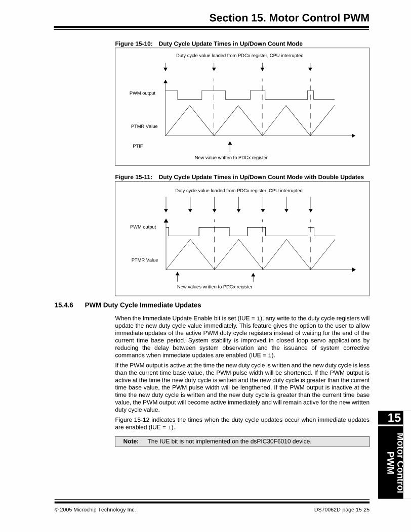
Section 15. Motor Control PWMM
otor C
ontrol
PW
M
15
Figure 15-10: Duty Cycle Update Times in Up/Down Count Mode
Figure 15-11: Duty Cycle Update Times in Up/Down Count Mode with Double Updates
15.4.6 PWM Duty Cycle Immediate Updates
When the Immediate Update Enable bit is set (IUE = 1), any write to the duty cycle registers willupdate the new duty cycle value immediately. This feature gives the option to the user to allowimmediate updates of the active PWM duty cycle registers instead of waiting for the end of thecurrent time base period. System stability is improved in closed loop servo applications byreducing the delay between system observation and the issuance of system correctivecommands when immediate updates are enabled (IUE = 1).
If the PWM output is active at the time the new duty cycle is written and the new duty cycle is lessthan the current time base value, the PWM pulse width will be shortened. If the PWM output isactive at the time the new duty cycle is written and the new duty cycle is greater than the currenttime base value, the PWM pulse width will be lengthened. If the PWM output is inactive at thetime the new duty cycle is written and the new duty cycle is greater than the current time basevalue, the PWM output will become active immediately and will remain active for the new writtenduty cycle value.
Figure 15-12 indicates the times when the duty cycle updates occur when immediate updatesare enabled (IUE = 1)..
PTMR Value
PWM output
Duty cycle value loaded from PDCx register, CPU interrupted
New value written to PDCx register
PTIF
PTMR Value
PWM output
Duty cycle value loaded from PDCx register, CPU interrupted
New values written to PDCx register
Note: The IUE bit is not implemented on the dsPIC30F6010 device.
© 2005 Microchip Technology Inc. DS70062D-page 15-25
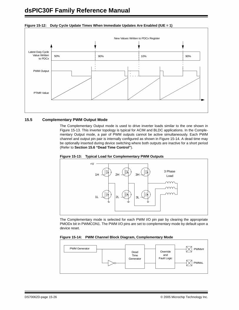
dsPIC30F Family Reference Manual
Figure 15-12: Duty Cycle Update Times When Immediate Updates Are Enabled (IUE = 1)
15.5 Complementary PWM Output Mode
The Complementary Output mode is used to drive inverter loads similar to the one shown inFigure 15-13. This inverter topology is typical for ACIM and BLDC applications. In the Comple-mentary Output mode, a pair of PWM outputs cannot be active simultaneously. Each PWMchannel and output pin pair is internally configured as shown in Figure 15-14. A dead time maybe optionally inserted during device switching where both outputs are inactive for a short period(Refer to Section 15.6 “Dead Time Control”).
Figure 15-13: Typical Load for Complementary PWM Outputs
The Complementary mode is selected for each PWM I/O pin pair by clearing the appropriatePMODx bit in PWMCON1. The PWM I/O pins are set to complementary mode by default upon adevice reset.
Figure 15-14: PWM Channel Block Diagram, Complementary Mode
50% 90% 10% 90%
Latest Duty CycleValue Written
PWM Output
PTMR Value
to PDCx
New Values Written to PDCx Register
+V
1H
1L
3 PhaseLoad2H
2L
3H
3L
DeadTime
Generator
PWM Generator PWMxH
PWMxL
Overrideand
Fault Logic
DS70062D-page 15-26 © 2005 Microchip Technology Inc.
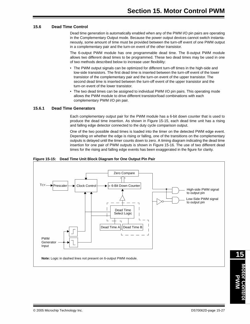
Section 15. Motor Control PWMM
otor C
ontrol
PW
M
15
15.6 Dead Time Control
Dead time generation is automatically enabled when any of the PWM I/O pin pairs are operatingin the Complementary Output mode. Because the power output devices cannot switch instanta-neously, some amount of time must be provided between the turn-off event of one PWM outputin a complementary pair and the turn-on event of the other transistor.
The 6-output PWM module has one programmable dead time. The 8-output PWM moduleallows two different dead times to be programmed. These two dead times may be used in oneof two methods described below to increase user flexibility:
• The PWM output signals can be optimized for different turn-off times in the high-side and low-side transistors. The first dead time is inserted between the turn-off event of the lower transistor of the complementary pair and the turn-on event of the upper transistor. The second dead time is inserted between the turn-off event of the upper transistor and the turn-on event of the lower transistor.
• The two dead times can be assigned to individual PWM I/O pin pairs. This operating mode allows the PWM module to drive different transistor/load combinations with each complementary PWM I/O pin pair.
15.6.1 Dead Time Generators
Each complementary output pair for the PWM module has a 6-bit down counter that is used toproduce the dead time insertion. As shown in Figure 15-15, each dead time unit has a risingand falling edge detector connected to the duty cycle comparison output.
One of the two possible dead times is loaded into the timer on the detected PWM edge event.Depending on whether the edge is rising or falling, one of the transitions on the complementaryoutputs is delayed until the timer counts down to zero. A timing diagram indicating the dead timeinsertion for one pair of PWM outputs is shown in Figure 15-16. The use of two different deadtimes for the rising and falling edge events has been exaggerated in the figure for clarity.
Figure 15-15: Dead Time Unit Block Diagram for One Output Pin Pair
Low-Side PWM signalto output pin
High-side PWM signalto output pin
Zero Compare
Clock Control 6-Bit Down Counter
PWM
TCY
Dead Time A Dead Time B
Dead TimeSelect Logic
Prescaler
GeneratorInput
Note: Logic in dashed lines not present on 6-output PWM module.
© 2005 Microchip Technology Inc. DS70062D-page 15-27
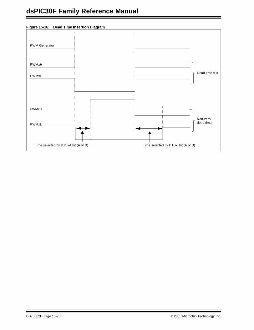
dsPIC30F Family Reference Manual
Figure 15-16: Dead Time Insertion Diagram
PWM Generator
PWMxH
PWMxL
Time selected by DTSxA bit (A or B) Time selected by DTSxI bit (A or B)
PWMxH
PWMxLDead time = 0
Non-zerodead time
DS70062D-page 15-28 © 2005 Microchip Technology Inc.
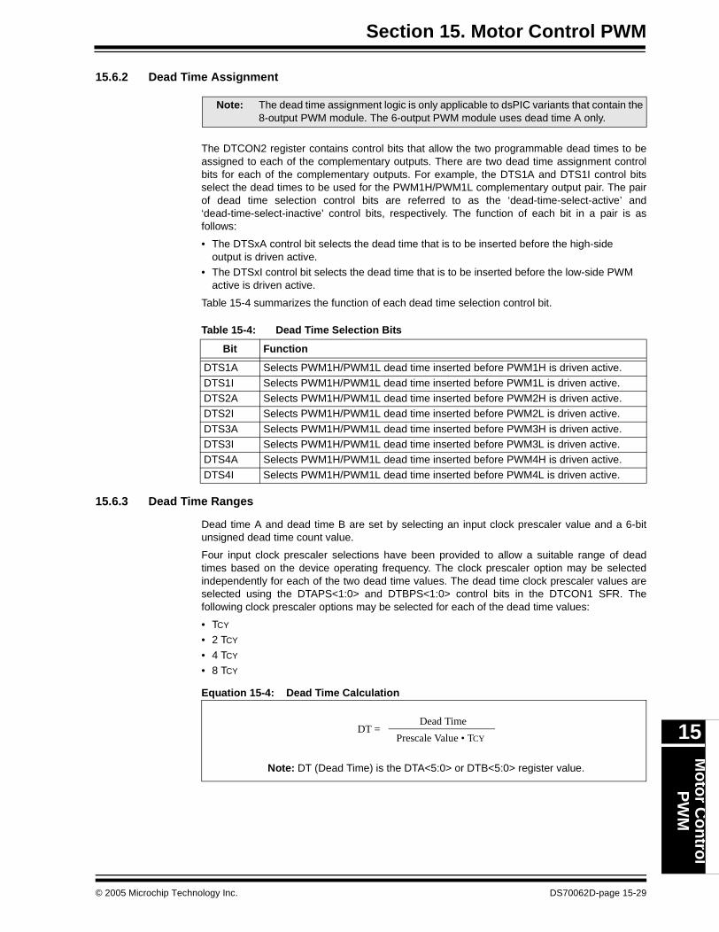
Section 15. Motor Control PWMM
otor C
ontrol
PW
M
15
15.6.2 Dead Time Assignment
The DTCON2 register contains control bits that allow the two programmable dead times to beassigned to each of the complementary outputs. There are two dead time assignment controlbits for each of the complementary outputs. For example, the DTS1A and DTS1I control bitsselect the dead times to be used for the PWM1H/PWM1L complementary output pair. The pairof dead time selection control bits are referred to as the ‘dead-time-select-active’ and‘dead-time-select-inactive’ control bits, respectively. The function of each bit in a pair is asfollows:
• The DTSxA control bit selects the dead time that is to be inserted before the high-side output is driven active.
• The DTSxI control bit selects the dead time that is to be inserted before the low-side PWM active is driven active.
Table 15-4 summarizes the function of each dead time selection control bit.
Table 15-4: Dead Time Selection Bits
15.6.3 Dead Time Ranges
Dead time A and dead time B are set by selecting an input clock prescaler value and a 6-bitunsigned dead time count value.
Four input clock prescaler selections have been provided to allow a suitable range of deadtimes based on the device operating frequency. The clock prescaler option may be selectedindependently for each of the two dead time values. The dead time clock prescaler values areselected using the DTAPS<1:0> and DTBPS<1:0> control bits in the DTCON1 SFR. Thefollowing clock prescaler options may be selected for each of the dead time values:
• TCY
• 2 TCY
• 4 TCY
• 8 TCY
Equation 15-4: Dead Time Calculation
Note: The dead time assignment logic is only applicable to dsPIC variants that contain the8-output PWM module. The 6-output PWM module uses dead time A only.
Bit Function
DTS1A Selects PWM1H/PWM1L dead time inserted before PWM1H is driven active.
DTS1I Selects PWM1H/PWM1L dead time inserted before PWM1L is driven active.DTS2A Selects PWM1H/PWM1L dead time inserted before PWM2H is driven active.DTS2I Selects PWM1H/PWM1L dead time inserted before PWM2L is driven active.
DTS3A Selects PWM1H/PWM1L dead time inserted before PWM3H is driven active.DTS3I Selects PWM1H/PWM1L dead time inserted before PWM3L is driven active.DTS4A Selects PWM1H/PWM1L dead time inserted before PWM4H is driven active.
DTS4I Selects PWM1H/PWM1L dead time inserted before PWM4L is driven active.
Dead Time
Prescale Value • TCY
Note: DT (Dead Time) is the DTA<5:0> or DTB<5:0> register value.
DT =
© 2005 Microchip Technology Inc. DS70062D-page 15-29
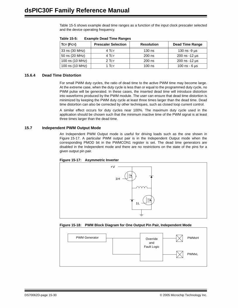
dsPIC30F Family Reference Manual
Table 15-5 shows example dead time ranges as a function of the input clock prescaler selectedand the device operating frequency.
Table 15-5: Example Dead Time Ranges
15.6.4 Dead Time Distortion
For small PWM duty cycles, the ratio of dead time to the active PWM time may become large.At the extreme case, when the duty cycle is less than or equal to the programmed duty cycle, noPWM pulse will be generated. In these cases, the inserted dead time will introduce distortioninto waveforms produced by the PWM module. The user can ensure that dead time distortion isminimized by keeping the PWM duty cycle at least three times larger than the dead time. Deadtime distortion can also be corrected by other techniques, such as closed loop current control.
A similar effect occurs for duty cycles near 100%. The maximum duty cycle used in theapplication should be chosen such that the minimum inactive time of the PWM signal is at leastthree times larger than the dead time.
15.7 Independent PWM Output Mode
An Independent PWM Output mode is useful for driving loads such as the one shown inFigure 15-17. A particular PWM output pair is in the Independent Output mode when thecorresponding PMOD bit in the PWMCON1 register is set. The dead time generators aredisabled in the Independent mode and there are no restrictions on the state of the pins for agiven output pin pair.
Figure 15-17: Asymmetric Inverter
Figure 15-18: PWM Block Diagram for One Output Pin Pair, Independent Mode
TCY (FCY) Prescaler Selection Resolution Dead Time Range
33 ns (30 MHz) 4 TCY 130 ns 130 ns -9 µs50 ns (20 MHz) 4 TCY 200 ns 200 ns -12 µs100 ns (10 MHz) 2 TCY 200 ns 200 ns -12 µs
100 ns (10 MHz) 1 TCY 100 ns 100 ns - 6 µs
+V
1H
1L
PWM Generator PWMxH
PWMxL
Overrideand
Fault Logic
DS70062D-page 15-30 © 2005 Microchip Technology Inc.
Section 15. Motor Control PWMM
otor C
ontrol
PW
M
15
15.8 PWM Output Override
The PWM output override bits allow the user to manually drive the PWM I/O pins to specifiedlogic states independent of the duty cycle comparison units. The PWM override bits are usefulwhen controlling various types of electrically commutated motors.
All control bits associated with the PWM output override function are contained in the OVDCONregister. The upper half of the OVDCON register contains 8 bits, POVDxx, that determine whichPWM I/O pins will be overridden. The lower half of the OVDCON register contains 8 bits,POUTxx, that determine the state of the PWM I/O pin when it is overridden via the POVDxx bit.
The POVD bits are active-low control bits. When the POVD bits are set, the correspondingPOUTxx bit will have no effect on the PWM output. When one of the POVD bits is cleared, theoutput on the corresponding PWM I/O pin will be determined by the state of the POUT bit. Whena POUT bit is set, the PWM pin will be driven to its active state. When the POUT bit is cleared,the PWM pin will be driven to its inactive state.
15.8.1 Override Control for Complementary Output Mode
The PWM module will not allow certain overrides when a pair of PWM I/O pins are operating inthe Complementary mode. (PMODx = 0) The module will not allow both pins in the output pairto become active simultaneously. The high-side pin in each output pair will always take priority.
15.8.2 Override Synchronization
If the OSYNC bit is set (PWMCON2<1>), all output overrides performed via the OVDCONregister will be synchronized to the PWM time base. Synchronous output overrides will occur atthe following times:
• Edge aligned mode, when PTMR is zero.• Center aligned modes, when PTMR is zero, or• When the value of PTMR matches PTPER.
The override synchronization function, when enabled, can be used to avoid unwanted narrowpulses on the PWM output pins.
15.8.3 Output Override Examples
Figure 15-19 shows an example of a waveform that might be generated using the PWM outputoverride feature. The Figure shows a six-step commutation sequence for a BLDC motor. Themotor is driven through a 3-phase inverter as shown in Figure 15-13. When the appropriaterotor position is detected, the PWM outputs are switched to the next commutation state in thesequence. In this example, the PWM outputs are driven to specific logic states. The OVDCONregister values used to generate the signals in Figure 15-19 are given in Table 15-6.
The PWM duty cycle registers may be used in conjunction with the OVDCON register. The dutycycle registers controls the current delivered to the load and the OVDCON register controls thecommutation. Such an example is shown in Figure 15-20. The OVDCON register values usedto generate the signals in Figure 15-20 are given in Table 15-7.
Note: Dead time insertion is still performed when PWM channels are overridden manually.
© 2005 Microchip Technology Inc. DS70062D-page 15-31
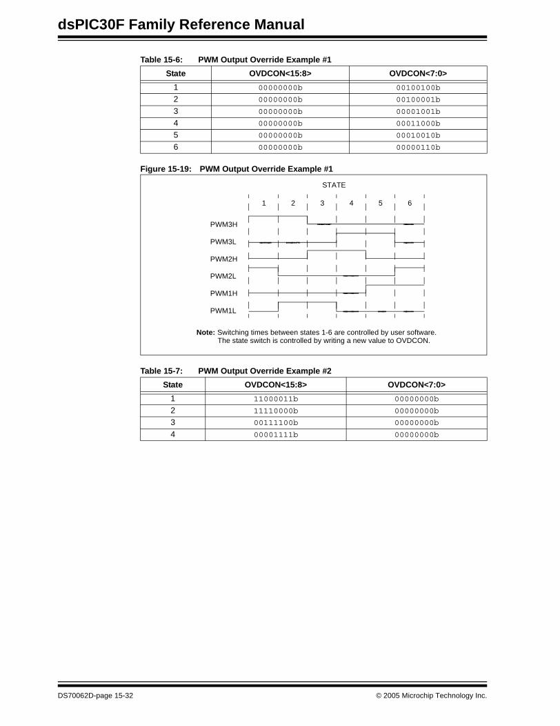
dsPIC30F Family Reference Manual
Table 15-6: PWM Output Override Example #1
Figure 15-19: PWM Output Override Example #1
Table 15-7: PWM Output Override Example #2
State OVDCON<15:8> OVDCON<7:0>
1 00000000b 00100100b
2 00000000b 00100001b
3 00000000b 00001001b
4 00000000b 00011000b
5 00000000b 00010010b
6 00000000b 00000110b
State OVDCON<15:8> OVDCON<7:0>
1 11000011b 00000000b
2 11110000b 00000000b
3 00111100b 00000000b
4 00001111b 00000000b
PWM3H
PWM3L
PWM2H
PWM2L
PWM1H
PWM1L
1 2 3 4 5 6
STATE
Note: Switching times between states 1-6 are controlled by user software.The state switch is controlled by writing a new value to OVDCON.
DS70062D-page 15-32 © 2005 Microchip Technology Inc.
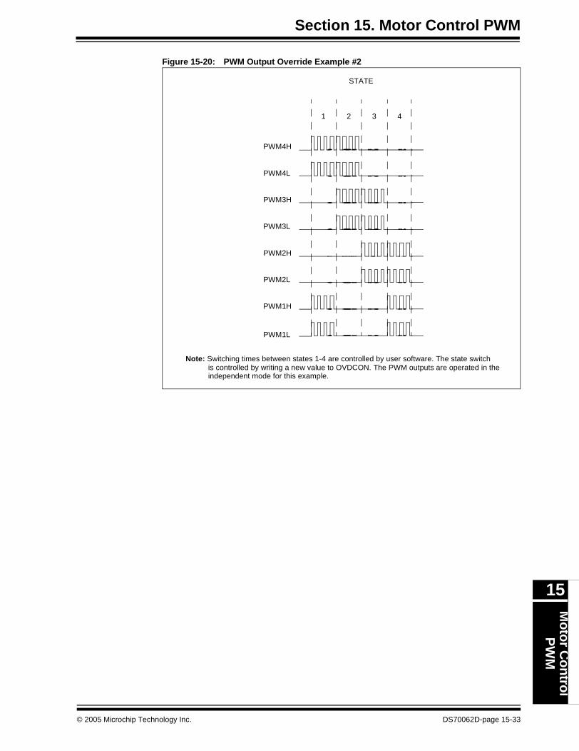
Section 15. Motor Control PWMM
otor C
ontrol
PW
M
15
Figure 15-20: PWM Output Override Example #2
PWM4H
PWM4L
PWM3H
PWM3L
PWM2H
PWM2L
1 2 3 4
PWM1H
PWM1L
STATE
Note: Switching times between states 1-4 are controlled by user software. The state switchis controlled by writing a new value to OVDCON. The PWM outputs are operated in theindependent mode for this example.
© 2005 Microchip Technology Inc. DS70062D-page 15-33
dsPIC30F Family Reference Manual
15.9 PWM Output and Polarity Control
The PENxx control bits in PWMCON1 enable each PWM output pin for use by the module.When a pin is enabled for PWM output, the PORT and TRIS registers controlling the pin aredisabled.
In addition to the PENxx control bits, there are three device configuration bits in the FBORPORdevice configuration register that provide PWM output pin control.
• HPOL configuration bit
• LPOL configuration bit• PWMPIN configuration bit
These three configuration bits work in conjunction with the PWM enable bits (PENxx) located inPWMCON1. The configuration bits ensure that the PWM pins are in the correct states after adevice reset occurs.
15.9.1 Output Polarity Control
The polarity of the PWM I/O pins is set during device programming via the HPOL and LPOLconfiguration bits in the FBORPOR Device Configuration register. The HPOL configurationbit sets the output polarity for the high-side PWM outputs PWM1H-PWM4H. The LPOLconfiguration bit sets the output polarity for the low-side PWM outputs PWM1L-PWM 4L.
If the polarity configuration bit is programmed to a ‘1’, the corresponding PWM I/O pins will haveactive-high output polarity. If the polarity configuration bit is programmed to a ‘0’, then thecorresponding PWM pins will have active-low polarity.
15.9.2 PWM Output Pin Reset States
The PWMPIN configuration bit determines the behavior of the PWM output pins on a devicereset and can be used to eliminate external pull-up/pull-down resistors connected to the devicescontrolled by the PWM module.
If the PWMPIN configuration bit is programmed to a ‘1’, the PENxx control bits will be clearedon a device reset. Consequently, all PWM outputs will be tri-stated and controlled by thecorresponding PORT and TRIS registers.
If the PWMPIN configuration bit is programmed to a ‘0’, the PENxx control bits will be set on adevice reset. All PWM pins will be enabled for PWM output at the device reset and will be attheir inactive states as defined by the HPOL and LPOL configuration bits.
15.10 PWM Fault Pins
There are two Fault pins, FLTA and FLTB, associated with the PWM module. When asserted,these pins can optionally drive each of the PWM I/O pins to a defined state. This action takesplace without software intervention so fault events can be managed quickly.
The Fault pins may have other multiplexed functions depending on the dsPIC device variant.When used as a fault input, each Fault pin is readable via its corresponding PORT register. TheFLTA and FLTB pins function as active low inputs so that it is easy to wire-OR many sources tothe same input through an external pull-up resistor. When not used with the PWM module, thesepins may be used as general purpose I/O or another multiplexed function. Each Fault pin has itsown interrupt vector, Interrupt Flag bit, Interrupt Enable bit and Interrupt Priority bits associatedwith it.
The function of the FLTA pin is controlled by the FLTACON register and the function of the FLTBpin is controlled by the FLTBCON register.
15.10.1 Fault Pin Enable Bits
The FLTACON and FLTBCON registers each have 4 control bits, FxEN1-FxEN4, that determinewhether a particular pair of PWM I/O pins is to be controlled by the fault input pin. To enable aspecific PWM I/O pin pair for fault overrides, the corresponding bit should be set in theFLTACON or FLTBCON register.
If all enable bits are cleared in the FLTACON or FLTBCON registers, then that fault input pin hasno effect on the PWM module and no fault interrupts will be produced.
DS70062D-page 15-34 © 2005 Microchip Technology Inc.
Section 15. Motor Control PWMM
otor C
ontrol
PW
M
15
15.10.2 Fault States
The FLTACON and FLTBCON special function registers each have 8 bits that determine thestate of each PWM I/O pin when the fault input pin becomes active. When these bits arecleared, the PWM I/O pin will be driven to the inactive state. If the bit is set, the PWM I/O pin willbe driven to the active state. The active and inactive states are referenced to the polaritydefined for each PWM I/O pin (set by HPOL and LPOL device configuration bits).
A special case exists when a PWM module I/O pair is in the Complementary mode and bothpins are programmed to be active on a fault condition. The high-side pin will always havepriority in the Complementary mode so that both I/O pins cannot be driven activesimultaneously.
15.10.3 Fault Input Modes
Each of the fault input pins has two modes of operation:
• Latched Mode: When the fault pin is driven low, the PWM outputs will go to the states defined in the FLTxCON register. The PWM outputs will remain in this state until the fault pin is driven high AND the corresponding interrupt flag (FLTxIF) has been cleared in software. When both of these actions have occurred, the PWM outputs will return to normal operation at the beginning of the next PWM period or half-period boundary regardless of the Immediate Update Enable bit value (IUE). If the interrupt flag is cleared before the fault condition ends, the PWM module will wait until the fault pin is no longer asserted to restore the outputs.
• Cycle-by-Cycle Mode: When the fault input pin is driven low, the PWM outputs will remain in the defined fault states for as long as the fault pin is held low. After the fault pin is driven high, the PWM outputs will return to normal operation at the beginning of the following PWM period (or half-period boundary in center aligned modes) even when immediate updates are enabled.
The operating mode for each fault input pin is selected using the FLTAM and FLTBM control bits(FLTACON<7> and FLTBCON<7>).
15.10.3.1 Entry Into a Fault Condition
When a fault pin is enabled and driven low, the PWM pins are immediately driven to theirprogrammed fault states regardless of the values in the PDCx and OVDCON registers. The faultaction has priority over all other PWM control registers.
15.10.3.2 Exit From a Fault Condition
A fault condition must be cleared by the external circuitry driving the fault input pin high andclearing the fault interrupt flag (Latched mode only). After the fault pin condition has beencleared, the PWM module will restore the PWM output signals on the next PWM period orhalf-period boundary. For edge aligned PWM generation, the PWM outputs will be restored whenPTMR = 0. For center aligned PWM generation, the PWM outputs will be restored when PTMR= 0 or PTMR = PTPER, whichever event occurs first.
An exception to these rules will occur when the PWM time base is disabled (PTEN = 0). If thePWM time base is disabled, the PWM module will restore the PWM output signals immediatelyafter the fault condition has been cleared.
© 2005 Microchip Technology Inc. DS70062D-page 15-35
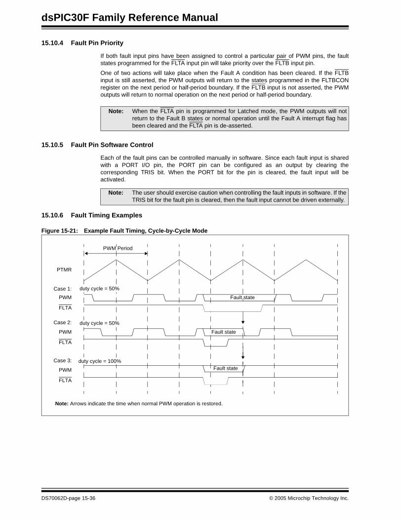
dsPIC30F Family Reference Manual
15.10.4 Fault Pin Priority
If both fault input pins have been assigned to control a particular pair of PWM pins, the faultstates programmed for the FLTA input pin will take priority over the FLTB input pin.
One of two actions will take place when the Fault A condition has been cleared. If the FLTBinput is still asserted, the PWM outputs will return to the states programmed in the FLTBCONregister on the next period or half-period boundary. If the FLTB input is not asserted, the PWMoutputs will return to normal operation on the next period or half-period boundary.
15.10.5 Fault Pin Software Control
Each of the fault pins can be controlled manually in software. Since each fault input is sharedwith a PORT I/O pin, the PORT pin can be configured as an output by clearing thecorresponding TRIS bit. When the PORT bit for the pin is cleared, the fault input will beactivated.
15.10.6 Fault Timing Examples
Figure 15-21: Example Fault Timing, Cycle-by-Cycle Mode
Note: When the FLTA pin is programmed for Latched mode, the PWM outputs will notreturn to the Fault B states or normal operation until the Fault A interrupt flag hasbeen cleared and the FLTA pin is de-asserted.
Note: The user should exercise caution when controlling the fault inputs in software. If theTRIS bit for the fault pin is cleared, then the fault input cannot be driven externally.
PWM
PTMR
FLTA
FLTA
Fault statePWM
Case 2:
Case 1:
Fault state
FLTA
PWM
Case 3:
duty cycle = 50%
duty cycle = 50%
duty cycle = 100%Fault state
PWM Period
Note: Arrows indicate the time when normal PWM operation is restored.
DS70062D-page 15-36 © 2005 Microchip Technology Inc.
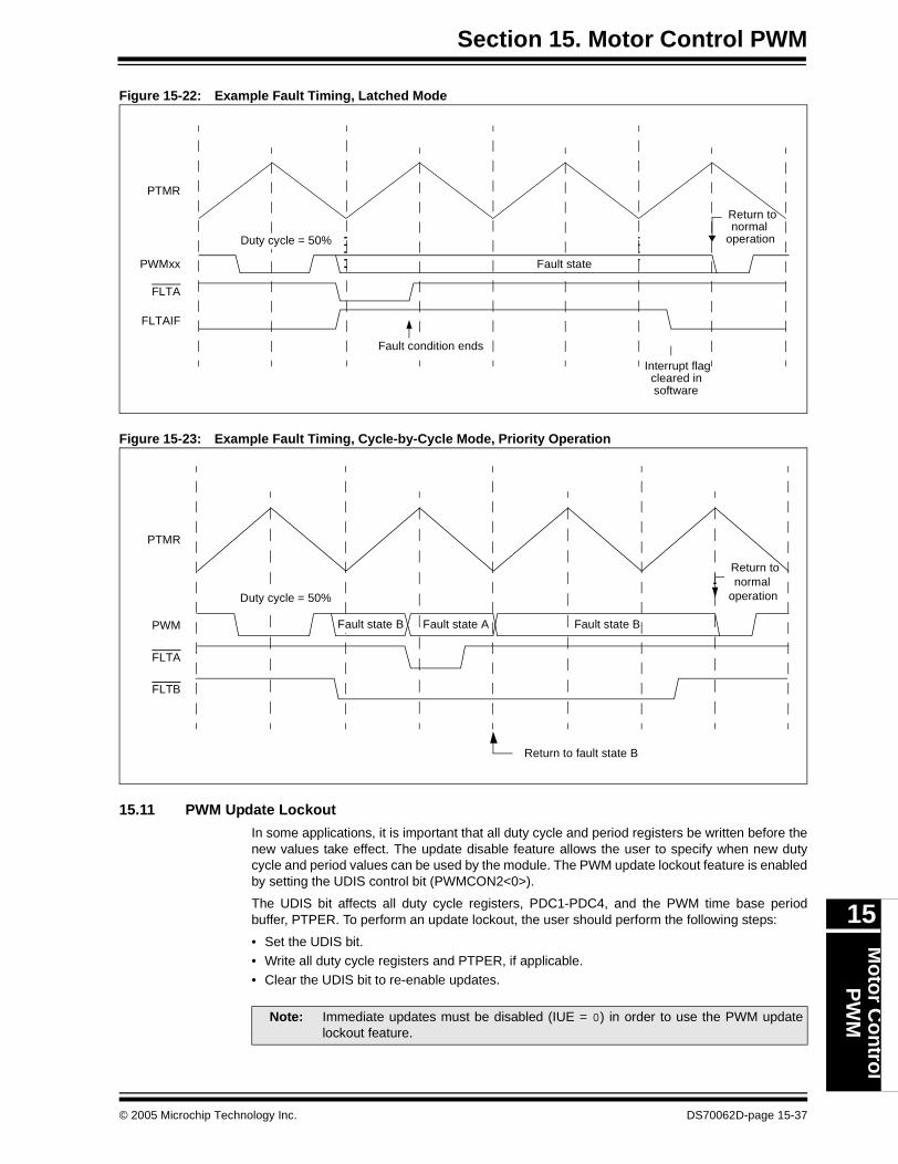
Section 15. Motor Control PWMM
otor C
ontrol
PW
M
15
Figure 15-22: Example Fault Timing, Latched Mode
Figure 15-23: Example Fault Timing, Cycle-by-Cycle Mode, Priority Operation
15.11 PWM Update Lockout
In some applications, it is important that all duty cycle and period registers be written before thenew values take effect. The update disable feature allows the user to specify when new dutycycle and period values can be used by the module. The PWM update lockout feature is enabledby setting the UDIS control bit (PWMCON2<0>).
The UDIS bit affects all duty cycle registers, PDC1-PDC4, and the PWM time base periodbuffer, PTPER. To perform an update lockout, the user should perform the following steps:
• Set the UDIS bit.• Write all duty cycle registers and PTPER, if applicable.• Clear the UDIS bit to re-enable updates.
PWMxx
PTMR
FLTA
Fault state
Duty cycle = 50%
Fault condition ends
Interrupt flagcleared insoftware
Return tonormal
operation
FLTAIF
PWM
PTMR
FLTA
Fault state B
Duty cycle = 50%
Return tonormal
operation
FLTB
Fault state B Fault state A
Return to fault state B
Note: Immediate updates must be disabled (IUE = 0) in order to use the PWM updatelockout feature.
© 2005 Microchip Technology Inc. DS70062D-page 15-37
dsPIC30F Family Reference Manual
15.12 PWM Special Event Trigger
The PWM module has a special event trigger that allows A/D conversions to be synchronized tothe PWM time base. The A/D sampling and conversion time may be programmed to occur atany point within the PWM period. The special event trigger allows the user to minimize the delaybetween the time when A/D conversion results are acquired and the time when the duty cyclevalue is updated.
The PWM special event trigger has one SFR, SEVTCMP, and four postscaler control bits(SEVOPS<3:0>) to control its operation. The PTMR value for which a special event triggershould occur is loaded into the SEVTCMP register.
When the PWM time base is in an Up/Down Counting mode, an additional control bit is requiredto specify the counting phase for the special event trigger. The count phase is selected usingthe SEVTDIR control bit in the MSb of SEVTCMP. If the SEVTDIR bit is cleared, the specialevent trigger will occur on the upward counting cycle of the PWM time base. If the SEVTDIR bitis set, the special event trigger will occur on the downward count cycle of the PWM time base.The SEVTDIR control bit has no effect unless the PWM time base is configured for an Up/DownCounting mode.
15.12.1 Special Event Trigger Enable
The PWM module will always produce the special event trigger signal. This signal mayoptionally be used by the A/D module. Refer to Section Section 17. “10-bit A/D Converter”for more information on using the special event trigger.
15.12.2 Special Event Trigger Postscaler
The PWM special event trigger has a postscaler that allows a 1:1 to 1:16 postcale ratio. Thepostscaler is useful when synchronized A/D conversions do not need to be performed duringevery PWM cycle. The postscaler is configured by writing the SEVOPS<3:0> control bits in thePWMCON2 SFR.
The special event output postscaler is cleared on the following events:
• Any write to the SEVTCMP register.• Any device reset.
15.13 Operation in Device Power Saving Modes
15.13.1 PWM Operation in Sleep mode
When the device enters Sleep mode, the system clock is disabled. Since the clock for the PWMtime base is derived from the system clock source (TCY), it will also be disabled. All enabled PWMoutput pins will be frozen in the output states that were in effect prior to entering Sleep.
If the PWM module is used to control a load in a power application, it is the user’s responsibilityto put the PWM module outputs into a ‘safe’ state prior to executing the PWRSAV instruction.Depending on the application, the load may begin to consume excessive current when the PWMoutputs are frozen in a particular output state. For example, the OVDCON register can be usedto manually turn off the PWM output pins as shown in the code example below.
; This code example drives all PWM pins to the inactive state
; before executing the PWRSAV instruction.
CLR OVDCON ; Force all PWM outputs inactive
PWRSAV #0 ; Put the device in SLEEP mode
SETM.B OVDCONH ; Set POVD bits when device wakes.
The Fault A and Fault B input pins, if enabled to control the PWM pins via the FLTxCON registers,will continue to function normally when the device is in Sleep mode. If one of the fault pins isdriven low while the device is in Sleep, the PWM outputs will be driven to the programmed faultstates in the FLTxCON register.
DS70062D-page 15-38 © 2005 Microchip Technology Inc.
Section 15. Motor Control PWMM
otor C
ontrol
PW
M
15
The fault input pins also have the ability to wake the CPU from Sleep mode. If the fault interruptenable bit is set (FLTxIE = 1), then the device will wake from Sleep when the fault pin is drivenlow. If the fault pin interrupt priority is greater than the current CPU priority, then programexecution will start at the fault pin interrupt vector location upon wake-up. Otherwise, executionwill continue from the next instruction following the PWRSAV instruction.
15.13.2 PWM Operation in Idle Mode
When the device enters Idle mode, the system clock sources remain functional and the CPUstops executing code. The PWM module can optionally continue to operate in Idle mode.ThePTSIDL bit (PTCON<13>) selects if the PWM module will stop in Idle mode or continue tooperate normally.
If PTSIDL = 0, the module will operate normally when the device enters Idle mode. The PWMtime base interrupt, if enabled, can be used to wake the device from Idle. If the PWM time baseinterrupt enable bit is set (PTIE = 1), then the device will wake from Idle when the PWM time baseinterrupt is generated. If the PWM time base interrupt priority is greater than the current CPUpriority, then program execution will start at the PWM interrupt vector location upon wake-up.Otherwise, execution will continue from the next instruction following the PWRSAV instruction.
If PTSIDL = 1, the module will stop in Idle mode. If the PWM module is programmed to stop inIdle mode, the operation of the PWM outputs and fault input pins will be the same as theoperation in Sleep mode. (See discussion in Section 15.13.1 “PWM Operation in Sleepmode”.)
15.14 Special Features for Device Emulation
The PWM module has a special feature to support the debugging environment. All enabledPWM pins can be optionally tri-stated when the hardware emulator or debugger device is haltedto examine memory contents. The user should install pull-up or pull-down resistors to ensurethe PWM outputs are driven to the correct state when device execution is halted.
The function of the PWM output pins at a device Reset and the output pin polarity is determinedby three device configuration bits (see Section 15.9 “PWM Output and Polarity Control”).The hardware debugger or emulation tool provides a method to change the values of theseconfiguration bits. Please refer to the tool’s user’s manual for more information.
© 2005 Microchip Technology Inc. DS70062D-page 15-39

dsPIC30F Family Reference Manual
Tab
le 1
5-8:
Reg
iste
rs A
sso
ciat
ed w
ith
th
e 8-
Ou
tpu
t P
WM
Mo
du
le
Nam
eA
DR
Bit
15
Bit
14
Bit
13
Bit
12
Bit
11
Bit
10
Bit
9B
it 8
Bit
7B
it 6
Bit
5B
it 4
Bit
3B
it 2
Bit
1B
it 0
Val
ue
on
Res
et
INT
CO
N1
0080
NS
TD
IS—
——
——
——
——
——
——
——
0000 0000 0000 0000
INT
CO
N2
0082
ALT
IVT
——
——
——
——
——
——
——
—0000 0000 0000 0000
IFS
200
88—
——
FLT
BIF
FLT
AIF
——
—P
WM
IF—
——
——
——
0000 0000 0000 0000
IEC
200
90—
——
FLT
BIE
FLT
AIE
——
—P
WM
IE—
——
——
——
0000 0000 0000 0000
IPC
900
A6
—P
WM
IP<
2:0>
——
——
——
——
——
——
0100 0100 0100 0100
IPC
1000
A8
—F
LTA
IP<
2:0>
——
——
——
——
——
——
0100 0100 0100 0100
IPC
1100
AA
——
——
——
——
——
——
—F
LTB
IP<
2:>
0000 0000 0000 0000
PT
CO
N01
C0
PT
EN
—P
TS
IDL
——
——
—P
TO
PS
<3:0
>P
TC
KP
S<
1:0>
PT
MO
D<
1:0>
0000 0000 0000 0000
PT
MR
01C
2P
TD
IRP
WM
Tim
e B
ase
regi
ster
0000 0000 0000 0000
PT
PE
R01
C4
—P
WM
Tim
e B
ase
Per
iod
regi
ster
0111 1111 1111 1111
SE
VT
CM
P01
C6
SE
VT
DIR
PW
M S
peci
al E
vent
Com
pare
reg
iste
r0000 0000 0000 0000
PW
MC
ON
101
C8
——
——
PM
OD
4P
MO
D3
PM
OD
2P
MO
D1
PE
N4H
PE
N3H
PE
N2H
PE
N1H
PE
N4L
PE
N3L
PE
N2L
PE
N1L
0000 0000 0000 0000
PW
MC
ON
201
CA
——
——
SE
VO
PS
<3:
0>—
——
——
IUE
OS
YN
CU
DIS
0000 0000 0000 0000
DT
CO
N1
01C
CD
TB
PS
<1:0
>D
ead
Tim
e B
Val
ue r
egis
ter
DTA
PS
<1:
0>D
ead
Tim
e A
Val
ue r
egis
ter
0000 0000 0000 0000
DT
CO
N2
01C
E—
——
——
——
—D
TS
4AD
TS
4ID
TS
3AD
TS
3ID
TS
2AD
TS
2ID
TS
1AD
TS
1I0000 0000 0000 0000
FLT
AC
ON
01D
0FA
OV
4HFA
OV
4LFA
OV
3HFA
OV
3LFA
OV
2HFA
OV
2LFA
OV
1HFA
OV
1LF
LTA
M—
——
FAE
N4
FAE
N3
FAE
N2
FAE
N1
0000 00-0 0000 0000
FLT
BC
ON
01D
2F
BO
V4H
FB
OV
4LF
BO
V3H
FB
OV
3LF
BO
V2H
FB
OV
2LF
BO
V1H
FB
OV
1LF
LTB
M—
——
FB
EN
4F
BE
N3
FB
EN
2F
BE
N1
0000 0000 0000 0000
OV
DC
ON
01D
4P
OV
D4H
PO
VD
4LP
OV
D3H
PO
VD
3LP
OV
D2H
PO
VD
2LP
OV
D1H
PO
VD
1LP
OU
T4H
PO
UT
4LP
OU
T3H
PO
UT
3LP
OU
T2H
PO
UT
2LP
OU
T1H
PO
UT
1L1111 1111 00-0 0000
PD
C1
01D
6P
WM
Dut
y C
ycle
#1
regi
ster
0000 0000 0000 0000
PD
C2
01D
8P
WM
Dut
y C
ycle
#2
regi
ster
0000 0000 0000 0000
PD
C3
01D
AP
WM
Dut
y C
ycle
#3
regi
ster
0000 0000 0000 0000
PD
C4
01D
CP
WM
Dut
y C
ycle
#4
regi
ster
0000 0000 0000 0000
No
te1:
Res
et s
tate
of P
EN
xx c
ontr
ol b
its d
epen
ds o
n th
e st
ate
of th
e P
WM
PIN
dev
ice
conf
igur
atio
n bi
t.
2:S
hade
d re
gist
er a
nd b
it lo
catio
ns n
ot im
plem
ente
d fo
r th
e 6-
outp
ut M
CP
WM
mod
ule.
3:T
he IU
E b
it is
not
impl
emen
ted
on th
e ds
PIC
30F
6010
dev
ice.
DS70062D-page 15-40 © 2005 Microchip Technology Inc.
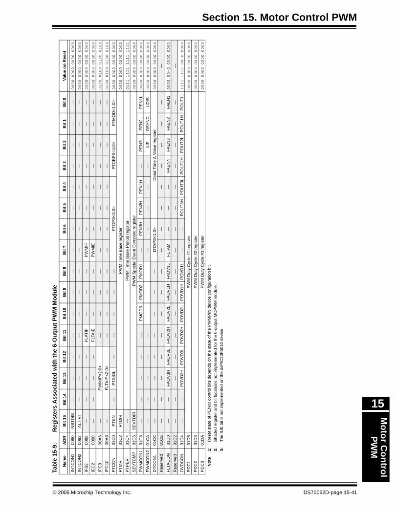
Section 15. Motor Control PWMM
oto
r Co
ntro
l P
WM
15
Tab
le 1
5-9:
Reg
iste
rs A
sso
ciat
ed w
ith
th
e 6-
Ou
tpu
t P
WM
Mo
du
le
Nam
eA
DR
Bit
15
Bit
14
Bit
13
Bit
12
Bit
11
Bit
10
Bit
9B
it 8
Bit
7B
it 6
Bit
5B
it 4
Bit
3B
it 2
Bit
1B
it 0
Val
ue
on
Res
et
INT
CO
N1
0080
NS
TD
IS—
——
——
——
——
——
——
——
0000 0000 0000 0000
INT
CO
N2
0082
ALT
IVT
——
——
——
——
——
——
——
—0000 0000 0000 0000
IFS
200
88—
——
—F
LAT
IF—
——
PW
MIF
——
——
——
—0000 0000 0000 0000
IEC
200
90—
——
—F
LTA
IE—
——
PW
MIE
——
——
——
—0000 0000 0000 0000
IPC
900
A6
—P
WM
IP<2
:0>
——
——
——
——
——
——
0100 0100 0100 0100
IPC
1000
A8
—F
LTA
IP<2
:0>
——
——
——
——
——
——
0100 0100 0100 0100
PT
CO
N01
C0
PT
EN
—P
TS
IDL
——
——
—P
TO
PS
<3:0
>P
TC
KP
S<1
:0>
PT
MO
D<
1:0>
0000 0000 0000 0000
PT
MR
01C
2P
TD
IRP
WM
Tim
e B
ase
regi
ster
0000 0000 0000 0000
PT
PE
R01
C4
—P
WM
Tim
e B
ase
Per
iod
regi
ster
0111 1111 1111 1111
SE
VT
CM
P01
C6
SE
VT
DIR
PW
M S
peci
al E
vent
Com
pare
reg
iste
r0000 0000 0000 0000
PW
MC
ON
101
C8
——
——
—P
MO
D3
PM
OD
2P
MO
D1
—P
EN
3HP
EN
2HP
EN
1H—
PE
N3L
PE
N2L
PE
N1L
0000 0000 0000 0000
PW
MC
ON
201
CA
——
——
——
——
——
IUE
OS
YN
CU
DIS
0000 0000 0000 0000
DT
CO
N1
01C
C—
——
——
——
—D
TAP
S<1
:0>
Dea
d Ti
me
A V
alue
reg
iste
r0000 0000 0000 0000
Res
erve
d01
CE
——
——
——
——
——
——
——
——
—
FLT
AC
ON
01D
0—
—FA
OV
3HFA
OV
3LFA
OV
2HFA
OV
2LFA
OV
1HFA
OV
1LF
LTA
M—
——
FAE
N4
FAE
N3
FAE
N2
FAE
N1
0000 00-0 0000 0000
Res
erve
d01
D2
——
——
——
——
——
——
——
——
—
OV
DC
ON
01D
4—
—P
OV
D3H
PO
VD
3LP
OV
D2H
PO
VD
2LP
OV
D1H
PO
VD
1L—
—P
OU
T3H
PO
UT
3LP
OU
T2H
PO
UT
2LP
OU
T1H
PO
UT
1L1111 1111 00-0 0000
PD
C1
01D
6P
WM
Dut
y C
ycle
#1
regi
ster
0000 0000 0000 0000
PD
C2
01D
8P
WM
Dut
y C
ycle
#2
regi
ster
0000 0000 0000 0000
PD
C3
01D
AP
WM
Dut
y C
ycle
#3
regi
ster
0000 0000 0000 0000
No
te1:
Res
et s
tate
of P
EN
xx c
ontr
ol b
its d
epen
ds o
n th
e st
ate
of th
e P
WM
PIN
dev
ice
conf
igur
atio
n bi
t.
2:S
hade
d re
gist
er a
nd b
it lo
catio
ns n
ot im
plem
ente
d fo
r th
e 6-
outp
ut M
CP
WM
mod
ule.
3:T
he IU
E b
it is
not
impl
emen
ted
on th
e ds
PIC
30F
6010
dev
ice.
© 2005 Microchip Technology Inc. DS70062D-page 15-41
dsPIC30F Family Reference Manual
15.15 Related Application Notes
This section lists application notes that are related to this section of the manual. Theseapplication notes may not be written specifically for the dsPIC30F Product Family, but theconcepts are pertinent, and could be used with modification and possible limitations. The currentapplication notes related to the MCPWM module are:
Title Application Note #
PIC18CXXX/PIC16CXXX Servomotor AN696
Using the dsPIC30F for Sensorless BLDC Control AN901
Using the dsPIC30F for Vector Control of an ACIM AN908
Sensored BLDC Motor Control Using dsPIC30F2010 AN957
An Introduction to AC Induction Motor Control Using the dsPIC30F MCU AN984
Note: Please visit the Microchip web site (www.microchip.com) for additional ApplicationNotes and code examples for the dsPIC30F Family of devices.
DS70062D-page 15-42 © 2005 Microchip Technology Inc.

Section 15. Motor Control PWMM
otor C
ontrol
PW
M
15
15.16 Revision History
Revision A
This is the initial released revision of this document.
Revision B
This revision provides expanded information for the dsPIC30F MCPWM module.
Revision C
This revision incorporates all known errata at the time of this document update.
Revision D
This revision includes the Immediate Update Enable Capability (IUE) bit.
© 2005 Microchip Technology Inc. DS70062D-page 15-43

dsPIC30F Family Reference Manual
NOTES:
DS70062D-page 15-44 © 2005 Microchip Technology Inc.
Qu
adratu
re En
cod
Interface (Q
EI)
16
Section 16. Quadrature Encoder Interface (QEI)
er
HIGHLIGHTS
This section of the manual contains the following major topics:
16.1 Module Introduction ..................................................................................................... 16-2
16.2 Control and Status Registers ....................................................................................... 16-416.3 Programmable Digital Noise Filters ............................................................................. 16-916.4 Quadrature Decoder .................................................................................................. 16-10
16.5 16-bit Up/Down Position Counter............................................................................... 16-1216.6 Using QEI as an Alternate 16-bit Timer/Counter........................................................ 16-1616.7 Quadrature Encoder Interface Interrupts ................................................................... 16-17
16.8 I/O Pin Control ........................................................................................................... 16-1816.9 QEI Operation During Power Saving Modes ............................................................. 16-1916.10 Effects of a Reset....................................................................................................... 16-19
16.11 Design Tips ................................................................................................................ 16-2116.12 Related Application Notes.......................................................................................... 16-2216.13 Revision History ......................................................................................................... 16-23
© 2004 Microchip Technology Inc. DS70063C-page 16-1

dsPIC30F Family Reference Manual
16.1 Module Introduction
16.1.1 Features Overview
Quadrature encoders (a.k.a. Incremental encoders or Optical encoders) are used in positionand speed detection of rotating motion systems. Quadrature encoders enable closed loopcontrol of many motor control applications, such as Switched Reluctance (SR) motor and ACInduction Motor (ACIM).
A typical incremental encoder includes a slotted wheel attached to the shaft of the motor and anemitter/detector module sensing the slots in the wheel. Typically, three outputs, termed: PhaseA, Phase B and INDEX, provide information that can be decoded to provide information on themovement of the motor shaft including distance and direction.
The two channels, Phase A (QEA) and Phase B (QEB), have a unique relationship. If Phase Aleads Phase B, then the direction (of the motor) is deemed positive or forward. If Phase A lagsPhase B then the direction (of the motor) is deemed negative or reverse. A third channel,termed index pulse, occurs once per revolution and is used as a reference to establish anabsolute position. See Figure 16-1 for a relative timing diagram of these three signals.
The quadrature signals produced by the encoder can have four unique states. These states areindicated for one count cycle in Figure 16-1. Note that the order of the states are reversed whenthe direction of travel is changed.
A Quadrature Decoder captures the phase signals and index pulse and converts the informationinto a numeric count of the position pulses. Generally, the count will increment when the shaft isrotating one direction and decrement when the shaft is rotating in the other direction.
Figure 16-1: Quadrature Encoder Interface Signals
QEA
QEB
INDX
QEA
QEB
INDX
1 Cycle
01 00 10 11
11 10 00 01
Forward Travel
Reverse Travel
DS70063C-page 16-2 © 2004 Microchip Technology Inc.
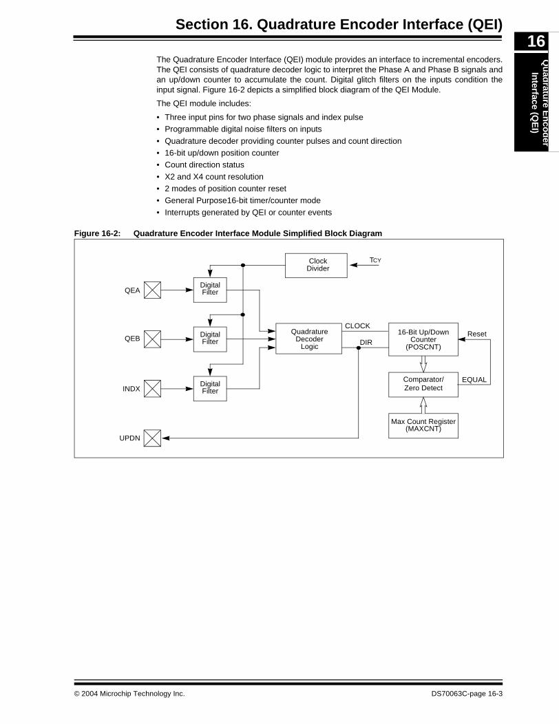
Section 16. Quadrature Encoder Interface (QEI)Q
uad
rature E
nco
der
Interface (Q
EI)
16
The Quadrature Encoder Interface (QEI) module provides an interface to incremental encoders.The QEI consists of quadrature decoder logic to interpret the Phase A and Phase B signals andan up/down counter to accumulate the count. Digital glitch filters on the inputs condition theinput signal. Figure 16-2 depicts a simplified block diagram of the QEI Module.The QEI module includes:
• Three input pins for two phase signals and index pulse• Programmable digital noise filters on inputs
• Quadrature decoder providing counter pulses and count direction• 16-bit up/down position counter• Count direction status
• X2 and X4 count resolution• 2 modes of position counter reset• General Purpose16-bit timer/counter mode
• Interrupts generated by QEI or counter events
Figure 16-2: Quadrature Encoder Interface Module Simplified Block Diagram
QuadratureDecoder
Logic
UPDN
16-Bit Up/DownCounterQEB
DigitalFilterQEA
CLOCK
DIR
ClockDivider
TCY
INDX
DigitalFilter
DigitalFilter
Comparator/
Max Count Register(MAXCNT)
Reset
EQUALZero Detect
(POSCNT)
© 2004 Microchip Technology Inc. DS70063C-page 16-3
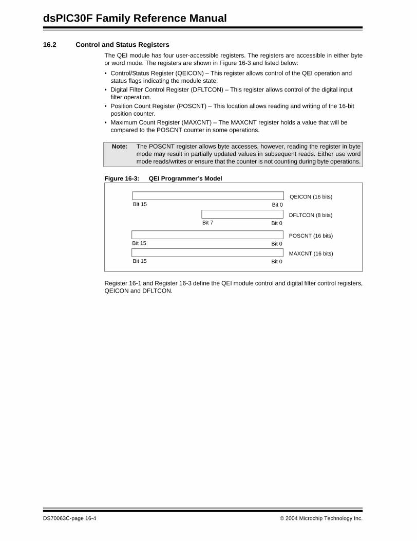
dsPIC30F Family Reference Manual
16.2 Control and Status Registers
The QEI module has four user-accessible registers. The registers are accessible in either byteor word mode. The registers are shown in Figure 16-3 and listed below:
• Control/Status Register (QEICON) – This register allows control of the QEI operation and status flags indicating the module state.
• Digital Filter Control Register (DFLTCON) – This register allows control of the digital input filter operation.
• Position Count Register (POSCNT) – This location allows reading and writing of the 16-bit position counter.
• Maximum Count Register (MAXCNT) – The MAXCNT register holds a value that will be compared to the POSCNT counter in some operations.
Figure 16-3: QEI Programmer’s Model
Register 16-1 and Register 16-3 define the QEI module control and digital filter control registers,QEICON and DFLTCON.
Note: The POSCNT register allows byte accesses, however, reading the register in bytemode may result in partially updated values in subsequent reads. Either use wordmode reads/writes or ensure that the counter is not counting during byte operations.
Bit 15 Bit 0
POSCNT (16 bits)
Bit 15 Bit 0
MAXCNT (16 bits)
Bit 7 Bit 0
DFLTCON (8 bits)
Bit 15 Bit 0
QEICON (16 bits)
DS70063C-page 16-4 © 2004 Microchip Technology Inc.
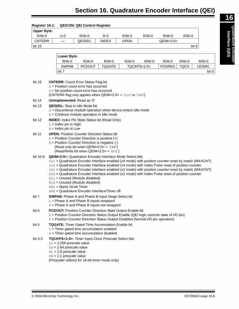
Section 16. Quadrature Encoder Interface (QEI)Q
uad
rature E
nco
der
Interface (Q
EI)
16
Register 16-1: QEICON: QEI Control RegisterUpper Byte:R/W-0 U-0 R/W-0 R-0 R/W-0 R/W-0 R/W-0 R/W-0
CNTERR — QEISIDL INDEX UPDN QEIM<2:0>
bit 15 bit 8
Lower Byte:R/W-0 R/W-0 R/W-0 R/W-0 R/W-0 R/W-0 R/W-0 R/W-0
SWPAB PCDOUT TQGATE TQCKPS<1:0> POSRES TQCS UDSRCbit 7 bit 0
bit 15 CNTERR: Count Error Status Flag bit1 = Position count error has occurred 0 = No position count error has occurred (CNTERR flag only applies when QEIM<2:0> = ‘110’ or ‘100’)
bit 14 Unimplemented: Read as ‘0’
bit 13 QEISIDL: Stop in Idle Mode bit1 = Discontinue module operation when device enters Idle mode0 = Continue module operation in Idle mode
bit 12 INDEX: Index Pin State Status bit (Read Only)1 = Index pin is High0 = Index pin is Low
bit 11 UPDN: Position Counter Direction Status bit1 = Position Counter Direction is positive (+)0 = Position Counter Direction is negative (-)
(Read only bit when QEIM<2:0> = ‘1XX’)(Read/Write bit when QEIM<2:0> = ‘001’)
bit 10-8 QEIM<2:0>: Quadrature Encoder Interface Mode Select bits111 = Quadrature Encoder Interface enabled (x4 mode) with position counter reset by match (MAXCNT)110 = Quadrature Encoder Interface enabled (x4 mode) with Index Pulse reset of position counter101 = Quadrature Encoder Interface enabled (x2 mode) with position counter reset by match (MAXCNT)100 = Quadrature Encoder Interface enabled (x2 mode) with Index Pulse reset of position counter011 = Unused (Module disabled)010 = Unused (Module disabled)001 = Starts 16-bit Timer000 = Quadrature Encoder Interface/Timer off
bit 7 SWPAB: Phase A and Phase B Input Swap Select bit1 = Phase A and Phase B inputs swapped0 = Phase A and Phase B inputs not swapped
bit 6 PCDOUT: Position Counter Direction State Output Enable bit1 = Position Counter Direction Status Output Enable (QEI logic controls state of I/O pin)0 = Position Counter Direction Status Output Disabled (Normal I/O pin operation)
bit 5 TQGATE: Timer Gated Time Accumulation Enable bit1 = Timer gated time accumulation enabled0 = Timer gated time accumulation disabled
bit 4-3 TQCKPS<1:0>: Timer Input Clock Prescale Select bits11 = 1:256 prescale value10 = 1:64 prescale value01 = 1:8 prescale value00 = 1:1 prescale value(Prescaler utilized for 16-bit timer mode only)
© 2004 Microchip Technology Inc. DS70063C-page 16-5

dsPIC30F Family Reference Manual
Register 16-1: QEICON: QEI Control Register (Continued)
bit 2 POSRES: Position Counter Reset Enable bit1 = Index Pulse resets Position Counter 0 = Index Pulse does not reset Position Counter (Bit only applies when QEIM<2:0> = 100 or 110)
bit 1 TQCS: Timer Clock Source Select bit1 = External clock from pin QEA (on the rising edge) 0 = Internal clock (TCY)
bit 0 UDSRC: Position Counter Direction Selection Control bit1 = QEB pin State Defines Position Counter Direction0 = Control/Status bit, UPDN (QEICON<11>), Defines Timer Counter (POSCNT) direction
Note: When configured for QEI mode, control bit is a ‘don’t care’
Legend:
R = Readable bit W = Writable bit U = Unimplemented bit, read as ‘0’
-n = Value at POR ‘1’ = Bit is set ‘0’ = Bit is cleared x = Bit is unknown
DS70063C-page 16-6 © 2004 Microchip Technology Inc.

Section 16. Quadrature Encoder Interface (QEI)Q
uad
rature E
nco
der
Interface (Q
EI)
16
Register 16-2: DFLTCON: Digital Filter Control Register (dsPIC30F6010 Only)Upper Byte:U-0 U-0 U-0 U-0 U-0 U-0 U-0 R/W-0— — — — — — — CEID
bit 15 bit 8
Lower Byte:R/W-0 R/W-0 R/W-0 R/W-0 R/W-0 R/W-0 R/W-0 R/W-0
QEOUT QECK<2:0> INDOUT INDCK<2:0>bit 7 bit 0
bit 15-9 Unimplemented: Read as ‘0’
bit 8 CEID: Count Error Interrupt Disable bit1 = Interrupts due to position count errors disabled0 = Interrupts due to position count errors enabled
bit 7 QEOUT: QEA/QEB Digital Filter Output Enable bit1 = Digital filter outputs enabled0 = Digital filter outputs disabled (Normal pin operation)
bit 6-4 QECK<2:0>: QEA/QEB Digital Filter Clock Divide Select bits111 = 1:256 Clock Divide110 = 1:128 Clock Divide101 = 1:64 Clock Divide100 = 1:32 Clock Divide011 = 1:16 Clock Divide010 = 1:4 Clock Divide001 = 1:2 Clock Divide000 = 1:1 Clock Divide
bit 3 INDOUT: Index Channel Digital Filter Output Enable bit1 = Digital filter output is enabled0 = Digital filter output is disabled (Normal pin operation)
bit 2-0 INDCK<2:0>: Index Channel Digital Filter Clock Divide Select bits111 = 1:256 Clock Divide110 = 1:128 Clock Divide101 = 1:64 Clock Divide100 = 1:32 Clock Divide011 = 1:16 Clock Divide010 = 1:4 Clock Divide001 = 1:2 Clock Divide000 = 1:1 Clock Divide
Note: The available control bits in the DFLTCON Register may vary depending on the dsPIC30F devicethat is used. Refer to Register 16-2 and Register 16-3 for details.
Legend:
R = Readable bit W = Writable bit U = Unimplemented bit, read as ‘0’
-n = Value at POR ‘1’ = Bit is set ‘0’ = Bit is cleared x = Bit is unknown
© 2004 Microchip Technology Inc. DS70063C-page 16-7
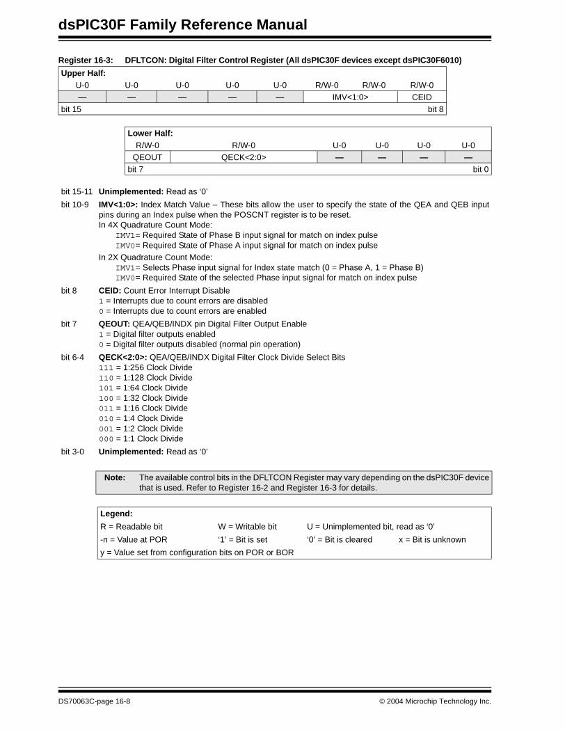
dsPIC30F Family Reference Manual
Register 16-3: DFLTCON: Digital Filter Control Register (All dsPIC30F devices except dsPIC30F6010)
Upper Half:U-0 U-0 U-0 U-0 U-0 R/W-0 R/W-0 R/W-0— — — — — IMV<1:0> CEID
bit 15 bit 8
Lower Half:R/W-0 R/W-0 U-0 U-0 U-0 U-0
QEOUT QECK<2:0> — — — —bit 7 bit 0
bit 15-11 Unimplemented: Read as ‘0’
bit 10-9 IMV<1:0>: Index Match Value – These bits allow the user to specify the state of the QEA and QEB inputpins during an Index pulse when the POSCNT register is to be reset.In 4X Quadrature Count Mode:
IMV1= Required State of Phase B input signal for match on index pulseIMV0= Required State of Phase A input signal for match on index pulse
In 2X Quadrature Count Mode:IMV1= Selects Phase input signal for Index state match (0 = Phase A, 1 = Phase B)IMV0= Required State of the selected Phase input signal for match on index pulse
bit 8 CEID: Count Error Interrupt Disable1 = Interrupts due to count errors are disabled0 = Interrupts due to count errors are enabled
bit 7 QEOUT: QEA/QEB/INDX pin Digital Filter Output Enable1 = Digital filter outputs enabled0 = Digital filter outputs disabled (normal pin operation)
bit 6-4 QECK<2:0>: QEA/QEB/INDX Digital Filter Clock Divide Select Bits111 = 1:256 Clock Divide110 = 1:128 Clock Divide101 = 1:64 Clock Divide100 = 1:32 Clock Divide011 = 1:16 Clock Divide010 = 1:4 Clock Divide001 = 1:2 Clock Divide000 = 1:1 Clock Divide
bit 3-0 Unimplemented: Read as ‘0’
Note: The available control bits in the DFLTCON Register may vary depending on the dsPIC30F devicethat is used. Refer to Register 16-2 and Register 16-3 for details.
Legend:
R = Readable bit W = Writable bit U = Unimplemented bit, read as ‘0’
-n = Value at POR ‘1’ = Bit is set ‘0’ = Bit is cleared x = Bit is unknown
y = Value set from configuration bits on POR or BOR
DS70063C-page 16-8 © 2004 Microchip Technology Inc.
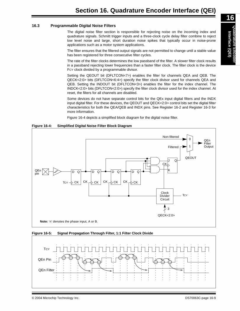
Section 16. Quadrature Encoder Interface (QEI)Q
uad
rature E
nco
der
Interface (Q
EI)
16
16.3 Programmable Digital Noise FiltersThe digital noise filter section is responsible for rejecting noise on the incoming index andquadrature signals. Schmitt trigger inputs and a three-clock cycle delay filter combine to rejectlow level noise and large, short duration noise spikes that typically occur in noise-proneapplications such as a motor system applications.
The filter ensures that the filtered output signals are not permitted to change until a stable valuehas been registered for three consecutive filter cycles.
The rate of the filter clocks determines the low passband of the filter. A slower filter clock resultsin a passband rejecting lower frequencies than a faster filter clock. The filter clock is the deviceFCY clock divided by a programmable divisor.
Setting the QEOUT bit (DFLTCON<7>) enables the filter for channels QEA and QEB. TheQECK<2:0> bits (DFLTCON<6:4>) specify the filter clock divisor used for channels QEA andQEB. Setting the INDOUT bit (DFLTCON<3>) enables the filter for the index channel. TheINDCK<2:0> bits (DFLTCON<2:0>) specify the filter clock divisor used for the index channel. Atreset, the filters for all channels are disabled.
Some devices do not have separate control bits for the QEx input digital filters and the INDXinput digital filter. For these devices, the QEOUT and QECK<2:0> control bits set the digital filtercharacteristics for both the QEA/QEB and INDX pins. See Register 16-2 and Register 16-3 formore information.
Figure 16-4 depicts a simplified block diagram for the digital noise filter.
Figure 16-4: Simplified Digital Noise Filter Block Diagram
Figure 16-5: Signal Propagation Through Filter, 1:1 Filter Clock Divide
QEn D Q
TCY
J Q
K
QEn
D Q D Q D Q
Filtered
ClockDividerCircuit
TCY
Non-filtered0
1
CK
3
CKCK CK CKCKCK CK
pin
Filter
QEOUT
QECK<2:0>
Output
Note: ‘n’ denotes the phase input, A or B.
TCY
QEn Pin
QEn Filter
© 2004 Microchip Technology Inc. DS70063C-page 16-9
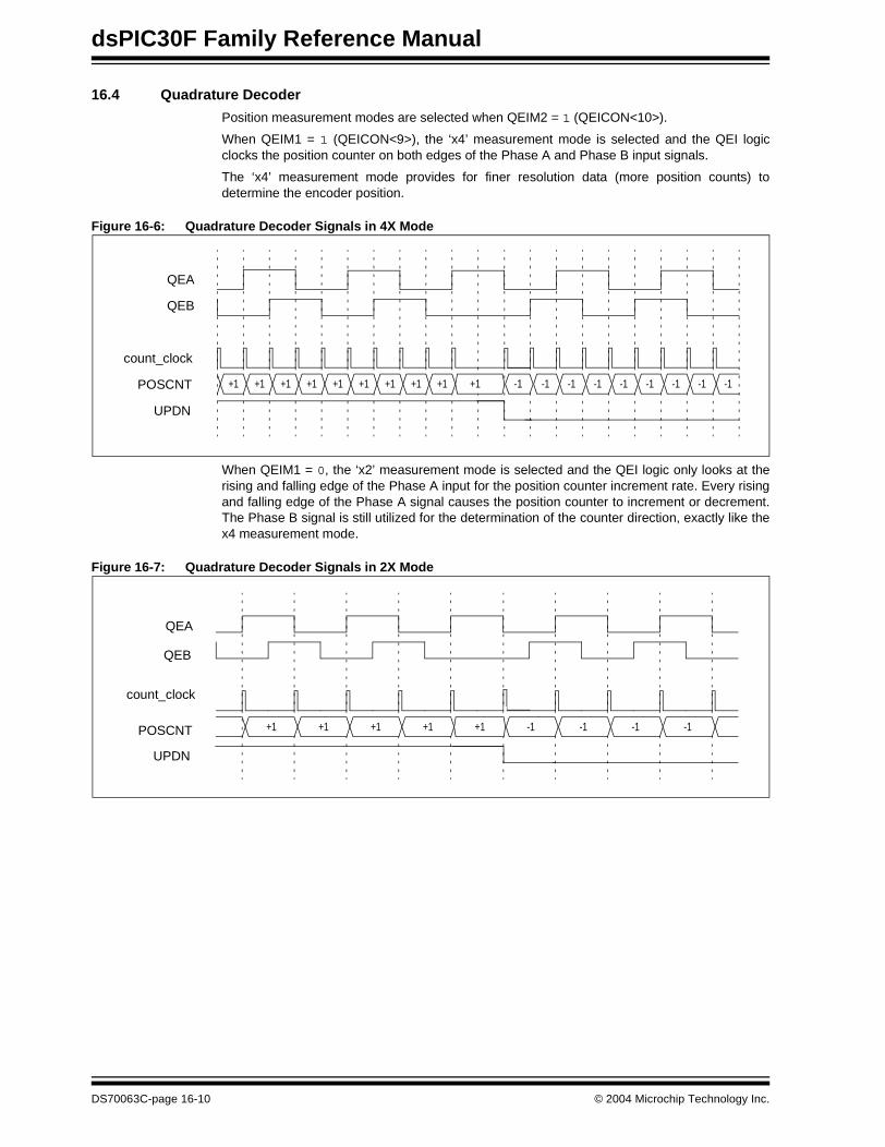
dsPIC30F Family Reference Manual
16.4 Quadrature Decoder
Position measurement modes are selected when QEIM2 = 1 (QEICON<10>).
When QEIM1 = 1 (QEICON<9>), the ‘x4’ measurement mode is selected and the QEI logicclocks the position counter on both edges of the Phase A and Phase B input signals.
The ‘x4’ measurement mode provides for finer resolution data (more position counts) todetermine the encoder position.
Figure 16-6: Quadrature Decoder Signals in 4X Mode
When QEIM1 = 0, the ‘x2’ measurement mode is selected and the QEI logic only looks at therising and falling edge of the Phase A input for the position counter increment rate. Every risingand falling edge of the Phase A signal causes the position counter to increment or decrement.The Phase B signal is still utilized for the determination of the counter direction, exactly like thex4 measurement mode.
Figure 16-7: Quadrature Decoder Signals in 2X Mode
+1 +1 +1 +1 +1 +1 +1 +1 +1 +1 -1 -1 -1 -1 -1 -1 -1 -1
QEA
QEB
count_clock
POSCNT
UPDN
-1
+1 +1 +1 +1 -1 -1 -1+1
QEA
QEB
count_clock
POSCNT
UPDN
-1
DS70063C-page 16-10 © 2004 Microchip Technology Inc.
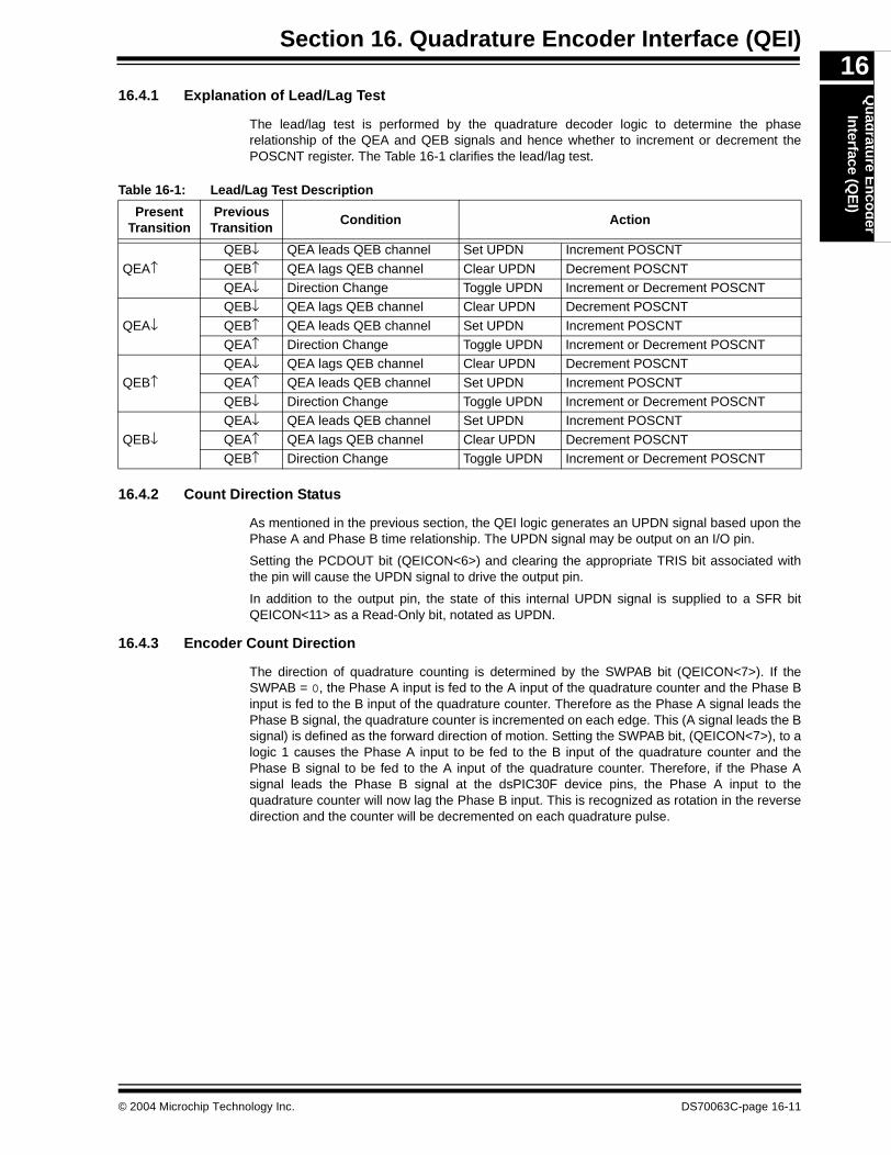
Section 16. Quadrature Encoder Interface (QEI)Q
uad
rature E
nco
der
Interface (Q
EI)
16
16.4.1 Explanation of Lead/Lag TestThe lead/lag test is performed by the quadrature decoder logic to determine the phaserelationship of the QEA and QEB signals and hence whether to increment or decrement thePOSCNT register. The Table 16-1 clarifies the lead/lag test.
Table 16-1: Lead/Lag Test Description
16.4.2 Count Direction Status
As mentioned in the previous section, the QEI logic generates an UPDN signal based upon thePhase A and Phase B time relationship. The UPDN signal may be output on an I/O pin.
Setting the PCDOUT bit (QEICON<6>) and clearing the appropriate TRIS bit associated withthe pin will cause the UPDN signal to drive the output pin.
In addition to the output pin, the state of this internal UPDN signal is supplied to a SFR bitQEICON<11> as a Read-Only bit, notated as UPDN.
16.4.3 Encoder Count Direction
The direction of quadrature counting is determined by the SWPAB bit (QEICON<7>). If theSWPAB = 0, the Phase A input is fed to the A input of the quadrature counter and the Phase Binput is fed to the B input of the quadrature counter. Therefore as the Phase A signal leads thePhase B signal, the quadrature counter is incremented on each edge. This (A signal leads the Bsignal) is defined as the forward direction of motion. Setting the SWPAB bit, (QEICON<7>), to alogic 1 causes the Phase A input to be fed to the B input of the quadrature counter and thePhase B signal to be fed to the A input of the quadrature counter. Therefore, if the Phase Asignal leads the Phase B signal at the dsPIC30F device pins, the Phase A input to thequadrature counter will now lag the Phase B input. This is recognized as rotation in the reversedirection and the counter will be decremented on each quadrature pulse.
PresentTransition
PreviousTransition
Condition Action
QEB↓ QEA leads QEB channel Set UPDN Increment POSCNT
QEA↑ QEB↑ QEA lags QEB channel Clear UPDN Decrement POSCNT QEA↓ Direction Change Toggle UPDN Increment or Decrement POSCNTQEB↓ QEA lags QEB channel Clear UPDN Decrement POSCNT
QEA↓ QEB↑ QEA leads QEB channel Set UPDN Increment POSCNTQEA↑ Direction Change Toggle UPDN Increment or Decrement POSCNTQEA↓ QEA lags QEB channel Clear UPDN Decrement POSCNT
QEB↑ QEA↑ QEA leads QEB channel Set UPDN Increment POSCNTQEB↓ Direction Change Toggle UPDN Increment or Decrement POSCNTQEA↓ QEA leads QEB channel Set UPDN Increment POSCNT
QEB↓ QEA↑ QEA lags QEB channel Clear UPDN Decrement POSCNT QEB↑ Direction Change Toggle UPDN Increment or Decrement POSCNT
© 2004 Microchip Technology Inc. DS70063C-page 16-11
dsPIC30F Family Reference Manual
16.4.4 Quadrature Rate
The RPM of the position control system will vary. The RPMs along with the quadrature encoderline count determine the frequency of the QEA and QEB input signals. The quadrature encodersignals can be decoded such that a count pulse is generated for every quadrature signal edge.This allows an angular position measurement resolution of up to 4 times the encoder line count.For example: a 6,000 RPM motor utilizing a 4096 line encoder yields a quadrature count rate of:((6000/60) * (4096*4)) = 1.6384 MHz. Likewise, a 10,000 RPM motor utilizing a 8,192 lineencoder yields a quadrature count rate of: ((10000/60) * (8192*4)) = 5.46 MHz.
The QEI allows a quadrature frequency of up to FCY/3. For example, if FCY = 30 MHz, the QEAand QEB signals may have a maximum frequency of 10 MHz. Refer to the “ElectricalSpecifications” section of the device data sheet for further details.
16.5 16-bit Up/Down Position Counter
The 16-bit Up/Down Counter counts up or down on every count pulse which is generated bythe quadrature decoder logic. The counter then acts as an integrator, whose count value isproportional to position. The direction of the count is determined by the quadrature decoder.
The user software may examine the contents of the count by reading the POSCNT register. Theuser software may also write to the POSCNT register to initialize a count.
Changing the QEIM bits does not affect the position counter register contents.
16.5.1 Using the Position Counter
The system may utilize position counter data in one of several methods. In some systems, theposition count is accumulated consistently and taken as an absolute value representing the totalposition of the system. For a typical example, assume that a quadrature encoder is affixed to amotor controlling the print head in a printer. In operation, the system is initialized by moving theprint head to the maximum left position and resetting the POSCNT register. As the print headmoves to the right, the quadrature encoder will begin to accumulate counts in the POSCNTregister. As the print head moves to the left, the accumulated count will decrease. As the printhead reaches the right most position, the maximum position count should be reached. If themaximum count is less than 216, the QEI module can encode the entire range of motion.
If, however, the maximum count is more than 216, the additional count precision must becaptured by the user software. Generally, to accomplish this, the module is set into a mode whereit resets the counter at match of a maximum count. QEIM0 = 1 enables modes where theMAXCNT register is used to reset the position counter. When the counter reaches apre-determined maximum count while incrementing or reaches zero while decrementing, thecount is reset and an interrupt is generated to allow the user software to increment or decrementa software counter containing the most significant bits of the position count. The maximum countcan be 0xFFFF, to enable a full range of the QEI counter and software counter or some smallervalue of significance, such as the number of counts for one encoder revolution.
In other systems, the position count may be cyclic. The position count is only used to referencethe position of the wheel within number of rotations determined by the index pulse. For example,a tool platform moved by a screw rod uses a quadrature encoder attached to the screw rod. Inoperation, the screw may require 5.5 rotations to achieve the desired position. The user softwarewill detect 5 index pulses to count the full rotations and use the position count to measure theremaining half rotation. In this method, the index pulse resets the position counter to initialize thecounter at each rotation and generates an interrupt for each rotation. QEIM0 = 0 enables thesemodes.
DS70063C-page 16-12 © 2004 Microchip Technology Inc.
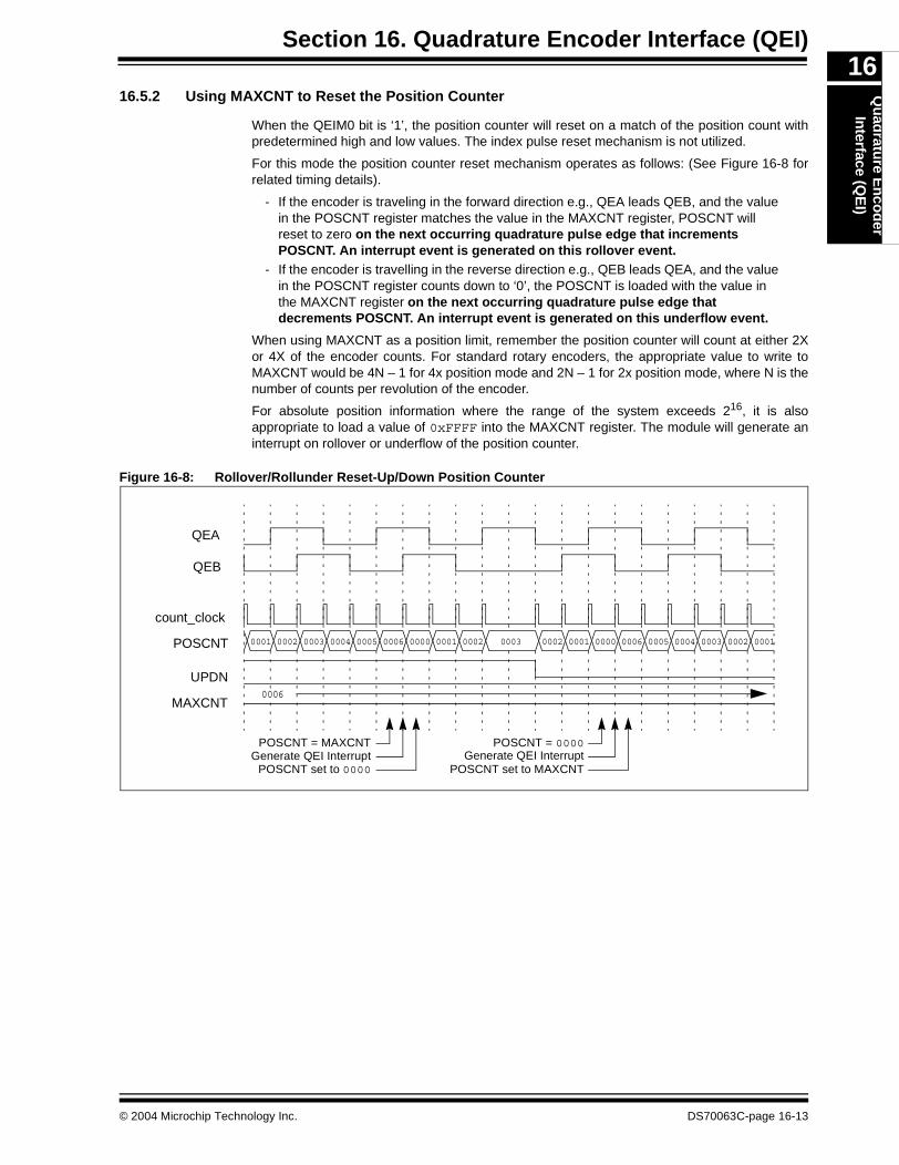
Section 16. Quadrature Encoder Interface (QEI)Q
uad
rature E
nco
der
Interface (Q
EI)
16
16.5.2 Using MAXCNT to Reset the Position CounterWhen the QEIM0 bit is ‘1’, the position counter will reset on a match of the position count withpredetermined high and low values. The index pulse reset mechanism is not utilized.
For this mode the position counter reset mechanism operates as follows: (See Figure 16-8 forrelated timing details).
- If the encoder is traveling in the forward direction e.g., QEA leads QEB, and the value in the POSCNT register matches the value in the MAXCNT register, POSCNT will reset to zero on the next occurring quadrature pulse edge that increments POSCNT. An interrupt event is generated on this rollover event.
- If the encoder is travelling in the reverse direction e.g., QEB leads QEA, and the value in the POSCNT register counts down to ‘0’, the POSCNT is loaded with the value in the MAXCNT register on the next occurring quadrature pulse edge that decrements POSCNT. An interrupt event is generated on this underflow event.
When using MAXCNT as a position limit, remember the position counter will count at either 2Xor 4X of the encoder counts. For standard rotary encoders, the appropriate value to write toMAXCNT would be 4N – 1 for 4x position mode and 2N – 1 for 2x position mode, where N is thenumber of counts per revolution of the encoder.
For absolute position information where the range of the system exceeds 216, it is alsoappropriate to load a value of 0xFFFF into the MAXCNT register. The module will generate aninterrupt on rollover or underflow of the position counter.
Figure 16-8: Rollover/Rollunder Reset-Up/Down Position Counter
0001 0002 0003 0004 0005 0006 0000 0001 0002 0003 0001 0000 0006 0005 0004 0003 0002 0001
0006
POSCNT = MAXCNT
POSCNT set to 0000
POSCNT = 0000
POSCNT set to MAXCNTGenerate QEI Interrupt Generate QEI Interrupt
0002
QEA
QEB
count_clock
POSCNT
UPDN
MAXCNT
© 2004 Microchip Technology Inc. DS70063C-page 16-13
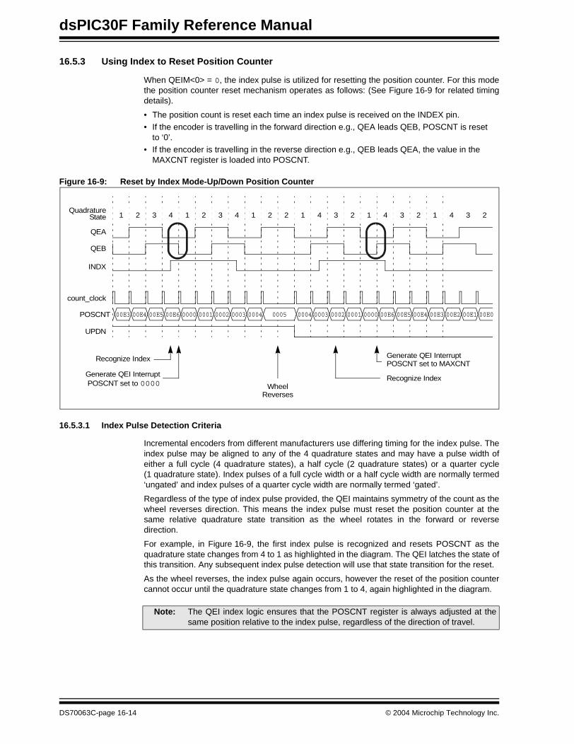
dsPIC30F Family Reference Manual
16.5.3 Using Index to Reset Position Counter
When QEIM<0> = 0, the index pulse is utilized for resetting the position counter. For this modethe position counter reset mechanism operates as follows: (See Figure 16-9 for related timingdetails).
• The position count is reset each time an index pulse is received on the INDEX pin.• If the encoder is travelling in the forward direction e.g., QEA leads QEB, POSCNT is reset
to ‘0’.• If the encoder is travelling in the reverse direction e.g., QEB leads QEA, the value in the
MAXCNT register is loaded into POSCNT.
Figure 16-9: Reset by Index Mode-Up/Down Position Counter
16.5.3.1 Index Pulse Detection Criteria
Incremental encoders from different manufacturers use differing timing for the index pulse. Theindex pulse may be aligned to any of the 4 quadrature states and may have a pulse width ofeither a full cycle (4 quadrature states), a half cycle (2 quadrature states) or a quarter cycle(1 quadrature state). Index pulses of a full cycle width or a half cycle width are normally termed‘ungated’ and index pulses of a quarter cycle width are normally termed ‘gated’.
Regardless of the type of index pulse provided, the QEI maintains symmetry of the count as thewheel reverses direction. This means the index pulse must reset the position counter at thesame relative quadrature state transition as the wheel rotates in the forward or reversedirection.
For example, in Figure 16-9, the first index pulse is recognized and resets POSCNT as thequadrature state changes from 4 to 1 as highlighted in the diagram. The QEI latches the state ofthis transition. Any subsequent index pulse detection will use that state transition for the reset.
As the wheel reverses, the index pulse again occurs, however the reset of the position countercannot occur until the quadrature state changes from 1 to 4, again highlighted in the diagram.
00E3POSCNT
QEA
QEB
UPDN
count_clock
00E4 00E5 00E6 0000 0001 0002 0003 0004 0005 0003 0002 0001 0000 00E6 00E5 00E4 00E0
POSCNT set to 0000Recognize Index
POSCNT set to MAXCNTGenerate QEI Interrupt
Generate QEI Interrupt
00E3 00E2 00E10004
Recognize Index
WheelReverses
INDX
1 2 3 4 1 2 3 4 1 2 2 1 4 3 2 1 4 3 2 1 4 3 2Quadrature
State
Note: The QEI index logic ensures that the POSCNT register is always adjusted at thesame position relative to the index pulse, regardless of the direction of travel.
DS70063C-page 16-14 © 2004 Microchip Technology Inc.
Section 16. Quadrature Encoder Interface (QEI)Q
uad
rature E
nco
der
Interface (Q
EI)
16
16.5.3.2 IMV Control BitsThe IMV<2:0> control bits are available on some dsPIC devices that have the QEI module. (SeeRegister 16-3). These control bits allow the user to select the state of the QEA and QEB signalsfor which an index pulse reset will occur.
Devices that do not have these control bits will select the QEA and QEB states automaticallyduring the first occurrence of an index pulse.
16.5.3.3 Index Pulse Status
The INDEX bit (QEICON<12>) provides status of the logic state on the index pin. This status bitis very useful in position control systems during the “homing” sequence, where the systemsearches for a reference position. The index bit indicates the status of the index pin after beingprocessed by the digital filter, if it is enabled.
16.5.3.4 Using the Index Pin and MAXCNT for Error Checking
When the counter operates in reset on index pulse mode, the QEI will also detect POSCNTregister boundary conditions. This may be used to detect system errors in the incrementalencoder system.
For example, assume a wheel encoder has 100 lines. When utilized in x4 measurement modeand reset on the index pulse, the counter should count from 0 to 399 (0x018E) and reset. If thePOSCNT register ever achieves the values of 0xFFFF or 0x0190, some sort of system errorhas occurred.
The contents of the POSCNT register is compared with MAXCNT + 1, if counting up, and with0xFFFF, if counting down. If the QEI detects one of these values, a position count errorcondition is generated by setting the CNTERR bit (QEICON<15>) and optionally generating aQEI interrupt.
If the CEID control bit (DFLTCON<8>) is cleared (default), then a QEI interrupt will be generatedwhen a position count error is detected. If the CEID control bit is set, then an interrupt will notoccur.
The position counter continues to count encoder edges after detecting a position count error. Nointerrupt is generated for subsequent position count error events until CNTERR is cleared bythe user.
16.5.3.5 Position Counter Reset Enable
The position counter reset enable bit, POSRES (QEICON<2>) enables reset of the positioncounter when the index pulse is detected. This bit only applies when the QEI module isconfigured for modes, QEIM<2:0> = ‘100’ or ‘110’.
If the POSRES bit is set to a logic ‘1’ then the position counter is reset when the index pulse isdetected as described in this section.
If the POSRES bit is set to a logic ‘0’, then the position counter is not reset when the index pulseis detected. The position counter will continue counting up or down and be reset on the rolloveror underflow condition. The QEI continues to generate interrupts on the detection of the indexpulse.
© 2004 Microchip Technology Inc. DS70063C-page 16-15
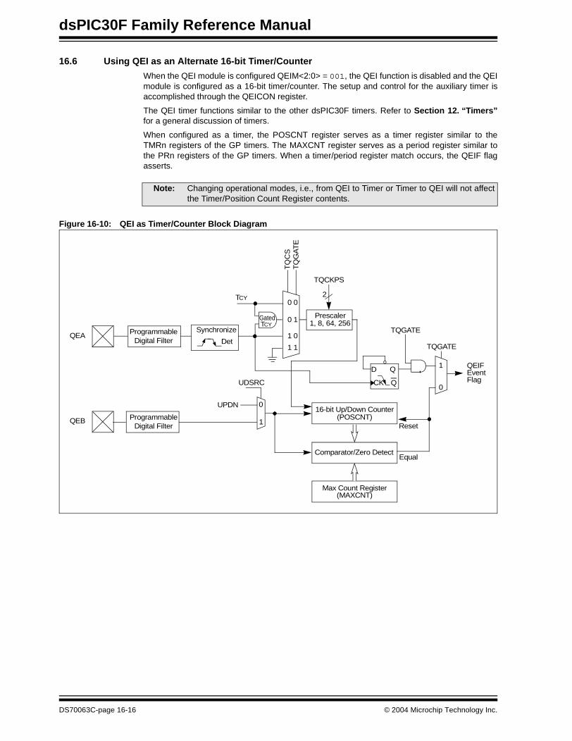
dsPIC30F Family Reference Manual
16.6 Using QEI as an Alternate 16-bit Timer/Counter
When the QEI module is configured QEIM<2:0> = 001, the QEI function is disabled and the QEImodule is configured as a 16-bit timer/counter. The setup and control for the auxiliary timer isaccomplished through the QEICON register.
The QEI timer functions similar to the other dsPIC30F timers. Refer to Section 12. “Timers”for a general discussion of timers.
When configured as a timer, the POSCNT register serves as a timer register similar to theTMRn registers of the GP timers. The MAXCNT register serves as a period register similar tothe PRn registers of the GP timers. When a timer/period register match occurs, the QEIF flagasserts.
Figure 16-10: QEI as Timer/Counter Block Diagram
Note: Changing operational modes, i.e., from QEI to Timer or Timer to QEI will not affectthe Timer/Position Count Register contents.
16-bit Up/Down Counter
Comparator/Zero Detect
Max Count Register
ProgrammableDigital Filter
QEA
ProgrammableDigital Filter
QEB (POSCNT)
(MAXCNT)
QEIFEvent Flag
Reset
Equal
1
0
TQCKPS
2
1, 8, 64, 256 Prescaler
Q
QD
CK
TQGATESynchronize
Det
0 0
UDSRC
UPDN
1
0
TQGATE
0 1
1 0
TQ
CS
TQ
GA
TE
1 1
GatedTCY
TCY
DS70063C-page 16-16 © 2004 Microchip Technology Inc.
Section 16. Quadrature Encoder Interface (QEI)Q
uad
rature E
nco
der
Interface (Q
EI)
16
16.6.1 Up/Down Timer OperationThe QEI timer can increment or decrement. This is a unique feature over most other timers.
When the timer is configured to count up, the timer (POSCNT) will increment until the countmatches the period register (MAXCNT). The timer resets to zero and restarts incrementing.
When the timer is configured to count down, the timer (POSCNT) will decrement until the countmatches the period register (MAXCNT). The timer resets to zero and restarts decrementing.
When the timer is configured to count down some general operation guidelines must befollowed for correct operation.
1. The MAXCNT register will serve as the period match register but because the counter isdecrementing, the desired match value is 2 count. For example, to count 0x1000 clocks,the period register must be loaded with 0xF000.
2. On a match condition, the timer resets to zero.
Either an I/O pin or a SFR control bit specify the count direction control.
Control bit UDSRC (QEICON<0>) determines what controls the timer count direction state.
When UDSRC = 1, the timer count direction is controlled from the QEB pin. If the QEB pin is ’1’,the count direction will be incrementing. If the QEB pin is ‘0’, the count direction will bedecrementing.
When UDSRC = 0, the timer count direction is controlled from the UPDN bit (QEICON<11>).When UPDN = 1, the timer increments. When UPDN = 0, the timer decrements.
16.6.2 Timer External Clock
The TQCS bit (QEICON<1>) selects internal or external clock. The QEI timer can use the QEApin as an external clock input when TQCS is set. The QEI timer does not support the externalasynchronous counter mode. If using an external clock source the clock will automatically besynchronized to the internal instruction cycle (TCY).
16.6.3 Timer Gate Operation
The QEA pin functions as a timer gate when the TQGATE bit (QEICON<5>) is set and TQCS iscleared.
In the event TQCS and TQGATE are concurrently set, the timer does not increment and doesnot generate an interrupt.
16.7 Quadrature Encoder Interface Interrupts
Depending on the mode of the QEI, the QEI will generate interrupts for the following events:
• When operating in reset on match mode, QEIM<2:0> = ‘111’ and ‘101’, an interrupt occurs on position counter rollover/underflow.
• When operating in reset on index mode, QEIM<2:0> = ‘110’ and ‘100’, an interrupt occurs on detection of index pulse and optionally when CNTERR bit is set.
• When operating as a Timer/Counter, QEIM<2:0> = ‘001’, an interrupt occurs on a period match event or a timer gate falling edge event when TQGATE = 1.
When a QEI interrupt event occurs, the QEIIF bit (IFS2<8>) is asserted and an interrupt will begenerated if enabled. The QEIIF bit must be cleared in software.
Enabling the QEI interrupt is accomplished via the respective enable bit, QEIIE (IEC2<8>).
© 2004 Microchip Technology Inc. DS70063C-page 16-17
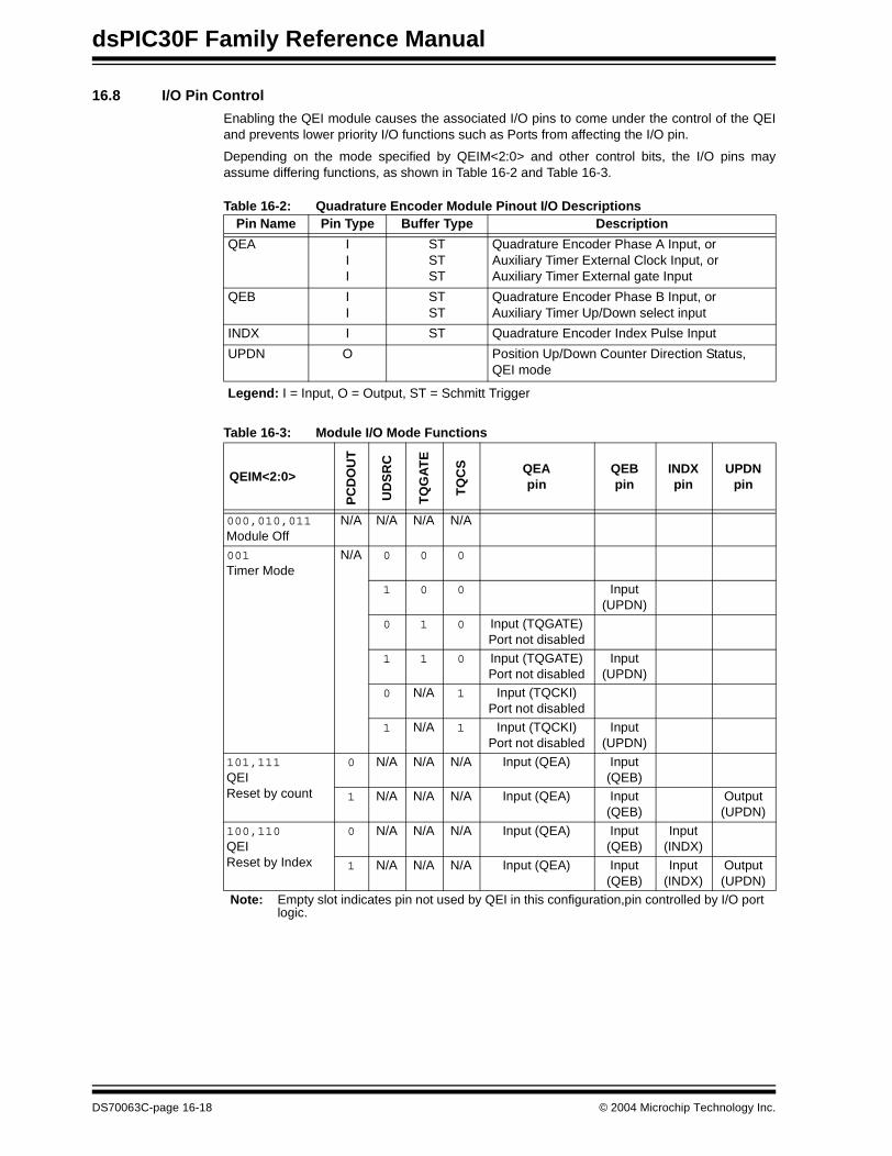
dsPIC30F Family Reference Manual
16.8 I/O Pin Control
Enabling the QEI module causes the associated I/O pins to come under the control of the QEIand prevents lower priority I/O functions such as Ports from affecting the I/O pin.
Depending on the mode specified by QEIM<2:0> and other control bits, the I/O pins mayassume differing functions, as shown in Table 16-2 and Table 16-3.
Table 16-2: Quadrature Encoder Module Pinout I/O Descriptions
Table 16-3: Module I/O Mode Functions
Pin Name Pin Type Buffer Type Description
QEA III
STSTST
Quadrature Encoder Phase A Input, orAuxiliary Timer External Clock Input, orAuxiliary Timer External gate Input
QEB II
STST
Quadrature Encoder Phase B Input, orAuxiliary Timer Up/Down select input
INDX I ST Quadrature Encoder Index Pulse Input
UPDN O Position Up/Down Counter Direction Status,QEI mode
Legend: I = Input, O = Output, ST = Schmitt Trigger
QEIM<2:0>
PC
DO
UT
UD
SR
C
TQ
GA
TE
TQ
CS QEA
pinQEBpin
INDXpin
UPDNpin
000,010,011Module Off
N/A N/A N/A N/A
001Timer Mode
N/A 0 0 0
1 0 0 Input(UPDN)
0 1 0 Input (TQGATE)Port not disabled
1 1 0 Input (TQGATE)Port not disabled
Input(UPDN)
0 N/A 1 Input (TQCKI)Port not disabled
1 N/A 1 Input (TQCKI)Port not disabled
Input(UPDN)
101,111QEI Reset by count
0 N/A N/A N/A Input (QEA) Input (QEB)
1 N/A N/A N/A Input (QEA) Input(QEB)
Output(UPDN)
100,110QEIReset by Index
0 N/A N/A N/A Input (QEA) Input(QEB)
Input(INDX)
1 N/A N/A N/A Input (QEA) Input(QEB)
Input(INDX)
Output(UPDN)
Note: Empty slot indicates pin not used by QEI in this configuration,pin controlled by I/O portlogic.
DS70063C-page 16-18 © 2004 Microchip Technology Inc.
Section 16. Quadrature Encoder Interface (QEI)Q
uad
rature E
nco
der
Interface (Q
EI)
16
16.9 QEI Operation During Power Saving Modes16.9.1 When the Device Enters Sleep
When the device enters Sleep mode, the QEI will cease all operations. POSCNT will stop at thecurrent value. The QEI will not respond to active signals on the QEA, QEB, INDX or UPDN pins.
The QEICON register will remain unchanged.
If the QEI is configured as a timer/counter, QEIM<2:0> = ‘001’, and the clock is providedexternally, TQCS = 1, the module will also cease operation during Sleep mode.
When the module wakes up, the quadrature decoder will accept the next transition on the QEAor QEB signals and compare that transition to the last transition before Sleep to determine thenext action.
16.9.2 When the Device Enters Idle
The module will enter a power saving state in Idle mode depending on the QEISIDL bit(QEICON<13>).
If QEICSIDL = 1, then the module will enter the power saving mode, similar to actions whileentering Sleep mode.
If QEICSIDL = 0, then the module will not enter a power saving mode. The module will continueto operate normally while the device is in Idle mode.
16.10 Effects of a Reset
Reset forces module registers to their initial reset state. See Register 16-1 for all initializationand reset conditions for QEI module related registers.
The quadrature decoder and the POSCNT counter are reset to an initial state.
© 2004 Microchip Technology Inc. DS70063C-page 16-19
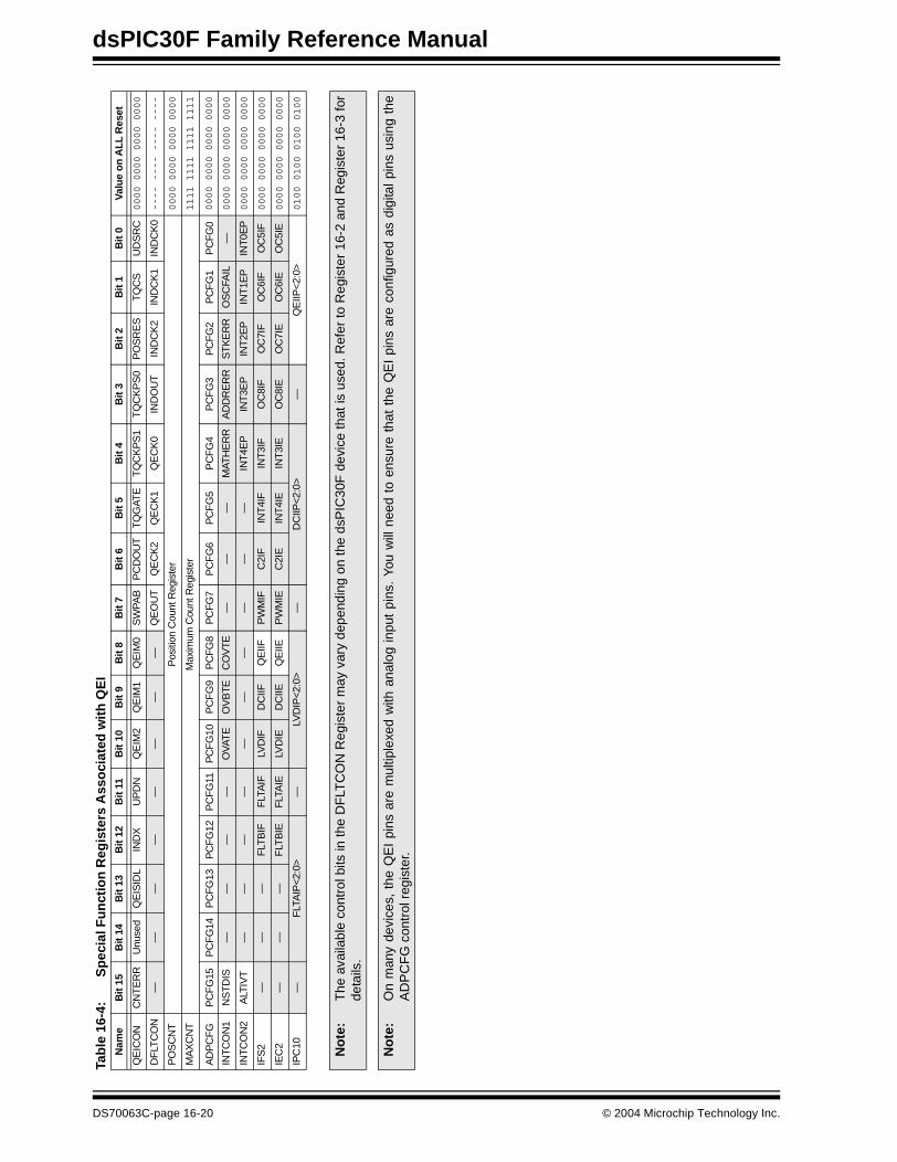
dsPIC30F Family Reference Manual
Tab
le 1
6-4:
Sp
ecia
l Fu
nct
ion
Reg
iste
rs A
sso
ciat
ed w
ith
QE
IN
ame
Bit
15
Bit
14B
it 1
3B
it 12
Bit
11B
it 10
Bit
9B
it 8
Bit
7B
it 6
Bit
5B
it 4
Bit
3B
it 2
Bit
1B
it 0
Val
ue
on
AL
L R
eset
QE
ICO
NC
NT
ER
RU
nuse
dQ
EIS
IDL
IND
XU
PD
NQ
EIM
2Q
EIM
1Q
EIM
0S
WP
AB
PC
DO
UT
TQ
GAT
ET
QC
KP
S1
TQ
CK
PS
0P
OS
RE
ST
QC
SU
DS
RC
0000 0000 0000 0000
DF
LTC
ON
——
——
——
——
QE
OU
TQ
EC
K2
QE
CK
1Q
EC
K0
IND
OU
TIN
DC
K2
IND
CK
1IN
DC
K0
---- ---- ---- ----
PO
SC
NT
Pos
ition
Cou
nt R
egis
ter
0000 0000 0000 0000
MA
XC
NT
Max
imum
Cou
nt R
egis
ter
1111 1111 1111 1111
AD
PC
FG
PC
FG
15P
CF
G14
PC
FG
13P
CF
G12
PC
FG
11P
CF
G10
PC
FG
9P
CF
G8
PC
FG
7P
CF
G6
PC
FG
5P
CF
G4
PC
FG
3P
CF
G2
PC
FG
1P
CF
G0
0000 0000 0000 0000
INT
CO
N1
NS
TD
IS—
——
—O
VAT
EO
VB
TE
CO
VT
E—
——
MAT
HE
RR
AD
DR
ER
RS
TK
ER
RO
SC
FAIL
—0000 0000 0000 0000
INT
CO
N2
ALT
IVT
——
——
——
——
——
INT
4EP
INT
3EP
INT
2EP
INT
1EP
INT
0EP
0000 0000 0000 0000
IFS
2—
——
FLT
BIF
FLT
AIF
LVD
IFD
CIIF
QE
IIFP
WM
IFC
2IF
INT
4IF
INT
3IF
OC
8IF
OC
7IF
OC
6IF
OC
5IF
0000 0000 0000 0000
IEC
2—
——
FLT
BIE
FLT
AIE
LVD
IED
CIIE
QE
IIEP
WM
IEC
2IE
INT
4IE
INT
3IE
OC
8IE
OC
7IE
OC
6IE
OC
5IE
0000 0000 0000 0000
IPC
10—
FLT
AIP
<2:0
>—
LVD
IP<2
:0>
—D
CIIP
<2:0
>—
QE
IIP<2
:0>
0100 0100 0100 0100
No
te:
The
ava
ilabl
e co
ntro
l bits
in th
e D
FLT
CO
N R
egis
ter
may
var
y de
pend
ing
on th
e ds
PIC
30F
dev
ice
that
is u
sed.
Ref
er to
Reg
iste
r 16
-2 a
nd R
egis
ter
16-3
for
deta
ils.
No
te:
On
man
y de
vice
s, t
he Q
EI
pins
are
mul
tiple
xed
with
ana
log
inpu
t pi
ns.
You
will
nee
d to
ens
ure
that
the
QE
I pi
ns a
re c
onfig
ured
as
digi
tal p
ins
usin
g th
eA
DP
CF
G c
ontr
ol r
egis
ter.
DS70063C-page 16-20 © 2004 Microchip Technology Inc.
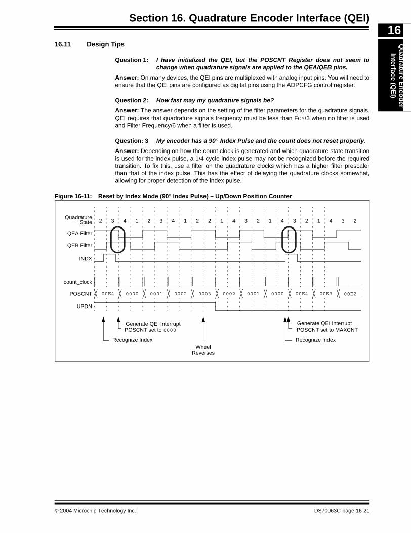
Section 16. Quadrature Encoder Interface (QEI)Q
uad
rature E
nco
der
Interface (Q
EI)
16
16.11 Design TipsQuestion 1: I have initialized the QEI, but the POSCNT Register does not seem tochange when quadrature signals are applied to the QEA/QEB pins.
Answer: On many devices, the QEI pins are multiplexed with analog input pins. You will need toensure that the QEI pins are configured as digital pins using the ADPCFG control register.
Question 2: How fast may my quadrature signals be?
Answer: The answer depends on the setting of the filter parameters for the quadrature signals.QEI requires that quadrature signals frequency must be less than FCY/3 when no filter is usedand Filter Frequency/6 when a filter is used.
Question: 3 My encoder has a 90° Index Pulse and the count does not reset properly.
Answer: Depending on how the count clock is generated and which quadrature state transitionis used for the index pulse, a 1/4 cycle index pulse may not be recognized before the requiredtransition. To fix this, use a filter on the quadrature clocks which has a higher filter prescalerthan that of the index pulse. This has the effect of delaying the quadrature clocks somewhat,allowing for proper detection of the index pulse.
Figure 16-11: Reset by Index Mode (90° Index Pulse) – Up/Down Position Counter
POSCNT
QEA Filter
QEB Filter
UPDN
count_clock
00E4 00E2
Recognize Index
POSCNT set to MAXCNTGenerate QEI Interrupt
WheelReverses
INDX
2 3 4 1 2 3 4 1 2 2 1 4 3 2 1 4 3 2 1 4 3 2Quadrature
State
0000 0001 0002 0003 0002 0001 0000 00E4 00E3
Recognize Index
POSCNT set to 0000Generate QEI Interrupt
© 2004 Microchip Technology Inc. DS70063C-page 16-21
dsPIC30F Family Reference Manual
16.12 Related Application Notes
This section lists application notes that are related to this section of the manual. Theseapplication notes may not be written specifically for the dsPIC30F Product Family, but theconcepts are pertinent and could be used with modification and possible limitations. The currentapplication notes related to the Quadrature Encoder Interface (QEI) module are:
Title Application Note #
Servo Control of a DC-Brush Motor AN532PIC18CXXX/PIC16CXXX DC Servomotor AN696Using the dsPIC30F for Vector Control of an ACIM AN908
Note: Please visit the Microchip web site (www.microchip.com) for additional ApplicationNotes and code examples for the dsPIC30F Family of devices.
DS70063C-page 16-22 © 2004 Microchip Technology Inc.
Section 16. Quadrature Encoder Interface (QEI)Q
uad
rature E
nco
der
Interface (Q
EI)
16
16.13 Revision HistoryRevision A
This is the initial released revision of this document.
Revision B
This revision provides expanded information for the dsPIC30F Quadrature Encoder Interface(QEI) module.
Revision C
This revision incorporates all known errata at the time of this document update.
© 2004 Microchip Technology Inc. DS70063C-page 16-23

dsPIC30F Family Reference Manual
NOTES:
DS70063C-page 16-24 © 2004 Microchip Technology Inc.
Section 17. 10-bit A/D Converter
10-bit A
/DC
on
verter
17
HIGHLIGHTSThis section of the manual contains the following major topics:
17.1 Introduction .................................................................................................................. 17-2
17.2 Control Registers ......................................................................................................... 17-417.3 A/D Result Buffer ......................................................................................................... 17-417.4 A/D Terminology and Conversion Sequence ............................................................. 17-11
17.5 A/D Module Configuration.......................................................................................... 17-1317.6 Selecting the Voltage Reference Source ................................................................... 17-1317.7 Selecting the A/D Conversion Clock .......................................................................... 17-13
17.8 Selecting Analog Inputs for Sampling ........................................................................ 17-1417.9 Enabling the Module .................................................................................................. 17-1617.10 Specifying the Sample/Conversion Sequence........................................................... 17-16
17.11 How to Start Sampling ............................................................................................... 17-1717.12 How to Stop Sampling and Start Conversions ........................................................... 17-1817.13 Controlling Sample/Conversion Operation................................................................. 17-29
17.14 Specifying How Conversion Results are Written Into the Buffer ................................ 17-3017.15 Conversion Sequence Examples............................................................................... 17-3117.16 A/D Sampling Requirements...................................................................................... 17-45
17.17 Reading the A/D Result Buffer................................................................................... 17-4617.18 Transfer Function....................................................................................................... 17-4717.19 A/D Accuracy/Error .................................................................................................... 17-47
17.20 Connection Considerations........................................................................................ 17-4717.21 Initialization ................................................................................................................ 17-4817.22 A/D Conversion Speeds............................................................................................. 17-49
17.23 Operation During Sleep and Idle Modes.................................................................... 17-5517.24 Effects of a Reset....................................................................................................... 17-5517.25 Special Function Registers Associated with the 10-bit A/D Converter ...................... 17-56
17.26 Design Tips ................................................................................................................ 17-5717.27 Related Application Notes.......................................................................................... 17-5817.28 Revision History ......................................................................................................... 17-59
© 2005 Microchip Technology Inc. DS70064D-page 17-1
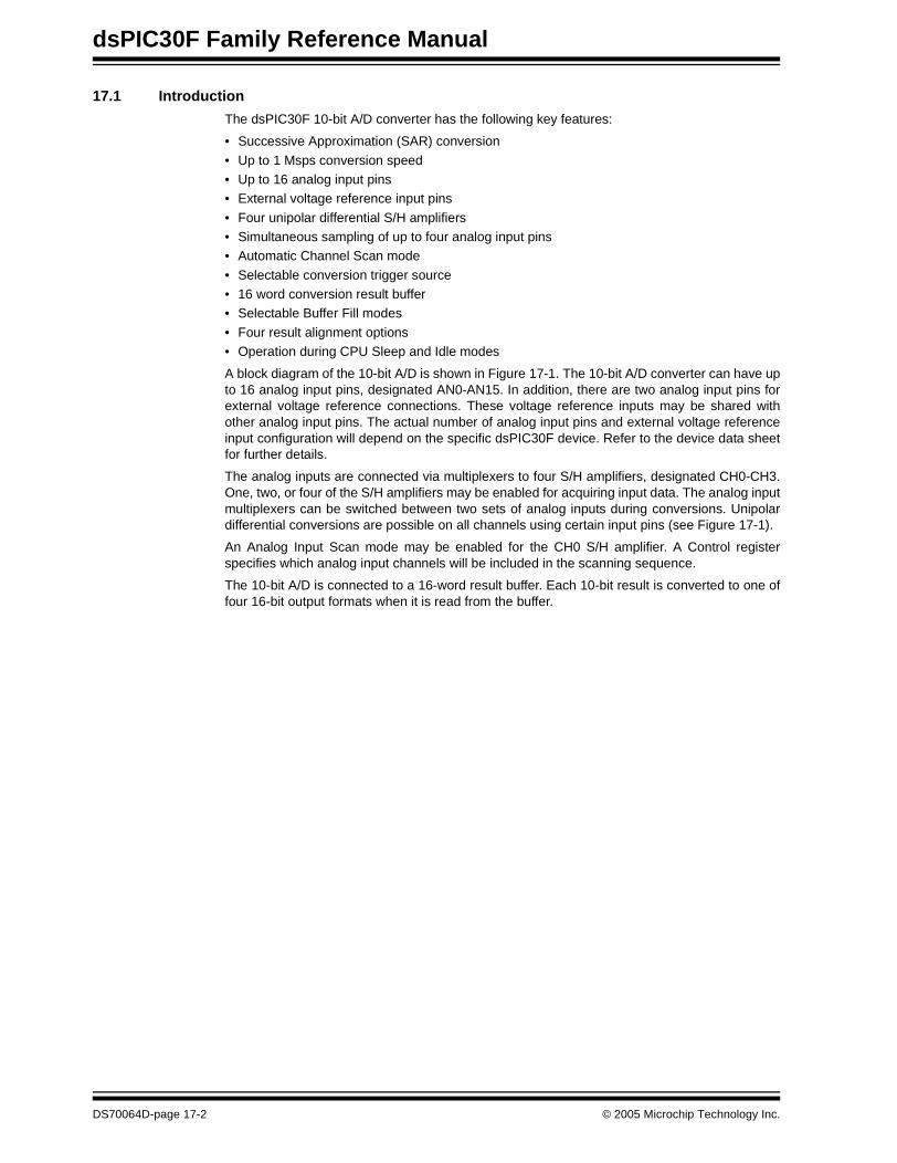
dsPIC30F Family Reference Manual
17.1 Introduction
The dsPIC30F 10-bit A/D converter has the following key features:
• Successive Approximation (SAR) conversion
• Up to 1 Msps conversion speed• Up to 16 analog input pins• External voltage reference input pins
• Four unipolar differential S/H amplifiers • Simultaneous sampling of up to four analog input pins• Automatic Channel Scan mode
• Selectable conversion trigger source• 16 word conversion result buffer• Selectable Buffer Fill modes
• Four result alignment options • Operation during CPU Sleep and Idle modes
A block diagram of the 10-bit A/D is shown in Figure 17-1. The 10-bit A/D converter can have upto 16 analog input pins, designated AN0-AN15. In addition, there are two analog input pins forexternal voltage reference connections. These voltage reference inputs may be shared withother analog input pins. The actual number of analog input pins and external voltage referenceinput configuration will depend on the specific dsPIC30F device. Refer to the device data sheetfor further details.
The analog inputs are connected via multiplexers to four S/H amplifiers, designated CH0-CH3.One, two, or four of the S/H amplifiers may be enabled for acquiring input data. The analog inputmultiplexers can be switched between two sets of analog inputs during conversions. Unipolardifferential conversions are possible on all channels using certain input pins (see Figure 17-1).
An Analog Input Scan mode may be enabled for the CH0 S/H amplifier. A Control registerspecifies which analog input channels will be included in the scanning sequence.
The 10-bit A/D is connected to a 16-word result buffer. Each 10-bit result is converted to one offour 16-bit output formats when it is read from the buffer.
DS70064D-page 17-2 © 2005 Microchip Technology Inc.
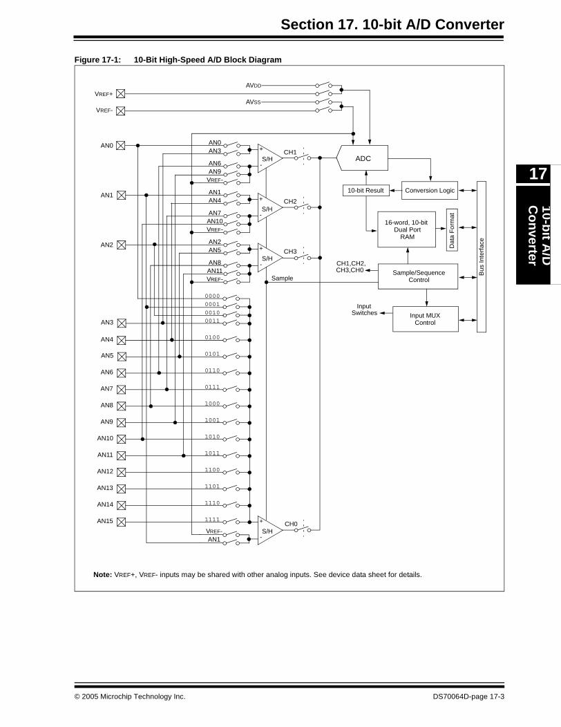
Section 17. 10-bit A/D Converter10-b
it A/D
Co
nverter
17
Figure 17-1: 10-Bit High-Speed A/D Block Diagram
S/H
+
-
10-bit Result Conversion Logic
VREF+AVSS
AVDD
ADC
Dat
a F
orm
at
16-word, 10-bitDual Port
RAM
Bus
Inte
rfac
e
AN12
0000
0101
0111
1001
1101
1110
1111
1100
000100100011
0100
0110
1000
1010
1011
AN13
AN14
AN15
AN8
AN9
AN10
AN11
AN2
AN4
AN7
AN0
AN3
AN1
AN5
CH1
CH2
CH3
CH0
AN5AN2
AN11AN8
VREF-
AN4AN1
AN10AN7
VREF-
AN3AN0
AN9AN6
VREF-
AN1VREF-
VREF-
Sample/SequenceControlSample
CH1,CH2,CH3,CH0
Input MUXControl
InputSwitches
S/H
+
-
S/H
+
-
S/H
+
-
AN6
Note: VREF+, VREF- inputs may be shared with other analog inputs. See device data sheet for details.
© 2005 Microchip Technology Inc. DS70064D-page 17-3
dsPIC30F Family Reference Manual
17.2 Control Registers
The A/D module has six Control and Status registers. These registers are:
• ADCON1: A/D Control Register 1
• ADCON2: A/D Control Register 2• ADCON3: A/D Control Register 3• ADCHS: A/D Input Channel Select Register
• ADPCFG: A/D Port Configuration Register• ADCSSL: A/D Input Scan Selection Register
The ADCON1, ADCON2 and ADCON3 registers control the operation of the A/D module. TheADCHS register selects the input pins to be connected to the S/H amplifiers. The ADPCFGregister configures the analog input pins as analog inputs or as digital I/O. The ADCSSL registerselects inputs to be sequentially scanned.
17.3 A/D Result Buffer
The module contains a 16-word dual port RAM, called ADCBUF, to buffer the A/D results. The16 buffer locations are referred to as ADCBUF0, ADCBUF1, ADCBUF2, ...., ADCBUFE,ADCBUFF.
Note: The A/D result buffer is a read only buffer.
DS70064D-page 17-4 © 2005 Microchip Technology Inc.
Section 17. 10-bit A/D Converter10-b
it A/D
Co
nverter
17
Register 17-1: ADCON1: A/D Control Register 1
Upper Byte:R/W-0 U-0 R/W-0 U-0 U-0 U-0 R/W-0 R/W-0ADON — ADSIDL — — — FORM<1:0>
bit 15 bit 8
Lower Byte:R/W-0 R/W-0 R/W-0 U-0 R/W-0 R/W-0 R/W-0
HC, HSR/C-0
HC, HS
SSRC<2:0> — SIMSAM ASAM SAMP DONEbit 7 bit 0
bit 15 ADON: A/D Operating Mode bit1 = A/D converter module is operating0 = A/D converter is off
bit 14 Unimplemented: Read as ‘0’
bit 13 ADSIDL: Stop in Idle Mode bit1 = Discontinue module operation when device enters Idle mode0 = Continue module operation in Idle mode
bit 12-10 Unimplemented: Read as ‘0’
bit 9-8 FORM<1:0>: Data Output Format bits11 = Signed Fractional (DOUT = sddd dddd dd00 0000)10 = Fractional (DOUT = dddd dddd dd00 0000)01 = Signed Integer (DOUT = ssss sssd dddd dddd)00 = Integer (DOUT = 0000 00dd dddd dddd)
bit 7-5 SSRC<2:0>: Conversion Trigger Source Select bits111 = Internal counter ends sampling and starts conversion (auto convert)110 = Reserved101 = Reserved100 = Reserved011 = Motor Control PWM interval ends sampling and starts conversion010 = GP Timer3 compare ends sampling and starts conversion001 = Active transition on INT0 pin ends sampling and starts conversion000 = Clearing SAMP bit ends sampling and starts conversion
bit 4 Unimplemented: Read as ‘0’
bit 3 SIMSAM: Simultaneous Sample Select bit (only applicable when CHPS = 01 or 1x)1 = Samples CH0, CH1, CH2, CH3 simultaneously (when CHPS = 1x)
orSamples CH0 and CH1 simultaneously (when CHPS = 01)
0 = Samples multiple channels individually in sequence
bit 2 ASAM: A/D Sample Auto-Start bit1 = Sampling begins immediately after last conversion completes. SAMP bit is auto set0 = Sampling begins when SAMP bit set
© 2005 Microchip Technology Inc. DS70064D-page 17-5
dsPIC30F Family Reference Manual
Register 17-1: ADCON1: A/D Control Register 1 (Continued)
bit 1 SAMP: A/D Sample Enable bit1 = At least one A/D sample/hold amplifier is sampling0 = A/D sample/hold amplifiers are holdingWhen ASAM = 0, writing ‘1’ to this bit will start samplingWhen SSRC = 000, writing ‘0’ to this bit will end sampling and start conversion
bit 0 DONE: A/D Conversion Status bit (Rev. B silicon or later)1 = A/D conversion is done0 = A/D conversion is NOT doneCleared by software or start of a new conversionClearing this bit will not effect any operation in progress
Legend:
R = Readable bit W = Writable bit U = Unimplemented bit, read as ‘0’
HC = Hardware clear HS = Hardware set C = Clearable by software
-n = Value at POR ‘1’ = Bit is set ‘0’ = Bit is cleared x = Bit is unknown
DS70064D-page 17-6 © 2005 Microchip Technology Inc.
Section 17. 10-bit A/D Converter10-b
it A/D
Co
nverter
17
Register 17-2: ADCON2: A/D Control Register 2
Upper Byte:R/W-0 R/W-0 R/W-0 U-0 U-0 R/W-0 R/W-0 R/W-0
VCFG<2:0> reserved — CSCNA CHPS<1:0>
bit 15 bit 8
Lower Byte:R-0 U-0 R/W-0 R/W-0 R/W-0 R/W-0 R/W-0 R/W-0
BUFS — SMPI<3:0> BUFM ALTSbit 7 bit 0
bit 15-13 VCFG<2:0>: Voltage Reference Configuration bits
bit 12 Reserved: User should write ‘0’ to this location
bit 11 Unimplemented: Read as ‘0’
bit 10 CSCNA: Scan Input Selections for CH0+ S/H Input for MUX A Input Multiplexer Setting bit1 = Scan inputs0 = Do not scan inputs
bit 9-8 CHPS<1:0>: Selects Channels Utilized bits1x = Converts CH0, CH1, CH2 and CH301 = Converts CH0 and CH100 = Converts CH0When SIMSAM bit (ADCON1<3>) = 0 multiple channels sampled sequentiallyWhen SMSAM bit (ADCON1<3>) = 1 multiple channels sampled as in CHPS<1:0>
bit 7 BUFS: Buffer Fill Status bitOnly valid when BUFM = 1 (ADRES split into 2 x 8-word buffers).1 = A/D is currently filling buffer 0x8-0xF, user should access data in 0x0-0x70 = A/D is currently filling buffer 0x0-0x7, user should access data in 0x8-0xF
bit 6 Unimplemented: Read as ‘0’
bit 5-2 SMPI<3:0>: Sample/Convert Sequences Per Interrupt Selection bits1111 = Interrupts at the completion of conversion for each 16th sample/convert sequence1110 = Interrupts at the completion of conversion for each 15th sample/convert sequence.....0001 = Interrupts at the completion of conversion for each 2nd sample/convert sequence0000 = Interrupts at the completion of conversion for each sample/convert sequence
bit 1 BUFM: Buffer Mode Select bit1 = Buffer configured as two 8-word buffers ADCBUF(15...8), ADCBUF(7...0)0 = Buffer configured as one 16-word buffer ADCBUF(15...0.)
bit 0 ALTS: Alternate Input Sample Mode Select bit1 = Uses MUX A input multiplexer settings for first sample, then alternate between MUX B and MUX A input
multiplexer settings for all subsequent samples0 = Always use MUX A input multiplexer settings
Legend:
R = Readable bit W = Writable bit U = Unimplemented bit, read as ‘0’
-n = Value at POR ‘1’ = Bit is set ‘0’ = Bit is cleared x = Bit is unknown
A/D VREFH A/D VREFL000 AVDD AVSS
001 External VREF+ pin AVSS
010 AVDD External VREF- pin011 External VREF+ pin External VREF- pin1XX AVDD AVSS
© 2005 Microchip Technology Inc. DS70064D-page 17-7
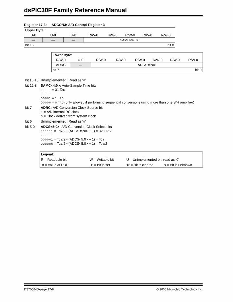
dsPIC30F Family Reference Manual
Register 17-3: ADCON3: A/D Control Register 3
Upper Byte:U-0 U-0 U-0 R/W-0 R/W-0 R/W-0 R/W-0 R/W-0— — — SAMC<4:0>
bit 15 bit 8
Lower Byte:R/W-0 U-0 R/W-0 R/W-0 R/W-0 R/W-0 R/W-0 R/W-0ADRC — ADCS<5:0>
bit 7 bit 0
bit 15-13 Unimplemented: Read as ‘0’
bit 12-8 SAMC<4:0>: Auto-Sample Time bits11111 = 31 TAD
·····00001 = 1 TAD
00000 = 0 TAD (only allowed if performing sequential conversions using more than one S/H amplifier)
bit 7 ADRC: A/D Conversion Clock Source bit1 = A/D internal RC clock0 = Clock derived from system clock
bit 6 Unimplemented: Read as ‘0’
bit 5-0 ADCS<5:0>: A/D Conversion Clock Select bits111111 = TCY/2 • (ADCS<5:0> + 1) = 32 • TCY
······000001 = TCY/2 • (ADCS<5:0> + 1) = TCY
000000 = TCY/2 • (ADCS<5:0> + 1) = TCY/2
Legend:
R = Readable bit W = Writable bit U = Unimplemented bit, read as ‘0’
-n = Value at POR ‘1’ = Bit is set ‘0’ = Bit is cleared x = Bit is unknown
DS70064D-page 17-8 © 2005 Microchip Technology Inc.
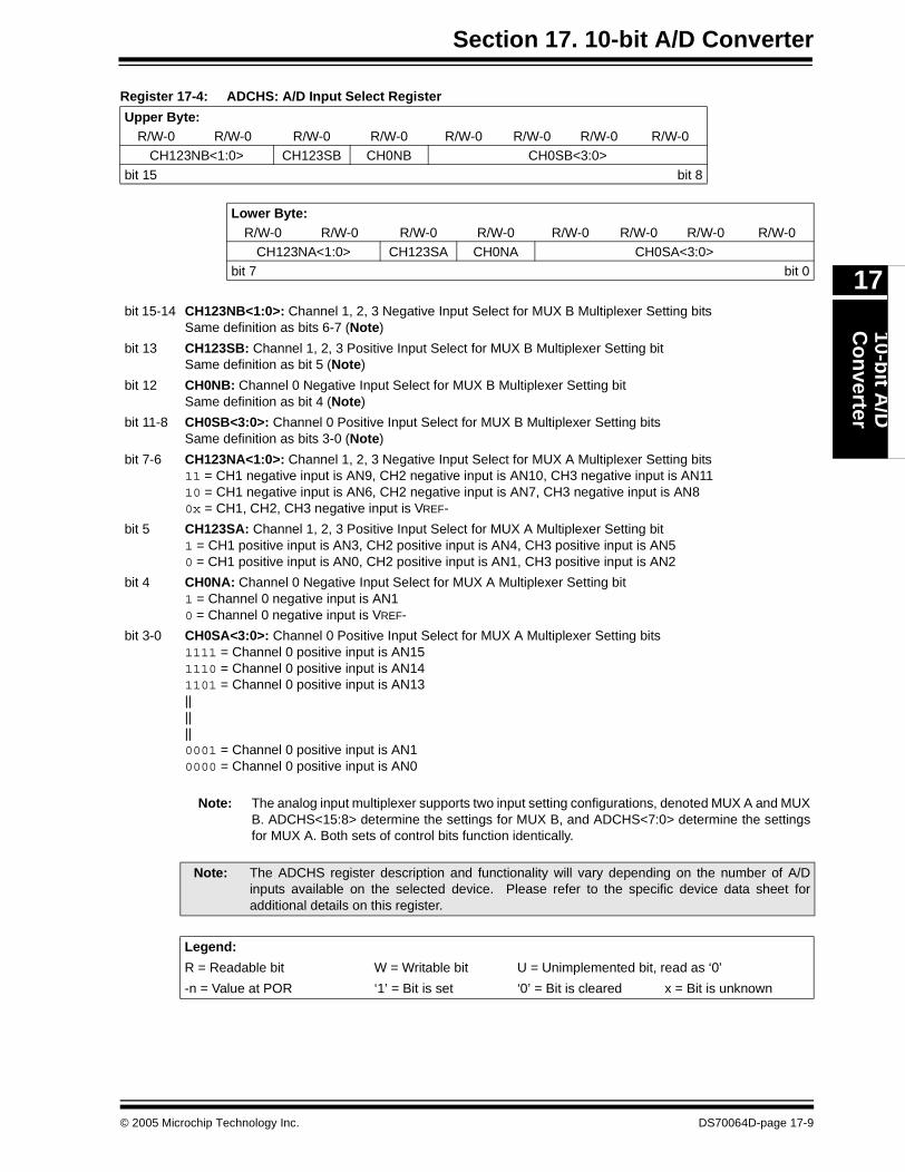
Section 17. 10-bit A/D Converter10-b
it A/D
Co
nverter
17
Register 17-4: ADCHS: A/D Input Select Register
Upper Byte:R/W-0 R/W-0 R/W-0 R/W-0 R/W-0 R/W-0 R/W-0 R/W-0
CH123NB<1:0> CH123SB CH0NB CH0SB<3:0>
bit 15 bit 8
Lower Byte:R/W-0 R/W-0 R/W-0 R/W-0 R/W-0 R/W-0 R/W-0 R/W-0
CH123NA<1:0> CH123SA CH0NA CH0SA<3:0>bit 7 bit 0
bit 15-14 CH123NB<1:0>: Channel 1, 2, 3 Negative Input Select for MUX B Multiplexer Setting bitsSame definition as bits 6-7 (Note)
bit 13 CH123SB: Channel 1, 2, 3 Positive Input Select for MUX B Multiplexer Setting bitSame definition as bit 5 (Note)
bit 12 CH0NB: Channel 0 Negative Input Select for MUX B Multiplexer Setting bitSame definition as bit 4 (Note)
bit 11-8 CH0SB<3:0>: Channel 0 Positive Input Select for MUX B Multiplexer Setting bitsSame definition as bits 3-0 (Note)
bit 7-6 CH123NA<1:0>: Channel 1, 2, 3 Negative Input Select for MUX A Multiplexer Setting bits11 = CH1 negative input is AN9, CH2 negative input is AN10, CH3 negative input is AN1110 = CH1 negative input is AN6, CH2 negative input is AN7, CH3 negative input is AN80x = CH1, CH2, CH3 negative input is VREF-
bit 5 CH123SA: Channel 1, 2, 3 Positive Input Select for MUX A Multiplexer Setting bit1 = CH1 positive input is AN3, CH2 positive input is AN4, CH3 positive input is AN50 = CH1 positive input is AN0, CH2 positive input is AN1, CH3 positive input is AN2
bit 4 CH0NA: Channel 0 Negative Input Select for MUX A Multiplexer Setting bit1 = Channel 0 negative input is AN10 = Channel 0 negative input is VREF-
bit 3-0 CH0SA<3:0>: Channel 0 Positive Input Select for MUX A Multiplexer Setting bits1111 = Channel 0 positive input is AN151110 = Channel 0 positive input is AN141101 = Channel 0 positive input is AN13||||||0001 = Channel 0 positive input is AN10000 = Channel 0 positive input is AN0
Note: The analog input multiplexer supports two input setting configurations, denoted MUX A and MUXB. ADCHS<15:8> determine the settings for MUX B, and ADCHS<7:0> determine the settingsfor MUX A. Both sets of control bits function identically.
Note: The ADCHS register description and functionality will vary depending on the number of A/Dinputs available on the selected device. Please refer to the specific device data sheet foradditional details on this register.
Legend:
R = Readable bit W = Writable bit U = Unimplemented bit, read as ‘0’
-n = Value at POR ‘1’ = Bit is set ‘0’ = Bit is cleared x = Bit is unknown
© 2005 Microchip Technology Inc. DS70064D-page 17-9
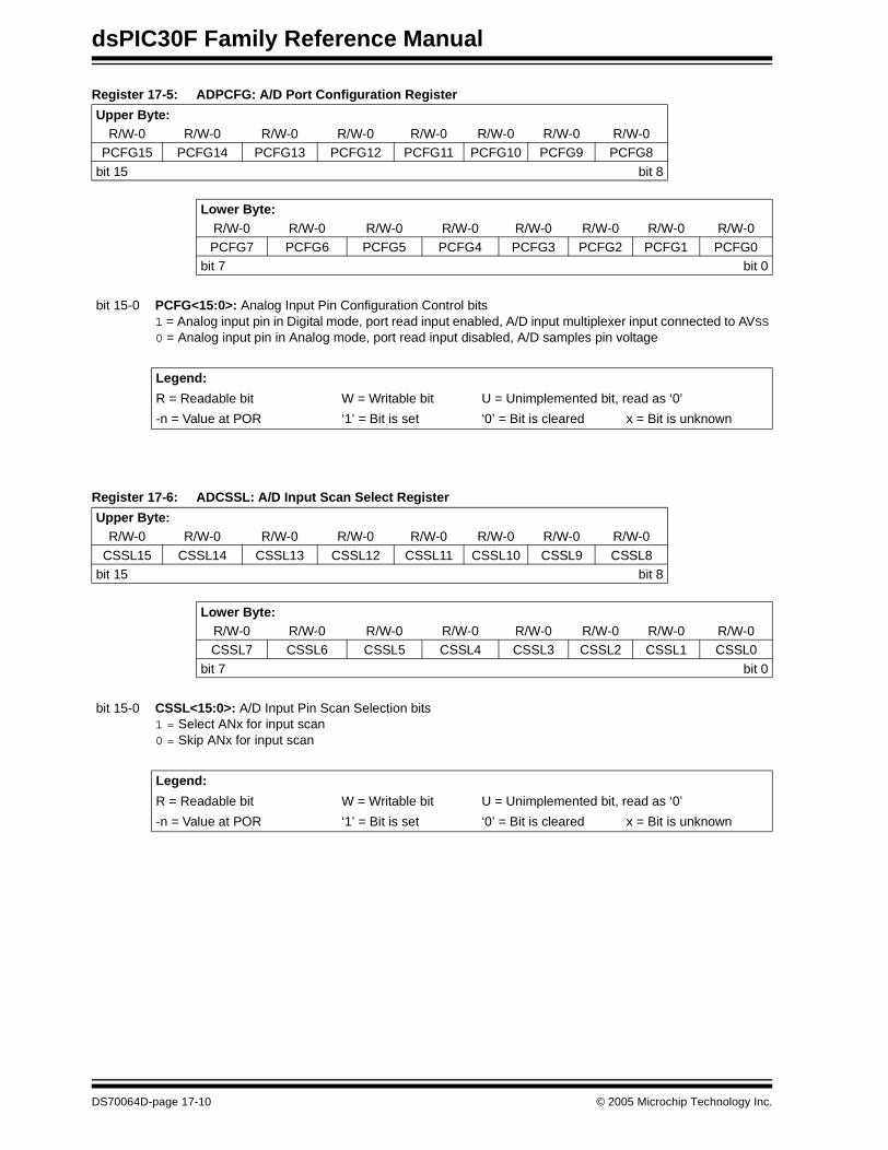
dsPIC30F Family Reference Manual
Register 17-5: ADPCFG: A/D Port Configuration Register
Register 17-6: ADCSSL: A/D Input Scan Select Register
Upper Byte:R/W-0 R/W-0 R/W-0 R/W-0 R/W-0 R/W-0 R/W-0 R/W-0
PCFG15 PCFG14 PCFG13 PCFG12 PCFG11 PCFG10 PCFG9 PCFG8
bit 15 bit 8
Lower Byte:R/W-0 R/W-0 R/W-0 R/W-0 R/W-0 R/W-0 R/W-0 R/W-0PCFG7 PCFG6 PCFG5 PCFG4 PCFG3 PCFG2 PCFG1 PCFG0
bit 7 bit 0
bit 15-0 PCFG<15:0>: Analog Input Pin Configuration Control bits1 = Analog input pin in Digital mode, port read input enabled, A/D input multiplexer input connected to AVSS
0 = Analog input pin in Analog mode, port read input disabled, A/D samples pin voltage
Legend:
R = Readable bit W = Writable bit U = Unimplemented bit, read as ‘0’
-n = Value at POR ‘1’ = Bit is set ‘0’ = Bit is cleared x = Bit is unknown
Upper Byte:R/W-0 R/W-0 R/W-0 R/W-0 R/W-0 R/W-0 R/W-0 R/W-0
CSSL15 CSSL14 CSSL13 CSSL12 CSSL11 CSSL10 CSSL9 CSSL8bit 15 bit 8
Lower Byte:R/W-0 R/W-0 R/W-0 R/W-0 R/W-0 R/W-0 R/W-0 R/W-0CSSL7 CSSL6 CSSL5 CSSL4 CSSL3 CSSL2 CSSL1 CSSL0
bit 7 bit 0
bit 15-0 CSSL<15:0>: A/D Input Pin Scan Selection bits1 = Select ANx for input scan0 = Skip ANx for input scan
Legend:
R = Readable bit W = Writable bit U = Unimplemented bit, read as ‘0’
-n = Value at POR ‘1’ = Bit is set ‘0’ = Bit is cleared x = Bit is unknown
DS70064D-page 17-10 © 2005 Microchip Technology Inc.
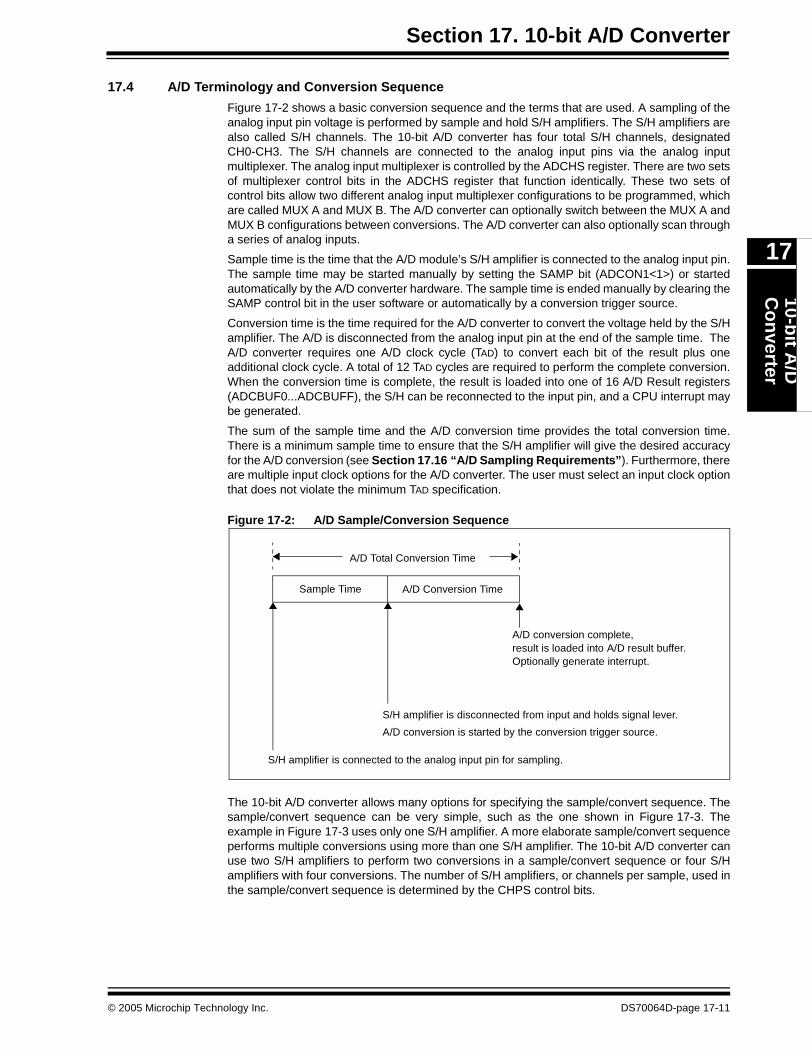
Section 17. 10-bit A/D Converter10-b
it A/D
Co
nverter
17
17.4 A/D Terminology and Conversion Sequence
Figure 17-2 shows a basic conversion sequence and the terms that are used. A sampling of theanalog input pin voltage is performed by sample and hold S/H amplifiers. The S/H amplifiers arealso called S/H channels. The 10-bit A/D converter has four total S/H channels, designatedCH0-CH3. The S/H channels are connected to the analog input pins via the analog inputmultiplexer. The analog input multiplexer is controlled by the ADCHS register. There are two setsof multiplexer control bits in the ADCHS register that function identically. These two sets ofcontrol bits allow two different analog input multiplexer configurations to be programmed, whichare called MUX A and MUX B. The A/D converter can optionally switch between the MUX A andMUX B configurations between conversions. The A/D converter can also optionally scan througha series of analog inputs.
Sample time is the time that the A/D module’s S/H amplifier is connected to the analog input pin.The sample time may be started manually by setting the SAMP bit (ADCON1<1>) or startedautomatically by the A/D converter hardware. The sample time is ended manually by clearing theSAMP control bit in the user software or automatically by a conversion trigger source.
Conversion time is the time required for the A/D converter to convert the voltage held by the S/Hamplifier. The A/D is disconnected from the analog input pin at the end of the sample time. TheA/D converter requires one A/D clock cycle (TAD) to convert each bit of the result plus oneadditional clock cycle. A total of 12 TAD cycles are required to perform the complete conversion.When the conversion time is complete, the result is loaded into one of 16 A/D Result registers(ADCBUF0...ADCBUFF), the S/H can be reconnected to the input pin, and a CPU interrupt maybe generated.
The sum of the sample time and the A/D conversion time provides the total conversion time.There is a minimum sample time to ensure that the S/H amplifier will give the desired accuracyfor the A/D conversion (see Section 17.16 “A/D Sampling Requirements”). Furthermore, thereare multiple input clock options for the A/D converter. The user must select an input clock optionthat does not violate the minimum TAD specification.
Figure 17-2: A/D Sample/Conversion Sequence
The 10-bit A/D converter allows many options for specifying the sample/convert sequence. Thesample/convert sequence can be very simple, such as the one shown in Figure 17-3. Theexample in Figure 17-3 uses only one S/H amplifier. A more elaborate sample/convert sequenceperforms multiple conversions using more than one S/H amplifier. The 10-bit A/D converter canuse two S/H amplifiers to perform two conversions in a sample/convert sequence or four S/Hamplifiers with four conversions. The number of S/H amplifiers, or channels per sample, used inthe sample/convert sequence is determined by the CHPS control bits.
Sample Time A/D Conversion Time
A/D Total Conversion Time
S/H amplifier is connected to the analog input pin for sampling.
S/H amplifier is disconnected from input and holds signal lever.
A/D conversion is started by the conversion trigger source.
A/D conversion complete, result is loaded into A/D result buffer. Optionally generate interrupt.
© 2005 Microchip Technology Inc. DS70064D-page 17-11
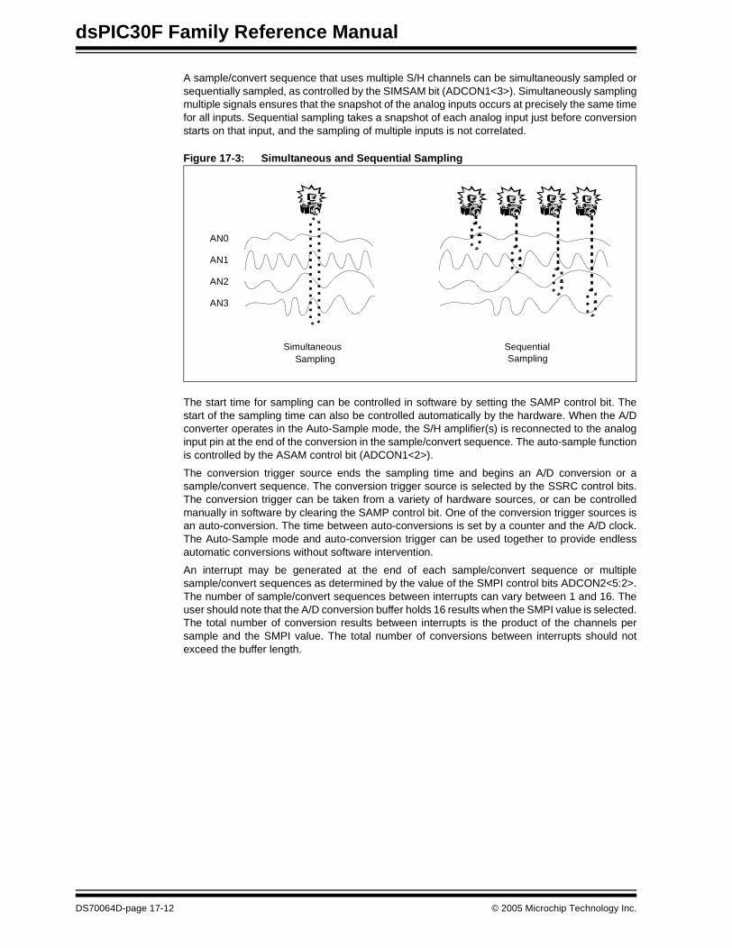
dsPIC30F Family Reference Manual
A sample/convert sequence that uses multiple S/H channels can be simultaneously sampled orsequentially sampled, as controlled by the SIMSAM bit (ADCON1<3>). Simultaneously samplingmultiple signals ensures that the snapshot of the analog inputs occurs at precisely the same timefor all inputs. Sequential sampling takes a snapshot of each analog input just before conversionstarts on that input, and the sampling of multiple inputs is not correlated.
Figure 17-3: Simultaneous and Sequential Sampling
The start time for sampling can be controlled in software by setting the SAMP control bit. Thestart of the sampling time can also be controlled automatically by the hardware. When the A/Dconverter operates in the Auto-Sample mode, the S/H amplifier(s) is reconnected to the analoginput pin at the end of the conversion in the sample/convert sequence. The auto-sample functionis controlled by the ASAM control bit (ADCON1<2>).
The conversion trigger source ends the sampling time and begins an A/D conversion or asample/convert sequence. The conversion trigger source is selected by the SSRC control bits.The conversion trigger can be taken from a variety of hardware sources, or can be controlledmanually in software by clearing the SAMP control bit. One of the conversion trigger sources isan auto-conversion. The time between auto-conversions is set by a counter and the A/D clock.The Auto-Sample mode and auto-conversion trigger can be used together to provide endlessautomatic conversions without software intervention.
An interrupt may be generated at the end of each sample/convert sequence or multiplesample/convert sequences as determined by the value of the SMPI control bits ADCON2<5:2>.The number of sample/convert sequences between interrupts can vary between 1 and 16. Theuser should note that the A/D conversion buffer holds 16 results when the SMPI value is selected.The total number of conversion results between interrupts is the product of the channels persample and the SMPI value. The total number of conversions between interrupts should notexceed the buffer length.
AN0
AN1
AN2
AN3
SimultaneousSampling
SequentialSampling
DS70064D-page 17-12 © 2005 Microchip Technology Inc.
Section 17. 10-bit A/D Converter10-b
it A/D
Co
nverter
17
17.5 A/D Module Configuration
The following steps should be followed for performing an A/D conversion:
1. Configure the A/D module
• Select port pins as analog inputs ADPCFG<15:0>• Select voltage reference source to match expected range on analog inputs
ADCON2<15:13>• Select the analog conversion clock to match desired data rate with processor clock
ADCON3<5:0>• Determine how many S/H channels will be used ADCON2<9:8> and ADPCFG<15:0>• Determine how sampling will occur ADCON1<3> and ADCSSL<15:0>
• Determine how inputs will be allocated to S/H channels ADCHS<15:0>• Select the appropriate sample/conversion sequence ADCON1<7:0> and
ADCON3<12:8>• Select how conversion results are presented in the buffer ADCON1<9:8>• Select interrupt rate ADCON2<5:9>
• Turn on A/D module ADCON1<15>2. Configure A/D interrupt (if required)
• Clear ADIF bit
• Select A/D interrupt priority
The options for each configuration step are described in the subsequent sections.
17.6 Selecting the Voltage Reference Source
The voltage references for A/D conversions are selected using the VCFG<2:0> control bits(ADCON2<15:13>). The upper voltage reference (VREFH) and the lower voltage reference(VREFL) may be the internal AVDD and AVSS voltage rails or the VREF+ and VREF- input pins.
The external voltage reference pins may be shared with the AN0 and AN1 inputs on low pin countdevices. The A/D converter can still perform conversions on these pins when they are sharedwith the VREF+ and VREF- input pins.
The voltages applied to the external reference pins must meet certain specifications. Refer to the“Electrical Specifications” section of the device data sheet for further details.
17.7 Selecting the A/D Conversion Clock
The A/D converter has a maximum rate at which conversions may be completed. An analogmodule clock, TAD, controls the conversion timing. The A/D conversion requires 12 clock periods(12 TAD). The A/D clock is derived from the device instruction clock or internal RC clock source.
The period of the A/D conversion clock is software selected using a 6-bit counter. There are 64possible options for TAD, specified by the ADCS<5:0> bits (ADCON3<5:0>). Equation 17-1 givesthe TAD value as a function of the ADCS control bits and the device instruction cycle clock period,TCY.
Equation 17-1: A/D Conversion Clock Period
For correct A/D conversions, the A/D conversion clock (TAD) must be selected to ensure aminimum TAD time of 83.33 nsec (see Section 17.22 “A/D Conversion Speeds” for furtherdetails).
Note: External VREF+ amd VREF- must be selected for conversion rates above 500 ksps.See Section 17.22 “A/D Conversion Speeds” for further details.
TAD =TCY(ADCS + 1)
2
ADCS =2TAD
TCY– 1
© 2005 Microchip Technology Inc. DS70064D-page 17-13
dsPIC30F Family Reference Manual
The A/D converter has a dedicated internal RC clock source that can be used to performconversions. The internal RC clock source should be used when A/D conversions are performedwhile the dsPIC30F is in Sleep mode. The internal RC oscillator is selected by setting the ADRCbit (ADCON3<7>). When the ADRC bit is set, the ADCS<5:0> bits have no effect on the A/Doperation.
17.8 Selecting Analog Inputs for Sampling
All Sample-and-Hold Amplifiers have analog multiplexers (see Figure 17-1) on both theirnon-inverting and inverting inputs to select which analog input(s) are sampled. Once thesample/convert sequence is specified, the ADCHS bits determine which analog inputs areselected for each sample.
Additionally, the selected inputs may vary on an alternating sample basis or may vary on arepeated sequence of samples.
The same analog input can be connected to two or more sample and hold channels to improveconversion rates.
17.8.1 Configuring Analog Port Pins
The ADPCFG register specifies the input condition of device pins used as analog inputs.
A pin is configured as analog input when the corresponding PCFGn bit (ADPCFG<n>) is clear.The ADPCFG register is clear at Reset, causing the A/D input pins to be configured for analoginput by default at Reset.
When configured for analog input, the associated port I/O digital input buffer is disabled so it doesnot consume current.
The ADPCFG register and the TRISB register control the operation of the A/D port pins.
The port pins that are desired as analog inputs must have their corresponding TRIS bit set, spec-ifying port input. If the I/O pin associated with an A/D input is configured as an output, TRIS bitis cleared and the ports digital output level (VOH or VOL) will be converted. After a device Reset,all TRIS bits are set.
A pin is configured as digital I/O when the corresponding PCFGn bit (ADPCFG<n>) is set. In thisconfiguration, the input to the analog multiplexer is connected to AVSS.
17.8.2 Channel 0 Input Selection
Channel 0 is the most flexible of the 4 S/H channels in terms of selecting analog inputs.
The user may select any of the up to 16 analog inputs as the input to the positive input of thechannel. The CH0SA<3:0> bits (ADCHS<3:0>) normally select the analog input for the positiveinput of channel 0.
The user may select either VREF- or AN1 as the negative input of the channel. The CH0NA bit(ADCHS<4>) normally selects the analog input for the negative input of channel 0.
Note: Different devices will have different numbers of analog inputs. Verify the analoginput availability against the device data sheet.
Note 1: When reading the A/D Port register, any pin configured as an analog input reads asa ‘0’.
2: Analog levels on any pin that is defined as a digital input (including the AN15:AN0pins) may cause the input buffer to consume current that is out of the device’sspecification.
DS70064D-page 17-14 © 2005 Microchip Technology Inc.
Section 17. 10-bit A/D Converter10-b
it A/D
Co
nverter
17
17.8.2.1 Specifying Alternating Channel 0 Input Selections
The ALTS bit (ADCON2<0>) causes the module to alternate between two sets of inputs that areselected during successive samples.
The inputs specified by CH0SA<3:0>, CH0NA, CHXSA and CHXNA<1:0> are collectively calledthe MUX A inputs. The inputs specified by CH0SB<3:0>, CH0NB, CHXSB and CHXNB<1:0> arecollectively called the MUX B inputs. When the ALTS bit is ‘1’ , the module will alternate betweenthe MUX A inputs on one sample and the MUX B inputs on the subsequent sample.
For channel 0, if the ALTS bit is ‘0’, only the inputs specified by CH0SA<3:0> and CH0NA areselected for sampling.
If the ALTS bit is ‘1’, on the first sample/convert sequence for channel 0, the inputs specified byCH0SA<3:0> and CH0NA are selected for sampling. On the next sample convert sequence forchannel 0, the inputs specified by CH0SB<3:0> and CH0NB are selected for sampling. Thispattern will repeat for subsequent sample conversion sequences.
Note that if multiple channels (CHPS = 01 or 1x) and simultaneous sampling (SIMSAM = 1) arespecified, alternating inputs will change every sample because all channels are sampled onevery sample time. If multiple channels (CHPS = 01 or 1x) and sequential sampling (SIMSAM= 0) are specified, alternating inputs will change only on each sample of a particular channel.
17.8.2.2 Scanning Through Several Inputs with Channel 0
Channel 0 has the ability to scan through a selected vector of inputs. The CSCNA bit(ADCON2<10>) enables the CH0 channel inputs to be scanned across a selected number ofanalog inputs. When CSCNA is set, the CH0SA<3:0> bits are ignored.
The ADCSSL register specifies the inputs to be scanned. Each bit in the ADCSSL registercorresponds to an analog input. Bit 0 corresponds to AN0, bit 1 corresponds to AN1 and so on.If a particular bit in the ADCSSL register is ‘1’, the corresponding input is part of the scansequence. The inputs are always scanned from lower to higher numbered inputs, starting at thefirst selected channel after each interrupt occurs.
The ADCSSL bits only specify the input of the positive input of the channel. The CH0NA bit stillselects the input of the negative input of the channel during scanning.
If the ALTS bit is ‘1’, the scanning only applies to the MUX A input selection. The MUX B inputselection, as specified by the CH0SB<3:0>, will still select the alternating channel 0 input. Whenthe input selections are programmed in this manner, the channel 0 input will alternate between aset of scanning inputs specified by the ADCSSL register and a fixed input specified by theCH0SB bits.
Note: If the number of scanned inputs selected is greater than the number of samplestaken per interrupt, the higher numbered inputs will not be sampled.
© 2005 Microchip Technology Inc. DS70064D-page 17-15
dsPIC30F Family Reference Manual
17.8.3 Channel 1, 2 and 3 Input Selection
Channel 1, 2 and 3 can sample a subset of the analog input pins. Channel 1, 2 and 3 may selectone of two groups of 3 inputs.
The CHXSA bit (ADCHS<5>) selects the source for the positive inputs of channel 1, 2 and 3.
Clearing CHXSA selects AN0, AN1 and AN2 as the analog source to the positive inputs ofchannel 1, 2 and 3, respectively. Setting CHXSA selects AN3, AN4 and AN5 as the analogsource.
The CHXNA<1:0> bits (ADCHS<7:6>) select the source for the negative inputs of channel 1, 2and 3.
Programming CHXNA = 0x, selects VREF- as the analog source for the negative inputs ofchannel 1, 2 and 3. Programming CHXNA = 10 selects AN6, AN7 and AN8 as the analog sourceto the negative inputs of channel 1, 2 and 3 respectively. Programming CHXNA = 11 selects AN9,AN10 and AN11 as the analog source.
17.8.3.1 Selecting Multiple Channels for a Single Analog Input
The analog input multiplexer can be configured so that the same input pin is connected to two ormore sample and hold channels. The A/D converts the value held on one S/H channel, while thesecond S/H channel acquires a new input sample.
17.8.3.2 Specifying Alternating Channel 1, 2 and 3 Input Selections
As with the channel 0 inputs, the ALTS bit (ADCON2<0>) causes the module to alternatebetween two sets of inputs that are selected during successive samples for channel 1,2 and 3.
The MUX A inputs specified by CHXSA and CHXNA<1:0> always select the input whenALTS = 0.
The MUX A inputs alternate with the MUX B inputs specified by CHXSB and CHXNB<1:0> whenALTS = 1.
17.9 Enabling the Module
When the ADON bit (ADCON1<15>) is ‘1’, the module is in Active mode and is fully powered andfunctional.
When ADON is ‘0’, the module is disabled. The digital and analog portions of the circuit areturned off for maximum current savings.
In order to return to the Active mode from the Off mode, the user must wait for the analog stagesto stabilize. For the stabilization time, refer to the Electrical Characteristics section of the devicedata sheet.
17.10 Specifying the Sample/Conversion Sequence
The 10-bit A/D module has 4 sample/hold amplifiers and one A/D converter. The module mayperform 1, 2 or 4 input samples and A/D conversions per sample/convert sequence.
17.10.1 Number of Sample/Hold Channels
The CHPS<1:0> control bits (ADCON2<9:8>) are used to select how many S/H amplifers areused by the A/D module during sample/conversion sequences. The following three options maybe selected:
• CH0 only• CH0 and CH1• CH0, CH1, CH2, CH3
The CHPS control bits work in conjunction with the SIMSAM (simultaneous sample) control bit(ADCON1<3>).
Note: The SSRC<2:0>, SIMSAM, ASAM, CHPS<1:0>, SMPI<3:0>, BUFM and ALTS bits,as well as the ADCON3 and ADCSSL registers, should not be written to whileADON = 1. This would lead to indeterminate results.
DS70064D-page 17-16 © 2005 Microchip Technology Inc.
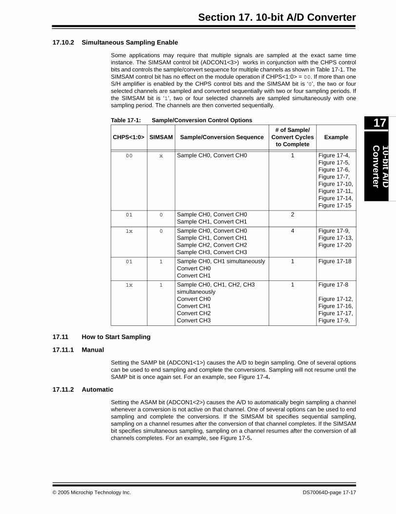
Section 17. 10-bit A/D Converter10-b
it A/D
Co
nverter
17
17.10.2 Simultaneous Sampling Enable
Some applications may require that multiple signals are sampled at the exact same timeinstance. The SIMSAM control bit (ADCON1<3>) works in conjunction with the CHPS controlbits and controls the sample/convert sequence for multiple channels as shown in Table 17-1. TheSIMSAM control bit has no effect on the module operation if CHPS<1:0> = 00. If more than oneS/H amplifier is enabled by the CHPS control bits and the SIMSAM bit is ‘0’, the two or fourselected channels are sampled and converted sequentially with two or four sampling periods. Ifthe SIMSAM bit is ‘1’, two or four selected channels are sampled simultaneously with onesampling period. The channels are then converted sequentially.
Table 17-1: Sample/Conversion Control Options
17.11 How to Start Sampling
17.11.1 Manual
Setting the SAMP bit (ADCON1<1>) causes the A/D to begin sampling. One of several optionscan be used to end sampling and complete the conversions. Sampling will not resume until theSAMP bit is once again set. For an example, see Figure 17-4.
17.11.2 Automatic
Setting the ASAM bit (ADCON1<2>) causes the A/D to automatically begin sampling a channelwhenever a conversion is not active on that channel. One of several options can be used to endsampling and complete the conversions. If the SIMSAM bit specifies sequential sampling,sampling on a channel resumes after the conversion of that channel completes. If the SIMSAMbit specifies simultaneous sampling, sampling on a channel resumes after the conversion of allchannels completes. For an example, see Figure 17-5.
CHPS<1:0> SIMSAM Sample/Conversion Sequence# of Sample/
Convert Cyclesto Complete
Example
00 x Sample CH0, Convert CH0 1 Figure 17-4,Figure 17-5,Figure 17-6,Figure 17-7,Figure 17-10,Figure 17-11,Figure 17-14,Figure 17-15
01 0 Sample CH0, Convert CH0Sample CH1, Convert CH1
2
1x 0 Sample CH0, Convert CH0Sample CH1, Convert CH1Sample CH2, Convert CH2Sample CH3, Convert CH3
4 Figure 17-9,Figure 17-13,Figure 17-20
01 1 Sample CH0, CH1 simultaneouslyConvert CH0Convert CH1
1 Figure 17-18
1x 1 Sample CH0, CH1, CH2, CH3simultaneouslyConvert CH0Convert CH1Convert CH2Convert CH3
1 Figure 17-8
Figure 17-12,Figure 17-16,Figure 17-17,Figure 17-9,
© 2005 Microchip Technology Inc. DS70064D-page 17-17
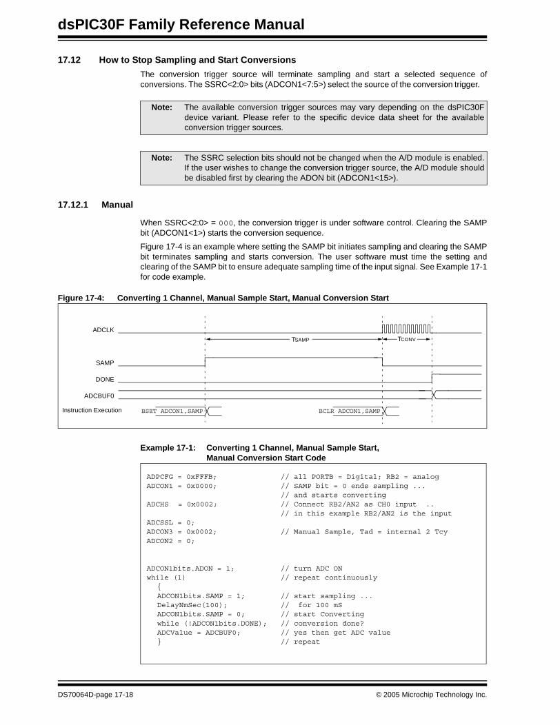
dsPIC30F Family Reference Manual
17.12 How to Stop Sampling and Start Conversions
The conversion trigger source will terminate sampling and start a selected sequence ofconversions. The SSRC<2:0> bits (ADCON1<7:5>) select the source of the conversion trigger.
17.12.1 Manual
When SSRC<2:0> = 000, the conversion trigger is under software control. Clearing the SAMPbit (ADCON1<1>) starts the conversion sequence.
Figure 17-4 is an example where setting the SAMP bit initiates sampling and clearing the SAMPbit terminates sampling and starts conversion. The user software must time the setting andclearing of the SAMP bit to ensure adequate sampling time of the input signal. See Example 17-1for code example.
Figure 17-4: Converting 1 Channel, Manual Sample Start, Manual Conversion Start
Example 17-1: Converting 1 Channel, Manual Sample Start,Manual Conversion Start Code
Note: The available conversion trigger sources may vary depending on the dsPIC30Fdevice variant. Please refer to the specific device data sheet for the availableconversion trigger sources.
Note: The SSRC selection bits should not be changed when the A/D module is enabled.If the user wishes to change the conversion trigger source, the A/D module shouldbe disabled first by clearing the ADON bit (ADCON1<15>).
ADCLK
SAMP
ADCBUF0
TSAMP TCONV
BCLR ADCON1,SAMPBSET ADCON1,SAMPInstruction Execution
DONE
ADPCFG = 0xFFFB; // all PORTB = Digital; RB2 = analog ADCON1 = 0x0000; // SAMP bit = 0 ends sampling ...
// and starts converting ADCHS = 0x0002; // Connect RB2/AN2 as CH0 input ..
// in this example RB2/AN2 is the input ADCSSL = 0; ADCON3 = 0x0002; // Manual Sample, Tad = internal 2 Tcy ADCON2 = 0;
ADCON1bits.ADON = 1; // turn ADC ON while (1) // repeat continuously
{ ADCON1bits.SAMP = 1; // start sampling ... DelayNmSec(100); // for 100 mS ADCON1bits.SAMP = 0; // start Converting
while (!ADCON1bits.DONE); // conversion done? ADCValue = ADCBUF0; // yes then get ADC value
} // repeat
DS70064D-page 17-18 © 2005 Microchip Technology Inc.
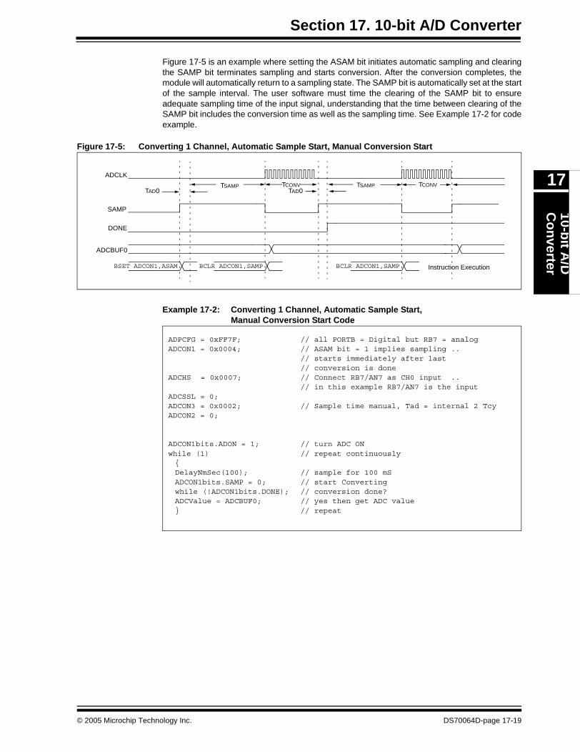
Section 17. 10-bit A/D Converter10-b
it A/D
Co
nverter
17
Figure 17-5 is an example where setting the ASAM bit initiates automatic sampling and clearingthe SAMP bit terminates sampling and starts conversion. After the conversion completes, themodule will automatically return to a sampling state. The SAMP bit is automatically set at the startof the sample interval. The user software must time the clearing of the SAMP bit to ensureadequate sampling time of the input signal, understanding that the time between clearing of theSAMP bit includes the conversion time as well as the sampling time. See Example 17-2 for codeexample.
Figure 17-5: Converting 1 Channel, Automatic Sample Start, Manual Conversion Start
Example 17-2: Converting 1 Channel, Automatic Sample Start,Manual Conversion Start Code
ADCLK
SAMP
ADCBUF0
TSAMP TCONV
BCLR ADCON1,SAMP Instruction Execution
TCONV
BSET ADCON1,ASAM BCLR ADCON1,SAMP
TSAMPTAD0 TAD0
DONE
ADPCFG = 0xFF7F; // all PORTB = Digital but RB7 = analog ADCON1 = 0x0004; // ASAM bit = 1 implies sampling ..
// starts immediately after last // conversion is done
ADCHS = 0x0007; // Connect RB7/AN7 as CH0 input ..// in this example RB7/AN7 is the input
ADCSSL = 0; ADCON3 = 0x0002; // Sample time manual, Tad = internal 2 Tcy ADCON2 = 0;
ADCON1bits.ADON = 1; // turn ADC ON while (1) // repeat continuously
{ DelayNmSec(100); // sample for 100 mS ADCON1bits.SAMP = 0; // start Converting
while (!ADCON1bits.DONE); // conversion done? ADCValue = ADCBUF0; // yes then get ADC value
} // repeat
© 2005 Microchip Technology Inc. DS70064D-page 17-19
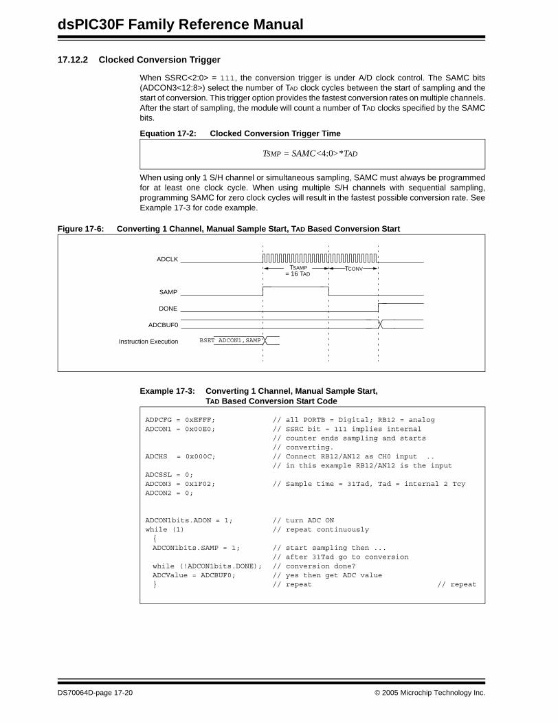
dsPIC30F Family Reference Manual
17.12.2 Clocked Conversion Trigger
When SSRC<2:0> = 111, the conversion trigger is under A/D clock control. The SAMC bits(ADCON3<12:8>) select the number of TAD clock cycles between the start of sampling and thestart of conversion. This trigger option provides the fastest conversion rates on multiple channels.After the start of sampling, the module will count a number of TAD clocks specified by the SAMCbits.
Equation 17-2: Clocked Conversion Trigger Time
When using only 1 S/H channel or simultaneous sampling, SAMC must always be programmedfor at least one clock cycle. When using multiple S/H channels with sequential sampling,programming SAMC for zero clock cycles will result in the fastest possible conversion rate. SeeExample 17-3 for code example.
Figure 17-6: Converting 1 Channel, Manual Sample Start, TAD Based Conversion Start
Example 17-3: Converting 1 Channel, Manual Sample Start,TAD Based Conversion Start Code
TSMP = SAMC<4:0>*TAD
ADCLK
SAMP
ADCBUF0
TSAMP TCONV
BSET ADCON1,SAMPInstruction Execution
DONE
= 16 TAD
ADPCFG = 0xEFFF; // all PORTB = Digital; RB12 = analog ADCON1 = 0x00E0; // SSRC bit = 111 implies internal
// counter ends sampling and starts// converting.
ADCHS = 0x000C; // Connect RB12/AN12 as CH0 input ..// in this example RB12/AN12 is the input
ADCSSL = 0; ADCON3 = 0x1F02; // Sample time = 31Tad, Tad = internal 2 Tcy ADCON2 = 0;
ADCON1bits.ADON = 1; // turn ADC ON while (1) // repeat continuously
{ ADCON1bits.SAMP = 1; // start sampling then ...
// after 31Tad go to conversionwhile (!ADCON1bits.DONE); // conversion done?
ADCValue = ADCBUF0; // yes then get ADC value} // repeat // repeat
DS70064D-page 17-20 © 2005 Microchip Technology Inc.
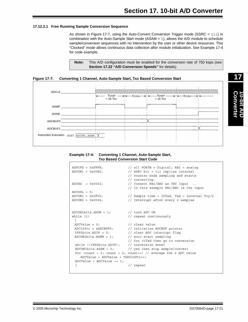
Section 17. 10-bit A/D Converter10-b
it A/D
Co
nverter
17
17.12.2.1 Free Running Sample Conversion Sequence
As shown in Figure 17-7, using the Auto-Convert Conversion Trigger mode (SSRC = 111) incombination with the Auto-Sample Start mode (ASAM = 1), allows the A/D module to schedulesample/conversion sequences with no intervention by the user or other device resources. This“Clocked” mode allows continuous data collection after module initialization. See Example 17-4for code example.
Figure 17-7: Converting 1 Channel, Auto-Sample Start, TAD Based Conversion Start
Example 17-4: Converting 1 Channel, Auto-Sample Start,TAD Based Conversion Start Code
Note: This A/D configuration must be enabled for the conversion rate of 750 ksps (seeSection 17.22 “A/D Conversion Speeds” for details)
ADCLK
SAMP
ADCBUF1
TSAMP TCONV
DONE
= 16 TADTSAMP TCONV
= 16 TAD
ADCBUF0
BSET ADCON1,ASAMInstruction Execution
ADPCFG = 0xFFFB; // all PORTB = Digital; RB2 = analog ADCON1 = 0x00E0; // SSRC bit = 111 implies internal
// counter ends sampling and starts// converting.
ADCHS = 0x0002; // Connect RB2/AN2 as CH0 input ..// in this example RB2/AN2 is the input
ADCSSL = 0; ADCON3 = 0x0F00; // Sample time = 15Tad, Tad = internal Tcy/2 ADCON2 = 0x0004; // Interrupt after every 2 samples
ADCON1bits.ADON = 1; // turn ADC ON while (1) // repeat continuously
{ADCValue = 0; // clear valueADC16Ptr = &ADCBUF0; // initialize ADCBUF pointerIFS0bits.ADIF = 0; // clear ADC interrupt flag
ADCON1bits.ASAM = 1; // auto start sampling // for 31Tad then go to conversion
while (!IFS0bits.ADIF); // conversion done?ADCON1bits.ASAM = 0; // yes then stop sample/convertfor (count = 0; count < 2; count++) // average the 2 ADC value
ADCValue = ADCValue + *ADC16Ptr++; ADCValue = ADCValue >> 1;} // repeat
© 2005 Microchip Technology Inc. DS70064D-page 17-21
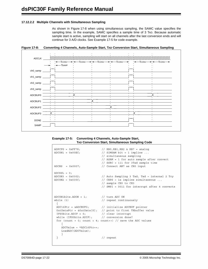
dsPIC30F Family Reference Manual
17.12.2.2 Multiple Channels with Simultaneous Sampling
As shown in Figure 17-8 when using simultaneous sampling, the SAMC value specifies thesampling time. In the example, SAMC specifies a sample time of 3 TAD. Because automaticsample start is active, sampling will start on all channels after the last conversion ends and willcontinue for 3 A/D clocks. See Example 17-5 for code example.
Figure 17-8: Converting 4 Channels, Auto-Sample Start, TAD Conversion Start, Simultaneous Sampling
Example 17-5: Converting 4 Channels, Auto-Sample Start,TAD Conversion Start, Simultaneous Sampling Code
TCONV TCONV TCONV TCONV
ADCLK
ch1_samp
ch2_samp
ch3_samp
ch0_samp
ADCBUF0
ADCBUF1
ADCBUF2
ADCBUF3
TCONV TCONV
DONE
SAMP
TSAMP
ADPCFG = 0xFF78; // RB0,RB1,RB2 & RB7 = analog ADCON1 = 0x00EC; // SIMSAM bit = 1 implies ...
// simultaneous sampling// ASAM = 1 for auto sample after convert// SSRC = 111 for 3Tad sample time
ADCHS = 0x0007; // Connect AN7 as CH0 input
ADCSSL = 0; ADCON3 = 0x0302; // Auto Sampling 3 Tad, Tad = internal 2 Tcy ADCON2 = 0x030C; // CHPS = 1x implies simultaneous ...
// sample CH0 to CH3// SMPI = 0011 for interrupt after 4 converts
ADCON1bits.ADON = 1; // turn ADC ON while (1) // repeat continuously
{ADC16Ptr = &ADCBUF0; // initialize ADCBUF pointerOutDataPtr = &OutData[0]; // point to first TXbuffer valueIFS0bits.ADIF = 0; // clear interruptwhile (IFS0bits.ADIF); // conversion done?for (count = 0; count < 4; count++) // save the ADC values
{ADCValue = *ADC16Ptr++;LoadADC(ADCValue);}
} // repeat
DS70064D-page 17-22 © 2005 Microchip Technology Inc.
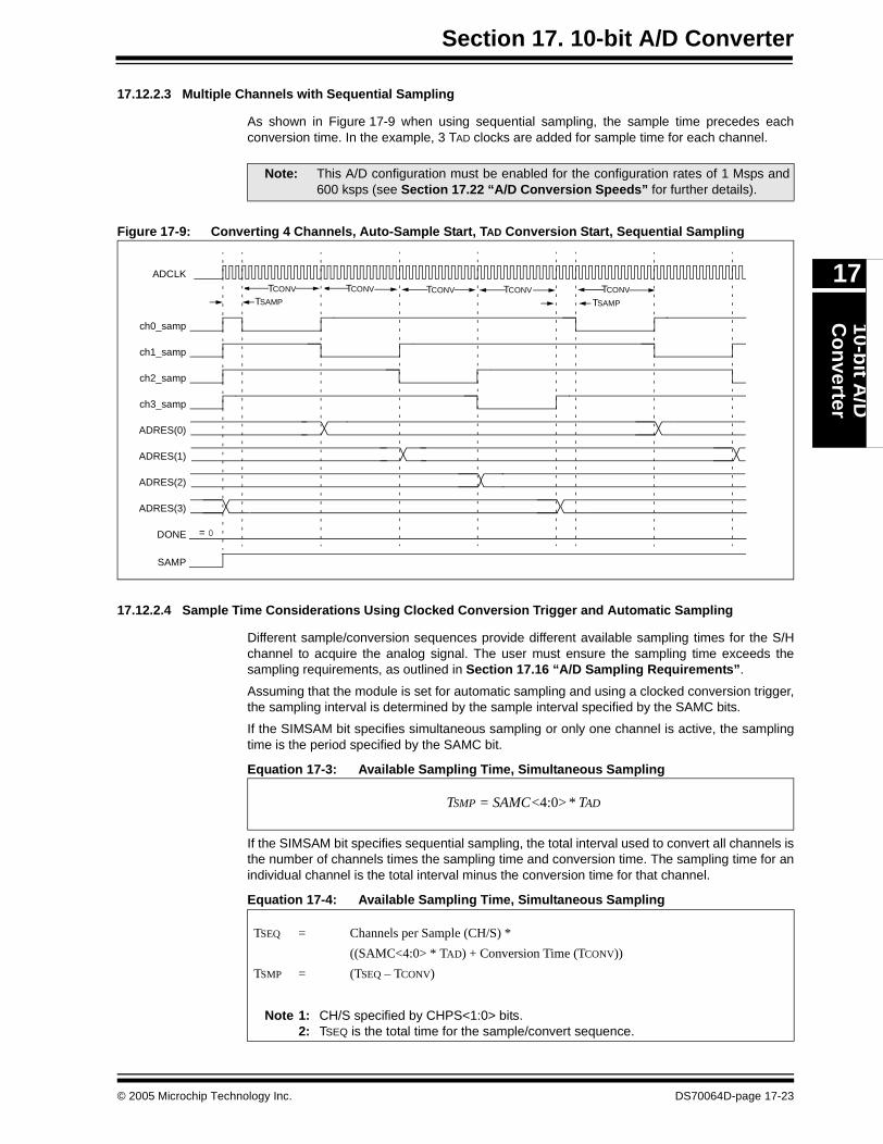
Section 17. 10-bit A/D Converter10-b
it A/D
Co
nverter
17
17.12.2.3 Multiple Channels with Sequential Sampling
As shown in Figure 17-9 when using sequential sampling, the sample time precedes eachconversion time. In the example, 3 TAD clocks are added for sample time for each channel.
Figure 17-9: Converting 4 Channels, Auto-Sample Start, TAD Conversion Start, Sequential Sampling
17.12.2.4 Sample Time Considerations Using Clocked Conversion Trigger and Automatic Sampling
Different sample/conversion sequences provide different available sampling times for the S/Hchannel to acquire the analog signal. The user must ensure the sampling time exceeds thesampling requirements, as outlined in Section 17.16 “A/D Sampling Requirements”.
Assuming that the module is set for automatic sampling and using a clocked conversion trigger,the sampling interval is determined by the sample interval specified by the SAMC bits.
If the SIMSAM bit specifies simultaneous sampling or only one channel is active, the samplingtime is the period specified by the SAMC bit.
Equation 17-3: Available Sampling Time, Simultaneous Sampling
If the SIMSAM bit specifies sequential sampling, the total interval used to convert all channels isthe number of channels times the sampling time and conversion time. The sampling time for anindividual channel is the total interval minus the conversion time for that channel.
Equation 17-4: Available Sampling Time, Simultaneous Sampling
Note: This A/D configuration must be enabled for the configuration rates of 1 Msps and600 ksps (see Section 17.22 “A/D Conversion Speeds” for further details).
TCONV
ADCLK
ch1_samp
ch2_samp
ch3_samp
ch0_samp
ADRES(0)
ADRES(1)
ADRES(2)
ADRES(3)
TCONV TCONV TCONV TCONV
SAMP
TSAMP TSAMP
DONE = 0
TSEQ = Channels per Sample (CH/S) *
((SAMC<4:0> * TAD) + Conversion Time (TCONV))
TSMP = (TSEQ – TCONV)
Note 1: CH/S specified by CHPS<1:0> bits.2: TSEQ is the total time for the sample/convert sequence.
TSMP = SAMC<4:0> * TAD
© 2005 Microchip Technology Inc. DS70064D-page 17-23

dsPIC30F Family Reference Manual
17.12.3 Event Trigger Conversion Start
It is often desirable to synchronize the end of sampling and the start of conversion with someother time event. The A/D module may use one of three sources as a conversion trigger.
17.12.3.1 External INT Pin Trigger
When SSRC<2:0> = 001, the A/D conversion is triggered by an active transition on the INT0 pin.The INT0 pin may be programmed for either a rising edge input or a falling edge input.
17.12.3.2 GP Timer Compare Trigger
The A/D is configured in this Trigger mode by setting SSRC<2:0> = 010. When a match occursbetween the 32-bit timer TMR3/TMR2 and the 32-bit Combined Period register PR3/PR2, aspecial ADC trigger event signal is generated by Timer3. This feature does not exist for theTMR5/TMR4 timer pair. Refer to Section 12. “Timers” for more details.
17.12.3.3 Motor Control PWM Trigger
The PWM module has an event trigger that allows A/D conversions to be synchronized to thePWM time base. When SSRC<2:0> = 011, the A/D sampling and conversion times occur at anyuser programmable point within the PWM period. The special event trigger allows the user tominimize the delay between the time when A/D conversion results are acquired and the timewhen the duty cycle value is updated. Refer to Section 15. “Motor Control PWM” for moredetails.
17.12.3.4 Synchronizing A/D Operations to Internal or External Events
Using the modes where an external event trigger pulse ends sampling and starts conversion(SSRC = 001, 10, 011) may be used in combination with auto-sampling (ASAM = 1) to causethe A/D to synchronize the sample conversion events to the trigger pulse source. For example,in Figure 17-11 where SSRC = 010 and ASAM = 1, the A/D will always end sampling and startconversions synchronously with the timer compare trigger event. The A/D will have a sampleconversion rate that corresponds to the timer comparison event rate. See Example 17-6 for codeexample.
Figure 17-10: Converting 1 Channel, Manual Sample Start, Conversion Trigger Based Conversion Start
Conversion
ADCLK
SAMP
ADCBUF0
TSAMP TCONV
BSET ADCON1,SAMPInstruction Execution
Trigger
DS70064D-page 17-24 © 2005 Microchip Technology Inc.
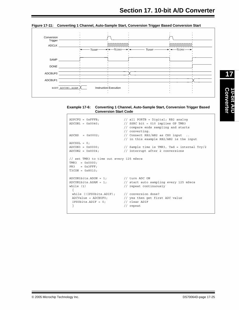
Section 17. 10-bit A/D Converter10-b
it A/D
Co
nverter
17
Figure 17-11: Converting 1 Channel, Auto-Sample Start, Conversion Trigger Based Conversion Start
Example 17-6: Converting 1 Channel, Auto-Sample Start, Conversion Trigger Based Conversion Start Code
ADCLK
SAMP
ADCBUF0
TSAMP TCONV
BSET ADCON1,ASAM Instruction Execution
TCONVTSAMP
ADCBUF1
DONE
ConversionTrigger
ADPCFG = 0xFFFB; // all PORTB = Digital; RB2 analog ADCON1 = 0x0040; // SSRC bit = 010 implies GP TMR3
// compare ends sampling and starts// converting.
ADCHS = 0x0002; // Connect RB2/AN2 as CH0 input ..// in this example RB2/AN2 is the input
ADCSSL = 0; ADCON3 = 0x0000; // Sample time is TMR3, Tad = internal Tcy/2 ADCON2 = 0x0004; // Interrupt after 2 conversions
// set TMR3 to time out every 125 mSecs TMR3 = 0x0000; PR3 = 0x3FFF; T3CON = 0x8010; ADCON1bits.ADON = 1; // turn ADC ON ADCON1bits.ASAM = 1; // start auto sampling every 125 mSecs while (1) // repeat continuously
{ while (!IFS0bits.ADIF); // conversion done?
ADCValue = ADCBUF0; // yes then get first ADC valueIFS0bits.ADIF = 0; // clear ADIF} // repeat
© 2005 Microchip Technology Inc. DS70064D-page 17-25
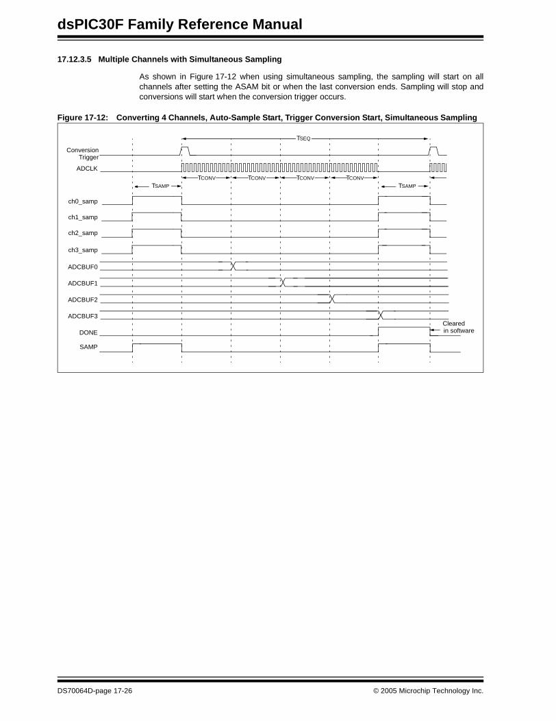
dsPIC30F Family Reference Manual
17.12.3.5 Multiple Channels with Simultaneous Sampling
As shown in Figure 17-12 when using simultaneous sampling, the sampling will start on allchannels after setting the ASAM bit or when the last conversion ends. Sampling will stop andconversions will start when the conversion trigger occurs.
Figure 17-12: Converting 4 Channels, Auto-Sample Start, Trigger Conversion Start, Simultaneous Sampling
TCONV TCONV TCONV TCONV
ADCLK
ch1_samp
ch2_samp
ch3_samp
ch0_samp
ADCBUF0
ADCBUF1
ADCBUF2
ADCBUF3
DONE
TSAMP
SAMP
TSAMP
TSEQ
ConversionTrigger
Clearedin software
DS70064D-page 17-26 © 2005 Microchip Technology Inc.
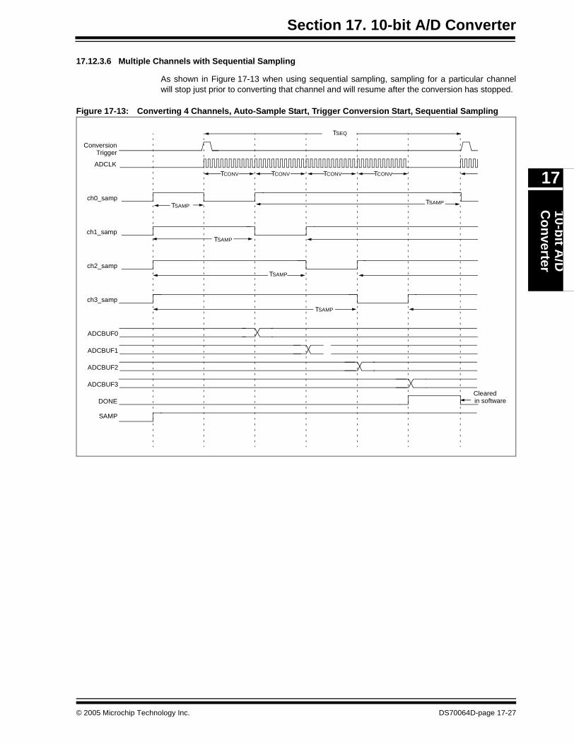
Section 17. 10-bit A/D Converter10-b
it A/D
Co
nverter
17
17.12.3.6 Multiple Channels with Sequential Sampling
As shown in Figure 17-13 when using sequential sampling, sampling for a particular channelwill stop just prior to converting that channel and will resume after the conversion has stopped.
Figure 17-13: Converting 4 Channels, Auto-Sample Start, Trigger Conversion Start, Sequential Sampling
TCONV TCONV TCONV TCONV
ADCLK
ch1_samp
ch2_samp
ch3_samp
ch0_samp
ADCBUF0
ADCBUF1
ADCBUF2
ADCBUF3
DONE
TSAMP
TSAMP
TSAMP
TSAMP
SAMP
TSAMP
TSEQ
ConversionTrigger
Clearedin software
© 2005 Microchip Technology Inc. DS70064D-page 17-27
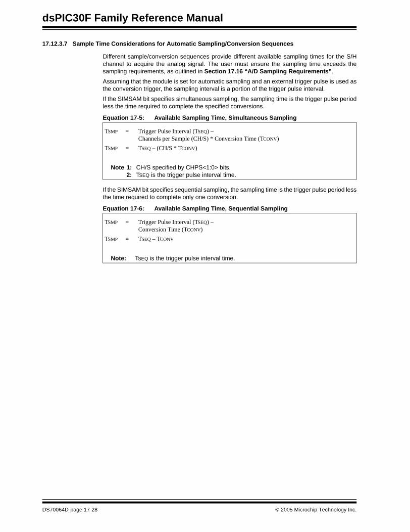
dsPIC30F Family Reference Manual
17.12.3.7 Sample Time Considerations for Automatic Sampling/Conversion Sequences
Different sample/conversion sequences provide different available sampling times for the S/Hchannel to acquire the analog signal. The user must ensure the sampling time exceeds thesampling requirements, as outlined in Section 17.16 “A/D Sampling Requirements”.
Assuming that the module is set for automatic sampling and an external trigger pulse is used asthe conversion trigger, the sampling interval is a portion of the trigger pulse interval.
If the SIMSAM bit specifies simultaneous sampling, the sampling time is the trigger pulse periodless the time required to complete the specified conversions.
Equation 17-5: Available Sampling Time, Simultaneous Sampling
If the SIMSAM bit specifies sequential sampling, the sampling time is the trigger pulse period lessthe time required to complete only one conversion.
Equation 17-6: Available Sampling Time, Sequential Sampling
TSMP = Trigger Pulse Interval (TSEQ) –Channels per Sample (CH/S) * Conversion Time (TCONV)
TSMP = TSEQ – (CH/S * TCONV)
Note 1: CH/S specified by CHPS<1:0> bits.2: TSEQ is the trigger pulse interval time.
TSMP = Trigger Pulse Interval (TSEQ) –Conversion Time (TCONV)
TSMP = TSEQ – TCONV
Note: TSEQ is the trigger pulse interval time.
DS70064D-page 17-28 © 2005 Microchip Technology Inc.

Section 17. 10-bit A/D Converter10-b
it A/D
Co
nverter
17
17.13 Controlling Sample/Conversion Operation
The application software may poll the SAMP and DONE bits to keep track of the A/D operationsor the module can interrupt the CPU when conversions are complete. The application softwaremay also abort A/D operations if necessary.
17.13.1 Monitoring Sample/Conversion Status
The SAMP (ADCON1<1>) and DONE (ADCON1<0>) bits indicate the sampling state and theconversion state of the A/D, respectively. Generally, when the SAMP bit clears, indicating end ofsampling, the DONE bit is automatically set, indicating end of conversion. If both SAMP andDONE are ‘0’, the A/D is in an inactive state. In some Operational modes, the SAMP bit may alsoinvoke and terminate sampling.
17.13.2 Generating an A/D Interrupt
The SMPI<3:0> bits control the generation of interrupts. The interrupt will occur some number ofsample/conversion sequences after starting sampling and re-occur on each equivalent numberof samples. Note that the interrupts are specified in terms of samples and not in terms ofconversions or data samples in the buffer memory.
When the SIMSAM bit specifies sequential sampling, regardless of the number of channelsspecified by the CHPS bits, the module samples once for each conversion and data sample inthe buffer. Therefore, the value specified by the SMPI bits will correspond to the number of datasamples in the buffer, up to the maximum of 16.
When the SIMSAM bit specifies simultaneous sampling, the number of data samples in the bufferis related to the CHPS bits. Algorithmically, the channels/sample times the number of sampleswill result in the number of data sample entries in the buffer. To avoid loss of data in the bufferdue to overruns, the SMPI bits must be set to the desired buffer size divided by the channels persample.
Disabling the A/D interrupt is not done with the SMPI bits. To disable the interrupt, clear the ADIEanalog module interrupt enable bit.
17.13.3 Aborting Sampling
Clearing the SAMP bit while in Manual Sampling mode will terminate sampling, but may also starta conversion if SSRC = 000.
Clearing the ASAM bit while in Automatic Sampling mode will not terminate an on goingsample/convert sequence, however, sampling will not automatically resume after subsequentconversions.
17.13.4 Aborting a Conversion
Clearing the ADON bit during a conversion will abort the current conversion. The A/D Resultregister pair will NOT be updated with the partially completed A/D conversion sample. That is,the corresponding ADCBUF buffer location will continue to contain the value of the lastcompleted conversion (or the last value written to the buffer).
© 2005 Microchip Technology Inc. DS70064D-page 17-29
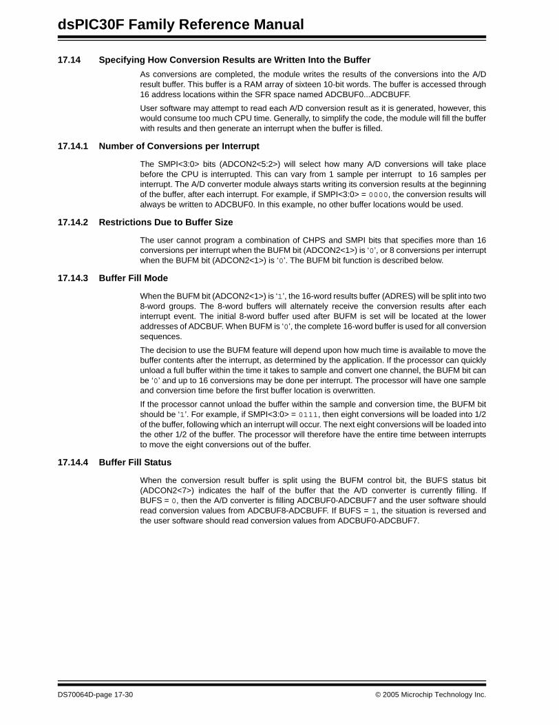
dsPIC30F Family Reference Manual
17.14 Specifying How Conversion Results are Written Into the Buffer
As conversions are completed, the module writes the results of the conversions into the A/Dresult buffer. This buffer is a RAM array of sixteen 10-bit words. The buffer is accessed through16 address locations within the SFR space named ADCBUF0...ADCBUFF.
User software may attempt to read each A/D conversion result as it is generated, however, thiswould consume too much CPU time. Generally, to simplify the code, the module will fill the bufferwith results and then generate an interrupt when the buffer is filled.
17.14.1 Number of Conversions per Interrupt
The SMPI<3:0> bits (ADCON2<5:2>) will select how many A/D conversions will take placebefore the CPU is interrupted. This can vary from 1 sample per interrupt to 16 samples perinterrupt. The A/D converter module always starts writing its conversion results at the beginningof the buffer, after each interrupt. For example, if SMPI<3:0> = 0000, the conversion results willalways be written to ADCBUF0. In this example, no other buffer locations would be used.
17.14.2 Restrictions Due to Buffer Size
The user cannot program a combination of CHPS and SMPI bits that specifies more than 16conversions per interrupt when the BUFM bit (ADCON2<1>) is ‘0’, or 8 conversions per interruptwhen the BUFM bit (ADCON2<1>) is ‘0’. The BUFM bit function is described below.
17.14.3 Buffer Fill Mode
When the BUFM bit (ADCON2<1>) is ‘1’, the 16-word results buffer (ADRES) will be split into two8-word groups. The 8-word buffers will alternately receive the conversion results after eachinterrupt event. The initial 8-word buffer used after BUFM is set will be located at the loweraddresses of ADCBUF. When BUFM is ‘0’, the complete 16-word buffer is used for all conversionsequences.
The decision to use the BUFM feature will depend upon how much time is available to move thebuffer contents after the interrupt, as determined by the application. If the processor can quicklyunload a full buffer within the time it takes to sample and convert one channel, the BUFM bit canbe ‘0’ and up to 16 conversions may be done per interrupt. The processor will have one sampleand conversion time before the first buffer location is overwritten.
If the processor cannot unload the buffer within the sample and conversion time, the BUFM bitshould be ‘1’. For example, if SMPI<3:0> = 0111, then eight conversions will be loaded into 1/2of the buffer, following which an interrupt will occur. The next eight conversions will be loaded intothe other 1/2 of the buffer. The processor will therefore have the entire time between interruptsto move the eight conversions out of the buffer.
17.14.4 Buffer Fill Status
When the conversion result buffer is split using the BUFM control bit, the BUFS status bit(ADCON2<7>) indicates the half of the buffer that the A/D converter is currently filling. IfBUFS = 0, then the A/D converter is filling ADCBUF0-ADCBUF7 and the user software shouldread conversion values from ADCBUF8-ADCBUFF. If BUFS = 1, the situation is reversed andthe user software should read conversion values from ADCBUF0-ADCBUF7.
DS70064D-page 17-30 © 2005 Microchip Technology Inc.
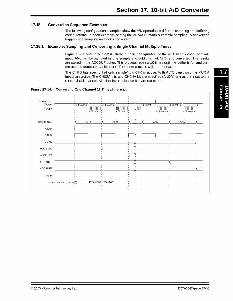
Section 17. 10-bit A/D Converter10-b
it A/D
Co
nverter
17
17.15 Conversion Sequence Examples
The following configuration examples show the A/D operation in different sampling and bufferingconfigurations. In each example, setting the ASAM bit starts automatic sampling. A conversiontrigger ends sampling and starts conversion.
17.15.1 Example: Sampling and Converting a Single Channel Multiple Times
Figure 17-11 and Table 17-2 illustrate a basic configuration of the A/D. In this case, one A/Dinput, AN0, will be sampled by one sample and hold channel, CH0, and converted. The resultsare stored in the ADCBUF buffer. This process repeats 16 times until the buffer is full and thenthe module generates an interrupt. The entire process will then repeat.
The CHPS bits specify that only sample/hold CH0 is active. With ALTS clear, only the MUX Ainputs are active. The CH0SA bits and CH0NA bit are specified (AN0-VREF-) as the input to thesample/hold channel. All other input selection bits are not used.
Figure 17-14: Converting One Channel 16 Times/Interrupt
ADCLK
SAMP
ADCBUF0
TSAMP
TCONV
BSET ADCON1,ASAM Instruction Execution
ADCBUF1
DONE
ADCBUFE
ADCBUFF
Input to CH0 AN0
TSAMP
TCONV
AN0
TSAMP
TCONV
AN0
TSAMP
TCONV
AN0
ADIF
ASAM
ConversionTrigger
© 2005 Microchip Technology Inc. DS70064D-page 17-31
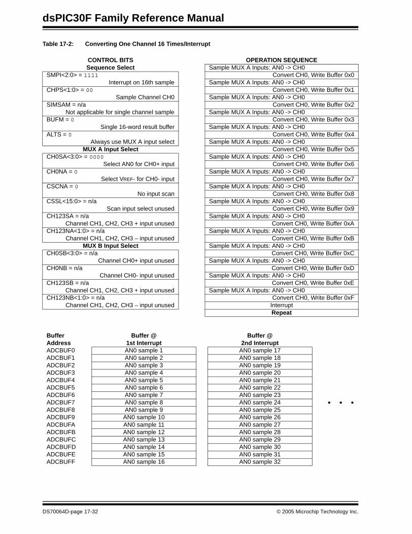
dsPIC30F Family Reference Manual
Table 17-2: Converting One Channel 16 Times/Interrupt
CONTROL BITS OPERATION SEQUENCESequence Select Sample MUX A Inputs: AN0 -> CH0
SMPI<2:0> = 1111 Convert CH0, Write Buffer 0x0Interrupt on 16th sample Sample MUX A Inputs: AN0 -> CH0
CHPS<1:0> = 00 Convert CH0, Write Buffer 0x1Sample Channel CH0 Sample MUX A Inputs: AN0 -> CH0
SIMSAM = n/a Convert CH0, Write Buffer 0x2Not applicable for single channel sample Sample MUX A Inputs: AN0 -> CH0
BUFM = 0 Convert CH0, Write Buffer 0x3Single 16-word result buffer Sample MUX A Inputs: AN0 -> CH0
ALTS = 0 Convert CH0, Write Buffer 0x4Always use MUX A input select Sample MUX A Inputs: AN0 -> CH0
MUX A Input Select Convert CH0, Write Buffer 0x5CH0SA<3:0> = 0000 Sample MUX A Inputs: AN0 -> CH0
Select AN0 for CH0+ input Convert CH0, Write Buffer 0x6CH0NA = 0 Sample MUX A Inputs: AN0 -> CH0
Select VREF- for CH0- input Convert CH0, Write Buffer 0x7CSCNA = 0 Sample MUX A Inputs: AN0 -> CH0
No input scan Convert CH0, Write Buffer 0x8CSSL<15:0> = n/a Sample MUX A Inputs: AN0 -> CH0
Scan input select unused Convert CH0, Write Buffer 0x9CH123SA = n/a Sample MUX A Inputs: AN0 -> CH0
Channel CH1, CH2, CH3 + input unused Convert CH0, Write Buffer 0xACH123NA<1:0> = n/a Sample MUX A Inputs: AN0 -> CH0
Channel CH1, CH2, CH3 – input unused Convert CH0, Write Buffer 0xBMUX B Input Select Sample MUX A Inputs: AN0 -> CH0
CH0SB<3:0> = n/a Convert CH0, Write Buffer 0xCChannel CH0+ input unused Sample MUX A Inputs: AN0 -> CH0
CH0NB = n/a Convert CH0, Write Buffer 0xDChannel CH0- input unused Sample MUX A Inputs: AN0 -> CH0
CH123SB = n/a Convert CH0, Write Buffer 0xEChannel CH1, CH2, CH3 + input unused Sample MUX A Inputs: AN0 -> CH0
CH123NB<1:0> = n/a Convert CH0, Write Buffer 0xFChannel CH1, CH2, CH3 – input unused Interrupt
Repeat
BufferAddress
Buffer @1st Interrupt
Buffer @2nd Interrupt
ADCBUF0 AN0 sample 1 AN0 sample 17ADCBUF1 AN0 sample 2 AN0 sample 18ADCBUF2 AN0 sample 3 AN0 sample 19ADCBUF3 AN0 sample 4 AN0 sample 20ADCBUF4 AN0 sample 5 AN0 sample 21ADCBUF5 AN0 sample 6 AN0 sample 22ADCBUF6 AN0 sample 7 AN0 sample 23ADCBUF7 AN0 sample 8 AN0 sample 24 • • •ADCBUF8 AN0 sample 9 AN0 sample 25ADCBUF9 AN0 sample 10 AN0 sample 26ADCBUFA AN0 sample 11 AN0 sample 27ADCBUFB AN0 sample 12 AN0 sample 28ADCBUFC AN0 sample 13 AN0 sample 29ADCBUFD AN0 sample 14 AN0 sample 30ADCBUFE AN0 sample 15 AN0 sample 31ADCBUFF AN0 sample 16 AN0 sample 32
DS70064D-page 17-32 © 2005 Microchip Technology Inc.

Section 17. 10-bit A/D Converter10-b
it A/D
Co
nverter
17
17.15.2 Example: A/D Conversions While Scanning Through All Analog Inputs
Figure 17-15 and Table 17-3 illustrate a very typical setup where all available analog inputchannels are sampled by one sample and hold channel, CH0, and converted. The set CSCNAbit specifies scanning of the A/D inputs to the CH0 positive input. Other conditions are similar toSubsection 17.15.1.
Initially, the AN0 input is sampled by CH0 and converted. The result is stored in the ADCBUFbuffer. Then the AN1 input is sampled and converted. This process of scanning the inputsrepeats 16 times until the buffer is full and then the module generates an interrupt. The entireprocess will then repeat.
Figure 17-15: Scanning Through 16 Inputs/Interrupt
ADCLK
SAMP
ADCBUF0
TSAMP
TCONV
BSET ADCON1,#ASAM Instruction Execution
ADCBUF1
DONE
ADCBUFE
ADCBUFF
Input to CH0 AN0
TSAMP
TCONV
AN1
TSAMP
TCONV
AN14
TSAMP
TCONV
AN15
ADIF
ASAM
ConversionTrigger
© 2005 Microchip Technology Inc. DS70064D-page 17-33
dsPIC30F Family Reference Manual
Table 17-3: Scanning Through 16 Inputs/Interrupt
CONTROL BITS OPERATION SEQUENCESequence Select Sample MUX A Inputs: AN0 -> CH0
SMPI<2:0> = 1111 Convert CH0, Write Buffer 0x0Interrupt on 16th sample Sample MUX A Inputs: AN1 -> CH0
CHPS<1:0> = 00 Convert CH0, Write Buffer 0x1Sample Channel CH0 Sample MUX A Inputs: AN2 -> CH0
SIMSAM = n/a Convert CH0, Write Buffer 0x2Not applicable for single channel sample Sample MUX A Inputs: AN3 -> CH0
BUFM = 0 Convert CH0, Write Buffer 0x3Single 16-word result buffer Sample MUX A Inputs: AN4 -> CH0
ALTS = 0 Convert CH0, Write Buffer 0x4Always use MUX A input select Sample MUX A Inputs: AN5 -> CH0
MUX A Input Select Convert CH0, Write Buffer 0x5CH0SA<3:0> = n/a Sample MUX A Inputs: AN6 -> CH0
Override by CSCNA Convert CH0, Write Buffer 0x6CH0NA = 0 Sample MUX A Inputs: AN7 -> CH0
Select VREF- for CH0- input Convert CH0, Write Buffer 0x7CSCNA = 1 Sample MUX A Inputs: AN8 -> CH0
Scan CH0+ Inputs Convert CH0, Write Buffer 0x8CSSL<15:0> = 1111 1111 1111 1111 Sample MUX A Inputs: AN9 -> CH0
Scan input select unused Convert CH0, Write Buffer 0x9CH123SA = n/a Sample MUX A Inputs: AN10 -> CH0
Channel CH1, CH2, CH3 + input unused Convert CH0, Write Buffer 0xACH123NA<1:0> = n/a Sample MUX A Inputs: AN11 -> CH0
Channel CH1, CH2, CH3 – input unused Convert CH0, Write Buffer 0xBMUX B Input Select Sample MUX A Inputs: AN12 -> CH0
CH0SB<3:0> = n/a Convert CH0, Write Buffer 0xCChannel CH0+ input unused Sample MUX A Inputs: AN13 -> CH0
CH0NB = n/a Convert CH0, Write Buffer 0xDChannel CH0- input unused Sample MUX A Inputs: AN14 -> CH0
CH123SB = n/a Convert CH0, Write Buffer 0xEChannel CH1, CH2, CH3 + input unused Sample MUX A Inputs: AN15 -> CH0
CH123NB<1:0> = n/a Convert CH0, Write Buffer 0xFChannel CH1, CH2, CH3 – input unused Interrupt
Repeat
BufferAddress
Buffer @1st Interrupt
Buffer @2nd Interrupt
ADCBUF0 AN0 sample 1 AN0 sample 17ADCBUF1 AN1 sample 2 AN1 sample 18ADCBUF2 AN2 sample 3 AN2 sample 19ADCBUF3 AN3 sample 4 AN3 sample 20ADCBUF4 AN4 sample 5 AN4 sample 21ADCBUF5 AN5 sample 6 AN5 sample 22ADCBUF6 AN6 sample 7 AN6 sample 23ADCBUF7 AN7 sample 8 AN7 sample 24 • • •ADCBUF8 AN8 sample 9 AN8 sample 25ADCBUF9 AN9 sample 10 AN9 sample 26ADCBUFA AN10 sample 11 AN10 sample 27ADCBUFB AN11 sample 12 AN11 sample 28ADCBUFC AN12 sample 13 AN12 sample 29ADCBUFD AN13 sample 14 AN13 sample 30ADCBUFE AN14 sample 15 AN14 sample 31ADCBUFF AN15 sample 16 AN15 sample 32
DS70064D-page 17-34 © 2005 Microchip Technology Inc.

Section 17. 10-bit A/D Converter10-b
it A/D
Co
nverter
17
17.15.3 Example: Sampling Three Inputs Frequently While Scanning Four Other Inputs
Figure 17-16 and Table 17-4 shows how the A/D converter could be configured to sample threeinputs frequently using sample/hold channels CH1, CH2 and CH3; while four other inputs aresampled less frequently by scanning them using sample/hold channel CH0. In this case, onlyMUX A inputs are used, and all 4 channels are sampled simultaneously. Four different inputs(AN4, AN5, AN6, AN7) are scanned in CH0, whereas AN0, AN1 and AN2 are the fixed inputs forCH1, CH2 and CH3, respectively. Thus, in every set of 16 samples, AN0, AN1 and AN2 wouldbe sampled 4 times, while AN4, AN5, AN6 and AN7 would be sampled only once each.
Figure 17-16: Converting Three Inputs, Four Times and Four Inputs, One Time/Interrupt
ADCLK
SAMP
DONE
Input to CH0 AN4
TSAMP
ADIF
TCONVTCONVTCONVTCONV
AN0
AN1
AN2
Input to CH1
Input to CH2
Input to CH3
ADCBUFD
ADCBUFE
ADCBUFF
AN5
TSAMP
AN0
AN1
AN2
AN7
TSAMP
AN0
AN1
AN2
ASAM
AN4
AN0
AN1
AN2
ADCBUF0
ADCBUF1
ADCBUF2
ADCBUF3
ADCBUFC
AN6
AN0
AN1
AN2
ConversionTrigger
TCONVTCONVTCONVTCONV TCONVTCONVTCONVTCONV
© 2005 Microchip Technology Inc. DS70064D-page 17-35
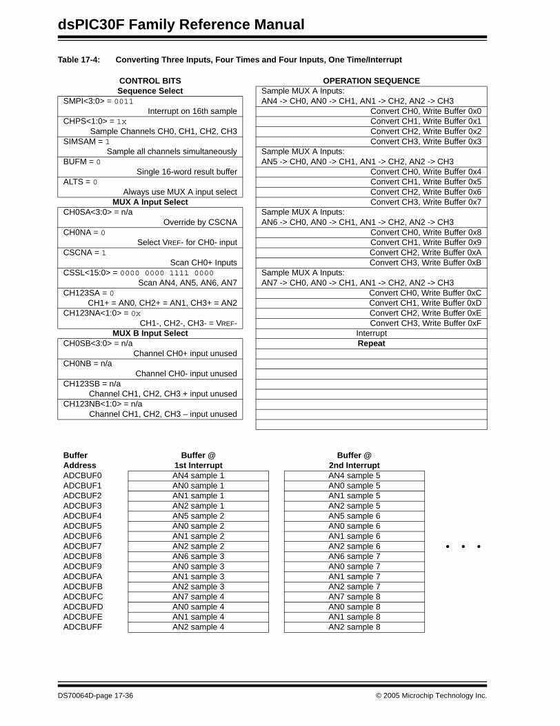
dsPIC30F Family Reference Manual
Table 17-4: Converting Three Inputs, Four Times and Four Inputs, One Time/Interrupt
CONTROL BITS OPERATION SEQUENCESequence Select Sample MUX A Inputs:
SMPI<3:0> = 0011 AN4 -> CH0, AN0 -> CH1, AN1 -> CH2, AN2 -> CH3Interrupt on 16th sample Convert CH0, Write Buffer 0x0
CHPS<1:0> = 1x Convert CH1, Write Buffer 0x1Sample Channels CH0, CH1, CH2, CH3 Convert CH2, Write Buffer 0x2
SIMSAM = 1 Convert CH3, Write Buffer 0x3Sample all channels simultaneously Sample MUX A Inputs:
BUFM = 0 AN5 -> CH0, AN0 -> CH1, AN1 -> CH2, AN2 -> CH3Single 16-word result buffer Convert CH0, Write Buffer 0x4
ALTS = 0 Convert CH1, Write Buffer 0x5Always use MUX A input select Convert CH2, Write Buffer 0x6
MUX A Input Select Convert CH3, Write Buffer 0x7CH0SA<3:0> = n/a Sample MUX A Inputs:
Override by CSCNA AN6 -> CH0, AN0 -> CH1, AN1 -> CH2, AN2 -> CH3CH0NA = 0 Convert CH0, Write Buffer 0x8
Select VREF- for CH0- input Convert CH1, Write Buffer 0x9CSCNA = 1 Convert CH2, Write Buffer 0xA
Scan CH0+ Inputs Convert CH3, Write Buffer 0xBCSSL<15:0> = 0000 0000 1111 0000 Sample MUX A Inputs:
Scan AN4, AN5, AN6, AN7 AN7 -> CH0, AN0 -> CH1, AN1 -> CH2, AN2 -> CH3CH123SA = 0 Convert CH0, Write Buffer 0xC
CH1+ = AN0, CH2+ = AN1, CH3+ = AN2 Convert CH1, Write Buffer 0xDCH123NA<1:0> = 0x Convert CH2, Write Buffer 0xE
CH1-, CH2-, CH3- = VREF- Convert CH3, Write Buffer 0xFMUX B Input Select Interrupt
CH0SB<3:0> = n/a RepeatChannel CH0+ input unused
CH0NB = n/aChannel CH0- input unused
CH123SB = n/aChannel CH1, CH2, CH3 + input unused
CH123NB<1:0> = n/aChannel CH1, CH2, CH3 – input unused
BufferAddress
Buffer @1st Interrupt
Buffer @2nd Interrupt
ADCBUF0 AN4 sample 1 AN4 sample 5ADCBUF1 AN0 sample 1 AN0 sample 5ADCBUF2 AN1 sample 1 AN1 sample 5ADCBUF3 AN2 sample 1 AN2 sample 5ADCBUF4 AN5 sample 2 AN5 sample 6ADCBUF5 AN0 sample 2 AN0 sample 6ADCBUF6 AN1 sample 2 AN1 sample 6ADCBUF7 AN2 sample 2 AN2 sample 6 • • •ADCBUF8 AN6 sample 3 AN6 sample 7ADCBUF9 AN0 sample 3 AN0 sample 7ADCBUFA AN1 sample 3 AN1 sample 7ADCBUFB AN2 sample 3 AN2 sample 7ADCBUFC AN7 sample 4 AN7 sample 8ADCBUFD AN0 sample 4 AN0 sample 8ADCBUFE AN1 sample 4 AN1 sample 8ADCBUFF AN2 sample 4 AN2 sample 8
DS70064D-page 17-36 © 2005 Microchip Technology Inc.
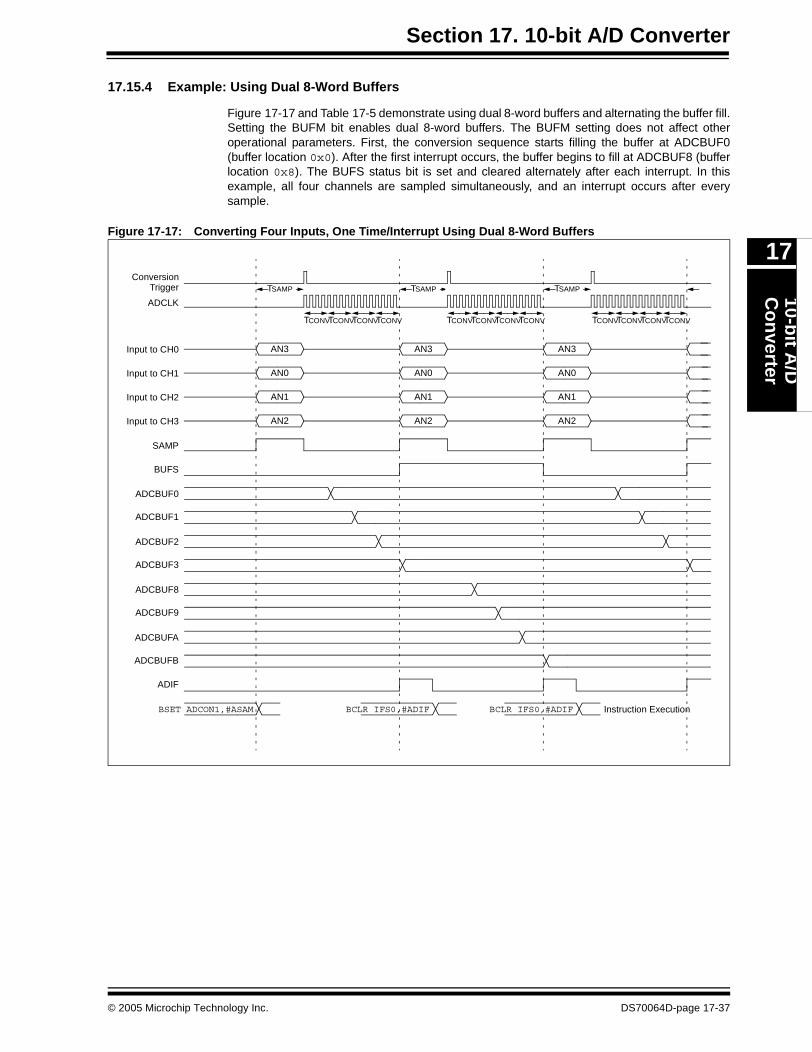
Section 17. 10-bit A/D Converter10-b
it A/D
Co
nverter
17
17.15.4 Example: Using Dual 8-Word Buffers
Figure 17-17 and Table 17-5 demonstrate using dual 8-word buffers and alternating the buffer fill.Setting the BUFM bit enables dual 8-word buffers. The BUFM setting does not affect otheroperational parameters. First, the conversion sequence starts filling the buffer at ADCBUF0(buffer location 0x0). After the first interrupt occurs, the buffer begins to fill at ADCBUF8 (bufferlocation 0x8). The BUFS status bit is set and cleared alternately after each interrupt. In thisexample, all four channels are sampled simultaneously, and an interrupt occurs after everysample.
Figure 17-17: Converting Four Inputs, One Time/Interrupt Using Dual 8-Word Buffers
ADCLK
SAMP
ADCBUF0
BSET ADCON1,#ASAM Instruction Execution
ADCBUF1
ADCBUF2
ADCBUF3
Input to CH0 AN3
TSAMP
ADIF
AN0
AN1
AN2
Input to CH1
Input to CH2
Input to CH3
ADCBUF8
ADCBUF9
ADCBUFA
ADCBUFB
AN3
TSAMP
AN0
AN1
AN2
AN3
TSAMP
AN0
AN1
AN2
BCLR IFS0,#ADIF BCLR IFS0,#ADIF
BUFS
ConversionTrigger
TCONVTCONVTCONVTCONV TCONVTCONVTCONVTCONV TCONVTCONVTCONVTCONV
© 2005 Microchip Technology Inc. DS70064D-page 17-37
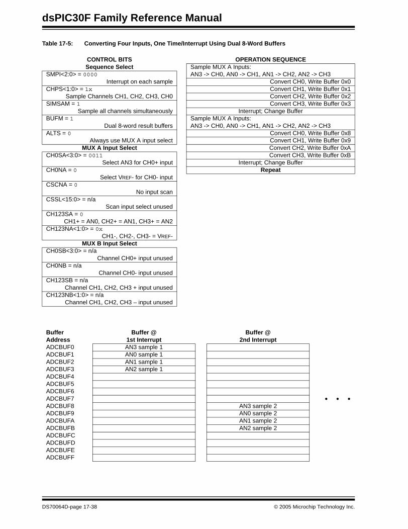
dsPIC30F Family Reference Manual
Table 17-5: Converting Four Inputs, One Time/Interrupt Using Dual 8-Word Buffers
CONTROL BITS OPERATION SEQUENCESequence Select Sample MUX A Inputs:
SMPI<2:0> = 0000 AN3 -> CH0, AN0 -> CH1, AN1 -> CH2, AN2 -> CH3Interrupt on each sample Convert CH0, Write Buffer 0x0
CHPS<1:0> = 1x Convert CH1, Write Buffer 0x1Sample Channels CH1, CH2, CH3, CH0 Convert CH2, Write Buffer 0x2
SIMSAM = 1 Convert CH3, Write Buffer 0x3Sample all channels simultaneously Interrupt; Change Buffer
BUFM = 1 Sample MUX A Inputs: Dual 8-word result buffers AN3 -> CH0, AN0 -> CH1, AN1 -> CH2, AN2 -> CH3
ALTS = 0 Convert CH0, Write Buffer 0x8Always use MUX A input select Convert CH1, Write Buffer 0x9
MUX A Input Select Convert CH2, Write Buffer 0xACH0SA<3:0> = 0011 Convert CH3, Write Buffer 0xB
Select AN3 for CH0+ input Interrupt; Change BufferCH0NA = 0 Repeat
Select VREF- for CH0- inputCSCNA = 0
No input scanCSSL<15:0> = n/a
Scan input select unusedCH123SA = 0
CH1+ = AN0, CH2+ = AN1, CH3+ = AN2CH123NA<1:0> = 0x
CH1-, CH2-, CH3- = VREF-MUX B Input Select
CH0SB<3:0> = n/aChannel CH0+ input unused
CH0NB = n/aChannel CH0- input unused
CH123SB = n/aChannel CH1, CH2, CH3 + input unused
CH123NB<1:0> = n/aChannel CH1, CH2, CH3 – input unused
BufferAddress
Buffer @1st Interrupt
Buffer @2nd Interrupt
ADCBUF0 AN3 sample 1ADCBUF1 AN0 sample 1ADCBUF2 AN1 sample 1ADCBUF3 AN2 sample 1ADCBUF4ADCBUF5ADCBUF6ADCBUF7 • • •ADCBUF8 AN3 sample 2ADCBUF9 AN0 sample 2ADCBUFA AN1 sample 2ADCBUFB AN2 sample 2ADCBUFCADCBUFDADCBUFEADCBUFF
DS70064D-page 17-38 © 2005 Microchip Technology Inc.
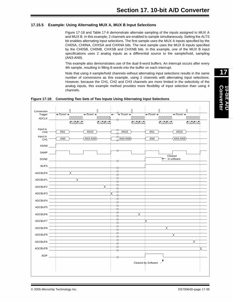
Section 17. 10-bit A/D Converter10-b
it A/D
Co
nverter
17
17.15.5 Example: Using Alternating MUX A, MUX B Input Selections
Figure 17-18 and Table 17-6 demonstrate alternate sampling of the inputs assigned to MUX Aand MUX B. In this example, 2 channels are enabled to sample simultaneously. Setting the ALTSbit enables alternating input selections. The first sample uses the MUX A inputs specified by theCH0SA, CH0NA, CHXSA and CHXNA bits. The next sample uses the MUX B inputs specifiedby the CH0SB, CH0NB, CHXSB and CHXNB bits. In this example, one of the MUX B inputspecifications uses 2 analog inputs as a differential source to the sample/hold, sampling(AN3-AN9).
This example also demonstrates use of the dual 8-word buffers. An interrupt occurs after every4th sample, resulting in filling 8-words into the buffer on each interrupt.
Note that using 4 sample/hold channels without alternating input selections results in the samenumber of conversions as this example, using 2 channels with alternating input selections.However, because the CH1, CH2 and CH3 channels are more limited in the selectivity of theanalog inputs, this example method provides more flexibility of input selection than using 4channels.
Figure 17-18: Converting Two Sets of Two Inputs Using Alternating Input Selections
ADCLK
SAMP
ADCBUF0
ADCBUF1
DONE
ADCBUF2
ADCBUF3
Input to AN1
TSAMP
ADIF
TCONVTCONV
AN0Input to
ADCBUF4
ADCBUF5
ADCBUF6
ADCBUF7
AN15
TSAMP
TCONVTCONV
AN3-AN9
ASAM
BUFS
AN1
TSAMP
TCONVTCONV
AN0
AN15
TSAMP
TCONVTCONV
AN3-AN9
ADCBUF8
ADCBUF9
ADCBUFA
ADCBUFB
TCONVTCONV
TSAMP
AN15
AN3-AN9
Cleared by Software
CH0
CH1
ConversionTrigger
Clearedin software
© 2005 Microchip Technology Inc. DS70064D-page 17-39
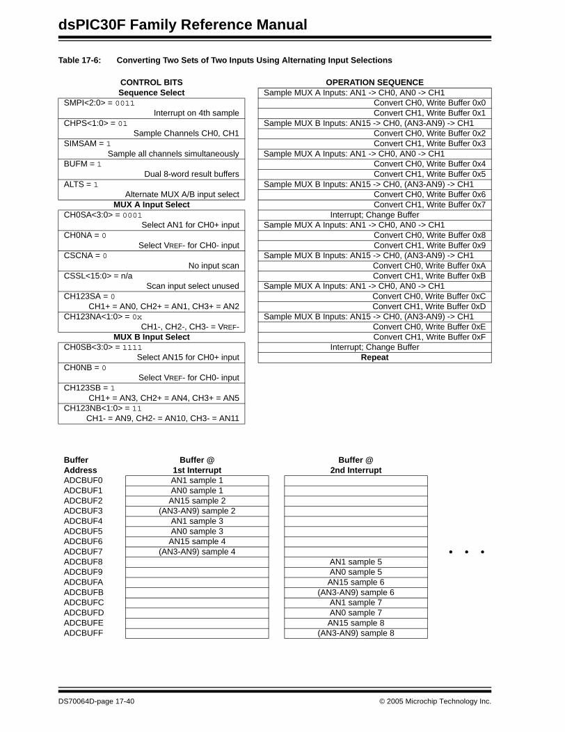
dsPIC30F Family Reference Manual
Table 17-6: Converting Two Sets of Two Inputs Using Alternating Input Selections
CONTROL BITS OPERATION SEQUENCESequence Select Sample MUX A Inputs: AN1 -> CH0, AN0 -> CH1
SMPI<2:0> = 0011 Convert CH0, Write Buffer 0x0Interrupt on 4th sample Convert CH1, Write Buffer 0x1
CHPS<1:0> = 01 Sample MUX B Inputs: AN15 -> CH0, (AN3-AN9) -> CH1Sample Channels CH0, CH1 Convert CH0, Write Buffer 0x2
SIMSAM = 1 Convert CH1, Write Buffer 0x3Sample all channels simultaneously Sample MUX A Inputs: AN1 -> CH0, AN0 -> CH1
BUFM = 1 Convert CH0, Write Buffer 0x4Dual 8-word result buffers Convert CH1, Write Buffer 0x5
ALTS = 1 Sample MUX B Inputs: AN15 -> CH0, (AN3-AN9) -> CH1Alternate MUX A/B input select Convert CH0, Write Buffer 0x6
MUX A Input Select Convert CH1, Write Buffer 0x7CH0SA<3:0> = 0001 Interrupt; Change Buffer
Select AN1 for CH0+ input Sample MUX A Inputs: AN1 -> CH0, AN0 -> CH1CH0NA = 0 Convert CH0, Write Buffer 0x8
Select VREF- for CH0- input Convert CH1, Write Buffer 0x9CSCNA = 0 Sample MUX B Inputs: AN15 -> CH0, (AN3-AN9) -> CH1
No input scan Convert CH0, Write Buffer 0xACSSL<15:0> = n/a Convert CH1, Write Buffer 0xB
Scan input select unused Sample MUX A Inputs: AN1 -> CH0, AN0 -> CH1CH123SA = 0 Convert CH0, Write Buffer 0xC
CH1+ = AN0, CH2+ = AN1, CH3+ = AN2 Convert CH1, Write Buffer 0xDCH123NA<1:0> = 0x Sample MUX B Inputs: AN15 -> CH0, (AN3-AN9) -> CH1
CH1-, CH2-, CH3- = VREF- Convert CH0, Write Buffer 0xEMUX B Input Select Convert CH1, Write Buffer 0xF
CH0SB<3:0> = 1111 Interrupt; Change BufferSelect AN15 for CH0+ input Repeat
CH0NB = 0Select VREF- for CH0- input
CH123SB = 1CH1+ = AN3, CH2+ = AN4, CH3+ = AN5
CH123NB<1:0> = 11CH1- = AN9, CH2- = AN10, CH3- = AN11
BufferAddress
Buffer @1st Interrupt
Buffer @2nd Interrupt
ADCBUF0 AN1 sample 1ADCBUF1 AN0 sample 1ADCBUF2 AN15 sample 2ADCBUF3 (AN3-AN9) sample 2ADCBUF4 AN1 sample 3ADCBUF5 AN0 sample 3ADCBUF6 AN15 sample 4ADCBUF7 (AN3-AN9) sample 4 • • •ADCBUF8 AN1 sample 5ADCBUF9 AN0 sample 5ADCBUFA AN15 sample 6ADCBUFB (AN3-AN9) sample 6ADCBUFC AN1 sample 7ADCBUFD AN0 sample 7ADCBUFE AN15 sample 8ADCBUFF (AN3-AN9) sample 8
DS70064D-page 17-40 © 2005 Microchip Technology Inc.

Section 17. 10-bit A/D Converter10-b
it A/D
Co
nverter
17
17.15.6 Example: Sampling Eight Inputs Using Simultaneous Sampling
Subsection 17.15.6 and Subsection 17.15.7 demonstrate identical setups with the exception thatSubsection 17.15.6 uses simultaneous sampling with SIMSAM = 1 and Subsection 17.15.7 usessequential sampling with SIMSAM = 0. Both examples use alternating inputs and specifydifferential inputs to the sample/hold.
Figure 17-19 and Table 17-7 demonstrate simultaneous sampling. When converting more thanone channel and selecting simultaneous sampling, the module will sample all channels, thenperform the required conversions in sequence. In this example, with ASAM set, sampling willbegin after the conversions complete.
Figure 17-19: Sampling Eight Inputs Using Simultaneous Sampling
ADCLK
SAMP
DONE
Input to CH0 AN13-AN1
TSAMP
ADIF
AN0
AN1
AN2
Input to CH1
Input to CH2
Input to CH3
ADCBUFD
ADCBUFE
ADCBUFF
AN14
TSAMP
AN3-AN6
AN4-AN7
AN5-AN8
AN14
TSAMP
AN3-AN6
AN4-AN7
AN5-AN8
ASAM
AN13-AN1
AN0
AN1
AN2
ADCBUF0
ADCBUF1
ADCBUF2
ADCBUF3
ADCBUFC
ConversionTrigger
TCONVTCONVTCONVTCONV TCONVTCONVTCONVTCONV TCONVTCONVTCONVTCONV
© 2005 Microchip Technology Inc. DS70064D-page 17-41
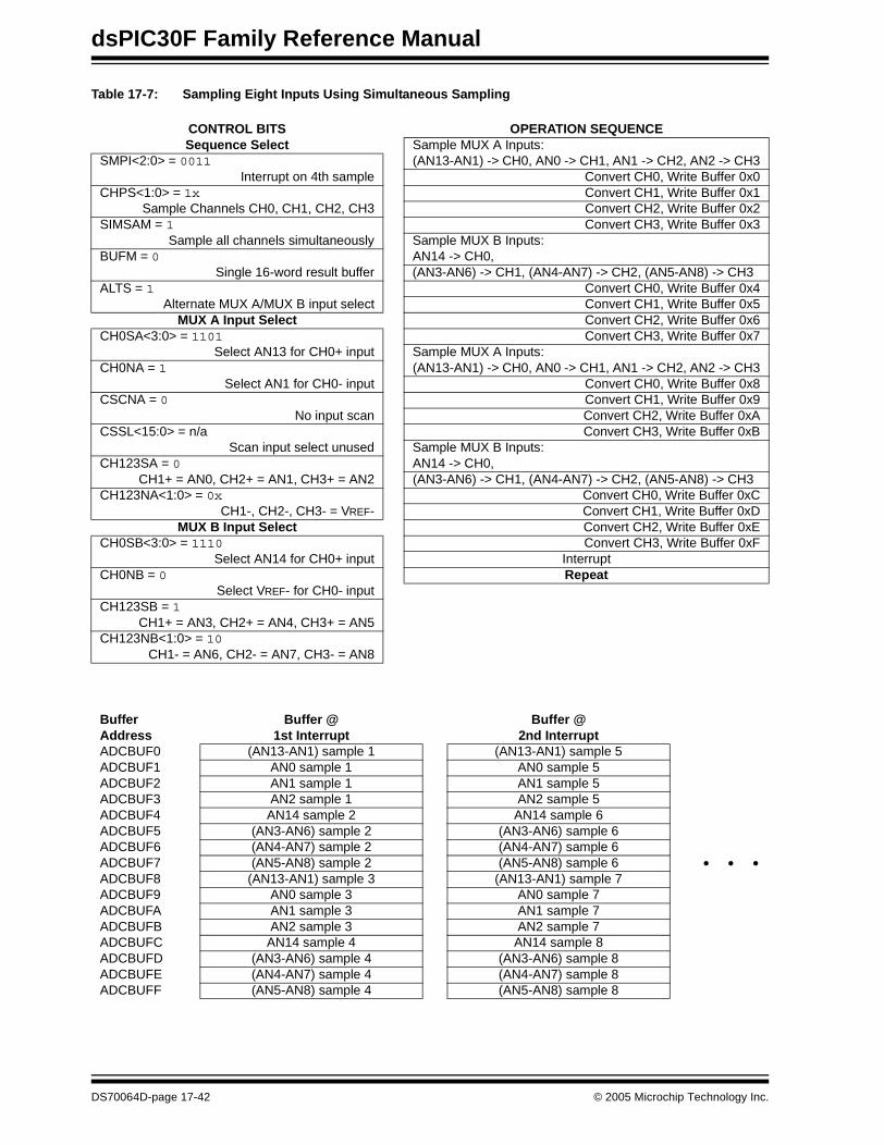
dsPIC30F Family Reference Manual
Table 17-7: Sampling Eight Inputs Using Simultaneous Sampling
CONTROL BITS OPERATION SEQUENCESequence Select Sample MUX A Inputs:
SMPI<2:0> = 0011 (AN13-AN1) -> CH0, AN0 -> CH1, AN1 -> CH2, AN2 -> CH3Interrupt on 4th sample Convert CH0, Write Buffer 0x0
CHPS<1:0> = 1x Convert CH1, Write Buffer 0x1Sample Channels CH0, CH1, CH2, CH3 Convert CH2, Write Buffer 0x2
SIMSAM = 1 Convert CH3, Write Buffer 0x3Sample all channels simultaneously Sample MUX B Inputs:
BUFM = 0 AN14 -> CH0, Single 16-word result buffer (AN3-AN6) -> CH1, (AN4-AN7) -> CH2, (AN5-AN8) -> CH3
ALTS = 1 Convert CH0, Write Buffer 0x4Alternate MUX A/MUX B input select Convert CH1, Write Buffer 0x5
MUX A Input Select Convert CH2, Write Buffer 0x6CH0SA<3:0> = 1101 Convert CH3, Write Buffer 0x7
Select AN13 for CH0+ input Sample MUX A Inputs: CH0NA = 1 (AN13-AN1) -> CH0, AN0 -> CH1, AN1 -> CH2, AN2 -> CH3
Select AN1 for CH0- input Convert CH0, Write Buffer 0x8CSCNA = 0 Convert CH1, Write Buffer 0x9
No input scan Convert CH2, Write Buffer 0xACSSL<15:0> = n/a Convert CH3, Write Buffer 0xB
Scan input select unused Sample MUX B Inputs: CH123SA = 0 AN14 -> CH0,
CH1+ = AN0, CH2+ = AN1, CH3+ = AN2 (AN3-AN6) -> CH1, (AN4-AN7) -> CH2, (AN5-AN8) -> CH3CH123NA<1:0> = 0x Convert CH0, Write Buffer 0xC
CH1-, CH2-, CH3- = VREF- Convert CH1, Write Buffer 0xDMUX B Input Select Convert CH2, Write Buffer 0xE
CH0SB<3:0> = 1110 Convert CH3, Write Buffer 0xFSelect AN14 for CH0+ input Interrupt
CH0NB = 0 RepeatSelect VREF- for CH0- input
CH123SB = 1CH1+ = AN3, CH2+ = AN4, CH3+ = AN5
CH123NB<1:0> = 10CH1- = AN6, CH2- = AN7, CH3- = AN8
BufferAddress
Buffer @1st Interrupt
Buffer @2nd Interrupt
ADCBUF0 (AN13-AN1) sample 1 (AN13-AN1) sample 5ADCBUF1 AN0 sample 1 AN0 sample 5ADCBUF2 AN1 sample 1 AN1 sample 5ADCBUF3 AN2 sample 1 AN2 sample 5ADCBUF4 AN14 sample 2 AN14 sample 6ADCBUF5 (AN3-AN6) sample 2 (AN3-AN6) sample 6ADCBUF6 (AN4-AN7) sample 2 (AN4-AN7) sample 6ADCBUF7 (AN5-AN8) sample 2 (AN5-AN8) sample 6 • • •ADCBUF8 (AN13-AN1) sample 3 (AN13-AN1) sample 7ADCBUF9 AN0 sample 3 AN0 sample 7ADCBUFA AN1 sample 3 AN1 sample 7ADCBUFB AN2 sample 3 AN2 sample 7ADCBUFC AN14 sample 4 AN14 sample 8ADCBUFD (AN3-AN6) sample 4 (AN3-AN6) sample 8ADCBUFE (AN4-AN7) sample 4 (AN4-AN7) sample 8ADCBUFF (AN5-AN8) sample 4 (AN5-AN8) sample 8
DS70064D-page 17-42 © 2005 Microchip Technology Inc.

Section 17. 10-bit A/D Converter10-b
it A/D
Co
nverter
17
17.15.7 Example: Sampling Eight Inputs Using Sequential Sampling
Figure 17-20 and Table 17-8 demonstrate sequential sampling. When converting more than onechannel and selecting sequential sampling, the module will start sampling a channel at theearliest opportunity, then perform the required conversions in sequence. In this example, withASAM set, sampling of a channel will begin after the conversion of that channel completes.
When ASAM is clear, sampling will not resume after conversion completion but will occur whensetting the SAMP bit.
When utilizing more than one channel, sequential sampling provides more sampling time sincea channel may be sampled while conversion occurs on another.
Figure 17-20: Sampling Eight Inputs Using Sequential Sampling
ADCLK
SAMP
DONE
Input to CH0 AN13-AN1
TSAMP
ADIF
AN0
AN1
AN2
Input to CH1
Input to CH2
Input to CH3
ADCBUFD
ADCBUFE
ADCBUFF
AN14
TSAMP
AN4-AN7
AN5-AN8
AN14
TSAMP
AN3-AN6
AN4-AN7
AN5-AN8
ASAM
AN1
AN2
ADCBUF0
ADCBUF1
ADCBUF2
ADCBUF3
ADCBUFC
AN13-AN1
AN0
AN2
ConversionTrigger
TCONVTCONVTCONVTCONV TCONVTCONVTCONVTCONV TCONVTCONVTCONVTCONV
AN3-AN6
AN1
AN13-AN1
AN0
© 2005 Microchip Technology Inc. DS70064D-page 17-43
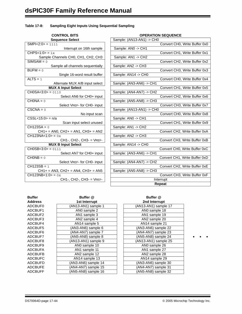
dsPIC30F Family Reference Manual
Table 17-8: Sampling Eight Inputs Using Sequential Sampling
CONTROL BITS OPERATION SEQUENCESequence Select Sample: (AN13-AN1) -> CH0
SMPI<2:0> = 1111 Convert CH0, Write Buffer 0x0Interrupt on 16th sample Sample: AN0 -> CH1
CHPS<1:0> = 1x Convert CH1, Write Buffer 0x1Sample Channels CH0, CH1, CH2, CH3 Sample: AN1 -> CH2
SIMSAM = 0 Convert CH2, Write Buffer 0x2Sample all channels sequentially Sample: AN2 -> CH3
BUFM = 0 Convert CH3, Write Buffer 0x3Single 16-word result buffer Sample: AN14 -> CH0
ALTS = 1 Convert CH0, Write Buffer 0x4Alternate MUX A/B input select Sample: (AN3-AN6) -> CH1
MUX A Input Select Convert CH1, Write Buffer 0x5CH0SA<3:0> = 0110 Sample: (AN4-AN7) -> CH2
Select AN6 for CH0+ input Convert CH2, Write Buffer 0x6CH0NA = 0 Sample: (AN5-AN8) -> CH3
Select VREF- for CH0- input Convert CH3, Write Buffer 0x7CSCNA = 0 Sample: (AN13-AN1) -> CH0
No input scan Convert CH0, Write Buffer 0x8CSSL<15:0> = n/a Sample: AN0 -> CH1
Scan input select unused Convert CH1, Write Buffer 0x9CH123SA = 0 Sample: AN1 -> CH2
CH1+ = AN0, CH2+ = AN1, CH3+ = AN2 Convert CH2, Write Buffer 0xACH123NA<1:0> = 0x Sample: AN2 -> CH3
CH1-, CH2-, CH3- = VREF- Convert CH3, Write Buffer 0xBMUX B Input Select Sample: AN14 -> CH0
CH0SB<3:0> = 0111 Convert CH0, Write Buffer 0xCSelect AN7 for CH0+ input Sample: (AN3-AN6) -> CH1
CH0NB = 0 Convert CH1, Write Buffer 0xDSelect VREF- for CH0- input Sample: (AN4-AN7) -> CH2
CH123SB = 1 Convert CH2, Write Buffer 0xECH1+ = AN3, CH2+ = AN4, CH3+ = AN5 Sample: (AN5-AN8) -> CH3
CH123NB<1:0> = 0x Convert CH3, Write Buffer 0xFCH1-, CH2-, CH3- = VREF- Interrupt
Repeat
BufferAddress
Buffer @1st Interrupt
Buffer @2nd Interrupt
ADCBUF0 (AN13-AN1) sample 1 (AN13-AN1) sample 17ADCBUF1 AN0 sample 2 AN0 sample 18ADCBUF2 AN1 sample 3 AN1 sample 19ADCBUF3 AN2 sample 4 AN2 sample 20ADCBUF4 AN14 sample 5 AN14 sample 21ADCBUF5 (AN3-AN6) sample 6 (AN3-AN6) sample 22ADCBUF6 (AN4-AN7) sample 7 (AN4-AN7) sample 23ADCBUF7 (AN5-AN8) sample 8 (AN5-AN8) sample 24 • • •ADCBUF8 (AN13-AN1) sample 9 (AN13-AN1) sample 25ADCBUF9 AN0 sample 10 AN0 sample 26ADCBUFA AN1 sample 11 AN1 sample 27ADCBUFB AN2 sample 12 AN2 sample 28ADCBUFC AN14 sample 13 AN14 sample 29ADCBUFD (AN3-AN6) sample 14 (AN3-AN6) sample 30ADCBUFE (AN4-AN7) sample 15 (AN4-AN7) sample 31ADCBUFF (AN5-AN8) sample 16 (AN5-AN8) sample 32
DS70064D-page 17-44 © 2005 Microchip Technology Inc.
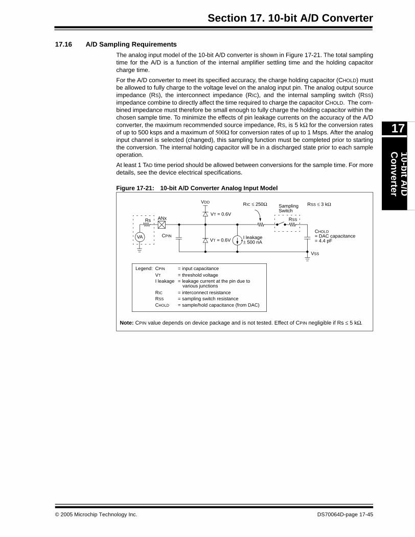
Section 17. 10-bit A/D Converter10-b
it A/D
Co
nverter
17
17.16 A/D Sampling Requirements The analog input model of the 10-bit A/D converter is shown in Figure 17-21. The total samplingtime for the A/D is a function of the internal amplifier settling time and the holding capacitorcharge time.
For the A/D converter to meet its specified accuracy, the charge holding capacitor (CHOLD) mustbe allowed to fully charge to the voltage level on the analog input pin. The analog output sourceimpedance (RS), the interconnect impedance (RIC), and the internal sampling switch (RSS)impedance combine to directly affect the time required to charge the capacitor CHOLD. The com-bined impedance must therefore be small enough to fully charge the holding capacitor within thechosen sample time. To minimize the effects of pin leakage currents on the accuracy of the A/Dconverter, the maximum recommended source impedance, RS, is 5 kΩ for the conversion ratesof up to 500 ksps and a maximum of 500Ω for conversion rates of up to 1 Msps. After the analoginput channel is selected (changed), this sampling function must be completed prior to startingthe conversion. The internal holding capacitor will be in a discharged state prior to each sampleoperation.
At least 1 TAD time period should be allowed between conversions for the sample time. For moredetails, see the device electrical specifications.
Figure 17-21: 10-bit A/D Converter Analog Input Model
CPINVA
Rs ANxVT = 0.6V
VT = 0.6V I leakage
RIC ≤ 250Ω SamplingSwitch
RSS
CHOLD= DAC capacitance
VSS
VDD
= 4.4 pF± 500 nA
Legend: CPIN
VT
I leakage
RIC
RSS
CHOLD
= input capacitance= threshold voltage= leakage current at the pin due to
= interconnect resistance= sampling switch resistance= sample/hold capacitance (from DAC)
various junctions
Note: CPIN value depends on device package and is not tested. Effect of CPIN negligible if Rs ≤ 5 kΩ.
RSS ≤ 3 kΩ
© 2005 Microchip Technology Inc. DS70064D-page 17-45
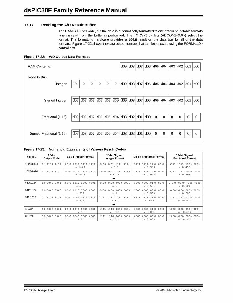
dsPIC30F Family Reference Manual
17.17 Reading the A/D Result Buffer
The RAM is 10-bits wide, but the data is automatically formatted to one of four selectable formatswhen a read from the buffer is performed. The FORM<1:0> bits (ADCON1<9:8>) select theformat. The formatting hardware provides a 16-bit result on the data bus for all of the dataformats. Figure 17-22 shows the data output formats that can be selected using the FORM<1:0>control bits.
Figure 17-22: A/D Output Data Formats
Figure 17-23: Numerical Equivalents of Various Result Codes
RAM Contents: d09 d08 d07 d06 d05 d04 d03 d02 d01 d00
Read to Bus:
Integer 0 0 0 0 0 0 d09 d08 d07 d06 d05 d04 d03 d02 d01 d00
Signed Integer d09 d09 d09 d09 d09 d09 d09 d08 d07 d06 d05 d04 d03 d02 d01 d00
Fractional (1.15) d09 d08 d07 d06 d05 d04 d03 d02 d01 d00 0 0 0 0 0 0
Signed Fractional (1.15) d09 d08 d07 d06 d05 d04 d03 d02 d01 d00 0 0 0 0 0 0
VIN/VREF10-bit
Output Code 16-bit Integer Format 16-bit SignedInteger Format 16-bit Fractional Format 16-bit Signed
Fractional Format
1023/1024 11 1111 1111 0000 0011 1111 1111= 1023
0000 0001 1111 1111= 511
1111 1111 1100 0000= 0.999
0111 1111 1100 0000= 0.499
1022/1024 11 1111 1110 0000 0011 1111 1110= 1022
0000 0001 1111 1110= 5 10
1111 1111 1000 0000= 0.998
0111 1111 1000 0000= 0.498
•••513/1024 10 0000 0001 0000 0010 0000 0001
= 5130000 0000 0000 0001
= 11000 0000 0100 0000
= 0.5010 000 0000 0100 0000
= 0.001
512/1024 10 0000 0000 0000 0010 0000 0000= 512
0000 0000 0000 0000= 0
1000 0000 0000 0000= 0.500
0000 0000 0000 0000= 0.000
511/1024 01 1111 1111 0000 0001 1111 1111= 511
1111 1111 1111 1111= -1
0111 1111 1100 0000= .499
1111 1111 1100 0000= -0.001
•••1/1024 00 0000 0001 0000 0000 0000 0001
= 11111 1110 0000 0001
= -5110000 0000 0100 0000
= 0.0011000 0000 0100 0000
= -0.499
0/1024 00 0000 0000 0000 0000 0000 0000= 0
1111 1110 0000 0000= -512
0000 0000 0000 0000= 0.000
1000 0000 0000 0000= -0.500
DS70064D-page 17-46 © 2005 Microchip Technology Inc.
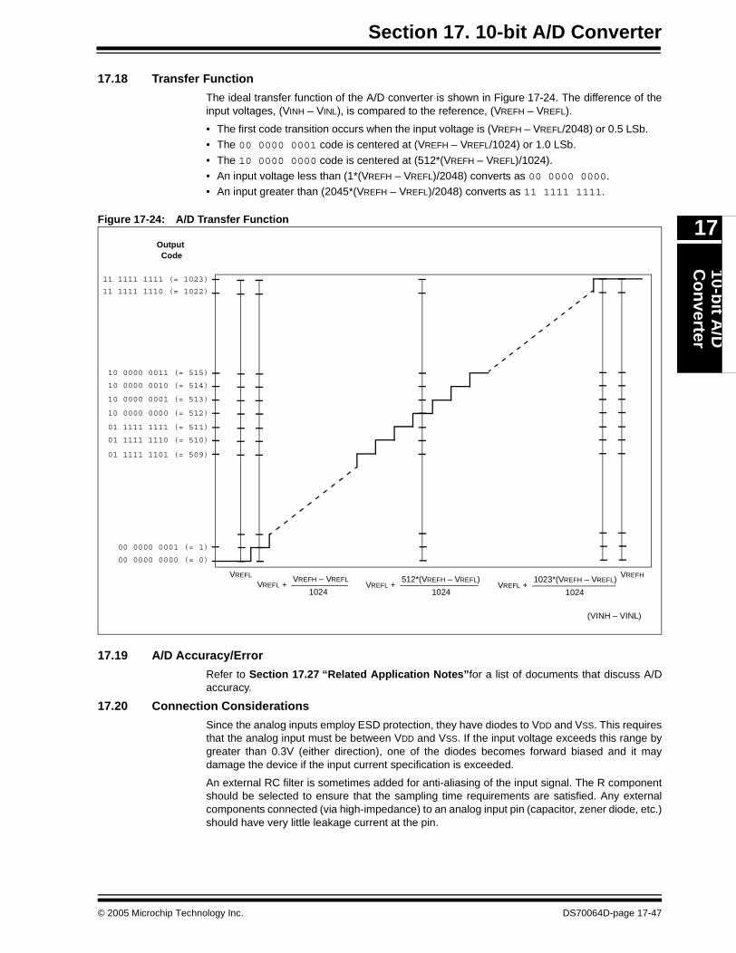
Section 17. 10-bit A/D Converter10-b
it A/D
Co
nverter
17
17.18 Transfer Function
The ideal transfer function of the A/D converter is shown in Figure 17-24. The difference of theinput voltages, (VINH – VINL), is compared to the reference, (VREFH – VREFL).
• The first code transition occurs when the input voltage is (VREFH – VREFL/2048) or 0.5 LSb. • The 00 0000 0001 code is centered at (VREFH – VREFL/1024) or 1.0 LSb.
• The 10 0000 0000 code is centered at (512*(VREFH – VREFL)/1024).• An input voltage less than (1*(VREFH – VREFL)/2048) converts as 00 0000 0000.• An input greater than (2045*(VREFH – VREFL)/2048) converts as 11 1111 1111.
Figure 17-24: A/D Transfer Function
17.19 A/D Accuracy/Error
Refer to Section 17.27 “Related Application Notes”for a list of documents that discuss A/Daccuracy.
17.20 Connection Considerations Since the analog inputs employ ESD protection, they have diodes to VDD and VSS. This requiresthat the analog input must be between VDD and VSS. If the input voltage exceeds this range bygreater than 0.3V (either direction), one of the diodes becomes forward biased and it maydamage the device if the input current specification is exceeded.
An external RC filter is sometimes added for anti-aliasing of the input signal. The R componentshould be selected to ensure that the sampling time requirements are satisfied. Any externalcomponents connected (via high-impedance) to an analog input pin (capacitor, zener diode, etc.)should have very little leakage current at the pin.
10 0000 0010 (= 514)
10 0000 0011 (= 515)
01 1111 1101 (= 509)
01 1111 1110 (= 510)
01 1111 1111 (= 511)
11 1111 1110 (= 1022)
11 1111 1111 (= 1023)
00 0000 0000 (= 0)
00 0000 0001 (= 1)
Output Code
10 0000 0000 (= 512)
(VINH – VINL)
VREFL VREFH – VREFL
1024
VREFH
VREFL +
10 0000 0001 (= 513)
512*(VREFH – VREFL)
1024VREFL +
1023*(VREFH – VREFL)
1024VREFL +
© 2005 Microchip Technology Inc. DS70064D-page 17-47
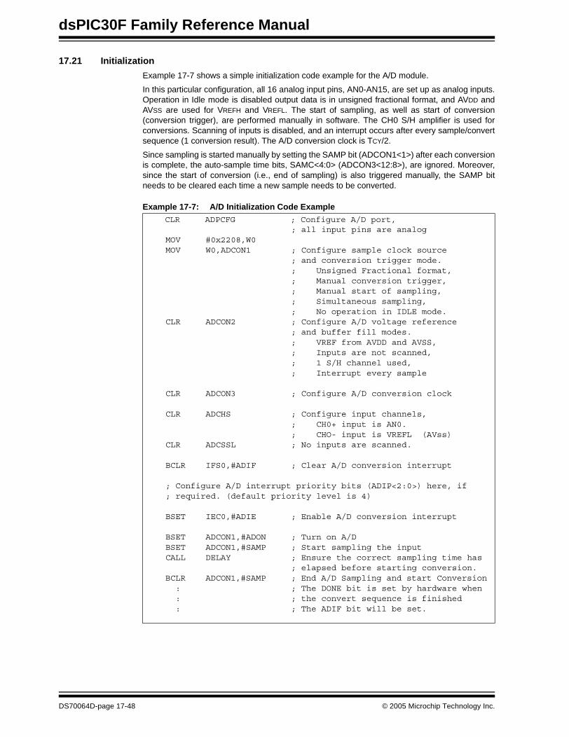
dsPIC30F Family Reference Manual
17.21 Initialization
Example 17-7 shows a simple initialization code example for the A/D module.
In this particular configuration, all 16 analog input pins, AN0-AN15, are set up as analog inputs.Operation in Idle mode is disabled output data is in unsigned fractional format, and AVDD andAVSS are used for VREFH and VREFL. The start of sampling, as well as start of conversion(conversion trigger), are performed manually in software. The CH0 S/H amplifier is used forconversions. Scanning of inputs is disabled, and an interrupt occurs after every sample/convertsequence (1 conversion result). The A/D conversion clock is TCY/2.
Since sampling is started manually by setting the SAMP bit (ADCON1<1>) after each conversionis complete, the auto-sample time bits, SAMC<4:0> (ADCON3<12:8>), are ignored. Moreover,since the start of conversion (i.e., end of sampling) is also triggered manually, the SAMP bitneeds to be cleared each time a new sample needs to be converted.
Example 17-7: A/D Initialization Code Example CLR ADPCFG ; Configure A/D port, ; all input pins are analog MOV #0x2208,W0 MOV W0,ADCON1 ; Configure sample clock source ; and conversion trigger mode. ; Unsigned Fractional format, ; Manual conversion trigger, ; Manual start of sampling, ; Simultaneous sampling, ; No operation in IDLE mode. CLR ADCON2 ; Configure A/D voltage reference ; and buffer fill modes. ; VREF from AVDD and AVSS, ; Inputs are not scanned, ; 1 S/H channel used, ; Interrupt every sample CLR ADCON3 ; Configure A/D conversion clock CLR ADCHS ; Configure input channels, ; CH0+ input is AN0. ; CHO- input is VREFL (AVss) CLR ADCSSL ; No inputs are scanned.
BCLR IFS0,#ADIF ; Clear A/D conversion interrupt
; Configure A/D interrupt priority bits (ADIP<2:0>) here, if ; required. (default priority level is 4)
BSET IEC0,#ADIE ; Enable A/D conversion interrupt BSET ADCON1,#ADON ; Turn on A/D BSET ADCON1,#SAMP ; Start sampling the input CALL DELAY ; Ensure the correct sampling time has ; elapsed before starting conversion. BCLR ADCON1,#SAMP ; End A/D Sampling and start Conversion : ; The DONE bit is set by hardware when : ; the convert sequence is finished : ; The ADIF bit will be set.
DS70064D-page 17-48 © 2005 Microchip Technology Inc.

Section 17. 10-bit A/D Converter10-b
it A/D
Co
nverter
17
17.22 A/D Conversion Speeds
The dsPIC30F 10-bit A/D converter specifications permit a maximum 1 Msps sampling rate. Thetable below summarizes the conversion speeds for the dsPIC30F 10-bit A/D converter and therequired operating conditions.
Table 17-9: 10-bit Conversion Rate Parameters
dsPIC30F 10-bit A/D Converter Conversion Rates
A/D SpeedTAD
MinimumSampling Time Min
Rs Max VDD Temperature A/D Channels Configuration
Up to 1 MSps(1)
83.33 ns 12 TAD 500 Ω 4.5V to 5.5V -40°C to +85°C
Up to 750 ksps(1)
95.24 ns 2 TAD 500 Ω 4.5V to 5.5V -40°C to +85°C
Up to 600 ksps(1)
138.89 ns 12 TAD 500 Ω 3.0V to 5.5V -40°C to +125°C
Up to 500 ksps
153.85 ns 1 TAD 5.0 kΩ 4.5V to 5.5V -40°C to +125°C
Up to 300 ksps
256.41 ns 1 TAD 5.0 kΩ 3.0V to 5.5V -40°C to +125°C
Note 1: External VREF- and VREF+ pins must be used for correct operation. See Figure 17-25 for recommendedcircuit.
VREF- VREF+
ADC
ANxS/H
S/H
CH1, CH2 or CH3
CH0
VREF- VREF+
ADCANx
S/H
CHX
VREF- VREF+
ADC
ANxS/H
S/H
CH1, CH2 or CH3
CH0
VREF- VREF+
ADCANx
S/H
CHX
ANx or VREF-
orAVSS
orAVDD
VREF- VREF+
ADCANx
S/H
CHX
ANx or VREF-
orAVSS
orAVDD
© 2005 Microchip Technology Inc. DS70064D-page 17-49
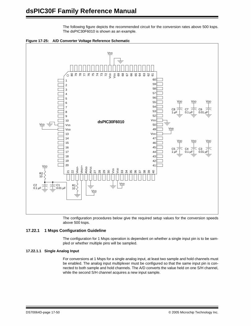
dsPIC30F Family Reference Manual
The following figure depicts the recommended circuit for the conversion rates above 500 ksps.The dsPIC30F6010 is shown as an example.
Figure 17-25: A/D Converter Voltage Reference Schematic
The configuration procedures below give the required setup values for the conversion speedsabove 500 ksps.
17.22.1 1 Msps Configuration Guideline
The configuration for 1 Msps operation is dependent on whether a single input pin is to be sam-pled or whether multiple pins will be sampled.
17.22.1.1 Single Analog Input
For conversions at 1 Msps for a single analog input, at least two sample and hold channels mustbe enabled. The analog input multiplexer must be configured so that the same input pin is con-nected to both sample and hold channels. The A/D converts the value held on one S/H channel,while the second S/H channel acquires a new input sample.
7274 73
VD
D
VS
S 69 68 67 66 65 64 63 62 61
20
2
3
4
5
6
7
8
9
10
VSS
VDD
13
14
15
16
50
49
VDD
47
46
45
44
21
41
40393837363534VR
EF-
VR
EF+
AV
DD
AV
SS
27 28 29 30 VS
S
VD
D
33
17
18
19
75
1
57
56
55
54
53
52
VSS
60
59
58
43
42
7678 777922
80
dsPIC30F6010
VDD
VDD
VDD
VDD
VDD
VDD
VDD
R210
C20.1 μF
C10.01 μF
R110
C81 μF
VDD
C70.1 μF
VDD
C60.01 μF
VDD
C51 μF
VDD
C40.1 μF
VDD
C30.01 μF
DS70064D-page 17-50 © 2005 Microchip Technology Inc.
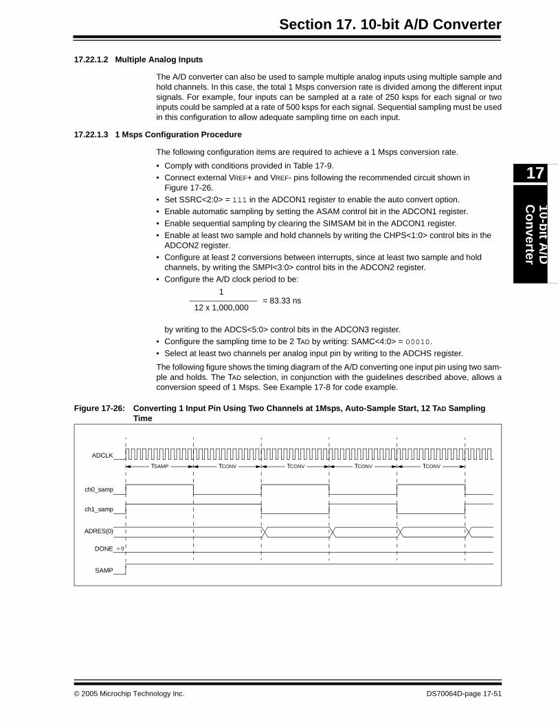
Section 17. 10-bit A/D Converter10-b
it A/D
Co
nverter
17
17.22.1.2 Multiple Analog Inputs
The A/D converter can also be used to sample multiple analog inputs using multiple sample andhold channels. In this case, the total 1 Msps conversion rate is divided among the different inputsignals. For example, four inputs can be sampled at a rate of 250 ksps for each signal or twoinputs could be sampled at a rate of 500 ksps for each signal. Sequential sampling must be usedin this configuration to allow adequate sampling time on each input.
17.22.1.3 1 Msps Configuration Procedure
The following configuration items are required to achieve a 1 Msps conversion rate.
• Comply with conditions provided in Table 17-9.• Connect external VREF+ and VREF- pins following the recommended circuit shown in
Figure 17-26.• Set SSRC<2:0> = 111 in the ADCON1 register to enable the auto convert option.• Enable automatic sampling by setting the ASAM control bit in the ADCON1 register.
• Enable sequential sampling by clearing the SIMSAM bit in the ADCON1 register.• Enable at least two sample and hold channels by writing the CHPS<1:0> control bits in the
ADCON2 register.• Configure at least 2 conversions between interrupts, since at least two sample and hold
channels, by writing the SMPI<3:0> control bits in the ADCON2 register.• Configure the A/D clock period to be:
by writing to the ADCS<5:0> control bits in the ADCON3 register.
• Configure the sampling time to be 2 TAD by writing: SAMC<4:0> = 00010.• Select at least two channels per analog input pin by writing to the ADCHS register.
The following figure shows the timing diagram of the A/D converting one input pin using two sam-ple and holds. The TAD selection, in conjunction with the guidelines described above, allows aconversion speed of 1 Msps. See Example 17-8 for code example.
Figure 17-26: Converting 1 Input Pin Using Two Channels at 1Msps, Auto-Sample Start, 12 TAD Sampling Time
1
12 x 1,000,000= 83.33 ns
TCONV
ADCLK
ch0_samp
ch1_samp
ADRES(0)
DONE
TSAMP TCONV TCONV TCONV
SAMP
= 0
© 2005 Microchip Technology Inc. DS70064D-page 17-51
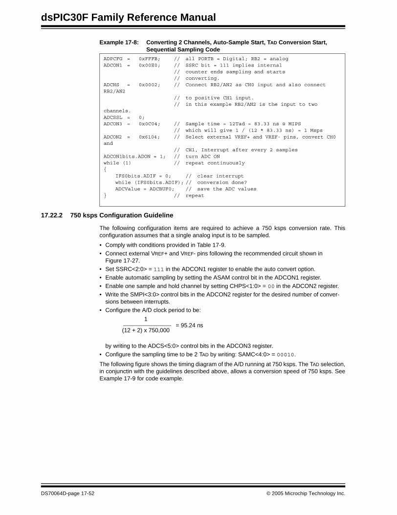
dsPIC30F Family Reference Manual
Example 17-8: Converting 2 Channels, Auto-Sample Start, TAD Conversion Start, Sequential Sampling Code
17.22.2 750 ksps Configuration Guideline
The following configuration items are required to achieve a 750 ksps conversion rate. Thisconfiguration assumes that a single analog input is to be sampled.
• Comply with conditions provided in Table 17-9.• Connect external VREF+ and VREF- pins following the recommended circuit shown in
Figure 17-27.• Set SSRC<2:0> = 111 in the ADCON1 register to enable the auto convert option.• Enable automatic sampling by setting the ASAM control bit in the ADCON1 register.
• Enable one sample and hold channel by setting CHPS<1:0> = 00 in the ADCON2 register.• Write the SMPI<3:0> control bits in the ADCON2 register for the desired number of conver-
sions between interrupts.• Configure the A/D clock period to be:
by writing to the ADCS<5:0> control bits in the ADCON3 register.
• Configure the sampling time to be 2 TAD by writing: SAMC<4:0> = 00010.
The following figure shows the timing diagram of the A/D running at 750 ksps. The TAD selection,in conjunctin with the guidelines described above, allows a conversion speed of 750 ksps. SeeExample 17-9 for code example.
ADPCFG = 0xFFFB; // all PORTB = Digital; RB2 = analogADCON1 = 0x00E0; // SSRC bit = 111 implies internal
// counter ends sampling and starts// converting.
ADCHS = 0x0002; // Connect RB2/AN2 as CH0 input and also connect RB2/AN2
// to positive CH1 input.// in this example RB2/AN2 is the input to two
channels.ADCSSL = 0;ADCON3 = 0x0C04; // Sample time = 12Tad = 83.33 ns @ MIPS
// which will give 1 / (12 * 83.33 ns) = 1 MspsADCON2 = 0x6104; // Select external VREF+ and VREF- pins, convert CH0 and
// CH1, Interrupt after every 2 samplesADCON1bits.ADON = 1; // turn ADC ONwhile (1) // repeat continuously{
IFS0bits.ADIF = 0; // clear interruptwhile (IFS0bits.ADIF); // conversion done?ADCValue = ADCBUF0; // save the ADC values
} // repeat
1
(12 + 2) x 750,000= 95.24 ns
DS70064D-page 17-52 © 2005 Microchip Technology Inc.
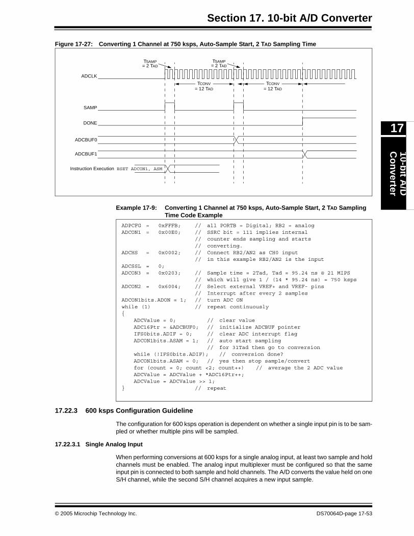
Section 17. 10-bit A/D Converter10-b
it A/D
Co
nverter
17
Figure 17-27: Converting 1 Channel at 750 ksps, Auto-Sample Start, 2 TAD Sampling Time
Example 17-9: Converting 1 Channel at 750 ksps, Auto-Sample Start, 2 TAD Sampling Time Code Example
17.22.3 600 ksps Configuration Guideline
The configuration for 600 ksps operation is dependent on whether a single input pin is to be sam-pled or whether multiple pins will be sampled.
17.22.3.1 Single Analog Input
When performing conversions at 600 ksps for a single analog input, at least two sample and holdchannels must be enabled. The analog input multiplexer must be configured so that the sameinput pin is connected to both sample and hold channels. The A/D converts the value held on oneS/H channel, while the second S/H channel acquires a new input sample.
TCONV= 12 TAD
TCONV= 12 TAD
TSAMP= 2 TAD
TSAMP= 2 TAD
ADCLK
SAMP
DONE
ADCBUF0
ADCBUF1
Instruction Execution BSET ADCON1, ASM
ADPCFG = 0xFFFB; // all PORTB = Digital; RB2 = analogADCON1 = 0x00E0; // SSRC bit = 111 implies internal
// counter ends sampling and starts// converting.
ADCHS = 0x0002; // Connect RB2/AN2 as CH0 input// in this example RB2/AN2 is the input
ADCSSL = 0;ADCON3 = 0x0203; // Sample time = 2Tad, Tad = 95.24 ns @ 21 MIPS
// which will give 1 / (14 * 95.24 ns) = 750 kspsADCON2 = 0x6004; // Select external VREF+ and VREF- pins
// Interrupt after every 2 samplesADCON1bits.ADON = 1; // turn ADC ONwhile (1) // repeat continuously{
ADCValue = 0; // clear valueADC16Ptr = &ADCBUF0; // initialize ADCBUF pointerIFS0bits.ADIF = 0; // clear ADC interrupt flagADCON1bits.ASAM = 1; // auto start sampling
// for 31Tad then go to conversionwhile (!IFS0bits.ADIF); // conversion done?ADCON1bits.ASAM = 0; // yes then stop sample/convertfor (count = 0; count <2; count++) // average the 2 ADC valueADCValue = ADCValue + *ADC16Ptr++;ADCValue = ADCValue >> 1;
} // repeat
© 2005 Microchip Technology Inc. DS70064D-page 17-53
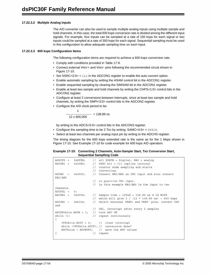
dsPIC30F Family Reference Manual
17.22.3.2 Multiple Analog Inputs
The A/D converter can also be used to sample multiple analog inputs using multiple sample andhold channels. In this case, the total 600 ksps conversion rate is divided among the different inputsignals. For example, four inputs can be sampled at a rate of 150 ksps for each signal or twoinputs could be sampled at a rate of 300 ksps for each signal. Sequential sampling must be usedin this configuration to allow adequate sampling time on each input.
17.22.3.3 600 ksps Configuration Items
The following configuration items are required to achieve a 600 ksps conversion rate.
• Comply with conditions provided in Table 17-9.• Connect external VREF+ and VREF- pins following the recommended circuit shown in
Figure 17-10.• Set SSRC<2:0> = 111 in the ADCON1 register to enable the auto convert option.• Enable automatic sampling by setting the ASAM control bit in the ADCON1 register.
• Enable sequential sampling by clearing the SIMSAM bit in the ADCON1 register.• Enable at least two sample and hold channels by writing the CHPS<1:0> control bits in the
ADCON2 register.• Configure at least 2 conversions between interrupts, since at least two sample and hold
channels, by writing the SMPI<3:0> control bits in the ADCON2 register.• Configure the A/D clock period to be:
by writing to the ADCS<5:0> control bits in the ADCON3 register.
• Configure the sampling time to be 2 TAD by writing: SAMC<4:0> = 00010.• Select at least two channels per analog input pin by writing to the ADCHS register.
The timing diagram for the 600 ksps extended rate is the same as for the 1 Msps shown inFigure 17-10. See Example 17-10 for code example for 600 ksps A/D operation.
Example 17-10: Converting 2 Channels, Auto-Sample Start, TAD Conversion Start, Sequential Samplling Code
1
12 x 600,000= 138.89 ns
ADPCFG = 0xFFFB; // all PORTB = Digital; RB2 = analogADCON1 = 0x00E0; // SSRC bit = 111 implies internal
// counter ends sampling and starts// converting.
ADCHS = 0x0002; // Connect RB2/AN2 as CH0 input and also connect RB2/AN2
// to positive CH1 input.// in this example RB2/AN2 is the input to two
channels.ADCSSL = 0;ADCON3 = 0x0C04; // Sample time = 12Tad = 138.89 ns @ 18 MIPS
// which will give 1 / (12 * 138.89 ns) = 600 kspsADCON2 = 0x6104; // Select external VREF+ and VREF- pins, convert CH0 and
// CH1, Interrupt after every 2 samplesADCON1bits.ADON = 1; // turn ADC ONwhile (1) // repeat continuously{
IFS0bits.ADIF = 0; // clear interruptwhile (IFS0bits.ADIF); // conversion done?ADCValue = ADCBUF0; // save the ADC values
} // repeat
DS70064D-page 17-54 © 2005 Microchip Technology Inc.
Section 17. 10-bit A/D Converter10-b
it A/D
Co
nverter
17
17.23 Operation During Sleep and Idle Modes Sleep and Idle modes are useful for minimizing conversion noise because the digital activity ofthe CPU, buses and other peripherals is minimized.
17.23.1 CPU Sleep Mode without RC A/D Clock
When the device enters Sleep mode, all clock sources to the module are shutdown and stay atlogic ‘0’.
If Sleep occurs in the middle of a conversion, the conversion is aborted unless the A/D is clockedfrom its internal RC clock generator. The converter will not resume a partially completedconversion on exiting from Sleep mode.
Register contents are not affected by the device entering or leaving Sleep mode.
17.23.2 CPU Sleep Mode with RC A/D Clock
The A/D module can operate during Sleep mode if the A/D clock source is set to the internal A/DRC oscillator (ADRC = 1). This eliminates digital switching noise from the conversion. When theconversion is completed, the DONE bit will be set and the result loaded into the A/D result buffer,ADCBUF.
If the A/D interrupt is enabled (ADIE = 1), the device will wake-up from Sleep when the A/Dinterrupt occurs. Program execution will resume at the A/D Interrupt Service Routine if the A/Dinterrupt is greater than the current CPU priority. Otherwise, execution will continue from theinstruction after the PWRSAV instruction that placed the device in Sleep mode.
If the A/D interrupt is not enabled, the A/D module will then be turned off, although the ADON bitwill remain set.
To minimize the effects of digital noise on the A/D module operation, the user should select aconversion trigger source that ensures the A/D conversion will take place in Sleep mode. Theautomatic conversion trigger option can be used for sampling and conversion in Sleep(SSRC<2:0> = 111). To use the automatic conversion option, the ADON bit should be set in theinstruction prior to the PWRSAV instruction.
17.23.3 A/D Operation During CPU Idle Mode
For the A/D, the ADSIDL bit (ADCON1<13>) selects if the module will stop on Idle or continueon Idle. If ADSIDL = 0, the module will continue normal operation when the device enters Idlemode. If the A/D interrupt is enabled (ADIE = 1), the device will wake up from Idle mode whenthe A/D interrupt occurs. Program execution will resume at the A/D Interrupt Service Routine ifthe A/D interrupt is greater than the current CPU priority. Otherwise, execution will continue fromthe instruction after the PWRSAV instruction that placed the device in Idle mode.
If ADSIDL = 1, the module will stop in Idle. If the device enters Idle mode in the middle of aconversion, the conversion is aborted. The converter will not resume a partially completedconversion on exiting from Idle mode.
17.24 Effects of a Reset
A device Reset forces all registers to their Reset state. This forces the A/D module to be turnedoff, and any conversion in progress is aborted. All pins that are multiplexed with analog inputswill be configured as analog inputs. The corresponding TRIS bits will be set.
The values in the ADCBUF registers are not initialized during a Power-on Reset.ADCBUF0...ADCBUFF will contain unknown data.
Note: For the A/D module to operate in Sleep, the A/D clock source must be set to RC(ADRC = 1).
© 2005 Microchip Technology Inc. DS70064D-page 17-55
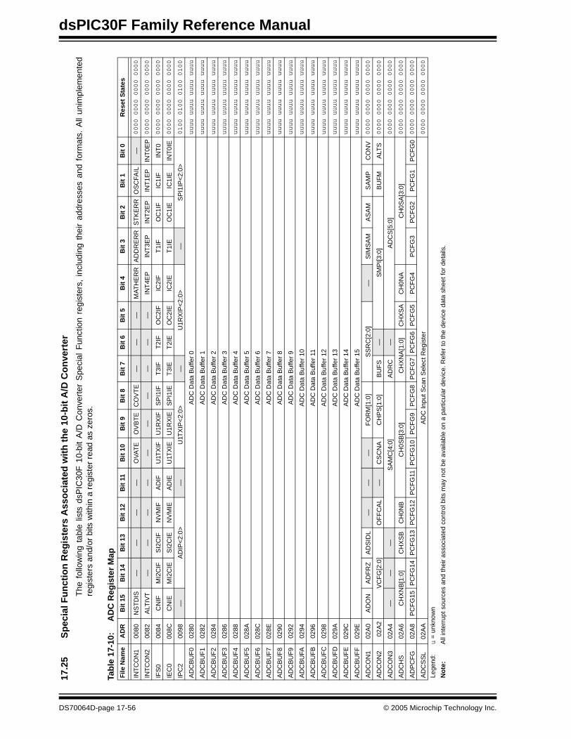
dsPIC30F Family Reference Manual
17.2
5S
pec
ial F
un
ctio
n R
egis
ters
Ass
oci
ated
wit
h t
he
10-b
it A
/D C
on
vert
er
The
fol
low
ing
tabl
e lis
ts d
sPIC
30F
10-
bit
A/D
Con
vert
er S
peci
al F
unct
ion
regi
ster
s, i
nclu
ding
the
ir ad
dres
ses
and
form
ats.
All
unim
plem
ente
dre
gist
ers
and/
or b
its w
ithin
a r
egis
ter
read
as
zero
s.
Tab
le 1
7-10
:A
DC
Reg
iste
r M
apF
ile N
ame
AD
RB
it 1
5B
it 1
4B
it 1
3B
it 1
2B
it 1
1B
it 1
0B
it 9
Bit
8B
it 7
Bit
6B
it 5
Bit
4B
it 3
Bit
2B
it 1
Bit
0R
eset
Sta
tes
INT
CO
N1
0080
NS
TD
IS—
——
—O
VA
TE
OV
BT
EC
OV
TE
——
—M
AT
HE
RR
AD
DR
ER
RS
TK
ER
RO
SC
FAIL
—0000 0000 0000 0000
INT
CO
N2
0082
ALT
IVT
——
——
——
——
——
INT
4EP
INT
3EP
INT
2EP
INT
1EP
INT
0EP
0000 0000 0000 0000
IFS
000
84C
NIF
MI2
CIF
SI2
CIF
NV
MIF
AD
IFU
1TX
IFU
1RX
IFS
PI1
IFT
3IF
T2I
FO
C2I
FIC
2IF
T1I
FO
C1I
FIC
1IF
INT
00000 0000 0000 0000
IEC
000
8CC
NIE
MI2
CIE
SI2
CIE
NV
MIE
AD
IEU
1TX
IEU
1RX
IES
PI1
IET
3IE
T2I
EO
C2I
EIC
2IE
T1I
EO
C1I
EIC
1IE
INT
0IE
0000 0000 0000 0000
IPC
200
98—
AD
IP<
2:0>
—U
1TX
IP<
2:0>
—U
1RX
IP<
2:0>
—S
PI1
IP<
2:0>
0100 0100 0100 0100
AD
CB
UF
002
80A
DC
Dat
a B
uffe
r 0
uuuu uuuu uuuu uuuu
AD
CB
UF
102
82A
DC
Dat
a B
uffe
r 1
uuuu uuuu uuuu uuuu
AD
CB
UF
202
84A
DC
Dat
a B
uffe
r 2
uuuu uuuu uuuu uuuu
AD
CB
UF
302
86A
DC
Dat
a B
uffe
r 3
uuuu uuuu uuuu uuuu
AD
CB
UF
402
88A
DC
Dat
a B
uffe
r 4
uuuu uuuu uuuu uuuu
AD
CB
UF
502
8AA
DC
Dat
a B
uffe
r 5
uuuu uuuu uuuu uuuu
AD
CB
UF
602
8CA
DC
Dat
a B
uffe
r 6
uuuu uuuu uuuu uuuu
AD
CB
UF
702
8EA
DC
Dat
a B
uffe
r 7
uuuu uuuu uuuu uuuu
AD
CB
UF
802
90A
DC
Dat
a B
uffe
r 8
uuuu uuuu uuuu uuuu
AD
CB
UF
902
92A
DC
Dat
a B
uffe
r 9
uuuu uuuu uuuu uuuu
AD
CB
UFA
0294
AD
C D
ata
Buf
fer
10uuuu uuuu uuuu uuuu
AD
CB
UF
B02
96A
DC
Dat
a B
uffe
r 11
uuuu uuuu uuuu uuuu
AD
CB
UF
C02
98A
DC
Dat
a B
uffe
r 12
uuuu uuuu uuuu uuuu
AD
CB
UF
D02
9AA
DC
Dat
a B
uffe
r 13
uuuu uuuu uuuu uuuu
AD
CB
UF
E02
9CA
DC
Dat
a B
uffe
r 14
uuuu uuuu uuuu uuuu
AD
CB
UF
F02
9EA
DC
Dat
a B
uffe
r 15
uuuu uuuu uuuu uuuu
AD
CO
N1
02A
0A
DO
NA
DF
RZ
AD
SID
L—
——
FO
RM
[1:0
]S
SR
C[2
:0]
—S
IMS
AM
AS
AM
SA
MP
CO
NV
0000 0000 0000 0000
AD
CO
N2
02
A2
VC
FG
[2:0
]O
FF
CA
L—
CS
CN
AC
HP
S[1
:0]
BU
FS
—S
MP
I[3:0
]B
UF
MA
LTS
0000 0000 0000 0000
AD
CO
N3
02A
4—
——
SA
MC
[4:0
]A
DR
C—
AD
CS
[5:0
]0000 0000 0000 0000
AD
CH
S02
A6
CH
XN
B[1
:0]
CH
XS
BC
H0N
BC
H0S
B[3
:0]
CH
XN
A[1
:0]
CH
XS
AC
H0N
AC
H0S
A[3
:0]
0000 0000 0000 0000
AD
PC
FG
02A
8P
CF
G15
PC
FG
14P
CF
G13
PC
FG
12P
CF
G11
PC
FG
10P
CF
G9
PC
FG
8P
CF
G7
PC
FG
6P
CF
G5
PC
FG
4P
CF
G3
PC
FG
2P
CF
G1
PC
FG
00000 0000 0000 0000
AD
CS
SL
02A
AA
DC
Inpu
t Sca
n S
elec
t Reg
iste
r0000 0000 0000 0000
Lege
nd:
u =
unk
now
n
No
te:
All
inte
rrup
t sou
rces
and
thei
r as
soci
ated
con
trol
bits
may
not
be
avai
labl
e on
a p
artic
ular
dev
ice.
Ref
er to
the
devi
ce d
ata
shee
t for
det
ails
.
DS70064D-page 17-56 © 2005 Microchip Technology Inc.
Section 17. 10-bit A/D Converter10-b
it A/D
Co
nverter
17
17.26 Design Tips
Question 1: How can I optimize the system performance of the A/D converter?
Answer:
1. Make sure you are meeting all of the timing specifications. If you are turning the moduleoff and on, there is a minimum delay you must wait before taking a sample. If you arechanging input channels, there is a minimum delay you must wait for this as well andfinally, there is TAD, which is the time selected for each bit conversion. This is selected inADCON3 and should be within a certain range as specified in the Electrical Characteris-tics. If TAD is too short, the result may not be fully converted before the conversion isterminated, and if TAD is made too long, the voltage on the sampling capacitor can decaybefore the conversion is complete. These timing specifications are provided in the“Electrical Specifications” section of the device data sheets.
2. Often the source impedance of the analog signal is high (greater than 10 kΩ), so thecurrent drawn from the source to charge the sample capacitor can affect accuracy. If theinput signal does not change too quickly, try putting a 0.1 μF capacitor on the analog input.This capacitor will charge to the analog voltage being sampled and supply theinstantaneous current needed to charge the 4.4 pF internal holding capacitor.
3. Put the device into Sleep mode before the start of the A/D conversion. The RC clocksource selection is required for conversions in Sleep mode. This technique increasesaccuracy because digital noise from the CPU and other peripherals is minimized.
Question 2: Do you know of a good reference on A/D’s?
Answer: A good reference for understanding A/D conversions is the “Analog-Digital ConversionHandbook” third edition, published by Prentice Hall (ISBN 0-13-03-2848-0).
Question 3: My combination of channels/sample and samples/interrupt is greater thanthe size of the buffer. What will happen to the buffer?
Answer: This configuration is not recommended. The buffer will contain unknown results.
© 2005 Microchip Technology Inc. DS70064D-page 17-57
dsPIC30F Family Reference Manual
17.27 Related Application Notes
This section lists application notes that are related to this section of the manual. Theseapplication notes may not be written specifically for the dsPIC30F Product Family, but theconcepts are pertinent and could be used with modification and possible limitations. The currentapplication notes related to the 10-bit A/D Converter module are:
Title Application Note #
Using the Analog-to-Digital (A/D) Converter AN546
Four Channel Digital Voltmeter with Display and Keyboard AN557
Understanding A/D Converter Performance Specifications AN693
Using the dsPIC30F for Sensorless BLDC Control AN901
Using the dsPIC30F for Vector Control of an ACIM AN908
Sensored BLDC Motor Control Using the dsPIC30F2010 AN957
An Introduction to AC Induction Motor Control Using the dsPIC30F MCU AN984
Note: Please visit the Microchip web site (www.microchip.com) for additional ApplicationNotes and code examples for the dsPIC30F Family of devices.
DS70064D-page 17-58 © 2005 Microchip Technology Inc.
Section 17. 10-bit A/D Converter10-b
it A/D
Co
nverter
17
17.28 Revision History
Revision A
This is the initial released revision of this document.
Revision B
To reflect editorial and technical content revisions for the dsPIC30F 10-bit A/D Converter module.
Revision C
This revision incorporates all known errata at the time of this document update.
Revision D
This revision includes the extended conversion rate guidelines.
© 2005 Microchip Technology Inc. DS70064D-page 17-59

dsPIC30F Family Reference Manual
NOTES:
DS70064D-page 17-60 © 2005 Microchip Technology Inc.
Section 18. 12-bit A/D Converter
12-bit A
/DC
on
verter
18
HIGHLIGHTS
This section of the manual contains the following major topics:
18.1 Introduction .................................................................................................................. 18-2
18.2 Control Registers ......................................................................................................... 18-418.3 A/D Result Buffer ......................................................................................................... 18-418.4 A/D Terminology and Conversion Sequence ............................................................. 18-10
18.5 A/D Module Configuration.......................................................................................... 18-1118.6 Selecting the Voltage Reference Source ................................................................... 18-1118.7 Selecting the A/D Conversion Clock .......................................................................... 18-12
18.8 Selecting Analog Inputs for Sampling ........................................................................ 18-1218.9 Enabling the Module .................................................................................................. 18-1418.10 How to Start Sampling ............................................................................................... 18-14
18.11 How to Stop Sampling and Start Conversions ........................................................... 18-1418.12 Controlling Sample/Conversion Operation................................................................. 18-1918.13 Specifying How Conversion Results are Written into the Buffer ................................ 18-19
18.14 Conversion Sequence Examples............................................................................... 18-2118.15 A/D Sampling Requirements...................................................................................... 18-2618.16 Reading the A/D Result Buffer................................................................................... 18-27
18.17 Transfer Function ....................................................................................................... 18-2818.18 A/D Accuracy/Error .................................................................................................... 18-2818.19 Connection Considerations........................................................................................ 18-28
18.20 Initialization ................................................................................................................ 18-2918.21 A/D Conversion Speeds............................................................................................. 18-3018.22 Operation During Sleep and Idle Modes.................................................................... 18-33
18.23 Effects of a Reset....................................................................................................... 18-3318.24 Special Function Registers Associated with the 12-bit A/D Converter ...................... 18-3418.25 Design Tips ................................................................................................................ 18-35
18.26 Related Application Notes.......................................................................................... 18-3618.27 Revision History ......................................................................................................... 18-37
© 2005 Microchip Technology Inc. DS70065D-page 18-1
dsPIC30F Family Reference Manual
18.1 Introduction
The dsPIC30F 12-bit A/D converter has the following key features:
• Successive Approximation Register (SAR) conversion
• Up to 200 ksps conversion speed• Up to 16 analog input pins• External voltage reference input pins
• Unipolar differential S/H amplifier• Automatic Channel Scan mode• Selectable conversion trigger source
• 16-word conversion result buffer• Selectable Buffer Fill modes• Four result alignment options
• Operation during CPU Sleep and Idle modes
A block diagram of the 12-bit A/D is shown in Figure 18-1. The 12-bit A/D converter can have upto 16 analog input pins, designated AN0-AN15. In addition, there are two analog input pins forexternal voltage reference connections. These voltage reference inputs may be shared withother analog input pins. The actual number of analog input pins and external voltage referenceinput configuration will depend on the specific dsPIC30F device. Refer to the dsPIC30F devicedata sheets (DS70082 and DS70083) for further details.
The analog inputs are connected via multiplexers to the S/H amplifier, designated CH0. Theanalog input multiplexer can be switched between two sets of analog inputs during conversions.Unipolar differential conversions are possible using certain input pins (see Figure 18-1).
An Analog Input Scan mode may be enabled for the CH0 S/H amplifier. A Control registerspecifies which analog input channels will be included in the scanning sequence.
The 12-bit A/D is connected to a 16-word result buffer. Each 12-bit result is converted to one offour 16-bit output formats when it is read from the buffer.
DS70065D-page 18-2 © 2005 Microchip Technology Inc.

Section 18. 12-bit A/D Converter12-b
it A/D
Co
nverter
18
Figure 18-1: 12-bit High Speed A/D Block Diagram
Comparator
12-bit SAR Conversion Logic
VREF+
DAC
Dat
a
16-word, 12-bitDual Port
RAM
Bus
Inte
rfac
e
AN12
0000
0101
0111
1001
1101
1110
1111
1100
0001
0010
0011
0100
0110
1000
1010
1011
AN13
AN14
AN15
AN8
AN9
AN10
AN11
AN4
AN5
AN6
AN7
AN0
AN1
AN2
AN3
CH0
AN1VREF-
VREF-
Sample/SequenceControlSample
Input MUXControl
InputSwitches
S/H
AVSS
AVDD
For
mat
© 2005 Microchip Technology Inc. DS70065D-page 18-3

dsPIC30F Family Reference Manual
18.2 Control Registers
The A/D module has six Control and Status registers. These registers are:
• ADCON1: A/D Control Register 1
• ADCON2: A/D Control Register 2• ADCON3: A/D Control Register 3• ADCHS: A/D Input Channel Select Register
• ADPCFG: A/D Port Configuration Register• ADCSSL: A/D Input Scan Selection Register
The ADCON1, ADCON2 and ADCON3 registers control the operation of the A/D module. TheADCHS register selects the input pins to be connected to the S/H amplifiers. The ADPCFGregister configures the analog input pins as analog inputs or as digital I/O. The ADCSSL registerselects inputs to be sequentially scanned.
18.3 A/D Result Buffer
The module contains a 16-word dual port RAM, called ADCBUF, to buffer the A/D results. The16 buffer locations are referred to as ADCBUF0, ADCBUF1, ADCBUF2, ..., ADCBUFE,ADCBUFF.
Note: The A/D result buffer is a read only buffer.
DS70065D-page 18-4 © 2005 Microchip Technology Inc.
Section 18. 12-bit A/D Converter12-b
it A/D
Co
nverter
18
Register 18-1: ADCON1: A/D Control Register 1
Upper Byte:R/W-0 U-0 R/W-0 U-0 U-0 U-0 R/W-0 R/W-0ADON — ADSIDL — — — FORM<1:0>
bit 15 bit 8
Lower Byte:R/W-0 R/W-0 R/W-0 U-0 U-0 R/W-0 R/W-0
HC, HSR/C-0
HC, HS
SSRC<2:0> — — ASAM SAMP DONEbit 7 bit 0
bit 15 ADON: A/D Operating Mode bit1 = A/D converter module is operating0 = A/D converter is off
bit 14 Unimplemented: Read as ‘0’
bit 13 ADSIDL: Stop in Idle Mode bit1 = Discontinue module operation when device enters Idle mode0 = Continue module operation in Idle mode
bit 12-10 Unimplemented: Read as ‘0’
bit 9-8 FORM<1:0>: Data Output Format bits11 = Signed fractional (DOUT = sddd dddd dddd 0000)10 = Fractional (DOUT = dddd dddd dddd 0000)01 = Signed integer (DOUT = ssss sddd dddd dddd)00 = Integer (DOUT = 0000 dddd dddd dddd)
bit 7-5 SSRC<2:0>: Conversion Trigger Source Select bits111 = Internal counter ends sampling and starts conversion (auto convert)110 = Reserved101 = Reserved100 = Reserved011 = Motor Control PWM interval ends sampling and starts conversion010 = General purpose Timer3 compare ends sampling and starts conversion001 = Active transition on INT0 pin ends sampling and starts conversion000 = Clearing SAMP bit ends sampling and starts conversion
bit 4-3 Unimplemented: Read as ‘0’
bit 2 ASAM: A/D Sample Auto-Start bit1 = Sampling begins immediately after last conversion completes. SAMP bit is auto set.0 = Sampling begins when SAMP bit set
bit 1 SAMP: A/D Sample Enable bit1 = At least one A/D sample/hold amplifier is sampling0 = A/D sample/hold amplifiers are holdingWhen ASAM = 0, writing ‘1’ to this bit will start sampling.When SSRC = 000, writing ‘0’ to this bit will end sampling and start conversion.
bit 0 DONE: A/D Conversion Status bit1 = A/D conversion is done0 = A/D conversion is not doneClearing this bit will not effect any operation in progress.Cleared by software or start of a new conversion.
Legend:
R = Readable bit W = Writable bit C = Clearable by software
HC = Hardware clear HS = Hardware set U = Unimplemented bit, read as ‘0’
-n = Value at POR ‘1’ = Bit is set ‘0’ = Bit is cleared x = Bit is unknown
© 2005 Microchip Technology Inc. DS70065D-page 18-5
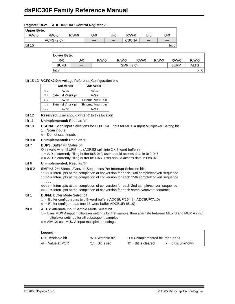
dsPIC30F Family Reference Manual
Register 18-2: ADCON2: A/D Control Register 2
Upper Byte:R/W-0 R/W-0 R/W-0 U-0 U-0 R/W-0 U-0 U-0
VCFG<2:0> — — CSCNA — —
bit 15 bit 8
Lower Byte:R-0 U-0 R/W-0 R/W-0 R/W-0 R/W-0 R/W-0 R/W-0
BUFS — SMPI<3:0> BUFM ALTSbit 7 bit 0
bit 15-13 VCFG<2:0>: Voltage Reference Configuration bits
bit 12 Reserved: User should write ‘0’ to this location
bit 11 Unimplemented: Read as ‘0’
bit 10 CSCNA: Scan Input Selections for CH0+ S/H Input for MUX A Input Multiplexer Setting bit1 = Scan inputs0 = Do not scan inputs
bit 9-8 Unimplemented: Read as ‘0’
bit 7 BUFS: Buffer Fill Status bitOnly valid when BUFM = 1 (ADRES split into 2 x 8-word buffers) 1 = A/D is currently filling buffer 0x8-0xF, user should access data in 0x0-0x70 = A/D is currently filling buffer 0x0-0x7, user should access data in 0x8-0xF
bit 6 Unimplemented: Read as ‘0’
bit 5-2 SMPI<3:0>: Sample/Convert Sequences Per Interrupt Selection bits1111 = Interrupts at the completion of conversion for each 16th sample/convert sequence1110 = Interrupts at the completion of conversion for each 15th sample/convert sequence.....0001 = Interrupts at the completion of conversion for each 2nd sample/convert sequence0000 = Interrupts at the completion of conversion for each sample/convert sequence
bit 1 BUFM: Buffer Mode Select bit1 = Buffer configured as two 8-word buffers ADCBUF(15...8), ADCBUF(7...0)0 = Buffer configured as one 16-word buffer ADCBUF(15...0)
bit 0 ALTS: Alternate Input Sample Mode Select bit1 = Uses MUX A input multiplexer settings for first sample, then alternate between MUX B and MUX A input
multiplexer settings for all subsequent samples0 = Always use MUX A input multiplexer settings
Legend:
R = Readable bit W = Writable bit U = Unimplemented bit, read as ‘0’
-n = Value at POR ‘1’ = Bit is set ‘0’ = Bit is cleared x = Bit is unknown
A/D VREFH A/D VREFL000 AVDD AVSS
001 External VREF+ pin AVSS
010 AVDD External VREF- pin011 External VREF+ pin External VREF- pin1xx AVDD AVSS
DS70065D-page 18-6 © 2005 Microchip Technology Inc.
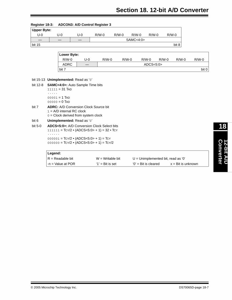
Section 18. 12-bit A/D Converter12-b
it A/D
Co
nverter
18
Register 18-3: ADCON3: A/D Control Register 3
Upper Byte:U-0 U-0 U-0 R/W-0 R/W-0 R/W-0 R/W-0 R/W-0— — — SAMC<4:0>
bit 15 bit 8
Lower Byte:R/W-0 U-0 R/W-0 R/W-0 R/W-0 R/W-0 R/W-0 R/W-0ADRC — ADCS<5:0>
bit 7 bit 0
bit 15-13 Unimplemented: Read as ‘0’
bit 12-8 SAMC<4:0>: Auto Sample Time bits11111 = 31 TAD
·····00001 = 1 TAD
00000 = 0 TAD
bit 7 ADRC: A/D Conversion Clock Source bit1 = A/D internal RC clock0 = Clock derived from system clock
bit 6 Unimplemented: Read as ‘0’
bit 5-0 ADCS<5:0>: A/D Conversion Clock Select bits111111 = TCY/2 • (ADCS<5:0> + 1) = 32 • TCY
······000001 = TCY/2 • (ADCS<5:0> + 1) = TCY
000000 = TCY/2 • (ADCS<5:0> + 1) = TCY/2
Legend:
R = Readable bit W = Writable bit U = Unimplemented bit, read as ‘0’
-n = Value at POR ‘1’ = Bit is set ‘0’ = Bit is cleared x = Bit is unknown
© 2005 Microchip Technology Inc. DS70065D-page 18-7
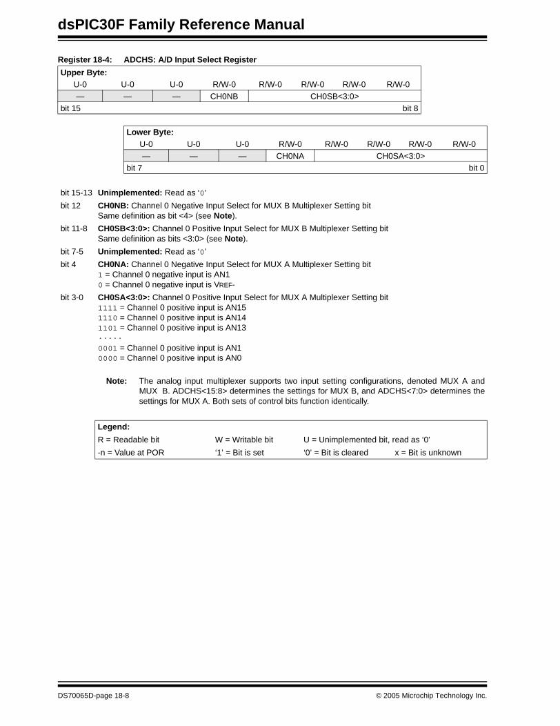
dsPIC30F Family Reference Manual
Register 18-4: ADCHS: A/D Input Select Register
Upper Byte:U-0 U-0 U-0 R/W-0 R/W-0 R/W-0 R/W-0 R/W-0— — — CH0NB CH0SB<3:0>
bit 15 bit 8
Lower Byte:U-0 U-0 U-0 R/W-0 R/W-0 R/W-0 R/W-0 R/W-0— — — CH0NA CH0SA<3:0>
bit 7 bit 0
bit 15-13 Unimplemented: Read as ‘0’
bit 12 CH0NB: Channel 0 Negative Input Select for MUX B Multiplexer Setting bitSame definition as bit <4> (see Note).
bit 11-8 CH0SB<3:0>: Channel 0 Positive Input Select for MUX B Multiplexer Setting bitSame definition as bits <3:0> (see Note).
bit 7-5 Unimplemented: Read as ‘0’
bit 4 CH0NA: Channel 0 Negative Input Select for MUX A Multiplexer Setting bit1 = Channel 0 negative input is AN10 = Channel 0 negative input is VREF-
bit 3-0 CH0SA<3:0>: Channel 0 Positive Input Select for MUX A Multiplexer Setting bit1111 = Channel 0 positive input is AN151110 = Channel 0 positive input is AN141101 = Channel 0 positive input is AN13·····0001 = Channel 0 positive input is AN10000 = Channel 0 positive input is AN0
Note: The analog input multiplexer supports two input setting configurations, denoted MUX A andMUX B. ADCHS<15:8> determines the settings for MUX B, and ADCHS<7:0> determines thesettings for MUX A. Both sets of control bits function identically.
Legend:
R = Readable bit W = Writable bit U = Unimplemented bit, read as ‘0’
-n = Value at POR ‘1’ = Bit is set ‘0’ = Bit is cleared x = Bit is unknown
DS70065D-page 18-8 © 2005 Microchip Technology Inc.
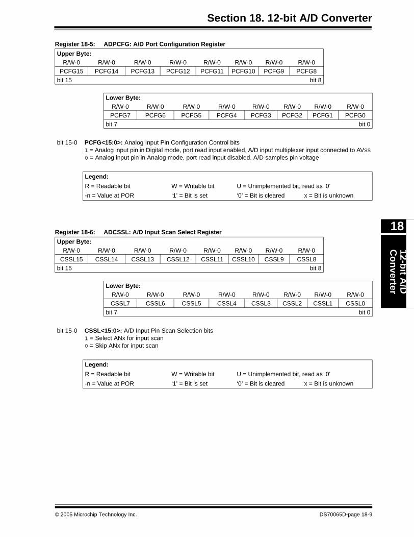
Section 18. 12-bit A/D Converter12-b
it A/D
Co
nverter
18
Register 18-5: ADPCFG: A/D Port Configuration Register
Register 18-6: ADCSSL: A/D Input Scan Select Register
Upper Byte:R/W-0 R/W-0 R/W-0 R/W-0 R/W-0 R/W-0 R/W-0 R/W-0
PCFG15 PCFG14 PCFG13 PCFG12 PCFG11 PCFG10 PCFG9 PCFG8
bit 15 bit 8
Lower Byte:R/W-0 R/W-0 R/W-0 R/W-0 R/W-0 R/W-0 R/W-0 R/W-0PCFG7 PCFG6 PCFG5 PCFG4 PCFG3 PCFG2 PCFG1 PCFG0
bit 7 bit 0
bit 15-0 PCFG<15:0>: Analog Input Pin Configuration Control bits1 = Analog input pin in Digital mode, port read input enabled, A/D input multiplexer input connected to AVSS
0 = Analog input pin in Analog mode, port read input disabled, A/D samples pin voltage
Legend:
R = Readable bit W = Writable bit U = Unimplemented bit, read as ‘0’
-n = Value at POR ‘1’ = Bit is set ‘0’ = Bit is cleared x = Bit is unknown
Upper Byte:R/W-0 R/W-0 R/W-0 R/W-0 R/W-0 R/W-0 R/W-0 R/W-0
CSSL15 CSSL14 CSSL13 CSSL12 CSSL11 CSSL10 CSSL9 CSSL8bit 15 bit 8
Lower Byte:R/W-0 R/W-0 R/W-0 R/W-0 R/W-0 R/W-0 R/W-0 R/W-0CSSL7 CSSL6 CSSL5 CSSL4 CSSL3 CSSL2 CSSL1 CSSL0
bit 7 bit 0
bit 15-0 CSSL<15:0>: A/D Input Pin Scan Selection bits1 = Select ANx for input scan0 = Skip ANx for input scan
Legend:
R = Readable bit W = Writable bit U = Unimplemented bit, read as ‘0’
-n = Value at POR ‘1’ = Bit is set ‘0’ = Bit is cleared x = Bit is unknown
© 2005 Microchip Technology Inc. DS70065D-page 18-9
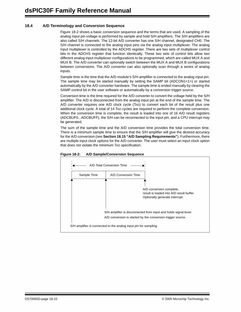
dsPIC30F Family Reference Manual
18.4 A/D Terminology and Conversion Sequence
Figure 18-2 shows a basic conversion sequence and the terms that are used. A sampling of theanalog input pin voltage is performed by sample and hold S/H amplifiers. The S/H amplifiers arealso called S/H channels. The 12-bit A/D converter has one S/H channel, designated CH0. TheS/H channel is connected to the analog input pins via the analog input multiplexer. The analoginput multiplexer is controlled by the ADCHS register. There are two sets of multiplexer controlbits in the ADCHS register that function identically. These two sets of control bits allow twodifferent analog input multiplexer configurations to be programmed, which are called MUX A andMUX B. The A/D converter can optionally switch between the MUX A and MUX B configurationsbetween conversions. The A/D converter can also optionally scan through a series of analoginputs.
Sample time is the time that the A/D module’s S/H amplifier is connected to the analog input pin.The sample time may be started manually by setting the SAMP bit (ADCON1<1>) or startedautomatically by the A/D converter hardware. The sample time is ended manually by clearing theSAMP control bit in the user software or automatically by a conversion trigger source.
Conversion time is the time required for the A/D converter to convert the voltage held by the S/Hamplifier. The A/D is disconnected from the analog input pin at the end of the sample time. TheA/D converter requires one A/D clock cycle (TAD) to convert each bit of the result plus oneadditional clock cycle. A total of 14 TAD cycles are required to perform the complete conversion.When the conversion time is complete, the result is loaded into one of 16 A/D result registers(ADCBUF0...ADCBUFF), the S/H can be reconnected to the input pin, and a CPU interrupt maybe generated.
The sum of the sample time and the A/D conversion time provides the total conversion time.There is a minimum sample time to ensure that the S/H amplifier will give the desired accuracyfor the A/D conversion (see Section 18.15 “A/D Sampling Requirements”). Furthermore, thereare multiple input clock options for the A/D converter. The user must select an input clock optionthat does not violate the minimum TAD specification.
Figure 18-2: A/D Sample/Conversion Sequence
Sample Time A/D Conversion Time
A/D Total Conversion Time
S/H amplifier is connected to the analog input pin for sampling.
S/H amplifier is disconnected from input and holds signal lever.
A/D conversion is started by the conversion trigger source.
A/D conversion complete, result is loaded into A/D result buffer. Optionally generate interrupt.
DS70065D-page 18-10 © 2005 Microchip Technology Inc.
Section 18. 12-bit A/D Converter12-b
it A/D
Co
nverter
18
The start time for sampling can be controlled in software by setting the SAMP control bit. Thestart of the sampling time can also be controlled automatically by the hardware. When the A/Dconverter operates in the Auto Sample mode, the S/H amplifier(s) is reconnected to the analoginput pin at the end of the conversion in the sample/convert sequence. The auto sample functionis controlled by the ASAM control bit.
The conversion trigger source ends the sampling time and begins an A/D conversion or asample/convert sequence. The conversion trigger source is selected by the SSRC control bits.The conversion trigger can be taken from a variety of hardware sources or can be controlledmanually in software by clearing the SAMP control bit. One of the conversion trigger sources isan auto conversion. The time between auto conversions is set by a counter and the A/D clock.The Auto Sample mode and auto conversion trigger can be used together to provide endlessautomatic conversions without software intervention.
An interrupt may be generated at the end of each sample/convert sequence or multiplesample/convert sequences, as determined by the value of the SMPI control bits. The number ofsample/convert sequences between interrupts can vary between 1 and 16.
18.5 A/D Module Configuration
The following steps should be followed for performing an A/D conversion:
1. Configure the A/D module• Select voltage reference source to match expected range on analog inputs
• Select the analog conversion clock to match desired data rate with processor clock• Determine how sampling will occur• Determine how inputs will be allocated to the S/H channel
• Select how conversion results are presented in the buffer• Select interrupt rate• Turn on A/D module
2. Configure A/D interrupt (if required)• Clear ADIF bit • Select A/D interrupt priority
The options for each configuration step are described in the subsequent sections.
18.6 Selecting the Voltage Reference Source
The voltage references for A/D conversions are selected using the VCFG<2:0> control bits(ADCON2<15:13>). The upper voltage reference (VREFH) and the lower voltage reference(VREFL) may be the internal AVDD and AVSS voltage rails or the VREF+ and VREF- input pins.
The external voltage reference pins may be shared with the AN0 and AN1 inputs on low pin countdevices. The A/D converter can still perform conversions on these pins when they are sharedwith the VREF+ and VREF- input pins.
The voltages applied to the external reference pins must meet certain specifications. Refer to the“Electrical Specifications” section of the device data sheet for further details..
Note: The SSRC<2:0>, SIMSAM, ASAM, CHPS<1:0>, SMPI<3:0>, BUFM and ALTS bits,as well as the ADCON3 and ADCSSL registers, should not be written to whileADON = 1. This would lead to indeterminate results.
Note: External VREF+ and VREF- pins must be selected for the conversion rates above 100ksps. See Section 18.21 “A/D Conversion Speeds” for further details.
© 2005 Microchip Technology Inc. DS70065D-page 18-11
dsPIC30F Family Reference Manual
18.7 Selecting the A/D Conversion Clock
The A/D converter has a maximum rate at which conversions may be completed. An analogmodule clock, TAD, controls the conversion timing. The A/D conversion requires 14 clock periods(14 TAD). The A/D clock is derived from the device instruction clock.
The period of the A/D conversion clock is software selected using a six-bit counter. There are 64possible options for TAD, specified by the ADCS<5:0> bits (ADCON3<5:0>). Equation 18-1 givesthe TAD value as a function of the ADCS control bits and the device instruction cycle clock period,TCY.
Equation 18-1: A/D Conversion Clock Period
For correct A/D conversions, the A/D conversion clock (TAD) must be selected to ensure aminimum TAD time of 333.33 nsec (see Section 18.21 “A/D Conversion Speeds” for furtherdetails).
The A/D converter has a dedicated internal RC clock source that can be used to performconversions. The internal RC clock source should be used when A/D conversions are performedwhile the dsPIC30F is in Sleep mode. The internal RC oscillator is selected by setting the ADRCbit (ADCON3<7>). When the ADRC bit is set, the ADCS<5:0> bits have no effect on the A/Doperation.
18.8 Selecting Analog Inputs for Sampling
The Sample-and-Hold Amplifier has analog multiplexers (see Figure 18-1) on both itsnon-inverting and inverting inputs, to select which analog input(s) are sampled. Once thesample/convert sequence is specified, the ADCHS bits determine which analog inputs areselected for each sample.
Additionally, the selected inputs may vary on an alternating sample basis, or may vary on arepeated sequence of samples.
18.8.1 Configuring Analog Port Pins
The ADPCFG register specifies the input condition of device pins used as analog inputs.
A pin is configured as analog input when the corresponding PCFGn bit (ADPCFG<n>) is clear.The ADPCFG register is clear at Reset, causing the A/D input pins to be configured for analoginput by default at Reset.
When configured for analog input, the associated port I/O digital input buffer is disabled so it doesnot consume current.
The ADPCFG register and the TRISB register control the operation of the A/D port pins.
The port pins that are desired as analog inputs must have their corresponding TRIS bit set,specifying port input. If the I/O pin associated with an A/D input is configured as an output, TRISbit is cleared, the pin is in Analog mode (ADPCFG<n> = 0) and the port digital output level (VOH
or VOL) will be converted. After a device Reset, all TRIS bits are set.
A pin is configured as digital I/O when the corresponding PCFGn bit (ADPCFG<n>) is set. In thisconfiguration, the input to the analog multiplexer is connected to AVSS.
TAD =TCY(ADCS + 1)
2
ADCS =2TAD
TCY– 1
Note: Different devices will have different numbers of analog inputs. Verify the analoginput availability against the device data sheet.
Note 1: When reading a port register, any pin configured as an analog input reads as a ‘0’.2: Analog levels on any pin that is defined as a digital input (including the AN15:AN0
pins) may cause the input buffer to consume current that is out of the device’sspecification.
DS70065D-page 18-12 © 2005 Microchip Technology Inc.
Section 18. 12-bit A/D Converter12-b
it A/D
Co
nverter
18
18.8.2 Channel 0 Input Selection
The user may select any one of the up to 16 analog inputs to connect to the positive input of thechannel. The CH0SA<3:0> bits (ADCHS<3:0>) normally select the analog input for the positiveinput of channel 0.
The user may select either VREF- or AN1 as the negative input of the channel. The CH0NA bit(ADCHS<4>) normally selects the analog input for the negative input of channel 0.
18.8.2.1 Specifying Alternating Channel 0 Input Selections
The ALTS bit (ADCON2<0>) causes the module to alternate between two sets of inputs that areselected during successive samples.
The inputs specified by CH0SA<3:0>, CH0NA, CHXSA and CHXNA<1:0> are collectively calledthe MUX A inputs. The inputs specified by CH0SB<3:0>, CH0NB, CHXSB and CHXNB<1:0> arecollectively called the MUX B inputs. When the ALTS bit is ‘1’, the module will alternate betweenthe MUX A inputs on one sample and the MUX B inputs on the subsequent sample.
For channel 0, if the ALTS bit is ‘0’, only the inputs specified by CH0SA<3:0> and CH0NA areselected for sampling.
If the ALTS bit is ‘1’ on the first sample/convert sequence for channel 0, the inputs specified byCH0SA<3:0> and CH0NA are selected for sampling. On the next sample convert sequence forchannel 0, the inputs specified by CH0SB<3:0> and CH0NB are selected for sampling. Thispattern will repeat for subsequent sample conversion sequences.
18.8.2.2 Scanning Through Several Inputs
Channel 0 has the ability to scan through a selected vector of inputs. The CSCNA bit(ADCON2<10>) enables the CH0 channel inputs to be scanned across a selected number ofanalog inputs. When CSCNA is set, the CH0SA<3:0> bits are ignored.
The ADCSSL register specifies the inputs to be scanned. Each bit in the ADCSSL registercorresponds to an analog input. Bit 0 corresponds to AN0, bit 1 corresponds to AN1 and so on.If a particular bit in the ADCSSL register is ‘1’, the corresponding input is part of the scansequence. The inputs are always scanned from lower to higher numbered inputs, starting at thefirst selected channel after each interrupt occurs.
The ADCSSL bits only specify the input of the positive input of the channel. The CH0NA bit stillselects the input of the negative input of the channel during scanning.
If the ALTS bit is ‘1’, the scanning only applies to the MUX A input selection. The MUX B inputselection, as specified by the CH0SB<3:0>, will still select the alternating input. When the inputselections are programmed in this manner, the input will alternate between a set of scanninginputs specified by the ADCSSL register and a fixed input specified by the CH0SB bits.
Note: If the number of scanned inputs selected is greater than the number of samplestaken per interrupt, the higher numbered inputs will not be sampled.
© 2005 Microchip Technology Inc. DS70065D-page 18-13
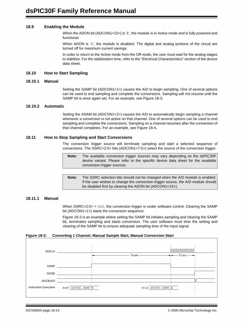
dsPIC30F Family Reference Manual
18.9 Enabling the Module
When the ADON bit (ADCON1<15>) is ‘1’, the module is in Active mode and is fully powered andfunctional.
When ADON is ‘0’, the module is disabled. The digital and analog portions of the circuit areturned off for maximum current savings.
In order to return to the Active mode from the Off mode, the user must wait for the analog stagesto stabilize. For the stabilization time, refer to the “Electrical Characteristics” section of the devicedata sheet.
18.10 How to Start Sampling
18.10.1 Manual
Setting the SAMP bit (ADCON1<1>) causes the A/D to begin sampling. One of several optionscan be used to end sampling and complete the conversions. Sampling will not resume until theSAMP bit is once again set. For an example, see Figure 18-3.
18.10.2 Automatic
Setting the ASAM bit (ADCON1<2>) causes the A/D to automatically begin sampling a channelwhenever a conversion is not active on that channel. One of several options can be used to endsampling and complete the conversions. Sampling on a channel resumes after the conversion ofthat channel completes. For an example, see Figure 18-4.
18.11 How to Stop Sampling and Start Conversions
The conversion trigger source will terminate sampling and start a selected sequence ofconversions. The SSRC<2:0> bits (ADCON1<7:5>) select the source of the conversion trigger.
18.11.1 Manual
When SSRC<2:0> = 000, the conversion trigger is under software control. Clearing the SAMPbit (ADCON1<1>) starts the conversion sequence.
Figure 18-3 is an example where setting the SAMP bit initiates sampling and clearing the SAMPbit, terminates sampling and starts conversion. The user software must time the setting andclearing of the SAMP bit to ensure adequate sampling time of the input signal.
Figure 18-3: Converting 1 Channel, Manual Sample Start, Manual Conversion Start
Note: The available conversion trigger sources may vary depending on the dsPIC30Fdevice variant. Please refer to the specific device data sheet for the availableconversion trigger sources.
Note: The SSRC selection bits should not be changed when the A/D module is enabled.If the user wishes to change the conversion trigger source, the A/D module shouldbe disabled first by clearing the ADON bit (ADCON1<15>).
ADCLK
SAMP
ADCBUF0
TSAMP TCONV
BCLR ADCON1,SAMPBSET ADCON1,SAMPInstruction Execution
DONE
DS70065D-page 18-14 © 2005 Microchip Technology Inc.

Section 18. 12-bit A/D Converter12-b
it A/D
Co
nverter
18
Example 18-1: Converting 1 Channel, Manual Sample Start,Manual Conversion Start Code Example
Figure 18-4 is an example where setting the ASAM bit initiates automatic sampling and clearingthe SAMP bit, terminates sampling and starts conversion. After the conversion completes, themodule will automatically return to a sampling state. The SAMP bit is automatically set at the startof the sample interval. The user software must time the clearing of the SAMP bit to ensureadequate sampling time of the input signal, understanding that the time between clearing of theSAMP bit includes the conversion time, as well as the sampling time.
Figure 18-4: Converting 1 Channel, Automatic Sample Start, Manual Conversion Start
ADPCFG = 0xFFFB; // all PORTB = Digital; RB2 = analogADCON1 = 0x0000; // SAMP bit = 0 ends sampling ...
// and starts convertingADCHS = 0x0002; // Connect RB2/AN2 as CH0 input ..
// in this example RB2/AN2 is the inputADCSSL = 0;ADCON3 = 0x0002; // Manual Sample, Tad = internal 2 TcyADCON2 = 0; ADCON1bits.ADON = 1; // turn ADC ONwhile (1) // repeat continuously
{ADCON1bits.SAMP = 1; // start sampling ...DelayNmSec(100); // for 100 mSADCON1bits.SAMP = 0; // start Convertingwhile (!ADCON1bits.DONE); // conversion done?ADCValue = ADCBUF0; // yes then get ADC value} // repeat
ADCLK
SAMP
ADCBUF0
TSAMP TCONV
BCLR ADCON1,SAMP Instruction Execution
TCONV
BSET ADCON1,ASAM BCF ADCON1,SAMP
TSAMPTAD0 TAD0
© 2005 Microchip Technology Inc. DS70065D-page 18-15
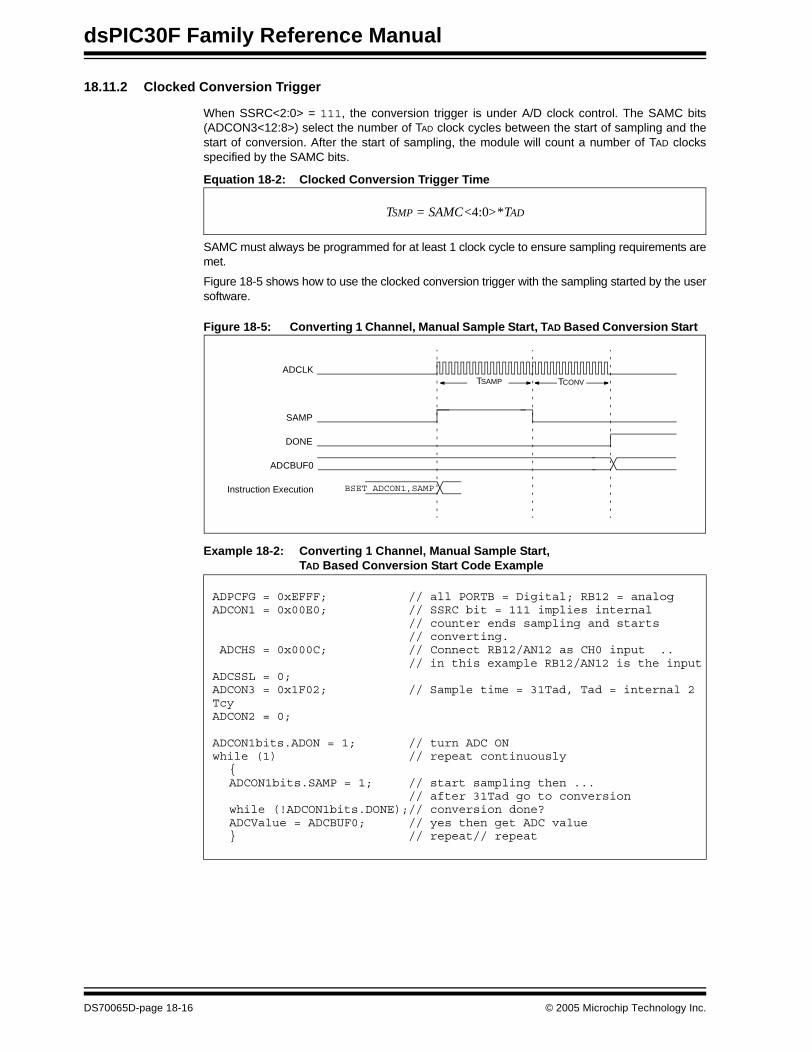
dsPIC30F Family Reference Manual
18.11.2 Clocked Conversion Trigger
When SSRC<2:0> = 111, the conversion trigger is under A/D clock control. The SAMC bits(ADCON3<12:8>) select the number of TAD clock cycles between the start of sampling and thestart of conversion. After the start of sampling, the module will count a number of TAD clocksspecified by the SAMC bits.
Equation 18-2: Clocked Conversion Trigger Time
SAMC must always be programmed for at least 1 clock cycle to ensure sampling requirements aremet.
Figure 18-5 shows how to use the clocked conversion trigger with the sampling started by the usersoftware.
Figure 18-5: Converting 1 Channel, Manual Sample Start, TAD Based Conversion Start
Example 18-2: Converting 1 Channel, Manual Sample Start,TAD Based Conversion Start Code Example
TSMP = SAMC<4:0>*TAD
ADPCFG = 0xEFFF; // all PORTB = Digital; RB12 = analogADCON1 = 0x00E0; // SSRC bit = 111 implies internal
// counter ends sampling and starts// converting.
ADCHS = 0x000C; // Connect RB12/AN12 as CH0 input ..// in this example RB12/AN12 is the input
ADCSSL = 0;ADCON3 = 0x1F02; // Sample time = 31Tad, Tad = internal 2 TcyADCON2 = 0; ADCON1bits.ADON = 1; // turn ADC ONwhile (1) // repeat continuously
{ ADCON1bits.SAMP = 1; // start sampling then ...
// after 31Tad go to conversionwhile (!ADCON1bits.DONE);// conversion done?ADCValue = ADCBUF0; // yes then get ADC value} // repeat// repeat
ADCLK
SAMP
ADCBUF0
TSAMP TCONV
BSET ADCON1,SAMPInstruction Execution
DONE
DS70065D-page 18-16 © 2005 Microchip Technology Inc.
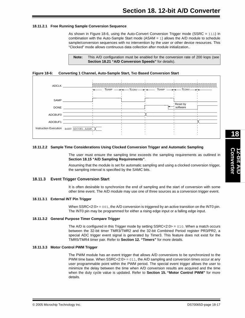
Section 18. 12-bit A/D Converter12-b
it A/D
Co
nverter
18
18.11.2.1 Free Running Sample Conversion Sequence
As shown in Figure 18-6, using the Auto-Convert Conversion Trigger mode (SSRC = 111) incombination with the Auto-Sample Start mode (ASAM = 1) allows the A/D module to schedulesample/conversion sequences with no intervention by the user or other device resources. This“Clocked” mode allows continuous data collection after module initialization..
Figure 18-6: Converting 1 Channel, Auto-Sample Start, TAD Based Conversion Start
18.11.2.2 Sample Time Considerations Using Clocked Conversion Trigger and Automatic Sampling
The user must ensure the sampling time exceeds the sampling requirements as outlined inSection 18.15 “A/D Sampling Requirements”.
Assuming that the module is set for automatic sampling and using a clocked conversion trigger,the sampling interval is specified by the SAMC bits.
18.11.3 Event Trigger Conversion Start
It is often desirable to synchronize the end of sampling and the start of conversion with someother time event. The A/D module may use one of three sources as a conversion trigger event.
18.11.3.1 External INT Pin Trigger
When SSRC<2:0> = 001, the A/D conversion is triggered by an active transition on the INT0 pin.The INT0 pin may be programmed for either a rising edge input or a falling edge input.
18.11.3.2 General Purpose Timer Compare Trigger
The A/D is configured in this Trigger mode by setting SSRC<2:0> = 010. When a match occursbetween the 32-bit timer TMR3/TMR2 and the 32-bit Combined Period register PR3/PR2, aspecial ADC trigger event signal is generated by Timer3. This feature does not exist for theTMR5/TMR4 timer pair. Refer to Section 12. “Timers” for more details.
18.11.3.3 Motor Control PWM Trigger
The PWM module has an event trigger that allows A/D conversions to be synchronized to thePWM time base. When SSRC<2:0> = 011, the A/D sampling and conversion times occur at anyuser programmable point within the PWM period. The special event trigger allows the user tominimize the delay between the time when A/D conversion results are acquired and the timewhen the duty cycle value is updated. Refer to Section 15. “Motor Control PWM” for moredetails.
Note: This A/D configuration must be enabled for the conversion rate of 200 ksps (seeSection 18.21 “A/D Conversion Speeds” for details).
ADCLK
SAMP
ADCBUF1
TSAMP TCONV
DONE
TSAMP TCONV
ADCBUF0
BSET ADCON1,ASAMInstruction Execution
Reset bysoftware
© 2005 Microchip Technology Inc. DS70065D-page 18-17
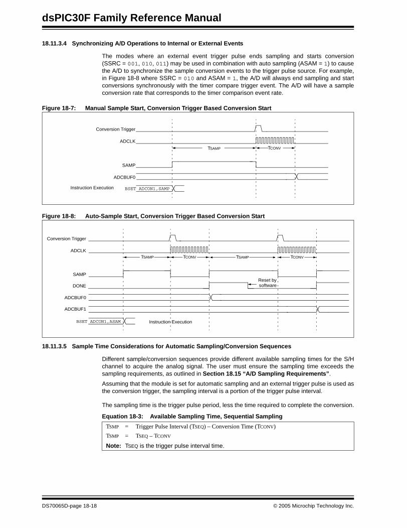
dsPIC30F Family Reference Manual
18.11.3.4 Synchronizing A/D Operations to Internal or External Events
The modes where an external event trigger pulse ends sampling and starts conversion(SSRC = 001, 010, 011) may be used in combination with auto sampling (ASAM = 1) to causethe A/D to synchronize the sample conversion events to the trigger pulse source. For example,in Figure 18-8 where SSRC = 010 and ASAM = 1, the A/D will always end sampling and startconversions synchronously with the timer compare trigger event. The A/D will have a sampleconversion rate that corresponds to the timer comparison event rate.
Figure 18-7: Manual Sample Start, Conversion Trigger Based Conversion Start
Figure 18-8: Auto-Sample Start, Conversion Trigger Based Conversion Start
18.11.3.5 Sample Time Considerations for Automatic Sampling/Conversion Sequences
Different sample/conversion sequences provide different available sampling times for the S/Hchannel to acquire the analog signal. The user must ensure the sampling time exceeds thesampling requirements, as outlined in Section 18.15 “A/D Sampling Requirements”.
Assuming that the module is set for automatic sampling and an external trigger pulse is used asthe conversion trigger, the sampling interval is a portion of the trigger pulse interval.
The sampling time is the trigger pulse period, less the time required to complete the conversion.
Equation 18-3: Available Sampling Time, Sequential Sampling
Conversion Trigger
ADCLK
SAMP
ADCBUF0
TSAMP TCONV
BSET ADCON1,SAMPInstruction Execution
Conversion Trigger
ADCLK
SAMP
ADCBUF0
TSAMP TCONV
BSET ADCON1,ASAM Instruction Execution
TCONVTSAMP
ADCBUF1
DONEReset bysoftware
TSMP = Trigger Pulse Interval (TSEQ) – Conversion Time (TCONV)
TSMP = TSEQ – TCONV
Note: TSEQ is the trigger pulse interval time.
DS70065D-page 18-18 © 2005 Microchip Technology Inc.
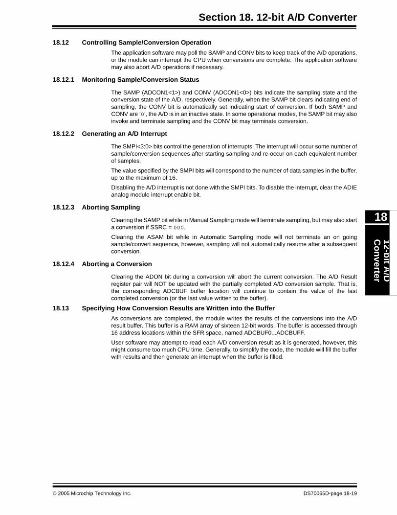
Section 18. 12-bit A/D Converter12-b
it A/D
Co
nverter
18
18.12 Controlling Sample/Conversion Operation
The application software may poll the SAMP and CONV bits to keep track of the A/D operations,or the module can interrupt the CPU when conversions are complete. The application softwaremay also abort A/D operations if necessary.
18.12.1 Monitoring Sample/Conversion Status
The SAMP (ADCON1<1>) and CONV (ADCON1<0>) bits indicate the sampling state and theconversion state of the A/D, respectively. Generally, when the SAMP bit clears indicating end ofsampling, the CONV bit is automatically set indicating start of conversion. If both SAMP andCONV are ‘0’, the A/D is in an inactive state. In some operational modes, the SAMP bit may alsoinvoke and terminate sampling and the CONV bit may terminate conversion.
18.12.2 Generating an A/D Interrupt
The SMPI<3:0> bits control the generation of interrupts. The interrupt will occur some number ofsample/conversion sequences after starting sampling and re-occur on each equivalent numberof samples.
The value specified by the SMPI bits will correspond to the number of data samples in the buffer,up to the maximum of 16.
Disabling the A/D interrupt is not done with the SMPI bits. To disable the interrupt, clear the ADIEanalog module interrupt enable bit.
18.12.3 Aborting Sampling
Clearing the SAMP bit while in Manual Sampling mode will terminate sampling, but may also starta conversion if SSRC = 000.
Clearing the ASAM bit while in Automatic Sampling mode will not terminate an on goingsample/convert sequence, however, sampling will not automatically resume after a subsequentconversion.
18.12.4 Aborting a Conversion
Clearing the ADON bit during a conversion will abort the current conversion. The A/D Resultregister pair will NOT be updated with the partially completed A/D conversion sample. That is,the corresponding ADCBUF buffer location will continue to contain the value of the lastcompleted conversion (or the last value written to the buffer).
18.13 Specifying How Conversion Results are Written into the Buffer
As conversions are completed, the module writes the results of the conversions into the A/Dresult buffer. This buffer is a RAM array of sixteen 12-bit words. The buffer is accessed through16 address locations within the SFR space, named ADCBUF0...ADCBUFF.
User software may attempt to read each A/D conversion result as it is generated, however, thismight consume too much CPU time. Generally, to simplify the code, the module will fill the bufferwith results and then generate an interrupt when the buffer is filled.
© 2005 Microchip Technology Inc. DS70065D-page 18-19
dsPIC30F Family Reference Manual
18.13.1 Number of Conversions per Interrupt
The SMPI<3:0> bits (ADCON2<5:2>) will select how many A/D conversions will take placebefore the CPU is interrupted. This can vary from 1 sample per interrupt to 16 samples perinterrupt. The A/D converter module always starts writing its conversion results at the beginningof the buffer, after each interrupt. For example, if SMPI<3:0> = 0000, the conversion results willalways be written to ADCBUF0. In this example, no other buffer locations would be used.
18.13.2 Restrictions Due to Buffer Size
The user cannot program the SMPI bits to a value that specifies more than 8 conversions perinterrupt when the BUFM bit (ADCON2<1>) is ‘1’. The BUFM bit function is described below.
18.13.3 Buffer Fill Mode
When the BUFM bit (ADCON2<1>) is ‘1’, the 16-word results buffer (ADRES) will be split into two8-word groups. The 8-word buffers will alternately receive the conversion results after eachinterrupt event. The initial 8-word buffer used after BUFM is set will be located at the loweraddresses of ADCBUF. When BUFM is ‘0’, the complete 16-word buffer is used for all conversionsequences.
The decision to use the BUFM feature will depend upon how much time is available to move thebuffer contents after the interrupt, as determined by the application. If the processor can quicklyunload a full buffer within the time it takes to sample and convert one channel, the BUFM bit canbe ‘0’ and up to 16 conversions may be done per interrupt. The processor will have one sampleand conversion time before the first buffer location is overwritten.
If the processor cannot unload the buffer within the sample and conversion time, the BUFM bitshould be ‘1’. For example, if SMPI<3:0> = 0111, then eight conversions will be loaded into 1/2of the buffer, following which an interrupt will occur. The next eight conversions will be loaded intothe other 1/2 of the buffer. The processor will, therefore, have the entire time between interruptsto move the eight conversions out of the buffer.
18.13.4 Buffer Fill Status
When the conversion result buffer is split using the BUFM control bit, the BUFS status bit(ADCON2<7>) indicates the half of the buffer that the A/D converter is currently filling. IfBUFS = 0, then the A/D converter is filling ADCBUF0-ADCBUF7 and the user software shouldread conversion values from ADCBUF8-ADCBUFF. If BUFS = 1, the situation is reversed, andthe user software should read conversion values from ADCBUF0-ADCBUF7.
DS70065D-page 18-20 © 2005 Microchip Technology Inc.
Section 18. 12-bit A/D Converter12-b
it A/D
Co
nverter
18
18.14 Conversion Sequence Examples
The following configuration examples show the A/D operation in different sampling and bufferingconfigurations. In each example, setting the ASAM bit starts automatic sampling. A conversiontrigger ends sampling and starts conversion.
18.14.1 Example: Sampling and Converting a Single Channel Multiple Times
Figure 18-9 and Table 18-1 illustrate a basic configuration of the A/D. In this case, one A/D input,AN0, will be sampled and converted. The results are stored in the ADCBUF buffer. This processrepeats 16 times until the buffer is full and then the module generates an interrupt. The entireprocess will then repeat.
With ALTS clear, only the MUX A inputs are active. The CH0SA bits and CH0NA bit are specified(AN0-VREF-) as the input to the sample/hold channel. All other input selection bits are not used.
Figure 18-9: Converting One Channel 16 Times/Interrupt
Conversion
ADCLK
SAMP
ADCBUF0
TSAMP
TCONV
BSET ADCON1,ASAM Instruction Execution
ADCBUF1
DONE
ADCBUFE
ADCBUFF
Input to CH0 AN0
TSAMP
TCONV
AN0
TSAMP
TCONV
AN0
TSAMP
TCONV
AN0
ADIF
ASAM
Trigger
© 2005 Microchip Technology Inc. DS70065D-page 18-21
dsPIC30F Family Reference Manual
Example 18-3: Sampling and Converting a Single ChannelMultiple Times Code Example
ADPCFG = 0xFFFB; // all PORTB = Digital; RB2 = analogADCON1 = 0x00E0; // SSRC bit = 111 implies internal
// counter ends sampling and starts// converting.
ADCHS = 0x0002; // Connect RB2/AN2 as CH0 input ..// in this example RB2/AN2 is the input
ADCSSL = 0;ADCON3 = 0x0F00; // Sample time = 15Tad, Tad = internal Tcy/2ADCON2 = 0x003C; // Interrupt after every 16 samples ADCON1bits.ADON = 1; // turn ADC ONwhile (1) // repeat continuously
{ADCValue = 0; // clear valueADC16Ptr = &ADCBUF0; // initialize ADCBUF pointerIFS0bits.ADIF = 0; // clear ADC interrupt flagADCON1bits.ASAM = 1; // auto start sampling
// for 31Tad then go to conversionwhile (!IFS0bits.ADIF); // conversion done?ADCON1bits.ASAM = 0; // yes then stop sample/convertfor (count = 0; count < 16; count++) // average the 16 ADC value
ADCValue = ADCValue + *ADC16Ptr++; ADCValue = ADCValue >> 4;} // repeat
DS70065D-page 18-22 © 2005 Microchip Technology Inc.

Section 18. 12-bit A/D Converter12-b
it A/D
Co
nverter
18
Table 18-1: Converting One Channel 16 Times/Interrupt
CONTROL BITS OPERATION SEQUENCESequence Select Sample MUX A Inputs: AN0 -> CH0
SMPI<2:0> = 1111 Convert CH0, Write Buffer 0x0Interrupt on 16th sample Sample MUX A Inputs: AN0 -> CH0
BUFM = 0 Convert CH0, Write Buffer 0x1Single 16-word result buffer Sample MUX A Inputs: AN0 -> CH0
ALTS = 0 Convert CH0, Write Buffer 0x2Always use MUX A input select Sample MUX A Inputs: AN0 -> CH0
MUX A Input Select Convert CH0, Write Buffer 0x3CH0SA<3:0> = 0000 Sample MUX A Inputs: AN0 -> CH0
Select AN0 for CH0+ input Convert CH0, Write Buffer 0x4CH0NA = 0 Sample MUX A Inputs: AN0 -> CH0
Select VREF- for CH0- input Convert CH0, Write Buffer 0x5CSCNA = 0 Sample MUX A Inputs: AN0 -> CH0
No input scan Convert CH0, Write Buffer 0x6CSSL<15:0> = n/a Sample MUX A Inputs: AN0 -> CH0
Scan input select unused Convert CH0, Write Buffer 0x7MUX B Input Select Sample MUX A Inputs: AN0 -> CH0
CH0SB<3:0> = n/a Convert CH0, Write Buffer 0x8Channel CH0+ input unused Sample MUX A Inputs: AN0 -> CH0
CH0NB = n/a Convert CH0, Write Buffer 0x9Channel CH0- input unused Sample MUX A Inputs: AN0 -> CH0
Convert CH0, Write Buffer 0xASample MUX A Inputs: AN0 -> CH0
Convert CH0, Write Buffer 0xBSample MUX A Inputs: AN0 -> CH0
Convert CH0, Write Buffer 0xCSample MUX A Inputs: AN0 -> CH0
Convert CH0, Write Buffer 0xDSample MUX A Inputs: AN0 -> CH0
Convert CH0, Write Buffer 0xESample MUX A Inputs: AN0 -> CH0
Convert CH0, Write Buffer 0xFInterruptRepeat
BufferAddress
Buffer @1st Interrupt
Buffer @2nd Interrupt
ADCBUF0 AN0 sample 1 AN0 sample 17ADCBUF1 AN0 sample 2 AN0 sample 18ADCBUF2 AN0 sample 3 AN0 sample 19ADCBUF3 AN0 sample 4 AN0 sample 20ADCBUF4 AN0 sample 5 AN0 sample 21ADCBUF5 AN0 sample 6 AN0 sample 22ADCBUF6 AN0 sample 7 AN0 sample 23ADCBUF7 AN0 sample 8 AN0 sample 24 • • •ADCBUF8 AN0 sample 9 AN0 sample 25ADCBUF9 AN0 sample 10 AN0 sample 26ADCBUFA AN0 sample 11 AN0 sample 27ADCBUFB AN0 sample 12 AN0 sample 28ADCBUFC AN0 sample 13 AN0 sample 29ADCBUFD AN0 sample 14 AN0 sample 30ADCBUFE AN0 sample 15 AN0 sample 31ADCBUFF AN0 sample 16 AN0 sample 32
© 2005 Microchip Technology Inc. DS70065D-page 18-23
dsPIC30F Family Reference Manual
18.14.2 Example: A/D Conversions While Scanning Through All Analog Inputs
Figure 18-10 and Table 18-2 illustrate a typical setup, where all available analog input channelsare sampled and converted. The set CSCNA bit specifies scanning of the A/D inputs to the CH0positive input. Other conditions are similar to Subsection 18.14.1.
Initially, the AN0 input is sampled by CH0 and converted. The result is stored in the ADCBUFbuffer. Then the AN1 input is sampled and converted. This process of scanning the inputsrepeats 16 times until the buffer is full and then the module generates an interrupt. The entireprocess will then repeat.
Figure 18-10: Scanning Through 16 Inputs/Interrupt
Conversion
ADCLK
SAMP
ADCBUF0
TSAMP
TCONV
BSET ADCON1,#ASAM Instruction Execution
ADCBUF1
DONE
ADCBUFE
ADCBUFF
Input to CH0 AN0
TSAMP
TCONV
AN1
TSAMP
TCONV
AN14
TSAMP
TCONV
AN15
ADIF
ASAM
Trigger
DS70065D-page 18-24 © 2005 Microchip Technology Inc.
Section 18. 12-bit A/D Converter12-b
it A/D
Co
nverter
18
Table 18-2: Scanning Through 16 Inputs/Interrupt
CONTROL BITS OPERATION SEQUENCESequence Select Sample MUX A Inputs: AN0 -> CH0
SMPI<2:0> = 1111 Convert CH0, Write Buffer 0x0Interrupt on 16th sample Sample MUX A Inputs: AN1 -> CH0
BUFM = 0 Convert CH0, Write Buffer 0x1Single 16-word result buffer Sample MUX A Inputs: AN2 -> CH0
ALTS = 0 Convert CH0, Write Buffer 0x2Always use MUX A input select Sample MUX A Inputs: AN3 -> CH0
MUX A Input Select Convert CH0, Write Buffer 0x3CH0SA<3:0> = n/a Sample MUX A Inputs: AN4 -> CH0
Override by CSCNA Convert CH0, Write Buffer 0x4CH0NA = 0 Sample MUX A Inputs: AN5 -> CH0
Select VREF- for CH0- input Convert CH0, Write Buffer 0x5CSCNA = 1 Sample MUX A Inputs: AN6 -> CH0
Scan CH0+ Inputs Convert CH0, Write Buffer 0x6CSSL<15:0> = 1111 1111 1111 1111 Sample MUX A Inputs: AN7 -> CH0
Scan all inputs Convert CH0, Write Buffer 0x7MUX B Input Select Sample MUX A Inputs: AN8 -> CH0
CH0SB<3:0> = n/a Convert CH0, Write Buffer 0x8Channel CH0+ input unused Sample MUX A Inputs: AN9 -> CH0
CH0NB = n/a Convert CH0, Write Buffer 0x9Channel CH0- input unused Sample MUX A Inputs: AN10 -> CH0
Convert CH0, Write Buffer 0xASample MUX A Inputs: AN11 -> CH0
Convert CH0, Write Buffer 0xBSample MUX A Inputs: AN12 -> CH0
Convert CH0, Write Buffer 0xCSample MUX A Inputs: AN13 -> CH0
Convert CH0, Write Buffer 0xDSample MUX A Inputs: AN14 -> CH0
Convert CH0, Write Buffer 0xESample MUX A Inputs: AN15 -> CH0
Convert CH0, Write Buffer 0xFInterruptRepeat
BufferAddress
Buffer @1st Interrupt
Buffer @2nd Interrupt
ADCBUF0 AN0 sample 1 AN0 sample 17ADCBUF1 AN1 sample 2 AN1 sample 18ADCBUF2 AN2 sample 3 AN2 sample 19ADCBUF3 AN3 sample 4 AN3 sample 20ADCBUF4 AN4 sample 5 AN4 sample 21ADCBUF5 AN5 sample 6 AN5 sample 22ADCBUF6 AN6 sample 7 AN6 sample 23ADCBUF7 AN7 sample 8 AN7 sample 24 • • •ADCBUF8 AN8 sample 9 AN8 sample 25ADCBUF9 AN9 sample 10 AN9 sample 26ADCBUFA AN10 sample 11 AN10 sample 27ADCBUFB AN11 sample 12 AN11 sample 28ADCBUFC AN12 sample 13 AN12 sample 29ADCBUFD AN13 sample 14 AN13 sample 30ADCBUFE AN14 sample 15 AN14 sample 31ADCBUFF AN15 sample 16 AN15 sample 32
© 2005 Microchip Technology Inc. DS70065D-page 18-25

dsPIC30F Family Reference Manual
18.14.3 Example: Using Dual 8-Word Buffers
Refer to Subsection 17.15.4 in Section 17. “10-bit A/D Converter” for an example that usesdual buffers.
18.14.4 Example: Using Alternating MUX A, MUX B Input Selections
See Subsection 17.15.5 in Section 17. “10-bit A/D Converter” for an example that uses theMUX A and MUX B input selections.
18.15 A/D Sampling Requirements The analog input model of the 12-bit A/D converter is shown in Figure 18-11. The total samplingtime for the A/D is a function of the internal amplifier settling time and the holding capacitorcharge time.
For the A/D converter to meet its specified accuracy, the charge holding capacitor (CHOLD) mustbe allowed to fully charge to the voltage level on the analog input pin. The source impedance(RS), the interconnect impedance (RIC), and the internal sampling switch (RSS) impedancecombine to directly affect the time required to charge the capacitor CHOLD. The combined imped-ance of the analog sources must therefore be small enough to fully charge the holding capacitorwithin the chosen sample time. To minimize the effects of pin leakage currents on the accuracyof the A/D converter, the maximum recommended source impedance, RS, is 2.5 kΩ. After theanalog input channel is selected (changed), this sampling function must be completed prior tostarting the conversion. The internal holding capacitor will be in a discharged state prior to eachsample operation.
At least 1 TAD time period should be allowed between conversions for the sample time. For moredetails, see the device electrical specifications.
Figure 18-11: 12-bit A/D Converter Analog Input Model
CPINVA
Rs ANxVT = 0.6V
VT = 0.6V I leakage
RIC ≤ 250Ω SamplingSwitch
RSS
CHOLD= DAC capacitance
VSS
VDD
= 18 pF± 500 nA
Legend: CPIN
VT
I leakage
RIC
RSS
CHOLD
= input capacitance= threshold voltage= leakage current at the pin due to
= interconnect resistance= sampling switch resistance= sample/hold capacitance (from DAC)
various junctions
Note: CPIN value depends on device package and is not tested. Effect of CPIN negligible if Rs ≤ 2.5 kΩ.
RSS ≤ 3 kΩ
DS70065D-page 18-26 © 2005 Microchip Technology Inc.
Section 18. 12-bit A/D Converter12-b
it A/D
Co
nverter
18
18.16 Reading the A/D Result Buffer
The RAM is 12-bits wide, but the data is automatically formatted to one of four selectable formatswhen a read from the buffer is performed. The FORM<1:0> bits (ADCON1<9:8>) select the for-mat. The formatting hardware provides a 16-bit result on the data bus for all of the data formats.Figure 18-12 shows the data output formats that can be selected using the FORM<1:0> controlbits.
Figure 18-12: A/D Output Data Formats
Table 18-3: Numerical Equivalents of Various Result Codes
RAM Contents: d11 d10 d09 d08 d07 d06 d05 d04 d03 d02 d01 d00
Read to Bus:
Integer 0 0 0 0 d11 d10 d09 d08 d07 d06 d05 d04 d03 d02 d01 d00
Signed Integer d11 d11 d11 d11 d11 d10 d09 d08 d07 d06 d05 d04 d03 d02 d01 d00
Fractional d11 d10 d09 d08 d07 d06 d05 d04 d03 d02 d01 d00 0 0 0 0
Signed Fractional (1.15) d11 d10 d09 d08 d07 d04 d03 d02 d01 d00 d01 d00 0 0 0 0
VIN/VREF12-bit
Output Code16-bit UnsignedInteger Format
16-bit SignedInteger Format
16-bit UnsignedFractional Format
16-bit SignedFractional Format
4095/4096 1111 1111 1111 0000 1111 1111 1111= 4095
0000 0111 1111 1111= 2047
1111 1111 1111 0000= 0.9998
0111 1111 1111 0000= 0.9995
4094/4096 1111 1111 1110 0000 1111 1111 1110= 4094
0000 0111 1111 1110= 2046
1111 1111 1110 0000= 0.9995
0111 1111 1110 0000= 0.9990
• • •
2049/4096 1000 0000 0001 0000 1000 0000 0001= 2049
0000 0000 0000 0001= 1
1000 0000 0001 0000= 0.5002
0000 0000 0001 0000= 0.0005
2048/4096 1000 0000 0000 0000 1000 0000 0000= 2048
0000 0000 0000 0000= 0
1000 0000 0000 0000= 0.500
0000 0000 0000 0000= 0.000
2047/4096 0111 1111 1111 0000 0111 1111 1111= 2047
1111 1111 1111 1111= -1
0111 1111 1111 0000= 0.4998
1111 1111 1111 0000= -0.0005
• • •
1/4096 0000 0000 0001 0000 0000 0000 0001= 1
1111 1000 0000 0001= -2047
0000 0000 0001 0000= 0.0002
1000 0000 0001 0000= -0.9995
0/4096 0000 0000 0000 0000 0000 0000 0000= 0
1111 1000 0000 0000= -2048
0000 0000 0000 0000= 0.000
1000 0000 0000 0000= -1.000
© 2005 Microchip Technology Inc. DS70065D-page 18-27

dsPIC30F Family Reference Manual
18.17 Transfer Function The ideal transfer function of the A/D converter is shown in Figure 18-13. The difference of theinput voltages (VINH – VINL) is compared to the reference (VREFH – VREFL).
• The first code transition occurs when the input voltage is (VREFH – VREFL/8192) or 0.5 LSb. • The 00 0000 0001 code is centered at (VREFH – VREFL/4096) or 1.0 LSb.
• The 10 0000 0000 code is centered at (2048*(VREFH – VREFL)/4096).• An input voltage less than (1*(VREFH – VREFL)/8192) converts as 00 0000 0000.• An input greater than (8192*(VREFH – VREFL)/8192) converts as 11 1111 1111.
Figure 18-13: A/D Transfer Function
18.18 A/D Accuracy/Error
Refer to Section 18.26 “Related Application Notes” for a list of documents that discuss A/Daccuracy.
18.19 Connection Considerations Since the analog inputs employ ESD protection, they have diodes to VDD and VSS. This requiresthat the analog input must be between VDD and VSS. If the input voltage exceeds this range bygreater than 0.3V (either direction), one of the diodes becomes forward biased and it maydamage the device if the input current specification is exceeded.
An external RC filter is sometimes added for anti-aliasing of the input signal. The R componentshould be selected to ensure that the sampling time requirements are satisfied. Any externalcomponents connected (via high-impedance) to an analog input pin (capacitor, zener diode, etc.)should have very little leakage current at the pin.
1000 0000 0001 (= 2049)
1000 0000 0010 (= 2050)
1000 0000 0011 (= 2051)
0111 1111 1101 (= 2045)
0111 1111 1110 (= 2046)
0111 1111 1111 (= 2047)
1111 1111 1110 (= 4094)
1111 1111 1111 (= 4095)
0000 0000 0000 (= 0)
0000 0000 0001 (= 1)
Output Code
1000 0000 0000 (= 2048)
(VINH – VINL)
VREFLVREFH – VREFL
4096
2048*(VREFH – VREFL)
4096
VREFH
VREFL + VREFL +
DS70065D-page 18-28 © 2005 Microchip Technology Inc.
Section 18. 12-bit A/D Converter12-b
it A/D
Co
nverter
18
18.20 Initialization
Example 18-4 shows a simple initialization code example for the A/D module.
In this particular configuration, all 16 analog input pins, AN0-AN15, are set up as analog inputs.Operation in Idle mode is disabled, output data is in unsigned fractional format, and AVDD andAVSS are used for VREFH and VREFL. The start of sampling, as well as the start of conversion(conversion trigger), are performed manually in software. Scanning of inputs is disabled and aninterrupt occurs after every sample/convert sequence (1 conversion result). The A/D conversionclock is TCY/2; AN0 is converted.
Since sampling is started manually by setting the SAMP bit (ADCON1<1>) after each conversionis complete, the auto-sample time bits, SAMC<4:0> (ADCON3<12:8>), are ignored. Moreover,since the start of conversion (i.e., end of sampling) is also triggered manually, the SAMP bitneeds to be cleared each time a new sample needs to be converted.
Example 18-4: A/D Initialization Code Example
CLR ADPCFG ; Configure A/D port, ; all input pins are analog MOV #0x2200,W0 MOV W0,ADCON1 ; Configure sample clock source ; and conversion trigger mode. ; Unsigned Fractional format, ; Manual conversion trigger, ; Manual start of sampling, ; No operation in IDLE mode. CLR ADCON2 ; Configure A/D voltage reference ; and buffer fill modes. ; VREF from AVDD and AVSS, ; Inputs are not scanned, ; Interrupt every sample CLR ADCON3 ; Configure A/D conversion clock CLR ADCHS ; Configure input channels, ; CH0+ input is AN0. ; CHO- input is VREFL (AVss) CLR ADCSSL ; No inputs are scanned.
BCLR IFS0,#ADIF ; Clear A/D conversion interrupt flag
; Configure A/D interrupt priority bits (ADIP<2:0>) here, if ; required. (default priority level is 4)
BSET IEC0,#ADIE ; Enable A/D conversion interrupt BSET ADCON1,#ADON ; Turn on A/D BSET ADCON1,#SAMP ; Start sampling the input CALL DELAY ; Ensure the correct sampling time has ; elapsed before starting conversion. BCLR ADCON1,#SAMP ; End A/D Sampling and start Conversion : ; The DONE bit is set by hardware when
conversion sequence is complete. : ; The ADIF bit will be set.
© 2005 Microchip Technology Inc. DS70065D-page 18-29
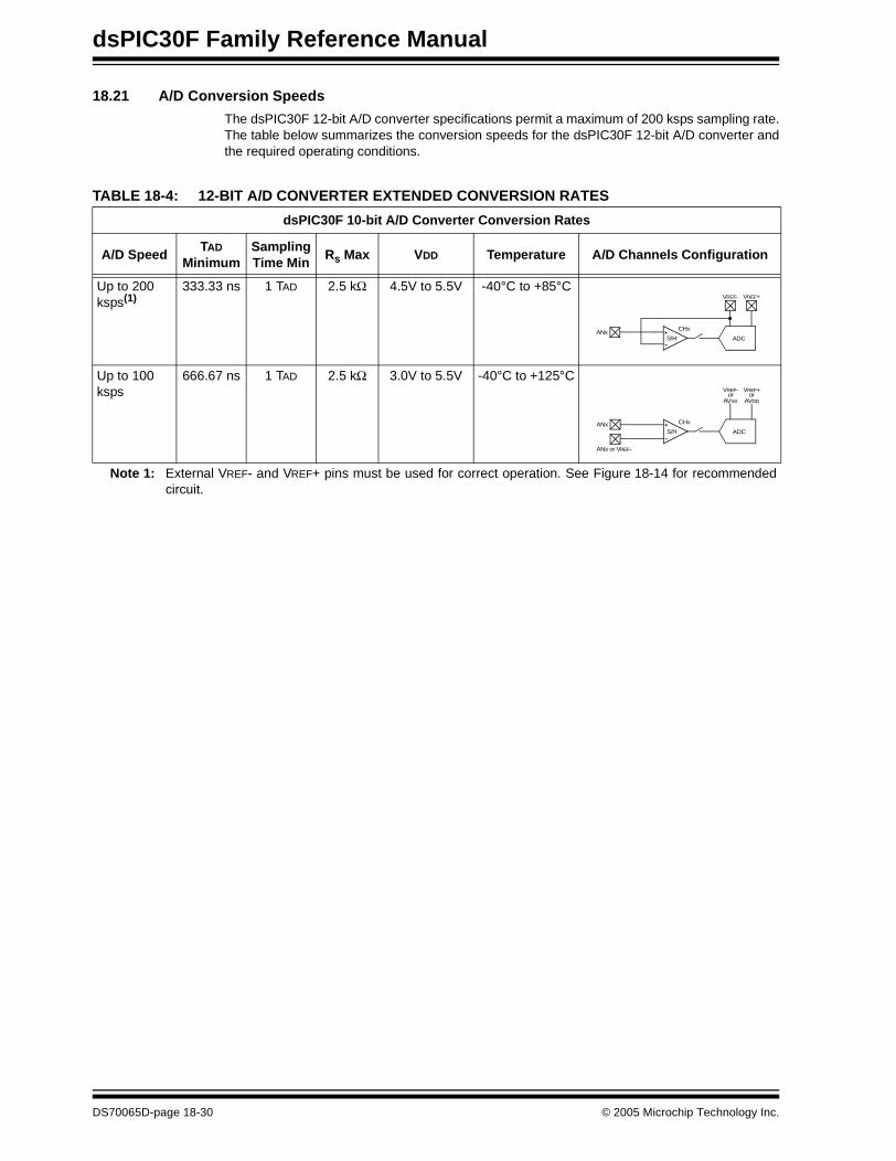
dsPIC30F Family Reference Manual
18.21 A/D Conversion Speeds
The dsPIC30F 12-bit A/D converter specifications permit a maximum of 200 ksps sampling rate.The table below summarizes the conversion speeds for the dsPIC30F 12-bit A/D converter andthe required operating conditions.
TABLE 18-4: 12-BIT A/D CONVERTER EXTENDED CONVERSION RATES
dsPIC30F 10-bit A/D Converter Conversion Rates
A/D SpeedTAD
MinimumSampling Time Min
Rs Max VDD Temperature A/D Channels Configuration
Up to 200 ksps(1)
333.33 ns 1 TAD 2.5 kΩ 4.5V to 5.5V -40°C to +85°C
Up to 100 ksps
666.67 ns 1 TAD 2.5 kΩ 3.0V to 5.5V -40°C to +125°C
Note 1: External VREF- and VREF+ pins must be used for correct operation. See Figure 18-14 for recommendedcircuit.
VREF- VREF+
ADCANx
S/H
CHX
VREF- VREF+
ADCANx
S/H
CHX
ANx or VREF-
orAVSS
orAVDD
DS70065D-page 18-30 © 2005 Microchip Technology Inc.
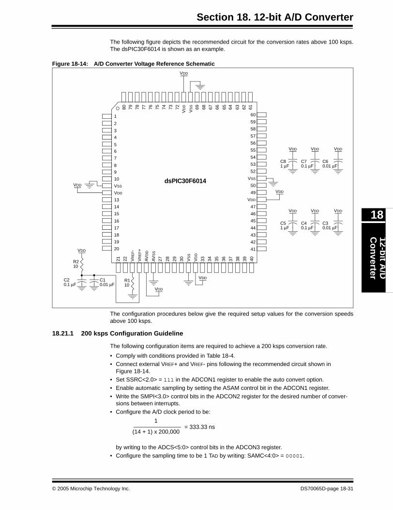
Section 18. 12-bit A/D Converter12-b
it A/D
Co
nverter
18
The following figure depicts the recommended circuit for the conversion rates above 100 ksps.The dsPIC30F6014 is shown as an example.
Figure 18-14: A/D Converter Voltage Reference Schematic
The configuration procedures below give the required setup values for the conversion speedsabove 100 ksps.
18.21.1 200 ksps Configuration Guideline
The following configuration items are required to achieve a 200 ksps conversion rate.
• Comply with conditions provided in Table 18-4.• Connect external VREF+ and VREF- pins following the recommended circuit shown in
Figure 18-14.• Set SSRC<2.0> = 111 in the ADCON1 register to enable the auto convert option.• Enable automatic sampling by setting the ASAM control bit in the ADCON1 register.
• Write the SMPI<3.0> control bits in the ADCON2 register for the desired number of conver-sions between interrupts.
• Configure the A/D clock period to be:
by writing to the ADCS<5:0> control bits in the ADCON3 register.• Configure the sampling time to be 1 TAD by writing: SAMC<4:0> = 00001.
7274 73
VD
D
VS
S 69 68 67 66 65 64 63 62 6120
2
3
4
5
6
7
8
9
10
VSS
VDD
13
14
15
16
50
49
VDD
47
46
45
44
21
4140393837363534V
RE
F-
VR
EF+
AV
DD
AV
SS
27 28 29 30 VS
S
VD
D
33
17
18
19
75
1
57
56
55
54
53
52
VSS
60
59
58
43
42
7678 777922
80
dsPIC30F6014
VDD
VDD
VDD
VDD
VDD
VDD
VDD
R210
C20.1 μF
C10.01 μF
R110
C81 μF
VDD
C70.1 μF
VDD
C60.01 μF
VDD
C51 μF
VDD
C40.1 μF
VDD
C30.01 μF
1
(14 + 1) x 200,000= 333.33 ns
© 2005 Microchip Technology Inc. DS70065D-page 18-31
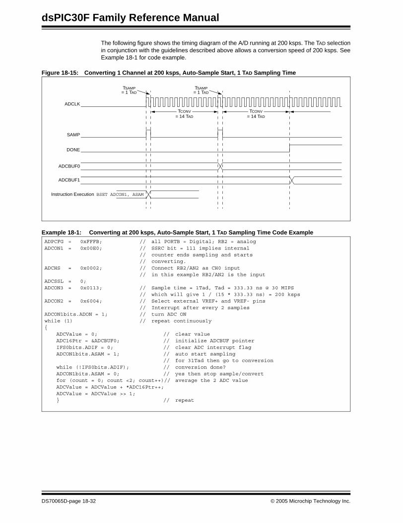
dsPIC30F Family Reference Manual
The following figure shows the timing diagram of the A/D running at 200 ksps. The TAD selectionin conjunction with the guidelines described above allows a conversion speed of 200 ksps. SeeExample 18-1 for code example.
Figure 18-15: Converting 1 Channel at 200 ksps, Auto-Sample Start, 1 TAD Sampling Time
Example 18-1: Converting at 200 ksps, Auto-Sample Start, 1 TAD Sampling Time Code Example
TCONV= 14 TAD
TSAMP= 1 TAD
TSAMP= 1 TAD
ADCLK
SAMP
DONE
ADCBUF0
ADCBUF1
Instruction Execution BSET ADCON1, ASAM
TCONV= 14 TAD
ADPCFG = 0xFFFB; // all PORTB = Digital; RB2 = analogADCON1 = 0x00E0; // SSRC bit = 111 implies internal
// counter ends sampling and starts// converting.
ADCHS = 0x0002; // Connect RB2/AN2 as CH0 input// in this example RB2/AN2 is the input
ADCSSL = 0;ADCON3 = 0x0113; // Sample time = 1Tad, Tad = 333.33 ns @ 30 MIPS
// which will give 1 / (15 * 333.33 ns) = 200 kspsADCON2 = 0x6004; // Select external VREF+ and VREF- pins
// Interrupt after every 2 samplesADCON1bits.ADON = 1; // turn ADC ONwhile (1) // repeat continuously{
ADCValue = 0; // clear valueADC16Ptr = &ADCBUF0; // initialize ADCBUF pointerIFS0bits.ADIF = 0; // clear ADC interrupt flagADCON1bits.ASAM = 1; // auto start sampling
// for 31Tad then go to conversionwhile (!IFS0bits.ADIF); // conversion done?ADCON1bits.ASAM = 0; // yes then stop sample/convertfor (count = 0; count <2; count++)// average the 2 ADC valueADCValue = ADCValue + *ADC16Ptr++;ADCValue = ADCValue >> 1;} // repeat
DS70065D-page 18-32 © 2005 Microchip Technology Inc.
Section 18. 12-bit A/D Converter12-b
it A/D
Co
nverter
18
18.22 Operation During Sleep and Idle Modes Sleep and Idle modes are useful for minimizing conversion noise because the digital activity ofthe CPU, buses and other peripherals is minimized.
18.22.1 CPU Sleep Mode Without RC A/D Clock
When the device enters Sleep mode, all clock sources to the module are shutdown and stay atlogic ‘0’.
If Sleep occurs in the middle of a conversion, the conversion is aborted unless the A/D is clockedfrom its internal RC clock generator. The converter will not resume a partially completedconversion on exiting from Sleep mode.
Register contents are not affected by the device entering or leaving Sleep mode.
18.22.2 CPU Sleep Mode With RC A/D Clock
The A/D module can operate during Sleep mode if the A/D clock source is set to the internal A/DRC oscillator (ADRC = 1). This eliminates digital switching noise from the conversion. When theconversion is completed, the CONV bit will be cleared and the result loaded into the A/D resultbuffer, ADCBUF.
If the A/D interrupt is enabled (ADIE = 1), the device will wake-up from Sleep when the A/Dinterrupt occurs. Program execution will resume at the A/D Interrupt Service Routine if the A/Dinterrupt is greater than the current CPU priority. Otherwise, execution will continue from theinstruction after the PWRSAV instruction, that placed the device in Sleep mode.
If the A/D interrupt is not enabled, the A/D module will then be turned off, although the ADON bitwill remain set.
To minimize the effects of digital noise on the A/D module operation, the user should select aconversion trigger source that ensures the A/D conversion will take place in Sleep mode. Theautomatic conversion trigger option can be used for sampling and conversion in Sleep(SSRC<2:0> = 111). To use the automatic conversion option, the ADON bit should be set in theinstruction prior to the PWRSAV instruction.
18.22.3 A/D Operation During CPU Idle Mode
For the A/D, the ADSIDL bit (ADCON1<13>) selects if the module will stop on Idle or continueon Idle. If ADSIDL = 0, the module will continue normal operation when the device enters Idlemode. If the A/D interrupt is enabled (ADIE = 1), the device will wake-up from Idle mode whenthe A/D interrupt occurs. Program execution will resume at the A/D Interrupt Service Routine ifthe A/D interrupt is greater than the current CPU priority. Otherwise, execution will continue fromthe instruction after the PWRSAV instruction that placed the device in Idle mode.
If ADSIDL = 1, the module will stop in Idle. If the device enters Idle mode in the middle of aconversion, the conversion is aborted. The converter will not resume a partially completedconversion on exiting from Idle mode.
18.23 Effects of a Reset
A device Reset forces all registers to their Reset state. This forces the A/D module to be turnedoff, and any conversion in progress is aborted. All pins that are multiplexed with analog inputswill be configured as analog inputs. The corresponding TRIS bits will be set.
The values in the ADCBUF registers are not initialized during a Power-on Reset.ADCBUF0...ADCBUFF will contain unknown data.
Note: For the A/D module to operate in Sleep, the A/D clock source must be set to RC(ADRC = 1).
© 2005 Microchip Technology Inc. DS70065D-page 18-33
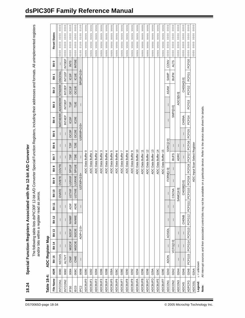
dsPIC30F Family Reference Manual
18.2
4S
pec
ial F
un
ctio
n R
egis
ters
Ass
oci
ated
wit
h t
he
12-b
it A
/D C
on
vert
er
The
follo
win
g ta
ble
lists
dsP
IC30
F 1
2-bi
t A/D
Con
vert
er S
peci
al F
unct
ion
Reg
iste
rs, i
nclu
ding
thei
r add
ress
es a
nd fo
rmat
s. A
ll un
impl
emen
ted
regi
ster
san
d/or
bits
with
in a
reg
iste
r re
ad a
s ze
ros.
Tab
le 1
8-4:
AD
C R
egis
ter
Map
File
Nam
eA
DR
Bit
15
Bit
14
Bit
13
Bit
12
Bit
11
Bit
10
Bit
9B
it 8
Bit
7B
it 6
Bit
5B
it 4
Bit
3B
it 2
Bit
1B
it 0
Res
et S
tate
s
INT
CO
N1
0080
NS
TD
IS—
——
—O
VA
TE
OV
BT
EC
OV
TE
——
—M
AT
HE
RR
AD
DR
ER
RS
TK
ER
RO
SC
FAIL
—0000 0000 0000 0000
INT
CO
N2
0082
ALT
IVT
——
——
——
——
——
INT
4EP
INT
3EP
INT
2EP
INT
1EP
INT
0EP
0000 0000 0000 0000
IFS
000
84C
NIF
MI2
CIF
SI2
CIF
NV
MIF
AD
IFU
1TX
IFU
1RX
IFS
PI1
IFT
3IF
T2I
FO
C2I
FIC
2IF
T1I
FO
C1I
FIC
1IF
INT
00000 0000 0000 0000
IEC
000
8CC
NIE
MI2
CIE
SI2
CIE
NV
MIE
AD
IEU
1TX
IEU
1RX
IES
PI1
IET
3IE
T2I
EO
C2I
EIC
2IE
T1I
EO
C1I
EIC
1IE
INT
0IE
0000 0000 0000 0000
IPC
200
98—
AD
IP<
2:0>
—U
1TX
IP<
2:0>
—U
1RX
IP<
2:0>
—S
PI1
IP<
2:0>
0100 0100 0100 0100
AD
CB
UF
002
80A
DC
Dat
a B
uffe
r 0
uuuu uuuu uuuu uuuu
AD
CB
UF
102
82A
DC
Dat
a B
uffe
r 1
uuuu uuuu uuuu uuuu
AD
CB
UF
202
84A
DC
Dat
a B
uffe
r 2
uuuu uuuu uuuu uuuu
AD
CB
UF
302
86A
DC
Dat
a B
uffe
r 3
uuuu uuuu uuuu uuuu
AD
CB
UF
402
88A
DC
Dat
a B
uffe
r 4
uuuu uuuu uuuu uuuu
AD
CB
UF
502
8AA
DC
Dat
a B
uffe
r 5
uuuu uuuu uuuu uuuu
AD
CB
UF
602
8CA
DC
Dat
a B
uffe
r 6
uuuu uuuu uuuu uuuu
AD
CB
UF
702
8EA
DC
Dat
a B
uffe
r 7
uuuu uuuu uuuu uuuu
AD
CB
UF
802
90A
DC
Dat
a B
uffe
r 8
uuuu uuuu uuuu uuuu
AD
CB
UF
902
92A
DC
Dat
a B
uffe
r 9
uuuu uuuu uuuu uuuu
AD
CB
UFA
0294
AD
C D
ata
Buf
fer
10uuuu uuuu uuuu uuuu
AD
CB
UF
B02
96A
DC
Dat
a B
uffe
r 11
uuuu uuuu uuuu uuuu
AD
CB
UF
C02
98A
DC
Dat
a B
uffe
r 12
uuuu uuuu uuuu uuuu
AD
CB
UF
D02
9AA
DC
Dat
a B
uffe
r 13
uuuu uuuu uuuu uuuu
AD
CB
UF
E02
9CA
DC
Dat
a B
uffe
r 14
uuuu uuuu uuuu uuuu
AD
CB
UF
F02
9EA
DC
Dat
a B
uffe
r 15
uuuu uuuu uuuu uuuu
AD
CO
N1
02A
0A
DO
N—
AD
SID
L—
——
FO
RM
[1:0
]S
SR
C[2
:0]
——
AS
AM
SA
MP
CO
NV
0000 0000 0000 0000
AD
CO
N2
02A
2V
CF
G[2
:0]
——
CS
CN
A—
—B
UF
S—
SM
PI[3
:0]
BU
FM
ALT
S0000 0000 0000 0000
AD
CO
N3
02A
4—
——
SA
MC
[4:0
]A
DR
C—
AD
CS
[5:0
]0000 0000 0000 0000
AD
CH
S02
A6
——
—C
H0N
BC
H0S
B[3
:0]
——
—C
H0N
AC
H0S
A[3
:0]
0000 0000 0000 0000
AD
PC
FG
02A
8P
CF
G15
PC
FG
14P
CF
G13
PC
FG
12P
CF
G11
PC
FG
10P
CF
G9
PC
FG
8P
CF
G7
PC
FG
6P
CF
G5
PC
FG
4P
CF
G3
PC
FG
2P
CF
G1
PC
FG
00000 0000 0000 0000
AD
CS
SL
02A
AA
DC
Inpu
t Sca
n S
elec
t Reg
iste
r0000 0000 0000 0000
Leg
end
:u
= u
nkno
wn
No
te:
All
inte
rrup
t sou
rces
and
thei
r as
soci
ated
con
trol
bits
may
not
be
avai
labl
e on
a p
artic
ular
dev
ice.
Ref
er to
the
devi
ce d
ata
shee
t for
det
ails
.
DS70065D-page 18-34 © 2005 Microchip Technology Inc.
Section 18. 12-bit A/D Converter12-b
it A/D
Co
nverter
18
18.25 Design Tips
Question 1: How can I optimize the system performance of the A/D converter?
Answer:
1. Make sure you are meeting all of the timing specifications. If you are turning the moduleoff and on, there is a minimum delay you must wait before taking a sample. If you arechanging input channels, there is a minimum delay you must wait for this as well, andfinally, there is TAD, which is the time selected for each bit conversion. This is selected inADCON3 and should be within a certain range, as specified in the Electrical Characteris-tics. If TAD is too short, the result may not be fully converted before the conversion isterminated, and if TAD is made too long, the voltage on the sampling capacitor can decaybefore the conversion is complete. These timing specifications are provided in the“Electrical Specifications” section of the device data sheets.
2. Often, the source impedance of the analog signal is high (greater than 10 kΩ), so thecurrent drawn from the source by leakage, and to charge the sample capacitor, can affectaccuracy. If the input signal does not change too quickly, try putting a 0.1 μF capacitor onthe analog input. This capacitor will charge to the analog voltage being sampled andsupply the instantaneous current needed to charge the 18 pF internal holding capacitor.
3. Put the device into Sleep mode before the start of the A/D conversion. The RC clocksource selection is required for conversions in Sleep mode. This technique increasesaccuracy, because digital noise from the CPU and other peripherals is minimized.
Question 2: Do you know of a good reference on A/D’s?
Answer: A good reference for understanding A/D conversions is the “Analog-Digital ConversionHandbook” third edition, published by Prentice Hall (ISBN 0-13-03-2848-0).
Question 3: My combination of channels/sample and samples/interrupt is greater thanthe size of the buffer. What will happen to the buffer?
Answer: This configuration is not recommended. The buffer will contain unknown results.
© 2005 Microchip Technology Inc. DS70065D-page 18-35
dsPIC30F Family Reference Manual
18.26 Related Application Notes
This section lists application notes that are related to this section of the manual. Theseapplication notes may not be written specifically for the dsPIC30F Product Family, but theconcepts are pertinent and could be used with modification and possible limitations. The currentapplication notes related to the 12-bit A/D Converter module are:
Title Application Note #
Using the Analog-to-Digital (A/D) Converter AN546Four Channel Digital Voltmeter with Display and Keyboard AN557Understanding A/D Converter Performance Specifications AN693
Note: Please visit the Microchip web site (www.microchip.com) for additional ApplicationNotes and code examples for the dsPIC30F Family of devices.
DS70065D-page 18-36 © 2005 Microchip Technology Inc.
Section 18. 12-bit A/D Converter12-b
it A/D
Co
nverter
18
18.27 Revision History
Revision A
This is the initial released revision of this document.
Revision B
To reflect editorial and technical content revisions for the dsPIC30F 12-bit A/D Converter module.
Revision C
This revision incorporates all known errata at the time of this document update.
Revision D
This revision includes the extended conversion rate guidelines.
© 2005 Microchip Technology Inc. DS70065D-page 18-37

dsPIC30F Family Reference Manual
NOTES:
DS70065D-page 18-38 © 2005 Microchip Technology Inc.
Section 19. UART
UA
RT
19
HIGHLIGHTS
This section of the manual contains the following major topics:
19.1 Introduction .................................................................................................................. 19-2
19.2 Control Registers ......................................................................................................... 19-319.3 UART Baud Rate Generator (BRG)............................................................................. 19-819.4 UART Configuration................................................................................................... 19-10
19.5 UART Transmitter ...................................................................................................... 19-1119.6 UART Receiver .......................................................................................................... 19-1419.7 Using the UART for 9-bit Communication.................................................................. 19-18
19.8 Receiving Break Characters ...................................................................................... 19-1919.9 Initialization ................................................................................................................ 19-2019.10 Other Features of the UART ...................................................................................... 19-21
19.11 UART Operation During CPU Sleep and Idle Modes ................................................ 19-2119.12 Registers Associated with UART Module .................................................................. 19-2219.13 Design Tips ................................................................................................................ 19-23
19.14 Related Application Notes.......................................................................................... 19-2419.15 Revision History ......................................................................................................... 19-25
© 2004 Microchip Technology Inc. DS70066C-page 19-1

dsPIC30F Family Reference Manual
19.1 Introduction
The Universal Asynchronous Receiver Transmitter (UART) module is one of the serial I/Omodules available in the dsPIC30F device family. The UART is a full-duplex asynchronous sys-tem that can communicate with peripheral devices, such as personal computers, RS-232 andRS-485 interfaces.
The primary features of the UART module are:
• Full-duplex 8- or 9-bit data transmission through the UxTX and UxRX pins
• Even, Odd or No Parity options (for 8-bit data)• One or two Stop bits• Fully integrated Baud Rate Generator with 16-bit prescaler
• Baud rates ranging from 29 bps to 1.875 Mbps at FCY = 30 MHz• 4-deep First-In-First-Out (FIFO) transmit data buffer• 4-deep FIFO receive data buffer
• Parity, Framing and Buffer Overrun error detection• Support for 9-bit mode with Address Detect (9th bit = 1)• Transmit and Receive Interrupts
• Loopback mode for diagnostic support
A simplified block diagram of the UART is shown in Figure 19-1. The UART module consists ofthe key important hardware elements:
• Baud Rate Generator• Asynchronous Transmitter• Asynchronous Receiver
Figure 19-1: UART Simplified Block Diagram
Note: Each dsPIC30F device variant may have one or more UART modules. An ‘x’ usedin the names of pins, control/status bits and registers denotes the particular module.Refer to the specific device data sheets for more details.
Baud Rate Generator
UART Receiver
UART Transmitter
UxRX
UxTX
DS70066C-page 19-2 © 2004 Microchip Technology Inc.
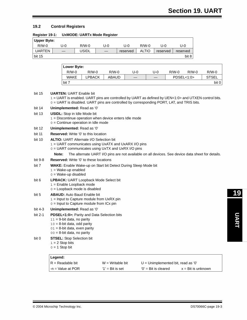
Section 19. UARTU
AR
T
19
19.2 Control Registers
Register 19-1: UXMODE: UARTX Mode Register
Upper Byte:R/W-0 U-0 R/W-0 U-0 U-0 R/W-0 U-0 U-0
UARTEN — USIDL — reserved ALTIO reserved reserved
bit 15 bit 8
Lower Byte:R/W-0 R/W-0 R/W-0 U-0 U-0 R/W-0 R/W-0 R/W-0WAKE LPBACK ABAUD — — PDSEL<1:0> STSEL
bit 7 bit 0
bit 15 UARTEN: UART Enable bit1 = UART is enabled. UART pins are controlled by UART as defined by UEN<1:0> and UTXEN control bits.0 = UART is disabled. UART pins are controlled by corresponding PORT, LAT, and TRIS bits.
bit 14 Unimplemented: Read as ‘0’
bit 13 USIDL: Stop in Idle Mode bit1 = Discontinue operation when device enters Idle mode0 = Continue operation in Idle mode
bit 12 Unimplemented: Read as ‘0’
bit 11 Reserved: Write ‘0’ to this location
bit 10 ALTIO: UART Alternate I/O Selection bit1 = UART communicates using UxATX and UxARX I/O pins0 = UART communicates using UxTX and UxRX I/O pins
Note: The alternate UART I/O pins are not available on all devices. See device data sheet for details.
bit 9-8 Reserved: Write ‘0’ to these locations
bit 7 WAKE: Enable Wake-up on Start bit Detect During Sleep Mode bit1 = Wake-up enabled0 = Wake-up disabled
bit 6 LPBACK: UART Loopback Mode Select bit1 = Enable Loopback mode0 = Loopback mode is disabled
bit 5 ABAUD: Auto Baud Enable bit1 = Input to Capture module from UxRX pin0 = Input to Capture module from ICx pin
bit 4-3 Unimplemented: Read as ‘0’
bit 2-1 PDSEL<1:0>: Parity and Data Selection bits11 = 9-bit data, no parity10 = 8-bit data, odd parity01 = 8-bit data, even parity00 = 8-bit data, no parity
bit 0 STSEL: Stop Selection bit1 = 2 Stop bits0 = 1 Stop bit
Legend:
R = Readable bit W = Writable bit U = Unimplemented bit, read as ‘0’
-n = Value at POR ‘1’ = Bit is set ‘0’ = Bit is cleared x = Bit is unknown
© 2004 Microchip Technology Inc. DS70066C-page 19-3
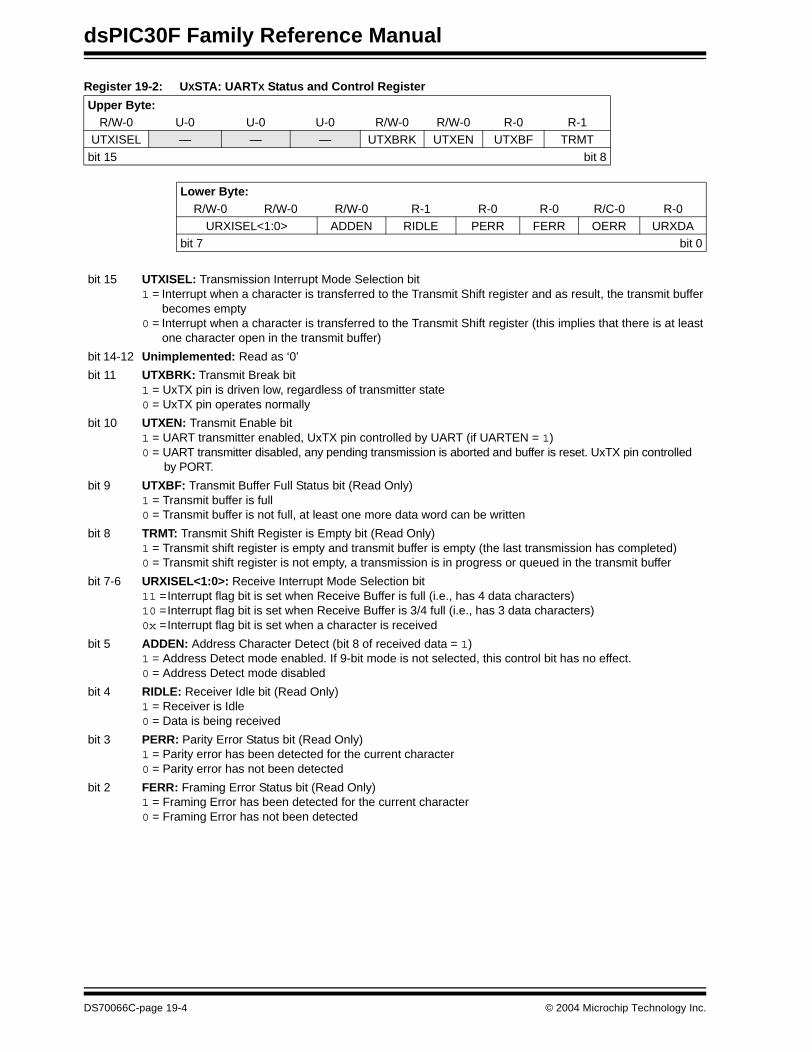
dsPIC30F Family Reference Manual
Register 19-2: UXSTA: UARTX Status and Control Register
Upper Byte:R/W-0 U-0 U-0 U-0 R/W-0 R/W-0 R-0 R-1
UTXISEL — — — UTXBRK UTXEN UTXBF TRMT
bit 15 bit 8
Lower Byte:R/W-0 R/W-0 R/W-0 R-1 R-0 R-0 R/C-0 R-0
URXISEL<1:0> ADDEN RIDLE PERR FERR OERR URXDAbit 7 bit 0
bit 15 UTXISEL: Transmission Interrupt Mode Selection bit1 = Interrupt when a character is transferred to the Transmit Shift register and as result, the transmit buffer
becomes empty0 = Interrupt when a character is transferred to the Transmit Shift register (this implies that there is at least
one character open in the transmit buffer)
bit 14-12 Unimplemented: Read as ‘0’
bit 11 UTXBRK: Transmit Break bit1 = UxTX pin is driven low, regardless of transmitter state0 = UxTX pin operates normally
bit 10 UTXEN: Transmit Enable bit1 = UART transmitter enabled, UxTX pin controlled by UART (if UARTEN = 1)0 = UART transmitter disabled, any pending transmission is aborted and buffer is reset. UxTX pin controlled
by PORT.
bit 9 UTXBF: Transmit Buffer Full Status bit (Read Only)1 = Transmit buffer is full0 = Transmit buffer is not full, at least one more data word can be written
bit 8 TRMT: Transmit Shift Register is Empty bit (Read Only)1 = Transmit shift register is empty and transmit buffer is empty (the last transmission has completed)0 = Transmit shift register is not empty, a transmission is in progress or queued in the transmit buffer
bit 7-6 URXISEL<1:0>: Receive Interrupt Mode Selection bit11 =Interrupt flag bit is set when Receive Buffer is full (i.e., has 4 data characters)10 =Interrupt flag bit is set when Receive Buffer is 3/4 full (i.e., has 3 data characters)0x =Interrupt flag bit is set when a character is received
bit 5 ADDEN: Address Character Detect (bit 8 of received data = 1)1 = Address Detect mode enabled. If 9-bit mode is not selected, this control bit has no effect.0 = Address Detect mode disabled
bit 4 RIDLE: Receiver Idle bit (Read Only)1 = Receiver is Idle0 = Data is being received
bit 3 PERR: Parity Error Status bit (Read Only)1 = Parity error has been detected for the current character 0 = Parity error has not been detected
bit 2 FERR: Framing Error Status bit (Read Only)1 = Framing Error has been detected for the current character 0 = Framing Error has not been detected
DS70066C-page 19-4 © 2004 Microchip Technology Inc.

Section 19. UARTU
AR
T
19
Register 19-2: UXSTA: UARTX Status and Control Register (Continued)
bit 1 OERR: Receive Buffer Overrun Error Status bit (Read/Clear Only)1 = Receive buffer has overflowed0 = Receive buffer has not overflowed
bit 0 URXDA: Receive Buffer Data Available bit (Read Only)1 = Receive buffer has data, at least one more character can be read0 = Receive buffer is empty
Legend:
R = Readable bit W = Writable bit U = Unimplemented bit, read as ‘0’ C = Bit can be cleared
-n = Value at POR ‘1’ = Bit is set ‘0’ = Bit is cleared x = Bit is unknown
© 2004 Microchip Technology Inc. DS70066C-page 19-5

dsPIC30F Family Reference Manual
Register 19-3: UXRXREG: UARTX Receive Register
Register 19-4: UXTXREG: UARTX Transmit Register (Write Only)
Upper Byte:U-0 U-0 U-0 U-0 U-0 U-0 U-0 R-0— — — — — — — URX8
bit 15 bit 8
Lower Byte:R-0 R-0 R-0 R-0 R-0 R-0 R-0 R-0
URX<7:0>bit 7 bit 0
bit 15-9 Unimplemented: Read as ‘0’
bit 8 URX8: Data bit 8 of the Received Character (in 9-bit mode)
bit 7-0 URX<7:0>: Data bits 7-0 of the Received Character
Legend:
R = Readable bit W = Writable bit U = Unimplemented bit, read as ‘0’
-n = Value at POR ‘1’ = Bit is set ‘0’ = Bit is cleared x = Bit is unknown
Upper Byte:U-0 U-0 U-0 U-0 U-0 U-0 U-0 W-x
— — — — — — — UTX8bit 15 bit 8
Lower Byte:W-x W-x W-x W-x W-x W-x W-x W-x
UTX<7:0>
bit 7 bit 0
bit 15-9 Unimplemented: Read as ‘0’
bit 8 UTX8: Data bit 8 of the Character to be Transmitted (in 9-bit mode)
bit 7-0 UTX<7:0>: Data bits 7-0 of the Character to be Transmitted
Legend:
R = Readable bit W = Writable bit U = Unimplemented bit, read as ‘0’
-n = Value at POR ‘1’ = Bit is set ‘0’ = Bit is cleared x = Bit is unknown
DS70066C-page 19-6 © 2004 Microchip Technology Inc.
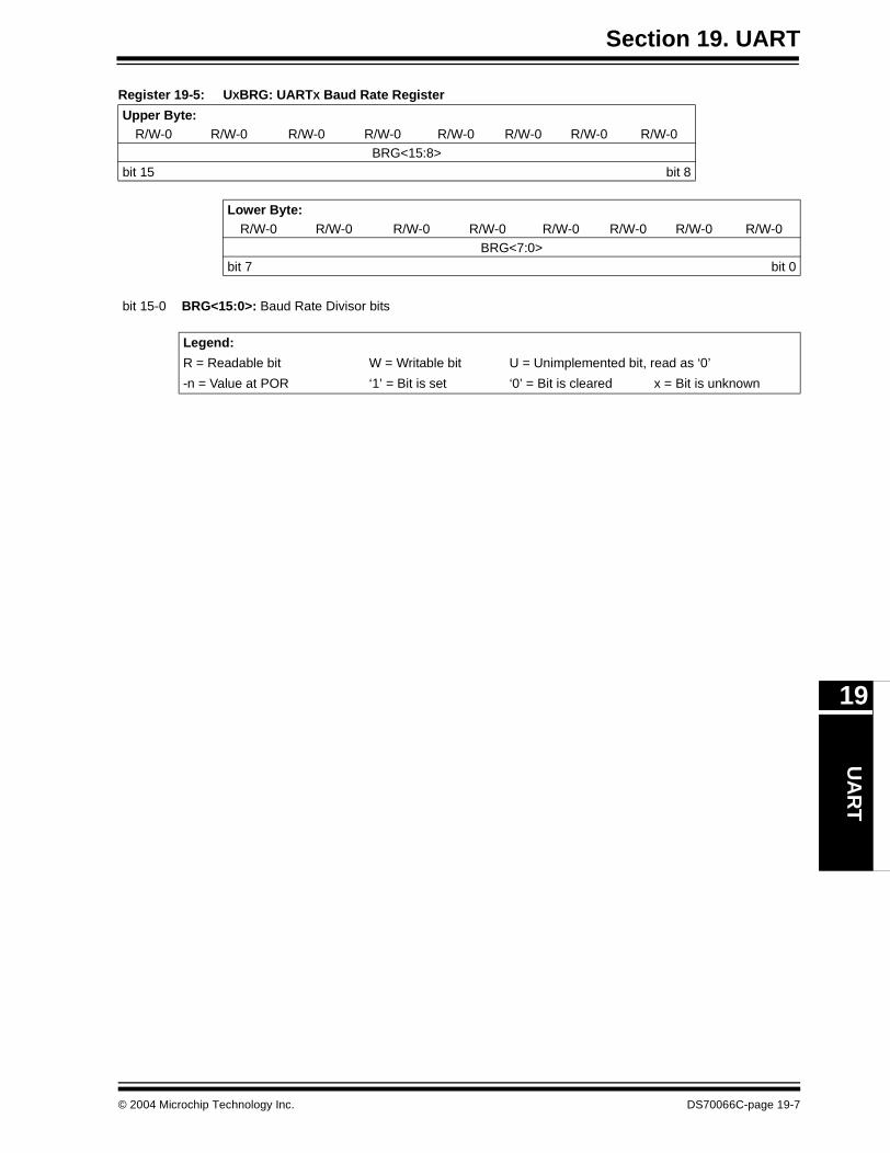
Section 19. UARTU
AR
T
19
Register 19-5: UXBRG: UARTX Baud Rate Register
Upper Byte:R/W-0 R/W-0 R/W-0 R/W-0 R/W-0 R/W-0 R/W-0 R/W-0
BRG<15:8>
bit 15 bit 8
Lower Byte:R/W-0 R/W-0 R/W-0 R/W-0 R/W-0 R/W-0 R/W-0 R/W-0
BRG<7:0>bit 7 bit 0
bit 15-0 BRG<15:0>: Baud Rate Divisor bits
Legend:
R = Readable bit W = Writable bit U = Unimplemented bit, read as ‘0’
-n = Value at POR ‘1’ = Bit is set ‘0’ = Bit is cleared x = Bit is unknown
© 2004 Microchip Technology Inc. DS70066C-page 19-7
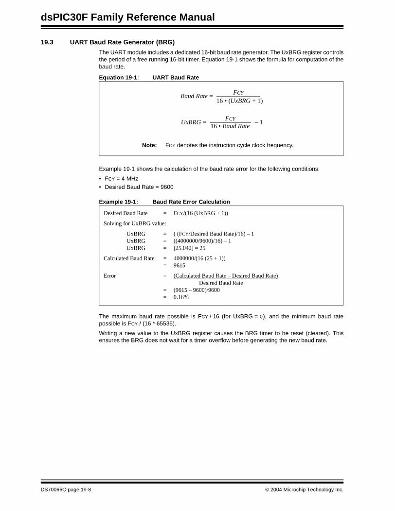
dsPIC30F Family Reference Manual
19.3 UART Baud Rate Generator (BRG)
The UART module includes a dedicated 16-bit baud rate generator. The UxBRG register controlsthe period of a free running 16-bit timer. Equation 19-1 shows the formula for computation of thebaud rate.
Equation 19-1: UART Baud Rate
Example 19-1 shows the calculation of the baud rate error for the following conditions:
• FCY = 4 MHz • Desired Baud Rate = 9600
Example 19-1: Baud Rate Error Calculation
The maximum baud rate possible is FCY / 16 (for UxBRG = 0), and the minimum baud ratepossible is FCY / (16 * 65536).
Writing a new value to the UxBRG register causes the BRG timer to be reset (cleared). Thisensures the BRG does not wait for a timer overflow before generating the new baud rate.
Note: FCY denotes the instruction cycle clock frequency.
Baud Rate = FCY
16 • (UxBRG + 1)
FCY
16 • Baud RateUxBRG = – 1
Desired Baud Rate = FCY/(16 (UxBRG + 1))
Solving for UxBRG value:
UxBRG = ( (FCY/Desired Baud Rate)/16) – 1UxBRG = ((4000000/9600)/16) – 1 UxBRG = [25.042] = 25
Calculated Baud Rate = 4000000/(16 (25 + 1)) = 9615
Error = (Calculated Baud Rate – Desired Baud Rate)Desired Baud Rate
= (9615 – 9600)/9600 = 0.16%
DS70066C-page 19-8 © 2004 Microchip Technology Inc.
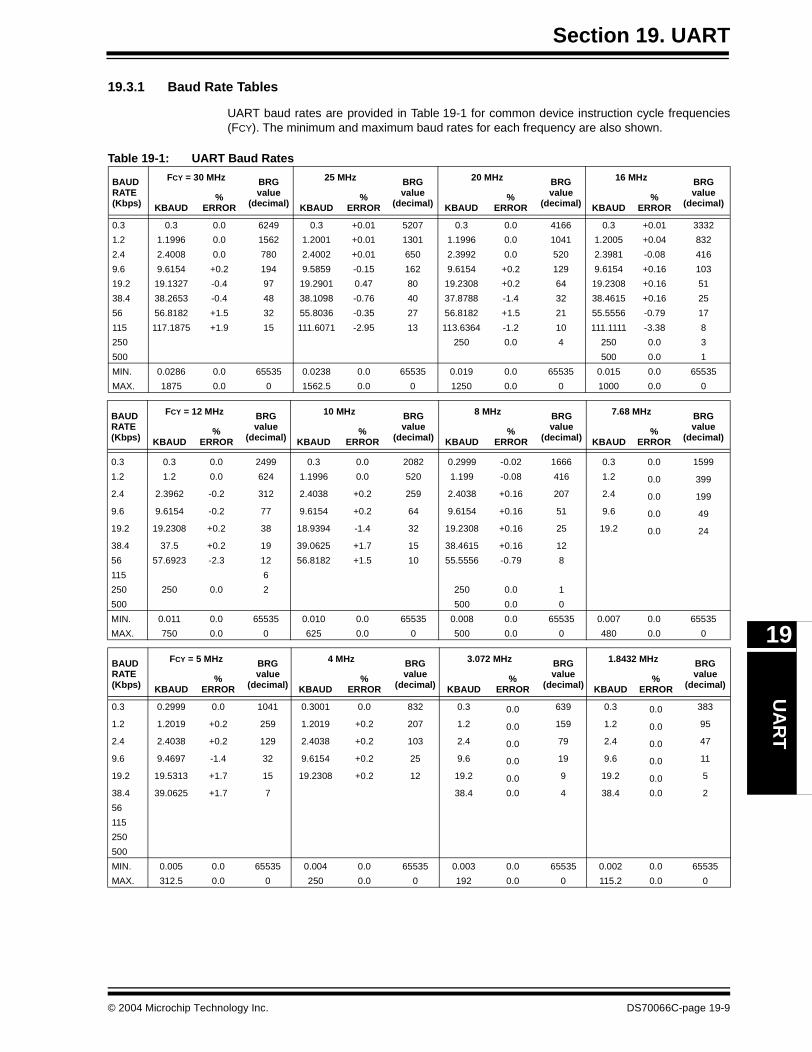
Section 19. UARTU
AR
T
19
19.3.1 Baud Rate Tables
UART baud rates are provided in Table 19-1 for common device instruction cycle frequencies(FCY). The minimum and maximum baud rates for each frequency are also shown.
Table 19-1: UART Baud Rates
BAUDRATE(Kbps)
FCY = 30 MHz BRGvalue
(decimal)
25 MHz BRGvalue
(decimal)
20 MHz BRGvalue
(decimal)
16 MHz BRGvalue
(decimal)KBAUD%
ERROR KBAUD%
ERROR KBAUD%
ERROR KBAUD%
ERROR
0.3 0.3 0.0 6249 0.3 +0.01 5207 0.3 0.0 4166 0.3 +0.01 3332
1.2 1.1996 0.0 1562 1.2001 +0.01 1301 1.1996 0.0 1041 1.2005 +0.04 832
2.4 2.4008 0.0 780 2.4002 +0.01 650 2.3992 0.0 520 2.3981 -0.08 416
9.6 9.6154 +0.2 194 9.5859 -0.15 162 9.6154 +0.2 129 9.6154 +0.16 103
19.2 19.1327 -0.4 97 19.2901 0.47 80 19.2308 +0.2 64 19.2308 +0.16 51
38.4 38.2653 -0.4 48 38.1098 -0.76 40 37.8788 -1.4 32 38.4615 +0.16 25
56 56.8182 +1.5 32 55.8036 -0.35 27 56.8182 +1.5 21 55.5556 -0.79 17
115 117.1875 +1.9 15 111.6071 -2.95 13 113.6364 -1.2 10 111.1111 -3.38 8
250 250 0.0 4 250 0.0 3
500 500 0.0 1
MIN. 0.0286 0.0 65535 0.0238 0.0 65535 0.019 0.0 65535 0.015 0.0 65535
MAX. 1875 0.0 0 1562.5 0.0 0 1250 0.0 0 1000 0.0 0
BAUDRATE(Kbps)
FCY = 12 MHz BRGvalue
(decimal)
10 MHz BRGvalue
(decimal)
8 MHz BRGvalue
(decimal)
7.68 MHz BRGvalue
(decimal)KBAUD%
ERROR KBAUD%
ERROR KBAUD%
ERROR KBAUD%
ERROR
0.3 0.3 0.0 2499 0.3 0.0 2082 0.2999 -0.02 1666 0.3 0.0 1599
1.2 1.2 0.0 624 1.1996 0.0 520 1.199 -0.08 416 1.2 0.0 399
2.4 2.3962 -0.2 312 2.4038 +0.2 259 2.4038 +0.16 207 2.4 0.0 199
9.6 9.6154 -0.2 77 9.6154 +0.2 64 9.6154 +0.16 51 9.6 0.0 49
19.2 19.2308 +0.2 38 18.9394 -1.4 32 19.2308 +0.16 25 19.2 0.0 24
38.4 37.5 +0.2 19 39.0625 +1.7 15 38.4615 +0.16 12
56 57.6923 -2.3 12 56.8182 +1.5 10 55.5556 -0.79 8
115 6
250 250 0.0 2 250 0.0 1
500 500 0.0 0
MIN. 0.011 0.0 65535 0.010 0.0 65535 0.008 0.0 65535 0.007 0.0 65535
MAX. 750 0.0 0 625 0.0 0 500 0.0 0 480 0.0 0
BAUDRATE(Kbps)
FCY = 5 MHz BRGvalue
(decimal)
4 MHz BRGvalue
(decimal)
3.072 MHz BRGvalue
(decimal)
1.8432 MHz BRGvalue
(decimal)KBAUD%
ERROR KBAUD%
ERROR KBAUD%
ERROR KBAUD%
ERROR
0.3 0.2999 0.0 1041 0.3001 0.0 832 0.3 0.0 639 0.3 0.0 383
1.2 1.2019 +0.2 259 1.2019 +0.2 207 1.2 0.0 159 1.2 0.0 95
2.4 2.4038 +0.2 129 2.4038 +0.2 103 2.4 0.0 79 2.4 0.0 47
9.6 9.4697 -1.4 32 9.6154 +0.2 25 9.6 0.0 19 9.6 0.0 11
19.2 19.5313 +1.7 15 19.2308 +0.2 12 19.2 0.0 9 19.2 0.0 5
38.4 39.0625 +1.7 7 38.4 0.0 4 38.4 0.0 2
56
115
250
500
MIN. 0.005 0.0 65535 0.004 0.0 65535 0.003 0.0 65535 0.002 0.0 65535
MAX. 312.5 0.0 0 250 0.0 0 192 0.0 0 115.2 0.0 0
© 2004 Microchip Technology Inc. DS70066C-page 19-9
dsPIC30F Family Reference Manual
19.4 UART Configuration
The UART uses standard non-return-to-zero (NRZ) format (one Start bit, eight or nine data bits,and one or two Stop bits). Parity is supported by the hardware, and may be configured by theuser as even, odd or no parity. The most common data format is 8 bits, no parity and one Stopbit (denoted as 8, N, 1), which is the default (POR) setting. The number of data bits and Stop bits,and the parity, are specified in the PDSEL<1:0> (UxMODE<2:1>) and STSEL (UxMODE<0>)bits. An on-chip dedicated 16-bit baud rate generator can be used to derive standard baud ratefrequencies from the oscillator. The UART transmits and receives the LSb first. The UART’stransmitter and receiver are functionally independent, but use the same data format and baudrate.
19.4.1 Enabling the UART
The UART module is enabled by setting the UARTEN (UxMODE<15>) bit and UTXEN(UxSTA<10>) bit. Once enabled, the UxTX and UxRX pins are configured as an output and aninput, respectively, overriding the TRIS and PORT register bit settings for the corresponding I/Oport pins. The UxTX pin is at logic ‘1’ when no transmission is taking place.
19.4.2 Disabling the UART
The UART module is disabled by clearing the UARTEN (UxMODE<15>) bit. This is the defaultstate after any Reset. If the UART is disabled, all UART pins operate as port pins under thecontrol of their corresponding PORT and TRIS bits.
Disabling the UART module resets the buffers to empty states. Any data characters in the buffersare lost, and the baud rate counter is reset.
All error and status flags associated with the UART module are reset when the module isdisabled. The URXDA, OERR, FERR, PERR, UTXEN, UTXBRK and UTXBF bits are cleared,whereas RIDLE and TRMT are set. Other control bits, including ADDEN, URXISEL<1:0>,UTXISEL, as well as the UxMODE and UxBRG registers, are not affected.
Clearing the UARTEN bit while the UART is active will abort all pending transmissions andreceptions and reset the module as defined above. Re-enabling the UART will restart the UARTin the same configuration.
19.4.3 Alternate UART I/O Pins
Some dsPIC30F devices have an alternate set of UART transmit and receive pins that can beused for communications. The alternate UART pins are useful when the primary UART pins areshared by other peripherals. The alternate I/O pins are enabled by setting the ALTIO bit(UxMODE<10>). If ALTIO = 1, the UxATX and UxARX pins (alternate transmit and alternatereceive pins, respectively) are used by the UART module, instead of the UxTX and UxRX pins.If ALTIO = 0, the UxTX and UxRX pins are used by the UART module.
Note: The UTXEN bit should not be set until the UARTEN bit has been set. Otherwise,UART transmissions will not be enabled.
DS70066C-page 19-10 © 2004 Microchip Technology Inc.
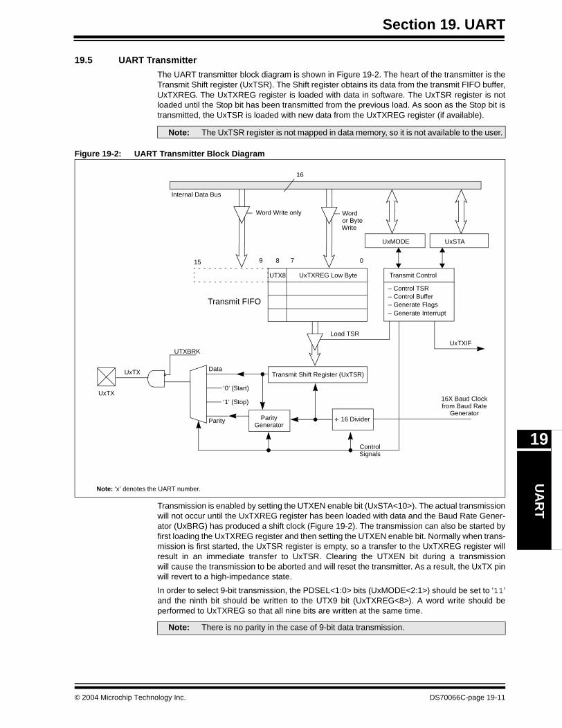
Section 19. UARTU
AR
T
19
19.5 UART Transmitter
The UART transmitter block diagram is shown in Figure 19-2. The heart of the transmitter is theTransmit Shift register (UxTSR). The Shift register obtains its data from the transmit FIFO buffer,UxTXREG. The UxTXREG register is loaded with data in software. The UxTSR register is notloaded until the Stop bit has been transmitted from the previous load. As soon as the Stop bit istransmitted, the UxTSR is loaded with new data from the UxTXREG register (if available).
Figure 19-2: UART Transmitter Block Diagram
Transmission is enabled by setting the UTXEN enable bit (UxSTA<10>). The actual transmissionwill not occur until the UxTXREG register has been loaded with data and the Baud Rate Gener-ator (UxBRG) has produced a shift clock (Figure 19-2). The transmission can also be started byfirst loading the UxTXREG register and then setting the UTXEN enable bit. Normally when trans-mission is first started, the UxTSR register is empty, so a transfer to the UxTXREG register willresult in an immediate transfer to UxTSR. Clearing the UTXEN bit during a transmissionwill cause the transmission to be aborted and will reset the transmitter. As a result, the UxTX pinwill revert to a high-impedance state.
In order to select 9-bit transmission, the PDSEL<1:0> bits (UxMODE<2:1>) should be set to ‘11’and the ninth bit should be written to the UTX9 bit (UxTXREG<8>). A word write should beperformed to UxTXREG so that all nine bits are written at the same time.
Note: The UxTSR register is not mapped in data memory, so it is not available to the user.
Word Write only Word
UTX8 UxTXREG Low Byte
Load TSR
Transmit Control
– Control TSR– Control Buffer– Generate Flags– Generate Interrupt
UxTXIF
Data
‘0’ (Start)
‘1’ (Stop)
Parity ParityGenerator
Transmit Shift Register (UxTSR)
16 Divider
ControlSignals
16X Baud Clockfrom Baud Rate
Generator
Internal Data Bus
UTXBRK
UxTX
Note: ‘x’ denotes the UART number.
UxTX
UxMODE UxSTA
16
or Byte Write
Transmit FIFO
15 9 8 7 0
Note: There is no parity in the case of 9-bit data transmission.
© 2004 Microchip Technology Inc. DS70066C-page 19-11
dsPIC30F Family Reference Manual
19.5.1 Transmit Buffer (UxTXB)
Each UART has a 4-deep, 9-bit wide FIFO transmit data buffer. The UxTXREG register providesuser access to the next available buffer location. The user may write up to 4 words in the buffer.Once the UxTXREG contents are transferred to the UxTSR register, the current buffer locationbecomes available for new data to be written and the next buffer location is sourced to the UxTSRregister. The UTXBF (UxSTA<9>) status bit is set whenever the buffer is full. If a user attemptsto write to a full buffer, the new data will not be accepted into the FIFO.
The FIFO is reset during any device Reset, but is not affected when the device enters a PowerSaving mode or wakes up from a Power Saving mode.
19.5.2 Transmit Interrupt
The transmit interrupt flag (UxTXIF) is located in the corresponding interrupt flag status (IFS)register. The UTXISEL control bit (UxSTA<15>) determines when the UART will generate atransmit interrupt.
1. If UTXISEL = 0, an interrupt is generated when a word is transferred from the transmitbuffer to the Transmit Shift register (UxTSR). This implies that the transmit buffer has atleast one empty word. Since an interrupt is generated after the transfer of each individualword, this mode is useful if interrupts can be handled frequently (i.e., the ISR is completedbefore the transmission of the next word).
2. If UTXISEL = 1, an interrupt is generated when a word is transferred from the transmitbuffer to the Transmit Shift register (UxTSR) and the transmit buffer is empty. Since aninterrupt is generated only after all 4 words have been transmitted, this ‘Block Transmit’mode is useful if the user’s code cannot handle interrupts quickly enough (i.e., the ISR iscompleted before the transmission of the next word).
The UxTXIF bit will be set when the module is first enabled.
The user should clear the UxTXIF bit in the ISR.
Switching between the two Interrupt modes during operation is possible.
While the UxTXIF flag bit indicates the status of the UxTXREG register, the TRMT bit(UxSTA<8>) shows the status of the UxTSR register. The TRMT status bit is a read only bit,which is set when the UxTSR register is empty. No interrupt logic is tied to this bit, so the userhas to poll this bit in order to determine if the UxTSR register is empty.
Note: When the UTXEN bit is set, the UxTXIF flag bit will also be set if UTXISEL = 0, sincethe transmit buffer is not yet full (can move transmit data to the UxTXREG register).
DS70066C-page 19-12 © 2004 Microchip Technology Inc.
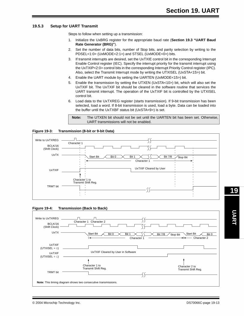
Section 19. UARTU
AR
T
19
19.5.3 Setup for UART Transmit
Steps to follow when setting up a transmission:
1. Initialize the UxBRG register for the appropriate baud rate (Section 19.3 “UART BaudRate Generator (BRG)”).
2. Set the number of data bits, number of Stop bits, and parity selection by writing to thePDSEL<1:0> (UxMODE<2:1>) and STSEL (UxMODE<0>) bits.
3. If transmit interrupts are desired, set the UxTXIE control bit in the corresponding InterruptEnable Control register (IEC). Specify the interrupt priority for the transmit interrupt usingthe UxTXIP<2:0> control bits in the corresponding Interrupt Priority Control register (IPC).Also, select the Transmit Interrupt mode by writing the UTXISEL (UxSTA<15>) bit.
4. Enable the UART module by setting the UARTEN (UxMODE<15>) bit.5. Enable the transmission by setting the UTXEN (UxSTA<10>) bit, which will also set the
UxTXIF bit. The UxTXIF bit should be cleared in the software routine that services theUART transmit interrupt. The operation of the UxTXIF bit is controlled by the UTXISELcontrol bit.
6. Load data to the UxTXREG register (starts transmission). If 9-bit transmission has beenselected, load a word. If 8-bit transmission is used, load a byte. Data can be loaded intothe buffer until the UxTXBF status bit (UxSTA<9>) is set.
Figure 19-3: Transmission (8-bit or 9-bit Data)
Figure 19-4: Transmission (Back to Back)
Note: The UTXEN bit should not be set until the UARTEN bit has been set. Otherwise,UART transmissions will not be enabled.
Character 1Stop Bit
Character 1 toTransmit Shift Reg.
Start Bit Bit 0 Bit 1 Bit 7/8
Write to UxTXREGCharacter 1
BCLK/16(Shift Clock)
UxTX
UxTXIF
TRMT bit
UxTXIF Cleared by User
Transmit Shift Reg.
Write to UxTXREG
BCLK/16(Shift Clock)
UxTX
UxTXIF
TRMT bit
Character 1 Character 2
Character 1 to Character 2 to
Start Bit Stop Bit Start Bit
Transmit Shift Reg.
Character 1 Character 2Bit 0 Bit 1 Bit 7/8 Bit 0
Note: This timing diagram shows two consecutive transmissions.
(UTXISEL = 0)
UxTXIF(UTXISEL = 1)
UxTXIF Cleared by User in Software
© 2004 Microchip Technology Inc. DS70066C-page 19-13
dsPIC30F Family Reference Manual
19.5.4 Transmission of Break Characters
Setting the UTXBRK bit (UxSTA<11>) will force the UxTX line to ‘0’. UTXBRK overrides any othertransmitter activity. The user should wait for the transmitter to be Idle (TRMT = 1) before settingUTXBRK.
To send a break character, the UTXBRK bit must be set by software and remain set for a mini-mum of 13 baud clocks. The baud clock periods are timed in software. The UTXBRK bit is thencleared by software to generate the Stop bit. The user must wait at least one or two baud clocksto ensure a valid Stop bit(s) before loading the UTXBUF again or renewing transmitter activity.
19.6 UART Receiver
The receiver block diagram is shown in Figure 19-5. The heart of the receiver is the Receive(Serial) Shift register (UxRSR). The data is received on the UxRX pin and is sent to the datarecovery block. The data recovery block operates at 16 times the baud rate, whereas the mainreceive serial shifter operates at the baud rate. After sampling the UxRX pin for the Stop bit, thereceived data in UxRSR is transferred to the receive FIFO (if it is empty).
The data on the UxRX pin is sampled three times by a majority detect circuit to determine if ahigh or a low level is present at the UxRX pin. Figure 19-5 shows the sampling scheme.
19.6.1 Receive Buffer (UxRXB)
The UART receiver has a 4-deep, 9-bit wide FIFO receive data buffer. UxRXREG is a memorymapped register that provides access to the output of the FIFO. It is possible for 4 words of datato be received and transferred to the FIFO and a fifth word to begin shifting to the UxRSR registerbefore a buffer overrun occurs.
19.6.2 Receiver Error Handling
If the FIFO is full (four characters) and a fifth character is fully received into the UxRSR register,the overrun error bit, OERR (UxSTA<1>), will be set. The word in UxRSR will be kept, but furthertransfers to the receive FIFO are inhibited as long as the OERR bit is set. The user must clearthe OERR bit in software to allow further data to be received.
If it is desired to keep the data received prior to the overrun, the user should first read all fivecharacters, then clear the OERR bit. If the five characters can be discarded, the user can simplyclear the OERR bit. This effectively resets the receive FIFO and all prior received data is lost.
The framing error bit, FERR (UxSTA<2>), is set if a Stop bit is detected as a logic low level.
The parity error bit, PERR (UxSTA<3>), is set if a parity error has been detected in the data wordat the top of the buffer (i.e., the current word). For example, a parity error would occur if the parityis set to be even, but the total number of ones in the data has been detected to be odd. The PERRbit is irrelevant in the 9-bit mode. The FERR and PERR bits are buffered along with thecorresponding word and should be read before reading the data word.
Note: Sending a break character does not generate a transmitter interrupt.
Note: The UxRSR register is not mapped in data memory, so it is not available to the user.
Note: The data in the receive FIFO should be read prior to clearing the OERR bit. TheFIFO is reset when OERR is cleared, which causes all data in the buffer to be lost.
DS70066C-page 19-14 © 2004 Microchip Technology Inc.

Section 19. UARTU
AR
T
19
19.6.3 Receive Interrupt
The UART receive interrupt flag (UxRXIF) is located in the corresponding Interrupt Flag Status(IFS) register. The URXISEL<1:0> (UxSTA<7:6>) control bits determine when the UART receivergenerates an interrupt.
a) If URXISEL<1:0> = 00 or 01, an interrupt is generated each time a data word istransferred from the Receive Shift register (UxRSR) to the receive buffer. There may beone or more characters in the receive buffer.
b) If URXISEL<1:0> = 10, an interrupt is generated when a word is transferred from theReceive Shift register (UxRSR) to the receive buffer and as a result, the receive buffercontains 3 or 4 characters.
c) If URXISEL<1:0> = 11, an interrupt is generated when a word is transferred from theReceive Shift register (UxRSR) to the receive buffer and as a result, the receive buffercontains 4 characters (i.e., becomes full).
Switching between the three Interrupt modes during operation is possible.
While the URXDA and UxRXIF flag bits indicate the status of the UxRXREG register, the RIDLEbit (UxSTA<4>) shows the status of the UxRSR register. The RIDLE status bit is a read only bit,which is set when the receiver is Idle (i.e., the UxRSR register is empty). No interrupt logic is tiedto this bit, so the user has to poll this bit in order to determine if the UxRSR is Idle.
The URXDA bit (UxSTA<0>) indicates whether the receive buffer has data or whether the bufferis empty. This bit is set as long as there is at least one character to be read from the receivebuffer. URXDA is a read only bit.
Figure 19-5 shows a block diagram of the UART receiver.
© 2004 Microchip Technology Inc. DS70066C-page 19-15
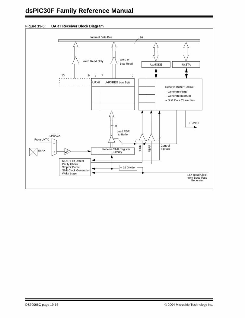
dsPIC30F Family Reference Manual
Figure 19-5: UART Receiver Block Diagram
URX8 UxRXREG Low Byte
Load RSR
UxMODE
Receive Buffer Control
– Generate Flags
– Generate Interrupt
UxRXIF
UxRX
· START bit Detect
Receive Shift Register
16 Divider
ControlSignals
16X Baud Clockfrom Baud Rate
Generator
UxSTA
– Shift Data Characters
to Buffer
9
(UxRSR) PE
RR
FE
RR
· Parity Check· Stop bit Detect· Shift Clock Generation· Wake Logic
16Internal Data Bus
1
0
LPBACKFrom UxTX
15 9 8 7 0
Word Read Only Word or
Byte Read
DS70066C-page 19-16 © 2004 Microchip Technology Inc.

Section 19. UARTU
AR
T
19
19.6.4 Setup for UART Reception
Steps to follow when setting up a Reception:
1. Initialize the UxBRG register for the appropriate baud rate (Section 19.3 “UART BaudRate Generator (BRG)”).
2. Set the number of data bits, number of Stop bits and parity selection by writing to thePDSEL<1:0> (UxMODE<2:1>) and STSEL (UxMODE<0>) bits.
3. If interrupts are desired, then set the UxRXIE bit in the corresponding Interrupt EnableControl register (IEC). Specify the interrupt priority for the interrupt using theUxRXIP<2:0> control bits in the corresponding Interrupt Priority Control register (IPC).Also, select the Receive Interrupt mode by writing to the URXISEL<1:0> (UxSTA<7:6>)bits.
4. Enable the UART module by setting the UARTEN (UxMODE<15>) bit.5. Receive interrupts will depend on the URXISEL<1:0> control bit settings. If receive
interrupts are not enabled, the user can poll the URXDA bit. The UxRXIF bit should becleared in the software routine that services the UART receive interrupt.
6. Read data from the receive buffer. If 9-bit transmission has been selected, read a word.Otherwise, read a byte. The URXDA status bit (UxSTA<0>) will be set whenever data isavailable in the buffer.
Figure 19-6: UART Reception
Figure 19-7: UART Reception with Receive Overrun
Startbit bit1bit0 bit7 bit0Stop
bit
Startbit bit7 Stop
bit
UxRX
RIDLE bit
Character 1 to UxRXREG
Character 2 to UxRXREG
Note: This timing diagram shows 2 characters received on the UxRX input.
UxRXIF(URXISEL = 0x)
Startbit bit7/8bit1bit0 bit7/8 bit0Stop
bit
Startbit
Startbitbit7/8 Stop
bitUxRX
OERR bit
RIDLE bit
Character 1,2,3,4stored in Receive
Character 5held in UxRSR
Stopbit
Character 1 Characters 2,3,4,5 Character 6
FIFO
OERR Cleared by User
Note: This diagram shows 6 characters received without the user reading the input buffer. The 5th character received is held in the receive shift register. An overrun error occurs at the start of the 6th character.
© 2004 Microchip Technology Inc. DS70066C-page 19-17
dsPIC30F Family Reference Manual
19.7 Using the UART for 9-bit Communication
A typical multi-processor communication protocol will differentiate between data bytes andaddress/control bytes. A common scheme is to use a 9th data bit to identify whether a data byteis address or data information. If the 9th bit is set, the data is processed as address or controlinformation. If the 9th bit is cleared, the received data word is processed as data associated withthe previous address/control byte.
The protocol operates as follows:
• The master device transmits a data word with the 9th bit set. The data word contains the address of a slave device.
• All slave devices in the communication chain receive the address word and check the slave address value.
• The slave device that was addressed will receive and process subsequent data bytes sent by the master device. All other slave devices will discard subsequent data bytes until a new address word (9th bit set) is received.
19.7.1 ADDEN Control Bit
The UART receiver has an Address Detect mode which allows it to ignore data words with the9th bit cleared. This reduces the interrupt overhead, since data words with the 9th bit cleared arenot buffered. This feature is enabled by setting the ADDEN bit (UxSTA<5>).
The UART must be configured for 9-bit data to use the Address Detect mode. The ADDEN bithas no effect when the receiver is configured in 8-bit Data mode.
19.7.2 Setup for 9-bit Transmit
The setup procedure for 9-bit transmission is identical to the 8-bit Transmit modes, exceptthat PDSEL<1:0> (UxMODE<2:1) should be set to ‘11’ (see Section 19.5.3 “Setup for UARTTransmit”).
Word writes should be performed to the UxTXREG register (starts transmission).
DS70066C-page 19-18 © 2004 Microchip Technology Inc.
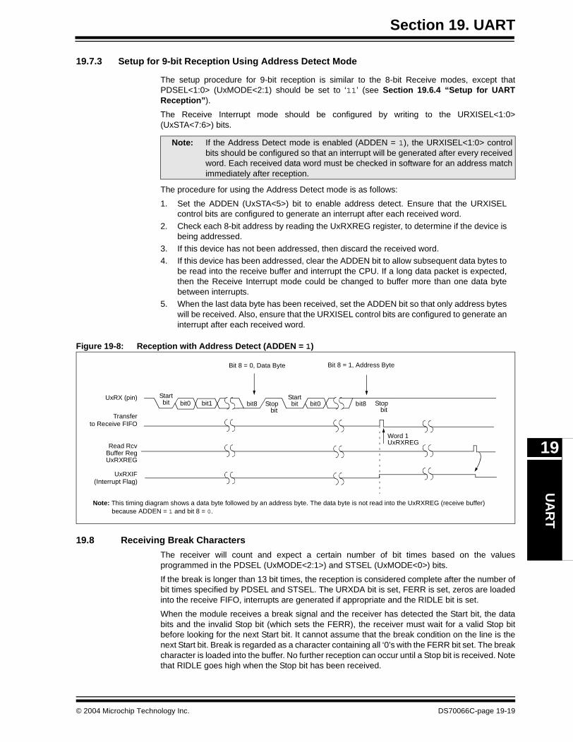
Section 19. UARTU
AR
T
19
19.7.3 Setup for 9-bit Reception Using Address Detect Mode
The setup procedure for 9-bit reception is similar to the 8-bit Receive modes, except thatPDSEL<1:0> (UxMODE<2:1) should be set to ‘11’ (see Section 19.6.4 “Setup for UARTReception”).
The Receive Interrupt mode should be configured by writing to the URXISEL<1:0>(UxSTA<7:6>) bits.
The procedure for using the Address Detect mode is as follows:
1. Set the ADDEN (UxSTA<5>) bit to enable address detect. Ensure that the URXISELcontrol bits are configured to generate an interrupt after each received word.
2. Check each 8-bit address by reading the UxRXREG register, to determine if the device isbeing addressed.
3. If this device has not been addressed, then discard the received word.4. If this device has been addressed, clear the ADDEN bit to allow subsequent data bytes to
be read into the receive buffer and interrupt the CPU. If a long data packet is expected,then the Receive Interrupt mode could be changed to buffer more than one data bytebetween interrupts.
5. When the last data byte has been received, set the ADDEN bit so that only address byteswill be received. Also, ensure that the URXISEL control bits are configured to generate aninterrupt after each received word.
Figure 19-8: Reception with Address Detect (ADDEN = 1)
19.8 Receiving Break Characters
The receiver will count and expect a certain number of bit times based on the valuesprogrammed in the PDSEL (UxMODE<2:1>) and STSEL (UxMODE<0>) bits.
If the break is longer than 13 bit times, the reception is considered complete after the number ofbit times specified by PDSEL and STSEL. The URXDA bit is set, FERR is set, zeros are loadedinto the receive FIFO, interrupts are generated if appropriate and the RIDLE bit is set.
When the module receives a break signal and the receiver has detected the Start bit, the databits and the invalid Stop bit (which sets the FERR), the receiver must wait for a valid Stop bitbefore looking for the next Start bit. It cannot assume that the break condition on the line is thenext Start bit. Break is regarded as a character containing all ‘0’s with the FERR bit set. The breakcharacter is loaded into the buffer. No further reception can occur until a Stop bit is received. Notethat RIDLE goes high when the Stop bit has been received.
Note: If the Address Detect mode is enabled (ADDEN = 1), the URXISEL<1:0> controlbits should be configured so that an interrupt will be generated after every receivedword. Each received data word must be checked in software for an address matchimmediately after reception.
Startbit bit1bit0 bit8 bit0Stop
bit
Startbit bit8 Stop
bit
UxRX (pin)
Read RcvBuffer RegUxRXREG
UxRXIF(Interrupt Flag)
Word 1UxRXREG
Bit 8 = 0, Data Byte Bit 8 = 1, Address Byte
Transferto Receive FIFO
Note: This timing diagram shows a data byte followed by an address byte. The data byte is not read into the UxRXREG (receive buffer) because ADDEN = 1 and bit 8 = 0.
© 2004 Microchip Technology Inc. DS70066C-page 19-19
dsPIC30F Family Reference Manual
19.9 Initialization
Example 19-2 is an initialization routine for the Transmitter/Receiver in 8-bit mode. Example 19-3shows an initialization of the Addressable UART in 9-bit Address Detect mode. In both examples,the value to load into the UxBRG register is dependent on the desired baud rate and the devicefrequency.
Example 19-2: 8-bit Transmit/Receive (UART1)
Example 19-3: 8-bit Transmit/Receive (UART1), Address Detect Enabled
Note: The UTXEN bit should not be set until the UARTEN bit has been set. Otherwise,UART transmissions will not be enabled.
MOV #baudrate,W0 ; Set Baudrate MOV W0,U1BRG BSET IPC2,#U1TXIP2 ; Set UART TX interrupt priority BCLR IPC2,#U1TXIP1 ; BCLR IPC2,#U1TXIP0 ; BSET IPC2,#U1RXIP2 ; Set UART RX interrupt priority BCLR IPC2,#U1RXIP1 ; BCLR IPC2,#U1RXIP0 ;
CLR U1STA
MOV #0x8800,W0 ; Enable UART for 8-bit data, ; no parity, 1 STOP bit, ; no wakeup MOV W0,U1MODE
BSET U1STA,#UTXEN ; Enable transmit
BSET IEC0,#U1TXIE ; Enable transmit interrupts BSET IEC0,#U1RXIE ; Enable receive interrupts
MOV #baudrate,W0 ; Set Baudrate MOV W0,U1BRG
BSET IPC2,#U1TXIP2 ; Set UART TX interrupt priority BCLR IPC2,#U1TXIP1 ; BCLR IPC2,#U1TXIP0 ; BSET IPC2,#U1RXIP2 ; Set UART RX interrupt priority BCLR IPC2,#U1RXIP1 ; BCLR IPC2,#U1RXIP0 ;
BSET U1STA,#ADDEN ; Enable address detect
MOV #0x8883,W0 ; UART1 enabled for 9-bit data, ; no parity, 1 STOP bit, ; wakeup enabled MOV W0,U1MODE
BSET U1STA,#UTXEN ; Enable transmit
BSET IEC0,#U1TXIE ; Enable transmit interrupts BSET IEC0,#U1RXIE ; Enable receive interrupts
DS70066C-page 19-20 © 2004 Microchip Technology Inc.

Section 19. UARTU
AR
T
19
19.10 Other Features of the UART
19.10.1 UART in Loopback Mode
Setting the LPBACK bit enables this special mode, in which the UxTX output is internallyconnected to the UxRX input. When configured for the Loopback mode, the UxRX pin isdisconnected from the internal UART receive logic. However, the UxTX pin still functionsnormally.
To select this mode:
1. Configure UART for the desired mode of operation.
2. Set LPBACK = 1 to enable Loopback mode.3. Enable transmission as defined in Section 19.5 “UART Transmitter”.
The Loopback mode is dependent on the UEN<1:0> bits, as shown in Table 19-2.
Table 19-2: Loopback Mode Pin Function
19.10.2 Auto Baud Support
To allow the system to determine baud rates of the received characters, the UxRX input can beinternally connected to a selected input capture channel. When the ABAUD bit (UxMODE<5>) isset, the UxRX pin is internally connected to the input capture channel. The ICx pin isdisconnected from the input capture channel.
The input capture channel used for auto baud support is device specific. Please refer to thedevice data sheet for further details.
This mode is only valid when the UART is enabled (UARTEN = 1) and the Loopback mode isdisabled (LPBACK = 0). Also, the user must program the capture module to detect the falling andrising edges of the Start bit.
19.11 UART Operation During CPU Sleep and Idle Modes
The UART does not function in Sleep mode. If entry into Sleep mode occurs while a transmissionis in progress, then the transmission is aborted and the UxTX pin is driven to logic ‘1’. Similarly,if entry into Sleep mode occurs while a reception is in progress, then the reception is aborted.
The UART can be used to optionally wake the dsPIC device from Sleep mode on the detectionof a Start bit. If the WAKE bit (UxSTA<7>) is set, the device is in Sleep mode, and the UARTreceive interrupt is enabled (UxRXIE = 1), then a falling edge on the UxRX pin will generate areceive interrupt. The Receive Interrupt Select mode bit (URXISEL) has no effect for thisfunction. The UARTEN bit must be set in order to generate a wake-up interrupt.
The USIDL bit (UxMODE<13>) selects if the module will stop operation when the device entersIdle mode, or whether the module will continue normal operation in Idle mode. If USIDL = 0, themodule will continue normal operation during Idle mode. If USIDL = 1, the module will stop in Idlemode. Any transmission or reception in progress will be aborted.
UEN<1:0> Pin Function, LPBACK = 1
00 UxRX input connected to UxTX; UxTX pin functions; UxRX pin ignored; UxCTS/UxRTS unused
01 UxRX input connected to UxTX; UxTX pin functions; UxRX pin ignored;UxRTS pin functions, UxCTS unused
10 UxRX input connected to UxTX; UxTX pin functions; UxRX pin ignored;UxRTS pin functions, UxCTS input connected to UxRTS; UxCTS pin ignored
11 UxRX input connected to UxTX; UxTX pin functions; UxRX pin ignored;BCLK pin functions; UxCTS/UxRTS unused
© 2004 Microchip Technology Inc. DS70066C-page 19-21

dsPIC30F Family Reference Manual
19.1
2 R
egis
ters
Ass
oci
ated
wit
h U
AR
T M
od
ule
Tab
le 1
9-3:
Reg
iste
rs A
sso
ciat
ed w
ith
UA
RT
1S
FR
Nam
eB
it 1
5B
it 1
4B
it 1
3B
it 1
2B
it 1
1B
it 1
0B
it 9
Bit
8B
it 7
Bit
6B
it 5
Bit
4B
it 3
Bit
2B
it 1
Bit
0R
eset
Sta
te
U1M
OD
EU
AR
TE
N—
US
IDL
—re
serv
edA
LTIO
rese
rved
rese
rved
WA
KE
LPB
AC
KA
BA
UD
——
PD
SE
L<1:
0>S
TS
EL
0000 0000 0000 0000
U1S
TAU
TX
ISE
L—
——
UT
XB
RK
UT
XE
NU
TX
BF
TR
MT
UR
XIS
EL<
1:0>
AD
DE
NR
IDLE
PE
RR
FE
RR
OE
RR
UR
XD
A0000 0001 0001 0000
U1T
XR
EG
——
——
——
—U
TX
8Tr
ansm
it R
egis
ter
0000 0000 0000 0000
U1R
XR
EG
——
——
——
—U
RX
8R
ecei
ve R
egis
ter
0000 0000 0000 0000
U1B
RG
Bau
d R
ate
Gen
erat
or P
resc
aler
0000 0000 0000 0000
IFS
0C
NIF
MI2
CIF
SI2
CIF
NV
MIF
AD
IFU
1TX
IFU
1RX
IFS
PI1
IFT
3IF
T2I
FO
C2I
FIC
2IF
T1I
FO
C1I
FIC
1IF
INT
00000 0000 0000 0000
IEC
0C
NIE
MI2
CIE
SI2
CIE
NV
MIE
AD
IEU
1TX
IEU
1RX
IES
PI1
IET
3IE
T2I
EO
C2I
EIC
2IE
T1I
EO
C1I
EIC
1IE
INT
0IE
0000 0000 0000 0000
IPC
2—
AD
IP<
2:0>
—U
1TX
IP<
2:0>
—U
1RX
IP<
2:0>
—S
PI1
IP<
2:0>
0100 0100 0100 0100
No
te:
The
reg
iste
rs a
ssoc
iate
d w
ith U
AR
T1
are
show
n fo
r re
fere
nce.
See
the
devi
ce d
ata
shee
t for
the
regi
ster
s as
soci
ated
with
oth
er U
AR
T m
odul
es.
DS70066C-page 19-22 © 2004 Microchip Technology Inc.
Section 19. UARTU
AR
T
19
19.13 Design Tips
Question 1: The data I transmit with the UART does not get received correctly. Whatcould cause this?
Answer: The most common reason for reception errors is that an incorrect value has beencalculated for the UART baud rate generator. Ensure the value written to the UxBRG register iscorrect.
Question 2: I am getting framing errors even though the signal on the UART receive pinlooks correct. What are the possible causes?
Answer: Ensure the following control bits have been setup correctly:
• UxBRG: UART Baud Rate register
• PDSEL<1:0>: Parity and Data Size Selection bits• STSEL: Stop bit Selection
© 2004 Microchip Technology Inc. DS70066C-page 19-23

dsPIC30F Family Reference Manual
19.14 Related Application Notes
This section lists application notes that are related to this section of the manual. Theseapplication notes may not be written specifically for the dsPIC30F Product Family, but theconcepts are pertinent and could be used with modification and possible limitations. The currentapplication notes related to the UART module are:
Title Application Note #
Serial Port Utilities Implementing Table Read and Table Write AN547
Note: Please visit the Microchip web site (www.microchip.com) for additional ApplicationNotes and code examples for the dsPIC30F Family of devices.
DS70066C-page 19-24 © 2004 Microchip Technology Inc.
Section 19. UARTU
AR
T
19
19.15 Revision History
Revision A
This is the initial released revision of this document.
Revision B
Revision B has been expanded to include a full description of the dsPIC30F UART module.
Revision C
This revision incorporates all known errata at the time of this document update.
© 2004 Microchip Technology Inc. DS70066C-page 19-25

dsPIC30F Family Reference Manual
NOTES:
DS70066C-page 19-26 © 2004 Microchip Technology Inc.

Section 20. Serial Peripheral Interface (SPI™)
Serial P
eriph
eralIn
terface (SP
I)
20
HIGHLIGHTS
This section of the manual contains the following major topics:
20.1 Introduction .................................................................................................................. 20-2
20.2 Status and Control Registers ....................................................................................... 20-420.3 Modes of Operation ..................................................................................................... 20-720.4 SPI Master Mode Clock Frequency ........................................................................... 20-19
20.5 Operation in Power Save Modes ............................................................................... 20-2020.6 Special Function Registers Associated with SPI Modules......................................... 20-2220.7 Related Application Notes.......................................................................................... 20-23
20.8 Revision History ......................................................................................................... 20-24
© 2004 Microchip Technology Inc. DS70067C-page 20-1
dsPIC30F Family Reference Manual
20.1 Introduction
The Serial Peripheral Interface (SPI) module is a synchronous serial interface useful forcommunicating with other peripheral or microcontroller devices. These peripheral devices maybe Serial EEPROMs, shift registers, display drivers, A/D converters, etc. The SPI module iscompatible with Motorola's SPI and SIOP interfaces.
Depending on the variant, the dsPIC30F family offers one or two SPI modules on a single device.SPI1 and SPI2 are functionally identical. The SPI2 module is available in many of the higher pincount packages (64-pin and higher), while the SPI1 module is available on all devices.
The SPI serial port consists of the following Special Function Registers (SFR):
• SPIxBUF: Address in SFR space that is used to buffer data to be transmitted and data that is received. This address is shared by the SPIxTXB and SPIxRXB registers.
• SPIxCON: A control register that configures the module for various modes of operation. • SPIxSTAT: A status register that indicates various status conditions.
In addition, there is a 16-bit shift register, SPIxSR, that is not memory mapped. It is used forshifting data in and out of the SPI port.
The memory mapped SFR, SPIxBUF, is the SPI Data Receive/Transmit register. Internally, theSPIxBUF register actually comprises of two separate registers - SPIxTXB and SPIxRXB. TheReceive Buffer register, SPIxRXB, and the Transmit Buffer register, SPIxTXB, are two unidirec-tional 16-bit registers. These registers share the SFR address named SPIxBUF. If a user writesdata to be transmitted to the SPIxBUF address, internally the data gets written to the SPIxTXBregister. Similarly, when the user reads the received data from SPIxBUF, internally the data isread from the SPIxRXB register. This double-buffering of transmit and receive operations allowscontinuous data transfers in the background. Transmission and reception occur simultaneously.
The SPI serial interface consists of the following four pins:
• SDIx: serial data input• SDOx: serial data output• SCKx: shift clock input or output• SSx: active low slave select or frame synchronization I/O pulse
Note: In this section, the SPI modules are referred together as SPIx or separately as SPI1and SPI2. Special Function registers will follow a similar notation. For example,SPIxCON refers to the control register for the SPI1 or SPI2 module.
Note: The user cannot write to the SPIxTXB register or read from the SPIxRXB registerdirectly. All reads and writes are performed on the SPIxBUF register.
Note: The SPI module can be configured to operate using 3 or 4 pins. In the 3-pin mode,the SSx pin is not used.
DS70067C-page 20-2 © 2004 Microchip Technology Inc.
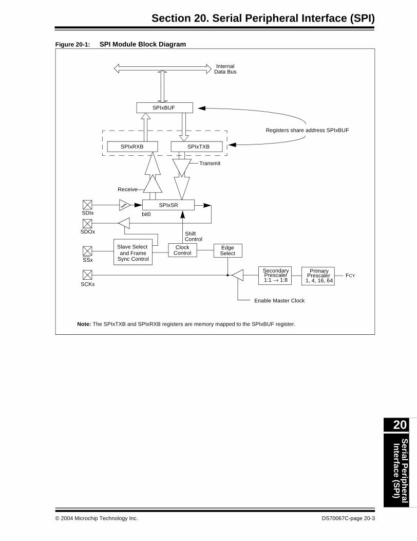
Section 20. Serial Peripheral Interface (SPI)S
erial Perip
heral
Interface (S
PI)
20
Figure 20-1: SPI Module Block Diagram
InternalData Bus
SDIx
SDOx
SSx
SCKx
SPIxSR
bit0
ShiftControl
EdgeSelect
FCYPrimary
1, 4, 16, 64
Enable Master Clock
PrescalerSecondaryPrescaler1:1 → 1:8
Slave Select
Sync Control
ClockControl
Transmit
SPIxRXB
Receive
and Frame
Note: The SPIxTXB and SPIxRXB registers are memory mapped to the SPIxBUF register.
Registers share address SPIxBUF
SPIxTXB
SPIxBUF
© 2004 Microchip Technology Inc. DS70067C-page 20-3
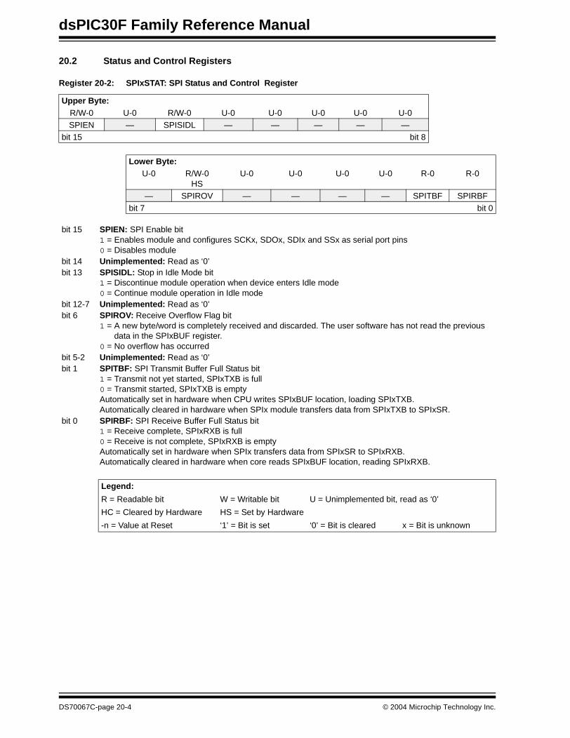
dsPIC30F Family Reference Manual
20.2 Status and Control Registers
Register 20-2: SPIxSTAT: SPI Status and Control Register
Upper Byte:R/W-0 U-0 R/W-0 U-0 U-0 U-0 U-0 U-0SPIEN — SPISIDL — — — — —
bit 15 bit 8
Lower Byte:U-0 R/W-0
HSU-0 U-0 U-0 U-0 R-0 R-0
— SPIROV — — — — SPITBF SPIRBF
bit 7 bit 0
bit 15 SPIEN: SPI Enable bit1 = Enables module and configures SCKx, SDOx, SDIx and SSx as serial port pins0 = Disables module
bit 14 Unimplemented: Read as ‘0’bit 13 SPISIDL: Stop in Idle Mode bit
1 = Discontinue module operation when device enters Idle mode0 = Continue module operation in Idle mode
bit 12-7 Unimplemented: Read as ‘0’bit 6 SPIROV: Receive Overflow Flag bit
1 = A new byte/word is completely received and discarded. The user software has not read the previousdata in the SPIxBUF register.
0 = No overflow has occurredbit 5-2 Unimplemented: Read as ‘0’bit 1 SPITBF: SPI Transmit Buffer Full Status bit
1 = Transmit not yet started, SPIxTXB is full0 = Transmit started, SPIxTXB is emptyAutomatically set in hardware when CPU writes SPIxBUF location, loading SPIxTXB.Automatically cleared in hardware when SPIx module transfers data from SPIxTXB to SPIxSR.
bit 0 SPIRBF: SPI Receive Buffer Full Status bit1 = Receive complete, SPIxRXB is full0 = Receive is not complete, SPIxRXB is emptyAutomatically set in hardware when SPIx transfers data from SPIxSR to SPIxRXB.Automatically cleared in hardware when core reads SPIxBUF location, reading SPIxRXB.
Legend:
R = Readable bit W = Writable bit U = Unimplemented bit, read as ‘0’
HC = Cleared by Hardware HS = Set by Hardware
-n = Value at Reset ‘1’ = Bit is set ‘0’ = Bit is cleared x = Bit is unknown
DS70067C-page 20-4 © 2004 Microchip Technology Inc.
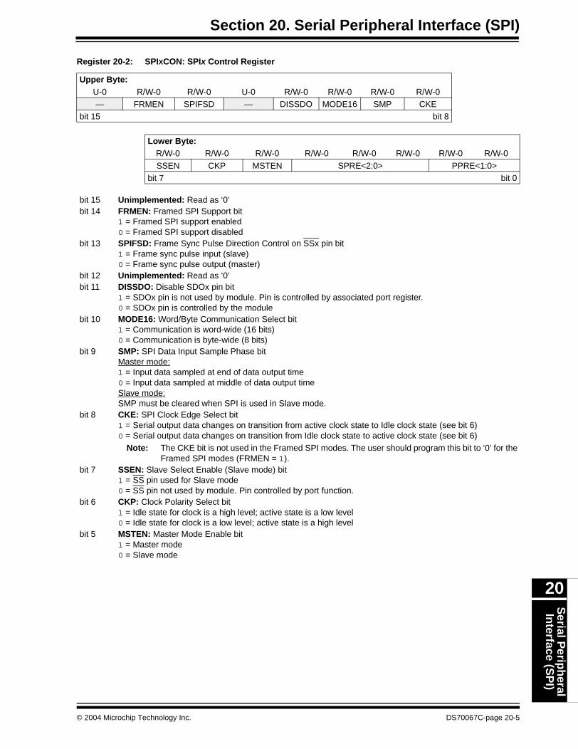
Section 20. Serial Peripheral Interface (SPI)S
erial Perip
heral
Interface (S
PI)
20
Register 20-2: SPIXCON: SPIx Control Register
Upper Byte:U-0 R/W-0 R/W-0 U-0 R/W-0 R/W-0 R/W-0 R/W-0— FRMEN SPIFSD — DISSDO MODE16 SMP CKE
bit 15 bit 8
Lower Byte:R/W-0 R/W-0 R/W-0 R/W-0 R/W-0 R/W-0 R/W-0 R/W-0
SSEN CKP MSTEN SPRE<2:0> PPRE<1:0>bit 7 bit 0
bit 15 Unimplemented: Read as ‘0’bit 14 FRMEN: Framed SPI Support bit
1 = Framed SPI support enabled0 = Framed SPI support disabled
bit 13 SPIFSD: Frame Sync Pulse Direction Control on SSx pin bit1 = Frame sync pulse input (slave)0 = Frame sync pulse output (master)
bit 12 Unimplemented: Read as ‘0’bit 11 DISSDO: Disable SDOx pin bit
1 = SDOx pin is not used by module. Pin is controlled by associated port register.0 = SDOx pin is controlled by the module
bit 10 MODE16: Word/Byte Communication Select bit1 = Communication is word-wide (16 bits)0 = Communication is byte-wide (8 bits)
bit 9 SMP: SPI Data Input Sample Phase bitMaster mode:1 = Input data sampled at end of data output time0 = Input data sampled at middle of data output timeSlave mode:SMP must be cleared when SPI is used in Slave mode.
bit 8 CKE: SPI Clock Edge Select bit1 = Serial output data changes on transition from active clock state to Idle clock state (see bit 6)0 = Serial output data changes on transition from Idle clock state to active clock state (see bit 6)
Note: The CKE bit is not used in the Framed SPI modes. The user should program this bit to ‘0’ for theFramed SPI modes (FRMEN = 1).
bit 7 SSEN: Slave Select Enable (Slave mode) bit1 = SS pin used for Slave mode0 = SS pin not used by module. Pin controlled by port function.
bit 6 CKP: Clock Polarity Select bit1 = Idle state for clock is a high level; active state is a low level0 = Idle state for clock is a low level; active state is a high level
bit 5 MSTEN: Master Mode Enable bit1 = Master mode0 = Slave mode
© 2004 Microchip Technology Inc. DS70067C-page 20-5
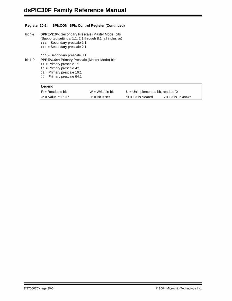
dsPIC30F Family Reference Manual
Register 20-2: SPIXCON: SPIx Control Register (Continued)
bit 4-2 SPRE<2:0>: Secondary Prescale (Master Mode) bits(Supported settings: 1:1, 2:1 through 8:1, all inclusive)111 = Secondary prescale 1:1110 = Secondary prescale 2:1...000 = Secondary prescale 8:1
bit 1-0 PPRE<1:0>: Primary Prescale (Master Mode) bits11 = Primary prescale 1:110 = Primary prescale 4:101 = Primary prescale 16:100 = Primary prescale 64:1
Legend:
R = Readable bit W = Writable bit U = Unimplemented bit, read as ‘0’
-n = Value at POR ‘1’ = Bit is set ‘0’ = Bit is cleared x = Bit is unknown
DS70067C-page 20-6 © 2004 Microchip Technology Inc.
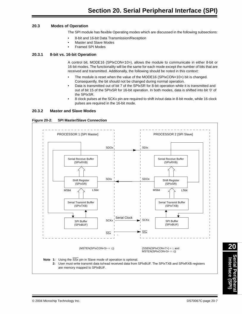
Section 20. Serial Peripheral Interface (SPI)S
erial Perip
heral
Interface (S
PI)
20
20.3 Modes of Operation
The SPI module has flexible Operating modes which are discussed in the following subsections:
• 8-bit and 16-bit Data Transmission/Reception• Master and Slave Modes• Framed SPI Modes
20.3.1 8-bit vs. 16-bit Operation
A control bit, MODE16 (SPIxCON<10>), allows the module to communicate in either 8-bit or16-bit modes. The functionality will be the same for each mode except the number of bits that arereceived and transmitted. Additionally, the following should be noted in this context:
• The module is reset when the value of the MODE16 (SPIxCON<10>) bit is changed. Consequently, the bit should not be changed during normal operation.
• Data is transmitted out of bit 7 of the SPIxSR for 8-bit operation while it is transmitted and out of bit 15 of the SPIxSR for 16-bit operation. In both modes, data is shifted into bit ‘0’ of the SPIxSR.
• 8 clock pulses at the SCKx pin are required to shift in/out data in 8-bit mode, while 16 clock pulses are required in the 16-bit mode.
20.3.2 Master and Slave Modes
Figure 20-2: SPI Master/Slave Connection
Serial Receive Buffer(SPIxRXB)
Shift Register(SPIxSR)
LSbitMSbit
SDIx
SDOx
PROCESSOR 2 [SPI Slave]
SCKx
SSx
Serial Transmit Buffer(SPIxTXB)
Serial Receive Buffer(SPIxRXB)
Shift Register(SPIxSR)
MSbit LSbit
SDOx
SDIx
PROCESSOR 1 [SPI Master]
Serial Clock
.
(SSEN(SPIxCON<7>) = 1 andMSTEN(SPIxCON<5> = 0))
Note 1: Using the SSx pin in Slave mode of operation is optional.2: User must write transmit data to/read received data from SPIxBUF. The SPIxTXB and SPIxRXB registers
are memory mapped to SPIxBUF.
SSx
SCKx
Serial Transmit Buffer(SPIxTXB)
(MSTEN(SPIxCON<5> = 1))
SPI Buffer(SPIxBUF)
SPI Buffer(SPIxBUF)
© 2004 Microchip Technology Inc. DS70067C-page 20-7

dsPIC30F Family Reference Manual
20.3.2.1 Master Mode
The following steps should be taken to set up the SPI module for the Master mode of operation:
1. If using interrupts:
• Clear the SPIxIF bit in the respective IFSn register.• Set the SPIxIE bit in the respective IECn register.• Write the SPIxIP bits in the respective IPCn register.
2. Write the desired settings to the SPIxCON register with MSTEN (SPIxCON<5>) = 1. 3. Clear the SPIROV bit (SPIxSTAT<6>).4. Enable SPI operation by setting the SPIEN bit (SPIxSTAT<15>).
5. Write the data to be transmitted to the SPIxBUF register. Transmission (and Reception)will start as soon as data is written to the SPIxBUF register.
In Master mode, the system clock is prescaled and then used as the serial clock. The prescalingis based on the settings in the PPRE<1:0> (SPIxCON<1:0>) and SPRE<1:0> (SPIxCON<4:2>)bits. The serial clock is output via the SCKx pin to slave devices. Clock pulses are only generatedwhen there is data to be transmitted. For further information, refer to Section 20.4 “SPI MasterMode Clock Frequency”.
The CKP and CKE bits determine on which edge of the clock, data transmission occurs.
Both data to be transmitted and data that is received are respectively written into or read fromthe SPIxBUF register.
The following describes the SPI module operation in Master mode:
1. Once the module is set up for Master mode of operation and enabled, data to betransmitted is written to the SPIxBUF register. The SPITBF (SPIxSTAT<1>) bit is set.
2. The contents of SPIxTXB are moved to the shift register, SPIxSR, and the SPITBF bit iscleared by the module.
3. A series of 8/16 clock pulses shifts out 8/16 bits of transmit data from the SPIxSR to theSDOx pin and simultaneously shifts in the data at the SDIx pin into the SPIxSR.
4. When the transfer is complete, the following events will occur:• The interrupt flag bit, SPIxIF, is set. SPI interrupts can be enabled by setting the
interrupt enable bit SPIxIE. The SPIxIF flag is not cleared automatically by the hardware.
• Also, when the ongoing transmit and receive operation is completed, the contents of the SPIxSR are moved to the SPIxRXB register.
• The SPIRBF (SPIxSTAT<0>) bit is set by the module, indicating that the receive buffer is full. Once the SPIxBUF register is read by the user code, the hardware clears the SPIRBF bit.
5. If the SPIRBF bit is set (receive buffer is full) when the SPI module needs to transfer datafrom SPIxSR to SPIxRXB, the module will set the SPIROV (SPIxSTAT<6>) bit, indicatingan overflow condition.
6. Data to be transmitted can be written to SPIxBUF by the user software at any time as longas the SPITBF (SPIxSTAT<1>) bit is clear. The write can occur while SPIxSR is shiftingout the previously written data, allowing continuous transmission.
Note: The SPIxSR register cannot be written into directly by the user. All writes to theSPIxSR register are performed through the SPIxBUF register.
DS70067C-page 20-8 © 2004 Microchip Technology Inc.

Section 20. Serial Peripheral Interface (SPI)S
erial Perip
heral
Interface (S
PI)
20
Figure 20-3: SPI Master Mode Operation
SCKx(CKP = 0
SCKx(CKP = 1
SCKx(CKP = 0
SCKx(CKP = 1
4 Clockmodes
InputSample
InputSample
SDIx
bit7 bit0
SDOx bit7 bit6 bit5 bit4 bit3 bit2 bit1 bit0
bit7 bit0
SDIx
SPIxIF
(SMP = 1)
(SMP = 0)
(SMP = 1)
CKE = 1)
CKE = 0)
CKE = 0)
CKE = 0)
(SMP = 0)
User writesto SPIxBUF
SDOx bit7 bit6 bit5 bit4 bit3 bit2 bit1 bit0
(CKE = 0)
(CKE = 1)
1 instruction cycle latency to setSPIxIF flag bit
Note 1: Four SPI Clock modes shown to demonstrate CKP (SPIxCON<6>) and CKE (SPIxCON<8>) bit functionality only.Only one of the four modes can be chosen for operation.
2: SDI and input sample shown for two different values of the SMP (SPIxCON<9>) bit, for demonstration purposesonly. Only one of the two configurations of the SMP bit can be chosen during operation.
3: If there are no pending transmissions, SPIxTXB is transferred to SPIxSR as soon as the user writes to SPIxBUF.4: Operation for 8-bit mode shown. The 16-bit mode is similar.
SPIxSR movedinto SPIxRXB
User reads SPIxBUF
(clock output at the SCKx
pin in Master mode)
(SPIxSTAT<0>)
SPITBF
SPIxTXB to SPIxSR
User writes new data
during transmission
SPIRBF
Two modesavailablefor SMPcontrolbit (seeNote 4)
© 2004 Microchip Technology Inc. DS70067C-page 20-9
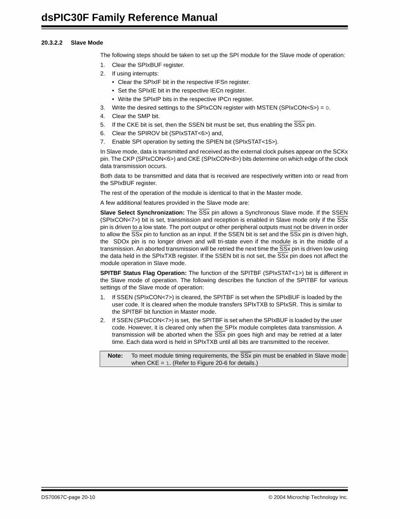
dsPIC30F Family Reference Manual
20.3.2.2 Slave Mode
The following steps should be taken to set up the SPI module for the Slave mode of operation:
1. Clear the SPIxBUF register.
2. If using interrupts:• Clear the SPIxIF bit in the respective IFSn register.• Set the SPIxIE bit in the respective IECn register.
• Write the SPIxIP bits in the respective IPCn register.3. Write the desired settings to the SPIxCON register with MSTEN (SPIxCON<5>) = 0. 4. Clear the SMP bit.
5. If the CKE bit is set, then the SSEN bit must be set, thus enabling the SSx pin.6. Clear the SPIROV bit (SPIxSTAT<6>) and,7. Enable SPI operation by setting the SPIEN bit (SPIxSTAT<15>).
In Slave mode, data is transmitted and received as the external clock pulses appear on the SCKxpin. The CKP (SPIxCON<6>) and CKE (SPIxCON<8>) bits determine on which edge of the clockdata transmission occurs.
Both data to be transmitted and data that is received are respectively written into or read fromthe SPIxBUF register.
The rest of the operation of the module is identical to that in the Master mode.
A few additional features provided in the Slave mode are:
Slave Select Synchronization: The SSx pin allows a Synchronous Slave mode. If the SSEN(SPIxCON<7>) bit is set, transmission and reception is enabled in Slave mode only if the SSxpin is driven to a low state. The port output or other peripheral outputs must not be driven in orderto allow the SSx pin to function as an input. If the SSEN bit is set and the SSx pin is driven high,the SDOx pin is no longer driven and will tri-state even if the module is in the middle of atransmission. An aborted transmission will be retried the next time the SSx pin is driven low usingthe data held in the SPIxTXB register. If the SSEN bit is not set, the SSx pin does not affect themodule operation in Slave mode.
SPITBF Status Flag Operation: The function of the SPITBF (SPIxSTAT<1>) bit is different inthe Slave mode of operation. The following describes the function of the SPITBF for varioussettings of the Slave mode of operation:
1. If SSEN (SPIxCON<7>) is cleared, the SPITBF is set when the SPIxBUF is loaded by theuser code. It is cleared when the module transfers SPIxTXB to SPIxSR. This is similar tothe SPITBF bit function in Master mode.
2. If SSEN (SPIxCON<7>) is set, the SPITBF is set when the SPIxBUF is loaded by the usercode. However, it is cleared only when the SPIx module completes data transmission. Atransmission will be aborted when the SSx pin goes high and may be retried at a latertime. Each data word is held in SPIxTXB until all bits are transmitted to the receiver.
Note: To meet module timing requirements, the SSx pin must be enabled in Slave modewhen CKE = 1. (Refer to Figure 20-6 for details.)
DS70067C-page 20-10 © 2004 Microchip Technology Inc.

Section 20. Serial Peripheral Interface (SPI)S
erial Perip
heral
Interface (S
PI)
20
Figure 20-4: SPI Slave Mode Operation: Slave Select Pin Disabled
SCKx Input(CKP = 1
SCKx Input(CKP = 0
InputSample
SDIx Input
bit7 bit0
SDOx bit7 bit6 bit5 bit4 bit3 bit2 bit1 bit0
SPIxIF
(SMP = 0)
CKE = 0)
CKE = 0)
(SMP = 0)
User writes toSPIxBUF
SPISR toSPIxRXB
SPITBF
SPIRBF
Output
Note 1: Two SPI Clock modes shown only to demonstrate CKP (SPIxCON<6>) and CKE (SPIxCON<8>) bit functionality.Any combination of CKP and CKE bits can be chosen for module operation.
2: If there are no pending transmissions or a transmission in progress, SPIxBUF is transferred to SPIxSR as soonas the user writes to SPIxBUF.
3: Operation for 8-bit mode shown. The 16-bit mode is similar.
1 instruction cycle latency to setSPIxIF flag bit
© 2004 Microchip Technology Inc. DS70067C-page 20-11
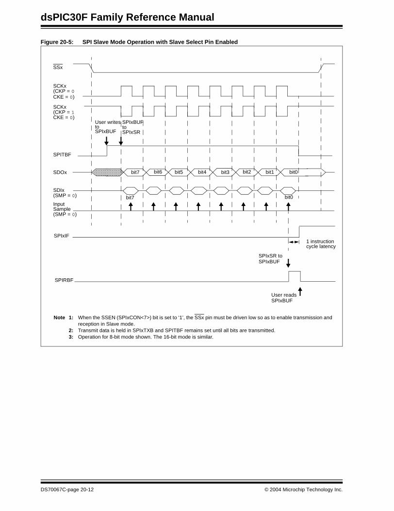
dsPIC30F Family Reference Manual
Figure 20-5: SPI Slave Mode Operation with Slave Select Pin Enabled
SCKx(CKP = 1
SCKx(CKP = 0
InputSample
SDIx
bit7 bit0
SDOx bit7 bit6 bit5 bit4 bit3 bit2 bit1 bit0
SPIxIF
(SMP = 0)
CKE = 0)
CKE = 0)
(SMP = 0)
User writes
SPIxBUF
SPIxSR toSPIxBUF
SSx
Note 1: When the SSEN (SPIxCON<7>) bit is set to ‘1’, the SSx pin must be driven low so as to enable transmission andreception in Slave mode.
2: Transmit data is held in SPIxTXB and SPITBF remains set until all bits are transmitted.3: Operation for 8-bit mode shown. The 16-bit mode is similar.
User readsSPIxBUF
SPIRBF
1 instructioncycle latency
SPITBF
SPIxBUF to SPIxSR
to
DS70067C-page 20-12 © 2004 Microchip Technology Inc.
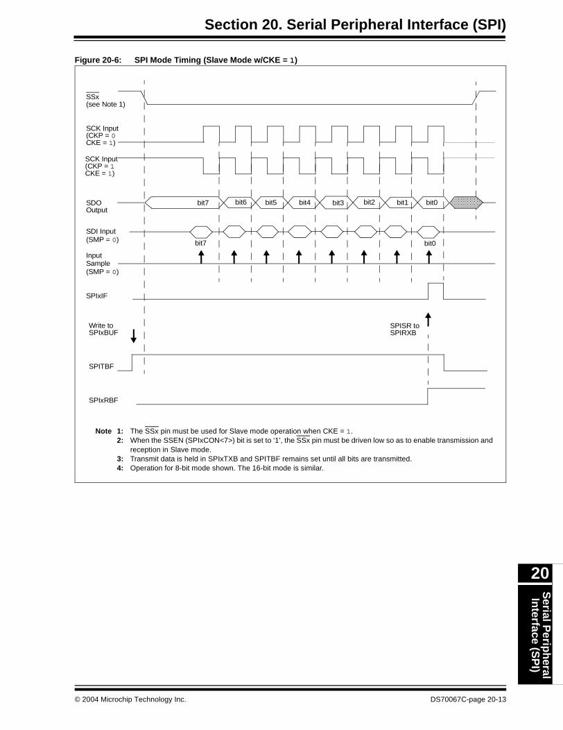
Section 20. Serial Peripheral Interface (SPI)S
erial Perip
heral
Interface (S
PI)
20
Figure 20-6: SPI Mode Timing (Slave Mode w/CKE = 1)
SCK Input(CKP = 1
SCK Input(CKP = 0
InputSample
SDI Input
bit7 bit0
SDO bit7 bit6 bit5 bit4 bit3 bit2 bit1 bit0
SPIxIF
(SMP = 0)
CKE = 1)
CKE = 1)
(SMP = 0)
Write toSPIxBUF
SPISR toSPIRXB
SSx(see Note 1)
SPITBF
SPIxRBF
Output
Note 1: The SSx pin must be used for Slave mode operation when CKE = 1.2: When the SSEN (SPIxCON<7>) bit is set to ‘1’, the SSx pin must be driven low so as to enable transmission and
reception in Slave mode.3: Transmit data is held in SPIxTXB and SPITBF remains set until all bits are transmitted.4: Operation for 8-bit mode shown. The 16-bit mode is similar.
© 2004 Microchip Technology Inc. DS70067C-page 20-13
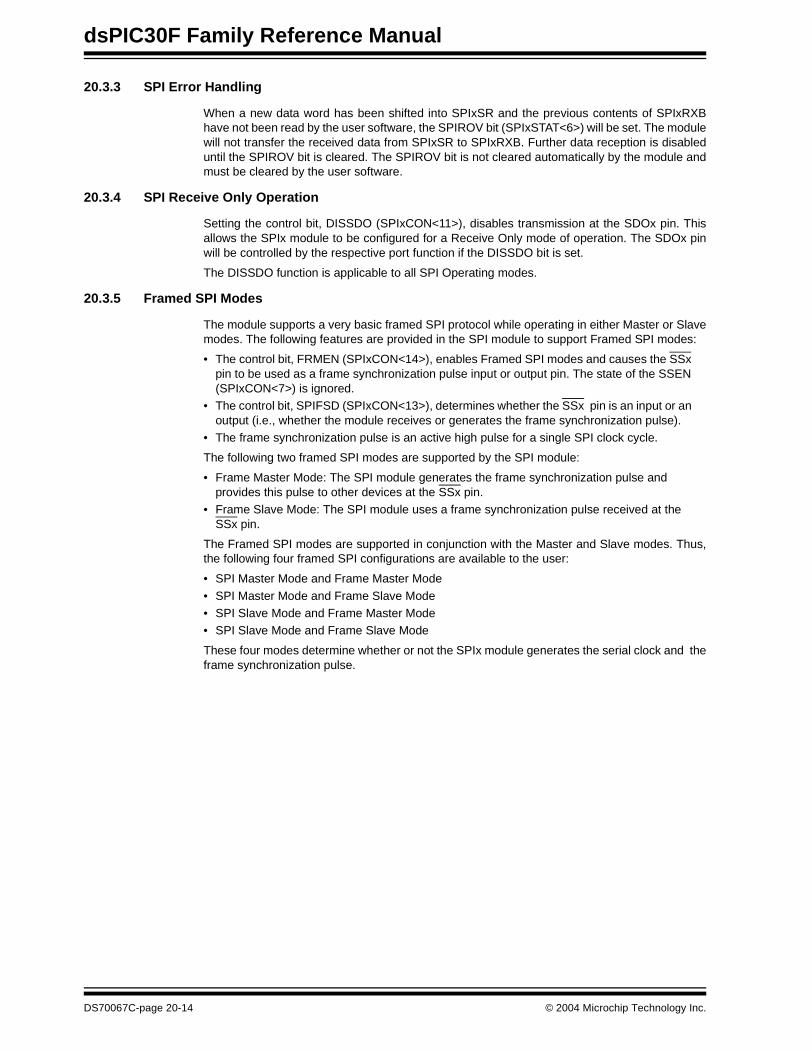
dsPIC30F Family Reference Manual
20.3.3 SPI Error Handling
When a new data word has been shifted into SPIxSR and the previous contents of SPIxRXBhave not been read by the user software, the SPIROV bit (SPIxSTAT<6>) will be set. The modulewill not transfer the received data from SPIxSR to SPIxRXB. Further data reception is disableduntil the SPIROV bit is cleared. The SPIROV bit is not cleared automatically by the module andmust be cleared by the user software.
20.3.4 SPI Receive Only Operation
Setting the control bit, DISSDO (SPIxCON<11>), disables transmission at the SDOx pin. Thisallows the SPIx module to be configured for a Receive Only mode of operation. The SDOx pinwill be controlled by the respective port function if the DISSDO bit is set.
The DISSDO function is applicable to all SPI Operating modes.
20.3.5 Framed SPI Modes
The module supports a very basic framed SPI protocol while operating in either Master or Slavemodes. The following features are provided in the SPI module to support Framed SPI modes:
• The control bit, FRMEN (SPIxCON<14>), enables Framed SPI modes and causes the SSx pin to be used as a frame synchronization pulse input or output pin. The state of the SSEN (SPIxCON<7>) is ignored.
• The control bit, SPIFSD (SPIxCON<13>), determines whether the SSx pin is an input or an output (i.e., whether the module receives or generates the frame synchronization pulse).
• The frame synchronization pulse is an active high pulse for a single SPI clock cycle.
The following two framed SPI modes are supported by the SPI module:
• Frame Master Mode: The SPI module generates the frame synchronization pulse and provides this pulse to other devices at the SSx pin.
• Frame Slave Mode: The SPI module uses a frame synchronization pulse received at the SSx pin.
The Framed SPI modes are supported in conjunction with the Master and Slave modes. Thus,the following four framed SPI configurations are available to the user:
• SPI Master Mode and Frame Master Mode
• SPI Master Mode and Frame Slave Mode• SPI Slave Mode and Frame Master Mode• SPI Slave Mode and Frame Slave Mode
These four modes determine whether or not the SPIx module generates the serial clock and theframe synchronization pulse.
DS70067C-page 20-14 © 2004 Microchip Technology Inc.
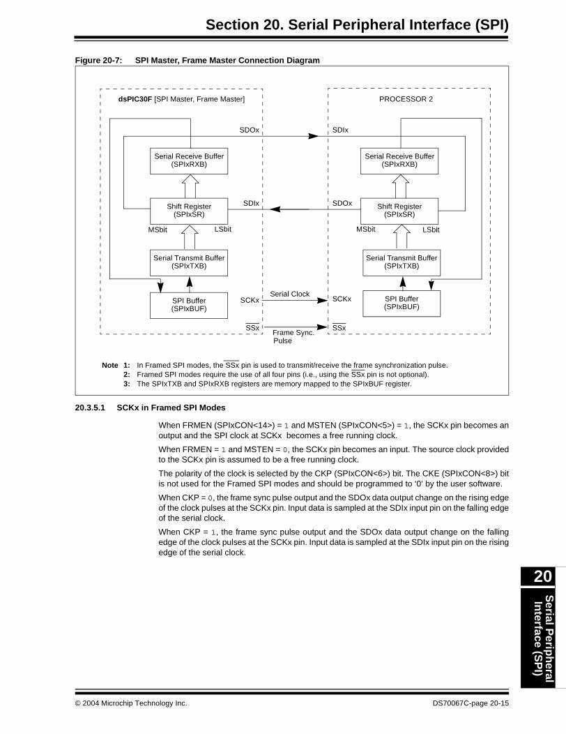
Section 20. Serial Peripheral Interface (SPI)S
erial Perip
heral
Interface (S
PI)
20
Figure 20-7: SPI Master, Frame Master Connection Diagram
20.3.5.1 SCKx in Framed SPI Modes
When FRMEN (SPIxCON<14>) = 1 and MSTEN (SPIxCON<5>) = 1, the SCKx pin becomes anoutput and the SPI clock at SCKx becomes a free running clock.
When FRMEN = 1 and MSTEN = 0, the SCKx pin becomes an input. The source clock providedto the SCKx pin is assumed to be a free running clock.
The polarity of the clock is selected by the CKP (SPIxCON<6>) bit. The CKE (SPIxCON<8>) bitis not used for the Framed SPI modes and should be programmed to ‘0’ by the user software.
When CKP = 0, the frame sync pulse output and the SDOx data output change on the rising edgeof the clock pulses at the SCKx pin. Input data is sampled at the SDIx input pin on the falling edgeof the serial clock.
When CKP = 1, the frame sync pulse output and the SDOx data output change on the fallingedge of the clock pulses at the SCKx pin. Input data is sampled at the SDIx input pin on the risingedge of the serial clock.
Serial Receive Buffer(SPIxRXB)
Shift Register(SPIxSR)
MSbit LSbit
SDOx
SDIx
dsPIC30F [SPI Master, Frame Master]
Serial Receive Buffer(SPIxRXB)
Shift Register(SPIxSR)
LSbitMSbit
SDIx
SDOx
PROCESSOR 2
Serial Clock
Note 1: In Framed SPI modes, the SSx pin is used to transmit/receive the frame synchronization pulse.2: Framed SPI modes require the use of all four pins (i.e., using the SSx pin is not optional).3: The SPIxTXB and SPIxRXB registers are memory mapped to the SPIxBUF register.
SCKx
SSxSSx
SCKx
Serial Transmit Buffer(SPIxTXB)
Serial Transmit Buffer(SPIxTXB)
Frame Sync.Pulse
SPI Buffer(SPIxBUF)
SPI Buffer(SPIxBUF)
© 2004 Microchip Technology Inc. DS70067C-page 20-15
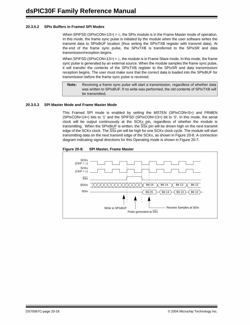
dsPIC30F Family Reference Manual
20.3.5.2 SPIx Buffers in Framed SPI Modes
When SPIFSD (SPIxCON<13>) = 0, the SPIx module is in the Frame Master mode of operation.In this mode, the frame sync pulse is initiated by the module when the user software writes thetransmit data to SPIxBUF location (thus writing the SPIxTXB register with transmit data). Atthe end of the frame sync pulse, the SPIxTXB is transferred to the SPIxSR and datatransmission/reception begins.
When SPIFSD (SPIxCON<13>) = 1, the module is in Frame Slave mode. In this mode, the framesync pulse is generated by an external source. When the module samples the frame sync pulse,it will transfer the contents of the SPIxTXB register to the SPIxSR and data transmission/reception begins. The user must make sure that the correct data is loaded into the SPIxBUF fortransmission before the frame sync pulse is received.
20.3.5.3 SPI Master Mode and Frame Master Mode
This Framed SPI mode is enabled by setting the MSTEN (SPIxCON<5>) and FRMEN(SPIxCON<14>) bits to ‘1’ and the SPIFSD (SPIxCON<13>) bit to ‘0’. In this mode, the serialclock will be output continuously at the SCKx pin, regardless of whether the module istransmitting. When the SPIxBUF is written, the SSx pin will be driven high on the next transmitedge of the SCKx clock. The SSx pin will be high for one SCKx clock cycle. The module will starttransmitting data on the next transmit edge of the SCKx, as shown in Figure 20-8. A connectiondiagram indicating signal directions for this Operating mode is shown in Figure 20-7.
Figure 20-8: SPI Master, Frame Master
Note: Receiving a frame sync pulse will start a transmission, regardless of whether datawas written to SPIxBUF. If no write was performed, the old contents of SPIxTXB willbe transmitted.
SCKx
SSx
SDOx
(CKP = 0)
Bit 15 Bit 14 Bit 13 Bit 12
SDIx
Bit 15 Bit 14 Bit 13 Bit 12
Write to SPIxBUF Receive Samples at SDIx
Pulse generated at SSx
SCKx(CKP = 1)
DS70067C-page 20-16 © 2004 Microchip Technology Inc.
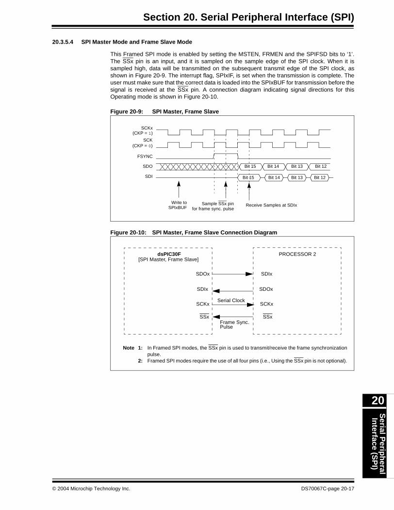
Section 20. Serial Peripheral Interface (SPI)S
erial Perip
heral
Interface (S
PI)
20
20.3.5.4 SPI Master Mode and Frame Slave Mode
This Framed SPI mode is enabled by setting the MSTEN, FRMEN and the SPIFSD bits to ‘1’.The SSx pin is an input, and it is sampled on the sample edge of the SPI clock. When it issampled high, data will be transmitted on the subsequent transmit edge of the SPI clock, asshown in Figure 20-9. The interrupt flag, SPIxIF, is set when the transmission is complete. Theuser must make sure that the correct data is loaded into the SPIxBUF for transmission before thesignal is received at the SSx pin. A connection diagram indicating signal directions for thisOperating mode is shown in Figure 20-10.
Figure 20-9: SPI Master, Frame Slave
Figure 20-10: SPI Master, Frame Slave Connection Diagram
SCK
FSYNC
SDO
(CKP = 0)
Bit 15 Bit 14 Bit 13 Bit 12
SDI
Sample SSx pinfor frame sync. pulse
Receive Samples at SDIx
Bit 15 Bit 14 Bit 13 Bit 12
Write toSPIxBUF
SCKx(CKP = 1)
SDOx
SDIx
dsPIC30F
Serial Clock
Note 1: In Framed SPI modes, the SSx pin is used to transmit/receive the frame synchronizationpulse.
2: Framed SPI modes require the use of all four pins (i.e., Using the SSx pin is not optional).
SSx
SCKx
Frame Sync.Pulse
SDIx
SDOx
PROCESSOR 2
SSx
SCKx
[SPI Master, Frame Slave]
© 2004 Microchip Technology Inc. DS70067C-page 20-17
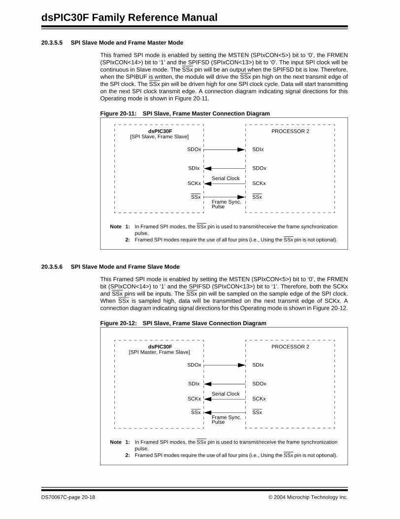
dsPIC30F Family Reference Manual
20.3.5.5 SPI Slave Mode and Frame Master Mode
This framed SPI mode is enabled by setting the MSTEN (SPIxCON<5>) bit to ‘0’, the FRMEN(SPIxCON<14>) bit to ‘1’ and the SPIFSD (SPIxCON<13>) bit to ‘0’. The input SPI clock will becontinuous in Slave mode. The SSx pin will be an output when the SPIFSD bit is low. Therefore,when the SPIBUF is written, the module will drive the SSx pin high on the next transmit edge ofthe SPI clock. The SSx pin will be driven high for one SPI clock cycle. Data will start transmittingon the next SPI clock transmit edge. A connection diagram indicating signal directions for thisOperating mode is shown in Figure 20-11.
Figure 20-11: SPI Slave, Frame Master Connection Diagram
20.3.5.6 SPI Slave Mode and Frame Slave Mode
This Framed SPI mode is enabled by setting the MSTEN (SPIxCON<5>) bit to ‘0’, the FRMENbit (SPIxCON<14>) to ‘1’ and the SPIFSD (SPIxCON<13>) bit to ‘1’. Therefore, both the SCKxand SSx pins will be inputs. The SSx pin will be sampled on the sample edge of the SPI clock.When SSx is sampled high, data will be transmitted on the next transmit edge of SCKx. Aconnection diagram indicating signal directions for this Operating mode is shown in Figure 20-12.
Figure 20-12: SPI Slave, Frame Slave Connection Diagram
SDOx
SDIx
dsPIC30F
Serial Clock
Note 1: In Framed SPI modes, the SSx pin is used to transmit/receive the frame synchronizationpulse.
2: Framed SPI modes require the use of all four pins (i.e., Using the SSx pin is not optional).
SSx
SCKx
Frame Sync.Pulse
SDIx
SDOx
PROCESSOR 2
SSx
SCKx
[SPI Slave, Frame Slave]
SDOx
SDIx
dsPIC30F
Serial Clock
Note 1: In Framed SPI modes, the SSx pin is used to transmit/receive the frame synchronizationpulse.
2: Framed SPI modes require the use of all four pins (i.e., Using the SSx pin is not optional).
SSx
SCKx
Frame Sync.Pulse
SDIx
SDOx
PROCESSOR 2
SSx
SCKx
[SPI Master, Frame Slave]
DS70067C-page 20-18 © 2004 Microchip Technology Inc.
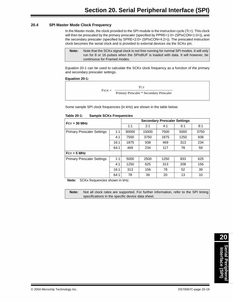
Section 20. Serial Peripheral Interface (SPI)S
erial Perip
heral
Interface (S
PI)
20
20.4 SPI Master Mode Clock Frequency
In the Master mode, the clock provided to the SPI module is the instruction cycle (TCY). This clockwill then be prescaled by the primary prescaler (specified by PPRE<1:0> (SPIxCON<1:0>)), andthe secondary prescaler (specified by SPRE<2:0> (SPIxCON<4:2>)). The prescaled instructionclock becomes the serial clock and is provided to external devices via the SCKx pin.
Equation 20-1 can be used to calculate the SCKx clock frequency as a function of the primaryand secondary prescaler settings.
Equation 20-1:
Some sample SPI clock frequencies (in kHz) are shown in the table below:
Table 20-1: Sample SCKx Frequencies
Note: Note that the SCKx signal clock is not free running for normal SPI modes. It will onlyrun for 8 or 16 pulses when the SPIxBUF is loaded with data. It will however, becontinuous for Framed modes.
Primary Prescaler * Secondary Prescaler
FCY FSCK =
FCY = 30 MHzSecondary Prescaler Settings
1:1 2:1 4:1 6:1 8:1
Primary Prescaler Settings 1:1 30000 15000 7500 5000 3750
4:1 7500 3750 1875 1250 938
16:1 1875 938 469 313 234
64:1 469 234 117 78 59
FCY = 5 MHz
Primary Prescaler Settings 1:1 5000 2500 1250 833 625
4:1 1250 625 313 208 156
16:1 313 156 78 52 39
64:1 78 39 20 13 10
Note: SCKx frequencies shown in kHz.
Note: Not all clock rates are supported. For further information, refer to the SPI timingspecifications in the specific device data sheet.
© 2004 Microchip Technology Inc. DS70067C-page 20-19
dsPIC30F Family Reference Manual
20.5 Operation in Power Save Modes
The dsPIC30FXXXX family of devices has three Power modes:
• Operational mode: The core and peripherals are running.
• Power Save modes: These are invoked by the execution of the PWRSAV instruction. There are two Power Save modes supported in the dsPIC30F family of devices. These are specified in the PWRSAV instruction via a parameter. The two modes are:- Sleep mode: Device clock source and entire device is shut down. This is achieved by
the following instruction.;include device p30fxxxx.inc filePWRSAV #SLEEP_MODE
- Idle mode: Device clock is operational, CPU and selected peripherals are shut down.;include device p30fxxxx.inc filePWRSAV #IDLE_MODE
20.5.1 Sleep Mode
When the device enters Sleep mode, the system clock is disabled.
20.5.1.1 Master Mode Operation
The following are a consequence of entering Sleep mode when the SPIx module is configuredfor master operation:
• The baud rate generator in the SPIx module stops and is reset.• If the SPIx module enters Sleep mode in the middle of a transmission/reception, then the
transmission/reception is aborted. Since there is no automatic way to prevent an entry into Sleep mode if a transmission or reception is pending, the user software must synchronize entry into Sleep with SPI module operation to avoid aborted transmissions.
• The transmitter and receiver will stop in Sleep. The transmitter or receiver does not continue with a partially completed transmission at wake-up.
20.5.1.2 Slave Mode Operation
Since the clock pulses at SCKx are externally provided for Slave mode, the module will continueto function in Sleep mode. It will complete any transactions during the transition into Sleep. Oncompletion of a transaction, the SPIRBF flag is set. Consequently, the SPIxIF bit will be set. IfSPI interrupts are enabled (SPIxIE = 1), the device will wake from Sleep. If the SPI interrupt pri-ority level is greater than the present CPU priority level, code execution will resume at the SPIxinterrupt vector location. Otherwise, code execution will continue with the instruction following thePWRSAV instruction that previously invoked Sleep mode. The module is not reset on enteringSleep mode if it is operating as a slave device.
Register contents are not affected when the SPIx module is going into or coming out of Sleepmode.
20.5.2 Idle Mode
When the device enters Idle mode, the system clock sources remain functional. The SPISIDL bit(SPIxSTAT<13>) selects whether the module will stop or continue functioning on Idle.
• If SPISIDL = 1, the SPI module will stop communication on entering Idle mode. It will operate in the same manner as it does in Sleep mode.
• If SPISID = 0 (default selection), the module will continue operation in Idle mode.
DS70067C-page 20-20 © 2004 Microchip Technology Inc.

Section 20. Serial Peripheral Interface (SPI)S
erial Perip
heral
Interface (S
PI)
20
Table 20-2: Pins Associated with the SPI Modules
Pin NamePin
TypeBufferType
Description
SCK1 I/O CMOS SPI1 module Clock Input or Output SCK2 I/O CMOS SPI2 module Clock Input or Output
SDI1 I CMOS SPI1 module Data Receive pinSDI2 I CMOS SPI2 module Data Receive pinSDO1 O CMOS SPI1 module Data Transmit pin
SDO2 O CMOS SPI2 module Data Transmit pinSS1 I/O CMOS SPI1 module Slave Select Control pin
1) Used to enable transmit/receive in Slave mode,if SSEN (SPI1CON<7>) has been set to ‘1’
2) Used as Frame Sync I/O Pulse when FRMEN andSPIFSD (SPI1CON<14:13>) are set to ‘11’ or ‘10’.
SS2 I/O CMOS SPI2 module Slave Select Control pin1) Used to enable transmit/receive in Slave mode,
if SSEN (SPI2CON<7>) has been set to ‘1’2) Used as Frame Sync I/O Pulse when FRMEN
and SPIFSD (SPI2CON<14:13>) are set to ‘11’ or ‘10’. Legend: CMOS = CMOS compatible input or output, ST = Schmitt Trigger input with
CMOS levels, I = Input, O = Output
© 2004 Microchip Technology Inc. DS70067C-page 20-21

dsPIC30F Family Reference Manual
20.6
Sp
ecia
l Fu
nct
ion
Reg
iste
rs A
sso
ciat
ed w
ith
SP
I Mo
du
les
Tab
le 2
0-3:
SP
I1 R
egis
ter
Map
Tab
le 2
0-4:
SP
I2 R
egis
ter
Map
Tab
le 2
0-5:
SP
I Mo
du
le R
elat
ed In
terr
up
t R
egis
ters
SF
R
Nam
eA
dd
r.B
it 1
5B
it 1
4B
it 1
3B
it 1
2B
it 1
1B
it 1
0B
it 9
Bit
8B
it 7
Bit
6B
it 5
Bit
4B
it 3
Bit
2B
it 1
Bit
0R
eset
Sta
te
SP
I1S
TAT
0220
SP
IEN
—S
PIS
IDL
——
——
——
SP
IRO
V—
——
—S
PIT
BF
SP
IRB
F0000 0000 0000 0000
SP
I1C
ON
0222
—F
RM
EN
SP
IFS
D—
DIS
SD
OM
OD
E16
SM
PC
KE
SS
EN
CK
PM
ST
EN
SP
RE
2S
PR
E1
SP
RE
0P
PR
E1
PP
RE
00000 0000 0000 0000
SP
I1B
UF
0224
Tran
smit
and
Rec
eive
Buf
fer
Add
ress
sha
red
by S
PI1
TX
B a
nd S
PI1
RX
B r
egis
ters
0000 0000 0000 0000
SF
R
Nam
eA
dd
r.B
it 1
5B
it 1
4B
it 1
3B
it 1
2B
it 1
1B
it 1
0B
it 9
Bit
8B
it 7
Bit
6B
it 5
Bit
4B
it 3
Bit
2B
it 1
Bit
0R
eset
Sta
te
SP
I2S
TAT
0226
SP
IEN
—S
PIS
IDL
——
——
——
SP
IRO
V—
——
—S
PIT
BF
SP
IRB
F0000 0000 0000 0000
SP
I2C
ON
0228
—F
RM
EN
SP
IFS
D—
DIS
SD
OM
OD
E16
SM
PC
KE
SS
EN
CK
PM
ST
EN
SP
RE
2S
PR
E1
SP
RE
0P
PR
E1
PP
RE
00000 0000 0000 0000
SP
I2B
UF
022A
Tra
nsm
it an
d R
ecei
ve B
uffe
r A
ddre
ss s
hare
d by
SP
I2T
XB
and
SP
I2R
XB
reg
iste
rs0000 0000 0000 0000
SF
R
Nam
eA
dd
r.B
it 1
5B
it 1
4B
it 1
3B
it 1
2B
it 1
1B
it 1
0B
it 9
Bit
8B
it 7
Bit
6B
it 5
Bit
4B
it 3
Bit
2B
it 1
Bit
0R
eset
Sta
te
INT
CO
N1
0080
NS
TD
IS—
——
—O
VA
TE
OV
BT
EC
OV
TE
——
—S
WT
RA
PO
VR
FLO
WA
DD
RE
RR
ST
KE
RR
—0000 0000 0000 0000
INT
CO
N2
0082
ALT
IVT
DIS
I—
——
—LE
V8F
——
——
INT
4EP
INT
3EP
INT
2EP
INT
1EP
INT
0EP
0000 0000 0000 0000
IFS
000
84C
NIF
MI2
CIF
SI2
CIF
NV
MIF
AD
IFU
1TX
IFU
1RX
IFS
PI1
IFT
3IF
T2I
FO
C2I
FIC
2IF
T1I
FO
C1I
FIC
1IF
INT
00000 0000 0000 0000
IFS
100
86IC
6IF
IC5I
FIC
4IF
IC3I
FC
1IF
SP
I2IF
U2T
XIF
U2R
XIF
INT
2IF
T5I
FT
4IF
OC
4IF
OC
3IF
IC8I
FIC
7IF
INT
1IF
0000 0000 0000 0000
IEC
000
8CC
NIE
MI2
CIE
SI2
CIE
NV
MIE
AD
IEU
1TX
IEU
1RX
IES
PI1
IET
3IE
T2I
EO
C2I
EIC
2IE
T1I
EO
C1I
EIC
1IE
INT
0IE
0000 0000 0000 0000
IEC
100
8EIC
6IE
IC5I
EIC
4IE
IC3I
EC
1IE
SP
I2IE
U2T
XIE
U2R
XIE
INT
2IE
T5I
ET
4IE
OC
4IE
OC
3IE
IC8I
EIC
7IE
INT
1IE
0000 0000 0000 0000
IPC
200
98—
AD
IP<
2:0>
—U
1TX
IP<
2:0>
—U
1RX
IP<
2:0>
—S
PI1
IP<
2:0>
0100 0100 0100 0100
IPC
600
A0
—C
1IP
<2:
0>—
SP
I2IP
<2:
0>—
U2T
XIP
<2:
0>—
U2R
XIP
<2:
0>0100 0100 0100 0100
DS70067C-page 20-22 © 2004 Microchip Technology Inc.
Section 20. Serial Peripheral Interface (SPI)S
erial Perip
heral
Interface (S
PI)
20
20.7 Related Application Notes
This section lists application notes that are related to this section of the manual. Theseapplication notes may not be written specifically for the dsPIC30F Product Family, but theconcepts are pertinent and could be used with modification and possible limitations. The currentapplication notes related to the Serial Peripheral Interface (SPI) module are:
Title Application Note #
Interfacing Microchip’s MCP41XXX/MCP42XXX Digital Potentiometers to a PICmicro® Microcontroller AN746Interfacing Microchip’s MCP3201 Analog-to-Digital Converter to the PICmicro® Microcontroller AN719
Note: Please visit the Microchip web site (www.microchip.com) for additional ApplicationNotes and code examples for the dsPIC30F Family of devices.
© 2004 Microchip Technology Inc. DS70067C-page 20-23
dsPIC30F Family Reference Manual
20.8 Revision History
Revision A
This is the initial released revision of this document.
Revision B
This revision reflects editorial and technical content changes for the dsPIC30F Serial PeripheralInterface (SPI) module.
Revision C
There were no technical content revisions to this section of the manual, however, this section wasupdated to reflect Revision C throughout the manual.
DS70067C-page 20-24 © 2004 Microchip Technology Inc.
Inter-In
tegrated
Circu
it (I 2C)
21
Section 21. Inter-Integrated Circuit™ (I2C™)
HIGHLIGHTS
This section of the manual contains the following major topics:
21.1 Overview ...................................................................................................................... 21-2
21.2 I2C Bus Characteristics................................................................................................ 21-421.3 Control and Status Registers ....................................................................................... 21-721.4 Enabling I2C Operation .............................................................................................. 21-13
21.5 Communicating as a Master in a Single Master Environment ................................... 21-1521.6 Communicating as a Master in a Multi-Master Environment ..................................... 21-2921.7 Communicating as a Slave ........................................................................................ 21-32
21.8 Connection Considerations for I2C Bus ..................................................................... 21-4721.9 Module Operation During PWRSAV Instruction......................................................... 21-4921.10 Effects of a Reset....................................................................................................... 21-49
21.11 Design Tips ................................................................................................................ 21-5021.12 Related Application Notes.......................................................................................... 21-5121.13 Revision History ......................................................................................................... 21-52
© 2005 Microchip Technology Inc. DS70068D-page 21-1
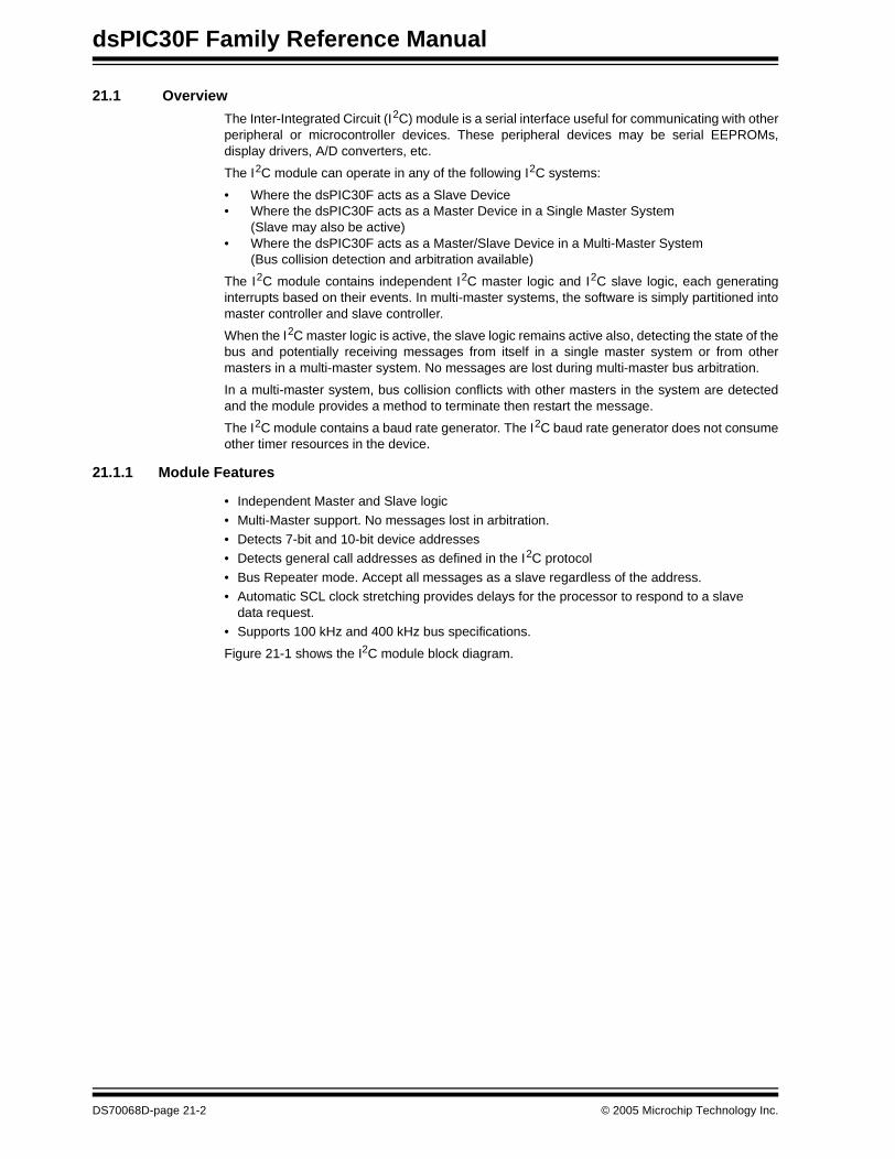
dsPIC30F Family Reference Manual
21.1 Overview
The Inter-Integrated Circuit (I2C) module is a serial interface useful for communicating with otherperipheral or microcontroller devices. These peripheral devices may be serial EEPROMs,display drivers, A/D converters, etc.
The I2C module can operate in any of the following I2C systems:
• Where the dsPIC30F acts as a Slave Device• Where the dsPIC30F acts as a Master Device in a Single Master System
(Slave may also be active)• Where the dsPIC30F acts as a Master/Slave Device in a Multi-Master System
(Bus collision detection and arbitration available)
The I2C module contains independent I2C master logic and I2C slave logic, each generatinginterrupts based on their events. In multi-master systems, the software is simply partitioned intomaster controller and slave controller.
When the I2C master logic is active, the slave logic remains active also, detecting the state of thebus and potentially receiving messages from itself in a single master system or from othermasters in a multi-master system. No messages are lost during multi-master bus arbitration.
In a multi-master system, bus collision conflicts with other masters in the system are detectedand the module provides a method to terminate then restart the message.
The I2C module contains a baud rate generator. The I2C baud rate generator does not consumeother timer resources in the device.
21.1.1 Module Features
• Independent Master and Slave logic
• Multi-Master support. No messages lost in arbitration.• Detects 7-bit and 10-bit device addresses• Detects general call addresses as defined in the I2C protocol
• Bus Repeater mode. Accept all messages as a slave regardless of the address.• Automatic SCL clock stretching provides delays for the processor to respond to a slave
data request.• Supports 100 kHz and 400 kHz bus specifications.
Figure 21-1 shows the I2C module block diagram.
DS70068D-page 21-2 © 2005 Microchip Technology Inc.
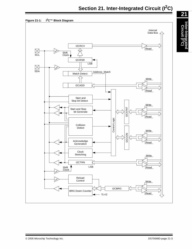
Section 21. Inter-Integrated Circuit (I2C)In
ter-Integ
ratedC
ircuit (I 2C
)21
Figure 21-1: I2C™ Block Diagram
I2CRSR
I2CRCV
InternalData Bus
SCL
SDA
Shift
Match Detect
I2CADD
Start andStop bit Detect
Clock
Address_Match
ClockStretching
I2CTRN
LSBShiftClock
Write
ReadBRG Down Counter
I2CBRG
ReloadControl
TCY/2
Start and Stopbit Generate
Write
Read
AcknowledgeGeneration
CollisionDetect
Write
Read
Write
ReadI2C
CO
N
Write
ReadI2C
STA
T
Con
trol
Log
ic
Read
LSB
© 2005 Microchip Technology Inc. DS70068D-page 21-3
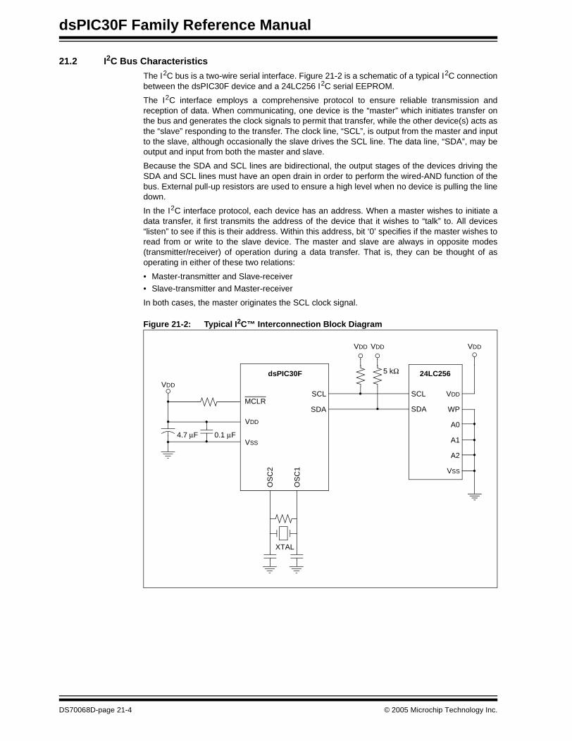
dsPIC30F Family Reference Manual
21.2 I2C Bus Characteristics
The I2C bus is a two-wire serial interface. Figure 21-2 is a schematic of a typical I2C connectionbetween the dsPIC30F device and a 24LC256 I2C serial EEPROM.
The I2C interface employs a comprehensive protocol to ensure reliable transmission andreception of data. When communicating, one device is the “master” which initiates transfer onthe bus and generates the clock signals to permit that transfer, while the other device(s) acts asthe “slave” responding to the transfer. The clock line, “SCL”, is output from the master and inputto the slave, although occasionally the slave drives the SCL line. The data line, “SDA”, may beoutput and input from both the master and slave.
Because the SDA and SCL lines are bidirectional, the output stages of the devices driving theSDA and SCL lines must have an open drain in order to perform the wired-AND function of thebus. External pull-up resistors are used to ensure a high level when no device is pulling the linedown.
In the I2C interface protocol, each device has an address. When a master wishes to initiate adata transfer, it first transmits the address of the device that it wishes to “talk” to. All devices“listen” to see if this is their address. Within this address, bit ‘0’ specifies if the master wishes toread from or write to the slave device. The master and slave are always in opposite modes(transmitter/receiver) of operation during a data transfer. That is, they can be thought of asoperating in either of these two relations:
• Master-transmitter and Slave-receiver• Slave-transmitter and Master-receiver
In both cases, the master originates the SCL clock signal.
Figure 21-2: Typical I2C™ Interconnection Block Diagram
MCLR
VDD
VSS
OS
C1
OS
C2
SCL
SDA
dsPIC30F
4.7 μF
XTAL
0.1 μF
VDD
VSS
SDA
SCL VDD
A0
A1
A2
WP
VDD VDD VDD
5 kΩ 24LC256
DS70068D-page 21-4 © 2005 Microchip Technology Inc.
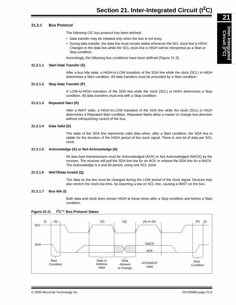
Section 21. Inter-Integrated Circuit (I2C)In
ter-Integ
ratedC
ircuit (I 2C
)21
21.2.1 Bus Protocol
The following I2C bus protocol has been defined:
• Data transfer may be initiated only when the bus is not busy.• During data transfer, the data line must remain stable whenever the SCL clock line is HIGH.
Changes in the data line while the SCL clock line is HIGH will be interpreted as a Start or Stop condition.
Accordingly, the following bus conditions have been defined (Figure 21-3).
21.2.1.1 Start Data Transfer (S)
After a bus Idle state, a HIGH-to-LOW transition of the SDA line while the clock (SCL) is HIGHdetermines a Start condition. All data transfers must be preceded by a Start condition.
21.2.1.2 Stop Data Transfer (P)
A LOW-to-HIGH transition of the SDA line while the clock (SCL) is HIGH determines a Stopcondition. All data transfers must end with a Stop condition.
21.2.1.3 Repeated Start (R)
After a WAIT state, a HIGH-to-LOW transition of the SDA line while the clock (SCL) is HIGHdetermines a Repeated Start condition. Repeated Starts allow a master to change bus directionwithout relinquishing control of the bus.
21.2.1.4 Data Valid (D)
The state of the SDA line represents valid data when, after a Start condition, the SDA line isstable for the duration of the HIGH period of the clock signal. There is one bit of data per SCLclock.
21.2.1.5 Acknowledge (A) or Not-Acknowledge (N)
All data byte transmissions must be Acknowledged (ACK) or Not Acknowledged (NACK) by thereceiver. The receiver will pull the SDA line low for an ACK or release the SDA line for a NACK.The Acknowledge is a one-bit period, using one SCL clock.
21.2.1.6 WAIT/Data Invalid (Q)
The data on the line must be changed during the LOW period of the clock signal. Devices mayalso stretch the clock low time, by asserting a low on SCL line, causing a WAIT on the bus.
21.2.1.7 Bus Idle (I)
Both data and clock lines remain HIGH at those times after a Stop condition and before a Startcondition.
Figure 21-3: I2C™ Bus Protocol States
AddressValid
DataAllowed
to Change
StopCondition
StartCondition
SCL
SDA
(I) (S) (D) (A) or (N) (P) (I)
Data or
(Q)
ACK/NACKValid
NACK
ACK
© 2005 Microchip Technology Inc. DS70068D-page 21-5
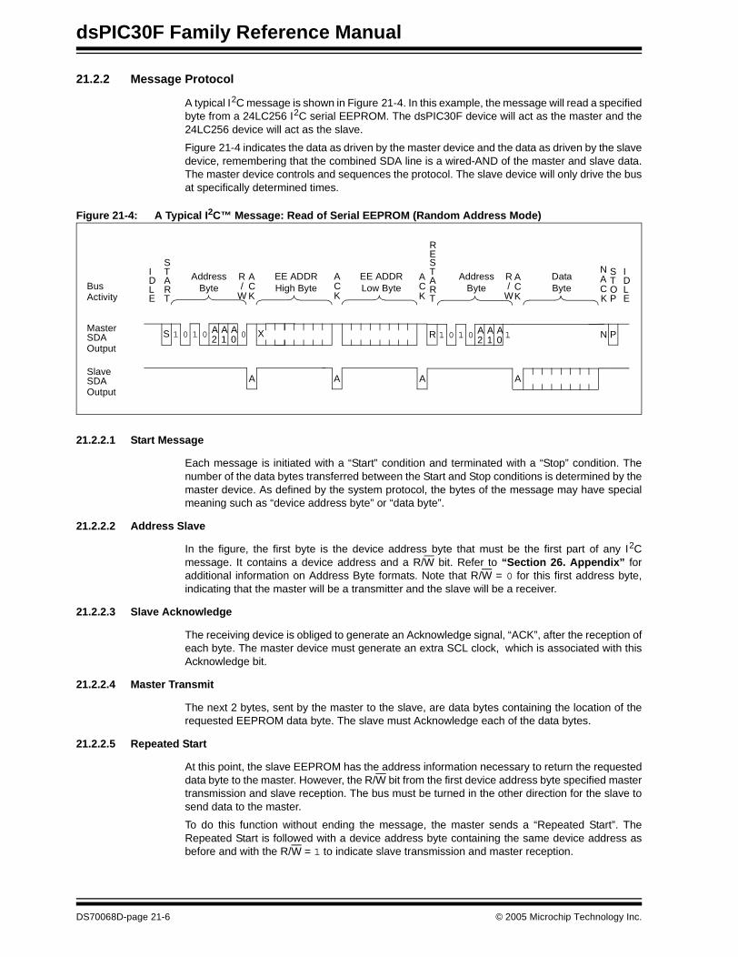
dsPIC30F Family Reference Manual
21.2.2 Message Protocol
A typical I2C message is shown in Figure 21-4. In this example, the message will read a specifiedbyte from a 24LC256 I2C serial EEPROM. The dsPIC30F device will act as the master and the24LC256 device will act as the slave.
Figure 21-4 indicates the data as driven by the master device and the data as driven by the slavedevice, remembering that the combined SDA line is a wired-AND of the master and slave data.The master device controls and sequences the protocol. The slave device will only drive the busat specifically determined times.
Figure 21-4: A Typical I2C™ Message: Read of Serial EEPROM (Random Address Mode)
21.2.2.1 Start Message
Each message is initiated with a “Start” condition and terminated with a “Stop” condition. Thenumber of the data bytes transferred between the Start and Stop conditions is determined by themaster device. As defined by the system protocol, the bytes of the message may have specialmeaning such as “device address byte” or “data byte”.
21.2.2.2 Address Slave
In the figure, the first byte is the device address byte that must be the first part of any I2Cmessage. It contains a device address and a R/W bit. Refer to “Section 26. Appendix” foradditional information on Address Byte formats. Note that R/W = 0 for this first address byte,indicating that the master will be a transmitter and the slave will be a receiver.
21.2.2.3 Slave Acknowledge
The receiving device is obliged to generate an Acknowledge signal, “ACK”, after the reception ofeach byte. The master device must generate an extra SCL clock, which is associated with thisAcknowledge bit.
21.2.2.4 Master Transmit
The next 2 bytes, sent by the master to the slave, are data bytes containing the location of therequested EEPROM data byte. The slave must Acknowledge each of the data bytes.
21.2.2.5 Repeated Start
At this point, the slave EEPROM has the address information necessary to return the requesteddata byte to the master. However, the R/W bit from the first device address byte specified mastertransmission and slave reception. The bus must be turned in the other direction for the slave tosend data to the master.
To do this function without ending the message, the master sends a “Repeated Start”. TheRepeated Start is followed with a device address byte containing the same device address asbefore and with the R/W = 1 to indicate slave transmission and master reception.
X
Bus
MasterSDA
ACK
NAC
ACK
ACK
ACK
STOP
START
AddressByte
EE ADDRHigh Byte
EE ADDRLow Byte
AddressByte
DataByte
START
S 1 0 1 0 A A A 02 1 0 R 1 0 1 0 A A A 12 1 0 P
K
SlaveSDA
Activity
N
AAAA
ER
R/
W
R/
W
Output
Output
IDLE
IDLE
DS70068D-page 21-6 © 2005 Microchip Technology Inc.

Section 21. Inter-Integrated Circuit (I2C)In
ter-Integ
ratedC
ircuit (I 2C
)21
21.2.2.6 Slave Reply
Now the slave transmits the data byte driving the SDA line, while the master continues tooriginate clocks but releases its SDA drive.
21.2.2.7 Master Acknowledge
During reads, a master must terminate data requests to the slave by NOT Acknowledging(generate a “NACK”) on the last byte of the message.
21.2.2.8 Stop Message
The master sends Stop to terminate the message and return the bus to an Idle state.
21.3 Control and Status Registers
The I2C module has six user-accessible registers for I2C operation. The registers are accessiblein either Byte or Word mode. The registers are shown in Figure 21-5 and listed below:
• Control Register (I2CCON): This register allows control of the I2C operation.• Status Register (I2CSTAT): This register contains status flags indicating the module state
during I2C operation.• Receive Buffer Register (I2CRCV): This is the buffer register from which data bytes can be
read. The I2CRCV register is a read only register.• Transmit Register (I2CTRN): This is the transmit register; bytes are written to this register
during a transmit operation. The I2CTRN register is a read/write register.• Address Register (I2CADD): The I2CADD register holds the slave device address. • Baud Rate Generator Reload Register (I2CBRG): Holds the baud rate generator reload
value for the I2C module baud rate generator.
Figure 21-5: I2C™ Programmer’s Model
Bit 7 Bit 0I2CRCV (8 bits)
Bit 7 Bit 0I2CTRN (8 bits)
Bit 8 Bit 0I2CBRG (9 bits)
Bit 15 Bit 0I2CCON (16 bits)
Bit 15 Bit 0I2CSTAT (16 bits)
Bit 9 Bit 0I2CADD (10 bits)
© 2005 Microchip Technology Inc. DS70068D-page 21-7
dsPIC30F Family Reference Manual
Register 21-1 and Register 21-2 define the I2C module Control and Status registers, I2CCONand I2CSTAT.
The I2CTRN is the register to which transmit data is written. This register is used when themodule operates as a master transmitting data to the slave or as a slave sending reply data tothe master. As the message progresses, the I2CTRN register shifts out the individual bits.Because of this, the I2CTRN may not be written to unless the bus is Idle. The I2CTRN may bereloaded while the current data is transmitting.
Data being received by either the master or the slave is shifted into a non-accessible Shiftregister called I2CRSR. When a complete byte is received, the byte transfers to the I2CRCVregister. In receive operations, the I2CRSR and I2CRCV create a double-buffered receiver. Thisallows reception of the next byte to begin before reading the current byte of received data.
If the module receives another complete byte before the software reads the previous byte fromthe I2CRCV register, a receiver overflow occurs and sets the I2COV (I2CCON<6>). The byte inthe I2CRSR is lost.
The I2CADD register holds the slave device address. In 10-bit mode, all bits are relevant. In7-bit addressing mode, only I2CADD<6:0> are relevant. The A10M (I2CCON<10>) specifies theexpected mode of the slave address.
DS70068D-page 21-8 © 2005 Microchip Technology Inc.
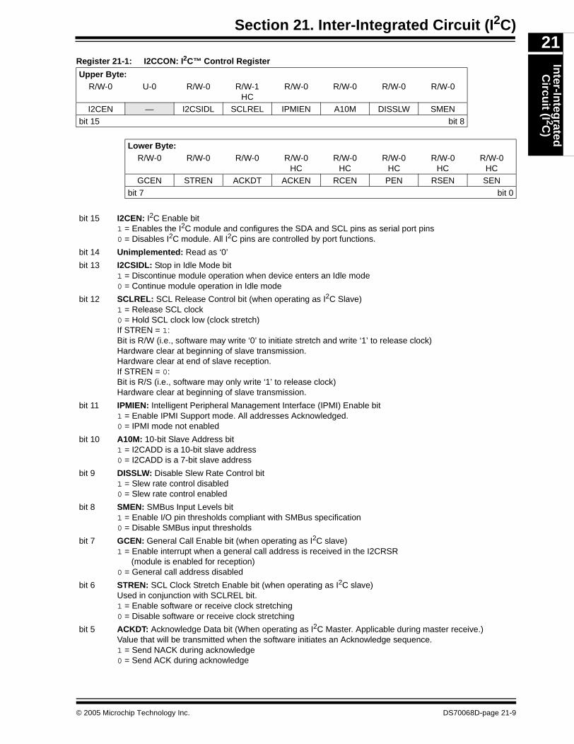
Section 21. Inter-Integrated Circuit (I2C)In
ter-Integ
ratedC
ircuit (I 2C
)21
Register 21-1: I2CCON: I2C™ Control Register
Upper Byte:R/W-0 U-0 R/W-0 R/W-1
HCR/W-0 R/W-0 R/W-0 R/W-0
I2CEN — I2CSIDL SCLREL IPMIEN A10M DISSLW SMENbit 15 bit 8
Lower Byte:R/W-0 R/W-0 R/W-0 R/W-0
HCR/W-0
HCR/W-0
HCR/W-0
HCR/W-0
HCGCEN STREN ACKDT ACKEN RCEN PEN RSEN SEN
bit 7 bit 0
bit 15 I2CEN: I2C Enable bit 1 = Enables the I2C module and configures the SDA and SCL pins as serial port pins0 = Disables I2C module. All I2C pins are controlled by port functions.
bit 14 Unimplemented: Read as ‘0’
bit 13 I2CSIDL: Stop in Idle Mode bit1 = Discontinue module operation when device enters an Idle mode0 = Continue module operation in Idle mode
bit 12 SCLREL: SCL Release Control bit (when operating as I2C Slave)1 = Release SCL clock0 = Hold SCL clock low (clock stretch)If STREN = 1: Bit is R/W (i.e., software may write ‘0’ to initiate stretch and write ‘1’ to release clock)Hardware clear at beginning of slave transmission.Hardware clear at end of slave reception.If STREN = 0: Bit is R/S (i.e., software may only write ‘1’ to release clock)Hardware clear at beginning of slave transmission.
bit 11 IPMIEN: Intelligent Peripheral Management Interface (IPMI) Enable bit1 = Enable IPMI Support mode. All addresses Acknowledged.0 = IPMI mode not enabled
bit 10 A10M: 10-bit Slave Address bit1 = I2CADD is a 10-bit slave address0 = I2CADD is a 7-bit slave address
bit 9 DISSLW: Disable Slew Rate Control bit1 = Slew rate control disabled0 = Slew rate control enabled
bit 8 SMEN: SMBus Input Levels bit1 = Enable I/O pin thresholds compliant with SMBus specification0 = Disable SMBus input thresholds
bit 7 GCEN: General Call Enable bit (when operating as I2C slave)1 = Enable interrupt when a general call address is received in the I2CRSR
(module is enabled for reception)0 = General call address disabled
bit 6 STREN: SCL Clock Stretch Enable bit (when operating as I2C slave)Used in conjunction with SCLREL bit.1 = Enable software or receive clock stretching0 = Disable software or receive clock stretching
bit 5 ACKDT: Acknowledge Data bit (When operating as I2C Master. Applicable during master receive.)Value that will be transmitted when the software initiates an Acknowledge sequence.1 = Send NACK during acknowledge0 = Send ACK during acknowledge
© 2005 Microchip Technology Inc. DS70068D-page 21-9
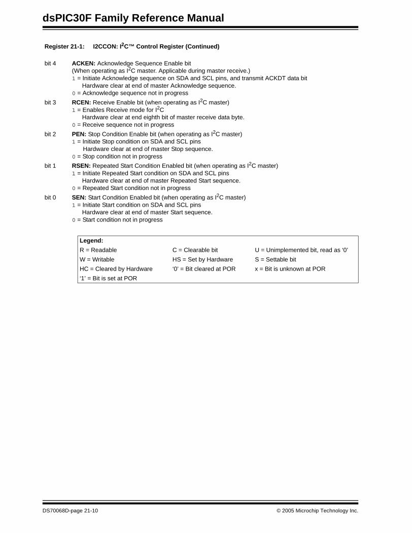
dsPIC30F Family Reference Manual
Register 21-1: I2CCON: I2C™ Control Register (Continued)
bit 4 ACKEN: Acknowledge Sequence Enable bit(When operating as I2C master. Applicable during master receive.)1 = Initiate Acknowledge sequence on SDA and SCL pins, and transmit ACKDT data bit
Hardware clear at end of master Acknowledge sequence.0 = Acknowledge sequence not in progress
bit 3 RCEN: Receive Enable bit (when operating as I2C master)1 = Enables Receive mode for I2C
Hardware clear at end eighth bit of master receive data byte.0 = Receive sequence not in progress
bit 2 PEN: Stop Condition Enable bit (when operating as I2C master)1 = Initiate Stop condition on SDA and SCL pins
Hardware clear at end of master Stop sequence.0 = Stop condition not in progress
bit 1 RSEN: Repeated Start Condition Enabled bit (when operating as I2C master)1 = Initiate Repeated Start condition on SDA and SCL pins
Hardware clear at end of master Repeated Start sequence.0 = Repeated Start condition not in progress
bit 0 SEN: Start Condition Enabled bit (when operating as I2C master)1 = Initiate Start condition on SDA and SCL pins
Hardware clear at end of master Start sequence.0 = Start condition not in progress
Legend:
R = Readable C = Clearable bit U = Unimplemented bit, read as ‘0’
W = Writable HS = Set by Hardware S = Settable bit
HC = Cleared by Hardware ‘0’ = Bit cleared at POR x = Bit is unknown at POR
‘1’ = Bit is set at POR
DS70068D-page 21-10 © 2005 Microchip Technology Inc.
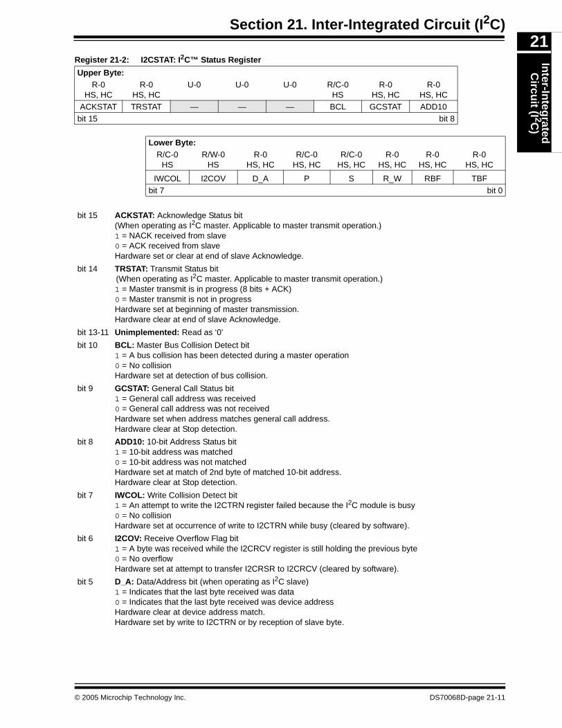
Section 21. Inter-Integrated Circuit (I2C)In
ter-Integ
ratedC
ircuit (I 2C
)21
Register 21-2: I2CSTAT: I2C™ Status Register
Upper Byte:R-0
HS, HCR-0
HS, HCU-0 U-0 U-0 R/C-0
HSR-0
HS, HCR-0
HS, HCACKSTAT TRSTAT — — — BCL GCSTAT ADD10
bit 15 bit 8
Lower Byte:R/C-0
HSR/W-0
HSR-0
HS, HCR/C-0
HS, HCR/C-0
HS, HCR-0
HS, HCR-0
HS, HCR-0
HS, HC
IWCOL I2COV D_A P S R_W RBF TBFbit 7 bit 0
bit 15 ACKSTAT: Acknowledge Status bit (When operating as I2C master. Applicable to master transmit operation.)1 = NACK received from slave0 = ACK received from slaveHardware set or clear at end of slave Acknowledge.
bit 14 TRSTAT: Transmit Status bit (When operating as I2C master. Applicable to master transmit operation.)1 = Master transmit is in progress (8 bits + ACK)0 = Master transmit is not in progressHardware set at beginning of master transmission.Hardware clear at end of slave Acknowledge.
bit 13-11 Unimplemented: Read as ‘0’
bit 10 BCL: Master Bus Collision Detect bit1 = A bus collision has been detected during a master operation0 = No collisionHardware set at detection of bus collision.
bit 9 GCSTAT: General Call Status bit1 = General call address was received0 = General call address was not receivedHardware set when address matches general call address.Hardware clear at Stop detection.
bit 8 ADD10: 10-bit Address Status bit1 = 10-bit address was matched0 = 10-bit address was not matchedHardware set at match of 2nd byte of matched 10-bit address.Hardware clear at Stop detection.
bit 7 IWCOL: Write Collision Detect bit1 = An attempt to write the I2CTRN register failed because the I2C module is busy 0 = No collisionHardware set at occurrence of write to I2CTRN while busy (cleared by software).
bit 6 I2COV: Receive Overflow Flag bit1 = A byte was received while the I2CRCV register is still holding the previous byte0 = No overflowHardware set at attempt to transfer I2CRSR to I2CRCV (cleared by software).
bit 5 D_A: Data/Address bit (when operating as I2C slave)1 = Indicates that the last byte received was data0 = Indicates that the last byte received was device addressHardware clear at device address match.Hardware set by write to I2CTRN or by reception of slave byte.
© 2005 Microchip Technology Inc. DS70068D-page 21-11
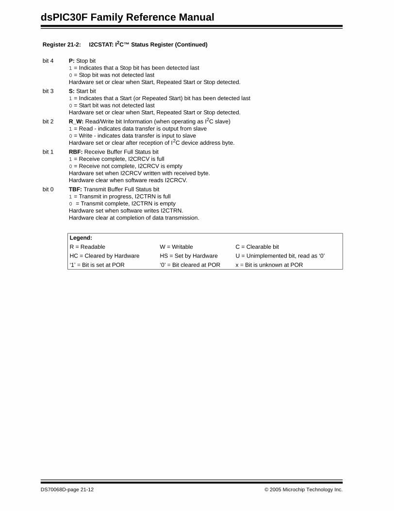
dsPIC30F Family Reference Manual
Register 21-2: I2CSTAT: I2C™ Status Register (Continued)
bit 4 P: Stop bit 1 = Indicates that a Stop bit has been detected last0 = Stop bit was not detected lastHardware set or clear when Start, Repeated Start or Stop detected.
bit 3 S: Start bit 1 = Indicates that a Start (or Repeated Start) bit has been detected last0 = Start bit was not detected lastHardware set or clear when Start, Repeated Start or Stop detected.
bit 2 R_W: Read/Write bit Information (when operating as I2C slave)1 = Read - indicates data transfer is output from slave0 = Write - indicates data transfer is input to slaveHardware set or clear after reception of I2C device address byte.
bit 1 RBF: Receive Buffer Full Status bit 1 = Receive complete, I2CRCV is full0 = Receive not complete, I2CRCV is emptyHardware set when I2CRCV written with received byte.Hardware clear when software reads I2CRCV.
bit 0 TBF: Transmit Buffer Full Status bit1 = Transmit in progress, I2CTRN is full0 = Transmit complete, I2CTRN is emptyHardware set when software writes I2CTRN.Hardware clear at completion of data transmission.
Legend:
R = Readable W = Writable C = Clearable bit
HC = Cleared by Hardware HS = Set by Hardware U = Unimplemented bit, read as ‘0’
‘1’ = Bit is set at POR ‘0’ = Bit cleared at POR x = Bit is unknown at POR
DS70068D-page 21-12 © 2005 Microchip Technology Inc.
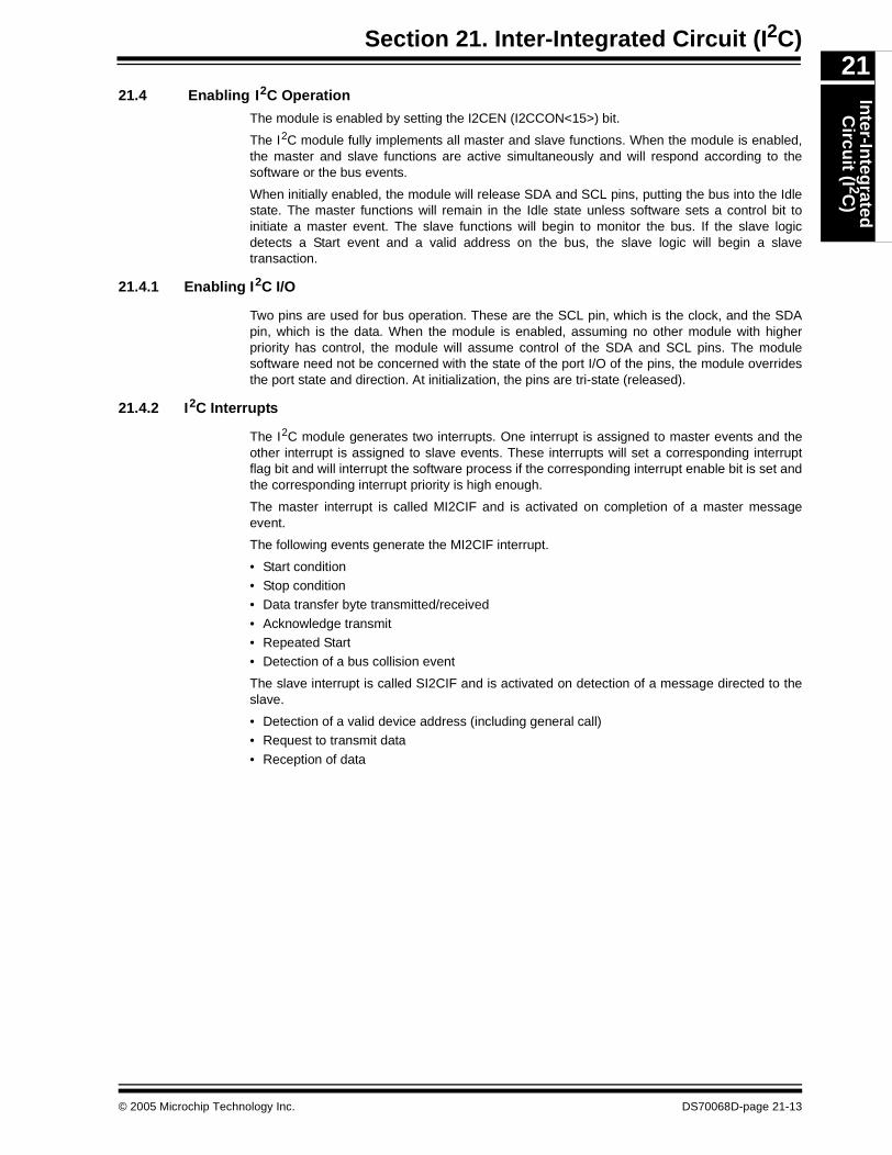
Section 21. Inter-Integrated Circuit (I2C)In
ter-Integ
ratedC
ircuit (I 2C
)21
21.4 Enabling I2C Operation
The module is enabled by setting the I2CEN (I2CCON<15>) bit.
The I2C module fully implements all master and slave functions. When the module is enabled,the master and slave functions are active simultaneously and will respond according to thesoftware or the bus events.
When initially enabled, the module will release SDA and SCL pins, putting the bus into the Idlestate. The master functions will remain in the Idle state unless software sets a control bit toinitiate a master event. The slave functions will begin to monitor the bus. If the slave logicdetects a Start event and a valid address on the bus, the slave logic will begin a slavetransaction.
21.4.1 Enabling I2C I/O
Two pins are used for bus operation. These are the SCL pin, which is the clock, and the SDApin, which is the data. When the module is enabled, assuming no other module with higherpriority has control, the module will assume control of the SDA and SCL pins. The modulesoftware need not be concerned with the state of the port I/O of the pins, the module overridesthe port state and direction. At initialization, the pins are tri-state (released).
21.4.2 I2C Interrupts
The I2C module generates two interrupts. One interrupt is assigned to master events and theother interrupt is assigned to slave events. These interrupts will set a corresponding interruptflag bit and will interrupt the software process if the corresponding interrupt enable bit is set andthe corresponding interrupt priority is high enough.
The master interrupt is called MI2CIF and is activated on completion of a master messageevent.
The following events generate the MI2CIF interrupt.
• Start condition• Stop condition• Data transfer byte transmitted/received
• Acknowledge transmit• Repeated Start• Detection of a bus collision event
The slave interrupt is called SI2CIF and is activated on detection of a message directed to theslave.
• Detection of a valid device address (including general call)• Request to transmit data
• Reception of data
© 2005 Microchip Technology Inc. DS70068D-page 21-13
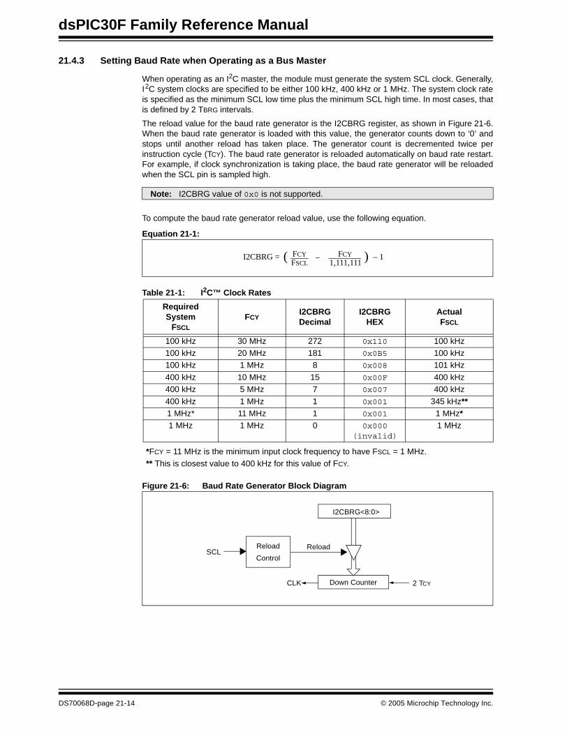
dsPIC30F Family Reference Manual
21.4.3 Setting Baud Rate when Operating as a Bus Master
When operating as an I2C master, the module must generate the system SCL clock. Generally,I2C system clocks are specified to be either 100 kHz, 400 kHz or 1 MHz. The system clock rateis specified as the minimum SCL low time plus the minimum SCL high time. In most cases, thatis defined by 2 TBRG intervals.
The reload value for the baud rate generator is the I2CBRG register, as shown in Figure 21-6.When the baud rate generator is loaded with this value, the generator counts down to ‘0’ andstops until another reload has taken place. The generator count is decremented twice perinstruction cycle (TCY). The baud rate generator is reloaded automatically on baud rate restart.For example, if clock synchronization is taking place, the baud rate generator will be reloadedwhen the SCL pin is sampled high.
To compute the baud rate generator reload value, use the following equation.
Equation 21-1:
Table 21-1: I2C™ Clock Rates
Figure 21-6: Baud Rate Generator Block Diagram
Note: I2CBRG value of 0x0 is not supported.
I2CBRG = FCY FCYFSCL 1,111,111
– 1–( )
RequiredSystem
FSCL
FCYI2CBRGDecimal
I2CBRGHEX
ActualFSCL
100 kHz 30 MHz 272 0x110 100 kHz100 kHz 20 MHz 181 0x0B5 100 kHz100 kHz 1 MHz 8 0x008 101 kHz
400 kHz 10 MHz 15 0x00F 400 kHz400 kHz 5 MHz 7 0x007 400 kHz
400 kHz 1 MHz 1 0x001 345 kHz**1 MHz* 11 MHz 1 0x001 1 MHz*1 MHz 1 MHz 0 0x000
(invalid)1 MHz
*FCY = 11 MHz is the minimum input clock frequency to have FSCL = 1 MHz. ** This is closest value to 400 kHz for this value of FCY.
Down CounterCLK 2 TCY
I2CBRG<8:0>
SCLReload
Control
Reload
DS70068D-page 21-14 © 2005 Microchip Technology Inc.
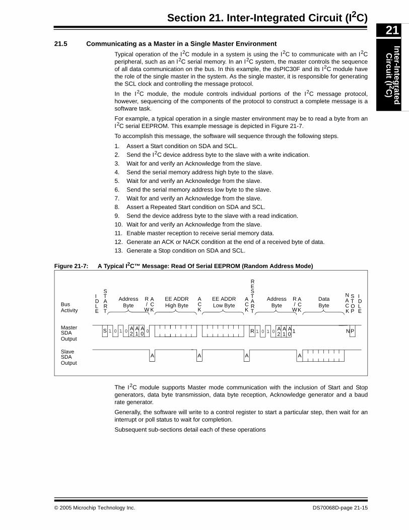
Section 21. Inter-Integrated Circuit (I2C)In
ter-Integ
ratedC
ircuit (I 2C
)21
21.5 Communicating as a Master in a Single Master Environment
Typical operation of the I2C module in a system is using the I2C to communicate with an I2Cperipheral, such as an I2C serial memory. In an I2C system, the master controls the sequenceof all data communication on the bus. In this example, the dsPIC30F and its I2C module havethe role of the single master in the system. As the single master, it is responsible for generatingthe SCL clock and controlling the message protocol.
In the I2C module, the module controls individual portions of the I2C message protocol,however, sequencing of the components of the protocol to construct a complete message is asoftware task.
For example, a typical operation in a single master environment may be to read a byte from anI2C serial EEPROM. This example message is depicted in Figure 21-7.
To accomplish this message, the software will sequence through the following steps.
1. Assert a Start condition on SDA and SCL.2. Send the I2C device address byte to the slave with a write indication.
3. Wait for and verify an Acknowledge from the slave.4. Send the serial memory address high byte to the slave.5. Wait for and verify an Acknowledge from the slave.
6. Send the serial memory address low byte to the slave.7. Wait for and verify an Acknowledge from the slave.8. Assert a Repeated Start condition on SDA and SCL.
9. Send the device address byte to the slave with a read indication.10. Wait for and verify an Acknowledge from the slave.11. Enable master reception to receive serial memory data.
12. Generate an ACK or NACK condition at the end of a received byte of data.13. Generate a Stop condition on SDA and SCL.
Figure 21-7: A Typical I2C™ Message: Read Of Serial EEPROM (Random Address Mode)
The I2C module supports Master mode communication with the inclusion of Start and Stopgenerators, data byte transmission, data byte reception, Acknowledge generator and a baudrate generator.
Generally, the software will write to a control register to start a particular step, then wait for aninterrupt or poll status to wait for completion.
Subsequent sub-sections detail each of these operations
Bus
MasterSDA
ACK
NAC
ACK
ACK
ACK
STOP
START
AddressByte
EE ADDRHigh Byte
EE ADDRLow Byte
AddressByte
DataByte
START
S 1 0 1 0 A A A 02 1 0 R 1 0 1 0 A A A 12 1 0 P
K
SlaveSDA
Activity
N
AAAA
ER
R/
W
R/
W
Output
Output
IDLE
IDLE
© 2005 Microchip Technology Inc. DS70068D-page 21-15

dsPIC30F Family Reference Manual
21.5.1 Generating Start Bus Event
To initiate a Start event, the software sets the Start enable bit, SEN (I2CCON<0>). Prior tosetting the Start bit, the software can check the P (I2CSTAT<4>) status bit to ensure that the busis in an Idle state.
Figure 21-8 shows the timing of the Start condition.
• Slave logic detects the Start condition, sets the S bit (I2CSTAT<3>) and clears the P bit (I2CSTAT<4>).
• SEN bit is automatically cleared at completion of the Start condition.• MI2CIF interrupt generated at completion of the Start condition.
• After Start condition, SDA line and SCL line are left low (Q state).
21.5.1.1 IWCOL Status Flag
If the software writes the I2CTRN when a Start sequence is in progress, then IWCOL is set andthe contents of the transmit buffer are ignored.
Figure 21-8: Master Start Timing Diagram
Note: Because queueing of events is not allowed, writing to the lower 5 bits of I2CCON isdisabled until the Start condition is complete.
SCL (Master)
SDA (Master)
S
SEN
MI2CIF Interrupt
TBRG
1 2 3 4
- Writing SEN = 1 initiates a master Start event. 1
TBRG
Baud generator starts.
- Baud generator times out. Master module drives SDA low. 2Baud generator restarts.
- Slave module detects Start, sets S = 1, P = 0. 3
- Baud generator times out. Master module drives SCL low,4generates interrupt and clears SEN.
I2C™ Bus State (I) (S) (Q)
P
DS70068D-page 21-16 © 2005 Microchip Technology Inc.
Section 21. Inter-Integrated Circuit (I2C)In
ter-Integ
ratedC
ircuit (I 2C
)21
21.5.2 Sending Data to a Slave Device
Transmission of a data byte, a 7-bit device address byte or the second byte of a 10-bit address,is accomplished by simply writing the appropriate value to the I2CTRN register. Loading thisregister will start the following process:
• The software loads the I2CTRN with the data byte to transmit.• Writing I2CTRN sets the buffer full flag bit, TBF (I2CSTAT<0>).
• The data byte is shifted out the SDA pin until all 8 bits are transmitted. Each bit of address/data will be shifted out onto the SDA pin after the falling edge of SCL.
• On the ninth SCL clock, the module shifts in the ACK bit from the slave device and writes its value into the ACKSTAT bit (I2CCON<15>).
• The module generates the MI2CIF interrupt at the end of the ninth SCL clock cycle.
Note that the module does not generate or validate the data bytes. The contents and usage ofthe byte is dependant on the state of the message protocol maintained by the software.
21.5.2.1 Sending a 7-bit Address to the Slave
Sending a 7-bit device address involves sending 1 byte to the slave. A 7-bit address byte mustcontain the 7 bits of I2C device address and a R/W bit that defines if the message will be a writeto the slave (master transmission and slave receiver) or a read from the slave (slave transmissionand master receiver).
21.5.2.2 Sending a 10-bit Address to the Slave
Sending a 10-bit device address involves sending 2 bytes to the slave. The first byte contains 5bits of I2C device address reserved for 10-bit Addressing modes and 2 bits of the 10-bit address.Because the next byte, which contains the remaining 8 bits of the 10-bit address must bereceived by the slave, the R/W bit in the first byte must be ‘0’, indicating master transmission andslave reception. If the message data is also directed toward the slave, the master can continuesending the data. However, if the master expects a reply from the slave, a Repeated Startsequence with the R/W bit at ‘1’ will change the R/W state of the message to a read of the slave.
21.5.2.3 Receiving Acknowledge from the Slave
On the falling edge of the eighth SCL clock, the TBF bit is cleared and the master will de-assertthe SDA pin allowing the slave to respond with an Acknowledge. The master will then generatea ninth SCL clock.
This allows the slave device being addressed to respond with an ACK bit during the ninthbit time if an address match occurs, or if data was received properly. A slave sends anAcknowledge when it has recognized its device address (including a general call), or when theslave has properly received its data.
The status of ACK is written into the Acknowledge status bit, ACKSTAT (I2CSTAT<15>), on thefalling edge of the ninth SCL clock. After the ninth SCL clock, the module generates the MI2CIFinterrupt and enters an Idle state until the next data byte is loaded into I2CTRN.
21.5.2.4 ACKSTAT Status Flag
The ACKSTAT bit (I2CCON<15>) is cleared when the slave has sent an Acknowledge(ACK = 0), and is set when the slave does not Acknowledge (ACK = 1).
© 2005 Microchip Technology Inc. DS70068D-page 21-17
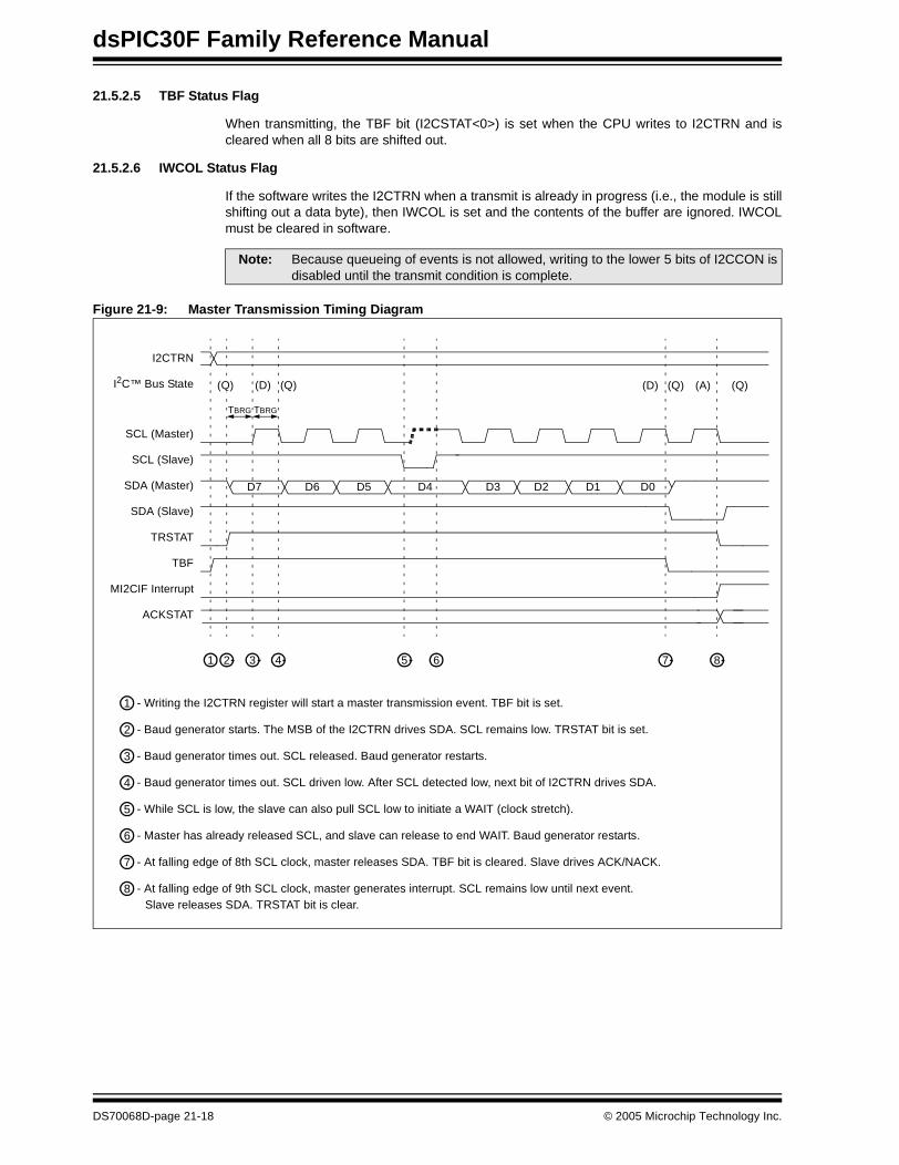
dsPIC30F Family Reference Manual
21.5.2.5 TBF Status Flag
When transmitting, the TBF bit (I2CSTAT<0>) is set when the CPU writes to I2CTRN and iscleared when all 8 bits are shifted out.
21.5.2.6 IWCOL Status Flag
If the software writes the I2CTRN when a transmit is already in progress (i.e., the module is stillshifting out a data byte), then IWCOL is set and the contents of the buffer are ignored. IWCOLmust be cleared in software.
Figure 21-9: Master Transmission Timing Diagram
Note: Because queueing of events is not allowed, writing to the lower 5 bits of I2CCON isdisabled until the transmit condition is complete.
D7 D6 D5 D4 D3 D2 D1 D0
SCL (Master)
SCL (Slave)
SDA (Master)
SDA (Slave)
TBF
I2CTRN
MI2CIF Interrupt
TBRG TBRG
5 6 7 81 2 3 4
- Writing the I2CTRN register will start a master transmission event. TBF bit is set.1
- Baud generator starts. The MSB of the I2CTRN drives SDA. SCL remains low. TRSTAT bit is set.2
- Baud generator times out. SCL released. Baud generator restarts.3
- Baud generator times out. SCL driven low. After SCL detected low, next bit of I2CTRN drives SDA.4
- While SCL is low, the slave can also pull SCL low to initiate a WAIT (clock stretch).5
- Master has already released SCL, and slave can release to end WAIT. Baud generator restarts.6
- At falling edge of 8th SCL clock, master releases SDA. TBF bit is cleared. Slave drives ACK/NACK.7
- At falling edge of 9th SCL clock, master generates interrupt. SCL remains low until next event. 8Slave releases SDA. TRSTAT bit is clear.
I2C™ Bus State (Q) (D) (Q) (A) (Q)(D) (Q)
TRSTAT
ACKSTAT
DS70068D-page 21-18 © 2005 Microchip Technology Inc.
Section 21. Inter-Integrated Circuit (I2C)In
ter-Integ
ratedC
ircuit (I 2C
)21
21.5.3 Receiving Data from a Slave Device
Setting the receive enable bit, RCEN (I2CCON<3>), enables the master to receive data from aslave device.
The master logic begins to generate clocks and before each falling edge of the SCL, SDA line issampled and data is shifted into the I2CRSR.
After the falling edge of the eighth SCL clock:
• The RCEN bit is automatically cleared.
• The contents of the I2CRSR transfer into the I2CRCV.• The RBF flag bit is set.• The module generates the MI2CIF interrupt.
When the CPU reads the buffer, the RBF flag bit is automatically cleared. The software canprocess the data and then do an Acknowledge sequence.
21.5.3.1 RBF Status Flag
When receiving data, the RBF bit is set when an device address or data byte is loaded intoI2CRCV from I2CRSR. It is cleared when software reads the I2CRCV register.
21.5.3.2 I2COV Status Flag
If another byte is received in the I2CRSR while the RBF bit remains set and the previous byteremains in the I2CRCV register, the I2COV bit is set and the data in the I2CRSR is lost.
Leaving I2COV set does not inhibit further reception. If RBF is cleared by reading the I2CRCV,and the I2CRSR receives another byte, that byte will be transferred to the I2CRCV.
21.5.3.3 IWCOL Status Flag
If the software writes the I2CTRN when a receive is already in progress (i.e., I2CRSR is stillshifting in a data byte), then the IWCOL bit is set and the contents of the buffer are ignored.
Note: The lower 5 bits of I2CCON must be ‘0’ before attempting to set the RCEN bit. Thisensures the master logic is inactive.
Note: Since queueing of events is not allowed, writing to the lower 5 bits of I2CCON isdisabled until the data reception condition is complete.
© 2005 Microchip Technology Inc. DS70068D-page 21-19
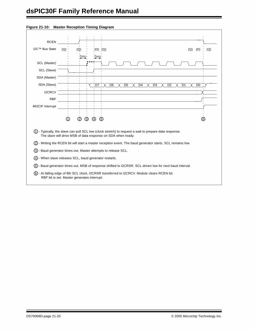
dsPIC30F Family Reference Manual
Figure 21-10: Master Reception Timing Diagram
D7 D6 D5 D4 D3 D2 D1 D0
SCL (Master)
SCL (Slave)
SDA (Slave)
SDA (Master)
RBF
I2C™ Bus State
MI2CIF Interrupt
TBRG
5 62 3 4
- Writing the RCEN bit will start a master reception event. The baud generator starts. SCL remains low.2
- Baud generator times out. Master attempts to release SCL. 3
- When slave releases SCL, baud generator restarts.4
- Baud generator times out. MSB of response shifted to I2CRSR. SCL driven low for next baud interval. 5
- At falling edge of 8th SCL clock, I2CRSR transferred to I2CRCV. Module clears RCEN bit. 6
TBRG
RCEN
(Q) (D) (Q) (Q)(D)(Q)
I2CRCV
RBF bit is set. Master generates interrupt.
(Q)
1
- Typically, the slave can pull SCL low (clock stretch) to request a wait to prepare data response. 1The slave will drive MSB of data response on SDA when ready.
DS70068D-page 21-20 © 2005 Microchip Technology Inc.
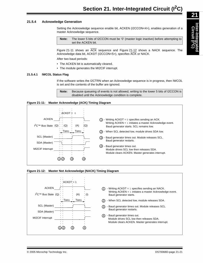
Section 21. Inter-Integrated Circuit (I2C)In
ter-Integ
ratedC
ircuit (I 2C
)21
21.5.4 Acknowledge Generation
Setting the Acknowledge sequence enable bit, ACKEN (I2CCON<4>), enables generation of amaster Acknowledge sequence.
Figure 21-11 shows an ACK sequence and Figure 21-12 shows a NACK sequence. TheAcknowledge data bit, ACKDT (I2CCON<5>), specifies ACK or NACK.
After two baud periods:
• The ACKEN bit is automatically cleared.
• The module generates the MI2CIF interrupt.
21.5.4.1 IWCOL Status Flag
If the software writes the I2CTRN when an Acknowledge sequence is in progress, then IWCOLis set and the contents of the buffer are ignored.
Figure 21-11: Master Acknowledge (ACK) Timing Diagram
Figure 21-12: Master Not Acknowledge (NACK) Timing Diagram
Note: The lower 5 bits of I2CCON must be ‘0’ (master logic inactive) before attempting toset the ACKEN bit.
Note: Because queueing of events is not allowed, writing to the lower 5 bits of I2CCON isdisabled until the Acknowledge condition is complete.
SCL (Master)
SDA (Master)
ACKEN
MI2CIF Interrupt
TBRG
1 2 3
Writing ACKEN = 1 initiates a master Acknowledge event. 1
TBRG
- Writing ACKDT = 0 specifies sending an ACK.
- When SCL detected low, module drives SDA low. 2
- Baud generator times out. Module releases SCL.3
- Baud generator times out. 4
I2C™ Bus State (A) (Q)(Q)
4
Baud generator restarts.
Baud generator starts. SCL remains low.
Module drives SCL low then releases SDA.Module clears ACKEN. Master generates interrupt.
(Q)
ACKDT = 0
SCL (Master)
SDA (Master)
ACKEN
MI2CIF Interrupt
TBRG
1 2 3
Writing ACKEN = 1 initiates a master Acknowledge event. 1
TBRG
- Writing ACKDT = 1 specifies sending an NACK.
- When SCL detected low, module releases SDA.2
- Baud generator times out. Module releases SCL.3
- Baud generator times out. 4
I2C™ Bus State (A) (I)(Q)
4
Baud generator restarts.
Baud generator starts.
Module drives SCL low then releases SDA.Module clears ACKEN. Master generates interrupt.
ACKDT = 1
© 2005 Microchip Technology Inc. DS70068D-page 21-21
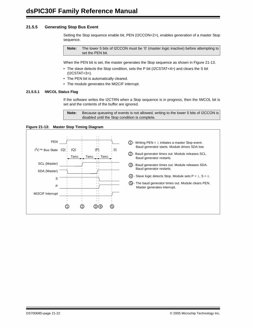
dsPIC30F Family Reference Manual
21.5.5 Generating Stop Bus Event
Setting the Stop sequence enable bit, PEN (I2CCON<2>), enables generation of a master Stopsequence.
When the PEN bit is set, the master generates the Stop sequence as shown in Figure 21-13.
• The slave detects the Stop condition, sets the P bit (I2CSTAT<4>) and clears the S bit (I2CSTAT<3>).
• The PEN bit is automatically cleared.• The module generates the MI2CIF interrupt.
21.5.5.1 IWCOL Status Flag
If the software writes the I2CTRN when a Stop sequence is in progress, then the IWCOL bit isset and the contents of the buffer are ignored.
Figure 21-13: Master Stop Timing Diagram
Note: The lower 5 bits of I2CCON must be ‘0’ (master logic inactive) before attempting toset the PEN bit.
Note: Because queueing of events is not allowed, writing to the lower 5 bits of I2CCON isdisabled until the Stop condition is complete.
SCL (Master)
SDA (Master)
S
PEN
MI2CIF Interrupt
TBRG
1 2 3 5
- Writing PEN = 1 initiates a master Stop event. 1
TBRG
Baud generator starts. Module drives SDA low.
- Baud generator times out. Module releases SCL. 2Baud generator restarts.
- Baud generator times out. Module releases SDA.3
- Slave logic detects Stop. Module sets P = 1, S = 0.4
I2C™ Bus State (P) (I)
P
TBRG
(Q)
4
Baud generator restarts.
- The baud generator times out. Module clears PEN. 5Master generates interrupt.
(Q)
DS70068D-page 21-22 © 2005 Microchip Technology Inc.
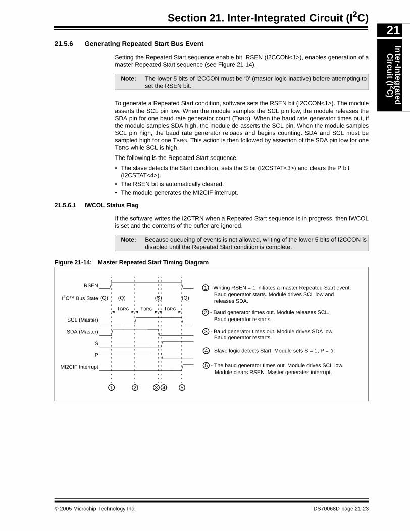
Section 21. Inter-Integrated Circuit (I2C)In
ter-Integ
ratedC
ircuit (I 2C
)21
21.5.6 Generating Repeated Start Bus Event
Setting the Repeated Start sequence enable bit, RSEN (I2CCON<1>), enables generation of amaster Repeated Start sequence (see Figure 21-14).
To generate a Repeated Start condition, software sets the RSEN bit (I2CCON<1>). The moduleasserts the SCL pin low. When the module samples the SCL pin low, the module releases theSDA pin for one baud rate generator count (TBRG). When the baud rate generator times out, ifthe module samples SDA high, the module de-asserts the SCL pin. When the module samplesSCL pin high, the baud rate generator reloads and begins counting. SDA and SCL must besampled high for one TBRG. This action is then followed by assertion of the SDA pin low for oneTBRG while SCL is high.
The following is the Repeated Start sequence:
• The slave detects the Start condition, sets the S bit (I2CSTAT<3>) and clears the P bit (I2CSTAT<4>).
• The RSEN bit is automatically cleared.• The module generates the MI2CIF interrupt.
21.5.6.1 IWCOL Status Flag
If the software writes the I2CTRN when a Repeated Start sequence is in progress, then IWCOLis set and the contents of the buffer are ignored.
Figure 21-14: Master Repeated Start Timing Diagram
Note: The lower 5 bits of I2CCON must be ‘0’ (master logic inactive) before attempting toset the RSEN bit.
Note: Because queueing of events is not allowed, writing of the lower 5 bits of I2CCON isdisabled until the Repeated Start condition is complete.
SCL (Master)
SDA (Master)
S
RSEN
MI2CIF Interrupt
TBRG
1 2 3 5
- Writing RSEN = 1 initiates a master Repeated Start event. 1
TBRG
Baud generator starts. Module drives SCL low and
- Baud generator times out. Module releases SCL. 2Baud generator restarts.
- Baud generator times out. Module drives SDA low.3
- Slave logic detects Start. Module sets S = 1, P = 0.4
I2C™ Bus State (S) (Q)
P
TBRG
(Q)
4
Baud generator restarts.
- The baud generator times out. Module drives SCL low. 5Module clears RSEN. Master generates interrupt.
(Q)releases SDA.
© 2005 Microchip Technology Inc. DS70068D-page 21-23
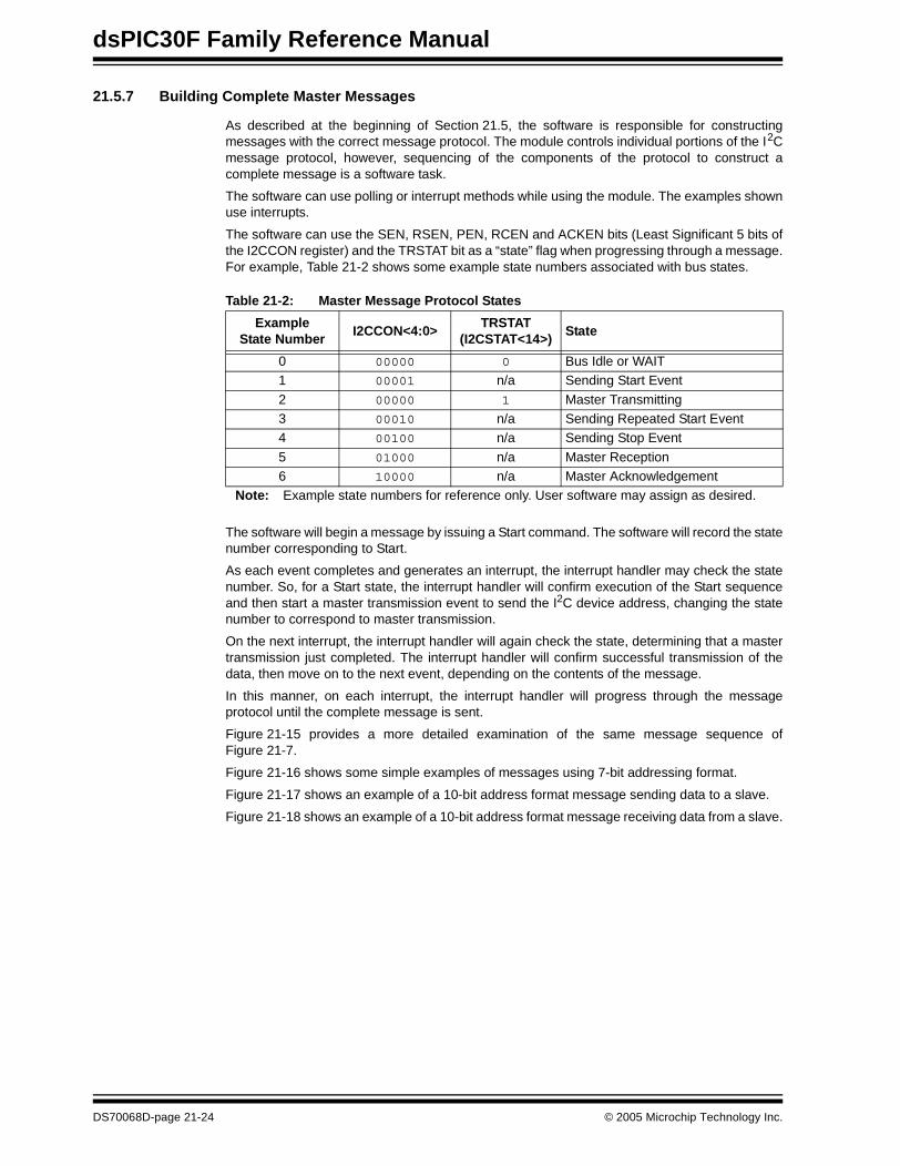
dsPIC30F Family Reference Manual
21.5.7 Building Complete Master Messages
As described at the beginning of Section 21.5, the software is responsible for constructingmessages with the correct message protocol. The module controls individual portions of the I2Cmessage protocol, however, sequencing of the components of the protocol to construct acomplete message is a software task.
The software can use polling or interrupt methods while using the module. The examples shownuse interrupts.
The software can use the SEN, RSEN, PEN, RCEN and ACKEN bits (Least Significant 5 bits ofthe I2CCON register) and the TRSTAT bit as a “state” flag when progressing through a message.For example, Table 21-2 shows some example state numbers associated with bus states.
Table 21-2: Master Message Protocol States
The software will begin a message by issuing a Start command. The software will record the statenumber corresponding to Start.
As each event completes and generates an interrupt, the interrupt handler may check the statenumber. So, for a Start state, the interrupt handler will confirm execution of the Start sequenceand then start a master transmission event to send the I2C device address, changing the statenumber to correspond to master transmission.
On the next interrupt, the interrupt handler will again check the state, determining that a mastertransmission just completed. The interrupt handler will confirm successful transmission of thedata, then move on to the next event, depending on the contents of the message.
In this manner, on each interrupt, the interrupt handler will progress through the messageprotocol until the complete message is sent.
Figure 21-15 provides a more detailed examination of the same message sequence ofFigure 21-7.
Figure 21-16 shows some simple examples of messages using 7-bit addressing format.
Figure 21-17 shows an example of a 10-bit address format message sending data to a slave.
Figure 21-18 shows an example of a 10-bit address format message receiving data from a slave.
ExampleState Number
I2CCON<4:0>TRSTAT
(I2CSTAT<14>)State
0 00000 0 Bus Idle or WAIT1 00001 n/a Sending Start Event
2 00000 1 Master Transmitting3 00010 n/a Sending Repeated Start Event4 00100 n/a Sending Stop Event
5 01000 n/a Master Reception6 10000 n/a Master Acknowledgement
Note: Example state numbers for reference only. User software may assign as desired.
DS70068D-page 21-24 © 2005 Microchip Technology Inc.
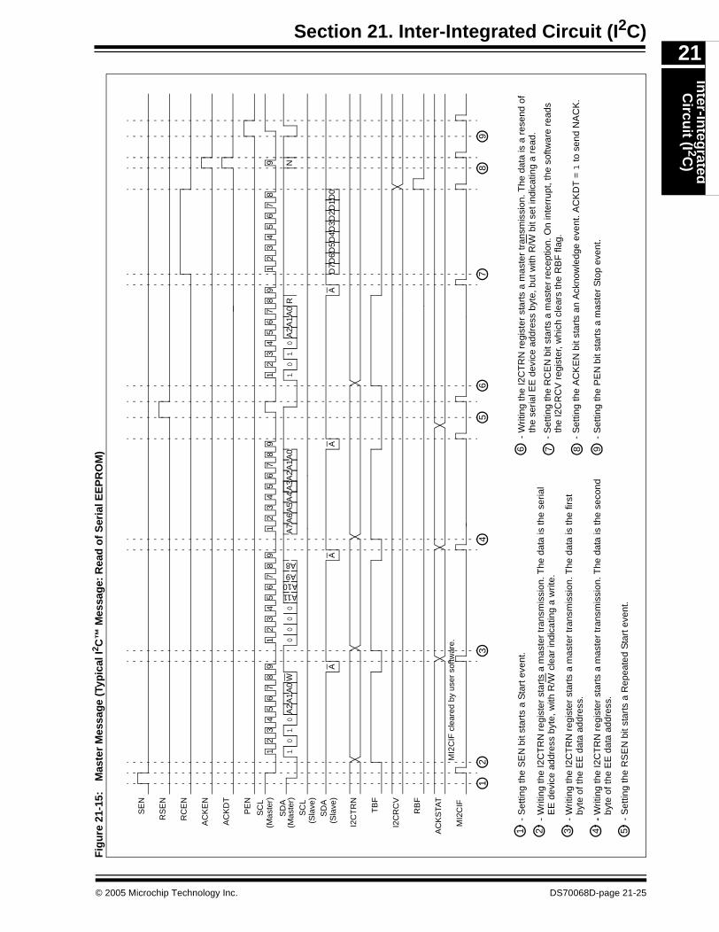
Section 21. Inter-Integrated Circuit (I2C)In
ter-Integ
ratedC
ircuit (I 2C
)
21
Fig
ure
21-
15:
Mas
ter
Mes
sag
e (T
ypic
al I2 C
™ M
essa
ge:
Rea
d o
f S
eria
l EE
PR
OM
)
T
1-
Set
ting
the
SE
N b
it st
arts
a S
tart
eve
nt.
AC
KD
T
AC
KE
N
SE
N
SC
L
SD
A
SC
L
SD
A
I2C
TR
N
TB
F
I2C
RC
V
RB
F
MI2
CIF
AC
KS
TAT
12
34
56
78
A1
A0
9 A
PE
N
RC
EN
12
34
56
78
A11A10A9A8
12
34
56
78
9
W1
1
RS
EN
12
34
56
78
9
13
2
9 A
12
34
56
78
D3D
2D1D
0D
7D6D
5D4
9 N
AA
45
78
9
2-
Writ
ing
the
I2C
TR
N r
egis
ter
star
ts a
mas
ter
tran
smis
sion
. The
dat
a is
the
seria
l
3-
Writ
ing
the
I2C
TR
N r
egis
ter
star
ts a
mas
ter
tran
smis
sion
. The
dat
a is
the
first
4-
5
- W
ritin
g th
e I2
CT
RN
reg
iste
r st
arts
a m
aste
r tr
ansm
issi
on. T
he d
ata
is a
res
end
of6
- S
ettin
g th
e R
CE
N b
it st
arts
a m
aste
r re
cept
ion.
On
inte
rrup
t, th
e so
ftwar
e re
ads
7 9
- S
ettin
g th
e A
CK
EN
bit
star
ts a
n A
ckno
wle
dge
even
t. A
CK
DT
= 1
to s
end
NA
CK
.
- S
ettin
g th
e P
EN
bit
star
ts a
mas
ter
Sto
p ev
ent.
EE
dev
ice
addr
ess
byte
, with
R/W
cle
ar in
dica
ting
a w
rite.
byte
of t
he E
E d
ata
addr
ess.
the
seria
l EE
dev
ice
addr
ess
byte
, but
with
R/W
bit
set i
ndic
atin
g a
read
.
the
I2C
RC
V r
egis
ter,
whi
ch c
lear
s th
e R
BF
flag
.
00
A2
A7
A6
A5
A4
A2
A1
A0
A1
A0
R1
10
0A
20
00
0
6
- W
ritin
g th
e I2
CT
RN
reg
iste
r st
arts
a m
aste
r tr
ansm
issi
on. T
he d
ata
is th
e se
cond
byte
of t
he E
E d
ata
addr
ess.
8
- S
ettin
g th
e R
SE
N b
it st
arts
a R
epea
ted
Sta
rt e
vent
.
(Mas
ter)
(Mas
ter)
(Sla
ve)
(Sla
ve)
A3
MI2
CIF
cle
ared
by
user
sof
twar
e.
© 2005 Microchip Technology Inc. DS70068D-page 21-25
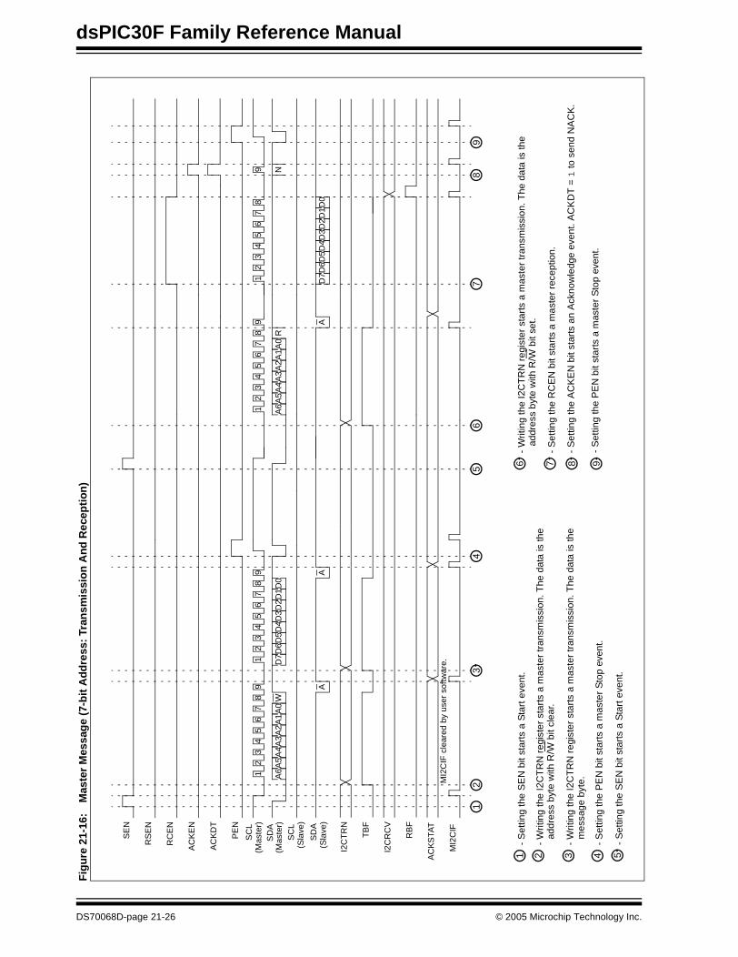
dsPIC30F Family Reference Manual
Fig
ure
21-
16:
Mas
ter
Mes
sag
e (7
-bit
Ad
dre
ss:
Tran
smis
sio
n A
nd
Rec
epti
on
)
1-
Set
ting
the
SE
N b
it st
arts
a S
tart
eve
nt.
AC
KD
T
AC
KE
N
SE
N
SC
L
SD
A
SC
L
SD
A
I2C
TR
N
TB
F
I2C
RC
V
RB
F
MI2
CIF
AC
KS
TAT
12
34
56
78
A1
A0
9 A
PE
N
RC
EN
12
34
56
78
D7D
6D5D
4D3D
2D1D
0
12
34
56
78
9
W
RS
EN
13
2
91
23
45
67
8
D3D
2D1D
0D
7D6D
5D4
9 N
A
45
69
78
2-
Writ
ing
the
I2C
TR
N r
egis
ter
star
ts a
mas
ter
tran
smis
sion
. The
dat
a is
the
3-
Writ
ing
the
I2C
TR
N r
egis
ter
star
ts a
mas
ter
tran
smis
sion
. The
dat
a is
the
4-
Set
ting
the
PE
N b
it st
arts
a m
aste
r S
top
even
t.
5-
Set
ting
the
SE
N b
it st
arts
a S
tart
eve
nt.
6-
Writ
ing
the
I2C
TR
N r
egis
ter
star
ts a
mas
ter
tran
smis
sion
. The
dat
a is
the
7-
Set
ting
the
RC
EN
bit
star
ts a
mas
ter
rece
ptio
n.
8-
Set
ting
the
AC
KE
N b
it st
arts
an
Ack
now
ledg
e ev
ent.
AC
KD
T =
1 to
sen
d N
AC
K.
- S
ettin
g th
e P
EN
bit
star
ts a
mas
ter
Sto
p ev
ent.
addr
ess
byte
with
R/W
bit
clea
r.
mes
sage
byt
e.A6
A5
A4
A3
A2
A
A1
A0
RA
6A
5A
4A
3A
2
addr
ess
byte
with
R/W
bit
set.
9
(Mas
ter)
(Mas
ter)
(Sla
ve)
(Sla
ve)
MI2
CIF
cle
ared
by
user
sof
twar
e.
DS70068D-page 21-26 © 2005 Microchip Technology Inc.
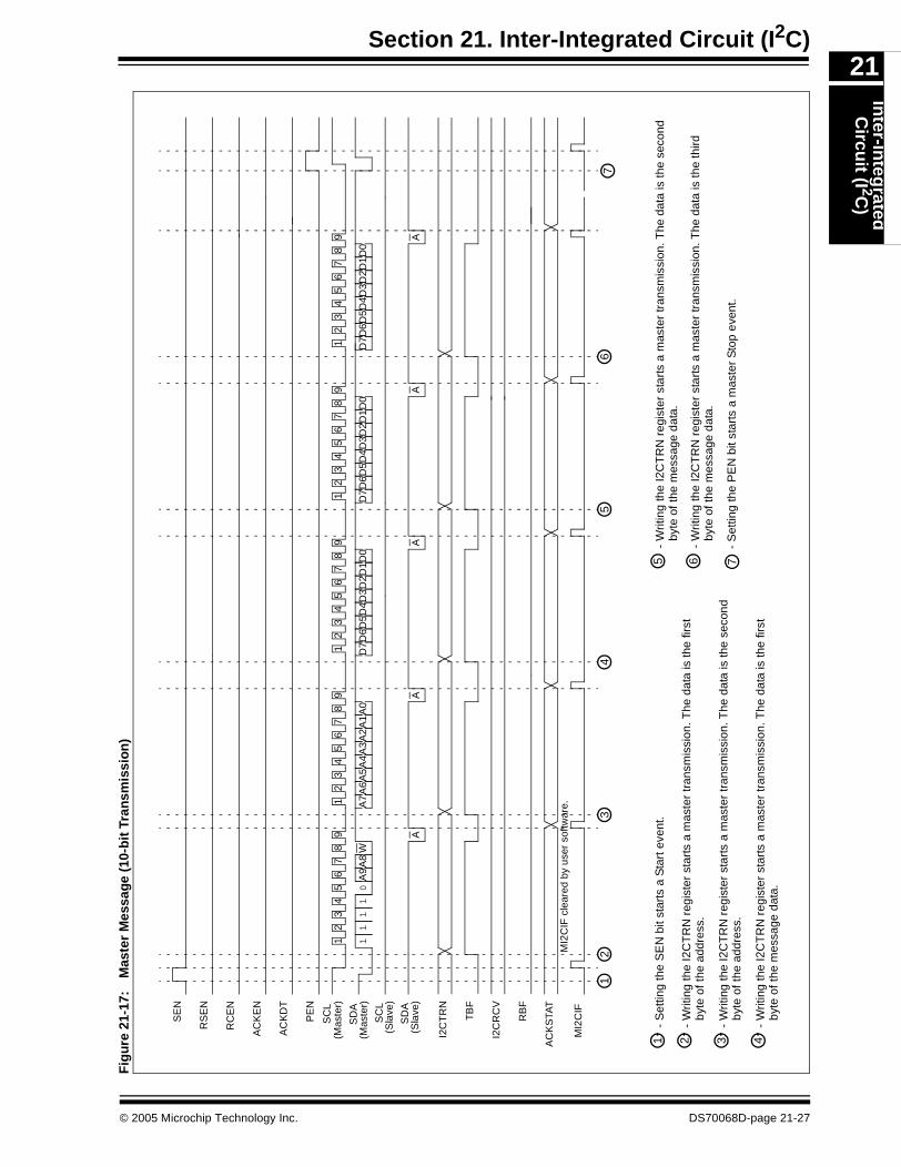
Section 21. Inter-Integrated Circuit (I2C)In
ter-Integ
ratedC
ircuit (I 2C
)
21
Fig
ure
21-
17:
Mas
ter
Mes
sag
e (1
0-b
it T
ran
smis
sio
n)
T
1-
Set
ting
the
SE
N b
it st
arts
a S
tart
eve
nt.
AC
KD
T
AC
KE
N
SE
N
SC
L
SD
A
SC
L
SD
A
I2C
TR
N
TB
F
I2C
RC
V
RB
F
MI2
CIF
AC
KS
TAT
12
34
56
78
A9
A8
9 A
PE
N
RC
EN
12
34
56
78
D3D
2D1D
0D
7D6D
5D4
A7
A6
A5
A4
A3
A2
A1
A0
12
34
56
78
9
W0
11
11
RS
EN
12
34
56
78
9
13
2
9 A
12
34
56
78
9
AA
45
67
2-
Writ
ing
the
I2C
TR
N r
egis
ter
star
ts a
mas
ter
tran
smis
sion
. The
dat
a is
the
first
3-
Writ
ing
the
I2C
TR
N r
egis
ter
star
ts a
mas
ter
tran
smis
sion
. The
dat
a is
the
seco
nd
4-
Writ
ing
the
I2C
TR
N r
egis
ter
star
ts a
mas
ter
tran
smis
sion
. The
dat
a is
the
first
- S
ettin
g th
e P
EN
bit
star
ts a
mas
ter
Sto
p ev
ent.
byte
of t
he a
ddre
ss.
byte
of t
he a
ddre
ss.
byte
of t
he m
essa
ge d
ata.
D3D
2D1D
0D
7D6D
5D4
D3D
2D1D
0D
7D6D
5D4
A
5-
Writ
ing
the
I2C
TR
N r
egis
ter
star
ts a
mas
ter
tran
smis
sion
. The
dat
a is
the
seco
ndby
te o
f the
mes
sage
dat
a.
6-
Writ
ing
the
I2C
TR
N r
egis
ter
star
ts a
mas
ter
tran
smis
sion
. The
dat
a is
the
third
byte
of t
he m
essa
ge d
ata.
7
(Mas
ter)
(Mas
ter)
(Sla
ve)
(Sla
ve)
MI2
CIF
cle
ared
by
user
sof
twar
e.
© 2005 Microchip Technology Inc. DS70068D-page 21-27

dsPIC30F Family Reference Manual
Fig
ure
21-
18:
Mas
ter
Mes
sag
e (1
0-b
it R
ecep
tio
n)
1-
Set
ting
the
SE
N b
it st
arts
a S
tart
eve
nt.
AC
KD
T
AC
KE
N
SE
N
SC
L
SD
A
SC
L
SD
A
I2C
TR
N
TB
F
I2C
RC
V
RB
F
MI2
CIF
AC
KS
TAT
12
34
56
78
A9
A8
9 A
PE
N
RC
EN
12
34
56
78
D3D
2D1D
0D
7D6D
5D4
A7
A6
A5
A4
A3
A2
A1
A0
12
34
56
78
9
W0
11
11
RS
EN
A9
A8
01
11
1R
12
34
56
78
9
13
2
9 A
12
34
56
78
D3D
2D1D
0D
7D6D
5D4
9 N
AA
45
67
89
10
2-
Writ
ing
the
I2C
TR
N r
egis
ter
star
ts a
mas
ter
tran
smis
sion
. The
dat
a is
the
first
3-
Writ
ing
the
I2C
TR
N r
egis
ter
star
ts a
mas
ter
tran
smis
sion
. The
dat
a is
the
seco
nd
4-
Set
ting
the
RS
EN
bit
star
ts a
mas
ter
RE
Sta
rt e
vent
.
5-
Writ
ing
the
I2C
TR
N r
egis
ter
star
ts a
mas
ter
tran
smis
sion
. The
dat
a is
a r
esen
d
6-
Set
ting
the
RC
EN
bit
star
ts a
mas
ter
rece
ptio
n. O
n in
terr
upt,
the
softw
are
read
s
7-
Set
ting
the
AC
KE
N b
it st
arts
an
Ack
now
ledg
e ev
ent.
AC
KD
T =
0 to
sen
d A
CK
.
8-
Set
ting
the
RC
EN
bit
star
ts a
mas
ter
rece
ptio
n.
9-
Set
ting
the
AC
KE
N b
it st
arts
an
Ack
now
ledg
e ev
ent.
AC
KD
T =
1 to
sen
d N
AC
K.
- S
ettin
g th
e P
EN
bit
star
ts a
mas
ter
Sto
p ev
ent.
byte
of t
he a
ddre
ss w
ith th
e R
/W b
it cl
eare
d.
byte
of t
he a
ddre
ss.
of th
e fir
st b
yte
with
the
R/W
bit
set.
the
I2C
RC
V r
egis
ter,
whi
ch c
lear
s th
e R
BF
flag
.
10
(Sla
ve)
(Sla
ve)
(Mas
ter)
(Mas
ter)
MI2
CIF
cle
ared
in u
ser
softw
are.
DS70068D-page 21-28 © 2005 Microchip Technology Inc.

Section 21. Inter-Integrated Circuit (I2C)In
ter-Integ
ratedC
ircuit (I 2C
)21
21.6 Communicating as a Master in a Multi-Master Environment
The I2C protocol allows for more than one master to be attached to a system bus. Remember-ing that a master can initiate message transactions and generate clocks for the bus, theprotocol has methods to account for situations where more than one master is attempting tocontrol the bus. Clock synchronization ensures that multiple nodes can synchronize their SCLclocks to result in one common clock on the SCL line. Bus arbitration ensures that if more thanone node attempts a message transaction, one and only one node will be successful incompleting the message. The other nodes will lose bus arbitration and be left with a buscollision.
21.6.1 Multi-Master Operation
The master module has no special settings to enable multi-master operation. The moduleperforms clock synchronization and bus arbitration at all times. If the module is used in a singlemaster environment, clock synchronization will only occur between the master and slaves andbus arbitration will not occur.
21.6.2 Master Clock Synchronization
In a multi-master system, different masters may have different baud rates. Clock synchronizationwill ensure that when these masters are attempting to arbitrate the bus, their clocks will becoordinated.
Clock synchronization occurs when the master de-asserts the SCL pin (SCL intended to floathigh). When the SCL pin is released, the baud rate generator (BRG) is suspended from countinguntil the SCL pin is actually sampled high. When the SCL pin is sampled high, the baud rategenerator is reloaded with the contents of I2CBRG<8:0> and begins counting. This ensures thatthe SCL high time will always be at least one BRG rollover count in the event that the clock isheld low by an external device, as shown in Figure 21-19.
Figure 21-19: Baud Rate Generator Timing with Clock Synchronization
SCL (Slave)
- The baud counter decrements twice per TCY. On rollover, the master SCL will transition.1
1
000 003001002003000
SCL (Master)
001002003000Baud Counter
SDA (Master)
3 4 6
- The slave has pulled SCL low to initiate a wait.2
- At what would be the master baud counter rollover, detecting SCL low holds counter.3
- Logic samples SCL once per TCY. Logic detects SCL high.4
2
- The baud counter rollover occurs on next cycle.5
5
- On next rollover, the master SCL will transition.6
TBRG TBRG
TCY
© 2005 Microchip Technology Inc. DS70068D-page 21-29
dsPIC30F Family Reference Manual
21.6.3 Bus Arbitration and Bus Collision
Bus arbitration supports multi-master system operation.
The wired-and nature of the SDA line permits arbitration. Arbitration takes place when the firstmaster outputs a ‘1’ on SDA by letting SDA float high and, simultaneously, the second masteroutputs a ‘0’ on SDA by pulling SDA low. The SDA signal will go low. In this case, the secondmaster has won bus arbitration. The first master has lost bus arbitration and thus has a buscollision.
For the first master, the expected data on SDA is a ‘1’ yet the data sampled on SDA is a ‘0’. Thisis the definition of a bus collision.
The first master will set the bus collision bit, BCL (I2CSTAT<10>), and generate a masterinterrupt. The master module will reset the I2C port to its Idle state.
In multi-master operation, the SDA line must be monitored for arbitration to see if the signallevel is the expected output level. This check is performed by the master module, with the resultplaced in the BCL bit.
The states where arbitration can be lost are:
• A Start condition • A Repeated Start condition
• Address, Data or Acknowledge bit• A Stop condition
21.6.4 Detecting Bus Collisions and Resending Messages
When a bus collision occurs, the module sets the BCL bit and generates a master interrupt. Ifbus collision occurs during a byte transmission, the transmission is halted, the TBF flag iscleared and the SDA and SCL pins are de-asserted. If bus collision occurs during a Start,Repeated Start, Stop or Acknowledge condition, the condition is aborted, the respective controlbits in the I2CCON register are cleared and the SDA and SCL lines are de-asserted.
The software is expecting an interrupt at the completion of the master event. The software cancheck the BCL bit to determine if the master event completed successfully or if a collisionoccurred. If a collision occurs, the software must abort sending the rest of the pending messageand prepare to resend the entire message sequence beginning with Start condition, after thebus returns to an Idle state. The software can monitor the S and P bits to wait for an Idle bus.When the software services the master Interrupt Service Routine and the I2C bus is free, thesoftware can resume communication by asserting a Start condition.
DS70068D-page 21-30 © 2005 Microchip Technology Inc.

Section 21. Inter-Integrated Circuit (I2C)In
ter-Integ
ratedC
ircuit (I 2C
)21
21.6.5 Bus Collision During a Start Condition
Before issuing a Start command, the software should verify an Idle state of the bus using the Sand P status bits. Two masters may attempt to initiate a message at a similar point in time.Typically, the masters will synchronize clocks and continue arbitration into the message untilone loses arbitration. However, certain conditions can cause a bus collision to occur during aStart. In this case, the master that loses arbitration during the Start bit generates a bus collisioninterrupt.
21.6.6 Bus Collision During a Repeated Start Condition
Should two masters not collide throughout an address byte, a bus collision may occur when onemaster attempts to assert a Repeated Start while another transmits data. In this case, themaster generating the Repeated Start will lose arbitration and generate a bus collision interrupt.
21.6.7 Bus Collision During Message Bit Transmission
The most typical case of data collision occurs while the master is attempting to transmit thedevice address byte, a data byte or an Acknowledge bit.
If the software is properly checking the bus state, it is unlikely that a bus collision will occur on aStart condition. However, because another master can at a very similar time, check the bus andinitiate its own Start condition, it is likely that SDA arbitration will occur and synchronize thestarts of two masters. In this condition, both masters will begin and continue to transmit theirmessages until one master loses arbitration on a message bit. Remember that SCL clocksynchronization will keep the two masters synchronized until one loses arbitration.
Figure 21-20 shows an example of message bit arbitration.
Figure 21-20: Bus Collision During Message Bit Transmission
21.6.8 Bus Collision During a Stop Condition
If the master software loses track of the state of the I2C bus, there are conditions which cause abus collision during a Stop condition. In this case, the master generating the Stop condition willlose arbitration and generate a bus collision interrupt.
SCL (Master)
SDA (Master)
TBF
TBRG
1 2 3
- Master transmits bit value of ‘1’ in next SCL clock.1
TBRG
Module releases SDA.
- Another master on bus transmits bit value of ‘0’ 2in next SCL clock. Another master pulls SDA low.
- Baud generator times out. Module attempts to verify3
I2C™ Bus State
BCL
(D)
SCL (Bus)
SDA (Bus)
SDA high. Bus collision detected.Module releases SDA, SCL. Module sets BCL bit andclears TBF bit. Master generates interrupt.
(D)(Q)(Q) (Q)
MI2CIF Interrupt
© 2005 Microchip Technology Inc. DS70068D-page 21-31
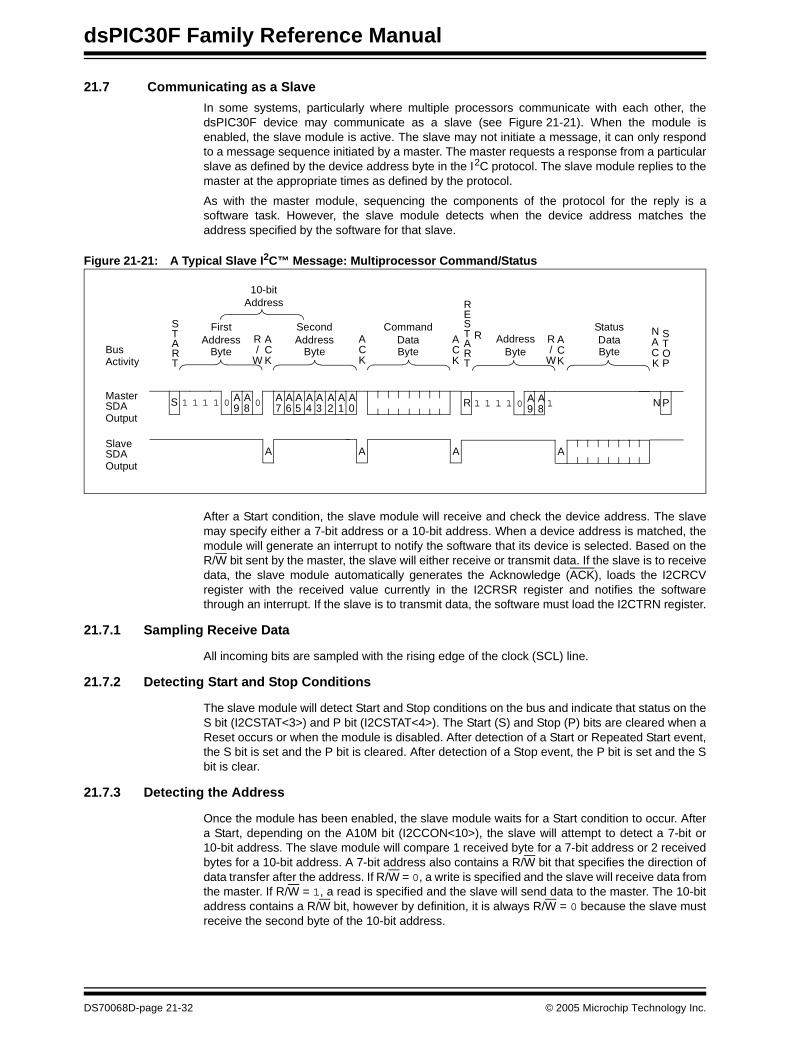
dsPIC30F Family Reference Manual
21.7 Communicating as a Slave
In some systems, particularly where multiple processors communicate with each other, thedsPIC30F device may communicate as a slave (see Figure 21-21). When the module isenabled, the slave module is active. The slave may not initiate a message, it can only respondto a message sequence initiated by a master. The master requests a response from a particularslave as defined by the device address byte in the I2C protocol. The slave module replies to themaster at the appropriate times as defined by the protocol.
As with the master module, sequencing the components of the protocol for the reply is asoftware task. However, the slave module detects when the device address matches theaddress specified by the software for that slave.
Figure 21-21: A Typical Slave I2C™ Message: Multiprocessor Command/Status
After a Start condition, the slave module will receive and check the device address. The slavemay specify either a 7-bit address or a 10-bit address. When a device address is matched, themodule will generate an interrupt to notify the software that its device is selected. Based on theR/W bit sent by the master, the slave will either receive or transmit data. If the slave is to receivedata, the slave module automatically generates the Acknowledge (ACK), loads the I2CRCVregister with the received value currently in the I2CRSR register and notifies the softwarethrough an interrupt. If the slave is to transmit data, the software must load the I2CTRN register.
21.7.1 Sampling Receive Data
All incoming bits are sampled with the rising edge of the clock (SCL) line.
21.7.2 Detecting Start and Stop Conditions
The slave module will detect Start and Stop conditions on the bus and indicate that status on theS bit (I2CSTAT<3>) and P bit (I2CSTAT<4>). The Start (S) and Stop (P) bits are cleared when aReset occurs or when the module is disabled. After detection of a Start or Repeated Start event,the S bit is set and the P bit is cleared. After detection of a Stop event, the P bit is set and the Sbit is clear.
21.7.3 Detecting the Address
Once the module has been enabled, the slave module waits for a Start condition to occur. Aftera Start, depending on the A10M bit (I2CCON<10>), the slave will attempt to detect a 7-bit or10-bit address. The slave module will compare 1 received byte for a 7-bit address or 2 receivedbytes for a 10-bit address. A 7-bit address also contains a R/W bit that specifies the direction ofdata transfer after the address. If R/W = 0, a write is specified and the slave will receive data fromthe master. If R/W = 1, a read is specified and the slave will send data to the master. The 10-bitaddress contains a R/W bit, however by definition, it is always R/W = 0 because the slave mustreceive the second byte of the 10-bit address.
Bus
MasterSDA
ACK
NAC
ACK
ACK
ACK
STOP
START
FirstAddress
SecondAddress
CommandData Address
Byte
StatusData
START
S A A A0 2 1 0 R 1 1 1 1 A A 19 8 P
K
SlaveSDA
Activity
N
AAAA
R
ER
R/
W
R/
W
Output
Output
A3
A4
A5
A6
A7
A8
A901111 0
ByteByteByte Byte
10-bitAddress
DS70068D-page 21-32 © 2005 Microchip Technology Inc.
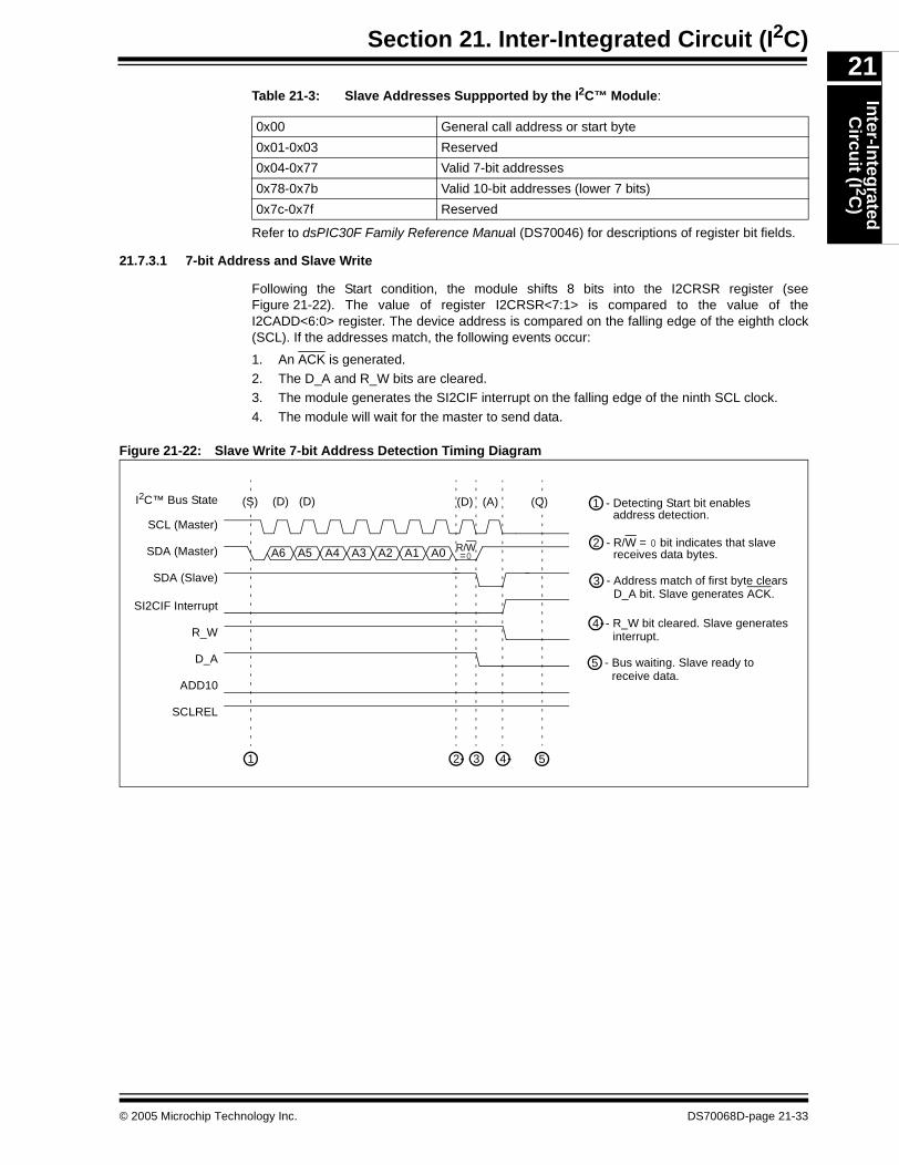
Section 21. Inter-Integrated Circuit (I2C)In
ter-Integ
ratedC
ircuit (I 2C
)21
Table 21-3: Slave Addresses Suppported by the I2C™ Module:
Refer to dsPIC30F Family Reference Manual (DS70046) for descriptions of register bit fields.
21.7.3.1 7-bit Address and Slave Write
Following the Start condition, the module shifts 8 bits into the I2CRSR register (seeFigure 21-22). The value of register I2CRSR<7:1> is compared to the value of theI2CADD<6:0> register. The device address is compared on the falling edge of the eighth clock(SCL). If the addresses match, the following events occur:
1. An ACK is generated.2. The D_A and R_W bits are cleared.3. The module generates the SI2CIF interrupt on the falling edge of the ninth SCL clock.
4. The module will wait for the master to send data.
Figure 21-22: Slave Write 7-bit Address Detection Timing Diagram
0x00 General call address or start byte
0x01-0x03 Reserved
0x04-0x77 Valid 7-bit addresses
0x78-0x7b Valid 10-bit addresses (lower 7 bits)
0x7c-0x7f Reserved
SCL (Master)
SDA (Master)
SDA (Slave)
SI2CIF Interrupt
3 41 2
- Detecting Start bit enables1I2C™ Bus State (S) (D) (D) (A)(D) (Q)
A4A5A6 A3 A2 A1 A0 R/W
D_A
ADD10
SCLREL
R_W
address detection.
- R/W = 0 bit indicates that slave 2receives data bytes.
- Address match of first byte clears 3D_A bit. Slave generates ACK.
- R_W bit cleared. Slave generates 4interrupt.
5
- Bus waiting. Slave ready to 5receive data.
=0
© 2005 Microchip Technology Inc. DS70068D-page 21-33
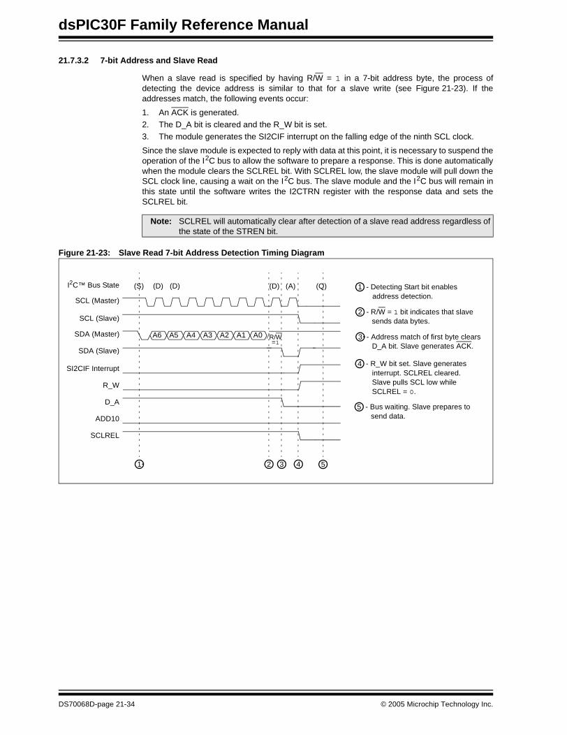
dsPIC30F Family Reference Manual
21.7.3.2 7-bit Address and Slave Read
When a slave read is specified by having R/W = 1 in a 7-bit address byte, the process ofdetecting the device address is similar to that for a slave write (see Figure 21-23). If theaddresses match, the following events occur:
1. An ACK is generated.2. The D_A bit is cleared and the R_W bit is set.3. The module generates the SI2CIF interrupt on the falling edge of the ninth SCL clock.
Since the slave module is expected to reply with data at this point, it is necessary to suspend theoperation of the I2C bus to allow the software to prepare a response. This is done automaticallywhen the module clears the SCLREL bit. With SCLREL low, the slave module will pull down theSCL clock line, causing a wait on the I2C bus. The slave module and the I2C bus will remain inthis state until the software writes the I2CTRN register with the response data and sets theSCLREL bit.
Figure 21-23: Slave Read 7-bit Address Detection Timing Diagram
Note: SCLREL will automatically clear after detection of a slave read address regardless ofthe state of the STREN bit.
SCL (Master)
SDA (Master)
SDA (Slave)
SI2CIF Interrupt
3 41 2
- Detecting Start bit enables1I2C™ Bus State (S) (D) (D) (A)(D) (Q)
A4A5A6 A3 A2 A1 A0 R/W
D_A
ADD10
SCLREL
R_W
address detection.
- R/W = 1 bit indicates that slave 2sends data bytes.
- Address match of first byte clears 3D_A bit. Slave generates ACK.
- R_W bit set. Slave generates 4interrupt. SCLREL cleared.
5
- Bus waiting. Slave prepares to 5send data.
=1
SCL (Slave)
Slave pulls SCL low whileSCLREL = 0.
DS70068D-page 21-34 © 2005 Microchip Technology Inc.
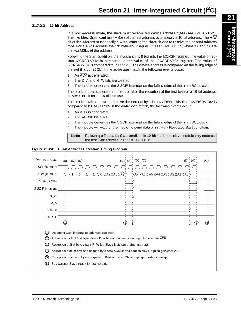
Section 21. Inter-Integrated Circuit (I2C)In
ter-Integ
ratedC
ircuit (I 2C
)21
21.7.3.3 10-bit Address
In 10-bit Address mode, the slave must receive two device address bytes (see Figure 21-24).The five Most Significant bits (MSbs) of the first address byte specify a 10-bit address. The R/Wbit of the address must specify a write, causing the slave device to receive the second addressbyte. For a 10-bit address the first byte would equal ‘11110 A9 A8 0’, where A9 and A8 arethe two MSbs of the address.
Following the Start condition, the module shifts 8 bits into the I2CRSR register. The value of reg-ister I2CRSR<2:1> is compared to the value of the I2CADD<9:8> register. The value ofI2CRSR<7:3> is compared to ‘11110’. The device address is compared on the falling edge ofthe eighth clock (SCL). If the addresses match, the following events occur:
1. An ACK is generated.2. The D_A and R_W bits are cleared.
3. The module generates the SI2CIF interrupt on the falling edge of the ninth SCL clock.
The module does generate an interrupt after the reception of the first byte of a 10-bit address,however this interrupt is of little use.
The module will continue to receive the second byte into I2CRSR. This time, I2CRSR<7:0> iscompared to I2CADD<7:0>. If the addresses match, the following events occur:
1. An ACK is generated.2. The ADD10 bit is set.
3. The module generates the SI2CIF interrupt on the falling edge of the ninth SCL clock.4. The module will wait for the master to send data or initiate a Repeated Start condition.
Figure 21-24: 10-bit Address Detection Timing Diagram
Note: Following a Repeated Start condition in 10-bit mode, the slave module only matchesthe first 7-bit address, ‘11110 A9 A8 0’.
SCL (Master)
SDA (Master)
SDA (Slave)
SI2CIF Interrupt
2 4 51 3
- Detecting Start bit enables address detection.1
- Address match of first byte clears D_A bit and causes slave logic to generate ACK.2
- Reception of first byte clears R_W bit. Slave logic generates interrupt.3
- Address match of first and second byte sets ADD10 and causes slave logic to generate ACK.4
- Reception of second byte completes 10-bit address. Slave logic generates interrupt.5
I2C™ Bus State (S) (D) (D) (A) (Q)(D)
111 1 0 A9 A8R/W
D_A
ADD10
SCLREL
A5A6A7 A4 A3 A2 A1 A0=0
R_W
(D) (D) (A)(D)
6
- Bus waiting. Slave ready to receive data.5
© 2005 Microchip Technology Inc. DS70068D-page 21-35
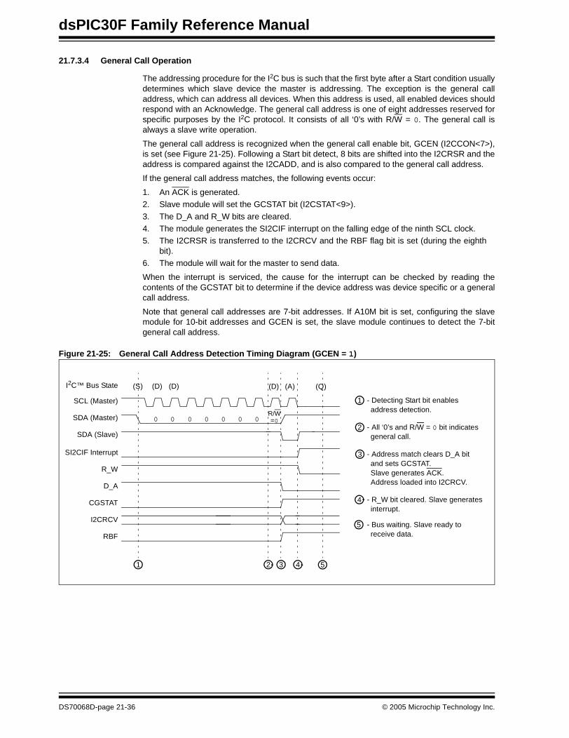
dsPIC30F Family Reference Manual
21.7.3.4 General Call Operation
The addressing procedure for the I2C bus is such that the first byte after a Start condition usuallydetermines which slave device the master is addressing. The exception is the general calladdress, which can address all devices. When this address is used, all enabled devices shouldrespond with an Acknowledge. The general call address is one of eight addresses reserved forspecific purposes by the I2C protocol. It consists of all ‘0’s with R/W = 0. The general call isalways a slave write operation.
The general call address is recognized when the general call enable bit, GCEN (I2CCON<7>),is set (see Figure 21-25). Following a Start bit detect, 8 bits are shifted into the I2CRSR and theaddress is compared against the I2CADD, and is also compared to the general call address.
If the general call address matches, the following events occur:
1. An ACK is generated.2. Slave module will set the GCSTAT bit (I2CSTAT<9>).
3. The D_A and R_W bits are cleared.4. The module generates the SI2CIF interrupt on the falling edge of the ninth SCL clock.5. The I2CRSR is transferred to the I2CRCV and the RBF flag bit is set (during the eighth
bit).6. The module will wait for the master to send data.
When the interrupt is serviced, the cause for the interrupt can be checked by reading thecontents of the GCSTAT bit to determine if the device address was device specific or a generalcall address.
Note that general call addresses are 7-bit addresses. If A10M bit is set, configuring the slavemodule for 10-bit addresses and GCEN is set, the slave module continues to detect the 7-bitgeneral call address.
Figure 21-25: General Call Address Detection Timing Diagram (GCEN = 1)
SCL (Master)
SDA (Master)
SDA (Slave)
SI2CIF Interrupt
3 41 2
- Detecting Start bit enables1
I2C™ Bus State (S) (D) (D) (A)(D) (Q)
000 0 0 0 0R/W
D_A
I2CRCV
RBF
R_W
address detection.
- All ‘0’s and R/W = 0 bit indicates2general call.
- Address match clears D_A bit3and sets GCSTAT.
- R_W bit cleared. Slave generates 4interrupt.
5
- Bus waiting. Slave ready to 5receive data.
=0
CGSTAT
Slave generates ACK.Address loaded into I2CRCV.
DS70068D-page 21-36 © 2005 Microchip Technology Inc.
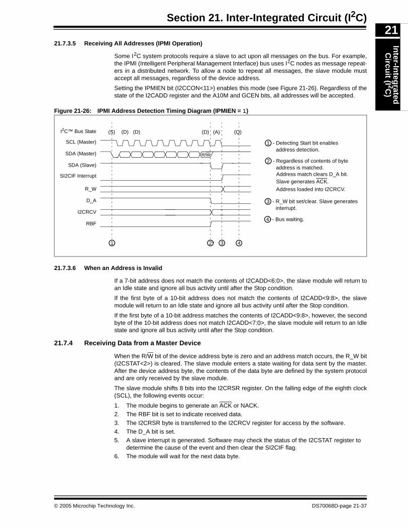
Section 21. Inter-Integrated Circuit (I2C)In
ter-Integ
ratedC
ircuit (I 2C
)21
21.7.3.5 Receiving All Addresses (IPMI Operation)
Some I2C system protocols require a slave to act upon all messages on the bus. For example,the IPMI (Intelligent Peripheral Management Interface) bus uses I2C nodes as message repeat-ers in a distributed network. To allow a node to repeat all messages, the slave module mustaccept all messages, regardless of the device address.
Setting the IPMIEN bit (I2CCON<11>) enables this mode (see Figure 21-26). Regardless of thestate of the I2CADD register and the A10M and GCEN bits, all addresses will be accepted.
Figure 21-26: IPMI Address Detection Timing Diagram (IPMIEN = 1)
21.7.3.6 When an Address is Invalid
If a 7-bit address does not match the contents of I2CADD<6:0>, the slave module will return toan Idle state and ignore all bus activity until after the Stop condition.
If the first byte of a 10-bit address does not match the contents of I2CADD<9:8>, the slavemodule will return to an Idle state and ignore all bus activity until after the Stop condition.
If the first byte of a 10-bit address matches the contents of I2CADD<9:8>, however, the secondbyte of the 10-bit address does not match I2CADD<7:0>, the slave module will return to an Idlestate and ignore all bus activity until after the Stop condition.
21.7.4 Receiving Data from a Master Device
When the R/W bit of the device address byte is zero and an address match occurs, the R_W bit(I2CSTAT<2>) is cleared. The slave module enters a state waiting for data sent by the master.After the device address byte, the contents of the data byte are defined by the system protocoland are only received by the slave module.
The slave module shifts 8 bits into the I2CRSR register. On the falling edge of the eighth clock(SCL), the following events occur:
1. The module begins to generate an ACK or NACK.2. The RBF bit is set to indicate received data.
3. The I2CRSR byte is transferred to the I2CRCV register for access by the software.4. The D_A bit is set.5. A slave interrupt is generated. Software may check the status of the I2CSTAT register to
determine the cause of the event and then clear the SI2CIF flag.6. The module will wait for the next data byte.
SCL (Master)
SDA (Master)
SDA (Slave)
SI2CIF Interrupt
2 31
- Detecting Start bit enables1
I2C™ Bus State (S) (D) (D) (A)(D) (Q)
R/W
D_A
I2CRCV
RBF
R_W
address detection.
- Regardless of contents of byte2address is matched.Address match clears D_A bit.
- R_W bit set/clear. Slave generates 3interrupt.
4
- Bus waiting. 4
Slave generates ACK.
Address loaded into I2CRCV.
© 2005 Microchip Technology Inc. DS70068D-page 21-37
dsPIC30F Family Reference Manual
21.7.4.1 Acknowledge Generation
Normally, the slave module will Acknowledge all received bytes by sending an ACK on the ninthSCL clock. If the receive buffer is overrun, the slave module does not generate this ACK.Overrun is indicated if either (or both):
1. The buffer full bit, RBF (I2CSTAT<1>), was set before the transfer was received.2. The overflow bit, I2COV (I2CSTAT<6>), was set before the transfer was received.
Table 21-4 shows what happens when a data transfer byte is received, given the status of theRBF and I2COV bits. If the RBF bit is already set when the slave module attempts to transfer tothe I2CRCV, the transfer does not occur but the interrupt is generated and the I2COV bit is set.If both the RBF and I2COV bits are set, the slave module acts similarly. The shaded cells showthe condition where software did not properly clear the overflow condition.
Reading the I2CRCV clears the RBF bit. The I2COV is cleared by writing to a ‘0’ throughsoftware.
Table 21-4: Data Transfer Received Byte Actions
21.7.4.2 WAIT States During Slave Receptions
When the slave module receives a data byte, the master can potentially begin sending the nextbyte immediately. This allows the software controlling the slave module 9 SCL clock periods toprocess the previously received byte. If this is not enough time, the slave software may want togenerate a bus WAIT period.
The STREN bit (I2CCON<6>) enables a bus WAIT to occur on slave receptions. WhenSTREN = 1 at the falling edge of the 9th SCL clock of a received byte, the slave module clearsthe SCLREL bit. Clearing the SCLREL bit causes the slave module to pull the SCL line low,initiating a WAIT. The SCL clock of the master and slave will synchronize, as shown in Section21.6.2 “Master Clock Synchronization”.
When the software is ready to resume reception, the software sets SCLREL. This causes theslave module to release the SCL line and the master resumes clocking.
Status Bits as DataByte Received Transfer
I2CRSR → I2CRCVGenerate
ACK
GenerateSI2CIF Interrupt(Interrupt occurs
if enabled)
SetRBF
SetI2COV
RBF I2COV
0 0 Yes Yes Yes Yes No change
1 0 No No Yes No change Yes1 1 No No Yes No change Yes0 1 Yes No Yes Yes No change
Note: Shaded cells show state where the software did not properly clear the overflow condition.
DS70068D-page 21-38 © 2005 Microchip Technology Inc.
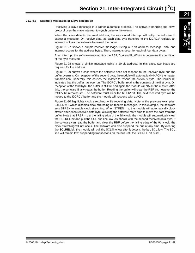
Section 21. Inter-Integrated Circuit (I2C)In
ter-Integ
ratedC
ircuit (I 2C
)21
21.7.4.3 Example Messages of Slave Reception
Receiving a slave message is a rather automatic process. The software handling the slaveprotocol uses the slave interrupt to synchronize to the events.
When the slave detects the valid address, the associated interrupt will notify the software toexpect a message. On receive data, as each data byte transfers to the I2CRCV register, aninterrupt notifies the software to unload the buffer.
Figure 21-27 shows a simple receive message. Being a 7-bit address message, only oneinterrupt occurs for the address bytes. Then, interrupts occur for each of four data bytes.
At an interrupt, the software may monitor the RBF, D_A and R_W bits to determine the conditionof the byte received.
Figure 21-28 shows a similar message using a 10-bit address. In this case, two bytes arerequired for the address.
Figure 21-29 shows a case where the software does not respond to the received byte and thebuffer overruns. On reception of the second byte, the module will automatically NACK the mastertransmission. Generally, this causes the master to resend the previous byte. The I2COV bitindicates that the buffer has overrun. The I2CRCV buffer retains the contents of the first byte. Onreception of the third byte, the buffer is still full and again the module will NACK the master. Afterthis, the software finally reads the buffer. Reading the buffer will clear the RBF bit, however theI2COV bit remains set. The software must clear the I2COV bit. The next received byte will bemoved to the I2CRCV buffer and the module will respond with a ACK.
Figure 21-30 highlights clock stretching while receiving data. Note in the previous examples,STREN = 0 which disables clock stretching on receive messages. In this example, the softwaresets STREN to enable clock stretching. When STREN = 1, the module will automatically clockstretch after each received data byte, allowing the software more time to move the data from thebuffer. Note that if RBF = 1 at the falling edge of the 9th clock, the module will automatically clearthe SCLREL bit and pull the SCL bus line low. As shown with the second received data byte, ifthe software can read the buffer and clear the RBF before the falling edge of the 9th clock, theclock stretching will not occur. The software can also suspend the bus at any time. By clearingthe SCLREL bit, the module will pull the SCL line low after it detects the bus SCL low. The SCLline will remain low, suspending transactions on the bus until the SCLREL bit is set.
© 2005 Microchip Technology Inc. DS70068D-page 21-39
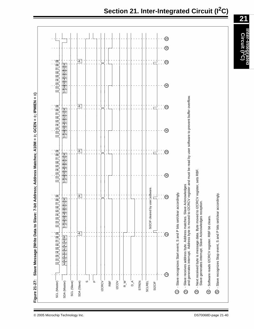
Section 21. Inter-Integrated Circuit (I2C)In
ter-Integ
ratedC
ircuit (I 2C
)
21
Fig
ure
21-
27:
Sla
ve M
essa
ge
(Wri
te D
ata
to S
lave
: 7-
bit
Ad
dre
ss;
Ad
dre
ss M
atch
es;
A10
M =
0;
GC
EN
= 0
; IP
MIE
N =
0)
T
1-
Sla
ve r
ecog
nize
s S
tart
eve
nt, S
and
P b
its s
et/c
lear
acc
ordi
ngly
.
SC
L (M
aste
r)
SD
A (
Mas
ter)
SC
L (S
lave
)
SD
A (
Sla
ve)
I2C
RC
V
RB
F
SI2
CIF
ST
RE
N
12
34
56
78
A1
A0
9 A
D7D
6D5D
4D3D
2D1D
0
12
34
56
78
9
W
13
2
A
43
33
5
2-
Sla
ve r
ecei
ves
addr
ess
byte
. Add
ress
mat
ches
. Sla
ve A
ckno
wle
dges
3-
Nex
t rec
eive
d by
te is
mes
sage
dat
a. B
yte
mov
ed to
I2C
RC
V r
egis
ter,
sets
RB
F.
4-
Sof
twar
e re
ads
I2C
RC
V r
egis
ter.
RB
F b
it cl
ears
.
5-
Sla
ve r
ecog
nize
s S
top
even
t, S
and
P b
its s
et/c
lear
acc
ordi
ngly
.
Add
ress
byt
e is
mov
ed to
I2C
RC
V r
egis
ter
and
mus
t be
read
by
user
sof
twar
e to
pre
vent
buf
fer
over
flow
.
Sla
ve g
ener
ates
inte
rrup
t. S
lave
Ack
now
ledg
es r
ecep
tion.
A6
A5
A4
A3
A2
S P
I2C
OV
R_W D_A
D7D
6D5D
4D3D
2D1D
0
12
34
56
78
9 A
D7D
6D5D
4D3D
2D1D
0
12
34
56
78
9 A
D7D
6D5D
4D3D
2D1D
0
12
34
56
78
9 A
SC
LRE
L
44
4
SI2
CIF
cle
ared
by
user
sof
twar
e.
and
gen
erat
es in
terr
upt.
© 2005 Microchip Technology Inc. DS70068D-page 21-40
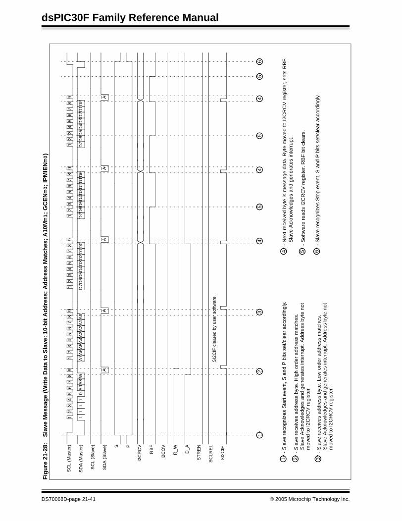
dsPIC30F Family Reference Manual
Fig
ure
21-
28:
Sla
ve M
essa
ge
(Wri
te D
ata
to S
lave
: 10
-bit
Ad
dre
ss;
Ad
dre
ss M
atch
es;
A10
M=1
; G
CE
N=0
; IP
MIE
N=0
)
T
1-
Sla
ve r
ecog
nize
s S
tart
eve
nt, S
and
P b
its s
et/c
lear
acc
ordi
ngly
.
SC
L (M
aste
r)
SD
A (
Mas
ter)
SC
L (S
lave
)
SD
A (
Sla
ve)
I2C
RC
V
RB
F
SI2
CIF
ST
RE
N
12
34
56
78
A9
A8
9 A
A7
A6
A5
A4
A3
A2
A1
A0
12
34
56
78
9
W
13
2
A
44
46
2-
Sla
ve r
ecei
ves
addr
ess
byte
. Hig
h or
der
addr
ess
mat
ches
.
3-
Sla
ve r
ecei
ves
addr
ess
byte
. Low
ord
er a
ddre
ss m
atch
es.
4-
Nex
t rec
eive
d by
te is
mes
sage
dat
a. B
yte
mov
ed to
I2C
RC
V r
egis
ter,
sets
RB
F.
5-
Sof
twar
e re
ads
I2C
RC
V r
egis
ter.
RB
F b
it cl
ears
.
6-
Sla
ve r
ecog
nize
s S
top
even
t, S
and
P b
its s
et/c
lear
acc
ordi
ngly
.
Sla
ve A
ckno
wle
dges
and
gen
erat
es in
terr
upt.
Add
ress
byt
e no
t
Sla
ve A
ckno
wle
dges
and
gen
erat
es in
terr
upt.
S P
I2C
OV
R_W D_A
D7D
6D5D
4D3D
2D1D
0
12
34
56
78
9 A
D7D
6D5D
4D3D
2D1D
0
12
34
56
78
9 A
D7D
6D5D
4D3D
2D1D
0
12
34
56
78
9 A
SC
LRE
L
55
5
11
11
0
Sla
ve A
ckno
wle
dges
and
gen
erat
es in
terr
upt.
Add
ress
byt
e no
t
mov
ed to
I2C
RC
V r
egis
ter.
mov
ed to
I2C
RC
V r
egis
ter.
SI2
CIF
cle
ared
by
user
sof
twar
e.
DS70068D-page 21-41 © 2005 Microchip Technology Inc.
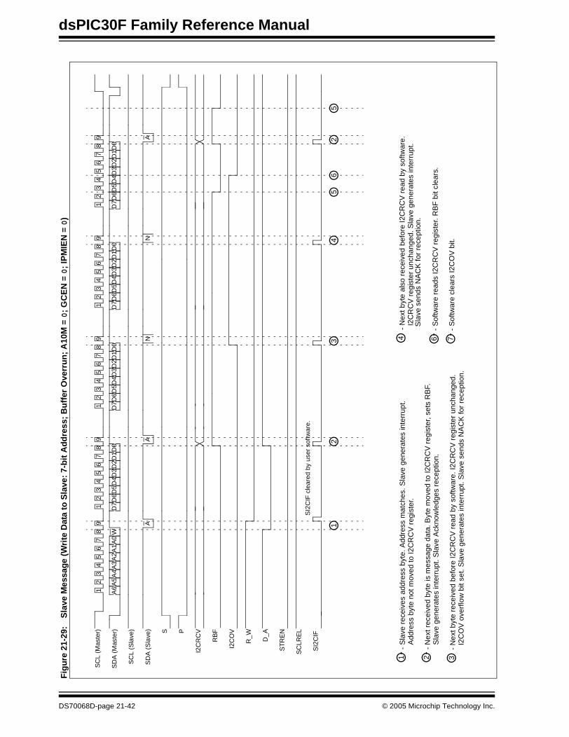
dsPIC30F Family Reference Manual
Fig
ure
21-
29:
Sla
ve M
essa
ge
(Wri
te D
ata
to S
lave
: 7-
bit
Ad
dre
ss;
Bu
ffer
Ove
rru
n;
A10
M =
0;
GC
EN
= 0
; IP
MIE
N =
0)
T
SC
L (M
aste
r)
SD
A (
Mas
ter)
SC
L (S
lave
)
SD
A (
Sla
ve)
I2C
RC
V
RB
F
SI2
CIF
ST
RE
N
12
34
56
78
A1
A0
9 A
D7D
6D5D
4D3D
2D1D
0
12
34
56
78
9
W
21
A
34
2
1-
Sla
ve r
ecei
ves
addr
ess
byte
. Add
ress
mat
ches
. Sla
ve g
ener
ates
inte
rrup
t.
2-
Nex
t rec
eive
d by
te is
mes
sage
dat
a. B
yte
mov
ed to
I2C
RC
V r
egis
ter,
sets
RB
F.6
- S
oftw
are
read
s I2
CR
CV
reg
iste
r. R
BF
bit
clea
rs.
7-
Sof
twar
e cl
ears
I2C
OV
bit.
Add
ress
byt
e no
t mov
ed to
I2C
RC
V r
egis
ter.
Sla
ve g
ener
ates
inte
rrup
t. S
lave
Ack
now
ledg
es r
ecep
tion.
A6
A5
A4
A3
A2
S P
I2C
OV
R_W D_A
D7D
6D5D
4D3D
2D1D
0
12
34
56
78
9 N
D7D
6D5D
4D3D
2D1D
0
12
34
56
78
9
D7D
6D5D
4D3D
2D1D
0
12
34
56
78
9
SC
LRE
L
55
3-
Nex
t byt
e re
ceiv
ed b
efor
e I2
CR
CV
rea
d by
sof
twar
e. I2
CR
CV
reg
iste
r un
chan
ged.
I2C
OV
ove
rflo
w b
it se
t. S
lave
gen
erat
es in
terr
upt.
Sla
ve s
ends
NA
CK
for
rece
ptio
n.
NA
6
4-
Nex
t byt
e al
so r
ecei
ved
befo
re I2
CR
CV
rea
d by
sof
twar
e.
Sla
ve s
ends
NA
CK
for
rece
ptio
n.I2
CR
CV
reg
iste
r un
chan
ged.
Sla
ve g
ener
ates
inte
rrup
t.
SI2
CIF
cle
ared
by
user
sof
twar
e.
DS70068D-page 21-42 © 2005 Microchip Technology Inc.
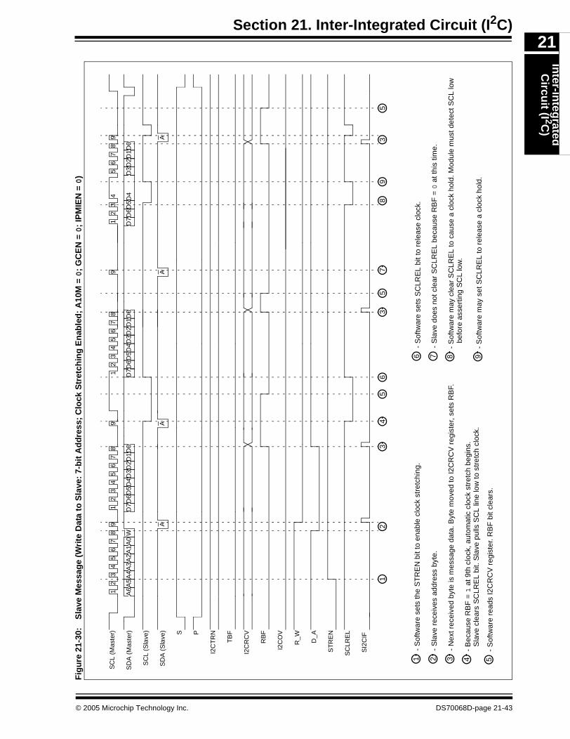
Section 21. Inter-Integrated Circuit (I2C)In
ter-Integ
ratedC
ircuit (I 2C
)
21
Fig
ure
21-
30:
Sla
ve M
essa
ge
(Wri
te D
ata
to S
lave
: 7-
bit
Ad
dre
ss;
Clo
ck S
tret
chin
g E
nab
led
; A
10M
= 0
; G
CE
N =
0;
IPM
IEN
= 0
)
T
1-
Sof
twar
e se
ts th
e S
TR
EN
bit
to e
nabl
e cl
ock
stre
tchi
ng.
SC
L (M
aste
r)
SD
A (
Mas
ter)
SC
L (S
lave
)
SD
A (
Sla
ve)
I2C
TR
N
TB
F
I2C
RC
V
RB
F
SI2
CIF
ST
RE
N
12
34
56
78
A1
A0
9 A
D7D
6D5D
4D3D
2D1D
0
12
34
56
78
9
W
32
A
53
83
2-
Sla
ve r
ecei
ves
addr
ess
byte
.
3-
Nex
t rec
eive
d by
te is
mes
sage
dat
a. B
yte
mov
ed to
I2C
RC
V r
egis
ter,
sets
RB
F.
6-
Sof
twar
e se
ts S
CLR
EL
bit t
o re
leas
e cl
ock.
7-
Sla
ve d
oes
not c
lear
SC
LRE
L be
caus
e R
BF
= 0
at t
his
time.
A6
A5
A4
A3
A2
S P
I2C
OV
R_W D_A
D7D
6D5D
4D3D
2D1D
0
12
34
56
78
9 A
D7D
6D5
D3D
2D1D
0
12
34
56
78
9 A
SC
LRE
L
59
5
D4
46
71
4-
Bec
ause
RB
F =
1 a
t 9th
clo
ck, a
utom
atic
clo
ck s
tret
ch b
egin
s.
Sla
ve c
lear
s S
CLR
EL
bit.
Sla
ve p
ulls
SC
L lin
e lo
w to
str
etch
clo
ck.
5-
Sof
twar
e re
ads
I2C
RC
V r
egis
ter.
RB
F b
it cl
ears
.
8-
Sof
twar
e m
ay c
lear
SC
LRE
L to
cau
se a
clo
ck h
old.
Mod
ule
mus
t det
ect S
CL
low
9-
Sof
twar
e m
ay s
et S
CLR
EL
to r
elea
se a
clo
ck h
old.
befo
re a
sser
ting
SC
L lo
w.
© 2005 Microchip Technology Inc. DS70068D-page 21-43
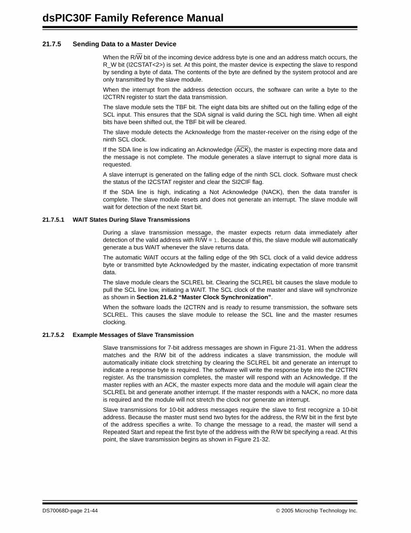
dsPIC30F Family Reference Manual
21.7.5 Sending Data to a Master Device
When the R/W bit of the incoming device address byte is one and an address match occurs, theR_W bit (I2CSTAT<2>) is set. At this point, the master device is expecting the slave to respondby sending a byte of data. The contents of the byte are defined by the system protocol and areonly transmitted by the slave module.
When the interrupt from the address detection occurs, the software can write a byte to theI2CTRN register to start the data transmission.
The slave module sets the TBF bit. The eight data bits are shifted out on the falling edge of theSCL input. This ensures that the SDA signal is valid during the SCL high time. When all eightbits have been shifted out, the TBF bit will be cleared.
The slave module detects the Acknowledge from the master-receiver on the rising edge of theninth SCL clock.
If the SDA line is low indicating an Acknowledge (ACK), the master is expecting more data andthe message is not complete. The module generates a slave interrupt to signal more data isrequested.
A slave interrupt is generated on the falling edge of the ninth SCL clock. Software must checkthe status of the I2CSTAT register and clear the SI2CIF flag.
If the SDA line is high, indicating a Not Acknowledge (NACK), then the data transfer iscomplete. The slave module resets and does not generate an interrupt. The slave module willwait for detection of the next Start bit.
21.7.5.1 WAIT States During Slave Transmissions
During a slave transmission message, the master expects return data immediately afterdetection of the valid address with R/W = 1. Because of this, the slave module will automaticallygenerate a bus WAIT whenever the slave returns data.
The automatic WAIT occurs at the falling edge of the 9th SCL clock of a valid device addressbyte or transmitted byte Acknowledged by the master, indicating expectation of more transmitdata.
The slave module clears the SCLREL bit. Clearing the SCLREL bit causes the slave module topull the SCL line low, initiating a WAIT. The SCL clock of the master and slave will synchronizeas shown in Section 21.6.2 “Master Clock Synchronization”.
When the software loads the I2CTRN and is ready to resume transmission, the software setsSCLREL. This causes the slave module to release the SCL line and the master resumesclocking.
21.7.5.2 Example Messages of Slave Transmission
Slave transmissions for 7-bit address messages are shown in Figure 21-31. When the addressmatches and the R/W bit of the address indicates a slave transmission, the module willautomatically initiate clock stretching by clearing the SCLREL bit and generate an interrupt toindicate a response byte is required. The software will write the response byte into the I2CTRNregister. As the transmission completes, the master will respond with an Acknowledge. If themaster replies with an ACK, the master expects more data and the module will again clear theSCLREL bit and generate another interrupt. If the master responds with a NACK, no more datais required and the module will not stretch the clock nor generate an interrupt.
Slave transmissions for 10-bit address messages require the slave to first recognize a 10-bitaddress. Because the master must send two bytes for the address, the R/W bit in the first byteof the address specifies a write. To change the message to a read, the master will send aRepeated Start and repeat the first byte of the address with the R/W bit specifying a read. At thispoint, the slave transmission begins as shown in Figure 21-32.
DS70068D-page 21-44 © 2005 Microchip Technology Inc.
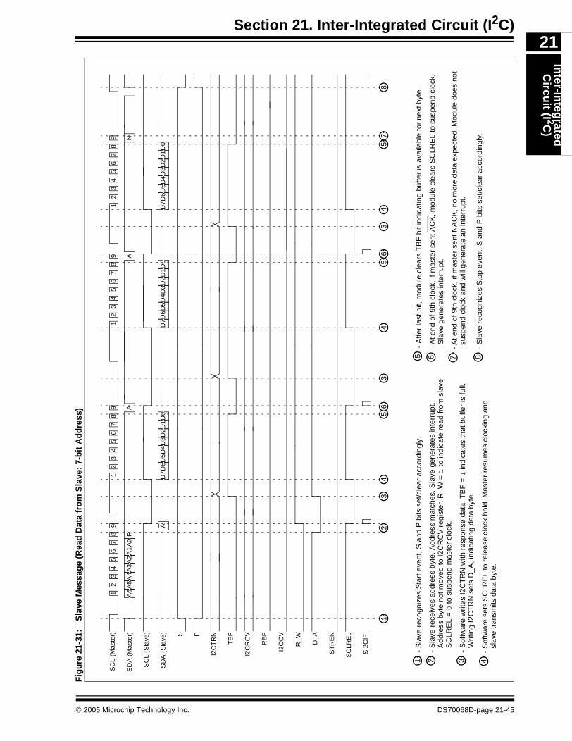
Section 21. Inter-Integrated Circuit (I2C)In
ter-Integ
ratedC
ircuit (I 2C
)
21
Fig
ure
21-
31:
Sla
ve M
essa
ge
(Rea
d D
ata
fro
m S
lave
: 7-
bit
Ad
dre
ss)
T
1-
Sla
ve r
ecog
nize
s S
tart
eve
nt, S
and
P b
its s
et/c
lear
acc
ordi
ngly
.
SC
L (M
aste
r)
SD
A (
Mas
ter)
SC
L (S
lave
)
SD
A (
Sla
ve)
I2C
TR
N
TB
F
I2C
RC
V
RB
F
SI2
CIF
ST
RE
N
12
34
56
78
A1
A0
9 AD
7D6D
5D4D
3D2D
1D0
12
34
56
78
9
R
14
2
A
53
53
8
2-
Sla
ve r
ecei
ves
addr
ess
byte
. Add
ress
mat
ches
. Sla
ve g
ener
ates
inte
rrup
t.
3-
Sof
twar
e w
rites
I2C
TR
N w
ith r
espo
nse
data
. TB
F =
1 in
dica
tes
that
buf
fer
is fu
ll.
6-
At e
nd o
f 9th
clo
ck, i
f mas
ter
sent
AC
K, m
odul
e cl
ears
SC
LRE
L to
sus
pend
clo
ck.
8-
Sla
ve r
ecog
nize
s S
top
even
t, S
and
P b
its s
et/c
lear
acc
ordi
ngly
.
Add
ress
byt
e no
t mov
ed to
I2C
RC
V r
egis
ter.
R_W
= 1
to in
dica
te r
ead
from
sla
ve.
Writ
ing
I2C
TR
N s
ets
D_A
, ind
icat
ing
data
byt
e.
A6
A5
A4
A3
A2
S P
I2C
OV
R_W D_A
SC
LRE
L
44
D7D
6D5D
4D3D
2D1D
0
12
34
56
78
9 A
D7D
6D5D
4D3D
2D1D
0
12
34
56
78
9 N
36
65
7
SC
LRE
L =
0 to
sus
pend
mas
ter
cloc
k.
4-
Sof
twar
e se
ts S
CLR
EL
to r
elea
se c
lock
hol
d. M
aste
r re
sum
es c
lock
ing
and
slav
e tr
ansm
its d
ata
byte
.
5-
Afte
r la
st b
it, m
odul
e cl
ears
TB
F b
it in
dica
ting
buffe
r is
ava
ilabl
e fo
r ne
xt b
yte.
Sla
ve g
ener
ates
inte
rrup
t.
7-
At e
nd o
f 9th
clo
ck, i
f mas
ter
sent
NA
CK
, no
mor
e da
ta e
xpec
ted.
Mod
ule
does
not
su
spen
d cl
ock
and
will
gen
erat
e an
inte
rrup
t.
© 2005 Microchip Technology Inc. DS70068D-page 21-45
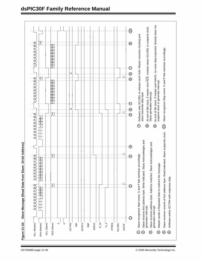
dsPIC30F Family Reference Manual
Fig
ure
21-
32:
Sla
ve M
essa
ge
(Rea
d D
ata
fro
m S
lave
: 10
-bit
Ad
dre
ss)
T
1-
Sla
ve r
ecog
nize
s S
tart
eve
nt, S
and
P b
its s
et/c
lear
acc
ordi
ngly
.
SC
L (M
aste
r)
SD
A (
Mas
ter)
SC
L (S
lave
)
SD
A (
Sla
ve)
I2C
TR
N
TB
F
I2C
RC
V
RB
F
SI2
CIF
ST
RE
N
12
34
56
78
9 A
14
27
8
2-
Sla
ve r
ecei
ves
first
add
ress
byt
e. W
rite
indi
cate
d. S
lave
Ack
now
ledg
es a
nd
6-
Sof
twar
e w
rites
I2C
TR
N w
ith r
espo
nse
data
.
8-
At e
nd o
f 9th
clo
ck, i
f mas
ter
sent
AC
K, m
odul
e cl
ears
SC
LRE
L to
sus
pend
clo
ck.
- S
lave
rec
ogni
zes
Sto
p ev
ent,
S a
nd P
bits
set
/cle
ar a
ccor
ding
ly.
S P
AD
D10
R_W D_A
SC
LRE
L
56
D7D
6D5D
4D3D
2D1D
0
12
34
56
78
9 N
36
97
7-
Sof
twar
e se
ts S
CLR
EL
to r
elea
se c
lock
hol
d. M
aste
r re
sum
es c
lock
ing
and
slav
e tr
ansm
its d
ata
byte
.
Sla
ve g
ener
ates
inte
rrup
t.
9-
At e
nd o
f 9th
clo
ck, i
f mas
ter
sent
NA
CK
, no
mor
e da
ta e
xpec
ted.
Mod
ule
does
not
su
spen
d cl
ock
or g
ener
ate
inte
rrup
t.
A7
A6
A5
A4
A3
A2
A1
A0
12
34
56
78
9 A
A9
A8
W1
11
10
12
34
56
78
9 A
A9
A8
11
11
0
D7D
6D5D
4D3D
2D1D
0
12
34
56
78
9 A
3-
Sla
ve r
ecei
ves
addr
ess
byte
. Add
ress
mat
ches
. Sla
ve A
ckno
wle
dges
and
10
10
4-
Mas
ter
send
s a
Rep
eate
d S
tart
to r
edire
ct th
e m
essa
ge.
5-
Sla
ve r
ecei
ves
rese
nd o
f firs
t add
ress
byt
e. R
ead
indi
cate
d. S
lave
sus
pend
s cl
ock.
R
gen
erat
es in
terr
upt.
gen
erat
es in
terr
upt.
DS70068D-page 21-46 © 2005 Microchip Technology Inc.

Section 21. Inter-Integrated Circuit (I2C)In
ter-Integ
ratedC
ircuit (I 2C
)21
21.8 Connection Considerations for I2C Bus
By definition of the I2C bus being a wired AND bus connection, pull-up resistors on the bus arerequired, shown as RP in Figure 21-33. Series resistors, shown as RS are optional and used toimprove ESD susceptibility. The values of resistors RP and RS depend on the followingparameters:
• Supply voltage• Bus capacitance• Number of connected devices (input current + leakage current)
Because the device must be able to pull the bus low against RP, current drawn by RP must begreater than the I/O pin minimum sink current IOL of 3 mA at VOL(MAX) = 0.4V for the deviceoutput stage. For example, with a supply voltage of VDD = 5V +10%:
RP(MIN) = (VDD(MAX) – VOL(MAX)) / IOL = (5.5-0.4) / 3 mA = 1.7 kΩ
In a 400 kHz system, a minimum rise time specification of 300 nsec exists and in a 100 kHzsystem, the specification is 1000 nsec.
Because RP must pull the bus up against the total capacitance CB with a maximum rise time of300 nsec to 0.7 VDD, the maximum resistance for RP must be less than:
RP(MAX) = -tR / CB * ln(1 – (VIL(MAX) – VDD(MAX)) = -300 nsec / (100pf * ln(1-0.7)) = 2.5 kΩ
The maximum value for RS is determined by the desired noise margin for the low level. RS
cannot drop enough voltage to make the device VOL plus voltage across RS more than themaximum VIL.
Rs(MAX) = (VIL(MAX) – VOL(MIN)) / IOL(MAX) = (0.3 VDD-0.4) / 3 mA = 366Ω
The SCL clock input must have a minimum high and low time for proper operation. The high andlow times of the I2C specification as well as the requirements of the I2C module, are shown inthe “Electrical Specifications” section in the specific device data sheet.
Figure 21-33: Sample Device Configuration for I2C™ Bus
RPRP
VDD + 10%
SDA
SCL
Device
CB = 10 - 400 pF
RSRS
Note: I2C devices with input levels related to VDD must have one common supply lineto which the pull-up resistor is also connected.
© 2005 Microchip Technology Inc. DS70068D-page 21-47
dsPIC30F Family Reference Manual
21.8.1 Integrated Signal Conditioning
The SCL and SDA pins have an input glitch filter. The I2C bus requires this filter in both the100 kHz and 400 kHz systems.
When operating on a 400 kHz bus, the I2C specification requires a slew rate control of thedevice pin output. This slew rate control is integrated into the device. If the DISSLW bit(I2CCON<9>) is cleared, the slew rate control is active. For other bus speeds, the I2Cspecification does not require slew rate control and DISSLW should be set.
Some system implementations of I2C busses require different input levels for VIL(MAX) andVIH(MIN).
In a normal I2C system:
VIL(MAX) = lesser of 1.5V and 0.3 VDD
VIH(MIN) = greater of 3.0V and 0.7 VDD
In an SMBus (System Management Bus) system:
VIL(MAX) = 0.2 VDD
VIH(MIN) = 0.8 VDD
The SMEN bit (I2CCON<8>) controls the input levels. SMEN is set to change the input levels toSMBus specifications.
DS70068D-page 21-48 © 2005 Microchip Technology Inc.
Section 21. Inter-Integrated Circuit (I2C)In
ter-Integ
ratedC
ircuit (I 2C
)21
21.9 Module Operation During PWRSAV Instruction
21.9.1 When the Device Enters Sleep Mode
When the device executes a PWRSAV 0 instruction, the device enters Sleep mode. When thedevice enters Sleep mode, the master and slave module abort any pending message activityand reset the state of the modules. Any transmission/reception that is in progress will notcontinue when the device wakes from Sleep. After the device returns to Operational mode, themaster module will be in an Idle state waiting for a message command and the slave modulewill be waiting for a Start condition. During Sleep, the IWCOL, I2COV and BCL bits are cleared.Additionally, because the master functions are aborted, the SEN, RSEN, PEN, RCEN, ACKENand TRSTAT bits are cleared. TBF and RBF are cleared and the buffers are available atwake-up.
There is no automatic method to prevent Sleep entry if a transmission or reception is active orpending. The software must synchronize Sleep entry with I2C operation to avoid abortedmessages.
During Sleep, the slave module will not monitor the I2C bus. Thus, it is not possible to generatea wake-up event based on the I2C bus using the I2C module. Other interrupt inputs, such as theinterrupt-on-change inputs can be used to detect message traffic on a I2C bus and cause adevice wake-up.
21.9.2 When the Device Enters Idle Mode
When the device executes a PWRSAV 1 instruction, the device enters Idle mode. The modulewill enter a power saving state in Idle mode depending on the I2CSIDL bit (I2CCON<13>).
If I2CSIDL = 1, the module will enter the Power Saving mode similarly to actions while enteringSleep mode.
If I2CSIDL = 0, the module will not enter a Power Saving mode. The module will continue tooperate normally.
21.10 Effects of a Reset
A Reset disables the I2C module and terminates any active or pending message activity. Seethe register definitions of I2CCON and I2CSTAT for the Reset conditions of those registers.
Note: In this discussion, ‘Idle’ refers to the CPU power saving state. The lower-case ‘idle’refers to the time when the I2C module is not transferring data on the bus.
© 2005 Microchip Technology Inc. DS70068D-page 21-49
dsPIC30F Family Reference Manual
21.11 Design Tips
Question 1: I’m operating as a bus master and transmitting data, however, slave andreceive interrupts are also occurring.
Answer: The master and slave circuits are independent. The slave module will receive eventsfrom the bus sent by the master.
Question 2: I’m operating as a slave and I write data to the I2CTRN register, but the datadid not transmit.
Answer: The slave enters an automatic wait when preparing to transmit. Ensure that you setthe SCLREL bit to release the I2C clock.
Question 3: How do I tell what state the master module is in?
Answer: Looking at the condition of SEN, RSEN, PEN, RCEN, ACKEN and TRSTAT bits willindicate the state of the master module. If all bits are ‘0’, the module is Idle.
Question 4: Operating as a slave, I receive a byte while STREN = 0. What should thesoftware do if it cannot process the byte before the next one is received?
Answer: Because STREN was ‘0’, the module did not generate an automatic WAIT on thereceived byte. However, the software may, at any time during the message, set STREN thenclear SCLREL. This will cause a WAIT on the next opportunity to synchronize the SCL clock.
Question 5: My I2C system is a multi-master system. When I attempt to send a message,it is being corrupted.
Answer: In a multi-master system, other masters may cause bus collisions. In the InterruptService Routine for the master, check the BCL bit to ensure that the operation completedwithout a collision. If a collision is detected, the message must be resent from the beginning.
Question 6: My I2C system is a multi-master system. How can I tell when it is OK tobegin a message?
Answer: Look at the S and P bits. If S = 0 and P = 0 the bus is Idle. If S = 0 and P = 1, the busis Idle.
Question 7: I tried to send a Start condition on the bus, then transmit a byte by writingto the I2CTRN register. The byte did not get transmitted. Why?
Answer: You must wait for each event on the I2C bus to complete before starting the next one.In this case, you should poll the SEN bit to determine when the Start event completed, or wait forthe master I2C interrupt before data is written to I2CTRN.
DS70068D-page 21-50 © 2005 Microchip Technology Inc.

Section 21. Inter-Integrated Circuit (I2C)In
ter-Integ
ratedC
ircuit (I 2C
)21
21.12 Related Application Notes
This section lists application notes that are related to this section of the manual. Theseapplication notes may not be written specifically for the dsPIC30F Product Family, but theconcepts are pertinent and could be used with modification and possible limitations. The currentapplication notes related to the Inter-Integrated Circuit (I2C) module are:
Title Application Note #
Use of the SSP Module in the I 2C™ Multi-Master Environment AN578Using the PICmicro® SSP for Slave I2C™ Communication AN734Using the PICmicro® MSSP Module for Master I2C™ Communications AN735An I2C™ Network Protocol for Environmental Monitoring AN736
Note: Please visit the Microchip web site (www.microchip.com) for additional ApplicationNotes and code examples for the dsPIC30F Family of devices.
© 2005 Microchip Technology Inc. DS70068D-page 21-51
dsPIC30F Family Reference Manual
21.13 Revision History
Revision A
This is the initial released revision of this document.
Revision B
This revision has been expanded to contain a full description of the dsPIC30F Inter-IntegratedCircuit (I2C) module.
Revision C
This revision incorporates all known errata at the time of this document update.
DS70068D-page 21-52 © 2005 Microchip Technology Inc.
Section 22. Data Converter Interface (DCI)
Data C
on
verterIn
terface (DC
I)
22
HIGHLIGHTSThis section of the manual contains the following topics:
22.1 Introduction .................................................................................................................. 22-2
22.2 Control Register Descriptions ...................................................................................... 22-222.3 Codec Interface Basics and Terminology..................................................................... 22-822.4 DCI Operation ............................................................................................................ 22-10
22.5 Using the DCI Module................................................................................................ 22-1722.6 Operation in Power Saving Modes ............................................................................ 22-2822.7 Registers Associated with DCI................................................................................... 22-28
22.8 Design Tips ................................................................................................................ 22-3022.9 Related Application Notes.......................................................................................... 22-3122.10 Revision History ......................................................................................................... 22-32
© 2004 Microchip Technology Inc. DS70069C-page 22-1
dsPIC30F Family Reference Manual
22.1 Introduction
The dsPIC Data Converter Interface (DCI) module allows simple interfacing of devices, such asaudio coder/decoders (codecs), A/D converters, and D/A converters.
The following interfaces are supported:
• Framed Synchronous Serial Transfer (Single or Multi-Channel)• Inter-IC Sound (I2S) Interface
• AC-Link Compliant mode
Many codecs intended for use in audio applications support sampling rates between 8 kHz and48 kHz and use one of the interface protocols listed above. The DCI automatically handles theinterface timing associated with these codecs. No overhead from the CPU is required until therequested amount of data has been transmitted and/or received by the DCI. Up to four datawords may be transferred between CPU interrupts.
The data word length for the DCI is programmable up to 16 bits to match the data size of thedsPIC30F CPU. However, many codecs have data word sizes greater than 16 bits. Long dataword lengths can be supported by the DCI. The DCI is configured to transmit/receive the longword in multiple 16-bit time slots. This operation is transparent to the user and the long data wordis stored in consecutive register locations.
The DCI can support up to 16 time slots in a data frame, for a maximum frame size of 256 bits.There are control bits for each time slot in the data frame that determine whether the DCI willtransmit/receive during the time slot.
22.2 Control Register Descriptions
The DCI has five Control registers and one Status register, which are listed below:
• DCICON1: DCI module enable and mode bits.• DCICON2: DCI module word length, data frame length, and buffer setup.• DCICON3: DCI module bit clock generator setup.
• DCISTAT: DCI module status information.• RSCON: Active frame time slot control for data reception.• TSCON: Active frame time slot control for data transmit.
In addition to these Control and Status registers, there are four Transmit registers,TXBUF0....TXBUF3, and four Receive registers, RXBUF0....RXBUF3.
DS70069C-page 22-2 © 2004 Microchip Technology Inc.
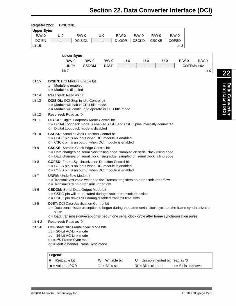
Section 22. Data Converter Interface (DCI)D
ata Co
nverter
Interface (D
CI)
22
Register 22-1: DCICON1
Upper Byte:R/W-0 U-0 R/W-0 U-0 R/W-0 R/W-0 R/W-0 R/W-0DCIEN — DCISIDL — DLOOP CSCKD CSCKE COFSD
bit 15 bit 8
Lower Byte:R/W-0 R/W-0 R/W-0 U-0 U-0 U-0 R/W-0 R/W-0UNFM CSDOM DJST — — — COFSM<1:0>
bit 7 bit 0
bit 15 DCIEN: DCI Module Enable bit1 = Module is enabled0 = Module is disabled
bit 14 Reserved: Read as ‘0’
bit 13 DCISIDL: DCI Stop in Idle Control bit1 = Module will halt in CPU Idle mode0 = Module will continue to operate in CPU Idle mode
bit 12 Reserved: Read as ‘0’
bit 11 DLOOP: Digital Loopback Mode Control bit1 = Digital Loopback mode is enabled. CSDI and CSDO pins internally connected.0 = Digital Loopback mode is disabled
bit 10 CSCKD: Sample Clock Direction Control bit1 = CSCK pin is an input when DCI module is enabled0 = CSCK pin is an output when DCI module is enabled
bit 9 CSCKE: Sample Clock Edge Control bit1 = Data changes on serial clock falling edge, sampled on serial clock rising edge0 = Data changes on serial clock rising edge, sampled on serial clock falling edge
bit 8 COFSD: Frame Synchronization Direction Control bit1 = COFS pin is an input when DCI module is enabled0 = COFS pin is an output when DCI module is enabled
bit 7 UNFM: Underflow Mode bit1 = Transmit last value written to the Transmit registers on a transmit underflow0 = Transmit ‘0’s on a transmit underflow
bit 6 CSDOM: Serial Data Output Mode bit1 = CSDO pin will be tri-stated during disabled transmit time slots0 = CSDO pin drives ‘0’s during disabled transmit time slots
bit 5 DJST: DCI Data Justification Control bit1 = Data transmission/reception is begun during the same serial clock cycle as the frame synchronization
pulse0 = Data transmission/reception is begun one serial clock cycle after frame synchronization pulse
bit 4-2 Reserved: Read as ‘0’
bit 1-0 COFSM<1:0>: Frame Sync Mode bits11 = 20-bit AC-Link mode10 = 16-bit AC-Link mode01 = I2S Frame Sync mode00 = Multi-Channel Frame Sync mode
Legend:
R = Readable bit W = Writable bit U = Unimplemented bit, read as ‘0’
-n = Value at POR ‘1’ = Bit is set ‘0’ = Bit is cleared x = Bit is unknown
© 2004 Microchip Technology Inc. DS70069C-page 22-3
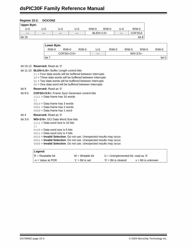
dsPIC30F Family Reference Manual
Register 22-2: DCICON2
Upper Byte:U-0 U-0 U-0 U-0 R/W-0 R/W-0 U-0 R/W-0— — — — BLEN<1:0> — COFSG3
bit 15 bit 8
Lower Byte:R/W-0 R/W-0 R/W-0 U-0 R/W-0 R/W-0 R/W-0 R/W-0
COFSG<2:0> — WS<3:0>bit 7 bit 0
bit 15-12 Reserved: Read as ‘0’
bit 11-10 BLEN<1:0>: Buffer Length control bits11 = Four data words will be buffered between interrupts10 = Three data words will be buffered between interrupts01 = Two data words will be buffered between interrupts00 = One data word will be buffered between interrupts
bit 9 Reserved: Read as ‘0’
bit 8-5 COFSG<3:0>: Frame Sync Generator control bits1111 = Data frame has 16 words||0010 = Data frame has 3 words0001 = Data frame has 2 words0000 = Data frame has 1 word
bit 4 Reserved: Read as ‘0’
bit 3-0 WS<3:0>: DCI Data Word Size bits1111 = Data word size is 16 bits||0100 = Data word size is 5 bits0011 = Data word size is 4 bits0010 = Invalid Selection. Do not use. Unexpected results may occur.0001 = Invalid Selection. Do not use. Unexpected results may occur.0000 = Invalid Selection. Do not use. Unexpected results may occur.
Legend:
R = Readable bit W = Writable bit U = Unimplemented bit, read as ‘0’
-n = Value at POR ‘1’ = Bit is set ‘0’ = Bit is cleared x = Bit is unknown
DS70069C-page 22-4 © 2004 Microchip Technology Inc.
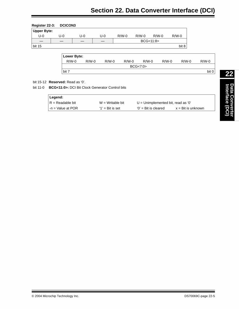
Section 22. Data Converter Interface (DCI)D
ata Co
nverter
Interface (D
CI)
22
Register 22-3: DCICON3
Upper Byte:U-0 U-0 U-0 U-0 R/W-0 R/W-0 R/W-0 R/W-0— — — — BCG<11:8>
bit 15 bit 8
Lower Byte:R/W-0 R/W-0 R/W-0 R/W-0 R/W-0 R/W-0 R/W-0 R/W-0
BCG<7:0>bit 7 bit 0
bit 15-12 Reserved: Read as ‘0’.
bit 11-0 BCG<11:0>: DCI Bit Clock Generator Control bits
Legend:
R = Readable bit W = Writable bit U = Unimplemented bit, read as ‘0’
-n = Value at POR ‘1’ = Bit is set ‘0’ = Bit is cleared x = Bit is unknown
© 2004 Microchip Technology Inc. DS70069C-page 22-5
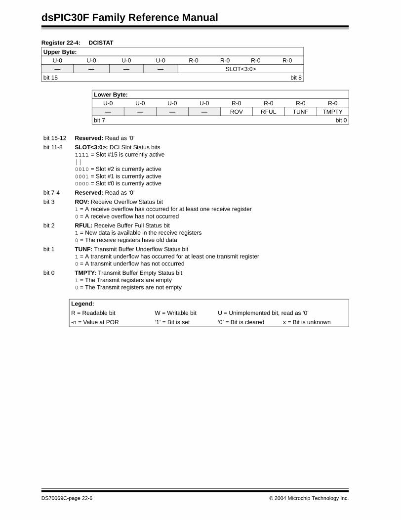
dsPIC30F Family Reference Manual
Register 22-4: DCISTAT
Upper Byte:U-0 U-0 U-0 U-0 R-0 R-0 R-0 R-0— — — — SLOT<3:0>
bit 15 bit 8
Lower Byte:U-0 U-0 U-0 U-0 R-0 R-0 R-0 R-0— — — — ROV RFUL TUNF TMPTY
bit 7 bit 0
bit 15-12 Reserved: Read as ‘0’
bit 11-8 SLOT<3:0>: DCI Slot Status bits1111 = Slot #15 is currently active||0010 = Slot #2 is currently active0001 = Slot #1 is currently active0000 = Slot #0 is currently active
bit 7-4 Reserved: Read as ‘0’
bit 3 ROV: Receive Overflow Status bit1 = A receive overflow has occurred for at least one receive register0 = A receive overflow has not occurred
bit 2 RFUL: Receive Buffer Full Status bit1 = New data is available in the receive registers0 = The receive registers have old data
bit 1 TUNF: Transmit Buffer Underflow Status bit1 = A transmit underflow has occurred for at least one transmit register0 = A transmit underflow has not occurred
bit 0 TMPTY: Transmit Buffer Empty Status bit1 = The Transmit registers are empty0 = The Transmit registers are not empty
Legend:
R = Readable bit W = Writable bit U = Unimplemented bit, read as ‘0’
-n = Value at POR ‘1’ = Bit is set ‘0’ = Bit is cleared x = Bit is unknown
DS70069C-page 22-6 © 2004 Microchip Technology Inc.
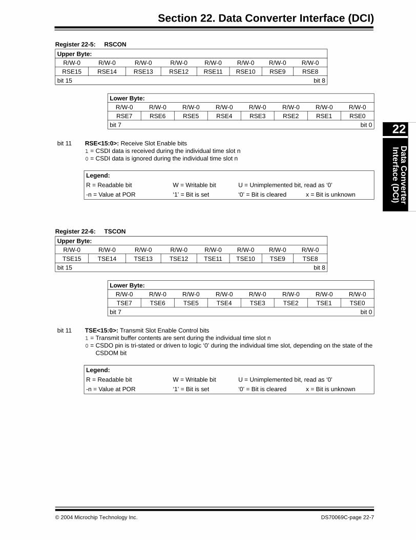
Section 22. Data Converter Interface (DCI)D
ata Co
nverter
Interface (D
CI)
22
Register 22-5: RSCON
Register 22-6: TSCON
Upper Byte:R/W-0 R/W-0 R/W-0 R/W-0 R/W-0 R/W-0 R/W-0 R/W-0RSE15 RSE14 RSE13 RSE12 RSE11 RSE10 RSE9 RSE8
bit 15 bit 8
Lower Byte:R/W-0 R/W-0 R/W-0 R/W-0 R/W-0 R/W-0 R/W-0 R/W-0RSE7 RSE6 RSE5 RSE4 RSE3 RSE2 RSE1 RSE0
bit 7 bit 0
bit 11 RSE<15:0>: Receive Slot Enable bits1 = CSDI data is received during the individual time slot n0 = CSDI data is ignored during the individual time slot n
Legend:
R = Readable bit W = Writable bit U = Unimplemented bit, read as ‘0’
-n = Value at POR ‘1’ = Bit is set ‘0’ = Bit is cleared x = Bit is unknown
Upper Byte:R/W-0 R/W-0 R/W-0 R/W-0 R/W-0 R/W-0 R/W-0 R/W-0
TSE15 TSE14 TSE13 TSE12 TSE11 TSE10 TSE9 TSE8bit 15 bit 8
Lower Byte:R/W-0 R/W-0 R/W-0 R/W-0 R/W-0 R/W-0 R/W-0 R/W-0TSE7 TSE6 TSE5 TSE4 TSE3 TSE2 TSE1 TSE0
bit 7 bit 0
bit 11 TSE<15:0>: Transmit Slot Enable Control bits1 = Transmit buffer contents are sent during the individual time slot n0 = CSDO pin is tri-stated or driven to logic ‘0’ during the individual time slot, depending on the state of the
CSDOM bit
Legend:
R = Readable bit W = Writable bit U = Unimplemented bit, read as ‘0’
-n = Value at POR ‘1’ = Bit is set ‘0’ = Bit is cleared x = Bit is unknown
© 2004 Microchip Technology Inc. DS70069C-page 22-7
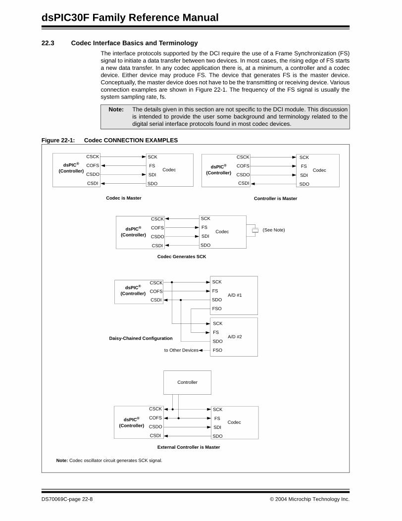
dsPIC30F Family Reference Manual
22.3 Codec Interface Basics and Terminology
The interface protocols supported by the DCI require the use of a Frame Synchronization (FS)signal to initiate a data transfer between two devices. In most cases, the rising edge of FS startsa new data transfer. In any codec application there is, at a minimum, a controller and a codecdevice. Either device may produce FS. The device that generates FS is the master device.Conceptually, the master device does not have to be the transmitting or receiving device. Variousconnection examples are shown in Figure 22-1. The frequency of the FS signal is usually thesystem sampling rate, fs.
Figure 22-1: Codec CONNECTION EXAMPLES
Note: The details given in this section are not specific to the DCI module. This discussionis intended to provide the user some background and terminology related to thedigital serial interface protocols found in most codec devices.
Codec
SCK
FS
SDI
Controller
SDO
CSCK
COFS
CSDO
CSDI
Codec
SCK
FS
SDI
SDO
Codec is Master
dsPIC®
(Controller)
CSCK
COFS
CSDO
CSDI
Codec
SCK
FS
SDI
SDO
Controller is Master
CSCK
COFS
CSDO
CSDI
A/D #1
Daisy-Chained Configuration A/D #2
FSO
FS
SCK
SDO
FSO
FS
SCK
SDO
CSCK
COFS
CSDI
to Other Devices
Codec
SCK
FS
SDI
SDO
Codec Generates SCK
CSCK
COFS
CSDO
CSDI
(See Note)
External Controller is Master
Note: Codec oscillator circuit generates SCK signal.
dsPIC®
(Controller)
dsPIC®
(Controller)
dsPIC®
(Controller)
dsPIC®
(Controller)
DS70069C-page 22-8 © 2004 Microchip Technology Inc.

Section 22. Data Converter Interface (DCI)D
ata Co
nverter
Interface (D
CI)
22
All interfaces have a serial transfer clock, SCK. The SCK signal may be generated by any of theconnected devices or can be provided externally. In some systems, SCK is also referred to asthe bit clock. For codecs that offer high signal fidelity, it is common for the SCK signal to bederived from the crystal oscillator on the codec device. The protocol defines the edge of SCK onwhich data is sampled. The master device generates the FS signal with respect to SCK.
The period of the FS signal delineates one data frame. This period is the same as the datasample period. The number of SCK cycles that occur during the data frame will depend on thetype of codec that is selected. The ratio of the SCK frequency to the system sample rate isexpressed as a ratio of n, where n is the number of SCK periods per data frame.
One advantage of using a framed interface protocol is that multiple data words can be transferredduring each sample period, or data frame. Each division of the data frame is referred to as a timeslot. The time slots can be used for multiple codec data channels and/or control information.Furthermore, multiple devices can be multiplexed on the same serial data pins. Each slavedevice is programmed to place its data on the serial data connection during the proper time slot.The output of each slave device is tri-stated at all other times to permit other devices to use theserial bus.
Some devices allow the FS signal to be daisy-chained via Frame Synchronization Output (FSO)pins. A typical daisy-chained configuration is shown in Figure 22-1. When the transfer from thefirst slave device has completed, a FS pulse is sent to the second device in the chain via its FSOpin. This process continues until the last device in the chain has sent its data. The controller(master) device should be programmed for a data frame size that accommodates all of the datawords that will be transferred.
The timing for a typical data transfer is shown in Figure 22-2. Most protocols begin the datatransfer one SCK cycle after the FS signal is detected. This example uses a 16 fs clock andtransfers four 4-bit data words per frame.
Figure 22-2: FRAMED DATA TRANSFER EXAMPLE
The timing for a typical data transfer with daisy-chained devices is shown in Figure 22-3. Thisexample uses a 16 fs SCK frequency and transfers two 8-bit data words per frame. After the FSpulse is detected, the first device in the chain transfers the first 8-bit data word and generates theFSO signal at the end of the transfer. The FSO signal begins the transfer of the second data wordfrom the second device in the chain.
Figure 22-3: DAISY-CHAINED DATA TRANSFER EXAMPLE
SCK
FS
Time Slot 0SDI or SDO Time Slot 1
Data Frame Period (1/fs)
FSO
SCK
FS
Time Slot 0 Time Slot 1SDI or SDO Time Slot 2 Time Slot 3
Data Frame Period (1/fs)
© 2004 Microchip Technology Inc. DS70069C-page 22-9
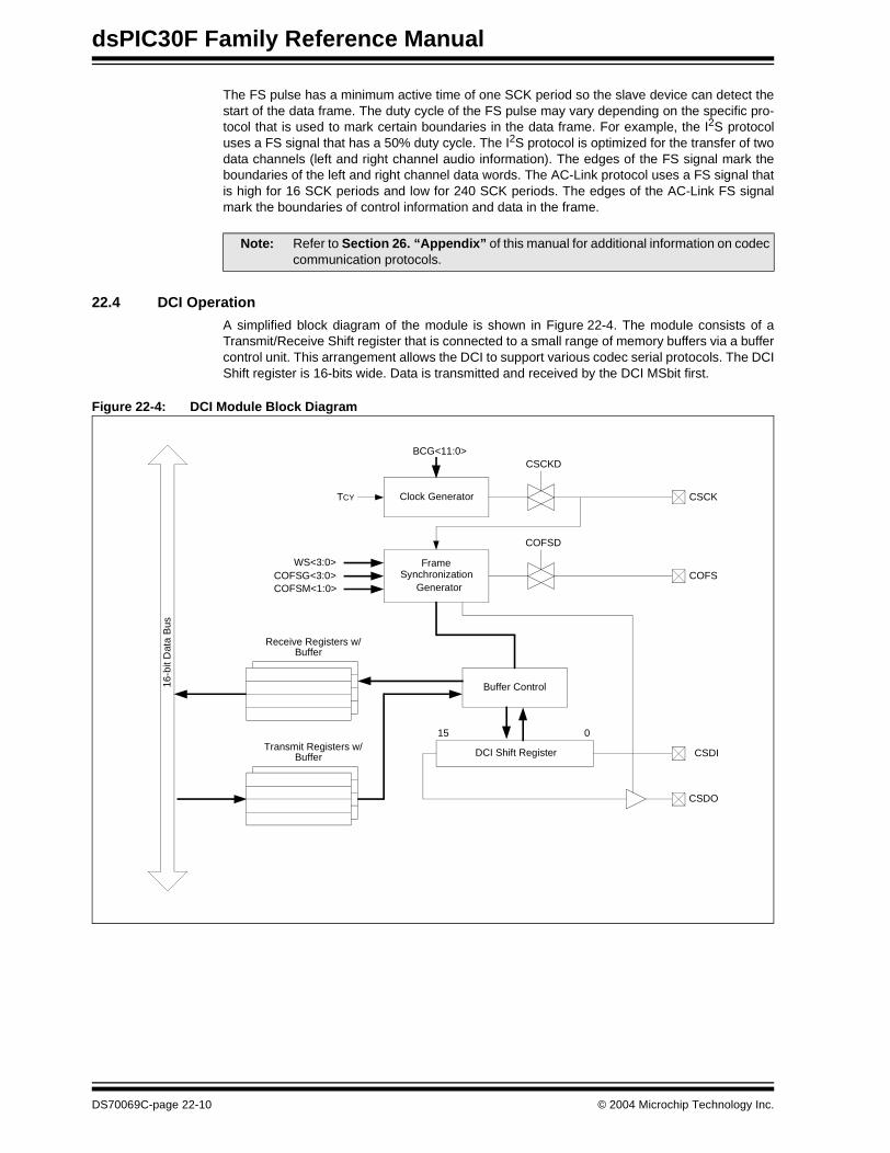
dsPIC30F Family Reference Manual
The FS pulse has a minimum active time of one SCK period so the slave device can detect thestart of the data frame. The duty cycle of the FS pulse may vary depending on the specific pro-tocol that is used to mark certain boundaries in the data frame. For example, the I2S protocoluses a FS signal that has a 50% duty cycle. The I2S protocol is optimized for the transfer of twodata channels (left and right channel audio information). The edges of the FS signal mark theboundaries of the left and right channel data words. The AC-Link protocol uses a FS signal thatis high for 16 SCK periods and low for 240 SCK periods. The edges of the AC-Link FS signalmark the boundaries of control information and data in the frame.
22.4 DCI Operation
A simplified block diagram of the module is shown in Figure 22-4. The module consists of aTransmit/Receive Shift register that is connected to a small range of memory buffers via a buffercontrol unit. This arrangement allows the DCI to support various codec serial protocols. The DCIShift register is 16-bits wide. Data is transmitted and received by the DCI MSbit first.
Figure 22-4: DCI Module Block Diagram
Note: Refer to Section 26. “Appendix” of this manual for additional information on codeccommunication protocols.
Clock Generator CSCK
Frame
Generator
TCY
COFS
16-b
it D
ata
Bus
DCI Shift Register CSDI
Buffer Control
WS<3:0>COFSG<3:0>COFSM<1:0>
COFSD
CSCKD
CSDO
015
Receive Registers w/Buffer
Transmit Registers w/Buffer
BCG<11:0>
Synchronization
DS70069C-page 22-10 © 2004 Microchip Technology Inc.

Section 22. Data Converter Interface (DCI)D
ata Co
nverter
Interface (D
CI)
22
22.4.1 DCI Pins
There are four I/O pins associated with the DCI. The DCI, when enabled, controls the datadirection of each of the four pins.
22.4.1.1 CSCK Pin
The CSCK pin provides the serial clock connection for the DCI. The CSCK pin may be configuredas an input or output using the CSCKD control bit, DCICON1<10>. When the CSCK pin isconfigured as an output (CSCKD = 0), the serial clock is derived from the dsPIC30F system clocksource and supplied to external devices by the DCI. When the CSCK pin is configured as an input(CSCKD = 1), the serial clock must be provided by an external device.
22.4.1.2 CSDO Pin
The Serial Data Output (CSDO) pin is configured as an output only pin when the module isenabled. The CSDO pin drives the serial bus whenever data is to be transmitted. The CSDO pincan be tri-stated or driven to ‘0’ during serial clock periods when data is not transmitted, depend-ing on the state of the CSDOM control bit (DCICON1<6>). The tri-state option allows otherdevices to be multiplexed onto the CSDO connection.
22.4.1.3 CSDI Pin
The serial data input (CSDI) pin is configured as an input only pin when the module is enabled.
22.4.1.4 COFS Pin
The frame synchronization (COFS) pin is used to synchronize data transfers that occur on theCSDO and CSDI pins. The COFS pin may be configured as an input or an output. The data direc-tion for the COFS pin is determined by the COFSD control bit (DCICON1<8>). When the COFSDbit is cleared, the COFS pin is an output. The DCI module will generate frame synchronizationpulses to initiate a data transfer. The DCI is the master device for this configuration. When theCOFSD bit is set, the COFS pin becomes an input. Incoming synchronization signals to themodule will initiate data transfers. The DCI is a slave device when the COFSD control bit is set.
22.4.2 Module Enable
The DCI module is enabled or disabled by setting/clearing the DCIEN control bit(DCICON1<15>). Clearing the DCIEN control bit has the effect of resetting the module. Inparticular, all counters associated with serial clock generation, frame sync, and the buffer controllogic are reset (see Section 22.5.1.1 “DCI Start-up and Data Buffering” and Section22.5.1.2 “DCI Disable” for additional information).
When enabled, the DCI controls the data direction for the CSCK, CSDI, CSDO and COFS I/Opins associated with the module. The PORT, LAT, and TRIS register values for these I/O pins areoverridden by the DCI module when the DCIEN bit is set.
It is also possible to override the CSCK pin separately when the bit clock generator is enabled.This permits the bit clock generator to be operated without enabling the rest of the DCI module.
© 2004 Microchip Technology Inc. DS70069C-page 22-11
dsPIC30F Family Reference Manual
22.4.3 Bit Clock Generator
The DCI module has a dedicated 12-bit time base that produces the bit clock. The bit clock rate(period) is set by writing a non-zero 12-bit value to the BCG<11:0> control bits(DCICON3<11:0>). When the BCG<11:0> bits are set to zero, the bit clock will be disabled.
When the CSCK pin is controlled by the DCI module, the corresponding PORT, LAT and TRISControl register values for the CSCK pin will be overridden and the data direction for the CSCKpin will be controlled by the CSCKD control bit (DCICON1<10>).
If the serial clock for the DCI is to be provided by an external device, the BCG<11:0> bits shouldbe set to ‘0’ and the CSCKD bit set to ‘1’.
If the serial clock is to be generated by the DCI module, the BCG<11:0> control bits should beset to a non-zero value (see Equation 22-1) and the CSCKD control bit should be set to zero.
The formula for the bit clock frequency is given in Equation 22-1.
Equation 22-1: DCI Bit Clock Generator Value
The required bit clock frequency will be determined by the system sampling rate and frame size.Typical bit clock frequencies range from 16x to 512x the converter sample rate, depending onthe data converter and the communication protocol that is used.
22.4.4 Sample Clock Edge Selection
The CSCKE control bit (DCICON1<9>) determines the sampling edge for the serial clock signal.If the CSCKE bit is cleared (default), data will be sampled on the falling edge of the CSCK signal.The AC-Link protocols and most multi-channel formats require that data be sampled on thefalling edge of the CSCK signal. If the CSCKE bit is set, data will be sampled on the rising edgeof CSCK. The I2S protocol requires that data be sampled on the rising edge of the serial clocksignal.
22.4.5 Frame Sync Mode Control Bits
The type of interface protocol supported by the DCI is selected using the COFSM<1:0> controlbits (DCICON1<1:0>). The following Operating modes can be selected:
• Multi-channel Mode
• I2S Mode• AC-Link Mode (16-bit)• AC-Link Mode (20-bit)
Specific information for each of the protocols is provided in subsequent sections.
22.4.6 Word-Size Selection Bits
The WS<3:0> word-size selection bits (DCICON2<3:0>) determine the number of bits in eachDCI data word. Any data length from 4 to 16 bits may be selected.
Note: The CSCK I/O pin will be controlled by the DCI module if the DCIEN bit is set ORthe bit clock generator is enabled by writing a non-zero value to BCG<11:0>. Thisallows the bit clock generator to be operated independently of the DCI module.
BCG<11:0> = fCY
2 fCSCK– 1
Note: The BCG<11:0> bits have no effect on the operation of the DCI module when theCSCK signal is provided externally (CSCKD = 1).
Note: The WS control bits are used only in the multi-channel and I2S modes. These bitshave no effect in AC-Link mode since the data slot sizes are fixed by the protocol.
DS70069C-page 22-12 © 2004 Microchip Technology Inc.
Section 22. Data Converter Interface (DCI)D
ata Co
nverter
Interface (D
CI)
22
22.4.7 Frame Synchronization Generator
The Frame Sync Generator (FSG) is a 4-bit counter that sets the frame length in data words. Theperiod for the FSG is set by writing the COFSG<3:0> control bits (DCICON2<8:5>). The FSGperiod (in serial clock cycles) is determined by the following formula:
Equation 22-2: Frame Length, In CSCK Cycles
Frame lengths up to 16 data words may be selected. The frame length in serial clock periods willvary up to a maximum of 256 depending on the word size that is selected.
22.4.8 Transmit and Receive Registers
The DCI has four Transmit registers, TXBUF0...TXBUF3, and four Receive registers,RXBUF0..RXBUF3. All of the Transmit and Receive registers are memory mapped.
22.4.8.1 Buffer Data Alignment
Data values are always stored left-justified in the DCI registers, since audio PCM data isrepresented as a signed 2’s complement fractional number. If the programmed DCI word size isless than 16 bits, the unused LSbs in the Receive registers are set to ‘0’ by the module. Also, theunused LSbs in the Transmit register are ignored by the module.
22.4.8.2 Transmit and Receive Buffers
The Transmit and Receive registers each have a set of buffers that are not accessible by theuser. Effectively, each transmit and receive buffer location is double-buffered. The DCI transmitsdata from the transmit buffers and writes received data to the receive buffers. The buffers allowthe user to read and write the RXBUF and TXBUF registers, while the DCI uses data from thebuffers.
22.4.9 DCI Buffer Control Unit
The DCI module contains a buffer control unit that transfers data between the buffer memory andthe Serial Shift register. The buffer control unit also transfers data between the buffer memoryand the TXBUF and RXBUF registers. The buffer control unit allows the DCI to queue thetransmission and reception of multiple data words without CPU overhead.
The DCI generates an interrupt each time a transfer between the buffer memory and the TXBUFand RXBUF registers takes place. The number of data words buffered between interrupts isdetermined by the BLEN<1:0> control bits (DCICON2<11:10>). The size of the transmit andreceive buffering may be varied from 1 to 4 data words using the BLEN<1:0> bits.
Each time a data transfer takes place between the DCI Shift register and the buffer memory, theDCI buffer control unit is incremented to point to the next buffer location. If the number oftransmitted or received data words is equal to the BLEN value + 1, the following will occur:
• The buffer control unit is reset to point to the first buffer location
• The received data held in the buffer is transferred to the RXBUF registers• The data in the TXBUF registers is transferred to the buffer• A CPU interrupt is generated
The DCI buffer control unit will also reset the buffer pointer to the first buffer location each time aframe boundary is reached. This action ensures alignment between the buffer locations and theenabled time slots in the data frame.
The DCI buffer control unit always accesses the same relative location in the Transmit andReceive buffers. If the DCI is transmitting data from TXBUF3, for example, then any datareceived during that time slot will be written to RXBUF3.
FrameLength = (WS<3:0> + 1) • (COFSG<3:0> + 1)
Note: The COFSG control bits will have no effect in AC-Link mode, since the frame lengthis set to 256 serial clock periods by the protocol.
© 2004 Microchip Technology Inc. DS70069C-page 22-13
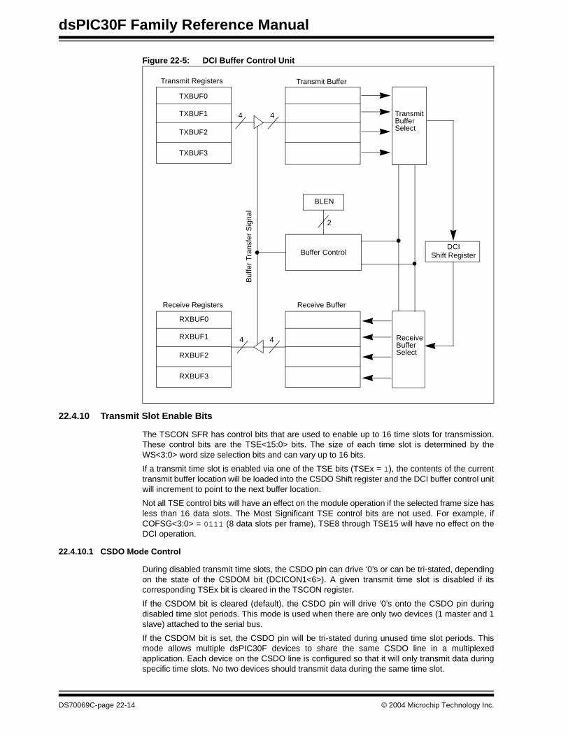
dsPIC30F Family Reference Manual
Figure 22-5: DCI Buffer Control Unit
22.4.10 Transmit Slot Enable Bits
The TSCON SFR has control bits that are used to enable up to 16 time slots for transmission.These control bits are the TSE<15:0> bits. The size of each time slot is determined by theWS<3:0> word size selection bits and can vary up to 16 bits.
If a transmit time slot is enabled via one of the TSE bits (TSEx = 1), the contents of the currenttransmit buffer location will be loaded into the CSDO Shift register and the DCI buffer control unitwill increment to point to the next buffer location.
Not all TSE control bits will have an effect on the module operation if the selected frame size hasless than 16 data slots. The Most Significant TSE control bits are not used. For example, ifCOFSG<3:0> = 0111 (8 data slots per frame), TSE8 through TSE15 will have no effect on theDCI operation.
22.4.10.1 CSDO Mode Control
During disabled transmit time slots, the CSDO pin can drive ‘0’s or can be tri-stated, dependingon the state of the CSDOM bit (DCICON1<6>). A given transmit time slot is disabled if itscorresponding TSEx bit is cleared in the TSCON register.
If the CSDOM bit is cleared (default), the CSDO pin will drive ‘0’s onto the CSDO pin duringdisabled time slot periods. This mode is used when there are only two devices (1 master and 1slave) attached to the serial bus.
If the CSDOM bit is set, the CSDO pin will be tri-stated during unused time slot periods. Thismode allows multiple dsPIC30F devices to share the same CSDO line in a multiplexedapplication. Each device on the CSDO line is configured so that it will only transmit data duringspecific time slots. No two devices should transmit data during the same time slot.
Transmit Registers Transmit Buffer
Buf
fer
Tran
sfer
Sig
nal
Receive Registers Receive Buffer
BLEN
Buffer Control
Receive Buffer Select
Transmit Buffer Select
DCI
RXBUF0
RXBUF1
RXBUF2
RXBUF3
TXBUF0
TXBUF1
TXBUF2
TXBUF3
4 4
2
4 4
Shift Register
DS70069C-page 22-14 © 2004 Microchip Technology Inc.
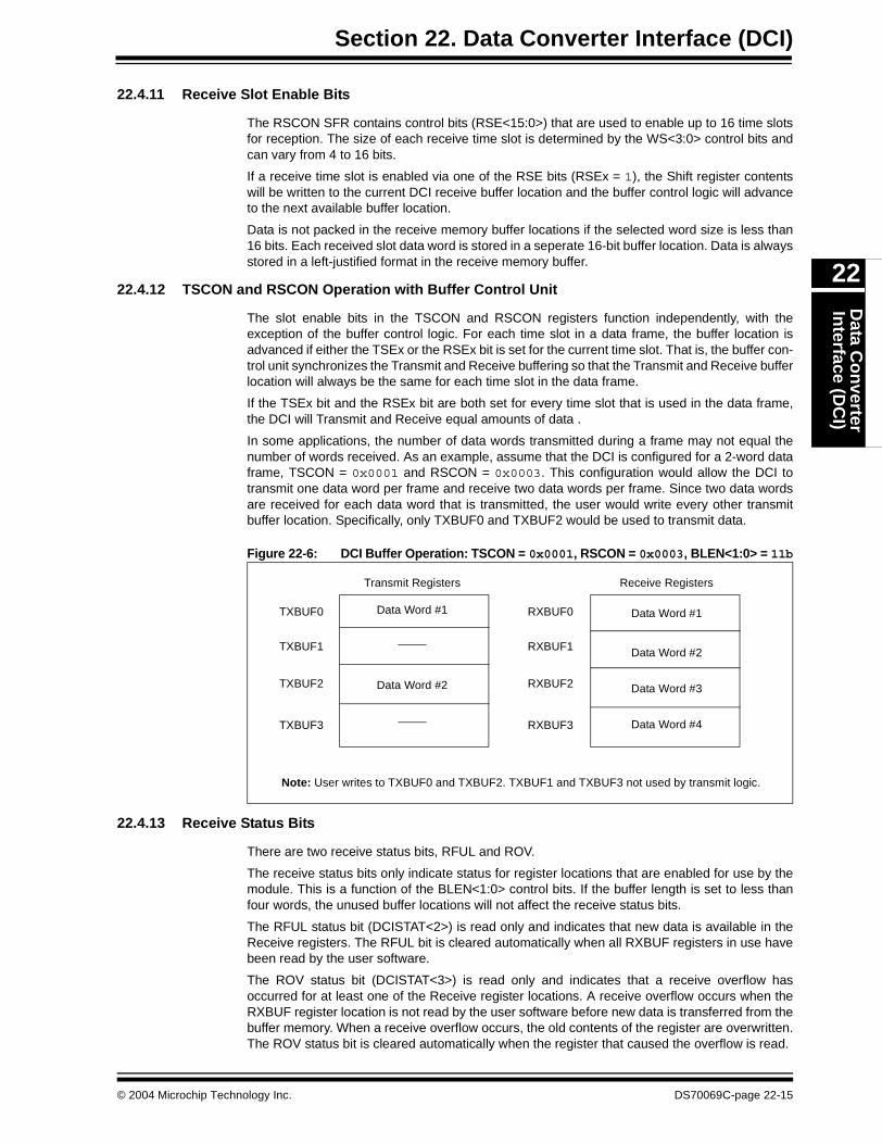
Section 22. Data Converter Interface (DCI)D
ata Co
nverter
Interface (D
CI)
22
22.4.11 Receive Slot Enable Bits
The RSCON SFR contains control bits (RSE<15:0>) that are used to enable up to 16 time slotsfor reception. The size of each receive time slot is determined by the WS<3:0> control bits andcan vary from 4 to 16 bits.
If a receive time slot is enabled via one of the RSE bits (RSEx = 1), the Shift register contentswill be written to the current DCI receive buffer location and the buffer control logic will advanceto the next available buffer location.
Data is not packed in the receive memory buffer locations if the selected word size is less than16 bits. Each received slot data word is stored in a seperate 16-bit buffer location. Data is alwaysstored in a left-justified format in the receive memory buffer.
22.4.12 TSCON and RSCON Operation with Buffer Control Unit
The slot enable bits in the TSCON and RSCON registers function independently, with theexception of the buffer control logic. For each time slot in a data frame, the buffer location isadvanced if either the TSEx or the RSEx bit is set for the current time slot. That is, the buffer con-trol unit synchronizes the Transmit and Receive buffering so that the Transmit and Receive bufferlocation will always be the same for each time slot in the data frame.
If the TSEx bit and the RSEx bit are both set for every time slot that is used in the data frame,the DCI will Transmit and Receive equal amounts of data .
In some applications, the number of data words transmitted during a frame may not equal thenumber of words received. As an example, assume that the DCI is configured for a 2-word dataframe, TSCON = 0x0001 and RSCON = 0x0003. This configuration would allow the DCI totransmit one data word per frame and receive two data words per frame. Since two data wordsare received for each data word that is transmitted, the user would write every other transmitbuffer location. Specifically, only TXBUF0 and TXBUF2 would be used to transmit data.
Figure 22-6: DCI Buffer Operation: TSCON = 0x0001, RSCON = 0x0003, BLEN<1:0> = 11b
22.4.13 Receive Status Bits
There are two receive status bits, RFUL and ROV.
The receive status bits only indicate status for register locations that are enabled for use by themodule. This is a function of the BLEN<1:0> control bits. If the buffer length is set to less thanfour words, the unused buffer locations will not affect the receive status bits.
The RFUL status bit (DCISTAT<2>) is read only and indicates that new data is available in theReceive registers. The RFUL bit is cleared automatically when all RXBUF registers in use havebeen read by the user software.
The ROV status bit (DCISTAT<3>) is read only and indicates that a receive overflow hasoccurred for at least one of the Receive register locations. A receive overflow occurs when theRXBUF register location is not read by the user software before new data is transferred from thebuffer memory. When a receive overflow occurs, the old contents of the register are overwritten.The ROV status bit is cleared automatically when the register that caused the overflow is read.
Transmit Registers
TXBUF0
TXBUF1
TXBUF2
TXBUF3
Receive Registers
RXBUF0
RXBUF1
RXBUF2
RXBUF3
Note: User writes to TXBUF0 and TXBUF2. TXBUF1 and TXBUF3 not used by transmit logic.
Data Word #1
Data Word #2
Data Word #1
Data Word #2
Data Word #3
Data Word #4
© 2004 Microchip Technology Inc. DS70069C-page 22-15
dsPIC30F Family Reference Manual
22.4.14 Transmit Status Bits
There are two transmit status bits, TMPTY and TUNF.
The transmit status bits only indicate status for register locations that are used by the module. Ifthe buffer length is set to less than four words, for example, the unused register locations will notaffect the transmit status bits.
The TMPTY bit (DCISTAT<0>) is read only and is set when the contents of the active TXBUFregisters are transferred to the Transmit Buffer registers. The TMPTY bit may be polled insoftware to determine when the Transmit registers may be written. The TMPTY bit is clearedautomatically by the hardware when a write to any of the TXBUF registers in use occurs.
The TUNF bit (DCISTAT<1>) is read only and indicates that a transmit underflow has occurredfor at least one of the Transmit registers that is in use. The TUNF bit is set when the TXBUFregister contents are transferred to the transmit buffer memory and the user did not write all ofthe TXBUF registers in use since the last buffer transfer. The TUNF status bit is clearedautomatically when the TXBUF register that underflowed is written by the user software.
22.4.15 SLOT Status Bits
The SLOT<3:0> status bits (DCISTAT<11:7>) indicate the current active time slot in the dataframe and are useful when more than four words per data frame need to be transferred. The usermay poll these status bits in software when a DCI interrupt occurs to determine what time slotdata was last received and which time slot data should be loaded into the TXBUF registers.
22.4.16 Digital Loopback Mode
Digital Loopback mode is enabled by setting the DLOOP control bit (DCICON1<11>). When theDLOOP bit is set, the module internally connects the CSDO signal to CSDI. The actual data inputon the CSDI pin will be ignored in Digital Loopback mode.
22.4.17 Underflow Mode Control Bit
When a transmit underflow occurs, one of two actions may occur depending on the state of theUNFM control bit (DCICON1<7>). If the UNFM bit is cleared (default), the module will transmit‘0’s on the CSDO pin during the active time slot for the buffer location. In this Operating mode,the codec device attached to the DCI module will simply be fed digital ‘silence’. If the UNFMcontrol bit is set, the module will transmit the last data written to the buffer location. ThisOperating mode permits the user to send a continuous data value to the codec device withoutconsuming software overhead.
22.4.18 Data Justification Control
In most applications, the data transfer begins one serial clock cycle after the FS signal is sampledactive. This is the DCI module default. An alternate data alignment can be selected by setting theDJST control bit (DCICON2<5>). When DJST = 1, data transfers will begin during the sameserial clock cycle as the FS signal.
22.4.19 DCI Module Interrupts
The frequency of DCI module interrupts is dependent on the number of active time slots (TSCONand RSCON registers), length of the data frame (WS and COFSG control bits), and the BLENcontrol bits. An interrupt is generated at the following times:
• When the buffer length has been reached
• When a frame boundary is reached
A buffer memory transfer takes place each time the above events occur. A buffer memorytransfer is defined as the time when the previously written TXBUF values are transferred to thetransmit buffer memory and new received values in the receive buffer memory are transferredinto the RXBUF registers.
DS70069C-page 22-16 © 2004 Microchip Technology Inc.
Section 22. Data Converter Interface (DCI)D
ata Co
nverter
Interface (D
CI)
22
22.5 Using the DCI Module
This section explains how to configure and use the DCI with specific kinds of data converters.
22.5.1 How to Transmit and Receive Data Using the DCI Buffers, Status Bits and Interrupts
The DCI can buffer up to four data words between CPU interrupts depending on the setting ofthe BLEN control bits. The buffered data can be transmitted and received in a single data frame,or across multiple data frames, depending on the TSCON and RSCON register settings. Forexample, assume BLEN<1:0> = 00b ( buffer one data word per interrupt) and TSCON = RSCON= 0x0001. This particular configuration represents the most basic setup and would cause theDCI to transmit/receive one data word at the beginning of every data frame. The CPU would beinterrupted after every data word transmitted/received since BLEN<1:0> = 00b.
For a second configuration example, assume BLEN<1:0> = 11b (buffer four data words perinterrupt) and TSCON = RSCON = 0x0001. This configuration would cause the DCI totransmit/receive one data word at the beginning of every data frame, but a CPU interrupt wouldbe generated after four data words were transmitted/received. This configuration would be usefulfor block processing, where multiple data samples are processed at once.
For a third configuration example, assume BLEN<1:0> = 11b (buffer four data words perinterrupt) and TSCON = RSCON = 0x000F. This configuration would cause the DCI totransmit/receive four data words at the beginning of every data frame. A CPU interrupt would begenerated every data frame in this case because the DCI was setup to buffer four data words ina data frame. This configuration represents a typical multi-channel buffering setup.
The DCI can also be configured to buffer more than four data words per frame. For example,assume BLEN<1:0> = 11b (buffer four data words per interrupt) and TSCON = RSCON =0x00FF. In this configuration, the DCI will transmit/receive 8 data words per data frame. Aninterrupt will be generated twice per data frame. To determine which portion of the data is in theTransmit/Receive registers at each interrupt, the user will need to check the SLOT status bits(DCISTAT <11:7>) in the Interrupt Service Routine to determine the current data frame position.
The Transmit and Receive registers are double-buffered, so the DCI module can work on one setof Transmit and Receive data while the user software is manipulating the other set of data.Because of the double-buffers, it will take three interrupt periods to receive the data, process thatdata, and transmit the processed data. For each DCI interrupt, the CPU will process a data wordthat was received during a prior interrupt period and generate a data word that will be transmittedduring the next interrupt period. The buffering and data processing time of the dsPIC device willinsert a two-interrupt period delay into the processed data. This data delay is negligible, in mostcases.
The DCI status flags and CPU interrupt indicate that a buffer transfer has taken place and that itis time for the CPU to process more data. In a typical application, the following steps will occureach time the DCI data is processed:
1. The RXBUF registers are read by the user software. The RFUL status bit (DCISTAT<2>)will have been set by the module to indicate the Receive registers contain new data. TheRFUL bit is cleared automatically after all the active Receive registers have been read.
2. The user software will process the received data.3. The processed data is written to the TXBUF registers. The TMPTY status bit
(DCISTAT<0>) will have been previously set to indicate that the Transmit registers areready for more data to be written.
For applications that are configured to Transmit and Receive data (TSCON and RSCON arenon-zero), the RFUL and TMPTY status bits can be polled in user software to determine when aDCI buffer transfer takes place. If the DCI is only used to transmit data (RSCON = 0), then theTMPTY bit can be polled to indicate a buffer transfer. If the DCI is configured to only receive data(TSCON = 0), then the RFUL bit can be polled to indicate a buffer transfer.
The DCIIF status bit (IFS2<9>) is set each time a DCI buffer transfer takes place and generatesa CPU interrupt, if enabled. The DCIIF status bit is generated by the logical ORing of the RFULand TMPTY status bits.
© 2004 Microchip Technology Inc. DS70069C-page 22-17
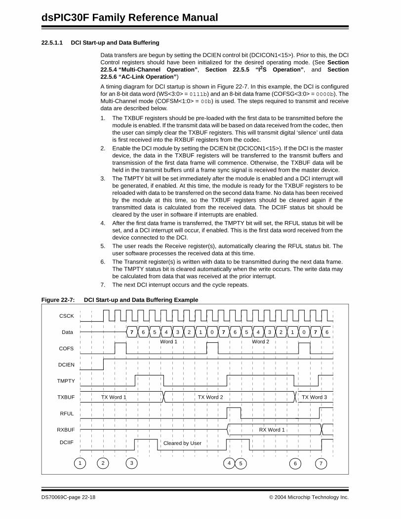
dsPIC30F Family Reference Manual
22.5.1.1 DCI Start-up and Data Buffering
Data transfers are begun by setting the DCIEN control bit (DCICON1<15>). Prior to this, the DCIControl registers should have been initialized for the desired operating mode. (See Section22.5.4 “Multi-Channel Operation”, Section 22.5.5 “I2S Operation”, and Section22.5.6 “AC-Link Operation”)
A timing diagram for DCI startup is shown in Figure 22-7. In this example, the DCI is configuredfor an 8-bit data word (WS<3:0> = 0111b) and an 8-bit data frame (COFSG<3:0> = 0000b). TheMulti-Channel mode (COFSM<1:0> = 00b) is used. The steps required to transmit and receivedata are described below.
1. The TXBUF registers should be pre-loaded with the first data to be transmitted before themodule is enabled. If the transmit data will be based on data received from the codec, thenthe user can simply clear the TXBUF registers. This will transmit digital ‘silence’ until datais first received into the RXBUF registers from the codec.
2. Enable the DCI module by setting the DCIEN bit (DCICON1<15>). If the DCI is the masterdevice, the data in the TXBUF registers will be transferred to the transmit buffers andtransmission of the first data frame will commence. Otherwise, the TXBUF data will beheld in the transmit buffers until a frame sync signal is received from the master device.
3. The TMPTY bit will be set immediately after the module is enabled and a DCI interrupt willbe generated, if enabled. At this time, the module is ready for the TXBUF registers to bereloaded with data to be transferred on the second data frame. No data has been receivedby the module at this time, so the TXBUF registers should be cleared again if thetransmitted data is calculated from the received data. The DCIIF status bit should becleared by the user in software if interrupts are enabled.
4. After the first data frame is transferred, the TMPTY bit will set, the RFUL status bit will beset, and a DCI interrupt will occur, if enabled. This is the first data word received from thedevice connected to the DCI.
5. The user reads the Receive register(s), automatically clearing the RFUL status bit. Theuser software processes the received data at this time.
6. The Transmit register(s) is written with data to be transmitted during the next data frame.The TMPTY status bit is cleared automatically when the write occurs. The write data maybe calculated from data that was received at the prior interrupt.
7. The next DCI interrupt occurs and the cycle repeats.
Figure 22-7: DCI Start-up and Data Buffering Example
7
CSCK
Data
RFUL
6 5 4 3 2 1 0 7 6 5 4 3 2 1 0 7 6
TMPTY
DCIEN
COFS
RX Word 1RXBUF
TX Word 1 TX Word 2 TX Word 3TXBUF
1 2 3 4 5 6
DCIIF
7
Word 1 Word 2
Cleared by User
DS70069C-page 22-18 © 2004 Microchip Technology Inc.
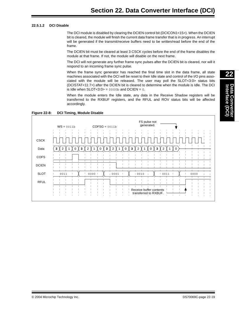
Section 22. Data Converter Interface (DCI)D
ata Co
nverter
Interface (D
CI)
22
22.5.1.2 DCI Disable
The DCI module is disabled by clearing the DCIEN control bit (DCICON1<15>). When the DCIENbit is cleared, the module will finish the current data frame transfer that is in progress. An interruptwill be generated if the transmit/receive buffers need to be written/read before the end of theframe.
The DCIEN bit must be cleared at least 3 CSCK cycles before the end of the frame disables themodule at that frame. If not, the module will disable on the next frame.
The DCI will not generate any further frame sync pulses after the DCIEN bit is cleared, nor will itrespond to an incoming frame sync pulse.
When the frame sync generator has reached the final time slot in the data frame, all statemachines associated with the DCI will be reset to their Idle state and control of the I/O pins asso-ciated with the module will be released. The user may poll the SLOT<3:0> status bits(DCISTAT<11:7>) after the DCIEN bit is cleared to determine when the module is Idle. The DCIis Idle when SLOT<3:0> = 0000b and DCIEN = 0.
When the module enters the Idle state, any data in the Receive Shadow registers will betransferred to the RXBUF registers, and the RFUL and ROV status bits will be affectedaccordingly.
Figure 22-8: DCI Timing, Module Disable
3
CSCK
Data 2 1 0 3 2 1 0 3 2 1 0 3 2 1 0
DCIEN
COFS
3 2 1 0
0011 0000 0001 0010 0011 0000SLOT
RFUL
WS = 0011b COFSG = 0011b
FS pulse notgenerated.
Receive buffer contentstransferred to RXBUF.
© 2004 Microchip Technology Inc. DS70069C-page 22-19

dsPIC30F Family Reference Manual
22.5.2 Master vs. Slave Operation
The DCI can be configured for master or slave operation. The master device generates the framesync signal to initiate a data transfer. The Operating mode (master or slave) is selected by theCOFSD control bit (DCICON1<8>).
When the DCI module is operating as a master device (COFSD = 0), the COFSM mode bitsdetermine the type of frame sync pulse that is generated by the frame sync generator logic. Anew frame synchronization signal is generated when the frame sync generator resets and isoutput on the COFS pin.
When the DCI module is operating as a frame sync slave (COFSD = 1), data transfers arecontrolled by the device attached to the DCI module. The COFSM control bits control how theDCI module responds to incoming FS signals.
In the Multi-Channel mode, a new data frame transfer will begin one serial clock cycle after theCOFS pin is sampled high. The pulse on the COFS pin resets the frame sync generator logic.
In the I2S mode, a new data word will be transferred one serial clock cycle after a low-to-high ora high-to-low transition is sampled on the COFS pin. A rising or falling edge on the COFS pinresets the frame sync generator logic.
In the AC-Link mode, the tag slot and subsequent data slots for the next frame will be transferredone serial clock cycle after the COFS pin is sampled high.
The COFSG and WS bits must be configured to provide the expected frame length when themodule is operating in the Slave mode. Once a valid frame sync pulse has been sampled by themodule on the COFS pin, an entire data frame transfer will take place. The module will notrespond to further frame sync pulses until the current data frame transfer has fully completed.
22.5.3 Data Packing for Long Data Word Support
Many codecs have data word lengths in excess of 16 bits. The DCI natively supports wordlengths up to 16 bits, but longer word lengths can be supported by enabling multiple Transmitand Receive slots and packing data into multiple transmit and receive buffer locations. Forexample, assume that a particular codec transmits/receives 24-bit data words. This data couldbe transmitted and received by setting BLEN<1:0> = 01b (two data words per interrupt) andsetting TSCON = RSCON = 0x0003. This will enable transmission and reception during the firsttwo time slots of the data frame. The 16 MSbs of the transmit data are written to TXBUF0. The8 LSbs of the transmit data are written left-justified to TXBUF1 as shown in Figure 22-9. The 8LSbs of TXBUF1 can be written to ‘0’. The 24-bit data received from the codec will be loaded intoRXBUF0 and RXBUF1 with the same format as the transmit data.
Any combination of word size and enabled time slots may be used to transmit and receive longdata words in multiple Transmit and Receive registers. For example, the 24 bit data wordexample shown in Figure 22-9 could be transmitted/received in three consecutive registers bysetting WS<3:0> = 0111 (word size = 8 bits), BLEN<1:0> = 10 (buffer three words betweeninterrupts), and TSCON = RSCON = 0x0007 (transmit/receive during the first three time slots ofthe data frame). Each Transmit and Receive register would contain 8 bits of the data word.
Figure 22-9: Data Packing Example for Long Data Words
Transmit Registers
TXBUF0
TXBUF1
TXBUF2
TXBUF3
Data Word bits 24:8
0 0 0 0 0 0 0 00bits 7:0
TSCON = RSCON = 0x0003BLEN<1:0> = 01b
DS70069C-page 22-20 © 2004 Microchip Technology Inc.
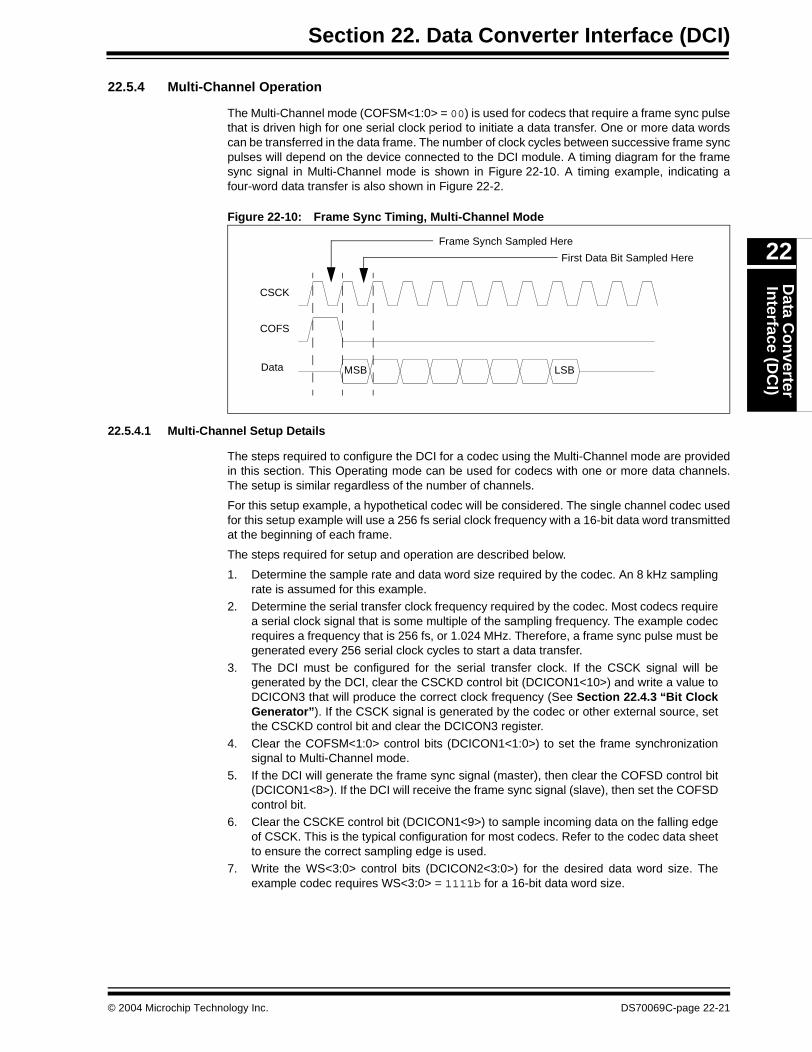
Section 22. Data Converter Interface (DCI)D
ata Co
nverter
Interface (D
CI)
22
22.5.4 Multi-Channel Operation
The Multi-Channel mode (COFSM<1:0> = 00) is used for codecs that require a frame sync pulsethat is driven high for one serial clock period to initiate a data transfer. One or more data wordscan be transferred in the data frame. The number of clock cycles between successive frame syncpulses will depend on the device connected to the DCI module. A timing diagram for the framesync signal in Multi-Channel mode is shown in Figure 22-10. A timing example, indicating afour-word data transfer is also shown in Figure 22-2.
Figure 22-10: Frame Sync Timing, Multi-Channel Mode
22.5.4.1 Multi-Channel Setup Details
The steps required to configure the DCI for a codec using the Multi-Channel mode are providedin this section. This Operating mode can be used for codecs with one or more data channels.The setup is similar regardless of the number of channels.
For this setup example, a hypothetical codec will be considered. The single channel codec usedfor this setup example will use a 256 fs serial clock frequency with a 16-bit data word transmittedat the beginning of each frame.
The steps required for setup and operation are described below.
1. Determine the sample rate and data word size required by the codec. An 8 kHz samplingrate is assumed for this example.
2. Determine the serial transfer clock frequency required by the codec. Most codecs requirea serial clock signal that is some multiple of the sampling frequency. The example codecrequires a frequency that is 256 fs, or 1.024 MHz. Therefore, a frame sync pulse must begenerated every 256 serial clock cycles to start a data transfer.
3. The DCI must be configured for the serial transfer clock. If the CSCK signal will begenerated by the DCI, clear the CSCKD control bit (DCICON1<10>) and write a value toDCICON3 that will produce the correct clock frequency (See Section 22.4.3 “Bit ClockGenerator”). If the CSCK signal is generated by the codec or other external source, setthe CSCKD control bit and clear the DCICON3 register.
4. Clear the COFSM<1:0> control bits (DCICON1<1:0>) to set the frame synchronizationsignal to Multi-Channel mode.
5. If the DCI will generate the frame sync signal (master), then clear the COFSD control bit(DCICON1<8>). If the DCI will receive the frame sync signal (slave), then set the COFSDcontrol bit.
6. Clear the CSCKE control bit (DCICON1<9>) to sample incoming data on the falling edgeof CSCK. This is the typical configuration for most codecs. Refer to the codec data sheetto ensure the correct sampling edge is used.
7. Write the WS<3:0> control bits (DCICON2<3:0>) for the desired data word size. Theexample codec requires WS<3:0> = 1111b for a 16-bit data word size.
CSCK
Data
COFS
MSB LSB
Frame Synch Sampled Here
First Data Bit Sampled Here
© 2004 Microchip Technology Inc. DS70069C-page 22-21
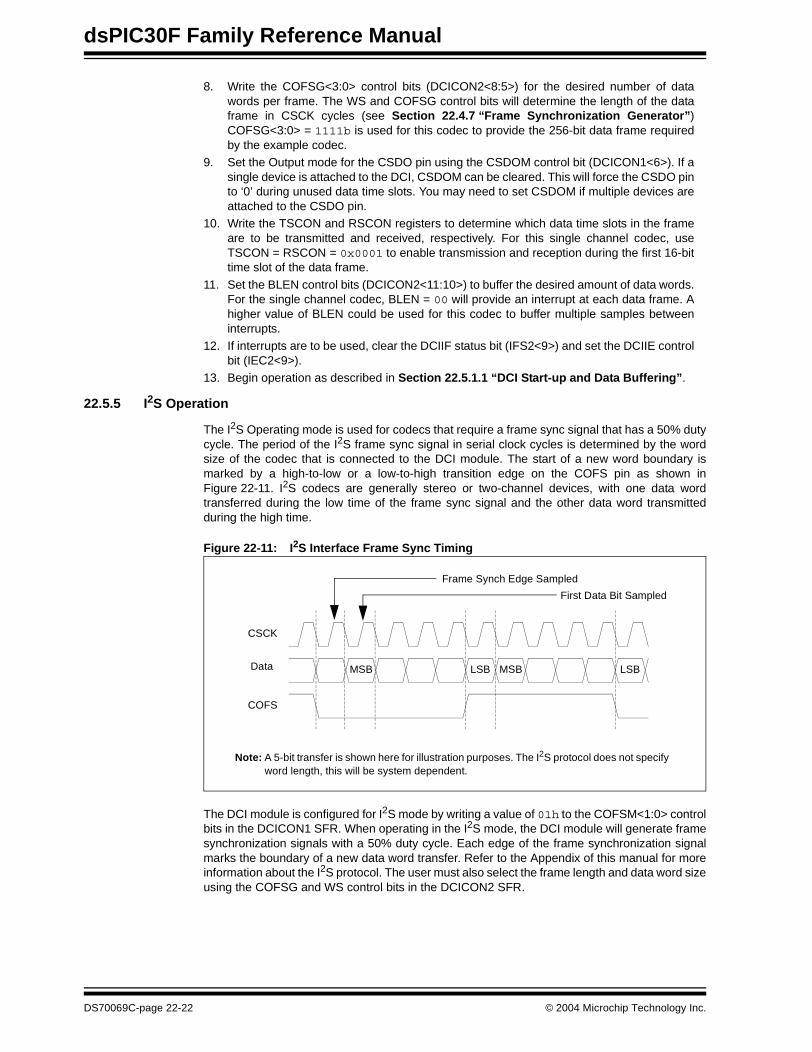
dsPIC30F Family Reference Manual
8. Write the COFSG<3:0> control bits (DCICON2<8:5>) for the desired number of datawords per frame. The WS and COFSG control bits will determine the length of the dataframe in CSCK cycles (see Section 22.4.7 “Frame Synchronization Generator”)COFSG<3:0> = 1111b is used for this codec to provide the 256-bit data frame requiredby the example codec.
9. Set the Output mode for the CSDO pin using the CSDOM control bit (DCICON1<6>). If asingle device is attached to the DCI, CSDOM can be cleared. This will force the CSDO pinto ‘0’ during unused data time slots. You may need to set CSDOM if multiple devices areattached to the CSDO pin.
10. Write the TSCON and RSCON registers to determine which data time slots in the frameare to be transmitted and received, respectively. For this single channel codec, useTSCON = RSCON = 0x0001 to enable transmission and reception during the first 16-bittime slot of the data frame.
11. Set the BLEN control bits (DCICON2<11:10>) to buffer the desired amount of data words.For the single channel codec, BLEN = 00 will provide an interrupt at each data frame. Ahigher value of BLEN could be used for this codec to buffer multiple samples betweeninterrupts.
12. If interrupts are to be used, clear the DCIIF status bit (IFS2<9>) and set the DCIIE controlbit (IEC2<9>).
13. Begin operation as described in Section 22.5.1.1 “DCI Start-up and Data Buffering”.
22.5.5 I2S Operation
The I2S Operating mode is used for codecs that require a frame sync signal that has a 50% dutycycle. The period of the I2S frame sync signal in serial clock cycles is determined by the wordsize of the codec that is connected to the DCI module. The start of a new word boundary ismarked by a high-to-low or a low-to-high transition edge on the COFS pin as shown inFigure 22-11. I2S codecs are generally stereo or two-channel devices, with one data wordtransferred during the low time of the frame sync signal and the other data word transmittedduring the high time.
Figure 22-11: I2S Interface Frame Sync Timing
The DCI module is configured for I2S mode by writing a value of 01h to the COFSM<1:0> controlbits in the DCICON1 SFR. When operating in the I2S mode, the DCI module will generate framesynchronization signals with a 50% duty cycle. Each edge of the frame synchronization signalmarks the boundary of a new data word transfer. Refer to the Appendix of this manual for moreinformation about the I2S protocol. The user must also select the frame length and data word sizeusing the COFSG and WS control bits in the DCICON2 SFR.
Note: A 5-bit transfer is shown here for illustration purposes. The I2S protocol does not specifyword length, this will be system dependent.
MSB LSB MSB LSB
CSCK
Data
COFS
Frame Synch Edge Sampled
First Data Bit Sampled
DS70069C-page 22-22 © 2004 Microchip Technology Inc.
Section 22. Data Converter Interface (DCI)D
ata Co
nverter
Interface (D
CI)
22
22.5.5.1 I2S Setup Details
The steps required to configure the DCI for an I2S codec are provided in this section. For thissetup example, a hypothetical I2S codec will be considered.
The I2S codec in this setup example will use a 64 fs serial clock frequency, with two 16 bit datawords during the data frame. Therefore, the frame length will be 64 CSCK cycles, with the COFSsignal high for 32 cycles and low for 32 cycles. The first data word will be transmitted one CSCKcycle after the falling edge of COFS, and the second data word will be transmitted one CSCKcycle after the rising edge of COFS as shown in Figure 22-11.
1. Determine the sample rate used by the codec to determine the CSCK frequency. It isassumed in this example that fs is 48 kHz.
2. Determine the serial transfer clock frequency required by the codec. The example codecrequires a frequency that is 64 fs, or 3.072 MHz.
3. The DCI must be configured for the serial transfer clock. If the CSCK signal will be gener-ated by the DCI, clear the CSCKD control bit (DCICON1<10>) and write a value toDCICON3 that will produce the correct clock frequency (see Section 22.4.3 “Bit ClockGenerator”). If the CSCK signal is generated by the codec or other external source, setthe CSCKD control bit and clear the DCICON3 register.
4. Next, set COFSM<1:0> = 01b to set the frame synchronization signal to I2S mode.5. If the DCI will generate the frame sync signal (master), then clear the COFSD control bit
(DCICON1<8>). If the DCI will receive the frame sync signal (slave), then set the COFSDcontrol bit.
6. Set the CSCKE control bit (DCICON1<9>) to sample incoming data on the rising edge ofCSCK. This is the typical configuration for most I2S codecs.
7. Write the WS<3:0> control bits (DCICON2<3:0>) for the desired data word size. For theexample codec, use WS<3:0> = 1111b for a 16-bit data word size.
8. Write the COFSG<3:0> control bits (DCICON2<8:5) for the desired number of data wordsper frame. The WS and COFSG control bits will determine the length of the data frame inCSCK cycles (see Section 22.4.7 “Frame Synchronization Generator”). For this exam-ple codec, set COFSG<3:0> = 0001b.
9. Set the Output mode for the CSDO pin using the CSDOM control bit (DCICON1<6>). If asingle device is attached to the DCI, CSDOM can be cleared. You may need to setCSDOM if multiple devices are attached to the CSDO pin.
10. Write the TSCON and RSCON registers to determine which data time slots in the frameare to be transmitted and received, respectively. For this codec, set TSCON = 0x0001and RSCON = 0x0001 to enable transmission and reception during the first 16-bit timeslot of the 32-bit data frame. Adjacent time slots can be enabled to buffer data wordslonger than 16 bits.
11. Set the BLEN<1:0> control bits (DCICON2<11:10>) to buffer the desired amount of datawords. For a two-channel I2S codec, BLEN<1:0> = 01b will generate an interrupt aftertransferring two data words.
12. If interrupts are to be used, clear the DCIIF status bit (IFS2<9>) and set the DCIIE controlbit (IEC2<9>).
13. Begin operation as described in Section 22.5.1.1 “DCI Start-up and Data Buffering”. Inthe I2S Master mode, the COFS pin will be driven high after the module is enabled andbegin transmitting the data loaded in TXBUF0.
Note: In the I2S mode, the COFSG bits are set to the length of 1/2 of the data frame. Forthis example codec, set COFSG<3:0> = 0001b (two data words per frame) toproduce a 32-bit frame. This will produce an I2S data frame that is 64 bits in length.
© 2004 Microchip Technology Inc. DS70069C-page 22-23
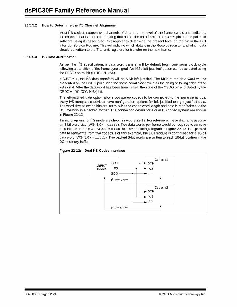
dsPIC30F Family Reference Manual
22.5.5.2 How to Determine the I2S Channel Alignment
Most I2S codecs support two channels of data and the level of the frame sync signal indicatesthe channel that is transferred during that half of the data frame. The COFS pin can be polled insoftware using its associated Port register to determine the present level on the pin in the DCIInterrupt Service Routine. This will indicate which data is in the Receive register and which datashould be written to the Transmit registers for transfer on the next frame.
22.5.5.3 I2S Data Justification
As per the I2S specification, a data word transfer will by default begin one serial clock cyclefollowing a transition of the frame sync signal. An ‘MSb left-justified’ option can be selected usingthe DJST control bit (DCICON1<5>).
If DJST = 1, the I2S data transfers will be MSb left justified. The MSb of the data word will bepresented on the CSDO pin during the same serial clock cycle as the rising or falling edge of theFS signal. After the data word has been transmitted, the state of the CSDO pin is dictated by theCSDOM (DCICON1<6>) bit.
The left-justified data option allows two stereo codecs to be connected to the same serial bus.Many I2S compatible devices have configuration options for left-justified or right-justified data.The word size selection bits are set to twice the codec word length and data is read/written to theDCI memory in a packed format. The connection details for a dual I2S codec system are shownin Figure 22-12.
Timing diagrams for I2S mode are shown in Figure 22-13. For reference, these diagrams assumean 8-bit word size (WS<3:0> = 0111b). Two data words per frame would be required to achievea 16-bit sub-frame (COFSG<3:0> = 0001b). The 3rd timing diagram in Figure 22-13 uses packeddata to read/write from two codecs. For this example, the DCI module is configured for a 16-bitdata word (WS<3:0> = 1111b). Two packed 8-bit words are written to each 16-bit location in theDCI memory buffer.
Figure 22-12: Dual I2S Codec Interface
dsPIC®
Codec #1SCK
FS
SDO
SCK
WS
SDI
Codec #2SCK
WS
SDI
Device
I2C™/SPI™
I2C™/SPI™
DS70069C-page 22-24 © 2004 Microchip Technology Inc.
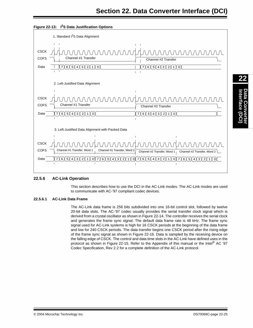
Section 22. Data Converter Interface (DCI)D
ata Co
nverter
Interface (D
CI)
22
Figure 22-13: I2S Data Justification Options
22.5.6 AC-Link Operation
This section describes how to use the DCI in the AC-Link modes. The AC-Link modes are usedto communicate with AC-’97 compliant codec devices.
22.5.6.1 AC-Link Data Frame
The AC-Link data frame is 256 bits subdivided into one 16-bit control slot, followed by twelve20-bit data slots. The AC-’97 codec usually provides the serial transfer clock signal which isderived from a crystal oscillator as shown in Figure 22-14. The controller receives the serial clockand generates the frame sync signal. The default data frame rate is 48 kHz. The frame syncsignal used for AC-Link systems is high for 16 CSCK periods at the beginning of the data frameand low for 240 CSCK periods. The data transfer begins one CSCK period after the rising edgeof the frame sync signal as shown in Figure 22-16. Data is sampled by the receiving device onthe falling edge of CSCK. The control and data time slots in the AC-Link have defined uses in theprotocol as shown in Figure 22-15. Refer to the Appendix of this manual or the Intel® AC ‘97Codec Specification, Rev 2.2 for a complete definition of the AC-Link protocol.
7 6 5 4 3 2 1 0 7 6 5 4 3 2 1 0
Channel #1 Transfer Channel #2 Transfer
CSCK
COFS
Data
7 6 5 4 3 2 1 0 7 6 5 4 3 2 1 0
Channel #1 Transfer Channel #2 Transfer
CSCK
COFS
Data
7 6 5 4 3 2 1 0 7 6 5 4 3 2 1 0
Channel #1 Transfer, Word 1
CSCK
COFS
Data 7 6 5 4 3 2 1 0 7 6 5 4 3 2 1 0
1. Standard I2S Data Alignment
2. Left-Justified Data Alignment
3. Left-Justified Data Alignment with Packed Data
Channel #1 Transfer, Word 2 Channel #2 Transfer, Word 1 Channel #2 Transfer, Word 2
© 2004 Microchip Technology Inc. DS70069C-page 22-25
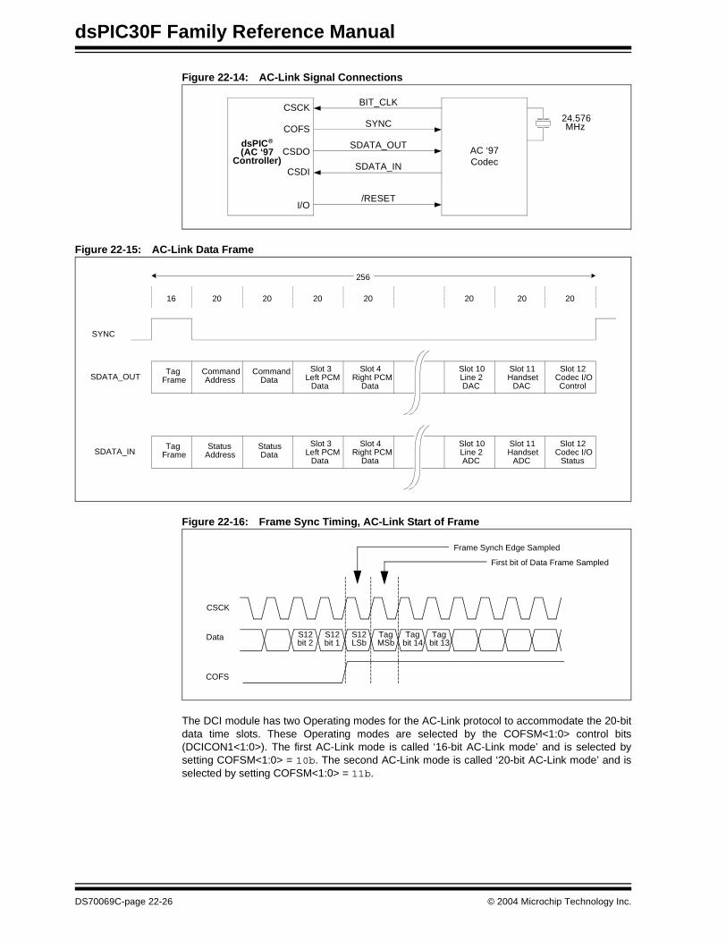
dsPIC30F Family Reference Manual
Figure 22-14: AC-Link Signal Connections
Figure 22-15: AC-Link Data Frame
Figure 22-16: Frame Sync Timing, AC-Link Start of Frame
The DCI module has two Operating modes for the AC-Link protocol to accommodate the 20-bitdata time slots. These Operating modes are selected by the COFSM<1:0> control bits(DCICON1<1:0>). The first AC-Link mode is called ‘16-bit AC-Link mode’ and is selected bysetting COFSM<1:0> = 10b. The second AC-Link mode is called ‘20-bit AC-Link mode’ and isselected by setting COFSM<1:0> = 11b.
dsPIC®
(AC ‘97Controller)
AC ‘97Codec
24.576MHz
BIT_CLK
SYNC
SDATA_OUT
SDATA_IN
/RESET
CSCK
COFS
CSDO
CSDI
I/O
TagFrame
CommandAddress
CommandData
Slot 3 Left PCM
Data
Slot 4Right PCM
Data
Slot 10Line 2DAC
Slot 11Handset
DAC
Slot 12Codec I/OControl
TagFrame
StatusAddress
StatusData
Slot 3 Left PCM
Data
Slot 4Right PCM
Data
Slot 10Line 2ADC
Slot 11Handset
ADC
Slot 12Codec I/O
Status
16 20 20 20 20 20 20 20
256
SYNC
SDATA_OUT
SDATA_IN
TagMSb
CSCK
Data
COFS
Tagbit 14
S12LSb
S12bit 1
S12bit 2
Tagbit 13
Frame Synch Edge Sampled
First bit of Data Frame Sampled
DS70069C-page 22-26 © 2004 Microchip Technology Inc.
Section 22. Data Converter Interface (DCI)D
ata Co
nverter
Interface (D
CI)
22
22.5.6.2 16-bit AC-Link Mode
In the 16-bit AC-Link mode, transmit and receive data word lengths are restricted to 16 bits to fitthe DCI Transmit and Receive registers. Note that this restriction only affects the 20-bit data timeslots of the AC-Link protocol. For received time slots, the incoming data will be truncated to 16bits. For outgoing time slots, the 4 LSbs of the data word are set to ‘0’ by the module. ThisOperating mode simplifies the AC-Link data frame by treating every time slot as a 16-bit time slot.The frame sync generator maintains alignment to the time slot boundaries.
22.5.6.3 20-bit AC-Link Mode
The 20-bit AC-Link mode allows all bits in the data time slots to be transmitted and received, butdoes not maintain data alignment to the specific time slot boundaries defined in the AC-Linkprotocol.
The 20-bit AC-Link mode functions similarly to the Multi-Channel mode of the DCI module,except for the duty cycle of the frame synchronization signal that is produced. The AC-Link framesynchronization signal should remain high for 16 clock cycles and should be low for the following240 cycles.
The 20-bit mode treats each 256-bit AC-Link frame as sixteen 16-bit time slots. In the 20-bitAC-Link mode, the module operates as if COFSG<3:0> = 1111b and WS<3:0> = 1111b. Thedata alignment for 20-bit data slots is not maintained in this Operating mode. For example, anentire 256-bit AC-Link data frame can be transmitted and received in a packed fashion by settingall bits in the TSCON and RSCON registers. Since the total available buffer length is 64 bits, itwould take 4 consecutive interrupts to transfer the AC-Link frame. The application software mustkeep track of the current AC-Link frame segment by monitoring the SLOT<3:0> status bits(DCISTAT<11:7>).
22.5.6.4 AC-Link Setup Details
The module is enabled for AC-Link mode by writing 10h or 11h to the COFSM<1:0> control bitsin the DCICON1 SFR. The word size selection bits (WS<3:0>) and the frame synchronizationgenerator bits (COFSG<3:0>) have no effect for the 16 and 20-bit AC-Link modes since theframe and word sizes are set by the protocol.
Most AC ‘97 codecs generate the clock signal that controls data transfers. Therefore, the CSCKDcontrol bit is set in software. The COFSD control bit is cleared because the DCI will generate theFS signal from the incoming clock signal. The CSCKE bit is cleared so that data is sampled onthe rising edge.
The user must decide which time slots in the AC-Link data frame are to be buffered and set theTSE and RSE control bits accordingly. At a minimum, it will be necessary to buffer the transmitand receive TAG slots, so the TSCON<0> and RSCON<1> control bits should be set in software.
1. The DCI must be configured to accept the serial transfer clock from the AC ’97 codec. Setthe CSCKD control bit and clear the DCICON3 register.
2. Next, set the COFSM<1:0> control bits (DCICON1<1:0>) to 10b or 11b to set the desiredAC-Link Frame Synchronization mode.
3. Clear the COFSD control bit (DCICON1<8>), so the DCI will output the frame sync signal.4. Clear the CSCKE control bit (DCICON1<9>) to sample incoming data on the falling edge
of CSCK.
Note: Only the TSCON<12:0> control bits and the RSCON<12:0> control bits will have aneffect in the 16-bit AC-Link mode, since an AC-Link frame has 13 time slots.
Note: The word size selection bits (WS<3:0>) and the frame synchronization generatorbits (COFSG<3:0>) have no effect for the 16- and 20-bit AC-Link modes, since theframe and word sizes are set by the protocol.
© 2004 Microchip Technology Inc. DS70069C-page 22-27

dsPIC30F Family Reference Manual
5. Clear the CSDOM control bit (DCICON1<6>).6. Write the TSCON and RSCON registers to determine which data time slots in the frame
are to be transmitted and received, respectively. This will depend on which data time slotsin the AC-Link protocol will be used. At a minimum, communication on slot #0 (Tag Slot)is required. Refer to the discussion in Section 22.5.6.2 “16-bit AC-Link Mode”, Section22.5.6.3 “20-bit AC-Link Mode” and Section 26. “Appendix” of this manual foradditional information.
7. Set the BLEN control bits (DCICON2<11:10>) to buffer the desired amount of data words.For the single channel codec, BLEN = 00 will provide an interrupt at each data frame. Ahigher value of BLEN could be used for this codec to buffer multiple samples betweeninterrupts.
8. If interrupts are to be used, clear the DCIIF status bit (IFS2<9>) and set the DCIIE controlbit (IEC2<9>).
9. Begin operation as described in Section 22.5.1.1 “DCI Start-up and Data Buffering”.
22.6 Operation in Power Saving Modes
22.6.1 CPU Idle Mode
The DCI module may optionally continue to operate while the CPU is in Idle mode. The DCISIDLcontrol bit (DCICON1<13>) determines whether the DCI module will operate when the CPU is inIdle mode. If the DCISIDL control bit is cleared (default), the module will continue to operatenormally in Idle mode. If the DCISIDL bit is set, the module will halt when the CPU enters Idlemode.
22.6.2 Sleep Mode
The DCI will not operate while the device is in Sleep mode if the CSCK signal is derived from thedevice instruction clock, TCY.
However, the DCI module has the ability to operate while in Sleep mode and wake the CPU whenthe CSCK signal is supplied by an external device (CSCKD = 1). The DCI interrupt enable bit,DCIIE, must be set to allow a wake-up event from Sleep mode. When the DCI interrupt flag,DCIIF is set, the device will wake from Sleep mode. If the DCI interrupt priority level is greaterthan the current CPU priority, program execution will resume from the DCI ISR. Otherwise,execution will resume with the instruction following the PWRSAV instruction that previouslyentered Sleep mode.
22.7 Registers Associated with DCI
Table 22-1 lists the registers associated with the DCI module.
DS70069C-page 22-28 © 2004 Microchip Technology Inc.

Section 22. Data Converter Interface (DCI)D
ata Co
nverter
Interface (D
CI)
22
Tab
le 2
2-1:
DC
I Reg
iste
r M
ap
Nam
eA
dd
ress
Bit
15
Bit
14
Bit
13
Bit
12
Bit
11
Bit
10
Bit
9B
it 8
Bit
7B
it 6
Bit
5B
it 4
Bit
3B
it 2
Bit
1B
it 0
Val
ue
on
all
Res
ets
IFS
200
88—
——
FLT
BIF
FLT
AIF
LVD
IFD
CIIF
QE
IIFP
WM
IFC
2IF
INT
4IF
INT
3IF
OC
8IF
OC
7IF
OC
6IF
OC
5IF
0000 0000 0000 0000
IEC
200
90—
——
FLT
BIE
FLT
AIE
LVD
IED
CIIE
QE
IIEP
WM
IEC
2IE
INT
4IE
INT
3IE
OC
8IE
OC
7IE
OC
6IE
OC
5IE
0000 0000 0000 0000
IPC
1000
A8
—F
LTA
IP<
2:0>
—LV
DIP
<2:
0>—
DC
IIP<
2:0>
—Q
EIIP
<2:
0>0100 0100 0100 0100
DC
ICO
N1
240
DC
IEN
—D
CIS
IDL
—D
LOO
PC
SC
KD
CS
CK
EC
OF
SD
UN
FM
SD
OM
DJS
T—
——
CO
FS
M<
1:0>
000- -000 000- --00
DC
ICO
N2
242
——
——
BLE
N<
1:0>
—C
OF
SG
<3:
0>—
WS
<3:
0>---- 00-0 000- 0000
DC
ICO
N3
244
——
——
BC
G<
11:0
>---- 0000 0000 0000
DC
ISTA
T24
6—
——
—S
LOT
<3:
0>—
——
—R
OV
RF
UL
TU
NF
TM
PT
Y---- 0000 ---0 0000
TS
CO
N24
8T
SE
15T
SE
14T
SE
13T
SE
12T
SE
11T
SE
10T
SE
9T
SE
8T
SE
7T
SE
6T
SE
5T
SE
4T
SE
3T
SE
2T
SE
1T
SE
00000 0000 0000 0000
RS
CO
N24
CR
SE
15R
SE
14R
SE
13R
SE
12R
SE
11R
SE
10R
SE
9R
SE
8R
SE
7R
SE
6R
SE
5R
SE
4R
SE
3R
SE
2R
SE
1R
SE
00000 0000 0000 0000
RX
BU
F0
250
Rec
eive
#0
Dat
a R
egis
ter
uuuu uuuu uuuu uuuu
RX
BU
F1
252
Rec
eive
#1
Dat
a R
egis
ter
uuuu uuuu uuuu uuuu
RX
BU
F2
254
Rec
eive
#2
Dat
a R
egis
ter
uuuu uuuu uuuu uuuu
RX
BU
F3
256
Rec
eive
#3
Dat
a R
egis
ter
uuuu uuuu uuuu uuuu
TX
BU
F0
258
Tra
nsm
it #0
Dat
a R
egis
ter
0000 0000 0000 0000
TX
BU
F1
25A
Tra
nsm
it #1
Dat
a R
egis
ter
0000 0000 0000 0000
TX
BU
F2
25C
Tra
nsm
it #2
Dat
a R
egis
ter
0000 0000 0000 0000
TX
BU
F3
25E
Tra
nsm
it #3
Dat
a R
egis
ter
0000 0000 0000 0000
Leg
end
: r
= R
eser
ved,
x =
Unk
now
n, u
= U
ncha
nged
.
No
te:
Gra
yed
loca
tions
indi
cate
res
erve
d sp
ace
in S
FR
map
for
futu
re m
odul
e ex
pans
ion.
Rea
d re
serv
ed lo
catio
ns a
s ‘0
’s.
© 2004 Microchip Technology Inc. DS70069C-page 22-29
dsPIC30F Family Reference Manual
22.8 Design Tips
Question 1: Can the DCI support data word lengths greater than 16-bits?
Answer: Yes. A long data word can be transmitted and received using multiple Transmit andReceive registers. See Section 22.5.3 “Data Packing for Long Data Word Support” fordetails.
DS70069C-page 22-30 © 2004 Microchip Technology Inc.

Section 22. Data Converter Interface (DCI)D
ata Co
nverter
Interface (D
CI)
22
22.9 Related Application Notes
This section lists application notes that are related to this section of the manual. Theseapplication notes may not be written specifically for the dsPIC30F Product Family, but theconcepts are pertinent and could be used with modification and possible limitations. The currentapplication notes related to the Data Converter Interface (DCI) module are:
Title Application Note #
No related application notes at this time.
Note: Please visit the Microchip web site (www.microchip.com) for additional ApplicationNotes and code examples for the dsPIC30F Family of devices.
© 2004 Microchip Technology Inc. DS70069C-page 22-31
dsPIC30F Family Reference Manual
22.10 Revision History
Revision A
This is the initial released revision of this document.
Revision B
This revision incorporates additional technical content and changes for the dsPIC30F DataConverter Interface (DCI) module.
Revision C
This revision incorporates all known errata at the time of this document update.
DS70069C-page 22-32 © 2004 Microchip Technology Inc.
Section 23. CAN Module
CA
N M
od
ule
23
HIGHLIGHTS
This section of the manual contains the following major topics:
23.1 Introduction .................................................................................................................. 23-2
23.2 Control Registers for the CAN Module......................................................................... 23-223.3 CAN Module Features ............................................................................................... 23-2823.4 CAN Module Implementation ..................................................................................... 23-29
23.5 CAN Module Operation Modes .................................................................................. 23-3623.6 Message Reception ................................................................................................... 23-3923.7 Transmission.............................................................................................................. 23-49
23.8 Error Detection........................................................................................................... 23-5823.9 CAN Baud Rate ......................................................................................................... 23-6023.10 Interrupts.................................................................................................................... 23-64
23.11 CAN Capture.............................................................................................................. 23-6523.12 CAN Module I/O......................................................................................................... 23-6523.13 Operation in CPU Power Saving Modes.................................................................... 23-66
23.14 CAN Protocol Overview ............................................................................................. 23-6823.15 Related Application Notes.......................................................................................... 23-7223.16 Revision History ......................................................................................................... 23-73
© 2005 Microchip Technology Inc. DS70070C-page 23-1
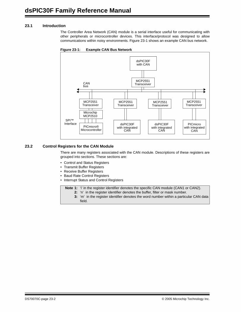
dsPIC30F Family Reference Manual
23.1 Introduction
The Controller Area Network (CAN) module is a serial interface useful for communicating withother peripherals or microcontroller devices. This interface/protocol was designed to allowcommunications within noisy environments. Figure 23-1 shows an example CAN bus network.
Figure 23-1: Example CAN Bus Network
23.2 Control Registers for the CAN Module
There are many registers associated with the CAN module. Descriptions of these registers aregrouped into sections. These sections are:
• Control and Status Registers• Transmit Buffer Registers• Receive Buffer Registers• Baud Rate Control Registers• Interrupt Status and Control Registers
MCP2510SPI™
Interface
CANbus
dsPIC30Fwith CAN
Microchip
PICmicrowith integrated
CAN
MCP2551Transceiver
MCP2551Transceiver
MCP2551Transceiver
MCP2551Transceiver
MCP2551Transceiver
dsPIC30Fwith integrated
CAN
dsPIC30Fwith integrated
CANPICmicro®
Microcontroller
Note 1: ‘i’ in the register identifier denotes the specific CAN module (CAN1 or CAN2).2: ‘n’ in the register identifier denotes the buffer, filter or mask number.3: ‘m’ in the register identifier denotes the word number within a particular CAN data
field.
DS70070C-page 23-2 © 2005 Microchip Technology Inc.
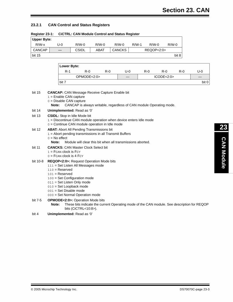
Section 23. CANC
AN
Mo
du
le
23
23.2.1 CAN Control and Status Registers
Register 23-1: CiCTRL: CAN Module Control and Status Register
Upper Byte:
R/W-x U-0 R/W-0 R/W-0 R/W-0 R/W-1 R/W-0 R/W-0
CANCAP — CSIDL ABAT CANCKS REQOP<2:0>
bit 15 bit 8
Lower Byte:
R-1 R-0 R-0 U-0 R-0 R-0 R-0 U-0
OPMODE<2:0> — ICODE<2:0> —
bit 7 bit 0
bit 15 CANCAP: CAN Message Receive Capture Enable bit1 = Enable CAN capture0 = Disable CAN capture
Note: CANCAP is always writable, regardless of CAN module Operating mode.
bit 14 Unimplemented: Read as ‘0’
bit 13 CSIDL: Stop in Idle Mode bit1 = Discontinue CAN module operation when device enters Idle mode0 = Continue CAN module operation in Idle mode
bit 12 ABAT: Abort All Pending Transmissions bit1 = Abort pending transmissions in all Transmit Buffers0 = No effect
Note: Module will clear this bit when all transmissions aborted.
bit 11 CANCKS: CAN Master Clock Select bit1 = FCAN clock is FCY
0 = FCAN clock is 4 FCY
bit 10-8 REQOP<2:0>: Request Operation Mode bits111 = Set Listen All Messages mode110 = Reserved101 = Reserved100 = Set Configuration mode 011 = Set Listen Only mode010 = Set Loopback mode001 = Set Disable mode000 = Set Normal Operation mode
bit 7-5 OPMODE<2:0>: Operation Mode bitsNote: These bits indicate the current Operating mode of the CAN module. See description for REQOP
bits (CiCTRL<10:8>).
bit 4 Unimplemented: Read as ‘0’
© 2005 Microchip Technology Inc. DS70070C-page 23-3
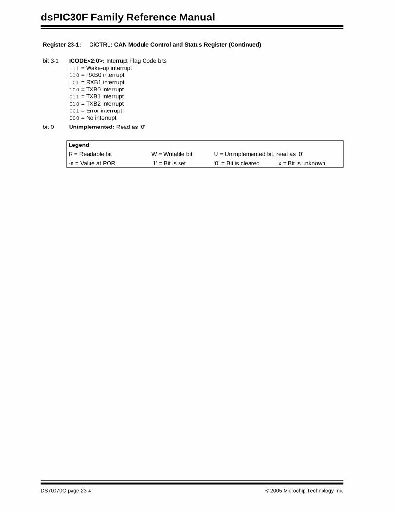
dsPIC30F Family Reference Manual
Register 23-1: CiCTRL: CAN Module Control and Status Register (Continued)
bit 3-1 ICODE<2:0>: Interrupt Flag Code bits111 = Wake-up interrupt110 = RXB0 interrupt101 = RXB1 interrupt100 = TXB0 interrupt011 = TXB1 interrupt010 = TXB2 interrupt001 = Error interrupt000 = No interrupt
bit 0 Unimplemented: Read as ‘0’
Legend:
R = Readable bit W = Writable bit U = Unimplemented bit, read as ‘0’
-n = Value at POR ‘1’ = Bit is set ‘0’ = Bit is cleared x = Bit is unknown
DS70070C-page 23-4 © 2005 Microchip Technology Inc.

Section 23. CANC
AN
Mo
du
le
23
23.2.2 CAN Transmit Buffer Registers
This subsection describes the CAN Transmit Buffer Register and the associated Transmit BufferControl Registers.
Register 23-2: CiTXnCON: Transmit Buffer Status and Control Register
Upper Byte:
U-0 U-0 U-0 U-0 U-0 U-0 U-0 U-0
— — — — — — — —
bit 15 bit 8
Lower Byte:
U-0 R-0 R-0 R-0 R/W-0 U-0 R/W-0 R/W-0
— TXABT TXLARB TXERR TXREQ — TXPRI<1:0>
bit 7 bit 0
bit 15-7 Unimplemented: Read as '0'
bit 6 TXABT: Message Aborted bit1 = Message was aborted0 = Message has not been aborted
Note: This bit is cleared when TXREQ is set.
bit 5 TXLARB: Message Lost Arbitration bit1 = Message lost arbitration while being sent0 = Message did not lose arbitration while being sent
Note: This bit is cleared when TXREQ is set.
bit 4 TXERR: Error Detected During Transmission bit1 = A bus error occurred while the message was being sent0 = A bus error did not occur while the message was being sent
Note: This bit is cleared when TXREQ is set.
bit 3 TXREQ: Message Send Request bit1 = Request message transmission0 = Abort message transmission if TXREQ already set, otherwise no effect
Note: The bit will automatically clear when the message is successfully sent.
bit 2 Unimplemented: Read as ‘0’
bit 1-0 TXPRI<1:0>: Message Transmission Priority bits11 = Highest message priority10 = High intermediate message priority01 = Low intermediate message Priority00 = Lowest message priority
Legend:
R = Readable bit W = Writable bit U = Unimplemented bit, read as ‘0’
-n = Value at POR ‘1’ = Bit is set ‘0’ = Bit is cleared x = Bit is unknown
© 2005 Microchip Technology Inc. DS70070C-page 23-5
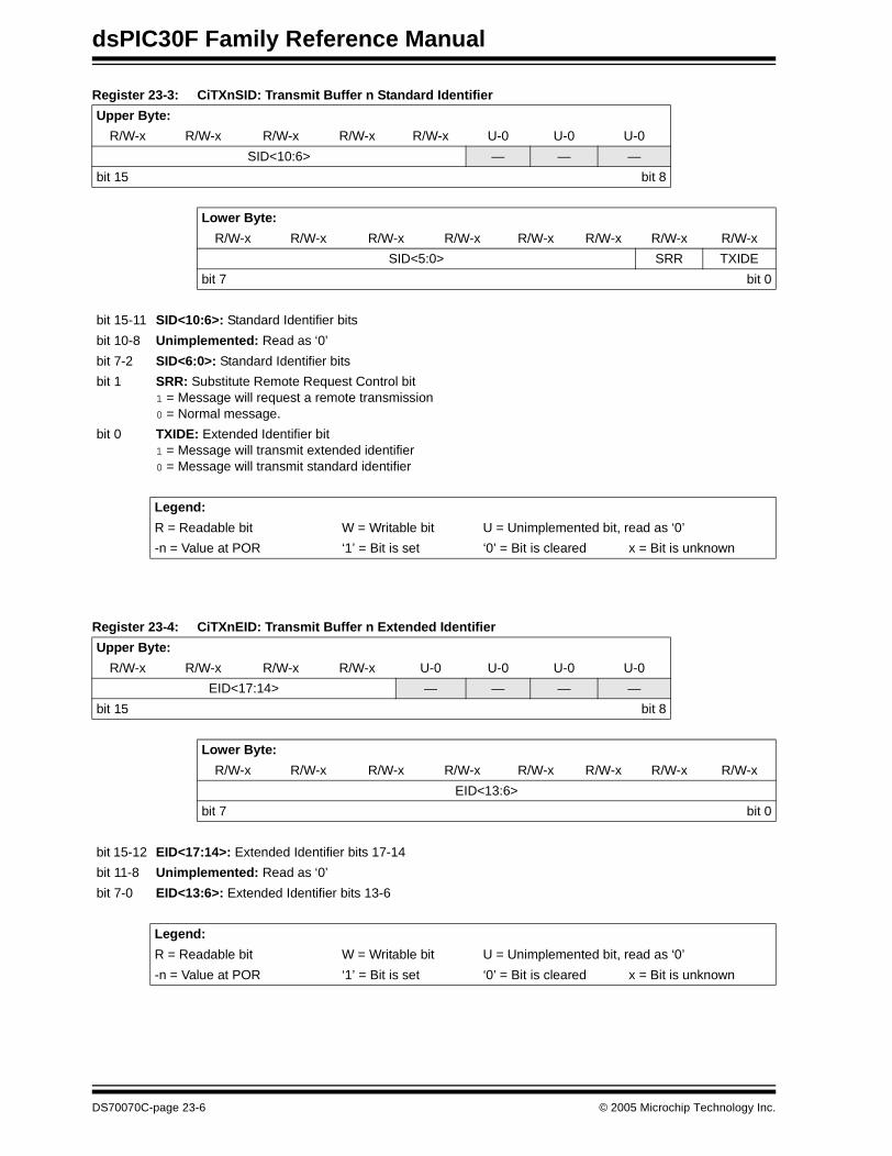
dsPIC30F Family Reference Manual
Register 23-3: CiTXnSID: Transmit Buffer n Standard Identifier
Register 23-4: CiTXnEID: Transmit Buffer n Extended Identifier
Upper Byte:
R/W-x R/W-x R/W-x R/W-x R/W-x U-0 U-0 U-0
SID<10:6> — — —
bit 15 bit 8
Lower Byte:
R/W-x R/W-x R/W-x R/W-x R/W-x R/W-x R/W-x R/W-x
SID<5:0> SRR TXIDE
bit 7 bit 0
bit 15-11 SID<10:6>: Standard Identifier bits
bit 10-8 Unimplemented: Read as ‘0’
bit 7-2 SID<6:0>: Standard Identifier bits
bit 1 SRR: Substitute Remote Request Control bit1 = Message will request a remote transmission0 = Normal message.
bit 0 TXIDE: Extended Identifier bit1 = Message will transmit extended identifier 0 = Message will transmit standard identifier
Legend:
R = Readable bit W = Writable bit U = Unimplemented bit, read as ‘0’
-n = Value at POR ‘1’ = Bit is set ‘0’ = Bit is cleared x = Bit is unknown
Upper Byte:
R/W-x R/W-x R/W-x R/W-x U-0 U-0 U-0 U-0
EID<17:14> — — — —
bit 15 bit 8
Lower Byte:
R/W-x R/W-x R/W-x R/W-x R/W-x R/W-x R/W-x R/W-x
EID<13:6>
bit 7 bit 0
bit 15-12 EID<17:14>: Extended Identifier bits 17-14
bit 11-8 Unimplemented: Read as ‘0’
bit 7-0 EID<13:6>: Extended Identifier bits 13-6
Legend:
R = Readable bit W = Writable bit U = Unimplemented bit, read as ‘0’
-n = Value at POR ‘1’ = Bit is set ‘0’ = Bit is cleared x = Bit is unknown
DS70070C-page 23-6 © 2005 Microchip Technology Inc.
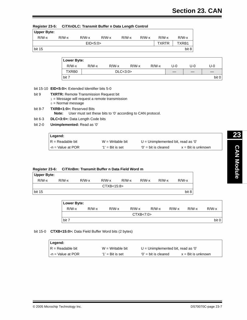
Section 23. CANC
AN
Mo
du
le
23
Register 23-5: CiTXnDLC: Transmit Buffer n Data Length Control
Register 23-6: CiTXnBm: Transmit Buffer n Data Field Word m
Upper Byte:
R/W-x R/W-x R/W-x R/W-x R/W-x R/W-x R/W-x R/W-x
EID<5:0> TXRTR TXRB1
bit 15 bit 8
Lower Byte:
R/W-x R/W-x R/W-x R/W-x R/W-x U-0 U-0 U-0
TXRB0 DLC<3:0> — — —
bit 7 bit 0
bit 15-10 EID<5:0>: Extended Identifier bits 5-0
bit 9 TXRTR: Remote Transmission Request bit1 = Message will request a remote transmission0 = Normal message
bit 8-7 TXRB<1:0>: Reserved BitsNote: User must set these bits to ‘0’ according to CAN protocol.
bit 6-3 DLC<3:0>: Data Length Code bits
bit 2-0 Unimplemented: Read as ‘0’
Legend:
R = Readable bit W = Writable bit U = Unimplemented bit, read as ‘0’
-n = Value at POR ‘1’ = Bit is set ‘0’ = bit is cleared x = Bit is unknown
Upper Byte:
R/W-x R/W-x R/W-x R/W-x R/W-x R/W-x R/W-x R/W-x
CTXB<15:8>
bit 15 bit 8
Lower Byte:
R/W-x R/W-x R/W-x R/W-x R/W-x R/W-x R/W-x R/W-x
CTXB<7:0>
bit 7 bit 0
bit 15-0 CTXB<15:0>: Data Field Buffer Word bits (2 bytes)
Legend:
R = Readable bit W = Writable bit U = Unimplemented bit, read as ‘0’
-n = Value at POR ‘1’ = Bit is set ‘0’ = bit is cleared x = Bit is unknown
© 2005 Microchip Technology Inc. DS70070C-page 23-7

dsPIC30F Family Reference Manual
23.2.3 CAN Receive Buffer Registers
This subsection shows the Receive buffer registers with their associated control registers.
Register 23-7: CiRX0CON: Receive Buffer 0 Status and Control Register
Upper Byte:
U-0 U-0 U-0 U-0 U-0 U-0 U-0 U-0
— — — — — — — —
bit 15 bit 8
Lower Byte:
R/C-0 U-0 U-0 U-0 R-0 R/W-0 R/W-0 R-0
RXFUL — — — RXRTRRO DBEN JTOFF FILHIT0
bit 7 bit 0
bit 15-8 Unimplemented: Read as ‘0’
bit 7 RXFUL: Receive Full Status bit 1 = Receive buffer contains a valid received message0 = Receive buffer is open to receive a new message
Note: This bit is set by the CAN module and should be cleared by software after the buffer is read.
bit 6-4 Unimplemented: Read as ‘0’
bit 3 RXRTRRO: Received Remote Transfer Request bit (read only)1 = Remote Transfer Request was received0 = Remote Transfer Request not received
Note: This bit reflects the status of the last message loaded into Receive Buffer 0.
bit 2 DBEN: Receive Buffer 0 Double Buffer Enable bit 1 = Receive Buffer 0 overflow will write to Receive Buffer 10 = No Receive Buffer 0 overflow to Receive Buffer 1
bit 1 JTOFF: Jump Table Offset bit (read only copy of DBEN)1 = Allows Jump Table offset between 6 and 70 = Allows Jump Table offset between 0 and 1
bit 0 FILHIT0: Indicates Which Acceptance Filter Enabled the Message Reception bit1 = Acceptance Filter 1 (RXF1)0 = Acceptance Filter 0 (RXF0)
Note: This bit reflects the status of the last message loaded into Receive Buffer 0.
Legend:
R = Readable bit W = Writable bit C = Bit can be cleared U = Unimplemented bit, read as ‘0’
-n = Value at POR ‘1’ = Bit is set ‘0’ = Bit is cleared x = Bit is unknown
DS70070C-page 23-8 © 2005 Microchip Technology Inc.
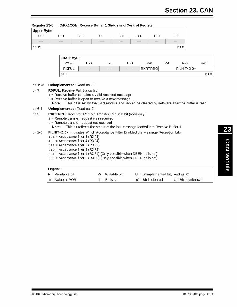
Section 23. CANC
AN
Mo
du
le
23
Register 23-8: CiRX1CON: Receive Buffer 1 Status and Control Register
Upper Byte:
U-0 U-0 U-0 U-0 U-0 U-0 U-0 U-0
— — — — — — — —
bit 15 bit 8
Lower Byte:
R/C-0 U-0 U-0 U-0 R-0 R-0 R-0 R-0
RXFUL — — — RXRTRRO FILHIT<2:0>
bit 7 bit 0
bit 15-8 Unimplemented: Read as ‘0’
bit 7 RXFUL: Receive Full Status bit 1 = Receive buffer contains a valid received message0 = Receive buffer is open to receive a new message
Note: This bit is set by the CAN module and should be cleared by software after the buffer is read.
bit 6-4 Unimplemented: Read as ‘0’
bit 3 RXRTRRO: Received Remote Transfer Request bit (read only)1 = Remote transfer request was received0 = Remote transfer request not received
Note: This bit reflects the status of the last message loaded into Receive Buffer 1.
bit 2-0 FILHIT<2:0>: Indicates Which Acceptance Filter Enabled the Message Reception bits101 = Acceptance filter 5 (RXF5)100 = Acceptance filter 4 (RXF4)011 = Acceptance filter 3 (RXF3)010 = Acceptance filter 2 (RXF2)001 = Acceptance filter 1 (RXF1) (Only possible when DBEN bit is set) 000 = Acceptance filter 0 (RXF0) (Only possible when DBEN bit is set)
Legend:
R = Readable bit W = Writable bit U = Unimplemented bit, read as ‘0’
-n = Value at POR ‘1’ = Bit is set ‘0’ = Bit is cleared x = Bit is unknown
© 2005 Microchip Technology Inc. DS70070C-page 23-9
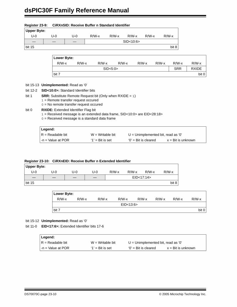
dsPIC30F Family Reference Manual
Register 23-9: CiRXnSID: Receive Buffer n Standard Identifier
Register 23-10: CiRXnEID: Receive Buffer n Extended Identifier
Upper Byte:
U-0 U-0 U-0 R/W-x R/W-x R/W-x R/W-x R/W-x
— — — SID<10:6>
bit 15 bit 8
Lower Byte:
R/W-x R/W-x R/W-x R/W-x R/W-x R/W-x R/W-x R/W-x
SID<5:0> SRR RXIDE
bit 7 bit 0
bit 15-13 Unimplemented: Read as ‘0’
bit 12-2 SID<10:0>: Standard Identifier bits
bit 1 SRR: Substitute Remote Request bit (Only when RXIDE = 1)1 = Remote transfer request occured 0 = No remote transfer request occured
bit 0 RXIDE: Extended Identifier Flag bit1 = Received message is an extended data frame, SID<10:0> are EID<28:18> 0 = Received message is a standard data frame
Legend:
R = Readable bit W = Writable bit U = Unimplemented bit, read as ‘0’
-n = Value at POR ‘1’ = Bit is set ‘0’ = Bit is cleared x = Bit is unknown
Upper Byte:
U-0 U-0 U-0 U-0 R/W-x R/W-x R/W-x R/W-x
— — — — EID<17:14>
bit 15 bit 8
Lower Byte:
R/W-x R/W-x R/W-x R/W-x R/W-x R/W-x R/W-x R/W-x
EID<13:6>
bit 7 bit 0
bit 15-12 Unimplemented: Read as ‘0’
bit 11-0 EID<17:6>: Extended Identifier bits 17-6
Legend:
R = Readable bit W = Writable bit U = Unimplemented bit, read as ‘0’
-n = Value at POR ‘1’ = Bit is set ‘0’ = Bit is cleared x = Bit is unknown
DS70070C-page 23-10 © 2005 Microchip Technology Inc.
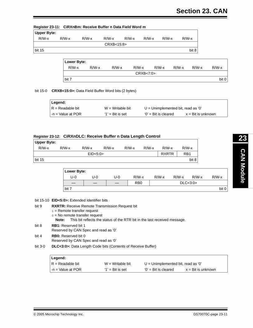
Section 23. CANC
AN
Mo
du
le
23
Register 23-11: CiRXnBm: Receive Buffer n Data Field Word m
Register 23-12: CiRXnDLC: Receive Buffer n Data Length Control
Upper Byte:
R/W-x R/W-x R/W-x R/W-x R/W-x R/W-x R/W-x R/W-x
CRXB<15:8>
bit 15 bit 8
Lower Byte:
R/W-x R/W-x R/W-x R/W-x R/W-x R/W-x R/W-x R/W-x
CRXB<7:0>
bit 7 bit 0
bit 15-0 CRXB<15:0>: Data Field Buffer Word bits (2 bytes)
Legend:
R = Readable bit W = Writable bit U = Unimplemented bit, read as ‘0’
-n = Value at POR ‘1’ = Bit is set ‘0’ = Bit is cleared x = Bit is unknown
Upper Byte:
R/W-x R/W-x R/W-x R/W-x R/W-x R/W-x R/W-x R/W-x
EID<5:0> RXRTR RB1
bit 15 bit 8
Lower Byte:
U-0 U-0 U-0 R/W-x R/W-x R/W-x R/W-x R/W-x
— — — RB0 DLC<3:0>
bit 7 bit 0
bit 15-10 EID<5:0>: Extended Identifier bits
bit 9 RXRTR: Receive Remote Transmission Request bit 1 = Remote transfer request 0 = No remote transfer request
Note: This bit reflects the status of the RTR bit in the last received message.
bit 8 RB1: Reserved bit 1Reserved by CAN Spec and read as ‘0’
bit 4 RB0: Reserved bit 0Reserved by CAN Spec and read as ‘0’
bit 3-0 DLC<3:0>: Data Length Code bits (Contents of Receive Buffer)
Legend:
R = Readable bit W = Writable bit U = Unimplemented bit, read as ‘0’
-n = Value at POR ‘1’ = Bit is set ‘0’ = Bit is cleared x = Bit is unknown
© 2005 Microchip Technology Inc. DS70070C-page 23-11
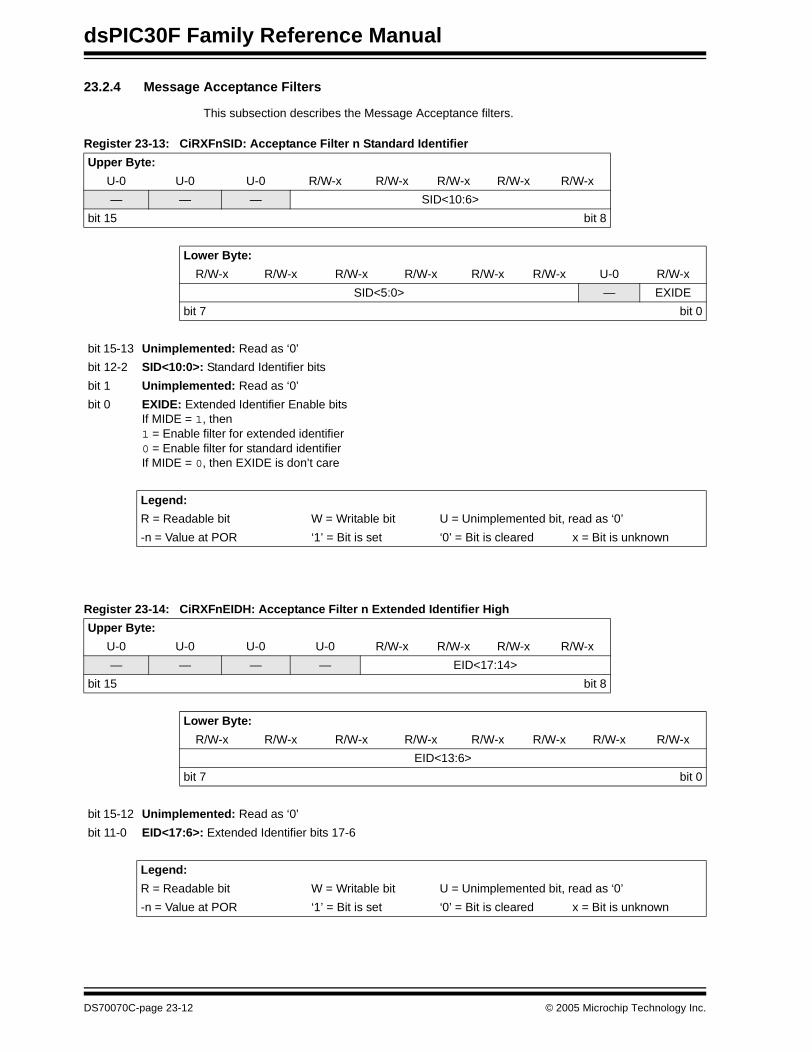
dsPIC30F Family Reference Manual
23.2.4 Message Acceptance Filters
This subsection describes the Message Acceptance filters.
Register 23-13: CiRXFnSID: Acceptance Filter n Standard Identifier
Register 23-14: CiRXFnEIDH: Acceptance Filter n Extended Identifier High
Upper Byte:
U-0 U-0 U-0 R/W-x R/W-x R/W-x R/W-x R/W-x
— — — SID<10:6>
bit 15 bit 8
Lower Byte:
R/W-x R/W-x R/W-x R/W-x R/W-x R/W-x U-0 R/W-x
SID<5:0> — EXIDE
bit 7 bit 0
bit 15-13 Unimplemented: Read as ‘0’
bit 12-2 SID<10:0>: Standard Identifier bits
bit 1 Unimplemented: Read as ‘0’
bit 0 EXIDE: Extended Identifier Enable bitsIf MIDE = 1, then1 = Enable filter for extended identifier0 = Enable filter for standard identifierIf MIDE = 0, then EXIDE is don’t care
Legend:
R = Readable bit W = Writable bit U = Unimplemented bit, read as ‘0’
-n = Value at POR ‘1’ = Bit is set ‘0’ = Bit is cleared x = Bit is unknown
Upper Byte:
U-0 U-0 U-0 U-0 R/W-x R/W-x R/W-x R/W-x
— — — — EID<17:14>
bit 15 bit 8
Lower Byte:
R/W-x R/W-x R/W-x R/W-x R/W-x R/W-x R/W-x R/W-x
EID<13:6>
bit 7 bit 0
bit 15-12 Unimplemented: Read as ‘0’
bit 11-0 EID<17:6>: Extended Identifier bits 17-6
Legend:
R = Readable bit W = Writable bit U = Unimplemented bit, read as ‘0’
-n = Value at POR ‘1’ = Bit is set ‘0’ = Bit is cleared x = Bit is unknown
DS70070C-page 23-12 © 2005 Microchip Technology Inc.
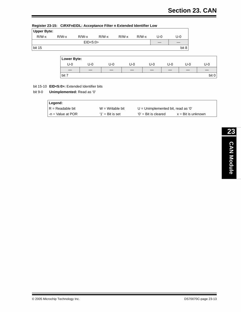
Section 23. CANC
AN
Mo
du
le
23
Register 23-15: CiRXFnEIDL: Acceptance Filter n Extended Identifier Low
Upper Byte:
R/W-x R/W-x R/W-x R/W-x R/W-x R/W-x U-0 U-0
EID<5:0> — —
bit 15 bit 8
Lower Byte:
U-0 U-0 U-0 U-0 U-0 U-0 U-0 U-0
— — — — — — — —
bit 7 bit 0
bit 15-10 EID<5:0>: Extended Identifier bits
bit 9-0 Unimplemented: Read as ‘0’
Legend:
R = Readable bit W = Writable bit U = Unimplemented bit, read as ‘0’
-n = Value at POR ‘1’ = Bit is set ‘0’ = Bit is cleared x = Bit is unknown
© 2005 Microchip Technology Inc. DS70070C-page 23-13

dsPIC30F Family Reference Manual
23.2.5 Acceptance Filter Mask Registers
Register 23-16: CiRXMnSID: Acceptance Filter Mask n Standard Identifier
Register 23-17: CiRXMnEIDH: Acceptance Filter Mask n Extended Identifier High
Upper Byte:
U-0 U-0 U-0 R/W-x R/W-x R/W-x R/W-x R/W-x
— — — SID<10:6>
bit 15 bit 8
Lower Byte:
R/W-x R/W-x R/W-x R/W-x R/W-x R/W-x U-0 R/W-x
SID<5:0> — MIDE
bit 7 bit 0
bit 15-13 Unimplemented: Read as ‘0’
bit 12-2 SID<10:0>: Standard Identifier Mask bits1 = Include bit in the filter comparison0 = Don’t include bit in the filter comparison
bit 1 Unimplemented: Read as ‘0’
bit 0 MIDE: Identifier Mode Selection bit1 = Match only message types (standard or extended address) as determined by EXIDE bit in filter0 = Match either standard or extended address message if the filters match
Legend:
R = Readable bit W = Writable bit U = Unimplemented bit, read as ‘0’
-n = Value at POR ‘1’ = Bit is set ‘0’ = Bit is cleared x = Bit is unknown
Upper Byte:
U-0 U-0 U-0 U-0 R/W-x R/W-x R/W-x R/W-x
— — — — EID<17:14>
bit 15 bit 8
Lower Byte:
R/W-x R/W-x R/W-x R/W-x R/W-x R/W-x R/W-x R/W-x
EID<13:6>
bit 7 bit 0
bit 15-12 Unimplemented: Read as ‘0’
bit 11-0 EID<17:6>: Extended Identifier Mask bits 17-61 = Include bit in the filter comparison0 = Don’t include bit in the filter comparison
Legend:
R = Readable bit W = Writable bit U = Unimplemented bit, read as ‘0’
-n = Value at POR ‘1’ = Bit is set ‘0’ = Bit is cleared x = Bit is unknown
DS70070C-page 23-14 © 2005 Microchip Technology Inc.
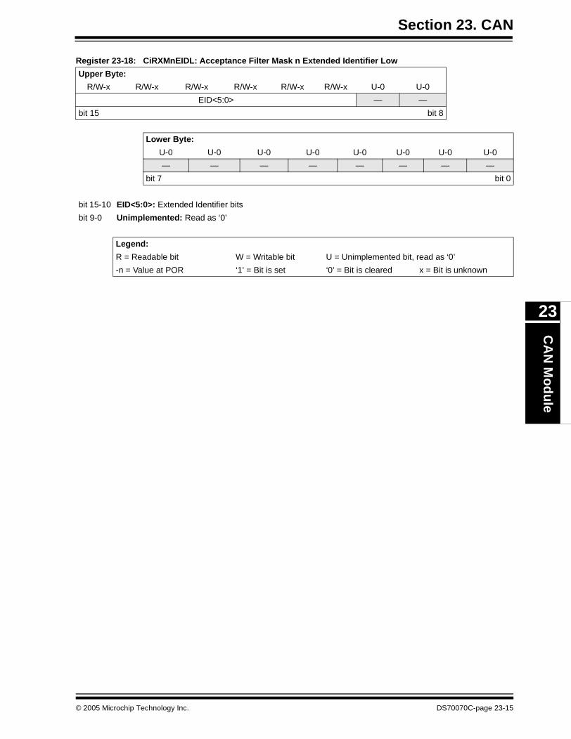
Section 23. CANC
AN
Mo
du
le
23
Register 23-18: CiRXMnEIDL: Acceptance Filter Mask n Extended Identifier Low
Upper Byte:
R/W-x R/W-x R/W-x R/W-x R/W-x R/W-x U-0 U-0
EID<5:0> — —
bit 15 bit 8
Lower Byte:
U-0 U-0 U-0 U-0 U-0 U-0 U-0 U-0
— — — — — — — —
bit 7 bit 0
bit 15-10 EID<5:0>: Extended Identifier bits
bit 9-0 Unimplemented: Read as ‘0’
Legend:
R = Readable bit W = Writable bit U = Unimplemented bit, read as ‘0’
-n = Value at POR ‘1’ = Bit is set ‘0’ = Bit is cleared x = Bit is unknown
© 2005 Microchip Technology Inc. DS70070C-page 23-15
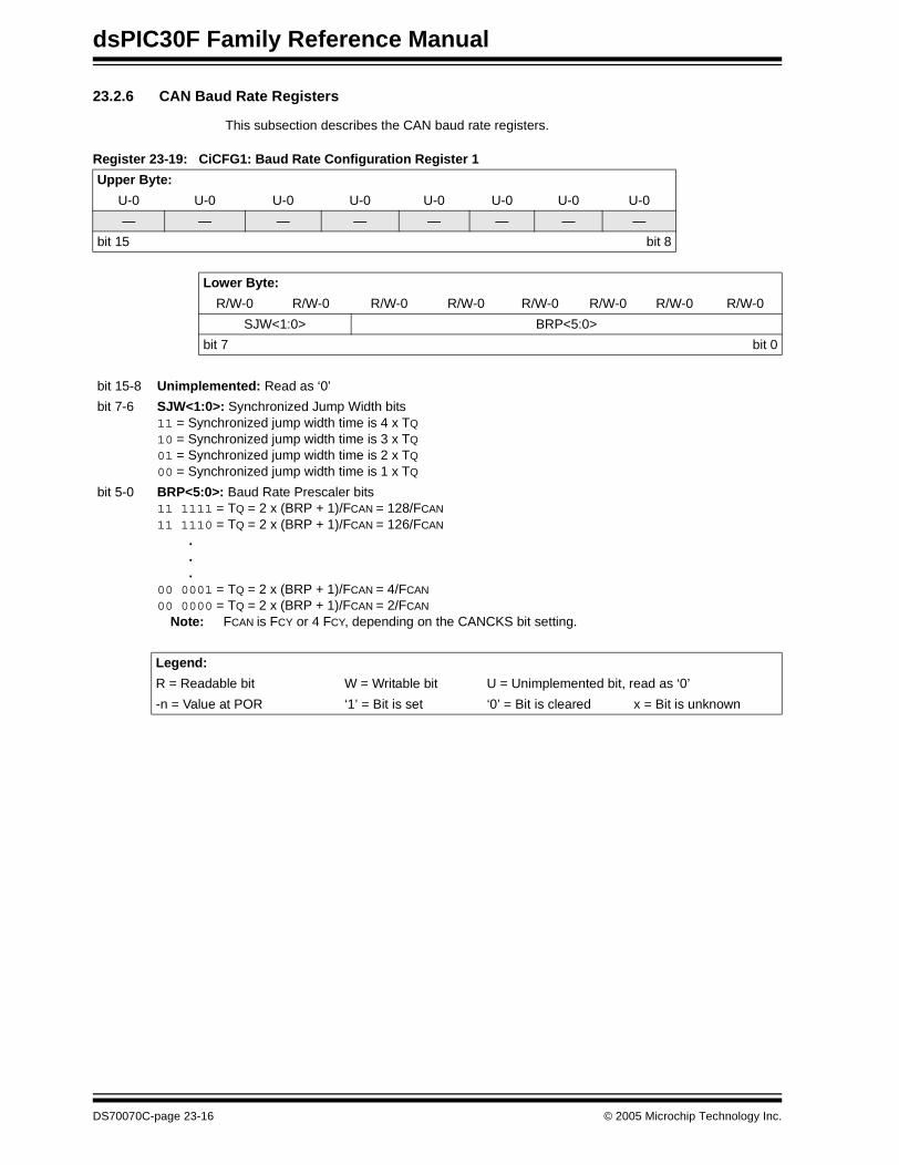
dsPIC30F Family Reference Manual
23.2.6 CAN Baud Rate Registers
This subsection describes the CAN baud rate registers.
Register 23-19: CiCFG1: Baud Rate Configuration Register 1
Upper Byte:
U-0 U-0 U-0 U-0 U-0 U-0 U-0 U-0
— — — — — — — —
bit 15 bit 8
Lower Byte:
R/W-0 R/W-0 R/W-0 R/W-0 R/W-0 R/W-0 R/W-0 R/W-0
SJW<1:0> BRP<5:0>
bit 7 bit 0
bit 15-8 Unimplemented: Read as ‘0’
bit 7-6 SJW<1:0>: Synchronized Jump Width bits11 = Synchronized jump width time is 4 x TQ
10 = Synchronized jump width time is 3 x TQ
01 = Synchronized jump width time is 2 x TQ
00 = Synchronized jump width time is 1 x TQ
bit 5-0 BRP<5:0>: Baud Rate Prescaler bits11 1111 = TQ = 2 x (BRP + 1)/FCAN = 128/FCAN 11 1110 = TQ = 2 x (BRP + 1)/FCAN = 126/FCAN
.
.
.00 0001 = TQ = 2 x (BRP + 1)/FCAN = 4/FCAN 00 0000 = TQ = 2 x (BRP + 1)/FCAN = 2/FCAN
Note: FCAN is FCY or 4 FCY, depending on the CANCKS bit setting.
Legend:
R = Readable bit W = Writable bit U = Unimplemented bit, read as ‘0’
-n = Value at POR ‘1’ = Bit is set ‘0’ = Bit is cleared x = Bit is unknown
DS70070C-page 23-16 © 2005 Microchip Technology Inc.
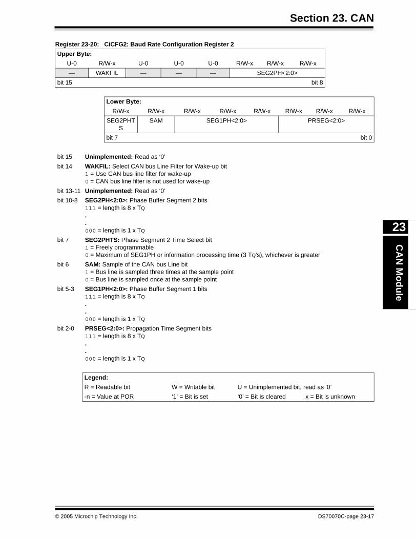
Section 23. CANC
AN
Mo
du
le
23
Register 23-20: CiCFG2: Baud Rate Configuration Register 2
Upper Byte:
U-0 R/W-x U-0 U-0 U-0 R/W-x R/W-x R/W-x
— WAKFIL — — — SEG2PH<2:0>
bit 15 bit 8
Lower Byte:
R/W-x R/W-x R/W-x R/W-x R/W-x R/W-x R/W-x R/W-x
SEG2PHTS
SAM SEG1PH<2:0> PRSEG<2:0>
bit 7 bit 0
bit 15 Unimplemented: Read as ‘0’
bit 14 WAKFIL: Select CAN bus Line Filter for Wake-up bit1 = Use CAN bus line filter for wake-up0 = CAN bus line filter is not used for wake-up
bit 13-11 Unimplemented: Read as ‘0’
bit 10-8 SEG2PH<2:0>: Phase Buffer Segment 2 bits111 = length is 8 x TQ ..000 = length is 1 x TQ
bit 7 SEG2PHTS: Phase Segment 2 Time Select bit1 = Freely programmable0 = Maximum of SEG1PH or information processing time (3 TQ’s), whichever is greater
bit 6 SAM: Sample of the CAN bus Line bit1 = Bus line is sampled three times at the sample point 0 = Bus line is sampled once at the sample point
bit 5-3 SEG1PH<2:0>: Phase Buffer Segment 1 bits111 = length is 8 x TQ ..000 = length is 1 x TQ
bit 2-0 PRSEG<2:0>: Propagation Time Segment bits111 = length is 8 x TQ ..000 = length is 1 x TQ
Legend:
R = Readable bit W = Writable bit U = Unimplemented bit, read as ‘0’
-n = Value at POR ‘1’ = Bit is set ‘0’ = Bit is cleared x = Bit is unknown
© 2005 Microchip Technology Inc. DS70070C-page 23-17
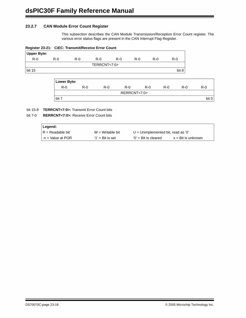
dsPIC30F Family Reference Manual
23.2.7 CAN Module Error Count Register
This subsection describes the CAN Module Transmission/Reception Error Count register. Thevarious error status flags are present in the CAN Interrupt Flag Register.
Register 23-21: CiEC: Transmit/Receive Error Count
Upper Byte:
R-0 R-0 R-0 R-0 R-0 R-0 R-0 R-0
TERRCNT<7:0>
bit 15 bit 8
Lower Byte:
R-0 R-0 R-0 R-0 R-0 R-0 R-0 R-0
RERRCNT<7:0>
bit 7 bit 0
bit 15-8 TERRCNT<7:0>: Transmit Error Count bits
bit 7-0 RERRCNT<7:0>: Receive Error Count bits
Legend:
R = Readable bit W = Writable bit U = Unimplemented bit, read as ‘0’
-n = Value at POR ‘1’ = Bit is set ‘0’ = Bit is cleared x = Bit is unknown
DS70070C-page 23-18 © 2005 Microchip Technology Inc.
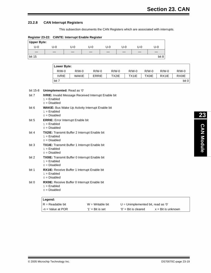
Section 23. CANC
AN
Mo
du
le
23
23.2.8 CAN Interrupt Registers
This subsection documents the CAN Registers which are associated with interrupts.
Register 23-22: CiINTE: Interrupt Enable Register
Upper Byte:
U-0 U-0 U-0 U-0 U-0 U-0 U-0 U-0
— — — — — — — —
bit 15 bit 8
Lower Byte:
R/W-0 R/W-0 R/W-0 R/W-0 R/W-0 R/W-0 R/W-0 R/W-0
IVRIE WAKIE ERRIE TX2IE TX1IE TX0IE RX1IE RX0IE
bit 7 bit 0
bit 15-8 Unimplemented: Read as ‘0’
bit 7 IVRIE: Invalid Message Received Interrupt Enable bit1 = Enabled0 = Disabled
bit 6 WAKIE: Bus Wake Up Activity Interrupt Enable bit1 = Enabled0 = Disabled
bit 5 ERRIE: Error Interrupt Enable bit1 = Enabled0 = Disabled
bit 4 TX2IE: Transmit Buffer 2 Interrupt Enable bit1 = Enabled0 = Disabled
bit 3 TX1IE: Transmit Buffer 1 Interrupt Enable bit1 = Enabled0 = Disabled
bit 2 TX0IE: Transmit Buffer 0 Interrupt Enable bit1 = Enabled0 = Disabled
bit 1 RX1IE: Receive Buffer 1 Interrupt Enable bit1 = Enabled0 = Disabled
bit 0 RX0IE: Receive Buffer 0 Interrupt Enable bit1 = Enabled0 = Disabled
Legend:
R = Readable bit W = Writable bit U = Unimplemented bit, read as ‘0’
-n = Value at POR ‘1’ = Bit is set ‘0’ = Bit is cleared x = Bit is unknown
© 2005 Microchip Technology Inc. DS70070C-page 23-19
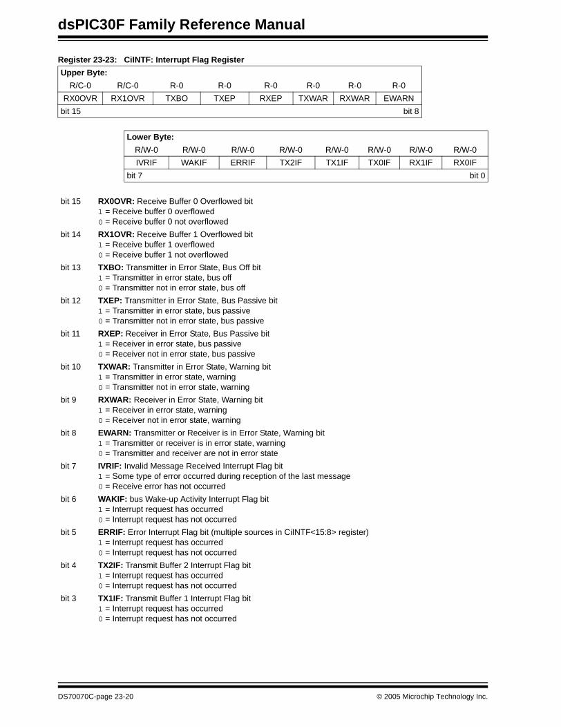
dsPIC30F Family Reference Manual
Register 23-23: CiINTF: Interrupt Flag Register
Upper Byte:
R/C-0 R/C-0 R-0 R-0 R-0 R-0 R-0 R-0
RX0OVR RX1OVR TXBO TXEP RXEP TXWAR RXWAR EWARN
bit 15 bit 8
Lower Byte:
R/W-0 R/W-0 R/W-0 R/W-0 R/W-0 R/W-0 R/W-0 R/W-0
IVRIF WAKIF ERRIF TX2IF TX1IF TX0IF RX1IF RX0IF
bit 7 bit 0
bit 15 RX0OVR: Receive Buffer 0 Overflowed bit1 = Receive buffer 0 overflowed0 = Receive buffer 0 not overflowed
bit 14 RX1OVR: Receive Buffer 1 Overflowed bit1 = Receive buffer 1 overflowed0 = Receive buffer 1 not overflowed
bit 13 TXBO: Transmitter in Error State, Bus Off bit1 = Transmitter in error state, bus off0 = Transmitter not in error state, bus off
bit 12 TXEP: Transmitter in Error State, Bus Passive bit1 = Transmitter in error state, bus passive0 = Transmitter not in error state, bus passive
bit 11 RXEP: Receiver in Error State, Bus Passive bit1 = Receiver in error state, bus passive0 = Receiver not in error state, bus passive
bit 10 TXWAR: Transmitter in Error State, Warning bit1 = Transmitter in error state, warning 0 = Transmitter not in error state, warning
bit 9 RXWAR: Receiver in Error State, Warning bit1 = Receiver in error state, warning0 = Receiver not in error state, warning
bit 8 EWARN: Transmitter or Receiver is in Error State, Warning bit1 = Transmitter or receiver is in error state, warning0 = Transmitter and receiver are not in error state
bit 7 IVRIF: Invalid Message Received Interrupt Flag bit1 = Some type of error occurred during reception of the last message0 = Receive error has not occurred
bit 6 WAKIF: bus Wake-up Activity Interrupt Flag bit1 = Interrupt request has occurred0 = Interrupt request has not occurred
bit 5 ERRIF: Error Interrupt Flag bit (multiple sources in CiINTF<15:8> register)1 = Interrupt request has occurred0 = Interrupt request has not occurred
bit 4 TX2IF: Transmit Buffer 2 Interrupt Flag bit1 = Interrupt request has occurred0 = Interrupt request has not occurred
bit 3 TX1IF: Transmit Buffer 1 Interrupt Flag bit1 = Interrupt request has occurred0 = Interrupt request has not occurred
DS70070C-page 23-20 © 2005 Microchip Technology Inc.
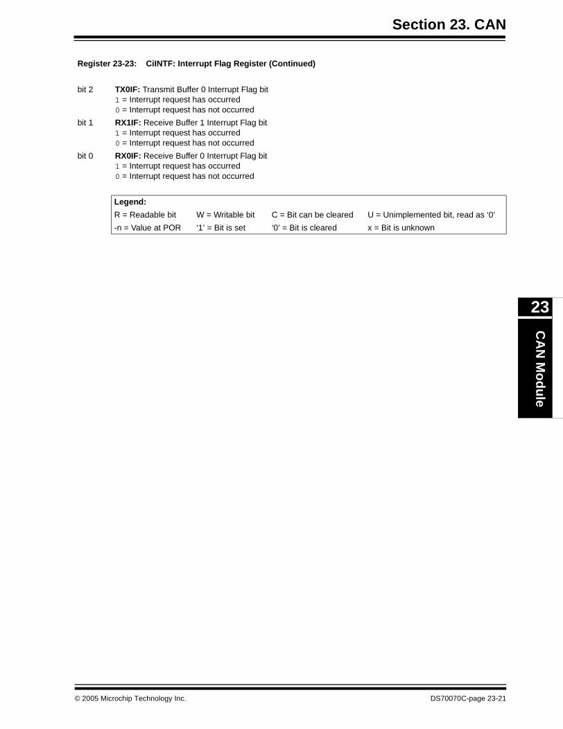
Section 23. CANC
AN
Mo
du
le
23
Register 23-23: CiINTF: Interrupt Flag Register (Continued)
bit 2 TX0IF: Transmit Buffer 0 Interrupt Flag bit1 = Interrupt request has occurred0 = Interrupt request has not occurred
bit 1 RX1IF: Receive Buffer 1 Interrupt Flag bit1 = Interrupt request has occurred0 = Interrupt request has not occurred
bit 0 RX0IF: Receive Buffer 0 Interrupt Flag bit1 = Interrupt request has occurred0 = Interrupt request has not occurred
Legend:
R = Readable bit W = Writable bit C = Bit can be cleared U = Unimplemented bit, read as ‘0’
-n = Value at POR ‘1’ = Bit is set ‘0’ = Bit is cleared x = Bit is unknown
© 2005 Microchip Technology Inc. DS70070C-page 23-21
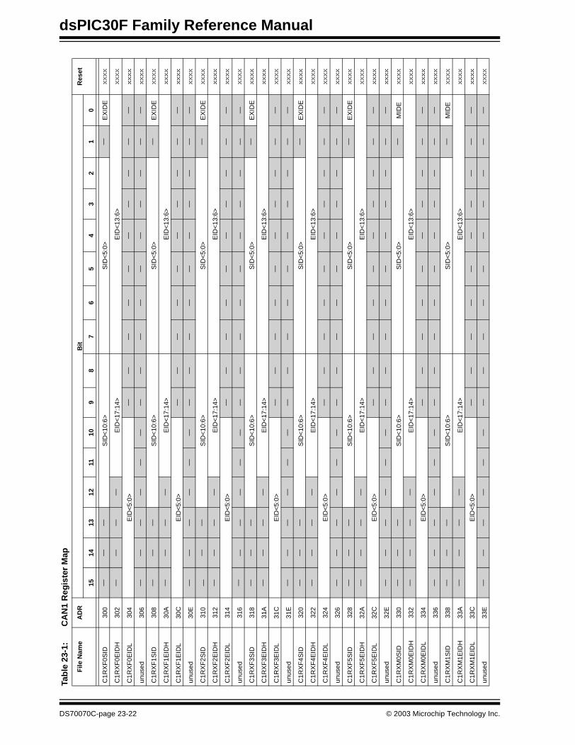
dsPIC30F Family Reference Manual
Tab
le 2
3-1:
CA
N1
Reg
iste
r M
ap
File
Nam
eA
DR
Bit
Res
et
1514
1312
1110
98
76
54
32
10
C1R
XF
0SID
300
——
—S
ID<
10:6
>S
ID<
5:0>
—E
XID
Exxxx
C1R
XF
0EID
H30
2—
——
—E
ID<
17:1
4>E
ID<
13:6
>xxxx
C1R
XF
0EID
L30
4E
ID<
5:0>
——
——
——
——
——
xxxx
unus
ed30
6—
——
——
——
——
——
——
——
—xxxx
C1R
XF
1SID
308
——
—S
ID<
10:6
>S
ID<
5:0>
—E
XID
Exxxx
C1R
XF
1EID
H30
A—
——
—E
ID<
17:1
4>E
ID<
13:6
>xxxx
C1R
XF
1EID
L30
CE
ID<
5:0>
——
——
——
——
——
xxxx
unus
ed30
E—
——
——
——
——
——
——
——
—xxxx
C1R
XF
2SID
310
——
—S
ID<
10:6
>S
ID<
5:0>
—E
XID
Exxxx
C1R
XF
2EID
H31
2—
——
—E
ID<
17:1
4>E
ID<
13:6
>xxxx
C1R
XF
2EID
L31
4E
ID<
5:0>
——
——
——
——
——
xxxx
unus
ed31
6—
——
——
——
——
——
——
——
—xxxx
C1R
XF
3SID
318
——
—S
ID<
10:6
>S
ID<
5:0>
—E
XID
Exxxx
C1R
XF
3EID
H31
A—
——
—E
ID<
17:1
4>E
ID<
13:6
>xxxx
C1R
XF
3EID
L31
CE
ID<
5:0>
——
——
——
——
——
xxxx
unus
ed31
E—
——
——
——
——
——
——
——
—xxxx
C1R
XF
4SID
320
——
—S
ID<
10:6
>S
ID<
5:0>
—E
XID
Exxxx
C1R
XF
4EID
H32
2—
——
—E
ID<
17:1
4>E
ID<
13:6
>xxxx
C1R
XF
4EID
L32
4E
ID<
5:0>
——
——
——
——
——
xxxx
unus
ed32
6—
——
——
——
——
——
——
——
—xxxx
C1R
XF
5SID
328
——
—S
ID<
10:6
>S
ID<
5:0>
—E
XID
Exxxx
C1R
XF
5EID
H32
A—
——
—E
ID<
17:1
4>E
ID<
13:6
>xxxx
C1R
XF
5EID
L32
CE
ID<
5:0>
——
——
——
——
——
xxxx
unus
ed32
E—
——
——
——
——
——
——
——
—xxxx
C1R
XM
0SID
330
——
—S
ID<
10:6
>S
ID<
5:0>
—M
IDE
xxxx
C1R
XM
0EID
H33
2—
——
—E
ID<
17:1
4>E
ID<
13:6
>xxxx
C1R
XM
0EID
L33
4E
ID<
5:0>
——
——
——
——
——
xxxx
unus
ed33
6—
——
——
——
——
——
——
——
—xxxx
C1R
XM
1SID
338
——
—S
ID<
10:6
>S
ID<
5:0>
—M
IDE
xxxx
C1R
XM
1EID
H33
A—
——
—E
ID<
17:1
4>E
ID<
13:6
>xxxx
C1R
XM
1EID
L33
CE
ID<
5:0>
——
——
——
——
——
xxxx
unus
ed33
E—
——
——
——
——
——
——
——
—xxxx
DS70070C-page 23-22 © 2003 Microchip Technology Inc.
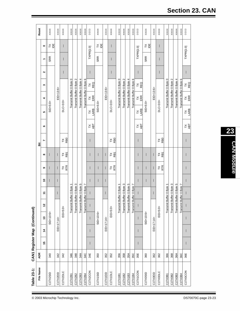
Section 23. CANC
AN
Mo
du
le
23
C1T
X2S
ID34
0S
ID<
10:6
>—
——
SID
<5:
0>S
RR
TX
IDE
xxxx
C1T
X2E
ID34
2E
ID<
17:1
4>—
——
—E
ID<
13:6
>xxxx
C1T
X2D
LC34
2E
ID<
5:0>
TX
RT
RT
XR
B1
TX
RB
0D
LC<
3:0>
——
—xxxx
C1T
X2B
134
6T
rans
mit
Buf
fer
0 B
yte
1Tr
ansm
it B
uffe
r 0
Byt
e 0
xxxx
C1T
X2B
234
8T
rans
mit
Buf
fer
0 B
yte
3Tr
ansm
it B
uffe
r 0
Byt
e 2
xxxx
C1T
X2B
334
AT
rans
mit
Buf
fer
0 B
yte
5Tr
ansm
it B
uffe
r 0
Byt
e 4
xxxx
C1T
X2B
434
CT
rans
mit
Buf
fer
0 B
yte
7Tr
ansm
it B
uffe
r 0
Byt
e 6
xxxx
C1T
X2C
ON
34E
——
——
——
——
—T
XA
BT
TX
LAR
BT
XE
RR
TX
RE
Q—
TX
PR
I[1:0
]0000
C1T
X1S
ID35
0S
ID<
10:6
>—
——
SID
<5:
0>S
RR
TX
IDE
xxxx
C1T
X1E
ID35
2E
ID<
17:1
4>—
——
—E
ID<
13:6
>xxxx
C1T
X1D
LC35
2E
ID<
5:0>
TX
RT
RT
XR
B1
TX
RB
0D
LC<
3:0>
——
—xxxx
C1T
X1B
135
6T
rans
mit
Buf
fer
0 B
yte
1Tr
ansm
it B
uffe
r 0
Byt
e 0
xxxx
C1T
X1B
235
8T
rans
mit
Buf
fer
0 B
yte
3Tr
ansm
it B
uffe
r 0
Byt
e 2
xxxx
C1T
X1B
335
AT
rans
mit
Buf
fer
0 B
yte
5Tr
ansm
it B
uffe
r 0
Byt
e 4
xxxx
C1T
X1B
435
CT
rans
mit
Buf
fer
0 B
yte
7Tr
ansm
it B
uffe
r 0
Byt
e 6
xxxx
C1T
X1C
ON
35E
——
——
——
——
—T
XA
BT
TX
LAR
BT
XE
RR
TX
RE
Q—
TX
PR
I[1:0
]0000
C1T
X0S
ID36
0S
ID<
10:6
>—
——
SID
<5:
0>S
RR
TX
IDE
xxxx
C1T
X0E
ID36
2E
ID<
17:1
4>—
——
—E
ID<
13:6
>xxxx
C1T
X0D
LC36
2E
ID<
5:0>
TX
RT
RT
XR
B1
TX
RB
0D
LC<
3:0>
——
—xxxx
C1T
X0B
136
6T
rans
mit
Buf
fer
0 B
yte
1Tr
ansm
it B
uffe
r 0
Byt
e 0
xxxx
C1T
X0B
236
8T
rans
mit
Buf
fer
0 B
yte
3Tr
ansm
it B
uffe
r 0
Byt
e 2
xxxx
C1T
X0B
336
AT
rans
mit
Buf
fer
0 B
yte
5Tr
ansm
it B
uffe
r 0
Byt
e 4
xxxx
C1T
X0B
436
CT
rans
mit
Buf
fer
0 B
yte
7Tr
ansm
it B
uffe
r 0
Byt
e 6
xxxx
C1T
X0C
ON
36E
——
——
——
——
—T
XA
BT
TX
LAR
BT
XE
RR
TX
RE
Q—
TX
PR
I[1:0
]0000
Tab
le 2
3-1:
CA
N1
Reg
iste
r M
ap (
Co
nti
nu
ed)
File
Nam
eA
DR
Bit
Res
et
1514
1312
1110
98
76
54
32
10
© 2003 Microchip Technology Inc. DS70070C-page 23-23
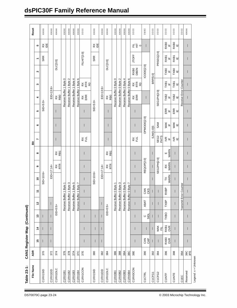
dsPIC30F Family Reference Manual
C1R
X1S
ID37
0—
——
SID
<10
:6>
SID
<5:
0>S
RR
RX
IDE
xxxx
C1R
X1E
ID37
2—
——
—E
ID<
17:1
4>E
ID<
13:6
>xxxx
C1R
X1D
LC37
4E
ID<
0:5>
RX
RT
RR
XR
B1
——
—R
XR
B0
DLC
[3:0
]xxxx
C1R
X1B
137
6R
ecei
ve B
uffe
r 1
Byt
e 1
Rec
eive
Buf
fer
1 B
yte
0xxxx
C1R
X1B
237
8R
ecei
ve B
uffe
r 1
Byt
e 3
Rec
eive
Buf
fer
1 B
yte
2xxxx
C1R
X1B
337
AR
ecei
ve B
uffe
r 1
Byt
e 5
Rec
eive
Buf
fer
1 B
yte
4xxxx
C1R
X1B
437
CR
ecei
ve B
uffe
r 1
Byt
e 7
Rec
eive
Buf
fer
1 B
yte
6xxxx
C1R
X1C
ON
37E
——
——
——
——
RX
FU
L—
—R
XE
RR
RX
RT
RR
0
FIL
HIT
[2:0
]0000
C1R
X1S
ID38
0—
——
SID
<10
:6>
SID
<5:
0>S
RR
RX
IDE
xxxx
C1R
X1E
ID38
2—
——
—E
ID<
17:1
4>E
ID<
13:6
>xxxx
C1R
X1D
LC38
4E
ID<
0:5>
RX
RT
RR
XR
B1
——
—R
XR
B0
DLC
[3:0
]xxxx
C1R
X0B
138
6R
ecei
ve B
uffe
r 0
Byt
e 1
Rec
eive
Buf
fer
0 B
yte
0xxxx
C1R
X0B
238
8R
ecei
ve B
uffe
r 0
Byt
e 3
Rec
eive
Buf
fer
0 B
yte
2xxxx
C1R
X0B
338
AR
ecei
ve B
uffe
r 0
Byt
e 5
Rec
eive
Buf
fer
0 B
yte
4xxxx
C1R
X0B
438
CR
ecei
ve B
uffe
r 0
Byt
e 7
Rec
eive
Buf
fer
0 B
yte
6xxxx
C1R
X0C
ON
38E
——
——
——
——
RX
FU
L—
—R
XE
RR
RX
RT
RR
0
RX
B0
DB
EN
JTO
FF
FIL
HIT 0
0000
C1C
TR
L39
0C
AN
CA
P—
CS
IDL
AB
AT
CA
NC
KS
RE
QO
P[2
:0]
OP
MO
DE
[2:0
]—
ICO
DE
[2:0
]—
0480
C1C
FG
139
2—
——
——
——
—S
JW[1
:0]S
BR
P[5
:0]
0000
C1C
FG
239
4—
WA
KF
IL—
——
SE
G2P
H[2
:0]
SE
G2
PH
TS
SA
MS
EG
1PH
[2:0
]P
RS
EG
[2:0
]0000
C1I
NT
F39
6R
XB
0O
VR
RX
B1
OV
RT
XB
OT
XB
PR
XB
PT
XW
AR
NR
XW
AR
NE
WA
RN
IVR
IFW
AK
IFE
RR
IFT
XB
2IF
TX
B1
IFT
XB
0IF
RX
B1
IFR
XB
0IF
0000
C1I
NT
E39
8—
——
——
——
—IV
RIE
WA
KIE
ER
RIE
TX
B2
IET
XB
1IE
TX
B0
IER
XB
1IE
RX
B0
IE0000
C1E
C39
ATr
ansm
it E
rror
Cou
nter
Rec
eive
Err
or C
ount
er0000
Res
erve
d39
C3F
E—
——
——
——
——
——
——
——
—xxxx
Lege
nd: x
= U
nkno
wn
Tab
le 2
3-1:
CA
N1
Reg
iste
r M
ap (
Co
nti
nu
ed)
File
Nam
eA
DR
Bit
Res
et
1514
1312
1110
98
76
54
32
10
DS70070C-page 23-24 © 2003 Microchip Technology Inc.
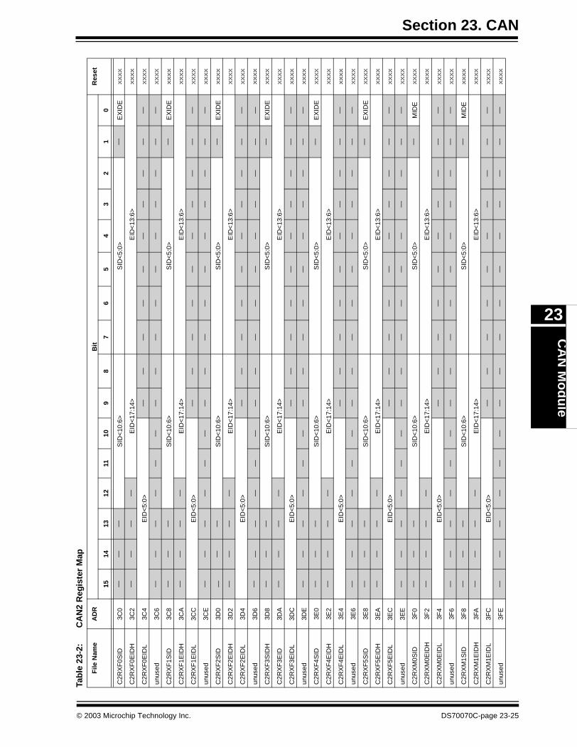
Section 23. CANC
AN
Mo
du
le
23
Tab
le 2
3-2:
CA
N2
Reg
iste
r M
ap
File
Nam
eA
DR
Bit
Res
et
1514
1312
1110
98
76
54
32
10
C2R
XF
0SID
3C0
——
—S
ID<
10:6
>S
ID<
5:0>
—E
XID
Exxxx
C2R
XF
0EID
H3C
2—
——
—E
ID<
17:1
4>E
ID<
13:6
>xxxx
C2R
XF
0EID
L3C
4E
ID<
5:0>
——
——
——
——
——
xxxx
unus
ed3C
6—
——
——
——
——
——
——
——
—xxxx
C2R
XF
1SID
3C8
——
—S
ID<
10:6
>S
ID<
5:0>
—E
XID
Exxxx
C2R
XF
1EID
H3C
A—
——
—E
ID<
17:1
4>E
ID<
13:6
>xxxx
C2R
XF
1EID
L3C
CE
ID<
5:0>
——
——
——
——
——
xxxx
unus
ed3C
E—
——
——
——
——
——
——
——
—xxxx
C2R
XF
2SID
3D0
——
—S
ID<
10:6
>S
ID<
5:0>
—E
XID
Exxxx
C2R
XF
2EID
H3D
2—
——
—E
ID<
17:1
4>E
ID<
13:6
>xxxx
C2R
XF
2EID
L3D
4E
ID<
5:0>
——
——
——
——
——
xxxx
unus
ed3D
6—
——
——
——
——
——
——
——
—xxxx
C2R
XF
3SID
H3D
8—
——
SID
<10
:6>
SID
<5:
0>—
EX
IDE
xxxx
C2R
XF
3EID
3DA
——
——
EID
<17
:14>
EID
<13
:6>
xxxx
C2R
XF
3EID
L3D
CE
ID<
5:0>
——
——
——
——
——
xxxx
unus
ed3D
E—
——
——
——
——
——
——
——
—xxxx
C2R
XF
4SID
3E0
——
—S
ID<
10:6
>S
ID<
5:0>
—E
XID
Exxxx
C2R
XF
4EID
H3E
2—
——
—E
ID<
17:1
4>E
ID<
13:6
>xxxx
C2R
XF
4EID
L3E
4E
ID<
5:0>
——
——
——
——
——
xxxx
unus
ed3E
6—
——
——
——
——
——
——
——
—xxxx
C2R
XF
5SID
3E8
——
—S
ID<
10:6
>S
ID<
5:0>
—E
XID
Exxxx
C2R
XF
5EID
H3E
A—
——
—E
ID<
17:1
4>E
ID<
13:6
>xxxx
C2R
XF
5EID
L3E
CE
ID<
5:0>
——
——
——
——
——
xxxx
unus
ed3E
E—
——
——
——
——
——
——
——
—xxxx
C2R
XM
0SID
3F0
——
—S
ID<
10:6
>S
ID<
5:0>
—M
IDE
xxxx
C2R
XM
0EID
H3F
2—
——
—E
ID<
17:1
4>E
ID<
13:6
>xxxx
C2R
XM
0EID
L3F
4E
ID<
5:0>
——
——
——
——
——
xxxx
unus
ed3F
6—
——
——
——
——
——
——
——
—xxxx
C2R
XM
1SID
3F8
——
—S
ID<
10:6
>S
ID<
5:0>
—M
IDE
xxxx
C2R
XM
1EID
H3F
A—
——
—E
ID<
17:1
4>E
ID<
13:6
>xxxx
C2R
XM
1EID
L3F
CE
ID<
5:0>
——
——
——
——
——
xxxx
unus
ed3F
E—
——
——
——
——
——
——
——
—xxxx
© 2003 Microchip Technology Inc. DS70070C-page 23-25

dsPIC30F Family Reference Manual
C2T
X2S
ID40
0S
ID<
10:6
>—
——
SID
<5:
0>S
RR
TX
IDE
xxxx
C2T
X2E
ID40
2E
ID<
17:1
4>—
——
—E
ID<
13:6
>xxxx
C2T
X2D
LC40
4E
ID<
5:0>
TX
RT
RT
XR
B1
TX
RB
0D
LC<
3:0>
——
—xxxx
C2T
X2B
140
6T
rans
mit
Buf
fer
0 B
yte
1Tr
ansm
it B
uffe
r 0
Byt
e 0
xxxx
C2T
X2B
240
8T
rans
mit
Buf
fer
0 B
yte
3Tr
ansm
it B
uffe
r 0
Byt
e 2
xxxx
C2T
X2B
340
AT
rans
mit
Buf
fer
0 B
yte
5Tr
ansm
it B
uffe
r 0
Byt
e 4
xxxx
C2T
X2B
440
CT
rans
mit
Buf
fer
0 B
yte
7Tr
ansm
it B
uffe
r 0
Byt
e 6
xxxx
C2T
X2C
ON
40E
——
——
——
——
—T
XA
BT
TX
LAR
BT
XE
RR
TX
RE
Q—
TX
PR
I[1:0
]0000
C2T
X1S
ID41
0S
ID<
10:6
>—
——
SID
<5:
0>S
RR
TX
IDE
xxxx
C2T
X1E
ID41
2E
ID<
17:1
4>—
——
—E
ID<
13:6
>xxxx
C2T
X1D
LC41
4E
ID<
5:0>
TX
RT
RT
XR
B1
TX
RB
0D
LC<
3:0>
——
—xxxx
C2T
X1B
141
6T
rans
mit
Buf
fer
0 B
yte
1Tr
ansm
it B
uffe
r 0
Byt
e 0
xxxx
C2T
X1B
241
8T
rans
mit
Buf
fer
0 B
yte
3Tr
ansm
it B
uffe
r 0
Byt
e 2
xxxx
C2T
X1B
341
AT
rans
mit
Buf
fer
0 B
yte
5Tr
ansm
it B
uffe
r 0
Byt
e 4
xxxx
C2T
X1B
441
CT
rans
mit
Buf
fer
0 B
yte
7Tr
ansm
it B
uffe
r 0
Byt
e 6
xxxx
C2T
X1C
ON
41E
——
——
——
——
—T
XA
BT
TX
LAR
BT
XE
RR
TX
RE
Q—
TX
PR
I[1:0
]0000
C2T
X0S
ID42
0S
ID<
10:6
>—
——
SID
<5:
0>S
RR
TX
IDE
xxxx
C2T
X0E
ID42
2E
ID<
17:1
4>—
——
—E
ID<
13:6
>xxxx
C2T
X0D
LC42
4E
ID<
5:0>
TX
RT
RT
XR
B1
TX
RB
0D
LC<
3:0>
——
—xxxx
C2T
X0B
142
6T
rans
mit
Buf
fer
0 B
yte
1Tr
ansm
it B
uffe
r 0
Byt
e 0
xxxx
C2T
X0B
242
8T
rans
mit
Buf
fer
0 B
yte
3Tr
ansm
it B
uffe
r 0
Byt
e 2
xxxx
C2T
X0B
342
AT
rans
mit
Buf
fer
0 B
yte
5Tr
ansm
it B
uffe
r 0
Byt
e 4
xxxx
C2T
X0B
442
CT
rans
mit
Buf
fer
0 B
yte
7Tr
ansm
it B
uffe
r 0
Byt
e 6
xxxx
C2T
X0C
ON
42E
——
——
——
——
—T
XA
BT
TX
LAR
BT
XE
RR
TX
RE
Q—
TX
PR
I[1:0
]0000
Tab
le 2
3-2:
CA
N2
Reg
iste
r M
ap (
Co
nti
nu
ed)
File
Nam
eA
DR
Bit
Res
et
1514
1312
1110
98
76
54
32
10
DS70070C-page 23-26 © 2003 Microchip Technology Inc.

Section 23. CANC
AN
Mo
du
le
23
C2R
X1S
ID43
0—
——
SID
<10
:6>
SID
<5:
0>S
RR
RX
IDE
xxxx
C2R
X1E
ID43
2—
——
—E
ID<
17:1
4>E
ID<
13:6
>xxxx
C2R
X1D
LC43
4E
ID<
0:5>
RX
RT
RR
XR
B1
——
—R
XR
B0
DLC
[3:0
]xxxx
C2R
X1B
143
6R
ecei
ve B
uffe
r 1
Byt
e 1
Rec
eive
Buf
fer
1 B
yte
0xxxx
C2R
X1B
243
8R
ecei
ve B
uffe
r 1
Byt
e 3
Rec
eive
Buf
fer
1 B
yte
2xxxx
C2R
X1B
343
AR
ecei
ve B
uffe
r 1
Byt
e 5
Rec
eive
Buf
fer
1 B
yte
4xxxx
C2R
X1B
443
CR
ecei
ve B
uffe
r 1
Byt
e 7
Rec
eive
Buf
fer
1 B
yte
6xxxx
C2R
X1C
ON
43E
——
——
——
——
RX
FU
L—
—R
XE
RR
RX
RT
RR
0
FIL
HIT
[2:0
]0000
C2R
X1S
ID44
0—
——
SID
<10
:6>
SID
<5:
0>S
RR
RX
IDE
xxxx
C2R
X1E
ID44
2—
——
—E
ID<
17:1
4>E
ID<
13:6
>xxxx
C2R
X1D
LC44
4E
ID<
0:5>
RX
RT
RR
XR
B1
——
—R
XR
B0
DLC
[3:0
]xxxx
C2R
X0B
144
6R
ecei
ve B
uffe
r 0
Byt
e 1
Rec
eive
Buf
fer
0 B
yte
0xxxx
C2R
X0B
244
8R
ecei
ve B
uffe
r 0
Byt
e 3
Rec
eive
Buf
fer
0 B
yte
2xxxx
C2R
X0B
344
AR
ecei
ve B
uffe
r 0
Byt
e 5
Rec
eive
Buf
fer
0 B
yte
4xxxx
C2R
X0B
444
CR
ecei
ve B
uffe
r 0
Byt
e 7
Rec
eive
Buf
fer
0 B
yte
6xxxx
C2R
X0C
ON
44E
——
——
——
——
RX
FU
L—
—R
XE
RR
RX
RT
RR
0
RX
B0
DB
EN
JTO
FF
FIL
HIT 0
0000
C2C
TR
L45
0C
AN
CA
P—
CS
IDL
AB
AT
CA
NC
KS
RE
QO
P[2
:0]
OP
MO
DE
[2:0
]—
ICO
DE
[2:0
]—
0480
C2C
FG
145
2—
——
——
——
—S
JW[1
:0]S
BR
P[5
:0]
0000
C2C
FG
245
4—
WA
KF
IL—
——
SE
G2P
H[2
:0]
SE
G2
PH
TS
SA
MS
EG
1PH
[2:0
]P
RS
EG
[2:0
]0000
C2I
NT
F45
6R
XB
0O
VR
RX
B1
OV
RT
XB
OT
XB
PR
XB
PT
XW
AR
NR
XW
AR
NE
WA
RN
IVR IF
WA
KIF
ER
RIF
TX
B2
IFT
XB
1IF
TX
B0
IFR
XB
1IF
RX
B0
IF0000
C2I
NT
E45
8—
——
——
——
—IV
RIE
WA
KIE
ER
RIE
TX
B2
IET
XB
1IE
TX
B0
IER
XB
1IE
RX
B0
IE0000
C2E
C45
AT
rans
mit
Err
or C
ount
erR
ecei
ve E
rror
Cou
nter
0000
Res
erve
d45
C4F
E—
——
——
——
——
——
——
——
—xxxx
Lege
nd: x
= U
nkno
wn
Tab
le 2
3-2:
CA
N2
Reg
iste
r M
ap (
Co
nti
nu
ed)
File
Nam
eA
DR
Bit
Res
et
1514
1312
1110
98
76
54
32
10
© 2003 Microchip Technology Inc. DS70070C-page 23-27
dsPIC30F Family Reference Manual
23.3 CAN Module Features
The CAN module is a communication controller implementing the CAN 2.0A/B protocol asdefined in the BOSCH specification. The module will support CAN 1.2, CAN 2.0A, CAN 2.0BPassive and CAN 2.0B Active versions of the protocol. The module implementation is a Full CANsystem.
The module features are as follows:
• Implementation of the CAN protocol CAN 1.2, CAN 2.0A and CAN 2.0B
• Standard and extended data frames• Data length from 0-8 bytes• Programmable bit rate up to 1 Mbit/sec
• Support for remote data frames• Double buffered receiver with two prioritized received message storage buffers• Six full (standard/extended identifier) acceptance filters, 2 associated with the high priority
receive buffer, and 4 associated with the low priority receive buffer• Two full acceptance filter masks, one each associated with the high and low priority receive
buffers• Three Transmit Buffers with application specified prioritization and abort capability
• Programmable wake-up functionality with integrated low-pass filter• Programmable Loopback mode supports self-test operation• Signaling via interrupt capabilities for all CAN receiver and transmitter error states
• Programmable clock source• Programmable link to input capture module for time-stamping and network synchronization• Low power Sleep mode
DS70070C-page 23-28 © 2005 Microchip Technology Inc.
Section 23. CANC
AN
Mo
du
le
23
23.4 CAN Module Implementation
The CAN bus module consists of a Protocol Engine and message buffering and control. TheProtocol Engine can best be understood by defining the types of data frames to be transmittedand received by the module. These blocks are shown in Figure 23-2.
Figure 23-2: CAN Buffers and Protocol Engine Block Diagram
Acceptance FilterRXF2
RXB1
Accept
Accept
Identifier
Data Field Data Field
Identifier
Acceptance MaskRXM1
Acceptance FilterRXF3
Acceptance FilterRXF4
Acceptance FilterRXF5
Acceptance MaskRXM0
Acceptance FilterRXF0
Acceptance FilterRXF1
RXB0
MS
GR
EQ
TXB2
TX
AB
TT
XLA
RB
TX
ER
RM
TX
BU
FF
ME
SS
AG
EMessageQueueControl
Transmit Byte Sequencer
MS
GR
EQ
TXB1
TX
AB
TT
XLA
RB
TX
ER
RM
TX
BU
FF
ME
SS
AG
E
MS
GR
EQ
TXB0
TX
AB
TT
XLA
RB
TX
ER
RM
TX
BU
FF
ME
SS
AG
E
Receive ShiftTransmit Shift
ReceiveError
TransmitError
Protocol
RERRCNT
TERRCNT
ErrPasBusOff
FiniteState
Machine
Counter
Counter
TransmitLogic
BitTimingLogic
CxTX CxRX
Bit TimingGenerator
PROTOCOLENGINE
BUFFERS
CRC CheckCRC Generator
Note: x = 1 or 2
Message
AssemblyBuffer
© 2005 Microchip Technology Inc. DS70070C-page 23-29
dsPIC30F Family Reference Manual
23.4.1 CAN Message Formats
The CAN protocol engine handles all functions for receiving and transmitting messages on theCAN bus. Messages are transmitted by first loading the appropriate data registers. Status anderrors can be checked by reading the appropriate registers. Any message detected on the CANbus is checked for errors and then matched against filters to see if it should be received andstored in one of the two receive registers.
The CAN Module supports the following frame types:
• Standard Data Frame
• Extended Data Frame• Remote Frame• Error Frame
• Interframe Space
23.4.1.1 Standard Data Frame
A standard data frame is generated by a node when the node wishes to transmit data. Thestandard CAN data frame is shown in Figure 23-3. In common with all other frames, the framebegins with a Start-Of-Frame bit (SOF - dominant state) for hard synchronization of all nodes.
The SOF is followed by the Arbitration field consisting of 12 bits, the 11-bit identifier (reflectingthe contents and priority of the message) and the RTR bit (Remote Transmission Request bit).The RTR bit is used to distinguish a data frame (RTR - dominant) from a remote frame.
The next field is the Control field, consisting of 6 bits. The first bit of this field is called the IdentifierExtension (IDE) bit and is at dominant state to specify that the frame is a standard frame. Thefollowing bit is reserved by the CAN protocol, RB0, and defined as a dominant bit. The remaining4 bits of the Control field are the Data Length Code (DLC) and specify the number of bytes ofdata contained in the message.
The data being sent follows in the Data field which is of the length defined by the DLC above (0-8bytes).
The Cyclic Redundancy Check (CRC) field follows and is used to detect possible transmissionerrors. The CRC field consists of a 15-bit CRC sequence and a delimiter bit. The message iscompleted by the End-Of-Frame (EOF) field, which consists of seven recessive bits with nobit-stuffing.
The final field is the Acknowledge field. During the ACK Slot bit the transmitting node sends outa recessive bit. Any node that has received an error free frame acknowledges the correctreception of the frame by sending back a dominant bit (regardless of whether the node isconfigured to accept that specific message or not). The recessive Acknowledge Delimitercompletes the Acknowledge Slot and may not be overwritten by a dominant bit, except when anerror frame occurs.
23.4.1.2 Extended Data Frame
In the extended CAN data frame, shown in Figure 23-4, the Start-Of-Frame bit (SOF) is followedby the Arbitration Field consisting of 38 bits. The first 11 bits are the 11 Most Significant bits ofthe 29-bit identifier (“Base-lD”). These 11 bits are followed by the Substitute Remote Request bit(SRR), which is transmitted as recessive. The SRR is followed by the lDE bit which is recessiveto denote that the frame is an extended CAN frame. It should be noted from this, that if arbitrationremains unresolved after transmission of the first 11 bits of the identifier, and one of the nodesinvolved in arbitration is sending a standard CAN frame (11-bit identifier), then the standard CANframe will win arbitration due to the assertion of a dominant lDE bit. Also, the SRR bit in anextended CAN frame must be recessive to allow the assertion of a dominant RTR bit by a nodethat is sending a standard CAN remote frame. The SRR and lDE bits are followed by the remain-ing 18 bits of the identifier (“lD-Extension”) and a dominant Remote Transmission Request bit.
DS70070C-page 23-30 © 2005 Microchip Technology Inc.
Section 23. CANC
AN
Mo
du
le
23
To enable standard and extended frames to be sent across a shared network, it is necessary tosplit the 29-bit extended message identifier into 11-bit (Most Significant) and 18-bit (Least Signif-icant) sections. This split ensures that the Identifier Extension bit (lDE) can remain at the samebit position in both standard and extended frames.
The next field is the Control field, consisting of 6 bits. The first 2 bits of this field are reserved andare at dominant state. The remaining 4 bits of the Control field are the Data Length Code (DLC)and specify the number of data bytes.
The remaining portion of the frame (Data field, CRC field, Acknowledge field, End-Of-Frame andintermission) is constructed in the same way as for a standard data frame.
23.4.1.3 Remote Frame
A data transmission is usually performed on an autonomous basis with the data source node(e.g., a sensor sending out a data frame). It is possible however for a destination node to requestthe data from the source. For this purpose, the destination node sends a “remote frame” with anidentifier that matches the identifier of the required data frame. The appropriate data source nodewill then send a data frame as a response to this remote request.
There are two differences between a remote frame and a data frame, shown in Figure 23-5. First,the RTR bit is at the recessive state and second there is no Data field. In the very unlikely eventof a data frame and a remote frame with the same identifier being transmitted at the same time,the data frame wins arbitration due to the dominant RTR bit following the identifier. In this way,the node that transmitted the remote frame receives the desired data immediately.
23.4.1.4 The Error Frame
An error frame is generated by any node that detects a bus error. An error frame, shown inFigure 23-6, consists of 2 fields, an error flag field followed by an Error Delimiter field. The ErrorDelimiter consists of 8 recessive bits and allows the bus nodes to restart bus communicationscleanly after an error. There are two forms of error flag fields. The form of the error flag fielddepends on the error status of the node that detects the error.
If an error-active node detects a bus error then the node interrupts transmission of the currentmessage by generating an active error flag. The active error flag is composed of six consecutivedominant bits. This bit sequence actively violates the bit-stuffing rule. All other stations recognizethe resulting bit-stuffing error and in turn generate error frames themselves, called Error EchoFlags. The error flag field therefore consists of between six and twelve consecutive dominant bits(generated by one or more nodes). The Error Delimiter field completes the error frame. Aftercompletion of the error frame, bus activity retains to normal and the interrupted node attempts toresend the aborted message.
If an error passive node detects a bus error then the node transmits an Error Passive flagfollowed, again, by the Error Delimiter field. The Error Passive flag consists of six consecutiverecessive bits. From this it follows that, unless the bus error is detected by the transmitting nodeor other error active receiver that is actually transmitting, the transmission of an error frame byan error passive node will not affect any other node on the network. If the bus master nodegenerates an error passive flag then this may cause other nodes to generate error frames dueto the resulting bit-stuffing violation. After transmission of an error frame, an error passive nodemust wait for 6 consecutive recessive bits on the bus before attempting to rejoin buscommunications.
23.4.1.5 The Interframe Space
Interframe Space separates a proceeding frame (of whatever type) from a following data orremote frame. lnterframe Space is composed of at least 3 recessive bits, called the intermission.This is provided to allow nodes time for internal processing of the message by receiving nodesbefore the start of the next message frame. After the intermission, the bus line remains in therecessive state (bus idle) until the next transmission starts.
If the transmitting node is in the error passive state, an additional 8 recessive bit times will beinserted in the Interframe Space before any other message is transmitted by that node. This timeperiod is called the Suspend Transmit field. The Suspend Transmit field allows additional delaytime for other transmitting nodes to take control of the bus.
© 2005 Microchip Technology Inc. DS70070C-page 23-31
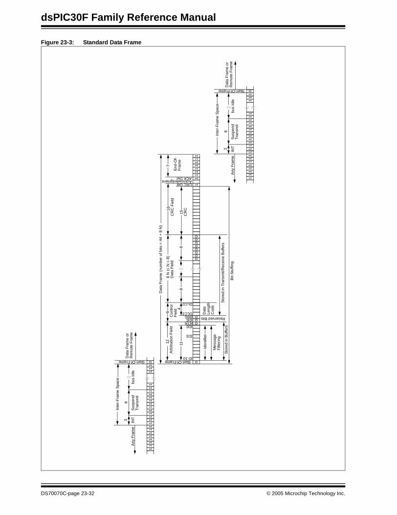
dsPIC30F Family Reference Manual
Figure 23-3: Standard Data Frame
11
11
11
11
11
11
11
11
11
11
11
11
0
INT
Sus
pend
Tra
nsm
itbu
s Id
leA
ny F
ram
e
Inte
r-F
ram
e S
pace
Start-Of-Frame
Dat
a F
ram
e or
Rem
ote
Fra
me
38
00
00
00
00
00
00
11
11
11
11
1
Start-Of-Frame
Dat
a F
ram
e (n
umbe
r of
bits
=44
+8
N)
12A
rbitr
atio
n F
ield
ID 10
11ID3
ID0
Iden
tifie
r
Mes
sage
Filt
erin
g
Sto
red
in B
uffe
rs
RTRIDERB0DLC3
DLC0
6
4
Con
trol
Fie
ld
Dat
aLe
ngth
Cod
e
Reserved Bits
8N
(≤
N≤
8)D
ata
Fie
ld
88
Sto
red
in T
rans
mit/
Rec
eive
Buf
fers
Bit-
Stu
ffing
16C
RC
Fie
ld
15 CR
C
7
End
-Of-
Fra
me
CRC DelAcknowledgmentACK Del 1
11
11
11
11
11
11
11
11
11
11
11
10
INT
Sus
pend
Tra
nsm
itbu
s Id
leA
ny F
ram
e
Inte
r-F
ram
e S
pace
Start-Of-Frame
Dat
a F
ram
e or
Rem
ote
Fra
me
38
DS70070C-page 23-32 © 2005 Microchip Technology Inc.
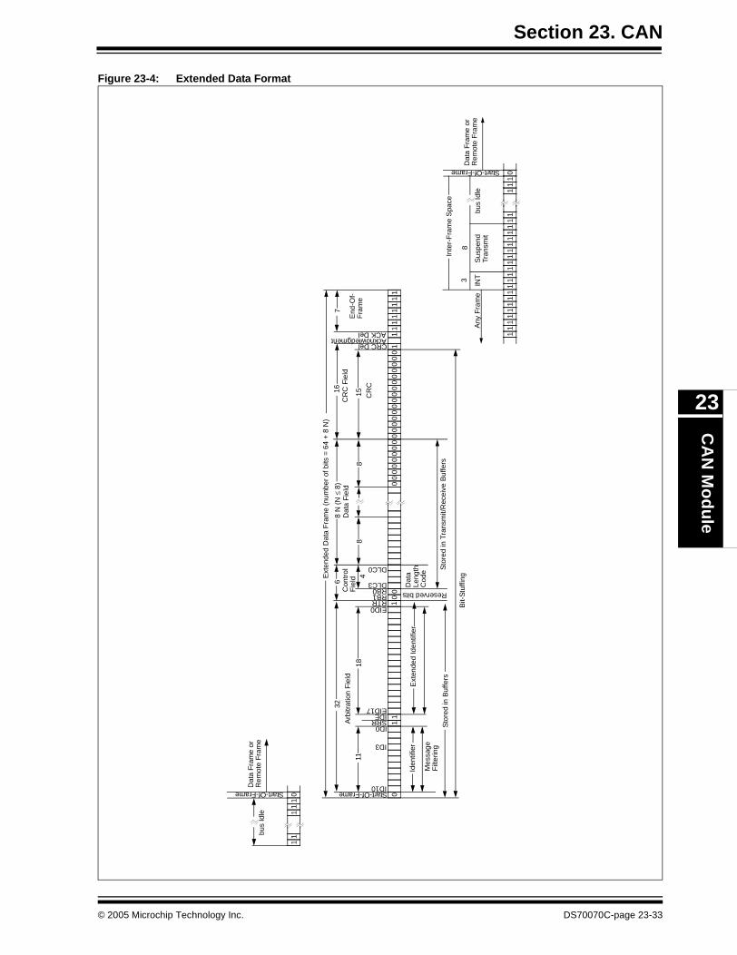
Section 23. CANC
AN
Mo
du
le
23
Figure 23-4: Extended Data Format
11
11
10
bus
Idle
Start-Of-Frame
Dat
a F
ram
e or
Rem
ote
Fra
me
01
10
00
00
00
00
00
00
00
00
00
00
00
00
1
Start-Of-Frame
Arb
itrat
ion
Fie
ld32
11
ID10
ID3
ID0
IDE
Iden
tifie
r
Mes
sage
Filt
erin
gS
tore
d in
Buf
fers
SRR
EID17
EID0RTRRB1RB0DLC3
18
DLC0
6C
ontr
olF
ield 4
Reserved bits
Dat
aLe
ngth
Cod
e
Sto
red
in T
rans
mit/
Rec
eive
Buf
fers
88
Ext
ende
d D
ata
Fra
me
(num
ber
of b
its=
64+
8N
)
8N
(N
≤ 8)
Dat
a F
ield
11
11
11
11
16C
RC
Fie
ld
15 CR
C
CRC DelAcknowledgmentACK Del
End
-Of-
Fra
me
7
Bit-
Stu
ffing
11
11
11
11
11
11
11
11
11
11
11
11
0
INT
Sus
pend
Tran
smit
bus
Idle
Any
Fra
me
Inte
r-F
ram
e S
pace
Start-Of-Frame
Dat
a F
ram
e or
Rem
ote
Fra
me
38
Ext
ende
d Id
entif
ier
1
© 2005 Microchip Technology Inc. DS70070C-page 23-33
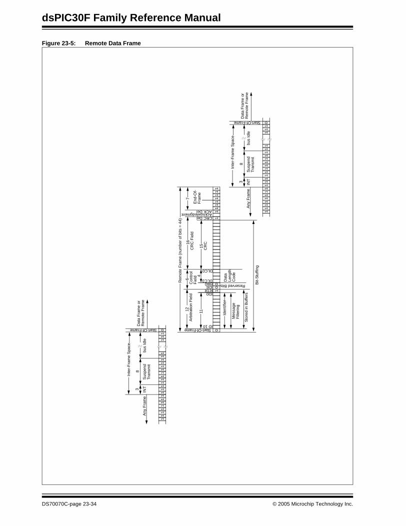
dsPIC30F Family Reference Manual
Figure 23-5: Remote Data Frame
Iden
tifie
r
Mes
sage
Filt
erin
g
Sto
red
in B
uffe
rs
Dat
aLe
ngth
Cod
e
Reserved Bits Bit-
Stu
ffing
11
11
11
11
11
11
11
11
11
11
11
11
0
INT
Sus
pend
Tran
smit
bus
Idle
Any
Fra
me
Inte
r-F
ram
e S
pace
Start-Of-Frame
Dat
a F
ram
e or
Rem
ote
Fra
me
38
01
00
11
11
11
11
1
Start-Of-Frame
Rem
ote
Fra
me
(num
ber
of b
its=
44)
12A
rbitr
atio
n F
ield
ID 1011
ID0RTRIDERB0DLC3
DLC0
6
4
Con
trol
Fie
ld
16C
RC
Fie
ld
15 CR
C
7
End
-Of-
Fra
me
CRC DelAcknowledgmentACK Del 1
11
11
11
11
11
11
11
11
11
11
11
10
INT
Sus
pend
Tra
nsm
itbu
s Id
leA
ny F
ram
e
Inte
r-F
ram
e S
pace
Start-Of-Frame
Dat
a F
ram
e or
Rem
ote
Fra
me
38
DS70070C-page 23-34 © 2005 Microchip Technology Inc.
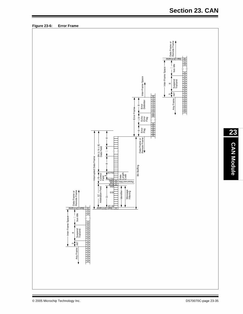
Section 23. CANC
AN
Mo
du
le
23
Figure 23-6: Error Frame
11
11
11
11
11
11
11
11
11
11
11
11
0
INT
Sus
pend
Tra
nsm
itbu
s Id
leA
ny F
ram
e
Inte
r-F
ram
e S
pace
Start-Of-Frame
Dat
a F
ram
e or
Rem
ote
Fra
me
38
00
00
Start-Of-Frame
Inte
rrup
ted
Dat
a F
ram
e
12A
rbitr
atio
n F
ield
ID 1011
ID3
ID0
Iden
tifie
r
Mes
sage
Filt
erin
gRTRIDERB0DLC3
DLC0
6
4
Con
trol
Fie
ld
Dat
aLe
ngth
Cod
e
Reserved Bits
8N (
≤ N
≤ 8
)D
ata
Fie
ld
88
Bit-
Stu
ffing
11
11
11
11
11
11
11
11
11
11
11
11
0
INT
Sus
pend
Tra
nsm
itbu
s Id
leA
ny F
ram
e
Inte
r-F
ram
e S
pace
Star-Of-Frame
Dat
a F
ram
e or
Rem
ote
Fra
me
38
00
00
00
00
01
11
11
11
10
Dat
a F
ram
e or
Rem
ote
Fra
me
Err
or F
ram
e
6E
rror
Fla
g
≤ 6
Ech
oE
rror
Fla
g
8E
rror
Del
imite
rIn
ter-
Fra
me
Spa
ce
© 2005 Microchip Technology Inc. DS70070C-page 23-35
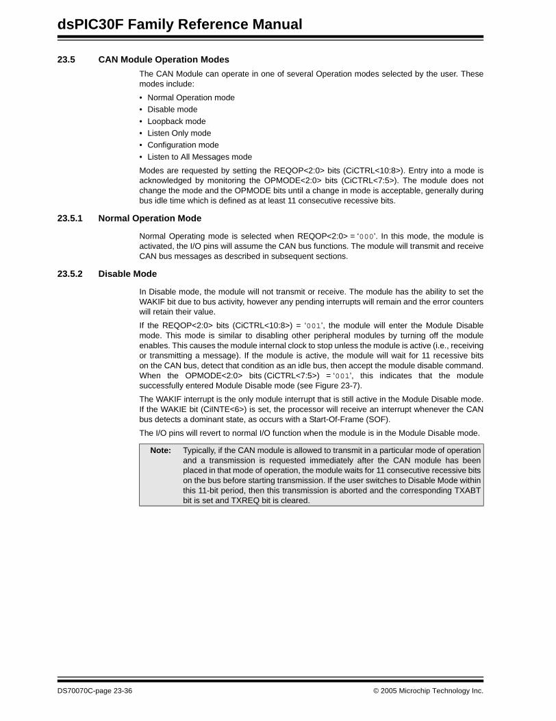
dsPIC30F Family Reference Manual
23.5 CAN Module Operation Modes
The CAN Module can operate in one of several Operation modes selected by the user. Thesemodes include:
• Normal Operation mode• Disable mode
• Loopback mode• Listen Only mode• Configuration mode
• Listen to All Messages mode
Modes are requested by setting the REQOP<2:0> bits (CiCTRL<10:8>). Entry into a mode isacknowledged by monitoring the OPMODE<2:0> bits (CiCTRL<7:5>). The module does notchange the mode and the OPMODE bits until a change in mode is acceptable, generally duringbus idle time which is defined as at least 11 consecutive recessive bits.
23.5.1 Normal Operation Mode
Normal Operating mode is selected when REQOP<2:0> = ‘000’. In this mode, the module isactivated, the I/O pins will assume the CAN bus functions. The module will transmit and receiveCAN bus messages as described in subsequent sections.
23.5.2 Disable Mode
In Disable mode, the module will not transmit or receive. The module has the ability to set theWAKIF bit due to bus activity, however any pending interrupts will remain and the error counterswill retain their value.
If the REQOP<2:0> bits (CiCTRL<10:8>) = ‘001’, the module will enter the Module Disablemode. This mode is similar to disabling other peripheral modules by turning off the moduleenables. This causes the module internal clock to stop unless the module is active (i.e., receivingor transmitting a message). If the module is active, the module will wait for 11 recessive bitson the CAN bus, detect that condition as an idle bus, then accept the module disable command.When the OPMODE<2:0> bits (CiCTRL<7:5>) = ‘001’, this indicates that the modulesuccessfully entered Module Disable mode (see Figure 23-7).
The WAKIF interrupt is the only module interrupt that is still active in the Module Disable mode.If the WAKIE bit (CiINTE<6>) is set, the processor will receive an interrupt whenever the CANbus detects a dominant state, as occurs with a Start-Of-Frame (SOF).
The I/O pins will revert to normal I/O function when the module is in the Module Disable mode.
Note: Typically, if the CAN module is allowed to transmit in a particular mode of operationand a transmission is requested immediately after the CAN module has beenplaced in that mode of operation, the module waits for 11 consecutive recessive bitson the bus before starting transmission. If the user switches to Disable Mode withinthis 11-bit period, then this transmission is aborted and the corresponding TXABTbit is set and TXREQ bit is cleared.
DS70070C-page 23-36 © 2005 Microchip Technology Inc.
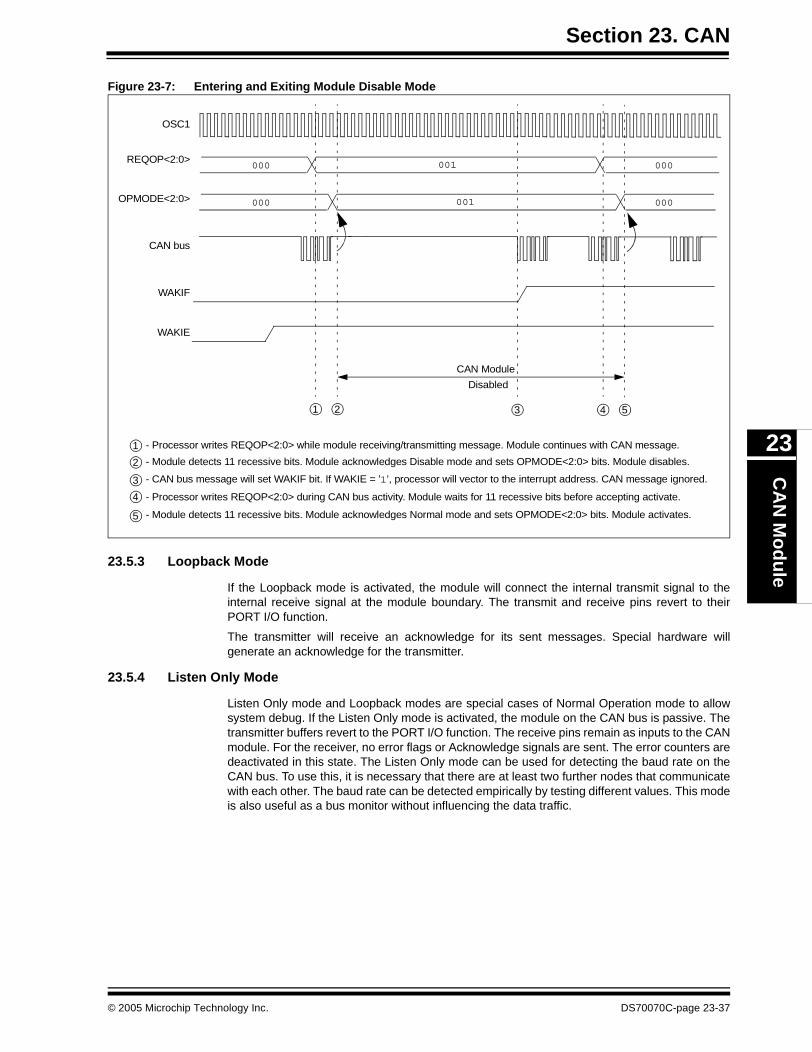
Section 23. CANC
AN
Mo
du
le
23
Figure 23-7: Entering and Exiting Module Disable Mode
23.5.3 Loopback Mode
If the Loopback mode is activated, the module will connect the internal transmit signal to theinternal receive signal at the module boundary. The transmit and receive pins revert to theirPORT I/O function.
The transmitter will receive an acknowledge for its sent messages. Special hardware willgenerate an acknowledge for the transmitter.
23.5.4 Listen Only Mode
Listen Only mode and Loopback modes are special cases of Normal Operation mode to allowsystem debug. If the Listen Only mode is activated, the module on the CAN bus is passive. Thetransmitter buffers revert to the PORT I/O function. The receive pins remain as inputs to the CANmodule. For the receiver, no error flags or Acknowledge signals are sent. The error counters aredeactivated in this state. The Listen Only mode can be used for detecting the baud rate on theCAN bus. To use this, it is necessary that there are at least two further nodes that communicatewith each other. The baud rate can be detected empirically by testing different values. This modeis also useful as a bus monitor without influencing the data traffic.
1 2 4 5
- Processor writes REQOP<2:0> while module receiving/transmitting message. Module continues with CAN message.
- Module detects 11 recessive bits. Module acknowledges Disable mode and sets OPMODE<2:0> bits. Module disables.
- Processor writes REQOP<2:0> during CAN bus activity. Module waits for 11 recessive bits before accepting activate.
- Module detects 11 recessive bits. Module acknowledges Normal mode and sets OPMODE<2:0> bits. Module activates.
OSC1
CAN bus
CAN Module
Disabled
3
001
001000
000 000
000
- CAN bus message will set WAKIF bit. If WAKIE = ’1’, processor will vector to the interrupt address. CAN message ignored.
WAKIF
WAKIE
1
2
3
4
5
OPMODE<2:0>
REQOP<2:0>
© 2005 Microchip Technology Inc. DS70070C-page 23-37
dsPIC30F Family Reference Manual
23.5.5 Configuration Mode
In the Configuration mode, the module will not transmit or receive. The error counters are clearedand the interrupt flags remain unchanged. The programmer will have access to configurationregisters that are access restricted in other modes.
After a device Reset the CAN module is in the Configuration mode (OPMODE<2:0> = ‘100’). Theerror counters are cleared and all registers contain the Reset values. It should be ensured thatthe initialization is performed before REQOP<2> bit is cleared.
The CAN module has to be initialized before its activation. This is only possible if the module isin the Configuration mode. The Configuration mode is requested by setting the REQOP<2> bit.Only when the Status bit OPMODE<2> has a high level, the initialization can be performed.Afterwards the configuration registers and the acceptance mask registers and the acceptancefilter registers can be written. The module is activated by clearing the control bits REQOP<2:0>.
The module will protect the user from accidentally violating the CAN protocol through program-ming errors. All registers which control the configuration of the module can not be modified whilethe module is on-line. The CAN module will not be allowed to enter the Configuration mode whilea transmission is taking place. The Configuration mode serves as a lock to protect the followingregisters.
• All Module Control Registers• Baud Rate and Interrupt Configuration Registers • Bus Timing Registers
• Identifier Acceptance Filter Registers • Identifier Acceptance Mask Registers
23.5.6 Listen All Messages Mode
Listen All Messages mode is a special case of Normal Operation mode to allow system debug.If the Listen All Messages mode is activated, the module on the CAN bus is passive. Thetransmitter buffers revert to the PORT I/O function. The receive pins remain inputs. For thereceiver, no error flags or Acknowledge signals are sent. The error counters are deactivated inthis state. The filters are disabled. Receive Buffer 0 will receive any message transferred on thebus. This mode is useful to record all bus traffic as a bus monitor without influencing the datatraffic.
DS70070C-page 23-38 © 2005 Microchip Technology Inc.
Section 23. CANC
AN
Mo
du
le
23
23.6 Message Reception
This subsection describes CAN module message reception.
23.6.1 Receive Buffers
The CAN bus module has 3 receive buffers. However, one of the receive buffers is alwayscommitted to monitoring the bus for incoming messages. This buffer is called the messageassembly buffer, MAB. So there are 2 receive buffers visible, RXB0 and RXB1, that canessentially instantaneously receive a complete message from the protocol engine. The CPU canbe operating on one while the other is available for reception or holding a previously receivedmessage.
The MAB holds the destuffed bit stream from the bus line to allow parallel access to the wholedata or remote frame for the acceptance match test and the parallel transfer of the frame to thereceive buffers. The MAB will assemble all messages received. These messages will betransferred to the RXBn buffers only if the acceptance filter criterion are met. When a messageis received, the RXnIF flag (CiINTF<0> or CiINRF<1>) will be set. This bit can only be set by themodule when a message is received. The bit is cleared by the CPU when it has completedprocessing the message in the buffer. This bit provides a positive lockout to ensure that the CPUhas finished with the message buffer. If the RXnIE bit (CiINTE<0> or CiINTE<1>) is set , aninterrupt will be generated when a message is received.
There are 2 programmable acceptance filter masks associated with the receive buffers, one foreach buffer.
When the message is received, the FILHIT bits (CiRX0CON<0> for Receive Buffer 0 andCiRX1CON<2:0> for Receive Buffer 1) indicate the acceptance criterion for the message. Thenumber of the acceptance filter that enabled the reception will be indicated as well as a Statusbit that indicates that the received message is a remote transfer request.
Note: In the case of Receive Buffer 0, a limited number of Acceptance Filters can be usedto enable a reception. A single bit, FILHIT0 (CiRX0CON<0>) determines which ofthe 2 filters, RXF0 or RXF1, enabled the message reception.
© 2005 Microchip Technology Inc. DS70070C-page 23-39
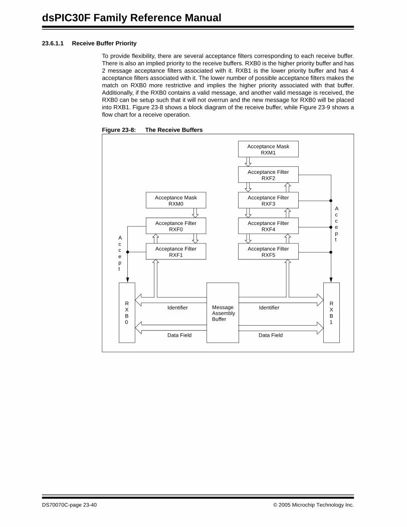
dsPIC30F Family Reference Manual
23.6.1.1 Receive Buffer Priority
To provide flexibility, there are several acceptance filters corresponding to each receive buffer.There is also an implied priority to the receive buffers. RXB0 is the higher priority buffer and has2 message acceptance filters associated with it. RXB1 is the lower priority buffer and has 4acceptance filters associated with it. The lower number of possible acceptance filters makes thematch on RXB0 more restrictive and implies the higher priority associated with that buffer.Additionally, if the RXB0 contains a valid message, and another valid message is received, theRXB0 can be setup such that it will not overrun and the new message for RXB0 will be placedinto RXB1. Figure 23-8 shows a block diagram of the receive buffer, while Figure 23-9 shows aflow chart for a receive operation.
Figure 23-8: The Receive Buffers
Acceptance MaskRXM1
Acceptance FilterRXF2
Acceptance FilterRXF3
Acceptance FilterRXF4
Acceptance FilterRXF5
RXB1
RXB0
Acceptance MaskRXM0
Acceptance FilterRXF0
Acceptance FilterRXF1
AcceptA
ccept
Identifier
Data Field Data Field
IdentifierMessageAssemblyBuffer
DS70070C-page 23-40 © 2005 Microchip Technology Inc.
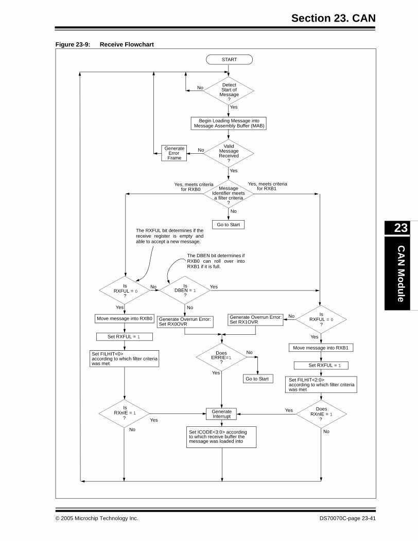
Section 23. CANC
AN
Mo
du
le
23
Figure 23-9: Receive Flowchart
START
DetectStart of
Message?
ValidMessageReceived
?
GenerateError
MessageIdentifier meetsa filter criteria
?
IsRXFUL = 0
?
Go to Start
Move message into RXB0
Set RXFUL = 1
Set FILHIT<2:0>
IsRXFUL = 0
?
Move message into RXB1
Set RXFUL = 1
Yes, meets criteriafor RXB0
Yes, meets criteriafor RXB1
No
GenerateInterrupt
Yes
Yes
No No
Yes
Yes
No
No
Yes
Yes
Frame
The RXFUL bit determines if thereceive register is empty andable to accept a new message.
No Yes
No
Generate Overrun Error:
Begin Loading Message intoMessage Assembly Buffer (MAB)
was met
IsRXnIE = 1
?
DoesRXnIE = 1
?
IsDBEN = 1
?
The DBEN bit determines ifRXB0 can roll over intoRXB1 if it is full.
Set RX0OVR
Generate Overrun Error:Set RX1OVR
DoesERRIE=1
?
No
Go to StartYes
NoSet FILHIT<0>according to which filter criteriawas met
Set ICODE<3:0> accordingto which receive buffer themessage was loaded into
according to which filter criteria
© 2005 Microchip Technology Inc. DS70070C-page 23-41
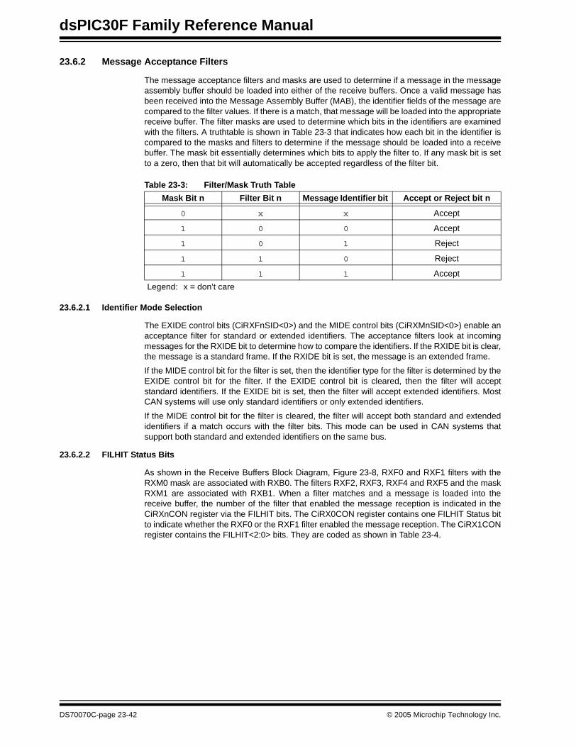
dsPIC30F Family Reference Manual
23.6.2 Message Acceptance Filters
The message acceptance filters and masks are used to determine if a message in the messageassembly buffer should be loaded into either of the receive buffers. Once a valid message hasbeen received into the Message Assembly Buffer (MAB), the identifier fields of the message arecompared to the filter values. If there is a match, that message will be loaded into the appropriatereceive buffer. The filter masks are used to determine which bits in the identifiers are examinedwith the filters. A truthtable is shown in Table 23-3 that indicates how each bit in the identifier iscompared to the masks and filters to determine if the message should be loaded into a receivebuffer. The mask bit essentially determines which bits to apply the filter to. If any mask bit is setto a zero, then that bit will automatically be accepted regardless of the filter bit.
Table 23-3: Filter/Mask Truth Table
23.6.2.1 Identifier Mode Selection
The EXIDE control bits (CiRXFnSID<0>) and the MIDE control bits (CiRXMnSID<0>) enable anacceptance filter for standard or extended identifiers. The acceptance filters look at incomingmessages for the RXIDE bit to determine how to compare the identifiers. If the RXIDE bit is clear,the message is a standard frame. If the RXIDE bit is set, the message is an extended frame.
If the MIDE control bit for the filter is set, then the identifier type for the filter is determined by theEXIDE control bit for the filter. If the EXIDE control bit is cleared, then the filter will acceptstandard identifiers. If the EXIDE bit is set, then the filter will accept extended identifiers. MostCAN systems will use only standard identifiers or only extended identifiers.
If the MIDE control bit for the filter is cleared, the filter will accept both standard and extendedidentifiers if a match occurs with the filter bits. This mode can be used in CAN systems thatsupport both standard and extended identifiers on the same bus.
23.6.2.2 FILHIT Status Bits
As shown in the Receive Buffers Block Diagram, Figure 23-8, RXF0 and RXF1 filters with theRXM0 mask are associated with RXB0. The filters RXF2, RXF3, RXF4 and RXF5 and the maskRXM1 are associated with RXB1. When a filter matches and a message is loaded into thereceive buffer, the number of the filter that enabled the message reception is indicated in theCiRXnCON register via the FILHIT bits. The CiRX0CON register contains one FILHIT Status bitto indicate whether the RXF0 or the RXF1 filter enabled the message reception. The CiRX1CONregister contains the FILHIT<2:0> bits. They are coded as shown in Table 23-4.
Mask Bit n Filter Bit n Message Identifier bit Accept or Reject bit n
0 x x Accept
1 0 0 Accept
1 0 1 Reject
1 1 0 Reject
1 1 1 Accept
Legend: x = don’t care
DS70070C-page 23-42 © 2005 Microchip Technology Inc.
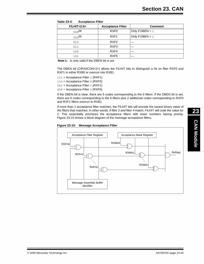
Section 23. CANC
AN
Mo
du
le
23
Table 23-4: Acceptance Filter
The DBEN bit (CiRX0CON<2>) allows the FILHIT bits to distinguish a hit on filter RXF0 andRXF1 in either RXB0 or overrun into RXB1.
111 = Acceptance Filter 1 (RXF1) 110 = Acceptance Filter 0 (RXF0) 001 = Acceptance Filter 1 (RXF1) 000 = Acceptance Filter 0 (RXF0)
If the DBEN bit is clear, there are 6 codes corresponding to the 6 filters. If the DBEN bit is set,there are 6 codes corresponding to the 6 filters plus 2 additional codes corresponding to RXF0and RXF1 filters overrun to RXB1.
If more than 1 acceptance filter matches, the FILHIT bits will encode the lowest binary value ofthe filters that matched. In other words, if filter 2 and filter 4 match, FILHIT will code the value for2. This essentially prioritizes the acceptance filters with lower numbers having priority.Figure 23-10 shows a block diagram of the message acceptance filters.
Figure 23-10: Message Acceptance Filter
FILHIT<2:0> Acceptance Filter Comment
000(1) RXF0 Only if DBEN = 1
001(1) RXF1 Only if DBEN = 1
010 RXF2 —
011 RXF3 —
100 RXF4 —
101 RXF5 —
Note 1: Is only valid if the DBEN bit is set.
Acceptance Filter Register Acceptance Mask Register
RxRqst
Message Assembly Buffer
RXFn0
RXFn1
RXFnn
RXMn0
RXMn1
RXMnn
Identifier
© 2005 Microchip Technology Inc. DS70070C-page 23-43
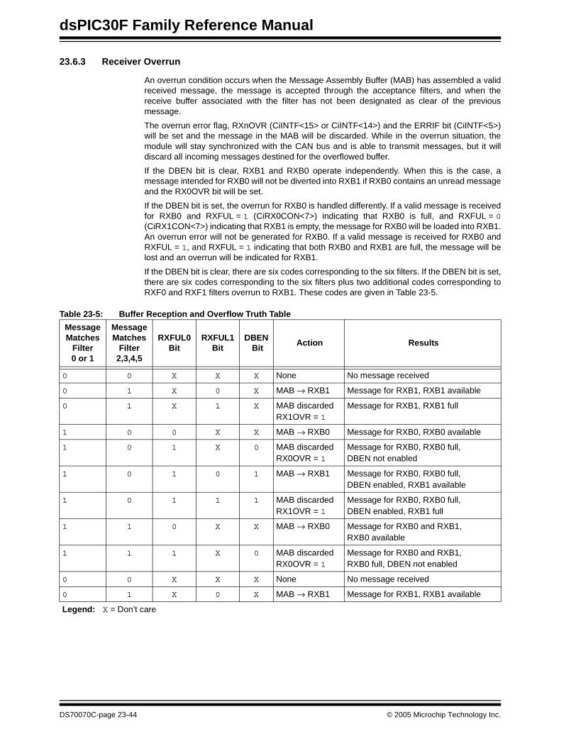
dsPIC30F Family Reference Manual
23.6.3 Receiver Overrun
An overrun condition occurs when the Message Assembly Buffer (MAB) has assembled a validreceived message, the message is accepted through the acceptance filters, and when thereceive buffer associated with the filter has not been designated as clear of the previousmessage.
The overrun error flag, RXnOVR (CiINTF<15> or CiINTF<14>) and the ERRIF bit (CiINTF<5>)will be set and the message in the MAB will be discarded. While in the overrun situation, themodule will stay synchronized with the CAN bus and is able to transmit messages, but it willdiscard all incoming messages destined for the overflowed buffer.
If the DBEN bit is clear, RXB1 and RXB0 operate independently. When this is the case, amessage intended for RXB0 will not be diverted into RXB1 if RXB0 contains an unread messageand the RX0OVR bit will be set.
If the DBEN bit is set, the overrun for RXB0 is handled differently. If a valid message is receivedfor RXB0 and RXFUL = 1 (CiRX0CON<7>) indicating that RXB0 is full, and RXFUL = 0(CiRX1CON<7>) indicating that RXB1 is empty, the message for RXB0 will be loaded into RXB1.An overrun error will not be generated for RXB0. If a valid message is received for RXB0 andRXFUL = 1, and RXFUL = 1 indicating that both RXB0 and RXB1 are full, the message will belost and an overrun will be indicated for RXB1.
If the DBEN bit is clear, there are six codes corresponding to the six filters. If the DBEN bit is set,there are six codes corresponding to the six filters plus two additional codes corresponding toRXF0 and RXF1 filters overrun to RXB1. These codes are given in Table 23-5.
Table 23-5: Buffer Reception and Overflow Truth Table
MessageMatches
Filter0 or 1
MessageMatches
Filter2,3,4,5
RXFUL0Bit
RXFUL1Bit
DBEN Bit
Action Results
0 0 X X X None No message received
0 1 X 0 X MAB → RXB1 Message for RXB1, RXB1 available
0 1 X 1 X MAB discardedRX1OVR = 1
Message for RXB1, RXB1 full
1 0 0 X X MAB → RXB0 Message for RXB0, RXB0 available
1 0 1 X 0 MAB discardedRX0OVR = 1
Message for RXB0, RXB0 full, DBEN not enabled
1 0 1 0 1 MAB → RXB1 Message for RXB0, RXB0 full, DBEN enabled, RXB1 available
1 0 1 1 1 MAB discardedRX1OVR = 1
Message for RXB0, RXB0 full, DBEN enabled, RXB1 full
1 1 0 X X MAB → RXB0 Message for RXB0 and RXB1,RXB0 available
1 1 1 X 0 MAB discardedRX0OVR = 1
Message for RXB0 and RXB1,RXB0 full, DBEN not enabled
0 0 X X X None No message received
0 1 X 0 X MAB → RXB1 Message for RXB1, RXB1 available
Legend: X = Don’t care
DS70070C-page 23-44 © 2005 Microchip Technology Inc.
Section 23. CANC
AN
Mo
du
le
23
23.6.4 Effects of a Reset
Upon any Reset the CAN module has to be initialized. All registers are set according to the Resetvalues. The content of a received message is lost. The initialization is discussed in Section23.5.5 “Configuration Mode”.
23.6.5 Receive Errors
The CAN module will detect the following receive errors:
• Cyclic Redundancy Check (CRC) Error• Bit Stuffing Error
• Invalid message receive error
These receive errors do not generate an interrupt. However, the receive error counter isincremented by one in case one of these errors occur. The RXWAR bit (CiINTF<9>) indicatesthat the Receive Error Counter has reached the CPU warning limit of 96 and an interrupt isgenerated.
23.6.5.1 Cyclic Redundancy Check (CRC) Error
With the Cyclic Redundancy Check, the transmitter calculates special check bits for the bitsequence from the start of a frame until the end of the data field. This CRC sequence istransmitted in the CRC Field. The receiving node also calculates the CRC sequence using thesame formula and performs a comparison to the received sequence. If a mismatch is detected,a CRC error has occurred and an Error Frame is generated. The message is repeated. Thereceive error interrupt counter is incremented by one. An Interrupt will only be generated if theerror counter passes a threshold value.
23.6.5.2 Bit Stuffing Error
If, between the Start -Of-Frame and the CRC Delimiter, 6 consecutive bits with the same polarityare detected, the bit-stuffing rule has been violated. A bit-stuffing error occurs and an error frameis generated. The message is repeated. No interrupt will be generated upon this event.
23.6.5.3 Invalid Message Received Error
If any type of error occurs during reception of a message, an error will be indicated by the IVRIFbit (CiINTF<7>). This bit can be used (optionally with an interrupt) for autobaud detection withthe device in Listen Only mode. This error is not an indicator that any action needs to be taken,but it does indicate that an error has occurred on the CAN bus.
23.6.5.4 Rules for Modifying the Receive Error Counter
The Receive Error Counter is modified according to the following rules:
• When the receiver detects an error, the Receive Error Counter is incremented by 1, except when the detected error was a bit error during the transmission of an active error flag.
• When the receiver detects a “dominant” bit as the first bit after sending an error flag, the Receive Error Counter will be incremented by 8.
• If a receiver detects a bit error while sending an active error flag, the Receive Error Counter is incremented by 8.
• Any node tolerates up to 7 consecutive “dominant” bits after sending an active error flag or passive error flag. After detecting the 14th consecutive “dominant” bit (in case of an Active error flag) or after detecting the 8th consecutive “dominant” bit following a passive error flag, and after each sequence of eight additional consecutive “dominant” bits, every trans-mitter increases its Transmission Error Counter and every receiver increases its Receive Error Counter by 8.
• After a successful reception of a message (reception without error up to the ACK slot and the successful sending of the ACK bit), the Receive Error Counter is decreased by one, if the Receive Error Counter was between 1 and 127. If the Receive Error Counter was ‘0’, it will stay ‘0’. If the Receive Error Counter was greater than 127, it will change to a value between 119 and 127.
© 2005 Microchip Technology Inc. DS70070C-page 23-45

dsPIC30F Family Reference Manual
23.6.6 Receive Interrupts
Several Interrupts are linked to the message reception. The receive interrupts can be broken upinto two separate groups:
• Receive Error Interrupts
• Receive interrupts
23.6.6.1 Receive Interrupt
A message has been successfully received and loaded into one of the receive buffers. This inter-rupt is activated immediately after receiving the End-Of-Frame (EOF) field. Reading the RXnIFflag will indicate which receive buffer caused the interrupt. Figure 23-11 depicts when the receivebuffer interrupt flag RXnIF will be set.
23.6.6.2 Wake-up Interrupt
The Wake-up interrupt sequences are described in Section 23.13.1 “Operation in SleepMode”.
DS70070C-page 23-46 © 2005 Microchip Technology Inc.
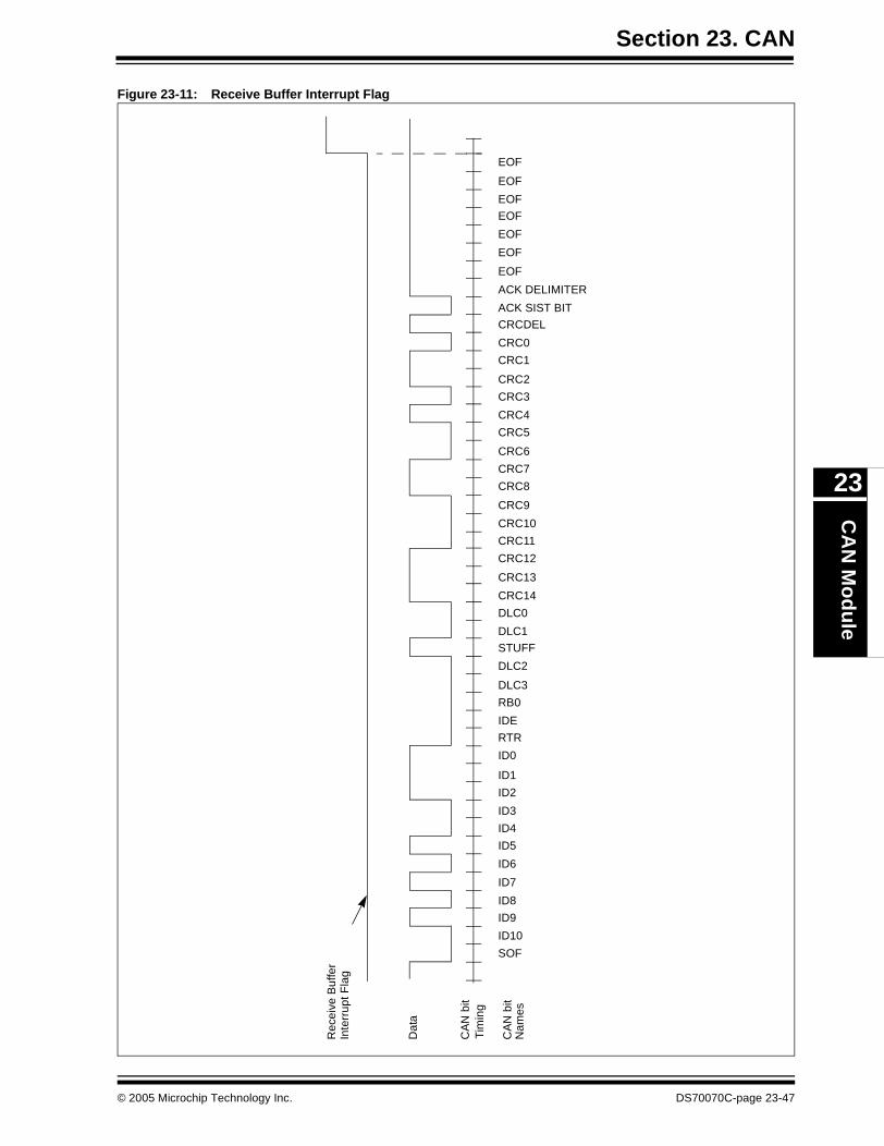
Section 23. CANC
AN
Mo
du
le
23
Figure 23-11: Receive Buffer Interrupt Flag
SOF
ID10
ID9
ID8
ID7
ID6
ID5
ID4
ID3
ID2
ID1
RTR
IDE
RB0
DLC3
DLC2
STUFF
DLC1
DLC0
CRC14
CRC13
CRC12
CRC11
CRC10
CRC9
CRC8
CRC7
CRC6
CRC5
CRC4
CRC3
CRC2
CRC1
CRC0
CRCDEL
ACK SIST BIT
ACK DELIMITER
EOF
EOF
EOF
EOF
EOF
EOF
EOF
ID0
Rec
eive
Buf
fer
Inte
rrup
t Fla
g
Dat
a
Tim
ing
CA
N b
it
CA
N b
it
Nam
es
© 2005 Microchip Technology Inc. DS70070C-page 23-47
dsPIC30F Family Reference Manual
23.6.6.3 Receive Error Interrupts
A receive error interrupt will be indicated by the ERRIF bit (CiINTF<5>). This bit shows that anerror condition occurred. The source of the error can be determined by checking the bits in theCAN Interrupt Status Register CiINTF. The bits in this register are related to receive and transmiterrors. The following subsequences will show which flags are linked to the receive errors.
23.6.6.3.1 Invalid Message Received Interrupt
If any type of error occurred during reception of the last message, an error will be indicated bythe IVRIF bit (CiINTF<7>). The specific error that occurred is unknown. This bit can be used(optionally with an interrupt) for autobaud detection with the device in Listen Only mode. Thiserror is not an indicator that any action needs to be taken, but an indicator that an error hasoccurred on the CAN bus.
23.6.6.3.2 Receiver Overrun Interrupt
The RXnOVR bit (CiINTF<15>, CiINTF<14>) indicates that an overrun condition occurred for thereceive buffer. An overrun condition occurs when the Message Assembly Buffer (MAB) hasassembled a valid received message, the message is accepted through the acceptance filters,however, the receive buffer associated with the filter is not clear of the previous message. Theoverflow error interrupt will be set and the message is discarded. While in the overrun situation,the module will stay synchronized with the CAN bus and is able to transmit and receivemessages.
23.6.6.4 Receiver Warning Interrupt
The RXWAR bit (CiINTF<8>) indicates that the Receive Error Counter has reached the CPUwarning limit of 96. When RXWAR transitions from a ‘0’ to a ‘1’, it will cause the Error InterruptFlag ERRIF to become set. This bit cannot be manually cleared, as it should remain an indicatorthat the Receive Error Counter has reached the CPU warning limit of 96. The RXWAR bit willbecome clear automatically if the Receive Error Counter becomes less than or equal to 95. TheERRIF bit can be manually cleared allowing the interrupt service routine to be exited withoutaffecting the RXWAR bit.
23.6.6.5 Receiver Error Passive
The RXEP bit (CiINTF<11>) indicates that the Receive Error Counter has exceeded the ErrorPassive limit of 127 and the module has gone to Error Passive state. When the RXEP bit transi-tions from a ‘0’ to a ‘1’, it will cause the error interrupt flag to become set. The RXEP bit cannotbe manually cleared, as it should remain an indicator that the bus is in Error State Passive. TheRXEP bit will become clear automatically if the Receive Error Counter becomes less than orequal to 127. The ERRIF bit can be manually cleared allowing the interrupt service routine to beexited without affecting the RXEP bit.
DS70070C-page 23-48 © 2005 Microchip Technology Inc.
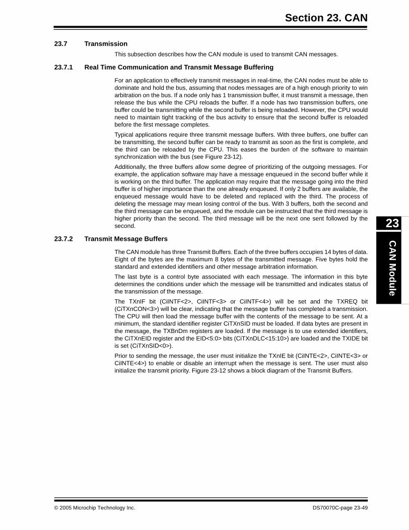
Section 23. CANC
AN
Mo
du
le
23
23.7 Transmission
This subsection describes how the CAN module is used to transmit CAN messages.
23.7.1 Real Time Communication and Transmit Message Buffering
For an application to effectively transmit messages in real-time, the CAN nodes must be able todominate and hold the bus, assuming that nodes messages are of a high enough priority to winarbitration on the bus. If a node only has 1 transmission buffer, it must transmit a message, thenrelease the bus while the CPU reloads the buffer. If a node has two transmission buffers, onebuffer could be transmitting while the second buffer is being reloaded. However, the CPU wouldneed to maintain tight tracking of the bus activity to ensure that the second buffer is reloadedbefore the first message completes.
Typical applications require three transmit message buffers. With three buffers, one buffer canbe transmitting, the second buffer can be ready to transmit as soon as the first is complete, andthe third can be reloaded by the CPU. This eases the burden of the software to maintainsynchronization with the bus (see Figure 23-12).
Additionally, the three buffers allow some degree of prioritizing of the outgoing messages. Forexample, the application software may have a message enqueued in the second buffer while itis working on the third buffer. The application may require that the message going into the thirdbuffer is of higher importance than the one already enqueued. If only 2 buffers are available, theenqueued message would have to be deleted and replaced with the third. The process ofdeleting the message may mean losing control of the bus. With 3 buffers, both the second andthe third message can be enqueued, and the module can be instructed that the third message ishigher priority than the second. The third message will be the next one sent followed by thesecond.
23.7.2 Transmit Message Buffers
The CAN module has three Transmit Buffers. Each of the three buffers occupies 14 bytes of data.Eight of the bytes are the maximum 8 bytes of the transmitted message. Five bytes hold thestandard and extended identifiers and other message arbitration information.
The last byte is a control byte associated with each message. The information in this bytedetermines the conditions under which the message will be transmitted and indicates status ofthe transmission of the message.
The TXnIF bit (CiINTF<2>, CiINTF<3> or CiINTF<4>) will be set and the TXREQ bit(CiTXnCON<3>) will be clear, indicating that the message buffer has completed a transmission.The CPU will then load the message buffer with the contents of the message to be sent. At aminimum, the standard identifier register CiTXnSID must be loaded. If data bytes are present inthe message, the TXBnDm registers are loaded. If the message is to use extended identifiers,the CiTXnEID register and the EID<5:0> bits (CiTXnDLC<15:10>) are loaded and the TXIDE bitis set (CiTXnSID<0>).
Prior to sending the message, the user must initialize the TXnIE bit (CiINTE<2>, CiINTE<3> orCiINTE<4>) to enable or disable an interrupt when the message is sent. The user must alsoinitialize the transmit priority. Figure 23-12 shows a block diagram of the Transmit Buffers.
© 2005 Microchip Technology Inc. DS70070C-page 23-49
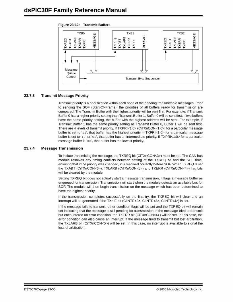
dsPIC30F Family Reference Manual
Figure 23-12: Transmit Buffers
23.7.3 Transmit Message Priority
Transmit priority is a prioritization within each node of the pending transmittable messages. Priorto sending the SOF (Start-Of-Frame), the priorities of all buffers ready for transmission arecompared. The Transmit Buffer with the highest priority will be sent first. For example, if TransmitBuffer 0 has a higher priority setting than Transmit Buffer 1, Buffer 0 will be sent first. If two buffershave the same priority setting, the buffer with the highest address will be sent. For example, ifTransmit Buffer 1 has the same priority setting as Transmit Buffer 0, Buffer 1 will be sent first.There are 4 levels of transmit priority. If TXPRI<1:0> (CiTXnCON<1:0>) for a particular messagebuffer is set to ‘11’, that buffer has the highest priority. If TXPRI<1:0> for a particular messagebuffer is set to ‘10’ or ‘01’, that buffer has an intermediate priority. If TXPRI<1:0> for a particularmessage buffer is ‘00’, that buffer has the lowest priority.
23.7.4 Message Transmission
To initiate transmitting the message, the TXREQ bit (CiTXnCON<3>) must be set. The CAN busmodule resolves any timing conflicts between setting of the TXREQ bit and the SOF time,ensuring that if the priority was changed, it is resolved correctly before SOF. When TXREQ is setthe TXABT (CiTXnCON<6>), TXLARB (CiTXnCON<5>) and TXERR (CiTXnCON<4>) flag bitswill be cleared by the module.
Setting TXREQ bit does not actually start a message transmission, it flags a message buffer asenqueued for transmission. Transmission will start when the module detects an available bus forSOF. The module will then begin transmission on the message which has been determined tohave the highest priority.
If the transmission completes successfully on the first try, the TXREQ bit will clear and aninterrupt will be generated if the TXnIE bit (CiINTE<2>, CiINTE<3>, CiINTE<4>) is set.
If the message fails to transmit, other condition flags will be set and the TXREQ bit will remainset indicating that the message is still pending for transmission. If the message tried to transmitbut encountered an error condition, the TXERR bit (CiTXnCON<4>) will be set. In this case, theerror condition can also cause an interrupt. If the message tried to transmit but lost arbitration,the TXLARB bit (CiTXnCON<5>) will be set. In this case, no interrupt is available to signal theloss of arbitration.
TX
RE
Q
TXB0
TX
AB
T
TX
LAR
B
TX
ER
R
TX
PR
I
ME
SS
AG
E
MessageQueueControl
Transmit Byte Sequencer
TX
RE
Q
TXB1
TX
AB
T
TX
LAR
B
TX
ER
R
TX
PR
I
ME
SS
AG
E
TX
RE
Q
TXB2
TX
AB
T
TX
LAR
B
TX
ER
R
TX
PR
I
ME
SS
AG
E
DS70070C-page 23-50 © 2005 Microchip Technology Inc.
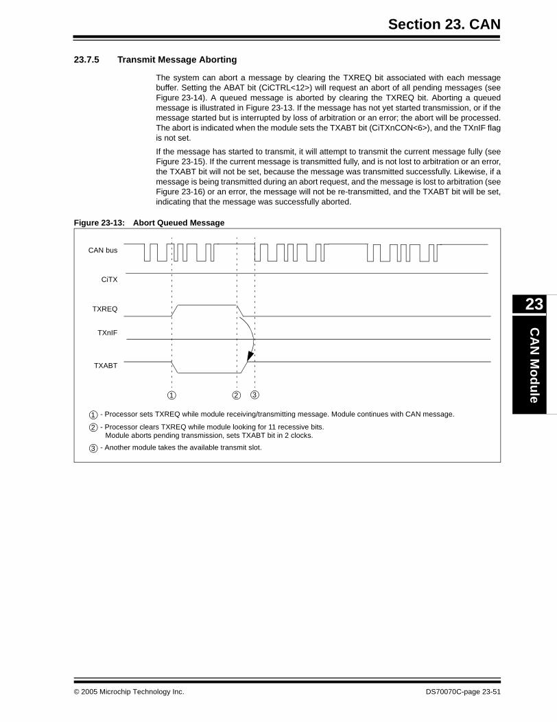
Section 23. CANC
AN
Mo
du
le
23
23.7.5 Transmit Message Aborting
The system can abort a message by clearing the TXREQ bit associated with each messagebuffer. Setting the ABAT bit (CiCTRL<12>) will request an abort of all pending messages (seeFigure 23-14). A queued message is aborted by clearing the TXREQ bit. Aborting a queuedmessage is illustrated in Figure 23-13. If the message has not yet started transmission, or if themessage started but is interrupted by loss of arbitration or an error; the abort will be processed.The abort is indicated when the module sets the TXABT bit (CiTXnCON<6>), and the TXnIF flagis not set.
If the message has started to transmit, it will attempt to transmit the current message fully (seeFigure 23-15). If the current message is transmitted fully, and is not lost to arbitration or an error,the TXABT bit will not be set, because the message was transmitted successfully. Likewise, if amessage is being transmitted during an abort request, and the message is lost to arbitration (seeFigure 23-16) or an error, the message will not be re-transmitted, and the TXABT bit will be set,indicating that the message was successfully aborted.
Figure 23-13: Abort Queued Message
1 2
- Processor sets TXREQ while module receiving/transmitting message. Module continues with CAN message.
- Processor clears TXREQ while module looking for 11 recessive bits.
CAN bus
3
TXREQ
- Another module takes the available transmit slot.
CiTX
TXnIF
TXABT
Module aborts pending transmission, sets TXABT bit in 2 clocks.
1
2
3
© 2005 Microchip Technology Inc. DS70070C-page 23-51
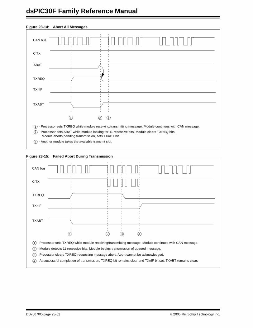
dsPIC30F Family Reference Manual
Figure 23-14: Abort All Messages
Figure 23-15: Failed Abort During Transmission
1 2
- Processor sets TXREQ while module receiving/transmitting message. Module continues with CAN message.
- Processor sets ABAT while module looking for 11 recessive bits. Module clears TXREQ bits.
CAN bus
3
TXREQ
- Another module takes the available transmit slot.
CiTX
TXnIF
TXABT
ABAT
Module aborts pending transmission, sets TXABT bit.
1
2
3
1 2
- Processor sets TXREQ while module receiving/transmitting message. Module continues with CAN message.
- Module detects 11 recessive bits. Module begins transmission of queued message.
CAN bus
TXREQ
- Processor clears TXREQ requesting message abort. Abort cannot be acknowledged.
CiTX
TXnIF
TXABT
43
- At successful completion of transmission, TXREQ bit remains clear and TXnIF bit set. TXABT remains clear.
1
2
3
4
DS70070C-page 23-52 © 2005 Microchip Technology Inc.
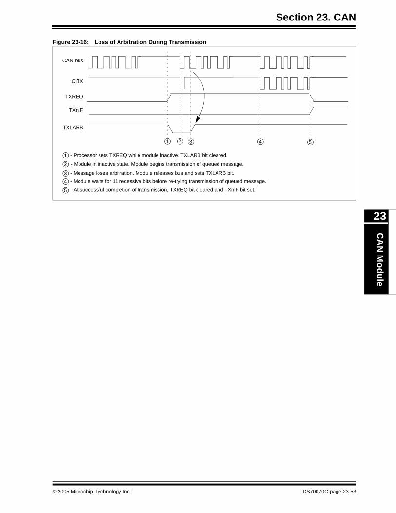
Section 23. CANC
AN
Mo
du
le
23
Figure 23-16: Loss of Arbitration During Transmission
1 2 4 5
- Processor sets TXREQ while module inactive. TXLARB bit cleared.
- Module in inactive state. Module begins transmission of queued message.
- Module waits for 11 recessive bits before re-trying transmission of queued message.
- At successful completion of transmission, TXREQ bit cleared and TXnIF bit set.
CAN bus
3
TXREQ
- Message loses arbitration. Module releases bus and sets TXLARB bit.
CiTX
TXnIF
TXLARB
1
2
3
4
5
© 2005 Microchip Technology Inc. DS70070C-page 23-53
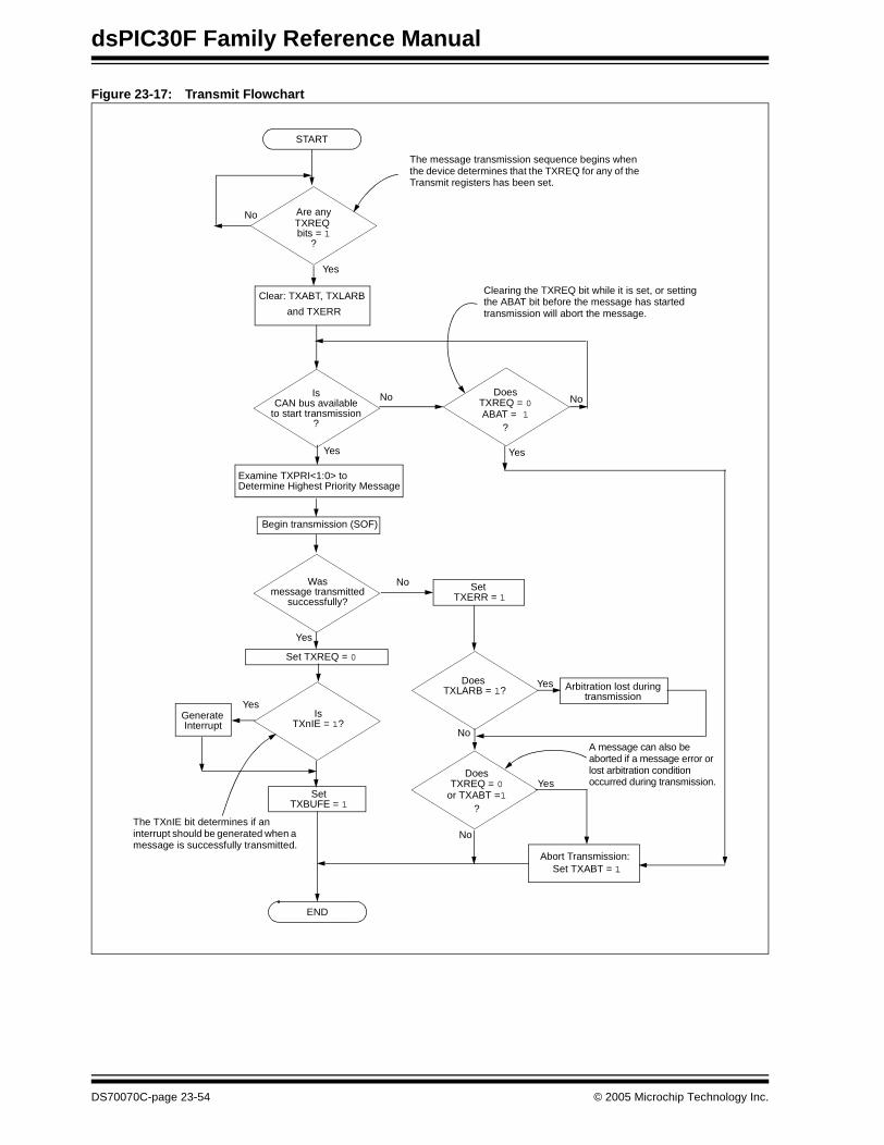
dsPIC30F Family Reference Manual
Figure 23-17: Transmit Flowchart
START
IsCAN bus available
to start transmission
No
Examine TXPRI<1:0> to
Are anyTXREQ
?bits = 1
The message transmission sequence begins when the device determines that the TXREQ for any of the Transmit registers has been set.
Clear: TXABT, TXLARB
and TXERR
Yes
?
DoesTXREQ = 0ABAT = 1
Clearing the TXREQ bit while it is set, or setting the ABAT bit before the message has started transmission will abort the message.
No
Begin transmission (SOF)
Abort Transmission:
Wasmessage transmitted
successfully?
No
Yes
Set TXREQ = 0
IsTXnIE = 1?
Generate Interrupt
Yes
Yes
Set TXABT = 1
Set
Set TXERR = 1
Yes
No
Determine Highest Priority Message
No
?
Does TXLARB = 1?
The TXnIE bit determines if an interrupt should be generated when a message is successfully transmitted.
END
DoesTXREQ = 0
or TXABT =1?
Yes
No
TXBUFE = 1
Yes
A message can also be aborted if a message error or lost arbitration condition occurred during transmission.
Arbitration lost duringtransmission
DS70070C-page 23-54 © 2005 Microchip Technology Inc.

Section 23. CANC
AN
Mo
du
le
23
23.7.6 Transmit Boundary Conditions
The module handles transmit commands which are not necessarily synchronized to the CAN busmessage framing time.
23.7.6.1 Clearing TXREQ bit as a Message Starts
The TXREQ bit can be cleared just when a message is starting transmission, with the intent ofaborting the message. If the message is not being transmitted, the TXABT bit will be set,indicating that the Abort was successfully processed.
When the user clears the TXREQ bit and the TXABT bit is not set two cycles later, the messagehas already begun transmission.
If the message is being transmitted, the abort is not immediately processed, at some point later,the TXnIF interrupt flag or the TXABT bit is set. If transmission has begun the message will onlybe aborted if either an error or a loss of arbitration occurs.
23.7.6.2 Setting TXABT bit as a Message Starts
Setting the ABAT bit will abort all pending Transmit Buffers and has the function of clearing all ofthe TXREQ bits for all buffers. The boundary conditions are the same as clearing the TXREQ bit.
23.7.6.3 Clearing TXREQ bit as a Message Completes
The TXREQ bit can be cleared when a message is just about to successfully complete transmis-sion. Even if the TXREQ bit is cleared by the Data bus a short time before it will be cleared bythe successful transmission of the message, the TXnIF flag will still be set due to the successfultransmission.
23.7.6.4 Setting TXABT bit as a Message Completes
The boundary conditions are the same as clearing the TXREQ bit.
23.7.6.5 Clearing TXREQ bit as a Message Loses Transmission
The TXREQ bit can be cleared when a message is just about to be lost to arbitration or an error.
If the TXREQ signal falls before the loss of arbitration signal or error signal, the result will be likeclearing TXREQ during transmission. When the arbitration is lost or the error is set, the TXABTbit will be set, as it will see that an error has occurred while transmitting, and that the TXREQ bitwas not set.
If the TXREQ bit falls after the arbitration signal has entered the block, the result will be likeclearing TXREQ during an inactive transmit time. The TXABT bit will be set.
23.7.6.6 Setting TXABT bit as a Message Loses Transmission
The boundary conditions are the same as clearing the TXREQ bit.
23.7.7 Effects of a Reset
Upon any Reset the CAN module has to be initialized. All registers are set according to the resetvalues. The content of a transmitted message is lost. The initialization is discussed in Section23.5.5 “Configuration Mode”.
© 2005 Microchip Technology Inc. DS70070C-page 23-55
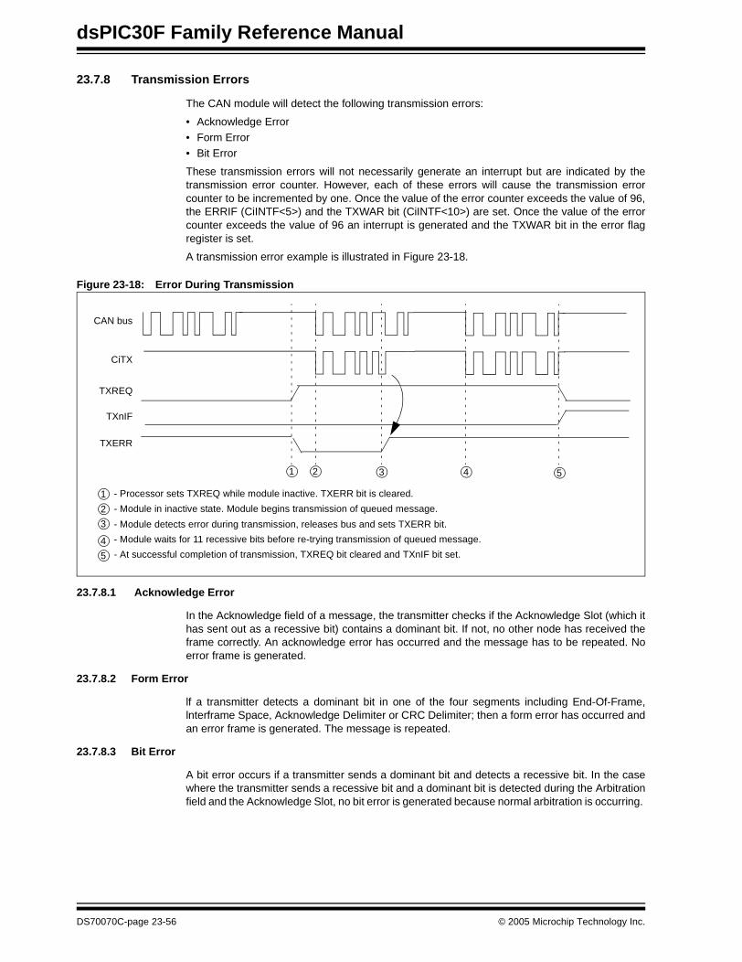
dsPIC30F Family Reference Manual
23.7.8 Transmission Errors
The CAN module will detect the following transmission errors:
• Acknowledge Error• Form Error• Bit Error
These transmission errors will not necessarily generate an interrupt but are indicated by thetransmission error counter. However, each of these errors will cause the transmission errorcounter to be incremented by one. Once the value of the error counter exceeds the value of 96,the ERRIF (CiINTF<5>) and the TXWAR bit (CiINTF<10>) are set. Once the value of the errorcounter exceeds the value of 96 an interrupt is generated and the TXWAR bit in the error flagregister is set.
A transmission error example is illustrated in Figure 23-18.
Figure 23-18: Error During Transmission
23.7.8.1 Acknowledge Error
In the Acknowledge field of a message, the transmitter checks if the Acknowledge Slot (which ithas sent out as a recessive bit) contains a dominant bit. If not, no other node has received theframe correctly. An acknowledge error has occurred and the message has to be repeated. Noerror frame is generated.
23.7.8.2 Form Error
lf a transmitter detects a dominant bit in one of the four segments including End-Of-Frame,lnterframe Space, Acknowledge Delimiter or CRC Delimiter; then a form error has occurred andan error frame is generated. The message is repeated.
23.7.8.3 Bit Error
A bit error occurs if a transmitter sends a dominant bit and detects a recessive bit. In the casewhere the transmitter sends a recessive bit and a dominant bit is detected during the Arbitrationfield and the Acknowledge Slot, no bit error is generated because normal arbitration is occurring.
1 2 4 5
- Processor sets TXREQ while module inactive. TXERR bit is cleared.
- Module in inactive state. Module begins transmission of queued message.
- Module waits for 11 recessive bits before re-trying transmission of queued message.
- At successful completion of transmission, TXREQ bit cleared and TXnIF bit set.
CAN bus
3
TXREQ
- Module detects error during transmission, releases bus and sets TXERR bit.
CiTX
TXnIF
TXERR
1
2
3
4
5
DS70070C-page 23-56 © 2005 Microchip Technology Inc.
Section 23. CANC
AN
Mo
du
le
23
23.7.8.4 Rules for Modifying the Transmit Error Counter
The Transmit Error Counter is modified according to the following rules:
• When the transmitter sends an error flag the Transmit Error Counter is increased by 8 with the following exceptions. In these two exceptions, the Transmit Error Counter is not changed.- If the transmitter is “error passive” and detects an acknowledgment error because of
not detecting a “dominant” ACK, and does not detect a “dominant” bit while sending a passive error flag.
- If the transmitter sends an error flag because of a bit-stuffing error occurred during arbitration whereby the Stuffbit is located before the RTR bit, and should have been “recessive”, and has been sent as “recessive” but monitored as “dominant”.
• If a transmitter detects a bit error while sending an active error flag the Transmit Error Counter is increased by 8.
• Any Node tolerates up to 7 consecutive “dominant” bits after sending an active error flag or passive error flag. After detecting the 14th consecutive “dominant” bit (in case of an active error flag) or after detecting the 8th consecutive “dominant” following a passive error flag, and after each sequence of eight additional consecutive “dominant” bits, every transmitter increases its Transmission Error Counter and every receiver increases its Receive Error Counter by 8.
• After the successful transmission of a message (getting an acknowledge and no error until End-Of-Frame is finished) the Transmit Error Counter is decreased by one unless it was already 0.
23.7.9 Transmission Interrupts
There are several interrupts linked to the message transmission. The transmission interrupts canbe broken up into two groups:
• Transmission interrupts• Transmission error interrupts
23.7.9.1 Transmit Interrupt
At least one of the three transmit buffers is empty (not scheduled) and can be loaded to schedulea message for transmission. Reading the TXnIF flags in the CiINTF register will indicate whichtransmit buffer is available and caused the interrupt.
© 2005 Microchip Technology Inc. DS70070C-page 23-57

dsPIC30F Family Reference Manual
23.7.9.2 Transmission Error Interrupts
A transmission error interrupt will be indicated by the ERRIF flag. This flag shows that an errorcondition occurred. The source of the error can be determined by checking the error flags in theCAN Interrupt Status register CiINTF. The flags in this register are related to receive and transmiterrors.
The TXWAR bit (CiINTF<10>) indicates that the Transmit Error Counter has reached the CPUwarning limit of 96. When this bit transitions from a ‘0’ to a ‘1’, it will cause the error interrupt flagto become set. The TXWAR bit cannot be manually cleared, as it should remain as an indicatorthat the Transmit Error Counter has reached the CPU warning limit of 96. The TXWAR bit willbecome clear automatically if the Transmit Error Counter becomes less than or equal to 95. TheERRIF flag can be manually cleared allowing the interrupt service routine to be exited withoutaffecting the TXWAR bit.
The TXEP bit (CiINTF<12>) indicates that the Transmit Error Counter has exceeded the ErrorPassive limit of 127 and the module has gone to Error Passive state. When this bit transitionsfroma ‘0’ to a ‘1’, it will cause the error interrupt flag to become set. The TXEP bit cannot bemanually cleared, as it should remain as an indicator that the bus is in Error Passive state. TheTXEP bit will become clear automatically if the Transmit Error Counter becomes less than orequal to 127. The ERRIF flag can be manually cleared allowing the interrupt service routine tobe exited without affecting the TXEP bit.
The TXBO bit (CiINTF<13>) indicates that the Transmit Error Counter has exceeded 255 and themodule has gone to bus off state. When this bit transitions from a ‘0’ to a ‘1’, it will cause the errorinterrupt flag to become set. The TXBO bit cannot be manually cleared, as it should remain asan indicator that the bus is off. The ERRIF flag can be manually cleared allowing the interruptservice routine to be exited without affecting the TXBO bit.
23.8 Error Detection
The CAN protocol provides sophisticated error detection mechanisms. The following errors canbe detected. These errors are either receive or transmit errors.
Receive errors are:
• Cyclic Redundancy Check (CRC) Error (see Section 23.6.5.1 “Cyclic Redundancy Check (CRC) Error”)
• Bit Stuffing Bit Error (see Section 23.6.5.2 “Bit Stuffing Error”)• lnvalid Message Received Error (see Section 23.6.5.3 “Invalid Message Received
Error”)
The transmit errors are:
• Acknowledge Error (see Section 23.7.8.1 “Acknowledge Error”)• Form Error (see Section 23.7.8.2 “Form Error”)• Bit Error (see Section 23.7.8.3 “Bit Error”)
23.8.1 Error States
Detected errors are made public to all other nodes via error frames. The transmission of theerroneous message is aborted and the frame is repeated as soon as possible. Furthermore, eachCAN node is in one of the three error states “error active”, “error passive” or “bus off” accordingto the value of the internal error counters. The error active state is the usual state where the busnode can transmit messages and active error frames (made of dominant bits) without any restric-tions. In the error passive state, messages and passive error frames (made of recessive bits)may be transmitted. The bus off state makes it temporarily impossible for the station to participatein the bus communication. During this state, messages can neither be received nor transmitted.
DS70070C-page 23-58 © 2005 Microchip Technology Inc.
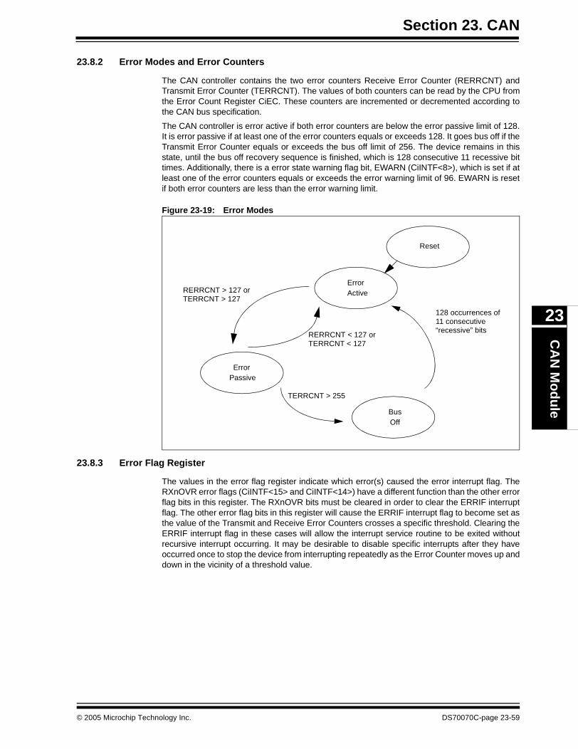
Section 23. CANC
AN
Mo
du
le
23
23.8.2 Error Modes and Error Counters
The CAN controller contains the two error counters Receive Error Counter (RERRCNT) andTransmit Error Counter (TERRCNT). The values of both counters can be read by the CPU fromthe Error Count Register CiEC. These counters are incremented or decremented according tothe CAN bus specification.
The CAN controller is error active if both error counters are below the error passive limit of 128.It is error passive if at least one of the error counters equals or exceeds 128. It goes bus off if theTransmit Error Counter equals or exceeds the bus off limit of 256. The device remains in thisstate, until the bus off recovery sequence is finished, which is 128 consecutive 11 recessive bittimes. Additionally, there is a error state warning flag bit, EWARN (CiINTF<8>), which is set if atleast one of the error counters equals or exceeds the error warning limit of 96. EWARN is resetif both error counters are less than the error warning limit.
Figure 23-19: Error Modes
23.8.3 Error Flag Register
The values in the error flag register indicate which error(s) caused the error interrupt flag. TheRXnOVR error flags (CiINTF<15> and CiINTF<14>) have a different function than the other errorflag bits in this register. The RXnOVR bits must be cleared in order to clear the ERRIF interruptflag. The other error flag bits in this register will cause the ERRIF interrupt flag to become set asthe value of the Transmit and Receive Error Counters crosses a specific threshold. Clearing theERRIF interrupt flag in these cases will allow the interrupt service routine to be exited withoutrecursive interrupt occurring. It may be desirable to disable specific interrupts after they haveoccurred once to stop the device from interrupting repeatedly as the Error Counter moves up anddown in the vicinity of a threshold value.
BusOff
ErrorActive
ErrorPassive
RERRCNT > 127 orTERRCNT > 127
RERRCNT < 127 orTERRCNT < 127
TERRCNT > 255
128 occurrences of11 consecutive“recessive” bits
Reset
© 2005 Microchip Technology Inc. DS70070C-page 23-59

dsPIC30F Family Reference Manual
23.9 CAN Baud Rate
All nodes on any particular CAN bus must have the same nominal bit rate. The CAN bus usesNRZ coding which does not encode a clock. Therefore the receivers independent clock must berecovered by the receiving nodes and synchronized to the transmitters clock.
In order to set the baud rate the following bits have to be initialized:
• Synchronization Jump Width (see Section Section 23.9.6.2 “Re-synchronization”)• Baud Rate Prescaler (see Section Section 23.9.2 “Prescaler Setting”) • Phase Segments (see Section Section 23.9.4 “Phase Segments”)
• Length Determination of Phase Segment 2 (see Section Section 23.9.4 “Phase Segments”)
• Sample Point (see Section Section 23.9.5 “Sample Point”)• Propagation Segment Bits (see Section Section 23.9.3 “Propagation Segment”)
23.9.1 Bit Timing
As oscillators and transmission time may vary from node to node, the receiver must have sometype of PLL synchronized to data transmission edges to synchronize and maintain the receiverclock. Since the data is NRZ coded, it is necessary to include bit-stuffing to ensure that an edgeoccurs at least every 6 bit times, to maintain the Digital Phase Lock Loop (DPLL) synchronization.
Bus timing functions executed within the bit time frame, such as synchronization to the localoscillator, network transmission delay compensation, and sample point positioning, are definedby the programmable bit timing logic of the DPLL.
All controllers on the CAN bus must have the same baud rate and bit length. However, differentcontrollers are not required to have the same master oscillator clock. At different clockfrequencies of the individual controllers, the baud rate has to be adjusted by adjusting thenumber of time quanta in each segment.
The nominal bit time can be thought of as being divided into separate non-overlapping timesegments. These segments are shown in Figure 23-20.
• Synchronization segment (Sync Seg)• Propagation time segment (Prop Seg)• Phase buffer segment 1 (Phase1 Seg)• Phase buffer segment 2 (Phase2 Seg)
The time segments and also the nominal bit time are made up of integer units of time called timequanta or TQ. By definition, the nominal bit time has a minimum of 8 TQ and a maximum of 25 TQ.Also, by definition the minimum nominal bit time is 1 μsec, corresponding to a maximum 1 MHzbit rate.
Figure 23-20: CAN Bit Timing
Input Signal
SyncProp
SegmentPhase
Segment 1Phase
Segment 2 Sync
Sample Point
TQ
DS70070C-page 23-60 © 2005 Microchip Technology Inc.

Section 23. CANC
AN
Mo
du
le
23
23.9.2 Prescaler Setting
There is a programmable prescaler, with integral values ranging from 1 to 64, in addition to afixed divide-by-2 for clock generation. The Time Quanta (TQ) is a fixed unit of time derived fromthe input clock frequency, FCAN. Time quanta is defined as shown in Equation 23-1.
Equation 23-1: Time Quanta for Clock Generation
Example 23-1: Bit Rate Calculation Example
Example 23-2: Baud Rate Prescaler Calculation Example
The frequencies of the oscillators in the different nodes must be coordinated in order to providea system-wide specified time quantum. This means that all oscillators must have a TOSC that isa integral divisor of TQ.
Note: FCAN must not exceed 30 MHz. If CANCKS = 0, then FCY must not exceed 7.5 MHz.
Where BRP is the binary value of BRP <5:0>FCAN is FCY or 4 FCY depending on CANCKS bit
TQ = 2 (BRP<5:0> + 1)FCAN
If 4FCY = 32 MHz, BRP<5:0> = 0x01 and CANCKS = 0, then:
If Nominal Bit Time = 8 TQ then:Nominal Bit Rate Mbps1 8 125
9–×10×( )⁄=
TQ = 2 • (BRP + 1) •TCY
= 2 X 2 X (1/32X106) = 125ns4
CAN Baud Rate = 125 kHzFCY = 5 MHz, CANCKS = 1
1. Select number of TQ clocks per bit time (e.g., K=16).
3. Calculate BRP<5:0>:
BRP 2TQ TCY⁄( ) 1–=
2 5009–×10( )
1 56×10( )⁄
-------------------------------= 1–
4=
2. Calculate TQ from baud rate:
TQ1 BaudRate( )⁄
K--------------------------------------=
1 1253×10⁄
16---------------------------- 500ns= =
TQ = 2 • (BRP + 1) • TCAN
© 2005 Microchip Technology Inc. DS70070C-page 23-61
dsPIC30F Family Reference Manual
23.9.3 Propagation Segment
This part of the bit time is used to compensate physical delay times within the network. Thesedelay times consist of the signal propagation time on the bus line and the internal delay time ofthe nodes. The delay is calculated as the round trip from transmitter to receiver as twice thesignal's propagation time on the bus line, the input comparator delay, and the output driver delay.The Propagation Segment can be programmed from 1 TQ to 8 TQ by setting the PRSEG<2:0>bits (CiCFG2<2:0>).
23.9.4 Phase Segments
The phase segments are used to optimally locate the sampling of the received bit within thetransmitted bit time. The sampling point is between Phase1 Segment and Phase2 Segment.These segments are lengthened or shortened by re-synchronization. The end of the Phase1Segment determines the sampling point within a bit period. The segment is programmable from1 TQ to 8 TQ. Phase2 Segment provides delay to the next transmitted data transition. Thesegment is programmable from 1 TQ to 8 TQ or it may be defined to be equal to the greater ofPhase1 Segment or the Information Processing Time (3 TQ’s). The phase segment 1 is initializedby setting bits SEG1PH<2:0> (CiCFG2<5:3>), and phase segment 2 is initialized by settingSEG2PH<2:0> (CiCFG2<10:8>).
23.9.5 Sample Point
The sample point is the point of time at which the bus level is read and interpreted as the valueof that respective bit. The location is at the end of phase segment 1. If the bit timing is slow andcontains many TQ, it is possible to specify multiple sampling of the bus line at the sample point.The level determined by the CAN bus then corresponds to the result from the majority decisionof three values. The majority samples are taken at the sample point and twice before with adistance of TQ/2. The CAN module allows to chose between sampling three times at the samepoint or once at the same point. This is done by setting or clearing the SAM bit (CiCFG2<6>).
23.9.6 Synchronization
To compensate for phase shifts between the oscillator frequencies of the different bus stations,each CAN controller must be able to synchronize to the relevant signal edge of the incomingsignal. When an edge in the transmitted data is detected, the logic will compare the location ofthe edge to the expected time (Synchronous Segment). The circuit will then adjust the values ofPhase1 Segment and Phase2 Segment. There are 2 mechanisms used to synchronize.
23.9.6.1 Hard Synchronization
Hard Synchronization is only done whenever there is a “recessive” to “dominant” edge during busIdle, indicating the start of a message. After hard synchronization, the bit time counters arerestarted with Synchronous Segment. Hard synchronization forces the edge which has causedthe hard synchronization to lie within the synchronization segment of the restarted bit time.Due to the rules of synchronization, if a hard synchronization is done, there will not be are-synchronization within that bit time.
DS70070C-page 23-62 © 2005 Microchip Technology Inc.
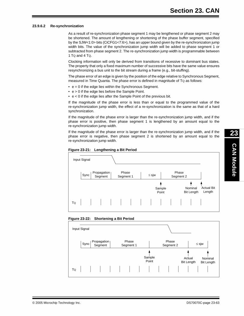
Section 23. CANC
AN
Mo
du
le
23
23.9.6.2 Re-synchronization
As a result of re-synchronization phase segment 1 may be lengthened or phase segment 2 maybe shortened. The amount of lengthening or shortening of the phase buffer segment, specifiedby the SJW<1:0> bits (CiCFG1<7:6>), has an upper bound given by the re-synchronization jumpwidth bits. The value of the synchronization jump width will be added to phase segment 1 orsubtracted from phase segment 2. The re-synchronization jump width is programmable between1 TQ and 4 TQ.
Clocking information will only be derived from transitions of recessive to dominant bus states.The property that only a fixed maximum number of successive bits have the same value ensuresresynchronizing a bus unit to the bit stream during a frame (e.g., bit-stuffing).
The phase error of an edge is given by the position of the edge relative to Synchronous Segment,measured in Time Quanta. The phase error is defined in magnitude of TQ as follows:
• e = 0 if the edge lies within the Synchronous Segment.• e > 0 if the edge lies before the Sample Point.• e < 0 if the edge lies after the Sample Point of the previous bit.
If the magnitude of the phase error is less than or equal to the programmed value of there-synchronization jump width, the effect of a re-synchronization is the same as that of a hardsynchronization.
If the magnitude of the phase error is larger than the re-synchronization jump width, and if thephase error is positive, then phase segment 1 is lengthened by an amount equal to there-synchronization jump width.
If the magnitude of the phase error is larger than the re-synchronization jump width, and if thephase error is negative, then phase segment 2 is shortened by an amount equal to there-synchronization jump width.
Figure 23-21: Lengthening a Bit Period
Figure 23-22: Shortening a Bit Period
Input Signal
SyncPropagation
SegmentPhase
Segment 1Phase
Segment 2≤ sjw
Sample Nominal Actual BitLengthBit LengthPoint
TQ
Input Signal
SyncPropagation
SegmentPhase
Segment 1Phase
Segment 2 ≤ sjw
Sample Actual NominalBit Length
TQ
Point Bit Length
© 2005 Microchip Technology Inc. DS70070C-page 23-63
dsPIC30F Family Reference Manual
23.9.7 Programming Time Segments
Some requirements for programming of the time segments are as follows:
• Propagation Segment + Phase1 Segment > = Phase2 Segment• Phase2 Segment > Synchronous Jump Width
Typically, the sampling of the bit should take place at about 60-70% through the bit time,depending on the system parameters.
Example 23-2 has a 16 TQ bit time. If we choose Synchronous Segment = 1 TQ and PropagationSegment = 2 TQ, setting Phase Segment 1 = 7 TQ would place the sample point at 10 TQ (62%of the bit time) after the initial transition. This would leave 6 TQ for phase segment 2.
Since phase segment 2 is 6, according to the rules, the SJWS<1:0> bits could be set to themaximum of 4 TQ. However, normally a large synchronization jump width is only necessary whenthe clock generation of the different nodes is inaccurate or unstable, such as using ceramicresonators. So a synchronization jump width of 1 is typically enough.
23.10 Interrupts
The module has several sources of interrupts. Each of these interrupts can be individuallyenabled or disabled. A CiINTF register contains interrupt flags. A CiINTE register controls theenabling of the 8 main interrupts. A special set of read only bits in the CiCTRL register(ICODE<2:0>) can be used in combination with a jump table for efficient handling of interrupts.
All interrupts have one source, with the exception of the error interrupt. Any of the error interruptsources can set the error interrupt flag. The source of the error interrupt can be determined byreading the CiINTF register.
The interrupts can be broken up into two categories: receive and transmit interrupts.
The receive related interrupts are:
• Receive interrupt • Wake-up interrupt• Receiver Overrun interrupt
• Receiver Warning interrupt • Receiver Error Passive interrupt
The Transmit related interrupts are:
• Transmit interrupt • Transmitter Warning interrupt
• Transmitter Error Passive interrupt • Bus Off interrupt
23.10.1 Interrupt Acknowledge
Interrupts are directly associated with one or more status flags in CiINTF register. Interrupts arepending as long as one of the corresponding flags is set. The flags in the registers must be resetwithin the interrupt handler in order to handshake the interrupt. A flag can not be cleared if therespective condition still prevails, with the exception being interrupts that are caused by a certainvalue being reached in one of the error counter registers.
DS70070C-page 23-64 © 2005 Microchip Technology Inc.

Section 23. CANC
AN
Mo
du
le
23
23.10.2 The ICODE Bits
The ICODE<2:0> bits (CiCTRL<3:1>) are a set of read only bits designed for efficient handlingof interrupts via a jump table. The ICODE<2:0> bits can only display one interrupt at a timebecause the interrupt bits are multiplexed into this register. Therefore, the pending interrupt withthe highest priority and enabled interrupt is reflected in the ICODE<2:0> bits. Once the highestpriority interrupt flag has been cleared, the next highest priority interrupt code is reflected in theICODE<2:0> bits. An interrupt code for a corresponding interrupt can only be displayed if bothits interrupt flag and interrupt enable are set. Table 23-6 describes the operation of theICODE<2:0> bits.
Table 23-6: ICODE Bits Decode Table
23.11 CAN Capture
The CAN module will generate a signal that can be sent to a timer capture input whenever a validframe has been accepted. This is useful for time-stamping and network synchronization.Because the CAN specification defines a frame to be valid if no errors occurred before the EOFfield has been transmitted successfully, the timer signal will be generated right after the EOF. Apulse of one bit time is generated.
Time-stamping is enabled by the TSTAMP control bit (CiCTRL<15>). The IC2 capture input isused for time-stamping.
23.12 CAN Module I/O
The CAN bus module communicates on up to 2 I/O pins. There is 1 transmit pin and 1 receivepin. These pins are multiplexed with normal digital I/O functions of the device.
When the module is in the Configuration mode, Module Disable mode or Loopback mode, theI/O pins revert to the PORT I/O function.
When the module is active, the CiTX pin (i = 1 or 2) is always dedicated to the CAN outputfunction. The TRIS bits associated with the transmit pins are overridden by the CAN bus modes.The module receives the CAN input on the CiRX input pin.
ICODE<2:0> Boolean Expression
000 ERR•WAK•TX0•TX1•TX2•RX0•RX1
001 ERR
100 ERR•TX0
011 ERR•TX0•TX1
010 ERR•TX0•TX1•TX2
110 ERR•TX0•TX1•TX2•RX0
101 ERR•TX0•TX1•TX2•RX0•RX1
111 ERR•TX0•TX1•TX2•RX0•RX1•WAK
Legend: ERR = ERRIF • ERRIETX0 = TX0IF • TX0IETX1 = TX1IF • TX1IETX2 = TX2IF • TX2IERX0 = RX0IF • RX0IERX1 = RX1IF • RX1IEWAK = WAKIF • WAKIE
Note: If the CAN capture is enabled, the IC2 pin becomes unusable as a general inputcapture pin. In this mode, the IC2 channel derives its input signal from the C1RX orC2RX pin instead of the IC2 pin.
© 2005 Microchip Technology Inc. DS70070C-page 23-65
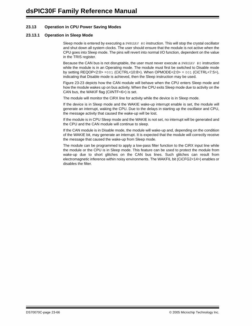
dsPIC30F Family Reference Manual
23.13 Operation in CPU Power Saving Modes
23.13.1 Operation in Sleep Mode
Sleep mode is entered by executing a PWRSAV #0 instruction. This will stop the crystal oscillatorand shut down all system clocks. The user should ensure that the module is not active when theCPU goes into Sleep mode. The pins will revert into normal I/O function, dependent on the valuein the TRIS register.
Because the CAN bus is not disruptable, the user must never execute a PWRSAV #0 instructionwhile the module is in an Operating mode. The module must first be switched to Disable modeby setting REQOP<2:0> =001 (CiCTRL<10:8>). When OPMODE<2:0> = 001 (CiCTRL<7:5>),indicating that Disable mode is achieved, then the Sleep instruction may be used.
Figure 23-23 depicts how the CAN module will behave when the CPU enters Sleep mode andhow the module wakes up on bus activity. When the CPU exits Sleep mode due to activity on theCAN bus, the WAKIF flag (CiINTF<6>) is set.
The module will monitor the CiRX line for activity while the device is in Sleep mode.
If the device is in Sleep mode and the WAKIE wake-up interrupt enable is set, the module willgenerate an interrupt, waking the CPU. Due to the delays in starting up the oscillator and CPU,the message activity that caused the wake-up will be lost.
If the module is in CPU Sleep mode and the WAKIE is not set, no interrupt will be generated andthe CPU and the CAN module will continue to sleep.
If the CAN module is in Disable mode, the module will wake-up and, depending on the conditionof the WAKIE bit, may generate an interrupt. It is expected that the module will correctly receivethe message that caused the wake-up from Sleep mode.
The module can be programmed to apply a low-pass filter function to the CiRX input line whilethe module or the CPU is in Sleep mode. This feature can be used to protect the module fromwake-up due to short glitches on the CAN bus lines. Such glitches can result fromelectromagnetic inference within noisy environments. The WAKFIL bit (CiCFG2<14>) enables ordisables the filter.
DS70070C-page 23-66 © 2005 Microchip Technology Inc.
Section 23. CANC
AN
Mo
du
le
23
Figure 23-23: Processor Sleep and CAN bus Wake-up Interrupt
23.13.2 CAN Module Operation during CPU Idle Mode
On executing a CPU Idle (PWRSAV #1) instruction, the operation of the CAN module isdetermined by the state of the CSIDL bit (CiCTRL<13>).
If CSIDL = 0, the module will continue operation on assertion of Idle mode. The CAN module canwake the device from Idle mode if the CAN module interrupt is enabled.
If CSIDL = 1, the module will discontinue operation in Idle mode. The same rules and conditionsfor entry to and wake from Sleep mode apply. Refer to Section 23.13.1 “Operation in SleepMode” for further details.
TOST
Processor inSLEEP
2 3 4 5
- Processor executes SLEEP (PWRSAV #0) instruction.
- SOF of message wakes up processor. Oscillator start time begins. CAN message lost. WAKIF bit set.
- Processor completes oscillator start time. Processor resumes program or interrupt, based on GIE bits.
accepting CAN bus activity. CAN message lost. - Module detects 11 recessive bits. Module will begin to receive messages and transmit any pending messages.
OSC1
CAN bus
CAN ModuleDisabled
001
001000
000 000
000
Sleep
WAKIF
WAKIE
1
- Processor requests and receives Module Disable mode. Wake-up interrupt enabled.
Processor requests Normal Operating mode. Module waits for 11 recessive bits before
1
2
3
4
5
REQOP<2:0>
OPMODE<2:0>
© 2005 Microchip Technology Inc. DS70070C-page 23-67

dsPIC30F Family Reference Manual
23.14 CAN Protocol Overview
The Controller Area Network (CAN) is a serial communications protocol which efficientlysupports distributed real-time control with a very high level of robustness. The CAN Protocol isfully defined by Robert Bosch GmbH, in the CAN Specification V2.0B from 1991.
Its domain of application ranges from high speed networks to low cost multiplex wiring.Automotive electronics (i.e., engine control units, sensors, anti-skid-systems, etc.) are connectedusing CAN with bit rates up to 1 Mbit/sec. The CAN Network allows a cost effective replacementof wiring harnesses in the automobile. The robustness of the bus in noisy environments and theability to detect and recover from fault conditions makes the bus suitable for industrial controlapplications such as DeviceNet, SDS and other fieldbus protocols.
CAN is an asynchronous serial bus system with one logical bus line. It has an open, linear busstructure with equal bus nodes. A CAN bus consists of two or more nodes. The number of nodeson the bus may be changed dynamically without disturbing the communication of other nodes.This allows easy connection and disconnection of bus nodes (e.g., for addition of systemfunction, error recovery or bus monitoring).
The bus logic corresponds to a “wired-AND” mechanism, “recessive” bits (mostly, but notnecessarily equivalent to the logic level ‘1’) are overwritten by “dominant” bits (mostly logic level‘0’). As long as no bus node is sending a dominant bit, the bus line is in the recessive state, buta dominant bit from any bus node generates the dominant bus state. Therefore, for the CAN busline, a medium must be chosen that is able to transmit the two possible bit states (dominant andrecessive). One of the most common and cheapest ways is to use a twisted wire pair. The buslines are then called “CANH” and “CANL”, and may be connected directly to the nodes, or via aconnector. There's no standard defined by CAN regarding connector requirements. The twistedwire pair is terminated by terminating resistors at each end of the bus line. The maximum busspeed is 1 Mbit, which can be achieved with a bus length of up to 40 meters. For bus lengthslonger than 40 meters, the bus speed must be reduced (a 1000 m bus can be realized with a40 Kbit bus speed). For bus lengths above 1000 meters, special drivers should be used. At least20 nodes may be connected without additional equipment. Due to the differential nature oftransmission, CAN is not inherently susceptible to radiated electromagnetic energy because bothbus lines are affected in the same way, which leaves the differential signal unaffected. The buslines may also be shielded to reduce the radiated electromagnetic emission from the bus itself,especially at high baud rates.
The binary data is coded corresponding to the NRZ code (Non-Return-to-Zero; lowlevel = dominant state; high level = recessive state). To ensure clock synchronization of all busnodes, bit-stuffing is used. This means that during the transmission of a message, a maximumof five consecutive bits may have the same polarity. Whenever five consecutive bits of the samepolarity have been transmitted, the transmitter will insert one additional bit of the opposite polarityinto the bit stream before transmitting further bits. The receiver also checks the number of bitswith the same polarity and removes the stuff bits from the bit stream (destuffing).
In the CAN protocol, it is not bus nodes that are addressed. The address information is containedin the messages that are transmitted. This is done via an identifier (part of each message) whichidentifies the message content (e.g., engine speed, oil temperature etc.). This identifier alsoindicates the priority of the message. The lower the binary value of the identifier, the higher thepriority of the message.
For bus arbitration, Carrier Sense Multiple Access/Collision Detection (CSMA/CD) withNon-Destructive Arbitration (NDA) is used. If bus node A wants to transmit a message across thenetwork, it first checks that the bus is in the Idle state (“Carrier Sense”), (i.e., no node is currentlytransmitting). If this is the case (and no other node wishes to start a transmission at the samemoment), node A becomes the bus master and sends its message. All other nodes switch toReceive mode during the first transmitted bit (Start-Of-Frame bit). After correct reception of themessage (which is Acknowledged by each node), each bus node checks the message identifierand stores the message, if required. Otherwise, the message is discarded.
DS70070C-page 23-68 © 2005 Microchip Technology Inc.
Section 23. CANC
AN
Mo
du
le
23
If two or more bus nodes start their transmission at the same time (“Multiple Access”), collisionof the messages is avoided by bitwise arbitration (“Collision Detection/Non-DestructiveArbitration” together with the “Wired-AND” mechanism, “dominant” bits override “recessive” bits).Each node sends the bits of its message identifier (MSb first) and monitors the bus level. A nodethat sends a recessive identifier bit but reads back a dominant one loses bus arbitration andswitches to Receive mode. This condition occurs when the message identifier of a competingnode has a lower binary value (dominant state = logic 0) and therefore, the competing node issending a message with a higher priority. In this way, the bus node with the highest prioritymessage wins arbitration without losing time by having to repeat the message. All other nodesautomatically try to repeat their transmission once the bus returns to the Idle state. It is notpermitted for different nodes to send messages with the same identifier, as arbitration could fail,leading to collisions and errors later in the message.
The original CAN specifications (Versions 1.0, 1.2 and 2.0A) defined the message identifier ashaving a length of 11 bits giving a possible 2048 message identifiers. The specification has sincebeen updated (to version 2.0B) to remove this limitation. CAN specification Version 2.0B allowsmessage identifier lengths of 11 and/or 29 bits to be used (an identifier length of 29 bits allowsover 536 million message identifiers). Version 2.0B CAN is also referred to as “Extended CAN”;and Versions 1.0, 1.2 and 2.0A) are referred to as “Standard CAN”.
23.14.1 Standard CAN vs. Extended CAN
Those data frames and remote frames, which only contain the 11-bit identifier, are calledstandard frames according to CAN specification V2.0A. With these frames, 2048 differentmessages can be identified (identifiers 0-2047). However, the 16 messages with the lowestpriority (2032-2047) are reserved. Extended frames according to CAN specification V2.0B havea 29-bit identifier. As already mentioned, this 29-bit identifier is made up of the 11-bit identifier(“Standard lD”) and the 18-bit Extended identifier (“Extended ID”).
CAN modules specified by CAN V2.0A are only able to transmit and receive standard framesaccording to the Standard CAN protocol. Messages using the 29-bit identifier cause errors. If adevice is specified by CAN V2.0B, there is one more distinction. Modules named “Part B Passive”can only transmit and receive standard frames but tolerate extended frames without generatingerror frames. “Part B Active” devices are able to transmit and receive both standard andextended frames.
23.14.2 ISO Model
The lSO/OSl Reference Model is used to define the layers of protocol of a communication systemas shown in Figure 23-24. At the highest end, the applications need to communicate betweeneach other. At the lowest end, some physical medium is used to provide electrical signaling.
The higher levels of the protocol are run by software. Within the CAN bus specification, there isno definition of the type of message, or the contents, or meaning of the messages transferred.These definitions are made in systems such as Volcano, the Volvo automotive CAN specificationJ1939, the U.S. heavy truck multiplex wiring specification; and Allen-Bradley DeviceNet andHoneywell SDS, industrial protocols.
The CAN bus module definition encompasses two levels of the overall protocol:
• The Data Link Layer
- The Logical Link Control (LLC) sub layer- The Medium Access Control (MAC) sub layer
• The Physical Layer
- The Physical Signaling (PLS) sub layer
© 2005 Microchip Technology Inc. DS70070C-page 23-69
dsPIC30F Family Reference Manual
The LLC sub layer is concerned with Message Filtering, Overload Notification and ErrorRecovery Management. The scope of the LLC sub layer is:
• To provide services for data transfer and for remote data request.• To decide which messages received by the LLC sub layer are actually to be accepted.• To provide means for error recovery management and overload notifications.
The MAC sub layer represents the kernel of the CAN protocol. The MAC sub layer defines thetransfer protocol, (i.e., controlling the Framing, Performing Arbitration, Error Checking, ErrorSignalling and Fault Confinement). It presents messages received from the LLC sub layer andaccepts messages to be transmitted to the LLC sub layer. Within the MAC sub layer is where it’sdecided whether the bus is free for starting a new transmission, or whether a reception is juststarting. The MAC sub layer is supervised by a management entity called Fault Confinementwhich is a self-checking mechanism for distinguishing short disturbances from permanentfailures. Also, some general features of the bit timing are regarded as part of the MAC sub layer.
The physical layer defines the actual transfer of the bits between the different nodes with respectto all electrical properties. The PLS sub layer defines how signals are actually transmitted andtherefore deals with the description of Bit Timing, Bit Encoding and Synchronization.
The lower levels of the protocol are implemented in driver/receiver chips and the actual interfacesuch as twisted pair wiring or optical fiber, etc. Within one network, the physical layer has to bethe same for all nodes. The driver/receiver characteristics of the physical layer are not defined inthe CAN specification so as to allow transmission medium and signal level implementations tobe optimized for their application. The most common example of the physical transmissionmedium is defined in Road Vehicles ISO11898, a multiplex wiring specification.
DS70070C-page 23-70 © 2005 Microchip Technology Inc.
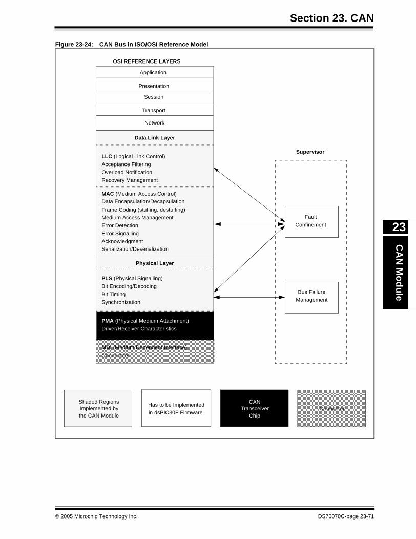
Section 23. CANC
AN
Mo
du
le
23
Figure 23-24: CAN Bus in ISO/OSI Reference Model
OSI REFERENCE LAYERS
Presentation
Transport
Data Link Layer
LLC (Logical Link Control)
Acceptance Filtering
Overload Notification
Recovery Management
MAC (Medium Access Control)Data Encapsulation/Decapsulation
Frame Coding (stuffing, destuffing)
Medium Access Management
Error Detection
Error Signalling
AcknowledgmentSerialization/Deserialization
Physical Layer
PLS (Physical Signalling)
Bit Encoding/Decoding
Bit Timing
Synchronization
PMA (Physical Medium Attachment)
Driver/Receiver Characteristics
MDI (Medium Dependent Interface)
Connectors
Fault
Confinement
Bus Failure
Management
Supervisor
Shaded RegionsImplemented by the CAN Module
Has to be Implemented in dsPIC30F Firmware
Session
Network
Application
CANTransceiver
ChipConnector
© 2005 Microchip Technology Inc. DS70070C-page 23-71
dsPIC30F Family Reference Manual
23.15 Related Application Notes
This section lists application notes that are related to this section of the manual. Theseapplication notes may not be written specifically for the dsPIC30F Product Family, but theconcepts are pertinent and could be used with modification and possible limitations. The currentapplication notes related to the CAN module are:
Title Application Note #
An Introduction to the CAN Protocol AN713
Note: Please visit the Microchip web site (www.microchip.com) for additional ApplicationNotes and code examples for the dsPIC30F Family of devices.
DS70070C-page 23-72 © 2005 Microchip Technology Inc.

Section 23. CANC
AN
Mo
du
le
23
23.16 Revision History
Revision A
This is the initial released revision of this document.
Revision B
This revision incorporates additional technical content for the dsPIC30F CAN module.
Revision C
This revision incorporates all known errata at the time of this document update.
© 2005 Microchip Technology Inc. DS70070C-page 23-73

dsPIC30F Family Reference Manual
NOTES:
DS70070C-page 23-74 © 2005 Microchip Technology Inc.
Section 24. Device Configuration
Device
Co
nfig
uratio
n
24
HIGHLIGHTS
This section of the manual contains the following topics:
24.1 Introduction .................................................................................................................. 24-2
24.2 Device Configuration Registers ................................................................................... 24-224.3 Configuration Bit Descriptions...................................................................................... 24-624.4 Device Identification Registers..................................................................................... 24-7
24.5 Related Application Notes............................................................................................ 24-824.6 Revision History ........................................................................................................... 24-9
© 2005 Microchip Technology Inc. DS70071D-page 24-1
dsPIC30F Family Reference Manual
24.1 Introduction
The device Configuration registers allow each user to customize certain aspects of the device tofit the needs of the application. Device Configuration registers are nonvolatile memory locationsin the program memory map that hold settings for the dsPIC device during power-down. TheConfiguration registers hold global setup information for the device, such as the oscillator source,Watchdog Timer mode and code protection settings.
The device Configuration registers are mapped in program memory locations, starting at address0xF80000 and are accessible during normal device operation. This region is also referred to as“configuration space”.
The Configuration bits can be programmed (read as ‘0’), or left unprogrammed (read as ‘1’) toselect various device configurations.
24.2 Device Configuration Registers
Each device Configuration register is a 24-bit register, but only the lower 16 bits of each registerare used to hold configuration data. There are four device Configuration registers available to theuser:
• FOSC (0xF80000): Oscillator Configuration Register (Note 2)• FWDT (0xF80002): Watchdog Timer Configuration Register
• FBORPOR (0xF80004): BOR and POR Configuration Register• FGS (0xF8000A): General Code Segment Configuration Register
The device Configuration registers can be programmed using Run-Time Self-Programming(RTSP), In-Circuit Serial Programming™ (ICSP™), or by a device programmer.
Note 1: Not all device Configuration bits shown in the subsequent Configuration registerdescriptions may be available on a specific device. Refer to the device data sheetfor more information.
2: dsPIC30F devices in the General Purpose, Sensor and Motor Control families fea-ture one of three versions of the Oscillator system – Version 1, Version 2 and Ver-sion 3. For information on the Configuration bits of the FOSC device Configurationregister available in each of these versions, please refer to Section 7. "Oscillator”.
DS70071D-page 24-2 © 2005 Microchip Technology Inc.
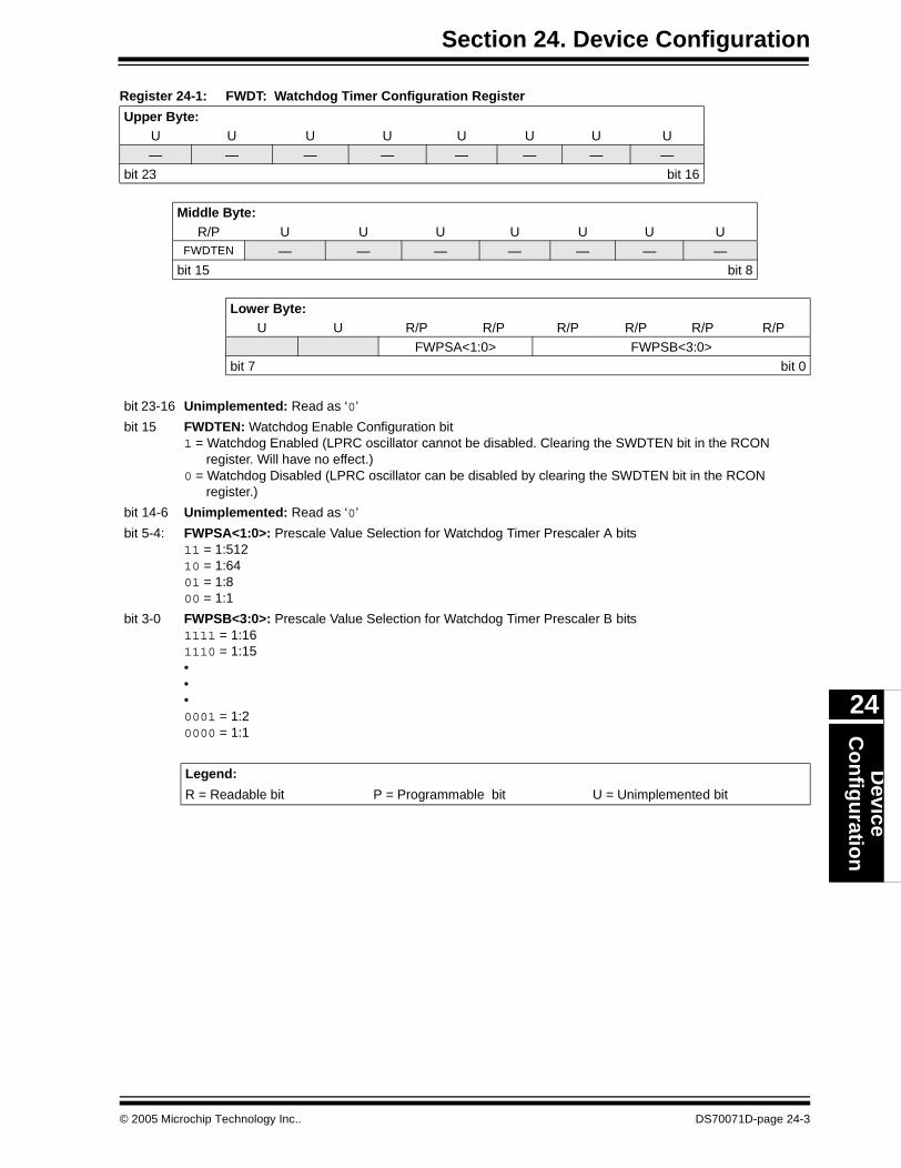
Section 24. Device ConfigurationD
eviceC
on
figu
ration
24
Register 24-1: FWDT: Watchdog Timer Configuration Register
Upper Byte:U U U U U U U U— — — — — — — —
bit 23 bit 16
Middle Byte:R/P U U U U U U U
FWDTEN — — — — — — —bit 15 bit 8
Lower Byte:U U R/P R/P R/P R/P R/P R/P
FWPSA<1:0> FWPSB<3:0>bit 7 bit 0
bit 23-16 Unimplemented: Read as ‘0’
bit 15 FWDTEN: Watchdog Enable Configuration bit1 = Watchdog Enabled (LPRC oscillator cannot be disabled. Clearing the SWDTEN bit in the RCON
register. Will have no effect.)0 = Watchdog Disabled (LPRC oscillator can be disabled by clearing the SWDTEN bit in the RCON
register.)
bit 14-6 Unimplemented: Read as ‘0’
bit 5-4: FWPSA<1:0>: Prescale Value Selection for Watchdog Timer Prescaler A bits11 = 1:51210 = 1:6401 = 1:800 = 1:1
bit 3-0 FWPSB<3:0>: Prescale Value Selection for Watchdog Timer Prescaler B bits1111 = 1:161110 = 1:15•••0001 = 1:20000 = 1:1
Legend:
R = Readable bit P = Programmable bit U = Unimplemented bit
© 2005 Microchip Technology Inc.. DS70071D-page 24-3
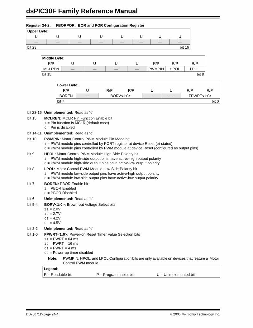
dsPIC30F Family Reference Manual
Register 24-2: FBORPOR: BOR and POR Configuration Register
Upper Byte:U U U U U U U U— — — — — — — —
bit 23 bit 16
Middle Byte:R/P U U U U R/P R/P R/P
MCLREN — — — — PWMPIN HPOL LPOLbit 15 bit 8
Lower Byte:R/P U R/P R/P U U R/P R/P
BOREN — BORV<1:0> — — FPWRT<1:0>
bit 7 bit 0
bit 23-16 Unimplemented: Read as ‘0’
bit 15 MCLREN: MCLR Pin Function Enable bit1 = Pin function is MCLR (default case)0 = Pin is disabled
bit 14-11 Unimplemented: Read as ‘0’
bit 10 PWMPIN: Motor Control PWM Module Pin Mode bit1 = PWM module pins controlled by PORT register at device Reset (tri-stated)0 = PWM module pins controlled by PWM module at device Reset (configured as output pins)
bit 9 HPOL: Motor Control PWM Module High Side Polarity bit1 = PWM module high-side output pins have active-high output polarity0 = PWM module high-side output pins have active-low output polarity
bit 8 LPOL: Motor Control PWM Module Low Side Polarity bit1 = PWM module low-side output pins have active-high output polarity0 = PWM module low-side output pins have active-low output polarity
bit 7 BOREN: PBOR Enable bit1 = PBOR Enabled0 = PBOR Disabled
bit 6 Unimplemented: Read as ‘0’
bit 5-4 BORV<1:0>: Brown-out Voltage Select bits11 = 2.0V10 = 2.7V01 = 4.2V00 = 4.5V
bit 3-2 Unimplemented: Read as ‘0’
bit 1-0 FPWRT<1:0>: Power-on Reset Timer Value Selection bits11 = PWRT = 64 ms10 = PWRT = 16 ms01 = PWRT = 4 ms00 = Power-up timer disabled
Note: PWMPIN, HPOL, and LPOL Configuration bits are only available on devices that feature a MotorControl PWM module.
Legend:
R = Readable bit P = Programmable bit U = Unimplemented bit
DS70071D-page 24-4 © 2005 Microchip Technology Inc.
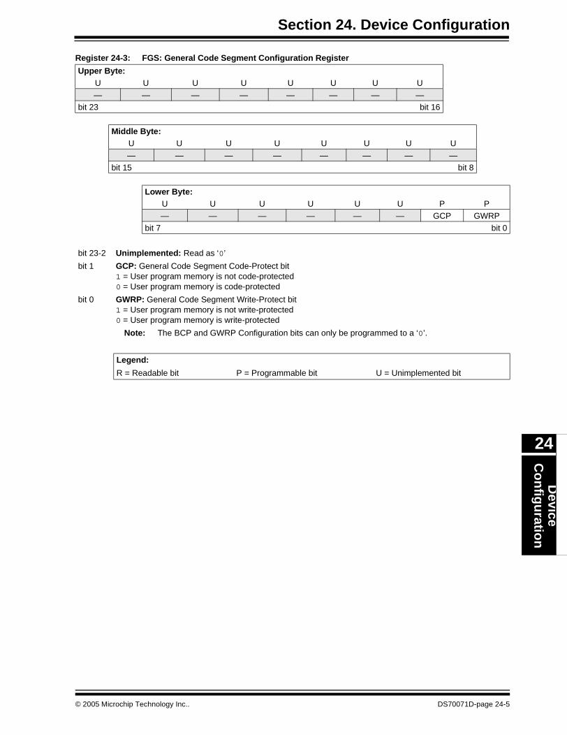
Section 24. Device ConfigurationD
eviceC
on
figu
ration
24
Register 24-3: FGS: General Code Segment Configuration Register
Upper Byte:U U U U U U U U— — — — — — — —
bit 23 bit 16
Middle Byte:U U U U U U U U
— — — — — — — —bit 15 bit 8
Lower Byte:U U U U U U P P— — — — — — GCP GWRP
bit 7 bit 0
bit 23-2 Unimplemented: Read as ‘0’
bit 1 GCP: General Code Segment Code-Protect bit1 = User program memory is not code-protected0 = User program memory is code-protected
bit 0 GWRP: General Code Segment Write-Protect bit1 = User program memory is not write-protected0 = User program memory is write-protected
Note: The BCP and GWRP Configuration bits can only be programmed to a ‘0’.
Legend:
R = Readable bit P = Programmable bit U = Unimplemented bit
© 2005 Microchip Technology Inc.. DS70071D-page 24-5
dsPIC30F Family Reference Manual
24.3 Configuration Bit Descriptions
This section provides specific functional information on each of the device Configuration bits.
24.3.1 Oscillator Configuration Bits
dsPIC30F devices in the General Purpose, Sensor and Motor Control families feature one ofthree versions of the Oscillator system – Version 1, Version 2 and Version 3. For information onthe Configuration bits of the FOSC device Configuration register available in each of theseversions, please refer to Section 7. "Oscillator”.
24.3.2 BOR and POR Configuration Bits
The BOR and POR Configuration bits found in the FBORPOR Configuration register are used toset the Brown-out Reset voltage for the device, enable the Brown-out Reset circuit, and set thePower-up Timer delay time. For more information on these Configuration bits, please refer toSection 8. "Reset”.
24.3.3 Motor Control PWM Module Configuration Bits
The motor control PWM module Configuration bits are located in the FBORPOR Configurationregister and are present only on devices that have the PWM module. The Configuration bitsassociated with the PWM module have two functions:
1. Select the state of the PWM pins at a device Reset (high-Z or output).2. Select the active signal polarity for the PWM pins. The polarity for the high side and low
side PWM pins may be selected independently.
For more information on these Configuration bits, please refer to Section 15. "Motor ControlPWM”.
24.3.4 General Code Segment Configuration Bits
The general code segment Configuration bits in the FGS Configuration register are used tocode-protect or write-protect the user program memory space. The general code segmentincludes all user program memory with the exception of the interrupt vector table space(0x000000-0x0000FE).
If the general code segment is code-protected by programming the GCP Configuration bit(FGS<1>) to a ‘0’, the device program memory cannot be read from the device using In-CircuitSerial Programming (ICSP), or the device programmer. Additionally, further code cannot beprogrammed into the device without first erasing the entire general code segment.
When the general segment is code-protected, user code can still access the program memorydata via table read instructions, or Program Space Visibility (PSV) accesses from data space.
If the GWRP (FGS<0>) Configuration bit is programmed, all writes to the user program memoryspace are disabled.
24.3.4.1 General Code Segment Configuration Bit Group
The GCP and GWRP Configuration bits in the FGS Configuration register must beprogrammed/erased as a group. If one or both of the Configuration bits is programmed to a ‘0’,a full chip erase must be performed to change the state of either bit.
Note: If the code protection Configuration fuse group (FGS<GCP:GWRP>) bits have beenprogrammed, an erase of the entire code-protected device is only possible atvoltages, VDD >= 4.5 volts.
DS70071D-page 24-6 © 2005 Microchip Technology Inc.

Section 24. Device ConfigurationD
eviceC
on
figu
ration
24
24.4 Device Identification Registers
The dsPIC30F devices have two sets of registers located in configuration space that provideidentification information.
24.4.1 Device ID (DEVID) Registers
The configuration memory space locations 0xFF0000 and 0xFF0002 are used to store aread-only Device ID number that is set when the device is manufactured. This number identifiesthe dsPIC30F device type and the silicon revision.
The Device ID registers can be read by the user using table read instructions.
24.4.2 Unit ID Field
The Unit ID field is located at configuration memory space locations 0x800600 through0x80063E. This field consists of 32 program memory locations and can be programmed at theMicrochip factory with unique device information. This field cannot be written or erased by theuser, but can be read using table read instructions.
Please contact Microchip technical support or your local Microchip representative for furtherdetails.
© 2005 Microchip Technology Inc.. DS70071D-page 24-7
dsPIC30F Family Reference Manual
24.5 Related Application Notes
This section lists application notes that are related to this section of the manual. Theseapplication notes may not be written specifically for the dsPIC30F Product Family, but theconcepts are pertinent and could be used with modification and possible limitations. The currentapplication notes related to the Device Configuration module are:
Title Application Note #
Using the dsPIC30F for Sensorless BLDC Control AN901
Note: Please visit the Microchip web site (www.microchip.com) for additional ApplicationNotes and code examples for the dsPIC30F Family of devices.
DS70071D-page 24-8 © 2005 Microchip Technology Inc.

Section 24. Device ConfigurationD
eviceC
on
figu
ration
24
24.6 Revision History
Revision A
This is the initial released revision of this document.
Revision B
This revision incorporates technical content changes for the dsPIC30F Device Configurationmodule.
Revision C
This revision incorporates all known errata at the time of this document update.
Revision D
Descriptions of three versions of the Oscillator Control module have been added. The definitionof the FOSC Configuration register was moved to DS70054.
© 2005 Microchip Technology Inc.. DS70071D-page 24-9

dsPIC30F Family Reference Manual
DS70071D-page 24-10 © 2005 Microchip Technology Inc.
Section 25. Development Tool Support
Develo
pm
ent
Too
l Su
pp
ort
25
HIGHLIGHTS
This section of the manual contains the following topics:
25.1 Introduction .................................................................................................................. 25-2
25.2 Microchip Hardware and Language Tools.................................................................... 25-225.3 Third Party Hardware/Software Tools and Application Libraries.................................. 25-625.4 dsPIC30F Hardware Development Boards................................................................ 25-11
25.5 Related Application Notes.......................................................................................... 25-1525.6 Revision History ......................................................................................................... 25-16
© 2004 Microchip Technology Inc. DS70072C-page 25-1
dsPIC30F Family Reference Manual
25.1 Introduction
Microchip will offer a comprehensive package of development tools and libraries to support thedsPIC architecture. In addition, the company is partnering with many third party toolmanufacturers for additional dsPIC device support.
25.2 Microchip Hardware and Language Tools
The Microchip tools proposed include:
• MPLAB® Integrated Development Environment (IDE)
• dsPIC Language Suite, including MPLAB C30 C Compiler, Assembler, Linker and Librarian• MPLAB SIM Software Simulator• MPLAB ICE 4000 In-Circuit Emulator
• MPLAB ICD 2 In-Circuit Debugger• PRO MATE® II Universal Device Programmer• PICSTART® Plus Development Programmer
25.2.1 MPLAB 6.XX Integrated Development Environment Software
The MPLAB Integrated Development Environment (IDE) is available at no cost. MPLAB IDEsoftware is a desktop development environment with tool sets for developing and debugging amicrocontroller design application. MPLAB IDE allows quick changes between different develop-ment and debugging activities. Designed for use with the Windows® operating environment, it isa powerful, affordable, run-time development tool. It is also the common user interface forMicrochip's development systems tools, including MPLAB Editor, MPLAB ASM30 Assembler,MPLAB SIM software simulator, MPLAB LIB30 Library, MPLAB LINK30 Linker, MPLAB ICE 4000In-Circuit Emulators, PRO MATE II programmer and In-Circuit Debugger (ICD 2). The MPLABIDE gives users the flexibility to edit, compile and emulate, all from a single user interface.Engineers can design and develop code for the dsPIC devices in the same design environmentthat they have used for PICmicro® microcontrollers.
The MPLAB IDE is a 32-bit Windows-based application. It provides many advanced features forthe engineer in a modern, easy-to-use interface. MPLAB IDE integrates:
• Full featured, color coded text editor• Easy-to-use project manager with visual display• Source level debugging
• Enhanced source level debugging for ‘C’ - (Structures, automatic variables, etc.)
• Customizable toolbar and key mapping
• Dynamic status bar that displays processor condition at a glance• Context sensitive, interactive on-line help• Integrated MPLAB SIM instruction simulator
• User interface for PRO MATE II and PICSTART Plus device programmers (sold separately)
• User interface for MPLAB ICE 4000 In-Circuit Emulator (sold separately)• User interface for MPLAB ICD 2 In-Circuit Debugger (sold separately)
Note: Some development tools described in this section are not available at the time of thiswriting, however they are currently under development. Some of the product details maychange. Please check the Microchip web site or your local Microchip sales office for themost current information and the availability of each product.
Note: This product is currently available on Microchip’s web site, www.microchip.com.
DS70072C-page 25-2 © 2004 Microchip Technology Inc.
Section 25. Development Tool SupportD
evelop
men
tTo
ol S
up
po
rt
25
The MPLAB IDE allows the engineer to:
• Edit source files in either assembly or ‘C’• One-touch compile and download to dsPIC program memory on emulator or simulator.
All project information is updated.• Debug using:
- Source files- Machine code- Mixed mode source and machine code
The ability to use the MPLAB IDE with multiple development and debugging targets allows usersto easily switch from the cost effective simulator to a full featured emulator with minimal retraining.
25.2.2 dsPIC Language Suite
The Microchip Technology MPLAB C30 C compiler is a complete, easy-to-use language product.It allows dsPIC applications codes to be written in high level C language and then be fullyconverted into machine-object code for programming of the microcontroller. It simplifies develop-ment of code by removing code obstacles and allowing the designer to focus on program flowand not on program elements. Several options for compiling are available so the user can selectthose that will maximize the efficiency of the code characteristics.
It is a fully ANSI compliant product with standard libraries for the dsPIC family of microcontrollers.It uses the many advanced features of the dsPIC devices to provide very efficient assembly codegeneration.
MPLAB C30 also provides extensions that will allow for excellent support of the hardware, suchas interrupts and peripherals. It is fully integrated with the MPLAB IDE for high level, sourcedebugging. Some features include:
• 16-bit native data types• Efficient use of register-based, 3-operand instructions
• Complex Addressing modes• Efficient multi-bit shift operations• Efficient signed/unsigned comparisons
MPLAB C30 comes complete with its own assembler, linker and librarian. These allow the userto write mixed mode C and assembly programs and link the resulting object files into a singleexecutable file. The compiler is sold separately. The assembler, linker and librarian is availablefor free with MPLAB IDE.
25.2.3 MPLAB SIM Software Simulator
The MPLAB SIM software simulator allows code development in a PC-hosted environment bysimulating the dsPIC device on an instruction level. On any given instruction, the data areas areable to be examined or modified. The execution is able to be performed in Single Step, ExecuteUntil Break or Trace mode.(1)
The MPLAB SIM simulator fully supports symbolic debugging using the MPLAB C30 compilerand assembler. The software simulator offers the flexibility to develop and debug code outside ofthe laboratory environment, making it an excellent multi-project software development tool.
Note: This product is currently available on Microchip’s web site, www.microchip.com. TheAssembler, Linker and Librarian are included with MPLAB IDE. Contact your localMicrochip sales office for availability of the MPLAB C30 C compiler.
Note: This product is included with MPLAB IDE.
Note 1: Some features, including peripheral support, have not been implemented at thetime of this writing. Please check Microchip’s web site or your local Microchip salesoffice for the most current information.
© 2004 Microchip Technology Inc. DS70072C-page 25-3
dsPIC30F Family Reference Manual
25.2.4 MPLAB ICE 4000 In-Circuit Emulator
The MPLAB ICE 4000 In-Circuit Emulator will provide the product development engineer with acomplete hardware design tool for the dsPIC devices. Software control of the emulator will beprovided by MPLAB IDE.
The MPLAB ICE 4000 will be a full-featured emulator system with enhanced trace, trigger anddata monitoring features. Interchangeable processor modules will allow the system to be easilyreconfigured for emulation of different processors.
The MPLAB ICE 4000 will support the extended, high-end PICmicro microcontrollers, thePIC18CXXX and PIC18FXXX devices, as well as the dsPIC Family of digital signal controllers.The modular architecture of the MPLAB ICE 4000 in-circuit emulator will allow expansion tosupport new devices.
The MPLAB ICE 4000 in-circuit emulator system has been designed as a real-time emulationsystem, with advanced features that are generally found on more expensive development tools.Features will include:
• Full speed emulation, up to 50 MHz bus speed or 200 MHz external clock speed• Low voltage emulation down to 1.8 volts
• Configured with 2 Mb program emulation memory; additional modular memory up to 16 Mb• 64K x 136-bit wide Trace Memory• Unlimited software breakpoints
• Complex break, trace and trigger logic• Multi-level trigger up to 4 levels• Filter trigger functions to trace specific event
• 16-bit Pass counter for triggering on sequential events• 16-bit Delay counter• 48-bit time-stamp
• Stopwatch feature• Time between events• Statistical performance analysis
• Code coverage analysis• USB and parallel printer port PC connection
Note: This product is currently under development at the time of this writing. Some of theproduct details may change. Please refer to the Microchip web site or your localMicrochip sales office for the most current information and the availability of thisproduct.
DS70072C-page 25-4 © 2004 Microchip Technology Inc.

Section 25. Development Tool SupportD
evelop
men
tTo
ol S
up
po
rt
25
25.2.5 MPLAB ICD 2 In-Circuit Debugger
Microchip's In-Circuit Debugger, MPLAB ICD, will be a powerful, low cost, run-time developmenttool. This tool is based on the PICmicro® and dsPIC Flash devices.
The MPLAB ICD 2 will utilize the in-circuit debugging capability built into the various devices. Thisfeature, along with Microchip's In-Circuit Serial Programming™ protocol (ICSP™), will offer costeffective, in-circuit debugging from the graphical user interface of MPLAB IDE. This will enable adesigner to develop and debug source code by watching variables, single-stepping and settingbreak points. Running at full speed enables testing hardware in real-time. Some of its features willinclude:
• Full speed operation to the range of the device• Serial or USB PC connector
• Serial interface externally powered• USB powered from PC interface• Low noise power (VPP and VDD) for use with analog and other noise sensitive applications
• Operation down to 2.0V• Can be used as an ICD or inexpensive serial programmer• Modular application connector as MPLAB ICD
• Limited number of breakpoints• “Smart watch” variable windows• Some chip resources required (RAM, program memory and 2 pins)
25.2.6 PRO MATE II Universal Device Programmer
The PRO MATE II universal device programmer will be a full-featured programmer capable ofoperating in Stand-alone mode, as well as PC-hosted mode.
The PRO MATE II device programmer will have programmable VDD and VPP supplies, which willallow it to verify programmed memory at VDDMIN and VDDMAX for maximum reliability whenprogramming requires this capability. It will have an LCD display for instructions and errormessages and keys to enter commands. Interchangeable optional socket modules will supportall package types.
In Stand-alone mode, the PRO MATE II device programmer will be able to read, verify or programPICmicro and dsPIC30F devices. It will also be able to set code protection in this mode.PRO MATE II features will include:
• Runs under MPLAB IDE
• Field upgradable firmware• DOS Command Line interface for production• Host, Safe and “Stand-alone” operation
• Automatic downloading of object file• SQTPSM serialization adds an unique serial number to each device programmed• In-Circuit Serial Programming Kit (sold separately)
• Interchangeable socket modules supporting all package options (sold separately)
Note: This product is available, but does not provide support for dsPIC30F devices at thistime. Please refer to the Microchip web site for information about product upgrades.
Note: This product is available, but does not provide support for dsPIC30F devices at thistime. Please refer to the Microchip web site for information about product upgrades.
© 2004 Microchip Technology Inc. DS70072C-page 25-5
dsPIC30F Family Reference Manual
25.3 Third Party Hardware/Software Tools and Application Libraries
Microchip is partnering with key third party tool manufacturers for the development of qualityhardware and software tools in support of the dsPIC30F Product Family. Microchip plans to offerthis initial set of tools and libraries, which will enable customers to rapidly develop their dsPIC30Fbased application(s).
Microchip will expand this current list to provide our customers with additional value added ser-vices, (i.e., repository of skilled/certified technical applications contacts, reference designs,hardware and software developers).
Please refer to the Microchip web site (www.microchip.com) for the most current informationabout third party support for the dsPIC30F Device Family.
The dsPIC30F software tools and libraries will include:
• Third Party C compilers
• Floating Point and Double Precision Math Library• DSP Algorithm Library• Digital Filter Design Software Utility
• Peripheral Driver Library• CAN Library• Real-Time Operating Systems (RTOS)
• OSEK Operating Systems• TCP/IP Protocol Stacks• V.22/V.22bis and V.32 ITU Specifications
The dsPIC30F hardware development board tools include:
• General Purpose Development Board
• Motor Control Development System• Connectivity Development Board
25.3.1 Third Party C Compilers
In addition to the Microchip MPLAB C30 C Compiler, the dsPIC30F will be supported by ANSI Ccompilers developed by IAR, HI-TECH and Custom Computer Services (CCS).
The compilers will allow dsPIC application code to be written in high level C language, and thenbe fully converted into machine object code for programming of the microcontroller. Eachcompiler tool will provide several options for compiling, so the user can select those that willmaximize the efficiency of the generated code characteristics.
The multiple C compiler solutions will have different price targets and features, enabling thecustomer to select the compiler best suited for their application requirements.
Note: These products are currently under development at the time of this writing. Some ofthe product details may change. Please refer to the Microchip web site or your localMicrochip sales office for the most current information and the availability of thisproduct.
Note: These products are currently under development at the time of this writing. Some ofthe product details may change. Please refer to the Microchip web site or your localMicrochip sales office for the most current information and the availability of theseproducts.
DS70072C-page 25-6 © 2004 Microchip Technology Inc.
Section 25. Development Tool SupportD
evelop
men
tTo
ol S
up
po
rt
25
25.3.2 Math Library
The Math Library will support several standard C functions, including, but not limited to:
• sin(), cos(), tan()
• asin(), acos(), atan(),• log(), log10()• sqrt(), power()
• ceil(), floor()• fmod(), frexp()
The math function routines will be developed and optimized in dsPIC30F assembly language andwill be callable from both assembly and C language. Floating point and double precision versionsof each function shall be provided. The Microchip MPLAB C30 and IAR C compilers will besupported.
25.3.3 DSP Algorithm Library
The DSP library will support multiple filtering, convolution, vector and matrix functions. Some ofthe functions will include, but will not be limited to:
• Cascaded Infinite Impulse Response (IIR) Filters
• Correlation• Convolution• Finite Impulse Response (FIR) Filters
• Windowing Functions• FFTs• LMS Filter
• Vector Addition and Subtraction• Vector Dot Product• Vector Power
• Matrix Addition and Subtraction• Matrix Multiplication
Note: This product is currently under development at the time of this writing. Some of theproduct details may change. Please refer to the Microchip web site or your localMicrochip sales office for the most current information and the availability of thisproduct.
Note: This product is currently under development at the time of this writing. Some of theproduct details may change. Please refer to the Microchip web site or your localMicrochip sales office for the most current information and the availability of thisproduct.
© 2004 Microchip Technology Inc. DS70072C-page 25-7
dsPIC30F Family Reference Manual
25.3.4 DSP Filter Design Software Utility
Microchip will offer a digital filter design software tool which will enable the user to developoptimized assembly code for Low-pass, High-pass, Band-pass and Band-stop IIR and FIR filters,including 16-bit fractional data size filter coefficients from a graphical user interface. Theapplication developer will enter the required filter frequency specifications and the software tooldevelops the filter code and coefficients. Ideal filter frequency response and time domain plotsare generated for analysis.
FIR filter lengths up to 513 taps and IIR filter lengths up to 10 cascaded sections will besupported.
All IIR and FIR routines are generated in assembly language and will be callable from bothassembly and C language. The Microchip MPLAB C30 C compiler will be supported.
25.3.5 Peripheral Driver Library
Microchip will offer a peripheral driver library that will support the setup and control of dsPIC30Fhardware peripherals, including, but not limited to:
• Analog-to-Digital Converter
• Motor Control PWM• Quadrature Encoder Interface• UART
• SPI™• Data Converter Interface• I2C™
• General Purpose Timers• Input Capture• Output Compare/Simple PWM
Note: This product is currently under development at the time of this writing. Some of theproduct details may change. Please refer to the Microchip web site or your localMicrochip sales office for the most current information and the availability of thisproduct.
Note: This product is currently under development at the time of this writing. Some of theproduct details may change. Please refer to the Microchip web site or your localMicrochip sales office for the most current information and the availability of thisproduct.
DS70072C-page 25-8 © 2004 Microchip Technology Inc.
Section 25. Development Tool SupportD
evelop
men
tTo
ol S
up
po
rt
25
25.3.6 CAN Library
Microchip will offer a CAN driver library, which will support the dsPIC30F CAN peripheral. Someof the CAN functions which will be supported are:
• Initialize CAN Module
• Set CAN Operational Mode• Set CAN Baud Rate• Set CAN Masks
• Set CAN Filters• Send CAN Message• Receive CAN Message
• Abort CAN Sequence• Get CAN TX Error Count• Get CAN RX Error Count
25.3.7 Real-Time Operating System (RTOS)
Real-Time Operating System (RTOS) solutions for the dsPIC30F Product Family will beprovided. These RTOS solutions will provide the necessary function calls and operating systemroutines to write efficient C and/or assembly code for multi-tasking applications. In addition,RTOS solutions will be provided that address those applications in which program and moreimportantly, data memory resources, are limited. Configurable and optimized kernels will beavailable to support various RTOS application requirements.
The RTOS solutions will range from a fully-true, preemptive and multi-tasking scheduler to acooperative type scheduler, both of which will be designed to optimally run on the dsPIC30Fdevices. Depending on the RTOS implementation, some of the function calls provided in thesystem kernel will be:
• Control Tasks
• Send And Receive Messages• Handle Events
• Control Resources• Control Semaphores• Regulate Timing in a Variety of Ways
• Provide Memory Management• Handle Interrupts and Swap Tasks
Most functions will be written in ANSI C, with the exception of time critical functions, which willbe optimized in assembly, thereby reducing execution time for maximum code efficiency. TheANSI C and assembly routines will be supported by the Microchip MPLAB C30 C compiler.
Electronic documentation will accompany the RTOS, enabling the user to efficiently understandand implement the RTOS in their application.
Note: This product is currently under development at the time of this writing. Some of theproduct details may change. Please refer to the Microchip web site or your localMicrochip sales office for the most current information and the availability of thisproduct.
Note: This product is currently under development at the time of this writing. Some of theproduct details may change. Please refer to the Microchip web site or your localMicrochip sales office for the most current information and the availability of thisproduct.
© 2004 Microchip Technology Inc. DS70072C-page 25-9
dsPIC30F Family Reference Manual
25.3.8 OSEK Operating Systems
Operating Systems for the vehicle software standard OSEK/VDX will be developed for supportof the dsPIC30F product family. The functionality of OSEK, “Offene Systeme und derenSchnittstellen für die Elektronik im Kraftfahrzeug” (Open systems and the correspondinginterfaces for automotive electronics), is harmonized with VDX “Vehicle Distributed eXecutive”yielding OSEK/VDX.
Structured and modular RTOS software implementations based on standardized interfaces andprotocols will be provided. Structured and modular implementations will provide for portability andextendability for distributed control units for vehicles.
Various OSEK COM modules will be provided, such as:
• OSEK/COM Standard API
• OSEK/COM Communication API• OSEK/COM Network API• OSEK/COM Standard Protocols
• OSEK/COM Device Driver Interface
Microchip will also provide Internal and External CAN driver support. The physical layer will beintegrated into the communication controller’s hardware and will not be covered by the OSEKspecifications.
Most module functions will be developed in ANSI C, with the exception of time critical functionsand peripheral utilization, which will be optimized in assembly, thereby reducing execution timefor maximum code efficiency. The Microchip MPLAB C30 C compiler will be supported.
25.3.9 TCP/IP Protocol Stack
Microchip will offer various Transmission Control Protocol/Internet Protocol (TCP/IP) Stack Layersolutions for Internet connectivity solutions implemented on the dsPIC30F product family. Bothreduced and full stack implementations will be provided, which will allow the user to select theoptimum TCP/IP stack solution for their application.
Application protocol layers, such as FTP, TFTP and SMTP, Transport and Internet layers, suchas TCP, UDP, ICMP and IP, and Network Access layers, such as PPP, SLIP, ARP and DHCP, willbe provided. Various configurations, such as a minimal UDP/IP stack will be available for limitedconnectivity requirements.
Most stack protocol functions will be developed and optimized in Microchip’s MPLAB C30 Clanguage. Assembly language coding may be developed for specific dsPIC30F hardwareperipherals and Ethernet drivers to optimize code size and execution time. These assemblylanguage specific routines will be assembly and C callable.
Electronic documentation will accompany the TCP/IP protocol stack, enabling the user toefficiently understand and implement the protocol stack in their application.
Note: This product is currently under development at the time of this writing. Some of theproduct details may change. Please refer to the Microchip web site or your localMicrochip sales office for the most current information and the availability of thisproduct.
Note: This product is currently under development at the time of this writing. Some of theproduct details may change. Please refer to the Microchip web site or your localMicrochip sales office for the most current information and the availability of thisproduct.
DS70072C-page 25-10 © 2004 Microchip Technology Inc.

Section 25. Development Tool SupportD
evelop
men
tTo
ol S
up
po
rt
25
25.3.10 V.22/V.22bis and V.32 Specification
Microchip will offer ITU compliant V.22/V.22bis (1200/2400 bps) and V.32 (non-trellis coding at9600 bps) modem specifications to support a range of “connected” applications.
Applications which will benefit from these modem specifications will be numerous and will fall intomany applications, some of which are listed here:
• Internet enabled home security systems• Internet connected power, gas and water meters• Internet connected vending machines
• Smart Appliances• Industrial monitoring• POS Terminals
• Set Top Boxes• Drop Boxes• Fire Panels
Most ITU specification modules will be developed and optimized in Microchip’s MPLAB C30 Clanguage. Assembly language coding may be developed for specific dsPIC30F hardwareperipherals, along with key transmitter and receiver filtering routines to optimize code size andexecution time. These assembly language specific routines will be assembly and C callable.
Electronic documentation will accompany the modem library, enabling the user to efficientlyunderstand and implement the library functions.
25.4 dsPIC30F Hardware Development Boards
Microchip will initially provide three hardware development boards, which will providethe application developer with a tool in which to quickly prototype and validate key designrequirements. Each board will feature key dsPIC30F peripherals and support Microchip’s MPLABIn-Circuit Debugger (ICD 2) tool for cost effective debugging and programming of the dsPIC30Fdevice. The three initial boards to be provided are:
• General Purpose Development Board• Motor Control Development System
• Connectivity Development Board
Note: This product is currently under development at the time of this writing. Some of theproduct details may change. Please refer to the Microchip web site or your localMicrochip sales office for the most current information and the availability of thisproduct.
Note: These products are currently under development at the time of this writing. Some ofthe product details may change. Please refer to the Microchip web site or your localMicrochip sales office for the most current information and the availability of theseproducts.
© 2004 Microchip Technology Inc. DS70072C-page 25-11
dsPIC30F Family Reference Manual
25.4.1 General Purpose Development Board
The dsPIC30F general purpose development board will provide the application designer with alow cost development tool in which to become familiar with the dsPIC30F 16-bit architecture, highperformance peripherals and powerful instruction set. The development board will serve as anideal prototyping tool in which to quickly develop and validate key design requirements.
Some key features and attributes of the general purpose development board will be:
• Supports various dsPIC30F packages• CAN communication channel• RS-232 and RS-485 communication channels
• Codec interface with line in/out jacks• In-Circuit Debugger interface• MPLAB ICE 4000 emulation support
• Microchip temperature sensor• Microchip Op Amp circuit, supporting user input signals • Microchip Digital-to-Analog Converter
• 2x16 LCD• General purpose prototyping area• Various LEDS, switches and potentiometers
The general purpose development board will be shipped with a 9V power supply, RS-232 I/Ocable, preprogrammed dsPIC30F device, example software and appropriate documentation toenable the user to exercise the development board demonstration programs.
Note: This product is currently under development at the time of this writing. Some of theproduct details may change. Please refer to the Microchip web site or your localMicrochip sales office for the most current information and the availability of thisproduct.
DS70072C-page 25-12 © 2004 Microchip Technology Inc.

Section 25. Development Tool SupportD
evelop
men
tTo
ol S
up
po
rt
25
25.4.2 Motor Control Development System
The dsPIC30F motor control development system will initially provide the application developerwith three main components for quick prototyping and validation of BLDC, PMAC and ACIMapplications. The three main components will be:
• dsPIC30F Motor Control Main Board • 3-phase Low Voltage Power Module• 3-phase High Voltage Power Module
The main control board will support the dsPIC30F6010 device, various peripheral interfaces, anda custom interface header system that will allow different motor power modules to be connected.The control board also will have connectors for mechanical position sensors, such as incrementalrotary encoders and hall effect sensors, and a breadboard area for custom circuits. The maincontrol board will receive its power from a standard plug-in transformer.
The low voltage power module will be optimized for 3-phase motor applications that will requirea DC bus voltage less than 60 volts and will deliver up to 400W power output. The 3-phase lowvoltage power module is intended to power BLDC and PMAC motors.
The high voltage power module will be optimized for 3-phase motor applications that require DCbus voltages up to 400 volts and up to 1 kW power output. The high voltage module will have anactive power factor correction circuit that will be controlled by the dsPIC30F device. This powermodule is intended for AC induction motor and power inverter applications.
Both power modules will have automatic Fault protection and electrical isolation from the controlinterface. Both power module boards will provide preconditioned voltage and current signals tothe main control board. All position feedback devices that will be isolated from the motor controlcircuitry, such as incremental encoders, hall-effect sensors or tachometer sensors, will be directlyconnected to the main control board. Both modules will be equipped with motor braking circuits.
Note: This product is currently under development at the time of this writing. Some of theproduct details may change. Please refer to the Microchip web site or your localMicrochip sales office for the most current information and the availability of thisproduct.
© 2004 Microchip Technology Inc. DS70072C-page 25-13
dsPIC30F Family Reference Manual
25.4.3 Connectivity Development Board
The dsPIC30F connectivity development board will provide the application developer a basicplatform for developing and evaluating various connectivity solutions, implementing TCP/IPprotocol layers combined with V.22/V.22bis and V.32 (non-trellis coding) ITU specifications,across PSTN or Ethernet communication channels.
Some key features and attributes of the connectivity development board will be:
• Supports the dsPIC30F6014 device• Media Access Control (MAC) and PHY interface• PSTN interface with DAA/AFE
• RS-232 and RS-485 communication channels• In-Circuit Debugger interface• MPLAB ICE 4000 emulation support
• Microchip temperature sensor• Microchip Digital-to-Analog Converter
• 2x16 LCD• General purpose prototyping area• Various LEDs, switches and potentiometers
The connectivity development board will be shipped with a 9V power supply, RS-232 I/O cableand preprogrammed dsPIC30F devices with example connectivity software and appropriatedocumentation to enable the user to exercise the development board connectivity demoprogram.
Note: This product is currently under development at the time of this writing. Some of theproduct details may change. Please refer to the Microchip web site or your localMicrochip sales office for the most current information and the availability of thisproduct.
DS70072C-page 25-14 © 2004 Microchip Technology Inc.

Section 25. Development Tool SupportD
evelop
men
tTo
ol S
up
po
rt
25
25.5 Related Application Notes
This section lists application notes that are related to this section of the manual. Theseapplication notes may not be written specifically for the dsPIC30F Product Family, but theconcepts are pertinent and could be used with modification and possible limitations. The currentapplication notes related to the Development Tool Support are:
Title Application Note #
No related application notes at this time.
Note: Please visit the Microchip web site (www.microchip.com) for additional ApplicationNotes and code examples for the dsPIC30F Family of devices.
© 2004 Microchip Technology Inc. DS70072C-page 25-15

dsPIC30F Family Reference Manual
25.6 Revision History
Revision A
This is the initial released revision of the dsPIC30F Development Tool Support description.
Revision B
There were no technical content or editorial revisions to this section of the manual, however, thissection was updated to reflect Revision B throughout the manual.
Revision C
There were no technical content revisions to this section of the manual, however, this section wasupdated to reflect Revision C throughout the manual.
DS70072C-page 25-16 © 2004 Microchip Technology Inc.
Ap
pen
dix
26
Section 26. Appendix
HIGHLIGHTS
This section of the manual contains the following topics:
Appendix A: I2C™ Overview.................................................................................................. 26-2
Appendix B: CAN Overview ................................................................................................. 26-12Appendix C: Codec Protocol Overview................................................................................ 26-25
I2C is a trademark of Philips Corporation.
© 2004 Microchip Technology Inc. DS70074C-page 26-1
dsPIC30F Family Reference Manual
APPENDIX A: I2C™ OVERVIEWThis appendix provides an overview of the Inter-Integrated Circuit (I2C™) bus, with SubsectionA.2 “Addressing I2C Devices” discussing the operation of the SSP modules in I2C mode.
The I2C bus is a two-wire serial interface. The original specification, or standard mode, is fordata transfers of up to 100 Kbps. An enhanced specification, or fast mode (400 Kbps), issupported. Standard and Fast mode devices will operate when attached to the same bus, if thebus operates at the speed of the slower device.
The I2C interface employs a comprehensive protocol to ensure reliable transmission andreception of data. When transmitting data, one device is the “master”, which initiates transfer onthe bus and generates the clock signals to permit that transfer, while the other device(s) acts asthe “slave.” All portions of the slave protocol are implemented in the SSP module’s hardware,except general call support, while portions of the master protocol need to be addressed in thePIC16CXX software. The MSSP module supports the full implementation of the I2C masterprotocol, the general call address and data transfers up to 1 Mbps. The 1 Mbps data transfersare supported by some of Microchip’s Serial EEPROMs. Table A-1 defines some of the I2C busterminology.
In the I2C interface protocol, each device has an address. When a master wishes to initiate adata transfer, it first transmits the address of the device that it wishes to “talk” to. All devices“listen” to see if this is their address. Within this address, a bit specifies if the master wishes toread-from/write-to the slave device. The master and slave are always in opposite modes(transmitter/receiver) of operation during a data transfer. That is, they can be thought of asoperating in either of these two relations:
• Master-transmitter and Slave-receiver
• Slave-transmitter and Master-receiver
In both cases, the master generates the clock signal.
The output stages of the clock (SCL) and data (SDA) lines must have an open-drain oropen-collector in order to perform the wired-AND function of the bus. External pull-up resistorsare used to ensure a high level when no device is pulling the line down. The number of devicesthat may be attached to the I2C bus is limited only by the maximum bus loading specification of400 pF and addressing capability.
DS70074C-page 26-2 © 2004 Microchip Technology Inc.
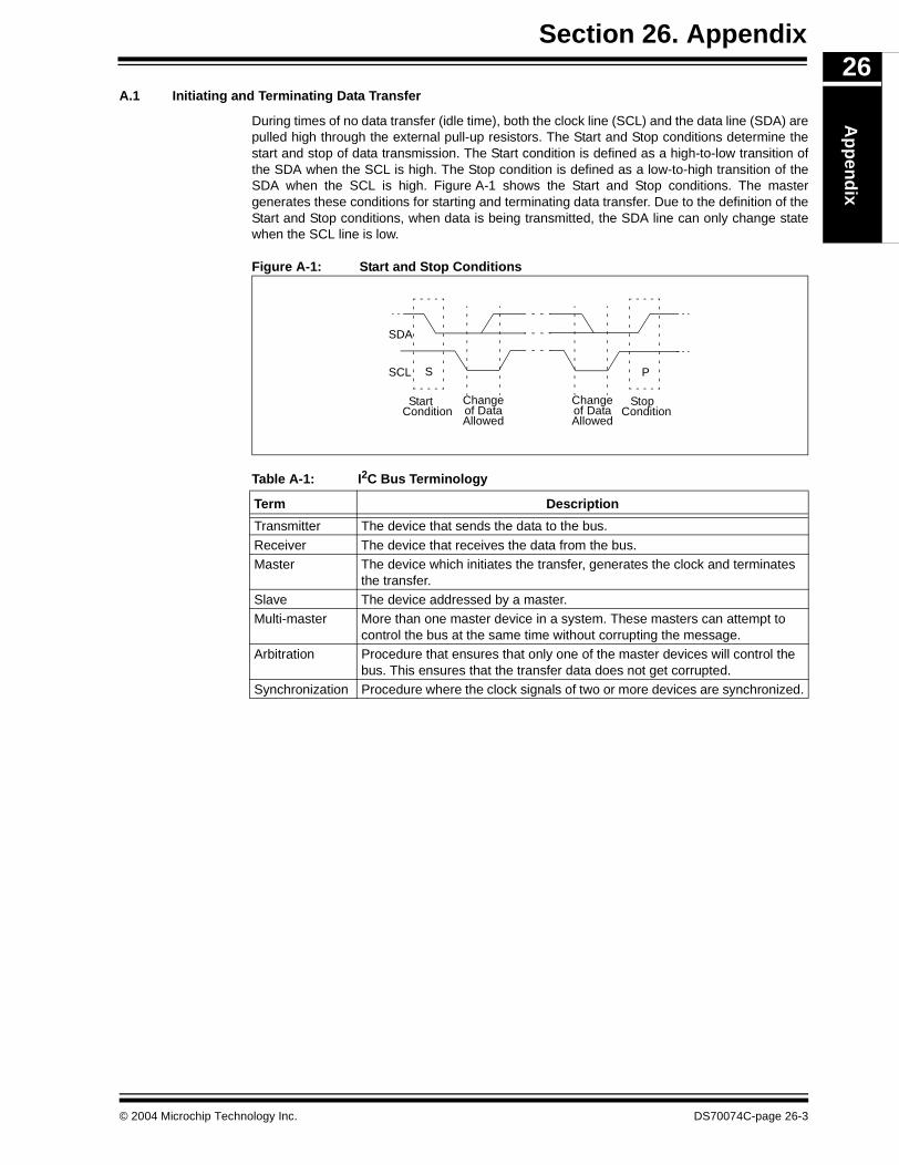
Section 26. AppendixA
pp
end
ix26
A.1 Initiating and Terminating Data Transfer
During times of no data transfer (idle time), both the clock line (SCL) and the data line (SDA) arepulled high through the external pull-up resistors. The Start and Stop conditions determine thestart and stop of data transmission. The Start condition is defined as a high-to-low transition ofthe SDA when the SCL is high. The Stop condition is defined as a low-to-high transition of theSDA when the SCL is high. Figure A-1 shows the Start and Stop conditions. The mastergenerates these conditions for starting and terminating data transfer. Due to the definition of theStart and Stop conditions, when data is being transmitted, the SDA line can only change statewhen the SCL line is low.
Figure A-1: Start and Stop Conditions
Table A-1: I2C Bus Terminology
SDA
SCL S P
StartCondition
Changeof DataAllowed
Changeof DataAllowed
StopCondition
Term Description
Transmitter The device that sends the data to the bus.
Receiver The device that receives the data from the bus.Master The device which initiates the transfer, generates the clock and terminates
the transfer.Slave The device addressed by a master.Multi-master More than one master device in a system. These masters can attempt to
control the bus at the same time without corrupting the message.Arbitration Procedure that ensures that only one of the master devices will control the
bus. This ensures that the transfer data does not get corrupted.Synchronization Procedure where the clock signals of two or more devices are synchronized.
© 2004 Microchip Technology Inc. DS70074C-page 26-3

dsPIC30F Family Reference Manual
A.2 Addressing I2C Devices
There are two address formats. The simplest is the 7-bit address format with a R/W bit(Figure A-2). The more complex is the 10-bit address with a R/W bit (Figure A-3). For 10-bitaddress format, two bytes must be transmitted. The first five bits specify this to be a 10-bitaddress format. The 1st transmitted byte has 5 bits which specify a 10-bit address, the twoMSbs of the address, and the R/W bit. The second byte is the remaining 8 bits of the address.
Figure A-2: 7-bit Address Format
Figure A-3: I2C 10-bit Address Format
S R/W ACK
Sent bySlave
Slave Address
SR/W Read/Write pulse
MSb LSb
Start Condition
ACK Acknowledge
S 1 1 1 1 0 A9 A8 R/W ACK A7 A6 A5 A4 A3 A2 A1 A0 ACK
Sent By Slave
= 0 for writeSR/WACK
- Start Condition- Read/Write Pulse- Acknowledge
DS70074C-page 26-4 © 2004 Microchip Technology Inc.
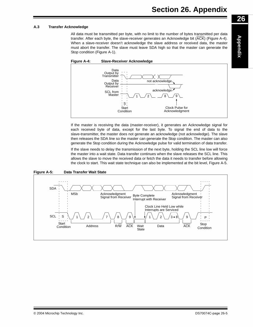
Section 26. AppendixA
pp
end
ix26
A.3 Transfer Acknowledge
All data must be transmitted per byte, with no limit to the number of bytes transmitted per datatransfer. After each byte, the slave-receiver generates an Acknowledge bit (ACK) (Figure A-4).When a slave-receiver doesn’t acknowledge the slave address or received data, the mastermust abort the transfer. The slave must leave SDA high so that the master can generate theStop condition (Figure A-1).
Figure A-4: Slave-Receiver Acknowledge
If the master is receiving the data (master-receiver), it generates an Acknowledge signal foreach received byte of data, except for the last byte. To signal the end of data to theslave-transmitter, the master does not generate an acknowledge (not acknowledge). The slavethen releases the SDA line so the master can generate the Stop condition. The master can alsogenerate the Stop condition during the Acknowledge pulse for valid termination of data transfer.
If the slave needs to delay the transmission of the next byte, holding the SCL line low will forcethe master into a wait state. Data transfer continues when the slave releases the SCL line. Thisallows the slave to move the received data or fetch the data it needs to transfer before allowingthe clock to start. This wait state technique can also be implemented at the bit level, Figure A-5.
Figure A-5: Data Transfer Wait State
S
DataOutput by
TransmitterData
Output byReceiver
SCL fromMaster
Clock Pulse forAcknowledgment
not acknowledge
acknowledge
1 2 8 9
StartCondition
1 2 7 8 9 1 2 3 • 8 9 P
SDA
SCL S
StartCondition Address R/W ACK Wait
StateData ACK
MSb AcknowledgmentSignal from Receiver
AcknowledgmentSignal from ReceiverByte Complete
Interrupt with Receiver
Clock Line Held Low whileInterrupts are Serviced
StopCondition
© 2004 Microchip Technology Inc. DS70074C-page 26-5
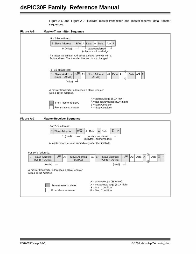
dsPIC30F Family Reference Manual
Figure A-6 and Figure A-7 illustrate master-transmitter and master-receiver data transfersequences.
Figure A-6: Master-Transmitter Sequence
Figure A-7: Master-Receiver Sequence
For 7-bit address:
S
Slave Address(Code + A9:A8)
S R/W A1 Slave Address(A7:A0)
A2 Data A Data P
A master transmitter addresses a slave receiverwith a 10-bit address.
A/A
Slave Address R/W A Data A Data A/A P
'0' (write) data transferred(n bytes - acknowledge)
A master transmitter addresses a slave receiver with a7-bit address. The transfer direction is not changed.
From master to slave
From slave to master
A = acknowledge (SDA low)A = not acknowledge (SDA high)S = Start ConditionP = Stop Condition
(write)
For 10-bit address:
For 7-bit address:
S
Slave Address(Code + A9:A8)
S R/W A1 Slave Address(A7:A0)
A2
A master transmitter addresses a slave receiverwith a 10-bit address.
Slave Address R/W A Data A Data A P
'1' (read) data transferred(n bytes - acknowledge)
A master reads a slave immediately after the first byte.
From master to slave
From slave to master
A = acknowledge (SDA low)A = not acknowledge (SDA high)S = Start ConditionP = Stop Condition
(write)
For 10-bit address:
Slave Address(Code + A9:A8)
Sr R/W A3 AData A PData
(read)
DS70074C-page 26-6 © 2004 Microchip Technology Inc.
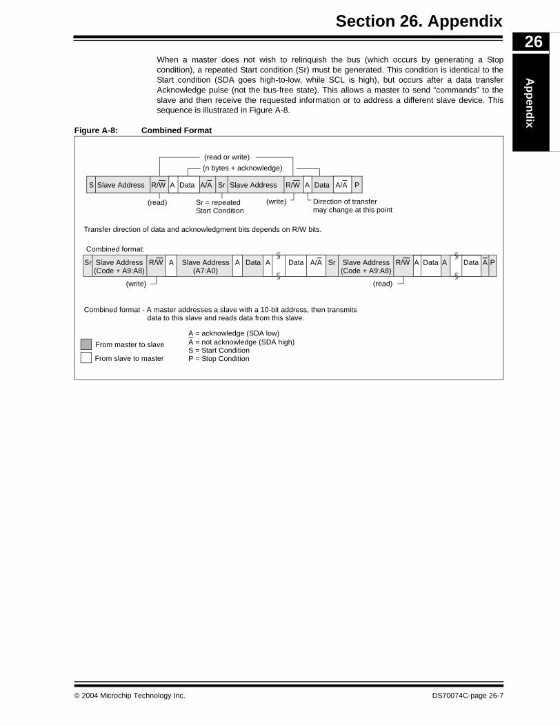
Section 26. AppendixA
pp
end
ix26
When a master does not wish to relinquish the bus (which occurs by generating a Stopcondition), a repeated Start condition (Sr) must be generated. This condition is identical to theStart condition (SDA goes high-to-low, while SCL is high), but occurs after a data transferAcknowledge pulse (not the bus-free state). This allows a master to send “commands” to theslave and then receive the requested information or to address a different slave device. Thissequence is illustrated in Figure A-8.
Figure A-8: Combined Format
Combined format:
S
Combined format - A master addresses a slave with a 10-bit address, then transmits
Slave Address R/W A Data A/A Sr P
(read) Sr = repeated
Transfer direction of data and acknowledgment bits depends on R/W bits.
From master to slave
From slave to master
A = acknowledge (SDA low)A = not acknowledge (SDA high)S = Start ConditionP = Stop Condition
Slave Address(Code + A9:A8)
Sr R/W A
(write)
data to this slave and reads data from this slave.
Slave Address(A7:A0)
Data Sr Slave Address(Code + A9:A8)
R/W A Data A A PA A Data A/A Data
(read)
Slave Address R/W A Data A/A
Start Condition(write) Direction of transfer
may change at this point
(read or write)
(n bytes + acknowledge)
© 2004 Microchip Technology Inc. DS70074C-page 26-7
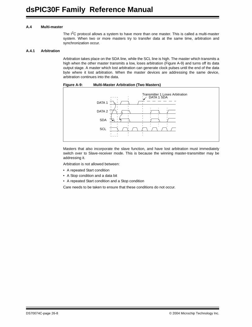
dsPIC30F Family Reference Manual
A.4 Multi-master
The I2C protocol allows a system to have more than one master. This is called a multi-mastersystem. When two or more masters try to transfer data at the same time, arbitration andsynchronization occur.
A.4.1 Arbitration
Arbitration takes place on the SDA line, while the SCL line is high. The master which transmits ahigh when the other master transmits a low, loses arbitration (Figure A-9) and turns off its dataoutput stage. A master which lost arbitration can generate clock pulses until the end of the databyte where it lost arbitration. When the master devices are addressing the same device,arbitration continues into the data.
Figure A-9: Multi-Master Arbitration (Two Masters)
Masters that also incorporate the slave function, and have lost arbitration must immediatelyswitch over to Slave-receiver mode. This is because the winning master-transmitter may beaddressing it.
Arbitration is not allowed between:
• A repeated Start condition
• A Stop condition and a data bit• A repeated Start condition and a Stop condition
Care needs to be taken to ensure that these conditions do not occur.
Transmitter 1 Loses ArbitrationDATA 1 SDA
DATA 1
DATA 2
SDA
SCL
DS70074C-page 26-8 © 2004 Microchip Technology Inc.
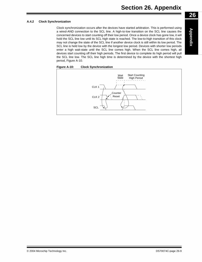
Section 26. AppendixA
pp
end
ix26
A.4.2 Clock Synchronization
Clock synchronization occurs after the devices have started arbitration. This is performed usinga wired-AND connection to the SCL line. A high-to-low transition on the SCL line causes theconcerned devices to start counting off their low period. Once a device clock has gone low, it willhold the SCL line low until its SCL high state is reached. The low-to-high transition of this clockmay not change the state of the SCL line if another device clock is still within its low period. TheSCL line is held low by the device with the longest low period. Devices with shorter low periodsenter a high wait-state until the SCL line comes high. When the SCL line comes high, alldevices start counting off their high periods. The first device to complete its high period will pullthe SCL line low. The SCL line high time is determined by the device with the shortest highperiod, Figure A-10.
Figure A-10: Clock Synchronization
CLK 1
CLK 2
SCL
WaitState
Start CountingHigh Period
CounterReset
© 2004 Microchip Technology Inc. DS70074C-page 26-9
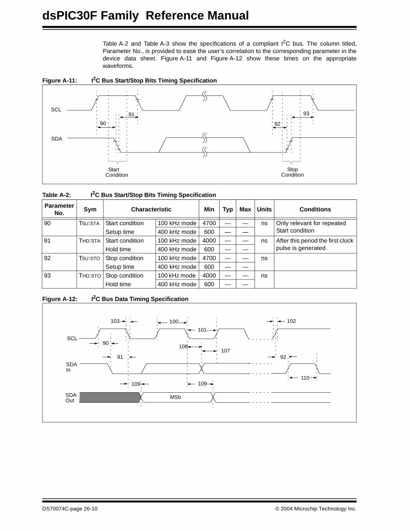
dsPIC30F Family Reference Manual
Table A-2 and Table A-3 show the specifications of a compliant I2C bus. The column titled,Parameter No., is provided to ease the user’s correlation to the corresponding parameter in thedevice data sheet. Figure A-11 and Figure A-12 show these times on the appropriatewaveforms.
Figure A-11: I2C Bus Start/Stop Bits Timing Specification
Table A-2: I2C Bus Start/Stop Bits Timing Specification
Figure A-12: I2C Bus Data Timing Specification
Parameter No.
Sym Characteristic Min Typ Max Units Conditions
90 TSU:STA Start condition 100 kHz mode 4700 — — ns Only relevant for repeated Start conditionSetup time 400 kHz mode 600 — —
91 THD:STA Start condition 100 kHz mode 4000 — — ns After this period the first clock pulse is generatedHold time 400 kHz mode 600 — —
92 TSU:STO Stop condition 100 kHz mode 4700 — — nsSetup time 400 kHz mode 600 — —
93 THD:STO Stop condition 100 kHz mode 4000 — — ns
Hold time 400 kHz mode 600 — —
91 93SCL
SDA
StartCondition
StopCondition
90 92
90
91 92
100
101
103
106107
109 109110
102
SCL
SDAIn
SDAOut
MSb
DS70074C-page 26-10 © 2004 Microchip Technology Inc.
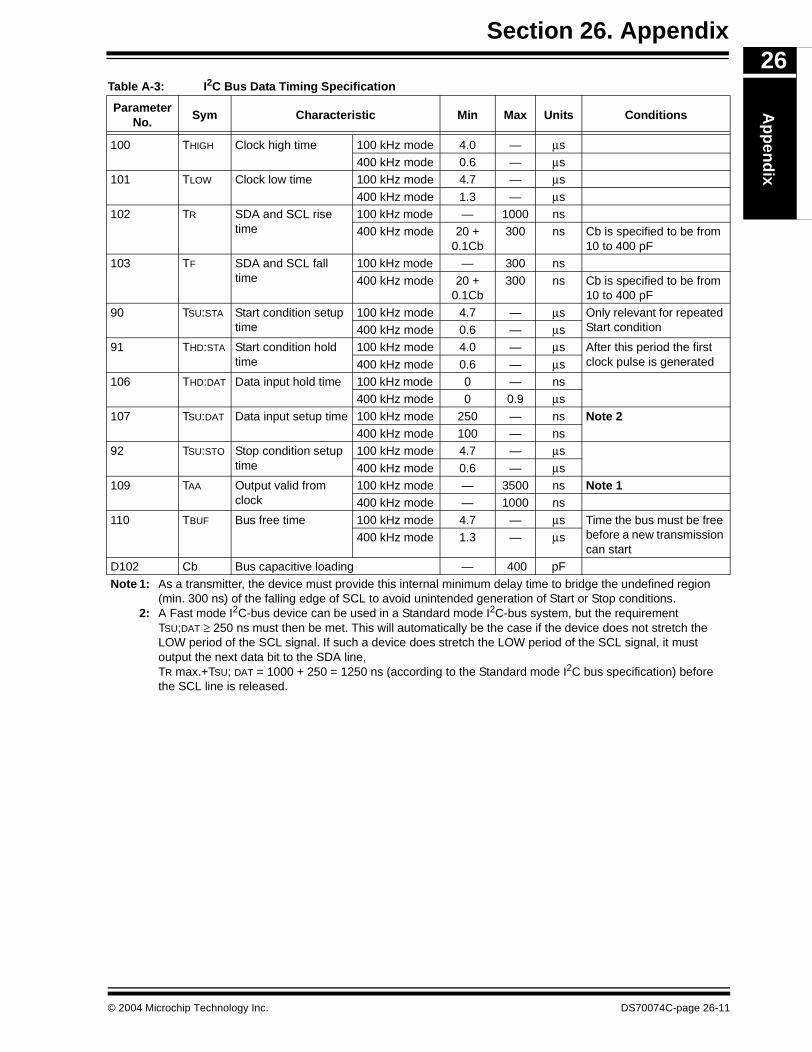
Section 26. AppendixA
pp
end
ix26
Table A-3: I2C Bus Data Timing Specification Parameter
No.Sym Characteristic Min Max Units Conditions
100 THIGH Clock high time 100 kHz mode 4.0 — μs400 kHz mode 0.6 — μs
101 TLOW Clock low time 100 kHz mode 4.7 — μs
400 kHz mode 1.3 — μs102 TR SDA and SCL rise
time100 kHz mode — 1000 ns400 kHz mode 20 +
0.1Cb300 ns Cb is specified to be from
10 to 400 pF 103 TF SDA and SCL fall
time100 kHz mode — 300 ns
400 kHz mode 20 + 0.1Cb
300 ns Cb is specified to be from 10 to 400 pF
90 TSU:STA Start condition setup time
100 kHz mode 4.7 — μs Only relevant for repeated Start condition400 kHz mode 0.6 — μs
91 THD:STA Start condition hold time
100 kHz mode 4.0 — μs After this period the first clock pulse is generated400 kHz mode 0.6 — μs
106 THD:DAT Data input hold time 100 kHz mode 0 — ns400 kHz mode 0 0.9 μs
107 TSU:DAT Data input setup time 100 kHz mode 250 — ns Note 2400 kHz mode 100 — ns
92 TSU:STO Stop condition setup time
100 kHz mode 4.7 — μs
400 kHz mode 0.6 — μs109 TAA Output valid from
clock100 kHz mode — 3500 ns Note 1400 kHz mode — 1000 ns
110 TBUF Bus free time 100 kHz mode 4.7 — μs Time the bus must be free before a new transmission can start
400 kHz mode 1.3 — μs
D102 Cb Bus capacitive loading — 400 pF
Note 1: As a transmitter, the device must provide this internal minimum delay time to bridge the undefined region (min. 300 ns) of the falling edge of SCL to avoid unintended generation of Start or Stop conditions.
2: A Fast mode I2C-bus device can be used in a Standard mode I2C-bus system, but the requirement TSU;DAT ≥ 250 ns must then be met. This will automatically be the case if the device does not stretch the LOW period of the SCL signal. If such a device does stretch the LOW period of the SCL signal, it must output the next data bit to the SDA line, TR max.+TSU; DAT = 1000 + 250 = 1250 ns (according to the Standard mode I2C bus specification) before the SCL line is released.
© 2004 Microchip Technology Inc. DS70074C-page 26-11
dsPIC30F Family Reference Manual
APPENDIX B: CAN OVERVIEWThis appendix provides an overview of the Controller Area Network (CAN) bus. The CANSection of this reference manual discusses the implementation of the CAN protocol for thathardware module.
B.1 CAN Bus Background
The Controller Area Network (CAN) is a serial communications protocol which efficientlysupports distributed real-time control with a very high level of security.
Its domain of application ranges from high speed networks to low cost multiplex wiring. Inautomotive electronics, engine control units, sensors, anti-skid-systems, etc., are connectedusing CAN with bit rates up to 1 Mbit/sec. The silicon cost is also low enough to be cost effectiveat replacing wiring harnesses in the automobile. The robustness of the bus in noisyenvironments and the ability to detect and recover from fault conditions makes the bus suitablefor industrial control applications such as DeviceNet, SDS and other field bus protocols.
CAN is an asynchronous serial bus system with one logical bus line. It has an open, linear busstructure with equal bus nodes. A CAN bus consists of two or more nodes. The number ofnodes on the bus may be changed dynamically without disturbing the communication of othernodes. This allows easy connection and disconnection of bus nodes (e.g., for addition of systemfunction, error recovery or bus monitoring).
The bus logic corresponds to a “wired-AND” mechanism, “recessive” bits (mostly, but notnecessarily equivalent to the logic level “1”) are overwritten by “dominant” bits (mostly logic level“0”). As long as no bus node is sending a dominant bit, the bus line is in the recessive state, buta dominant bit from any bus node generates the dominant bus state. Therefore, for the CANbus line, a medium must be chosen that is able to transmit the two possible bit states (dominantand recessive). One of the most common and cheapest ways is to use a twisted wire pair. Thebus lines are then called “CANH” and “CANL”, and may be connected directly to the nodes orvia a connector. There's no standard defined by CAN regarding the connector to be used. Thetwisted wire pair is terminated by terminating resistors at each end of the bus line. Themaximum bus speed is 1 Mbit, which can be achieved with a bus length of up to 40 meters. Forbus lengths longer than 40 meters, the bus speed must be reduced (a 1000 m bus can berealized with a 40 Kbit bus speed). For a bus length above 1000 meters, special drivers shouldbe used. At least 20 nodes may be connected without additional equipment. Due to thedifferential nature of transmission, CAN is insensitive to EMI because both bus lines areaffected in the same way which leaves the differential signal unaffected. The bus lines can alsobe shielded to reduce the electromagnetic emission of the bus itself, especially at high baudrates.
The binary data is coded corresponding to the NRZ code (Non-Return-to-Zero; low level =dominant state; high level = recessive state). To ensure exact synchronization of all bus nodes,bit stuffing is used. This means that during the transmission of a message a maximum of fiveconsecutive bits may have the same polarity. Whenever five consecutive bits of the samepolarity have been transmitted, the transmitter will insert one additional bit of the oppositepolarity into the bit stream before transmitting further bits. The receiver also checks the numberof bits with the same polarity and removes the stuff bits from the bit stream (-destuffing).
In the CAN protocol it is not bus nodes that are addressed, but the address information iscontained in the messages that are transmitted. This is done via an identifier (part of eachmessage) which identifies the message content (e.g., engine speed, oil temperature etc.). Theidentifier additionally indicates the priority of the message. The lower the binary value of theidentifier, the higher the priority of the message.
DS70074C-page 26-12 © 2004 Microchip Technology Inc.
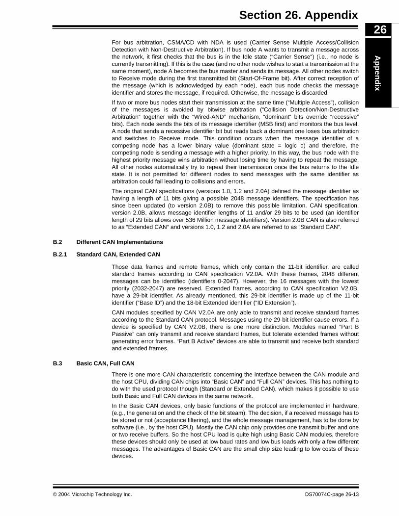
Section 26. AppendixA
pp
end
ix26
For bus arbitration, CSMA/CD with NDA is used (Carrier Sense Multiple Access/CollisionDetection with Non-Destructive Arbitration). If bus node A wants to transmit a message acrossthe network, it first checks that the bus is in the Idle state (“Carrier Sense“) (i.e., no node iscurrently transmitting). If this is the case (and no other node wishes to start a transmission at thesame moment), node A becomes the bus master and sends its message. All other nodes switchto Receive mode during the first transmitted bit (Start-Of-Frame bit). After correct reception ofthe message (which is acknowledged by each node), each bus node checks the messageidentifier and stores the message, if required. Otherwise, the message is discarded.
If two or more bus nodes start their transmission at the same time (“Multiple Access”), collisionof the messages is avoided by bitwise arbitration (“Collision Detection/Non-DestructiveArbitration“ together with the “Wired-AND” mechanism, “dominant“ bits override “recessive”bits). Each node sends the bits of its message identifier (MSB first) and monitors the bus level.A node that sends a recessive identifier bit but reads back a dominant one loses bus arbitrationand switches to Receive mode. This condition occurs when the message identifier of acompeting node has a lower binary value (dominant state = logic 0) and therefore, thecompeting node is sending a message with a higher priority. In this way, the bus node with thehighest priority message wins arbitration without losing time by having to repeat the message.All other nodes automatically try to repeat their transmission once the bus returns to the Idlestate. It is not permitted for different nodes to send messages with the same identifier asarbitration could fail leading to collisions and errors.
The original CAN specifications (versions 1.0, 1.2 and 2.0A) defined the message identifier ashaving a length of 11 bits giving a possible 2048 message identifiers. The specification hassince been updated (to version 2.0B) to remove this possible limitation. CAN specification,version 2.0B, allows message identifier lengths of 11 and/or 29 bits to be used (an identifierlength of 29 bits allows over 536 Million message identifiers). Version 2.0B CAN is also referredto as “Extended CAN“ and versions 1.0, 1.2 and 2.0A are referred to as “Standard CAN”.
B.2 Different CAN Implementations
B.2.1 Standard CAN, Extended CAN
Those data frames and remote frames, which only contain the 11-bit identifier, are calledstandard frames according to CAN specification V2.0A. With these frames, 2048 differentmessages can be identified (identifiers 0-2047). However, the 16 messages with the lowestpriority (2032-2047) are reserved. Extended frames, according to CAN specification V2.0B,have a 29-bit identifier. As already mentioned, this 29-bit identifier is made up of the 11-bitidentifier (“Base lD”) and the 18-bit Extended identifier (“ID Extension”).
CAN modules specified by CAN V2.0A are only able to transmit and receive standard framesaccording to the Standard CAN protocol. Messages using the 29-bit identifier cause errors. If adevice is specified by CAN V2.0B, there is one more distinction. Modules named “Part BPassive” can only transmit and receive standard frames, but tolerate extended frames withoutgenerating error frames. “Part B Active” devices are able to transmit and receive both standardand extended frames.
B.3 Basic CAN, Full CAN
There is one more CAN characteristic concerning the interface between the CAN module andthe host CPU, dividing CAN chips into “Basic CAN” and “Full CAN” devices. This has nothing todo with the used protocol though (Standard or Extended CAN), which makes it possible to useboth Basic and Full CAN devices in the same network.
In the Basic CAN devices, only basic functions of the protocol are implemented in hardware,(e.g., the generation and the check of the bit steam). The decision, if a received message has tobe stored or not (acceptance filtering), and the whole message management, has to be done bysoftware (i.e., by the host CPU). Mostly the CAN chip only provides one transmit buffer and oneor two receive buffers. So the host CPU load is quite high using Basic CAN modules, thereforethese devices should only be used at low baud rates and low bus loads with only a few differentmessages. The advantages of Basic CAN are the small chip size leading to low costs of thesedevices.
© 2004 Microchip Technology Inc. DS70074C-page 26-13
dsPIC30F Family Reference Manual
Full CAN devices do the whole bus protocol in hardware, including the acceptance filtering andthe message management. They contain several so called message objects which handle theidentifier, the data, the direction (receive or transmit) and the information StandardCAN/Extended CAN. During the initialization of the device, the host CPU defines whichmessages are to be sent and which are to be received. The host CPU is informed by interrupt ifthe identifier of a received message matches with one of the programmed (receive-) messageobjects. In this way. the CPU load is reduced. Using Full CAN devices, high baud rates and highbus loads with many messages can be handled. These chips are more expensive than theBasic CAN devices, though.
Many Full CAN chips provide a “Basic-CAN Feature”. One of their messages objects can beprogrammed in a way that every message is stored there that does not match with one of theother message objects. This can be very helpful in a number of applications.
B.4 ISO Model
The lSO/OSl Reference Model is used to define the layers of protocol of a communicationsystem, as shown in Figure B-1. At the highest end, the applications need to communicatebetween each other. At the lowest end, some physical medium is used to provide electricalsignaling.
The higher levels of the protocol are run by software. Typically, only the application layer isimplemented. Within the CAN bus specification, there is no definition of the type of message orthe contents or meaning of the messages transferred. These definitions are made in systemssuch as Volcano, the Volvo automotive CAN specification; J1939, the U.S. heavy truck multiplexwiring spec; and Allen-Bradly DeviceNet and Honeywell SDS, examples of industrial protocols.
The CAN bus module definition encompasses two levels of the overall protocol.
• The Data Link Layer- The Logical Link Control (LLC) sub-layer- The Medium Access Control (MAC) sub-layer
• - The Physical Layer- The Physical Signaling (PLS) sub-layer
The LLC sub layer is concerned with Message Filtering, Overload Notification and ErrorRecovery Management. The scope of the LLC sub-layer is:
• To provide services for data transfer and for remote data request• To decide which messages received by the LLC sub layer are actually to be accepted• To provide means for error recovery management and overload notifications
The MAC sub-layer represents the kernel of the CAN protocol. The MAC sub-layer defines thetransfer protocol (i.e., controlling the Framing, Performing Arbitration, Error Checking, ErrorSignalling and Fault Confinement). It presents messages received from the LLC sub-layer andaccepts messages to be transmitted to the LLC sub-layer. Within the MAC sub-layer, it isdecided whether the bus is free for starting a new transmission or whether a reception is juststarting. The MAC sub-layer is supervised by a management entity called Fault Confinement,which is a self-checking mechanism for distinguishing short disturbances from permanentfailures. Also, some general features of the bit timing are regarded as part of the MACsub-layer.
The physical layer defines the actual transfer of the bits between the different nodes withrespect to all electrical properties. The PLS sub-layer defines how signals are actuallytransmitted and therefore deals with the description of Bit Timing, Bit Encoding andSynchronization.
The lower levels of the protocol are implemented in driver/receiver chips and the actualinterface, such as twisted pair wiring or optical fiber etc. Within one network, the physical layerhas to be the same for all nodes. The Driver/Receiver Characteristics of the Physical Layer arenot defined so as to allow transmission medium and signal level implementations to beoptimized for their application. The most common example is defined in the ISO11898 RoadVehicles Multiplex Wiring specification.
DS70074C-page 26-14 © 2004 Microchip Technology Inc.
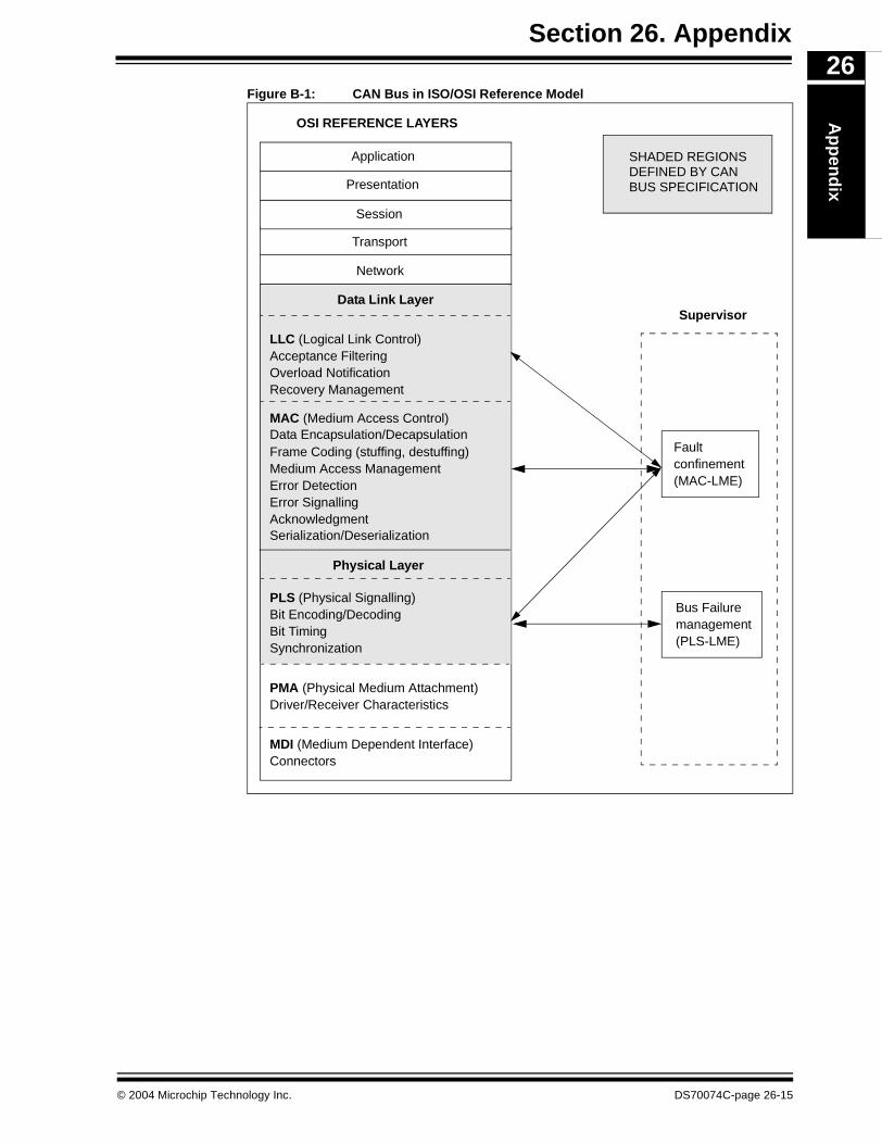
Section 26. AppendixA
pp
end
ix26
Figure B-1: CAN Bus in ISO/OSI Reference Model
OSI REFERENCE LAYERS
Application
Presentation
Session
Transport
Network
Data Link Layer
LLC (Logical Link Control)Acceptance FilteringOverload NotificationRecovery Management
MAC (Medium Access Control)Data Encapsulation/DecapsulationFrame Coding (stuffing, destuffing)Medium Access ManagementError DetectionError SignallingAcknowledgmentSerialization/Deserialization
PLS (Physical Signalling)Bit Encoding/DecodingBit TimingSynchronization
PMA (Physical Medium Attachment)Driver/Receiver Characteristics
MDI (Medium Dependent Interface)Connectors
Faultconfinement(MAC-LME)
Bus Failuremanagement(PLS-LME)
Supervisor
SHADED REGIONSDEFINED BY CAN BUS SPECIFICATION
Physical Layer
© 2004 Microchip Technology Inc. DS70074C-page 26-15
dsPIC30F Family Reference Manual
B.5 CAN Bus Features
CAN has the following properties:
• Prioritization of messages• Latency times ensured• Configuration flexibility
• Multi-cast reception with time synchronization• System wide data consistency• Multi-master
• Error detection and signaling• Automatic retransmission of corrupted messages• Distinction between temporary errors and permanent failures of nodes and autonomous
switching off of defect nodes1. Messages – information on the bus is sent in fixed format messages of different but limited
length. When the bus is free any connected unit may start to transmit a new message.2. Information Routing – In CAN systems, a CAN node does not make use of any information
about the system configuration (e.g., station addresses). 3. System Flexibility – Nodes can be added to the CAN network without requiring any
change in the software or hardware of any node and application layer.4. Message Routing – The content of a message is named by an ldentifier. The ldentifier
does not indicate the destination of the message, but describes the meaning of the data,so that all nodes in the network are able to decide by Message Filtering whether the datais to be acted upon by them or not.
5. Multicast – As a consequence of the concept of Message Filtering, any number of nodescan receive and simultaneously act upon the same message.
6. Data Consistency – Within a CAN network, it is ensured that a message is simultaneouslyaccepted either by all nodes or by no node. Thus, data consistency of a system isachieved by the concepts of multicast and by error handling.
7. Bit Rate – The speed of CAN may be different in different systems. However, in a givensystem, the bit-rate is uniform and fixed.
8. Prioritization – The ldentifier defines a static message priority during bus access.
9. Remote Data Request – By sending a remote frame, a node requiring data may requestanother node to send the corresponding data frame. The date frame and thecorresponding remote frame are named by the same ldentifier.
10. Multimaster – When the bus is free, any unit may start to transmit a message. The unitwith the message of higher priority to be transmitted gains bus access.
11. Arbitration – Whenever the bus is free, any unit may start to transmit a message. If 2 ormore units start transmitting messages at the same time, the bus access conflict isresolved by bitwise arbitration using the ldentifier. The mechanism of arbitration ensuresthat neither information nor time is lost. If a data frame and a remote frame with the sameldentifier are initiated at the same time, the data frame prevails over the remote frame.During arbitration, every transmitter compares the level of the bit transmitted with the levelthat is monitored on the bus. If these levels are equal, the unit may continue to send.When a ’recessive’ level is sent and a ’dominant’ level is monitored, the unit has lostarbitration and must withdraw without sending one more bit.
12. Safety – In order to achieve the highest safety of data transfer, powerful measures forerror detection, signaling and self-checking are implemented in every CAN node.
13. Error Detection – For detecting errors the following measures have been taken:• Monitoring (transmitters compare the bit levels to be transmitted with the bit levels
detected on the bus)• Cyclic Redundancy Check
• Bit Stuffing• Message Frame Check
DS70074C-page 26-16 © 2004 Microchip Technology Inc.
Section 26. AppendixA
pp
end
ix26
The error detection mechanisms have the following properties:
• all global errors are detected• all local errors at transmitters are detected
• up to 5 randomly distributed errors in a message are detected• burst errors of length less than 15 in a message are detected• errors of any odd number in a message are detected
14. Error Signalling and Recovery Time – Corrupted messages are flagged by any nodedetecting an error. Such messages are aborted and will be retransmitted automatically.The recovery time from detecting an error until the start of the next message is at most 31bit times, if there is no further error.
15. Fault Confinement – CAN nodes are able to distinguish short disturbances frompermanent failures. Defective nodes are switched off.
16. Connections – The CAN serial communication link is a bus to which a number of units maybe connected. This number has no theoretical limit. Practically the total number of unitswill be limited by delay times and/or electrical loads on the bus line.
17. Single Channel – The bus consists of a single channel that carries bits. From this dataresynchronization, information can be derived. The way in which this channel isimplemented is not fixed in this specification (i.e., single wire (plus ground), two differentialwires, optical fires, etc).
18. Bus values – The bus can have one of two complementary logical values; ‘dominant’ or‘recessive’. During simultaneous transmission of ‘dominant’ and ‘recessive’ bits, theresulting bus value will be ‘dominant’. For example, in case of a wired-ANDimplementation of the bus, the ‘dominant’ level would be represented by a logical ‘0’ andthe ‘recessive’ level by a logical ‘1’. Physical states (e.g., electrical voltage, light) thatrepresent the logical levels are not given in the specification.
19. Acknowledgment – All receivers check the consistency of the message being receivedand will acknowledge a consistent message and flag an inconsistent message.
20. Sleep Mode; Wake-up – To reduce the system's power consumption, a CAN device maybe set into Sleep mode without any internal activity and with disconnected bus drivers.The Sleep mode is finished with a wake-up by any bus activity or by internal conditions ofthe system. On wake-up, the internal activity is restarted, although the MAC sub-layer willbe waiting for the system's oscillator to stabilize and it will then wait until it hassynchronized itself to the bus activity (by checking for eleven consecutive ‘recessive’ bits),before the bus drivers are set to “on-bus” again.
© 2004 Microchip Technology Inc. DS70074C-page 26-17

dsPIC30F Family Reference Manual
B.6 Frame Types
B.6.1 Standard Data Frame
A data frame is generated by a node when the node wishes to transmit data. The Standard CANData Frame is shown in Figure B-2. In common with all other frames, the frame begins with aStart-Of-Frame bit (SOF – dominant state) for hard synchronization of all nodes.
The SOF is followed by the Arbitration field consisting of 12 bits, the 11-bit ldentifier (reflectingthe contents and priority of the message) and the RTR bit (Remote Transmission Request bit).The RTR bit is used to distinguish a data frame (RTR – dominant) from a remote frame.
The next field is the Control field, consisting of 6 bits. The first bit of this field is called the lDE bit(Identifier Extension) and is at dominant state to specify that the frame is a standard frame. Thefollowing bit is reserved, RB0, and defined as a dominant bit. The remaining 4 bits of the Controlfield are the Data Length Code (DLC) and specify the number of bytes of data contained in themessage.
The data being sent follows in the Data field, which is of the length defined by the DLC above(1-8 bytes).
The Cyclic Redundancy field (CRC) follows and is used to detect possible transmission errors.The CRC field consists of a 15-bit CRC sequence, completed by the recessive CRC Delimiterbit.
The final field is the Acknowledge field. During the ACK Slot bit, the transmitting node sends outa recessive bit. Any node that has received an error free frame acknowledges the correctreception of the frame by sending back a dominant bit (regardless of whether the node isconfigured to accept that specific message or not). From this, it can be seen that CAN belongsto the “in-bit-response” group of protocols. The recessive Acknowledge Delimiter completes theAcknowledge slot and may not be overwritten by a dominant bit.
B.7 Extended Data Frame
In the Extended CAN Data frame, shown in Figure B-3, the Start-Of-Frame bit (SOF) is followedby the Arbitration field consisting of 38 bits. The first 11 bits are the 11 most significant bits of the29-bit identifier (“Base-lD”). These 11 bits are followed by the Substitute Remote Request bit,SRR, which is transmitted as recessive. The SRR is followed by the lDE bit, which is recessiveto denote that the frame is an extended CAN frame. It should be noted from this, that ifarbitration remains unresolved after transmission of the first 11 bits of the identifier, and one ofthe nodes involved in arbitration is sending a standard CAN frame (11-bit identifier), then thestandard CAN frame will win arbitration due to the assertion of a dominant lDE bit. Also, theSRR bit in an extended CAN frame must be recessive to allow the assertion of a dominant RTRbit by a node that is sending a standard CAN remote frame. The SRR and lDE bits are followedby the remaining 18 bits of the identifier (“lD-Extension”) and the Remote Transmission Requestbit.
To enable standard and extended frames to be sent across a shared network, it is necessary tosplit the 29-bit extended message identifier into 11-bit (most significant) and 18-bit (leastsignificant) sections. This split ensures that the Identifier Extension bit (lDE) can remain at thesame bit position in both standard and extended frames.
The next field is the Control field, consisting of 6 bits. The first 2 bits of this field are reservedand are at dominant state. The remaining 4 bits of the Control field are the Data Length Code(DLC) and specify the number of data bytes.
The remaining portion of the frame (Data field, CRC field, Acknowledge field, End-Of-Frameand lntermission) is constructed in the same way as for a standard data frame.
DS70074C-page 26-18 © 2004 Microchip Technology Inc.
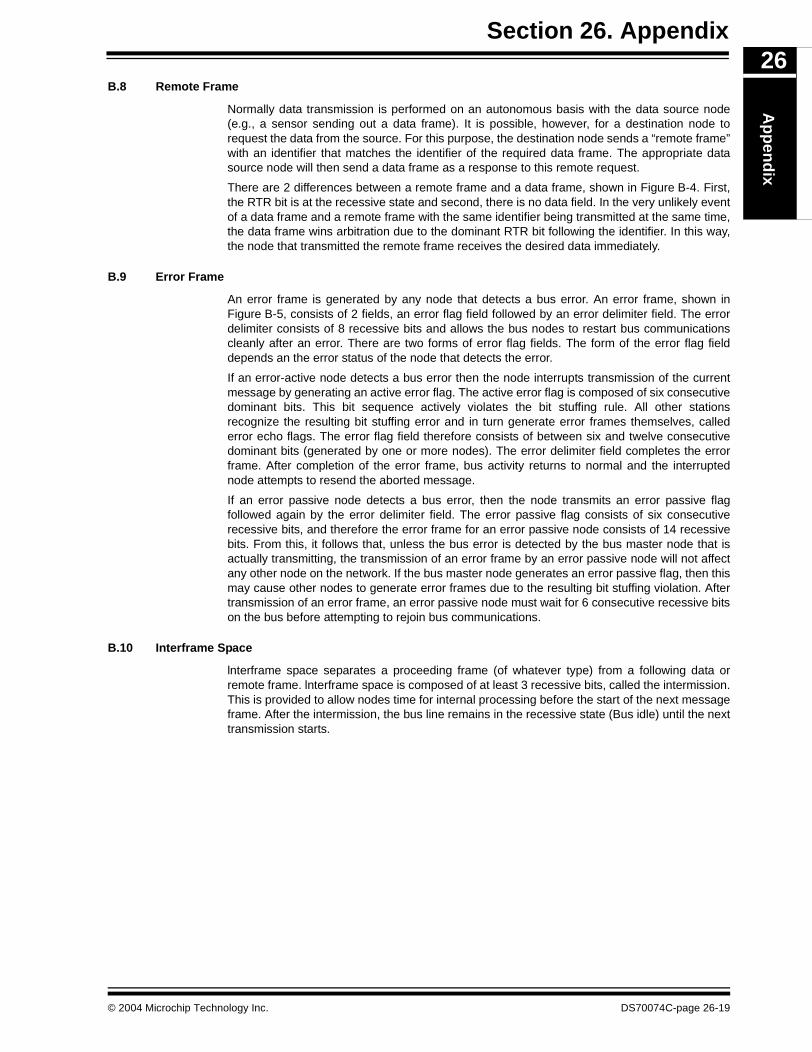
Section 26. AppendixA
pp
end
ix26
B.8 Remote Frame
Normally data transmission is performed on an autonomous basis with the data source node(e.g., a sensor sending out a data frame). It is possible, however, for a destination node torequest the data from the source. For this purpose, the destination node sends a “remote frame”with an identifier that matches the identifier of the required data frame. The appropriate datasource node will then send a data frame as a response to this remote request.
There are 2 differences between a remote frame and a data frame, shown in Figure B-4. First,the RTR bit is at the recessive state and second, there is no data field. In the very unlikely eventof a data frame and a remote frame with the same identifier being transmitted at the same time,the data frame wins arbitration due to the dominant RTR bit following the identifier. In this way,the node that transmitted the remote frame receives the desired data immediately.
B.9 Error Frame
An error frame is generated by any node that detects a bus error. An error frame, shown inFigure B-5, consists of 2 fields, an error flag field followed by an error delimiter field. The errordelimiter consists of 8 recessive bits and allows the bus nodes to restart bus communicationscleanly after an error. There are two forms of error flag fields. The form of the error flag fielddepends an the error status of the node that detects the error.
If an error-active node detects a bus error then the node interrupts transmission of the currentmessage by generating an active error flag. The active error flag is composed of six consecutivedominant bits. This bit sequence actively violates the bit stuffing rule. All other stationsrecognize the resulting bit stuffing error and in turn generate error frames themselves, callederror echo flags. The error flag field therefore consists of between six and twelve consecutivedominant bits (generated by one or more nodes). The error delimiter field completes the errorframe. After completion of the error frame, bus activity returns to normal and the interruptednode attempts to resend the aborted message.
If an error passive node detects a bus error, then the node transmits an error passive flagfollowed again by the error delimiter field. The error passive flag consists of six consecutiverecessive bits, and therefore the error frame for an error passive node consists of 14 recessivebits. From this, it follows that, unless the bus error is detected by the bus master node that isactually transmitting, the transmission of an error frame by an error passive node will not affectany other node on the network. If the bus master node generates an error passive flag, then thismay cause other nodes to generate error frames due to the resulting bit stuffing violation. Aftertransmission of an error frame, an error passive node must wait for 6 consecutive recessive bitson the bus before attempting to rejoin bus communications.
B.10 Interframe Space
lnterframe space separates a proceeding frame (of whatever type) from a following data orremote frame. lnterframe space is composed of at least 3 recessive bits, called the intermission.This is provided to allow nodes time for internal processing before the start of the next messageframe. After the intermission, the bus line remains in the recessive state (Bus idle) until the nexttransmission starts.
© 2004 Microchip Technology Inc. DS70074C-page 26-19
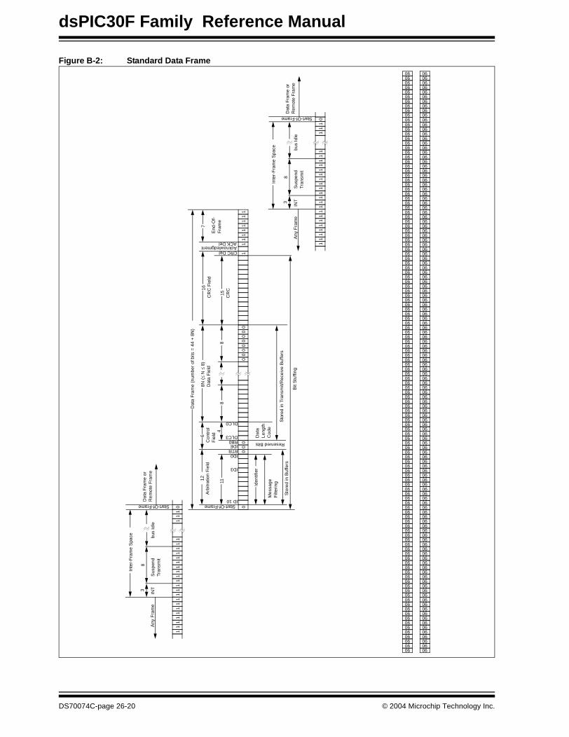
dsPIC30F Family Reference Manual
Figure B-2: Standard Data Frame
90909090909090909090909090909090909090909090909090909090909090909090909090909090909090909090909090909090909090909090909090909090909090909090909090909090909090909090909090909090909090909090909090909090909090909090909090909090909090
11
11
11
11
11
11
11
11
11
11
11
11
0
INT
Sus
pend
Tra
nsm
itbu
s Id
leA
ny F
ram
e
Inte
r-F
ram
e S
pace
Start-Of-Frame
Da
ta F
ram
e or
Re
mot
e F
ram
e
38
00
00
00
00
00
00
11
11
11
11
1
Start-Of-Frame
Dat
a F
ram
e (n
um
ber
of b
its =
44
+ 8
N)
12A
rbitr
atio
n F
ield
ID 10
11
ID3
ID0
Iden
tifie
r
Mes
sage
Filt
erin
g
Sto
red
in B
uffe
rsRTRIDERB0DLC3
DLC0
6
4
Con
trol
Fie
ld Da
taL
engt
hC
ode
Reserved Bits
8N (
≤ N
≤ 8
)D
ata
Fie
ld
88
Sto
red
in T
rans
mit/
Rec
eive
Buf
fers
Bit
Stu
ffin
g
16C
RC
Fie
ld
15 CR
C
7
End
-Of-
Fra
me
CRC DelAcknowledgmentACK Del 1
11
11
11
11
11
11
11
11
11
11
11
10
INT
Sus
pend
Tra
nsm
itb
us I
dle
Any
Fra
me
Inte
r-F
ram
e S
pace
Start-Of-Frame
Dat
a F
ram
e or
Rem
ote
Fra
me
38
9090909090909090909090
909090909090909090909090909090909090909090909090909090909090909090909090909090909090909090909090909090909090909090909090909090909090909090909090909090909090909090909090909090909090909090909090909090909090909090909090909090909090909090909090909090909090
DS70074C-page 26-20 © 2004 Microchip Technology Inc.

Section 26. AppendixA
pp
end
ix26
Figure B-3: Extended Data Format
11
11
10
bus
Idle
Start-Of-Frame
Dat
a F
ram
e or
Rem
ote
Fra
me
00
10
00
00
00
00
00
00
00
00
00
00
00
00
01
Start-Of-Frame
Arb
itrat
ion
Fie
ld
32
11
ID10
ID3
ID0
IDE
Iden
tifie
r
Mes
sage
Filt
erin
g
Sto
red
in B
uffe
rs
SRR
EID17
EID0RTRRB1RB0DLC3
18
DLC0
6C
ontr
olF
ield
4
Reserved bits
Dat
aLe
ngt
hC
ode
Sto
red
in T
rans
mit/
Rec
eiv
e B
uffe
rs
88
Dat
a F
ram
e (
num
ber
of b
its =
64
+ 8
N)
8N (
≤ N
≤ 8
)D
ata
Fie
ld
11
11
11
11
16C
RC
Fie
ld
15 CR
C
CRC DelAcknowledgmentACK Del
End
-Of-
Fra
me
7
Bit
Stu
ffing
11
11
11
11
11
11
11
11
11
11
11
11
0
INT
Sus
pen
dT
rans
mit
bus
Idle
Any
Fra
me
Inte
r-F
ram
e S
pace
Start-Of-Frame
Dat
a F
ram
e o
rR
emot
e F
ram
e
38
909090909090909090909090909090909090909090909090909090909090909090909090909090909090909090909090909090909090909090909090909090909090909090909090909090909090909090909090909090909090909090909090909090909090909090909090909090909090909090909090909090909090
909090909090909090909090909090909090909090909090909090909090909090909090909090909090909090909090909090909090909090909090909090909090909090909090909090909090909090909090909090909090909090909090909090909090909090909090909090909090909090909090909090909090
Ext
ende
d Id
ent
ifier
© 2004 Microchip Technology Inc. DS70074C-page 26-21
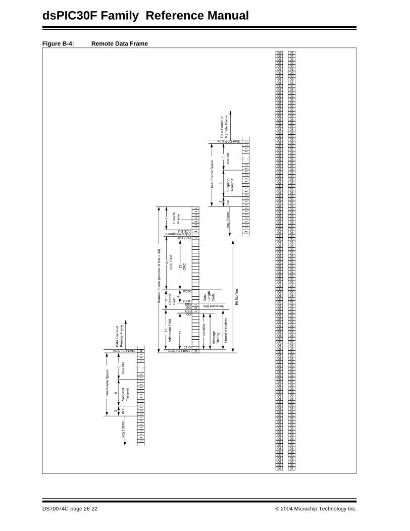
dsPIC30F Family Reference Manual
Figure B-4: Remote Data Frame
Ide
ntifi
er
Mes
sage
Filt
erin
g
Sto
red
in B
uffe
rs
Dat
aL
engt
hC
ode
Reserved Bits Bit
Stu
ffin
g
11
11
11
11
11
11
11
11
11
11
11
11
0
INT
Sus
pend
Tra
nsm
itbu
s Id
leA
ny F
ram
e
Inte
r-F
ram
e S
pace
Start-Of-Frame
Dat
a F
ram
e or
Rem
ote
Fra
me
38
01
00
11
11
11
11
1
Start-Of-Frame
Rem
ote
Fra
me
(num
ber
of b
its =
44)
12A
rbitr
atio
n F
ield
ID 1011
ID0RTRIDERB0DLC3
DLC0
6
4
Con
trol
Fie
ld
16
CR
C F
ield
15 CR
C
7
End
-Of-
Fra
me
CRC DelAcknowledgmentACK Del
11
11
11
11
11
11
11
11
11
11
11
11
0
INT
Sus
pend
Tra
nsm
itbu
s Id
leA
ny F
ram
e
Inte
r-F
ram
e S
pace
Start-Of-Frame
Da
ta F
ram
e or
Re
mot
e F
ram
e
38
909090909090909090909090909090909090909090909090909090909090909090909090909090909090909090909090909090909090909090909090909090909090909090909090909090909090909090909090909090909090909090909090909090909090909090909090909090909090909090909090909090909090
909090909090909090909090909090909090909090909090909090909090909090909090909090909090909090909090909090909090909090909090909090909090909090909090909090909090909090909090909090909090909090909090909090909090909090909090909090909090909090909090909090909090
DS70074C-page 26-22 © 2004 Microchip Technology Inc.
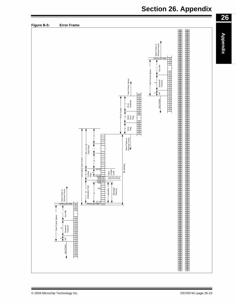
Section 26. AppendixA
pp
end
ix26
Figure B-5: Error Frame
11
11
11
11
11
11
11
11
11
11
11
11
0
INT
Sus
pen
dTr
ansm
itbu
s Id
leA
ny F
ram
e
Inte
r-F
ram
e S
pace
Start-Of-Frame
Dat
a F
ram
e o
rR
emo
te F
ram
e
38
00
00
Start-Of-Frame
Inte
rrup
ted
Dat
a F
ram
e
12A
rbitr
atio
n F
ield
ID 10
11
ID3
ID0
Iden
tifie
r
Me
ssag
eF
ilter
ing
RTRIDERB0DLC3
DLC0
6
4
Co
ntro
lF
ield Dat
aLe
ngth
Cod
e
Reserved Bits
8N (
≤ N
≤ 8
)D
ata
Fie
ld
88
Bit
Stu
ffing
11
11
11
11
11
11
11
11
11
11
11
11
0
INT
Sus
pend
Tra
nsm
itbu
s Id
leA
ny F
ram
e
Inte
r-F
ram
e S
pace
Start-Of-Frame
Dat
a F
ram
e or
Rem
ote
Fra
me
38
00
00
00
00
01
11
11
11
10
Dat
a F
ram
e o
rR
emot
e F
ram
e
Err
or F
ram
e
6
Err
orF
lag
≤ 6
Ech
oE
rror
Fla
g
8
Err
orD
elim
iter
Inte
r-F
ram
e S
pace
909090909090909090909090909090909090909090909090909090909090909090909090909090909090909090909090909090909090909090909090909090909090909090909090909090909090909090909090909090909090909090909090909090909090909090909090909090909090909090909090909090909090
909090909090909090909090909090909090909090909090909090909090909090909090909090909090909090909090909090909090909090909090909090909090909090909090909090909090909090909090909090909090909090909090909090909090909090909090909090909090909090909090909090909090
© 2004 Microchip Technology Inc. DS70074C-page 26-23
dsPIC30F Family Reference Manual
B.11 Referenced Documents
TitleDocument
Road Vehicles; Interchange of Digital Information, Controller Area Network ISO11898Bosch CAN Specification Version 2.0
DS70074C-page 26-24 © 2004 Microchip Technology Inc.
Section 26. AppendixA
pp
end
ix26
APPENDIX C: CODEC PROTOCOL OVERVIEWThis appendix summarizes audio coder/decoder (codec) protocols for Inter-IC Sound (I2S) andAC-Link Compliant mode interfaces. Many codecs intended for use in audio applicationssupport sampling rates between 8 kHz and 48 kHz and typically use one of the interfaceprotocols previously mentioned. The Data Converter Interface (DCI) module automaticallyhandles the interface timing associated with these codecs. No overhead from the CPU isrequired until the requested amount of data has been transmitted and/or received by the DCI.Up to four data words may be transferred between CPU interrupts.
C.1 I2S Protocol Description
Inter-IC Sound (I2S) is a simple, three-wire bus interface used for the transfer of digital audiodata between the following devices:
• DSP processors• A/D and D/A converters
• Digital input/output interfaces
This Appendix information is intended to supplement the I2S Protocol Specification®, which ispublished by Philips, Inc.
The I2S bus is a time division multiplexed and transfers two channels of data. These two datachannels are typically the left and right channels of a digital audio stream.
The I2S bus has the following connection pins:
• SCK: The I2S serial clock line • SDx: The I2S serial data line (input or output)
• WS: The I2S word select line
A timing diagram for a data transfer is shown in Figure C-2. Serial data is transmitted on the I2Sbus in two’s complement format with the MSb transmitted first. The MSb must be transferredfirst because the protocol allows different transmitter and receiver data word lengths. If areceiver is sent more bits than in can accept for a data word, the LSbits are ignored. If a receiveris sent fewer bits than its native word length, it must set the remaining LSbits to zero internally.
The WS line indicates the data channel that is being transmitted. The following standard isused:
• WS = 0: Channel 1 or left audio channel• WS = 1: Channel 2 or right audio channel
The WS line is sampled by the receiver on the rising edge of SCK and the MSb of the next dataword is transmitted one SCK period after WS changes. The one period delay after WS changesprovides the receiver time to store the previously transmitted word and prepare for the nextword. Serial data sent by the transmitter is placed on the bus on the falling edge of SCK and islatched by the receiver on the rising edge of SCK.
Any device may act as the system master in an I2S system. The system master generates theSCK and WS signals. Typically, the transmitter is the system master, but the receiver or a thirddevice may perform this function. Figure C-1 shows possible I2S bus configurations. Although itis not indicated in Figure C-1, the two connected devices may have both a data transmit and adata receive connection.
© 2004 Microchip Technology Inc. DS70074C-page 26-25

dsPIC30F Family Reference Manual
Figure C-1: I2S Bus Connections
Figure C-2: I2S Interface Timing Diagram
C.2 AC ‘97 Protocol
The Audio Codec ‘97 (AC ‘97) specification defines a standard architecture and digital interfaceprotocol for audio codecs used in PC platforms. The digital interface protocol for an AC ‘97compliant codec is called AC-Link and is the focus of this discussion. The specific requirementsand features of the AC ‘97 controller device are not described here.
This Appendix information is intended to supplement the AC ‘97 Component Specificationdocument, which is published by Intel, Corp.
C.3 AC-Link Signal Descriptions
All AC-Link signals are derived from the AC ‘97 master clock source. The recommended clocksource is a 24.576 MHz crystal connected to the AC ‘97 codec to minimize clock jitter. The24.576 MHz clock may also be provided by the AC ‘97 controller or by an external source.
All AC-Link signal names are referenced to the AC ‘97 controller, not the AC ‘97 codec. Thecontroller is the device that generates the SYNC signal to initiate data transfers. Each signal isdescribed in subsequent sections.
SCK
WS
SD
SCK
WS
SD
I2S Receiver
SCK
WS
SD
Transmitter master
Receiver master
Separate controller as masterI2S Transmitter
I2S Controller
I2S Transmitter I2S Receiver
I2S ReceiverI2S Transmitter
Note: A 5 bit transfer is shown here for illustration purposes. The I2S protocol doesnot specify word length – this is system dependent.
MSB LSB MSB LSB
SCK
SD
WS
DS70074C-page 26-26 © 2004 Microchip Technology Inc.

Section 26. AppendixA
pp
end
ix26
C.3.1 Bit Clock (BIT_CLK)
A 12.288 MHz BIT_CLK signal is provided by the master AC ’97 codec in a system. TheBIT_CLK signal is an input to the AC ‘97 controller and up to three slave AC ‘97 codec devicesin the system. All data on the AC-Link transitions on the rising edge of BIT_CLK and is sampledby the receiving device on the falling edge of BIT_CLK.
C.3.2 Serial Data Output (SDO)
SDO is a time division multiplexed data stream sent to the AC ‘97 codec
C.3.3 Serial Data Input (SDI)
SDI is the time division multiplexed data stream from the AC ‘97 codec.
C.3.4 SYNC
SYNC is a 48 kHz fixed rate sample synchronization signal that is supplied from the AC ‘97controller to the AC ‘97 codec. The SYNC signal is derived by dividing the BIT_CLK signal by256. The SYNC signal is high for 16 BIT_CLK periods and is low for 240 BIT_CLK periods. TheSYNC signal only changes on the rising edge of BIT_CLK and its period defines the boundariesof one audio data frame.
C.3.5 Reset
The RESET signal is an input to each AC ‘97 codec in the system and resets the codechardware.
C.4 AC-Link Protocol
C.4.1 AC-Link Serial Interface Protocol
The AC-Link serial data stream uses a time division multiplexed (TDM) scheme with a 256-bitdata frame. Each data frame is subdivided into 13 time slots, numbered Slot #0 – Slot #12. Slot#0 is a special time slot that contains 16 bits. The remaining 12 slots are 20-bits wide.
An example of an AC-Link frame is shown in Figure C-4. The frame begins with a rising edge ofthe SYNC signal which is coincident with the rising edge of BIT_CLK. The AC ‘97 codecsamples the assertion of SYNC on the falling edge of BIT_CLK that immediately follows. Thisfalling edge marks the time when both the codec and controller are aware of the start of a newframe. On the next rising edge of BIT_CLK, the codec asserts the MSb of SDATA_IN and thecodec asserts the first edge of SDATA_OUT. This sequence ensures that data transitions andsubsequent sample points for both incoming and outgoing data streams are time aligned.
Slot #0, Slot #1 and Slot #2 have special use for status and control in the AC-Link protocol. Theremaining time slots are assigned to certain types of digital audio data. The data assignment forSlot #3 – Slot #12 is dependent on the AC ‘97 codec that is selected, so the slot usage issummarized briefly here. For more details on slot usage, refer to the AC ‘97 ComponentSpecification.
© 2004 Microchip Technology Inc. DS70074C-page 26-27
dsPIC30F Family Reference Manual
C.4.2 Slot #0, TAG Frame
Slot #0 is commonly called the ‘tag frame’. The tag frame has a bit location for each data timeslot in the AC-Link protocol. These bits are used to specify which time slots in a frame are validfor use by the controller. A “1” in a given bit position of Slot #0 indicates that the correspondingtime slot within the current audio frame has been assigned to a data stream, and contains validdata. If a slot is “tagged” invalid, it is the responsibility of the source of the data, (AC ‘97 codecfor the input stream, AC ’97 controller for the output stream), to stuff all bit positions with 0sduring the slot’s active time.
There are also special bits in the tag frame. The MSb of the tag frame for SDATA_OUT is a‘Frame Valid’ Status bit. The Frame Valid bit serves as a global indicator to the codec that atleast one time slot in the frame has valid data. If the entire frame is tagged invalid, the codeccan ignore all subsequent slots in the frame. This feature is used to implement sample ratesother than 48 kHz.
The two LSbs of the SDATA_OUT tag frame indicate the codec address. Up to four AC ‘97codecs may be connected in a system. If only one codec is used in a system, these bits remain0’s.
The MSb of the SDATA_IN is used as a ‘Codec Ready’ Status bit. If this bit location is a ‘0’, thenthe codec is powered down and/or not ready for normal operation. If the ‘Codec Ready’ bit isset, it is the responsibility of the controller to query the status registers in the codec to see whichsubsections are operable.
C.4.3 Slot #1 (Command Address) and Slot #2 (Command Data)
Slot #1 and Slot #2 also have special uses in the AC-Link protocol. These time slots are usedfor address and data values when reading or writing the AC ‘97 codec control registers. Thesetime slots must be tagged as valid in Slot #0 in order to read and write the control registers. TheAC ‘97 Component Specification allows for sixty-four (64) 16-bit control registers in the codec.Seven address bits are provided in the AC-Link protocol, but only even-numbered addressesare used. The odd numbered address values are reserved.
Slot #1 and Slot #2 for the SDATA_OUT line are called the Command Address and CommandData, respectively. The Command Address slot on the SDATA_OUT line is used to specify thecodec register address and to specify whether the register access will be a read or a write. TheCommand Data slot on SDATA_OUT contains the 16-bit value that will be written to one of thecodec control registers. If a read of the codec registers is being performed, the Command Databits are set to ‘0’s.
Slot #1 and Slot #2 for the SDATA_IN line are called the Status Address and Status Data slots,respectively. The Status Address time slot echos the register address that was previously sentto the codec. If this value is ‘0’, an invalid address was previously sent to the codec.
The Status Address time slot also has ten Slot Request bits. The Slot Request bits can bemanipulated by the codec for applications with variable sample rates.
The Status Data time slot returns 16-bit data read from the codec control/status registers.
C.4.4 Slot #3 (PCM Left Channel)
Slot #3 in the SDATA_OUT signal is used for the composite digital audio left playback stream.For soundcard applications, this is typically the combined .WAV audio and MIDI synthesizeroutput.
Slot #3 in the SDATA_IN signal is the left channel record data taken from the AC ‘97 codec inputmixer.
C.4.5 Slot #4 (PCM Right Channel)
Slot #4 in the SDATA_OUT signal is used for the composite digital audio right playback stream.For soundcard applications, this is typically the combined .WAV audio and MIDI synthesizeroutput.
Slot #4 in the SDATA_IN signal is the right channel record data taken from the AC ‘97 codecinput mixer.
DS70074C-page 26-28 © 2004 Microchip Technology Inc.
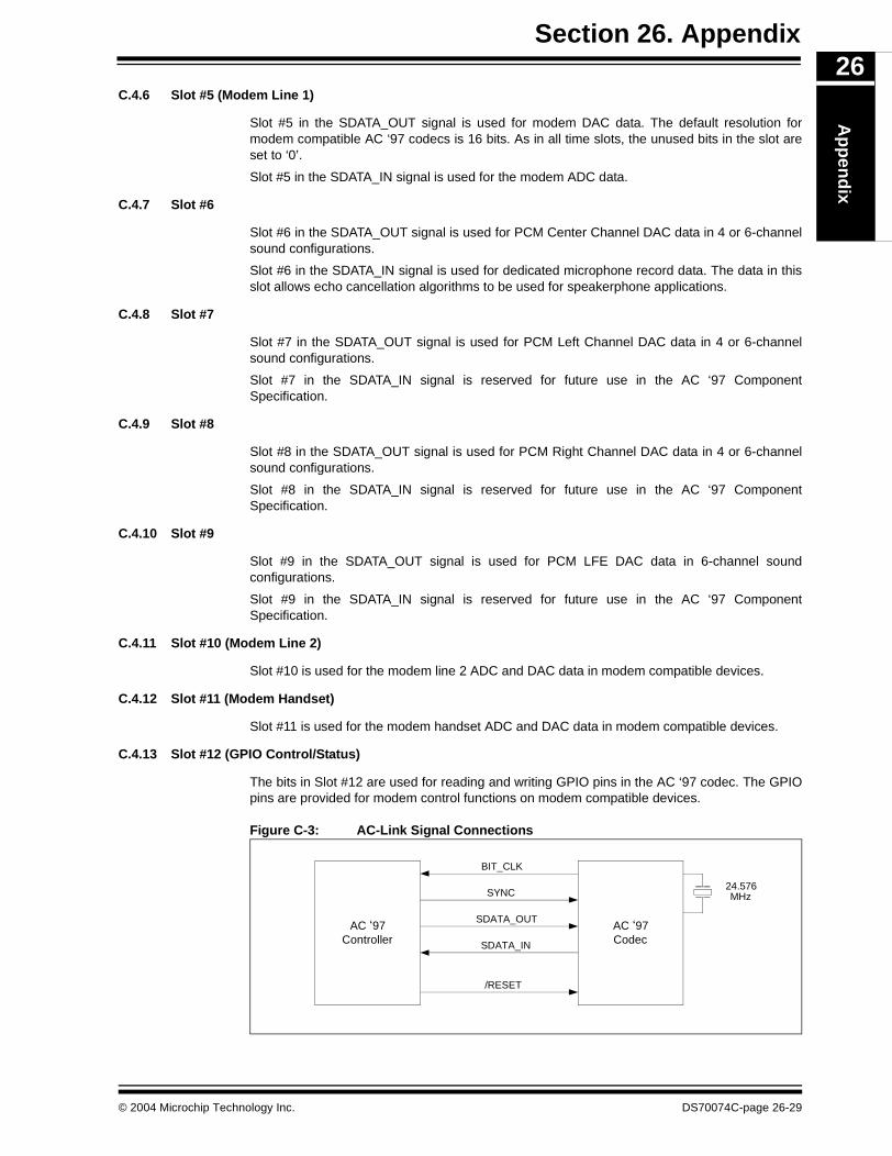
Section 26. AppendixA
pp
end
ix26
C.4.6 Slot #5 (Modem Line 1)
Slot #5 in the SDATA_OUT signal is used for modem DAC data. The default resolution formodem compatible AC ‘97 codecs is 16 bits. As in all time slots, the unused bits in the slot areset to ‘0’.
Slot #5 in the SDATA_IN signal is used for the modem ADC data.
C.4.7 Slot #6
Slot #6 in the SDATA_OUT signal is used for PCM Center Channel DAC data in 4 or 6-channelsound configurations.
Slot #6 in the SDATA_IN signal is used for dedicated microphone record data. The data in thisslot allows echo cancellation algorithms to be used for speakerphone applications.
C.4.8 Slot #7
Slot #7 in the SDATA_OUT signal is used for PCM Left Channel DAC data in 4 or 6-channelsound configurations.
Slot #7 in the SDATA_IN signal is reserved for future use in the AC ‘97 ComponentSpecification.
C.4.9 Slot #8
Slot #8 in the SDATA_OUT signal is used for PCM Right Channel DAC data in 4 or 6-channelsound configurations.
Slot #8 in the SDATA_IN signal is reserved for future use in the AC ‘97 ComponentSpecification.
C.4.10 Slot #9
Slot #9 in the SDATA_OUT signal is used for PCM LFE DAC data in 6-channel soundconfigurations.
Slot #9 in the SDATA_IN signal is reserved for future use in the AC ‘97 ComponentSpecification.
C.4.11 Slot #10 (Modem Line 2)
Slot #10 is used for the modem line 2 ADC and DAC data in modem compatible devices.
C.4.12 Slot #11 (Modem Handset)
Slot #11 is used for the modem handset ADC and DAC data in modem compatible devices.
C.4.13 Slot #12 (GPIO Control/Status)
The bits in Slot #12 are used for reading and writing GPIO pins in the AC ‘97 codec. The GPIOpins are provided for modem control functions on modem compatible devices.
Figure C-3: AC-Link Signal Connections
AC ‘97Controller
AC ‘97Codec
24.576MHz
BIT_CLK
SYNC
SDATA_OUT
SDATA_IN
/RESET
© 2004 Microchip Technology Inc. DS70074C-page 26-29
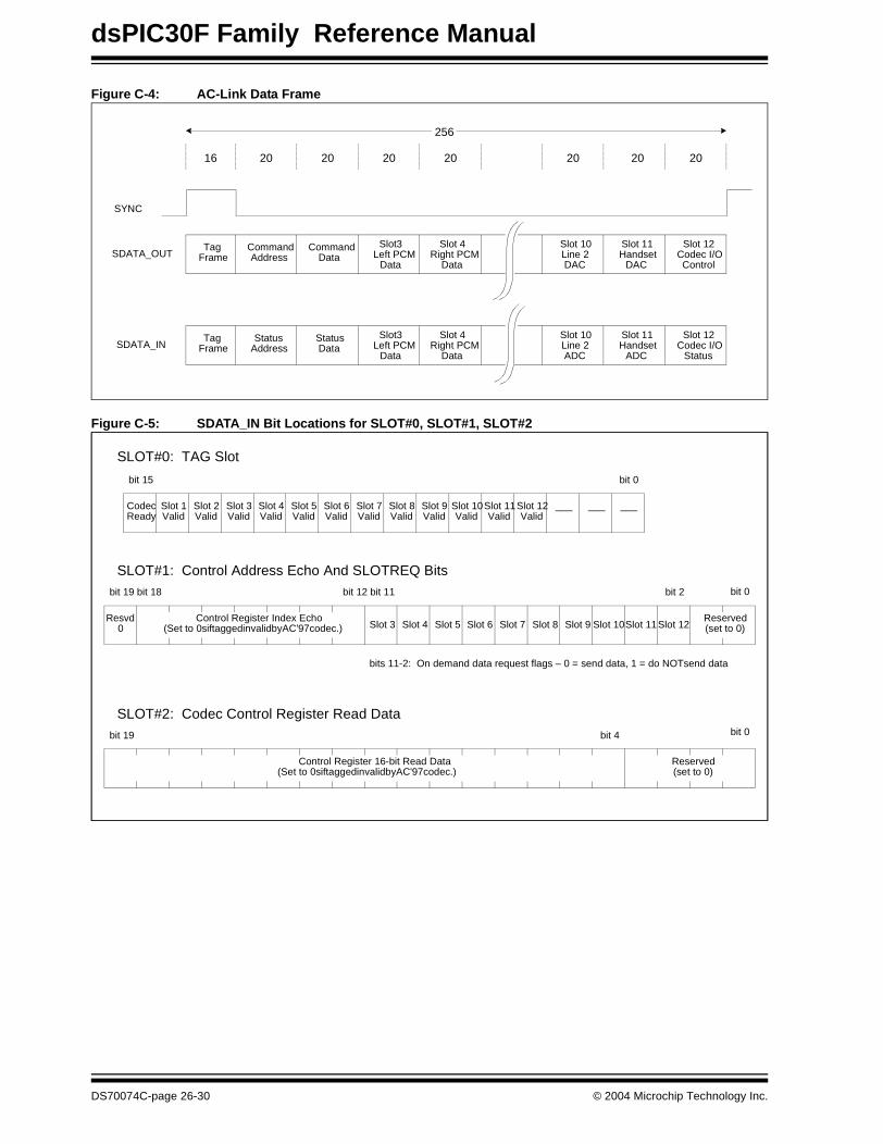
dsPIC30F Family Reference Manual
Figure C-4: AC-Link Data Frame
Figure C-5: SDATA_IN Bit Locations for SLOT#0, SLOT#1, SLOT#2
TagFrame
CommandAddress
CommandData
Slot3 Left PCM
Data
Slot 4Right PCM
Data
Slot 10Line 2DAC
Slot 11Handset
DAC
Slot 12Codec I/OControl
TagFrame
StatusAddress
StatusData
Slot3 Left PCM
Data
Slot 4Right PCM
Data
Slot 10Line 2ADC
Slot 11Handset
ADC
Slot 12Codec I/O
Status
16 20 20 20 20 20 20 20
256
SDATA_OUT
SDATA_IN
SYNC
SLOT#0: TAG Slot
SLOT#1: Control Address Echo And SLOTREQ Bits
CodecReady
Slot 1Valid
Slot 2Valid
Slot 3Valid
Slot 4Valid
Slot 5Valid
Slot 6Valid
Slot 7Valid
Slot 9Valid
Slot 10Valid
Slot 11Valid
Slot 12Valid
Slot 8Valid
___ ___ ___
bit 0bit 15
Resvd0 Slot 4 Slot 5 Slot 6 Slot 7Slot 3 Slot 8 Slot 9 Slot 10
bit 0bit 19 bit 18 bit 12
Control Register Index Echo(Set to 0siftaggedinvalidbyAC'97codec.) Slot 11Slot 12
Reserved(set to 0)
bits 11-2: On demand data request flags – 0 = send data, 1 = do NOTsend data
bit 11 bit 2
bit 0bit 19
Control Register 16-bit Read Data(Set to 0siftaggedinvalidbyAC'97codec.)
Reserved(set to 0)
bit 4
SLOT#2: Codec Control Register Read Data
DS70074C-page 26-30 © 2004 Microchip Technology Inc.

Section 26. AppendixA
pp
end
ix26
Figure C-6: SDATA_OUT Bit Locations for SLOT#0, SLOT#1, SLOT#2
SLOT#0: TAG Slot
SLOT#1: Command Address
SLOT#2: Command Data
ValidFrame
Slot 1Valid
Slot 2Valid
Slot 3Valid
Slot 4Valid
Slot 5Valid
Slot 6Valid
Slot 7Valid
Slot 9Valid
Slot 10Valid
Slot 11Valid
Slot 12Valid
Slot 8Valid
___ CodecID
CodecID
bit 0bit 15
R/Wbit
bit 0bit 19 bit 18 bit 12
Control Register IndexReserved(set to 0)
bit 11
bit 0bit 19
Control Register 16-bit Write Data(Set to 0sifcurrentlyperformingareadoperation.)'
Reserved(set to 0)
bit 4
© 2004 Microchip Technology Inc. DS70074C-page 26-31
dsPIC30F Family Reference Manual
NOTES:
DS70074C-page 26-32 © 2004 Microchip Technology Inc.

dsPIC30F Family Reference ManualIn
dex
A
A/DAccuracy/Error ............................................17-47, 18-28ADCON0 Register...........................................17-4, 18-4Configuring Analog Port Pins......................17-14, 18-12Edge Detection Mode .............................................. 13-8Effects of a Reset........................................16-19, 17-55Effects of a Reset (12-bit) ...................................... 18-33Enabling the Module .............................................. 17-16Enabling the Module (12-bit).................................. 18-14How to Start Sampling ........................................... 17-17How to Stop Sampling and Start Conversions....... 17-18Reading the A/D Result Buffer...............................17-46Sampling Requirements..............................17-45, 18-26Transfer Function........................................17-47, 18-28Transfer Function (12-bit) ...................................... 18-28
A/D Accuracy/Error ........................................................17-47A/D Accuracy/Error (12-bit) ............................................ 18-28A/D Conversion Speeds......................................17-49, 18-30A/D Converter External Conversion Request .................. 6-10A/D Module Configuration.............................................. 17-13A/D Module Configuration (12-bit) .................................18-11A/D Sampling Requirements (12-bit) ............................. 18-26A/D Special Event Trigger.............................................. 12-22A/D Terminology and Conversion Sequence................. 17-11A/D Terminology and Conversion Sequence (12-bit) .... 18-10Accumulator ‘Write Back’ ................................................. 2-25ACK................................................................................ 21-38Acknowledge Pulse........................................................21-38Address Generator Units and DSP Class Instructions....... 3-6Address Register Dependencies .....................................2-35AKS................................................................................ 21-17Alternate Vector Table ....................................................... 6-2Arithmetic Logic Unit (ALU).............................................. 2-17
B
Barrel Shifter .................................................................... 2-26Baud Rate
Generator (BRG)......................................................19-8Tables ...................................................................... 19-9
BF .......................................................................21-18, 21-19Bit-Reversed Addressing ................................................. 3-14
and Modulo Addressing ........................................... 3-15Code Example ......................................................... 3-18Intro.......................................................................... 3-14Modifier Value ..........................................................3-16Operation ................................................................. 3-15
Block DiagramsDedicated Port Structure.......................................... 11-2DSP Engine ............................................................. 2-19dsPIC30F CPU Core.................................................. 2-3External Power-on Reset Circuit (For Slow VDD
Rise Time) ......................................................... 8-7Input Capture ........................................................... 13-2Input Change Notification......................................... 11-7Low Voltage Detect (LVD) ......................................... 9-3Oscillator System....................................................... 7-4Output Compare Module.......................................... 14-2Reset System............................................................. 8-2Shared Port Structure .............................................. 11-4Type A Timer ........................................................... 12-3Type B - Type C Timer Pair (32-bit Timer)............. 12-17Type B Timer ........................................................... 12-4Type C Timer ........................................................... 12-5UART ....................................................................... 19-2UART Receiver ......................................................19-16
UART Transmitter.................................................. 19-11WDT ........................................................................ 10-6
Brown-out Reset (BOR)..................................................... 8-8Configuration ............................................................. 8-9Current Consumption for Operation .......................... 8-9
Byte to Word Conversion................................................. 2-17
C
CANBuffer Reception and Overflow Truth Table .......... 23-44Message Acceptance Filters ................................. 23-12
CAN Library ..................................................................... 25-9Capture Buffer Operation................................................. 13-8Clock Switching
Aborting ................................................................... 7-36Enable ..................................................................... 7-34Entering Sleep Mode During ................................... 7-36Operation................................................................. 7-34Recommended Code Sequence ............................. 7-36Tips.......................................................................... 7-36
CNChange Notification Pins ......................................... 11-7Configuration and Operation ................................... 11-8Control Registers..................................................... 11-7Operation in Sleep and Idle Modes ......................... 11-8
Code ExamplesClock Switching ....................................................... 7-37Compare Mode Toggle Mode Pin State Setup........ 14-8Compare Mode Toggle Setup and Interrupt
Servicing.......................................................... 14-8Configuration Register Write ................................... 5-15Continuous Output Pulse Setup and Interrupt
Servicing........................................................ 14-16Initialization Code for 16-bit Asynchronous Counter
Mode Using an External Clock Input ............. 12-11Initialization Code for 16-bit Gated Time Accumulation
Mode ............................................................. 12-13Initialization Code for 16-bit Synchronous Counter Mode
Using an External Clock Input ....................... 12-10Initialization Code for 16-bit Timer Using
System Clock................................................... 12-9Initialization Code for 32-bit Gated Time
Accumulation Mode....................................... 12-20Initialization Code for 32-bit Synchronous Counter Mode
Using an External Clock Input ....................... 12-19Initialization Code for 32-bit Timer Using Instruction
Cycle as Input Clock...................................... 12-18Prescaled Capture................................................... 13-7PWM Mode Pulse Setup and Interrupt
Servicing........................................................ 14-22Reading from a 32-bit Timer.................................. 12-21Single Output Pulse Setup and Interrupt
Servicing........................................................ 14-12Single Row Programming........................................ 5-148-bit Transmit/Receive (UART1) ........................... 19-209-bit Transmit/Receive (UART1), Address Detect
Enabled ......................................................... 19-20CODEC Interface Basics and Terminology ..................... 22-8Complementary PWM Output Mode.............................. 15-26Configuration Bit Descriptions ......................................... 24-6
BOR and POR ......................................................... 24-6General Code Segment........................................... 24-6Motor Control PWM Module .................................... 24-6Oscillator.................................................................. 24-6
Connection Considerations............................................ 17-47Connectivity Development Board .................................. 25-14Control Register Descriptions .......................................... 3-18
© 2006 Microchip Technology Inc. DS70046E-page 1
Index
Control Registers .......................................... 12-6, 17-4, 18-4Assignment of Interrupts ..........................................6-14
Controlling Sample/Conversion Operation.....................17-29Controlling Sample/Conversion Operation (12-bit) ........18-19Conversion Sequence Examples ...................................17-31Conversion Sequence Examples (12-bit).......................18-21CPU
Register Maps..........................................................2-38Related Application Notes........................................2-40Revision History .......................................................2-41
CPU Clocking Scheme.......................................................7-5CPU Priority Status ............................................................6-5CPU Register Descriptions ..............................................2-11Crystal Oscillators, Ceramic Resonators .........................7-22
D
Data AccumulatorStatus Bits ................................................................2-23
Data Accumulator Adder/Subtractor ................................2-23Data Accumulators...........................................................2-20Data Alignment...................................................................3-7Data EEPROM Programming ..........................................5-15
Erasing One Row.....................................................5-19Erasing One Word ...................................................5-17Reading Memory......................................................5-21Row Algorithm..........................................................5-16Single Word Algorithm .............................................5-16Write One Row.........................................................5-20Writing One Word ....................................................5-18
Data MemoryMap ............................................................................3-3Near ...........................................................................3-4
Data Space AddressGenerator Units (AGUs).............................................3-5X Address Generator Unit ..........................................3-5Y Address Generator Unit ..........................................3-5
Data Space Write Saturation............................................2-24DCI
Buffer Control Unit .................................................22-13Control Register Descriptions ..................................22-2Operation ...............................................................22-10Using the Module ...................................................22-17
Dead Time Control .........................................................15-27Determining Best Values for Crystals, Clock Mode,
C1, C2, and Rs ........................................................7-24Device Configuration
Register Descriptions...............................................24-2Device Identification Registers.........................................24-7
Device ID (DEVID) ...................................................24-7Unit ID Field .............................................................24-7
Device Reset Times .........................................................8-11Device Start-up Time Lines..............................................8-13Device Wake-up on Sleep/Idle.......................................13-10Disable Interrupts Instruction .............................................6-8Divide Support..................................................................2-27DSP Algorithm Library......................................................25-7DSP Engine......................................................................2-18DSP Engine Mode Selection............................................2-26DSP Engine Trap Events .................................................2-26DSP Filter Design Software Utility....................................25-8dsPIC Language Suite .....................................................25-3dsPIC30F Hardware Development Boards ....................25-11
E
EquationsCalculating the PWM Period.................................. 14-19Calculation for Maximum PWM Resolution ........... 14-20Modulo End Address for Incrementing Buffer............ 3-9Modulo Start Address for Decrementing Buffer ......... 3-9WDT Time-out Period .............................................. 10-7
External Clock Input......................................................... 7-25External Interrupt Support................................................ 6-10External RC Oscillator ..................................................... 7-26
Operating Frequency ............................................... 7-27Start-up.................................................................... 7-27with I/O Enabled ...................................................... 7-27
External Reset (EXTR) ...................................................... 8-7
F
Fail-Safe Clock Monitor (FSCM)...................................... 7-32and Slow Oscillator Start-up .................................... 7-33and WDT ................................................................. 7-33Delay ....................................................................... 7-32
Flash and Data EEPROM ProgrammingControl Registers ....................................................... 5-5
NVMADR ........................................................... 5-6NVMCON........................................................... 5-5NVMKEY ........................................................... 5-6
Flash Program MemoryErasing a Row ......................................................... 5-12Loading Write Latches ............................................. 5-13Programming Algorithm........................................... 5-11
FSCMand Device Resets................................................... 8-12Delay for Crystal and PLL Clock Sources................ 8-12
G
General Purpose Development Board........................... 25-12
H
Hard Traps......................................................................... 6-7Address Error (Level 13)............................................ 6-8Oscillator Failure (Level 14)....................................... 6-8Priority and Conflicts.................................................. 6-7Stack Error (Level 12)................................................ 6-6
How to Start Sampling (12-bit)....................................... 18-14How to Start Sampling and Start
Conversions (12-bit) .............................................. 18-14
I
I/O Multiplexing with Multiple Peripherals ........................ 11-4I/O Pin Control ..............................12-22, 13-10, 14-23, 16-18I/O Port Control Registers................................................ 11-3I/O Ports
Related Application Notes ..................................... 11-11Revision History..................................................... 11-12
Idle Mode ......................................................................... 10-4Time Delays on Wake-up from ................................ 10-5Wake-up from on Interrupt....................................... 10-5Wake-up from on Reset........................................... 10-5Wake-up from on WDT Time-out............................. 10-5
Independent PWM Output Mode ................................... 15-30Initialization .................................................................... 17-48Initialization (12-bit)........................................................ 18-29
DS70046E-page 2 © 2006 Microchip Technology Inc.
dsPIC30F Family Reference ManualIn
dex
Input CaptureAssociated Special Function Registers.................. 13-11Buffer Not Empty (ICBNE) ....................................... 13-9Design Tips ............................................................ 13-12Interrupts.................................................................. 13-9
Control Bits ......................................................13-9Operation in Power Saving States ......................... 13-10Overflow (ICOV)....................................................... 13-9Related Application Notes...................................... 13-13
Input Capture Event Modes ............................................. 13-4Input Capture Registers ................................................... 13-3Instruction Flow Types ..................................................... 2-27Instruction Stall Cycles..................................................... 2-36Internal Fast RC Oscillator (FRC) .................................... 7-31Internal Low Power RC (LPRC) Oscillator ....................... 7-32
Enabling ................................................................... 7-32Internal Voltage Reference ................................................ 9-3Interrupt Control and Status Registers............................. 6-14
CORCON ................................................................. 6-14IECx ......................................................................... 6-14IFSx.......................................................................... 6-14INTCON1, INTCON2 ............................................... 6-14IPCx ......................................................................... 6-14SR ............................................................................ 6-14
Interrupt ControllerAssociated Special Function Registers.................... 6-43
Interrupt LatencyOne-Cycle Instructions............................................. 6-11Two-Cycle Instructions............................................. 6-12
Interrupt Operation............................................................. 6-9Nesting..................................................................... 6-10Return From Interrupt ................................................ 6-9
Interrupt Priority ................................................................. 6-5Interrupt Processing Timing ............................................. 6-11Interrupt Setup Procedures .............................................. 6-42
Initialization .............................................................. 6-42Interrupt Disable....................................................... 6-42Interrupt Service Routine ......................................... 6-42Trap Service Routine ............................................... 6-42
Interrupt Vector Table ........................................................6-2Interrupts
Design Tips .............................................................. 6-44Related Application Notes........................................ 6-45Revision History ....................................................... 6-46
Interrupts Coincident with Power Save Instructions......... 10-5Introduction
Revision History ......................................................... 1-7IWCOL ...........................................................................21-22I2C
Acknowledge Generation....................................... 21-21Building Complete Master Messages .................... 21-24Bus Arbitration and Bus Collision........................... 21-30Bus Collision During a Repeated Start
Condition........................................................21-31Bus Collision During a Start Condition................... 21-31Bus Collision During a Stop Condition ................... 21-31Bus Collision During Message Bit
Transmission ................................................. 21-31Bus Connection Considerations............................. 21-47Communicating as a Master in a Multi-Master
Environment................................................... 21-29Communicating as a Slave .................................... 21-32Detecting Bus Collisions and Resending
Messages ......................................................21-30Detecting Start and Stop Conditions...................... 21-32Detecting the Address............................................ 21-32Enabling I/O ........................................................... 21-13
Enabling Operation................................................ 21-13Generating Repeated Start Bus Event .................. 21-23Generating Start Bus Event................................... 21-16Generating Stop Bus Event ................................... 21-22Initiating and Terminating Data Transfer ................. 26-3Interrupts ............................................................... 21-13Master Message Protocol States........................... 21-24Module Operation during PWRSAV Instruction..... 21-49Receiving Data from a Master Device ................... 21-37Receiving Data from a Slave Device ..................... 21-19Sending Data to a Master Device.......................... 21-44Sending Data to a Slave Device............................ 21-17Start ......................................................................... 26-3Stop ......................................................................... 26-3
I2C ModuleMulti-master Mode................................................. 21-29Register Map ......................................................... 21-3310-bit Address Mode ............................................. 21-35
L
LAT (I/O Latch) Registers ................................................ 11-3Loop Constructs .............................................................. 2-30
DO ........................................................................... 2-32REPEAT .................................................................. 2-30
Low Power 32 kHz Crystal Oscillator............................... 7-31Low Power 32 kHz Crystal Oscillator Input.................... 12-15LP Oscillator
Continuous Operation.............................................. 7-31Enable ..................................................................... 7-31Intermittent Operation.............................................. 7-31Operation with Timer1 ............................................. 7-31
LVDControl Bits ................................................................ 9-3Current Consumption for Operation .......................... 9-5Design Tips................................................................ 9-6Initialization Steps...................................................... 9-5Operation................................................................... 9-5Operation During Sleep and Idle Mode ..................... 9-5Related Application Notes ......................................... 9-7Trip Point Selection ................................................... 9-3
M
Math Library..................................................................... 25-7Microchip Hardware and Language Tools ....................... 25-2Modes of Operation ......................................................... 14-4
Compare Mode Output Driven High ........................ 14-5Compare Mode Output Driven Low ......................... 14-6Compare Mode Toggle Output ................................ 14-7Dual Compare Match............................................... 14-9Dual Compare, Continuous Output Pulses............ 14-14Dual Compare, Generating Continuous Output Pulses
Special Cases (table) .................................... 14-17Dual Compare, Single Output Pulse........................ 14-9
Special Cases (table) .................................... 14-13Single Compare Match ............................................ 14-4
Modulo Addressing ............................................................ 3-7Applicability.............................................................. 3-11Calculation................................................................. 3-9Initialization for Decrementing Buffer....................... 3-13Initialization for Incrementing Modulo Buffer ........... 3-12Start and End Address Selection............................... 3-8W Address Register Selection................................... 3-9
© 2006 Microchip Technology Inc. DS70046E-page 3

Index
Modulo Start and End Address SelectionXMODEND Register ..................................................3-8XMODSRT Register...................................................3-8YMODEND Register ..................................................3-8YMODSRT Register...................................................3-8
Motor Control Development Board.................................25-13MPLAB ICD 2 In-Circuit Debugger...................................25-5MPLAB ICE 4000 In-Circuit Emulator ..............................25-4MPLAB SIM Software Simulator ......................................25-3MPLAB 6.XX Integrated Development Environment
Software...................................................................25-2Multi-Master Mode .........................................................21-29Multiplier...........................................................................2-20Multiply Instructions..........................................................2-22
N
Non-Maskable Traps..........................................................6-6Address Error .............................................................6-6Arithmetic Error ..........................................................6-6Oscillator Failure ........................................................6-6Stack Error .................................................................6-6
O
OscillatorConfiguration..............................................................7-6
Clock Switching Mode Configuration Bits ..........7-6Design Tips ..............................................................7-38Related Application Notes........................................7-39Resonator Start-up...................................................7-22Revision History .......................................................7-40System Features Summary .......................................7-2
Oscillator Control Register (OSCCON) ............................7-13Oscillator Mode Selection Guidelines ..............................7-21Oscillator Start-up From Sleep Mode...............................7-23Oscillator Start-up Timer (OST) .......................................7-31Oscillator Switching Sequence.........................................7-35OSEK Operating Systems..............................................25-10Other dsPIC30F CPU Control Registers..........................2-16
DISICNT...................................................................2-16MODCON.................................................................2-16PSVPAG ..................................................................2-16TBLPAG...................................................................2-16XBREV.....................................................................2-16XMODSRT, XMODEND...........................................2-16YMODSRT, YMODEND...........................................2-16
Output CompareAssociated Register Map .......................................14-24Design Tips ............................................................14-26Related Application Notes......................................14-27Revision History .....................................................14-28
Output Compare Operating in Power Saving States......14-23Output Compare Operation in Power Saving States
Idle Mode ...............................................................14-23Sleep Mode............................................................14-23
Output Compare Registers ..............................................14-3
P
Peripheral Driver Library ..................................................25-8Peripheral Module Disable (PMD) Registers ...................10-9Peripheral Multiplexing.....................................................11-4Peripherals Using Timer Modules ..................................12-22Phase Locked Loop (PLL)................................................7-30
Frequency Range ....................................................7-30Lock Status ..............................................................7-30Loss of Lock During a Power-on Reset ...................7-30Loss of Lock During Clock Switching .......................7-30
Loss of Lock During Normal Device Operation........ 7-30POR and Long Oscillator Start-up Times ........................ 8-12Port (I/O Port) Registers .................................................. 11-3Power Saving Modes....................................................... 10-2Power-on Reset (POR)...................................................... 8-5
Using ......................................................................... 8-7Power-up Timer (PWRT) ................................................... 8-7Prescaler Capture Events................................................ 13-6Primary Oscillator ............................................................ 7-20PRO MATE II Universal Device Programmer .................. 25-5Program Memory
Address Map ............................................................. 4-2Counter ...................................................................... 4-4Data Access From ..................................................... 4-4Data Storage ............................................................. 4-7High Word Access ..................................................... 4-7Low Word Access ...................................................... 4-6Program Space Visibility from Data Space................ 4-8Related Application Notes ....................................... 4-12Table Address Generation......................................... 4-6Table Instruction Summary........................................ 4-5Writes ............................................................. 4-10, 4-11
Programmable Digital Noise Filters ................................. 16-9Programmable Oscillator Postscaler ............................... 7-33Programmer’s Model .................................................. 2-3, 2-4
Register Description .................................................. 2-4Protection Against Accidental Writes to OSCCON .......... 7-13PSV Configuration ............................................................. 4-8
PSV Mapping with X and Y Data Spaces .................. 4-8Timing...................................................................... 4-10
Instruction Stalls .............................................. 4-10Using PSV in a Repeat Loop........................... 4-10
Pulse Width Modulation Mode ....................................... 14-18Duty Cycle ............................................................. 14-20Period .................................................................... 14-19With Fault Protection Input Pin .............................. 14-19
PWM Duty Cycle Comparison Units .............................. 15-20PWM Fault Pins ............................................................. 15-34PWM Output and Polarity Control.................................. 15-34PWM Output Override ................................................... 15-31PWM Special Event Trigger........................................... 15-38PWM Time Base............................................................ 15-16PWM Update Lockout.................................................... 15-37
Q
QEI Operation During Power Saving Modes ................. 16-19Quadrature Decoder ...................................................... 16-10Quadrature Encoder Interface Interrupts ....................... 16-17
R
R/W Bit.................................................................. 21-35, 26-4Read-After-Write Dependency Rules .............................. 2-36Reading A/D Result Buffer (12-bit) ................................ 18-27Reading and Writing into 32-bit Timers ......................... 12-21Reading and Writing 16-bit Timer Module
Registers ............................................................... 12-15Real-Time Operating System (RTOS) ............................. 25-9
DS70046E-page 4 © 2006 Microchip Technology Inc.

dsPIC30F Family Reference ManualIn
dex
RegistersA/D Input Scan Select (ADCSSL - 12-bit) ................18-9A/D Input Scan Select (ADCSSL) .......................... 17-10ADCHS (A/D Input Select) Register................17-9, 18-8ADCHS A/D Input Select ......................................... 17-9ADCHS A/D Input Select (12-bit) ............................. 18-8ADCON1 (A/D Control) Register1........17-5, 18-5, 21-11ADCON1 A/D Control 1 ..................................17-5, 17-6ADCON1 A/D Control 1 (12-bit) ............................... 18-5ADCON2 (A/D Control) Register2...................17-7, 18-6ADCON2 A/D Control 2 ........................................... 17-7ADCON2 A/D Control 2 (12-bit) ............................... 18-6ADCON3 (A/D Control) Register3...................17-8, 18-7ADCON3 A/D Control 3 ........................................... 17-8ADCON3 A/D Control 3 (12-bit) ............................... 18-7ADPCFG (A/D Port Configuration)
Register ................................................17-10, 18-9ADPCFG A/D Port Configuration ........................... 17-10ADPCFG A/D Port Configuration (12-bit)................. 18-9CiCFG1 (Baud Rate Configuration Register)......... 23-16CiCFG2 (Baud Rate Configuration Register 2)...... 23-17CiCTRL (CAN Module Control and Status
Register) ..........................................................23-3CiEC (Transmit/Receive Error Count).................... 23-18CiINTE (Interrupt Enable Register) ........................ 23-19CiINTF (Interrupt Flag Register) ............................ 23-20CiRXFnEIDH (Acceptance Filter n Extended
Identifier High) ............................................... 23-12CiRXFnEIDL (Acceptance Filter n Extended
Identifier Low) ................................................ 23-13CiRXMnEIDH (Acceptance Filter Mask n Extended
Identifier High) ............................................... 23-14CiRXMnEIDL (Acceptance Filter Mask n Extended
Identifier Low) ................................................ 23-15CiRXMnSID (Acceptance Filter Mask n Standard
Identifier) ........................................................23-14CiRXnBm (Receive Buffer n Data Field
Word m) ......................................................... 23-11CiRXnDLC (Receive Buffer n Data Length
Control) .......................................................... 23-11CiRXnEID (Receive Buffer n Extended
Identifier) ........................................................23-10CiRXnSID (Receive Buffer n Standard
Identifier) ........................................................23-10CiRX0CON (Receive Buffer 0 Status and Control
Register) ..........................................................23-8CiRX1CON (Receive Buffer 1 Status and Control
Register) ..........................................................23-9CiRX1FnSID (Acceptance Filter n Standard
Identifier) ........................................................23-12CiTXnBm (Transmit Buffer n Data Field
Word m) ........................................................... 23-7CiTXnCON (Transmit Buffer Status and Control
Register) ..........................................................23-5CiTXnDLC (Transmit Buffer n Data Length
Control) ............................................................ 23-7CiTXnEID
(Transmit Buffer n Extended Identifier) ............23-6CiTXnSID (Transmit Buffer n Standard
Identifier) ..........................................................23-6CNEN1 (Input Change Notification Interrupt
Enable 1) ......................................................... 11-9CNEN2 (Input Change Notification Interrupt
Enable 2) ......................................................... 11-9CNPU1 (Input Change Notification Pull-up
Enable 1) ....................................................... 11-10
CNPU2 (Input Change Notification Pull-up Enable 2) ....................................................... 11-10
Control and Status................................................... 16-4Control Registers..................................................... 15-4CORCON (Core Control) ................................ 2-14, 6-15DCICON1 ................................................................ 22-3DCICON2 ................................................................ 22-4DCICON3 ................................................................ 22-5DCISTAT ................................................................. 22-6DFLTCON Digital Filter Control ...................... 16-7, 16-8DTCON1 Dead Time Control 1................................ 15-9DTCON2 Dead Time Control 2.............................. 15-10FBORPOR (BOR and POR Configuration
Register) .......................................................... 24-4FBORPOR BOR and POR Device
Configuration ................................................. 15-15FGS (General Code Segment Configuration
Register) .......................................................... 24-5FLTACON Fault A Control ..................................... 15-11FLTBCON Fault B Control ..................................... 15-12FOSC (Oscillator Configuration
Register) ............................................7-7, 7-9, 7-11FWDT (Watchdog Timer Configuration
Register) .......................................................... 24-3ICxCON (Input Capture x Control)........................... 13-3IEC0 (Interrupt Enable Control 0) ............................ 6-24IEC1 (Interrupt Enable Control 1) ............................ 6-26IEC2 (Interrupt Enable Control 2) ................... 6-28, 6-29IFS0 (Interrupt Flag Status 0) .................................. 6-18IFS1 (Interrupt Flag Status 1) .................................. 6-20IFS2 (Interrupt Flag Status 2) ......................... 6-22, 6-23INTCON1 (Interrupt Control 1) ................................ 6-16INTCON2 (Interrupt Control 2) ................................ 6-17IPC0 (Interrupt Priority Control 0) ............................ 6-30IPC1 (Interrupt Priority Control 1) ............................ 6-31IPC10 (Interrupt Priority Control 10) ........................ 6-40IPC11 (Interrupt Priority Control 11) ........................ 6-41IPC2 (Interrupt Priority Control 2) ............................ 6-32IPC3 (Interrupt Priority Control 3) ............................ 6-33IPC4 (Interrupt Priority Control 4) ............................ 6-34IPC5 (Interrupt Priority Control 5) ............................ 6-35IPC6 (Interrupt Priority Control 6) ............................ 6-36IPC7 (Interrupt Priority Control 7) ............................ 6-37IPC8 (Interrupt Priority Control 8) ............................ 6-38IPC9 (Interrupt Priority Control 9) ............................ 6-39I2CSTAT (I2C Status) Register..........21-9, 21-10, 21-11MODCON (Modulo and Bit-Reversed Addressing
Control)............................................................ 3-19NVMADR (Non-Volatile Memory Address) ................ 5-8NVMADRU (Non-Volatile Memory Address) ............. 5-9NVMCON (Non-Volatile Memory Control) ................. 5-7NVMKEY (Non-Volatile Memory Key) ....................... 5-9OCxCON (Output Compare x Control) .................... 14-3OVDCON Override Control ................................... 15-13PDC1 PWM Duty Cycle 1...................................... 15-13PDC2 PWM Duty Cycle 2...................................... 15-14PDC3 PWM Duty Cycle 3...................................... 15-14PDC4 PWM Duty Cycle 4...................................... 15-15PTCON PWM Time Base Control ........................... 15-5PTMR PWM Time Base .......................................... 15-6PTPER PWM Time Base Period ............................. 15-6PWMCON1 PWM Control 1 .................................... 15-7PWMCON2 PWM Control 2 .................................... 15-8QEI Special Function............................................. 16-20QEICON QEI Control...................................... 16-5, 16-6RCON (Reset Control)........................................ 8-3, 9-4RSCON.................................................................... 22-7
© 2006 Microchip Technology Inc. DS70046E-page 5
Index
SEVTCMP Special Event Compare .........................15-7SR (CPU Status) ......................................................2-12SR (Status in CPU) ..................................................6-15TSCON ....................................................................22-7TxCON (Timer Control for Type A Time Base) ........12-6TxCON (Timer Control for Type B Time Base) ........12-7TxCON (Timer Control for Type C Time Base) ........12-8UxBRG (UARTx Baud Rate) ....................................19-7UxMODE (UARTx Mode).........................................19-3UxRXREG (UARTx Receive) ...................................19-6UxSTA (UARTx Status and Control) ........................19-4UxTXREG (UARTx Transmit - Write Only) ..............19-6XBREV (X Write AGU Bit-Reversal Addressing
Control) ............................................................3-22XMODEND (X AGU Modulo Addressing End) .........3-20XMODSRT (X AGU Modulo Addressing Start) ........3-20YMODEND (Y AGU Modulo Addressing End) .........3-21YMODSRT (Y AGU Modulo Addressing Start) ........3-2110-bit A/D Converter Special Function...................17-5612-bit A/D Converter Special Function...................18-346-Output PWM Module ..........................................15-418-Output PWM Module ..........................................15-40
ResetDesign Tips ..............................................................8-17Illegal Opcode ............................................................8-9Trap Conflict...............................................................8-9Uninitialized W Register .............................................8-9
Reset Sequence.................................................................6-2Returning From Interrupt..................................................6-13Round Logic .....................................................................2-25Run-Time Self Programming (RTSP)...............................5-10
FLASH Operations...................................................5-10Operation .................................................................5-10
S
Saturation and Overflow Modes.......................................2-24Selecting A/D Conversion Clock ....................................17-13Selecting Analog Inputs for Sampling ............................17-14Selecting Analog Inputs for Sampling (12-bit)................18-12Selecting the A/D Conversion Clock (12-bit)..................18-12Selecting the Voltage Reference Source .......................17-13Selecting the Voltage Reference Source (12-bit) ...........18-11Setup for Continuous Output Pulse Generation.............14-15Shadow Registers ..............................................................2-6
DO Loop.....................................................................2-7PUSH.S and POP.S...................................................2-7
Simple Capture Events ....................................................13-4Sleep and Idle Modes Operation....................................17-55Sleep and Idle Modes Operation (12-bit) .......................18-33Sleep Mode ......................................................................10-2
and FSCM Delay......................................................10-3Clock Selection on Wake-up from............................10-2Delay on Wake-up from ...........................................10-3Delay Times for Exit .................................................10-3Wake-up from on Interrupt .......................................10-4Wake-up from on Reset ...........................................10-4Wake-up from on Watchdog Time-out .....................10-4Wake-up from with Crystal Oscillator or PLL ...........10-3
Slow Oscillator Start-up....................................................10-3Soft Traps...........................................................................6-6
Arithmetic Error (Level 11) .........................................6-7Software Reset Instruction (SWR) .....................................8-7Software Stack
Examples ...................................................................2-9Pointer........................................................................2-8Pointer Overflow ......................................................2-10Pointer Underflow ....................................................2-10
W14 Stack Frame Pointer........................................ 2-10Special Conditions for Interrupt Latency.......................... 6-13Special Features for Device Emulation.......................... 15-39Special Function Register Reset States .......................... 8-16Specifying How Conversion Results are Written Into
Buffer ..................................................................... 17-30Specifying How Conversion Results are Written into
Buffer (12-bit)......................................................... 18-19SSPOV .......................................................................... 21-19
T
Table Instruction Operation ............................................... 5-2TCP/IP Protocol Stack ................................................... 25-10Third Party C Compilers .................................................. 25-6Third Party Hardware/Software Tools and Application
Libraries ................................................................... 25-6Time-base for Input Capture/Output Compare .............. 12-22Timer as an External Interrupt Pin ................................. 12-22Timer Interrupts ............................................................. 12-14Timer Modes of Operation ............................................... 12-9
Synchronous Counter Using External Clock Input............................................................... 12-10
Timer Mode.............................................................. 12-9Type A Timer Asynchronous Counter Mode Using
External Clock Input ...................................... 12-1132-bit Timer............................................................ 12-18
Timer ModulesAssociated Special Function Registers ................. 12-23
Timer Operation in Power Saving States....................... 12-21Timer Operation Modes
Gated Time Accumulation ..................................... 12-12with Fast External Clock Source............................ 12-12
Timer Prescalers............................................................ 12-14Timer Selection................................................................ 13-4Timer Variants ................................................................. 12-3Timers
Design Tips............................................................ 12-24Related Application Notes ..................................... 12-25Revision History..................................................... 12-26
Timing DiagramsBrown-out Situations.................................................. 8-8Clock Transition ....................................................... 7-35Clock/Instruction Cycle .............................................. 7-5Data Space Access .......................................... 2-35, 3-6Dead Time ............................................................. 15-28Device Reset Delay, Crystal + PLL Clock Source,
PWRT Disabled ............................................... 8-13Device Reset Delay, Crystal + PLL Clock Source,
PWRT Enabled................................................ 8-14Device Reset Delay, EC + PLL Clock, PWRT
Enabled ........................................................... 8-15Device Reset Delay, EC or RC Clock, PWRT
Disabled........................................................... 8-16Dual Compare Mode.............................................. 14-10Dual Compare Mode (Continuous Output Pulse,
PR2 = OCxRS) ................................... 14-14, 14-15Dual Compare Mode (Single Output Pulse,
OCxRS > PR2) .............................................. 14-10Edge Detection Mode .............................................. 13-8Gated Timer Mode Operation ................................ 12-13Interrupt Timing During a Two-Cycle Instruction ..... 6-12Interrupt Timing for Timer Period Match ................ 12-14Interrupt Timing, Interrupt Occurs During 1st Cycle
of a Two-Cycle Instruction ............................... 6-12POR Module for Rising VDD ...................................... 8-6Postscaler Update ................................................... 7-34PWM Output ............................................... 14-18, 14-21
DS70046E-page 6 © 2006 Microchip Technology Inc.
dsPIC30F Family Reference ManualIn
dex
Reception with Address Detect (ADDEN = 1)........ 19-19Return From Interrupt .............................................. 6-13Simple Capture Event, Time-base
Prescaler = 1:1................................................. 13-5Simple Capture Event, Time-base
Prescaler = 1:4................................................. 13-5Single Compare Mode (Force OCx Low on Compare
Match Event).................................................... 14-6Single Compare Mode (Set OCx High on Compare
Match Event).................................................... 14-5Single Compare Mode (Toggle Output on Compare
Match Event, PR2 = OCxR)............................. 14-7Single Compare Mode (Toggle Output on Compare
Match Event, PR2 > OCxR)............................. 14-7SPI Mode Timing (No SS Control) ..............20-12, 20-13Transmission (Back to Back) .................................19-13Transmission (8-bit or 9-bit Data) .......................... 19-13UART Reception ....................................................19-17UART Reception with Receive Overrun................. 19-17
TRIS (Data Direction) Registers ...................................... 11-3Tuning the Oscillator Circuit ............................................. 7-23Type A Timer ................................................................... 12-3Type B Timer ................................................................... 12-4Type C Timer ................................................................... 12-5
U
UARTADDEN Control Bit................................................. 19-18Alternate I/O Pins................................................... 19-10Associated Registers ............................................. 19-22Baud Rate Generator............................................... 19-8Configuration.......................................................... 19-10Control Registers ..................................................... 19-3Design Tips ............................................................ 19-23Disabling ................................................................ 19-10Enabling ................................................................. 19-10Other Features....................................................... 19-21
Auto Baud Support ........................................ 19-21Loopback Mode ............................................. 19-21Operation During CPU Sleep and Idle Modes .............................................. 19-21
Receiver................................................................. 19-14Buffer (UxRXB) .............................................. 19-14Error Handling................................................ 19-14Interrupt ......................................................... 19-15Setup for Reception ....................................... 19-17
Related Application Notes...................................... 19-24Setup for 9-bit Transmit ......................................... 19-18Transmitter............................................................. 19-11
Buffer (UxTXB) .............................................. 19-12Interrupt ......................................................... 19-12Setup ............................................................. 19-13Transmission of Break Characters ................ 19-14
Using for 9-bit Communication...............................19-18UART Autobaud Support ................................................. 13-9Uninitialized W Register Reset .......................................... 2-7USART
Initialization ............................................................ 19-20Introduction .............................................................. 19-2Receiving Break Characters .................................. 19-19Revision History ..................................................... 19-25Setup for 9-bit Reception Using Address Detect
Mode.............................................................. 19-19Using QEI as Alternate 16-bit Timer/Counter ................ 16-16Using Table Read Instructions........................................... 5-3
Byte Mode.................................................................. 5-3Word Mode ................................................................ 5-3
Using Table Write Instructions........................................... 5-4Byte Mode ................................................................. 5-5Holding Latches......................................................... 5-4Word Mode ................................................................ 5-4
Using the RCON Status Bits............................................ 8-10
V
V.22/V.22bis and V.32 Specification.............................. 25-11
W
Wake-up from Sleep and Idle .......................................... 6-10Watchdog Time-out Reset (WDTR)................................... 8-7Watchdog Timer .............................................................. 10-6
Enabling and Disabling............................................ 10-6Operation................................................................. 10-7Operation in Sleep and Idle Modes ......................... 10-8Period Selection ...................................................... 10-7Prescalers................................................................ 10-7Resetting ................................................................. 10-8Software Controlled ................................................. 10-6
WCOL......................................................21-18, 21-19, 21-21WDT and Power Saving Modes
Design Tips............................................................ 10-10Related Application Notes ..................................... 10-11Revision History..................................................... 10-12
Working Register Array...................................................... 2-6W Register Memory Mapping .................................... 2-6W Registers and Byte Mode Instructions .................. 2-6W0 and File Register Instructions.............................. 2-6
Writing to Device Configuration Registers ....................... 5-14Write Algorithm ........................................................ 5-14
Z
10-bit Address Mode...................................................... 21-3512-Bit A/D
ADCHS........................................................... 17-4, 18-4ADPCFG......................................................... 17-4, 18-4
12-bit A/DOperation During CPU Idle Mode............... 17-55, 18-33Operation During CPU Sleep Mode ........... 17-55, 18-33
16-bit Up/Down Position Counter .................................. 16-1232-bit Timer Configuration ............................................. 12-16
© 2006 Microchip Technology Inc. DS70046E-page 7

DS70046E © 2006 Microchip Technology Inc.
AMERICASCorporate Office2355 West Chandler Blvd.Chandler, AZ 85224-6199Tel: 480-792-7200 Fax: 480-792-7277Technical Support: http://support.microchip.comWeb Address: www.microchip.com
AtlantaAlpharetta, GA Tel: 770-640-0034 Fax: 770-640-0307
BostonWestborough, MA Tel: 774-760-0087 Fax: 774-760-0088
ChicagoItasca, IL Tel: 630-285-0071 Fax: 630-285-0075
DallasAddison, TX Tel: 972-818-7423 Fax: 972-818-2924
DetroitFarmington Hills, MI Tel: 248-538-2250Fax: 248-538-2260
KokomoKokomo, IN Tel: 765-864-8360Fax: 765-864-8387
Los AngelesMission Viejo, CA Tel: 949-462-9523 Fax: 949-462-9608
San JoseMountain View, CA Tel: 650-215-1444Fax: 650-961-0286
TorontoMississauga, Ontario, CanadaTel: 905-673-0699 Fax: 905-673-6509
ASIA/PACIFICAustralia - SydneyTel: 61-2-9868-6733 Fax: 61-2-9868-6755
China - BeijingTel: 86-10-8528-2100 Fax: 86-10-8528-2104
China - ChengduTel: 86-28-8676-6200 Fax: 86-28-8676-6599
China - FuzhouTel: 86-591-8750-3506 Fax: 86-591-8750-3521
China - Hong Kong SARTel: 852-2401-1200 Fax: 852-2401-3431
China - QingdaoTel: 86-532-8502-7355Fax: 86-532-8502-7205
China - ShanghaiTel: 86-21-5407-5533 Fax: 86-21-5407-5066
China - ShenyangTel: 86-24-2334-2829Fax: 86-24-2334-2393
China - ShenzhenTel: 86-755-8203-2660 Fax: 86-755-8203-1760
China - ShundeTel: 86-757-2839-5507 Fax: 86-757-2839-5571
China - WuhanTel: 86-27-5980-5300Fax: 86-27-5980-5118
China - XianTel: 86-29-8833-7250Fax: 86-29-8833-7256
ASIA/PACIFICIndia - BangaloreTel: 91-80-4182-8400 Fax: 91-80-4182-8422
India - New DelhiTel: 91-11-5160-8631Fax: 91-11-5160-8632
India - PuneTel: 91-20-2566-1512Fax: 91-20-2566-1513
Japan - YokohamaTel: 81-45-471- 6166 Fax: 81-45-471-6122
Korea - GumiTel: 82-54-473-4301Fax: 82-54-473-4302
Korea - SeoulTel: 82-2-554-7200Fax: 82-2-558-5932 or 82-2-558-5934
Malaysia - PenangTel: 60-4-646-8870Fax: 60-4-646-5086
Philippines - ManilaTel: 63-2-634-9065Fax: 63-2-634-9069
SingaporeTel: 65-6334-8870Fax: 65-6334-8850
Taiwan - Hsin ChuTel: 886-3-572-9526Fax: 886-3-572-6459
Taiwan - KaohsiungTel: 886-7-536-4818Fax: 886-7-536-4803
Taiwan - TaipeiTel: 886-2-2500-6610 Fax: 886-2-2508-0102
Thailand - BangkokTel: 66-2-694-1351Fax: 66-2-694-1350
EUROPEAustria - WelsTel: 43-7242-2244-399Fax: 43-7242-2244-393Denmark - CopenhagenTel: 45-4450-2828 Fax: 45-4485-2829
France - ParisTel: 33-1-69-53-63-20 Fax: 33-1-69-30-90-79
Germany - MunichTel: 49-89-627-144-0 Fax: 49-89-627-144-44
Italy - Milan Tel: 39-0331-742611 Fax: 39-0331-466781
Netherlands - DrunenTel: 31-416-690399 Fax: 31-416-690340
Spain - MadridTel: 34-91-708-08-90Fax: 34-91-708-08-91
UK - WokinghamTel: 44-118-921-5869Fax: 44-118-921-5820
WORLDWIDE SALES AND SERVICE
02/16/06