DiskOnChip 2000 DIP Sheets/M-Systems... · DiskOnChip 2000 DIP 2 Data Sheet, Rev. 3.8...
29
1 Data Sheet, Rev. 3.8 91-SR-002-42-8L DiskOnChip 2000 DIP From 16MByte to 1GByte Data Sheet, September 2004 Highlights DiskOnChip 2000 DIP is a member of M-Systems’ family of DiskOnChip flash disk products. It is available in capacities of 16MByte to 1GByte. DiskOnChip 2000 DIP features: Single-chip plug-n-play flash disk Low power, single 3.3V or 5V power supply 16MByte (MB) to 1GByte (GB) capacity Simple, easy-to-integrate interface 8KB sized memory window Boot OS capability Proprietary TrueFFS ® technology for full hard-disk emulation, high data reliability and maximum flash lifetime Software tools for programming, duplicating, testing, and debugging Reliability On-the-fly Reed-Solomon Error Detection Code/Error Correction Code (EDC/ECC) Guaranteed data integrity, even after power failure Transparent bad-block management Dynamic and static wear-leveling TrueFFS Software Full hard-disk read/write emulation for transparent file system management Identical software for all DiskOnChip capacities Patented methods to extend flash lifetime, including: Dynamic virtual mapping Dynamic and static wear-leveling Support for all major OSs, including: VxWorks, Windows CE/.NET, Linux, Windows NT/XP, QNX and others. Operates with TrueFFS Software Development Kit (SDK) in OS-less environment.
Transcript of DiskOnChip 2000 DIP Sheets/M-Systems... · DiskOnChip 2000 DIP 2 Data Sheet, Rev. 3.8...

1 Data Sheet, Rev. 3.8 91-SR-002-42-8L
DiskOnChip 2000 DIP From 16MByte to 1GByte
Data Sheet, September 2004
Highlights
DiskOnChip 2000 DIP is a member of M-Systems’ family of DiskOnChip flash disk products. It is available in capacities of 16MByte to 1GByte.
DiskOnChip 2000 DIP features: Single-chip plug-n-play flash disk Low power, single 3.3V or 5V power
supply 16MByte (MB) to 1GByte (GB) capacity Simple, easy-to-integrate interface 8KB sized memory window Boot OS capability Proprietary TrueFFS® technology for full
hard-disk emulation, high data reliability and maximum flash lifetime
Software tools for programming, duplicating, testing, and debugging
Reliability On-the-fly Reed-Solomon Error Detection
Code/Error Correction Code (EDC/ECC) Guaranteed data integrity, even after power
failure Transparent bad-block management Dynamic and static wear-leveling
TrueFFS Software Full hard-disk read/write emulation for
transparent file system management Identical software for all DiskOnChip
capacities Patented methods to extend flash lifetime,
including: Dynamic virtual mapping Dynamic and static wear-leveling
Support for all major OSs, including: VxWorks, Windows CE/.NET, Linux, Windows NT/XP, QNX and others.
Operates with TrueFFS Software Development Kit (SDK) in OS-less environment.

DiskOnChip 2000 DIP
2 Data Sheet, Rev. 3.8 91-SR-002-42-8L
Hardware Compatibility 32-pin DIP, JEDEC standard,
EEPROM-compatible pinout Pinout compatible with DiskOnChip
Millennium DIP 8MB Compatible with all major CPUs, including:
x86 StrongARM XScale Geode® SCxxxx PowerPC™ MPC8xx MediaGX 68K MIPS SuperH™ SH-x
8-bit, 16-bit and 32-bit bus architecture support
Applications Embedded systems Internet access devices Internet set-top boxes/ITV, Web browsers WBT, thin clients, network computers Routers, networking Web phones, car PCs, DVD, HPC Point of sale, industrial PCs Telecom, medical
Capacities Low profile: 16, 24, 32, 48, 64, 96, 128, 192,
256, 384MB High profile: 576, 768, 1024MB Commercial (0°C to 70°C) and Extended
Temperature Range (-40°C to +85°C) for all capacities

DiskOnChip 2000 DIP
1 Data Sheet, Rev. 3.8 91-SR-002-42-8L
TABLE OF CONTENTS 1. Introduction ............................................................................................................................... 3 2. Product Overview...................................................................................................................... 4
2.1 Product Description ............................................................................................................ 4 2.2 I/O Operation ...................................................................................................................... 5 2.3 Pin Diagram........................................................................................................................ 5 2.4 Signal Descriptions............................................................................................................. 6
3. Theory of Operation .................................................................................................................. 7 3.1 Overview............................................................................................................................. 7 3.2 System Interface................................................................................................................. 7 3.3 Boot Block .......................................................................................................................... 8 3.4 Error Detection Code/Error Correction Code (EDC/ECC) .................................................. 8 3.5 Flash Control ...................................................................................................................... 8
4. Operating Modes ....................................................................................................................... 9 5. TrueFFS Technology............................................................................................................... 10
5.1 General Description.......................................................................................................... 10 5.1.1 Built-In Operating System Support..................................................................................... 11 5.1.2 TrueFFS Software Development Kit (SDK)........................................................................ 11 5.1.3 File Management................................................................................................................ 11 5.1.4 Bad-Block Management ..................................................................................................... 11 5.1.5 Wear-Leveling .................................................................................................................... 11
5.2 Power Failure Management ............................................................................................. 12 5.2.1 Error Detection/Correction.................................................................................................. 12 5.2.2 Special Features through I/O Control (IOCTL) Mechanism ............................................... 13 5.2.3 Compatibility ....................................................................................................................... 13
5.3 8KB Memory Window....................................................................................................... 14 6. Booting from DiskOnChip 2000 ............................................................................................. 15
6.1 Introduction....................................................................................................................... 15 6.2 Boot Procedure in PC-Compatible Platforms ................................................................... 15
7. Design Considerations ........................................................................................................... 17 7.1 Design Environment ......................................................................................................... 17 7.2 System Interface...............................................................................................................17 7.3 Connecting Signals........................................................................................................... 18 7.4 Platform-Specific Issues ................................................................................................... 18

DiskOnChip 2000 DIP
2 Data Sheet, Rev. 3.8 91-SR-002-42-8L
7.4.1 Wait State ........................................................................................................................... 18 7.4.2 Big and Little Endian Systems............................................................................................ 18 7.4.3 Working with 8/16/32-Bit Systems...................................................................................... 19
8. Product Specifications ........................................................................................................... 20 8.1 Environmental Specifications ........................................................................................... 20
8.1.1 Temperature Ranges ......................................................................................................... 20 8.1.2 DiskOnChip Assembly........................................................................................................ 20 8.1.3 Humidity.............................................................................................................................. 20 8.1.4 Shock and Vibration ........................................................................................................... 20
8.2 Electrical Specifications.................................................................................................... 20 8.2.1 Absolute Maximum Ratings................................................................................................ 20 8.2.2 Capacitance........................................................................................................................ 21 8.2.3 DC Electrical Characteristics over Operating Range ......................................................... 21 8.2.4 AC Operating Conditions.................................................................................................... 22
8.3 Timing Specifications........................................................................................................ 23 8.3.1 Read Cycle Timing ............................................................................................................. 23 8.3.2 Write Cycle Timing ............................................................................................................. 24
8.4 Mechanical Dimensions.................................................................................................... 25 9. Ordering Information............................................................................................................... 26 How to Contact Us ........................................................................................................................ 27

DiskOnChip 2000 DIP
3 Data Sheet, Rev. 3.8 91-SR-002-42-8L
1. INTRODUCTION This data sheet includes the following sections:
Section 1: Overview of data sheet contents
Section 2: Product overview, including brief product description, a pin diagram and signal descriptions
Section 3: Theory of operation for the major building blocks
Section 4: Modes of operation
Section 5: Description of TrueFFS technology
Section 6: Using DiskOnChip 2000 DIP as a boot device
Section 7: Design considerations for implementing popular applications and for maximizing built-in flexibility features
Section 8: Environmental, mechanical, electrical and production specifications
To contact M-Systems’ worldwide offices for general information and technical support, please see the listing on the back page, or visit M-Systems’ website (www.m-systems.com).
DiskOnChip 2000 DIP
4 Data Sheet, Rev. 3.8 91-SR-002-42-8L
2. PRODUCT OVERVIEW
2.1 Product Description The DiskOnChip 2000 product line is the second-generation of M-Systems’ DiskOnChip series of products. The DiskOnChip 2000 series provides a small, single-chip, solid-state flash disk in a standard 32-pin DIP package. Combining a disk controller with flash memory on a single chip, DiskOnChip 2000 is the solution where minimal weight, space, and power consumption are essential. DiskOnChip 2000 is used in a wide range of products, such as information appliances, set-top boxes, thin clients, thin servers, network computers, and embedded, portable computers.
By placing DiskOnChip 2000 in a standard socket, physical space requirements are reduced. Unlike standard IDE drives, no cables or extra space are required. DiskOnChip 2000 has no moving parts, resulting in significantly decreased power consumption and increased reliability. It is easy to use and reduces integration overhead. DiskOnChip 2000 is therefore a very attractive alternative to conventional hard and floppy disk drives.
Using TrueFFS technology, DiskOnChip 2000 delivers full hard disk emulation. As such, the design and integration stages can be considerably reduced, thereby enabling very fast time-to-market and ease of production. Combined with its very attractive cost structure, DiskOnChip 2000 is a superior alternative to resident flash array (RFA).
DiskOnChip 2000 products are available in capacities ranging from 16MB to 1GB. DiskOnChip technology provides broad support for all major operating systems and processors in the market, enabling it to be readily integrated with any architecture.
DiskOnChip 2000 is shipped as a plug-and-play device that is fully tested and formatted, and programmed with a DOS driver. Future driver, software or content upgrades, or formatting, can be made on-board or off-board using DiskOnChip utilities and accessories provided by M-Systems.

DiskOnChip 2000 DIP
5 Data Sheet, Rev. 3.8 91-SR-002-42-8L
2.2 I/O Operation See Figure 1 for a simplified I/O diagram.
OE#
CE#
D[7:0]
WE#
DiskOnChip 2000
A[12:0]
Figure 1: Simplified I/O Diagram
2.3 Pin Diagram
DiskOnChip2000 DIP
4
5
6
7
8
9
10
11
12
14
15
16
13
1
2
3
29
28
27
26
25
24
23
22
21
19
18
17
20
32
31
30
NC
NC
NC
A12
A7
A6
A5
A4
A3
A2
A1
A0
D0
D1
D2
VSS
VCC
WE#
NC
NC
NC
A8
A9
A11
OE#
A10
CE#
D7
D6
D5
D4
D3
Figure 2: Package Description and Pinout

DiskOnChip 2000 DIP
6 Data Sheet, Rev. 3.8 91-SR-002-42-8L
2.4 Signal Descriptions Table 1: DiskOnChip 2000 Signal Descriptions
Signal Pin Number
Input Type
Description Signal Type
System Interface A[12:0] 4 to 12, 23,
25 to 27 ST Address signals Input
D[7:0] 13 to 15, 17 to 21
IN Data signals Input/Output
CE# 22 ST Chip Enable, active low Input
OE# 24 ST Output Enable, active low Input
WE# 31 ST Write Enable, active low Input
Power VCC 32 - Device supply Supply
VSS 16 - Ground Supply
Other NC 1, 2, 3, 28,
29, 30 - Not Connected. These pins should be left floating. Absolute
maximum ratings must be observed.
The following abbreviations are used:
1. IN: Standard (non-Schmidt) input
2. ST: Schmidt Trigger input

DiskOnChip 2000 DIP
7 Data Sheet, Rev. 3.8 91-SR-002-42-8L
3. THEORY OF OPERATION
3.1 Overview DiskOnChip 2000 consists of the following major functional blocks, as shown in Figure 3:
• System Interface for host interface.
• Boot Block that contains IPL ROM required for recognition during BIOS expansion search in PC architectures.
• Reed-Solomon-based Error Detection and Error Correction Code (EDC/ECC) for on-the-fly error handling.
• Flash Control block that contains registers responsible for transferring the address, data and control information between the TrueFFS driver and the flash media.
Flash FlashControl
System Interface
CE# WE# OE#
D[0:7]
Boot Block(IPL ROM)
A[0:12]
EDC/ECC
Figure 3: DiskOnChip 2000 Simplified Block Diagram
3.2 System Interface The system interface block provides an easy-to-integrate SRAM-like (also EEPROM-like) interface to DiskOnChip 2000, enabling it to interface with various CPU interfaces, such as a local bus, ISA bus, SRAM interface, EEPROM interface or any other compatible interface.
A 13-bit wide address bus enables access to the DiskOnChip 8KB memory window (as shown in Figure 5). The Chip Enable (CE#), Write Enable (WE#) and Output Enable (OE#) signals trigger read and write cycles. A write cycle occurs while both the CE# and the WE# inputs are asserted. Similarly, a read cycle occurs while both the CE# and OE# inputs are asserted. Note that DiskOnChip 2000 does not require a clock signal. The CE#, WE# and OE# signals trigger the controller (e.g., system interface block, bus control and data pipeline) and flash access.

DiskOnChip 2000 DIP
8 Data Sheet, Rev. 3.8 91-SR-002-42-8L
3.3 Boot Block The boot block is responsible for answering the BIOS expansion search in PC architectures. After the BIOS identifies DiskOnChip 2000 as a valid BIOS expansion device, it executes the code stored in the boot block. The BIOS then loads the TrueFFS software from the flash memory into the host memory, delivering full disk capabilities to the operating system. This code is identical for all DiskOnChip 2000 capacities, since TrueFFS automatically detects the memory capacity of DiskOnChip 2000.
3.4 Error Detection Code/Error Correction Code (EDC/ECC) NAND flash, being an imperfect memory, requires error handling. DiskOnChip 2000 implements Reed-Solomon Error Detection Code (EDC). A hardware-generated, 6-byte error detection signature is computed each time a page (512 bytes) is written to or read from DiskOnChip 2000.
The TrueFFS driver implements complementary Error Correction Code (ECC). Unlike error detection, which is required on every cycle, error correction is relatively seldom required, hence implemented in software. The combination of DiskOnChip’s built-in EDC mechanism and the TrueFFS driver ensures highly reliable error detection and correction, while providing maximum performance.
The following detection and correction capability is provided for each 512 bytes:
• Corrects up to two 10-bit symbols, including two random bit errors.
• Corrects single bursts up to 11 bits.
• Detects single bursts up to 31 bits and double bursts up to 11 bits.
• Detects up to 4 random bit errors.
3.5 Flash Control The Flash Control block contains registers responsible for transferring the address, data and control information between the DiskOnChip TrueFFS driver and the flash media. Additional registers are used to monitor the status of the flash media (ready/busy) and of the DiskOnChip controller.
DiskOnChip 2000 DIP
9 Data Sheet, Rev. 3.8 91-SR-002-42-8L
4. OPERATING MODES DiskOnChip 2000 can operate in two modes:
• Normal: The device responds to every valid hardware cycle. While in this mode, all sections respond to valid read and write cycles.
• Reset: The device ignores all write cycles (except for the “leave Reset mode” sequence), and returns predetermined values for all read cycles. Mode changes can occur due to any of the following events:
o A valid write sequence to the Control register
o Triggering the Boot Detector circuit, which enables automatic driver loading in a PC environment.

DiskOnChip 2000 DIP
10 Data Sheet, Rev. 3.8 91-SR-002-42-8L
5. TRUEFFS TECHNOLOGY
5.1 General Description M-Systems’ patented TrueFFS technology was designed to maximize the benefits of flash memory while overcoming inherent flash limitations that would otherwise reduce its performance, reliability and lifetime. TrueFFS emulates a hard disk, making it completely transparent to the OS. In addition, since it operates under the OS file system layer (see Figure 4), it is completely transparent to the application.
Application
OS File System
TrueFFS
DiskOnChip
Figure 4: TrueFFS Location in System Hierarchy
TrueFFS technology support includes:
• Binary driver support for all major OSs
• TrueFFS Software Development Kit (SDK)
• Boot Software Development Kit (BDK)
• Support for all major CPUs, including 8-, 16- and 32-bit bus architectures
TrueFFS technology features:
• Block device API
• Flash file system management
• Bad-block management
• Dynamic virtual mapping
• Dynamic and static wear-leveling
• Power failure management
• Implementation of Reed-Solomon EDC/ECC
• Performance optimization
• Compatible with all DiskOnChip products

DiskOnChip 2000 DIP
11 Data Sheet, Rev. 3.8 91-SR-002-42-8L
5.1.1 Built-In Operating System Support
The TrueFFS driver is integrated into all major OSs, including: Windows CE/NT/NT Embedded/XP, Linux (various kernels), VxWorks, Nucleus, QNX, DOS, Symbian, and others. For a complete listing of all available drivers, please refer to M-Systems’ website www.m-systems.com. It is advised to use the latest driver versions that can be downloaded from the DiskOnChip 2000 web page on the M-Systems site. 5.1.2 TrueFFS Software Development Kit (SDK)
The basic TrueFFS Software Development Kit (SDK) provides the source code of the TrueFFS driver. It can be used in an OS-less environment or when special customization of the driver is required for proprietary OSs. 5.1.3 File Management
TrueFFS accesses the flash memory within DiskOnChip 2000 through an 8KB window in the CPU memory space. It provides block device API, by using standard file system calls, identical to those used by a mechanical hard disk, to enable reading from and writing to any sector on DiskOnChip 2000. This makes it compatible with any file system and file system utilities such as diagnostic tools and applications. When using the File Allocation Table (FAT) file system, the data stored on DiskOnChip 2000 uses FAT-16.
Note: DiskOnChip 2000 is shipped formatted, and contains the FAT file system.
5.1.4 Bad-Block Management
NAND flash, being an imperfect storage media, contains some bad blocks that cannot be used for storage because of their high error rates. TrueFFS automatically detects and maps bad blocks upon system initialization, ensuring that they are not used for storage. This management process is completely transparent to the user, who remains unaware of the existence and location of bad blocks, while remaining confident of the integrity of data stored. The Bad Block Table in DiskOnChip 2000 DIP is stored in a protected area for ensured reliability. 5.1.5 Wear-Leveling
Flash memory can be erased a limited number of times. This number is called the erase cycle limit or write endurance limit and is defined by the flash array vendor. The erase cycle limit applies to each individual erase block in the flash device. After reaching the cycle limit, as given by the flash vendor, the erase block begins to make storage errors at a rate significantly higher than the error rate that is typical to the flash.
In a typical application and especially if a file system is used, a specific page or pages are constantly updated (e.g., the page/s that contain the FAT, registry etc.). Without any special handling, these pages would wear out more rapidly than other pages, reducing the lifetime of the entire flash.
To overcome this inherent deficiency, TrueFFS uses M-Systems’ patented wear-leveling algorithm. The wear-leveling algorithm ensures that consecutive writes of a specific sector are not written physically to the same page in the flash. This spreads flash media usage evenly across all pages, thereby maximizing flash lifetime. TrueFFS wear-leveling extends the flash lifetime 10 to 15 years beyond the lifetime of a typical application.

DiskOnChip 2000 DIP
12 Data Sheet, Rev. 3.8 91-SR-002-42-8L
Dynamic Wear-Leveling
TrueFFS uses statistical allocation to perform dynamic wear-leveling on newly written data. This not only minimizes the number of erase cycles per block, it also minimizes the total number of erase cycles. Because a block erase is the most time-consuming operation, dynamic wear-leveling has a major impact on overall performance. This impact cannot be noticed during the first write to flash (since there is no need to erase blocks beforehand), but it is more and more noticeable as the flash media becomes full. Static Wear-Leveling
Areas on the flash media may contain static files, characterized by blocks of data that remain unchanged for very long periods of time, or even for the whole device lifetime. If wear-leveling were only applied on newly written pages, static areas would never be cycled. This limited application of wear-leveling would lower life expectancy significantly in cases where flash memory contains large static areas. To overcome this problem, TrueFFS forces data transfer in static areas as well as in dynamic areas, thereby applying wear-leveling to the entire media.
5.2 Power Failure Management TrueFFS uses algorithms based on “erase after write” instead of "erase before write" to ensure data integrity during normal operation and in the event of a power failure. Used areas are reclaimed for erasing and writing the flash management information into them only after an operation is complete. This procedure serves as a check on data integrity.
The “erase after write” algorithm is also used to update and store mapping information on the flash memory. This keeps the mapping information coherent even during power failures. The only mapping information held in RAM is a table pointing to the location of the actual mapping information. This table is reconstructed during power-up or after reset from the information stored in the flash memory.
To prevent data from being lost or corrupted, TrueFFS uses the following mechanisms:
• When writing, copying, or erasing the flash device, the data format remains valid at all intermediate stages. Previous data is never erased until the operation has been completed and the new data has been verified.
• A data sector cannot exist in a partially written state. Either the operation is successfully completed, in which case the new sector contents are valid, or the operation has not yet been completed or has failed, in which case the old sector contents remain valid.
5.2.1 Error Detection/Correction
TrueFFS implements a Reed-Solomon Error Correction Code (ECC) algorithm to ensure data reliability. Refer to Section 3.4 for further information on the EDC/ECC mechanism.
DiskOnChip 2000 DIP
13 Data Sheet, Rev. 3.8 91-SR-002-42-8L
5.2.2 Special Features through I/O Control (IOCTL) Mechanism
In addition to standard storage device functionality, the TrueFFS driver provides extended functionality. This functionality goes beyond simple data storage capabilities to include features such as: format the media, binary partition(s) access, flash defragmentation, and other options. This unique functionality is available in all TrueFFS-based drivers through the standard I/O control command of the native file system.
For further information, please refer to application note AP-DOC-046, Extended Functions of the TrueFFS Driver for DiskOnChip. 5.2.3 Compatibility
The TrueFFS driver supports all released DiskOnChip products. Upgrading from one product to another requires no additional software integration.
When using different drivers (e.g. TrueFFS SDK, BDK, BIOS extension firmware, etc.) to access DiskOnChip, the user must verify that all software is based on the same code base version. It is also important to use only tools (e.g. DFORMAT, DINFO, GETIMAGE, etc.) derived from the same version as the firmware version and the TrueFFS drivers used in the application. Failure to do so may lead to unexpected results, such as lost or corrupted data. The driver and firmware version can be verified by the sign-on messages displayed, or by the version information stored in the driver or tool.

DiskOnChip 2000 DIP
14 Data Sheet, Rev. 3.8 91-SR-002-42-8L
5.3 8KB Memory Window The DiskOnChip 2000 memory map occupies a total address space of 8KB. This space consists of four 2KB sections, as shown in Figure 5and described below.
• Section 0: Boot Block This section includes data that is typically used for booting code from the CPU. The available size is 64 bytes, aliased 32 times in the 2KB section. The second half of the boot block is located in Section 2.
• Section 1: Boot Block This section includes the second 64 bytes of the Boot Block. The first 64 bytes can be found in Section 0, aliased 32 times.
• Section 2: Control Registers Used to control the behavior of DiskOnChip 2000 and the flash media.
• Section 3: Flash Area Window Used as a window to the flash media for data to be written or read.
Boot Block
Reset Mode000H
800H
1000H
1800H
Control Registers
Section 0
Section 1
Section 2
Section 3
Normal Mode
Flash Area Window
00H
00H
Boot Block
Boot Block
Boot Block
Figure 5: DiskOnChip 2000 Memory Map

DiskOnChip 2000 DIP
15 Data Sheet, Rev. 3.8 91-SR-002-42-8L
6. BOOTING FROM DISKONCHIP 2000
6.1 Introduction DiskOnChip 2000 can operate as the OS boot device. The DiskOnChip default firmware contains drivers to enable it to perform as the OS boot device under DOS. For other OSs, please refer to the TrueFFS driver readme file.
6.2 Boot Procedure in PC-Compatible Platforms When used in PC-compatible platforms, DiskOnChip 2000 is connected to an 8KB memory window in the BIOS expansion memory range, typically located between 0C8000H to 0EFFFFH. During the boot process, the BIOS loads the TrueFFS firmware into the PC memory and installs DiskOnChip 2000 as a disk drive in the system. When the operating system is loaded, DiskOnChip 2000 is recognized as a standard disk. No external software is required to boot from DiskOnChip 2000. Figure 6 illustrates the location of the DiskOnChip 2000 memory window in the PC memory map.
8k
1M
640k
0
Display
RAM
0C8000H
BIOS
0B0000H
0F0000H
0FFFFFH
DiskOnChip
Extended Memory
Figure 6: DiskOnChip 2000 Memory Window in the PC Memory Map
After reset, the BIOS code first executes the Power On Self-Test (POST) and then searches for all expansion ROM devices. When DiskOnChip 2000 is found, the BIOS code executes from it the IPL (Initial Program Loader) code, located in the boot block. This code loads the TrueFFS driver into system memory, installs DiskOnChip 2000 as a disk in the system, and then returns control to the BIOS code. The operating system subsequently identifies DiskOnChip 2000 as an available disk. TrueFFS responds by emulating a hard disk.
From this point onward, DiskOnChip 2000 appears as a standard disk drive. It is assigned a drive letter and can be used by any application, without any modifications to either the BIOS set-up or the autoexec.bat/config.sys files. DiskOnChip 2000 can be used as the only disk in the system, with or without a floppy drive, and with or without hard disks.
The drive letter assigned depends on how DiskOnChip 2000 is used in the system, as follows:

DiskOnChip 2000 DIP
16 Data Sheet, Rev. 3.8 91-SR-002-42-8L
• If DiskOnChip 2000 is used as the only disk in the system, the system boots directly from it and assigns it drive C.
• If DiskOnChip 2000 is used with other disks in the system:
o DiskOnChip 2000 can be configured as the last drive (the default configuration). The system assigns drive C to the hard disk and drive D to DiskOnChip 2000.
o Alternatively, DiskOnChip 2000 can be configured as the system’s first drive. The system assigns drive D to the hard disk and drive C to DiskOnChip 2000.
• If DiskOnChip 2000 is used as the OS boot device when configured as drive C, it must be formatted as a bootable device by copying the OS files onto it. This is done by using the SYS command when running DOS.
DiskOnChip 2000 DIP
17 Data Sheet, Rev. 3.8 91-SR-002-42-8L
7. DESIGN CONSIDERATIONS
7.1 Design Environment DiskOnChip 2000 provides a complete design environment consisting of:
• Evaluation Boards (EVBs) for enabling software integration and development with DiskOnChip 2000, even before the target platform is available. An EVB with an ISA standard connector and a PCI standard connector for immediate plug and play usage are available.
• Programming solutions:
o GANG programmer
o Programming house
o On-board programming
• TrueFFS Software Development Kit (SDK) and BDK
• DOS utilities:
• DFORMAT
• GETIMG/PUTIMG
• DINFO
• Documentation:
o Data Sheet
o Application Notes
o Technical Notes
o Articles
o White Papers
Please visit M-Systems’ website (www.m-systems.com) for the most updated documentation, utilities and drivers.
7.2 System Interface DiskOnChip 2000 uses an SRAM-like interface that can easily be connected to any microprocessor bus. With a standard interface, it requires 13 address lines, 8 data lines and basic memory control signals (CE#, OE#, WE#), as shown in Figure 7 below. Typically, DiskOnChip 2000 can be mapped to any free 8KB memory space. In a PC-compatible platform, it is usually mapped into the BIOS expansion area. If the allocated memory window is larger than 8KB, an automatic anti-aliasing mechanism prevents the firmware from being loaded more than once during the ROM expansion search.

DiskOnChip 2000 DIP
18 Data Sheet, Rev. 3.8 91-SR-002-42-8L
DiskOnChip 2000
Address
Data
Output Enable
Write Enable
Chip Enable
VSS
3.3V or 5V
VCC
D[7:0]
OE#
WE#
CE#
A[12:0]
10 nF0.1 uF
Figure 7: DiskOnChip 2000 System Interface
Notes: 1. The 0.1 µF and the 10 nF low-inductance high-frequency capacitors must be attached to each of the device’s VCC and VSS pins.
2. DiskOnChip 2000 is an edge-sensitive device. CE#, OE# and WE# should be properly terminated (according to board layout, serial parallel, or both terminations) to avoid signal ringing.
7.3 Connecting Signals DiskOnChip 2000 uses standard SRAM-like control signals, which should be connected as follows:
• Address (A[12:0]) – Connect these signals to the host address bus.
• Data (D[7:0]) – Connect these signals to the host data bus.
• Write (WE#) and Output Enable (OE#) – Connect these signals to the host WR# and RD# signals, respectively.
• Chip Enable (CE#) – Connect this signal to the memory address decoder.
7.4 Platform-Specific Issues The following section describes hardware design issues. 7.4.1 Wait State
Wait states can be implemented only when DiskOnChip 2000 is designed in a bus that supports a Wait state insertion, and supplies a WAIT signal. 7.4.2 Big and Little Endian Systems
PowerPC, ARM, and other RISC processors can use either Big or Little Endian systems. DiskOnChip 2000 uses the Little Endian system. Therefore, byte D[7:0] is its Least Significant Byte (LSB); bit D0 is the least significant bit within that byte. When connecting DiskOnChip 2000 to a

DiskOnChip 2000 DIP
19 Data Sheet, Rev. 3.8 91-SR-002-42-8L
device that supports Big Endian systems, make sure to that the bytes of the CPU and DiskOnChip 2000 match.
Note: Processors, such as the PowerPC, also change the bit ordering within the bytes. Failing to follow these rules results in improper connection of DiskOnChip 2000, and prevents the TrueFFS driver from identifying DiskOnChip 2000.
7.4.3 Working with 8/16/32-Bit Systems
The TrueFFS driver supports 8-bit, 16-bit, and 32-bit bus architectures. Support for the 16-bit and 32-bit bus architectures, typically used in RISC processors, can be achieved by using the LSB of the data bus as follows:
• For 16-bit address boundary shifts, shift the address lines by one, so that the host address line A1 connects to DiskOnChip 2000 address line A0, the host address line A2 connects to DiskOnChip 2000 line A1, and so on.
• For 32-bit address boundary shifts, shift the address lines by two, so that the host address line A2 connects to DiskOnChip 2000 address line A0, the host address line A3 connects to DiskOnChip 2000 line A1, and so on.

DiskOnChip 2000 DIP
20 Data Sheet, Rev. 3.8 91-SR-002-42-8L
8. PRODUCT SPECIFICATIONS
8.1 Environmental Specifications 8.1.1 Temperature Ranges
• Commercial operating temperature: 0ºC to +70ºC
• Extended operating temperature: -40ºC to +85ºC
• Storage temperature: -50ºC to +85ºC 8.1.2 DiskOnChip Assembly
The DiskOnChip 2000 DIP device is not hermetically sealed. Therefore, it must be assembled after the PCB goes through its final rinse. Assembling DiskOnChip 2000 prior to the rinse phase may cause it to absorb moisture. Failure to adhere to the above assembly instruction can lead to device failures not covered by M-Systems' warranty.
Note: DiskOnChip 2000 DIP requires a DIP socket on the target platform. Due to its plastic shell and molding material, it cannot be soldered directly to the platform.
8.1.3 Humidity
10% - 90% relative, non-condensing 8.1.4 Shock and Vibration
Table 2: Reliability Tests
Reliability Test Test Conditions Reference Standard Vibration 100 ~ 2000 Hz, 15 G peak, 3 cycles per axis (1hr.), 3
axes STD-202F, Method 204D
Mechanical Shock Half-sine shock 50 G, 11 msec, ±3 shocks per axis, 3 axes
STD-202F, Method 213B
8.2 Electrical Specifications 8.2.1 Absolute Maximum Ratings
Table 3: Maximum Ratings
Parameter Symbol 3.3V Model Rating1 5V Model Rating1 Units Notes DC supply voltage VCCS -0.5 to 4.6 -0.3 to 6.0 V
Input pin voltage2 VIN -0.5 to VCC + 0.3 -0.3 to VCC + 0.3 V
Input pin current IIN Not Specified -10 to 10 mA +25°C
Power Dissipation PD 1.3 2.0 Watt
1. The voltage on any pin may undershoot to -2.0V or overshoot to Vcc+2.0V for periods <20 ns.
2. The unit shall be supplied from limited power source, which meets the requirements, detailed in clause 2.5 of UL 60950-1.
3. Permanent device damage may occur if absolute maximum ratings are exceeded. Exposure to absolute maximum rating conditions for extended periods may affect device reliability.
DiskOnChip 2000 DIP
21 Data Sheet, Rev. 3.8 91-SR-002-42-8L
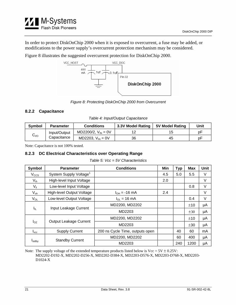
In order to protect DiskOnChip 2000 when it is exposed to overcurrent, a fuse may be added, or modifications to the power supply’s overcurrent protection mechanism may be considered.
Figure 8 illustrates the suggested overcurrent protection for DiskOnChip 2000.
Figure 8: Protecting DiskOnChip 2000 from Overcurrent
8.2.2 Capacitance Table 4: Input/Output Capacitance
Symbol Parameter Conditions 3.3V Model Rating 5V Model Rating Unit MD2200/2, VIN = 0V 12 15 pF
CI/O Input/Output Capacitance MD2203, VIN = 0V 36 45 pF
Note: Capacitance is not 100% tested.
8.2.3 DC Electrical Characteristics over Operating Range Table 5: Vcc = 5V Characteristics
Symbol Parameter Conditions Min Typ Max Unit VCCS System Supply Voltage1 4.5 5.0 5.5 V Vih High-level Input Voltage 2.0 V Vil Low-level Input Voltage 0.8 V Voh High-level Output Voltage IOH = -16 mA 2.4 V VOL Low-level Output Voltage IOL = 16 mA 0.4 V
MD2200, MD2202 ±10 µA IIL Input Leakage Current
MD2203 ±30 µA
MD2200, MD2202 ±10 µA IOZ Output Leakage Current
MD2203 ±30 µA Ivcc Supply Current 200 ns Cycle Time, outputs open 40 60 mA
MD2200, MD2202 60 400 µA Istdby Standby Current
MD2203 240 1200 µA
Note: The supply voltage of the extended temperature products listed below is Vcc = 5V ± 0.25V: MD2202-D192-X, MD2202-D256-X, MD2202-D384-X, MD2203-D576-X, MD2203-D768-X, MD2203-D1024-X
DiskOnChip 2000 DIP
22 Data Sheet, Rev. 3.8 91-SR-002-42-8L
Table 6: Vcc = 3.3V Characteristics
Symbol Parameter Conditions Min Typ Max Unit VCCS System Supply Voltage1 3.0 3.3 3.6 V
Vih High-level Input Voltage 2.7 V
Vil Low-level Input Voltage 0.6 V
VHYS Input Voltage Hysteresis 1.1 1.5 V
IOH = -18 mA 2.4 V Voh
High-level Output Voltage IOH = 0 mA Vcc-0.1 V
IOL = 18 mA 0.4 V VOL Low-level Output Voltage
IOL = 0 mA 0.1 V
MD2200, MD2202 ±10 µA IIL Input Leakage Current
MD2203 ±30 µA
MD2200, MD2202 ±10 µA IOZ Output Leakage Current
MD2203 ±30 µA
Ivcc Supply Current 150 ns Cycle Time, outputs open
30 60 mA
MD2200, MD2202 70 400 µA Istdby Standby Current
MD2203 300 1350 µA
Note: The supply voltage of the extended temperature products listed below is Vcc = 3. 3V ± 0.15V: MD2202-D192-V3-X, MD2202-D256-V3-X, MD2202-D384-V3-X, MD2203-D576-V3-X, MD2203-D768-V3-X, MD2203-D1024-V3-X
8.2.4 AC Operating Conditions
Timing specifications are based on the following conditions: Table 7: AC Operating Conditions
Parameter 3.3V Model 5V Model
Supply Voltage1,2 VCC = 3.3V ±0.3V VCC = 5V ±0.5V
Input Pulse Levels 0.2V to 2.9V 0.4V to 2.6V
Input Rise and Fall Times 1 ns 5 ns
Input and Output Timing Levels 1.5V 0.8V and 2.0V
Output Load 100 pF 50 pF
Notes: 1. The supply voltage of the extended temperature products listed below is Vcc = 3. 3V ±0.15V: MD2202-D192-V3-X, MD2202-D256-V3-X, MD2202-D384-V3-X, MD2203-D576-V3-X, MD2203-D768-V3-X, MD2203-D1024-V3-X
2. The supply voltage of the extended temperature products listed below is Vcc = 5V ±0.25V: MD2202-D192-X, MD2202-D256-X, MD2202-D384-X, MD2203-D576-X, MD2203-D768-X, MD2203-D1024-X
DiskOnChip 2000 DIP
23 Data Sheet, Rev. 3.8 91-SR-002-42-8L
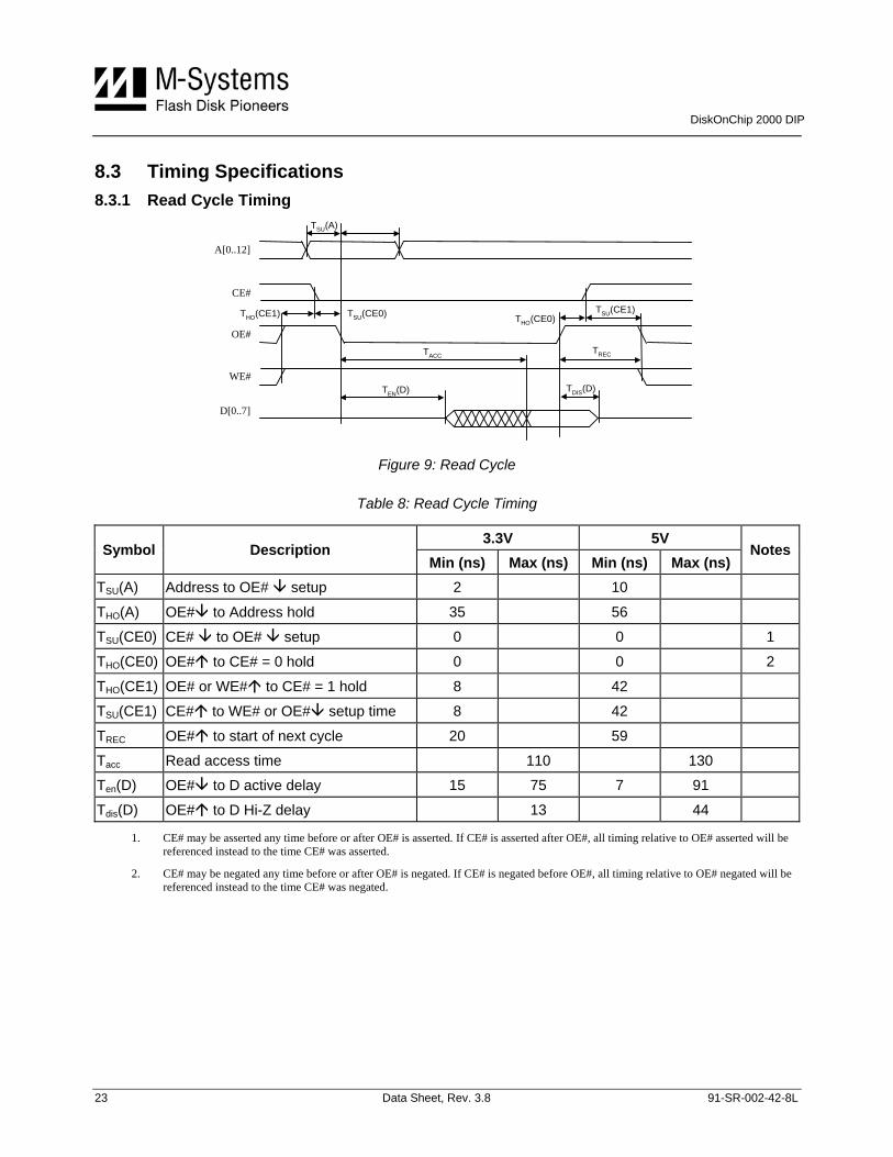
8.3 Timing Specifications 8.3.1 Read Cycle Timing
CE#
A[0..12]
OE#
D[0..7]
WE#
TSU(A)
TEN(D)
THO(CE1) TSU(CE0) THO(CE0)TSU(CE1)
TRECTACC
TDIS(D)
Figure 9: Read Cycle
Table 8: Read Cycle Timing
3.3V 5V Symbol Description
Min (ns) Max (ns) Min (ns) Max (ns) Notes
TSU(A) Address to OE# setup 2 10
THO(A) OE# to Address hold 35 56
TSU(CE0) CE# to OE# setup 0 0 1
THO(CE0) OE# to CE# = 0 hold 0 0 2
THO(CE1) OE# or WE# to CE# = 1 hold 8 42
TSU(CE1) CE# to WE# or OE# setup time 8 42
TREC OE# to start of next cycle 20 59
Tacc Read access time 110 130
Ten(D) OE# to D active delay 15 75 7 91
Tdis(D) OE# to D Hi-Z delay 13 44
1. CE# may be asserted any time before or after OE# is asserted. If CE# is asserted after OE#, all timing relative to OE# asserted will be referenced instead to the time CE# was asserted.
2. CE# may be negated any time before or after OE# is negated. If CE# is negated before OE#, all timing relative to OE# negated will be referenced instead to the time CE# was negated.

DiskOnChip 2000 DIP
24 Data Sheet, Rev. 3.8 91-SR-002-42-8L
8.3.2 Write Cycle Timing
CE#
TW(WE)OE#
WE#
A[0..12]
THO(A)TSU(A)
THO(CE1)
THO(CE0)
TSU(D) THO(D)
TREC
THO(CE0)TSU(CE1)
D[0..7]
Figure 10: Write Cycle
Table 9: Write Cycle Timing
3.3V 5V Symbol Description Min (ns) Max (ns) Min (ns) Max (ns)
Notes
TSU(A) Address to WE# setup time 0 10
THO(A) WE# to Address hold time 35 56
TW(WE) WE# asserted width 62 98
TSU(CE0) CE# to WE# setup time 0 0 1
THO(CE0) WE# to CE# = 0 hold time 0 0 2
THO(CE1) OE# or WE# to CE# = 1 hold time 8 42
TSU(CE1) CE# to WE# or OE# setup time 8 42
TREC WE# to start of next cycle 22 59
TSU(D) D to WE# setup time 50 48
THO(D) WE# to D hold time 0 40
1. CE# may be asserted any time before or after WE# is asserted. If CE# is asserted after WE#, all timing relative to WE# asserted will be referenced instead to the time CE# was asserted.
2. CE# may be negated any time before or after WE# is negated. If CE# is negated before WE#, all timing relative to WE# negated will be referenced instead to the time CE# was negated.

DiskOnChip 2000 DIP
25 Data Sheet, Rev. 3.8 91-SR-002-42-8L
8.4 Mechanical Dimensions
Figure 11: MD220x Mechanical Dimensions
Table 10: Low-Profile
MD2200 MD2202 Millimeters (max.) Millimeters (max.)
A 41.9 43.95
B 18.05 18.3
C 2.54 2.54
D 15.24 15.24
E 5.7 6.0
F 4.0 4.0
G 0.51 0.51
H 38.2 38.2
Table 11: High-Profile
MD2203 Millimeters (max.)
A 45.6
B 18.8
C 2.54
D 15.24
E 13.5
F 4.0
G 0.51
H 38.2
Note: The above dimensions are maximum values.

DiskOnChip 2000 DIP
26 Data Sheet, Rev. 3.8 91-SR-002-42-8L
9. ORDERING INFORMATION
MD2200-DCC-V-T (Low-Profile)
CC: Capacity (MB) 24
V: Supply Voltage Blank V3
5V 3.3V
T: Temperature Range (optional)
Blank X
Commercial: 0°C to +70°C Extended: -40°C to +85°C
MD2202-DCCC-V-T (Low-Profile)
CC: Capacity (MB) 16, 32, 48, 64, 96, 128, 192, 256, 384
V: Supply Voltage Blank V3
5V 3.3V
T: Temperature Range (optional)
Blank X
Commercial: 0°C to +70°C Extended: -40°C to +85°C
MD2203-DCCC-V-T (High-Profile)
CCC:
Capacity (MB) 576, 768, 1024
V: Supply Voltage Blank V3
5V 3.3V
T: Temperature Range (optional)
Blank X
Commercial: 0°C to +70°C Extended: -40°C to +85°C

DiskOnChip 2000 DIP
27 Data Sheet, Rev. 3.8 91-SR-002-42-8L
HOW TO CONTACT US USA M-Systems Inc. 8371 Central Ave, Suite A Newark CA 94560 Phone: +1-510-494-2090 Fax: +1-510-494-5545
China M-Systems China Ltd. Room 121-122 Bldg. 2, International Commerce & Exhibition Ctr. Hong Hua Rd. Futian Free Trade Zone Shenzhen, China Phone: +86-755-8348-5218 Fax: +86-755-8348-5418
Europe M-Systems Ltd. 7 Atir Yeda St. Kfar Saba 44425, Israel Tel: +972-9-764-5000 Fax: +972-3-548-8666
Internet www.m-systems.com
General Information [email protected]
Japan M-Systems Japan Inc. Asahi Seimei Gotanda Bldg., 3F 5-25-16 Higashi-Gotanda Shinagawa-ku Tokyo, 141-0022 Phone: +81-3-5423-8101 Fax: +81-3-5423-8102
Taiwan M-Systems Asia Ltd. 14 F, No. 6, Sec. 3 Minquan East Road Taipei, Taiwan, 104 Tel: +886-2-2515-2522 Fax: +886-2-2515-2295 Sales and Technical Information
This document is for information use only and is subject to change without prior notice. M-Systems Flash Disk Pioneers Ltd. assumes no responsibility for any errors that may appear in this document. No part of this document may be reproduced, transmitted, transcribed, stored in a retrievable manner or translated into any language or computer language, in any form or by any means, electronic, mechanical, magnetic, optical, chemical, manual or otherwise, without prior written consent of M-Systems.
M-Systems products are not warranted to operate without failure. Accordingly, in any use of the Product in life support systems or other applications where failure could cause injury or loss of life, the Product should only be incorporated in systems designed with appropriate and sufficient redundancy or backup features.
Contact your local M-Systems sales office or distributor, or visit our website at www.m-systems.com to obtain the latest specifications before placing your order.
© 2004 M-Systems Flash Disk Pioneers Ltd. All rights reserved.
M-Systems, DiskOnChip, DiskOnChip Millennium, DiskOnKey, DiskOnKey MyKey, FFD, Fly-By, iDiskOnChip, iDOC, mDiskOnChip, mDOC, Mobile DiskOnChip, Smart DiskOnKey, SmartCaps, SuperMAP, TrueFFS, uDiskOnChip, uDOC, and Xkey are trademarks or registered trademarks of M-Systems Flash Disk Pioneers, Ltd. Other product names or service marks mentioned herein may be trademarks or registered trademarks of their respective owners and are hereby acknowledged. All specifications are subject to change without prior notice.