Direct Sequence Spread Spectrum (DSSS) Receiver · The Direct-sequence spread-spectrum (DSSS)...
85
Direct Sequence Spread Spectrum (DSSS) Receiver User's Manual K L Harman Command, Control, Communications and Intelligence Division Defence Science and Technology Organisation DSTO-GD-0525 ABSTRACT The direct-sequence spread-spectrum (DSSS) receiver performs demodulation of wideband DSSS signals, accepting as input an analogue signal at low intermediate frequency (IF) or baseband, and producing as output the recovered digital message bitstream. It consists of firmware (FW) entities that perform signal processing; a PCI-compliant digital processor card (DPC) that provides analogue to digital conversion and host resources for the FW; and a computer which hosts the DPC and runs software to access, control and monitor it. This manual provides the information required to allow an operator to connect, configure and dynamically control the DSSS Receiver in a precise way to achieve the best demodulation performance. RELEASE LIMITATION Approved for public release
-
Upload
hoangthuan -
Category
Documents
-
view
230 -
download
1
Transcript of Direct Sequence Spread Spectrum (DSSS) Receiver · The Direct-sequence spread-spectrum (DSSS)...
Direct Sequence Spread Spectrum (DSSS) Receiver User's Manual
K L Harman
Command, Control, Communications and Intelligence Division Defence Science and Technology Organisation
DSTO-GD-0525
ABSTRACT The direct-sequence spread-spectrum (DSSS) receiver performs demodulation of wideband DSSS signals, accepting as input an analogue signal at low intermediate frequency (IF) or baseband, and producing as output the recovered digital message bitstream. It consists of firmware (FW) entities that perform signal processing; a PCI-compliant digital processor card (DPC) that provides analogue to digital conversion and host resources for the FW; and a computer which hosts the DPC and runs software to access, control and monitor it. This manual provides the information required to allow an operator to connect, configure and dynamically control the DSSS Receiver in a precise way to achieve the best demodulation performance.
RELEASE LIMITATION
Approved for public release
Published by Command, Control, Communications and Intelligence Division DSTO Defence Science and Technology Organisation PO Box 1500 Edinburgh South Australia 5111 Australia Telephone: (08) 8259 5555 Fax: (08) 8259 6567 © Commonwealth of Australia 2008 AR- 014-083 January 2008 APPROVED FOR PUBLIC RELEASE
DSSS Receiver User's Manual (U)
Executive Summary The Direct-sequence spread-spectrum (DSSS) Receiver program is a multi-faceted contribution to Defence wireless communications capability – it provides an alternative modulation scheme for special-purpose link scenarios as well as an advanced, reconfigurable, wideband signal processing engine that lends itself to multiple applications, with inherent functional and logistic advantages. Physically, a single receiver unit consists of the signal processing platform (designated the Digital Processor Card, or DPC) hosted in a computer chassis on the industry-standard PCI bus. The DPC digitises its input signal and provides reconfigurable logic circuits in which a wide variety of digital signal processing algorithms can be implemented. Functionally, the unit also requires both the signal processing code for the reconfigurable logic (known as firmware) and the application software which lets the host computer communicate with, control and monitor the DPC. Both the firmware and software for the DSSS application are parameterised and run-time configurable. To exploit this capability then, an operator needs to connect, configure and dynamically control the DSSS Receiver in such a way as to achieve the expected performance. It is the purpose of this manual to adequately define the interfaces and operation of the Receiver to allow this. Accordingly, this manual includes: definitions of hardware and firmware interfaces; the typical sequence of control and monitoring events following system power-up that lead to valid demodulation in the presence of a continuously transmitted signal; a file-level review of the DSTO DSSS graphical user interface (GUI) and driver software, which includes an example of fully automated set-up and operation; and receiver operating characteristics, in the form of bit error rate (BER) versus signal-quality curves, that indicate the expected performance levels in benign (white noise) channels. Dissemination of this document will facilitate uptake of the DSSS Receiver capability by Defence personnel and Defence contractors.
Authors
K L Harman Command, Control, Communications and Intelligence Division Kevin was awarded a Bachelor's Degree with Honours in Electrical & Electronic Engineering from the University of Adelaide in 1991. He joined DSTO in 1998 as a researcher in the domain of communications signal processing, focussing on wideband digital modem architectures and implementations.
____________________ ________________________________________________
Contents ABBREVIATIONS AND ACRONYMS
1. INTRODUCTION............................................................................................................... 1 1.1 Scope ........................................................................................................................... 1 1.2 Overview .................................................................................................................... 2
1.2.1 The DSTO Digital Processor Card (DPC)............................................... 2 1.2.2 DSSS signalling and the DSTO Receiver Architecture ......................... 3 1.2.3 DSTO DSSS Receiver Operations Summary.......................................... 8
2. RECEIVER INTERFACES ............................................................................................... 10 2.1 External Interfaces .................................................................................................. 11
2.1.1 Analogue Inputs ...................................................................................... 11 2.1.2 Reference Output..................................................................................... 11 2.1.3 JTAG .......................................................................................................... 12 2.1.4 LVDS Digital I/O .................................................................................... 12 2.1.5 PCI Bus Connector .................................................................................. 12
2.2 Internal Interfaces................................................................................................... 13 2.2.1 DCC Control Out..................................................................................... 13 2.2.2 Sample Clock In ....................................................................................... 14 2.2.3 Sampled Data In ...................................................................................... 14 2.2.4 Data and Clock Out................................................................................. 14 2.2.5 Configuration and Status Register I/O ................................................ 15 2.2.6 FIFO1 Out (Signal Monitoring) ............................................................. 15 2.2.7 FIFO2 Out (Data Logging) ..................................................................... 15
2.3 DSSS Memory Map................................................................................................ 16
3. CONFIGURATION REGISTER DEFINITIONS........................................................ 19 3.1 fir_bypass ................................................................................................................. 19 3.2 reset_ctrl.................................................................................................................... 20 3.3 interp_ctrl ................................................................................................................. 21 3.4 agc_dwell .................................................................................................................. 22 3.5 agc_thresh................................................................................................................. 22 3.6 agc_gain .................................................................................................................... 23 3.7 agc_ctrl ...................................................................................................................... 23 3.8 acq_thresh0............................................................................................................... 24 3.9 acq_thresh1............................................................................................................... 24 3.10 acq_thresh2............................................................................................................... 24 3.11 acq_thresh3............................................................................................................... 25 3.12 acq_thresh4............................................................................................................... 25 3.13 acq_thresh5............................................................................................................... 26 3.14 acq_thresh6............................................................................................................... 26 3.15 acq_thresh7............................................................................................................... 27 3.16 acq_serdwell ............................................................................................................ 27 3.17 acq_ctrl ...................................................................................................................... 27 3.18 chips_per_sym ......................................................................................................... 28

3.19 acqh_Nsym............................................................................................................... 29 3.20 dll_gain ..................................................................................................................... 29 3.21 dll_dwell................................................................................................................... 30 3.22 iprbs_tap ................................................................................................................... 30 3.23 iprbs_pha.................................................................................................................. 31 3.24 iprbs_ospha.............................................................................................................. 31 3.25 qprbs_tap.................................................................................................................. 32 3.26 qprbs_pha................................................................................................................. 32 3.27 qprbs_ospha............................................................................................................. 33 3.28 mode/dds_ctrl .......................................................................................................... 33 3.29 str_dwell ................................................................................................................... 34 3.30 str_gain...................................................................................................................... 34 3.31 str_lock...................................................................................................................... 35 3.32 dds_msw ................................................................................................................... 35 3.33 dds_lsw ..................................................................................................................... 36 3.34 afc_rate ...................................................................................................................... 36 3.35 ddet_gain .................................................................................................................. 37 3.36 clkset_data ................................................................................................................ 37 3.37 clkset_ctrl.................................................................................................................. 38 3.38 fifo_ctrl...................................................................................................................... 39 3.39 acqh_symlen ............................................................................................................ 39 3.40 pll_arst....................................................................................................................... 40 3.41 bsif_fifo_clr .............................................................................................................. 40 3.42 ddc_ph_msw ............................................................................................................ 41 3.43 ddc_ph_lsw .............................................................................................................. 41 3.44 ddc_rst ....................................................................................................................... 42
4. STATUS REGISTER DEFINITIONS............................................................................ 43 4.1 interp_status / agc_status....................................................................................... 43 4.2 acq_status.................................................................................................................. 43 4.3 str_samp_status ....................................................................................................... 44 4.4 str_lock_status ......................................................................................................... 45 4.5 prbs_offset................................................................................................................ 45 4.6 isym_mag.................................................................................................................. 46 4.7 qsym_mag................................................................................................................. 46 4.8 dsym_mag................................................................................................................. 47 4.9 dsym_pha.................................................................................................................. 47 4.10 afc_lsw....................................................................................................................... 48 4.11 afc_msw .................................................................................................................... 48 4.12 clkset_busy............................................................................................................... 48 4.13 fifo_status ................................................................................................................. 49 4.14 bsif_status................................................................................................................. 50 4.15 clkskew_test............................................................................................................. 50
5. FIFO SIGNAL CAPTURE INTERFACE ....................................................................... 51 5.1 Input Channels........................................................................................................ 51 5.2 Packing Modes ........................................................................................................ 51
6. RECEIVER CONFIGURATION AND OPERATION................................................ 53 6.1 Event Flowchart : Power-up to Demodulation .................................................. 53 6.2 Flowchart Event Descriptions............................................................................... 57
6.2.1 Power-up .................................................................................................. 57 6.2.1.1 State (1)...................................................................................................... 57 6.2.2 Device Initialisations............................................................................... 57 6.2.2.1 State (2)...................................................................................................... 57 6.2.2.2 State (3)...................................................................................................... 58 6.2.2.3 State (4)...................................................................................................... 59 6.2.3 Select Acquisition Mode ......................................................................... 63 6.2.3.1 State (5)...................................................................................................... 63 6.2.4 Initial Blind Acquisition ......................................................................... 64 6.2.4.1 States (9 to 22)........................................................................................... 64 6.2.5 Resume from Blind.................................................................................. 65 6.2.5.1 State (7)...................................................................................................... 65 6.2.6 Assisted Acquisition ............................................................................... 65 6.2.6.1 State (8)...................................................................................................... 65
7. THE DSTO DEVELOPMENT GUI................................................................................ 68 7.1 Code Hierarchy and Classes ................................................................................. 68
APPENDIX A: APPLICABLE SYSTEM CONFIGURATION ..................................... 72 A.1. Hardware configuration................................................................ 72 A.2. Firmware configuration ................................................................ 72 A.3. Development GUI configuration ................................................ 74
APPENDIX B: DSSS RECEIVER PERFORMANCE PROFILES ................................ 75

Abbreviations and Acronyms
A Ampere, used with SI prefixes AC Alternating current ADC Analogue-to-digital converter AFC Automatic frequency control AFF Asynchronous feed-forward AGC Automatic gain control AWGN Additive white Gaussian noise BB Baseband BER Bit error rate BITE Built-in test equipment bps Bits per second, used with SI prefixes BPSK Binary phase-shift keying CMOS CMOS semiconductor technology CORDIC COordinate Rotation DIgital Computer dB Decibel DC Direct current DCC Data conversion and clocking DDC Digital down-conversion DDP Digital data processor DDS Direct digital synthesis/synthesiser DPC Digital processor card DSP Digital signal processing DSSS Direct sequence spread spectrum DSTO Defence Science and Technology Organisation DQPSK Differential QPSK EEPROM Electrically erasable/programmable read-only memory ELDLL Early-late gate delay-locked loop EPLL Enhanced PLL FIFO First-in, first-out memory buffer FIR Finite impulse response (filter) FPGA Field-programmable gate array FW Firmware GBBM Generic baseband modem (a legacy designation for the
DPC) Gp Processing gain (in a spread spectrum system) GUI Graphical user interface HW Hardware Hz Hertz (cycle/second), used with SI prefixes I/O Input/Output IF Intermediate frequency JTAG Joint Test Action Group Interface standard LFSR Linear feedback shift-register

LO Local oscillator LPD Low probability of detection LPF Low-pass filter LSB Least significant bit/byte LSW Least significant word LVCMOS Low-voltage CMOS LVDS Low-voltage differential signalling m Metre, used with SI prefixes MB Megabyte MCPS Mega-chips per second MSB Most significant bit/byte m-sequence Maximum-length type PRBS MSW Most significant word NCO Numerically-controlled oscillator O(x) A value “of the order of “ x PC Personal computer PCI Peripheral component interconnect bus standard PLL Phase-locked loop PN Pseudo-noise ppm Parts per million PRBS Pseudo-random binary sequence QPSK Quaternary phase-shift keying RF Radio frequency RRC Root-raised cosine s Second, used with SI prefixes SNR Signal-to-noise power ratio SPS Samples per second, used with SI prefixes STR Symbol timing recovery SW Software .ttf Tabular text file format V Volts, used with SI prefixes VHDL Very high speed integrated circuit Hardware Description
Language Ω Ohms
DSTO-GD-0525
1
1. Introduction
1.1 Scope
This document is the User’s Manual for the Direct-sequence Spread-spectrum (DSSS) Receiver developed by the Secure Communications Branch of the Defence Science and Technology Organisation (DSTO). The DSSS Receiver performs demodulation of wideband DSSS signals, accepting as input a spread analogue signal at low intermediate frequency (IF) or baseband, and producing as output a despread message bitstream in digital form. It consists of DSSS firmware (FW) entities (in VHDL) that perform signal processing; a PCI-compliant digital processor card (DPC) that provides analogue to digital conversion (ADC) and FPGA resources for the FW; a computer with a PCI-bus which hosts the DPC; and driver and interface software (SW) for control and monitoring of the FW application. The operator needs to connect, configure and dynamically control the DSSS Receiver in a precise way to achieve the best demodulation performance. This manual provides the following information to facilitate such operation:
• Definitions of hardware (HW) and FW interfaces. • The typical sequence of control and monitoring events following system power-up
that lead to valid demodulation in the presence of a continuously transmitted signal. • A file-level review of the DSTO DSSS graphical user interface (GUI) and driver
software, which includes an example of fully automated Receiver set-up and operation.
• Receiver operating characteristics, in the form of bit error rate (BER) versus Eb/No
curves, that indicate the expected performance levels in benign (AWGN) channels. In the remainder of this introduction, the fundamental physical and logical components of the Receiver and the basic concepts of operation will be reviewed. Then in Section 2, the Receiver’s interfaces, both physical and functional, will be described. Many of the interfaces are defined in FW and accessed over the PCI bus. These include configuration registers, status registers and signal capture channels, for which interface definitions are given in Sections, 3, 4 and 5 respectively. With these interfaces, a method of operation is described in Section 6. For this approach many of the suggested algorithms have already been coded into functional SW in the form of a Development GUI, and this application is described in Section 7. Due to the highly reconfigurable nature of the DPC and its FW applications, the applicability of this manual is restricted to the specific Receiver configuration given in Appendix A.

DSTO-GD-0525
2
1.2 Overview
1.2.1 The DSTO Digital Processor Card (DPC)
The DSTO DPC is a highly configurable and computationally powerful signal processing engine. It consists of a mainboard with up to four plug-in modules. The mainboard is a universal (3.3v or 5v) PCI plug-in card with extended length form-factor that supports 64/32-bit and 66/33- MHz modes of operation and is compliant with revision 2.2 of the PCI standard. The mainboard features include:
• A PCI Interface Target, implemented as a custom FW entity in an Altera EP1S10F484C5 FPGA. This device is configured at boot-time from an Altera EPC8QC100 configuration EEPROM in fast passive-parallel mode.
• Four module sites designated Slot#0 to Slot#3, each of which can host a plug-in module. A pair of high-density connectors for each slot facilitates Target-to-Slot, Slot-to-Slot (adjacent Slots only) and power rail connectivity.
• Back-end (application-side) PCI signalling between the Target and the Slots, allowing PCI access to each plug-in module.
• Custom signalling between the Target and the Slots, intended primarily as an FPGA configuration bus when plug-in modules contain volatile FPGAs.
• JTAG interfacing to the Target and Slots. There are independent 3.3v and 1.5v JTAG chains accessible via the same 12-pin header. The 3.3v chain is for the PCI Target FPGA and its configuration EEPROM, whereas the 1.5v chain is for Altera Stratix-type FPGAs in the Slots.
• Local power generation and conditioning, using custom switching supply circuits with the PCI power rails as inputs.
• A PCI back-panel with analogue I and Q inputs (SMA F/M), a reference frequency output (SMA F/M), and a JTAG port (12-pin header, M).
There are two plug-in modules pertinent to the DSSS Receiver, namely a Data Conversion and Clocking (DCC) module and a Digital Data Processing (DDP) module. The DCC is essentially an ADC module, and also provides the primary signal processing clock. It features:
• High-stability clock generation and distribution. It provides a fixed-rate, 200 MHz sample clock with 100ppm stability and 1ps of 1-σ phase jitter.
• Two channels of synchronous analogue to digital conversion with 10-bit, 200MSPS ADC devices identified as the in-phase (I) and quadrature-phase (Q) channels (consistent with application in quadrature signalling schemes). The ADC output on each channel is presented in a demultiplexed form at half rate, together with a sample-synchronous 100 MHz output clock. The demultiplexed channels are designated as channel A and channel B, leading to four 100MSPS output streams designated IA, IB, QA and QB, each with 10-bit resolution.
DSTO-GD-0525
3
• External (adjacent Slot) control of the ADC enable, output data format and output data interleaving controls.
• Local power generation and conditioning. The DDP is the main signal processing engine, hosting a high-density FPGA for FW-based operations. It features:
• An Altera EP1S80F1508C6 FPGA. This provides approximately 80,000 LE, 7,427kbit RAM, and 22 embedded DSP Blocks for up to 176 x 9-bit multipliers. It supports clock rates in excess of 200 MHz.
• Connection to the mainboard back-end PCI and configuration buses. • High-density signalling to adjacent Slots. • A 42-way LVDS (or 84-way LVCMOS) Digital Input/Output (I/O) Header for general
purpose I/O. • Local power generation and conditioning. • Test headers.
When hosting the DSSS Receiver FW, the DPC would normally be configured with a DCC in Slot#0 and a DDP in Slot#1. 1.2.2 DSSS signalling and the DSTO Receiver Architecture
This manual does not provide a technical introduction to DSSS signals and systems, but does assume familiarity with key concepts such as spreading signal generation and modulation, processing gain (Gp), the processes inherent in spread signal demodulation such as acquisition, tracking and despreading, and QPSK modulation principles. The DSTO DSSS transceiver is a noncoherent, burst-capable simplex link optimised for low probability of detection (LPD), fast acquisition, high data rates and simple transmitter architecture.
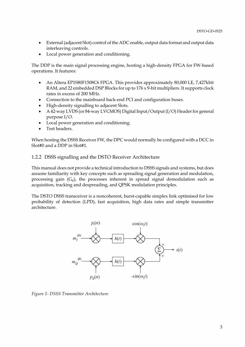
Figure 1- DSSS Transmitter Architecture
DSTO-GD-0525
4
On the transmit side, the signal varies from conventional DQPSK only through the independent (but synchronous) spreading of each of the I and Q components of the symbol prior to upconversion, as shown in Figure 1. Referring to this figure, note the following:
• This is an unbalanced modulator, in which different signals are applied to the I and Q channels, allowing the higher spectral efficiency of QPSK (relative to BPSK) to be utilised but requiring specialised processing to facilitate despreading in the presence of frequency errors.
• The QPSK message symbol m = mI + j*mQ is differentially encoded. The following Karnuagh maps define the encoding process, with the input symbol stream given by S(n) = In + j*Qn:
mI In-1 / Qn-1
In / Qn 00 01 11 10 00 0 1 1 0 01 1 1 0 0 11 1 0 0 1 10 0 0 1 1
mQ In-1 / Qn-1
In / Qn 00 01 11 10 00 0 0 1 1 01 0 1 1 0 11 1 1 0 0 10 1 0 0 1
• The spreading codes pI and pQ should be m-sequences of up to 16th order (65535 chips
in length). • The spreading codes should be of the same order to minimise acquisition time, but
should have different sequences and initial phases to allow discrimination between the I and Q channels in the presence of frequency error at the receiver.
• The Receiver supports spreading rates up to 50 MCPS, but could have its FW “place and route” optimised to support at least 100 MCPS.
• The symbol rate can be up to 2MSPS (4 Mbps) at 50 MCPS or 4MSPS (8 Mbps) at 100 MCPS. At these rates the processing gain for demodulation is Gp = 14dB.
• The symbol rate should be chosen with respect to the spreading rate to give an integer number of chips per symbol (equal to the processing gain Gp) but need not be otherwise synchronised with the spreading codes. This allows a very long and noise-like PRBS to be used with very short symbols, preserving the desired LPD spectral properties even at high data rates, but requires specialised symbol timing recovery at the receiver.
On the receive-side, the architecture is shown in Figure 2. A representative RF Downconverter stage is shown at the top of this figure, and serves to provide a quadrature baseband or low-IF signal r(t) to the DPC.

DSTO-GD-0525
5
Following the signal processing path, the received signal is then anti-alias filtered (analogue LPF with fc = 140 MHz ) and digitised at 200MSPS with 10-bit resolution. Each of the I and Q channels are independently but synchronously sampled.
Complex Real
ADC
FIR Filter
Interpolator
Acquisition Correlators
Acquisition Control
Tracking Correlators
Tracking Control
Noncoherent Despreader
RPC Diff Det
Sym Dec
Acquired Flag
2 x OS r(t)
Early
Late
AFF Sample control
Yi
Yq
Ymag
Yang
Ydm
Yda Data Out
I(z)+jQ(z)
4 x OS
On-time
Adv., Ret.
Adv., On-time
S BAND TUNER 2 TO 2.5 GHz ALC
QUADRATURE DOWN-CONVERSION
720MHz LO
r(t)
fc
LNA
RF Stage
e-j.fIF
Figure 2- DSSS Receiver Architecture
A digital downconversion (DDC) stage follows in which the full-rate complex signal is downconverted by mixing with a FW-generated complex numerically controlled oscillator (NCO). The NCO has a 32-bit, dithered phase accumulator, providing fine frequency resolution and good spurious suppression in the downconversion. Sample rate decimation occurs at chip rates less than 100 MCPS. The DCC HW always samples at 200MSPS, but the DSSS FW expects minimum (x2) over-sampling of the chip rate, which facilitates the maximum possible chip rate for a given ADC capability. The decimation

DSTO-GD-0525
6
scheme only permits chip periods of 20ns or longer in 10ns increments, which is a constraint that facilitates decimation without the FW complexity of high rate interpolated resampling. The signal is then root raised-cosine (RRC) match-filtered to the expected chip pulse shape with finite impulse response (FIR) filters (or just lowpass filtered if the transmitted pulses are not matched). These filters have a multi-rate architecture and multiplier-free implementation which facilitates high throughput but conserves FW resources. These filters may be bypassed under FW control. Linear interpolators then up-sample the signal to 4 samples per chip. This was established by design to be the minimum sufficient sample rate for good tracking performance and hence good demodulator BER. The interpolators span a sliding window of 5 input samples, producing all the “in-between” samples to give an output set of eight interpolated samples. Three of these output channels at ½-chip relative offsets, designated ‘advanced’, ‘on-time’ and ‘retarded’, are selected under the control of the tracking loop, and used variously for the remaining demodulation processes. Note that each interpolated channel here is still a spread, complex signal and may have timing errors in both the carrier domain (a frequency error fe, typically referred to as noncoherence) and in the modulation domain (a chip rate error Re, typically referred to as synchronisation error). Of the interpolated outputs, the on-time and advanced are used as inputs to the acquisition circuits, the advanced and retarded are used as inputs to the tracking circuits, and the on-time is processed for demodulation. Spreading code acquisition is the first process that must occur to facilitate demodulation. The acquisition circuits consist of acquisition correlators and an acquisition controller. To minimise the mean acquisition time in support of burst transmissions, the correlators have a parallel architecture and the longest length that could be implemented in the first generation of DPC hardware. To reduce the variance in the acquisition time, two channels of interpolated output are tested simultaneously, in the so-called on-time and advanced correlators. To permit noncoherent correlation a sum-of-squares (envelope) style test is made. The correlators can be configured for different internal arrangements which are trade-offs between correlation length and number of effective bits of the input samples used in the correlation. The arrangement 512 x 1-bit is effective for most scenarios and provides correlation testing with 27dB of processing gain. To initialise acquisition testing, the controller will preload correlator code registers with known phases of the local spreading codes, disable code register clocking to maintain those code phases, and reset an acquisition state tree (dwell tree) to the zero (bottom) state, representing the unacquired condition. On every subsequent chip-clock event, sampled data is clocked in to correlator data registers and a comparison is made between the code and data register contents, producing a correlation score with a pipeline delay. The controller compares the correlation scores from both the on-time and advanced correlators against a user-defined threshold and if either exceeds the threshold it advances the dwell state and enables clocking of the code registers with a phase advanced copy of the local spreading codes (to compensate for pipeline latency). The correlation score is retested after the code and data registers have flushed stale data (which takes as many chip clocks as the correlators are long), and then
DSTO-GD-0525
7
retested periodically at this rate. Every time the threshold for the current dwell is exceeded the dwell state is incremented, otherwise it is decremented. If the dwell state reaches a user-defined height then acquisition is declared. If the dwell state reaches zero again, then acquisition fails and the process is repeated. To compensate the chip error Re a tracking loop is required. The tracking loop has a conventional early-late gate delay-locked loop (ELDLL) architecture. A noncoherent correlation against both the advanced and retarded timing phases out of the interpolator is performed against the current local code phases following acquisition. These correlators have a serial (accumulator-like) architecture, giving a new result once per accumulation period (or dwell) as specified by the user. The difference between the advanced and retarded test results is an error signal that, after smoothing and scaling, can be used to change the interpolator channel selections to maintain the on-time channel at the optimum sampling instant. Since there are 4 samples per chip after interpolation, the tracking loop timing accuracy is (+/-) 1/8th of a chip. Also, the tracking loop can make at most three state adjustments in one direction before the desired timing point crosses a chip boundary, in which case the local spreading code phases must be incremented or decremented by 1 clock. When the tracking loop gain is correct, the on-time channel from the interpolators will represent the received signal with 1 sample per chip at the best available sampling instant, and can be input to the demodulation chain for despreading and QPSK demodulation. Note that up to this point there are no feedback loops for carrier or clock recovery, and hence no associated loop synchronisation delays. This architecture, which has been described as an asynchronous feed-forward (AFF) architecture, was chosen in support of rapid processing for burst signalling, and to allow operation at very low SNR where timing recovery circuits can be ineffective. In the demodulation chain, the despreader cannot use envelope-style correlators without masking the underlying symbol. Accordingly an alternative noncoherent despreader which preserves the modulation content was developed. This allows noncoherent operation, but has a 3dB performance penalty when compared against a coherent equivalent. The despreader is based on serial correlators, with accumulation time equal to the number of chips per symbol. Its output, at 1 sample per symbol, is a DQPSK symbol with 16-bit real component on the I-channel and 16-bit imaginary component on the Q-channel. As the despreader correlators are of the accumulation type they require a sample and dump timing strobe, which is in fact the synchronised symbol-rate clock. This symbol clock is also required for the remainder of the DQPSK demodulation. The symbol clock rate is known from the chip timing and fixed number of chips per symbol, but the clock phase is initially unknown. A symbol timing recovery (STR) loop operates in parallel with the despreader to find the required phase. It employs noncoherent despreaders operating at assumed optimal and offset sampling phases to generate an error signal that, after smoothing and scaling, can be used to drive the actual sample phase to the correct point. Demodulation of the DQPSK symbol stream follows conventional algorithms. This FW implementation first uses a CORDIC rotator to convert the symbol from rectangular to polar
DSTO-GD-0525
8
coordinates. Differential detection is then computationally simple, and yields the difference angle Yda, at one sample per symbol, which can be decoded to recover the message bitstream. Automatic gain control (AGC) and automatic frequency control (AFC) are ancillary functions not shown explicitly in Figure 2. AGC is available immediately after sampling from a control loop that senses overflow events in the sampled data. The application of the AGC loop output to the actual control of attenuators in the RF Downconverter will depend on the specifics of the downconverter used. AFC is available after differential detection from a control loop that strips the modulation from the differentially detected angle and averages the result to estimate a mean fe. A correction ‘-fe’ to the DDC downconversion frequency can then effect frequency control. The AFC loop algorithm has a finite deterministic detection range of –Rs/8 ≤ fe ≤ +Rs/8, where Rs is the symbol rate. Actual errors outside of this range ‘fold back’ into this range and can lead to ‘tracked errors’ at multiples of Rs/4. Note that the AFC loop output is only valid when the decoded DQPSK signal is valid, hence AFC should be disabled until acquisition, tracking, and possibly data verification, have been achieved. 1.2.3 DSTO DSSS Receiver Operations Summary
This section provides a brief summary of normal operation of the DSSS Receiver. Operation starts at power-up. Since the Stratix FPGAs on the DPC are volatile, they will be unconfigured at power-up, with all user I/O pins tri-stated. ADC control pins will be floating, leaving the ADCs in an unknown state. The PCI Target FW will be automatically uploaded to the EP1S10 from the EPC8 EEPROM, such that it is fully configured before the host BIOS interrogates its PCI Device Configuration Header. During boot-up, the host will interrogate the DPC device and allocate memory resources for DPC in the host memory map. When the host has finished booting, a DPC device driver must be installed to facilitate DPC control and monitoring. This would normally be integrated into start-up scripts. Application SW on the host can then interact with the DPC PCI Target’s Configuration peripheral to configure the FPGA on the Slot#1 DDP. The desired (DSSS) configuration file, in Altera’s tabular text file (.ttf) format, should reside on the host and be uploaded to the DDP. The DSSS FW application is then available (FPGA user I/O are active, and the DSSS will respond as a peripheral on the back-end PCI-bus in accordance with its defined memory map) but unconfigured. Application SW should set the state of each configuration register to specify a desired operating mode.

DSTO-GD-0525
9
The DSSS application expects a low IF or baseband quadrature input signal. This should be provided by a suitable wideband RF downconverter, tuned to the nominal carrier frequency and with its I/Q outputs connected to the I/Q inputs on the DCC via the DPC backpanel. When it is desired to commence demodulation, the ADCs should be enabled with parallel interleaving and offset-binary data format. Keeping the ADCs disabled until this point reduces power dissipation. AGC should be enabled at this stage. The AGC FW will provide a control word (an 8-bit digital attenuator setting) that needs to be monitored by the host and updated on the RF Downconverter on a periodic basis appropriate to the hosts scheduling priorities and the rate of change of amplitude variation induced by the channel. Signal demodulation then requires the successful completion of a sequence of processes, starting with spreading code acquisition. Acquisition control registers should be set for the expected (or tested) signal conditions. Code tracking will take place when acquisition completes. The tracking loop gain may need to be (dynamically) adjusted to maintain acquisition. Symbol timing recovery will also be attempted when acquisition is completed. STR loop gain is normally static for a given symbol rate. The Receiver will produce a demodulated bitstream at this stage. The quality (BER) of the bitstream will depend on many factors, and it may be appropriate at this stage to initiate monitoring operations which attempt to verify valid demodulation, and initiate operations such as AFC to minimise BER. The demodulated message bitstream is available via the DDP Digital I/O interface or may be logged directly by the host over PCI.
DSTO-GD-0525
10
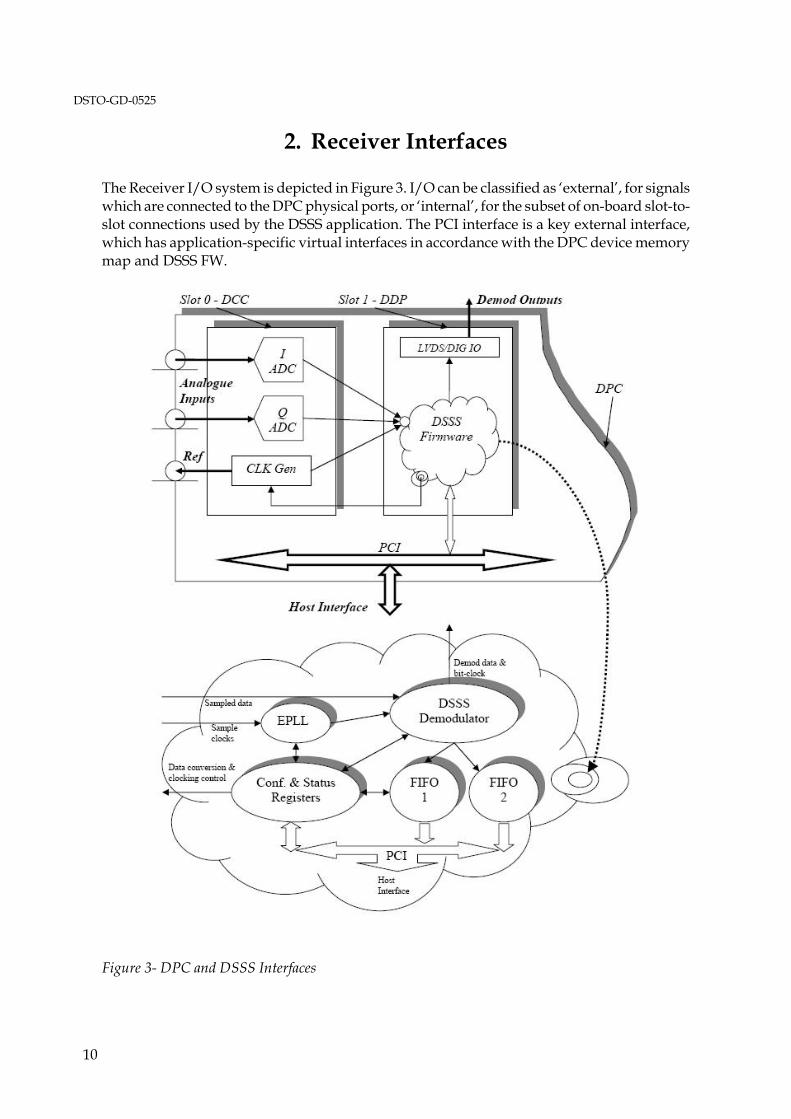
2. Receiver Interfaces
The Receiver I/O system is depicted in Figure 3. I/O can be classified as ‘external’, for signals which are connected to the DPC physical ports, or ‘internal’, for the subset of on-board slot-to-slot connections used by the DSSS application. The PCI interface is a key external interface, which has application-specific virtual interfaces in accordance with the DPC device memory map and DSSS FW.
Figure 3- DPC and DSSS Interfaces
DSTO-GD-0525
11
In a typical installation, the Receiver is powered, controlled and monitored via the PCI interface. The modulated input signal is applied to external analogue input channels, and the demodulated output bits are either taken as digital I/O from an external interface or logged over PCI to digital storage. 2.1 External Interfaces
2.1.1 Analogue Inputs
Designation : I_in, Q_in. Location : DPC backpanel. Type : SMA F/M. Specifications : Maximum input: -5V ≤ Vin ≤ +5V Full-scale input: -128mV ≤ Vin ≤ +128mV Impedance: 50Ω, AC-coupled. Signal BW: ≤ 100 MHz Signal occupancy: 200 kHz ≤ fc ≤ 300 MHz (768 MHz) Narrowband Description : These are the primary signal inputs. Each input channel is independently but synchronously sampled with a 10-bit, 200MSPS ADC, leading to a maximum non-aliased signal BW of 100 MHz. When the signal spectrum extends beyond 100 MHz a complex downconversion is required to shift the spectrum below 100 MHz to avoid aliasing. The ADC BW is 768 MHz, but the realisable complex downconversion will be limited by the maximum internal LO that can be generated by DDS. For the given DSSS application this is presently 200 MHz, leading to the actual maximum occupancy of 300 MHz. For DSSS applications, I_in and Q_in should be used as a quadrature pair. 2.1.2 Reference Output
Designation : REF. Location : DPC backpanel. Type : SMA F/M. Specifications : VOL: ≤ 300mV +3.2mA VOH: ≥ 2.6V -3.2mA Impedance: 50Ω, DC-coupled. Frequency range: 10.7 MHz +/- 180 kHz Description : Provides a nominal 10.7 MHz squarewave reference signal for synchronisation of external systems. In DSSS applications where the input is at low-IF and final downconversion is done digitally this reference is likely to be redundant. Otherwise this reference may be used for AFC applications under control of the DSSS FW.
DSTO-GD-0525
12
2.1.3 JTAG
Designation : JTAG. Location : DPC backpanel. Type : 12-pin, 0.1” header. Specifications : JTAG standard port. Description : This connector provides access to both a 3.3V and a 1.5V JTAG chain. The 3.3V chain accesses the DPC Mainboard FPGA and its configuration EEPROM. The 1.5V chain accesses FPGAs on Slots 0 to 3. Pin assignments for 3.3V or 1.5V connectivity follow from the DPC schematics Sheet “F1.3 BS-2”. A breakout cable is available. 2.1.4 LVDS Digital I/O
Designation : DDP-X1. Location : DDP component-side. Type : 84-pin SAMTEC high speed header (2 x 42 x 0.8mm). Specifications : 17mΩ, 2.0A per contact typical. 8GHz sinusoidal signalling rate. Description : Operates as either 42 LVDS-standard differential I/O channels or 84 LVCMOS single-ended I/O channels. The DSSS FW configures the interface for 21 LVDS output channels and 21 LVDS input channels. 2.1.5 PCI Bus Connector
Designation : DPC-X1. Location : DPC card edge. Type : 64-bit universal PCI edge connector. Specifications : See “PCI Local Bus Specification, Revision 2.2”. Description : The PCI physical interface supports 32/64-bit and 33/66 MHz transactions in accordance with Revision 2.2 of the PCI Standard. The DPC PCI Target FW supports the following transaction types from the standard : C/BE[3::0]# Command Type 0110 Memory Read 0111 Memory Write
DSTO-GD-0525
13
1010 Configuration Read 1011 Configuration Write 1100 Memory Read Multiple 1110 Memory Read Line 1111 Memory Write and Invalidate The DSSS FW operates in 32-bit/33 MHz mode and will halt transactions that request multiple data phases using ‘Disconnect with data’ handshaking (See Section 3.3.3.2 of the PCI 2.2 Standard). 2.2 Internal Interfaces
2.2.1 DCC Control Out
This is a set of logic signals passing from a Slot#1 DDP to a Slot#0 DCC for control of the ADCs and DDS. The signals include :
• ADC_SYNC : The ADC enable strobes, ACTIVE LOW, which enable both the sampled data ports and the output clock ports. A single signal is connected to both ADCs in parallel and should be controllable via the DDP (not tied low). The ADC_SYNC signal is sampled by the ADC Encode clock and must meet set-up and hold times with respect to the rising edge of this clock. However because the assertion of ADC_SYNC from the adjacent DDP will be asynchronous to the Encode clock it is possible for the signal to be asserted in violation of the set-up time, with the result that it is indeterminate if the ADC will synchronise sampling about the current clock edge or the next edge. This creates the possibility that the ADCs will synchronise about different edges, which will skew the relative timings of the sampled data in the I and Q channels.
To prevent this it is necessary to test the relative phases of the ADCs and repeatedly disable and enable the sampling until the correct phase is achieved. The DSSS FW provides a suitable test circuit based on sampling the output clock of one ADC with the output clock of the other ADC, and returning the sample result (1 or 0) via a status bit. For any given turn-on phase, the test result will be constant. In the alternate phase position, the opposite test result will be returned constantly. Thus if the skewed phase result is less likely than the correct result, the correct phase may be established by a majority vote on a set of tests.
• ADC_IP : Controls the relative timing (interleaved or parallel) of the demultiplexed A
and B sampled data ports. The DSSS FW expects parallel mode (ADC_IP = 0). • ADC_DFS : Controls the signed number format (offset binary or two’s complement) of
the sampled data. The DSSS FW expects offset binary (ADC_DFS = 0). • dds_upd : Causes the DDS to update its output in accordance with the contents of its
input registers (ACTIVE HIGH). • dds_rst : Resets the DDS output to zero (ACTIVE HIGH). • dds_clk : Clocks data in to the input registers, rising edge sensitive. • dds_data[7..0] : Configuration data port for the DDS.
DSTO-GD-0525
14
2.2.2 Sample Clock In
When the ADCs are enabled, each ADC outputs a demultiplexed sample rate clock (at 100 MHz) that is sample synchronous, i.e. the rising edge of the sample clocks is the optimum sampling point for the sampled data. A complement clock is also issued (falling edge sample synchronous). All four of these clocks strobes are routed from Slot#0 to Slot#1 for use by Slot#1 FW. The DSSS FW utilises the true clock from the I-channel ADC as the reference clock (ref_clk) for DSSS signal processing. This clock becomes the reference to a Stratix EPLL entity that is programmed for both frequency and phase to become the DSSS chip clock (chip_clk). The DSSS chip_clk may be programmed for periods of 20ns or more, in 10ns increments (giving allowable chip rates, in MHz or MCPS, of 50, 33.3, 25, 20, 16.6, 14.3, etc.). This is a limitation not of the EPLL but of the simplified sampled data decimation circuit which uses both ref_clk and chip_clk to decimate sampled data and only provides valid resampling when the 10ns increments are preserved. The chip_clk phase may need to be adjusted when a new frequency is programmed or a new place and route of the DSSS FW is developed. This is because the sampled data from the ADCs has a narrow window of validity and the original synchronisation between sampled data and the ADC output clocks is skewed in an indeterminate way as the clocks and data are routed through the FPGA floorplan, or as the phase of the EPLL output clock changes when reprogrammed. Adjustment is a trial and error process based on visualising sampled data and checking for perturbations consistent with poor sampling phase. Once established for given operating conditions, the required phase is repeatable. 2.2.3 Sampled Data In
Sampled data is routed from Slot#0 to Slot#1. Each ADC outputs two (demultiplexed) streams of data, suffixed with A- or B- identifiers. Thus there are I_A[9..0], I_B[9..0], Q_A[9..0] and Q_B[9..0] data channels, each clocking at 100 MHz (a 4Gbps data throughput). Note that the DSSS FW is an 8-bit application, and uses only the top 8-bits of each data channel. 2.2.4 Data and Clock Out
Demodulated data from the DSSS FW is available as a bitstream via the LVDS Digital I/O header on the DDP in Slot#1. To aid resampling of the bitstream a bit-synchronous clock is also provided (resample on the rising edge). These signals are provided as single-ended LVCMOS (3.3V) digital outputs, with the demodulated data assigned to DDP-X1-p46 (EXT_TXOUT(16)) and the clock assigned to DDP-X1-p58 (EXT_TXOUT(20)). When used in conjunction with the DPC Break-out board these map to connectors X1-p9 and X2-p33 respectively.
DSTO-GD-0525
15
2.2.5 Configuration and Status Register I/O
The DSSS FW implements a number of Configuration and Status Registers that facilitate control and monitoring of the DPC and the DSSS demodulator. In the current configuration, there are 128 x 16-bit register locations of which 96 are designated as configuration registers (they may be written to by the PCI Host, and can be read by both the DSSS application and the host) and the remaining 32 are designated as status registers (they are written to by the DSSS application, and can only be read by the host). Register operations are synchronous with the PCI clock and hence asynchronous with the DSSS signal processing clocks (chip_clk and its derivatives). Of these, forty four (44) configuration registers are in use, and are defined in Section 3. Fifteen (15) status registers are in use, and are defined in Section 4. 2.2.6 FIFO1 Out (Signal Monitoring)
The DSSS FW implements a 64k x 32-bit FIFO buffer for high rate sampling of the DSSS FW internal signals. The FIFO is clocked at half the chip rate (which is a legacy of an older generation of DSTO DSSS hardware). Thus the maximum sampling rate of internal signals is 25 MHz (at 50 MCPS). A variety of signal capture combinations are predefined in the FW (see dsss_fifopacker.vhd and dsss_gbbm_port.vhd). These are split into modes and channels, where the mode determines the actual sample rate of the signals (which may be increased by double-buffering when the signal of interest is no more than 16-bits in width, or decreased by interleaving multiple signals) and the channel determines which signals are input to that mode. This is discussed further in Section 5. FIFO management is via the Configuration and Status registers. FIFO data is read over the PCI bus to the host. Note that although described as a FIFO this memory is in fact implemented with dual-port RAM internal to the EP1S80 FPGA on the DDP, and is allocated its full size in the DSSS memory map. Thus the PCI host can actually have random access to the FIFO if required. However the FIFO-like access granted to the DSSS application on the input side of the FIFO relies on internal address counters and control logic such that the FIFO, once filled, is only declared empty again after the host has performed 64k reads to FIFO memory space. Thus FIFO address pointers can become corrupted if the host accesses the memory this way. 2.2.7 FIFO2 Out (Data Logging)
The DSSS FW implements a dedicated data logging FIFO, with a dual, paged 8k x 32-bit arrangement. The incoming demodulated data bitstream is packed into 32-bit words and written into one FIFO (the write-FIFO) while the other FIFO (the read-FIFO) is being emptied by the host. When the write-FIFO fills it automatically becomes the read-FIFO and the previous read-FIFO, which should now have been emptied by the host, becomes the new write-FIFO. The Configuration and Status Register interface facilitates FIFO reset and FIFO

DSTO-GD-0525
16
FULL and Overflow polling operations. A dedicated 32-bit register is assigned for FIFO2 retrieval, and the read-FIFO is emptied by 1 word every time this location is read by the host. 2.3 DSSS Memory Map
The DPC is allocated dedicated memory addresses in the host memory map. The size of the DPC memory allocation is determined by a constant specified in FW at boot time and read by the host BIOS from the DPC PCI Configuration Register space. This constant resides in the pcitgt_package.vhd file, where it is defined as follows:
-- PCI Base Address Register, Memory Space required: the L_CR_BAR_SIZE constant specifies the amount -- of memory space required, in units of 16 bytes. Determine the amount of memory required, write out -- the value in binary, subtract 1, and then invert to get the value to set the L_CR_BAR_SIZE constant. constant L_CR_BAR_SIZE : std_logic_vector(27 downto 0) := X"FFF0000";
This is the request used by the DSSS Receiver, and specifies a 16MB space. The actual (‘physical’ or ‘bus’) base address at which this memory resides is system dependent. There are multiple PCI-capable peripherals within the DPC allocation (such as the FPGA Configuration entity, and the Slots #0 to #3) so additional partitioning of the DPC memory is required to enable decoding of individual ‘chip-selects’. This partitioning is handled in the PCI Target FW. The following extract from pciif_package.vhd shows how the DPC memory is mapped in the DSSS Receiver application:
constant BKLC_XXX_LADDR : std_logic_vector( 31 downto 0) := X"00000000"; -- Deliberately Unused Lower Address range. constant BKLC_XXX_UADDR : std_logic_vector( 31 downto 0) := X"000000FF"; -- Deliberately Unused Upper Address range. constant BKLC_CFG_LADDR : std_logic_vector( 31 downto 0) := X"00000100"; -- External Stratix Configuration Lower Address Range. constant BKLC_CFG_UADDR : std_logic_vector( 31 downto 0) := X"000001FF"; -- External Stratix Configuration Upper Address Range. constant BKLC_PERIPH1_LADDR : std_logic_vector( 31 downto 0) := X"00000200"; -- Example peripheral 1 Lower Address Range. constant BKLC_PERIPH1_UADDR : std_logic_vector( 31 downto 0) := X"000002FF"; -- Example peripheral 1 Upper Address Range. constant BKLC_PERIPH2_LADDR : std_logic_vector( 31 downto 0) := X"00000300"; -- Example peripheral 2 Lower Address Range. constant BKLC_PERIPH2_UADDR : std_logic_vector( 31 downto 0) := X"000003FF" -- Example peripheral 2 Upper Address Range. constant BKLC_IRQMGR_LADDR : std_logic_vector( 31 downto 0) := X"00000400"; -- Interrupt manager Lower Address Range. constant BKLC_IRQMGR_UADDR : std_logic_vector( 31 downto 0) := X"000004FF"; -- Interrupt manager Upper Address Range. constant BKLC_TP_LADDR : std_logic_vector( 31 downto 0) := X"00000500"; -- Test Point Lower Address Range. constant BKLC_TP_UADDR : std_logic_vector( 31 downto 0) := X"000005FF"; -- Test Point Upper Address Range. constant BKLC_TS_LADDR : std_logic_vector( 31 downto 0) := X"00000600"; -- Temperature Sensor Lower Address Range.

DSTO-GD-0525
17
constant BKLC_TS_UADDR : std_logic_vector( 31 downto 0) := X"000006FF"; -- Temperature Sensor Upper Address Range. constant BKLC_EXTSLOT0_LADDR : std_logic_vector( 31 downto 0) := X"00000700"; -- External Slot 0 Lower Address Range. constant BKLC_EXTSLOT0_UADDR : std_logic_vector( 31 downto 0) := X"002006FF"; -- External Slot 0 Upper Address Range. constant BKLC_EXTSLOT1_LADDR : std_logic_vector( 31 downto 0) := X"00200700"; -- External Slot 1 Lower Address Range. constant BKLC_EXTSLOT1_UADDR : std_logic_vector( 31 downto 0) := X"004006FF"; -- External Slot 1 Upper Address Range. constant BKLC_EXTSLOT2_LADDR : std_logic_vector( 31 downto 0) := X"00400700"; -- External Slot 2 Lower Address Range. constant BKLC_EXTSLOT2_UADDR : std_logic_vector( 31 downto 0) := X"006006FF"; -- External Slot 2 Upper Address Range. constant BKLC_EXTSLOT3_LADDR : std_logic_vector( 31 downto 0) := X"00600700"; -- External Slot 3 Lower Address Range. constant BKLC_EXTSLOT3_UADDR : std_logic_vector( 31 downto 0) := X"008006FF"; -- External Slot 3 Upper Address Range.
In the DSSS Receiver, Slot#1 hosts the DSSS FW and requires additional (local) chip-select generation to differentiate between its various targets, namely 16-bit registers, a 32-bit register, temperature sensor functions, and FIFO memory. This is handled in DSSS PCI target entities in accordance with the following address constants, extracted from pbus_tgt_dsss.vhd (and dsss_tsif.vhd):
constant TGT_BASE_ADDR : std_logic_vector(31 downto 0) := X"00200700"; constant MEM_SIZE : std_logic_vector(31 downto 0) := X"00010000"; constant REG_BASE_ADDR : std_logic_vector(31 downto 0) := X"00240700"; constant TSIF_BASE_ADDR : std_logic_vector(31 downto 0) := X"00250600"; constant BSIF_ADDR : std_logic_vector(31 downto 0) := X"002505FC"; (constant TSIF_BASE_ADDR : std_logic_vector(31 downto 0) := X"00094180";)
An equivalent data structure in the application software aids with memory-mapped accesses to the DPC, allowing simple offset addressing within named memory partitions. This structure is extracted from dsssdriver.h: typedef struct unsigned long dsss_pci_spare[ 0x40]; unsigned long dsss_pci_cnfg[ 0x40]; unsigned long dsss_pci_p1reg[ 0x40];
unsigned long dsss_pci_p2reg[ 0x40]; unsigned long dsss_pci_irqmg[ 0x40]; unsigned long dsss_pci_testp[ 0x40]; unsigned long dsss_pci_therm[ 0x40]; unsigned long dsss_pci_slot0[ 0x640]; unsigned long dsss_pci_s1mem[ 0x10000]; unsigned long dsss_pci_s1reg[ 0x80]; unsigned long dsss_pci_s1spare[ 0x3F80]; unsigned long dsss_pci_slot2[ 0x40]; unsigned long dsss_pci_slot3[ 0x40]; ddst_app_data;

DSTO-GD-0525
18
With this mapping, the first address of the 64k data capture FIFO is the first member of the dsss_pci_s1mem[] array, and Configuration and Status Register addresses defined in Sections 3 and 4 map 1:1 with offsets in the dsss_pci_s1reg[] array.
DSTO-GD-0525
19
3. Configuration Register Definitions
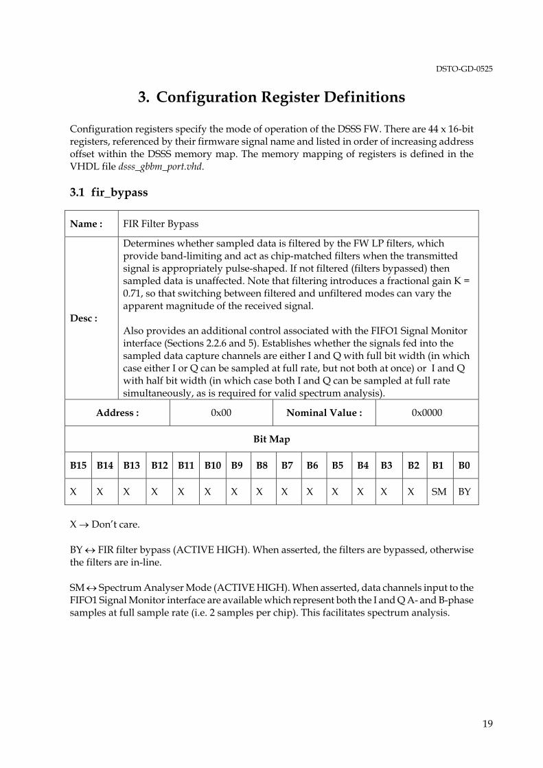
Configuration registers specify the mode of operation of the DSSS FW. There are 44 x 16-bit registers, referenced by their firmware signal name and listed in order of increasing address offset within the DSSS memory map. The memory mapping of registers is defined in the VHDL file dsss_gbbm_port.vhd. 3.1 fir_bypass
Name : FIR Filter Bypass
Desc :
Determines whether sampled data is filtered by the FW LP filters, which provide band-limiting and act as chip-matched filters when the transmitted signal is appropriately pulse-shaped. If not filtered (filters bypassed) then sampled data is unaffected. Note that filtering introduces a fractional gain K = 0.71, so that switching between filtered and unfiltered modes can vary the apparent magnitude of the received signal. Also provides an additional control associated with the FIFO1 Signal Monitor interface (Sections 2.2.6 and 5). Establishes whether the signals fed into the sampled data capture channels are either I and Q with full bit width (in which case either I or Q can be sampled at full rate, but not both at once) or I and Q with half bit width (in which case both I and Q can be sampled at full rate simultaneously, as is required for valid spectrum analysis).
Address : 0x00 Nominal Value : 0x0000
Bit Map
B15 B14 B13 B12 B11 B10 B9 B8 B7 B6 B5 B4 B3 B2 B1 B0
X X X X X X X X X X X X X X SM BY
X → Don’t care. BY ↔ FIR filter bypass (ACTIVE HIGH). When asserted, the filters are bypassed, otherwise the filters are in-line. SM ↔ Spectrum Analyser Mode (ACTIVE HIGH). When asserted, data channels input to the FIFO1 Signal Monitor interface are available which represent both the I and Q A- and B-phase samples at full sample rate (i.e. 2 samples per chip). This facilitates spectrum analysis.
DSTO-GD-0525
20
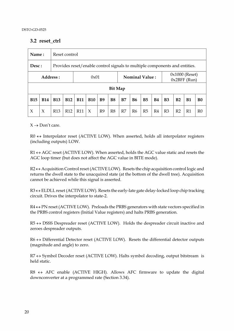
3.2 reset_ctrl
Name : Reset control
Desc : Provides reset/enable control signals to multiple components and entities.
Address : 0x01 Nominal Value : 0x1000 (Reset) 0x2BFF (Run)
Bit Map
B15 B14 B13 B12 B11 B10 B9 B8 B7 B6 B5 B4 B3 B2 B1 B0
X X R13 R12 R11 X R9 R8 R7 R6 R5 R4 R3 R2 R1 R0
X → Don’t care. R0 ↔ Interpolator reset (ACTIVE LOW). When asserted, holds all interpolator registers (including outputs) LOW. R1 ↔ AGC reset (ACTIVE LOW). When asserted, holds the AGC value static and resets the AGC loop timer (but does not affect the AGC value in BITE mode). R2 ↔ Acquisition Control reset (ACTIVE LOW). Resets the chip acquisition control logic and returns the dwell state to the unacquired state (at the bottom of the dwell tree). Acquisition cannot be achieved while this signal is asserted. R3 ↔ ELDLL reset (ACTIVE LOW). Resets the early-late gate delay-locked loop chip tracking circuit. Drives the interpolator to state-2. R4 ↔ PN reset (ACTIVE LOW). Preloads the PRBS generators with state vectors specified in the PRBS control registers (Initial Value registers) and halts PRBS generation. R5 ↔ DSSS Despreader reset (ACTIVE LOW). Holds the despreader circuit inactive and zeroes despreader outputs. R6 ↔ Differential Detector reset (ACTIVE LOW). Resets the differential detector outputs (magnitude and angle) to zero. R7 ↔ Symbol Decoder reset (ACTIVE LOW). Halts symbol decoding, output bitstream is held static. R8 ↔ AFC enable (ACTIVE HIGH). Allows AFC firmware to update the digital downconverter at a programmed rate (Section 3.34).
DSTO-GD-0525
21
R9 ↔ Symbol Timing Recovery enable (ACTIVE HIGH). Enables the STR loop. If disabled there will be no reference clock for the despreader and all subsequent circuits. R11 ↔ FIR Filter reset (ACTIVE LOW). Resets the FIR filters, with outputs tied to zero. When fir_bypass is asserted sampled data is not affected. R12 ↔ ADC enable (ACTIVE LOW). When deasserted the I and Q channel ADCs are idle (sampled data outputs constant, sample clocks static). When asserted the ADCs commence sampling at full rate and the sample clocks are available to the DSSS FW. R13 ↔ Acquisition Hold-up enable (ACTIVE HIGH). Turns on the acquisition hold-up circuit, which provides robustness to acquisition decisions in the presence of score nulling introduced by the underlying data. Deassertion is effectively a bypass mode, so that acquisition is still possible. Note that the hold-up circuit has a latency of 1 clock cycle, so the PRBS offset phases (Sections 3.24 and 3.27) must be adjusted accordingly. 3.3 interp_ctrl
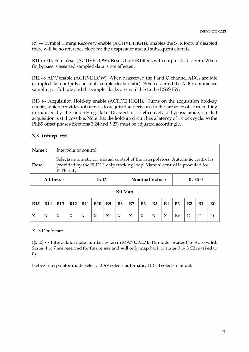
Name : Interpolator control
Desc : Selects automatic or manual control of the interpolators. Automatic control is provided by the ELDLL chip tracking loop. Manual control is provided for BITE only.
Address : 0x02 Nominal Value : 0x0000
Bit Map
B15 B14 B13 B12 B11 B10 B9 B8 B7 B6 B5 B4 B3 B2 B1 B0
X X X X X X X X X X X X Isel I2 I1 I0
X → Don’t care. I[2..0] ↔ Interpolator state number when in MANUAL/BITE mode. States 0 to 3 are valid. States 4 to 7 are reserved for future use and will only map back to states 0 to 3 (I2 masked to 0). Isel ↔ Interpolator mode select. LOW selects automatic, HIGH selects manual.

DSTO-GD-0525
22
3.4 agc_dwell
Name : AGC dwell value.
Desc : Specifies the number of (chip) clocks over which each test (dwell) in the AGC loop is conducted. In each dwell period, the number of ADC overflow events is accumulated, starting from zero.
Address : 0x03 Nominal Value : 0x4E20
Bit Map
B15 B14 B13 B12 B11 B10 B9 B8 B7 B6 B5 B4 B3 B2 B1 B0
D15 D14 D13 D12 D11 D10 D9 D8 D7 D6 D5 D4 D3 D2 D1 D0
D[15..0] ↔ AGC dwell value in the range 0 to 65535 clock edges. 3.5 agc_thresh
Name : AGC threshold value.
Desc : Specifies the number of ADC overflow events per AGC dwell period that the AGC should maintain.
Address : 0x04 Nominal Value : 0x07D0
Bit Map
B15 B14 B13 B12 B11 B10 B9 B8 B7 B6 B5 B4 B3 B2 B1 B0
D15 D14 D13 D12 D11 D10 D9 D8 D7 D6 D5 D4 D3 D2 D1 D0
D[15..0] ↔ AGC threshold value in the range 0 to 65535 full-scale (FS) events. Note that on any sample clock edge there may be 0, 1 or 2 FS events depending on whether either the I or Q channel A-phase samples overflowed, either the I or Q channel B-phase samples overflowed, or both an A-phase and a B-phase sample overflowed.
DSTO-GD-0525
23
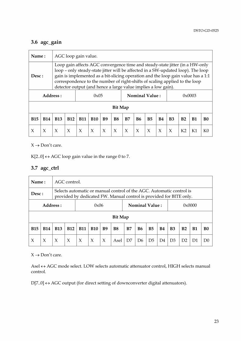
3.6 agc_gain
Name : AGC loop gain value.
Desc :
Loop gain affects AGC convergence time and steady-state jitter (in a HW-only loop – only steady-state jitter will be affected in a SW-updated loop). The loop gain is implemented as a bit-slicing operation and the loop gain value has a 1:1 correspondence to the number of right-shifts of scaling applied to the loop detector output (and hence a large value implies a low gain).
Address : 0x05 Nominal Value : 0x0003
Bit Map
B15 B14 B13 B12 B11 B10 B9 B8 B7 B6 B5 B4 B3 B2 B1 B0
X X X X X X X X X X X X X K2 K1 K0
X → Don’t care. K[2..0] ↔ AGC loop gain value in the range 0 to 7. 3.7 agc_ctrl
Name : AGC control.
Desc : Selects automatic or manual control of the AGC. Automatic control is provided by dedicated FW. Manual control is provided for BITE only.
Address : 0x06 Nominal Value : 0x0000
Bit Map
B15 B14 B13 B12 B11 B10 B9 B8 B7 B6 B5 B4 B3 B2 B1 B0
X X X X X X X Asel D7 D6 D5 D4 D3 D2 D1 D0
X → Don’t care. Asel ↔ AGC mode select. LOW selects automatic attenuator control, HIGH selects manual control. D[7..0] ↔ AGC output (for direct setting of downconverter digital attenuators).
DSTO-GD-0525
24
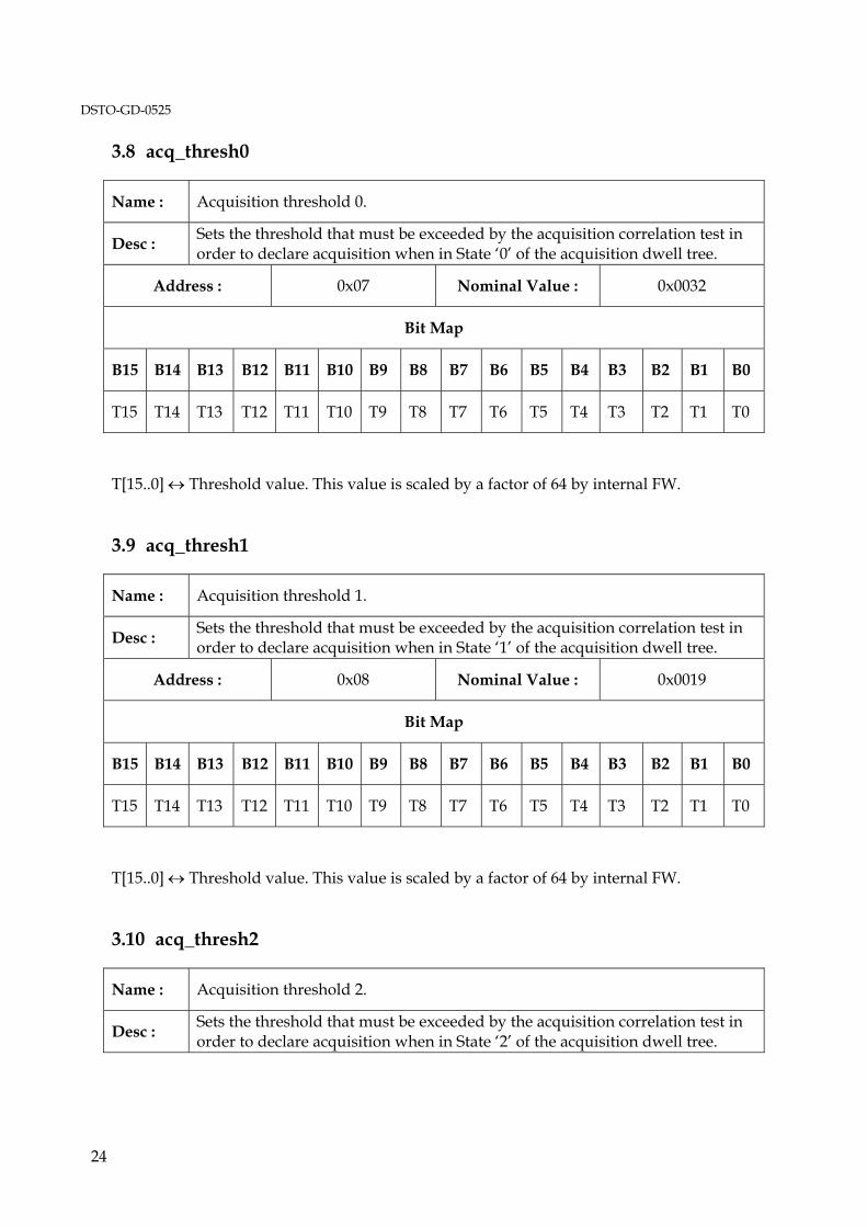
3.8 acq_thresh0
Name : Acquisition threshold 0.
Desc : Sets the threshold that must be exceeded by the acquisition correlation test in order to declare acquisition when in State ‘0’ of the acquisition dwell tree.
Address : 0x07 Nominal Value : 0x0032
Bit Map
B15 B14 B13 B12 B11 B10 B9 B8 B7 B6 B5 B4 B3 B2 B1 B0
T15 T14 T13 T12 T11 T10 T9 T8 T7 T6 T5 T4 T3 T2 T1 T0
T[15..0] ↔ Threshold value. This value is scaled by a factor of 64 by internal FW. 3.9 acq_thresh1
Name : Acquisition threshold 1.
Desc : Sets the threshold that must be exceeded by the acquisition correlation test in order to declare acquisition when in State ‘1’ of the acquisition dwell tree.
Address : 0x08 Nominal Value : 0x0019
Bit Map
B15 B14 B13 B12 B11 B10 B9 B8 B7 B6 B5 B4 B3 B2 B1 B0
T15 T14 T13 T12 T11 T10 T9 T8 T7 T6 T5 T4 T3 T2 T1 T0
T[15..0] ↔ Threshold value. This value is scaled by a factor of 64 by internal FW. 3.10 acq_thresh2
Name : Acquisition threshold 2.
Desc : Sets the threshold that must be exceeded by the acquisition correlation test in order to declare acquisition when in State ‘2’ of the acquisition dwell tree.

DSTO-GD-0525
25
Address : 0x09 Nominal Value : 0x0019
Bit Map
B15 B14 B13 B12 B11 B10 B9 B8 B7 B6 B5 B4 B3 B2 B1 B0
T15 T14 T13 T12 T11 T10 T9 T8 T7 T6 T5 T4 T3 T2 T1 T0
T[15..0] ↔ Threshold value. This value is scaled by a factor of 64 by internal FW. 3.11 acq_thresh3
Name : Acquisition threshold 3.
Desc : Sets the threshold that must be exceeded by the acquisition correlation test in order to declare acquisition when in State ‘3’ of the acquisition dwell tree.
Address : 0x0A Nominal Value : 0x0019
Bit Map
B15 B14 B13 B12 B11 B10 B9 B8 B7 B6 B5 B4 B3 B2 B1 B0
T15 T14 T13 T12 T11 T10 T9 T8 T7 T6 T5 T4 T3 T2 T1 T0
T[15..0] ↔ Threshold value. This value is scaled by a factor of 64 by internal FW. 3.12 acq_thresh4
Name : Acquisition threshold 4.
Desc : Sets the threshold that must be exceeded by the acquisition correlation test in order to declare acquisition when in State ‘4’ of the acquisition dwell tree.
Address : 0x0B Nominal Value : 0x0019
Bit Map
B15 B14 B13 B12 B11 B10 B9 B8 B7 B6 B5 B4 B3 B2 B1 B0
DSTO-GD-0525
26
T15 T14 T13 T12 T11 T10 T9 T8 T7 T6 T5 T4 T3 T2 T1 T0
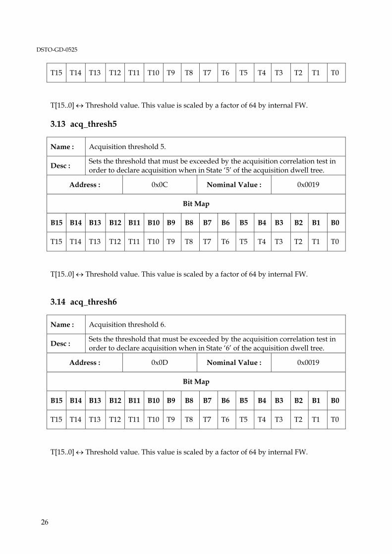
T[15..0] ↔ Threshold value. This value is scaled by a factor of 64 by internal FW. 3.13 acq_thresh5
Name : Acquisition threshold 5.
Desc : Sets the threshold that must be exceeded by the acquisition correlation test in order to declare acquisition when in State ‘5’ of the acquisition dwell tree.
Address : 0x0C Nominal Value : 0x0019
Bit Map
B15 B14 B13 B12 B11 B10 B9 B8 B7 B6 B5 B4 B3 B2 B1 B0
T15 T14 T13 T12 T11 T10 T9 T8 T7 T6 T5 T4 T3 T2 T1 T0
T[15..0] ↔ Threshold value. This value is scaled by a factor of 64 by internal FW. 3.14 acq_thresh6
Name : Acquisition threshold 6.
Desc : Sets the threshold that must be exceeded by the acquisition correlation test in order to declare acquisition when in State ‘6’ of the acquisition dwell tree.
Address : 0x0D Nominal Value : 0x0019
Bit Map
B15 B14 B13 B12 B11 B10 B9 B8 B7 B6 B5 B4 B3 B2 B1 B0
T15 T14 T13 T12 T11 T10 T9 T8 T7 T6 T5 T4 T3 T2 T1 T0
T[15..0] ↔ Threshold value. This value is scaled by a factor of 64 by internal FW.
DSTO-GD-0525
27
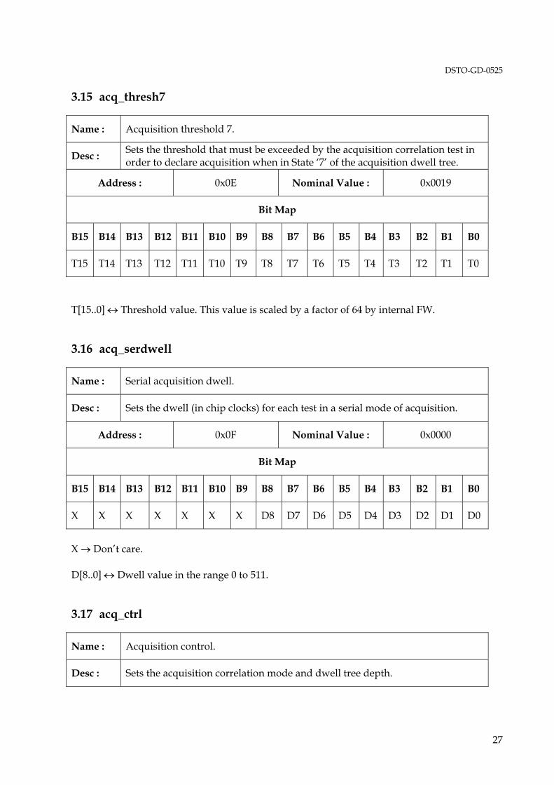
3.15 acq_thresh7
Name : Acquisition threshold 7.
Desc : Sets the threshold that must be exceeded by the acquisition correlation test in order to declare acquisition when in State ‘7’ of the acquisition dwell tree.
Address : 0x0E Nominal Value : 0x0019
Bit Map
B15 B14 B13 B12 B11 B10 B9 B8 B7 B6 B5 B4 B3 B2 B1 B0
T15 T14 T13 T12 T11 T10 T9 T8 T7 T6 T5 T4 T3 T2 T1 T0
T[15..0] ↔ Threshold value. This value is scaled by a factor of 64 by internal FW. 3.16 acq_serdwell
Name : Serial acquisition dwell.
Desc : Sets the dwell (in chip clocks) for each test in a serial mode of acquisition.
Address : 0x0F Nominal Value : 0x0000
Bit Map
B15 B14 B13 B12 B11 B10 B9 B8 B7 B6 B5 B4 B3 B2 B1 B0
X X X X X X X D8 D7 D6 D5 D4 D3 D2 D1 D0
X → Don’t care. D[8..0] ↔ Dwell value in the range 0 to 511. 3.17 acq_ctrl
Name : Acquisition control.
Desc : Sets the acquisition correlation mode and dwell tree depth.

DSTO-GD-0525
28
Address : 0x10 Nominal Value : 0x0010
Bit Map
B15 B14 B13 B12 B11 B10 B9 B8 B7 B6 B5 B4 B3 B2 B1 B0
X X X X X X X X X S_P D2 D1 D0 M2 M1 M0
X → Don’t care. S_P ↔ Serial (HIGH) or parallel (LOW) correlation mode. ONLY PARALLEL MODE SHOULD BE USED. SERIAL MODE IS RESERVED FOR FUTURE USE. D[2..0] ↔ Dwell tree depth, in the range 1 to 7. DO NOT SET TO ZERO. M[2..0] ↔ Correlation mode. Refer to the table below. When setting acquisition thresholds with respect to the output scores, note that the output is derived from a sum of squares of values, and has a quadratic rather than a linear profile.
M[2..0] Correlation Type Processing Gain
Output range
000 QPSK, 1-bit x 512 chips 27dB 0..262,144 001 QPSK, 2-bit x 256 chips 24dB 0..589,824 010 QPSK, 4-bit x 128 chips 21dB 0..3,686,400 011 BPSK, 1-bit x 1024 chips 30dB 0..262,144 1XX BPSK, 4-bit x 256 chips 24dB 0..3,686,400
3.18 chips_per_sym
Name : Chips per symbol.
Desc : Defines the symbol rate with respect to the chip rate, as the number of chips per symbol period.
Address : 0x11 Nominal Value : Fchip / Fsym
Bit Map
B15 B14 B13 B12 B11 B10 B9 B8 B7 B6 B5 B4 B3 B2 B1 B0
D15 D14 D13 D12 D11 D10 D9 D8 D7 D6 D5 D4 D3 D2 D1 D0
DSTO-GD-0525
29
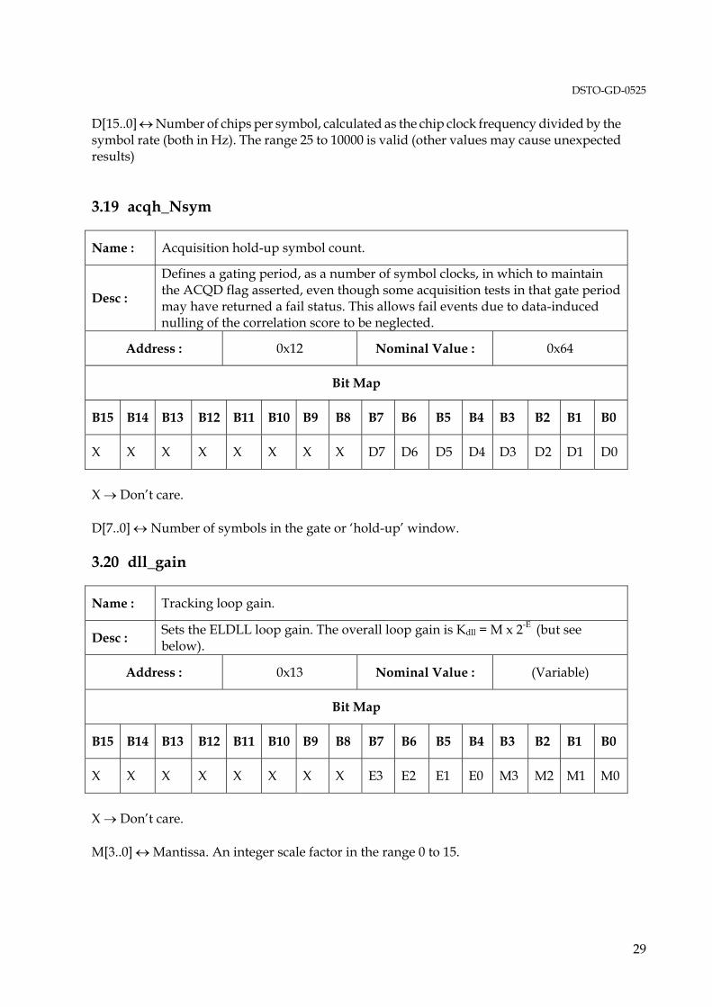
D[15..0] ↔ Number of chips per symbol, calculated as the chip clock frequency divided by the symbol rate (both in Hz). The range 25 to 10000 is valid (other values may cause unexpected results) 3.19 acqh_Nsym
Name : Acquisition hold-up symbol count.
Desc :
Defines a gating period, as a number of symbol clocks, in which to maintain the ACQD flag asserted, even though some acquisition tests in that gate period may have returned a fail status. This allows fail events due to data-induced nulling of the correlation score to be neglected.
Address : 0x12 Nominal Value : 0x64
Bit Map
B15 B14 B13 B12 B11 B10 B9 B8 B7 B6 B5 B4 B3 B2 B1 B0
X X X X X X X X D7 D6 D5 D4 D3 D2 D1 D0
X → Don’t care. D[7..0] ↔ Number of symbols in the gate or ‘hold-up’ window. 3.20 dll_gain
Name : Tracking loop gain.
Desc : Sets the ELDLL loop gain. The overall loop gain is Kdll = M x 2-E (but see below).
Address : 0x13 Nominal Value : (Variable)
Bit Map
B15 B14 B13 B12 B11 B10 B9 B8 B7 B6 B5 B4 B3 B2 B1 B0
X X X X X X X X E3 E2 E1 E0 M3 M2 M1 M0
X → Don’t care. M[3..0] ↔ Mantissa. An integer scale factor in the range 0 to 15.

DSTO-GD-0525
30
E[3..0] ↔ Exponent. A bit shift in the range 0 to 2-15. Note that a zero value results in NO SHIFT. The desired value may be determined either by a trained operator (based on jitter in an interpolator state vector plot window) or through an automation algorithm (see Section 6.2.2). 3.21 dll_dwell
Name : Tracking loop dwell.
Desc : Sets the ELDLL loop dwell. This specifies the length (and hence the processing gain) for both the advanced and retarded correlation tests.
Address : 0x14 Nominal Value : (Variable)
Bit Map
B15 B14 B13 B12 B11 B10 B9 B8 B7 B6 B5 B4 B3 B2 B1 B0
X X X X X X X D8 D7 D6 D5 D4 D3 D2 D1 D0
X → Don’t care. D[8..0] ↔ ELDLL loop dwell in the range 0 to 511 chips. This should be set high enough for sufficient processing gain but low enough (fast enough) to allow the actual chip clock error to be compensated. A typical set point is ½-symbol duration. 3.22 iprbs_tap
Name : I-channel PRBS tap word.
Desc : Defines the PRBS sequence for the I-channel spreading code.
Address : 0x15 Nominal Value : (Variable)
Bit Map
B15 B14 B13 B12 B11 B10 B9 B8 B7 B6 B5 B4 B3 B2 B1 B0
D15 D14 D13 D12 D11 D10 D9 D8 D7 D6 D5 D4 D3 D2 D1 D0
DSTO-GD-0525
31
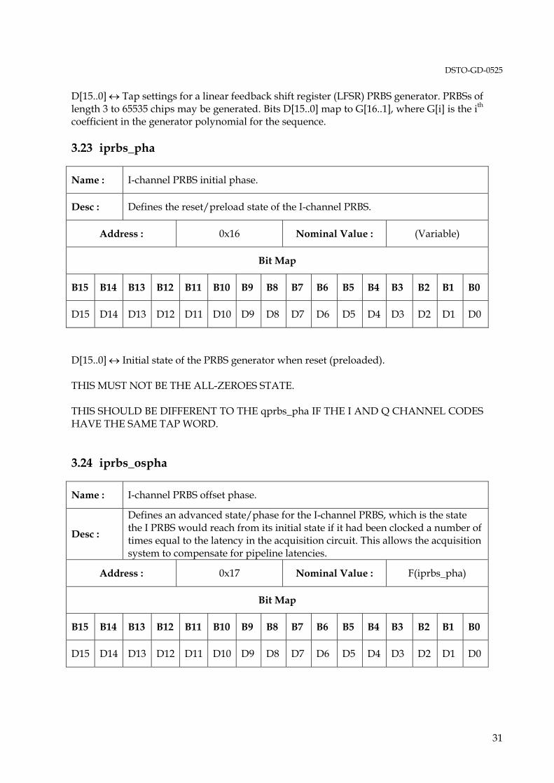
D[15..0] ↔ Tap settings for a linear feedback shift register (LFSR) PRBS generator. PRBSs of length 3 to 65535 chips may be generated. Bits D[15..0] map to G[16..1], where G[i] is the ith coefficient in the generator polynomial for the sequence. 3.23 iprbs_pha
Name : I-channel PRBS initial phase.
Desc : Defines the reset/preload state of the I-channel PRBS.
Address : 0x16 Nominal Value : (Variable)
Bit Map
B15 B14 B13 B12 B11 B10 B9 B8 B7 B6 B5 B4 B3 B2 B1 B0
D15 D14 D13 D12 D11 D10 D9 D8 D7 D6 D5 D4 D3 D2 D1 D0
D[15..0] ↔ Initial state of the PRBS generator when reset (preloaded). THIS MUST NOT BE THE ALL-ZEROES STATE. THIS SHOULD BE DIFFERENT TO THE qprbs_pha IF THE I AND Q CHANNEL CODES HAVE THE SAME TAP WORD. 3.24 iprbs_ospha
Name : I-channel PRBS offset phase.
Desc :
Defines an advanced state/phase for the I-channel PRBS, which is the state the I PRBS would reach from its initial state if it had been clocked a number of times equal to the latency in the acquisition circuit. This allows the acquisition system to compensate for pipeline latencies.
Address : 0x17 Nominal Value : F(iprbs_pha)
Bit Map
B15 B14 B13 B12 B11 B10 B9 B8 B7 B6 B5 B4 B3 B2 B1 B0
D15 D14 D13 D12 D11 D10 D9 D8 D7 D6 D5 D4 D3 D2 D1 D0
DSTO-GD-0525
32
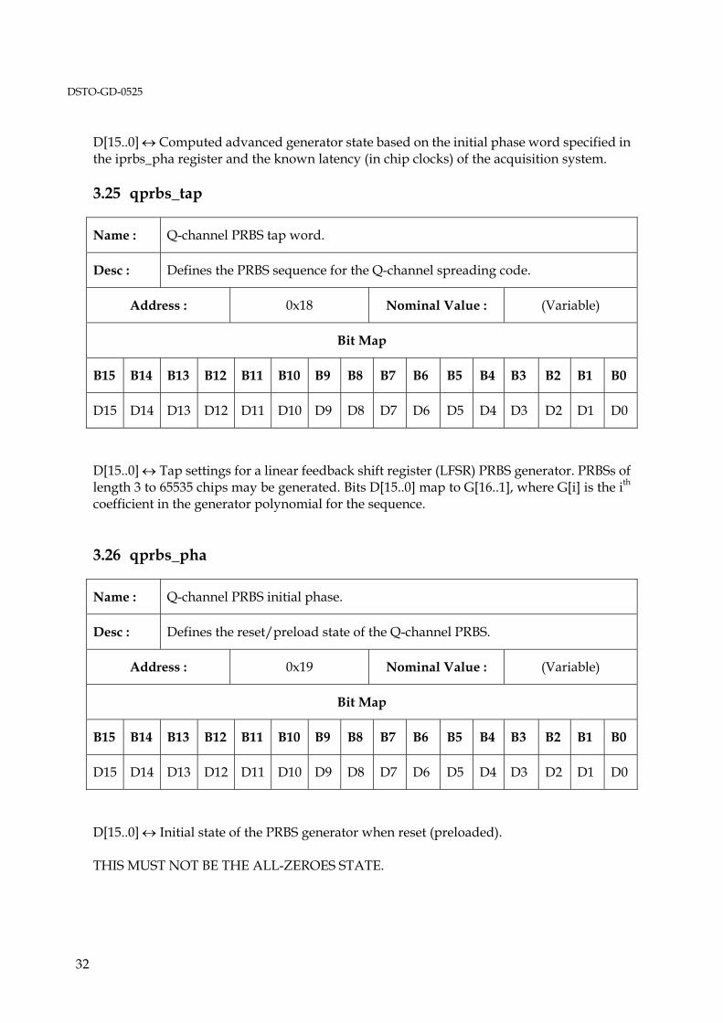
D[15..0] ↔ Computed advanced generator state based on the initial phase word specified in the iprbs_pha register and the known latency (in chip clocks) of the acquisition system. 3.25 qprbs_tap
Name : Q-channel PRBS tap word.
Desc : Defines the PRBS sequence for the Q-channel spreading code.
Address : 0x18 Nominal Value : (Variable)
Bit Map
B15 B14 B13 B12 B11 B10 B9 B8 B7 B6 B5 B4 B3 B2 B1 B0
D15 D14 D13 D12 D11 D10 D9 D8 D7 D6 D5 D4 D3 D2 D1 D0
D[15..0] ↔ Tap settings for a linear feedback shift register (LFSR) PRBS generator. PRBSs of length 3 to 65535 chips may be generated. Bits D[15..0] map to G[16..1], where G[i] is the ith coefficient in the generator polynomial for the sequence. 3.26 qprbs_pha
Name : Q-channel PRBS initial phase.
Desc : Defines the reset/preload state of the Q-channel PRBS.
Address : 0x19 Nominal Value : (Variable)
Bit Map
B15 B14 B13 B12 B11 B10 B9 B8 B7 B6 B5 B4 B3 B2 B1 B0
D15 D14 D13 D12 D11 D10 D9 D8 D7 D6 D5 D4 D3 D2 D1 D0
D[15..0] ↔ Initial state of the PRBS generator when reset (preloaded). THIS MUST NOT BE THE ALL-ZEROES STATE.
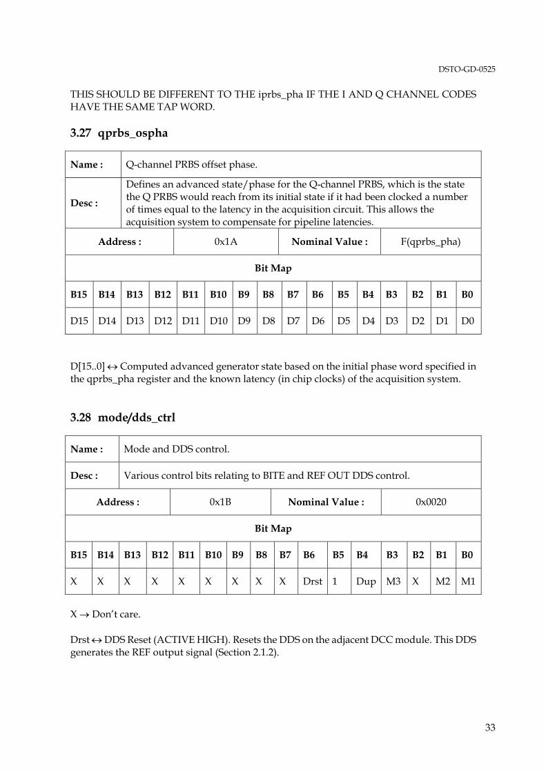
DSTO-GD-0525
33
THIS SHOULD BE DIFFERENT TO THE iprbs_pha IF THE I AND Q CHANNEL CODES HAVE THE SAME TAP WORD. 3.27 qprbs_ospha
Name : Q-channel PRBS offset phase.
Desc :
Defines an advanced state/phase for the Q-channel PRBS, which is the state the Q PRBS would reach from its initial state if it had been clocked a number of times equal to the latency in the acquisition circuit. This allows the acquisition system to compensate for pipeline latencies.
Address : 0x1A Nominal Value : F(qprbs_pha)
Bit Map
B15 B14 B13 B12 B11 B10 B9 B8 B7 B6 B5 B4 B3 B2 B1 B0
D15 D14 D13 D12 D11 D10 D9 D8 D7 D6 D5 D4 D3 D2 D1 D0
D[15..0] ↔ Computed advanced generator state based on the initial phase word specified in the qprbs_pha register and the known latency (in chip clocks) of the acquisition system. 3.28 mode/dds_ctrl
Name : Mode and DDS control.
Desc : Various control bits relating to BITE and REF OUT DDS control.
Address : 0x1B Nominal Value : 0x0020
Bit Map
B15 B14 B13 B12 B11 B10 B9 B8 B7 B6 B5 B4 B3 B2 B1 B0
X X X X X X X X X Drst 1 Dup M3 X M2 M1
X → Don’t care. Drst ↔ DDS Reset (ACTIVE HIGH). Resets the DDS on the adjacent DCC module. This DDS generates the REF output signal (Section 2.1.2).

DSTO-GD-0525
34
Dup ↔ DDS Update. A rising edge on this bit causes the DDS to be reprogrammed with the current contents of its internal update registers. M3 ↔ Enable PRBS loop back test. When this bit is HIGH an unmodulated, fixed-scale copy of the spreading codes is muxed in to the front end of the DSSS receiver instead of actual sampled data. This provides a rudimentary built-in-test capability. M2 ↔ Force the ACQD flag. When this bit is HIGH the ACQD flag is driven high (asserted) even though acquisition may not have been achieved. This enables rudimentary built-in-test of functions that are only enabled when the ACQD flag is asserted. M1 ↔ BPSK mode. When this bit is HIGH the DSSS despreader circuits are in BPSK mode. This is reserved for future use, and should generally be left LOW. 3.29 str_dwell
Name : Symbol timing recovery loop dwell.
Desc : Sets the number of chips per symbol for the STR loop.
Address : 0x1C Nominal Value : chips_per_sym-3
Bit Map
B15 B14 B13 B12 B11 B10 B9 B8 B7 B6 B5 B4 B3 B2 B1 B0
D15 D14 D13 D12 D11 D10 D9 D8 D7 D6 D5 D4 D3 D2 D1 D0
D[15..0] ↔ (Number of chips per symbol) - 3. The offset of 3 here compensates for a 3-chip latency in the STR loop. 3.30 str_gain
Name : Symbol timing recovery loop gain and DDS Byte0
Desc : Sets the STR loop gain. The overall loop gain is Kstr = M x 2-E (but see below). Also stores one byte of the REF DDS configuration data.
Address : 0x1D Nominal Value : 0x00KeKm
Bit Map
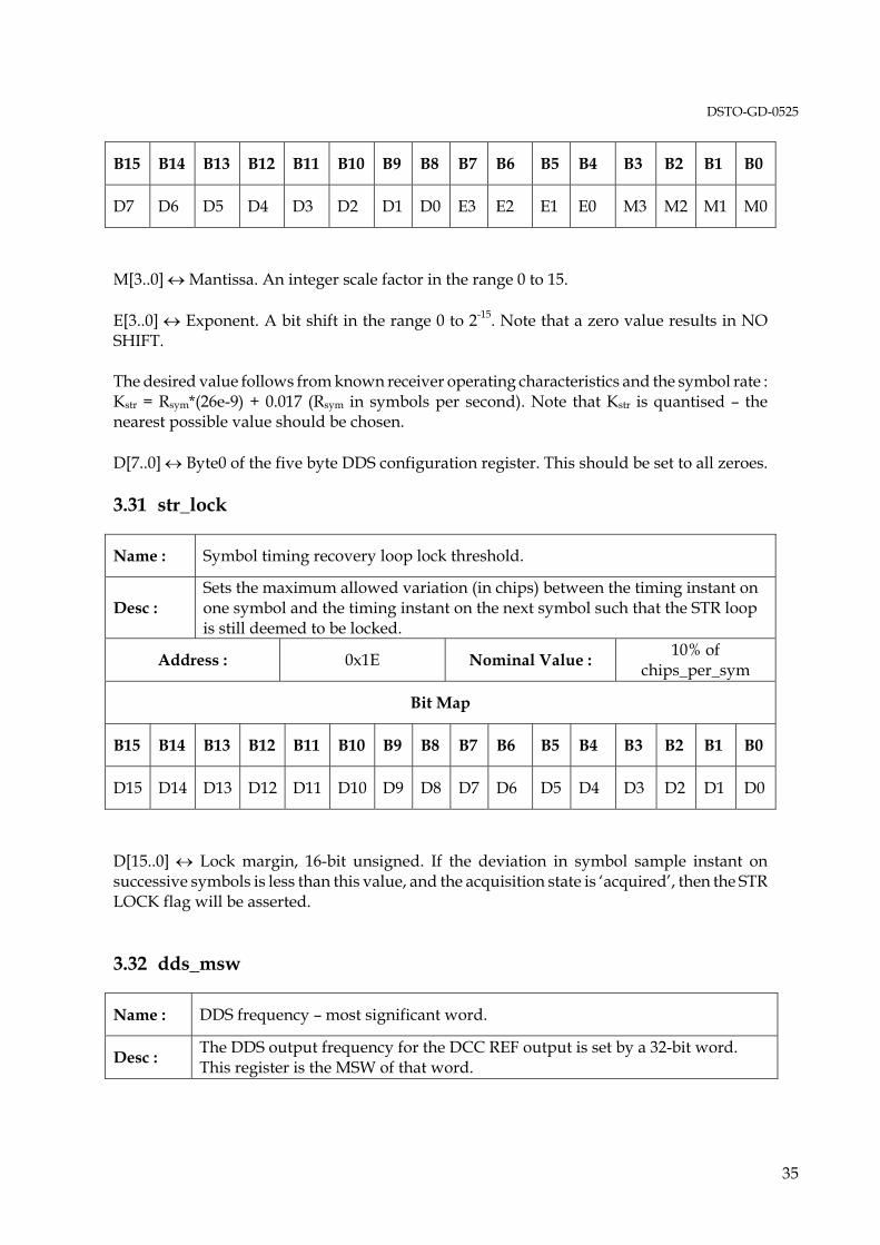
DSTO-GD-0525
35
B15 B14 B13 B12 B11 B10 B9 B8 B7 B6 B5 B4 B3 B2 B1 B0
D7 D6 D5 D4 D3 D2 D1 D0 E3 E2 E1 E0 M3 M2 M1 M0
M[3..0] ↔ Mantissa. An integer scale factor in the range 0 to 15. E[3..0] ↔ Exponent. A bit shift in the range 0 to 2-15. Note that a zero value results in NO SHIFT. The desired value follows from known receiver operating characteristics and the symbol rate : Kstr = Rsym*(26e-9) + 0.017 (Rsym in symbols per second). Note that Kstr is quantised – the nearest possible value should be chosen. D[7..0] ↔ Byte0 of the five byte DDS configuration register. This should be set to all zeroes. 3.31 str_lock
Name : Symbol timing recovery loop lock threshold.
Desc : Sets the maximum allowed variation (in chips) between the timing instant on one symbol and the timing instant on the next symbol such that the STR loop is still deemed to be locked.
Address : 0x1E Nominal Value : 10% of chips_per_sym
Bit Map
B15 B14 B13 B12 B11 B10 B9 B8 B7 B6 B5 B4 B3 B2 B1 B0
D15 D14 D13 D12 D11 D10 D9 D8 D7 D6 D5 D4 D3 D2 D1 D0
D[15..0] ↔ Lock margin, 16-bit unsigned. If the deviation in symbol sample instant on successive symbols is less than this value, and the acquisition state is ‘acquired’, then the STR LOCK flag will be asserted. 3.32 dds_msw
Name : DDS frequency – most significant word.
Desc : The DDS output frequency for the DCC REF output is set by a 32-bit word. This register is the MSW of that word.
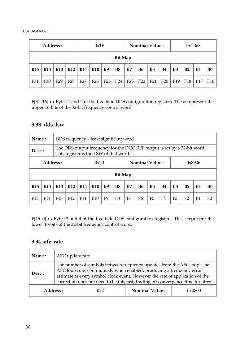
DSTO-GD-0525
36
Address : 0x1F Nominal Value : 0x1B63
Bit Map
B15 B14 B13 B12 B11 B10 B9 B8 B7 B6 B5 B4 B3 B2 B1 B0
F31 F30 F29 F28 F27 F26 F25 F24 F23 F22 F21 F20 F19 F18 F17 F16
F[31..16] ↔ Bytes 1 and 2 of the five byte DDS configuration registers. These represent the upper 16-bits of the 32-bit frequency control word. 3.33 dds_lsw
Name : DDS frequency – least significant word.
Desc : The DDS output frequency for the DCC REF output is set by a 32-bit word. This register is the LSW of that word.
Address : 0x20 Nominal Value : 0x8906
Bit Map
B15 B14 B13 B12 B11 B10 B9 B8 B7 B6 B5 B4 B3 B2 B1 B0
F15 F14 F13 F12 F11 F10 F9 F8 F7 F6 F5 F4 F3 F2 F1 F0
F[15..0] ↔ Bytes 3 and 4 of the five byte DDS configuration registers. These represent the lower 16-bits of the 32-bit frequency control word. 3.34 afc_rate
Name : AFC update rate.
Desc :
The number of symbols between frequency updates from the AFC loop. The AFC loop runs continuously when enabled, producing a frequency error estimate at every symbol clock event. However the rate of application of the correction does not need to be this fast, trading off convergence time for jitter.
Address : 0x21 Nominal Value : 0x0800

DSTO-GD-0525
37
Bit Map
B15 B14 B13 B12 B11 B10 B9 B8 B7 B6 B5 B4 B3 B2 B1 B0
D15 D14 D13 D12 D11 D10 D9 D8 D7 D6 D5 D4 D3 D2 D1 D0
D[15..0] ↔ Number of symbols between updates to the downconversion frequency in accordance with the current AFC loop frequency error estimate. 3.35 ddet_gain
Name : Differential detector bit-slicer ‘gain’.
Desc :
The differential detector works in polar coordinate mode. The output magnitude term is the resultant of |Yn|*|Yn-1| for input symbols Yk. The input magnitude has a 16-bit representation, leading to a 31-bit output term. To conserve FW resources, the 31-bit term is truncated to a 16-bit term, with the position of the LSB of the 16-bit slice set manually in accordance with this gain value.
Address : 0x22 Nominal Value : 0x0009
Bit Map
B15 B14 B13 B12 B11 B10 B9 B8 B7 B6 B5 B4 B3 B2 B1 B0
X X X X X X X X X X X X D3 D2 D1 D0
X → Don’t care. D[3..0] ↔ Bit position for the LSB of the 16-bit slice of a 32-bit magnitude term, in the range 0 to 15. Note that if the gain is incorrectly set (i.e. set such that the chosen bit slice overflows, or such that there are significant bits above the chosen slice) then the interpretation of the differentially detected magnitude will be invalid when monitored. However this will have no effect on BER, as only the angle term is significant in the demodulation process. 3.36 clkset_data
Name : Clock set data parameters.

DSTO-GD-0525
38
Desc :
The DCC output clock is retimed in the DDP to produce the master chip-rate clock used throughout the DSSS FW. Retiming is achieved with an embedded EPLL (enhanced PLL) entity in the FPGA. This register supplies ‘address’ and ‘data’ fields in support of run-time configuration of the EPLL.
Address : 0x24 Nominal Value : 0x4800
Bit Map
B15 B14 B13 B12 B11 B10 B9 B8 B7 B6 B5 B4 B3 B2 B1 B0
F2 F1 F0 I3 I2 I1 I0 D8 D7 D6 D5 D4 D3 D2 D1 D0
I[3..0] ↔ Identity code. Identifies which counter in the EPLL is to be updated (see Altera Application Note AN282, Table 6). F[2..0] ↔ Feature code. Identifies which parameter of the selected counter is to be updated (see Altera Application Note AN282, Table 7). D[8..0] ↔ Data. The new value for the selected counter feature. 3.37 clkset_ctrl
Name : Clock set control parameters.
Desc :
The DCC output clock is retimed in the DDP to produce the master chip-rate clock used throughout the DSSS FW. Retiming is achieved with an embedded EPLL (enhanced PLL) entity in the FPGA. This register controls update commands for run-time configuration of the EPLL.
Address : 0x25 Nominal Value : 0x0000
Bit Map
B15 B14 B13 B12 B11 B10 B9 B8 B7 B6 B5 B4 B3 B2 B1 B0
X X X X X X X X X X X X X Clr Upd Wr
X → Don’t care. Clr ↔ Asynchronous reset (ACTIVE HIGH). Resets the EPLL configuration entity.

DSTO-GD-0525
39
Upd ↔ Update (ACTIVE HIGH). Loads the EPLL with the configuration data stored in a configuration register cache. Wr ↔ Write (ACTIVE HIGH). Updates the selected field in the configuration register cache. 3.38 fifo_ctrl
Name : FIFO control parameters.
Desc : The DSSS FW implements a FIFO buffer for capture of selected data channels at high sample rates. This register controls data capture operations.
Address : 0x26 Nominal Value : 0x000F
Bit Map
B15 B14 B13 B12 B11 B10 B9 B8 B7 B6 B5 B4 B3 B2 B1 B0
X X X X X X X X X X En M3 M2 M1 M0 Clr
X → Don’t care. En ↔ Asynchronous enable (ACTIVE HIGH). Initiates data capture with the selected channel. M[3..0] ↔ Capture Mode. Selects one of 16 data capture modes (see Section 5). Clr ↔ Asynchronous clear (ACTIVE HIGH). Clears the data capture FIFO. 3.39 acqh_symlen
Name : Acquisition hold-up symbol length.
Desc : Sets the number of chips per symbol for the acquisition hold-up circuit.
Address : 0x27 Nominal Value : chips_per_sym
Bit Map
B15 B14 B13 B12 B11 B10 B9 B8 B7 B6 B5 B4 B3 B2 B1 B0
D15 D14 D13 D12 D11 D10 D9 D8 D7 D6 D5 D4 D3 D2 D1 D0

DSTO-GD-0525
40
D[15..0] ↔ Number of chips per symbol. This is nominally the same as the chips_per_sym control register, but could be varied to obtain a different hold-up duration without affecting other aspects of the demodulation. 3.40 pll_arst
Name : PLL asynchronous reset.
Desc :
The DCC output clock is retimed in the DDP to produce the master chip-rate clock used throughout the DSSS FW. Retiming is achieved with an embedded EPLL (enhanced PLL) entity in the FPGA. This register is the reset control for the embedded PLL.
Address : 0x28 Nominal Value : 0x0000
Bit Map
B15 B14 B13 B12 B11 B10 B9 B8 B7 B6 B5 B4 B3 B2 B1 B0
X X X X X X X X X X X X X X X Clr
X → Don’t care. Clr ↔ Asynchronous reset (ACTIVE HIGH). Resets the EPLL entity. 3.41 bsif_fifo_clr
Name : Bitstream interface FIFO clear.
Desc : The DSSS FW implements a FIFO buffer for logging demodulated data over the PCI interface. This register is the reset control for that FIFO.
Address : 0x29 Nominal Value : 0x0000
Bit Map
B15 B14 B13 B12 B11 B10 B9 B8 B7 B6 B5 B4 B3 B2 B1 B0
X X X X X X X X X X X X X X X Clr
X → Don’t care. Clr ↔ Asynchronous reset (ACTIVE HIGH). Resets the FIFO buffer. The FIFO should be reset before logging to disk to avoid overflows and junk data.

DSTO-GD-0525
41
3.42 ddc_ph_msw
Name : Digital Downconverter (DDC) phase increment – most significant word.
Desc : The DSSS FW implements a DDC stage at the front end. This register specifies the upper 16-bits of the 32-bit phase increment word for the DDS that generates the downconversion LO within the DDC.
Address : 0x2A Nominal Value : 0x5999 (for 70 MHz IF)
Bit Map
B15 B14 B13 B12 B11 B10 B9 B8 B7 B6 B5 B4 B3 B2 B1 B0
P31 P30 P29 P28 P27 P26 P25 P24 P23 P22 P21 P20 P19 P18 P17 P16
P[31..16] ↔ Upper 16-bits of the DDC DDS phase word. The phase increment word (Δφ, 32-bits) follows from the required downconversion frequency (fLO , in MHz) and sample rate (fs , fixed at 200MSPS) as follows :
Δφ = 232 * ( fLO / 200 )
3.43 ddc_ph_lsw
Name : Digital Downconverter (DDC) phase increment – least significant word.
Desc : The DSSS FW implements a DDC stage at the front end. This register specifies the lower 16-bits of the 32-bit phase increment word for the DDS that generates the downconversion LO within the DDC.
Address : 0x2B Nominal Value : 0x999A (for 70 MHz IF)
Bit Map
B15 B14 B13 B12 B11 B10 B9 B8 B7 B6 B5 B4 B3 B2 B1 B0
P15 P14 P13 P12 P11 P10 P9 P8 P7 P6 P5 P4 P3 P2 P1 P0
P[15..0] ↔ Lower 16-bits of the DDC DDS phase word. Refer to register ddc_ph_msw to determine the required value.
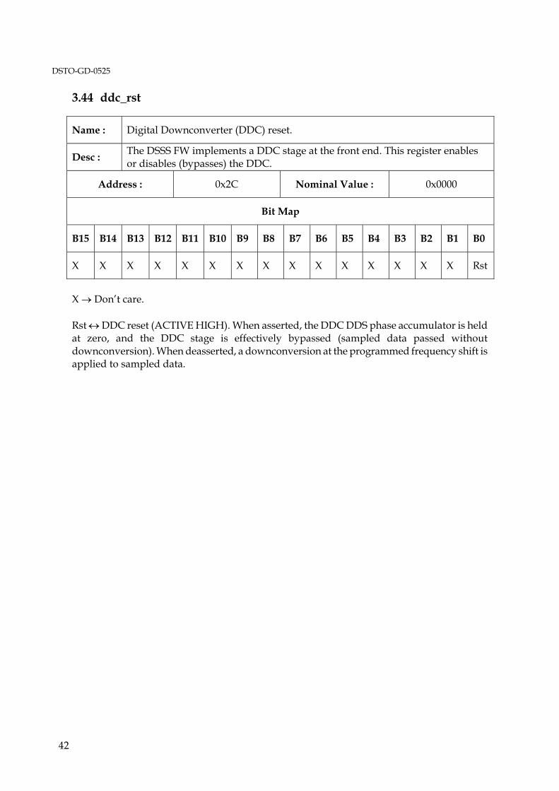
DSTO-GD-0525
42
3.44 ddc_rst
Name : Digital Downconverter (DDC) reset.
Desc : The DSSS FW implements a DDC stage at the front end. This register enables or disables (bypasses) the DDC.
Address : 0x2C Nominal Value : 0x0000
Bit Map
B15 B14 B13 B12 B11 B10 B9 B8 B7 B6 B5 B4 B3 B2 B1 B0
X X X X X X X X X X X X X X X Rst
X → Don’t care. Rst ↔ DDC reset (ACTIVE HIGH). When asserted, the DDC DDS phase accumulator is held at zero, and the DDC stage is effectively bypassed (sampled data passed without downconversion). When deasserted, a downconversion at the programmed frequency shift is applied to sampled data.
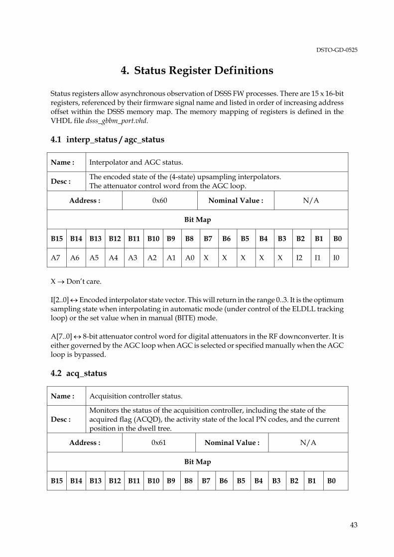
DSTO-GD-0525
43
4. Status Register Definitions
Status registers allow asynchronous observation of DSSS FW processes. There are 15 x 16-bit registers, referenced by their firmware signal name and listed in order of increasing address offset within the DSSS memory map. The memory mapping of registers is defined in the VHDL file dsss_gbbm_port.vhd. 4.1 interp_status / agc_status
Name : Interpolator and AGC status.
Desc : The encoded state of the (4-state) upsampling interpolators. The attenuator control word from the AGC loop.
Address : 0x60 Nominal Value : N/A
Bit Map
B15 B14 B13 B12 B11 B10 B9 B8 B7 B6 B5 B4 B3 B2 B1 B0
A7 A6 A5 A4 A3 A2 A1 A0 X X X X X I2 I1 I0
X → Don’t care. I[2..0] ↔ Encoded interpolator state vector. This will return in the range 0..3. It is the optimum sampling state when interpolating in automatic mode (under control of the ELDLL tracking loop) or the set value when in manual (BITE) mode. A[7..0] ↔ 8-bit attenuator control word for digital attenuators in the RF downconverter. It is either governed by the AGC loop when AGC is selected or specified manually when the AGC loop is bypassed. 4.2 acq_status
Name : Acquisition controller status.
Desc : Monitors the status of the acquisition controller, including the state of the acquired flag (ACQD), the activity state of the local PN codes, and the current position in the dwell tree.
Address : 0x61 Nominal Value : N/A
Bit Map
B15 B14 B13 B12 B11 B10 B9 B8 B7 B6 B5 B4 B3 B2 B1 B0
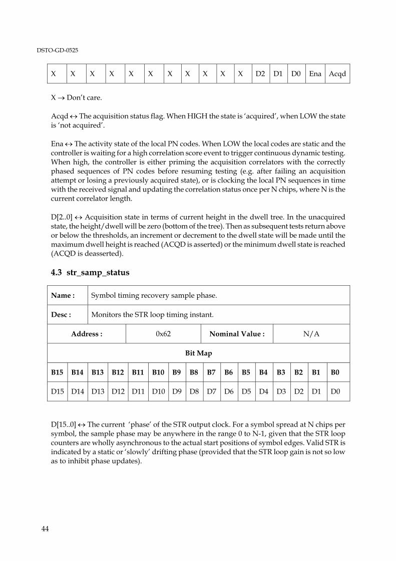
DSTO-GD-0525
44
X X X X X X X X X X X D2 D1 D0 Ena Acqd
X → Don’t care. Acqd ↔ The acquisition status flag. When HIGH the state is ‘acquired’, when LOW the state is ‘not acquired’. Ena ↔ The activity state of the local PN codes. When LOW the local codes are static and the controller is waiting for a high correlation score event to trigger continuous dynamic testing. When high, the controller is either priming the acquisition correlators with the correctly phased sequences of PN codes before resuming testing (e.g. after failing an acquisition attempt or losing a previously acquired state), or is clocking the local PN sequences in time with the received signal and updating the correlation status once per N chips, where N is the current correlator length. D[2..0] ↔ Acquisition state in terms of current height in the dwell tree. In the unacquired state, the height/dwell will be zero (bottom of the tree). Then as subsequent tests return above or below the thresholds, an increment or decrement to the dwell state will be made until the maximum dwell height is reached (ACQD is asserted) or the minimum dwell state is reached (ACQD is deasserted). 4.3 str_samp_status
Name : Symbol timing recovery sample phase.
Desc : Monitors the STR loop timing instant.
Address : 0x62 Nominal Value : N/A
Bit Map
B15 B14 B13 B12 B11 B10 B9 B8 B7 B6 B5 B4 B3 B2 B1 B0
D15 D14 D13 D12 D11 D10 D9 D8 D7 D6 D5 D4 D3 D2 D1 D0
D[15..0] ↔ The current ‘phase’ of the STR output clock. For a symbol spread at N chips per symbol, the sample phase may be anywhere in the range 0 to N-1, given that the STR loop counters are wholly asynchronous to the actual start positions of symbol edges. Valid STR is indicated by a static or ‘slowly’ drifting phase (provided that the STR loop gain is not so low as to inhibit phase updates).

DSTO-GD-0525
45
4.4 str_lock_status
Name : Symbol timing recovery LOCK status.
Desc : Monitors the STR LOCK flag. Also monitors the demodulated data stream and the interpolator state.
Address : 0x63 Nominal Value : N/A
Bit Map
B15 B14 B13 B12 B11 B10 B9 B8 B7 B6 B5 B4 B3 B2 B1 B0
X X X X X X X X X X I1 I0 D DQ DI Lock
X → Don’t care. Lock ↔ The STR LOCK flag. When asserted HIGH, the variation between the str_samp_status from one STR clock event to the next was within a user-defined lock margin. DI ↔ The data decoded from the I-component of the detected symbol stream, which varies at the symbol rate. DQ ↔ The data decoded from the Q-component of the detected symbol stream, which varies at the symbol rate. D ↔ The interleaved I/Q data, which varies at the bit rate. I[1..0] ↔ The two significant bits of the interpolator state encoding. 4.5 prbs_offset
Name : PRBS offset count.
Desc :
The PRBS offset count provides a relative measure of the chip clock error between the transmitter and receiver. As the ELDLL tracks the optimum sampling state, and because the DSSS receiver operates in a noncoherent mode with imperfect carrier and modulation timing, the optimum sampling state will tend to drift from one code phase (chip) to an adjacent code phase (chip). To maintain acquisition the local PN codes must be advanced or retarded by one chip depending on the direction of the drift in the input signal. At each increment or decrement of the local code phase, the PRBS offset counter is similarly incremented or decremented. Thus independent observations of the offset count value will show an increase or decrease in proportion to the chip error.
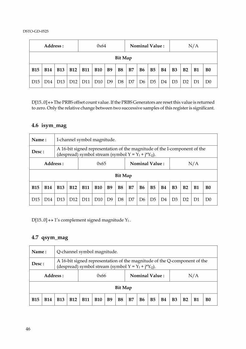
DSTO-GD-0525
46
Address : 0x64 Nominal Value : N/A
Bit Map
B15 B14 B13 B12 B11 B10 B9 B8 B7 B6 B5 B4 B3 B2 B1 B0
D15 D14 D13 D12 D11 D10 D9 D8 D7 D6 D5 D4 D3 D2 D1 D0
D[15..0] ↔ The PRBS offset count value. If the PRBS Generators are reset this value is returned to zero. Only the relative change between two successive samples of this register is significant. 4.6 isym_mag
Name : I-channel symbol magnitude.
Desc : A 16-bit signed representation of the magnitude of the I-component of the (despread) symbol stream (symbol Y = YI + j*YQ).
Address : 0x65 Nominal Value : N/A
Bit Map
B15 B14 B13 B12 B11 B10 B9 B8 B7 B6 B5 B4 B3 B2 B1 B0
D15 D14 D13 D12 D11 D10 D9 D8 D7 D6 D5 D4 D3 D2 D1 D0
D[15..0] ↔ 1’s complement signed magnitude YI . 4.7 qsym_mag
Name : Q-channel symbol magnitude.
Desc : A 16-bit signed representation of the magnitude of the Q-component of the (despread) symbol stream (symbol Y = YI + j*YQ).
Address : 0x66 Nominal Value : N/A
Bit Map
B15 B14 B13 B12 B11 B10 B9 B8 B7 B6 B5 B4 B3 B2 B1 B0

DSTO-GD-0525
47
D15 D14 D13 D12 D11 D10 D9 D8 D7 D6 D5 D4 D3 D2 D1 D0
D[15..0] ↔ 1’s complement signed magnitude YQ . 4.8 dsym_mag
Name : Differential symbol magnitude.
Desc : A 16-bit unsigned representation of the magnitude component of the (despread) symbol stream after differential detection. (symbol Y = Ydm ∠ Yda).
Address : 0x67 Nominal Value : N/A
Bit Map
B15 B14 B13 B12 B11 B10 B9 B8 B7 B6 B5 B4 B3 B2 B1 B0
D15 D14 D13 D12 D11 D10 D9 D8 D7 D6 D5 D4 D3 D2 D1 D0
D[15..0] ↔ 16-bit unsigned magnitude Ydm . 4.9 dsym_pha
Name : Differential symbol phase.
Desc :
An 8-bit signed representation of the angle component of the (despread) symbol stream after differential detection. (symbol Y = Ydm ∠ Yda). Also returns the current value on the dds_data[7..0] port that is used to configure the DDS on the DCC.
Address : 0x68 Nominal Value : N/A
Bit Map
B15 B14 B13 B12 B11 B10 B9 B8 B7 B6 B5 B4 B3 B2 B1 B0
D7 D6 D5 D4 D3 D2 D1 D0 A7 A6 A5 A4 A3 A2 A1 A0
D[7..0] ↔ The status of the DDS configuration data port.
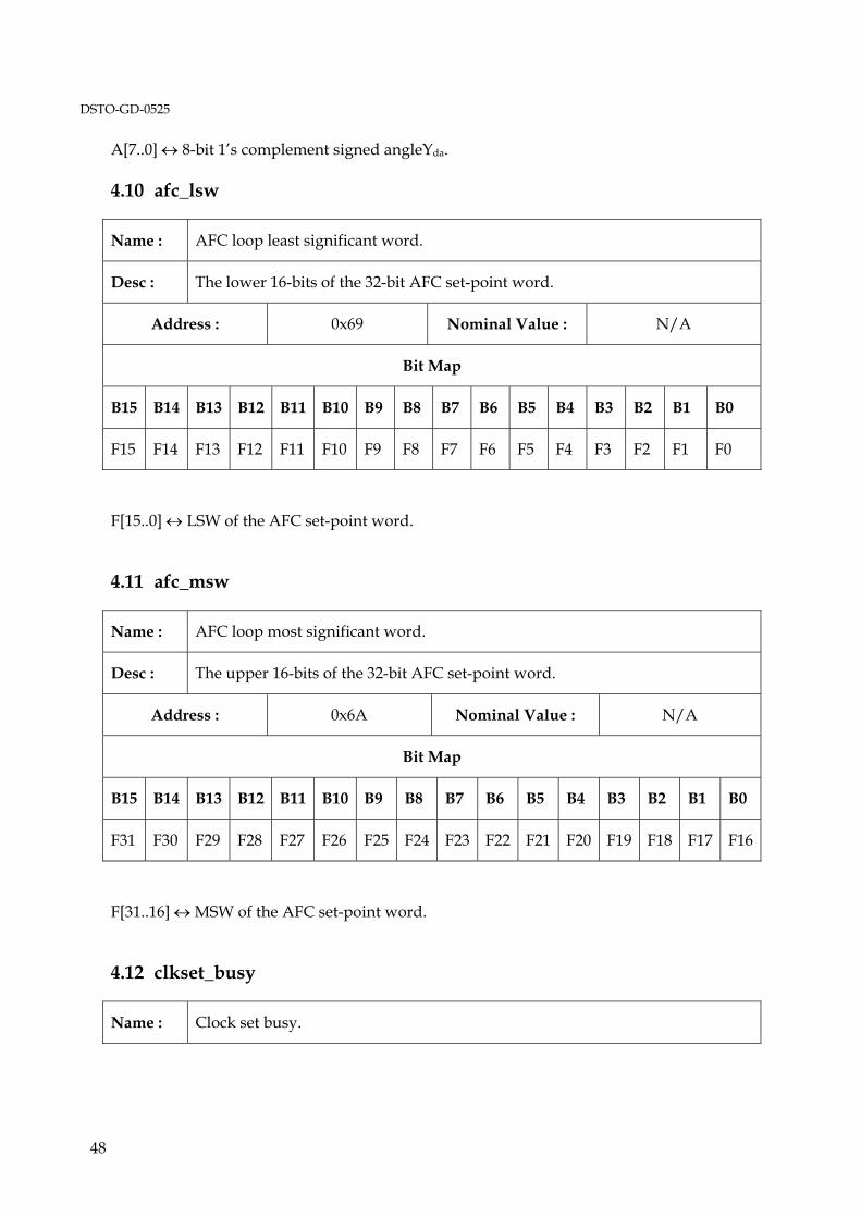
DSTO-GD-0525
48
A[7..0] ↔ 8-bit 1’s complement signed angleYda. 4.10 afc_lsw
Name : AFC loop least significant word.
Desc : The lower 16-bits of the 32-bit AFC set-point word.
Address : 0x69 Nominal Value : N/A
Bit Map
B15 B14 B13 B12 B11 B10 B9 B8 B7 B6 B5 B4 B3 B2 B1 B0
F15 F14 F13 F12 F11 F10 F9 F8 F7 F6 F5 F4 F3 F2 F1 F0
F[15..0] ↔ LSW of the AFC set-point word. 4.11 afc_msw
Name : AFC loop most significant word.
Desc : The upper 16-bits of the 32-bit AFC set-point word.
Address : 0x6A Nominal Value : N/A
Bit Map
B15 B14 B13 B12 B11 B10 B9 B8 B7 B6 B5 B4 B3 B2 B1 B0
F31 F30 F29 F28 F27 F26 F25 F24 F23 F22 F21 F20 F19 F18 F17 F16
F[31..16] ↔ MSW of the AFC set-point word. 4.12 clkset_busy
Name : Clock set busy.

DSTO-GD-0525
49
Desc : When the chip_clk EPLL is being reconfigured, this bit is set high.
Address : 0x6B Nominal Value : N/A
Bit Map
B15 B14 B13 B12 B11 B10 B9 B8 B7 B6 B5 B4 B3 B2 B1 B0
X X X X X X X X X X X X X X X BSY
X → Don’t care. BSY ↔ Status of the chip_clk EPLL configuration process. When asserted HIGH, the configuration controller is busy processing the previous update request. 4.13 fifo_status
Name : FIFO fill status.
Desc : Returns the state of the data capture FIFO EMPTY and FULL flags.
Address : 0x6C Nominal Value : N/A
Bit Map
B15 B14 B13 B12 B11 B10 B9 B8 B7 B6 B5 B4 B3 B2 B1 B0
X X X X X X X X X X X X X X nF nE
X → Don’t care. nE ↔ FIFO Empty flag (ACTIVE LOW). nF ↔ FIFO Full flag (ACTIVE LOW).
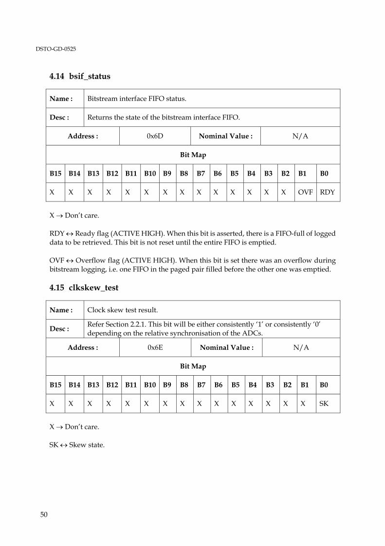
DSTO-GD-0525
50
4.14 bsif_status
Name : Bitstream interface FIFO status.
Desc : Returns the state of the bitstream interface FIFO.
Address : 0x6D Nominal Value : N/A
Bit Map
B15 B14 B13 B12 B11 B10 B9 B8 B7 B6 B5 B4 B3 B2 B1 B0
X X X X X X X X X X X X X X OVF RDY
X → Don’t care. RDY ↔ Ready flag (ACTIVE HIGH). When this bit is asserted, there is a FIFO-full of logged data to be retrieved. This bit is not reset until the entire FIFO is emptied. OVF ↔ Overflow flag (ACTIVE HIGH). When this bit is set there was an overflow during bitstream logging, i.e. one FIFO in the paged pair filled before the other one was emptied. 4.15 clkskew_test
Name : Clock skew test result.
Desc : Refer Section 2.2.1. This bit will be either consistently ‘1’ or consistently ‘0’ depending on the relative synchronisation of the ADCs.
Address : 0x6E Nominal Value : N/A
Bit Map
B15 B14 B13 B12 B11 B10 B9 B8 B7 B6 B5 B4 B3 B2 B1 B0
X X X X X X X X X X X X X X X SK
X → Don’t care. SK ↔ Skew state.

DSTO-GD-0525
51
5. FIFO Signal Capture Interface
The FIFO1 (Signal Monitoring) Receiver Interface (Section 2.2.6) allows signals internal to the DSSS signal processing chain to be captured in a FIFO at a known sample rate and extracted to the host as a contiguous block of data for subsequent analysis purposes, typically quasi-real-time graphical display. Signals of interest are mapped to the available sets of input channels in FW. Depending on the current packing mode, a subset of input channels is selected for input to the FIFO in a certain order. The FIFO has a 64k x 32-bit arrangement and is clocked at a fixed rate equal to half the chip rate. The partitioning of input channels into sets, and the use of the half-rate chip clock as sample clock, are legacies of the first generation HW architecture, and were preserved in the migration to the DPC for compatibility with the Development GUI. 5.1 Input Channels
Input channels are grouped into sets, and two types of set are implemented, namely fast sets and slow sets. Fast sets are designated s#f(5..0) and provide 6 x 8-bit inputs. Slow sets are designated s#s(11..0) and provide 12 x 16-bit inputs. The DSSS FW facilitates ‘#’, the set number, in the range 0 to 2. The fast channels are double-buffered internal to the interface to allow sampling at the full chip rate. Here, 16-bits of the input word are allocated to simultaneously log both the current 8-bit sample and its predecessor. The slow rate channels are typically interleaved in the packing circuit, giving more signals but at a slower rate. The mapping of signals to input channels is scripted in the VHDL file dsss_gbbm_port.vhd. 5.2 Packing Modes
The packing mode is set via the fifo_ctrl register (Section 3.38). The same register controls resetting and filling operations. When the FIFO is full it sets a bit in the fifo_status register (Section 4.13). The packing operations are defined in the VHDL file dsss_fifopacker.vhd, and are summarised in the following table, where Rc is the chip rate and the suffix ‘d’ on a channel designation implies the double-buffered (previous) sample.

DSTO-GD-0525
52
32-bit Word Format Mode Channels Logged and Sample Rates 31..24 23..16 15..8 7..0
0 s2f(0) Rc s2f(2) Rc s2f(2)d s2f(0)d s2f(2) s2f(0) 1 s2f(1) Rc s2f(2) Rc s2f(2)d s2f(1)d s2f(2) s2f(1) 2 s2f(0) Rc s2f(3) Rc s2f(3)d s2f(0)d s2f(3) s2f(0) 3 s2f(1) Rc s2f(3) Rc s2f(3)d s2f(1)d s2f(3) s2f(1) 4 s2f(0) Rc s2f(2,4) Rc/2 s2f(4) s2f(0)d s2f(2) s2f(0) 5 s2f(1) Rc s2f(3,4) Rc/2 s2f(4) s2f(1)d s2f(3) s2f(1) 6 s1f(0) Rc s1f(1) Rc s1f(1)d s1f(0)d s1f(1) s1f(0) 7 s1f(2) Rc s1f(3) Rc s1f(3)d s1f(2)d s1f(3) s1f(2) 8 s1f(0,1) Rc/2 s1f(2,3) Rc/2 s1f(3)d s1f(2)d s1f(1) s1f(0) 9 s0f(0) Rc s0f(1) Rc s0f(1)d s0f(0)d s0f(1) s0f(0)
10 s0f(2) Rc s0f(3) Rc s0f(3)d s0f(2)d s0f(3) s0f(2) 11 s0f(4) Rc s0f(5) Rc s0f(5)d s0f(4)d s0f(5) s0f(4) 12 s0f(1) Rc s0f(2) Rc s0f(2)d s0f(1)d s0f(2) s0f(1)
s0s(0) Rc/12 s0f(0,1) Rc/2 s0s(0) s0f(1) s0f(0) s0s(1) Rc/12 s0s(1) s0f(1) s0f(0) s0s(2) Rc/12 s0s(2) s0f(1) s0f(0) s0s(3) Rc/12 s0s(3) s0f(1) s0f(0) s0s(4) Rc/12 s0s(4) s0f(1) s0f(0) s0s(5) Rc/12 s0s(5) s0f(1) s0f(0) s0s(6) Rc/12 s0s(6) s0f(1) s0f(0) s0s(7) Rc/12 s0s(7) s0f(1) s0f(0) s0s(8) Rc/12 s0s(8) s0f(1) s0f(0) s0s(9) Rc/12 s0s(9) s0f(1) s0f(0)
s0s(10) Rc/12 s0s(10) s0f(1) s0f(0)
13..15
s0s(11) Rc/12 s0s(11) s0f(1) s0f(0)
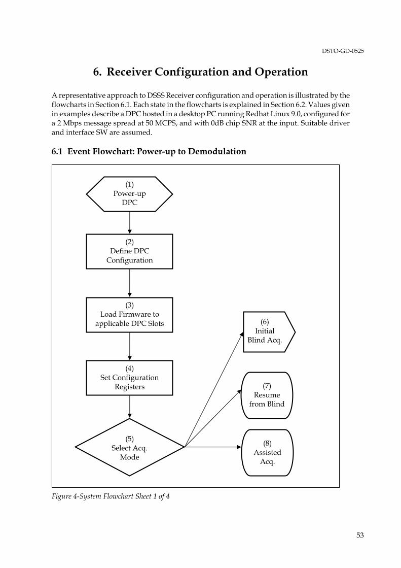
DSTO-GD-0525
53
6. Receiver Configuration and Operation
A representative approach to DSSS Receiver configuration and operation is illustrated by the flowcharts in Section 6.1. Each state in the flowcharts is explained in Section 6.2. Values given in examples describe a DPC hosted in a desktop PC running Redhat Linux 9.0, configured for a 2 Mbps message spread at 50 MCPS, and with 0dB chip SNR at the input. Suitable driver and interface SW are assumed. 6.1 Event Flowchart: Power-up to Demodulation
Figure 4-System Flowchart Sheet 1 of 4
(1) Power-up
DPC
(3) Load Firmware to
applicable DPC Slots
(4) Set Configuration
Registers
(5) Select Acq.
Mode
(6) Initial
Blind Acq.
(7) Resume
from Blind
(8) Assisted
Acq.
(2) Define DPC
Configuration
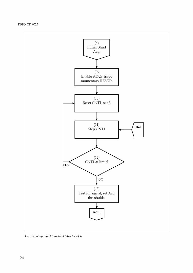
DSTO-GD-0525
54
Figure 5-System Flowchart Sheet 2 of 4
(6) Initial Blind
Acq.
(9) Enable ADCs, issue momentary RESETs
(10) Reset CNT1, set fc
(11) Step CNT1
(12) CNT1 at limit?
(13) Test for signal, set Acq
thresholds.
Aout
Bin
YES
NO
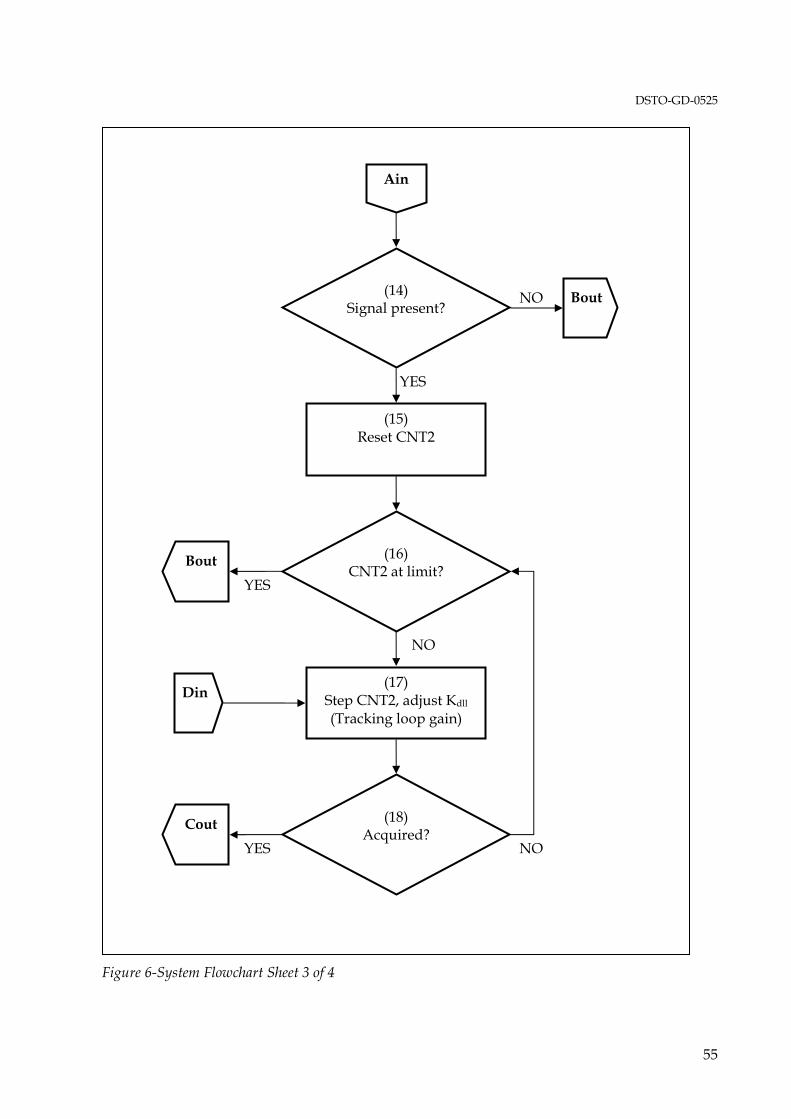
DSTO-GD-0525
55
Figure 6-System Flowchart Sheet 3 of 4
(15) Reset CNT2
(14) Signal present?
Ain
Bout
(17) Step CNT2, adjust Kdll (Tracking loop gain)
(16) CNT2 at limit?
NO
YES
YES
NO
(18) Acquired?
Cout YES NO
Bout
Din
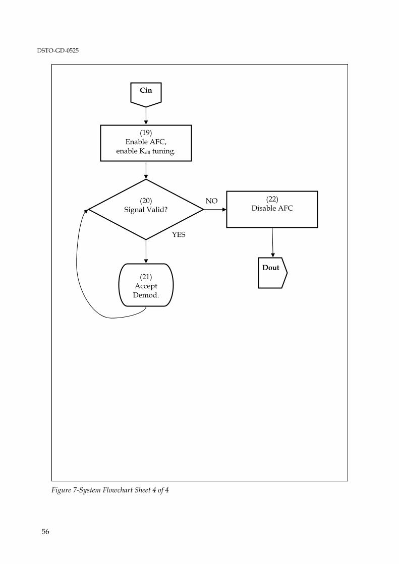
DSTO-GD-0525
56
Figure 7-System Flowchart Sheet 4 of 4
(19) Enable AFC,
enable Kdll tuning.
(20) Signal Valid?
Cin
Dout
NO
YES
(21) Accept Demod.
(22) Disable AFC
DSTO-GD-0525
57
6.2 Flowchart Event Descriptions
6.2.1 Power-up
6.2.1.1 State (1) When power is applied to the host, the PCI Target FW and a small set of application-side PCI peripherals will be loaded into the mainboard EP1S10 FPGA by the EPC8 boot EEPROM. The DPC should be registered as a valid PCI device by the host BIOS, and will be available to interact with device driver SW. In the Linux /proc/pci listing the DPC might appear as follows :
Bus 4, device 1, function 0: Signal processing controller: PCI device 0011:0012 (rev 0). IRQ 3. Non-prefetchable 32 bit memory at 0xdb000000 [0xdbffffff].
Note that the memory allocation spans 16MB (0xFFFFFF) as requested in FW. The identity label and device numbers will be constant from platform to platform. Without further activity, the DPC will be idle on the PCI bus, with the Slot#1 DDP unconfigured (all FPGA User-I/O will be tri-stated), and hence with the Slot#0 DCC state unknown (but since the ADC enable strobe is active-LOW, the ADCs may be clocking at full rate). In a development environment there may be changes to the EP1S10 FW. These may be uploaded to the EPC8, necessitating a shutdown for the changes to take effect on the next power-up, or directly to the FPGA, necessitating a reboot for the changes to take effect. When stable, a DPC device driver should be installed, and the desired UI SW should be launched. 6.2.2 Device Initialisations
6.2.2.1 State (2) In general purpose UI SW, the state of the DPC module configuration will be variable and hence must be defined for each application. This example assumes that the DPC has a DCC in Slot#0, a DDP in Slot#1, and that Slots#2 and #3 are either unloaded or loaded but will not be programmed. It may be necessary to specify the intended configuration and expected usage to enable SW to check that all necessary Slots are loaded prior to continuing.

DSTO-GD-0525
58
6.2.2.2 State (3) The DSSS FW application must be uploaded into the Slot#1 FPGA. The DPC has a Configuration peripheral, memory-mapped to the following array segment : dsss_pci_cnfg[ 0x40] This peripheral provides access to the configuration control and status pins of each loaded DDP FPGA (indexed by Slot#), in accordance with the following scheme, where on the PCI interface the write strobe, chip-select (for the Conf. Peripheral), and lower 3 address bits are significant :
-- l_wr l_cs l_a[2] l_a[1] l_a[0] Description -- ====================================== -- 1 1 0 0 0 Write to Control Register 0 -- 1 1 0 0 1 Write to Control Register 1 -- 1 1 0 1 0 Write to Control Register 2 -- 1 1 0 1 1 Write to Control Register 3 -- -- -- 0 1 0 0 0 Read from Status Register 0 -- 0 1 0 0 1 Read from Status Register 1 -- 0 1 0 1 0 Read from Status Register 2 -- 0 1 0 1 1 Read from Status Register 3 -- -- 1 1 1 X X Write Configuration Data Byte
The FPGA configuration file must be in the Altera tabular text file (.ttf) format. It must be opened for reading, read and transferred in accordance with a specific algorithm, an example of which is provided in the software utility referenced in Section 7. The following header extract defines the core functionality that this code implements :
/****************************************************************************** * Function: fpga_cfg_main * * Description: * Main function for configuration. Performs the following: * - Calls if_chk_inputs to check inputs provided. * - Calls if_init to initialise signals/buffers. * - Does setup: Set nCONFIG low, wait 40us, set nCONFIG high, set nCS * low, wait 40 us * - Reads from configuration file and extracts a config byte to write. * Writes configuration byte to FPGA, Reads nSTATUS, CONF_DONE and * INIT_DONE. Exits if nSTATUS low. Repeats this until all bytes sent. * - Reads nSTATUS, CONF_DONE and INIT_DONE. Exits if nSTATUS low. * Checks if CONF_DONE high, if so checks if INIT_DONE high. Repeats * until CONF_DONE and INIT_DONE are both high. Now Config is complete. * - Calls if_cleanup to reinitialise signals/buffers. * Returns 0 if successful or < 0 if there is an error. *

DSTO-GD-0525
59
******************************************************************************/
The DSSS FW application is then available (FPGA user I/O are active, and the DSSS will respond as a peripheral on the back-end PCI-bus in accordance with its defined memory map) but unconfigured. 6.2.2.3 State (4) The DPC state and DSSS operating mode are defined by configuration registers. The following settings form a consistent example. ADDR (0x)
Name Nominal Value (0x)
Comment
00 fir_bypass 0000 FIR filters would normally be in-line. 01 reset_ctrl 2DFF See Note(1) below. 02 interp_ctrl 0000 Automatic (ELDLL) interpolator control. 03 agc_dwell 4E20 Dwell for 20000 chips. 04 agc_thresh 07D0 Target 10% full-scale events. 05 agc_gain 0003 Good steady-state response. 06 agc_ctrl 0000 Automatic AGC (manual value at 0dB). 07 acq_thresh0 0032 See Note (2) below. 08 acq_thresh1 0014 See Note (2) below. 09 acq_thresh2 0014 See Note (2) below. 0A acq_thresh3 0014 See Note (2) below. 0B acq_thresh4 0014 See Note (2) below. 0C acq_thresh5 0014 See Note (2) below. 0D acq_thresh6 0014 See Note (2) below. 0E acq_thresh7 0014 See Note (2) below. 0F acq_serdwell 0000 Don’t care, not using serial acq. Mode. 10 acq_ctrl 0010 Parallel correlation in the 512 x 1-bit mode.
Acq. dwell tree height is 2 (two verifications after the initial acquisition).
11 chips_per_sym 0032 Based on the assumed 2 Mbps (1MSps) and 50 MCPS.
12 acqh_Nsym 0064 100 symbols of hold-up time. Known good value from development testing.
13 dll_gain 0087 Kdll = 2.73e-2. See Note (3) below. 14 dll_dwell 0020 Tracking loop dwell of 32 chips is
appropriate for this high data rate case. 15 iprbs_tap 236D 14th order PRBS with tap word 43333
(sequence length 16383 chips long). 16 iprbs_pha 000F Arbitrary. 17 iprbs_ospha 3857 Calculated w.r.t. “iprbs_pha”. 18 qprbs_tap 2421 14th order PRBS with tap word 44103
(sequence length 16383 chips long).
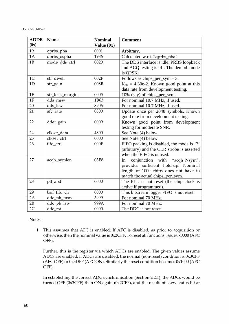
DSTO-GD-0525
60
ADDR (0x)
Name Nominal Value (0x)
Comment
19 qprbs_pha 0001 Arbitrary. 1A qprbs_ospha 1986 Calculated w.r.t. “qprbs_pha”. 1B mode_dds_ctrl 0020 The DDS interface is idle. PRBS loopback
and ACQ testing is off. The demod. mode is QPSK.
1C str_dwell 002F Follows as chips_per_sym – 3. 1D str_gain 008B Kstr = 4.30e-2. Known good point at this
data rate from development testing. 1E str_lock_margin 0005 10% (say) of chips_per_sym. 1F dds_msw 1B63 For nominal 10.7 MHz, if used. 20 dds_lsw 8906 For nominal 10.7 MHz, if used. 21 afc_rate 0800 Update once per 2048 symbols. Known
good rate from development testing. 22 ddet_gain 0009 Known good point from development
testing for moderate SNR. 24 clkset_data 4800 See Note (4) below. 25 clkset_ctrl 0000 See Note (4) below. 26 fifo_ctrl 000F FIFO packing is disabled, the mode is ‘7’
(arbitrary) and the CLR strobe is asserted when the FIFO is unused.
27 acqh_symlen 03E8 In conjunction with “acqh_Nsym”, provides sufficient hold-up. Nominal length of 1000 chips does not have to match the actual chips_per_sym.
28 pll_arst 0000 The PLL is not reset (the chip clock is active if programmed).
29 bsif_fifo_clr 0000 This bitstream logger FIFO is not reset. 2A ddc_ph_msw 5999 For nominal 70 MHz. 2B ddc_ph_lsw 999A For nominal 70 MHz. 2C ddc_rst 0000 The DDC is not reset. Notes :
1. This assumes that AFC is enabled. If AFC is disabled, as prior to acquisition or otherwise, then the nominal value is 0x2CFF. To reset all functions, issue 0x0000 (AFC OFF). Further, this is the register via which ADCs are enabled. The given values assume ADCs are enabled. If ADCs are disabled, the normal (non-reset) condition is 0x3CFF (AFC OFF) or 0x3DFF (AFC ON). Similarly the reset condition becomes 0x1000 (AFC OFF). In establishing the correct ADC synchronisation (Section 2.2.1), the ADCs would be turned OFF (0x3CFF) then ON again (0x2CFF), and the resultant skew status bit at
DSTO-GD-0525
61
register address 0x6E would be polled. The detail of this approach resides in the code of the Development GUI, discussed at Section 7.
2. An automatic routine for setting acquisition thresholds has been developed. Here the
on-time acquisition scores are monitored via the data-capture FIFO interface, under a variety of conditions. First, the local spreading codes are set to erroneous sequences, to establish the correlation noise floor (in the absence of any true correlation events). Then, the correct sequences are loaded with high threshold levels, and the peak values that result from unsustained correlation bursts are determined. Then the initial threshold point is set at a percentage of the difference, added to the noise floor, and the remaining thresholds are set at a user-defined fraction of the initial threshold (typically 50%). The detail of this algorithm resides in the code of the Development GUI, discussed at Section 7.
To set thresholds manually, the first threshold may be decreased from an initial high value while monitoring the on-time acquisition scores in a plot window and with the tracking loop gain set mid-range. The other thresholds can follow a 50% rule. When acquisition events become apparent, the tracking loop gain should be adjusted to see if acquisition is sustainable, otherwise the thresholds may still be too high.
3. The given value applies only to an AWGN channel with received chip SNR near 0dB.
In general the required gain is a function of the signal quality and channel characteristics. An automatic routine for determining the correct gain setting has been developed. Here, the interpolator state vector is monitored via the signal capture interface. As the tracking loop adjusts the interpolator output state to maintain the optimum on-time sampling instant, the state bits toggle from one state to an adjacent state. However because the tracking is a noisy process, there will be not one single transition but a number of transitions back and forth as the loop settles to the new state. This ‘state jitter’ varies as a function of loop gain consistent with normal loop theory (i.e. high gain implies a broad pull-in range (bandwidth) but high jitter whereas low gain narrows the pull-in range and improves the jitter), and development testing has shown that optimum BER performance is linked to a defined amount of state jitter. Thus the gain setting process is to monitor the state vector, compute a jitter metric as the number of transitions per state change, averaged over sufficient blocks of data, then increment or decrement the loop gain to drive the jitter metric to within desired bounds. The detail of this algorithm resides in the code of the Development GUI, discussed at Section 7.
An operator may achieve the correct gain setting by manually adjusting the gain word while monitoring a real-time plot of the interpolator state vector and striving for the desired amount of jitter. Note that due to the mantissa and exponent format of the gain word (Section 3.20) a simple increment or decrement to the gain value does not follow from a numeric increment or decrement of the word. Instead a look-up table is required, and an example is provided in the Development GUI (Section 7).
DSTO-GD-0525
62
4. These two registers allow configuration of the variable elements in the enhanced phase-locked loop (EPLL) entity on the EP1S80 FPGA that provides the chip clock for DSSS signal processing. An EPLL accepts a single reference clock as input (fref) and can operate in several modes to produce up to six output clocks (foi) to the FPGA array. For any given output, the frequency is given by foi = fref*M/(N*Pi), where M is a pre-scale multiplier, N is a pre-scale divider, and Pi is a post-scale divider for the ith output. The output phase can also be controlled via delay parameters associated with each scaler, and the output duty cycle is controlled by splitting Pi into high and low components, Pi = Pi_hi + Pi_lo.
In the DSSS FW, the EPLL is instantiated with N = 1 and uses only one of the output clocks (designated g0 in Altera’s PLL documentation). The input clock is the 100 MHz sample clock from the I-channel ADC, and the output is the chip clock which must have period 20ns or slower, in 10ns increments (in order to be compatible with the input sample decimation scheme, see Section 2.2.2). Thus the chip clock rate is set as chip_clk (MHz) = 100*M/P where M ≤ 8 (due to rate limitations in the embedded silicon), M and P must satisfy the 10ns period increment constraint, and P should have duty cycle as close to 50% as possible. Delay parameters DM and DP can also be set, with allowable range 0 ≤ D ≤ 12 and with actual delay ΔT (ps) = 250*(DM - DP). To program the EPLL each of the five variable parameters must be updated in a configuration register chain and a trigger signal must be sent to a configuration controller entity which will upload the entire chain for the new settings to take effect. An example of this sequence of events may be found in the development GUI, which is summarised by the code extracts:
// // Update the chip clock PLL based on the M and P scaling and delay factors... // // Parameters from the user interface… // M = sbConfigDemodValueMFactor->value(); // P = sbConfigDemodValuePFactor->value(); // DM = sbConfigDemodValueMDelay->value(); // DP = sbConfigDemodValuePDelay->value(); // Calculate high and low periods close to 50% duty cycle... // if((P - floor((double)P/2)*2) == 0) // // P_hi = P/2; // P_lo = P/2; // //else // // P_hi = (P-1)/2; // P_lo = P_hi +1; //
DSTO-GD-0525
63
// Perform a sequence of writes to the PLL controller... // Write the M value and wait until complete... //driver->write_s1reg(PLL_DATA, 0x0200 + M); //driver->write_s1reg(PLL_CTRL, PLL_WR); //driver->write_s1reg(PLL_CTRL, 0); //timeout = 5; //msec //while(timeout > 0 && driver->read_s1reg(PLL_STATUS) == 1) // // qWarning("Waiting for Chip Clock PLL Controller...\n"); // usleep(1000); // timeout--; // // Write the P_hi value and wait until complete... // Write the P_lo value and wait until complete... // Write the M-Delay value and wait until complete... // Write the P-Delay value and wait until complete... // Update the PLL... //driver->write_s1reg(PLL_CTRL, PLL_UPD); //driver->write_s1reg(PLL_CTRL, 0);
The correct values for the delay parameters must be established by trial and error. For example, after updating the EPLL, check that with I_in and Q_in disconnected there are no spurious signals present in the sampled data streams, as logged via the data capture interface. 6.2.3 Select Acquisition Mode
6.2.3.1 State (5) At this stage the DSSS Receiver is ready to begin acquiring a signal. It is assumed that a suitable RF downconverter has been used to provide a low IF or baseband quadrature input to the DPC analogue input ports. Note that the I and Q outputs from downconversion must map to the corresponding I and Q inputs on the DPC – if these channels are crossed over, the DSSS Receiver may appear to acquire and track a signal correctly, but will be unable to correctly demodulate the underlying QPSK symbols. The signal will have (initially) unknown carrier frequency and SNR in a time varying fading channel, preventing exact a priori setting of the local frequency, acquisition thresholds and tracking loop gain. A strategy must be chosen to manage these unknowns. The most general case is blind acquisition where there is no assumed knowledge and no added signal content to aid the acquisition process. With the exception of states (7) and (8), the remainder of this example assumes blind acquisition. An abbreviated process may be possible when resuming from a previously blind acquisition (Section 6.2.5) or when the signal content is modified to aid
DSTO-GD-0525
64
acquisition. Proposals for the latter approach are given in Section 6.2.6, but note that these are not implemented in the Development GUI described in Section 7. 6.2.4 Initial Blind Acquisition
6.2.4.1 States (9 to 22) The given process attempts to manage centre frequency searching, acquisition threshold setting, and tracking loop gain control. Much of this process is coded in the Development GUI (see Section 7). These processes are nested within each other, and for any given setting of an outer process, the inner processes may or may not be successful. This leads to the idea of allowing an inner process to iterate only a bounded number of times before deciding that the outer process may also need adjusting, then regressing outwards. Counters could be used to control these iterations. A counter CNT1 is proposed to regulate the overall number of acquisition attempts at any given centre frequency. CNT2 regulates the number of iterations of coarse gain setting before concluding acquisition failure. So the proposed process is as follows. In state (9), momentarily reset the FW and ensure the ADCs are enabled with the correct (previously established) relative timing. In state (10), choose a centre frequency and reset CNT1. For multiple iterations from this starting point, the centre frequency could be zigzag searched, i.e. started at the assumed centre frequency, then alternately incrementing and decrementing this value by increasing multiples of the AFC loop pull-in range (which is +/- Rs/8, i.e. check fc, fc+/-2Rs/8, fc+/-4Rs/8, fc+/-6Rs/8, etc.). If user-defined bounds on centre frequency are reached (consistent with reasonable expectations on the stability and accuracy of the transmit and receive oscillators) then the search could be repeated or the conclusion that no signal is present could be reached. In state (11), increment the counter CNT1. Then, provided that CNT1 has not expired, proceed to state (13) to test for the presence of a signal, as indicated by the existence of temporary correlation events in the correlator output scores. If a signal is present, the acquisition thresholds can be determined and updated with the automation algorithm (Section 6.2.2.3), or these could be programmed in accordance with a different scheme. If strong correlations are occurring, reset CNT2 and (state 17) execute the automatic tracking loop gain routine (or otherwise set the tracking loop gain). Increment CNT2 when complete. If a loop gain that results in sustained acquisition cannot be found, and until CNT2 reaches its limit, repeat this test. If CNT2 expires, return to the acquisition threshold setting (state 11). Otherwise, the signal has been acquired and AFC should be enabled (state 19). At this stage it is desirable to continuously test if the demodulated signal is valid or not (state 20). The ACQD flag provides a coarse indicator, but even when the acquired flag is asserted the demodulated signal may be invalid, for example if thresholds were set too low and the

DSTO-GD-0525
65
local code phase is incorrect, or if the centre frequency is out by a multiple of Rs/4, leading to excessive frequency error. Provided the signal is deemed valid, the demodulated data can be used (state 21). Otherwise, disable AFC before regressing backward via tracking loop gain adjustment, and if CNT2 expires via acquisition threshold setting, and if CNT1 expires via frequency stepping. It may also be desirable to periodically check and adjust the tracking loop gain at this stage. This would be a fine-tuning of the gain and would be done without regressing through the process. An example of this process is provided in the Development GUI (Section 7). The technique used for testing signal validity will depend on applications. Some confidence may be gained by executing a K-means style of SNR estimation on the recovered symbol constellation, to check that both the correct number of constellation clusters is present and that the SNR is meaningful (refer “Techniques for the Blind Estimation of Signal to Noise Ratio for Quadrature Modulated Signals”, Parker, G., Proceedings of the fourth international symposium on signal processing and its applications, ISSPA ‘96, August 1996, vol.1, pp.238-241). In the event that the message contains known framing data, the presence of framing data could be checked periodically. 6.2.5 Resume from Blind
6.2.5.1 State (7) If acquisition is being re-established after a previous successful transmission, if the elapsed time is short or the channel is known to be quite static, and if the transmitter and receiver oscillators are known to be quite stable, then the previous parameters may still be applicable and could be used as an informed starting point for demodulation. For example, direct entry to state (20) could be assumed (with CNT1 and CNT2 set to ‘1’). 6.2.6 Assisted Acquisition
6.2.6.1 State (8) The signal content could be modified to assist initial acquisition. This section suggests one possible approach, but note that these ideas are not yet incorporated in the Development GUI detailed in Section 7. Conventional packet signalling schemes partition a packet into a series of frames, comprising preamble frames, a synchronisation frame, and the actual data frame. The preamble is concerned with assisting carrier recovery and symbol timing recovery. A preamble might consist of a special sequence of symbols constructive to these processes, and of sufficient duration to allow the timing synchronisation to be achieved with some level of confidence. The synchronisation frame is concerned with identifying the start of the following data frame. By far the most common approach to frame synchronisation (refer “Optimum Frame

DSTO-GD-0525
66
Synchronisation”, James L. Massey, IEEE Transactions on Communications Vol. COM-20, No.2) is the insertion of a unique word (UW) message, with optimised auto- and cross-correlation properties that seek to minimise the probability of false alarms and missed detections. When the UW is detected it is assumed both that the next symbol is data and that the prior timing recovery operations were successful. With the DSSS Receiver, the packet structure might be similar to that shown in Figure 8, where it is important to recognise that the whole packet is spread (is a DSSS signal). Here, the following frames are proposed:
• An all 1s acquisition phase, which eliminates PRBS inversions due to data and prevents cancellation between the I and Q branches of the complex correlators.
• An all 1s tracking phase, which eliminates PRBS inversions due to data. • An alternating 0/X, 1/X, 0/X, 1/X, … I/Q-pattern which assists STR (the STR loop
error detector provides an estimate of the timing error on a per-symbol basis, but the detector output is conditioned on a data polarity transition between one symbol and the next; thus successive 1s or 0s do not contribute to the error estimation). The STR loop only uses the I-channel information, so the Q-bit is ‘don’t care’.
• A UW frame synchronisation marker (or markers), for which a short PRBS or a Barker sequence would be sufficient. The UW correlation is implemented post-despreading, where the symbol SNR needs to be sufficiently large to allow a useful BER. Under these conditions, characterisation testing of the DSSS correlator circuits has shown that correlator performance is excellent (the output is at least 90% of the perfect score) which would allow robust threshold-based detection. A UW length of 31-symbols would provide 15dB of processing gain in the UW detection.
The UW could also provide additional benefits. Firstly, the UW detection event could be used to set a status bit (UW_Flag) that could be logged (interleaved, for example 1 bit in 32) with the data. This would provide confidence that the data is valid, and if the UW_Flag is reset by loss of acquisition it could be used to sense such events during the data frame. This UW_Flag would be expected within a known time interval of the start of acquisition and so, with simple FW time-stamping or counting, could also be used to trigger packet abort and retry if not present. Secondly, UW events could be used to initiate and validate AFC. Upon UW detection, the Receiver has acquired the spread signal, is tracking chip timing errors and is despreading in-phase with the underlying symbols. It is then valid to enable AFC to reduce carrier noncoherence. If there are no UW events, or if after enabling AFC the UW events stop, then the frequency error may be too great and the AFC loop will pull-in to a centre frequency with offset (+/-) n*Rs/4 from the actual carrier frequency.

DSTO-GD-0525
67
Figure 8- DSSS Signalling Packet Structure
In Figure 8, each frame should have an appropriate duration. The following considerations apply:
• τacq O(100ms): In an AWGN channel and using 14th-order (16383-long) PRBS, the acquisition time has been shown to be of the order of 10ms across a range of SNR. Increasing this by an order of magnitude for margin results in the 100ms estimate. Note that at 50 MCPS, this is approximately 300 iterations of the 14th-order sequence.
• τtrk O(1s): The time required for tracking will depend largely on the SW scheme used for gain estimation. In the Development GUI a stepped gain search is conducted which takes several seconds to complete. This is likely to be the slowest component.
• τstr O(1000 symbols): Measurements of the STR loop indicate several hundred symbols are required for loop pull-in. The duration of this frame will be a function of symbol rate; for example 1000 symbols at 2 Mbps requires 1ms whereas 1000 symbols at 20kbps requires 100ms.
• τuw O(N*31*Ts): For N repetitions of a 31-bit UW. A 1ms period allows 32 repetitions of a 31-bit UW at 2 Mbps. If UW repetitions are to facilitate AFC, then the duration should be consistent with the AFC update rate and the expected pull-in time of the AFC loop (typically O(100 symbols)).
• τdata O(K*Ts): For K symbols in the frame. Using the DSSS Receiver with structured packets may also lead to FW architecture variations. For example, the STR loop could be removed, with edge timing coming instead from a contrived relative alignment between the symbols and the spreading codes. This would be re-established at the start of each data frame, as indicated by the UW detector. Another useful function that would be better facilitated by the adoption of a suitable packet structure is channel estimation, necessary in higher performance receiver equalisers.
ACQ 1s TRK 1s STR 1/0 UW1 UWN DATA
τacq τtrk τstr τuw τdata
DSTO-GD-0525
68
7. The DSTO Development GUI
The DSTO Development GUI is a complete interface to the DSSS Receiver for Redhat Linux 9.0 on an Intel 32-bit architecture PC. It comprises both device driver SW in ‘C’ and GUI SW in ‘C++’, as described in the following section. Reference is made here to the generic baseband modem (GBBM), a legacy designation for the DPC. 7.1 Code Hierarchy and Classes
The code hierarchy and classes are depicted in Figure 9. Note the following
• The software is configured as a Qt project, except for the GBBM device driver which is built independently of the project.
• Each box with solid edges represents a C++ class (except dsssmain – this is the top-level “main” program). All the C++ class files are in the top-level directory. In general, the classes have the same name as the file (.cpp and/or .h); however those that differ show the class name followed by the filename in brackets. Only the higher level classes that are the main content of a file are shown.
• The boxes with dotted edges do not represent C++ classes. • The GBBM device driver box represents the device driver C software, which consists
of source (.c), header (.h) and makefiles in the driver subdirectory. • The App/Cfg box represents the C software which is used for configuring the FPGA
devices and Temperature Sensors on the GBBM card. This software is contained in the application and cfg_sw subdirectories and is written in C, although the files have a .cpp extension, to allow them to be used in the Qt project.
• There are some other files which exist in this software which are not indicated in the diagram. These are:
o Extra header files (MyMacros.h) – This contains some simple #define macros.
o GUI files (dssscontrol.ui, dssscontrol.ui.h) – These hold the top-level GUI component and layout descriptions.
o Project files (dsss_ctrl.pro) – This is the Qt project file which keeps track of the source (.cpp) and header (.h) files in the project.
o Compilation files (makefile) – This is the file (generated using qmake) used by make to compile the project.
o Executable files (dsss_ctrl) – This is the resulting executable from the compilation.
o Config files (ControlPanelInitFile.cfg, PlotConfigFile.cfg) – These hold initial values for the control panel controls and the modes available for plotting.
o Hardware register list files (master.reg) – This holds the name, size and address of the registers implemented in firmware that the DSSS application can access.

D
STO-G
D-0525
69
Figure 9- G
UI and D
river Code Hierarchy
DSTO-GD-0525
70
o Firmware configuration files (content of cfg_files directory) – These are Altera .ttf files for configuring the FPGA devices.
The list below identifies the role of each source module/C++ class (.cpp and/or .h file), separated into functional groups:
• Main/Initialisation/Cleanup o dsssmain – main program that sets up the DSSS implementation and runs it. o dsssimpl – DSSS Implementation which uses GUI description files and has the
bulk of the receiver processing. o ControlPanelInit – Allows saving and restoring of control panel control values
(uses ControlPanelInitFile.cfg). o CloseCatcher – Catches keypress events.
• Plotting
o IPlotDataSource – Interface for plot data sources. Provides plot data types and methods for manipulating plot data sources.
o PlotDataSourceDriver – Implements IPlotDataSource. Supplies data requested by PlotRenderer from dsssDriver.
o PlotDataSourceDriverSync – Implements IPlotDataSource. Supplies data that has been synchronized from dsssDriver to PlotRenderer.
o PlotDataSourceFile – Implements IPlotDataSource. Loads data from a supplied file and passes the data to PlotRenderer.
o PlotConfigFileReader – Reads PlotConfigFile.cfg to obtain the different modes and data signals and passes them to PlotDataSourceDriver.
o PlotRenderer – Converts the raw plot data given to it into a collection of lines for plotting. Allows many different plot types and controls for the plot.
o PlotCanvas – Widget which shows lines that are calculated by PlotRenderer on a labelled Cartesian or polar grid.
o PlotWindow – Provides a separate window which uses PlotRenderer to show a plot in the window. Also includes some toolbars with plot controls.
o PowerSpectrumGenerator – Used by Plot Renderer to convert blocks of time-based data to frequency-based data. Uses a FFT function (with window if desired) and scales the power spectrum to one of these formats: linear, dB, Power Spectral Density (dB) or dBm.
• Hardware Interface
o dsssDriver (dsssdriver) – Interface to GBBM device driver. Allows DSSS application to read/write memory/registers on GBBM card via device file /dev/gbbm.
o dsssRegisterList (initfile) – Maintains a list of registers that are implemented in firmware (uses master.reg).
• “application”/”configuration” source (.cpp and .h files in application and cfg_sw
directories) o gbal_gbbm_fpga_cfg – Allows configuration of Altera Stratix FPGA devices on
the GBBM card.
DSTO-GD-0525
71
o gbal_gbbm_ts_cfg – Allows configuration of the Maxim MAX1617 Temperature Sensor devices on the GBBM card
• GBBM device driver (.c and .h files in driver subdirectory):
o This implements a Linux Device Driver for accessing the GBBM card with the following operations: open, release, read, write, ioctl, mmap and fasync.
o Most reading and writing of the GBBM card is done using the mmap method.
o It relies on the existence of a device file at /dev/gbbm with major number 240.
o The driver is compiled using the makefile and there are also targets for creating the device file (mkdev), loading the driver into the kernel (load) and unloading the driver from the kernel (unload). These 3 targets must be run as root.

DSTO-GD-0525
72
Appendix A: Applicable System Configuration
This document applies only to a DSSS Receiver compliant with the following configuration descriptions. A.1. Hardware configuration
• DPC Mainboard with serial number prefix 111368 or 118187. • Slot#0 : DDC with serial number prefix 111366 or 118187. • Slot#1 : DDP with serial number prefix 111367 or 118187. • Slot#2 : Unloaded with JTAG chain bypassed, or loaded with a DDP that is
unconfigured during DSSS operation. • Slot#3 : Unloaded with JTAG chain bypassed, or loaded with a DDP that is
unconfigured during DSSS operation. A.2. Firmware configuration
• PCI Target version : pci_interface_15.sof. • DSSS Application version : dsss_r1_0.ttf.
The DSSS FW is further defined by the following extracts from the project compilation report produced by the Altera QuartusII development tools : +--------------------------------------------------------------------------+ ; Fitter Summary ; +--------------------------+-----------------------------------------------+ ; Fitter Status ; Successful - Tue Jul 04 12:09:05 2006 ; ; Quartus II Version ; 4.2 Build 178 01/19/2005 SP 1 SJ Full Version ; ; Revision Name ; dsss_gbbm_port_top ; ; Top-level Entity Name ; dsss_gbbm_port_top ; ; Family ; Stratix ; ; Device ; EP1S80F1508C6 ; ; Timing Models ; Final ; ; Total logic elements ; 27,731 / 79,040 ( 35 % ) ; ; Total pins ; 959 / 1,212 ( 79 % ) ; ; Total virtual pins ; 0 ; ; Total memory bits ; 2,640,064 / 7,427,520 ( 35 % ) ; ; DSP block 9-bit elements ; 26 / 176 ( 14 % ) ; ; Total PLLs ; 1 / 12 ( 8 % ) ; ; Total DLLs ; 0 / 2 ( 0 % ) ;
+-----------+ ; Hierarchy ; +-----------+ dsss_gbbm_port_top |-- dsss_gbbm_port:dsss_app |-- agcc:agcc1 |-- dsss_clock_ctrl:chip_clk_gen |-- chip_clk_epll:chip_clk |-- chip_clk_ctrl:controller |-- ddconv:ddc |-- cos_LUT:cos_IA |-- cos_LUT:cos_IB |-- png_par:dither_src |-- ddc_afc_lut:phi_err_lut |-- sin_LUT:sin_IA

DSTO-GD-0525
73
|-- sin_LUT:sin_IB |-- dsss_demod:dsss |-- acq_ctrl_top:acq_control |-- acq_ctrl:acq_ctrl_1 |-- combiner:t1_score_combiner |-- combiner:t2_score_combiner |-- acq_holdup:acq_holdup_1 |-- correlator_array_top:adv_time_corr |-- corr_array:corr_array1 |-- demod_control:demod |-- despreader_v2:despreader_v2_1 |-- diffdet:diffdet_1 |-- cordic_rpc_v2:cordic_rpc_v2_1 |-- eldll:eldll_1 |-- cplx_corr_v2:ccv1 |-- cplx_corr_v2:ccv2 |-- freq_ctrl:freq_ctrl_1 |-- eavg:eavg1 |-- rom:rom1 |-- pn_gen:pn_gen1 |-- png:png1 |-- png:png2 |-- spng:spng1 |-- spng:spng2 |-- png:tpni_png |-- png:tpnq_png |-- str_v3:str_v3_1 |-- sym_clock:sym_clk |-- sym_dec:sym_dec_1 |-- fir_filter:FIR |-- fsdet:fs_fsdet |-- buff8:ia_out_buff8 |-- buff8:iadat_buff8 |-- buff8:ib_out_buff8 |-- buff8:ibdat_buff8 |-- fir01:ix_fir_fir01 |-- buff8:qa_out_buff8 |-- buff8:qadat_buff8 |-- buff8:qb_out_buff8 |-- buff8:qbdat_buff8 |-- fir01:qx_fir_fir01 |-- interpolator_top:Interpolator |-- agcc:agcc1 |-- interpolator:interpolator1 |-- interpolator:interpolator2 |-- specan_src_mux:specan_src_mux1 |-- correlator_array_top:on_time_corr |-- corr_array:corr_array1 |-- dsss_bitstream_if:dsss_bsif |-- bsif_ram:fifo_A |-- bsif_ram:fifo_B |-- dsss_membank:dsss_fifo |-- dsss_pciif_regbank:dsss_regbank |-- dsss_fifopacker:fifo_packer |-- fsdet:fs_fsdet |-- pbus_tgt_dsss:pciif |-- dsss_lvdsif:lvdsif |-- dsss_tsif:tsif |-- temperature_sensor_interface:ts_wrap |-- divide_by_N:clock_divider |-- status_register:error_sr |-- parallel_to_serial_converter:psc |-- mux_2to1_8bit:readdata_mux |-- serial_to_parallel_converter:spc |-- tsi_sm:state_machine |-- mux_2to1_1bit:writedata_mux

DSTO-GD-0525
74
• Maximum chip rate : 50 MCPS. • Maximum data rate : 4 Mbps. • Maximum Ambient : 60° C.
A.3. Development GUI configuration
• GUI code release : Version 3. • Driver code release : Version 3.
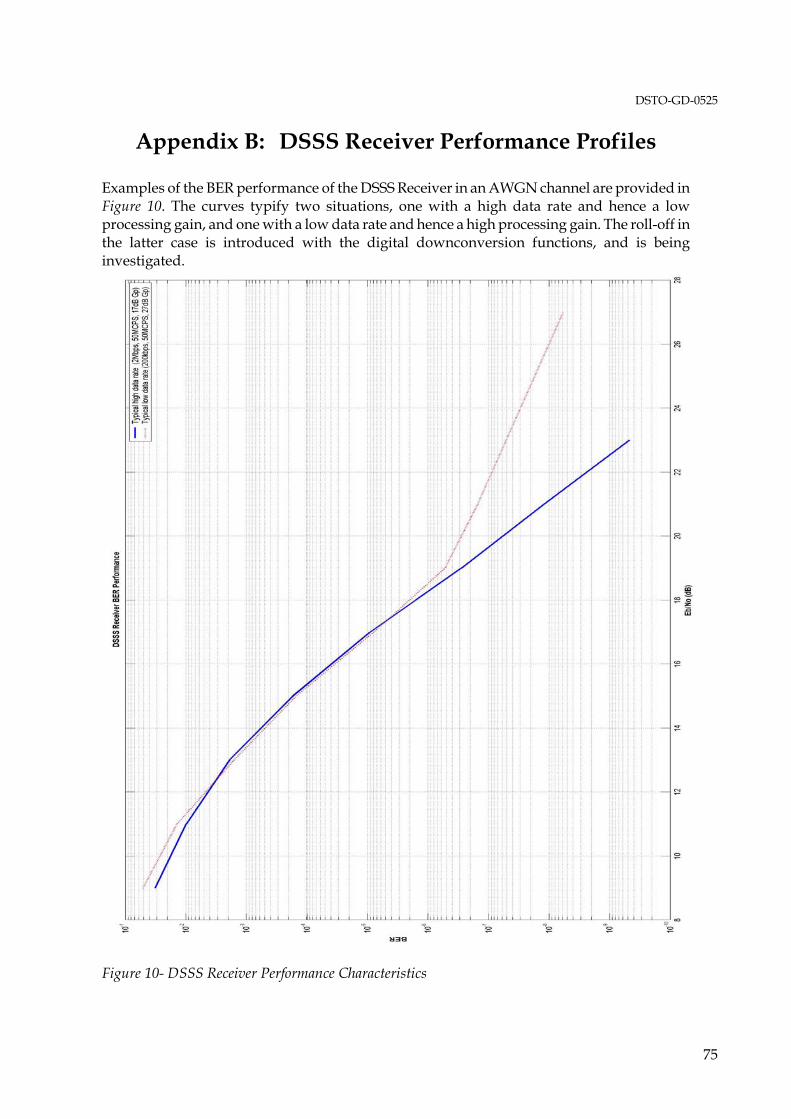
DSTO-GD-0525
75
Appendix B: DSSS Receiver Performance Profiles
Examples of the BER performance of the DSSS Receiver in an AWGN channel are provided in Figure 10. The curves typify two situations, one with a high data rate and hence a low processing gain, and one with a low data rate and hence a high processing gain. The roll-off in the latter case is introduced with the digital downconversion functions, and is being investigated.
Figure 10- DSSS Receiver Performance Characteristics

Page classification: UNCLASSIFIED
DEFENCE SCIENCE AND TECHNOLOGY ORGANISATION
DOCUMENT CONTROL DATA 1. PRIVACY MARKING/CAVEAT (OF DOCUMENT)
2. TITLE DSSS Receiver User's Manual
3. SECURITY CLASSIFICATION (FOR UNCLASSIFIED REPORTS THAT ARE LIMITED RELEASE USE (L) NEXT TO DOCUMENT CLASSIFICATION) Document (U) Title (U) Abstract (U)
4. AUTHOR(S) K.L. Harman
5. CORPORATE AUTHOR DSTO Defence Science and Technology Organisation PO Box 1500 Edinburgh South Australia 5111 Australia
6a. DSTO NUMBER DSTO-GD-0525
6b. AR NUMBER AR-014-083
6c. TYPE OF REPORT General Document
7. DOCUMENT DATE January 2008
8. FILE NUMBER 2007/1101206/1
9. TASK NUMBER INT 07/020
10. TASK SPONSOR ASCP
11. NO. OF PAGES 77
12. NO. OF REFERENCES 0
13. URL on the World Wide Web http://www.dsto.defence.gov.au/corporate/reports/DSTO-GD-0525.pdf
14. RELEASE AUTHORITY Chief, Command, Control, Communications and Intelligence Division
15. SECONDARY RELEASE STATEMENT OF THIS DOCUMENT
Approved for public release OVERSEAS ENQUIRIES OUTSIDE STATED LIMITATIONS SHOULD BE REFERRED THROUGH DOCUMENT EXCHANGE, PO BOX 1500, EDINBURGH, SA 5111 16. DELIBERATE ANNOUNCEMENT No Limitations 17. CITATION IN OTHER DOCUMENTS No 18. DSTO RESEARCH LIBRARY THESAURUS http://web-vic.dsto.defence.gov.au/workareas/library/resources/dsto_thesaurus.htm Documentation, Spread Spectrum Communications, Digital Signal Processing, User manual 19. ABSTRACT The direct-sequence spread-spectrum (DSSS) receiver performs demodulation of wideband DSSS signals, accepting as input an analogue signal at low intermediate frequency (IF) or baseband, and producing as output the recovered digital message bitstream. It consists of firmware (FW) entities that perform signal processing; a PCI-compliant digital processor card (DPC) that provides analogue to digital conversion and host resources for the FW; and a computer which hosts the DPC and runs software to access, control and monitor it. This manual provides the information required to allow an operator to connect, configure and dynamically control the DSSS Receiver in a precise way to achieve the best demodulation performance.
Page classification: UNCLASSIFIED