Diagnostic Ultrasound System · 2017-06-15 · Diagnostic Ultrasound System Service Manual Revision...
289
M7 Series Diagnostic Ultrasound System Service Manual Revision 12.0
Transcript of Diagnostic Ultrasound System · 2017-06-15 · Diagnostic Ultrasound System Service Manual Revision...

M7 Series
Diagnostic Ultrasound System
Service Manual
Revision 12.0


i
Contents Contents ..............................................................................................................................................i
Revision History ................................................................................................................................. I
Intellectual Property Statement ......................................................................................................... II
Responsibility on the Manufacturer Party ......................................................................................... II
Warranty ........................................................................................................................................... III
This warranty shall not extend to: .................................................................................................... III
Customer Service Department ............................................................................................III Important Information ....................................................................................................................... IV
Safety Precautions ............................................................................................................................ V
1 System Overview ........................................................................................................ 1-1 1.1 Intended Use ........................................................................................................................ 1-1
1.2 Contraindication ................................................................................................................... 1-1
1.3 Product and Model Code ..................................................................................................... 1-1
2 System Structure ........................................................................................................ 2-1 2.1 Introduction of Each Unit ...................................................................................................... 2-1
2.2 Peripherals Supported ......................................................................................................... 2-3
2.3 Extend Modules .................................................................................................................... 2-3
2.3.1 Transducer Extend Module ........................................................................................... 2-3
2.3.2 I/O Extend Module. ....................................................................................................... 2-4
2.3.3 V/A Extend Module ....................................................................................................... 2-5
2.3.4 ECG Module ................................................................................................................. 2-7
2.4 Control Panel ........................................................................................................................ 2-8
3 Principle Description .................................................................................................. 3-1 3.1 Electric Principle of the System ............................................................................................ 3-1
3.1.1 Power System ............................................................................................................... 3-2
3.1.2 Principle of the Main Board ........................................................................................ 3-17
3.1.3 Principle of Transmitting Board ................................................................................... 3-47
3.1.4 4D Driving Board ........................................................................................................ 3-52
3.1.5 Principle of Keyboard Board ....................................................................................... 3-56
3.1.6 Display Unit ................................................................................................................. 3-65
3.1.7 Principle of ECG Board .............................................................................................. 3-69
3.1.8 Principle of Video/Audio Capture Card ....................................................................... 3-73
3.1.9 Principle of the CW Board .......................................................................................... 3-74
4 Structure and Assembly/Disassembly ...................................................................... 4-1

ii
4.1 Explosive Figure of the Structure ......................................................................................... 4-1
4.1.1 Explosive Figure of the Complete System ................................................................... 4-1
4.1.2 Explosive Figure of the Modules .................................................................................. 4-3
4.2 Field Replaceable Unit ......................................................................................................... 4-6
4.3 Assembly/Disassembly ...................................................................................................... 4-18
4.3.1 Removing Batteries .................................................................................................... 4-18
4.3.2 Removing Display Assembly ...................................................................................... 4-18
4.3.3 Removing Top Cover of Main Unit .............................................................................. 4-23
4.3.4 Removing the Power Module ..................................................................................... 4-26
4.3.5 Removing CW Board and Installation ......................................................................... 4-29
4.3.6 Removing CPU Fan .................................................................................................... 4-31
4.3.7 Removing CPU Board and Radiator Module .............................................................. 4-32
4.3.8 Removing the System Fan ......................................................................................... 4-34
4.3.9 Remove the Speakers ................................................................................................ 4-35
4.3.10 Removing Transmission Board ................................................................................... 4-36
4.3.11 Removing Main Board and Transducer Board Assembly ........................................... 4-37
4.3.12 Remove the Transducer Board ................................................................................... 4-39
4.3.13 Removing 4D Board and Installation .......................................................................... 4-40
4.3.14 Removing Hard Disk ................................................................................................... 4-42
4.3.15 Removing Transducer Extend Module PEM-21 ......................................................... 4-43
4.3.16 Removing ECG Module .............................................................................................. 4-46
4.3.17 Removing Video and Audio Capture Module ............................................................. 4-48
4.3.18 Removing I/O Extend Module ..................................................................................... 4-49
5 System and Software ................................................................................................. 5-1
5.1 XPE System Introduction ..................................................................................................... 5-1
5.2 Introduction of Doppler ......................................................................................................... 5-2
5.2.1 Resume Package ......................................................................................................... 5-2
5.2.2 Data Processing ........................................................................................................... 5-2
5.3 Run the Resume Package in Doppler .................................................................................. 5-4
5.4 Power ON Process ............................................................................................................... 5-5
5.5 Software Maintenance .......................................................................................................... 5-6
5.5.1 Entering Preset ............................................................................................................. 5-6
5.5.2 Viewing System Information ......................................................................................... 5-7
5.5.3 Manage Settings ........................................................................................................... 5-7
5.5.4 Maintenance Status ...................................................................................................... 5-9
5.5.5 Model Setup ................................................................................................................ 5-10
5.5.6 Installing Optional Software ........................................................................................ 5-10
5.6 Warning .............................................................................................................................. 5-11
5.6.1 Battery warning ........................................................................................................... 5-11

iii
5.6.2 PHV Exception Warning Verification .......................................................................... 5-15
5.6.3 Fan Warning ............................................................................................................... 5-16
5.6.4 Temperature Warning ................................................................................................. 5-17
5.6.5 Volt Warning................................................................................................................ 5-17
6 Function and Performance Checking Method ......................................................... 6-1 6.1 Note ...................................................................................................................................... 6-1
6.2 System Running Status ........................................................................................................ 6-1
6.2.1 Running Status ............................................................................................................. 6-1
6.2.2 Working Condition ........................................................................................................ 6-1
6.3 General exam ....................................................................................................................... 6-2
6.3.1 Check Flow ................................................................................................................... 6-2
6.3.2 Checking Content ......................................................................................................... 6-2
6.4 Function Checking ................................................................................................................ 6-4
6.4.1 Checking Flow .............................................................................................................. 6-5
6.4.2 Content ......................................................................................................................... 6-5
6.5 Performance Test ............................................................................................................... 6-11
6.5.1 Test Process ............................................................................................................... 6-11
6.5.2 Test Content ................................................................................................................ 6-11
7 System Self-diagnosis ............................................................................................... 7-1 7.1 Screen Introduction .............................................................................................................. 7-1
7.2 Region of Self-diagnosis Items and Testing Results ............................................................ 7-4
7.2.1 Info Display Area ........................................................................................................... 7-5
7.2.2 Status Bar ..................................................................................................................... 7-6
7.2.3 Test Report ................................................................................................................... 7-7
7.3 Description of Self-diagnosis Test Items .............................................................................. 7-9
8 Care and Maintenance ................................................................................................ 8-1 8.1 Overview .............................................................................................................................. 8-1
8.1.1 Tools, Measurement Devices and Consumables ......................................................... 8-1
8.1.2 Care and Maintenance Items ....................................................................................... 8-2
8.2 Cleaning ............................................................................................................................... 8-3
8.2.1 Clean the System ......................................................................................................... 8-3
8.2.2 Content ......................................................................................................................... 8-3
8.2.3 Clean the Peripherals ................................................................................................... 8-5
8.3 Checking .............................................................................................................................. 8-6
8.3.1 General check ............................................................................................................... 8-6
8.3.2 System Function Check ................................................................................................ 8-7
8.3.3 Peripherals and Options Check .................................................................................... 8-7
8.3.4 Mechanical Safety Inspection ....................................................................................... 8-8
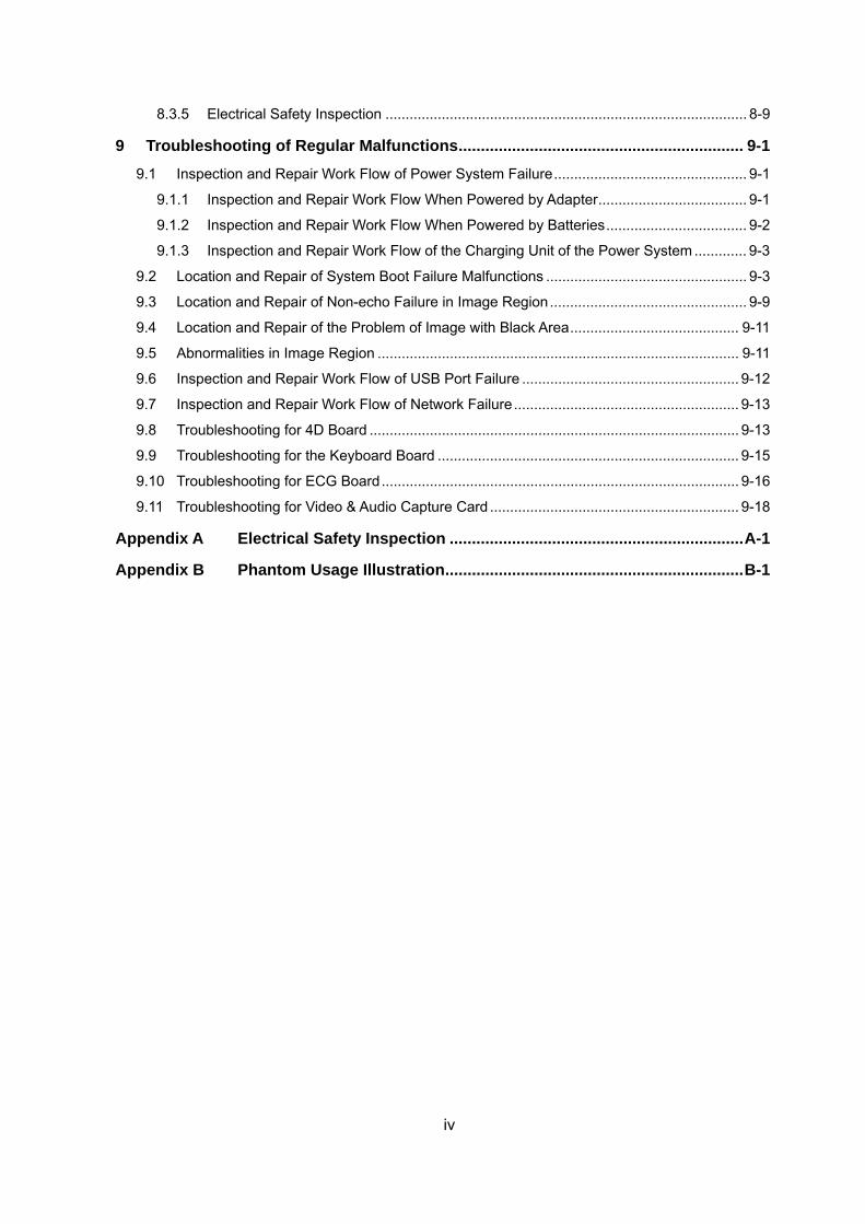
iv
8.3.5 Electrical Safety Inspection .......................................................................................... 8-9
9 Troubleshooting of Regular Malfunctions ................................................................ 9-1 9.1 Inspection and Repair Work Flow of Power System Failure ................................................ 9-1
9.1.1 Inspection and Repair Work Flow When Powered by Adapter ..................................... 9-1
9.1.2 Inspection and Repair Work Flow When Powered by Batteries ................................... 9-2
9.1.3 Inspection and Repair Work Flow of the Charging Unit of the Power System ............. 9-3
9.2 Location and Repair of System Boot Failure Malfunctions .................................................. 9-3
9.3 Location and Repair of Non-echo Failure in Image Region ................................................. 9-9
9.4 Location and Repair of the Problem of Image with Black Area .......................................... 9-11
9.5 Abnormalities in Image Region .......................................................................................... 9-11
9.6 Inspection and Repair Work Flow of USB Port Failure ...................................................... 9-12
9.7 Inspection and Repair Work Flow of Network Failure ........................................................ 9-13
9.8 Troubleshooting for 4D Board ............................................................................................ 9-13
9.9 Troubleshooting for the Keyboard Board ........................................................................... 9-15
9.10 Troubleshooting for ECG Board ......................................................................................... 9-16
9.11 Troubleshooting for Video & Audio Capture Card .............................................................. 9-18
Appendix A Electrical Safety Inspection .................................................................. A-1
Appendix B Phantom Usage Illustration ................................................................... B-1

I
Revision History Mindray may revise this publication from time to time without written notice.
Revision Date Reason for Change
5.0 2012.3.30
1. Increase “4.2 Field Replaceable Unit” list with pictures and important information.
2. Change “6 Maintenance Requirement” to “6 Function and Performance Checking Method”, increase detailed information of checking.
3. Change “7 Checking” to “6 Care and Maintenance”, increase detailed information of maintaining.
4. Change “8 System Maintenance” to “7 System Self-diagnosis”, move the content of cleaning to the chapter 8.
5. Increase “Electrical Safety Inspection” normative description and delete original content of electrical safety.
6. Increase CW installation method in 4.3.5. 7. Modify several clerical errors in the initial release.
6.0 2013.4.17
1. Add FRU part number for HDD of different regions/types (CE/FDA/human/vet) in 4.2
2. Add warning that human resume package is not compatible with vet machine, and vet resume package is not compatible with human machine.
7.0 2013.6.24 Add “The attentions to the assembly/disassembly, otherwise the hard disk will be damaged” to Chapter 4.3.14.
8.0 2015.2.15 Add SONY UP-D898MD, UP-X898MD printers in chapter 2.2 along with compatibility description.
9.0 2016.1.14 Change the order number of the display assembly in chapter 4.2
10.0 2016.11 Change the order number of the CPU and HDD assembly in chapter 4.2
11.0 2016.11 Change the order number of the CPU in chapter 4.2
12.0 2017.4 Add FRU part of M7 Premium in chapter 4.2 Update self-test screen and items in chapter 7
© 2016 Shenzhen Mindray Bio-medical Electronics Co., Ltd. All Rights Reserved.

II
Intellectual Property Statement SHENZHEN MINDRAY BIO-MEDICAL ELECTRONICS CO., LTD. (hereinafter called Mindray)
owns the intellectual property rights to this Mindray product and this manual. This manual may refer
to information protected by copyright or patents and does not convey any license under the patent
rights or copyright of Mindray, or of others.
Mindray intends to maintain the contents of this manual as confidential information. Disclosure of
the information in this manual in any manner whatsoever without the written permission of Mindray
is strictly forbidden.
Release, amendment, reproduction, distribution, rental, adaptation, translation or any other
derivative work of this manual in any manner whatsoever without the written permission of Mindray
is strictly forbidden.
, , , , BeneView, WATO, BeneHeart,
are the trademarks, registered or otherwise, of Mindray in China and other countries. All other
trademarks that appear in this manual are used only for informational or editorial purposes. They
are the property of their respective owners.
Responsibility on the Manufacturer Party Contents of this manual are subject to change without prior notice.
All information contained in this manual is believed to be correct. Mindray shall not be liable for
errors contained herein or for incidental or consequential damages in connection with the furnishing,
performance, or use of this manual.
Mindray is responsible for the effects on safety, reliability and performance of this product, only if:
all installation operations, expansions, changes, modifications and repairs of this product
are conducted by Mindray authorized personnel;
the electrical installation of the relevant room complies with the applicable national and
local requirements; and
the product is used in accordance with the instructions for use.
MindrayVNC ver. 1.0 is free open source software, the performance of MindrayVNC ver.
1.0 is not guaranteed by MINDRAY.

III
Note This equipment must be operated by skilled/trained clinical professionals.
Warning It is important for the hospital or organization that employs this equipment to carry out a reasonable
service/maintenance plan. Neglect of this may result in machine breakdown or personal injury.
Warranty THIS WARRANTY IS EXCLUSIVE AND IS IN LIEU OF ALL OTHER WARRANTIES, EXPRESSED
OR IMPLIED, INCLUDING WARRANTIES OF MERCHANTABILITY OR FITNESS FOR ANY
PARTICULAR PURPOSE.
Exemptions Mindray's obligation or liability under this warranty does not include any transportation or other
charges or liability for direct, indirect or consequential damages or delay resulting from the improper
use or application of the product or the use of parts or accessories not approved by Mindray or
repairs by people other than Mindray authorized personnel.
This warranty shall not extend to: Malfunction or damage caused by improper use or man-made failure.
Malfunction or damage caused by unstable or out-of-range power input.
Malfunction or damage caused by force majeure such as fire and earthquake.
Malfunction or damage caused by improper operation or repair by unqualified or unauthorized service people.
Malfunction of the instrument or part whose serial number is not legible enough.
Others not caused by instrument or part itself.
Customer Service Department Manufacturer: Shenzhen Mindray Bio-Medical Electronics Co., Ltd.
Address: Mindray Building, Keji 12th Road South, High-tech industrial park, Nanshan, Shenzhen 518057,P.R.China
Website: www.mindray.com
E-mail Address: [email protected]
Tel: +86 755 81888998
Fax: +86 755 26582680
IV
Important Information 1. It is the customer’s responsibility to maintain and manage the system after delivery.
2. The warranty does not cover the following items, even during the warranty period:
(1) Damage or loss due to misuse or abuse.
(2) Damage or loss caused by Acts of God such as fires, earthquakes, floods, lightning, etc.
(3) Damage or loss caused by failure to meet the specified conditions for this system, such as
inadequate power supply, improper installation or environmental conditions.
(4) Damage or loss due to use of the system outside the region where the system was
originally sold.
(5) Damage or loss involving the system purchased from a source other than Mindray or its
authorized agents.
3. This system shall not be used by persons other than fully qualified and certified medical
personnel.
4. DO NOT make changes or modifications to the software or hardware of this system.
5. In no event shall Mindray be liable for problems, damage, or loss caused by relocation,
modification, or repair performed by personnel other than those designated by Mindray.
6. The purpose of this system is to provide physicians with data for clinical diagnosis. It is the
physician’s responsibility for diagnostic procedures. Mindray shall not be liable for the results of
diagnostic procedures.
7. Important data must be backed up on external memory media.
8. Mindray shall not be liable for loss of data stored in the memory of this system caused by
operator error or accidents.
9. This manual contains warnings regarding foreseeable potential dangers, but you shall always
be alert to dangers other than those indicated as well. Mindray shall not be liable for damage or
loss that results from negligence or from ignoring the precautions and operating instructions
described in this operator’s manual.
10. If the manager for this system is changed, be sure to hand over this operator’s manual to the
new manager.
V
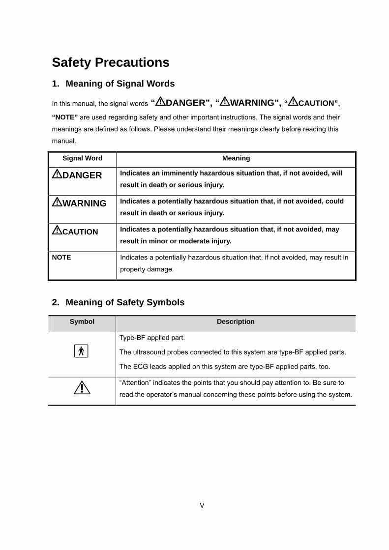
Safety Precautions 1. Meaning of Signal Words
In this manual, the signal words “ DANGER”, “ WARNING”, “ CAUTION”,
“NOTE” are used regarding safety and other important instructions. The signal words and their
meanings are defined as follows. Please understand their meanings clearly before reading this
manual.
Signal Word Meaning
DANGER Indicates an imminently hazardous situation that, if not avoided, will result in death or serious injury.
WARNING Indicates a potentially hazardous situation that, if not avoided, could result in death or serious injury.
CAUTION Indicates a potentially hazardous situation that, if not avoided, may result in minor or moderate injury.
NOTE Indicates a potentially hazardous situation that, if not avoided, may result in
property damage.
2. Meaning of Safety Symbols
Symbol Description
Type-BF applied part.
The ultrasound probes connected to this system are type-BF applied parts.
The ECG leads applied on this system are type-BF applied parts, too.
“Attention” indicates the points that you should pay attention to. Be sure to
read the operator’s manual concerning these points before using the system.

VI
3. Safety Precautions
Please observe the following precautions to ensure patient’s and operator’s safety when using this
system.
DANGER: Do not use flammable gasses, such as anesthetic gas, oxygen or hydrogen, or flammable liquids such as ethanol, near this system, because there is danger of explosion.
WARNING: 1. Do connect the power plug of this system and power plugs of the peripherals to wall receptacles that meet the ratings indicated on the rating nameplate. Using an adapter or multifunctional receptacle may affect the system’s grounding performance, and cause the leakage current to exceed safety requirements. You must use the power cord provided with the system.
2. Use the cable provided with this system to connect the printer. Other cables may result in electric shock.
3. Before cleaning the system, disconnect the power cord from the outlet. System failure and electric shock may result.
4. DO NOT use a probe that has a damaged, scratched surface, or exposed wiring of any kind. Immediately stop using the transducer and contact Mindray Customer Service Department or sales representative. There is risk of electric shock if using a damaged or scratched transducer.
5. This system is not water-proof. Do not use this system in any place where water leakage may occur. If any water is sprayed on or into the system, electric shock may result. If water is accidentally sprayed on or into the system, contact Mindray Customer Service Department or sales representative.
6. Do not allow the patient to contact the live parts of the ultrasound system or other devices, e.g. signal I / O ports. Electric shock may occur.
7. Do not use an aftermarket transducer other than those specified by Mindray. The transducers may damage the system causing a profound failure, e.g. a fire in the worst case.

VII
8. Do not subject the transducers to knocks or drops. Use of a defective transducer may cause an electric shock.
9. Do not open the covers and front panel of the system. Otherwise, short circuit or electric shock may result.
10. Do not use this system when any digital device such as a high-frequency electrotome, high-frequency therapeutic device or defibrillator is applied already. Otherwise, there is a risk of electric shock to the patient.
11. When moving the system, you should first fold the LCD display, disconnect the system from other devices (including transducers) and disconnect the system from the power supply. Separate the system from the mobile trolley before transportation.
12. Prolonged and repeated use of keyboards may result in hand or arm nerve disorders for some individuals. Observe the local safety or health regulations concerning the use of keyboards.
13. Accessory equipments connected to the analog and digital ports must comply with the relevant IEC standards (e.g., IEC 60950 information technology equipment safety standard and IEC 60601-1 medical equipment standard).Furthermore, all configurations must comply with the standard IEC 60601-1-1.It is the responsibility of the person, who connects additional equipment to the signal input or output ports and configures a medical system, to verify that the system complies with the requirements of IEC 60601-1-1.If you have any questions regarding these requirements, consult your sales representative.
CAUTION:
1. Precautions concerning clinical examination techniques:
This system must be used only by qualified medical professionals.
This operator’s manual does not describe clinical examination techniques. The clinician should select the proper examination techniques based on specialized training and clinical experience.

VIII
2. Malfunctions due to radio wave:
If a radio wave emitting device is used in the proximity of this system, it may interfere with operations. Do not bring or use devices that generate radio waves, such as cellular telephones, transceivers, and radio controlled toys, in the room where the system is installed.
If a person brings a device that generates radio waves near the system, ask him / her to immediately turn OFF the device.
3. Precautions concerning movement of the system:
When you place the system on the mobile trolley and move them together, you must secure all objects on the mobile trolley to prevent them from falling. Otherwise you should separate the system from the mobile trolley and move them individually. When you have to move the system with the mobile trolley upward or downward the stairs, you must separate them first and then move them individually.
Object placed on the monitor may fall and injure an individual when moving.
Fasten and fully secure any peripheral device before moving the system. A loose peripheral device may fall and injure an individual.
4. If the circuit protector is tripped, it indicates that the system or a peripheral device was improperly shut down and the system is unstable. You cannot repair the system under this circumstance and must call the Mindray Customer Service Department or sales representative.
5. There is no risk of high-temperature burns during normal ultrasound examinations. It is possible for the surface temperature of the transducer to exceed the body temperature of a patient due to environmental temperature and exam type combinations. Do not apply the transducer to the same region on the patient for a long time. Apply the transducer only for a period of time required for the purpose of diagnosis.
6. Do not use the system to examine a fetus for a long period of time.

IX
7. The system and its accessories are not disinfected or sterilized prior to delivery. The operator is responsible for the cleaning and disinfection of transducers and sterilization of biopsy brackets according to the manuals, prior to the use. All items must be thoroughly processed to completely remove harmful residual chemicals, which will not only harmful to the human body, but also damage the accessory.
8. It is necessary to press <End Exam> to end the current scan that is in progress and clear the current Patient Information field. Otherwise, new patient data may be combined with the previous patient data.
9. Do not connect or disconnect the system’s power cord or its accessories (e.g., a printer or a recorder) without turning OFF the power first. This may damage the system and its accessories or cause electric shock.
10. Read the Acoustic Output Principle in the operation manual carefully before operate this system on clinical examination.
11. The cover contains natural rubber that can cause allergic reactions in some individuals.
12. Please use the ultrasound gel compliant with the relevant local regulations.
13. Do not connect this system to outlets with the same circuit breakers and fuses that control the current of devices such as life-support systems. If malfunctions or over-current appear on this system, or when there is an instantaneous current at power ON, the breakers and fuses of the building’s supply circuit may be tripped.
NOTE: 1. Do not use the system in the vicinity of strong electromagnetic field (such as a
transformer), which may affect the performance of the system.
2. Do not use the system in the vicinity of high-frequency radiation source, which may
affect the performance of the system or even lead to failure.

X
3. To avoid damaging the system, DO NOT use it in following environment:
Locations exposed to direct sunlight;
Locations subject to sudden changes in environmental temperature;
Dusty locations;
Locations subject to vibration;
Locations near heat generators;
Locations with high humidity.
4. Turn ON the system only after the power has been turned OFF for more than 20
seconds. If the system is turned ON immediately after being turned OFF, the system
may not be rebooted properly and could malfunction.
5. Press <Freeze> or turn off the power of the system before connecting or
disconnecting a transducer. Otherwise, the system and / or transducer may be
damaged.
6. Remove ultrasound gel from the face of a probe when the examination is complete.
Water in the gel may enter the acoustic lens and adversely affect the performance
and safety of the transducer.
7. You should properly back up the system to a secure external storage media,
including system configuration and settings and patient data. Data stored to the
system’s hard drive may be lost due to system failure, improper operation or
accident.
8. Do not apply external force to the control panel. Otherwise, the system may be
damaged.
9. If the system is used in a small room, the room temperature may rise. Please provide
proper ventilation and free air exchange.
10. When using or placing the system, keep the system horizontal to avoid disbalance.
11. To dispose of the system or any part, contact Mindray Customer Service Department
or sales representative. Mindray is not responsible for any system content or
accessories that have been discarded improperly. Mindray is not responsible for any
system content or accessories that have been discarded improperly.
12. Electrical and mechanical performance may be degraded due to long usage (such as
current leakage or distortion and abrasion), the image sensitivity and precision may
become worse too. To ensure optimal system operations, it is recommended that you
maintain the system under a Mindray service agreement.
XI
13. Do not use gel, disinfectant, transducers or needle-guided brackets that are not
compatible with the system.
14. The replaceable fuse is inside the chassis. Refer replacing job to Mindray service
engineers or engineers authorized by Mindray only.
15. Do not turn OFF the power supply of the system during printing, file storage or
invoking other system operations. An interrupted process may not be completed, and
can become lost or corrupted.
16. If the system is powered off improperly during operation, it may result in data
damage of the system’s hard disk or system failure.
17. Do not use a USB memory device (e.g., an USB flash drive, removable hard disk)
which has unsafe data. Otherwise, system damage may result.
18. It is recommended to only use the video devices specified in this manual.
19. When using this system with portable package, be careful not to block the ventilation
slots.
20. DO NOT directly remove a USB memory device during file being copied; otherwise,
the USB memory device and/or the system may be damaged.
21. Do not connect a removable hard disk of many partitions to the system.
22. Do not press any key on the control panel when perform DICOM file sending or file
duplication from the USB memory devices.
4. Warning Labels
The warning labels are attached to this system in order to call your attention to potential hazards.
The symbol
on the warning labels indicates safety precautions. The warning labels use the
same signal words as those used in the operator’s manual.
Refer to the operator’s manual for detailed information about the warning labels. Read operator’s
manual carefully before using the system.

XII
5. Symbol Explanation
Symbol Name Function
Power off Power button
Power on
Remote control port
I/O panel
Video print control
Video out
VGA out
Footswitch port
USB
ETHERNET
A
Transducer port A
Transducer port
B Transducer port B
1-1
1 System Overview
1.1 Intended Use This product is applicable in ultrasound examining room, ward, emergency, anesthesia room and
operating room, etc.
M7
Applicable for examinations to adults, pregnant women, pediatric patients and neonates, and it is
intended for use in abdominal, cardiac, small parts (breast, testes, thyroid, etc.), peripheral vascular,
fetal, transesophagel, transrectal, transvaginal, pediatric, neonatal cephalic, musculoskeletal
(general and superficial), intraoperative, interventional, anesthesia (nerve), emergency, ICU/CCU,
urology, sports health and transcranial exams.
M7Vet
M7Vet is a veterinary use color Doppler diagnostic ultrasound system, which is intended for use in
clinical ultrasonic exams, such as abdominal, cardiac, small parts, peripheral vascular, transrectal,
musculoskeletal (general and superficial), and intraoperative exams.
1.2 Contraindication None.
1.3 Product and Model Code M –
Model code
Product code
2-1
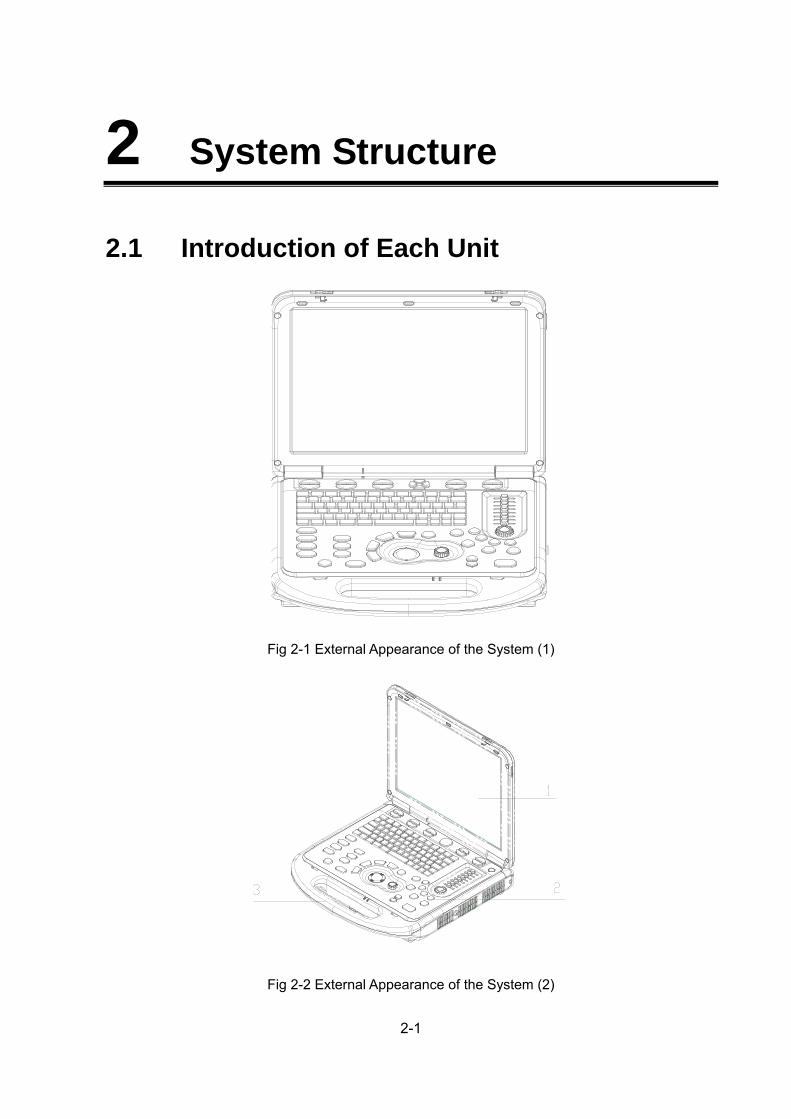
2 System Structure
2.1 Introduction of Each Unit
Fig 2-1 External Appearance of the System (1)
Fig 2-2 External Appearance of the System (2)

System Structure
2-2
Fig 2-3 External Appearance of the System (3)
No. Name Function
1 Display Displays the images and parameters during
scanning.
2 Control panel Operator-system interface or control
3 Handle Used for carrying the system
4 Transducer port Connects a probe to the main unit; or
connects a probe extend module
5 Transducer locking lever
Locks or unlocks the probe connected with
the main unit
: Locked symbol
: Unlocked symbol
6 IO extend port
Connects the IO extend module
7 Power input port
Connects the power adapter
8 USB port Connects USB devices

System Structure
2-3
No. Name Function
9 Network port Connects the network
10 S-Video separate video output
Connects with image signal output devices
like the video recorder, video printer,
text/graph workstation and so on.
2.2 Peripherals Supported B/W video printer: MITSUBISHI: P93DC, SONY:UP-D897, UP-D898MD, UP-X898MD
Color video printer: SONY: UP-D23MD
DVD Recorder: MVR-11
Graph/text printer
NOTE: printer UP-D898MD and UP-X898MD should be used in compatible with 1.00.7 2015-1-27 OS version or above versions. You can also select “DVR: 897” in the DIGITAL -> - DRIVER path on the printer (use UPD897 driver) if OS is not updated.
2.3 Extend Modules Note: Make sure VGA cable is not too long .
There are four extend modules available for the system: probe extend module, IO extend module,
V/A extend module, and ECG module. Interfaces of each extend module is described as follows:
2.3.1 Transducer Extend Module The system can be configured with probe extend modules: PEM-21.

System Structure
2-4
PEM-21
Fig 2-4 PEM-21 Transducer Extend Module PEM-21 transducer extend module can be used with the mobile trolley UMT-200 or UMT-300, for
the figures, please refer to the service manual of trolley.
CAUTION: You must turn off the ultrasound system before connecting or disconnecting the probe extend module. Otherwise the system may be damaged.
NOTE: If you use the probe extend module to connect a probe, the image quality may be
degraded.
2.3.2 I/O Extend Module. Interfaces
Fig 2-5 I/O Extend Module

System Structure
2-5
No. Symbol Function
<1>、<2> USB port Connects USB devices.
<3> ECG Port Connects the ECG Module
<4> Serial port Connects serial port devices
<5>、<6> Audio output port Used for audio signals of D mode sound from
DVD output or audio comments
<7> Mic In port
Reserved. (Connects a microphone used for
receiving audio comments when a recorder is
used to record images)
<8> Remote control port Connects the control port of the video printer
<9> Composite video output port
Connects with image signal output devices like
the video recorder, video printer, text/graph
workstation and so on.
<10> DVI-I output port Connects a display or projector, etc.
Connection
Connect the I/O extend module to the main unit via the I/O extend port, thus the data port is
extended. As shown in the following figure.
Fig 2-6 PEM-11 Connect the I/O Extend Module
2.3.3 V/A Extend Module About the Interfaces
The module is connected to the USB port of the main unit via a USB cable.
I/O extend module

System Structure
2-6
< >1 < >2 < >3 < >4
Fig 2-7 V/A Extend Module
No. Name Function
<1> Audio input port Used for audio signal input
<2> Audio input port Used for audio signal input
<3> Composite video input port Used for composite signal video input
<4> Separate video input port Used for separate signal video input
Connection
Connect the V/A extend module to the main unit via an USB port, after that, you can see USB 2861
Device and USB Audio Device in the device manager. V/A extend module connection is shown in
the following figure.
Fig 2-8 PEM-11 Connect the V/A Extend Module

System Structure
2-7
2.3.4 ECG Module Interfaces
Fig 2-9 ECG Module
Name Function
ECG lead port Used for ECG signal input
ECG Lead
Two kinds of ECG leads are available for M7: AHA standard and IEC standard. For FDA region, only
the ECG leads of AHA standard can be selected, and for other regions, both kinds can be used.
Connection
To use the ECG module, you need to configure with the I/O extend module at the same time.
First connect the I/O extend module, and then connect the ECG module to the I/O extend module,
see the figure below:
Fig 2-10 Connect the ECG Module
System Structure
2-8
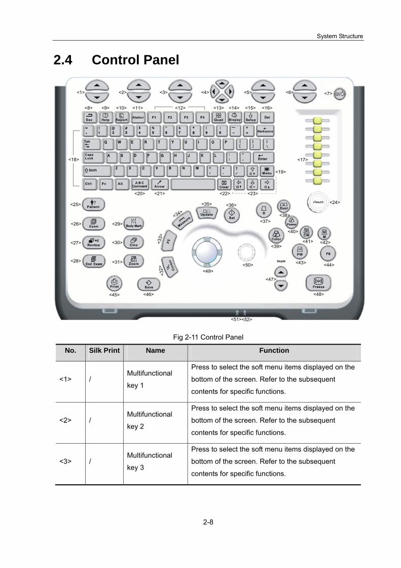
2.4 Control Panel
<1> <2> <3> <4> <5> <6> <7>
<8> <9> <10> <11> <12> <13> <14> <15> <16>
<17><18>
<19>
<20> <21> <22> <23>
<24><25>
<26>
<27>
<28>
<29>
<30>
<31>
<32>
<33>
<34>
<35> <36>
<37><38>
<39>
<40>
<41> <42>
<43> <44>
<45> <46>
<47>
<48>
<49><50>
<51><52>
Fig 2-11 Control Panel
No. Silk Print Name Function
<1> / Multifunctional
key 1
Press to select the soft menu items displayed on the
bottom of the screen. Refer to the subsequent
contents for specific functions.
<2> / Multifunctional
key 2
Press to select the soft menu items displayed on the
bottom of the screen. Refer to the subsequent
contents for specific functions.
<3> / Multifunctional
key 3
Press to select the soft menu items displayed on the
bottom of the screen. Refer to the subsequent
contents for specific functions.

System Structure
2-9
No. Silk Print Name Function
<4> / Multifunctional
key 4
Up / down controls are used to turn pages up / down
when there are more-than-one pages for the soft
menu;
Left / right keys are used to switch between the
different modes.
<5> / Multifunctional
key 5
Press to select the soft menu items displayed on the
bottom of the screen. Refer to the subsequent
contents for specific functions.
<6> / Multifunctional
key 6
Press to select the soft menu items displayed on the
bottom of the screen. Refer to the subsequent
contents for specific functions.
<7> / Power button
Power button
It does not illuminate when the system is turned off;
Press the button to turn on the system, the system
enters the work status and the indicator lights on in
green.
When the system enters the standby status, the
indicator turns green.
<8> Esc Exit Press to exit the current status to the previous status.
<9> Help Help Press to open or close the accompanying help
documents.
<10> Report Report Press to open or close the diagnosis reports.
<11> iStation / Press to enter or exit the patient information
management system.
<12> F1-F4 User-defined key You can assign a function to the key.
<13> Quad Quad-split screen Press to enter or exit the quad-split screen display.
<14> Biopsy Biopsy Press to show or hide the biopsy guide line.
<15> Setup Setup Press to show or hide the Setup menu.
<16> Del / Press to delete the comment, etc.
<17> TGC / Move to adjust time gain compensation.

System Structure
2-10
No. Silk Print Name Function
<18> / Alphanumeric
keys Same as those of PC.
<19> Menu Main menu Press to display or hide a mode-specific parameter
menu.
<20> Comment ABC (Comments) Press to enter or exit the character comment status.
<21> Arrow Arrow Press to enter or exit the arrow comment status.
<22> Clear Delete Press to clear the comments or measurement
calipers on the screen.
<23>
Up/down,
left/right
keys
Fn+/: to adjust volume or monitor brightness
<24> iTouch /
Rotate to increase or decrease the image gain; press
to optimize the image, serving as a one-key
optimization.
<25> Patient Patient Info To enter into patient information input interface.
<26> Exam Exam Mode Switch the exam mod and probe
<27> Review Review To review the stored images.
<28> End
Exam End Exam Press to end an exam.
<29> Body
Mark
Body Marks
(Pictograms) Press to enter or exit the Body Mark status.
<30> Cine Cine Review Press to enter or exit the Cine Review status.
<31> Zoom Zoom Press to enter or exit the Zoom status.
<32> Cursor Cursor Press to show the cursor.
<33> F5 User-defined key You can assign a function to the key.
<34> Measure Measurement Press to enter or exit the application measurement
mode.

System Structure
2-11
No. Silk Print Name Function
<35> Update /
Switching key: Press to change the currently active
window.
Press to start or end image capture in 3D/4D or
iScape mode.
<36> Set Set Press to confirm an operation, same as the
left-button of the mouse.
<37> B / Press to enter the B mode
<38> Dual /
Press to enter the Dual mode from another mode;
Press to switch between the two display windows in
the Dual mode.
<39> Color / Press to enter the Color mode.
<40> Power / Press to enter Power mode.
<41> CW / Press to enter the CW mode.
<42> M / Press to enter the M mode.
<43> PW / Press to enter the PW mode.
<44> F6 User-defined key You can assign a function to the key.
<45> Print Print Press to print: user-defined key.
<46> Save Storage Press to save; user-defined key.
<47> Depth Depth Press to increase or decrease the imaging depth in
scanning mode.
<48> Freeze Freeze Press to freeze or unfreeze the image.
<49> / Trackball Roll the trackball to change the cursor position.
<50> / Multifunction knob
Rotate to adjust the menu items, parameters and
direction of the comment arrow, etc.
Press to show the menu, and rotate the view the
items.

System Structure
2-12
No. Silk Print Name Function
<51> / Indicator 1
Indicates if the main unit is connected to the power
supply.
If not connected, the indicator does not illuminate;
If connected, the indicator illuminates in green color.
<52> / Indicator 2
Indicates the current status of the batteries.
When the system is supplied with power by the
batteries and the power capacity is lower than 30%,
the indicator is yellow and flashes.
When the batteries are being charged, the indicator
light is on and in yellow color.
When the battery capacity is charged to the full
capacity, the indicator color turns green.
In other statuses, the indicator light is off.
Tip: “/” means the key / knob has no silk-printed name.
Keys which can work with the Fn key:
Key Function
Fn+ Increase the brightness of the LCD display.
Fn+ Decrease the brightness of the LCD display.
Fn+S Press the two keys to mute the speaker.
Fn+ Press the two keys to increase display contrast.
Fn+ Press the two keys to decrease display contrast.

3-1
3 Principle Description
3.1 Electric Principle of the System The schematic diagram of M7 diagnostic ultrasound system is show in the following figure:
Fig 3-1 Schematic Diagram of System
According to functions of hardware, the block diagram of the hardware system is shown below:

Principle Description
3-2
Fig 3-2 Block Diagram of the Hardware System The main board unit is the core of the whole system, including the transducer port, transmitting,
receiving, beam forming, signal processing, system monitor and management, audio, video,
interfaces and so on, and these will be introduced later. Main logic unit completes the main logic
processing functions, including transmitting control logic, beam former logic, signal processing logic.
The functions of the other modules can be explained by their names, and will not be explained here.
Besides, M7 also supports ECG module, probe extend module and video capture module. Principle
of Boards
3.1.1 Power System
3.1.1.1 Basic Functions of Power System As the power supply of the system, the power system consists of adapter, batteries, main power
board, auxiliary power board, flexible boards for connecting batteries and flexible boards of analog
power, etc. The power is supplied through two methods, external power adapter or batteries. The
system is first powered by the adapter, and the batteries are provided for back-up. The main power
board and auxiliary power board are mainly responsible for supplying the system with the DC output
listed in the following table, charging management of the batteries, monitoring the power, and
communicating with the main board.
Table 3-1 DC Output of Power Supply System
Project Output Board of the Function Unit
Notes
1 3V3STB Main power board Available when there is an adapter or dual
batteries
2 5VSTB_CPU Main power board Controlled by 5Vstb_CPU_EN signal
3 +12V Main power board Controlled by POWER_ON# signal
4 +95V Main power board Controlled by POWER_ON# signal
5 -95V Main power board Controlled by POWER_ON# signal
6 PHV1P Main power board Controlled by POWER_ON# signal
7 PHV1N Main power board Controlled by POWER_ON# signal
8 PHV2P Main power board Controlled by POWER_ON# signal
9 PHV2N Main power board Controlled by POWER_ON# signal

Principle Description
3-3
10 +5V Auxiliary power board Controlled by POWER_ON# signal
11 +3.6V Auxiliary power board Controlled by POWER_ON# signal
12 +3.3V Auxiliary power board Controlled by POWER_ON# signal
13 +2.8V Auxiliary power board Controlled by POWER_ON# signal
14 +1.8V Main power board Controlled by POWER_ON# signal
15 +1.5V Auxiliary power board Controlled by POWER_ON# signal
16 -5V Auxiliary power board Controlled by POWER_ON# signal
17 -12V Auxiliary power board Controlled by POWER_ON# signal
3.1.1.2 Basic Principle of Power System The principle diagram of the power system is shown in figure below. The power is supplied through
two methods, external power adapter or batteries. The adapter is connected to the power board via
the system main board when the system is powered by adapter. The batteries are connected to the
power board via the flexible boards when the system is powered by batteries. The main power
board generates 4 PHV outputs: 3V3STB, 5VSTB_CPU, +12V and ±95V, monitors and manages
the power output. The auxiliary power board generates +5V, -5V, -12V, +3.6V, +3.3V, +2.8V, +1.8V
and +1.5V outputs, and manages the charging of the batteries. The main power board and the
auxiliary power board are connected via two 26 PIN connectors.
Fig 3-3 Schematic Diagram of Power System

Principle Description
3-4
The system main board and the digital ports of the power board are connected together via a 64
PIN connector, and the digital power ports and signals are defined in table below; the system
main board and the auxiliary power board are connected together via an analog flexible board,
and the analog power ports and signals are defined in
Table 3-3; the main power board and the batteries are connected together via the battery flexible
board, and the signals are defined in Table 3-4; the main power board and the auxiliary power board
are connected together via two 26 PIN connectors, and the signals are defined in Table 3-5 and
Table 3-6.
Table 3-2 Signal definition of connectors between main power board and system main board
digital power
No. Signal name No. Signal name
1 EDC_PWR 2 EDC_PWR
3 EDC_PWR 4 EDC_PWR
5 EDC_PWR 6 EDC_PWR
7 GND 8 GND
9 GND 10 GND
11 GND 12 GND
13 N12V 14 STS_EDC#
15 GND 16 GND
17 POWER_ON# 18 CPU12V_OK#
19 T_D+ 20 T_D-
21 GND 22 GND
23 GND 24 GND
25 D12V 26 D12V
27 D12V 28 D12V
29 GND 30 GND
31 D5V1 32 D5V1
33 GND 34 GND

Principle Description
3-5
No. Signal name No. Signal name
35 5VSTB_OK# 36 5VSTB_EN#
37 GND 38 GND
39 5VSTB_CPU 40 3V3STB
41 GND 42 GND
43 D3V3 44 D3V3
45 GND 46 GND
47 D2V8 48 D1V5
49 GND 50 GND
51 D1V8 52 D1V8
53 GND 54 GND
55 PWR_RX 56 PWR_CONF_N
57 PWR_TX 58 PWR_RST
59 GND 60 GND
61 BATA_PRT# 62 BATB_PRT#
63 BATSTS_O 64 BATSTS_G
Signal definition
EDC_PWR: adapter power input;
GND: ground;
N12V: analog -12V output;
STS_EDC#: adapter normal working signal, low level means the output of adapter is normal;
POWER_ON#: power on signal from the system main board, low level effective;
CPU12V_OK#: +12V output signal, lower level means normal output;
T_D+, T_D-: power board temperature detecting signal;
D12V: digital power +12V output;
D5V1: digital power +5V output;
5VSTB_OK#: 5VSTB output signal, lower level means normal output;
5VSTB_EN#: 5VSTB enable signal from the system main board, low level effective;
5VSTB_CPU: standby power 5VSTB_CPU output, the voltage is +5V;

Principle Description
3-6
3V3STB: standby power 3V3STB output, the voltage is +3.3V;
D3V3: digital power +3.3V output;
D2V8: digital power +2.8V output;
D1V5: digital power +1.5V output;
D1V8: digital power +1.8V output;
PWR_RX: serial port communication receiving port of the the power and system mother board;
PWR_TX: serial port communication transmitting port of the power and system mother board;
PWR_CONF_N: power board chip configuration signal from the system main board;
PWR_CONF_N: power board chip reset signal from the system main board;
BATA _ PRT#: battery A presenting signal, low level means the battery is presenting;
BATA _ PRT#: battery B presenting signal, low level means the battery is presenting;
BATSTS_O: battery status indicating light, orange;
BATSTS_G: battery status indicating light, green.
Table 3-3 Signal and analog power definition between auxiliary power board and system main
board
No. Signal name No. Signal name
1 N95V 2 GND
3 95V 4 GND
5 PHV2N 6 GND
7 PHV1N 8 GND
9 PHV2P 10 GND
11 PHV1P 12 GND
13 A12V 14 GND
15 A2V8 16 GND
17 GND 18 GND
19 A3V6 20 A3V6
21 GND 22 GND

Principle Description
3-7
23 A1V5 24 A1V5
25 A1V5 26 A1V5
27 GND 28 GND
29 NA12V 30 GND
31 NA5V1 32 GND
33 GND 34 GND
35 A5V1 36 A5V1
37 A5V1 38 A5V1
39 GND 40 GND
Signal definition
N95V: -95V fixed high voltage output;
GND: ground;
95V: +95V fixed high voltage output;
PHV2N: PHV2 negative voltage output, -5~-85V;
PHV1N: PHV1 negative voltage output, PW outputs -13~-85V, CW outputs -2~-5V;
PHV2P: PHV2 positive voltage output, 5~85V;
PHV1P: PHV1 positive voltage output, PW outputs 13~85V, CW outputs 2~5V;
A12V: analog +12V output;
A2V8: analog 2.8V output;
A3V6: analog 3.6V output;
A1V5: analog 1.5V output;
NA12V: analog -12V output;
NA5V: analog -5V output;
A5V1: analog +5V output.
Table 3-4 Signal definition between the battery and main power board
No. Signal name No. Signal name
1 BATB+ 2 BATB+
3 BATB+ 4 BATB+
5 BATB_PRT# 6 GND

Principle Description
3-8
No. Signal name No. Signal name
7 NTC_BATB 8 GND
9 BATB_FB 10 GND
11 BATB_SCL 12 GND
13 BATB_SDA 14 GND
15 BATA_PRT# 16 GND
17 NTC_BATA 18 GND
19 BATA_FB 20 GND
21 BATA_SCL 22 GND
23 BATA_SDA 24 GND
25 GND 26 GND
27 BATA+ 28 BATA+
29 BATA+ 30 BATA+
Signal definition
BATB+: battery B input;
GND: ground;
BATB_PRT#: battery B presenting signal, low level is effective;
NTC_BATB: battery B temperature signal;
BATB_FB: battery B far end sampling signal;
BATA_SCL: battery B SMBUS communication clock signal;
BATA_SDA: battery B SMBUS communication data signal;
BATA_PRT#: battery A presenting signal, low level is effective;
NTC_BATA: battery A temperature signal;
BATA_FB: battery B far end sampling signal;
BATA_SCL: battery A SMBUS communication clock signal;
BATA_SDA: battery A SMBUS communication data signal;
BATA+: battery A input;

Principle Description
3-9
Table 3-5 Signal definition between main power board and auxiliary power board
No. Signal name No. Signal name
1 VBUS+ 2 VBUS+
3 VBUS+ 4 GND
5 GND 6 GND
7 5V_CW 8 D5V1
9 START 10 D2V8
11 GND 12 GND
13 N5V_CW 14 A12V
15 GND 16 N12V
17 PHV2P 18 D1V5
19 PHV1P 20 GND
21 PHV2N 22 GND
23 PHV1N 24 GND
25 95V 26 N95V
Signal definition
VBUS+: input bus voltage on the power board;
GND: ground;
5V_CW: LDO input of PHV1P CW voltage;
D5V1: digital power +5V output;
START: auxiliary power board power on signal from the system main board, low level effective;
D2V8: digital power +2.8V output;
5V_CW: LDO input of PHV1N CW voltage;
A12V: analog +12V output;
N12V: digital power -12V output;
PHV2P: PHV2 positive voltage output, 5~85V;
D1V5: digital power +1.5V output;
PHV1P: PHV1 positive voltage output, PW output 13~85V, CW output 2~5V;
PHV2N: PHV2 negative voltage output, -5~85V;

Principle Description
3-10
PHV1N: PHV1 negative voltage output, PW output -13~85V, CW output -2~5V;
95V: +95V fixed high voltage output;
N95V: -95V fixed high voltage output.
Table 3-6 Signal definition between main power board and auxiliary power board (2)
No. Signal name No. Signal name
1 EDC_POWER 2 EDC_POWER
3 ISENSE 4 EDC_POWER
5 GND 6 GND
7 CHARGE_EN 8 GND
9 BATA+ 10 BATA+
11 BATA_FB 12 NTC_BATA
13 GND 14 GND
15 BATB_FB 16 NTC_BATB
17 BATB+ 18 BATB+
19 GND 20 GND
21 D1V8 22 D1V8
23 GND 24 GND
25 D3V3 26 D3V3
Signal definition
EDC_PWR: adapter power input;
ISENSE: main system load current signal from the power main board to the auxiliary power board;
GND: ground;
CHARGE_EN: battery charge enable signal, low level effective;
BATA+: battery A input;
BATA_FB: battery A far end sampling signal;
NTC_BATA: battery A temperature signal;
BATB_FB: battery B far end sampling signal;
NTC_BATB: battery B temperature signal;
BATB+: battery B input;

Principle Description
3-11
D1V8: digital power +1.8V output;
D3V3: digital power +3.3V output.
3.1.1.3 3V3STB Circuit Unit
Basic Principle of 3V3STB Circuit
The 3V3STB takes EDC_POWER from the adapter or the BATTERY_BUS from the batteries as the
input and generates 3V3STB via linear voltage-stabilizing chip TPS715A01.
TPS715A01 is equipped with current-limiting function itself.
The Maintenance Points of 3V3STB Circuit
If the 3V3STB unit is faulty, first check whether the input voltage of U12 PIN1 is normal; if it is
normal, it indicates that the U12 is damaged or the fault is caused by the over-current or short
circuit of the load.
3.1.1.4 5VSTB_CPU Circuit Unit
Basic Principle of 5VSTB_CPU Circuit
The 5VSTB_CPU takes the BATTERY_BUS from the batteries as input and generates the output
via the synchronous rectifying step-down chip TPS62110 through BUCK transformation.
The TPS62110 chip itself is equipped with MOSFET, current-limiting function and over-temperature
protection.
The Maintenance Points of 5VSTB_CPU Circuit
If the 5VSTB_CPU unit is faulty, first check whether the input voltage of U35 PIN2 is normal and
whether the enabling signal of PIN4 is 3.3V; if they are all normal, it indicates that the U35 is
damaged or the fault is caused by the over-current or short circuit of the load; if PIN4 is low level,
check whether the system main board provides 5VSTB_EN# signal and whether the feedback
connection or overvoltage circuit is normal.
3.1.1.5 +12V Circuit Unit
Basic Principle of +12V
Voltage rise-and-fall IC LTC3780 of LINEAR Company is applied in +12V circuit unit, and whether
the input voltage is higher or lower than 12V, the output voltage will be kept at 12V.
The +12V over-current and overvoltage protection is not locked, and the over-current is over 8A.
The output voltage returns to normal after over-current disappears.

Principle Description
3-12
The Maintenance Points of +12V
Before testing, ensure that the POWER_ON# signal is of low level and the input voltage VBUS+ is
normal.
The work flow of maintenance is shown as follows:
Test the voltage of PIN8 of U14, which should be higher than 3V;
Test the voltage of PIN19 of U14, which should be higher than 6V;
Use an oscilloscope to measure G poles of Q6, Q7, Q8 and Q9 to check whether there is driving
pulse; at least two MOSFETs’ G poles should have drive pulse;
Check if there is any damage to the four MOSFETs Q6, Q7, Q8 and Q9 and diode D5 and D7;
If +12V hiccups, check whether the output is overloaded, and check the feedback and overvoltage
protection circuits.
3.1.1.6 PHV Circuit Unit
Basic Principle of PHV
The PHV circuit consists of PHV1P, PHV1N, HV2P and PHV2N, of which, the PHV1P and PHV1N
consist of PW and CW output. The PW output range of PHV1 is ±13V~±85V, and the CW output
range is ±2V~±4V. Only PW output of PHV2 is available, and the output range is ±5V~±85V.
The input of the PW circuit of the 4 PHVs is controlled +12V, which is under the control of PMOS
Q5.The PW output voltage of PHV1P and PHV2P is generated by BOOST circuit. The controlling IC
is TL594, which is frequently adopted by our company. The range of output voltage of PHV2P is
+5V~+85V, so when the output voltage is over than 15V, the input is +12V; and when the output
voltage is lower than 15V, the input is +5V. Both the two inputs are under the control of output
voltage controlling signal. The PW output voltage of PHV1N and PHV2N is generated by
BUCK-BOOST circuit. The controlling IC is MAX1847, which is frequently adopted by our company.
The CW output of PHV1P and PHV1N is generated through linear voltage-stabilizing. The input of
CW circuit of PHV1P is +5V and the chip LT1963 LDO is adopted for the linear voltage-stabilizing;
the input of CW circuit of PHV1N is -5V, and the chip LT1185 LDO is adopted for the linear
voltage-stabilizing. The voltage of CW output is regulated by the output voltage controlling signal.
When the controlling signal is 0.45~2.25V, the corresponding output voltage is ±2V~±4V.
The 4 PHV are all equipped with overvoltage protection, and the overvoltage protection of each
circuit is independent. The overvoltage will not be locked, and the voltage is about 93V when
overvoltage occurs.
The 4 PHV are all equipped with over-current protection. In PW mode, once over-current occurs, all
the 4 PHV PW outputs and ±95V will be switched off, while the CW output is not influenced. The

Principle Description
3-13
over current protection in CW mode is implemented by current-limiting of LDO chip itself. Only the
output is cut off and other outputs are not influenced.
The Maintenance Points of PHVP PW Circuit Unit
Make sure the +12V output is normal, and PHV_CW is low level before testing.
Test the grid electrode of Q5, and the voltage should be around 3V and VCC2 is 12V.
The work flow of troubleshooting for U17 and U18 and their peripheral circuits are shown as follows:
Test the voltage of PIN8 and PIN11, which should be 12V;
Test the voltage of PIN14, which should be +5V;
Test PIN5, and there should be oscillation wave form, the frequency of which is around 100kHz;
Test the voltage of PIN15, which should be around 5V;
Test PIN9 and PIN10, and there should be driving pulses.
If the test shows the grid electrode of Q5 is 12V, check the +5V output and whether over-current or
short circuit occurs.
The Maintenance Points of PHVN PW Circuit Unit
Make sure the +12V output is normal, and PHV_CW is low level before testing.
Test the grid electrode of Q5, and the voltage should be around 3V and VCC2 is 12V.
The work flow of troubleshooting for U24 and U25 and their peripheral circuits are shown as follows:
Test the voltage of PIN15, which should be 12V;
Test the voltage of PIN5, which should be +1.25V;
Test the voltage of PIN2, which should be around 4.25V;
Test PIN14, and there should be driving pulses.
If the test shows the grid electrode of Q5 is 12V, check the +5V output and whether over-current or
short circuit occurs.
The Maintenance Points of PHV CW Circuit Unit
Make sure the +5V and -5V outputs are normal, and PHV_CW is high level before testing;
The work flow of troubleshooting for U13 and its peripheral circuit is shown as follows:
Test the voltage of PIN12, which should be +5V;
Test the voltage of PIN6, which should be +1.21V;
If the output voltage is not consistent with the controlling signal, check R66, R203, R260, R150 and
U2 related circuits.

Principle Description
3-14
The work flow of troubleshooting for U31 and its peripheral circuits are shown as follows:
Test the voltage of PIN3, which should be -5V;
Test the voltage of PIN2, which should be -2.37V;
If the output voltage is not consistent with the controlling signal, check R67, R204, R198 and U3
related circuits.
3.1.1.7 +5V Circuit Unit
Basic Principle of +5V Circuit
The input of +5V circuit is VBUS+, and stable +5V output is generated through BUCK
transformation step-down. The controlling IC is LM5642 from NS, which is a biphase step-down
synchronously rectifying controlling IC.
+5V circuit is equipped with overvoltage and over-current protection and is locked during protection.
The Maintenance Points of +5V Circuit
Check by sight whether LM5642 and its peripheral devices are well welded before power on, and
check whether the MOSFETs Q16~Q19 and diodes D3 and D6 are broken down using a
multimeter.
Before testing, make sure that the STRAT signal is free or of low level, and the input voltage VBUS+
is normal.
The work flow of maintenance after power on is shown as follows:
Test the voltage of PIN22, which should be VBUS+;
Test the voltage of PIN7, PIN19 and PIN25, which should be around +5V;
Test PIN9 and PIN10, which should be over than 1V;
Test PIN17, PIN20, PIN23 and PIN26, and there should be driving pulses at the frequency of
around 200kHz;
If there is no output with the circuit, check whether the output is over-current and check the
feedback circuit.
3.1.1.8 +1.5V Circuit Unit
Basic Principle of +1.5V Circuit
+1.5V output adopts the synchronously rectifying step-down chip EL7566, which is frequently
adopted by our company. This chip is integrated with over-current and over-temperature protection
internally. The over-current protection protects from hiccup.

Principle Description
3-15
The Maintenance Points of +1.5V Circuit Unit
Check by sight whether EL7566 and its peripheral devices are well welded before power on. The
work flow after power on is:
Test the voltage of PIN19~PIN21, which should be +5V;
Test the voltage of PIN22, which should be +5V;
Test PIN27, which should have oscillatory wave output;
Test PIN8~PIN13, which should have pulse voltage waveform;
If there is no output with the circuit or the if circuit is hiccupping, check if the output is over-current
and check the feedback circuit.
3.1.1.9 +3.6V/3.3V/2.8V/1.8V Circuit Unit
Basic Principle of +3.6V/3.3V/2.8V/1.8V Circuit
The output adopts the synchronously rectifying step-down chip LM2854 of NS Corporation. This
chip is integrated with MOSFET and over-current protection internally. The over-current protection
protects from hiccup.
The Maintenance Points of +3.6V/3.3V/2.8V/1.8V Circuit Unit
Check by sight whether LM2854 and its peripheral devices are well welded before power on. The
work flow after power on is:
Test the voltage of PIN5~PIN7 and PIN10~11, which should be +5V;
Test PIN12~PIN13, which should have pulse voltage waveform;
If there is no output with the circuit or if the circuit is hiccupping, check if the output is over-current
and check the feedback circuit.
3.1.1.10 -5V and -12V Circuit Unit
Basic Principle of -5V and -12V
The implementations of -5V and -12V are the same. The negative voltage IC MAX1847 is adopted
for both circuits. The -5V and -12V are both equipped with overvoltage and over-current protection
circuits, so once either overvoltage or over-current occurs, both circuits will be cut off and locked.
The Maintenance Points of -5V and -12V Circuits
Make sure that VBUS+ for -5V and -12V is within the normal range.
After power on, refer to the work flow shown as follows:

Principle Description
3-16
Test the voltage of PIN15 of the power supply chip U15~16, which should be the same as VBUS+;
Test the voltage of PIN5 (the reference voltage pin), which should be 1.25V;
Test PIN8, the overvoltage and over-current protection controlling pin, which should be higher than
2V;
Test PIN14 (drive pin), which should output drive pulse.
If there is no output with the circuit, check if the output is over-current and check the feedback
circuit.
3.1.1.11 Charging Unit
Basic Principle of Charging Unit
The rise-and-fall charging chip MAX1870A made by MAXIM is adopted for both charging units A
and B.
The MAX1870A enabling is controlled by the system’s main board and batteries’ temperature, and
eventually controlled by level of PIN15. When PIN15 is high level (about 5V), the charging is
enabled; when PIN15 is low level, the charging is disenabled. The charging current is affected by
the status of the batteries and the load current of the main unit. The charging circuit regulates the
charging current dynamically according to the load current of the main unit to ensure fast charging
and the load current of the adapter is not overloaded when the system is on.
The Maintenance Points of Charging Unit
Before testing, ensure that the charging chip is enabled, that is, PIN15 is high level.
The maintenance work flow of charging IC U7 and U8 and their peripheral circuits.
Check by sight if the soldering position departs from normal position, if so, it will cause short circuit
of pins.
Test power supplying voltage PIN32, which should be equal to adapter’s output voltage of
EDC_POWER.
Test reference end’s PIN2, which should be about 4.0V.
Test linear stabilizing output PIN1, which should be 5.4V.
Test the voltage difference between PIN28 and PIN30, which should be less than 90mV.
Test driving pin PIN27 and PIN22, and at least one PIN should have driving pulse output.
Test if there is any damage to the power device MOS semiconductor and diode.
±95V circuit.

Principle Description
3-17
Basic Principle of ±95V Circuit
±95V is generated from +12V through the non-isolated reverse converter, the chip is UC3843B of
ONSEMI.±95V output is figured with overvoltage, over-current and short circuit protection, it will not
be locked in the case of overvoltage, and be locked during over-current and short circuit protection.
The Maintenance Points of ±95V Circuit
First check if +12V output voltage is within the normal range, and if START signal is low level.
After power on, refer to the work flow shown as follows:
Test PIN8 of U1, the voltage should be +5V;
Test PIN4 of U1, there should have triangular wave of about 130 kHz;
Test PIN4 of U1, there should have drive pulse output;
Test PIN3 of U1, there should have triangular wave with the amplitude less than 1V.
If there is no output with the circuit, check if the output is over-current, check the feedback circuit,
meanwhile, check if PHV_OCP is high level.
3.1.2 Principle of the Main Board The schematic diagram of the main board is shown in figure below.

Principle Description
3-18
Fig 3-4 Principle Diagram of Main Board As shown in figure above, the main board unit is mainly configured with the following functional
modules:
Transducer sockets;
Ultrasound receiving;
Ultrasound transmission;
Beam forming;
System clock;
Signal processing;
System monitoring and managing;
Audio;

Principle Description
3-19
Video;
IO ports;
Where, the transducer sockets, ultrasound transmission and receiving, beam forming and system
clock are categorized as analog power region. The signal processing, signal monitoring and
managing, audio, video and I/O ports are categorized as digital power region.
The main board provides the interfaces for:
Transducer board;
Transmission board;
CW board;
4D board;
Keyboard board;
Flexible board for connecting the batteries;
CPU module;
LVDS display ports;
Power supply module;
Hard disk;
Reserved power interfaces;
Reserved signal interfaces;
Fan;
Speaker.
External interfaces include:
S_Video;
Network;
USB (2);
Extend interface.
The layout of the above-mentioned module interfaces in the main board is shown in figure below.
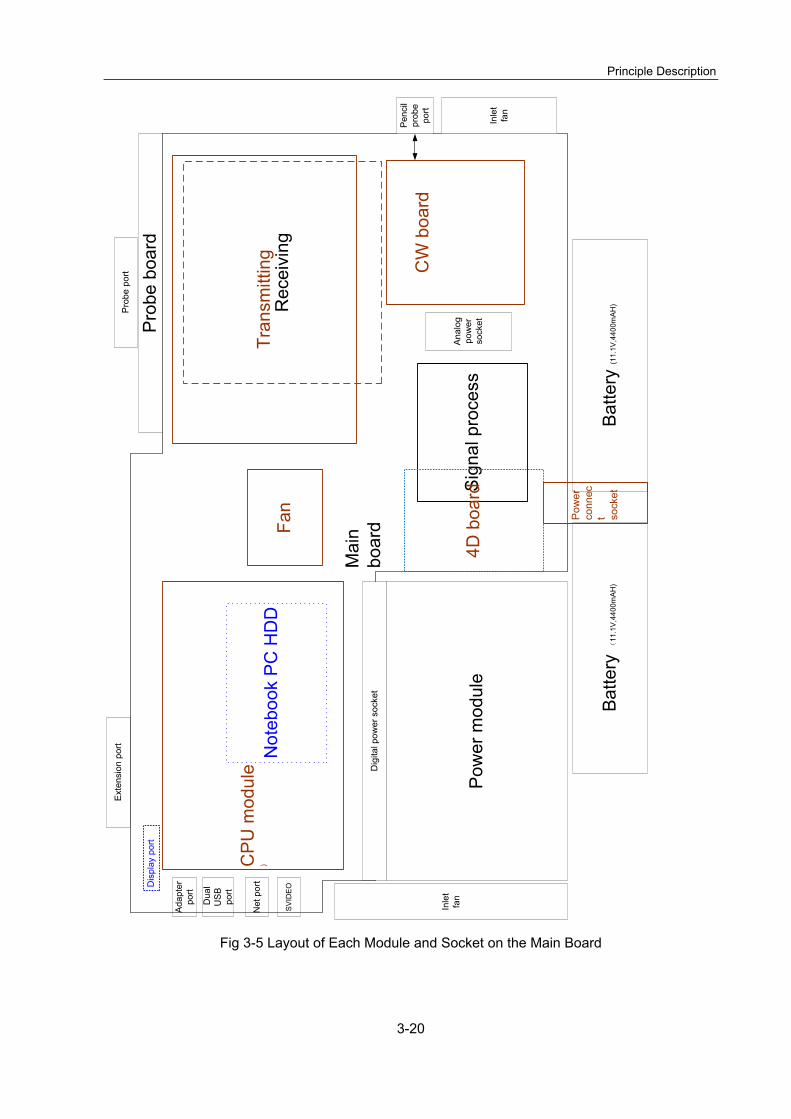
Principle Description
3-20
Ada
pter
po
rt
Pow
er m
odul
e
CP
U m
odul
e)
Inle
t fa
n
Dua
l U
SB
port
Net
por
t
SV
IDE
ODis
play
por
t
Not
eboo
k P
C H
DD
Ext
ensi
on p
ort
Pro
be b
oard
Pro
be p
ort
Fan
Tran
smitt
ing
CW
boa
rd
Bat
tery
(11
.1V
,440
0mA
H)
Pow
er
conn
ect so
cket
Bat
tery
(11.1
V,4
400m
AH
)
Pen
cil
prob
e po
rt
Rec
eivi
ng
Mai
n bo
ard
Inle
t fa
n
Sig
nal p
roce
ss
Dig
ital p
ower
soc
ket
Ana
log
pow
er
sock
et4D
boa
rd
Fig 3-5 Layout of Each Module and Socket on the Main Board
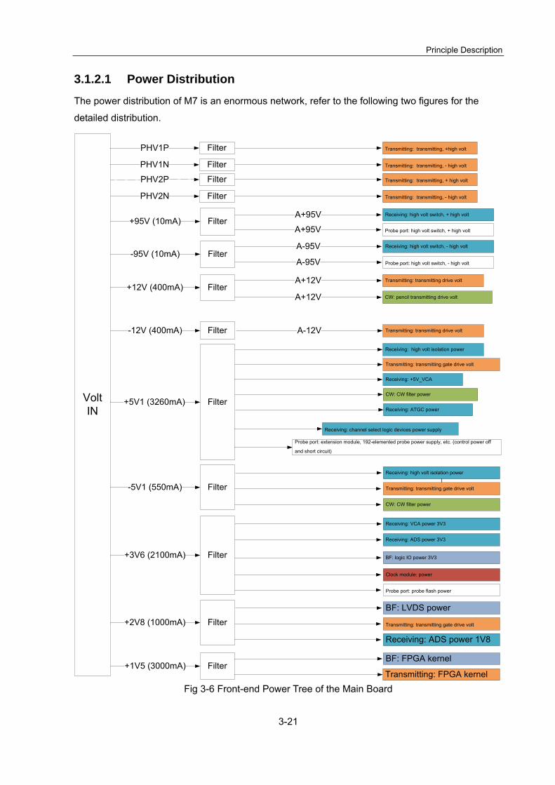
Principle Description
3-21
3.1.2.1 Power Distribution The power distribution of M7 is an enormous network, refer to the following two figures for the
detailed distribution.
Volt IN
FilterPHV2P
FilterPHV2N
Transmitting: transmitting, + high volt
Transmitting: transmitting, - high volt
Filter+12V (400mA)Transmitting: transmitting drive volt
CW: pencil transmitting drive volt
Filter-12V (400mA) Transmitting: transmitting drive volt
+5V1 (3260mA) Filter
Receiving: high volt isolation power
Transmitting: transmitting gate drive volt
Receiving: +5V_VCA
Receiving: channel select logic devices power supply
Probe port: extension module, 192-elemented probe power supply, etc. (control power off
and short circuit)
-5V1 (550mA) Filter
Receiving: high volt isolation power
Transmitting: transmitting gate drive volt
CW: CW filter power
A+12V
A-12V
A+12V
+3V6 (2100mA) Filter
Receiving: VCA power 3V3
Clock module: power
+2V8 (1000mA) Filter
BF: LVDS power
Transmitting: transmitting gate drive volt
Receiving: ADS power 1V8
+1V5 (3000mA) FilterBF: FPGA kernel
Receiving: ADS power 3V3
CW: CW filter power
BF: logic IO power 3V3
Transmitting: FPGA kernel
Filter
Filter
+95V (10mA)
-95V (10mA)
Receiving: high volt switch, + high volt
Receiving: high volt switch, - high volt
A+95V
Probe port: probe flash power
Receiving: ATGC power
Probe port: high volt switch, - high voltA-95V
A-95V
Probe port: high volt switch, + high voltA+95V
FilterPHV1P
FilterPHV1N
Transmitting: transmitting, +high volt
Transmitting: transmitting, - high volt
Fig 3-6 Front-end Power Tree of the Main Board

Principle Description
3-22
Fig 3-7 Back-end Power Tree of the Main Board

Principle Description
3-23
3.1.2.2 Ultrasound Receiving The basic structure of the front-end circuit is shown in figure below:
2 to 1 channel switching circuit
128<->64 channel switching
(high-voltage switch 16pcs)
POUT[1:128]Transducer
TX[1:64]
RX[1:64]
64-channel receiving circuit
64-channel 5-level transmitting circuit(MOS driver + high-voltage MOS)
Clock circuit
160MHz crystal oscillator
Clock allocator
160MHzLVPECL
DSP FPGA
BF FPGA
Beam forming data bus
Beam forming controlling bus
Transmission controlling
bus
PCIE bus
Ultrasound back-
end
CW circuit
AFE chipHigh-voltage isolation
AD dataATGC
CW data
40MHz LVDS
160MHz LVDS
40MHz*8ch LVDS
160MHz LVDS
Transmission FPGA
High-voltage transmission
module
Fig 3-8 Diagram of Front-end Circuit
The receiving circuit of the main board consists of channel switching and receiving circuits.
Channel switching circuit
Transmitting and receiving circuits are 64 channels, but the actual transducer is 128 channels, so
channel switching circuit is needed to switch the 64 channels of the transmitting and receiving into
128 channels. 8 channel conversion circuit is completed through 16-channel high voltage switch
chip. Refer to the principle diagram for the principle.
Receiving circuit
The receiving circuit consists of high-voltage isolation circuit, voltage-controlled gain amplification
circuit and high-speed ADC.
The high-voltage isolation circuit protects the receiving amplification circuit during transmission from
high-voltage transmission pulse damage.
Voltage-controlled gain amplification circuit amplifies weak ultrasound echoes and transmits them
to ADC for analog-to-digital conversion. It converts ultrasound echoes to digital signals for
succeeding digital processing.
Voltage-controlled amplification circuit and high-speed ADC are all integrated in one AFE chip in
M7.An AFE chip consists of 8-channel voltage-controlled gain amplification circuit and high-speed
ADC. There are 8 AFEs in M7, composing 64 receiving channels.
3.1.2.3 Clock Circuit The clock circuit provides low phase noise clock to the above-mentioned modules.

Principle Description
3-24
The clock circuit consists of crystal oscillator and clock allocator. The crystal oscillator is a 160Mhz
oscillator with good phase noises. It distributes the clock signals via the clock allocator. The clock
allocator has 12 LVDS outputs, and each one can split the frequency independently.
The outputs of the clock circuit are shown in figure below:
Fig 3-9 Diagram of Clock Circuit
3.1.2.4 Signal Processing The signal processing is mainly implemented through two FPGAs: FPGA1 and FPGA2.
The FPGA1 mainly responsible for controlling on the front-end chips (such as channel selection
CPLD, VGA gain control DAC, ADC, transducer and transducer extend module), beam forming, and
orthogonal demodulation, generating transmission sequence pulse, etc.
The FPGA2 implements signal processing, data uploading, real time scan parameters loading, 4D
controlling, etc. Data is uploaded through PCIE interface.
3.1.2.5 Power Management Power management is basically implemented by the power management FPGA.
System power can be sorted as STANDBY power, CPU STANDBY power and normal working
power in terms of power-on sequence.
STANDBY power is provided in the status of system POWERDOWN, including 3V3STB and
1V5_FPGA.These power supplies are mainly for powering the power managing FPGA devices for
power management. The power of power managing FPGA reset signal, 10k crystal oscillator, power
managing FPGA, CPU12V_OK and CPU5VSTB_OK, etc. As long as the adapter is connected or
batteries are loaded, they will be powered.
CPU STANDBY power is required in the POWER DOWN status of PC module, including 5VSBY
and 3V3_STB_CPU.In the system is POWER DOWN, this power is turned off. Turn on this power
before starting the PC system.

Principle Description
3-25
The working power is provided when the system is working normally. Except the two types of
powers mentioned above, other powers all belong to working powers. The following indicators are
used for the working powers:
Table 3-7 Power indicators on main board
No. LED Number Meaning
1 D227 12V
2 D18 VCC
3 D17 VDD
There are some indicators on the control panel for indicating power status. The signals are
described in the following table:
Table 3-8 Indicators on the control panel
No. Indicator Drive signal Definition Notes
1 Work Status
LED WORKSTS_O Dual-color, indicating the current status
of the main unit:
It remains off when the system is turned
off.
Press POWERBTN, the light flashes in
green when S3# is disenabled.
When S3# is disenabled after system
power on, the light turns into green.
WORKSTS_G
2 EDC Status
LED
EDCSTS_G Single color, indicating if the main unit
is connected with the mains power:
When disconnected, the light is off,
otherwise, in green.
3 Battery
Status LED BATSTS_O
Dual-color, indicating the current
battery status:
It illuminates in orange color when
battery is charging;
It illuminates in green color when
battery is charging to full capacity;
It flashes in orange color if battery
BATSTS_G

Principle Description
3-26
No. Indicator Drive signal Definition Notes
capacity is less than 30%, the battery is
discharging, and the system is working;
It flashes in green color if battery
capacity is more than 30%, the battery
is discharging, and the system is at
standby status;
It flashes in green and orange
alternately if battery capacity is less
than 30%, the battery is discharging,
and the system is at standby status;
The light flashes in orange at the cycle
of 0.5S, that is to say, 0.25S on, and
0.25S off.
The light flashes in green at the cycle of
1S, that is to say, 0.5S on, and 0.5S off.
When the light flashes in in green and
orange alternately, the green light is
0.25S on and 0.25S off; the orange light
is 0.25S on and 0.25S off.
3.1.2.6 System Monitoring The system monitoring includes voltage monitoring, temperature monitoring and fan rotating
control.
Monitor on the voltage: direct measurement, including measurement of 12V, N12V, VCC, VDD, 1.5V,
2.8V, 1.8V and 1.2V;
It detects power board and front-end temperature.
Monitors and controls on fans and ventilation unit.
3.1.2.7 Video Processing There are two versions for M7 video processing:
The first version:
On the PCBA of the main board 051-000098-00 VA, 051-000098-01 V1-V4, the following method
is adopted:

Principle Description
3-27
Fig 3-10 Block diagram of video module (the first version)
Of which, the video signals of LVDS, VGA, and DVI are all from LVDS of PC module.
Both S-VIDEO and VIDEO are generated by SVIDEO of PC module.
The display switch is on the control panel.
The display parameters are saved in EEPROM of LCD parameter board, they are accessed by
SMBUS of the PC module.
The second version:
On the PCBA of the main board 051-000098-02 V1, the following method is adopted:
COME Module
CEGM45
LVDSALVDSB
1024x768@60Hz
SDVOB
SDVOC
CVBS
S-Video
MFFPGA
EP3C16Main LCD
S-Video
CVBS
ExternalDisplay
External CRT
Video Encoder
CH7026BDVI Transmitter
TFP410
Frame BufferMT47H64M16HR S-Video
VGA1024x768@60Hz
DVI1024x768@60Hz
PALNTSC
PALNTSC
RGB8881024x768@60Hz
LVDS1024x768@60Hz
SSCCY25562
I2C0-400KHz
LPC33MHz
Fig 3-11 Block diagram of video module (the second version)
External display video signal is generated from VGA of PC module.
S-Video, CVBS, DVI, and LVDS video signals are all generated from LVDS of PC module.
The display switch is on the control panel.

Principle Description
3-28
The display parameters are saved in EEPROM of LCD parameter board, they are accessed by
SMBUS of the PC module.
3.1.2.8 Interfaces of Main Board
Interfaces of Main Board and Transducer Board
Signals of the main board and transducer board are defined in table below.
Table 3-9 Interfaces of the main board and transducer board
CON1 CON2
PIN PIN NAME PIN PIN NAME PIN PIN NAME PIN PIN NAME PIN
PIN
NAME
PI
N
PIN
NAME
1 GND 2 POUT1 3 GND 1 POUT69 2 POUT70 3 POUT71
4 POUT2 5 GND 6 POUT3 4 POUT72 5 POUT73 6 POUT74
7 GND 8 POUT4 9 POUT5 7 POUT75 8 GND 9 POUT76
10 POUT6 11 POUT7 12 GND 10 GND 11 POUT77 12 POUT78
13 POUT8 14 GND 15 POUT9 13 POUT79 14 POUT80 15 GND
16 GND 17 POUT10 18 POUT11 16 POUT81 17 GND 18 POUT82
19 POUT12 20 POUT13 21 GND 19 GND 20 POUT83 21 POUT84
22 POUT14 23 GND 24 POUT15 22 POUT85 23 POUT86 24 GND
25 GND 26 POUT16 27 POUT17 25 POUT87 26 GND 27 POUT88
28 POUT18 29 POUT19 30 GND 28 GND 29 POUT89 30 POUT90
31 POUT20 32 GND 33 POUT21 31 POUT91 32 POUT92 33 GND
34 GND 35 POUT22 36 POUT23 34 POUT93 35 GND 36 POUT94
37 POUT24 38 POUT25 39 GND 37 GND 38 POUT95 39 POUT96
40 POUT26 41 GND 42 POUT27 40 POUT97 41 POUT98 42 GND
43 GND 44 POUT28 45 POUT29 43 POUT99 44 GND 45 POUT100
46 POUT30 47 POUT31 48 GND 46 POUT101 47 POUT102 48 POUT103
49 POUT32 50 GND 51 POUT33 49 POUT104 50 POUT105 51 GND
52 GND 53 POUT34 54 POUT35 52 POUT106 53 GND 54 POUT107
55 POUT36 56 POUT37 57 GND 55 GND 56 POUT108 57 POUT109
58 POUT38 59 GND 60 POUT39 58 POUT110 59 POUT111 60 POUT112
61 GND 62 POUT40 63 POUT41 61 POUT113 62 GND 63 POUT114

Principle Description
3-29
CON1 CON2
64 POUT42 65 POUT43 66 GND 64 POUT115 65 POUT116 66 POUT117
67 POUT44 68 GND 69 POUT45 67 POUT118 68 POUT119 69 GND
70 GND 71 POUT46 72 POUT47 70 POUT120 71 GND 72 POUT121
73 POUT48 74 POUT49 75 GND 73 GND 74 POUT122 75 POUT123
76 POUT50 77 GND 78 POUT51 76 POUT124 77 POUT125 78 POUT126
79 GND 80 POUT52 81 POUT53 79 POUT127 80 GND 81 POUT128
82
POUT54
83
POUT55
84
GND
82
PROBE_SPI
CLK 83
PROBE_
SPICS_N 84
PROBE_S
PIDIN
85
POUT56
86
GND
87
POUT57
85
PROBE_SPI
DOUT
86
PROBE_
FLASH_
WP_N 87
PRB_DP_
FREEZE_
N
88
GND
89
POUT58
90
POUT59
88
A+3V3_PRB
89
GND
90
A+85V_P
ROBE
91
POUT60
92
POUT61
93
GND
91
PROBE_PL
UG 92
CLK_192
_PROBE 93
DIN1_192
_PROBE
94
POUT62
95
GND
96
POUT63
94
DIN2_192_P
ROBE 95
LE_N_19
2_PROBE 96
A-85V_PR
OBE
97
GND
98
POUT64
99
POUT65
97
EXPRESS_
PRESENT_
N 98
PRB_DP_
SWITCH_
N 99
PROBE_P
RESENT_
N
100
POUT66
101
POUT67
102
GND
100
GND
101
GND 10
2
GND
103
GND
104
GND
105
POUT68
103
A+5V_PROB
E 104
A+5V_PR
OBE
10
5
A+5V_PR
OBE
The signals are described in the following table:
Table 3-10 Interface & signals of main board and transducer board
SIGNAL NAME DESCRIPTION
POUT[1:128] Transmitting signals and receiving echo signals
SPIDIN_PROBE Probe Flash SPI Data IN
SPIDOUT_PROBE Probe Flash SPI Data OUT
SPICS_N_PROBE Probe Flash SPI CS_N
SPICLK_PROBE Probe Flash SPI CLOCK
Principle Description
3-30
SIGNAL NAME DESCRIPTION
FLASH_WP_N_PROBE Probe Flash Write Protect
FLASHSPIOE_N_PROB
E
Probe Flash SPI enable
CTRL_A+3V3_PROBE_
N
Enable Flash power of transducer
CTRL_A+5V_PROBE Enable transducer extend power
PRB_PRESENT Transducer present signal
EXP_PRESENT Transducer extend module present signal
192_CLK_PROBE High-voltage switch clock of 192-elemented transducer
192_LE_N_PROBE Enabling signal of 192-elemented transducer high-voltage switch
192_DIN1_PROBE High-voltage switch data 1 of 192-elemented transducer
192_DIN2_PROBE High-voltage switch data 2 of 192-elemented transducer
192_SPIOE_N_PROBE Enabling SPI of 192-elemented transducer
CTRL_192HV _PROBE Control high-voltage output of 192 transducer
PRB_DP_FRZ FREEZE signal of real-time bi-planar transducer
PRB_DP_SW Switching signal of real-time bi-planar transducer
PRB_PLUG_N Detection of connection and disconnection with power on of the
transducer
Interfaces of Main Board and Transmission Board
Signals of the main board and transmission board are defined in table below.
Table 3-11 Interfaces of main board and transmission board
CON1(J6)
PIN SIG PIN SIG PIN SIG PIN SIG
1 GND 2 GND 61 EMIT33 62 GND
3 EMIT1 4 EMIT2 63 GND 64 EMIT36
5 EMIT3 6 EMIT4 65 EMIT35 66 GND

Principle Description
3-31
7 GND 8 GND 67 GND 68 EMIT38
9 EMIT5 10 EMIT6 69 EMIT37 70 GND
11 EMIT7 12 EMIT8 71 GND 72 EMIT40
13 GND 14 GND 73 EMIT39 74 GND
15 EMIT9 16 EMIT10 75 GND 76 EMIT42
17 EMIT11 18 EMIT12 77 EMIT41 78 GND
19 GND 20 GND 79 GND 80 EMIT44
21 EMIT13 22 EMIT14 81 EMIT43 82 GND
23 GND 24 EMIT16 83 GND 84 EMIT46
25 EMIT15 26 GND 85 EMIT45 86 GND
27 GND 28 EMIT18 87 GND 88 EMIT48
29 EMIT17 30 GND 89 EMIT47 90 GND
31 GND 32 EMIT20 91 GND 92 EMIT50
33 EMIT19 34 GND 93 EMIT49 94 GND
35 GND 36 EMIT22 95 GND 96 EMIT52
37 EMIT21 38 GND 97 EMIT51 98 GND
39 GND 40 EMIT24 99 GND 100 EMIT54
41 EMIT23 42 GND 101 EMIT53 102 GND
43 GND 44 EMIT26 103 GND 104 EMIT56
45 EMIT25 46 GND 105 EMIT55 106 GND
47 GND 48 EMIT28 107 EMIT57 108 EMIT58
49 EMIT27 50 GND 109 GND 110 EMIT60
51 GND 52 EMIT30 111 EMIT59 112 GND
53 EMIT29 54 GND 113 EMIT61 114 EMIT62
55 GND 56 EMIT32 115 GND 116 EMIT64
57 EMIT31 58 GND 117 EMIT63 118 GND
59 GND 60 EMIT34 119 GND 120 GND

Principle Description
3-32
CON2(J5)
PIN SIG PIN SIG PIN SIG PIN SIG
1 PHV1_N 2 PHV1_P 31 GND 32 NC
3
PHV1_N
4
PHV1_P
33
HSSB_TX0RF
CKN 34
A+75V_sub
5
NC
6
NC
35
HSSB_TX0RF
CKP 36
NC
7 PHV2_N 8 PHV2_P 37 GND 38 GND
9
PHV2_N
10
PHV2_P
39
HSSB_TX0RB
CKN 40
CLK_N_EMIT
11
NC
12
NC
41
HSSB_TX0RB
CKP 42
CLK_P_EMIT
13 A-12V 14 A+12V 43 GND 44 GND
15
A-12V
16
A+12V
45
HSSB_TX0RN 46
HSSB_TX0TFCK
N
17
A-5V1
18
A+5V1
47
HSSB_TX0RP 48
HSSB_TX0TFCK
P
19 A+2V8 20 A+1V5 49 GND 50 GND
21
A+2V8
22
A+1V5
51
HSSB_TX1RN 52
HSSB_TX0TBCK
N
23
RATE_P
_EMIT 24
RESET_EMI
T 53
HSSB_TX1RP 54
HSSB_TX0TBCK
P
25
RATE_N
_EMIT 26
CLOCKEN_
N_EMIT 55
GND 56
GND
27
TMS
28
TDI_EMIT_T
DO_BF 57
HSSB_TX0TN 58
HSSB_TX1TN
29
TDO_EM
IT 30
TCK
59
HSSB_TX0TP 60
HSSB_TX1TP
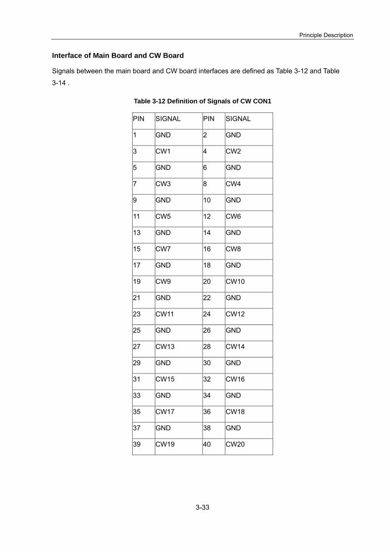
Principle Description
3-33
Interface of Main Board and CW Board
Signals between the main board and CW board interfaces are defined as Table 3-12 and Table
3-14 .
Table 3-12 Definition of Signals of CW CON1
PIN SIGNAL PIN SIGNAL
1 GND 2 GND
3 CW1 4 CW2
5 GND 6 GND
7 CW3 8 CW4
9 GND 10 GND
11 CW5 12 CW6
13 GND 14 GND
15 CW7 16 CW8
17 GND 18 GND
19 CW9 20 CW10
21 GND 22 GND
23 CW11 24 CW12
25 GND 26 GND
27 CW13 28 CW14
29 GND 30 GND
31 CW15 32 CW16
33 GND 34 GND
35 CW17 36 CW18
37 GND 38 GND
39 CW19 40 CW20
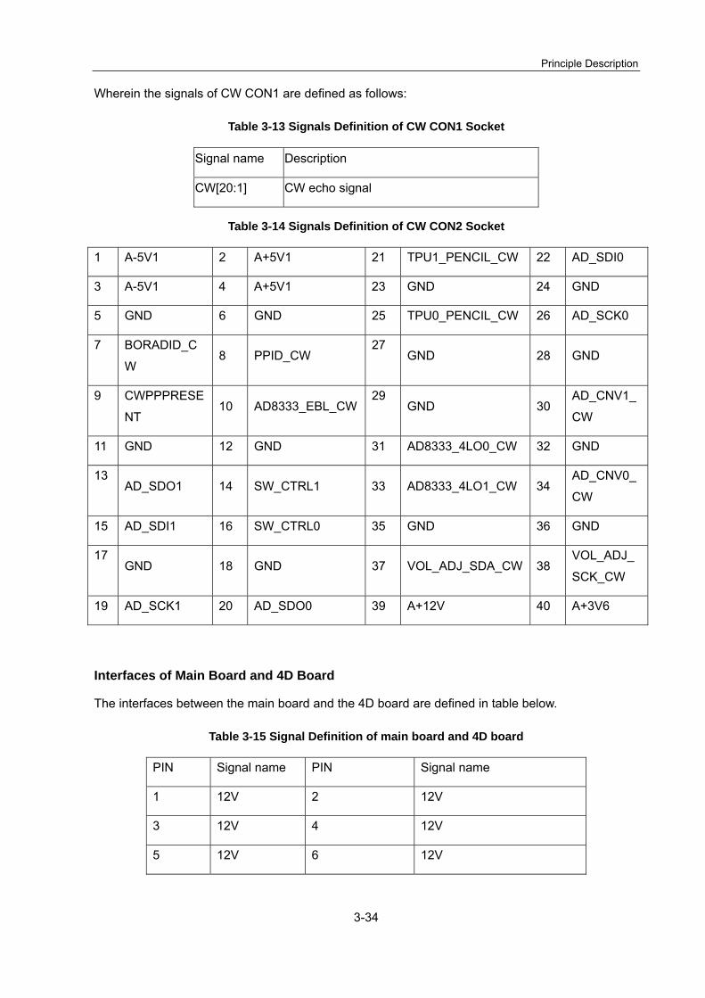
Principle Description
3-34
Wherein the signals of CW CON1 are defined as follows:
Table 3-13 Signals Definition of CW CON1 Socket
Signal name Description
CW[20:1] CW echo signal
Table 3-14 Signals Definition of CW CON2 Socket
1 A-5V1 2 A+5V1 21 TPU1_PENCIL_CW 22 AD_SDI0
3 A-5V1 4 A+5V1 23 GND 24 GND
5 GND 6 GND 25 TPU0_PENCIL_CW 26 AD_SCK0
7 BORADID_C
W 8 PPID_CW
27 GND 28 GND
9 CWPPPRESE
NT 10 AD8333_EBL_CW
29 GND 30
AD_CNV1_
CW
11 GND 12 GND 31 AD8333_4LO0_CW 32 GND
13 AD_SDO1 14 SW_CTRL1 33 AD8333_4LO1_CW 34
AD_CNV0_
CW
15 AD_SDI1 16 SW_CTRL0 35 GND 36 GND
17 GND 18 GND 37 VOL_ADJ_SDA_CW 38
VOL_ADJ_
SCK_CW
19 AD_SCK1 20 AD_SDO0 39 A+12V 40 A+3V6
Interfaces of Main Board and 4D Board
The interfaces between the main board and the 4D board are defined in table below.
Table 3-15 Signal Definition of main board and 4D board
PIN Signal name PIN Signal name
1 12V 2 12V
3 12V 4 12V
5 12V 6 12V

Principle Description
3-35
PIN Signal name PIN Signal name
7 12V 8 12V
9 GND 10 GND
11 GND 12 GND
13 GND 14 GND
15 GND 16 GND
17 -12V 18 -12V
19 -12V 20 -12V
21 -12V 22 -12V
23 GND 24 GND
25 GND 26 GND
27 GND 28 GND
29 VDD 30 VDD
31 GND 32 GND
33 VCC 34 VCC
35 GND 36 GND
37 NC 38 NC
39 NC 40 NC
41 NC 42 NC
43 NC 44 NC
45 NC 46 NC
47 NC 48 NC
49 GND 50 GND
51 POWEREN_N 52 GND
53 HALL 54 GND
55 NC 56 GND
57 SPI_CLK 58 GND

Principle Description
3-36
PIN Signal name PIN Signal name
59 SPI_DAT 60 GND
61 SPI_SYNC 62 GND
63 FD_ID 64 GND
65 AD_SCLK 66 GND
67 AD_DIN 68 GND
69 AD_DOUT 70 AD_NCS
Interfaces of Main Board and Display Module
There are 3 sockets in all for the main board and display module, refer to the following 3 tables for
the definitions:
Table 3-16 Definition of signals of the main board end (J25) of the LVDS socket
NO. NAME NO. NAME
1 VDD 2 VDD
3 GND 4 GND
5 RXE0- 6 RXE1-
7 RXE0+ 8 RXE1+
9 GND 10 GND
11 RXE2- 12 RXEC-
13 RXE2+ 14 RXEC+
15 GND 16 GND
17 RXE3- 18 GND
19 RXE3+ 20 GND
Table 3-17 Socket definition of display power supply (J26)
No: Name
1 +12V
2 +12V
3 +12V

Principle Description
3-37
4 BL_On/Off
5 BL_ADJ
6 GND
7 GND
8 GND
Table 3-18 Definition of Color Temperature Correction Socket (J24)
PIN Signal name
1 VDD
2 GND
3 SCL
4 SDA
Interfaces of Main Board and Speakers
The interfaces of the main board and speakers are defined in the following table:
Table 3-19 Interfaces of Main Board and Speakers (J27)
PIN SIG
1 ROUTP
2 ROUTN
3 NC
4 LOUTP
5 LOUTN
Socket between Fan and Main Board
The interfaces of the main board and fan are defined in the following table:
Table 3-20 Socket Definition of Fan Power Supply (J29)
No. Signal name No. Signal name
1 FANLF_SP 2 FANLF_PWR
3 FANLFM_CTRL 4 FANLMC_PWR
5 FANLM_SP 6 FANC_CTRL

Principle Description
3-38
7 FANLB_SP 8 FANC_SP
9 FANLBR_CTRL 10 FANLB_PWR
11 FANR_SP 12 FANR_PWR
FPGA JTAG Sockets of Main Board Power Management
The FPGA JTAG sockets of the main board are defined in the following table:
Table 3-21 Signal Definition of FPGA JTAG sockets (J23) of Power Management
No. Signal name
1 VPUMP
2 VJTAG
3 GND
4 TDO
5 TDI
6 TCK
7 TMS
8 TRST
Reserved Signal Interfaces
The reserved signal interfaces are defined in the following table:
Table 3-22 Definition of Reserved Signal Interfaces (J17)
No. Signal name No. Signal name
1 NC 2 GND
3 NC 4 GND
5 GND 6 GND
7 NC 8 ATA_ACT#
9 SYS_RESET# 10 GND
11 CPRT_PRINT 12 BK_STS
13 CPRT_BUSY 14 GND
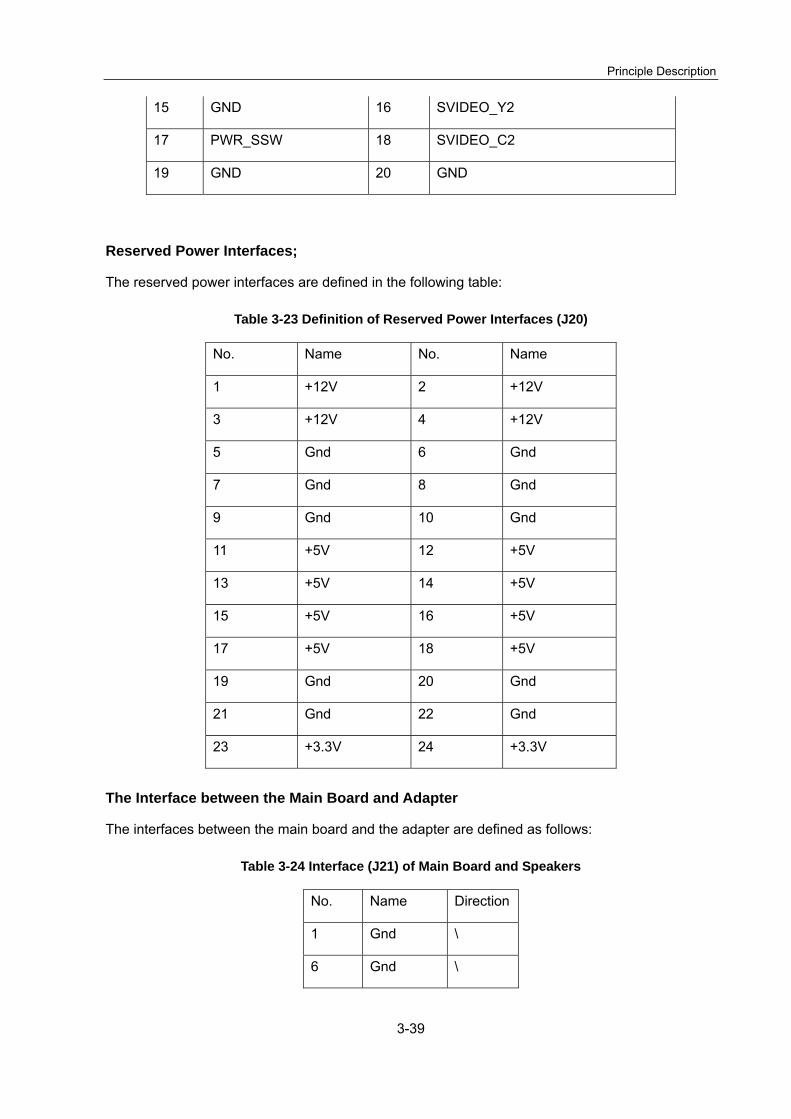
Principle Description
3-39
15 GND 16 SVIDEO_Y2
17 PWR_SSW 18 SVIDEO_C2
19 GND 20 GND
Reserved Power Interfaces;
The reserved power interfaces are defined in the following table:
Table 3-23 Definition of Reserved Power Interfaces (J20)
No. Name No. Name
1 +12V 2 +12V
3 +12V 4 +12V
5 Gnd 6 Gnd
7 Gnd 8 Gnd
9 Gnd 10 Gnd
11 +5V 12 +5V
13 +5V 14 +5V
15 +5V 16 +5V
17 +5V 18 +5V
19 Gnd 20 Gnd
21 Gnd 22 Gnd
23 +3.3V 24 +3.3V
The Interface between the Main Board and Adapter
The interfaces between the main board and the adapter are defined as follows:
Table 3-24 Interface (J21) of Main Board and Speakers
No. Name Direction
1 Gnd \
6 Gnd \

Principle Description
3-40
No. Name Direction
2 Gnd \
4 Gnd \
3 +12V In
7 +12V In
5 +12V In
8 +12V In
The Interface between the Main Board and Power Module
The interfaces between the main board and the power module consist of digital socket and analog
power socket.
The digital socket is defined in the following table:
Table 3-25 Socket Definition of igital Socket (J22)
No. Signal name No. Signal name
1 EDC_PWR 2 EDC_PWR
3 EDC_PWR 4 EDC_PWR
5 EDC_PWR 6 EDC_PWR
7 EDC_GND 8 EDC_GND
9 EDC_GND 10 EDC_GND
11 EDC_GND EDC_GND
13 -12V 14 STS_EDC#
15 GND 16 GND
17 POWER_ON# 18 CPU12V_OK#
19 T_D+ 20 T_D-
21 GND 22 GND
23 GND 24 GND
25 12V+ 26 12V+
27 12V+ 28 12V+

Principle Description
3-41
No. Signal name No. Signal name
29 GND 30 GND
31 5V+ 32 5V+
33 GND 34 GND
35 5VSTB_OK# 36 5VSTB_EN#
37 GND 38 GND
39 5VSTB_CPU 40 3V3STB
41 GND 42 GND
43 3V3 44 3V3
45 GND 46 GND
47 2V8 48 1V5
49 GND 50 GND
51 1V8 52 1V8
53 GND 54 GND
55 PWR_RX 56 PWR_CONF_N
57 PWR_TX 58 PWR_RST
59 GND 60 GND
61 PRT_BATA 62 PRT_BATB
63 BATSTS_O 64 BATSTS_G
Table 3-26 Signal Definition of Socket (J9) between Analog Power and Main Board
No. Signal name No. Signal name
1 GND 2 GND
3 A5V1 4 A5V1
5 A5V1 6 A5V1
7 GND 8 GND
9 -A5V1 10 GND
11 -A12V 12 GND

Principle Description
3-42
No. Signal name No. Signal name
13 GND 14 GND
15 A1V5 16 A1V5
17 A1V5 18 A1V5
19 GND 20 GND
21 A3V6 22 A3V6
23 GND 24 GND
25 A2V8 26 GND
27 A12V 28 GND
29 PHV1+ 30 PHV2+
31 GND 32 GND
33 PHV1- 34 PHV2-
35 GND 36 GND
37 85V+ 38 GND
39 GND 40 85V-
Interfaces of Main Board and I/O Extend Board
Signal definition between master board and I/O extended board is shown as table below.
Table 3-27 Signal Definition between Mater Board and I/O Extended Socket-J1
PIN Definition of
Signal
PIN Definition of
Signal
PIN Definition of
Signal
PIN Definition of
Signal
A1 USB+4 B1 USB-4 C1 USB+5 D1 USB-5
A2 VBUS_SYS45 B2 GND C2 VBUS_SYS45 D2 GND
A3 GND B3 VGA_HS C3 VGA_RED D3 VGA_GREEN
A4 UART_RX0 B4 VGA_VS C4 GND D4 SDISP_PRT_N
A5 UART_TX0 B5 GND C5 VGA_BLUE D5
A6 GND B6 AUDIO_L C6 GND D6
A7 BWPRT _PRINT B7 AUDIO_R C7 D7 GND

Principle Description
3-43
PIN Definition of
Signal
PIN Definition of
Signal
PIN Definition of
Signal
PIN Definition of
Signal
A8 BWPRT_BUSY B8 GND C8 DVI_D0+ D8 DVI_D0-
A9 GND B9 ECG_PWR C9 DVI_D1+ D9 DVI_D1-
A10 MIC_L B10 DVI_HPD C10 GND D10 GND
A11 MIC_R B11 C11 DVI_CLK+ D11 DVI_CLK-
A12 VIDEO B12 ECG_TX C12 DVI_D2+ D12 DVI_D2-
\ \ B13 ECG_RX \ \ D13 ECG_PRT
The Interfaces between the Main Board and the Keyboard
The interfaces between the main board and the keyboard are defined in table below.
Table 3-28 Signal Definition between Master Board and Keyboard Board-J19
No. Name No. Name
1 +3.3V 2 +3.3V
3 +3.3V 4 +3.3V
5 Gnd 6 Gnd
7 Gnd 8 Gnd
9 +5V 10 +5V
11 +5V 12 +5V
13 Gnd 14 Gnd
15 Gnd 16 Audio Out
17 Gnd 18 Gnd
19 Work_Status_O 20 Work_Status_G
21 Battery_Status_O 22 Battery_Status_G
23 Gnd 24 EDC_Status_G
25 USB_DN 26 LCD_SW
27 USB_DP 28 Power_BTN
29 Gnd 30 Gnd

Principle Description
3-44
3.1.2.9 Testing Points of Main Board and LED Indicator Light The testing points of the main board are shown in the following figures:
Fig 3-12 Testing Points of Main Board
Table 3-29 List of Testing Points of Main Board
No. Label of the Testing Point Network of the Testing Point
1 TP206-GND Ground network
2 TP248-VAA0 Voltage of video DA chip (3.3V)
3 TP228-1V5STB Power management standby voltage (1.5V)
4 TP249-SV-VDD Voltage of video driving chip (3.3V)
5 TP202-12V 12V voltage (12V)
6 TP246-3V3S_CPU PC module standby (3.3V)
7 TP7-PWROK Power OK signal of PC module (3.3V)
8 TP9-S3
Initialization status indicating signal S3 of PC module
(3.3V)

Principle Description
3-45
No. Label of the Testing Point Network of the Testing Point
9 TP8-S4
Initialization status indicating signal S4 of PC module
(3.3V)
10 TP10-S5
Initialization status indicating signal S5 of PC module
(3.3V)
11 TP224-EDC_PWR 12V input of the adapter (12V)
12 TP218-N12V -12V voltage (-12V)
13 TP215-5VSBY Standby voltage (5V)
14 TP203-VDD VDD voltage (3.3V)
15 TP217-D1V5 D1V5 voltage (1.6V)
16 TP216-D2V8 D2V8 voltage (3.0V)
17 TP6-CPUBTN Button start-up signal of PC module (3.3V)
18 TP214-D1V8 D1V8 voltage (1.8V)
19 TP201-VCC VCC voltage (5V)
20 TP20-IQ_VTT VTT voltage of DDR2 (0.9V)
21 TP236-VCCINT_DSP_MF FPGA core voltage (1.2V)
22 TP226-12V_4D 12V voltage of 4D module (12V)
23 TP235-D2V5 D2V5 voltage (2.5V)
24 TP19-UP_VTT VTT voltage of DDR2 (0.9V)
25 TP227-3V3STB Standby voltage (3.3V)
26 TP146-A+5V_PROBE Transducer port 5V
27 TP148-A+3V3_PRB Transducer port 3.3V
28 TP147-A+5V1 Analog 5V
29 TP155-A-5V_HVISO2 High-voltage isolation power
30 TP241-A-85V_HVSW High-voltage switch power
31 TP151-A+85V_HVSW High-voltage switch power
32 TP153-A+5V_HVISO2 High-voltage isolation power
33 TP152-A+5V_HVISO1 High-voltage isolation power

Principle Description
3-46
No. Label of the Testing Point Network of the Testing Point
34 TP193-A-12V -12V power
35 TP165-A+1V8_ADS AFE power
36 TP194--12V_A -12V power
37 TP163-A+3V3_VCA AFE power
38 TP164-A+3V3_ADS AFE power
39 TP178-A+5V_ATGC ATGC power
40 TP162-A+5V_VCA AFE power
41 TP144-A+3V3_CLOCK Clock power
42 TP240-VBAT Voltage of the button cell (3V)
43 TP190-A+1V5 Analog 1.5V power
44 TP189-+1V5_A Analog 1.5V power
45 TP184-+5V1_A Analog 5V power
46 TP137-A+5V1 Analog 5V power
47 TP196-+12V_A Analog 12V power
48 TP195-A+12V Analog 12V power
49 TP187-+2V8_A Analog 2.8V power
50 TP185-+3V6_A Analog 3.6V power
51 TP186-A+3V6 Analog 3.6V power
52 TP180--95V_A Analog -95V power
53 TP188-A+2V8 Analog 2.8V power
54 TP192--5V1_A Analog -5V power
55 TP36-+95V_A Analog 95V power
56 TP191-A-5V1 Analog -5V power
57 TP38-A-95V Analog -95V power
58 TP179-A-5V_ATGC ATGC-5V power
59 TP37-A+95V Analog 95V power

Principle Description
3-47
Table 3-30 Main board LED indicator light
No. LED Indication
1 D227 12V
2 D18 VCC
3 D17 VDD
4 D220
Multifunctional FPGA
configuration indicator light
5 D11
DSP FPGA configuration
indicator light
6 D15
Beam FPGA configuration
indicator light
3.1.3 Principle of Transmitting Board The main board sends commands to transmitting board, the transmitting board calculates the
parameters in real time and controls the high-voltage pulses necessary for the output of the
transmitting circuit. The schematic diagram is shown below:
Fig 3-13 Structure Diagram of Ultrasound Transmission

Principle Description
3-48
3.1.3.1 Power Structure of Transmission Board
PHV1_N
PHV1_P
PHV2_P
PHV2_N
Capacitor filter
Capacitor filter
Capacitor filter
Capacitor filter
A+12V
A-12V
A+2V5
VDD+11V
VSS-11V-HIGH
A+2V8LDO
LDO
PHV1_N
PHV1_P
PHV2_P
PHV2_N
LDO
AVDD1+11V
DVDD1+11V
DVDD2+11V
AVSS-11V-HIGH
DVSS-11V-HIGH
LC
LC
LC
LC
LC
VCCAUX
VF+2V5
VLL+2V5
LC
LC
LC
A+5V1 P+3v3LDO
A+1V5 VF+1V2LDO
VSS-11V-LOW AVSS-11V-LOW
DVSS-11V-LOW
LC
LC
LDO
100mA
100mA
500mA
1600mA
360mA
300mA
300mA
300mA
300mA
Fig 3-14 Structure Diagram of Transmitting Board Power Supply
3.1.3.2 Definition of Transmission Board Interface Detailed definition of external interface of transmission board is shown below:

Principle Description
3-49
Table 3-31 Detailed Definition of External Interface of Transmission Board
Interface with the
Main Board
(DSP_FPGA)HSSB_TX0TP/N,HSSB_TX1TP/N,
HSSB_TX0TBCKP/N,HSSB_TX0TFCKP/N,HSSB_TX0RP/N,
HSSB_TX1RP/N, HSSB_TX0RBCKP/,
HSSB_TX0RFCKP/NCLOCKEN_N_EMIT
(BF_FPGA) RESET_EMIT,RATE_P/N_EMIT
(clock) CLK_P/N_EMIT
Interface with analog
part of main board
64-channel transmission pulse/echo POUT[EMIT64..1]
Interface with power
of main board
A+12V,A-12V,A+5V1,A-5V1,A+2V8,
A+1V5,PHV1_P,PHV1_N,PHV2_P,PHV2_N
JTAG signal TCK,TDO_EMIT,TMS,TDI_EMIT_TDO_BF
The instrumentation diagram of transmission board is shown in the following figure. The figure
marks the sockets and their names.

Principle Description
3-50
Fig 3-15 The instrumentation diagram of transmission board
Table 3-32 Definition of J1 of JTAG Socket
1 JTAG_TCK
2 JTAG_ TDO_EMIT
3 JTAG_ TMS
4 JTAG_ TDI_EMIT_TDO_BF
5 P+3V3
6 GND
7 NC
8 NC
Table 3-33 Detailed Definition of Bus Socket J2
1 GND 2 GND 61 EMIT33 62 GND
3 EMIT1 4 EMIT2 63 GND 64 EMIT36
5 EMIT3 6 EMIT4 65 EMIT35 66 GND
7 GND 8 GND 67 GND 68 EMIT38
9 EMIT5 10 EMIT6 69 EMIT37 70 GND
11 EMIT7 12 EMIT8 71 GND 72 EMIT40
13 GND 14 GND 73 EMIT39 74 GND
15 EMIT9 16 EMIT10 75 GND 76 EMIT42
17 EMIT11 18 EMIT12 77 EMIT41 78 GND
19 GND 20 GND 79 GND 80 EMIT44
21 EMIT13 22 EMIT14 81 EMIT43 82 GND
23 GND 24 EMIT16 83 GND 84 EMIT46
25 EMIT15 26 GND 85 EMIT45 86 GND
27 GND 28 EMIT18 87 GND 88 EMIT48
29 EMIT17 30 GND 89 EMIT47 90 GND
31 GND 32 EMIT20 91 GND 92 EMIT50

Principle Description
3-51
33 EMIT19 34 GND 93 EMIT49 94 GND
35 GND 36 EMIT22 95 GND 96 EMIT52
37 EMIT21 38 GND 97 EMIT51 98 GND
39 GND 40 EMIT24 99 GND 100 EMIT54
41 EMIT23 42 GND 101 EMIT53 102 GND
43 GND 44 EMIT26 103 GND 104 EMIT56
45 EMIT25 46 GND 105 EMIT55 106 GND
47 GND 48 EMIT28 107 EMIT57 108 EMIT58
49 EMIT27 50 GND 109 GND 110 EMIT60
51 GND 52 EMIT30 111 EMIT59 112 GND
53 EMIT29 54 GND 113 EMIT61 114 EMIT62
55 GND 56 EMIT32 115 GND 116 EMIT64
57 EMIT31 58 GND 117 EMIT63 118 GND
59 GND 60 EMIT34 119 GND 120 GND
Table 3-34 Detailed Definition of Bus Socket J3
1 PHV1_N 2 PHV1_P 31 GND 32 NC
3 PHV1_N 4
PHV1_P 33
HSSB_TX0RFC
KN 34
A+75V_sub
5 NC 6
NC 35
HSSB_TX0RFC
KP 36
NC
7 PHV2_N 8 PHV2_P 37 GND 38 GND
9 PHV2_N 10
PHV2_P 39
HSSB_TX0RBC
KN 40
CLK_N_EMIT
11 NC 12
NC 41
HSSB_TX0RBC
KP 42
CLK_P_EMIT
13 A-12V 14 A+12V 43 GND 44 GND
15 A-12V 16
A+12V 45
HSSB_TX0RN 46
HSSB_TX0TFC
KN

Principle Description
3-52
17 A-5V1 18
A+5V1 47
HSSB_TX0RP 48
HSSB_TX0TFC
KP
19 A+2V8 20 A+1V5 49 GND 50 GND
21 A+2V8 22
A+1V5 51
HSSB_TX1RN 52
HSSB_TX0TBC
KN
23 RATE_P_EMIT 24
RESET_EMIT 53
HSSB_TX1RP 54
HSSB_TX0TBC
KP
25 RATE_N_EMIT 26
CLOCKEN_N_E
MIT 55
GND 56
GND
27 TMS 28
TDI_EMIT_TDO
_BF 57
HSSB_TX0TN 58
HSSB_TX1TN
29 TDO_EMIT 30 TCK 59 HSSB_TX0TP 60 HSSB_TX1TP
3.1.4 4D Driving Board The principle diagram of 4D driving board is shown in figure below. The interface signals of 4D
driving board and main board consist of power, SPI interface signals of ADC and DAC, and the
enabling signal of power module. The interface signals of 4D driving board and transducer
connecting board are: two driving signals A and B, HALL signal and its 5V power supply, and
temperature and angle signals of TEE transducer. 4D driving board mainly implements the following
two functions:
Amplifies the command-driven current and generates signals of appropriate power to drive
the transducer to the desired position.
As a reserved design, it amplifies the temperature and angle signals of the TEE transducer
and provides data collection channel.

Principle Description
3-53
Fig 3-16 Block diagram of 4D driving board
3.1.4.1 Definition of the Interface between the 4D Driving Board and Main
Board Signals of the socket are defined as follows:
Table 3-35 Definition of Socket between 4D Driving Board and Main Board
PIN Signal name Direction PIN Signal name Direction
1 12V Input 2 12V Input
3 12V Input 4 12V Input
5 12V Input 6 12V Input
7 12V Input 8 12V Input
9 GND / 10 GND /
11 GND / 12 GND /
13 GND / 14 GND /
15 GND / 16 GND /
17 -12V Input 18 -12V Input

Principle Description
3-54
PIN Signal name Direction PIN Signal name Direction
19 -12V Input 20 -12V Input
21 -12V Input 22 -12V Input
23 GND / 24 GND /
25 GND / 26 GND /
27 GND / 28 GND /
29 VDD Input 30 VDD Input
31 GND / 32 GND /
33 VCC Input 34 VCC Input
35 GND / 36 GND /
37 NC / 38 NC /
39 NC / 40 NC /
41 NC / 42 NC /
43 NC / 44 NC /
45 NC / 46 NC /
47 NC / 48 NC /
49 GND / 50 GND /
51 PWR_EN Input 52 GND /
53 HALL Output 54 GND /
55 NC / 56 GND /
57 SPI_CLK Input 58 GND /
59 SPI_DAT Bidirectional 60 GND /
61 SPI_SYNC Input 62 GND /
63 FD_ID Bidirectional 64 GND /
65 AD_SCLK Input 66 GND /
67 AD_DIN Input 68 GND /
69 AD_DOUT Output 70 AD_NCS Input

Principle Description
3-55
Note: wherein the direction of signal is defined as: the signal from main board to 4D driving board is
input signal, the signal from 4D driving board to main board is output signal.
3.1.4.2 Definition of the Interface between the 4D Driving Board and
Transducer Connecting Board The wire-to-board socket (WTB) of 4D driving board signals are defined as follows:
Table 3-36 Definition of Socket between 4D Driving Board and Transducer Connecting Board
PIN Signal name Direction
1 AGND /
2 5V Output
3 HALL Input
4 ANGLE Input
5 AGND /
6 T+ Input
7 T- Input
8 PHASE_B_NEG Output
9 PHASE_B_NEG Output
10 PHASE_B_POS Output
11 PHASE_B_POS Output
12 PHASE_A_NEG Output
13 PHASE_A_NEG Output
14 PHASE_A_POS Output
15 PHASE_A_POS Output
Note: wherein the direction of signal is defined as: the signal from transducer connecting board to
4D driving board is input signal, the signal from 4D driving board to transducer connecting board is
output signal.
3.1.4.3 Testing Points of 4D Driving Board The testing points of 4D driving board are listed in the following table:

Principle Description
3-56
Table 3-37 List of Testing Points of 4D Driving Board
No. Label of the Testing
Point Signal definition of testing points
1 TP3 Command current bias voltage from DAC (DAC_BIAS)
2 TP4 Output of command current error amplification circuit of phase B
3 TP5 Positive output of driving current of phase B (PHASE_B_POS)
4 TP6 Command current of phase B from DAC (DAC_B_SET)
5 TP7 Output of command current signal amplification circuit of phase B
6 TP8 Command current of phase A from DAC (DAC_A_SET)
7 TP9 Output of command current signal amplification circuit of phase A
8 TP10 Output of command current error amplification circuit of phase A
9 TP11 Positive output of driving current of phase A (PHASE_A_POS)
3.1.5 Principle of Keyboard Board
3.1.5.1 General Description The control panel of 2118 implements the following functions:
Input from buttons: input by general button, combination button, repeat button and encoder are
supported;
Backlight LED of buttons, control of status indicating LEDs
Control of beeps of buttons; larger adjustable range of volume; more than 3 grades are provided;
TGC input, full-scale and 0 available
Input from encoder
Input from optical trackball; control of backlight of optical trackball
3.1.5.2 Block Diagram of Structure The block diagram of control panel is shown in below:

Principle Description
3-57
Fig 3-17 Block Diagram of the Control Panel
3.1.5.3 Scanning Circuit of Buttons The keyboard array is controlled by row-and-column controlling method. FPGA outputs tests signals
line-by-line. When a key is pressed, the corresponding row and line signals shall be consistent.
According to the numbers of the row and line, the position of the key pressed can be defined.
GND
L0
L1
L2
R0R1R2
R
R
R
74LS07
74HC14
FPGA
Fig 3-18 Principle Diagram of Key Scanning
3.1.5.4 Driving of LED Constant-current source driving dedicated chip is adopted to drive the LEDs.

Principle Description
3-58
Fig 3-19 Connection of LED Driving Circuit There are 16 constant-current sources for each TLC5922, and the brightness can be adjusted
respectively.SPI interface control is adopted for TLC5922, and plural chips can be connected in
series for control. The power supply voltage is 5V.
3.1.5.5 Processing of Signals from Trackball A newly designed optical trackball and a mechanical trackball are supported by 2118. The
advantages of the new trackball are:
Higher resolution and performance;
Full color backlight;
Optical device, no need for daily clean;
Larger in size;
Digital interface, more flexible in control;
The data returned from the trackball interface is square waveform data. There are a pair of signal
cables in X and Y directions respectively, and four signal cables in all. The trackball is powered by
5V, supplied by the control panel.
The basic scheme of the optical trackball is shown below. It consists of trackball IC and backlight
LED.
Fig 3-20 Basic Scheme of the Optical Trackball

Principle Description
3-59
3.1.5.6 Buzzer The speaker is piezoelectric ceramic. It is driven by 74LS07. The basic drive circuit is shown below:
74LS07 Control logic
Piezoelectric ceramic piece
+5V
Fig 3-21 Speaker Control Circuit The piezoelectric ceramic has no positive / negative pole. As long as driving voltage with
appropriate frequency is put to its two ends, it will make a sound with the same frequency as that of
the driving voltage.
Whether it sounds or not, this is under the control of control logic. To generate sounds of different
frequencies, just change the frequency of the driving circuit.
3.1.5.7 Encoder Circuit There are two encoders on the control panel, and each encoder has two signal cables. The output
signal is in the form of square waveform and the electrical level is 5V.
3.1.5.8 TGC Interface Circuit TGC is actually a group of sliding rheostats, the output voltage of which is in linear relationship with
its slider displacement. The output analog voltage is converted to digital signal by AD converter and
sent to FPGA, thus obtaining the slider position.AD is powered by 3.3V, externally connected to
2.5V reference level. To keep good precision of the AD converter, the output of the sliding
potentiometer is applied with LM358 for follow-up. The principle of the interface is shown in figure
below.
Fig 3-22 TGC Interface Circuit

Principle Description
3-60
3.1.5.9 FPGA and Peripheral Circuits FPGA is the core of boards and cards, externally connected to SPI flash and SDRAM. Its logic and
software codes are stored in SPI Flash, and they are loaded to FPGA and initiate the software when
powered on.
NiosII soft core is a 32bit CPU. It can read and write SPI Flash on line and support on-line code
upgrading.
FPGA, Flash and SDRAM are all 3.3V devices. The core voltage of FPGA is 1.2V.
3.1.5.10 USB Communication Interfaces FPGA is externally connected with a USB interface chip U4 (3.3V device), supporting USB
communication protocol 1.1. The frequency of external crystal oscillator X1 is 6MHz.USB interface
is shown in figure below. In the figure, L8 is common mode suppression inductor, and U5 is
anti-static chip.
USB chipU4
VBUS
DP
GND
DML8
U5
FPGA
Fig 3-23 Schematic of USB Port
3.1.5.11 Socket Definition The components and sockets positions of the control panel are shown in the following figures. The
socket definition is shown in Table 3-38.

Principle Description
3-61
Fig 3-24 Components Layout of the Control Panel Board (Frontal)
Display switch
Encoder
Encoder

Principle Description
3-62
Fig 3-25 Components Layout of the Control Panel Board (Bottom)
Table 3-38 Definition Table of Keyboard Board Socket
Socket
number
on PCB
Name Definition of Pin Notes
Pin No Definition of
Pin
Description of PIN
J1
JTAG
debugging
socket
1 TCK TCK signal,
pull-down
2 TDO TDO
3 TMS TMS signal, pull up
3.3V
4 TDI TDI signal, pull up
3.3V
5 VDD 3.3V power
6 GND System ground
J2 TGC socket 1 TGC VDD 3.3V power

Principle Description
3-63
2 GND System ground
3 ATGC0 Slide bar 0 output
4 ATGC1 Slide bar 1 output
5 ATGC2 Slide bar 2 output
6 ATGC3 Slide bar 3 output
7 ATGC4 Slide bar 4 output
8 ATGC5 Slide bar 5 output
9 ATGC6 Slide bar 6 output
10 ATGC7 Slide bar 7 output
J3
Main board
connecting
socket
3 DP USB-DP
4 POWER_STB Power status Power
connecting
switch K93
5 DN USB-DN
6 LCD_SW Display position
status
Connect
display
position
switch S3
8 EDC_STATU
S_G
EDC status Connectio
n indicator
light D4
9 BATTERY_ST
ATUS_O
Power status O Connectio
n indicator
light D5
10 BATTERY_ST
ATUS_G
Power status G Connectio
n indicator
light D5
11 WORK_STAT
US_O
Working status O Connectio
n indicator
light D6-7

Principle Description
3-64
12 WORK_STAT
US_G
Working status G Connectio
n indicator
light D6-7
1,2,7,1
3~15,1
7~18,
23~26
GND System ground
16 Audio Out Keyboard board
audio power
amplification output
Reserved
19~22 +5 External input 5V
27~30 +3V3 External input 3.3V
J5
Mechanical
trackball
socket
1 GND System ground
2 VCC 5V
3 TRACK_HBA
LL2
Trackball signal 2 Signal 0
and 1 is a
match;
signal 2
and 3 is a
match
4 TRACK_HBA
LL3
Trackball signal 3
5 TRACK_HBA
LL0
Trackball signal 0
6 TRACK_HBA
LL1
Trackball signal 1
J4 Mechanical
trackball
socket
1,9,
11,13,
15
GND System ground
2 VDD
3 MISO Serial Data Output
(Master In/Slave
Out)
Output
4 MOSI Serial Data
Input( Master
Out/Slave In)
Input

Principle Description
3-65
5 SCLK Serial Clock Input Input
6 NCS Chip Select(Active
Low Input)
Input
7 MOTION Motion Detect
(Active Low
Output)
Input
8 SHTDWN Shutdown(Active
High Input)
Input
10 LED_DRIVER
1
LED driver 1 Input
12 LED_DRIVER
2
LED driver 2 Input
14 LED_DRIVER
3
LED driver 3 Input
J8 Buzzer socket 1 BUZ0 Buzzer signal 0
2 BUZ1 Buzzer signal 1
3.1.6 Display Unit The LCD interface consists of LVDS digital signal input interface and CCFL strip lamps interface;
wherein LVDS signals are low-voltage difference digital signals, and VDD is 3.3V; the definition of
its socket connecting to main board is shown as follows:
Table 3-39 Interfaces of Main Board and Speakers
PIN Definition PIN Definition
1 VDD 2 VDD
3 GND 4 GND
5 RXE0- 6 RXE1-
7 RXE0+ 8 RXE1+
9 GND 10 GND
11 RXE2- 12 RXEC-

Principle Description
3-66
PIN Definition PIN Definition
13 RXE2+ 14 RXEC+
15 GND 16 GND
17 RXE3- 18 GND
CCFL strip lamps are supplied with high voltage from the inverter, producing different brightness
according to different currents. The principle of the inverter is:
The 12V input of the inverter comes from the main board. The main IC of the inverter drives 4
MOSFETs opening/closing alternatively and puts AC square wave to the primary winding the
transformer. The high-voltage square wave induced by the secondary winding is transformed into
sine wave through LC filtering and drives CCFL strip lamp shining. The switch signal controls the
on/off of the strip lamp by controlling the enabling of main IC. The brightness signal adjusts the
brightness of the strip lamp by controlling the duty cycle of square wave of main IC.
The inverter board is equipped with protection circuits of strip lamp open circuit, overvoltage and
over-current. Protection of strip lamp: whenever any of the strip lamps is open circuit, the protection
circuit will act; over-current protection: when the output current is over-current, the feedback signals
from the strip lamp to main IC will restrain the duty ratio of the square wave to reduce the current for
protection; overvoltage protection: the IC has been configured with the voltage-limiting function to
ensure the output voltage is not too high. The socket J26 connecting to main board is defined as
follows:
Table 3-40 Interfaces of Main Board and Inverter
PIN Definition
1 12V
2 12V
3 12V
4 ON/OFF
5 ADJ
6 GND
7 GND
8 GND

Principle Description
3-67
Wherein ON/OFF is the switch signal of the inverter; ADJ controls the brightness of the LCD by
inputting different voltages which are then converted to currents by the inverter;
EEPROM board storages one-to-one related information of LCD (such as serial number and color
temperature version, etc) and gamma correction parameters; the socket connecting to main board
is defined as follows:
Table 3-41 Interfaces of Main Board and EEPROM
PIN Definition
1 VDD
2 GND
3 SCL
4 SDA
The logic will output different RGB mapping tables according to the storage contents to ensure the
consistence of image output effect for different LCDs;
Note: To ensure the display effect, when changing LCD assembly or main board assembly, enter Maintenance Menu to reload the LCD parameters. This is display parameter synchronization. The synchronization procedure is described as follows:
1. Restart the Doppler system:
2. Log onto the system as service engineer:
3. Press <F10> to open the Setup menu, see the figure below:
Fig 3-26 Setup Menu 4. Click [Maintenance] in the menu to open the menu in the figure below:

Principle Description
3-68
Fig 3-27 Maintenance Menu 5. Click [Monitor Test] →[Main Monitor] to open the following screen:
Fig 3-28 Main Screen Maintenance Screen 6. See the figure above, click the top icon on the screen (update) to start the maintenance, when
completed, a dialogue box showing successful maintenance will be displayed, restart the
system to make the new setting take effect. If the maintenance is failed, please return the
system to development center. The following two figures show the two situations respectively.

Principle Description
3-69
Fig 3-29 Successful Update
Fig 3-30 Update Failed
3.1.7 Principle of ECG Board The function of the ECG board contains: ECG signal detection; ECG waveform display; ultrasound
image reference signal; producing real-time 2-D image and color flow image synchronous signal;
displaying ECG signals from external patient monitor.
After being amplified, filtered and sampled, the ECG signal is sent to host PC, and R-waveform
detection is performed simultaneously. After being detected, the ECG trigger signal is sent to host
PC via serial port. Block diagram is shown as follows:

Principle Description
3-70
Fig 3-31 Block Diagram of the ECG Board
3.1.7.1 Power Principle of ECG Board ECG board is powered by main unit, and the voltage is 5V. 5V is transformed to 12V after going
through the step-up circuit. T1 is the isolated transformer. The 12V power is isolated and then sent
to ECG board to power the analog and digital circuits. As shown in figure below.
Fig 3-32 Power Functional Block Diagram of ECG Board
3.1.7.2 Instrumentation Diagram and Component Description The instrumentation diagram of ECG board is shown in the following figure. The figure marks the
sockets and their names. The blue dotted line indicates the component isolation boundary. The right
isolation area indicates the power circuit and communication port, and the left isolation area
indicates ECG signal processing circuit

Principle Description
3-71
Fig 3-33 The instrumentation diagram of ECG board The interfaces are shown in the figure, and the interfaces are defined in the following table:
Table 3-42 ECG Board Instrumentation Diagram Description
Socket
number
on PCB
Name Definition of Pin Notes
Pin No Definition of Pin Description of PIN
J1 DC_IN 1 FGND ECG module floating ground
2 FGND ECG module floating ground
3 DC_IN DC IN
4 FGND ECG module floating ground
5 FGND ECG module floating ground
6 FGND ECG module floating ground
J2 Lead
cable
1 Lead_F_IN Lead cable 1
2 Lead_R_IN Lead cable 2

Principle Description
3-72
interface
socket 3 Lead_N_DR Lead cable 3 (connected with
the right ) (to the right leg)
4 NC No connection
5 C_SHIELD Cable shield drive
6 NC No connection
J4 Main
system
interface
socket
1 GND Main system ground
2 ECG_RX ECG signal receiving (relative to
the main board )
3 ECG_TX ECG signal transmitting (relative
to the main board )
4 ECG_PWR Power for ECG board
5 GND Earth terminal of main system
6 NC Earth terminal of main system
7 GND Earth terminal of main system
8 GND Earth terminal of main system
J6 JTAG
debugging
socket
1 VCC 3.3V Debugging
2 GND ECG module floating ground
3 TRST JTAG——TRST
4 TCK JTAG——TCK
5 TDI JTAG——TDI
6 TDO JTAG——TDO
7 TMS JTAG——TMS
8 RTCK JTAG——RTCK
9 NRST JTAG——NRST
10 NC No connection
J7 ARM
BOOT
1 / Connect to LPC213X P0.14 pin
of ARM chip
Service
2 GND ECG module floating ground

Principle Description
3-73
3.1.8 Principle of Video/Audio Capture Card The diagram of video capture card is shown in the figure below:
EMP202
TVP5150
EM2860
8-bit parallel digital signal
I2C
Line-field syn. signal
TVP5150 Synchronization clock
EMP202 syn. ClockSyn. signal
Control feedbackControl
Reset control
USB
ADG774
CH select
VIDEO/SVIDEOSVIDEO
VIDEO
Audio_L
Audio_R
Fig 3-34 System Block Diagram of Video/Audio Capture Card
The power relation of video audio capture card is shown in the figure below:
3.3V
Fig 3-35 Power Relation Diagram of Video/Audio Capture Card Principle of the video capture card is described as follows:
After the video capture card is powered on, EM2860 first resets and communicates with the main
unit, and TVP5150 resets simultaneously. At this moment the system displays the newly found
hardware, namely EM2860.After EM2860 resets, its GPIO1 signal will change and control the reset
of EMP202 through PMOSFET.
After the process is completed, both the BCLK and VCLK have clock signals, and SYNC has cyclic
pulses.

Principle Description
3-74
When the capture software is started, LED pin of EM2860 is pulled high, and green LED in the
board is lit up. The video capture card transmits the video capture configuration in the software to
TVP5150 via I2C bus. The TVP5150 sends channel selecting command to analog switch ADG774
according to the received command, and selects encoding method corresponding to configuration.
TVP5150 converts the input video signals to 8-bit digital signals, and transmits them to EM2860. At
the same time, EMP202 transmits the captured audio signals to EM2860 via serial channel.
EM2860 integrates the received signals and then sends them to PC via USB port.
3.1.9 Principle of the CW Board The block diagram of CW board is shown as figure below:
Fig 3-36 Principle Diagram of CW board
The hardware block diagram of CW board is shown as the figure above. Echo signals that received
by the phased probe and pencil probe will first be amplified through low-noise-amplifying (LNA)
circuit, then pass through the DEMODULATOR to obtain I, Q signals, and I, Q signals will be
sampled through ADC after being filtered out the useless low-frequency and high-frequency signals.
The sampled signals then will be sent through the interface for beam-forming and so on.
Low-phase noise demodulation clock is provided by the clock distributor circuit.
In addition to echo receiving, CW board is also responsible for pencil probe signal transmitting.
The control signals, as well as the data signals, are communicated with the external through
interfaces
Definition of CW board interfaces is shown as follows:

Principle Description
3-75
Table 3-43 Pin definition of J1
1 GND 2 GND 21 GND 22 GND
3 CW19 4 CW20 23 CW9 24 CW10
5 GND 6 GND 25 GND 26 GND
7 CW17 8 CW18 27 CW7 28 CW8
9 GND 10 GND 29 GND 30 GND
11 CW15 12 CW16 31 CW5 32 CW6
13 GND 14 GND 33 GND 34 GND
15 CW13 16 CW14 35 CW3 36 CW4
17 GND 18 GND 37 GND 38 GND
19 CW11 20 CW12 39 CW1 40 CW2
Table 3-44 Pin definition of J2
1 A-5V1 2 A+5V1 21 SHUTDOWN 22 AD8339_CSB
3 A-5V1 4 A+5V1 23 GND 24 GND
5 GND 6 GND 25 TPU0_PENCIL_CW 26 AD_SCK
7 BOARDID_CW 8 PPID_CW 27 GND 28 GND
9 CWPPPRESENT 10 TUNING_SW_CW 29 GND 30 AD_CNV_CW
11 GND 12 GND 31 AD8339_4LO0_CW 32 GND
13 AD_SDO1 14 AD8339_RSTS 33 AD8339_4LO1_CW 34 AD8339_RSET
15 AD8339_SDI 16 AD8339_SCLK 35 GND 36 GND
17 GND 18 GND 37 VOL_ADJ_SDA 38 VOL_ADJ_SCK
19 AD8339_SDO 20 AD_SDO0 39 A+12V 40 A+3V6
Table 3-45 Pin definition of J3
1 CWPPPRESENT 4 PEN_EMIT
2 PPID_CW 5 GND
3 GND 6 PEN_SIGNAL
Table 3-46 Connector signal description of CW board

Principle Description
3-76
Name Meaning Direction Type Notes
J1
CW[10:1] CW IN I(sink) Single-end current
CW[20:11] CW IN I(sink) Single-end Current (reserved)
J2
A-5V1 A-5.1V power I Power
A+5V1 A+5.1V power I Power
A+12V A+12V power I Power
A+3V6 A+3.6V power I Power
BOARDID_CW CW board ID I/O Single-end One signal device
CWPPPRESENT Pencil probe
present O
Single-end
AD_SDO[1:0] AD serial port
output data O
Single-end
AD8339_SDI
AD8339SPI daisy
chain serial port
input data
I
Single-end
AD8339_SDO
AD8339SPI daisy
chain serial port
output data
O
Single-end
PPID_CW Pencil probe ID O Single-end One signal device
TUNING_SW_CW Tuning inductive
relay switch I
Single-end
AD8339_RSTS AD8339 internal
register reset I
Single-end
AD8339_SCLK AD8339 SPI data
clock I
Single-end
TPU0_PENCIL_CW CW pencil probe
transmitting input I
Single-endLow-phase noise
SHUTDOWN ENB of AD8432 I Single-end

Principle Description
3-77
AD8339_4LO[1:0]_CW Input demodulation
clock I difference
Variable-frequency,
low-phase noise
AD8339_CSB AD8339 SPI CS
(chip selection) I
Single-end
AD_SCK ADC data clock I Single-end I/Q share
AD_CNV_CW ADC sample clock
input I
Single-end I/Q share,
low-phase noise
AD8339_RSET AD8339 internal LO
reset I
Single-end
VOL_ADJ_SDA
I2C data line of
digital potentiometer
AD5259
I/O
Single-end
I2C
VOL_ADJ_SCK
I2C clock line of
digital potentiometer
AD5259
I/O
Single-end
I2C
J3
PEN_SIGNAL Pencil probe input
signal I
Single-end
PEN_EMIT Pencil probe
transmit signal O
Single-end
PEN_ID Pencil probe ID I Single-end
PEN_PRESENT Pencil probe
present signal I
Single-end

4-1
4 Structure and Assembly/Disassembly
4.1 Explosive Figure of the Structure
4.1.1 Explosive Figure of the Complete System

Structure and Assembly/Disassembly
4-2
Fig 4-1 Overall exploded view
No. Name No. Name No. Name
<1> Display assembly
115-002254-00
<2> Main board
051-000098-01
<3> Transducer board
assembly
115-002943-00
<4> CPU board and
radiator module
115-003754-00
<5> Rear cover
assembly of main
unit
034-000041-00
<6> Damping axis cover
043-000453-00
1
2
3
4
5
6
7
8
9
10 12

Structure and Assembly/Disassembly
4-3
<7> Power supply
module;
115-002256-00
<8> Top cover assembly
of main unit
115-002942-00
<9> Fan mounting
bracket of CPU
module
042-000415-00
<10> Battery
2108-20-65792
<11> CW board PCBA
051-000170-00
<12> 4D board PCBA
051-000102-01
4.1.2 Explosive Figure of the Modules
4.1.2.1 Explosive Figure of the Power Module
Fig 4-2 Explosive figure of the power system
No. Name No. Name No. Name
<1> Top cover of power box <2> Philips panhead screw
M3×6
<3> Power supply main
board
1
4
5
3 2
6

Structure and Assembly/Disassembly
4-4
<4> Separating plate. <5> Power supply auxiliary
board
<6> Bottom cover of
power box
4.1.2.2 Explosive Figure of Main Unit Top Cover
Fig 4-3 Explosive figure of the main unit top cover
No. Name No. Name No. Name
<1> Philips panhead screw
M3×6
<4> Buzzer <7> Control panel
<2> TGC adjusting board <5> Top cover of main unit <8> Trackball
connection
wire
<3> Philips panhead screw
M2×10
<6> Philips panhead screw
M3×6
<9> STC
connection
wire

Structure and Assembly/Disassembly
4-5
Fig 4-4 Explosive figure of the main unit
No. Name No. Name
<1> Main board <2> 4D board
<3> HDD <4> Transmitting board
shielding cover
1
3
2
4

4-6
4.2 Field Replaceable Unit
NO. Classification Description Order Number Photo Model Compatibility Assembly/
Disassembly
1.1
Main unit
related
Main Board 801-2118-00006-00
M7/M7
Premium/
M7Vet
Includes button battery and jumper Refer to 4.3.11
1.2
CPU module
(with Radisys
PC module)
801-2118-00011-00
M7/M7
Premium/
M7Vet
Old PC module, stop production:
Refer to 4.3.7
CPU module
(with Baytrail PC module)
115-044556-00
M7/M7 Premium/
M7Vet
New PC module
Matched with software version of
08.00.00(Rev43717) and later.

Structure and Assembly/Disassembly
4-7
NO. Classification Description Order Number Photo Model Compatibility Assembly/
Disassembly
1.3
HDD(M7/FDA/F
RU/XP OS)
500G
115-018485-00
M7
Matched with software version of 05.00.00(Rev41607) and before. Configuration type: FDA.
Not include metal support
HDD(M7/FDA/F
RU/WIN7)
500G
115-028221-00.
M7
Matched with software version between 06.00.00(Rev42040) and 07.02.00(Rev43234) Configuration type: FDA. Not include metal support
HDD(M7/FDA/F
RU/WIN7/
BayTrail PC)
500G
115-044564-00
M7
Matched with software version of
08.XX.XX Configuration type: FDA.
Not include metal support
HDD(M7
Premium/1T//FD
A/FRU/WIN7)
1T
115-046993-00
M7
(Premium)
Matched with software version of
09.00.00 and later. Configuration type: FDA.
Not include metal support
SSD(M7
Premium/FDA/F
RU/WIN7)
128G
115-046992-00
M7
(Premium)
Matched with software version of
09.00.00 and later. Configuration type: FDA.
Not include metal support

Structure and Assembly/Disassembly
4-8
NO. Classification Description Order Number Photo Model Compatibility Assembly/
Disassembly
HHD(M7Vet/FD
A/FRU/XP OS)
500G
115-018486-00
M7 Vet
Matched with software version of 05.00.00(Rev41607) and before. Configuration type: FDA.
Not include metal support
HDD(M7Vet/FDA/FRU/WIN7) 500G
115-028222-00
M7 Vet
Matched with software version between 06.00.00(Rev42040) and 07.02.00(Rev43234) Configuration type: FDA. Not include metal support
HDD(M7Vet/FDA/FRU/WIN7/ BayTrail PC) 500G
115-044565-00
M7 Vet
Matched with software version of
08.00.00(Rev43717) and later. Configuration type: FDA.
Not include metal support

Structure and Assembly/Disassembly
4-9
NO. Classification Description Order Number Photo Model Compatibility Assembly/
Disassembly
HHD(M7/CE/FR
U/XP OS)
115-018487-00
M7
Matched with software version of 05.00.00(Rev41607) and before. Configuration type: CE.
Not include metal support
HHD(M7/CE/FRU/WIN7)
115-028223-00
M7
Matched with software version between 06.00.00(Rev42040) and 07.02.00(Rev43234) Configuration type: CE. Not include metal support
HHD(M7/CE/FRU/WIN7/ BayTrail PC)
115-044561-00
M7
Matched with software version of
08.XX.XX Configuration type: CE.
Not include metal support
HDD(M7
Premium/1T/CE/
FRU/WIN7)
1T
115-046685-00
M7
Premium
Matched with software version of
09.00.00and later. Configuration type: CE.
Not include metal support
SSD(M7
Premium/CE/FR
U/WIN7)
128G
115-046686-00
M7
Premium
Matched with software version of
09.00.00and later. Configuration type: CE.
Not include metal support

Structure and Assembly/Disassembly
4-10
NO. Classification Description Order Number Photo Model Compatibility Assembly/
Disassembly
SSD(M7
/CE/FRU/WIN7)
128G
115-047034-00
M7
(Premium)
Matched with software version of
09.00.00and later. Configuration type: CE.
Not include metal support
HDD(M7
Premium/1T/CE/
FRU/WIN7)
1T
115-047035-00
M7
(Premium)
Matched with software version of
09.00.00and later. Configuration type: CE.
Not include metal support
HHD(M7Vet/CE/FRU/XP OS)
115-018488-00
M7 Vet
Matched with software version of 05.00.00(Rev41607) and before. Configuration type: CE. Not include metal support
HHD(M7Vet/CE/FRU/WIN7)
115‐028224‐00
M7 Vet
Matched with software version between 06.00.00(Rev42040) and 07.02.00(Rev43234)
HHD(M7Vet/CE/FRU/WIN7/BayTrail PC)
115-044562-00
M7 Vet
Matched with software version of
08.00.00(Rev43717) and later. Configuration type: CE. Not include metal support

Structure and Assembly/Disassembly
4-11
NO. Classification Description Order Number Photo Model Compatibility Assembly/
Disassembly
1.4 Transmission
Board 801-2118-00004-00
M7/M7
Premium/
M7Vet
Mark software version when apply Refer to 4.3.10
1.5 Probe board
assembly 801-2118-00013-00
M7/M7
Premium/
M7Vet
Refer to 4.3.12
1.6 CW board 801-2118-00030-00
M7/M7
Premium/
M7Vet
Refer to 4.3.5
1.7.
1
4D and TEE
board assembly 801-2118-00036-00
M7/M7
Premium/
M7Vet
Support TEE probe and 4D probe Refer to 4.3.13

Structure and Assembly/Disassembly
4-12
NO. Classification Description Order Number Photo Model Compatibility Assembly/
Disassembly
1.7.
2
4D board
assembly 801-2118-00031-00
M7/M7
Premium/
M7Vet
Stop production, this board cannot
support TEE probe Refer to 4.3.13
2.1
Power related
Power supply
module 801-2118-00001-00
M7/M7
Premium/
M7Vet
Refer to 4.3.4
2.2 Adapter
(ADP1210-01) 801-2108-00049-01
M7/M7
Premium/
M7Vet
Not included the power line /
2.3.
1
Rechargeable
Li-ion Battery
Pack
2108-30-66176
M7/M7
Premium/
M7Vet
For CE
Two batteries should be
replaced together
Refer to 4.3.1
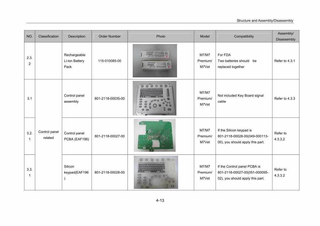
Structure and Assembly/Disassembly
4-13
NO. Classification Description Order Number Photo Model Compatibility Assembly/
Disassembly
2.3.
2
Rechargeable
Li-ion Battery
Pack
115-010085-00
M7/M7
Premium/
M7Vet
For FDA
Two batteries should be
replaced together
Refer to 4.3.1
3.1
Control panel
related
Control panel
assembly 801-2118-00035-00
M7/M7
Premium/
M7Vet
Not included Key Board signal
cable Refer to 4.3.3
3.2.
1
Control panel
PCBA (EAF196) 801-2118-00027-00
M7/M7
Premium/
M7Vet
If the Silicon keypad is
801-2118-00028-00(049-000113-
00), you should apply this part.
Refer to
4.3.3.2
3.3.
1
Silicon
keypad(EAF196
)
801-2118-00028-00
M7/M7
Premium/
M7Vet
If the Control panel PCBA is
801-2118-00027-00(051-000095-
02), you should apply this part.
Refer to
4.3.3.2
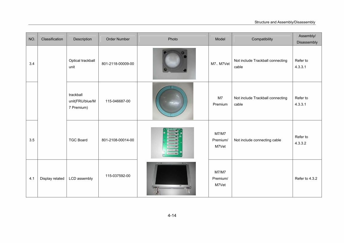
Structure and Assembly/Disassembly
4-14
NO. Classification Description Order Number Photo Model Compatibility Assembly/
Disassembly
3.4 Optical trackball
unit 801-2118-00009-00 M7、M7Vet
Not include Trackball connecting
cable
Refer to
4.3.3.1
trackball
unit(FRU/blue/M
7 Premium)
115-046687-00
M7
Premium
Not include Trackball connecting
cable
Refer to
4.3.3.1
3.5 TGC Board 801-2108-00014-00
M7/M7
Premium/
M7Vet
Not include connecting cable Refer to
4.3.3.2
4.1 Display related LCD assembly
115-037592-00 M7/M7
Premium/
M7Vet
Refer to 4.3.2

Structure and Assembly/Disassembly
4-15
NO. Classification Description Order Number Photo Model Compatibility Assembly/
Disassembly
5.1
Others
Fan 801-2118-00015-00
M7/M7
Premium/
M7Vet
CPU fun Refer to 4.3.6
5.2 Fan & Connect
Wire 801-2108-00052-00
M7/M7
Premium/
M7Vet
Right fun Refer to 4.3.8
5.3 Fan & Connect
Wire 115-020423-00
M7/M7
Premium/
M7Vet
Left fan (3 as a group ) Refer to 4.3.8
5.4 speaker 801-2108-00019-00
M7/M7
Premium/
M7Vet

Structure and Assembly/Disassembly
4-16
NO. Classification Description Order Number Photo Model Compatibility Assembly/
Disassembly
6.1
Accessories
related
IO Extend
Module
115-003485-00
M7/M7
Premium/
M7Vet
For CE
Refer to 4.3.18
6.2 115-003486-00
M7/M7
Premium/
M7Vet
For FDA
6.3
Video Extend
Module
2108-30-66045
M7/M7
Premium/
M7Vet
For CE
Refer to 4.3.17
6.4 2108-30-66211
M7/M7
Premium/
M7Vet
For FDA
6.5
ECG module
115-003488-00
M7/M7
Premium/
M7Vet
For CE, AHA ECG lead, need IO
Extend Module to be connected to
M7
Refer to 4.3.16 6.6 115-003489-00
M7/M7
Premium/
M7Vet
For CE, IEC ECG lead, need IO
Extend Module to be connected to
M7
6.7 115-003490-00
M7/M7
Premium/
M7Vet
For FDA, AHA ECG lead, need IO
Extend Module to be connected to
M7

Structure and Assembly/Disassembly
4-17
NO. Classification Description Order Number Photo Model Compatibility Assembly/
Disassembly
6.8 Wireless card 115-005370-00
M7/M7
Premium/
M7Vet
Need KEY file /
6.9
M7 Probe
extend module
for UMT-300
115-006962-00
M7/M7
Premium/
M7Vet
For CE Refer to
UMT-300
mobile trolley
service
manual 6.10 115-006966-00
M7/M7
Premium/
M7Vet
For FDA
6.11
M7 Probe
extend module
(PEM-21) for
UMT-200
115-009385-00
M7/M7
Premium/
M7Vet
For CE Refer to M7
Probe
Expander
UMT-200
installation
manual 6.12 115-009386-00
M7/M7
Premium/
M7Vet
For FDA

4-18
4.3 Assembly/Disassembly This section describes the disassembling and assembling of the main modules and boards. The assembling is the inverse process of disassembling if not mentioned in particular.
4.3.1 Removing Batteries
Fig 4-5 Removing the battery Move the two battery buckles in the direction as shown in the figure above, then take out the
battery.
No. Name No. Name
<1> Battery Buckle <2> Battery
4.3.2 Removing Display Assembly As shown in below, remove the screws and the bottom cover and cable cover;
Disconnect the display signal cable and power cord connectors.
Fig 4-6 Removing Cables Cover at the Bottom Side
No. Name No. Name
<1> Screws M3×8 <2> Cable cover
1
2

Structure and Assembly/Disassembly
4-19
<3> Display signal cable connector <4> Display power cord connector
1. As shown in figure below, open the display to the biggest angle, press down the damping axis
cover to pop up the damping axis cover; take out the damping axis cover upward.
There are left and right damping axes, and they can be removed with the same method.
Fig 4-7 Removing the Damping Axis Cover
No. Name No. Name
<1> Main unit assembly <2> Damping axis cover
2. As shown in figure below, remove the six M3×8 screws; take out the display assembly upward
from the assembly. Pay attention not to damage the display signal cable, power cord, and
connectors during removal.

Structure and Assembly/Disassembly
4-20
Fig 4-8 Disassembling Display Assembly
No. Name No. Name
<1> Display assembly <2> Screw M3×8
3. As shown in figure below, take out the the screw caps securing the display, remove the four M3×8
screws, and then take out the display front cover from the back cover.
Fig 4-9 Removing Display Front Cover
No. Name No. Name
<1> Display screw cap <2> Screw M3×8
<3> Display front cover <4> LCD assembly
<5> Display back cover
Note: A hook is used to connect the front cover with back cover. It is recommended that you first pry the lower-left corner and lower-right corner.
4. Remove the 2 screws fixing the inverter board of the LCD, and remove the 1 screw from the
cable clip, then remove the power cable of the backlight of the LCD, and then remove the
inverter board.
2
3
4 5
1
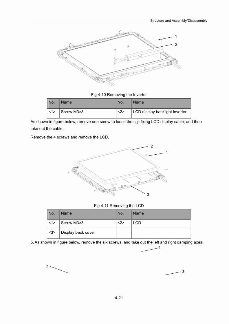
Structure and Assembly/Disassembly
4-21
Fig 4-10 Removing the Inverter
No. Name No. Name
<1> Screw M3×8 <2> LCD display backlight inverter
As shown in figure below, remove one screw to loose the clip fixing LCD display cable, and then
take out the cable.
Remove the 4 screws and remove the LCD.
Fig 4-11 Removing the LCD
No. Name No. Name
<1> Screw M3×8 <2> LCD
<3> Display back cover
5. As shown in figure below, remove the six screws, and take out the left and right damping axes.
1 2
3
2
1
3 2
1

Structure and Assembly/Disassembly
4-22
Fig 4-12 Removing the Left/right Damping Axis
No. Name No. Name
<1> Screw M3×8 <2> Left damping axis
<3> Right damping axis
6. Take off the LCD screen, the back side view is as shown in figure 4-13.
Fig 4-13 Backside of LCD Screen
NOTE: 1. The whole LCD module should be replaced in the maintenance. The corresponding LCD parameter board should be replaced once the LCD is replaced, since the two is bonded together. 2. Before replacing, make sure the module has passed the test and the related parameters have been burnt on the LCD parameter board.
7. According to figure below, first press the spring in axial direction, wait until the shorter axis comes
out, and then take out the hook upward.
LCD signal cable
LCD parameter board

Structure and Assembly/Disassembly
4-23
Fig 4-14 Removing Hooks of Display
No. Name No. Name No. Name
<1> Right display hook <2> Left display hook <3> Display hook spring
NOTE: After replacing the LCD module, start up the system and updates the LCD by entering [Maintenance] -> [Main Monitor], and clicking the update button on the top of the screen.
4.3.3 Removing Top Cover of Main Unit 1. As shown in figure below, remove the 9 screws.
Fig 4-15 Removing the Top Cover Assembly of Main Unit (1)
No. Name No. Name
<1> Screw M3×8
2. Lift up the main unit top cover for 30 degrees, disconnect the wire between the control panel and
main board; pull it out in the direction as per the figure, and then take out the main unit top
cover.

Structure and Assembly/Disassembly
4-24
Fig 4-16 Removing the Top Cover Assembly of Main Unit (2)
No. Name No. Name
<1> Top cover assembly of main unit <2> Connective cable between
control panel and main board
<3> Display
4.3.3.1 Removing the Trackball As shown in figure below, pull out the socket of the trackball and remove the screws fixing the
trackball, and then remove the optical trackball.
Fig 4-17 Removing the Trackball
No. Name No. Name
<1> Philips panhead screw M3×6 <2> Trackball
1
2
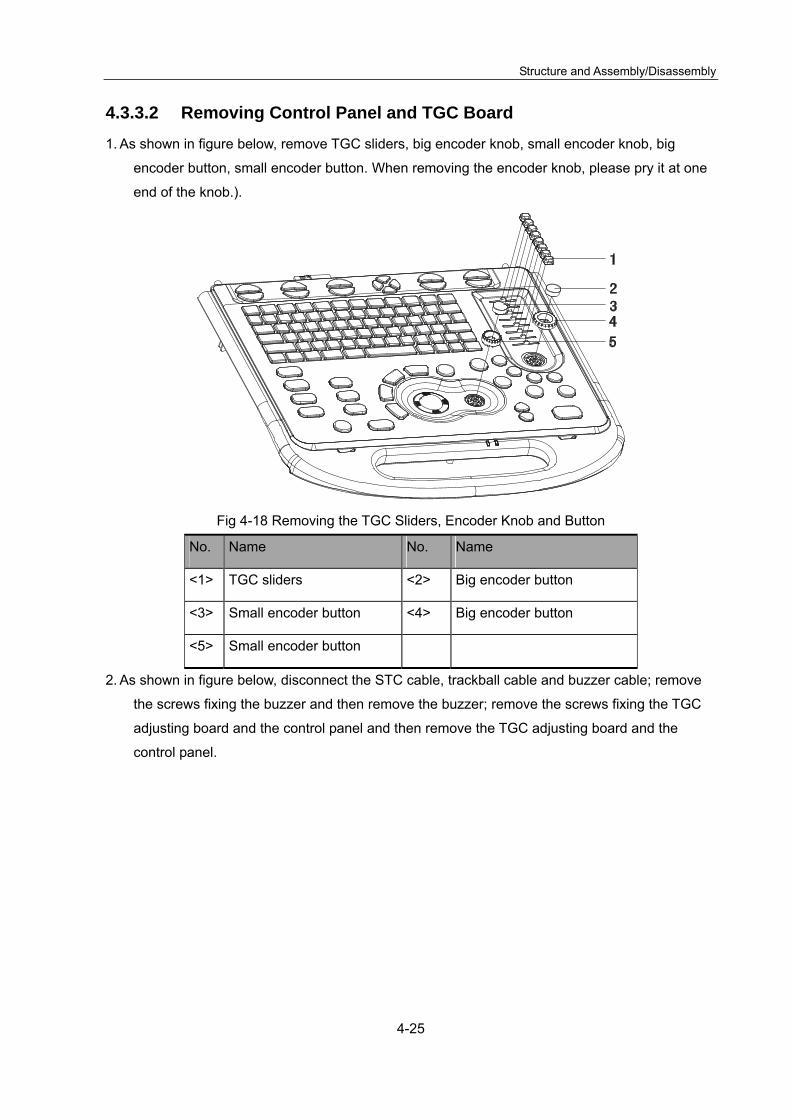
Structure and Assembly/Disassembly
4-25
4.3.3.2 Removing Control Panel and TGC Board 1. As shown in figure below, remove TGC sliders, big encoder knob, small encoder knob, big
encoder button, small encoder button. When removing the encoder knob, please pry it at one
end of the knob.).
Fig 4-18 Removing the TGC Sliders, Encoder Knob and Button
No. Name No. Name
<1> TGC sliders <2> Big encoder button
<3> Small encoder button <4> Big encoder button
<5> Small encoder button
2. As shown in figure below, disconnect the STC cable, trackball cable and buzzer cable; remove
the screws fixing the buzzer and then remove the buzzer; remove the screws fixing the TGC
adjusting board and the control panel and then remove the TGC adjusting board and the
control panel.

Structure and Assembly/Disassembly
4-26
Fig 4-19 Removing TGC Adjusting Board and Control Panel
No Name No. Name No. Name
<1> Philips panhead screw
M3×6
<4> Buzzer <7> Control panel
<2> TGC adjusting board <5> Top cover of
main unit
<8> Trackball connection
wire
<3> Philips panhead screw
M2×10
<6> Philips panhead
screw M3×6
<9> STC cables
4.3.4 Removing the Power Module 1. According to 4.3.3, remove the top cover of the main unit;
2. As shown in figure below, remove the four M3×6 Philips panhead screws to take out the power
module from the main board.

Structure and Assembly/Disassembly
4-27
Fig 4-20 Removing the Power Module
No. Name No. Name
<1> Philips panhead screw
M3×6
<2> Power supply module;
Note: When removing the power module, keep the power board horizontally to prevent damaging the connector pins.
4.3.4.1 Remove the Battery Socket Pressing Board See figure below, remove the 1 Philips panhead screw M3×6, and then remove the battery socket
pressing board from the flexible board for connecting the batteries.
Fig 4-21 Remove the Battery Socket Pressing Board
1
2
2
1

Structure and Assembly/Disassembly
4-28
No. Name No. Name
<1> Philips panhead screw
M3×6
<2> Battery socket pressing
board
4.3.4.2 Disassembling Power Module 1. As shown in figure below, remove the 2 screws 5 to remove the top cover of the power module;
remove the 4 screws 2 to take out the power board, separating board and auxiliary board
assembly.
Fig 4-22 Disassembling the Power Module
No. Name No. Name No. Name
<1> Top cover of power
box
<2> Philips panhead screw
M3×6
<3> Power main board,
separating board,
and auxiliary board
<4> Bottom cover of
power box
<5> Philips panhead screw
M3×6
2. As shown in figure below, remove the 8 screws to disconnect the connector between the main
power board and auxiliary power board.
1
2
4
3
5
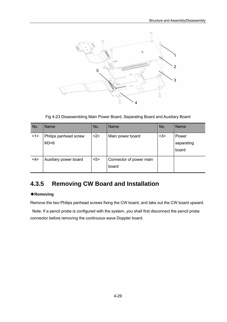
Structure and Assembly/Disassembly
4-29
Fig 4-23 Disassembling Main Power Board, Separating Board and Auxiliary Board
No. Name No. Name No. Name
<1> Philips panhead screw
M3×6
<2> Main power board <3> Power
separating
board
<4> Auxiliary power board <5> Connector of power main
board
4.3.5 Removing CW Board and Installation Removing
Remove the two Philips panhead screws fixing the CW board, and take out the CW board upward.
Note: If a pencil probe is configured with the system, you shall first disconnect the pencil probe
connector before removing the continuous wave Doppler board.
1
2
3
4
5

Structure and Assembly/Disassembly
4-30
Fig 4-24 Removing CW Board
No: Name No. Name
<1> Philips panhead screw M2.5×8 <2> CW board
Installation 1. If pencil probe is optional configured, remove the top of pencil probe hole in the rear cover
assembly of main unit, then install the pencil probe socket (The gap of socket is up),as shown in the figure.
2. Use two M2.5X8 panhead screws to fix the CW board. (If pencil probe is optional configured, plug the pencil probe cable into the socket on the CW board and then tidy up the cable).
1
2
Pencil probe socket

Structure and Assembly/Disassembly
4-31
4.3.6 Removing CPU Fan As shown in 4.3.3, remove the top cover assembly of main unit;
As shown in figure below, pull out the CPU fan connector,
Remove the 4 screws of fan fixing bracket and 2 insulation grains on the left, and remove fan fixing
bracket and CPU fan and connection wire from the main board;
Take away the 4 CPU fan screws, and then remove the CPU fan.
Note: when install the lateral side fan, make sure the fan direction is the same as shown in the figure below.
Pencil probe cable CW Board
Two M2.5X8 screws

Structure and Assembly/Disassembly
4-32
Fig 4-25 Removing CPU Fan
No. Name No. Name
<1> Philips panhead screw
M3×6
<2> Insulation particles
<3> Fan fixing bracket <4> CPU fan and cable
<5> Philips panhead screw
M4×10
4.3.7 Removing CPU Board and Radiator Module 1. According to 4.3.3, remove the top cover of the main unit;
2. As shown in figure below, first remove the four M3×6 Philips panhead screws, and then
disconnect CPU board radiator and industrial control board assembly from the main board;
Note: there is a jumper cap on the industrial control board, if it is forgotten to install, then the system time will return to the default time each time you restart the system. So make sure to fix the jumper cap at the right position.
1
2
3
4
5

Structure and Assembly/Disassembly
4-33
Fig 4-26 Removing CPU Board and Radiator Module
No. Name No. Name
<1> Philips panhead screw
M3×6
<2> CPU board and radiator
module
3. As shown in figure below, remove the 5 M2.5×8 Philips panhead screws fixing the CPU board
radiator and industrial control board, separate the CPU board radiator and industrial control
board.
Fig 4-27 Removing CPU Board
1
2
1
2
3
Prop-up hole

Structure and Assembly/Disassembly
4-34
No. Name No. Name No. Name
<1> CPU board and
memory
<2> Shielding cover
of CPU board
<3> Philips panhead screw
M2.5×8
4.3.7.1 Removing Memory Stick Move the buckles of the memory stick outside, the memory stick will automatically pop up, then take
out the memory stick.
Fig 4-28 Removing the Memory Stick
4.3.8 Removing the System Fan As shown in 4.3.3, remove the top cover assembly of main unit.
As shown in figure below, pull out connectors between the system fan, main board, and CPU fan;
Pull out the fan from the main unit bottom cover in the vertical direction.
Buckle

Structure and Assembly/Disassembly
4-35
Fig 4-29 Removing CPU Fan
No. Name No. Name No. Name
<1> Bottom cover of
main unit
<2> Fan (3 as a group) <3> Fan
Note: When you reinstall the fans, note that the three system fans shall blow wind outside (the brand shall face to the outside); the single fan shall blow wind outside (the brand shall face to the inside),then verify that all fans can rotate normally.
4.3.9 Remove the Speakers As shown in 4.3.3, remove the top cover assembly of main unit;
As shown in figure below, pull out the connector of the speaker;
Remove the four (2×2) M2.5×8 screws, and remove the speakers.
1
2
3

Structure and Assembly/Disassembly
4-36
Fig 4-30 Removing the Speakers
No. Name No. Name
<1> Speaker <2> Philips panhead screw
M2.5×8
4.3.10 Removing Transmission Board As shown in 4.3.3, remove the top cover assembly of main unit;
As shown in figure below, remove the nine M2.5×8 Philips panhead screws;
Remove the top shield cover of the main board;
Remove the 4 screws fixing the transmission board, and disconnect the transmission board with
two hands. Note that the transmission board and main board are connected by four connectors, so
use force evenly.
1
2
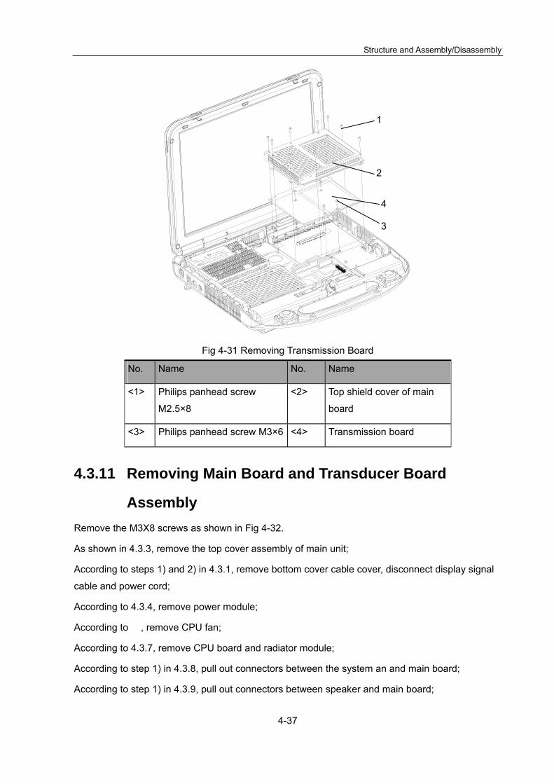
Structure and Assembly/Disassembly
4-37
Fig 4-31 Removing Transmission Board
No. Name No. Name
<1> Philips panhead screw
M2.5×8
<2> Top shield cover of main
board
<3> Philips panhead screw M3×6 <4> Transmission board
4.3.11 Removing Main Board and Transducer Board
Assembly Remove the M3X8 screws as shown in Fig 4-32.
As shown in 4.3.3, remove the top cover assembly of main unit;
According to steps 1) and 2) in 4.3.1, remove bottom cover cable cover, disconnect display signal
cable and power cord;
According to 4.3.4, remove power module;
According to , remove CPU fan;
According to 4.3.7, remove CPU board and radiator module;
According to step 1) in 4.3.8, pull out connectors between the system an and main board;
According to step 1) in 4.3.9, pull out connectors between speaker and main board;
1
2
3
4

Structure and Assembly/Disassembly
4-38
As shown in Fig 4-33, remove the four M3×6 screws, and tilt the main board assembly up for about 30 degrees; Pull the main board and transducer board assembly out slightly to remove them.
Fig 4-32 Removing the M3X8 Screw
No. Name No. Name
<1> M3×8 screw
Fig 4-33 Remove the Main board and Transducer Board
No. Name No. Name
<1> Philips panhead screw M3×6
1

Structure and Assembly/Disassembly
4-39
4.3.12 Remove the Transducer Board 1. According to 4.3.11, remove the main board and transducer board;
2. As shown in figure below, remove the 9 screws fixing transmission board shield cover; then
remove main board top shield cover and main board bottom shield cover.
Fig 4-34 Remove the Transducer Board (1)
No. Name No. Name
<1> Philips panhead screw M2.5×8 <2> Top shield cover of main
board
<3> Bottom shield cover of main board
3. As shown in Fig 4-35 Remove the Transducer Board (2), pull out the transducer board from the
main board with two hands, use force evenly to prevent damaging the connector pins.
Fig 4-35 Remove the Transducer Board (2)
1
2
3
1
2

Structure and Assembly/Disassembly
4-40
No. Name No. Name
<1> Transducer board assembly <2> The connector between
main board and transducer
4.3.13 Removing 4D Board and Installation Removing:
1. According to 4.3.11, remove the main board and transducer board;
2. As shown in figure below, remove the 3 M2.5×8 screws, and then take out the 4D driving board.
Fig 4-36 Removing 4D Board
No. Name No. Name
<1> Main board assembly <2> Philips panhead screw
M2.5×8
<3> 4D Driving Board
Installation:
1、 Affix the 4D heat outlet washer in the bottom board of the main unit cover as shown in figure 4-37.
2、 Plug the 4D board PCBA to the main board, fix the board with 3 M2.5X8 cross panhead screws, as shown in figure 4-38.
3、 Install the cable: A. Plug one end of the 4D signal line to the 4D board PCBA socket, and affix the cables
tightly with fiber tape, as shown in figure 4-39.
1
2
3

Structure and Assembly/Disassembly
4-41
B. Plug the other end of the 4D signal line to the probe board socket across the hole in the main board, and fix the cable using fiber cape and cable tie, as shown in figure 4-40. 4、 Install the mother board and probe board assembly into the main unit cover. Figure 4-38
Figure 4-39
Figure 4-40
28~30mm to bottom
Next to stud hole
<1>
<4>
<3>
Board (left)
<2>
Fiber tape

Structure and Assembly/Disassembly
4-42
Figure 4-41
Serial No.
Name No. Serial No.
Name No.
<1> 4D heat outlet washer 045-000164-00
1 <2> 4D signal line
009-000188-00 1
<3> 4D board PCBA 051-000102-01 1
<4> Philips panhead screw M2.5×8 M04-051121---
3
Caution: Use screw driver to manually screw the M2.5 screw tightly and appropriately, be careful not to damage the board.
Note: 1. Discard the films at the both sides of the 4D heat outlet washer. 2. Press and hold the left board as in figure 2 when screwing the 4D board PCBA screws. 3. Use adhesive tape to affix the 4D signal line, or other insulting tapes.
4.3.14 Removing Hard Disk
NOTE please pay attention to the following matters during disassembling/assembling, otherwise the hard disk will be damaged:
Hold the side of the hard disk, and please do not touch the board of the hard disk. Fasten the screws with the handy screw driver, and do not with the electric screw driver. The torsion value of the screw lock is: M3: 4 to 6 kgf.cm M4: 6 to 8 kgf.cm
1. According to 4.3.11, remove the main board and transducer board;
2. Shown as figure below, remove the M3×6 screws, horizontally pull out the HDD and HDD fixing
part, then remove the four M3×4 screws.

Structure and Assembly/Disassembly
4-43
Fig 4-42 Removing the HDD
No. Name No. Name
<1> Main board assembly <2> Philips panhead screw
M3×4
<3> Philips panhead screw M3×6 <4> HDD fixing part,
<5> Hard disk
4.3.15 Removing Transducer Extend Module PEM-21 1. Remove four M3×6 Philips panhead screws, and then remove the fixing board of the transducer
extend module.
2. Remove four M3×6 Philips panhead screws, then remove the bottom cover of the transducer
extend module.
3 1
2
4
5

Structure and Assembly/Disassembly
4-44
Fig 4-43 Remove the Transducer Extend Module (1)
3. Remove three M3×6 Philips panhead screws.
4. Pull out B transducer extend board vertically upward, and separate it from socket on the A
transducer extend board.
5. Disconnect the connective board on the transducer extend module socket of the B transducer
extend board, and remove B transducer extend board.
6. Hold the transducer wire sheath and pull it out vertically, and remove the extend module socket.
Fig 4-44 Remove the Transducer Extend Module (2)
2
1
3
4
1
2
3
4
5

Structure and Assembly/Disassembly
4-45
7. Remove two M2×4 Philips sunk screws, and pull out the transducer lever.
Fig 4-45 Remove the Transducer Extend Module (3)
No. Name No. Name
<1> Transducer lever <2> Philips sunk screws M2×4
8. Remove the 8 M3×6Philips panhead screws, and carefully pull out the A transducer extend
board.
Fig 4-46 Remove the Transducer Extend Module (4)
1
2
1
2

Structure and Assembly/Disassembly
4-46
No. Name No. Name
<1> Philips sunk screws M3×6 <2> A transducer extend board
9. As shown in step 7), remove the transducer lever.
10. Remove the 8 M3×6 Philips panhead screws, remove the female base of transducer socket.
Fig 4-47 Remove the Transducer Extend Module (5)
No. Name No. Name
<1> Philips panhead screw M3×6 <2> Transducer bracket
Note: Transducer extend module can be used with the UMT-300 mobile trolley, for
disassembling UMT-300, please refer to the corresponding service manual.
4.3.16 Removing ECG Module 1. Use tweezers to take out the four connector enclosure screw caps (take care not to scratch the
enclosure), remove the four M3X8 screws, and remove ECG module top cover.
1
2

Structure and Assembly/Disassembly
4-47
Fig 4-48 Remove the ECG Module (1)
No. Name No. Name
<1> Screw cap <2> Screw M3X8
<3> Top cover of ECG module
2. Remove the two M3X8 screws, disconnect connector of the ECG module internal signal cable,
and then remove the ECG board.
Fig 4-49 Remove the ECG Module (2)
No. Name No. Name
<1> Screw M3X8 <2> Socket
<3> ECG board PCBA <4> ECG serial cable
2
4
1
3
1
2
3

Structure and Assembly/Disassembly
4-48
3. Remove the four M2X8 Philips panhead tapping screws and flat washers. Cut off the two wire
strips on the magnetic ring, and remove the internal signal cable of ECG module.
Fig 4-50 Remove the ECG Module (3)
No. Name No. Name
1 ECG socket fixing part 2 Screw M3X8
3 Cable tie 4 ECG internal signal cable
5 Magnetic ring fixing part 6 Philips panhead tapping screw
M2X8 and flat washer
4.3.17 Removing Video and Audio Capture Module 1. Use tweezers to take out the four connector enclosure screw caps (take care not to scratch the
enclosure), remove the four M3X8 screws, and then remove the top cover.
2. Remove the three M3X8 screws fixing the video and audio capture card, and remove video and
audio capture card.
2
3
4
5
1
6
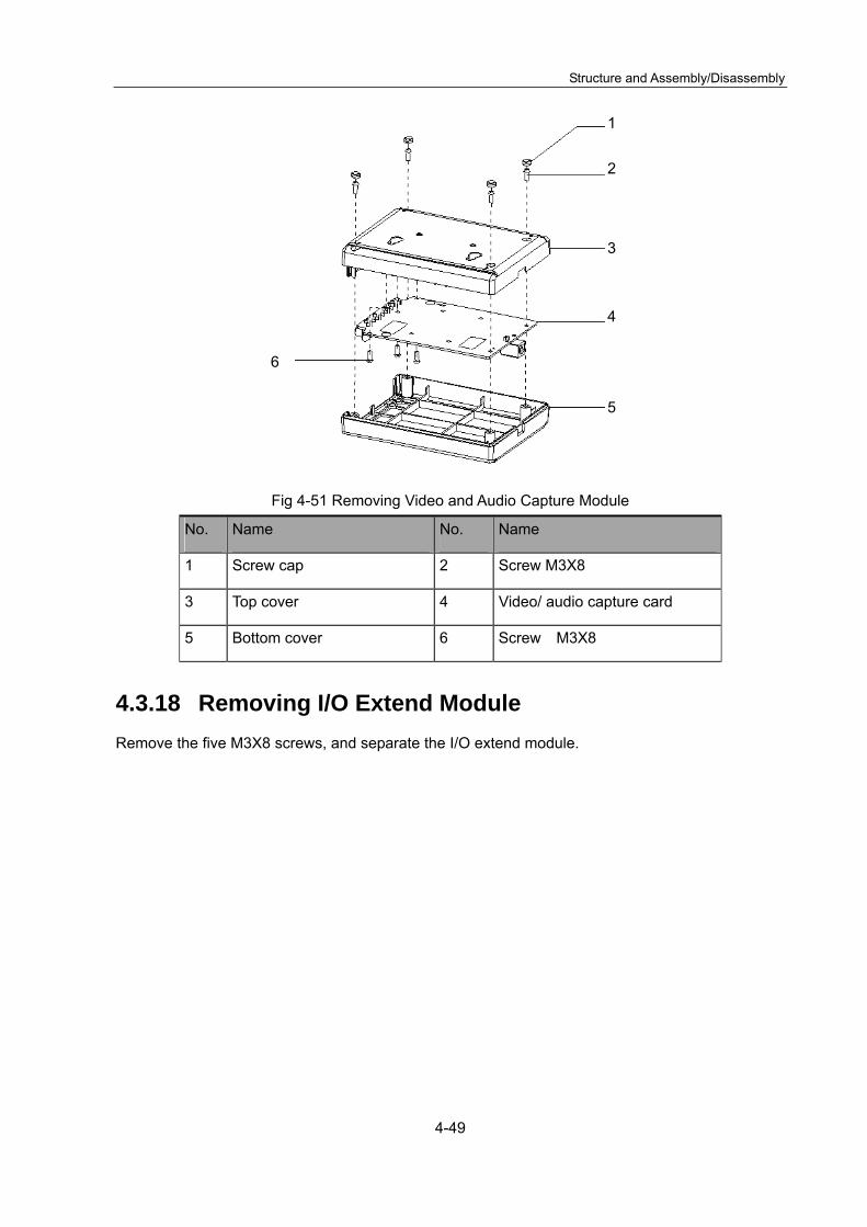
Structure and Assembly/Disassembly
4-49
Fig 4-51 Removing Video and Audio Capture Module
No. Name No. Name
1 Screw cap 2 Screw M3X8
3 Top cover 4 Video/ audio capture card
5 Bottom cover 6 Screw M3X8
4.3.18 Removing I/O Extend Module Remove the five M3X8 screws, and separate the I/O extend module.
1
2
3
4
5
6

Structure and Assembly/Disassembly
4-50
Fig 4-52 Remove the I/O Extend Module
No. Name No. Name
1 Screw M3X8 2 Back cover
3 IO extend board 4 Front cover
1
2
3
4

5-1
5 System and Software
5.1 XPE System Introduction The full name of XPE is Windows™ XP Embedded, it is the embedded system for Windows™ XP of
Microsoft® company. It is not a dedicated embedded operation system, but providing a tool for
development and deployment. XPE can be used to define and edit the standard Windows XP, and
some embedded application features and units are added to it.
For M7, after the XP operation system, the following drivers and functions are automatically
installed:
Table 5-1 Functions defined by XP operation system
Install the main board driver: chip group, video card, audio card, and network card.
Install the video printer driver: SONY UP-D23MD driver, SONY UP-D897 driver, and
MITSUBISHI P93D driver.
Install digital printer: HP Deskjet 2568, HP Office 3600, and HP 1015
USB video capturing box driver
USB Footswitch
Install CPU temperature and fan monitoring service
Hardware self-test program running environment
Keyboard filter driver
Install east Asia language: set the language and region as Chinese (PRC)
Install the desktop theme: M7.Theme, no voice.
Power on/Power off/login define
WINDOWS boot-up interface setting
No Autorun or autoplay
No screen saver
Shut down functions like the fire wall and automatic updating.

System and Software
5-2
5.2 Introduction of Doppler
5.2.1 Resume Package
run.bat: run the batch file
recover.exe: recover file
preset.txt: preset data default regulatory type control file
gina and gina.cmd: define the boot-up progress bar
demo: demo data
DC7Filelist.bak: recover data list.
Fig 5-1 Structure of the resume package
Note: Resume package should be compatible with the machine type, that human package be resumed on human machine, vet use package be resumed on vet machine.
5.2.2 Data Processing After the resume package is activated, the data structure and storage destination are listed as
follows:

System and Software
5-3
Table 5-2 Data processing
Type File
suffix Signal definition of testing points Destination
Data in
the hard
disk
APD
Compress the update files and check if there are
same directory data in the hard disk, if yes, then
delete the old directory data, and then create new
directory number.
C:\M7\app
EXD C:\M7\exe
GPD C:\M7\fpga
VDD C:\M7\video
GUD C:\M7\gui
IMD C:\M7\Image
PST C:\M7\Preset
FKY C:\M7\Key
PCD
Decompress the update files and check if there
are same directory data in the hard disk, if yes,
delete it and create new directory data, and then
configure the Windows desktop.
C:\M7\config,
C:\WINDOWS\boot.bmp
Demo Copy the Demo data in the resume package to
the target directory E:\M7\Demo
Drive DRD
Including DSP drive, multifunctional board drive,
USB keyboard drive, Smbus drive, decompress
the update files to the temporary directory in the
hard disk, and install the drives respectively, then
delete the temporary directories when finished the
installation.
Installed the
corresponding drives
C:\windows\system32\
FPGA FPD
Including DSP FPGA, multifunctional FPGA,
beam former FPGA, transmitting FPGA,
decompress the update files to the temporary
directory of the hard disk, and write data in their
configured flash through the corresponding drive
program. Delete the temporary directory when
finished.
The corresponding
configurations of the
logic flash
Keyboard KUG Analyze the update files and cache the keyboard
data into buffer, and then check keyboard Keyboard board
System and Software
5-4
Type File
suffix Signal definition of testing points Destination
communication, and E/W keyboard flash.
ECG ECG
Analyze the update files and save the ECG data
into buffer, and then check ECG module
communication, and E/WECG flash.
ECG module
Power
monitor ARM
Analyze the update files and decompress the
ARM data into the temporary directory of the hard
disk, check the ARM communication and E/W,
delete the temporary directories when finished.
Power monitor module
5.3 Run the Resume Package in Doppler NOTE: 1. Before executing the resume package, please back up the patient data as well as the
user-defined preset data.
2. If the resume is performed with a disk in Doppler, then the disk inserted can’t be recognized when the ultrasound machine is running, in this case, please shut down the system first, then insert the disk, and then restart the system. The disk can be recognized, and resume can be performed.
Operation procedures: 1. Copy the resume package to the USB disk; 2. After system boot-up, login as service engineer; 3. Press <Setup> to open the Setup menu, select [Maintenance] to open the Maintenance menu. 4. Select [Enter Windows], and you can see all the drive letters; 5. Found the run.bat file in the USB disk, and double click it. The following information appears:
SUCCESS: The process "appmon.exe" with PID XXXX has been terminated. SUCCESS: The process "doppler.exe" with PID XXXX has been terminated Press any key to continue… Press any key to continue, and the recovery operation will be processed automatically.
6. During the recovery, the system prompts “Do you want to delete user preset data? (Y/N)”, input “Y” (note: you must select “Y”, because it is possible that the preset data may not be compatible, the new preset data have to be used.)
7. After the recovery is completed, the system prompts “Press any key to continue…”, inspect if all the items have been finished successfully, and press <Enter> according to the prompt, the DOS window will be closed automatically.
8. Now, delete the PATIENTDATA file in the path D:/M7/PATIENTDATA (as the patient data have been backed up already);
9. Shut down the system and then reboot the system; 10. Check the version, which should be consistent with that of the newly updated.
NOTE: After the system is restored, please check if the system model and regulation type are correct (the same as before restoration)

System and Software
5-5
5.4 Power ON Process The power ON process will last for 20 seconds, refer to the table below for the details.
Table 5-3 Power ON process
Step Operation Increments Step
The possible
causes when
initialization
dead
No prompt
Initialize Windows; Appmon initialize Doppler; Bind the path
of the configuration files; Set Windows properties; Initialize
the display devices, the main window, sound, USB devices
agency; Activate bus devices BackboneDev and LPC;
Initialize time and multi-lingual process functions; Initialize
peripheral file system, network, drive, enumerate peripheral
device port; Configure the timers, initialize the soft
interruption, construct maintenance server, configure
system static data; Configure system fonts; Load layout
information; Initialize UI manager and UI graph libraries.
In increments of 7.
Configure
the
hardware
and XPE
system
Pull out the
CD/DVD
drive if any
Initializing
hardware…
Load-on the boot-strap bitmap, display the progress bar (7),
decompress the configured factory data
Boot-strap
bitmap /
Loading
system
preset…
Create local preset and system preset server In increments of 1.
Configure
preset data
May be the
preset data is
not
compatible,
delete the
preset data
Loading
common
exam
preset…
Create exam mode general data manager In increments of 1.
Loading
exam
preset...
Create measure preset, peripheral devices and network,
image KMP package, network storage preset servers. In increments of 4.
Initializing
local…
Set the region related information, the language, font
library, entry method; Create control “factory”; Construct
GUI layer; Set the menus; Initialize function libraries; Create
UICenter
In increments of 1.
Configure
HDD data /
Initializing
gui…
Construct the application layer; Initialize keyboard board;
Construct the access management, remote desktop
management
In increments of 1.
Pay
attention to
the
keyboard
/

System and Software
5-6
Step Operation Increments Step
The possible
causes when
initialization
dead
Initializing
ultrasound
peripheral…
Configure the file dialog box; Initialize print library; Battery
monitor, 2118 system monitor; Load-on print task icon;
Construct low consumption; Construct USB manager and
record manager; Initialize video replay devices
In increments of 1.
Configure
peripheral
device, pay
attention to
the battery
Occasional
system crash
was found,
not resolved
yet.
Initializing
ultrasound
image…
Create ECG debt collection thread; Set virtual machine,
initialize the virtual machine; Create front-end/back-end
object tree (ultrasys, etc.)
In increments of 2. Pod data
Occasional
system
crash, not
resolved yet
Initializing
ultrasound
application…
Add measure menu functional package; Register measure
patient application interface In increments of 1.
Patient Info
/
Initialization
completed… Construct patient info manager (UPatientApp) In increments of 1. /
Hide the
boot-strap
bitmap
/ / /
Including
operation on
the LCD,
may lead to
system crash
5.5 Software Maintenance Before performing the software maintenance, ensure the data used matches with the model.
5.5.1 Entering Preset Press <Setup> key, pops up the preset menu.

System and Software
5-7
5.5.2 Viewing System Information In the Setup menu, select [About], and the system information dialog box appears.
Be sure to confirm the system information before and after the software maintenance.
5.5.3 Manage Settings 1. Press <Setup> key to enter into the preset status.
2. Move the cursor onto [Manage Settings] and press [Set].

System and Software
5-8
3. Select Export (Import or Restore factory) as required.
Tips:
Code in Figure Function Description
A Export the selected presets, and save them in different files
B Import the preset parameters, or recover the factory settings
C Export all preset parameters, and save them in a file
C D E

System and Software
5-9
Code in Figure Function Description
D Import all preset data at one time
E Recover factory settings for all preset data
5.5.4 Maintenance Status Copy the files to be used into a USB flash drive. Then insert the USB flash drive into the USB port
on the main unit.
1. Enter the Preset menu.
2. Select “Maintenance”.
Note: to enter the Maintenance menu, please login the system with the user name of Service.
3. Select “Maintenance”

System and Software
5-10
5.5.5 Model Setup 1. Enter into maintenance status. Select “Config”, and press <Set>.Enter into the Config menu:
2. Select the correct files, and click [OK]. After the operation is completed, the successful prompt
appears. Restart the system according to the prompt.
Note: the default configuration is that of M7, and it is already finished during the resume package configuration. For M7T, the product information has to be configured according to the configuration files.
5.5.6 Installing Optional Software 1. Enter the Setup menu.
2. Click [System] on the Setup menu to open the System Preset screen.
3. In the System Preset dialog box, select [Option] to open the dialogue box shown in the figure
below.
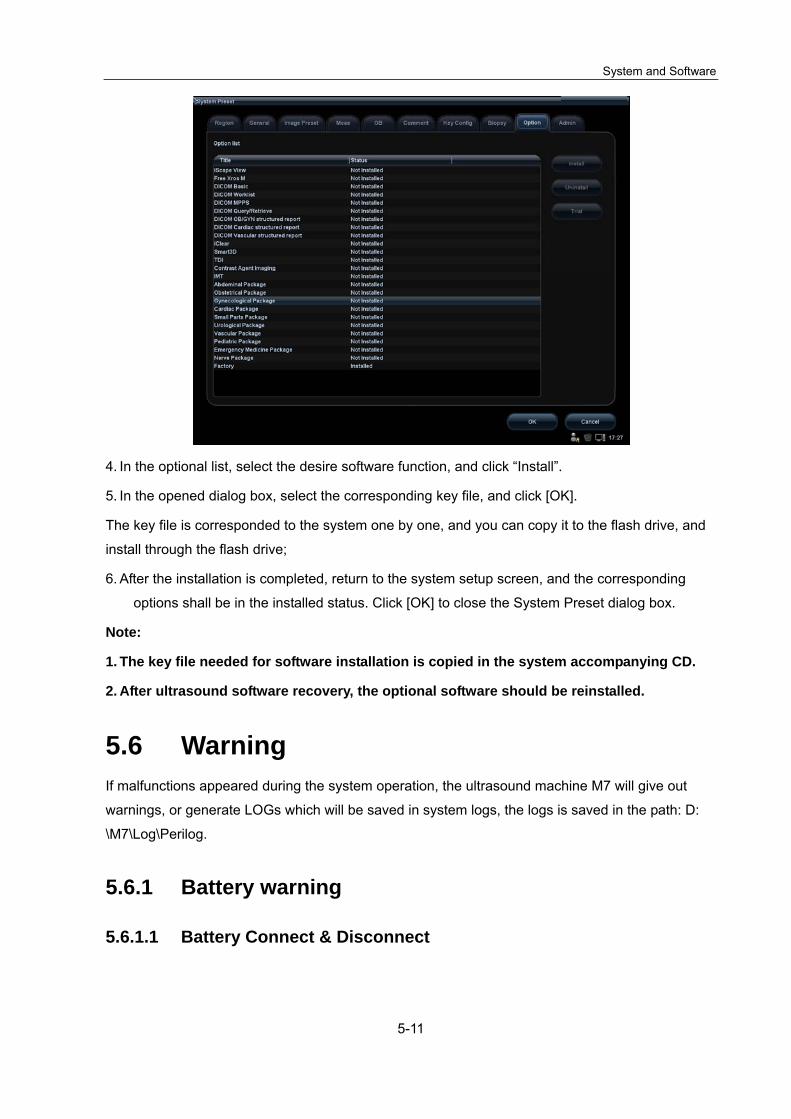
System and Software
5-11
4. In the optional list, select the desire software function, and click “Install”.
5. In the opened dialog box, select the corresponding key file, and click [OK].
The key file is corresponded to the system one by one, and you can copy it to the flash drive, and
install through the flash drive;
6. After the installation is completed, return to the system setup screen, and the corresponding
options shall be in the installed status. Click [OK] to close the System Preset dialog box.
Note:
1. The key file needed for software installation is copied in the system accompanying CD.
2. After ultrasound software recovery, the optional software should be reinstalled.
5.6 Warning If malfunctions appeared during the system operation, the ultrasound machine M7 will give out
warnings, or generate LOGs which will be saved in system logs, the logs is saved in the path: D:
\M7\Log\Perilog.
5.6.1 Battery warning
5.6.1.1 Battery Connect & Disconnect

System and Software
5-12
Operation Warning LOG
Left battery hot
plug
“Warning! Invalid battery
operation!May lead to
battery damage”
“2009-9-7,2:43:11 U2118Monitor: Left Battery
Hot Plug”
Right battery hot
plug
“Warning! Invalid battery
operation! May lead to
battery damage”
“2009-9-7,2:43:11 U2118Monitor: Right Battery
Hot Plug”
Left battery hot
insert
None “2009-9-7,2:43:11 U2118Monitor: Left Battery
Hot Insert”
Right battery hot
insert
None “2009-9-7,2:43:11 U2118Monitor: Right Battery
Hot Insert”
Left Battery Hot
Plug, Shutdown
State
None “2009-9-11,2:43:11 U2118Monitor: Left Battery
Hot Plug, Shutdown State”
Right Battery Hot
Plug, Shutdown
State
None “2009-9-11,2:43:11 U2118Monitor: Right Battery
Hot Plug, Shutdown State”
5.6.1.2 Battery I2C Exception
Operation Warning LOG
Adapter power
supply, light
battery I2C
exception
Left battery communication I2C
error, battery capacity can’t
correctly displayed, or current
battery can’t be used
“2009-9-7,2:55:11 U2118Monitor: Left
Battery Communication I2C error”
Adapter power
supply, right
battery I2C
exception
Right battery communication I2C
error, battery capacity can’t
correctly displayed, or current
battery can’t be used
“2009-9-7,2:55:18 U2118Monitor: Right
Battery Communication I2C error”
Battery power
supply, left battery
I2C exception<
Left battery communication I2C
error, please insert the adapter
or power off the system,
otherwise, the system will be
shut down after XX seconds!
“2009-9-7,3:11:13 U2118Monitor: Left
Battery Communication I2C error”

System and Software
5-13
5.6.1.3 Battery Cycle Count beyond the Limitation
Operation Warning Log
Left battery cycle count is
beyond the limitation
Battery life will do,
replace it as soon as
possible.
“Left Battery Cycle count is: 65535,Right
Battery Cycle count is: 16”
Beyond the number of
the right battery
recycling times
Battery life will do,
replace it as soon as
possible.
“Left Battery Cycle count is: 16,Right
Battery Cycle count is: 65535”
5.6.1.4 Battery Volt Exception
Operation Warning Log
Left battery Volt
Exception
Left battery voltage is low,
please insert the adapter or
power off the system,
otherwise, the system will be
shut down after XX seconds!
“2009-9-7,3:11:19 U2118Monitor: Left
Battery voltage is low: left battery volt is:
12.16V”
Right battery Volt
Exception
Right battery voltage is low,
please insert the adapter or
power off the system,
otherwise, the system will be
shut down after XX seconds!
“2009-9-7,3:11:19 U2118Monitor: Right
Battery voltage is low, Right battery volt is:
12.15V”
Battery power
supply, Right
battery I2C
exception<
Right battery communication I2C
error, please insert the adapter
or power off the system,
otherwise, the system will be
shut down after XX seconds!
“2009-9-7,3:11:19 U2118Monitor: Right
Battery Communication I2C error”
Left Battery I2C
Exception,
Shutdown State
None “2009-9-11,3:11:19 U2118Monitor: Left
Battery I2C Exception, Shutdown State”
Right battery I2C
exception,
Shutdown state
None “2009-9-11,3:11:19 U2118Monitor: Right
Battery I2C Exception, Shutdown State”

System and Software
5-14
Left battery volt
exception, shutdown
state
None “2009-9-9,3:11:19 U2118Monitor: Left
Battery Volt Exception, Shutdown State”
Right battery volt
exception, shutdown
state
None “2009-9-9,3:11:19 U2118Monitor: Right
Battery Volt Exception, Shutdown State”
5.6.1.5 Battery Current Exception
Operation Warning Log
Battery current
exception
The current difference of the
two batteries is out of range,
please insert the adapter or
power off the system,
otherwise, the system will
be shut down after XX
seconds!
“2009-9-7,3:45:19 U2118Monitor: The
difference in battery discharge current is out of
range, Left battery current is: -2.604A, Right
battery current is: -2.663A”
Right battery
current exception,
shutdown state
None “2009-9-9,3:45:19 U2118Monitor: Left Battery
Current Exception, Shutdown State”
“2009-9-9,3:45:19 U2118Monitor: Right Battery
Current Exception, Shutdown State”
5.6.1.6 Battery Temperature Exception
Operation Warning Log
Left Battery temperature
is out of range
Left Battery temperature is out
of range, please insert the
adapter or power off the
system; otherwise, the system
will be shut down after XX
seconds!
“2009-9-7,3:49:19 U2118Monitor: Left
Battery temperature is out of range,
left battery temperature is: 36.0
centigrade”
Right battery temperature
is out of range
Right battery temperature is
out of range, please insert the
adapter or power off the
system; otherwise, the system
will be shut down after XX
“2009-9-7,3:49:19 U2118Monitor:
Right Battery temperature is out of
range, right battery temperature is:
31.5 centigrade”

System and Software
5-15
seconds!
Left battery temperature
is out of range, shutdown
state
None “2009-9-9,3:49:19 U2118Monitor: Left
Battery Temperature Exception,
Shutdown State”
Right battery temperature
is out of range, shutdown
state
None “2009-9-9,3:49:19 U2118Monitor:
Right Battery Temperature Exception,
Shutdown State”
5.6.1.7 Battery Break
Operation Warning Log
Left battery break Battery exception! Battery
charge/discharge can’t be proceeded!
“2009-9-7,3:49:19
U2118Monitor:Left Battery Break”
Right battery break Battery exception! Battery
charge/discharge can’t be proceeded!
“2009-9-7,3:49:19
U2118Monitor:Right Battery Break”
5.6.1.8 Low Battery Power
Operation Warning Log
Wait until the battery
power is lower than
6%
Battery power is low, please insert
the adapter or shutdown the
system, otherwise, the system will
be shut down after XX seconds!
“2009-9-7,3:49:19 U2118Monitor:Low
battery power, Left battery power
is:5%,Right battery power is: 7%”
5.6.2 PHV Exception Warning Verification
5.6.2.1 95V High Volt Exception
Exception Warning Log
+95V error None “2009-9-8,2:43:11 UBatMonitor::95VPower supply voltage
error:%.2fV,normal region is 90V to 100V
-95V error None “2009-9-8,2:43:55 UBatMonitor::-95VPower supply voltage
error:%.2fV,normal region is 90V to 100V”

System and Software
5-16
5.6.2.2 Other PHV Warning
Exception Warning Log
PHV1+ Warning! Transmitting high volt
error, image can’t be displayed in
the right way.
“2009-9-8,2:43:11
UBatMonitor::PHV1+Power supply voltage
error: 62.93V(upper limit is %.2fV)”
PHV1- Warning! Transmitting high volt
error, image can’t be displayed in
the right way.
“2009-9-8,2:43:55 UBatMonitor::PHV1-Power
supply voltage error:62.66V(upper limit
is %.2fV)”
PHV2+ Warning! Transmitting high volt
error, image can’t be displayed in
the right way.
“2009-9-8,2:43:55
UBatMonitor::PHV2+Power supply voltage
error:5.08V(upper limit is %.2fV)”
PHV2- Warning! Transmitting high volt
error, image can’t be displayed in
the right way.
“2009-9-8,2:43:55 UBatMonitor::PHV2-Power
supply voltage error:5.06V(upper limit
is %.2fV”
5.6.3 Fan Warning
Stop working Warning Log
Left front fan Left front fan has gone off! Please
contact the service engineer
ADT7462: Left Front Fan has gone off!
Left middle
fan
Left middle fan has gone off! Please
contact the service engineer
ADT7462: Left Middle Fan has gone off!
Left back fan Left back fan has gone off! Please
contact the service engineer
ADT7462: Left Back Fan has gone off!
Right fan Right fan has gone off! Please
contact the service engineer
ADT7462: Right Fan has gone off!
CPU fan CPU fan has gone off! Please
contact the service engineer
ADT7462: CPU Fan has gone off!
The position of the fans is shown as the figure below:

System and Software
5-17
Fig 5-2 The position of the fans
5.6.4 Temperature Warning
Temp protection Warning Log
Main board Temperature
alert
None ADT7462: Main Board Temperature Alert
Power board temperature
alert
None ADT7462: Power Board Temperature Alert
CP temperature is beyond
105
Temperature warning,
XX countdown
CPU Temperature too high, ShutDown,
CPU Temperature =
5.6.5 Volt Warning
Volt Warning LOG
12V None ADT7462:12V Power supply voltage:%f, VoltLimtFloat: %f--%f
N12V None ADT7462:-12V Power supply voltage:%f, VoltLimtFloat: %f--%f
5V1 None ADT7462:5.1V Power supply voltage:%f, VoltLimtFloat: %f--%f
3V3 None ADT7462:3.3V Power supply voltage:%f, VoltLimtFloat: %f--%f
1V5 None ADT7462:1.5V Power supply voltage:%f, VoltLimtFloat: %f--%f
2V8 None ADT7462:2.8V Power supply voltage:%f, VoltLimtFloat: %f--%f
1V8 None ADT7462:1.8V Power supply voltage:%f, VoltLimtFloat: %f--%f
1V2 None ADT7462:1.2V Power supply voltage:%f, VoltLimtFloat: %f--%f

Function and Performance Checking Method
6-1
6 Function and Performance Checking Method
6.1 Note The chapter supplies the detailed method for product main function and performance checking. This is used for referring or studying by engineer but not required.
6.2 System Running Status
6.2.1 Running Status 1. Power on/off normal (duration time is normal), no abnormal sounds or phenomena occur during
normal operation. 2. After ultrasound system is turned on, the fan starts working and no abnormal sound when the
fan is working. 3. Check if configuration, software version are normal through the [About] in preset menu. 4. Check if contrast and brightness of the monitor are normal. 5. Check if time and date are valid and correct. 6. Check if all status indicators are normal. 7. Check all log records with user, to confirm if there is any abnormality.
6.2.2 Working Condition Check the ambient temperature and humidity. The measurements related to safety features are particularly sensitive to humidity. If the insulation feature of the system deteriorates due to the increase of system service time or system malfunctions, the fluctuation range of measurement results are likely to increase with the increase of humidity.

Function and Performance Checking Method
6-2
6.3 General exam
6.3.1 Check Flow
Check control panel
Check monitor
Check DVD-R/W
Check peripherals
Check I/O ports
Check ECG module
6.3.2 Checking Content
6.3.2.1 Check Control Panel
Procedure Checking standard check all buttons, keys and knobs Follow the direction: left to right, and up to down.
All keys and knobs are effective.
Function checking of the trackball: Press the <Freeze> key to enter the Freeze status. Press <Measure> to enter into measure status, do
vertical and horizontal measurement, or do other trackball operations.
The trackball can be rotated easily; the cursor responds sensitively, the rotation direction is the same as the direction of the cursor.
6.3.2.2 Check the Monitor

Function and Performance Checking Method
6-3
Procedure Standard
Adjust LCD brightness Enter [Preset]->[ Peripheral preset], On the “Input & display” page:
click [default] Click “cold/warm” Monitor maintenance
Log on as Service, click [Maintenance]->[ Main Monitor] to check the monitor functions
Press 『Fn』and 『 』, the brightness increases; and press 『Fn』and 『 』, the brightness decreases.
Brightness load factory values. Color temperature of LCD will be changed
correspondingly. Click each functional button, the LCD responds
correctly, the standard is as follows: 1. Light-spot: 0; flash point: 0. 2. The adjoining dark spots are no more than 3 pairs, and
there is no adjoining dark spot in image area. 3. There is no adjoining dark spot of 3 or more than 3. 4. The dark spots are no more than 7 and those in the
image area are no more than 2 5. The distance between bad spots is no less than 5mm.
Note: image area refers to rectangle when the background is black/right.
6.3.2.3 Check DVD-R/W Procedure Standard
Press [Eject] Use the optical disk drive to read and burning.
Disk can be normally ejected. Normal, no abnormal sounds.
6.3.2.4 Check Peripherals Procedure Standard
Footswitch: Connect the footswitch; check the functions of footswitch according to the functions listed in Key Config. (e.g. right key- image frozen, middle key- color print, left key- B/W print)
Press the freeze key (the right key), image is frozen, the freeze menu is displayed; press the key again, image is unfrozen.
Press the print key (middle key), color printing starts.
Press the print key (left key), B/W printing starts.
Video printer: Check if the video printer and ultrasound system are correctly connected. Then check the function of each key.
Press <Print> key, the printer begins to work, no image print deficiency or degradation. Switch video output port; repeat the step.
Text/graph printer: Check if the printer and ultrasound system are correctly connected. Then check the function of each key.
Press <Print> key, the printer begins to work, no print deficiency or degradation.
6.3.2.5 Check ECG Module

Function and Performance Checking Method
6-4
Procedure Standard
Confirm if the ECG module is configured, then: Set [ECG] as “On”.
ECG trace is displayed; the heart icon is displayed at the upper right corner of the screen.
The parameters [Speed], [ECG Gain] can be adjusted.
ECG signal can be reviewed correctly.
6.3.2.6 Check I/O Ports Procedure Standard
Checking the main I/O ports: Besides the video port, USB ports, the other ports required to be checked including:
S-video port; Connect external VGA/LCD monitor
Network port.
The contents displayed on the VGA/LCD are
the same as those displayed on the ultrasound system displayer, no character and image loss, no color difference, no fluttering and flicking.
Smooth communication.
6.4 Function Checking NOTE: A complete function inspection is described here, do the checking according to
the actual system configuration.

Function and Performance Checking Method
6-5
6.4.1 Checking Flow
6.4.2 Content
6.4.2.1 Imaging Modes
1. B mode In B Mode scanning, the image parameter area in the upper left corner of the screen will display
the real-time parameter values as follows:
Display F 5.0 D 17.6 G 50 FR 40 IP 4 DR 60
Parameter Frequency Depth Gain Frame Rate B IP B Dynamic Range
Parameters that can be adjusted to optimize the B Mode image are indicated in the following.
Adjustment Items
Control Panel Gain, Depth, TGC, iTouch

Function and Performance Checking Method
6-6
Adjustment Items
Menu and Soft Menu
Dynamic Range, Focus Number, FOV Position, Line Density, IP, Colorize, L/R Flip, Rotation, Persistence, Colorize Map, U/D Flip, iTouch, Frequency, Gray Map, Focus Position, iClear, FOV, Smooth, TSI, Curve, Gray Rejection, γ, High FR, iTouch Bright, A. power, B Steer, iBeam, Trapezoid, Image Merge
1. Control Panel
2. Menu Procedure Standard
Frequency B mode menu [Frequency]
Frequency value is displayed in real time in the left upper part of the screen via adjusting. The frequency scales of different probes are not the same.
Focus B mode menu
Focus number or position can be adjusted. The focus position symbol is displayed on the right side of the image.
Procedure Standard
Press <B> Enter B mode, and B image displays
Gain adjustment. Rotate <iTouch>
Rotate clockwise to increase Rotate anticlockwise to decrease
Depth Adjustment Press <Depth/> direction key.
The image depth will be changed. The adjustable depth values vary depending upon the probe types.
TGC adjustment Adjust through the 8-segment toggles
Push the toggle to the right to increase the corresponding area brightness Push the toggle to the left to decrease the corresponding area brightnessAbout 1.5s after the adjustment is finished, the TGC curve disappears.
iTouch Press <iTouch>
iTouch sign will be displayed in the image area to activate image effect auto optimization.
Image Magnification Press <zoom> to light on the Zoom indicator.
Roll the trackball to change position of the magnified image. Press <Zoom> in zoom status to exit the mode, the current window returns to the display before zoom. Configured with image menu “Magnify” to realize different Magnification.
Press <B>, and then
press Enter dual mode, and the right image is activated Press again to switch between the windows
Press <B>, and then
press
Press 4 times, and 4 images will be displayed on the screen with only one image activated at one time
Press again to switch among the windows
Press <B> To enter single mode in multiple window mode, or to exit from other modes.

Function and Performance Checking Method
6-7
[Focus Number]/[Focus Position]
Dynamic Range B mode menu-> [Dynamic Range]
to the dynamic range can be adjusted, the real time value will be displayed on the image parameter area in the upper right of the screen. As the dynamic range increases, the darker the image and the contrast, as well as the noise may increase.
Line Density B mode menu-> [Line Density]
Click [Line Density], and rotate the multifunction knob to adjust the parameter.The higher the line density, the higher the resolution, and the lower the frame rate.
iClear B mode menu-> [iClear]
Click [iClear] to adjust, off represents no iClear is turned on, and the bigger the value the stronger the effect. The bigger the value the more clearly the profile of the image.
B mode menu-> [U/D Flip]/[L/R Flip] B mode menu-> [Rotate]
B mode menu-> [U/D Flip]/[L/R Flip] When you flip or rotate an image, the “M” mark will change its position on the screen; the M mark is located in the upper left corner of the imaging area by default.
2. M mode In M mode scanning, the image parameter area in the upper left corner of the screen displays
the real-time parameter values as follows:
Display V 3 IP 6 DR 65 G 45
Parameter M Speed M IP M Dynamic Range M Gain
Parameters that can be adjusted to optimize the M mode image are indicated in the following.
Adjustment Items
Control Panel Gain, TGC, Depth
Menu and Soft Menu IP, Time Mark, Speed, Colorize, Colorize Map, Acoustic Power, Edge Enhance, Frequency, Gray Map, Focus Position, Dynamic Range, M Soften, Curve, Gray Rejection, γ, Display Format
3. Color mode In Color mode scanning, the image parameter area in the upper left corner of the screen
displays the real-time parameter values as follows:
Display F 3.3 G38 IP 1 WF 43 PRF 0.4k
Parameter Frequency Color Gain
Color IP Color Wall Filter
Pulse Repetition Frequency PRF

Function and Performance Checking Method
6-8
Parameters that can be adjusted to optimize the Color mode image are indicated in the following.
Adjustment Items
Control Panel Gain, Depth
Menu and Soft Menu B/C Wide, Frequency, Priority, Baseline, Packet Size, Dual Live, Color IP, Map, A. power, Focus Position, Scale, Flow State, WF, Invert, Line Density, Smooth, Persistence, B Display, Steer
4. Power mode In Power mode scanning, the image parameter area in the upper left corner of the screen
displays the real-time parameter values as follows:
Display F 2.5 G 38 IP 1 WF32 PRF 0.3k
Parameter Frequency Power Gain
Power IP
Power Wall Filter
Pulse Repetition Frequency PRF
Parameters that can be adjusted to optimize the Power mode image are indicated in the following.
Type Parameter
Control Panel Gain, TGC, Depth
Menu and Soft Menu B/C Wide, Frequency, Priority, Dynamic Range, Packet Size, Dual Live, Power IP, Map, Acoustic Power, Focus Position, Scale, Flow State, Wall Filter, Invert, Line Density, Smooth, Persistence, B Display, Steer
5. PW/CW mode In PW/ CW mode scanning, the image parameter area in the upper left corner of the screen displays the real-time parameter values as follows:
PW Display F 2.5 G 60 PRF 3.6k WF295 SVD 8.8 SV 3.0
Parameters Frequency Gain Pulse
Repetition Frequency PRF
WF (Wall Filter)
SV Position
SV Size
CW Display F 3.3 G 30 WF407 PRF 7.3k SVD 35.0
Parameters Frequency Gain WF (Wall Filter)
Pulse Repetition Frequency PRF
SV Position

Function and Performance Checking Method
6-9
Parameters that can be adjusted to optimize the PW/ CW mode image are indicated in the following.
Adjustment Items
Control Panel Gain, TGC, Depth
Soft Menu & Menu
PW
Invert, SV, WF, Frequency, Duplex/Triplex, V Max, V Mean, Audio, Trace Area, Colorize Map, Speed, Acoustic Power, Trace Sensitivity, T/F Res, Gray Map, Dynamic Range, Scale, Baseline, Colorize, Quick Angle, Angle, Trace Smooth, Time Mark, HPRF, Curve, Gray Rejection, γ, Display Format, Auto Calculation, Auto Calculation Parameter, PW Steer
CW
WF, Invert, Colorize Map, Frequency, Speed, V Max, V Mean, Dynamic Range, Audio, Trace Area, Trace Sensitivity, Gray Map, Scale, Baseline, Colorize, Quick Angle, Angle, Acoustic Power, Trace Smooth, Time Mark, T/F Res, Curve, Gray Rejection, γ, Display Format, Auto Calculation, Auto Calculation Parameter
6.4.2.2 Basic Measurements Procedure Standard
In B image mode: Press <Measure>
The system enters general measurement mode. Perform any 1-2 measurements (e.g., length, area), the results will display at the right lower part of the image.
Press the same key again or press <Esc>.
Exits measurement.
Do the same operation in other image modes.
Application measurements are classified into different application packages, do the application measurements selectively.
6.4.2.3 Cine Review Procedure Standard
Press [Freeze] key to freeze an image, and the [Cine] key indicator lights on. The system automatically enters the manual cine status.(It has been set that when system enters into freeze mode, the default status is cine review.) Press <iStation> key, then click [Review]; or press <Review> key to open a cine file.
The system enters into cine review status The system enters into auto cine review status.
Roll the trackball Manual cine review
Click [Auto Play] on the menu or soft menu.
Auto play function is turned on, adjust the soft menu button. The greater the value is, the quicker the speed is. When the value is 0, the system exits auto play mode.
Move the cursor onto the desired start point of the cine loop, click [Set First Frame] in the menu or soft menu to set the start point.
Set the start point of cine loop.

Function and Performance Checking Method
6-10
Move the cursor onto the desired end point of the cine loop, click [Set Last Frame] in the menu or soft menu to set the start point.
Set the end point of cine loop.
Click [Auto Play] again Review region is confined to the set start point and end point.
Then press the [Cine] key again. Cine review stops.
Press the <Freeze> key to unfreeze the image. Press <Cine> or <Esc> key.
Freeze indicator light is off; the system will return to image scanning and exit cine review. The images are still frozen but the system exits cine review.
6.4.2.4 Probe Switching
Procedure Standard
Press <Freeze> key→ connect the probe to the system→ press <Freeze> key→ press <Probe>
key to select the probe.
Connect a convex probe to probe socket A, and then connect a linear probe to probe socket B, the operator can select probe A or probe B as the active probe.
Press <Freeze> key→ disconnect the probe→ connect another probe to the port
The system can recognize the newly connected probe in no time.
6.4.2.5 Patient Information Management Procedure Standard
Press <Save> (the function already set) during image scanning
Image will be saved to the patient database, and a thumbnail will be displayed at the right part of the screen.
Open [Setup] →[System Preset]→”General”, then check “Send/Print Image after End Exam” in the Patient Management area. Press <End Exam> during image scanning
The system automatically sends the images of the exam to the default DICOM storage server or print server.
Press <Review> key. Click [Exit] on the Review screen; or,
press <Review> again, or, press <Esc> key
The system enters into image review mode. The system exits image review mode.
Click [iVision] on the other menu; or Open iVision screen:

Function and Performance Checking Method
6-11
press user-defined iVision key. Select the contents to be demonstrated,
and select the demo mode in the iVision screen. Then select an item already added to the list and click [Start]
When the demonstration is finished, click [Exit] or press <Esc>.
Demonstration begins. Image files are played according to file names one
by one (including the image of system-relevant and PC-compatible format).
The system exits the demonstration.
Press <iStation> key to enter patient information management (iStation page)
The saved patient information (images) can be found, and the patient information can be:
Backed up/ Restored Sent (To DICOM.U disk .etc )
6.5 Performance Test
6.5.1 Test Process
6.5.2 Test Content
NOTE: The image used here is only for reference, stick to the image effect in the real situation.
Requirements: 1. Display: set the contrast and brightness at the clinical application value (or the default status)
2. Operation environment: dark room, simulating the clinical application environment.
3. Scanning techniques: contact the probe with the acoustic window of the phantom, no spacing
nor pressing.

Function and Performance Checking Method
6-12
Tips:
For the testing phantoms, please refer to Appendix B.
KS107BD is low frequency phantom and used when Probe focus frequency is less than 4MHZ; KS107BG is high frequency phantom and used when Probe focus frequency is more than 5MHZ;
6.5.2.1 Resolution transverse resolution
Test Step:
1. Cover the scan surface of the phantom with water or couple gel, gently contact the probe with
the scan surface, making the transverse resolution testing targets to be displayed around the
midline of the image.
2. Adjust the focus point focuses at the position where the transverse resolution testing targets
are displayed.
3. Adjust parameters like gain, dynamic range, TGC, making the background tissue unseen, just
displaying the target image clearly.
4. In condition that the transverse resolution testing targets are horizontally displayed, record the
minimal distance of two targets that can be clearly recognized.
5. Repeat the operation above for the transverse resolution testing targets at other depths.
As shown in figure below.
Axial resolution
Test Step:
1. Cover the scan surface of the phantom with water or couple gel, gently contact the probe with
the scan surface, making the longitudinal resolution testing targets to be displayed around the
midline of the image.
2. Adjust the focus point focuses at the position where the longitudinal resolution testing targets

Function and Performance Checking Method
6-13
are displayed.
3. Adjust parameters like gain, dynamic range, TGC, making the background tissue unseen, just
displaying the target image clearly.
4. Record the minimal distance of two longitudinal resolution testing targets that can be clearly
recognized.
5. Repeat the operation above for the longitudinal resolution testing targets at other depths.
NOTE: 1. When using the convex probe, keep the transverse resolution testing targets to be displayed near the midline.
2. When using a linear probe with steer function, do not turn on the steer function when perform the transverse resolution test.
3. Zoom in the region where the targets located if necessary.
4. The diameter of the target point at a certain depth is equal to the transverse resolution at the depth.
6.5.2.2 Maximum Depth Test Step:
1. Cover the scan surface of the phantom with water or couple gel, gently contact the probe with
the scan surface
2. Set the system display depth according to the eXPcted maximum available depth of the probe
in use.
3. Adjust the focus point to the deepest, and AP at the maximum value.
4. Set gain, contrast, TGC at a greater value, but no halation nor defocus is allowed.
5. Record the depth of the furthest target (the target can be seen clearly).
NOTE: 1. Increasing the gain will also increase the noise, and echo may be covered.

Function and Performance Checking Method
6-14
2. When using a linear probe, please completely contact the probe with the scan surface, no side clearance is allowed.
3. When using a convex or phased-array probe, make the axis targets to be displayed at the middle of the scanning image.
4. When system is not frozen, the fast field target information may be similar to that of the noise, do not use this target.
As shown in figure below.
6.5.2.3 Geometric positioning accuracy
Longitudinal geometric positioning accuracy Test Step:
1. Do adjustments as the way in testing the maximum depth.
2. Record the distance by 20mm each segment on the longitudinal targets line using the

Function and Performance Checking Method
6-15
measurement caliper;
3. Select the value with the greatest error (to 20mm), calculate the accuracy using the formula
below
NOTE: 1. The measurement caliper should be positioned at the upper edge of the target, not the middle nor the lower edge.
2. The scanning plane should be vertical to the target line, that means the scanning plane is parallel with the cross-section of the phantom
As shown in figure below.
Transverse geometric positioning accuracy Test Step:
1. Cover the scan surface of the phantom with water or couple gel, gently contact the probe with
the scan surface
2. Adjust the depth, making the transverse targets to be displayed in the image.
3. Adjust the focus point to be posited beside the transverse targets (the standard is not clear)
4. Adjust parameters like gain, TGC, making each transverse targets to be clearly displayed.
5. Record the distance by 20mm each segment on the transverse targets line by using the
measurement caliper
6. Select the value with the greatest error (to 20mm), calculate the accuracy by using the formula
below

Function and Performance Checking Method
6-16
NOTE: 1. When using a linear probe, record the transverse distance by segment.
2. When using a convex probe, all transverse targets should be displayed integrally in an image.
3. The measure caliper should be posited at the upper side or lower side of the target center.
As shown in figure below.
6.5.2.4 Blackout Area Test Step:
1. Cover the scan surface of the phantom with water or couple gel, gently contact the probe with
the scan surface
2. Adjust the depth at a lower value, and set the focus at the nearest place to the scan surface.
3. Decrease the value of parameters like AP, Gain until the background noise just can be seen.
4. Record the smallest depth of the target that can be seen clearly, that value is the blackout area
value.
NOTE: 1. When using a linear probe, please completely contact the probe with the scan surface, no side clearance is allowed.
2. For convex probe, the targets in the blackout area should be positioned on the midline of the scanning plane.
As shown in figure below.

Function and Performance Checking Method
6-17

7-1
7 System Self-diagnosis
7.1 Screen Introduction The booting screen of the self-diagnosis system is:
Fig 7-1 Interface of System Self-Diagnosis and Boot
The main interface of self-diagnosis system
There are 3 kinds of main interfaces of self-diagnosis system: manufacturing, customer service and
user, as shown in figures below:
The self-diagnosis interface of manufacturing and customer service can be divided into 4 regions.
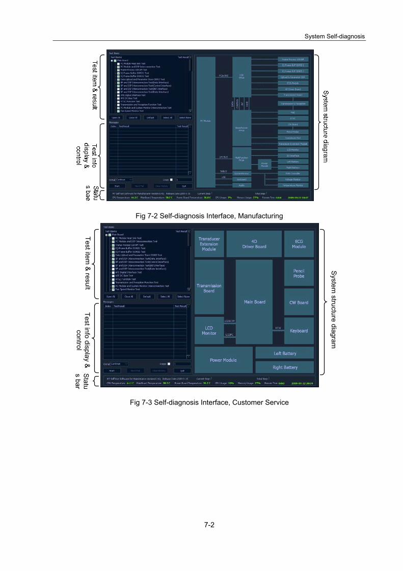
System Self-diagnosis
7-2
Fig 7-2 Self-diagnosis Interface, Manufacturing
Test item &
resultTest info display &
control
Statu
s bar
System
structure diagram
Fig 7-3 Self-diagnosis Interface, Customer Service

System Self-diagnosis
7-3
Fig 7-4 Self-diagnosis Interface, User Test Report Save Location: display the removable storage media (such as USB disk, removable
HDD), if no removable storage media is connected; or, if the system is undergoing the test, this
selection is not available.
Save Report: save the tested data to the root of the specified logic disk, if no logic disk is specified;
or, if the system is undergoing the test, this selection is not available.
Start/Stop: Start/Stop the test;
Shut Down: shut down the program, and shut down the system automatically.
Interface of tested results
Displays the test results, not available for the user.

System Self-diagnosis
7-4
Fig 7-5 Interface of testing results Test Report Save Location: display the removable storage media (such as USB disk, removable
HDD), if no removable storage media is connected; or, if the system is undergoing the test, this
selection is not available.
Save Report: save the tested data to the root of the specified logic disk, if no logic disk is specified;
or, if the system is undergoing the test, this selection is not available.
Shut Down: shut down the program, and shut down the system automatically.
7.2 Region of Self-diagnosis Items and Testing Results
Configuration of testing items
In this region, the testing items are divided into parent items according to boards and there are
several sub items for each parent item. The testing items can be customized according to
requirements. If the check box before an item is selected ( ), this item is in the testing list;
contrariwise, if the check box before the item is deselected ( ), this item is not in the testing list.
When a parent item is selected, all the sub items of this item are selected by default; contrariwise,
when deselecting a parent item, all the sub items of this item are deselected by default.

System Self-diagnosis
7-5
OutDentAll: click this button to unfold all test items if they are folded;
InDentAll: click this button to fold all test items if they are unfolded;
Default: click this button to select all the items to be tested by default;
SelectAll: click this button to select all test items;
SelectNone: click this button to deselect all test items selected.
Display of Testing Results
The testing result is displayed behind each sub item. For the sub item, if an item passes the test, it
is marked with green “PASS”; if not, it is marked with red “FAIL”; if the item is not selected, it is
marked with “Skip” of normal color. See Fig 8-11.
Fig 7-6 Test Results of Items in Testitems Table
Test Result Navigation
After the test is completed, click the test items in Testitems, the program will show the
corresponding detailed test results, which will be displayed in the first line of Message.
7.2.1 Info Display Area
Test information
The area displays test results.
Messages list: display test information of each test item.
Index is the number of test, namely the index number corresponding sub items;
TestResult is the name and detailed test information of test items, as shown in Fig 8-12.

System Self-diagnosis
7-6
Fig 7-7 Interface of Testing Results
Test Configuration
Onfail drop-down list: there are two options, “Continue” and “Stop”. If you select [Continue], the test
will continue even though a test item fails during testing; however, if you select [Stop], the test will
stop once a test item fails during testing.
Start button: click to test the selected items one by one, and the button turns to [Stop] at the same
time. During the test, click [Stop] to stop the test. After the test is completed, the [Stop] button turns
to [Start], ready for the next test.
Next Fail: after the test is completed, click [Next Fail] to show the next failed test item in the
Message list, and the related information will be displayed in the first line. If already navigated to the
last line, then the query will begin from the first line.
Clear History: click to clear all data in Testitems and Messages list, and recover the flow chart to the
initial status.
Loops check box: check this item to perform loop test. If it is checked and the loop test number is
input at the right side, the test will be performed as many as the number you set. If the number is
less than 0, the test will be cycled, until it was manually stopped or any error appeared.
Quit: for user operation, click the button to exit the self-diagnosis and shut down the system; for
manufacturer and service engineer operation, click this button to exit the test interface and then to
view the tested results.
7.2.2 Status Bar When the program is running, the version and issued date will be displayed on the left side of the
status bar: M7 SelfTest Software for Manufacture Version: xx; Release Date: YYYYMMDDXX.
During the test, the software version in the status bar will turn to the name of the item on test.

System Self-diagnosis
7-7
During the test, the test progress of current item and the total test progress are also displayed in the
status bar.
Besides, the following items are also displayed in the status bar: temperature of CPU, main board
and power module, occupation rate of CPU and memory, remaining test time and current time.
Fig 7-8 Sketch Map of Status Bar When the temperature goes beyond the working temperature, the value will be displayed in red.
The normal range is listed below:
Temperature type Lower limitation Upper limitation
CPU temperature 0 100
Main board temperature -10 78
Power board temperature -10 70
7.2.3 Test Report Save the test report
Non-loop test
For the non-loop test, the test result will be saved in D:\M7\log\Selftest\Test Report. The result of the
former test will be deleted after the new test is completed.
Loop test
For the loop test, the test result will be saved in D:\M7\log\Selftest\Test Report Loop_N. The test
result is PASS or FAIL, N refers to the test times.
Meanwhile, after each test is finished, the current test result will be automatically compressed into
Loop Test Reports.zip, and the test data will be deleted.
The test report is in the format of HTML, which can be opened by IE browser by default. The test
report is shown as below:
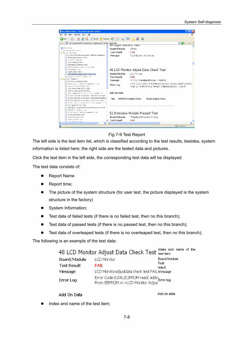
System Self-diagnosis
7-8
Fig 7-9 Test Report The left side is the test item list, which is classified according to the test results, besides, system
information is listed here; the right side are the tested data and pictures.
Click the test item in the left side, the corresponding test data will be displayed.
The test data consists of:
Report Name
Report time;
The picture of the system structure (for user test, the picture displayed is the system
structure in the factory)
System Information;
Test data of failed tests (if there is no failed test, then no this branch);
Test data of passed tests (if there is no passed test, then no this branch);
Test data of overleaped tests (if there is no overleaped test, then no this branch);
The following is an example of the test data:
Index and name of the test item;

System Self-diagnosis
7-9
Board/module;
Test result (PASS, FAIL, and Skip, each result is displayed in different color);
Message
Error log (may not exist);
Add on data (exist only when the LCD Monitor Adjust Data Check Test is failed).
Notes when open the test report:
When double click M7 Selftest Report.html using IE (Java Script is applied), it may be blocked,
which can be seen in the figure below.
Fig 7-10 Internet Explorer Prompt Right click the prompt, then click “Allow Blocked Content” (see the figure below), the report can be
opened by IE in the normal way.
Fig 7-11 Display the Blocked Content
7.3 Description of Self-diagnosis Test Items (1)PC Module Heat Sink Test
Test Content
Test if the PC module heat sink is installed in the right way.
Test Description
The following screen will be opened after the test is started. There displays the current CPU
working temperature, the yellow line represents the highest working temperature of the CPU, and
the changing wave represents the current CPU temperature. If the temperature didn’t go beyond
the limit, the waveform is displayed in green; otherwise, it is red. At the bottom of the dialogue box,
there displays the current CPU temperature and the remaining test time.
The interface can’t be closed manually after the test is started, until the test is completed. If the test
failed, please turn off the power as soon as possible.
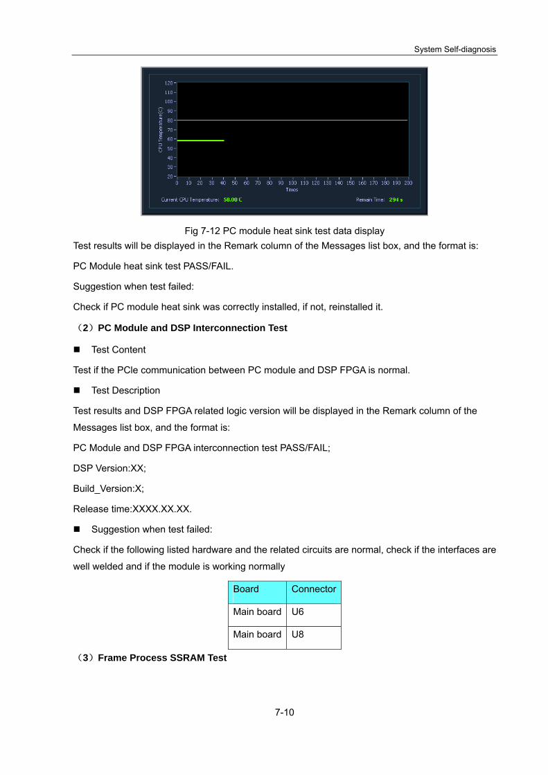
System Self-diagnosis
7-10
Fig 7-12 PC module heat sink test data display Test results will be displayed in the Remark column of the Messages list box, and the format is:
PC Module heat sink test PASS/FAIL.
Suggestion when test failed:
Check if PC module heat sink was correctly installed, if not, reinstalled it.
(2)PC Module and DSP Interconnection Test
Test Content
Test if the PCle communication between PC module and DSP FPGA is normal.
Test Description
Test results and DSP FPGA related logic version will be displayed in the Remark column of the
Messages list box, and the format is:
PC Module and DSP FPGA interconnection test PASS/FAIL;
DSP Version:XX;
Build_Version:X;
Release time:XXXX.XX.XX.
Suggestion when test failed:
Check if the following listed hardware and the related circuits are normal, check if the interfaces are
well welded and if the module is working normally
Board Connector
Main board U6
Main board U8
(3)Frame Process SSRAM Test
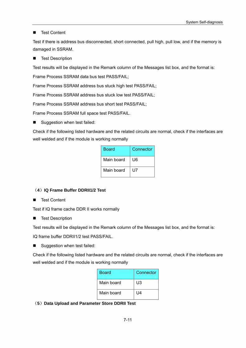
System Self-diagnosis
7-11
Test Content
Test if there is address bus disconnected, short connected, pull high, pull low, and if the memory is
damaged in SSRAM.
Test Description
Test results will be displayed in the Remark column of the Messages list box, and the format is:
Frame Process SSRAM data bus test PASS/FAIL;
Frame Process SSRAM address bus stuck high test PASS/FAIL;
Frame Process SSRAM address bus stuck low test PASS/FAIL;
Frame Process SSRAM address bus short test PASS/FAIL;
Frame Process SSRAM full space test PASS/FAIL.
Suggestion when test failed:
Check if the following listed hardware and the related circuits are normal, check if the interfaces are
well welded and if the module is working normally
Board Connector
Main board U6
Main board U7
(4)IQ Frame Buffer DDRII1/2 Test
Test Content
Test if IQ frame cache DDR II works normally
Test Description
Test results will be displayed in the Remark column of the Messages list box, and the format is:
IQ frame buffer DDRII1/2 test PASS/FAIL.
Suggestion when test failed:
Check if the following listed hardware and the related circuits are normal, check if the interfaces are
well welded and if the module is working normally
Board Connector
Main board U3
Main board U4
(5)Data Upload and Parameter Store DDRII Test

System Self-diagnosis
7-12
Test Content
Test if data uploading and parameter storage DDR II are normal.
Test Description
Test results will be displayed in the Remark column of the Messages list box, and the format is:
Data Upload and Parameter Store DDRII test PASS/FAIL.
Suggestion when test failed:
Check if the following listed hardware and the related circuits are normal, check if the interfaces are
well welded and if the module is working normally
Board Connector
Main board U5
(6)BF and DSP Interconnection Test(Data Interface)
Test Content
Test if the RF data bus between BF FPGA and DSP FPGA work normally.
Test Description
Test results will be displayed in the Remark column of the Messages list box, and the format is:
BF and DSP Interconnection Test (Data Interface) test PASS/FAIL.
Suggestion when test failed:
Check if the following listed hardware and the related circuits are normal, check if the interfaces are
well welded and if the module is working normally
Board Connector
Main board U6
Main board U10
(7)BF and DSP Interconnection Test(Control Interface)
Test Content
Test if the control bus between BF FPGA and DSP FPGA work normally.
Test Description
Test results will be displayed in the Remark column of the Messages list box, and the format is:
BF and DSP Interconnection Test (Control Interface) test PASS/FAIL;
BF logic version: 0xXX;
BF logic build version: 0xXXX;

System Self-diagnosis
7-13
BF logic release time: XXXX.XX.XX.
Suggestion when test failed:
Check if the following listed hardware and the related circuits are normal, check if the interfaces are
well welded and if the module is working normally
Board Connector
Main board U6
Main board U10
(8)BF and DSP Interconnection Test(INT Interface)
Test Content
Test if the interruption bus between BF FPGA and DSP FPGA work normally.
Test Description
Test results will be displayed in the Remark column of the Messages list box, and the format is:
BF and DSP Interconnection Test (INT Interface) test PASS/FAIL.
Suggestion when test failed:
Check if the following listed hardware and the related circuits are normal, check if the interfaces are
well welded and if the module is working normally
Board Connector
Main board U6
Main board U10
(9)BF and DSP Interconnection Test(Rate Interface)
Test Content
Test the Rate signal from BF FPGA, check if DSP FPGA and TX FPG can receive normally, and if
the Rate related connections and logics can work normally.
Test Description
Test results will be displayed in the Remark column of the Messages list box, and the format is:
BF and DSP Interconnection Test (Rate Interface) test PASS/FAIL.
Suggestion when test failed:
Check if the following listed hardware and the related circuits are normal, check if the interfaces are
well welded and if the module is working normally

System Self-diagnosis
7-14
Board Connector
Main board U6
Main board U10
(10)AFE Digital Interface Test
Test Content
Verify if the 8 analog front-end digital interfaces are normal.
Test Description
Test results will be displayed in the Remark column of the Messages list box, and the format is:
AFE ADC digital Interface test PASS/FAIL;
AFE ADC0 digital Interface test PASS/FAIL;
AFE ADC1 digital Interface test PASS/FAIL;
AFE ADC2 digital Interface test PASS/FAIL;
AFE ADC3 digital Interface test PASS/FAIL;
AFE ADC4 digital Interface test PASS/FAIL;
AFE ADC5 digital Interface test PASS/FAIL;
AFE ADC6 digital Interface test PASS/FAIL;
AFE ADC7 digital Interface test PASS/FAIL.
Suggestion when test failed:
Check if the following listed hardware and the related circuits are normal, check if the interfaces are
well welded and if the module is working normally
Board Connector Board Connector
Main board U10 Main board U47
Main board U46 Main board U48
Main board U52 Main board U51
Main board U50 Main board U49
Main board U1
(11)AFE Noise Test
Test Content
Test if the front-end noise data is in the specified range when the analog front-end is under normal
working.

System Self-diagnosis
7-15
Test Description
Test results will be displayed in the Remark column of the Messages list box, and the format is:
AFE noise test PASS. Or,
AFE noise test PASS.
Broken channel: CHX…….
Suggestion when test failed:
Check if the following listed hardware and the related circuits are normal, check if the interfaces are
well welded and if the module is working normally
Board Connector Board Connector
Main board U10 Main board U47
Main board U46 Main board U48
Main board U52 Main board U51
Main board U50 Main board U49
Main board U1
(12)ATGC Function Test
Test Content
Test if ATGC functions normally.
Test Description
Test results will be displayed in the Remark column of the Messages list box, and the format is:
ATGC function test PASS/FAIL.
Suggestion when test failed:
Check if the following listed hardware and the related circuits are normal, check if the interfaces are
well welded and if the module is working normally
Board Connector Board Connector
Main board U25 Main board U1
Main board U10 Main board U47
Main board U46 Main board U48
Main board U52 Main board U51
Main board U50 Main board U49
(13)Transmission and Reception Function Test

System Self-diagnosis
7-16
Test Content
Test if the circuits related with transmitting, receiving, high-voltage isolation and high-voltage
switching are normal.
Test Description
Test results will be displayed in the Remark column of the Messages list box, and the format is:
Transmission and Reception function test PASS ; or,
Transmission and Reception function test FAIL;
Open circuit emit receive channel: CHX……;
Short circuit emit receive channel: CHX……;
Broken high voltage switch channel: CHX…….
(14)PC Module and System Monitor Interconnection Test
Test Content
Test if SMBUS between the PC module and system monitor chip is correctly connected.
Test Description
Test results will be displayed in the Remark column of the Messages list box, and the format is:
PC module and system monitor interconnection test PASS/FAIL;
Device ID: 0xXX;
Company ID: 0xXX;
Revision Number: 0xXX.
Suggestion when test failed:
Check if the following listed hardware and the related circuits are normal, check if the interfaces are
well welded and if the module is working normally
Board Connector
Main board U90
(15)Fan Speed Monitor Test
Test Content
It tests whether the 5 fans inside the system work normally.
Test Description
Test results of fan rotational speed will be displayed in the Remark column of the Messages list box,
and the format is:

System Self-diagnosis
7-17
CPU Fan Test PASS/FAIL.
Left Fan(Near Speaker) Test PASS/FAIL.
Left Fan(Middle) Test PASS/FAIL.
Left Fan(Near PC Module) Test PASS/FAIL.
Right Fan Test PASS/FAIL.
Suggestion when test failed:
Check if the following listed hardware and the related circuits are normal, check if the interfaces are
well welded and if the module is working normally
Board Connector
Main board U90
(16)Main Board and Power Module Temperature Test
Test Content
Test if the main board and power module temperatures are normal.
Test Description
Test results will be displayed in the Remark column of the Messages list box, and the format is:
Main Board temperature test PASS/FAIL(XX.XX C);
Power Board temperature test PASS/FAIL(XX.XX C).
Suggestion when test failed:
Check if the following listed hardware and the related circuits are normal, check if the interfaces are
well welded and if the module is working normally
Board Connector
Main board U90
Main board Q1
Main power board Q17
(17)Main Board Voltage Test
Test Content
Test if main board voltage is normal.
Test Description
Test results will be displayed in the Remark column of the Messages list box, and the format is:
12V power voltage test PASS/FAIL (XX. XX V);
N12V power voltage test PASS/FAIL (XX. XX V);

System Self-diagnosis
7-18
VCC power voltage test PASS/FAIL (XX. XX V);
VDD power voltage test PASS/FAIL (XX. XX V);
1V5L power voltage test PASS/FAIL (XX. XX V);
D2V8 power voltage test PASS/FAIL (XX. XX V);
D1V8 power voltage test PASS/FAIL (XX. XX V);
VCCINT power voltage test PASS/FAIL (XX. XX V).
Suggestion when test failed:
Check if the following listed hardware and the related circuits are normal, check if the interfaces are
well welded and if the module is working normally
Board Connector
Main board U90
(18)PC Module and MF Interconnection Test
Test Content
Test if PC module and MF interconnection is normal.
Test Description
Test results will be displayed in the Remark column of the Messages list box, for the main board
with the ID as 0x33 (manufacture)/0x32 (development), the test result is:
PC Module and Multifunction FPGA interconnection test PASS/FAIL;
Multifunction FPGA DDR test PASS/FAIL;
Main Board ID: XX.XX.XX.
And for other main boards, the test result is:
PC Module and Multifunction FPGA interconnection test PASS/FAIL;
Main Board ID: XX.XX.XX.
Suggestion when test failed:
Check if the following listed hardware and the related circuits are normal, check if the interfaces are
well welded and if the module is working normally
Board Connector
Main board U75
(19)USB Interface Test
Test Content
Test if the four USB Interfaces on the machine and the I/O extend module work normally.

System Self-diagnosis
7-19
Test Description
When started the self-diagnosis, please insert the 4 USB test clamps to the 4 USB ports. If no test
clamp is connected, the system pops up the following dialog box.
Fig 7-13 Prompt for connecting USB port test clamp Test results will be displayed in the Remark column of the Messages list box, and the format is:
USB port test PASS
Or,
USB port test FAIL;
USBX…….
Suggestion when test failed:
Check if the following listed hardware and the related circuits are normal, check if the interfaces are
well welded and if the module is working normally
Board Connector
Main board J1
Main board J13
IO extend module J1
IO extend module J6
IO extend module J7
(20)Svideo Interface Test
Test Content
It tests whether the function of Svideo Out in the IO extend board is normal.
Test Description
A display with Svideo interface should be connected to the system during the test.
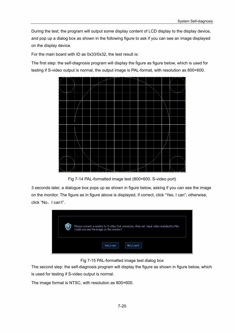
System Self-diagnosis
7-20
During the test, the program will output some display content of LCD display to the display device,
and pop up a dialog box as shown in the following figure to ask if you can see an image displayed
on the display device.
For the main board with ID as 0x33/0x32, the test result is:
The first step: the self-diagnosis program will display the figure as figure below, which is used for
testing if S-video output is normal, the output image is PAL-format, with resolution as 800×600.
Fig 7-14 PAL-formatted image test (800×600, S-video port)
3 seconds later, a dialogue box pops up as shown in figure below, asking if you can see the image
on the monitor. The figure as in figure above is displayed, if correct, click “Yes, I can”; otherwise,
click “No,I can’t”.
Fig 7-15 PAL-formatted image test dialog box The second step: the self-diagnosis program will display the figure as shown in figure below, which
is used for testing if S-video output is normal.
The image format is NTSC, with resolution as 800×600.

System Self-diagnosis
7-21
Fig 7-16 NTSC-formatted image test (800×600)
3 seconds later, a dialogue box pops up as shown in figure below, asking if you can see the image
on the monitor. The figure as in figure above is displayed, if correct, click “Yes, I can”; otherwise,
click “No,I can’t”.
Fig 7-17 NTSC-formatted image test dialog box The first step: the self-diagnosis program will display the figure as figure below, which is used for
testing if S-video output is normal, the output image is NTSC-format, with resolution as 640×480.

System Self-diagnosis
7-22
Fig 7-18 NTSC-formatted image test (640×480)
3 seconds later, a dialogue box pops up as shown in Fig 7-17, asking if you can see the image on
the monitor. The figure as in figure above is displayed, if correct, click “Yes, I can”; otherwise, click
“No,I can’t”.
The first step: the self-diagnosis program will display the figure as figure below, which is used for
testing if S-video output is normal, the output image is PAL-formatted, with resolution as 640×480.
Fig 7-19 PAL-formatted image test (640×480)
3 seconds later, a dialogue box pops up as shown in Fig 7-15, asking if you can see the image on
the monitor. The figure as in figure above is displayed, if correct, click “Yes, I can”; otherwise, click
“No,I can’t”.

System Self-diagnosis
7-23
And for main board with ID as 0x33/0x32, the test result is:
Fig 7-20 S-video Interface Test Dialog Box If you can see it, click “Yes, I can”; otherwise, click “No, I Can’t”.
Test results will be displayed in the Remark column of the Messages list box, and the format is:
S-video interface test PASS/FAIL.
Suggestion when test failed:
Check if the following listed hardware and the related circuits are normal, check if the interfaces are
well welded and if the module is working normally
Board Connector
Main board U75
Main board U86
Main board J28
(21)Video Interface Test
Test Content
It tests whether the function of Video Out in the I/O extend board is normal.
Test Description
A display with Video interface should be connected to the system during the test.
During the test, the program will output some display content of LCD display to the display device,
and pop up a dialog box as shown in the following figure to ask if you can see an image displayed
on the monitor.
For the main board with ID as 0x33/0x32, the test result is:
The first step: the self-diagnosis program will display the figure as Fig 7-14, which is used for testing
if Video output is normal, the output image is PAL-format, with resolution as 800×600.
3 seconds later, a dialogue box pops up as shown in figure below, asking if you can see the image
on the monitor. The figure as in Fig 7-14 is displayed, if correct, click “Yes, I can”; otherwise, click
“No,I can’t”.

System Self-diagnosis
7-24
Fig 7-21 PAL-formatted image test dialog box (Video)
The first step: the self-diagnosis program will display the figure as Fig 7-14, which is used for testing
if video output is normal, the output image is PAL-format, with resolution as 800×600.
3 seconds later, a dialogue box pops up as shown in figure below, asking if you can see the image
on the monitor. The figure as in Fig 7-16 is displayed, if correct, click “Yes, I can”; otherwise, click
“No,I can’t”.
Fig 7-22 NTSC-formatted image test dialog box (Video)
The third step: the self-diagnosis program will display the figure as Fig 7-18, which is used for
testing if Video output is normal, the output image is NTSC-format, with resolution as 640×480.
3 seconds later, a dialogue box pops up as shown in figure above, asking if you can see the image
on the monitor. The figure as in Fig 7-18 is displayed, if correct, click “Yes, I can”; otherwise, click
“No,I can’t”.
The first step: the self-diagnosis program will display the figure as Fig 7-19, which is used for testing
if S-video output is normal, the output image is PAL-formatted, with resolution as 640×480.
3 seconds later, a dialogue box pops up as shown in Fig 7-21, asking if you can see the image on
the monitor. The figure as in Fig 7-19 is displayed, if correct, click “Yes, I can”; otherwise, click “No,
I can’t”.
And for other main boards, the test result is:
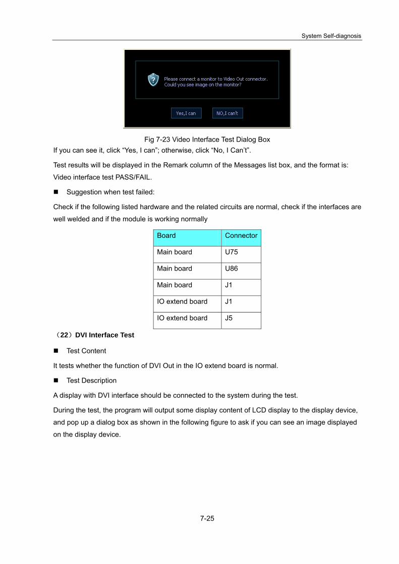
System Self-diagnosis
7-25
Fig 7-23 Video Interface Test Dialog Box If you can see it, click “Yes, I can”; otherwise, click “No, I Can’t”.
Test results will be displayed in the Remark column of the Messages list box, and the format is:
Video interface test PASS/FAIL.
Suggestion when test failed:
Check if the following listed hardware and the related circuits are normal, check if the interfaces are
well welded and if the module is working normally
Board Connector
Main board U75
Main board U86
Main board J1
IO extend board J1
IO extend board J5
(22)DVI Interface Test
Test Content
It tests whether the function of DVI Out in the IO extend board is normal.
Test Description
A display with DVI interface should be connected to the system during the test.
During the test, the program will output some display content of LCD display to the display device,
and pop up a dialog box as shown in the following figure to ask if you can see an image displayed
on the display device.

System Self-diagnosis
7-26
Fig 7-24 DVI Interface Test Dialog Box If you can see it, click “Yes, I can”; otherwise, click “No, I Can’t”.
Test results will be displayed in the Remark column of the Messages list box, and the format is:
DVI interface test PASS/FAIL.
Suggestion when test failed:
Check if the following listed hardware and the related circuits are normal, check if the interfaces are
well welded and if the module is working normally
Board Connector
Main board U75
Main board U76
Main board J1
IO extend board J1
IO extend board J10
(23)VGA Interface Test
Test Content
It tests whether the function of VGA Out in the IO extend board is normal.
Test Description
A display with VGA interface should be connected to the system during the test.
During the test, the program will output some display content of LCD display to the display device,
and pop up a dialog box as shown in the following figure to ask if you can see an image displayed
on the display device.

System Self-diagnosis
7-27
Fig 7-25 VGA Interface Test Dialog Box If you can see it, click “Yes, I can”; otherwise, click “No, I Can’t”.
Test results will be displayed in the Remark column of the Messages list box, and the format is:
VGA interface test PASS/FAIL.
Suggestion when test failed:
Check if the following listed hardware and the related circuits are normal, check if the interfaces are
well welded and if the module is working normally
Board Connector
Main board U75
Main board U80
IO extend board J1
IO extend board J1
IO extend board J10
(24)Serial Port Test
Test Content
It tests whether the function of the serial port of the IO extend board is normal.
Test Description
Short connect pin 2 and pin 3.
Test results of serial port will be displayed in the Remark column of the Messages list box, and the
format is:
Serial port test PASS/FAIL.
Suggestion when test failed:
Check if the following listed hardware and the related circuits are normal, check if the interfaces are
well welded and if the module is working normally

System Self-diagnosis
7-28
Board Connector
Main board U75
Main board U65
Main board J1
IO extend board J1
IO extend board J2
(25)Audio Test
Test Content
It tests whether the function of audio chip, power amplification circuit and speaker are normal.
Test Description
During the test, the left side of machine will play out “Ding~~”, and pops up the following dialog box
to ask if you can hear “Ding~~” playing out of the left side machine. If you didn’t hear it, please click
“Retry” to play it again, and click “No, I Can’t”, if you still can’t hear it after trying many times. And if
you heard it, please click “Yes, I Can”.
Fig 7-26 Audio Test Dialog Box The program will control the system right side buzzer to give off “ding…”, and popup the dialog box
as shown above. The tests for right and left side buzzers are the same.
Test results will be displayed in the Remark column of the Messages list box, and the format is:
Left Speaker Test PASS/FAIL;
Right Speaker Test PASS/FAIL;
Suggestion when test failed:
Check if the following listed hardware and the related circuits are normal, check if the interfaces are
well welded and if the module is working normally
Board Connector Board Connector

System Self-diagnosis
7-29
Main board U85 Main board U83
Main board J1 Main board U84
IO extend board J1 Main board J27
IO extend board J3 Speaker
IO extend board J4
(26)Transducer Interface Test
Test Content
Test if probe presenting can be recognized, and if communication is normal.
Test Description
The test flow is shown as follows, please perform the operation according to the workflow strictly.
No
Probe present Probe extend module present
Yes
Tips: disconnect the probe extend module, connect the probe
Program judge
Tips: disconnect the probe
No
Yes
Check if probe and probe extend module are present?
Start self-diagnosis
Tips: connect the probe
Program judge
Tips: disconnect the probe
Yes
Tips: disconnect the probe
Program judge
Tips: connect the probe
Yes
NoNo
Get probe info
Get probe info
Get probe info
End
Program judge
Fig 7-27 Transducer interface test flow
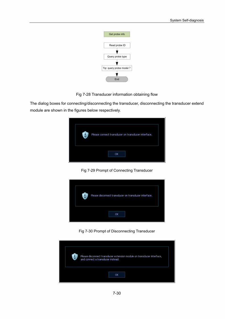
System Self-diagnosis
7-30
Read probe ID
Query probe type
Tip: query probe model?
End
Get probe info
Fig 7-28 Transducer information obtaining flow
The dialog boxes for connecting/disconnecting the transducer, disconnecting the transducer extend
module are shown in the figures below respectively.
Fig 7-29 Prompt of Connecting Transducer
Fig 7-30 Prompt of Disconnecting Transducer

System Self-diagnosis
7-31
Fig 7-31 Prompt of Disconnecting Transducer Extend Module and Connecting Transducer
Fig 7-32 Dialogue Box Asking for Transducer Model
Test results will be displayed in the Remark column of the Messages list box, and the format is:
Transducer present test PASS/FAIL;
Transducer interface SPI interconnection test PASS;
Transducer Type: XXXX. Or,
Transducer present test PASS/FAIL;
Transducer interface SPI interconnection test FAIL.
Suggestion when test failed:
Check if the following listed hardware and the related circuits are normal, check if the interfaces are
well welded and if the module is working normally
Board Connector
Main board U6
Main board U10
Main board J8
(27)Transmission Board and Main Board Interconnection Test
Test Content
Test if the interconnection between TXFPGA and DSPFPGA work normally.
Test Description
Test results will be displayed in the Remark column of the Messages list box, and the format is:
Transmission Board and Main Board interconnection test PASS/FAIL.
Suggestion when test failed:
Check if the following listed hardware and the related circuits are normal, check if the interfaces are
well welded and if the module is working normally

System Self-diagnosis
7-32
Board Connector
Main board U6
Main board J5
Main board J6
Transmitting board U3
Transmitting board J2
Transmitting board J3
(28)Transmission Board ID and Logic Version Test
Test Content
Read TX FPGA logic version, logic compilation version, and the compiled time.
Test Description
Test results will be displayed in the Remark column of the Messages list box, and the format is:
TX FPGA logic version:0xXX;
TX FPGA logic build version:0xXXX;
TX FPGA logic release time: XXXX.XX.XX.
Suggestion when test failed:
Check if the following listed hardware and the related circuits are normal, check if the interfaces are
well welded and if the module is working normally
Board Connector
Main board U6
Main board J5
Main board J6
Transmitting board U3
Transmitting board J2
Transmitting board J3
(29)MF and Power Module Interconnection Test
Test Content
Test if communication serial port between MF FPGA and power ARM works normally.

System Self-diagnosis
7-33
Test Description
Test results will be displayed in the Remark column of the Messages list box, and the format is:
Power Board ID:XX;
Power Board firmware version: X.X.
Suggestion when test failed:
Check if the following listed hardware and the related circuits are normal, check if the interfaces are
well welded and if the module is working normally
Board Connector
Main board U75
Main board U70
Main board J22
Power board J1
Power board U15
(30)Power Module Function Test
Test Content
Test if ECG module functions normally.
Test Description
Test results will be displayed in the Remark column of the Messages list box, and the format is:
+95V power voltage test PASS/FAIL (+XX.XX V);
-95V power voltage test PASS/FAIL (-XX.XX V).
CW Mode PHV control test PASS/FAIL;
PW Mode PHV control test PASS/FAIL.
Suggestion when test failed:
Check if the following listed hardware and the related circuits are normal, check if the interfaces are
well welded and if the module is working normally
Board Connector
Main board U75
Main board U70
Main board J22
Power board J1

System Self-diagnosis
7-34
Power board U15
Power board U1
Power board U11
(31)CW Board ID Test(unfinished)
(32)Demodulator and Phase Shifter SPI BUS Function Test(unfinished)
(33)CW Board AD Noise Test(unfinished)
(34)4D Driver Board ID Test
Test Content
Test if 4D drive board is presenting, and if the devices that record the IDs are normally working.
Test Description
Test results will be displayed in the Remark column of the Messages list box, and the format is:
4D Driver Board logic version: 0xXX;
4D Driver Board board ID:XX.XX.XX.
Suggestion when test failed:
Check if the following listed hardware and the related circuits are normal, check if the interfaces are
well welded and if the module is working normally
Board Connector
Main board U6
Main board J4
4D Driving Board U10
4D Driving Board P2
(35)4D Driver Board Driver Circuit Test
Test Content
Test if the driving circuit of 4D driver board works normally.
Test Description
Test results will be displayed in the Remark column of the Messages list box, and the format is:
4D Driver Board driver circuit test PASS/FAIL.
Suggestion when test failed:
Check if the following listed hardware and the related circuits are normal, check if the interfaces are
well welded and if the module is working normally

System Self-diagnosis
7-35
Board Connector
Main board U6
Main board J4
4D Driving Board P2
4D Driving Board U4
4D Driving Board U6
4D Driving Board U9
4D Driving Board U13
4D Driving Board U14
(36)4D Driver Board Programmable Voltage Test(unfinished)
(37)Left/Right Battery I2C Interconnection Test
Test Content
Checks if the I2C communication bus between the batteries and the power management ARM
works normally.
Test Description
Test results of left/right battery I2C connection will be displayed in the Remark column of the
Messages list box, and the format is:
Left/Right Battery I2C connection test PASS/FAIL.
Suggestion when test failed:
Check if the following listed hardware and the related circuits are normal, check if the interfaces are
well welded and if the module is working normally
Board Connector
Main board U75
Main board U70
Main board J22
Power board J1
Power board U15
Battery
(38)Left/Right Battery Test

System Self-diagnosis
7-36
Test Content
It tests whether the battery works normally.
Test Description
Test results of left/right battery will be displayed in the Remark column of the Messages list box, and
the format is:
Left/Right Battery is on site;
Left/Right Battery voltage is: XXXXmV.
Left/Right Battery temperature is: XX.X C.
Left/Right Battery current is: XXXXmA.
Left/Right Battery capacity is: XX%.
Left/Right Battery charge and discharge time is: XXXXX.
Left/Right Battery Safety Status test PASS/FAIL.
Left/Right Battery Permanent Failure Status test PASS/FAIL.
Suggestion when test failed:
Check if the following listed hardware and the related circuits are normal, check if the interfaces are
well welded and if the module is working normally
Board Connector
Main board U75
Main board U70
Main board J22
Power board J1
Power board U15
Battery
(39)LCD Monitor ID Test
Test Content
Read LCD displayed information.
Test Description
Test results will be displayed in the Remark column of the Messages list box, and the format is:
LCD code: 0xXXXXXXXX;
LCD serial number: 0xXXXXXXXX;
LCD version: 0xXX.
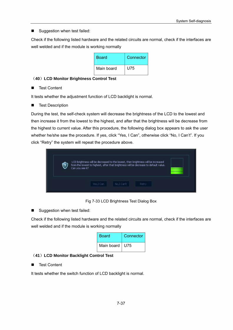
System Self-diagnosis
7-37
Suggestion when test failed:
Check if the following listed hardware and the related circuits are normal, check if the interfaces are
well welded and if the module is working normally
Board Connector
Main board U75
(40)LCD Monitor Brightness Control Test
Test Content
It tests whether the adjustment function of LCD backlight is normal.
Test Description
During the test, the self-check system will decrease the brightness of the LCD to the lowest and
then increase it from the lowest to the highest, and after that the brightness will be decrease from
the highest to current value. After this procedure, the following dialog box appears to ask the user
whether he/she saw the procedure. If yes, click “Yes, I Can”, otherwise click “No, I Can’t”. If you
click “Retry” the system will repeat the procedure above.
Fig 7-33 LCD Brightness Test Dialog Box
Suggestion when test failed:
Check if the following listed hardware and the related circuits are normal, check if the interfaces are
well welded and if the module is working normally
Board Connector
Main board U75
(41)LCD Monitor Backlight Control Test
Test Content
It tests whether the switch function of LCD backlight is normal.
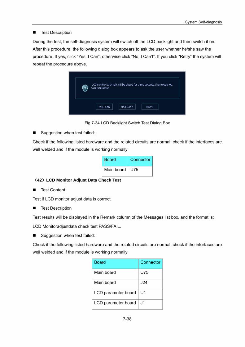
System Self-diagnosis
7-38
Test Description
During the test, the self-diagnosis system will switch off the LCD backlight and then switch it on.
After this procedure, the following dialog box appears to ask the user whether he/she saw the
procedure. If yes, click “Yes, I Can”, otherwise click “No, I Can’t”. If you click “Retry” the system will
repeat the procedure above.
Fig 7-34 LCD Backlight Switch Test Dialog Box
Suggestion when test failed:
Check if the following listed hardware and the related circuits are normal, check if the interfaces are
well welded and if the module is working normally
Board Connector
Main board U75
(42)LCD Monitor Adjust Data Check Test
Test Content
Test if LCD monitor adjust data is correct.
Test Description
Test results will be displayed in the Remark column of the Messages list box, and the format is:
LCD Monitoradjustdata check test PASS/FAIL.
Suggestion when test failed:
Check if the following listed hardware and the related circuits are normal, check if the interfaces are
well welded and if the module is working normally
Board Connector
Main board U75
Main board J24
LCD parameter board U1
LCD parameter board J1

System Self-diagnosis
7-39
(43)Keyboard USB Interconnection Test
Test Content
Test if keyboard and USB port on the main unit can communicate normally.
Test Description
Test results will be displayed in the Remark column of the Messages list box, and the format is:
Keyboard self test PASS/FAIL.
Suggestion when test failed:
Check if the following listed hardware and the related circuits are normal, check if the interfaces are
well welded and if the module is working normally
Board Connector
Keyboard board; U4
(44)Keyboard Key, Encoder, TGC, Trackball Test
Test Content
It mainly tests whether the buttons, encoders, TGCs, trackball, backlight LEDs and indicating LEDs
in the keyboard are normal, and reads board ID, keyboard FPGA and version of program.
Test Description
The keyboard testing interface is shown as follows:

System Self-diagnosis
7-40
Fig 7-35 Interface of Keyboard Test
As shown in the figure above, click [Start] to start the keyboard test. The controls in the simulation
keyboard are corresponding to those of the real keyboard assembly.
As for the buttons, press a button in the real keyboard and the corresponding button in the
simulation keyboard blinks, which means the button is being tested. Changing in color means the
button has being tested.
As for the trackball, roll the trackball in the keyboard and the cursor in the interface moves
accordingly and the in the simulation keyboard blinks, which means the system has
received data from the trackball and the trackball has being tested.
The encoder rotation test: the on the simulation keyboard corresponds to the encoder
on the real keyboard. When you rotate the encoder in a direction, the corresponding green ball
around the encoder on the simulation keyboard will rotate in the same direction. The encoder face
will flicker and turn green.

System Self-diagnosis
7-41
The encoder key test: when you press the encoder key, the encoder key on the simulation keyboard
will change status accordingly, and flicker and turn green.
TGC test: 8 TGC sliders on the keyboard correspond to controls on the
simulation keyboard. When sliding TGC sliders on the keyboard, the corresponding controls on the
simulation keyboard will move as well.
Keyboard backlight test: when the simulation keyboard initializes, all dual-color lights will highlight in
green on the keyboard. When a key is being tested, the dual-color backlight will automatically turn
orange after it is pressed.
After all tests for the keyboard assembly finished, the keyboard screen is shown in Fig 7-36 Keyboard Test Screen after the Test .
Fig 7-36 Keyboard Test Screen after the Test
After the tests, if functions of the keyboard assembly are normal, click “Keyboard is OK”; otherwise,
click “Keyboard is Bad”.

System Self-diagnosis
7-42
Test results will be displayed in the Remark column of the Messages list box, and the format is:
Keyboard Test PASS/FAIL;
Keyboard ID: XX.XX.XX;
Keyboard FPGA Version: XX.XX;
Application Version: XX.XX.
Suggestion when test failed:
Check if the following listed hardware and the related circuits are normal, check if the interfaces are
well welded and if the module is working normally
Board Connector
Key board board U4
Key board board U1
Key board board U6
Key board board U30
(45)Keyboard Key and Trackball LED Test
Test Content
It tests whether the button LEDs and trackball LED in the keyboard work normally.
Test Description
The following dialog box appears when testing. Change the brightness of the white and orange
LEDs respectively and check whether the brightness of LEDs on the keyboard change accordingly.
Change the color of the trackball LED and check whether the LED on the keyboard changes
accordingly. If the brightness of the keyboard LEDs and color of the trackball LED are the same as
configured, click “LED is OK and Quit” to quit the dialog box. If not, click “LED is not OK and Quit” to
quit the dialog box.
Fig 7-37 Interface of Keyboard LED Test

System Self-diagnosis
7-43
Test results will be displayed in the Remark column of the Messages list box, and the format is:
Keyboard Key and Trackball LED Test PASS/FAIL.
Suggestion when test failed:
Check if the following listed hardware and the related circuits are normal, check if the interfaces are
well welded and if the module is working normally
Board Connector
Key board board U4
Key board board U1
Key board board U6
(46)Extend Module Test
Test Content
Test if the transducer extend module present can be recognized.
Test Description
The test flow is shown as follows, please perform the operation according to the workflow strictly.

System Self-diagnosis
7-44
Probe extend module present?
NoYes
The number of the probes?
0 >0
Tips: disconnect probe extend module
Tips: disconnect probe and probe extend module
Program judge 1?
Probe extend modulenot present ?
Tips: connect probe extend module (no probe)
Program judge 2?
Initialize the probe
Probe extend module present?
Read probe extend module info
Probe recognize test flow
Program judge 2?
Initialize the probe
Probe extend module present
Yes
Yes
Tips: connect probe extend module (no probe)
Read probe extend module info
Probe recognize test flow
Tips: disconnect probe extend module
Program judge 2?
Probe extend module not present?
End
No
Tips: disconnect the probe
Start the self-diagnosis
Probe present?No
Yes
No
No
No
No
No
No
No
Fig 7-38 Extend Module Test Flow

System Self-diagnosis
7-45
Fig 7-39 Transducer Present Recognize Test Flow
The dialog boxes asking for disconnecting the transducer, connecting/disconnecting the transducer
extend module are shown in the figures below respectively.
Fig 7-40 Prompt of Disconnecting Transducer

System Self-diagnosis
7-46
Fig 7-41 Prompt of Connecting Transducer Extend Module
Fig 7-42 Prompt of Disconnecting Transducer Extend Module
Fig 7-43 Prompt for Disconnecting Transducer on Extend Module, and Then Disconnect Extend
Module
Fig 7-44 Prompt of Connecting General Transducer

System Self-diagnosis
7-47
Fig 7-45 Prompt of Connecting Transducer
Fig 7-46 Prompt of Asking if the User Connected XXXX Transducer on X Socket
Test results will be displayed in the Remark column of the Messages list box, and the format is:
Transducer Extend Module present test PASS;
Extend Module SPI interconnection test PASS;
Extend Module transducer recognition test PASS;
Board ID: 0xXXXX;
Logic version: 0xXXXX.
Or,
Transducer Extend Module present test FAIL;
Extend Module SPI interconnection test FAIL.
Extend Module transducer recognition test FAIL.
Suggestion when test failed:
Check if the following listed hardware and the related circuits are normal, check if the interfaces are
well welded and if the module is working normally.
Board Connector
Main board U6

System Self-diagnosis
7-48
Board Connector
Main board U10
Transducer extend module
(47)ECG Module Information Read Test
Test Content
Verify if ECG module communicates well with the main unit, read Bootloader version, board ID and
software version.
Test Description
After tested is started, if ECG is not presented, then a dialog box is opened to ask the user to
connect ECG module, see the figure below:
Fig 7-47 Ask the User to Connect ECG Module
Test results will be displayed in the Remark column of the Messages list box, and the format is:
ECG Module information read test PASS;
Bootloader version: XX.XX;
Board ID: %d.XX.XX;
Software version: XX.XX.
Or,
ECG Module information read test FAIL.
Suggestion when test failed:
Check if the following listed hardware and the related circuits are normal, check if the interfaces are
well welded and if the module is working normally.
Board Connector
Main board U6
Main board U75

System Self-diagnosis
7-49
Main board J1
IO extend module J1
IO extend module J11
ECG module
(48)ECG Module Self Test
Test Content
Test if ECG module functions normally.
Test Description
After tested is started, if ECG is not presented, then a dialog box is opened to ask the user to
connect ECG module, see the figure below:
Fig 7-48 Ask the User to Connect ECG Module
Test results will be displayed in the Remark column of the Messages list box, and the format is:
ECG Module self test PASS.
Or,
ECG Module self test FAIL;
XXX,XXX,XXX……
Suggestion when test failed:
Check if the following listed hardware and the related circuits are normal, check if the interfaces are
well welded and if the module is working normally.
Board Connector
Main board U6
Main board U75
Main board J1

System Self-diagnosis
7-50
IO extend module J1
IO extend module J11
ECG extend module
(49)Pencil Probe Present Test(unfinished)
(50)Pencil Probe ID Test(unfinished)

8-1
8 Care and Maintenance
8.1 Overview The following procedures are recommended.
8.1.1 Tools, Measurement Devices and Consumables Table 8-1 Tools and Measurement Devices
Tool/Measurement Devices Qty. Remarks
Resin or plastic container 1 pcs Can accommodate two probes
Soft brush 1 pcs About a toothbrush size
Small plastic basin 1 pcs Used to fill the soapy water
Safety test analyzer 1 pcs Refer to appendix A
Inner hexagon wrench 2 pcs Inner hexagon wrench 6
Table 8-2 Consumable List
Consumable Qty. Remarks
Aluminum foil About 1 meter
Physiological saline About 1000ml Filling a half container Immerging the whole probe (referring to appendix A). (concentration 0.85 ~ 0.95%)
Mild soapy water About 400ml
Dry soft cloth/cotton cloth About 5 pcs

Care and Maintenance
8-2
8.1.2 Care and Maintenance Items Table 8-3 Maintenance Items and Frequency
NO. Maintain content Frequency Method
1. Clean display Monthly Referring to 8.2.1
2. Clean trackball Monthly Same as the above
3. Clean control panel Monthly Same as the above
4. Clean probes (the head) Every time after using
Same as the above
5. Clean probe cable and the surface of connector
Monthly Same as the above
6. Clean holders (including probe holder and gel holder)
Monthly Same as the above
7. Clean cover Monthly Same as the above
8. Clean peripherals Monthly Referring to 8.2.2
9. Check surface of probe Daily Referring to 8.3.1
10. Check power cable and plug Monthly Same as the above
11. Check battery Annually Same as the above
12. Check function of peripherals and options
Annually Referring to 8.3.3
13. Mechanical safety inspection Annually Referring to8.3.4
14. Electrical safety inspection Annually Referring to appendix A

Care and Maintenance
8-3
8.2 Cleaning
8.2.1 Clean the System
8.2.1.1 Flow of Cleaning
Clean display
Clean trackball
Clean cover
Clean probe
Clean control panel
Power off and pull out the power cables
Figure 8-1 View of Cleaning Maintenance
WARNING: Before cleaning the system, be sure to turn off the power and disconnect the power cord from the outlet. If you clean the system while the power is “On”, it may result in electric shock.
8.2.2 Content
1. Clean Display
Tool: soft dry cloth ,clear water or mild soapy water
Method:
Surface of display should be cleaned with soft dry cloth. Remained stain should be washed out by cloth with clear water or soapy water, and then air-dry the surface.
2. Clean Trackball
Paper or dry cloth
Method:
Trackball is one of important interface parts, which are embedded into the main unit keyboard, and part of which is exploded to be operated by users in order to implement variety of module’s control

Care and Maintenance
8-4
functions. Trackball is one of the most using frequency of input assemblies on the whole operation panel, and the trackball similar to a multi-directory caster can rotate in every direction drived manually, due to the feature, gas or dust can enter into module internal easily, as a result, contamination of lens would lead to the failure of the trackball. a) Disassembling the trackball:
Turn the trackball ring about 35°counterclockwise until it lifts, now, you would remove the ring and pull out the trackball with plastic cloth if you can’t hold it by your hands directly. Disassembling the trackball is as following:
Turn trackball ring 35°to the left Disassemble the ring Remove the trackball
Figure 8-2 Disassembly of the Trackball
a) Cleaning After removing the ring and the trackball, wipe down the lens with a clean paper until you can
see nothing in the groove zoom, and then clean the other contaminant material , please pay attention to your intensity adopted on wiping dust of bead down, as shown in the following figure. Power-off is not need during cleaning, and maintenance effect can be experienced directly. After cleaning completely, you can install the trackball and the ring.
Figure 8-3 The Sketch Map of Len, Bead, Dragon groove
If liquid is accidentally sprayed on or into the system, most of which could discharge from the dragon port of trackball, but some of which would left in the trackball cover, now you may clean it with clean soft dry cloth or paper according to the above maintenance procedure.
b) Installing the trackball After the trackball maintenance, you can restore the installing following procedure: Put the
trackball back in the trackball mechanism and align the clamping ring with the top cover notches. Press the bulges on the ring with both hands and turn the ring about 35° counterclockwise until the ring clicks and locks. As the bulges are flush with the top cover, the ring is secured. See the figure below.
3 beads
Trackball
Lens zoom
Dragon groove
Ring
Installing ring
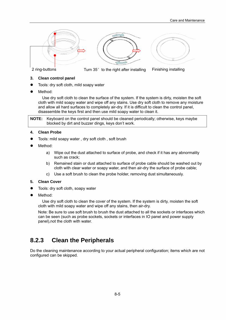
Care and Maintenance
8-5
3. Clean control panel Tools: dry soft cloth, mild soapy water
Method: Use dry soft cloth to clean the surface of the system. If the system is dirty, moisten the soft cloth with mild soapy water and wipe off any stains. Use dry soft cloth to remove any moisture and allow all hard surfaces to completely air-dry. If it is difficult to clean the control panel, disassemble the keys first and then use mild soapy water to clean it.
NOTE: Keyboard on the control panel should be cleaned periodically; otherwise, keys maybe blocked by dirt and buzzer dings, keys don’t work.
4. Clean Probe Tools: mild soapy water , dry soft cloth , soft brush
Method:
a) Wipe out the dust attached to surface of probe, and check if it has any abnormality such as crack;
b) Remained stain or dust attached to surface of probe cable should be washed out by cloth with clear water or soapy water, and then air-dry the surface of probe cable;
c) Use a soft brush to clean the probe holder, removing dust simultaneously.
5. Clean Cover Tools: dry soft cloth, soapy water
Method: Use dry soft cloth to clean the cover of the system. If the system is dirty, moisten the soft cloth with mild soapy water and wipe off any stains, then air-dry. Note: Be sure to use soft brush to brush the dust attached to all the sockets or interfaces which can be seen (such as probe sockets, sockets or interfaces in IO panel and power supply panel),not the cloth with water.
8.2.3 Clean the Peripherals Do the cleaning maintenance according to your actual peripheral configuration; items which are not configured can be skipped.
2 ring-buttons Turn 35°to the right after installing Finishing installing

Care and Maintenance
8-6
Table 8-4 Peripherals Cleaning List
No. Content Description
1. Color and B/W video printer
First wipe off dust or stain attached to the cover of printer with soft dry cloth, then clean the inside of printer. Be sure to do the cleaning maintenance according to the operation manual if is necessary.
2. Graph / text printer First wipe off dust or stain attached to the cover of printer with soft dry cloth, then clean the inside of printer. Be sure to do the cleaning maintenance according to the operation manual if is necessary.
3. Foot switch Use soft dry cloth with a little mild soap water to wipe off the dust or stain attached to the pedals or cable of foot switch.
8.3 Checking
8.3.1 General check Table 8-5 General check list
No. Content Method
1. Probe
a) Visually check to confirm that there is no crack and expansion to probe head.
b) Visually check to confirm that there is no deterioration or desquamation to probe cable.
c) Visually check to confirm that there is no bend, destroyed or falling off pins to the connector
2.
Power supply
adapter
a) Visually check to confirm that there is no wrinkles, crack or deterioration; No crack and expansion to the surface of adapter.
b) Manually check to confirm that there is no looseness or rupture. The connection of plug is reliable.
3. Battery
Check the battery: a) Check the abnormal information or log of battery and ask abnormal
situation in use Operate as follow if necessary:
b) Check if battery can be charged normally when power-off: Record one capacity value before power-off, then check the capacity change after period of time when power-on. It takes less than 2 minutes to increase 1% capacity when the total capacity is less than 90% and it takes more time when the capacity is more than 90%.
c) Disconnect the system from the AC power supply to confirm if the system can maintain normal work status in the battery power supply.

Care and Maintenance
8-7
8.3.2 System Function Check The system function checking is not required during Preventive Maintenance. Engineer or Customer may use it as part of their product Quality Assurance Program tests。
Table 8-6 System function list
No. Content Method
1. B mode Verify basic operation of B mode. Check basic software and hardware controls affecting B mode operations.
2. Color mode Verify basic operation of Color mode. Check basic software and hardware controls affecting Color mode operations.
3. Doppler mode (PW/CW) Verify basic operation of Doppler mode. Check basic software and hardware controls affecting Doppler mode operations.
4. M mode Verify basic operation of M mode. Check basic software and hardware controls affecting M mode operations.
5.
Measurement(2D, M, Doppler general measurement, applied measurement optional)
Scanning gray scale imaging on phantom, verify distance and area accuracy with measurement control. Verify measurement accuracy by performance test.
6. Keyboard test Operate keyboard test to verify if all control keys can work normally.
7. LCD Verify LCD display function and parameters adjustment. Refer to that of LCD checking.
8. Software menu check Verify software menu display function: if each operation menu and page can be accessed.
Remark:Please refer to 6.4~6.5 for details.
8.3.3 Peripherals and Options Check If the system is not configured with any module or peripheral, the corresponding items checking can be skipped.
Table 8-7 Options, Peripherals and Accessories Check list
No. Content Method
1. Color and B/W video printer Check if the output of video printer is normal.
2. Graph / text printer Check if the output of graph / text printer is normal.
3. Foot switch Check if the foot switch can implement the set functions according to the program.
4. DVD-R/W Check if DVD can work normally (write, read and pop).
5. DICOM Check if DICOM can work normally and send pictures and other data to DICOM server.

Care and Maintenance
8-8
No. Content Method
Remark:Please refer to 6.3 for details.
8.3.4 Mechanical Safety Inspection Mechanical safety inspection is mainly used to check mechanical strength and mechanical
function of the key assembly of ultrasonic system. The mode of test evaluation mainly is: Perform the evaluation by means of visual check and operating check, if the check result cannot pass, the system is in abnormal status now. Stop using the system and adopt proper measures. The test flow is as following:
Fig 8-4 Mechanical Safety Inspection Flow
Table 8-8 Mechanical Safety Check
NO. Item Method Tool
1. Casters of cart a) Visually check to confirm there is no any crack.
b) Operate the casters to confirm the locking and releasing functions are normal.
none
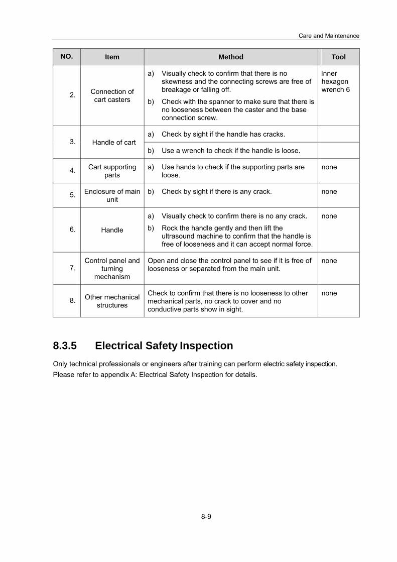
Care and Maintenance
8-9
NO. Item Method Tool
2. Connection of cart casters
a) Visually check to confirm that there is no skewness and the connecting screws are free of breakage or falling off.
b) Check with the spanner to make sure that there is no looseness between the caster and the base connection screw.
Inner hexagon wrench 6
3. Handle of cart a) Check by sight if the handle has cracks.
b) Use a wrench to check if the handle is loose.
4. Cart supporting parts
a) Use hands to check if the supporting parts are loose.
none
5. Enclosure of main unit
b) Check by sight if there is any crack. none
6. Handle
a) Visually check to confirm there is no any crack.
b) Rock the handle gently and then lift the ultrasound machine to confirm that the handle is free of looseness and it can accept normal force.
none
7. Control panel and
turning mechanism
Open and close the control panel to see if it is free of looseness or separated from the main unit.
none
8. Other mechanical structures
Check to confirm that there is no looseness to other mechanical parts, no crack to cover and no conductive parts show in sight.
none
8.3.5 Electrical Safety Inspection Only technical professionals or engineers after training can perform electric safety inspection. Please refer to appendix A: Electrical Safety Inspection for details.

9-1
9 Troubleshooting of Regular Malfunctions
9.1 Inspection and Repair Work Flow of Power System Failure
9.1.1 Inspection and Repair Work Flow When Powered by
Adapter
Fig 9-1 Inspection and Repair Work Flow when Powered by Adapter

Troubleshooting of Regular Malfunctions
9-2
9.1.2 Inspection and Repair Work Flow When Powered by
Batteries
Fig 9-2 Inspection and Repair Work Flow when Powered by Batteries

Troubleshooting of Regular Malfunctions
9-3
9.1.3 Inspection and Repair Work Flow of the Charging
Unit of the Power System When the power adapter is not powered, put the battery pack in the machine and turn it off
For A_battery+ or B_battery+ in the main power board, check if the voltage is normal
The charging unit A or B in the auxiliary power board is faulty; service
Yes
The battery pack is faulty or power capacity
is not sufficient or connection is faulty;
service
No
Adapter power on
Check if A_battery+ or B_battery+ voltage is
about 12.6v or the voltage rises slowly
Yes
No
End
Fig 9-3 Inspection and Repair Work Flow of the Charging Unit of the Power System
9.2 Location and Repair of System Boot Failure Malfunctions
No. Failure Description Failure Analysis Measure
1
a. The output indicator of the adapter is off when
the adapter is not connected to main unit;
b. The output indicator of the adapter and the
adapter-present indicator of main unit are off when
the adapter is connected to main unit;
c. There is no response as POWERBTN is pressed
when the system is powered by adapter only; the
system starts up normally but the status indicator of
the batteries is off or blinking in orange when both
the adapter and the batteries are connected.
The adapter is
damaged.
Replace the
adapter.
2 a. The power output indicator is lit up and the
adapter-present indicator of main unit is off when The output voltage of
the adapter is lower
Replace the
adapter.

Troubleshooting of Regular Malfunctions
9-4
No. Failure Description Failure Analysis Measure
the adapter is connected to main unit;
b. There is no response as POWERBTN is pressed
when the system is powered by adapter only;
c. The system starts up normally but the status
indicator of the batteries is off or blinking in orange
when both the adapter and the batteries are
connected.
than 10.8V (low
possibility).
The common-mode
inductor of main
board adapter is open
circuit (high
possibility).
Replace the
main board.
3
a. The output indicator of the adapter is normal;
b. All the indicators in the control panel are off;
c. There is no response as PWR_BTN is pressed
and the system is powered by either adapter or
batteries.
The 3V3STB of power
module is abnormal
(medium possibility).
Replace the
power
module.
The 3V3STB of main
board is
short-circuited (low
possibility).
Replace the
main board.
The 5VSTB of power
module is abnormal
(medium possibility).
Replace the
power
module.
The 5VSTB of main
board is
short-circuited (low
possibility).
Replace the
main board.
Power management
FPGA is damaged
(high possibility).
Replace the
main board.
The 5VSTB of
industrial control
board is
short-circuited (low
possibility).
Replace the
industrial
control board.

Troubleshooting of Regular Malfunctions
9-5
No. Failure Description Failure Analysis Measure
4
a. The power output indicator of the adapter is
normal when the adapter is not connected to main
unit, and the output indicator is off when the
adapter is connected to main unit;
b. All the indicators in the control panel are off;
c. There is no response when PWR_BTN is
pressed and the system is powered by either
adapter or batteries.
The input segment of
the power module is
short-circuited.
Replace the
power
module.
5
a. The output indicator of the adapter is lit up; the
adapter-present indicator in the control panel is off;
b. The system starts up normally when it is
powered by the adapter, but the indicator
PWR_BTN in the control panel is off and the
indicators related to batteries are displayed
normally;
c. There is no response as Power_BTN is pressed
when the system is powered by batteries.
The 5VSTB_OK#
output of power
module is abnormal
(low possibility)
Replace the
power
module.
The reception of
5VSTB_OK# of main
board is abnormal
(high possibility).
Replace the
main board.
6
a. The indicator of the adapter, indicator of quantity
of electricity and backlight of Power_BTN are all
normal when the system is turned off;
b. Press Power_BTN and its backlight first blinks
and then lights up continuously. The backlight of
control panel is off, the keyboard sound
unavailable, fan not working, and LCD, VGA, DVI,
Video and S-video displaying nothing;
POWER_ON# of
main board is
abnormal (high
possibility).
Replace the
main board.
The 12V output of
power module is
abnormal (medium
possibility).
Replace the
power
module.
The 12V of main
board is
short-circuited (low
possibility).
Replace the
main board.
The 12V of industrial
control board is
short-circuited (low
possibility).
Replace the
industrial
control board.

Troubleshooting of Regular Malfunctions
9-6
No. Failure Description Failure Analysis Measure
7
a. The indicator of the adapter, indicator of quantity
of electricity and backlight of Power_BTN are all
normal when the system is turned off;
b. Press PWR_BTN and its backlight keeps
blinking. The backlight of control panel is off, the
keyboard sound unavailable, fan not working, and
LCD, VGA, DVI, Video and Svideo displaying
nothing;
The main board
cannot send power-on
PWR_BTN to
industrial control
board (high
possibility).
Replace the
main board.
The industrial control
board cannot respond
PWR_BTN signal
normally (low
possibility).
Replace the
industrial
control board.
The main board
cannot S3# signal
from the industrial
control board (high
possibility).
Replace the
main board.
8
a. Nothing is wrong when the system is powered by
the adapter;
b. There is no response as PWR_BTN is pressed
when the system is powered by batteries;
Cannot switch to
batteries.
Replace the
power
module.
9
a. Nothing is wrong when the system is powered by
batteries;
b. The adapter-preset indicator is off and there is
no response as PWR_BTN is pressed when only
the adapter is connected;
c. When both the adapter and batteries are
connected, the adapter-present indicator is normal,
and the system is actually powered by batteries
during startup and running and the quantity of
electricity of batteries is being consumed;
d. Charging with the system off is available;
Cannot switch to the
adapter.
Replace the
power
module.
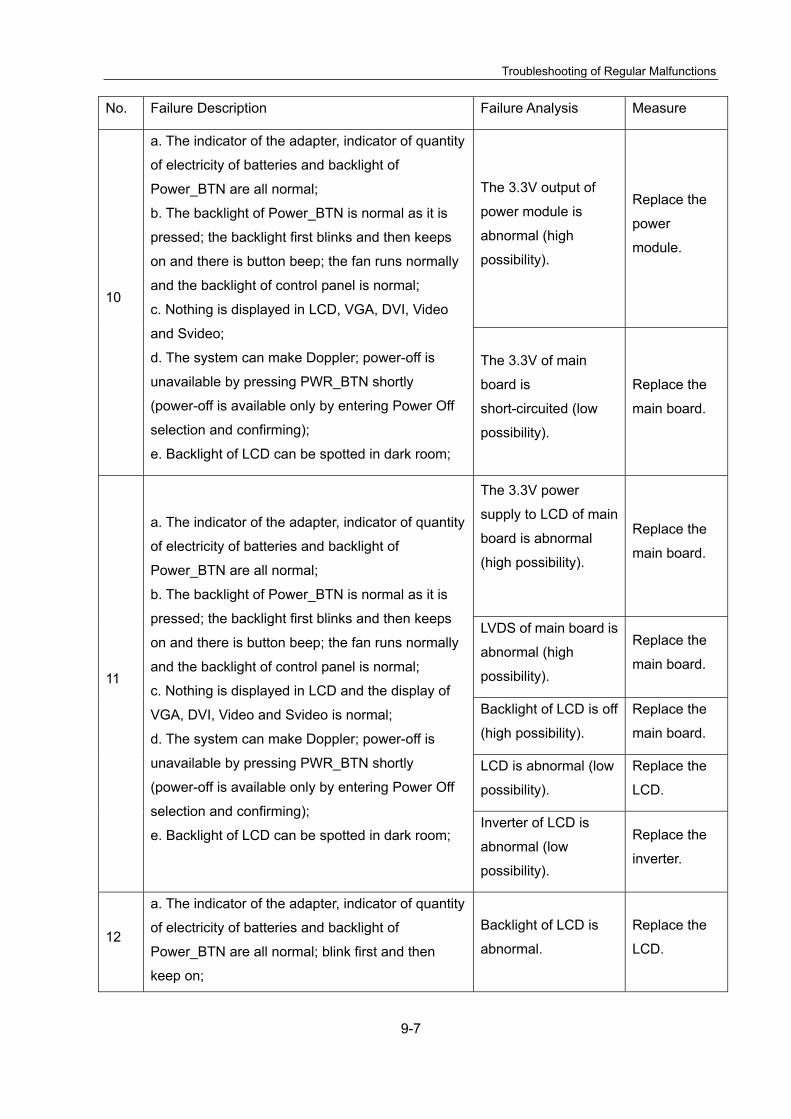
Troubleshooting of Regular Malfunctions
9-7
No. Failure Description Failure Analysis Measure
10
a. The indicator of the adapter, indicator of quantity
of electricity of batteries and backlight of
Power_BTN are all normal;
b. The backlight of Power_BTN is normal as it is
pressed; the backlight first blinks and then keeps
on and there is button beep; the fan runs normally
and the backlight of control panel is normal;
c. Nothing is displayed in LCD, VGA, DVI, Video
and Svideo;
d. The system can make Doppler; power-off is
unavailable by pressing PWR_BTN shortly
(power-off is available only by entering Power Off
selection and confirming);
e. Backlight of LCD can be spotted in dark room;
The 3.3V output of
power module is
abnormal (high
possibility).
Replace the
power
module.
The 3.3V of main
board is
short-circuited (low
possibility).
Replace the
main board.
11
a. The indicator of the adapter, indicator of quantity
of electricity of batteries and backlight of
Power_BTN are all normal;
b. The backlight of Power_BTN is normal as it is
pressed; the backlight first blinks and then keeps
on and there is button beep; the fan runs normally
and the backlight of control panel is normal;
c. Nothing is displayed in LCD and the display of
VGA, DVI, Video and Svideo is normal;
d. The system can make Doppler; power-off is
unavailable by pressing PWR_BTN shortly
(power-off is available only by entering Power Off
selection and confirming);
e. Backlight of LCD can be spotted in dark room;
The 3.3V power
supply to LCD of main
board is abnormal
(high possibility).
Replace the
main board.
LVDS of main board is
abnormal (high
possibility).
Replace the
main board.
Backlight of LCD is off
(high possibility).
Replace the
main board.
LCD is abnormal (low
possibility).
Replace the
LCD.
Inverter of LCD is
abnormal (low
possibility).
Replace the
inverter.
12
a. The indicator of the adapter, indicator of quantity
of electricity of batteries and backlight of
Power_BTN are all normal; blink first and then
keep on;
Backlight of LCD is
abnormal.
Replace the
LCD.

Troubleshooting of Regular Malfunctions
9-8
No. Failure Description Failure Analysis Measure
b. The backlight of Power_BTN is normal as it is
pressed; the backlight first blinks and then keeps
on and there is button beep; the fan runs normally
and the backlight of control panel is normal;
c. The display of LCD is not even and the display of
VGA, DVI, Video and Svideo is normal;
d. The system can make Doppler; power-off is
unavailable by pressing PWR_BTN shortly
(power-off is available only by entering Power Off
selection and confirming);
e. Backlight of LCD can be spotted in dark room;
13
a. The indicator of the adapter, indicator of quantity
of electricity of batteries and backlight of
Power_BTN are all normal;
b. The backlight of Power_BTN is normal as it is
pressed; the backlight first blinks and then keeps
on and there is button beep; the backlight of control
panel is off and the fan runs normally;
c. Nothing is displayed in LCD, VGA, DVI, Video
and Svideo;
d. Backlight of LCD can be spotted in dark room;
e. Power-off is unavailable by pressing PWR_BTN
shortly;
12VOK of power
module is abnormal.
Replace the
power
module.
14
a. The indicator of the adapter, indicator of quantity
of electricity of batteries and backlight of
Power_BTN are all normal;
b. The backlight of Power_BTN is normal as it is
pressed; the backlight first blinks and then keeps
on and there is button beep; the backlight of control
panel is off and the fan runs normally;
c. Nothing is displayed in LCD, VGA, DVI, Video
and Svideo;
d. Backlight of LCD can be spotted in dark room;
e. Power-off is available by pressing PWR_BTN
shortly;
The 5V output of
power module is
abnormal (high
possibility).
Replace the
power
module.
The 5V of main board
is short-circuited (low
possibility).
Replace the
main board.

Troubleshooting of Regular Malfunctions
9-9
No. Failure Description Failure Analysis Measure
15
a. The indicator of the adapter, indicator of quantity
of electricity of batteries and backlight of
Power_BTN are all normal;
b. The backlight of Power_BTN is normal as it is
pressed; the backlight first blinks and then keeps
on and there is button beep; the backlight of control
panel is on and the fan runs normally;
c. Nothing is displayed in LCD, VGA, DVI, Video
and S-video;
d. Backlight of LCD can be spotted in dark room;
e. Power-off is unavailable by pressing PWR_BTN
shortly;
The processing to
12VOK of main board
is abnormal.
Replace the
main board.
The POST of industry
control board fails.
Replace the
industrial
control board.
16 Prompts “Operating system no found” during the
startup.
HDD failure Replace
HDD.
The operating system
fails to boot up.
Restore the
operating
system.
9.3 Location and Repair of Non-echo Failure in Image Region
No. Failure Description Failure Analysis Measure
1
There is no noise image
when there is no
transducer and the digital
gain is maximal.
Something is wrong with AFE of main
board (high possibility)
Replace the
main board.
The 3V6 output of power module is
abnormal (low possibility)
Replace the
power module.
2
a. Connect the transducer,
and the system identifies
the transducer correctly
b. Connect the transducer,
Something is wrong with the programmed
voltage of power module (high possibility).
Replace the
power module.
The programmed power of main board is
short-circuited (high possibility).
Replace the
main board.
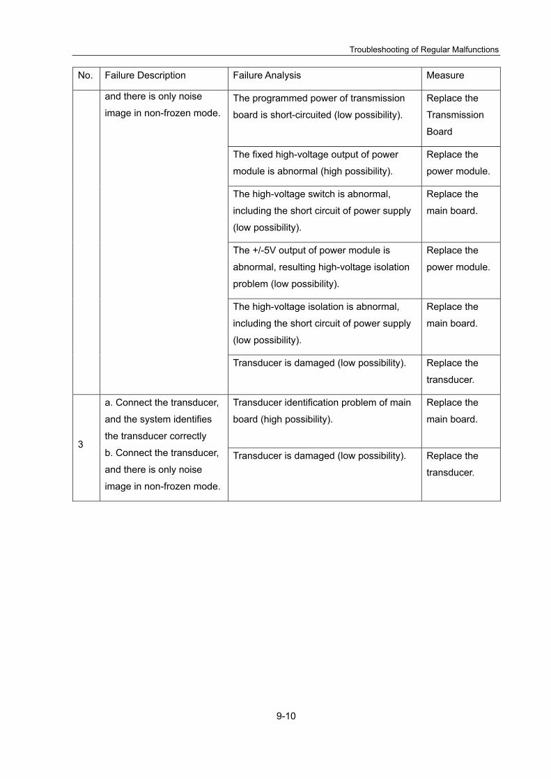
Troubleshooting of Regular Malfunctions
9-10
No. Failure Description Failure Analysis Measure
and there is only noise
image in non-frozen mode. The programmed power of transmission
board is short-circuited (low possibility).
Replace the
Transmission
Board
The fixed high-voltage output of power
module is abnormal (high possibility).
Replace the
power module.
The high-voltage switch is abnormal,
including the short circuit of power supply
(low possibility).
Replace the
main board.
The +/-5V output of power module is
abnormal, resulting high-voltage isolation
problem (low possibility).
Replace the
power module.
The high-voltage isolation is abnormal,
including the short circuit of power supply
(low possibility).
Replace the
main board.
Transducer is damaged (low possibility). Replace the
transducer.
3
a. Connect the transducer,
and the system identifies
the transducer correctly
b. Connect the transducer,
and there is only noise
image in non-frozen mode.
Transducer identification problem of main
board (high possibility).
Replace the
main board.
Transducer is damaged (low possibility). Replace the
transducer.

Troubleshooting of Regular Malfunctions
9-11
9.4 Location and Repair of the Problem of Image with Black Area
No. Failure Description Failure Analysis Measure
1
There is black area in the noise
image when there is no
transducer and the digital gain
is maximal.
Something is wrong with
AFE of main board
Replace the main board.
2
a. The self-diagnosis of
front-end channel is passed
b. Connect the transducer, and
there is black area in
non-frozen mode.
The high-voltage switch of
main board is abnormal.
Replace the main board.
The transducer is damaged. Replace the transducer.
3
a. The self-diagnosis of
front-end channel is failed
b. Connect the transducer, and
there is black area in
non-frozen mode.
The transmission and main
board are in poor contact.
Pull out and reinsert the
transmission board.
The channel of transmission
board is damaged.
Replace the
Transmission Board
The high-voltage isolation is
abnormal.
Replace the main board.
9.5 Abnormalities in Image Region The problems to be solved in this section include abnormalities of B, C, PW and CW images. To
solve this problem, replace the power module first to exclude the problems of the power module,
then transmission board and at last the main board. If there is analog CW board for CW mode, it
should be replaced first.

Troubleshooting of Regular Malfunctions
9-12
9.6 Inspection and Repair Work Flow of USB Port Failure
Fig 9-4 Inspection and Repair Work Flow of USB Port Failure

Troubleshooting of Regular Malfunctions
9-13
9.7 Inspection and Repair Work Flow of Network Failure
Fig 9-5 Inspection and Repair Work Flow of Network Failure
9.8 Troubleshooting for 4D Board No. Failure Description Failure
Analysis
Measure
1
Switch to 4D, and the
mechanical scan of
the 4D transducer
does not begin,
The -12V
output of the
power module
is unavailable.
Test the -12V output of the power module. If the
-12V is unavailable, replace the power module;

Troubleshooting of Regular Malfunctions
9-14
No. Failure Description Failure
Analysis
Measure
namely the electric
motor is not working. The
±(7V~11.5V)
of
programmed
power module
of 4D driving
board is not
available.
(1) Measure whether the voltage of PIN 3 and PIN
5 of U13 (or U4) of 4D driving board are normal.
Generally, PIN 3 should be negative (-7V ~
-11.5V), and PIN 5 should be positive (+7V ~
+11.5V).
(2) If they are both unavailable, check whether
fuse F1 is burnt out. If it is, first check whether the
two ends of the fuse are short-circuited to ground
and replace the fuse if they are short-circuited.
(3) If the fuse is not burnt out, measure whether
the +12V voltage of either end of the fuse is
normal. If not, the problem is not resulted from the
driving board and main board socket, then check
the power module.
(4) If the problems mentioned in (2) and (3) are all
excluded, replace U12 in the 4D driving board.
The driving
signal of the
4D driving
board is
unavailable.
(1) Measure TP3, TP6 and TP8 with oscillograph,
and skip to (2) if they are normal. If no output,
measure VDD (PIN 1) and VREF (PIN 5) of U6
with multimeter. If VDD is abnormal, check 3.3V
of the main board; if VREF is abnormal, replace
U18.If both VDD and VREF are normal, replace
DAC U6.
(2) Measure TP5 and TP11 with oscillograph. If
there are no driving signals, replace U13 and U4;
(3) If both TP5 and TP11 are available, measure
PIN 8 and PIN 12 of socket P5 of 4D driving
board with oscillograph. If there is no output, it
means the electric motor inside the transducer is
damaged. Replace 4D transducer.
2 Switch to 4D, and the
mechanical scan of
4D transducer stops
after a few seconds,
Electric motor
stops working
after started
for a few
(1) Check whether there is square wave output in
PIN 3 (HALL signal) of socket P5 of 4D driving
board during the time when the transducer is
working.

Troubleshooting of Regular Malfunctions
9-15
No. Failure Description Failure
Analysis
Measure
namely the electric
motor stops working.
seconds (2) If not, check whether the 4 driving signals of
PIN 1 ~ PIN 8 of socket J1 of transducer
connection board are normally output. If normal,
skip to (4).If not, check the output of driving
signals from the 4D driving board (refer to
malfunction 1 and failure analysis 2 for the
measurement and solutions)
(3) If the driving signals of 4D driving board are
normally output, replace the cables.
(4) The HALL of 4D transducer is damaged.
Replace 4D transducer.
9.9 Troubleshooting for the Keyboard Board No. Failure Description Failure Analysis Measure
1 Indicator D175 is OFF.
The keyboard cable is pulled out or
something is wrong with the keyboard
cable. Test TP11, which should be 5V.
Fix the keyboard
cable again or
replace the
keyboard cable.
2 Indicator D176 is OFF.
The keyboard cable is pulled out or
something is wrong with the keyboard
cable. Test TP21, which should be 12V.
Fix the keyboard
cable again or
replace the
keyboard cable.
3
LED D175 and D176 are
lit up normally. The LED
D1 of FPGA is not lit up
or is blinking. The
keyboard board
program cannot run
normally.
FPGA configuration files haven’t been
burnt.
Burn FPGA
configuration files.
Make sure the core voltage of FPGA is
normal. The voltage of TP17 should be
1.2V.
Replace U20.
The FLASH is damaged. Replace U3.
4 TGC value is unstable;
even when you don’t
Make sure TGC line is connected well
(J2)
Fixed

Troubleshooting of Regular Malfunctions
9-16
No. Failure Description Failure Analysis Measure
move the slider, the
value varies; the offset
between the value and
position is great.
The connector of TGC connection wire
looses.
Replace TGC
connection wire.
5
Some LEDs in boards
and cards are not lit up,
and the dual-color LEDs
are always lit up at the
same time.
Check whether the LED soldering
direction is correct; check whether the
lights are damaged in appearance;
check whether the pin of dual-color light
is broken circuit.
Solder the
component again or
replace it.
6
Windows cannot identify
the keyboard board (the
power of boards and
cards is normal, and
software and logic are
correctly burnt).
No keyboard board driver is installed. Install the driver.
The main board connection wire is
damaged.
Replace the main
board connection
wire.
Test whether USB common-mode
inductor L8 is normally conducted.
Replace L8.
The anti-static chip U5 is damaged. Replace U5.
The USB interface chip U4 is damaged. Replace U4.
9.10 Troubleshooting for ECG Board No. Failure Description Failure Analysis Measure
1
The corresponding
function is unavailable.
The connection between the main
unit and the ECG module is
abnormal.
Replace the connection
cable.
Power failure Refer to power failure
resolution (Note A)
The communication of the serial
port is abnormal.
Replace U8
2
Open the corresponding
function, and the wave
form is displayed as a
line, or it is abnormal.
ECG lead abnormal Replace the ECG lead
The connection between the main
unit and the ECG module is
abnormal.
Replace the connection
cable.

Troubleshooting of Regular Malfunctions
9-17
No. Failure Description Failure Analysis Measure
If the connection cable is normal,
open the ECG board and check
the indicators D15 and D20 are lit
up. If not, it means something is
wrong with the power.
Refer to power failure
resolution (Note A)
ECG program abnormal Rewrite the inferior
program of ECG board.
ECG board abnormal Replace the ECG board.
Note A. ECG board power failure resolution
When trying to solve power failure, check the power tree of ECG board of 2118 step by step.
Fig 9-6 Power Tree of ECG Board
The following table lists the relevant information of the test points.
Network
Name
Standard
Voltage (V)
Voltage Testing
Points
Failure Analysis Failure
Resolution
ECG+5V 5±10% Voltage drop of
two ends of
C102
Test whether the two ends of
F2 are conducted. If not,
replace F2.
Replace F2.
+12V 12±10% Voltage drop of
two ends of
C112
Maybe U17 is damaged. Replace U17.
SVCC 3.3±10% Testing points of
the board
Maybe U23 is damaged Replace U23

Troubleshooting of Regular Malfunctions
9-18
Network
Name
Standard
Voltage (V)
Voltage Testing
Points
Failure Analysis Failure
Resolution
ECG+5V 5±10% Voltage drop of
two ends of
C102
Test whether the two ends of
F2 are conducted. If not,
replace F2.
Replace F2.
+6V,
+6D
6±10% Testing points of
the board
Test whether T1 primary or
secondary coil is broken
circuit. If it is, replace TI.
Otherwise, Q1 or U18 may be
faulty.
Replace T1, Q1,
orU18
-6V -6±10% Testing points of
the board
+5V 5±5% Testing points of
the board
Maybe U22 is damaged Replace U22
+3V3 3.3±5% Testing points of
the board
Maybe U24 is damaged Replace U24
+
3V3REF
3.3±5% Testing points of
the board
Maybe U19 is damaged Replace U19
-5V -5±5% Testing points of
the board
Maybe U25 is damaged Replace U25
9.11 Troubleshooting for Video & Audio Capture Card
No. Failure Description Failure Analysis Measure
1
After the video capture card is
connected, the screen prompts that
the surge occurs or the current is
not enough.
USB port cannot provide
sufficient power to drive the
video capture card.
Replace the main
board.
2
After the video capture card is
connected, the screen doesn’t
display images.
USB cable is not secured. Reconnect the USB
cable.
The chip is damaged. Replace the chip.

Troubleshooting of Regular Malfunctions
9-19
No. Failure Description Failure Analysis Measure
3
The image is not continuous or
some image frames are missing or
discolored.
The signal cable is in bad
contact, e.g. SVIDEO signal
cable is in bad contact or
USB signal cable is in bad
contact.
Change cable or
change the socket.
4
After the video capture card is
connected, clicking the capture
command cannot normally capture
sound.
The installation of the driver
isn’t correct. Reinstall the driver.
Check if the audio input
signal rule is specified in the
capture software.
Specify it in the
software.
Check if there is BCLK signal,
if not, it indicates EMP202
chip is damaged.
Replace the chip.
6 Only part of the source video can
be seen.
The video displayed by
capture card is of 640*480
resolution. If resolution is not
correct, the display will be
abnormal.
/

A-1
Appendix A Electrical Safety Inspection
The following electrical safety tests are recommended as part of a comprehensive preventive maintenance program. They are a proven means of detecting abnormalities that, if undetected, could prove dangerous to either the patient or the operator. Additional tests may be required according to local regulations. All tests can be performed using commercially available safety analyzer test equipment. These procedures assume the use of a 601PROXL International Safety Analyzer or equivalent safety analyzer. Other popular testers complying with IEC 60601-1 used in Europe such as Fluke, Metron, or Gerb may require modifications to the procedure. Follow the instructions of the analyzer manufacturer. The consistent use of a safety analyzer as a routine step in closing a repair or upgrade is emphasized as a mandatory step if an approved agency status is to be maintained. The safety analyzer also proves to be an excellent troubleshooting tool to detect abnormalities of line voltage and grounding, as well as total current loads.

Electrical Safety Inspection
A-2
ELECTRICAL SAFETY INSPECTION 1- Power Cord Plug
TEST PROCEDURE
The Power Plug
The Power Plug Pins No broken or bent pin. No discolored pins.
The Plug Body No physical damage to the plug body.
The Strain Relief No physical damage to the strain relief. No plug warmth for device in use.
The Power Plug No loose connections.
The Power Cord
The Power Cord
No physical damage to the cord. No deterioration to the cord.
‐‐For devices with detachable power cords, inspect the connection at the device.
‐‐For devices with non‐detachable power cords, inspect the strain relief at the device.

Electrical Safety Inspection
A-3
ELECTRICAL SAFETY INSPECTION 2- Device Enclosure And Accessories
TEST PROCEDURE
Visual Inspection
The Enclosure and Accessories
No physical damage to the enclosure and accessories.
No physical damage to meters, switches, connectors, etc.
No residue of fluid spillage (e.g., water, coffee, chemicals, etc.).
No physical damage to probe head (e.g., crack)
No loose or missing parts (e.g., knobs, dials, terminals, etc.).
Contextual Inspection
The Enclosure and Accessories
No unusual noises (e.g., a rattle inside the case).
No unusual smells (e.g., burning or smoky smells, particularly from ventilation holes).
No taped notes that may suggest device deficiencies or operator concerns.
Electrical Safety Inspection
A-4
ELECTRICAL SAFETY INSPECTION 3- Device Labeling
TEST PROCEDURE
Check the labels provided by the manufacturer or the healthcare facility is present and
legible.
Main Unit Label Integrated Warning Labels Slope and High Voltage Caution Label Don’t Stress Label

Electrical Safety Inspection
A-5
ELECTRICAL SAFETY INSPECTION 5- Earth Leakage Test
OVERVIEW
Run an Earth Leakage test on the device being tested before performing any other leakage tests.
Leakage current is measured the following ways:
♦ Earth Leakage Current, leakage current measured through DUT outlet Earth
♦ Earth Leakage Current AP-EARTH (ALL Applied Parts connected to Earth), leakage current measured through DUT outlet Earth
There is no need to attach a test lead; the 601PRO automatically connects the measuring device internally.
TEST PROCEDURE
Perform the Test
1) From the MAIN MENU, or with the outlet unpowered, plug the DUT into the 601PRO front panel outlet, and turn on the device.
2) Attach the device's applied parts to the 601PRO applied part terminals if applicable. 3) Press shortcut key 4.The Earth Leakage test appears on the display, and the test begins
immediately:
SOFT KEY 1 toggles the DUT outlet Polarity from Normal to Off to Reverse. SOFT KEY 2 toggles the DUT outlet from Earth to No Earth. SOFT KEY 3 toggles the DUT outlet from L2 to No L2. SOFT KEY 4 toggles the AP to Earth to No AP to Earth.
4) Press the print data key at any time to generate a printout of the latest measurement.

Electrical Safety Inspection
A-6
ELECTRICAL SAFETY INSPECTION 5- Earth Leakage Test
Figure 1 Earth leakage test
Failure
Check any short‐circuits of the Y capacitor on power unit. Replace a new one if any portion defective.
Check any broken of the Power Unit. Replace a new one if any portion defective.
Inspect mains wiring for bad crimps, poor connections, or damage.
Test the wall outlet; verify it is grounded and is free of other wiring abnormalities. Notify the user or owner to correct any deviations. As a work around, check the other outlets to see if they could be used instead.
Change another probe to confirm if the fail is caused by console.
Inspect mains wiring for bad crimps, poor connections, or damage.
If the leakage current measurement tests fail on a new unit and if situation cannot be corrected, submit a Safety Failure Report to document the system problem. Remove unit from operation.
If all else fails, stop using and inform the Customer Service Engineer for analysis and disposal.
LIMITS
UL60601‐1:300 μA Normal Condition
1000 μA Single Fault Condition
IEC60601‐1: 500 μA Normal Condition
1000 μA Single Fault Condition

Electrical Safety Inspection
A-7
ELECTRICAL SAFETY INSPECTION 6- Patient Leakage Current
OVERVIEW
Patient leakage currents are measured between a selected applied part and mains earth.
TEST PROCEDURE
Prepare
Perform a calibration from the Mains on Applied Part menu.
The following outlet conditions apply when performing this test:
Normal Polarity, Earth Open, Outlet ON Normal Polarity, Outlet ON
Normal Polarity, L2 Open, Outlet ON Reversed Polarity, Outlet ON
Reversed Polarity, Earth Open, Outlet ON Reversed Polarity, L2 Open, Outlet ON
Warning
If all of the applied parts correspond to the instrument type, the applied parts will be tied together and one reading will be taken. If any of the applied parts differ from the instrument type, all applied parts will be tested individually, based on the type of applied part. This applies to Auto and Step modes only.
Perform the Test
1) From the MAIN MENU, or with the outlet unpowered, plug the DUT into the 601PRO front panel outlet, and turn on the device.
2) Attach the applied parts to the 601PRO's applied part terminals.
3) Press shortcut key 6. The Patient Leakage test is displayed, and the test begins immediately.
4) Press APPLIED PART (SOFT KEY 4) at any time to select the desired applied part leakage current.
5) Modify the configuration of the front panel outlet by pressing the appropriate SOFT KEY on the 601PRO.
6) Press the print data key at any time to generate a printout of the latest measurement.

Electrical Safety Inspection
A-8
ELECTRICAL SAFETY INSPECTION 6- Patient Leakage Current
Figure 2 patient leakage Current
Note
1, In addition to Probes ,Patient leakage current test should be perform if ECG or PCG parts used;
2, If the current test standard being used does not include Patient Leakage DC readings, or the DC option is not enabled, then DC readings will not be available through the APPLIED PART SOFT KEY selections. Refer to Chapter 8, Standards and Principles.
Failure
Check any broken of the Applied parts. Replace any defective one.
Check any broken of the ECG/PCG module if used, Replace any defective one.
Check any broken of the Power Unit. Replace a new one if any portion defective.
Inspect wiring for bad crimps, poor connections, or damage.
Test the wall outlet; verify it is grounded and is free of other wiring abnormalities. Notify the user or owner to correct any deviations. As a work around, check the other outlets to see if they could be used instead.
Change another probe to confirm if the fail is caused by console.
Inspect wiring for bad crimps, poor connections, or damage.
If the leakage current measurement tests fail on a new unit and if situation can not be corrected, submit a Safety Failure Report to document the system problem. Remove unit from operation.
If all else fails, stop using and inform the Customer Service Engineer for analysis and disposal.
LIMITS

Electrical Safety Inspection
A-9
ELECTRICAL SAFETY INSPECTION 6- Patient Leakage Current
All countries
For BF ECG input and transducer
100μA Normal Condition
500μA Single Fault Condition

Electrical Safety Inspection
A-10
ELECTRICAL SAFETY INSPECTION 7- Mains on Applied Part Leakage
OVERVIEW
The Mains on Applied Part test applies a test voltage, which is 110% of the mains voltage, through a limiting resistance, to selected applied part terminals. Current measurements are then taken between the selected applied part and earth. Measurements are taken with the test voltage (110% of mains) to applied parts in the normal and reverse polarity conditions as indicated on the display.
The following outlet conditions apply when performing the Mains on Applied Part test.
Normal Polarity;
Reversed Polarity
TEST PROCEDURE
Prepare
To perform a calibration from the Mains on Applied Part test, press CAL (SOFT KEY 2).
1) Disconnect ALL patient leads, test leads, and DUT outlet connections. 2) Press CAL to begin calibration, as shown:
If the calibration fails, the previously stored readings will be used until a passing calibration has occurred. Also, the esc/stop key has no effect during calibration.
3) When the calibration is finished, the Mains on Applied Part test will reappear.
Warning
1) A 2-beep-per-second signal indicates high voltage present at the applied part terminals while a calibration is being performed.
2) High voltage is present at applied part terminals while measurements are being taken.
Performance
1) From the MAIN MENU, or with the outlet unpowered, plug the DUT into the 601

Electrical Safety Inspection
A-11
ELECTRICAL SAFETY INSPECTION 7- Mains on Applied Part Leakage
2) Attach the applied parts to the 601PRO applied part terminals. 3) Attach the red terminal lead to a conductive part on the DUT enclosure. 4) Press shortcut key 7. The Mains on Applied Part test is displayed.
5) Select the desired outlet configuration and applied part to test using the appropriate SOFT
KEYS: 6) Press START TEST (SOFT KEY 1) to begin the test. 7) Press the print data key to generate a printout of the latest measurement.
Figure 3 Mains on Applied part leakage
Note
1, In addition to Probes ,Patient leakage current test should be perform if ECG or PCG parts used;
2, If all of the applied parts correspond to the instrument type, the applied parts will be tied together and one reading will be taken. If any of the applied parts differ from the instrument type, all applied parts will be tested individually, based on the type of applied part. This applies to Auto and Step modes only.
Failure
Check any broken of the Applied part. Replace any defective one.
Check any broken of the ECG/PCG module if used, Replace any defective one.
Check any broken of the Power Unit. Replace a new one if any portion defective.
Inspect wiring for bad crimps, poor connections, or damage.

Electrical Safety Inspection
A-12
ELECTRICAL SAFETY INSPECTION 7- Mains on Applied Part Leakage
Test the wall outlet; verify it is grounded and is free of other wiring abnormalities. Notify the user or owner to correct any deviations. As a work around, check the other outlets to see if they could be used instead.
Change another probe to confirm if the fail is caused by console.
Inspect wiring for bad crimps, poor connections, or damage.
If the leakage current measurement tests fail on a new unit and if situation can not be corrected, submit a Safety Failure Report to document the system problem. Remove unit from operation.
If all else fails, stop using and inform the Customer Service Engineer for analysis and disposal.
LIMITS
All countries:
For BF ECG input and transducer:
5000μA
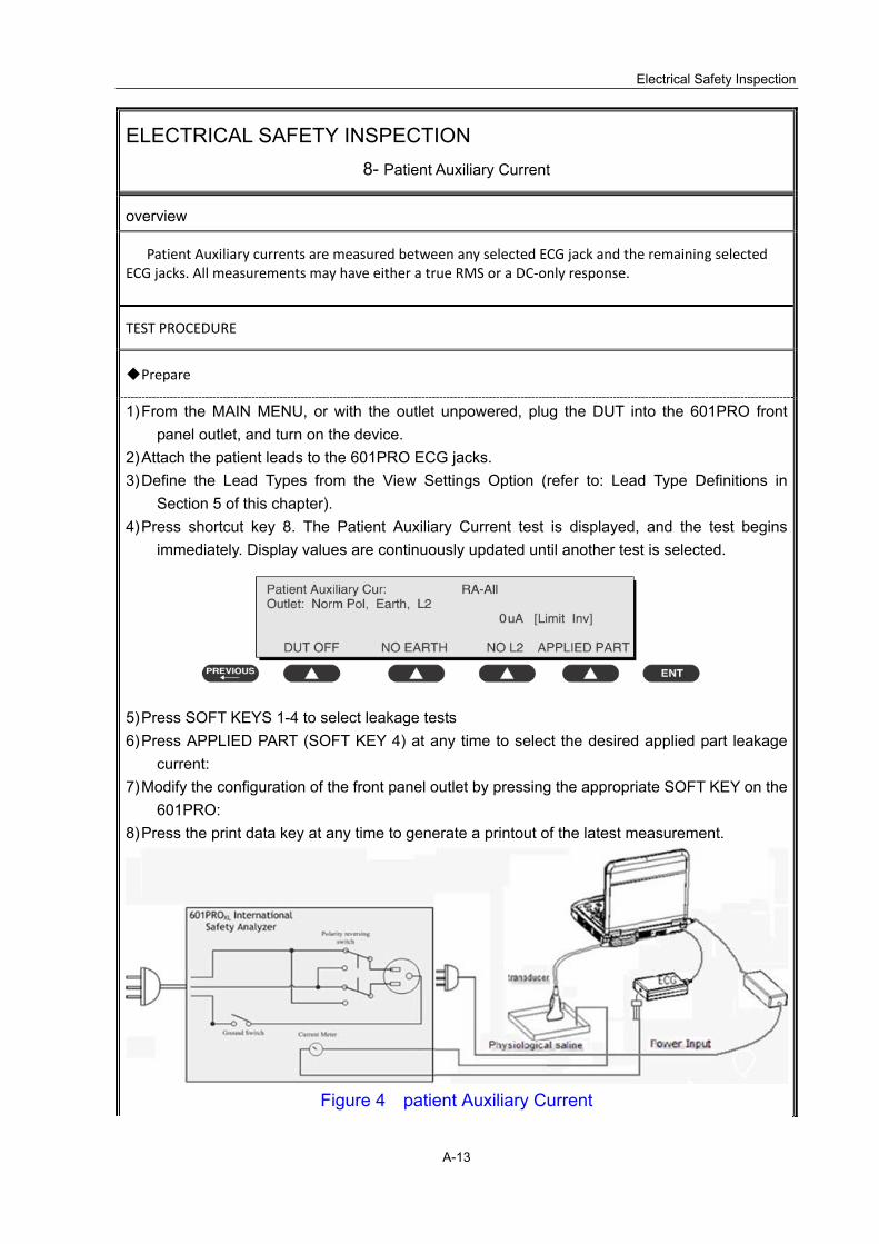
Electrical Safety Inspection
A-13
ELECTRICAL SAFETY INSPECTION 8- Patient Auxiliary Current
overview
Patient Auxiliary currents are measured between any selected ECG jack and the remaining selected ECG jacks. All measurements may have either a true RMS or a DC‐only response.
TEST PROCEDURE
Prepare
1) From the MAIN MENU, or with the outlet unpowered, plug the DUT into the 601PRO front panel outlet, and turn on the device.
2) Attach the patient leads to the 601PRO ECG jacks. 3) Define the Lead Types from the View Settings Option (refer to: Lead Type Definitions in
Section 5 of this chapter). 4) Press shortcut key 8. The Patient Auxiliary Current test is displayed, and the test begins
immediately. Display values are continuously updated until another test is selected.
5) Press SOFT KEYS 1-4 to select leakage tests 6) Press APPLIED PART (SOFT KEY 4) at any time to select the desired applied part leakage
current: 7) Modify the configuration of the front panel outlet by pressing the appropriate SOFT KEY on the
601PRO: 8) Press the print data key at any time to generate a printout of the latest measurement.
Figure 4 patient Auxiliary Current

Electrical Safety Inspection
A-14
ELECTRICAL SAFETY INSPECTION 8- Patient Auxiliary Current
Note
If the current test standard being used does not include Patient Auxiliary Current DC readings, or the DC option is not enabled, then DC readings will not be available through the APPLIED PART SOFT KEY selections.
Failure
Check any broken of the AC cable. Replace a new one if any portion defective.
Check any broken of the enclosure. Replace any defective part.
Inspect wiring for bad crimps, poor connections, or damage.
Test the wall outlet; verify it is grounded and is free of other wiring abnormalities. Notify the user or owner to correct any deviations. As a work around, check the other outlets to see if they could be used instead.
Change another probe to confirm if the fail is caused by console.
Inspect wiring for bad crimps, poor connections, or damage.
If the leakage current measurement tests fail on a new unit and if situation can not be corrected, submit a Safety Failure Report to document the system problem. Remove unit from operation.
If all else fails, stop using and inform the Customer Service Engineer for analysis and disposal.
LIMITS
All countries
For BF ECG input and transducer
100μA Normal Condition
500μA Single Fault Condition

Electrical Safety Inspection
A-15
ELECTRICAL SAFETY INSPECTION FORM
(Class I equipment) Overall assessment:
Scheduled inspection Test item: 1, 2, 3, 9
Unopened repair type Test item: 1, 2, 3, 9
Opened repair type, not modify the power part
including transformer or patient circuit board
Test item: 1, 2, 3, 4, 5, 9
Opened repair type, modify the power part including
transformer or patient circuit board
Test item: 1, 2, 3, 4, 5, 6, 7, 8, 9
Location: Technician:
Equipment: Control Number:
Manufacturer: Model: SN:
Measurement equipment /SN: Date of Calibration:
INSPECTION AND TESTING Pass/Fail Limit
1 Power Cord Plug 2 Device Enclosure and Accessories 3 Device Labeling 4 Protective Earth Resistance Ω Max 0.2 Ω
5 Earth Leakage
Normal condition(NC)
____μA
Max: NC: 300μA(refer to UL60601-1) * NC: 500μA(refer to IEC60601-1) * SFC: 1000μA
Single Fault condition(SFC) ____μA
6 Patient Leakage Current
Normal condition(NC) BF____μA Max: BF applied part: NC:100μA, SFC: 500μA Single Fault condition(SFC) BF____μA
7 Mains on Applied Part Leakage BF____μA Max: BF applied part: 5000μA
8 Patient Auxliary Leakage Current
Normal condition(NC)
BF____μA
Max: BF applied part: NC:100μA, SFC: 500μA
Single Fault condition(SFC)
BF____μA

Electrical Safety Inspection
A-16
Note: The equipment which sell to America shall comply with the requirement of UL60601-1,
others shall comply with the requirement of IEC60601-1. Name/ Signature: ____________________ Date:_____________________________

Phantom Usage Illustration
B-1
Appendix B Phantom Usage Illustration
Targets Disposal of Phantom KS107BD A1——A5: Axial resolution target group B: Blind-area target group
C: Longitudinal target group D: Horizontal target group
E: Mimic tumor F: Mimic sac (diam 10mm) and stone G Mimic sac (diam 6mm) 4. Line Target System There are 8 groups of nylon line targets disposed as shown in the figure. 1.A1——A5: Axial and lateral resolution target group. The distances between the horizontal branch and the acoustic window are 30, 50, 70, 120 and 160mm, the center horizontal distances between two adjacent lines of A1 and A2 groups are 1, 5, 4, 3, 2mm, A3~A5 groups are 5, 4, 3, 2mm. The center longitudinal distances between two adjacent lines of the longitudinal branches are 4, 3, 2, 1mm. 2.B: Blind-area target group. Center horizontal distance of adjacent lines is 10mm, distances to the acoustic window are 10, 9, 8, 7, 6, 5, 4, 3mm. 3.C: Longitudinal target group. 19 target lines with a 10mm center distance between adjacent lines. 4.D:
Horizontal target group. 7 target lines with a 20mm center distance between adjacent lines.

Phantom Usage Illustration
B-2
Targets disposal- KS107BD A1——A4 Axial resolution target group
B1——B4 Lateral resolution target group
C Longitudinal target group
D Horizontal target group
E1——E3 Mimic sacs with diameters of 2, 4, 6mm
4. Line Target System There are 8 groups of line targets disposed in TM material as shown in the figure. 1.A1——A4: Axial resolution target group. The upmost lines in each target locate at the depth of 10, 30, 50, 70mm, the center longitudinal distances of each group (from the top down) are 3, 2, 1, 0.5mm, and the horizontal distance is 1mm. 2.B1——B4: Lateral resolution target group. Locate at a depth of 10, 30, 50, 70mm, with a center horizontal distance of 4, 3, 2, 1mm in each group. 3.C: Longitudinal target group. 12 target lines with a 10mm center distance between adjacent lines. 4.D: Horizontal target group. Locate at a depth of 40mm, with a 20mm center distance between adjacent lines.

P/N: 046-000545-00 (V12.0)