Device Variability and USJ Implant & Anneal Options ...
84
J.O.B. Technology (Strategic Marketing, Sales & Technology) 1 Device Variability and USJ Implant & Anneal Options Limited by Strain-Si and High- k Gate Process Integration John Ogawa Borland J.O.B. Technologies Aiea, Hawaii July 19, 2007 www.job-technologies.com
Transcript of Device Variability and USJ Implant & Anneal Options ...

J.O.B. Technology (Strategic Marketing, Sales & Technology)
1
Device Variability and USJ Implant & Anneal Options
Limited by Strain-Si and High-k Gate Process Integration
John Ogawa BorlandJ.O.B. Technologies
Aiea, HawaiiJuly 19, 2007
www.job-technologies.com

J.O.B. Technology (Strategic Marketing, Sales & Technology)
2
Outline• Introduction: Device & Process Variation Caused By
Implant & Annealing• Channel Doping Optimization
– Extension & HALO Implantation Options– Annealing Options– Metrology
• Implanter signature• Annealer signature
• Channel Mobility Options• Gate Stack Options
– Tinv reduction– EOT scaling
• Summary

Design For Manufacturing: Controlling Process Variability Key For sub-45nm Node Manufacturing!
T.C. Chen, IBM, IEEE Solid State Circuits Society Newsletter, Vol. 20, No. 3, Sept 2006, p.5
Delta Vt=>100mV (0.1V)!-Process proximity effects-Layout loading effects-Gate line edge roughness effects-Implant dopant positioning-Thermally induced variation by RTAKey will be Characterization, Reduction & Accommodation
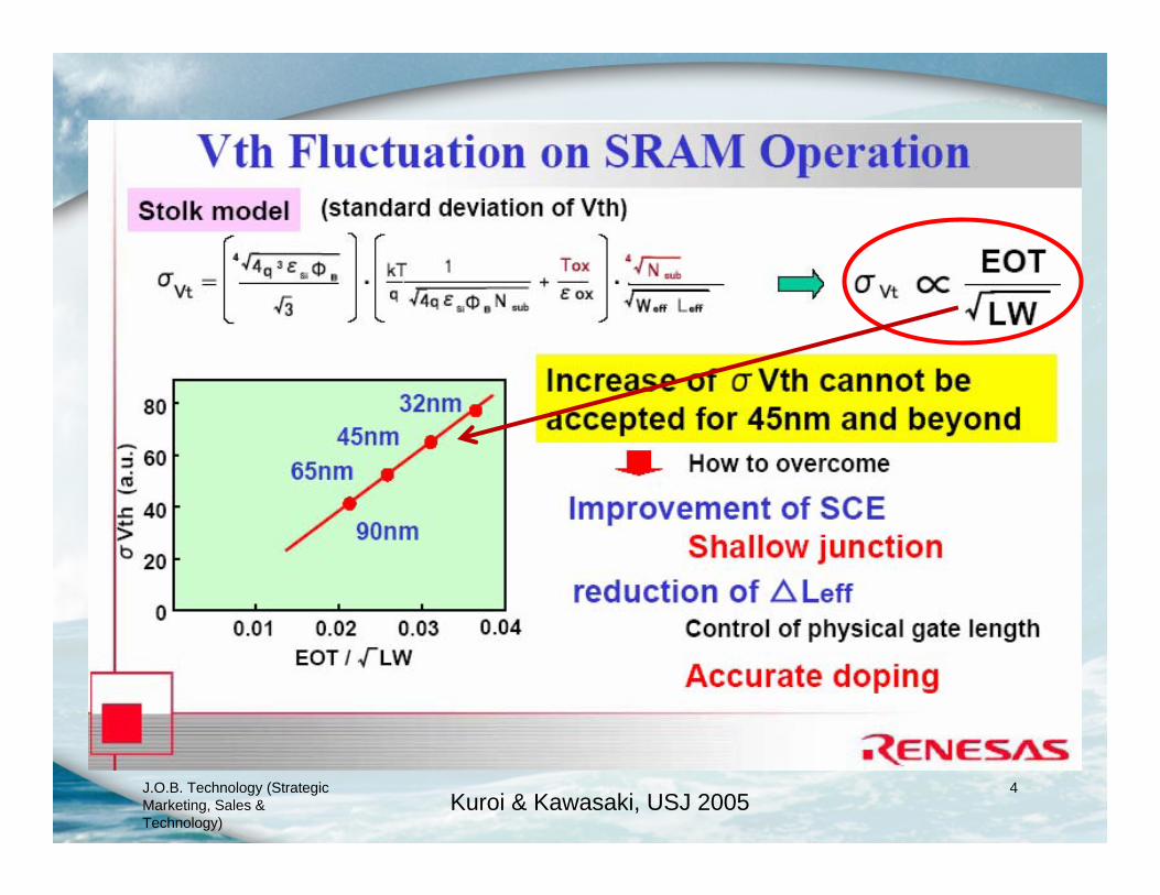
J.O.B. Technology (Strategic Marketing, Sales & Technology)
4Kuroi & Kawasaki, USJ 2005

Serial High Current Implanter Precision (Dose or Angle?)
J.O.B. Technologies (Strategic Marketing, Sales & Technology)
5Kuroi & Kawasaki, USJ 2005

J.O.B. Technology (Strategic Marketing, Sales & Technology)
6
Large nMOS Vt Variation With Lamp Annealing
2.5x
1.25x0.5x
0.75x
2x degradation with lampsHot wall 3x better and only 50% degradation

J.O.B. Technology (Strategic Marketing, Sales & Technology)
7

Lower spike temp reduces device variation
J.O.B. Technologies (Strategic Marketing, Sales & Technology)
8
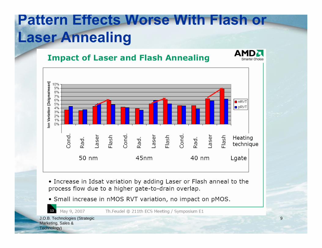
Pattern Effects Worse With Flash or Laser Annealing
J.O.B. Technologies (Strategic Marketing, Sales & Technology)
9

J.O.B. Technology (Strategic Marketing, Sales & Technology)
10
Vt Process Variability: SSDM-2006
T. Skotnicki, ST, SSDM-2006, PL-1, p.2 A. Asenov, U of Glasgow, SSDM-2006, F-5-1, p.358
Use In or B18H22 HALOsUse metal gate electrode

32nm Node FEOL Obstacles• Gate Stack: hybrid high-k and mixed with SiON & poly
– Increase high-k from a medium-k of 8-12 to >20– High quality <0.6nm SiO2 interface by low temp RTO– Extending SiON use to 32nm node by >30%N– Tinv reduction by increasing poly dopant activation with SiON and high-k
MIPS (metal inserted poly stack)
• Channel Mobility Engineering– Push limit of localized strain-Si to >2GPa and reduce strain relaxation– Localized Ge-channel for nMOS & pMOS
• Channel Dopant Engineering (doping & annealing integration)– HALO/pocket optimization (multi-HALO, iso-scan, B18, In, As4 or P4)
• Junction quality (msec dopant activation and leakage)
– SDE optimization (serial spot -vs-ribbon beamline or plasma, multi-tilt, B18, Sb or P4)
• Retained dose limits & junction quality (msec dopant activation and leakage)
• Other: Detection & metrology techniquesJ.O.B. Technology (Strategic Marketing, Sales & Technology)
11

J.O.B. Technology (Strategic Marketing, Sales & Technology)
12
Outline• Introduction: Device & Process Variation Caused By Implant &
Annealing• Channel Doping Optimization
– Extension & HALO Implantation Options– Annealing Options– Metrology
• Implanter signature• Annealer signature
• Channel Mobility Options• Gate Stack Options
– Tinv reduction– EOT scaling
• Summary

J.O.B. Technology (Strategic Marketing, Sales & Technology)
13
Challenges Facing Ultra Shallow Junctions At The 32nm Node
USJ Problems– Energy
contamination <0.1% so decel ratio <2/1
– No channeling so need PAI but no EOR damage after anneal degrading junction leakage
– Enhanced dopant activation above Bss without diffusion
– Productivity >30wph
Node 65nm 45nm 32nm
Xj 15-30nm
12-20nm 9-20nm
Maximum Diffusion
Spike10-20nm
Spike+msecor ms+spike5-15nm
msec only0-5nm
Implant Energy
200eVto 1keV
200eVto 500eV
<100eVto 500eV
Not ITRS Roadmap (JOB Customer’s Roadmap)

J.O.B. Technology (Strategic Marketing, Sales & Technology)
14
Borland, Matsuda & Sakamoto, VSEA/NEC, Solid State Technology, June 2002, p. 83
Keep EOR Damage Within Junction

J.O.B. Technology (Strategic Marketing, Sales & Technology)
15
Implant Energy Versus Xj
0
100
200
300
400
500
600
700
800
900
1000
0 1 2 3 4 5 6 7 8 9 10 11 12 13 14 15
Xj (nm)
Impl
ant E
nerg
y (e
V)
B
BF2
BF3
BBF3 PLADBF2
32nm Node 45nm Node
Borland, Semiconductor International, Dec. 2006, p.49

J.O.B. Technology (Strategic Marketing, Sales & Technology)
16
PAI Enhanced Activation At Lower Flash Temperatures But EOR Damage/Leakage
J. GelpyIto et.al, IWJT-2002

J.O.B. Technology (Strategic Marketing, Sales & Technology)
17
Laser Annealed
B-defectsPL=193E-7A/cm2
B18H22-cleanPL=131E-7A/cm2
B18H22+PAI-amorphous (11.5nm)PL=552E-2A/cm2
BF2-EOR damagePL=273E-6A/cm2

J.O.B. Technology (Strategic Marketing, Sales & Technology)
18
650C SPE AnnealedPL=301E-5A/cm2B-defects
PL=142E-7A/cm2B18H22-clean
PL=292E-5A/cm2B18H22+PAI-EOR
PL=251E-6A/cm2BF2-EOR

J.O.B. Technology (Strategic Marketing, Sales & Technology)
19
But Co-Implants Increases Leakage
Pawlak et al., MRS April 2006

J.O.B. Technology (Strategic Marketing, Sales & Technology)
20
B Retained Dose & Flash Bss Versus Xj
0
2E+14
4E+14
6E+14
8E+14
1E+15
1.2E+15
0 2 4 6 8 10 12 14 16
Xj Junction Depth @ 5E18/cm3 (nm)
Bor
on R
etai
ned
Dos
e (1
/cm
2)
B
BF2
BF3
Borland, Semiconductor International, Dec. 2006, p.49
B2H6 PIII
Flash Bss>1E20/cm3Flash Bss=9E19/cm3
Flash Bss=5E19/cm3
J.O.B. Technology (Strategic Marketing, Sales & Technology)
21
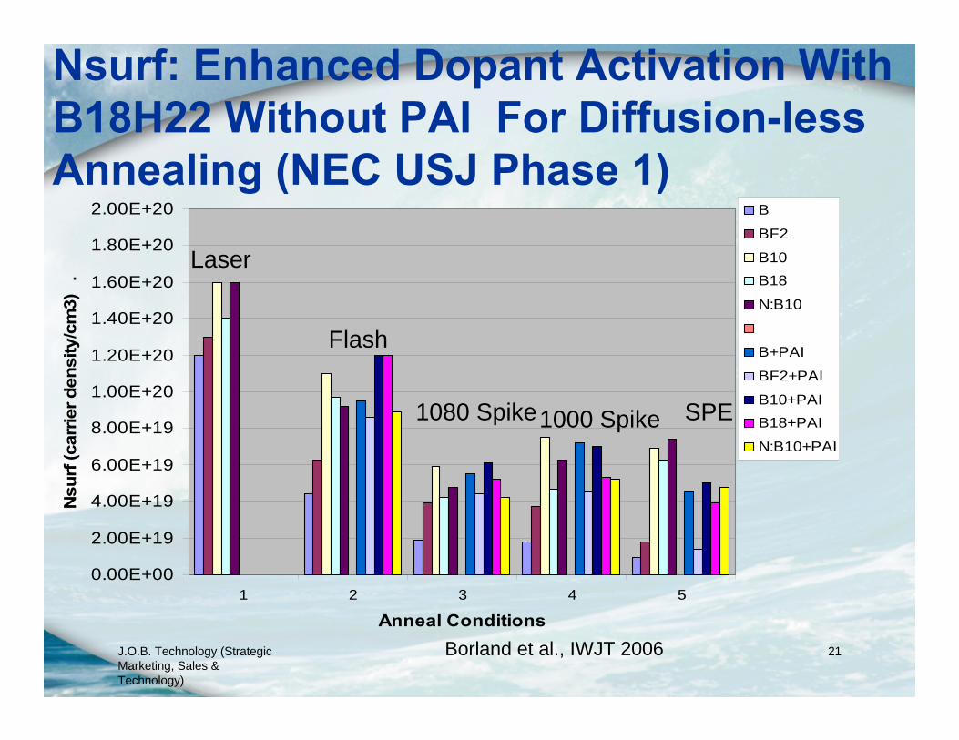
Nsurf: Enhanced Dopant Activation With B18H22 Without PAI For Diffusion-less Annealing (NEC USJ Phase 1)
0.00E+00
2.00E+19
4.00E+19
6.00E+19
8.00E+19
1.00E+20
1.20E+20
1.40E+20
1.60E+20
1.80E+20
2.00E+20
1 2 3 4 5
Anneal Conditions
Nsu
rf (c
arrie
r den
sity
/cm
3)
.
B
BF2
B10B18
N:B10
B+PAI
BF2+PAI
B10+PAIB18+PAI
N:B10+PAI
Laser
Flash
SPE1080 Spike1000 Spike
Borland et al., IWJT 2006

Micro Uniformity (Thermawave: Micro Uniformity (Thermawave: 55--vsvs--1mm pitch)1mm pitch)Condition: As 20keV 1E15cm-2 Tilt 7/Twist 0Contents: Thermawave (near the wafer center:1mm pitch measurement)
0.98
0.99
1.00
1.01
1.02
-30 -25 -20 -15 -10 -5 0 5 10 15 20 25 30
Wafer Position (mm)
TW S
igna
ls [n
orm
ariz
ed]
SHXSHXQuantum-XQuantum-XVIISta-HCVIISta-HC
As 20keV 1E15cm-2 7/0 Horizontal
Spot Beam-2: 1-D mechanicalSpot Beam-1: 2-D mechanical
Ribbon Beam 1-D mechanical
0.98
0.99
1.00
1.01
1.02
-150 -100 -50 0 50 100 150
Wafer Position (mm)
TW S
igna
ls [n
orm
ariz
ed]
SHXQuantum-XVIISta-HC
As 20keV 1E15cm-2 7/0 Horizontal
0.98
0.99
1.00
1.01
1.02
-150 -100 -50 0 50 100 150
Wafer Position (mm)
TW S
igna
ls [n
orm
ariz
ed]
SHXQuantum-XVIISta-HC
As 20keV 1E15cm-2 7/0 Vertical
0.98
0.99
1.00
1.01
1.02
-30 -25 -20 -15 -10 -5 0 5 10 15 20 25 30
Wafer Position (mm)
TW S
igna
ls [n
orm
ariz
ed]
SHXSHXQuantum-XQuantum-XVIISta-HCVIISta-HC
As 20keV 1E15cm-2 7/0 Vertical

Ribbon Beam Paint Brush Striping Pattern To Quad-mode 4-Fold Symmetry Signature Pattern
J.O.B. Technology (Strategic Marketing, Sales & Technology)
23
Grossmann et al., VSEA, Solid State Technology, July 2007, p. 71
Issue for DRAM with 10 degree tilted As implant for nMOS at 70nm node resulting in device asymmetry that can not be corrected with quad implant, also 65nm node logic
Bi-mode or Quad-mode
Single-mode scan
Erokin, VSEA, IWJT 2006 4 degree tilt quad-mode implant

Ribbon Beam Paint Brush Striping Pattern To Quad-mode 4-Fold Symmetry Signature Pattern
J.O.B. Technology (Strategic Marketing, Sales & Technology)
24
Borland et al., March 2007 Semiconductor International Web-site paper
Issue for DRAM with 10 degree tilted As implant at 70nm node resulting in device asymmetry that can not be corrected with quad implant, also 65nm node logic
Bi-mode or Quad-modeSingle-mode scan
Line Scan (300 um spacing between data points)

1mm Resolution
J.O.B. Technologies (Strategic Marketing, Sales & Technology)
25
E. Don et al., Semilab, INSIGHTS 2007, p. 134, May 2007Single-mode Rs map Quad-mode Rs map
PLi for different quad-mode implants J P V l i n e s c a n s 1 1 2 o r e l a t i v e t o t h e n o t c h
5 5 0
5 7 0
5 9 0
6 1 0
6 3 0
6 5 0
6 7 0
6 9 0
7 1 0
7 3 0
7 5 0
- 1 5 0 -1 0 0 - 5 0 0 5 0 1 0 0 1 5 0D is t a n c e [ m m ]
JPV
resi
stan
ce [Ω
/sq.
]
A s m e a s u r e dE d g e c o r r e c te d
5% Rs global variation
Batch spot beam & Spike RTA combined signatures by Semilab Rs wih1mm resolution

2mm SPV Metrology Of HC Spot Beam-1
1000C/10sec anneal
C. Krueger et al., AMD, IIT-2006
9 scans?
Spike annealer signatureA. Renau, VSEA, IIT-2004, p.284

J.O.B. Technology (Strategic Marketing, Sales & Technology)
27
Implanter Unique Non-Uniformity Signatures Due To Localized Angle/Dose Variation (1mm)
=10.4% dose!
=13.9% dose!
HC: spot beam-2
HC: batch spot beam
HC: spot beam-1
HC: ribbon beam

J.O.B. Technology (Strategic Marketing, Sales & Technology)
28
Without Spike/RTA, msec Annealing Uniformity Signature Is Critical
Spike/RTA: no lamps
Spike/RTA: lamps
Flash Anneal
Laser Anneal
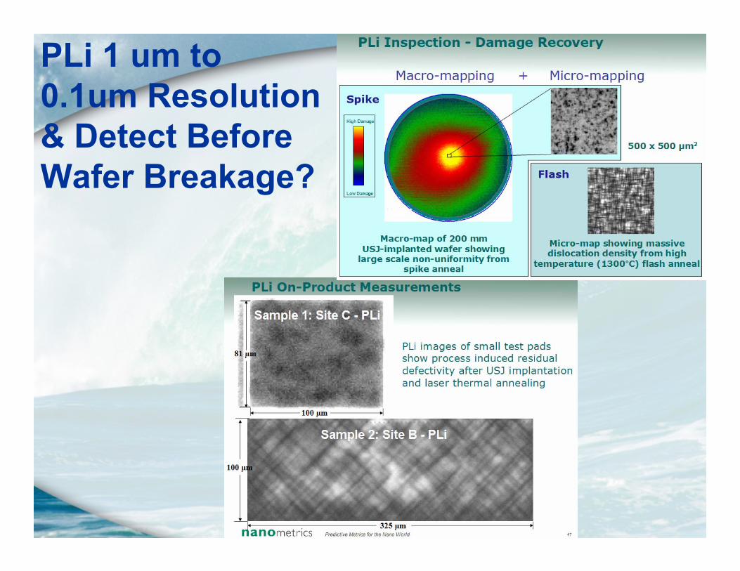
PLi 1 um to 0.1um Resolution & Detect Before Wafer Breakage?

Wafer Cracking With Flash & Laser Annealing
Higher Pre-Heat Temperature

J.O.B. Technology (Strategic Marketing, Sales & Technology)
31
Y. Chen et al., ECS May 2005, PV 2005-05, p. 171

DSA Line Laser Power Variation Even With a-C Layer (9% Global, 6% Local)
D. Petersen et al., Capres/IMEC, INSIGHTS 2007, p. 162, May 2007
Q-X with quad-mode+DSA!

Correlation of DSA Micro-variation To Devices
T. Hoffmann et al., IMEC, IWJT 2007, p.137

Improving Junction Uniformity and Quality with Optimized
Diffusion-less Annealing
John Borland1, Fumio Ohtsuka2, Takayuki Aoyama2, Takashi Onizawa2 and Andrzej Buczkowski3,
1J.O.B. Technologies, 98-1204 Kuawa St. Aiea, Hawaii 967012Selete, 16-1 Onogawa, Tsukuba-Shi, Ibaraki-Ken, 305-8569, Japan
3Nanometrics, 1320 SE Armour Dr., Suite B-2, Bend , OR 97702IWJT-2007
June 8, 2007
J.O.B. Technologies (Strategic Marketing, Sales & Technology)
34

J.O.B. Technology (Strategic Marketing, Sales & Technology)
35
PLi Of Flash And 1000C Spike+Flash
Borland et al., JOB/Selete/Nanometrics, IWJT 2007, S4-7

Rs From Semilab
J.O.B. Technology (Strategic Marketing, Sales & Technology)
36
Flash (Boron)
Flash (Ge-PAI + B)

PLi Of 1000C Spike And 1000C Spike+Flash
J.O.B. Technology (Strategic Marketing, Sales & Technology)
37Borland et al., JOB/Selete/Nanometrics, IWJT 2007, S4-7

Rs From Semilab
J.O.B. Technology (Strategic Marketing, Sales & Technology)
38
1000C Spike
1000C Spike + Flash

PLi Of Flash And 900C Spike+Flash
J.O.B. Technology (Strategic Marketing, Sales & Technology)
39Borland et al., JOB/Selete/Nanometrics, IWJT 2007, S4-7

Rs From Semilab
J.O.B. Technology (Strategic Marketing, Sales & Technology)
40
900C Spike + Flash
Flash

Lifetime Measurements

J.O.B. Technology (Strategic Marketing, Sales & Technology)
42
PoorLeakage
PoorActivation
PoorLeakage
Experimental Matrix RsL Results On Junction Quality& Semilab Rs (---)

J.O.B. Technology (Strategic Marketing, Sales & Technology)
43
Experimental Matrix

Spike 1st or msec Annealing 1st?• AMD/Dresden at ECS May 2007 reported no degradation in gate
oxide with spike1st + msec annealing for 65nm node volume porduction.
• IMEC at INSIGHTS May 2007 meeting reported that spike 1st + DSA laser annealing results in gate oxide degradation compared to DSA 1st followed by spike. At IWJT June 2007 reported better device results but must add post laser anneal to reactivate dopant!
• Mattson at INSIGHTS May 2007 reported that FLA 1st followed by spike results in deeper junctions than spike 1st +FLA. Also spike+FLA resulted in higher dopant activation than FLA+spikeannealing sequence.
• TSMC at IEDM-2006 reported better Rs with msec+spike compared to spike+msec for Ge+BF2.
• Asian company reported that better LG control (SDE lateral diffusion) with spike+LSA compared to LSA+spike.
• Renesas at IWJT June 2007 reported LSA 1st better but again must add 2nd LSA last step to reactivate dopant.J.O.B. Technologies (Strategic
Marketing, Sales & Technology)
44

J.O.B. Technology (Strategic Marketing, Sales & Technology)
45
Multi-HALO Design With LSA
Narihiro et al., NEC, IEEE/RTP 2006, p.147

J.O.B. Technology (Strategic Marketing, Sales & Technology)
46
Enhanced SDE & HALO Dopant Activation (NEC Phase 2)
• pMOS– pSDE (5E14 or 1E15/cm2 dose limited by Bss)
• B: 200eV/1E15• BF2: 1keV/1E15• B10: 2keV/1E14• B18: 4keV/5E13
– HALO (3E13/cm2 dose)• As: 20keV/3E13• As2: 40keV/3E13• As4:: 80keV/3E13• Sb:
• nMOS – nSDE (1E15/cm2 or > dose)
• As: 1keV/1e15• As2: 2keV/1E15• As4: 4keV/1E15• P: • P2:• P4:• Sb:
– HALO (3E13/cm2 dose)• B: 3keV/3E13• BF2: 15keV/3E13• In:• B10: 30keV/3E12• B18: 60keV/1.5E12
<900C Spike/RTA<750C SPE<1300C Flash<1300C Laser
Mineji et al., NEC/JOB/Nissin, IWJT 2007, S4-8

J.O.B. Technologies (Strategic Marketing, Sales & Technology)
47
Molecular Dopants and High Mass Dopants for HALO and
Extension ImplantationAkira Mineji1, John Borland2, Seiichi Shishiguchi1, Masami Hane1, Masayasu Tanjo3 and
Tsutomu Nagayama3
1NEC Electronics Corp., 1120, Shimokuzawa, Sagamihara, Kanagawa, 229-1198, Japan
2J.O.B. Technologies, 98-1204 Kuawa St. Aiea, Hawaii 967013Nissin Ion Equipment, 575, Kuze-Tonoshiro-Cho, Minami-Ku, Kyoto, 601-8205, Japan
IWJT June 8, 2007

NEC Phase 1 Results
J.O.B. Technologies (Strategic Marketing, Sales & Technology)
48
Borland et al., IWJT 2006

NEC Phase 1 Results
J.O.B. Technologies (Strategic Marketing, Sales & Technology)
49
Borland et al., IWJT 2006

Dopant Movement!SPE 0nm900C Spike 0nmFlash +2-3nm1050C Spike +25nm
Mineji et al., NEC/JOB/Nissin, IWJT 2007, S4-8

J.O.B. Technologies (Strategic Marketing, Sales & Technology)
51Mineji et al., NEC/JOB/Nissin, IWJT 2007, S4-8
No PAI For Good Junction Quality

Indium FLA results different from Toshiba IWJT 2002
Mineji et al., NEC/JOB/Nissin, IWJT 2007, S4-8

P-Halo (In, B10, BF2)
53
In case of indium I/I, a leakage current was detected by RsL.The leakage current depend on the anneal condition.⇒ High temperature annealing can reduce the leakage.
Leakage current density
Mineji et al., NEC/JOB/Nissin, IWJT 2007, S4-8

J.O.B. Technology (Strategic Marketing, Sales & Technology)
54
Sb SPE Better Activation Than As
Ponomarevet al, Philips, VLSI Sym. June 2001

H. Kennel et al., Intel, IEEE RTP Oct 2006 meeting, paper #13
Mineji et al., NEC/JOB/Nissin, IWJT 2007, S4-8

Arsenic, Phos. or Antimony For nSDE?
J.O.B. Technology (Strategic Marketing, Sales & Technology)
56
S. Kato et al., Selete, IWJT 2007, S8-5

J.O.B. Technologies (Strategic Marketing, Sales & Technology)
57Mineji et al., NEC/JOB/Nissin, IWJT 2007, S4-8

Summary Of NEC & Selete Data And Differences Between DNS & MTSN Flash
J.O.B. Technology (Strategic Marketing, Sales & Technology)
58
Bss (atoms/cm3)

J.O.B. Technology (Strategic Marketing, Sales & Technology)
59
PAI Enhanced Activation At Lower Flash Temperatures But EOR Damage/Leakage
J. GelpyKato et al., Selete, IWJT 2007, p.143

J.O.B. Technology (Strategic Marketing, Sales & Technology)
60
Outline• Introduction: Device & Process Variation Caused By Implant &
Annealing• Channel Doping Optimization
– Extension & HALO Implantation Options– Annealing Options– Metrology
• Implanter signature• Annealer signature
• Channel Mobility Options• Gate Stack Options
– Tinv reduction– EOT scaling
• Summary

J.O.B. Technology (Strategic Marketing, Sales & Technology)
61K. Goto, TSMC, Apr 2006 MRSSiGe lowest cost for performance improvement

IBM VLSI Sym 2007: 6% by C Imp. SPELiu et al., VLSI 2007, p.44

Carbon Molecular Implant For nMOS Tensile Stress, Reported up to 2GPa!
J.O.B. Technologies (Strategic Marketing, Sales & Technology)
63
W. Krull et al., SemEquip, INSIGHTS 2007
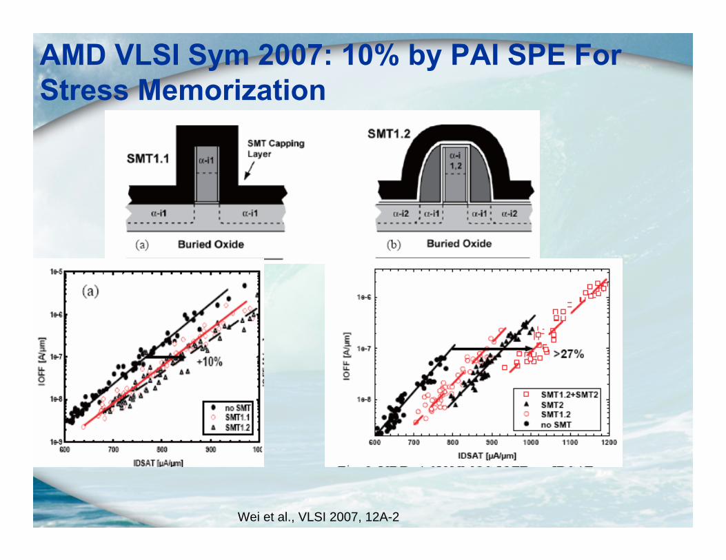
AMD VLSI Sym 2007: 10% by PAI SPE For Stress Memorization
Wei et al., VLSI 2007, 12A-2

Required Localized Strain Level• 90nm node 17% SiGe=0.6GPa• 65nm node 20% SiGe=1.2GPa• 45nm node 25% SiGe=1.5GPa• 32nm node 30% SiGe=2GPa
J.O.B. Technology (Strategic Marketing, Sales & Technology)
65April 2006 MRS TutorialS. Thompson & K. Jones
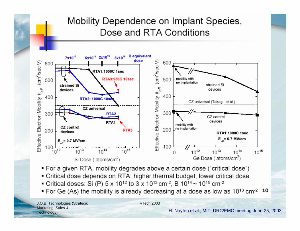
J.O.B. Technologies (Strategic Marketing, Sales & Technology)
vTech 2003
H. Nayfeh et al., MIT, DRC/EMC meeting June 25, 2003

LSA Strain Relaxation Limits
J.O.B. Technology (Strategic Marketing, Sales & Technology)
67
C. Cheirigh et al., MIT, ECS Trans., vol.3, no. 2, p.355, Oct. 2006
M. Yu et al., TSMC, IEDM 2006, section 33.5, p. 867

Mobility Degradation (Strain Relaxation) With Laser Annealing But DSA 1st Is Best
T. Hoffmann et al., IMEC, IWJT 2007, p.137

But 45nm Node Process Integration Requires 3-Spike Anneals for Poly/SD, Disposable Spacer & SMT Stressor Then msec Annealing
J.O.B. Technology (Strategic Marketing, Sales & Technology)
69
Toshiba/NEC/Sony, VLSI Sym. 2007, 12A-3

J.O.B. Technology (Strategic Marketing, Sales & Technology)
70
Outline• Introduction: Device & Process Variation Caused By Implant &
Annealing• Channel Doping Optimization
– Extension & HALO Implantation Options– Annealing Options– Metrology
• Implanter signature• Annealer signature
• Channel Mobility Options• Gate Stack Options
– Tinv reduction– EOT scaling
• Summary

Reduced Tox(inv)by increasing active dopant in poly electrode
M. Rodder, TI, vTech 2005
Need B=1-6keV, 5-20E15 dose

Enhanced Poly Activation Not Detected By SIMS!Need SRP? Also What Is Grain Size Effects?
Y. Chen et al., TI, ECS May 2005, PV 2005-05, p. 171

J.O.B. Technology (Strategic Marketing, Sales & Technology)
73

Borland’s Updated Gate Dielectric Roadmap
NodeGate
Dielectric
GateElectrode
AnnealingOptions
GateIntegration
45nmSiON
HfSiON (medium-k=9-12)HfOx (high-k>20)
PolyPoly/metal
MetalFUSI
Spike+msec (FLA or LSA)msec+spike
Gate 1st
+Disposable spacerGate last (ALD)
32nmSiONHfSiONHfOx
PolyPoly/metalMetalFUSI
Combinationsmsec onlySPE (high-k)Gate 1st
Disposable spacerGate last (ALD)
IBM 45nm &spike+LSA

J.O.B. Technology (Strategic Marketing, Sales & Technology)
75
Interview S. Biesemans, IMEC at VLSI Sym. 2007

J.O.B. Technology (Strategic Marketing, Sales & Technology)
76

J.O.B. Technology (Strategic Marketing, Sales & Technology)
77
Why only 0.1x and not >0.01x?IL effect?
MTB 6/07
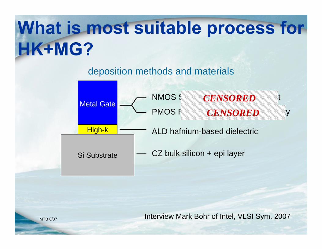
What is most suitable process for HK+MG?
ALD hafnium-based dielectric
deposition methods and materials
Si Substrate
Metal Gate
CZ bulk silicon + epi layer
PMOS Report yourself to Intel securityCENSORED
High-k
NMOS Shame on you for doing thatCENSORED
Interview Mark Bohr of Intel, VLSI Sym. 2007

MTB 6/07
What is most suitable process for HK+MG?
ALD hafnium-based dielectric
deposition methods and materials
Si Substrate
Metal Gate
CZ bulk silicon + epi layer
PMOS Report yourself to Intel securityCENSORED
High-k
NMOS Shame on you for doing that
Interview Mark Bohr of Intel, VLSI Sym. 2007

MTB 6/07
What is most suitable process for HK+MG?
ALD hafnium-based dielectric
deposition methods and materials
Si Substrate
Metal Gate
CZ bulk silicon + epi layer
PMOS Report yourself to Intel security
High-k
NMOS Shame on you for doing that
Interview Mark Bohr of Intel, VLSI Sym. 2007

J.O.B. Technology (Strategic Marketing, Sales & Technology)
81

Poly & USJ Activation Roadmap
Spike/RTA+
Flash or Laser-poly dopant diffusion & activation
-improved Tox(inversion)-USJ diffusion
65nm & 45nm Node Lower TemperatureSpike/RTA
-poly dopant diffusion
Flash or Laser-improved poly dopant activation
-improved Tox(inversion)-USJ diffusion-less activation
Flash, Laser or SPE-USJ diffusion-less activation
45nm & 32nm Node
32nm & 22nm Node
Borland, Semiconductor International, Dec. 2006, p.49
IBM VLSI 2007 45nm1000C Spike
Process Integration Options:1)Gate 1st (medium k=7-12)2)Disposable spacer (medium k=7-12)3)Replacement gate (high k>20 by ALD for step coverage)
45nm nodeIBM
Japan?

DRAM p+ Dopant Deactivation During BEOL & LSA With Metal Gate
G.H. Buh et al., Samsung, section 33.4, IEDM-06

J.O.B. Technology (Strategic Marketing, Sales & Technology)
84
Summary• Must Reduce Device & Process Variation• Channel Doping Optimization
– Improved implanter micro-uniformity• Molecular dopant species for Extension & HALO
– Diffusion-less activation with improved micro-uniformity (how best to integrate?)
• High temperature msec annealing for medium-k 8-15• Low temperature SPE <800C for high-k >20
– Metrology for micro-uniformity detection
• Channel Mobility Options– Need >2GPa of strain but must optimize process integration to minimize
strain relaxation
• At 32nm Node Many Different Gate Stack Options– Single hybrid or dual: poly/medium-k, MIPS/HK and metal/HK– Still poly/SiON for nMOS or pMOS– Process Integration options: gate 1st, gate last or hybrid combination